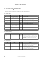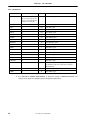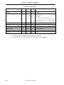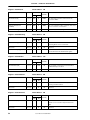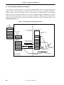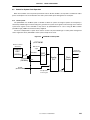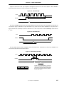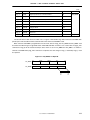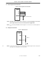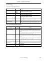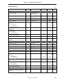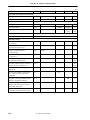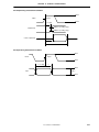
1
To our customers,
Old Company Name in Catalogs and Other Documents
On April 1st, 2010, NEC Electronics Corporation merged with Renesas Technology
Corporation, and Renesas Electronics Corporation took over all the business of both
companies. Therefore, although the old company name remains in this document, it is a valid
Renesas Electronics document. We appreciate your understanding.
Renesas Electronics website: http://www.renesas.com
April 1st, 2010
Renesas Electronics Corporation
Issued by: Renesas Electronics Corporation (http://www.renesas.com)
Send any inquiries to http://www.renesas.com/inquiry.
Notice
1.
2.
3.
4.
5.
6.
7.
All information included in this document is current as of the date this document is issued. Such information, however, is
subject to change without any prior notice. Before purchasing or using any Renesas Electronics products listed herein, please
confirm the latest product information with a Renesas Electronics sales office. Also, please pay regular and careful attention to
additional and different information to be disclosed by Renesas Electronics such as that disclosed through our website.
Renesas Electronics does not assume any liability for infringement of patents, copyrights, or other intellectual property rights
of third parties by or arising from the use of Renesas Electronics products or technical information described in this document.
No license, express, implied or otherwise, is granted hereby under any patents, copyrights or other intellectual property rights
of Renesas Electronics or others.
You should not alter, modify, copy, or otherwise misappropriate any Renesas Electronics product, whether in whole or in part.
Descriptions of circuits, software and other related information in this document are provided only to illustrate the operation of
semiconductor products and application examples. You are fully responsible for the incorporation of these circuits, software,
and information in the design of your equipment. Renesas Electronics assumes no responsibility for any losses incurred by
you or third parties arising from the use of these circuits, software, or information.
When exporting the products or technology described in this document, you should comply with the applicable export control
laws and regulations and follow the procedures required by such laws and regulations. You should not use Renesas
Electronics products or the technology described in this document for any purpose relating to military applications or use by
the military, including but not limited to the development of weapons of mass destruction. Renesas Electronics products and
technology may not be used for or incorporated into any products or systems whose manufacture, use, or sale is prohibited
under any applicable domestic or foreign laws or regulations.
Renesas Electronics has used reasonable care in preparing the information included in this document, but Renesas Electronics
does not warrant that such information is error free. Renesas Electronics assumes no liability whatsoever for any damages
incurred by you resulting from errors in or omissions from the information included herein.
Renesas Electronics products are classified according to the following three quality grades: “Standard”, “High Quality”, and
“Specific”. The recommended applications for each Renesas Electronics product depends on the product’s quality grade, as
indicated below. You must check the quality grade of each Renesas Electronics product before using it in a particular
application. You may not use any Renesas Electronics product for any application categorized as “Specific” without the prior
written consent of Renesas Electronics. Further, you may not use any Renesas Electronics product for any application for
which it is not intended without the prior written consent of Renesas Electronics. Renesas Electronics shall not be in any way
liable for any damages or losses incurred by you or third parties arising from the use of any Renesas Electronics product for an
application categorized as “Specific” or for which the product is not intended where you have failed to obtain the prior written
consent of Renesas Electronics. The quality grade of each Renesas Electronics product is “Standard” unless otherwise
expressly specified in a Renesas Electronics data sheets or data books, etc.
“Standard”:
8.
9.
10.
11.
12.
Computers; office equipment; communications equipment; test and measurement equipment; audio and visual
equipment; home electronic appliances; machine tools; personal electronic equipment; and industrial robots.
“High Quality”: Transportation equipment (automobiles, trains, ships, etc.); traffic control systems; anti-disaster systems; anticrime systems; safety equipment; and medical equipment not specifically designed for life support.
“Specific”:
Aircraft; aerospace equipment; submersible repeaters; nuclear reactor control systems; medical equipment or
systems for life support (e.g. artificial life support devices or systems), surgical implantations, or healthcare
intervention (e.g. excision, etc.), and any other applications or purposes that pose a direct threat to human life.
You should use the Renesas Electronics products described in this document within the range specified by Renesas Electronics,
especially with respect to the maximum rating, operating supply voltage range, movement power voltage range, heat radiation
characteristics, installation and other product characteristics. Renesas Electronics shall have no liability for malfunctions or
damages arising out of the use of Renesas Electronics products beyond such specified ranges.
Although Renesas Electronics endeavors to improve the quality and reliability of its products, semiconductor products have
specific characteristics such as the occurrence of failure at a certain rate and malfunctions under certain use conditions. Further,
Renesas Electronics products are not subject to radiation resistance design. Please be sure to implement safety measures to
guard them against the possibility of physical injury, and injury or damage caused by fire in the event of the failure of a
Renesas Electronics product, such as safety design for hardware and software including but not limited to redundancy, fire
control and malfunction prevention, appropriate treatment for aging degradation or any other appropriate measures. Because
the evaluation of microcomputer software alone is very difficult, please evaluate the safety of the final products or system
manufactured by you.
Please contact a Renesas Electronics sales office for details as to environmental matters such as the environmental
compatibility of each Renesas Electronics product. Please use Renesas Electronics products in compliance with all applicable
laws and regulations that regulate the inclusion or use of controlled substances, including without limitation, the EU RoHS
Directive. Renesas Electronics assumes no liability for damages or losses occurring as a result of your noncompliance with
applicable laws and regulations.
This document may not be reproduced or duplicated, in any form, in whole or in part, without prior written consent of Renesas
Electronics.
Please contact a Renesas Electronics sales office if you have any questions regarding the information contained in this
document or Renesas Electronics products, or if you have any other inquiries.
(Note 1) “Renesas Electronics” as used in this document means Renesas Electronics Corporation and also includes its majorityowned subsidiaries.
(Note 2) “Renesas Electronics product(s)” means any product developed or manufactured by or for Renesas Electronics.
User’s Manual
μPD720102
USB 2.0 Host Controller
Document No
Date Published
S17999EJ4V0UD00 (4th edition)
March 2007 NS CP (N)
2006
Printed in Japan
[MEMO]
2
User’s Manual S17999EJ4V0UD
NOTES FOR CMOS DEVICES
1
VOLTAGE APPLICATION WAVEFORM AT INPUT PIN
Waveform distortion due to input noise or a reflected wave may cause malfunction. If the input of the
CMOS device stays in the area between VIL (MAX) and VIH (MIN) due to noise, etc., the device may
malfunction. Take care to prevent chattering noise from entering the device when the input level is fixed,
and also in the transition period when the input level passes through the area between VIL (MAX) and
VIH (MIN).
2
HANDLING OF UNUSED INPUT PINS
Unconnected CMOS device inputs can be cause of malfunction. If an input pin is unconnected, it is
possible that an internal input level may be generated due to noise, etc., causing malfunction. CMOS
devices behave differently than Bipolar or NMOS devices. Input levels of CMOS devices must be fixed
high or low by using pull-up or pull-down circuitry. Each unused pin should be connected to VDD or GND
via a resistor if there is a possibility that it will be an output pin. All handling related to unused pins must
be judged separately for each device and according to related specifications governing the device.
3
PRECAUTION AGAINST ESD
A strong electric field, when exposed to a MOS device, can cause destruction of the gate oxide and
ultimately degrade the device operation. Steps must be taken to stop generation of static electricity as
much as possible, and quickly dissipate it when it has occurred.
Environmental control must be
adequate. When it is dry, a humidifier should be used. It is recommended to avoid using insulators that
easily build up static electricity. Semiconductor devices must be stored and transported in an anti-static
container, static shielding bag or conductive material. All test and measurement tools including work
benches and floors should be grounded.
The operator should be grounded using a wrist strap.
Semiconductor devices must not be touched with bare hands. Similar precautions need to be taken for
PW boards with mounted semiconductor devices.
4
STATUS BEFORE INITIALIZATION
Power-on does not necessarily define the initial status of a MOS device. Immediately after the power
source is turned ON, devices with reset functions have not yet been initialized. Hence, power-on does
not guarantee output pin levels, I/O settings or contents of registers. A device is not initialized until the
reset signal is received. A reset operation must be executed immediately after power-on for devices
with reset functions.
5
POWER ON/OFF SEQUENCE
In the case of a device that uses different power supplies for the internal operation and external
interface, as a rule, switch on the external power supply after switching on the internal power supply.
When switching the power supply off, as a rule, switch off the external power supply and then the
internal power supply. Use of the reverse power on/off sequences may result in the application of an
overvoltage to the internal elements of the device, causing malfunction and degradation of internal
elements due to the passage of an abnormal current.
The correct power on/off sequence must be judged separately for each device and according to related
specifications governing the device.
6
INPUT OF SIGNAL DURING POWER OFF STATE
Do not input signals or an I/O pull-up power supply while the device is not powered. The current
injection that results from input of such a signal or I/O pull-up power supply may cause malfunction and
the abnormal current that passes in the device at this time may cause degradation of internal elements.
Input of signals during the power off state must be judged separately for each device and according to
related specifications governing the device.
User’s Manual S17999EJ4V0UD
3
USB logo is a trademark of USB Implementers Forum, Inc.
Windows is either a registered trademark or a trademark of Microsoft Corporation in the United States
and/or other countries.
• The information in this document is current as of March, 2007. The information is subject to change
without notice. For actual design-in, refer to the latest publications of NEC Electronics data sheets or
data books, etc., for the most up-to-date specifications of NEC Electronics products. Not all
products and/or types are available in every country. Please check with an NEC Electronics sales
representative for availability and additional information.
• No part of this document may be copied or reproduced in any form or by any means without the prior
written consent of NEC Electronics. NEC Electronics assumes no responsibility for any errors that may
appear in this document.
• NEC Electronics does not assume any liability for infringement of patents, copyrights or other intellectual
property rights of third parties by or arising from the use of NEC Electronics products listed in this document
or any other liability arising from the use of such products. No license, express, implied or otherwise, is
granted under any patents, copyrights or other intellectual property rights of NEC Electronics or others.
• Descriptions of circuits, software and other related information in this document are provided for illustrative
purposes in semiconductor product operation and application examples. The incorporation of these
circuits, software and information in the design of a customer's equipment shall be done under the full
responsibility of the customer. NEC Electronics assumes no responsibility for any losses incurred by
customers or third parties arising from the use of these circuits, software and information.
• While NEC Electronics endeavors to enhance the quality, reliability and safety of NEC Electronics products,
customers agree and acknowledge that the possibility of defects thereof cannot be eliminated entirely. To
minimize risks of damage to property or injury (including death) to persons arising from defects in NEC
Electronics products, customers must incorporate sufficient safety measures in their design, such as
redundancy, fire-containment and anti-failure features.
• NEC Electronics products are classified into the following three quality grades: "Standard", "Special" and
"Specific".
The "Specific" quality grade applies only to NEC Electronics products developed based on a customerdesignated "quality assurance program" for a specific application. The recommended applications of an NEC
Electronics product depend on its quality grade, as indicated below. Customers must check the quality grade of
each NEC Electronics product before using it in a particular application.
"Standard": Computers, office equipment, communications equipment, test and measurement equipment, audio
and visual equipment, home electronic appliances, machine tools, personal electronic equipment
and industrial robots.
"Special": Transportation equipment (automobiles, trains, ships, etc.), traffic control systems, anti-disaster
systems, anti-crime systems, safety equipment and medical equipment (not specifically designed
for life support).
"Specific": Aircraft, aerospace equipment, submersible repeaters, nuclear reactor control systems, life
support systems and medical equipment for life support, etc.
The quality grade of NEC Electronics products is "Standard" unless otherwise expressly specified in NEC
Electronics data sheets or data books, etc. If customers wish to use NEC Electronics products in applications
not intended by NEC Electronics, they must contact an NEC Electronics sales representative in advance to
determine NEC Electronics' willingness to support a given application.
(Note)
(1) "NEC Electronics" as used in this statement means NEC Electronics Corporation and also includes its
majority-owned subsidiaries.
(2) "NEC Electronics products" means any product developed or manufactured by or for NEC Electronics (as
defined above).
M8E 02. 11-1
4
User’s Manual S17999EJ4V0UD
Major Revisions in this Edition
Page
p. 13
pp. 18, 19
pp. 25 to 27
Description
CHAPTER 1 INTRODUCTION
Addition of the μPD720102F1-CA7-A to 1.2 Ordering Information
Addition of the μPD720102F1-CA7-A to 1.4 Pin Configuration
CHAPTER 2 PIN FUNCTIONS
Addition of 2.2 Pin Functions of the μPD720102F1-CA7-A
CHAPTER 3 REGISTER INFORMATION
p. 35
Addition of description to Table 3-9. EXT1 Register
p. 36
Addition of description to Table 3-10. EXT2 Register
p. 43
Addition of description to Table 3-18. EXT1 Register
p. 44
Addition of description to Table 3-19. EXT2 Register
CHAPTER 9 HOW TO CONNECT TO EXTERNAL ELEMENTS
p. 115
Modification of Remark of Figure 9-3. RREF Connection
CHAPTER 10 PRODUCT SPECIFICATIONS
p. 126
Addition of Max. value of PCI clock cycle time in 10.3 Electrical Specifications
p.134
Addition of CHAPTER 11 PACKAGE DRAWINGS
The mark <R> shows major revised points.
The revised points can be easily searched by copying an "<R>" in the PDF file and specifying it in the "Find what:" field.
User’s Manual S17999EJ4V0UD
5
PREFACE
Readers
This manual is intended for engineers who need to be familiar with the capability of
the μPD720102 in order to develop application systems based on it.
Purpose
The purpose of this manual is to help users understand the hardware capabilities
(listed below) of the μPD720102.
Configuration
This manual consists of the following chapters:
• Introduction
• Pin functions
• Register information
• OHCI host controller
• EHCI host controller
• Power management
• Hyper-speed transfer mode
• How to write external serial ROM
• How to connect to external elements
• Product specifications
Guidance
Readers of this manual should already have a general knowledge of electronics, logic
circuits, and microcomputers.
Notation
This manual uses the following conventions:
Data bit significance:
High-order bits on the left side;
low-order bits on the right side
Active low:
XXXX0 (Pin and signal names are suffixed with 0.)
Note:
Explanation of an indicated part of text
Caution:
Information requiring the user’s special attention
Remark:
Supplementary information
Numerical value:
Binary ... xxxx or xxxxb
Decimal ... xxxx
Hexadecimal ... xxxxh
Related Document
Use this manual in combination with the following document.
The related documents indicated in this publication may include preliminary versions.
However, preliminary versions are not marked as such.
• μPD720102 Data Sheet: S17998E
6
User’s Manual S17999EJ4V0UD
CONTENTS
CHAPTER 1 INTRODUCTION............................................................................................................... 13
1.1 Features ..................................................................................................................................... 13
1.2 Ordering Information ................................................................................................................ 13
1.3 Block Diagram ........................................................................................................................... 14
1.4 Pin Configuration ...................................................................................................................... 16
1.5 Pin Information.......................................................................................................................... 20
CHAPTER 2 PIN FUNCTIONS ............................................................................................................. 22
2.1 Pin Functions of the μPD720102GC-YEB-A ........................................................................... 22
2.2
2.1.1
Power supply....................................................................................................................................22
2.1.2
Analog signaling ...............................................................................................................................22
2.1.3
System clock ....................................................................................................................................22
2.1.4
PCI interface.....................................................................................................................................23
2.1.5
USB interface ...................................................................................................................................24
2.1.6
Serial ROM interface ........................................................................................................................24
2.1.7
System interface...............................................................................................................................24
2.1.8
Test signals ......................................................................................................................................24
Pin Functions of the μPD720102F1-CA7-A............................................................................. 25
2.2.1
Power supply....................................................................................................................................25
2.2.2
Analog signaling ...............................................................................................................................25
2.2.3
System clock ....................................................................................................................................25
2.2.4
PCI interface.....................................................................................................................................26
2.2.5
USB interface ...................................................................................................................................27
2.2.6
Serial ROM interface ........................................................................................................................27
2.2.7
System interface...............................................................................................................................27
2.2.8
Test signals ......................................................................................................................................27
CHAPTER 3 REGISTER INFORMATION............................................................................................. 28
3.1 PCI Configuration Space .......................................................................................................... 28
3.2
3.3
3.1.1
PCI configuration space for OHCI host controller.............................................................................29
3.1.2
PCI configuration space for EHCI host controller .............................................................................37
OHCI Operational Registers..................................................................................................... 45
3.2.1
Mapping of operational registers for OHCI host controller................................................................46
3.2.2
Overview of OHCI operational registers ...........................................................................................46
EHCI Capability and Operational Registers ........................................................................... 60
3.3.1
Mapping of capability and operational registers for EHCI host controller .........................................61
3.3.2
Overview of EHCI capability and operational registers.....................................................................62
CHAPTER 4 OHCI HOST CONTROLLER .......................................................................................... 76
4.1 Communication between OHCI Host Controller and HCD.................................................... 76
4.2 Endpoint Descriptor.................................................................................................................. 77
4.3
4.2.1
Endpoint descriptor format ...............................................................................................................77
4.2.2
Endpoint descriptor field definitions ..................................................................................................77
Transfer Descriptors................................................................................................................. 79
4.3.1
General transfer descriptor format....................................................................................................79
User’s Manual S17999EJ4V0UD
7
4.4
4.3.2
General transfer descriptor field definitions ..................................................................................... 79
4.3.3
Isochronous transfer descriptor format ............................................................................................ 81
4.3.4
Isochronous transfer descriptor field definitions............................................................................... 81
4.3.5
Packet status word format ............................................................................................................... 82
4.3.6
Packet status word field definitions.................................................................................................. 82
4.3.7
Completion code definitions ............................................................................................................ 82
Host Controller Communications Area................................................................................... 83
4.4.1
Host controller communications area format ................................................................................... 83
4.4.2
Host controller communications area description ............................................................................ 83
CHAPTER 5 EHCI HOST CONTROLLER ........................................................................................... 84
5.1 Control EHCI Host Controller by HCD..................................................................................... 84
5.2 Isochronous Transfer Descriptor ............................................................................................ 84
5.3
5.4
5.5
5.6
5.2.1
Isochronous transfer descriptor format ............................................................................................ 84
5.2.2
Isochronous transfer descriptor field definitions............................................................................... 85
Split Transaction Isochronous Transfer Descriptor.............................................................. 87
5.3.1
Split transaction isochronous transfer descriptor format.................................................................. 87
5.3.2
Split transaction isochronous transfer descriptor field definitions .................................................... 87
Queue Element Transfer Descriptor........................................................................................ 89
5.4.1
Queue element transfer descriptor format ....................................................................................... 89
5.4.2
Queue element transfer descriptor field definitions.......................................................................... 89
Queue Head ............................................................................................................................... 91
5.5.1
Queue head format.......................................................................................................................... 91
5.5.2
Queue head field definitions ............................................................................................................ 92
Periodic Frame Span Traversal Node (FSTN)......................................................................... 94
5.6.1
Periodic frame span traversal node descriptor format ..................................................................... 94
5.6.2
Periodic frame span traversal node field definitions ........................................................................ 94
CHAPTER 6 POWER MANAGEMENT................................................................................................. 95
6.1 Bus Power States and Function Power Management States ............................................... 95
6.2
6.3
6.1.1
PCI bus power states ...................................................................................................................... 95
6.1.2
USB bus states................................................................................................................................ 95
6.1.3
PCI function power management states.......................................................................................... 96
Power Management Event........................................................................................................ 97
6.2.1
PME event support .......................................................................................................................... 97
6.2.2
How to support the PME generation from D3cold............................................................................ 97
6.2.3
PME0 assertion condition ................................................................................................................ 99
Control for System Clock Operation ..................................................................................... 103
6.3.1
Clock system ..................................................................................................................................103
6.3.2
Condition for clock system stopping/resuming................................................................................104
6.3.3
CLKRUN# support..........................................................................................................................106
CHAPTER 7 HYPER-SPEED TRANSFER MODE ............................................................................ 108
7.1 Setting from HSMODE ............................................................................................................ 108
7.2 Setting from PCI configuration space (or external serial ROM) ......................................... 108
7.3 No need to support “Hyper-Speed Transfer Mode” ............................................................ 108
8
User’s Manual S17999EJ4V0UD
CHAPTER 8 HOW TO WRITE EXTERNAL SERIAL ROM............................................................ 109
8.1 Registers to Control I2C Interface.......................................................................................... 109
8.2 Supported Command for I2C Interface .................................................................................. 110
CHAPTER 9 HOW TO CONNECT TO EXTERNAL ELEMENTS .................................................. 114
9.1 Handling Unused Pins ............................................................................................................ 114
9.2 USB Port Connection.............................................................................................................. 114
9.3 Internal Regulator Circuit Connection .................................................................................. 115
9.4 Analog Circuit Connection..................................................................................................... 115
9.5 Crystal Connection ................................................................................................................. 116
9.6 External Serial ROM Connection........................................................................................... 117
CHAPTER
10.1
10.2
10.3
10.4
10 PRODUCT SPECIFICATIONS ...................................................................................... 118
Buffer List ............................................................................................................................. 118
Terminology ......................................................................................................................... 119
Electrical Specifications ..................................................................................................... 121
Timing Diagram.................................................................................................................... 130
CHAPTER 11 PACKAGE DRAWINGS ................................................................................................ 134
User’s Manual S17999EJ4V0UD
9
LIST OF FIGURES
Figure No.
Title
Page
3-1
OpenHCI’s PCI Configuration Space...........................................................................................................45
3-2
Enhanced HCI’s PCI Configuration Space ..................................................................................................60
6-1
6-2
Wake Up State Transition from D3cold .......................................................................................................98
μPD720102’s Clock System ...................................................................................................................... 103
6-3
Clock Operation Diagram (Using 30 MHz Crystal) .................................................................................... 105
6-4
Clock Operation Diagram (Using 48 MHz Oscillator)................................................................................. 106
6-5
PCI Clock Stop .......................................................................................................................................... 107
6-6
PCI Clock Start .......................................................................................................................................... 107
6-7
Maintaining PCI Clock ............................................................................................................................... 107
8-1
I2C_WND0/1 vs. Byte No. ......................................................................................................................... 111
8-2
I2C Timing Chart ........................................................................................................................................ 112
8-3
External Serial ROM Setting Flowchart ..................................................................................................... 113
9-1
USB Downstream Port Connection ........................................................................................................... 114
9-2
Internal regulator circuit Connection .......................................................................................................... 115
9-3
RREF Connection ..................................................................................................................................... 115
9-4
Crystal Connection .................................................................................................................................... 116
9-5
External Serial ROM Connection............................................................................................................... 117
10-1
Differential Input Sensitivity Range for Low-/Full-speed ............................................................................ 124
10-2
Receiver Sensitivity for Transceiver at DP/DM.......................................................................................... 124
10-3
Receiver Measurement Fixtures................................................................................................................ 124
10-4
Transmit Waveform for Transceiver at DP/DM .......................................................................................... 129
10-5
Transmitter Measurement Fixtures............................................................................................................ 129
10
User’s Manual S17999EJ4V0UD
LIST OF TABLES (1/2)
Table No.
Title
Page
3-1
Function No. List ......................................................................................................................................... 28
3-2
Configuration Space for OHCI Host Controller ............................................................................................ 29
3-3
Register Information .................................................................................................................................... 30
3-4
Command Register ..................................................................................................................................... 31
3-5
Status Register............................................................................................................................................ 32
3-6
Base Address (BAR_OHCI) Register .......................................................................................................... 32
3-7
Power Management Capabilities (PMC) Register ....................................................................................... 33
3-8
Power Management Control/Status (PMCSR) Register .............................................................................. 34
3-9
EXT1 Register ............................................................................................................................................. 35
3-10
EXT2 Register ............................................................................................................................................. 36
3-11
Configuration Space for EHCI Host Controller ............................................................................................ 37
3-12
Register Information .................................................................................................................................... 38
3-13
Command Register ..................................................................................................................................... 39
3-14
Status Register............................................................................................................................................ 40
3-15
Base Address Register................................................................................................................................ 40
3-16
Power Management Capabilities (PMC) Register ....................................................................................... 41
3-17
Power Management Control/Status (PMCSR) Register .............................................................................. 42
3-18
EXT1 Register ............................................................................................................................................. 43
3-19
EXT2 Register ............................................................................................................................................. 44
3-20
Operational Registers for OHCI Host Controller.......................................................................................... 46
3-21
Port_no Field vs NDP Field ......................................................................................................................... 53
3-22
Port_no Field vs DR and PPCM Field ......................................................................................................... 54
3-23
Port No Field vs HcRhPortStatus[1:3] ......................................................................................................... 56
3-24
Capability and Operational Registers for EHCI Host Controller .................................................................. 61
4-1
Endpoint Descriptor Format ........................................................................................................................ 77
4-2
Description of Endpoint Descriptors ............................................................................................................ 77
4-3
General TD Format ..................................................................................................................................... 79
4-4
Description of General TD........................................................................................................................... 80
4-5
Isochronous TD Format............................................................................................................................... 81
4-6
Description of Isochronous TD .................................................................................................................... 81
4-7
Packet Status Word Format ........................................................................................................................ 82
4-8
Description of Packet Status Word.............................................................................................................. 82
4-9
Description of Completion Code.................................................................................................................. 82
4-10
Description of Host Controller Communications Area ................................................................................. 83
5-1
Isochronous Transfer Descriptor Format..................................................................................................... 84
5-2
Description of Isochronous Transfer Descriptors......................................................................................... 85
5-3
Split Transaction Isochronous Transfer Descriptor Format ......................................................................... 87
5-4
Description of Split Transaction Isochronous Transfer Descriptors ............................................................. 87
5-5
Queue Element Transfer Descriptor Format ............................................................................................... 89
5-6
Description of Queue Element Transfer Descriptors ................................................................................... 89
5-7
Queue Head Format.................................................................................................................................... 91
User’s Manual S17999EJ4V0UD
11
LIST OF TABLES (2/2)
Table No.
Title
Page
5-8
Description of Queue Head .........................................................................................................................92
5-9
Periodic Frame Span Traversal Node Descriptor Format............................................................................94
5-10
Description of Periodic Frame Span Traversal Node Field..........................................................................94
8-1
Semantics for Each Byte/Bit in Page ......................................................................................................... 110
9-1
Unused Pin Connection............................................................................................................................. 114
9-2
External Parameters.................................................................................................................................. 116
9-3
External Parameters.................................................................................................................................. 117
12
User’s Manual S17999EJ4V0UD
CHAPTER 1 INTRODUCTION
The μPD720102 complies with the universal serial bus specification revision 2.0 and open host controller interface
specification for full-/low-speed signaling and Intel's enhanced host controller interface specification for high-speed
signaling and works up to 480 Mbps. The μPD720102 is integrated 2 host controller cores with PCI Interface and
USB 2.0 transceivers into a single chip.
1.1
Features
• Compliant with universal serial bus specification revision 2.0 (data rate 1.5/12/480 Mbps)
• Compliant with open host controller interface specification for USB release 1.0a
• Compliant with enhanced host controller interface specification for USB revision 1.0
• PCI multi-function device consists of one OHCI host controller core for full-/low-speed signaling and one EHCI
host controller core for high-speed signaling
• Root hub with 3 (Max.) downstream facing ports which are shared by OHCI and EHCI host controller cores.
• All downstream facing ports can handle high-speed (480 Mbps), full-speed (12 Mbps), and low-speed (1.5
Mbps) transaction
• Supports hyper-speed transfer mode using HSMODE signal
• Configurable number of downstream facing ports (1 to 3)
• 32-bit 33 MHz host interface compliant with PCI specification revision 2.2
• Supports PCI mobile design guide version 1.1
• Supports PCI-bus power management interface specification revision 1.1
• PCI bus bus-master access
• Supports 3.3 V PCI
• System clock is generated by 30 MHz crystal or 48 MHz clock input
• Operational registers direct-mapped to PCI memory space
• 3.3 V single power supply, 1.5 V internal operating voltage from on chip regulator
• On chip Rs and Rpd resisters for USB signals
1.2
Ordering Information
Part Number
<R>
Package
Remark
μPD720102GC-YEB-A
120-pin plastic TQFP (Fine pitch) (14 × 14)
Lead-free product
μPD720102F1-CA7-A
121-pin plastic FBGA (8 × 8)
Lead-free product
User’s Manual S17999EJ4V0UD
13
CHAPTER 1 INTRODUCTION
1.3
Block Diagram
PCI Bus
PME0
INTA0
PCI Bus Interface
WakeUp_Event
WakeUp_Event
Arbiter
EHCI
Host
Controller
OHCI
Host
Controller
SMI0
Root Hub
PHY
Port 1
Port 2
USB Bus
14
User’s Manual S17999EJ4V0UD
Port 3
CHAPTER 1 INTRODUCTION
PCI Bus Interface
: handles 32-bit 33 MHz PCI bus master and target function which comply with PCI
specification revision 2.2. The number of enabled ports is set by bits in configuration
space.
Arbiter
: arbitrates among OHCI host controller core and EHCI host controller core.
OHCI Host Controller
: handles full- (12 Mbps)/low-speed (1.5 Mbps) signaling.
EHCI Host Controller
: handles high- (480 Mbps) signaling.
Root Hub
: handles USB hub function in host controller and controls connection (routing) between
host controller core and port.
PHY
: consists of high-speed transceiver, full-/low-speed transceiver, serializer, deserializer,
etc.
INTA0
: is the PCI interrupt signal for OHCI host controller and EHCI host controller.
SMI0
: is the interrupt signal which is specified by open host controller interface specification
for USB release 1.0a and enhanced host controller interface specification revision 1.0.
The SMI signal of OHCI host controller and EHCI host controller appears at this signal.
PME0
: is the interrupt signal which is specified by PCI-Bus power management interface
specification revision 1.1. Wakeup signal of each host controller core appears at this
signal.
User’s Manual S17999EJ4V0UD
15
CHAPTER 1 INTRODUCTION
1.4
Pin Configuration
• 120-pin plastic TQFP (fine pitch) (14 × 14)
μPD720102GC-YEB-A
95
100
105
110
1
120
90
5
85
10
80
15
75
20
70
25
65
60
55
50
45
VSS
AD23
AD22
AD21
AD20
AD19
VDD
AD18
VSS
AD17
AD16
CBE20
FRAME0
IRDY0
VSS
N.C.
TRDY0
VDD
DEVSEL0
STOP0
PERR0
SERR0
PAR
VSS
CBE10
AD15
VDD
AD14
AD13
VSS
40
30
35
PPON1
OCI20
VSS
PPON2
OCI30
PPON3
VDD
VCCRST0
PME0
N.C.
PCLK
VSS
VBBRST0
INTA0
GNT0
REQ0
AD31
VDD
AD30
AD29
VSS
AD28
AD27
AD26
AD25
AD24
VDD
CBE30
IDSEL
VDD15
115
OCI10
TEST3
TEST4
VDD
VDD
VDD15OUT
VSS
N.C.
VDD
VSS
DP3
DM3
VDD
VDD
DP2
DM2
VSS
VSS
DP1
DM1
VDD15
VSS
AVSS
AVDD15
AVDD33
RREF
AVSS(R)
TESTEN
HSMODE
CLKSEL
Top View
16
User’s Manual S17999EJ4V0UD
SRDTA
SRMOD
SRCLK
VSS
SMI0
CRUN0
VDD
XT2
N.C.
XT1/SCLK
VSS
AD0
AD1
AD2
AD3
VDD
AD4
AD5
AD6
VSS
AD7
N.C.
CBE00
AD8
AD9
VDD
AD10
AD11
AD12
VDD15
CHAPTER 1 INTRODUCTION
Pin Name
• 120-pin plastic TQFP (fine pitch) (14 × 14)
μPD720102GC-YEB-A
Pin No.
Pin Name
Pin No.
Pin Name
Pin No.
Pin Name
Pin No.
Pin Name
1
PPON1
31
VSS
61
VDD15
91
CLKSEL
2
OCI20
32
AD23
62
AD12
92
HSMODE
3
VSS
33
AD22
63
AD11
93
TESTEN
4
PPON2
34
AD21
64
AD10
94
AVSS(R)
5
OCI30
35
AD20
65
VDD
95
RREF
6
PPON3
36
AD19
66
AD9
96
AVDD33
7
VDD
37
VDD
67
AD8
97
AVDD15
8
VCCRST0
38
AD18
68
CBE00
98
AVSS
9
PME0
39
VSS
69
N.C.
99
VSS
10
N.C.
40
AD17
70
AD7
100
VDD15
11
PCLK
41
AD16
71
VSS
101
DM1
12
VSS
42
CBE20
72
AD6
102
DP1
13
VBBRST0
43
FRAME0
73
AD5
103
VSS
14
INTA0
44
IRDY0
74
AD4
104
VSS
15
GNT0
45
VSS
75
VDD
105
DM2
16
REQ0
46
N.C.
76
AD3
106
DP2
17
AD31
47
TRDY0
77
AD2
107
VDD
18
VDD
48
VDD
78
AD1
108
VDD
19
AD30
49
DEVSEL0
79
AD0
109
DM3
20
AD29
50
STOP0
80
VSS
110
DP3
21
VSS
51
PERR0
81
XT1/SCLK
111
VSS
22
AD28
52
SERR0
82
N.C.
112
VDD
23
AD27
53
PAR
83
XT2
113
N.C.
24
AD26
54
VSS
84
VDD
114
VSS
25
AD25
55
CBE10
85
CRUN0
115
VDD15OUT
26
AD24
56
AD15
86
SMI0
116
VDD
27
VDD
57
VDD
87
VSS
117
VDD
28
CBE30
58
AD14
88
SRCLK
118
TEST4
29
IDSEL
59
AD13
89
SRMOD
119
TEST3
30
VDD15
60
VSS
90
SRDTA
120
OCI10
Remark
AVSS(R) should be used to connect RREF through 1 % precision reference resistor of 1.6 kΩ.
User’s Manual S17999EJ4V0UD
17
CHAPTER 1 INTRODUCTION
<R> Pin Configuration
• 121-pin plastic FPBGA (8 × 8)
μPD720102F1-CA7-A
Bottom View
18
21
22
23
24
25
26
27
28
29
30
31
11
20
57
58
59
60
61
62
63
64
65
32
10
19
56
85
86
87
88
89
90
91
66
33
9
18
55
84
105
106
107
108
109
92
67
34
8
17
54
83
104
117
118
119
110
93
68
35
7
16
53
82
103
116
121
120
111
94
69
36
6
15
52
81
102
115
114
113
112
95
70
37
5
14
51
80
101
100
99
98
97
96
71
38
4
13
50
79
78
77
76
75
74
73
72
39
3
12
49
48
47
46
45
44
43
42
41
40
2
11
10
9
8
7
6
5
4
3
2
1
1
L
K
J
H
G
F
E
D
C
B
A
User’s Manual S17999EJ4V0UD
CHAPTER 1 INTRODUCTION
<R>
Pin name
• 121-pin plastic FBGA (8 × 8)
μPD720102F1-CA7-A
Pin No.
1
Pin Name
DP3
Pin No.
32
Pin Name
RREF
Pin No.
63
Pin Name
Pin No.
Pin Name
VSS
94
VDD
2
PPON1
33
VDD15
64
SMI0
95
VDD15OUT
3
OCI30
34
DM1
65
AVSS(R)
96
TEST3
4
VCCRST0
35
DP1
66
AVDD33
97
VDD
5
PCLK
36
VSS
67
VSS
98
VDD
6
GNT0
37
DM2
68
VSS
99
VDD
7
AD30
38
DP2
69
VSS
100
VDD
8
AD28
39
VDD
70
VSS
101
VDD15
9
AD25
40
DM3
71
VSS
102
VDD15
10
CBE30
41
TEST4
72
VSS
103
VSS
11
VSS
42
OCI20
73
OCI10
104
VSS
12
AD23
43
PPON3
74
PPON2
105
VDD15
13
AD21
44
PME0
75
VBBRST0
106
VDD15
14
AD18
45
INTA0
76
AD31
107
VSS
15
CBE20
46
REQ0
77
AD27
108
VSS
16
TRDY0
47
AD29
78
IDSEL
109
VSS
17
STOP0
48
AD26
79
VSS
110
AVSS
18
PAR
49
AD24
80
AD19
111
VDD
19
AD14
50
AD22
81
AD16
112
VDD
20
VSS
51
AD20
82
IRDY0
113
VDD
21
AD12
52
AD17
83
SERR0
114
VSS
22
AD11
53
FRAME0
84
CBE10
115
VSS
23
CBE00
54
DEVSEL0
85
AD9
116
VDD
24
AD6
55
PERR0
86
AD8
117
VDD
25
AD3
56
AD15
87
AD4
118
VDD
26
AD1
57
AD13
88
AD0
119
VDD
27
XT1/SCLK
58
AD10
89
CRUN0
120
VDD
28
XT2
59
AD7
90
SCLK
121
VDD
29
SRMOD
60
AD5
91
SRDTA
30
HSMODE
61
AD2
92
CLKSEL
31
TESTEN
62
VSS
93
AVDD15
Remark AVSS(R) should be used to connect RREF through 1 % precision reference resistor of 1.6 kΩ.
User’s Manual S17999EJ4V0UD
19
CHAPTER 1 INTRODUCTION
1.5
Pin Information
(1/2)
Pin Name
I/O
Buffer Type
Active
Function
Level
Normal (Test)
AD (31:0)
I/O
3.3 V PCI I/O with OR input
PCI “AD [31:0]” signal
CBE (3:0)0
I/O
3.3 V PCI I/O with OR input
PCI “C/BE [3:0]” signal
PAR
I/O
3.3 V PCI I/O with OR input
PCI “PAR” signal
FRAME0
I/O
3.3 V PCI I/O with OR input
Low
PCI “FRAME#” signal
IRDY0
I/O
3.3 V PCI I/O with OR input
Low
PCI “IRDY#” signal
TRDY0
I/O
3.3 V PCI I/O with OR input
Low
PCI “TRDY#” signal
STOP0
I/O
3.3 V PCI I/O with OR input
Low
PCI “STOP#” signal
IDSEL
I
3.3 V PCI input with OR input
High
PCI “IDSEL” signal
I/O
3.3 V PCI I/O with OR input
Low
PCI “DEVSEL#” signal
REQ0
O (I/O)
3.3 V PCI I/O with OR input
Low
PCI “REQ#” signal
GNT0
I
3.3 V PCI input with OR input
Low
PCI “GNT#” signal
3.3 V PCI I/O with OR input
Low
PCI “PERR#” signal
Low
PCI “SERR#” signal
Low
PCI “INTA#” signal
DEVSEL0
PERR0
I/O
SERR0
O (I/O)
3.3 V PCI I/O with OR input
3.3 V PCI I/O with OR input
Note 1
Note 1
INTA0
O (I/O)
PCLK
I
3.3 V PCI input with OR input
VBBRST0
I
3.3 V input schmitt input
Low
PCI “RST#” signal
PCI “CLK” signal
CRUN0
I/O
3.3 V PCI I/O with OR input
Low
PCI “CLKRUN#” signal
PME0
O
N-ch open drain buffer
Low
PCI “PME#” signal
VCCRST0
I
3.3 V input schmitt input
Low
PCI “RST#” signal for D3cold support
3.3 V I/O buffer
Low
System management interrupt output
SMI0
O (I/O)
XT1/SCLK
I
OSC block
System clock input or oscillator in
XT2
O
OSC block
Oscillator out
CLKSEL
I
3.3 V Input
Input clock frequency select signal
HSMODE
I
3.3 V Input
High
Hyper-Speed transfer mode enable signal
SRCLK
O (I/O)
3.3 V I/O buffer
Serial ROM clock out
SRDTA
I/O
3.3 V I/O buffer
Serial ROM data
SRMOD
TESTEN
TEST3
TEST4
Note 2
Note 2
Note 2
I
3.3 V Input with pull down resistor
High
Serial ROM input enable
I
3.3 V Input with pull down resistor
High
Test enable pin
I
3.3 V Input with pull down resistor
High
Test control
I
3.3 V Input with pull down resistor
High
Test control
Notes 1. These signals become N-ch open drain buffers in normal operation.
2. These pins must be open on board.
20
User’s Manual S17999EJ4V0UD
CHAPTER 1 INTRODUCTION
(2/2)
Pin Name
I/O
Buffer Type
Normal (Test)
Active
Level
Function
OCI (3:1)0
I (I/O)
3.3 V I/O buffer with OR input
Low
USB port’s overcurrent status input
PPON (3:1)
O (I/O)
3.3 V I/O buffer
High
USB port’s power supply control output
DP (3:1)
I/O
USB high speed D+ I/O
USB high speed D+ signal
DM (3:1)
I/O
USB high speed D− I/O
USB high speed D− signal
RREF
A
Analog
Reference resistor
VDD15OUT
O
Internal Regulator Output
1.5 V voltage output from internal regulator
VDD15
1.5 V VDD from VDD15OUT
VDD
3.3 V VDD
AVDD15
1.5 V VDD for analog circuit
AVDD33
3.3 V VDD for analog circuit
VSS
VSS
AVSS
VSS for analog circuit
AVSS(R)
VSS for RREF circuit
N.C.
No connection
Remark
The signal marked as “(I/O)” in the above table operates as I/O signals during testing. However, they do
not need to be considered in normal use.
User’s Manual S17999EJ4V0UD
21
CHAPTER 2 PIN FUNCTIONS
2.1
Pin Functions of the μPD720102GC-YEB-A
The pin type describes a signal either as analog, power, input, or I/O (bi-directional).
2.1.1 Power supply
Pin
VDD
Pin No.
Direction
7, 18, 27, 37, 48, 57, 65, 75,
Function
Power
+3.3 V power supply
Power
+1.5 V power supply. These pins must be supplied from
84, 107, 108, 112, 116, 117
VDD15
30, 61, 100
VDD15OUT, output from internal regulator
VDD15OUT
115
Power
+1.5 V voltage output from internal regulator.
AVDD33
96
Power
+3.3 V power supply for analog circuit
AVDD15
97
Power
+1.5 V power supply for analog circuit
VSS
3, 12, 21. 31, 39, 45, 54, 60,
Power
Ground
71, 80, 87, 99, 103, 104, 111,
114
AVSS
98
Power
Ground for analog circuit
AVSS(R)
94
Power
Ground for reference resistor
2.1.2 Analog signaling
Pin
RREF
Pin No.
95
Direction
Analog
Function
RREF must be connected to a 1% precision reference
resistor of 1.6 kΩ. The other side of the resistor must be
connected to AVSS(R) which must be connected to
stable AVSS.
2.1.3 System clock
Pin
XT1/SCLK
Pin No.
81
Direction
I
Caution
System clock input or Oscillator input
Apply 48-MHz clock input or connect to 30-MHz crystal.
Clock frequency is selected by CLKSEL.
XT2
83
O
If 48-MHz clock input is applied to SCLK, this signal
must be opened. Otherwise, connect to 30-MHz crystal.
Clock frequency is selected by CLKSEL.
22
User’s Manual S17999EJ4V0UD
CHAPTER 2 PIN FUNCTIONS
2.1.4 PCI interface
Pin
AD (31:0)
Pin No.
Direction
Function
17, 19, 20, 22, 23, 24, 25, 26,
I/O
PCI “AD [31:0]” signal
32, 33, 34, 35, 36, 38, 40, 41,
56, 58, 59, 62, 63, 64, 66, 67,
70, 72, 73, 74, 76, 77, 78, 79
CBE (3:0)0
28, 42, 55, 68
I/O
PCI “C/BE [3:0]” signal
PAR
53
I/O
PCI “PAR” signal
FRAME0
43
I/O
PCI “FRAME#” signal
IRDY0
44
I/O
PCI “IRDY#” signal
TRDY0
47
I/O
PCI “TRDY#” signal
STOP0
50
I/O
PCI “STOP#” signal
IDSEL
29
I
PCI “IDSEL” signal
DEVSEL0
49
I/O
PCI “DEVSEL#” signal
REQ0
16
O
PCI “REQ#” signal
GNT0
15
I
PCI “GNT#” signal
PERR0
51
I/O
PCI “PERR#” signal
SERR0
52
O
PCI “SERR#” signal
INTA0
14
O
PCI “INTA#” signal
PCLK
11
I
PCI “CLK” signal
VBBRST0
13
I
PCI “RST#” signal
VCCRST0
8
I
PCI “RST#” signal for D3cold support. This signal must
be clamped to high, when system does not support
D3cold wakeup.
CRUN0
85
I/O
PCI “CLKRUN#” signal
PME0
9
O
PCI “PME#” signal
Remarks 1. For details of PCI operations, see the PCI Local Bus Specification Revision 2.2.
2.
See CHAPTER 6 POWER MANAGEMENT to decide the setting of VBBRST0/VCCRST0. The
setting of these signals are decided by power management support level.
User’s Manual S17999EJ4V0UD
23
CHAPTER 2 PIN FUNCTIONS
2.1.5 USB interface
Pin
Pin No.
Direction
Function
DP (3:1)
102, 106, 110
I/O
USB D+ high-speed signal
Shared with DMx pins having the same numbers.
DM (3:1)
101, 105, 109
I/O
USB D− high-speed signal
Shared with DPx pins having the same numbers.
OCI (3:1)0
120, 2, 5
I
Over-current status input of the down stream facing
ports.
1: No over-current condition is detected.
0: Over-current condition is detected.
PPON (3:1)
1, 4, 6
O
Power supply control output for downstream facing ports.
0: Power supply OFF
1: Power supply ON
2.1.6 Serial ROM interface
Pin
Pin No.
Direction
Caution
SRCLK
88
O
Serial ROM Clock Out
SRDTA
90
I/O
Serial ROM Data
SRMOD
89
I
Serial ROM Input Enable
0 (default): Serial ROM inactive.
1: Serial ROM active.
2.1.7 System interface
Pin
CLKSEL
Pin No.
91
Direction
I
Caution
Clock frequency selects
1: External 48MHz clock input mode. XT2 must be open.
0: 30MHz crystal mode.
HSMODE
92
I
Hyper-Speed transfer mode selects.
1: Hyper-Speed transfer mode is enabled.
0: Hyper-Speed transfer mode is disabled.
SMI0
86
O
System management interrupt output
1: Interrupt occurs
0: Interrupt does not occur
2.1.8 Test signals
Pin
24
Pin No.
Direction
Caution
TESTEN
93
I
Test enable pin. This must be open on board.
TEST3
119
I
Test mode pin. This must be open on board.
TEST4
118
I
Test enable pin. This must be opened on board.
N.C
10, 46, 69, 82, 113
-
No Connection.
User’s Manual S17999EJ4V0UD
CHAPTER 2 PIN FUNCTIONS
<R>
2.2
Pin Functions of the μPD720102F1-CA7-A
The pin type describes a signal either as analog, power, input, or I/O (bi-directional).
2.2.1 Power supply
Pin
VDD
Pin No.
Direction
39, 94, 97, 98, 99, 100, 111,
Function
Power
+3.3 V power supply
112, 113, 116, 117, 118, 119,
120, 121
VDD15
33, 101, 102, 105, 106
Power
+1.5 V power supply. These pins must be supplied from
VDD15OUT, output from internal regulator
VDD15OUT
95
Power
+1.5 V voltage output from internal regulator.
AVDD33
66
Power
+3.3 V power supply for analog circuit
AVDD15
93
Power
+1.5 V power supply for analog circuit
VSS
11, 20, 36, 62, 63, 67, 68, 69,
Power
Ground
70, 71, 72, 79, 103, 104, 107,
108, 109, 114, 115
AVSS
110
Power
Ground for analog circuit
AVSS(R)
65
Power
Ground for reference resistor
2.2.2 Analog signaling
Pin
RREF
Pin No.
32
Direction
Analog
Function
RREF must be connected to a 1% precision reference
resistor of 1.6 kΩ. The other side of the resistor must be
connected to AVSS(R) which must be connected to
stable AVSS.
2.2.3 System clock
Pin
XT1/SCLK
Pin No.
27
Direction
I
Caution
System clock input or Oscillator input
Apply 48-MHz clock input or connect to 30-MHz crystal.
Clock frequency is selected by CLKSEL.
XT2
28
O
If 48-MHz clock input is applied to SCLK, this signal
must be opened. Otherwise, connect to 30-MHz crystal.
Clock frequency is selected by CLKSEL.
User’s Manual S17999EJ4V0UD
25
CHAPTER 2 PIN FUNCTIONS
2.2.4 PCI interface
Pin
AD (31:0)
Pin No.
Direction
Function
76, 7, 47, 8, 77, 48, 9, 49, 12,
I/O
PCI “AD [31:0]” signal
50, 13, 51, 80, 14, 52, 81, 56,
19, 57, 21, 22, 58, 85, 86, 59,
24, 60, 87, 25, 61, 26, 88
CBE (3:0)0
10, 15, 84, 23
I/O
PCI “C/BE [3:0]” signal
PAR
18
I/O
PCI “PAR” signal
FRAME0
53
I/O
PCI “FRAME#” signal
IRDY0
82
I/O
PCI “IRDY#” signal
TRDY0
16
I/O
PCI “TRDY#” signal
STOP0
17
I/O
PCI “STOP#” signal
IDSEL
78
I
PCI “IDSEL” signal
DEVSEL0
54
I/O
PCI “DEVSEL#” signal
REQ0
46
O
PCI “REQ#” signal
GNT0
6
I
PCI “GNT#” signal
PERR0
55
I/O
PCI “PERR#” signal
SERR0
83
O
PCI “SERR#” signal
INTA0
45
O
PCI “INTA#” signal
PCLK
5
I
PCI “CLK” signal
VBBRST0
75
I
PCI “RST#” signal
VCCRST0
4
I
PCI “RST#” signal for D3cold support. This signal must
be clamped to high, when system does not support
D3cold wakeup.
CRUN0
89
I/O
PCI “CLKRUN#” signal
PME0
44
O
PCI “PME#” signal
Remarks 1. For details of PCI operations, see the PCI Local Bus Specification Revision 2.2.
2. See CHAPTER 6 POWER MANAGEMENT to decide the setting of VBBRST0/VCCRST0. The
setting of these signals are decided by power management support level.
26
User’s Manual S17999EJ4V0UD
CHAPTER 2 PIN FUNCTIONS
2.2.5 USB interface
Pin
Pin No.
Direction
Function
DP (3:1)
1, 38, 35
I/O
USB D+ high-speed signal
Shared with DMx pins having the same numbers.
DM (3:1)
40, 37, 34
I/O
USB D− high-speed signal
Shared with DPx pins having the same numbers.
OCI (3:1)0
3, 42, 73
I
Over-current status input of the down stream facing
ports.
1: No over-current condition is detected.
0: Over-current condition is detected.
PPON (3:1)
43, 74, 2
O
Power supply control output for downstream facing ports.
0: Power supply OFF
1: Power supply ON
2.2.6 Serial ROM interface
Pin
Pin No.
Direction
Caution
SRCLK
90
O
Serial ROM Clock Out
SRDTA
91
I/O
Serial ROM Data
SRMOD
29
I
Serial ROM Input Enable
0 (default): Serial ROM inactive.
1: Serial ROM active.
2.2.7 System interface
Pin
CLKSEL
Pin No.
92
Direction
I
Caution
Clock frequency selects
1: External 48MHz clock input mode. XT2 must be open.
0: 30MHz crystal mode.
HSMODE
30
I
Hyper-Speed transfer mode selects.
1: Hyper-Speed transfer mode is enabled.
0: Hyper-Speed transfer mode is disabled.
SMI0
64
O
System management interrupt output
1: Interrupt occurs
0: Interrupt does not occur
2.2.8 Test signals
Pin
Pin No.
Direction
Caution
TESTEN
31
I
Test enable pin. This must be open on board.
TEST3
96
I
Test mode pin. This must be open on board.
TEST4
41
I
Test enable pin. This must be opened on board.
User’s Manual S17999EJ4V0UD
27
CHAPTER 3 REGISTER INFORMATION
The μPD720102 consists of one Open HCI (OHCI) Host Controller cores and one Enhanced HCI (EHCI) Host
Controller core. OHCI Host Controller handles full-speed and low-speed device (USB1.x compliant device), which is
connected to root hub port on μPD720102. On the other hand, EHCI host controller handles high-speed device
(USB2.0 compliant device), which is connected to root hub port on μPD720102. The following sections show PCI
configuration space and register information for each host controller. The number of valid ports is controlled by
“EXT1” register in EHCI’s (OHCI’s) configuration space.
3.1
PCI Configuration Space
The configuration registers are accessed in order to set up hardware resources, device characteristics or
operations, etc. in PCI Local Bus. The following sections describe the PCI Configuration Space, which is the address
space for the configuration register. For more detail description, see the PCI Local Bus Specification Revision 2.2.
The settings in PCI configuration space of one Host Controller core are independent of the setting in PCI configuration
space of the other, except for “EXT1/EXT2” register respectively. For example, if “Bus Master” bit in command register
of OHCI Host Controller is set to “0”, the bus master function of the OHCI Host Controller is disabled. At that time, if
“Bus Master” bit in command register of EHCI Host Controller is set to “1”, the bus master function of EHCI Host
Controller is enabled. All corresponding bits shall be set accordingly for each host controller.
Table 3-1. Function No. List
Function
28
Function number
Supported port
OHCI Host Controller
0
Port 1, 2, and 3
EHCI Host Controller
1
Port 1, 2, and 3
User’s Manual S17999EJ4V0UD
CHAPTER 3 REGISTER INFORMATION
3.1.1 PCI configuration space for OHCI host controller
Table 3-2. Configuration Space for OHCI Host Controller
31
24 23
16 15
8 7
0
Offset
Device ID
Vender ID
00h
Status
Command
04h
Revision ID
08h
Cache Line Size
0Ch
Class Code
BIST
Header Type
Latency Timer
10h
BAR_OHCI Register
14h
18h
1Ch
Reserved
20h
24h
28h
Reserved
Subsystem ID
Subsystem Vender ID
30h
Expansion ROM Base Address
Cap_ptr
Reserved
Reserved
Max_Lat
Min_Gnt
PMC
Data
2Ch
34h
38h
Interrupt Pin
Interrupt Line
3Ch
Next_Item_Ptr
Cap_ID
40h
PMCSR_BSE
PMCSR
44h
46h
Reserved
….
DCh
EXT1
E0h
EXT2
E4h
User’s Manual S17999EJ4V0UD
29
CHAPTER 3 REGISTER INFORMATION
Table 3-3. Register Information
Register
Address
bits
Read/
Write
Value
(Default)
Vender ID
00h
15 : 0
R
1033h
NEC’s vendor ID
Device ID
02h
15 : 0
R
0035h
NEC OHCI’s device ID
Command
04h
15 : 0
See Table 3-4.
Status
06h
15 : 0
See Table 3-5.
Revision ID
08h
7:0
R
44h
Revision ID
09h
23 : 16
R
0Ch
Serial Bus Controller Device
-Sub_Class
15 : 8
R
03h
USB Device
-Programming Interface
7:0
R
10h
Open HCI Host Controller
Cache Line Size
Class Code
-Base Class
Cache Line Size
0Ch
7:0
R/W
00h
Latency Timer
0Dh
7:2
R/W
000010b
1:0
R
00b
Comment
Latency Timer for this PCI bus master
Header Type
0Eh
7:0
R
80h
This is PCI Multi-function.
BIST
0Fh
7:0
R
00h
BIST is not supported.
Base Address Register
10h
31 : 0
Subsystem Vender ID
2Ch
15 : 0
R (/W)
1033h
Indicates Subsystem Vender ID
Subsystem ID
2Eh
15 : 0
R (/W)
0035h
Indicates Subsystem ID
Expansion ROM Base
30h
31 : 0
R
0000h
Expansion ROM address
Cap_ptr
34h
7:0
R
40h
Indicates Capability List header
Interrupt Line
3Ch
7:0
R/W
00h
Indicates interrupt line’s route
Interrupt Pin
3Dh
7:0
R
01h
Routing to INTA0
Min_Gnt
3Eh
7:0
R (/W)
01h
Minimum request for burst period.
Max_Lat
3Fh
7:0
R (/W)
2Ah
Frequency request of PCI access
Cap_ID
40h
7:0
R
01h
ID for PCI Power Management reg.
Next_Item_Ptr
41h
7:0
R
00h
There is no next item in the list.
PMC
42h
15 : 0
See Table 3-7.
PMCSR
44h
15 : 0
See Table 3-8.
PMCSR_BSE
46h
7:0
R
00h
Not PCI-to-PCI bridge device
Data
47h
7:0
R
00h
No support
EXT1
E0h
32 : 0
See Table 3-9.
EXT2
E4h
32 : 0
See Table 3-10.
Note
See Table 3-6.
Address
Note This register should be set by system (OS). However, some system may not set this register. So, default value
of this register is 08h.
Remark
30
The register marked as “(/W)” in the above table can be written by BIOS when ID_write_enable in EHCI’s
(OHCI’s) configuration space is set to “1”. On the other, the value of these registers can be loaded from
external serial ROM with I2C I/F before starting PCI configuration registers access if serial ROM is available.
User’s Manual S17999EJ4V0UD
CHAPTER 3 REGISTER INFORMATION
Table 3-4. Command Register
Field
bit
Read/
Write
Value
(Default)
Comment
I/O space
0
R
0b
No support I/O space.
Memory space
1
R/W
0b
Controls response to memory access
0: Memory access disable
1: Memory access enable
After reset, this bit is set to “0”.
Bus Master
2
R/W
0b
Controls bus master operation
0: Bus master functionality disable
1: Bus master functionality enable
After reset, this bit is set to “0”.
Special Cycles
3
R
0b
Ignores special cycles
Memory write and invalidate enable
4
R/W
0b
Enables memory write and invalidate command.
0: Memory write and invalidate command disable
1: Memory write and invalidate command enable
After reset, this bit is set to “0”.
VGA palette snoop
5
R
0b
Sets VGA palette snoop as invalid
Parity Error response
6
R/W
0b
Controls response to parity error.
0: PERR0 can not assert.
1: PERR0 can assert.
Even this bit is set to “0”, when parity error is
detected. Detected parity error bit in Status Reg. is
set to “1”.
After reset, this bit is set to “0”.
Wait cycle control
7
R
0b
Address/data stepping is not supported.
SERR# enable
8
R/W
0b
Controls response to system errors.
0: SERR0 can not assert.
1: SERR0 can assert.
After reset, this bit is set to “0”.
Fast back-to-back enable
Reserved
9
R
0b
15 : 10
R
000000b
Fast back-to-back access is not supported.
Reserved
User’s Manual S17999EJ4V0UD
31
CHAPTER 3 REGISTER INFORMATION
Table 3-5. Status Register
Field
bit
Read/
Write
Value
3:0
R
0000b
Capabilities List
4
R
1b
Supports Power Management
66 MHz capable
5
R
0b
33 MHz operation
Reserved
6
R
0b
Reserved
Fast back-to-back capable
7
R
0b
Fast back-to-back access is not supported.
Master Data Parity Error
8
R/W
Reserved
Comment
Reserved
This bit is set when the following three conditions are met.
(1) This host controller asserted PERR0 (on a read), or
observed PERR0 asserted (on a write).
(2) This host controller setting the bit acted as the bus master
for the operation in which the error occurred
(3) The Parity Error Response bit (Command register) is set.
This bit can be cleared by setting to “1” from PCI.
DEVSEL timing
10 : 9
R
01b
DEVSEL0 assert timing: Medium speed
Signaled target abort
11
R/W
The target sets to “1” whenever it terminates a transaction with
Target-abort. This bit can be cleared by set to “1” from PCI.
Received target abort
12
R/W
The master sets to “1” whenever its transaction is terminated
with Target-abort. This bit can be cleared by set to “1” from PCI.
Received master abort
13
R/W
The master sets to “1” whenever it terminates a transaction with
Master-abort. This bit can be cleared by set to “1” from PCI.
Signaled system error
14
R/W
“1” is set to this bit when SERR0 is asserted. This bit can be
cleared by set to “1” from PCI.
Detected parity error
15
R/W
“1” is set to this bit when Address/Data parity error is detected
even Parity Error response bit in Command Reg. is set to “0”.
This bit can be cleared by set to “1” from PCI.
Table 3-6. Base Address (BAR_OHCI) Register
Field
Memory space indicator
bit
0
Read/
Value
Write
(Default)
R
0b
Comment
Operational registers are mapped to main memory
space.
Type
2:1
R
00b
Operational registers can be allocated in any part
of the 4-G main memory space.
Prefetchable
3
R
0b
Prefetch is disabled.
Base address (LSB)
11 : 4
R
00h
Operational registers have 4-Kbyte address space.
Base address (MSB)
31 : 12
R/W
000h
Indicates the high-order 20 bits of the base
address in the Operational registers.
32
User’s Manual S17999EJ4V0UD
CHAPTER 3 REGISTER INFORMATION
Table 3-7. Power Management Capabilities (PMC) Register
Field
Version
bit
Read/
Write
Value
(Default)
2:0
R
010b
Comment
PCI Power Management Interface Specification
release 1.1
PME Clock
3
R
0b
PCLK is not required for PME0 assertion.
Reserved
4
R
0b
Reserved
DSI
5
R
0b
Does not required Specific Initialization before the
generic class device driver is able to use it.
Aux_Current
8:6
R (/W)
000b
Indicates current requirement
If PME0 generation from D3cold is not supported by
this host controller core, this field must return a
value of “000b” when read.
If PME0 generation from D3cold is supported by this
host controller core, following assignments apply:
Bit
8 7 6
3.3Vaux
Max. Current Required
1 1 1
375 mA
1 1 0
320 mA
1 0 1
270 mA
1 0 0
220 mA
0 1 1
160 mA
0 1 0
100 mA
0 0 1
0 0 0
55 mA
0 (self powerd)
D1_support
9
R
1b
Support D1 Power Management State
D2_support
10
R
1b
Support D2 Power Management State
PME_support
15
R (/W)
0b
Indicates whether D3cold is supported or not.
14 : 11
R
1111b
PME0 can be asserted from D0, D1, D2, D3hot.
Remark The register marked as “(/W)” in the above table can be written by BIOS when ID_write_enable bit is set to
“1”. On the other, the value of these registers can be loaded from external serial ROM with I2C I/F before
starting PCI configuration registers access if serial ROM is available.
User’s Manual S17999EJ4V0UD
33
CHAPTER 3 REGISTER INFORMATION
Table 3-8. Power Management Control/Status (PMCSR) Register
Field
Power State
bit
Read/
Write
Value
(Default)
1:0
R/W
00b
Comment
Shows power state of a host controller core and
sets the host controller core into a new power
state.
00b: D0
01b: D1
10b: D2
11b: D3hot
Reserved
7:2
R
00h
Reserved
PME_En
8
R/W
0b
Enable to assert PME0.
0: PME0 assertion disable
1: PME0 assertion enable
This bit default to “0” if the host controller core
does not support PME0 generation from D3cold.
If the host controller core supports PME0
generation from D3cold, then this bit is sticky and
must be explicitly cleared by the OS each time it is
initially loaded.
Data_Select
12 : 9
R
0000b
Data register is not implemented.
Data_Scale
14 : 13
R
00b
Data register is not implemented.
PME_Status
15
R/W
0b
PME_Status is set to “1” when ResumeDetected
(RD) bit of HcInterruptStatus Reg. in OHCI is set to
“1” even PME_En bit is set to “0”.
This bit can be cleared by set to “1” from PCI.
This bit defaults to “0” if the host controller core
does not support PME0 generation from D3cold.
If the host controller core supports PME0
generation from D3cold, then this bit is sticky and
must be explicitly cleared by the OS each time it is
initially loaded.
Remark
When Power State is not “D0”, the function assumes that it is in Global Suspend and internal clock is
stopped.
34
User’s Manual S17999EJ4V0UD
CHAPTER 3 REGISTER INFORMATION
Table 3-9. EXT1 Register
Field
Port_no
bit
Read/
Write
Value
(Default)
1:0
R/W
3h
Comment
Configures valid port number.
Value
Active ports
3h
Port 1, 2, and 3
2h
1h
Port 1 and 2
Port 1
Prohibited setting the value except for above mentioned.
Ppcnt
2
R/W
1b
Set PPC bit in HCSPARAMS reg.
0: PPC is set to “0”.
HC does not have the port power control switches.
And then, port power is always active.
1: PPC is set to “1”.
HC has the port power control switches.
If port power is always active, this bit should be set to
“0” and NPS bit in OHCI’s HcRhDescriptorA reg. should
be set to “1”.
NEC private #1
3
R/W
1b
Prohibited setting to “0”.
NEC private #2
4
R/W
1b
Prohibited setting to “0”.
NEC private #3
5
R/W
0b
Prohibited setting to “1”.
NEC private #4
6
R/W
0b
Prohibited setting to “1”.
ID_write_enable
7
R/W
0b
Write protection of Subsystem ID and Subsystem
Vendor ID, Min_Gnt, Max_Lat, and PME_support.
0: Write Mask
1: Write Enable
NEC private #5
11 : 8
R/W
3h
Prohibited setting the value except for “3h”.
NEC private #6
12
R/W
1b
Prohibited setting to “0”.
Hyper-Speed transfer control #1
13
R/W
0b
Sets Hyper-Speed transfer mode for bulk/control OUT
(R)
(1b)
transfer.
1: Enabled.
0: Disabled. Compatible with μPD720101.
<R>
The setting of this bit is valid only when HSMODE pin is
low level.
NEC private #7
18-14
R/W
10h
Hyper-Speed transfer control #2
23-19
R/W
02h
Prohibited setting the value except for “10h”.
Sets Hyper-Speed transfer mode for bulk/control IN
transfer.
02 - 03h: High
04 – 0Fh: Medium
10h: Disabled. Compatible with μPD720101.
Potpgt
31 : 24
R/W
01h
Set the value of POTPGT in OHCI’s HcRhDescriptorA reg.
Remarks 1. The value of these registers except for ID_write_enable bit can be loaded from external serial ROM with
I2C I/F before starting PCI configuration registers access if serial ROM is available.
2.
This register equals to EXT1 register which is indicated in EHCI configuration space. So, this register
can be accessed by offset address E0h of EHCI configuration register.
3.
The registers marked as “(R)” and “(#value)” in the above table are set by HSMODE pin.
User’s Manual S17999EJ4V0UD
35
CHAPTER 3 REGISTER INFORMATION
Table 3-10. EXT2 Register
Field
EHCI_mask
bit
Read/
Write
Value
(Default)
0
R/W
0b
Comment
Enables EHCI host controller
0: EHCI host controller is enable.
1: EHCI host controller is disable.
All PCI access (configuration and memory) to
EHCI related space is ignored and EHCI does
not work.
Hyper-Speed transfer control #3
1
R/W
0b
(R)
(1b)
Hyper-Speed transfer mode selects for bulk/control
IN/OUT transfer.
1: Enabled.
0: Disabled. Compatible with μPD720101.
<R>
The setting of this bit is valid only when HSMODE
pin is low level.
NEC private #8
2
R/W
0b
Prohibited setting to “1”.
5:3
R
0h
Reserved
NEC private #9
6
R
1b
Fixed value.
NEC private #10
7
R/W
0b
Prohibited setting to “1”.
NEC private #11
15 : 8
R/W
6Ch
Prohibited setting the value except for “6Ch”.
Reserved
31 : 16
R
000h
Reserved
Reserved
Remarks 1.
This register except EHCI_mask bit can be accessed by offset address E4h of EHCI configuration
register. NEC Electronics strongly recommends to set “1” in EHCI_mask bit, when EHCI function is not
used.
2.
36
The register marked as “(R)” and “(#value)” in the above table is set by HSMODE pin.
User’s Manual S17999EJ4V0UD
CHAPTER 3 REGISTER INFORMATION
3.1.2 PCI configuration space for EHCI host controller
Table 3-11. Configuration Space for EHCI Host Controller
31
24 23
16 15
87
0
Offset
Device ID
Vender ID
00h
Status
Command
04h
Revision ID
08h
Cache Line Size
0Ch
Class Code
BIST
Header Type
Latency Timer
10h
USB Base Address Register
14h
18h
1Ch
Reserved
20h
24h
28h
Reserved
Subsystem ID
Subsystem Vender ID
30h
Expansion ROM Base Address
Cap_ptr
Reserved
Reserved
Max_Lat
Min_Gnt
PMC
Data
2Ch
34h
38h
Interrupt Pin
Interrupt Line
3Ch
Next_Item_Ptr
Cap_ID
40h
PMCSR_BSE
PMCSR
44h
46h
Reserved
….
5Ch
PORTWAKECAP
FLADJ
SBRN
60h
64h
Reserved
….
DCh
EXT1
E0h
EXT2
E4h
USBLEGSUP
E8h
USBLEGCTLSTS
ECh
User’s Manual S17999EJ4V0UD
37
CHAPTER 3 REGISTER INFORMATION
Table 3-12. Register Information
(1/2)
Register
Address
bits
Read/
Value
Write
(Default)
Comment
Vender ID
00h
15 : 0
R
1033h
NEC’s vendor ID
Device ID
02h
15 : 0
R
00E0h
NEC EHCI’s device ID
Command
04h
15 : 0
See Table 3-13.
Status
06h
15 : 0
See Table 3-14.
Revision ID
08h
7:0
R
05h
Revision ID
09h
23 : 16
R
0Ch
Serial Bus Controller Device
-Sub_Class
15 : 8
R
03h
USB Device
-Programming Interface
7:0
R
20h
Enhanced HCI Host Controller
Cache Line Size
Class Code
-Base Class
Cache Line Size
0Ch
7:0
R/W
00h
Latency Timer
0Dh
7:2
R/W
010001b
1:0
R
00b
Latency Timer for this PCI bus master
Header Type
0Eh
7:0
R
00h
Not a PCI-to-PCI Bridge.
BIST
0Fh
7:0
R
00h
BIST is not supported.
Base Address Register
10h
31 : 0
Subsystem Vender ID
2Ch
15 : 0
R (/W)
1033h
Indicates Subsystem Vender ID
Subsystem ID
2Eh
15 : 0
R (/W)
00E0h
Indicates Subsystem ID
Expansion ROM Base
30h
31 : 0
R
0000h
Expansion ROM address
Cap_ptr
34h
7:0
R
40h
Indicates Capability List header
Interrupt Line
3Ch
7:0
R/W
00h
Indicates interrupt line’s route
Interrupt Pin
3Dh
7:0
R
01h
Routing to INTA0
Min_Gnt
3Eh
7:0
R (/W)
10h
Minimum request for burst period.
Max_Lat
3Fh
7:0
R (/W)
22h
Frequency request of PCI access
Cap_ID
40h
7:0
R
01h
ID for PCI Power Management reg.
Next_Item_Ptr
41h
7:0
R
00h
There is no next item in the list.
PMC
42h
15 : 0
See Table 3-16.
PMCSR
44h
15 : 0
See Table 3-17.
PMCSR_BSE
46h
7:0
R
00h
Not PCI-to-PCI bridge device
Data
47h
7:0
R
00h
No support
SBRN
60h
7:0
R
20h
Serial Bus Release Number
FLADJ
61h
5:0
R/W
20h
Frame Length Adjustment
7:6
R
00b
15 : 0
R/W
003Fh
Note
See Table 3-15.
Address
PORTWAKECAP
62h
Default SOF cycle time is 60000.
Port wake capabilities
(1:3) ports are to be used for wake events.
Note This register should be set by system (OS). However, some system may not set this register. So, default value
of this register is 44h.
38
User’s Manual S17999EJ4V0UD
CHAPTER 3 REGISTER INFORMATION
(2/2)
Register
Address
bits
Read/
Write
Value
(Default)
Comment
EXT1
E0h
32 : 0
See Table 3-18.
EXT2
E4h
32 : 0
See Table 3-19.
USBLEGSUP
E8h
32 : 0
R, R/W
00000001h
USB Legacy Support Extended Capability
USBLEGCTLSTS
ECh
32 : 0
R, R/W,
0000h
USB Legacy Support Control/Status
R/W/C
Remark
The register marked as “(/W)” in the above table can be written by BIOS when ID_write_enableable bit is
set to “1”. On the other, the value of these registers can be loaded from external serial ROM with I2C I/F
before starting PCI configuration registers access if serial ROM is available.
Table 3-13. Command Register
Field
bit
Read/
Value
Write
(Default)
Comment
I/O space
0
R
0b
No support I/O space.
Memory space
1
R/W
0b
Controls response to memory access
0: Memory access disable
1: Memory access enable
After reset, this bit is set to “0”.
Bus Master
2
R/W
0b
Controls bus master operation
0: Bus master functionality disable
1: Bus master functionality enable
After reset, this bit is set to “0”.
Special Cycles
3
R
0b
Ignores special cycles
Memory write and invalidate enable
4
R/W
0b
Enables memory write and invalidate command.
0: Memory write and invalidate command disable
1: Memory write and invalidate command enable
After reset, this bit is set to “0”.
VGA palette snoop
5
R
0b
Sets VGA palette snoop as invalid
Parity Error response
6
R/W
0b
Controls response to parity error.
0: PERR0 can not assert.
1: PERR0 can assert.
Even this bit is set to “0”, when parity error is
detected, Detected parity error bit in Status Reg. is
set to “1”.
After reset, this bit is set to “0”.
Wait cycle control
7
R
0b
Address/data stepping is not supported.
SERR# enable
8
R/W
0b
Controls response to system errors.
0: SERR0 can not assert.
1: SERR0 can assert.
After reset, this bit is set to “0”.
Fast back-to-back enable
Reserved
9
R
0b
15 : 10
R
000000b
Fast back-to-back access is not supported.
Reserved
User’s Manual S17999EJ4V0UD
39
CHAPTER 3 REGISTER INFORMATION
Table 3-14. Status Register
Field
bit
Read/
Write
Value
3:0
R
0000b
Capabilities List
4
R
1b
Supports Power Management
66 MHz capable
5
R
0b
33-MHz operation
Reserved
6
R
0b
Reserved
Fast back-to-back capable
7
R
0b
Fast back-to-back access is not supported.
Master Data Parity Error
8
R/W
Reserved
Comment
Reserved
This bit is set when the following three conditions are met.
(1) This host controller asserted PERR0 (on a read), or
observed PERR0 asserted (on a write).
(2) This host controller setting the bit acted as the bus master
for the operation in which the error occurred
(3) The Parity Error Response bit (Command register) is set.
This bit can be cleared by setting to “1” from PCI.
DEVSEL timing
10 : 9
R
01b
DEVSEL0 assert timing: Medium speed
Signaled target abort
11
R/W
The target set to “1” whenever it terminates a transaction with
Target-abort. This bit can be cleared by set to “1” from PCI.
Received target abort
12
R/W
The master set to “1” whenever its transaction is terminated
with Target-abort. This bit can be cleared by set to “1” from
PCI.
Received master abort
13
R/W
The master set to “1” whenever it terminates a transaction with
Master-abort. This bit can be cleared by set to “1” from PCI.
Signaled system error
14
R/W
“1” is set to this bit when SERR0 is asserted. This bit can be
cleared by set to “1” from PCI.
Detected parity error
15
R/W
“1” is set to this bit when Address/Data parity error is detected
even Parity Error response bit in Command Reg. is set to “0”.
This bit can be cleared by set to “1” from PCI.
Table 3-15. Base Address Register
Field
Memory space indicator
bit
0
Read/
Value
Write
(Default)
R
0b
Comment
EHCI registers are mapped to main memory
space.
Type
2:1
R
00b
Capability and Operational registers can be
mapped into 32-bit addressing space.
Prefetchable
3
R
0b
Prefetch is disabled.
Base address (LSB)
7:4
R
00h
EHCI registers have a 256 byte address space.
Base address (MSB)
31 : 8
R/W
000h
Indicates the high-order 24 bits of the base
address in the Operational registers.
40
User’s Manual S17999EJ4V0UD
CHAPTER 3 REGISTER INFORMATION
Table 3-16. Power Management Capabilities (PMC) Register
Field
Version
bit
Read/
Write
Value
(Default)
2:0
R
010b
Comment
PCI Power Management Interface Specification
release 1.1
PME Clock
3
R
0b
PCLK is not required for PME0 assertion.
Reserved
4
R
0b
Reserved
DSI
5
R
0b
Does not required Specific Initialization before the
generic class device driver is able to use it.
Aux_Current
8:6
R (/W)
000b
Indicates current requirement
If PME0 generation from D3cold is not supported by
this host controller core, this field must return a
value of “000b” when read
If PME0 generation from D3cold is supported by this
host controller core, following assignments apply:
Bit
8 7 6
3.3Vaux
Max. Current Required
1 1 1
375 mA
1 1 0
320 mA
1 0 1
270 mA
1 0 0
220 mA
0 1 1
160 mA
0 1 0
100 mA
0 0 1
0 0 0
55 mA
0 (self powerd)
D1_support
9
R
1b
Support D1 Power Management State
D2_support
10
R
1b
Support D2 Power Management State
PME_support
15
R (/W)
0b
Indicates whether D3cold is supported or not.
14 : 11
R
1111b
Remark
PME0 can be asserted from D0, D1, D2, D3hot.
The register marked as “(/W)” in the above table can be written by BIOS when id_write_enable bit is set to
“1”. On the other, the value of these registers can be loaded from external serial ROM with I2C I/F before
starting PCI configuration registers access if serial ROM is available.
User’s Manual S17999EJ4V0UD
41
CHAPTER 3 REGISTER INFORMATION
Table 3-17. Power Management Control/Status (PMCSR) Register
Field
Power State
bit
Read/
Write
Value
(Default)
1:0
R/W
00b
Comment
Shows power state of a host controller core and
sets the host controller core into a new power
state.
00b: D0
01b: D1
10b: D2
11b: D3hot
Reserved
7:2
R
00h
Reserved
PME_En
8
R/W
0b
Enable to assert PME0.
0: PME0 assertion disable
1: PME0 assertion enable
This bit default to “0” if the host controller core
does not support PME0 generation from D3cold.
If the host controller core supports PME0
generation from D3cold, then this bit is sticky and
must be explicitly cleared by the OS each time it is
initially loaded.
Data_Select
12 : 9
R
0000b
Data register is not implemented.
Data_Scale
14 : 13
R
00b
Data register is not implemented.
PME_Status
15
R/W
0b
PME_Status is set to “1” when event, which is
allowed by PORTSC Reg. in EHCI, is occurred
even PME_En bit is set to “0”. This bit can be
cleared by set to “1” from PCI.
This bit default to “0” if the host controller core
does not support PME0 generation from D3cold.
If the host controller core supports PME0
generation from D3cold, then this bit is sticky and
must be explicitly cleared by the OS each time it is
initially loaded.
Remark
When Power State is not “D0”, the function assumes that it is in Global Suspend and internal clock is
stopped.
42
User’s Manual S17999EJ4V0UD
CHAPTER 3 REGISTER INFORMATION
Table 3-18. EXT1 Register
Field
Port_no
bit
Read/
Write
Value
(Default)
1:0
R/W
3h
Comment
Configures valid port number.
Value
Active ports
3h
Port 1, 2, and 3
2h
1h
Port 1 and 2
Port 1
Prohibited setting the value except for above mentioned.
Ppcnt
2
R/W
1b
Set PPC bit in HCSPARAMS reg.
0: PPC is set to “0”.
HC does not have the port power control switches. And
then, port power is always active.
1: PPC is set to “1”.
HC has the port power control switches.
If port power is always active, this bit should be set to “0”
and NPS bit in OHCI’s HcRhDescriptorA reg. should be
set to “1”.
NEC private #1
3
R/W
1b
Prohibited setting to “0”.
NEC private #2
4
R/W
1b
Prohibited setting to “0”.
NEC private #3
5
R/W
0b
Prohibited setting to “1”.
NEC private #4
6
R/W
0b
Prohibited setting to “1”.
ID_write_enable
7
R/W
0b
Write protection of Subsystem ID and Subsystem Vendor
ID, Min_Gnt, Max_Lat, and PME_support.
0: Write Mask
1: Write Enable
NEC private #5
11 : 8
R/W
3h
Prohibited setting the value except for “3h”.
NEC private #6
12
R/W
1b
Prohibited setting to “0”.
Hyper-Speed transfer control #1
13
R/W
0b
Hyper-Speed transfer mode selects for bulk/control OUT
(R)
(1b)
transfer.
1: Enabled.
0: Disabled. Compatible with μPD720101.
<R>
The setting of this bit is valid only when HSMODE pin is
low level.
NEC private #7
18-14
R/W
10h
Hyper-Speed transfer control #2
23-19
R/W
02h
Prohibited setting the value except for “10h”.
Hyper-Speed transfer mode selects for bulk/control IN
transfer.
02 - 03h: High
04 – 0Fh: Medium
10h: Disabled. Compatible with μPD720101.
Potpgt
31 : 24
R/W
01h
Set the value of POTPGT in OHCI’s HcRhDescriptorA reg.
Remarks 1. The value of these registers except for ID_write_enable bit can be loaded from external serial ROM with
I2C I/F before starting PCI configuration registers access if serial ROM is available.
2.
This register equals to EXT1 register which is indicated in EHCI configuration space. So, this register
can be accessed by offset address E0h of EHCI configuration register.
3.
The registers marked as “(R)” and “(#value)” in the above table are set by HSMODE pin.
User’s Manual S17999EJ4V0UD
43
CHAPTER 3 REGISTER INFORMATION
Table 3-19. EXT2 Register
Field
bit
Read/
Write
Value
(Default)
Comment
Reserved
0
R
0b
Reserved
Hyper-Speed transfer control #3
1
R/W
0b
Hyper-Speed transfer mode selects for bulk/control
(R)
(1b)
IN/OUT transfer.
1: Enabled.
0: Disabled. Compatible with μPD720101.
<R>
The setting of this bit is valid only when HSMODE
pin is low level.
NEC private #8
2
R/W
0b
Prohibited setting to “1”.
5:3
R
0h
Reserved
NEC private #9
6
R
1b
Fixed value
NEC private #10
7
R/W
0b
Prohibited setting to “1”.
NEC private #11
15 : 8
R/W
6Ch
Prohibited setting the value except for “6Ch”.
Reserved
31 : 16
R
000h
Reserved
Reserved
Remarks 1. This register equals to EXT2 register which indicated in OHCI configuration space. So, this register bit
can be accessed by offset address Eh4 of OHCI configuration register.
2.
44
The register marked as “(R)” and “(#value)” in the above table is set by HSMODE pin.
User’s Manual S17999EJ4V0UD
CHAPTER 3 REGISTER INFORMATION
3.2
OHCI Operational Registers
The OHCI Host controller includes the Operational Registers, which are the starting point for communication with
the host CPU. The PCI Configuration Space’s Base Address (BAR_OHCI) Register in OHCI Host Controllers
indicates the base address of Operational Registers. This set of registers is mapped to a 4-Kbyte range in the 4-Gbyte
main memory space, where it is used by the HCD (Host Controller Driver). All of the registers should be read and
written as Dwords. For more detail description, see the Open HCI Specification Release 1.0a.
Figure 3-1. OpenHCI’s PCI Configuration Space
PCI Device
.....
COMMAND
.....
CLASS_CODE
.....
OpenHCI
Operational
Registers
Host Controller
Communications Area
BAR_OHCI
Mode
.....
HCCA
Interrupt 0
Status
Interrupt 1
Event
Interrupt 2
Frame Int
.....
Ratio
Interrupt 31
..
..
.
..
..
.
...
..
...............
Control
Bulk
.....
Done
Device Register
in memory space
Shared RAM
User’s Manual S17999EJ4V0UD
45
CHAPTER 3 REGISTER INFORMATION
3.2.1 Mapping of operational registers for OHCI host controller
Table 3-20. Operational Registers for OHCI Host Controller
31
0
Offset
HcRevision
00h
HcControl
04h
HcCommandStatus
08h
HcInterruptStatus
0Ch
HcInterruptEnable
10h
HcInterruptDisable
14h
HcHCCA
18h
HcPeriodCurrentED
1Ch
HcControlHeadED
20h
HcControlCurrentED
24h
HcBulkHeadED
28h
HcBulkCurrentED
2Ch
HcDoneHead
30h
HcFmInterval
34h
HcFmRemaining
38h
HcFmNumber
3Ch
HcPeriodicStart
40h
HcLSThreshold
44h
HcRhDescriptorA
48h
HcRhDescriptorB
4Ch
HcRhStatus
50h
HcRhPortStatus1
54h
HcRhPortStatus2
58h
HcRhPortStatus3
5Ch
3.2.2 Overview of OHCI operational registers
Register: HcRevision
Field
Offset Address: 00h
Bit
Read/Write
HCD
HC
Value
Comment
(Default)
Revision
7:0
R
R
10h
Complies with OpenHCI R1.0
Reserved
31 : 8
R
R
0h
Reserved
46
User’s Manual S17999EJ4V0UD
CHAPTER 3 REGISTER INFORMATION
Register: HcControl
Field
Offset Address: 04h
Bit
ControlBulkServiceRatio
Read/Write
HCD
HC
R/W
R
1:0
Value
Comment
(Default)
00b
(CBSR)
Indicates the service ratio between Control and Bulk
EDs.
CBSR No. of Control EDs over Bulk EDs served
PeriodicListEnable (PLE)
2
R/W
R
0b
00b
1:1
01b
2:1
10b
11b
3:1
4:1
Sets the next frame’s periodic list servicing as valid
or invalid.
1: Valid, 0: Invalid
IsochronousEnable (IE)
3
R/W
R
0b
Sets the next frame’s isochronous ED servicing as
valid or invalid.
1: Valid, 0: Invalid
ControlListEnable (CLE)
4
R/W
R
0b
Sets the next frame’s control list servicing as valid or
invalid.
1: Valid, 0: Invalid
BulkListEnable (BLE)
5
R/W
R
0b
Sets the next frame’s bulk list servicing as valid or
invalid.
1: Valid, 0: Invalid
HostControllerFunctional
7:6
R/W
R/W
StateforUSB (HCFS)
Note
InterruptRouting (IR)
8
R/W
R
00b
00b: USBRESET
(H/W_R)
01b: USBRESUME
11b
(S/W_R)
10b: USBOPERATIONAL
11b: USBSUSPEND
0b
This bit determines the routing of interrupts
generated by events registered in HclnterruptStatus.
1: SMI0 output, 0: INTA0 output
RemoteWakeup
Note
Connected (RWC)
9
R/W
R/W
0b
This bit indicates whether HC support remote
wakeup signaling. If remote wakeup is supported and
used by system, it will be the responsibility of system
firmware to set this bit during POST.
RemoteWakeupEnable (RWE)
10
R/W
R
0b
This bit control PME0 assertion. If this bit is set to
"high", when ResumeDetected bit is set, PME0 will
be asserted.
1: PME0 enable, 0: PME0 disable
Reserved
31 : 11
R
R
0h
Reserved
Note Only Hardware Reset is available.
Remarks 1. H/W_R = Hardware Reset
2. S/W_R = Software Reset
User’s Manual S17999EJ4V0UD
47
CHAPTER 3 REGISTER INFORMATION
Register: HcCommandStatus
Field
HostControllerReset (HCR)
Offset Address: 08h
Bit
0
Read/Write
HCD
HC
R/W
R/W
Value
Comment
(Default)
0b
HC software reset. This bit is set by the HCD and
cleared by the HC.
ControlListFilled (CLF)
1
R/W
R/W
0b
Indicates whether any TDs exist on the control list or
not.
BulkListFilled (BLF)
2
R/W
R/W
0b
Indicates whether any TDs exist on the bulk list or
not.
OwnershipChangeRequest
3
R/W
R/W
0b
This bit is set by the HCD to request a change of
(OCR)
control of the HC.
Reserved
15 : 4
R
R
0h
Reserved
SchedulingOverrunCount
17 : 16
R
R/W
00b
These bits are incremented on each scheduling
(SOC)
overrun error. It is initialized to 00b and wraps
around at 11b.
Reserved
31 : 18
Register: HcInterruptStatus
Field
SchedulingOverrun (SO)
R
R
0h
Reserved
Offset Address: 0Ch
Bit
0
Read/Write
HCD
HC
R/W
R/W
Value
Comment
(Default)
0b
This bit is set when the USB schedule for the current
frame overruns.
WritebackDoneHead (WDH)
1
R/W
R/W
0b
This bit is set when HC has written HcDoneHead to
HccaDoneHead. The HCD should only clear this bit
after it has saved the contents of HccaDoneHead.
StartofFrame (SF)
2
R/W
R/W
0b
ResumeDetected (RD)
3
R/W
R/W
0b
This bit is set at each start of a frame.
This bit is set when a resume signal has been
detected. This bit is not set when HCD sets the
USBRESUME state.
UnrecoverableError (UE)
4
R/W
R/W
0b
This bit is set when a system error that is not related
to USB has been detected.
FrameNumberOverflow (FNO)
5
R/W
R/W
0b
This bit is set when the MSb (bit 15) of HcFmNumber
has changed its value, from “0” to “1” or from “1” to
“0”.
RootHubStatusChange (RHSC)
6
R/W
R/W
0b
This bit is set when the content of either HcRhStatus
or HcRhPortStatusX has changed.
Reserved
OwnershipChange (OC)
29 : 7
R
R
0h
Reserved
30
R/W
R/W
0b
This bit is set by the HC when the HCD has set the
OCR field in the HcCommandStatus register. If this
event is not masked, it immediately generates a
system management interrupt (SMI0) even if IR bit is
set to "0".
Other
31
R
R
0b
Remark HCD will clear specific bits in this register by writing "1" to bit positions to be cleared.
48
User’s Manual S17999EJ4V0UD
CHAPTER 3 REGISTER INFORMATION
Register: HcInterruptEnable
Field
SO
Offset Address: 10h
Bit
0
Read/Write
HCD
HC
R/W
R
Value
Comment
(Default)
0b
0: Ignore
1: Interrupt is triggered by Scheduling Overrun
WDH
1
R/W
R
0b
0: Ignore
1: Interrupt is triggered by Writeback HcDoneHead
SF
2
R/W
R
0b
0: Ignore
1: Interrupt is triggered by Start of Frame
RD
3
R/W
R
0b
0: Ignore
1: Interrupt is triggered by Resume Detect
UE
4
R/W
R
0b
0: Ignore
1: Interrupt is triggered by Unrecoverable Error
FNO
5
R/W
R
0b
0: Ignore
1: Interrupt is triggered by Frame Number Overflow
RHSC
6
R/W
R
0b
0: Ignore
1: Interrupt is triggered by Root Hub Status Change
Reserved
OC
29 : 7
R
R
0h
Reserved
30
R/W
R
0b
0: Ignore
1: Interrupt is triggered by Ownership Change
Master Interrupt Enable (MIE)
31
R/W
R
0b
0: Ignore
1: Interrupt triggering is enabled when an event
other than those listed above occurs.
User’s Manual S17999EJ4V0UD
49
CHAPTER 3 REGISTER INFORMATION
Register: HcInterruptDisable
Field
SO
Offset Address: 14h
Bit
0
Read/Write
HCD
HC
R/W
R
Value
Comment
(Default)
0b
0: Ignore
1: Interrupt is not triggered by Scheduling Overrun
WDH
1
R/W
R
0b
0: Ignore
1: Interrupt is not triggered by Writeback
HcDoneHead
SF
2
R/W
R
0b
0: Ignore
1: Interrupt is not triggered by Start of Frame
RD
3
R/W
R
0b
0: Ignore
1: Interrupt is not triggered by Resume Detect
UE
4
R/W
R
0b
0: Ignore
1: Interrupt is not triggered by Unrecoverable Error
FNO
5
R/W
R
0b
0: Ignore
1: Interrupt is not triggered by Frame Number
Overflow
RHSC
6
R/W
R
0b
0: Ignore
1: Interrupt is not triggered by Root Hub Status
Change
Reserved
OC
29 : 7
R
R
0h
Reserved
30
R/W
R
0b
0: Ignore
1: Interrupt is not triggered by Ownership Change
Master Interrupt Enable (MIE)
31
R/W
R
0b
0: Ignore
1: Interrupt triggering is disabled when an event
other than those listed above occurs.
Register: HcHCCA
Field
Host Controller Communication
Offset Address: 18h
Bit
Read/Write
Value
HCD
HC
7:0
R
R
00h
This is the base address of the Host Controller
31 : 8
R/W
R
0h
Communication Area. Since it is allocated in 256byte boundary, the bits 0 through 7are fixed at “0”.
Area (HCCA)
Register: HcPeriodCurrentED
Field
PeriodCurrentED (PCED)
Comment
(Default)
Offset Address: 1Ch
Bit
Read/Write
Value
Comment
(Default)
HCD
HC
3:0
R
R
00h
31 : 4
R
R/W
0h
This is the physical address of the current
Isochronous or Interrupt ED in the periodic list being
serviced during the current frame. Since the ED is
allocated in 16-byte boundary, bits 0 through 4 are
fixed at “0”.
50
User’s Manual S17999EJ4V0UD
CHAPTER 3 REGISTER INFORMATION
Register: HcControlHeadED
Offset Address: 20h
Field
Bit
ControlHeadED (CHED)
ControlCurrentED (CCED)
BulkHeadED (BHED)
3:0
R
R
00h
This is the physical address of the first ED of the
31 : 4
R/W
R
0h
control list. In case of setting this pointer to Null, it
must wait 1 frame after ControlListEnable is cleared.
Offset Address: 24h
Bit
BulkCurrentED (BCED)
DoneHead (DH)
Value
Comment
(Default)
HC
3:0
R
R
00h
31 : 4
R/W
R/W
0h
This is the physical address of the current ED of the
control list.
Offset Address: 28h
Bit
Read/Write
Value
(Default)
Comment
HCD
HC
3:0
R
R
00h
This is the physical address of the first ED of the bulk
31 : 4
R/W
R
0h
list. In case of setting this pointer to Null, it must wait
1 frame after BulkListEnable is cleared.
Offset Address: 2Ch
Bit
Read/Write
Value
(Default)
HCD
HC
3:0
R
R
00h
31 : 4
R/W
R/W
0h
Register: HcDoneHead
Field
Read/Write
HCD
Register: HcBulkCurrentED
Field
Comment
HC
Register: HcBulkHeadED
Field
Value
(Default)
HCD
Register: HcControlCurrentED
Field
Read/Write
Comment
This is the physical address of the current ED of the
bulk list.
Offset Address: 30h
Bit
Read/Write
Value
Comment
(Default)
HCD
HC
3:0
R
R
00h
31 : 4
R
R/W
0h
This is the physical address of the last completed TD
to be added to the Done queue.
User’s Manual S17999EJ4V0UD
51
CHAPTER 3 REGISTER INFORMATION
Register: HcFmInterval
Field
FrameInterval (FI)
Offset Address: 34h
Bit
13 : 0
Read/Write
HCD
HC
R/W
R
Value
Comment
(Default)
2EDFh
This bit indicates a bit time value between two
consecutive SOFs.
Reserved
15 : 14
R
R
0h
FSLargestDataPacket
(FSMPS)
30 : 16
R/W
R
0000h
31
R/W
R
0b
FrameIntervalToggle (FIT)
Register: HcFmRemaining
Field
FrameRemaining (FR)
Reserved
This is the maximum number of data bits that can be
sent or received in one transaction.
This is inverted when loading new value to FI.
Offset Address: 38h
Bit
13 : 0
Read/Write
HCD
HC
R
R/W
Value
Comment
(Default)
2EDFh
This is a 14-bit down counter which indicates the
remaining bit time in the current frame.
Reserved
FrameRemainingToggle (FRT)
30 : 14
R
R
0h
Reserved
31
R
R/W
0b
When the value of FR becomes “0”, a value is loaded
from the FIT field of the HcFmInterval register.
Register: HcFmNumber
Field
Offset Address: 3Ch
Bit
Read/Write
HCD
HC
Value
Comment
(Default)
FrameNumber (FN)
15 : 0
R
R/W
0h
This is a 16-bit counter that is incremented when
HcFmRemaining is reloaded.
Reserved
31 : 16
R
R
0h
Reserved
Register: HcPeriodicStart
Field
PeriodicStart (PS)
Offset Address: 40h
Bit
13 : 0
Read/Write
HCD
HC
R/W
R
Value
Comment
(Default)
0h
This indicates the earliest time when periodic list
servicing should be started.
Reserved
31 : 14
Register: HcLSThreshold
Field
LSThreshold (LST)
R
R
0h
Reserved
Offset Address: 44h
Bit
11 : 0
Read/Write
HCD
HC
R/W
R
Value
Comment
(Default)
0628h
This includes a value that is used to determine
whether or not to send the LS packet before the
EOF.
Reserved
52
31 : 12
R
R
0h
Reserved
User’s Manual S17999EJ4V0UD
CHAPTER 3 REGISTER INFORMATION
Register: HcRhDescriptorA
Field
Offset Address: 48h
Bit
NumberDownstreamPorts
Note 1
(NDP)
Read/Write
7:0
HC
R
R
Comment
Note2
These bits indicate the number of downstream ports
supported by the root hub.
8
PowerSwitchingMode
Note 1
(PSM)
HCD
Value
(Default)
R/W
R
1b
0: Power supply is applied to all ports at the same
time.
1: Power supply is applied separately to each port.
Note 1
NoPowerSwitching (NPS)
9
R/W
R
0b
0: Power supply to ports can be switched on and off.
1: Power supply to ports is always applied when HC
is powered on.
DeviceType (DT)
Note 1
OverCurrentProtection
Note 1
Mode (OCPM)
10
R
R
0b
Indicates that the root hub is not a compound device.
11
R/W
R
1b
0: Overcurrent status is reported for all downstream
ports at once.
1: Overcurrent status is reported separately for each
port.
12
R/W
R
0b
0: Overcurrent status is reported.
1: Overcurrent protection is not supported.
Reserved
23 : 13
R
R
0h
Reserved
PowerOnToPowerGood
Note 1
Time (POTPGT)
31 : 24
R/W
R
01h
These bits indicate the amount of time that the HCD
NoOverCurrentProtection
Note 1
(NOCP)
must wait before accessing the root hub port to
which a power supply is applied.
Notes 1. These fields can only be reset by hardware reset.
2. These bits are set by the value of Port_no field in PCI configuration's EXT1 register as wing table.
Table 3-21. Port_no Field vs NDP Field
Port_no
NDP
3
3h
2
2h
1
1h
User’s Manual S17999EJ4V0UD
53
CHAPTER 3 REGISTER INFORMATION
Register: HcRhDescriptorB
Offset Address: 4Ch
Field
Bit
DeviceRemovable
Note 1
(DR)
Read/Write
3:0
HCD
HC
R/W
R
Value
Comment
(Default)
Note 2,
Each bit is dedicated to a port of the root hub. When
3
cleared, the attached deice is removal. When set, the
attached device is not removal.
bit0: Reserved
bit1: Device is connected to Port#1
bit2: Device is connected to Port#2
bit3: Device is connected to Port#3
Reserved
15 : 4
R
R
0h
Reserved
PortPowerControlMask
Note 1
(PPCM)
19 : 16
R/W
R
Note 3
Each bit indicates if a port is affected by a global
power control command when PSM is set. When set,
the port's power state is only affected by per-port
power control(SPP/CPP). When cleared, the port is
controlled by the global power switch(SGP/CGP). If
the device is configured to global switching mode
(PSM=0), this field is not valid.
bit0: Reserved
bit1: Ganged-power mask on Port#1
bit2: Ganged-power mask on Port#2
bit3: Ganged-power mask on Port#3
Reserved
31 : 20
R
R
0h
Reserved
Notes 1. These fields can only be reset by hardware reset.
2. These bits should be set to 0000b to support EHCI host controller.
3. These bits are set by the value of Port_no field in PCI configuration's EXT1 register as following table.
Table 3-22. Port_no Field vs DR and PPCM Field
Port
_no
OHCI
bit19
bit18
3
2
1
bit17
bit16
bit3
bit2
PPCM (Eh)
R
PPCM (6h)
R
PPCM (2h)
bit1
bit0
DR (0h)
R
DR (0h)
R
DR (0h)
The numbers in () represent the default value for each field. "R" indicates "reserved" field. Reserved bit is readonly bit and it is set to zero.
54
User’s Manual S17999EJ4V0UD
CHAPTER 3 REGISTER INFORMATION
Register: HcRhStatus
Offset Address: 50h
Field
LocalPowerStatus (LPS)
Bit
Note
0
Read/Write
HCD
HC
R/W
R
Value
Comment
(Default)
0b
(read) LocalPowerStatus
The root hub does not support local power status.
(write) ClearGlobalPower
1: Power supply to all ports is off when PSM = 0.
When PSM = 1, only PPS is cleared for ports
whose PPCM has not been set.
0: No change
OverCurrentIndicator (OCI)
Note
1
R
R/W
0b
This bit indicates over-current condition when overcurrent status is reported to all downstream ports at
once.
1: Over-current status exists
0: Normal power supply operations
Be sure that this is set to “0” when over-current
status is reported for each port.
Reserved
DeviceRemoteWakeup
Note
Enable (DRWE)
14 : 2
R
R
0h
Reserved
15
R/W
R
0b
(read) DeviceRemoteWakeupEnable
0: CSC is not a remote wakeup event
1: CSC is a remote wakeup event
(write) SetRemoteWakeupEnable
1: Sets DRWE
0: No change
LocalPowerStatusChange
Note
(LPSC)
16
R/W
R
0b
(read) LocalPowerStatusChange
The root hub does not support local power status.
(write) SetGlobalPower
1: Power supply to all ports is on when PSM = 0.
When PSM = 1, only PPS is set for ports whose
PPCM has not been set.
0: No change
OverCurrentIndicator
Note
Change (OCIC)
Reserved
ClearRemoteWakeup
Note
Enable (CRWE)
17
R/W
R/W
0b
HC sets “1” when a change has occurred in OCI. It
is cleared when the HCD writes “1”. There is no
change when the HCD writes “0”.
30 : 18
R
R
0h
31
W
R
0b
Reserved
1: Clears DRWE
0: No change
Note These fields can only be reset by hardware reset.
User’s Manual S17999EJ4V0UD
55
CHAPTER 3 REGISTER INFORMATION
Register: HcRhPortStatus [1:3]
Offset Address: 54h, 58h, 5Ch
These registers are set by the value of Port_no field in PCI configuration's EXT1 register as following table. When
the invalid register is read, it returns FFFFFFFFh.
Table 3-23. Port No Field vs HcRhPortStatus[1:3]
Port_no
OHCI
HcRhPortStatus1
HcRhPortStatus2
HcRhPortStatus3
3
Valid
Valid
Valid
2
Valid
Valid
Invalid
1
Valid
Invalid
Invalid
(1/4)
Field
Bit
CurrentConnectStatus
Note
(CCS)
0
Read/Write
HCD
HC
R/W
R/W
Value
Comment
(Default)
0b
(read) CurrentConnectStatus
This bit reflects the current state of the downstream
port.
0: no device connected
1: device connected
(write) ClearPortEnable
The HCD writes a ‘1’ to this bit to clear the PES bit.
Writing a ‘0’ has no effect. The CCS is not affected
by any write.
Note: This bit is always read ‘1b’ when the attached
device is non-removable.
PortEnableStatus (PES)
Note
1
R/W
R/W
0b
(read) PortEnableStatus
This bit indicates whether the port is enabled or
disabled. The Root Hub may clear this bit when an
overcurrent condition, disconnect event, switched-off
power, or operational bus error such as babble is
detected. This change also causes PESC to be set.
HCD clears it by writing CPE. This bit cannot be set
when CCS is cleared. This bit is also set, if not
already, at the completion of a port reset when RSC
is set or port suspend when SSC is set.
0: port is disabled
1: port is enabled
(write) SetPortEnable
The HCD writes ‘1’ to this bit to set PES bit. Writing a
‘0’ has no effect. If CCS is cleared, this write does
not set PES, but instead sets CSC. This informs the
driver that it attempted to enable a disconnected
port.
Note These fields can only be reset by hardware reset.
56
User’s Manual S17999EJ4V0UD
CHAPTER 3 REGISTER INFORMATION
(2/4)
Field
Bit
PortSuspendStatus (PSS)
Note
2
Read/Write
HCD
HC
R/W
R/W
Value
(Default)
0b
Comment
(read) PortSuspendStatus
This bit indicates the port is suspended or in the
resume sequence. It is set by a SPS write and
cleared when PSSC is set at the end of the resume
interval. This bit cannot be set if CCS is cleared. This
bit is also cleared when PRSC is set at the end of the
port reset or when the HC is placed in the
USBRESUME state. If an upstream resume is in
progress, it should propagate to the HC.
0: port is not suspended
1: port is suspended
(write) SetPortSuspend
The HCD sets the PSS bit by writing a ‘1’ to this bit.
Writing a ‘0’ has no effect. If CCS is cleared, this
write does not set PSS; instead it sets CSC. This
informs the driver that it attempted to suspend a
disconnected port.
PortOverCurrentIndicator
Note
(POCI)
3
R/W
R/W
0b
(read) PortOverCurrentIndicator
This bit is only valid when the Root Hub is configured
in such a way that over-current conditions are
reported on a per-port basis. If per-port over-current
reporting is not supported, this bit is set to 0. If
cleared, all power operations are normal for this port.
If set, an over-current condition exists on this port.
This bit always reflects the over-current input signal
0: no over-current condition.
1: over-current condition detected.
(write) ClearSuspendStatus
The HCD writes a ‘1’ to initiate a resume. Writing a
‘0’ has no effect. A resume is initiated only if PSS is
set.
PortResetStatus (PRS)
Note
4
R/W
R/W
0b
(read) PortResetStatus
When this bit is set by a write to SPR, port reset
signaling is asserted. When reset is completed, this
bit is cleared when PRSC is set. This bit cannot be
set if CCS is cleared.
0: port reset signal is not active
1: port reset signal is active
(write) SetPortReset
The HCD sets the port reset signaling by writing a ‘1’
to this bit. Writing a ‘0’ has no effect. If CCS is
cleared, this write does not set PRS, but instead sets
CSC. This informs the driver that it attempted to
reset a disconnected port.
Reserved
7:5
R
R
0h
Reserved
Note These fields can only be reset by hardware reset.
User’s Manual S17999EJ4V0UD
57
CHAPTER 3 REGISTER INFORMATION
(3/4)
Field
Bit
Note
PortPowerStatus (PPS)
8
Read/Write
HCD
HC
R/W
R/W
Value
(Default)
0b
Comment
(read) PortPowerStatus
This bit reflects the port’s power status, regardless of
the type of power switching implemented. This bit is
cleared if an over-current condition is detected. HCD
sets this bit by writing SPP or SGP. HCD clears this
bit by writing CPP or CGP. Which power control
switches are enabled is determined by PSM and
PPCM. In global switching mode (PSM = 0), only
SGP/CGP controls this bit. In per-port power
switching (PSM = 1), if the PPCM bit for the port is
set, only SPP/CPP commands are enabled. If the
mask is not set, only SGP/CGP commands are
enabled. When this bit is cleared, CCS, PES, PSS,
PRS, and LSDA will be reset to ‘0’ within 300 ns.
0: port power is off
1: port power is on
(write) SetPortPower
The HCD writes a ‘1’ to set the PPS bit. Writing a ‘0’
has no effect.
Note: This bit is always reads ‘1b’ if power switching
is not supported.
LowSpeedDeviceAttached
Note
(LSDA)
9
R/W
R/W
0b
(read) LowSpeedDeviceAttached
This bit indicates the speed of the device attached to
this port. When set, a Low Speed device is attached
to this port. When clear, a Full Speed device is
attached to this port. This field is valid only when the
CCS is set.
0: full speed device attached
1: low speed device attached
(write) ClearPortPower
The HCD clears the PPS bit by writing a ‘1’ to this bit.
Writing a ‘0’ has no effect.
Reserved
ConnectStatusChange
Note
(CSC)
15 : 10
R
R
0h
Reserved
16
R/W
R/W
0b
This bit is set whenever a connect or disconnect
event occurs. The HCD writes a ‘1’ to clear this bit.
Writing a ‘0’ has no effect. If CCS is cleared when a
SPR, SPE, or SPS write occurs, this bit is set to
force the driver to re-evaluate the connection status
since these writes should not occur if the port is
disconnected.
0: no change in CCS
1: change in CCS
Note: If the DR bit is set, this bit is set only after a
Root Hub reset to inform the system that the device
is attached.
Note These fields can only be reset by hardware reset.
58
User’s Manual S17999EJ4V0UD
CHAPTER 3 REGISTER INFORMATION
(4/4)
Field
PortEnableStatusChange
Note
(PESC)
Bit
17
Read/Write
HCD
HC
R/W
R/W
Value
(Default)
Comment
0b
This bit is set when hardware events cause the PES
bit to be cleared. Changes from HCD writes do not
set this bit. The HCD writes a ‘1’ to clear this bit.
Writing a ‘0’ has no effect.
0: no change in PES
1: change in PES
PortSuspendStatusChange
Note
(PSSC)
18
R/W
R/W
0b
This bit is set when the full resume sequence has
been completed. This sequence includes the 20-ms
resume pulse, LS EOP, and 3-ms resychronization
delay. The HCD writes a ‘1’ to clear this bit. Writing a
‘0’ has no effect. This bit is also cleared when PRSC
is set.
0: resume is not completed
1: resume completed
PortOverCurrentIndicator
Note
Change (OCIC)
19
R/W
R/W
0b
This bit is valid only if over-current conditions are
reported on a per-port basis. This bit is set when
Root Hub changes the POCI bit. The HCD writes a
‘1’ to clear this bit. Writing a ‘0’ has no effect.
0: no change in POCI
1: POCI has changed
PortResetStatusChange
Note
(PRSC)
20
R/W
R/W
0b
This bit is set at the end of the 10-ms port reset
signal. The HCD writes a ‘1’ to clear this bit. Writing a
‘0’ has no effect.
0: port reset is not completed
1: port reset is completed
Reserved
31 : 21
R
R
0h
Reserved
Note These fields can only be reset by hardware reset.
User’s Manual S17999EJ4V0UD
59
CHAPTER 3 REGISTER INFORMATION
3.3
EHCI Capability and Operational Registers
The EHCI Host controller includes a set of read only Capability Registers and a set of read/write Operational
Registers, which are the starting point for communication with the host CPU. The PCI Configuration Space’s Base
Address Register in EHCI Host Controller indicates the base address of Capability Registers. The Operational
Register base must be calculated by adding the value in the first Capabilities Register (CAPLENGTH) to the EHCI
Host Controller register address space. These sets of registers are mapped to a 256 bytes range in the 4-Gbyte main
memory spaces. All of the registers should be read and written as Dwords. For a more detailed description, see the
EHCI Specification Rev. 1.0.
Figure 3-2. Enhanced HCI’s PCI Configuration Space
PCI
Configuration
space
.....
COMMAND
.....
CLASS_CODE
.....
1024, 512, or 256
elements
Enhanced HCI
Capability
Registers
USB Base Address
LENGTH
.....
Parameters
Operational
Registers
.
.
.
.
.
Periodic Frame List
Element Address
Command
Status
Periodic Frame List
.
.
.
.
. iTDs/siTDs : Poll
.
Rate = 1
.
.
.
.
31
1211
.
.
.
.
210
Event
1312
FRINDEX
PERIODICLISTBASE
320
1
4
N
31
N/2
12
N
...
8
Interrupt QHs
Poll Rate = 4 ms
Interrupt QHs
Poll Rate = N ms
ASYNCLISTADDR
H
Device Register
in memory space
60
Control/Bulk QH
Shared RAM
User’s Manual S17999EJ4V0UD
CHAPTER 3 REGISTER INFORMATION
3.3.1 Mapping of capability and operational registers for EHCI host controller
Table 3-24. Capability and Operational Registers for EHCI Host Controller
31
HCIVERSION
16 15
Reserved
87
0
CAPLENGTH 00h
HCSPARAMS
04h
HCCPARAMS
08h
HCSP_PORTROUTE
0Ch
USBCMD
20h
USBSTS
24h
USBINTR
28h
FRINDEX
2Ch
CTRLDSSEGMENT
30h
PERIODICLISTBASE
34h
ASYNCLISTADDR
CONFIGFLAG
38h
3Ch
·········
5Fh
60h
PORTSC1
64h
PORTSC2
68h
PORTSC3
NEC private Reg. 1
6Ch
78h
·········
E8h
ECh
NEC private Reg. 2
F0h
I2C_CMD
F4h
I2C_WND0
F8h
I2C_WND1
FCh
Reserved
Reserved
Remark
Offset
Prohibits accessing NEC private Reg. X which are allocated to offset address ECh-F0h.
User’s Manual S17999EJ4V0UD
61
CHAPTER 3 REGISTER INFORMATION
3.3.2 Overview of EHCI capability and operational registers
Register: CAPLENGTH
Field
Offset Address: 00h
Bit
Read/Write
HCD
Capability Registers Length
7:0
Register: HCIVERSION
Field
R
Bit
15 : 0
Register: HCSPARAMS
Field
Read/Write
R
20h
Offset address for the beginning of operational registers.
Value
Comment
(Default)
10h
Complies with Enhanced HCI R1.0
Offset Address: 04h
Bit
Read/Write
HCD
Number of Ports (N_PORTS)
Comment
Offset Address: 02h
HCD
Interface Version Number
Value
(Default)
3:0
R
Value
Comment
(Default)
0011b
Indicates the number of physical downstream ports on
EHCI HC. This bit is reflected by the value of port_no
field in PCI configuration space’s EXT1 reg.
Port Power Control (PPC)
4
R
1b
This bit is reflected by the value of Ppcnt bit in PCI
configuration space’s EXT1 reg.
0: HC does not have the port power
control switches. And then, port power
is always active.
1: HC has the port power control switches.
If port power is always active, this bit should be set to a
zero by Ppcnt bit and NPS bit in OHCI's
HcRhDescriptorA reg. should be set to a one.
Reserved
Port Routing Rules
6:5
R
00b
7
R
1b
Reserved
The port routing is explicitly enumerated by the first
N_PORTS elements of the HCSP_PORTROUTE array.
Number of Ports per
11 : 8
R
0011b
Companion Controller (N_PCC)
Indicates the number of ports supported companion
OHCI host controllers. This bit is reflected by the value
of port_no field in PCI configuration space’s EXT1 reg.
port_no
Number of Companion
15 : 12
R
0001b
Controller (N_CC)
Port Indicators (P_INDICATOR)
N_PORTS N_PCC
3
3
3
2
1
2
1
2
1
Indicates the number of companion OHCI host
controllers associated with EHCI HC.
16
R
0b
HC does not support the port indicator control.
Reserved
19 : 17
R
0h
Reserved
Debug Port Number
23 : 20
R
0000b
Reserved
31 : 24
R
0h
62
HC does not support the debug port.
Reserved
User’s Manual S17999EJ4V0UD
CHAPTER 3 REGISTER INFORMATION
Register: HCCPARAMS
Offset Address: 08h
Field
Bit
Read/Write
HCD
Value
Comment
(Default)
64-bit Addressing Capability
0
R
0b
Programmable Frame List
1
R
1b
Flag
Data structure using 32-bit address memory pointers.
HCD can specify and use a smaller frame list and
configure HC (EHCI) via the USBCMD register Frame
List Size field.
Asynchronous Schedule Park
Capability
2
R
1b
Reserved
3
R
00b
7:4
R
0000b
This bit indicates whether HC supports the park
feature for high-speed queue heads in the
Asynchronous schedule.
Isochronous Scheduling
Threshold
Reserved
HC does not support to cache the isochronous data
structure for an entire frame.
EHCI Extended Capabilities
15 : 8
R
E8h
Pointer (EECP)
Reserved
capabilities list and offset in PCI configuration space of
the first EHCI extended capability.
31 : 16
Register: HCSP_PORTROUTE
Field
R
0h
Reserved
Offset Address: 0Ch
Bit
Read/Write
HCD
Companion Port Route
This optional register indicates the existence of a
31 : 0
R
Value
Comment
(Default)
0h
All of three ports are routed to OHCI HC.
User’s Manual S17999EJ4V0UD
63
CHAPTER 3 REGISTER INFORMATION
Register: USBCMD
Offset Address: 20h
(1/2)
Field
Bit
Read/Write
HCD
Run/Stop (RS)
0
R/W
Value
Comment
(Default)
0b
0: Stop (HC completes the current transaction on the
USB and then halts.)
1: Run (HC proceeds with execution of the schedule.)
HC continues execution as long as this bit is set to a
one. The HCHalted bit in the USBSTS register
indicates when HC has finished the transaction and
has entered the stopped state. HCD should not write a
one unless HC is in the Halted state.
Host Controller Reset
1
R/W
0b
(HCRESET)
When HCD writes a one, HC resets its internal
pipelines, state machines, etc. to their initial value. Any
transaction currently in progress on USB is
immediately terminated. A USB reset is not driven on
downstream ports.
PCI Configuration registers are not affected by this
reset. All operational registers, including port registers
and port state machines are set to their initial values.
Port ownership reverts to companion (OHCI) host
controller(s).
When the reset process is complete, HC sets to a
zero. HCD cannot terminate the reset process early by
writing a zero.
HCD should not set this bit to a one when the
HCHalted bit is a zero.
Frame List Size
3:2
R/W
00b
Specifies the size of the frame list. The FRINDEX
register should be used for the Frame List Current
index.
00b: 1024 elements (4096 bytes)
01b: 512 elements (2048 bytes)
10b: 256 elements (1024 bytes)
- for resource-constrained environments
11b: Reserved
Periodic Schedule Enable
4
R/W
0b
Controls whether HC skips processing the Periodic
Schedule.
0: Do not process the Periodic Schedule.
1: Use the PERIODICLISTBASE register to access
the Periodic Schedule
Asynchronous Schedule
Enable
5
R/W
0b
Controls whether HC skips processing the
Asynchronous Schedule.
0: Do not process the Asynchronous Schedule.
1: Use the ASYNCLISTADDR register to access the
Asynchronous Schedule
64
User’s Manual S17999EJ4V0UD
CHAPTER 3 REGISTER INFORMATION
(2/2)
Field
Bit
Read/Write
HCD
Interrupt on Async Advance
6
R/W
Value
(Default)
0b
Doorbell
Comment
HCD uses this bit as a doorbell to tell HC to issue an
interrupt at the next interrupt threshold when it
advances next queue head. HCD must write a one to
ring the doorbell.
When HC has evicted all appropriate cached schedule
state, it sets the interrupt on Async Advance bit in the
USBSTS register.
HC sets to a zero after it has set the Interrupt on
Async Advance bit to a one.
Light Host Controller Reset
7
R
0b
HC does not support the light HC Reset
9:8
RW
11b
This field counts the number of successive
transactions HC can execute from one queue head.
Reserved
10
R
0h
Reserved
Asynchronous Schedule Park
11
RW
1b
This bit indicate Park mode enable/disable.
Asynchronous Schedule Park
Mode Count
Mode Enable
0 : disable
1 : enable
Reserved
15 : 12
R
0h
Reserved
Interrupt Threshold Control
23 : 16
R/W
08h
Indicates the maximum rate at which HC will issue
interrupts.
Value
Maximum Interrupt Interval
00h:
Reserved
01h:
1 micro-frame
02h:
2 micro-frames
04h:
4 micro-frames
08h:
8 micro-frames (1 ms)
10h:
16 micro-frames (2 ms)
20h:
32 micro-frames (4 ms)
40h:
64 micro-frames (8 ms)
Any other value yields undefined result.
Reserved
31 : 24
R
0h
Reserved
User’s Manual S17999EJ4V0UD
65
CHAPTER 3 REGISTER INFORMATION
Register: USBSTS
Offset Address: 24h
(1/2)
Field
Bit
Read/Write
HCD
USB Interrupt (USBINT)
0
R/W
Value
Comment
(Default)
0b
HC sets it to a one when the cause of an interrupt is a
completion of a USB transaction.
HC also sets to a one when a short packet is detected
(actual number of bytes received was less than the
expected number of bytes).
HCD writes a one to clear this bit. Writing a zero has
no effect.
USB Error Interrupt
1
R/W
0b
(USBERRINT)
HC sets it to a one when completion of a USB
transaction results in an error condition (e.g. error
counter underflow).
HCD writes a one to clear this bit. Writing a zero has
no effect.
Port Change Detect
2
R/W
0b
HC sets it to a one when any port for which the Port
Owner bit in the PORTSC[n] register is set to zero is
satisfied one of following conditions.
A change bit of port transitions from a zero to a one.
A PORTSC[n] register Force Port Resume bit of port
transitions from a zero to a one as a result of a J-K
transition detected on a suspended port.
It is acceptable that on a D3 to D0 transition of the
EHCI HC device, this bit is loaded with the OR of all of
the PORTSC[n] register change bits (including Force
Port Resume, Over-current Change, Port
Enable/Disable Change, and Connect Status Change)
HCD writes a one to clear this bit. Writing a zero has
no effect.
Frame List Rollover
3
R/W
0b
HC sets it to a one when the Frame Index field in the
FRINDEX register rolls over from its maximum value to
zero. The exact value at which the rollover occurs
depends on the frame list size.
HCD writes a one to clear this bit. Writing a zero has
no effect.
Host System Error
4
R/W
0b
HC sets it to a one when a serious error occurs during
a host system access involving the HC module. In a
PCI system, HC sets this bit to a one by PCI Parity
error, etc. When this error occurs, the HC clears the
RS bit in the USBCMD register to prevent further
execution of the scheduled TDs.
HCD writes a one to clear this bit. Writing a zero has
no effect.
66
User’s Manual S17999EJ4V0UD
CHAPTER 3 REGISTER INFORMATION
(2/2)
Field
Bit
Read/Write
HCD
Interrupt on Async Advance
5
R/W
Value
(Default)
0b
Comment
When HC fetch QH, It will check whether Interrupt on
Async Advance Doorbell bit in the USBCMD register is
a one or not. If Interrupt on Async Advance Doorbell
bit is a one, HC will issue this interrupt at the next
interrupt threshold when HC advances next queue
head.
HCD writes a one to clear this bit. Writing a zero has
no effect.
Reserved
11 : 6
R
0h
Reserved
HCHalted
12
R
1b
This bit is a zero whenever the RS bit in the USBCMD
register is a one. HC sets to a one after it has stopped
executing as a result of the RS bit being set to a zero,
either by HCD or by HC hardware (e.g. internal error)
Reclamation
13
R
0b
This is used to detect an empty asynchronous
schedule.
When HC fetches Queue Head with H = 1 or after
reset, HC set it to a zero. When HC executes async
transaction or detects start event, HC set it to a one. If
HC fetches Queue Head with H = 1 and this bit is a
zero, HC transtions to Async Sched sleeping mode.
Periodic Schedule Status
14
R
0b
Reports the current real status of the Periodic
Schedule.
0: The Periodic Schedule is disabled.
1: The Periodic Schedule is enabled.
When this bit and the Periodic Schedule Enable bit in
the USBCMD register are the same value, the Periodic
Schedule is either enabled (1) or disabled (0).
Asynchronous Schedule
15
R
0b
Status
Reports the current real status of the Asynchronous
Schedule.
0: The Asynchronous Schedule is disabled.
1: The Asynchronous Schedule is enabled.
When this bit and the Asynchronous Schedule Enable
bit in the USBCMD register are the same value, the
Asynchronous Schedule is either enabled (1) or
disabled (0).
Reserved
31 : 16
R
0h
Reserved
User’s Manual S17999EJ4V0UD
67
CHAPTER 3 REGISTER INFORMATION
Register: USBINTR
Field
Offset Address: 28h
Bit
Read/Write
HCD
USB Interrupt Enable
0
R/W
Value
Comment
(Default)
0b
0: Ignore
1: The USBINT bit in the USBSTS register is a one,
HC will issue an interrupt at the next interrupt
threshold.
The interrupt is acknowledged by HCD clearing the
USBINT bit.
USB Error Interrupt Enable
1
R/W
0h
0: Ignore
1: The USBERRINT bit in the USBSTS register is a
one, HC will issue an interrupt at the next interrupt
threshold.
The interrupt is acknowledged by HCD clearing the
USBERRINT bit.
Port Change Interrupt Enable
2
R/W
0b
0: Ignore
1: The Port Change Detect bit in the USBSTS
register is a one, HC will issue an interrupt
immediately.
The interrupt is acknowledged by HCD clearing the
Port Change Defect bit.
Frame List Rollover Enable
3
R/W
0b
0: Ignore
1: The Frame List Rollover bit in the USBSTS
register is a one, HC will issue an interrupt
immediately.
The interrupt is acknowledged by HCD clearing the
Frame List Rollover bit.
Host System Error Enable
4
R/W
0b
0: Ignore
1: The Host System Error bit in the USBSTS
register is a one, HC will issue an interrupt
immediately.
The interrupt is acknowledged by HCD clearing the
Host System Error bit.
Interrupt on Async Advance
5
R/W
0b
Enable
0: Ignore
1: The Interrupt on Async Advance bit in the
USBSTS register is a one, HC will issue an
interrupt at the next interrupt threshold.
The interrupt is acknowledged by HCD clearing the
Interrupt on Async Advance bit.
Reserved
68
31 : 6
R
0h
Reserved
User’s Manual S17999EJ4V0UD
CHAPTER 3 REGISTER INFORMATION
Register: FRINDEX
Offset Address: 2Ch
Field
Bit
Read/Write
HCD
Frame Index
13 : 0
R/W
Value
Comment
(Default)
00h
The value in this register increments at the end of
each micro-frame. Bits [N:3] are used for the Frame
List Current index. This means that each location of
the frame list is accessed 8 times before moving to the
next index.
Frame List Size
Number Elements
N
00b
(1024)
12
01b
(512)
11
10b
11b
(256)
Reserved
10
This register cannot be written unless HC is in the
Halted state as indicated by the HCHalted bit.
Writes to this register also effect the SOF value. The
SOF frame number value for the bus SOF token is
derived from this register.
Reserved
31 : 14
Register: CTRLDSSEGMENT
R
Reserved
Offset Address: 30h
Field
Bit
Read/Write
HCD
CTRLDSSEGMENT
0h
31 : 0
R
Value
(Default)
00h
Comment
64-bit Addressing Capability field in HCCPARAMS
register is a zero, so this register is not used. HCD
cannot write to it.
Register: PERIODICLISTBASE
Field
Offset Address: 34h
Bit
Read/Write
HCD
Reserved
11 : 0
R
Value
Comment
(Default)
000h
Reserved (The memory structure is assumed to be 4Kbyte aligned.)
During runtime, the values of these bits are undefined.
BaseAddress(Low)
31 : 12
R/W
00000h
Contains the beginning address of the Periodic Frame
List in the system memory.
HCD loads this register prior to starting the schedule
execution by HC. The contents of this register are
combined with the Frame Index field in the FRINDEX
register to enable HC to step through the Periodic
Frame List in sequence.
User’s Manual S17999EJ4V0UD
69
CHAPTER 3 REGISTER INFORMATION
Register: ASYNCLISTADDR
Field
Offset Address: 38h
Bit
Read/Write
HCD
Reserved
4:0
R
Value
Comment
(Default)
0h
Reserved (The memory structure is assumed to be 32byte aligned.)
This value has no effect on operation.
Link Pointer Low(LPL)
31 : 5
R/W
0000000
h
Register: CONFIGFLAG
Field
head to be executed.
Offset Address: 60h
Bit
Read/Write
HCD
Configure Flag (CF)
Contains the address of the next asynchronous queue
0
R/W
Value
Comment
(Default)
0b
HCD sets this bit as the last action in its process of
configuring the HC. This bit controls the default portrouting control logic.
0: Port routing control logic default-routes each port to
an implementation dependent companion (OHCI)
host controller.
1: Port routing control logic default-routes all ports to
EHCI HC.
When HCD clears this bit, HC clears PED, FPR, SPD,
and PR bit in PORTSC within 390 ns, and sets PO bit
within 300 ns.
Reserved
31 : 1
R
0h
Reserved
Remark It is only reset by hardware when the auxiliary power is initially applied or in response to a host controller
reset.
70
User’s Manual S17999EJ4V0UD
CHAPTER 3 REGISTER INFORMATION
Register: PORTSC [1:3]
Offset Address: 64h, 68h, 6Ch
These registers are set by the value of Port_no field in PCI configuration's EXT1 register as following table. When
the invalid register is read, it returns FFFFFFFFh.
Port _no
EHCI
PORTSC1
PORTSC2
PORTSC3
3
Valid
Valid
Valid
2
Valid
Valid
Invalid
1
Valid
Invalid
Invalid
(1/4)
Field
Bit
Read/Write
HCD
Current Connect Status
0
R
Value
Comment
(Default)
0b
(CCS)
This value reflects the current state of the port.
1: Device is present on port.
0: No device is present.
This field is zero if PP bit (bit 12) is zero.
When HC detects disconnection condition, HC clears
PED and SPD within 100 ns.
Connect Status Change
1
R/W
0b
Indicates a change has occurred in the port's Current
Connect Status bit. HC sets this bit for all changes to
(CSC)
the port device connect status, even if HCD has not
cleared an existing connect status change.
1: Change in Current Connect Status
0: No change
HCD writes a one to clear this bit. Writing a zero has
no effect. This field is zero if PP bit (bit 12) is zero.
Port Enabled/Disabled
2
R/W
0b
Ports can only be enabled by HC as a part of the reset
and enable. Ports can be disabled by either a fault
(PED)
condition (disconnect event or other fault condition) or
by HCD. Note that the bit status does not change until
the port state actually changes.
When the port is disabled (0b) downstream
propagation of data is blocked on this port, except for
reset.
1: Enable
0: Disable
This field is zero if PP bit (bit 12) is zero.
Port Enable/Disable Change
(PEDC)
3
R/W
0b
1: Port Enabled/Disabled status has changed.
0: No change.
For the root hub, this bit gets set to a one only when a
port is disabled due to disconnect on the port or due to
the appropriate conditions existing at the EOF2 point
(See Chapter 11 of the USB Specification).
HCD writes a one to clear this bit. Writing a zero has
no effect. This field is zero if PP bit (bit 12) is zero.
User’s Manual S17999EJ4V0UD
71
CHAPTER 3 REGISTER INFORMATION
(2/4)
Field
Bit
Read/Write
HCD
Over-current Active
4
R
Value
(Default)
0b
Comment
1: The port currently has an over-current.
0: The port does not have an over-current.
When HC detects over-current condition HC clears PP
bit and its related bits. This bit will automatically transit
from a one to a zero when the over-current condition is
removed.
Over-current Change
5
R/W
0b
1: Over-current Active status has changed.
0: No change.
HCD writes a one to clear this bit. Writing a zero has
no effect.
Force Port Resume
6
R/W
0b
(FPR)
1: Resume detected/driven on port.
0: No resume (K-state) detected/driven on port.
HC sets it to a one and the Port Change Detect bit in
the USBSTS register is also set to a one if a J-to-K
transition is detected while the port is in the suspend
state. HCD sets it to a one to drive resume signaling.
At that time, HC must not set the Port Change Detect
bit.
The resume signaling (Full-speed 'K') is driven on the
port as long as this bit remains a one. HCD must set
this bit to a zero when the appropriate amount of time
has elapsed.
Writing a zero (from one) causes the port to return to
high-speed mode (forcing the bus below the port into a
high-speed idle). This bit will remain a one until the
port has switched to the high-speed idle.
This field is zero if PP bit (bit 12) is zero.
Suspend
(SPD)
7
R/W
0b
1: Port is in suspend state.
0: Port is not in suspend state.
Port Enabled/Disabled bit (bit 2) and this bit define the
port states as follows.
Port Enabled/Disabled
Suspend
Port State
0
X
Disable
1
1
0
1
Enable
Suspend
When in suspend state downstream propagation of
data is blocked on this port, except for port reset. The
blocking and bit status change occurs at the end of the
current transaction, if a transaction was in progress
when this bit was written to a one.
HC will unconditionally set to a zero when:
· HCD sets the Force Port Resume bit (bit 6) to a zero.
· HCD sets the Port Reset bit (bit 8) to a one.
This field is zero if PP bit (bit 12) is zero.
72
User’s Manual S17999EJ4V0UD
CHAPTER 3 REGISTER INFORMATION
(3/4)
Field
Bit
Read/Write
HCD
Port Reset
8
R/W
Value
Comment
(Default)
0b
1: Port is in Reset.
0: Port is not in Reset.
(PR)
When HCD writes a one to this bit (from a zero), the
bus reset sequence as defined in the USB
Specification Revision 2 0 is started. HCD writes a
zero to this bit to terminate the bus reset sequence.
HCD must keep this bit a one long enough to ensure
the reset sequence, as specified in the USB
Specification Revision 2 0, completes.
HCD should not attempt to reset a port if the HCHalted
bit in the USBSTS register is a one.
This field is zero if PP bit (bit 12) is zero.
Reserved
Line Status
9
R
0b
Reserved
11 : 10
R
00b
These bits reflect the current logical levels of the D+
(bit 11) and D- (bit 10) signal lines. These bits are
used for detection of low-speed USB devices prior to
the port reset and enable sequence. This field is valid
only when the port enable bit is zero and the current
connect status bit is set to a one.
The encoding of the bits are:
Bits[11:10]
USB State Interpretation
00b
10b
01b
11b
SE0
J-state
K-state
Undefined
Not Low-speed device, perform EHCI reset
Not Low-speed device, perform EHCI reset
Low-speed device, release ownership of port
Not Low-speed device, perform EHCI reset.
This value of this field is undefined if Port Power is
zero.
Port Power (PP)
12
R/W
0b
The function of this bit depends on the value of the
Port Power Control (PPC) field in the HCSPARAMS
register. The behavior is as follows:
PPC PP
Operation
0b
1b
HC does not have port power control switches. Each port
is hard-wired to power.
1b
1b/0b
HC has port power control switches. This bit represents
the current setting of the switch (0 = off, 1 = on). When
power is not available on a port (i.e. PP equals a 0), the
port is nonfunctional and will not report attaches,
detaches, etc.
When an over current condition is detected on a
powered port and PPC is a one, the PP bit in each
affected port may be transitioned by HC from a one to
a zero (removing power from the port).
When HCD clears this bit or HC detects over-current
condition, HC also clears the following bits within 300
ns.
CCS, CSC, PED, PEDC, FPR, SPD, PR, WKCNNT_E,
WKDSCNNT_E, WKOC_E
User’s Manual S17999EJ4V0UD
73
CHAPTER 3 REGISTER INFORMATION
(4/4)
Field
Bit
Read/Write
HCD
Port Owner
13
R/W
Value
Comment
(Default)
1b
This bit unconditionally goes to a zero when the
Configured Flag bit in the CONFIGFLAG register
makes a 0b to 1b transition. This bit unconditionally
goes to a one whenever the Configured Flag bit is
zero. HCD uses this field to release ownership of the
port to a selected HC. HCD writes a one to this bit
when the attached device is not a high-speed device.
When HCD sets this bit, HC clears the following bits
within 300 ns.
PED, FPR, SPD, PR
Port Indicator Control
15 : 14
R
00b
The P_INDICATOR bit in the HCSPARAMS register is
a zero. So, writing to this bit has no effect.
Port Test Control
19 : 16
R/W
0000b
When this field is zero, the port is NOT operating in a
test mode. The encoding of the test mode bits are
(0110b -1111b are reserved)
Bits
0000b
0001b
0010b
0011b
0100b
0101b
Test Mode
Test mode not enabled
Test J_STATE
Test K_STATE
Test SE0_NAK
Test Packet
Test FORCE_ENABLE
Refer to USB Specification Revision 2 0, Chapter 7 for
details on each test mode.
Wake on Connect Enable
20
R/W
0b
(WKCNNT_E)
Writing this bit to a one enables the port to be sensitive
to device connects as wake-up events. This bit does
not affect operation when HC is running.
This field is zero if PP bit (bit 12) is zero.
Wake on Disconnect Enable
21
R/W
0b
(WKDSCNNT_E)
Writing this bit to a one enables the port to be sensitive
to device disconnects as wake-up events. This bit
does not affect operation when HC is running.
This field is zero if PP bit (bit 12) is zero.
Wake on Over-current Enable
22
R/W
0b
(WKOC_E)
Writing this bit to a one enables the port to be sensitive
to over-current conditions as wake-up events. This bit
does not affect operation when HC is running.
This field is zero if PP bit (bit 12) is zero.
Reserved
31 : 23
R
0h
Reserved
Remarks 1. HCD uses this information as an input parameter to determine how many ports need to be serviced.
2. It is only reset by hardware when the auxiliary power is initially applied or in response to a host controller
reset. The initial conditions of a port are a
• No device connected,
• Port disabled
74
User’s Manual S17999EJ4V0UD
CHAPTER 3 REGISTER INFORMATION
Register: I2C_CMD
Offset Address: F4h
Register: I2C_WND0
Offset Address: F8h
Register: I2C_WND1
Offset Address: FCh
Refer CHAPTER 8 HOW TO WRITE EXTERNAL SERIAL ROM for detail information about these three registers.
User’s Manual S17999EJ4V0UD
75
CHAPTER 4 OHCI HOST CONTROLLER
OpenHCI is the specifications that apply to the relation between the host controller and the HCD software. This
chapter provides an OHCI host controller's communication flow and the data structure that is used. For details, see
the Open Host Controller Interface Specification Release 1.0a.
4.1
Communication between OHCI Host Controller and HCD
The OHCI host controller (HC) and the host controller driver (HCD) communicate via the following two paths.
•
Operational registers
•
Host Controller Communications Area (HCCA)
In communication that uses the operational registers which are built into the OHCI HC, the OHCI HC is the PCI
target device. For details of operational registers, see section 3.2. They also include pointers that indicate the position
of the HCCA (Host Controller Communications Area) within system memory. The OHCI HC becomes the PCI bus
master for communications that are executed via the HCCA. The HCCA is a 256-byte system memory area that
contains head pointers to the interrupt ED list, head pointers to the Done Queue, and frame-related status information.
The software uses this system memory to directly control the HC’s functions without reading from the HC, as long as
operation conditions are normal (i.e., there are no errors). These two paths are used for handling HC control tasks
and USB data transfer results.
The HCD executes communication between the HC and USB devices, based on the enqueued ED (Endpoint
Descriptor) and TD (Transfer Descriptor). An ED contains information (maximum packet size, endpoint address,
endpoint speed and data flow direction) that the HC requires to communicate with the endpoint, and the ED can also
be used as the TD queue’s anchor. The HCD generates EDs and assigns them to the various endpoints, when are
then listed and linked.
A TD contains information (data toggle information, buffer positions in system memory, and complete status code)
that is required for the data packet to be sent. Each TD also contains information (data buffer size ranging from 0 to
8192 bytes, with a maximum of 1023-byte transfer per data packet) that is related to at least one data packet.
Enqueued TDs are serviced in FIFO order. The TD queue is linked with a certain endpoint’s ED and the TDs are
linked with the TD queue. The HCD generates data from this structure and passes the data to the HC for processing.
76
User’s Manual S17999EJ4V0UD
CHAPTER 4 OHCI HOST CONTROLLER
4.2
Endpoint Descriptor
An ED is always allocated in 16-byte units to system memory. When the ED list is referenced, if it contains a TD
that is linked to an ED, the HC executes the transfer specified by that TD. If the HCD must change the head pointer
(HeadP) value, list servicing for all EDs that have the same transfer type as the ED to be deleted must be rendered
invalid so as to prevent the HC from accessing the EDs. Therefore, the HCD sets a Skip bit.
4.2.1 Endpoint descriptor format
Table 4-1. Endpoint Descriptor Format
31
Dword0
27 26
16 15 14 13 1211 10
-
MPS
F K S
D
Dword1
TD Queue Tail Pointer (TailP)
Dword2
TD Queue Head Pointer (HeadP)
Dword3
Next Endpoint Descriptor (NextED)
07 06
EN
04 03 02 01 00
FA
0
C H
-
4.2.2 Endpoint descriptor field definitions
Table 4-2. Description of Endpoint Descriptors
(1/2)
Name
FA
HC Access
R
Description
Function Address
USB address of function that includes the endpoint that is controlled by this ED
EN
R
Endpoint Number
Endpoint address in function
D
R
Direction
Indicates the data flow direction (IN or OUT). If neither IN nor OUT are specified, the transfer
direction is defined by the TD’s PID (Packet ID) field.
Code
S
R
Direction
00b
Get direction From TD
01b
OUT
10b
IN
11b
Get direction From TD
Speed
This indicates the endpoint’s speed.
• full-speed (S = 0)
• low-speed (S = 1)
K
R
Skip
When this bit is set, the HC proceeds to the next ED without accessing the TD queue or issuing a
USB token to the endpoint.
F
R
Format
This indicates the format of a TD that is linked to this ED. For control, bulk, or interrupt
endpoints, if F = 0, then the General TD format is used. For isochronous endpoints, if F = 1, the
Isochronous TD format is used.
User’s Manual S17999EJ4V0UD
77
CHAPTER 4 OHCI HOST CONTROLLER
(2/2)
Name
MPS
HC Access
R
Description
Maximum Packet Size
This field indicates the maximum number of bytes (1023 bytes) per data packet that can be
received from the endpoint or sent to an endpoint. When a write operation (OUT or SETUP) is
executed from the HC to the endpoint, the size of the data packet to be sent always becomes
either the Maximum Packet Size or the size of the data in the buffer, whichever is smaller. When
a read operation (IN) is executed from the endpoint to the HC, the data packet size is determined
according to the endpoint.
TailP
R
TD Queue Tail Pointer
When TailP and HeadP have the same value, the list does not contain any TDs that can be
serviced by the HC. When the TailP and HeadP values are different, the list contains TDs.
H
R/W
Halted
This bit is set by the HC to indicate when servicing of the endpoint TD queue has been
suspended due to a normal TD servicing error.
C
R/W
toggle Carry
This bit is the data toggle carry bit. Whenever a TD is retired, the last data toggle value (LSb in
the data Toggle field) that was used by the retired TD is written. This field cannot be used by
isochronous endpoints.
HeadP
R/W
TD Queue Head Pointer
This indicates the next TD to be serviced at this endpoint.
NextED
R
Next ED
When its value is other than zero, this bit indicates the next ED.
78
User’s Manual S17999EJ4V0UD
CHAPTER 4 OHCI HOST CONTROLLER
4.3
Transfer Descriptors
TDs (Transfer Descriptors) are used by the HC to indicate the buffer for the data that is sent to or from an endpoint.
TDs are divided into two types: General TDs and Isochronous TDs. General TDs are used by interrupt, control, and
bulk endpoints while Isochronous TDs are used for handling isochronous transfers.
For both General and Isochronous TDs, buffers ranging from 0 bytes to 8,192 bytes can be indicated. Also, the
data buffer described by one TD can be divided into two pages. This enables the elimination of various problems,
such as problems related to forced physical connection of buffers or transfer of surplus data.
When the HCD appends a TD, the TD indicated by TailP is linked to the new TD, and TailP is then changed to
indicate the appended TD. Therefore, the appended TD is always added to the end of the TD queue. The HC services
the TD asynchronously in relation to servicing performed by the host processor. Consequently, when it is necessary to
switch from the TD queue to something else, the HC’s endpoint TD queue servicing must be suspended to avoid
problems from occurring due to this switch. Suspension of TD servicing is achieved when the HCD sets the Skip bit in
the ED to be deleted.
4.3.1 General transfer descriptor format
General TDs are used for control, bulk, or interrupt transfers, and they must always be allocated in 16-byte units to
system memory.
Table 4-3. General TD Format
31
Dword0
28 2726 2524 23
CC
EC
T
21 2019 18 17
DI
DP R
Dword1
Current Buffer Pointer (CBP)
Dword2
Next TD (Next TD)
Dword3
04 03
00
0
Buffer End (BE)
4.3.2 General transfer descriptor field definitions
The General TD’s Current Buffer Pointer indicates the data buffer address used for a data packet transfer to or
from an endpoint. If the transfer is completed without the occurrence of any kind of error, the HC advances the
Current Buffer Pointer by exactly the number of transferred bytes. If the buffer address indicated by the Current Buffer
Pointer exceeds the 4-K boundary during a data packet transfer, the high-order 20 bits of the Buffer End field is
copied to the working value from the Current Buffer Pointer. The next buffer address becomes byte 0 in the same 4-K
page space that is used when the final byte is retained.
User’s Manual S17999EJ4V0UD
79
CHAPTER 4 OHCI HOST CONTROLLER
Table 4-4. Description of General TD
Name
R
HC Access
R
Description
buffer Rounding
When this bit’s value is “0”, the data buffer defined by the last data packet sent from the endpoint
specified by the TD must be a completely full buffer. When its value is “1”, the data buffer
defined by the last data packet is not full, even if there are no errors.
DP
R
Direction/PID
This indicates the data flow direction and PID used by a token. This field only has significance in
relation to the HC when 00b or 11b is set to indicate that the ED’s D field has delayed the PID
judgment until the TD.
Code
DI
R
PID Type
Data Direction
00b
SETUP
to endpoint
01b
OUT
to endpoint
10b
IN
From endpoint
11b
Reserved
Delay Interrupt
This indicates the time until a interrupt occurs as notification of completed TD servicing. When
the TD has been completed, the HC delays the interrupt event until the frame indicated by this
bit. When this bit’s value is 111b, interrupts related to completion of this TD do not occur.
T
R/W
Data Toggle
This field is used to generate a comparison or occurrence of data PID values (DATA0 or DATA1).
This field is updated after each successful transfer of a data packet. When the data Toggle
field’s Msb is “0”, the data Toggle field’s Lsb, which was acquired from the ED’s toggle Carry bit,
is ignored. When data Toggle field’s Msb is “1”, the data Toggle field’s LSb indicates the data
toggle.
EC
R/W
Error Count
This field is incremented after each transmission error. If an error occurs after the Error Count
has reached “2”, the type of error is written to the Condition Code field and is transferred to the
done queue. If servicing ends without any errors, the Error Count is reset to “0”.
CC
R/W
Condition Code
This field is updated each time processing is executed, regardless of whether or not the
processing was successful. If it was successful, this field is set as NOERROR. If unsuccessful, it is
set according to the type of error.
CBP
R/W
Current Buffer Pointer
This includes the next physical address in memory that will be accessed by a transfer from or to
an endpoint.
A “0” value indicates either that the data packet has zero length or that all bytes have been
transferred.
NextTD
R/W
Next TD
This specifies the next TD in the TD list linked to the endpoint.
BE
R
Buffer End
This indicates the physical address of the last byte in the TD’s buffer.
80
User’s Manual S17999EJ4V0UD
CHAPTER 4 OHCI HOST CONTROLLER
4.3.3 Isochronous transfer descriptor format
Isochronous TDs are used only by isochronous endpoints. All TDs linked to the ED must use this format when F =
1. This TD is allocated to system memory in 32-byte units.
Table 4-5. Isochronous TD Format
31
Dword0
28 27 26
CC
-
24 23
FC
Dword1
21 20
16 15
DI
12 11
05 04
-
Buffer Page 0 (BP0)
Dword2
-
NextTD
Dword3
00
SF
0
Buffer End (BE)
Dword4
Offset1/PSW1
Offset0/PSW0
Dword5
Offset3/PSW3
Offset2/PSW2
Dword6
Offset5/PSW5
Offset4/PSW4
Dword7
Offset7/PSW7
Offset6/PSW6
4.3.4 Isochronous transfer descriptor field definitions
Isochronous TDs have a (Frame Count + 1) frame buffer with a continuous range from 1 to 8. The first data packet
is sent when the low-order 16 bits of HcFmNumber matches the Isochronous TD’s Starting Frame value. If the buffer
address exceeds the 4-K boundary during a data packet transfer, the high-order 20 bits of the Buffer End field is used
as the physical address of the next page. Consequently, the next buffer address becomes byte 0 in the same 4-K
page space that is used when the final byte is retained.
Table 4-6. Description of Isochronous TD
Name
SF
HC Access
R
Description
Starting Frame
This includes the low-order 16 bits of the number of frames sent by the Isochronous TD’s first
data packet.
DI
R
Delay Interrupt
This indicates the time until a interrupt occurs following completion of Isochronous TD servicing.
FC
R
Frame Count
This is the number of data packets indicated by the Isochronous TD. When Frame Count = 0,
one data packet is included and when Frame Count = 7, eight data packets are included.
CC
R/W
Condition Code
This field includes a completion code when an Isochronous TD has been transferred to the Done
Queue.
BP0
R
Buffer Page 0
This is the physical page number of the first byte in the data buffer used by the Isochronous TD.
NextTD
R/W
Next TD
This indicates the next Isochronous TD in the Isochronous TD queue linked to an ED.
BE
R
Buffer End
This includes the physical address of the buffer’s last byte.
OffsetN
R
Offset
This is used to determine the size and start address of an isochronous data packet.
PSWN
W
Packet Status Word
This includes the size of the completion code and the received isochronous data packet.
User’s Manual S17999EJ4V0UD
81
CHAPTER 4 OHCI HOST CONTROLLER
4.3.5 Packet status word format
Table 4-7. Packet Status Word Format
15
12 11 10
CC
0
00
SIZE
4.3.6 Packet status word field definitions
Table 4-8. Description of Packet Status Word
Name
SIZE
HC Access
R/W
Description
Size of Packet
For IN transfers, this field is written the number of bytes which are received from the endpoint.
For OUT transfer, this field is written to 0.
CC
R/W
Condition Code
This field indicates both completion code and the format of the word. When the Condition Code
indicates NOTACCESSED, the data is in Offset format. Otherwise, the SIZE field contains a value that
is appropriate to the direction of data flow and the completion status.
4.3.7 Completion code definitions
Table 4-9. Description of Completion Code
Code
0000
Meaning
NOERROR
Description
General TD or isochronous data packet processing completed with no detected
errors
0001
CRC
Last data packet from endpoint contained a CRC error
0010
BITSTUFFING
Last data packet from endpoint contained a bit stuffing violation
0011
DATATOGGLEMISMATCH
Last data packet from endpoint had data toggle PID that did not match the expected
value.
0100
STALL
TD was moved to the Done Queue.
0101
DEVICENOTRESPONDING
Device did not respond to token (IN) or did not send any handshake (OUT).
0110
PIDCHECKFAILURE
PID from endpoint is failed.
0111
UNEXPECTEDPID
Received PID is undefined or invalid.
1000
DATAOVERRUN
The amount of data returned by the endpoint exceeded either the size of the
maximum data packet allowed from the endpoint or the remaining buffer size.
1001
DATAUNDERRUN
The endpoint returned less than Maximum Packet Size and the amount was not
sufficient to fill the specified buffer.
1010
Reserved
1011
Reserved
1100
BUFFEROVERRUN
During an IN, HC received data from endpoint faster than it could be written to
system memory.
1101
BUFFERUNDERRUN
During an OUT, HC could not retrieve data from system memory fast enough to keep
up with data USB data rate.
111x
NOTACCESSED
This code is set by software before the TD is placed on a list to be processed by the
HC.
82
User’s Manual S17999EJ4V0UD
CHAPTER 4 OHCI HOST CONTROLLER
4.4
Host Controller Communications Area
The HCCA (Host Controller Communications Area) is a 256-byte area in system memory that is used by the
system software for sending and receiving control/status information to and from the HC. The system software always
writes the address of the area to the HC’s HcHCCA field.
4.4.1 Host controller communications area format
Table 4-10. Description of Host Controller Communications Area
Offset
Size
Name
R/W
Description
(bytes)
0
128
HccalnterruptTable
R
80h
2
HccaFrameNumber
W
This 32-Dword entry table is a pointer to ED interrupt lists.
This includes the current frame number. This value is updated by
the HC before periodic list servicing of the frame begins.
82h
2
HccaPad1
W
When the HC updates the HccaFrameNumber value, the HC sets
“0” to this word.
84h
4
HccaDoneHead
W
When the HC reaches the end of a frame and a decremented value
of “0” is shown as the Delay Interrupt value, the HC writes the
current HcDoneHead value to this field.
At this point, interrupts
occur as valid interrupts. The HC does not write again until the
software clears the WD bit in the HcInterruptStatus register. If this
field has a value of “0”, interrupts can occur for reasons other than
updating of HccaDoneHead, and the HcInterruptStatus register must
be accessed to determine the cause of the interrupt. If this field’s
value is not “0”, the interrupt is due to updating of the Done Queue.
If this field’s LSb is not “0”, another interrupt event has also
occurred. The HcInterruptStatus field must be checked to determine
the cause of that interrupt.
88h
116
Reserved
R/W
This field is reserved for use by the HC.
4.4.2 Host controller communications area description
HccaInterruptTable is a 32-Dword entry table which functions as a pointer to the ED list’s various interrupt lists.
The more of these lists that an ED is linked to, the higher the execution rate. The execution rate is 32 ms for an ED
that is in only one list, but it is 16 ms for an ED that is in two lists. An ED that is linked to all 32 lists is executed at a
rate of once per frame. The last entry in each of the 32 interrupt lists must specify an isochronous list.
After an SOF (Start Of Frame) token is sent, the HC overwrites HccaFrameNumber using the FrameNumber value
from HcFmNumber before it starting reading the ED to be serviced in a new frame.
User’s Manual S17999EJ4V0UD
83
CHAPTER 5 EHCI HOST CONTROLLER
Enhanced HCI is the specifications that apply to the relation between the host controller and the HCD software.
This chapter provides the data structure that is used. For details, see the Enhanced Host Controller Interface
Specification Revision 1.0.
5.1
Control EHCI Host Controller by HCD
The HCD executes communication between the HC and USB devices, based on the enqueued iTD (Isochronous
Transfer Descriptor), siTD (Split transaction Isochronous Transfer Descriptor), QH (Queue Head), and qTD (Queue
element Transfer Descriptor). These descriptors contain information such as maximum packet size, endpoint address,
endpoint speed, data flow direction, and buffer positions in system memory etc.
5.2
Isochronous Transfer Descriptor
An iTD is used only for high-speed isochronous endpoints. This always allocated in 16-Dword units to system
memory.
5.2.1 Isochronous transfer descriptor format
Table 5-1. Isochronous Transfer Descriptor Format
31 30 29 28 27 26 25 24 23 22 21 20 19 18 17 16 15 14 13 12 11 10 09 08 07 06 05 04 03 02 01 00
Dword0
84
Next Link Pointer (NLP)
0
TYP T
Dword1
STA
Transaction 0 Length (T0L)
I
P
Transaction 0 Offset (T0O)
Dword2
STA
Transaction 1 Length (T1L)
I
P
Transaction 1 Offset (T1O)
Dword3
STA
Transaction 2 Length (T2L)
I
P
Transaction 2 Offset (T2O)
Dword4
STA
Transaction 3 Length (T3L)
I
P
Transaction 3 Offset (T3O)
Dword5
STA
Transaction 4 Length (T4L)
I
P
Transaction 4 Offset (T4O)
Dword6
STA
Transaction 5 Length (T5L)
I
P
Transaction 5 Offset (T5O)
Dword7
STA
Transaction 6 Length (T6L)
I
P
Transaction 6 Offset (T6O)
Dword8
STA
Transaction 7 Length (T7L)
I
P
Transaction 7 Offset (T7O)
Dword9
Buffer Pointer (BP Page 0)
Dword10
Buffer Pointer (BP Page 1)
Dword11
Buffer Pointer (BP Page 2)
Dword12
Buffer Pointer (BP Page 3)
0
Dword13
Buffer Pointer (BP Page 4)
0
Dword14
Buffer Pointer (BP Page 5)
0
Dword15
Buffer Pointer (BP Page 6)
0
User’s Manual S17999EJ4V0UD
EP
0
DA
D
MPS
0
MLT
CHAPTER 5 EHCI HOST CONTROLLER
5.2.2 Isochronous transfer descriptor field definitions
Table 5-2. Description of Isochronous Transfer Descriptors
(1/2)
Name
NLP
HC Access
R
Description
Next Link Pointer
This field indicates another Isochronous Transaction descriptor (iTD or siTD) or Queue Head
(QH).
TYP
R
QH/(s)iTD/FSTN select
This indicates the descriptor type.
00b: iTD
01b: QH
10b: siTD
11b: FSTN
T
R
Terminate
1: Link Pointer field is not valid.
0: Link Pointer field is valid.
STA
R/W
Status
Offset
Description
Definition
Bit 3
Active
HCD set this bit to a one to enable the execution of this
transaction. When the transaction associated with this
descriptor is completed, HC sets this bit to a zero.
TxL
R/W
Bit 2
Data buffer Error
HC set this bit to a one to indicate overrun or underrun.
Bit 1
Babble Detected
HC set this bit to a one to indicate that a “babble” is
Bit 0
Transaction Error
detected.
HC set this bit to a one to indicate that transaction error.
Transaction X Length
For an OUT, this field is the number of data bytes HC will send during an isochronous
transaction. HC does not update this field.
For an IN, the initial value of the field is the number of bytes HC expects the endpoint
to deliver. During the status update, HC writes back the number of bytes successfully
received.
I
R
Interrupt On Complete
If this bit is set to a one, it specifies that when the transaction completes, HC should issue an
interrupt at the next interrupt threshold.
P
R/W
Page Select
These bits are set by HCD to indicate which of the buffer page pointers the offset field should be
concatenated to produce the starting memory address. For an OUT, these fields may be modified
by HC.
TxO
RW
Transaction X Offset
This field is a value that is an offset from the beginning of a buffer. For an OUT, these fields may
be modified by HC.
BP
R
Buffer Pointer
This is a 4K aligned pointer to physical memory.
EP
R
Endpoint Number
DA
R
Device Address
User’s Manual S17999EJ4V0UD
85
CHAPTER 5 EHCI HOST CONTROLLER
(2/2)
Name
D
HC Access
R
Description
Direction
Indicates the data flow direction (IN or OUT)
1: IN
0: OUT
MPS
R
Maximum Packet Size
This field indicates the maximum number of bytes (1024 bytes) per data packet that can be
received from the endpoint or sent to an endpoint.
MLT
R
Multi
This field is used to indicate to HC the number of transactions that should be executed per
transaction description.
00b: Reserved
01b: One transaction per transaction description
10b: Two transactions per transaction description
11b: Three transactions per transaction description
86
User’s Manual S17999EJ4V0UD
CHAPTER 5 EHCI HOST CONTROLLER
5.3
Split Transaction Isochronous Transfer Descriptor
All full-speed isochronous transfers through Transaction Translators are managed using the siTD data structure.
This always allocated in 7-Dword units to system memory.
5.3.1 Split transaction isochronous transfer descriptor format
Table 5-3. Split Transaction Isochronous Transfer Descriptor Format
31 30 29 28 27 26 25 24 23 22 21 20 19 18 17 16 15 14 13 12 11 10 09 08 07 06 05 04 03 02 01 00
Dword0
Dword1
Next Link Pointer (NLP)
D
PN
0
Dword2
Dword3
HA
0
0
0
I P
0
TBT
Dword4
Buffer Pointer (BP Page 0)
Dword5
Buffer Pointer (BP Page 1)
Dword6
EP
0
UFCM
TYP T
DA
UFSM
CPM
STA
Current Offset (CO)
0
TP
Back Pointer (BKP)
TC
0
T
5.3.2 Split transaction isochronous transfer descriptor field definitions
Table 5-4. Description of Split Transaction Isochronous Transfer Descriptors
(1/2)
Name
NLP
HC Access
R
Description
Next Link Pointer
This field indicates another Isochronous Transaction descriptor (iTD or siTD) or Queue Head (QH).
TYP
R
QH/(s)iTD/FSTN select
This indicates the descriptor type.
00b: iTD
01b: QH
10b: siTD
11b: FSTN
T
R
Terminate
1: Link Pointer field or Back Pointer field is not valid.
0: Link Pointer field or Back Pointer field is valid.
D
R
Direction
Indicates the data flow direction (IN or OUT)
1: IN
0: OUT
PN
R
Port Number
This field indicates the port number of the recipient transaction translator.
HA
R
Hub Address
This field holds the device address of the transaction translator’s hub.
EP
R
Endpoint Number
DA
R
Device Address
UFCM
R
Split Completion Mask (μFrame C-mask)
This field are used to determine during which micro-frames HC should execute complete-split
transactions.
User’s Manual S17999EJ4V0UD
87
CHAPTER 5 EHCI HOST CONTROLLER
(2/2)
Name
UFSM
HC Access
R
Description
Split Start Mask (μFrame S-mask)
This field are used to determine during which micro-frames HC should execute start-split
transactions.
I
R
Interrupt On Complete
If this bit is set to a one, it specifies that when the transaction completes, HC should issue an
interrupt at the next interrupt threshold.
P
R/W
Page Select
Used to indicate which data page pointer should be concatenated with the CO to construct a data
buffer pointer.
TBT
R/W
Total Bytes to Transfer
HCD initiates this field with the total number of bytes expected in this transfer.
CPM
R/W
μFrame Complete-split Progress Mask
This field is used by HC to record which split-completes has been executed.
STA
R/W
Status
Offset
Description
Definition
Bit 7
Active
HCD set this bit to a one to enable the execution of this
Bit 6
ERR
HC set this bit to a one when an ERR response is
Bit 5
Data buffer Error
HC set this bit to a one to indicate overrun or underrun.
Bit 4
Babble Detected
HC set this bit to a one to indicate that a “babble” is
Bit 3
Bit 2
Transaction Error
Missed μFrame
HC set this bit to a one to indicate that transaction error.
miss a required complete-split transaction.
Bit 1
Bit 0
SplitXstate
reserved
0: Do start split 1: Do complete split
transaction.
received from the transaction translator.
detected.
BP
R
Buffer Pointer
This is a 4K aligned pointer to physical memory.
CO
R/W
Current offset
This field is a value that is an offset from the beginning of a buffer.
TP
R/W
Transaction position
00b: All
01b: Begin
10b: Mid.
11b: End.
TC
R/W
Transaction count
HCD initiates this field with the number of OUT start-splits this transfer requires.
BKP
R
siTD Back Pointer
This is a physical memory pointer to an siTD.
88
User’s Manual S17999EJ4V0UD
CHAPTER 5 EHCI HOST CONTROLLER
5.4
Queue Element Transfer Descriptor
This data structure is only used with queue head. This structure can describe one or more USB transaction. This
structure is 32 bytes (or one 32-byte cache line).
5.4.1 Queue element transfer descriptor format
Table 5-5. Queue Element Transfer Descriptor Format
31 30 29 28 27 26 25 24 23 22 21 20 19 18 17 16 15 14 13 12 11 10 09 08 07 06 05 04 03 02 01 00
Dword0
Next qTD Pointer (NTP)
0
T
Dword1
Alternate Next qTD Pointer (ANTP)
0
T
Dword2
dt
TBT
I
CP
EC PID
STA
Dword3
Buffer Pointer (BP Page 0)
Current Offset (CO)
Dword4
Buffer Pointer (BP Page 1)
0
Dword5
Buffer Pointer (BP Page 2)
0
Dword6
Buffer Pointer (BP Page 3)
0
Dword7
Buffer Pointer (BP Page 4)
0
5.4.2 Queue element transfer descriptor field definitions
Table 5-6. Description of Queue Element Transfer Descriptors
(1/2)
Name
NTP
HC Access
R
Description
Next Element Transaction Descriptor Link Pointer
This field indicates next Queue element Transaction descriptor.
ANTP
R
Alternate Next Element Transaction Descriptor Link Pointer
This field contains the physical memory address of the next qTD to be processed in the event
that the current qTD execution encounters a short packet.
T
R
Terminate
1: Pointer field is not valid.
0: Pointer field is valid.
dt
R/W
Data Toggle
This is data toggle sequence bit.
TBT
R/W
Total Bytes to Transfer
HCD initiates this field with the total number of bytes expected in this transfer.
I
R
Interrupt On Complete
If this bit is set to a one, it specifies that when the transaction completes, HC should issue an
interrupt at the next interrupt threshold.
CP
R/W
Current Page
This field is used as an index into the qTD buffer pointer list.
EC
R/W
Error Counter
This is a 2 bit down counter. When HC find transaction error, HC decreases this field.
PID
R
PID Code
00: OUT
01: IN
10: SETUP
11: Reserved
User’s Manual S17999EJ4V0UD
89
CHAPTER 5 EHCI HOST CONTROLLER
(2/2)
Name
STA
HC Access
R/W
Description
Status
Offset
Description
Definition
Bit 7
Active
HCD set this bit to a one to enable the execution of this
Bit 6
Halted
HC set this bit to a one when a serious error has
Bit 5
Data buffer Error
HC set this bit to a one to indicate overrun or underrun.
Bit 4
Babble Detected
HC set this bit to a one to indicate that a “babble” is
Bit 3
Transaction Error
HC set this bit to a one to indicate that transaction error.
Bit 2
Missed µFrame
see specification.
Bit 1
Bit 0
SplitXstate
Ping State
0: Do start split 1: Do complete split
0: Do OUT
1: Do PING
transaction.
occurred at the device/endpoint address.
detected.
BP
R
Buffer Pointer
This is a 4K aligned pointer to physical memory.
CO
R/W
Current offset
This field is a value that is an offset from the beginning of a buffer.
90
User’s Manual S17999EJ4V0UD
CHAPTER 5 EHCI HOST CONTROLLER
5.5
Queue Head
All interrupt, control, and bulk data transfers are managed via Queue Head. It is always allocated in 12 Dword units
to system memory.
5.5.1 Queue head format
Table 5-7. Queue Head Format
31 30 29 28 27 26 25 24 23 22 21 20 19 18 17 16 15 14 13 12 11 10 09 08 07 06 05 04 03 02 01 00
Dword0
Queue Head Horizontal Link pointer (QHP)
Dword1
Dword2
RL
MLT
C
MPS
PN
H dtc EPS
HA
0
EP
I
TYP T
DA
UFCM
UFSM
Dword3
Current qTD Pointer (CTP)
Dword4
Next qTD Pointer (NTP)
0
T
Dword5
Alternate Next qTD Pointer (ANTP)
NC
T
Dword6
dt
TBT
I
CP
0
EC PID
STA
Dword7
Buffer Pointer (BP Page 0)
Dword8
Buffer Pointer (BP Page 1)
Dword9
Buffer Pointer (BP Page 2)
Dword10
Buffer Pointer (BP Page 3)
0
Dword11
Buffer Pointer (BP Page 4)
0
User’s Manual S17999EJ4V0UD
Current Offset (CO)
0
CPM
SB
FT
91
CHAPTER 5 EHCI HOST CONTROLLER
5.5.2 Queue head field definitions
Table 5-8. Description of Queue Head
(1/2)
Name
QHP
HC Access
R
Description
Queue Head Horizontal Link Pointer
This field indicates another Queue Head (QH).
TYP
R
QH/(s)iTD/FSTN select
This indicates the descriptor type.
00b: iTD
01b: QH
10b: siTD
11b: FSTN
T
R
Terminate
1: Pointer field is not valid.
0: Pointer field is valid.
RL
R
Nak Count Reload
This field contains a value, which is used by HC to reload the Nak Counter field.
C
R
Control Endpoint Flag
HCD set this bit to a one to indicate the endpoint is not a high-speed device, and the endpoint is
a control endpoint.
MPS
R
Maximum Packet Size
This field indicates the maximum number of bytes (1024 bytes) per data packet that can be
received from the endpoint or sent to an endpoint.
H
R
Head of Reclamation List Flag
HCD set this bit to a one to mark a queue head as being the head of the reclamation list.
92
User’s Manual S17999EJ4V0UD
CHAPTER 5 EHCI HOST CONTROLLER
(2/2)
Name
dtc
HC Access
R
Description
Data Toggle Control
0b: Ignore dt bit from incoming qTD. HC preserves dt bit in QH.
1b: Initial data toggle comes from incoming qTD dt bit.
EPS
R
Endpoint Speed
00b: Full-speed
01b: Low-speed
10b: High-speed
11b: Reserved
EP
R
Endpoint Number
I
R
Inactive on Next Transaction
This bit is set only when the queue head is in the Periodic Schedule and the EPS field indicates
Full- or Low-speed.
DA
R
MLT
R
Device Address
Multi
This field is used to indicate to HC the number of transactions that should be executed per
transaction description.
00b: Reserved
01b: One transaction per transaction description
10b: Two transactions per transaction description
11b: Three transactions per transaction description
PN
R
Port Number
This field indicates the port number of the recipient transaction translator.
HA
R
Hub Address
This field holds the device address of the transaction translator’s hub.
UFCM
R
Split Completion Mask (μFrame C-mask)
This field are used to determine during which micro-frames HC should execute complete-split
transactions.
UFSM
R
Split Start Mask (μFrame S-mask)
This field are used to determine during which micro-frames HC should execute start-split
transactions.
CTP
R
Current Element Transaction Descriptor Link Pointer
This field indicates current Queue element Transaction descriptor.
NC
R/W
Nak counter
This is a counter HC decrements whenever a transaction results in a Nak or Nyet response.
CPM
R/W
μFrame Complete-split Progress Mask
This field is used to track the progress of an interrupt split-transaction.
FT
R/W
Split-transaction Frame Tag
This field is used to track the progress of an interrupt split-transaction.
SB
R/W
S-byte
This field is used to keep track of the number of bytes sent or received during a IN or OUT splittransaction.
User’s Manual S17999EJ4V0UD
93
CHAPTER 5 EHCI HOST CONTROLLER
5.6
Periodic Frame Span Traversal Node (FSTN)
This data structure is only used for Full-/Low-speed transaction that spans a Host-frame boundary.
5.6.1 Periodic frame span traversal node descriptor format
Table 5-9. Periodic Frame Span Traversal Node Descriptor Format
31 30 29 28 27 26 25 24 23 22 21 20 19 18 17 16 15 14 13 12 11 10 09 08 07 06 05 04 03 02 01 00
Dword0
Normal Path Link Pointer
0
TYP T
Dword1
Back Path Link Pointer
0
TYP T
5.6.2 Periodic frame span traversal node field definitions
Table 5-10. Description of Periodic Frame Span Traversal Node Field
Name
NPLP
HC Access
R
Description
Normal Path Link Pointer
This field contains the address of the next data to be processed in the periodic list.
TYP
R
QH/(s)iTD/FSTN select
This indicates the descriptor type.
00b: iTD
01b: QH
10b: siTD
11b: FSTN
T
R
Terminate
1: Pointer field is not valid.
0: Pointer field is valid.
BPLP
R
Back Path Link Pointer
This field contains the address of Queue Head.
TYP
R
Must be set to indicate Queue Head.
T
R
Terminate
1: Pointer field is not valid.
0: Pointer field is valid.
94
User’s Manual S17999EJ4V0UD
CHAPTER 6 POWER MANAGEMENT
The μPD720102 supports some power management functions.
1.
Compliant with PCI Bus Power Management Interface Specification (Rev 1.1)
2.
Support PCI CLKRUN# signal
3.
Support special clock stopping operation to minimize the power consumption. ,etc
This chapter describes the power management.
6.1
Bus Power States and Function Power Management States
This section defines the PCI Bus Power States, USB Bus States, and PCI Function Power Management States.
6.1.1 PCI bus power states
B0 : VCC = On, PCLK = 33 MHz, PCI Bus activity = any PCI transaction, interrupt, or PME (Power Management
Event) event. A system reset always returns the PCI bus to B0. Also, CLKRUN function is included this state.
For detail about CLKRUN, see PCI Mobile Design Guide Version1.1.
B1 : VCC = On, PCLK = 33 MHz, PCI Bus activity = PME event, State of PCI Bus is a perpetual idle. All PCI bus
signals are required to be held at valid logic states at all time. Bus parking is allowed.
B2 : VCC = On, PCLK = Stopped and held in the low state, PCI Bus activity = PME event. All PCI bus signals are
required to be held at valid logic states at all time. Bus parking is allowed.
B3 : VCC = Off, PCLK = N/A, PCI Bus activity = PME event
6.1.2 USB bus states
USB_Reset : USB Bus = Reset, stopped USB bus activity
USB_Operational : USB Bus = Active
USB_Suspend : USB Bus = Suspend, Constant J state
USB_Resume : USB Bus = Resume, K state
User’s Manual S17999EJ4V0UD
95
CHAPTER 6 POWER MANAGEMENT
6.1.3 PCI function power management states
The μPD720102 has two host controller cores (OHCI, EHCI). Each host controller core has its power management
registers, which comply with PCI Bus Power Management Interface Specification (Rev 1.1), respectively. However, it
is illogical to put each host controller core into different PCI Function Power Management States. Same value shall be
written to the power management registers of two host controller cores.
D0 : Normal operation state.
During this state, PCI Bus Power State should be “B0” and PCLK is just 33 MHz. And then PCI side can use
any PCI transaction which is used by host controller cores, interrupt, and PME event. On the other hand, the
host controller cores are put into one of the following USB Bus States (USB_Reset, USB_Operational,
USB_Suspend, or USB_Resume).
D1 : Light sleep state.
During this state, PCI Bus Power State should be either “B0” or “B1”. PCLK is just 33MHz. If PCI Bus Power
State is “B1”, host controller cores will be allowed only PME event. For USB side, the host controller cores are
put into one of the following USB Bus States (USB_Reset, USB_Suspend).
D2 : Sleep state.
During this state, PCI Bus Power State can be put into “B0”, “B1”, or “B2”. If PCI Bus Power State is “B1” or
“B2”, the host controller cores will be allowed only PME event. For USB side, the host controller cores are put
into one of the following USB Bus States (USB_Reset, USB_Suspend).
D3hot : Disable state.
During this state, PCI Bus Power State can be put into “B0”, “B1”, or “B2”. If PCI Bus Power State is “B1” or
“B2”, the host controller cores will be allowed only PME event. For USB side, the host controllers core are
put into one of the following USB Bus States (USB_Reset, USB_Suspend).
D3cold : Power-off state.
During this state, PCI Bus Power State should be “B3” and the host controller cores can be allowed Bus
segment reset or PME event. For USB side, the host controller cores should put into one of the following
USB Bus States (USB_Reset, USB_Suspend).
96
User’s Manual S17999EJ4V0UD
CHAPTER 6 POWER MANAGEMENT
6.2
Power Management Event
As above mentioned, the host controller cores can use PME (Power Management Event) event during all PCI Bus
Power States. The PME event can be indicated by PME0 (Power Management Event) signal. And it is used to
indicate that host controller cores’ power state has changed. The following sections describe PME event.
6.2.1 PME event support
If the power state of host controller cores should be changed from D0, D1, D2, or D3hot to the other, PME event will
be occurred as shown in the PME_support bits in PMC (Power Management Capabilities) register. For default setting,
the host controller core does not support the wake up event detection under D3cold. If wake up event detection under
D3cold support is required, bit 15 of PME_support in PMC register shall be set “high” and the Aux_Current bits in PMC
register should also be set to appropriate value. The PME_support and Aux_Current can be written by BIOS when
ID_write_enable in EHCI’s (OHCI’s) configuration space is set to “1” or can be loaded from external serial ROM with
I2C I/F before starting PCI configuration registers access if serial ROM is available. When the system boot or the
resuming sequence from power-off state is occurred, these bits should be restored if the host controller core supports
the wake up event detection under D3cold. When these bits are set, both host controller cores (OHCI, EHCI) should be
set to same appropriate value.
6.2.2 How to support the PME generation from D3cold
If the PME generation from D3cold is required, not only the setting for the related register shall be considered, but
system board implementation shall be taken into consideration too.
If the PME generation from D3cold is required, the host controller cores will be put into D3cold when system goes into
S3. And the system SW may set Power State and PME_En bits to appropriate value before S3 transition. When
system is in S3 and the device is in D3cold, PCI Bus is not powered (B3 state) because main power is shut down.
When wake up event is occurred, PME0 is asserted without PCLK.
This device does not provide 3.3Vaux pin which is power supply to realize PME0 generation under D3cold. If PME
generation under D3cold is required, auxiliary power source instead of system main power supply VCC, which supplies
power to this device’s VDD for S3 system sate, should be required on system board implementation.
Also if PME generation under D3cold support is required, reset signals shall be connected as in below.
Pin name
Support PME generation under D3cold
Not support PME generation under D3cold
VBBRST0
Connects to system reset signal as RSMRST#.
Connects to PCI “RST#” signal.
VCCRST0
Connects to PCI “RST#” signal. Under D3cold,
“H” clamp
this pin should be low level.
VDD /AVDD33
Should be changed backup power supply under
Connects to system main power supply.
suspend mode.
USB_VBUS
Should be changed backup power supply under
Connects to system main power supply.
suspend mode.
User’s Manual S17999EJ4V0UD
97
CHAPTER 6 POWER MANAGEMENT
When Power State bits in PMCSR register indicate D3 and VBBRST0 is clamped high, this device maintain
register values as defined in PCI Bus Power Management Interface Specification (Rev 1.1), even if system goes into
S3(VCCRST0 goes low). When Power State bits in PMCSR are not D3, VCCRST0 resets whole circuit in this device.
VCCRST0 also controls enable or disable PCI Bus signal. It is useful to avoid some noise such as invalid PCI write
access on the PCI Bus under D3cold.
When supporting PME generation under D3cold, VCCRST0 should be controlled as in below.
1) VCCRST0 should be “high” during normal PCI operation.
2) System SW sets the appropriate conditions in OHCI/EHCI host controller, described in chapter 6.2.3.
3) System SW sets D3 in Power State bits.
4) System goes into S3 state (PCI B3 state) and VCCRST0 goes low.
5) When USB wake-up event occurs, PME0 is asserted.
6) When PCI Bus wakes up from B3, VCCRST0 should be set to “high” after PCI Bus state transitions to B0
(after PCI RST# is deasserted).
If the PME generation from D3cold is not required, VCCRST0 is always tied to VDD bus line.
Figure 6-1. Wake Up State Transition from D3cold
VCC
(System main power
supply which includes
PCI Bus power)
VDD
(Power supply for
device)
this
PCI Bus Power state
VBBRST0
High (On)
B0
B3
B0
High
VCCRST0
(W4)
(W3)
Device's Function Power
Management State
D0
D3
(W1)
D0
(W2)
PME0 (PME#)
PME0 is asserted
USB wake-up event
(W1) : USB wake up event occurs and host controller asserts PME0.
(W2) : After the system chipset receives PME0, the system starts wake-up sequence. The chipset wakes
system power supply and clock generator up . And then, system main power supply is activated
and system PCI Bus transits from B3 to B0.
(W3) : When the device find the rising edge of VCCRST0, PME_State bit in Power Management Control/Status
(PMCSR) transits from D3 to D0. And host controller can accept PCI bus access.
(W4) : System SW (BIOS) checks each PME_Status register for 2 host controller cores in the device via
PCI configuration access.
98
User’s Manual S17999EJ4V0UD
CHAPTER 6 POWER MANAGEMENT
6.2.3 PME0 assertion condition
The Power Management Event signal (PME0) of this device is OR-ed signal of the value of PME_Status bit in
PMECSR register, which is the part of power management registers. The power management registers, which comply
with PCI Bus Power Management Interface Specification (Rev 1.1), are provided by two host controller cores (OHCI,
EHCI) respectively and are allocated in configuration space. Each PME_Status bit is set by wake up event which is
allowed for each port.
•
When the port is controlled by OHCI, the following setting should be done to reflect PME event detection on
PME_Status bit. If the wake-up event is the connect/disconnect detection of the USB device, DRWE bit in
HcRhStatus reg. and RWE bit in HcControl reg. of related OHCI host controller should be set to “1”.
•
If the wake-up event is the resume signal (remote wake up event) from USB device, RWE bit in HcControl
reg. of related OHCI host controller should be set to “1”.
When the port is controlled by EHCI, the following setting should be done to reflect PME event detection on
PME_Status bit.
•
If the wake-up event is the device connect detection of the USB device, WKCNNT_E bit in PORTSCn reg.
should be set to “1”.
•
If the wake-up event is the device disconnect detection of the USB device, WKDSCNNT_E bit in PORTSCn
reg. should be set to “1”.
•
If the wake-up event is the over-current detection, WKOC_E bit in PORTSCn reg. should be set to “1”.
When PME_En bit in PMECSR register is set to “1”, the value of related PME_Status bit is appeared at PME0 pin.
The assertion and deassertion of PME0 signal is not synchronized with PCI “CLK” (PCLK). So, even if PCLK is
stopped, this device can assert PME0 signal. It is possible to generate PME0 signal under D0, D1, D2, D3hot, and
D3cold (by special setting).
After above setting, PME0 signal will be asserted if wake up event is detected.
User’s Manual S17999EJ4V0UD
99
CHAPTER 6 POWER MANAGEMENT
1) D0 : Normal operation state.
USB = USB_Suspend, the port is controlled by OHCI. :
For PME0 assertion
Action
RWE bit
DRWE bit
PME_En bit
PME0
0
X
X
Disable
1
0
X
Disable
1
X
0
Disable
1
1
1
Enable
0
X
X
Disable
1
0
X
Disable
1
X
0
Disable
1
1
1
Enable
0
X
X
Disable
1
X
0
Disable
1
X
1
Enable
DRWE bit
RD bit
RHSC bit
Interrupt
0
X
0
Disable
0
X
1
Enable
1
0
0
Disable
1
X
1
Enable
1
1
X
Enable
0
X
0
Disable
0
X
1
Enable
1
0
0
Disable
1
X
1
Enable
1
1
X
Enable
X
0
X
Disable
X
1
X
Enable
Device connect
Device disconnect
Remote wake up
For Interrupt (INTA0) assertion
Action
Device connect
Device disconnect
Remote wake up
Remarks 1. RD bit is located in HcInterruptEnable Reg.
2. RHSC bit is located in HcInterruptEnable Reg.
3. If device disconnect event is occurred under RWE = DRWE = PME_EN = 1 and RD or
RHSC = 1, PME0 and INTA0 will be asserted at the same time.
4. After wake-up event is detected, even if RWE and DRWE are set to “1”, PME0/INTA0 will
not be asserted by latest wake-up event. On the other hand, if PME_En, RD, and RHSC
are set to “1” after wake-up event is detected, PME0/INTA0 will be asserted by latest
wake-up event.
100
User’s Manual S17999EJ4V0UD
CHAPTER 6 POWER MANAGEMENT
USB = USB_Suspend (Port suspend), the port is controlled by EHCI. :
For PME0 assertion
Action
WKCNNT_E bit
WKDSCNNT_E bit
WKOC_E bit
PME_En bit
PME0
0
X
X
X
Disable
1
X
X
0
Disable
1
X
X
1
Enable
X
0
X
X
Disable
X
1
X
0
Disable
X
1
X
1
Enable
Remote wakeup
X
X
X
0
Disable
X
X
X
1
Enable
Over current
X
X
0
X
Disable
X
X
1
0
Disable
X
X
1
1
Enable
Device
connect
Device
disconnect
For Interrupt (INTA0) assertion
Action
Device connect
Device disconnect
Remote wake up
Overcurrent
Port Change Interrupt Enable bit
Interrupt
0
Disable
1
Enable
0
Disable
1
Enable
0
Disable
1
Enable
0
Disable
1
Enable
Remarks 1. Port Change Interrupt Enable (PCIE) bit is located in USBINTR Reg.
2. If device disconnect event is occurred under WKDSCNNT_E = PME_EN = PCIE = 1,
PME0 and INTA0 will be asserted at the same time.
3. After related wake-up event is detected, even if WKCNNT_E, WKDSCNNT_E or
WKOC_E are set to “1”, PME0 will not be asserted by latest wake up event. On the
other hand, if PME_En and PCIE are set to “1” after wake-up event is detected,
PME0/INTA0 will be asserted by latest wake up event.
USB = USB_Reset, the port is controlled by OHCI :
Host controller core cannot detect the device connect, device disconnect, remote wake-up event. It
detects only over current state.
USB = USB_Reset (Port Reset), the port is controlled by EHCI :
Host controller core cannot detect the device disconnect, remote wake-up event. Also, the device
connect is not detected because the device is connected to port under Port Reset. It detects only
over current state.
User’s Manual S17999EJ4V0UD
101
CHAPTER 6 POWER MANAGEMENT
2) D1 : Light sleep state, D2 : Sleep state, D3hot or D3cold : Disable state.
USB = USB_Suspend/USB_Reset, the port is controlled by OHCI. :
For PME0 assertion
Action
RWE bit
DRWE bit
PME_EN bit
PME0
0
X
X
Disable
1
0
X
Disable
1
X
0
Disable
1
1
1
Enable
0
X
X
Disable
1
0
X
Disable
1
X
0
Disable
1
1
1
Enable
0
X
X
Disable
1
X
0
Disable
1
X
1
Enable
Device connect
Device disconnect
Remote wake up
Remark After wake up event is detected, even if RWE and DRWE are set to “1”, PME0 will not be
asserted by latest wake up event. On the other hand, if PME_En is set to “1” after wake up
event is detected, PME0 will be asserted by latest wake up event.
For Interrupt (INTA0) assertion
Not available under these device state
USB = USB_Suspend (Port suspend), the port is controlled by EHCI. :
For PME0 assertion
Action
Device
connect
Device
disconnect
Remote wakeup
Overcurrent
WKCNNT_E bit
WKDSCNNT_E bit
WKOC_E bit
PME_EN bit
PME0
0
X
X
X
Disable
1
X
X
0
Disable
1
X
X
1
Enable
X
0
X
X
Disable
X
1
X
0
Disable
X
1
X
1
Enable
X
X
X
0
Disable
X
X
X
1
Enable
X
X
0
X
Disable
X
X
1
0
Disable
X
X
1
1
Enable
Remark After related wake up event is detected, even if WKCNNT_E, WKDSCNNT_E or WKOC_E are set to “1”,
PME0 will not be asserted by latest wake up event. On the other hand, if PME_En is set to “1” after wake
up event is detected, PME0 will be asserted by latest wake-up event.
For Interrupt (INTA0) assertion
Not available under these device state
102
User’s Manual S17999EJ4V0UD
CHAPTER 6 POWER MANAGEMENT
6.3
Control for System Clock Operation
When host controller cores are put into power down state as D1, D2 and D3hot, clock system is controlled to reduce
power consumption. This section describes the clock system and the power management for clock path.
6.3.1 Clock system
The μPD720102 uses 30 MHz crystal or 48 MHz oscillator for system clock signal. System clock frequency is
selected by CLKSEL signal. Internal analog PLL generates the system clock signals for internal logic circuit. Internal
system clock signals can be controlled to stop and run by μPD720102 itself. In case of using 48 MHz oscillator
(CLKSEL is high), 48MHz clock must be always supplied.
PCI clock is independent of system clock and it is used for only PCI related logic to realize power management
control. Figure 6-2 shows μPD720102’s clock system, except for PCI clock.
Figure 6-2. μPD720102’s Clock System
μ PD720102
External oscillator
(Alternative)
External
OSC
(48 MHz)
Crystal
(30 MHz)
OSC Control
signal
XT1/SCLK
Clocks for
Internal Logic
OSC
Block
Analog
PLL
XT2
Clock
Control
CLKSEL
(30 MHz/48 MHz)
PLL Operation
Control signal
User’s Manual S17999EJ4V0UD
Clock
Control signals
103
CHAPTER 6 POWER MANAGEMENT
6.3.2 Condition for clock system stopping/resuming
There are 3 levels of the internal clock control to minimize power consumption of this device. Lower level is that HC
stops the clocks for internal logic. Middle level is that HC stops the clocks for internal logic and analog PLL. Higher
level is that HC stops all clock signals, which include internal oscillator block, completely.
At first, the following register setting should be satisfied to stop clock function.
1)
2)
HcHalted bit in USBSTS reg. for EHCI should be set to “1”.
Suspend bit in PORTSCn register should be set to “1” or Port Enabled/Disabled bit in PORTSCn register
should be set to “0”. This means that all ports should be put into suspend or disabled.
3)
HCFS bit in HcControl reg. should be set to “USB_Suspend” or “USB_Reset”.
And then the level of the internal clock control of this device depends on VCCRST0 signals and Power State bits in
PMCSR register of each host controllers.
a. Stop condition of the clocks for internal logic stop condition
1)
VCCRST0 should be set to “high”.
2)
All PCI Function Power Management States of 2 host controller cores are D0 sate.
b. Stop condition of the clocks for internal logic and analog PLL
1)
VCCRST0 should be set to “high”.
2)
All PCI Function Power Management States of 2 host controller cores are not D0 sate.
c. Stop condition of whole clocks including internal oscillator block (only for using 30 MHz crystal)
1)
VCCRST0 should be set to “low”.
2)
All PCI Function Power Management States of 2 host controller cores are not D0 sate.
When one of the following conditions is satisfied, the internal oscillator block and analog PLL restarts.
104
1)
System has changed the setting as above mentioned.
2)
There is any bus activity (remote wake up signaling, connect/disconnect at any port) on USB Bus line.
3)
Over-current condition is detected, when over-current detection is allowed as a wake-up event.
User’s Manual S17999EJ4V0UD
CHAPTER 6 POWER MANAGEMENT
Figure 6-3. Clock Operation Diagram (Using 30 MHz Crystal)
VDD
(Power supply for device)
Device's Function Power
Management State
PCI access
(Including PCLK)
D0
D3cold
D0
accessible
NA
accessible
VCCRST0
VBBRST0
700 μ s
700 μ s
System clock
(30 MHz)
VALID
VALID
30 μ s
30 μ s
Analog PLL
output
VALID
Internal
clock
VALID
VALID
6 ms
(A)
(B)
(C) (D)
(E)
(F)
(A) : System starts write access to operational register of OHCI/EHCI, or one of the following condition is met.
(USBSTS.HcHalted = '0')
or (HcControl.HCFS = "USB Operational")
(B) : System stops write access to operational register of OHCI/EHCI, and the following condition is met.
(USBSTS.HcHalted = '1')
and (HcControl.HCFS = "USB_Suspend" or "USB_Reset")
and (All ports are suspended or disabled)
(C) : System sets all Power state bits of the host controller to NOT D0 state.
(D) : VCCRST0 becomes "L" and this device becomes D3cold state.
(E) : VCCRST0 becomes "H" and this device recovers from D3cold state to D0.
(F) : System sets one of the Power state bit of the host controller to D0 state.
User’s Manual S17999EJ4V0UD
105
CHAPTER 6 POWER MANAGEMENT
Figure 6-4. Clock Operation Diagram (Using 48 MHz Oscillator)
VDD
(Power supply for device)
Device's Function Power
Management State
PCI access
(Including PCLK)
D0
D3cold
D0
accessible
NA
accessible
VCCRST0
VBBRST0
System clock
(48 MHz)
VALID
30 μ s
Analog PLL
output
VALID
Internal
clock
VALID
6 ms
(A) (B)
(C) (D)
(E) (F)
(G) (H)
(A) : System starts write access to operational register of OHCI/EHCI, or the following condition is met.
(HcControl.HCFS = "USB_Operational")
(B) : System sets USBCMD.Run/Stop bit to "1" and analog PLL is enabled.
(C) : Analog PLL is disabled in the following condition.
(USBCMD.HcHalted is set to "1")
and (EHCI is idle state)
and (Port owner is EHCI and not in Reset/Resume sequence)
(D) : System stops write access to operational register of OHCI/EHCI, and the following condition are met.
(USBSTS.HcHalted = '1')
and (HcControl.HCFS = "USB_Suspend" or "USB_Reset")
and (All ports are suspended or disabled)
(E) : System sets all Power state bits of the host controller to NOT D0 state.
(F) : VCCRST0 becomes "L" and this device becomes D3cold state.
(G) : VCCRST0 becomes "H" and this device recovers from D3cold state to D0.
(H) : System sets one of the Power state bit of the host controller to D0 state.
6.3.3 CLKRUN# support
This device supports CLKRUN# signal, and system can stop PCI clock when HC does not need PCI operation.
This section describes CLKRUN# signals.
HC can accept to stop PCI clock except for following condition.
• OHCI host controller core needs to work as PCI bus master function.
• USBCMD register's RS bit in EHCI host controller is set to “1”.
106
User’s Manual S17999EJ4V0UD
CHAPTER 6 POWER MANAGEMENT
Figure 6-5 shows PCI clock stop sequence and Figure 6-6 shows PCI clock start sequence. After CRUN0 is
deasserted, PCLK continues to run for a minimum of 4 clock period.
Figure 6-5. PCI Clock Stop
PCLK
CRUN0
Driven by central resource
Pullup enabled
HC asserts CRUN0 asynchronously and it holds CRUN0 asserted until it detects two rising edge of PCLK. After the
second clock edge, HC disables its open drain buffer. The central resource drives CRUN0 low at any time after it
detects that the line asserted by HC, but not later than on 3rd clock. It also must not drive CRUN0 high earlier than on
5th clock.
Figure 6-6. PCI Clock Start
PCLK
CRUN0
Pullup enabled
Driven by central resource
Driven by HC
HC may require the PCI clock to complete current internal processes. At that time, HC will assert CRUN0 for two
successive clocks after it has been deasserted.
Figure 6-7. Maintaining PCI Clock
PCLK
Tcrdel
CRUN0
Driven by central resource
Pullup enabled
Driven by central resource
Driven by HC
Tcrdel
Min.
1 clock
Max.
2 clocks
The HC asserts CRUN0 within a certain time
window (Tcrdel). HC holds CRUN0 asserted
until it detects two rising edge of PLCK. After
the second clock edge, the HC must disable
its open drain driver.
User’s Manual S17999EJ4V0UD
107
CHAPTER 7 HYPER-SPEED TRANSFER MODE
The μPD720102 supports “Hyper-Speed Transfer Mode” for asynchronous transfer in high-speed mode, and it can
greatly improve data transfer rate for high-speed devices supporting bulk transfer, such as USB storage, scanner,
printer, etc. To use this function, “Hyper-Speed transfer control #1 to #3” in EXT1/EXT2 register in PCI configuration
space must be set to appropriate value. To set values in these registers, there are two ways. One is from HSMODE
signal, and the other is from PCI configuration register or external serial ROM.
7.1
Setting from HSMODE
HSMODE signal enables all of the “Hyper-Speed transfer control #1 to #3” in EXT1/EXT2 register automatically. If
HSMODE is set to “high”, related registers are set as in below.
• Hyper-Speed transfer control #1 = ‘1’ (Fixed value and read only from PCI configuration space)
• Hyper-Speed transfer control #2 = ‘02h’ (Read/write from PCI configuration space)
• Hyper-Speed transfer control #3 = ‘1’ (Fixed value and read only from PCI configuration space)
In this case, HSMODE must be clamped to “high” and system must not control this signal.
7.2
Setting from PCI configuration space (or external serial ROM)
If HSMODE is set to “low”, all of the “Hyper-Speed transfer control #1 to #3” bits are disabled. These bits can be
set from PCI configuration cycle or external serial ROM. System software (or external serial ROM) should set these
bits according to system requirements.
7.3
No need to support “Hyper-Speed Transfer Mode”
When system does not require higher data transfer rate, NEC recommends disabling this mode to reduce CPU
load and PCI access. In this case, the following settings are desirable.
• HSMODE = ‘0’
• Hyper-Speed transfer control #1 = ‘0’
• Hyper-Speed transfer control #2 = ‘10h’
• Hyper-Speed transfer control #3 = ‘0’
108
User’s Manual S17999EJ4V0UD
CHAPTER 8 HOW TO WRITE EXTERNAL SERIAL ROM
In this device, some fields such as subsystem ID in PCI configuration registers are programmable. This device has
I2C interface to hold the 24 bytes customer specific value for PCI configuration registers on external serial ROM. This
chapter describes how to use external serial ROM interface.
8.1
Registers to Control I2C Interface
The three registers, which are allocated in EHCI’s operational register space, are used to control I2C Interface. And
then, EHCI_mask bit (in EXT2 register) in OHCI PCI configuration space should be set to a zero to enable EHCI’s
operational register space if I2C interface. These registers are write-only. When these registers are read, it returns 00h.
Register: I2C_CMD
Field
Offset Address: F4h
Bit
Read/Write
HCD
Page Write Command
0
W
Value
(Default)
Undefined
(PWC)
Comment
1: Issue page_write command to external
serial ROM.
0: Issue sequential_read command to external
serial ROM.
Page for Page Write
2:1
W
Undefined
00: When PWC = 1, Page_0 page_write
command will be issued.
01: When PWC = 1, Page_1 page_write
command will be issued.
10: When PWC = 1, Page_2 page_write
command will be issued.
11: When PWC = 0, sequential_read
command will be issued.
Reserved
31 : 3
Register: I2C_WND0
Field
NA
Reserved
Offset Address: F8h
Bit
Read/Write
HCD
Window0
Undefined
31 : 0
W
Value
Comment
(Default)
Undefined
Lower Dword temporarily register for page_write to
external serial ROM. This register should be written as
Dword.
Register: I2C_WND1
Field
Offset Address: FCh
Bit
Read/Write
HCD
Window1
31 : 0
W
Value
Comment
(Default)
Undefined
Upper Dword temporarily register for page_write to
external serial ROM. This register should be written as
Dword.
User’s Manual S17999EJ4V0UD
109
CHAPTER 8 HOW TO WRITE EXTERNAL SERIAL ROM
Supported Command for I2C Interface
8.2
The I2C interface of HC supports only 8 bytes mode page_write and sequential_read command. When
programming external serial ROM for the first time, 3 page_write commands shall be issued to hold all 24 bytes
customer specific value for PCI configuration registers. When partial data is required to be updated in serial ROM,
page (8 bytes) boundary shall be written. Note that Serial ROM can not be used with I2C, which does not support 8
bytes mode page_write command. Table 8-1 shows the semantics for each byte or bit in each page.
Table 8-1. Semantics for Each Byte/Bit in Page
(1/2)
Page
Byte No.
Semantics
Page_0
0
Lower byte of Subsystem Vender ID for OHCI
33h
Page_0
1
Upper byte of Subsystem Vender ID for OHCI
10h
Page_0
2
Lower byte of Subsystem Vender ID for EHCI
33h
Page_0
3
Upper byte of Subsystem Vender ID for EHCI
10h
Page_0
0
Lower byte of Subsystem ID for OHCI
35h
Page_0
1
Upper byte of Subsystem ID for OHCI
00h
Page_0
2
Lower byte of Subsystem ID for EHCI
E0h
Page_0
3
Upper byte of Subsystem ID for EHCI
00h
Page_1
0
Min_Gnt for OHCI
01h
Page_1
1
Min_Gnt for EHCI
10h
Page_1
2
Max_Lat for OHCI
2Ah
Page_1
3
Max_Lat for EHCI
22h
Page_1
0 (bit2:0)
Aux_Current for OHCI
000b
Page_1
0 (bit3)
PME_support(D3cold) for OHCI
0b
Page_1
0 (bit6:4)
Aux_Current for EHCI
000b
Page_1
0 (bit7)
PME_support(D3cold) for EHCI
0b
Page_1
1 (bit0)
Hyper-Speed transfer control #1 in EXT1
0b
Page_1
1 (bit5:1)
NEC private #7 (Should write default value.)
10h
Page_1
1 (bit7:6)
Port_no in EXT1
3h
Page_1
2 (bit4:0)
Hyper-speed transfer control #2 in EXT1
02h
Page_1
2 (bit5)
Ppcnt in EXT1
1b
Page_1
2 (bit6)
NEC private #1 (Should write default value.)
1b
Page_1
2 (bit7)
NEC private #6 (Should write default value.)
1b
Page_1
3 (bit3:0)
NEC private #5 (Should write default value.)
3h
Page_1
3 (bit4)
NEC private #4 (Should write default value.)
0b
Page_1
3 (bit5)
NEC private #3 (Should write default value.)
0b
Page_1
3 (bit6)
NEC private #2 (Should write default value.)
1b
Page_1
3 (bit7)
EHCI_mask in EXT2 register
0b
Note Prohibited setting the value except for 1h to 3h.
110
Default Value
User’s Manual S17999EJ4V0UD
Note
Window
I2C_WND0
I2C_WND1
I2C_WND0
I2C_WND1
CHAPTER 8 HOW TO WRITE EXTERNAL SERIAL ROM
(2/2)
Page
Byte No.
Semantics
Default Value
Page_2
0 (bit0)
Hyper-Speed transfer control #3 in EXT1
0b
Page_2
0 (bit1)
NEC private #8 (Should write default value.)
0b
Page_2
0 (bit2)
NEC private #9 (Fixed value.)
1b
Page_2
0 (bit3)
NEC private #10 (Should write default value.)
0b
Page_2
0 (bit7:4)
Reserved
-
Page_2
1 (bit7:0)
Potpgt in EXT1
01h
Page_2
2 (bit7:0)
NEC private #11 (Should write default value.)
6Ch
Page_2
3 (bit7:0)
Reserved
-
Page_2
0-3
Reserved
-
Window
I2C_WND0
I2C_WND1
The default value in table shows the initial value of register in EXT1/EXT2 Reg without external serial ROM. NEC
private bytes or bits should be written as default value when external serial ROM is used.
When external serial ROM is programmed for the first time, data for Page_0 to I2C_WND0 and I2C_WND1 shall
be written first. When Page for Page Write field is written 00b and PWC is written a one at same time, the page_write
command to Page_0 will be issued and 8 bytes data, which are set in I2C_WND0 and I2C_WND1, are written to
external serial ROM. After page_write command is completed, the same thing for Page_1 followed by Page_2 shall
be repeated.
Figure 8-1. I2C_WND0/1 vs. Byte No.
31
I2C_WND1
24 23
3
31
I2C_WND0
16 15
2
24 23
3
87
16 15
2
0
0
1
87
1
0
0
M
S
B
User’s Manual S17999EJ4V0UD
L
S
B
111
CHAPTER 8 HOW TO WRITE EXTERNAL SERIAL ROM
Timing chart for expected external serial ROM with I2C interface is as follows. This host controller issues “000b” for
device address, and these three bits must correspond to hard-wired setting of serial ROM (Refer to Figure 9-5.
External Serial ROM Connection).
Figure 8-2. I2C Timing Chart
page_write
SRDAT
A
C
K
S
T
A
R
T
DEVICE
ADDRESS
W
R
I
T
E
sequential_read
SRDAT
S
T
A
R
T
A
C
K
WORD
ADDRESS
A
C
K
DEVICE
ADDRESS
W
R
I
T
E
DATA0
A
C
K
S
T
A
R
T
DEVICE
ADDRESS
A
C
K
A
C
K
DATA1
A
C
K
WORD
ADDRESS
A
C
K
A
C
K
R
E
A
D
S
T
O
P
DATA7
DATA0
DATA1 - 22
All ACK are driven by Slave (Memory).
Besides ACK are driven by Master (HC).
ACK which is sent until establishing
Randome Read and DATA are driven by
Slave (Memory).
DATA23
A
C
K
N
S
O
T
A
O
C
P
K
A
C
K
Besides the above (ACK & DATA) are
driven by Master (HC).
Dummy Write
Random Read
guard_time = 10ms
access_guard_time
A
C
K
DATA23
SRDAT
A
C
K
N
S
O
T
A
O
C
P
K
S
T
A
R
T
DEVICE
ADDRESS
W
R
I
T
E
A
C
K
WORD
ADDRESS
A
C
K
DATA0
It takes about 2 ms to complete page_write command and more than 12 ms shall be waited before starting next
page_write or sequential_read command. On the other hands, It takes about 5 ms to complete sequential_read
command. So, more than 15 ms shall be waited before starting next page_write or sequential_read command. And
also more than 5 ms shall be waited before reading PCI configuration register after sequential_read command starts.
112
User’s Manual S17999EJ4V0UD
CHAPTER 8 HOW TO WRITE EXTERNAL SERIAL ROM
Figure 8-3. External Serial ROM Setting Flowchart
Write data for Page_0 (byte 1:4) to I2C_WND0.
Write data for Page_0 (byte 5:8) to I2C_WND1.
Write 1h to I2C_CMD to excute
page_write command for Page_0.
Page_0
write
Wait for at least 12 ms
Write data for Page_1 (byte 1:4) to I2C_WND0.
Write data for Page_1 (byte 5:8) to I2C_WND1.
Write 3h to I2C_CMD to excute
page_write command for Page_1.
Page_1
write
Wait for at least 12 ms
Write data for Page_2 (byte 1:4) to I2C_WND0.
Write data for Page_2 (byte 5:8) to I2C_WND1.
Write 5h to I2C_CMD to excute
page_write command for Page_2.
Page_2
write
Wait for at least 12 ms
Write 6h to I2C_CMD to excute
sequential_read command.
User’s Manual S17999EJ4V0UD
113
CHAPTER 9 HOW TO CONNECT TO EXTERNAL ELEMENTS
9.1
Handling Unused Pins
To realize less than 3 ports host controller implementation, appropriate value shall be set to port_no field in EXT1
register. And unused pins shall be connected as shown below.
Table 9-1. Unused Pin Connection
Pin
9.2
Direction
Connection Method
DPx
I/O
No Connection (Open)
DMx
I/O
No Connection (Open)
OCIx
I
“H” clamp
PPONx
O
No Connection (Open)
USB Port Connection
Figure 9-1. USB Downstream Port Connection
μ PD720102
from Power switch output
Downstream port
USB A receptacle connector
VBUS
D−
D+
DMn
DPn
GND
114
User’s Manual S17999EJ4V0UD
1
2
3
4
CHAPTER 9 HOW TO CONNECT TO EXTERNAL ELEMENTS
9.3
Internal Regulator Circuit Connection
Figure 9-2. Internal regulator circuit Connection
μ
DD15
DD15
DD15
3.3 μ F (Ceramic type only)
Caution
VDD15OUT must be routed to only VDD15 (and AVDD15). In case that VDD15OUT is also used for
power supply of other ICs, this may cause unstable operation of the μ PD720102.
Remark
VDD15 is powered by VDD15OUT from internal regulator. It is not necessary to use external regulator for
VDD15.
9.4
Analog Circuit Connection
Figure 9-3. RREF Connection
μ
1.6 kΩ+1
− %
55
55
<R>
Remark
The board layout should minimize the total path length from RREF through the resistor to AVSS(R) and
path length to AVSS (analog ground). AVSS must be stable.
User’s Manual S17999EJ4V0UD
115
CHAPTER 9 HOW TO CONNECT TO EXTERNAL ELEMENTS
9.5
Crystal Connection
Figure 9-4. Crystal Connection
μ
Crystal
The following crystals are evaluated on our reference design board. Table 9-2 shows the external parameters.
Table 9-2. External Parameters
Vender
KDS
NDK
Note 1
Note 2
Crystal
R
C1
C2
AT-49 30.000 MHz
100 Ω
12 pF
12 pF
AT-41 30.000 MHz
470 Ω
10 pF
10 pF
Notes 1. DAISHINKU CORP.
2. NIHON DEMPA KOGYO CO., LTD.
In using these crystals, contact KDS or NDK to get the specification on external components to be used in
conjunction with the crystal.
KDS's Home page: http://www.kds.info/english.html
NDK's home page: http://www.ndk.com/
116
User’s Manual S17999EJ4V0UD
CHAPTER 9 HOW TO CONNECT TO EXTERNAL ELEMENTS
9.6
External Serial ROM Connection
Figure 9-5. External Serial ROM Connection
3.3 V
μ
1.5 kΩ
,,
The following serial ROM is used on our reference design board.
Table 9-3. External Parameters
Vender
Product name
Size
Atmel Corporation
AT24C01A-10SC-2.7
128 bytes
SRMOD/SRCLK/SRDTA can be opened, when serial ROM is not necessary on board.
User’s Manual S17999EJ4V0UD
117
CHAPTER 10 PRODUCT SPECIFICATIONS
10.1 Buffer List
•
3.3 V input buffer
•
CLKSEL, HSMODE
3.3 V input buffer with pull down resistor
•
SRMOD, TESTEN, TEST3, TEST4
3.3 V input schmitt buffer
•
VBBRST0, VCCRST0
3.3 V IOL = 9 mA bi-directional buffer
•
SMI0, PPON(3:1), SRCLK, SRDTA
3.3 V IOL = 9 mA bi-directional buffer with enable (OR type)
•
OCI(3:1)0
3.3 V PCI input buffer with enable (OR type)
•
IDSEL, GNT0, PCLK
3.3 V PCI bi-directional buffer with enable (OR type)
AD(31:0), CBE(3:0)0, PAR, FRAME0, IRDY0, TRDY0, STOP0, DEVSEL0, REQ0, PERR0, SERR0, INTA0,
•
CRUN0
N-ch open drain buffer
•
PME0
3.3 V oscillator interface
•
XT1/SCLK, XT2
USB interface, analog signal
DP(3:1), DM(3:1), RREF
118
User’s Manual S17999EJ4V0UD
CHAPTER 10 PRODUCT SPECIFICATIONS
10.2 Terminology
Terms Used in Absolute Maximum Ratings
Parameter
Symbol
Power supply voltage
VDD, VDD15,
Indicates the voltage range within which damage or reduced reliability will
AVDD,
AVDD15
not result when power is applied to a VDD pin.
VI
Indicates voltage range within which damage or reduced reliability will not
Input voltage
Meaning
result when power is applied to an input pin.
Output voltage
VO
Indicates voltage range within which damage or reduced reliability will not
result when power is applied to an output pin.
Output current
IO
Indicates absolute tolerance values for DC current to prevent damage or
reduced reliability when current flows out of or into output pin.
Operating temperature
TA
Indicates the ambient temperature range for normal logic operations.
Storage temperature
Tstg
Indicates the element temperature range within which damage or reduced
reliability will not result while no voltage or current is applied to the device.
Terms Used in Recommended Operating Range
Parameter
Symbol
Meaning
Power supply voltage
VDD, AVDD
Indicates the voltage range for normal logic operations occur when VSS = 0 V.
High-level input voltage
VIH
Indicates the voltage, which is applied to the input pins of the device, is the
voltage indicates that the high level states for normal operation of the input
buffer.
* If a voltage that is equal to or greater than the “Min.” value is applied, the
input voltage is guaranteed as high level voltage.
Low-level input voltage
VIL
Indicates the voltage, which is applied to the input pins of the device, is the
voltage indicates that the low level states for normal operation of the input
buffer.
* If a voltage that is equal to or lesser than the “Max.” value is applied, the
input voltage is guaranteed as low level voltage.
Hysteresis voltage
VH
Indicates the differential between the positive and the negative trigger
voltage.
Input rise time
tri
Indicates allowable input rise time to input signal transition time from 0.1 x
VDD to 0.9 x VDD.
Input fall time
tfi
Indicates allowable input fall time to input signal transition time from 0.9 x VDD
to 0.1 x VDD.
User’s Manual S17999EJ4V0UD
119
CHAPTER 10 PRODUCT SPECIFICATIONS
Terms Used in DC Characteristics
Parameter
Off-state output leakage current
Symbol
IOZ
Meaning
Indicates the current that flows from the power supply pins when the rated
power supply voltage is applied when a 3-state output has high impedance.
Input leakage current
II
Indicates the current that flows when the input voltage is supplied to the input
pin.
Low-level output current
IOL
Indicates the current that flows to the output pins when the rated low-level
output voltage is being applied.
High-level output current
IOH
Indicates the current that flows from the output pins when the rated high-level
output voltage is being applied.
120
User’s Manual S17999EJ4V0UD
CHAPTER 10 PRODUCT SPECIFICATIONS
10.3 Electrical Specifications
Absolute Maximum Ratings
Parameter
Power supply voltage
Symbol
Condition
Rating
Unit
VDD, AVDD
–0.5 to 4.6
V
VDD15, AVDD15
–0.5 to 2.0
V
Input voltage, 3.3 V buffer
VI
VI < VDD + 0.5 V
–0.5 to 4.6
V
Output voltage, 3.3 V buffer
VO
VO < VDD + 0.5 V
–0.5 to 4.6
V
Output current
IO
3.3 V buffer (IOL = 9 mA)
29
mA
PCI buffer
58
mA
Operating ambient temperature
TA
−20 to 70
°C
Storage temperature
Tstg
−40 to 125
°C
Caution
Product quality may suffer if the absolute maximum rating is exceeded even momentarily for any
parameters. That is, the absolute maximum ratings are rated values at which the product is on
the verge of suffering physical damage, and therefore the product must be used under
conditions that ensure that the absolute maximum ratings are not exceeded.
The ratings and conditions indicated for DC characteristics and AC characteristics represent the
quality assurance range during normal operation.
Recommended Operating Ranges
Parameter
Symbol
Operating voltage
VDD, AVDD
High-level input voltage
VIH
3.3 V high-level input voltage
Condition
Min.
Typ.
Max.
Unit
3.135
3.3
3.465
V
VBBRST0, VCCRST0
2.4
VDD
V
Other input pins
2.0
VDD
V
VBBRST0, VCCRST0
0
0.6
V
Other input pins
0
0.8
V
0.3
1.5
V
Normal buffer
0
200
ns
Schmitt buffer
0
10
ms
Normal buffer
0
200
ns
Schmitt buffer
0
10
ms
Low-level input voltage
VIL
3.3 V low-level input voltage
Hysteresis voltage
VH
3.3 V hysteresis voltage
Input rise time
Input fall time
tri
tfi
User’s Manual S17999EJ4V0UD
121
CHAPTER 10 PRODUCT SPECIFICATIONS
DC Characteristics (VDD = 3.135 to 3.465 V, TA = −20 to +70°C)
Control pin block
Parameter
Symbol
Off-state output current
IOZ
Low-level output current
IOL
Max.
Unit
±10
μA
VOL = 0.4 V
9.0
mA
VOH = 2.4 V
−9.0
mA
IOH
3.3 V high-level output current (9 mA)
Input leakage current
Min.
VO = VDD or VSS
3.3 V low-level output current (9 mA)
High-level output current
Condition
II
3.3 V buffer
VI = VDD or VSS
±10
μA
3.3 V buffer with pull down resistor
VI = VDD
175
μA
Min.
Max.
Unit
PCI interface block
Parameter
Symbol
Condition
High-level input voltage
VIH
0.5VDD
VDD+0.5
V
Low-level input voltage
VIL
–0.5
0.3VDD
V
Low-level output current
IOL
VOL = 0.1VDD
1.5
mA
High-level output current
IOH
VOH = 0.9VDD
–0.5
mA
Input leakage current
Iil
0 < VIN < VDD
PME0 leakage current
IOFF
VO < 3.6 V
VDD off or floating
122
User’s Manual S17999EJ4V0UD
±10
μA
1
μA
CHAPTER 10 PRODUCT SPECIFICATIONS
USB interface block
Parameter
Min.
Max.
Unit
ZHSDRV
40.5
49.5
Ω
High-level input voltage (drive)
VIH
2.0
High-level input voltage (floating)
VIHZ
2.7
Low-level input voltage
VIL
Differential input sensitivity
VDI
⏐(D+) − (D−)⏐
0.2
Differential common mode range
VCM
Includes VDI range
0.8
2.5
V
High-level output voltage
VOH
RL of 14.25 kΩ to GND
2.8
3.6
V
Low-level output voltage
VOL
RL of 1.425 kΩ to 3.6 V
0.0
0.3
V
SE1
VOSE1
0.8
Output signal crossover point voltage
VCRS
1.3
2.0
V
VHSSQ
100
150
mV
VHSDSC
525
625
mV
High-speed data signaling common mode
voltage range
VHSCM
−50
+500
mV
High-speed differential input signaling level
See Figure 10-2.
Output pin impedance
Symbol
Conditions
Input Levels for Low-/full-speed:
V
3.6
V
0.8
V
V
Output Levels for Low-/full-speed:
V
Input Levels for High-speed:
High-speed squelch detection threshold
(differential signal)
High-speed disconnect detection threshold
(differential signal)
Output Levels for High-speed:
High-speed idle state
VHSOI
−10
+10
mV
High-speed data signaling high
VHSOH
360
440
mV
High-speed data signaling low
VHSOL
−10
+10
mV
Chirp J level (differential signal)
VCHIRPJ
700
1100
mV
Chirp K level (differential signal)
VCHIRPK
−900
−500
mV
User’s Manual S17999EJ4V0UD
123
CHAPTER 10 PRODUCT SPECIFICATIONS
Figure 10-1. Differential Input Sensitivity Range for Low-/Full-speed
Differential Input Voltage Range
Differential Output
Crossover
Voltage Range
−1.0
0.0
0.2
0.4
0.6
0.8
1.0
1.2
1.4
1.6
1.8
2.0
2.2
2.4
2.6
2.8
3.0
3.2
Input Voltage Range (V)
Figure 10-2. Receiver Sensitivity for Transceiver at DP/DM
Level 1
+400 mV
Differential
Point 3
Point 1
Point 4
0V
Differential
Point 2
Point 5
Point 6
−400 mV
Differential
Level 2
Unit Interval
0%
100%
Figure 10-3. Receiver Measurement Fixtures
Test Supply Voltage
15.8 Ω
USB
Connector
Nearest
Device
Vbus
D+
D−
Gnd
15.8 Ω
143 Ω
124
50 Ω
Coax
50 Ω
Coax
143 Ω
User’s Manual S17999EJ4V0UD
+
To 50 Ω Inputs of a
High Speed Differential
Oscilloscope, or 50 Ω
Outputs of a High Speed
Differential Data Generator
−
4.6
CHAPTER 10 PRODUCT SPECIFICATIONS
Power consumption
Parameter
Symbol
Power
PWD0-0
Consumption
Condition
With 30 MHz
With 48 MHz
Crystal
Oscillator
Unit
Typ.
Max.
Typ.
Max.
11.0
16.0
3.0
7.0
mA
Full- or low-speed device is on the port.
15.6
22.6
7.7
13.5
mA
High-speed device is on the port.
60.3
70.8
60.7
71.3
mA
Full- or low-speed devices are on the port.
17.4
31.6
9.5
22.4
mA
High-speed devices are on the port.
96.1
111.8
96.6
112.4
mA
Full- or low-speed devices are on the port.
18.8
40.0
10.8
31.5
mA
High-speed devices are on the port.
130.7
151.8
131.2
152.2
mA
11.0
16.0
3.0
7.0
mA
2.1
5.9
3.0
7.0
mA
2.1
5.9
3.0
7.0
mA
2.1
5.9
3.0
7.0
mA
0.03
3.0
1.38
5.2
mA
Device state = D0, All the ports does not connect to any
function, and each OHCI controller is under UsbSuspend
Note 1
and EHCI controller is stopped.
PWD0-1
PWD0-2
PWD0-3
PWD0_C
The power consumption under the state without suspend.
Note 2
Device state = D0, The number of active ports is 1.
The power consumption under the state without suspend.
Note 2
Device state = D0, The number of active ports is 2.
The power consumption under the state without suspend.
Note 2
Device state = D0, The number of active ports is 3.
The power consumption under suspend state during PCI
clock is stopped by CRUN0. Device state = D0.
PWD1
Device state = D1, Analog PLL output is stopped.
Note 3
Note 3
PWD2
Device state = D2, Analog PLL output is stopped.
PWD3H
Device state = D3hot, VCCRST0 = High, Analog PLL
Note 3
output is stopped.
PWD3C
Device state = D3cold, VCCRST0 = Low.
Note 4
Notes 1. When any device is not connected to all the ports of HC, the power consumption for HC does not depend
on the number of active ports.
2. The number of active ports is set by the value of port_no Field in PCI configuration space EXT register.
3. This is the case when PCI bus state is B0.
4. This is the case when PCI bus state is B3.
Remark
These are estimated value on Windows™ XP environment.
Pin capacitance
Parameter
Symbol
Condition
Min.
Max.
Unit
Input capacitance
CI
VDD = 0 V, TA = 25°C
8
pF
Output capacitance
CO
fC = 1 MHz
8
pF
I/O capacitance
CIO
Unmeasured pins returned to 0 V
8
pF
PCI input pin capacitance
Cin
8
pF
PCI clock input pin capacitance
Cclk
8
pF
CIDSEL
8
pF
PCI IDSEL input pin capacitance
User’s Manual S17999EJ4V0UD
125
CHAPTER 10 PRODUCT SPECIFICATIONS
AC Characteristics (VDD = 3.135 to 3.465 V, TA = −20 to +70°C)
System clock ratings
Parameter
Symbol
Clock frequency
fCLK
Condition
Crystal
Min.
Typ.
Max.
Unit
−500
30
+500
MHz
ppm
ppm
−500
Oscillator block
+500
48
Clock duty cycle
tDUTY
40
MHz
ppm
ppm
50
60
%
Remarks 1. Recommended accuracy of clock frequency is ± 100 ppm.
2. Required accuracy of crystal or oscillator block is including initial frequency accuracy, the spread of
crystal capacitor loading, supply voltage, temperature, and aging, etc.
PCI interface block
Parameter
Min.
Max.
Unit
tcyc
30
33
ns
PCI clock pulse, high-level width
thigh
11
ns
PCI clock pulse, low-level width
tlow
11
ns
PCI clock, rise slew rate
Scr
0.2VDD to 0.6VDD
1
4
V/ns
PCI clock, fall slew rate
Scf
0.2VDD to 0.6VDD
1
4
V/ns
PCI reset active time (vs. power supply stability)
trst
PCI reset active time (vs. CLK start)
trst-clk
Output float delay time (vs. RST0↓)
trst-off
PCI reset rise slew rate
Srr
50
PCI bus signal output time (vs. PCLK↑)
tval
2
11
ns
PCI point-to-point signal output time (vs. PCLK↑)
tval (ptp)
2
12
ns
Output delay time (vs. PCLK↑)
ton
Output float delay time (vs. PCLK↑)
toff
Input setup time (vs. PCLK↑)
tsu
Point-to-point input setup time (vs. PCLK↑)
tsu (ptp)
Input hold time
th
<R> PCI clock cycle time
126
Symbol
Condition
1
ms
100
μs
40
REQ0
mV/ns
2
ns
28
GNT0
User’s Manual S17999EJ4V0UD
ns
ns
7
ns
10
ns
0
ns
CHAPTER 10 PRODUCT SPECIFICATIONS
USB interface block
(1/2)
Parameter
Symbol
Conditions
Min.
Max.
Unit
Low-speed Source Electrical Characteristics
Rise time (10 to 90%)
tLR
CL = 200 to 600 pF,
RS = 36 Ω
75
300
ns
Fall time (90 to 10%)
tLF
CL = 200 to 600 pF,
RS = 36 Ω
75
300
ns
Differential rise and fall time matching
tLRFM
(tLR/tLF)
80
125
%
Low-speed data rate
tLDRATHS
Average bit rate
1.49925
1.50075
Mbps
tDDJ1
tDDJ2
−25
−14
+25
+14
ns
ns
tLDEOP
−40
+100
ns
To next transition
For paired transitions
tUJR1
tUJR2
−152
−200
+152
+200
ns
ns
Source SE0 interval of EOP
tLEOPT
1.25
1.50
μs
Receiver SE0 interval of EOP
tLEOPR
670
Width of SE0 interval during differential
tFST
Source jitter total (including frequency
tolerance):
To next transition
For paired transitions
Source jitter for differential transition to
SE0 transition
Receiver jitter:
ns
210
ns
transition
Full-speed Source Electrical Characteristics
Rise time (10 to 90%)
tFR
CL = 50 pF
4
20
ns
Fall time (90 to 10%)
tFF
CL = 50 pF
4
20
ns
Differential rise and fall time matching
tFRFM
(tFR/tFF)
90
111.11
%
Full-speed data rate
tFDRATHS
Average bit rate
11.9940
12.0060
Mbps
Frame interval
tFRAME
0.9995
1.0005
ms
Consecutive frame interval jitter
tRFI
42
ns
−3.5
−4.0
+3.5
+4.0
ns
ns
−2
+5
ns
−18.5
−9
+18.5
+9
ns
ns
175
ns
No clock adjustment
Source jitter total (including frequency
tolerance):
To next transition
For paired transitions
Source jitter for differential transition to
tDJ1
tDJ2
tFDEOP
SE0 transition
Receiver jitter:
To next transition
For paired transitions
tJR1
tJR2
Source SE0 interval of EOP
tFEOPT
160
Receiver SE0 interval of EOP
tFEOPR
82
Width of SE0 interval during differential
tFST
ns
14
ns
transition
User’s Manual S17999EJ4V0UD
127
CHAPTER 10 PRODUCT SPECIFICATIONS
(2/2)
Parameter
Symbol
Conditions
Min.
Max.
Unit
High-speed Source Electrical Characteristics
Rise time (10 to 90%)
tHSR
500
ps
Fall time (90 to 10%)
tHSF
500
ps
Driver waveform
See Figure 10-4.
High-speed data rate
tHSDRAT
479.760
480.240
Mbps
Microframe interval
tHSFRAM
124.9375
125.0625
μs
Consecutive microframe interval difference
tHSRFI
Data source jitter
See Figure 10-4.
Receiver jitter tolerance
See Figure 10-2.
4 high-
Bit
speed
times
Hub Event Timings
tDCNN
2.5
2000
μs
Time to detect a disconnect event at a
hub’s downstream facing port
tDDIS
2.0
2.5
μs
Duration of driving resume to a
tDRSMDN
Time to detect a downstream facing port
connect event
Nominal
20
ms
downstream port
Time from detecting downstream resume
tURSM
1.0
ms
to rebroadcast
Inter-packet delay for packets traveling in
tHSIPDSD
88
Bit
same direction for high-speed
Inter-packet delay for packets traveling in
times
tHSIPDOD
8
Bit
opposite direction for high-speed
Inter-packet delay for root hub response for
times
tHSRSPIPD1
192
high-speed
Time for which a Chirp J or Chirp K must
Bit
times
tFILT
μs
2.5
be continuously detected during reset
handshake
Time after end of device Chirp K by which
tWTDCH
100
μs
hub must start driving first Chirp K
Time for which each individual Chirp J or
tDCHBIT
40
60
μs
tDCHSE0
100
500
μs
Chirp K in the chirp sequence is driven
downstream during reset
Time before end of reset by which a hub
must end its downstream chirp sequence
128
User’s Manual S17999EJ4V0UD
CHAPTER 10 PRODUCT SPECIFICATIONS
Figure 10-4. Transmit Waveform for Transceiver at DP/DM
+400 mV
Differential
Level 1
Point 3
Point 4
Point 1
0V
Differential
Point 2
Point 5
Point 6
−400 mV
Differential
Level 2
Unit Interval
0%
100%
Figure 10-5. Transmitter Measurement Fixtures
Test Supply Voltage
15.8 Ω
USB
Connector
Nearest
Device
Vbus
D+
D−
Gnd
15.8 Ω
143 Ω
50 Ω
Coax
50 Ω
Coax
+
To 50 Ω Inputs of a
High Speed Differential
Oscilloscope, or 50 Ω
Outputs of a High Speed
Differential Data Generator
−
143 Ω
User’s Manual S17999EJ4V0UD
129
CHAPTER 10 PRODUCT SPECIFICATIONS
10.4 Timing Diagram
PCI clock
tcyc
thigh
tlow
0.6VDD
0.5VDD
0.4VDD
0.3VDD
0.2VDD
0.4VDD (ptp: Min.)
PCI reset
PCLK
100 ms (Typ.)
PWR_GOOD
trst-clk
trst
VBBRST0
trst-off
PCI Signals
130
Valid
User’s Manual S17999EJ4V0UD
CHAPTER 10 PRODUCT SPECIFICATIONS
PCI output timing measurement condition
0.6VDD
PCLK
0.4VDD
0.2VDD
tval, tval (ptp)
0.615VDD (for falling edge)
Output delay
0.285VDD (for falling edge)
3-state output delay
ton
toff
PCI input timing measurement condition
0.6VDD
0.4VDD
PCLK
0.2VDD
tsu, tsu (ptp)
th
0.6VDD
Input
0.4VDD
0.2VDD
User’s Manual S17999EJ4V0UD
131
CHAPTER 10 PRODUCT SPECIFICATIONS
USB differential data jitter for full-speed
tPERIOD
Differential
Data Lines
Crossover
Points
Consecutive
Transitions
N × tPERIOD + txDJ1
Paired
Transitions
N × tPERIOD + txDJ2
USB differential-to-EOP transition skew and EOP width for low-/full-speed
tPERIOD
Differential
Data Lines
Crossover
Point Extended
Crossover
Point
Diff. Data-toSE0 Skew
N × tPERIOD + txDEOP
Source EOP Width: tFEOPT
tLEOPT
Receiver EOP Width: tFEOPR
tLEOPR
USB receiver jitter tolerance for low-/full-speed
tPERIOD
Differential
Data Lines
txJR
txJR1
Consecutive
Transitions
N × tPERIOD + txJR1
Paired
Transitions
N × tPERIOD + txJR2
132
User’s Manual S17999EJ4V0UD
txJR2
CHAPTER 10 PRODUCT SPECIFICATIONS
Low-/full-speed disconnect detection
D+/D−
VIZH (Min.)
VIL
D−/D+
VSS
tDDIS
Device
Disconnected
Disconnect
Detected
Full-/high-speed device connect detection
D+
VIH
D−
VSS
tDCNN
Device
Connected
Connect
Detected
Low-speed device connect detection
D−
VIH
D+
VSS
tDCNN
Device
Connected
Connect
Detected
User’s Manual S17999EJ4V0UD
133
CHAPTER 11 PACKAGE DRAWINGS
<R>
• μPD720102GC-YEB-A
120-PIN PLASTIC TQFP (FINE PITCH) (14x14)
A
B
90
91
61
60
detail of lead end
C D
S
P
T
120
1
R
31
30
U
F
G
L
Q
H
I
J
M
K
S
N
S
M
ITEM
MILLIMETERS
NOTE
A
16.00±0.20
Each lead centerline is located within 0.07 mm of
its true position (T.P.) at maximum material condition.
B
14.00±0.20
C
D
14.00±0.20
16.00±0.20
F
1.20
G
H
1.20
0.18±0.05
I
0.07
J
0.40 (T.P.)
K
1.00±0.20
L
0.50
M
0.17 +0.03
−0.07
N
0.08
P
1.00±0.05
Q
0.10±0.05
R
+4°
3° −3°
S
1.20MAX.
T
0.25
U
134
User’s Manual S17999EJ4V0UD
0.60±0.15
P120GC-40-YEB-1
CHAPTER 11 PACKAGE DRAWINGS
• μ PD720102F1-CA7-A
121-PIN PLASTIC FBGA (8x8)
w S A
D
ZE
ZD
A
11
10
9
8
7
6
5
4
3
2
1
B
E
L K J H G F E D C B A
w S B
INDEX MARK
INDEX MARK
A
y1
A2
S
(UNIT:mm)
S
y
e
S
φb
φx
M
A1
S AB
ITEM
D
E
8.00±0.10
w
0.20
A
0.99±0.10
A1
0.30±0.05
A2
0.69
e
0.65
b
0.40 ±0.05
x
0.08
y
0.10
y1
0.20
ZD
0.75
ZE
User’s Manual S17999EJ4V0UD
DIMENSIONS
8.00±0.10
0.75
P121F1-65-CA7
135
For further information,
please contact:
NEC Electronics Corporation
1753, Shimonumabe, Nakahara-ku,
Kawasaki, Kanagawa 211-8668,
Japan
Tel: 044-435-5111
http://www.necel.com/
[America]
[Europe]
[Asia & Oceania]
NEC Electronics America, Inc.
2880 Scott Blvd.
Santa Clara, CA 95050-2554, U.S.A.
Tel: 408-588-6000
800-366-9782
http://www.am.necel.com/
NEC Electronics (Europe) GmbH
Arcadiastrasse 10
40472 Düsseldorf, Germany
Tel: 0211-65030
http://www.eu.necel.com/
NEC Electronics (China) Co., Ltd
7th Floor, Quantum Plaza, No. 27 ZhiChunLu Haidian
District, Beijing 100083, P.R.China
Tel: 010-8235-1155
http://www.cn.necel.com/
Hanover Office
Podbielskistrasse 166 B
30177 Hannover
Tel: 0 511 33 40 2-0
Munich Office
Werner-Eckert-Strasse 9
81829 München
Tel: 0 89 92 10 03-0
Stuttgart Office
Industriestrasse 3
70565 Stuttgart
Tel: 0 711 99 01 0-0
United Kingdom Branch
Cygnus House, Sunrise Parkway
Linford Wood, Milton Keynes
MK14 6NP, U.K.
Tel: 01908-691-133
Succursale Française
9, rue Paul Dautier, B.P. 52
78142 Velizy-Villacoublay Cédex
France
Tel: 01-3067-5800
Sucursal en España
Juan Esplandiu, 15
28007 Madrid, Spain
Tel: 091-504-2787
Tyskland Filial
Täby Centrum
Entrance S (7th floor)
18322 Täby, Sweden
Tel: 08 638 72 00
NEC Electronics Shanghai Ltd.
Room 2511-2512, Bank of China Tower,
200 Yincheng Road Central,
Pudong New Area, Shanghai P.R. China P.C:200120
Tel: 021-5888-5400
http://www.cn.necel.com/
NEC Electronics Hong Kong Ltd.
Unit 1601-1613, 16/F., Tower 2, Grand Century Place,
193 Prince Edward Road West, Mongkok, Kowloon, Hong Kong
Tel: 2886-9318
http://www.hk.necel.com/
NEC Electronics Taiwan Ltd.
7F, No. 363 Fu Shing North Road
Taipei, Taiwan, R. O. C.
Tel: 02-8175-9600
http://www.tw.necel.com/
NEC Electronics Singapore Pte. Ltd.
238A Thomson Road,
#12-08 Novena Square,
Singapore 307684
Tel: 6253-8311
http://www.sg.necel.com/
NEC Electronics Korea Ltd.
11F., Samik Lavied’or Bldg., 720-2,
Yeoksam-Dong, Kangnam-Ku,
Seoul, 135-080, Korea
Tel: 02-558-3737
http://www.kr.necel.com/
Filiale Italiana
Via Fabio Filzi, 25/A
20124 Milano, Italy
Tel: 02-667541
Branch The Netherlands
Steijgerweg 6
5616 HS Eindhoven
The Netherlands
Tel: 040 265 40 10
G07.1A