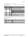
1
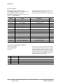
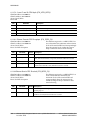
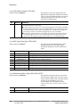
Data Sheet
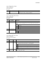
PRELIMINARY
December 2010
AR9344 Highly-Integrated and Feature-Rich IEEE 802.11n 2x2
2.4/5 GHz Premium SoC for Advanced WLAN Platforms
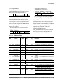
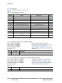
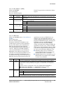
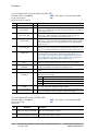
General Description
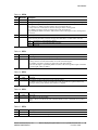
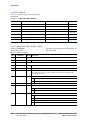
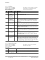
Features
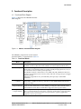
The Atheros AR9344 is a highly integrated and
feature-rich IEEE 802.11n 2x2 2.4/5 GHz Systemon-a-Chip (SoC) for advanced WLAN platforms.
■ 74Kc MIPS processor with 64 KB I-Cache and
It includes a MIPS 74Kc processor, PCI Express
1.1 Root Complex and Endpoint interfaces, five
port IEEE 802.3 Fast Ethernet Switch with MAC/
PHY, one MII/RMII/RGMII interface, one USB
2.0 MAC/PHY, and external memory interface
for serial Flash, SDRAM, DDR1 or DDR2, I2S/
SPDIF-Out audio interface, SLIC VOIP/PCM
interface, two UARTs, and GPIOs that can be
used for LED controls or other general purpose
interface configurations.
The AR9344 supports 802.11n operations up to
144 Mbps for 20 MHz and 300 Mbps for 40 MHz
respectively, and 802.11a/b/g data rates.
Additional features include Maximal Likelihood
(ML) decoding, Low-Density Parity Check
(LDPC), Maximal Ratio Combining (MRC), Tx
Beamforming (TxBF), and On-Chip One-Time
Programmable (OTP) memory.
The AR9344 PCIE Root Complex interface can be
used to connect to another Atheros single-chip
MAC/BB/radio for dual concurrent WLAN
applications. The AR9344 supports booting from
either NOR or NAND flash. If NOR flash is used
as boot codestore, an additional NAND flash
device can still be connected, for end-user multimedia storage and other applications.
When connecting the AR9344 to an external host
through the PCIE Endpoint interface, or the USB
Device interface, the AR9344 can off load the host
CPU from computation- intensive functions,
allowing it to focus on its dedicated tasks.
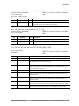
32 KB D-Cache, operating at up to 533 MHz
■ External 16- or 32-bit DDR1, DDR2 operating
■
■
■
■
■
■
■
■
■
■
■
■
■
■
■
■
■
at up to 200 MHz (400 M transfers/sec), or 16bit SDRAM memory interface operating at up
to 200 MHz
NAND and SPI NOR Flash memory support
10/100 Ethernet Switch with five IEEE 802.3
Ethernet LAN ports
MII/RMII/RGMII interface
802.3az Energy Efficient Ethernet compliant
Hardware-based NAT & ACL accelerators for
Ethernet interface
Both PCI Express 1.1 Root Complex and
Endpoint interfaces supported
simultaneously
One USB 2.0 controller with built-in MAC/
PHY supports Host or Device mode
Boot from external CPU via PCIE, USB, xMII,
eliminating need for external flash
I2S/SPDIF-out audio interface
SLIC for VOIP/PCM
One low-speed UART (115 Kbps), one highspeed UART (3 Mbps), and multiple GPIO
pins for general purpose I/O
Fully integrated RF Front-End including PAs
and LNAs
Optional external LNA/PA
25 MHz or 40 MHz reference clock input
1.2 V switching regulator
Advanced power management with dynamic
clock switching for ultra-low power modes
409-pin BGA package
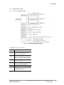
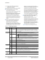
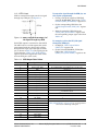
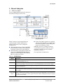
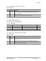
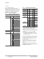
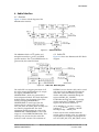
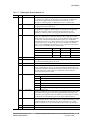
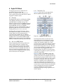
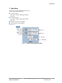
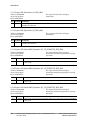
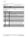
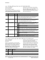
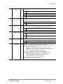
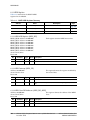
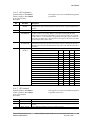
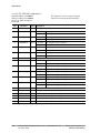
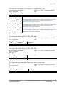
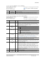
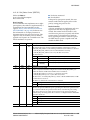
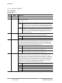
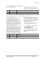
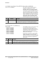
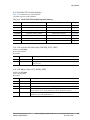
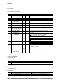
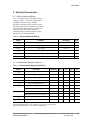
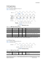
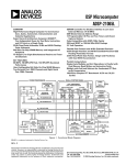
AR9344 System Block Diagram
© 2010 by Atheros Communications, Inc. All rights reserved. Atheros®, Atheros Driven®, Align®, Atheros XR®, Driving the Wireless Future®, Intellon®, Ethos®, IQUE®,
No New Wires®, Orion®, PLC4Trucks®, Powerpacket®, Spread Spectrum Carrier®, SSC®, ROCm®, Super A/G®, Super G®, Super N®, The Air is Cleaner at 5-GHz®, Total
802.11®, U-Nav®, Wake on Wireless®, Wireless Future. Unleashed Now.®, and XSPAN®, are registered by Atheros Communications, Inc. Atheros SST™, Signal-Sustain
Technology™, Install N Go™, ROCm™, amp™, Simpli-Fi™, There is Here™, U-Map™, U-Tag™, and 5-UP™ are trademarks of Atheros Communications, Inc. The Atheros
logo is a registered trademark of Atheros Communications, Inc. All other trademarks are the property of their respective holders. Subject to change without notice.
COMPANY CONFIDENTIAL
•
1
PRELIMINARY
2
2
•
•
AR9344 Highly-Integrated 802.11n 2x2 2.4/5 GHz Premium SoC
December 2010
Atheros Communications, Inc.
COMPANY CONFIDENTIAL
PRELIMINARY
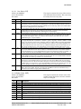
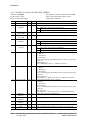
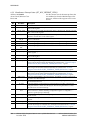
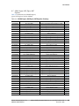
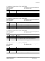
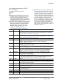
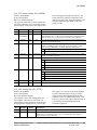
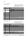
Table of Contents
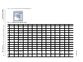
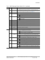
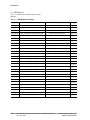
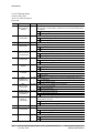
1 Pin Descriptions .......................... 23
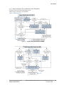
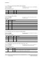
2 Functional Description ............... 35
2.1 Functional Block Diagram .................... 35
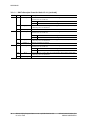
2.2 Bootstrap Options .................................. 37
2.3 RESET ...................................................... 38
2.12.2 GPIO Input .................................. 55
2.13 Serial Flash SPI/ROM .......................... 56
2.13.1 SPI Operations ............................ 56
2.13.2 Write Enable ................................ 56
2.13.3 Page Program .............................. 56
2.13.4 Page Read .................................... 56
2.4 PLL and Clock Control ......................... 39
2.4.1 Full Chip CLocking Structure ... 39
2.4.1 CPU PLL ...................................... 40
2.4.2 DDR PLL ...................................... 40
2.4.3 Audio PLL ................................... 41
2.14 MDIO Slave Interface ........................... 57
2.5 MIPS Processor ....................................... 41
2.5.1 Configuration .............................. 41
2.16 High-Speed UART Interface ............... 59
2.16.1 Transmit (Tx) ............................... 59
2.16.2 Receive (Rx) ................................. 60
2.6 Address MAP ......................................... 41
2.7 DDR Memory Controller ...................... 42
2.7.1 DDR Configurations .................. 42
2.7.2 Address Mapping ....................... 43
2.7.3 Refresh .......................................... 43
2.8 PCIE EP ................................................... 44
2.8.1 PCIE EP DMA Interface ............. 44
2.8.2 PCIE EP Descriptor Format ....... 44
2.8.3 Reset and Initialization .............. 46
2.8.4 Interrupts ..................................... 46
2.8.5 Power Management ................... 46
2.9 PCIE RC ................................................... 46
2.9.6 Power Management ................... 46
2.9.7 Interrupts ..................................... 46
2.9.8 Error Reporting Capability and
Status Checking .......................... 47
2.9.9 Byte-Swap Option ...................... 47
2.9.10 Request Sizes and Payloads ...... 47
2.10 SLIC ......................................................... 47
2.10.1 Overview ..................................... 47
2.10.2 SLIC Interface .............................. 48
2.10.3 Transmit ....................................... 48
2.10.4 Receive ......................................... 48
2.10.5 SLIC Interface Signals ................ 48
2.10.6 SLIC Master and Slave Modes .. 49
2.11 Segmentation/Desegmentation/
Checksum Accelerator 50
2.12 GPIO ....................................................... 52
2.12.1 GPIO Output ............................... 53
Atheros Communications, Inc.
COMPANY CONFIDENTIAL
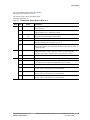
2.15 NAND Flash Controller ....................... 57
2.15.1 Devices Supported ..................... 58
2.15.2 Programmable NAND Interface
Timing .......................................... 58
2.17 Low-Speed UART Interface ................ 60
2.18 USB 2.0 Interface ................................... 60
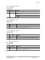
3 Ethernet Subsystem .....................61
3.1 GMAC0 and GMAC1 ............................ 61
3.1.1 External RGMII/RMII/MII
Interface ....................................... 62
3.1.2 Ingress and Egress Flow of Data and
Control Information ................... 63
3.2 GMAC Descriptor Structure: Rx ......... 64
3.2.1 Start Address for Packet Data
(PKT_START_ADDR) ................ 64
3.2.2 Packet Size and Flags (PKT_SIZE)
64
3.2.3 Start Address Packet Data
(PKT_START_ADDR) ................ 65
3.3 GMAC Descriptor Structure: Tx .......... 65
3.3.1 Start Address for Packet Data
(PKT_START_ADDR) ................ 65
3.3.2 Packet Size and Flags (PKT_SIZE)
66
3.3.3 Start Address Packet Data
(PKT_START_ADDR) ................ 66
3.4 NAT LUT Structure: Ingress and Egress
67
3.5 Hardware Ager: Ingress and Egress ... 68
3.6 Setup and Data/Packet Flow ............... 68
3.6.1 Ingress .......................................... 68
3.6.2 Egress ........................................... 69
AR9344 Highly-Integrated 802.11n 2x2 2.4/5 GHz Premium SoC •
December 2010 •
3
3
PRELIMINARY
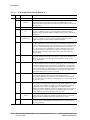
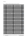
3.7 ACL
3.7.1
3.7.2
3.7.3
3.7.4
.......................................................... 70
ACL Data Structure .................... 70
Global Rules ................................ 72
Entry Programming ................... 73
ACL Programming and Software
Flow .............................................. 73
3.8 Ethernet Switch ...................................... 75
3.9 Five-Port Ethernet Switch ..................... 75
3.9.1 Overview ...................................... 75
3.9.2 Basic Switch Operation .............. 76
3.9.3 Media Access Controllers (MAC)
76
3.9.4 ACL ............................................... 76
3.9.5 Register Access ............................ 77
3.9.6 LED Control ................................. 77
3.9.7 VLANs .......................................... 78
3.9.8 IEEE Port Security ...................... 78
3.9.9 Mirroring ..................................... 78
3.9.10 Broadcast/Multicast/Unknown
Unicast .......................................... 78
3.9.11 IGMP/MLD Snooping ............... 78
3.9.12 Spanning Tree ............................. 79
3.9.13 MIB/Statistics Counters ............ 79
3.9.14 Atheros Header Configuration . 81
3.9.15 IEEE 802.3 Reserved Group
Addresses Filtering Control ...... 81
3.9.16 PPPoE Header Removal ............ 82
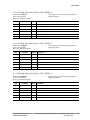
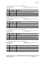
4 Audio Interface ............................ 83
4.1 Overview ................................................. 83
4.2 Audio PLL ............................................... 83
4.3 I2S Interface ............................................. 84
4.3.1 External DAC .............................. 84
4.3.2 Sample Sizes and Rates .............. 84
4.3.3 Stereo Software Interface ........... 84
4.4 SPDIF INTERFACE ............................... 84
4.5 Mailbox (DMA Controller) ................... 85
4.5.1 Mailboxes ..................................... 85
4.5.2 MBOX DMA Operation ............. 85
4.5.3 Software Flow Control ............... 86
4.5.4 Mailbox Error Conditions .......... 86
4.5.5 MBOX-Specific Interrupts ......... 86
5 WLAN Medium Access Control
(MAC) 87
4
4
•
•
5.1 Overview ................................................. 87
5.2 Descriptor ............................................... 87
5.3 Descriptor Format .................................. 88
5.4 Queue Control Unit (QCU) ................ 106
5.5 DCF Control Unit (DCU) .................... 106
5.5.1 DCU State Information ............ 107
5.6 Protocol Control Unit (PCU) .............. 107
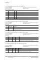
6 Digital PHY Block .....................109
6.1 Overview ............................................... 109
6.2 802.11n (MIMO) Mode ........................ 109
6.2.1 Transmitter (Tx) ........................ 109
6.2.2 Receiver (Rx) ............................. 110
6.3 802.11a/b/g Legacy Mode ................. 110
6.3.1 Transmitter ................................ 110
6.3.2 Receiver ...................................... 110
7 Radio Block .................................111
7.1 Receiver (Rx) Block .............................. 112
7.2 Transmitter (Tx) Block ........................ 113
7.3 Synthesizer (SYNTH) Block ............... 114
7.4 Bias/Control (BIAS) Block ................. 114
8 Register Descriptions ................115
8.1 DDR Registers ...................................... 116
8.1.1 DRR DRAM Configuration
(DDR_CONFIG) ....................... 117
8.1.2 DDR DRAM Configuration 2
(DDR_CONFIG2) ..................... 117
8.1.3 DDR Mode Value
(DDR_MODE_REGISTER) ...... 117
8.1.4 DDR Extended Mode
(DDR_EXTENDED_MODE_REGIS
TER) ............................................ 118
8.1.5 DDR Control (DDR_CONTROL) .
118
8.1.6 DDR Refresh Control and
Configuration (DDR_REFRESH) .
118
8.1.7 DDR Read Data Capture Bit Mask
(DDR_RD_DATA_THIS_CYCLE)
118
8.1.8 DQS Delay Tap Control for Byte 0
(TAP_CONTROL_0) ................ 119
8.1.9 DQS Delay Tap Control for Byte 1
(TAP_CONTROL_1) ................ 119
AR9344 Highly-Integrated 802.11n 2x2 2.4/5 GHz Premium SoC
December 2010
Atheros Communications, Inc.
COMPANY CONFIDENTIAL
PRELIMINARY
8.1.10 DQS Delay Tap Control for Byte 2
(TAP_CONTROL_2) ................ 119
8.1.11 DQS Delay Tap Control for Byte 3
(TAP_CONTROL_3) ................ 120
8.1.12 GMAC0 Interface Write Buffer
Flush
(DDR_WB_FLUSH_GMAC0) . 120
8.1.13 GMAC1 Interface Write Buffer
Flush
(DDR_WB_FLUSH_GMAC1) . 120
8.1.14 USB Interface Write Buffer Flush
(DDR_WB_FLUSH_USB) ........ 120
8.1.15 PCIE Interface Write Buffer Flush
(DDR_WB_FLUSH_PCIE) ....... 121
8.1.16 WMAC Interface Write Buffer Flush
(DDR_WB_FLUSH_WMAC) .. 121
8.1.17 SRC1 Interface Write Buffer Flush
(DDR_WB_FLUSH_SRC1) ...... 121
8.1.18 SRC2 Interface Write Buffer Flush
(DDR_WB_FLUSH_SRC2) ...... 121
8.1.19 DDR2 Configuration
(DDR_DDR2_CONFIG) ........... 122
8.1.20 DDR EMR2 (DDR_EMR2) ....... 122
8.1.21 DDR EMR3 (DDR_EMR3) ....... 122
8.1.22 AHB Master Timeout Control
(AHB_MASTER_TIMEOUT_MAX)
..................................................... 122
8.1.23 AHB Timeout Current Count
(AHB_MASTER_TIMEOUT_CUR
NT) .............................................. 123
8.1.24 Timeout Slave Address
(AHB_MASTER_TIMEOUT_SLV_
ADDR) ........................................ 123
8.1.25 DDR Controller Configuration
(DDR_CTL_CONFIG) .............. 123
8.1.26 DDR Self Refresh Control ..............
(DDR_SF_CTL) ......................... 124
8.1.27 Self Refresh Timer (SF_TIMER) 124
8.1.28 WMAC Flush (WMAC_FLUSH) ..
124
8.2 UART0 (Low-Speed) Registers .......... 125
8.2.1 Receive Buffer (RBR) ................ 125
8.2.2 Transmit Holding (THR) ......... 125
8.2.3 Divisor Latch Low (DLL) ........ 126
8.2.4 Divisor Latch High (DLH) ...... 126
8.2.5 Interrupt Enable (IER) .............. 126
8.2.6 Interrupt Identity (IIR) ............. 127
Atheros Communications, Inc.
COMPANY CONFIDENTIAL
8.2.7
8.2.8
8.2.9
8.2.10
8.2.11
FIFO Control (FCR) .................. 127
Line Control (LCR) ................... 128
Modem Control (MCR) ........... 128
Line Status (LSR) ...................... 129
Modem Status (MSR) ............... 129
8.3 GPIO Registers ..................................... 130
8.3.1 GPIO Output Enable (GPIO_OE) .
131
8.3.2 GPIO Input Value (GPIO_IN) 131
8.3.3 GPIO Output Value (GPIO_OUT)
131
8.3.4 GPIO Per Bit Set (GPIO_SET) . 131
8.3.5 GPIO Per Bit Clear (GPIO_CLEAR)
132
8.3.6 GPIO Interrupt Enable (GPIO_INT)
132
8.3.7 GPIO Interrupt Type
(GPIO_INT_TYPE) ................... 132
8.3.8 GPIO Interrupt Polarity
(GPIO_INT_POLARITY) ......... 132
8.3.9 GPIO Interrupt Pending
(GPIO_INT_PENDING) .......... 133
8.3.10 GPIO Interrupt Mask
(GPIO_INT_MASK) ................. 133
8.3.11 GPIO Ethernet LED Routing Select
(GPIO_IN_ETH_SWITCH_LED) .
133
8.3.12 GPIO Function 0
(GPIO_OUT_FUNCTION0) .... 134
8.3.13 GPIO Function 1
(GPIO_OUT_FUNCTION1) .... 134
8.3.14 GPIO Function 2
(GPIO_OUT_FUNCTION2) .... 135
8.3.15 GPIO Function 3
(GPIO_OUT_FUNCTION3) .... 135
8.3.16 GPIO Function 4
(GPIO_OUT_FUNCTION4) .... 135
8.3.17 GPIO In Signals 0
(GPIO_IN_ENABLE0) ............. 136
8.3.18 GPIO In Signals 1
(GPIO_IN_ENABLE1) ............. 136
8.3.19 GPIO In Signals 2
(GPIO_IN_ENABLE2) ............. 136
8.3.20 GPIO In Signals 3
(GPIO_IN_ENABLE3) ............. 136
8.3.21 GPIO In Signals 4
(GPIO_IN_ENABLE4) ............. 137
AR9344 Highly-Integrated 802.11n 2x2 2.4/5 GHz Premium SoC •
December 2010 •
5
5
PRELIMINARY
8.3.22 GPIO In Signals 9
(GPIO_IN_ENABLE9) .............. 137
8.3.23 GPIO Function
(GPIO_FUNCTION) ................. 137
8.4 PLL Control Registers ......................... 138
8.4.1 CPU Phase Lock Loop
Configuration
(CPU_PLL_CONFIG) ............... 139
8.4.2 DDR PLL Configuration
(DDR_PLL_CONFIG) .............. 139
8.4.3 CPU DDR Clock Control
(CPU_DDR_CLOCK_CONTROL)
140
8.4.4 PCIE RC PLL Configuration
(PCIE_PLL_CONFIG) .............. 141
8.4.5 PCIE Clock Jitter Max Value
Control
(PCIE_PLL_DITHER_DIV_MAX)
141
8.4.6 PCIE Clock Jitter Min Value Control
(PCIE_PLL_DITHER_DIV_MIN) .
141
8.4.7 PCIE Clock Jitter Step Control
(PCIE_PLL_DITHER_STEP) ... 142
8.4.8 Switch Clock Source Control
(SWITCH_CLOCK_CONTROL) ..
142
8.4.9 Current Dither Logic Output
(CURRENT_PCIE_PLL_DITHER)
142
8.4.10 Ethernet XMII Control
(ETH_XMII_CONTROL) ......... 143
8.4.11 Audio PLL Configuration
(AUDIO_PLL_CONFIG) ......... 143
8.4.12 Audio PLL Modulation Control
(AUDIO_PLL_MODULATION) ..
144
8.4.13 Audio PLL Jitter Control
(AUDIO_PLL_MOD_STEP) .... 144
8.4.14 Current Audio Modulation Output
(CURRENT_AUDIO_PLL_MODU
LATION) .................................... 144
8.4.15 DRR PLL Dither Parameter
(DRR_PLL_DITHER) ............... 145
8.4.16 CPU PLL Dither Parameter
(CPU_PLL_DITHER) ............... 145
8.5 Reset Registers ...................................... 146
8.5.1 General Purpose Timers
6
6
•
•
8.5.2
8.5.3
8.5.4
8.5.5
8.5.6
8.5.7
8.5.8
8.5.9
8.5.10
8.5.11
(RST_GENERAL_TIMERx) ..... 146
General Purpose Timers Reload
(RST_GENERAL_TIMER_RELOA
Dx) .............................................. 146
Watchdog Timer Control
(RST_WATCHDOG_TIMER_CON
TROL) ......................................... 147
Watchdog Timer
(RST_WATCHDOG_TIMER) . 147
Miscellaneous Interrupt Status
(RST_MISC_INTERRUPT_STATUS
) .................................................... 148
Miscellaneous Interrupt Mask
(RST_MISC_INTERRUPT_MASK)
149
Global Interrupt Status
(RST_GLOBAL_INTERRUPT_STA
TUS) ............................................ 149
Reset (RST_RESET) .................. 150
Chip Revision ID
(RST_REVISION_ID) ............... 151
PCIE RC and WMAC Interrupt
Status
(RST_PCIE_WMAC_INTERRUPT_
STATUS) .................................... 151
Miscellaneous CPU Control Bits
(RST_MISC2) ............................. 152
8.6 GMAC Interface Registers .................. 153
8.6.1 Ethernet Configuration
(ETH_CFG) ................................ 153
8.6.2 LUTs Ager Interrupt Status
(LUTs_AGER_INT) .................. 154
8.6.3 LUTs Ager Interrupt Mask
(LUTS_AGER_INTR_MASK) . 154
8.6.4 GMAC0 Rx Data CRC Calculation
Control
(GMAC0_RXDATA_CRC_CONTR
OL) .............................................. 154
8.6.5 GMAC0 Valid RX Data CRC Value
(GMAC0_RXDATA_CRC) ...... 154
8.7 GMAC0 Ingress NAT /Egress NAT
Registers 155
8.7.1 Egress CPU Requested LUT Entry
Lookup (EG_CPU_REQ) ......... 158
8.7.2 Egress CPU Request Status
(EG_CPU_REQ_STATUS) ....... 158
8.7.3 Egress DW0 Information
(EG_INFO_DW0) ...................... 159
AR9344 Highly-Integrated 802.11n 2x2 2.4/5 GHz Premium SoC
December 2010
Atheros Communications, Inc.
COMPANY CONFIDENTIAL
PRELIMINARY
8.7.4 Egress CPU Related DW0
Information
(EG_CPU_REQUESTED_INFO_D
W0) .............................................. 159
8.7.5 Egress DW0 Key (EG_KEY_DW0 )
159
8.7.6 Egress DW1 Key (EG_KEY_DW1)
159
8.7.7 Egress Ageout DW0 Key
(EG_AGER_KEY_DW0) ........... 159
8.7.8 Egress Ageout DW1 Key
(EG_AGER_KEY_DW1) ........... 160
8.7.9 Egress Ager FIFO Signals
(EG_AGER_INFO) .................... 160
8.7.10 Egress Memory (EG_MEM) .... 160
8.7.11 Egress Memory DW0
(EG_MEM_DW0) ...................... 160
8.7.12 Egress Memory DW1
(EG_MEM_DW1) ...................... 161
8.7.13 Egress Memory DW2
(EG_MEM_DW2) ...................... 161
8.7.14 Egress Link List (EG_LINKLIST) .
161
8.7.15 Egress Sub-Table Data
(EG_SUBTABLE) ...................... 161
8.7.16 Egress Timer Ager Values
(EG_AGER_TICK) .................... 162
8.7.17 Egress Ager Timeout
(EG_AGER_TIMEOUT) ........... 162
8.7.18 Ingress CPU Requested LUT Entry
Lookup (IG_CPU_REQ) ........... 162
8.7.19 Ingress CPU Request Status
(IG_CPU_REQ_STATUS) ........ 163
8.7.20 Ingress DW0 Information
(IG_INFO_DW0) ....................... 163
8.7.21 Ingress DW1 Information
(IG_INFO_DW1) ....................... 163
8.7.22 Ingress DW2 Information
(IG_INFO_DW2) ....................... 164
8.7.23 Ingress DW3 Information
(IG_INFO_DW3) ....................... 164
8.7.24 Ingress CPU Related DW0
Information
(IG_CPU_REQUESTED_INFO_DW
0) .................................................. 164
8.7.25 Ingress CPU Related DW1
Information
(IG_CPU_REQUESTED_INFO_DW
Atheros Communications, Inc.
COMPANY CONFIDENTIAL
8.7.26
8.7.27
8.7.28
8.7.29
8.7.30
8.7.31
8.7.32
8.7.33
8.7.34
8.7.35
8.7.36
8.7.37
8.7.38
8.7.39
8.7.40
8.7.41
8.7.42
8.7.43
8.7.44
8.7.45
1) ................................................. 164
Ingress CPU Related DW2
Information
(IG_CPU_REQUESTED_INFO_DW
2) ................................................. 164
Ingress CPU Related DW3
Information
(IG_CPU_REQUESTED_INFO_DW
3) ................................................. 165
Ingress DW0 Key (IG_KEY_DW0)
165
Ingress Ageout DW0 Key
(IG_AGER_KEY_DW0) ........... 165
Ingress Ager FIFO Signals
(IG_AGER_INFO) .................... 165
Ingress Memory (IG_MEM) .... 166
Ingress Memory DW0
(IG_MEM_DW0) ....................... 166
Ingress Memory DW1
(IG_MEM_DW1) ....................... 166
Ingress Memory DW2
(IG_MEM_DW2) ....................... 166
Ingress Memory DW3
(IG_MEM_DW3) ....................... 166
Ingress Link List (IG_LINKLIST) .
167
Ingress Sub-Table Data
(IG_SUBTABLE) ....................... 167
Ingress Timer Ager Values
(IG_AGER_TICK) ..................... 167
Ingress Ager Timeout
(IG_AGER_TIMEOUT) ............ 167
Tx QoS Arbiter Configuration
(TxQOS_ARB_CFG) ................. 168
Tx Status and Packet Count
(DMATXSTATUS) .................... 168
Local MAC Address Dword0
(LCL_MAC_ADDR_DW0) ...... 168
Local MAC Address Dword1
(LCL_MAC_ADDR_DW1) ...... 169
Next Hop Router’s MAC Address
Dword0
(NXT_HOP_DST_ADDR_DW0) ..
169
Next Hop Router’s MAC Address
Dword1
(NXT_HOP_DST_ADDR_DW1) ..
169
AR9344 Highly-Integrated 802.11n 2x2 2.4/5 GHz Premium SoC •
December 2010 •
7
7
PRELIMINARY
8.7.46 Local Global IP Address 0
(GLOBAL_IP_ADDR0) ............ 169
8.7.47 Local Global IP Address 1
(GLOBAL_IP_ADDR1) ............ 169
8.7.48 Local Global IP Address 2
(GLOBAL_IP_ADDR2) ............ 170
8.7.49 Local Global IP Address 3
(GLOBAL_IP_ADDR3) ............ 170
8.7.50 Egress NAT Control and Status
(EG_NAT_CSR) ........................ 170
8.7.51 Egress NAT Counter
(EG_NAT_CNTR) ..................... 171
8.7.52 Ingress NAT Control and Status
(IG_NAT_CSR) .......................... 171
8.7.53 Ingress NAT Counter
(IG_NAT_CNTR) ...................... 171
8.7.54 Egress ACL Control and Status
(EG_ACL_CSR) ......................... 172
8.7.55 Ingress ACL Control and Status
(IG_ACL_CSR) .......................... 172
8.7.56 Egress ACL CMD0 and Action
(EG_ACL_CMD0_AND_ACTION)
173
8.7.57 Egress ACL CMD1, CMD2, CMD3,
CMD4 (EG_ACL_CMD1234) .. 173
8.7.58 Egress ACL OPERAND0
(EG_ACL_OPERAND0) .......... 173
8.7.59 Egress ACL OPERAND1
(EG_ACL_OPERAND1) .......... 174
8.7.60 Egress ACL Memory Control
(EG_ACL_MEM_CONTROL) . 174
8.7.61 Ingress ACL CMD0 and Action
(IG_ACL_CMD0_AND_ACTION)
175
8.7.62 Ingress ACL CMD1, CMD2, CMD3,
CMD4 (IG_ACL_CMD1234) ... 175
8.7.63 Ingress ACL OPERAND0
(IG_ACL_OPERAND0) ........... 175
8.7.64 Egress ACL OPERAND1
(EG_ACL_OPERAND1) .......... 176
8.7.65 Ingress ACL Memory Control
(IG_ACL_MEM_CONTROL) .. 176
8.7.66 Ingress ACL Counter Group 0
(IG_ACL_COUNTER_GRP0) .. 177
8.7.67 Ingress ACL Counter Group 1
(IG_ACL_COUNTER_GRP1) .. 177
8.7.68 Ingress ACL Counter Group 2
(IG_ACL_COUNTER_GRP2) .. 177
8
8
•
•
8.7.69 Ingress ACL Counter Group 3
(IG_ACL_COUNTER_GRP3) . 177
8.7.70 Ingress ACL Counter Group 4
(IG_ACL_COUNTER_GRP4) . 178
8.7.71 Ingress ACL Counter Group 5
(IG_ACL_COUNTER_GRP5) . 178
8.7.72 Ingress ACL Counter Group 6
(IG_ACL_COUNTER_GRP6) . 178
8.7.73 Ingress ACL Counter Group 7
(IG_ACL_COUNTER_GRP7) . 178
8.7.74 Ingress ACL Counter Group 8
(IG_ACL_COUNTER_GRP8) . 179
8.7.75 Ingress ACL Counter Group 9
(IG_ACL_COUNTER_GRP9) . 179
8.7.76 Ingress ACL Counter Group 10
(IG_ACL_COUNTER_GRP10) 179
8.7.77 Ingress ACL Counter Group 11
(IG_ACL_COUNTER_GRP11) 179
8.7.78 Ingress ACL Counter Group 12
(IG_ACL_COUNTER_GRP12) 180
8.7.79 Ingress ACL Counter Group 13
(IG_ACL_COUNTER_GRP13) 180
8.7.80 Ingress ACL Counter Group 14
(IG_ACL_COUNTER_GRP14) 180
8.7.81 Ingress ACL Counter Group 15
(IG_ACL_COUNTER_GRP15) 180
8.7.82 Egress ACL Counter Group 0
(EG_ACL_COUNTER_GRP0) 181
8.7.83 Egress ACL Counter Group 1
(EG_ACL_COUNTER_GRP1) 181
8.7.84 Egress ACL Counter Group 2
(EG_ACL_COUNTER_GRP2) 181
8.7.85 Egress ACL Counter Group 3
(EG_ACL_COUNTER_GRP3) 181
8.7.86 Egress ACL Counter Group 4
(EG_ACL_COUNTER_GRP4) 182
8.7.87 Egress ACL Counter Group 5
(EG_ACL_COUNTER_GRP5) 182
8.7.88 Egress ACL Counter Group 6
(EG_ACL_COUNTER_GRP6) 182
8.7.89 Egress ACL Counter Group 7
(EG_ACL_COUNTER_GRP7) 182
8.7.90 Egress ACL Counter Group 8
(EG_ACL_COUNTER_GRP8) 183
8.7.91 Egress ACL Counter Group 9
(EG_ACL_COUNTER_GRP9) 183
8.7.92 Egress ACL Counter Group 10
(EG_ACL_COUNTER_GRP10) 183
AR9344 Highly-Integrated 802.11n 2x2 2.4/5 GHz Premium SoC
December 2010
Atheros Communications, Inc.
COMPANY CONFIDENTIAL
PRELIMINARY
8.7.93 Egress ACL Counter Group 11
(EG_ACL_COUNTER_GRP11) 183
8.7.94 Egress ACL Counter Group 12
(EG_ACL_COUNTER_GRP12) 184
8.7.95 Egress ACL Counter Group 13
(EG_ACL_COUNTER_GRP13) 184
8.7.96 Egress ACL Counter Group 14
(EG_ACL_COUNTER_GRP14) 184
8.7.97 Egress ACL Counter Group 15
(EG_ACL_COUNTER_GRP15) 184
8.7.98 Clear ACL Counters
(CLEAR_ACL_COUNTERS) .. 185
8.7.99 Ingress ACL Rule Vector Lower
(IG_ACL_RULE_VECTOR_LOWE
R) ................................................. 185
8.7.100 Ingress ACL Rule Vector Upper
(IG_ACL_RULE_VECTOR_UPPER
) .................................................... 185
8.7.101 Egress ACL Rule Vector Lower
(EG_ACL_RULE_VECTOR_LOWE
R) ................................................. 185
8.7.102 Egress ACL Rule Vector Upper
(EG_ACL_RULE_VECTOR_UPPE
R) ................................................. 185
8.7.103 Ingress ACL Rule Table0 Lower
(IG_ACL_RULE_TABLE0_LOWER
) .................................................... 186
8.7.104 Ingress ACL Rule Table0 Upper
(IG_ACL_RULE_TABLE0_UPPER)
186
8.7.105 Ingress ACL Rule Table1 Lower
(IG_ACL_RULE_TABLE1_LOWER
) .................................................... 186
8.7.106 Ingress ACL Rule Table1 Upper
(IG_ACL_RULE_TABLE1_UPPER)
186
8.7.107 Ingress ACL Rule Table2 Lower
(IG_ACL_RULE_TABLE2_LOWER
) .................................................... 186
8.7.108 Ingress ACL Rule Table2 Upper
(IG_ACL_RULE_TABLE2_UPPER)
187
8.7.109 Ingress ACL Rule Table3 Lower
(IG_ACL_RULE_TABLE3_LOWER
) .................................................... 187
8.7.110 Ingress ACL Rule Table3 Upper
(IG_ACL_RULE_TABLE3_UPPER)
187
8.7.111 Egress ACL Rule Table0 Lower
Atheros Communications, Inc.
COMPANY CONFIDENTIAL
(EG_ACL_RULE_TABLE0_LOWE
R) ................................................. 187
8.7.112 Egress ACL Rule Table0 Upper
(EG_ACL_RULE_TABLE0_UPPER)
..................................................... 187
8.7.113 Egress ACL Rule Table1 Lower
(EG_ACL_RULE_TABLE1_LOWE
R) ................................................. 188
8.7.114 Egress ACL Rule Table1 Upper
(EG_ACL_RULE_TABLE1_UPPER)
..................................................... 188
8.7.115 Egress ACL Rule Table2 Lower
(EG_ACL_RULE_TABLE2_LOWE
R) ................................................. 188
8.7.116 Egress ACL Rule Table2 Upper
(EG_ACL_RULE_TABLE2_UPPER)
..................................................... 188
8.7.117 Egress ACL Rule Table3 Lower
(EG_ACL_RULE_TABLE3_LOWE
R) ................................................. 188
8.7.118 Egress ACL Rule Table3 Upper
(EG_ACL_RULE_TABLE3_UPPER)
..................................................... 188
8.8 MBOX Registers ................................... 189
8.8.1 Non-Destructive FIFO Status Query
(MBOX_FIFO_STATUS) .......... 190
8.8.2 Non-Destructive SLIC FIFO Status
Query
(SLIC_MBOX_FIFO_STATUS) 190
8.8.3 Mailbox DMA Engine Policy
Control (MBOX_DMA_POLICY) .
191
8.8.4 SLIC Mailbox DMA Engine Policy
Control
(SLIC_MBOX_DMA_POLICY) 192
8.8.5 Mailbox Rx DMA Descriptors Base
Address
(MBOX_DMA_RX_DESCRIPTOR_
BASE) ......................................... 192
8.8.6 Mailbox Rx DMA Control
(MBOX_DMA_RX_CONTROL) 193
8.8.7 Mailbox Tx DMA Descriptors Base
Address
(MBOX_DMA_TX_DESCRIPTOR_
BASE) ......................................... 193
8.8.8 Mailbox Tx DMA Control
(MBOX_DMA_TX_CONTROL) 194
8.8.9 SLIC Rx DMA Descriptors Base
Address
AR9344 Highly-Integrated 802.11n 2x2 2.4/5 GHz Premium SoC •
December 2010 •
9
9
PRELIMINARY
8.8.10
8.8.11
8.8.12
8.8.13
8.8.14
8.8.15
8.8.16
8.8.17
8.8.18
8.8.19
8.8.20
8.8.21
(SLIC_DMA_RX_DESCRIPTOR_B
ASE) ............................................ 194
SLIC Rx DMA Control
(SLIC_DMA_RX_CONTROL) 195
SLIC Tx DMA Descriptors Base
Address
(SLIC_DMA_TX_DESCRIPTOR_B
ASE) ............................................ 195
SLIC Tx DMA Control
(SLIC_DMA_TX_CONTROL) . 196
Mailbox FIFO Status
(MBOX_FRAME) ...................... 196
SLIC Mailbox FIFO Status
(SLIC_MBOX_FRAME) ........... 196
FIFO Timeout Period
(FIFO_TIMEOUT) ..................... 197
MBOX Related Interrupt Status
(MBOX_INT_STATUS) ............ 197
SLIC MBOX Related Interrupt
Status
(SLIC_MBOX_INT_STATUS) . 198
MBOX Related Interrupt Enables
(MBOX_INT_ENABLE) ........... 198
SLIC MBOX Related Interrupt
Enables
(SLIC_MBOX_INT_ENABLE) 199
Reset and Clear MBOX FIFOs
(MBOX_FIFO_RESET) ............. 199
SLIC Reset and Clear MBOX FIFOs
(SLIC_MBOX_FIFO_RESET) ... 199
8.9 SLIC Registers ...................................... 200
8.9.1 SLIC Slots (SLIC_SLOT) .......... 200
8.9.2 SLIC Clock Control
(SLIC_CLOCK_CONTROL) .... 200
8.9.3 SLIC Control (SLIC_CTRL) ..... 201
8.9.4 SLIC Tx Slots 1 (SLIC_TX_SLOTS1)
201
8.9.5 SLIC Tx Slots 2 (SLIC_TX_SLOTS2)
201
8.9.6 SLIC Rx Slots 1 (SLIC_RX_SLOTS1)
201
8.9.7 SLIC Rx Slots 2 (SLIC_RX_SLOTS2)
201
8.9.8 SLIC Timing Control
(SLIC_TIMING_CTRL) ............ 202
8.9.9 SLIC Interrupt (SLIC_INTR) ... 203
8.9.10 SLIC Swap (SLIC_SWAP) ....... 203
8.10 Stereo Registers ................................... 204
10
10
•
•
8.10.1 Configure Stereo Block
(STEREO_CONFIG) ................. 204
8.10.2 Set Stereo Volume
(STEREO_VOLUME) ............... 206
8.10.3 Stereo Master Clock
(STEREO_MASTER_CLOCK) 207
8.10.4 Tx Sample Counter
(STEREO_TX_SAMPLE_CNT_LSB)
..................................................... 207
8.10.5 Tx Sample Counter
(STEREO_TX_SAMPLE_CNT_MSB
) .................................................... 207
8.10.6 Rx Sample Counter
(STEREO_RX_SAMPLE_CNT_LSB)
..................................................... 207
8.10.7 Rx Sample Counter
(STEREO_RX_SAMPLE_CNT_MSB
) .................................................... 207
8.11 MDIO Registers ................................... 208
8.11.1 MDIO APB Registers (MDIO_REG)
208
8.11.2 MDIO Interrupt (MDIO_ISR) . 208
8.11.3 MDIO Slave PHY Addresses
(MDIO_PHY_ADDR) .............. 208
8.12 PCIE RC Control Registers ................ 209
8.12.1 PCIE Application Control
(PCIE_APP) ............................... 210
8.12.2 PCIE Interrupt and Error
(PCIE_AER) ............................... 210
8.12.3 PCIE Power Management
(PCIE_PWR_MGMT) ............... 211
8.12.4 PCIE Electromechanical
(PCIE_ELEC) ............................. 211
8.12.5 PCIE Configuration (PCIE_CFG) .
212
8.12.6 PCIE Receive Completion
(PCIE_RX_CNTL) ..................... 212
8.12.7 PCIE Reset (PCIE_RESET) ...... 213
8.12.8 PCIE PHY Configuration Data
(PCIE_PHY_CFG_DATA) ....... 213
8.12.9 PCIE MAC-PHY Interface Signals
(PCIE_MAC_PHY) ................... 213
8.12.10 PCIE PHY-MAC Interface Signals
(PCIE_PHY_MAC) ................... 214
8.12.11 PCIE Sideband Bus1
(PCIE_SIDEBAND1) ................ 214
8.12.12 PCIE Sideband Bus2
(PCIE_SIDEBAND2) ................ 214
AR9344 Highly-Integrated 802.11n 2x2 2.4/5 GHz Premium SoC
December 2010
Atheros Communications, Inc.
COMPANY CONFIDENTIAL
PRELIMINARY
8.12.13 PCIE MSI Lower Address
(PCIE_MSI_ADDR) .................. 215
8.12.14 PCIE MSI Data Value
(PCIE_MSI_DATA) .................. 215
8.12.15 PCIE Interrupt Status
(PCIE_INT_STATUS) ............... 216
8.12.16 PCIE Interrupt Mask
(PCIE_INT_MASK) .................. 217
8.13 WDMA Registers ................................ 218
8.13.1 Command (CR) ......................... 219
8.13.2 Configuration and Status (CFG) ...
219
8.13.3 Rx DMA Data Buffer Pointer
Threshold (RXBUFPTR_THRESH)
220
8.13.4 Tx DMA Descriptor Pointer
Threshold (TXDPPTR_THRESH) .
220
8.13.5 Maximum Interrupt Rate Threshold
(MIRT) ........................................ 220
8.13.6 Interrupt Global Enable (IER) . 221
8.13.7 Tx Interrupt Mitigation Thresholds
(TIMT) ........................................ 221
8.13.8 Rx Interrupt Mitigation Thresholds
(RIMT) ........................................ 221
8.13.9 Tx Configuration (TXCFG) ...... 222
8.13.10 Rx Configuration (RXCFG) ... 222
8.13.11 MIB Control (MIBC) ............... 223
8.13.12 Global Tx Timeout (GTT) ...... 223
8.13.13 Global Tx Timeout Mode (GTTM)
223
8.13.14 Carrier Sense Timeout (CST) . 224
8.13.15 Size of High and Low Priority
(RXDP_SIZE) ............................. 224
8.13.16 MAC Rx High Priority Queue
RXDP Pointer
(RX_QUEUE_HP_RXDP) ........ 224
8.13.17 MAC Rx Low Priority Queue
RXDP Pointer
(RX_QUEUE_LP_RXDP) ......... 224
8.13.18 Primary Interrupt Status (ISR_P)
225
8.13.19 Secondary Interrupt Status 0
(ISR_S0) ...................................... 226
8.13.20 Secondary Interrupt Status 1
(ISR_S1) ...................................... 226
8.13.21 Secondary Interrupt Status 2
(ISR_S2) ...................................... 227
Atheros Communications, Inc.
COMPANY CONFIDENTIAL
8.13.22 Secondary Interrupt Status 3
(ISR_S3) ...................................... 228
8.13.23 Secondary Interrupt Status 4
(ISR_S4) ...................................... 228
8.13.24 Secondary Interrupt Status 5
(ISR_S5) ...................................... 228
8.13.25 Primary Interrupt Mask (IMR_P)
229
8.13.26 Secondary Interrupt Mask 0
(IMR_S0) .................................... 230
8.13.27 Secondary Interrupt Mask 1
(IMR_S1) .................................... 230
8.13.28 Secondary Interrupt Mask 2
(IMR_S2) .................................... 231
8.13.29 Secondary Interrupt Mask 3
(IMR_S3) .................................... 231
8.13.30 Secondary Interrupt Mask 4
(IMR_S4) .................................... 232
8.13.31 Secondary Interrupt Mask 5
(IMR_S5) .................................... 232
8.13.32 Primary Interrupt Status Read and
Clear (ISR_P_RAC) ................... 232
8.13.33 Secondary Interrupt Status 0
(ISR_S0_S) .................................. 233
8.13.34 Secondary Interrupt Status 1
(ISR_S1_S) .................................. 233
8.13.35 Secondary Interrupt Status 2
(ISR_S2_S) .................................. 233
8.13.36 Secondary Interrupt Status 3
(ISR_S3_S) .................................. 233
8.13.37 Secondary Interrupt Status 4
(ISR_S4_S) .................................. 233
8.13.38 Secondary Interrupt Status 5
(ISR_S5_S) .................................. 233
8.14 WQCU Registers ................................. 234
8.14.1 Tx Queue Descriptor (Q_TXDP) ..
234
8.14.2
QCU_STATUS_RING_START_AD
DRESS Lower 32 bits of Address
(Q_STATUS_RING_START) ... 235
8.14.3
QCU_STATUS_RING_END_ADD
R Lower 32 Bits of Address
(Q_STATUS_RING_END) ...... 235
8.14.4 QCU_STATUS_RING_CURRENT
Address
(Q_STATUS_RING_CURRENT) ..
AR9344 Highly-Integrated 802.11n 2x2 2.4/5 GHz Premium SoC
December 2010
•
•
11
11
PRELIMINARY
235
8.14.5 Tx Queue Enable (Q_TXE) ...... 235
8.14.6 Tx Queue Disable (Q_TXD) .... 236
8.14.7 CBR Configuration (Q_CBRCFG)
236
8.14.8 ReadyTime Configuration
(Q_RDYTIMECFG) ................... 236
8.14.9 OneShotArm Set Control
(Q_ONESHOTARM_SC) ......... 237
8.14.10 OneShotArm Clear Control
(Q_ONESHOTARM_CC) ........ 237
8.14.11 Misc. QCU Settings (Q_MISC) 238
8.14.12 Misc. QCU Status (Q_STS) ..... 240
8.14.13 ReadyTimeShutdown Status
(Q_RDYTIMESHDN) ............... 240
8.14.14 Descriptor CRC Check
(MAC_QCU_DESC_CRC_CHK) ..
240
8.15 WLAN DCU Registers ....................... 241
8.15.1 QCU Mask (D_QCUMASK) .... 241
8.15.2 DCU-Specific IFS Settings
(D_LCL_IFS) .............................. 242
8.15.3 Retry Limits (D_RETRY_LIMIT) ..
242
8.15.4 ChannelTime Settings
(D_CHNTIME) .......................... 242
8.15.5 Misc. DCU-Specific Settings
(D_MISC) ................................... 243
8.15.6 DCU-Global IFS Settings: SIFS
Duration (D_GBL_IFS_SIFS) ... 243
8.15.7 DCU-Global IFS Settings: Slot
Duration (D_GBL_IFS_SLOT) . 243
8.15.8 DCU-Global IFS Settings: EIFS
Duration (D_GBL_IFS_EIFS) ... 244
8.15.9 DCU-Global IFS Settings: Misc.
Parameters (D_GBL_IFS_MISC) ...
244
8.15.10 DCU Tx Pause Control/Status
(D_TXPSE) ................................. 245
8.15.11 DCU Transmission Slot Mask
(D_TXSLOTMASK) .................. 245
8.16 RTC Registers ...................................... 246
8.16.1 Reset Control (RESET_CONTROL)
246
8.16.2 PLL Control Settings
(PLL_CONTROL) ..................... 247
8.16.3 PLL Settling Time (PLL_SETTLE)
12
12
•
•
247
8.16.4 Crystal Settling Time
(XTAL_SETTLE) ....................... 248
8.16.5 Pin Clock Speed Control
(CLOCK_OUT) ......................... 248
8.16.6 Reset Cause (RESET_CAUSE) 249
8.16.7 System Sleep Status
(SYSTEM_SLEEP) ..................... 249
8.16.8 Keep Awake Timer
(KEEP_AWAKE) ...................... 249
8.16.9 Derived RTC Clock
(DERIVED_RTC_CLK) ............ 250
8.16.10 RTC Sync
(RTC_SYNC_REGISTER) ........ 250
8.16.11 RTC Sync Status
(RTC_SYNC_STATUS) ............ 250
8.16.12 RTC Interrupt Cause
(RTC_SYNC_INTR_CAUSE) .. 251
8.16.13 RTC Interrupt Enable
(RTC_SYNC_INTR_ENABLE) 251
8.16.14 RTC Interrupt Mask
(RTC_SYNC_INTR_MASK) .... 251
8.17 WPCU Registers .................................. 252
8.17.1 STA Address Lower 32 Bits
(WMAC_PCU_STA_ADDR_L32)
254
8.17.2 STA Address Upper 16 Bits
(WMAC_PCU_STA_ADDR_U16)
255
8.17.3 BSSID Lower 32 Bits
(WMAC_PCU_BSSID_L32) ..... 255
8.17.4 BSSID Upper 16 Bits
(WMAC_PCU_BSSID_U16) .... 255
8.17.5 Beacon RSSI Average
(WMAC_PCU_BCN_RSSI_AVE) .
256
8.17.6 ACK and CTS Timeout
(WMAC_PCU_ACK_CTS_TIMEO
UT) .............................................. 256
8.17.7 Beacon RSSI Control
(WMAC_PCU_BCN_RSSI_CTL) ..
256
8.17.8 Ms Counter and Rx/Tx Latency
(WMAC_PCU_USEC_LATENCY)
257
8.17.9 Reset TSF
(WMAC_PCU_RESET_TSF) ... 257
8.17.10 Maximum CFP Duration
AR9344 Highly-Integrated 802.11n 2x2 2.4/5 GHz Premium SoC
December 2010
Atheros Communications, Inc.
COMPANY CONFIDENTIAL
PRELIMINARY
(WMAC_PCU_MAX_CFP_DUR)
257
8.17.11 Rx Filter
(WMAC_PCU_RX_FILTER) ... 258
8.17.12 Multicast Filter Mask Lower 32 Bits
(WMAC_PCU_MCAST_FILTER_L
32) ................................................ 258
8.17.13 Multicast Filter Mask Upper 32 Bits
(WMAC_PCU_MCAST_FILTER_U
32) ................................................ 258
8.17.14 Diagnostic Switches
(WMAC_PCU_DIAG_SW) ...... 259
8.17.15 TSF Lower 32 Bits
(WMAC_PCU_TSF_L32) ......... 260
8.17.16 TSF Upper 32 Bits
(WMAC_PCU_TSF_U32) ........ 260
8.17.17 AES Mute Mask 0
(WMAC_PCU_AES_MUTE_MASK
_0) ................................................ 260
8.17.18 AES Mute Mask 1...........................
(WMAC_PCU_AES_MUTE_MASK
_1) ................................................ 260
8.17.19 Last Rx Beacon TSF
(WMAC_PCU_LAST_BEACON_T
SF) ............................................... 261
8.17.20 Current NAV
(WMAC_PCU_NAV) ............... 261
8.17.21 Successful RTS Count
(WMAC_PCU_RTS_SUCCESS_CN
T) ................................................. 261
8.17.22 Failed RTS Count
(WMAC_PCU_RTS_FAIL_CNT) .
261
8.17.23 FAIL ACK Count
(WMAC_PCU_ACK_FAIL_CNT)
262
8.17.24 Failed FCS Count
(WMAC_PCU_FCS_FAIL_CNT) .
262
8.17.25 Beacon Count
(WMAC_PCU_BEACON_CNT) ..
262
8.17.26 Sleep 1 (WMAC_PCU_SLP1) 262
8.17.27 Sleep 2 (WMAC_PCU_SLP2) 263
8.17.28 Address 1 Mask Lower 32 Bits
(WMAC_PCU_ADDR1_MASK_L3
2) .................................................. 263
8.17.29 Address 1 Mask Upper 16 Bits
(WMAC_PCU_ADDR1_MASK_U1
Atheros Communications, Inc.
COMPANY CONFIDENTIAL
6) ................................................. 263
8.17.30 Tx Power Control
(WMAC_PCU_TPC) ................ 263
8.17.31 Tx Frame Counter
(WMAC_PCU_TX_FRAME_CNT)
264
8.17.32 Rx Frame Counter
(WMAC_PCU_RX_FRAME_CNT)
264
8.17.33 Rx Clear Counter
(WMAC_PCU_RX_CLEAR_CNT)
264
8.17.34 Cycle Counter
(WMAC_PCU_CYCLE_CNT) 264
8.17.35 Quiet Time 1
(WMAC_PCU_QUIET_TIME_1) ..
264
8.17.36 Quiet Time 2
(WMAC_PCU_QUIET_TIME_2) ..
265
8.17.37 QoS NoACK
(WMAC_PCU_QOS_NO_ACK) ..
265
8.17.38 PHY Error Mask
(WMAC_PCU_PHY_ERROR_MAS
K) ................................................. 266
8.17.39 Rx Buffer (WMAC_PCU_RXBUF)
266
8.17.40 QoS Control
(WMAC_PCU_MIC_QOS_CONTR
OL) .............................................. 267
8.17.41 Michael QoS Select
(WMAC_PCU_MIC_QOS_SELECT
) ................................................... 267
8.17.42 Miscellaneous Mode
(WMAC_PCU_MISC_MODE) 268
8.17.43 Filtered OFDM Counter
(WMAC_PCU_FILTER_OFDM_C
NT) .............................................. 268
8.17.44 Filtered CCK Counter
(WMAC_PCU_FILTER_CCK_CNT
) ................................................... 269
8.17.45 PHY Error Counter 1
(WMAC_PCU_PHY_ERR_CNT_1)
269
8.17.46 PHY Error Counter 1 Mask
(WMAC_PCU_PHY_ERR_CNT_1_
MASK) ........................................ 269
8.17.47 PHY Error Counter 2
AR9344 Highly-Integrated 802.11n 2x2 2.4/5 GHz Premium SoC
December 2010
•
•
13
13
PRELIMINARY
(WMAC_PCU_PHY_ERR_CNT_2)
269
8.17.48 PHY Error Counter 2 Mask
(WMAC_PCU_PHY_ERR_CNT_2_
MASK) ........................................ 270
8.17.49 TSF Threshold
(WMAC_PCU_TSF_THRESHOLD)
..................................................... 270
8.17.50 PHY Error EIFS Mask
(WMAC_PCU_PHY_ERROR_EIFS
_MASK) ...................................... 270
8.17.51 PHY Error Counter 3
(WMAC_PCU_PHY_ERR_CNT_3)
270
8.17.52 PHY Error Counter 3 Mask
(WMAC_PCU_PHY_ERR_CNT_3_
MASK) ........................................ 270
8.17.53 MAC PCU Generic Timers 2
(WMAC_PCU_GENERIC_TIMERS
2) .................................................. 271
8.17.54 MAC PCU Generic Timers Mode 2
(WMAC_PCU_GENERIC_TIMERS
2_MODE) ................................... 271
8.17.55 SIFS, Tx Latency and ACK Shift
(WMAC_PCU_TXSIFS) ........... 271
8.17.56 TXOP for Non-QoS Frames
(WMAC_PCU_TXOP_X) ......... 272
8.17.57 TXOP for TID 0 to 3
(WMAC_PCU_TXOP_0_3) ...... 272
8.17.58 TXOP for TID 4 to 7
(WMAC_PCU_TXOP_4_7) ...... 272
8.17.59 TXOP for TID 8 to 11
(WMAC_PCU_TXOP_8_11) .... 272
8.17.60 TXOP for TID 0 to 3
(WMAC_PCU_TXOP_12_15) .. 273
8.17.61 Generic Timers
(WMAC_PCU_GENERIC_TIMERS
[0:15]) .......................................... 273
8.17.62 Generic Timers Mode
(WMAC_PCU_GENERIC_TIMERS
_MODE) ..................................... 273
8.17.63 32 KHz Sleep Mode
(WMAC_PCU_SLP32_MODE) 274
8.17.64 32 KHz Sleep Wake
(WMAC_PCU_SLP32_WAKE) 274
8.17.65 32 KHz Sleep Increment
(WMAC_PCU_SLP32_INC) .... 274
8.17.66 Sleep MIB Sleep Count
(WMAC_PCU_SLP_MIB1) ...... 275
14
14
•
•
8.17.67 Sleep MIB Cycle Count
(WMAC_PCU_SLP_MIB2) ...... 275
8.17.68 Sleep MIB Control Status
(WMAC_PCU_SLP_MIB3) ...... 275
8.17.69 MAC PCU WoW 1
(WMAC_PCU_WOW1) ........... 276
8.17.70 PCU WoW 2
(WMAC_PCU_WOW2) ........... 276
8.17.71 MAC PCU WoW Beacon Fail
Enable
(WMAC_PCU_WOW3_BEACON_
FAIL) .......................................... 276
8.17.72 MAC PCU WoW Beacon Fail
Timeout
(WMAC_PCU_WOW3_BEACON)
277
8.17.73 MAC PCU WoW Keep Alive
Timeout
(WMAC_PCU_WOW3_KEEP_ALI
VE) .............................................. 277
8.17.74 MAC PCU WoW Automatic Keep
Alive Disable
(WMAC_PCU_WOW_KA) ..... 277
8.17.75 WoW Offset 1 (PCU_WOW4) 277
8.17.76 WoW Offset 2 (PCU_WOW5) 278
8.17.77 Global Mode
(WMAC_PCU_20_40_MODE) 278
8.17.78 Difference RX_CLEAR Counter
(WMAC_PCU_RX_CLEAR_DIFF_
CNT) ........................................... 278
8.17.79 Control Registers for Block BA
Control Fields
(WMAC_PCU_BA_BAR_CONTRO
L) ................................................. 279
8.17.80 Legacy PLCP Spoof
(WMAC_PCU_LEGACY_PLCP_SP
OOF) ........................................... 279
8.17.81 PHY Error Mask and EIFS Mask
(WMAC_PCU_PHY_ERROR_MAS
K_CONT) ................................... 279
8.17.82 Tx Timer
(WMAC_PCU_TX_TIMER) .... 280
8.17.83 MAC PCU WoW 6
(WMAC_PCU_WOW6) ........... 280
8.17.84 MAC PCU WoW 5
(WMAC_PCU_WOW5) ........... 280
8.17.85 Length of Pattern Match for
Pattern 0
(WMAC_PCU_WOW_LENGTH1)
AR9344 Highly-Integrated 802.11n 2x2 2.4/5 GHz Premium SoC
December 2010
Atheros Communications, Inc.
COMPANY CONFIDENTIAL
PRELIMINARY
280
8.17.86 Length of Pattern Match for
Pattern 1
(WMAC_PCU_WOW_LENGTH2)
281
8.17.87 Enable Control for Pattern Match
Feature of WOW
(WOW_PATTERN_MATCH_LESS
_THAN_256_BYTES) ............... 281
8.17.88 PCU WoW 4
(WMAC_PCU_WOW4) ........... 281
8.17.89 Exact Length and Offset
Requirement Flag for WoW
Patterns (WOW2_EXACT) ...... 281
8.17.90 WoW Offset 2 (PCU_WOW6) 282
8.17.91 WoW Offset 3 (PCU_WOW7) 282
8.17.92 Length of Pattern Match for
Pattern 0
(WMAC_PCU_WOW_LENGTH3)
282
8.17.93 Length of Pattern Match for
Pattern 0
(WMAC_PCU_WOW_LENGTH4)
282
8.17.94 TID Value Access Category
(WMAC_PCU_TID_TO_AC) .. 283
8.17.95 High Priority Queue Control
(WMAC_PCU_HP_QUEUE) .. 283
8.17.96 Hardware Beacon Processing 1
(WMAC_PCU_HW_BCN_PROC1)
284
8.17.97 Hardware Beacon Processing 2
(WMAC_PCU_HW_BCN_PROC2)
284
8.17.98 Key Cache
(WMAC_PCU_KEY_CACHE[0:102
3]) ................................................ 285
8.18 PCIE Configuration Space Registers 286
8.18.1 Vendor ID .................................. 286
8.18.2 Device ID ................................... 286
8.18.3 Command .................................. 287
8.18.4 Status .......................................... 287
8.18.5 Revision ID ................................ 288
8.18.6 Class Code ................................. 288
8.18.7 Class Line Size ........................... 288
8.18.8 Master Latency Timer .............. 288
8.18.9 Header Type .............................. 288
8.18.10 Base Address 0 (BAR0) .......... 289
Atheros Communications, Inc.
COMPANY CONFIDENTIAL
8.18.11 BAR0 Mask .............................. 289
8.18.12 Bus Number ............................. 290
8.18.13 Secondary Status ..................... 290
8.18.14 Memory Base ........................... 290
8.18.15 Memory Limit ......................... 290
8.18.16 Prefetchable Memory Base .... 291
8.18.17 Prefetchable Memory Limit .. 291
8.18.18 Capability Pointer ................... 291
8.18.19 Interrupt Line .......................... 291
8.18.20 Interrupt Pin ............................ 292
8.18.21 Bridge Control ......................... 292
8.19 Checksum Registers ........................... 293
8.19.1 Checksum Transmit Control
(DMATX_CONTROL) ............. 293
8.19.2 Checksum Transmit Control1
(DMATX_CONTROL1) ........... 294
8.19.3 Checksum Transmit Control2
(DMATX_CONTROL2) ........... 294
8.19.4 Checksum Transmit Control3
(DMATX_CONTROL3) ........... 294
8.19.5 First Tx Descriptor0 Address
(DMATX_DESC0) ..................... 294
8.19.6 First Tx Descriptor1 Address
(DMATX_DESC1) ..................... 295
8.19.7 First Tx Descriptor2 Address
(DMATX_DESC2) ..................... 295
8.19.8 First Tx Descriptor3 Address
(DMATX_DESC3) ..................... 295
8.19.9 DMA Tx Descriptor Status
(DMATX_DESC_STATUS) ..... 295
8.19.10 DMA Tx Arbitration
Configuration
(DMATX_ARB_CFG) ............... 296
8.19.11 Channel 0 and 1 Round-robin
Packet Count (RR_PKTCNT01) 296
8.19.12 Channel 2 and 3 Round-robin
Packet Count (RR_PKTCNT01) 296
8.19.13 Tx Packet Count (TXST_PKTCNT)
296
8.19.14 DMA Rx Transmit Control
(DMARX_CONTROL) ............. 297
8.19.15 DMA Rx Descriptor
(DMARX_DESC) ...................... 297
8.19.16 DMA Rx Descriptor Status
(DMARX_DESC_STATUS) ..... 297
8.19.17 Checksum Interrupt (INTR) .. 297
8.19.18 Checksum IMask (IMASK) ... 298
AR9344 Highly-Integrated 802.11n 2x2 2.4/5 GHz Premium SoC
December 2010
•
•
15
15
PRELIMINARY
8.19.19 Checksum Burst Control
(ARB_BURST) ........................... 298
8.19.20 DMA Reset (RESET_DMA) ... 298
8.19.21 Checksum Configuration
(CONFIG) .................................. 298
8.20 UART1 (High-Speed) Registers ........ 299
8.20.1 UART1 Transmit and Rx FIFO
Interface (UART1_DATA) ....... 299
8.20.2 UART1 Configuration and Status
(UART1_CS) .............................. 300
8.20.3 UART1 Clock (UART1_CLOCK) .
301
8.20.4 UART1 Interrupt/Control Status
(UART1_INT) ............................ 301
8.20.5 UART1 Interrupt Enable
(UART1_INT_EN) .................... 302
8.21 GMAC0/GMAC1 Registers .............. 303
8.21.1 MAC Configuration 1 .............. 308
8.21.2 MAC Configuration 2 .............. 309
8.21.3 IPG/IFG ..................................... 309
8.21.4 Half-Duplex ............................... 310
8.21.5 Maximum Frame Length ......... 310
8.21.6 MII Configuration ..................... 311
8.21.7 MII Command ........................... 311
8.21.8 MII Address ............................... 312
8.21.9 MII Control ................................ 312
8.21.10 MII Status ................................. 312
8.21.11 MII Indicators .......................... 312
8.21.12 Interface Control ..................... 313
8.21.13 Interface Status ........................ 314
8.21.14 STA Address 1 ......................... 315
8.21.15 STA Address 2 ......................... 315
8.21.16 ETH_FIFO RAM Configuration 0
316
8.21.17 ETH Configuration 1 .............. 317
8.21.18 ETH Configuration 2 .............. 317
8.21.19 ETH Configuration 3 .............. 317
8.21.20 ETH Configuration 4 .............. 318
8.21.21 ETH Configuration 5 .............. 318
8.21.22 Tx/Rx 64 Byte Frame Counter
(TR64) ......................................... 319
8.21.23 Tx/Rx 65-127 Byte Frame Counter
(TR127) ....................................... 319
8.21.24 Tx/Rx 128-255 Byte Frame
Counter (TR255) ........................ 319
8.21.25 Tx/Rx 256-511 Byte Frame
16
16
•
•
Counter (TR511) ........................ 319
8.21.26 Tx/Rx 512-1023 Byte Frame
Counter (TR1K) ......................... 320
8.21.27 Tx/Rx 1024-1518 Byte Frame
Counter (TRMAX) .................... 320
8.21.28 Tx/Rx 1519-1522 Byte VLAN
Frame Counter (TRMGV) ........ 320
8.21.29 Receive Byte Counter (RXBT) 320
8.21.30 Receive Packet Counter (RPKT) .
321
8.21.31 Receive FCS Error Counter (RFCS)
321
8.21.32 Receive Multicast Packet Counter
(RMCA) ...................................... 321
8.21.33 Receive Broadcast Packet Counter
(RBCA) ....................................... 321
8.21.34 Receive Control Frame Packet
Counter (RXCF) ........................ 322
8.21.35 Receive Pause Frame Packet
Counter (RXPF) ......................... 322
8.21.36 Receive Unknown OPCode Packet
Counter (RXUO) ....................... 322
8.21.37 Receive Alignment Error Counter
(RALN) ....................................... 322
8.21.38 Receive Frame Length Error
Counter (RFLR) ......................... 323
8.21.39 Receive Code Error Counter
(RCDE) ....................................... 323
8.21.40 Receive Carrier Sense Error
Counter (RCSE) ......................... 323
8.21.41 Receive Undersize Packet Counter
(RUND) ...................................... 323
8.21.42 Receive Oversize Packet Counter
(ROVR) ....................................... 324
8.21.43 Receive Fragments Counter
(RFRG) ........................................ 324
8.21.44 Receive Jabber Counter (RJBR) 324
8.21.45 Receive Dropped Packet Counter
(RDRP) ....................................... 324
8.21.46 Transmit Byte Counter (TXBT) 325
8.21.47 Transmit Packet Counter (TPKT)
325
8.21.48 Transmit Multicast Packet Counter
(TMCA) ...................................... 325
8.21.49 Transmit Broadcast Packet
Counter (TBCA) ........................ 325
8.21.50 Transmit Pause Control Frame
Counter (TXPF) ......................... 326
AR9344 Highly-Integrated 802.11n 2x2 2.4/5 GHz Premium SoC
December 2010
Atheros Communications, Inc.
COMPANY CONFIDENTIAL
PRELIMINARY
8.21.51 Transmit Deferral Packet Counter
(TDFR) ........................................ 326
8.21.52 Transmit Excessive Deferral Packet
Counter (TEDF) ......................... 326
8.21.53 Transmit Single Collision Packet
Counter (TSCL) ......................... 326
8.21.54 Transmit Multiple Collision Packet
(TMCL) ....................................... 327
8.21.55 Transmit Late Collision Packet
Counter (TLCL) ......................... 327
8.21.56 Transmit Excessive Collision
Packet Counter (TXCL) ............ 327
8.21.57 Transmit Total Collision Counter
(TNCL) ....................................... 327
8.21.58 Transmit Pause Frames Honored
Counter (TPFH) ........................ 328
8.21.59 Transmit Drop Frame Counter
(TDRP) ........................................ 328
8.21.60 Transmit Jabber Frame Counter
(TJBR) ......................................... 328
8.21.61 Transmit FCS Error Counter
(TFCS) ......................................... 328
8.21.62 Transmit Control Frame Counter
(TXCF) ........................................ 329
8.21.63 Transmit Oversize Frame Counter
(TOVR) ....................................... 329
8.21.64 Transmit Undersize Frame
Counter (TUND) ....................... 329
8.21.65 Transmit Fragment Counter
(TFRG) ........................................ 329
8.21.66 Carry Register 1 (CAR1) ........ 330
8.21.67 Carry Register 2 (CAR2) ........ 331
8.21.68 Carry Mask Register 1 (CAM1) ...
332
8.21.69 Carry Mask Register 2 (CAM2) ...
333
8.21.70 DMA Transfer Control for Queue 0
(DMATXCNTRL_Q0) .............. 333
8.21.71 Descriptor Address for Queue 0 Tx
(DMATXDESCR_Q0) ............... 334
8.21.72 Transmit Status
(DMATXSTATUS) .................... 334
8.21.73 Receive Control (DMARXCTRL)
334
8.21.74 Pointer to Receive Descriptor
(DMARXDESCR) ...................... 335
8.21.75 Receive Status (DMARXSTATUS)
335
Atheros Communications, Inc.
COMPANY CONFIDENTIAL
8.21.76 Interrupt Mask
(DMAINTRMASK) .................. 336
8.21.77 Interrupts (DMAINTERRUPT) 337
8.21.78 Ethernet TX Burst
(ETH_ARB_TX_BURST) .......... 337
8.21.79 Current Tx and Rx FIFO Depth
(ETH_XFIFO_DEPTH) ............. 338
8.21.80 Ethernet Transmit FIFO
Throughput (ETH_TXFIFO_TH) .
338
8.21.81 Ethernet Receive FIFO Threshold
(ETH_RXFIFO_TH) .................. 338
8.21.82 Ethernet Free Timer
(ETH_FREE_TIMER) ............... 339
8.21.83 DMA Transfer Control for Queue 1
(DMATXCNTRL_Q1) .............. 339
8.21.84 Descriptor Address for Queue 1 Tx
(DMATXDESCR_Q1) ............... 339
8.21.85 DMA Transfer Control for Queue 2
(DMATXCNTRL_Q2) .............. 339
8.21.86 Descriptor Address for Queue 2 Tx
(DMATXDESCR_Q2) ............... 340
8.21.87 DMA Transfer Control for Queue 3
(DMATXCNTRL_Q3) .............. 340
8.21.88 Descriptor Address for Queue 3 Tx
(DMATXDESCR_Q3) ............... 340
8.21.89 DMA Transfer Arbitration
Configuration (DMATXARBCFG)
340
8.21.90 Tx Status and Packet Count for
Queues 1 to 3
(DMATXSTATUS_123) ............ 341
8.21.91 Local MAC Address Dword0
(LCL_MAC_ADDR_DW0) ...... 341
8.21.92 Local MAC Address Dword1
(LCL_MAC_ADDR_DW1) ...... 341
8.21.93 Next Hop Router MAC Address
Dword0
(NXT_HOP_DST_ADDR_DW0) ..
341
8.21.94 Next Hop Router MAC
Destination Address Dword1
(NXT_HOP_DST_ADDR_DW1) ..
342
8.21.95 Local Global IP Address 0
(GLOBAL_IP_ADDR0) ............ 342
8.21.96 Local Global IP Address 1
(GLOBAL_IP_ADDR1) ............ 342
AR9344 Highly-Integrated 802.11n 2x2 2.4/5 GHz Premium SoC
December 2010
•
•
17
17
PRELIMINARY
8.21.97 Local Global IP Address 2
(GLOBAL_IP_ADDR2) ............ 342
8.21.98 Local Global IP Address 3
(GLOBAL_IP_ADDR3) ............ 342
8.21.99 Egress NAT Control and Status
(EG_NAT_CSR) ........................ 343
8.21.100 Egress NAT Counter
(EG_NAT_CNTR) ..................... 343
8.21.101 Ingress NAT Control and Status
(IG_NAT_CSR) .......................... 344
8.21.102 Ingress NAT Counter
(IG_NAT_CNTR) ...................... 344
8.21.103 Egress ACL Control and Status
(EG_ACL_CSR) ......................... 345
8.21.104 Ingress ACL Control and Status
(IG_ACL_CSR) .......................... 345
8.21.105 Egress ACL CMD0 and Action
(EG_ACL_CMD0_AND_ACTION)
345
8.21.106 Egress ACL CMD1, CMD2,
CMD3 and CMD4
(EG_ACL_CMD1234) ............... 346
8.21.107 Egress ACL OPERAND 0
(EG_ACL_OPERAND0) .......... 346
8.21.108 Egress ACL OPERAND 1
(EG_ACL_OPERAND1) .......... 346
8.21.109 Egress ACL Memory Control
(EG_ACL_MEM_CONTROL) . 347
8.21.110 Ingress ACL CMD0 and Action
(IG_ACL_CMD0_AND_ACTION)
348
8.21.111 Ingress ACL CMD1, CMD2,
CMD3 and CMD4
(IG_ACL_CMD1234) ................ 348
8.21.112 Ingress ACL OPERAND 0
(IG_ACL_OPERAND0) ........... 348
8.21.113 Ingress ACL OPERAND 1
(IG_ACL_OPERAND1) ........... 349
8.21.114 Ingress ACL Memory Control
(IG_ACL_MEM_CONTROL) .. 349
8.21.115 Ingress ACL Counter Group 0
(IG_ACL_COUNTER_GRP0) .. 350
8.21.116 Ingress ACL Counter Group 1
(IG_ACL_COUNTER_GRP1) .. 350
8.21.117 Ingress ACL Counter Group 2
(IG_ACL_COUNTER_GRP2) .. 350
8.21.118 Ingress ACL Counter Group 3
(IG_ACL_COUNTER_GRP3) .. 350
18
18
•
•
8.21.119 Ingress ACL Counter Group 4
(IG_ACL_COUNTER_GRP4) . 351
8.21.120 Ingress ACL Counter Group 5
(IG_ACL_COUNTER_GRP5) . 351
8.21.121 Ingress ACL Counter Group 6
(IG_ACL_COUNTER_GRP6) . 351
8.21.122 Ingress ACL Counter Group 7
(IG_ACL_COUNTER_GRP7) . 351
8.21.123 Ingress ACL Counter Group 8
(IG_ACL_COUNTER_GRP8) . 352
8.21.124 Ingress ACL Counter Group 9
(IG_ACL_COUNTER_GRP9) . 352
8.21.125 Ingress ACL Counter Group 10
(IG_ACL_COUNTER_GRP10) 352
8.21.126 Ingress ACL Counter Group 11
(IG_ACL_COUNTER_GRP11) 352
8.21.127 Ingress ACL Counter Group 12
(IG_ACL_COUNTER_GRP12) 353
8.21.128 Ingress ACL Counter Group 13
(IG_ACL_COUNTER_GRP13) 353
8.21.129 Ingress ACL Counter Group 14
(IG_ACL_COUNTER_GRP14) 353
8.21.130 Ingress ACL Counter Group 15
(IG_ACL_COUNTER_GRP15) 353
8.21.131 Egress ACL Counter Group 0
(EG_ACL_COUNTER_GRP0) 354
8.21.132 Egress ACL Counter Group 1
(EG_ACL_COUNTER_GRP1) 354
8.21.133 Egress ACL Counter Group 2
(EG_ACL_COUNTER_GRP2) 354
8.21.134 Egress ACL Counter Group 3
(EG_ACL_COUNTER_GRP3) 354
8.21.135 Egress ACL Counter Group 4
(EG_ACL_COUNTER_GRP4) 355
8.21.136 Egress ACL Counter Group 5
(EG_ACL_COUNTER_GRP5) 355
8.21.137 Egress ACL Counter Group 6
(EG_ACL_COUNTER_GRP6) 355
8.21.138 Egress ACL Counter Group 7
(EG_ACL_COUNTER_GRP7) 355
8.21.139 Egress ACL Counter Group 8
(EG_ACL_COUNTER_GRP8) 356
8.21.140 Egress ACL Counter Group 9
(EG_ACL_COUNTER_GRP9) 356
8.21.141 Egress ACL Counter Group 10
(EG_ACL_COUNTER_GRP10) 356
8.21.142 Egress ACL Counter Group 11
(EG_ACL_COUNTER_GRP11) 356
AR9344 Highly-Integrated 802.11n 2x2 2.4/5 GHz Premium SoC
December 2010
Atheros Communications, Inc.
COMPANY CONFIDENTIAL
PRELIMINARY
8.21.143 Egress ACL Counter Group 12
(EG_ACL_COUNTER_GRP12) 357
8.21.144 Egress ACL Counter Group 13
(EG_ACL_COUNTER_GRP13) 357
8.21.145 Egress ACL Counter Group 14
(EG_ACL_COUNTER_GRP14) 357
8.21.146 Egress ACL Counter Group 15
(EG_ACL_COUNTER_GRP15) 357
8.21.147 Clear ACL Counters
(CLEAR_ACL_COUNTERS) .. 358
8.22 USB Controller Registers ................... 358
8.22.1 Identification (ID) ..................... 360
8.22.2 General Hardware Parameters
(HWGENERAL) ........................ 360
8.22.3 Host Hardware Parameters
(HWHOST) ................................ 360
8.22.4 Device Hardware Parameters
(HWDEVICE) ............................ 361
8.22.5 Tx Buffer Hardware Parameters
(HWTXBUF) .............................. 361
8.22.6 Rx Buffer Hardware Parameters
(HWRXBUF) .............................. 361
8.22.7 General Purpose Timer 0 Load
(GPTIMER0LD) ......................... 361
8.22.8 General Purpose Timer 0 Control
(GPTIMER0CTRL) .................... 362
8.22.9 General Purpose Timer 1 Load
(GPTIMER1LD) ......................... 362
8.22.10 General Purpose Timer 1 Control
(GPTIMER1CTRL) .................... 363
8.22.11 Capability Register Length
(CAPLENGTH) ......................... 363
8.22.12 Host Interface Version Number
(HCIVERSION) ......................... 364
8.22.13 Host Control Structural
Parameters (HCSPARAMS) .... 364
8.22.14 Host Control Capability
Parameters (HCCPARAMS) ... 365
8.22.15 Device Interface Version Number
(DCIVERSION) ......................... 365
8.22.16 Device Control Capability
Parameters (DCCPARAMS) ... 365
8.22.17 USB Command (USBCMD) ... 366
8.22.18 USB Status (USBSTS) .............. 368
8.22.19 USB Interrupt Enable (USBINTR)
370
8.22.20 USB Frame Index (FRINDEX) 372
Atheros Communications, Inc.
COMPANY CONFIDENTIAL
8.22.21 Frame List Base Address
(PERIODICLISTBASE) ............ 373
8.22.22 USB Device Address
(DEVICEADDR) ....................... 373
8.22.23 Next Asynchronous List Address
(ASYNCLISTADDR) ................ 373
8.22.24 Address at Endpointlist in
Memory
(ENEDPOINTLIST_ADDR) .... 374
8.22.25 TT Status and Control (TTCTRL)
374
8.22.26 Programmable Burst Size
(BURSTSIZE) ............................. 374
8.22.27 Host Tx Pre-Buffer Packet Tuning
(TXFILLTUNING) .................... 375
8.22.28 Endpoint NAK (ENDPTNAK) 376
8.22.29 Endpoint NAK Enable
(ENDPTNAKEN) ..................... 376
8.22.30 Port/Status Control (PORTSC0)
377
8.22.31 USB Mode (USBMODE) ........ 382
8.22.32 Endpoint Setup Status
(ENDPTSETUPSTAT) .............. 383
8.22.33 Endpoint Initialization
(ENDPTPRIME) ........................ 383
8.22.34 Endpoint De-Initialization
(ENDPTFLUSH) ....................... 384
8.22.35 Endpoint Status
(ENDPTSTATUS) ..................... 384
8.22.36 Endpoint Complete
(ENDPTCOMPLETE) .............. 385
8.22.37 Endpoint Control 0
(ENDPTCTRL0) ........................ 385
8.22.38 Endpoint Control 1
(ENDPTCTRL1) ........................ 386
8.23 NAND Flash Registers ....................... 387
8.23.1 Controller Commands
(COMMAND) ........................... 388
8.23.2 Main Configuration (CONTROL)
389
8.23.3 Controller Status (STATUS) .... 391
8.23.4 Interrupt Mask (INT_MASK) . 392
8.23.5 Interrupt Status (INT_STATUS) 392
8.23.6 Configuration Parameters for the
ECC Module (ECC_CTRL) ...... 393
8.23.7 ECC Offset Value (ECC_OFFSET)
393
AR9344 Highly-Integrated 802.11n 2x2 2.4/5 GHz Premium SoC
December 2010
•
•
19
19
PRELIMINARY
8.23.8 Most Significant Part of the Address
Register 0/1 (ADDR0_0, ADDR0_1,
ADDR1_0, ADDR1_1) .............. 394
8.23.9 NAND Flash Spare Area Size
(SPARE_SIZE) ........................... 395
8.23.10 Hardware Protect Against the
Write/Erase Process Control
(PROTECT) ................................ 395
8.23.11 Enables Look-Up Register During
NAND Flash Memory Address
(LOOKUP_EN) ......................... 396
8.23.12 Lookup Table [7:0]
(LOOKUP[7:0]) .......................... 396
8.23.13 DMA Module Base Address
(DMA_ADDR) .......................... 397
8.23.14 DMA Module Counters Initial
Value (DMA_CNT) .................. 397
8.23.15 DMA Module Control
(DMA_CTRL) ............................ 397
8.23.16 Memory Device Control
(MEM_CTRL) ............................ 398
8.23.17 Custom Page Size Value
(DATA_SIZE) ............................ 398
8.23.18 Read Status Command Output
Value (READ_STATUS) .......... 398
8.23.19 Command Sequence Timings
Configuration (TIME_SEQ) ..... 399
8.23.20 Timing Configuration 0
(TIMING_ASYN) ...................... 399
8.23.21 Timing Configuration 1
(TIMING_SYN) ......................... 399
8.23.22 FIFO Module Interface
(FIFO_DATA) ............................ 400
8.23.23 DQS Signal Delay Effect
(TIME_MODE) .......................... 400
8.23.24 DMA Module Address Offset
(DMA_ADDR_OFFSET) .......... 400
8.23.25 Control for the FIFO Module
(FIFO_INIT) ............................... 401
8.23.26 Configuration for the Two Generic
Sequences (GENERIC_SEQ_CTRL)
401
8.24 PCIE EP DMA Registers .................... 402
8.24.1 Rx Descriptor Start Address
(RX_DESC_START_ADDRESS) 403
8.24.2 Rx DMA Start (RX_DMA_START)
403
8.24.3 Rx AHB Burst Size
20
20
•
•
(RX_BURST_SIZE) .................... 403
8.24.4 Packet Offset (PKT_OFFSET) . 404
8.24.5 Checksum (CHECKSUM) ....... 404
8.24.6 Rx Data Swap (RX_DATA_SWAP)
404
8.24.7 Tx Descriptor Start Address
(TX_DESC_START_ADDRESS) 405
8.24.8 Tx DMA Start (TX_DMA_START)
405
8.24.9 Interrupt Limit
(INTERRUPT_LIMIT) .............. 405
8.24.10 Tx AHB Burst Size
(TX_BURST_SIZE) .................... 406
8.24.11 Tx Data Swap (TX_DATA_SWAP)
406
8.24.12 Interrupt Status
(HOST_DMA_INTERRUPT) .. 407
8.24.13 Interrupt Mask
(HOST_DMA_INTERRUPT_MASK
) .................................................... 408
8.24.14 Arbitration Priority (PRIORITY)
408
8.25 Serial Flash SPI Controller Registers 409
8.25.1 SPI Controller GPIO Mode Select
(FUNCTION_SELECT_ADDR) 409
8.25.2 SPI Address Control
(SPI_CONTROL_ADDR) ........ 409
8.25.3 SPI I/O Address Control
(SPI_IO_CONTROL_ADDR) .. 410
8.25.4 SPI Read Data Address
(SPI_READ_DATA_ADDR) ... 410
8.25.5 SPI Data to Shift Out
(SPI_SHIFT_DATAOUT_ADDR)
410
8.25.6 SPI Content to Shift Out or In
(SPI_SHIFT_CNT_ADDR) ...... 411
8.25.7 SPI Data to Shift In
(SPI_SHIFT_DATAIN_ADDR) 411
8.26 Global Control Registers .................... 412
8.26.1 Mask Control ............................. 413
8.26.2 Operational Mode 0 ................. 413
8.26.3 Operational Mode 1 ................. 413
8.26.4 Global Interrupt ........................ 414
8.26.5 Global Interrupt Mask ............. 415
8.26.6 Global MAC Address .............. 415
8.26.7 Loop Check Result ................... 416
8.26.8 Flood Mask ................................ 416
AR9344 Highly-Integrated 802.11n 2x2 2.4/5 GHz Premium SoC
December 2010
Atheros Communications, Inc.
COMPANY CONFIDENTIAL
PRELIMINARY
8.26.9 Global Control ........................... 417
8.26.10 Flow Control 0 ......................... 418
8.26.11 Flow Control 1 ......................... 418
8.26.12 QM Control .............................. 419
8.26.13 VLAN Table Function 0 ......... 420
8.26.14 VLAN Table Function 1 ......... 420
8.26.15 Address Table Function 0 ...... 421
8.26.16 Address Table Function 1 ...... 421
8.26.17 Address Table Function 2 ...... 422
8.26.18 Address Table Control ........... 423
8.26.19 IP Priority Mapping 2 ............. 424
8.26.20 Tag Priority Mapping ............. 426
8.26.21 Service Tag ............................... 426
8.26.22 CPU Port .................................. 426
8.26.23 MIB Function 0 ........................ 427
8.26.24 MDIO Control ......................... 427
8.26.25 LED Control ............................. 428
8.27 Port Control Registers 0x0100–0x0124 429
8.27.1 Port Status .................................. 430
8.27.2 Port Control ............................... 431
8.27.3 Port-Based VLAN ..................... 433
8.27.4 Port-Based VLAN 2 .................. 434
8.27.5 Rate Limit ................................... 435
8.27.6 Priority Control ......................... 436
8.27.7 Storm Control ............................ 436
8.27.8 Queue Control ........................... 437
8.27.9 Rate Limit 1 ................................ 438
8.27.10 Rate Limit 2 .............................. 438
8.27.11 Rate Limit 3 .............................. 439
8.27.12 Robin ......................................... 439
8.28 PHY Control Registers ....................... 440
8.28.1 Control ....................................... 441
8.28.2 Status .......................................... 442
8.28.3 PHY Identifier ........................... 442
8.28.4 PHY Identifier 2 ........................ 442
8.28.5 Auto-Negotiation Advertisement
443
8.28.6 Link Partner Ability ................. 444
8.28.7 Auto-negotiation Expansion ... 445
8.28.8 Function Control ....................... 445
8.28.9 PHY Specific Status .................. 446
8.28.10 Interrupt Enable ...................... 447
8.28.11 Interrupt Status ....................... 448
8.28.12 Receive Error Counter ............ 449
Atheros Communications, Inc.
COMPANY CONFIDENTIAL
8.28.13 Virtual Cable Tester Control . 449
8.28.14 Virtual Cable Tester Status .... 449
8.28.15 Debug Port (Address Offset) 450
8.28.16 Debug Port 2 (RW Port) ......... 450
8.28.17 Debug Register: Analog Test
Control ....................................... 450
8.28.18 Debug Register: System Mode
Control ....................................... 451
8.28.19 Debug Register: RGMII Mode
Selection ..................................... 451
9 Electrical Characteristics ..........453
9.1 Absolute Maximum Ratings .............. 453
9.2 Recommended Operating Conditions 453
9.3 General DC Electrical Characteristics 454
9.4 25 MHz/40 MHz Clock Characteristics .
456
9.5 Internal Voltage Regulators ............... 457
10 AC Specifications ......................459
10.1 DDR Interface Timing ........................ 459
10.2 DDR Input Timing .............................. 459
10.3 RGMII Output Timing ....................... 460
10.4 RGMII Input Timing .......................... 460
10.5 MII Mode Timing ............................... 461
10.6 SPI Timing ........................................... 461
10.7 Reset Timing ........................................ 462
11 Package Dimensions .................463
12 Ordering Information ...............465
AR9344 Highly-Integrated 802.11n 2x2 2.4/5 GHz Premium SoC
December 2010
•
•
21
21
PRELIMINARY
22
22
•
•
AR9344 Highly-Integrated 802.11n 2x2 2.4/5 GHz Premium SoC
December 2010
Atheros Communications, Inc.
COMPANY CONFIDENTIAL
PRELIMINARY
1. Pin Descriptions
This section contains both a package pinout
and tabular listings of the signal descriptions.
The following nomenclature is used for signal
names:
NC
No connection should be made to
this pin
The following nomenclature is used for signal
types:
IA
Analog input signal
I
Digital input signal
IH
Input signals with weak internal
pull-up, to prevent signals from
floating when left open
Input signals with weak internal
pull-down, to prevent signals
from floating when left open
_L
At the end of the signal name,
indicates active low signals
P
At the end of the signal name,
indicates the positive side of a
differential signal
IL
N
At the end of the signal name
indicates the negative side of a
differential signal
I/O
A digital bidirectional signal
OA
An analog output signal
OD
An open drain digital output
signal
Atheros Communications, Inc.
COMPANY CONFIDENTIAL
O
A digital output signal
P
A power or ground signal
AR9344 Highly-Integrated 802.11n 2x2 2.4/5 GHz Premium SoC
December 2010
•
•
23
23
•
•
PRELIMINARY
24
24
Table 1-1 shows the top left of the AR9344 pinout.
AR9344 Highly-Integrated 802.11n 2x2 2.4/5 GHz Premium SoC
December 2010
Table 1-1. AR9344 Pinout (Top Left)
1
A
2
DDR
DDR
_DATA_13 _DATA_8
3
4
5
6
7
8
9
10
DDR
_DQM_0
DDR
_DATA_6
DDR
_DATA_5
DDR
_DATA_2
DDR
_DATA_1
DDR
_DATA_0
NAND
_WE_L
NAND
_CLE
11
12
13
14
NAND_D NAND_D NAND_D NAND_D
ATA_IO_6 ATA_IO_3 ATA_IO_2 ATA_IO_0
DDR
DDR
DDR
DDR
DDR
_DATA_7
DDR
_DATA_4
DDR
_DATA_3
VDD25
NAND
_CS_0
NAND
_RE_L
NAND
_WP_L
NAND_D NAND_D
ATA_IO_5 ATA_IO_1
GND
DDR
GND
DDR
_DATA_23
VDD
_DDR
GND
VDD
_DDR
GND
VDD12
GND
NAND
_RB_L_0
NAND
_ALE
NAND_D NAND_D
ATA_IO_7 ATA_IO_4
VDD25
B _DATA_15 _DATA_12 _DATA_14 _DQS_0
C _DATA_11
D
DDR
DDR
DDR
_DATA_9 _DATA_10 _DATA_22
E
DDR_DQS
DDR
DDR
_1
_DATA_17 _DATA_21
Atheros Communications, Inc.
COMPANY CONFIDENTIAL
F
DDR
_VREF
VDD
_DDR
DDR
_DATA_20
G
DDR
_DQM_1
GND
GND
H
DDR
_CK_N
VDD12
DDR
_DATA_19
J
DDR
_CK_P
DDR
_CKE_L
GND
GND
GND
GND
GND
GND
GND
DDR_A_3
VDD
_DDR
DDR
_DATA_18
GND
GND
GND
GND
GND
GND
DDR_A_11
DDR
_A_12
GND
GND
GND
GND
GND
GND
GND
DDR
_DATA_16
GND
GND
GND
GND
GND
GND
K
L
M
N
P
DDR_A_8 DDR_A_9
GND
DDR_A_7
DDR
_DQS_2
GND
GND
GND
GND
GND
GND
DDR_A_6
DDR
_DQM_2
VDD
_DDR
GND
GND
GND
GND
GND
GND
Atheros Communications, Inc.
COMPANY CONFIDENTIAL
Table 1-2 shows the bottom left of the AR9344 pinout.
Table 1-2. AR9344 Pinout (Bottom Left)
1
9
10
11
12
13
14
DDR_
DATA_31
3
4
5
6
7
8
GND
GND
GND
GND
GND
GND
T
DDR
_WE_L
VDD12
DDR_
DATA_30
GND
GND
GND
GND
GND
GND
U
DDR_CAS
_L
GND
DDR_
DATA_29
GND
GND
GND
GND
GND
GND
V
DDR_RAS
_L
VDD
_DDR
DDR_
DATA_28
GND
GND
GND
GND
GND
GND
W
DDR_CS_
L
GND
DDR_
DATA_27
GND
GND
GND
GND
GND
GND
Y
DDR_BA_
DDR_
0
DATA_24
EMDIO
VDD12
GND
GND
AA
AB
AC
AD
DDR_
DATA_26
DDR_BA_ DDR_A_10 DDR_
1
DATA_25
DDR_A_0 VDD_DDR
DDR_A_1
DDR_
DQM_3
DDR_A_2 CTRL_DD
R_XPNP
AE RESET_L
DDR
_DQS_3
GND
VDD33
GND
GND
GPIO_0
GPIO_2
VDD25
GND
VDD12
GND
EMDC
AVDD12
_SWREG
_OUT
GPIO_1
GPIO_3
ETXD3
ETXD1
ETX_CLK
ERXD3
ERXD1
AF
AVDD12
_SWREG
_OUT
GND
GPIO_4
ETXD2
ETXD0
ETX_EN
ERXD2
ERXD0
AG
AVDD33_ AVDD33_ AVDD12_
SWREG
SWREG SWREG_
FB
GND
ERX_CLK PCIE_RST PCIE_EP_ PCIE_EP_
_IN_L REFCLK_P RX_N
•
•
ERX_EN
25
25
PCIE_EP_ PCIE_EP_ PCIE_EP_
REFCLK_
TX_N
TX_P
N
PRELIMINARY
AR9344 Highly-Integrated 802.11n 2x2 2.4/5 GHz Premium SoC
December 2010
R
2
DDR_A_4 DDR_A_5
•
•
PRELIMINARY
26
26
Table 1-3 shows the top right of the AR9344 pinout.
AR9344 Highly-Integrated 802.11n 2x2 2.4/5 GHz Premium SoC
December 2010
Table 1-3. AR9344 Pinout (Top Right)
A
B
C
15
16
17
18
GPIO_22
GPIO_20
GND
BIASREF
19
20
GPIO_21
GPIO_18
GND
AVDD12
GND
GND
GPIO_19
GND
GND
AVDD12
AVDD12
AVDD33
RFIN2GP_0 RFIN2GN
_0
D
E
F
G
Atheros Communications, Inc.
COMPANY CONFIDENTIAL
H
21
22
23
24
25
26
27
RFIN5GN
_0
RFIN5GP
_0
RFOUT
2GN_0
RFOUT
2GP_0
RFOUT
5GN_0
RFOUT5GP
_0
RFIN
2GP_1
AVDD12
XPABIAS2
_0
XPABIAS2
_1
ANTC
AVDD33
GND
RFIN
2GN_1
ANTD
ANTB
GND
AVDD12
RFIN
5GN_1
ANTA
GND
RFIN
5GP_1
GND
GND
RFOUT
2GN_1
AVDD12
GND
RFOUT
2GP_1
AVDD12
AVDD33
RFOUT
5GN_1
AVDD33
GND
RFOUT
5GP_1
XPABIAS5 XPABIAS5
_0
_1
J
GND
GND
GND
GND
GND
GND
GND
GND
K
GND
GND
GND
GND
GND
AVDD33
XTALI
XTALO
GND
GND
GND
GND
GND
VDD25
SYS_RST
_OUT_L
GND
M
GND
GND
GND
GND
GND
GPIO_17
GPIO_16
GPIO_15
N
GND
GND
GND
GND
GND
GPIO_14
GPIO_13
GPIO_12
P
GND
GND
GND
GND
GND
GND
VDD12
GND
L
Atheros Communications, Inc.
COMPANY CONFIDENTIAL
Table 1-4 shows the bottom right of the AR9344 pinout.
15
16
17
18
19
25
26
27
R
GND
GND
GND
GND
GND
20
21
22
23
24
VDD12
GPIO_11
GPIO_10
T
GND
GND
GND
GND
GND
GPIO_9
GPIO_8
GPIO_7
U
GND
GND
GND
GND
GND
VDD25
GPIO_5
GPIO_6
V
GND
GND
GND
GND
GND
GND
AVDD12
GND
W
GND
GND
GND
GND
GND
CTRL0
AVDD33
USB_DM
AVDD33
VDD25
_OUT
USB_DP
AA
AVDD20
_OUT
AVDD12
_ETH
GND
AB
AVDD12
_ETH
GND
RBIAS
AC
VDD25
GND
GND
VDD25
AVDD12
_ETH
TXN0
Y
AD
AE
AF
•
•
27
27
AG
AVDD12
_PCIE
GND
AVDD12
_PCIE
GND
PCIE_RST_ PCIE_TX_N PCIE_RX_N PCIE_CLK
OUT_L
OUT_N
PCIE_EP
_RX_P
PCIE_TX_P PCIE_RX_P PCIE_CLK
OUT_P
AVDD12_E
TH
GND
AVDD12_E
TH
VDD25
GND
VDD25
GND
GND
TXP0
RXP4
TXP4
TXP3
RXP3
RXP2
TXN2
TXN1
RXP1
RXN0
RXN4
TXN4
TXN3
RXN3
RXN2
TXP2
TXP1
RXN1
RXP0
PRELIMINARY
AR9344 Highly-Integrated 802.11n 2x2 2.4/5 GHz Premium SoC
December 2010
Table 1-4. AR9344 Pinout (Bottom Right)
PRELIMINARY
Table 1-5 provides the signal-to-pin
relationship information for the AR9344.
Table 1-5. Signal to Pin Relationships and Descriptions
Signal Name
Pin
Type
Description
AE1
IH
External power on reset with weak pull up
SYS_RST_OUT_L
L26
OD
System reset out, open drain, pull up is required
XTALI
K26
I
XTALO
K27
I/O
RFIN2GN_0
A20
IA
General
RESET_L
40 MHz or 25 MHz crystal
When using an external clock, the XTALI pin is grounded and
the XTALO pin should be driven with a square wave clock.
AC coupling is recommended for the clock signal to the
XTALO pin. The internal circuit provides the DC bias of
approximately 0.6 V. The peak to peak swing of the external
clock can be between 0.6 V to 1.2 V. Larger swing and sharper
edge will reduce jitter.
Radio
Differential RF inputs for 2.4 GHz chain 0;
Use one side for single-ended input
RFIN2GP_0
A19
IA
RFIN5GN_0
A21
IA
RFIN5GP_0
A22
IA
Differential RF inputs for 5 GHz chain 0;
Use one side for single-ended input
Differential RF outputs for 2.4 GHz chain 0
RFOUT2GN_0
A23
OA
RFOUT2GP_0
A24
OA
RFOUT5GN_0
A25
OA
RFOUT5GP_0
A26
OA
RFIN2GN_1
B27
IA
RFIN2GP_1
A27
IA
RFIN5GN_1
C27
IA
RFIN5GP_1
D27
IA
Differential RF inputs for 5 GHz chain 1;
Use one side for single-ended input
RFOUT2GN_1
E27
OA
Differential RF outputs for 2.4 GHz chain 1
RFOUT2GP_1
F27
OA
Differential RF outputs for 5 GHz chain 0
Differential RF inputs for 2.4 GHz chain 1;
Use one side for single-ended input
RFOUT5GN_1
G27
OA
RFOUT5GP_1
H27
OA
Differential RF outputs for 5 GHz chain 1
PCIE_CLKOUT_N
AF18
OA
PCIE_CLKOUT_P
AG18
OA
Differential reference clock (100 MHz), can be left open if not
used
PCIE_RST_OUT_L
AF15
OD
PCI Express reset, open drain, can be left open if not used
Differential receive, can be left open if not used
PCI Express Root Complex
28
28
•
•
PCIE_RX_N
AF17
IA
PCIE_RX_P
AG17
IA
PCIE_TX_N
AF16
OA
PCIE_TX_P
AG16
OA
Differential transmit, can be left open if not used
AR9344 Highly-Integrated 802.11n 2x2 2.4/5 GHz Premium SoC
December 2010
Atheros Communications, Inc.
COMPANY CONFIDENTIAL
PRELIMINARY
Table 1-5. Signal to Pin Relationships and Descriptions (continued)
Signal Name
Pin
Type
Description
PCI Express End Point
PCIE_EP_RX_N
AF14
IA
PCIE_EP_RX_P
AG15
IA
Differential receive, can be left open if not used
PCIE_EP_TX_N
AG13
OA
PCIE_EP_TX_P
AG14
OA
PCIE_EP_REFCLK_N
AG12
IA
PCIE_EP_REFCLK_P
AF13
IA
PCIE_RST_IN_L
AF12
I
BIASREF
A18
IA
BIASREF voltage is 310 mV; must connect a 6.19 KÙ ± 1%
resistor to ground
RBIAS
AB27
IA
BIAS for Ethernet
XPABIAS2_0
B22
OA
Bias for optional external power amplifier
Differential transmit, can be left open if not used
Differential reference clock, can be left open if not used
PCI Express reset, can be grounded if not used
Analog Interface
XPABIAS2_1
B23
OA
XPABIAS5_0
C21
OA
XPABIAS5_1
C22
OA
ANTA
D25
O
External Switch Control
ANTB
C24
O
ANTC
B24
O
ANTD
C23
O
External RF switch control
Ethernet Switch
RXN0
AF27
IA
RXP0
AG27
IA
RXN1
AG26
IA
RXP1
AF26
IA
RXN2
AG23
IA
RXP2
AF23
IA
RXN3
AG22
IA
RXP3
AF22
IA
RXN4
AG19
IA
RXP4
AF19
IA
TXN0
AD27
OA
TXP0
AE27
OA
TXN1
AF25
OA
TXP1
AG25
OA
TXN2
AF24
OA
TXP2
AG24
OA
TXN3
AG21
OA
TXP3
AF21
OA
TXN4
AG20
OA
TXP4
AF20
OA
Atheros Communications, Inc.
COMPANY CONFIDENTIAL
Ethernet port 0 receive pair, can be grounded if not used
Ethernet port 1 receive pair, can be grounded if not used
Ethernet port 2 receive pair, can be grounded if not used
Ethernet port 3 receive pair, can be grounded if not used
Ethernet port 4 receive pair, can be grounded if not used
Ethernet port 0 transmit pair, can be left open if not used
Ethernet port 1 transmit pair, can be left open if not used
Ethernet port 2 transmit pair, can be left open if not used
Ethernet port 3 transmit pair, can be left open if not used
Ethernet port 4 transmit pair, can be left open if not used
AR9344 Highly-Integrated 802.11n 2x2 2.4/5 GHz Premium SoC
December 2010
•
•
29
29
PRELIMINARY
Table 1-5. Signal to Pin Relationships and Descriptions (continued)
Signal Name
Pin
Type
Description
External Memory Interface
30
30
DDR_A_0
AB1
O
DDR_A_1
AC1
O
DDR_A_2
AD1
O
DDR_A_3
K1
O
DDR_A_4
R1
O
DDR_A_5
R2
O
DDR_A_6
P1
O
DDR_A_7
N2
O
DDR_A_8
M1
O
DDR_A_9
M2
O
DDR_A_10
AA2
O
DDR_A_11
L1
O
DDR_A_12
L2
O
DDR_BA_0
Y1
O
13-bit external memory address bus
2-bit bank address to indicate which bank the chip is accessing
DDR_BA_1
AA1
O
DDR_CKE_L
J2
O
Deactivates the external memory clock when the signal is high
DDR_CK_N
H1
O
DDR_CK_P
J1
O
DDR_CK_P and DDR_CK_N are differential clock outputs
from the AR9344. All address and control signals timing are
related to the crossing of the positive edge of DDR_CK_P and
the negative edge of DDR_CK_N.
DDR_CS_L
W1
O
External memory chip select signal, active low
DDR_CAS_L
U1
O
When this signal is asserted, it indicates the address is a
column address. Active when the signal is low.
DDR_RAS_L
V1
O
When this signal is asserted, it indicates the address is a row
address. Active when the signal is low.
DDR_DQM_0
A3
O
DDR data mask for data byte 0, 1, 2 and 3
DDR_DQM_1
G1
O
DDR_DQM_2
P2
O
DDR_DQM_3
AC2
O
DDR_DQS_0
B4
I/O
DDR data strobe for data byte 0, 1, 2 and 3
DDR_DQS_1
E1
I/O
DDR_DQS_2
N3
I/O
DDR_DQS_3
AB3
I/O
DDR_VREF
F1
I
DDR reference level for SSTL signals
DDR_WE_L
T1
O
When this signal is asserted, it indicates that the following
transaction is write. Active when the signal is low.
•
•
AR9344 Highly-Integrated 802.11n 2x2 2.4/5 GHz Premium SoC
December 2010
Atheros Communications, Inc.
COMPANY CONFIDENTIAL
PRELIMINARY
Table 1-5. Signal to Pin Relationships and Descriptions (continued)
Signal Name
Pin
Type
Description
DDR_DATA_0
A8
I/O
32-bit external memory data bus
DDR_DATA_1
A7
I/O
DDR_DATA_2
A6
I/O
DDR_DATA_3
B7
I/O
DDR_DATA_4
B6
I/O
DDR_DATA_5
A5
I/O
DDR_DATA_6
A4
I/O
DDR_DATA_7
B5
I/O
DDR_DATA_8
A2
I/O
DDR_DATA_9
D1
I/O
DDR_DATA_10
D2
I/O
DDR_DATA_11
C1
I/O
DDR_DATA_12
B2
I/O
DDR_DATA_13
A1
I/O
DDR_DATA_14
B3
I/O
DDR_DATA_15
B1
I/O
DDR_DATA_16
M3
I/O
DDR_DATA_17
E2
I/O
DDR_DATA_18
K3
I/O
DDR_DATA_19
H3
I/O
DDR_DATA_20
F3
I/O
DDR_DATA_21
E3
I/O
DDR_DATA_22
D3
I/O
DDR_DATA_23
C3
I/O
DDR_DATA_24
Y2
I/O
DDR_DATA_25
AA3
I/O
DDR_DATA_26
Y3
I/O
DDR_DATA_27
W3
I/O
DDR_DATA_28
V3
I/O
DDR_DATA_29
U3
I/O
DDR_DATA_30
T3
I/O
DDR_DATA_31
R3
I/O
Atheros Communications, Inc.
COMPANY CONFIDENTIAL
AR9344 Highly-Integrated 802.11n 2x2 2.4/5 GHz Premium SoC
December 2010
•
•
31
31
PRELIMINARY
Table 1-5. Signal to Pin Relationships and Descriptions (continued)
Signal Name
Pin
Type
Description
GPIO0
AE4
I/O
GPIO1
AF4
I/O
GPIO2
AE5
I/O
GPIO3
AF5
I/O
GPIO4
AG5
I/O
GPIO5
U26
I/O
General purpose I/O, programmable, can to be used as JTAG,
SPI, I2S, SLIC, UARTs, LED control. See section “GPIO” on
page 52 for more information.
See Table 2-11, “Default GPIO Signals,” on page 52 for the
default configuration of the GPIO pins. Default input pins can
be grounded, and default output pins can be left open if not
used.
GPIO6
U27
I/O
GPIO7
T27
I/O
GPIO8
T26
I/O
GPIO9
T25
I/O
GPIO
GPIO10
R27
I/O
GPIO11
R26
I/OD
GPIO12
N27
I/O
GPIO13
N26
I/O
GPIO14
N25
I/O
GPIO15
M27
I/O
GPIO16
M26
I/OD
GPIO17
M25
I/OD
GPIO18
B16
I/O
GPIO19
C15
I/O
GPIO20
A16
I/O
GPIO21
B15
I/O
GPIO22
A15
I/O
NAND_ALE
C11
O
NAND Flash
Address latch enable, indicates the type of bus cycle. Unused
NAND Flash pins can be left open.
NAND_CLE
A10
O
Command latch enable
NAND_CS_0
B9
O
Chip select
NAND_DATA_IO_0
A14
I/O
NAND_DATA_IO_1
B13
I/O
NAND_DATA_IO_2
A13
I/O
NAND_DATA_IO_3
A12
I/O
NAND_DATA_IO_4
C13
I/O
NAND_DATA_IO_5
B12
I/O
NAND_DATA_IO_6
A11
I/O
NAND_DATA_IO_7
C12
I/O
NAND_RB_L
C10
I
Ready/busy, indicates the target status
NAND_RE_L
B10
O
Read enable
NAND_WE_L
A9
O
Write enable
NAND_WP_L
B11
O
Write protect
32
32
•
•
I/O port for transferring address, command, and data to and
from the device
AR9344 Highly-Integrated 802.11n 2x2 2.4/5 GHz Premium SoC
December 2010
Atheros Communications, Inc.
COMPANY CONFIDENTIAL
PRELIMINARY
Table 1-5. Signal to Pin Relationships and Descriptions (continued)
Signal Name
Pin
Type
Description
USB_DM
W27
IA/OA USB D- signal; carries USB data to and from the USB 2.0 PHY
USB_DP
Y27
IA/OA USB D+ signal; carries USB data to and from the USB 2.0 PHY
USB
RGMII Interface
EMDC
AE10
OD
Management control interface clock
Management control interface data
EMDIO
AE11
I/OD
ERX_CLK
AF11
I
Receive clock, can be grounded if not used
ERXD0
AG10
I
Receive data, can be grounded if not used
ERXD1
AF10
I
ERXD2
AG9
I
ERXD3
AF9
I
ERX_EN
AG11
I
Receive enable, can be grounded if not used
ETX_CLK
AF8
O
Transmit clock, can be left open if not used
ETXD0
AG7
O
Transmit data, can be left open if not used
ETXD1
AF7
O
ETXD2
AG6
O
ETXD3
AF6
O
ETX_EN
AG8
O
CTRL_DDR_XPNP
AD2
OA
External PNP Control. Connect to the base of an external PNP:
collector to VDD_DDR and emitter to VDD33.
CTRL0
W25
OA
External PNP control. Connect to the base of an external PNP:
collector to AVDD20_OUT and emitter to VDD33.
Transmit enable, can be left open if not used
Regulator Control
Internal Switching Regulator
AVDD12_SWREG_OUT
AF2, AF3
P
1.2 V switching regulator output; see Figure 9-1, “Output
Voltages Regulated by the AR9344,” on page 471
AVDD33_SWREG
AG1, AG2
P
3.3 V input to the internal switching regulator
AVDD12_SWREG_FB
AG3
I
Feedback to the internal switching regulator
Atheros Communications, Inc.
COMPANY CONFIDENTIAL
AR9344 Highly-Integrated 802.11n 2x2 2.4/5 GHz Premium SoC
December 2010
•
•
33
33
PRELIMINARY
Symbol
Pin
Description
Power
AVDD12
B18, B21, C18, C19, C26, F25, G25, V26
Analog 1.2 V supply
VDD12
C8, H2, P26, R25, T2, AE8, AE12
Digital 1.2 V supply
AVDD12_ETH
AA26, AB25, AD26, AE19, AE21
Analog 1.2 V supply Ethernet
AVDD12_PCIE
AE15, AE17
AVDD20_OUT
AA25
AVDD33
B25, C20, G26, H25, K25, W26, Y25
VDD_DDR
C4, C6, F2, K2, P3, V2, AB2
VDD25
Analog 2.0 V supply output from the AR9344
Analog 3.3 V supply
Digital DDR1/DDR2 supply, 1.8 V or 2.6 V
B8, C14, L25, U25, AC25, AD25, AE6, AE22, Digital 2.5 V supply
AE24
VDD25_OUT
Y26
Digital 2.5 V supply output from the AR9344
VDD33
AD3
Digital 3.3 V supply
GND
34
34
Analog 1.2 V supply PCIE
•
•
A17, B14, B17, B19, B20, B26, C2, C5, C7, C9, Ground
C16, C17, C25, D26, E25, E26, F26, G2, G3,
H26, J3, J9, J10, J11, J12, J13, J14, J15, J16, J17,
J18, J19, J25, J26, J27, K9, K10, K11, K12, K13,
K14, K15, K16, K17, K18, K19, L3, L9, L10,
L11, L12, L13, L14, L15, L16, L17, L18, L19,
L27, M9, M10, M11, M12, M13, M14, M15,
M16, M17, M18, M19, N1, N9, N10, N11, N12,
N13, N14, N15, N16, N17, N18, N19, P9, P10,
P11, P12, P13, P14, P15, P16, P17, P18, P19,
P25, P27, R9, R10, R11, R12, R13, R14, R15,
R16, R17, R18, R19, T9, T10, T11, T12, T13,
T14, T15, T16, T17, T18, T19, U2, U9, U10,
U11, U12, U13, U14, U15, U16, U17, U18,
U19, V9, V10, V11, V12, V13, V14, V15, V16,
V17, V18, V19, V25, V27, W2, W9, W10, W11,
W12, W13, W14, W15, W16, W17, W18, W19,
AA27, AB26, AC3, AC26, AC27, AE2, AE3,
AE7, AE9, AE13, AE14, AE16, AE18, AE20,
AE23, AE25, AE26, AF1, AG4
AR9344 Highly-Integrated 802.11n 2x2 2.4/5 GHz Premium SoC
December 2010
Atheros Communications, Inc.
COMPANY CONFIDENTIAL
PRELIMINARY
2. Functional Description
2.1 Functional Block Diagram
Figure 2-1 illustrates the AR9344 functional
block diagram.
Figure 2-1. AR9344 Functional Block Diagram
The AR9344 is comprised of several internal
functional blocks, as summarized in Table 2-1.
Table 2-1. Functional Blocks
Block
Description
CPU
The 74Kc MIPS processor with 64 KByte I-Cache and 32 KByte D-Cache can run up to
533 MHz. It can boot either from internal ROM or an external SPI-based Flash device.
Clocking
The AR9344 can support 25 MHz or 40 MHz reference clock input.
The dynamic clock switching module is capable of quickly changing the clock (to any of
its even divide values) to memory/CPU separately.
The AR9344 contains five internal PLLs: CPU, DDR, audio, BB, and Ethernet. The PLLs
generate various internal clocks. Accuracy of the audio PLL can support up to a 200-ppb
frequency change.
Dithering is supported for CPU_CLK and DDR_CLK separately to reduce EMI
interference.
DDR Memory
Controller
The AR9344 allows an external memory interface that can support 16-bit SDRAM, 16- or
32-bit DDR1, or DDR2. The memory controller can enter DDR/SDRAM self refresh for
low power modes.
PCI Express
Endpoint Interface
The PCI Express endpoint interface is compatible with the PCI Express 1.1 standard. It
functions as the client interface for the AR9344, providing data and command transfer
between the host and software and the MAC. Supports L1/L2 low power states.
PCI Express Root
Complex Interface
The PCI Express root complex interface is compatible with the PCI Express 1.1 standard.
The root complex interface can be used for connecting another Atheros single-chip MAC/
BB/radio for dual concurrent wireless access point, router, or gateway applications.
Supports L1/L2 low power states.
Atheros Communications, Inc.
COMPANY CONFIDENTIAL
AR9344 Highly-Integrated 802.11n 2x2 2.4/5 GHz Premium SoC
December 2010
•
•
35
35
PRELIMINARY
Table 2-1. Functional Blocks
Block
Description
USB
Supports USB 2.0 Host/Device interface, configured using a bootstrap option.
In USB host mode, the AR9344 can support the full number of devices/endpoints
allowed in the USB 2.0 specification. It can also interface to the USB hub. In USB device
mode, the AR9344 is fully compliant to USB 2.0 specification and supports USB suspend
mode.
MDIO Interface
A separate MDIO slave interface used to download the boot code from a host processor.
Ethernet Switch/
GMAC
Internal 10/100 Ethernet switch with 4 LAN ports and one WAN port.
The AR9344 integrates two GB Ethernet MACs that are connected to the Ethernet WAN
port and switch. The WAN port can be configured as MII/RMII/RGMII Interface. See
“Ethernet Subsystem” on page 61. GMAC0 can be connected to one FE port, or as a
MAC interface that supports RGMII/MII/RMII.
GMAC0 Contains the Ethernet WAN port-specific accelerators.
GMAC1 Connects to the internal Ethernet switch
Can be configured to run at 1000 Mbps speed or in 100 Mbps speed. This
interface supports flow control between the CPU port and the switch.
UART
Supports a low-speed UART (up to 115.2 Kbps) and high-speed UART (up to 3 Mbps)
GPIO
Contains 22 GPIO pins; 17 of them are highly configurable, can be any input/output to
any pin (CPU configurable):
I2S/SPDIF Audio
Interface
SLIC
Segmentation/
Checksum
Accelerator
NAND Flash
Controller
Support for I2S/ SPDIF audio interface with sampling rate up to 96 KSps, with a sample
size of up to 32 bits. Both I2S master and slave modes are supported. The master clock can
be internal or external.
Incorporates audio PLL, which supports accuracy of up to 200 ppb frequency change and
has a separate audio clock adaptation module that can slowly change the clock assisted
by the CPU.
See “Audio Interface” on page 83.
A 8-bit, 64-slot SLIC interface with support for:
■ Both master and slave modes
■ Configurable number of active slots
■ Internal or external frame sync modes
■ Supports various frame sync widths: half-bit clock width, one-bit clock width, etc.
■ Delayed/non-delayed data modes
■ Both internal and external bit clock; the internal clock frequency is programmable
■ VOIP applications
■ Both Rx and Tx on different (configurable) slots
A dedicated hardware-based accelerator for segmentation/desegmentation of packets
with auto Checksum computation. The hardware can read from the DDR and write back
into a different location, simultaneously computing the checksum for the data chunk.
Computed checksum is updated as part of the descriptor status update.
The NAND Flash controller is ONFI2.0 compliant, and supports:
■ 16-ECC capability
■ SLC/MLC devices
■ Two chip select signals
■ A DMA controller to read/write data into the DDR directly
■ Booting from NAND/Flash
Wireless MAC/BB/ Integrated 2.4/5 GHz 802.11n 2x2 two spatial stream MIMO MAC/baseband/radio.
Radio
Additional features include the optional 802.11n features of Maximal Likelihood (ML)
decoding, Low-Density Parity Check (LDPC), Maximal Ratio Combining (MRC), and
Tx Beamforming (TxBF).
See “WLAN Medium Access Control (MAC)” on page 87.
36
36
•
•
AR9344 Highly-Integrated 802.11n 2x2 2.4/5 GHz Premium SoC
December 2010
Atheros Communications, Inc.
COMPANY CONFIDENTIAL
PRELIMINARY
2.2
Bootstrap Options
Table 2-2 details the AR9344 bootstrap options.
Table 2-2. Bootstrap Options
Bit
Name
Pin
23
22
21
SOFTWARE_OPTION_8
SOFTWARE_OPTION_7
DDR_WIDTH
GPIO9
GPIO8
NAND_CLE
20
19
18
17:16
SOFTWARE_OPTION_5
SOFTWARE_OPTION_4
SOFTWARE_OPTION_3
SOFTWARE_OPTION_2
SOFTWARE_OPTION_1
15:11
RES
10:8
RES
7
USB_MODE
6
5
RES
EJTAG_MODE
4
REF_CLK
3
2
RES
BOOT_SELECT
1
SDRAM_DISABLE
0
DDR_SELECT
Description
Not used
Not used
0 Selects DDR WIDTH 16 (Default)
1 Selects DDR WIDTH 32
GPIO4
Can be used by software for any purpose
DDR_A_12
Can be used by software for any purpose
DDR_CKE_L
Can be used by software for any purpose
Selects
the boot mode option. Valid only if
DDR_A_9 DDR_A_8 Interface
EXT_BOOT
(bit [2]) is 0.
0
0
USB
0
1
PCIE
EP
1
0
MII
1
1
NAND
FLASH
GPIO19, DDR_A_6,
Reserved; Should be set to 0
DDR_A_5
DDR_A_7, DDR_A_3,
Reserved; Should be set to 1
DDR_A_4
GPIO20
0 Host mode (Default)
1 Device mode
To enable USB device mode, GPIO20 should be tied
to 1. Otherwise by default, it is in host mode.
—
Reserved; should be set to 0
GPIO18
Should be set to 0.
To enable EJTAG, GPIO18 should be tied to 1.
Otherwise by default, it is in JTAG mode.
GPIO22
0 Selects REF_CLK 25 MHz (Default)
1 Selects REF_CLK 40 MHz
To enable REF_CLK 40 MHz, GPIO22 should be
tied to 1. Otherwise by default, it is in REF_CLK
25 MHz.
—
Reserved
GPIO6
0 Selects boot from ROM (Default)
1 Selects boot from SPI
To enable boot from SPI, GPIO6 should be tied to 1.
Otherwise by default, boot from ROM is selected.
GPIO7
0 SDRAM enabled (Default)
1 SDRAM disabled
To disable SDRAM, GPIO7 should be tied to 1.
Otherwise by default, SDRAM is enabled.
GPIO10
0 Selects DDR 2
1 Selects DDR 1 (Default)
To select DDR2, GPIO10 is tied to 1. Otherwise by
default, DDR1 is selected.
All GPIOs used as bootstrap should have stable
value at the pins until SYS_RST_L_OUT is
deasserted.
Atheros Communications, Inc.
COMPANY CONFIDENTIAL
AR9344 Highly-Integrated 802.11n 2x2 2.4/5 GHz Premium SoC
December 2010
•
•
37
37
PRELIMINARY
2.3
RESET
Figure 2-2 shows the AR9344 reset.
Figure 2-2. AR9344 Reset
Each of the pe- block resets can be issued by
software by writing to the RST_RESET register.
See “Reset (RST_RESET)” on page 150 for the
bit definitions for each per block reset.
38
38
•
•
AR9344 Highly-Integrated 802.11n 2x2 2.4/5 GHz Premium SoC
December 2010
Atheros Communications, Inc.
COMPANY CONFIDENTIAL
PRELIMINARY
2.4 PLL and Clock Control
2.4.1 Full Chip CLocking Structure
Figure 2-3. Full Chip Clocking Structure
The AR9344 includes these PLLS:
PLL
“CPU
PLL”
Description
By default the source clock for the
CPU_CLK, although it can also be
derived from the DDR PLL.
“DDR By default the source clock for
PLL” DDR_CLK and AHB_CLK, though both
can also be derived from the CPU PLL.
“Audio By default, the I2S, SPDIF, and SLIC
PLL” interfaces use this PLL.
BB PLL By default, this PLL generates clocks for
the radio, baseband and WMAC.
PCIE PLL Generates the PCIE RC 100 MHz clock.
ETH PLL Generates the clock for all Ethernet
interfaces, MAC, etc., as well as to the
NAND flash controller.
Atheros Communications, Inc.
COMPANY CONFIDENTIAL
AR9344 Highly-Integrated 802.11n 2x2 2.4/5 GHz Premium SoC
December 2010
•
•
39
39
PRELIMINARY
2.4.1 CPU PLL
The CPU PLL is configured by the bit
CPU_PLL_CONFIG in “CPU DDR Clock
Control (CPU_DDR_CLOCK_CONTROL)”.
The clock can vary slightly by changing the
divider’s FRAC. The dithering is controlled
through the CPU_PLL_DITHER register. Note
that if DDR_CLK is derived from the CPU PLL,
it is better to turn off dithering.
The clock switcher and dynamic clock divider
guarantee any change in inputs to this module
is glitch-free; thus input to this block can
change. Make sure that, when modifying the
select to the clock switcher module, both clock
inputs are present as switching from one clock
to another depends on both clocks. Figure 2-4
details the derivation of the CPU_CLK that
clocks the MIPS processor.
Figure 2-4. 74Kc Processor CPU Clock
2.4.2 DDR PLL
The DDR PLL is configured with “DDR PLL
Configuration (DDR_PLL_CONFIG)” and
“CPU DDR Clock Control
(CPU_DDR_CLOCK_CONTROL)”. The DDR
PLL clock is dithered by “Current Dither Logic
Output (CURRENT_PCIE_PLL_DITHER)”; it
is done immediately after issuing an auto
refresh command to the DDR. Figure 2-5 shows
the DDR_CLK and AHB_CLK select signal
change to clock switching logic, which should
be made only if both clock inputs are preset.
The FRAC part of the PLL is dynamic, but the
INT part of the divider requires the PWD to go
high and then low.
Thus, changing the PLL clocks dynamically
would be possible only by:
1. Asserting the PLL_BYPASS mode bit.
2. Asserting the PWD for that PLL.
3. Reconfiguring divider INT/FRAC values.
4. Waiting for the clock to become stable by
polling the UPDATE bit.
5. Removing the PLL_BYPASS bit for this PLL.
The CPU can do this procedure any time for
CPU_CLK/AHB_CLK, which is useful to
enter low power states leading to minimal
chip power consumption. Another way to
change the CPU/AHB/DDR_POST_DIV to
shift down to lower clock for these clocks.
An optimal DDR and CPU frequency can be
dynamically chosen, and the PLL
reprogrammed for optimal power.
However, make sure that no DDR
transaction is pending or in progress before
changing the DDR_CLK frequency.
Figure 2-5. DDR_CLK and AHB_CLK
40
40
•
•
AR9344 Highly-Integrated 802.11n 2x2 2.4/5 GHz Premium SoC
December 2010
Atheros Communications, Inc.
COMPANY CONFIDENTIAL
PRELIMINARY
2.4.3 Audio PLL
2.5
The audio PLL is configured with “Audio PLL
Configuration (AUDIO_PLL_CONFIG)”.
Hardware supports small variations in the PLL
clock by dynamically changing the FRAC value
using the “Audio PLL Modulation Control
(AUDIO_PLL_MODULATION)” and “Audio
PLL Jitter Control (AUDIO_PLL_MOD_STEP)”
registers.
MIPS Processor
The AR9344 integrates an embedded MIPS
74Kc processor. For more information, visit:
http://www.mips.com/products/cores/3264-bit-cores/mips32-74k/
Under Processor Cores-74K Family, refer to:
■ MIPS32® 74Kc™ Processor Core Datasheet
■ MIPS32® 74K® Processor Core Family
Software User’s Manual
2.5.1 Configuration
Table 2-3 summarizes the configuration
settings used by the AR9344. Upon reset, the
CPU puts out an address of 0xBFC00000 which
is mapped to the flash address space. The
AR9344 processor supports a clock frequency
of up to 533 MHz.
Table 2-3. Core Processor Configuration Settings
Setting
Cache Size
Endian
Block Addressing
2.6
Description
The AR9344 implements 64 KB 4-way set associative instruction cache and 32 KB
four-way set associative data cache. It supports single cycle multiply-accumulate,
MIPS32 and MIPS16 instruction sets and non-blocking cached reads.
The AR9344 implements big Endian addressing.
The AR9344 implements sequential ordering.
Address MAP
Figure 2-6 shows the address space allocation.
Figure 2-6. Address Space Allocation
Atheros Communications, Inc.
COMPANY CONFIDENTIAL
AR9344 Highly-Integrated 802.11n 2x2 2.4/5 GHz Premium SoC
December 2010
•
•
41
41
PRELIMINARY
2.7
DDR Memory Controller
The AR9344 allows an external memory
interface supporting 16-bit SDRAM, 16- or 32bit DDR1, or DDR2. The memory controller can
enter DDR/SDRAM self refresh for low power
modes.
The SDRAM, DDR1, and DDR2 modes have
small differences in read/write transactions.
For a write transaction, DDR2 memory expects
write data after a latency depending on CAS
latency. DDR1 memory expects the first data
immediately after the clock in which the write
command is issued. SDRAM expects the write
data to start with the write command itself.
The controller uses the configurable parameter
DDR2_TWL in the “DDR2 Configuration
(DDR_DDR2_CONFIG)” register. The
parameter is applicable for DDR1 and DDR2
modes: it should be set to one for DDR1 mode,
and to (CAS – 1) * 2 – 1 for DDR2 mode.
The controller handles SDRAM mode as
needed depending on the “DDR Controller
Configuration (DDR_CTL_CONFIG)” register
SDRAM_MODE_EN bit.
Enabling DDR1 Mode
Set the bit SDRAM_MODE_EN in “DDR2
Configuration (DDR_DDR2_CONFIG)” to
zero, and ENABLE_DDR2 to one.
■ If HALF_WIDTH is set, x16 mode is
selected and requires the VEC field in the
register “DDR Read Data Capture Bit Mask
(DDR_RD_DATA_THIS_CYCLE)” to be set
to 0xFFFF.
■ If HALF_WIDTH bit is not set, x32 mode is
selected and requires VEC to be set to 0xFF.
Enabling SDRAM Mode
Set SDRAM_MODE_EN in “DDR Controller
Configuration (DDR_CTL_CONFIG)”. Because
the 16-bit interface is only supported in this
mode, if this bit is set, HALF_WIDTH should
also be set, and the VEC bit in
“DDR Read Data Capture Bit Mask
(DDR_RD_DATA_THIS_CYCLE)” should be
set to 0xFFFF_FFFF.
2.7.1 DDR Configurations
Table 2-4 shows the DDR configurations.
On-Chip SRAM
The DDR controller provides 32 KBytes of onchip SRAM for access to critical information.
This SRAM is mapped at the base address
0x1D000000 and is accessible by CPU and all
other memory clients. The SRAM can be used
for critical control and data information
exchange between the CPU and memory
clients, when DDR memory is not accessible
during low power modes and during initial
boot from external hosts or NAND flash.
Table 2-4. DDR Configurations
42
42
•
•
Device on Board
Total Memory
Mode
DDR1
DDR2
Notes
512 Mbits x 16
64 MBytes
16 Bit
Yes
Yes
CPU address A26/A27
unused
512 Mbits x 16
512 Mbits x 16
128 MBytes
32 Bit
Yes
Yes
CPU address A27
unused
512 Mbits x 8
512 Mbits x 8
128 MBytes
16 Bit
Yes
No
CPU address A27
unused
512 Mbits x 8
512 Mbits x 8
512 Mbits x 8
512 Mbits x 8
256 MBytes
32 Bit
Yes
No
CPU address A26/A27
are A9/A11 of column
bits, respectively
AR9344 Highly-Integrated 802.11n 2x2 2.4/5 GHz Premium SoC
December 2010
Atheros Communications, Inc.
COMPANY CONFIDENTIAL
PRELIMINARY
2.7.2 Address Mapping
Table 2-5 shows the correspondence of the
internal CPU address, the DDR interface
address, and the physical memory address.
Supported devices include:
■ DDR1/DDR2 512 Mbits x 16
■ DDR1 512 Mbits x 8
Table 2-5. CPU Address: DDR Interface Address Mapping
DDR Interface Column Address[1]:
Address
32-Bit Mode
DDR_A_0
DDR_A_1
DDR_A_2
DDR_A_3
DDR_A_4
DDR_A_5
DDR_A_6
DDR_A_7
DDR_A_8
DDR_A_9
DDR_A_10
DDR_A_11
DDR_A_12
DDR_BA_0[3]
DDR_BA_1
Column Address:
16-Bit Mode
Bank Address:
16- or 32-Bit Mode
Row Address[2]:
16- or 32-Bit Mode
CPU_ADDR[2]
CPU_ADDR[3]
CPU_ADDR[4]
CPU_ADDR[5]
CPU_ADDR[6]
CPU_ADDR[7]
CPU_ADDR[8]
CPU_ADDR[23]
CPU_ADDR[25]
CPU_ADDR[26]
0
CPU_ADDR[27]
0
—
0
CPU_ADDR[2]
CPU_ADDR[3]
CPU_ADDR[4]
CPU_ADDR[5]
CPU_ADDR[6]
CPU_ADDR[7]
CPU_ADDR[8]
CPU_ADDR[23]
CPU_ADDR[25]
0
CPU_ADDR[26]
CPU_ADDR[27]
—
—
—
—
—
—
—
—
—
—
—
—
—
—
CPU_ADDR[9]
CPU_ADDR[11]
CPU_ADDR[12]
CPU_ADDR[13]
CPU_ADDR[14]
CPU_ADDR[15]
CPU_ADDR[16]
CPU_ADDR[17]
CPU_ADDR[18]
CPU_ADDR[19]
CPU_ADDR[20]
CPU_ADDR[21]
CPU_ADDR[22]
CPU_ADDR[24]
—
—
—
CPU_ADDR[10]
—
[1]Column address: DDR_A_0 through DDR_A_12, when the column is accessed.
[2]Row address: DDR_A_0 through DDR_A_12, when the row is accessed.
[3]The AR9344 does not support BA_2, which thus must be connected to GND at the memory if present.
2.7.3 Refresh
DDR memory must refresh periodically. The
DDR controller has an automatic 25- or 40MHz refresh command generation module that
clocks with REF_CLK. Because DDR_CLK is
dynamic, the auto REFRESH_PERIOD works
on the fixed REF_CLK.
2.7.3.1 Self Refresh
The AR9344 DDR controller supports a self
refresh (SF) sequence; that is, it has hardware
support to issue commands to place DDR
memory into and to exit SF mode. The register
“DDR Self Refresh Control (DDR_SF_CTL)”
controls basic SF behavior.
If EN_SELF_REFRESH is set and no valid DDR
transactions are in progress, the DDR controller
initiates an SF enter sequence. If DDR clients
have transactions in progress, the controller
waits until no DDR activity is occurring.
If EN_AUTO_SF_EXIT is set, the controller
initiates an exit SF sequence upon detecting a
DDR request from any DDR client. If this bit is
not set, DDR is in SF, a DDR new request is
seen, the controller generates a miscellaneous
Atheros Communications, Inc.
COMPANY CONFIDENTIAL
DDR_ACTIVITY_IN_SF interrupt (see the
register “Miscellaneous Interrupt Status
(RST_MISC_INTERRUPT_STATUS)”).
Software can alternatively force the controller
to exit SF by setting EN_SELF_REFRESH to 0.
The “Self Refresh Timer (SF_TIMER)” register
bits SF_TIMER_RF_OUT_DPR_COUNT and
SF_TIMER_IN_RF_DPR_COUNT indicate the
REFRESH_PERIOD number that the controller
was in SF and the duration for which it was out
of SF. Using these variables, software can
decide when to enable hardware to reenter SF.
The controller can also generate an interrupt to
the CPU while entering SF, exiting SF, and
while in SF if DDR activity is detected.
Immediately after exiting SF, read commands
should not be issued until TXSR is met and
non-read commands should not be issued until
TXSNR is met. These timing parameters can be
programmed via the TXSNR and TXSR fields
of the DDR_SF_CTL registers. Note that these
are in terms of DDR_CLK and not REF_CLK.
While in SF, DDR_CK_P and DDR_CK_N
clocks can be gated, optionally using the
EN_SF_CLK_GATING bit .
AR9344 Highly-Integrated 802.11n 2x2 2.4/5 GHz Premium SoC
December 2010
•
•
43
43
PRELIMINARY
2.8
PCIE EP
The AR9344 acts like a client device to an
external host via the PCIE EP interface. A
descriptor-based DMA engine enables
seamless transfer of packet between the
external host and on-chip memory. The DMA
engine consists of two parts: one to handle
DMA data transfer between external memory
and the DMA buffer (as controlled by the
external host through registers), and another to
handle data transfer between the DMA buffer
and on-chip memory (as controlled by the onchip processor through the local AHB/APB
interface). The external host cannot access the
internal registers directly, and the on-chip
processor cannot access the external hosts
resources directly. All information must be
transferred as a stream of packets through the
DMA engine. See Figure 2-7.
Figure 2-7. PCIE EP
2.8.1 PCIE EP DMA Interface
The PCIE EP DMA is packet-based transfer
from the external host to and from on-chip
memory. The external host allocates descriptors
and buffers and programs the DMA engine
with the descriptor start address and a start
command. For data transfers from the external
host (host) to on-chip memory (client), the
DMA engine performs a memory read
transaction through the PCIE EP interface. The
received data is stored in the DMA buffer (host
FIFO). When the data in the host FIFO exceeds
a threshold, it triggers a signal to the client
DMA to pick up the data and forward it to the
on-chip memory. The on-chip processor sets up
the required client-side descriptors and buffers.
Similarly for data transfers from the client to
the external host, the local processor sets up the
client side DMA with required data transfer
information. The DMA engine loads data into
the DMA buffer (client FIFO). Based on a
threshold, a memory write transaction is
performed via the PCIE EP interface to external
memory.
44
44
•
•
The required descriptors and host-side buffers
are set up by the external host. Host and client
transactions are simultaneous; they have
priority logic to and from the channels. The
DMA host side has 4 Tx channels (0, 1, 2, 3) and
2 Rx channels (0, 1). The client side of the DMA
thus has 4 Rx channels (0, 1, 2, 3) and 2 Tx
channels (0, 1). The capability to specify
priority for any of these Tx and Rx DMA
channels exists on the DMA host side.
2.8.2 PCIE EP Descriptor Format
Table 2-2 shows the AHB downstream DMA
(host data to device memory).
Table 2-2. AHB Downstream DMA
Byte 3
Byte 2
Byte 1
Byte 0
“DES0”
CONTROL
STATUS
“DES1”
TOTALLEN
DATASIZE
“DES2”
RES
LASTADDR
“DES3”
RES
DATAADDR
“DES4”
RES
NEXTADDR
AR9344 Highly-Integrated 802.11n 2x2 2.4/5 GHz Premium SoC
December 2010
Atheros Communications, Inc.
COMPANY CONFIDENTIAL
PRELIMINARY
Table 2-3. DES0
Bit
Bit Name Description
31:26
25
24
RES
FS
LS
23:2
1:0
RES
OWN
Reserved
First segment of a packet; Set by software to indicate this is the first descriptor for the packet
Last segment of a packet;
■ For memory-to-DMA controller transfers (host and client-side Tx):
Set by software to indicate this is the last descriptor in the current packet.
■ For DMA controller-to-memory transfers(host and client-side Rx)
Updated by the DMA controller to indicate this is the last descriptor for the current packet
received.
Reserved; Write zeroes to this field
Software set the OWN bits to tell the DMA controller that the descriptors belong to it. After
the data transfer, the DMA controller changes the OWN bits to another DMA controller.
00
Descriptor is owned by the software
01
Descriptor is owned by the DMA controller
11:10 Reserved
Table 2-4. DES1
Bit
Bit Name
Description
31:16 TOTALLEN Total length of buffer chains (in Bytes) of this packet.
15:0 DATASIZE Data buffer size (in Bytes).
■ Set by Software to indicate the buffer size of the current descriptor.
■ For DMA controller-to-memory transfers(host and client-side Rx)
The last descriptor is updated by DMA controller at the end of packet reception with the
actual length of that last buffer
Table 2-5. DES2
Bit
31:24
23:0
Bit Name
Description
RES
Reserved
LASTADDR The address of the last descriptor in the current packet.
For DMA controller-to-memory transfers(host and client-side Rx): Updated in the first
descriptor of the paclet after the data transfer is complete.
Table 2-6. DES3
Bit
Bit Name
Description
31:24
RES
Reserved
23:0 DATAADDR The address of the data buffer.
Set by software to indicate the start of the data buffer (source or destination) for packet
data.
Table 2-7. DES4
Bit
31:24
23:0
Bit Name
Description
RES
Reserved
NEXTADDR The address of the next descriptor.
Atheros Communications, Inc.
COMPANY CONFIDENTIAL
AR9344 Highly-Integrated 802.11n 2x2 2.4/5 GHz Premium SoC
December 2010
•
•
45
45
PRELIMINARY
2.8.3 Reset and Initialization
2.9
The interfaces must be brought out of reset
before transactions can be started, while able to
completely disable any of these interfaces. A
specific reset sequence must be adopted on
power-on to allow for graceful bringup of the
PCIE EP interface and PCI EP DMA engine.
1. The external host brings up the PCIE EP
link with the AR9344 as the PCIE EP client
(link-up). At this point the client side of the
DMA engine is still in reset state while the
host side is fully out of reset and active.
2. The external host polls the client DMA reset
bit and waits for the client to be out of reset.
3. The local processor brings the client side
DMA engine out of reset.
4. The external host sees that the client side of
the DMA engine is out of reset .
5. The external host proceeds to program the
host side DMA for data transfers.
The AR9344 has a PCIE root complex (RC)
supporting a single-lane PCIE link at 2.5 Gbps.
The RC core implements the PCIE protocol
layers: transaction, data link, and physical.
The local processor can poll on the host DMA
reset bit to check whether the host side DMA
engine is in or out of reset. Based on the status,
the local processor proceeds to program the
client-side DMA transfers.
■ PCI 3.0 compatible configuration space
Either the external host or on-chip processor
can use this mechanism at any time during
normal operation to reset and resynchronize
the DMA engines, in case they go out of sync.
The status of each DMA engine is visible to the
other through the DMA reset bits and a
corresponding interrupt: one on the PCIE EP
host side to inform the host and another on the
client side to inform the local processor.
2.8.4 Interrupts
Each Tx and Rx DMA chain has complete and
end interrupts used to track the status of each
transfer. The DMA interrupt on the host side
goes via the PCIE EP to the external host CPU.
The DMA interrupt on the client side is wired
to one of the interrupt lines of the AR9344 CPU.
2.8.5 Power Management
PCIE EP has the capability to support L1 and
L0s low power modes in ASPM. To enable
ASPM in the link, the link capability register
and link control registers can be programmed
to enable L1 and/or L0s ASPM .
46
46
•
•
PCIE RC
The PCIE PHY module resides outside of the
RC core, interfacing through the PIPE, which is
the standard interface between the PHY and
the RC core. The PHY is split across the PIPE so
MAC functionality is in the RC core and PHY
functionality is implemented in the PIPEcompliant PHY external to the RC.
It has a sideband interface referred to as data
bus interface (DBI) controlled by the CPU via
APB, which programs the RC core
configuration space. The DBI delivers a read/
write request from application logic to the
internal registers of the core. The RC core
configuration space contains these register
maps:
header
■ PCI capabilities structures
(starts at offset 0x40)
■ PCIE extended configuration space
(starts at offset 0x100)
■ Port logic (vendor-specific registers)
(starts at offset 0x700)
The CPU controls configuration and memory
requests to the external EP through the AHB.
2.9.6 Power Management
The PCIE RC supports L0s and L1 active state
power management space. L0s is the low
power standby state with lower entry/exit
latencies. L1 saves more power, but with
increased entry and exit latencies.
The PCIE RC includes the capacity to shut off
the reference clocks going to the endpoint and
powering down the RC PCIE PLL in L1 mode.
2.9.7 Interrupts
PCIE RC supports legacy INTx interrupts
generated through PCIE message transactions.
The application monitors the assertion and deassertion messages for inbound INTx legacy
interrupts (from the downstream component).
It also supports MSI-based interrupt signalling
through posted memory write transfers (only
one of INTx or MSI can be enabled at any time).
AR9344 Highly-Integrated 802.11n 2x2 2.4/5 GHz Premium SoC
December 2010
Atheros Communications, Inc.
COMPANY CONFIDENTIAL
PRELIMINARY
2.9.8 Error Reporting Capability and Status
Checking
PCIE RC support advanced error reporting
(AER) and has the ability to capture correctable
and uncorrectable (fatal and non-fatal) errors in
transmit and receive. The provision to capture
these error messages as interrupts also exists.
2.9.9 Byte-Swap Option
The PCIE RC AHB interface is configured as
big-Endian. Depending on whether data is to
be sent to the endpoint in little- or big-Endian
format, PCIE RC software can add a byte-swap
in slave data going into the PCIE core.
2.9.10 Request Sizes and Payloads
The PCIE RC supports:
■ The maximum number of outstanding
incoming non-posted requests is 32
■ The maximum payload size is 128
■ The maximum read the request size (AHB
Master) is 128 bytes
■ The burst size for master requests is
64 bytes (INCR)
2.10 SLIC
2.10.1 Overview
The AR9344 provides a single, 4-wired, multichannel PCM digital highway for connecting to
a SLIC-based VOIP interface circuit. The SLIC
interface is compatible with a standard PCM
interface based on T1 (24 channels at
1.544 MHz) or E1 (32 channels at 2.048 MHz).
Trunk interfaces are suitable for VOIP
applications. Other non-standard channel
numbers up to 64 channels and a bit rate up to
8.092 MHz are supported via register
configuration. In a VOIP application, the
AR9344 SLIC controller can be configured as a
bridge between the PCM voice interface and
the LAN/WAN/WLAN IP packet interface.
The major features include:
■ Programmable number of SLIC_SLOTs
■ Enabling multiple slots
■ Master or slave programming
■ Short/long frame sync
■ Delayed or non-delayed data operation
mode
■ SLIC enable/disable
■ Programmable divider clock
■ 8-bits/slot (maximum of 64 slots); having 16
bits/slot requires enabling two consecutive
slots. In 16-bit mode, the total number of
slots available becomes 32.
■ Separate interrupts for Rx and Tx DMA
completion
■ SLIC interrupt for unexpected frame sync in
slave mode
■ Bit swap across byte boundary
■ Configurable options to send data at
various edges after frame sync
■ Variations in frame sync duration
– Frame sync can last for a half clock
duration of BIT_CLK
– Frame sync can stay for more than one
clock duration of BIT_CLK (the number
of clocks for which frame sync should be
high is configurable)
Figure 2-8 shows the SLIC block diagram.
Figure 2-8. SLIC Block Diagram
The SLIC controller can transmit/receive on 1,
2, or multiple-time multiplexed 8-bit voice
channels on the PCM trunk. Up to 64 channels
are supported through the bit mask channel
enable registers. All Tx/Rx operations are 8-bit
PCM samples transferred using descriptorbased DMA controllers (mailboxes) between
the system memory and the trunk interface.
Each direction (Tx and Rx) has one mailbox
DMA controller.
Atheros Communications, Inc.
COMPANY CONFIDENTIAL
AR9344 Highly-Integrated 802.11n 2x2 2.4/5 GHz Premium SoC
December 2010
•
•
47
47
PRELIMINARY
2.10.2 SLIC Interface
2.10.4 Receive
The SLIC interface utilizes a versatile mailbox
DMA controller for all data transfers to and
from system Memory. See “Mailbox (DMA
Controller)” on page 85 for more information.
In the Rx direction, the SLIC controller receives
voice samples from the channels/time slots
reenabled by the Rx mask register. These 8-bit
samples are then assembled and DMAed to
system memory based on the buffer pointers
provided in the Rx descriptors. Like Tx, all Rx
sample operations synchronize with respect to
frame sync. Channel numbering starts with
frame sync being asserted and is based on the
programmable number of PCM clocks where
frame sync remains asserted.
2.10.3 Transmit
In the Tx direction, software prepares suitable
voice buffers from IP packets received from
LAN/WAN/WLAN in system memory, and
hands to the mailbox DMA using descriptors.
The DMA controller reads the buffers from
memory and puts them onto the Tx channels or
time slots on the PCM interface. Only
channels/time slots enabled by the Tx mask
registers are used for sending Tx data. All Tx
data synchronizes with respect to frame sync,
which provides voice sample synchronization
between the source and the voice data receiver.
Channel numbering starts with respect to the
frame sync being asserted and based on
programmable number PCM clocks where
frame sync remains asserted.
2.10.5 SLIC Interface Signals
The SLIC interface uses the GPIO pins to
implement the PCM highway. The GPIO must
be programmed for the necessary SLIC signals
(bit clock, frame sync, DI, DO) through the
GPIO module. Table 2-8 shows the SLIC
interface signals.
Table 2-8. SLIC Interface Signals
Signal Name
Type
SLIC_PCM_FS_IN
I
PCM frame sync input in slave mode
SLIC_PCM_DATA_IN
I
PCM serial data input
SLIC_PCM_CLK_IN
I
PCM bit CLK input in slave mode
SLIC_PCM_CLK_OUT
O
PCM bit CLK output in master mode
SLIC_PCM_DATA_OUT
O
PCM serial data output
SLIC_PCM_FS_OUT
O
PCM frame sync output in master mode
SLIC_FS_OUT_EN
O
PCM frame sync drive enable to GPO pad
SLIC_DATA_OUT_EN
O
PCM data out enable to GPO Pad
48
48
•
•
Description
AR9344 Highly-Integrated 802.11n 2x2 2.4/5 GHz Premium SoC
December 2010
Atheros Communications, Inc.
COMPANY CONFIDENTIAL
PRELIMINARY
2.10.6 SLIC Master and Slave Modes
■ Master Mode
■ Slave Mode
The SLIC controller is the master of the
PCM trunk interface and controls the
interface clock (PCM CLK), frame sync, and
the time slots. The SLIC controller requires a
clock source (from the on-chip PLL block)
and has an internal divider to generate the
PCM clock and frame sync frequencies.
Time Slot
Count
The SLIC controller is a slave device on the
PCM trunk interface and receives the
interface clock (PCM CLK) and frame sync
from an external PCM master.
The major programmable features include:
The number of time slots the SLIC controller generates (master mode) or looks for (slave mode)
is programmable (1–64). Each 8-bit time slot is referenced from the frame sync pulse and starts at
a programmable number of CLK edges from the CLK edge where frame sync is asserted (master)
or sampled high (slave mode).
Programmable The SLIC controller can send data (in Tx) or sample incoming data (Rx) on one or more time slots
Active Slots in a PCM frame as per a programmable mask. Each time slot (1–64) on the frame time is assigned
a mask bit. Each direction (Tx/Rx) has a separate 64-bit mask register.
The data from the internal buffer is sent only on time slots for which the corresponding mask bit
is set. For the remaining time slots, the Tx out line is tristated. Similarly, data is sampled from the
Rx in line only on those time slots for which the corresponding mask bit is set in the Rx mask
register.
FrameSync
Length and
Delay
The frame sync (generated during master mode and sampled in slave mode) can have a
programmable length (1/2 PCM CLK, or 1 to 8 PCM CLKs, i.e., one time slot in duration). It is
programmable using the fields LONG_FS and LONG_FSCLKS of the register “SLIC Timing
Control (SLIC_TIMING_CTRL)”.
The start of the first time slot in a PCM frame with reference to frame sync can be programmed to
be 1–8 CLK edges from the first CLK edge where frame sync is asserted (master mode) or
sampled high (slave mode).
Bit Endianness The bit ordering within a byte (1 time slot data = 8 bits) can be programmed, with bit [0] (closest
to frame sync) being the MSB OR bit [7] (farthest from frame sync) being MSB. The SLIC_SWAP
register has one bit each for Tx and Rx direction to set the bit ordering.
Atheros Communications, Inc.
COMPANY CONFIDENTIAL
AR9344 Highly-Integrated 802.11n 2x2 2.4/5 GHz Premium SoC
December 2010
•
•
49
49
PRELIMINARY
2.11 Segmentation/Desegmentation/
Checksum Accelerator
Three different operation modes are available:
■ Compute checksum of a data buffer.
Set the OFFTY field to 0x0.
In this case, the CPU sets up one descriptor
per data buffer in the Tx direction.
Hardware computes the checksum for each
data buffer individually, and updates the
checksum in DWord1 of the descriptor.
After processing a data buffer, hardware
sets the PktV bit in DWord1, indicating that
hardware completed processing this data
buffer.
■ Read in a chunk of buffer and split it to
many smaller chunks, computing the
checksum for each smaller chunk.
In this case the Tx descriptor has one
descriptor, and receive would be a chain of
descriptors one for each smaller chunk. It is
the responsibility of the software to set the
buffer sizes correctly for all the smaller
chunks as well as the big source data chunk
so that the sizes of all the smaller ones
match the size of the big source chunk.
For each smaller buffer, hardware computes
the checksum and updates the STATUS
field. Because hardware does not update the
SOF/EOF fields, it is recommended that
software queue desegmentation one chunk
at a time. The OFFTY field is set to 0x001.
■ Read in many small chunks of data,
combine them into one, and compute the
checksum of this big chunk.
Each buffer chunk is associated with a
descriptor. If many small pieces are present,
the first has the SOF bit in its descriptor set
and the last has the EOF bit set in its
descriptor. Hardware reads all data from
these data buffers and updates checksum in
the Rx descriptor. It also writes back the
data buffer size in the third word.
Table 2-9 shows the Tx descriptor structure.
Table 2-9. Tx Descriptor Structure
DWord
Bits
Name
0
31:0
BUFFER_
ADDR
Description
Buffer address; Indicates the data buffer start address. Non-word aligned
addresses are supported. The DMA can perform byte-write transactions,
which help in segmentation and desegmentation on buffers on any address
and on any length.
1
31
PKTV
Packet void; Software must set PktV to 0, and after the descriptor is
processed and checksum is updated, hardware sets it back to 1.
(CONTROL)
30:28
OFFTY
0 Compute checksum only. Bytes are not pushed to receive side for
segmentation or desegmentation
1 Compute checksum and fill up Rx buffers and compute checksum on
the Rx side with segmentation or desegmentation.
27
EOF
The frame ends with this buffer. If the frame spans multiple descriptors, the
first descriptor should have StartOfFrame set and last descriptor should
have EndOfFrame set.
26
SOF
Should be set on the first descriptor, when more that one buffers are liked
though descriptor link pointers.
25:19
RES
Reserved
18:0
PKTSIZE Tx buffer size (initialized by the CPU)
Supports up to 512 KByte buffers.
1
31
RES
Reserved; must be set to 1
(STATUS)
27:25
RES
Reserved
15:0
CHKSUM Checksum (written back by hardware); 16-bit checksum computed on bytes
in the buffer associated with the descriptor.
2
31:0 NEXTDESC Next descriptor address; The descriptor chain is traversed until it reaches
one with its PktV bit set to 1. If this descriptor is the last descriptor in the
chain, point the next descriptor address to the first descriptor in the chain,
which will already have PktVoid set by hardware.
3
31:19
RES
Reserved
(STATUS
18:0 HWPKTSIZE Hardware Tx packet size; Remains the same as the one in control descriptor.
ONLY)
50
50
•
•
AR9344 Highly-Integrated 802.11n 2x2 2.4/5 GHz Premium SoC
December 2010
Atheros Communications, Inc.
COMPANY CONFIDENTIAL
PRELIMINARY
Table 2-10 shows the Rx descriptor structure.
Table 2-10. Rx Descriptor Structure
DWord
Bits
Name
0
31:0
BUFFER_
ADDR
1
(CONTROL)
31
PKTV
30:19
RES
18:0
PKTSIZE
31
RES
Reserved; must be set to 1
27:25
RES
Reserved
15:0
CHKSUM
2
31:0
NEXTDESC
3
(STATUS
ONLY)
31:19
RES
1
(STATUS)
Description
Buffer address; Indicates the data buffer start address. Non-word aligned
addresses are supported. The DMA can perform byte-write transactions,
which help in segmentation and desegmentation on buffers on any
address and on any length.
Packet void; Software must set PktV to 0, and after the descriptor is
processed and checksum is updated, hardware sets it back to 1.
Reserved
Tx buffer size (initialized by the CPU)
Supports up to 512 KByte buffers.
Checksum (written back by hardware); 16-bit checksum computed on
bytes in the buffer associated with the descriptor.
Next descriptor address; The descriptor chain is traversed until it reaches
one with its PktV bit set to 1. If this descriptor is the last descriptor in the
chain, point the next descriptor address to the first descriptor in the
chain, which will already have PktVoid set by hardware.
Reserved
18:0 HWRXPKTSIZE Hardware Rx packet size; the number of Bytes in the Rx buffer
Atheros Communications, Inc.
COMPANY CONFIDENTIAL
AR9344 Highly-Integrated 802.11n 2x2 2.4/5 GHz Premium SoC
December 2010
•
•
51
51
PRELIMINARY
2.12 GPIO
The GPIO module is structured in such a way
that any signal listed in Table 2-12, “GPIO
Output Select Values,” on page 53 and
Table 2-13, “GPIO Input Select Values,” on
page 55 can be available through any GPIO
pin, except for the JTAG signals, which cannot
be programmed on any other GPIO pins.
GPIO pins can be configured as input/output
by programming the appropriate bits in the
GPIO function registers. On reset, GPIO[17:0]
are configured with certain default signals, as
shown in Table 2-11.
See “GPIO Registers” on page 130 for more
information on GPIO control and multiplexing.
NOTE: JTAG pins must use GPIO[3:0]. Apart from JTAG, all signals can use any GPIO and can use
GPIO[3:0] by setting the DISABLE_JTAG bit to 1 in “GPIO Function (GPIO_FUNCTION)”.
Table 2-11. Default GPIO Signals
GPIO
Signal
Direction
Description
GPIO0
TCK
Input
JTAG Clock
GPIO1
TDI
Input
JTAG data input
GPIO2
TDO
Output
JTAG data output
GPIO3
TMS
Input
JTAG test mode
GPIO4
CLK_OBS5[1]
Output
Clock observation
GPIO5
SPI_CS
Output
SPI chip select (Default = 1)
GPIO6
SPI_CLK
Output
SPI clock (Default = 0)
GPIO7
SPI_MOSI
Output
SPI data output (Default = 0)
GPIO8
SPI_MISO
Input
SPI data input
GPIO9
UART0_SIN
Input
Low-speed UART0 serial input
GPIO10
UART0_SOUT
Output
Low-speed UART0 serial output
GPIO11
—
Output
Software configurable
GPIO12
—
Output
Software configurable
GPIO13
—
Input
Software configurable
GPIO14
—
Input
Software configurable
GPIO15
—
Input
Software configurable
GPIO16
—
Output
Software configurable
GPIO17
—
Input
Software configurable
GPIO18
—
Output
Software configurable
GPIO19
—
Output
Software configurable
GPIO20
—
Output
Software configurable
GPIO21
—
Output
Software configurable
GPIO22
—
Output
Software configurable
[1]See Table 8.3.23, “GPIO Function (GPIO_FUNCTION),” on page 137 for clock signals that can be observed through GPIO pins.
52
52
•
•
AR9344 Highly-Integrated 802.11n 2x2 2.4/5 GHz Premium SoC
December 2010
Atheros Communications, Inc.
COMPANY CONFIDENTIAL
PRELIMINARY
2.12.1 GPIO Output
GPIO is structured to output one of 128 signal
through any GPIO pin. See Figure 2-9.
To output the signal through the GPIO pin, use
this register programming:
1. If using a non-JTAG signal on GPIO[3:0],
write the bit DISABLE_JTAG of the “GPIO
Function (GPIO_FUNCTION)” register to 1.
2. Set the corresponding GPIO bit in the
“GPIO Output Enable (GPIO_OE)” register
to 0.
Figure 2-9. GPIO is Structured to Output 1 of
128 Signal Through Any GPIO
Each GPIO output is structured as 128:1 MUX.
The MUX select is an 8-bit register that can be
programmed with the values 0–127 to allow
that particular input signal through the GPIO
pin, as shown in Table 2-12. The signal gets the
source from the “GPIO_OUT_FUNCTIONx”
registers. Each 32-bit register has select values
for four GPIO pins (8 bits each).
3. Write the particular GPIO field in the
“GPIO_OUT_FUNCTIONx” register with
the corresponding output signal value from
Table 2-12.
For example, to drive the SPI_CLK signal
through the GPIO4 pin:
1. Set bit[4] of “GPIO Output Enable
(GPIO_OE)” register to 0.
2. Set the 8-bit field ENABLE_GPIO4 (bits
[7:0]) of the “GPIO Function 1
(GPIO_OUT_FUNCTION1)” register to 10.
Table 2-12. GPIO Output Select Values
MUX Select Value
Signal Name
Description
1
NAND_CS
NAND Flash chip select
2
BOOT_RXT_MDI
Boot MDIO MDI signal (MDIO slave for boot up)
3
RES
Reserved
4
SLIC_DATA_OUT
SLIC data out
5
SLIC_PCM_FS
SLIC frame sync
6
SLIC_PCM_CLK
SLIC reference clock
7
SPI_CS_1
SPI chip select 1
8
SPI_CS_2
SPI chip select 2
9
SPI_CS_0
SPI chip select 0
10
SPI_CLK
SPI Clock
11
SPI_MOSI
SPI data output
12
I2S_CLK
I2S reference clock
13
I2S_WS
I2S word select for stereo
14
I2S_SD
I2S serial audio data
15
I2S_MCK
I2S master clock
Clock observation, see “GPIO Function
(GPIO_FUNCTION)” on page 137 for clock signals that
16
CLK_OBS0
17
CLK_OBS1
18
CLK_OBS2
19
CLK_OBS3
20
CLK_OBS04
21
CLK_OBS5
22
CLK_OBS6
23
CLK_OBS7
Atheros Communications, Inc.
COMPANY CONFIDENTIAL
can be observed through GPIO pins
AR9344 Highly-Integrated 802.11n 2x2 2.4/5 GHz Premium SoC
December 2010
•
•
53
53
PRELIMINARY
Table 2-12. GPIO Output Select Values
24
54
54
•
•
UART0_SOUT
Low-speed UART0 serial data out
25
SPDIF_OUT
SPDIF data output
26
LED_ACTN[0]
5 port Ethernet switch activity LEDs
27
LED_ACTN[1]
28
LED_ACTN[2]
29
LED_ACTN[3]
30
LED_ACTN[4]
31
LED_COLN[0]
32
LED_COLN[1]
33
LED_COLN[2]
34
LED_COLN[3]
35
LED_COLN[4]
36
LED_DUPLEXN[0]
37
LED_DUPLEXN[1]
38
LED_DUPLEXN[2]
39
LED_DUPLEXN[3]
40
LED_DUPLEXN[4]
41
LED_LINK[0]
42
LED_LINK[1]
43
LED_LINK[2]
44
LED_LINK[3]
45
LED_LINK[4]
5 port Ethernet switch collision detect LEDs
5 port Ethernet switch full duplex/half duplex LEDs
5 port Ethernet switch link indicator LEDs
46
ATT_LED
47
PWR_LED
External LNA control for chain 0
External LNA control for chain 1
48
TX_FRAME
MAC Tx frame (indicates the MAC is transmitting)
49
RX_CLEAR_EXTERNAL
WLAN active
50
LED_NETWORK_EN
MAC network enable
51
LED_POWER_EN
MAC power LED
71:52
RES
Reserved
72
WMAC_GLUE_WOW
MAC detected a WOW packet
73
BT_ANT
Indicates the BT is active
74
RX_CLEAR_EXTENSION
Medium clear for Rx
77:75
RES
Reserved
78
ETH_TX_ERR
MII transmit error
79
UART1_TD
High-speed UART1 transmit data
80
UART1_RTS
High-speed UART1 request to send
83:81
RES
Reserved
84
DDR_DQ_OE
DDR data output enable
86:85
RES
Reserved
87
USB_SUSPEND
USB suspend
91:88
RES
Reserved
AR9344 Highly-Integrated 802.11n 2x2 2.4/5 GHz Premium SoC
December 2010
Atheros Communications, Inc.
COMPANY CONFIDENTIAL
PRELIMINARY
2.12.2 GPIO Input
GPIO inputs are structured so that any signal
listed in Table 2-13 can source from any GPIO
pin. See Figure 2-10.
To route the GPIO input to a particular signal,
use this register programming:
1. If using a non-JTAG signal on GPIO[3:0],
write the bit DISABLE_JTAG of the “GPIO
Function (GPIO_FUNCTION)” register to 1.
2. Set the corresponding GPIO bit in the
“GPIO Output Enable (GPIO_OE)” register
to 1.
3. Write the particular 8-bit GPIO field in the
“GPIO_IN_ENABLEx” register with the
corresponding output signal value from
Table 2-13.
Figure 2-10. Any Signal Can Receive Input
From Any GPIO
Each signal can receive its input from
GPIO[22:0]. Each signal has an 8-bit register
that can be programmed with the GPIO values
0–22; the signal gets its input for the
corresponding GPIO pin programmed in the
“GPIO_IN_ENABLEx” registers.
See Table 2-13.
For example, to route the UART0_SIN signal
through the GPIO9 signal:
1. Set bit[9] of “GPIO Output Enable
(GPIO_OE)” register to 1.
2. Set the UART0_SIN field (bits[15:8]) in the
“GPIO In Signals 0 (GPIO_IN_ENABLE0)”
register to 0x9.
Table 2-13 shows the GPIO input select values.
Table 2-13. GPIO Input Select Values
Signal Name
Description
SPI_MISO
SPI data input
UART0_SIN
Low speed UART0 serial data in
I2S_MCLK
I2S master clock
I2S_CLK
I2S reference clock
I2S_MIC_SD
I2S serial MIC in data
I2S_WS
I2S word select for stereo
ETH_RX_ERR
MII receive error
ETH_RX_COL
MII receive collision
MII_EXT_MDO
External MDIO interface for boot up, management data clock
MII_EXT_MDC
External MDIO interface for boot up, management data I/O
SLIC_PCM_FS
SLIC frame sync
SLIC_DATA_IN
SLIC data in
UART1_CTS
High-speed UART1 clear to send
UART1_RD
High-speed UART1 receive data
Atheros Communications, Inc.
COMPANY CONFIDENTIAL
AR9344 Highly-Integrated 802.11n 2x2 2.4/5 GHz Premium SoC
December 2010
•
•
55
55
PRELIMINARY
2.13 Serial Flash SPI/ROM
The SPI controller supports two ways of
programming the SPI device:
■ The bit blasting method by which data,
CLK, and the CS are programmed directly
by CPU bit in the controller register
SPI_IO_CNTRL_ADDR, which is shifted on
to the interface signals.
■ Direct programming of the data and the
number of bits to shift. The controller takes
care of shifting the specified number of bits.
The SPI controller has a dedicated chip select
available to an external flash for booting, as
well as two more configurable chip selects.
2.13.1 SPI Operations
Before performing any SPI operation, the
FUNCTION_SELECT and REMAP_DISABLE
bits of the register SPI_FUNCTION_SELECT
are set to 1. Any page program or erase
operations on the SPI device must enable the
write enable latch (WEL).
2.13.2 Write Enable
1. Program the register
SPI_SHIFT_DATAOUT_ADDR with the
WREN CMD value.
2. Program SPI_SHIFT_CNT_ADDR:
SHIFT_CNT
8
Number of WREN
command bits
TERMINATE
1 After shifting 8-bit deassert
chip select
SHIFT_CLKOUT 0 Initial value of clk
SHIFT_CHNL 001 Enable chip select 0
SHIFT_EN
1 Enable shifting
■ Send the address:
a. Program SPI_SHIFT_DATAOUT_ADDR
with the address to be programmed.
b. Program SPI_SHIFT_CNT_ADDR:
SHIFT_CNT
24 Number of address
command bits
TERMINATE
0 Do not deassert CS; CMD is
followed by address/data
SHIFT_CLKOUT 0 Initial value of clk
SHIFT_CHNL 001 Enable chip select 0
SHIFT_EN
1 Enable shifting
■ Send the data:
a. Program SPI_SHIFT_DATAOUT_ADDR
with the data to be programmed.
b. Program SPI_SHIFT_CNT_ADDR:
SHIFT_CNT
TERMINATE
32
1
SHIFT_CLKOUT
SHIFT_CHNL
SHIFT_EN
0
001
1
The command and address can be
programmed together in
SPI_SHIFT_DATAOUT_ADDR in the order:
{8’CMD, 24’ADDR}. The SHIFT_CNT field in
SPI_SHIFT_CNT_ADDR is set to 32.
2.13.4 Page Read
■ Send command and address:
a. Program SPI_SHIFT_DATAOUT_ADDR
with the read command and address.
b. Program SPI_SHIFT_CNT_ADDR:
SHIFT_CNT
2.13.3 Page Program
■ Send a write enable command before any
page program or erase operations.
■ Use the send command:
a. Program SPI_SHIFT_DATAOUT_ADDR
with the PP CMD value.
b. Program SPI_SHIFT_CNT_ADDR:
SHIFT_CNT
TERMINATE
Number of command bits
Do not deassert CS; CMD is
followed by address/data
SHIFT_CLKOUT 0 Initial value of clk
SHIFT_CHNL 001 Enable chip select 0
SHIFT_EN
1 Enable shifting
56
56
•
•
8
0
Number of data bits
Deassert chip select after
programming the data
Initial value of clk
Enable chip select 0
Enable shifting
32
Number of command and
address bits
TERMINATE
0 Keep chip select asserted
until the data is read
SHIFT_CLKOUT 0 Initial value of clk
SHIFT_CHNL
001 Enable chip select 0
SHIFT_EN
1 Enable shifting
■ Read the data by programming
SPI_SHIFT_CNT_ADDR:
SHIFT_CNT
TERMINATE
Number of bits to be read
Deassert the chip select
after the data is read
SHIFT_CLKOUT 0 Initial value of clk
SHIFT_CHNL 001 Enable chip select 0
SHIFT_EN
1 Enable shifting
AR9344 Highly-Integrated 802.11n 2x2 2.4/5 GHz Premium SoC
December 2010
32
1
Atheros Communications, Inc.
COMPANY CONFIDENTIAL
PRELIMINARY
2.14 MDIO Slave Interface
The AR9344 supports a MDIO Slave interface
to allow an external MAC or Host CPU to
communicate with the AR9344 CPU. Typically,
an external host processor can download code
through this interface to boot the AR9344 CPU.
A set of eight external registers (“MDIO APB
Registers (MDIO_REG)”) can be accessed and
updated by an external MDIO master. The CPU
can poll the 8-bit MDIO_ISR_REGS register (1bit/MDIO_REG) to show which MDIO_REG
register is updated. Typically an external host
processor can download code through this
MDIO slave interface to boot the CPU.
MDIO_PHY_ADDR is the PHY address
register for MDIO slave. The CPU must
initialize this register with the intended PHY
address before initiating any transfer. By
default, this PHY address is 7.
2.15 NAND Flash Controller
Figure 2-11 shows the NAND flash controller
Figure 2-11. NAND FLash Controller
The NAND flash controller includes a
configurable instruction mechanism to support
a wide spectrum of flash devices with diverse
programming requirements. It features:
■ Page sizes of 256 Bytes to 16 KBytes
■ Block sizes from 32 pages per block to
256 pages per block
■ ECC support for error detection and
■
■
■
■
■
■
■
■
correction; up to 16 bits of error per
512-byte page can be corrected
Support for non-ONFI compliant devices
through generic command sequences
8-bit parallel flash device interface
Single external chip select supports device
capacity up to 16 Gb (2 GBytes)
Bus master DMA on the AHB interface
512-Byte data and ECC buffer
Programmable CMD/address/data cycles
Faulty-page-address-remappable; up to
8 page addresses can be remapped
Interrupts for device ready, command
completion, ECC error, and FIFO error
Atheros Communications, Inc.
COMPANY CONFIDENTIAL
■ Sequential page reads within a sector
■ Page copy back support (if the device
supports it)
Programming and accessing NAND flash data
uses a these software-configurable parameters:
■ Command codes sent to flash device during
the command cycle
■ Number and type of address cycles sent
during the addressing cycle
■ Programmable delays between the cycles
■ Type of command sequence to issue;
17 fixed sequences and 2 generic command
sequences can be sent to a NAND device
The instruction/command sequence can be
encoded as a 32-bit instruction issued to the
NAND controller:
Bits
Name Description
31:24
CMD2 Coding for the third command in
the sequence
23:16 CMD1 Coding for the second command
15:8 CMD0 Coding for the first command
7
ADDR_ Selects the next address register
SEL
0 Select address register 0
1 Select address register 1
6
INPUT_ Input mode
SEL
0 CPU PIO
1 DMA mode transfer
5:0
CMD_ Sequence code: 17 fixed sequences
SEL
are defined and 2 additional
generic sequences can be defined to
create a new generic command
The 17 fixed sequences for CMD_SEL are:
1. Command-only sequence
2. Read sequence with single command, single
address, and a programmable number of
data read cycles
3. Read sequence with single command, single
address, and programmable data read
cycles, with a programmable delay or poll
device busy before read
4. Write sequence with single command,
single address, and programmable data
write cycles
5. Read status sequence
6. Read status sequence, with additional
address cycles before status read
7. Basic read sequence with 1 command cycle,
3 address cycles, second command cycle
followed by data read cycles
AR9344 Highly-Integrated 802.11n 2x2 2.4/5 GHz Premium SoC
December 2010
•
•
57
57
PRELIMINARY
8. Basic read sequence with 1 command cycle,
3 address cycles, second command cycle
followed by data read cycles, with 5 address
cycles instead of 2 address cycles
9. Basic write sequence with command cycle,
3 address cycles, and data write cycles
10. Two command cycles, with five address
cycles in between; can be used for page
erase or copy back program
11. Basic read sequence with one command
cycle, five address cycles, second command
cycle followed by data read cycles
12. Command sequence followed by read data;
can be used for read page cache
13. Write sequence used for program page
14. Alternate write sequence for program page
15. Erase block sequence with 3-address cycle
for page/block address
16. Two-plane page read with two sets of
address and command cycles
17. Basic read cycle with the second command
cycle omitted
2.15.1 Devices Supported
The generic sequences mimic almost every
command supported by NAND flash devices.
Each sequence (e.g., CMD3:0, DEL0, DEL1
delays and ADDR sequences) can be
individually tailored to generate a wide
possibility of commands for new flash devices
or those with special instruction sequences:
2.15.2 Programmable NAND Interface Timing
These NAND flash devices have been tested
with the AR9344 NAND flash controller. Note
that ONFI-compliant NAND flash devices up
to 16-Gbit (2 GBytes) capacity will be
supported.
Table 2-14. Supported NAND Devices
Manufacturer Device Number
Numonyx
Size
(Capacity)
NAND01GW3B2C
128 MB
NAND02GW3B2D
256 MB
NAND04GW3B2D
512 MB
NAND08GW3C2B
1 GB
NAND08GW3F2A
1 GB
HY27UF082G2B
256 MB
H27U1G8F2B
128 MB
Hynix
In the available programming sequences,
timing parameters can be controlled by the
software for flexible programming of a variety
of flash devices, as shown in Table 2-15. All
parameters are in terms of the internal NAND
clock period when set to 50 MHz.
Table 2-15. NAND Interface Timing
Figure 2-12. Generic Sequence
58
58
•
•
Parameter Width Description
TWHR
3
NAND_WE_L high to
NAND_RE_L low delay
TRHW
3
NAND_RE_L high to
NAND_WE_L low delay
TADL
3
NAND_ALE to data start time
TCCS
3
Change column setup time
TRWH
3
NAND_RE_L or NAND_WE_L
high hold time
TRWP
3
NAND_RE_L or NAND_WE_L
pulse width
TCAD
3
Command/address/data delay
AR9344 Highly-Integrated 802.11n 2x2 2.4/5 GHz Premium SoC
December 2010
Atheros Communications, Inc.
COMPANY CONFIDENTIAL
PRELIMINARY
Figure 2-13 shows a typical NAND flash page
read cycle using sequence 17, with
TADL = 0x2, TRWH = 0x1, TRWP = 0x2.
Figure 2-13. Basic Read Page Command
Figure 2-14 shows a typical NAND flash page
write (program) cycle using sequence 9, with
TADL = 0x2, TRWH = 0x1, TRWP = 0x2.
Figure 2-14. Basic Write Page Command
2.16 High-Speed UART Interface
The AR9344 supports a high speed Universal
Asynchronous Receive and Transmit (UART)
interface for connecting to high speed serial
interface devices. This controller supports Tx
and Rx speeds of upto 3 Mbps with RTS/CTS
flow control. Data and control access is through
a APB PIO interface. The UART supports a
four-deep, byte-wide FIFO on both the Tx and
Rx interfaces to improve throughput. The
controller can be configured for either an RS232
DTE or for DCE equipment.
Figure 2-15. UART Block Diagram
The CPU can send and receive data through the
UART using a set of control and data registers
(see “UART1 (High-Speed) Registers” on
page 299). A FIFO is provided on both the Tx
Atheros Communications, Inc.
COMPANY CONFIDENTIAL
and Rx sides, to synchronize with the remote
equipment without loss of data.
The operating mode of the UART is set using
the “UART1 Configuration and Status
(UART1_CS)” register for DTE/DCE mode.
Flow control using RTS/CTS can be enabled or
disabled using the same register. The baud rate
for transmission and reception can be set using
the “UART1 Clock (UART1_CLOCK)” register.
2.16.1 Transmit (Tx)
To send data on the serial interface, the CPU
checks for Tx busy in the UART1_TX_BUSY bit
in the “UART1 Configuration and Status
(UART1_CS)” register. If Tx is idle, the CPU
proceeds to write the bytes into the register
“UART1 Transmit and Rx FIFO Interface
(UART1_DATA)”. The CPU can write data into
the Tx FIFO (if enabled) as long as the bit
TX_BUSY is reset (idle). The written bytes are
sent over the SLIC_DATA_OUT pin. The
UART1_TX_CSR bit must be set to enable the
Tx operation with FIFO.
AR9344 Highly-Integrated 802.11n 2x2 2.4/5 GHz Premium SoC
December 2010
•
•
59
59
PRELIMINARY
2.16.2 Receive (Rx)
2.18 USB 2.0 Interface
Received data is available for reading out from
the UART1_DATA register. Data availability is
indicated by the UART1_RX_BUSY bit being
set in the UART1_CS register. Data can be read
from the Rx FIFO (if enabled) as long as the bit
RX_BUSY is set. The UART1_RX_CSR bit must
be set to enable the Rx operation with FIFO.
The USB controller supports a standard
USB 2.0 host or device interface, configurable
using bootstraps on powerup. In USB host
mode, the AR9344 can support the full number
of devices/endpoints allowed in the USB 2.0
specification. It can also interface to a USB hub.
2.17 Low-Speed UART Interface
The AR9344 contains a 16550 equivalent UART
controller/port for debug/console monitoring.
The UART pins are multiplexed with GPIO
pins. “GPIO Output” on page 53 describes the
multiplexed GPIO options. The UART
controller can be programmed through a set of
control registers. “UART0 (Low-Speed)
Registers” on page 125 defines the required
registers and their descriptions for UART. The
UART supports programmable baud rates and
can support up to 115.2 KBps. This UART does
not support hardware flow control.
In USB device mode, the AR9344 is fully
compliant to USB 2.0 specification and
supports USB suspend mode. In device mode,
AR9344 provides 6 end-points: 1 control
endpoint and 5 endpoints configurable for
bulk/isochronous/interrupt and in or out
functions. See Figure 2-16.
Figure 2-16. USB Interface
Table 2-16 describes the USB interface
elements.
Table 2-16. USB Interface Elements
Name
Description
System The USB controller provides a AHB master interface for DMA transfer of descriptors and endpoint
Interface data between the System memory and the USB serial interface. AR9344 CPU can control the USB
controller operation through an AHB Slave interface. In Host Mode, the controller registers and data
structures are compliant to Intel EHCI specifications. In Device Mode of operation the controller
registers and data structures are implemented as extensions to EHCI programmers interface.
The AR9344 software needs to set the operation mode (Host Mode or Device mode) by writing into
the CM bits of the USBMODE register. Also the bootstrap input signal GPIO20 needs to be set
accordingly.
Device The device controller operates to transfer a request in the AR9344 system memory to and from the
Universal Serial Bus. The device controller performs data transfers using a set of linked list transfer
Data
Structure descriptors, pointed by a queue head one for each endpoint In and Out directions, The DMA engine
performs master operations on the AHB system bus to transfer data to and fro.
Host Data The host data structures are used to communicate control, status, data and between software and the
Structure USB host controller. The data structure is compliant with EHCI specifications. A periodic frame list
which is an array of pointers to a transfer list is used. There are Asynchronous transfer lists for bulk
and control data transfers and Isochronous Transfer list for Isochronous data transfers.
XCVR The USB Controller interfaces with an on-chip USB 2.0 PHY through the UTMI standard interface.
Interface
Table 2-17 shows the USB interface signals
Table 2-17. USB Interface Elements
60
60
Name
Type
Description
USB_DP
IA/OA
USB D+ Signal
USB_DM
IA/OA
USB D– Signal
•
•
AR9344 Highly-Integrated 802.11n 2x2 2.4/5 GHz Premium SoC
December 2010
Atheros Communications, Inc.
COMPANY CONFIDENTIAL
PRELIMINARY
3. Ethernet Subsystem
3.1 GMAC0 and GMAC1
The two AR9344 GB Ethernet MACs connect to
the Ethernet WAN port and switch.
Figure 3-1. Ethernet Subsystem
GMAC1 connects to the internal Ethernet
switch through a GMII or MII interface.
GMAC0 connectivity can be configured
multiple ways:
■ GMAC0 could connect to P0 or P4 FE PHY
port and GMAC1 connects to the Ethernet
switch that controls rest of the 4 FE ports.
■ GMAC0 connects to the MAC interface that
comes out as RGMII/RMII/MII. Ethernet
connects to all five FE ports of the Ethernet
PHY or to only four of them.
■ If none of the MAC interfaces are enabled
and SW_ONLY_MODE is set, GMAC0 does
not connect anywhere. All five PHY ports
connect to the Ethernet switch.
GMAC0 is treated as a WAN port and has
several Ethernet specific accelerators. Each
accelerator could be separately enabled/
disabled by software.
The major blocks in GMAC0 are:
Table 3-1. GMAC0 Blocks
Block
Description
MAC
Detects the SFD, takes care of IFG, and receives/transmits final data in MAC interface format
(RGMII/MII/RMII, and so on)
Parser
Parses the incoming data (from MAC in the case of ingress, or from DMA in the case of egress),
detects the packet type, and isolates all L2, L3, and L4 related fields for NAT and ACL engine.
NAT Engine Creates the lookup table (LUT) and supports lookup, addition, and deletion of entries in the LUT
for CPU and the parser.
ACL Engine Builds the ACL rule table. From the fields generated by the parser, this block checks all of the
rules and gets back with the packet drop or accept decision. If ACL is disabled, then all packets
are accepted.
Maintains the packet integrity in the FIFO, takes in the result from both the NAT and ACL
Packet
Control/Edit engines, edits the packet for NAT, and drops/queues the packet depending on ACL decisions. It
also takes care of generating control signals to the MAC/DMA, enabling these blocks to transmit
Block
the packet from the FIFO.
Atheros Communications, Inc.
COMPANY CONFIDENTIAL
AR9344 Highly-Integrated 802.11n 2x2 2.4/5 GHz Premium SoC
December 2010
•
•
61
61
PRELIMINARY
3.1.1 External RGMII/RMII/MII Interface
The “Ethernet Configuration (ETH_CFG)”
register controls whether the GMAC0 Ethernet
interface is RGMII, MII, or RMII:
■ In RMII mode, Tx clock loops back to Rx
clock in the board in Master mode.
■ In RGMII mode, Tx clock comes from an
internal PLL; the exact clock delay with
respect to data can be modified using the
ETH_CFG ETH_TXD_DELAY and
ETH_RXD_DELAY bits.
■ In MII master mode, the AR9344 can source
both Tx and Rx clocks. In slave mode, it
expects both clocks from external sources.
■ MDIO interface to external PHY registers,
through dedicated EMDIO and EMDC
pins. MDIO interface is controlled through
the GMAC0 MII registers described in “MII
Configuration” on page 311 through “MII
Indicators” on page 312.
Table 3-2. GMAC Accelerator Types
Accelerator Type Rx/Tx Description
Ingress and Egress Rx/Tx Type II/SNAP-tagged/untagged TCP/UDP/ICMP packets that can support up to
512 entries per direction. NAT is performed at wire-speed and is capable of
NAT Accelerator
handling GB Ethernet port maximum packet rate.
for IPv4
See “GMAC Descriptor Structure: Rx” through “Setup and Data/Packet
Flow” on page 68.
Ingress and Egress Rx/Tx Can support up to 64 entries per direction, with each entry supporting up to 5
match commands per entry. Supports an ACL accelerator for WAN Rx and Tx
ACL Accelerator
traffic. Can be used in accept (default) or reject mode.
See “ACL” on page 70.
QoS
62
62
•
•
Tx
Supports Tx QoS with different queues: fixed or weighted round-robin algorithms
AR9344 Highly-Integrated 802.11n 2x2 2.4/5 GHz Premium SoC
December 2010
Atheros Communications, Inc.
COMPANY CONFIDENTIAL
PRELIMINARY
3.1.2 Ingress and Egress Flow of Data and Control Information
The flow of data and control information in the
GMAC ingress and egress are detailed in
Figure 3-2 and Figure 3-3.
Figure 3-2. Ingress Data and Control in GMAC0
Figure 3-3. Egress Data and Control in GMAC0
Atheros Communications, Inc.
COMPANY CONFIDENTIAL
AR9344 Highly-Integrated 802.11n 2x2 2.4/5 GHz Premium SoC
December 2010
•
•
63
63
PRELIMINARY
3.2
GMAC Descriptor Structure: Rx
In the Rx descriptor, each descriptor comprises
a sequence of three 32-bit memory locations:
Table 3-3. Rx Descriptors
Address
Name
Description
0x0
PKT_START_ADDR
Start Address for Packet Data
0x4
PKT_SIZE
Packet Size and Flags
0x8
NEXT_DESCRIPTOR
Next Descriptor
Page
page 64
page 64
page 65
3.2.1 Start Address for Packet Data (PKT_START_ADDR)
Address Offset: 0x0
Access: Read/Write
Bit
31:2
1:0
Name
Description
PKT_START_ Top 30 bits of the packet start address. The built-in DMA controller reads this register to
ADDR
discover the location in host memory of the first byte of data.
Note: The start addresses used in any sequence of descriptors must be spaced to add
sufficient room in any location for a packet of the maximum size transferred.
RES
Ignored by the DMA controller, because it is a system requirement that all transfers are
32-bit aligned in host memory. Default is 0.
3.2.2 Packet Size and Flags (PKT_SIZE)
Address Offset: 0x4
Access: See fields descriptions
Bit
Name
31
EMPTY_FLAG
30
29:28
27:26
25
24
23
22:14
13:0
64
64
•
•
Access Description
R/W This bit indicates the availability of the specified location to store the
received packet. Setting this flag validates the descriptor. This bit is
also called the OWN (ownership) bit.
Note: On successful completion of an Rx operation, the DMA controller
writes 0 to this location to indicate that this location has been used to
store the received packet. This action ensures that received data is not
accidentally overwritten by a subsequent packet.
NAT_STATUS
RO Set by the DMA controller indicating the NAT Status for the packet.
0 NAT operation is not done. Valid only if Ingress NAT
functionality is enabled.
1 Successfully NAT edit.
RES
RO Reserved
SW_STATUS
RO Provides the software status bits loaded into the LUT for the
connection that the packet belongs to.
NAT_UNSUPPORTED RO Indicates an ERROR status for NAT because the packet is unsupported
0 Supported packet type
1 Unsupported packet type; valid only if NAT_STATUS is set to 0
and ingress NAT functionality is enabled
PER_PKT_INTR_EN R/W When set to 1 by software, the DMA controller generates an interrupt
to the CPU after successful completion of the packet DMA.
FRG
RO Indicates whether this packet is fragmented
RES
RO Reserved
PKT_SIZE
R/W The DMA controller writes the number of bytes received to this field;
the value of this field prior to the transfer being made is ignored.
AR9344 Highly-Integrated 802.11n 2x2 2.4/5 GHz Premium SoC
December 2010
Atheros Communications, Inc.
COMPANY CONFIDENTIAL
PRELIMINARY
3.2.3 Start Address Packet Data (PKT_START_ADDR)
Address Offset: 0x0
Access: Read/Write
Bit
31:2
Name
DESCRIPTOR_ Top 30 bits of Packet the descriptor address.
ADDR
The built-in DMA controller reads this register to discover the location in host
memory of the descriptor for the next packet in the sequence. The descriptors should
form a closed linked list.
1:0
3.3
Description
RES
Ignored by the DMA controller because it is a requirement of the system that all
descriptors are 32-bit aligned in host memory. Default is 0.
GMAC Descriptor Structure: Tx
In the Tx descriptor, each descriptor comprises
a sequence of three 32-bit memory locations:
Table 3-4. Tx Descriptors
Address Offset
Name
Description
Page
0x0
PKT_START_ADDR
Start Address for Packet Data
page 65
0x4
PKT_SIZE
Packet Size and Flags
page 66
0x8
NEXT_DESCRIPTOR
Next Descriptor
page 66
3.3.1 Start Address for Packet Data (PKT_START_ADDR)
Address Offset: 0x0
Access: Read/Write
Bit
31:2
1:0
Name
Description
PKT_START_ Top 30 bits of the packet start address.
ADDR
The built-in DMA controller reads this register to discover the location in host memory
of the first byte of data.
Note: The start addresses used in any sequence of descriptors must be spaced to add
sufficient room in any location for a packet of the maximum size transferred.
RES
Ignored by the DMA controller, because it is a system requirement that all transfers are
32-bit aligned in host memory. Default is 0.
Atheros Communications, Inc.
COMPANY CONFIDENTIAL
AR9344 Highly-Integrated 802.11n 2x2 2.4/5 GHz Premium SoC
December 2010
•
•
65
65
PRELIMINARY
3.3.2 Packet Size and Flags (PKT_SIZE)
Address Offset: 0x4
Access: See fields descriptions
Bit
Name
31
EMPTY_FLAG
30
PER_PACKET_NAT
_ENABLE
R/W Used to control NAT function for Tx Packets on per-packet basis.
PER_PACKET_ACL
_ENABLE
R/W Used to control ACL function for Tx Packets on per-packet basis.
29
28
27
Access Description
NAT_STATUS
ACL_STATUS
26
FRG
25
NAT_UNSUPPORTED
R/W This bit indicates the availability of the specified location to store the
received packet. Setting this flag validates the descriptor.
Note: On successful completion of an Rx operation, the DMA controller
writes 0 to this location to indicate that this location has been used to
store the received packet. This action ensures that received data is not
accidentally overwritten by a subsequent packet.
RO
RO
0
The Tx packet bypasses the egress NAT Engine. Valid only if
egress NAT is enabled.
1
The Tx packet goes through the egress NAT engine.
0
The Tx packet bypasses the egress ACL Engine. Valid only if
egress ACL is enabled.
1
The Tx packet goes through the egress NAT engine.
Set by the DMA controller indicating the NAT Status for the packet. '
0
NAT unsuccessful. Valid only if the egress NAT functionality is
enabled and PER_PACKET_ACL_ENABLE is set.
1
NAT successful.
Set by the DMA controller indicating the ACL Status for the packet.
0
ACL allow. Valid only if the egress ACL functionality is enabled
and PER_PACKET_ACL_ENABLE is set.
1
ACL drop
R/W Indicates whether the current packet is fragmented.
24
PER_PKT_INTR_EN
23:14
RES
13:0
PKT_SIZE
RO
Indicates an ERROR status for NAT because the packet is unsupported
0
Supported packet type
1
Unsupported packet type; valid only if NAT_STATUS is set to 0
and egress NAT functionality is enabled
R/W When set to 1 by software, the DMA controller generates an interrupt
to the CPU after successful completion of the packet DMA.
WO
Reserved; must be set to 0.
R/W The DMA controller writes the number of bytes received to this field:
the value of this field prior to the transfer being made is ignored.
3.3.3 Start Address Packet Data (PKT_START_ADDR)
Address Offset: 0x0
Access: Read/Write
Bit
31:2
1:0
66
66
•
•
Name
Description
DESCRIPTOR_ Top 30 bits of Packet the descriptor address.
ADDR
The built-in DMA controller reads this register to discover the location in host
memory of the descriptor for the next packet in the sequence. The descriptors should
form a closed linked list.
RES
Ignored by the DMA controller because it is a requirement of the system that all
descriptors are 32-bit aligned in host memory. Default is 0.
AR9344 Highly-Integrated 802.11n 2x2 2.4/5 GHz Premium SoC
December 2010
Atheros Communications, Inc.
COMPANY CONFIDENTIAL
PRELIMINARY
3.4
NAT LUT Structure: Ingress and Egress
The ingress and egress NAT engines contain a
lookup table (LUT) supporting up to 512
entries for ingress and 512 entries for egress
and built by sets of KEY+INFO fields. Note:
■ The CPU can lookup, insert, or delete an
LUT entry, or it can initialize the LUT.
■ The rising edge of the REQ is recognized as
a new request. Setting the INIT bit
initializes whole of the ingress LUT.
■ The CPU can add or delete an LUT entry. If
the INSERT_STATUS bit is set to one, the
insert was successful. If it is unsuccessful,
the reason for failure is indicated in
BUCKET_FULL or BINS_FULL. It is
possible for a particular bin to fill, in which
case it is unable to add an LUT entry.
If the entry’s KEY that they CPU is trying to
add is already present in the LUT, only the
INFO field is updated and the bit
DUPLICATE_KEY is set in
IG_CPU_REQ_STATUS.
Table 3-5. NAT LUT Structure
Ingress
TCP/UDP Key[19:0] + TCP/UDO Info[100:0]
KEY+INFO Constituent
KEY[19:0]
1:0
L3_DST_ADDR_ID
1:0
PRTCL
15:0
L4_SKTNO
INFO[100:0]
1:0
SW_BITS[1]
3:0
L4_CONN_STATE
47:0
L2_MAC_ADDR
15:0
L4_SEQ_ID
31:0
LCL_IP_ADDR
ICMP Key[19:0] + ICMP Info[100:0]
Registers Used to Program
KEY+INFO
KEY[19:0]
1:0
L3_DST_ADDR_ID
1:0
PRTCL
15:0
ICMP_SEQ_ID
INFO[100:0]
1:0
SW_BITS[1]
3:0
[2]
L4_CONN_STATE
47:0
L2_MAC_ADDR
15:0
L4_SEQ_ID
31:0
LCL_IP_ADDR
IG Key[19:0] + IG Info[100:0]
Registers Used to Program
KEY+INFO
KEY[19:0]
19:0
IG_KEY_DW0
INFO[100:0]
31:0
IG_INFO_DW0
31:0
IG_INFO_DW1
31:0
IG_INFO_DW2
4:0
IG_INFO_DW3
Atheros Communications, Inc.
COMPANY CONFIDENTIAL
Egress
TCP/UDP Key[49:0] + TCP/UDO Info[23:0]
KEY[49:0]
31:0
L3_SRC_ADDR
1:0
PRTC
15:0
ICMP_DEQ_ID
INFO[23:0]
0:0
SW_BITS[1]
4:0
L4_CONN_STATE[2]
1:0
GLOBAL_IP_INDEX
15:0
L4_DST_SEQ_NUM
ICMP Key[49:0] + ICMP Info[23:0]
KEY[49:0]
31:0
L3_SRC_ADDR
1:0
PRTC
15:0
ICMP_SEQ_ID
INFO[23:0]
0:0
SW_BITS[1]
4:0
L4_CONN_STATE[2]
1:0
GLOBAL_IP_INDEX
15:0
L4_SEQ_ID
Registers Used to Program
KEY+INFO
IG Key[19:0] + IG Info[100:0]
KEY[49:0]
17:0
EG_KEY_DW
31:0
EG_KEY_DW0
INFO[23:0]
23:0
EG_INFO_DW0
[1]Software bits: descriptor fields update with these bits
if the current packet hits this LUT entry.
[2]Used by the ACL engines to realize the rules based on
the L4 connection state. Thus states are hot encoded
and software can match it on an per-bit basis.
Each entry has an associated free running ager
timer’s timestamp field. When an entry is hit,
the timestamp for that entry is updated with
the current timestamp. Timer resolution is
software configurable; hardware periodically
scans all entries timestamps, and ages out the
ones that exceeded their limits.
The LUT is totally configured by the CPU.
Entries are added by software as sessions are
set up (TCP/UDP/ICMP).
■ The CPU uses the register IG_CPU_REQ/
EG_CPU_REQ for any LUT operation. The
CPU operation results to insert/lookup/
delete an entry return using the register
IG_CPU_REQ_STATUS/
EG_CPU_REQ_STATUS. Once REQ_DONE
is set, it implies the other register fields are
valid for the request initiated:
COMMAND[2:0]
INIT
REQ
0b2: Lookup 1: Init LUT New
Request
0b3: Insert
0b4: Delete
PKT_TYPE
00: TCP
01: UDP
02: ICMP
AR9344 Highly-Integrated 802.11n 2x2 2.4/5 GHz Premium SoC
December 2010
•
•
67
67
PRELIMINARY
3.5
Hardware Ager: Ingress and Egress
The hardware-based ager counter ticks
generate periodically. For every tick, all LUT
entries are scanned. If any entry’s timestamp is
off by more than the specified maximum
timeout, it deletes the entry. The deleted entry
is logged in a FIFO, which is visible to the CPU
through IG_AGER_FIFO/EG_AGER_FIFO. If
the FIFO is not empty, the CPU can issue a read
to delete the entry KEY in
IG_AGER_KEY_DW0/EG_AGER_KEY_DW0.
Once ager registers are initialized:
■ IG_AGER_TICK/EG_AGER_TICK indicate
■
■
■
■
the of REF_CLK (25 or 40 MHz) pulses/ms.
IG_AGER_TIME_OUT/
EG_AGER_TIME_OUT defines the
maximum timeout for TCP, UDP, and ICMP
separately in terms of IG_AGER_TICK/
EG_AGER_TICK.
The hardware-based AGER can be disabled
in bit [0] of IG_AGER_FIFO/
EG_AGER_FIFO.
If more than 4 entries are deleted, an
interrupt is generated to the CPU.
Once an entry is deleted from the LUT, all
packets for its KEY send with a
NAT_STATUS of 0.
3.6
Setup and Data/Packet Flow
3.6.1 Ingress
IG_NAT_CSR controls ingress NAT as it has
ingress NAT enable, per-field edit enable, data
swap, and other ACL global matching rules.
Pass unedited fragmented packets to the CPU
by setting IG_NAT_FRAG_EDIT to 1 (setting to
0 is not recommended). Software creates the
LUT when:
■ New TCP connections are established
■ An ingress UDP data connection is known
■ An ICMP ping request is sent out and
packets expected at ingress.
Software sets up the descriptors for Rx packets.
Upon receiving a packet:
■ Hardware parses and extracts packet fields,
forms the KEY, and performs a LUT lookup
■ If a lookup results in a hit, INFO is retrieved
from the LUT. The packet is edited for the
fields that are edit enabled.
■ If a lookup results in a miss, hardware
updates NAT_STATUS to 0.
■ If the packet is fragmented, the FRG bit in
the descriptor status word is set.
■ If NAT is unsuccessful because the packet is
not recognized by hardware, the descriptor
status word bit NAT_UNSUPPORTED sets.
Software looks at the descriptor status field
once it detects the ownership (OWN) bit
cleared, it looks at the status fields to decide
whether software-based NAT is needed or if
hardware has already done NAT for this
packet.
■ If the NAT_STATUS bit is set, the hardware
NAT was successful.
■ If the NAT_STATUS bit is not set, software
must do the NAT for this packet.
– If FRG is set, the packet was fragmented.
– If NAT_UNSUPPORTED is set,
hardware did not recognize the packet
type. If it is 0, this packet had no NAT
entry. The CPU processes the packet
then builds the NAT table if necessary
(e.g., for unprogrammed entries when
too many sessions are in progress).
– If PER_PKT_INTR_EN is set, it causes an
interrupt to the CPU once the packet is
sent to the DDR.
68
68
•
•
AR9344 Highly-Integrated 802.11n 2x2 2.4/5 GHz Premium SoC
December 2010
Atheros Communications, Inc.
COMPANY CONFIDENTIAL
PRELIMINARY
3.6.2 Egress
EG_NAT_CSR controls egress NAT as it has
ingress NAT enable, per-field edit enable, data
swap, and other ACL global matching rules.
By default, ingress NAT edits the fields
L2_DST_ADDR, L2_SRC_MAC_ADDR,
L3_DST_ADDR, and L4_DST_SOCKET. It also
computes and updates incremental
CHECKSUM.
Because L3_SRC_ADDR is the IP address of
this WAN port, it is assumed to be only one of
the four values set in the Local Global IP
Address 0, 1, 2, 3 registers. These addresses
index to 0, 1, 2, and 3 and are is populated by
the CPU while adding the entry.
Pass unedited fragmented packets to the CPU
by setting EG_NAT_FRAG_EDIT_DISABLE to
1 (setting to 0 is not recommended). Software
creates the LUT when:
■ New TCP connections are established
■ An ingress UDP data connection is known
■ An ICMP ping request is sent out and
packets expected at ingress.
■ Software sets up the Tx packet descriptors.
If, while deciding whether to forward to the
WAN port, software already knows if the
packet is unsupported (e.g. a fragmented or
IPv6 packet), it can disable the hardwarebased NAT for this packet by setting the bit
PER_PKT_NAT_ENABLE to 0. Otherwise
software can blindly the packet to transmit.
■ Upon receiving a packet from the DDR, if
the PER_PKT_NAT_ENABLE is set:
– Hardware parses and extracts packet
fields, forms the KEY, and performs a
LUT lookup
– If a lookup results in a hit, INFO is
retrieved from the LUT. The packet is
edited for the fields that are edit enabled.
– If a lookup results in a miss, hardware
updates NAT_STATUS to 0.
– If the packet is fragmented, the FRG bit
in the descriptor status word is set.
– If NAT is unsuccessful because the
packet is not recognized by hardware,
the descriptor status word bit
NAT_UNSUPPORTED sets.
Atheros Communications, Inc.
COMPANY CONFIDENTIAL
Software could queue the packet to be
transmitted out of the WAN port by default.
When the ownership (OWN) bit of the
descriptor is cleared by hardware, it can look at
the descriptor status word to decide whether
software-based NAT is required or hardware
has already done NAT for this packet.
■ If the NAT_STATUS bit is set (and
PER_PKT_NAT_ENABLE was set by the
CPU for this packet), the hardware NAT
was successful and the packet is sent.
■ If PER_PKT_NAT_ENABLE is not set by the
CPU, hardware unconditionally transmits
the packet.
■ If the NAT_STATUS bit is not set (and
PER_PKT_NAT_ENABLE is set), the packet
is not sent. Hardware just updates the status
word of the descriptor and proceeds
processing the next packet. In this case,
software does the appropriate processing.
– If either NAT_UNSUPPORTED or FRG
is set, software must do the NAT for this
packet and requeue this packet with
PER_PKT_NAT_ENABLE set to 0.
– If either NAT_UNSUPPORTED or FRG
is not set but NAT_STATUS is 0, then
hardware LUT lookup failed for this
packet. CPU can check whether an entry
must be added. After addition it can
requeue this packet.
■ The descriptor has a per-packet interrupt bit
which, if set, causes an interrupt to the CPU
once the packet is completely fetched from
the DDR and processed by hardware. For
example, this bit can be sent every 10
descriptors in a ring to indicate the CPU
often enough, but not every packet.
AR9344 Highly-Integrated 802.11n 2x2 2.4/5 GHz Premium SoC
December 2010
•
•
69
69
PRELIMINARY
3.7 ACL
3.7.1 ACL Data Structure
Ingress and egress ACLs have the same
structures, but separate enables. ACL rules are
a combination of the entries, each of which is a
combination of the CMD_DATA+OPCODE
structure. Table 3-8 defines supported
OPCODES, including their widths.
Table 3-6. CMD_DATA, OPCODE Structure
Ingress
CMD_DATA[63:0]
OPCODE[33:0]
63:0
33:0
IG_ACL_OPERAND1,
IG_ACL_OPERAND0
Table 3-7. ACL Rule Structure Example
Size
Entry 1
...
Entry 10
H (Head Entry)
1
1
...
0
L[1]
1
1
...
0
R (Reject)[2]
1
0
...
—
A (Accept)[2]
1
1
...
—
NEP (Next Entry
Pointer)
5
10
...
—
5
OP1
...
OP20
5
OP2
...
OP21
5
OP3
...
OP22
5
OP4
...
—
5
OP5
...
IG_ACL_CMD1234
4:0
OP4
4:0
OP3
4:0
OP2
4:0
OP1
4:0
OP0
OPCODE[3]
IG_ACL_CMD0_ACTION
4:0
NEP
0:0
A
0:0
R
0:0
L
0:0
H
Egress
CMD_DATA[63:0]
OPCODE[33:0]
63:0
33:0
EG_ACL_OPERAND1,
EG_ACL_OPERAND0
EG_ACL_CMD1234
4:0
OP4
4:0
OP3
4:0
OP2
4:0
OP1
4:0
OP0
EG_ACL_CMD0_ACTION
70
70
•
•
4:0
NEP
0:0
A
0:0
R
0:0
L
0:0
H
CMD_DATA
32
CD1
...
16
CD3
...
CD20
16
CD4
...
CD23
8
CD5
...
—
[1]If L is set, this entry is linked to another entry as
indicated by NEP. When more than one entry is
linked, the result of each entry is ANDed.
[2]Only A or R can be set; if one is set to 0, the other
must be set to 1. A/R is valid only for entries where
H is set.
[3]The data definition is fixed for each OPCODE.
The maximum number of OPCODEs per entry is 5.
If any OPCODE is ORed, then both sides of the OR cannot have a NULL command.
The total number of entries is 64 per direction.
The width of the OPCODEs are fixed at 5 bits;
the width of all the OPCODEs in an entry is
also fixed at 5 bits.
Depending on the OPCODE, the associated
CMD_DATA is interpreted as described in
Table 3-8.
CMD_DATA occurs in the same sequence as
the OPCODE. It is interpreted based on the five
OPCODES or commands.
AR9344 Highly-Integrated 802.11n 2x2 2.4/5 GHz Premium SoC
December 2010
Atheros Communications, Inc.
COMPANY CONFIDENTIAL
PRELIMINARY
Table 3-8. ACL OPCODE Definitions
CmdData
Quantized
Data
OpD1 OpD2
OpCode Width
ACL Field Definition Width Width Comments
0
0
NOP
0
0
Used to fill up unused commands
1
48
L2_DST_MAC_ADDR
48
0
Exact match of L2_DST_MAC_ADDR
2
3
48
16
L2_SRC_MAC_ADDR
L2_ETHERTYPE
48
16
0
0
OpD1
L2 MAC_ADDR
OpD2
NULL
Exact match of L2_SRC_MAC_ADDR
OpD1
L2 MAC_ADDR
OpD2
NULL
Exact match of L2_ETHERTYPE
OpD1
4
16
L2_VLAN
12
0
Exact match of L2 VLAN tag
OpD1
5
6
7
48
48
48
L3_IP_DST_ADDR
L3_IP_SRC_ADDR
L3_IP_DST_ADDR +
L3_PRTCTL
TCP/UDP/ICMP
32
32
32
6
6
9
EtherType to be matched
EtherType to be matched
Prefix-based range
OpD1
IP address
OpD2
Number of MSB bits to match
Prefix-based range
OpD1
IP address
OpD2
Number of MSB bits to match
Prefix-based range
OpD1
OpD2
IP address
[5:0] Number of MSB bits to match
[8:6] TCP, UDP, ICMP
8
48
L3_IP_SRC_ADDR +
L3_PRTCL
TCP/UDP/ICMP
32
9
Prefix-based range
OpD1
OpD2
IP address
[5:0] Number of MSB bits to match
[8:6] TCP, UDP, ICMP
9
16
L3_IP_TOS
8
8
Bit-wise masking
OpD1
ToS to be matched with
OpD2
ToS bits to be enabled for match
10
8
L3_PROTOCOL
TCP/UDP/ICMP
3
0
One bit each for TCP/UDP/ICMP
11
8
L3_PROTOCOL
Other
8
0
Exact match of only one protocol value
L4_DST_PORT
16
12
13
32
32
L4_SRC_PORT
Atheros Communications, Inc.
COMPANY CONFIDENTIAL
OpD1
16
16
16
Protocol Number to be matched with
Specifies L4_DST_PORT range Start2End port numbers
OpD1
End port number
OpD2
Start port number
Specifies L4_SRC_PORT range Start2End Port numbers
OpD1
End port number
OpD2
Start port number
AR9344 Highly-Integrated 802.11n 2x2 2.4/5 GHz Premium SoC
December 2010
•
•
71
71
PRELIMINARY
Table 3-8. ACL OPCODE Definitions (continued)
CmdData
Quantized
Data
OpD1 OpD2
OpCode Width
ACL Field Definition Width Width Comments
14
15
16
17
32
32
16
8
L4_DST_PORT2
L4_SRC_PORT2
L4_TCP_FLAGS
L3_ICMP_TYPE
16
16
16
16
8
8
8
0
Specifies L4_DST_PORT2 match (two port numbers)
OpD1
L4 port number 1
OpD2
L4 port number 2
Specifies L4_SRC_PORT2 match (two port numbers)
OpD1
L4 port number 1
OpD2
L4 port number 2
Indicates masked match of flag field
OpD1
Per-bit enable
OpD2
TCP flag field to be matched
Exact match
OpD1
18
16
L3_ICMP_CODE
8
5
8
ICMP type field
Mask based match
OpD1
ICMP code
OpD2
ICMP code per bit enable
19
8
L4_CONNECTION
_STATE
One bit for each state; the rule matches any state for which bits
are set
29:20
—
RES
Reserved
30
8
OR
All conditions between two OR are understood as AND
CDATA = {OpD2, OpD1:
CDATA forms the data part of the OPCODE
3.7.2 Global Rules
Apart from the ACL table rules, more generic
global rules are also possible:
■ In the ingress ACL, drop any packet not
from the next hop router L2 MAC address.
This rule is valid if a WAN port is connected
to a upstream next hop router.
■ If NAT lookup fails in ingress, then:
– Allow/drop only TCP packets with the
SYN bit set.
– Allow/ drop TCP packets with the
SYN+ACK bits set (new request/ACK).
– Allow packets, but update the descriptor
with NAT_FAILED. This scenario occurs
when the NAT table is full and software
must support more connections.
■ If ICMP packets are received, follow the
setup from the IG_NAT_CSR register:
– Allow or drop the message if it is not a
reply (0x0).
– Allow or drop the message if it is not a
request (0x8).
72
72
•
•
AR9344 Highly-Integrated 802.11n 2x2 2.4/5 GHz Premium SoC
December 2010
Atheros Communications, Inc.
COMPANY CONFIDENTIAL
PRELIMINARY
3.7.3 Entry Programming
3.7.4 ACL Programming and Software Flow
An entry is programmed as follows:
■ Each simple rule can have a maximum of
5 commands or 64 OPERAND bits.
■ Multiple simple rules can be chained to
form a complex rule. A rule has a head
entry containing a link with NEP set to the
entry to which it is linked. Any number of
entries can link together to form one rule.
■ Each Rule is associated with an action. The
accept/reject action in the entry with the
head bit set is taken as the action associated
with the rule. Actions in the non-head
linked rules are ignored.
■ For all simple rules, a head bit is always set.
For complex rules, the first rule in the chain
has the head bit set.
■ For all simple rules, the link bit is always
unset. For complex rules, as long as the
chain has more rules, the link bit is set. The
last rule in the chain has this bit unset.
■ When the link bit is set, the NEP bits point
to a valid rule in the list of programmed
rules. The rule pointed to by NEP is the next
rule in the chain forming the complex rule.
■ The rules are programmed in the order of
their priority. Lower rules in table are of
lesser priority than the higher ones.
■ The rule action should generally negate the
global ACL rule. The global rule can be
enabled to drop all packets or accept all
packets.
■ Ingress ACL is enabled through the register
IG_ACL_CSR. Egress ACL is enabled
through the register EG_ACL_CSR.
■ The registers IG_ACL_MEM_CONTROL
and EG_ACL_MEM_CONTROL:
– Determine whether the packet be is
accepted or dropped, if none of the rules
in the ACL is hit
– Initialize the ACL
– Determine whether the generic global
drop rules are enabled.
■ If the ACL is being dynamically enabled or
disabled, a particular sequence of steps
must be performed.
■ If more than one rule is hit and the actions
are different, the rule with the higher rule
number takes effect.
■ Note that the NOP should not be part of the
OR command.
To Program an Entry into the ACL Table:
Atheros Communications, Inc.
COMPANY CONFIDENTIAL
1. Populate the CMD0_AND_ACTION,
CMD1234, OPERAND0, and OPERAND1
registers with the actual rules and actions.
2. Set the rule location and write bit of
MEM_CONTROL then wait for the ACK.
Repeat until all but the last rule is added.
3. For the last rule, set the rule location, write
bit, the last rule bit (bit [10]), and global rule
preferences of MEM_CONTROL. Wait for
the write ACK and RULE_MAP_DONE (bit
[11]) to set themselves. For example:
– To write a non-last rule to location 10, set
MEM_CONTROL to 0x10A and wait for
(MEM_CONTROL+0x200) to be true.
– To write the last rule in location 10 to
enable the global drop rule, set
MEM_CONTROL to 0x350A and wait
for a true (MEM_CONTROL+0xA00).
To Set Up Software Flow:
1. Upon reset, enable ingress and egress ACL.
2. For ingress, if ACL is used without NAT,
bit [3] of IG_NAT_STATUS must be set.
For egress, if ACL is used without NAT,
bit [31] of EG_ACL_STATUS must be set.
3. Update the IG_ACL_MEM_CONTROL/
EG_ACL_MEM_CONTROL register.
– Each modification causes internal logic
to evaluate and act on the register.
– This register sets the global rules and
programs a rule to the table. Rules are
written one at a time using these bits:
Bit Description
5:0 Indicates the location to write a rule to.
8 If set, writes the register contents to the ACL
table location indicated by bits [5:0]. If not set,
reads the rule at that location into the register.
9 Acknowledges completion of the read/write
action initiated by bit [8].
10 Constructs the ACL table; should be set when
the current rule is the last rule to program to
the entire ACL table (it does not need to be set
for the last rule in a linked rule).
11 Acknowledges the construction of the internal
rule map initiated by setting bit [10].
12 Enables a global packet drop. If set, drops all
packets from Tx/Rx if no ACL rules are hit.
13 Enables the action in bit [12]. If not set, the
decision is made based on programmed rules.
14 If set, initializes the ACL by setting all rules to
NOPs. Once this bit reverts to 0, the ACL is
fully initialized.
AR9344 Highly-Integrated 802.11n 2x2 2.4/5 GHz Premium SoC
December 2010
•
•
73
73
PRELIMINARY
4. The higher the rule number, the greater its
priority. Sequence the rules from general to
higher priority. Program all ACL rules.
5. Enable packet flow.
6. For ingress, ACL dropped packets are silent
drop (not seen by the CPU).
For egress, check the egress ACL descriptor
status word to check if the ACL engine
dropped the egress packet.
7. If complex rules are used, even if only one
rule is added, reinitialize all rules then write
to the bit IG_ACL_LAST_ENTRY in
IG_ACL_MEM_CONTROL, making
hardware recompute the ACL table.
8. Software must enter the correct entry in bits
[5:0] in the IG_ACL_MEM_CONTROL/
EG_ACL_MEM_CONTROL register.
9. For ingress, packets are silently dropped.
For egress, a packet is dropped and the
descriptor status field updates with the
ACL status.
10. If the ACL table must be changed, this
sequence must be followed:
a. Pause the Rx/Tx.
b. Wait for the packets to flush from the
system.
c. Reprogram the ACL table.
d. Reenable Rx/Tx for ingress/egress.
To Set Up Ingress:
1. Disable packets from reaching the ingress
FIFO by setting ETH_IG_NAT_STATUS bit
[31], FRONTEND_DROP_ENABLE. Do not
unset CHECKSUM_ENABLE (bit [3]) when
enabling the front-end packet drop.
2. Wait for the FIFO to clear the existing rules
by watching bits [26:16] of XFIFO_DEPTH.
3. Disable ACL by setting bit [0] of the
IG_ACL_STATUS register.
4. Program the rules. The steps to program a
rule are the same for egress and ingress.
5. For a new rule added without affecting
existing rules, only the new entry can be
programmed. For a new complex rule with
multiple entries, it is recommended to do a
IG_ACL_INT/EG_ACL_INT and
reprogram all entries.
6. Reenable ACL by unsetting bit [0] of
IG_ACL_STATUS.
7. Unset the FRONTEND_DROP_ENABLE bit
to allow packets to reach the RX FIFO.
To Set up Egress:
1. Pause packets from Tx by setting the
DMA_PAUSE (bit [30]) in FREE_TIMER
(0x1B8 offset from GMAC_GE0_BASE).
2. Wait for TxFIFO to empty to ensure all
packets in the FIFO flush properly with the
existing rules. FIFO empty is determined by
XFIFO_DEPTH (0x1A8 offset from
GMAC_GE0_BASE) bits [11:0].
3. Disable the ACL by setting the bit [0] of
EG_ACL_STATUS. Do not unset the bit [31]
of this register when disabling ACL.
4. Program the rules. The steps to program a
rule are the same for egress and ingress.
5. For a new rule added without affecting
existing rules, only the new entry can be
programmed. For a new complex rule with
multiple entries, it is recommended to do a
IG_ACL_INT/EG_ACL_INT and
reprogram all entries.
6. Reenable ACL by unsetting bit [0] of
EG_ACL_STATUS. Do not unset bit [31] of
this register when enabling ACL.
7. Unset the DMA_PAUSE bit to resume Tx
with the new rules.
74
74
•
•
AR9344 Highly-Integrated 802.11n 2x2 2.4/5 GHz Premium SoC
December 2010
Atheros Communications, Inc.
COMPANY CONFIDENTIAL
PRELIMINARY
3.8
Ethernet Switch
3.9
The AR9344 integrates a 5-port fast Ethernet
switch with these features:
■ 802.3az (energy efficient Ethernet)
compliant
■ QoS support with four traffic classes based
on arrival port, IEEE802.1p, IPv4 TOS, IPv6
TC and Destination MAC Address
■ Supports strict priority, WRR, and mixed
mode (1 SP + 3 WRR or 2 SP + 2 WRR)
■ Full IEEE 802.1Q VLAN ID processing per
port and VLAN tagging for 4096 VLAN IDs;
and port based VLANs supported
■ Support VLAN tag insert or remove
function on per-port basis
■ Support QinQ double tag, and 16 entry of
VLAN translation table
■ IGMPv1/v2/v3 and MLDv1/v2 Snooping
with hardware join and fast leave function
■ Support 32 ACL rules/rule-based counters
■ Support 16 PPPoE sessions header remove
■ Port states and BPDU handling support
IEEE802.1D spanning tree protocol
■ High performance lookup engine with 1024
MAC address with automatic learning and
aging and support for static addresses
■ Support 40 MIB counters per port
■ Autocast MIB counters to CPU port
■ Support ingress and egress rate limit
■ Broadcast storm suppression
■ Supports port mirror
■ Support MAC and PHY loopback function
for diagnosis
■ Fully compliant with IEEE 802.3/802.3u
auto-negotiation function
■ Flow control fully supported IEEE 802.3x
flow control for full duplex and back
pressure for half duplex
■ Supports port lock function
■ Supports hardware looping detection
■ Power saving on no link and low traffic rate
for 10Base-T
■ Access to switch internal registers through
dedicated internal MDIO interface. The
internal MDIO interface is controlled
through GMAC1 MII registers described in
“MII Configuration” on page 311 through
“MII Indicators” on page 312.
Atheros Communications, Inc.
COMPANY CONFIDENTIAL
Five-Port Ethernet Switch
The Ethernet switch is a highly integrated twoGb MAC plus 5-port fast Ethernet switch with
non-blocking switch fabric, a highperformance lookup unit with 1024 MAC
address, 4096 VLAN table, 32 ACL rule table,
and a 4-traffic class QoS engine. It supports
various networking applications as well as
many offload functions to increase system
performance. The fast Ethernet in the Ethernet
switch complies with IEEE 802.3 standards.
The Ethernet switch implements power saving
to facilitate low power consumption and is
designed to work in all environments. True
Plug-n-Play is supported with auto-crossover,
auto-polarity, and auto- negotiation in PHYs.
3.9.1 Overview
Figure 3-4. 5-Port Ethernet Switch
The 5-port Ethernet switch supports many
operating modes configurable using the MDC/
MDIO interface and controlled by GMAC1
management interface registers. It also
supports a CPU header mode that appends two
bytes to each frame. The CPU can use headers
to configure the switch register, address lookup
table, VLAN, and receive auto-cast MIB
frames. The fifth port (PHY4) supports a PHY
interface as a WAN port. The first port (port0)
supports a MAC interface and can be
configured in GMII-PHY or RGMII-PHY mode
to connect to an external management CPU or
an integrated CPU in a routing or xDSL/
802.11n/PON engine. The Ethernet switch
contains a 2-K entry address lookup table with
two entries per bucket to avoid hash collision
and maintain non-blocking forwarding
performance. The address table provides read/
write access from the serial and CPU interfaces;
each entry can be configured as a static entry.
AR9344 Highly-Integrated 802.11n 2x2 2.4/5 GHz Premium SoC
December 2010
•
•
75
75
PRELIMINARY
The Ethernet switch supports 4096 VLAN
entries configurable as port-based VLANs or
802.1Q tag-based VLANs. It also supports a
QinQ function and VLAN translation.
To provide non-blocking switching
performance in all traffic environments, the
Ethernet switch supports several QoS function
types with four-level priority queues based on
port, IEEE 802.1p, IPv4 DSCP, IPv6 TC, 802.1Q
VID, MAC address, or ACL layer 1 to layer 4
rule result. Included back pressure and pause
frame-based flow control schemes support zero
packet loss in temporary traffic congestion. The
QoS switch architecture supports ingress
policing and egress rate limiting.
The Ethernet switch supports IPv4 IGMP
snooping and IPv6 MLD snooping to
significantly improve the performance of
streaming media and other bandwidthintensive IP multicast applications. The
Ethernet switch also supports PPPoE header
remove for multicast stream within 16 PPPoE
session. That can offload the CPU loading and
improve the system performance.
IEEE 802.3x full duplex flow control and backpressure half duplex flow control schemes are
supported to ensure zero packet loss during
temporary traffic congestion. A broadcast
storm control mechanism prevents the packets
from flooding into other parts of the network.
The Ethernet switch device has an intelligent
switch engine to prevent head-of-line blocking
problems on a per-CoS basis for each port.
3.9.2 Basic Switch Operation
The Ethernet switch automatically learns the
port number of an attached end station by
looking at the source MAC address of all
incoming packets at wire speed. If the source
address is not found in the address table, the
Ethernet switch device adds it to the table.
Once the MAC address/port number mapping
is learned, all packets directed to that end
station MAC address are forwarded to the
learned port number only. When the Ethernet
switch device receives incoming packets from
one of its ports, it searches in its address table
for the destination MAC address, then
forwards the packet to the appropriate port
within the VLAN group. If the destination
MAC address is not found (a new, unlearned
MAC address), the Ethernet switch handles the
packet as a broadcast packet and transmits it to
all ports within the VLAN group except to the
port where it came in.
76
76
•
•
3.9.3 Media Access Controllers (MAC)
The Ethernet switch integrates six independent
Fast Ethernet MACs that perform all functions
in the IEEE 802.3 specifications, for example,
frame formatting, frame stripping, CRC
checking, CSMA/ CD, collision handling, and
backpressure flow control. Each MAC supports
10 Mbps, or 100 Mbps operation in either fullduplex or half-duplex mode. 1000 Mbps is
supported in full-duplex mode.
3.9.4 ACL
The Ethernet switch supports up to 32 ACL
rule table entries. Each rule can support
filtering of the incoming packets based on these
fields in the packet:
■ Source MAC address
■ Destination MAC address
■ VID
■ Ethertype
■ Source IP address
■ Destination IP address
■ Protocol
■ Source TCP/UDP port number
■ Destination TCP/UDP port number
■ Physical port number
When the incoming packets match an entry in
the rules table, these actions can be taken and
defined in the result field:
■ Change VID field
■ Drop the packet
Figure 3-5 shows the ACL rule architecture.
Each rule is defined by rule control and rule
result. Rule control is 4 bytes wide, with four
indexes in each control field. Each index points
to one rule entry in the rule table. Each rule
entry in the rule table can be one of these rules:
■ MAC rule
■ IPv4 rule
■ IPv6 rule
Figure 3-5. ACL Rule Architecture
Note that this ACL engine is available only
when switch ports are being accessed through
GMAC1, and is independent of the ACL engine
available as part of the Ethernet subsystem
accessed through GMAC0.
AR9344 Highly-Integrated 802.11n 2x2 2.4/5 GHz Premium SoC
December 2010
Atheros Communications, Inc.
COMPANY CONFIDENTIAL
PRELIMINARY
3.9.5 Register Access
Where HIGH_ADDR[9:0] is
ADDRESS[18:9] of the register.
The MDIO interface allows access to Ethernet
switch and MII registers. The format to access
MII registers in the embedded PHY is:
Start OP 0x0
2. Then LOW_ADDR can be re-accessed:
Start OP 2’b10
PHY_
REG_
TA DATA
ADDR[2:0] ADDR[4:0] [1:0] [15:0]
3.9.6 LED Control
LED control consits of five rules: two control
PHY0–PHY3 LEDS, two control PHY4 LEDs,
and one controls the MAC0, MAC5, and MAC6
LED. Each PHY port has two LEDs; default
behavior is 100_LINK_ACTIVITY and
10_LINK_ACTIVITY. Each MAC0/5/6 has one
LED; default LED behavior is
LINK_ACTIVITY. Thus two can be connected
to indicate OR operation of the original LEDs.
Another way to achieve this operation is to
modify LED control. See Table 3-9.
1. Register address bits [18:9] are treated as
page address and written out first as
HIGH_ADDR[9:0]:
TA 6’b0
[1:0]
DATA
[15:0]
Where LOW_ADDR[7:1] is the address bit
[8:2] of the register and LOW_ADDR[0] is
0 for DATA[15:0] or 1 forDATA[31:16].
Where the PHY address is 0x00–0x04. OP code
10 indicates the read command, 01 the write
command. Ethernet switch internal registers
are 32 bits wide, but MDIO access only 16 bits;
thus it requires 2x access to complete internal
register access. Also, the address spacing has
more than 10 bits supported by MDIO, thus it
must write the upper address bits to internal
registers. For example:
Start OP 0x3 8’b0
LOW_
TA
ADDR[7:0] [1:0]
HIGH_
ADDR[9:0]
Table 3-9. LED Control Rules
MAC_LED LED_RULE LED_RULE
_RULE
_0/1
_2/3 Description
Bit
Name
15:14
PATTERN_EN
0xCF35
0xC935
0xCA35
13
12
11
0x3
0x0
0x0
0x3
0x0
0x0
0x3
0x0
0x0
0x1
0x1
0x1
0x1
0x0
0x0
0x1
0x0
0x1
7
FULL_LIGHT_EN
HALF_LIGHT_EN
POWER_ON
_LIGHT_EN
LINK_1000M
_LIGHT_EN
LINK_100M
_LIGHT_EN
LINK_10M
_LIGHT_EN
COL_BLINK_EN
0x1
6
5
RES
RX_BLINK_EN
0x1
4
3
2
TX_BLINK_EN
RES
LINKUP
_OVER_EN
0x1
1:0
LED_BLINK_FREQ
10
9
8
Atheros Communications, Inc.
COMPANY CONFIDENTIAL
0x0
—
0x1
0x0
0x1
0x1
—
0x1
0x0
0x1
0x1:
4 Hz
0x1:
4 Hz
0x1:
4 Hz
00 LED always off
01 LED blinking at 4 Hz
10 LED always on
11 LED controlled by the following bits
The LED lights when linked up at full duplex
The LED lights when linked up at half duplex
When set, the module should enter
POWER_ON_RESET status after reset
When set, the LED will light when linked up at
1000 Mbps
When set, the LED will light when linked up at
100 Mbps
When set, the LED will light when linked up at
10 Mbps
When set, the LED will blink when a collision is
detected
Reserved
When set, the LED will blink when a frame is
being received
The LED blinks when receiving a frame
Reserved
0 Rx/Tx blinking ignored at LINKUP speed.
1 If LINKUP LED is on, allow Tx/Rx
blinking. Otherwise the LED is off.
LED blink frequency select. If linked up at
1000 Mbps, use 4 Hz; at 10 Mbps, use 2 Hz.
00 2 Hz
01 4 Hz
10 8 Hz
AR9344 Highly-Integrated 802.11n 2x2 2.4/5 GHz Premium SoC
December 2010
•
•
77
77
PRELIMINARY
3.9.7 VLANs
3.9.9 Mirroring
The Ethernet switch supports many VLAN
options including IEEE 802.1Q and port-based
VLANs. The Ethernet switch supports 4096
IEEE 802.1Q VLAN groups and 4000 VLAN
table entries, and it checks VLAN port
membership from the VLAN ID extracted from
the tag header of the frame. The port-based
VLAN is enabled according to the user-defined
PORT VID value. The Ethernet switch supports
optional discards of tagged, untagged frames,
and priority tagged frames; the AR9344 also
supports untagging the VLAN ID for packets
going on untagged ports on a per-port basis.
Mirroring monitors traffic to gather
information or troubleshoot higher-layer
protocol operations. Users can specify that a
desired mirrored-to port (sniffer port) receive a
copy of all traffic passing through a designated
mirrored port. The Ethernet switch supports
mirror frames that:
■ Come from an ingress specified port
(ingress mirroring)
■ Are destined for egress-specified port
(egress mirroring)
■ Mirror all ingress and egress traffic to a
designated port
■ Mirror frames to a specific MAC address
3.9.8 IEEE Port Security
The Ethernet switch supports 802.1Q security
features. Its discards ingress frames that do not
meet security requirements and ensures those
frames that do meet the requirements are sent
to the designated ports only. Levels of security
can be set differently on each port, and options
are processed using the ingress frame VID:
Mode Description
Secure The frame is discarded and its VID is not
in the VLAN table, or the ingress port is
not a member of the VLAN. The frame
can exit only the ports that are members
of the frame VLAN.
Check The frame is discarded if its VID is not in
the VLAN table. It can exit only the ports
that are members of the frame VLAN.
Fallback If the frame VID is in the VLAN table, the
frame can exit only ports that are
members of the frame VLAN. Otherwise
the switch decides forwarding policy
based on the port-based VLAN. If a frame
arrives untagged, the AR9344 forwards it
based on the port-based VLAN, even if
the ingress port’s 802.1Q mode is enabled.
Egress The AR9344 supports port-based egress,
both unodified and force untagged.
The Ethernet switch identifies packet priority
based on QoS priority information: port-based,
802.1p CoS, IPv4 TOS/diffserv, and IPv6 TC. It
supports up to four queues per egress port. For
tagged packets, incoming packet priority maps
to one of four CoS queues based on either the
priority field in the tag header or the result of
classification lookup. For untagged packets,
CoS priority comes from a configurable field in
the VLAN address tables or from classification
lookup results. After packets map to an egress
queue, they are forwarded using either strict
priority or weighted fair queuing scheduler.
78
78
•
•
3.9.10 Broadcast/Multicast/Unknown Unicast
The Ethernet switch supports port-based
broadcast suppression including unregistered
multicast, unregistered unicast and broadcast.
If broadcast/multicast strom control is
enabled, all broadcast/ multicast/unknown
unicast packets beyond the default threshold of
10 ms (for 100 Mbps operations) and 100 ms
(for 10 Mbps operations) are discarded.
3.9.11 IGMP/MLD Snooping
The Ethernet switch supports IPv4 IGMP (v1/
v2/v3) snooping and IPv6 MLD (v1/v2)
snooping. By setting IGMP_MLD_EN in the
port control registers, the Ethernet switch can
look inside IPv4 and IPv6 packets and redirect
IGMP/MLD frames to the CPU for processing.
The Ethernet switch also supports hardware
IGMP join and fast leave functions. By setting
IGMP_JOIN_EN and IGMP_LEAVE_EN in the
port control registers, the Ethernet switch
updates the ARL table automatically when it
receives an IGMP/MLD join or leave packet,
then forwards it to the router port directly if the
CPU is not acting as a router or when enabling
multicast VLAN LEAKY to bypass multicast
traffic directly from WAN to LAN.
The statistics counter block maintains 40 MIB
counters per port; counters provide Ethernet
statistics for frames received on ingress and
transmitted on egress. The CPU can capture,
read, or clear counter values via the registers.
All MIB counters clear once read. Hardware
join/fast leave supports these packet types:
■ IGMPv1 join
■ IGMPv2/MLDv1 join/leave
■ IGMPv3/MLDv2 report (excluding NONE
or including NONE)
AR9344 Highly-Integrated 802.11n 2x2 2.4/5 GHz Premium SoC
December 2010
Atheros Communications, Inc.
COMPANY CONFIDENTIAL
PRELIMINARY
3.9.12 Spanning Tree
The counters support:
IEEE 802.1D spanning tree allows bridges to
automatically prevent and resolve Layer 2
forwarding loops. Switches exchange BPDUs
and configuration messages and selectively
enable and disable forwarding on specified
ports. A tree of active forwarding links ensures
an active path between any two nodes in the
networks. Spanning tree can be enabled
globally or on a per-port basis by configuring
the port status registers.
■
■
■
■
■
3.9.13 MIB/Statistics Counters
RMON MIB
Ethernet-like MIB
MIB II
Bridge MIB
RFC2819
The CPU interface supports:
■ Autocast MIB counters after half-full
■ Autocast MIB counters after time out
■ Autocast MIB counters when requested
■ Clearing all MIB counters
The statistics counter block maintains a set of
40 MIB counters per port, which provide a set
of Ethernet statistics for frames received on
ingress and transmitted on egress. A register
interface allows the CPU to capture, read, or
clear the counter values. All MIB counters are
cleared when read.
Table 3-10. MIB Counters
Counter
Width
(Bits)
Offset
RxBroad
32
0x00
The number of good broadcast frames received
RxPause
32
0x04
The number of PAUSE frame received
RxMulti
32
0x08
The number of good multicast frames received
RxFCSErr
32
0x0C
The number of frames received with a valid length, but an invalid FCS and an
integral number of octets
RxAlignErr
32
0x10
The total number of frame received with a valid length that do not have an
integral number of octets and an invalid FCS
RxRunt
32
0x14
The number of frames received that are <64 bytes long and have a bad FCS
RxFragment
32
0x18
The number of frames received that are <64 bytes long and have a bad FCS
Rx64Byte
32
0x1C
The number of frames received that are exactly 64 bytes long including errors
Rx128Byte
32
0x20
The number of frames received whose length is between 65 and 127 bytes,
including those with errors
Rx256Byte
32
0x24
The number of frames received whose length is between 128 and 255 bytes,
including those with errors
Rx512Byte
32
0x28
The number of frames received whose length is between 256 and 511 bytes,
including those with errors
Rx1024Byte
32
0x2C
The number of frames received whose length is between 512 and 1023 bytes,
including those with errors
Rx1518Byte
32
0x30
The number of frames received whose length is between 1024 and 1518 bytes,
including those with errors
RxMaxByte
32
0x34
The number of frames received whose length is between 1519 and maxlength,
including those with errors (Jumbo)
RxTooLong
32
0x38
The number of frames received whose length exceeds maxlength, including
those with FCS errors
RxGoodByte
64
Description
0x3C, 0x40 Total octets received in frame with a valid FCS. All frame sizes are included
Atheros Communications, Inc.
COMPANY CONFIDENTIAL
AR9344 Highly-Integrated 802.11n 2x2 2.4/5 GHz Premium SoC
December 2010
•
•
79
79
PRELIMINARY
Table 3-10. MIB Counters (continued)
RxBadByte
64
RxOverflow
32
0x4C
Total valid frames received that are discarded due to lack of buffer space
Filtered
32
0x50
Port disabled and unknown VID
TxBroad
32
0x54
The number of good broadcast frames transmitted
TxPause
32
0x58
The number of PAUSE frame transmitted
TxMulti
32
0x5C
The number of good multicast frames transmitted
TxUnderrun
32
0x60
Total valid frames discarded that were not transmitted due to transmit FIFO
buffer underflow
Tx64Byte
32
0x64
The number of frames transmitted exactly 64 bytes long including errors
Tx128Byte
32
0x68
The number of frames transmitted whose length is between 65 and 127 bytes,
including those with errors
Tx256Byte
32
0x6C
The number of frames transmitted whose length is between 128 and 255
bytes, including those with errors
Tx512Byte
32
0x70
The number of frames transmitted whose length is between 256 and 511 bytes,
including those with errors
Tx1024Byte
32
0x74
The number of frames transmitted whose length is between 512 and 1023
bytes, including those with errors
Tx1518Byte
32
0x78
The number of frames transmitted whose length is between 1024 and 1518
bytes, including those with errors
TxMaxByte
32
0x7C
The number of frames transmitted whose length is between 1519 and
maxlength, including those with errors (Jumbo)
TxOversize
32
0x80
Total frames over maxlength but transmitted truncated with bad FCS
TxByte
64
TxCollision
32
0x8C
Total collisions experienced by a port during packet transmission
TxAbortCol
32
0x90
Total number of frames not transmitted because the frame experienced 16
transmission attempts and was discarded
TxMultiCol
32
0x94
Total number of successfully transmitted frames that experienced more than
one collision
TxSignalCol
32
0x98
Total number of successfully transmitted frames that experienced exactly one
collision
TxExcDefer
32
0x9C
The number of frames that deferred for an excessive period of time
TxDefer
32
0xA0
Total frame whoe transmission was delayed on its first attempt because the
medium way was busy
TxLateCol
32
0xA4
Total number of times a collision is detected later than 512 bit-times into the
transmission of a frame
80
80
•
•
0x44, 0x48 Total valid frames received that are discarded due to lack of buffer space
0x84, 0x88 Total data octets transmitted from counted, including those with a bad FCS
AR9344 Highly-Integrated 802.11n 2x2 2.4/5 GHz Premium SoC
December 2010
Atheros Communications, Inc.
COMPANY CONFIDENTIAL
PRELIMINARY
3.9.14 Atheros Header Configuration
Table 3-11 describes the Atheros header
configuration. The Atheros header is a twobyte header that the CPU uses to configure the
Ethernet switch. The Atheros header will be
located after the packet SA.
Table 3-11. Atheros Header Configuration
Bit
Name
Description
15:14
VERSION
2’b10
13:12
PRIORITY
Packet priority
11:8
TYPE
Packet Type:
0
Normal Packet Normal packet from Ethernet including management. The
destination port is determined by the ARL and VLAN table.
1
RES
Reserved
2
MIB
Auto-cast MIB frame
4:3
RES
Reserved
5
READ_WRITE Read or write the register frame:
_REG
8-Byte
4-Byte
2-Byte
0–12-Byte 34–46-Byte
Command
Data
Header
Data
(low byte (low byte (high byte (low byte
first)
first)
first)
first)
6
6:0
CRC
READ_WRITE Read or write register ACK frame from the CPU
_REG_ACK
15:7
7
Padding
4-Byte
RES
Reserved
FROM_CPU Indicates the forwarding method:
0
Forwarding based on the VLAN table result and PORT_NUM (bit [6:0])
1
Forwarding based on the PORT_NUM (bit [6])
PORT_NUM If bit [6] (FROM_CPU) is set to 1, these bites define the port number to send the packet to.
If the packet is destined to the CPU, then PORT_NUM indicates the source port number.
3.9.15 IEEE 802.3 Reserved Group Addresses
Filtering Control
The Ethernet switch supports the ability to
drop/redirect/copy 802.1D specified reserved
group MAC addresses 01-80-C2- 00-00-04 to
01-80-C2-00-00-0F by adding the address to the
ARL table.
The Ethernet switch can be configured to
prevent the forwarding of unicast frames and
multicast frames with unregistered destination
MAC address on per port base by setting
UNI_FLOOD_DP and MULTI_FLOOD_DP,
where a bit represents a port of the Ethernet
switch.
Atheros Communications, Inc.
COMPANY CONFIDENTIAL
AR9344 Highly-Integrated 802.11n 2x2 2.4/5 GHz Premium SoC
December 2010
•
•
81
81
PRELIMINARY
3.9.16 PPPoE Header Removal
Table 3-12 shows the possible results.
The Ethernet switch supports PPPoE header
removal for multicast streaming to offload CPU
loading and improve CPU performance. The
PPPoE session supports is 16 sessions. See
Figure 3-6:
Table 3-12. PPPoE Session ID
Bit
Name
19
Session ID
Valid
18:16
RES
15:0
Session ID
Description
0
No valid session ID to
compare to
1
Session ID is valid (drop
PPPoE header)
Reserved
Session ID to be compared
with PPPoE session frame
Table 3-13 shows the Ethernet switch memory
map.
Table 3-13. Memory Map
Global Register
Offset
Global Register
Port Register
MIB Register
ACL Table
Translation Table
Session ID Table
0x0000–0x000FC
0z0100–0x0012C
0x20*00–0x20*A4
0x58000–0z58FEC
0x59000–0x5907C
0x59100–0x5913F
Figure 3-6. PPPoE Header Removal
82
82
•
•
AR9344 Highly-Integrated 802.11n 2x2 2.4/5 GHz Premium SoC
December 2010
Atheros Communications, Inc.
COMPANY CONFIDENTIAL
PRELIMINARY
4. Audio Interface
4.1 Overview
Figure 4-1 shows a block diagram of the
AR9344 audio interface.
Figure 4-1. Audio Interface
The AR9344 includes an I2S speaker and
microphone interface as well as an SPDIF
speaker interface. The I2S and SPDIF clocks are
generated by the audio PLL block.
4.2 Audio PLL
Figure 4-2 shows the AR9344 audio PLL block
diagram.
Figure 4-2. Audio PLL Block Diagram
The audio PLL can support generation of all
the audio master clock frequencies. It accepts
two inputs, SPDIFDIVINT and
SPDIFDIVFRAC, which are generated by a
clock adaptation module. The clock adaptation
module enables slow changing of the audio
clock by changing SPDIFDIVINT/
SPDIFDIVFRAC in small steps from the
current value to a target value. The target
TGT_DIV_INT/TGT_DIV_FRAC and step size
are software programmable. The clock
adaptation module changes the value of the
SPDIFDIVINT/SPDIFDIVFRAC values with
respect to a slow SPDIFCLKSDM clocks. This
small step size ensures that the audio PLL
tracks the small variation. The resolution of
Atheros Communications, Inc.
COMPANY CONFIDENTIAL
DIVFRAC ensures that the clock can be varied
with steps less than 200 ppb. Following the
audio PLL come three dividers: postPLL
divider and ExtDiv controlled through the
register AUDIO_PLL_CONFIG,
PostPLLDivide field, and another posedge
divider inside the I2S STEREO_CONFIG
register. The final clock relations is:
(25 or 40 MHz/3) * (int.frac) = vcofreq
vcofreq/(2PostPLLDiv * ExtDiv) = MCLK
MCLK/posedge = SPDIF_CLK
If the master must be modified from the
current value to another value, it is software’s
responsibility to recompute and program the
new TGT_DIV_INT/TGT_DIV_FRAC values.
AR9344 Highly-Integrated 802.11n 2x2 2.4/5 GHz Premium SoC
December 2010
•
•
83
83
PRELIMINARY
4.3 I2S Interface
The AR9344 I2S supports a two-channel digital
audio subsystem. This interface uses the I2S
pins listed in Table 1-5, “Signal to Pin
Relationships and Descriptions,” on page 28.
4.3.1 External DAC
An external DAC receives I2S digital audio
streams and converts them to analog output to
drive speaker or headphones. This data stream
is PCM data which is serialized and sent with a
left channel/right channel select and
synchronization signal. The I2S serializer can
be programmed to support a few different
variants of the I2S data format to be compatible
with a larger number of external DAC
components, including various PCM data
word sizes, serialization boundaries, and
clocking options.
I2S can also operate in a slave mode where the
stereo clock and word select are driven by
external master (DAC or external controller).
External DAC parts are often controlled by a
separate serial 2-wire or 3-wire interface. This
interface often controls volume and
configuration of the external DAC. This can be
attached to the AR9344 serial interface
controllers.
4.3.2 Sample Sizes and Rates
The stereo audio path supports PCM sample
sizes of 8, 16, 24, or 32 bits for speaker out and
PCM sample sizes of 16 and 32 bits for MICIN.
The serializer supports serialization sizes of 16
or 32 bits. The sample size and serialization
size need not be the same, LSBs will be padded
with 0's. If the AR9344 is programmed to be a
slave, word select and stereo clock (the bit
clock) are inputs from the external DAC/ADC.
Along with configuration information, a
sample counter provides the number of
samples transmitted per second through the I2S
SpeakerOut interface. This sample counter can
be used and cleared by software as required.
4.3.3 Stereo Software Interface
To play music, software configures the stereo
subsystem and sends interleaved (LRLR....)
PCM data to the mailbox DMA. To record
music, software configures the stereo
subsystem and the PCM samples (interleaved)
are written into the memory.
84
84
•
•
To send data PCM samples on the I2S
interface:
1. Program GPIO_FUNCTION register to
enable I2S.
2. Program the STEREO_CONFIG register to
enable the stereo.
3. Configure other parameters.
For example, sample size, word size, mono/
stereo mode, master/slave mode, clk
divider (if the AR9344 is master), and so on.
4. Issue a stereo reset.
5. Configure the DMA to send SpeakerOut
from the AR9344.
To receive data PCM samples:
1. Program the GPIO_FUNCTION register to
enable I2S.
2. Program STEREO_CONFIG register to
enable the stereo.
3. Issue a MICIN reset to reset Micin buffers.
4. Configure other parameters.
For example, sample size, word size, mono/
stereo mode, master/slave mode, clk
divider (if the AR9344 is master), and so on.
5. Configure the DMA to receive PCM
samples.
4.4 SPDIF INTERFACE
The AR9344 also includes a SPDIF interface for
audio. The SPDIF interface only includes
SPDIF_OUT to the speakers. SPDIF_IN is not
supported in the AR9344.
The SPDIF interface operates on the same
sample as I2S, so it always in sync with audio
played on the I2S interface. All configuration
information to the SPDIF block, such as the
sampling frequency, sample size, word size,
and so on, are inherited from the programming
of the I2S interface. If only the SPDIF interface
is required to operate and the I2S audio
interface is not required, the programming still
only needs to be done using I2S configuration
registers. The I2S interface can be disabled
using the GPIO function register.
The SPDIF specific data that forms part of each
SPDIF audio subframe such as the valid, CSW,
and user data are provided through the DMA
descriptor directly to the SPDIF Module. The
DMA controller describes how the data is
provided through the descriptor.
AR9344 Highly-Integrated 802.11n 2x2 2.4/5 GHz Premium SoC
December 2010
Atheros Communications, Inc.
COMPANY CONFIDENTIAL
PRELIMINARY
4.5 Mailbox (DMA Controller)
4.5.2 MBOX DMA Operation
The mailbox DMA controller is used in the
AR9344 used for I2S, SPDIF, and the SLIC
interfaces. The mailbox channel is a duplex
channel that can operate simultaneously for Rx
and Tx.
The AR9344 MBOX DMA engine has one
channel for Tx and one channel for Rx. Each
mailbox DMA channel follows a list of linked
descriptors.
4.5.1 Mailboxes
Figure 4-3 and Table 4-1 show the descriptor
format and description.
The AR9344 supports one duplex mailbox to
move data between the DDR memory and
audio interfaces I2S and SPDIF through the
AHB interface. Flow control of the DMA must
be managed by software.
Figure 4-3. DMA Descriptor Structure
Table 4-1. Descriptor Fields
Name
Bits
Length
12
Length of data in memory buffer.
If EOM=0, the Length = Size.
Size
12
Size of memory buffer.
VUC
1
When this bit set, the SPDIF block uses the VUC data for the audio
block fetched from the previous descriptor.
EOM
1
End of message indicator.
OWN
1
Descriptor is owned by the CPU or DMA engine.
(If set, it is owned by the DMA engine).
BufPtr
28
Points to memory buffer pointer. Byte aligned address.
NextPtr
28
Points to next descriptor in the list. Must be word aligned.
VUC
DWORD 1 to 36
Description
36 * 32 bits These are the VUC data for each audio block of the SPDIF.
192 Bits each of Valid, UserData and Channel Status Word for two
channels of audio corresponds to 36 Dwords. These data are SPDIF
specific and software does not need to provide this data if I2S is the only
active interface and SPDIF is disabled.
Once the DMA engine is started, it will follow
its descriptor chain until it arrives at a
descriptor that has its owner bit set to CPU
(bit [31] of the status word is not set). The DMA
engine then stops until the CPU restarts it.
Atheros Communications, Inc.
COMPANY CONFIDENTIAL
The DMA control registers include stop and
start commands, a programmable descriptor
chain base address, DMA policies to use, and
so on. DMA status registers inform the CPU
when the engine is running, done, or
encountered an error.
AR9344 Highly-Integrated 802.11n 2x2 2.4/5 GHz Premium SoC
December 2010
•
•
85
85
PRELIMINARY
4.5.3 Software Flow Control
4.5.4 Mailbox Error Conditions
To configure the MBOX channel to send data
from the AR9344 (Rx as referred in MBOX):
If flow control synchronization is lost for any
reason, these mailbox error conditions could
arise:
1. Set up the MBOX Rx descriptors. The owner
should be set to indicate it is owned by the
DMA controller. Hardware resets this once
DMA is complete.
2. Load the corresponding buffers with the
data to transmit.
3. Program the register
MBOX_DMA_TX_DESCRIPTOR_BASE_A
DDRESS with the base descriptor address.
4. Reset the corresponding MBOX FIFO.
5. Enable the DMA by setting the START bit in
the MBOX_DMA_RX_CONTROL register.
This register has a provision to stop and
resume at any time.
6. On DMA completion, the
RX_DMA_COMPLETE interrupt is
asserted.
To configure the MBOX channel for the
AR9344 to receive data (Tx as referred in
MBOX):
1. Set up the MBOX Tx descriptors. The owner
should be set to indicate it is owned by the
DMA controller. Hardware resets this once
DMA is complete.
2. Program the register
MBOX_DMA_TX_DESCRIPTOR_BASE_A
DDRESS with the base descriptor address.
Table 4-2.
If no DMA descriptors are available on
Tx
Mailbox the AR9344 Tx side, but an message is
Overflow coming in from the corresponding
interface, the Tx mailbox stalls the host
physical interface.
If the host interface remains stalled
with the Tx FIFO full for a timeout
period specified other than
FIFO_TIMEOUT, a timeout error
occurs. An interrupt is sent to CPU.
As long as the host status overflow bit
is set, any mailbox Tx bytes that arrive
from the host when the mailbox is full
are discarded. When the host clears the
overflow interrupt, mailbox FIFOs
return to normal operation. Software
must then either resynchronize flow
control state or reset the AR9344 to
recover.
Rx
If I2S reads a mailbox that does not
Mailbox contain any data and this condition
Underflow persists for more than a timeout period,
the CPU is sent an underflow error
interrupt. As long as status underflow
bit is set, any mailbox reads which
arrive when the mailbox is empty
return garbage data. Software must
then either resynchronize flow control
state or reset the AR9344 to recover.
3. Reset the corresponding MBOX FIFO.
4. Enable the DMA by setting START bit in
MBOX_DMA_TX_CONTROL register. This
register has a provision to stop and resume
at any time.
5. On DMA completion, the
TX_DMA_COMPLETE interrupt is
asserted.
4.5.5 MBOX-Specific Interrupts
All MBOX specific interrupts can be masked by
control registers (MBOX_INT_ENABLE).
MBOX sends an interrupt to MIPS in these
cases (if they are enabled):
■ Tx DMA complete, Rx DMA complete
■ Tx overflow, Tx not empty (incoming
traffic)
■ Rx underflow, Rx not full (outgoing traffic)
The status of these interrupts can be read from
the MBOX_INT_STATUS register.
86
86
•
•
AR9344 Highly-Integrated 802.11n 2x2 2.4/5 GHz Premium SoC
December 2010
Atheros Communications, Inc.
COMPANY CONFIDENTIAL
PRELIMINARY
5. WLAN Medium Access Control
(MAC)
The WLAN MAC consists of the following
major functional blocks: 10 queue control units
(QCUs), 10 distributed coordination function
(DCF) control units (DCUs), a single DMA Rx
unit (DRU), and a single protocol control unit
(PCU). See Figure 5-1.
Figure 5-1. WLAN MAC Block Diagram
5.1 Overview
The WLAN MAC block supports full busmastering descriptor-based scatter/gather
DMA. Frame transmission begins with the
QCUs. QCUs manage the DMA of frame data
from the host through the PCIE interface, and
determines when a frame is available for
transmission.
Each QCU targets exactly one DCU. Ready
frames are passed from a QCU to its targeted
DCU. The DCU manages the enhanced
distributed coordination function (EDCF)
channel access procedure on behalf of the
QCUs associated with it.
Functionality of the WLAN MAC block
includes:
■
■
■
■
■
Tx frame data transfer from the DDR
Rx frame data transfer the DDR
Interrupt generation and reporting
Sleep-mode sequencing
Miscellaneous error and status reporting
functions
Atheros Communications, Inc.
COMPANY CONFIDENTIAL
Once the DCU gains access to the channel, it
passes the frame to the PCU, which encrypts
the frame and sends it to the baseband logic.
The PCU handles both processing responses to
the transmitted frame, and reporting the
transmission attempt results to the DCU.
Frame reception begins in the PCU, which
receives the incoming frame bitstream from the
digital PHY. The PCU decrypts the frame and
passes it to the DRU, which manages Rx
descriptors and writes the incoming frame data
and status.
5.2 Descriptor
The WLAN MAC is responsible for
transferring frames between the DDR and the
digital PHY. For all normal frame transmit/
receive activity, the CPU provides a series of
descriptors to the WLAN MAC, and the
WLAN MAC then parses the descriptors and
performs the required set of data transfers.
AR9344 Highly-Integrated 802.11n 2x2 2.4/5 GHz Premium SoC
December 2010
•
•
87
87
PRELIMINARY
5.3 Descriptor Format
The transmit (Tx) descriptor format contains
twenty-three 32-bit words and the receive (Rx)
descriptor contains nine 32-bit words.
See these tables for more information:
A descriptor must be aligned on a 32-bit
boundary in host memory, although best
performance is achieved if the descriptor is
aligned on a cache-line boundary. The MAC
uses the final ten words of the Tx descriptor
and nine words of the Rx descriptor to report
status information back to the host.
Table 5-1
0–14
Tx descriptor format
Table 5-4
15–22
Tx descriptor format
Table 5-5
0–8
Tx descriptor status format
Table 5-6
0–11
Rx descriptor format
Table
Words Description
The Tx descriptor format is described in
Table 5-1. With certain exceptions as noted, all
Tx descriptor fields must be valid in the first
descriptor of a non-aggregate frame. The fields
for all following descriptors are ignored. For
aggregate frames only the first descriptor of the
first frame of the aggregate is valid. The fields
for all following descriptors are ignored.
Table 5-1. Tx Descriptor Format: Words 0–14
Word
Bits
Name
0
31:16
atheros_id
The unique Atheros identifier of 0x168C is used to visually identify the start
of the descriptor.
15
desc_tx_rx
Indicates whether the descriptor is a transmit or receive descriptor. The
value should be set to 1 indicating transmit.
14
desc_ctrl
_stat
13:12
RES
11:8
tx_qcu_num
Tx QCU number
Indicates which QCU this descriptor is part of.
7:0
desc_length
Descriptor length
Indicates the number of Dwords in this descriptor. The value should be set
to 0x17 (23 Dwords).
1
31:0
link_ptr
Link pointer address
Contains the 32-bit next descriptor pointer. Must be 32-bit aligned (bits [1:0]
must be 0). A null value: (link_ptr= 0x0) is only allowed at the end of a nonaggregate or non-RIFS packet. If the packet is part of an aggregate or RIFS
burst, a null is only allowed on the last descriptor of the last packet. A legal
null value causes the QCU to stop. Must be valid for all descriptors.
2
31:0
buf_ptr0
Data buffer pointer 0
Contains the 32-bits address of the first data buffer associated with this
descriptor. A transmit data buffer may begin at any byte address. Must not
be null (buf_ptr0 = 0x0) for all descriptors.
88
88
•
•
Description
Indicates whether the descriptor is a control or status descriptor. The value
should be set to 1 indicating control descriptor.
Reserved
AR9344 Highly-Integrated 802.11n 2x2 2.4/5 GHz Premium SoC
December 2010
Atheros Communications, Inc.
COMPANY CONFIDENTIAL
PRELIMINARY
Table 5-1. Tx Descriptor Format: Words 0–14
Word
Bits
Name
3
31:28
RES
27:16
buf_len0
Description
Reserved
Data buffer length associated with data buffer pointer 0. Specifies the length,
in bytes, of the data buffer associated with buf_ptr0. buf_len0 must not be 0.
Note: This field must be valid for all descriptors.
case (header_length, qos packet) {
24, no : pad_length = 0;
24, yes: pad_length = 2;
30, no : pad_length = 2;
30, yes: pad_length = 0;
}
case (encrypt_type) {
wep : icv_length = 4;
tkip nomic : icv_length = 4;
aes : icv_length = 8;
tkip : icv_length = 12;
wapi : icv_length = 16;
}
fcs_length = 4;
frame_length = buf_len0 + buf_len1 + buf_len2 + buf_len3 +
icv_length + fcs_length - pad_length
15:0
RES
4
31:0
buf_ptr1
5
31:28
RES
27:16
buf_len1
15:0
RES
6
31:0
buf_ptr2
7
31:28
RES
27:16
buf_len2
15:0
RES
8
31:0
buf_ptr3
9
31:28
RES
27:16
buf_len3
15:0
RES
31:16
tx_desc_id
15:0
ptr_checksum
10
Reserved
Data buffer pointer 1
Contains the 32-bits address of the second data buffer associated with this
descriptor. A transmit data buffer may begin at any byte address. Only valid
if buf_ptr0 is not null.
Reserved
Data buffer length associated with data buffer pointer 1. buf_len1 can only
be 0 if and only if buf_ptr1 is null. See buf_len0 for details.
Reserved
Data buffer pointer 2
Contains the 32-bits address of the third data buffer associated with this
descriptor. A transmit data buffer may begin at any byte address. Only valid
if buf_ptr0 and buf_ptr1 are not null.
Reserved
Data buffer length associated with data buffer pointer 2. buf_len2 can only
be 0 if and only if buf_ptr2 is null. See buf_len0 for details.
Reserved
Data buffer pointer 3
Contains the 32-bits address of the third data buffer associated with this
descriptor. A Tx data buffer may begin at any byte address. Only valid if
buf_ptr0, buf_ptr1, and buf_ptr2 are not null.
Reserved
Data buffer length associated with data buffer pointer 2. buf_len2 can only
be 0 if and only if buf_ptr3 is null. See buf_len0 for details.
Reserved
Tx descriptor sequence number
Software will select a unique sequence number associated with this
descriptor. This value is copied to the tx_desc_id in the transmit status.
Memory pointer checksum
Verifies the integrity of the memory pointers/addresses in this descriptor.
The equation looks like this:
checksum[31:0] = TXC[0]+TXC[1]+TXC[2]+TXC[3]+TXC[4]+
TXC[5]+TXC[6]+TXC[7]+TXC[8]+TXC[9];
ptr_checksum[15:0] = checksum[31:16] + checksum[15:0];
The carry bits above the MSB of the checksum or ptr_checksum will
disappear.
Atheros Communications, Inc.
COMPANY CONFIDENTIAL
AR9344 Highly-Integrated 802.11n 2x2 2.4/5 GHz Premium SoC
December 2010
•
•
89
89
PRELIMINARY
Table 5-1. Tx Descriptor Format: Words 0–14
Word
Bits
Name
Description
11
31
cts_enable
Self-CTS enable
Precedes the frame with CTS flag. If set, the PCU first sends a CTS before
sending the frame described by the descriptor; used mainly for 802.11g
frames to quiet legacy stations before sending a frame the legacy stations
cannot interpret, even at the PHY level. At most only one of the rts_enable
and cts_enable bits may be set; it is illegal to set both.
30
dest_index
_valid
Destination index valid flag
Specifies whether the contents of the DestIdx field are valid.
29
int_req
28:25
beam_form
Interrupt request flag
Set to one by the driver to request that the DMA engine generate an
interrupt upon completion of the frame to which this descriptor belongs.
Note: This field must be valid and identical for all descriptors of the frame.
That is, all descriptors for the frame must have this flag set, or all descriptors
for the frame must have this flag clear.
Tx beamforming in series 0–3. If this value is set, the current packet carries
an array V before MPDU in the current Tx series.
Bit [28] For Tx series 3
Bit [27] For Tx series 2
Bit [26] For Tx series 1
Bit [25] For Tx series 0
90
90
•
•
24
clear_dest
_mask
Clear destination mask bit flag
If set, instructs the DCU to clear the destination mask bit at the index
specified by the dest_index field.
23
veol
Virtual end-of-list flag
When set, indicates that the QCU should act (mostly) as if this descriptor
had a null link_ptr, even though its link_ptr field may be non-null. Note:
This field must be valid in the final descriptor of a frame and must be clear
for all other descriptors of the frame.
22
rts_enable
RTS enable
If set, the PCU transmits the frame using the RTS/CTS protocol. If clear, the
PCU transmits the frame without transmitting a RTS. At most only one of
the rts_enable and cts_enable bits may be set; it is illegal to set both.
21:16
tpc_0
TPC for Tx series 0. These bits pass unchanged to the baseband, where they
control Tx power for the frame.
15
clear_retry
14
low_rx_chain
When set to 1, indicates that switches the Rx chain mask to low power mode
after transmitted this frame.
13
fast_ant
_mode
Fast antenna mode
If set to 0, this means that this Tx frame to use the omni antenna mechanism.
if set to 1, then the opposite omni antenna should be used.
12
vmf
Virtual more fragment
If this bit is set, bursting is enabled for this frame. If there is no burst in
progress, it will initiate a CTS protected burst if cts_enable is set. If there is a
previous burst in progress, it ignores the cts_enable bit assuming that this
burst is protected.
11:0
frame_length
Setting this bit disables the retry bit from being set in the Tx header on a
frame retry; applies to both aggregate and non-aggregate frames.
Frame length
Specifies the length, in bytes, of the entire MAC frame, including the FCS,
IC, and ICV fields.
AR9344 Highly-Integrated 802.11n 2x2 2.4/5 GHz Premium SoC
December 2010
Atheros Communications, Inc.
COMPANY CONFIDENTIAL
PRELIMINARY
Table 5-1. Tx Descriptor Format: Words 0–14
Word
Bits
Name
12
31
more_rifs
More RIFS burst flag; When set, indicates that the current packet is not the
last packet of an aggregate. All descriptors for all packets of a RIFS burst
except the descriptors of the last packet must have this bit set. All
descriptors of the last packet of a RIFS burst must have this bit clear.
30
is_agg
This packet is part of an aggregate flag. All descriptors of the all packets in
an aggregate must have this bit set.
29
more_agg
More aggregate flag; When set, indicates that the current packet is not the
last packet of an aggregate. All descriptors for all packets of an aggregate
except the descriptors of the last packet must have this bit set. All
descriptors of the last packet of an aggregate must have this bit clear.
28
ext_and_ctl
27
RES
26
corrupt_fcs
25
RES
24
no_ack
23:20
frame_type
Description
Extension and control channel enable
Only four combinations are allowed; otherwise desc_config_error asserts.
When neither ext_only nor ext_and_ctl are set, the RTS/CTS and data frame
is sent based on the bandwidth: HT20 when 20_40 is set to 0 and HT40
shared when 20_40 is set to 1 (RTS/CTS frames are sent at in HT40 duplicate
mode if 20_40 is set to 1). When ext_and_ctl is set the RTS/CTS and data
frame is sent at HT40 duplicate. When ext_only is set the RTS/CTS and data
frame is sent out in HT20 extension channel mode.
ETX_AND_CTL
20_40
DATA
RTS/CTS
0
0
HT20 Control
HT20 Control
0
1
HT40 Shared
HT40 Duplicate
1
1
HT40 Duplicate HT40 Duplicate
Reserved
Corrupt packet FCS; When set, the FCS of the packet will be inverted to
guarantee the transmitted FCS is incorrect.
Reserved
No ACK flag; When set, indicates to the PCU that it should not expect to
receive (and should not wait for) an ACK for the frame. Must be set for any
frame that has the 802.11 NoACK bit set in the QoS field. Also must be set for
all other frame types (such as beacons and other broadcast/multicast
frames) that do not receive ACKs.
Frame type indication; indicates what type of frame is being sent:
15:5
Reserved
4
Probe response
3
Beacon
2
PS-Poll
1
ATIM
0
Frame type, other than the types listed in [15:1]
19:13
dest_index
Destination table index
Specifies an index into an on-chip table of per-destination information. The
PCU fetches the encryption key from the specified index in this table and
uses this key to encrypt the frame. The DMA logic uses the index to maintain
per-destination transmit filtering status and other related information.
12
more
More descriptors in this frame flag
Set to one by the driver to indicate that there are additional descriptors (that
is, DMA fragments) in the current frame. The last descriptor of a packet
must have this bit set to 0. Note: This field must be valid for all descriptors.
11:9
pa
8:0
RES
Atheros Communications, Inc.
COMPANY CONFIDENTIAL
Pre-distortion chain mask
Reserved
AR9344 Highly-Integrated 802.11n 2x2 2.4/5 GHz Premium SoC
December 2010
•
•
91
91
PRELIMINARY
Table 5-1. Tx Descriptor Format: Words 0–14
Word
Bits
Name
13
31:28
tx_tries3
Number of frame data exchange attempts permitted for Tx series 3. A value
of zero means skip this transmission series.
27:24
tx_tries2
Number of frame data exchange attempts permitted for Tx series 2. A value
of zero means skip this transmission series.
23:20
tx_tries1
Number of frame data exchange attempts permitted for Tx series 1. A value
of zero means skip this transmission series.
19:16
tx_tries0
Number of frame data exchange attempts permitted for Tx series 0. A frame
data exchange attempt means a transmission attempt in which the actual
frame is sent on the air (in contrast to the case in which the frame has RTS
enabled and the RTS fails to receive a CTS. In this case, the actual frame is
not sent on the air, so this does not count as a frame data exchange attempt.
Unlike TX_TRIES1...3, a value of zero is illegal for TX_TRIES0 field.
15
dur_update_en
14:0
burst
_duration
31:24
tx_rate3
Tx rate for transmission series 3; see Table 5-2 and Table 5-3
23:16
tx_rate2
Tx rate for transmission series 2; see Table 5-2 and Table 5-3
15:8
tx_rate1
Tx rate for transmission series 1; see Table 5-2 and Table 5-3
7:0
tx_rate0
Tx rate for transmission series 0; see Table 5-2 and Table 5-3
14
Table 5-2. MAC Rate Encodings
92
92
Frame duration update control. If set, the MAC updates (overwrites) the
duration field in the frame based on the current transmit rate. If clear, the
MAC does not alter the contents of the frame duration field.
Burst duration value in usec. If this frame is not part of a burst or the last
frame in a burst, this value should be zero. In a burst, this value is the
amount of time to be reserved (via NAV) after the completion of the current
transmit packet sequence (after the ACK if applicable).
Table 5-2. MAC Rate Encodings (continued)
0xF
OFDM_9Mb
Protocol
0x18
CCK_11Mb_L
Reserved
0x19
CCK_5_5Mb_L
0x02
0x1A
CCK_2Mb_L
0x03
0x1B
CCK_1Mb_L
0x06
0x1C
CCK_11Mb_S
0x07
0x1D
CCK_5_5Mb_S
0x1E
CCK_2Mb_S
MAC Rate
Encoding
0x01
•
•
Description
0x8
OFDM_48Mb
0x9
OFDM_24Mb
0xA
OFDM_12Mb
0xB
OFDM_6Mb
0xC
OFDM_54Mb
0xD
OFDM_36Mb
0xE
OFDM_18Mb
AR9344 Highly-Integrated 802.11n 2x2 2.4/5 GHz Premium SoC
December 2010
Atheros Communications, Inc.
COMPANY CONFIDENTIAL
PRELIMINARY
Table 5-3. Tx Rates[1]
Rate
Desc
Stream
HT20;
GI= 0 Mbps
HT20;
GI = 1 Mbps
HT40;
GI= 0 Mbps
HT40;
GI= 1 Mbps
0x80
MCS 0
1
6.5
7.2
13.5
15
0x81
MCS 1
1
13
14.4
27
30
0x82
MCS 2
1
19.5
21.7
40.5
45
0x83
MCS 3
1
26
28.9
54
60
0x84
MCS 4
1
39
43.3
81
90
0x85
MCS 5
1
52
57.8
108
120
0x86
MCS 6
1
58.5
65.0
121.5
135
0x87
MCS 7
1
65
72.2
135
150
0x88
MCS 8
2
13
14.4
27
30
0x89
MCS 9
2
26
28.9
54
60
0x8A
MCS 10
2
39
43.3
81
90
0x8B
MCS 11
2
52
57.8
108
120
0x8C
MCS 12
2
78
86.7
162
180
0x8D
MCS 13
2
104
115.6
216
240
0x8E
MCS 14
2
117
130.0
243
270
0x8F
MCS 15
2
130
144.4
270
300
[1]All rates not listed are reserved. Note that for short guard interval (GI=1), HT20 mode is allowed.
Atheros Communications, Inc.
COMPANY CONFIDENTIAL
AR9344 Highly-Integrated 802.11n 2x2 2.4/5 GHz Premium SoC
December 2010
•
•
93
93
PRELIMINARY
The Tx descriptor format for words 15 through
22 is described in Table 5-4.
Table 5-4. DMA Tx Descriptor Format for Words 15–22
Word
Bits
Name
Description
15
31
rts_cts
_qual1
Qualifies rts_enable or cts_enable in the Tx descriptor for Tx series 1
30:16
packet
_duration1
15
rts_cts
_qual0
14:0
packet
_duration0
31
rts_cts
_qual3
30:16
packet
_duration3
15
rts_cts
_qual2
14:0
packet
_duration2
31
RES
30
calibrating
29
dc_ap
_sta_sel
Select for remaining the TBTT between TSF and TSF2, where 0 is from TSF
and 1 is from TSF2. Should be used only when both ap_sta_enable and
txop_tbtt_limit_enable are enabled.
28:26
encrypt_type
Encryption type; DMA engine must add the number of necessary extra
Dwords at the end of a packet to account for the encryption ICV generated
by hardware. The encrypt type fields must be valid for all descriptors.
16
17
1
Qualifies rts_enable or cts_enable in the Tx descriptor for Tx series 0
1
pad_delim
17:16
RES
15:0
agg_length
Default behavior with respect to rts_enable and cts_enable
Packet duration 0 (in μs); Duration of the actual Tx frame associated with
TXRate0. This time does not include RTS, CTS, ACK, or any associated SIFS.
Qualifies rts_enable or cts_enable in the Tx descriptor for Tx series 3
1
Default behavior with respect to rts_enable and cts_enable
Packet duration 3 (in μs); Duration of the actual Tx frame associated with
TXRate3. This time does not include RTS, CTS, ACK, or any associated SIFS.
Qualifies rts_enable or cts_enable in the Tx descriptor for Tx series 2
1
Default behavior with respect to rts_enable and cts_enable
Packet duration 2 (in μs); Duration of the actual Tx frame associated with
TXRate2. This time does not include RTS, CTS, ACK, or any associated SIFS.
Reserved
Calibrating indication; causes the BB to apply the correct MCSD PPDU,
which is used for radio calibration.
0
None; 0 pad bytes
1
WEP or TKIP (no MIC); 4 pad bytes
2
AES; 8 pad bytes
3
TKIP; 12 pad bytes
4
WAPI; 16 pad bytes
7:5
25:18
Default behavior with respect to rts_enable and cts_enable
Packet duration 1 (in μs); Duration of the actual Tx frame associated with
TXRate1. This time does not include RTS, CTS, ACK, or any associated SIFS.
Reserved
Pad delimiters; Between each packet of an A-MPDU aggregate the hardware
will insert a start delimiter which includes the length of the next frame.
Sometimes hardware on the transmitter or receiver requires some extra time
between packets which can be satisfied by inserting zero length delimiters.
This field indicates the number of extra zero length delimiters to add.
Reserved
Aggregate (A-MPDU) length; the aggregate length is the number of bytes of
the entire aggregate. This length should be computed as:
delimiters = start_delim + pad_delim;
frame_pad = (frame_length % 4) ? (4 - (frame_length % 4)) : 0
agg_length = sum_of_all (frame_length + frame_pad + 4 *
delimiters)
For the last packet of an aggregate the FRAME_PAD = 0 and delimiter= 0,
frame_pad aligns to the next delimiter to be Dword aligned. Each delimiter is
4 bytes long. PAD_DELIM is the number of zero-length delimiters used to
introduce an extra time gap between packets. START_DELIM is always 1 and
includes the length of the next packet in the aggregate.
94
94
•
•
AR9344 Highly-Integrated 802.11n 2x2 2.4/5 GHz Premium SoC
December 2010
Atheros Communications, Inc.
COMPANY CONFIDENTIAL
PRELIMINARY
Table 5-4. DMA Tx Descriptor Format for Words 15–22 (continued)
Word
Bits
Name
18
31:28
stbc
STBC settings for all four series. If bit [0] is set, STBC is enabled for Tx series
0...3. Only supported for single stream rates, so only the lower bit is set.
27:20
rts_cts_rate
RTS or self-CTS rate selection. Specifies the rate the RTS sends at if rts_enable
is set, or self CTS sends at if cts_enable is set; see Table 5-3.
19:17
chain_sel_3
Chain select for Tx series 3. 1 and 3 are the only valid values.
16
gi_3
15
14:12
19
20_40_3
chain_sel_2
11
gi_2
10
20_40_2
9:7
chain_sel_1
6
gi_1
5
20_40_1
4:2
chain_sel_0
Description
Guard interval control for Tx series 3
0
Normal guard interval
1
Short guard interval
20_40 control for Tx series 3
0
HT20 Tx packet
1
HT40 Tx packet
Chain select for Tx series 2. 1 and 3 are the only valid values.
Guard interval control for Tx series 2
20_40 control for Tx series 2
Chain select for Tx series 1. 1 and 3 are the only valid values.
Guard interval control for Tx series 1
20_40 control for Tx series 1
Chain select for Tx series 0. 1 and 3 are the only valid values.
1
gi_0
0
20_40_0
20_40 control for Tx series 0
31:30
ness_0
Number of Extension Spatial Streams (NESS) field of HT-SIG for Tx series 0.
This setting is valid when the Tx rate is HT rate.
29
28
27
26:24
23:0
not
_sounding
rts_htc_trq
rts_htc_mrq
rts_htc_msi
antenna_0
Atheros Communications, Inc.
COMPANY CONFIDENTIAL
Guard interval control for Tx series 0
0
No Extension HTLTF is transmitting PPDU
1
One Extension HTLTF is transmitting PPDU
Not sounding HT-SIG field; sends sounding PPDU in explicit feedback as BF.
If rts_enable is set to 1, this field affects RTS only, not the next data frame.
0
The PPDU is a sounding PPDU
1
The PPDU is not a sounding PPDU
Sounding request of RTS frame; available when rts_enable is set to 1.
0
The responder is not requested to transmit a sounding PPDU
1
Request the responder to transmit a sounding PPDU
MCS request of RTS frame; available when rts_enable is set to 1
0
No MCS feedback is requested
1
MCS feedback is requested
MCS Request Sequence Identifier (MSI) of RTS frame
0
Reserved
1
Contains a sequence number (0–6) to identify the specific request
Antenna switch for Tx series 0
AR9344 Highly-Integrated 802.11n 2x2 2.4/5 GHz Premium SoC
December 2010
•
•
95
95
PRELIMINARY
Table 5-4. DMA Tx Descriptor Format for Words 15–22 (continued)
Word
Bits
Name
Description
20
31:30
ness_1
NESS field of HT-SIG for Tx series 1. This setting is valid when the
transmission rate is HT rate.
21
22
96
96
•
•
29:24
tpc_1
23:0
antenna_1
31:30
ness_2
29:24
tpc_2
23:0
antenna_2
31:30
ness_3
29:24
tpc_3
23:0
antenna_3
0
No Extension HTLTF is transmitting PPDU
1
One Extension HTLTF is transmitting PPDU
TPC for Tx series 1. These bits pass unchanged to the baseband, where they
control Tx power for the frame.
Antenna switch for Tx series 1
NESS field of HT-SIG for Tx series 2. This setting is valid when the
transmission rate is HT rate.
0
No Extension HTLTF is transmitting PPDU
1
One Extension HTLTF is transmitting PPDU
TPC for Tx series 2. These bits pass unchanged to the baseband, where they
control Tx power for the frame.
Antenna switch for Tx series 2
NESS field of HT-SIG for Tx series 3. This setting is valid when the
transmission rate is HT rate.
0
No Extension HTLTF is transmitting PPDU
1
One Extension HTLTF is transmitting PPDU
TPC for Tx series 3. These bits pass unchanged to the baseband, where they
control Tx power for the frame.
Antenna switch for Tx series 3
AR9344 Highly-Integrated 802.11n 2x2 2.4/5 GHz Premium SoC
December 2010
Atheros Communications, Inc.
COMPANY CONFIDENTIAL
PRELIMINARY
The Tx descriptor status format for words 0
through 8 is described in Table 5-5.
The words status is only considered valid
when the done bit is set.
Table 5-5. Tx Descriptor Status Format: Words 0–8
Word
Bits
Name
0
31:16
atheros_id
The unique Atheros identifier of 0x168C is used to visually identify the start
of the descriptor.
15
desc_tx_rx
Indicates whether the descriptor is a transmit or receive descriptor. The
value should be set to 1 indicating transmit.
14
desc_ctrl
_stat
13:12
RES
11:8
tx_qcu_num
Tx QCU number
Indicates which QCU this descriptor is part of.
7:0
desc_length
Descriptor length
Indicates the number of Dwords in this descriptor. The value should be set
to 0x9 (9 Dwords).
31:16
tx_desc_id
Tx descriptor sequence number
Software will select a unique sequence number associated with this
descriptor. This value is copied to the tx_desc_id in the Tx status.
15:0
RES
Reserved
31
RES
Reserved
30
ba_status
29:24
RES
23:16
ack_rssi_ant02
Rx ACK signal strength indicator of control channel chain 2
A value of 0x80 (–128) indicates an invalid number.
15:8
ack_rssi_ant01
Rx ACK signal strength indicator of control channel chain 1
A value of 0x80 (–128) indicates an invalid number.
7:0
ack_rssi_ant00
Rx ACK signal strength indicator of control channel chain 0
A value of 0x80 (–128) indicates an invalid number.
1
2
Atheros Communications, Inc.
COMPANY CONFIDENTIAL
Description
Indicates whether the descriptor is a control or status descriptor. The value
should be set to 0 indicating status descriptor.
Reserved
Block ACK status
If set, this bit indicates that the BA_BITMAP values are valid.
Reserved
AR9344 Highly-Integrated 802.11n 2x2 2.4/5 GHz Premium SoC
December 2010
•
•
97
97
PRELIMINARY
Table 5-5. Tx Descriptor Status Format: Words 0–8
Word
Bits
Name
3
31:20
RES
19
tx_timer
_expired
18
RES
17
98
98
•
•
Description
Reserved
Tx timer expired. This bit is set when the Tx frame is taking longer to send to
the baseband than is allowed based on the TX_TIMER register. Some
regulatory domains require that Tx packets may not exceed a certain amount
of transmit time.
Reserved
tx_data_underrun_ Tx data underrun error
err
These error conditions occur on aggregate frames when the underrun
condition happens while the MAC is sending the data portion of the frame
or delimiters.
16
tx_delmtr
_underrun_err
Tx delimiter underrun error
These error conditions occur on aggregate frames when the underrun
conditions happens while the MAC is sending delimiters.
15:12
virtual_retry_cnt
11:8
data_fail_cnt
Data failure count
Reports the number of times the actual frame (as opposed to the RTS) was
sent but no ACK was received for the final transmission series (see the
final_tx_index field).
7:4
rts_fail_cnt
RTS failure count
Reports the number of times an RTS was sent but no CTS was received for
the final transmission series (see the final_tx_index field). For frames that
have the rts_enable bit clear, this count always will be zero. Note that this
count is incremented only when the RTS/CTS exchange fails. In particular,
this count is not incremented if the RTS/CTS exchange succeeds but the
frame itself fails because no ACK was received.
3
filtered
Frame transmission filter indication
If set, indicates that the frame was not transmitted because the
corresponding destination mask bit was set when the frame reached the
PCU or if the frame violated TXOP on the first packet of a burst. Valid only if
frm_xmit_ok is clear.
2
fifo_underrun
Tx FIFO underrun flag
If set, transmission of the frame failed because the DMA engine was not able
to supply the PCU with data as quickly as the baseband was requesting
transmit data. Only valid for non-aggregate or non-RIFS underrun
conditions unless the underrun occurred on the first packet of the aggregate
or RIFS burst. See also the description for tx_delmtr_underrun_err and
tx_data_underrun_err. Valid only if frm_xmit_ok is clear.
1
excessive
_retries
Excessive tries flag
If set, transmission of the frame failed because the try limit was reached
before the frame transmitted. Valid only if frm_xmit_ok is clear.
0
frm_xmit_ok
Frame transmission success flag
If set, the frame was transmitted successfully. If clear, no ACK or BA was
received successfully.
Virtual collision count
Reports the number of virtual collisions that occurred before transmission of
the frame ended. The counter value saturates at 0xF. A virtual collision refers
to the case, as described in the 802.11e QoS specification, in which two or
more output queues are contending for a TXOP simultaneously. In such
cases, all lower-priority output queues experience a virtual collision in
which the frame is treated as if it had been sent on the air but failed to
receive an ACK.
AR9344 Highly-Integrated 802.11n 2x2 2.4/5 GHz Premium SoC
December 2010
Atheros Communications, Inc.
COMPANY CONFIDENTIAL
PRELIMINARY
Table 5-5. Tx Descriptor Status Format: Words 0–8
Word
Bits
Name
4
31:0
send
_timestamp
5
31:0
ba_bitmap_0-31
Block ACK bitmap 0 to 31
These bits are the values from the block ACK received after the successful
transmission of an aggregate frame. If set, bit [0] represents the successful
reception of the packet with the sequence number matching the seq_num
value.
6
31:0
ba_bitmap_32-63
Block ACK bitmap 32 to 63
These bits are the values from the block ACK received after the successful
transmission of an aggregate frame. If set, bit [32] represents the successful
reception of the packet with the sequence number matching the seq_num
value + 32.
7
31:24
ack_rssi
_combined
Rx ACK signal strength indicator of combination of all active chains on the
control and extension channels. The value of 0x80 (–128) is used to indicate
an invalid number.
23:16
RES
15:8
ack_rssi_ant11
Rx ACK signal strength indicator of control channel chain 1
A value of 0x80 (–128) indicates an invalid number.
7:0
ack_rssi_ant10
Rx ACK signal strength indicator of control channel chain 0
A value of 0x80 (–128) indicates an invalid number.
31:28
tid
Traffic Identifier (TID) of block ACK
Indicates the TID of the response block ACK. This field is only valid on the
last descriptor of the last packet of an aggregate.
27:26
RES
Reserved
25
pwr_mgmt
24
txbf_expired
_miss
8
Description
Timestamp at start of transmit
A snapshot of the lower 32 bits of the PCU timestamp (TSF value). This field
can be used to aid the software driver in implementing requirements
associated with the aMaxTransmitMSDULifetime MAC attribute. The
transmit timestamp is sampled on the rising of tx_frame signal which goes
from the MAC to the baseband. This value corresponds to the last attempt at
packet transmission not the first attempt.
Reserved
Power management state
Indicates the value of the PwrMgt bit in the frame control field of the
response ACK frame.
Time expired indication for TXBF
When set, indicates two kinds of status:
1
The left-time of CV for this transmission destination is lower than
the threshold set by software
2
CV is expired
23
txbf_dest_miss
Destination miss indication for TXBF
When set, indicates there is no CV for this destination. The PPDU is
transmitted out Tx without beamforming.
22:21
final_tx_index
Final transmission attempt series index
Specifies the number of the Tx series that caused frame transmission to
terminate.
20
RES
Atheros Communications, Inc.
COMPANY CONFIDENTIAL
Reserved
AR9344 Highly-Integrated 802.11n 2x2 2.4/5 GHz Premium SoC
December 2010
•
•
99
99
PRELIMINARY
Table 5-5. Tx Descriptor Status Format: Words 0–8
Word
Bits
Name
8
(Cont.)
19
txbf_stream
_miss
Stream miss indication for TxBF
When set, indicates that the CV information in CV cache is not enough for
transmitting steered PPDU with current Tx rate, but still transmitting this
PPDU out without Tx beamforming.
18
txbf_bw
_mismatch
Bandwidth mismatch indication for TxBF
If set, shows that the bandwidth of CV data is not same as the bandwidth of
transmitting PPDU, then HW will send the PPDU but without Tx
beamforming.
17
txop_exceeded
TXOP has been exceeded
Indicates that this transmit frame had to be filtered because the amount of
time to transmit this packet sequence would exceeded the TXOP limit. This
should only occur when software programs the TXOP limit improperly.
16:13
RES
12:1
seq_num
The starting sequence number is the value of the Block ACK Starting
Sequence Control field in the response Block ACK. Only consulted if the Tx
frame was an aggregate.
0
done
Descriptor completion flag
Set to one by the DMA engine when it has finished processing the descriptor
and has updated the status information. Valid only for the final descriptor of
a non-aggregate frame, regardless of the state of the FrTxOK flag. For an
aggregate frame it is valid for only the final descriptor of the final packet of
an aggregate. The driver is responsible for tracking what descriptors are
associated with a frame. When the DMA engine sets the done flag in the
final descriptor of a frame, the driver must be able to determine what other
descriptors belong to the same frame and thus also have been consumed.
100
100
•
•
Description
Reserved
AR9344 Highly-Integrated 802.11n 2x2 2.4/5 GHz Premium SoC
December 2010
Atheros Communications, Inc.
COMPANY CONFIDENTIAL
PRELIMINARY
The DMA Rx logic (the DRU block) manages
Rx descriptors and transfers the incoming
frame data and status to the host through the
PCIE Interface.
Words 0, and 2 are valid for all descriptors.
Words 0, 2, and 11 is valid for the last
descriptor of each packets. Words 0–11 are
valid for the last descriptor of an aggregate or
last descriptor of a stand-alone packet.
Additional validity qualifiers are described
individually. See Table 5-6.
Table 5-6. DMA Rx Descriptor Format for Words 0–11
Word
Bits
Name
0
31:16
atheros_id
The unique Atheros identifier of 0x168C is used to visually identify the start
of the descriptor.
15
desc_tx_rx
Indicates whether the descriptor is a transmit or receive descriptor. The value
should be set to 1 indicating transmit.
14
desc_ctrl_stat
1
2
Description
Indicates whether the descriptor is a control or status descriptor. The value
should be set to 1 indicating status descriptor.
13:9
RES
8
rx_priority
Reserved
7:0
desc_length
Descriptor length
Indicates the number of Dwords in this descriptor. The value should be set to
0x9 (9 Dwords).
31:24
rx_rate
Rx rate indication
Indicates the rate at which this frame was transmitted from the source.
Encodings match those used for the tx_rate*' field in word 5 of the Tx
descriptor. Valid only if the frame_rx_ok flag is set or if the frame_rx_ok flag
is clear and the phy_error flag is clear.
23:16
RES
15:8
rssi_ant01
Received signal strength indicator of control channel chain 1
A value of 0x80 (–128) indicates an invalid number.
7:0
rssi_ant00
Received signal strength indicator of control channel chain 0
A value of 0x80 (–128) indicates an invalid number.
0
Low priority queue
1
High priority queue
Reserved
31:23
RES
22
hw_upload
_data
Indicates the data carried by current descriptor is that hardware upload for
TXBF using (H, V, or CV data). The upload data is valid only when the field
hw_upload_data_valid at RXS 4 bit [7] is set. See RXS 11 bit [26:25]
hw_upload_data_type to know which data type is uploaded. Valid for all
descriptors.
Reserved
21:14
num_delim
Number of zero length pad delimiters after current packet
This field does not include the start delimiter which is required between each
packet in an aggregate. This field is only valid for aggregate packets except
for the last packet of an aggregate.
13
RES
Reserved
12
more
More descriptors in this frame flag
If set, then this is not the final descriptor of the frame. If clear, then this
descriptor is the final one of the frame. Valid for all descriptors.
11:0
data_len
Atheros Communications, Inc.
COMPANY CONFIDENTIAL
Received data length
Specifies the length, in bytes, of the data actually received into the data
buffer associated with this descriptor. The actual received data length will be
between zero and the total size of the data buffer, as specified originally in
this field (see the description for the buf_len field). Valid for all descriptors.
AR9344 Highly-Integrated 802.11n 2x2 2.4/5 GHz Premium SoC
December 2010
•
•
101
101
PRELIMINARY
Table 5-6. DMA Rx Descriptor Format for Words 0–11
Word
Bits
Name
3
31:0
rcv
_timestamp
4
31:8
RES
7
hw_upload
_data_valid
6:5
ness
4
not
_sounding
3
stbc
Rx packet STBC indicator
If this value is set then the baseband has received an STBC frames as
indicated in the HT_PLCP.
2
duplicate
Rx packet duplicate indicator
If this value is set, the baseband has determined that this packet is a
duplicate packet.
1
20_40
Rx packet 20 or 40 MHz bandwidth indicator
If this value is clear, then the receive frame was a HT20 packet (20 MHz
bandwidth). If this value is set, then the receive frame was a HT40 packet
(40 MHz bandwidth).
0
gi
Rx packet guard interval
If this value is clear, then the Rx frame used a long guard interval. If this
value is set, the Rx frame used a short guard interval.
31:24
rx_combined
5
6
7
102
102
A snapshot of the PCU timestamp (TSF value), expressed in μs (that is, bits
[31:0] of the PCU 64-bit TSF). Intended for packet logging and packet
sniffing. The timestamp is sampled on the rising edge of rx_clear, which goes
from the baseband to the MAC.
Reserved
Specifies whether the contents of the hardware upload data are valid
Receive packet NESS field
Shows the number of Rx extension spatial steams.
Rx packet not sounding flag
If this value is clear, then the Rx frame is a sounding PPDU. If this value is
set, the receive frame is not a sounding PPDU.
Receive signal strength indicator of combination of all active chains on the
control and extension channels. The value of 0x80 (–128) is used to indicate
an invalid number.
23:16
RES
15:8
rssi_ant11
Received signal strength indicator of extension channel chain 1
A value of 0x80 (–128) indicates an invalid number.
7:0
rssi_ant10
Received signal strength indicator of extension channel chain 0
A value of 0x80 (–128) indicates an invalid number.
31:0
evm0
31:0
•
•
Description
evm1
Reserved
Rx packet error vector magnitude 0
Bits Mode
HT20 Mode
HT40 Mode
Diagnostic
evm0[31:24]
pilot1_str0
pilot1_str0
legacy_plcp_byte_1
evm0[23:16]
RES
RES
legacy_plcp_byte_2
evm0[15:8]
pilot0_str1
pilot0_str1
legacy_plcp_byte_3
evm0[7:0]
pilot0_str0
pilot0_str0
service_byte_1
Rx packet error vector magnitude 1
Bits Mode
HT20 Mode
HT40 Mode
Diagnostic
evm1[31:24]
pilot2_str1
pilot2_str1
service_byte_2
evm1[23:16]
pilot2_str0
pilot2_str0
ht_plcp_byte_1
evm1[15:8]
RES
RES
ht_plcp_byte_2
evm1[7:0]
pilot1_str1
pilot1_str1
ht_plcp_byte_3
AR9344 Highly-Integrated 802.11n 2x2 2.4/5 GHz Premium SoC
December 2010
Atheros Communications, Inc.
COMPANY CONFIDENTIAL
PRELIMINARY
Table 5-6. DMA Rx Descriptor Format for Words 0–11
Word
Bits
Name
Description
8
31:0
evm2
Rx packet error vector magnitude 2
9
31:0
evm3
Bits Mode
HT20 Mode
HT40 Mode
Diagnostic
evm2[31:24]
RES
RES
service_byte_4
evm2[23:16]
pilot3_str1
pilot3_str1
ht_plcp_byte_5
evm2[15:8]
pilot3_str0
pilot3_str0
ht_plcp_byte_6
evm2[7:0]
RES
RES
0x0
HT20 Mode
HT40 Mode
Diagnostic
evm3[31:24]
0x80
pilot5_str0
0x0
evm3[23:16]
0x80
RES
0x0
evm3[15:8]
0x80
pilot4_str1
0x0
evm3[7:0]
0x80
pilot4_str0
0x0
Rx packet error vector magnitude 3
Bits Mode
10
11
31:22
noise_floor
21:16
RES
15:0
evm4
31
key_miss
30
RES
29
first_agg
28
hi_rx_chain
27
RES
Atheros Communications, Inc.
COMPANY CONFIDENTIAL
For responding CSI report in explicit TXBF procedure; software needs this
information to calculate SNR.
Reserved
Rx packet error vector magnitude 4
Bits Mode
HT20 Mode
HT40 Mode
Diagnostic
evm4[15:8]
0x80
RES
0x0
evm4[7:0]
0x80
pilot4_str1
0x0
Key cache miss indication
When set, indicates that the PCU could not locate a valid decryption key for
the frame. Valid only if the frame_rx_ok flag is clear.
Reserved
First packet of aggregate
If set, indicates that this packet is the first packet of an aggregate.
If set indicates that the Rx chain control in high power mode.
Reserved
AR9344 Highly-Integrated 802.11n 2x2 2.4/5 GHz Premium SoC
December 2010
•
•
103
103
PRELIMINARY
Table 5-6. DMA Rx Descriptor Format for Words 0–11
Word
Bits
11
26:25
(Cont.)
Name
Description
hw_upload_data Indicates the hardware upload data (H, V, or CV). The upload data is valid
_type
only when the field hw_upload_data_valid at RXS 4 bit [7] is set:
01
Upload is H
10
Upload is V
11
Upload is CV
To support a delay response at explicit TXBF, the upload data (H, V, or CV) at
different registers configuration:
regs_config =
{MAC_PCU_H_XFER_TIMEOUT_EXTXBF_IMMEDIATE_RESP,
MAC_PCU_H_XFER_TIMEOUT_DELAY_EXTXBF_ONLY_UPLOAD_H,
MAC_PCU_H_XFER_TIMEOUT_EXTXBF_NOACK_NORPT}
Request report:
regs_config
Request CSI
Request V/CV
{0,0,x}
HW upload H
HW upload V/CV
{0,1,x}
HW upload H
HW upload H
If regs_config is {1,x,0}, it means hardware supports immediate response
even if it does not need to respond to ACK. Hardware will upload H only
when the request report is CSI.
If regs_config is {1,0,1}, it means HW support immediate response but
hardware will upload H/V/CV base on request report for delay response if
hardware does not need to respond to ACK.
Request Report:
regs_config
Request CSI
Request V/CV
{0,0,x}
HW upload H
HW upload V/CV
{0,1,x}
HW upload H
HW upload H
If regs_config is {1,1,1}, the hardware supports immediate response but
hardware will only uploads H for a delay response if it does not need to
respond to ACK.
For RTS, hardware only supports a delay response and will upload H, V, or
CV to software.
104
104
•
•
24:19
RES
Reserved
18
post_delim
_crc_err
17
aggregate
Aggregate flag
If set, indicates that this packet is part of an aggregate.
16
more_agg
More aggregate flag
Set to 1 in all packets of an aggregate that have another packet of the current
aggregate to follow. If clear, indicates that this packet is the last one of an
aggregate.
15:9
key_idx
If the FrRxOK bit is set, then this field contains the decryption key table
index. If KEY_IDX_VALID is set, then this field specifies the index at which
the PCU located the frame’s destination address in its on-chip decryption
key table. If key_idx_VALID is clear, the value of this field is undefined. If the
FrRxOK bit is clear and the PHYErr bit is set, then this field contains bits [7:1]
of the PHY error code.
Delimiter CRC error is detected after this current frame
Only occurs when the start delimiter of the last frame in an aggregate is bad.
AR9344 Highly-Integrated 802.11n 2x2 2.4/5 GHz Premium SoC
December 2010
Atheros Communications, Inc.
COMPANY CONFIDENTIAL
PRELIMINARY
Table 5-6. DMA Rx Descriptor Format for Words 0–11
Word
Bits
Name
11
(Cont.)
8
key_idx_valid
7
aspd_trig
Received APSD trigger frame
The received frame matched the profile of an APSD trigger frame.
6
pre_delim
_crc_err
Delimiter CRC error detected before this current frame. May indicate that an
entire packet may have been lost.
5
mic_error
Michael integrity check error flag
If set, then the frame TKIP Michael integrity check value did not verify
correctly. Valid only when all of the following are true:
■ frame_rx_ok bit is set
■ The frame was decrypted using TKIP key type
■ The frame is not a fragment
4
phy_error
PHY error flag
If set, then reception of the frame failed because the PHY encountered an
error. In this case, bits [15:8] of this word indicate the specific type of PHY
error; see the baseband specification for details. Valid only if the frame_rx_ok
flag is clear.
3
decrypt_crc_err
Decryption CRC failure flag
If set, reception of the frame failed because the frame was marked as
encrypted but the PCU was unable to decrypt the frame properly because
the CRC check failed after the decryption process completed. Valid only if
the frame_rx_ok flag is clear.
2
crc_error
CRC error flag
If set, reception of the frame failed because the PCU detected an incorrect
CRC value. Valid only if the frame_rx_ok flag is clear.
1
frame_rx_ok
Frame reception success flag. If set, the frame was received successfully. If
clear, an error occurred during frame reception.
0
done
Atheros Communications, Inc.
COMPANY CONFIDENTIAL
Description
If frame_rx_ok is set, this field contains the decryption key table index valid
flag. If set, indicates that the PCU successfully located the frame's source
address in its on-chip key table and that the key_idx field reflects the table
index at which the destination address was found. If clear, indicates that
PCU failed to locate the destination address in the key table and that the
contents of key_idx field are undefined. If the frame_rx_ok bit is clear and
the phy_error bit is set, then this field contains bit [0] of the PHY error code.
Descriptor completion flag
Set to one by the DMA engine when it has finished processing the descriptor
and has updated the status information. Valid for all descriptors.
AR9344 Highly-Integrated 802.11n 2x2 2.4/5 GHz Premium SoC
December 2010
•
•
105
105
PRELIMINARY
5.4 Queue Control Unit (QCU)
5.5 DCF Control Unit (DCU)
The queue control unit performs two tasks:
Collectively, the ten DCUs implement the
EDCF channel access arbitration mechanism
defined in the Task Group E (TGe) QoS
extension to the 802.11 specification. Each DCU
is associated with one of the eight EDCF
priority levels and arbitrates with the other
DCUs on behalf of all QCUs associated with it.
A central DCU arbiter monitors the state of all
DCUs and grants one the next access to the
PCU (that is, access to the channel).
■ Managing the Tx descriptor chain
processing for frames pushed to the QCU
from the CPU by traversing the linked list of
Tx descriptors and transferring frame data
from the host to the targeted DCU.
■ Managing the queue transmission policy to
determine when the frame at the head of the
queue should be marked as available for
transmission.
The MAC contains ten QCUs. Each QCU
contains all the logic and state registers needed
to manage a single queue (linked list) of Tx
descriptors. A QCU is associated with exactly
one DCU. When a QCU prepares a new frame,
it signals ready to the DCU. When the DCU
accepts the frame, the QCU responds by
getting the frame data and passing it to the
DCU for eventual transmission to the PCU and
on to the air.
The host controls how the QCU performs these
tasks by writing to various QCU configuration
registers.
Because the EDCF standard defines eight
priority levels, the first eight DCUs (DCUs 0–7)
map directly to the eight EDCF priority levels.
The two additional DCUs handle beacons and
beacon-gated frames for a total of ten DCUs.
The mapping of physical DCUs to absolute
channel access priorities is fixed and cannot be
altered by software:
The highest-priority DCU is DCU 9. Typically,
this DCU is the one associated with beacons.
The next highest priority DCU is DCU 8.
Typically, this DCU is the one associated with
beacon-gated frames.
The remaining eight DCUs priority levels are
filled with DCUs 7 through 0. Among these 8
DCUs, DCU 7 has highest priority, DCU 6 the
next highest priority, and so on through DCU 0,
which has the lowest priority. Typically, these
DCUs are associated with EDCF priorities
seven through zero, respectively.
106
106
•
•
AR9344 Highly-Integrated 802.11n 2x2 2.4/5 GHz Premium SoC
December 2010
Atheros Communications, Inc.
COMPANY CONFIDENTIAL
PRELIMINARY
5.5.1 DCU State Information
Each DCU maintains sufficient state
information to implement EDCF channel
arbitration. Table 5-7 lists basic DCU state
registers. (See “DCF Control Unit (DCU)” on
page 106).
Table 5-7. DCU Registers
Register
Size
Page
“QCU Mask (D_QCUMASK)”
32
page 241
“Retry Limits (D_RETRY_LIMIT)”
32
page 242
“ChannelTime Settings (D_CHNTIME)”
32
page 242
“Misc. DCU-Specific Settings (D_MISC)”
32
page 243
“DCU-Global IFS Settings: SIFS Duration (D_GBL_IFS_SIFS)”
32
page 243
“DCU-Global IFS Settings: Slot Duration (D_GBL_IFS_SLOT)”
32
page 243
“DCU-Global IFS Settings: EIFS Duration (D_GBL_IFS_EIFS)”
32
page 244
“DCU-Global IFS Settings: Misc. Parameters (D_GBL_IFS_MISC)”
32
page 244
“DCU Tx Pause Control/Status (D_TXPSE)”
32
page 245
“DCU Transmission Slot Mask (D_TXSLOTMASK)”
32
page 245
5.6 Protocol Control Unit (PCU)
The PCU is responsible for the details of
sending a frame to the baseband logic for
transmission, for receiving frames from the
baseband logic and passing the frame data to
the DRU, including:
■ Buffering Tx and Rx frames
■ Encrypting and decrypting
■ Generating ACK, RTS, and CTS frames
■ Maintaining the timing synchronization
function (TSF)
■ Forming aggregate
■ Maintaining sequence state and generating
Block ACK.
■ Inserting and verifying FCS
■ Generating virtual clear channel assessment
(CCA)
■ Updating and parsing beacons
■ The PCU is primarily responsible for
buffering outgoing and incoming frames
and conducting medium access compatible
with the IEEE 802.11 DCF protocol.
Figure 5-1 shows the PCU functional block
diagram.
Figure 5-2. PCU Functional Block Diagram
Atheros Communications, Inc.
COMPANY CONFIDENTIAL
AR9344 Highly-Integrated 802.11n 2x2 2.4/5 GHz Premium SoC
December 2010
•
•
107
107
PRELIMINARY
108
108
•
•
AR9344 Highly-Integrated 802.11n 2x2 2.4/5 GHz Premium SoC
December 2010
Atheros Communications, Inc.
COMPANY CONFIDENTIAL
PRELIMINARY
6. Digital PHY Block
The digital physical layer (PHY) block is
described in 802.11n mode and
802.11 a/b/g legacy mode. Transmit and
receive paths are provided and shown as block
diagrams for 802.11n mode.
6.2.1 Transmitter (Tx)
Figure 6-1 shows the Tx path digital PHY
802.11n (MIMO mode) block diagram.
6.1 Overview
The digital PHY block is a half-duplex, OFDM,
CCK, DSSS baseband processor compatible
with IEEE 802.11n and 802.11a/b/g. The
AR9382 supports both 20- and 40-MHz channel
modes and data rates up to 300 Mbps defined
by the IEEE 802.11a/b/g/n standards.
Modulation schemes include BPSK, QPSK, 16QAM, 64-QAM and forward error correction
coding with rates of 1/2, 2/3, 3/4, 5/6.
All three 802.11n advanced features, Space
Time Block Code (STBC), Low-Density Parity
Check (LDPC) and Tx beamforming, are
supported in the AR9382 chip. In addition,
many new performance enhancing features are
included, such as maximum likelihood (ML)
MIMO receiver, and maximum ratio combining
(MRC) for OFDM and 802.11b packet detection.
6.2 802.11n (MIMO) Mode
Frames beginning with training symbols are
used for signal detection, automatic gain
control, frequency offset estimation, symbol
timing, and channel estimation. This process
uses 56 sub-carriers for 20-MHz HT mode: 52
for data transmission and 4 for pilots. It uses
114 sub-carriers for 40-MHz HT mode: 108 for
data transmission and 6 for pilots.
Atheros Communications, Inc.
COMPANY CONFIDENTIAL
Figure 6-1. Digital PHY 802.11n Tx
The PCU block initiates transmission. The
digital PHY powers on the digital to analog
converter (DAC) and transmit the training
symbol. The training symbols are a fixed
waveform and are generated within the digital
PHY in parallel with the PCU sending the Tx
header (frame length, data rate, etc.). The PCU
must send transmitted data quickly enough to
prevent buffers in the digital PHY from
becoming empty. The PCU is prevented from
sending data too quickly by pauses generated
within the digital PHY.
Figure 6-1 shows a 2x2 MIMO system with
three spatial data streams. The spatial parser
splits the coded data into multiple data streams
by allocating the proper number of bits to each
data stream so that the number of data symbols
resulted in each stream is the same. Then it
interleaves coded bits across different data
subcarriers followed by the modulation. To
achieve the maximum spatial diversity for onestream and two-stream transmission, the Walsh
matrix orthogonally spreads the modulated
stream(s) into three Tx antennas before
undergoing IFFT processing to produce time
domain signals.
AR9344 Highly-Integrated 802.11n 2x2 2.4/5 GHz Premium SoC
December 2010
•
•
109
109
PRELIMINARY
6.2.2 Receiver (Rx)
6.3 802.11a/b/g Legacy Mode
Figure 6-2 shows the Rx path digital PHY
802.11n (MIMO mode) block diagram.
6.3.1 Transmitter
The AR9382 digital PHY incorporates an
OFDM and DSSS transceiver that supports all
data rates defined by IEEE 802.11a/b/g.
Legacy mode is detected on per-frame basis.
PLCP frames are detected for legacy network
information. The transmitter switches
dynamically to generate legacy signals
(802.11b/g in 2.4 GHz and 802.11a in 5 GHz).
6.3.2 Receiver
The receiver is capable of dynamically
detecting legacy, HT 20 MHz or 40 MHz frames
and will demodulate the frame according to the
detected frame type. Maximum ratio
combining (MRC) is used for OFDM and
802.11b packet detection.
Figure 6-2. Digital PHY 802.11n Rx
The receiver inverts the transmitter’s steps,
performing a fast Fourier transform (FFT),
extracting bits from received constellations, deinterleaving, accounting for puncturing,
decoding, and descrambling. The Rx block
shows 2x2 MIMO configuration. Figure 6-2
shows a frequency-domain Maximum
Likelihood (ML) equalizer handling
degradation due to multi-path.
110
110
•
•
AR9344 Highly-Integrated 802.11n 2x2 2.4/5 GHz Premium SoC
December 2010
Atheros Communications, Inc.
COMPANY CONFIDENTIAL
PRELIMINARY
7. Radio Block
The transceiver of the AR9344 solution consists
of these major functional blocks:
■ 2 x Receive chain
Each chain = Radio + BB programmable
gain filter
■ 2 x Transmit chain
Each chain = Radio + BB programmable
gain filter
■ Frequency synthesizer (SYNTH)
■ Associated bias/control (BIAS)
See Figure 7-1.
Figure 7-1. Radio Functional Block Diagram
Atheros Communications, Inc.
COMPANY CONFIDENTIAL
AR9344 Highly-Integrated 802.11n 2x2 2.4/5 GHz Premium SoC
December 2010
•
•
111
111
PRELIMINARY
7.1 Receiver (Rx) Block
The receiver converts an RF signal (with 20
MHz or 40 MHz bandwidth) to baseband I and
Q outputs. The dual band receiver operates in
the 2.4 GHz and 5 GHz bands to support CCK
and OFDM signals for 802.11a, 802.11b, 802.11g,
and 802.11n.
The 2.4 GHz receiver implements a directconversion architecture. The 5 GHz receiver
implements a dual-conversion architecture that
eliminates the need for an external
intermediate frequency filter while providing
the advantages of traditional heterodyne
approaches.
The 2.4 GHz receiver consists of a low noise
amplifier (LNA), a pair of quadrature radio
frequency (RF) mixers, and in-phase (I) and
quadrature (Q) baseband programmable gain
filter/amplifiers (PGA). The mixers convert the
output of the on-chip LNA to baseband I and Q
signals. The I and Q signals are low-pass
filtered and amplified by a baseband
programmable gain filter controlled by digital
logic. The baseband signals are sent to the ADC
within the MAC/Baseband processor.
The 5 GHz receiver consists of an LNA, a RF
variable gain amplifier (VGA), quadrature RF
and intermediate frequency (IF) mixers, and I
and Q baseband PGA. The mixer(s) convert the
output of the RF VGA to baseband I and Q
signals. The I and Q signals are low-pass
filtered and amplified by a baseband
programmable gain filter controlled by digital
logic. The baseband signals are sent to the ADC
within the MAC/Baseband processor.
The DC offset of the receive chain is reduced
using multiple DACs controlled by the MAC/
Baseband processor. Additionally, the receive
chain can be digitally powered down to
conserve power.
Figure 7-2. Radio Receive Chain Block Diagram
112
112
•
•
AR9344 Highly-Integrated 802.11n 2x2 2.4/5 GHz Premium SoC
December 2010
Atheros Communications, Inc.
COMPANY CONFIDENTIAL
PRELIMINARY
7.2 Transmitter (Tx) Block
The transmitter converts baseband I and Q
inputs to 2.4/5 GHz RF outputs as shown in
Figure 7-3. The inputs to the transmitter are
current outputs of the I and Q DAC within the
MAC/Baseband processor. These currents are
low-pass filtered through an on-chip
reconstruction filter to remove spectral images
and out-of-band quantization noise.
The I and Q signals are converted to RF signals
using an integrated up-conversion architecture.
The transmit chain can be digitally powered
down to conserve power. To ensure that the
FCC limits are observed and the output power
stays close to the maximum allowed, the
transmit output power is adjusted by a
digitally programmed control loop at the start
of each packet. The AR9344 provides an open
loop power control based on an on-chip
temperature sensor.
For 2.4 GHz transmitter, the baseband I and Q
signals are up-converted directly to RF using a
pair of quadrature mixers. For 5 GHz
transmitter, the baseband I and Q signals are
up-converted to RF using a pair of IF
quadrature mixers and a pair of RF quadrature
mixers. The up-converted RF signals are driven
off-chip through a power amplifier.
Figure 7-3. Radio Transmit Chain Block Diagram
Atheros Communications, Inc.
COMPANY CONFIDENTIAL
AR9344 Highly-Integrated 802.11n 2x2 2.4/5 GHz Premium SoC
December 2010
•
•
113
113
PRELIMINARY
7.3 Synthesizer (SYNTH) Block
The radio supports an on-chip synthesizer to
generate local oscillator (LO) frequencies for
the receiver and transmitter mixers. The
synthesizer has the topology shown in
Figure 7-4. The AR9344 generates the reference
input from a 40 MHz crystal for the
synthesizer. An on-chip voltage controlled
oscillator (VCO) provides the desired LO signal
based on a phase locked loop.
Figure 7-4. Radio Synthesizer Block Diagram
7.4 Bias/Control (BIAS) Block
The bias/control block provides the reference
voltages and currents for all other circuit blocks
(see Figure 7-5). An on-chip bandgap reference
circuit provides the needed voltage and current
references based on an external 6.19 KΩ ±1%
resistor.
Figure 7-5. Bias/Control Block Diagram
114
114
•
•
AR9344 Highly-Integrated 802.11n 2x2 2.4/5 GHz Premium SoC
December 2010
Atheros Communications, Inc.
COMPANY CONFIDENTIAL
PRELIMINARY
8. Register Descriptions
These sections describe the internal registers
for the various AR9344 blocks.
Table 8-1 summarizes the CPU mapped
registers for the AR9344.
Table 8-1. CPU Mapped Registers Summary
Address
Description
Page
0x18000000–0x18000128
DDR Registers
page 116
0x18020000–0x18020018
UART0 (Low-Speed) Registers
page 125
0x18040000–0x1804006C
GPIO Registers
page 130
0x18050000–0x18050048
PLL Control Registers
page 138
0x18060000–0x1806405C
Reset Control Registers
page 146
0x18070000–0x18070010
GMAC Interface Registers
page 153
0x18080000–0x1808305C
GMAC0 Ingress NAT/Egress NAT Registers
page 155
0x180A0000–0x180A006C
MBOX Registers
page 189
0x180A9000–0x180A9024
SLIC Registers
page 200
0x180B0000–0x180B0018
Stereo Registers
page 204
0x180B8000–0x180B8024
MDIO Registers
page 208
0x180C0000–0x180F005C
PCIE RC Registers
page 209
0x18100008–0x18100104
WDMA Registers
page 218
0x18100800–0x18100A44
WQCU Registers
page 234
0x18101000–0x18101F04
WDCU Registers
page 241
0x18107000–0x18107058
RTC Registers
page 246
0x18108000–0x1810E000
WPCU Registers
page 252
0x180C0000–0x180C003E
PCIE Configuration Space Registers
page 286
0x18400000–0x18400054
Checksum Registers
page 293
0x18500000–0x18500010
UART1 (High-Speed) Registers
page 299
0x19000000–0x190001D8
0x1A000000–0x1A0001D8
GMAC0/GMAC1 Registers
page 303
0x1B000100–0x1B00017C
USB Controller Registers
page 358
0x1B000200–0x1B0002B4
NAND Flash Registers
page 387
0x18127800–0x18127D18,
0x00000000–0x00000F18
PCIE EP DMA Registers
page 402
0x1FFF0000–0x1FFF0018
Serial Flash SPI Registers
page 409
0x0000–0x00FC
0x0100–0x0124
Ethernet Switch Registers
page 412
Atheros Communications, Inc.
COMPANY CONFIDENTIAL
AR9344 Highly-Integrated 802.11n 2x2 2.4/5 GHz Premium SoC
December 2010
•
•
115
115
PRELIMINARY
8.1 DDR Registers
Table 8-1 summarizes the DDR registers for the
AR9344.
Table 8-2. DDR Registers Summary
Address
Name
Description
Page
0x18000000
DDR_CONFIG
DDR DRAM Configuration
page 117
0x18000004
DDR_CONFIG2
DDR DRAM Configuration 2
page 117
0x18000008
DDR_MODE_REGISTER
DDR Mode Value
page 117
0x1800000C
DDR_EXTENDED_MODE_REGISTER
DDR Extended Mode Value
page 118
0x18000010
DDR_CONTROL
DDR Control
page 118
0x18000014
DDR_REFRESH
0x18000018
DDR_RD_DATA_THIS_CYCLE
DDR Read Data Capture Bit Mask
page 118
0x1800001C
TAP_CONTROL_0
DQS Delay Tap Control for Byte 0
page 119
0x18000020
TAP_CONTROL_1
DQS Delay Tap Control for Byte 1
page 119
0x18000024
TAP_CONTROL_2
DQS Delay Tap Control for Byte 2
page 119
0x18000028
TAP_CONTROL_3
DQS Delay Tap Control for Byte 3
page 120
0x1800009C
DDR_WB_FLUSH_GMAC0
GMAC0 Interface Write Buffer Flush
page 120
0x180000A0
DDR_WB_FLUSH_GMAC1
GMAC1 Interface Write Buffer Flush
page 120
0x180000A4
DDR_WB_FLUSH_USB
USB Interface Write Buffer Flush
page 121
0x180000A8
DDR_WB_FLUSH_PCIE
PCIE Interface Write Buffer Flush
page 121
0x180000AC
DDR_WB_FLUSH_WMAC
WMAC Interface Write Buffer Flush
page 121
0x180000B0
DDR_WB_FLUSH_SRC1
SRC1 Interface Write Buffer Flush
page 121
0x180000B4
DDR_WB_FLUSH_SRC2
SRC2 Interface Write Buffer Flush
page 121
0x180000B8
DDR_DDR2_CONFIG
DDR2 Configuration
page 122
0x180000BC
DDR_EMR2
DDR Extended Mode 2 Value
page 122
0x180000C0
DDR_EMR3
DDR Extended Mode 3 Value
page 122
0x180000CC
AHB_MASTER_TIMEOUT_MAX
AHB Master Timeout Control
page 122
0x180000D0
AHB_MASTER_TIMEOUT_CURNT
AHB Timeout Current Count
page 123
Timeout Slave Address
page 123
0x180000D4 AHB_MASTER_TIMEOUT_SLAVE_ADDR
DDR Refresh Control and Configuration page 118
0x18000108
DDR_CTL_CONFIG
DDR Control Configuration
page 123
0x18000110
DDR_SF_CTL
DDR Self Refresh
page 124
0x18000114
SF_TIMER
DDR Self Refresh Timer
page 124
0x18000128
WMAC_FLUSH
WMAC Flush
page 124
116
116
•
•
AR9344 Highly-Integrated 802.11n 2x2 2.4/5 GHz Premium SoC
December 2010
Atheros Communications, Inc.
COMPANY CONFIDENTIAL
PRELIMINARY
8.1.1 DRR DRAM Configuration (DDR_CONFIG)
Address: 0x18000000
Access: Read/Write
Reset: See field description
This register is used to configure the DDR
DRAM parameters.
Bit
Bit Name
Reset Description
31
CAS_LATENCY_MSB
0x0
DRAM CAS latency parameter MSB rounded up in memory core clock
cycles
30
RES
0x1
Reserved
29:27
CAS_LATENCY
0x6
DRAM CAS latency parameter (first 3 bits) rounded up in memory core
clock cycles. CAS_LATENCY is used by the hardware to estimate the
internal DDR clock latency of a read. It should be greater than or equal to
GATE_OPEN_LATENCY as specified in the DDR_CONFIG2 register.
The value of this register should be memory cas_latency * 2 or
cas_latency * 2+1/2/3.
26:23
TMRD
0xF
DRAM tMRD parameter rounded up in memory core clock cycles
22:17
TRFC
0x1F DRAM tRFC parameter rounded up in memory core clock cycles
16:13
TRRD
0x4
DRAM tRRD parameter rounded up in memory core clock cycles
12:9
TRP
0x6
DRAM tRP parameter rounded up in memory core clock cycles
8:5
TRCD
0x6
DRAM tRCD parameter rounded up in memory core clock cycles
4:0
TRAS
0x10
DRAM tRAS parameter rounded up in memory core clock cycles
8.1.2 DDR DRAM Configuration 2 (DDR_CONFIG2)
Address: 0x18000004
Access: Read/Write
Reset: See field description
Bit
Bit Name
31:30
RES
Reset Description
—
Reserved
29:26
GATE_OPEN_LATENCY
0x6
DRAM gate open latency parameter rounded up in memory
core clock cycles
25:21
TWTR
0xE
DRAM tWTR parameter rounded up in memory core clock cycles
20:17
TRTP
0x8
DRAM read to precharge parameter rounded up in memory core
clock cycles. The normal value is two clock cycles.
16:12
TRTW
0x10
DRAM tRTW parameter rounded up in memory core clock cycles.
The value should be calculated as CAS LATENCY + BURST
LENGTH + BUS TURN AROUND TIME.
11:8
TWR
0x6
DRAM tWR parameter rounded up in memory core clock cycles
7
CKE
0x1
DRAM CKE bit
6:0
RES
0x28
Reserved
8.1.3 DDR Mode Value (DDR_MODE_REGISTER)
Address: 0x18000008
Access: Read/Write
Reset: See field description
Bit
Bit Name
31:13
12:0
RES
VALUE
Atheros Communications, Inc.
COMPANY CONFIDENTIAL
This register is used to set the DDR mode
register value.
Reset Description
0x0 Reserved. Must be written with zero. Contains zeros when read.
0x133 Mode register value. Reset to CAS 3, BL=8, sequential, DLL reset off.
AR9344 Highly-Integrated 802.11n 2x2 2.4/5 GHz Premium SoC
December 2010
•
•
117
117
PRELIMINARY
8.1.4 DDR Extended Mode (DDR_EXTENDED_MODE_REGISTER)
Address: 0x1800000C
Access: Read/Write
Reset: See field description
This register is used to set the extended DDR
mode register value.
Bit
Bit Name
Reset Description
31:13
RES
0x0
Reserved. Must be written with zero. Contains zeros when read.
12:0
VALUE
0x2
Extended mode register value. Reset to weak driver, DLL on.
8.1.5 DDR Control (DDR_CONTROL)
Address: 0x18000010
Access: Read/Write
Reset: 0x0
Bit
This register is used to force update cycles in
the DDR control.
Bit Name Description
31:6
RES
Reserved
5
EMR3S
Forces an EMR3 update cycle
4
EMR2S
Forces an EMR2 update cycle
3
PREA
Forces a PRECHARGE ALL cycle
2
REF
Forces an AUTO REFRESH cycle
1
EMRS
0
MRS
Forces an EMRS update cycle
Forces an MRS update cycle
8.1.6 DDR Refresh Control and Configuration (DDR_REFRESH)
Address: 0x18000014
Access: Read/Write
Reset: See field description
This register is used to configure the settings to
refresh the DDR,
Bit
Bit Name
Reset
Description
31:15
RES
0x0
Reserved
14
ENABLE
0x0
Setting this bit to one will enable a DDR refresh
13:0
PERIOD
0x12C
Sets the refresh period intervals with respect to the ref clock (25 MHz/40
MHz)
8.1.7 DDR Read Data Capture Bit Mask (DDR_RD_DATA_THIS_CYCLE)
Address: 0x18000018
Access: Read/Write
Reset: See field description
Bit
Bit Name
31:0
VEC
118
118
•
•
This register is used to set the parameters to
read the DDR and capture bit masks.
Reset Description
0xFF
DDR read and capture bit mask. Each bit represents a cycle of valid data. Set
to 0xFF for 32 bit wide memory systems and 0xFFFF for 16 bit wide memory
systems. Set to 0xFFFF_FFFF for SDRAM x16 mode.
AR9344 Highly-Integrated 802.11n 2x2 2.4/5 GHz Premium SoC
December 2010
Atheros Communications, Inc.
COMPANY CONFIDENTIAL
PRELIMINARY
8.1.8 DQS Delay Tap Control for Byte 0 (TAP_CONTROL_0)
Address: 0x1800001C
Access: Read/Write
Reset: See field description
This register is used along with DQ Lane 0,
DQ[7:0], DQS_0.
Bit
Bit Name
Reset Description
31:17
RES
0x0
Reserved
16
TAP_H_BYPASS
0x0
Set to 1 to bypass the higher 4-level coarse delay line
15:10
RES
0x0
Reserved
9:8
TAP_H
0x0
Tap setting for higher 4-level coarse delay line
7:5
RES
0x0
Reserved
4:0
TAP_L
0x5
Tap setting for lower 4-level coarse delay line
8.1.9 DQS Delay Tap Control for Byte 1 (TAP_CONTROL_1)
Address: 0x18000020
Access: Read/Write
Reset: See field description
This register is used along with DQ Lane 1,
DQ[15:8], DQS_1.
Bit
Bit Name
Reset Description
31:17
RES
0x0
Reserved
16
TAP_H_ BYPASS
0x0
Set to 1 to bypass the higher 32-level delay chain
15:10
RES
0x0
Reserved
9:8
TAP_H
0x5
Tap setting for higher 4-level coarse delay line
7:5
RES
0x0
Reserved
4:0
TAP_L
0x5
Tap setting for lower 32-level delay chain
8.1.10 DQS Delay Tap Control for Byte 2 (TAP_CONTROL_2)
Address: 0x18000024
Access: Read/Write
Reset: See field description
This register is used along with DQ Lane 2,
DQ[23:16], DQS_2.
Bit
Bit Name
31:17
RES
0x0
Reserved
16
TAP_H_ BYPASS
0x0
Set to 1 to bypass the higher 4-level coarse delay line
15:10
RES
0x0
Reserved
9:8
TAP_H
0x5
Tap setting for higher 4-level coarse delay line
7:5
RES
0x0
Reserved
4:0
TAP_L
0x5
Tap setting for lower 4-level coarse delay line
Atheros Communications, Inc.
COMPANY CONFIDENTIAL
Reset Description
AR9344 Highly-Integrated 802.11n 2x2 2.4/5 GHz Premium SoC
December 2010
•
•
119
119
PRELIMINARY
8.1.11 DQS Delay Tap Control for Byte 3 (TAP_CONTROL_3)
Address: 0x18000028
Access: Read/Write
Reset: See field description
This register is used along with DQ Lane 3,
DQ[31:24], DQS_3.
Bit
Bit Name
Reset Description
31:17
RES
0x0
Reserved
16
TAP_H_ BYPASS
0x0
Set to 1 to bypass the higher 4-level coarse delay line
15:10
RES
0x0
Reserved
9:8
TAP_H
0x5
Tap setting for higher 4-level coarse delay line
7:5
RES
0x0
Reserved
4:0
TAP_L
0x5
Tap setting for lower 4-level coarse delay line
8.1.12 GMAC0 Interface Write Buffer Flush (DDR_WB_FLUSH_GMAC0)
Address: 0x1800009C
Access: Read/Write
Reset: 0x0
Bit
Bit Name
31:1
RES
0
FLUSH
This register is used to flush the write buffer for
the GMAC0 interface.
Description
Reserved. Must be written with zero. Contains zeros when read.
Set this bit to 1 to flush the write buffer for the GMAC0 interface. This bit will reset to
0 when the flush is complete.
8.1.13 GMAC1 Interface Write Buffer Flush (DDR_WB_FLUSH_GMAC1)
Address: 0x180000A0
Access: Read/Write
Reset: 0x0
This register is used to flush the write buffer for
the GMAC1 interface.
Bit
Bit Name
Type
Reset
Description
31:1
RES
RO
0x0
Reserved. Must be written with zero. Contains zeros when read.
0
FLUSH
RW
0x0
Set this bit to 1 to flush the write buffer for the GMAC1 interface.
This bit will reset to 0 when the flush is complete.
8.1.14 USB Interface Write Buffer Flush (DDR_WB_FLUSH_USB)
Address: 0x180000A4
Access: Read/Write
Reset: 0x0
This register is used to flush the write buffer for
the USB interface.
Bit
Bit Name
Type
Reset
31:1
RES
RO
0x0
Reserved. Must be written with zero. Contains zeros when read.
0
FLUSH
RW
0x0
Set this bit to 1 to flush the write buffer for the USB interface. This
bit will reset to 0 when the flush is complete.
120
120
•
•
Description
AR9344 Highly-Integrated 802.11n 2x2 2.4/5 GHz Premium SoC
December 2010
Atheros Communications, Inc.
COMPANY CONFIDENTIAL
PRELIMINARY
8.1.15 PCIE Interface Write Buffer Flush (DDR_WB_FLUSH_PCIE)
Address: 0x180000A8
Access: Read/Write
Reset: 0x0
This register is used to flush the write buffer for
the PCIE interface.
Bit
Bit Name
Type
Reset
Description
31:1
RES
RO
0x0
Reserved. Must be written with zero. Contains zeros when read.
0
FLUSH
RW
0x0
Set this bit to 1 to flush the write buffer for the PCIE interface.
This bit will reset to 0 when the flush is complete.
8.1.16 WMAC Interface Write Buffer Flush (DDR_WB_FLUSH_WMAC)
Address: 0x180000AC
Access: Read/Write
Reset: 0x0
This register is used to flush the write buffer for
the WMAC interface.
Bit
Bit Name
Type
Reset
Description
31:1
RES
RO
0x0
Reserved. Must be written with zero. Contains zeros when read.
0
FLUSH
RW
0x0
Set this bit to 1 to flush the write buffer for the WMAC interface.
This bit will reset to 0 when the flush is complete.
8.1.17 SRC1 Interface Write Buffer Flush (DDR_WB_FLUSH_SRC1)
Address: 0x180000B0
Access: Read/Write
Reset: 0x0
This register is used to flush the write buffer for
the SRC1 (PCIE EP) interface.
Bit
Bit Name
Type
Reset
Description
31:1
RES
RO
0x0
Reserved. Must be written with zero. Contains zeros when read.
0
FLUSH
RW
0x0
Set this bit to 1 to flush the write buffer for the SRC1 interface.
This bit will reset to 0 when the flush is complete.
8.1.18 SRC2 Interface Write Buffer Flush (DDR_WB_FLUSH_SRC2)
Address: 0x180000B4
Access: Read/Write
Reset: 0x0
This register is used to flush the write buffer for
the SRC2 (checksum engine) interface.
Bit
Bit Name
Type
Reset
31:1
RES
RO
0x0
Reserved. Must be written with zero. Contains zeros when read.
0
FLUSH
RW
0x0
Set this bit to 1 to flush the write buffer for the SRC2 interface.
This bit will reset to 0 when the flush is complete.
Atheros Communications, Inc.
COMPANY CONFIDENTIAL
Description
AR9344 Highly-Integrated 802.11n 2x2 2.4/5 GHz Premium SoC
December 2010
•
•
121
121
PRELIMINARY
8.1.19 DDR2 Configuration (DDR_DDR2_CONFIG)
Address: 0x180000B8
Access: Read/Write
Reset: 0x0858
Bit
Bit Name
Type
RW
Description
31:14
RES
RO
0x0
Reserved
13:10
DDR2_TWL
RW
0x1
Delays driving the data signals for writing commands with
respect to command issue by TWL DDR clocks
9:8
RES
RO
0x0
Reserved
7:2
DDR2_TFAW
RW
0x16
tFAW parameter in core DDR_CLK cycles
Reserved
1
RES
RW
0x0
0
ENABLE_DDR
RW
0x0
0
DDR1
1
DDR2
8.1.20 DDR EMR2 (DDR_EMR2)
Address: 0x180000BC
Access: Read/Write
Reset: 0x0
This register is used set the extended mode
register 2 value.
Bit
Bit Name
Type
Reset
Description
31:13
RES
RO
0x0
Reserved. Must be written with zero. Contains zeros when read.
12:0
VALUE
RW
0x0
Extended mode register 2 value, reset to weak driver, DLL on
8.1.21 DDR EMR3 (DDR_EMR3)
Address: 0x180000C0
Access: Read/Write
Reset: 0x0
This register is used set the extended mode
register 3 value.
Bit
Bit Name
Type
Reset Description
31:13
RES
RO
0x0
Reserved. Must be written with zero. Contains zeros when read.
12:0
VALUE
RW
0x0
Extended mode register 3 value, reset to weak driver, DLL on
8.1.22 AHB Master Timeout Control (AHB_MASTER_TIMEOUT_MAX)
Address: 0x180000CC
Access: Read/Write
Reset: 0x0
This register specifies the maximum timeout
value of the AHB master control.
Bit
Bit Name
Type
31:20
RES
RO
19:0
VALUE
RW
122
122
•
•
Reset Description
0x0
Reserved. Must be written with zero. Contains zeros when read.
0x8000 Maximum time out value
AR9344 Highly-Integrated 802.11n 2x2 2.4/5 GHz Premium SoC
December 2010
Atheros Communications, Inc.
COMPANY CONFIDENTIAL
PRELIMINARY
8.1.23 AHB Timeout Current Count (AHB_MASTER_TIMEOUT_CURNT)
Address: 0x180000D0
Access: Read/Write
Reset: 0x0
This register specifies the current AHB timeout
value.
Bit
Bit Name
Type
31:20
RES
RO
Reset Description
0x0
Reserved. Must be written with zero. Contains zeros when read.
19:0
VALUE
RO
0x0
Current time out value
8.1.24 Timeout Slave Address (AHB_MASTER_TIMEOUT_SLV_ADDR)
Address: 0x180000D4
Access: Read/Write
Reset: 0x0
This register specifies the maximum timeout
value to access the slave address space.
Bit
Bit Name
Type
31:0
ADDR
RO
Reset Description
0x0
Maximum time out value
8.1.25 DDR Controller Configuration (DDR_CTL_CONFIG)
Address: 0x18000108
Access: Read/Write
Reset: 0x0
This register specifies the control bits for the
DDR.
Bit
Bit Name
31:30
SDRAM_TSEL
RW
0x1
Should not be modified.
29:21
CLIENT_ACTIVITY
RO
0x0
Indicates if there is currently any activity in each of the AHB/
AXI/OCP clients connected to the DDR
20:2
RES
RW
0x43
Reserved
1
HALF_WIDTH
RW
0x1
Set to one for x16 DDR configurations
0
SDRAM_MODE_EN
RW
0x0
SDRAM interface enable
Atheros Communications, Inc.
COMPANY CONFIDENTIAL
Type Reset Description
AR9344 Highly-Integrated 802.11n 2x2 2.4/5 GHz Premium SoC
December 2010
•
•
123
123
PRELIMINARY
8.1.26 DDR Self Refresh Control (DDR_SF_CTL)
Address: 0x18000110
Access: Read/Write
Reset: 0x0
This register specifies the settings for the DDR
self refresh mode.
Bit
Bit Name
31
EN_SELF_REFRESH
Type Reset Description
RW
0x0
Setting this bit will initiate entering self refresh mode. This bit can
be cleared by S/W or H/W if the auto exit is enabled
30
EN_AUTO_SF_EXIT
RW
0x0
Setting this bit will initiate exiting self refresh mode upon request
from any AHB/AXI master
29
CUR_SR_STATE
RO
0x0
Indicates if the DDR is currently in self refresh mode
28
CUR_CKE_STATE
RO
0x0
Indicates if the DDR CKE is high or low
27
EN_SF_CLK_
GATING
RW
0x0
Setting this bit gates CK_P and CK_N during self refresh mode
26:25
CKE_GATE_DLY_
SEL
RW
0x0
Determines the delay of the CKE assertion from CK_P and stops
gating when exiting self refresh mode
24:21
RES
RO
0x0
Reserved. Must be written with zero. Contains zeros when read.
20:18
NO_ACTIVITY_
CNTR
RO
0x0
Indicates the duration on no activity in the AHB/AXI clients of
the DDR in terms of the DDR refresh period
17:8
TXSRD
RW
0x1C2 Indicates XSND parameter of the memory in the number of
DDR_CLKs
7:0
TXSNR
RW
0x3C Indicates XSNR parameter of the memory in the number of
DDR_CLKs
8.1.27 Self Refresh Timer (SF_TIMER)
Address: 0x18000114
Access: Read/Write
Reset: 0x0
This register specifies the DDR refresh periods
for self refresh mode.
Bit
Bit Name
Type
Reset Description
31:16
RF_OUT_DPR_
COUNT
RO
0x0
Indicates the number of DDR_REFRESH_PERIODs for which
HW remained out of the self refresh mode
15:0
IN_RF_DPR_
COUNT
RO
0x0
Indicates the number of DDR_REFRESH_PERIODs for which
HW remained in self refresh mode
8.1.28 WMAC Flush (WMAC_FLUSH)
Address: 0x18000128
Access: Read/Write
Reset: 0x0
This register specifies the settings for the
WMAC Flush.
Bit
Bit Name
Type
31:10
RES
RO
0x0
Reserved. Must be written with zero. Contains zeros when read.
9
DONE
RW
0x0
Set to 1 by HW after the flush is completed and the adapter is ready. SW
clears it back to 0.
8:1
DDR_CLK_
CNTR
RW
0x28
Number of DDR clocks to count down after the last grant, ensuring all
I/O reads are completed. The worst case value is for the SDRAM
0
FORCE
RW
0X0
Set to 1 by SW to start AXI flush. HW clears it back to 0
124
124
•
•
Reset Description
AR9344 Highly-Integrated 802.11n 2x2 2.4/5 GHz Premium SoC
December 2010
Atheros Communications, Inc.
COMPANY CONFIDENTIAL
PRELIMINARY
8.2 UART0 (Low-Speed) Registers
Table 8-3 summarizes the UART0 registers for
the AR9344.
Table 8-3. UART0 (Low-Speed) Registers Summary
Address
Name
Description
0x18020000
RBR
Receive Buffer
0x18020000
THR
Transmit Holding
0x18020000
DLL
Divisor Latch Low
0x18020004
DLH
Divisor Latch High
0x18020004
IER
Interrupt Enable
0x18020008
IIR
Interrupt Identity
0x18020008
FCR
FIFO Control
0x1802000C
LCR
Line Control
0x18020010
MCR
Modem Control
0x18020014
LSR
Line Status
0x18020018
MSR
Modem Status
Page
page 125
page 125
page 126
page 126
page 126
page 127
page 127
page 128
page 128
page 129
page 129
8.2.1 Receive Buffer (RBR)
Address: 0x18020000
Access: Read-Only
Reset: 0x0
This read-only register contains the data byte
received on the serial input port (SIN). The
data in this register is only valid if the Data
Ready (DR) bit in the Line Status Register
(LSR) is set. In the non-FIFO mode
(FIFO_MODE = 0), the data in the RBR must be
read before the next data arrives, otherwise it
will be overwritten, resulting in an overrun
error. In FIFO mode (FIFO_MODE = 1), this
register accesses the head of the receive FIFO. If
the receive FIFO is full and this register is not
read before the next data character arrives, then
the data already residing in the FIFO is full and
this register will be preserved but any
incoming data will be lost. An overrun error
will also occur.
Bit
Bit Name
31:8
RES
Reserved. Must be written with zero. Contains zeros when read.
7:0
RBR
The receive buffer register value
8.2.2
Description
Transmit Holding (THR)
Address: 0x18020000
Access: Write-Only
Reset: 0x0
This write-only register contains data to be
transmitted on the serial port (sOUT). Data can
be written to the THR any time the THR Empty
(THRE) bit of the Line Status Register is set. If
FIFOs are not enabled and the THRE is set,
writing a single character to the THR clears the
THRE. Any additional writes to the THR
before the THRE is set again causes the THR
data to be overwritten. If FIFOs are enabled
and the THRE is set, up to sixteen characters of
data may be written to the THR before the
FIFO is full. Attempting to write data when the
FIFO is full results in the write data being lost.
Bit
Bit Name
31:8
RES
Reserved. Must be written with zero. Contains zeros when read.
7:0
THR
The transmit buffer value
Atheros Communications, Inc.
COMPANY CONFIDENTIAL
Description
AR9344 Highly-Integrated 802.11n 2x2 2.4/5 GHz Premium SoC
December 2010
•
•
125
125
PRELIMINARY
8.2.3
Divisor Latch Low (DLL)
Address: 0x18020000
Access: Read/Write
Reset: 0x0
This register, in conjunction with the “Divisor
Latch High (DLH)” register forms a 16-bit,
read/write, Divisor Latch register that contains
the baud rate divisor for the UART0. It is
accessed by first setting the DLAB bit (bit [7])
in the “Line Control (LCR)” register. The
output baud rate is equal to the input clock
frequency divided by sixteen times (*16) the
value of the baud rate divisor:
baud = (clock freq)/ (16 * divisor)
Bit
Bit Name
Type
31:8
RES
RO
0x0
Reserved. Must be written with zero. Contains zeros when read.
7:0
DLL
RW
0x0
Divisor latch low
8.2.4
Reset Description
Divisor Latch High (DLH)
Address: 0x18020004
Access: Read/Write
Reset: 0x0
This register, in conjunction with the “Divisor
Latch Low (DLL)” register forms a 16-bit,
read/write, Divisor Latch register that contains
the baud rate divisor for the UART0. It is
accessed by first setting the DLAB bit (bit [7])
in the “Line Control (LCR)” register. The
output baud rate is equal to the input clock
frequency divided by sixteen times (*16) the
value of the baud rate divisor:
baud = (clock freq)/ (16 * divisor)
Bit
Bit Name
31:8
RES
Reserved. Must be written with zero. Contains zeros when read.
7:0
DLH
Divisor latch high
8.2.5
Description
Interrupt Enable (IER)
Address: 0x18020004
Access: Read/Write
Reset: 0x0
This register contains four bits that enable the
generation of interrupts.
Bit
Bit Name
31:4
RES
3
EDDSI
2
ELSI
1
ETBEI
Enable register empty interrupt
0
ERBFI
Enable received data available interrupt
126
126
•
•
Description
Reserved. Must be written with zero. Contains zeros when read.
Enable modem status interrupt
Enable receiver line status interrupt
AR9344 Highly-Integrated 802.11n 2x2 2.4/5 GHz Premium SoC
December 2010
Atheros Communications, Inc.
COMPANY CONFIDENTIAL
PRELIMINARY
8.2.6
Interrupt Identity (IIR)
Address: 0x18020008
Access: Read-Only
Reset: 0x0
Bit
Bit Name
31:8
RES
7:6
FIFO_STATUS
This register identifies the source of an
interrupt. The two upper bits of the register are
FIFO-enabled bits.
Description
Reserved
FIFO enable status bits
00
FIFO disabled
11
FIFO enabled
5:4
RES
Reserved. Must be written with zero. Contains zeros when read.
3:0
IID
Used to identify the source of the interrupt
8.2.7
0000
Modem status changed
0001
No interrupt pending
0010
THR empty
0100
Received data available
0110
Receiver status
1100
Character time out
FIFO Control (FCR)
Address: 0x18020008
Access: Write-Only
Reset: 0x0
This register sets the parameters for FIFO
control. This register will also return current
time values.
Bit
Bit Name
31:8
RES
7:6
RCVR_TRIG
If FIFO mode is 0, this register has no effect. If
FIFO mode is 1, this register will control the
read and write data FIFO operation and the
mode of operation for the DMA signals
TXRDY_N and RXRDY_N.
If FIFO mode is enabled (FIFO mode = 1 and
bit [0] is set to 1), bit [3], bit [6], and bit [7] are
active.
Description
Reserved
Sets the trigger level in the receiver FIFO for both the RXRDY_N signal and the
Enable received data available interrupt (ERBFI)
00
1 byte in FIFO
01
4 bytes in FIFO
10
8 bytes in FIFO
11
14 bytes in FIFO
5:4
RES
3
DMA_MODE
2
XMIT_FIFO_RST
1
RCVR_FIFO_RST Writing this bit resets and flushes data in the receive FIFO
0
FIFO_EN
Atheros Communications, Inc.
COMPANY CONFIDENTIAL
Reserved
This bit determines the DMA signalling mode for TXRDY_N and RXRDY_N
output signals
Writing this bit resets and flushes data in the transmit FIFO
Setting this bit enables the transmit and receive FIFOs. The FIFOs are also reset
any time this bit changes its value.
AR9344 Highly-Integrated 802.11n 2x2 2.4/5 GHz Premium SoC
December 2010
•
•
127
127
PRELIMINARY
8.2.8
Line Control (LCR)
Address: 0x1802000C
Access: Read/Write
Reset: 0x0
Bit
Bit Name
This register controls the format of the data that
is transmitted and received by the UART0
controller.
Description
31:8
RES
7
DLAB
The divisor latch address bit. Setting this bit enables reading and writing of the
“Divisor Latch Low (DLL)” and “Divisor Latch High (DLH)” registers to set
the baud rate of the UART0. This bit must be cleared after the initial baud rate setup
in order to access the other registers.
6
BREAK
Setting this bit sends a break signal by holding the SOUT line low (when not in
loopback mode, as determined by “Modem Control (MCR)” register bit [4]), until
the BREAK bit is cleared. When in loopback mode, the break condition is internally
looped back to the receiver.
5
RES
Reserved
4
EPS
Used to set the even/odd parity. If parity is enabled, this bit selects between even
and odd parity. If this bit is a logic 1, an even number of logic 1s are transmitted or
checked. If this bit is a logic 0, an odd number of logic 1s are transmitted or checked.
3
PEN
Used to enable parity when set
2
STOP
Used to control the number of stop bits transmitted. If this bit is a logic 0, one-stop
bit is transmitted in the serial data. If this bit is a logic 1 and the data bits are set to 5,
one and a half stop bits are generated. Otherwise, two stop bits are generated and
transmitted in the serial data out.
1:0
CLS
8.2.9
Reserved
Used to control the number of bits per character
00
5 bits
01
6 bits
10
7 bits
11
8 bits
Modem Control (MCR)
Address: 0x18020010
Access: Read/Write
Reset: See field description
This register controls the interface with the
modem.
Bit
Bit Name
31:6
RES
0x0
Reserved
5
LOOPBACK
0x1
When set, the data on the SOUT line is held HIGH, while the serial data output
is looped back to the SIN line, internally. In this mode, all the interrupts are
fully functional. This feature is also used for diagnostic purposes.
The modem control inputs (DSR_L, CTS_L, RI_L, DCD_L) are disconnected
and the four modem control outputs (DTR_L, RTS_L, OUT1_L, OUT1_L) are
looped back to the inputs, internally.
4
RES
0x0
Reserved
3
OUT2
0x1
Used to drive the UART0 output UART0_OUT2_L
2
OUT1
0x1
Used to drive the UART0 output UART0_OUT1_L
1
RTS
0x1
Used to drive the UART0 output RTS_L
0
DTR
0x1
Used to drive the UART0 output DTR_L. Not supported.
128
128
•
•
Reset Description
AR9344 Highly-Integrated 802.11n 2x2 2.4/5 GHz Premium SoC
December 2010
Atheros Communications, Inc.
COMPANY CONFIDENTIAL
PRELIMINARY
8.2.10
Line Status (LSR)
Address: 0x18020014
Access: Read/Write
Reset: 0x0
This register contains the status of the receiver
and transmitter data transfers. This status may
be read by the user at any time.
Bit Bit Name Description
31:8
7
RES
FERR
6
TEMT
5
THRE
4
BI
3
FE
2
PE
1
OE
0
DR
Reserved
The error in receiver FIFO bit. This bit is only active when the FIFOs are enabled. This bit is set
when there is at least one parity error, framing error or break in the FIFO. This bit is cleared
when the LSR is read AND the character with the error is at the top of the receiver FIFO AND
there are no subsequent errors in the FIFO.
The transmitter empty bit. This bit is set in FIFO mode whenever the Transmitter Shift Register
and the FIFO are both empty. In non-FIFO mode, this bit is set whenever the Transmitter
Holding Register and the Transmitter Shift Register are both empty.
The transmitter holding register empty bit. When set, indicates the UART0 controller can accept
a new character for transmission. This bit is set whenever data is transferred from the THR to
the transmit shift register and no new data has been written to the THR. This also causes a
THRE Interrupt to occur, if enabled.
The break interrupt bit. This bit is set whenever the serial input (SIN) is held in a logic zero state
for longer than the sum of (start time + data bits + parity + stop bits). A break condition on SIN
causes one, and only one character, consisting of all zeros which will be received by the UART0.
In FIFO mode, the character associated with the break condition is carried through FIFO and
revealed when the character reaches the top of FIFO. Reading the LSR clears the BI bit. In nonFIFO mode, the BI direction occurs immediately and continues until the LSR has been read.
The framing error bit. This bit is set whenever there is a framing error in the receiver. A framing
error occurs when the receiver does not detect a valid STOP bit in the received data. In FIFO
mode, the framing error associated with the character received will come to the top of FIFO so it
can be noticed. The OE, PE and FE bits are reset when a read of the LSR is performed.
The parity error bit. This bit is set whenever there is a parity bit error in the receiver if the Parity
Enable (PEN) bit in the LCR is set. In FIFO mode, the parity error associated with the character
received will come to the top of FIFO so it can be noticed.
The overrun error bit. When set, indicates an overrun error occurred because a new data
character was received before the previous data was read. In non-FIFO mode, it is set when a
new character arrives in the receiver before the previous character has been read from the RBR.
In FIFO mode, an overrun error occurs when the FIFO is full and a new character arrives in the
receiver. The data in FIFO is retained and the data in the receive shift register is lost.
The data ready bit. When set, indicates that the receiver contains at least one character in the
RBR or the receiver FIFO. This bit is cleared when the RBR is read in the non-FIFO mode, or
when the receiver FIFO is empty when in FIFO mode.
8.2.11 Modem Status (MSR)
Address: 0x18020018
Access: Read/Write
Reset: 0x0
Bit
This register contains the current status of the
modem control input lines and notes whether
they have changed.
Bit Name Description
31:8
7
6
5
4
3
2
RES
DCD
RI
DSR
CTS
DDCD
TERI
1
0
DDSR
DCTS
Reserved
Contains information on the current state of the modem control lines; complement of DCD_L
Contains information on the current state of the modem control lines; complement of RI_L
Contains information on the current state of the modem control lines; complement of DSR_L
Contains information on the current state of the modem control lines; complement of CTS_L
Notes whether modem control line DCD_L changed since the last time the CPU read the MSR
Indicates whether RI_L changed from an active low to inactive high since the last time MSR
was read
Notes whether DSR_L has changed since the last time the CPU read the MSR
Notes whether CTS_L has changed since the last time the CPU read the MSR
Atheros Communications, Inc.
COMPANY CONFIDENTIAL
AR9344 Highly-Integrated 802.11n 2x2 2.4/5 GHz Premium SoC
December 2010
•
•
129
129
PRELIMINARY
8.3 GPIO Registers
Table 8-4 summarizes the GPIO registers for
the AR9344.
Table 8-4. General Purpose I/O (GPIO) Registers Summary
Address
Name
Description
Page
0x18040000
GPIO_OE
GPIO Output Enable
page 131
0x18040004
GPIO_IN
GPIO Input Value
page 131
0x18040008
GPIO_OUT
GPIO Output Value
page 131
0x1804000C
GPIO_SET
GPIO Per Bit Set
page 131
0x18040010
GPIO_CLEAR
GPIO Per Bit Clear
page 132
0x18040014
GPIO_INT
GPIO Interrupt Enable
page 132
0x18040018
GPIO_INT_TYPE
GPIO Interrupt Type
page 132
0x1804001C
GPIO_INT_POLARITY
GPIO Interrupt Polarity
page 132
0x18040020
GPIO_INT_PENDING
GPIO Interrupt Pending
page 133
0x18040024
GPIO_INT_MASK
GPIO Interrupt Mask
page 133
0x18040028
GPIO_IN_ETH_SWITCH_LED
GPIO Ethernet LED Routing Select
page 133
0x1804002C
GPIO_OUT_FUNCTION0
GPIO pins 0, 1, 2, 3 Output Multiplexing
page 134
0x18040030
GPIO_OUT_FUNCTION1
GPIO pins 4, 5, 6, 7 Output Multiplexing
page 134
0x18040034
GPIO_OUT_FUNCTION2
GPIO pins 8, 9, 10, 11 Output Multiplexing
page 135
0x18040038
GPIO_OUT_FUNCTION3
GPIO pins 12, 13, 14, 15 Output Multiplexing
page 135
0x1804003C
GPIO_OUT_FUNCTION4
GPIO pins 16, 17, 18, 19 Output Multiplexing
page 135
0x18040044
GPIO_IN_ENABLE0
UART0_SIN and SPI_DATA_IN Multiplexing
page 136
0x18040048
GPIO_IN_ENABLE1
I2S Interface Multiplexing
page 136
0x1804004C
GPIO_IN_ENABLE2
ETH_RX related Multiplexing
page 136
0x18040050
GPIO_IN_ENABLE3
External MDIO Multiplexing
page 136
0x18040054
GPIO_IN_ENABLE4
SLIC Interface Multiplexing
page 137
0x18040068
GPIO_IN_ENABLE9
UART1 Multiplexing
page 137
0x1804006C
GPIO_FUNCTION
Controls JTAG, External MDIO in GPIO
page 137
130
130
•
•
AR9344 Highly-Integrated 802.11n 2x2 2.4/5 GHz Premium SoC
December 2010
Atheros Communications, Inc.
COMPANY CONFIDENTIAL
PRELIMINARY
8.3.1 GPIO Output Enable (GPIO_OE)
Address: 0x18040000
Access: Read/Write
Reset: 0x2F30B
Bit
Bit Name
Description
31:23
RES
Reserved
22:0
OE
Per bit output enable, where bit [22] sets GPIO22, bit [21] sets GPIO21, bit [20] sets
GPIO20, and so on.
0
The bit is used as output
1
Enables the bit as input
8.3.2 GPIO Input Value (GPIO_IN)
Address: 0x18040004
Access: Read-Only
Reset: 0x0
Bit
Bit Name
31:23
RES
22:0
IN
Description
Reserved
Current values of each of the GPIO pins, where bit[22] sets GPIO22, bit [21]
sets GPIO21, bit [20] sets GPIO20, and so on.
8.3.3 GPIO Output Value (GPIO_OUT)
Address: 0x18040008
Access: Read-Only
Reset: 0x0
Bit
Bit Name
Description
31:23
RES
Reserved
22:0
OUT
Driver output value. If the corresponding bit in the GPIO_OE register is set to
0, the GPIO pin will drive the value in the corresponding bit of this register.
8.3.4 GPIO Per Bit Set (GPIO_SET)
Address: 0x1804000C
Access: Write-Only
Reset: 0x0
Bit
Bit Name
31:23
RES
Reserved
22:0
SET
On a write, any bit that is set causes the corresponding GPIO bit to be set;
any bit that is not set will have no effect.
Atheros Communications, Inc.
COMPANY CONFIDENTIAL
Description
AR9344 Highly-Integrated 802.11n 2x2 2.4/5 GHz Premium SoC
December 2010
•
•
131
131
PRELIMINARY
8.3.5 GPIO Per Bit Clear (GPIO_CLEAR)
Address: 0x18040010
Access: Write-Only
Reset: 0x0
Bit
Bit Name
31:23
RES
22:0
CLEAR
Description
Reserved
On a write, any bit that is set causes the corresponding GPIO bit to be cleared;
any bit that is not set will have no effect.
8.3.6 GPIO Interrupt Enable (GPIO_INT)
Address: 0x18040014
Access: Read/Write
Reset: 0x0
Bit
Bit Name
Description
31:23
RES
Reserved
22:0
INT
Each bit that is set is considered an interrupt ORd into the GPIO interrupt
line.
8.3.7 GPIO Interrupt Type (GPIO_INT_TYPE)
Address: 0x18040018
Access: Read/Write
Reset: 0x0
Bit
Bit Name
31:23
RES
22:0
TYPE
Description
Reserved
Interrupt type
0
Indicates the bit is a edge-sensitive interrupt
1
Indicates the bit is an level-sensitive interrupt
8.3.8 GPIO Interrupt Polarity (GPIO_INT_POLARITY)
Address: 0x1804001C
Access: Read/Write
Reset: 0x0
Bit
Bit Name
31:23
RES
22:0
POLARITY
132
132
•
•
Description
Reserved
Interrupt polarity
0
Indicates that the interrupt is active low (level) or falling edge (edge)
1
Indicates that the interrupt is active high (level) or rising edge (edge)
AR9344 Highly-Integrated 802.11n 2x2 2.4/5 GHz Premium SoC
December 2010
Atheros Communications, Inc.
COMPANY CONFIDENTIAL
PRELIMINARY
8.3.9 GPIO Interrupt Pending (GPIO_INT_PENDING)
Address: 0x18040020
Access: Read/Write (See field description)
Reset: 0x0
Bit
Bit Name
31:23
RES
22:0
PENDING
Description
Reserved
For each bit, indicates that an interrupt is currently pending for the particular
GPIO; for edge-sensitive interrupts, this register is read-with-clear.
8.3.10 GPIO Interrupt Mask (GPIO_INT_MASK)
Address: 0x18040024
Access: Read/Write
Reset: 0x0
Bit
Bit Name
31:23
RES
22:0
MASK
Description
Reserved
For each bit that is set, the corresponding interrupt in the register “GPIO
Interrupt Pending (GPIO_INT_PENDING)” is passed on to the central
interrupt controller.
8.3.11 GPIO Ethernet LED Routing Select (GPIO_IN_ETH_SWITCH_LED)
Address: 0x18040028
Access: Read-Only
Reset: 0x0
Selects routing of the signal indication groups
to the LED signals: activity, collision, link, or
duplex.
Bit
Bit Name
31:20
RES
19:15
LINK
The current value of LED_LINK100n_O and LED_LINK10n_O
14:10
DUPL
The current value of LED_DUPLEXn_O
9:5
COLL
The current value of LED_COLNn_O
4:0
ACTV
The current value of LED_ACTn_O
Atheros Communications, Inc.
COMPANY CONFIDENTIAL
Description
Reserved
AR9344 Highly-Integrated 802.11n 2x2 2.4/5 GHz Premium SoC
December 2010
•
•
133
133
PRELIMINARY
GPIO_OUT_FUNCTIONx
NOTE: The GPIO_OUT_FUNCTION[5:0] registers, along with the “GPIO Output Enable (GPIO_OE)”
register, determine which internal signal is driven to the GPIO pins. Each 32-bit GPIO_OUT_FUNCTIONx
register has select values for four GPIO pins (8 bits each). Each signal to output through the GPIO pin has
a select value programmed in the particular GPIO field through which it is output (see Table 2-11,
“Default GPIO Signals,” on page 52).
These defaults are the default signal settings on the GPIO pin. On reset, GPIO[17:0] are configured with
these default settings.
Apart from JTAG, all signals can use any GPIO and can use GPIO[3:0] by setting the DISABLE_JTAG bit to 1
in the “GPIO Function (GPIO_FUNCTION)” register. A value of zero in these fields selects the signal
from the “GPIO Output Value (GPIO_OUT)” register.
8.3.12 GPIO Function 0 (GPIO_OUT_FUNCTION0)
Address: 0x1804002C
Access: Read/Write
Reset: 0x0
MUX values for GPIO[3:0].
Note that JTAG pins are available only in
GPIO[3:0].
Bit
Bit Name
GPIO
Default
Function
31:24
ENABLE_GPIO_3
GPIO3
TMS
Selected programmed value is available in GPIO3
23:16
ENABLE_GPIO_2
GPIO2
TDO
Selected programmed value is available in GPIO2
Description
15:8
ENABLE_GPIO_1
GPIO1
TDI
Selected programmed value is available in GPIO1
7:0
ENABLE_GPIO_0
GPIO0
TCK
Selected programmed value is available in GPIO0
8.3.13 GPIO Function 1 (GPIO_OUT_FUNCTION1)
Address: 0x18040030
Access: Read/Write
Reset: 0x0
MUX values for GPIO[7:4].
Bit
Bit Name
GPIO
Default
Function
Description
31:24
ENABLE_GPIO_7
GPIO7
SPI_MOSI
Selected programmed value is available in GPIO7
23:16
ENABLE_GPIO_6
GPIO6
SPI_CLK
Selected programmed value is available in GPIO6
15:8
ENABLE_GPIO_5
GPIO5
SPI_CS0
7:0
ENABLE_GPIO_4
GPIO4
CLK_OBS4
Selected programmed value is available in GPIO5
[1]
Selected programmed value is available in GPIO4
[1]See Table 8.3.23, “GPIO Function (GPIO_FUNCTION),” on page 137 for clock signals that can be observed through GPIO pins.
134
134
•
•
AR9344 Highly-Integrated 802.11n 2x2 2.4/5 GHz Premium SoC
December 2010
Atheros Communications, Inc.
COMPANY CONFIDENTIAL
PRELIMINARY
8.3.14 GPIO Function 2 (GPIO_OUT_FUNCTION2)
Address: 0x18040034
Access: Read/Write
Reset: 0x0
MUX values for GPIO[11:8].
Bit
Bit Name
GPIO
Default
Function
Description
31:24
ENABLE_GPIO_11
GPIO11
Reserved
Selected programmed value is available in GPIO11
23:16
ENABLE_GPIO_10
GPIO10
UART0_SOUT
Selected programmed value is available in GPIO10
15:8
ENABLE_GPIO_9
GPIO9
UART0_SIN
Selected programmed value is available in GPIO9
7:0
ENABLE_GPIO_8
GPIO8
SPI_MISO
Selected programmed value is available in GPIO8
8.3.15 GPIO Function 3 (GPIO_OUT_FUNCTION3)
Address: 0x18040038
Access: Read/Write
Reset: 0x0
MUX values for GPIO[15:12].
Bit
Bit Name
GPIO
Default
Function
Description
31:24
ENABLE_GPIO_15
GPIO15
Reserved
Selected programmed value is available in GPIO15
23:16
ENABLE_GPIO_14
GPIO14
Reserved
Selected programmed value is available in GPIO14
15:8
ENABLE_GPIO_13
GPIO13
Reserved
Selected programmed value is available in GPIO13
7:0
ENABLE_GPIO_12
GPIO12
Reserved
Selected programmed value is available in GPIO12
8.3.16 GPIO Function 4 (GPIO_OUT_FUNCTION4)
Address: 0x1804003C
Access: Read/Write
Reset: 0x0
MUX values for GPIO[19:16].
Bit
Bit Name
GPIO
Default
Function
31:24
ENABLE_GPIO_19
GPIO19
—
Selected programmed value is available in GPIO19
23:16
ENABLE_GPIO_18
GPIO18
—
Selected programmed value is available in GPIO18
15:8
ENABLE_GPIO_17
GPIO17
Reserved
Selected programmed value is available in GPIO17
7:0
ENABLE_GPIO_16
GPIO16
Reserved
Selected programmed value is available in GPIO16
Atheros Communications, Inc.
COMPANY CONFIDENTIAL
Description
AR9344 Highly-Integrated 802.11n 2x2 2.4/5 GHz Premium SoC
December 2010
•
•
135
135
PRELIMINARY
GPIO_IN_ENABLEx
NOTE: The GPIO_IN_ENABLE[9:0] registers, along with the “GPIO Output Enable (GPIO_OE)” register,
drive internal logic. The registers indicate through which GPIO pins the particular input signal is available.
Program the GPIO pin number through which these signals are input.
See Table 2-13, “GPIO Input Select Values,” on page 55.
NOTE: Apart from JTAG, all signals listed in Table 2-13 can use any GPIO. GPIO[3:0] can be used by
setting the DISABLE_JTAG bit to 1 in the “GPIO Function (GPIO_FUNCTION)” register.
8.3.17 GPIO In Signals 0 (GPIO_IN_ENABLE0)
Address: 0x18040044
Access: Read/Write
Reset: See field description
Bit
Bit Name
Program the GPIO pin number through which
these signals are input. Legal values for this
register are 0–17 for GPIO0 to GPIO17.
Reset Default GPIO Description
31:16
RES
15:8 UART0_SIN
7:0 SPI_DATA_IN
0x0
0x9
0x8
—
GPIO9
GPIO8
Reserved
Programmed value indicates the GPIO that inputs UART0_SIN
Programmed value indicates the GPIO pin that inputs SPI_MISO
8.3.18 GPIO In Signals 1 (GPIO_IN_ENABLE1)
Address: 0x18040048
Access: Read/Write
Reset: 0x0
Bit
Bit Name
31:24
23:16
15:8
7:0
Program the GPIO pin number through which
these signals are input.
Signal
Description
I2SEXT_MCLK I2S_MCLK Programmed value indicates the GPIO pin that inputs I2S_MCLK
I2SEXTCLK
I2S_CLK Programmed value indicates the GPIO pin that inputs I2S_CLK
I2S0_MIC_SD
I2S_SD Programmed value indicates the GPIO pin that inputs I2S_MIC_SD
I2S0_WS
I2S_WS Programmed value indicates the GPIO pin that inputs I2S_WS
8.3.19 GPIO In Signals 2 (GPIO_IN_ENABLE2)
Address: 0x1804004C
Access: Read/Write
Reset: 0x0
Bit
Bit Name
Program the GPIO pin number through which
these signals are input.
Signal
Description
31:24
RES
—
23:16 ETH_RX_CRS ETH_RX_CRS
15:8 ETH_RX_COL ETH_RX_COL
7:0 ETH_RX_ERR ETH_RX_ERR
Reserved
Programmed value indicates the GPIO pin that inputs ETH_RX_CRS
Programmed value indicates the GPIO pin that inputs ETH_RX_COL
Programmed value indicates the GPIO pin that inputs ETH_RX_ERR
8.3.20 GPIO In Signals 3 (GPIO_IN_ENABLE3)
Address: 0x18040050
Access: Read/Write
Reset: 0x0
Bit
Bit Name
31:24
23:16
15:0
136
136
•
•
Program the GPIO pin number through which
these signals are input.
Signal
Description
BOOT_EXT_MDC BOOT_EXT_MDC Programmed value indicates the GPIO pin through which the
boot MDIO MDC signal is input (MDIO slave for boot up)
BOOT_EXT_MDO BOOT_EXT_MDO Programmed value indicates the GPIO pin through which the
boot MDIO MDO signal is input (MDIO slave for boot up)
RES
—
Reserved
AR9344 Highly-Integrated 802.11n 2x2 2.4/5 GHz Premium SoC
December 2010
Atheros Communications, Inc.
COMPANY CONFIDENTIAL
PRELIMINARY
8.3.21 GPIO In Signals 4 (GPIO_IN_ENABLE4)
Address: 0x18040054
Access: Read/Write
Reset: 0x0
Program the GPIO pin number through which
these signals are input.
Bit
Bit Name
Signal
31:16
RES
—
Description
15:8
SLIC_PCM
_FS_IN
7:0
SLIC_DATA SLIC_DATA Programmed value indicates the GPIO pin through which SLIC_DATA_IN is
_IN
_IN
input
Reserved
SLIC_PCM Programmed value indicates the GPIO pin through which SLIC_PCM_FS is
_FS
input. Note that the frame sync signal can be used as input or output
8.3.22 GPIO In Signals 9 (GPIO_IN_ENABLE9)
Address: 0x18040068
Access: Read/Write
Reset: 0x0
Bit
Bit Name
Program the GPIO pin number through which
these signals are input. UART1 is the highspeed UART.
Signal
Description
31:24 UART1_CTS UART1_CTS Programmed value indicates the GPIO pin that inputs UART1_CTS
23:16 UART1_RD UART1_RD Programmed value indicates the GPIO pin that inputs UART1_RD
15:8
RES
RES
Reserved
7:0
RES
RES
Reserved
8.3.23 GPIO Function (GPIO_FUNCTION)
Address: 0x1804006C
Access: Read/Write
Reset: See field description
Bit
Bit Name
Reset
31:10
RES
0x0
Reserved
Description
9
CLK_OBS7_ENABLE
0x0
Enables observation of audio PLL_CLK
8
CLK_OBS6_ENABLE
0x0
Enables observation of USB_CLK
7
CLK_OBS5_ENABLE
0x0
Enables observation of AHB_CLK/4
6
CLK_OBS4_ENABLE
0x1
Enables observation of AHB_CLK/2
5
CLK_OBS3_ENABLE
0x0
Enables observation of GMAC1_TX_CLK
4
CLK_OBS2_ENABLE
0x0
Enables observation of PCIE_EP_CLK
3
CLK_OBS1_ENABLE
0x0
Enables observation of PCIE_RC_CLK
2
CLK_OBS0_ENABLE
0x0
Enables observation of 25 MHz GMAC0 MII clock
1
DISABLE_JTAG
0x0
Disable JTAG port functionality to enable GPIO functionality
0
RES
0x0
Reserved
Atheros Communications, Inc.
COMPANY CONFIDENTIAL
AR9344 Highly-Integrated 802.11n 2x2 2.4/5 GHz Premium SoC
December 2010
•
•
137
137
PRELIMINARY
8.4 PLL Control Registers
Table 8-5 summarizes the AR9344 PLL control
registers.
Table 8-5. PLL Control Registers Summary
Address
Name
Description
Page
0x18050000
CPU_PLL_CONFIG
CPU PLL Configuration
page 139
0x18050004
DDR_PLL_CONFIG
DDR PLL Configuration
page 139
0x18050008
CPU_DDR_CLOCK_CONTROL
CPU DDR Clock Control
page 140
0x18050010
PCIE_PLL_CONFIG
PCIE RC PLL Configuration
page 141
0x18050014
PCIE_PLL_DITHER_DIV_MAX
PCIE Clock Jitter Max Value Control
page 141
0x18050018
PCIE_PLL_DITHER_DIV_MIN
PCIE Clock Jitter Min Value Control
page 141
0x1805001C
PCIE_PLL_DITHER_STEP
PCIE Clock Jitter Step Control
page 142
0x18050024
SWITCH_CLOCK_CONTROL
Switch Clock Source Control
page 142
0x18050028
CURRENT_PCIE_PLL_DITHER
Current Dither Logic Output
page 142
0x1805002C
ETH_XMII_CONTROL
Ethernet XMII Control
page 143
0x18050030
AUDIO_PLL_CONFIG
Audio PLL Configuration
page 143
0x18050034
AUDIO_PLL_MODULATION
Audio PLL Modulation Control
page 144
0x18050038
AUDIO_PLL_MOD_STEP
Audio PLL Jitter Control
page 144
0x1805003C
CURRENT_AUDIO_PLL_
MODULATION
Current Audio Modulation Output
page 144
0x18050044
DDR_PLL_DITHER
DDR PLL Dither Parameter
page 145
0x18050048
CPU_DLL_DITHER
CPU PLL Dither Parameter register
page 145
138
138
•
•
AR9344 Highly-Integrated 802.11n 2x2 2.4/5 GHz Premium SoC
December 2010
Atheros Communications, Inc.
COMPANY CONFIDENTIAL
PRELIMINARY
8.4.1 CPU Phase Lock Loop Configuration (CPU_PLL_CONFIG)
Address: 0x18050000
Access: Read/Write
Reset: See field description
Bit
Bit Name
31
UPDATING
30
PLLPWD
This register configures the CPU PLL.
Type Reset Description
RO
0x1
This bit is set during the PLL update process. After the software
configures CPU PLL, it takes about 32 µsec for the update to be finished.
Software may poll this bit to see if the update has completed.
0
PLL update is complete
1
PLL update is pending
RW
0x1
Power down control for CPU PLL, write zero to this bit to power up the
PLL
29:22
RES
RW
0x0
Reserved
21:19
OUTDIV
RW
0x0
Define the ratio between VCO output and PLL output.
VCOOUT * (1/2(OUTDIV)) = PLLOUT,
(REF_CLK/REF_DIV) * (Nint_Nfrac) = VCOOUT
18:17
RANGE
RW
0x3
Determines the VCO frequency range of the CPU PLL:
16:12
0/2
Reflects a frequency range of 530–830 MHz/2(OUTDIV)
1/3
Reflects a frequency range of 350–750 MHz/2(OUTDIV)
REFDIV
RW
0x20
Reference clock divider
11:6
NINT
RW
0x0
The integer part of the DIV to CPU PLL
5:0
NFRAC
RO
0x0
Reflects the current NFRAC. Use “CPU PLL Dither Parameter
(CPU_PLL_DITHER)” on page 145 to set.
8.4.2 DDR PLL Configuration (DDR_PLL_CONFIG)
Address: 0x18050004
Access: Read / Write
Reset: See field description
This register is used to configure the DDR PLL.
<PLL frequency> =
<F_REFCLK frequency / REFDIV *
(NINT + NFRAC*28/218-1/2OUTDIV.
Bit
Bit Name
Type
Reset Description
31
UPDATING
RO
0x1
This bit is set during the PLL update process. After the software
configures CPU PLL, it takes about 32 µsec for the update to be
finished. Software may poll this bit to see if the update has
completed.
30
PLLPWD
RW
0x1
Power up control for the PLL, write zero to this bit to power up
the PLL.
29:26
RES
RW
0x0
Reserved
25:23
OUTDIV
RW
0x0
Define the ratio between VCO output and PLL output.
VCOOUT * (1/2(OUTDIV)) = PLLOUT
22:21
RANGE
RW
0x3
Determines the VCO frequency range of the DDR PLL:
0/2 Reflects a frequency range of 530–830 MHz/2(OUTDIV)
1/3 Reflects a frequency range of 350–750 MHz/2(OUTDIV)
20:16
REFDIV
RW
0x2
Reference clock divider
15:10
NINT
RW
0x0
The integer part of the DIV to DDR PLL
9:0
NFRAC
RO
0x0
Reflects the current NFRAC. Use “DRR PLL Dither
Parameter (DRR_PLL_DITHER)” on page 145 to set.
Atheros Communications, Inc.
COMPANY CONFIDENTIAL
AR9344 Highly-Integrated 802.11n 2x2 2.4/5 GHz Premium SoC
December 2010
•
•
139
139
PRELIMINARY
8.4.3 CPU DDR Clock Control (CPU_DDR_CLOCK_CONTROL)
Address: 0x18050008
Access: Read / Write
Reset: See field description
This register is used to set the CPU and DDR
clocks. Any field in this register can be
dynamically modified.
Bit
Bit Name
31:25
RES
RW
0x0
Reserved
24
AHBCLK_FROM
_DDRPLL
RW
0x1
AHB_CLK setting
23
CPU_RESET_EN
_BP_DEASRT
RW
0x0
Enables reset to the CPU when the CPU_PLL bypass bit is reset
22
CPU_RESET_EN
_BP_ASRT
RW
0x0
Enables reset to the CPU when the CPU_PLL bypass bit is set
21
DDRCLK_FROM
_DDRPLL
RW
0x1
DDR_CLK setting. The DDR clock should be a 50% duty cycle clock
20
Type Reset Description
AHB_CLK is derived from the CPU_PLL
1
AHB_CLK is derived from the DDR_PLL
0
DDR_CLK is derived from the CPU_PLL
1
DDR_CLK is derived from the DDR_PLL
CPUCLK_FROM
_CPUPLL
RW
19:15
AHB_POST_DIV
RW
0x0
Division of the AHB clock:
■ 0: Bypass
■ 1: Divide by 2
■ 2: Divide by 3
And so on. Dividing by odd numbered values result in non-50% duty
cycle clocks.
<AHB frequency> =
<PLL or REFCLK frequency> / (AHB_POST_DIV+1)
14:10
DDR_POST_DIV
RW
0x0
Division of the DDR PLL clock, as follows.
■ 0: Bypass
■ 1: Divide by 2
■ 2: Divide by 3
And so on. Dividing by odd numbered values result in non-50% duty
cycle clocks.
<DDR frequency> =
<PLL frequency> / (DDR_POST_DIV+1) or <REFCLK frequency>
9:5
CPU_POST_DIV
RW
0x0
Division of the CPU PLL clock, as follows.
■ 0: Bypass
■ 1: Divide by 2
■ 2: Divide by 3
And so on. Dividing by odd numbered values result in non-50% duty
cycle clocks.
<CPU frequency> =
<PLL frequency> / (CPU_POST_DIV+1) or <REFCLK frequency>
4
AHB_PLL_
BYPASS
RW
0x1
Enables bypassing of the AHB PLL path
3
DDR_PLL_
BYPASS
RW
0x1
Enables bypassing of the DDR PLL
2
CPU_PLL_
BYPASS
RW
0x1
Enables bypassing of the CPU PLL
1
RESET_SWITCH
RW
0x0
Reset during clock switch trigger
0
RES
RO
0x0
Reserved. Must be written with zero. Contains zeros when read.
140
140
•
•
0x1
0
CPU_CLK setting. Division of the AHB clock is:
0
CPU_CLK is derived from the DDR_PLL
1
CPU_CLK is derived from the CPU_PLL
AR9344 Highly-Integrated 802.11n 2x2 2.4/5 GHz Premium SoC
December 2010
Atheros Communications, Inc.
COMPANY CONFIDENTIAL
PRELIMINARY
8.4.4 PCIE RC PLL Configuration (PCIE_PLL_CONFIG)
Address: 0x18050010
Access: Read / Write
Reset: See field description
Configure the PCIE RC PLL.
<PLL frequency> =
<REFCLK frequency> / REFDIV *
(DIV_INT + DIV_FRAC*24/(218-1))/8
The frequency range is (530–830 MHz)/8. Use
the PCIE_PLL_DITHER_DIV_MAX/MIN to
set the DIV_INT and DIV_FRAC.
Bit
Bit Name
Type
Reset Description
31
UPDATING
RO
0x0
This bit is set during the PLL update process. After the software
configures CPU PLL, it takes about 32 µsec for the update to be
finished. Software may poll this bit to see if the update has
completed.
30
PLLPWD
RW
0x1
Power up control for the PLL, write zero to this bit to power up the
PLL
29:17
RES
RO
0x0
Reserved. Must be written with zero. Contains zeros when read.
16
BYPASS
RW
0x1
Enables bypassing of the PCIE PLL
15
RES
RO
0x0
Reserved. Must be written with zero. Contains zeros when read.
14:10
REFDIV
RW
0x1
Reference clock divider
9:0
RES
RO
0x0
Reserved. Must be written with zero. Contains zeros when read.
8.4.5 PCIE Clock Jitter Max Value Control (PCIE_PLL_DITHER_DIV_MAX)
Address: 0x18050014
Access: Read / Write
Reset: See field description
This register is for the PCIE clock jitter control.
The maximum value controls the jitter
behavior of the PCIE PLL.
Bit
Bit Name
Type
Reset
Description
31
EN_DITHER
RW
0x1
Enables dither logic
30
USE_MAX
RW
0x1
When the Dither logic is disabled, this maximum value is used
29:21
RES
RO
0x0
Reserved. Must be written with zero. Contains zeros when read.
20:15
DIV_MAX_INT
RW
0x0
The maximum limit of the integer part of the divider
14:1
DIV_MAX_FRAC
RW
0x3FFF
0
RES
RO
0x0
The maximum limit of the fractional part of the divider
Reserved. Must be written with zero. Contains zeros when read.
8.4.6 PCIE Clock Jitter Min Value Control (PCIE_PLL_DITHER_DIV_MIN)
Address: 0x18050018
Access: Read / Write
Reset: See field description
This register is for the PCIE clock jitter control.
The minimum value controls the jitter behavior
of the PCIE PLL.
Bit
Bit Name
Type
Reset
31:21
RES
RO
0x0
Reserved. Must be written with zero. Contains zeros when read.
20:15
DIV_MIN_INT
RW
0x0
The minimum limit of the integer part of the divider
14:1
DIV_MIN_FRAC
RW
0
RES
RO
Atheros Communications, Inc.
COMPANY CONFIDENTIAL
Description
0x3FFF The minimum limit of the fractional part of the divider
0x0
Reserved. Must be written with zero. Contains zeros when read.
AR9344 Highly-Integrated 802.11n 2x2 2.4/5 GHz Premium SoC
December 2010
•
•
141
141
PRELIMINARY
8.4.7 PCIE Clock Jitter Step Control (PCIE_PLL_DITHER_STEP)
Address: 0x1805001C
Access: Read / Write
Reset: See field description
This register controls the jitter behavior of the
PCIE PLL.
Bit
Bit Name
31:28
27:25
24:15
UPDATE_CNT
RES
STEP_INT
Type Reset Description
RW
RO
RW
0x0
0x0
0x0
14:1
0
STEP_FRAC
RES
RW
RO
0x0
0x0
Sets the frequency of updates. 0 = every clock.
Reserved. Must be written with zero. Contains zeros when read.
The integer part of the step value of the divider, which should be
0. The integer part cannot be changed during configuration.
Fractional Part of the step divider
Reserved. Must be written with zero. Contains zeros when read.
8.4.8 Switch Clock Source Control (SWITCH_CLOCK_CONTROL)
Address: 0x18050024
Access: Read / Write
Reset: See field description
This register controls the clock sources to the
various blocks.
Bit
Bit Name
31:12
11:8
RES
USB
_REFCLK
_FREQ_SEL
RW
RW
0x0
0x5
7
UART1_CLK
_SEL
RW
0x0
6
MDIO_CLK_
SEL
RW
0x0
5
OEN_CLK12
5M_PLL
EN_PLL_TOP
EW_ENABLE
SWITCHCLK
_OFF
RES
SWITCHCLK
_SEL
RW
0x1
Reserved
Used to select the REFCLK input of 40- or 25-MHz to the USB PLL
2 25 MHz REFCLK
5 40 MHZ REFCLK
Select the clock for UART1 operation
0 REFCLK
1 100 MHZ clock
Selects the clock for the MDIO master operational clock
0 REFCLK
1 100 MHZ clock
Enable for the PLL CLK 125M from the Ethernet PHY. Active low.
RW
RW
RW
0x1
0x0
0x0
Enable the Ethernet PHY PLL
Enable for the switch
Shuts off the 25 MHz clock feed into the switch
RW
RW
0x0
0x1
Reserved
Used to select between the 40 MHz or 25 MHz REFCLK input to the
Ethernet PHY
0 40 MHz REFCLK
1 25 MHz REFCLK
4
3
2
1
0
Type Reset Description
8.4.9 Current Dither Logic Output (CURRENT_PCIE_PLL_DITHER)
Address: 0x18050028
Access: Read / Write
Reset: See field description
This register sets the integer and fractional
parts of the dither logic.
Bit
Bit Name
Type
Reset
Description
31:21
20:15
14
13:0
RES
INT
RES
FRAC
RO
RW
RO
RW
0x0
0x0
0x0
0x3FFF
Reserved. Must be written with zero. Contains zeros when read.
The integer part of the divider
Reserved. Must be written with zero. Contains zeros when read.
The fractional part of the divider
142
142
•
•
AR9344 Highly-Integrated 802.11n 2x2 2.4/5 GHz Premium SoC
December 2010
Atheros Communications, Inc.
COMPANY CONFIDENTIAL
PRELIMINARY
8.4.10 Ethernet XMII Control (ETH_XMII_CONTROL)
Address: 0x1805002C
Access: Read/Write
Reset: See field description
Controls the Tx and Rx clocks for the (MII/
GMII/RGMII) master mode of the GMAC. This
register should only be changed when GMAC0
is in reset.
Bit
Bit Name
31
TX_INVERT
Type Reset Description
RW
0x0
Decides whether to select the inversion of the GTX clock after the delay
line
30
GIGE_QUAD
RW
0x0
Decides whether to allow a 2 ns shift (clock in the middle of a data
transfer) to the GTX clock. This bit is only effective when bit 25 is set.
29:28
RX_DELAY
RW
0x0
The delay buffers in the Rx clock path to adjust against the edge/middlealigned RGMII inputs
27:26
TX_DELAY
RW
0x0
Delay line for the GTX clock that goes along with the data
00 Minimum delay
11 Maximum delay
25
GIGE
RW
0x0
Set only after a 1000 Mbps connection has been negotiated
24
OFFSET
_PHASE
RW
0x0
Used to select if the start is from the positive or negative phase (or whether
to have a 180 degree change in addition to the phase-delay in [11:8].
23:16 OFFSET_CNT
RW
0x0
Beginning counter value to phase-delay the GTX clock
15:8
PHASE1_CNT
RW
0x1
Number of 100 clock cycles in the negative cycle of the XMII Tx/Rx clock
7:0
PHASE0_CNT
RW
0x1
Number of 100 clock cycles in the positive cycle of the XMII Tx/Rx clock
8.4.11 Audio PLL Configuration (AUDIO_PLL_CONFIG)
Address: 0x18050030
Access: Read / Write
Reset: See field description
This register configures the Audio Phase Look
Loop.
<PLL frequency> =
<REFCLK frequency>/ REFDIV *
(DIV_INT = DIV_FRAC/(218-1))/2POSTPLLDIV
<MCLK Frequency> =
<PLL Frequency>/EXT_DIV
F_mclk = (F_REFCLK/REFDIV) *
(NINT.NFRAC)/((2POSTPLLPWD) * (EXT_DIV))
Use the “Audio PLL Modulation Control
(AUDIO_PLL_MODULATION)” on page 144
to set the DIV_INT and DIV_FRAC.
Bit
Bit Name
Type
Reset Description
31:15
RES
RO
0x0
Reserved. Contains zeros when read.
14:12
EXT_DIV
RW
0x1
Digital divider to derive the MCLK from the PLL output. Use
only even values for 50% of the duty cycle
11:10
RES
RO
0x0
Reserved. Contains zeros when read.
9:7
POSTPLLPWD
RW
0x1
Post power up control for the PLL
6
RES
RO
0x0
Reserved. Contains zeros when read.
5
PLLPWD
RW
0x1
Write 0 to this bit to power up the PLL
4
BYPASS
RW
0x1
Enables bypassing of the audio PLL
3:0
REFDIV
RW
0x1
Reference clock divider
Atheros Communications, Inc.
COMPANY CONFIDENTIAL
AR9344 Highly-Integrated 802.11n 2x2 2.4/5 GHz Premium SoC
December 2010
•
•
143
143
PRELIMINARY
8.4.12 Audio PLL Modulation Control (AUDIO_PLL_MODULATION)
Address: 0x18050034
Access: Read / Write
Reset: See field description
This register controls the jitter behavior of the
audio PLL.
Bit
Bit Name
Type
Reset Description
31:29
RES
RO
0x0
Reserved. Must be written with zero. Contains zeros when read.
28:11
TGT_DIV_FRAC
RW
0x0
Target value of the DIV fractional part for Audio PLL
10:7
RES
RO
0x0
Reserved. Must be written with zero. Contains zeros when read.
6:1
TGT_DIV_INT
RW
0x0
Target value of the integer part for Audio PLL
0
START
RW
0x0
Starts the audio modulation. If this bit is not set, then the
DIV_INT and DIV_FRAC inputs to the PLL are TGT_DIV_INT
and TGT_DIV_FRAC fields of this register. Otherwise, the PLL
inputs receive the modulated values.
8.4.13 Audio PLL Jitter Control (AUDIO_PLL_MOD_STEP)
Address: 0x18050038
Access: Read/Write
Reset: See field description
Controls the jitter behavior of the AUDIO PLL.
Bit
Bit Name
Type
Reset Description
31:14
FRAC
RW
0x1
Fractional part of the divider step value
13:4
INT
RW
0x0
Unused
3:0
UPDATE_ CNT
RW
0x0
Update frequency. 0 denotes an update every clock
8.4.14 Current Audio Modulation Output (CURRENT_AUDIO_PLL_MODULATION)
Address: 0x1805003C
Access: Read-Only
Reset: See field description
Sets the current audio modulation logic output.
Bit
Bit Name
31:28
RES
0x0
Reserved. Must be written with zero. Contains zeros when read.
27:10
FRAC
0x1
The fractional part of the divider
9:7
RES
0x0
Reserved. Must be written with zero. Contains zeros when read.
6:1
INT
0x0
Integer part of the divider
0
RES
0x0
Reserved
144
144
•
•
Reset Description
AR9344 Highly-Integrated 802.11n 2x2 2.4/5 GHz Premium SoC
December 2010
Atheros Communications, Inc.
COMPANY CONFIDENTIAL
PRELIMINARY
8.4.15 DRR PLL Dither Parameter (DRR_PLL_DITHER)
Address: 0x18050044
Access: Read/Write
Reset: See field description
Controls the FRAC of the DDRPLL. Should be
enabled only if the DDR_CLK is from the
DDRPLL.
Bit
Bit Name
Type
Reset Description
31
DITHER_ EN
RW
0x0
The step value which increments every refresh period
30:27
UPDATE_ COUNT
RW
0x0
The number of refresh periods between two updates
26:20
NFRAC_ STEP
RW
0x0
7-bit LSB step value which increments every refresh period
19:10
NFRAC_ MIN
RW
0x0
The minimum NFRAC value
9:0
NFRAC_ MAX
RW
0x0
The maximum NFRAC value
8.4.16 CPU PLL Dither Parameter (CPU_PLL_DITHER)
Address: 0x18050048
Access: Read/Write
Reset: 0x0
Sets the parameters for the CPU PLL dither.
Bit
Bit Name
31
DITHER_ EN
30:24
RES
Reserved. Must be written with zero. Contains zeros when read.
23:18
UPDATE_ COUNT
The number of 512 CPU clocks between two updates in NFRAC
17:12
NFRAC_ STEP
The step value increment
11:6
NFRAC_ MIN
The minimum NFRAC value. If DITHER_EN is set to 0, the min would be
used.
5:0
NFRAC_ MAX
The maximum NFRAC value
Atheros Communications, Inc.
COMPANY CONFIDENTIAL
Description
The step value which increments every refresh period
AR9344 Highly-Integrated 802.11n 2x2 2.4/5 GHz Premium SoC
December 2010
•
•
145
145
PRELIMINARY
8.5 Reset Registers
Table 8-6 summarizes the reset registers for the
AR9344.
Table 8-6. Reset Registers Summary
Address
Name
Description
Page
0x18060000
RST_GENERAL_TIMER
General Purpose Timer
page 146
0x18060004
RST_GENERAL_TIMER1_RELAOD
General Purpose Timer Reload
page 146
0x18060008
RST_WATCHDOG_TIMER_CONTROL
Watchdog Timer Control
page 147
0x1806000C
RST_WATCHDOG_TIMER
Watchdog Timer
page 147
0x18060010
RST_MISC_INTERUPT_STATUS
Misc Interrupt Status
page 148
0x18060014
RST_MISC_INTERUPT_MASK
Misc Interrupt Mask
page 149
0x18060018
RST_GLOBAL_INTERUPT_STATUS
Global Interrupt Status
page 149
0x1806001C
RST_RESET
Reset
page 150
0x18060090
RST_REVISION_ID
Chip Revision ID
page 151
0x180600AC
RST_PCIE_WMAC_INTERRUPT_
STATUS
PCIE, RC and WMAC Interrupt Status
page 151
0x180600BC
RST_MISC2
Miscellaneous CPU Control Bits
page 152
8.5.1 General Purpose Timers (RST_GENERAL_TIMERx)
Timer1 Address: 0x18060000
Timer2 Address: 0x18060094
Timer3 Address: 0x1806009C
Timer4 Address: 0x180600A4
Access: Read/Write
Reset: 0x0
Bit
Bit Name
Description
31:0
TIMER
Timer value
This timer counts down to zero, sets,
interrupts, and then reloads from the register
“General Purpose Timers Reload
(RST_GENERAL_TIMER_RELOADx)”. This
definition holds true for timer1, timer2, timer3,
and timer4.
8.5.2 General Purpose Timers Reload (RST_GENERAL_TIMER_RELOADx)
Timer1 Reload Address: 0x18060004
Timer2 Reload Address: 0x18060098
Timer3 Reload Address: 0x180600A0
Timer4 Reload Address: 0x180600A8
Access: Read/Write
Reset: 0x0
Bit
Bit Name
31:0
146
146
•
•
This register contains the value that will be
loaded into the register “General Purpose
Timers (RST_GENERAL_TIMERx)” when it
decrements to zero. This definition holds true
for timer1, timer2, timer3, and timer4.
Description
RELOAD_VALUE Timer reload value
AR9344 Highly-Integrated 802.11n 2x2 2.4/5 GHz Premium SoC
December 2010
Atheros Communications, Inc.
COMPANY CONFIDENTIAL
PRELIMINARY
8.5.3 Watchdog Timer Control (RST_WATCHDOG_TIMER_CONTROL)
Address: 0x18060008
Access: See field description
Reset: 0x0
Sets the action to take when the watchdog
timer reaches zero. The options are reset, nonmaskable interrupt and general purpose
interrupt after reaching zero.
Bit
Bit Name
Type Description
31
LAST
RO
Indicates if the last reset was due to a watchdog timeout
30:2
RES
RO
Reserved. Must be written with zero. Contains zeros when read.
1:0
ACTION
RW
The action to be taken after the timer reaches zero
00
No action
01
General purpose interrupt
10
Non-maskable interrupt
11
Full chip reset, same as power-on reset
8.5.4 Watchdog Timer (RST_WATCHDOG_TIMER)
Address: 0x1806000C
Access: Read/Write
Reset: 0x0
Bit
Bit Name
31:0
TIMER
Description
Counts down to zero and stays at zero until the software sets this timer to another
value. These bits should be set to a non-zero value before updating the
RST_WATCHDOG_TIMER_CONTROL register to a non-zero number.
Atheros Communications, Inc.
COMPANY CONFIDENTIAL
AR9344 Highly-Integrated 802.11n 2x2 2.4/5 GHz Premium SoC
December 2010
•
•
147
147
PRELIMINARY
8.5.5 Miscellaneous Interrupt Status (RST_MISC_INTERRUPT_STATUS)
Address: 0x18060010
Access: Read/Write-to-Clear
Reset: 0x0
Bit
Bit Name
Sets the current state of the interrupt lines that
are combined to form the MiscInterupt to the
processor. All bits of this register need a write
to clear.
Description
31:22
RES
21
NANDF_INTR
This interrupt is generated by the NAND_FLASH module. This bit is cleared after a
write of this register.
20
WOW_INTR
This interrupt is generated when the MAC detects a WOW event. This bit is cleared
after a write of this register.
19
SLIC_INTR
This interrupt is generated from SLIC for an unexpected frame sync in slave mode.
This bit is cleared after a write of this register.
18
Reserved. Must be written with zero. Contains zeros when read.
DDR_ACTIVITY_ This interrupt is generated when the memory controller detects a DDR request
IN_SF
when in self-refresh.
17
DDR_SF_EXIT
This interrupt is generated by the memory controller upon entering self-refresh
16
DDR_SF_ENTRY
This interrupt is generated by the memory controller upon entering self-refresh
15
CHKSUM_ACC_
INT
This interrupt is generated from the checksum accelerator
14
RES
13
Reserved
LUTS_AGER_INT This interrupt is generated from the ETH_LUT_TOP. This bit is cleared after a write
of this register.
12
SW_MAC_INT
The interrupt is generated from the Ethernet switch core. This bit is cleared after a
write of this register.
11
RES
10
TIMER4_INT
The interrupt corresponding to General Purpose Timer4. This bit is cleared after
being read. The timer has been immediately reloaded from the “General Purpose
Timers Reload (RST_GENERAL_TIMER_RELOADx)” register.
9
TIMER3_INT
The interrupt corresponding to General Purpose Timer3. This bit has been cleared
after being read. The timer will be immediately reloaded from the “General
Purpose Timers Reload (RST_GENERAL_TIMER_RELOADx)” register.
8
TIMER2_INT
The interrupt corresponding to General Purpose Timer2. This bit has been cleared
after being read. The timer will be immediately reloaded from the “General
Purpose Timers Reload (RST_GENERAL_TIMER_RELOADx)” register.
7
MBOX_INT
SLIC/I2S/SPDIF/MBOX controller interrupt. The MBOX controller register must
be read to clear this interrupt.
6
UART1_INT
This interrupt is generated by UART1. The UART1 interrupt registers must be read
for this bit to be cleared
5
PC_INT
CPU performance counter interrupt. Generated whenever either of the internal
CPU performance counters have bit [31] set. The relevant performance counter
must be reset to clear this interrupt.
4
WATCHDOG_
INT
The watchdog timer interrupt. This interrupt is generated when the watchdog
timer reaches zero and the watchdog configuration register is configured to
generate a general-purpose interrupt.
3
UART0_INT
2
GPIO_INT
1
ERROR_INT
The error interrupt.
0
TIMER_INT
Interrupt occurring in correspondence to the general purpose timer0. This bit is
cleared after being read. The timer has already been reloaded from the “General
Purpose Timers Reload (RST_GENERAL_TIMER_RELOADx)” register.
148
148
•
•
Reserved
The UART0 interrupt. UART0 interrupt registers must be read before this interrupt
can be cleared.
The GPIO interrupt. Individual lines must be masked before this interrupt can be
cleared.
AR9344 Highly-Integrated 802.11n 2x2 2.4/5 GHz Premium SoC
December 2010
Atheros Communications, Inc.
COMPANY CONFIDENTIAL
PRELIMINARY
8.5.6 Miscellaneous Interrupt Mask (RST_MISC_INTERRUPT_MASK)
Address: 0x18060014
Access: Read/Write
Reset: 0x0
Bit
Enables or disables a propagation of interrupts
in the “Miscellaneous Interrupt Status
(RST_MISC_INTERRUPT_STATUS)” register.
Bit Name
Description
31:22
RES
21
NANDF_INTR_MASK
20
WOW_INTR_MASK
19
SLIC_INTR_MASK
18
DDR_ACTIVITY_IN_SF_
MASK
17
DDR_SF_EXIT_MASK
16
15
14
13
12
11
10
9
8
7
6
5
4
3
2
1
0
Reserved. Must be written with zero. Contains zeros when read.
Enables the NANDF interrupt
Enable the WOW interrupt
Enables the SLIC interrupt
Enables the interrupt generated when the memory controller detects a DDR
request when in self-refresh
Enables the interrupt generated when the memory controller enters selfrefresh
DDR_SF_ENTRY_MASK Enables the interrupt generated when the memory controller enters selfrefresh
CHKSUM_ACC_MASK Enables the checksum interrupt
RES
Reserved
LUTS_AGER_INT_MASK Enables the LUT ager interrupt
SW_MAC_INT_MASK Enables the interrupt generated by the Ethernet switch core
DDR_PERF_MASK
Enables the DDR performance hit interrupt
TIMER4_MASK
When set, enables Timer3 interrupt
TIMER3_MASK
When set, enables Timer2 interrupt
TIMER2_MASK
When set, enables Timer1 interrupt
MBOX_MASK
When set, enables MBOX interrupt
UART1_MASK
When set, enables the UART1 interrupt
PC_MASK
When set, enables CPU performance counter interrupt
WATCHDOG_ MASK When set, enables watchdog interrupt
UART0_MASK
When set, enables the UART0 interrupt
GPIO_MASK
When set, enables GPIO interrupt
ERROR_MASK
When set, enables the error interrupt
TIMER_MASK
When set, enables timer interrupt
8.5.7 Global Interrupt Status (RST_GLOBAL_INTERRUPT_STATUS)
Address: 0x18060018
Access: Read-Only
Reset: 0x0
Bit
Bit Name
31:7
RES
6 PCIE_ HSTDMA_INT
5
TIMER_INT
4
MISC_INT
3
2
1
0
GMAC1_INT
GMAC0_INT
USB_INT
PCIE_INT
This register is a duplication of the Cause
register inside the CPU. During normal
operation, it should not be used by software.
Software can force and interrupt for testing by
writing bits to this register.
Description
Reserved. Must be written with zero. Contains zeros when read.
PCIE EP/Host DMA interrupt
Internal count/compare timer interrupt
Miscellaneous interrupt; source of the interrupt available on the “Miscellaneous
Interrupt Status (RST_MISC_INTERRUPT_STATUS)” register
Ethernet1 interrupt; information available in the Ethernet1 register space
Ethernet0 interrupt; information available in the Ethernet0 register space
USB interrupt
PCIE interrupt
Atheros Communications, Inc.
COMPANY CONFIDENTIAL
AR9344 Highly-Integrated 802.11n 2x2 2.4/5 GHz Premium SoC
December 2010
•
•
149
149
PRELIMINARY
8.5.8 Reset (RST_RESET)
Address: 0x1806001C
Access: Read/Write
Reset: See field description
This register individually controls the reset to
each of the chip’s submodules.
Bit
Bit Name
31
30
29
28
HOST_RESET
SLIC_REST
HDMA_RESET
EXTERNAL_RESET
0x0
0x0
0x1
0x0
RO
RW
RW
RW
27
26
RTC_RESET
PCIEEP_RST_INT
0x1
0x0
RW
RW
25
24
CHKSUM_ACC_RESET
FULL_CHIP_RESET
0x0
0x0
RW
RW
23
22
21
RESET_GMAC1_MDIO
RESET_GMAC0_MDIO
CPU_NMI
0x1
0x1
0x0
RW
RW
RW
20
CPU_COLD_RESET
0x0
RW
19
18
17
16
15
HOST_RESET_INT
PCIEEP_RESET
UART1_RESET
DDR_RESET
USB_PHY_PLL_PWD_
EXT
NANDF_RESET
GMAC1_MAC_RESET
ETH_SWITCH_
ARESET
USB_PHY_ARESET
HOST_DMA_INT
GMAC1_MAC_RESET
ETH_SWITCH_ RESET
PCIE_PHY_RESET
PCIE_RESET
0x0
0x0
0x0
0x0
0x0
RW
RO
RW
RW
RW
The host DMA reset status
The SLIC reset
The host DMA reset
Commands an external reset (SYS_RST_L pin) immediately;
inverted before being sent to the pin.
The RTC reset
This interrupt is asserted when the PCIE EP is reset by and
external host and cleared on a write to this bit
Used to reset the checksum
Used to command a full chip reset. This is the software
equivalent of pulling the reset pin. The system will reboot with
PLL disabled. Always zero when read.
Resets the Ethernet 1 MDIO
Resets the Ethernet 0 MDIO
Used to send an NMI to the CPU. Always zero when read. The
watchdog timer can also be used to generate NMI/full chip
reset.
Used to cold reset the entire CPU. This bit will be cleared
automatically immediately after the reset. Always zero when
read.
Host DMA reset interrupt. Cleared after a write to this bit
PCIE endpoint reset status
Resets the DDR controller
Resets the DDR controller. Self-cleared to 0 by hardware
Used to power down the USB PHY PLL
0x1
0x1
0x1
RW
RW
RW
Resets the NANDF controller
Used to reset the GMAC1 MAC
Resets the switch analog
0x1
0x0
0x1
0x1
0x1
0x1
RW
RO
RW
RW
RW
RW
Resets the USB PHY’s analog
Host DMA interrupt occurred
Used to reset the GMAC1 MAC
Asserts the external MII0_RESET_L pin
Used to reset the PCIE PHY
Used to reset the PCIE Host Controller. This bit will reset the
Endpoint as well.
Used to reset the USB Host Controller
Used to reset the USB PHYs
Used to set the USB suspend state
0 Used to put the USB PHY in suspend state
1 Delegates the Core to control the USB PHY suspend state
Resets the lookup engine in the GMAC
Resets the MBOX controller
14
13
12
11
10
9
8
7
6
Reset Type Description
5
4
3
USB_HOST_RESET
USB_PHY_RESET
USB_PHY_SUSPEND_
OVERRIDE
0x1
0x1
0x0
RW
RW
RW
2
1
0
LUT_RESET
MBOX_RESET
I2S_RESET
0x0
0x0
0x0
RW
RW
RW
150
150
•
•
Resets the I2S controller
AR9344 Highly-Integrated 802.11n 2x2 2.4/5 GHz Premium SoC
December 2010
Atheros Communications, Inc.
COMPANY CONFIDENTIAL
PRELIMINARY
8.5.9 Chip Revision ID (RST_REVISION_ID)
Address: 0x18060090
Access: Read-Only
Reset: See field description
This register is the revision ID for the chip.
Bit
Bit Name
Reset
31:0
VALUE
0x011C0
Description
Revision ID value
8.5.10 PCIE RC and WMAC Interrupt Status (RST_PCIE_WMAC_INTERRUPT_ STATUS)
Address: 0x180600AC
Access: Read-Only
Reset: 0x0
This register is used to read the interrupt
statuses for PCIE RC and WMAC interrupts.
Bit
Bit Name
31:9
RES
8
PCIE_RC_INT3
PCIE RC Multi-MSI interrupt (vector 3)/INTA interrupt status
7
PCIE_RC_INT2
PCIE RC Multi-MSI interrupt (vector 2)/INTB interrupt status
6
PCIE_RC_INT1
PCIE RC Multi-MSI interrupt (vector 1)/INTC interrupt status
5
PCIE_RC_INT0
PCIE RC Multi-MSI interrupt (vector 0)/INTD interrupt status
PCIE_RC_INT
Master PCIE RC interrupt
4
Description
Reserved. Must be written with zero. Contains zeros when read.
3
WMAC_RXHP_INT Interrupt corresponding to the WMAC high priority receive queue
2
WMAC_RXLP_INT Interrupt corresponding to the WMAC low priority receive queue
1
0
WMAC_TX_INT
Interrupt corresponding to the WMAC transmission
WMAC_MISC_INT Interrupt corresponding to the WMAC
Atheros Communications, Inc.
COMPANY CONFIDENTIAL
AR9344 Highly-Integrated 802.11n 2x2 2.4/5 GHz Premium SoC
December 2010
•
•
151
151
PRELIMINARY
8.5.11 Miscellaneous CPU Control Bits (RST_MISC2)
Address: 0x180600BC
Access: Read/Write
Reset: See field description
This register contains the miscellaneous CPU
controllable bits.
Bit
Bit Name
31:26
RES
RO
0x0
Reserved
25
PCIEEP_L2_EXIT_ INT
RW
0x0
L2 exit interrupt status for PCIE EP
24
PCIEEP_L2_ENTR_ INT
RW
0x0
L2 entry interrupt status for PCIE EP
23
PCIEEP_L1_EXIT_ INT
RW
0x0
L1 exit interrupt status for PCIE EP
22
PCIEEP_L1_ENTR_ INT
RW
0x0
L1 entry interrupt status for PCIE EP
21
PCIEEP_L0S_EXIT_ INT
RW
0x0
L0S exit interrupt status for PCIE EP
20
PCIEEP_L0S_ENTR_
INT
RW
0x0
L0S entry interrupt status for PCIE EP
19
PCIEEP_REGWR_EN
RW
0x1
CPU enable bit which allows programming of PCIE EP core
registers through the DBI
18
EXT_HOST_CHIP_RST_
EN
RW
0x0
Mode bit to allow an external host to rest the entire chip
through propagation of the PCIE_RST_L through to the chip
CPU.
17
PCIE_RST_INT_MASK
RW
0x0
The mask bit for the PCIE EP interrupt
16
HOST_RESET_INT_
MASK
RW
0x0
The mask bit for the host reset interrupt
15
CPU_HOST_WA
RW
0x0
The bit which allows the host WA register to use the values
written by the CPU in the RST_PCIEEP_WA register
14
PRESTN_EPPHY
RW
0x1
The bit which controls the PERTSN of the PCIE EP
13
PRESTN_RCPHY
RW
0x1
The bit which controls the PERTSN of the PCIE RC PHY
12:8
PCIEEP_LTSSM_STATE
RO
0x0
LTSSM state of the PCIE EP
7
PCIEEP_L2_INT_MASK
RW
0x0
The mask bit for the L2 interrupt status from the PCIE EP
6
PCIEEP_L1_INT_MASK
RW
0x0
The mask bit for the L1 interrupt status from the PCIE EP
5
PCIEEP_L0S_INT_
MASK
RW
0x0
The mask bit for the L0S interrupt status from the PCIE EP
4
PCIEEP_LINK_STATUS
RO
0x0
The status of the PCIE EP link, whether enabled or in reset
3:1
RESERVED
RW
0x0
Reserved bits
0
PCIEEP_CFG_DONE
RW
0x0
Enable bit set by the CPU after it has finished programming the
vector/device ID of the PCIE EP (after the external host
interface has asserted PCIE_RST_L
152
152
•
•
Type Reset Description
AR9344 Highly-Integrated 802.11n 2x2 2.4/5 GHz Premium SoC
December 2010
Atheros Communications, Inc.
COMPANY CONFIDENTIAL
PRELIMINARY
8.6 GMAC Interface Registers
Table 8-7 summarizes the GMAC interface
registers for the AR9344.
Table 8-7. GMAC Interface Registers Summary
Address
Name
Description
Page
0x18070000
ETH_CFG
Ethernet Configuration
page 153
0x18070004
LUTS_AGER_INTR
LUT4s Ager Interrupt Status
page 154
0x18070008
LUTS_AGER_INTR_MASK
LUTs Ager Interrupt Mask
page 154
0x1807000C
GMAC0_RX_DATA_CRC_CNTRL
GMAC0 RX Data CRC Calculation Control
page 154
0x18070010
GMAC0_RX_DATA_CRC
GMAC0 Valid Rx Data CRC Value
page 154
8.6.1 Ethernet Configuration (ETH_CFG)
Address: 0x18070000
Access: Read/Write
Reset: 0x0
This register determines how GMAC0 is
interfaced in the AR9344. If SW_ONLY_MODE
is set, then all five FE ports attach to the
Ethernet switch (LAN ports).
If RMII_GMAC0, RGMII_GMAC0, or
MII_GMAC0 is set, then GMAC0 comes out as
MAC interface.
Bit
Bit Name
31:22
RES
21:20
ETH_TXEN_DELAY
Specific selection of the delay line for Tx En
19:18
ETH_TXD_ DELAY
Specific selection of the delay line for Tx Data
17:16
ETH_RXDV_DELAY
Specific selection of the delay line for Rx DV
15:14
ETH_RXD_DELAY
13
Description
Reserved
Specific selection of the delay line for Rx Data
SW_ACC_ MSB_FIRST Enables MSB data first during the Switch register write
12
RMII_GMAC0_
MASTER
11
MII_CNTL_SPEED
10
RMII_GMAC0
9
SW_APB_ACCESS
8
RES
Enables RMII master mode. When set, the internal PLL clock is used. If not set,
the external clock is used.
Interface speed
Enables the RMII
Enables APB access to the Switch registers instead of the MDIO
Reserved
7
SW_PHY_SWAP
6
SW_ONLY_MODE
Enables the WAN port PHY to be connected to the Switch instead of GMAC0
5
GMAC0_ERR_EN
Enables ETX_ER and ERX_ER signals
4
MII_GMAC0_SLAVE
3
Enables swapping of PHY0 and PHY4 in the Switch for the WAN
If set, GMAC0 receives both Tx and Rx clocks. If unset, GMAC0 generates the
Tx clock
MII_GMAC0_MASTER If set, GMAC0 generates both Tx and Rx clocks. If unset, GMAC0 receives Rx
clocks
2
GMII_GMAC0
1
MII_GMAC0
0
RGMII
Atheros Communications, Inc.
COMPANY CONFIDENTIAL
Attaches the GMII interface to GMAC0
Attaches the MII interface to GMAC0
Attaches the RGMII interface to GMAC0
AR9344 Highly-Integrated 802.11n 2x2 2.4/5 GHz Premium SoC
December 2010
•
•
153
153
PRELIMINARY
8.6.2 LUTs Ager Interrupt Status (LUTs_AGER_INT)
Address: 0x18070004
Access: Read/Write
Reset: 0x0
Bit
This register configures the interrupt settings
for the Look Up Table (LUT).
Bit Name Description
31:4
3:0
RES
INTR
Reserved. Must be written with zero. Contains zeros when read.
Denotes the interrupt status
Bit[0] Egress fragmentation LUT
Bit[1] Egress LUT
Bit[2] Ingress fragmentation LUT
Bit[3] Ingress LUT
8.6.3 LUTs Ager Interrupt Mask (LUTS_AGER_INTR_MASK)
Address: 0x18070008
Access: Read/Write
Reset: See field description
Bit
Bit Name
Type
31:4
3:0
RES
INTR
RO
RW
This register configures the interrupt mask
settings for the Look Up Table (LUT).
Reset Description
0x0
0xF
Reserved. Must be written with zero. Contains zeros when read.
Denotes the interrupt status mask
Bit[0] Egress fragmentation LUT
Bit[1] Egress LUT
Bit[2] Ingress fragmenting LUT
Bit[3] Ingress LUT
0
Interrupt Masked
1
Interrupt Enabled
8.6.4 GMAC0 Rx Data CRC Calculation Control (GMAC0_RXDATA_CRC_CONTROL)
Address: 0x1807000C
Access: Read/Write
Reset: See field description
Bit
Bit Name
31:2
1
RES
RST
0x0
0x1
0
EN
0x0
This register is used to set the CRC calculations
and resulting values.
Reset Description
Reserved. Must be written with zero. Contains zeros when read.
CRC configuration
0 Enables CRC calculation
1 Resets DDR_ADRS_CRC
CRC calculation configuration
0 Holds the calculated CRC values
1 Enables CRC calculation
8.6.5 GMAC0 Valid RX Data CRC Value (GMAC0_RXDATA_CRC)
Address: 0x18070010
Access: Read-Only
Reset: 0x0
Bit
Bit Name Description
31:16
15:0
154
154
This register holds the CRC values for the FIFO
speed.
•
•
RES
VAL
Reserved. Must be written with zero. Contains zeros when read.
When enabled, holds the CRC values for the valid data that goes into async 10/100/1000
Mbps speed FIFO as per x16 + x12 + x5 + 1.
AR9344 Highly-Integrated 802.11n 2x2 2.4/5 GHz Premium SoC
December 2010
Atheros Communications, Inc.
COMPANY CONFIDENTIAL
PRELIMINARY
8.7 GMAC0 Ingress NAT /Egress NAT
Registers
Table 8-8 summarizes the GMAC0 ingress/
egress NAT registers for the AR9344.
Table 8-8. GMAC0 Ingress NAT/Egress NAT Registers Summary
Address
Name
Description
0x18080000
EG_CPU_REQ
Egress CPU Requested LUT Entry Lookup
0x18080004
EG_CPU_REQ_STATUS
Egress CPU Request Status
0x18080008
EG_INFO_DW0
Egress DW0 Information
0x1808000C
EG_CPU_REQUESTED_INFO_DW0
Egress CPU Requested DW0 Information
0x18080010
EG_KEY_DW0
Egress DW0 Key
0x18080014
EG_KEY_DW1
Egress DW1 Key
0x18080018
EG_AGER_KEY_DW0
Egress Ageout DW0 Key
0x1808001C
EG_AGER_KEY_DW1
Egress Ageout DW1 Key
0x18080020
EG_AGER_INFO
Egress Ager FIFO Signals
0x18080024
EG_MEM
Egress Memory
0x18080028
EG_MEM_DW0
Egress Memory DW0
0x1808002C
EG_MEM_DW1
Egress Memory DW1
0x18080030
EG_MEM_DW2
Egress Memory DW2
0x18080034
EG_LINKLIST
Egress Linklist
0x18080038
EG_SUBTABLE
Egress Subtable Data
0x1808003C
EG_AGER_TICK
Egress Timer Ager Values
0x18080040
EG_AGER_TIMEOUT
Egress Ager Timeout
0x18081000
IG_CPU_REQ
Ingress CPU Requested LUT Entry Lookup
0x18081004
IG_CPU_REQ_STATUS
Ingress CPU Request Status
0x18081008
IG_INFO_DW0
Ingress DW0 Information
0x1808100C
IG_INFO_DW1
Ingress DW1 Information
0x18081010
IG_INFO_DW2
Ingress DW2 Information
0x18081014
IG_INFO_DW3
Ingress DW3 Information
0x18081018
IG_CPU_REQUESTED_INFO_DW0
Ingress CPU Requested DW0 Information
0x1808101C
IG_CPU_REQUESTED_INFO_DW1
Ingress CPU Requested DW1 Information
0x18081020
IG_CPU_REQUESTED_INFO_DW2
Ingress CPU Requested DW2 Information
0x18081024
IG_CPU_REQUESTED_INFO_DW3
Ingress CPU Requested DW3 Information
0x18081028
IG_KEY_DW0
Ingress DW0 Key
0x1808102C
IG_AGER_KEY_DW0
Ingress Ageout DW0 Key
0x18081030
IG_AGER_INFO
Ingress Ager FIFO Signals
0x18081034
IG_MEM
Ingress Memory
0x18081038
IG_MEM_DW0
Ingress Memory DW0
0x1808103C
IG_MEM_DW1
Ingress Memory DW1
0x18081040
IG_MEM_DW2
Ingress Memory DW2
0x18081044
IG_MEM_DW3
Ingress Memory DW3
0x18081048
IG_LINKLIST
Ingress Linklist
0x1808104C
IG_SUBTABLE
Ingress Subtable Data
Atheros Communications, Inc.
COMPANY CONFIDENTIAL
AR9344 Highly-Integrated 802.11n 2x2 2.4/5 GHz Premium SoC
December 2010
Page
page 158
page 158
page 159
page 159
page 159
page 159
page 159
page 160
page 160
page 160
page 160
page 161
page 161
page 161
page 161
page 162
page 162
page 162
page 163
page 163
page 163
page 164
page 164
page 164
page 164
page 164
page 165
page 165
page 165
page 165
page 166
page 166
page 166
page 166
page 166
page 167
page 167
•
•
155
155
PRELIMINARY
Table 8-8. GMAC0 Ingress NAT/Egress NAT Registers Summary (continued)
Address
Name
Description
0x18081050
IG_AGER_TICK
Ingress Timer Ager Values
0x18081054
IG_AGER_TIMEOUT
Ingress Ager Timeout
0x180811D8
TxQOS_ARB_CFG
Tx QoS Arbiter Configuration
0x180811E4
DMATxStatus_123
Tx Status and Packet Count
0x18081200
LCL_MAC_ADDR_DW0
Local MAC Address Dword0
0x18081204
LCL_MAC_ADDR_DW0
Local MAC Address Dword1
0x18081208
NXT_HOP_DST_ADDR_DW0
Next Hope Router’s MAC Address Dword0
0x1808120C
NXT_HOP_DST_ADDR_DW01
Next Hope Router’s MAC Address Dword1
0x18081210
GLOBAL_IP_ADDR0
Local Global IP Address 0
0x18081214
GLOBAL_IP_ADDR1
Local Global IP Address 1
0x18081218
GLOBAL_IP_ADDR2
Local Global IP Address 2
0x1808121C
GLOBAL_IP_ADDR3
Local Global IP Address 3
0x18081228
EG_NAT_CSR
Egress NAT Control and Status
0x1808122C
EG_NAT_CNTR
Egress NAT Counter
0x18081230
IG_NAT_CSR
Ingress NAT Control and Status
0x18081234
IG_NAT_CNTR
Ingress NAT Counter
0x18081238
EG_ACL_CSR
Egress ACL Control and Status
0x1808123C
IG_ACL_CSR
Ingress ACL Control and Status
0x18081240
EG_ACL_CMD0_AND_ACTION
Egress ACL CMD0 and Action
0x18081244
EG_ACL_CMD1234
Egress ACL CMD1, CMD2, CMD3, CMD4
0x18081248
EG_ACL_OPERAND0
Egress ACL OPERAND0
0x1808124C
AG_ACL_OPERAND1
Egress ACL OPERAND0
0x18081250
EG_ACL_MEM_CONTROL
Egress ACL Memory Control
0x18081254
IG_ACL_CMD0_AND_ACTION
Ingress ACL CMD0 and Action
0x18081258
IG_ACL_CMD1234
Ingress ACL CMD1, CMD2, CMD3, CMD4
0x1808125C
IG_ACL_OPERAND0
Ingress ACL OPERAND0
0x1808125C
IG_ACL_OPERAND1
Ingress ACL OPERAND1
0x18081264
IG_ACL_MEM_CONTROL
Ingress ACL Memory Control
0x18081268
IG_ACL_COUNTER_GRP0
Ingress ACL Counter Group 0
0x18081268
IG_ACL_COUNTER_GRP1
Ingress ACL Counter Group 1
0x18081270
IG_ACL_COUNTER_GRP2
Ingress ACL Counter Group 2
0x18081274
IG_ACL_COUNTER_GRP3
Ingress ACL Counter Group 3
0x18081278
IG_ACL_COUNTER_GRP4
Ingress ACL Counter Group 4
0x1808127C
IG_ACL_COUNTER_GRP5
Ingress ACL Counter Group 5
0x18081280
IG_ACL_COUNTER_GRP6
Ingress ACL Counter Group 6
0x18081284
IG_ACL_COUNTER_GRP7
Ingress ACL Counter Group 7
0x18081288
IG_ACL_COUNTER_GRP8
Ingress ACL Counter Group 8
0x1808128C
IG_ACL_COUNTER_GRP9
Ingress ACL Counter Group 9
0x18081290
IG_ACL_COUNTER_GRP10
Ingress ACL Counter Group 10
0x18081294
IG_ACL_COUNTER_GRP11
Ingress ACL Counter Group 11
0x18081298
IG_ACL_COUNTER_GRP12
Ingress ACL Counter Group 12
0x1808129C
IG_ACL_COUNTER_GRP13
Ingress ACL Counter Group 13
156
156
•
•
AR9344 Highly-Integrated 802.11n 2x2 2.4/5 GHz Premium SoC
December 2010
Page
page 167
page 167
page 168
page 168
page 168
page 169
page 169
page 169
page 169
page 169
page 170
page 170
page 170
page 171
page 171
page 171
page 172
page 172
page 173
page 173
page 173
page 174
page 174
page 175
page 175
page 175
page 176
page 176
page 177
page 177
page 177
page 177
page 178
page 178
page 178
page 178
page 179
page 179
page 179
page 179
page 180
page 180
Atheros Communications, Inc.
COMPANY CONFIDENTIAL
PRELIMINARY
Table 8-8. GMAC0 Ingress NAT/Egress NAT Registers Summary (continued)
Address
Name
Description
0x180812A0
IG_ACL_COUNTER_GRP14
Ingress ACL Counter Group 14
0x180812A4
IG_ACL_COUNTER_GRP15
Ingress ACL Counter Group 15
0x180812A8
EG_ACL_COUNTER_GRP0
Egress ACL Counter Group 0
0x180812AC
EG_ACL_COUNTER_GRP1
Egress ACL Counter Group 1
0x180812B0
EG_ACL_COUNTER_GRP2
Egress ACL Counter Group 2
0x180812B4
EG_ACL_COUNTER_GRP3
Egress ACL Counter Group 3
0x180812B8
EG_ACL_COUNTER_GRP4
Egress ACL Counter Group 4
0x180812BC
EG_ACL_COUNTER_GRP5
Egress ACL Counter Group 5
0x180812C0
EG_ACL_COUNTER_GRP6
Egress ACL Counter Group 6
0x180812C4
EG_ACL_COUNTER_GRP7
Egress ACL Counter Group 7
0x180812C8
EG_ACL_COUNTER_GRP8
Egress ACL Counter Group 8
0x180812CC
EG_ACL_COUNTER_GRP9
Egress ACL Counter Group 9
0x180812D0
EG_ACL_COUNTER_GRP10
Egress ACL Counter Group 10
0x180812D4
EG_ACL_COUNTER_GRP11
Egress ACL Counter Group 11
0x180812D8
EG_ACL_COUNTER_GRP12
Egress ACL Counter Group 12
0x180812DC
EG_ACL_COUNTER_GRP13
Egress ACL Counter Group 13
0x180812E0
EG_ACL_COUNTER_GRP14
Egress ACL Counter Group 14
0x180812E4
EG_ACL_COUNTER_GRP15
Egress ACL Counter Group 15
0x180812E8
CLEAR_ACL_COUNTERS
Clear ACL Counters
0x18081320
IG_ACL_RULE_VECTOR_LOWER
Ingress ACL Rule Vector Lower
0x18081324
IG_ACL_RULE_VECTOR_UPPER
Ingress ACL Rule Vector Upper
0x18081328
EG_ACL_RULE_VECTOR_LOWER
Egress ACL Rule Vector Lower
0x1808132C
EG_ACL_RULE_VECTOR_UPPER
Egress ACL Rule Vector Upper
0x18081334
IG_ACL_RULE_TABLE0_LOWER
Ingress ACL Rule Table0 Lower
0x18081338
IG_ACL_RULE_TABLE0_UPPER
Ingress ACL Rule Table0 Upper
0x1808133C
IG_ACL_RULE_TABLE1_LOWER
Ingress ACL Rule Table1 Lower
0x18081340
IG_ACL_RULE_TABLE1_UPPER
Ingress ACL Rule Table1 Upper
0x18081344
IG_ACL_RULE_TABLE2_LOWER
Ingress ACL Rule Table2 Lower
0x18081348
IG_ACL_RULE_TABLE2_UPPER
Ingress ACL Rule Table2 Upper
0x1808134C
IG_ACL_RULE_TABLE3_LOWER
Ingress ACL Rule Table3 Lower
0x18081350
IG_ACL_RULE_TABLE3_UPPER
Ingress ACL Rule Table3 Upper
0x18081354
EG_ACL_RULE_TABLE0_LOWER
Egress ACL Rule Table0 Lower
0x18081358
EG_ACL_RULE_TABLE0_UPPER
Egress ACL Rule Table0 Upper
0x1808135C
EG_ACL_RULE_TABLE1_LOWER
Egress ACL Rule Table1 Lower
0x18081360
EG_ACL_RULE_TABLE1_UPPER
Egress ACL Rule Table1 Upper
0x18081364
EG_ACL_RULE_TABLE2_LOWER
Egress ACL Rule Table2 Lower
0x18081368
EG_ACL_RULE_TABLE2_UPPER
Egress ACL Rule Table2 Upper
0x1808136C
EG_ACL_RULE_TABLE3_LOWER
Egress ACL Rule Table3Lower
0x18081370
EG_ACL_RULE_TABLE3_UPPER
Egress ACL Rule Table3 Upper
Atheros Communications, Inc.
COMPANY CONFIDENTIAL
AR9344 Highly-Integrated 802.11n 2x2 2.4/5 GHz Premium SoC
December 2010
Page
page 180
page 180
page 181
page 181
page 181
page 181
page 182
page 182
page 182
page 182
page 183
page 183
page 183
page 183
page 184
page 184
page 184
page 184
page 185
page 185
page 185
page 185
page 185
page 186
page 186
page 186
page 186
page 186
page 187
page 187
page 187
page 187
page 187
page 188
page 188
page 188
page 188
page 188
page 188
•
•
157
157
PRELIMINARY
8.7.1 Egress CPU Requested LUT Entry Lookup (EG_CPU_REQ)
Address: 0x18080000
Access: Read/Write
Reset: See field description
This register denotes the CPU request to insert,
delete or lookup an entry in the LUT.
Bit
Bit Name
31:7
RES
Reset Description
0x0
Reserved. Must be written with zero. Contains zeros when read.
6:5
PKT_TYPE
0x1
Type of packet to be inserted into the LUT
1
TCP
2
UDP
3
ICMP
4
REQ
0x0
This bit is to be asserted to issue any command. Transitioning this bit from
0 to 1 is treated as a new request.
3
INIT
0x0
Initializes the total LUT
2:0
COMMAND
0x0
0
Out of initialization
1
Initialize
Indicates the type of operation the CPU wants to perform
1
Idle
2
Lookup
3
Insert
4
Delete
8.7.2 Egress CPU Request Status (EG_CPU_REQ_STATUS)
Address: 0x18080004
Access: Read/Write
Reset: 0x0
Bit
Bit Name
31:7
RES
6
BUCKET_ FULL
This register denotes and sets status for CPU
requests.
Description
Reserved. Must be written with zero. Contains zeros when read.
Denotes the status of the insertion request.
0
Indifferent
1
Insertion failed because the bucket is full
5
REQ_ DONE
A one denotes the CPU request was fulfilled. To know the statuses of other
commands such as insert_status, bins_full, bucket_full, check their respective
statuses.
4
INSERT_ STATUS
Indicates the status of the insert operation. This can be checked along with the
COMMAND_STATUS.
3
BINS_ FULL
2
DUPLICATE_KEY
1
DATA_ FOUND
0
158
158
0
Insertion not successful
1
Insertion successful
Current entry insertion failed due to bins_full
Denotes the status of the inserted duplicate key.
1
Duplicate key inserted using the insert command
2
Inserted key is not duplicate
This bit is checked when the COMMAND_STATUS or REQ_DONE bit is set to 1.
0
Data not found during lookup or deletion
1
Data found during lookup or deletion
COMMAND_STATUS This bit holds the equivalency of a CPU issued request
•
•
AR9344 Highly-Integrated 802.11n 2x2 2.4/5 GHz Premium SoC
December 2010
Atheros Communications, Inc.
COMPANY CONFIDENTIAL
PRELIMINARY
8.7.3 Egress DW0 Information (EG_INFO_DW0)
Address: 0x18080008
Access: Read/Write
Reset: See field description
This register holds 24 bits of Egress
information.
Bit
Bit Name
Reset
Description
31:24
RES
0x0
23:0
DWORD
0x7FFFF
Reserved. Must be written with zero. Contains zeros when read.
24 bits of Egress information
8.7.4 Egress CPU Related DW0 Information (EG_CPU_REQUESTED_INFO_DW0)
Address: 0x1808000C
Access: Read/Write
Reset: See field description
Bit
Bit Name
Reset
31:24
RES
0x0
23:0
DWORD
This register holds 24 bits of Egress information
found during deletion or lockup operations.
Description
Reserved. Must be written with zero. Contains zeros when read.
0x7FFFF 24 bits of Egress information found during deletion or lookup operations
8.7.5 Egress DW0 Key (EG_KEY_DW0)
Address: 0x18080010
Access: Read/Write
Reset: 0x0
This register holds LSB bits of the Egress Key.
Bit
Bit Name
Description
31:0
DWORD
32 LSB bits of the Egress key
8.7.6 Egress DW1 Key (EG_KEY_DW1)
Address: 0x18080014
Access: Read/Write
Reset: 0x0
Bit
Bit Name
31:18
RES
17:0
DWORD
This register holds MSB bits of the Egress Key.
Description
Reserved. Must be written with zero. Contains zeros when read.
32 MSB bits of the Egress key
8.7.7 Egress Ageout DW0 Key (EG_AGER_KEY_DW0)
Address: 0x18080018
Access: Read-Only
Reset: 0x0
This register holds LSB bits of the Egress Key.
Bit
Bit Name
Description
31:0
DWORD
32 LSB bits of the Egress key that were deleted during the ageout process
Atheros Communications, Inc.
COMPANY CONFIDENTIAL
AR9344 Highly-Integrated 802.11n 2x2 2.4/5 GHz Premium SoC
December 2010
•
•
159
159
PRELIMINARY
8.7.8 Egress Ageout DW1 Key (EG_AGER_KEY_DW1)
Address: 0x1808001C
Access: Read/Write
Reset: 0x0
Bit
Bit Name
31:18
RES
17:0
DWORD
This register holds MSB bits of the Egress Key.
Description
Reserved. Must be written with zero. Contains zeros when read.
18 MSB bits of the key deleted during the ageout process
8.7.9 Egress Ager FIFO Signals (EG_AGER_INFO)
Address: 0x18080020
Access: Read/Write
Reset: 0x0
Bit
Bit Name
31:3
RES
2
DISABLE
1
Description
Reserved. Must be written with zero. Contains zeros when read.
EMPTY
0
This register denotes the statuses for the Ager
FIFO signals.
READ
Denotes the status of the ager
0
Ager is active
1
Ager is inactive
Denotes is the ager FIFO is empty or not
0
Ager FIFO is not empty
1
Ager FIFO is empty
A rising transition of this signal removes the key from the ager FIFO. This bit can only
be read when the previous EMPTY bit is 0.
8.7.10 Egress Memory (EG_MEM)
Address: 0x18080024
Access: Read/Write
Reset: 0x0
This register is used to configure the settings
for a memory read or write.
Bit
Bit Name
31:12
RES
Reserved. Must be written with zero. Contains zeros when read.
11
ACK
Acknowledgement for a read/write
10:9
RW
Set to read or write to the memory
8:0
ADDR
Description
0
Read
1
Write
Denotes the address of the MAIN_MEMORY for a read/write request
8.7.11 Egress Memory DW0 (EG_MEM_DW0)
Address: 0x18080028
Access: Read/Write
Reset: 0x0
Bit
Bit Name Description
31:0
DWORD
160
160
•
•
This register is used to read or write to the
main memory.
Read/Write the DWORD0 data to the main memory for a read/write request
AR9344 Highly-Integrated 802.11n 2x2 2.4/5 GHz Premium SoC
December 2010
Atheros Communications, Inc.
COMPANY CONFIDENTIAL
PRELIMINARY
8.7.12 Egress Memory DW1 (EG_MEM_DW1)
Address: 0x1808002C
Access: Read-Only
Reset: 0x0
This register is used to read or write to the
main memory.
Bit
Bit Name
Description
31:0
DWORD
Read/Write the DWORD1 data to the main memory for a read/write request
8.7.13 Egress Memory DW2 (EG_MEM_DW2)
Address: 0x18080030
Access: Read-Only
Reset: 0x0
This register is used to read or write to the
main memory.
Bit
Bit Name
Description
31:0
DWORD
Read/Write the DWORD2 data to the main memory for a read/write request
8.7.14 Egress Link List (EG_LINKLIST)
Address: 0x18080034
Access: Read/Write
Reset: 0x0
Bit
Bit Name
31:15
RES
14:8
DATA
7
RW
6:0
ADDR
This register is used to read or write to the link
list.
Description
Reserved. Must be written with zero. Contains zeros when read.
The Read/Write data of the linklist
Linklist Read/Write request
0
Read
1
Write
The linklist address
8.7.15 Egress Sub-Table Data (EG_SUBTABLE)
Address: 0x18080038
Access: Read/Write
Reset: 0x0
Bit
Bit Name
31:14
RES
13:8
DATA
7:6
RES
5
RW
4:0
ADDR
This register is used to read or write to the subtable.
Description
Reserved. Must be written with zero. Contains zeros when read.
Holds the Read/Write data related to the subtable
Reserved. Must be written with zero. Contains zeros when read.
A Read/Write request for the subtable
The address of the subtable Read/Write address
Atheros Communications, Inc.
COMPANY CONFIDENTIAL
AR9344 Highly-Integrated 802.11n 2x2 2.4/5 GHz Premium SoC
December 2010
•
•
161
161
PRELIMINARY
8.7.16 Egress Timer Ager Values (EG_AGER_TICK)
Address: 0x1808003C
Access: Read/Write
Reset: See field description
Bit
Bit Name
Reset
31:24
RES
0x0
23:0
TIME
0x100000
This register denotes the ager timer related
values.
Description
Reserved. Must be written with zero. Contains zeros when read.
A nano-second timer which allows MSECTIMER increment by one when
the free running counter reaches the end of the timer value
8.7.17 Egress Ager Timeout (EG_AGER_TIMEOUT)
Address: 0x18080040
Access: Read/Write
Reset: 0x20
Bit
Bit Name
31:22
ICMP_
VALUE
This register denotes the ager timeout value.
Description
The ICMP timeout value which depends on the TIME bit in “Egress Timer Ager
Values (EG_AGER_TICK)” on page 162
21:12
UDP_ VALUE The UDP timeout value which depends on the TIME bit in “Egress Timer Ager
Values (EG_AGER_TICK)” on page 162
11:0
TCP_ VALUE TCP timeout value which depends on the TIME bit in “Egress Timer Ager Values
(EG_AGER_TICK)” on page 162
8.7.18 Ingress CPU Requested LUT Entry Lookup (IG_CPU_REQ)
Address: 0x18081000
Access: Read/Write
Reset: See field description
This register denotes the CPU request to insert,
delete or lookup an entry in the LUT.
Bit
Bit Name
31:7
RES
0x0
Reserved. Must be written with zero. Contains zeros when read.
6:5
PKT_TYPE
0x1
Type of packet to be inserted into the LUT
1
TCP
2
UDP
3
ICMP
4
REQ
0x0
This bit is to be asserted to issue any command. Transitioning this bit from 0
to 1 is treated as a new request.
3
INIT
0x0
Initializes the total LUT
2:0
162
162
Reset Description
COMMAND
•
•
0x0
0
Out of initialization
1
Initialize
Indicates the type of operation the CPU wants to perform
1
Idle
2
Lookup
3
Insert
4
Delete
AR9344 Highly-Integrated 802.11n 2x2 2.4/5 GHz Premium SoC
December 2010
Atheros Communications, Inc.
COMPANY CONFIDENTIAL
PRELIMINARY
8.7.19 Ingress CPU Request Status (IG_CPU_REQ_STATUS)
Address: 0x18081004
Access: Read/Write
Reset: 0x0
Bit
Bit Name
31:7
RES
6
BUCKET_ FULL
5
REQ_ DONE
4
INSERT_ STATUS
3
BINS_ FULL
2
DUPLICATE_KEY
1
0
DATA_ FOUND
This register denotes and sets status for CPU
requests.
Description
Reserved. Must be written with zero. Contains zeros when read.
Denotes the status of the insertion request.
0
Indifferent
1
Insertion failed because the bucket is full
A one denotes the CPU request was fulfilled. To know the statuses of other
commands such as insert_status, bins_full, bucket_full, check their status.
Indicates the status of the insert operation. This can be checked along with the
COMMAND_STATUS.
0
Insertion not successful
1
Insertion successful
Current entry insertion failed due to bins_full
Denotes the status of the inserted duplicate key.
1
Duplicate key inserted using the insert command
2
Inserted key is not duplicate
This bit is checked when the COMMAND_STATUS or REQ_DONE bit is set to 1.
0
Data not found during lookup or deletion
1
Data found during lookup or deletion
COMMAND_STATUS This bit holds the equivalency of a CPU issued request
8.7.20 Ingress DW0 Information (IG_INFO_DW0)
Address: 0x18081008
Access: Read/Write
Reset: 0xFFFFFFFF
This register holds 32 bits of Ingress
information.
Bit Bit Name Description
31:0
DWORD
24 bits of Ingress information which will be inserted into the LUT along with the key
DWORD0 from the LSB
8.7.21 Ingress DW1 Information (IG_INFO_DW1)
Address: 0x1808100C
Access: Read/Write
Reset: 0xFFFFFFFF
This register holds 32 bits of Ingress
information.
Bit Bit Name Description
31:0
DWORD
24 bits of Ingress information which will be inserted into the LUT along with the key
DWORD1 from the LSB
Atheros Communications, Inc.
COMPANY CONFIDENTIAL
AR9344 Highly-Integrated 802.11n 2x2 2.4/5 GHz Premium SoC
December 2010
•
•
163
163
PRELIMINARY
8.7.22 Ingress DW2 Information (IG_INFO_DW2)
Address: 0x18081010
Access: Read/Write
Reset: 0xFFFFFFFF
This register holds 32 bits of Ingress
information.
Bit Bit Name Description
31:0
DWORD
24 bits of Ingress information which will be inserted into the LUT along with the key
DWORD2 from the LSB
8.7.23 Ingress DW3 Information (IG_INFO_DW3)
Address: 0x18081014
Access: Read/Write
Reset: 0xFFFFFFFF
This register holds 32 bits of Ingress
information.
Bit Bit Name Description
31:0
DWORD
24 bits of Ingress information which will be inserted into the LUT along with the key
DWORD3 from the LSB
8.7.24 Ingress CPU Related DW0 Information (IG_CPU_REQUESTED_INFO_DW0)
Address: 0x18081018
Access: Read/Write
Reset: 0xFFFFFFFF
Bit
Bit Name Description
31:0
DWORD
This register holds 32 bits of Ingress
information found during deletion or lookup
operations.
32 bits of Ingress information found during deletion or lookup of the operation DWORD0
from the LSB
8.7.25 Ingress CPU Related DW1 Information (IG_CPU_REQUESTED_INFO_DW1)
Address: 0x1808101C
Access: Read/Write
Reset: 0xFFFFFFFF
Bit
Bit Name Description
31:0
DWORD
This register holds 32 bits of Ingress
information found during deletion or lookup
operations.
32 bits of Ingress information found during deletion or lookup of the operation DWORD1
from the LSB
8.7.26 Ingress CPU Related DW2 Information (IG_CPU_REQUESTED_INFO_DW2)
Address: 0x18081020
Access: Read/Write
Reset: 0xFFFFFFFF
Bit
Bit Name Description
31:0
DWORD
164
164
•
•
This register holds 32 bits of Ingress
information found during deletion or lookup
operations.
32 bits of Ingress information found during deletion or lookup of the operation DWORD2
from the LSB
AR9344 Highly-Integrated 802.11n 2x2 2.4/5 GHz Premium SoC
December 2010
Atheros Communications, Inc.
COMPANY CONFIDENTIAL
PRELIMINARY
8.7.27 Ingress CPU Related DW3 Information (IG_CPU_REQUESTED_INFO_DW3)
Address: 0x18081024
Access: Read/Write
Reset: 0xFFFFFFFF
This register holds 32 bits of Ingress
information found during deletion or lookup
operations.
Bit
Bit Name Description
31:0
DWORD
32 bits of Ingress information found during deletion or lookup of the operation DWORD3
from the LSB
8.7.28 Ingress DW0 Key (IG_KEY_DW0)
Address: 0x18081028
Access: Read/Write
Reset: 0x0
Bit
This register holds LSB bits of the Ingress Key.
Bit Name Description
31:20
RES
19:0
DWORD
Reserved. Must be written with zero. Contains zeros when read.
20 LSB bits of the Ingress key
8.7.29 Ingress Ageout DW0 Key (IG_AGER_KEY_DW0)
Address: 0x1808102C
Access: Read/Write
Reset: 0x0
Bit
This register holds LSB bits of the Ingress Key.
Bit Name Description
31:20
RES
Reserved. Must be written with zero. Contains zeros when read.
19:0
DWORD
20 LSB bits of the Ingress key deleted during the ageout process
8.7.30 Ingress Ager FIFO Signals (IG_AGER_INFO)
Address: 0x18081030
Access: Read/Write
Reset: See field description
Bit
Bit Name
This register denotes the statuses for the Ager
FIFO signals.
Reset Description
31:3
RES
0x0
Reserved. Must be written with zero. Contains zeros when read.
2
DISABLE
0x0
Denotes the status of the ager
1
0
EMPTY
READ
0x1
0x0
Atheros Communications, Inc.
COMPANY CONFIDENTIAL
0
Ager is active
1
Ager is inactive
Denotes is the ager FIFO is empty or not
0
Ager FIFO is not empty
1
Ager FIFO is empty
A rising transition of this signal removes the key from the ager FIFO. This bit
can only be read when the previous EMPTY bit is 0.
AR9344 Highly-Integrated 802.11n 2x2 2.4/5 GHz Premium SoC
December 2010
•
•
165
165
PRELIMINARY
8.7.31 Ingress Memory (IG_MEM)
Address: 0x18081034
Access: Read/Write
Reset: 0x0
Bit
This register is used to configure the settings
for a memory read or write.
Bit Name Description
31:12
RES
Reserved. Must be written with zero. Contains zeros when read.
11
ACK
Acknowledgement for a read/write
10:9
RW
Set to read or write to the memory
8:0
ADDR
0
Read
1
Write
Denotes the address of the MAIN_MEMORY for a read/write request
8.7.32 Ingress Memory DW0 (IG_MEM_DW0)
Address: 0x18081038
Access: Read/Write
Reset: 0x0
This register is used to read or write to the
main memory.
Bit Bit Name Description
31:0
DWORD Read/Write the DWORD0 data to the main memory for a read/write request from the LSB
8.7.33 Ingress Memory DW1 (IG_MEM_DW1)
Address: 0x1808103C
Access: Read/Write
Reset: 0x0
This register is used to read or write to the
main memory.
Bit Bit Name Description
31:0
DWORD
Read/Write the DWORD1 data to the main memory for a read or write request from the LSB
8.7.34 Ingress Memory DW2 (IG_MEM_DW2)
Address: 0x18081040
Access: Read/Write
Reset: 0x0
Bit
Bit Name Description
31:0
DWORD
This register is used to read or write to the
main memory.
Read/Write the DWORD2 data to the main memory for a read or write request
8.7.35 Ingress Memory DW3 (IG_MEM_DW3)
Address: 0x18081044
Access: Read/Write
Reset: 0x0
Bit
Bit Name Description
31:0
DWORD
166
166
•
•
This register is used to read or write to the
main memory.
Read/Write the DWORD3 data to the main memory for a read or write request
AR9344 Highly-Integrated 802.11n 2x2 2.4/5 GHz Premium SoC
December 2010
Atheros Communications, Inc.
COMPANY CONFIDENTIAL
PRELIMINARY
8.7.36 Ingress Link List (IG_LINKLIST)
Address: 0x18081048
Access: Read/Write
Reset: 0x0
Bit
Bit Name Description
31:15
RES
14:8
DATA
7
RW
6:0
This register is used to read or write to the link
list.
ADDR
Reserved. Must be written with zero. Contains zeros when read.
The Read/Write data of the linklist
Linklist Read/Write request
0
Read
1
Write
The linklist address
8.7.37 Ingress Sub-Table Data (IG_SUBTABLE)
Address: 0x1808104C
Access: Read/Write
Reset: 0x0
Bit
31:14
13:8
7:6
5
4:0
This register is used to read or write to the subtable.
Bit Name Description
RES
DATA
RES
RW
ADDR
Reserved. Must be written with zero. Contains zeros when read.
Holds the Read/Write data related to the subtable
Reserved. Must be written with zero. Contains zeros when read.
A Read/Write request for the subtable
The address of the subtable Read/Write address
8.7.38 Ingress Timer Ager Values (IG_AGER_TICK)
Address: 0x18081050
Access: Read/Write
Reset: See field description
Bit
Bit Name
31:24
23:0
RES
TIME
Reset
This register denotes the ager timer related
values.
Description
0x0
Reserved. Must be written with zero. Contains zeros when read.
0x100000 A nano-second timer which allows MSECTIMER increment by one when the
free running counter reaches the end of the timer value
8.7.39 Ingress Ager Timeout (IG_AGER_TIMEOUT)
Address: 0x18081054
Access: Read/Write
Reset: 0x20
Bit
Bit Name
This register denotes the ager timeout value.
Description
31:22
ICMP_ VALUE The ICMP timeout value which depends on the TIME bit in “Ingress Timer Ager
Values (IG_AGER_TICK)” on page 167
21:12
UDP_ VALUE
The UDP timeout value which depends on the TIME bit in “Ingress Timer Ager
Values (IG_AGER_TICK)” on page 167
11:0
TCP_ VALUE
TCP timeout value which depends on the TIME bit in “Ingress Timer Ager Values
(IG_AGER_TICK)” on page 167
Atheros Communications, Inc.
COMPANY CONFIDENTIAL
AR9344 Highly-Integrated 802.11n 2x2 2.4/5 GHz Premium SoC
December 2010
•
•
167
167
PRELIMINARY
8.7.40 Tx QoS Arbiter Configuration (TxQOS_ARB_CFG)
Address: 0x180811D8
Access: Read/Write
Reset: See field description
This register is used to set the arbitration for
QoS Weighted Round-Robin (WRR) queues.
Note that Wgt0/1/2/3 should not be 0 if WRR
is selected.
Bit
Bit Name
Reset Description
31:26
WGT3
0x1
Weight for queue 3, if WRR is selected
25:20
WGT2
0x2
Weight for queue 2, if WRR is selected
19:14
WGT1
0x4
Weight for queue 1, if WRR is selected
13:8
WGT3
0x8
Weight for queue 0, if WRR is selected
7:1
RES
0x0
Reserved. Must be written with zero. Contains zeros when read.
0
RRMODE
0x0
Used to select the QoS priority mode
0 Weighted round-robin (WRR)
1 Simple priority (queue 0 is the highest)
8.7.41 Tx Status and Packet Count (DMATXSTATUS)
Address: 0x180811E4
Access: Read/Write
Reset: 0x0
Bit
Bit Name
31:24
RES
This register is the Tx Status packet count
register for QoS queues 1 to 3.
Description
Reserved. Must be written with zero. Contains zeros when read.
23:16
TXPKTCOUNT 8-bit transmit packet counter that is incremented whenever the built-in DMA
_CH3
controller successfully transfers a packet for Queue 3, and decremented whenever the
host writes a 1 to bit TXPKTSENT_CH3 in the DMATxStatus register. (Default = 0)
15:8
TXPKTCOUNT 8-bit transmit packet counter that is incremented whenever the built-in DMA
_CH2
controller successfully transfers a packet for Queue 2, and decremented whenever the
host writes a 1 to bit TXPKTSENT_CH2 in the DMATxStatus register. (Default = 0)
7:0
TXPKTCOUNT 8-bit transmit packet counter that is incremented whenever the built-in DMA
_CH1
controller successfully transfers a packet for Queue 1, and decremented whenever the
host writes a 1 to bit TXPKTSENT_CH1 in the DMA Tx Status register. (Default = 0)
8.7.42 Local MAC Address Dword0 (LCL_MAC_ADDR_DW0)
Address: 0x18081200
Access: Read/Write
Reset: 0x0
Bit
Bit Name
31:0
168
168
•
•
This register contains bits for the Dword0 of
the local MAC address. This register is
available only for GE0 MAC.
Description
LOCAL_MAC Bits [31:0] of the local L2 MAC address
_ADDR_DW0
AR9344 Highly-Integrated 802.11n 2x2 2.4/5 GHz Premium SoC
December 2010
Atheros Communications, Inc.
COMPANY CONFIDENTIAL
PRELIMINARY
8.7.43 Local MAC Address Dword1 (LCL_MAC_ADDR_DW1)
Address: 0x18081204
Access: Read/Write
Reset: 0x0
Bit
Bit Name
31:16
RES
15:0
This register contains bits for the Dword0 of
the local MAC address. This register is
available only for GE0 MAC.
Description
Reserved. Must be written with zero. Contains zeros when read.
LOCAL_MAC_ADDR Bits [47:32] of the local L2 MAC address
_DW0
8.7.44 Next Hop Router’s MAC Address Dword0 (NXT_HOP_DST_ADDR_DW0)
Address: 0x18081208
Access: Read/Write
Reset: 0x0
Bit
Bit Name
31:0
LOCAL_MAC_
DST_ADDR_DW0
This register contains bits of the next hop
router’s MAC address Dword0, and is only
available for GE0 MAC.
Description
Bits [31:0] of the next hop router’s L2 MAC address
8.7.45 Next Hop Router’s MAC Address Dword1 (NXT_HOP_DST_ADDR_DW1)
Address: 0x1808120C
Access: Read/Write
Reset: 0x0
Bit
Bit Name
31:0
LOCAL_MAC_
DST_ADDR_DW1
This register contains bits of the next hop
router’s MAC address Dword1, and is only
available for GE0 MAC.
Description
Bits [47:32] of the next hop router’s L2 MAC address
8.7.46 Local Global IP Address 0 (GLOBAL_IP_ADDR0)
Address: 0x18081210
Access: Read/Write
Reset: 0x0
Bit
Bit Name
31:0
LOCAL_GLOBAL_
IP_ADDR0
This register contains the local global IP
address and is only available for GE0 MAC.
Description
Local IP address index 0. Up to 4 global IP addresses are supported for this
interface
8.7.47 Local Global IP Address 1 (GLOBAL_IP_ADDR1)
Address: 0x18081214
Access: Read/Write
Reset: 0x0
Bit
Bit Name
31:0
LOCAL_GLOBAL_
IP_ADDR1
Atheros Communications, Inc.
COMPANY CONFIDENTIAL
This register contains the local global IP
address and is only available for GE0 MAC.
Description
Local IP address index 1. Up to 4 global IP addresses are supported for this
interface
AR9344 Highly-Integrated 802.11n 2x2 2.4/5 GHz Premium SoC
December 2010
•
•
169
169
PRELIMINARY
8.7.48 Local Global IP Address 2 (GLOBAL_IP_ADDR2)
Address: 0x18081218
Access: Read/Write
Reset: 0x0
This register contains the local global IP
address and is only available for GE0 MAC.
Bit
Bit Name
Description
31:0
LOCAL_GLOBAL_
IP_ADDR2
Local IP address index 2. Up to 4 global IP addresses are supported for this
interface
8.7.49 Local Global IP Address 3 (GLOBAL_IP_ADDR3)
Address: 0x1808121C
Access: Read/Write
Reset: 0x0
This register contains the local global IP
address and is only available for GE0 MAC.
Bit
Bit Name
Description
31:0
LOCAL_GLOBAL_
IP_ADDR3
Local IP address index 3. Up to 4 global IP addresses are supported for this
interface
8.7.50 Egress NAT Control and Status (EG_NAT_CSR)
Address: 0x18081228
Access: Read/Write
Reset: See field description
This register configures NAT editing of egress
packets.
Bit
Bit Name
31:7
RES
Reset Description
0x0
Reserved. Must be written with zero. Contains zeros when read.
6
EG_NAT_FRAG
_EDIT_DISABLE
0x0
Disables NAT editing of the Egress fragmented packet
5:2
EG_FIELD_EDIT
_MASK
0x0
Setting the fill bits disables the editing of each of the fields of the egress
packet
Bit[0] Disables NAT editing of the L2 destination address field of the packet
Bit[1] Disables NAT editing of the L2 source address field of the packet
Bit[2] Disables NAT editing of the IP source address field of the packet
Bit[3] Disables NAT editing of the L4 source port field in the packet
1
EG_LOOKUP_
DATA_SWAP
0x0
Enables byte swapping of the data given by the lookup table, before editing
the egress packet
0
EG_ANT_
DISABLE
0x1
Disables the egress NAT engine. Packets that are Tx DMA-ed are transmitted
without going through the NAT Engine.
170
170
•
•
AR9344 Highly-Integrated 802.11n 2x2 2.4/5 GHz Premium SoC
December 2010
Atheros Communications, Inc.
COMPANY CONFIDENTIAL
PRELIMINARY
8.7.51 Egress NAT Counter (EG_NAT_CNTR)
Address: 0x1808122C
Access: Read-Only
Reset: 0x0
Bit
Bit Name
31:16
EG_NAT_ERR_
COUNTER
15:0
This register counts NAT egress packets.
Description
Counter indicating the number of packets that were not NAT edited on egress.
EG_NAT_DONE_ Counter indicating the number of packets that were successfully NAT edited on
COUNTER
egress.
8.7.52 Ingress NAT Control and Status (IG_NAT_CSR)
Address: 0x18081230
Access: Read/Write
Reset: See field description
This register is used to control and read the
status of ingress packets and is only available
for GE0 MAC.
Bit
Bit Name
Reset Description
31:14
RES
0x0
Reserved. Must be written with zero. Contains zeros when read.
13
IG_NAT_GLBL_ICMP
_REQ_ DRP_EN
0x0
When set to 1, ICMP Packets that are REQUEST are dropped. Effective
only if bit [8] of this register is set to 1.
12
IG_NAT_GLBL_ICMP
_RPLY_DRP_EN
0x0
When set to 1, ICMP Packets that are neither REQUEST, nor REPLY are
dropped. Effective only if bit [8] of this register is set to 1.
11
IG_NAT_GLBL_
TCP_ACK_ DRP_EN
0x0
When set to 1, TCP Packets received that fail NAT and have both the
SYN and ACK flags set to 1 are dropped. Effective only if bit [8] of this
register is set to 1.
10
IG_NAT_GLBL_
TCP_SYN_DRP_EN
0x0
When set to 1, TCP packets received that fail NAT and have the 'SYN'
flag set to 1 are dropped. Effective only if bit [8] of this register is set to 1.
9
IGNAT_GLBL_L2_
DROP_EN
0x0
When set to 1, Packets that do not match the L2 LOCAL_MAC_ADDR
programmed in the registers 0x200 and 0x204 are dropped. Effective
only if bit [8] of this register is set to 1.
8
IG_NAT_GLBL_
RULE_EN
0x0
Enables the basic firewall to drop packets for certain global rules based
on bits [13:9] of this register
7
IG_NAT_FRAG_EDIT
_DISABLE
0x0
Disables NAT editing of the ingress fragmented packet
6
IG_L4CKSUM_EN
0x0
Enables L4 checksum of the ingress fragmented packet
5:2
IG_FIELD_EDIT_
MASK
0x0
Setting the bits disables the edit of each of the fields in the ingress packet
Bit[0] Disables NAT editing of L2 DA field in the packet
Bit[1] Disables NAT editing of L2 SA field in the packet
Bit[2] Disables NAT editing of IP DA field in the packet
Bit[3] Disables NAT editing of L4 destination port field in the packet
1
IG_LOOKUP_DATA_
SWAP
0x0
Enables byte swapping of the data given by the lookup table, before
editing the ingress packet
0
IG_ANT_DISABLE
0x1
Packets that are received are DMAed without going through the NAT
engine
8.7.53 Ingress NAT Counter (IG_NAT_CNTR)
Address: 0x18081234
Access: Read-Only
Atheros Communications, Inc.
COMPANY CONFIDENTIAL
Reset: 0x0
AR9344 Highly-Integrated 802.11n 2x2 2.4/5 GHz Premium SoC
December 2010
•
•
171
171
PRELIMINARY
This register counts the number of NAT ingress
packets.
Bit
Bit Name
Description
31:16
IG_NAT_ERR_C Counter indicating the number of packets that were not NAT edited on ingress
OUTNER
15:0
IG_NAT_DONE Counter indicating the number of packets successfully NAT edited on ingress
_COUNTER
8.7.54 Egress ACL Control and Status (EG_ACL_CSR)
Address: 0x18081238
Access: Read/Write
Reset: See field description
This register is used to disable the functionality
of the egress ACL.
Bit
Bit Name
Reset Description
31:1
RES
0x0
Reserved. Must be written with zero. Contains zeros when read.
0
EG_ACL_
DISABLE
0x1
Disables the egress ACL functionality. The default is 1
8.7.55 Ingress ACL Control and Status (IG_ACL_CSR)
Address: 0x1808123C
Access: Read/Write
Reset: See field description
Bit
Bit Name
This register is used to disable the ingress
ACL4 functionality.
Reset Description
31:1
RES
0x0
Reserved. Must be written with zero. Contains zeros when read.
0
IG_ACL_
DISABLE
0x1
Disables the ingress ACL functionality. Default is 1.
172
172
•
•
AR9344 Highly-Integrated 802.11n 2x2 2.4/5 GHz Premium SoC
December 2010
Atheros Communications, Inc.
COMPANY CONFIDENTIAL
PRELIMINARY
8.7.56 Egress ACL CMD0 and Action (EG_ACL_CMD0_AND_ACTION)
Address: 0x18081240
Access: Read/Write
Reset: 0x0
Bit
Bit Name
31:21
RES
20:16
This register is sued for programming the ACL
table. Refer to the ACL section regarding the
various fields of entry in the ACL table and
their significance.
Description
Reserved. Must be written with zero. Contains zeros when read.
EG_ACL_ CMD0 The CMD0 field in the entry in the ACL table
15:14
RES
Reserved. Must be written with zero. Contains zeros when read.
13:8
EG_ACL_NEP
7:4
RES
3
EG_ACL_
ALLOW
When set, this entry in the ACL table, the action associated with this entry/rule is
to allow the packet
2
EG_ACL_
REJECT
Egress ACL reject: When set this entry in the ACL table, the action associated with
this entry/rule is to reject the packet.
1
EG_ACL_
LINKED
When set this entry in the ACL table is Linked to another entry in the table
0
EG_ACL_
RULE_HD
When set this entry in the ACL table is considered the head of the rule.
ACL Next Entry Pointer: Points to the Next Entry in the ACL Table to which this
entry is linked. Valid only if EG_ACL_LINKED is set to 1.
Reserved. Must be written with zero. Contains zeros when read.
8.7.57 Egress ACL CMD1, CMD2, CMD3, CMD4 (EG_ACL_CMD1234)
Address: 0x18081244
Access: Read/Write
Reset: 0x0
Bit
Bit Name
31:29
RES
28:24
EG_ACL_CMD4
23:21
RES
20:16
EG_ACL_CMD3
15:13
RES
12:8
EG_ACL_CMD2
7:5
RES
4:0
EG_ACL_CMD1
This register is used for programming the ACL
table.
Description
Reserved. Must be written with zero. Contains zeros when read.
The CMD4 field of the entry in the ACL table
Reserved. Must be written with zero. Contains zeros when read.
The CMD3 field of the entry in the ACL table
Reserved. Must be written with zero. Contains zeros when read.
The CMD2 field of the entry in the ACL table
Reserved. Must be written with zero. Contains zeros when read.
The CMD1 field of the entry in the ACL table
8.7.58 Egress ACL OPERAND0 (EG_ACL_OPERAND0)
Address: 0x18081248
Access: Read/Write
Reset: 0x0
Bit
31:0
Bit Name
This register is used for programming the ACL
table.
Description
EG_ACL_ OPERAND0 The lower order [31:0] bits of the operand field of the entry in the ACL table
Atheros Communications, Inc.
COMPANY CONFIDENTIAL
AR9344 Highly-Integrated 802.11n 2x2 2.4/5 GHz Premium SoC
December 2010
•
•
173
173
PRELIMINARY
8.7.59 Egress ACL OPERAND1 (EG_ACL_OPERAND1)
Address: 0x1808124C
Access: Read/Write
Reset: 0x0
Bit
Bit Name
31:0
This register is used for programming the ACL
table.
Description
EG_ACL_ OPERAND1 The higher order [63:32] bits of the operand field of the entry in the ACL table
8.7.60 Egress ACL Memory Control (EG_ACL_MEM_CONTROL)
Address: 0x18081250
Access: Read/Write
Reset: 0x0
Bit
Bit Name
31:15
RES
14
EG_ACL_INIT
13
EG_ACL_GLOBAL
_RULE_VALID
12
EG_ACL_ GLOBAL_
DROP
This register is used to control the ACL table
operations.
Description
Reserved. Must be written with zero. Contains zeros when read.
When set to 1, the ACL table gets initialized to all 0s. Software should always
initialize the ACL table before loading entries into the ACL Table. This bit clears
itself once the initial is action is done.
Egress ACL global rule valid
0
Only individual rules determine the allow/drop of the packets
1
Bit [12] of this register is valid
Egress ACL global drop
0
The global rule indicates whether to allow the packet, and individual
rules drop the packets
1
The global rule is to drop the packets, and individual rules indicate
whether to allow the packet
11
EG_ACL_RULE_
MAP_DONE
After the last entry is loaded, when hardware sets this bit to 1, it indicates that
the rule mapping is done. Only when hardware sets this bit to 1, the
ACL_DISABLE bit in the “Egress ACL Control and Status
(EG_ACL_CSR)” register will be set to 0 (ACL will be enabled).
10
EG_ACL_LAST_
ENTRY
Indicates if this is the last entry to be written to the ACL table.
9
EG_ACL_ACK_ REG
8
EG_ACL_TABLE_WR When software sets this bit to 1 during a write to this register, the entry as
pointed by the entry address is written to the ACL table with the fields taken
from the earlier registers such as commands, operands, etc. When set to 0 during
a write to this register, a read from the ACL table is initiated to the entry pointed
by the entry address and the entry fields are available in the above registers after
the ACK bit is set to 1. For write operations, software makes sure all these
registers and the fields of this register are correctly written.
7:6
RES
5:0
EG_ACL_ENTRY
_ADDR
174
174
•
•
When software reads this bit as '1' indicates that the write or read operation to
the ACL table is done.
Reserved. Must be written with zero. Contains zeros when read.
The entry address where this current entry is to be loaded in the ACL table.
AR9344 Highly-Integrated 802.11n 2x2 2.4/5 GHz Premium SoC
December 2010
Atheros Communications, Inc.
COMPANY CONFIDENTIAL
PRELIMINARY
8.7.61 Ingress ACL CMD0 and Action (IG_ACL_CMD0_AND_ACTION)
Address: 0x18081254
Access: Read/Write
Reset: 0x0
Bit
Bit Name
31:21
RES
20:16
IG_ACL_CMD0
15:14
RES
13:8
IG_ACL_NEP
7:4
RES
3
IG_ACL_
ALLOW
2
1
0
This register is sued for programming the ACL
table.
Description
Reserved. Must be written with zero. Contains zeros when read.
The CMD0 field of the entry in ACL table.
Reserved. Must be written with zero. Contains zeros when read.
Points to the next entry in the ACL table to which this entry is linked. Valid only if
IG_ACL_LINKED is set to 1.
Reserved. Must be written with zero. Contains zeros when read.
When set, the action associated with this entry/rule in the ACL table is to allow the
packet
IG_ACL_REJECT When set, the action associated with this entry/rule in the ACL table is to reject the
packet
IG_ACL_
LINKED
When set, this entry in the ACL table is linked to another entry in the table
IG_ACL_RULE_ When set, this entry in the ACL table is considered the head of the rule
HD
8.7.62 Ingress ACL CMD1, CMD2, CMD3, CMD4 (IG_ACL_CMD1234)
Address: 0x18081258
Access: Read/Write
Reset: 0x0
Bit
Bit Name
31:29
RES
28:24
23:21
20:16
15:13
12:8
7:5
4:0
This register is used for programming the
Ingress ACL rule in the ACL table.
Description
Reserved. Must be written with zero. Contains zeros when read.
IG_ACL_CMD4 The CMD4 field of the entry in the ACL table
RES
Reserved. Must be written with zero. Contains zeros when read.
IG_ACL_CMD3 The CMD3 field of the entry in the ACL table
RES
Reserved. Must be written with zero. Contains zeros when read.
IG_ACL_CMD2 The CMD2 field of the entry in the ACL table
RES
Reserved. Must be written with zero. Contains zeros when read.
IG_ACL_CMD1 The CMD1 field of the entry in the ACL table
8.7.63 Ingress ACL OPERAND0 (IG_ACL_OPERAND0)
Address: 0x1808125C
Access: Read/Write
Reset: 0x0
Bit
31:0
Bit Name
This register is used for programming the
Ingress rule for the ACL table.
Description
IG_ACL_ OPERAND0 The lower order [31:0] bits of the operand field of the entry in the ACL table
Atheros Communications, Inc.
COMPANY CONFIDENTIAL
AR9344 Highly-Integrated 802.11n 2x2 2.4/5 GHz Premium SoC
December 2010
•
•
175
175
PRELIMINARY
8.7.64 Egress ACL OPERAND1 (EG_ACL_OPERAND1)
Address: 0x18081260
Access: Read/Write
Reset: 0x0
Bit
Bit Name
31:0
This register is used for programming the
Ingress rule for the ACL table.
Description
IG_ACL_ OPERAND1 The higher order [63:32] bits of the operand field of the entry in the ACL table
8.7.65 Ingress ACL Memory Control (IG_ACL_MEM_CONTROL)
Address: 0x18081264
Access: Read/Write
Reset: 0x0
Bit
Bit Name
31:15
RES
14
IG_ACL_INIT
13
This register controls the ACL table operations.
Description
Reserved. Must be written with zero. Contains zeros when read.
When set to '1', the ACL table gets initialized to all 0's. Software should always
initialize the ACL table before loading entries into the ACL Table. This bit clears
itself once the initialization is done.
IG_ACL_GLOBAL_ When set to '1', the Global Drop Bit[12] is valid. When set to '0', only individual
RULE_VALID
rules determine allowing or dropping of packets
12
IG_ACL_
GLOBAL_ DROP
When set to '1', the global rule is to drop the packets and individual rules
indicating whether to allow the packet or not. When set to '0', it is vice-versa.
11
IG_ACL_RULE_
MAP_DONE
After the last entry is loaded, when HW sets this bit to '1', indicates that the rule
mapping is done. Only when HW sets this bit to '1', the 'ACL_DISABLE' bit in
the EG_ACL_CSR register will be set to '0' (ACL will be enabled).
10
IG_ACL_LAST_
ENTRY
Indicates if this is the last entry to be written to the ACL table.
9
IG_ACL_ACK_
REG
When software reads this bit as '1' indicates that the write or read operation to
the ACL table is done.
8
IG_ACL_TABLE_W When software sets this bit to '1' during a write to this register, the entry as
R
pointed by the entry address is written to the ACL table with the fields taken
from the earlier registers such as commands, operands, etc. When set to '0'
during a write to this register, a read from the ACL table is initiated to the entry
pointed by the entry address and the entry fields are available in the above
registers after the ACK bit is set to '1'. For write operations, software makes sure
all the above registers and the fields of this register are correctly written.
7:6
RES
5:0
176
176
Reserved. Must be written with zero. Contains zeros when read.
IG_ACL_ENTRY_A The entry address where this current entry is to be loaded in the ACL table.
DDR
•
•
AR9344 Highly-Integrated 802.11n 2x2 2.4/5 GHz Premium SoC
December 2010
Atheros Communications, Inc.
COMPANY CONFIDENTIAL
PRELIMINARY
8.7.66 Ingress ACL Counter Group 0 (IG_ACL_COUNTER_GRP0)
Address: 0x18081268
Access: Read-Only
Reset: 0x0
Bit
Bit Name
This register is used to count the packets that
hit a certain ACL rule.
Description
31:24
COUNT_IG_RULE3 Counter indicating the number of ingress packets that hit rule 3
23:16
COUNT_IG_RULE2 Counter indicating the number of ingress packets that hit rule 2
15:8
COUNT_IG_RULE1 Counter indicating the number of ingress packets that hit rule 1
7:0
COUNT_IG_RULE0 Counter indicating the number of ingress packets that hit rule 0
8.7.67 Ingress ACL Counter Group 1 (IG_ACL_COUNTER_GRP1)
Address: 0x1808126C
Access: Read-Only
Reset: 0x0
Bit
Bit Name
This register is used to count the packets that
hit a certain ACL rule.
Description
31:24
COUNT_IG_RULE7 Counter indicating the number of ingress packets that hit rule 7
23:16
COUNT_IG_RULE6 Counter indicating the number of ingress packets that hit rule 6
15:8
COUNT_IG_RULE5 Counter indicating the number of ingress packets that hit rule 5
7:0
COUNT_IG_RULE4 Counter indicating the number of ingress packets that hit rule 4
8.7.68 Ingress ACL Counter Group 2 (IG_ACL_COUNTER_GRP2)
Address: 0x18081270
Access: Read-Only
Reset: 0x0
This register is used to count the packets that
hit a certain ACL rule.
Bit
Bit Name
Description
31:24
COUNT_IG_RULE8
Counter indicating the number of ingress packets that hit rule 8
23:16
COUNT_IG_RULE9
Counter indicating the number of ingress packets that hit rule 9
15:8
COUNT_IG_RULE10 Counter indicating the number of ingress packets that hit rule 10
7:0
COUNT_IG_RULE11 Counter indicating the number of ingress packets that hit rule 11
8.7.69 Ingress ACL Counter Group 3 (IG_ACL_COUNTER_GRP3)
Address: 0x18081274
Access: Read-Only
Reset: 0x0
Bit
Bit Name
This register is used to count the packets that
hit a certain ACL rule.
Description
31:24
COUNT_IG_RULE15 Counter indicating the number of ingress packets that hit rule 15
23:16
COUNT_IG_RULE14 Counter indicating the number of ingress packets that hit rule 14
15:8
COUNT_IG_RULE13 Counter indicating the number of ingress packets that hit rule 13
7:0
COUNT_IG_RULE12 Counter indicating the number of ingress packets that hit rule 12
Atheros Communications, Inc.
COMPANY CONFIDENTIAL
AR9344 Highly-Integrated 802.11n 2x2 2.4/5 GHz Premium SoC
December 2010
•
•
177
177
PRELIMINARY
8.7.70 Ingress ACL Counter Group 4 (IG_ACL_COUNTER_GRP4)
Address: 0x18081278
Access: Read-Only
Reset: 0x0
Bit
Bit Name
This register is used to count the packets that
hit a certain ACL rule.
Description
31:24
COUNT_IG_RULE19 Counter indicating the number of ingress packets that hit rule 19
23:16
COUNT_IG_RULE18 Counter indicating the number of ingress packets that hit rule 18
15:8
COUNT_IG_RULE17 Counter indicating the number of ingress packets that hit rule 17
7:0
COUNT_IG_RULE16 Counter indicating the number of ingress packets that hit rule 16
8.7.71 Ingress ACL Counter Group 5 (IG_ACL_COUNTER_GRP5)
Address: 0x1808127C
Access: Read-Only
Reset: 0x0
Bit
Bit Name
This register is used to count the packets that
hit a certain ACL rule.
Description
31:24
COUNT_IG_RULE23 Counter indicating the number of ingress packets that hit rule 23
23:16
COUNT_IG_RULE22 Counter indicating the number of ingress packets that hit rule 22
15:8
COUNT_IG_RULE21 Counter indicating the number of ingress packets that hit rule 21
7:0
COUNT_IG_RULE20 Counter indicating the number of ingress packets that hit rule 20
8.7.72 Ingress ACL Counter Group 6 (IG_ACL_COUNTER_GRP6)
Address: 0x18081280
Access: Read-Only
Reset: 0x0
Bit
Bit Name
31:24
This register is used to count the packets that
hit a certain ACL rule.
Description
COUNT_IG_RULE27 Counter indicating the number of ingress packets that hit rule 27
23:16
COUNT_IG_RULE26 Counter indicating the number of ingress packets that hit rule 26
15:8
COUNT_IG_RULE25 Counter indicating the number of ingress packets that hit rule 25
7:0
COUNT_IG_RULE24 Counter indicating the number of ingress packets that hit rule 24
8.7.73 Ingress ACL Counter Group 7 (IG_ACL_COUNTER_GRP7)
Address: 0x18081284
Access: Read-Only
Reset: 0x0
Bit
Bit Name
This register is used to count the packets that
hit a certain ACL rule.
Description
31:24
COUNT_IG_RULE31 Counter indicating the number of ingress packets that hit rule 31
23:16
COUNT_IG_RULE30 Counter indicating the number of ingress packets that hit rule 30
15:8
COUNT_IG_RULE29 Counter indicating the number of ingress packets that hit rule 29
7:0
COUNT_IG_RULE28 Counter indicating the number of ingress packets that hit rule 28
178
178
•
•
AR9344 Highly-Integrated 802.11n 2x2 2.4/5 GHz Premium SoC
December 2010
Atheros Communications, Inc.
COMPANY CONFIDENTIAL
PRELIMINARY
8.7.74 Ingress ACL Counter Group 8 (IG_ACL_COUNTER_GRP8)
Address: 0x18081288
Access: Read-Only
Reset: 0x0
Bit
Bit Name
This register is used to count the packets that
hit a certain ACL rule.
Description
31:24
COUNT_IG_RULE35 Counter indicating the number of ingress packets that hit rule 35
23:16
COUNT_IG_RULE34 Counter indicating the number of ingress packets that hit rule 34
15:8
COUNT_IG_RULE33 Counter indicating the number of ingress packets that hit rule 33
7:0
COUNT_IG_RULE32 Counter indicating the number of ingress packets that hit rule 32
8.7.75 Ingress ACL Counter Group 9 (IG_ACL_COUNTER_GRP9)
Address: 0x1808128C
Access: Read-Only
Reset: 0x0
Bit
Bit Name
This register is used to count the packets that
hit a certain ACL rule.
Description
31:24
COUNT_IG_RULE39 Counter indicating the number of ingress packets that hit rule 39
23:16
COUNT_IG_RULE38 Counter indicating the number of ingress packets that hit rule 38
15:8
COUNT_IG_RULE37 Counter indicating the number of ingress packets that hit rule 37
7:0
COUNT_IG_RULE36 Counter indicating the number of ingress packets that hit rule 36
8.7.76 Ingress ACL Counter Group 10 (IG_ACL_COUNTER_GRP10)
Address: 0x18081290
Access: Read-Only
Reset: 0x0
Bit
31:24
Bit Name
This register is used to count the packets that
hit a certain ACL rule.
Description
COUNT_IG_RULE43 Counter indicating the number of ingress packets that hit rule 43
23:16
COUNT_IG_RULE42 Counter indicating the number of ingress packets that hit rule 42
15:8
COUNT_IG_RULE41 Counter indicating the number of ingress packets that hit rule 41
7:0
COUNT_IG_RULE40 Counter indicating the number of ingress packets that hit rule 40
8.7.77 Ingress ACL Counter Group 11 (IG_ACL_COUNTER_GRP11)
Address: 0x18081294
Access: Read-Only
Reset: 0x0
Bit
Bit Name
This register is used to count the packets that
hit a certain ACL rule.
Description
31:24
COUNT_IG_RULE47 Counter indicating the number of ingress packets that hit rule 47
23:16
COUNT_IG_RULE46 Counter indicating the number of ingress packets that hit rule 46
15:8
COUNT_IG_RULE45 Counter indicating the number of ingress packets that hit rule 45
7:0
COUNT_IG_RULE44 Counter indicating the number of ingress packets that hit rule 44
Atheros Communications, Inc.
COMPANY CONFIDENTIAL
AR9344 Highly-Integrated 802.11n 2x2 2.4/5 GHz Premium SoC
December 2010
•
•
179
179
PRELIMINARY
8.7.78 Ingress ACL Counter Group 12 (IG_ACL_COUNTER_GRP12)
Address: 0x18081298
Access: Read-Only
Reset: 0x0
Bit
Bit Name
This register is used to count the packets that
hit a certain ACL rule.
Description
31:24
COUNT_IG_RULE51 Counter indicating the number of ingress packets that hit rule 51
23:16
COUNT_IG_RULE50 Counter indicating the number of ingress packets that hit rule 50
15:8
COUNT_IG_RULE49 Counter indicating the number of ingress packets that hit rule 49
7:0
COUNT_IG_RULE48 Counter indicating the number of ingress packets that hit rule 48
8.7.79 Ingress ACL Counter Group 13 (IG_ACL_COUNTER_GRP13)
Address: 0x1808129C
Access: Read-Only
Reset: 0x0
Bit
Bit Name
This register is used to count the packets that
hit a certain ACL rule.
Description
31:24
COUNT_IG_RULE55 Counter indicating the number of ingress packets that hit rule 55
23:16
COUNT_IG_RULE54 Counter indicating the number of ingress packets that hit rule 54
15:8
COUNT_IG_RULE53 Counter indicating the number of ingress packets that hit rule 53
7:0
COUNT_IG_RULE52 Counter indicating the number of ingress packets that hit rule 52
8.7.80 Ingress ACL Counter Group 14 (IG_ACL_COUNTER_GRP14)
Address: 0x180812A0
Access: Read-Only
Reset: 0x0
Bit
Bit Name
31:24
This register is used to count the packets that
hit a certain ACL rule.
Description
COUNT_IG_RULE59 Counter indicating the number of ingress packets that hit rule 59
23:16
COUNT_IG_RULE58 Counter indicating the number of ingress packets that hit rule 58
15:8
COUNT_IG_RULE57 Counter indicating the number of ingress packets that hit rule 57
7:0
COUNT_IG_RULE56 Counter indicating the number of ingress packets that hit rule 56
8.7.81 Ingress ACL Counter Group 15 (IG_ACL_COUNTER_GRP15)
Address: 0x180812A4
Access: Read-Only
Reset: 0x0
Bit
Bit Name
This register is used to count the packets that
hit a certain ACL rule.
Description
31:24
COUNT_IG_RULE63 Counter indicating the number of ingress packets that hit rule 63
23:16
COUNT_IG_RULE62 Counter indicating the number of ingress packets that hit rule 62
15:8
COUNT_IG_RULE61 Counter indicating the number of ingress packets that hit rule 61
7:0
COUNT_IG_RULE60 Counter indicating the number of ingress packets that hit rule 60
180
180
•
•
AR9344 Highly-Integrated 802.11n 2x2 2.4/5 GHz Premium SoC
December 2010
Atheros Communications, Inc.
COMPANY CONFIDENTIAL
PRELIMINARY
8.7.82 Egress ACL Counter Group 0 (EG_ACL_COUNTER_GRP0)
Address: 0x180812A8
Access: Read-Only
Reset: 0x0
This register is used to count the packets that
hit a certain ACL rule.
Bit
Bit Name
Description
31:24
COUNT_IG_RULE3
Counter indicating the number of ingress packets that hit rule 3
23:16
COUNT_IG_RULE2
Counter indicating the number of ingress packets that hit rule 2
15:8
COUNT_IG_RULE1
Counter indicating the number of ingress packets that hit rule 1
7:0
COUNT_IG_RULE0
Counter indicating the number of ingress packets that hit rule 0
8.7.83 Egress ACL Counter Group 1 (EG_ACL_COUNTER_GRP1)
Address: 0x180812AC
Access: Read-Only
Reset: 0x0
This register is used to count the packets that
hit a certain ACL rule.
Bit
Bit Name
31:24
COUNT_IG_RULE7
Description
Counter indicating the number of ingress packets that hit rule 7
23:16
COUNT_IG_RULE6
Counter indicating the number of ingress packets that hit rule 6
15:8
COUNT_IG_RULE5
Counter indicating the number of ingress packets that hit rule 5
7:0
COUNT_IG_RULE4
Counter indicating the number of ingress packets that hit rule 4
8.7.84 Egress ACL Counter Group 2 (EG_ACL_COUNTER_GRP2)
Address: 0x180812B0
Access: Read-Only
Reset: 0x0
Bit
Bit Name
This register is used to count the packets that
hit a certain ACL rule.
Description
31:24
COUNT_IG_RULE11 Counter indicating the number of ingress packets that hit rule 11
23:16
COUNT_IG_RULE10 Counter indicating the number of ingress packets that hit rule 10
15:8
COUNT_IG_RULE9
Counter indicating the number of ingress packets that hit rule 9
7:0
COUNT_IG_RULE8
Counter indicating the number of ingress packets that hit rule 8
8.7.85 Egress ACL Counter Group 3 (EG_ACL_COUNTER_GRP3)
Address: 0x180812B4
Access: Read-Only
Reset: 0x0
Bit
Bit Name
This register is used to count the packets that
hit a certain ACL rule.
Description
31:24
COUNT_IG_RULE15 Counter indicating the number of ingress packets that hit rule 15
23:16
COUNT_IG_RULE14 Counter indicating the number of ingress packets that hit rule 14
15:8
COUNT_IG_RULE13 Counter indicating the number of ingress packets that hit rule 13
7:0
COUNT_IG_RULE12 Counter indicating the number of ingress packets that hit rule 12
Atheros Communications, Inc.
COMPANY CONFIDENTIAL
AR9344 Highly-Integrated 802.11n 2x2 2.4/5 GHz Premium SoC
December 2010
•
•
181
181
PRELIMINARY
8.7.86 Egress ACL Counter Group 4 (EG_ACL_COUNTER_GRP4)
Address: 0x180812B8
Access: Read-Only
Reset: 0x0
Bit
Bit Name
This register is used to count the packets that
hit a certain ACL rule.
Description
31:24
COUNT_IG_RULE19 Counter indicating the number of ingress packets that hit rule 19
23:16
COUNT_IG_RULE18 Counter indicating the number of ingress packets that hit rule 18
15:8
COUNT_IG_RULE17 Counter indicating the number of ingress packets that hit rule 17
7:0
COUNT_IG_RULE16 Counter indicating the number of ingress packets that hit rule 16
8.7.87 Egress ACL Counter Group 5 (EG_ACL_COUNTER_GRP5)
Address: 0x180812BC
Access: Read-Only
Reset: 0x0
Bit
Bit Name
This register is used to count the packets that
hit a certain ACL rule.
Description
31:24
COUNT_IG_RULE23 Counter indicating the number of ingress packets that hit rule 23
23:16
COUNT_IG_RULE22 Counter indicating the number of ingress packets that hit rule 22
15:8
COUNT_IG_RULE21 Counter indicating the number of ingress packets that hit rule 21
7:0
COUNT_IG_RULE20 Counter indicating the number of ingress packets that hit rule 20
8.7.88 Egress ACL Counter Group 6 (EG_ACL_COUNTER_GRP6)
Address: 0x180812C0
Access: Read-Only
Reset: 0x0
Bit
Bit Name
31:24
This register is used to count the packets that
hit a certain ACL rule.
Description
COUNT_IG_RULE27 Counter indicating the number of ingress packets that hit rule 27
23:16
COUNT_IG_RULE26 Counter indicating the number of ingress packets that hit rule 26
15:8
COUNT_IG_RULE25 Counter indicating the number of ingress packets that hit rule 25
7:0
COUNT_IG_RULE24 Counter indicating the number of ingress packets that hit rule 24
8.7.89 Egress ACL Counter Group 7 (EG_ACL_COUNTER_GRP7)
Address: 0x180812C4
Access: Read-Only
Reset: 0x0
Bit
Bit Name
This register is used to count the packets that
hit a certain ACL rule.
Description
31:24
COUNT_IG_RULE31 Counter indicating the number of ingress packets that hit rule 31
23:16
COUNT_IG_RULE30 Counter indicating the number of ingress packets that hit rule 30
15:8
COUNT_IG_RULE29 Counter indicating the number of ingress packets that hit rule 29
7:0
COUNT_IG_RULE28 Counter indicating the number of ingress packets that hit rule 28
182
182
•
•
AR9344 Highly-Integrated 802.11n 2x2 2.4/5 GHz Premium SoC
December 2010
Atheros Communications, Inc.
COMPANY CONFIDENTIAL
PRELIMINARY
8.7.90 Egress ACL Counter Group 8 (EG_ACL_COUNTER_GRP8)
Address: 0x180812C8
Access: Read-Only
Reset: 0x0
Bit
Bit Name
This register is used to count the packets that
hit a certain ACL rule.
Description
31:24
COUNT_IG_RULE35 Counter indicating the number of ingress packets that hit rule 35
23:16
COUNT_IG_RULE34 Counter indicating the number of ingress packets that hit rule 34
15:8
COUNT_IG_RULE33 Counter indicating the number of ingress packets that hit rule 33
7:0
COUNT_IG_RULE32 Counter indicating the number of ingress packets that hit rule 32
8.7.91 Egress ACL Counter Group 9 (EG_ACL_COUNTER_GRP9)
Address: 0x180812CC
Access: Read-Only
Reset: 0x0
Bit
Bit Name
This register is used to count the packets that
hit a certain ACL rule.
Description
31:24
COUNT_IG_RULE39 Counter indicating the number of ingress packets that hit rule 39
23:16
COUNT_IG_RULE38 Counter indicating the number of ingress packets that hit rule 38
15:8
COUNT_IG_RULE37 Counter indicating the number of ingress packets that hit rule 37
7:0
COUNT_IG_RULE36 Counter indicating the number of ingress packets that hit rule 36
8.7.92 Egress ACL Counter Group 10 (EG_ACL_COUNTER_GRP10)
Address: 0x180812D0
Access: Read-Only
Reset: 0x0
Bit
31:24
Bit Name
This register is used to count the packets that
hit a certain ACL rule.
Description
COUNT_IG_RULE43 Counter indicating the number of ingress packets that hit rule 43
23:16
COUNT_IG_RULE42 Counter indicating the number of ingress packets that hit rule 42
15:8
COUNT_IG_RULE41 Counter indicating the number of ingress packets that hit rule 41
7:0
COUNT_IG_RULE40 Counter indicating the number of ingress packets that hit rule 40
8.7.93 Egress ACL Counter Group 11 (EG_ACL_COUNTER_GRP11)
Address: 0x180812D4
Access: Read-Only
Reset: 0x0
Bit
Bit Name
This register is used to count the packets that
hit a certain ACL rule.
Description
31:24
COUNT_IG_RULE47 Counter indicating the number of ingress packets that hit rule 47
23:16
COUNT_IG_RULE46 Counter indicating the number of ingress packets that hit rule 46
15:8
COUNT_IG_RULE45 Counter indicating the number of ingress packets that hit rule 45
7:0
COUNT_IG_RULE44 Counter indicating the number of ingress packets that hit rule 44
Atheros Communications, Inc.
COMPANY CONFIDENTIAL
AR9344 Highly-Integrated 802.11n 2x2 2.4/5 GHz Premium SoC
December 2010
•
•
183
183
PRELIMINARY
8.7.94 Egress ACL Counter Group 12 (EG_ACL_COUNTER_GRP12)
Address: 0x180812D8
Access: Read-Only
Reset: 0x0
Bit
Bit Name
This register is used to count the packets that
hit a certain ACL rule.
Description
31:24
COUNT_IG_RULE51 Counter indicating the number of ingress packets that hit rule 51
23:16
COUNT_IG_RULE50 Counter indicating the number of ingress packets that hit rule 50
15:8
COUNT_IG_RULE49 Counter indicating the number of ingress packets that hit rule 49
7:0
COUNT_IG_RULE48 Counter indicating the number of ingress packets that hit rule 48
8.7.95 Egress ACL Counter Group 13 (EG_ACL_COUNTER_GRP13)
Address: 0x180812DC
Access: Read-Only
Reset: 0x0
Bit
Bit Name
This register is used to count the packets that
hit a certain ACL rule.
Description
31:24
COUNT_IG_RULE55 Counter indicating the number of ingress packets that hit rule 55
23:16
COUNT_IG_RULE54 Counter indicating the number of ingress packets that hit rule 54
15:8
COUNT_IG_RULE53 Counter indicating the number of ingress packets that hit rule 53
7:0
COUNT_IG_RULE52 Counter indicating the number of ingress packets that hit rule 52
8.7.96 Egress ACL Counter Group 14 (EG_ACL_COUNTER_GRP14)
Address: 0x180812E0
Access: Read-Only
Reset: 0x0
Bit
Bit Name
31:24
This register is used to count the packets that
hit a certain ACL rule.
Description
COUNT_IG_RULE59 Counter indicating the number of ingress packets that hit rule 59
23:16
COUNT_IG_RULE58 Counter indicating the number of ingress packets that hit rule 58
15:8
COUNT_IG_RULE57 Counter indicating the number of ingress packets that hit rule 57
7:0
COUNT_IG_RULE56 Counter indicating the number of ingress packets that hit rule 56
8.7.97 Egress ACL Counter Group 15 (EG_ACL_COUNTER_GRP15)
Address: 0x180812E4
Access: Read-Only
Reset: 0x0
Bit
Bit Name
This register is used to count the packets that
hit a certain ACL rule.
Description
31:24
COUNT_IG_RULE63 Counter indicating the number of ingress packets that hit rule 63
23:16
COUNT_IG_RULE62 Counter indicating the number of ingress packets that hit rule 62
15:8
COUNT_IG_RULE61 Counter indicating the number of ingress packets that hit rule 61
7:0
COUNT_IG_RULE60 Counter indicating the number of ingress packets that hit rule 60
184
184
•
•
AR9344 Highly-Integrated 802.11n 2x2 2.4/5 GHz Premium SoC
December 2010
Atheros Communications, Inc.
COMPANY CONFIDENTIAL
PRELIMINARY
8.7.98 Clear ACL Counters (CLEAR_ACL_COUNTERS)
Address: 0x180812E8
Access: Read/Write
Reset: 0x0
This register is used to clear ingress and egress
counters.
Bit
Bit Name
Description
31:2
RES
1
CLEAR_EG_
COUNTERS
Set to clear all egress ACL Counters. Software has to write a '0' to enable the ACL
counters.
0
CLEAR_IG_
COUNTERS
Set to clear all ingress ACL Counters. Software has to write a '0' to enable the ACL
counters.
Reserved. Must be written with zero. Contains zeros when read.
8.7.99 Ingress ACL Rule Vector Lower (IG_ACL_RULE_VECTOR_LOWER)
Address: 0x18081320
Access: Read/Write
Reset: 0x0
This register contains the lower bits of the
ingress ACL rule vector.
Bit
31:0
Bit Name
Description
IG_ACL_RULE_ VECTOR_LOWER Lower bits [31:0] of the Ingress ACL Rule Vector
8.7.100Ingress ACL Rule Vector Upper (IG_ACL_RULE_VECTOR_UPPER)
Address: 0x18081324
Access: Read/Write
Reset: 0x0
Bit
31:0
This register contains the upper bits of the
ingress ACL rule vector.
Bit Name
Description
IG_ACL_RULE_VECTOR_UPPER Upper bits [63:32] of the ingress ACL Rule Vector
8.7.101Egress ACL Rule Vector Lower (EG_ACL_RULE_VECTOR_LOWER)
Address: 0x18081328
Access: Read/Write
Reset: 0x0
Bit
31:0
This register contains the lower bits of the
egress ACL rule vector.
Bit Name
Description
EG_ACL_RULE_ VECTOR_LOWER Lower bits [31:0] of the egress ACL 3Rule Vector
8.7.102Egress ACL Rule Vector Upper (EG_ACL_RULE_VECTOR_UPPER)
Address: 0x1808132C
Access: Read/Write
Reset: 0x0
Bit
31:0
This register contains the upper bits of the
egress ACL rule vector.
Bit Name
Description
EG_ACL_RULE_ VECTOR_UPPER Upper bits [63:32] of the egress ACL Rule Vector
Atheros Communications, Inc.
COMPANY CONFIDENTIAL
AR9344 Highly-Integrated 802.11n 2x2 2.4/5 GHz Premium SoC
December 2010
•
•
185
185
PRELIMINARY
8.7.103Ingress ACL Rule Table0 Lower (IG_ACL_RULE_TABLE0_LOWER)
Address: 0x18081334
Access: Read/Write
Reset: 0x0
Bit
Bit Name
31:0
IG_ACL_RULE_TABLE_ENTRY
This register contains the ingress ACL Rule
Table0 entry lower bits.
Description
Ingress ACL rule table entry bits[31:0]
8.7.104Ingress ACL Rule Table0 Upper (IG_ACL_RULE_TABLE0_UPPER)
Address: 0x18081338
Access: Read/Write
Reset: 0x0
Bit
Bit Name
31:0
IG_ACL_RULE_TABLE_ENTRY
This register contains the ingress ACL Rule
Table0 entry upper bits.
Description
Ingress ACL rule table entry bits[63:32]
8.7.105Ingress ACL Rule Table1 Lower (IG_ACL_RULE_TABLE1_LOWER)
Address: 0x1808133C
Access: Read/Write
Reset: 0x0
Bit
Bit Name
31:0
IG_ACL_RULE_TABLE_ENTRY
This register contains the ingress ACL Rule
Table1 entry lower bits.
Description
Ingress ACL rule table entry bits[95:64]
8.7.106Ingress ACL Rule Table1 Upper (IG_ACL_RULE_TABLE1_UPPER)
Address: 0x18081340
Access: Read/Write
Reset: 0x0
Bit
Bit Name
31:0
IG_ACL_RULE_TABLE_ENTRY
This register contains the ingress ACL Rule
Table1 entry upper bits.
Description
Ingress ACL rule table entry bits[127:96]
8.7.107Ingress ACL Rule Table2 Lower (IG_ACL_RULE_TABLE2_LOWER)
Address: 0x18081344
Access: Read/Write
Reset: 0x0
Bit
Bit Name
31:0
IG_ACL_RULE_TABLE_ENTRY
186
186
•
•
This register contains the ingress ACL Rule
Table2 entry lower bits.
Description
Ingress ACL rule table entry bits[159:128]
AR9344 Highly-Integrated 802.11n 2x2 2.4/5 GHz Premium SoC
December 2010
Atheros Communications, Inc.
COMPANY CONFIDENTIAL
PRELIMINARY
8.7.108Ingress ACL Rule Table2 Upper (IG_ACL_RULE_TABLE2_UPPER)
Address: 0x18081348
Access: Read/Write
Reset: 0x0
This register contains the ingress ACL Rule
Table2 entry upper bits.
Bit
Bit Name
Description
31:0
IG_ACL_RULE_TABLE_ENTRY
Ingress ACL rule table entry bits[191:160]
8.7.109Ingress ACL Rule Table3 Lower (IG_ACL_RULE_TABLE3_LOWER)
Address: 0x1808134C
Access: Read/Write
Reset: 0x0
This register contains the ingress ACL Rule
Table3 entry lower bits.
Bit
Bit Name
Description
31:0
IG_ACL_RULE_TABLE_ENTRY
Ingress ACL rule table entry bits[223:192]
8.7.110Ingress ACL Rule Table3 Upper (IG_ACL_RULE_TABLE3_UPPER)
Address: 0x18081350
Access: Read/Write
Reset: 0x0
This register contains the ingress ACL Rule
Table3 entry upper bits.
Bit
Bit Name
Description
31:0
IG_ACL_RULE_TABLE_ENTRY
Ingress ACL rule table entry bits[63:32]
8.7.111Egress ACL Rule Table0 Lower (EG_ACL_RULE_TABLE0_LOWER)
Address: 0x18081354
Access: Read/Write
Reset: 0x0
This register contains the egress ACL Rule
Table0 entry lower bits.
Bit
Bit Name
Description
31:0
EG_ACL_RULE_TABLE_ENTRY
Egress ACL rule table entry bits[31:0]
8.7.112Egress ACL Rule Table0 Upper (EG_ACL_RULE_TABLE0_UPPER)
Address: 0x18081358
Access: Read/Write
Reset: 0x0
This register contains the egress ACL Rule
Table0 entry upper bits.
Bit
Bit Name
31:0
EG_ACL_RULE_TABLE_ENTRY
Atheros Communications, Inc.
COMPANY CONFIDENTIAL
Description
Egress ACL rule table entry bits[63:32]
AR9344 Highly-Integrated 802.11n 2x2 2.4/5 GHz Premium SoC
December 2010
•
•
187
187
PRELIMINARY
8.7.113Egress ACL Rule Table1 Lower (EG_ACL_RULE_TABLE1_LOWER)
Address: 0x1808135C
Access: Read/Write
Reset: 0x0
Bit
Bit Name
31:0
EG_ACL_RULE_TABLE_ENTRY
This register contains the egress ACL Rule
Table1 entry lower bits.
Description
Egress ACL rule table entry bits[95:64]
8.7.114Egress ACL Rule Table1 Upper (EG_ACL_RULE_TABLE1_UPPER)
Address: 0x18081360
Access: Read/Write
Reset: 0x0
Bit
Bit Name
31:0
EG_ACL_RULE_TABLE_ENTRY
This register contains the egress ACL Rule
Table1 entry upper bits.
Description
Egress ACL rule table entry bits[127:96]
8.7.115Egress ACL Rule Table2 Lower (EG_ACL_RULE_TABLE2_LOWER)
Address: 0x18081364
Access: Read/Write
Reset: 0x0
Bit
Bit Name
31:0
EG_ACL_RULE_TABLE_ENTRY
This register contains the egress ACL Rule
Table2 entry lower bits.
Description
Egress ACL rule table entry bits[159:28]
8.7.116Egress ACL Rule Table2 Upper (EG_ACL_RULE_TABLE2_UPPER)
Address: 0x18081368
Access: Read/Write
Reset: 0x0
Bit
Bit Name
31:0
EG_ACL_RULE_TABLE_ENTRY
This register contains the egress ACL Rule
Table2 entry upper bits.
Description
Egress ACL rule table entry bits[191:160]
8.7.117Egress ACL Rule Table3 Lower (EG_ACL_RULE_TABLE3_LOWER)
Address: 0x1808136C
Access: Read/Write
Reset: 0x0
Bit
Bit Name
31:0
EG_ACL_RULE_TABLE_ENTRY
This register contains the egress ACL Rule
Table3 entry lower bits.
Description
Egress ACL rule table entry bits[223:192]
8.7.118Egress ACL Rule Table3 Upper (EG_ACL_RULE_TABLE3_UPPER)
Address: 0x18081370
Access: Read/Write
Reset: 0x0
Bit
Bit Name
31:0
EG_ACL_RULE_TABLE_ENTRY
188
188
•
•
This register contains the egress ACL Rule
Table3 entry upper bits.
Description
Egress ACL rule table entry bits[255:224]
AR9344 Highly-Integrated 802.11n 2x2 2.4/5 GHz Premium SoC
December 2010
Atheros Communications, Inc.
COMPANY CONFIDENTIAL
PRELIMINARY
8.8 MBOX Registers
Table 8-9 summarizes the MBOX registers for
the AR9344.
Table 8-9. MBOX Registers Summary
Address
Name
Description
Page
0x180A0008
MBOX_FIFO_STATUS
Non-Destructive FIFO Status Query
page 190
0x180A000C
SLIC_MBOX_FIFO_STATUS
Non-Destructive SLIC FIFO Status Query
page 190
0x180A0010
MBOX_DMA_POLICY
Mailbox DMA Engine Policy Control
page 191
0x180A0014
SLIC_MBOX_DMA_POLICY
SLIC Mailbox DMA Engine Policy Control
page 192
0x180A0018
MBOX_DMA_RX_DESCRIPTOR_
BASE
Mailbox Rx DMA Descriptors Base Address
page 192
0x180A001C
MBOX_DMA_RX_CONTROL
Mailbox Rx DMA Control
page 193
0x180A0020
MBOX_DMA_TX_DESCRIPTOR_
BASE
Mailbox Tx DMA Descriptors Base Address
page 193
0x180A0024
MBOX_DMA_TX_CONTROL
Mailbox Tx DMA Control
page 194
0x180A0028
SLIC_DMA_RX_DESCRIPTOR_B
ASE
SLIC Rx DMA Descriptors Base Address
page 194
0x180A002C
SLIC_DMA_RX_CONTROL
SLIC Rx DMA Control
page 195
0x180A0030
SLIC_DMA_TX_DESCRIPTOR_B
ASE
SLIC Tx DMA Descriptors Base Address
page 195
0x180A0034
SLIC_DMA_TX_CONTROL
SLIC Tx DMA Control
page 196
0x180A0038
MBOX_FRAME
Mailbox FIFO Status
page 196
0x180A003C
SLIC_MBOX_FRAME
SLIC Mailbox FIFO Status
page 196
0x180A0040
FIFO_TIMEOUT
FIFO Timeout Period
page 197
0x180A0044
MBOX_INT_STATUS
MBOX Related Interrupt Status
page 197
0x180A0048
SLIC_MBOX_INT_STATUS
SLIC_MBOX Related Interrupt Status
page 198
0x180A004C
MBOX_INT_ENABLE
MBOX Related Interrupt Enables
page 198
0x180A0050
SLIC_MBOX_INT_ENABLE
SLIC_MBOX Related Interrupt Enables
page 199
0x180A0058
MBOX_FIFO_RESET
Reset and Clear MBOX FIFOs
page 199
0x180A005C
SLIC_MBOX_FIFO_RESET
SLIC Reset and Clear MBOX FIFOs
page 199
Atheros Communications, Inc.
COMPANY CONFIDENTIAL
AR9344 Highly-Integrated 802.11n 2x2 2.4/5 GHz Premium SoC
December 2010
•
•
189
189
PRELIMINARY
8.8.1 Non-Destructive FIFO Status Query (MBOX_FIFO_STATUS)
Address: 0x180A0008
Access: Read-Only
Reset: 0x0
This register returns the status of the mailbox
FIFOs. This register may be read at any time
without changing the mailbox state.
Bit
Bit Name
31:4
RES
0x0
Reserved
3:2
EMPTY
0x3
On a read: returns an empty status for the Tx mailbox
1:0
FULL
Reset Description
0x3
Bit [3]
MBOX 1 Tx FIFO is empty (I2S1)
Bit [2]
MBOX 0 Tx FIFO is empty (I2S0)
On a read: returns a full status for the Rx mailbox
Bit [1]
MBOX 1 Tx FIFO is full (I2S1)
Bit [0]
MBOX 0 Tx FIFO is full (I2S0)
8.8.2 Non-Destructive SLIC FIFO Status Query (SLIC_MBOX_FIFO_STATUS)
Address: 0x180A000C
Access: Read-Only
Reset: 0x0
This register returns the status of the SLIC
mailbox FIFOs. This register may be read at
any time without changing the SLIC mailbox
state.
Bit
Bit Name
31:4
RES
0x0
Reserved
3:2
EMPTY
0x3
On a read: returns an empty status for the Tx mailbox
1:0
190
190
FULL
•
•
Reset Description
0x3
Bit [3]
MBOX 1 Tx FIFO is empty (I2S1)
Bit [2]
MBOX 0 Tx FIFO is empty (I2S0)
On a read: returns a full status for the Rx mailbox
Bit [1]
MBOX 1 Tx FIFO is full (I2S1)
Bit [0]
MBOX 0 Tx FIFO is full (I2S0)
AR9344 Highly-Integrated 802.11n 2x2 2.4/5 GHz Premium SoC
December 2010
Atheros Communications, Inc.
COMPANY CONFIDENTIAL
PRELIMINARY
8.8.3 Mailbox DMA Engine Policy Control (MBOX_DMA_POLICY)
Address: 0x180A0010
Access: Read/Write
Reset: See field description
Controls the queue service policy of the
mailbox DMA engines. The Rx and Tx engines
can be programmed independently to service
their queues in round robin or strict priority
order. The engines can also be programmed to
make a new queue choice at the end of
messages or individual descriptors. The default
mode is round robin decisions being made at
the end of each message.
Bit
Bit Name
31:12
RES
0x0
Reserved
11:8
TX_FIFO_THRESH1
0x4
Threshold for SLIC MBOX TX FIFO1 in units of word (a value of 0 maps
to 0 bytes, a value of 1 maps to 4 bytes, etc.). Only if this threshold is
reached, the SLIC MBOX DMA engine will take Tx Chain1 into
consideration while making queue service choices
7:4
TX_FIFO_THRESH0
0x4
Threshold for SLIC MBOX TX FIFO0 in units of word (a value of 0 maps
to 0 bytes, a value of 1 maps to 4 bytes, etc.). Only if this threshold is
reached, the SLIC MBOX DMA engine will take Tx Chain0 into
consideration while making queue service choices
3
TX_QUANTUM
0x0
2
1
0
TX_ORDER
RX_QUANTUM
RX_ORDER
Atheros Communications, Inc.
COMPANY CONFIDENTIAL
Reset Description
0x0
0x0
0x0
0
Programming this field to 0 forces the SLIC Tx mailbox DMA
engine to make queue service choices only at the end of messages
(i.e., upon completing descriptors with the EOM bit set)
1
Programming this field to 1 allows it to make choices upon the
completion of every descriptor
0
Programming this field to 0 chooses round-robin and programming
1
Programming this field to 1 chooses strict priority (queue 0 is the
highest priority) service ordering of SLIC mailbox Tx queues
0
Programming this field to 0 forces the SLIC Rx mailbox DMA
engine to make queue service choices only at the end of messages
(i.e., upon completing descriptors with the EOM bit set)
1
Programming this field to 1 allows it to make choices upon the
completion of every descriptor
0
Programming this field to 0 chooses round-robin and programming
1
Programming this field to 1 chooses strict priority (queue 0 is the
highest priority) service ordering of SLIC mailbox Rx queues
AR9344 Highly-Integrated 802.11n 2x2 2.4/5 GHz Premium SoC
December 2010
•
•
191
191
PRELIMINARY
8.8.4 SLIC Mailbox DMA Engine Policy Control (SLIC_MBOX_DMA_POLICY)
Address: 0x180A0014
Access: Read/Write
Reset: See field description
Controls the queue service policy of the SLIC
mailbox DMA engines. The Rx and Tx engines
can be programmed independently to service
Bit
Bit Name
their queues in round robin or strict priority
order. The engines can also be programmed to
make a new queue choice at the end of
messages or individual descriptors. The default
mode is round robin decisions being made at
the end of each message.
Reset Description
31:12
RES
0x0
Reserved
11:8
TX_FIFO_THRESH1
0x4
Threshold for SLIC MBOX TX FIFO1 in units of word (a value of 0 maps
to 0 bytes, a value of 1 maps to 4 bytes, etc.). Only if this threshold is
reached, the SLIC MBOX DMA engine will take Tx Chain1 into
consideration while making queue service choices
7:4
TX_FIFO_THRESH0
0x4
Threshold for SLIC MBOX TX FIFO0 in units of word (a value of 0 maps
to 0 bytes, a value of 1 maps to 4 bytes, etc.). Only if this threshold is
reached, the SLIC MBOX DMA engine will take Tx Chain0 into
consideration while making queue service choices
3
TX_QUANTUM
0x0
2
TX_ORDER
1
RX_QUANTUM
0
RX_ORDER
0x0
0x0
0x0
0
Programming this field to 0 forces the SLIC Tx mailbox DMA
engine to make queue service choices only at the end of messages
(i.e., upon completing descriptors with the EOM bit set)
1
Programming this field to 1 allows it to make choices upon the
completion of every descriptor
0
Programming this field to 0 chooses round-robin and programming
1
Programming this field to 1 chooses strict priority (queue 0 is the
highest priority) service ordering of SLIC mailbox Tx queues
0
Programming this field to 0 forces the SLIC Rx mailbox DMA
engine to make queue service choices only at the end of messages
(i.e., upon completing descriptors with the EOM bit set)
1
Programming this field to 1 allows it to make choices upon the
completion of every descriptor
0
Programming this field to 0 chooses round robin and programming
1
Programming this field to 1 chooses strict priority (queue 0 is the
highest priority) service ordering of mailbox Rx queues
8.8.5 Mailbox Rx DMA Descriptors Base Address (MBOX_DMA_RX_DESCRIPTOR_BASE)
Address: 0x180A0018
Access: Read/Write
Reset: 0x0
Holds the starting address of the descriptor
chain for Mailbox’s Rx direction transfers. The
DMA engine starts by fetching a descriptor
from this address when the START bit in the
MBOX_DMA_RX_CONTROL register is set.
All DMA descriptors must be 4-byte aligned,
so the register’s bottom two bits of the
Bit
Bit Name Description
31:28
RES
27:2
ADDRESS
1:0
RES
192
192
contents, as well as the bottom two bits of the
next descriptor field of the individual
descriptors are ignored and assumed to be
zeros by the DMA engine. For the purposes of
the DMA engine, RX direction is defined to be
transfers from the chip to the host interface
(nominally, data received from the antenna)
and the Tx direction is defined to be transfers
from the host interface to the chip (nominally,
data to be transmitted to the antenna).
•
•
Reserved
Most significant 26 bits of the 4-byte-aligned address of the first descriptor in the DMA
chain
Reserved
AR9344 Highly-Integrated 802.11n 2x2 2.4/5 GHz Premium SoC
December 2010
Atheros Communications, Inc.
COMPANY CONFIDENTIAL
PRELIMINARY
8.8.6 Mailbox Rx DMA Control (MBOX_DMA_RX_CONTROL)
Address: 0x180A001C
Access: Read/Write
Reset: 0x0
Controls the operational state of the DMA
engine for Mailbox’s Rx direction transfers. The
register should always be written in a one shot
manner (only one of the operations should be
specified) and can be polled to see if the
desired operation has taken effect (indicated by
the clearing of the corresponding bit). The
DMA engine starts out stopped and must be
kicked off for the first time with a START
operation. The START operation causes the
DMA engine to start fetching a descriptor at
the address specified by the “Mailbox Rx DMA
Descriptors Base Address
Bit
31:3
2
(MBOX_DMA_RX_DESCRIPTOR_BASE)”
register. Once this first descriptor has been
fetched, if the DMA engine ever catches up
with a CPU-owned descriptor, it can be
requested to re-fetch the descriptor that it
stalled on by programming the RESUME
operation. Software can stop the operation of
the DMA engine by programming the STOP
operation. When the STOP operation is
programmed, the DMA engine stops transfers
immediately if it was already idle or at the end
of the transfer of the current descriptor it is
working on if it was busy. Note that this may
leave incomplete messages in the mailbox
FIFOs if the message in progress is scattered or
gathered across multiple descriptors.
Bit Name Description
RES
Reserved
RESUME Programming a 1 to this field causes a potentially stalled (due to having caught up with
CPU-owned descriptors) DMA engine to resume its transfers by refetching the last
descriptor it had fetched and found to be CPU-owned. Software can use RESUME
operations to add descriptors to the end of the descriptor chain (only modifying CPUowned descriptors) in a race-free atomic manner. If the RESUME operation is programmed
and the DMA engine is not stalled, it has no effect and is automatically cleared.
1
START
Programming a one to this field causes the DMA engine to start transferring data by
fetching the descriptor pointed to by the “Mailbox Rx DMA Descriptors Base Address
(MBOX_DMA_RX_DESCRIPTOR_BASE)” register. The START operation should
usually be used only when the DMA engine is known to be stopped (after power-on or
SOC reset) or after an explicit STOP operation.
0
STOP
Programming a one to this field causes the DMA engine to stop transferring any more data
from this descriptor chain (after the current descriptor is completed, if a transfer is already
in progress).
8.8.7 Mailbox Tx DMA Descriptors Base Address (MBOX_DMA_TX_DESCRIPTOR_BASE)
Address: 0x180A0020
Access: Read/Write
Reset: 0x0
Bit
Bit Name
31:28
RES
27:2
ADDRESS
1:0
RES
Atheros Communications, Inc.
COMPANY CONFIDENTIAL
See the description for the register “Mailbox Rx
DMA Descriptors Base Address
(MBOX_DMA_RX_DESCRIPTOR_BASE)”, as
applied to Mailbox’s Tx direction transfers.
Description
Reserved
Most significant 26 bits of the 4-byte-aligned address of the first descriptor in
the DMA chain
Reserved
AR9344 Highly-Integrated 802.11n 2x2 2.4/5 GHz Premium SoC
December 2010
•
•
193
193
PRELIMINARY
8.8.8 Mailbox Tx DMA Control (MBOX_DMA_TX_CONTROL)
Address: 0x180A0024
Access: Read/Write
Reset: 0x0
Bit
Bit Name
31:3
RES
2
RESUME
1
START
See the description for the register “Mailbox Rx
DMA Control
(MBOX_DMA_RX_CONTROL)”.
Description
Reserved
Programming a one to this field causes a potentially stalled (due to having
caught up with CPU-owned descriptors) DMA engine to resume its transfers by
re-fetching the last descriptor it had fetched and found to be CPU-owned.
Software can use RESUME operations to keep adding descriptors to the end of
the descriptor chain (only modifying CPU-owned descriptors) in a race free
atomic manner. If the RESUME operation is programmed and the DMA engine
is not stalled, it has no effect and is automatically cleared.
Programming a one to this field causes the DMA engine to start transferring
data by fetching the descriptor pointed to by the “Mailbox Tx DMA
Descriptors Base Address (MBOX_DMA_TX_DESCRIPTOR_BASE)”
register. The START operation should usually be used only when the DMA
engine is known to be stopped (after power-on or SOC reset) or after an explicit
STOP operation.
0
STOP
Programming a one to this field causes the DMA engine to stop transferring any
more data from this descriptor chain (after the current descriptor is completed, if
a transfer is already in progress).
8.8.9 SLIC Rx DMA Descriptors Base Address (SLIC_DMA_RX_DESCRIPTOR_BASE)
Address: 0x180A0028
Access: Read/Write
Reset: 0x0
Holds the starting address of the descriptor
chain for the mailbox’s Rx direction transfers.
The DMA engine starts by fetching a descriptor
from this address when the START bit in the
“SLIC Rx DMA Control
(SLIC_DMA_RX_CONTROL)” register is set.
All DMA descriptors must be 4-byte aligned,
so the register’s bottom two bits of the
Bit
Bit Name Description
31:28
RES
27:2
ADDRESS
1:0
RES
194
194
contents, as well as the bottom two bits of the
next descriptor field of the individual
descriptors are ignored and assumed to be
zeros by the DMA engine. For the purposes of
the DMA engine, RX direction is defined to be
transfers from the chip to the host interface
(nominally, data received from the antenna)
and the Tx direction is defined to be transfers
from the host interface to the chip (nominally,
data to be transmitted to the antenna).
•
•
Reserved. Must be written with zero. Contains zeros when read.
Most significant 26 bits of the 4-byte-aligned address of the first descriptor in the DMA
chain
Reserved. Must be written with zero. Contains zeros when read.
AR9344 Highly-Integrated 802.11n 2x2 2.4/5 GHz Premium SoC
December 2010
Atheros Communications, Inc.
COMPANY CONFIDENTIAL
PRELIMINARY
8.8.10 SLIC Rx DMA Control (SLIC_DMA_RX_CONTROL)
Address: 0x180A002C
Access: Read/Write
Reset: 0x0
Controls the operational state of the DMA
engine for the mailbox’s Rx direction transfers.
The register should always be written in a one
shot manner (only one of the operations should
be specified) and can be polled to see if the
desired operation has taken effect (indicated by
the clearing of the corresponding bit). The
DMA engine starts out stopped and must be
kicked off for the first time with a START
operation. The START operation causes the
DMA engine to start fetching a descriptor at
the address specified by the “SLIC Rx DMA
Descriptors Base Address
Bit
31:3
2
(SLIC_DMA_RX_DESCRIPTOR_BASE)”
register. Once this first descriptor has been
fetched, if the DMA engine ever catches up
with a CPU-owned descriptor, it can be
requested to re-fetch the descriptor that it
stalled on by programming the RESUME
operation. Software can stop the operation of
the DMA engine by programming the STOP
operation. When the STOP operation is
programmed, the DMA engine stops transfers
immediately if it was already idle or at the end
of the transfer of the current descriptor it is
working on if it was busy. Note that this may
leave incomplete messages in the mailbox
FIFOs if the message in progress is scattered or
gathered across multiple descriptors.
Bit Name Description
RES
Reserved. Must be written with zero. Contains zeros when read.
RESUME Programming a 1 to this field causes a potentially stalled (due to having caught up with
CPU-owned descriptors) DMA engine to resume its transfers by refetching the last
descriptor it had fetched and found to be CPU-owned. Software can use RESUME
operations to add descriptors to the end of the descriptor chain (only modifying CPUowned descriptors) in a race-free atomic manner. If the RESUME operation is programmed
and the DMA engine is not stalled, it has no effect and is automatically cleared.
1
START
Programming a one to this field causes the DMA engine to start transferring data by
fetching the descriptor pointed to by the “SLIC Rx DMA Descriptors Base Address
(SLIC_DMA_RX_DESCRIPTOR_BASE)” register. The START operation should
usually be used only when the DMA engine is known to be stopped (after power on or SOC
reset) or after an explicit STOP operation.
0
STOP
Programming a one to this field causes the DMA engine to stop transferring any more data
from this descriptor chain (after the current descriptor is completed, if a transfer is already
in progress).
8.8.11 SLIC Tx DMA Descriptors Base Address (SLIC_DMA_TX_DESCRIPTOR_BASE)
Address: 0x180A0030
Access: Read/Write
Reset: 0x0
Bit
Bit Name
31:28
RES
27:2
ADDRESS
1:0
RES
Atheros Communications, Inc.
COMPANY CONFIDENTIAL
See the description for the register “Mailbox Rx
DMA Descriptors Base Address
(MBOX_DMA_RX_DESCRIPTOR_BASE)”, as
applied to the mailbox Tx direction transfers.
Description
Reserved
Most significant 26 bits of the 4-byte-aligned address of the first descriptor in
the DMA chain
Reserved
AR9344 Highly-Integrated 802.11n 2x2 2.4/5 GHz Premium SoC
December 2010
•
•
195
195
PRELIMINARY
8.8.12 SLIC Tx DMA Control (SLIC_DMA_TX_CONTROL)
Address: 0x180A0034
Access: Read/Write
Reset: 0x0
See the description for the register “Mailbox Rx
DMA Control
(MBOX_DMA_RX_CONTROL)”.
Bit
Bit Name
Description
31:3
RES
2
RESUME
Programming a one to this field causes a potentially stalled (due to having caught up
with CPU-owned descriptors) DMA engine to resume its transfers by re-fetching the
last descriptor it had fetched and found to be CPU-owned. Software can use RESUME
operations to keep adding descriptors to the end of the descriptor chain (only
modifying CPU-owned descriptors) in a race free atomic manner. If the RESUME
operation is programmed and the DMA engine is not stalled, it has no effect and is
automatically cleared.
1
START
Programming a one to this field causes the DMA engine to start transferring data by
fetching the descriptor pointed to by the “SLIC Tx DMA Descriptors Base
Address (SLIC_DMA_TX_DESCRIPTOR_BASE)” register. The START operation
should usually be used only when the DMA engine is known to be stopped (after
power on or SOC reset) or after an explicit STOP operation.
0
STOP
Programming a one to this field causes the DMA engine to stop transferring any more
data from this descriptor chain (after the current descriptor is completed, if a transfer
is already in progress).
Reserved
8.8.13 Mailbox FIFO Status (MBOX_FRAME)
Address: 0x180A0038
Access: Read-Only
Reset: See field description
Bit
Bit Name
31:3
RES
Reset Description
0x0
Reserved. Must be written with zero. Contains zeros when read.
2
RX_EOM
0x0
Rx FIFO contains a data byte with the EOM end of message marker set in the
corresponding mailbox
1
RES
0x0
Reserved. Must be written with zero. Contains zeros when read.
0
RX_SOM
0x1
Rx FIFO contains a data byte with the SOM start of message marker set in the
corresponding mailbox; a SOM byte always follows an EOM byte from the
previous message
8.8.14 SLIC Mailbox FIFO Status (SLIC_MBOX_FRAME)
Address: 0x180A003C
Access: Read-Only
Reset: See field description
Bit
Bit Name
31:2
RES
0x0
Reserved. Must be written with zero. Contains zeros when read.
1
RX_EOM
0x0
Rx FIFO contains a data byte with the EOM end of message marker set
in the corresponding SLIC mailbox
0
RX_SOM
0x1
Rx FIFO contains a data byte with the SOM start of message marker set
in the corresponding SLIC mailbox; a SOM byte always follows an
EOM byte from the previous message
196
196
•
•
Reset Description
AR9344 Highly-Integrated 802.11n 2x2 2.4/5 GHz Premium SoC
December 2010
Atheros Communications, Inc.
COMPANY CONFIDENTIAL
PRELIMINARY
8.8.15 FIFO Timeout Period (FIFO_TIMEOUT)
Address: 0x180A0040
Access: Read/Write
Reset: See field description
Bit
Bit Name
31:9
RES
0x0
8
ENABLE
0x1
7:0
Reset Description
VALUE
0xFF
Reserved. Must be written with zero. Contains zeros when read.
0
FIFO timeouts are disabled
1
FIFO timeouts are enabled
Timeout value (in ms) when CORE_CLK = 40 MHz, or in 0.5 ms when
CORE_CLK=80 MHz; should never be set to 0
8.8.16 MBOX Related Interrupt Status (MBOX_INT_STATUS)
Address: 0x180A0044
Access: Read/Write-1-to-Clear
Reset: 0x0
Bit
Bit Name
31:11
RES
10
RX_DMA_COMPLETE
9
RES
8
Description
Reserved. Must be written with zero. Contains zeros when read.
MBOX Rx DMA completion (one descriptor completed) interrupts
Reserved. Must be written with zero. Contains zeros when read.
TX_DMA_EOM_COMPLETE MBOX Tx DMA completion of EOM (descriptor with EOM flag
completed) interrupts
7
RES
6
TX_DMA_COMPLETE
5
TX_OVERFLOW
MBOX Tx overflow error; the overflow condition is the same as the host
interface overflow error
4
RX_UNDERFLOW
MBOX Rx underflow error; the underflow condition is the same as the
host interface underflow error
3
RES
2
TX_NOT_EMPTY
1
RES
0
RX_NOT_FULL
Atheros Communications, Inc.
COMPANY CONFIDENTIAL
Reserved. Must be written with zero. Contains zeros when read.
MBOX Tx DMA completion (one descriptor completed) interrupts
Reserved. Must be written with zero. Contains zeros when read.
TX_NOT_EMPTY pending interrupt for Tx mailboxes; bit sets when the
MBOX FIFO has insufficient space
Reserved. Must be written with zero. Contains zeros when read.
RX_NOT_FULL pending interrupt for Rx mailboxes; bit sets when one
or more exist
AR9344 Highly-Integrated 802.11n 2x2 2.4/5 GHz Premium SoC
December 2010
•
•
197
197
PRELIMINARY
8.8.17 SLIC MBOX Related Interrupt Status (SLIC_MBOX_INT_STATUS)
Address: 0x180A0048
Access: Read/Write-1-to-Clear
Reset: 0x0
Bit
Bit Name
31:7
RES
6
RX_DMA_COMPLETE
5
Description
Reserved. Must be written with zero. Contains zeros when read.
SLIC mailbox Rx DMA completion (one descriptor completed)
interrupts
TX_DMA_EOM_COMPLETE SLIC mailbox Tx DMA completion of EOM (descriptor with EOM flag
completed) interrupts
4
TX_DMA_COMPLETE
SLIC mailbox Tx DMA completion (one descriptor completed)
interrupts
3
TX_OVERFLOW
SLIC MBOX Tx overflow error; the overflow condition is the same as
the host interface overflow error
2
RX_UNDERFLOW
SLIC MBOX Rx underflow error; the underflow condition is the same
as the host interface underflow error
1
TX_NOT_EMPTY
TX_NOT_EMPTY pending interrupt for SLIC Tx mailboxes; bit sets
when the MBOX FIFO has no room
0
RX_NOT_FULL
RX_NOT_FULL pending interrupt for SLIC Rx mailboxes; bit sets
when one or more exist
8.8.18 MBOX Related Interrupt Enables (MBOX_INT_ENABLE)
Address: 0x180A0028
Access: Read/Write
Reset: 0x0
Bit
Bit Name
31:12
RES
11:10
RX_DMA_COMPLETE
9:8
This register is used to mask/enable interrupts
to the CPU.
Description
Reserved
Enable per mailbox Rx DMA completion interrupts
TX_DMA_EOM_COMPLETE Enable per mailbox Tx DMA completion of end of message interrupts
7:6
TX_DMA_COMPLETE
5
TX_OVERFLOW
Enable MBOX Tx overflow error
4
RX_UNDERFLOW
Enable MBOX Rx overflow error
3:2
TX_NOT_EMPTY
Enable TX_NOT_EMPTY interrupts from MBOX Tx FIFOs
1:0
198
198
RX_NOT_FULL
•
•
Enable per mailbox Tx DMA completion interrupts
Bit [0]
Enable MBOX 0 TX_NOT_EMPTY interrupt
Bit [1]
Enable MBOX 1 TX_NOT_EMPTY interrupt
Enable RX_NOT_EMPTY interrupts from MBOX RX FIFOs
Bit [0]
Enable MBOX 0 RX_NOT_EMPTY interrupt
Bit [1]
Enable MBOX 1 RX_NOT_EMPTY interrupt
AR9344 Highly-Integrated 802.11n 2x2 2.4/5 GHz Premium SoC
December 2010
Atheros Communications, Inc.
COMPANY CONFIDENTIAL
PRELIMINARY
8.8.19 SLIC MBOX Related Interrupt Enables (SLIC_MBOX_INT_ENABLE)
Address: 0x180A0050
Access: Read/Write
Reset: 0x0
Bit
Bit Name
31:7
RES
6
5
This register is used to mask/enable interrupts
to the CPU.
Description
Reserved. Must be written with zero. Contains zeros when read.
RX_DMA_COMPLETE
SLIC mailbox Rx DMA completion interrupts
TX_DMA_EOM_COMPLETE Enable SLIC mailbox Tx DMA completion of end of message interrupts
4
TX_DMA_COMPLETE
3
TX_OVERFLOW
Enable SLIC MBOX Tx overflow error
Enable SLIC mailbox Tx DMA completion interrupts
2
RX_UNDERFLOW
Enable SLIC MBOX Rx overflow error
1
TX_NOT_EMPTY
Enable TX_NOT_EMPTY interrupts from SLIC MBOX Tx FIFOs
0
RX_NOT_FULL
Enable RX_NOT_EMPTY interrupts from SLIC MBOX RX FIFOs
8.8.20 Reset and Clear MBOX FIFOs (MBOX_FIFO_RESET)
Address: 0x180A0058
Access: Read/Write
Reset: 0x0
Bit
Bit Name
31:4
RES
3:2
RX_INIT
Resets and clears data from MBOX FIFOs. This
register should only be written to when no
DMAs are in progress. For stereo applications,
it is recommended that MBOX FIFOs be reset at
the beginning of each new audio stream (new
VoIP call, new song, etc.) The stereo block
should also be reset when the FIFOs are reset,
to maintain byte alignment.
Description
Reserved
Writing a 1 causes a Rx FIFO reset. The register is automatically reset to 0, and
will always return 0 on a read.
RX_INIT[0] Resets MBOX 0
RX_INIT[1] Resets MBOX 1
1:0
TX_INIT
Writing a 1 will cause a TX FIFO reset. The register is automatically reset to 0,
and will always return 0 on a read.
TX_INIT[0] Resets MBOX 0
TX_INIT[1] Resets MBOX 1
8.8.21 SLIC Reset and Clear MBOX FIFOs (SLIC_MBOX_FIFO_RESET)
Address: 0x180A005C
Access: Read/Write
Reset: 0x0
Bit
Bit Name
Resets and clears data from SLIC MBOX FIFOs.
This register should only be written to when no
DMAs are in progress.
Description
31:3
RES
1
RX_INIT
Writing a 1 causes a Rx FIFO reset. The register is automatically reset to 0, and
will always return 0 on a read.
0
TX_INIT
Writing a 1 will cause a Tx FIFO reset. The register is automatically reset to 0,
and will always return 0 on a read.
Atheros Communications, Inc.
COMPANY CONFIDENTIAL
Reserved. Must be written with zero. Contains zeros when read.
AR9344 Highly-Integrated 802.11n 2x2 2.4/5 GHz Premium SoC
December 2010
•
•
199
199
PRELIMINARY
8.9 SLIC Registers
Table 8-10 summarizes the SLIC registers for
the AR9344.
Table 8-10. SLIC Registers Summary
Address
Name
Description
Page
0x180A9000
SLIC_SLOT
SLIC Slots
page 200
0x180A9004
SLIC_CLOCK_CONTROL
SLIC Clock Control
page 200
0x180A9008
SLIC_CTRL
SLIC Control
page 201
0x180A900C
SLIC_TX_SLOTS1
SLIC Tx Slots1 Control
page 201
0x180A9010
SLIC_TX_SLOTS2
SLIC Tx Slots2 Control
page 201
0x180A9014
SLIC_RX_SLOTS1
SLIC Rx Slots1 Control
page 201
0x180A9018
SLIC_TX_SLOTS2
SLIC Tx Slots2 Control
page 201
0x180A901C
SLIC_TIMING_CTRL
SLIC Timing Control
page 202
0x180A9020
SLIC_INTR
SLIC Interrupt
page 203
0x180A9024
SLIC_SWAP
SLIC Swaps
page 203
8.9.1 SLIC Slots (SLIC_SLOT)
Address: 0x180A9000
Access: Read/Write
Reset: See field description
This register indicates the maximum number of
time slots supported by the connected SLIC
device. The AR9344 supports 1 to 64 slots, each
one has a duration of 8 bits.
Bit
Bit Name
Reset
Description
31:7
RES
0x0
Reserved. Must be written with zero. Contains zeros when read.
6:0
SEL
0x20
The number of SLIC slots
8.9.2 SLIC Clock Control (SLIC_CLOCK_CONTROL)
Address: 0x18090004
Access: Read/Write
Reset: 0x0
This register defines the divider value of
AUDIO_PLL_CLK. A value of “1” indicates
division by 2, “2” indicates division by 4 and so
on. This value needs to be programmed based
on the PLL_CLK frequency and maximum
number of slots programmed using the “SLIC
Slots (SLIC_SLOT)” on page 200.
Bit
Bit Name
31:6
RES
Reserved. Must be written with zero. Contains zeros when read.
5:0
DIV
Defines the divider value of AUDIO_PLL_CLK.
200
200
•
•
Description
AR9344 Highly-Integrated 802.11n 2x2 2.4/5 GHz Premium SoC
December 2010
Atheros Communications, Inc.
COMPANY CONFIDENTIAL
PRELIMINARY
8.9.3 SLIC Control (SLIC_CTRL)
Address: 0x18090008
Access: Read/Write
Reset: See field description
Bit
Bit Name
This register defines the various control signals
of the SLIC controller.
Reset Description
31:4
RES
0x0
Reserved. Must be written with zero. Contains zeros when read.
3
CLK_EN
0x0
Acts as a clock gate enable. It gates the AUDIO_PLL/external clock.
2
MASTER_SLAVE
0x1
Used to select the mode for SLIC control functionality
0
Slave mode. Indicates that the AR9344 is a device on the PCM
Highway and FS and SLIC_PCM_CLK are inputs.
1
Master mode. Indicates that the AR9344 is the master on the PCM
highway and will drive the Frame Sync and SLIC_PCM_CLK signal.
1
SLIC_EN
0x0
Enables the total SLIC controller functionality either in master or slave mode
0
RES
0x0
Reserved
8.9.4 SLIC Tx Slots 1 (SLIC_TX_SLOTS1)
Address: 0x1809000C
Access: Read/Write
Reset: 0x0
This register defines the LSB 32 Tx slots, each
bit corresponds to one of the 64 slots. Write a 1
to enable a particular slot.
Bit
Bit Name
Description
31:0
ONEHOT
Slots to be enabled. A 1 in any bit indicates the corresponding time slot is enabled.
8.9.5 SLIC Tx Slots 2 (SLIC_TX_SLOTS2)
Address: 0x18090010
Access: Read/Write
Reset: 0x0
This register defines the MSB 32 Tx slots, each
bit corresponds to one of the 64 slots. Write a 1
to enable a particular slot.
Bit
Bit Name
Description
31:0
ONEHOT
Slots to be enabled. A 1 in any bit indicates the corresponding time slot is enabled.
8.9.6 SLIC Rx Slots 1 (SLIC_RX_SLOTS1)
Address: 0x18090014
Access: Read/Write
Reset: 0x0
This register defines the LSB 32 Rx slots, each
bit corresponds to one of the 64 slots. Write a 1
to enable a particular slot.
Bit
Bit Name
Description
31:0
ONEHOT
Slots to be enabled. A 1 in any bit indicates the corresponding time slot is enabled.
8.9.7 SLIC Rx Slots 2 (SLIC_RX_SLOTS2)
Address: 0x18090018
Access: Read/Write
Reset: 0x0
This register defines the MSB 32 Rx slots, each
bit corresponds to one of the 64 slots. Write a 1
to enable a particular slot.
Bit
Bit Name
Description
31:0
ONEHOT
Slots to be enabled. A 1 in any bit indicates the corresponding time slot is enabled.
Atheros Communications, Inc.
COMPANY CONFIDENTIAL
AR9344 Highly-Integrated 802.11n 2x2 2.4/5 GHz Premium SoC
December 2010
•
•
201
201
PRELIMINARY
8.9.8 SLIC Timing Control (SLIC_TIMING_CTRL)
Address: 0x1809001C
Access: Read/Write
Reset: See field description
This register sets the timing control related bits
for FRAME_SYNC and data.
Bit
Bit Name
Reset Description
31:12
RES
0x0
Reserved. Must be written with zero. Contains zeros when read.
11
RXDATA_
SAMPLE_
POS_
EXTENDED
0x0
This bit, along with RX_DATA_SAMPLE_POS, provides a 3-bit field which
controls when data will be sampled with respect to the frame sync posedge.
000 Rx Data sampled at the second posedge of the BIT_CLK after the framesync
001 Rx Data sampled at the second negedge of BIT_CLK after framesync
010 Rx Data sampled at the third negedge of BIT_CLK after framesync
011 Rx Data sampled at the third posedge of BIT_CLK after framesync
100 Rx Data will be sampled at the fourth posedge of BIT_CLK after framesync
101 Rx Data will be sampled at the first posedge of BIT_CLK framesync
10
TXDATA_FS_
SYNC_
EXTEND
0x0
This bit (MSB), along with TXDATA_FS_SYNC field, provides a 3-bit field which
controls software when Tx data will be shifted out with respect to the frame sync
posedge.
000 Tx data will be sent at the first posedge of BIT_CLK after frame sync
001 Tx data will be sent at the first negedge of BIT_CLK after frame sync
010 Tx data will be sent in the second posedge of BIT_CLK after frame sync
011 Tx data will be sent at the second negedge of BIT_CLK after frame sync
100 Tx data will be sent in the third posedge of BIT_CLK after frame sync
101 Tx data will be sent in the third posedge of BIT_CLK after frame sync
9
DATAOEN_
ALWAYS
0x0
8:7
RXDATA_
SAMPLE_
POS
0x0
This field, along with the RXDATA_SAMPLE_POS_EXTEND bit, provides a 3-bit
field which controls when data will be sampled with respect to frame sync
posedge. See the descriptions for RXDATA_SAMPLE_POS_EXTEND.
6:5
TXDATA_FS_
SYNC
0x1
This field, along with the TXDATA_FS_SYNC_EXTEND bit, provides a 3-bit field
which controls when data will be sampled with respect to frame sync posedge. See
the descriptions for TXDATA_FS_SYNC_EXTEND.
4:2
LONG_
FSCLKS
0x0
This field depends on the LONG_FS. If the LONG_FS = 1, then this field specifies
then number of BIT_CLKs for which FS is high.
1
FS_POS
0
202
202
LONG_FS
•
•
0x1
0x1
0
The DATA_OEN is present for enabled slots
1
The DATA_OEN is high for all slots
0
1 BIT_CLK
...
...
7
8 BIT_CLKs
This field determines the relation between BIT_CLK and Framesync when the
AR9344 is in master mode
0
Send FS at the negative edge of the BIT_CLK
1
Send FS at the positive edge of the BIT_CLK
0
FS is high for a half bit clock
1
FS is high for more than 1 BIT_CLK duration
AR9344 Highly-Integrated 802.11n 2x2 2.4/5 GHz Premium SoC
December 2010
Atheros Communications, Inc.
COMPANY CONFIDENTIAL
PRELIMINARY
8.9.9 SLIC Interrupt (SLIC_INTR)
Address: 0x18090020
Access: Read/Write
Reset: See field description
Bit
Bit Name
31:10
RES
0x0
9:5
STATUS
0x0
This register controls the SLIC interrupt and
SLIC status registers.
Reset Description
Reserved. Must be written with zero. Contains zeros when read.
0
No interrupts
1
A particular bit location means a particular interrupt is asserted
Bit[5]
Bit[9:6]
0
TX_DATA
0x1F
Unexpected framesync received
Reserved
A 1 denotes the enabling of all interrupts
Bit[0]
A 0 denotes an interrupt for an unexpected framesync received that
was masked
Bit[4:1] Reserved
8.9.10 SLIC Swap (SLIC_SWAP)
Address: 0x18090024
Access: Read/Write
Reset: 0x0
Bit
Bit Name
31:2
RES
1
RX_DATA
0
TX_DATA
Atheros Communications, Inc.
COMPANY CONFIDENTIAL
This register denotes the bit level swap
registers at byte boundary for both Tx and Rx
data.
Description
Reserved. Must be written with zero. Contains zeros when read.
0
Do not swap the Rx byte
1
Swap the Rx byte
0
Do not swap the Tx byte
1
Swap the Tx byte
AR9344 Highly-Integrated 802.11n 2x2 2.4/5 GHz Premium SoC
December 2010
•
•
203
203
PRELIMINARY
8.10 Stereo Registers
Table 8-11 summarizes the stereo registers for
the AR9344.
Table 8-11. Stereo Registers Summary
Address
Name
Description
Page
0x180B0000
STEREO_CONFIG
Configure Stereo Block
page 204
0x180B0004
STEREO_VOLUME
Set Stereo Volume
page 206
0x180B0008
STEREO_MASTER_CLOCK
Stereo Master Clock
page 207
0x180B000C
STEREO_TX_SAMPLE_CNT_LSB
Tx Sample Counter
page 207
0x180B0010
STEREO_TX_SAMPLE_CNT_MSB
Tx Sample Counter
page 207
0x180B0014
STEREO_RX_SAMPLE_CNT_LSB
Rx Sample Counter LSB
page 207
0x180B0018
STEREO_RX_SAMPLE_CNT_MSB
Rx Sample Counter MSB
page 207
8.10.1 Configure Stereo Block (STEREO_CONFIG)
Address: 0x180B0000
Access: Read/Write
Reset: See field description
This register controls the basic configuration of
the stereo block.
Bit
Bit Name
Reset Description
31:24
RES
23
SPDIF_ENABLE
22
RES
21
ENABLE
0x0
Enables operation of the I2S stereo block
20
MIC_RESET
0x0
Resets the MIC buffers
19
RESET
0x0
Resets the stereo buffers and I2S state; Should be written to 1 when any of the
data word sizes change, or if data synchronization is lost. Hardware will
automatically clear to 0.
18
I2S_DELAY
0x1
No delay: I2S_WS is available one clock cycle before data
Reserved. Must be written with zero. Contains zeros when read.
0x0
Enables the SPDIF stereo block for operation
Reserved. Must be written with zero. Contains zeros when read.
0
No delay
1
One I2S_CK delay: I2S_WS is asserted on the same CLK edge as the data
17
PCM_SWAP
0x0
This bit is used for swapping byte order of PCM samples
16
MIC_WORD_SIZE
0x0
Causes configures microphone word size:
15:14
STEREO_MONO
0x0
0
16-bit PCM words
1
32-bit PCM words
Causes configures stereo or mono
0x0 Stereo
0x1 Mono from channel 0
0x2 Mono from channel 1
0x3 Reserved
204
204
•
•
AR9344 Highly-Integrated 802.11n 2x2 2.4/5 GHz Premium SoC
December 2010
Atheros Communications, Inc.
COMPANY CONFIDENTIAL
PRELIMINARY
13:12
DATA_WORD_
SIZE
0x0
Controls the word size loaded into the PCM register from the MBOX FIFO.
Data word size:
0x0 8 bits/word
0x1 16 bits/word
0x2 24 bits/word
0x3 32 bits/word
11
10
9
8
7:0
I2S_WORD_SIZE
MCK_SEL
SAMPLE_CNT
_CLEAR_TYPE
MASTER
POSEDGE
0x0
0x0
0x0
0x1
0x2
Atheros Communications, Inc.
COMPANY CONFIDENTIAL
Controls the word size sent to the external I2S DAC. When set to 32 bit words,
the PCM data will be left justified in the I2S word. I2S word size:
0
16 bits per I2S word
1
32 bits per I2S word
When a DAC master clock is required, this field selects the raw clock source
between divided audio clock and input master clock (MCLK_IN)
0
Raw master clock is divided audio PLL clock
1
Raw master clock is MCLK_IN
Indicates the strategy used to clear the sample counter Tx and Rx registers
0
Write an explicit zero data through software to the Tx and Rx sample
counter registers
1
A software read of the Tx and Rx sample counter registers clears the
counter registers
This field controls the I2S_CK and I2S_WS master
0
External DAC is the master and drives I2S_CK and I2S_WS
1
The AR9344 is the master and drives I2S_CK and I2S_WS
Counts in units of MCLK and can be calculated as follows:
■ Identify the relationship between MCLK and I2S bit clock (I2S_SCK):
I2S_SCK = MCLK / DIV
Where DIV = MCLK/(SAMPLE_RATE * I2S_WORD_SIZE * 2
channels); a common example, a 44.1 KSps sample rate with 32 bits/
word and a 11.2896 MHz MCLK would yield:
DIV = 11.2896MHz/(44.1 KSps * 32 bits/word * 2) = 4
■ Identify the relationship between I2S_SCK and SPDIF_SCK:
If I2S_WORD_SIZE=16, then I2S_SCK = SPDIF_SCK / 4
If I2S_WORD_SIZE=32, then I2S_SCK = SPDIF_SCK / 2
Note that SPDIF is always 32 bits per word.
■ Determine the value of this register (POSEDGE):
SPDIF_SCK = MCLK/POSEDGE
AR9344 Highly-Integrated 802.11n 2x2 2.4/5 GHz Premium SoC
December 2010
•
•
205
205
PRELIMINARY
8.10.2 Set Stereo Volume (STEREO_VOLUME)
Address: 0x180B0004
Access: Read/Write
Reset: 0x0
Bit
Bit Name
31:13
RES
12:8
CHANNEL1
This register digitally attenuates or increases
the volume level of the stereo output. Volume
is adjusted in 6-dB steps. If the gain is set too
high, the PCM values saturate and waveform
clipping occurs.
Description
Reserved. Must be written with zero. Contains zeros when read.
Channel 1 gain/attenuation. Setting the gain above +7 is not supported.
A 5 bit number; the MSB is a sign bit, the others are magnitude:
Binary
(Decimal)
Result
11111 (–16)
Maximum attenuation
11110 (–14)
–84 dB
...
–6 dB
10000 (0)
0 dB
00000 (0)
0 dB
00001 (+1)
+6 dB
...
+42 dB (maximum gain)
01000 (+8)
Reserved
...
RES
4:0
CHANNEL0
Reserved
Channel 0 gain/attenuation. Setting the gain above +7 is not supported.
A 5 bit number; the MSB is a sign bit, the others are magnitude:
Binary
(Decimal)
Result
11111 (–16)
Maximum attenuation
11110 –14)
–84 dB
...
10001 (–1)
–6 dB
10000 (0)
0 dB
00000 (0)
0 dB
00001 (+1)
+6 dB
...
...
00111 (+7)
+42 dB (maximum gain)
01000 (+8)
Reserved
...
...
...
...
01111 (+15)
•
•
...
Reserved. Must be written with zero. Contains zeros when read.
...
206
206
...
00111 (+7)
01111 (+15)
7:5
...
10001 (–1)
Reserved
AR9344 Highly-Integrated 802.11n 2x2 2.4/5 GHz Premium SoC
December 2010
Atheros Communications, Inc.
COMPANY CONFIDENTIAL
PRELIMINARY
8.10.3 Stereo Master Clock (STEREO_MASTER_CLOCK)
Address: 0x180B0008
Access: Read/Write
Reset: 0x0
Bit
Bit Name
31:1
RES
15:0
MCK_SEL
This register is used to configure the stereo
block.
Description
Reserved. Must be written with zero. Contains zeros when read.
Master clock select
8.10.4 Tx Sample Counter (STEREO_TX_SAMPLE_CNT_LSB)
Address: 0x180B000C
Access: Read/Write
Reset: 0x0
This register counts the number of Tx samples
transmitted by stereo. This register holds the 16
LSBs of the sample counter.
Bit
Bit Name
Description
31:16
CH1
Holds the 16 LSBs of Tx CH1 sample counter
15:0
CH0
Holds the 16 LSBs of Tx CH0 sample counter; also, these are the 16 LSBs of the
sample counter
8.10.5 Tx Sample Counter (STEREO_TX_SAMPLE_CNT_MSB)
Address: 0x180B0010
Access: Read/Write
Reset: 0x0
This register counts the number of Tx samples
transmitted by stereo. This register holds only
the 16 MSBs of the sample counter.
Bit
Bit Name
Description
31:16
CH1
Holds the 16 MSBs of Tx CH1 sample counter
15:0
CH0
Holds the 16 MSBs of Tx CH0 sample counter; also, these are the 16 LSBs of
the sample counter
8.10.6 Rx Sample Counter (STEREO_RX_SAMPLE_CNT_LSB)
Address: 0x180B0014
Access: Read/Write
Reset: 0x0
This register counts the number of Rx samples
transmitted by stereo. This register holds only
the 16 LSBs of the sample counter.
Bit
Bit Name
Description
31:16
CH1
Holds the 16 LSBs of Rx CH1 sample counter
15:0
CH0
Holds the 16 LSBs of Rx CH0 sample counter
8.10.7 Rx Sample Counter (STEREO_RX_SAMPLE_CNT_MSB)
Address: 0x180B0018
Access: Read/Write
Reset: 0x0
This register counts the number of Rx samples
transmitted by stereo. This register holds only
the 16 MSBs of the sample counter.
Bit
Bit Name
31:16
CH1
Holds the 16 MSBs of Rx CH1 sample counter
15:0
CH0
Holds the 16 MSBs of Rx CH0 sample counter
Atheros Communications, Inc.
COMPANY CONFIDENTIAL
Description
AR9344 Highly-Integrated 802.11n 2x2 2.4/5 GHz Premium SoC
December 2010
•
•
207
207
PRELIMINARY
8.11 MDIO Registers
Table 8-12 summarizes the BOOT MDIO
registers for the AR9344.
Table 8-12. BOOT MDIO Registers Summary
Address
Name
Description
Page
0x180B8000 - 0180B801C
MDIO_REG
MDIO APBs
page 208
0x180B8020
MDIO_ISR
MDIO Interrupt
page 208
0x180B8024
MDIO_PHY_ADDR
MDIO Slave PHY Addresses
page 208
8.11.1 MDIO APB Registers (MDIO_REG)
MDIO_REG0 Address: 0x180B8000
MDIO_REG1 Address: 0x180B8004
MDIO_REG2 Address: 0x180B8008
MDIO_REG3 Address: 0x180B800C
MDIO_REG4 Address: 0x180B8010
MDIO_REG5 Address: 0x180B8014
MDIO_REG6 Address: 0x180B8018
MDIO_REG7 Address: 0x180B801C
Access: Read/Write
Reset: 0x0
Bit
Bit Name
Type
Each register contains MDIO master data.
Reset Description
31:16
RES
RO
0x0
Reserved. Must be written with zero. Contains zeros when read.
15:0
VALUE
RW
0x0
MDIO master data
8.11.2 MDIO Interrupt (MDIO_ISR)
Address: 0x180B8020
Access: Read to clear
Reset: 0x0
This register denotes the registers modified by
the external host.
Bit
Bit Name
Type
Reset Description
31:8
RES
RO
0x0
Reserved. Must be written with zero. Contains zeros when read.
7:0
REGS
RCLR
0x0
Registers modified by the external host. One bit per register. (individual
bits)
8.11.3 MDIO Slave PHY Addresses (MDIO_PHY_ADDR)
Address: 0x180B8024
Access: Read/Write
Reset: 0x0
This register denotes the address of the MDIO
slave.
Bit
Bit Name
Type
31:3
RES
RO
0x0
Reserved. Must be written with zero. Contains zeros when read.
2:0
VALUE
RW
0x7
Address of the MDIO Slave
208
208
•
•
Reset Description
AR9344 Highly-Integrated 802.11n 2x2 2.4/5 GHz Premium SoC
December 2010
Atheros Communications, Inc.
COMPANY CONFIDENTIAL
PRELIMINARY
8.12 PCIE RC Control Registers
Table 8-13 summarizes the PCIE RC control
registers for the AR9344.
Table 8-13. PCIE RC Registers Summary
Address
Name
Description
Page
0x180F0000
PCIE_APP
PCIE Application Control
page 210
0x180F0004
PCIE_AER
PCIE Interrupt and Error
page 210
0x180F0008
PCIE_PWR_MGMT
PCIE Power Management
page 211
0x180F000C
PCIE_ELEC
PCIE Electromechanical
page 211
0x180F0010
PCIE_CFG
PCIE Configuration
page 212
0x180F0014
PCIE_RX_CNTL
PCIE Receive Completion
page 212
0x180F0018
PCIE_RESET
PCIE Reset
page 213
0x180F002C
PCIE_PHY_CFG_DATA
PCIE PHY Configuration Data
page 213
0x180F0030
PCIE_MAC_PHY
PCIE MAC-PHY Interface Signals
page 213
0x180F0034
PCIE_PHY_MAC
PCIE PHY-MAC Interface Signals
page 214
0x180F0038
PCIE_SIDEBAND1
PCIE Sideband Bus1
page 214
0x180F003C
PCIE_SIDEBAND2
PCIE Sideband Bus2
page 214
0x180F0044
PCIE_MSI_ADDR
PCIE MSI Lower Address
page 215
0x180F0048
PCIE_MSI_DATA
PCIE MSI Data Value
page 215
0x180F004C
PCIE_INT_STATUS
PCIE Interrupt Status
page 216
0x180F0050
PCIE_INT_MASK
PCIE Interrupt Mask
page 217
Atheros Communications, Inc.
COMPANY CONFIDENTIAL
AR9344 Highly-Integrated 802.11n 2x2 2.4/5 GHz Premium SoC
December 2010
•
•
209
209
PRELIMINARY
8.12.1 PCIE Application Control (PCIE_APP)
Address: 0x180F0000
Access: Read/Write
Reset: See field description
Bit
Bit Name
This register is used to map error responses
and generate unlock messages.
Reset Description
31:12
RES
0x0
Reserved. Must be written with zero. Contains zeros when read.
11:6
SLV_RESP_ERR_
MAP
0x3F
AHB slave response error map. This signal allows the application to
select a slave response error report mechanism received from a PCIE
completion.
There are six kinds of PCIE completion errors that the core can report to
the AHB interface. The application can choose to not assert the AHB
response error as a slave.
6 bits == {completion_tlp_abort, completion_ecrc, completion_ep,
completion_crs, completion_ca, completion_ur}, where:
5:4
MSTR_RESP_ERR
_MAP
0x0
0
SLVERR
1
DECERR
AHB master response error map. This signal allows the application to
select a master response error report mechanism received from an AHB
response channel to the CPL status of native PCIE core transmissions.
MSB is not currently used.
■ When the LSB is set to 1, it will set an AHB response error to a UR of a
PCIE completion.
■ When the LSB is set to 0, it will set an AHB response error to a CA of a
PCIE completion:
2 bits == {decerr, slverr}
0
ERR goes to completed aborts
1
ERR goes to unsupported requests
3
INIT_RST
0x0
Application request to initiate a training reset
2
PM_XMT_TURN
OFF
0x0
Application signal to generate PM turnoff messages for power
management
1
UNLOCK_MSG
0x0
Application signal to generate unlock message. This is to support legacy
PCI Lock transactions. If the RC has sent a lock transaction it would need
to assert this signal to unlock the path through the PCIE fabric which is
locked.
0
LTSSM_ENABLE
0x0
Application signal to enable the LTSSM. If set to zero, it indicates that the
application is not ready.
8.12.2 PCIE Interrupt and Error (PCIE_AER)
Address: 0x180F0004
Access: Read-Only
Reset: 0x0
Bit
Bit Name
31:5
RES
4:0
INT_MSG_NUM
210
210
•
•
Description
Reserved
Advanced error interrupt message number
Used when MSI or MSI-X is enabled
AR9344 Highly-Integrated 802.11n 2x2 2.4/5 GHz Premium SoC
December 2010
Atheros Communications, Inc.
COMPANY CONFIDENTIAL
PRELIMINARY
8.12.3 PCIE Power Management (PCIE_PWR_MGMT)
Address: 0x180F0008
Access: See field description
Reset: 0x0
Bit
Bit Name
Access Description
31:5
RES
RW
Reserved
4
AUX_PM_EN
RO
AUX power PM enable; enable device to draw auxiliary power
independent of PME AUX power
3
READY_ENTR_L23
RW
Indication from the application that it is ready to enter the L2/L3 state
2
REQ_EXIT_L1
RW
Request from the application to exit ASPM state L1, only effective if
L1 is enabled
1
REQ_ENTRY_L1
RW
Capability for applications to request PM state to enter L1; only
effective if ASPM of L1 is enabled
0
AUX_PWR_DET
RW
Auxiliary power detected; indicates that auxiliary power is present
8.12.4 PCIE Electromechanical (PCIE_ELEC)
Address: 0x180F000C
Access: See field description
Reset: 0x0
Bit
Bit Name
31:3
RES
RW
Reserved
2
SYS_ATTEN_BUTTON
_PRESSED
RW
Attention button pressed. Indicates that the system attention
button was pressed, sets the attention button pressed bit in the Slot
Status register
1
CLK_REQ_N
RO
Clock enable
Allows the application clock generation module to turn off
CORE_CLK based on the current power management state:
0
WAKE_N
Atheros Communications, Inc.
COMPANY CONFIDENTIAL
Access Description
RO
0
CORE_CLK must be active for the current power state
1
Current power state allows CORE_CLK to be shut down
Wake up from power management unit. PCIE RC core generates
WAKE_L to request the system to restore power and clock when a
beacon has been detected. Assertion of WAKE_L could be a clock
or multiple clock cycles.
AR9344 Highly-Integrated 802.11n 2x2 2.4/5 GHz Premium SoC
December 2010
•
•
211
211
PRELIMINARY
8.12.5 PCIE Configuration (PCIE_CFG)
Address: 0x180F0010
Access: Read-Only
Reset: 0x0
Bit
Bit Name
31:26
RES
25
EML_CONTROL
24
Description
Reserved. Must be written with zero. Contains zeros when read.
The electromechanical interlock control. This bit denotes the state of the
Electromechanical Interlock Control bit in the slot control register.
PWR_CTRLER_ CTRL The power controller control. This bit controls the system power controller
(from bit [10] of the Slot Control register in the PCIE RC).
23:22
ATTEN_IND
The attention indicator control. These bits control the system attention
indicator (from bits [7:6] of the Slot Control register in the PCIE RC).
21:17
PBUS_DEV_NUM
The configured device number. These bits denotes the device number
assigned to the device.
16:9
PBUS_NUM
8
RCB
7:5
The configured primary bus number. These bits denote the primary bus
number assigned to the device.
The read completion boundary (RCB). This bit denotes the value of the RCB
bit in the Link Control register in the PCIE RC.
MAX_PAYLOAD_SIZE The maximum payload size. This bit denotes the value of the
MAX_PAYLOAD_SIZE field in the Device Control register in the PCIE RC.
4:2
MAX_RDREQ_ SIZE
The maximum read request size. This bit denotes the value of the
MAX_READ_REQUEST_SIZE field in the Device Control register in the
PCIE RC.
1
MEM_SPACE_EN
Memory space enable. This bit denotes the state of the Memory Space Enable
bit in the PCI-compatible Command register in the PCIE RC.
0
BUS_MASTER_ EN
Bus master enable. This bit denotes the state of the Bus Master Enable bit in
the PCI-compatible Command register in the PCIE RC.
8.12.6 PCIE Receive Completion (PCIE_RX_CNTL)
Address: 0x180F0014
Access: Read-Only
Reset: 0x0
This register is used to denote the field values
related to the completion timeout of the PCIE.
Bit
Bit Name
Description
31:29
RES
28:21
TIMEOUT_CPL_ TAG
The tag field of the timed out completion. This bit is only valid when the
PCIE core Rx timeout signal is asserted
20:9
TIMEOUT_CPL_ LEN
The length field of the timed out completion. This bit is only valid when the
PCIE core Rx timeout signal is asserted.
8:7
TIMEOUT_CPL _ATTR The attributes field of the timed out completion. This bit is only valid when
the PCIE core Rx timeout signal is asserted.
Reserved. Must be written with zero. Contains zeros when read.
6:4
TIMEOUT_CPL_ TC
The traffic class of the timed out completion. This bit is valid when the PCIE
core Rx timeout signal is asserted.
3:1
TIMEOUT_FN_ NUM
The function number of the timed out completion. This bit is valid when the
PCIE core Rx timeout signal is asserted.
0
CPL_TIMEOUT
212
212
•
•
The completion timeout. This bit indicates that the completion TLP for a
request has not been received within the expected time window.
AR9344 Highly-Integrated 802.11n 2x2 2.4/5 GHz Premium SoC
December 2010
Atheros Communications, Inc.
COMPANY CONFIDENTIAL
PRELIMINARY
8.12.7 PCIE Reset (PCIE_RESET)
Address: 0x180F0018
Access: Read/Write
Reset: See field description
This register is used to set the bits for the PCIE
reset.
Bit
Bit Name
Reset Description
31:3
RES
0x0
Reserved. Must be written with zero. Contains zeros when read.
2
EP_RESET_L
0x1
The reset bit for indicating an endpoint reset through the PCIE PHY
1
LINK_REQ_
RESET
0x0
The reset request due to a Link down status. A high-to-low transition
indicates that the RC Core is requesting external logic to reset the RC
Core because the PHY link is down.
0
LINK_UP
0x0
Indicates if the PHY link is up or down
0
Link is down
1
Link is up
8.12.8 PCIE PHY Configuration Data (PCIE_PHY_CFG_DATA)
Address: 0x180F002C
Access: Read/Write
Reset: See field description
Bit
Bit Name
31:0
PHY_CFG_DATA
This register holds the PCIE PHY configuration
data.
Reset Description
0x5
The PCIE PHY configuration data
8.12.9 PCIE MAC-PHY Interface Signals (PCIE_MAC_PHY)
Address: 0x180F0030
Access: Read-Only
Reset: See field description
Bit
Bit Name
31:24
RES
23:22
PWRDOWN
This register is used to denote the interface
signals for the MAC-PHY interface.
Description
Reserved. Must be written with zero. Contains zeros when read.
The power control. Power control bits to the PHY. The
MAC_PHY_POWERDOWN is a 2-bit signal that is shared by all Lanes.
00
21
20
RXPOLARITY
P0 (L0: normal)
01
P0s (L0s: Low recovery time, power saving)
10
P1 (L1: longer recovery time, additional power saving)
11
P2 (L2: lowest power state)
Inverted polarity on receive. This bit directs the PHY to perform a polarity
inversion on the received data on the specified Lanes.
TXCOMPLIANCE The transmit compliance pattern. This bit sets the running disparity to negative.
This is used when the transmitting compliance is patterned.
19
TXELECIDLE
The electrical idle transmit. This bit forces the transmit output to Electrical Idle
for each Lane on which is it asserted.
18
TXDETRX_
LOOPBACK
The combined loopback and transmit detection control
17:16
TXDATAK
15:0
TXDATA
Atheros Communications, Inc.
COMPANY CONFIDENTIAL
The control indicator for the transmit data
Parallel data for transmission. Bits [7:0] correspond to the first symbol of Lane 0.
Bits [15:8] correspond to the second symbol of Lane 0. (16-bit PHY interface)
AR9344 Highly-Integrated 802.11n 2x2 2.4/5 GHz Premium SoC
December 2010
•
•
213
213
PRELIMINARY
8.12.10PCIE PHY-MAC Interface Signals (PCIE_PHY_MAC)
Address: 0x180F0034
Access: Read-Only
Reset: 0x0
Bit
Bit Name
31:24
RES
23
RXVALID
22
PHYSTATUS
21:19
RXSTATUS
This register is used to denote the interface
signals for the PHY-MAC interface.
Description
Reserved. Must be written with zero. Contains zeros when read.
Receive data invalid. Indicates the symbol lock and valid data for each lane.
The PHY status. This bit communicates completion of the PHY functions
including power management transitions and receiver detection
The receive status and error codes for each lane
000
18
RXELECIDLE
17:16
RXDATAK
15:0
RXDATA
Received data OK
001
1 SKP added
010
1 SKP removed
011
Receiver detected
100
8b/10b decode error
101
Elastic buffer overflow
110
Elastic buffer underflow
111
Receive disparity error
Electrical Idle Receive. This bit indicates the receiver detection of an electrical idle
for each lane
The control indicator for the receive data.
The parallel receive data. Bits [7:0] correspond to the first symbol of Lane 0. Bits
[15:8] correspond to the second symbol of Lane 0. (16-bit PHY interface)
8.12.11PCIE Sideband Bus1 (PCIE_SIDEBAND1)
Address: 0x180F0038
Access: Read-Only
Reset: 0x0
Bit
Bit Name
31:0
CFG_PHY_
CONTROL
This register is used to control additional PHY
purposes.
Description
The output bus that can be used for additional PHY control purposes. The
CFG_PHY_CONTROL bus maps to the PHY Control register.
8.12.12PCIE Sideband Bus2 (PCIE_SIDEBAND2)
Address: 0x180F003C
Access: Read-Only
Reset: 0x0
Bit
Bit Name
31:0
PHY_CFG_ STATUS
214
214
•
•
This register is used to read the PHY status
from the PCIE-PHY.
Description
Used to read the PHY status from the PCIE-PHY. The PHY_CFG_STATUS
bus maps to the PHY Status register.
AR9344 Highly-Integrated 802.11n 2x2 2.4/5 GHz Premium SoC
December 2010
Atheros Communications, Inc.
COMPANY CONFIDENTIAL
PRELIMINARY
8.12.13PCIE MSI Lower Address (PCIE_MSI_ADDR)
Address: 0x180F0044
Access: Read/Write
Reset: 0x0
Bit
Bit Name
31:0
LADDR
This register holds the lower address for the
MSI.
Description
The lower address register for the MSI
8.12.14PCIE MSI Data Value (PCIE_MSI_DATA)
Address: 0x180F0048
Access: Read/Write
Reset: 0x0
Bit
Bit Name
31:16
RES
15:0
VALUE
Atheros Communications, Inc.
COMPANY CONFIDENTIAL
This register is used to hold the data for the
MSI including vector.
Description
Reserved. Must be written with zero. Contains zeros when read.
These bits hold the data for the MSI including vector [4:0]. The pattern
assigned by the system software.
AR9344 Highly-Integrated 802.11n 2x2 2.4/5 GHz Premium SoC
December 2010
•
•
215
215
PRELIMINARY
8.12.15PCIE Interrupt Status (PCIE_INT_STATUS)
Address: 0x180F004C
Access: See field description
Reset: 0x0
This register is used to generate interrupts from
PCIE functions or errors.
Bit
Bit Name
Type Description
31:26
RES
RO
Reserved. Must be written with zero. Contains zeros when read.
25:22
MSI_VEC
RW
Indicates which MSI interrupt has happened
21
CPU_INTD
RO
The status bit to indicate that an INTD assertion has occurred and the
client needs to send a deassert interrupt
20
CPU_INTC
RO
The status bit to indicate that an INTC assertion has occurred and the
client needs to send a deassert interrupt
19
CPU_INTB
RO
The status bit to indicate that an INTB assertion has occurred and the
client needs to send a deassert interrupt
18
CPU_INTA
RO
The status bit to indicate that an INTA assertion has occurred and the
client needs to send a deassert interrupt
17
INTDL
RO
The level triggered assertion and deassertion of INTD virtual wire used
for PCI 3.0 compatible INTx
16
INTCL
RO
The level triggered assertion and deassertion of INTC virtual wire used
for PCI 3.0 compatible INTx
15
INTBL
RO
The level triggered assertion and deassertion of INTB virtual wire used
for PCI 3.0 compatible INTx
14
INTAL
RO
The level triggered assertion and deassertion of INTA virtual wire used
for PCI 3.0 compatible INTx
13
SYS_ERR
RW
A system error. The RC Core asserts CFG_SYS_ERR_RC if any device in
the hierarchy reports any of the following errors and the associated
enable bit is set in the Root Control register: ERR_COR, ERR_FATAL,
ERR_NONFATAL.
12
AER_MSI_INT
RW
AER MSI interrupt; set if MSI interrupt is enabled and an AER occurs
11
AER_INT
RW
The AER interrupt
10
MSI_ERR
RW
The interrupt generated by an MSI error
9
MSI
RW
The interrupt caused by the MSI
8
INTD
RW
The edge-triggered INTD virtual wire used for the PCI 3.0 compatible
INTx emulation
7
INTC
RW
The edge-triggered INTC virtual wire used for the PCI 3.0 compatible
INTx emulation
6
INTB
RW
The edge-triggered INTB virtual wire used for the PCI 3.0 compatible
INTx emulation
5
INTA
RW
The edge-triggered INTA virtual wire used for PCI 3.0 compatible INTx
emulation
4
RADMX_COMP_
LOOKUP_ERR
RW
The RADMX response composer TAG lookup error. This is a fatal error
condition.
3
GM_COMP_
LOOKUP_ERR
RW
GM response composer TAG lookup error. This is a fatal error condition.
2
FATAL_ERR
RW
The received fatal error message. One clock cycle pulse that indicates
that the RC core received an ERR_FATAL message
1
NONFATAL_ERR
RW
The received non-fatal error message. One clock cycle pulse that
indicates that the RC core received an ERR_NONFATAL message
0
CORR_ERR
RW
The received correctable error message. One clock cycle pulse that
indicates that the RC core received an ERR_COR message.
216
216
•
•
AR9344 Highly-Integrated 802.11n 2x2 2.4/5 GHz Premium SoC
December 2010
Atheros Communications, Inc.
COMPANY CONFIDENTIAL
PRELIMINARY
8.12.16PCIE Interrupt Mask (PCIE_INT_MASK)
Address: 0x180F0050
Access: See field description
Reset: 0x0
This register is used to selectively enable or
disable propagation of interrupts.
Bit
Bit Name
31:18
RES
RO
Reserved. Must be written with zero. Contains zeros when read.
17
INTDL
RO
The level triggered assertion and deassertion of INTD virtual wire used
for PCI 3.0 compatible INTx
16
INTCL
RO
The level triggered assertion and deassertion of INTC virtual wire used
for PCI 3.0 compatible INTx
15
INTBL
RO
The level triggered assertion and deassertion of INTB virtual wire used
for PCI 3.0 compatible INTx
14
INTAL
RO
The level triggered assertion and deassertion of INTA virtual wire used
for PCI 3.0 compatible INTx
13
SYS_ERR
RW
A system error. The RC Core asserts CFG_SYS_ERR_RC if any device in
the hierarchy reports any of the following errors and the associated
enable bit is set in the Root Control register: ERR_COR, ERR_FATAL,
ERR_NONFATAL.
12
AER_MSI
RW
AER MSI interrupt
11
AER_INT
RW
The AER interrupt
10
MSI_ERR
RW
The interrupt generated by an MSI error
9
MSI
RW
The interrupt caused by the MSI
8
INTD
RW
The edge-triggered INTD virtual wire used for the PCI 3.0 compatible
INTx emulation
7
INTC
RW
The edge-triggered INTC virtual wire used for the PCI 3.0 compatible
INTx emulation
6
INTB
RW
The edge-triggered INTB virtual wire used for the PCI 3.0 compatible
INTx emulation
5
INTA
RW
The edge-triggered INTA virtual wire used for PCI 3.0 compatible INTx
emulation
4
RADMX_COMP_
LOOKUP_ERR
RW
The RADMX response composer TAG lookup error. This is a fatal error
condition.
3
GM_COMP_
LOOKUP_ERR
RW
GM response composer TAG lookup error. This is a fatal error condition.
2
FATAL_ERR
RW
The received fatal error message. One clock cycle pulse that indicates
that the RC core received an ERR_FATAL message
1
NONFATAL_ERR
RW
The received non-fatal error message. One clock cycle pulse that
indicates that the RC core received an ERR_NONFATAL message
0
CORR_ERR
RW
The received correctable error message. One clock cycle pulse that
indicates that the RC core received an ERR_COR message.
Atheros Communications, Inc.
COMPANY CONFIDENTIAL
Type Description
AR9344 Highly-Integrated 802.11n 2x2 2.4/5 GHz Premium SoC
December 2010
•
•
217
217
PRELIMINARY
8.13 WDMA Registers
Table 8-14 shows the mapping of the general
DMA and Rx-related (WMAC interface)
registers.
Table 8-14. WDMA Registers
Offset
Page
0x18100008
CR
Command
page 219
0x18100014
CFG
Configuration and Status
page 219
0x18100018 RXBUFPTR_THRESH
Rx DMA Data Buffer Pointer Threshold
page 220
0x1810001C
TXDPPTR_THRESH
Tx DMA Descriptor Pointer Threshold
page 220
0x18100020
MIRT
Maximum Interrupt Rate Threshold
page 220
0x18100024
IER
Interrupt Global Enable
page 221
0x18100028
TIMT
Tx Interrupt Mitigation Thresholds
page 221
0x1810002C
RIMT
Rx Interrupt Mitigation Thresholds
page 221
0x18100030
TXCFG
Transmit Configuration
page 222
0x18100034
RXCFG
Receive Configuration
page 222
0x18100040
MIBC
MIB Control
page 223
0x18100064
GTT
Global Transmit Timeout
page 223
0x18100068
GTTM
Global Transmit Timeout Mode
page 223
0x1810006C
CST
Carrier Sense Timeout
page 224
0x18100070
RXDP_SIZE
Size of High and Low Priority
page 224
0x18100074 RX_QUEUE_HP_RXDP Lower 32 bits of MAC Rx High Priority Queue RXDP Pointer page 224
0x18100078 RX_QUEUE_LP_RXDP Lower 32 bits of MAC Rx Low Priority Queue RXDP Pointer page 224
0x18100080
ISR_P
Primary Interrupt Status
page 225
0x18100084
ISR_S0
Secondary Interrupt Status 0
page 226
0x18100088
ISR_S1
Secondary Interrupt Status 1
page 226
0x1810008C
ISR_S2
Secondary Interrupt Status 2
page 227
0x18100090
ISR_S3
Secondary Interrupt Status 3
page 228
0x18100094
ISR_S4
Secondary Interrupt Status 4
page 228
0x18100098
ISR_S5
Secondary Interrupt Status 5
page 228
0x181000A0
IMR_P
Primary Interrupt Mask
page 229
0x181000A4
IMR_S0
Secondary Interrupt Mask 0
page 230
0x181000A8
IMR_S1
Secondary Interrupt Mask 1
page 230
0x181000AC
IMR_S2
Secondary Interrupt Mask 2
page 231
0x181000B0
IMR_S3
Secondary Interrupt Mask 3
page 231
0x181000B4
IMR_S4
Secondary Interrupt Mask 4
page 232
0x181000B8
IMR_S5
Secondary Interrupt Mask 5
page 232
0x181000C0
ISR_P_RAC
Primary Interrupt Status Read-and-Clear
page 232
0x181000C4
ISR_S0_S
Secondary Interrupt Status 0 (Shadow Copy)
page 233
0x181000C8
ISR_S1_S
Secondary Interrupt Status 1 (Shadow Copy)
page 233
0x181000D0
ISR_S2_S
Secondary Interrupt Status 2 (Shadow Copy)
page 233
0x181000D4
ISR_S3_S
Secondary Interrupt Status 3 (Shadow Copy)
page 233
0x181000D8
ISR_S4_S
Secondary Interrupt Status 4 (Shadow Copy)
page 233
0x181000DC
ISR_S5_S
Secondary Interrupt Status 5 (Shadow Copy)
page 233
218
218
•
•
Name
Description
AR9344 Highly-Integrated 802.11n 2x2 2.4/5 GHz Premium SoC
December 2010
Atheros Communications, Inc.
COMPANY CONFIDENTIAL
PRELIMINARY
8.13.1 Command (CR)
Offset: 0x18100008
Access: Read/Write
Reset: 0x0
Bit
Bit Name
31:7
6
5
4
3
RES
SWI
RXD
RES
RXE_HP
2
RXE_LP
1:0
RES
Description
Reserved
Software interrupt; this bit is one-shot/auto-cleared, so it always reads as 0
Rx disabled
Reserved
Receive enabled; this read-only bit indicates RxDMA status for HP frames. Set when
software writes to the RxBP register and cleared when RxDMA runs out of RxBP or
when RxD is asserted.
Receive enabled; this read-only bit indicates RxDMA status for LP frames. Set when
software writes to RXBUFPTR_THRESH register and cleared when RxDMA runs out of
RXBUFPTR_THRESH or when RxD is asserted.
Reserved
8.13.2 Configuration and Status (CFG)
Offset: 0x18100014
Access: Read/Write
Reset: See field description
Bit
Bit Name
31:19
18:17
RES
FULL_THRESHOLD
0x0
0x0
16:13
12
RES
CFG_HALT_ACK
0x0
0x0
11
CFG_HALT_REQ
0x0
10
CFG_CLKGATE
_DIS
0x0
9:6
5
RES
REG_CFG_ADHOC
0x0
0x0
4
3
2
1
0
MODE_MMR
MODE_RCV_DATA
MODE_RCV_DESC
MODE_XMIT_DATA
MODE_XMIT_DESC
0x0
0x0
0x0
0x0
0x0
Atheros Communications, Inc.
COMPANY CONFIDENTIAL
Reset Description
Reserved
PCIE core master request queue full threshold
0 Use default value of 4
3:1 Use indicated value
Reserved
DMA halt status
0 DMA has not yet halted
1 DMA has halted
DMA halt in preparation for reset request
0 DMA logic operates normally
1 Request DMA logic to stop so software can reset the MAC
Bit [12] indicates when the halt has taken effect; the DMA halt is not
recoverable; once software sets bit [11] to request a DMA halt,
software must wait for bit [12] to be set and reset the MAC.
Clock gating disable
0 Allow clock gating in all DMA blocks to operate normally
1 Disable clock gating in all DMA blocks (for debug use)
Reserved
AP/ad hoc indication
0 AP mode: MAC is operating either as an access point (AP) or as a
station (STA) in a BSS
1 Ad hoc mode: MAC is operating as a STA in an independent basic
service set (IBSS)
Byteswap register access (MMR) data words
Byteswap Rx data buffer words
Byteswap Rx descriptor words
Byteswap Tx data buffer words
Byteswap Tx descriptor words
AR9344 Highly-Integrated 802.11n 2x2 2.4/5 GHz Premium SoC
December 2010
•
•
219
219
PRELIMINARY
8.13.3 Rx DMA Data Buffer Pointer Threshold (RXBUFPTR_THRESH)
Offset: 0x18100018
Access: Read/Write
Reset: 0x0
Bit
Bit Name
31:15
RES
14:8
LP_DATA
7:4
RES
3:0
HP_DATA
Description
Reserved
Indicates the Rx DMA data buffer pointer threshold. An interrupt will be asserted (if
enabled) if the number of available data buffer pointers is less than this threshold.
There is a separate threshold for high and low priority buffers.
Reserved
Indicates the Rx DMA data buffer pointer threshold. An interrupt will be asserted (if
enabled) if the number of available data buffer pointers is less than this threshold.
The high and low priority buffers have separate thresholds.
8.13.4 Tx DMA Descriptor Pointer Threshold (TXDPPTR_THRESH)
Offset: 0x1810001C
Access: Read/Write
Reset: 0x0
Bit
Bit Name
31:4
RES
3:0
DATA
Description
Reserved
Indicates the Tx DMA descriptor pointer threshold. An interrupt will be asserted (if
enabled) if the number of available descriptor pointers for any of the 10 queues is less
than this threshold.
8.13.5 Maximum Interrupt Rate Threshold (MIRT)
Offset: 0x18100020
Access: Read/Write
Reset: 0x0
Bit
Bit Name
31:16
RES
15:0
INTR_RATE_THRESH
220
220
•
•
Description
Reserved
Maximum interrupt rate threshold
This register is described in μs up to a maximum of 65.535 ms. If this register
is 0x0, the interrupt mitigation mechanism is disabled. The maximum
interrupt rate timer is started when either the TXINTM or RXIMTM status
bits are set. TXMINTR or RXMINTR are asserted at this time. No future
TXINTM or RXINTM events can cause the TXMINTR or TXMINTR to be
asserted until this timer has expired. If both the TXINTM and RXINTM
status bits are set while the timer is expired then the TXMINTR and
RXMINTR will round robin between the two.
AR9344 Highly-Integrated 802.11n 2x2 2.4/5 GHz Premium SoC
December 2010
Atheros Communications, Inc.
COMPANY CONFIDENTIAL
PRELIMINARY
8.13.6 Interrupt Global Enable (IER)
Offset: 0x18100024
Access: Read/Write
Reset: 0x0
Bit
Bit Name
31:1
RES
0
REG_IER
Description
Reserved
Enable hardware signaling of interrupts
8.13.7 Tx Interrupt Mitigation Thresholds (TIMT)
Offset: 0x18100028
Access: Read/Write
Reset: 0x0
Bit
Bit Name
Description
31:16
TX_FIRST_PKT Tx first packet threshold
_THRESH
This register is in μs up to a maximum of 65.535 ms. If this register is 0x0, the
interrupt mitigation mechanism is disabled. The Tx first packet timer starts counting
after any Tx completion. If the timer is still counting when the next Tx completion
occurs, it resets and starts over. The first Tx packet timer expires when either the last
Tx packet threshold equals the last Tx packet timer count or the first Tx packet
threshold equals the first Tx packet timer count.
15:0
TX_LAST_PKT_ Tx last packet threshold
THRESH
This register is in μs up to a maximum of 65.535 ms. If this register is 0x0, the
interrupt mitigation mechanism is disabled. The Tx last packet timer starts counting
after any Tx completion. If the timer is still counting when the next Tx completion
occurs, it resets and starts over. The last Tx packet timer expires when either the last
Tx packet threshold equals the last Tx packet timer count or the first Tx packet
threshold equals the first Tx packet timer count.
8.13.8 Rx Interrupt Mitigation Thresholds (RIMT)
Offset: 0x1810002C
Access: Read/Write
Reset: Undefined
Bit
Bit Name
Description
31:16
RX_FIRST_PKT Receive first packet threshold
_THRESH
This register is in μs up to a maximum of 65.535 ms. If this register is 0x0, the
interrupt mitigation mechanism is disabled. The Rx first packet timer starts counting
after any receive completion. If the timer is still counting when the next receive
completion occurs, it resets and starts over. The first receive packet timer expires
when either the last receive packet threshold equals the last receive packet timer
count or the first receive packet threshold equals the first receive packet timer count.
15:0
RX_LAST_PKT_ Receive last packet threshold
THRESH
This register is in μs up to a maximum of 65.535 ms. If this register is 0x0, the
interrupt mitigation mechanism is disabled. The Rx last packet timer starts counting
after any receive completion. If the timer is still counting when the next receive
completion occurs, it resets and starts over. The last receive packet timer expires
when either the last receive packet threshold equals the last receive packet timer
count or the first receive packet threshold equals the first receive packet timer count.
Atheros Communications, Inc.
COMPANY CONFIDENTIAL
AR9344 Highly-Integrated 802.11n 2x2 2.4/5 GHz Premium SoC
December 2010
•
•
221
221
PRELIMINARY
8.13.9 Tx Configuration (TXCFG)
Offset: 0x18100030
Access: Read/Write
Reset: See field description
Bit
Bit Name
31:18
RES
Reset Description
0x0
Reserved
17
DIS_RETRY
_UNDERRUN
0x1
Disable retry of underrun packets
0
Underrun packets will retry indefinitely
1
Underrun packets will quit after first underrun attempt and
write status indicating underrun
16:10
RES
0x0
Reserved
9:4
TXCFG_TRIGLVL
0x1
Frame trigger level
Specifies the minimum number of bytes, in units of 64 bytes, which
must be DMAed into the PCU TXFIFO before the PCU initiates
sending the frame on the air. Resets to 0x1 (meaning 64 Bytes or a full
frame, whichever occurs first).
3
RES
0x0
Reserved
2:0
TXCFG_DMA_SIZE
0x5
Maximum DMA request size for master reads
0
4B
1
8B
2
16 B
3
32 B
4
64 B
5
128 B
6
256 B
7
Reserved
8.13.10Rx Configuration (RXCFG)
Offset: 0x18100034
Access: Read/Write
Reset: See field description
Bit
Bit Name
31:5
RES
0x0
Reserved
4:3
ZERO_LEN_DMA_EN
0x0
Zero-length frame DMA enable
2:0
222
222
DMA_SIZE
•
•
Reset Description
0x4
0
Disable DMA of all zero-length frames. In this mode, the
DMA logic suppresses all zero-length frames. Reception
of zero-length frames is invisible to the host (they neither
appear in host memory nor consume a Rx descriptor).
1
Reserved
2
Enable DMA of all zero-length frames. In this mode, all
zero-length frames (chirps, double-chirps, and nonchirps) are DMAed into host memory just like normal
(non-zero-length) frames.
3
Reserved
Maximum DMA size for master writes; (See the encodings for the
register “Tx Configuration (TXCFG)” on page 222)
AR9344 Highly-Integrated 802.11n 2x2 2.4/5 GHz Premium SoC
December 2010
Atheros Communications, Inc.
COMPANY CONFIDENTIAL
PRELIMINARY
8.13.11MIB Control (MIBC)
Offset: 0x18100040
Access: Read/Write
Reset: See field description
Bit
Bit Name
Reset Description
31:4
RES
0x0
Reserved
3
STROBE
0x0
MIB counter strobe. This bit is a one-shot and always reads as zero. For writes:
0
No effect
1
Causes every MIB counter to increment by one
2
CLEAR
0x1
Clear all counters
1
FREEZE
0x1
Freeze all counters
0
RES
0x0
Reserved
8.13.12Global Tx Timeout (GTT)
Offset: 0x18100064
Access: Read/Write
Reset: 0x0
Bit
Bit Name
31:16
LIMIT
15:0
COUNT
Description
Timeout limit (in TU: 1024 μs); on reset, this value is set to 25 TU.
Timeout counter (in TU: 1024 μs)
The current value of the timeout counter that is reset on every transmit. If no Tx frame
is queued up and ready to transmit, the timeout counter stays at 0 or else the counter
increments every 1024 μs. If the timeout counter is equal to or greater than the timeout
limit, the global transmit timeout interrupt is set in the ISR. This mechanism can be
used to detect whether a Tx frame is ready and is unable to be transmitted.
8.13.13Global Tx Timeout Mode (GTTM)
Offset: 0x18100068
Access: Read/Write
Reset: 0x0
Bit
Bit Name
31:4
RES
3
CST_USEC_STROBE
2
Description
Reserved
CST μs strobe; if this bit is set, then the CST timer will not use the TU based
strobe but rather use the μs strobe to increment the timeout counter.
RESET_ON_CHAN_IDLE Reset count on chan idle low. Reset count every time channel idle is low.
1
IGNORE_CHAN_IDLE
0
USEC_STROBE
Atheros Communications, Inc.
COMPANY CONFIDENTIAL
Ignore channel idle; if this bit is set then the GTT timer does not increment
if the channel idle indicates the air is busy or NAV is still counting down.
μs strobe; if this bit is set then the GTT timer will not use the TU based
strobe but rather use a μs strobe to increment the timeout counter.
AR9344 Highly-Integrated 802.11n 2x2 2.4/5 GHz Premium SoC
December 2010
•
•
223
223
PRELIMINARY
8.13.14Carrier Sense Timeout (CST)
Offset: 0x1810006C
Access: Read/Write
Reset: 0x0
Bit
Bit Name Description
31:16
LIMIT
15:0
COUNT
Timeout limit (in TU: 1024 μs). On reset, this value is set to 0 TU.
Timeout counter (in TU: 1024 μs)
The current value of the timeout counter that is reset on every transmit. If no Tx frame is
queued up and ready to transmit, the timeout counter stays at 0 or the counter increments
every 1024 μs. If the timeout counter is equal to or greater than the timeout limit then
carrier sense timeout (CST) interrupt is set in the ISR. This counter starts counting if any
queues are ready for Tx. It continues counting when RX_CLEAR is low, which is useful to
determine whether the transmit is stuck because RX_CLEAR is low for a long time.
8.13.15Size of High and Low Priority (RXDP_SIZE)
Offset: 0x18100070
Access: Read-Only
Reset: 0x0
Bit
Bit Name Description
31:13
RES
Reserved
12:8
HP
Indicates the size of high priority RXDP FIFO
7:0
LP
Indicates the size of low priority RXDP FIFO
8.13.16MAC Rx High Priority Queue RXDP Pointer (RX_QUEUE_HP_RXDP)
Offset: 0x18100074
Access: Read/Write
Reset: 0x0
Bit
Bit Name Description
31:0
ADDR
MAC Rx high priority queue RXDP pointer
8.13.17MAC Rx Low Priority Queue RXDP Pointer (RX_QUEUE_LP_RXDP)
Offset: 0x18100078
Access: Read/Write
Reset: 0x0
Bit
Bit Name Description
31:0
224
224
ADDR
•
•
MAC Rx low priority queue RXDP pointer
AR9344 Highly-Integrated 802.11n 2x2 2.4/5 GHz Premium SoC
December 2010
Atheros Communications, Inc.
COMPANY CONFIDENTIAL
PRELIMINARY
8.13.18Primary Interrupt Status (ISR_P)
■ Only the bits in this register (ISR_P) and the
Offset: 0x18100080
Access: Read/Write-One-to-Clear
Reset: 0x0
NOTE:
■ The bits that are logical ORs of bits in the
secondary ISRs are generated by logically
ORing the secondary ISR bits after the
secondary ISR bits have been masked with
the appropriate bits from the corresponding
secondary interrupt mask register.
■ A write of one to a bit that is a logical OR of
bits in a secondary ISR clears the secondary
ISR bits from which the primary ISR bit is
generated. E.g.: A write of a one to the
TXOK bit (bit [6]) in ISR_P clears all 10
TXOK bits in ISR_S0 (bits [9:0] of
“Secondary Interrupt Status 0 (ISR_S0)”).
primary interrupt mask register (“Primary
Interrupt Mask (IMR_P)”) control whether
the MAC’s interrupt output is asserted. The
bits in the several secondary interrupt
status/mask registers control what bits are
set in the primary interrupt status register;
however, the IMR_S* registers do not
determine whether an interrupt is asserted.
That is, an interrupt is asserted only when
the logical AND of ISR_P and IMR_P is
non-zero. The secondary interrupt mask/
status registers affect which bits are set in
ISR_P, but do not directly affect whether an
interrupt is asserted.
Bit
Bit Name
Description
31
RXINTM
Rx completion interrupt after mitigation; either the first Rx packet or last Rx packet
interrupt mitigation count has reached its threshold (see the register “Rx Interrupt
Mitigation Thresholds (RIMT)” on page 221)
30
TXINTM
Tx completion interrupt after mitigation; either the first Tx packet or last Tx packet
interrupt mitigation count has reached its threshold (see the register “Tx Interrupt
Mitigation Thresholds (TIMT)” on page 221)
29
28
RES
GENTMR
27
QTRIG
26
QCBRURN
25
QCBROVF
24
RXMINTR
23
BCNMISC
22:21
20
RES
BNR
19
18
TXMINTR
BMISS
17
BRSSI
16
15
14
SWBA
RXKCM
RXPHY
Reserved
Logical OR of all GENERIC TIMER bits in the secondary ISR 5 which include the
GENERIC_TIMER_TRIGGER[7:0], GENERIC_TIMER_THRESH[7:0],
GENERIC_TIMER_OVERFLOW
Logical OR of all QTRIG bits in secondary ISR 4; indicates that at least one QCU's frame
scheduling trigger event has occurred
Logical OR of all QCBRURN bits in secondary ISR 3; indicates that at least one QCU's
frame scheduling trigger event occurred when no frames were present on the queue
Logical OR of all QCBROVF bits in secondary ISR 3; indicates that at least one QCU’s
CBR expired counter has reached the value of the QCU’s CBR_OVR_THRESH
parameter (see “CBR Configuration (Q_CBRCFG)” register bits [31:24])
RXMINTR maximum receive interrupt rate; same as RXINTM with the added
requirement that maximum interrupt rate count has reached its threshold; this
interrupt alternates with TXMINTR.
Miscellaneous beacon-related interrupts
This bit is the Logical OR of the CST, GTT, TIM, CABEND, DTIMSYNC, BCNTO,
CABTO, TSFOOR, DTIM, and TBTT_TIME bits in secondary ISR 2.
Reserved
Beacon not ready
Indicates that the QCU marked as being used for beacons received a DMA beacon alert
when the queue contained no frames.
TXMINTR maximum Tx interrupt rate
The PCU indicates that is has not received a beacon during the previous N (N is
programmable) beacon periods
The PCU indicates that the RSSI of a beacon it has received has fallen below a
programmable threshold
The PCU has signalled a software beacon alert
Key cache miss; a frame was received with a set key cache miss Rx status bit
The PHY signalled an error on a received frame
Atheros Communications, Inc.
COMPANY CONFIDENTIAL
AR9344 Highly-Integrated 802.11n 2x2 2.4/5 GHz Premium SoC
December 2010
•
•
225
225
PRELIMINARY
Bit
Bit Name
13
SWI
12
11
MIB
TXURN
10
TXEOL
9
8
RES
TXERR
7
6
RES
TXOK
5
4
3
2
1
0
RXORN
RXEOL
RXNOFR
RXERR
RXOK_LP
RXOK_HP
Description
Software interrupt signalled; see the register “Command (CR)” on page 219
One of the MIB regs has reached its threshold
Logical OR of all TXURN bits in secondary ISR 2. Indicates that the PCU reported a
txfifo underrun for at least one QCU’s frame
Logical OR of all TXEOL bits in secondary ISR 1; indicates that at least one Tx desc
fetch state machine has no more Tx descs available
Reserved
Logical OR of all TXERR bits in secondary ISR 1; indicates that at least one frame was
completed with an error, regardless of whether the InterReq bit was set
Reserved
Logical OR of all TXOK bits in secondary ISR 0; indicates that at least one frame was
completed with no errors and at the requested rate, regardless of whether the InterReq
bit was set.
RxFIFO overrrun
Rx descriptor fetch logic has no more Rx descs available
No frame was received for RXNOFR timeout clocks
The frame was received with errors
Low priority frame was received with no errors
High priority frame was received with no errors
8.13.19Secondary Interrupt Status 0 (ISR_S0)
Offset: 0x18100084
Access: Read/Write-One-to-Clear
Reset: 0x0
Bit
Bit Name
Description
31:10
9
...
1
0
RES
TXOK[9]
...
TXOK[1]
TXOK[0]
Reserved
TXOK for QCU 9
...
TXOK for QCU 1
TXOK for QCU 0
8.13.20Secondary Interrupt Status 1 (ISR_S1)
Offset: 0x18100088
Access: Read/Write-One-to-Clear
Reset: 0x0
Bit
Bit Name
Description
31:26
25
...
17
16
15:10
9
...
1
0
RES
TXEOL[9]
...
TXEOL]1]
TXEOL[0]
RES
TXERR[9]
...
TXERR[1]
TXERR[0]
Reserved
TXEOL for QCU 9
...
TXEOL for QCU 1
TXEOL for QCU 0
Reserved
TXERR for QCU 9
...
TXERR for QCU 1
TXERR for QCU 0
226
226
•
•
AR9344 Highly-Integrated 802.11n 2x2 2.4/5 GHz Premium SoC
December 2010
Atheros Communications, Inc.
COMPANY CONFIDENTIAL
PRELIMINARY
8.13.21Secondary Interrupt Status 2 (ISR_S2)
Offset: 0x1810008C
Access: Read/Write-One-to-Clear
Reset: 0x0
Bit
Bit Name
Description
31
TBTT_TIME
30
TSFOOR
29
DTIM
28
CABTO
CAB timeout; a beacon was received that indicated that the STA should expect to
receive CAB traffic. However, the PCU's CAB timeout expired either because the STA
received no CAB traffic, or because the STA received some CAB traffic but never
received a CAB frame with the more data bit clear in the frame control field (which
would indicate the final CAB frame).
27
BCNTO
Beacon timeout; a TBTT occurred and the STA began waiting to receive a beacon, but
no beacon was received before the PCU’s beacon timeout expired
26
DTIMSYNC
25
CABEND
24
TIM
A beacon was received with the local STA’s bit set in the TIM element
23
GTT
Global Tx timeout; indicates the GTT count ≥ than the GTT limit
22
CST
Carrier sense timeout; indicates the CST count ≥ than the CST limit
21:10
RES
Reserved
9
TXURN[9]
...
...
1
TXURN[1]
TXURN for QCU 1
0
TXURN[0]
TXURN for QCU 0
TBTT-referenced timer interrupt; indicates the PCU’s TBTT-referenced timer has
elapsed.
TSF out of range; indicates that the corrected TSF received from a beacon differs from
the PCU's internal TSF by more than a (programmable) threshold
A beacon was received with the DTIM bit set and a DTIM count value of zero.
Beacons with a set DTIM bit but a non-zero DTIM count do not generate it.
DTIM synchronization lost; a beacon was received that was expected to be a DTIM
but was not, or a beacon was received that was not expected to be a DTIM but was
End of CAB traffic; a CAB frame was received with the more data bit clear in the
frame control field
TXURN for QCU 9
...
Atheros Communications, Inc.
COMPANY CONFIDENTIAL
AR9344 Highly-Integrated 802.11n 2x2 2.4/5 GHz Premium SoC
December 2010
•
•
227
227
PRELIMINARY
8.13.22Secondary Interrupt Status 3 (ISR_S3)
Offset: 0x18100090
Access: Read/Write-One-to-Clear
Reset: 0x0
Bit
Bit Name
31:26
25
...
17
16
15:10
9
1
...
0
RES
QCBRURN[9]
...
QCBRURN[1]
QCBRURN[0]
RES
QCBROVF[9]
QCBROVF[1]
...
QCBROVF[0]
Description
Reserved
QCBRURN for QCU 9
...
QCBRURN for QCU 1
QCBRURN for QCU 0
Reserved
QCBROVF for QCU 9
QCBROVF for QCU 1
...
QCBROVF for QCU 0
8.13.23Secondary Interrupt Status 4 (ISR_S4)
Offset: 0x18100094
Access: Read/Write-One-to-Clear
Reset: 0x0
Bit
Bit Name
Description
31:10
9
...
1
0
RES
QTRIG[9]
...
QTRIG[1]
QTRIG[0]
Reserved
QTRIG for QCU 9
...
QTRIG for QCU 1
QTRIG for QCU 0
8.13.24Secondary Interrupt Status 5 (ISR_S5)
Offset: 0x18100098
Access: Read/Write-One-to-Clear
Reset: 0x0
Bit
Bit Name
31
...
17
16
15
...
1
0
GENERIC_TIMER[15]
...
GENERIC_TIMER[11]
GENERIC_TIMER_OVERFLOW
GENERIC_TIMER_TRIGGER[15]
...
GENERIC_TIMER_TRIGGER[1]
GENERIC_TIMER_TRIGGER[0]
228
228
•
•
NOTE: The trigger indicates that the TSF matched
or exceeded the timer. The threshold is set when
the TSF exceeds the timer by the
GENERIC_TIMER_THRESH value. The GENERIC_TIMER
overflow occurs when the TSF exceeds the timer by
such a large amount that TSF ≥ Timer + Period,
indicating incorrect software programming. The
GENERIC_TIMER 0 threshold was removed because
timer 0 is special and does not generate threshold
event.
Description
GENERIC_TIMER 15 threshold
...
GENERIC_TIMER 1 threshold
GENERIC_TIMER overflow
GENERIC_TIMER 15 trigger
...
GENERIC_TIMER 1 trigger
GENERIC_TIMER 0 trigger
AR9344 Highly-Integrated 802.11n 2x2 2.4/5 GHz Premium SoC
December 2010
Atheros Communications, Inc.
COMPANY CONFIDENTIAL
PRELIMINARY
8.13.25Primary Interrupt Mask (IMR_P)
Offset: 0x181000A0
Access: Read/Write
Reset: 0x0
NOTE: Only the bits in this register control
whether the MAC’s interrupt outputs are asserted.
The bits in the secondary interrupt mask
registers control what bits are set in the
“Primary Interrupt Mask (IMR_P)” register;
however, the IMR_S* registers do not determine
whether an interrupt is asserted.
Bit
Bit Name
Description
31
RXINTM
RXINTM interrupt enable
30
TXINTM
TXINTM interrupt enable
29
RES
28
GENTMR
27
QTRIG
26
QCBRURN
QCBRURN interrupt enable
25
QCBROVF
QCBROVF interrupt enable
24
RXMINTR
RXMINTR interrupt enable
23
BCNMISC
BCNMISC interrupt enable
22:21
RES
Reserved
20
BNR
BNR interrupt enable
19
TXMINTR
18
BMISS
BMISS interrupt enable
17
BRSSI
BRSSI interrupt enable
16
SWBA
SWBA interrupt enable
15
RXKCM
RXKCM interrupt enable
14
RXPHY
RXPHY interrupt enable
13
SWI
SWI interrupt enable
12
MIB
MIB interrupt enable
11
TXURN
TXURN interrupt enable
10
TXEOL
TXEOL interrupt enable
9
TXNOFR
8
TXERR
7
RES
6
TXOK
5
RXORN
RXORN interrupt enable
4
RXEOL
RXEOL interrupt enable
3
RXNOFR
2
RXERR
1
RXOK_LP
RXOK_LP interrupt enable
0
RXOK_HP
RXOK_HP interrupt enable
Reserved
GENTMR interrupt enable
QTRIG interrupt enable
TXMINTR interrupt enable
TXNOFR interrupt enable
TXERR interrupt enable
Reserved
TXOK interrupt enable
RXNOFR interrupt enable
RXERR interrupt enable
Atheros Communications, Inc.
COMPANY CONFIDENTIAL
AR9344 Highly-Integrated 802.11n 2x2 2.4/5 GHz Premium SoC
December 2010
•
•
229
229
PRELIMINARY
8.13.26Secondary Interrupt Mask 0 (IMR_S0)
Offset: 0x181000A4
Access: Read/Write
Reset: 0x0
Bit
Bit Name
Description
31:10
RES
9
TXOK[9]
...
...
1
TXOK[1]
TXOK for QCU 1 interrupt enable
0
TXOK[0]
TXOK for QCU 0 interrupt enable
Reserved
TXOK for QCU 9 interrupt enable
...
8.13.27 Secondary Interrupt Mask 1 (IMR_S1)
Offset: 0x181000A8
Access: Read/Write
Reset: 0x0
Bit
Bit Name
31:26
RES
25
TXEOL[9]
...
...
17
TXEOL[1]
TXEOL for QCU 1 interrupt enable
16
TXEOL[0]
TXEOL for QCU 0 interrupt enable
15:10
RES
9
TXERR[9]
...
...
1
TXERR[1]
TXERR for QCU 1 interrupt enable
0
TXERR[0]
TXERR for QCU 0 interrupt enable
230
230
•
•
Description
Reserved
TXEOL for QCU 9 interrupt enable
...
Reserved
TXERR for QCU 9 interrupt enable
...
AR9344 Highly-Integrated 802.11n 2x2 2.4/5 GHz Premium SoC
December 2010
Atheros Communications, Inc.
COMPANY CONFIDENTIAL
PRELIMINARY
8.13.28Secondary Interrupt Mask 2 (IMR_S2)
Offset: 0x181000AC
Access: Read/Write
Reset: 0x0
Bit
Bit Name
Description
31
TBTT_TIME
30
TSFOOR
29
DTIM
28
CABTO
CABTO interrupt enable
27
BCNTO
BCNTO interrupt enable
26
DTIMSYNC
25
CABEND
24
TIM
TIM interrupt enable
23
GTT
GTT interrupt enable
22
CST
CST interrupt enable
21:10
RES
Reserved
9
TXURN[9]
...
...
1
TXURN[1]
TXURN for QCU 1 interrupt enable
0
TXURN[0]
TXURN for QCU 0 interrupt enable
TBTT_TIME interrupt enable
TSFOOR interrupt enable
DTIM interrupt enable
DTIMSYNC interrupt enable
CABEND interrupt enable
TXURN for QCU 9 interrupt enable
...
8.13.29Secondary Interrupt Mask 3 (IMR_S3)
Offset: 0x181000B0
Access: Read/Write
Reset: 0x0
Bit
Bit Name
Description
31:26
RES
25
QCBRURN[9]
...
...
17
QCBRURN[1]
QCBRURN for QCU 1 interrupt enable
16
QCBRURN[0]
QCBRURN for QCU 0 interrupt enable
15:10
RES
9
QCBROVF[9]
...
...
1
QCBROVF[1]
QCBROVF for QCU 1 interrupt enable
0
QCBROVF[0]
QCBROVF for QCU 0 interrupt enable
Reserved
QCBRURN for QCU 9 interrupt enable
...
Reserved
QCBROVF for QCU 9 interrupt enable
...
Atheros Communications, Inc.
COMPANY CONFIDENTIAL
AR9344 Highly-Integrated 802.11n 2x2 2.4/5 GHz Premium SoC
December 2010
•
•
231
231
PRELIMINARY
8.13.30Secondary Interrupt Mask 4 (IMR_S4)
Offset: 0x181000B4
Access: Read/Write
Reset: 0x0
Bit
Bit Name
31:10
RES
9
QTRIG[9]
Description
Reserved
QTRIG for QCU 9 interrupt enable
...
...
1
QTRIG[1]
...
QTRIG for QCU 1 interrupt enable
0
QTRIG[0]
QTRIG for QCU 0 interrupt enable
8.13.31Secondary Interrupt Mask 5 (IMR_S5)
Offset: 0x181000B8
Access: Read/Write-One-to-Clear
Reset: 0x0
Bit
Bit Name
NOTE: The trigger indicates the TSF matched or
exceeded the timer; threshold is set when the TSF
exceeds the timer by the GENERIC_TIMER_THRESH
value. The GENERIC_TIMER overflow occurs when
the TSF exceeds the timer by such a large amount
that TSF ≥ Timer + Period, indicating incorrect
software programming. The threshold
GENERIC_TIMER 0 was removed because timer 0 is
special and does not generate a threshold event.
Description
31
GENERIC_TIMER_THRESHOLD[15] GENERIC_TIMER_THRESHOLD 15
30
GENERIC_TIMER_THRESHOLD[14] GENERIC_TIMER_THRESHOLD 14
...
...
18
GENERIC_TIMER_THRESHOLD[2]
...
17
GENERIC_TIMER_THRESHOLD[1]
GENERIC_TIMER_THRESHOLD 1
16
GENERIC_TIMER_OVERFLOW
GENERIC_TIMER overflow enable
15
GENERIC_TIMER_TRIGGER[15]
GENERIC_TIMER 15 trigger enable
...
...
1
GENERIC_TIMER_TRIGGER[1]
GENERIC_TIMER 1 trigger enable
0
GENERIC_TIMER_TRIGGER[0]
GENERIC_TIMER 0 trigger enable
GENERIC_TIMER_THRESHOLD 2
...
8.13.32Primary Interrupt Status Read and Clear (ISR_P_RAC)
Offset: 0x181000C0
NOTE: A read from this location atomically:
Access: Read-and-Clear (No Write Access)
Reset: 0x0
Bit
Bit Name
31:0
ISR_P
232
232
•
•
■ Copies all secondary ISRs into the corresponding
secondary ISR shadow registers (ISR_S0 is copied
to ISR_S0_S, etc.)
■ Clears all bits of the primary ISR (ISR_P) and all
bits of all secondary ISRs (ISR_S0–ISR_S4)
■ Returns the contents of the primary ISR (ISR_P)
Description
Same format as “Primary Interrupt Status (ISR_P)”
AR9344 Highly-Integrated 802.11n 2x2 2.4/5 GHz Premium SoC
December 2010
Atheros Communications, Inc.
COMPANY CONFIDENTIAL
PRELIMINARY
8.13.33Secondary Interrupt Status 0 (ISR_S0_S)
Offset: 0x181000C4
Access: Read-Only
Reset: 0x0
Bit
Bit Name
31:0
ISR_S0
Description
Same format as “Secondary Interrupt Status 0 (ISR_S0)”
8.13.34Secondary Interrupt Status 1 (ISR_S1_S)
Offset: 0x181000C8
Access: Read-Only
Reset: 0x0
Bit
Bit Name
31:0
ISR_S0
Description
Same format as “Secondary Interrupt Status 1 (ISR_S1)”
8.13.35Secondary Interrupt Status 2 (ISR_S2_S)
Offset: 0x181000D0
Access: Read-Only
Reset: 0x0
Bit
Bit Name
31:0
ISR_S0
Description
Same format as “Secondary Interrupt Status 2 (ISR_S2)”
8.13.36Secondary Interrupt Status 3 (ISR_S3_S)
Offset: 0x181000D4
Access: Read-Only
Reset: 0x0
Bit
Bit Name
31:0
ISR_S0
Description
Same format as “Secondary Interrupt Status 3 (ISR_S3)”
8.13.37Secondary Interrupt Status 4 (ISR_S4_S)
Offset: 0x181000D8
Access: Read-Only
Reset: 0x0
Bit
Bit Name
31:0
ISR_S0
Description
Same format as “Secondary Interrupt Status 4 (ISR_S4)”
8.13.38Secondary Interrupt Status 5 (ISR_S5_S)
Offset: 0x181000DC
Access: Read-Only
Reset: 0x0
Bit
Bit Name
31:0
ISR_S0
Atheros Communications, Inc.
COMPANY CONFIDENTIAL
Description
Same format as “Secondary Interrupt Status 5 (ISR_S5)”
AR9344 Highly-Integrated 802.11n 2x2 2.4/5 GHz Premium SoC
December 2010
•
•
233
233
PRELIMINARY
8.14 WQCU Registers
The WQCU registers occupy the offset range
0x18100800– 0x18100A40 in the AR9344
address space. The AR9344 has ten QCUs,
numbered from 0 to 9.
Table 8-15. WQCU Registers
Offset
0x18100800 + (Q << 2)
[1]
Name
Description
Page
Q_TXDP
Tx Queue Descriptor Pointer
page 234
QCU_STATUS_RING_START_ADDRESS page 235
Lower 32 bits of Address
0x18100830
Q_STATUS_RING_START
0x18100834
Q_STATUS_RING_END
QCU_STATUS_RING_END_ADDR
Lower 32 Bits of Address
page 235
0x18100838
Q_STATUS_RING_CURRENT
QCU_STATUS_RING_CURRENT
Address
page 235
0x18100840
Q_TXE
Tx Queue Enable
page 235
0x18100880
Q_TXD
Tx Queue Disable
page 236
0x181008C0 + (Q << 2)[1]
Q_CBRCFG
CBR Configuration
page 236
0x18100900 + (Q << 2)[1]
Q_RDYTIMECFG
ReadyTime Configuration
page 236
0x18100940
Q_ONESHOTARM_SC
OneShotArm Set Control
page 237
0x18100980
Q_ONESHOTARM_CC
OneShotArm Clear Control
page 237
0x181009C0 + (Q << 2)[1]
Q_MISC
Miscellaneous QCU Settings
page 238
0x18100A00 + (Q << 2)[1]
Q_STS
Miscellaneous QCU Status
page 240
0x18100A40
Q_RDYTIMESHDN
ReadyTimeShutdown Status
page 240
0x18100A44
Q_MAC_QCU_DESC_CRC_
CHK
Descriptor CRC Check
page 240
[1]The variable Q in the register addresses refers to the QCU number.
8.14.1 Tx Queue Descriptor (Q_TXDP)
Offset: 0x18100800 + (Q < 2)
Access: Read/Write
Cold Reset: Undefined
Warm Reset: Unaffected
Bit
Bit Name
31:2
TXDP
1:0
RES
234
234
•
•
Description
Tx descriptor pointer
Reserved
AR9344 Highly-Integrated 802.11n 2x2 2.4/5 GHz Premium SoC
December 2010
Atheros Communications, Inc.
COMPANY CONFIDENTIAL
PRELIMINARY
8.14.2 QCU_STATUS_RING_START_ADDRESS Lower 32 bits of Address (Q_STATUS_RING_START)
Offset: 0x18100830
Access: Read/Write
Reset: 0x0
Bit
Bit Name
31:0
ADDR
Description
Lower 32 bits of QCU_STATUS_RING_START_ADDR
8.14.3 QCU_STATUS_RING_END_ADDR Lower 32 Bits of Address (Q_STATUS_RING_END)
Offset: 0x18100834
Access: Read/Write
Reset: 0x0
Bit
Bit Name
31:0
ADDR
Description
Lower 32 bits of QCU_STATUS_RING_END_ADDR
8.14.4 QCU_STATUS_RING_CURRENT Address (Q_STATUS_RING_CURRENT)
Offset: 0x18100838
Access: Read/Write
Reset: 0x0
Bit
Bit Name
31:0
ADDR
Description
MAC_QCU_STATUS_RING_CURRENT_ADDRESS
8.14.5 Tx Queue Enable (Q_TXE)
Offset: 0x18100840
Access: Read/Write
Reset: 0x0
NOTE: Writing a 1 in bit position N sets the TXE
bit for QCU N. Writing a 0 in bit position N has
no effect; in particular, it does not clear the TXE
bit for the QCU.
Bit
Bit Name
Description
31:10
RES
9
QCU_EN[9]
...
...
1
QCU_EN[1]
Enable QCU 1
0
QCU_EN[0]
Enable QCU 0
Reserved
Enable QCU 9
...
Atheros Communications, Inc.
COMPANY CONFIDENTIAL
AR9344 Highly-Integrated 802.11n 2x2 2.4/5 GHz Premium SoC
December 2010
•
•
235
235
PRELIMINARY
8.14.6 Tx Queue Disable (Q_TXD)
At this point, QCU Q has shut down and has no
frames pending in its associated DCU.
Offset: 0x18100880
Access: Read/Write
Reset: 0x0
NOTE:
To stop transmission for QCU Q:
1.Write a 1 to QCU Q's TXD bit
2.Poll the “Tx Queue Enable (Q_TXE)”
register until QCU Q’s TXE bit is clear
3.Poll QCU Q’s “Misc. QCU Status (Q_STS)”
register until its pending frame count
(Q_STS bits [1:0]) is zero
4.Write a 0 to QCU Q’s TXD bit
Bit
Bit Name
31:10
RES
9
QCU_DIS[9]
...
...
1
QCU_DIS[1]
Disable QCU 1
0
QCU_DIS[0]
Disable QCU 0
Software must not write a 1 to a QCU’s TXE bit
when that QCU's TXD bit is set; an undefined
operation will result. Software must ensure that
it sets a QCU’s TXE bit only when the QCU’s TXD
bit is clear. It is fine to write a 0 to TXE when
TXD is set, but this has no effect on the QCU.
Description
Reserved
Disable QCU 9
...
8.14.7 CBR Configuration (Q_CBRCFG)
Offset: 0x181008C0 + (Q < 2)
Access: Read/Write
Reset: 0x0
Bit
Bit Name
Description
31:24
CBR_OVF_THRESH
23:0
CBR_INTV
CBR overflow threshold
CBR interval in μs
8.14.8 ReadyTime Configuration (Q_RDYTIMECFG)
Offset: 0x18100900 + (Q < 2)
Access: Read/Write
Reset: 0x0
Bit
Bit Name
31:25
RES
24
RDYTIME_EN
23:0
236
236
RDYTIME_DUR
•
•
Description
Reserved
ReadyTime enable
0
Disable ReadyTime use
1
Enable ReadyTime use
ReadyTime duration in μs
AR9344 Highly-Integrated 802.11n 2x2 2.4/5 GHz Premium SoC
December 2010
Atheros Communications, Inc.
COMPANY CONFIDENTIAL
PRELIMINARY
8.14.9 OneShotArm Set Control (Q_ONESHOTARM_SC)
Offset: 0x18100940
NOTE: A read to this register returns the current
Access: Read/Write
Reset: 0x0
Bit
Bit Name
31:10
RES
9
ONESHOTARM[9]
...
...
1
ONESHOTARM[1]
0
state of all OneShotArm bits (QCU Q’s
OneShotArm bit is returned in bit position Q).
Description
Reserved
0
No effect
1
Set OneShot arm bit for QCU 9
0
No effect
1
Set OneShot arm bit for QCU 1
0
No effect
1
Set OneShot arm bit for QCU 0
...
ONESHOTARM[0]
8.14.10OneShotArm Clear Control (Q_ONESHOTARM_CC)
Offset: 0x18100980
NOTE: A read to this register returns the current
Access: Read/Write
Reset: 0x0
Bit
Bit Name
31:10
RES
9
ONESHOT_CLEAR[9]
...
...
1
ONESHOT_CLEAR[1]
0
ONESHOT_CLEAR[0]
Atheros Communications, Inc.
COMPANY CONFIDENTIAL
state of all OneShotArm bits (QCU Q’s
OneShotArm bit is returned in bit position Q).
Description
Reserved
0
No effect
1
Clear OneShot arm bit for QCU 9
0
No effect
1
Clear OneShot arm bit for QCU 1
0
No effect
1
Clear OneShot arm bit for QCU 0
...
AR9344 Highly-Integrated 802.11n 2x2 2.4/5 GHz Premium SoC
December 2010
•
•
237
237
PRELIMINARY
8.14.11Misc. QCU Settings (Q_MISC)
Offset: 0x181009C0 + (Q < 2)
Access: Read/Write
Reset: See field description
Bit
Bit Name
31:12
RES
0x0
Reserved
11
QCU_FR
_ABORT
_REQ_EN
0x1
DCU frame early termination request control
10
CBR_EXP_CNT
_CLR_EN
9
TXE_CLR_ON_
CBR_END
8
CBR_EXP_INC_
LIMIT
7
QCU_IS_BCN
6
238
238
CBR_EXP_INC_
DIS_NOBCNFR
•
•
Reset Description
0x0
0x0
0x0
0x0
0x0
0
Never request early frame termination. Once a frame enters the
DCU, it will remain active until its normal retry count has been
reached or the frame succeeds.
1
Allow this QCU to request early frame termination. When
requested, the DCU attempts to complete processing the frame
more quickly than it normally would.
CBR expired counter force-clear control. Write-only (always reads as zero).
Write of:
0
No effect
1
Resets the CBR expired counter to zero
ReadyTime expiration and VEOL handling policy
0
On expiration of ReadyTime or on VEOL, the TXE bit is not
cleared. Only reaching the physical end-of-queue (that is, a NULL
LinkPtr) will clear TXE
1
The TXE bit is cleared on expiration of ReadyTime, on VEOL, and
on reaching the physical end-of-queue
CBR expired counter limit enable
0
The maximum CBR expired counter value is 255, but a CBROVF
interrupt is generated when the counter reaches the value set in
the CBR overflow threshold field of the “CBR Configuration
(Q_CBRCFG)” register.
1
The maximum CBR expired counter is limited to the value of the
CBR overflow threshold field of the “CBR Configuration
(Q_CBRCFG)” register. Note that in addition to limiting the
maximum CBR expired counter to this value, a CBROVF interrupt
is also generated when the CBR expired counter reaches the CBR
overflow threshold.
Beacon use indication. Indicates whether the QCU is being used for beacons
0
QCU is being used for non-beacon frames only
1
QCU is being used for beacon frames (and possibly for non-beacon
frames)
Disable the CBR expired counter increment if the frame scheduling trigger
occurs and the QCU marked as being used for beacon transmission (i.e., the
QCU that has bit [7] set in its “Misc. QCU Settings (Q_MISC)” register)
contains no frames
0
Increment the CBR expired counter each time the frame
scheduling trigger occurs, regardless of whether the beacon queue
contains frames
1
Increment the CBR expired counter only when both the frame
scheduling trigger occurs and the beacon queue is valid (the
beacon queue is valid whenever its TXE is asserted)
AR9344 Highly-Integrated 802.11n 2x2 2.4/5 GHz Premium SoC
December 2010
Atheros Communications, Inc.
COMPANY CONFIDENTIAL
PRELIMINARY
Bit
Bit Name
5
CBR_EXP_INC
_DIS_NOFR
4
3:0
ONESHOT_EN
FSP
Reset Description
0x0
0x0
0x0
Disable the CBR expired counter increment if the frame scheduling trigger
occurs and the queue contains no frames
0
Increment the CBR expired counter each time the frame
scheduling trigger occurs, regardless of whether the queue
contains frames
1
Increment the CBR expired counter only when both the frame
scheduling trigger occurs and the queue is valid (the queue is valid
whenever TXE is asserted)
OneShot enable
0
Disable OneShot function
1
Enable OneShot function
Note that OneShot must not be enabled when the QCU is set to an
ASAP frame scheduling policy.
Frame scheduling policy setting
0
ASAP
The QCU is enabled continuously.
1
CBR
The QCU is enabled under control of the settings in the “CBR
Configuration (Q_CBRCFG)” register.
2
DBA-gated
The QCU will be enabled at each occurrence of a DMA beacon
alert.
3
TIM-gated
The QCU will be enabled whenever:
■ In STA mode, the PCU indicates that a beacon frame has been
received with the local STA’s bit set in the TIM element
■ In IBSS mode, the PCU indicates that an ATIM frame has been
received
4
Beacon-sent-gated
The QCU will be enabled when the DCU that is marked as being
used for beacon transmission (see bit [16] of the “Misc. DCUSpecific Settings (D_MISC)” register) indicates that it has sent
the beacon frame on the air
5
Beacon-received-gated
The QCU will be enabled when the PCU indicates that it has
received a beacon.
6
HCF Poll gated
The QCU will be enabled whenever the Rx HCF poll event occurs;
the signals come from the PCU when a directed HCF poll frame
type is received with valid FCS.
15:7
Atheros Communications, Inc.
COMPANY CONFIDENTIAL
Reserved
AR9344 Highly-Integrated 802.11n 2x2 2.4/5 GHz Premium SoC
December 2010
•
•
239
239
PRELIMINARY
8.14.12Misc. QCU Status (Q_STS)
Offset: 0x18100A00 + (Q < 2)
Access: Read-Only
Reset: 0x0
Bit
Bit Name
Description
31:16
RES
15:8
CBR_EXP
7:2
RES
Reserved
1:0
FC
Pending frame count; Indicates the number of frames this QCU presently has
pending in its associated DCU.
Reserved
Current value of the CBR expired counter
8.14.13ReadyTimeShutdown Status (Q_RDYTIMESHDN)
Offset: 0x18100A40
Access: Read/Write
Reset: 0x0
Bit
Bit Name
Description
31:10
RES
9
READYTIME_SHUTDOWN[9]
...
...
1
READYTIME_SHUTDOWN[1]
ReadyTimeShutdown status for QCU 1
0
READYTIME_SHUTDOWN[0]
ReadyTimeShutdown status for QCU 0
On read, returns ReadyTimeShutdown indication. Write of:
Reserved
ReadyTimeShutdown status for QCU 9
...
0
No effect
1
Set OneShot arm bit for QCU 0
8.14.14Descriptor CRC Check (MAC_QCU_DESC_CRC_CHK)
Offset: 0x18100A44
Access: Read/Write
Reset: 0x1
Bit
Bit Name
31:1
RES
Reserved
0
EN
QCU frame descriptor CRC check
240
240
•
•
Description
0
Disable CRC check on the descriptor fetched from HOST
1
Enable CRC check on the descriptor fetched from HOST
AR9344 Highly-Integrated 802.11n 2x2 2.4/5 GHz Premium SoC
December 2010
Atheros Communications, Inc.
COMPANY CONFIDENTIAL
PRELIMINARY
8.15 WLAN DCU Registers
The WLAN DCU registers occupy the offset
range 0x18101000– 0x181012F0 in the AR9344
address space. The AR9344 has ten DCUs,
numbered from 0 to 9.
Table 8-16. WLAN DCU Registers
Offset
Name
Description
Page
0x18101000 + (D << 2)[1]
D_QCUMASK
QCU Mask
page 241
0x18101040 + (D << 2)[1]
D_LCL_IFS
DCU-Specific IFS Settings
page 242
0x18101080 + (D << 2)[1]
D_RETRY_LIMIT
Retry Limits
page 242
0x181010C0 + (D << 2)[1]
D_CHNTIME
ChannelTime Settings
page 242
0x18101100 + (D << 2)[1]
D_MISC
Miscellaneous DCU-Specific Settings
page 243
0x18101030
D_GBL_IFS_SIFS
DCU-Global IFS Settings: SIFS Duration
page 243
0x18101070
D_GBL_IFS_SLOT
DCU-Global IFS Settings: Slot Duration
page 243
0x181010B0
D_GBL_IFS_EIFS
DCU-Global IFS Settings: EIFS Duration
page 244
0x181010F0
D_GBL_IFS_MISC
DCU-Global IFS Settings: Misc.
Parameters
page 244
0x18101270
D_TXPSE
DCU Transmit Pause Control/Status
page 245
0x181012F0
D_TXSLOTMASK
DCU Transmission Slot Mask
page 245
[1]The variable D in the register addresses refers to the DCU number.
8.15.1 QCU Mask (D_QCUMASK)
Offset: 0x18101000 + (D < 2)
Access: Read/Write
Cold Reset: 0x0
Warm Reset: Unaffected
Bit
Bit Name
31:10
RES
9:0
QCU_MASK
NOTE: To achieve lowest power consumption,
software should set this register to 0x0 for all
DCUs that are not in use. The hardware detects
that the QCU mask is set to zero and shuts down
certain logic in response, helping to save power.
Description
Reserved
QCU mask
Setting bit Q means that QCU Q is associated with (i.e., feeds into) this DCU. These
register have reset values which corresponding to a 1 to 1 mapping between QCUs
and DCUs.
A register offset of 0x1000 maps to 0x1, 0x1004 maps to 0x2, 0x1008 maps to 0x4, etc.
Atheros Communications, Inc.
COMPANY CONFIDENTIAL
AR9344 Highly-Integrated 802.11n 2x2 2.4/5 GHz Premium SoC
December 2010
•
•
241
241
PRELIMINARY
8.15.2 DCU-Specific IFS Settings (D_LCL_IFS)
Offset: 0x18101040 + (D < 2)
Access: Read/Write
Cold Reset: See field description
Warm Reset: Unaffected
Bit
Bit Name
Reset Description
When Long AIFS is 0:
31:28
27:20
RES
DATA_AIFS_D[7:0]
19:10
9:0
DATA_CW_MAX
DATA_CW_MIN
0x0
0x2
Reserved
AIFS value, in slots beyond SIFS; e.g., a setting of 2 (the reset value)
means AIFS is equal to DIFS.
NOTE: This field is 17 bits wide (including the 9 MSBs accessed using the
AIFS field), but the maximum supported AIFS value is 0x1FFFC. Setting AIFS to
0x1FFFD, 0x1FFFE, or 0x1FFFF causes the DCU to hang.
0x3FF CW_MAX value; must be equal to a power of 2, minus 1
0xF CW_MIN value; must be equal to a power of 2, minus 1
When Long AIFS is 1:
31:29
28
27:9
8:0
RES
LONG_AIFS
[DCU_IDX_D]
RES
DATA_AIFS_D[16:8]
0x0
0x0
Reserved
Long AIFS bit; used to read or write to the nine MSBs of the AIFS value
0x0
0x2
Reserved
Upper nine bits of the AIFS value (see bits [27:20] listed in this register)
8.15.3 Retry Limits (D_RETRY_LIMIT)
Offset: 0x18101080 + (D < 2)
Access: Read/Write
Cold Reset: See field description
Warm Reset: Unaffected
Bit
Bit Name
31:20
19:14
RES
SDFL
Reset Description
0x20
0x20
13:8
SRFL
0x20
7:4
3:0
RES
FRFL
0x0
0x4
Reserved
STA data failure limit: Specifies the number of times a frame’s data exchange
may fail before CW is reset to CW_MIN. Note: A value of 0x0 is unsupported.
STA RTS failure limit: Specifies the number of times a frame’s RTS exchange may
fail before the CW is reset to CW_MIN. Note: A value of 0x0 is unsupported.
Reserved
Frame RTS failure limit: Specifies the number of times a frame’s RTS exchange
may fail before the current transmission series is terminated. A frame’s RTS
exchange fails if RTS is enabled for the frame, but when the MAC sends the RTS
on the air, no CTS is received. Note: A value of 0x0 is unsupported.
8.15.4 ChannelTime Settings (D_CHNTIME)
Offset: 0x181010C0 + (D < 2)
Access: Read/Write
Cold Reset: 0x0
Warm Reset: Unaffected
Bit
Bit Name
31:21
RES
20
CHANNEL_TIME_EN ChannelTime enable
19:0
242
242
Description
Reserved
DATA_CT_MMR
•
•
ChannelTime duration in μs
AR9344 Highly-Integrated 802.11n 2x2 2.4/5 GHz Premium SoC
December 2010
Atheros Communications, Inc.
COMPANY CONFIDENTIAL
PRELIMINARY
8.15.5 Misc. DCU-Specific Settings (D_MISC)
Offset: 0x18101100 + (D < 2)
Access: Read/Write
Cold Reset: See field description
Warm Reset: Unaffected
Bit
Bit Name
Reset Description
31:19
18:17
RES
DCU_ARB
_LOCKOUT
_IF_EN
0x0
0x0
16
DCU_IS_BRN
0x0
15:6
5:0
RES
DATA
_BKOFF
_THRESH
0x0
0x2
Reserved
DCU arbiter lockout control
0
No lockout. Allows lower-priority DCUs to arbitrate for access to the
PCU concurrently with this DCU.
1
Intra-frame lockout only. Forces all lower-priority DCUs to defer
arbitrating for access to the PCU while the current DCU arbitrates for
access to the PCU or doing an intra-frame backoff.
2
Global lockout. Forces all lower-priority DCUs to defer arbitration for
access to the PCU when:
■ At least one QCU feeding to the current DCU has a frame ready
■ The DCU is actively processing a frame, including arbitrating for
PCU access, performing intra- or post-frame backoff, DMAing frame
data to the PCU, or waiting for the PCU to complete the frame.
3
Reserved
Beacon use indication. Indicates whether the DCU is being used for beacons.
0
DCU is being used for non-beacon frames only
1
DCU is being used for beacon frames only
Reserved
Backoff threshold setting
Determines the backoff count at which the DCU will initiate arbitration for
access to the PCU and commit to sending the frame.
8.15.6 DCU-Global IFS Settings: SIFS Duration (D_GBL_IFS_SIFS)
Offset: 0x18101030
Access: Read/Write
Cold Reset: 640 (16 μs at 40 MHz)
Warm Reset: Unaffected
Bit
Bit Name
31:16
RES
15:0
SIFS_DUR
Description
Reserved
SIFS duration in core clocks (40 MHz for legacy or HT20, 80 MHz for HT40)
8.15.7 DCU-Global IFS Settings: Slot Duration (D_GBL_IFS_SLOT)
Offset: 0x18101070
Access: Read/Write
Cold Reset: 360 (9 μs at 40 MHz)
Warm Reset: Unaffected
Bit
Bit Name
31:16
15:0
RES
SLOT_DUR
Description
Reserved
Slot duration in core clocks (40 MHz for legacy or HT20 mode, 80 MHz for HT40 mode)
Atheros Communications, Inc.
COMPANY CONFIDENTIAL
AR9344 Highly-Integrated 802.11n 2x2 2.4/5 GHz Premium SoC
December 2010
•
•
243
243
PRELIMINARY
8.15.8 DCU-Global IFS Settings: EIFS Duration (D_GBL_IFS_EIFS)
Offset: 0x181010B0
Access: Read/Write
Cold Reset: 3480 (87 μs at 40 MHz)
Warm Reset: Unaffected
Bit
Bit Name
Description
31:16
15:0
RES
EIFS_DUR
Reserved
EIFS duration in core clocks (40 MHz for legacy or HT20 mode, 80 MHz for HT40 mode)
8.15.9 DCU-Global IFS Settings: Misc. Parameters (D_GBL_IFS_MISC)
Offset: 0x181010F0
Access: Read/Write
Cold Reset: See field description
Warm Reset: Unaffected
Bit
Bit Name
31:29
26:25
RES
CHAN_SLO
T
_WIN_DUR
0x0
0x0
28
IGNORE
_BACKOFF
0x0
27
CHAIN
_SLOT
_ALWAYS
0x0
24
LFSR_SLICE
_RANDOM
_DIS
0x0
23
AIFS_RST
_UNCOND
0x0
22
SIFS_RST
_UNCOND
0x0
21:3
2:0
RES
LFSR_SLICE
_SEL
0x0
0x0
244
244
•
•
Reset Description
Reserved
Slot transmission window length
Specifies the number of core clocks after a slot boundary during which the MAC
is permitted to send a frame. Specified in units of 8 core clocks, with the value
0x0 being special. If set to a value of 0x0 (the reset value), the MAC is permitted
to send at any point in the slot.
Ignore back off
Allows the DCU to ignore backoff as well as EIFS; it should be set during fast
channel change to guarantee low latency and flush the Tx pipe.
Force transmission always on slot boundaries
When bits [26:25] of this register are non-zero, the MAC transmits on slot
boundaries as required by the 802.11 spec. When bits [26:25] are not 0x0 and this
bit is non-zero, the MAC always transmits on slot boundaries.
Random LFSR slice selection disable
0 Allow the IFS logic to randomly generate the LFSR slice select value (see bits
[2:0] of this register). Random selection ensures independence of LFSR
output values for nodes on different PCIE busses and on the same network
as well as for multiple nodes connected to the same physical PCIE bus.
1 Disable random LFSR slice selection and use the value of the LFSR slice
select field (bits [2:0] of this register) instead
AIFS counter reset policy (debug use only)
0 Reset the AIFS counter only when PCU_RST_AIFS is asserted and the
counter already has reached AIFS
1 Reset the AIFS counter unconditionally when PCU_RST_AIFS is asserted
SIFS counter reset policy (debug use only)
0 Reset the SIFS counter only when PCU_RST_SIFS is asserted and the counter
already has reached SIFS
1 Reset the SIFS counter unconditionally whenever PCU_RST_SIFS is asserted
Reserved
LFSR slice select
Determines which slice of the internal LFSR will generate the random sequence
used to determine backoff counts in the PCU’s DCUs and scrambler seeds. This
allows different STAs to contain different LFSR slice values (e.g., by using bits
from the MAC address) to minimize random sequence correlations among STAs
in the same BSS/IBSS.
NOTE: Affects the MAC only when random LFSR slice selection disable (bit [24]) is set.
When random LFSR slice selection is enabled (default), it is ignored.
AR9344 Highly-Integrated 802.11n 2x2 2.4/5 GHz Premium SoC
December 2010
Atheros Communications, Inc.
COMPANY CONFIDENTIAL
PRELIMINARY
8.15.10DCU Tx Pause Control/Status (D_TXPSE)
Offset: 0x18101270
Access: Read/Write
Cold Reset: See field description
Warm Reset: Unaffected
Bit
Bit Name
31:17
RES
Reset Description
0x0
Reserved
16
TX_PAUSED
0x1
Tx pause status
0
Tx pause request has not yet taken effect, so some DCUs for
which a transmission pause request has been issued using bits
[9:0] of this register are still transmitting and have not paused.
1
All DCUs for which a transmission pause request has been
issued via bits [9:0] of this register, if any, have paused their
transmissions. Note that if no transmission pause request is
pending (i.e., bits [9:0] of this register are all set to 0), then this
Tx pause status bit will be set to one.
15:10
RES
0x0
Reserved
9:0
DCU_REG_TXPSE
0x0
Request that some subset of the DCUs pause transmission.
For bit D of this field (9 ≥ D ≥ 0):
0
Allow DCU D to continue to transmit normally
1
Request that DCU D pause transmission as soon as it is able
8.15.11DCU Transmission Slot Mask (D_TXSLOTMASK)
Offset: 0x181012F0
NOTE: When bits [26:25] of the “DCU-Global
Access: Read/Write
Cold Reset: 0x0
Warm Reset: Unaffected
Bit
Bit Name
31:16
15
RES
SLOT_TX[15]
...
1
...
SLOT_TX[1]
0
SLOT_TX[0]
IFS Settings: Misc. Parameters
(D_GBL_IFS_MISC)” register are non-zero,
D_TXSLOTMASK controls the slots DCUs can start
frame transmission on. The slot occurring
coincident with SIFS elapsing is slot 0. Slot
numbers increase thereafter, whether the
channel was idle or busy during the slot. If bits
[26:25] of D_GBL_IFS_MISC are zero, this
register has no effect.
Description
Reserved
Specifies whether transmission may start on slot numbers that are congruent to 15
(mod 16)
0
Transmission may start on such slots
1
Transmission may not start on such slots
...
Specifies whether transmission may start on slot numbers that are congruent to 1
(mod 16)
0
Transmission may start on such slots
1
Transmission may not start on such slots
Specifies whether transmission may start on slot numbers that are congruent to 0
(mod 16)
0
Transmission may start on such slots
1
Transmission may not start on such slots
Atheros Communications, Inc.
COMPANY CONFIDENTIAL
AR9344 Highly-Integrated 802.11n 2x2 2.4/5 GHz Premium SoC
December 2010
•
•
245
245
PRELIMINARY
8.16 RTC Registers
RTC registers occupy the offset range
0x18107000–0x18107FFC in the AR9344 address
space. Within this address range, the
0x18107040–0x18107058 registers are always on
and available for software access regardless of
whether the RTC is asleep. Table 8-17
summarizes the RTC registers for the AR9344.
Table 8-17. RTC Summary
Address
Name
Description
0x18107000
RESET_CONTROL
Reset Control
0x18107014
PLL_CONTROL
PLL Control Settings
0x18107018
PLL_SETTLE
PLL Settling Time
0x1810701C
XTAL_SETTLE
Crystal Settling Time
0x18107020
CLOCK_OUT
Pin Clock Speed Control
0x18107028
RESET_CAUSE
Reset Cause
0x1810702C
SYSTEM_SLEEP
System Sleep Status
0x18107034
KEEP_AWAKE
Keep Awake Timer
0x18107038
DERIVED_RTC_CLK
Derived RTC Clock
0x18107040
RTC_SYNC_REGISTER
RTC Sync
0x18107044
RTC_SYNC_STATUS
RTC Sync Status
0x18107050
RTC_SYNC_INTR_CAUSE
RTC Interrupt Cause
0x18107054
RTC_SYNC_INTR_ENABLE
RTC Interrupt Enable
0x18107058
RTC_SYNC_INTR_MASK
RTC Interrupt Mask
Page
page 246
page 247
page 247
page 248
page 248
page 249
page 249
page 249
page 250
page 250
page 250
page 251
page 251
page 251
8.16.1 Reset Control (RESET_CONTROL)
Address: 0x18107000
Access: Read/Write
Reset: 0x0
Bit
Bit Name
31:4
RES
3
COLD_RST
2
Description
Reserved. Must be written with zero. Contains zeros when read.
Cold reset
WARM_ RESET Warm reset
1:0
246
246
This register is used to control individual reset
pulses to functional blocks. Software can hold
any target block in reset by writing a 1 to the
corresponding bit in this register. Reset will be
held asserted to the target block as long as the
corresponding bit is set. Multiple blocks may
be held in reset simultaneously.
RES
•
•
Reserved. Must be written with zero. Contains zeros when read.
AR9344 Highly-Integrated 802.11n 2x2 2.4/5 GHz Premium SoC
December 2010
Atheros Communications, Inc.
COMPANY CONFIDENTIAL
PRELIMINARY
8.16.2 PLL Control Settings (PLL_CONTROL)
Address: 0x18107014
Access: Read/Write
Reset: See field description
This register contains the control settings for
the PLL by allowing access to the PLL setup
control signals. Any write to this register will
Bit
Bit Name
Type
Reset
freeze all high speed clocks for 61 μsecs. The
clock select lines and PLL control lines will
change after 30.5 μsecs, then another 30.5 μsecs
will pass before being enabled to allow the
clocks to settle.
Description
31
RES
RO
0x0
Reserved. Must be written with zero. Contains zeros when read.
30
MAC_
OVERRIDE
RW
0x0
When set, a MAC clock request will deassert PLLBYPASS even if the
BYPASS field is set to 1. This can be set when its the preferable time to
select the ON state to use the PLL, instead of the SOC_ON state.
29
NOPWD
RW
0x0
Prevents the PLL from being powered down when the PLLBYPASS is
asserted or when in light sleep
28
UPDATING
RO
0x0
This bit is set during the PLL update process. After software writes to
the PLL_CONTROL, it takes about 45 secs for the update to occur.
Software may poll this bit to see if the update has taken place.
27
BYPASS
RW
26:25
CLK_SEL
RW
0
PLL update is complete
1
PLL update is pending
0x00000001 Bypass PLL. This defaults to 1 for test purposes. Software must enable
the PLL for normal operation.
0x0
Controls the final PLL select.
00 1
01 2
10 4
11 Bypass
24:20
REFDIV
RW
0x00000005 Reference clock divider
00 1
01 2
10 4
11 5
19:6
DIV_FRAC
RW
0x0
Primary multiplier
5:0
DIV_INT
RW
0x2C
Primary multiplier
8.16.3 PLL Settling Time (PLL_SETTLE)
Address: 0x18107018
Access: Read/Write
Reset: See field description
This register sets the PLL settling time. The
PLL requires some time to settle once it is
powered up or reprogrammed. Each time the
PLL parameters change due to a write to the
Bit
Bit Name
31:11
RES
10:0
TIME
Reset
0x0
PLL register or a system event which changes
the PLL control, hardware will gate off the
clocks for PLL_SETTLE time while the PLL
stabilizes. Units are in REFCLK periods. Note:
The reset values of this register must be kept in
sync with the corresponding field in the
baseband register 31.
Description
Reserved. Must be written with zero. Contains zeros when read.
0x00000400 Time required for the PLL to settle. Units are in REFCLK periods, so the
default value of 1024 will result in a 25.6 μsec settling time. This register
should never be set less than 100.
Atheros Communications, Inc.
COMPANY CONFIDENTIAL
AR9344 Highly-Integrated 802.11n 2x2 2.4/5 GHz Premium SoC
December 2010
•
•
247
247
PRELIMINARY
8.16.4 Crystal Settling Time (XTAL_SETTLE)
Address: 0x1810701C
Access: Read/Write
Reset: See field description
This register sets the crystal settling time. The
external crystal requires some time to settle
once it is powered up. The power occurs as
chip passes through the WAKEUP state,
between OFF and ON or between SLEEP an
ON. This exact time will vary and must be
characterized, so this register is provided to
allow the XTAL power up FSM to transition in
the minimal correct time. The default value of
Bit
Bit Name
Reset
31:7
RES
0x0
6:0
TIME
63 will always allow the XTAL to be fully
settled before clocks are enabled, but this value
can be set to a smaller value if hardware
characterization approves. The timer will
expire in (XTAL_SETTLE + 1) clocks. Unlike
most registers, XTAL_SETTLE will retain its
programmed value in the RTC block during
reset. The value programmed in this register
should be matched to the MAC register 'Sleep
Clock 32KHz Wake', field
'SLEEP32_WAKE_XTL_TIME'. Note that the
MAC register value is in microseconds.
Description
Reserved. Must be written with zero. Contains zeros when read.
0x00000001 Time required for the XTAL to settle. Units are in 30 μsecs, so the default
value of 66 will result in 2.0 msec settling time. this register should never be
set to 0.
8.16.5 Pin Clock Speed Control (CLOCK_OUT)
Address: 0x18107020
Access: Read/Write
Reset: See field description
Bit
Bit Name
Reset
31:7
RES
0x0
6:4
DELAY
0x00000000
3:0
SELECT
0x00000000
This register controls the CLK_OUT pin clock
speed. The output clock can be used for testing
or to drive external components.
Description
Reserved. Must be written with zero. Contains zeros when read.
Controls the tap selection point for CLK_OUT on a delay line when
SELECT[2] is set. 000 corresponds to the least delay while 111 corresponds to
the maximum display (100 to 180 degree delay).
Controls the CLK_OUT speed. The binary MUX select decode is as follows:
0000 Low
0001 CLKOBSOUT (from the PCIE PHY)
0010 CLK80_ADC
0011
CLK160_DAC
0100 LCL20A (delayed as specified by the DELAY field)
0101 LCL40A (delayed as specified by the DELAY field)
0110
LCL80A (delayed as specified by the DELAY field)
0111
LCL160A (delayed as specified by the DELAY field)
1000 CLK128
1001 XTLCLK
1010 CLK80_ADC
248
248
•
•
1011
CLK160_DAC
1100
RTC_CLK_W (delayed as specified by the DELAY field)
1101
REFCLK_W (delayed as specified by the DELAY field)
1110
PCI_CLK_W (delayed as specified by the DELAY field)
1111
PCIE_CORE_CLK_W (delayed as specified by the DELAY field)
AR9344 Highly-Integrated 802.11n 2x2 2.4/5 GHz Premium SoC
December 2010
Atheros Communications, Inc.
COMPANY CONFIDENTIAL
PRELIMINARY
8.16.6 Reset Cause (RESET_CAUSE)
Address: 0x18107028
Access: Read/Write
Reset: See field description
Bit
Bit Name
Reset
31:2
RES
0x0
1:0
LAST
This register holds the cause of the last reset
event.
Description
Reserved. Must be written with zero. Contains zeros when read.
0x00000000 The value of this register holds the cause of the last reset, as stated:
0
Hard reset of the RTC
1
Software wrote to the RTC_CONTOL_COLD_RST register
2
Software wrote to the RTC_CONTOL_WARM_RST register
3
Reserved
8.16.7 System Sleep Status (SYSTEM_SLEEP)
Address: 0x1810702C
Access: Read/Write
Reset: See field description
This register contains the system sleep status
bits. System sleep state is entered when all high
frequency clocks are gated and the high
frequency crystal is shut down. This register is
used to indicate the status of each sleep control
Bit
Bit Name
31:3
RES
2
MAC_IF
1
0
LIGHT
DISABLE
Reset
0x0
interface. If any bit in this control register is 0,
sleep is not permitted. If all bits are 1, sleep is
permitted. The system will enter sleep as soon
as the CPU executes a WAIT instruction. The
LIGHT field will gate clocks off in SLEEP, but
will keep the crystal running for faster wakeup.
The DISABLE field will prevent the chip from
entering SLEEP.
Description
Reserved. Must be written with zero. Contains zeros when read.
0x00000001 THE MAC block sleep state
0
The MAC block will not allow a sleep state
1
The MAC block has enabled the sleep state
0x00000000 Controls whether or not the crystal is turned off during SLEEP. If the crystal is
turned off, power consumption is lowered during sleep but the wakeup time
is controlled by XTAL_SETTLE. If the crystal remains on, power consumption
is higher but the wakeup time is about 45 μs.
0x0000000
0
System sleep is DEEP, resulting in minimal power consumption
1
System sleep will be LIGHT
Enables or disables the system sleep
0
System sleep is enabled
1
System sleep is disabled
8.16.8 Keep Awake Timer (KEEP_AWAKE)
Address: 0x18107034
Access: Read/Write
Reset: See field description
Bit
Bit Name
31:8
RES
7:0
COUNT
Reset
0x0
This register ensures that the chip does not
enter the SLEEP state until at least the COUNT
cycles have passed from the time of the last
CLK_REQ event.
Description
Reserved. Must be written with zero. Contains zeros when read.
0x00000000 The keep awake timer measured in 32 KHz (30.5 μsecs) cycles
Atheros Communications, Inc.
COMPANY CONFIDENTIAL
AR9344 Highly-Integrated 802.11n 2x2 2.4/5 GHz Premium SoC
December 2010
•
•
249
249
PRELIMINARY
8.16.9 Derived RTC Clock (DERIVED_RTC_CLK)
Address: 0x18107038
Access: Read/Write
Reset: See field description
This register creates a 32 KHz clock, derived
from the HF. This register controls a scaled
output clock which can be used to generate
lower frequency clocks based on the reference
clock. For example, a 32.768 KHz clock can be
generated by setting the divisor of the high
Bit
Bit Name
speed clock accordingly. The accuracy will
depend on how the divisors align with this
integer count. RTC will start up normally using
the derived RTC_CLK, and will switch to the
LF_XTAL if it detects an LF_XTAL (this
behavior can be modified using the fields in the
RTC_SYNC_DERIVED register) since the
external LF_XTAL is mostly unsupported.
Type Reset Description
31:19
RES
18 EXTERNAL
_DETECT
RO
RO
17:16
15:1
RES
PERIOD
RO
RW
0
RES
RO
0x0
0x0
Reserved. Must be written with zero. Contains zeros when read.
Detects external 32 KHz XTALs; if a LF XTAL is detected and
RTC_SYNC_DERIVED clear, the RTC automatically uses the external XTAL.
0 No XTAL is detected
1 LFXTAL not detected
0x0 Reserved. Must be written with zero. Contains zeros when read.
0x262 The period of the derived clock is 2 * (PERIOD + 1). The reset value creates a
30.55 sec clock if the REFCLK is 40 MHz. The 30.5 μs value is closer to 32.768
KHz. To set it to 30.5 μs, the PERIOD value should be 0x261. The rest value
creates a 48.88 μs clock if the REFCLK is 25 MHz. To set to 30.48 μs, the
PERIOD should be 0x17C. HALF_CLK_LATENCY and TSF_INC fields in
MAC PCU should also be set appropriately.
0x0 Reserved. Must be written with zero. Contains zeros when read.
8.16.10RTC Sync (RTC_SYNC_REGISTER)
Address: 0x18107040
Access: Read/Write
Reset: See field description
Bit
Bit Name
Type
31:1
0
RES
RESET
RO
RW
This register sets the RTC reset, force sleep and
force wakeup.
Reset Description
0x0
0x0
Reserved. Must be written with zero. Contains zeros when read.
Active low signal setting
0 RTC is currently resetting
1 RTC is not currently resetting
8.16.11RTC Sync Status (RTC_SYNC_STATUS)
Address: 0x18107044
Access: Read-Only
Reset: 0x0
Bit
Bit Name
31:6
RES
5
PLL_ CHANGING
4
WRESET
3
WAKEUP_STATE
2
SLEEP_STATE
1
ON_STATE
0
SHUTDOWN_STATE
250
250
•
•
This register denotes the current use of RTC.
Description
Reserved. Must be written with zero. Contains zeros when read.
PLL_CHANGING signal from RTC
Denotes the RTC was accessed while the MAC is asleep
RTC is in the wakeup state
RTC is in the sleep state
RTC is in the on state
RTC is in the shutdown state
AR9344 Highly-Integrated 802.11n 2x2 2.4/5 GHz Premium SoC
December 2010
Atheros Communications, Inc.
COMPANY CONFIDENTIAL
PRELIMINARY
8.16.12RTC Interrupt Cause (RTC_SYNC_INTR_CAUSE)
Address: 0x18107050
Access: Read/Write
Reset: 0x0
This register is a controller that works the same
way as the host interface interrupt controller.
Each bit in the interrupt cause register pertains
to an event as described here. A write of 1 to
any bit in this register will clear that bit in the
interrupt cause register until the corresponding
event occurs again.
Bit
Bit Name
31:6
RES
5
PLL_CHANGING
4
SLEEP_ACCESS
RTC accessed while MAC is asleep
3
WAKEUP_STATE
RTC is in wakeup state
2
SLEEP_STATE
1
0
ON_STATE
Description
Reserved. Must be written with zero. Contains zeros when read.
PLL_CHANGING signal received from RTC
RTC is in sleep state
RTC is in on state
SHUTDOWN_STATE RTC is in shutdown state
8.16.13RTC Interrupt Enable (RTC_SYNC_INTR_ENABLE)
Address: 0x18107054
Access: Read/Write
Reset: 0x0
This register is used for the RTC interrupts.
Writing a 1 to any bit in this register allows that
bit in the interrupt cause register to be set when
the corresponding event occurs. Writing a 0 to
any bit in this register will automatically clear
the corresponding bit in the interrupt cause
register regardless of the corresponding event.
Bit
Bit Name
31:6
RES
5
PLL_CHANGING
4
SLEEP_ACCESS
RTC accessed while MAC is asleep
3
WAKEUP_STATE
RTC is in wakeup state
2
SLEEP_STATE
1
0
ON_STATE
Description
Reserved. Must be written with zero. Contains zeros when read.
PLL_CHANGING signal received from RTC
RTC is in sleep state
RTC is in on state
SHUTDOWN_STATE RTC is in shutdown state
8.16.14RTC Interrupt Mask (RTC_SYNC_INTR_MASK)
Address: 0x18107058
Access: Read/Write
Reset: 0x0
This register is the mask for RTC interrupts.
Writing a 1 to any bit in this register will allow
Bit
Bit Name
31:6
5
4
3
2
1
0
RES
PLL_CHANGING
SLEEP_ACCESS
WAKEUP_STATE
SLEEP_STATE
ON_STATE
SHUTDOWN_STATE
Atheros Communications, Inc.
COMPANY CONFIDENTIAL
the corresponding event to generate an RTC
Interrupt to the host interface, which can be
programmed to generate a system interrupt.
The corresponding bit in the RTC Interrupt
Enable register must also be set.
Description
Reserved. Must be written with zero. Contains zeros when read.
PLL_CHANGING signal received from RTC
RTC accessed while MAC is asleep
RTC is in wakeup state
RTC is in sleep state
RTC is in on state
RTC is in shutdown state
AR9344 Highly-Integrated 802.11n 2x2 2.4/5 GHz Premium SoC
December 2010
•
•
251
251
PRELIMINARY
8.17 WPCU Registers
Table 8-18 shows the mapping of the WPCU
registers.
Table 8-18. WPCU Registers
Address
Name
0x18108000
WMAC_PCU_STA_ADDR_L32
0x18108004
WMAC_PCU_STA_ADDR_U16
0x18108008
WMAC_PCU_BSSID_L32
0x1810800C
WMAC_PCU_BSSID_U16
0x18108010
WMAC_PCU_BCN_RSSI_AVE
0x18108014
WMAC_PCU_ACK_CTS_TIMEOUT
0x18108018
WMAC_PCU_BCN_RSSI_CTL
0x1810801C
WMAC_PCU_USEC_LATENCY
0x18108020
WMAC_PCU_RESET_TSF
0x18108038
WMAC_PCU_MAX_CFP_DUR
0x1810803C
WMAC_PCU_RX_FILTER
0x18108040
WMAC_PCU_MCAST_FILTER_L32
0x18008044
WMAC_PCU_MCAST_FILTER_U32
0x18108048
WMAC_PCU_DIAG_SW
0x1810804C
WMAC_PCU_TSF_L32
0x18108050
WMAC_PCU_TSF_U32
0x1810805C
WMAC_PCU_AES_MUTE_MASK_0
0x18108060
WMAC_PCU_AES_MUTE_MASK_1
0x18108080
WMAC_PCU_LAST_BEACON_TSF
0x18108084
WMAC_PCU_NAV
0x18108088
WMAC_PCU_RTS_SUCCESS_CNT
0x1810808C
WMAC_PCU_RTS_FAIL_CNT
0x18108090
WMAC_PCU_ACK_FAIL_CNT
0x18108094
WMAC_PCU_FCS_FAIL_CNT
0x18108098
WMAC_PCU_BEACON_CNT
0x181080D4
WMAC_PCU_SLP1
0x181080D8
WMAC_PCU_SLP2
0x181080E0
WMAC_PCU_ADDR1_MASK_L32
0x181080E4
WMAC_PCU_ADDR1_MASK_U16
0x181080E8
WMAC_PCU_TPC
0x181080EC
WMAC_PCU_TX_FRAME_CNT
0x181080F0
WMAC_PCU_RX_FRAME_CNT
0x181080F4
WMAC_PCU_RX_CLEAR_CNT
0x181080F8
WMAC_PCU_CYCLE_CNT
0x181080FC
WMAC_PCU_QUIET_TIME_1
0x18108100
WMAC_PCU_QUIET_TIME_2
0x18108108
WMAC_PCU_QOS_NO_ACK
252
252
•
•
Page
STA Address Lower 32 Bits
page 254
STA Address Upper 16 Bits
page 255
BSSID Lower 32 Bits
page 255
BSSID Upper 16 Bits
page 255
Beacon RSSI Average
page 256
ACK and CTS Timeout
page 256
Beacon RSSI Control
page 256
Millisecond Counter and Rx/Tx Latency page 257
Reset TSF
page 257
Maximum CFP Duration
page 257
Rx Filter
page 258
Multicast Filter Mask Lower 32 Bits
page 258
Multicast Filter Mask Upper 32 Bits
page 258
Diagnostic Switches
page 259
TSF Lower 32 Bits
page 260
TSF Upper 32 Bits
page 260
AES Mute Mask 0
page 260
AES Mute Mask 1
page 260
Last Receive Beacon TSF
page 261
Current NAV
page 261
Successful RTS Count
page 261
Failed RTS Count
page 261
FAIL ACK Count
page 262
Failed FCS Count
page 262
Beacon Count
page 262
Sleep 1
page 262
Sleep 2
page 263
Address 1 Mask Lower 32 Bits
page 263
Address 1 Mask Upper 16 Bits
page 263
Tx Power Control
page 263
Tx Frame Counter
page 264
Rx Frame Counter
page 264
Rx Clear Counter
page 264
Cycle Counter
page 264
Quiet Time 1
page 264
Quiet Time 2
page 265
QoS NoACK
page 265
AR9344 Highly-Integrated 802.11n 2x2 2.4/5 GHz Premium SoC
December 2010
Description
Atheros Communications, Inc.
COMPANY CONFIDENTIAL
PRELIMINARY
Table 8-18. WPCU Registers (continued)
Address
Name
Description
0x1810810C
WMAC_PCU_PHY_ERROR_MASK
PHY Error Mask
0x18108114
WMAC_PCU_RXBUF
Rx Buffer
0x18108118
WMAC_PCU_MIC_QOS_CONTROL
QoS Control
0x1810811C
WMAC_PCU_MIC_QOS_SELECT
Michael QoS Select
0x18108120
WMAC_PCU_MISC_MODE
Miscellaneous Mode
0x18108124
WMAC_PCU_FILTER_OFDM_CNT
Filtered OFDM Counter
0x18108128
WMAC_PCU_FILTER_CCK_CNT
Filtered CCK Counter
0x1810812C
WMAC_PCU_PHY_ERR_CNT_1
PHY Error Counter 1
0x18108130
WMAC_PCU_PHY_ERR_CNT_1_MASK
PHY Error Counter 1 Mask
0x18108134
WMAC_PCU_PHY_ERR_CNT_2
PHY Error Counter 2
0x18108138
WMAC_PCU_PHY_ERR_CNT_2_MASK
PHY Error Counter 2 Mask
0x1810813C
WMAC_PCU_TSF_THRESHOLD
TSF Threshold
0x18108144
WMAC_PCU_PHY_ERROR_EIFS_MASK
PHY Error EIFS Mask
0x18108168
WMAC_PCU_PHY_ERR_CNT_3
PHY Error Counter 3
0x1810816C
WMAC_PCU_PHY_ERR_CNT_3_MASK
PHY Error Counter 3 Mask
0x18108180
WMAC_PCU_GENERIC_TIMERS2
MAC PCU Generic Timers 2
0x181081C0
WMAC_PCU_GENERIC_TIMERS2_MODE
MAC PCU Generic Timers Mode 2
0x181081D0
WMAC_PCU_TXSIFS
SIFS, Tx Latency and ACK Shift
0x181081EC
WMAC_PCU_TXOP_X
TXOP for Non-QoS Frames
0x181081F0
WMAC_PCU_TXOP_0_3
TXOP for TID 0 to 3
0x181081F4
WMAC_PCU_TXOP_4_7
TXOP for TID 4 to 7
0x181081F8
WMAC_PCU_TXOP_8_11
TXOP for TID 8 to 11
0x181081FC
WMAC_PCU_TXOP_12_15
TXOP for TID 0 to 3
0x18108200
WMAC_PCU_GENERIC_TIMERS[0:15]
Generic Timers
0x18108240
WMAC_PCU_GENERIC_TIMERS_MODE
Generic Timers Mode
0x18108244
WMAC_PCU_SLP32_MODE
32 KHz Sleep Mode
0x18108248
WMAC_PCU_SLP32_WAKE
32 KHz Sleep Wake
0x1810824C
WMAC_PCU_SLP32_INC
32 KHz Sleep Increment
0x18108250
WMAC_PCU_SLP_MIB1
Sleep MIB Sleep Count
0x18108254
WMAC_PCU_SLP_MIB2
Sleep MIB Cycle Count
0x18108258
WMAC_PCU_SLP_MIB3
Sleep MIB Control Status
0x1810825C
WMAC_PCU_WOW1
MAC PCU Wake-on-Wireless (WoW) 1
Page
page 266
page 266
page 267
page 267
page 268
page 268
page 269
page 269
page 269
page 269
page 270
page 270
page 270
page 270
page 270
page 271
page 271
page 271
page 272
page 272
page 272
page 272
page 273
page 273
page 273
page 274
page 274
page 274
page 275
page 275
page 275
page 276
page 276
page 276
page 277
page 277
page 277
0x18108260
WMAC_PCU_WOW2
MAC PCU WOW 2
0x18108270
WMAC_PCU_WOW3_BEACON_FAIL
MAC PCU WoW Beacon Fail Enable
0x18108274
WMAC_PCU_WOW3_BEACON
MAC PCU WoW Beacon Fail Timeout
0x18108278
WMAC_PCU_WOW3_KEEP_ALIVE
MAC PCU WoW Keep Alive Timeout
0x1810827C
WMAC_PCU_WOW_KA
MAC PCU WoW Automatic Keep Alive
Disable
0x18108294
PCU_WOW4
WoW Offset 1
page 277
0x18108298
PCU_WOW5
WoW Offset 2
page 278
Atheros Communications, Inc.
COMPANY CONFIDENTIAL
AR9344 Highly-Integrated 802.11n 2x2 2.4/5 GHz Premium SoC
December 2010
•
•
253
253
PRELIMINARY
Table 8-18. WPCU Registers (continued)
Address
Name
Description
Page
page 278
page 278
page 279
0x18108318
WMAC_PCU_20_40_MODE
Global Mode
0x18108328
WMAC_PCU_RX_CLEAR_DIFF_CNT
Difference RX_CLEAR Counter
0x18108330
WMAC_PCU_BA_BAR_CONTROL
Control Registers for Block BA
Control Fields
0x18108334
WMAC_PCU_LEGACY_PLCP_SPOOF
Legacy PLCP Spoof
page 279
0x18108338
WMAC_PCU_PHY_ERROR_MASK_CONT
PHY Error Mask and EIFS Mask
page 279
0x1810833C
WMAC_PCU_TX_TIMER
Tx Timer
page 280
0x1810834C
WMAC_PCU_WOW6
MAC PCU WoW 6
page 280
0x1810835C
WMAC_PCU_WOW5
MAC PCU WoW 5
page 280
0x1818360
WMAC_PCU_WOW_LENGTH1
Length of Pattern Match for Pattern 0
page 280
Length of Pattern Match for Pattern 1
page 281
0x1818364
WMAC_PCU_WOW_LENGTH2
0x1818368
WOW_PATTERN_MATCH_LESS
_THAN_256_BYTES
0x1818370
WMAC_PCU_WOW4
MAC PCU WoW 4
page 281
0x1818374
WOW2_EXACT
Exact Length and Offset Requirement
Flag for WoW Patterns
page 281
0x1818378
PCU_WOW6
WoW Offset 2
page 282
0x181837C
PCU_WOW7
WoW Offset 3
page 282
0x1818380
WMAC_PCU_WOW_LENGTH3
Length of Pattern Match for Pattern 0
page 282
0x1818384
WMAC_PCU_WOW_LENGTH4
Length of Pattern Match for Pattern 0
page 282
0x181083A4
WMAC_PCU_TID_TO_AC
TID Value Access Category
page 283
0x181083A8
WMAC_PCU_HP_QUEUE
High Priority Queue Control
page 283
Enable Control for Pattern Match Feature page 281
of WOW
0x181083C8
WMAC_PCU_HW_BCN_PROC1
Hardware Beacon Processing 1
page 284
0x181083CC
WMAC_PCU_HW_BCN_PROC2
Hardware Beacon Processing 2
page 284
0x18108800
WMAC_PCU_KEY_CACHE[0:1023]
Key Cache Lower Half
page 285
8.17.1 STA Address Lower 32 Bits (WMAC_PCU_STA_ADDR_L32)
Offset: 0x18108000
Access: Hardware = Read-Only
Software = Read/Write
Reset Value: 0x0
Bit
Name
31:0
ADDR_31_0
254
254
•
•
Description
Lower 32 bits of STA MAC address (PCU_STA_ADDR[31:0])
AR9344 Highly-Integrated 802.11n 2x2 2.4/5 GHz Premium SoC
December 2010
Atheros Communications, Inc.
COMPANY CONFIDENTIAL
PRELIMINARY
8.17.2 STA Address Upper 16 Bits (WMAC_PCU_STA_ADDR_U16)
Offset: 0x18108004
Access: Hardware = Read-Only
Software = Read/Write
Reset Value: 0x2000_0000
Bit
31
This register contains the lower 32 bits of the
STA address.
Name
Description
REG_ADHOC_MCAST_SEARCH Enables the key cache search for ad hoc MCAST packets
30
PCU_CBCIV_ENDIAN
29
REG_PRESERVE_SEQNUM
28
PCU_KSRCH_MODE
27
REG_CRPT_MIC_ENABLE
26
RES
25
PCU_BSRATE_11B
Endianess of IV in CBC nonce
Stops PCU from replacing the sequence number; must be set to 1
Search key cache first. If not, match use offset for IV = 0, 1, 2, 3.
■ If KSRCH_MODE = 0 then do not search
■ If IV = 1, 2, or 3, then search
■ If IV = 0, do not search
Enables the checking and insertion of MIC in TKIP
Reserved
802.11b base rate
24
PCU_ACKCTS_6MB
23:21
RES
0
Use all rates
1
Use only 1–2 Mbps
Use 6 Mbps rate for ACK and CTS
Reserved
20
PCU_PCF
19
PCU_NO_KEYSEARCH
Set if associated AP is PCF capable
18
PCU_PSMODE
Set if STA is in power-save mode
17
PCU_ADHOC
Set if STA is in an ad hoc network
16
PCU_AP
15:0
PCU_STA_ADDR[47:32]
Disable key search
Set if STA is an AP
Upper 16 bits of STA MAC address
8.17.3 BSSID Lower 32 Bits (WMAC_PCU_BSSID_L32)
Offset: 0x18108008
Access: Hardware = Read-Only
Software = Read/Write
Reset Value: 0x0
Bit
Name
31:0
PCU_BSSID[31:0]
This register contains the lower 32 bits of the
BSS identification information.
Description
Lower 32 bits of BSSID
8.17.4 BSSID Upper 16 Bits (WMAC_PCU_BSSID_U16)
Offset: 0x1810800C
Access: Hardware = Read-Only
Software = Read/Write
Reset Value: 0x0
Bit
Name
31:17
RES
26:16
PCU_AID
15:0
PCU_BSSID[47:32]
Atheros Communications, Inc.
COMPANY CONFIDENTIAL
This register contains the upper 32 bits of the
BSS identification information.
Description
Reserved
Association ID
Upper 16 bits of BSSID
AR9344 Highly-Integrated 802.11n 2x2 2.4/5 GHz Premium SoC
December 2010
•
•
255
255
PRELIMINARY
8.17.5 Beacon RSSI Average (WMAC_PCU_BCN_RSSI_AVE)
Offset: 0x18108010
Access: Hardware = Read/Write
Software = Read-Only
Reset Value: 0x800
Bit
Name
31:12
RES
11:0
REG_BCN_RSSI_AVE
BCN_RSSI_AVE
Description
Reserved
Holds the average RSSI with 1/16 dB resolution. The RSSI is averaged over
multiple beacons which matched our BSSID.
AVE_VALUE is 12 bits with 4 bits below the normal 8 bits. These lowest 4
bits provide for a resolution of 1/16 dB. The averaging function is depends
on the BCN_RSSI_WEIGHT; determines the ratio of weight given to the
current RSSI value compared to the average accumulated value.
8.17.6 ACK and CTS Timeout (WMAC_PCU_ACK_CTS_TIMEOUT)
Offset: 0x18108014
Access: Hardware = Read-Only
Software = Read/Write
Reset Value: 0x0
Bit
Name
31:30
RES
29:16
PCU_CTS_TIMEOUT
15:14
RES
13:0
PCU_ACK_TIMEOUT
Description
Reserved
Timeout while waiting for CTS (in cycles)
Reserved
Timeout while waiting for ACK (in cycles)
8.17.7 Beacon RSSI Control (WMAC_PCU_BCN_RSSI_CTL)
Offset: 0x18108018
Access: Hardware = Read-Only
Software = Read/Write
Reset Value: 0x0
Bit
Name
31:30
RES
29
REG_BCN_RSSI_RST_
STROBE
28:24
Description
Reserved
The BCN_RSSI_RESET clears “BCN_RSSI_AVE” to aid in changing
channels
REG_BCN_RSSI_WEIGHT Used to calculate “BCN_RSSI_AVE”
23:16
RES
15:8
PCU_BCN_MISS_THR
Threshold at which the beacon miss interrupt asserts. Because the beacon
miss counter increments at TBTT, it increments to 1 before the first beacon.
7:0
PCU_RSSI_THR
The threshold at which the beacon low RSSI interrupt is asserted when the
average RSSI (“BCN_RSSI_AVE”) below this level
256
256
•
•
Reserved
AR9344 Highly-Integrated 802.11n 2x2 2.4/5 GHz Premium SoC
December 2010
Atheros Communications, Inc.
COMPANY CONFIDENTIAL
PRELIMINARY
8.17.8 Ms Counter and Rx/Tx Latency (WMAC_PCU_USEC_LATENCY)
Offset: 0x1810801C
Access: Hardware = Read-Only
Software = Read/Write
Reset Value: 0x0
Bit
Name
Description
31:29
RES
28:23
PCU_RXDELAY
Baseband Rx latency to start of SIGNAL (in μs)
22:14
PCU_TXDELAY
Baseband Tx latency to start of timestamp in beacon frame (in μs)
13:0
RES
Reserved
Reserved
8.17.9 Reset TSF (WMAC_PCU_RESET_TSF)
Controls beacon operation by the PCU.
Offset: 0x18108020
Access: Hardware = Read/Write
Software = Read/Write
Reset Value: 0x0
Bit
Name
Description
31:26
RES
25
ONE_SHOT
Setting this bit causes the TSF2 to reset. This register clears immediately after reset.
24
ONE_SHOT
Setting this bit causes the TSF to reset. This register clears immediately after reset.
23:0
RES
Reserved
Reserved
8.17.10Maximum CFP Duration (WMAC_PCU_MAX_CFP_DUR)
Offset: 0x18108038
Access:Hardware = Read-Only
Software = Read/Write
Reset Value: 0x0
Bit
Name
31:28
RES
27
23:20
16:16
15:0
Contains the maximum time for a CFP.
Description
Reserved
USEC_FRAC
See description for the WMAC_PCU_USEC_LATENCY register bit USEC
_DENOMINATOR[27:24]
RES
Reserved
USEC_FRAC
See description for the WMAC_PCU_USEC_LATENCY register bit USEC
_DENOMINATOR[19:16]
VALUE[15:0]
Atheros Communications, Inc.
COMPANY CONFIDENTIAL
Maximum contention free period duration (in μs)
AR9344 Highly-Integrated 802.11n 2x2 2.4/5 GHz Premium SoC
December 2010
•
•
257
257
PRELIMINARY
8.17.11Rx Filter (WMAC_PCU_RX_FILTER)
Offset: 0x1810803C
Access: Hardware = Read-Only
Software = Read/Write
Reset Value: 0x0
Bit
Name
31:19
RES
18
This register determines Rx frame filtering.
NOTE: If any bit is set, the corresponding packet types
pass the filter and DMA. All filter conditions except the
promiscuous setting rely on the no early PHY error and
protocol version being checked to ensure it is version 0.
Description
Reserved
MGMT_ACTION_MCAST Enable receive of multicast frames for management action frames
17
HW_BCN_PROC
_ENABLE
If set, the beacon frame with matching BSSID is filtered per hardware
beacon processing logic. See the HW_BCN_PROC register.
16
RST_DLMTR_CNT
_DISABLE
Clearing this bit resets the ST_DLMTR_CNT to 0 when RXSM.STATE
leaves the START_DELIMITER state.
15
MCAST_BCAST_ALL
Enables receipt of all multicast and broadcast frames
14
PS_POLL
13:10
RES
Enables receipt of PS-POLL
9
MY_BEACON
8
RES
7
PROBE_REQ
6
RES
5
PROMISCUOUS
4
BEACON
Beacon frame enable; enables reception of beacon frames.
3
CONTROL
Control frame enable; enables reception of control frames
2
BROADCAST
Broadcast frame enable; enables reception of non beacon broadcast
frames that originate from the BSS whose ID matches BSSID
1
MULTICAST
Multicast frame enable; enables reception of multicast frames that match
the multicast filter
0
UNICAST
Unicast frame enable; enables reception of unicast (directed) frames that
match the STA address
Reserved
Retrieves any beacon frame with matching SSID
Reserved
Probe request enable; enables reception of all probe request frames
Reserved
Promiscuous Rx enable; enables reception of all frames, including errors
8.17.12Multicast Filter Mask Lower 32 Bits (WMAC_PCU_MCAST_FILTER_L32)
Offset: 0x18108040
Access: Hardware = Read-Only
Software = Read/Write
Reset Value: 0x0
Bit
Name
31:0
PCU_MCAST_MASK
Description
Multicast filter mask low. Lower 32 bits of multicast filter mask.
8.17.13Multicast Filter Mask Upper 32 Bits (WMAC_PCU_MCAST_FILTER_U32)
Offset: 0x18108044
Access: Hardware = Read-Only
Software = Read/Write
Reset Value: 0x0
Bit
Name
31:0
PCU_MCAST_MASK
258
258
•
•
Description
Multicast filter mask high. Upper 32 bits of multicast filter mask.
AR9344 Highly-Integrated 802.11n 2x2 2.4/5 GHz Premium SoC
December 2010
Atheros Communications, Inc.
COMPANY CONFIDENTIAL
PRELIMINARY
8.17.14Diagnostic Switches (WMAC_PCU_DIAG_SW)
Offset: 0x18108048
Access: Hardware = Read-Only
Software = Read/Write
Reset Value: 0x0
Controls the operation of the PCU, including
enabling/disabling acknowledgements, CTS,
transmission, reception, encryption, loopback,
FCS, channel information, and scrambler seeds.
Bit
Name
31:30
RES
29
RX_CLEAR_EXT_LOW
Force the RX_CLEAR_EXT signal to appear to the MAC as being low
28
RX_CLEAR_CTL_LOW
Force the RX_CLEAR_CTL signal to appear to the MAC as being low
27
RES
26
SATURATE_CYCLE_CNT
The saturate cycle count bit, if set, causes the “Cycle Counter
(WMAC_PCU_CYCLE_CNT)” register to saturate instead of
shifting to the right by 1 every time the count reaches 0xFFFFFFFF. This
saturate condition also holds the RX_CLEAR, RX_FRAME, and
TX_FRAME counts.
25
FORCE_RX_ABORT
Force Rx abort bit in conjunction with Rx block aids quick channel
change to shut down Rx. The force Rx abort bit kills with the Rx_abort
any frame currently transferring between the MAC and baseband.
while the RX block bit prevents any new frames from getting started.
24:23
RES
22
CHAN_IDLE_HIGH
21
IGNORE_NAV
20
RX_CLEAR_HIGH
19:18
RES
17
ACCEPT_NON_V0
16:7
RES
6
LOOP_BACK
5
HALT_RX
4
NO_DECRYPT
Enable or disable decryption
3
NO_ENCRYPT
Enable or disable encryption
2
NO_CTS
Enable or disable CTS generation
1
NO_ACK
Enable or disable acknowledgement generation for all frames
0
PCU_INVALKEY_NOACK
Atheros Communications, Inc.
COMPANY CONFIDENTIAL
Description
Reserved
Reserved
Reserved
Force channel idle high
Ignore virtual carrier sense (NAV)
Force RX_CLEAR high
Reserved
Enable or disable protocol field
Reserved
Enable or disable Tx data loopback
Enable or disable reception
Enable or disable acknowledgement when a valid key is not found for
the received frames in the key cache.
AR9344 Highly-Integrated 802.11n 2x2 2.4/5 GHz Premium SoC
December 2010
•
•
259
259
PRELIMINARY
8.17.15TSF Lower 32 Bits (WMAC_PCU_TSF_L32)
Offset: 0x1810804C
Access: Hardware = Read/Write
Software = Read/Write
Reset Value: 0xFFFFFFF
Bit
Name
31:0
VALUE
Description
The timestamp value in μs
Writes to this register do not cause the TSF to change. Rather, the value is
held in a temporary staging area until this register is written, at which point
both the lower and upper parts of the TSF are loaded.
A read result of 0xFFFFFFFF indicates that the read occurred before TSF
logic came out of sleep. It may take up to 45 μs after the chip is brought out
of sleep for the TSF logic to wake.
8.17.16TSF Upper 32 Bits (WMAC_PCU_TSF_U32)
Offset: 0x18108050
Access: Hardware = Read/Write
Software = Read/Write
Reset Value: 0xFFFFFFF
Bit
Name
31:0
VALUE
Description
The timestamp value in μs
8.17.17AES Mute Mask 0 (WMAC_PCU_AES_MUTE_MASK_0)
Offset: 0x1810805C
Access: Hardware = Read-Only
Software = Read/Write
Reset Value: See field description
Bit
Name
Reset
Description
31:16
QOS_MUTEMASK
0xFFFF
AES mute mask for TID field
15:0
FC_MUTEMASK
0x478F
AES mute mask for frame control field
8.17.18AES Mute Mask 1(WMAC_PCU_AES_MUTE_MASK_1)
Offset: 0x18108060
Access: Hardware = Read-Only
Software = Read/Write
Reset Value: See field description
Bit
Name
Reset
Description
31:16
FC_MGMT
0xE7FF
AES mute mask for management frame control field
15:0
SEQ_MUTEMASK
0x000F
AES mute mask for sequence number field
260
260
•
•
AR9344 Highly-Integrated 802.11n 2x2 2.4/5 GHz Premium SoC
December 2010
Atheros Communications, Inc.
COMPANY CONFIDENTIAL
PRELIMINARY
8.17.19Last Rx Beacon TSF (WMAC_PCU_LAST_BEACON_TSF)
Offset: 0x18108080
Access: Hardware = Write-only
Software = Read-Only
Reset Value: 0x0
Bit
Name
31:0
LAST_TSTP
This threshold register indicates the minimum
amount of data required before initiating a
transmission.
Description
Beacon timestamp. Lower 32 bits of timestamp of the last beacon received.
8.17.20Current NAV (WMAC_PCU_NAV)
Offset: 0x18108084
Access: Hardware = Read/Write
Software = Read/Write
Reset Value: 0x0
Bit
Name
31:26
RES
25:0
CS_NAV
Description
Reserved
Current NAV value (in μs)
8.17.21Successful RTS Count (WMAC_PCU_RTS_SUCCESS_CNT)
Offset: 0x18108088
Access: Hardware = Read/Write
Software = Read-Only
Reset Value: 0x0
Bit
Name
31:16
RES
15:0
RTS_OK
This register counts the number of successful
RTS exchanges. The counter stops at 0xFFFF.
After a read, automatically resets to 0.
Description
Reserved
RTS/CTS exchange success counter
8.17.22Failed RTS Count (WMAC_PCU_RTS_FAIL_CNT)
Offset: 0x1810808C
Access: Hardware = Read/Write
Software = Read-Only
Reset Value: 0x0
Bit
Name
31:16
RES
15:0
RTS_FAIL
Atheros Communications, Inc.
COMPANY CONFIDENTIAL
This register counts the number of failed RTS
exchanges. The counter stops at 0xFFFF. After a
read, this register is automatically reset to 0.
Description
Reserved
RTS/CTS exchange failure counter
AR9344 Highly-Integrated 802.11n 2x2 2.4/5 GHz Premium SoC
December 2010
•
•
261
261
PRELIMINARY
8.17.23FAIL ACK Count (WMAC_PCU_ACK_FAIL_CNT)
Offset: 0x18108090
Access: Hardware = Read/Write
Software = Read-Only
Reset Value: 0x0
Bit
Name
31:16
RES
15:0
ACK_FAIL
This register counts the number of failed
acknowledgements. The counter stops at
0xFFFF. After a read, this register is
automatically reset to 0.
Description
Reserved
DATA/ACK failure counter
8.17.24Failed FCS Count (WMAC_PCU_FCS_FAIL_CNT)
Offset: 0x18108094
Access: Hardware = Read/Write
Software = Read-Only
Reset Value: 0x0
Bit
Name
31:16
RES
15:0
FCS_FAIL
This register counts the number of failed frame
check sequences. The counter stops at 0xFFFF.
After a read, this register is automatically reset
to 0.
Description
Reserved
FCS failure counter
8.17.25Beacon Count (WMAC_PCU_BEACON_CNT)
Offset: 0x18108098
Access: Hardware = Read/Write
Software = Read-Only
Reset Value: 0x0
Bit
Name
31:16
RES
15:0
BEACONCNT
This register counts the number of valid beacon
frames received. The counter stops at 0xFFFF.
After a read, automatically resets to 0.
Description
Reserved
Valid beacon counter
8.17.26Sleep 1 (WMAC_PCU_SLP1)
Offset: 0x181080D4
Access: Hardware = Read/Write
Software = Read-Only
Reset Value: 0x0
The Sleep 1 register in conjunction with the
“Sleep 2 (WMAC_PCU_SLP2)” register,
controls when the AR9344 should wake when
waiting for AP Rx traffic. Sleep registers are
only used when the AR9344 is in STA mode.
Bit
Name
Reset
31:21
CAB_TIMEOUT
0x5
20
RES
0x0
Reserved
19
ASSUME_DTIM
0x0
A mode bit which indicates whether to assume a beacon was missed
when the SLP_BEACON_TIMEOUT occurs with no received beacons, in
which case is assumes the DTIM was missed, and waits for CAB.
18:0
RES
0x0
Reserved
262
262
•
•
Description
Time in 1/8 TU the PCU waits for CAB after receiving the beacon or the
previous CAB; insures that if no CAB is received after the beacon or if a
long gap occurs between CABs, CAB powersave state returns to idle.
AR9344 Highly-Integrated 802.11n 2x2 2.4/5 GHz Premium SoC
December 2010
Atheros Communications, Inc.
COMPANY CONFIDENTIAL
PRELIMINARY
8.17.27Sleep 2 (WMAC_PCU_SLP2)
Offset: 0x181080D8
Access: Hardware = Read/Write
Software = Read-Only
Reset Value: 0x2
Bit
31:21
20:0
Name
Description
BEACON_TIMEOUT Time in TU that the PCU waits for a beacon after waking up. If this time expires,
the PCU woke due to SLP_NEXT_DTIM, and SLP_ASSUME_DTIM is active,
then it assumes the beacon was missed and goes directly to watching for CAB.
Otherwise when this time expires, the beacon powersave state returns to idle.
RES
Reserved
8.17.28Address 1 Mask Lower 32 Bits (WMAC_PCU_ADDR1_MASK_L32)
This STA register provides multiple BSSID
support when the AR9344 is in AP mode.
Offset: 0x181080E0
Access: Hardware = Read-Only
Software = Read/Write
Reset Value: 0xFFFFFFFF
Bit
Name
31:0
STA_MASK_L
Description
STA address mask lower 32-bit register. Provides multiple BSSID support.
8.17.29Address 1 Mask Upper 16 Bits (WMAC_PCU_ADDR1_MASK_U16)
This STA register provides multiple BSSID
support when the AR9344 is in AP mode.
Offset: 0x181080E4
Access: Hardware = Read-Only
Software = Read/Write
Reset Value: 0xFFFF
Bit
Name
31:16
RES
15:0
STA_MASK_L
Description
Reserved
STA address mask upper 16-bit register. Provides multiple BSSID support.
8.17.30Tx Power Control (WMAC_PCU_TPC)
The 6-bit Tx power control sent from the MAC
to the baseband is typically controlled using
the Tx descriptor field. But self-generated
response frames such as ACK, CTS, and chirp
that do not have a Tx descriptor use the values
in the Tx power control register instead.
Offset: 0x181080E8
Access: Hardware = Read-Only
Software = Read/Write
Reset Value: 0x3F
Bit
Name
31:30
RES
29:24
RPT_PWR
23:22
RES
21:16
CHIRP_PWR
15:14
RES
13:8
CTS_PWR
7:6
RES
5:0
ACK_PWR
Atheros Communications, Inc.
COMPANY CONFIDENTIAL
Description
Reserved
Tx power control for self-generated action/NoACK frame
Reserved
Tx power control for chirp
Reserved
Tx power control for CTS
Reserved
Tx power control for ACK
AR9344 Highly-Integrated 802.11n 2x2 2.4/5 GHz Premium SoC
December 2010
•
•
263
263
PRELIMINARY
8.17.31Tx Frame Counter (WMAC_PCU_TX_FRAME_CNT)
Offset: 0x181080EC
Access: Hardware = Read/Write
Software = Read/Write
Reset Value: 0x0
Bit
Name
31:0
TX_FRAME_CNT
The Tx frame counter counts the number of
cycles the TX_FRAME signal is active.
Description
Counts the number of cycles the TX_FRAME signal is active
8.17.32Rx Frame Counter (WMAC_PCU_RX_FRAME_CNT)
Offset: 0x181080F0
Access: Hardware = Read/Write
Software = Read/Write
Reset Value: 0x0
Bit
Name
31:0
RX_FRAME_CNT
The receive frame counter counts the number
of cycles the RX_FRAME signal is active.
Description
Counts the number of cycles the RX_FRAME signal is active
8.17.33Rx Clear Counter (WMAC_PCU_RX_CLEAR_CNT)
Offset: 0x181080F4
Access: Hardware = Read/Write
Software = Read/Write
Reset Value: 0x0
Bit
Name
31:0
RX_CLEAR_CNT
The receive clear counter counts the number of
cycles the RX_CLEAR signal is not active.
Description
Counts the number of cycles the RX_CLEAR signal is low
8.17.34Cycle Counter (WMAC_PCU_CYCLE_CNT)
Offset: 0x181080F8
Access: Hardware = Read/Write
Software = Read/Write
Reset Value: 0x0
Bit
Name
31:0
CYCLE_CNT
The cycle counter counts the number of clock
cycles.
Description
Counts the number of clock cycles
8.17.35Quiet Time 1 (WMAC_PCU_QUIET_TIME_1)
Offset: 0x181080FC
Access: Hardware = Read-Only
Software = Read/Write
Reset Value: 0x0
Bit
Name
31:18
RES
17
Description
Reserved
QUIET_ACK_CTS_ENABLE If set, then the MAC sends an ACK or CTS in response to a received frame
16:0
264
264
The Quiet Time registers implement the quiet
time function specified in the proposed 802.11h
extension supporting radar detection.
RES
•
•
Reserved
AR9344 Highly-Integrated 802.11n 2x2 2.4/5 GHz Premium SoC
December 2010
Atheros Communications, Inc.
COMPANY CONFIDENTIAL
PRELIMINARY
8.17.36Quiet Time 2 (WMAC_PCU_QUIET_TIME_2)
Offset: 0x18108100
Access: Hardware = Read-Only
Software = Read/Write
Reset Value: 0x0
NOTE: QUIET_ENABLE is implemented as
GENERIC_TIMER_ENABLE and NEXT_QUIET as
GENERIC_TIMER_NEXT. QUIET_PERIOD is
implemented as GENERIC_TIMER_PERIOD.
The Quiet Time registers implement the quiet
time function specified in the proposed 802.11h
extension supporting radar detection.
Bit
Name
31:16
QUIET_DURATION
15:0
RES
Description
The length of time in TUs (TU = 1024 μs) that the chip is required to be quiet
Reserved
8.17.37QoS NoACK (WMAC_PCU_QOS_NO_ACK)
Offset: 0x18108108
Access: Hardware = Read-Only
Software = Read/Write
Reset Value: 0x52
Bit
Name
31:9
RES
8:7
6:4
3:0
This register provides a mechanism to locate
the NoACK information in the QoS field and
determine which encoding means NoACK.
Description
Reserved
NOACK_BYTE_OFFSET Number of bytes from the byte after end of the header of a data packet to the
byte location where NoACK information is stored. (The end of the header is
at byte offset 25 for 3-address packets and 31 for 4-address packets.)
NOACK_BIT_OFFSET
Offsets from the byte where the NoACK information should be stored; offset
can range from 0 to 6 only
NOACK_2_BIT_VALUES These values are of a two bit field that indicate NoACK
Atheros Communications, Inc.
COMPANY CONFIDENTIAL
NOACK_2_BIT_VALUE
Encoding Matching NoACK
xxx1
00
xx1x
01
x1xx
10
1xxx
11
AR9344 Highly-Integrated 802.11n 2x2 2.4/5 GHz Premium SoC
December 2010
•
•
265
265
PRELIMINARY
8.17.38PHY Error Mask (WMAC_PCU_PHY_ERROR_MASK)
Offset: 0x1810810C
NOTE:
Provides the ability to choose which PHY errors
to filter from the BB; the number offsets into this
register. If the mask value at the offset is 0, the error
filters and does not show on the Rx queue.
Access: Hardware = Read-Only
Software = Read/Write
Reset Value: 0x2
Bit
Name
31
ERROR CCK RESTART
CCK restart error
30
ERROR CCK SERVICE
CCK service error
29:28
RES
27
ERROR CCK RATE_ILLEGAL
CCK illegal rate error
26
ERROR CCK HEADER_CRC
CCK CRC header error
25
ERROR CCK TIMING
False detection for CCK
24
RES
23
ERROR OFDM RESTART
OFDM restart error
22
ERROR OFDM SERVICE
OFDM service error
21
ERROR OFDM POWER_DROP
20
Description
Reserved
Reserved
OFDM power drop error
ERROR OFDM LENGTH_ILLEGAL OFDM illegal length error
19
ERROR OFDM RATE_ILLEGAL
OFDM illegal rate error
18
ERROR OFDM SIGNAL_PARITY
OFDM signal parity error
17
ERROR OFDM TIMING
False detection for OFDM
16:8
RES
7
ERROR TX_INTERRUPT_RX
6
ERROR ABORT
5
ERROR RADAR_DETECT
4
ERROR PANIC
3:1
RES
0
ERROR TRANSMIT_UNDERRUN
Reserved
Transmit interrupt
Abort error
Radar detect error
Panic error
Reserved
Transmit underrun error
8.17.39Rx Buffer (WMAC_PCU_RXBUF)
Offset: 0x18108114
Access: Hardware = Read-Only
Software = Read/Write
Reset Value: See field description
Bit
Name
Reset
31:12
RES
0x0
Reserved
11
REG_RD
_ENABLE
0x0
When reading WMAC_PCU_BUF with this bit set, hardware returns the
contents of the receive buffer.
10:0
HIGH_PRIORITY
_THRSHD
0x7FF
When number of valid entries in the receive buffer is larger than this
threshold, the host interface logic gives the higher priority to receive side
to prevent receive buffer overflow.
266
266
•
•
Description
AR9344 Highly-Integrated 802.11n 2x2 2.4/5 GHz Premium SoC
December 2010
Atheros Communications, Inc.
COMPANY CONFIDENTIAL
PRELIMINARY
8.17.40QoS Control (WMAC_PCU_MIC_QOS_CONTROL)
Offset: 0x18108118
Access: Hardware = Read-Only
Software = Read/Write
Reset Value: 0xAA
Bit
Name
31:17
RES
16
MIC_QOS_ENABLE
Description
Reserved
Enable MIC QoS control
0
Disable hardware Michael
1
Enable hardware Michael
15:14
MIC_QOS_CONTROL [7]
MIC QoS control [7]. See options for “MIC_QOS_CONTROL [0]”.
13:12
MIC_QOS_CONTROL [6]
MIC QoS control [6]. See options for “MIC_QOS_CONTROL [0]”.
11:10
MIC_QOS_CONTROL [5]
MIC QoS control [5]. See options for “MIC_QOS_CONTROL [0]”.
9:8
MIC_QOS_CONTROL [4]
MIC QoS control [4]. See options for “MIC_QOS_CONTROL [0]”.
7:6
MIC_QOS_CONTROL [3]
MIC QoS control [3]. See options for “MIC_QOS_CONTROL [0]”.
5:4
MIC_QOS_CONTROL [2]
MIC QoS control [2]. See options for “MIC_QOS_CONTROL [0]”.
3:2
MIC_QOS_CONTROL [1]
MIC QoS control [1]. See options for “MIC_QOS_CONTROL [0]”.
1:0
MIC_QOS_CONTROL [0]
MIC QoS control [0]
0
Use 0 when calculating Michael
1
Use 1 when calculating Michael
2
Use MIC_QOS_SELECT when calculating Michael
3
Use inverse of MIC_QOS_SELECT when calculating Michael
8.17.41Michael QoS Select (WMAC_PCU_MIC_QOS_SELECT)
Offset: 0x1810811C
Access: Hardware = Read-Only
Software = Read/Write
Reset Value: 0x3210
Bit
Name
31:28
MIC_QOS_SELECT [7]
MIC QoS select [7]. Select the OOS TID bit when calculating Michael.
27:24
MIC_QOS_SELECT [6]
MIC QoS select [6]. Select the OOS TID bit when calculating Michael.
23:20
MIC_QOS_SELECT [5]
MIC QoS select [5]. Select the OOS TID bit when calculating Michael.
19:16
MIC_QOS_SELECT [4]
MIC QoS select [4]. Select the OOS TID bit when calculating Michael.
15:12
MIC_QOS_SELECT [3]
MIC QoS select [3]. Select the OOS TID bit when calculating Michael.
11:8
MIC_QOS_SELECT [2]
MIC QoS select [2]. Select the OOS TID bit when calculating Michael.
7:4
MIC_QOS_SELECT [1]
MIC QoS select [1]. Select the OOS TID bit when calculating Michael.
3:0
MIC_QOS_SELECT [0]
MIC QoS select [0]. Select the OOS TID bit when calculating Michael.
Atheros Communications, Inc.
COMPANY CONFIDENTIAL
Description
AR9344 Highly-Integrated 802.11n 2x2 2.4/5 GHz Premium SoC
December 2010
•
•
267
267
PRELIMINARY
8.17.42Miscellaneous Mode (WMAC_PCU_MISC_MODE)
Offset: 0x18108120
Access: Hardware = Read-Only
Software = Read/Write
Reset Value: See field description
Bit
Name
31:29
RES
28
ALWAYS_PERFORM
_KEY_SEARCH
Reset Description
0x0
0x0
27
SEL_EVM
0x1
26
25:22
21
CLEAR_BA_VALID
RES
TBTT_PROTECT
0x0
0x0
0x1
20
19
18
RES
RES
FORCE_QUIET_
COLLISION
RES
TXOP_TBTT
_LIMIT_ENABLE
0x1
0x0
0x0
11:5
4
RES
CCK_SIFS_MODE
0x0
0x0
3
TX_ADD_TSF
0x0
2
MIC_NEW_LOCATI
ON_ENABLE
RES
BSSID_MATCH
_FORCE
0x0
17:13
12
1
0
0x0
0x0
0x0
0x0
Reserved
If this bit is set, key search is performed for every frame in an aggregate. If
this bit is cleared, key search is only performed for the first frame of an
aggregate. Unless the transmitter address is different between the frames
in an aggregate. This bit has no effect on non-aggregate frame packets.
If set, the EVM field of the Rx descriptor status contains the EVM data
received from the BB. If cleared, the EVM field of the Rx descriptor status
contains 3 bytes of Legacy PLCP, 2 service bytes, and 6 bytes of HP PLCP.
If set, the state of the block ACK storage is invalidated.
Reserved
If set, then the time from TBTT to 20 μs after TBTT is protected from
transmit. Turn this off in ad hoc mode or if this MAC is used in the AP.
Reserved
Reserved
If set, the PCU thinks that it is in quiet collision period, kills any transmit
frame in progress, and prevents any new frame from starting.
Reserved
If this limit is set, then logic to limit the value of the duration to fit the time
remaining in TXOP and time remaining until TBTT is turned on. This logic
will also filter frames, which will exceed TXOP.
Reserved
If set, the chip assumes that it is using 802.11g mode where SIFS is set to
10 μs and non-CCK frames must add 6 to SIFS to make it CCK frames. This
bit is needed in duration calculation, as is the SIFS_TIME register.
If the TX_ADD_TSF bit is set, the TSF in the transmit packet will be added
to the internal TSF value for transmit beacons and prob_response frames.
If MIC_NEW_LOCATION_ENABLE is set, the Tx Michael Key is assumed
to be co-located in the same entry where the Rx Michael key is.
Reserved
If the BSSID_MATCH_FORCE bit is set, all logic based on matching the
BSSID thinks that the BSSID matches.
8.17.43Filtered OFDM Counter (WMAC_PCU_FILTER_OFDM_CNT)
Offset: 0x18108124
Access: Hardware = Read/Write
Software = Read/Write
Reset Value: 0x0
Bit
Name
31:24
23:0
268
268
•
•
The filtered OFDM counters use the MIB
control signals.
Description
RES
Reserved
FILTOFDM Counts the OFDM frames that were filtered using MIB control signals. The MIB freeze
_CNT
register holds all the values of these registers, and MIB zeros out all the values of these
registers. PIB MIB forces incrementation of all registers in each cycle. This counter saturates
at the highest value and is writable. If the upper two bits of these counters are b11,
PCU_MIB_THRESHOLD is asserted and an interrupt generated.
AR9344 Highly-Integrated 802.11n 2x2 2.4/5 GHz Premium SoC
December 2010
Atheros Communications, Inc.
COMPANY CONFIDENTIAL
PRELIMINARY
8.17.44Filtered CCK Counter (WMAC_PCU_FILTER_CCK_CNT)
Offset: 0x18108128
Access: Hardware = Read/Write
Software = Read/Write
Reset Value: 0x0
Bit
31:24
23:0
Name
Description
RES
Reserved
FILTCCK_CNT Counts the CCK frames that were filtered using MIB control signals. The MIB freeze
register holds all the values of these registers, and MIB zeros out all the values of
these registers. PIB MIB forces incrementation of all registers in each cycle. This
counter saturates at the highest value and is writable. If the upper two bits of these
counters are b11, PCU_MIB_THRESHOLD is asserted and an interrupt generated.
8.17.45PHY Error Counter 1 (WMAC_PCU_PHY_ERR_CNT_1)
Offset: 0x1810812C
Access: Hardware = Read/Write
Software = Read/Write
Reset Value: 0x0
The PHY error counters count any PHY error
matching the respective mask. The bits of 32-bit
Bit
31:24
23:0
Name
masks correspond to the first 32 encoded
values of the error. Setting multiple bits in the
mask provides an ORing function to provide
flexibility in counting. For example, if setting
the mask bits to 0xFF0000FF, then all PHY
errors from 0–7 and 24–31 are counted.
Description
RES
Reserved
PHY_ERROR Counts any PHY error1 using MIB control signals. The MIB freeze register holds all the
_CNT1
values of these registers, and MIB zeros out all the values of these registers. PIB MIB
forces incrementation of all registers in each cycle. Counter saturates at the highest
value and is writable. If the upper two counter bits are b11, PCU_MIB_THRESHOLD is
asserted and an interrupt generated.
8.17.46PHY Error Counter 1 Mask (WMAC_PCU_PHY_ERR_CNT_1_MASK)
Offset: 0x18108130
Access: Hardware = Read-Only
Software = Read/Write
Reset Value: 0x0
Bit
31:0
Name
Description
PHY_ERROR_ Counts any error that matches the PHY error1 mask. The values of any 32-bit masks
CNT_MASK1 correspond to the first 32 encoded values of the error. Setting multiple bits in the mask
provides an ORing function to allow counting flexibility (e.g., setting the mask to
0xFF0000FF means all PHY errors from [7:0] and [31:24] are counted).
8.17.47PHY Error Counter 2 (WMAC_PCU_PHY_ERR_CNT_2)
Offset: 0x18108134
Access: Hardware = Read-Only
Software = Read/Write
Reset Value: 0x0
Bit
Name
31:24
RES
23:0
Description
Reserved
PHY_ERRO Counts any error that matches the PHY error2 mask. The values of any 32-bit masks
R_CNT
correspond to the first 32 encoded values of the error. Setting multiple bits in the mask
provides an ORing function to allow counting flexibility (e.g., setting the mask to
0xFF0000FF means all PHY errors from 0:7 and 24:31 are counted).
Atheros Communications, Inc.
COMPANY CONFIDENTIAL
AR9344 Highly-Integrated 802.11n 2x2 2.4/5 GHz Premium SoC
December 2010
•
•
269
269
PRELIMINARY
8.17.48PHY Error Counter 2 Mask (WMAC_PCU_PHY_ERR_CNT_2_MASK)
Offset: 0x18108138
Access: Hardware = Read-Only
Software = Read/Write
Reset Value: 0x0
Bit
Name
31:0
Description
PHY_ERROR_ Counts any PHY error2 using MIB control signals.
CNT_MASK2 The MIB freeze register holds all the values of these registers, and MIB zeros out all
values of these registers. PIB MIB forces incrementation of all registers in each cycle.
This counter saturates at the highest value and is writable. If the upper two bits of
these counters are b11, PCU_MIB_THRESHOLD is asserted, generating an interrupt.
8.17.49TSF Threshold (WMAC_PCU_TSF_THRESHOLD)
Offset: 0x1810813C
Access: Hardware = Read-Only
Software = Read/Write
Reset Value: 0xFFFF
Bit
Name
31:16
15:0
RES
TSF_THRESHOLD
Description
Reserved
Asserts the PCU_TSF_OUT_OF_RANGE_INTER if the corrected receive TSF in
a beacon is different from the internal TSF by more than this threshold.
8.17.50PHY Error EIFS Mask (WMAC_PCU_PHY_ERROR_EIFS_MASK)
Offset: 0x18108144
Access: Hardware = Read-Only
Software = Read/Write
Reset Value: 0x0
Bit
Name
31:0
VALUE
Description
This mask provides the ability to choose which PHY errors from the baseband cause
EIFS delay. The error number is used as an offset into this mask. If the mask value at
the offset is 1, then this error will not cause EIFS delay.
8.17.51PHY Error Counter 3 (WMAC_PCU_PHY_ERR_CNT_3)
Offset: 0x18108168
Access: Hardware = Read-Only
Software = Read/Write
Reset Value: 0x0
Bit
Name
31:24
23:0
Description
RES
Reserved
PHY_ERROR_CNT3 Count of PHY errors that pass the PHY_ERR_CNT_3_MASK filter
8.17.52PHY Error Counter 3 Mask (WMAC_PCU_PHY_ERR_CNT_3_MASK)
Offset: 0x1810816C
Access: Hardware = Read-Only
Software = Read/Write
Reset Value: 0x0
Bit
Name
31:0
PHY_ERROR_CNT_MASK3
270
270
•
•
Description
Mask of the PHY error number allowed to be counted
AR9344 Highly-Integrated 802.11n 2x2 2.4/5 GHz Premium SoC
December 2010
Atheros Communications, Inc.
COMPANY CONFIDENTIAL
PRELIMINARY
8.17.53MAC PCU Generic Timers 2 (WMAC_PCU_GENERIC_TIMERS2)
Offset: 0x18108180
Access: Read/Write
Reset Value: Undefined
Bit
Name
Description
31:0
DATA
WMAC_PCU_GENERIC_TIMERS
8.17.54MAC PCU Generic Timers Mode 2 (WMAC_PCU_GENERIC_TIMERS2_MODE)
Offset: 0x181081C0
Access: See field description
Reset Value: Undefined
Bit
Name
Access Description
31:11
RES
RO
Reserved
10:8
OVERFLOW_INDEX
RO
Overflow index
7:0
ENABLE
RW
Enable
8.17.55SIFS, Tx Latency and ACK Shift (WMAC_PCU_TXSIFS)
Offset: 0x181081D0
Access: Hardware = Read-Only
Software = Read/Write
Reset Value: 0x0
Bit
Name
31:15
RES
14:12
ACK_SHIFT
11:8
TX_LATENCY
7:0
SIFS_TIME
Atheros Communications, Inc.
COMPANY CONFIDENTIAL
Description
Reserved
ACK_SHIFT is used to generate the ACK_TIME, which is used to generate the
ACK_SIFS_TIME. The ACK_TIME table in the hardware assumes a channel
width of 2.5 MHz. This value should be 3 for CCK rates.
0
2.5 MHz
1
5 MHz
TX_LATENCY is the latency in μs from TX_FRAME being asserted by the MAC
to when the energy of the frame is on the air. This value is used to decrease the
time to TBTT and time remaining in TXOP in the calculation to determine quiet
collision.
SIFS_TIME is the number of μs in SIFS.
For example, in 802.11a, SIFS_TIME would be set to 16. This value is used to
determine quiet collision and filtering due to TBTT and TXOP limits.
AR9344 Highly-Integrated 802.11n 2x2 2.4/5 GHz Premium SoC
December 2010
•
•
271
271
PRELIMINARY
8.17.56TXOP for Non-QoS Frames (WMAC_PCU_TXOP_X)
Offset: 0x181081EC
Access: Hardware = Read-Only
Software = Read/Write
Reset Value: 0x0
Bit
Name
31:8
RES
7:0
SIFS_TIME
Description
Reserved
TXOP in units of 32 μs. A TXOP value exists for each QoS TID value. When a new
burst starts, the TID is used to select one of the 16 TXOP values. This TXOP
decrements until the end of the burst to make sure that the packets are not sent out
by the time TXOP expires. This register is used for legacy non QoS frames.
8.17.57TXOP for TID 0 to 3 (WMAC_PCU_TXOP_0_3)
Offset: 0x181081F0
Access: Hardware = Read-Only
Software = Read/Write
Reset Value: 0x0
Bit
Name
31:24
VALUE_3
Value in units of 32 μs
Description
23:16
VALUE_2
Value in units of 32 μs
15:8
VALUE_1
Value in units of 32 μs
7:0
VALUE_0
Value in units of 32 μs
8.17.58TXOP for TID 4 to 7 (WMAC_PCU_TXOP_4_7)
Offset: 0x181081F4
Access: Hardware = Read-Only
Software = Read/Write
Reset Value: 0x0
Bit
Name
Description
31:24
VALUE_7
Value in units of 32 μs
23:16
VALUE_6
Value in units of 32 μs
15:8
VALUE_5
Value in units of 32 μs
7:0
VALUE_4
Value in units of 32 μs
8.17.59TXOP for TID 8 to 11 (WMAC_PCU_TXOP_8_11)
Offset: 0x181081F8
Access: Hardware = Read-Only
Software = Read/Write
Reset Value: 0x0
Bit
Name
Description
31:24
VALUE_11
Value in units of 32 μs
23:16
VALUE_10
Value in units of 32 μs
15:8
VALUE_9
Value in units of 32 μs
7:0
VALUE_8
Value in units of 32 μs
272
272
•
•
AR9344 Highly-Integrated 802.11n 2x2 2.4/5 GHz Premium SoC
December 2010
Atheros Communications, Inc.
COMPANY CONFIDENTIAL
PRELIMINARY
8.17.60TXOP for TID 0 to 3 (WMAC_PCU_TXOP_12_15)
Offset: 0x181081FC
Access: Hardware = Read-Only
Software = Read/Write
Reset Value: 0x0
Bit
Name
Description
31:24
VALUE_15
Value in units of 32 μs
23:16
VALUE_14
Value in units of 32 μs
15:8
VALUE_13
Value in units of 32 μs
7:0
VALUE_12
Value in units of 32 μs
8.17.61Generic Timers (WMAC_PCU_GENERIC_TIMERS[0:15])
Offset: 0x18108200
Access: Hardware = Read/Write
Software = Read/Write
Reset Value: 0x0
Address
Generic
Timer Function
Default Description
0x8200–
0x821C
0x0
GENERIC_TIMER_NEXT
0x8220–
0x823C
0x0
GENERIC_TIMER_PERIOD
NOTE: GENERIC _TIMER_0, unlike other generic
timers, does not wake the MAC before timer
expiration and its overflow mechanism does not
generate an interrupt. Instead, it silently adds
this period repeatedly until the next timer
advances past the TSF. Thus when MAC wakes
after sleeping for multiple TBTTs, the TGBTT does
not assert repeatedly or cause the beacon miss
count to jump.
0
TBTT
1
DMA beacon alert
2
SW beacon alert
3
Reserved
4
NEXT_TIM
5
NEXT_DTIM
6
Quiet time trigger
7
No dedicated function
8.17.62Generic Timers Mode (WMAC_PCU_GENERIC_TIMERS_MODE)
Offset: 0x18108240
Access: Hardware = Read/Write
Software = Read/Write
Reset Value: 0x00100000
Bit
Name
31:11
THRESH
10:8
7:0
Description
Number of μs that generate a threshold interrupt if exceeded in TSF comparison
OVERFLOW_INDEX Indicates the last generic timer that overflowed
ENABLE
Atheros Communications, Inc.
COMPANY CONFIDENTIAL
Timer enable
AR9344 Highly-Integrated 802.11n 2x2 2.4/5 GHz Premium SoC
December 2010
•
•
273
273
PRELIMINARY
8.17.6332 KHz Sleep Mode (WMAC_PCU_SLP32_MODE)
Offset: 0x18108244
Access: Hardware = Read-Only
Software = Read/Write
Reset Value: See field description
Bit
Name
Reset Description
31:23
RES
0x0
Reserved
22
DISABLE_32KHZ
0x0
Indicates the 32 KHz clock is not used to control the TSF, but the
MAC clock increments the TSF. Only used on AP class devices that
do not go to sleep.
21
TSF_WRITE_STATUS
0x1
The TSF write status
20
ENABLE
0x1
When set, indicates that the TSF should be allowed to increment
on its own
19:0
HALF_CLK_LATENCY
0xF424 Time in μs from the detection of the falling edge of the 32 KHz clk
to the rising edge of the 32 KHz clk
8.17.6432 KHz Sleep Wake (WMAC_PCU_SLP32_WAKE)
Offset: 0x18108248
Access: Hardware = Read-Only
Software = Read/Write
Reset Value: 0x800
Bit
Name
31:16
RES
15:0
XTL_TIME
Description
Reserved
Time in μs before a generic timer should expire that the wake signal asserts
to the crystal wake logic. Add an extra 31 μs due to 32 KHz clock resolution.
8.17.6532 KHz Sleep Increment (WMAC_PCU_SLP32_INC)
Offset: 0x1810824C
Access: Hardware = Read-Only
Software = Read/Write
Reset Value: 0x1E848
Bit
Name
31:20
RES
19:0
TSF_INC
Description
Reserved
Time in 1/212 of a μs the TSF increments on the rising edge of the 32 KHz
clk (30.5176 μs period). The upper 8 bits are at μs resolution. The lower
12 bits are the fractional portion.
1 unit
________
1/212 ms
=
X
__________
30.5176 ms
Where X = 125000, or 0x1E848 is the default setting for 32.768 MHz clock.
274
274
•
•
AR9344 Highly-Integrated 802.11n 2x2 2.4/5 GHz Premium SoC
December 2010
Atheros Communications, Inc.
COMPANY CONFIDENTIAL
PRELIMINARY
8.17.66Sleep MIB Sleep Count (WMAC_PCU_SLP_MIB1)
Offset: 0x18108250
Access: Hardware = Read/Write
Software = Read/Write
Reset Value: 0x0
Bit
Name
Description
31:0
SLEEP_CNT
Counts the number of 32 KHz clock cycles that the MAC has been asleep
8.17.67Sleep MIB Cycle Count (WMAC_PCU_SLP_MIB2)
Offset: 0x18108254
Access:Hardware = Read/Write
Software = Read/Write
Reset Value: 0x0
Bit
Name
Description
31:0
CYCLE_CNT
Counts the absolute number of 32KHz clock cycles. When CYCLE_CNT bit
31 is 1, the MIB interrupt will be asserted. SLEEP_CNT and CYCLE_CNT
are saturating counters when the value of CYCLE_CNT reaches
0xFFFF_FFFF both counters will stop incrementing.
8.17.68Sleep MIB Control Status (WMAC_PCU_SLP_MIB3)
Offset: 0x18108258
Access: Hardware = Read/Write
Software = Read/Write
Reset Value: 0x0
Bit
Name
Description
31:2
RES
1
PENDING
SLEEP_CNT, CYCLE_CNT, and CLR_CNT are writable for diagnostic purposes.
Before every read/write, the pending bit should be polled to verify any pending
write has cleared.
0
CLR_CNT
CLR_CNT clears both SLEEP_CNT and CYCLE_CNT. Pending is asserted while the
clearing of these registers is pending.
Reserved
Atheros Communications, Inc.
COMPANY CONFIDENTIAL
AR9344 Highly-Integrated 802.11n 2x2 2.4/5 GHz Premium SoC
December 2010
•
•
275
275
PRELIMINARY
8.17.69MAC PCU WoW 1 (WMAC_PCU_WOW1)
Offset: 0x1810825C
Access: See field description
Reset Value: See field description
Bit
Name
Access Reset Description
31:28
CW_BITS
RW
0x4
Indicates the number of bits used in the contention window.
If = N, the random backoff is selected between 0 and (2N) – 1.
For example, if CS_BITS = 4, the random backoff is selected
between 0 and 15. Values larger than 10 are assumed to be 10.
27:22
RES
RO
0x0
Reserved
21
BEACON_FAIL
RO
0x0
Beacon receive timeout
20
KEEP_ALIVE_FAIL
RO
0x0
Indicates excessive retry or other problems which cause the
keep alive packet from transmitting successfully
19
INTR_DETECT
RO
0x0
Set when an interrupt was detected
18
INTR_ENABLE
RW
0x0
When set, indicates that MAC interrupts that are not masked
cause WoW detection
17
MAGIC_DETECT
RO
0x0
Set when a magic packet has been detected
16
MAGIC_ENABLE
RW
0x0
When set, indicates the magic packet detection has been enabled
15:8
PATTERN_DETECT
RO
0x0
Indicate the which of the 8 patterns were matched a receive
packet
7:0
PATTERN_ENABLE
RW
0x0
Indicate the which of the 8 patterns are enabled for compare
8.17.70PCU WoW 2 (WMAC_PCU_WOW2)
Offset: 0x18108260
Access: Read/Write
Reset Value: See field description
Bit
Name
Reset
Description
31:24
RES
0X0
23:16
TRY_CNT
0X00000008
Time in μs for TRY_CNT
15:8
SLOT
0X00000009
Time in μs for SLOT
7:0
AIFS
0X000000CC
Time in μs for AIFS
Reserved
8.17.71MAC PCU WoW Beacon Fail Enable (WMAC_PCU_WOW3_BEACON_FAIL)
Offset: 0x18108270
Access: Read/Write
Reset Value: 0x0
Bit
Name
31:1
RES
0
ENABLE
276
276
•
•
Description
Reserved
Enable WoW if the AP fails to send a beacon
AR9344 Highly-Integrated 802.11n 2x2 2.4/5 GHz Premium SoC
December 2010
Atheros Communications, Inc.
COMPANY CONFIDENTIAL
PRELIMINARY
8.17.72MAC PCU WoW Beacon Fail Timeout (WMAC_PCU_WOW3_BEACON)
Offset: 0x18108274
Access: Read/Write
Reset Value: 0x40000000
Bit
Name
31:0
TIMEOUT
Description
WoW beacon fail timeout value (REFCLK cycles)
8.17.73MAC PCU WoW Keep Alive Timeout (WMAC_PCU_WOW3_KEEP_ALIVE)
Offset: 0x18108278
Access: Read/Write
Reset Value: 0x3E4180
Bit
Name
31:0
TIMEOUT
Description
WoW keep alive timeout value (REFCLK cycles)
8.17.74MAC PCU WoW Automatic Keep Alive Disable (WMAC_PCU_WOW_KA)
Offset: 0x1810827C
Access: Read/Write
Reset Value: See field description
Bit
Name
Reset
31:3
RES
0x0
2
BKOFF_CS
_ENABLE
1
FAIL_DISABLE
0
AUTO_DISABLE
Description
Reserved
0x00000001 Enable carrier sense during KEEPALIVEBACKOFF state
0x00000000 Disable WoW If there is a failure in sending keep-alive frames
0x00000000 Disable automatic transmission of keep-alive frames
8.17.75WoW Offset 1 (PCU_WOW4)
Offset: 0x18108294
Access: Read/Write
Reset Value: 0x0
Bit
Name
Description
31:24
OFFSET3
Offset for pattern 3
23:16
OFFSET2
Offset for pattern 2
15:8
OFFSET1
Offset for pattern 1
7:0
OFFSET0
Offset for pattern 0
Atheros Communications, Inc.
COMPANY CONFIDENTIAL
AR9344 Highly-Integrated 802.11n 2x2 2.4/5 GHz Premium SoC
December 2010
•
•
277
277
PRELIMINARY
8.17.76WoW Offset 2 (PCU_WOW5)
Offset: 0x18108298
Access: Read/Write
Reset Value: 0x0
Bit
Name
Description
31:24
OFFSET7
Offset for pattern 7
23:16
OFFSET6
Offset for pattern 6
15:8
OFFSET5
Offset for pattern 5
7:0
OFFSET4
Offset for pattern 4
8.17.77Global Mode (WMAC_PCU_20_40_MODE)
Offset: 0x18108318
Access: Hardware = Read-Only
Software = Read/Write
Reset Value: 0x0
Bit
Name
31:1
RES
0
Description
Reserved
JOINED_RX_CLEAR Setting this bit causes the RX_CLEAR used in the MAC to be the AND of the
control channel RX_CLEAR and the extension channel RX_CLEAR. If this bit is
clear then the MAC will use only the control channel RX_CLEAR.
8.17.78Difference RX_CLEAR Counter (WMAC_PCU_RX_CLEAR_DIFF_CNT)
Offset: 0x18108328
Access: Hardware = Read-Only
Software = Read/Write
Reset Value: 0x0
Bit
Name
31:0
278
278
Description
RX_CLEAR_DIFF_CNT A cycle counter MIB register. On every cycle of the MAC clock, this counter
increments every time the extension channel RX_CLEAR is low when the
MAC is not actively transmitting or receiving. Due to a small lag between
TX_FRAME and RX_CLEAR as well as between RX_CLEAR and
RX_FRAME, the count may have some residual value even when no activity
is on the extension channel.
•
•
AR9344 Highly-Integrated 802.11n 2x2 2.4/5 GHz Premium SoC
December 2010
Atheros Communications, Inc.
COMPANY CONFIDENTIAL
PRELIMINARY
8.17.79Control Registers for Block BA Control Fields (WMAC_PCU_BA_BAR_CONTROL)
Offset: 0x18108330
Access: Hardware = Read-Only
Software = Read/Write
Reset Value: See field description
Bit
Name
Reset Description
31:13
RES
0x0
Reserved
12
UPDATE_BA_BITMAP
_QOS_NULL
0x0
When set, it enables the update of BA_BITMAP on a QoS Null
frame
11
TX_BA_CLEAR_BA
_VALID
0x0
When set, enables the BA_VALID bits to be cleared upon transmit
of the block ACK for an aggregate frame or on receiving a BAR
10
FORCE_NO_MATCH
0x0
Causes the BA logic to never find a match of previous saved
bitmap in the memory
9
ACK_POLICY_VALUE
0x1
The value of the ACK policy bit
8
COMPRESSED_VALUE
0x1
The value of the compressed bit
7:4
ACK_POLICY_OFFSET
0x0
Indicates the bit offset in the block ACK or block ACK request
control field which defines the location of the ACK policy bit.
3:0
COMPRESSED_OFFSET
0x2
Indicates the bit offset in the block ACK or block ACK request
control field which defines the location of the COMPRESSED bit.
8.17.80Legacy PLCP Spoof (WMAC_PCU_LEGACY_PLCP_SPOOF)
Offset: 0x18108334
Access: Hardware = Read-Only
Software = Read/Write
Reset Value: See field description
Bit
Name
Reset Description
31:9
RES
0X0
Reserved
12:8
MIN_LENGTH
0xE
Defines the minimum spoofed legacy PLCP length
7:0
EIFS_MINUS
_DIFS
0x0
Defines the number of μs to be subtracted from the transmit packet
duration to provide fairness for legacy devices as well as HT devices.
8.17.81PHY Error Mask and EIFS Mask (WMAC_PCU_PHY_ERROR_MASK_CONT)
Offset: 0x18108338
Access: Hardware = Read-Only
Software = Read/Write
Reset Value: 0x0
Bit
Name
31:19
RES
23:16
EIFS_VALUE
15:8
RES
7:0
Description
Reserved
Continuation of WMAC_PCU_PHY_ERROR_MASK_VALUE. Bits [2], [1], and [0]
correspond to PHY errors 34, 33, and 32. All PHY errors above 39 cause EIFS delay.
Reserved
MASK_VALUE Continuation of WMAC_PCU_PHY_ERROR_MASK_VALUE. Bits [2], [1], and [0]
correspond to PHY errors 34, 33, and 32. All PHY errors above 39 are filtered.
Atheros Communications, Inc.
COMPANY CONFIDENTIAL
AR9344 Highly-Integrated 802.11n 2x2 2.4/5 GHz Premium SoC
December 2010
•
•
279
279
PRELIMINARY
8.17.82Tx Timer (WMAC_PCU_TX_TIMER)
Offset: 0x1810833C
Access:Hardware = Read/Write
Software = Read/Write
Reset Value: 0x0
Bit
Name
Description
31:16
RES
15
TX_TIMER_ENABLE
14:0
TX_TIMER
Reserved
Enabled when this bit is set to 1
Guarantees the transmit frame does not take more time than the values
programmed in this timer. The unit for this timer is in μs.
8.17.83MAC PCU WoW 6 (WMAC_PCU_WOW6)
Offset: 0x1810834C
Access: Read-Only
Reset Value: 0x0
Bit
Name
Description
31:16
RES
15:0
RXBUF_START_ADDR
Reserved
Indicates the start address of the frame in RxBUF that caused the WoW event
8.17.84MAC PCU WoW 5 (WMAC_PCU_WOW5)
Offset: 0x1810835C
Access: Read/Write
Reset Value: 0x0
Bit
Name
Description
31:16
RES
15:0
RX_ABORT_ENABLE
Reserved
Enables generation of RX_ABORT when a pattern is matched
8.17.85Length of Pattern Match for Pattern 0 (WMAC_PCU_WOW_LENGTH1)
Offset: 0x18108360
Access: Read/Write
Reset Value: 0xFF
The antenna mask normally comes from the Tx
descriptor. For self generated frames, this
register provides the antenna mask to the
baseband via the MAC/baseband interface.
Bit
Name
31:24
PATTERN_0
Used for pattern matching length of the WoW feature
23:16
PATTERN_1
Used for pattern matching length of the WoW feature
15:8
PATTERN_2
Used for pattern matching length of the WoW feature
7:0
PATTERN_3
Used for pattern matching length of the WoW feature
280
280
•
•
Description
AR9344 Highly-Integrated 802.11n 2x2 2.4/5 GHz Premium SoC
December 2010
Atheros Communications, Inc.
COMPANY CONFIDENTIAL
PRELIMINARY
8.17.86Length of Pattern Match for Pattern 1 (WMAC_PCU_WOW_LENGTH2)
Offset: 0x18108364
Access: Read/Write
Reset Value: 0xFF
The antenna mask normally comes from the Tx
descriptor. For self generated frames, this
register provides the antenna mask to the
baseband via the MAC/baseband interface.
Bit
Name
Description
31:24
PATTERN_4
Used for pattern matching length of the WoW feature
23:16
PATTERN_5
Used for pattern matching length of the WoW feature
15:8
PATTERN_6
Used for pattern matching length of the WoW feature
7:0
PATTERN_7
Used for pattern matching length of the WoW feature
8.17.87Enable Control for Pattern Match Feature of WOW
(WOW_PATTERN_MATCH_LESS_THAN_256_BYTES)
Offset: 0x18108368
Access: Read/Write
Reset Value: 0x0
The antenna mask normally comes from the Tx
descriptor. For self generated frames, this
register provides the antenna mask to the
baseband via the MAC/baseband interface.
Bit
Name
Description
31:16
RES
Reserved
15:0
EN
Used for turning on the feature of pattern matching length (<256 bytes) of the WOW
feature
8.17.88PCU WoW 4 (WMAC_PCU_WOW4)
Offset: 0x18108370
Access: Read/Write
Reset Value: 0x0
Bit
Name
31:16
RES
Description
Reserved
15:8
PATTERN_DETECT Indicates the which of the 8 patterns were matched a receive packet
7:0
PATTERN_ENABLE Indicates the which of the 8 patterns are enabled for compare
8.17.89Exact Length and Offset Requirement Flag for WoW Patterns (WOW2_EXACT)
Offset: 0x18108374
Access: Read/Write
Reset Value: See field description
Bit
Name
31:16
RES
0x0
Reserved
15:8
OFFSET
0x0
Exact offset requirement flag for WoW patterns; 1 bit for each pattern
7:0
LENGTH
0xFF
Exact length requirement flag for WoW patterns;1 bit for each pattern
Atheros Communications, Inc.
COMPANY CONFIDENTIAL
Reset Description
AR9344 Highly-Integrated 802.11n 2x2 2.4/5 GHz Premium SoC
December 2010
•
•
281
281
PRELIMINARY
8.17.90WoW Offset 2 (PCU_WOW6)
Offset: 0x18108378
Access: Read/Write
Reset Value: 0x0
Bit
Name
Description
31:24
OFFSET11
Offset for pattern 11
23:16
OFFSET10
Offset for pattern 10
15:8
OFFSET9
Offset for pattern 9
7:0
OFFSET8
Offset for pattern 8
8.17.91WoW Offset 3 (PCU_WOW7)
Offset: 0x1810837C
Access: Read/Write
Reset Value: 0x0
Bit
Name
31:24
OFFSET15
Description
Offset for pattern 15
23:16
OFFSET14
Offset for pattern 14
15:8
OFFSET13
Offset for pattern 13
7:0
OFFSET12
Offset for pattern 12
8.17.92Length of Pattern Match for Pattern 0 (WMAC_PCU_WOW_LENGTH3)
Offset: 0x18108380
Access: Read/Write
Reset Value: 0xFF
The antenna mask normally comes from the Tx
descriptor. For self generated frames, this
register provides the antenna mask to the
baseband via the MAC/baseband interface.
Bit
Name
Description
31:24
PATTERN_8
Used for pattern matching length of the WoW feature
23:16
PATTERN_9
Used for pattern matching length of the WoW feature
15:8
PATTERN_10
Used for pattern matching length of the WoW feature
7:0
PATTERN_11
Used for pattern matching length of the WoW feature
8.17.93Length of Pattern Match for Pattern 0 (WMAC_PCU_WOW_LENGTH4)
Offset: 0x18108384
Access: Read/Write
Reset Value: 0x0
The antenna mask normally comes from the Tx
descriptor. For self generated frames, this
register provides the antenna mask to the
baseband via the MAC/baseband interface.
Bit
Name
Description
31:24
PATTERN_12
Used for pattern matching length of the WoW feature
23:16
PATTERN_13
Used for pattern matching length of the WoW feature
15:8
PATTERN_14
Used for pattern matching length of the WoW feature
7:0
PATTERN_15
Used for pattern matching length of the WoW feature
282
282
•
•
AR9344 Highly-Integrated 802.11n 2x2 2.4/5 GHz Premium SoC
December 2010
Atheros Communications, Inc.
COMPANY CONFIDENTIAL
PRELIMINARY
8.17.94TID Value Access Category (WMAC_PCU_TID_TO_AC)
Offset: 0x181083A4
Access: Read/Write
Reset Value: 0x0
Bit
Name
Description
31:0
DATA
Maps the 16 user priority TID values to corresponding access category (AC). Two
bits denote the AC for each TID. Bits [1:0] define the AC for TID 0 and next two bits
are used for AC of TID 1, and finally bits [31:30] define the AC for TID 15.
Default values are as specified in the 11e specification: TID 1 and 2 are BK, TID 0 and
3 are BK, TID 4 and 5 are VI, and TID 6 and 7 are V0.
ACs:
00
BE
01
BK
10
VI
11
VO
8.17.95High Priority Queue Control (WMAC_PCU_HP_QUEUE)
Offset: 0x181083A8
Access: Read/Write
Reset Value: See field description
Bit
Name
31:21
RES
0x0
Reserved
20
UAPSD_EN
0xF
Enable UAPSD trigger
19:16
FRAME_SUBTYPE_MASK0
0x0
Frame subtype mask for FRAME_SUBTYPE0, to be matched for
the frame to be placed in high priority receive queue
15:12
FRAME_SUBTYPE0
0x0
Frame sub type to be matched for the frame to be placed in high
priority receive queue
11:10
FRAME_TYPE_MASK0
0x3
Frame type mask for FRAME_TYPE0, to be matched for the
frame to be placed in high priority receive queue
9:8
FRAME_TYPE0
0x0
Frame type to be matched for the frame to be placed in high
priority receive queue
7
FRAME_BSSID_MATCH0
0x0
If set to 1, frames with matching BSSID are only moved to high
priority receive queue on a frame type match
6
FRAME_FILTER_ENABLE0
0x0
Enables the mode where a frame is moved to high priority
receive queue based on frame type
5
HPQON_UAPSD
0x0
Set to 1 if UAPSD receive frame needs to be placed in high
priority receive queue. If UAPSD is enable is set for AC of an
error free QoS frame with Address1 match with AP address, the
frame will be placed in high priority receive queue
4
AC_MASK_VO
0x0
Set to 1 if BK traffic needs to be placed in high priority Rx queue
3
AC_MASK_VI
0x0
Set to 1 if VI traffic needs to be placed in high priority Rx queue
2
AC_MASK_BK
0x0
Set to 1 if BK traffic needs to be placed in high priority Rx queue
1
AC_MASK_BE
0x0
Set to 1 if BE traffic needs to be placed in high priority Rx queue
0
ENABLE
0x0
Enables high priority Rx queue
Atheros Communications, Inc.
COMPANY CONFIDENTIAL
Reset Description
AR9344 Highly-Integrated 802.11n 2x2 2.4/5 GHz Premium SoC
December 2010
•
•
283
283
PRELIMINARY
8.17.96Hardware Beacon Processing 1 (WMAC_PCU_HW_BCN_PROC1)
Offset: 0x181083C8
Access: Read/Write
Reset Value: 0x0
Bit
Name
Description
31:24
ELM2_ID
Element ID 2
23:16
ELM1_ID
Element ID 1
15:8
ELM0_ID
Element ID 0
7
EXCLUDE_ELM2
Exclude information with element ID ELM2 in CRC calculation
6
EXCLUDE_ELM1
Exclude information with element ID ELM1 in CRC calculation
5
EXCLUDE_ELM0
Exclude information with element ID ELM0 in CRC calculation
4
EXCLUDE_TIM_ELM
Exclude beacon TIM element in CRC calculation
3
EXCLUDE_CAP_INFO
Exclude beacon capability information in CRC calculation
2
EXCLUDE_BCN_INTVL Exclude beacon interval in CRC calculation
1
RESET_CRC
0
CRC_ENABLE
Reset the last beacon CRC calculated
Hardware beacon processing
8.17.97Hardware Beacon Processing 2 (WMAC_PCU_HW_BCN_PROC2)
Offset: 0x181083CC
Access: Read/Write
Reset Value: 0x0
Bit
Name
31:24
RES
23:16
ELM3_ID
15:8
FILTER_INTERVAL
7:3
RES
2
EXCLUDE_ELM3
1
INTERVAL
0
FILTER_INTERVAL
_ENABLE
284
284
•
•
Description
Reserved
Element ID 3
Filter interval for beacons
Reserved
Exclude information with element ID ELM3 in CRC calculation
Reset internal interval counter
Enable filtering beacons based on filter interval
AR9344 Highly-Integrated 802.11n 2x2 2.4/5 GHz Premium SoC
December 2010
Atheros Communications, Inc.
COMPANY CONFIDENTIAL
PRELIMINARY
8.17.98Key Cache (WMAC_PCU_KEY_CACHE[0:1023])
Offset: 0x18108800
Access: Hardware = Read-Only
Software = Read/Write
Reset Value: 0x0
When the key type is 4 (TKIP) and key is valid,
this entry + 64 contains the Michael key.
Table 8-20. Offset to First Dword of Nth Key
Table 8-19. Offset to First Dword of Nth Key
Intra Key
Offset
Bits Description
[1]
(Continued)
Intra Key
Offset
Bits Description
8*N + 00
31:0
Key[31:0]
8*N + 800
31:0
Rx Michael key 0
8*N + 04
15:0
Key[47:32]
8*N + 804
15:0
Tx Michael key 0 [31:16]
8*N + 08
31:0
Key[79:48]
8*N + 808
31:0
Rx Michael key 1
8*N + 0C
15:0
Key[95:79]
8*N + 10
31:0
Key[127:96]
8*N + 80C
15:0
Tx Michael key 0 [15:0]
8*N + 14
2:0
Key type:
8*N + 810
31:0
Tx Michael key 1
0
40b
8*N + 814
RES
Reserved
1
104b
8*N + 818
RES
Reserved
2
TKIP without MIC
8*N + 81C
RES
Reserved
3
128b
4
TKIP
5
Reserved
6
AES_CCM
7
Do nothing
8*N + 14
14:3
Reserved
8*N + 18
31:0
Addr[32:1]
8*N + 1C
14:0
Addr[47:33]
15
17:16
Key valid
Key ID
[1]Key = (PCIE Address: 8800 + 20*N)
Atheros Communications, Inc.
COMPANY CONFIDENTIAL
15
Key Valid = 0
TKIP keys are not allowed to reside in the
entries 64–127 because they require the Michael
key. Entries 64–67 are always reserved for
Michael.
Internally this memory is 50 bits wide, thus to
write a line of the memory requires two 32-bit
writes. All writes to registers with an offset of
0x0 or 0x8 actually write to a temporary holding
register. A write to register with an offset of 0x4
or 0xC writes to the memory.
AR9344 Highly-Integrated 802.11n 2x2 2.4/5 GHz Premium SoC
December 2010
•
•
285
285
PRELIMINARY
8.18 PCIE Configuration Space Registers
Table 8-21 shows the PCI Express configuration
space registers for the AR9344.
Table 8-21. PCI Configuration Space Registers
Offset
Description
Page
0x180C0000
Vendor ID
page 286
0x180C0002
Device ID
page 286
0x180C0004
Command
page 287
0x180C0006
Status
page 287
0x180C0008
Revision ID
page 288
0x180C0009
Class Code
page 288
0x180C000C
Cache Line Size
page 288
0x180C000D
Master Latency Timer
page 288
0x180C000E
Header Type
page 288
0x180C0010
Base Address 0 (Read-Only)
page 289
0x180C0010
BAR0 Mask (Write-Only)
page 289
0x180C0018
Bus Number
page 290
0x180C001E
Secondary Status
page 290
0x180C0020
Memory Base
page 290
0x180C0022
Memory Limit
page 290
0x180C0024
Prefetchable Memory Base
page 291
0x180C0026
Prefetchable Memory Limit
page 291
0x180C0034
Capability Pointer
page 291
0x180C003C
Interrupt Line
page 291
0x180C003D
Interrupt Pin
page 292
0x180C003E
Bridge Control
page 292
8.18.1 Vendor ID
Address: 0x180C
Access: Read-Only
Bit
Bit Name
15:0
CX_VENDOR_ID_0
8.18.2
The default value is the hardware
configuration parameter.
Description
Vendor ID
Device ID
Address: 0x180C0002
Access: Read-Only
Bit
Bit Name
15:0
CX_DEVICE_ID_0
286
286
•
•
The default value is the hardware
configuration parameters.
Description
Device ID
AR9344 Highly-Integrated 802.11n 2x2 2.4/5 GHz Premium SoC
December 2010
Atheros Communications, Inc.
COMPANY CONFIDENTIAL
PRELIMINARY
8.18.3
Command
Address: 0x180C0004
Access: See field description
Reset: 0
Bit
Access Description
15:11
RO
10
R/W
9
RO
8
R/W
7
RO
6
R/W
5
RO
VGA palette snoop
Not applicable for PCIE. Hardwired to 0.
4
RO
Memory write and invalidate
Not applicable for PCIE. Hardwired to 0.
3
RO
Special cycle enable
Not applicable for PCIE. Hardwired to 0.
2
R/W
Bus master enable
1
R/W
Memory space enable
0
R/W
I/O space enable
8.18.4
Reserved
INTx assertion disable
Fast back-to-back enable
Not applicable for PCIE. Hardwired to 0.
SERR# enable
IDSEL stepping/wait cycle control
Not applicable for PCIE. Hardwired to 0.
Parity error response
Status
Address: 0x180C0006
Access: See field description
Reset: See field description
Bit
Access Reset Description
15
RW1C
0
Detected parity error
14
RW1C
0
Signalled system error
13
RW1C
0
Received master abort
12
RW1C
0
Received target abort
11
RW1C
0
Signalled target abort
10:9
RO
0x0
8
RW1C
0
Master data parity error
7
RO
0
Fast back-to-back capable; not applicable for PCIE. Hardwired to 0.
6
RO
0
Reserved
5
RO
0
66 MHz capable; not applicable for PCIE. Hardwired to 0.
4
RO
1
Capabilities list
Indicates presence of an extended capability item. Hardwired to 1.
3
RO
0
INTx status
2:0
RO
0x0
DEVSEL timing; not applicable for PCIE. Hardwired to 0.
Reserved
Atheros Communications, Inc.
COMPANY CONFIDENTIAL
AR9344 Highly-Integrated 802.11n 2x2 2.4/5 GHz Premium SoC
December 2010
•
•
287
287
PRELIMINARY
8.18.5
Revision ID
Address: 0x180C0008
Access: Read-Only
Reset: 0x0
Bit
Bit Name
Description
7:0
CX_REVISION_ID_0
Revision ID
8.18.6
Class Code
Address: 0x180C0009
Access: Read-Only
Reset: 0x0
Bit
Bit Name
23:16
BASE_CLASS_CODE_0 Base class code
15:8
SUB_CLASS_CODE_0
7:0
IF_CODE_0
8.18.7
Description
Sub class code
Programming interface
Class Line Size
Address: 0x180C000C
Access: Read/Write
Reset: 0x0
Bit
Description
7:0
Cache line size
This register is R/W for legacy compatibility purposes and is not applicable to PCI Express device
functionality. Writing to the Cache Line Size register does not impact functionality of the RC.
8.18.8
Master Latency Timer
Address: 0x180C000D
Access: Read-Only
Reset: 0x0
Bit
Description
7:0
Master latency timer; not applicable to PCIE. Hardwired to 0.
8.18.9
Header Type
Address: 0x180C000E
Access: Read-Only
Reset: See field descriptions
Bit
Reset
7
0x0
Multi-function device
6:0
0x01
Configuration header format. Hardwired to 0x01.
288
288
•
•
Description
AR9344 Highly-Integrated 802.11n 2x2 2.4/5 GHz Premium SoC
December 2010
Atheros Communications, Inc.
COMPANY CONFIDENTIAL
PRELIMINARY
8.18.10 Base Address 0 (BAR0)
Address: 0x180C0010
Access: Read-Only
Reset: See field descriptions
Bit
Reset
31:4
0x0000000
3
The RC Core provides one 32-bit base address
register.
Description
BAR0 base address bits. The BAR0 mask value determines which address bits
are masked.
PREFETCHABLE0_0 If BAR0 is a memory BAR, indicates if the memory region is prefetchable:
for memory BAR
0
Non-prefetchable
1
2:1
0
BAR0_TYPE_0 for
memory BAR
MEM0_SPACE
_DECODER_0
Prefetchable
If BAR 0 is a memory BAR, bits [2:1] determine the BAR type:
00
32-bit BAR
10
Unused
0
BAR0 is a memory BAR
1
Unused
8.18.11 BAR0 Mask
Address: 0x180C0010 (same as “Base Address 0
(BAR0)”
Access: Write-Only
Reset: See field descriptions
Determines which bits in the BAR are nonwritable by host software, which determines
the size of the address space claimed by the
BAR. This register only exists when the
corresponding BARn_MASK_WRITABLE_0
value is 1. Otherwise, the BARn_MASK_0
value sets the BAR Mask value in hardware.
BAR Mask values indicate the range of loworder bits in each implemented BAR to not use
for address matching. The BAR Mask value
also indicates the range of low-order bits in the
BAR that cannot be written from the host. The
application can write to all BAR bits to set
memory, I/O, and other BAR options. To
disable a BAR, the application can write a 0 to
bit [0] of the BAR Mask register. To change the
BAR Mask value for a disabled BAR, the
application must first enable the BAR by
writing 1 to bit [0]. After enabling the BAR, the
application can write a new value to the BAR
Mask register. If the BAR Mask value for a BAR
is less than that required for the BAR type, the
RC Core uses the minimum BAR type value:
■ BAR bits [11:0] are always masked for a
memory BAR. The RC Core requires each
memory BAR to claim at least 4 KB
■ BAR bits [7:0] are always masked for an I/O
BAR. The RC Core requires each I/O BAR
to claim at least 256 bytes
Bit
Bit Name
Description
31:1
BAR0
_MASK_0
Indicates which BAR0 bits to mask (make nonwritable) from host software, which in
turn determines the size of the BAR. For example, writing 0xFFF to the BAR0 Mask
register claims a 4096-byte BAR by masking bits 11:0 of the BAR from writing by host
software.
Application write access depends on the value of BAR0_MASK_WRITABLE_0:
■ If BAR0_MASK_WRITABLE_0 = 1, the BAR0 Mask register is writable
■ If BAR0_MASK_WRITABLE_0 = 0, BAR0 Mask is not writable
0
BAR0
BAR0 enable
_ENABLED
0
BAR0 is disabled
_0
1
BAR0 is enabled
Bit [0] is interpreted as BAR enable when writing to the BAR Mask register rather than
as a mask bit because bit [0] of a BAR is always masked from writing by host software.
Atheros Communications, Inc.
COMPANY CONFIDENTIAL
AR9344 Highly-Integrated 802.11n 2x2 2.4/5 GHz Premium SoC
December 2010
•
•
289
289
PRELIMINARY
8.18.12 Bus Number
Address: 0x180C0018
Access: See field descriptions
Reset: 0x00
Bit
Access
31:24
RO
Description
23:16
R/W
Subordinate bus number
15:8
R/W
Secondary bus number
7:0
R/W
Primary bus number
Secondary latency timer; not applicable to PCI Express, hardwired to 0x00.
8.18.13 Secondary Status
Address: 0x180C001E
Access: See field descriptions
Reset: 0
Bit
Access
Description
15
RW1C
Detected parity error
14
RW1C
Received system error
13
RW1C
Received master abort
12
RW1C
Received target abort
Signalled timer abort
11
RW1C
10:9
RO
8
RW1C
7
RO
Fast back-to-back capable; not applicable to PCIE. Hardwired to 0.
6
RO
Reserved
5
RO
66 MHz; not applicable to PCIE. Hardwired to 0.
4:0
RO
Reserved
DEVSEL timing; not applicable to PCIE. Hardwired to 0.
Master data parity error
8.18.14 Memory Base
Address: 0x180C0020
Access: See field descriptions
Reset: 0x00
Bit
Access
15:4
R/W
3:0
RO
Description
Memory base address
Reserved
8.18.15 Memory Limit
Address: 0x180C0022
Access: See field descriptions
Reset: 0x00
Bit
Access
15:5
R/W
4:0
RO
290
290
•
•
Description
Memory limit address
Reserved
AR9344 Highly-Integrated 802.11n 2x2 2.4/5 GHz Premium SoC
December 2010
Atheros Communications, Inc.
COMPANY CONFIDENTIAL
PRELIMINARY
8.18.16 Prefetchable Memory Base
Address: 0x180C0024
Access: See field descriptions
Reset: See field descriptions
Bit
Access
Default
15:4
R/W
0x000
3:1
RO
0x0
0
RO
Description
Upper 12 bits of 32-bit prefetchable memory start address
Reserved
MEM_DECODE_64_0 64-bit memory addressing
0
32-bit memory addressing
1
Unused
8.18.17 Prefetchable Memory Limit
Address: 0x180C0026
Access: See field descriptions
Reset: See field descriptions
Bit
Access
Default
15:4
R/W
0x000
3:1
RO
0x0
0
RO
Description
Upper 12 bits of 32-bit prefetchable memory end address
Reserved
MEM_DECODE_64_0 64-bit memory addressing
0
32-bit memory addressing
1
Unused
8.18.18 Capability Pointer
Address: 0x180C0034
Access: Read-Only
Reset: 0x40
Bit
Description
7:0
First capability pointer
Points to power management capability structure by default.
8.18.19 Interrupt Line
Address: 0x180C003C
Access: Read/Write
Reset: 0xFF
Bit
Description
7:0
Interrupt line
Atheros Communications, Inc.
COMPANY CONFIDENTIAL
AR9344 Highly-Integrated 802.11n 2x2 2.4/5 GHz Premium SoC
December 2010
•
•
291
291
PRELIMINARY
8.18.20 Interrupt Pin
Address: 0x180C003D
Access: Read-Only
Reset: 0x1
Bit
Description
7:0
Interrupt pin. Identifies the legacy interrupt Message that the device uses. Valid values are:
00
The device does not use legacy interrupt
01
The device uses INTA
8.18.21 Bridge Control
Address: 0x180C003E
Access: See field descriptions
Reset: 0x0
Bit
Access Description
15:12
RO
Reserved
11
RO
Discard timer SERR enable status; not applicable to PCIE. Hardwired to 0.
10
RO
Discard timer status; not applicable to PCIE. Hardwired to 0.
9
RO
Secondary discard timer; not applicable to PCIE. Hardwired to 0.
8
RO
Primary discard timer; not applicable to PCIE. Hardwired to 0.
7
RO
Fast back-to-back transactions enable; not applicable to PCIE. Hardwired to 0.
6
R/W
5
RO
4
R/W
VGA 16-bit decode
3
R/W
VGA enable
2
R/W
ISA enable
1
R/W
SERR enable
0
R/W
Parity error response enable
292
292
•
•
Secondary bus reset
Master abort mode; not applicable to PCIE. Hardwired to 0.
AR9344 Highly-Integrated 802.11n 2x2 2.4/5 GHz Premium SoC
December 2010
Atheros Communications, Inc.
COMPANY CONFIDENTIAL
PRELIMINARY
8.19 Checksum Registers
Table 8-22 summarizes the Checksum registers
for the AR9344.
Table 8-22. Checksum Registers Summary
Address
Name
Description
Page
0x18400000
DMATX_CONTROL
Checksum Transmit Control
page 293
0x18400004
DMATX_CONTROL1
Checksum Transmit Control 1
page 294
0x18400008
DMATX_CONTROL2
Checksum Transmit Control 2
page 294
0x1840000C
DMATX_CONTROL3
Checksum Transmit Control 3
page 294
0x18400010
DMATX_DESC0
First Tx Descriptor Address
page 294
0x18400014
DMATX_DESC1
First Tx Descriptor Address 2
page 295
0x18400018
DMATX_DESC2
First Tx Descriptor Address 3
page 295
0x1840001C
DMATX_DESC3
First Tx Descriptor Address 4
page 295
0x18400020
DMATX_DESC_ STATUS
DMA Tx Descriptor Status
page 295
0x18400024
DMATX_ARB_CFG
DMA Tx Arbitration Configuration
page 296
0x18400028
RR_PKTCNT01
Channel 0 and 1 Round Robin Packet Count
page 296
0x1840002C
RR_PKTCNT23
Channel 2 and 3 Round Robin Packet Count
page 296
0x18400030
TXST_PKTCNT
Tx Packet Count
page 296
0x18400034
DMARX_CONTROL
DMA Rx Transmit Control
page 297
0x18400038
DMARX_DESC
DMA Rx Descriptor
page 297
0x1840003C
DMARX_DESC_STATUS
DMA Rx Descriptor Status
page 297
0x18400040
INTR
Checksum Interrupt
page 297
0x18400044
IMASK
Checksum Interrupt Mask
page 298
0x18400048
ARB_BURST
Checksum Burst Control
page 298
0x18400050
RESET_DMA
DMA Reset
page 298
0x18400054
CONFIG
Checksum Configuration
page 298
8.19.1 Checksum Transmit Control (DMATX_CONTROL)
Address: 0x18400000
Access: Read/Write
Reset: 0x0
Bit
Bit Name
31:1
RES
0
TXEN
Atheros Communications, Inc.
COMPANY CONFIDENTIAL
This register is used to enable DMA transmit
packet transfers.
Description
Reserved. Must be written with zero. Contains zeros when read.
Setting this bit enables DMA transmit packet transfers. This bit is cleared by the
built-in DMA controller whenever it encounters a Tx Underrun or Bus Error state.
AR9344 Highly-Integrated 802.11n 2x2 2.4/5 GHz Premium SoC
December 2010
•
•
293
293
PRELIMINARY
8.19.2 Checksum Transmit Control1 (DMATX_CONTROL1)
Address: 0x18400004
Access: Read/Write
Reset: 0x0
Bit
Bit Name
31:1
RES
0
TXEN
This register is used to enable DMA transmit
packet transfers.
Description
Reserved. Must be written with zero. Contains zeros when read.
Setting this bit enables DMA transmit packet transfers. This bit is cleared by the
built-in DMA controller whenever it encounters a Tx Underrun or Bus Error
state.
8.19.3 Checksum Transmit Control2 (DMATX_CONTROL2)
Address: 0x18400008
Access: Read/Write
Reset: 0x0
Bit
Bit Name
31:1
RES
0
TXEN
This register is used to enable DMA transmit
packet transfers.
Description
Reserved. Must be written with zero. Contains zeros when read.
Setting this bit enables DMA transmit packet transfers. This bit is cleared by the
built-in DMA controller whenever it encounters a Tx Underrun or Bus Error
state.
8.19.4 Checksum Transmit Control3 (DMATX_CONTROL3)
Address: 0x1840000C
Access: Read/Write
Reset: 0x0
Bit
Bit Name
31:1
RES
0
TXEN
This register is used to enable DMA transmit
packet transfers.
Description
Reserved. Must be written with zero. Contains zeros when read.
Setting this bit enables DMA transmit packet transfers. This bit is cleared by the
built-in DMA controller whenever it encounters a Tx Underrun or Bus Error
state.
8.19.5 First Tx Descriptor0 Address (DMATX_DESC0)
Address: 0x18400010
Access: Read/Write
Reset: 0x0
Bit
Bit Name
31:0
ADDR
294
294
•
•
This register contains the first Tx descriptor0
address.
Description
The address of the first Tx descriptor in the chain
AR9344 Highly-Integrated 802.11n 2x2 2.4/5 GHz Premium SoC
December 2010
Atheros Communications, Inc.
COMPANY CONFIDENTIAL
PRELIMINARY
8.19.6 First Tx Descriptor1 Address (DMATX_DESC1)
Address: 0x18400014
Access: Read/Write
Reset: 0x0
Bit
Bit Name
31:0
ADDR
This register contains the first Tx descriptor1
address.
Description
The address of the first Tx descriptor in the chain
8.19.7 First Tx Descriptor2 Address (DMATX_DESC2)
Address: 0x18400018
Access: Read/Write
Reset: 0x0
Bit
Bit Name
31:0
ADDR
This register contains the first Tx descriptor2
address.
Description
The address of the first Tx descriptor in the chain
8.19.8 First Tx Descriptor3 Address (DMATX_DESC3)
Address: 0x1840001C
Access: Read/Write
Reset: 0x0
Bit
Bit Name
31:0
ADDR
This register contains the first Tx descriptor3
address.
Description
The address of the first Tx descriptor in the chain
8.19.9 DMA Tx Descriptor Status (DMATX_DESC_STATUS)
Address: 0x18400020
Access: Read/Write
Reset: 0x0
This register configures the status of the DMA
Tx Descriptor.
Bit
Bit Name
31:26
RES
25:24
CHAIN_NUM
23:16
PKTCNT
15:9
RES
8:5
DESC_INTR
When set, indicates that a Tx descriptor interrupt is pending for a corresponding
chain (Ex. chain3, chain2 etc.)
4
BUSERROR
When set, indicates that a host slave split, retry or error response was received by
the DMA controller
3
UNDERRUN
Set whenever the chain 3 DMA controller reads a set 1 Empty Flag in the
descriptor is processing
2
UNDERRUN
Set whenever the chain 2 DMA controller reads a set 1 Empty Flag in the
descriptor is processing
1
UNDERRUN
Set whenever the chain 1 DMA controller reads a set 1 Empty Flag in the
descriptor is processing
0
UNDERRUN
Set whenever the chain 0 DMA controller reads a set 1 Empty Flag in the
descriptor is processing
Atheros Communications, Inc.
COMPANY CONFIDENTIAL
Description
Reserved. Must be written with zero. Contains zeros when read.
Denotes an active chain
Packet count for channel 0
Reserved. Must be written with zero. Contains zeros when read.
AR9344 Highly-Integrated 802.11n 2x2 2.4/5 GHz Premium SoC
December 2010
•
•
295
295
PRELIMINARY
8.19.10DMA Tx Arbitration Configuration (DMATX_ARB_CFG)
Address: 0x18400024
Access: Read/Write
Reset: See field description
This register configures the Tx arbitration.
Bit
Bit Name
31:26
WGT3
Reset Description
0x8
Weight for channel 3
25:20
WGT2
0x4
Weight for channel 2
19:14
WGT1
0x2
Weight for channel 1
13:8
WGT0
0x1
Weight for channel 0
7:1
RES
0x0
Reserved. Must be written with zero. Contains zeros when read.
0
RRMODE
0x1
Round robin mode
8.19.11Channel 0 and 1 Round-robin Packet Count (RR_PKTCNT01)
Address: 0x18400028
Access: Read/Write
Reset: 0x0
This register contains the round-robin packet
count for channels 0 and 1.
Bit
Bit Name
31:25
RES
Reset Description
0x0
Reserved. Must be written with zero. Contains zeros when read.
24:16
PKTCNT1
0x0
Packet count for channel 1
15:9
RES
0x0
Reserved. Must be written with zero. Contains zeros when read.
8:0
PKTCNT0
0x0
Packet count for channel 0
8.19.12Channel 2 and 3 Round-robin Packet Count (RR_PKTCNT01)
Address: 0x1840002C
Access: Read/Write
Reset: 0x0
Bit
Bit Name
31:25
RES
24:16
PKTCNT3
15:9
RES
8:0
PKTCNT2
This register contains the round-robin packet
count for channels 2 and 3.
Description
Reserved. Must be written with zero. Contains zeros when read.
Packet count for channel 3
Reserved. Must be written with zero. Contains zeros when read.
Packet count for channel 2
8.19.13Tx Packet Count (TXST_PKTCNT)
Address: 0x18400030
Access: Read/Write
Reset: 0x0
This register contains the Tx packet count for
channels 3, 2, 1, and 0.
Bit
Bit Name
Description
31:24
PKTCNT3
Packet count for channel 3
23:16
PKTCNT2
Packet count for channel 2
15:8
PKTCNT1
7:0
RES
296
296
•
•
Packet count for channel 1
Reserved. Must be written with zero. Contains zeros when read.
AR9344 Highly-Integrated 802.11n 2x2 2.4/5 GHz Premium SoC
December 2010
Atheros Communications, Inc.
COMPANY CONFIDENTIAL
PRELIMINARY
8.19.14DMA Rx Transmit Control (DMARX_CONTROL)
Address: 0x18400034
Access: Read/Write
Reset: 0x0
Bit
Bit Name
31:1
RES
0
RXEN
This register enables DMA receive packets
transfers.
Description
Reserved. Must be written with zero. Contains zeros when read.
Setting this bit enables DMA receive packets transfers. When set, the built-in DMA
controller will start to receive a new packet whenever the FIFO indicates that a new
packet is available (FRSOF asserted). This bit is cleared by the built-in DMA controller
whenever it encounters an Rx overflow or bus error.
8.19.15DMA Rx Descriptor (DMARX_DESC)
Address: 0x18400038
Access: Read/Write
Reset: 0x0
Bit
Bit Name
31:0
ADDR
This register is used to discover the packet
descriptor location.
Description
When RXENABLE is set by the host, the built-in DMA controller reads this register to
discover the location in the host memory of the first receive packet descriptor
8.19.16DMA Rx Descriptor Status (DMARX_DESC_STATUS)
Address: 0x1840003C
Access: Read/Write
Reset: 0x0
Bit
Bit Name
31:24
RES
23:16
PKTCNT
15:3
RES
This register sets the status for various DMA
Rx descriptor functions.
Description
Reserved. Must be written with zero. Contains zeros when read.
An 8-bit transmit packet counter that is incremented whenever the built-in DMA
controller successfully transfers a packet, and decremented whenever the host writes a
“1” to bit 0 (OVERFLOW) of this register.
Reserved. Must be written with zero. Contains zeros when read.
2
DESC_INTR When set, indicates that an Rx descriptor interrupt is pending
1
BUSERROR When set, indicates that a host slave split, retry or error response was received by the
DMA controller
0
OVERFLOW Set whenever the DMA controller reads a set 1 Empty Flag in the descriptor it is
processing
8.19.17Checksum Interrupt (INTR)
Address: 0x18400040
Access: Read/Write
Reset: 0x0
This register is used to set the interrupts for
Checksums.
Bit
Bit Name
31:17
RES
Description
16:4
TX_VAL
Per chain TxPktIntr[3:0], TxPktCnt2, TxPktCnt1, TxUnderrun_ch2, TxUnderrun_ch1,
BusError, TxUnderrun and TxPktCnt
3:0
RX_VAL
RxPktIntr, BusError, RxOverflow and RxPktCnt
Reserved. Must be written with zero. Contains zeros when read.
Atheros Communications, Inc.
COMPANY CONFIDENTIAL
AR9344 Highly-Integrated 802.11n 2x2 2.4/5 GHz Premium SoC
December 2010
•
•
297
297
PRELIMINARY
8.19.18Checksum IMask (IMASK)
Address: 0x18400044
Access: Read/Write
Reset: 0x0
Bit
Bit Name
This register is used to set the checksum masks.
Description
31:17
RES
16:4
TX_VAL
Reserved. Must be written with zero. Contains zeros when read.
Checksum mask per chain TxPktIntr[3:0], TxPktCnt2, TxPktCnt1, TxUnderrun_ch2,
TxUnderrun_ch1, BusError, TxUnderrun and TxPktCnt
3:0
RX_VAL
Checksum mask for RxPktIntr, BusError, RxOverflow and RxPktCnt
8.19.19Checksum Burst Control (ARB_BURST)
Address: 0x18400048
Access: Read/Write
Reset: See field description
This register is used to set the maximum burst
size for Rx and Tx.
Bit
Bit Name
31:26
RES
Reset Description
0x0
Reserved. Must be written with zero. Contains zeros when read.
25:16
MAX_RX
0x42
Rx Maximum burst size
15:10
RES
0x0
Reserved. Must be written with zero. Contains zeros when read.
9:0
MAX_TX
0x42
Tx Maximum Burst Size
8.19.20DMA Reset (RESET_DMA)
Address: 0x18400050
Access: Read/Write
Reset: 0x0
This register is used to reset parts of the DMA
engine.
Bit
Bit Name
31:2
RES
Reserved. Must be written with zero. Contains zeros when read.
Description
1
RX
Resets the Rx portion of the DMA engine
0
TX
Resets the Tx portion of the DMA engine
8.19.21Checksum Configuration (CONFIG)
Address: 0x18400054
Access: Read/Write
Reset: See field description
This register configures the checksum settings.
Bit
Bit Name
31:22
SPARE
0x16
21:16
TXFIFO_MIN_TH
0x16
Restarts the Tx DMA when the number of words are less than this value
15:10
RES
0x0
Reserved. Must be written with zero. Contains zeros when read.
9:4
TXFIFO_MAX_TH
0x19
Stops the Tx DMA and waits for the FIFO to be flushed when the number
of words are greater than this value
3:1
RES
0x0
Reserved. Must be written with zero. Contains zeros when read.
0
CHKSUM_SWAP
0x0
Swap checksum computation
298
298
•
•
Reset Description
Spare registers
AR9344 Highly-Integrated 802.11n 2x2 2.4/5 GHz Premium SoC
December 2010
Atheros Communications, Inc.
COMPANY CONFIDENTIAL
PRELIMINARY
8.20 UART1 (High-Speed) Registers
Table 8-23 summarizes the UART1 registers for
the AR9344.
Table 8-23. UART1 (High-Speed) Registers Summary
Address
Name
Description
Page
0x18500000
UART1_DATA
UART1 Transmit and Rx FIFO
page 299
0x18500004
UART1_CS
UART1 Configuration and Status
page 300
0x18500008
UART1_CLOCK
UART1 Clock
page 301
0x1850000C
UART1_INT
UART1 Interrupt
page 301
0x18500010
UART1_INT_EN
UART1 Interrupt Enable
page 302
8.20.1 UART1 Transmit and Rx FIFO Interface (UART1_DATA)
Address: 0x18500000
Access: Read/Write
Reset: 0x0
This register pushes data on the Tx FIFO and
pop data off the Rx FIFO. This interface can be
used only if all other interfaces are disabled in
the “UART1 Configuration and Status
(UART1_CS)” on page 300.
Bit
Bit Name
Description
31:10
RES
9
UART1_TX_
CSR
Read returns the status of the Tx FIFO. If set, the Tx FIFO can accept more transmit
data. Setting this bit will push UART1_TX_RX_DATA on the Tx FIFO. Clearing this
bit has no effect.
8
UART1_RX_
CSR
Read returns the status of the Rx FIFO. If set, the receive data in
UART1_TX_RX_DATA is valid. Setting this bit will pop the Rx FIFO if there is valid
data. Clearing this bit has no effect.
7:0
UART1_TX_
RX_DATA
Read returns receive data from the Rx FIFO, but leaves the FIFO unchanged. The
receive data is valid only if UART1_RX_CSR is also set. Write pushes the transmit
data on the Tx FIFO if UART1_TX_CSR is also set.
Reserved. Must be written with zero. Contains zeros when read.
Atheros Communications, Inc.
COMPANY CONFIDENTIAL
AR9344 Highly-Integrated 802.11n 2x2 2.4/5 GHz Premium SoC
December 2010
•
•
299
299
PRELIMINARY
8.20.2 UART1 Configuration and Status (UART1_CS)
Address: 0x18500004
Access: Read/Write
Reset: 0x0
This register configures the UART1 operation
and reports the operating status.
Bit
Bit Name
31:16
RES
Type Description
RO
Reserved. Must be written with zero. Contains zeros when read.
15
UART1_RX_
BUSY
RO
This bit is set whenever there is receive data or data is being received. It is
clear when receive is completely idle.
14
UART1_TX_
BUSY
RO
This bit is set whenever there is data ready to transmit or being transmitted.
It is clear when transmit is completely idle.
13
UART1_
HOST_INT_EN
RW
Enables an interrupt on the UART1 host
12
UART1_HOST_
INT
RO
This bit will be set while the host interrupt is being asserted and will clear
when host interrupt is deasserted.
11
UART1_TX_
BREAK
RW
This bit blocks the Tx FIFO and causes a break to be continuously
transmitted. The Tx FIFO will resume normal operation when this bit is
clear.
10
UART1_RX_
BREAK
RO
This bit will be set while a break is being received. It will clear when the
receive break stops.
9
UART1_SERIAL_
TX_READY
RO
This bit will be set while Serial Tx Ready is asserted and is cleared when
Serial Tx Ready is deasserted.
8
UART1_TX_
READY_ORIDE
RW
This bit overrides the transmit ready flow control. If clear, transmit ready is
controlled by UART1_FLOW_CONTROL_MODE. If set, then transmit ready
will be true.
7
UART1_RX_
READY_ORIDE
RW
This bit overrides the receive ready flow control. If clear, receive ready is
controlled by UART1_FLOW_CONTROL_MODE. If set, then receive ready
will be true.
6
RES
RO
Reserved
5:4
UART1_FLOW_
CONTROL_
MODE
RW
Select which hardware flow control to enable
00 No flow control. Disable hardware flow control. Serial Transmit Ready
and Serial Receive Ready are controlled by
UART1_RX_READY_ORIDE and UART1_TX_READY_ORIDE.
10 Hardware flow control. Enable standard RTS/CTS flow control to
control Serial Transmit Ready and Serial Receive Ready.
11 Inverted Flow Control. Enable inverted RTS/CTS flow control to
control Serial Transmit Ready and Serial Receive Ready
3:2
UART1_
INTERFACE_
MODE
RW
Select which serial port interface to enable
00 No interface. Disable serial port.
01 DTE interface. Configure serial port for DTE (Data Terminal
Equipment) operation. Transmit on TD, receive on RD, flow control out
on RTS, flow control in on CTS.
10 DCE interface. Configure serial port for DCE (Data Communication
Equipment) operation. Transmit on RD, receive on TD, flow control out
on CTS, flow control in on RTS.
1:0
UART1_PARITY_
MODE
RW
Select the parity mode for transmit and receive data
00 No parity. Parity is not transmitted or received
10 Odd parity. Odd parity is transmitted and checked on receive
11 Even parity. Even parity is transmitted and checked on receive
300
300
•
•
AR9344 Highly-Integrated 802.11n 2x2 2.4/5 GHz Premium SoC
December 2010
Atheros Communications, Inc.
COMPANY CONFIDENTIAL
PRELIMINARY
8.20.3 UART1 Clock (UART1_CLOCK)
Address: 0x18500008
Access: Read/Write
Reset: 0x0
Bit
31:24
23:16
15:0
Bit Name
RES
This register sets the scaling factors use by the
serial clock interpolator to create the transmit
bit clock and receive sample clock.
Description
Reserved. Must be written with zero. Contains zeros when read.
UART1_
The serial clock divisor used to create a scaled Serial Clock. This is used to bring the
CLOCK_ SCALE serial clock into a range that can be interpolated by UART1_CLOCK_STEP. The
actual divisor is (1 + UART1_CLOCK_SCALE). Use the formula:
UART1_CLOCK_SCALE = truncate(((1310*serialClockFreq)/
(131072*baudClockFreq)))
UART1_
CLOCK_STEP
The ratio of the scaled serial clock to the baud clock, as expressed by a 17-bit
fraction. This value should range between 1310–13107 to maintain a better than +5%
accuracy. Smaller is generally better, because interpolation errors caused by a small
value are far less than quantization errors caused by a large value. Use the formula:
UART1_CLOCK_STEP = round((131072*baudClockFreq)/(serialClockFreq/
(UART1ClockScale+1)))
8.20.4 UART1 Interrupt/Control Status (UART1_INT)
Address: 0x1850000C
Access: Read/Write
Reset: 0x0
Bit
Bit Name
31:10
RES
9
UART1_TX_
EMPTY_INT
8
This register when read, returns the current
interrupt status. Setting a bit will clear the
individual attempt. Clearing a bit has no effect.
Description
Reserved. Must be written with zero. Contains zeros when read.
This bit will be high while the Tx FIFO is almost empty. Setting this bit will clear
this interrupt. Clearing this bit has no effect.
UART1_RX_FULL_ This bit will be high while the Rx FIFO is almost full, triggering hardware flow
INT
control, if enabled. Setting this bit will clear this interrupt. Clearing this bit has no
effect.
7
UART1_RX_
BREAK_OFF_INT
This bit will be high while a break is not received. Setting this bit will clear this
interrupt. Clearing this bit has no effect.
6
UART1_RX_
BREAK_ON_INT
This bit will be high while a break is received. Setting this bit will clear this
interrupt. Clearing this bit has no effect.
5
UART1_RX_
This bit will be high if receive parity checking is enabled and the receive parity
PARITY_ERR_INT does not match the value configured by UART1_PARITY_EVEN. Setting this bit
will clear this interrupt. Clearing this bit has no effect.
4
UART1_TX_
This bit will be high if the Tx FIFO overflowed. Setting this bit will clear this
OFLOW_ERR_INT interrupt. Clearing this bit has no effect.
3
UART1_RX_
This bit will be high if the Rx FIFO overflowed. Setting this bit will clear this
OFLOW_ERR_INT interrupt. Clearing this bit has no effect.
2
UART1_RX_
FRAMING_ERR_
INT
1
UART1_TX_
READY_INT
0
This bit will be high if a receive framing error was detected. Setting this bit will
clear this interrupt. Clearing this bit has no effect
This bit will be high while there is room for more data in the Tx FIFO. Setting this
bit will clear this interrupt if there is room for more data in the Tx FIFO. Clearing
this bit has no effect.
UART1_RX_VALID This bit will be high while there is data in the Rx FIFO. Setting this bit will clear
_INT
this interrupt if there is no more data in the Rx FIFO. Clearing this bit has no effect.
Atheros Communications, Inc.
COMPANY CONFIDENTIAL
AR9344 Highly-Integrated 802.11n 2x2 2.4/5 GHz Premium SoC
December 2010
•
•
301
301
PRELIMINARY
8.20.5 UART1 Interrupt Enable (UART1_INT_EN)
Address: 0x18500010
Access: Read/Write
Reset: 0x0
Bit
Bit Name
31:10
RES
This register enables interrupts in the UART1
Interrupt register.
Description
Reserved. Must be written with zero. Contains zeros when read.
UART1_TX_ EMPTY_INT_EN Enables UART1_TX_EMPTY_INT in “UART1 Interrupt/Control
Status (UART1_INT)” on page 301.
9
8
UART1_RX_FULL_ INT_EN
Enables UART1_RX_FULL_INT in “UART1 Interrupt/Control
Status (UART1_INT)” on page 301.
7
UART1_RX_BREAK_OFF_INT Enables UART1_RX_BREAK_OFF_INT in “UART1 Interrupt/
_EN
Control Status (UART1_INT)” on page 301.
6
UART1_RX_BREAK_ON_INT Enables UART1_RX_BREAK_ON_INT in “UART1 Interrupt/
_EN
Control Status (UART1_INT)” on page 301.
5
UART1_RX_PARITY_ERR
_INT_EN
Enables UART1_PARITY_ERR_INT in “UART1 Interrupt/Control
Status (UART1_INT)” on page 301.
4
UART1TX_OFLOW_ERR_INT Enables UART1_TX_OFLOW_ERR_INT in “UART1 Interrupt/
_EN
Control Status (UART1_INT)” on page 301.
3
UART1_RX_OFLOW_ERR_IN Enables UART1_RX_OFLOW_ERR_INT in “UART1 Interrupt/
T_EN
Control Status (UART1_INT)” on page 301.
2
UART1_RX_ FRAMING_ERR_ Enables UART1_RX_FRAMING_ERR_INT in “UART1 Interrupt/
INT_EN
Control Status (UART1_INT)” on page 301.
1
UART1_TX_READY_INT_EN Enables UART1_TX_READY_INT in “UART1 Interrupt/Control
Status (UART1_INT)” on page 301.
0
UART1_RX_VALID_ INT_EN Enables UART1_RX_VALID_INT in “UART1 Interrupt/Control
Status (UART1_INT)” on page 301.
302
302
•
•
AR9344 Highly-Integrated 802.11n 2x2 2.4/5 GHz Premium SoC
December 2010
Atheros Communications, Inc.
COMPANY CONFIDENTIAL
PRELIMINARY
8.21 GMAC0/GMAC1 Registers
Table 8-24 summarizes the GMAC0/GMAC1
registers for the AR9344.
Table 8-24. Ethernet Registers Summary
GMAC0 Address
GMAC1 Address
Description
Page
0x19000000
0x1A000000
MAC Configuration 1
page 308
0x19000004
0x1A000004
MAC Configuration 2
page 309
0x19000008
0x1A000008
IPG/IFG
page 309
0x1900000C
0x1A00000C
Half-Duplex
page 310
0x19000010
0x1A000010
Maximum Frame Length
page 310
0x19000020
0x1A100020
MII Configuration
page 311
0x19000024
0x1A000024
MII Command
page 311
0x19000028
0x1A000028
MII Address
page 312
0x1900002C
0x1A00002C
MII Control
page 312
0x19000030
0x1A000030
MII Status
page 312
0x19000034
0x1A000034
MII Indicators
page 312
0x19000038
0x1A000038
Interface Control
page 313
0x1900003C
0x1A00003C
Interface Status
page 314
0x19000040
0x1A000040
STA Address 1
page 315
0x19000044
0x1A000044
STA Address 2
page 315
0x19000048
0x1A000048
ETH Configuration 0
page 316
0x1900004C
0x1A00004C
ETH Configuration 1
page 317
0x19000050
0x1A000050
ETH Configuration 2
page 317
0x19000054
0x1A000054
ETH Configuration 3
page 317
0x19000058
0x1A000058
ETH Configuration 4
page 318
0x1900005C
0x1A00005C
ETH Configuration 5
page 318
0x19000080
0x1A000080
TR64
Tx/Rx 64 Byte Frame Counter
page 319
0x19000084
0x1A000084
TR127
Tx/Rx 65-127 Byte Frame Counter
page 319
0x19000088
0x1A000088
TR255
Tx/Rx 128-255 Byte Frame Counter
page 319
0x1900008C
0x1A00008C
TR511
Tx/Rx 256-511 Byte Frame Counter
page 319
0x19000090
0x1A000090
TR1K
Tx/Rx 512-1023 Byte Frame Counter page 320
0x19000094
0x1A000094
TRMAX
0x19000098
0x1A000098
TRMGV
0x1900009C
0x1A00009C
RBYT
Receive Byte Counter
page 320
0x190000A0
0x1A0000A0
RPKT
Receive Packet Counter
page 321
0x190000A4
0x1A0000A4
RFCS
Receive FCS Error Counter
page 321
0x190000A8
0x1A0000A8
RMCA
Receive Multicast Packet Counter
page 321
0x190000AC
0x1A0000AC
RBCA
Receive Broadcast Packet Counter
page 321
Atheros Communications, Inc.
COMPANY CONFIDENTIAL
Tx/Rx 1024-1518 Byte Frame
Counter
page 320
Tx/Rx 1519-1522 Byte VLAN Frame page 320
Counter
AR9344 Highly-Integrated 802.11n 2x2 2.4/5 GHz Premium SoC
December 2010
•
•
303
303
PRELIMINARY
Table 8-24. Ethernet Registers Summary (continued)
Description
Page
GMAC0 Address
GMAC1 Address
0x190000B0
0x1A0000B0
RXCF
Receive Control Frame Packet
Counter
page 322
0x190000B4
0x1A0000B4
RXPF
Receive Pause Frame Packet
Counter
page 322
0x190000B8
0x1A0000B8
RXUO
Receive Unknown OPCode Packet
Counter
page 322
0x190000BC
0x1A0000BC
RALN
Receive Alignment Error Counter
page 322
0x190000C0
0x1A0000C0
RFLR
0x190000C4
0x1A0000C4
RCDE
0x190000C8
0x1A0000C8
RCSE
0x190000CC
0x1A0000CC
RUND
Receive Undersize Packet Counter
page 323
0x190000D0
0x1A0000D0
ROVR
Receive Oversize Packet Counter
page 324
0x190000D4
0x1A0000D4
RFRG
Receive Fragments Counter
page 324
0x190000D8
0x1A0000D8
RJBR
Receive Jabber Counter
page 324
0x190000DC
0x1A0000DC
RDRP
Receive Dropped Packet Counter
page 324
0x190000E0
0x1A0000E0
TBYT
Transmit Byte Counter
page 325
0x190000E4
0x1A0000E4
TPKT
Transmit Packet Counter
page 325
0x190000E8
0x1A0000E8
TMCA
Transmit Multicast Packet Counter
page 325
0x190000EC
0x1A0000EC
TBCA
Transmit Broadcast Packet Counter
page 325
0x190000F0
0x1A0000F0
TXPF
Transmit Pause Control Frame
Counter
page 326
0x190000F4
0x1A0000F4
TDFR
Transmit Deferral Packet Counter
page 326
0x190000F8
0x1A0000F8
TEDF
Transmit Excessive Deferral Packet
Counter
page 326
0x190000FC
0x1A0000FC
TSCL
Transmit Single Collision Packet
Counter
page 326
0x19000100
0x1A000100
TMCL
Transmit Multiple Collision Packet
page 327
0x19000104
0x1A000104
TLCL
Transmit Late Collision Packet
Counter
page 327
0x19000108
0x1A000108
TXCL
Transmit Excessive Collision Packet
Counter
page 327
0x1900010C
0x1A00010C
TNCL
Transmit Total Collision Counter
page 327
0x19000110
0x1A000110
TPFH
Transmit Pause Frames Honored
Counter
page 328
0x19000114
0x1A000114
TDRP
Transmit Drop Frame Counter
page 328
0x19000118
0x1A000118
TJBR
Transmit Jabber Frame Counter
page 328
0x1900011C
0x1A00011C
TFCS
Transmit FCS Error Counter
page 328
0x19000120
0x1A000120
TXCF
Transmit Control Frame Counter
page 329
0x19000124
0x1A000124
TOVR
Transmit Oversize Frame Counter
page 329
0x19000128
0x1A000128
TUND
Transmit Undersize Frame Counter
page 329
0x1900012C
0x1A00012C
TFRG
Transmit Fragment Counter
page 329
304
304
•
•
Receive Frame Length Error Counter page 323
Receive Code Error Counter
page 323
Receive Carrier Sense Error Counter page 323
AR9344 Highly-Integrated 802.11n 2x2 2.4/5 GHz Premium SoC
December 2010
Atheros Communications, Inc.
COMPANY CONFIDENTIAL
PRELIMINARY
Table 8-24. Ethernet Registers Summary (continued)
Description
Page
GMAC0 Address
GMAC1 Address
0x19000130
0x1A000130
CAR1
Carry Register 1
page 330
0x19000134
0x1A000134
CAR2
Carry Register 2
page 331
0x19000138
0x1A000138
CAM1
Carry Mask Register 1
page 332
0x1900013C
0x1A00013C
CAM2
Carry Mask Register 2
page 333
0x19000180
0x1A000180
DMATXCNTRL_Q0
DMA Transfer Control for Queue 0
page 333
0x19000184
0x1A000184
DMATXDESCR_Q0
Descriptor Address for Queue 0 Tx
page 334
0x19000188
0x1A000188
0x1900018C
0x1A00018C
DMARXCTRL
Rx Control
page 334
0x19000190
0x1A000190
DMARXDESCR
Pointer to Rx Descriptor
page 335
0x19000194
0x1A000194
DMARXSTATUS
Rx Status
page 335
0x19000198
0x1A000198
DMAINTRMASK
Interrupt Mask
page 336
0x1900019C
0x1A00019C
0x190001A0
0x1A0001A0
ETH_TX_BURST
Ethernet Tx burst
page 338
0x190001A4
0x1A0001A4
ETH_TXFIFO_TH
Ethernet Tx FIFO Max and Min
Threshold
page 338
0x190001A8
0x1A0001A8
ETH_XFIFO_DEPTH
Current Tx and Rx FIFO Depth
page 338
0x190001AC
0x1A0001AC
ETH_RXFIFO_TH
Ethernet Rx FIFO
page 338
0x190001B8
0x1A0001B8
ETH_FREE_TIMER
Ethernet Free Timer
page 339
0x190001C0
0x1A0001C0
DMATXCNTRL_Q1
DMA Transfer Control for Queue 1
page 339
0x190001C4
0x1A0001C4
DMATXDESCR_Q1
Descriptor Address for Queue 1 Tx
page 339
0x190001C8
0x1A0001C8
DMATXCNTRL_Q2
DMA Transfer Control for Queue 2
page 340
0x190001CC
0x1A0001CC
DMATXDESCR_Q2
Descriptor Address for Queue 2 Tx
page 340
0x190001D0
0x1A0001D0
DMATXCNTRL_Q3
DMA Transfer Control for Queue 3
page 340
0x190001D4
0x1A0001D4
DMATXDESCR_Q3
Descriptor Address for Queue 3 Tx
page 340
0x190001D8
0x1A0001D8
DMATXARBCFG
DMA Tx Arbitration Configuration
page 340
0x190001E4
0x1A0001E4
DMATXSTATUS_123
Tx Status and Packet Count for
Queues 1 to 3
page 341
0x19000200
—
LCL_MAC_ADDR_DW0
Local MAC Address Dword0
page 341
0x19000204
—
LCL_MAC_ADDR_DW1
Local MAC Address Dword1
page 341
0x19000208
—
NXT_HOP_DST_ADDR
_DW0
Next Hop Router MAC Address
Dword0
page 341
0x1900020C
—
NXT_HOP_DST_ADDR Next Hop Router MAC Destination
_DW1
Address Dword1
0x19000210
—
GLOBAL_IP_ADDR0
Local Global IP Address 0
page 342
0x19000214
—
GLOBAL_IP_ADDR1
Local Global IP Address 1
page 342
0x19000218
—
GLOBAL_IP_ADDR2
Local Global IP Address 2
page 342
0x1900021C
—
GLOBAL_IP_ADDR3
Local Global IP Address 3
page 342
0x19000228
—
EG_NAT_CSR
Egress NAT Control and Status
page 343
0x1900022C
—
EG_NAT_CNTR
Egress NAT Counter
page 343
Atheros Communications, Inc.
COMPANY CONFIDENTIAL
page 334
DMA Tx Status
Interrupts
page 337
page 342
AR9344 Highly-Integrated 802.11n 2x2 2.4/5 GHz Premium SoC
December 2010
•
•
305
305
PRELIMINARY
Table 8-24. Ethernet Registers Summary (continued)
Description
Page
GMAC0 Address
GMAC1 Address
0x19000230
—
IG_NAT_CSR
Ingress NAT Control and Status
page 344
0x19000234
—
IG_NAT_CNTR
Ingress NAT Counter
page 344
0x19000238
—
EG_ACL_CSR
Egress ACL Control and Status
page 345
0x1900023C
—
IG_ACL_CSR
Ingress ACL Control and Status
page 345
0x19000240
—
EG_ACL_CMD0_AND_
ACTION
Egress ACL CMD0 and Action
page 345
0x19000244
—
EG_ACL_CMD1234
Egress ACL CMD1, CMD2, CMD3
and CMD4
page 346
0x19000248
—
EG_ACL_OPERAND0
Egress ACL OPERAND 0
page 346
0x1900024C
—
EG_ACL_OPERAND1
Egress ACL OPERAND 1
page 346
0x19000250
—
EG_ACL_MEM
_CONTROL
Egress ACL Memory Control
page 347
0x19000254
—
IG_ACL_CMD0_AND_
ACTION
Ingress ACL CMD0 and Action
page 348
0x19000258
—
IG_ACL_CMD1234
Ingress ACL CMD1, CMD2, CMD3
and CMD4
page 348
0x1900025C
—
IG_ACL_OPERAND0
Ingress ACL OPERAND 0
page 348
0x19000260
—
IG_ACL_OPERAND1
Ingress ACL OPERAND 1
page 349
0x19000264
—
IG_ACL_MEM
_CONTROL
Ingress ACL Memory Control
page 349
0x19000268
—
IG_ACL_COUNTER
_GRP0
Ingress ACL Counter Group 0
page 350
0x1900026C
—
IG_ACL_COUNTER
_GRP1
Ingress ACL Counter Group 1
page 350
0x19000270
—
IG_ACL_COUNTER
_GRP2
Ingress ACL Counter Group 2
page 350
0x19000274
—
IG_ACL_COUNTER
_GRP3
Ingress ACL Counter Group 3
page 350
0x19000278
—
IG_ACL_COUNTER
_GRP4
Ingress ACL Counter Group 4
page 351
0x1900027C
—
IG_ACL_COUNTER
_GRP5
Ingress ACL Counter Group 5
page 351
0x19000280
—
IG_ACL_COUNTER
_GRP6
Ingress ACL Counter Group 6
page 351
0x19000284
—
IG_ACL_COUNTER
_GRP7
Ingress ACL Counter Group 7
page 351
0x19000288
—
IG_ACL_COUNTER
_GRP8
Ingress ACL Counter Group 8
page 352
0x1900028C
—
IG_ACL_COUNTER
_GRP9
Ingress ACL Counter Group 9
page 352
0x19000290
—
IG_ACL_COUNTER
_GRP10
Ingress ACL Counter Group 10
page 352
0x19000294
—
IG_ACL_COUNTER
_GRP11
Ingress ACL Counter Group 11
page 352
0x19000298
—
IG_ACL_COUNTER
_GRP12
Ingress ACL Counter Group 12
page 353
306
306
•
•
AR9344 Highly-Integrated 802.11n 2x2 2.4/5 GHz Premium SoC
December 2010
Atheros Communications, Inc.
COMPANY CONFIDENTIAL
PRELIMINARY
Table 8-24. Ethernet Registers Summary (continued)
Description
Page
GMAC0 Address
GMAC1 Address
0x1900029C
—
IG_ACL_COUNTER
_GRP13
Ingress ACL Counter Group 13
page 353
0x190002A0
—
IG_ACL_COUNTER
_GRP14
Ingress ACL Counter Group 14
page 353
0x190002A4
—
IG_ACL_COUNTER
_GRP15
Ingress ACL Counter Group 15
page 353
0x190002A8
—
EG_ACL_COUNTER
_GRP0
Egress ACL Counter Group 0
page 354
0x190002AC
—
EG_ACL_COUNTER
_GRP1
Egress ACL Counter Group 1
page 354
0x190002B0
—
EG_ACL_COUNTER
_GRP2
Egress ACL Counter Group 2
page 354
0x190002B4
—
EG_ACL_COUNTER
_GRP3
Egress ACL Counter Group 3
page 354
0x190002B8
—
EG_ACL_COUNTER
_GRP4
Egress ACL Counter Group 4
page 355
0x190002BC
—
EG_ACL_COUNTER
_GRP5
Egress ACL Counter Group 5
page 355
0x190002C0
—
EG_ACL_COUNTER
_GRP6
Egress ACL Counter Group 6
page 355
0x190002C4
—
EG_ACL_COUNTER
_GRP7
Egress ACL Counter Group 7
page 355
0x190002C8
—
EG_ACL_COUNTER
_GRP8
Egress ACL Counter Group 8
page 356
0x190002CC
—
EG_ACL_COUNTER
_GRP9
Egress ACL Counter Group 9
page 356
0x190002D0
—
EG_ACL_COUNTER
_GRP10
Egress ACL Counter Group 10
page 356
0x190002D4
—
EG_ACL_COUNTER
_GRP11
Egress ACL Counter Group 11
page 356
0x190002D8
—
EG_ACL_COUNTER
_GRP12
Egress ACL Counter Group 12
page 357
0x190002DC
—
EG_ACL_COUNTER
_GRP13
Egress ACL Counter Group 13
page 357
0x190002E0
—
EG_ACL_COUNTER
_GRP14
Egress ACL Counter Group 14
page 357
0x190002E4
—
EG_ACL_COUNTER
_GRP15
Egress ACL Counter Group 15
page 357
0x190002E8
—
CLEAR_ACL
_COUNTERS
Clear ACL Counters
page 358
Atheros Communications, Inc.
COMPANY CONFIDENTIAL
AR9344 Highly-Integrated 802.11n 2x2 2.4/5 GHz Premium SoC
December 2010
•
•
307
307
PRELIMINARY
8.21.1 MAC Configuration 1
GMAC0 Address: 0x19000000
GMAC1 Address: 0x1A000000
Access: See field description
Reset: See field description
This register is used to set the actions for
transmitting and receiving frames.
Bit
Bit Name
31
SOFT_RESET
RW
0x1
Setting this bit resets all modules except the host interface. The
host interface is reset via HRST.
30
RES
RO
0x0
Reserved. Must be written with zero. Contains zeros when
read.
29:20
RES
RO
0x0
Reserved. Must be written with zero. Contains zeros when
read.
19
RESET_RX_MAC_
CONTROL
RW
0x0
Resets the receive (Rx) MAC control block
18
RESET_TX_MAC_
CONTROL
RW
0x0
Resets the transmit (Tx) MAC control
17
RESET_RX_
FUNCTION
RW
0x0
Resets the Rx function
16
RESET_TX_
FUNCTION
RW
0x0
Resets the Tx function
15:9
RES
RO
0x0
Reserved. Must be written with zero. Contains zeros when
read.
8
LOOP_BACK
RW
0x0
Setting this bit causes MAC Rx outputs to loop back to the
MAC Rx inputs. Clearing this bit results in normal operation.
7:6
RES
RO
0x0
Reserved. Must be written with zero. Contains zeros when
read.
5
RX_FLOW
_CONTROL
RW
0x0
Setting this bit causes the Rx MAC control to detect and act on
pause flow control frames.
4
TX_FLOW_
CONTROL
RW
0x0
Setting this bit causes the Tx MAC control to send requested
flow control frames. Clearing this bit prevents the MAC from
sending flow control frames. The default is 0.
3
SYNCHRONIZED_RX
RO
0x0
Rx enable synchronized to the receive stream
2
RX_ENABLE
RW
0x0
Setting this bit will allow the MAC to receive frames from the
PHY. Clearing this bit will prevent the reception of frames.
1
SYNCHRONIZED_TX
RO
0x0
Tx enable synchronized to the Tx stream
0
TX_ENABLE
RW
0x0
Allows the MAC to transmit frames from the system. Clearing
this bit will prevent the transmission of frames.
308
308
•
•
Type Reset Description
AR9344 Highly-Integrated 802.11n 2x2 2.4/5 GHz Premium SoC
December 2010
Atheros Communications, Inc.
COMPANY CONFIDENTIAL
PRELIMINARY
8.21.2
MAC Configuration 2
GMAC0 Address: 0x19000004
GMAC1 Address: 0x1A000004
Access: Read/Write
Reset: See field description
Bit
Bit Name
31:16
15:12
RES
PREAMBLE_
LENGTH
RES
INTERFACE_
MODE
11:10
9:8
This register is used to set the parameters
relating to the MAC, including duplex, CRC,
and oversized frames.
Reset Description
0x0
0x7
Reserved. Must be written with zero. Contains zeros when read.
Determines the length of the preamble field of the packet, in bytes.
0x0
0x0
Reserved. Must be written with zero. Contains zeros when read.
Determines the type of interface to which the MAC is connected.
Interface Mode
7:6
5
RES
HUGE_FRAME
0x0
0x0
4
LENGTH_FIELD
0x0
3
2
RES
PAD/CRC
ENABLE
0x0
0x0
1
CRC_ENABLE
0x0
0
FULL_DUPLEX
0x0
Bit [9]
Bit [8]
RESERVED
0
0
Nibble Mode (10/100 Mbps MII/RMII/SMII...)
0
1
RESERVED
1
0
RESERVED
1
1
Reserved. Must be written with zero. Contains zeros when read.
Set this bit to allow frames longer than the MAXIMUM FRAME LENGTH
to be transmitted and received. Clear this bit to have the MAC limit the
length of frames at the MAXIMUM FRAME LENGTH value, which is
contained in the “Maximum Frame Length” register.
Set this bit to cause the MAC to check the frame’s length field to ensure it
matches the data field length. Clear this bit for no length field checking.
Reserved. Must be written with zero. Contains zeros when read.
Set this bit to have the MAC pad all short frames and append a CRC to
every frame whether or not padding was required. Clear this bit if frames
presented to the MAC have a valid length and contain a CRC.
Set this bit to have the MAC append a CRC to all frames. Clear this bit if
frames presented to the MAC have a valid length and contain a valid CRC.
Setting this bit configures the MAC to operate in full-duplex mode.
Clearing this bit configures the MAC to operate in half-duplex mode only.
8.21.3 IPG/IFG
GMAC0 Address: 0x19000008
GMAC1 Address: 0x1A000008
Access: Read/Write
Reset: See field description
Bit
Bit Name
31
30:24
RES
NON_BACK_TO_
BACK_INTER
_PACKET_GAP1
RES
NON_BACK_TO_
BACK_INTER
_PACKET_GAP2
MINIMUM_IFG_
ENFORCEMENT
RES
BACK_TO_BACK_
INTER_PACKET_
GAP
23
22:16
15:8
7
6:0
Atheros Communications, Inc.
COMPANY CONFIDENTIAL
This register is used to configure settings for
the inter-packet gap and the inter-frame gap.
Reset Description
0x0
0x40
0x0
0x60
0x50
0x0
0x60
Reserved. Must be written with zero. Contains zeros when read.
Represents the carrier sense window. If a carrier is detected, MAC defers
to the carrier. If the carrier becomes active, MAC continues timing and
Tx, knowingly causing a collision to ensure fair access to the medium.
Reserved. Must be written with zero. Contains zeros when read.
This programmable field represents the non-back-to-back inter-packet
gap in bit times
Represents the minimum IFG size to enforce between frames (expressed
in bit times). Frames with a IFG of less than programmed are dropped.
Reserved. Must be written with zero. Contains zeros when read.
Represents the IPG between back-to-back packets (expressed in bit
times). This IPG parameter is used in full- duplex mode when two Tx
packets are sent back-to-back. Set this field to the desired number of bits.
AR9344 Highly-Integrated 802.11n 2x2 2.4/5 GHz Premium SoC
December 2010
•
•
309
309
PRELIMINARY
8.21.4
Half-Duplex
GMAC0 Address: 0x1900000C
GMAC1 Address: 0x1A00000C
Access: Read/Write
Reset: See field description
This register is used to configure the settings
for half-duplex, including back pressure,
excessive defer and collisions.
Bit
Bit Name
31:24
RES
0x0
Reserved. Must be written with zero. Contains zeros when read.
23:20
ALTERNATE
BINARY
EXPONENTIAL
BACKOFF
TRUNCATION
0xA
Used when bit [19] is set. The value programmed is substituted for the
Ethernet standard value of ten.
19
ALTERNATE
BINARY
EXPONENTIAL
BACKOFF ENABLE
0x0
Setting this bit will configure the Tx MAC to use the setting of bits
[23:20] instead of the tenth collision. Clearing this bit will cause the TX
MAC to follow the standard binary exponential backoff rule, which
specifies that any collision after the tenth uses 210-1 as the maximum
backoff time.
18
BACKPRESSURE_N
O_BACKOFF
0x0
Setting this bit will configure the Tx MAC to immediately retransmit
following a collision during backpressure operation. Clearing this bit
will cause the Tx MAC to follow the binary exponential backoff rule.
17
NO_BACKOFF
0x0
Setting this bit will configure the Tx MAC to immediately retransmit
following a collision. Clearing this bit will cause the Tx MAC to follow
the binary exponential backoff rule.
16
EXCESSIVE_
DEFER
0x1
Setting this bit will configure the Tx MAC to allow the transmission of a
packet that has been excessively deferred. Clearing this bit will cause the
Tx MAC to abort the transmission of a packet that has been excessively
deferred.
15:12
RETRANSMISSION
_MAXIMUM
0xF
This is a programmable field specifying the number of retransmission
attempts following a collision before aborting the packet due to
excessive collisions. The maximum number of attempts is defined by
802.11 standards as 0xF.
11:10
RES
0x0
Reserved. Must be written with zero. Contains zeros when read.
9:0
COLLISION_
WINDOW
0x37
This programmable field represents the slot time or collision window
during which collisions might occur in a properly configured network.
Since the collision window starts at the beginning of a transmission, the
preamble and SFD are included. The reset value (0x37) corresponds to
the count of frame bytes at the end of the window. If the value is larger
than 0x3F the TPST single will no longer work correctly.
8.21.5
Reset Description
Maximum Frame Length
GMAC0 Address: 0x19000010
GMAC1 Address: 0x1A000010
Access: Read/Write
Reset: 0x600
Bit
Bit Name
31:16
RES
15:0
MAX_FRAME
_LENGTH
310
310
•
•
This register is used to set the maximum
allowable frame length.
Description
Reserved. Must be written with zero. Contains zeros when read.
This programmable field sets the maximum frame size in both the Tx and Rx
directions
AR9344 Highly-Integrated 802.11n 2x2 2.4/5 GHz Premium SoC
December 2010
Atheros Communications, Inc.
COMPANY CONFIDENTIAL
PRELIMINARY
8.21.6
MII Configuration
GMAC0 Address: 0x19000020
GMAC1 Address: 0x1A000020
Access: Read/Write
Reset: 0x0
Bit
Bit Name
31
RESET_MII_
MGMT
30:6
5
4
3:0
8.21.7
This register is used to set the MII management
parameters.
Description
Setting this bit resets the MII Management. Clearing this bit allows MII
Management to perform management read/write cycles as requested by the Host
interface.
RES
Reserved. Must be written with zero. Contains zeros when read.
SCAN_AUTO_ Setting this bit causes MII Management to continually read from a set of
INCREMENT
contiguous PHYs. The starting address of the PHY is specified by the PHY
address field recorded in the MII Address register. The next PHY to be read will
be PHY address + 1. The last PHY to be queried in this read sequence will be the
one residing at address 0x31, after which the read sequence will return to the PHY
specified by the PHY address field.
PREAMBLE_
Setting this bit causes MII Management to suppress preamble generation and
SUPRESSION
reduce the management cycle from 64 clocks to 32 clocks. Clearing this bit causes
MII Management to perform Management read/write cycles with the 64 clocks of
preamble.
MGMT_CLOCK_ This field determines the clock frequency of the management clock (MDC).
SELECT
Management Clock Select
3
2
1
0
Source clock divided by 4
0
0
0
0
Source clock divided by 4
0
0
0
1
Source clock divided by 6
0
0
1
0
Source clock divided by 8
0
0
1
1
Source clock divided by 10
0
1
0
0
Source clock divided by 14
0
1
0
1
Source clock divided by 20
0
1
1
0
Source clock divided by 28
0
1
1
1
Source clock divided by 34
1
0
0
0
Source clock divided by 42
1
0
0
1
Source clock divided by 50
1
0
1
0
Source clock divided by 58
1
0
1
1
Source clock divided by 66
1
1
0
0
Source clock divided by 74
1
1
0
1
Source clock divided by 82
1
1
1
0
Source clock divided by 98
1
1
1
1
MII Command
GMAC0 Address: 0x19000024
GMAC1 Address: 0x1A000024
Access: Read/Write
Reset: 0x0
Bit
Bit Name
31:2
1
RES
SCAN_CYCLE
0
READ_CYCLE
Atheros Communications, Inc.
COMPANY CONFIDENTIAL
This register is used to cause MII management
to perform read cycles.
Description
Reserved. Must be written with zero. Contains zeros when read.
Causes MII management to perform read cycles continuously (e.g. to monitor
link fail).
Causes MII management to perform a single read cycle.
AR9344 Highly-Integrated 802.11n 2x2 2.4/5 GHz Premium SoC
December 2010
•
•
311
311
PRELIMINARY
8.21.8
MII Address
GMAC0 Address: 0x19000028
GMAC1 Address: 0x1A000028
Access: Read/Write
Reset: 0x0
Bit
Bit Name
31:13
12:8
7:5
4:0
8.21.9
All MAC/PHY registers are accessed via the
MII address and MII control registers of
GMAC0 only. GMAC1 MII address and control
registers are not used. The details of the
Ethernet MAC/PHY that are accessible
through the MAC 0 MII address.
Description
RES
Reserved. Must be written with zero. Contains zeros when read.
PHY_ADDRESS Represents the five-bit PHY address field used in management cycles. Up to 31
PHYs can be addressed (0 is reserved).
RES
Reserved. Must be written with zero. Contains zeros when read.
REGISTER
Represents the five-bit register address field used in management cycles. Up to 32
ADDRESS
registers can be accessed.
MII Control
GMAC0 Address: 0x1900002C
GMAC1 Address: 0x1A00002C
Access: Write-Only
Reset: 0x0
Bit
Bit Name
31:16
15:0
RES
MII_MGMT_
CONTROL
All MAC/PHY registers are accessed via the
MII Address and MII Control registers.
This register is used to perform write cycles
using the information in the MII Address
register.
Description
Reserved. Must be written with zero. Contains zeros when read.
When written, an MII management write cycle is performed using the 16-bit data
and the pre-configured PHY and register addresses from ““MII Address”” (0x0A).
8.21.10 MII Status
GMAC0 Address: 0x19000030
GMAC1 Address: 0x1A000030
Access: Read-Only
Reset: 0x0
Bit
Bit Name
This register is used to read information
following an MII management read cycle.
Description
31:16
RES
Reserved. Must be written with zero. Contains zeros when read.
15:0 MII_MGMT_ STATUS After an MII management read cycle, 16-bit data can be read from this register.
8.21.11 MII Indicators
GMAC0 Address: 0x19000034
GMAC1 Address: 0x1A000034
Access: Read-Only
Reset: 0x0
Bit
Bit Name
31:3
2
RES
NOT_VALID
1
SCANNING
0
BUSY
312
312
•
•
This register is used indicate various functions
of the MII management are currently being
performed.
Description
Reserved. Must be written with zero. Contains zeros when read.
When a 1 is returned, this bit indicates that the MII management read cycle has
not yet completed and that the read data is not yet valid
When a 1 is returned, this bit indicates that a scan operation (continuous MII
management read cycles) is in progress
When a 1 is returned, this bit indicates that the MII management block is
currently performing an MII management read or write cycle
AR9344 Highly-Integrated 802.11n 2x2 2.4/5 GHz Premium SoC
December 2010
Atheros Communications, Inc.
COMPANY CONFIDENTIAL
PRELIMINARY
8.21.12 Interface Control
MAC 0 Address: 0x19000038
MAC 1 Address: 0x1A000038
Access: Read/Write
Reset: 0x0
This register is used to configure and set the
interface modules.
Bit
Bit Name
31
RESET_
INTERFACE_
MODULE
30:28
RES
27
TBIMODE
26
GHDMODE
Setting this bit configures the A-RGMII to expect half-duplex at the GMII
interface. It also enables the use of CRS and COL signals.
25
LHDMODE
Setting this bit configures the A-RGMII module to expect 10 or 100 Mbps halfduplex MII at the GMII interface and will enable the use of CRS and COL signals.
This bit should not be asserted unless this mode is being used.
24
PHY_MODE
Setting this bit configures the serial MII module to be in PHY Mode. Link
characteristics are taken directly from the RX segments supplied by the PHY.
23
RESET_PERMII
Setting this bit resets the PERMII module. Clearing this bit allows for normal
operation.
22:17
RES
16
SPEED
15
RESET_PE100X
14:11
RES
10
FORCE_QUIET
9
8
NO_CIPHER
Description
Setting this bit resets the interface module. Clearing this bit allows for normal
operation. This bit can be used in place of bits [23], [15] and [7] when any
interface module is connected.
Reserved. Must be written with zero. Contains zeros when read.
Setting this bit configures the A-RGMII module to expect TBI signals at the GMII
interface. This bit should not be asserted unless this mode is being used.
Reserved. Must be written with zero. Contains zeros when read.
This bit configures the reduced MII module with the current operating speed.
0
Selects 10 Mbps mode
1
Selects 100 Mbps mode
This bit resets the PE100X module, which contains the 4B/5B symbol encipher/
decipher code.
Reserved. Must be written with zero. Contains zeros when read.
Affects PE100X module only.
0
Normal operation
1
Tx data is quiet, allowing the contents of the cipher to be output
Affects PE100X module only.
0
Normal ciphering occurs
1
The raw transmit 5B symbols are transmitting without ciphering
DISABLE_LINK_ Affects PE100X module only.
FAIL
0
Normal Operation
1
7
RESET GPSI
6:1
RES
0
ENABLE_
JABBER_
PROTECTION
Atheros Communications, Inc.
COMPANY CONFIDENTIAL
Disables the 330-ms link fail timer, allowing shorter simulations.
Removes the 330-ms link-up time before stream reception is allowed.
This bit resets the PE10T module which converts MII nibble streams to the serial
bit stream of ENDEC PHYs. Affects PE10T module only.
Reserved. Must be written with zero. Contains zeros when read.
This bit enables the Jabber Protection logic within the PE10T in ENDEC mode.
Jabber is the condition where a transmitter is on for longer than 50 ms preventing
other stations from transmitting. Affects PE10T module only.
AR9344 Highly-Integrated 802.11n 2x2 2.4/5 GHz Premium SoC
December 2010
•
•
313
313
PRELIMINARY
8.21.13 Interface Status
GMAC0 Address: 0x1900003C
GMAC1 Address: 0x1A00003C
Access: Read-Only
Reset: 0x0
Bit
Bit Name
31:10
RES
9
EXCESS_DEFER
8
CLASH
7
JABBER
6
LINK_OK
5
FULL_DUPLEX
4
SPEED
3
LINK_FAIL
2
CARRIER_LOSS
1
SQE_ERROR
0
314
314
JABBER
•
•
Identifies the interface statuses. The range of
bits that are active are dependant upon the
optional interfaces connected at the time.
Description
Reserved. Must be written with zero. Contains zeros when read.
This bit sets when the MAC excessively defers a transmission. It clears when
read. This bit latches high.
Used to identify the serial MII module mode
0
In PHY mode or in a properly configured MAC to MAC mode
1
MAC to MAC mode with the partner in 10 Mbps and/or half-duplex
mode indicative of a configuration error
Used to identify a jabber condition as detected by the serial MII PHY
0
No jabber condition detected
1
Jabber condition detected
Used to identify the validity of a serial MII PHY link
0
No valid link detected
1
Valid link detected
Used to identify the current duplex of the serial MII PHY
0
Half-duplex
1
Full-duplex
Used to identify the current running speed of the serial MII PHY
0
10 Mbps
1
100 Mbps
Used to read the PHY link fail register. For asynchronous host accesses, this bit
must be read at least once every scan read cycle of the PHY.
0
The MII management module has read the PHY link fail register to be 0
1
The MII management module has read the PHY link fail register to be 1
Carrier status. This bit latches high.
0
No carrier loss detection
1
Loss of carrier detection
0
Has not detected an SQE error. Latches high.
1
Has detected an SQE error.
0
Has not detected a Jabber condition. Latches high.
1
Has detected a Jabber condition
AR9344 Highly-Integrated 802.11n 2x2 2.4/5 GHz Premium SoC
December 2010
Atheros Communications, Inc.
COMPANY CONFIDENTIAL
PRELIMINARY
8.21.14 STA Address 1
GMAC0 Address: 0x19000040
GMAC1 Address: 0x1A000040
Access: Read/Write
Reset: 0x0
Bit
Bit Name
This register holds the first four octets of the
station address.
Description
31:24
STATION_ ADDRESS_1 This field holds the first octet of the station address
23:16
STATION_ ADDRESS_2 This field holds the second octet of the station address
15:8
STATION_ ADDRESS_3 This field holds the third octet of the station address
7:0
STATION_ ADDRESS_4 This field holds the fourth octet of the station address
8.21.15 STA Address 2
GMAC0 Address: 0x19000044
GMAC1 Address: 0x1A000044
Access: Read/Write
Reset: 0x0
Bit
Bit Name
This register holds the last two octets of the
station address.
Description
31:24
STATION_ ADDRESS_5 This field holds the fifth octet of the station address
23:16
STATION_ ADDRESS_6 This field holds the sixth octet of the station address
15:0
RES
Atheros Communications, Inc.
COMPANY CONFIDENTIAL
Reserved
AR9344 Highly-Integrated 802.11n 2x2 2.4/5 GHz Premium SoC
December 2010
•
•
315
315
PRELIMINARY
8.21.16 ETH_FIFO RAM Configuration 0
GMAC0 Address: 0x19000048
GMAC1 Address: 0x1A000048
Access: See field description
Reset: 0x0
Bit
Bit Name
31:21
RES
RO
20
FTFENRPLY
RO
19
STFENRPLY
18
FRFENRPLY
17
SRFENRPLY
16
WTMENRPLY
Access Description
RO
RO
RO
RO
15:13
RES
RO
12
FTFENREQ
RW
11
STFENREQ
10
FRFENREQ
9
SRFENREQ
8
WTMENREQ
This register is used to assert and negate
functions concerning the ETH module.
RW
RW
RW
RW
Reserved. Must be written with zero. Contains zeros when read.
Asserted
The eth_fab module is enabled
Negated
The eth_fab module is disabled
Asserted
The eth_sys module is enabled
Negated
The eth_sys module is disabled
Asserted
The eth_fab module is enabled
Negated
The eth_fab module is disabled
Asserted
The eth_sys module is enabled
Negated
The eth_sys module is disabled
Asserted
The eth_wtm module is enabled
Negated
The eth_wtm module is disabled
Reserved. Must be written with zero. Contains zeros when read.
Asserted
Requests enabling of the eth_fab module
Negated
Requests disabling of the eth_fab module
Asserted
Requests enabling of the eth_sys module
Negated
Requests disabling of the eth_sys module
Asserted
Requests enabling of the eth_fab module
Negated
Requests disabling of the eth_fab module
Asserted
Requests enabling of the eth_sys module
Negated
Requests disabling of the eth_sys module
Asserted
Requests enabling of the eth_wtm module
Negated
Requests disabling of the eth_wtm module
7:5
RES
RW
Reserved. Must be written with zero. Contains zeros when read.
4
HSTRSTFT
RW
When asserted, this bit places the eth_fab module in reset
3
HSTRSTST
RW
When asserted, this bit places the eth_sys module in reset
2
HSTRSTFR
RW
When asserted, this bit places the eth_fab module in reset
1
HSTRSTSR
RW
When asserted, this bit places the eth_sys module in reset
0
HSTRSTWT
RW
When asserted, this bit places the eth_wtm module in reset
316
316
•
•
AR9344 Highly-Integrated 802.11n 2x2 2.4/5 GHz Premium SoC
December 2010
Atheros Communications, Inc.
COMPANY CONFIDENTIAL
PRELIMINARY
8.21.17 ETH Configuration 1
GMAC0 Address: 0x1900004C
GMAC1 Address: 0x1A00004C
Access: Read/Write
Reset: 0xFFFF
Bit
Bit Name
31:28
RES
27:16
CFGFRTH
[11:0]
15:0
This register is used to configure the ETH
storage area.
Description
Reserved. Must be written with zero. Contains zeros when read.
This hex value represents the minimum number of 4-byte locations to store
simultaneously in the receive RAM, relative to the beginning of the frame being
input, before FRRDY may be asserted. Note that FRRDY will be latent a certain
amount of time due to fabric transmit clock to system transmit clock time domain
crossing, and conditional on FRACPT assertion. When set to the maximum value,
FRRD may be asserted only after the completion of the input frame. The value of this
register must be greater than 18D when HSTDRPLT64 is asserted.
CFGXOFFRTX This hexadecimal value represents the number of pause quanta (64-bit times) after an
XOFF pause frame has been acknowledged until the ETH reasserts TCRQ if the ETH
receive storage level has remained higher than the low watermark.
8.21.18 ETH Configuration 2
MAC 0 Address: 0x19000050
MAC 1 Address: 0x1A000050
Access: Read/Write
Reset: See field description
Bit
31:29
28:16
Bit Name
Reset
RES
0x0
This register is used to number the minimum
amount of 8-byte words in the Rx RAM before
pause frames are transmitted.
Description
Reserved. Must be written with zero. Contains zeros when read.
CFGHWM 0xAAA This hex value represents the maximum number of 8-byte words to store
[12:0]
simultaneously in the Rx RAM before TCRQ and PSVAL facilitates an XOFF
pause control frame.
15:13
RES
0x0
12:0
CFGLWM
[12:0]
0x555
Reserved. Must be written with zero. Contains zeros when read.
This hex value represents the minimum number of 8-byte words to store
simultaneously in Rx RAM before TCRQ and PSVAL facilitate an XON pause
control frame in response to a transmitted XOFF pause control frame.
8.21.19ETH Configuration 3
GMAC0 Address: 0x19000054
GMAC1 Address: 0x1A000054
Access: Read/Write
Reset: See field description
Bit
Bit Name
31:28
RES
0x0
27:16
CFGHWMFT
[11:0]
0x555
15:12
RES
0x0
11:0
CFGFTTTH
[11:0]
This register is used denote the minimum
number of 4-byte locations to simultaneously
store in the Tx RAM before assertion.
Reset Description
Reserved. Must be written with zero. Contains zeros when read.
This hex value represents the maximum number of 4-byte locations to store
simultaneously in Tx RAM before FTHWM is asserted. Note that FTHWM has
two FTCLK clock periods of latency before assertion or negation, as should be
considered when calculating required headroom for maximum size packets.
Reserved. Must be written with zero. Contains zeros when read.
0xFFF This hex value represents the minimum number of 4-byte locations to store
simultaneously in the Tx RAM, relative to the beginning of the frame being
input, before TPSF is asserted. Note that TPSF is latent for a certain amount of
time due to fabric Tx clock system Tx clock time domain crossing. When set to
the maximum value, TPSF asserts only after the completion of the input frame.
Atheros Communications, Inc.
COMPANY CONFIDENTIAL
AR9344 Highly-Integrated 802.11n 2x2 2.4/5 GHz Premium SoC
December 2010
•
•
317
317
PRELIMINARY
8.21.20 ETH Configuration 4
GMAC0 Address: 0x19000058
GMAC1 Address: 0x1A000058
Access: Read/Write
Reset: 0x0
Bit
Bit Name
31:18
RES
17
Unicast MAC address match
16
Truncated frame
15
VLAN tag
14
Unsupported op-code
13
Pause frame
12
Control frame
11
Long event
10
Dribble nibble
9
Broadcast
8
Multicast
7
OK
6
Out of range
5
Length mismatch
4
CRC error
3
Code error
2
False carrier
1
RX_DV event
0
Drop event
This register is used to signal drop frame
conditions internal to the Ethernet.
Description
Reserved. Must be written with zero. Contains zeros when read.
In combination with “ETH Configuration 5”, bits [17:0] of this
register control which frames are dropped and which are sent to the
DMA engine. If the bit is set in “ETH Configuration 5” and it
does not match the value in this bit, then the frame is dropped.
8.21.21 ETH Configuration 5
GMAC0 Address: 0x1900005C
GMAC1 Address: 0x1A00005C
Access: Read/Write
Reset: See field description
This register is used to assert or negate bits of
the ETH component.
Bit
Bit Name
Reset
Description
31:20
RES
0x0
Reserved. Must be written with zero. Contains zeros when read.
19
Byte/Nibble
0x0
This bit should be set to 1 for GMAC0 or set to 0 for GMAC1.
18
Short Frame
0x0
If set to 1, all frames under 64 bytes are dropped.
17:0
Rx Filter[17:0]
0x3FFFF
If set in this vector, the corresponding field must match exactly in
“ETH Configuration 4” for the packet to pass on to the DMA engine.
318
318
•
•
AR9344 Highly-Integrated 802.11n 2x2 2.4/5 GHz Premium SoC
December 2010
Atheros Communications, Inc.
COMPANY CONFIDENTIAL
PRELIMINARY
8.21.22 Tx/Rx 64 Byte Frame Counter (TR64)
GMAC0 Address: 0x19000080
GMAC1 Address: 0x1A000080
Access: Read/Write
Reset: 0x0
Bit
Bit Name
31:18
17:0
RES
TR64
This register is used to count frames
transmitted or received that were up to 64
bytes in length.
Description
Reserved. Must be written with zero. Contains zeros when read.
The transmit and receive 64 byte frame counter. This bit is incremented for each
good or bad frame transmitted and received which is 64 bytes in length inclusive
(excluding framing bits but including FCS bytes).
8.21.23 Tx/Rx 65-127 Byte Frame Counter (TR127)
GMAC0 Address: 0x19000084
GMAC1 Address: 0x1A000084
Access: Read/Write
Reset: 0x0
Bit
Bit Name
31:18
RES
17:0
TR127
This register is used to count frames
transmitted or received that were between 65–
127 bytes in length.
Description
Reserved. Must be written with zero. Contains zeros when read.
The transmit and receive 65–127 byte frame counter. This bit is incremented for
each good or bad frame transmitted and received which between 65-127 bytes in
length inclusive (excluding framing bits but including FCS bytes).
8.21.24 Tx/Rx 128-255 Byte Frame Counter (TR255)
GMAC0 Address: 0x19000088
GMAC1 Address: 0x1A000088
Access: Read/Write
Reset: 0x0
Bit
Bit Name
31:18
RES
17:0
TR255
This register is used to count frames
transmitted or received that were between 128–
255 bytes in length.
Description
Reserved. Must be written with zero. Contains zeros when read.
The transmit and receive 128-255 byte frame counter. This bit is incremented for
each good or bad frame transmitted and received which between 128-255 bytes in
length inclusive (excluding framing bits but including FCS bytes).
8.21.25 Tx/Rx 256-511 Byte Frame Counter (TR511)
GMAC0 Address: 0x1900008C
GMAC1 Address: 0x1A00008C
Access: Read/Write
Reset: 0x0
Bit
Bit Name
31:18
RES
17:0
TR511
Atheros Communications, Inc.
COMPANY CONFIDENTIAL
This register is used to count frames
transmitted or received that were between 256–
511 bytes in length.
Description
Reserved. Must be written with zero. Contains zeros when read.
The transmit and receive 256–511 byte frame counter. This bit is incremented for
each good or bad frame transmitted and received which between 256–511 bytes in
length inclusive (excluding framing bits but including FCS bytes).
AR9344 Highly-Integrated 802.11n 2x2 2.4/5 GHz Premium SoC
December 2010
•
•
319
319
PRELIMINARY
8.21.26 Tx/Rx 512-1023 Byte Frame Counter (TR1K)
GMAC0 Address: 0x19000090
GMAC1 Address: 0x1A000090
Access: Read/Write
Reset: 0x0
Bit
Bit Name
31:18
RES
17:0
TR1K
This register is used to count frames
transmitted or received that were between 512–
1023 bytes in length.
Description
Reserved. Must be written with zero. Contains zeros when read.
The transmit and receive 512–1023 byte frame counter. This bit is incremented for
each good or bad frame transmitted and received which between 512–1023 bytes
in length inclusive (excluding framing bits but including FCS bytes).
8.21.27 Tx/Rx 1024-1518 Byte Frame Counter (TRMAX)
GMAC0 Address: 0x19000094
GMAC1 Address: 0x1A000094
Access: Read/Write
Reset: 0x0
Bit
Bit Name
31:18
RES
17:0
TRMAX
This register is used to count frames
transmitted or received that were between
1024–1518 bytes in length.
Description
Reserved. Must be written with zero. Contains zeros when read.
The transmit and receive 1024-1518 byte frame counter. This bit is incremented
for each good or bad frame transmitted and received which between 1024-1518
bytes in length inclusive (excluding framing bits but including FCS bytes).
8.21.28 Tx/Rx 1519-1522 Byte VLAN Frame Counter (TRMGV)
GMAC0 Address: 0x19000098
GMAC1 Address: 0x1A000098
Access: Read/Write
Reset: 0x0
Bit
Bit Name
31:18
RES
17:0
TRMGV
This register is used to count frames
transmitted or received that were between
1519–1522 bytes in length.
Description
Reserved. Must be written with zero. Contains zeros when read.
The transmit and receive 1519–1522 byte frame counter. This bit is incremented
for each good or bad frame transmitted and received which between 1519–1522
bytes in length inclusive (excluding framing bits but including FCS bytes).
8.21.29 Receive Byte Counter (RXBT)
GMAC0 Address: 0x1900009C
GMAC1 Address: 0x1A00009C
Access: Read/Write
Reset: 0x0
Bit
Bit Name
31:24
RES
23:0
RBYT
320
320
•
•
This register is used to count incoming frames
and then increment this register accordingly.
Description
Reserved. Must be written with zero. Contains zeros when read.
The receive byte counter. This statistic count register is incremented by the byte
count of all frames received, including bad packets but excluding framing bits but
including FCS bytes.
AR9344 Highly-Integrated 802.11n 2x2 2.4/5 GHz Premium SoC
December 2010
Atheros Communications, Inc.
COMPANY CONFIDENTIAL
PRELIMINARY
8.21.30 Receive Packet Counter (RPKT)
GMAC0 Address: 0x190000A0
GMAC1 Address: 0x1A0000A0
Access: Read/Write
Reset: 0x0
This register is used to count packets received.
Bit
Bit Name
31:18
RES
17:0
RPKT
Description
Reserved. Must be written with zero. Contains zeros when read.
The receive packet counter. This register is incremented for each received packet
(including bad packets, all Unicast, broadcast and Multicast packets).
8.21.31 Receive FCS Error Counter (RFCS)
GMAC0 Address: 0x190000A4
GMAC1 Address: 0x1A0000A4
Access: Read/Write
Reset: 0x0
Bit
Bit Name
31:12
RES
11:0
RFCS
This register is used to count frames received
between 64–1518 in length and has a FCS error.
Description
Reserved. Must be written with zero. Contains zeros when read.
The received FCS error counter. This register is incremented for each frame
received that has an integral 64–1518 length and contains a frame check sequence
error.
8.21.32 Receive Multicast Packet Counter (RMCA)
GMAC0 Address: 0x190000A8
GMAC1 Address: 0x1A0000A8
Access: Read/Write
Reset: 0x0
Bit
Bit Name
31:18
RES
17:0
RMCA
This register is used to count received good
standard multicast packets.
Description
Reserved. Must be written with zero. Contains zeros when read.
The receive multicast packet counter. This register is incremented for each
multicast good frame of lengths smaller than 1518 (non-VLAN) or 1522 (VLAN)
excluding broadcast frames. This does not include range/length errors.
8.21.33 Receive Broadcast Packet Counter (RBCA)
GMAC0 Address: 0x190000AC
GMAC1 Address: 0x1A0000AC
Access: Read/Write
Reset: 0x0
Bit
Bit Name
31:22
RES
21:0
RBCA
Atheros Communications, Inc.
COMPANY CONFIDENTIAL
This register is used to count received good
broadcast frames.
Description
Reserved. Must be written with zero. Contains zeros when read.
The receive broadcast packet counter. This register is incremented for each
broadcast good frame of lengths smaller than 1518 (non-VLAN) or 1522 (VLAN)
excluding multicast frames. This does not include range or length errors.
AR9344 Highly-Integrated 802.11n 2x2 2.4/5 GHz Premium SoC
December 2010
•
•
321
321
PRELIMINARY
8.21.34 Receive Control Frame Packet Counter (RXCF)
GMAC0 Address: 0x190000B0
GMAC1 Address: 0x1A0000B0
Access: Read/Write
Reset: 0x0
Bit
Bit Name
31:18
RES
17:0
RXCF
This register is used to count received MAC
control frames.
Description
Reserved. Must be written with zero. Contains zeros when read.
The receive control frame packet counter. This register is incremented for each
MAC control frame received (pause and unsupported).
8.21.35 Receive Pause Frame Packet Counter (RXPF)
GMAC0 Address: 0x190000B4
GMAC1 Address: 0x1A0000B4
Access: Read/Write
Reset: 0x0
Bit
Bit Name
31:12
RES
11:0
RXPF
This register is used to count received pause
frame packets.
Description
Reserved. Must be written with zero. Contains zeros when read.
The receive pause frame packet counter. This register is incremented each time a
valid pause MAC control frame is received.
8.21.36 Receive Unknown OPCode Packet Counter (RXUO)
GMAC0 Address: 0x190000B8
GMAC1 Address: 0x1A0000B8
Access: Read/Write
Reset: 0x0
Bit
Bit Name
31:12
RES
11:0
RXUO
This register is used to count received MAC
control frames that contain an opcode.
Description
Reserved. Must be written with zero. Contains zeros when read.
The receive unknown OPcode counter. This bit is incremented each time a MAC
control frame is received which contains an opcode other than a pause.
8.21.37 Receive Alignment Error Counter (RALN)
GMAC0 Address: 0x190000BC
GMAC1 Address: 0x1A0000BC
Access: Read/Write
Reset: 0x0
Bit
Bit Name
31:12
11:0
RES
RALN
322
322
•
•
This register is used to count received packets
with an alignment error.
Description
Reserved. Must be written with zero. Contains zeros when read.
The receive alignment error counter. This register is incremented for each
received frame from 64–1518 bytes that contains an invalid FCS and is not an
integral number of bytes.
AR9344 Highly-Integrated 802.11n 2x2 2.4/5 GHz Premium SoC
December 2010
Atheros Communications, Inc.
COMPANY CONFIDENTIAL
PRELIMINARY
8.21.38 Receive Frame Length Error Counter (RFLR)
GMAC0 Address: 0x190000C0
GMAC1 Address: 0x1A0000C0
Access: Read/Write
Reset: 0x0
Bit
Bit Name
31:16
15:0
RES
RFLR
This register is used to count received frames
that have a length error.
Description
Reserved. Must be written with zero. Contains zeros when read.
The received frame length error counter. this register is incremented for each
received frame in which the 802.3 length field did not match the number of data
bytes actually received (46–1500 bytes). The counter is not incremented if the
length field is not a valid 802.3 length, such as an EtherType value.
8.21.39 Receive Code Error Counter (RCDE)
GMAC0 Address: 0x190000C4
GMAC1 Address: 0x1A0000C4
Access: Read/Write
Reset: 0x0
Bit
Bit Name
31:12
11:0
RES
RCDE
This register is used to count the number of
received frames that had a code error counter.
Description
Reserved. Must be written with zero. Contains zeros when read.
The receive code error counter. This register is incremented each time a valid
carrier was present and at least one invalid data symbol was detected.
8.21.40 Receive Carrier Sense Error Counter (RCSE)
GMAC0 Address: 0x190000C8
GMAC1 Address: 0x1A0000C8
Access: Read/Write
Reset: 0x0
Bit
Bit Name
31:12
11:0
RES
RCSE
This register is used to count the number of
frames received that had a false carrier.
Description
Reserved. Must be written with zero. Contains zeros when read.
The receive false carrier counter. This register is incremented each time a false carrier
is detected during idle, as defined by a 1 on RX_ER and an 0xE on RXD. This event is
reported along with the statistics generated on the next received frame. Only one
false carrier condition can be detected and logged between frames.
8.21.41 Receive Undersize Packet Counter (RUND)
GMAC0 Address: 0x190000CC
GMAC1 Address: 0x1A0000CC
Access: Read/Write
Reset: 0x0
Bit
Bit Name
31:12
RES
11:0
RUND
Atheros Communications, Inc.
COMPANY CONFIDENTIAL
This register is used to count the number of
received packets that were undersized.
Description
Reserved. Must be written with zero. Contains zeros when read.
The receive undersize packet counter. This register is incremented each time a
frame is received which is less than 64 bytes in length and contains a valid FCS
and were otherwise well formed. This does not include Range Length errors
AR9344 Highly-Integrated 802.11n 2x2 2.4/5 GHz Premium SoC
December 2010
•
•
323
323
PRELIMINARY
8.21.42 Receive Oversize Packet Counter (ROVR)
GMAC0 Address: 0x190000D0
GMAC1 Address: 0x1A0000D0
Access: Read/Write
Reset: 0x0
Bit
Bit Name
31:12
RES
11:0
ROVR
This register is used to count received packets
that were oversized.
Description
Reserved. Must be written with zero. Contains zeros when read.
The receive oversize packet counter., This register is incremented each time a
frame is received which exceeded 1518 (non-VLAN) or 1522 (VLAN) and
contains a valid FCS and were otherwise well formed. This does not include
Range Length errors.
8.21.43 Receive Fragments Counter (RFRG)
GMAC0 Address: 0x190000D4
GMAC1 Address: 0x1A0000D4
Access: Read/Write
Reset: 0x0
Bit
Bit Name
31:12
RES
11:0
RFRG
This register is used to count received
fragmented frames.
Description
Reserved. Must be written with zero. Contains zeros when read.
The receive fragments counter. This register is incremented for each frame
received which is less than 64 bytes in length and contains an invalid FCS. This
includes integral and non-integral lengths.
8.21.44 Receive Jabber Counter (RJBR)
GMAC0 Address: 0x190000D8
GMAC1 Address: 0x1A0000D8
Access: Read/Write
Reset: 0x0
Bit
Bit Name
This register is used to count received jabber
frames.
Description
31:12
RES
Reserved. Must be written with zero. Contains zeros when read.
11:0
RJBR
The received jabber counter. This register is incremented for frames which exceed
1518 (non-VLAN) or 1522 (VLAN) bytes and contains an invalid FCS, including
alignment errors.
8.21.45 Receive Dropped Packet Counter (RDRP)
GMAC0 Address: 0x190000DC
GMAC1 Address: 0x1A0000DC
Access: Read/Write
Reset: 0x0
Bit
Bit Name
31:12
RES
11:0
RDRP
324
324
•
•
This register is used to count received dropped
packets.
Description
Reserved. Must be written with zero. Contains zeros when read.
The received dropped packets counter. this register is incremented for frames
received which are streamed to the system but are later dropped due to a lack of
system resources.
AR9344 Highly-Integrated 802.11n 2x2 2.4/5 GHz Premium SoC
December 2010
Atheros Communications, Inc.
COMPANY CONFIDENTIAL
PRELIMINARY
8.21.46 Transmit Byte Counter (TXBT)
GMAC0 Address: 0x190000E0
GMAC1 Address: 0x1A0000E0
Access: Read/Write
Reset: 0x0
Bit
Bit Name
31:24
23:0
RES
TXBT
This register is used to count transmitted bytes.
Description
Reserved. Must be written with zero. Contains zeros when read.
The transmit byte counter. This register is incremented by the number of bytes
that were put on the wire including fragments of frames that were involved with
collisions. This count does not include preamble/SFD or jam bytes.
8.21.47 Transmit Packet Counter (TPKT)
GMAC0 Address: 0x190000E4
GMAC1 Address: 0x1A0000E4
Access: Read/Write
Reset: 0x0
Bit
Bit Name
31:18
17:0
RES
TPKT
This register is used to count transmitted
packets.
Description
Reserved. Must be written with zero. Contains zeros when read.
The transmit packet counter. This register is incremented for each transmitted
packet (including bad packets, excessive deferred packets, excessive collision
packets, late collision packets, all Unicast, Broadcast and Multicast packets.
8.21.48 Transmit Multicast Packet Counter (TMCA)
GMAC0 Address: 0x190000E8
GMAC1 Address: 0x1A0000E8
Access: Read/Write
Reset: 0x0
Bit
Bit Name
31:18
17:0
RES
TMCA
This register is used to count transmitted
multicast packets.
Description
Reserved. Must be written with zero. Contains zeros when read.
Transmit multicast packet counter. Incremented for each multicast valid frame
transmitted (excluding broadcast frames).
8.21.49 Transmit Broadcast Packet Counter (TBCA)
GMAC0 Address: 0x190000EC
GMAC1 Address: 0x1A0000EC
Access: Read/Write
Reset: 0x0
Bit
Bit Name
31:18
17:0
RES
TBCA
Atheros Communications, Inc.
COMPANY CONFIDENTIAL
This register is used to count transmitted
broadcast packets.
Description
Reserved. Must be written with zero. Contains zeros when read.
Transmit broadcast packet counter. Incremented for each broadcast frame
transmitted (excluding multicast frames).
AR9344 Highly-Integrated 802.11n 2x2 2.4/5 GHz Premium SoC
December 2010
•
•
325
325
PRELIMINARY
8.21.50 Transmit Pause Control Frame Counter (TXPF)
GMAC0 Address: 0x190000F0
GMAC1 Address: 0x1A0000F0
Access: Read/Write
Reset: 0x0
Bit
Bit Name
31:12
11:0
RES
TXPF
This register is used to count transmitted pause
control frames.
Description
Reserved. Must be written with zero. Contains zeros when read.
Transmit pause frame packet counter. Incremented each time a valid pause MAC
control frame is transmitted.
8.21.51 Transmit Deferral Packet Counter (TDFR)
GMAC0 Address: 0x190000F4
GMAC1 Address: 0x1A0000F4
Access: Read/Write
Reset: 0x0
Bit
Bit Name
31:12
RES
11:0
TDFR
This register is used to count transmitted
deferral packets.
Description
Reserved. Must be written with zero. Contains zeros when read.
Transmit deferral packet counter. Incremented for each frame that was deferred
on its first transmission attempt. Does not include frames involved in collisions.
8.21.52 Transmit Excessive Deferral Packet Counter (TEDF)
GMAC0 Address: 0x190000F8
GMAC1 Address: 0x1A0000F8
Access: Read/Write
Reset: 0x0
Bit
Bit Name
31:12
RES
11:0
TEDF
This register is used to count excessive
transmitted deferral packets.
Description
Reserved. Must be written with zero. Contains zeros when read.
Transmit excessive deferral packet counter. Incremented for frames aborted that
were deferred for an excessive period of time (3036 byte times).
8.21.53 Transmit Single Collision Packet Counter (TSCL)
GMAC0 Address: 0x190000FC
GMAC1 Address: 0x1A0000FC
Access: Read/Write
Reset: 0x0
Bit
Bit Name
31:12
RES
11:0
TSCL
326
326
•
•
This register is used to count transmitted single
collision packets.
Description
Reserved. Must be written with zero. Contains zeros when read.
Transmit single collision packet counter. Incremented for each frame transmitted
that experienced exactly one collision during transmission.
AR9344 Highly-Integrated 802.11n 2x2 2.4/5 GHz Premium SoC
December 2010
Atheros Communications, Inc.
COMPANY CONFIDENTIAL
PRELIMINARY
8.21.54 Transmit Multiple Collision Packet (TMCL)
GMAC0 Address: 0x19000100
GMAC1 Address: 0x1A000100
Access: Read/Write
Reset: 0x0
Bit
Bit Name
31:12
11:0
RES
TMCL
This register is used to count transmitted
multiple collision packets.
Description
Reserved. Must be written with zero. Contains zeros when read.
Transmit multiple collision packet counter. Incremented for each frame transmitted
that experienced 2–15 collisions (including any late collisions) during transmission as
defined using the RETRY[3:0] field of the Tx function control register.
8.21.55 Transmit Late Collision Packet Counter (TLCL)
GMAC0 Address: 0x19000104
GMAC1 Address: 0x1A000104
Access: Read/Write
Reset: 0x0
Bit
Bit Name
31:12
11:0
RES
TLCL
This register is used to count transmitted late
collision packets.
Description
Reserved. Must be written with zero. Contains zeros when read.
Transmit late collision packet counter. Incremented for each frame transmitted
that experienced a late collision during a transmission attempt. Late collisions are
defined using the LCOL[5:0] field of the Tx function control register.
8.21.56 Transmit Excessive Collision Packet Counter (TXCL)
GMAC0 Address: 0x19000108
GMAC1 Address: 0x1A000108
Access: Read/Write
Reset: 0x0
Bit
Bit Name
31:12
11:0
RES
TXCL
This register is used to count excessive
transmitted collision packets.
Description
Reserved. Must be written with zero. Contains zeros when read.
Transmit excessive collision packet counter. Incremented for each frame that
experienced 16 collisions during transmission and was aborted.
8.21.57 Transmit Total Collision Counter (TNCL)
GMAC0 Address: 0x1900010C
GMAC1 Address: 0x1A00010C
Access: Read/Write
Reset: 0x0
Bit
Bit Name
31:13
12:0
RES
TNCL
This register is used to count transmitted total
collision packets.
Description
Reserved. Must be written with zero. Contains zeros when read.
Transmit total collision counter. Incremented by the number of collisions experienced
during the transmission of a frame as defined as the simultaneous presence of signals on
the DO and RD circuits (i.e., transmitting and receiving at the same time). Note, this
register does not include collisions that result in an excessive collision condition).
Atheros Communications, Inc.
COMPANY CONFIDENTIAL
AR9344 Highly-Integrated 802.11n 2x2 2.4/5 GHz Premium SoC
December 2010
•
•
327
327
PRELIMINARY
8.21.58 Transmit Pause Frames Honored Counter (TPFH)
GMAC0 Address: 0x19000110
GMAC1 Address: 0x1A000110
Access: Read/Write
Reset: 0x0
Bit
Bit Name
31:12
11:0
RES
TPFH
This register is used to count honored
transmitted pause frames.
Description
Reserved. Must be written with zero. Contains zeros when read.
Transmit pause frames honored counter. Incremented each time a valid pause
MAC control frame is transmitted and honored.
8.21.59 Transmit Drop Frame Counter (TDRP)
GMAC0 Address: 0x19000114
GMAC1 Address: 0x1A000114
Access: Read/Write
Reset: 0x0
Bit
Bit Name
31:12
11:0
RES
TDRP
This register is used to count transmitted drop
frames.
Description
Reserved. Must be written with zero. Contains zeros when read.
Transmit drop frame counter. Incremented each time input PFH is asserted.
8.21.60 Transmit Jabber Frame Counter (TJBR)
GMAC0 Address: 0x19000118
GMAC1 Address: 0x1A000118
Access: Read/Write
Reset: 0x0
Bit
Bit Name
31:12
11:0
RES
TJBR
This register is used to count transmitted jabber
frames.
Description
Reserved. Must be written with zero. Contains zeros when read.
Transmit jabber frame counter. Incremented for each oversized transmitted frame
with an incorrect FCS value.
8.21.61 Transmit FCS Error Counter (TFCS)
GMAC0 Address: 0x1900011C
GMAC1 Address: 0x1A00011C
Access: Read/Write
Reset: 0x0
Bit
Bit Name
31:12
11:0
RES
TFCS
328
328
•
•
This register is used to count transmitted FCS
errors.
Description
Reserved. Must be written with zero. Contains zeros when read.
Transmit FCS error counter. Incremented for every valid sized packet with an
incorrect FCS value.
AR9344 Highly-Integrated 802.11n 2x2 2.4/5 GHz Premium SoC
December 2010
Atheros Communications, Inc.
COMPANY CONFIDENTIAL
PRELIMINARY
8.21.62 Transmit Control Frame Counter (TXCF)
GMAC0 Address: 0x19000120
GMAC1 Address: 0x1A000120
Access: Read/Write
Reset: 0x0
Bit
Bit Name
31:12
RES
11:0
TXCF
This register is used to count transmitted
control frames.
Description
Reserved. Must be written with zero. Contains zeros when read.
Transmit control frame counter. Incremented for every valid size frame with a
type field signifying a control frame.
8.21.63Transmit Oversize Frame Counter (TOVR)
GMAC0 Address: 0x19000124
GMAC1 Address: 0x1A000124000128
Access: Read/Write
Reset: 0x0
Bit
Bit Name
31:12
RES
11:0
TOVR
This register is used to count transmitted
oversize frames.
Description
Reserved. Must be written with zero. Contains zeros when read.
Transmit oversize frame counter. Incremented for each oversized transmitted
frame with an correct FCS value.
8.21.64 Transmit Undersize Frame Counter (TUND)
GMAC0 Address: 0x19000128
GMAC1 Address: 0x1A000128
Access: Read/Write
Reset: 0x0
Bit
Bit Name
31:12
RES
11:0
TUND
This register is used to count transmitted
undersize frames.
Description
Reserved. Must be written with zero. Contains zeros when read.
Transmit undersize frame counter. Incremented for every frame less then 64
bytes, with a correct FCS value.
8.21.65 Transmit Fragment Counter (TFRG)
GMAC0 Address: 0x1900012C
GMAC1 Address: 0x1A00012C
Access: Read/Write
Reset: 0x0
Bit
Bit Name
31:12
RES
11:0
TFRG
Atheros Communications, Inc.
COMPANY CONFIDENTIAL
This register is used to count transmitted
fragments.
Description
Reserved. Must be written with zero. Contains zeros when read.
Transmit fragment counter. Incremented for every frame less then 64 bytes, with
an incorrect FCS value.
AR9344 Highly-Integrated 802.11n 2x2 2.4/5 GHz Premium SoC
December 2010
•
•
329
329
PRELIMINARY
8.21.66 Carry Register 1 (CAR1)
GMAC0 Address: 0x19000130
GMAC1 Address: 0x1A000130
Access: Read-Only
Reset: 0x0
Carry register bits are cleared on carry register
write while the respective bit is asserted.
Bit
Bit Name
31
C1_64
Carry register 1 TR64 counter carry bit
30
C1_127
Carry register 1 TR127 counter carry bit
29
C1_255
Carry register 1 TR255 counter carry bit
28
C1_511
Carry register 1 TR511 counter carry bit
27
C1_1K
Carry register 1 TR1K counter carry bit
26
C1_MAX
Carry register 1 TRMAX counter carry bit
25
C1_MGV
Carry register 1 TRMGV counter carry bit
24:17
RES
16
C1_RBY
Carry register 1 RBYT counter carry bit
15
C1_RPK
Carry register 1 RPKT counter carry bit
14
C1_RFC
Carry register 1 RFCS counter carry bit
13
C1_RMC
Carry register 1 RMCA counter carry bit
12
C1_RBC
Carry register 1 RBCA counter carry bit
11
C1_RXC
Carry register 1 RXCF counter carry bit
10
C1_RXP
Carry register 1 RXPF counter carry bit
9
C1_RXU
Carry register 1 RXUO counter carry bit
8
C1_RAL
Carry register 1 RALN counter carry bit
7
C1_RFL
Carry register 1 RFLR counter carry bit
6
C1_RCD
Carry register 1 RCDE counter carry bit
5
C1_RCS
Carry register 1 RCSE counter carry bit
4
C1_RUN
Carry register 1 RUND counter carry bit
3
C1_ROV
Carry register 1 ROVR counter carry bit
2
C1_RFR
Carry register 1 RFRG counter carry bit
1
C1_RJB
Carry register 1 RJBR counter carry bit
0
C1_RDR
Carry register 1 RDRP counter carry bit
330
330
•
•
Description
Reserved. Must be written with zero. Contains zeros when read.
AR9344 Highly-Integrated 802.11n 2x2 2.4/5 GHz Premium SoC
December 2010
Atheros Communications, Inc.
COMPANY CONFIDENTIAL
PRELIMINARY
8.21.67 Carry Register 2 (CAR2)
GMAC0 Address: 0x19000134
GMAC1 Address: 0x1A000134
Access: Read-Only
Reset: 0x0
Carry register bits are cleared on carry register
write while the respective bit is asserted.
Bit
Bit Name
31:20
RES
19
C2_TJB
Carry register 2 TJBR counter carry bit
18
C2_TFC
Carry register 2 TFCS counter carry bit
17
C2_TCF
Carry register 2 TXCF counter carry bit
16
C2_TOV
Carry register 2 TOVR counter carry bit
15
C2_TUN
Carry register 2 TUND counter carry bit
14
C2_TFG
Carry register 2 TFRG counter carry bit
13
C2_TBY
Carry register 2 TBYT counter carry bit
12
C2_TPK
Carry register 2 TPKT counter carry bit
11
C2_TMC
Carry register 2 TMCA counter carry bit
10
C2_TBC
Carry register 2 TBCA counter carry bit
9
C2_TPF
Carry register 2 TXPF counter carry bit
8
C2_TDF
Carry register 2 TDFR counter carry bit
7
C2_TED
Carry register 2 TEDF counter carry bit
6
C2_TSC
Carry register 2 TSCL counter carry bit
5
C2_TMA
Carry register 2 TMCL counter carry bit
4
C2_TLC
Carry register 2 TLCL counter carry bit
3
C2_TXC
Carry register 2 TXCL counter carry bit
2
C2_TNC
Carry register 2 TNCL counter carry bit
1
C2_TPH
Carry register 2 TPFH counter carry bit
0
C2_TDP
Carry register 2 TDRP counter carry bit
Atheros Communications, Inc.
COMPANY CONFIDENTIAL
Description
Reserved. Must be written with zero. Contains zeros when read.
AR9344 Highly-Integrated 802.11n 2x2 2.4/5 GHz Premium SoC
December 2010
•
•
331
331
PRELIMINARY
8.21.68 Carry Mask Register 1 (CAM1)
GMAC0 Address: 0x19000138
GMAC1 Address: 0x1A000138
Access: Read/Write
Reset: 0x1
When one of these mask bits is set to zero, the
corresponding interrupt bit is allowed to cause
interrupt indications on output CARRY.
Bit
Bit NaM1e
31
M1_64
Mask register 1 TR64 counter carry bit
30
M1_127
Mask register 1 TR127 counter carry bit
29
M1_255
Mask register 1 TR255 counter carry bit
28
M1_511
Mask register 1 TR511 counter carry bit
27
M1_1K
Mask register 1 TR1K counter carry bit
26
M1_MAX
Mask register 1 TRMAX counter carry bit
25
M1_MGV
Mask register 1 TRMGV counter carry bit
24:17
RES
16
M1_RBY
Mask register 1 RBYT counter carry bit
15
M1_RPK
Mask register 1 RPKT counter carry bit
14
M1_RFC
Mask register 1 RFCS counter carry bit
13
M1_RMC
Mask register 1 RMCA counter carry bit
12
M1_RBC
Mask register 1 RBCA counter carry bit
11
M1_RXC
Mask register 1 RXCF counter carry bit
10
M1_RXP
Mask register 1 RXPF counter carry bit
9
M1_RXU
Mask register 1 RXUO counter carry bit
8
M1_RAL
Mask register 1 RALN counter carry bit
7
M1_RFL
Mask register 1 RFLR counter carry bit
6
M1_RCD
Mask register 1 RCDE counter carry bit
5
M1_RCS
Mask register 1 RCSE counter carry bit
4
M1_RUN
Mask register 1 RUND counter carry bit
3
M1_ROV
Mask register 1 ROVR counter carry bit
2
M1_RFR
Mask register 1 RFRG counter carry bit
1
M1_RJB
Mask register 1 RJBR counter carry bit
0
M1_RDR
Mask register 1 RDRP counter carry bit
332
332
•
•
Description
Reserved. Must be written with zero. Contains zeros when read.
AR9344 Highly-Integrated 802.11n 2x2 2.4/5 GHz Premium SoC
December 2010
Atheros Communications, Inc.
COMPANY CONFIDENTIAL
PRELIMINARY
8.21.69 Carry Mask Register 2 (CAM2)
GMAC0 Address: 0x1900013C
GMAC1 Address: 0x1A00013C
Access: Read/Write
Reset: 0x1
When one of these mask bits is set to zero, the
corresponding interrupt bit is allowed to cause
interrupt indications on output CARRY.
Bit
Bit Name
Description
31:20
RES
19
M2_TJB
Mask register 2 TJBR counter carry bit
18
M2_TFC
Mask register 2 TFCS counter carry bit
17
M2_TCF
Mask register 2 TXCF counter carry bit
16
M2_TOV
Mask register 2 TOVR counter carry bit
15
M2_TUN
Mask register 2 TUND counter carry bit
14
M2_TFG
Mask register 2 TFRG counter carry bit
13
M2_TBY
Mask register 2 TBYT counter carry bit
12
M2_TPK
Mask register 2 TPKT counter carry bit
11
M2_TMC
Mask register 2 TMCA counter carry bit
10
M2_TBC
Mask register 2 TBCA counter carry bit
9
M2_TPF
Mask register 2 TXPF counter carry bit
8
M2_TDF
Mask register 2 TDFR counter carry bit
7
M2_TED
Mask register 2 TEDF counter carry bit
6
M2_TSC
Mask register 2 TSCL counter carry bit
5
M2_TMA
Mask register 2 TMCL counter carry bit
4
M2_TLC
Mask register 2 TLCL counter carry bit
3
M2_TXC
Mask register 2 TXCL counter carry bit
2
M2_TNC
Mask register 2 TNCL counter carry bit
1
M2_TPH
Mask register 2 TPFH counter carry bit
0
M2_TDP
Mask register 2 TDRP counter carry bit
Reserved. Must be written with zero. Contains zeros when read.
8.21.70 DMA Transfer Control for Queue 0 (DMATXCNTRL_Q0)
GMAC0 Address: 0x19000180
GMAC1 Address: 0x1A000180
Access: Read/Write
Reset: 0x0
Bit
Bit Name
31:1
RES
0
TX_ENABLE
Atheros Communications, Inc.
COMPANY CONFIDENTIAL
Description
Reserved. Must be written with zero. Contains zeros when read.
Enables queue 0
AR9344 Highly-Integrated 802.11n 2x2 2.4/5 GHz Premium SoC
December 2010
•
•
333
333
PRELIMINARY
8.21.71 Descriptor Address for Queue 0 Tx (DMATXDESCR_Q0)
GMAC0 Address: 0x19000184
GMAC1 Address: 0x1A000184
Access: Read/Write
Reset: 0x0
Bit
Bit Name
31:2
DESCR_ ADDR
1:0
RES
Description
The descriptor address to be fetched for queue 0
Reserved. Must be written with zero. Contains zeros when read.
8.21.72 Transmit Status (DMATXSTATUS)
GMAC0 Address: 0x19000188
GMAC1 Address: 0x1A000188
Access: Read/Write
Reset: 0x0
Bit
Bit Name
31:24
RES
23:16
TXPKTCOUNT
15:12
RES
This register is used to set the bits and flags
regarding the DMA controller and its
transferring status.
Description
Reserved. Must be written with zero. Contains zeros when read.
This 8-bit Tx packet counter increments when the DMA controller transfers a
packet successfully, and decrements when the host writes a 1 to TXPKTSENT
(bit [0]).
Reserved.
11
TX_UNDERRUN_Q3 Indicates TXUNDERRUN_Q3 as an interrupt source
10
TX_UNDERRUN_Q2 Indicates TXUNDERRUN_Q2 as an interrupt source
9
TX_UNDERRUN_Q1 Indicates TXUNDERRUN_Q1 as an interrupt source
8:4
RES
3
BUS_ERROR
2
RES
1
Reserved. Must be written with zero. Contains zeros when read.
Indicates that the DMA controller received a host/slave split, error, or retry
response
Reserved. Must be written with zero. Contains zeros when read.
TXUNDERRUN_Q0 This bit is set when the DMA controller reads a set (1) empty flag in the
descriptor it is processing
0
TXPKTSENT
Indicates that one or more packets transferred successfully. This bit is cleared
when TXPKTCOUNT (bits [23:16]) is zero. Writing a 1 to this bit reduces
TXPKTCOUNT by one.
8.21.73 Receive Control (DMARXCTRL)
GMAC0 Address: 0x1900018C
GMAC1 Address: 0x1A00018C
Access: Read/Write
Reset: 0x0
Bit
Bit Name
31:1
RES
0
RXENABLE
334
334
•
•
This register is used to enable the DMA to
receive packets.
Description
Reserved. Must be written with zero. Contains zeros when read.
Allows the DMA to receive packet transfers. When set, the built-in DMA
controller begins receiving packets as the FIFO indicates they are available
(FRSOF asserted). The DMA controller clears this bit when it encounters an RX
overflow or bus error state.
AR9344 Highly-Integrated 802.11n 2x2 2.4/5 GHz Premium SoC
December 2010
Atheros Communications, Inc.
COMPANY CONFIDENTIAL
PRELIMINARY
8.21.74 Pointer to Receive Descriptor (DMARXDESCR)
GMAC0 Address: 0x19000190
GMAC1 Address: 0x1A000190
Access: Read/Write
Reset: 0x0
Bit
Bit Name
31:2
DESCRIPTOR_
ADDRESS
This register is used to find the location of the
first TX packet descriptor in the memory.
Description
The descriptor address. When the RXENABLE (bit [0] of the “Receive Control
(DMARXCTRL)” register) is set by the host, the DMA controller reads this
register to find the host memory location of the first receive packet descriptor.
1:0
RES
Ignored by the DMA controller, because it is a requirement of the system that all
descriptors are 32-bit aligned in the host memory.
8.21.75 Receive Status (DMARXSTATUS)
GMAC0 Address: 0x19000194
GMAC1 Address: 0x1A000194
Access: Read/Write
Reset: 0x0
Bit
Bit Name
31:24
RES
23:16
RXPKTCOUNT
15:4
RES
3
BUSERROR
2
RXOVERFLOW
1
RES
0
RXPKT
RECEIVED
Atheros Communications, Inc.
COMPANY CONFIDENTIAL
This register is used to set the bits and flags
regarding the DMA controller and its receiving
status.
Description
Reserved. Must be written with zero. Contains zeros when read.
This 8-bit receive packet counter increments when the DMA controller transfers a
packet successfully, and decrements when the host writes a 1 to
RXPKTRECEIVED (bit [0]).
Reserved. Must be written with zero. Contains zeros when read.
Indicates that the DMA controller received a host/slave split, error, or retry
response
This bit is set when the DMA controller reads a set empty flag in the descriptor it
is processing
Reserved. Must be written with zero. Contains zeros when read.
Indicates that one or more packets were received successfully. This bit is cleared
when the RXPKTCOUNT (bits [23:16]) is zero. Writing a 1 to this bit reduces
RXPKTCOUNT by one.
AR9344 Highly-Integrated 802.11n 2x2 2.4/5 GHz Premium SoC
December 2010
•
•
335
335
PRELIMINARY
8.21.76 Interrupt Mask (DMAINTRMASK)
GMAC0 Address: 0x19000198
GMAC1 Address: 0x1A000198
Access: Read/Write
Reset: 0x0
Bit
Bit Name
31:12
RES
This register is used to configure interrupt
masks for the DMA. Setting a bit to 1 enables
the corresponding status signal as an interrupt
source. The register “DMA Interrupts” is the
AND of DMA status bits with this register.
Description
Reserved. Must be written with zero. Contains zeros when read.
11
TX_UNDERRUN_Q3_MASK Setting this bit 1 enables TXUNDERRUN_Q3(bit [11] in the “Transmit
Status (DMATXSTATUS)” register) as an interrupt source
10
TX_UNDERRUN_Q2_MASK Setting this bit 1 enables TXUNDERRUN_Q2 (bit [10] in the “Transmit
Status (DMATXSTATUS)” register) as an interrupt source
9
TX_UNDERRUN_Q1_MASK Setting this bit 1 enables TXUNDERRUN_Q1 (bit [9] in the “Transmit
Status (DMATXSTATUS)” register) as an interrupt source
8
RES
7
BUS_ERROR_MASK
6
RX_OVERFLOW_MASK
5
RES
4
RXPKTRECEIVED_MASK
3
BUSERROR_MASK
2
RES
Setting this bit to 1 enables BUSERROR (bit [3] in the “Receive Status
(DMARXSTATUS)” register) as an interrupt source
Setting this bit to 1 enables RXOVERFLOW (bit [1] in the “Receive
Status (DMARXSTATUS)” register) as in interrupt source
Reserved. Must be written with zero. Contains zeros when read.
Enables RXPKTRECEIVED (bit [0] in the “Receive Status
(DMARXSTATUS)” register) as an interrupt source
Setting this bit to 1 enables BUSERROR (bit [3] in the “Transmit Status
(DMATXSTATUS)” register) as an interrupt source
Reserved. Must be written with zero. Contains zeros when read.
TX_UNDERRUN_Q0_MASK Setting this bit 1 enables TXUNDERRUN_Q0 (bit [1] in the “Transmit
Status (DMATXSTATUS)” register) as an interrupt source
1
0
336
336
Reserved. Must be written with zero. Contains zeros when read.
TXPKTSENT_MASK
•
•
Setting this bit to 1 enables TXPKTSENT (bit [0] in the “Transmit Status
(DMATXSTATUS)” register) as an interrupt source
AR9344 Highly-Integrated 802.11n 2x2 2.4/5 GHz Premium SoC
December 2010
Atheros Communications, Inc.
COMPANY CONFIDENTIAL
PRELIMINARY
8.21.77 Interrupts (DMAINTERRUPT)
GMAC0 Address: 0x1900019C
GMAC1 Address: 0x1A00019C
Access: Read/Write
Reset: 0x0
Bit
Bit Name
This register is used to configure interrupts for
the DMA. Flags in this register clear when their
corresponding Status bit is cleared.
Description
31:12
RES
Reserved. Must be written with zero. Contains zeros when read.
11
TX_UNDERRUN_ Setting this bit 1 enables TXUNDERRUN_Q3(bit [11] in the “Transmit Status
Q3
(DMATXSTATUS)” register) as an interrupt source
10
TX_UNDERRUN_ Setting this bit 1 enables TXUNDERRUN_Q2 (bit [10] in the “Transmit Status
Q2
(DMATXSTATUS)” register) as an interrupt source
9
TX_UNDERRUN_ Setting this bit 1 enables TXUNDERRUN_Q1 (bit [9] in the “Transmit Status
Q1
(DMATXSTATUS)” register) as an interrupt source
8
7
6
5
4
3
2
1
0
RES
BUS_ERROR
_MASK
Reserved. Must be written with zero. Contains zeros when read.
Setting this bit to 1 records an Rx bus error interrupt when BUS_ERROR (bit [3] in
the “Receive Status (DMARXSTATUS)” register) and BUS_ERROR_MASK (bit
[7] of the “Interrupt Mask (DMAINTRMASK)” register) are both set
RX_OVERFLOW_ Setting this bit to 1 records an Rx overflow error interrupt when RX_OVERFLOW
MASK
(bit [1] in the “Receive Status (DMARXSTATUS)” register) and
RX_OVERFLOW_MASK (bit [6] of the “Interrupt Mask (DMAINTRMASK)”
register) are both set
RES
Reserved. Must be written with zero. Contains zeros when read.
RXPKT_
Records a RX_PKT_RECEIVED error interrupt when RX_PKT_RECEIVED (bit [0] in
RECEIVED_
the “Receive Status (DMARXSTATUS)” register) and
MASK
RXPKT_RECEIVED_MASK (bit [4] of the “Interrupt Mask (DMAINTRMASK)”
register) are both set
BUS_ERROR
Setting this bit to 1 enables BUSERROR (bit [3] in the “Transmit Status
(DMATXSTATUS)” register) and BUSERROR_MASK (bit [3] of the “Interrupt
Mask (DMAINTRMASK)” register) are both set
RES
Reserved. Must be written with zero. Contains zeros when read.
TX_UNDERRUN_ Setting this bit to 1 enables TX_UNDERRUN (bit [1] in the “Transmit Status
Q0
(DMATXSTATUS)” register) and TX_UNDERRUN_MASK (bit [1] of the
“Interrupt Mask (DMAINTRMASK)” register) are both set
TXPKTSENT
Set this bit to 1 enables TXPKTSENT (bit [0] in the “Transmit Status
(DMATXSTATUS)” register) and TXPKTSENT_MASK (bit [0] of the “Interrupt
Mask (DMAINTRMASK)” register) are both set
8.21.78Ethernet TX Burst (ETH_ARB_TX_BURST)
GMAC0 Address: 0x190001A0
GMAC1Address: 0x1A0001A0
Access: Read/Write
Reset: 0x48
Bit
31:26
25:16
Bit Name
RES
Tx and Rx requests are arbitrated based on
these parameters. These parameters ensure
DDR bandwidth is available to both Tx and Rx
until the specified number of DWs transfer.
Note that this affects the bandwidth/latency of
the data for transmit and receive.
Description
Reserved
MAX_RCV_BURST Maximum number of DWs to be continuously allowed for Rx
15:10
RES
9:0
MAX_TX_BURST
Atheros Communications, Inc.
COMPANY CONFIDENTIAL
Reserved
Maximum number of DWs to be continuously allowed for Tx
AR9344 Highly-Integrated 802.11n 2x2 2.4/5 GHz Premium SoC
December 2010
•
•
337
337
PRELIMINARY
8.21.79 Current Tx and Rx FIFO Depth (ETH_XFIFO_DEPTH)
GMAC0 Address: 0x190001A8
GMAC1Address: 0x1A0001A8
Access: Read/Write
Reset: 0x0
Bit
Bit Name
31:26
RES
25:16
Reserved
CURRENT_RX_FIFO_DEPTH Current Rx FIFO depth
15:10
9:0
Description
RES
Reserved
CURRENT_TX_FIFO_DEPTH Current Tx FIFO depth
8.21.80 Ethernet Transmit FIFO Throughput (ETH_TXFIFO_TH)
GMAC0 Address: 0x190001A4
GMAC1 Address: 0x1A0001A4
Access: Read/Write
Reset: See field description
Bit
Bit Name
31:26
RES
25:16
TXFIFO_MAXTH
15:10
RES
0x0
9:0
TXFIFO_MINTH
0x160
This Ethernet register has a 2 KB Tx FIFO. It is
use to determine the minimum and maximum
levels of the transfer FIFO and correspondingly
keep the transmit levels within the range to
keep a continuous data transfer flowing.
Reset Description
0x0
Reserved. Must be written with zero. Contains zeros when read.
0x1D8 This bit represents the maximum number of double words in the Tx
FIFO, and once this limit is surpassed, this bit should be de-asserted
Reserved. Must be written with zero. Contains zeros when read.
This bit specifies the minimum number of double words in the Tx FIFO,
and if it is less than this value, this bit needs to be asserted.
8.21.81Ethernet Receive FIFO Threshold (ETH_RXFIFO_TH)
GMAC0 Address: 0x190001AC
GMAC1 Address: 0x1A0001AC
Access: Read/Write
Reset: See field description
This Ethernet register has a 2 KB Rx FIFO. It is
used to determine the minimum and
maximum levels of the transfer FIFO and
correspondingly keep the transmit levels
within the range to keep a continuous data
transfer flowing.
Bit
Bit Name
31:10
SCRATCHREG_0
0x28
This bit is a pure scratch pad register that can be used by the CPU for any
general purpose.
9:0
RCVFIFO_MINTH
0x0
The minimum number of double words in the receive FIFO. Once this
number is reached, this bit needs to be asserted.
338
338
•
•
Reset Description
AR9344 Highly-Integrated 802.11n 2x2 2.4/5 GHz Premium SoC
December 2010
Atheros Communications, Inc.
COMPANY CONFIDENTIAL
PRELIMINARY
8.21.82Ethernet Free Timer (ETH_FREE_TIMER)
GMAC0 Address: 0x190001B8
GMAC1 Address: 0x1A0001B8
Access: Read/Write
Reset: See field description
This register updates the Ethernet descriptors
with time stamps
Bit
Bit Name
Reset
31
TIMER_UPDATE
0x1
30:21
SCRATCHREG_1
20:0
FREE_TIMER
0x0
Description
0
Timer update at the AHB_CLK
1
Free timer at the AHB_CLK/4
The pure general purpose register for use by the CPU
0x3FFFFF Free timer
8.21.83 DMA Transfer Control for Queue 1 (DMATXCNTRL_Q1)
GMAC0 Address: 0x190001C0
GMAC1 Address: 0x1A0001C0
Access: Read/Write
Reset: 0x0
Bit
Bit Name
31:1
RES
0
TX_ENABLE
Description
Reserved. Must be written with zero. Contains zeros when read.
Enables queue 1
8.21.84 Descriptor Address for Queue 1 Tx (DMATXDESCR_Q1)
GMAC0 Address: 0x190001C4
GMAC1 Address: 0x1A0001C4
Access: Read/Write
Reset: 0x0
Bit
Bit Name
31:2
DESCR_ ADDR
1:0
RES
Description
The descriptor address to be fetched for queue 1
Reserved. Must be written with zero. Contains zeros when read.
8.21.85 DMA Transfer Control for Queue 2 (DMATXCNTRL_Q2)
GMAC0 Address: 0x190001C8
GMAC1 Address: 0x1A0001C8
Access: Read/Write
Reset: 0x0
Bit
Bit Name
31:1
RES
0
TX_ENABLE
Atheros Communications, Inc.
COMPANY CONFIDENTIAL
Description
Reserved. Must be written with zero. Contains zeros when read.
Enables queue 2
AR9344 Highly-Integrated 802.11n 2x2 2.4/5 GHz Premium SoC
December 2010
•
•
339
339
PRELIMINARY
8.21.86 Descriptor Address for Queue 2 Tx (DMATXDESCR_Q2)
GMAC0 Address: 0x190001CC
GMAC1 Address: 0x1A0001CC
Access: Read/Write
Reset: 0x0
Bit
Bit Name
31:2
DESCR_ ADDR
1:0
RES
Description
The descriptor address to be fetched for queue 2
Reserved. Must be written with zero. Contains zeros when read.
8.21.87 DMA Transfer Control for Queue 3 (DMATXCNTRL_Q3)
GMAC0 Address: 0x190001D0
GMAC1 Address: 0x1A0001D0 Access: Read/
Write
Reset: 0x0
Bit
Bit Name
31:1
RES
0
TX_ENABLE
Description
Reserved. Must be written with zero. Contains zeros when read.
Enables queue 3
8.21.88 Descriptor Address for Queue 3 Tx (DMATXDESCR_Q3)
GMAC0 Address: 0x190001D4
GMAC1 Address: 0x1A0001D4
Access: Read/Write
Reset: 0x0
Bit
Bit Name
31:2
DESCR_ ADDR
1:0
RES
Description
The descriptor address to be fetched for queue 3
Reserved. Must be written with zero. Contains zeros when read.
8.21.89 DMA Transfer Arbitration Configuration (DMATXARBCFG)
GMAC0 Address: 0x190001D8
GMAC1 Address: 0x1A0001D8
Access: Read/Write
Reset: See field description
This register is used to select the type of
arbitration used for the QoS feature and the
weight to be assigned to a particular queue.
Note that a weight of zero is not permitted and
causes the hardware to misbehave.
Bit
Bit Name
31:26
WGT3
0x1
The weight for Queue 3, if WRR has been selected
25:20
WGT2
0x2
The weight for Queue 2, if WRR has been selected
19:14
WGT1
0x4
The weight for Queue 1, if WRR has been selected
13:8
WGT0
0x8
The weight for Queue 0, if WRR has been selected
7:1
RES
0x0
Reserved. Must be written with zero. Contains zeros when read.
0
RRMODE
0x4
Round robin mode
340
340
•
•
Reset Description
0
Simple priority (Q0 highest priority)
1
Weighted round robin (WRR)
AR9344 Highly-Integrated 802.11n 2x2 2.4/5 GHz Premium SoC
December 2010
Atheros Communications, Inc.
COMPANY CONFIDENTIAL
PRELIMINARY
8.21.90Tx Status and Packet Count for Queues 1 to 3 (DMATXSTATUS_123)
GMAC0 Address: 0x190001E4
NOTE: This register is available only for GE0
Access: Read/Write
Reset: 0x0
MAC.
Bit
Bit Name
31:24
RES
Description
23:16
TXPKTCOUNT
_CH3
8-bit Tx packet counter that increments when the built-in DMA controller
successfully transfers a packet for queue 3, and decrements when the host writes
a 1 to bit TXPKTSENT for chain 3 in the “Tx Status and Packet Count
(DMATXSTATUS)” register. Default is 0.
15:8
TXPKTCOUNT
_CH2
8-bit Tx packet counter that increments when the built-in DMA controller
successfully transfers a packet for queue 2, and decrements when the host writes
a 1 to bit TXPKTSENT for chain 2 in the “Tx Status and Packet Count
(DMATXSTATUS)” register. Default is 0.
7:0
TXPKTCOUNT
_CH1
8-bit Tx packet counter that increments when the built-in DMA controller
successfully transfers a packet for queue 1, and decrements when the host writes
a 1 to bit TXPKTSENT for chain 1 in the “Tx Status and Packet Count
(DMATXSTATUS)” register. Default is 0.
Reserved
8.21.91Local MAC Address Dword0 (LCL_MAC_ADDR_DW0)
GMAC0 Address: 0x19000200
NOTE: This register is available only for GE0
Access: Read/Write
Reset: 0x0
MAC.
Bit
Bit Name
31:0
LOCAL_MAC_ADDR_DW0
Description
Bits [31:0] of the local L2 MAC address
8.21.92Local MAC Address Dword1 (LCL_MAC_ADDR_DW1)
GMAC0 Address: 0x19000204
NOTE: This register is available only for GE0
Access: Read/Write
Reset: 0x0
MAC.
Bit
Bit Name
31:16
RES
Description
15:0
LOCAL_MAC_ADDR_DW1
Reserved
Bits [47:32] of the local L2 MAC address
8.21.93Next Hop Router MAC Address Dword0 (NXT_HOP_DST_ADDR_DW0)
GMAC0 Address: 0x19000208
NOTE: This register is available only for GE0
Access: Read/Write
Reset: 0x0
Bit
31:0
MAC.
Bit Name
Description
LOCAL_MAC_DST_ADDR_DW0 Bits [31:0] of the next hop router’s local L2 MAC address
Atheros Communications, Inc.
COMPANY CONFIDENTIAL
AR9344 Highly-Integrated 802.11n 2x2 2.4/5 GHz Premium SoC
December 2010
•
•
341
341
PRELIMINARY
8.21.94Next Hop Router MAC Destination Address Dword1 (NXT_HOP_DST_ADDR_DW1)
GMAC0 Address: 0x1900020C
NOTE: This register is available only for GE0
Access: Read/Write
Reset: 0x0
MAC.
Bit
Bit Name
31:16
RES
15:0
Description
Reserved
LOCAL_MAC_DST_ADDR_DW1 Bits [47:32] of the local L2 MAC address
8.21.95Local Global IP Address 0 (GLOBAL_IP_ADDR0)
GMAC0 Address: 0x19000210
NOTE: This register is available only for GE0
Access: Read/Write
Reset: 0x0
Bit
Bit Name
31:0
MAC.
Description
LOCAL_GLOBAL_IP_ADDR0 Local IP address 0 (up to 4 global IP addresses are supported)
8.21.96Local Global IP Address 1 (GLOBAL_IP_ADDR1)
GMAC0 Address: 0x19000214
NOTE: This register is available only for GE0
GMAC1 Address: 0x1A000214
Access: Read/Write
Reset: 0x0
Bit
Bit Name
31:0
MAC.
Description
LOCAL_GLOBAL_IP_ADDR1 Local IP address 1 (up to 4 global IP addresses are supported)
8.21.97Local Global IP Address 2 (GLOBAL_IP_ADDR2)
GMAC0 Address: 0x19000218
NOTE: This register is available only for GE0
Access: Read/Write
Reset: 0x0
Bit
Bit Name
31:0
MAC.
Description
LOCAL_GLOBAL_IP_ADDR2 Local IP address 2 (up to 4 global IP addresses are supported)
8.21.98 Local Global IP Address 3 (GLOBAL_IP_ADDR3)
GMAC0 Address: 0x1900021C
NOTE: This register is available only for GE0
Access: Read/Write
Reset: 0x0
Bit
Bit Name
31:0
342
342
•
•
MAC.
Description
LOCAL_GLOBAL_IP_ADDR3 Local IP address 3 (up to 4 global IP addresses are supported)
AR9344 Highly-Integrated 802.11n 2x2 2.4/5 GHz Premium SoC
December 2010
Atheros Communications, Inc.
COMPANY CONFIDENTIAL
PRELIMINARY
8.21.99 Egress NAT Control and Status (EG_NAT_CSR)
GMAC0 Address: 0x19000228
NOTE: This register is available only for GE0
Access: Read/Write
Reset: See field description
MAC.
Bit
Bit Name
31:7
RES
Reset Description
0x0
Reserved
6
EG_NAT_FRAG_
EDIT_DISABLE
0x0
Egress NAT fragmention packet edit disable;
Disables NAT editing of the egress fragmented packet
5:2
EG_FIELD_EDIT_
MASK
0x0
Egress field edit mask;
Setting these bits disables the edit of each field in the egress packet.
Bit [0]
Disables NAT Edit of L2 DA field in the packet
Bit [1]
Disables NAT Edit of L2 SA field in the packet
Bit [2]
Disables NAT Edit of IP SA field in the packet
Bit [3]
Disables NAT Edit of L4 source port field in the packet
1
EG_LOOKUP
_DATA_SWAP
0x0
Egress lookup data swap;
Enables byte swapping of the data given by the lookup table before
editing the egress packet
0
EG_NAT
_DISABLE
0x1
Egress NAT disable;
Disables the egress NAT engine. Packets that are Tx DMAed transmit
without going through the NAT engine.
8.21.100 Egress NAT Counter (EG_NAT_CNTR)
GMAC0 Address: 0x1900022C
Access: Read-Only
Reset: 0x0
NOTE: This register is available only for GE0
MAC.
Bit
Bit Name
31:16
EG_NAT_ERR_COUNTER
Counter indicating the number of packets that were not NAT edited
on egress.
15:0
EG_NAT_DONE_COUNTER
Counter indicating the number of packets successfully NAT edited
on egress.
Atheros Communications, Inc.
COMPANY CONFIDENTIAL
Description
AR9344 Highly-Integrated 802.11n 2x2 2.4/5 GHz Premium SoC
December 2010
•
•
343
343
PRELIMINARY
8.21.101 Ingress NAT Control and Status (IG_NAT_CSR)
GMAC0 Address: 0x19000230
NOTE: This register is available only for GE0
Access: Read/Write
Reset: See field description
Bit
Bit Name
31:14
RES
13 IG_NAT_GLBL_ICMP_
REQ_DRP_EN
MAC.
Reset Description
0x0
0x0
12
IG_NAT_GLBL_ICMP_
RPLY_DRP_EN
0x0
11
IG_NAT_GLBL_TCP_A
CK_DRP_EN
0x0
10
IG_NAT_GLBL_TCP
_SYN_DRP_EN
0x0
9
IG_NAT_GLBL_L2
_DROP_EN
0x0
8
IG_NAT_GLBL_RULE_
EN
IG_NAT_FRAG_EDIT_
DISABLE
IG_L4CKSUM_EN
0x0
7
6
0x0
0x0
5:2
IG_FIELD_EDIT
_MASK[3:0]
0x0
1
IG_LOOKUP_DATA
_SWAP
IG_NAT_DISABLE
0x0
0
0x1
Reserved
Ingress NAT global rule ICMP request packet drop enable;
When set to 1, ICMP request packets are dropped. Effective only if bit [8]
of this register is set to 1.
Ingress NAT global rule ICMP reply packet drop enable;
When set to 1, ICMP packets that are neither request nor reply are
dropped. Effective only if bit [8] of this register is set to 1.
Ingress NAT global rule TCP SYN/ACK packet drop enable;
When set to 1, any TCP packet received that fails NAT and has both the
SYN and ACK flags set to 1 are dropped. Effective only if bit [8] of this
register is set to 1.
Ingress NAT global rule TCP SYN packet drop enable;
When set to 1, any TCP packet received that fails NAT and has the SYN
flag set to 1 are dropped. Effective only if bit [8] of this register is set to 1.
Ingress NAT global rule L2 drop enable; When set to 1, packets that do
not match the L2 LOCAL_MAC_ADDR programmed in the “Local
MAC Address Dword0 (LCL_MAC_ADDR_DW0)” and “Local
MAC Address Dword1 (LCL_MAC_ADDR_DW1)” registers are
dropped. Effective only if bit [8] of this register is set to 1.
Ingress NAT global rule enable; Enables the basic firewall to drop
packets for certain global rules based on bits [13:9] of this register
Ingress NAT fragmention packet edit disable;
Disables NAT editing of the ingress fragmented packet
Ingress L4 checksum; Disables NAT editing of the ingress fragmented
packet
Ingress field edit mask; setting the bits disables the edit of each of the
fields in the ingress packet.
Bit [0] Disables NAT edit of L2 DA field in the packet
Bit [1] Disables NAT edit of L2 SA field in the packet
Bit [2] Disables NAT edit of IP DA field in the packet
Bit [3] Disables NAT edit of L4 dest port field in the packet
Ingress lookup data swap; Enables byte swapping of the data given by
the lookup table before editing the ingress packet
Ingress NAT disable; Disables the ingress NAT engine. Packets that are
received are DMAed without going through the NAT engine.
8.21.102 Ingress NAT Counter (IG_NAT_CNTR)
GMAC0 Address: 0x19000234
Access: Read-Only
Reset: 0x0
Bit
Bit Name
31:16
IG_NAT_ERR_COUNTER
[EG_NAT_ERR_COUNTER]
15:0
344
344
NOTE: This register is available only for GE0
MAC.
Description
Ingress NAT error counter; Counter indicating the number of packets
that were not NAT edited on ingress.
IG_NAT_DONE_COUNTER Ingress NAT done counter; Counter indicating the number of packets
[EG_NAT_DONE_COUNTER] successfully NAT edited on ingress.
•
•
AR9344 Highly-Integrated 802.11n 2x2 2.4/5 GHz Premium SoC
December 2010
Atheros Communications, Inc.
COMPANY CONFIDENTIAL
PRELIMINARY
8.21.103 Egress ACL Control and Status (EG_ACL_CSR)
GMAC0 Address: 0x19000238
NOTE: This register is available only for GE0
Access: Read-Only
Reset: See field description
MAC.
Bit
Bit Name
31:1
RES
Reset Description
0x0
Reserved
0
EG_ACL_DISABLE
0x1
Egress ACL disable;
Disables the egress ACL functionality. Default is 1.
8.21.104 Ingress ACL Control and Status (IG_ACL_CSR)
GMAC0 Address: 0x1900023C
NOTE: This register is available only for GE0
Access: Read/Write
Reset: See field description
MAC.
Bit
Bit Name
31:1
RES
Reset Description
0x0
Reserved
0
IG_ACL_DISABLE
0x1
Ingress ACL disable;
Disables the ingress ACL functionality. Default is 1.
8.21.105Egress ACL CMD0 and Action (EG_ACL_CMD0_AND_ACTION)
GMAC0 Address: 0x19000240
Access: Read/Write
Reset: 0x0
Bit
Bit Name
31:21
RES
20:16
EG_ACL_CMD0
15:14
RES
13:8
EG_ACL_NEP
This register is used to program the ACL table.
NOTE: This register is available only for GE0
MAC.
Description
Reserved
Egress ACL command 0;
The CMD0 field of the entry in ACL table.
Reserved
Egress ACL next entry pointer
Points to the next entry in the ACL Table this entry is linked to. Valid only if
bit [1] of this register is set to 1.
7:4
RES
3
EG_ACL_ALLOW
Egress ACL allow;
When set, the action associated with this entry/rule in the ACL table is to
allow the packet.
2
EG_ACL_REJECT
Egress ACL reject;
When set, the action associated with this entry/rule in the ACL table is to
reject the packet.
1
EG_ACL_LINKED
Egress ACL linked;
When set, this entry in the ACL table is linked to another entry in the table.
0
EG_ACL_RULE_HD
Atheros Communications, Inc.
COMPANY CONFIDENTIAL
Reserved
Egress ACL rule head;
When set, this entry in the ACL table is considered the head of the rule.
AR9344 Highly-Integrated 802.11n 2x2 2.4/5 GHz Premium SoC
December 2010
•
•
345
345
PRELIMINARY
8.21.106 Egress ACL CMD1, CMD2, CMD3 and CMD4 (EG_ACL_CMD1234)
GMAC0 Address: 0x19000244
Access: Read/Write
Reset: 0x0
Bit
Bit Name
31:29
28:24
23:21
20:16
15:13
12:8
7:5
4:0
RES
EG_ACL_CMD4
RES
EG_ACL_CMD3
RES
EG_ACL_CMD2
RES
EG_ACL_CMD1
This register is used to program the ACL table.
NOTE: This register is available only for GE0
MAC.
Description
Reserved
Egress ACL command 4: the CMD4 field of the entry in ACL table
Reserved
Egress ACL command 3: the CMD4 field of the entry in ACL table
Reserved
Egress ACL command 2: the CMD4 field of the entry in ACL table
Reserved
Egress ACL command 1: the CMD4 field of the entry in ACL table
8.21.107 Egress ACL OPERAND 0 (EG_ACL_OPERAND0)
GMAC0 Address: 0x19000248
Access: Read/Write
Reset: 0x0
Bit
Bit Name
31:0
EG_ACL
_OPERAND0
This register is used to program the ACL table.
NOTE: This register is available only for GE0
MAC.
Description
Egress ACL operand 0;
The lower order [31:0] bits of the Operand field of the entry in ACL table.
8.21.108 Egress ACL OPERAND 1 (EG_ACL_OPERAND1)
GMAC0 Address: 0x1900024C
Access: Read/Write
Reset: 0x0
Bit
Bit Name
31:0
EG_ACL
_OPERAND0
346
346
•
•
This register is used to program the ACL table.
NOTE: This register is available only for GE0
MAC.
Description
Egress ACL operand 1;
The higher order [63:32] bits of the operand field of the entry in ACL table.
AR9344 Highly-Integrated 802.11n 2x2 2.4/5 GHz Premium SoC
December 2010
Atheros Communications, Inc.
COMPANY CONFIDENTIAL
PRELIMINARY
8.21.109 Egress ACL Memory Control (EG_ACL_MEM_CONTROL)
GMAC0 Address: 0x19000250
Access: See field description
Reset: 0x0
This register is used to control the ACL table
operations.
NOTE: This register is available only for GE0
MAC.
Bit
Bit Name
31:15
RES
RO
Reserved
14
EG_ACL_INIT
RW
Egress ACL initializaion;
When set to 1, the ACL table is initialized to all 0s. Software should
always initialize the ACL table before loading entries into the ACL table.
This bit clears itself once initialization is done.
13
EG_ACL
_GLOBAL_RULE_
VALID
RW
Egress ACL global rule valid
EG_ACL
_GLOBAL_DROP
RW
12
Access Description
0
Only individual rules determine the allow/drop of the packets
1
Bit [12] of this register is valid
Egress ACL global drop
0
The global rule indicates whether to allow the packet, and
individual rules drop the packets
1
The global rule is to drop the packets, and individual rules
indicate whether to allow the packet
11
EG_ACL_RULE_M
AP_DONE
RO
Egress ACL rule map done;
After the last entry is loaded, when hardware sets this bit to 1, it indicates
that the rule mapping is done. Only when hardware sets this bit to 1, the
ACL_DISABLE bit in the “Egress ACL Control and Status
(EG_ACL_CSR)” register shall be set to 0 (ACL shall be enabled).
10
EG_ACL_LAST
_ENTRY
RW
Egress ACL last entry;
Indicates if this is the last entry to write to the ACL table.
9
EG_ACL_ACK
_REG
RO
Egress ACL acknowledge;
When this bit is ready by software as 1, it indicates that the write or read
operation to the ACL table is done.
8
EG_ACL_TABLE_
WR
RW
Egress ACL register write;
When software sets this bit to 1 during a write to this register, the entry as
pointed by the entry address is written to the ACL table with the fields
taken from the earlier registers (e.g., commands or operands).
When software sets this bit to 0 during a write to this register, a read from
the ACL table is initiated to the entry pointed by the entry address and
the entry fields are available in these registers after the ACK bit is set to 1.
For write operations, software ensure all these registers and the fields of
this register are correctly written.
7:6
RES
RO
Reserved
5:0
EG_ACL_ENTRY_
ADDR
RW
Egress ACL entry addr;
The entry address where this entry is to be loaded in the ACL table.
Atheros Communications, Inc.
COMPANY CONFIDENTIAL
AR9344 Highly-Integrated 802.11n 2x2 2.4/5 GHz Premium SoC
December 2010
•
•
347
347
PRELIMINARY
8.21.110 Ingress ACL CMD0 and Action (IG_ACL_CMD0_AND_ACTION)
GMAC0 Address: 0x19000254
Access: Read/Write
Reset: 0x0
Bit
Bit Name
31:21
RES
20:16
IG_ACL_CMD0
15:14
RES
13:8
IG_ACL_NEP
7:4
RES
This register is used to program the ACL table.
NOTE: This register is available only for GE0
MAC.
Description
Reserved
Ingress ACL command 0;
The CMD0 field of the entry in ACL table.
Reserved
Ingress ACL next entry pointer;
Points to the Next Entry in the ACL Table to which this entry is linked to. Valid
only if bit [1] of this register is set to 1.
Reserved
3
IG_ACL_ALLOW Ingress ACL allow;
When set, the action associated with this entry/rule is to allow the packet.
2
IG_ACL_REJECT Ingress ACL reject;
When set, the action associated with this entry/rule is to reject the packet.
1
IG_ACL_LINKED Ingress ACL linked;
When set, this entry in the ACL table is linked to another entry in the table.
0
IG_ACL_RULE
_HD
Ingress ACL rule head;
When set, this entry in the ACL table is considered the head of the rule.
8.21.111 Ingress ACL CMD1, CMD2, CMD3 and CMD4 (IG_ACL_CMD1234)
GMAC0 Address: 0x19000258
Access: Read/Write
Reset: See field description
Bit
Bit Name
31:29
RES
28:24
IG_ACL_CMD4
23:21
RES
20:16
IG_ACL_CMD3
This register is used to program the ACL table.
NOTE: This register is available only for GE0
MAC.
Description
Reserved
Ingress ACL command 4: the CMD4 field of the entry in ACL table
Reserved
15:13
RES
12:8
IG_ACL_CMD2
7:5
RES
4:0
IG_ACL_CMD1
Ingress ACL command 3: the CMD4 field of the entry in ACL table
Reserved
Ingress ACL command 2: the CMD4 field of the entry in ACL table
Reserved
Ingress ACL command 1: the CMD4 field of the entry in ACL table
8.21.112 Ingress ACL OPERAND 0 (IG_ACL_OPERAND0)
GMAC0 Address: 0x1900025C
Access: Read/Write
Reset: See field description
Bit
Bit Name
31:0
IG_ACL
_OPERAND0
348
348
•
•
This register is used to program the ACL table.
NOTE: This register is available only for GE0
MAC.
Description
Ingress ACL operand 0;
The lower order [31:0] bits of the operand field of the entry in ACL table.
AR9344 Highly-Integrated 802.11n 2x2 2.4/5 GHz Premium SoC
December 2010
Atheros Communications, Inc.
COMPANY CONFIDENTIAL
PRELIMINARY
8.21.113 Ingress ACL OPERAND 1 (IG_ACL_OPERAND1)
GMAC0 Address: 0x19000260
Access: Read/Write
Reset: See field description
Bit
Bit Name
31:0
IG_ACL
_OPERAND0
This register is used to program the ACL table.
NOTE: This register is available only for GE0
MAC.
Description
Ingress ACL operand 1;
The higher order [63:32] bits of the operand field of the entry in ACL table.
8.21.114 Ingress ACL Memory Control (IG_ACL_MEM_CONTROL)
GMAC0 Address: 0x19000264
Access: Read/Write
Reset: See field description
Bit
Bit Name
This register is used to control the ACL table
operations.
This register is available only for GE0 MAC.
Access Description
31:15
RES
RO
Reserved
14
IG_ACL_INIT
RW
Ingress ACL initializaion;
When set to 1, the ACL table is initialized to all 0s. Software should
always initialize the ACL table before loading entries into the ACL table.
This bit clears itself once initialization is done.
13
IG_ACL
_GLOBAL_RULE_
VALID
RW
Ingress ACL global rule valid
IG_ACL
_GLOBAL_DROP
RW
12
0
Only individual rules determine the allow/drop of the packets
1
Bit [12] of this register is valid
Ingress ACL global drop
0
The global rule indicates whether to allow the packet, and
individual rules drop the packets
1
The global rule is to drop the packets, and individual rules
indicate whether to allow the packet
11
IG_ACL_RULE_M
AP_DONE
RO
Ingress ACL rule map done;
After the last entry is loaded, when hardware sets this bit to 1, it indicates
that the rule mapping is done. Only when hardware sets this bit to 1, the
ACL_DISABLE bit in the “Egress ACL Control and Status
(EG_ACL_CSR)” register shall be set to 0 (ACL shall be enabled).
10
IG_ACL_LAST
_ENTRY
RW
Ingress ACL last entry;
Indicates if this is the last entry to write to the ACL table.
9
IG_ACL_ACK
_RIG
RO
Ingress ACL acknowledge;
When this bit is ready by software as 1, it indicates that the write or read
operation to the ACL table is done.
8
IG_ACL_TABLE_
WR
RW
Ingress ACL register write;
When software sets this bit to 1 during a write to this register, the entry as
pointed by the entry address is written to the ACL table with the fields
taken from the earlier registers (e.g., commands or operands).
When software sets this bit to 0 during a write to this register, a read from
the ACL table is initiated to the entry pointed by the entry address and
the entry fields are available in these registers after the ACK bit is set to 1.
For write operations, software ensure all these registers and the fields of
this register are correctly written.
7:6
RES
RO
Reserved
5:0
IG_ACL_ENTRY_
ADDR
RW
Ingress ACL entry addr;
The entry address where this entry is to be loaded in the ACL table.
Atheros Communications, Inc.
COMPANY CONFIDENTIAL
AR9344 Highly-Integrated 802.11n 2x2 2.4/5 GHz Premium SoC
December 2010
•
•
349
349
PRELIMINARY
8.21.115 Ingress ACL Counter Group 0 (IG_ACL_COUNTER_GRP0)
GMAC0 Address: 0x19000268
NOTE: This register is available only for GE0
Access: Read-Only
Reset: 0x0
MAC.
Bit
Bit Name
31:24
COUNT_IG_RULE3
Description
Counter indicating the number of ingress packets that hit rule 3
23:16
COUNT_IG_RULE2
Counter indicating the number of ingress packets that hit rule 2
15:8
COUNT_IG_RULE1
Counter indicating the number of ingress packets that hit rule 1
7:0
COUNT_IG_RULE0
Counter indicating the number of ingress packets that hit rule 0
8.21.116 Ingress ACL Counter Group 1 (IG_ACL_COUNTER_GRP1)
GMAC0 Address: 0x1900026C
NOTE: This register is available only for GE0
Access: Read/Write
Reset: 0x0
MAC.
Bit
Bit Name
Description
31:24
COUNT_IG_RULE7
Counter indicating the number of ingress packets that hit rule 7
23:16
COUNT_IG_RULE6
Counter indicating the number of ingress packets that hit rule 6
15:8
COUNT_IG_RULE5
Counter indicating the number of ingress packets that hit rule 5
7:0
COUNT_IG_RULE4
Counter indicating the number of ingress packets that hit rule 4
8.21.117 Ingress ACL Counter Group 2 (IG_ACL_COUNTER_GRP2)
GMAC0 Address: 0x19000270
NOTE: This register is available only for GE0
Access: Read/Write
Reset: 0x0
MAC.
Bit
Bit Name
Description
31:24
COUNT_IG_RULE11
Counter indicating the number of ingress packets that hit rule 11
23:16
COUNT_IG_RULE10
Counter indicating the number of ingress packets that hit rule 10
15:8
COUNT_IG_RULE9
Counter indicating the number of ingress packets that hit rule 9
7:0
COUNT_IG_RULE8
Counter indicating the number of ingress packets that hit rule 8
8.21.118 Ingress ACL Counter Group 3 (IG_ACL_COUNTER_GRP3)
GMAC0 Address: 0x19000274
NOTE: This register is available only for GE0
Access: Read/Write
Reset: 0x0
MAC.
Bit
Bit Name
Description
31:24
COUNT_IG_RULE15
Counter indicating the number of ingress packets that hit rule 15
23:16
COUNT_IG_RULE14
Counter indicating the number of ingress packets that hit rule 14
15:8
COUNT_IG_RULE13
Counter indicating the number of ingress packets that hit rule 13
7:0
COUNT_IG_RULE12
Counter indicating the number of ingress packets that hit rule 12
350
350
•
•
AR9344 Highly-Integrated 802.11n 2x2 2.4/5 GHz Premium SoC
December 2010
Atheros Communications, Inc.
COMPANY CONFIDENTIAL
PRELIMINARY
8.21.119 Ingress ACL Counter Group 4 (IG_ACL_COUNTER_GRP4)
GMAC0 Address: 0x19000278
NOTE: This register is available only for GE0
Access: Read/Write
Reset: 0x0
MAC.
Bit
Bit Name
31:24
COUNT_IG_RULE19
Description
Counter indicating the number of ingress packets that hit rule 19
23:16
COUNT_IG_RULE18
Counter indicating the number of ingress packets that hit rule 18
15:8
COUNT_IG_RULE17
Counter indicating the number of ingress packets that hit rule 17
7:0
COUNT_IG_RULE16
Counter indicating the number of ingress packets that hit rule 16
8.21.120 Ingress ACL Counter Group 5 (IG_ACL_COUNTER_GRP5)
GMAC0 Address: 0x1900027C
NOTE: This register is available only for GE0
Access: Read/Write
Reset: 0x0
MAC.
Bit
Bit Name
Description
31:24
COUNT_IG_RULE23
Counter indicating the number of ingress packets that hit rule 23
23:16
COUNT_IG_RULE22
Counter indicating the number of ingress packets that hit rule 22
15:8
COUNT_IG_RULE21
Counter indicating the number of ingress packets that hit rule 21
7:0
COUNT_IG_RULE20
Counter indicating the number of ingress packets that hit rule 20
8.21.121 Ingress ACL Counter Group 6 (IG_ACL_COUNTER_GRP6)
GMAC0 Address: 0x19000280
NOTE: This register is available only for GE0
Access: Read/Write
Reset: 0x0
MAC.
Bit
Bit Name
Description
31:24
COUNT_IG_RULE27
Counter indicating the number of ingress packets that hit rule 27
23:16
COUNT_IG_RULE26
Counter indicating the number of ingress packets that hit rule 26
15:8
COUNT_IG_RULE25
Counter indicating the number of ingress packets that hit rule 25
7:0
COUNT_IG_RULE24
Counter indicating the number of ingress packets that hit rule 24
8.21.122 Ingress ACL Counter Group 7 (IG_ACL_COUNTER_GRP7)
GMAC0 Address: 0x19000284
NOTE: This register is available only for GE0
Access: Read/Write
Reset: 0x0
MAC.
Bit
Bit Name
Description
31:24
COUNT_IG_RULE31
Counter indicating the number of ingress packets that hit rule 31
23:16
COUNT_IG_RULE30
Counter indicating the number of ingress packets that hit rule 30
15:8
COUNT_IG_RULE29
Counter indicating the number of ingress packets that hit rule 29
7:0
COUNT_IG_RULE28
Counter indicating the number of ingress packets that hit rule 28
Atheros Communications, Inc.
COMPANY CONFIDENTIAL
AR9344 Highly-Integrated 802.11n 2x2 2.4/5 GHz Premium SoC
December 2010
•
•
351
351
PRELIMINARY
8.21.123 Ingress ACL Counter Group 8 (IG_ACL_COUNTER_GRP8)
GMAC0 Address: 0x19000288
NOTE: This register is available only for GE0
Access: Read/Write
Reset: 0x0
MAC.
Bit
Bit Name
31:24
COUNT_IG_RULE35
Description
Counter indicating the number of ingress packets that hit rule 35
23:16
COUNT_IG_RULE34
Counter indicating the number of ingress packets that hit rule 34
15:8
COUNT_IG_RULE33
Counter indicating the number of ingress packets that hit rule 33
7:0
COUNT_IG_RULE32
Counter indicating the number of ingress packets that hit rule 32
8.21.124 Ingress ACL Counter Group 9 (IG_ACL_COUNTER_GRP9)
GMAC0 Address: 0x1900028C
NOTE: This register is available only for GE0
Access: Read/Write
Reset: 0x0
MAC.
Bit
Bit Name
Description
31:24
COUNT_IG_RULE39
Counter indicating the number of ingress packets that hit rule 39
23:16
COUNT_IG_RULE38
Counter indicating the number of ingress packets that hit rule 38
15:8
COUNT_IG_RULE37
Counter indicating the number of ingress packets that hit rule 37
7:0
COUNT_IG_RULE36
Counter indicating the number of ingress packets that hit rule 36
8.21.125 Ingress ACL Counter Group 10 (IG_ACL_COUNTER_GRP10)
GMAC0 Address: 0x19000290
NOTE: This register is available only for GE0
Access: Read/Write
Reset: 0x0
MAC.
Bit
Bit Name
Description
31:24
COUNT_IG_RULE43
Counter indicating the number of ingress packets that hit rule 43
23:16
COUNT_IG_RULE42
Counter indicating the number of ingress packets that hit rule 42
15:8
COUNT_IG_RULE41
Counter indicating the number of ingress packets that hit rule 41
7:0
COUNT_IG_RULE40
Counter indicating the number of ingress packets that hit rule 40
8.21.126 Ingress ACL Counter Group 11 (IG_ACL_COUNTER_GRP11)
GMAC0 Address: 0x19000294
NOTE: This register is available only for GE0
Access: Read/Write
Reset: 0x0
MAC.
Bit
Bit Name
Description
31:24
COUNT_IG_RULE47
Counter indicating the number of ingress packets that hit rule 47
23:16
COUNT_IG_RULE46
Counter indicating the number of ingress packets that hit rule 46
15:8
COUNT_IG_RULE45
Counter indicating the number of ingress packets that hit rule 45
7:0
COUNT_IG_RULE44
Counter indicating the number of ingress packets that hit rule 44
352
352
•
•
AR9344 Highly-Integrated 802.11n 2x2 2.4/5 GHz Premium SoC
December 2010
Atheros Communications, Inc.
COMPANY CONFIDENTIAL
PRELIMINARY
8.21.127 Ingress ACL Counter Group 12 (IG_ACL_COUNTER_GRP12)
GMAC0 Address: 0x19000298
NOTE: This register is available only for GE0
Access: Read/Write
Reset: 0x0
MAC.
Bit
Bit Name
31:24
COUNT_IG_RULE51
Description
Counter indicating the number of ingress packets that hit rule 51
23:16
COUNT_IG_RULE50
Counter indicating the number of ingress packets that hit rule 50
15:8
COUNT_IG_RULE49
Counter indicating the number of ingress packets that hit rule 49
7:0
COUNT_IG_RULE48
Counter indicating the number of ingress packets that hit rule 48
8.21.128 Ingress ACL Counter Group 13 (IG_ACL_COUNTER_GRP13)
GMAC0 Address: 0x1900029C
NOTE: This register is available only for GE0
Access: Read/Write
Reset: 0x0
MAC.
Bit
Bit Name
Description
31:24
COUNT_IG_RULE55
Counter indicating the number of ingress packets that hit rule 55
23:16
COUNT_IG_RULE54
Counter indicating the number of ingress packets that hit rule 54
15:8
COUNT_IG_RULE53
Counter indicating the number of ingress packets that hit rule 53
7:0
COUNT_IG_RULE52
Counter indicating the number of ingress packets that hit rule 52
8.21.129 Ingress ACL Counter Group 14 (IG_ACL_COUNTER_GRP14)
GMAC0 Address: 0x190002A0
NOTE: This register is available only for GE0
Access: Read/Write
Reset: 0x0
MAC.
Bit
Bit Name
Description
31:24
COUNT_IG_RULE59
Counter indicating the number of ingress packets that hit rule 59
23:16
COUNT_IG_RULE58
Counter indicating the number of ingress packets that hit rule 58
15:8
COUNT_IG_RULE57
Counter indicating the number of ingress packets that hit rule 57
7:0
COUNT_IG_RULE56
Counter indicating the number of ingress packets that hit rule 56
8.21.130 Ingress ACL Counter Group 15 (IG_ACL_COUNTER_GRP15)
GMAC0 Address: 0x190002A4
NOTE: This register is available only for GE0
Access: Read/Write
Reset: 0x0
MAC.
Bit
Bit Name
Description
31:24
COUNT_IG_RULE63
Counter indicating the number of ingress packets that hit rule 63
23:16
COUNT_IG_RULE62
Counter indicating the number of ingress packets that hit rule 62
15:8
COUNT_IG_RULE61
Counter indicating the number of ingress packets that hit rule 61
7:0
COUNT_IG_RULE60
Counter indicating the number of ingress packets that hit rule 60
Atheros Communications, Inc.
COMPANY CONFIDENTIAL
AR9344 Highly-Integrated 802.11n 2x2 2.4/5 GHz Premium SoC
December 2010
•
•
353
353
PRELIMINARY
8.21.131 Egress ACL Counter Group 0 (EG_ACL_COUNTER_GRP0)
GMAC0 Address: 0x190002A8
NOTE: This register is available only for GE0
Access: Read/Write
Reset: 0x0
MAC.
Bit
Bit Name
31:24
COUNT_EG_RULE3
Description
Counter indicating the number of egress packets that hit rule 3
23:16
COUNT_EG_RULE2
Counter indicating the number of egress packets that hit rule 2
15:8
COUNT_EG_RULE1
Counter indicating the number of egress packets that hit rule 1
7:0
COUNT_EG_RULE0
Counter indicating the number of egress packets that hit rule 0
8.21.132 Egress ACL Counter Group 1 (EG_ACL_COUNTER_GRP1)
GMAC0 Address: 0x190002AC
NOTE: This register is available only for GE0
Access: Read/Write
Reset: See field description
MAC.
Bit
Bit Name
Description
31:24
COUNT_EG_RULE7
Counter indicating the number of egress packets that hit rule 7
23:16
COUNT_EG_RULE6
Counter indicating the number of egress packets that hit rule 6
15:8
COUNT_EG_RULE5
Counter indicating the number of egress packets that hit rule 5
7:0
COUNT_EG_RULE4
Counter indicating the number of egress packets that hit rule 4
8.21.133 Egress ACL Counter Group 2 (EG_ACL_COUNTER_GRP2)
GMAC0 Address: 0x190002B0
NOTE: This register is available only for GE0
Access: Read/Write
Reset: See field description
MAC.
Bit
Bit Name
Description
31:24
COUNT_EG_RULE11
Counter indicating the number of egress packets that hit rule 11
23:16
COUNT_EG_RULE10
Counter indicating the number of egress packets that hit rule 10
15:8
COUNT_EG_RULE9
Counter indicating the number of egress packets that hit rule 9
7:0
COUNT_EG_RULE8
Counter indicating the number of egress packets that hit rule 8
8.21.134 Egress ACL Counter Group 3 (EG_ACL_COUNTER_GRP3)
GMAC0 Address: 0x190002B4
NOTE: This register is available only for GE0
Access: Read/Write
Reset: See field description
MAC.
Bit
Bit Name
Description
31:24
COUNT_EG_RULE15
Counter indicating the number of egress packets that hit rule 15
23:16
COUNT_EG_RULE14
Counter indicating the number of egress packets that hit rule 14
15:8
COUNT_EG_RULE13
Counter indicating the number of egress packets that hit rule 13
7:0
COUNT_EG_RULE12
Counter indicating the number of egress packets that hit rule 12
354
354
•
•
AR9344 Highly-Integrated 802.11n 2x2 2.4/5 GHz Premium SoC
December 2010
Atheros Communications, Inc.
COMPANY CONFIDENTIAL
PRELIMINARY
8.21.135 Egress ACL Counter Group 4 (EG_ACL_COUNTER_GRP4)
GMAC0 Address: 0x190002B8
NOTE: This register is available only for GE0
Access: Read/Write
Reset: See field description
Bit
Bit Name
31:24
COUNT_EG_RULE19
MAC.
Description
Counter indicating the number of egress packets that hit rule 19
23:16
COUNT_EG_RULE18
Counter indicating the number of egress packets that hit rule 18
15:8
COUNT_EG_RULE17
Counter indicating the number of egress packets that hit rule 17
7:0
COUNT_EG_RULE16
Counter indicating the number of egress packets that hit rule 16
8.21.136 Egress ACL Counter Group 5 (EG_ACL_COUNTER_GRP5)
GMAC0 Address: 0x190002BC
NOTE: This register is available only for GE0
Access: Read/Write
Reset: See field description
MAC.
Bit
Bit Name
Description
31:24
COUNT_EG_RULE23
Counter indicating the number of egress packets that hit rule 23
23:16
COUNT_EG_RULE22
Counter indicating the number of egress packets that hit rule 22
15:8
COUNT_EG_RULE21
Counter indicating the number of egress packets that hit rule 21
7:0
COUNT_EG_RULE20
Counter indicating the number of egress packets that hit rule 20
8.21.137 Egress ACL Counter Group 6 (EG_ACL_COUNTER_GRP6)
GMAC0 Address: 0x190002C0
NOTE: This register is available only for GE0
Access: Read/Write
Reset: See field description
Bit
Bit Name
31:24
COUNT_EG_RULE27
MAC.
Description
Counter indicating the number of egress packets that hit rule 27
23:16
COUNT_EG_RULE26
Counter indicating the number of egress packets that hit rule 26
15:8
COUNT_EG_RULE25
Counter indicating the number of egress packets that hit rule 25
7:0
COUNT_EG_RULE24
Counter indicating the number of egress packets that hit rule 24
8.21.138 Egress ACL Counter Group 7 (EG_ACL_COUNTER_GRP7)
GMAC0 Address: 0x190002C4
NOTE: This register is available only for GE0
Access: Read/Write
Reset: See field description
MAC.
Bit
Bit Name
Description
31:24
COUNT_EG_RULE31
Counter indicating the number of egress packets that hit rule 31
23:16
COUNT_EG_RULE30
Counter indicating the number of egress packets that hit rule 30
15:8
COUNT_EG_RULE29
Counter indicating the number of egress packets that hit rule 29
7:0
COUNT_EG_RULE28
Counter indicating the number of egress packets that hit rule 28
Atheros Communications, Inc.
COMPANY CONFIDENTIAL
AR9344 Highly-Integrated 802.11n 2x2 2.4/5 GHz Premium SoC
December 2010
•
•
355
355
PRELIMINARY
8.21.139 Egress ACL Counter Group 8 (EG_ACL_COUNTER_GRP8)
GMAC0 Address: 0x190002C8
NOTE: This register is available only for GE0
Access: Read/Write
Reset: See field description
MAC.
Bit
Bit Name
31:24
COUNT_EG_RULE35
Description
Counter indicating the number of egress packets that hit rule 35
23:16
COUNT_EG_RULE34
Counter indicating the number of egress packets that hit rule 34
15:8
COUNT_EG_RULE33
Counter indicating the number of egress packets that hit rule 33
7:0
COUNT_EG_RULE32
Counter indicating the number of egress packets that hit rule 32
8.21.140 Egress ACL Counter Group 9 (EG_ACL_COUNTER_GRP9)
GMAC0 Address: 0x190002CC
NOTE: This register is available only for GE0
Access: Read/Write
Reset: See field description
MAC.
Bit
Bit Name
Description
31:24
COUNT_EG_RULE39
Counter indicating the number of egress packets that hit rule 39
23:16
COUNT_EG_RULE38
Counter indicating the number of egress packets that hit rule 38
15:8
COUNT_EG_RULE37
Counter indicating the number of egress packets that hit rule 37
7:0
COUNT_EG_RULE36
Counter indicating the number of egress packets that hit rule 36
8.21.141 Egress ACL Counter Group 10 (EG_ACL_COUNTER_GRP10)
GMAC0 Address: 0x190002D0
NOTE: This register is available only for GE0
Access: Read/Write
Reset: See field description
MAC.
Bit
Bit Name
Description
31:24
COUNT_EG_RULE43
Counter indicating the number of egress packets that hit rule 43
23:16
COUNT_EG_RULE42
Counter indicating the number of egress packets that hit rule 42
15:8
COUNT_EG_RULE41
Counter indicating the number of egress packets that hit rule 41
7:0
COUNT_EG_RULE40
Counter indicating the number of egress packets that hit rule 40
8.21.142 Egress ACL Counter Group 11 (EG_ACL_COUNTER_GRP11)
GMAC0 Address: 0x190002D4
NOTE: This register is available only for GE0
Access: Read/Write
Reset: See field description
MAC.
Bit
Bit Name
Description
31:24
COUNT_EG_RULE47
Counter indicating the number of egress packets that hit rule 47
23:16
COUNT_EG_RULE46
Counter indicating the number of egress packets that hit rule 46
15:8
COUNT_EG_RULE45
Counter indicating the number of egress packets that hit rule 45
7:0
COUNT_EG_RULE44
Counter indicating the number of egress packets that hit rule 44
356
356
•
•
AR9344 Highly-Integrated 802.11n 2x2 2.4/5 GHz Premium SoC
December 2010
Atheros Communications, Inc.
COMPANY CONFIDENTIAL
PRELIMINARY
8.21.143 Egress ACL Counter Group 12 (EG_ACL_COUNTER_GRP12)
GMAC0 Address: 0x190002D8
NOTE: This register is available only for GE0
Access: Read/Write
Reset: See field description
Bit
Bit Name
31:24
COUNT_EG_RULE51
MAC.
Description
Counter indicating the number of egress packets that hit rule 51
23:16
COUNT_EG_RULE50
Counter indicating the number of egress packets that hit rule 50
15:8
COUNT_EG_RULE49
Counter indicating the number of egress packets that hit rule 49
7:0
COUNT_EG_RULE48
Counter indicating the number of egress packets that hit rule 48
8.21.144 Egress ACL Counter Group 13 (EG_ACL_COUNTER_GRP13)
GMAC0 Address: 0x190002DC
NOTE: This register is available only for GE0
Access: Read/Write
Reset: See field description
MAC.
Bit
Bit Name
Description
31:24
COUNT_EG_RULE55
Counter indicating the number of egress packets that hit rule 55
23:16
COUNT_EG_RULE54
Counter indicating the number of egress packets that hit rule 54
15:8
COUNT_EG_RULE53
Counter indicating the number of egress packets that hit rule 53
7:0
COUNT_EG_RULE52
Counter indicating the number of egress packets that hit rule 52
8.21.145 Egress ACL Counter Group 14 (EG_ACL_COUNTER_GRP14)
GMAC0 Address: 0x190002E0
NOTE: This register is available only for GE0
Access: Read/Write
Reset: See field description
Bit
Bit Name
31:24
COUNT_EG_RULE59
MAC.
Description
Counter indicating the number of egress packets that hit rule 59
23:16
COUNT_EG_RULE58
Counter indicating the number of egress packets that hit rule 58
15:8
COUNT_EG_RULE57
Counter indicating the number of egress packets that hit rule 57
7:0
COUNT_EG_RULE56
Counter indicating the number of egress packets that hit rule 56
8.21.146 Egress ACL Counter Group 15 (EG_ACL_COUNTER_GRP15)
GMAC0 Address: 0x190002E4
NOTE: This register is available only for GE0
Access: Read/Write
Reset: See field description
MAC.
Bit
Bit Name
Description
31:24
COUNT_EG_RULE63
Counter indicating the number of egress packets that hit rule 63
23:16
COUNT_EG_RULE62
Counter indicating the number of egress packets that hit rule 62
15:8
COUNT_EG_RULE61
Counter indicating the number of egress packets that hit rule 61
7:0
COUNT_EG_RULE60
Counter indicating the number of egress packets that hit rule 60
Atheros Communications, Inc.
COMPANY CONFIDENTIAL
AR9344 Highly-Integrated 802.11n 2x2 2.4/5 GHz Premium SoC
December 2010
•
•
357
357
PRELIMINARY
8.21.147 Clear ACL Counters (CLEAR_ACL_COUNTERS)
GMAC0 Address: 0x190002E8
NOTE: This register is available only for GE0
Access: Read/Write
Reset: 0x0
MAC.
Bit
Bit Name
31:2
RES
Description
1
CLEAR_EG_COUNTERS
Set to clear all the egress ACL counters;
Software must write a 0 to enable the ACL counters
0
CLEAR_IG_COUNTERS
Set to clear all the ingress ACL counters
Software must write a 0 to enable the ACL counters
Reserved
8.22 USB Controller Registers
Table 8-25 summarizes the USB controller
registers and the modes they support.
Table 8-25. USB Controller Registers
Offset
Access
[1]
Name
Description
DEV SPH
Page
Identification Registers
Declare the slave interface presence
0x1B000000
RO
ID
Identification
X
X
page 360
0x1B000004
RO
HWGENERAL
General Hardware Parameters
X
X
page 360
0x1B000008
RO
HWHOST
Host Hardware Parameters
X
page 360
0x1B00000C
RO
HWDEVICE
Device Hardware Parameters
X
0x1B000010
RO
HWTXBUF
Tx Buffer Hardware Parameters
X
X
page 361
0x1B000014
RO
HWRXBUF
Rx Buffer Hardware Parameters
X
X
page 361
page 361
Device/Host Timer Registers
Measure time-related activities
0x1B000080
RW
GPTIMER0LD
General Purpose Timer 0 Load
X
X
page 361
0x1B000084
Varies
GPTIMER0CTRL
General Purpose Timer 0 Control
X
X
page 362
0x1B000088
RW
GPTIMER1LD
General Purpose Timer 1 Load
X
X
page 362
0x1B00008C
RW
GPTIMER1CTRL
General Purpose Timer 1 Control
X
X
page 363
Device/Host Capability Registers
Specify the software limits, restrictions, and capabilities of the host/device controller implementation
X
page 363
Host Interface Version Number
X
page 364
HCSPARAMS
Host Control Structural Parameters
X
page 364
RO
HCCPARAMS
Host Control Capability Parameters
X
page 365
0x1B000120
RO
DCIVERSION
Device Interface Version Number
X
page 365
0x1B000122
RO
DCCPARAMS
Device Control Capability
Parameters
X
page 365
0x1B000100
RO
CAPLENGTH
Capability Register Length
0x1B000102
RO
HCIVERSION
0x1B000104
RO
0x1B000108
358
358
•
•
AR9344 Highly-Integrated 802.11n 2x2 2.4/5 GHz Premium SoC
December 2010
X
Atheros Communications, Inc.
COMPANY CONFIDENTIAL
PRELIMINARY
Table 8-25. USB Controller Registers (continued)[1]
Offset
Access
Name
Description
DEV SPH
Page
Device/Host Operational Registers
0x1B000140
Varies
USBCMD
USB Command
X
X
page 366
0x1B000144
Varies
USBSTS
USB Status
X
X
page 368
0x1B000148
RW
USBINTR
USB Interrupt Enable
X
X
page 370
0x1B00014C
Varies
FRINDEX
USB Frame Index
X
X
page 372
0x1B000154
RW
PERIODICLISTBASE
Frame List Base Address
X
page 373
—
RW
DEVICEADDR
USB Device Address
0x1B000158
RW
ASYNCLISTADDR
Next Asynchronous List Address
—
RW
ENDPOINTLIST_
ADDR
Address at Endpoint List in Memory
0x1B00015C
RW
TTCTRL
TT Status and Control
0x1B000160
RW
BURSTSIZE
Programmable Burst Size
0x1B000164
RW
TXFILLTUNING
Host Tx Pre-Buffer Packet Tuning
0x1B000178
RWC
ENDPTNAK
Endpoint NAK
X
page 376
0x1B00017C
RW
ENDPTNAKEN
Endpoint NAK Enable
X
page 376
0x1B000184
Varies
PORTSC0
Port/Status Control
X
X
page 377
0x1B0001A8
RW
USBMODE
USB Mode
X
X
page 382
0x1B0001AC
RWC
ENDPTSETUPSTAT
Endpoint Setup Status
X
page 383
0x1B0001B0
RWC
ENDPTPRIME
Endpoint Initialization
X
page 383
0x1B0001B4
WC
ENDPTFLUSH
Endpoint De-Initialization
X
page 384
0x1B0001B8
RO
ENDPTSTATUS
Endpoint Status
X
page 384
0x1B0001BC
RWC
ENDPTCOMPLETE
Endpoint Complete
X
page 385
0x1B0001C0
RW
ENDPTCTRL0
Endpoint Control 0
X
page 385
0x1B0001C4
RW
ENDPTCTRL1
Endpoint Control 1
X
page 386
0x1B0001C8
RW
ENDPTCTRL2
Endpoint Control 2
X
page 386
0x1B0001CC
RW
ENDPTCTRL3
Endpoint Control 3
X
page 386
0x1B0001D0
RW
ENDPTCTRL4
Endpoint Control 4
X
page 386
0x1B0001D4
RW
ENDPTCTRL5
Endpoint Control 5
X
page 386
page 373
X
X
page 374
X
X
page 373
X
page 374
X
page 374
X
page 375
[1]DEV = Device Mode
SPH = Single-Port Host
Atheros Communications, Inc.
COMPANY CONFIDENTIAL
AR9344 Highly-Integrated 802.11n 2x2 2.4/5 GHz Premium SoC
December 2010
•
•
359
359
PRELIMINARY
8.22.1 Identification (ID)
Offset: 0x1B000000
Access: Read-Only
Reset Value: 0x42FA05
Bit
Name
31:24
RES
23:16
REVISION[7:0]
15:14
RES
13:8
NID[5:0]
7:6
RES
5:0
ID
8.22.2
Provides a simple way to determine whether
the system provides the USB-HS USB 2.0 core
and identifies the USB-HS USB 2.0 core and
revision number.
Description
Reserved. Must be set to 0.
Core revision number
Reserved. Must be set to 1.
Complement version of ID bits [5:0]
Reserved. Must be set to 0.
Configuration number; Set to 0x05
Indicates that the peripheral is the USB-HS USB 2.0 core.
General Hardware Parameters (HWGENERAL)
Offset: 0x1B000004
Access: Read-Only
Reset Value: 0x22
Bit
Name
31:10
RES
Reserved. Must be set to 0.
9
SM
VUSB_HS_PHY_SERIAL
8:6
PHYM
VUSB_HS_PHY_TYPE
5:4
PHYW
VUSB_HS_PHY16_8
3
RES
2:1
CLKC
0
RT
8.22.3
Description
Reserved
VUSB_HS_CLOCK_CONFIGURATION
VUSB_HS_RESET_TYPE
Host Hardware Parameters (HWHOST)
Offset: 0x1B000008
Access: Read-Only
Reset Value: 0x1002001
Bit
Name
Description
31:24
TTPER
VUSB_HS_TT_PERIODIC_CONTEXTS
23:16
TTASY
VUSB_HS_TT_ASYNC_CONTEXTS
15:4
RES
Reserved. Must be set to 0.
3:1
NPORT
VUSB_HS_NUM_PORT – 1
0
HC
360
360
•
•
VUSB_HS_HOST
AR9344 Highly-Integrated 802.11n 2x2 2.4/5 GHz Premium SoC
December 2010
Atheros Communications, Inc.
COMPANY CONFIDENTIAL
PRELIMINARY
8.22.4
Device Hardware Parameters (HWDEVICE)
Offset: 0x1B00000C
Access: Read-Only
Reset Value: 0xD
Bit
Name
31:6
RES
5:1
DEVEP
0
DC
8.22.5
Description
Reserved. Must be set to 0.
VUSB_HS_DEV_EP
Device capable; [0 ≥ VUSB_HS_DEV]
Tx Buffer Hardware Parameters (HWTXBUF)
Offset: 0x1B000010
Access: Read-Only
Reset Value: 0x80060908
Bit
Name
31:24
RES
23:16
TXCHANADD
15:8
TXADD
7:0
TXBURST
8.22.6
Description
Reserved. Must be set to 0.
VUSB_HS_TX_CHAN_ADD
VUSB_HS_TX_ADD
VUSB_HS_TX_BURST
Rx Buffer Hardware Parameters (HWRXBUF)
Offset: 0x1B000014
Access: Read-Only
Reset Value: 0x608
Bit
Name
31:16
RES
15:8
RXADD
7:0
RXBURST
8.22.7
Description
Reserved. Must be set to 0.
VUSB_HS_RX_ADD
VUSB_HS_RX_BURST
General Purpose Timer 0 Load (GPTIMER0LD)
Offset: 0x1B000080
Access: Read/Write
Reset Value: 0
Bit
Name
31:24
RES
23:0
GPTLD
Contains the timer duration or load value.
Description
Reserved. Must be set to 0.
General purpose timer load value
The value to load into the GPTCNT countdown timer on a reset action. This value in
this register represents the time (in ms minus 1) for the timer duration.
Atheros Communications, Inc.
COMPANY CONFIDENTIAL
AR9344 Highly-Integrated 802.11n 2x2 2.4/5 GHz Premium SoC
December 2010
•
•
361
361
PRELIMINARY
8.22.8
General Purpose Timer 0 Control (GPTIMER0CTRL)
Offset: 0x1B000084
Access: Read/Write
Reset Value: 0
Bit
Name
31
GPTRUN
30
GPTRST
29:25
RES
24
GPTMODE
23:0
GPTCNT
8.22.9
Contains the timer control. A data field can be
queried to determine the running count value.
This timer has granularity on 1 μs and can be
programmed to over 16 s. This timer supports
two modes: a one-shot and a looped count.
When the timer counter value goes to zero an
interrupt can be generated using the timer
interrupts in the USBSTS and USBINTR
registers.
Description
General purpose timer run (read/write)
Enables the general-purpose timer to run. Setting or clearing this bit will not have an
effect on the GPTCNT.
0
Timer stop
1
Timer run
General purpose timer reset (write-only)
0
No action
1
Load counter value
Writing a one to this bit reloads GPTCNT with the value in GPTLD.
Reserved. Must be set to 0.
General purpose timer mode (read/write)
Selects between a single-timer (one-shot) countdown and a looped countdown.
0
One-shot
The timer counts down to zero, generates an interrupt, and stops until the
counter is reset by software.
1
Repeat
The timer counts down to zero, generates an interrupt, and automatically
reloads the counter to restart.
General purpose timer counter (read-only)
The running timer value.
General Purpose Timer 1 Load (GPTIMER1LD)
Offset: 0x1B000088
Access: Read/Write
Reset Value: 0
Bit
Name
31:24
RES
23:0
GPTLD
362
362
•
•
See also “General Purpose Timer 0 Load
(GPTIMER0LD)” on page 361.
Description
Reserved. Must be set to 0.
General purpose timer load value
The value to load into the GPTCNT countdown timer on a reset action. This value in
this register represents the time (in ms minus 1) for the timer duration.
AR9344 Highly-Integrated 802.11n 2x2 2.4/5 GHz Premium SoC
December 2010
Atheros Communications, Inc.
COMPANY CONFIDENTIAL
PRELIMINARY
8.22.10 General Purpose Timer 1 Control (GPTIMER1CTRL)
Offset: 0x1B00008C
Access: Read/Write
Reset Value: 0
Bit
Name
31
GPTRUN
30
GPTRST
29:25
RES
24
GPTMODE
23:0
GPTCNT
See also “General Purpose Timer 0 Control
(GPTIMER0CTRL)” on page 362.
Description
General purpose timer run (read/write)
Enables the general-purpose timer to run. Setting or clearing this bit will not have an
effect on the GPTCNT.
0
Timer stop
1
Timer run
General purpose timer reset (write-only)
0
No action
1
Load counter value
Writing a one to this bit reloads GPTCNT with the value in GPTLD.
Reserved. Must be set to 0.
General purpose timer mode (read/write)
Selects between a single-timer (one-shot) countdown and a looped countdown.
0
One-shot
The timer counts down to zero, generates an interrupt, and stops until the
counter is reset by software.
1
Repeat
The timer counts down to zero, generates an interrupt, and automatically
reloads the counter to restart.
General purpose timer counter (read-only)
The running timer value.
8.22.11 Capability Register Length (CAPLENGTH)
Offset: 0x1B000100
Access: Read-Only
Reset Value: 0x40
Bit
Name
31:8
RES
7:0
CAPLENGTH
Description
Reserved. Must be set to 0.
Capability register length
Indicates which offset to add to the beginning of the register base address of the
operational registers (see Table 8-25, “Device/Host Operational Registers” on
page 359)
Atheros Communications, Inc.
COMPANY CONFIDENTIAL
AR9344 Highly-Integrated 802.11n 2x2 2.4/5 GHz Premium SoC
December 2010
•
•
363
363
PRELIMINARY
8.22.12 Host Interface Version Number (HCIVERSION)
Offset: 0x1B000102
Access: Read-Only
Bit
Name
31:16
RES
15:0
HCIVERSION
Description
Reserved. Must be set to 0.
This two-byte register contains a BCD encoding of the EHCI revision number
supported by this host controller. The most significant byte of this register represents
a major revision, and the least significant byte is the minor revision.
8.22.13 Host Control Structural Parameters (HCSPARAMS)
Offset: 0x1B000104
Access: Read-Only
Bit
Name
31:28
RES
27:24
N_TT
Number of transaction translators
Indicates the number of embedded transaction translators associated with the
USB2.0 host controller. Always set to 0.
23:20
N_PTT
Number of ports per transaction translator
Indicates the number of ports assigned to each transaction translator within the
USB2.0 host controller.
19:17
RES
16
PI
Port indicator
Indicates whether ports support port indicator control. This field is always set to 1, so
the port status and control registers include a read/writable field for controlling the
port indicator state.
15:12
N_CC
Number of companion controllers
Indicates the number of companion controllers associated with this USB 2.0 host
controller. A value larger than zero in this field indicates there are companion USB1.1
host controller(s) and port-ownership hand-offs are supported. High, Full- and Lowspeed devices are supported on the host controller root ports.
11:8
N_PCC
Number of ports per companion controller
Indicates the number of ports supported per internal companion controller; used to
indicate the port routing configuration to the system software.
7:5
RES
Reserved. Must be set to 0.
4
PPC
Port power control
Indicates whether the host controller implementation includes port power control.
3:0
364
364
N_PORTS
•
•
Description
Reserved. Must be set to 0.
Reserved. Must be set to 0.
0
Indicates the ports do not have port power switches. The value of this field
affects the functionality of the port power field in each port status and
control register.
1
Indicates the ports have port power switches
Number of downstream ports
Specifies the number of physical downstream ports implemented on this host
controller. The value determines how many port registers are addressable in the
operational registers (see Table 8-25, “Device/Host Operational Registers” on
page 359). Valid values range from 0x1–0xF. A zero in this field is undefined.
AR9344 Highly-Integrated 802.11n 2x2 2.4/5 GHz Premium SoC
December 2010
Atheros Communications, Inc.
COMPANY CONFIDENTIAL
PRELIMINARY
8.22.14 Host Control Capability Parameters (HCCPARAMS)
Offset: 0x1B000108
Access: Read-Only
Reset Value: 0x0006
Identifies multiple mode control addressing
capability.
Bit
Name
Description
31:16
15:8
RES
EECP
7:4
IST
3
2
RES
ASP
1
PFL
0
ADC
Reserved. Must be set to 0.
EHCI extended capabilities pointer (default = 0)
This optional field indicates the existence of a capabilities list.
Isochronous scheduling threshold; Indicates where software can reliably update the
isochronous schedule relative to the current position of the executing host controller.
bit [7] The value of the least significant three bits indicates the number of micro-frames a
= 0 host controller can hold a set of isochronous data structures (one or more) before
flushing the state
bit [7] Host software assumes the host controller may cache an isochronous data structure
= 1 for an entire frame
Reserved. Must be set to 0.
Asynchronous schedule park capability (default = 1)
The feature can be disabled or enabled and set to a specific level by using the asynchronous
schedule park mode enable and asynchronous schedule park mode count fields in the
register “USB Command (USBCMD)” on page 366.
1
The host controller supports the park feature for high-speed queue heads in the
asynchronous schedule
Programmable frame list flag
0
System software must use a frame list length of 1024 elements with this host
controller. The frame list size field in the register “USB Command (USBCMD)”
is read-only and must be set to zero.
1
System software can specify and use a smaller frame list and configure the host
controller via the frame list size field in the register “USB Command
(USBCMD)”. The frame list must always be aligned on a 4K-page boundary,
ensuring the frame list is always physically contiguous.
64-bit addressing capability; must be set to 0. 64-bit addressing capability is not supported.
8.22.15 Device Interface Version Number (DCIVERSION)
Offset: 0x1B000120
Access: Read-Only
Bit
Name
31:16
15:0
RES
DCIVERSION
Description
Reserved. Must be set to 0.
The device controller interface conforms to the two-byte BCD encoding of the
interface version number contained in this register.
8.22.16 Device Control Capability Parameters (DCCPARAMS)
Offset: 0x1B000124
Access: Read-Only
Bit
Name
Description
31:9
8
7
6:5
4:0
RES
HC
DC
RES
DEN
Reserved. Must be set to 0.
Host capable; the controller can operate as an EHCI-compatible USB 2.0 host controller.
Device capable; when set to 1, this controller is capable of operating as a USB 2.0 device.
Reserved. Must be set to 0.
Device endpoint number
Indicates the number of endpoints (0–16) built into the device controller. If this
controller is not device capable, this field is zero.
Atheros Communications, Inc.
COMPANY CONFIDENTIAL
AR9344 Highly-Integrated 802.11n 2x2 2.4/5 GHz Premium SoC
December 2010
•
•
365
365
PRELIMINARY
8.22.17 USB Command (USBCMD)
Offset: 0x1B000140
Access: See field description
Reset Value: 00080B00h (host mode)
00080000h (device mode)
Bit
Name Description
31:24
23:16
15
14
13
12
11
10
366
366
•
•
RES
ITC
Reserved. Must be set to zero.
RW Interrupt threshold control
System software uses this field to set the max. rate the host/device controller issues
interrupts at. ITC contains the maximum interrupt interval measured in micro-frames.
0x0 Immediate (no threshold)
0x1 1 micro-frame
0x2 2 micro-frames
0x4 4 micro-frames
0x8 8 micro-frames
0x10 16 micro-frames
0x20 32 micro-frames
0x40 64 micro-frames
FS2
RW Frame list size
/RO Read/write if programmable frame list flag in the register “Host Control Structural
Parameters (HCSPARAMS)” on page 364 is set to one. Specifies the size of the frame
list that controls which bits in the register “USB Frame Index (FRINDEX)” on
page 372 to use for the frame list current index. This field is made up of bits [15, 3:2] of
this register.
000 1024 elements (4096 bytes) (default)
001 512 elements (2048 bytes)
010 256 elements (1024 bytes)
011 128 elements (512 bytes)
100 64 elements (256 bytes)
101 32 elements (128 bytes)
110 16 elements (64 bytes)
111 8 elements (32 bytes)
ATDT RW Add dTD tripwire (device mode only)
W
Used as a semaphore to ensure the to proper addition of a new dTD to an active
(primed) endpoint’s linked list. This bit is set and cleared by software. This bit shall also
be cleared by hardware when its state machine is hazard region for which adding a dTD
to a primed endpoint may go unrecognized.
SUTW RW Setup tripwire (device mode only)
Used as a semaphore to ensure the 8-byte setup data payload is extracted from a QH by
the DCD without being corrupted. If the setup lockout mode is off, a hazard exists when
new setup data arrives while the DCD is copying the setup data payload from the QH
for a previous setup packet. This bit is set and cleared by software and cleared by
hardware when a hazard exists.
RES Reserved. Must be set to zero.
ASPE RW Asynchronous schedule park mode enable (Host mode only)
/RO If the asynchronous park capability bit in the register “Host Control Structural
Parameters (HCSPARAMS)” is a one, this bit defaults to 0x1 and is read/write.
Otherwise the bit must be a zero and is RO. Software uses this bit to enable or disable
park mode.
0
Park mode is disabled
1
Park mode is enabled
RES Reserved. Must be set to zero.
AR9344 Highly-Integrated 802.11n 2x2 2.4/5 GHz Premium SoC
December 2010
Atheros Communications, Inc.
COMPANY CONFIDENTIAL
PRELIMINARY
Bit
Name Description
9
8
ASP1
ASP0
7
6
RES
IAA
5
ASE
4
PSE
3
2
1
FS1
FS0
RST
0
RS
RW Asynchronous schedule park mode count (optional)
/RO If the asynchronous park capability bit in the register “Host Control Structural
Parameters (HCSPARAMS)” is a one, this field defaults to 0x3 and is read/write.
Otherwise it defaults to zero and is RO.
Contain a count of the number of successive transactions the host controller is allowed
to execute from a high-speed queue head on the asynchronous schedule before
continuing traversal of the asynchronous schedule. Valid values are 0x1–0x3. Software
should not write a zero to this bit when park mode is enabled.
Reserved. Must be set to zero.
RW Interrupt on asynchronous advance doorbell (host mode only)
Used as a doorbell by software to tell the host controller to issue an interrupt the next
time it advances asynchronous schedule. Software must write a 1 to this bit to ring the
doorbell. When the host controller has evicted all appropriate cached schedule states, it
sets the interrupt on the asynchronous advance status bit in the register “USB Status
(USBSTS)”. If the interrupt on synchronous advance enable bit in the register “USB
Interrupt Enable (USBINTR)” is set to one, the host controller asserts an interrupt at
the next interrupt threshold.
The host controller sets this bit to zero after setting the interrupt on the synchronous
advance status bit in the register “USB Status (USBSTS)” to one. Software should not
write a one to this bit if asynchronous schedule is inactive.
RW Asynchronous schedule enable (host mode only)
0
Do not process the asynchronous schedule (default)
1
Use the register “Next Asynchronous List Address (ASYNCLISTADDR)”
to access the asynchronous schedule
RW Periodic schedule enable (host mode only)
0
Do not process the periodic schedule (default)
1
Use the register “Frame List Base Address (PERIODICLISTBASE)” on
page 373 to access the asynchronous schedule
RW Frame list size
/RO See bit [15], “FS2”, for description.
RW Controller reset (RESET)
Software uses this bit to reset the controller. This bit is set to zero by the host/device
controller when the reset process is complete. Software cannot terminate the reset
process early by writing a zero to this register.
Host When this bit is set by software, the host controller resets internal pipelines,
timers, etc. to the initial values. Any transaction in progress on USB is
immediately terminated. A USB reset is not driven on downstream ports. SW
should not set this bit to 1 when HCHalted in the register “USB Status
(USBSTS)” is set to 0.
Device When software writes a 1 to this bit, the device controller resets internal
pipelines, timers, etc. to the initial values. Writing a 1 to this bit when the device
is in the attached state is not recommended. To ensure the device is not in
attached state before initiating a device controller reset, primed endpoints must
be flushed and the run/stop bit [0] set to 0.
RW Run/Stop (1 = Run, 0 = stop (default))
Host When set to a 1, the host controller proceeds with the schedule and continues as
long as this bit is set to 1. When this bit is set to 0, the host controller completes
the current transaction on the USB then halts. The HCHalted bit in the register
“USB Status (USBSTS)” indicates when the host controller has completed the
transaction and stopped. Software should not write a one to this field unless the
host controller is stopped.
Device Writing a 1 to this bit causes the device controller to enable a pull-up on D+ and
initiates an attach event. This bit is not connected to pull-up enable, as the pullup becomes disabled on transitioning to high-speed mode. This bit to prevents
an attach event before the device controller is properly initialized. Writing a 0
causes a detach event.
Atheros Communications, Inc.
COMPANY CONFIDENTIAL
AR9344 Highly-Integrated 802.11n 2x2 2.4/5 GHz Premium SoC
December 2010
•
•
367
367
PRELIMINARY
8.22.18 USB Status (USBSTS)
Offset: 0x1B000144
Access: See field description
Reset Value: 0
Indicates various states of the host/device
controller and pending interrupts. This register
does not indicate status resulting from a
transaction on the serial bus. Software clears
some bits in this register by writing a 1 to them.
Bit
Name
31:26
RES
25
TI
RWC General purpose timer interrupt 1
Set when the counter in the register “General Purpose Timer 1 Control
(GPTIMER1CTRL)” on page 363 transitions to zero. Write-one-to-clear.
24
TI0
RWC General purpose timer interrupt 0
Set when the counter in the register “General Purpose Timer 0 Control
(GPTIMER0CTRL)” on page 362 transitions to zero. Write-one-to-clear.
23:20
RES
Reserved. Must be set to zero.
19
UPI
RWC USB host periodic interrupt
Set by the host controller when the cause of an interrupt is a completion of a USB
transaction where the transfer descriptor (TD) has an interrupt on complete (IOC) bit
set and the TD was from the periodic schedule.
This bit is also set by the host controller when a short packet (the actual number of
bytes received was less than the expected number of bytes) is detected and the packet
is on the periodic schedule. Write-one-to-clear.
18
UAI
RWC USB host asynchronous interrupt
Set by the host controller when the cause of an interrupt is a completion of a USB
transaction where the TD has an interrupt on complete (IOC) bit set AND the TD was
from the asynchronous schedule.
This bit is also set by the host controller when a short packet (the actual number of
bytes received was less than the expected number of bytes) is detected and the packet
is on the asynchronous schedule. Write-one-to-clear.
17
RES
Reserved. Must be set to zero.
16
NAKI
RO
Set by hardware when for one endpoint, both the Tx/Rx endpoint NAK bit and the
corresponding Tx/Rx endpoint NAK enable bit are set. Automatically cleared by
hardware when the all enabled Tx/Rx endpoint NAK bits are cleared.
15
AS
RO
Reports the real status of the asynchronous schedule (host mode only)
The host controller is not required to immediately disable or enable the asynchronous
schedule when software transitions the asynchronous schedule enable bit in the
register “USB Command (USBCMD)” on page 366. When this bit and the
asynchronous schedule enable bit are the same value, the asynchronous schedule is
either enabled (1) or disabled (0 = Default).
14
PS
RO
Reports the real status of the periodic schedule (host mode only)
The host controller is not required to immediately disable or enable the periodic
schedule when software transitions the periodic schedule enable bit in the register
“USB Command (USBCMD)”. When this bit and the periodic schedule enable bit
are the same value, the periodic schedule is either enabled (1) or disabled (0 =
Default).
13
RCL
RO
Reclamation (host mode only)
Used to detect an empty asynchronous schedule.
12
HCH
RO
HCHaIted (host mode only)
This bit is a zero whenever the run/stop bit in the register “USB Command
(USBCMD)” is set to one. The host controller sets this bit to one (default setting) after
it has stopped executing because the run/stop bit is set to 0, either by software or by
the host controller hardware.
368
368
•
•
Description
Reserved. Must be set to zero.
AR9344 Highly-Integrated 802.11n 2x2 2.4/5 GHz Premium SoC
December 2010
Atheros Communications, Inc.
COMPANY CONFIDENTIAL
PRELIMINARY
Bit
Name
Description
11
RES
10
ULPII
9
RES
Reserved. Must be set to zero.
8
SLI
RWC DCSuspend
When a device controller enters a suspend state from an active state, this bit is set to 1.
Cleared by the device controller upon exiting from a suspend state. Write-one-to-clear.
7
SRI
RWC Start-of-(micro-)frame (SOF) received
When the device controller detects a SOF, this bit is set to 1. When a SOF is late, the
device controller automatically sets this bit to indicate that an SOF was expected, thus
this bit is set about every 1 ms in device FS mode and every 125 ms in HS mode, and
synchronized to the received SOF.
Because the device controller initializes to FS before connect, this bit is set at an
interval of 1 ms during the prelude to connect and chirp. Write-one-to-clear.
6
URI
RWC USB reset received (device controller only)
When the device controller detects a USB Reset and enters the default state (0), this bit
is set to 1. Write-one-to-clear.
5
AAI
RWC Interrupt on asynchronous advance (Host mode only)
System software can force the host controller to issue an interrupt the next time the
host controller advances the asynchronous schedule by writing a 1 to the interrupt on
asynchronous advance doorbell bit in the register “USB Command (USBCMD)”.
Indicates the assertion of that interrupt source. Write-one-to-clear.
4
RES
Reserved. Must be set to zero.
3
FRI
RWC Frame list rollover (Host mode only)
The host controller sets this bit to a 1 when the frame list index rolls over from its
maximum value to 0. The exact value at which the rollover occurs depends on frame
list size, e.g, if the size (as programmed in the frame list size field of the register “USB
Command (USBCMD)”) is 1024, the frame index register rolls over every time
FRINDEX [13] toggles. Similarly, if the size is 512, the host controller sets this bit to 1
every time FHINDEX [12] toggles. Write-one-to-clear.
2
PCI
RWC Port change detect
Reserved. Must be set to zero.
RWC ULPI interrupt
Only present in designs where the configuration constant VUSB_HS_PHY_ULPI = 1.
Host
The host controller sets this bit to 1 when on any port, a connect status or a
port enable/disable change occurs, or the force port resume bit is set as the
result of a transition on the suspended port.
Device The device controller sets this bit to1 when the port controller enters full- or
high-speed operational state. When the port controller exits full- or highspeed operation states due to reset or suspend events, the notification
mechanisms are the USB Reset Received bit and the DCSuspend bits
respectively. Write-one-to-clear.
1
UEI
RWC USB error interrupt
When completion of a USB transaction results in an error condition, this bit along with
the USBINT bit is set by the host/device controller if the TD on which the error
interrupt occurred also had its interrupt on complete (IOC) bit set. Write-one-to-clear.
0
UI
RWC USB interrupt
Set by the host/device controller when the cause of an interrupt is a completion of a
USB transaction where the TD has an interrupt on complete (IOC) bit set.
Also set by the host/device controller when a short packet (the actual number of bytes
received was less than the expected number of bytes) is detected. Write-one-to-clear.
Atheros Communications, Inc.
COMPANY CONFIDENTIAL
AR9344 Highly-Integrated 802.11n 2x2 2.4/5 GHz Premium SoC
December 2010
•
•
369
369
PRELIMINARY
8.22.19 USB Interrupt Enable (USBINTR)
Offset: 0x1B000148
Access: Read/Write
Reset Value: 0
Interrupts to software are enabled with this
register. An interrupt is generated when a bit is
set and the corresponding interrupt is active.
The “USB Status (USBSTS)” register still shows
interrupt sources even if they are disabled by
this register, allowing polling of interrupt
events by software.
Bit
Name
31:26
RES
Reserved. Must be set to zero.
25
TIE1
General purpose timer interrupt enable 1; when enabled:
24
TIE0
Description
This bit:
USBSTS bit:
=1
GPTINT1 = 1
Controller:
Issues an interrupt at acknowledged by software
clearing the general purpose timer interrupt 1 bit.
General purpose timer interrupt enable 0; when enabled:
This bit:
USBSTS bit:
=1
GPTINT0 = 1
Controller:
Issues an interrupt at acknowledged by software
clearing the general purpose timer interrupt 0 bit.
23:20
RES
Reserved. Must be set to zero.
19
UPIE
USB host periodic interrupt enable; when enabled:
18
UAIE
This bit:
USBSTS bit:
=1
USBHSTPERINT = 1
=1
RES
16
NAKE
15:11
RES
10
ULPIE
9
370
370
RES
•
•
Issues an interrupt at the next interrupt threshold.
The interrupt is acknowledged by software clearing
the USB host periodic interrupt bit.
USB host asynchronous interrupt enable; when enabled:
This bit:
17
Host controller:
USBSTS bit:
Host controller:
USBHSTASYNCINT = Issues an interrupt at the next interrupt threshold.
1
The interrupt is acknowledged by software clearing
the USB host asynchronous interrupt bit.
Reserved. Must be set to zero.
NAK interrupt enable. Set by software if it wants to enable the hardware interrupt for
the NAK interrupt bit. When enabled:
This bit:
USBSTS bit:
Interrupt:
=1
NAKI = 1
A hardware interrupt is generated.
Reserved. Must be set to zero.
ULPI enable; when enabled:
This bit:
USBSTS bit:
Device Controller:
=1
ULPII = 1
Issues an interrupt acknowledged by software
writing a one to the ULPI interrupt bit.
Reserved. Must be set to zero.
AR9344 Highly-Integrated 802.11n 2x2 2.4/5 GHz Premium SoC
December 2010
Atheros Communications, Inc.
COMPANY CONFIDENTIAL
PRELIMINARY
Bit
Name
8
SLE
7
6
5
4
3
2
1
0
SRE
URE
AAE
SEE
FRE
PCE
UEE
UE
Description
DC suspend interrupt enable; when enabled:
When this bit is 1, and the bit in the register “USB Status (USBSTS)” transitions, the
device controller issues an interrupt acknowledged by software DCSuspend bit.
This bit:
USBSTS bit:
=1
SLI = 1
Device Controller:
Issues an interrupt acknowledged by software
writing a one to the DCSuspend bit.
SOF received enable; when enabled:
This bit:
USBSTS bit:
=1
SRI = 1
Device Controller:
Issues an interrupt acknowledged by software
clearing the interrupt on the SOF received bit.
USB reset enable; when enabled:
This bit:
USBSTS bit:
=1
URI = 1
Device Controller:
Issues an interrupt acknowledged by software
clearing USB reset received bit.
Interrupt on asynchronous advance enable; when enabled:
This bit:
USBSTS bit:
=1
AAI = 1
Host Controller:
Issues an interrupt acknowledged by software
clearing the interrupt on the asynchronous advance
bit.
System error enable; when enabled:
This bit:
USBSTS bit:
=1
SEI = 1
Host/Device Controller:
Issues an interrupt acknowledged by software
clearing the system error bit.
Frame list rollover enable (host controller only); when enabled:
This bit:
USBSTS bit:
=1
FRI = 1
Host Controller:
Issues an interrupt acknowledged by software
clearing the frame list rollover bit.
Port change detect enable; when enabled:
This bit:
USBSTS bit:
=1
PCE = 1
Host/Device Controller:
Issues an interrupt acknowledged by software
clearing the port change detect bit.
USB error interrupt enable; when enabled:
This bit:
USBSTS bit:
=1
USBERRINT = 1
Host/Device Controller:
Issues an interrupt at the next interrupt threshold.
The interrupt is acknowledged by software clearing
the USB error interrupt bit.
USB interrupt enable; when enabled:
This bit:
USBSTS bit:
=1
USBINT = 1
Atheros Communications, Inc.
COMPANY CONFIDENTIAL
Host/Device Controller:
Issues an interrupt at the next interrupt threshold.
The interrupt is acknowledged by software clearing
the USB interrupt bit.
AR9344 Highly-Integrated 802.11n 2x2 2.4/5 GHz Premium SoC
December 2010
•
•
371
371
PRELIMINARY
8.22.20 USB Frame Index (FRINDEX)
Offset: 0x1B00014C
Access: Read/Write (host mode)
Read-Only (device mode)
Reset Value: Undefined (free-running counter)
In device mode this register is read only and,
the device controller updates the FRINDEX
[13:3] register from the frame number indicated
by the SOF marker. Whenever a SOF is
received by the USB bus, FRINDEX [13:3] is
checked against the SOF marker. If FRINDEX
[13:3] is different from the SOF marker,
FRINDEX [13:3] is set to the SOF value and
FRINDEX [2:0] is set to 0 (i.e., SOF for 1 ms
frame). If FRINDEX [13:3] is equal to the SOF
value, FRINDEX [2:0] increments (i.e., SOF for
125-μs micro-frame.)
Used by the host controller to index the
periodic frame list. The register updates every
125 ms (once each micro-frame). Bits [N:3] are
used to select a particular entry in the periodic
frame list during periodic schedule execution.
The number of bits used for the index depends
on the size of the frame list as set by system
software in the frame list size field in the
register “USB Command (USBCMD)” on
page 366. This register must be written as a
DWord. Byte writes produce-undefined results.
This register cannot be written unless the Host
Controller is in the halted state. A write to this
register while the run/stop hit is set to a one
produces undefined results. Writes to this
register also affect the SOF value.
Bit
Name
31:14
RES
13:0
FRINDEX
372
372
•
•
Description
Reserved. Must be written to 0.
Frame index
The value, in this register, increments at the end of each time frame (micro-frame). Bits
[N:3] are used for the frame list current index, thus each location of the frame list is
accessed 8 times (frames or micro-frames) before moving to the next index.
In device mode the value is the current frame number of the last frame transmitted. It is
not used as an index.
In either mode bits 2:0 indicate the current micro-frame.
The values of N are based on the value of the frame list size field in the register “USB
Command (USBCMD)” when used in host mode:
USBCMD
[Frame Size List] Number
Elements N
000
1024
12
001
512
11
010
256
10
011
128
9
100
64
8
101
32
7
110
16
6
111
8
5
AR9344 Highly-Integrated 802.11n 2x2 2.4/5 GHz Premium SoC
December 2010
Atheros Communications, Inc.
COMPANY CONFIDENTIAL
PRELIMINARY
8.22.21 Frame List Base Address (PERIODICLISTBASE)
Offset: 0x1B000154
Access: Read/Write (writes must be DWord)
Reset Value: 0
Bit
Name
31:12
PERBASE
11:0
RES
Description
Contains the beginning address of the periodic frame list in the system memory.
HCD loads this register prior to starting the schedule execution by the host
controller. The memory structure referenced by this physical memory pointer is
assumed to be 4-Kb aligned. The contents of this register are combined with the
frame index register (FRINDEX) to enable the host controller to step through the
periodic frame list in sequence. (Host mode only)
Reserved. Must be written to zero.
8.22.22 USB Device Address (DEVICEADDR)
Access: Read/Write
Reset Value: 0
Bit
Name
31:25
USBADR
24
USBADRA
23:0
RES
Description
USB device address
After any controller reset or a USB reset, the device address is set to the default
address (0). The default address will match all incoming addresses. Software shall
reprogram the address after receiving a SET_ADDRESS descriptor.
Device address advance (default=0)
When written to 0, any writes to USBADR are instantaneous.
When this bit is written to 1 at the same time or before USBADR (bits [31:25]) is
written, the write to the USBADR field is staged and held in a hidden register. After
an IN occurs on endpoint 0 and is ACKed, USBADR is loaded from the holding
register.
Hardware will automatically clear this bit if:
■ IN is ACKed to endpoint 0 (USBADR is updated from staging register)
■ OUT/SETUP occur to endpoint 0 (USBADR is not updated)
■ Device reset occurs (USBADR is reset to 0)
Note: After the status phase of the SET_ADDRESS descriptor, the DCD has 2 ms to
program the USBADR field. This mechanism ensures this specification is met when
the DCD can not write of the device address within 2ms from the SET_ADDRESS
status phase. If the DCD writes the USBADR with USBADRA = 1 after the
SET_ADDRESS data phase (before the prime of the status phase), the USBADR is
programmed instantly at the correct time and meets the 2 ms USB requirement.
Reserved. Must be written to zero.
8.22.23Next Asynchronous List Address (ASYNCLISTADDR)
Offset: 0x1B000158
Access: Read/Write (writes must be DWord)
Reset Value: 0
Bit
Name
31:5
ASYBASE
4:0
RES
Description
Link pointer low (LPL) (Host mode only)
Correspond to memory address signals [31:5], respectively.
Reserved. Must be written to zero.
Atheros Communications, Inc.
COMPANY CONFIDENTIAL
AR9344 Highly-Integrated 802.11n 2x2 2.4/5 GHz Premium SoC
December 2010
•
•
373
373
PRELIMINARY
8.22.24 Address at Endpointlist in Memory (ENEDPOINTLIST_ADDR)
Access: Read/Write
Reset Value: 0
Bit
Name
31:11
EPBASE
10:0
RES
Description
Endpoint list pointer (low)
These bits correspond to memory address signals [31:11], respectively. This field
references a list of up to 32 queue heads, i.e., one queue head per endpoint and
direction.
In device mode, this register contains the address of the top of the endpoint list in
system memory. Bits [10:0] of this register cannot be modified by the system software
and will always return a zero when read.The memory structure referenced by this
physical memory pointer is assumed 64-byte.
Reserved. Must be written to zero.
8.22.25 TT Status and Control (TTCTRL)
Offset: 0x1B00015C
Access: Read/Write (writes must be DWord)
Reset Value: 0
Bit
Name
31
RES
30:24
TTHA
23:0
RES
Description
Reserved. Must be written to zero.
Internal TT hub address representation
Used to match against the hub address field in queue head and SITD to determine
whether the packet is routed to the internal TT for directly attached FS/LS devices. If
the hub address in the queue head or SITD does not match this address, the packet is
broadcast on the high speed ports destined for a downstream high speed hub with
the address in the queue head or SITD.
This register contains parameters needed for internal TT operations. This register is
not used in the device controller operation.
Reserved. Must be written to zero.
8.22.26 Programmable Burst Size (BURSTSIZE)
Offset: 0x1B000160
Access: Read/Write (writes must be DWord)
Reset Value: 0
Bit
Name
31:16
RES
15:8
TXPBURST
Programmable Tx burst length
Represents the maximum length of the burst in 32-bit words while moving data from
system memory to the USB bus. The default is the constant VUSB_HS_TX_BURST.
7:0
RXPBURST
Programmable Rx burst length
Represents the maximum length of the burst in 32-bit words while moving data from
the USB bus to system memory. The default is the constant VUSB_HS_RX_BURST.
374
374
•
•
Description
Reserved. Must be written to zero.
AR9344 Highly-Integrated 802.11n 2x2 2.4/5 GHz Premium SoC
December 2010
Atheros Communications, Inc.
COMPANY CONFIDENTIAL
PRELIMINARY
8.22.27 Host Tx Pre-Buffer Packet Tuning (TXFILLTUNING)
Offset: 0x1B000164
Access: Read/Write (writes must be DWord)
Reset Value: See field description
Definitions:
T0
Standard packet overload
T1
Time for send data payload
TFF
Time to fetch a packet into Tx FIFO up to
specified level
Total packet flight time (send-only) packet
= T0 + T 1
TS
TP
Total packet time (fetch-and-send) packet
= TFF + T0 + T1
Controls performance tuning associated with
how the host controller posts data to the Tx
latency FIFO before moving the data to the
USB bus. The specific areas of performance
include how much data to post into the FIFO
and an estimate of how long the operation will
take in the target system.
On discovery of a Tx packet (OUT/SETUP) in
the data structures, the host controller checks
whether TP remains before the end of the
(micro-)frame. If so, it pre-fills the Tx FIFO. If
during the pre-fill operation the time
remaining in the (micro-)frame is < TS, the
packet attempt ceases and the packet is tried at
a later time. This condition is not an error and
the host controller eventually recovers, but a
note of a “back-off” occurrence is made on the
scheduler health counter. When a back-off
event is detected, the partial packet fetched
may need to be discarded from the latency
buffer to make room for periodic traffic that
begins after the next SOF. Excessive back-off
events can waste bandwidth and power on the
system bus and thus should be minimized.
Back-offs can be minimized with use of the
TSCHHEALTH (TFF).
Bit
Name
Reset Description
31:22
RES
0x0
Reserved. Must be written to zero.
21:16
TXFIFOTHRES
0x2
FIFO burst threshold
Controls the number of data bursts posted to the Tx latency FIFO in host
mode before the packet begins on to the bus. The minimum value is 2; this
value should be a low as possible to maximize USB performance. A higher
value can be used in systems with unpredictable latency and/or insufficient
bandwidth where the FIFO may underrun because the data transferred from
the latency FIFO to USB occurs before it can be replenished from system
memory.
15:13
RES
0x0
Reserved. Must be written to zero.
12:8
TXSCHEALTH
0x0
Scheduler health counter
Increments when the host controller fails to fill the Tx latency FIFO to the level
programmed by TXFIFOTHRES before running out of time to send the packet
before the next SOF. This health counter measures how many times this
occurs to aid in selecting a proper TXSCHOH. Writing to this register clears
the counter and this counter maxes out at 31.
7
RES
0x0
Reserved. Must be written to zero.
6:0
TXSCHOH
0x0
Scheduler overload
This register adds an additional fixed offset to the schedule time estimator
described above as TFF. As an approximation, the value chosen for this
register should limit the number of back-off events captured in the
TXSCHHEALTH to less than 10 per second in a highly utilized bus. Choosing
a value that is too high for this register is not desired as it can needlessly
reduce USB utilization.
Atheros Communications, Inc.
COMPANY CONFIDENTIAL
AR9344 Highly-Integrated 802.11n 2x2 2.4/5 GHz Premium SoC
December 2010
•
•
375
375
PRELIMINARY
8.22.28 Endpoint NAK (ENDPTNAK)
Offset: 0x1B000178
Access: Read/Write-to-Clear
Reset Value: 0
Bit
Name
Description
31:16
EPTN
Tx endpoint NAK
Each Tx endpoint has 1 bit in this field. The bit is set when the device sends a NAK
handshake on a received IN token for the corresponding endpoint.
Bit [15] Endpoint 15
...
15:0
EPRN
...
Bit [1]
Endpoint 1
Bit [0]
Endpoint 0
Rx endpoint NAK
Each Rx endpoint has 1 bit in this field. The bit is set when the device sends a NAK
handshake on a received OUT or PING token for the corresponding endpoint.
Bit [15] Endpoint 15
...
...
Bit [1]
Endpoint 1
Bit [0]
Endpoint 0
8.22.29 Endpoint NAK Enable (ENDPTNAKEN)
Offset: 0x1B00017C
Access: Read/Write
Reset Value: 0
Bit
Name
Description
31:16
EPTNE
Tx endpoint NAK enable
Each bit is an enable bit for the corresponding Tx endpoint NAK bit. If this bit is set
and the corresponding Tx endpoint NAK bit is set, the NAK interrupt bit is set.
Bit [15] Endpoint 15
...
15:0
EPRNE
...
Bit [1]
Endpoint 1
Bit [0]
Endpoint 0
Rx endpoint NAK enable
Each bit is an enable bit for the corresponding Rx endpoint NAK bit. If this bit is set
and the corresponding Rx endpoint NAK bit is set, the NAK interrupt bit is set.
Bit [15] Endpoint 15
...
376
376
•
•
...
Bit [1]
Endpoint 1
Bit [0]
Endpoint 0
AR9344 Highly-Integrated 802.11n 2x2 2.4/5 GHz Premium SoC
December 2010
Atheros Communications, Inc.
COMPANY CONFIDENTIAL
PRELIMINARY
8.22.30 Port/Status Control (PORTSC0)
■ No device connected
■ Port disabled
Offset: 0x1B000184
Access: See field description
Reset Value: 0x0
Host Controller
A host controller must implement one to eight
port registers; the number is implemented by a
instantiation of a host controller (see the
register “Host Control Structural Parameters
(HCSPARAMS)” on page 364). Software uses
this information as an input parameter to
determine how many ports need service. This
register is only reset when power is initially
applied or in response to a controller reset. The
initial conditions of a port are:
Bit
Name
31:30
PTS
If the port has port power control, this state
remains until software applies power to the
port by setting port power to one.
Device Controller
A device controller must implement only port
register one and does not support power
control. Port control in device mode is only
used for status port reset, suspend, and current
connect status. It also initiates test mode or
forces signaling and allows software to place
the PHY into low power suspend mode and
disable the PHY clock.
Access Description
RW/
RO
Parallel transceiver select
This register bit pair is used in conjunction with the configuration constant
VUSB_HS_PHY_TYPE to control which parallel transceiver interface is selected.
■ If VUSB_HS_PHY_TYPE is set for 0–3 then this bit is read only
■ If VUSB_HS_PHY_TYPE is set for 4–7, this bit is read/write
This field resets to:
00
UTMI/UTMI If VUSB_HS_PHY_TYPE = 0, 4
01
RES
Reserved
10
11
29
28
RES
PTW
RO
RW/
RO
27:26
PSPD
RO
25
RES
RO
Atheros Communications, Inc.
COMPANY CONFIDENTIAL
ULPI
If VUSB_HS_PHY_TYPE = 2, 6
Serial/1.1 PHY If VUSB_HS_PHY_TYPE = 3, 7
(FS Only)
Reserved
Parallel transceiver width
Used in conjunction with the configuration constant VUSB_HS_PHY16_8 to
control the data bus width of the UTMI transceiver interface.
■ If VUSB_HS_PHY16_8 is set for 0 or 1, this bit is read only
■ If VUSB_HS_PHY16_8 is 2 or 3, this bit is read/write
This bit resets to 1 if VUSB_HS_PHY16_8 selects a default UTMI interface width
of 16-bits else it is reset to 0.
This bit has no effect if the serial interface is selected.
0
Writing this bit to 0 selects the 8-bit [60MHz] UTMI interface
1
Writing this bit to 1 selects the 16-bit [30MHz] UTMI interface
Port speed
Indicates the speed at which the port is operating. For HS mode operation in the
host controller and HS/FS operation in the device controller the port routing
steers data to the protocol engine. For FS and LS mode operation in the host
controller, the port routing steers data to the Protocol Engine with the embedded
transaction translator.
00
Full Speed
01
Low Speed
10
High Speed
11
Not used
Reserved. Must be set to zero.
AR9344 Highly-Integrated 802.11n 2x2 2.4/5 GHz Premium SoC
December 2010
•
•
377
377
PRELIMINARY
Bit
Name
24
PFSC
Access Description
RW
23
PHCD
RW
22
WKOC
RW
21
WKDS
RW
20
WKCN
RW
19:16
PTC[3:0]
RW
Port force full speed connect; Default = 0 (debug mode only)
Setting this bit to 1 forces the port to only connect at Full Speed and disables the
chirp sequence, allowing the port to identify itself as High Speed (useful for
testing FS configurations with a HS host, hub or device).
PHY low power suspend: clock disable (PLPSCD)
0
Disables the PHY clock (Default)
1
Enables the PHY clock
Reading this bit indicates the status of the PHY clock. NOTE: The PHY clock
cannot be disabled if it is being used as the system clock.
Device The PHY can be put into Low Power Suspend – Clock Disable when the
Mode device is not running (USBCMD Run/Stop = 0) or the host has signaled
suspend (PORTSC SUSPEND = 1). Low power suspend clears
automatically when the host has signaled resume if using a circuit
similar to that in 10. Before forcing a resume from the device, the device
controller driver must clear this bit.
Host The PHY can be put into Low Power Suspend – Clock Disable when the
Mode downstream device has been put into suspend mode or when no
downstream device is connected. Low power suspend is completely
under the control of software.
Wake on over-current enable (WKOC_E) (Host mode only)
0
This field is zero if Port Power (PP) is zero (Default)
1
Sensitizes the port to over-current conditions as wake-up events
Wake on Disconnect Enable (WKDSCNNT_E) (Host mode only)
0
This field is zero if Port Power (PP) is zero or in device mode (Default)
1
Sensitizes the port to device disconnects as wake-up events
Wake on connect enable (WKCNNT_E) (Host mode only)
0
This field is zero if Port Power (PP) is zero or in device mode (Default)
1
Sensitizes the port to device connects as wake-up events
Port test control
The FORCE_ENABLE_FS and FORCE ENABLE_LS are extensions to the test
mode support. Writing the PTC field to any of the FORCE_ENABLE_{HS/FS/
LS} values forces the port into the connected and enabled state at the selected
speed. Writing the PTC field back to TEST_MODE_DISABLE will allow the port
state machines to progress normally from that point.
Note: Low speed operations are not supported as a peripheral device.
Any other value than zero indicates that the port is operating in test mode.
Value
0000
0001
0010
0011
0100
0101
0110
0111
1111:
1000
378
378
•
•
Specific Test
TEST_MODE_DISABLE (Default)
J_ STATE
K_STATE
SE0 (host) / NAK (device)
Packet
FORCE_ENABLE_HS
FORCE_ENABLE_FS
FORCE_ENABLE_LS
Reserved
AR9344 Highly-Integrated 802.11n 2x2 2.4/5 GHz Premium SoC
December 2010
Atheros Communications, Inc.
COMPANY CONFIDENTIAL
PRELIMINARY
Bit
Name
15:14
PIC
Access Description
RW
13
PO
RO
12
11:10
RES
LS
RW
RO
Port indicator control
Writes to this field have no effect if the P_INDICATOR bit in the HCSPARAMS
register is a zero. If P_INDICATOR bit is a one, then the bit is:
Value Specific Test
00
Port indicators off (Default)
01
Amber
10
Green
11
Undefined
Port owner; default = 0
Port owner hand-off is not implemented in this design, therefore this bit always
reads back as 0. System software uses this field to release ownership of the port
to a selected host controller (in the event that the attached device is not a highspeed device.
Reserved
Line status; bit encoding is:
Setting Meaning
00
SE0
01
J_ STATE
10
K_STATE
11
Undefined
These bits reflect the current logical levels of the D+ (bit [11]) and D– (bit [10])
signal lines.
Device In device mode, the use of line-state by the device controller driver is
Mode not necessary.
Host
Mode
9
HSP
RO
8
PR
RW/
RO
In host mode, the use of line-state by the host controller driver is not
necessary (unlike EHCI), because the port controller state machine and
the port routing manage the connection of LS and FS.
High-speed port; see also bits [27:26], PSPD
0
Connected host/device is not in a high-speed mode (Default)
1
The host/device connected to the port is in high-speed mode
Port reset
■ This field is zero if Port power (PP) is zero
■ When software writes a one to this bit, the bus-reset sequence as defined in
USB2.0 is started. This bit automatically changes to zero after reset.
Device Mode: Read-Only
Device reset from the USB bus is also indicated in the register “USB Status
(USBSTS)” on page 368.
Host Mode: Read/Write
0
Port is not in reset (Default)
1
Port is in reset
Atheros Communications, Inc.
COMPANY CONFIDENTIAL
AR9344 Highly-Integrated 802.11n 2x2 2.4/5 GHz Premium SoC
December 2010
•
•
379
379
PRELIMINARY
Bit
Name
7
SUSP
6
FPR
Access Description
RW/
RO
RW
Suspend
Port Enabled Bit and Suspend bit of this register define the port states:
Bits Port State
0x
Disable
10
Enable
11
Suspend
This field is zero if Port Power (PP) is zero in host mode.
Device Read-Only
Mode ■ 0=Port not in suspend state (Default)
■ 1=Port in suspend state
Host Read/Write
Mode ■ 0=Port not in suspend state (Default)
■ 1=Port in suspend state
In suspend state, downstream propagation of data is blocked on this
port, except for port reset. The blocking occurs at the end of the current
transaction if a transaction was in progress when this bit was written to
1. In the suspend state, the port is sensitive to resume detection. Note
that the bit status does not change until the port is suspended and that
there may be a delay in suspending a port if there is a transaction
currently in progress on the USB.
The host controller unconditionally sets this bit to zero when software
sets the force port resume bit to zero. The host controller ignores a write
of zero to this bit. If host software sets this bit to a one when the port is
not enabled (i.e. Port enabled bit is a zero) the results are undefined.
Force port resume
0
No resume (K-state) detected/driven on port (Default)
1
Resume detected/driven on port
This field is zero if Port Power (PP) is zero in host mode.
Device After the device has been in suspend state for 5 ms or more, software
Mode must set this bit to 1 to drive resume signaling before clearing. The
device controller sets this bit to one if a J-to-K transition is detected
while the port is in the suspend state. The bit will be cleared when the
device returns to normal operation. Also, when this bit transitions to a
one because a J-to-K transition detected, the port change detect bit in
the register“USB Status (USBSTS)” is also set to one.
Host
Mode
5
OCC
RWC
4
OCA
RO
380
380
•
•
Software sets this bit to one to drive resume signaling. The host
controller sets this bit to one if a J-to-K transition is detected while the
port is in the suspend state. When this bit transitions to a one because a
J-to-K transition is detected, the port change detect bit in the register
“USB Status (USBSTS)” is also set to one.
This bit automatically changes to zero after the resume sequence is
complete. This behavior is different from EHCI where the host
controller driver is required to set this bit to a zero after the resume
duration is timed in the driver.
Over-current change. For device-only implementations this bit shall always be 0.
0
(Default)
1
This bit is set to 1 when there is a change to over-current active.
Software clears this bit by writing a one to this bit position.
Over-current active. For device-only implementations this bit shall always be 0.
0
This port does not have an over-current condition. This bit
automatically transitions from one to zero when the over-current
condition is removed. (Default)
1
This port currently has an over-current condition
AR9344 Highly-Integrated 802.11n 2x2 2.4/5 GHz Premium SoC
December 2010
Atheros Communications, Inc.
COMPANY CONFIDENTIAL
PRELIMINARY
Bit
Name
3
PEC
Access Description
RWC
2
PE
RW
1
CSC
RWC
0
CCS
RO
Atheros Communications, Inc.
COMPANY CONFIDENTIAL
Port enable/disable change
0
No change (Default)
1
Port enabled/disabled status has changed
This field is zero if Port Power (PP) is zero.
Device The device port is always enabled (this bit will be zero)
Mode
Host For the root hub, this bit gets set to a one only when a port is disabled
Mode due to disconnect on the port or due to the appropriate conditions
existing at the EOF2 point (See Chapter 11 of the USB Specification).
Software clears this by writing a one to it.
Port enabled/disabled
0
Disabled (Default)
1
Enabled
This field is zero if Port Power (PP) is zero in host mode.
Device The device port is always enabled (this bit will be one)
Mode
Host Ports can only be enabled by the host controller as a part of reset and
Mode enable. Software cannot enable a port by writing a one to this field.
Ports can be disabled by either a fault condition (disconnect event or
other fault condition) or by the host software. Note that the bit status
does not change until the port state actually changes. There may be a
delay in disabling or enabling a port due to other host controller and
bus events.
When the port is disabled, (0b) downstream propagation of data is
blocked except for reset.
Connect status change
0
No change (Default)
1
Change in current connect status. Software clears this bit by writing a 1
to it.
This field is zero if Port Power (PP) is zero in host mode.
Device This bit is undefined in device controller mode.
Mode
Host Indicates a change has occurred in the port’s Current Connect Status.
Mode The host/device controller sets this bit for all changes to the port device
connect status, even if system software has not cleared an existing
connect status change. For example, the insertion status changes twice
before system software has cleared the changed condition, hub
hardware will be ‘setting’ an already-set bit (i.e., the bit will remain set).
Current connect status
Device ■ 0 = Not attached (Default)
Mode
A zero indicates that the device did not attach successfully or was
forcibly disconnected by the software writing a zero to the Run bit in
the register “USB Command (USBCMD)” on page 366. It does
not state the device being disconnected or suspended.
■ 1 = Attached
A 1 indicates that the device successfully attached and is operating
in either high speed or full speed as indicated by the high speed port
bit in this register.
Host This value reflects the current state of the port, and may not correspond
Mode directly to the event that caused the connect status change bit to be set.
■ 0 = No device is present. (Default)
■ 1 = Device is present on port.
This field is zero if Port Power (PP) is zero in host mode.
AR9344 Highly-Integrated 802.11n 2x2 2.4/5 GHz Premium SoC
December 2010
•
•
381
381
PRELIMINARY
8.22.31 USB Mode (USBMODE)
Offset: 0x1B0001A8
Access: Read/Write
Reset Value: 0
Bit
Name
Description
31:5
RES
Reserved. Must be written to zero.
4
SDIS
Stream disable mode
■ 0 = Inactive (Default)
■ 1 = Active
Device Setting to a 1 disables double priming on both Rx and Tx for low bandwidth
Mode systems. This mode, when enabled, ensures that the Rx and Tx buffers are
sufficient to contain an entire packet, so the usual double buffering scheme
is disabled to prevent overruns/underruns in bandwidth limited systems.
Host
Mode
3
SLOM
2
ES
Setup lockout mode
In device mode, this bit controls behavior of the setup lock mechanism.
0
Setup lockouts on (Default)
1
Setup lockouts off
Endian select
Can change the byte ordering of transfer buffers to match the host microprocessor
bus architecture. The bit fields in the microprocessor interface and the DMA data
structures (including the setup buffer within the device QH) are unaffected by the
value of this bit, because they are based upon 32-bit words.
Bit
1:0
382
382
CM
•
•
Setting to a 1 ensures that overruns/underruns of the latency FIFO are
eliminated for low bandwidth systems where the Rx and Tx buffers are
sufficient to contain the entire packet. Enabling stream disable also has the
effect of ensuring the Tx latency is filled to capacity before the packet is
launched onto the USB.
Meaning
0
Little Endian (Default)
First byte referenced in least significant byte of 32-bit word
1
Big Endian
First byte referenced in most significant byte of 32-bit word
Controller mode
Controller mode is defaulted to the proper mode for host only and device only
implementations. For those designs that contain both host and device capability, the
controller will default to an idle state and will need to be initialized to the desired
operating mode after reset. For combination host/device controllers, this register can
only be written once after reset. If it is necessary to switch modes, software must
reset the controller by writing to the RESET bit in the register “USB Command
(USBCMD)” on page 366 before reprogramming this register.
Bit
Meaning
00
Idle (Default for combination host/device)
01
Reserved
10
Device Controller (Default for device-only controller)
11
Host Controller (Default for host-only controller)
AR9344 Highly-Integrated 802.11n 2x2 2.4/5 GHz Premium SoC
December 2010
Atheros Communications, Inc.
COMPANY CONFIDENTIAL
PRELIMINARY
8.22.32 Endpoint Setup Status (ENDPTSETUPSTAT)
Offset: 0x1B0001AC
Access: Read/Write-One-to-Clear
Reset Value: 0x00000000
Bit
Name
Description
31:16
RES
15:0
ENDPTSETUPSTAT
Reserved
Setup endpoint status (Device mode only)
For every setup transaction received, a corresponding bit in this register is
set to 1. Software must clear or acknowledge the setup transfer by writing a
one to a respective bit after it has read the setup data from Queue head. The
response to a setup packet as in the order of operations and total response
time is crucial to limit bus time outs while the setup lock our mechanism is
engaged.
8.22.33 Endpoint Initialization (ENDPTPRIME)
Offset: 0x1B0001B0
Access: Read/Write-One-to-Clear
Reset Value: 0x00000000
Bit
Name
Description
31:16
PETB
Prime endpoint Tx buffer (Device mode only)
For each endpoint a corresponding bit is used to request that a buffer prepared for a
Tx operation in order to respond to a USB IN/INTERRUPT transaction. Software
should write a 1 to the corresponding bit when posting a new transfer descriptor to
an endpoint. Hardware automatically uses this bit to begin parsing for a new transfer
descriptor from the queue head and prepare a Tx buffer. Hardware clears this bit
when the associated endpoint(s) are successfully primed.
Bit [15] Endpoint 15
...
15:0
PERB
...
Bit [1]
Endpoint 1
Bit [0]
Endpoint 0
Prime endpoint Rx buffer
For each endpoint a corresponding bit is used to request that a buffer prepared for a
Rx operation in order to respond to a USB IN/INTERRUPT transaction. Software
should write a 1 to the corresponding bit when posting a new transfer descriptor to
an endpoint. Hardware automatically uses this bit to begin parsing for a new transfer
descriptor from the queue head and prepare a Rx buffer. Hardware clears this bit
when the associated endpoint(s) are successfully primed.
Bit [15] Endpoint 15
...
...
Bit [1]
Endpoint 1
Bit [0]
Endpoint 0
Atheros Communications, Inc.
COMPANY CONFIDENTIAL
AR9344 Highly-Integrated 802.11n 2x2 2.4/5 GHz Premium SoC
December 2010
•
•
383
383
PRELIMINARY
8.22.34 Endpoint De-Initialization (ENDPTFLUSH)
Offset: 0x1B0001B4
Access: Writing a 1 to a bit in this register
causes the associated endpoint(s) to
clear any primed buffers.
Reset Value: 0
This register is for device mode only.
Bit
Name
Description
31:16
FETB
15:0
FERB
Flush endpoint Tx buffer
If a packet is in progress for one of the associated endpoints, that transfer continues
until completion. Hardware clears this register after the endpoint flush operation.
Bit [15] Endpoint 15
...
...
Bit [1] Endpoint 1
Bit [0] Endpoint 0
Flush endpoint Rx buffer
If a packet is in progress for one of the associated endpoints, that transfer continues
until completion. Hardware clears this register after the endpoint flush operation.
Bit [15] Endpoint 15
...
...
Bit [1] Endpoint 1
Bit [0] Endpoint 0
8.22.35 Endpoint Status (ENDPTSTATUS)
Offset: 0x1B0001B8
Access: Read-Only
Reset Value: 0
This register is for device mode only.
Bit
Name
Description
31:16
ETBR
15:0
ERBR
Endpoint Tx buffer ready
One bit for each endpoint indicates status of the respective endpoint buffer. This bit
is set to a 1 by the hardware as a response to a command from a corresponding bit in
the register “Endpoint Initialization (ENDPTPRIME)” on page 383. A delay
always occurs between setting a bit in the ENDPTPRIME register and endpoint
indicating ready. This delay time varies based upon the current USB traffic and the
number of bits set in the ENDPTPRIME register. Buffer ready is cleared by USB reset,
by the USB DMA system, or through the ENDPTFLUSH register.
Bit [15] Endpoint 15
...
...
Bit [1] Endpoint 1
Bit [0] Endpoint 0
Endpoint Rx buffer ready
One bit for each endpoint indicates status of the respective endpoint buffer. This bit
is set to a 1 by the hardware as a response to a command from a corresponding bit in
the register “Endpoint Initialization (ENDPTPRIME)”. A delay always occurs
between setting a bit in the ENDPTPRIME register and endpoint indicating ready.
This delay time varies based upon the current USB traffic and the number of bits set
in the ENDPTPRIME register. Buffer ready is cleared by USB reset, by the USB DMA
system, or through the ENDPTFLUSH register.
Bit [15] Endpoint 15
...
...
Bit [1] Endpoint 1
Bit [0] Endpoint 0
384
384
•
•
AR9344 Highly-Integrated 802.11n 2x2 2.4/5 GHz Premium SoC
December 2010
Atheros Communications, Inc.
COMPANY CONFIDENTIAL
PRELIMINARY
8.22.36 Endpoint Complete (ENDPTCOMPLETE)
Offset: 0x1B0001BC
Access: Read/Write-One-to-Clear
Reset Value: 0
This register is for device mode only.
Bit
Name
Description
31:16
ETCE
Endpoint Tx complete event
Indicates a Tx event (IN/INTERRUPT) occurred and software should read the
corresponding endpoint queue to determine the endpoint status. If the
corresponding IOC bit is set in the transfer descriptor, this bit is set simultaneously
with the register USBINTR.
Bit [15] Endpoint 15
...
15:0
ERCE
...
Bit [1]
Endpoint 1
Bit [0]
Endpoint 0
Endpoint Rx complete event
Indicates a Rx event (IN/INTERRUPT) occurred and software should read the
corresponding endpoint queue to determine the endpoint status. If the
corresponding IOC bit is set in the transfer descriptor, this bit is set simultaneously
with the register USBINTR.
Bit [15] Endpoint 15
...
...
Bit [1]
Endpoint 1
Bit [0]
Endpoint 0
8.22.37 Endpoint Control 0 (ENDPTCTRL0)
Offset: 0x1B0001C0
Access: Read/Write
Reset Value: 0x0080008
Bit
Name
31:24
23
22:20
19:18
17
16
RES
TXE
RES
TXT
RES
TXS
15:8
7
6:4
3:2
RES
RXE
RES
RXT
1
0
RES
RXS
Every device implements Endpoint0 as a
control endpoint.
Description
Reserved. Must be written to zero.
Tx endpoint enable. Endpoint 0 is always enabled; this bit is always 1.
Reserved. Must be written to zero.
Tx endpoint type (0 = Control). Endpoint 0 is always 0; this bit is always 0.
Reserved. Must be written to zero.
Tx endpoint stall
0
Endpoint OK (Default)
1
Endpoint stalled
Reserved. Must be written to zero.
Rx endpoint enable. Endpoint 0 is always enabled; this bit is always 1.
Reserved. Must be written to zero.
Rx endpoint type (0 = Control). Endpoint 0 is fixed as a control endpoint; this bit is
always 0
Reserved. Must be written to zero.
Rx endpoint stall
0
Endpoint OK (Default)
1
Endpoint stalled
Atheros Communications, Inc.
COMPANY CONFIDENTIAL
AR9344 Highly-Integrated 802.11n 2x2 2.4/5 GHz Premium SoC
December 2010
•
•
385
385
PRELIMINARY
8.22.38 Endpoint Control 1 (ENDPTCTRL1)
Offset: 0x1B0001C4 (Endpoint Control 1)
0x1B0001C8 (Endpoint Control 2)
0x1B0001CC (Endpoint Control 3)
0x1B0001D0 (Endpoint Control 4)
0x1B0001D4 (Endpoint Control 5)
Bit
Name
Access: Read/Write
Reset Value: 0
Description
31:24
RES
Reserved. Must be written to zero.
23
TXE
Tx endpoint enable
An Endpoint should be enabled only after it has been configured
22
TXR
Tx data toggle reset
When a configuration event is received for this Endpoint, software must write a 1 to
this bit in order to synchronize the data PIDs between the host and device.
21
TXI
Tx data toggle inhibit
0
PID sequencing enabled (Default)
1
PID sequencing disabled
20
RES
Reserved. Must be written to zero.
19:18
TXT
Tx endpoint type
00
Control
01
Isochronous
10
Bulk
11
Interrupt
17
TXD
Tx endpoint data source; should always be written to zero
16
TXS
Tx endpoint stall
0
Endpoint OK (Default)
1
Endpoint stalled
15:8
RES
Reserved. Must be written to zero.
7
RXE
Rx endpoint enable
An Endpoint should be enabled only after it has been configured
6
RXR
Rx data toggle reset
When a configuration event is received for this Endpoint, software must write a 1 to
this bit in order to synchronize the data PIDs between the host and device.
5
RXI
Rx data toggle inhibit
0
PID sequencing enabled (Default)
1
PID sequencing disabled
4:3
RES
Reserved. Must be written to zero.
2
RXT
Rx endpoint type
00
Control
01
Isochronous
10
Bulk
11
Interrupt
1
RXD
Rx endpoint data source; should always be written to zero
0
RXS
Rx endpoint stall
386
386
•
•
0
Endpoint OK (Default)
1
Endpoint stalled
AR9344 Highly-Integrated 802.11n 2x2 2.4/5 GHz Premium SoC
December 2010
Atheros Communications, Inc.
COMPANY CONFIDENTIAL
PRELIMINARY
8.23 NAND Flash Registers
Table 8-26 summarizes the NAND flash
registers.
Table 8-26. NAND Flash Register Summary
Offset
Register
Description
Page
0x1B000200
COMMAND
Controller Commands
page 388
0x1B000204
CONTROL
Main Configuration
page 389
0x1B000208
STATUS
Controller Status
page 391
0x1B00020C
INT_MASK
Interrupt Mask
page 392
0x1B000210
INT_STATUS
Interrupt Status
page 392
0x1B000214
ECC_CTRL
Configuration Parameters for the ECC Module
page 393
0x1B000218
ECC_OFFSET
Stores the ECC Offset Value
page 393
0x1B00021C
ADDR0_0
Most Significant Part of the Address Register 0
page 394
0x1B000224
ADDR0_1
0x1B000220
ADDR1_0
Most Significant Part of the Address Register 1
page 394
0x1B000228
ADDR1_1
0x1B000230
SPARE_SIZE
Stores the Value of the NAND Flash Spare Area Size
page 395
0x1B000238
PROTECT
Hardware Protect Against the Write/Erase Process Control
page 395
0x1B000240
LOOKUP_EN
0x1B000244
LOOKUP0
Lookup Table 0
0x1B000248
LOOKUP1
Lookup Table 1
Enables Look-Up Register During NAND Flash Memory Address page 396
0x1B00024C
LOOKUP2
Lookup Table 2
0x1B000250
LOOKUP3
Lookup Table 3
0x1B000254
LOOKUP4
Lookup Table 4
0x1B000258
LOOKUP5
Lookup Table 5
page 396
0x1B00025C
LOOKUP6
Lookup Table 6
0x1B000260
LOOKUP7
Lookup Table 7
0x1B000264
DMA_ADDR
DMA Module Base Address
page 397
0x1B000268
DMA_CNT
DMA Module Counters Initial Value
page 397
0x1B00026C
DMA_CTRL
DMA Module Control
page 397
0x1B000280
MEM_CTRL
Memory Device Control
page 398
0x1B000284
DATA_SIZE
Custom Page Size Value
page 398
0x1B000288
READ_STATUS
Read Status Command Output Value
page 398
0x1B00028C
TIME_SEQ
Command Sequence Timings Configuration
page 399
0x1B000290
TIMING_ASYN
Timing Configuration 0
page 399
0x1B000294
TIMING_SYN
Timing Configuration 1
page 399
0x1B000298
FIFO_DATA
FIFO Module Interface
page 400
0x1B00029C
TIME_MODE
DQS Signal Delay Effect
page 400
0x1B0002A0
DMA_ADDR
_OFFSET
DMA Module Address Offset
page 400
0x1B0002B0
FIFO_INIT
Control for the FIFO Module
page 401
0x1B0002B4
GENERIC_SEQ_
CTRL
Stores Configuration for the Two Generic Sequences
page 401
Atheros Communications, Inc.
COMPANY CONFIDENTIAL
AR9344 Highly-Integrated 802.11n 2x2 2.4/5 GHz Premium SoC
December 2010
•
•
387
387
PRELIMINARY
8.23.1 Controller Commands (COMMAND)
Address Offset: 0x1B000200
The write of the command sequence code to
this register triggers the programmed
command sequence execution as soon as
possible. If execution cannot be done
immediately then the transfer to this register is
prolonged by the series of the WAIT responses
best suited for the selected system bus. For the
AHB it is the series of the RETRY responses.
Each command sequence can trigger the
interrupt when it is completed.
Bit
Bit Name
31:24
CMD_2
Code of the third command in a sequence
23:16
CMD_1
Code of the second command in a sequence
15:8
CMD_0
Code of the first command in a sequence
7
ADDR_SEL
6
INPUT_SEL
5:0
388
388
CMD_SEQ
•
•
Description
Address register select flag
0
Select address register 0
1
Select address register 1
Input module select flag
0
Select the SIU module as input
1
Select the DMA module as input
Command code
AR9344 Highly-Integrated 802.11n 2x2 2.4/5 GHz Premium SoC
December 2010
Atheros Communications, Inc.
COMPANY CONFIDENTIAL
PRELIMINARY
8.23.2 Main Configuration (CONTROL)
Address Offset: 0x1B000204
Bit
Bit Name
31:22
RES
21
SMALL_BLOCK_EN
20:18
17
ADDR_CYCLE1
ADDR1_AUTO_INCR
16
ADDR0_AUTO_INCR
15
WORK_MODE
14
PROT_EN
13
LOOKUP_EN
12
IO_WIDTH
11
CUSTOM_SIZE_EN
Atheros Communications, Inc.
COMPANY CONFIDENTIAL
This register stores the configuration
parameters that are common to all controller
modules.
Description
Reserved
Enable small block mode.
In this mode controller sends only the single byte as the column address
instead of the two bytes as it is done for the big block NAND flash devices.
0
Big block mode enabled
1
Small block mode enabled
Address cycles: number of address bytes sent to the NAND flash device.
000
0 address cycles
001
1 address cycle
010
2 address cycles
011
3 address cycles
100
4 address cycles
101
5 address cycles
Address auto increment for address register 0
0
Auto-increment disabled
1
Auto-increment enabled
Address auto increment for address register 1
Controller work mode
0
Asynchronous mode
1
Source synchronous mode
Protect mechanism enable
0
Protect disable
1
Protect enable
Lookup enable
NAND flash input/output width
Must be additionally set when the controller is in synchronous mode
0
8 bits
1
16 bits
Custom page size enable flag
0
Transfer full data page
1
Transfer custom data block
AR9344 Highly-Integrated 802.11n 2x2 2.4/5 GHz Premium SoC
December 2010
•
•
389
389
PRELIMINARY
Bit
Bit Name
10:8
PAGE_SIZE
7:6
BLOCK_SIZE
5
ECC_EN
4
INT_EN
3
SPARE_EN
2:0
390
390
ADDR_CYCLE0
•
•
Description
000
256 bytes
001
512 bytes
010
1024 bytes
011
2048 bytes
100
4096 bytes
101
8192 bytes
110
8192 bytes
111
0 bytes
00
32 pages per block
01
64 pages per block
10
128 pages per block
11
256 pages per block
Hardware ECC support enable
0
ECC disabled
1
ECC enabled
Global interrupt enable
0
Interrupt disabled
1
Interrupt enabled
Spare area enable signal
0
Spare area enabled for the given command sequence
1
Spare area disabled for the given command sequence
Address cycles: Number of address bytes sent to NAND flash
000
0 address cycles
001
1 address cycle
010
2 address cycles
011
3 address cycles
100
4 address cycles
101
5 address cycles
AR9344 Highly-Integrated 802.11n 2x2 2.4/5 GHz Premium SoC
December 2010
Atheros Communications, Inc.
COMPANY CONFIDENTIAL
PRELIMINARY
8.23.3 Controller Status (STATUS)
Address Offset: 0x1B000208
Bit
Bit Name
31:10
RES
9
SYN_STAT
8
7
CTRL_STAT
MEM7_ST
This register stores the NAND flash controller
and connected devices status flags. Those flags
can be used by the host controller to implement
interleaved devices access.
Description
Reserved
Mode busy synchronous bit
Set after the controller change the NAND flash device work mode from the
asynchronous to the source synchronous mode.
0
Controller ready
1
Controller busy
Main controller status bit
Set after the controller starts to execute the requested command for the selected
NAND flash device and is prolonged to the moment when the command sequence
part to the moment when the NAND flash device goes to the busy state is finished.
As long as this flag is set controller did not accept new command.
0
Controller ready
1
Controller busy
Device 7 status flag
Corresponds to the NAND flash device with the same index value. The flag gives
information about the NAND flash device state.
0
Device ready
1
Device busy
6
MEM6_ST
Device 6 status flag
5
MEM5_ST
Device 5 status flag
4
MEM4_ST
Device 4 status flag
3
MEM3_ST
Device 3status flag
2
MEM2_ST
Device 2 status flag
1
MEM1_ST
Device 1 status flag
0
MEM0_ST
Device 0 status flag
Atheros Communications, Inc.
COMPANY CONFIDENTIAL
AR9344 Highly-Integrated 802.11n 2x2 2.4/5 GHz Premium SoC
December 2010
•
•
391
391
PRELIMINARY
8.23.4 Interrupt Mask (INT_MASK)
Address Offset: 0x1B00020C
Bit
Bit Name
31:13
12
RES
FIFO_ERROR_EN
11
MEM7_RDY_INT_EN
10
9
8
7
6
5
4
3
MEM6_RDY_INT_EN
MEM5_RDY_INT_EN
MEM4_RDY_INT_EN
MEM3_RDY_INT_EN
MEM2_RDY_INT_EN
MEM1_RDY_INT_EN
MEM0_RDY_INT_EN
ECC_TRSH_ERR_EN
2
1
0
ECC_FATAL_ERR_EN
CMD_END_INT_EN
PROT_INT_EN
This register allows masking the selected
interrupts source in the NAND flash controller.
The masked interrupts still sets appropriate
bits in the status register, but those changes do
not trigger the interrupt.
Description
Reserved
FIFO error
0
Interrupt disabled
1
Interrupt enabled
Memory device 7 is ready for the new command
0
Interrupt disabled
1
Interrupt enabled
Memory device 6 is ready for the new command
Memory device 5 is ready for the new command
Memory device 4 is ready for the new command
Memory device 3 is ready for the new command
Memory device 2 is ready for the new command
Memory device 1 is ready for the new command
Memory device 0 is ready for the new command
The ECC module detected that the error level sat by the
ECC_CTRL.ERR_THRESHOLD was exceeded
The ECC module detected uncorrectable errors number during read operation
Command sequence ended
Erase/write protected area attempt interrupt enable
8.23.5 Interrupt Status (INT_STATUS)
Address Offset: 0x1B000210
Bit
Bit Name
31:13
12
11
10
9
8
7
6
5
4
3
RES
FIFO_ERROR_FL
MEM7_RDY_INT_FL
MEM6_RDY_INT_FL
MEM5_RDY_INT_FL
MEM4_RDY_INT_FL
MEM3_RDY_INT_FL
MEM2_RDY_INT_FL
MEM1_RDY_INT_FL
MEM0_RDY_INT_FL
ECC_TRSH_ERR_FL
2
1
0
392
392
•
•
This register stores the NAND flash controller
interrupt flags. If a bit is set to 0, the
corresponding interrupt condition is not met. If
set to 1, that interrupt condition is met.
Description
Reserved
FIFO error
Memory device 7 is ready for the new command
Memory device 6 is ready for the new command
Memory device 5 is ready for the new command
Memory device 4 is ready for the new command
Memory device 3 is ready for the new command
Memory device 2 is ready for the new command
Memory device 1 is ready for the new command
Memory device 0 is ready for the new command
The ECC module detected that the error level sat by the
ECC_CTRL.ERR_THRESHOLD was exceeded
ECC_FATAL_ERR_FL The ECC module detected uncorrectable errors number during read operation
CMD_FLD_INT_FL Command sequence ended
PROT_INT_FL
Erase/write protected area attempt interrupt enable
AR9344 Highly-Integrated 802.11n 2x2 2.4/5 GHz Premium SoC
December 2010
Atheros Communications, Inc.
COMPANY CONFIDENTIAL
PRELIMINARY
8.23.6 Configuration Parameters for the ECC Module (ECC_CTRL)
Address Offset: 0x1B000214
Bit
Bit Name
31:13
RES
12:8
ERR_THRESHOLD
7:5
ECC_CAP
4:3
RES
2
ERR_OVER
1
ERR_UNCORRECT
0
ERR_CORRECT
This register stores all configuration
parameters required by the ECC module, and
stores the ECC module status information. The
status fields of the register are ignored during
the write process.
Description
Reserved
Acceptable errors level
Contains the number of errors acceptable for the host system. This field
must be initialized by the host system.
ECC module correction ability
000
2
001
4
010
6
011
8
100
10
101
12
110
14
111
16
Reserved
Acceptable errors level overflow
Set when the number of errors is greater than the value ERR_THRESHOLD
(bits [12:8]).
Uncorrectable error flag
Set when during the read operation the uncorrectable errors occur.
Correctable error flag
Set when correctable errors occur during the read operation.
8.23.7 ECC Offset Value (ECC_OFFSET)
Address Offset: 0x1B000218
Bit
Bit Name
31:16
RES
15:0
ECC_OFFSET
Atheros Communications, Inc.
COMPANY CONFIDENTIAL
This register stores the offset value from
beginning of the page to the place where
correction words will be stored. The register
value is valid only if ERR_WORD_POS field of
the “Configuration Parameters for the ECC
Module (ECC_CTRL)” register chose the
correction words location in the spare area.
Description
Reserved
Correction words block offset
AR9344 Highly-Integrated 802.11n 2x2 2.4/5 GHz Premium SoC
December 2010
•
•
393
393
PRELIMINARY
8.23.8 Most Significant Part of the Address Register 0/1 (ADDR0_0, ADDR0_1, ADDR1_0,
ADDR1_1)
Address Offset: ADDR0_0: 0x1B00021C
ADDR0_1: 0x1B000224
ADDR1_0: 0x1B000220
ADDR1_1: 0x1B000228
Bit
Bit Name
The ADDRx_0 and ADDRx_1 registers store
the packaged version of the address that will be
used by the next command sequence during
access to the NAND flash device.
Description
ADDRx_0
31:24
ADDRx_0_3
Fourth address byte; A31–A24 address bits
23:16
ADDRx_0_2
Third address byte; A23–A16 address bits
15:8
ADDRx_0_1
Second address byte; A15–A8 address bits
7:0
ADDRx_0_0
First address byte; A7–A0 address bits
31:8
ADDRx_1_1
Reserved
7:0
ADDRx_1_0
Complete block address to 40 bits
ADDRx_1
No register defines the total memory size of the
NAND flash memory chip, so the controller is
not able to determine which address bits in the
ADDRx registers are important and which
have been set to zero. Therefore software must
take care about the values written to the
ADDRx registers. Incorrect values of unused
address bits can cause errors in memory access.
“Main Configuration (CONTROL)” register.
This field determines a number of address
bytes that are used when addressing a NAND
flash device. If the ADDR_CYCLE field is
cleared (the four-address cycle mode is used),
the last byte (fifth cycle) is omitted.
The address written to the address register
must be aligned in the way that is required by
the NAND flash device. Unused bits must be
padded with zeros.
A relationship between the ADDRx registers
and the memory device address width is
configured in the ADDR_CYCLE field of the
Table 8-27. Relationship of Address Register and Address Bytes
Address Cycle
I/O 0
I/O 1
I/O 2
I/O 3
I/O 4
I/O 5
I/O 6
I/O 7
First Cycle
A0
A1
A2
A3
A4
A5
A6
A7
Second Cycle
A8
A9
A10
A11
A12
A13
A14
A15
Third Cycle
A16
A17
A18
A19
A20
A21
A22
A23
Fourth Cycle
A24
A25
A26
A27
A28
A29
A30
A31
Fifth Cycle
A32
A33
A34
A35
A36
A37
A38
A39
394
394
•
•
AR9344 Highly-Integrated 802.11n 2x2 2.4/5 GHz Premium SoC
December 2010
Atheros Communications, Inc.
COMPANY CONFIDENTIAL
PRELIMINARY
8.23.9 NAND Flash Spare Area Size (SPARE_SIZE)
Address Offset: 0x1B000230
Bit
Bit Name
31:9
RES
8:0
SPARE_CNT
This register stores the actual value of the
NAND flash device spare area size. The size
value is aligned to the NAND flash word size.
Description
Reserved
Spare area size value
8.23.10Hardware Protect Against the Write/Erase Process Control (PROTECT)
Address Offset: 0x1B000238
The NAND flash controller allows defining the
area that will be protected against any
modifications. The protected area is a space
that cannot be erased or overwritten. An
attempt to erase/overwrite this space causes an
error. Because write and erase process have
constraints (only page can be written and only
block can be erased), the protected area can be
defined with block-size precision.
The lower [15:0] bits of this register define the
beginning address of the protected area and are
related to the NAND Flash memory block
address bits of ADDRx_0/ADDRx_1 registers.
The higher bits [31:16] of this register define the
ending address of the protected area and are
related to the NAND Flash memory block
address bits of ADDRx registers. Independent
of the memory type, the block address always
has 16 bits. For 16-bit devices the column
address width has one byte less, contrary to the
8-bit devices, so to keep constant block address
width the most significant address bit is
ignored for these devices.
Figure 8-1 shows the how these register fields
are used to define the protected area.
Figure 8-1. Write/Erase Protected Area
Definition
Bit
Bit Name
Description
31:16
PROT_UP
Protected area upper limit
15:0
PROT_DOWN
Protected area lower limit
Atheros Communications, Inc.
COMPANY CONFIDENTIAL
AR9344 Highly-Integrated 802.11n 2x2 2.4/5 GHz Premium SoC
December 2010
•
•
395
395
PRELIMINARY
8.23.11Enables Look-Up Register During NAND Flash Memory Address (LOOKUP_EN)
Address Offset: 0x1B000240
Bit
Bit Name
31:8
RES
7:0
LUT_EN
This register enables LOOKUPx registers
during the remapping process. Each
LOOKUPx register has an appropriate bit in
this register. The asserted bit means that the
contents of the associated LOOKUPx register is
valid. Each LOOKUPx register has two fields
the first one stores the address of the block that
must be remapped, the second one stores the
address of block that will replace the one from
the first field. After the controllers LOOKUP
initialization the bits corresponding to the
initialized registers must be set in this register.
Description
Reserved
Enable bits
Every bit of this field corresponds to the LOOKUP register. If the bit is
asserted, the given LOOKUP register is used during the remapping process.
8.23.12Lookup Table [7:0] (LOOKUP[7:0])
Address Offset:
LOOKUP0: 0x1B000244
LOOKUP1: 0x1B000248
LOOKUP2: 0x1B00024C
LOOKUP3: 0x1B000250
LOOKUP4: 0x1B000254
LOOKUP5: 0x1B000258
LOOKUP6: 0x1B00025C
LOOKUP7: 0x1B000260
Bit
Bit Name
The LOOKUPx registers can be treated as rows
in the bad blocks remapping table. The
remapping table has two columns: the first
column stores an address of the block that will
be replaced; the second column stores an
address of the block that will be replacing the
block from the first column.
By default, the controller has eight LOOKUP
registers. Each register can be separately
enabled or disabled, or can also be completely
removed to save chip area. The register amount
can be easily extended to meet application
requirements.
Description
31:16
DST_ADDR Destination address
Contains an address of the block that replaces the bad one in the remapping process.
15:0
SRC_ADDR Source address
The field contains an address of the block that will be replaced in the remapping process.
396
396
•
•
AR9344 Highly-Integrated 802.11n 2x2 2.4/5 GHz Premium SoC
December 2010
Atheros Communications, Inc.
COMPANY CONFIDENTIAL
PRELIMINARY
8.23.13DMA Module Base Address (DMA_ADDR)
Address Offset: 0x1B000264
Bit
Bit Name
31:24
23:16
15:8
7:0
DMA_ADDR3
DMA_ADDR2
DMA_ADDR1
DMA_ADDR0
Contains the address of the first data in the
data block written to the NAND flash device.
The DMA module can read data from the
memory location set by this register and write
it to the FIFO module, or read data from the
FIFO module and write it to the memory
starting from the location indicated.
Description
Fourth DMA address byte; A31–A24 address bits
Third DMA address byte; A23–A16 address bits
Second DMA address byte; A15–A8 address bits
First DMA address byte; A7–A0 address bits
8.23.14DMA Module Counters Initial Value (DMA_CNT)
Address Offset: 0x1B000268
This register defines the number of the bytes
transferred by the DMA module. It remains
unchanged during the transfer process.
Bit
Bit Name
Description
31:16
15:0
RES
CNT_INIT
Reserved
Bytes counter initial value; The field contains data page length in bytes
(0x0000–0xFFFD). The number of the bytes must be divided by 4.
8.23.15DMA Module Control (DMA_CTRL)
Address Offset: 0x1B00026C
Bit
Bit Name
31:8
7
RES
DMA_START
6
5
4:2
1
0
This control register for the DMA channel
defines the parameters of the DMA transfer.
Description
Reserved
DMA start; set this bit to start DMA when the command sequence will be sent to
NAND flash memory.
DMA_DIR
Defines the DMA transfer (transmission) direction
0
Write data from AHB to the internal buffer (FIFO)
1
Read from internal buffer (FIFO) and write to AHB
DMA_MODE DMA work mode
0
Register-managed mode
1
Scatter-gather mode
DMA_BURST Burst type; These bits define the main transfer type used by the DMA to precede the
requested transfer.
000
Incrementing precise burst of precisely four transfers
001
Steam burst (address constant)
010
Single transfer (address increment)
011
Burst of unspecified length (address increment)
100
Incrementing precise burst of precisely eight transfers
101
Incrementing precise burst of precisely sixteen transfers
ERR_FLAG
DMA error flag; Set when a Tx error occurs during the DMA transfer. Set when the
logical 1 value on the SERROR line was set.
DMA_READY DMA ready flag. The flag is set transfer is completed.
Atheros Communications, Inc.
COMPANY CONFIDENTIAL
AR9344 Highly-Integrated 802.11n 2x2 2.4/5 GHz Premium SoC
December 2010
•
•
397
397
PRELIMINARY
8.23.16Memory Device Control (MEM_CTRL)
Address Offset: 0x1B000280
Bit
Bit Name
This register stores the set of configuration
parameters used to select the destination
NAND flash device for the current transfer and
state of the write protect bit for each device.
Description
31:16
RES
15
MEM7_WP
Reserved
WP line state of the eighth device in the selected bank
14
MEM6_WP
WP line state of the seventh device in the selected bank
13
MEM5_WP
WP line state of the sixth device in the selected bank
12
MEM4_WP
WP line state of the fifth device in the selected bank
11
MEM3_WP
WP line state of the fourth device in the selected bank
10
MEM2_WP
WP line state of the third device in the selected bank
9
MEM1_WP
WP line state of the second device in the selected bank
8
MEM0_WP
7:3
RES
2:0
MEM0_CE
WP line state of the first device in the selected bank
Reserved
The memory selection field. The number of selected memory is binary coded.
8.23.17Custom Page Size Value (DATA_SIZE)
Address Offset: 0x1B000284
Stores the size of the data block. It is used only
when the CUSTOM_SIZE_EN field of “Main
Configuration (CONTROL)” chooses the
custom size, otherwise the fixed value is used.
The data size value is the number of bytes per
transferred block, but its size must be declared
Bit
Bit Name
31:16
RES
15:0
DATA_SIZE
as the multiple of the chosen NAND flash
word size. Unused bits for the word size
configuration are replaced with 0. When a noncustom data size is selected, the register value
is overwritten by the value decoded from the
PAGE_SIZE field of the CONTROL register.
Description
Reserved
Defines the data size
8.23.18Read Status Command Output Value (READ_STATUS)
Address Offset: 0x1B000288
Stores the value of the “Controller Status
(STATUS)” register that was a result of the
latest READ STATUS command. A read of this
register must be preceded by sending the
Bit
Bit Name
31:16
RES
15:8
STATE_MASK
7:0
STATUS
398
398
•
•
READ STATUS command to the device
requiring the status. This register is valid as
soon as the destination device status is in the
STATUS register back to ready state after
command execution.
Description
Reserved
Marks the ready/busy bits in the NAND flash device status byte. This field is
used during internal read status operation.
The READ STATUS command output value.
AR9344 Highly-Integrated 802.11n 2x2 2.4/5 GHz Premium SoC
December 2010
Atheros Communications, Inc.
COMPANY CONFIDENTIAL
PRELIMINARY
8.23.19Command Sequence Timings Configuration (TIME_SEQ)
Address Offset: 0x1B00028C
The NAND flash controller is intended to be
used with a wide range of host clock rates. To
maximize flexibility, some timing parameters
are configurable. This register defines some of
the waveform configuration parameters.
Bit
Bit Name
7:15
RES
Description
Reserved
14:12
TWB
Busy time for interface change
The busy time when the interface changes from asynchronous to synchronous using the
SET FEATURES command or synchronous to asynchronous using the RESET command.
11:9
TWHR
Command cycle to data output time for synchronous interface.
NAND_WE_L high to NAND_RE_L low time for asynchronous interface.
8:6
TRHW
Data output to command , address, or data input time for synchronous interface.
NAND_RE_L high to NAND_WE_L low time for asynchronous interface.
5:3
TADL
NAND_ALE to data loading time for synchronous interface.
NAND_ALE to data start time for asynchronous interface.
2:0
TCCS
Change column setup.
8.23.20Timing Configuration 0 (TIMING_ASYN)
Address Offset: 0x1B000290
The NAND flash controller is intended to be
used with a wide range of host clock rates. To
maximize flexibility, some timing parameters
are configurable. Two waveform configuration
parameters are defined in this register.
Bit
Bit Name
Description
31:8
RES
7:4
TRHW
NAND_WE_L or NAND_RE_L high hold time.
3:0
TRWP
NAND_WE_L or NAND_RE_L pulse width.
Reserved
8.23.21Timing Configuration 1 (TIMING_SYN)
Address Offset: 0x1B000294
Bit
The NAND flash controller is intended to be
used with a wide range of host clock rates. To
maximize flexibility, some timing parameters
are configurable. This register contains one
waveform configuration parameter.
Bit Name Description
31:4
RES
3:0
TCAD
Reserved
Command address delay
Atheros Communications, Inc.
COMPANY CONFIDENTIAL
AR9344 Highly-Integrated 802.11n 2x2 2.4/5 GHz Premium SoC
December 2010
•
•
399
399
PRELIMINARY
8.23.22FIFO Module Interface (FIFO_DATA)
Address Offset: 0x1B000298
Bit
Bit Name
31:0
This register is used as an entry point to the
FIFO module for the SIU module. The external
CPU can access the FIFO module by reading or
writing to this register in the same way as it
accesses any other registers.
Description
FIFO_DATA FIFO data. The FIFO module works on 32-bit words so when the FIFO DATA register is
accessed from the narrower bus then:
■ For the read operation: The access to lowest byte triggers the word read from the FIFO
module. If the requested data is narrower than the FIFO word size, then the read word
is stored for further accesses. If the read request does not strobe the lowest byte, the
previously stored data is used instead, triggering new access to the FIFO.
■ For the write operation situation is almost the same. Only the request that strobe the
lowest byte trigger the write access to the FIFO module. Any other requests cause
only writes to the temporary register used in further access to the FIFO module.
8.23.23DQS Signal Delay Effect (TIME_MODE)
Address Offset: 0x1B00029C
This register contains the DQS delay which
determine the delay of the strobe signal
introduced during data read in synchronous
mode.
Bit
Bit Name
Description
31:28
DQS_DELAY_7
The DQS delay value for memory device 7
27:24
DQS_DELAY_6
The DQS delay value for memory device 6
23:20
DQS_DELAY_5
The DQS delay value for memory device 5
19:16
DQS_DELAY_4
The DQS delay value for memory device 4
15:12
DQS_DELAY_3
The DQS delay value for memory device 3
11:8
DQS_DELAY_2
The DQS delay value for memory device 2
7:4
DQS_DELAY_1
The DQS delay value for memory device 1
3:0
DQS_DELAY_0
The DQS delay value for memory device 0
8.23.24DMA Module Address Offset (DMA_ADDR_OFFSET)
Address Offset: 0x1B0002A0
Bit
Bit Name
31:0
DMA_ADDR_OFFSET
400
400
•
•
This register contains the offset vector for the
master interface address bus. The value on the
master interface address bus is composed from
the offset part and address part. It is a
concatenation of the this register and the
“DMA Module Base Address (DMA_ADDR)”
registers.
Description
DMA address offset bytes
AR9344 Highly-Integrated 802.11n 2x2 2.4/5 GHz Premium SoC
December 2010
Atheros Communications, Inc.
COMPANY CONFIDENTIAL
PRELIMINARY
8.23.25Control for the FIFO Module (FIFO_INIT)
Address Offset: 0x1B0002B0
Bit
Bit Name
31:1
RES
0
FIFO_INIT
Description
Reserved
FIFO init bit. Setting of this bit causes the flushing of FIFO.
8.23.26Configuration for the Two Generic Sequences (GENERIC_SEQ_CTRL)
Address Offset: 0x1B0002B4
Bit
Bit Name
31:18
RES
17
COL_ADDR
16
DATA_EN
15:8
CMD3_CODE
7:6
DEL_EN
This register stores the set of the configuration
for the two generic sequences available to
mimic the almost any command available in
the NAND flash devices.
Description
Reserved
Enable or disable the column part of the address
Enable or disable the presence of the data phase in the universal command sequence
Command 3 code value
This field holds the value of the command that will be send to the NAND flash
device in the command 3 phase of the generic command sequence.
Enable the busy 1 phase
This bit allows enabling or disabling the presence of the busy 1 phase in the
universal command sequence.
00
Disable both delays
01
Enable delay 0
10
Enable delay 1
11
Disable both delays
5
CMD3_EN
Enable command 3 phase
This bit allows enabling or disabling the presence of the command 3 phase in the
universal command sequence.
4
CMD2_EN
Enable command 2 phase
This bit allows enabling or disabling the presence of the command 2 phase in the
universal command sequence.
3
ADDR1_EN
Enable address 1 phase
This bit allows enabling or disabling the presence of the address 1 phase in the
universal command sequence.
2
CMD1_EN
Enable command 1 phase
This bit allows enabling or disabling the presence of the command 1 phase in the
universal command sequence.
1
ADDR0_EN
Enable address 0 phase
This bit allows enabling or disabling the presence of the address 0 phase in the
universal command sequence.
0
CMD0_EN
Enable command 0 phase
This bit allows enabling or disabling the presence of the command 0 phase in the
universal command sequence.
Atheros Communications, Inc.
COMPANY CONFIDENTIAL
AR9344 Highly-Integrated 802.11n 2x2 2.4/5 GHz Premium SoC
December 2010
•
•
401
401
PRELIMINARY
8.24 PCIE EP DMA Registers
Table 8-28 summarizes the PCIE EP DMA
registers for the AR9344.
Table 8-28. PCIE EP Host DMA Registers Summary
Client Register
Address
Host Register
Address
Name
Description
0x18127800 (Chain 0) 0x00000800 (Chain 0)
0x18127900 (Chain 1) 0x00000900 (Chain 1)
0x18127A00 (Chain 2)
0x18127B00 (Chain 3)
RX_DESC_START
_ADDRESS
Rx Descriptor Start Address
Page
page 403
0x18127804 (Chain 0) 0x00000804 (Chain 0)
0x18127904 (Chain 1) 0x00000904 (Chain 1)
0x18127A04 (Chain 2)
0x18127B04 (Chain 3)
RX_DMA_START
Rx DMA Start
page 403
0x18127808 (Chain 0) 0x00000808 (Chain 0)
0x18127908 (Chain 1) 0x00000908 (Chain 1)
0x18127A08 (Chain 2)
0x18127B08 (Chain 3)
RX_BURST_SIZE
Rx AHB Burst Size
page 403
0x1812780C (Chain 0) 0x0000080C (Chain 0)
0x1812790C (Chain 1) 0x0000090C (Chain 1)
0x18127A0C (Chain 2)
0x18127B0C (Chain 3)
PKT_OFFSET
Packet Offset
page 404
0x18127810 (Chain 0) 0x00000810 (Chain 0)
0x18127910 (Chain 1) 0x00000910 (Chain 1)
0x18127A10 (Chain 2)
0x18127B10 (Chain 3)
CHECKSUM
Checksum
page 404
RX_DATA_SWAP
Data Swap
page 404
0x18127C00 (Chain 0) 0x00000C00 (Chain 0)
0x18127D00 (Chain 1) 0x00000D00 (Chain 1)
0x00000E00 (Chain 2)
0x00000F00 (Chain 3)
TX_DESC_START
_ADDRESS
Rx Descriptor Start Address
page 405
0x18127C04 (Chain 0) 0x00000C04 (Chain 0)
0x18127D04 (Chain 1) 0x00000D04 (Chain 1)
0x00000E04 (Chain 2)
0x00000F04 (Chain 3)
TX_DMA_START
Tx DMA Start
page 405
Interrupt Limit
page 405
0x1812781C (Chain 0)
0x1812791C (Chain 1)
0x18127A1C (Chain 2)
0x18127B1C (Chain 3)
—
0x18127C08 (Chain 0) 0x00000C08 (Chain 0) INTERRUPT_LIMIT
0x18127D08 (Chain 1) 0x00000D08 (Chain 1)
0x00000E08 (Chain 2)
0x00000F08 (Chain 3)
0x18127C0C (Chain 0) 0x00000C0C (Chain 0)
0x18127D0C (Chain 1) 0x00000D0C (Chain 1)
0x00000E0C (Chain 2)
0x00000F0C (Chain 3)
TX_BURST_SIZE
Tx AHB Burst Size
page 406
0x18127C18 (Chain 0) 0x00000C18 (Chain 0)
0x18127D18 (Chain 1) 0x00000D18 (Chain 1)
0x00000E18 (Chain 2)
0x00000F18 (Chain 3)
TX_DATA_SWAP
Tx Data Swap
page 406
402
402
•
•
—
0x00000000
HOST_DMA
_INTERRUPT
Interrupt Status
page 407
—
0x00000004
HOST_DMA
_INTERUPT_MASK
Interrupt Mask
page 408
—
0x00000008
PRIORITY
Arbitration Priority
page 408
AR9344 Highly-Integrated 802.11n 2x2 2.4/5 GHz Premium SoC
December 2010
Atheros Communications, Inc.
COMPANY CONFIDENTIAL
PRELIMINARY
8.24.1 Rx Descriptor Start Address (RX_DESC_START_ADDRESS)
Client Address: 0x18127800 (Chain 0)
0x18127900 (Chain 1)
0x18127A00 (Chain 2)
0x18127B00 (Chain 3)
Host Address: 0x00000800 (Chain 0)
0x00000900 (Chain 1)
Access: Read/Write
Reset: 0s0
This register contains the address at the start of
the descriptor chain. It needs to be set only
once after reset.
Bit
Bit Name
Description
31:0
ADDRESS
The start address of the descriptor
8.24.2 Rx DMA Start (RX_DMA_START)
Client register address: 0x18127804 (Chain 0)
0x18127904 (Chain 1)
0x18127A04 (Chain 2)
0x18127B04 (Chain 3)
Host register address: 0x00000804 (Chain 0)
0x00000904 (Chain 1)
Access: Read/Write
Reset: 0x0
Bit
Bit Name
31:5
RES
4
RESTART
3:1
RES
0
START
This register is used to start or resume reading
the descriptor chain.
Description
Reserved. Must be written with zero. Contains zeros when read.
Write a 1 to this bit when a chain is stopped will force a reload of the “Rx Descriptor
Start Address (RX_DESC_START_ADDRESS)” on page 403 register.
Reserved. Must be written with zero. Contains zeros when read.
Writing a 1 to this bit will start the DMA chain if it stopped. This bit will be cleared once
the DMA engine has stopped and restarted.
8.24.3 Rx AHB Burst Size (RX_BURST_SIZE)
Client register address: 0x18127808 (Chain 0)
0x18127908 (Chain 1)
0x18127A08 (Chain 2)
0x18127B08 (Chain 3)
Host register address: 0x00000808 (Chain 0)
0x00000908 (Chain 1)
Access: Read/Write
Reset: 0x0
Bit
Bit Name
31:2
RES
1:0
BURST
Atheros Communications, Inc.
COMPANY CONFIDENTIAL
This register sets the standard DMA burst size
used on the AHB bus.
Description
Reserved. Must be written with zero. Contains zeros when read.
Defines the burst size
00
4 words, 16 bytes
01
8 words, 32 bytes
10
16 words, 64 bytes
AR9344 Highly-Integrated 802.11n 2x2 2.4/5 GHz Premium SoC
December 2010
•
•
403
403
PRELIMINARY
8.24.4 Packet Offset (PKT_OFFSET)
Client register address: 0x1812780C (Chain 0)
0x1812790C (Chain 1)
0x18127A0C (Chain 2)
0x18127B0C (Chain 3)
Host register address: 0x0000080C (Chain 0)
0x0000090C (Chain 1)
Access: Read/Write
Reset: 0x0
Bit
Bit Name
31:8
RES
7:0
OFFSET
This register informs the DMA engine to place
the packet a programmable number of bytes
after the start of the buffer. This allows
software to add an additional header in front of
the packet without doing a copy.
Description
Reserved. Must be written with zero. Contains zeros when read.
The offset in bytes. The size of the buffer attached to the first descriptor of the
packet must be larger than the offset value.
8.24.5 Checksum (CHECKSUM)
Client register address: 0x18127810 (Chain 0)
0x18127910 (Chain 1)
0x18127A10 (Chain 2)
0x18127B10 (Chain 3)
Host register address: 0x00000810 (Chain 0)
0x00000910 (Chain 1)
Access: See field description
Reset: 0x0
This register informs the DMA whether or not
to insert a TCP or UDP checksum during a
receive operation.
Bit
Bit Name
Type Description
31:2
RES
RO
Reserved. Must be written with zero. Contains zeros when read.
1
UDP
RW
Insert a UDP checksum for packets received
0
TCP
WO
Insert a TCP checksum for packets received
8.24.6 Rx Data Swap (RX_DATA_SWAP)
Client register address: 0x1812781C (Chain 0)
0x1812791C (Chain 1)
0x18127A1C (Chain 2)
0x18127B1C (Chain 3)
Access: Read/Write
Reset: 0x0
Bit
Bit Name
31:2
RES
1
SWAPD
0
SWAP
404
404
•
•
This register controls whether the data is
swapped before being sent on. Descriptors are
never swapped.
Description
Reserved. Must be written with zero. Contains zeros when read.
Swap descriptor data
Swap data
AR9344 Highly-Integrated 802.11n 2x2 2.4/5 GHz Premium SoC
December 2010
Atheros Communications, Inc.
COMPANY CONFIDENTIAL
PRELIMINARY
8.24.7 Tx Descriptor Start Address (TX_DESC_START_ADDRESS)
Client register address: 0x18127C00 (Chain 0)
0x18127D00 (Chain 1)
Host register address: 0x00000C00 (Chain 0)
0x00000D00 (Chain 1)
0x00000E00 (Chain 2)
0x00000F00 (Chain 3)
Access: Read/Write
Reset: 0x0
This register contains the address at the start of
the descriptor chain. It needs to be set only
once after reset.
Bit
Bit Name
Description
31:0
ADDRESS
The start address of the descriptor
8.24.8 Tx DMA Start (TX_DMA_START)
Client register address: 0x18127C04 (Chain 0)
0x18127D04 (Chain 1)
Host register address: 0x00000C04 (Chain 0)
0x00000D04 (Chain 1)
0x00000E04 (Chain 2)
0x00000F04 (Chain 3)
Access: Read/Write
Reset: 0x0
Bit
Bit Name
31:5
RES
4
RESTART
3:1
RES
0
START
This register is used to start or resume reading
the descriptor chain.
Description
Reserved. Must be written with zero. Contains zeros when read.
Write a 1 to this bit when a chain is stopped will force a reload of the “Tx Descriptor
Start Address (TX_DESC_START_ADDRESS)” on page 405 register.
Reserved. Must be written with zero. Contains zeros when read.
Writing a 1 to this bit will start the DMA chain if it stopped. This bit will be cleared once
the DMA engine has stopped and restarted.
8.24.9 Interrupt Limit (INTERRUPT_LIMIT)
Client register address: 0x18127C08 (Chain 0)
0x18127D08 (Chain 1)
Host register address: 0x00000C08 (Chain 0)
0x00000D08 (Chain 1)
0x00000E08 (Chain 2)
0x00000F08 (Chain 3)
Access: Read/Write
Reset: See field description
This register contains limits that set how often
the COMPLETE interrupt is asserted.
Bit
Bit Name
Reset Description
31:16
RES
0x0
Reserved. Must be written with zero. Contains zeros when read.
15:4
TIMEOUT
0x0
This value sets the maximum time the DMA engine will wait before asserting an
interrupt after a packet has been received. The value is set in units of 32 clock
cycles.
3:0
COUNT
0x1
In the absence of a timeout, an interrupt will be asserted after the number of
packets stated here have passed since the last time the interrupt register was read.
Atheros Communications, Inc.
COMPANY CONFIDENTIAL
AR9344 Highly-Integrated 802.11n 2x2 2.4/5 GHz Premium SoC
December 2010
•
•
405
405
PRELIMINARY
8.24.10Tx AHB Burst Size (TX_BURST_SIZE)
Client register address: 0x18127C0C (Chain 0)
0x18127D0C (Chain 1)
Host register address: 0x00000C0C (Chain 0)
0x00000D0C (Chain 1)
0x00000E0C (Chain 2)
0x00000F0C (Chain 3)
Access: Read/Write
Reset: 0x0
Bit
Bit Name
31:2
RES
1:0
BURST
This register sets the standard DMA burst size
used on the AHB bus.
Description
Reserved. Must be written with zero. Contains zeros when read.
Defines the burst size
00
4 words, 16 bytes
01
8 words, 32 bytes
10
16 words, 64 bytes
8.24.11Tx Data Swap (TX_DATA_SWAP)
Client register address: 0x18127C18 (Chain 0)
0x18127D18 (Chain 1)
Host register address: 0x00000C18 (Chain 0)
0x00000D18 (Chain 1)
0x00000E18 (Chain 2)
0x00000F18 (Chain 3)
Access: Read/Write
Reset: 0x0
Bit
Bit Name
31:2
RES
1
SWAPD
0
SWAP
406
406
•
•
This register controls whether the data is
swapped before being sent on. Descriptors are
never swapped.
Description
Reserved. Must be written with zero. Contains zeros when read.
Swap descriptor data
Swap data
AR9344 Highly-Integrated 802.11n 2x2 2.4/5 GHz Premium SoC
December 2010
Atheros Communications, Inc.
COMPANY CONFIDENTIAL
PRELIMINARY
8.24.12Interrupt Status (HOST_DMA_INTERRUPT)
Address: 0x00000000
Access: Read-Only
Reset: 0x0
This register denotes the current status of the
DMA engines.
Bit
Bit Name
Description
31:28
RES
27
TX_3_END
The DMA engine has reached the end of the descriptor chain on Tx chain 3
26
TX_2_END
The DMA engine has reached the end of the descriptor chain on Tx chain 2
25
TX_1_END
The DMA engine has reached the end of the descriptor chain on Tx chain 1
24
TX_0_END
The DMA engine has reached the end of the descriptor chain on Tx chain 0
23:20
RES
Reserved. Must be written with zero. Contains zeros when read.
Reserved. Must be written with zero. Contains zeros when read.
19
TX_3_COMPLETE A packet has been received on Tx chain 3
18
TX_2_COMPLETE A packet has been received on Tx chain 2
17
TX_1_COMPLETE A packet has been received on Tx chain 1
16
TX_0_COMPLETE A packet has been received on Tx chain 0
15:10
RES
Reserved. Must be written with zero. Contains zeros when read.
9
RX_1_END
The DMA engine has reached the end of the descriptor chain on RX chain 1
8
RX_1_END
The DMA engine has reached the end of the descriptor chain on RX chain 0
7:2
RES
Reserved. Must be written with zero. Contains zeros when read.
1
RX_1_COMPLETE A packet has been received on Rx chain 1
0
RX_0_COMPLETE A packet has been received on Rx chain 0
Atheros Communications, Inc.
COMPANY CONFIDENTIAL
AR9344 Highly-Integrated 802.11n 2x2 2.4/5 GHz Premium SoC
December 2010
•
•
407
407
PRELIMINARY
8.24.13Interrupt Mask (HOST_DMA_INTERRUPT_MASK)
Address: 0x00000004
Access: Read/Write
Reset: 0x0
This register selectively enables or disables
propagation of interrupts in the INTERRUPT
register.
Bit
Bit Name
Description
31:28
RES
27
TX_3_END_MASK
Enables TX_3_END interrupt if 1
26
TX_2_END_MASK
Enables TX_2_END interrupt if 1
25
TX_1_END_MASK
Enables TX_1_END interrupt if 1
24
TX_0_END_MASK
Enables TX_0_END interrupt if 1
23:20
RES
Reserved. Must be written with zero. Contains zeros when read.
Reserved. Must be written with zero. Contains zeros when read.
19
TX_3_COMPLETE_MASK Enables TX_3_COMPLETE interrupt if 1
18
TX_2_COMPLETE_MASK Enables TX_2_COMPLETE interrupt if 1
17
TX_1_COMPLETE_MASK Enables TX_1_COMPLETE interrupt if 1
16
TX_0_COMPLETE_MASK Enables TX_0_COMPLETE interrupt if 1
15:10
RES
Reserved. Must be written with zero. Contains zeros when read.
9
RX_1_END_MASK
Enables RX_1_END interrupt if 1
8
RX_0_END_MASK
Enables RX_0_END interrupt if 1
7:2
RES
Reserved. Must be written with zero. Contains zeros when read.
1
RX_1_COMPLETE_MASK Enables RX_1_COMPLETE interrupt if 1
0
RX_0_COMPLETE_MASK Enables RX_0_COMPLETE interrupt if 1
8.24.14Arbitration Priority (PRIORITY)
Address: 0x00000008
Access: Read/Write
Reset: 0x0
Bit
Bit Name
31:22
RES
21:20
RX_1_PRIORITY
19:18
RES
17:16
RX_0_PRIORITY
15:14
RES
13:12
TX_3_PRIORITY
11:10
RES
9:8
TX_2_PRIORITY
7:6
RES
5:4
TX_1_PRIORITY
3:2
RES
1:0
TX_0_PRIORITY
408
408
•
•
This register sets the priority level of each
DMA chain.
Description
Reserved. Must be written with zero. Contains zeros when read.
Priority level of Rx chain 1
Reserved. Must be written with zero. Contains zeros when read.
Priority level of Rx chain 0
Reserved. Must be written with zero. Contains zeros when read.
Priority level of Tx chain 3
Reserved. Must be written with zero. Contains zeros when read.
Priority level of Tx chain 2
Reserved. Must be written with zero. Contains zeros when read.
Priority level of Tx chain 1
Reserved. Must be written with zero. Contains zeros when read.
Priority level of Tx chain 0
AR9344 Highly-Integrated 802.11n 2x2 2.4/5 GHz Premium SoC
December 2010
Atheros Communications, Inc.
COMPANY CONFIDENTIAL
PRELIMINARY
8.25 Serial Flash SPI Controller Registers
Table 8-29 summarizes the serial flash SPI
controller registers for the AR9344.
Table 8-29. Serial Flash SPI Controller Registers Summary
Address
Name
Description
Page
0x1FFF0000
FUNCTION_SELECT_ADDR
SPI Controller GPIO Mode Select
page 409
0x1FFF0004
SPI_CONTROL_ADDR
SPI Address Control
page 409
0x1FFF0008
SPI_IO_CONTROL_ADDR
SPI I/O Address Control
page 410
0x1FFF000C
SPI_READ_DATA_ADDR
SPI Read Data Address
page 410
0x1FFF0010
SPI_SHIFT_DATAOUT_ADDR
SPI Data to Shift Out
page 410
0x1FFF0014
SPI_SHIFT_CNT_ADDR
SPI Content to Shift Out or In
page 411
0x1FFF0018
SPI_SHIFT_DATAIN_ADDR
SPI Data to Shift In
page 411
8.25.1 SPI Controller GPIO Mode Select (FUNCTION_SELECT_ADDR)
Address: 0x1FFF0000
Access: Read/Write
Reset: 0x0
Bit
Bit Name
31:1
RES
0
Description
Reserved
FUNCTION_SELECT Writing a non-zero value to this register selects the GPIO mode for the
SPI controller.
8.25.2 SPI Address Control (SPI_CONTROL_ADDR)
Address: 0x1FFF0004
Access: Read/Write
Reset: 0x0
Bit
Bit Name
31:14
RES
13:8
TSHSL_CNT
7
SPI_RELOCATE
6
5:0
Description
Reserved
Minimum time for which CS has must be deasserted between two SPI transactions.
When this bit is set, 16 MB of SPI is mapped to 0x1E00_0000.
REMAP_DISABLE Disables the alias of the lower 4 MB of SPI space, enabling the ROM to boot from
0x1FC_0000 to alias to 0x1F0_0000 until software disables the aliasing.
CLOCK_DIVIDER The clock divider is based on the AHB clock. The generated clock is
AHBclock/((CLOCK_DIVIDER+1) * 2).
Atheros Communications, Inc.
COMPANY CONFIDENTIAL
AR9344 Highly-Integrated 802.11n 2x2 2.4/5 GHz Premium SoC
December 2010
•
•
409
409
PRELIMINARY
8.25.3 SPI I/O Address Control (SPI_IO_CONTROL_ADDR)
Address: 0x1FFF0008
Access: Read/Write
Reset: 0x0
Bit
Bit Name
31:19
RES
18
IO_CS2
Description
Reserved
Chip select 2. Active low signal.
0
Enable chip select 2
1
Disable chip select 2
17
IO_CS1
Chip select 1. Active low signal.
16
IO_CS0
Chip select 0. Active low signal.
15:9
RES
Reserved
8
IO_CLK
SPI clock
7:1
RES
Reserved
0
IO_DO
Data out
8.25.4 SPI Read Data Address (SPI_READ_DATA_ADDR)
Address: 0x1FFF000C
Access: Read/Write
Reset: 0x0
Bit
Bit Name
31:0
READ_DATA
Description
The SPI read data is shifted in and sampled every cycle
8.25.5 SPI Data to Shift Out (SPI_SHIFT_DATAOUT_ADDR)
Address: 0x1FFF0010
Access: Read/Write
Reset: 0x0
Bit
Bit Name
31:0
SHIFT_DATAOUT
410
410
•
•
Description
The data (either CMD, ADDR, or DATA) to be shifted out every clock cycle
AR9344 Highly-Integrated 802.11n 2x2 2.4/5 GHz Premium SoC
December 2010
Atheros Communications, Inc.
COMPANY CONFIDENTIAL
PRELIMINARY
8.25.6 SPI Content to Shift Out or In (SPI_SHIFT_CNT_ADDR)
Address: 0x1FFF0014
Access: Read/Write
Reset: 0x0
Bit
Bit Name
Description
31
SHIFT_EN
Enables shifting data out
30
SHIFT_CHNL
If set to 1, enables chip select 2
29
If set to 1, enables chip select 1
28
If set to 1, enables chip select 0
27
SHIFT_CLKOUT
26
TERMINATE
25:7
RES
6:0
SHIFT_COUNT
Initial value of the clock signal
When set to 1, deasserts the chip select
Reserved
The number of bits to be shifted out or shifted in on the data line
8.25.7 SPI Data to Shift In (SPI_SHIFT_DATAIN_ADDR)
Address: 0x1FFF0018
Access: Read/Write
Reset: 0x0
Bit
Bit Name
Description
31:0
SHIFT_DATAIN
SPI read data
Atheros Communications, Inc.
COMPANY CONFIDENTIAL
AR9344 Highly-Integrated 802.11n 2x2 2.4/5 GHz Premium SoC
December 2010
•
•
411
411
PRELIMINARY
Ethernet Switch Registers
This section describes the internal registers of
the Ethernet Switch registers. Table 8-30
summarizes the Ethernet registers for the
Ethernet switch.
Table 8-30. Ethernet Switch Registers Summary
Address
Name
0x0000–0x00FC
Global Control Registers
0x0100–0x0124
Port Control Registers
PHY Registers
Page
page 412
page 429
page 440
8.26 Global Control Registers
Table 8-31 summarizes the global control
registers.
Table 8-31. Global Control Register Summary
Offset
Description
Page
0x0000
Mask Control
page 413
0x0004
Operational Mode 0
page 413
0x0008
Operational Mode 1
page 413
0x0014
Global Interrupt
page 414
0x0018
Global Interrupt Mask
page 415
0x0020 — 0x0024
Global MAC Address
page 415
0x0028
Loop Check Result
page 416
0x002C
Flood Mask
page 416
0x0030
Global Control
page 417
0x0034
Flow Control 0
page 418
0x0038
Flow Control 1
page 418
0x003C
QM Control
page 419
0x0040 — 0x0044
VLAN Table Function
page 420
0x0050 — 0x0058
Address Table Function
page 420
0x005C
Address Table Control
page 421
0x0060 — 0x006C
IP Priority Mapping 2
page 424
0x0070
Tag Priority
page 426
0x0074
Service Tag
page 426
0x0078
CPU Port
page 426
0x0080
MIB Function
page 427
0x0098
MDIO Control
page 427
0x00B0 — 0x00B8
LED Control
page 428
412
412
•
•
AR9344 Highly-Integrated 802.11n 2x2 2.4/5 GHz Premium SoC
December 2010
Atheros Communications, Inc.
COMPANY CONFIDENTIAL
PRELIMINARY
8.26.1 Mask Control
Address Offset: 0x0000
Access: See field description
Reset: See field description
Bit
Bit Name
Type
31
SOFT_RET
30:17
16
RES
LOAD_
EEPROM
DEVICE_ID
REV_ID
WO/
SC
RO
RW
15:8
7:0
RO
RO
This register can only be reset by a hardware
reset.
Reset Description
0x0
Set to 1 for a software reset; set by the software to initiate the hardware. It
should be self-cleared by the hardware after the initialization is done.
0x0 Reserved. Must be written with zero. Contains zeros when read.
0x0 Load EEPROM enable. This bit is set to automatically load registers from
an EEPROM. It should be cleared after the loading is complete.
0x02 Device identifier
0x01 Revision identifier
8.26.2 Operational Mode 0
Address Offset: 0x0004
Access: Read/Write
Reset: 0x0
This register can only be reset by a hardware
reset.
Bit
Bit Name
31:11
10
9:7
6
5:0
RES
MAC0_PHY_MII_EN
RES
MAC0_MAC_GMII_EN
RES
Description
Reserved. Must be written with zero. Contains zeros when read.
Set to 1 to connect mac0 to CPU through MII interface, PHY mode
Reserved.
Set to 1 to connect mac0 to CPU through GMII interface, MAC mode
Reserved.
8.26.3 Operational Mode 1
Address Offset: 0x0008
Access: Read/Write
Reset: 0x0
Bit
This register can only be reset by a hardware
reset.
Bit Name
Description
31:29
RES
28
PHY4_MII_EN
27:0
MAC5_MAC_MII_RXCLK_SEL
Atheros Communications, Inc.
COMPANY CONFIDENTIAL
Reserved. Must be written with zero. Contains zeros when read.
Set to 1 to connect phy4 to CPU through MII interface
Set to 1 to select invert clock input for port0 MAC mode, MII
interface RXCLK
AR9344 Highly-Integrated 802.11n 2x2 2.4/5 GHz Premium SoC
December 2010
•
•
413
413
PRELIMINARY
8.26.4 Global Interrupt
Address Offset: 0x0014
Access: Read/Write
Reset: See field description
Bit
Bit Name
Type
Reset Description
31:19
RES
RO
0x0
Reserved. Must be written with zero. Contains zeros
when read.
18
LOOP_CHECK_INT
RW1C
0x0
Interrupt when loop checked by hardware
17:15
RES
RO
0x0
Reserved. Must be written with zero. Contains zeros
when read.
14
HARDWARE_INI_DONE
RW1C
0x1
Interrupt when hardware memory initialization is
complete
13
MIB_INI_INT
RW1C
0x1
Interrupt when MIB memory initialization is complete
12
MIB_DONE_INT
RW1C
0x0
Interrupt when MIB access by CPU is complete
11
BIST_DONE_INT
RW1C
0x0
Interrupt when BIST test is complete
10
VT_MISS_VIO_INT
RW1C
0x0
Interrupt when the VID is not found in the VLAN table
9
VT_MEM_VIO_INT
RW1C
0x0
Interrupt when the VID is in the VLAN table, but the
source port is not a member of the VLAN
8
VT_DONE_INT
RW1C
0x0
Interrupt when the CPU has completed an access of the
VLAN table
7
QM_INI_INT
RW1C
0x1
Interrupt when the QM memory initialization is
complete
6
AT_INI_INT
RW1C
0x1
Interrupt when the Address table initialization is
complete
5
ARL_FULL_INT
RW1C
0x0
Interrupt when a new address is “learned” by being
added to the address table, but the two addresses are
both valid
4
ARL_DONE_INT
RW1C
0x0
Interrupt when the CPU access of the Address table is
complete
3
MDIO_DONE_INT
RW1C
0x0
Interrupt when MDIO access of the switch register is
complete
2
PHY_INT
RW1C
0x0
Physical layer interrupt
1
EEPROM_ERR_INT
RW1C
0x0
Interrupt when an error is detected during the loading of
an EEPROM
0
EEPROM_INT
RW1C
0x0
Interrupt when the loading of an EEPROM is complete
414
414
•
•
AR9344 Highly-Integrated 802.11n 2x2 2.4/5 GHz Premium SoC
December 2010
Atheros Communications, Inc.
COMPANY CONFIDENTIAL
PRELIMINARY
8.26.5 Global Interrupt Mask
Address Offset: 0x0018
Access: Read/Write
Reset: 0x0
Each bit in this register is corresponding to a bit
in the GLOBAL INTERRUPT REGISTER.
Interrupts are allowed to be sent out when both
the interrupt event and mask bit are set.
Bit
Bit Name
Type
Description
31:19
RES
RW
Reserved. Must be written with zero. Contains zeros when read.
18
LOOP_CHECK_INT_EN
RW
Enable loop check interrupt
17:15
RES
RW
Reserved. Must be written with zero. Contains zeros when read.
14
HARDWARE_INI_DONE_
EN
RW
Enable interrupt when hardware memory initiation is complete
13
MIB_INI_INT_EN
RW
MIB was accessed by the CPU
12
MIB_DONE_INT_EN
RW
Enable the interrupt of MIB accesses done by CPU
11
BIST_DONE_INT_EN
RW
Enable BIST test complete interrupt
10
VT_MISS_VIO_INT_EN
RW
Interrupt when the VID of the received frame is not in the VLAN
table
9
VT_MEM_VIO_INT_EN
RW
Interrupt when the VID of the received frame is in the VLAN
table, but the source port is not the member of the VID
8
VT_DONE_INT_EN
RW
The VLAN table was accessed by the CPU
7
QM_INI_INT_EN
RW
Enable interrupt when QM memory initiation is complete
6
AT_INI_INT_EN
RW
Enable interrupt when address table initiation is complete
5
ARL_FULL_INT_EN
RW
Interrupt when a new address to learn is in the address table, but
the address’s two entries are both valid
4
ARL_DONE_INT_EN
RW
The address table was accessed by the CPU
3
MDIO_DONE_INT_EN
RW
The MDIO access switch register was interrupted
2
PHY_INT_EN
RW
Physical layer interrupt
1
EEPROM_ERR_INT_EN
RW
Interrupt when an error occurred during load EEPROM
0
EEPROM_INT_EN
RW
Interrupt when an EEPROM load has completed
8.26.6 Global MAC Address
Address Offset: 0x0020, 0x0024
Access: Read/Write
Reset: See field description
These registers can only be reset by hardware.
Offset
Bit
Bit Name
Type
Reset
0x0020
31:16
Reserved
RO
0x0
15:8
MAC_ADDR_BYTE4
RW
0x0
7:0
MAC_ADDR_BYTE5
RW
0x01
31:24
MAC_ADDR_BYTE0
RW
0x0
23:16
MAC_ADDR_BYTE1
RW
0x0
15:8
MAC_ADDR_BYTE2
RW
0x0
7:0
MAC_ADDR_BYTE3
RW
0x0
0x0024
Atheros Communications, Inc.
COMPANY CONFIDENTIAL
Description
Station address of switch. Used as source
address in pause frame or other management
frames
Station address of the switch, used as source
address in pause frame or other management
frames
AR9344 Highly-Integrated 802.11n 2x2 2.4/5 GHz Premium SoC
December 2010
•
•
415
415
PRELIMINARY
8.26.7 Loop Check Result
Address Offset: 0x0028
Access: Read Only
Reset: 0x0
These registers can only be reset by hardware.
Bit
Bit Name
Type
Description
31:8
RES
RO
Reserved. Must be written with zero. Contains zeros when read.
7:4
PORT_NUM_NEW
RO
When hardware checked loops occur, these bits indicate MAC address
new port number.
4:0
PORT_NUM_OLD
RO
When hardware checked loops occur, these bits indicate MAC address
old port number.
8.26.8 Flood Mask
Address Offset: 0x002C
Access: Read/Write
Reset: See field description
Bit
Bit Name
Type
Reset Description
31:25
BROAD_DP
RW
0x7E
24
ARL_UNI_LEAKY
_EN
RW
0x0
23
ARL_MULTI_
LEAKY_EN
RW
0
22:16
MULTI_FLOOD_
DP
RW
0x7E
15:14
RES
RO
0
13:8
IGMP_JOIN_
LEAVE_DP
RW
0x6
7:6
RES
RO
0
6:0
UNI_FLOOD_DP
RW
0x7E
416
416
•
•
If the MAC receives broadcast frames, use these bits to
determine the destination port
Configures unicast frame leaky VLANs
0
USE LEAKY_EN bit in ARL table to control unicast frame
leaky VLAN and ignore “UNI_LEAKY_EN”
1
Ignore LEAKY_EN bit in ARL table to control unicast
frame leaky VLAN. Only use port-based
UNI_LEAKY_EN to control unicast frame leaky VLAN
Configures multicast frame leaky VLANs
0
Use LEAKY_EN bit in ARL table to control multicast
frame leaky VLAN, and ignore MULTI_LEAKY_EN.
1
Ignore LEAKY_EN bit in ARL table to control multicast
frame leaky VLAN. Only use port base
MULTI_LEAKY_EN to control multicast frame leaky
VLAN.
If the MAC receives unknown a multicast frame which the DA
is not contained in the ARL table, use these bits to determine
the destination port.
Reserved. Must be written with zero. Contains zeros when
read.
If the MAC receives an IGMP/MLD fast join or leave frame,
use these bits to determine the destination port
Reserved. Must be written with zero. Contains zeros when
read.
If the MAC receives unknown unicast frames in which the DA
is not contained in the ARL table, use these bits to determine
the destination port
AR9344 Highly-Integrated 802.11n 2x2 2.4/5 GHz Premium SoC
December 2010
Atheros Communications, Inc.
COMPANY CONFIDENTIAL
PRELIMINARY
8.26.9 Global Control
Address Offset: 0x0030
Access: Read/Write
Reset: See field description
Bit
Bit Name
Type
31:30
RES
RW
0x0
Reserved. Must be written with zero. Contains zeros when read.
29
RATE_DROP_EN
RW
0x1
Drop packet enable due to rate limit.
28:26
RES
25:24 ING_RATE_TIME_
SLOT
Reset Description
0
Switch would use flow control to the source port due to rate
limit, if the port won't stop switch will drop frame from that
port.
1
Switch will drop frames due to rate limit.
RW
0x0
Reserved. Must be written with zero. Contains zeros when read.
RW
0x1
Ingress rate limit control timer slot.
Note: If the port rate limit set to less than 96 Kbps, do not select
100 μs as time slot.
00
100 μs
01
1 ms
10
10 ms
11
100 ms
23:20
RELOAD_TIMER
RW
0xF
Reload EEPROM timer
If the EEPROM can’t be read from, the EEPROM should be
reloaded when the timer is completed. The timer is set by
multiplying the number here by 8 ms. If these bits are zero, the
EEPROM will not be reloaded
19
RES
RO
0x0
Reserved. Must be written with zero. Contains zeros when read.
18
BROAD_DROP_
EN
RW
0x0
Broadcast storm control drop packet enable.
17:14
RES
RO
13:0
MAX_FRAME_
SIZE
RW
Atheros Communications, Inc.
COMPANY CONFIDENTIAL
0x0
0
When broadcast storm occur, switch will use flow control to
the source port first, if the port will not stop, the switch will
drop frame.
1
Switch will drop frames if broadcast storm occur.
Reserved. Must be written with zero. Contains zeros when read.
0x5EE Max frame sized can be received and transmitted by MAC. If a
packet’s size is larger than MX_FRAME_SIZE, it will be dropped
by the MAC.
The value is for a normal packet. It should add 4 by MAC if
VLANs are supported, add 8 for double VLANs, and add 2 for
Atheros header.
For Jumbo frames, the maximum frame size is 9 Kbytes.
AR9344 Highly-Integrated 802.11n 2x2 2.4/5 GHz Premium SoC
December 2010
•
•
417
417
PRELIMINARY
8.26.10 Flow Control 0
Address Offset: 0x0034
Access: Read/Write
Reset: See field description
Bit
Bit Name
Type
Reset Description
31:24
RES
RO
0x0
Reserved. Must be written with zero. Contains zeros when read.
23:16
GOL_XON_
THRES
RW
0x60
Global-based transmit on threshold. When block memory used by
all the ports is less that the value entered here, the MAC would
send out a pause off frame and the link partner will start to
transmit frames
15:8
RES
RO
0x0
Reserved. Must be written with zero. Contains zeros when read.
7:0
GOL_XOFF_
THRES
RW
0x90
Global-based transmit off threshold. When block memory used by
all the ports is more than the value entered here, the MAC will
send out a pause on frame, and the link partner will stop
transmitting frames
8.26.11 Flow Control 1
Address Offset: 0x0038
Access: Read/Write
Reset: See field description
Bit
Bit Name
Type
31:24
RES
RW
0x0
Reserved. Must be written with zero. Contains zeros when read.
23:16
PORT_XON_
THRES
RW
0x16
Port-based transmit on threshold. When block memory used by
one port is less than this value, the MAC will send out a pause off
frame and the link partner will begin to transmit frames
15:8
RES
RO
0x0
Reserved. Must be written with zero. Contains zeros when read.
7:0
PORT_XOFF_
THRES
RW
0x20
Port-based transmit off threshold. When block memory used by
one port is more than this value, the MAC will send out a pause
on frame and the link partner will stop transmitting frames
418
418
•
•
Reset Description
AR9344 Highly-Integrated 802.11n 2x2 2.4/5 GHz Premium SoC
December 2010
Atheros Communications, Inc.
COMPANY CONFIDENTIAL
PRELIMINARY
8.26.12 QM Control
Address Offset: 0x003C
Access: Read/Write
Reset: See field description
Bit
Bit Name
31:28
27:24
RES
IGMP_JOIN_
STATUS
RW
RW
0x0
—
23
IGMP_JOIN_
LEAKY_EN
RW
0x1
22
IGMP_JOIN_
NEW_EN
RW
0
21
20
Type Reset Description
ACL_EN
RW
PPPOE_
RW
REDIRECT_ EN
0x0
0x0
19
IGMP_V3_EN
RW
0x0
18
IGMP_JOIN_PR
I_REMAP_EN
IGMP_JOIN_PR
I
ARP_EN
ARP_REDIREC
T_EN
RW
0x0
RW
0x0
RW
RW
0x0
0x0
17:16
15
14
13
RIP_COPY_EN
RW
0x0
12
EAPOL_REDIR
ECT_ EN
RW
0x0
11
IGMP_COPY_
EN
RW
0x0
10
9:7
6
PPPOE_EN
RES
MANAGE_VID
_VIO_DROP
_EN
RW
RO
RW
0x0
0x0
0x1
5:0
FLOW_DROP_
CNT
RW
0xE
Atheros Communications, Inc.
COMPANY CONFIDENTIAL
Reserved. Must be written with zero. Contains zeros when read.
Use for IGMP packet learn in ARL table, define the status
0 Indicates entry is empty
7:1 Indicates entry is dynamic and valid
14:8 Reserved
15 Indicates entry is static and will not be aged out or changed by the
hardware
IGMP join address leaky VLAN enable.
0 IGMP join address should clear the LEAKY_EN bit in ARL table
1 IGMP join address should set the LEAKY_EN bit in ARL table
Enable hardware. Add a new address to ARL table when IGMP/MLD
join frame are received and remove address from ARL when IGMP/
MLD leave frames are received.
ACL rule enable. If this bit is set to zero, ACL check is disable.
Enable sending PPPoE discovery frames to the CPU. If this bit is set to
1, PPPoE discovery frames are sent to the CPU port. If this bit is set to 0,
PPPoE discovery frames are transmitted as normal frames
Set to 1 for hardware to acknowledge IGMP v3 frame and MLD v2
frame, and multicast address can join or leave hardware
Use for IGMP packet learning in ARL table. Defines DA priority remap
enable
Use for IGMP packet learning in ARL table. Defines the DA priority
when IGMP_JOIN_PRI_REMAP_EN is enabled.
ARP frame acknowledge enable
Used to denote the destination of the redirected ARP frame
0 ARP frame redirect to CPU port
1 ARP frame copy to CPU
Choose to copy or not copy the RIP v1 frame
0 Do not copy RIP v1 frame to CPU
1 RIP v1 frame copy to CPU
Used to process the 802.1x frame
0 802.1x frame redirected to CPU
1 802.1x frame copy to CPU
Used to process the IGMP/MLD frames
0 QM will copy IGMP/MLD frames to the CPU port
1 QM will redirect IGMP/MLD frames to the CPU port
Set to 1 to enable hardware acknowledgement of PPPoE frames
Reserved. Must be written with zero. Contains zeros when read.
Used to configure management frames if a VLAN violation occurs
0 Management frames are transmitted out if a VLAN violation
occurs
1 Management frames should be dropped if a VLAN violation
occurs
Max free queue could be use after the port has been flow control. Then
packets should be drop except the highest priority.
Default value 0xE is set to normal packets which length is no more than
1518 bytes. For jumbo frame, 0x21 is commanded.
AR9344 Highly-Integrated 802.11n 2x2 2.4/5 GHz Premium SoC
December 2010
•
•
419
419
PRELIMINARY
8.26.13 VLAN Table Function 0
Address Offset: 0x0040
Access: Read/Write
Reset: 0x0
Bit
Bit Name
Type
Description
31
VT_PRI_EN
RW
When VT_PRI_EN is set, then VT_PRI will replace the VLAN priority in
the frame as its QoS classification
30:28
VT_PRI
RW
When VT_PRI_EN is set, the VT_PRI will replace VLAN priority in the
frame as its QoS classification
27:16
VID
RW
VLAN ID to be added or purged
15:12
RES
RO
Reserved. Must be written with zero. Contains zeros when read
11:8
VT_PORT_NUM
RW
Port number to be removed
7:4
RES
RO
Reserved. Must be written with zero. Contains zeros when read
3
VT_BUSY
RW
VLAN table is busy. This bit must be set to 1 to start a VT operation and
cleared to 0 after the operation is done. If this bit is set to 1, the CPU can
not request another operation
2:0
VT_FUNC
RW
VLAN table operation control
000 No operation
001 Flush all entries
011
Load an entry. If these bits are set, the CPU will load an entry form
the VLAN table
011
Purge an entry. If these bits are set, the CPU will purge an entry
form the VLAN table
100 Remove a port form the VLAN table. The port number which will
be removed is indicted in VT_PORT_NUM
101 Get the next VID.
If VID is 12’b0 and VT_BUSY is set by software, hardware will
search for the first valid entry in the VLAN table
If VID is 12’b0 and VT_Busy is reset by hardware, then there is no
valid entry from VID set by the software
110
Read one entry
8.26.14 VLAN Table Function 1
Address Offset: 0x0044
Access: Read/Write
Reset 0x0
Bit
Bit Name
Type
Description
31:12
Reserved
RO
Reserved. Must be written with zero. Contains zeros when read
11
VT_VALID
RW
Used to indicate the validity for the VLAN table
0
Indicates the entry is empty
1
Indicates entry is valid
10:7
Reserved
RO
Reserved. Must be written with zero. Contains zeros when read
6:0
VID_MEM
RW
VID member in the VLAN table. These bits are used to indicate which ports
are members of the VLAN. Bit 0 is assigned to port0, 1 to port1, 2, to port2,
and so on.
420
420
•
•
AR9344 Highly-Integrated 802.11n 2x2 2.4/5 GHz Premium SoC
December 2010
Atheros Communications, Inc.
COMPANY CONFIDENTIAL
PRELIMINARY
8.26.15 Address Table Function 0
Address Offset: 0x0050
Access: Read/Write
Reset:0x0
Bit
Bit Name
Type Description
31:24
23:16
15:13
12
AT_ADDR_BYTE4
AT_ADDR_BYTE5
RES
AT_FULL_VIO
RW
RW
RO
RW1C
11:8
AT_PORT_NUM
RW
7:5
4
RES
FLUSH_STATIC_EN
RO
RW
3
AT_BUSY
RW
2:0
AT_FUNC
RW
Byte 4 of the address
The last byte of the address
Reserved. Must be written with zero. Contains zeros when read
ARL table-full violation. This bit is set to 1 if the ARL table is full when the
CPU wants to add a new entry to the ARL table; it can also be set to 1 if the
ARL table is empty when the CPU wants to purge and entry to the ARL
table.
Port number to be flushed. If AT_FUNC is set to 101, lookup module must
flush all the unicast entries for the port (or flush the port from the ARL
table)
Reserved. Must be written with zero. Contains zeros when read
Used to select dynamic or static ACL entries
0 When AT_FUNC is set to 101, only dynamic entries in the ARL table
will be flushed
1 When AT_FUNC is set to 101, all static entries in the ARL table can
be flushed.
Address table busy. This bit must be set to 1 to start an AT operation and
cleared to 0 when the operation is complete. If this bit is set to 1, the CPU
can not request another operation
Address table function
000 No operation
001 Flush all entries
010 Load an entry. If these bits are set to 3’b010, the CPU will load an
entry into the ARL table
011 Purge an entry. If these bits are set, the CPU will purge an entry from
the ARL table.
100 Flush all unlocked entries in the ARL
101 Flush one port from the ARL table
110 Get the next valid or static entry in the ARL table
If the address and AT_STATUS are all zero, the hardware will search
for the first valid entry from entry0
If the address and AT_STATUS is not zero, the hardware will search
for the next valid entry whose address is 48’h0.
If hardware returns with the address and AT_STATUS all zero, there
is no next valid entry in the ARL table.
111 Search MAC address
8.26.16 Address Table Function 1
Address Offset: 0x0054
Access: Read/Write
Reset: 0x0
Bit
Bit Name
31:24
AT_ADDR_BYTE0
RW
23:16
15:18
7:0
AT_ADDR_BYTE1
AT_ADDR_BYTE2
AT_ADDR_BYTE3
RW
RW
RW
Atheros Communications, Inc.
COMPANY CONFIDENTIAL
Type Description
The first byte of the address to operate. This byte is the highest byte of
the MAC address for the MSB.
The second byte of the address
The third byte of the address
The forth byte of the address
AR9344 Highly-Integrated 802.11n 2x2 2.4/5 GHz Premium SoC
December 2010
•
•
421
421
PRELIMINARY
8.26.17Address Table Function 2
Address Offset: 0x0058
Access: Read/Write
Reset: 0x0
Bit
Bit Name
RW
Description
31:27
RES
RO
Reserved. Must be written with zero. Contains zeros when read
26
COPY_TO_CPU
RW
Set to 1 so packets received with this address will be copied to the
CPU port
25
REDIRECT_TO_CPU
RW
Set to 1 so packets received with this address will be redirected to
the CPU port. If no CPU is connected to the switch, this packet will
be discarded
24
LEAKY_EN
RW
Setting this bit to 1 enables leaky VLANs for this MAC address.
This bit can be used for unicast and multicast frames, control by
ARL_UNI_LEAKY_EN and ARL_MULTI_LEAKY_EN
23:20
RES
RO
Reserved. Must be written with zero. Contains zeros when read
19:16
AT_STATUS
RW
Destination address status, associated to STATUS bits in the
address table
0
Indicates entry is empty
7:1
Indicates the entry is dynamic and valid
14:8
Reserved
15
Indicates entry is static and won’t be aged out or changed
by the hardware.
15
MAC_CLONE
RW
MAC clone address.
Set to 1 to clone this MAC address. CPU cannot age-out. Other
ports learn and age as normal. If DA and VID result is CPU port,
send the packet to normal ports only.
14
SA_DROP_EN
RW
SA drop enable
Drop packet enable when source address in this entry. If this bit is
set to 1, the packet with an Source Address (SA) of this entry will be
dropped
13
MIRROR_EN
RW
Port mirror enable
0
Indicates packet will be sent only to the destination port
1
Indicates packets will be sent to the mirror port and the
destination port.
12
AT_PRIORITY_EN
RW
DA priority enable
Set to 1 to indicate AT_PRIORITY can override any other priority
determined by the frame’s data
11:10
AT_PRIORITY
RW
DA priority
These priority bits can be used as a frame’s priority when
AT_PRIORITY_EN is set to one.
9
HASH_HIGH_ADDR
RW
MAC hash address max bit, used for CPU_FUNC (get next valid)
8
CROSS_PORT_STATE_EN
RW
Set to 1 to enable cross PORT_STATE.
7
RES
RW
Reserved. Must be written with zero. Contains zeros when read
6:0
DES_PORT
RW
Destination port bits for address.
These bits indicate which ports are associated with the MAC
address when they are set to one. Bit 0 is assigned to port 0, 1 to
port1, 2 to port2, and so on.
422
422
•
•
AR9344 Highly-Integrated 802.11n 2x2 2.4/5 GHz Premium SoC
December 2010
Atheros Communications, Inc.
COMPANY CONFIDENTIAL
PRELIMINARY
8.26.18Address Table Control
Address Offset: 0x005C
Access: Read/Write
Reset: See field description
Bit
Bit Name
Type
Reset Description
31:27
RES
RO
0x0
Reserved. Must be written with zero. Contains zeros when read
26:24
LOOP_CHECK_
TIMER
RW
0x0
Used to set the loop back timer
0
Disable loop back check
1
1 ms
2
10 ms
3
100 ms
4
500 ms
7:5
Reserved
23
RES
RO
0x0
Reserved. Must be written with zero. Contains zeros when read
22
VID_4095_DROP_
EN
RW
0x0
Set to 1 to drop a frame with VID ='d4095i, if received by the
switch
21
SWITCH_STAG_M
ODE
RW
0x0
Select switch work VLAN mode.
0
S-TAG mode
1
C-TAG mode
20:19
RES
RW
0x0
Reserved. Must be written with zero. Contains zeros when read
18
LEARN_CHANGE
_EN
RW
0x0
Used to select new address learning due to a hash violation.
0
If a hash violation occur when learning, no new
address be learned to ARL.
1
Enable new MAC address change if a hash violation
occurs when learning
17
AGE_EN
RW
0x1
Enable age operation. Set to 1 to use the lookup module to age
the address in the address table.
16
RES
RO
0x0
Reserved. Must be written with zero. Contains zeros when read
15:0
AGE_TIME
RW
0x2B
Address Table Age Timer. These bits determine the time that
each entry remains valid in the address table, since last accessed.
For the time is times 7s, maximum age time is about 10,000
minutes. The default value is 'h2B for five minutes. If AGE_EN is
set to 1, these bits should not be set to zero.
Atheros Communications, Inc.
COMPANY CONFIDENTIAL
AR9344 Highly-Integrated 802.11n 2x2 2.4/5 GHz Premium SoC
December 2010
•
•
423
423
PRELIMINARY
8.26.19IP Priority Mapping 2
Address Offset: 0x0060,0x0064,0x0068,0x006C
Access: Read/Write
Reset: 0x0
Offset
Bit
Bit Name
Type
0x0060
31:30
IP_0x3C
RW
0x0
29:28
IP_0x38
RW
0x0
27:26
IP_0x34
RW
0x0
25:24
IP_0x30
RW
0x0
23:22
IP_0x2C
RW
0x0
21:20
IP_0x28
RW
0x0
19:18
IP_0x24
RW
0x0
17:16
IP_0x20
RW
0x0
15:14
IP_0x1C
RW
0x0
13:12
IP_0x18
RW
0x0
11:10
IP_0x14
RW
0x0
9:8
IP_0x10
RW
0x0
7:6
IP_0x0C
RW
0x0
5:4
IP_0x08
RW
0x0
3:2
IP_0x04
RW
0x0
1:0
IP_0x00
RW
0x0
31:30
IP_0x7C
RW
0x1
29:28
IP_0x78
RW
0x1
27:26
IP_0x74
RW
0x1
25:24
IP_0x70
RW
0x1
23:22
IP_0x6C
RW
0x1
21:20
IP_0x68
RW
0x1
19:18
IP_0x64
RW
0x1
17:16
IP_0x60
RW
0x1
15:14
IP_0x5C
RW
0x1
13:12
IP_0x58
RW
0x1
11:10
IP_0x54
RW
0x1
9:8
IP_0x50
RW
0x1
7:6
IP_0x4C
RW
0x1
5:4
IP_0x48
RW
0x1
3:2
IP_0x44
RW
0x1
1:0
IP_0x40
RW
0x1
0x0064
424
424
•
•
Reset Description
Priority mapping value of IPv4 ToS or IPv6 TC field.
Bit[7] to Bit[2] are used to map queue priority, but bit1 and
bit0 are ignored.
If ToS[7:2] or TC[7:2] is equal to 0x3C, the queue priority
should be mapped to value of these bits.
Priority mapping value of IPv4 TOS or IPv6 TC field
Bits [7:2] map queue priority, but bits [1:0] are ignored.
If TOS[7:2] or TC[7:2] is equal to 0x3C, the queue priority
should be mapped to value of these bits.
AR9344 Highly-Integrated 802.11n 2x2 2.4/5 GHz Premium SoC
December 2010
Atheros Communications, Inc.
COMPANY CONFIDENTIAL
PRELIMINARY
Offset
Bit
Bit Name
Type
0x0068
31:30
IP_0xBC
RW
0x2
29:28
IP_0xB8
RW
0x2
27:26
IP_0xB4
RW
0x2
25:24
IP_0xB0
RW
0x2
23:22
IP_0xAC
RW
0x2
21:20
IP_0xA8
RW
0x2
19:18
IP_0xA4
RW
0x2
17:16
IP_0xA0
RW
0x2
15:14
IP_0x9C
RW
0x2
13:12
IP_0x98
RW
0x2
11:10
IP_0x94
RW
0x2
9:8
IP_0x90
RW
0x2
7:6
IP_0x8C
RW
0x2
5:4
IP_0x88
RW
0x2
3:2
IP_0x84
RW
0x2
1:0
IP_0x80
RW
0x2
31:30
IP_0xFC
RW
0x3
29:28
IP_0xF8
RW
0x3
27:26
IP_0xF4
RW
0x3
25:24
IP_0xF0
RW
0x3
23:22
IP_0xEC
RW
0x3
21:20
IP_0xE8
RW
0x3
19:18
IP_0xE4
RW
0x3
17:16
IP_0xE0
RW
0x3
15:14
IP_0xDC
RW
0x3
13:12
IP_0xD8
RW
0x3
11:10
IP_0xD4
RW
0x3
9:8
IP_0xD0
RW
0x3
7:6
IP_0xCC
RW
0x3
5:4
IP_0xC8
RW
0x3
3:2
IP_0xC4
RW
0x3
1:0
IP_0xC0
RW
0x3
0x006C
Atheros Communications, Inc.
COMPANY CONFIDENTIAL
Reset Description
Priority mapping value of IPv4 TOS or IPv6 TC field
Bits [7:2] map queue priority, but bits [1:0] are ignored.
If TOS[7:2] or TC[7:2] is equal to 0x3C, the queue priority
should be mapped to value of these bits.
Priority mapping value of IPv4 TOS or IPv6 TC field
Bits [7:2] map queue priority, but bits [1:0] are ignored.
If TOS[7:2] or TC[7:2] is equal to 0x3C, the queue priority
should be mapped to value of these bits.
AR9344 Highly-Integrated 802.11n 2x2 2.4/5 GHz Premium SoC
December 2010
•
•
425
425
PRELIMINARY
8.26.20 Tag Priority Mapping
Address Offset: 0x0070
Access: Read/Write
Reset: See field description
Bit
Bit Name
Type
Reset Description
31:16
RES
RO
0x0
Reserved. Must be written with zero. Contains zeros when read
15:14
TAG_0X07
RW
0x3
Priority mapping value of TAG.
13:12
TAG_0X06
RW
0x3
11:10
TAG_0X05
RW
0x2
9:8
TAG_0X04
RW
0x2
7:6
TAG_0X03
RW
0x1
5:4
TAG_0X02
RW
0x1
3:2
TAG_0X01
RW
0x0
1:0
TAG_0X00
RW
0x0
If pri[2:0] in the tag is equal to 0x07, the queue priority should be
mapped to value of these bits.
8.26.21 Service Tag
Address Offset: 0x0074
Access: Read/Write
Reset: See field description
Bit
Bit Name
Type
Reset
Description
31:16
RES
RO
0x0
15:0
SERVICE_TAG
RW
0x88A8
Reserved. Must be written with zero. Contains zeros when read
Service tag. These bits are used to recognize double tagged
packets at ingress and inserts double tags on egress.
8.26.22 CPU Port
Address Offset: 0x0078
Access: Read/Write
Reset: See field description
Bit
Bit Name
Type Reset Description
31:9
RES
RO
0x0
Reserved. Must be written with zero. Contains zeros when read
8
CPU_PORT_EN
RW
0x0
Used to enable the CPU port
0
No CPU is connected to switch
1
CPU is connected to port0
7:4
MIRROR_PORT_
NUM
RW
0xF
Port number which packet should be mirrored to. 0 is port0, 1 is
port1,etc.
If the value is more than 4, no mirror port is connected to the
switch
3:0
RES
RO
0x0
Reserved. Must be written with zero. Contains zeros when read
426
426
•
•
AR9344 Highly-Integrated 802.11n 2x2 2.4/5 GHz Premium SoC
December 2010
Atheros Communications, Inc.
COMPANY CONFIDENTIAL
PRELIMINARY
8.26.23 MIB Function 0
Address Offset: 0x0080
Access: Read/Write
Reset: See field Description
Bit
Bit Name
Type
Reset
Description
31
RES
RW
0x0
Reserved. Must be written with zero. Contains zeros when read
30
MIB_EN
RW
0x0
Set to 1 to enable the MIB count
If this bit set to zero, the MIB module will not count.
29:27
RES
RO
0x0
Reserved. Must be written with zero. Contains zeros when read
26:24
MIB_FUNC
RW
0x0
Used to set the MIB counters
000
No operation
001
Flush all counters for all ports
010
Reserved
011
Capture all counters for all ports and auto-cast to CPU port
1xx
Reserved
23:18
RES
RO
0x0
Reserved. Must be written with zero. Contains zeros when read
17
MIB_BUSY
RW
0x0
Configures the MIB setting when busy
0
MIB module is busy now, and cannot access another new
command
1
MIB module is empty now, and can access new command
16
MIB_AT_
HALF_EN
RW
0x1
MIB auto-cast enable due to half flow. If this bit is set to 1, MIB
would be auto-cast when any counter's highest bit count to 1.
15:0
MIB_TIMER
RW
0x15
MIB auto-cast timer. If these bits are set to zero, MIB will not autocast due to timer time out. The timer is set in multiples of 8.4 ms,
and the recommended value is 'h100.
8.26.24 MDIO Control
Address Offset: 0x0098
Access: Read/Write
Reset: 0x0
Bit
Bit Name
Type
Description
31
MDIO_BUSY
RW
Set to 1 if the internal MDIO interface is busy.
This bit should be set to 1 when CPU reads or writes PHY register
through the internal MDIO interface, and should be cleared after
hardware finish the command.
30
MDIO_MASTER_
EN
RW
Set to 1 to use the MDIO master to configure the PHY register. MDC
should be changed to internal MDC to PHY.
29:28
RES
RO
Reserved. Must be written with zero. Contains zeros when read
27
MDIO_CMD
RW
Denotes the current MDIO command
0
Write
1
Read
26
MDIO_SUP_PRE
RW
Set to 1 to enable suppose preamble
25:21
PHY_ADDR
RW
PHY address
20:16
REG_ADDR
RW
PHY register address
15:0
MDIO_DATA
RW
When write, these bits are data written to the PHY register. When read,
these bits are data read out from the PHY register.
Atheros Communications, Inc.
COMPANY CONFIDENTIAL
AR9344 Highly-Integrated 802.11n 2x2 2.4/5 GHz Premium SoC
December 2010
•
•
427
427
PRELIMINARY
8.26.25 LED Control
Address Offset: 0x00B0, 0x00B4, 0x00B8,
0x00BC
Access: Read/Write
Reset: See field description
Offset
Bit
This register can be reset by hardware only.
Bit Name
Type
Reset
0x00B0 31:16
LED_CTRL
_RULE_1
RW
0XC935
WAN port LED_LINK1000n_4 control rule
15:0
LED_CTRL
_RULE_0
RW
0xC935
LAN port LED_LINK1000n_[3:0] control rule
0x00B4 31:16
LED_CTRL
_RULE_3
RW
0xCA35
WAN port LED_LINK100n_4 control rule
15:0
LED_CTRL
_RULE_2
RW
0xCA35
LAN port LED_LINK100n_[3:0] control rule
RES
RW
0x0
MAC_LED
_CTRL_RULE
RW
0xCF35
RES
RO
0x0
Reserved. Must be written with zero. Contains zeros
when read.
25:24
LED_PATTERN
_EN_31
RW
0x3
Pattern enable for port3 LED1
23:22
LED_PATTERN
_EN_30
RW
0x3
Pattern enable for port3 LED0
21:20
LED_PATTERN
_EN_21
RW
0x3
Pattern enable for port2 LED0
19:18
LED_PATTERN
_EN_20
RW
0x3
Pattern enable for port2 LED0
17:16
LED_PATTERN
_EN_11
RW
0x3
Pattern enable for port1 LED1
15:14
LED_PATTERN
_EN_10
RW
0x3
Pattern enable for port1 LED0
13:12
MAC_LED_
PATTERN_EN_6
RW
0x3
LED control pattern for MAC6
11:10
MAC_LED_PATTE
RN_EN_5
RW
0x3
LED control pattern for MAC5
9:2
RES
RW
0x0
Reserved. Must be written with zero. Contains zeros
when read.
1:0
BLINK_HIGH_
TIME
RW
0xCF35
0x00B8 31:16
15:0
0x00BC 31:26
428
428
•
•
Description
Reserved. Must be written with zero. Contains zeros
when read
MAC LED control rule
[15:14] only control pattern enable for port0, other
LAN ports controlled by
MAC_LED_PATTERN_EN_**.
When the LED is blinking, these bits determine the
LED light time
00
50% of blinking period. 250 ms for 2 Hz, 125 ms
for 4 Hz, 62.5 ms for 8 Hz
01
12.5%
10
25%
11
75%
AR9344 Highly-Integrated 802.11n 2x2 2.4/5 GHz Premium SoC
December 2010
Atheros Communications, Inc.
COMPANY CONFIDENTIAL
PRELIMINARY
8.27 Port Control Registers 0x0100–0x0124
Table summarizes the port control registers.
Table 8-32. Port Control Registers Summary
Port
Offset
Port 0
0x0100–0x01FC
0x0100
0x0104
0x0108
0x0110
0x0114
0x0118
0x010C, 0x011C, 0x0120
Port 1
Port 2
Port 3
Port 4
Name
Total Port 0 Control Memory Allocation
Port Status
Port Control
Port-Based VLAN
Priority Control
Storm Control
Queue Control
Rate Limits
Page
page 430
page 431
page 433
page 434
page 436
page 436
page 437
page 438
0x0200–0x01FC
0x0200
0x0204
0x0208
0x0210
0x0214
0x0218
0x020C, 0x021C, 0x0220
Total Port 1 Control Memory Allocation
Port Status
Port Control
Port-Based VLAN
Priority Control
Storm Control
Queue Control
Rate Limits
page 430
page 431
page 433
page 436
page 436
page 437
page 438
0x0300–0x03FC
0x0300
0x0304
0x0308
0x0310
0x0314
0x0318
0x030C, 0x031C, 0x0320
Total Port 2 Control Memory Allocation
Port Status
Port Control
Port-Based VLAN
Priority Control
Storm Control
Queue Control
Rate Limits
page 430
page 431
page 433
page 436
page 436
page 437
page 438
0x0400–0x04FC
0x0400
0x0404
0x0408
0x0410
0x0414
0x0418
0x040C, 0x041C, 0x0420
Total Port 3 Control Memory Allocation
Port Status
Port Control
Port-Based VLAN
Priority Control
Storm Control
Queue Control
Rate Limits
page 430
page 431
page 433
page 436
page 436
page 437
page 438
0x0500–0x05FC
0x0500
0x0504
0x0508
0x0510
0x0514
0x0518
0x050C, 0x051C, 0x0520
Total Port 4 Control Memory Allocation
Port Status
Port Control
Port-Based VLAN
Priority Control
Storm Control
Queue Control
Rate Limits
page 430
page 431
page 433
page 436
page 436
page 437
page 438
Atheros Communications, Inc.
COMPANY CONFIDENTIAL
AR9344 Highly-Integrated 802.11n 2x2 2.4/5 GHz Premium SoC
December 2010
•
•
429
429
PRELIMINARY
Table 8-32. Port Control Registers Summary (continued)
Port
Offset
Port 5
0x0600–0x06FC
0x0600
0x0604
0x0608
0x0610
0x0614
0x0618
0x060C, 0x061C, 0x0620
Name
Page
Total Port 5 Control Memory Allocation
Port Status
Port Control
Port-Based VLAN
Priority Control
Storm Control
Queue Control
Rate Limits
page 430
page 431
page 433
page 436
page 436
page 437
page 438
8.27.1 Port Status
Address Offset:
Port 0: 0x0100, Port 1: 0x0200 Port 2: 0x0300,
Port 3: 0x0400, Port 4: 0x0500, Port 5: 0x0600
Access: Read/Write
Reset: See field description
Bit Name
Type
31:13
12
Bit
RES
FLOW_LINK_EN
RO
RW
0x0
0x1
11
RO
0x0
RO
0x0
Link partner support flow control
9
LINK_ASYN_
PAUSE_ EN
LINK_PAUSE_
EN
LINK_EN
Reserved. Must be written with zero. Contains zeros when read.
PHY link mode enable.
0 Enable MAC flow control. Configures auto-negotiation with
the PHY.
1 MAC can be configured by software
Link partner support ASYN flow control
RW
0x1
8
LINK
RO
0x0
7
TX_HALF_
FLOW_EN
DUPLEX_MODE
RW
0x1
PHY link mode enable
0 Software can configure the MAC
1 Enable PHY link status to configure the MAC
Link status
0 PHY link down
1 PHY link up
Set to 1 to enable flow control, transmitting in half-duplex mode
RW
0x0
RX_FLOW_EN
TX_FLOW_EN
RXMAC_EN
TXMAC_EN
SPEED
RW
RW
RW
RW
RW
0x0
0x0
0x0
0x0
0x0
10
6
5
4
3
2
1:0
430
430
•
•
Reset Description
Duplex mode
0 Half-duplex mode
1 Full-duplex mode
Enables RXMAC Flow Control
Enables TXMAC Flow Control
RXMAC enable
TXMAC enable
Speed mode
00 10 Mbps
01 100 Mbps
10 1000 Mbps
11 Error speed mode
AR9344 Highly-Integrated 802.11n 2x2 2.4/5 GHz Premium SoC
December 2010
Atheros Communications, Inc.
COMPANY CONFIDENTIAL
PRELIMINARY
8.27.2 Port Control
Address Offset:
Port 0: 0x0104, Port 1: 0x0204 Port 2: 0x0304,
Port 3: 0x0404, Port 4: 0x0504, Port 5: 0x0604
Access: Read/Write
Reset: See field description
Bit
Bit Name
Type
Reset Description
31:24
RES
RO
0x0
Reserved. Must be written with zero. Contains zeros when read.
23
EAPOL_EN
RW
0x0
Set to 1 so hardware acknowledges 802.1x frames, and sends a
frame copy, or redirects to CPU controlled by
EAPAL_REDIRECT_EN
22
ARP_LEAKY_EN
RW
0x0
Sets the VLAN rule for ARP frames entering VLANs
0
ARP frame cannot cross VLANs
1
If the MAC receives an ARP frame from this port, it can
cross all VLANs (including port base VLAN and 802.1q)
21
IGMP_LEAVE_EN
RW
0x0
Set to 1 to enable IGMP/MLD fast leave
20
IGMP_JOIN_EN
RW
0x0
Set to 1 to enable MLD hardware join
19
DHCP_EN
RW
0x0
Set to 1 to enable acknowledgement of DHCP frames
18
IPG_DEC_EN
RW
0x0
Set to 1 mac will decrease two bytes of IPG when sending out
frames and receiving checks.
17
ING_MIRROR_EN
RW
0x0
Ingress port mirror. If this bit is set to 1, all packets received from
this port will be copied to the mirror port.
16
EG_MIRROR_EN
RW
0x0
Egress port mirror. If this bit is set to 1, all packets send out
through this port should be copied to the mirror port.
15
RES
RW
0x0
Reserved. Must be written with zero. Contains zeros when read.
14
LEARN_EN
RW
0x1
Enable learn operation.
Set to 1 to enable the lookup module to learn new address in the
address table.
13
RES
RW
0x0
Reserved. Must be written with zero. Contains zeros when read.
12
MAC_LOOP_
BACK
RW
0x0
Set to 1 to enable MAC loop back at MII interface
11
HEAD_EN
RW
0x0
Enables frames transmitted out and received to add the Atheros
header. If this bit is set to 1, all frames transmitted and received
will add 2 bytes of the Atheros header.
10
IGMP_MLD_EN
RW
0x0
IGMP/MLD snooping enable. If this bit is set to 1'b1, the port
will examine all received frames and copy or redirect to CPU
port controlled by IGMP_COPY_EN.
9:8
EG_VLAN_MODE
RW
0x0
Egress VLAN mode.
7
LEARN_ONE_
LOCK
Atheros Communications, Inc.
COMPANY CONFIDENTIAL
RW
0x0
00
Egress transmits frames unmodified.
01
Egress transmits frames without VLAN
10
Egress transmits frames with VLAN
Used to configure the learning mode for source addresses
0
Normal learning mode
1
This port should not learn the source address, except the
first packet, and locked the address to static.
AR9344 Highly-Integrated 802.11n 2x2 2.4/5 GHz Premium SoC
December 2010
•
•
431
431
PRELIMINARY
Bit
Bit Name
Type
Reset Description
6
PORT_LOCK_EN
RW
0x0
Set to 1 to enable port lock. All packets received with a source
address not in the ARL table or the source address is in the ARL
table but no port members are the source port will redirect
packets to the CPU or be dropped. Controlled by
LOCK_DROP_EN.
5
LOCK_DROP_EN
RW
0x0
Used to configure the port lock
0
If the source address is not in the ARL table or the source
address is in the ARL but no port member is the source
port, the packet should be redirected to the CPU when
PORT_LOCK_EN is set to 1.
1
If the source address is not in the ARL table or the source
address is in the ARL but no port member is the source
port, the packet will be dropped when PORT_LOCK_EN is
set to 1.
4:3
RES
RO
0x0
Reserved. Must be written with zero. Contains zeros when read.
2:0
PORT_STATE
RW
0x4
Port State. These bits are used to manage the port to determine
what kind of frames are allowed to enter or leave the port for
simple bridge loop detection or 803.1D Spanning Tree.
000 Disable mode. The port is completely disabled, and cannot
receive or transmit any frames.
001 Blocking Mode. In this state, the port forwards received
management frames to the designed port only. Any other
frames cannot be transmitted or received by the port, and
without learning any source address.
010 Listening Mode. In this state, the port will receive and
transmit only management frames, but without learning
any source address. Any other frames cannot be
transmitted or received by the port.
011 Learning Mode. In this state, the port will learning all
source addresses, and discard all frames except
management frames, and only management frames are
allowed to be transmitted out.
100 Forward Mode. In this state, the port will learning all
source addresses, transmit and receive all frames as
normal.
432
432
•
•
AR9344 Highly-Integrated 802.11n 2x2 2.4/5 GHz Premium SoC
December 2010
Atheros Communications, Inc.
COMPANY CONFIDENTIAL
PRELIMINARY
8.27.3 Port-Based VLAN
Address Offset:
Port 0: 0x0108, Port 1: 0x0208 Port 2: 0x0308,
Port 3: 0x0408, Port 4: 0x0508, Port 5: 0x0608
Access: Read/Write
Reset: See field description
Bit
Bit Name
Type
Reset Description
31:29
ING_PORT_PRI
RW
0x0
Port default priority for received frames.
28
FORCE_PORT_
VLAN_EN
RW
0x0
Set to 1 to force enable using port-base VLANs. If this bit is set to
1, use port-base VLANs and use this table to determine the
destination port.
27:16
PORT_DEFAULT_
CVID
RW
0x1
Port Default VID. This field is used as Tagged VID added to
untagged frames when transmitted from this port.
15
PORT_CLONE_EN
RW
0x0
Used to set the port cloning mechanism
0
Enable port replace
1
Enable port cloning
14
PORT_VLAN_
PROP_EN
RW
0x0
Set to 1 to enable the port-base VLAN propagation function.
13
PORT_TLS_MODE
RW
0x0
Used to set the port TLS mode
12
11:0
FORCE_DEFAULT
_VID_EN
PORT_DEFAULT_
SVID
Atheros Communications, Inc.
COMPANY CONFIDENTIAL
RW
RW
0x0
0x1
0
Port works in TLS mode
1
Port works in NON-TLS mode
Used to set the default VID for received frames
0
Use frame tags only
1
Force using port default VID and priority for received
frames, when 802.1Q mode is not disabled.
Port Default VID. This field is used to add Tagged VIDs to
untagged frames when received from this port.
AR9344 Highly-Integrated 802.11n 2x2 2.4/5 GHz Premium SoC
December 2010
•
•
433
433
PRELIMINARY
8.27.4 Port-Based VLAN 2
Address Offset:
Port 0: 0x010C, Port 1: 0x020C Port 2: 0x030C,
Port 3: 0x040C, Port 4: 0x050C, Port 5: 0x060C
Access: Read/Write
Reset: See field description
Bit
Bit Name
31:30
802.1Q_MODE
Reset Description
0x0
29
CORE_PORT_EN
0x0
28:27
ING_VLAN_
MODE
0x0
Used to set the 802.1Q mode for this port
00 802.1Q disable. Use port base VLAN only.
01 Fallback. Enable 802.1Q for all received frames. Do not discard ingress
membership violations and use the port base VLAN if the frame's VID is
not contained in the VLAN Table.
10 Check. Enable 802.1Q for all received frames. Do not discard ingress
membership violations but discard frames when the VID is not contained
in the VLAN Table.
11 Secure. Enable 802.1Q for all received frames. Discard frames with ingress
membership violations or whose VID is not contained in the VLAN Table.
Used to enable core ports
0 Edge port
1 Core port
Use to configure types of packets that can be received in the VLAN
00 All frames can be received, including untagged and tagged
01 Only frames with tags can be received by this port
10 Only untagged frames can be received by this port, including no VLAN
and priority VLAN.
11 Reserved
Reserved. Must be written with zero. Contains zeros when read.
Set to 1 to enable VLAN priority propagation
26:24
RES
0x0
23 VLAN_PRI_PRO 0x0
_EN
22:16
PORT_VID_
Port0: Port base VLAN member.
MEM
111110 Each bit restricts to which port frames can be sent. To send frames to port0, bit
Port1: 16 must be set to 1, etc. These bits are set to one after reset except the port’s bit.
111101 This prevents frames going out the port they were received in.
……
15
RES
0x0 Reserved. Must be written with zero. Contains zeros when read.
14 UNI_LEAKY_EN 0x0 Enable unicast frame leaky VLANs
Also use this bit and LEAKY_EN bit in the ARL table to control unicast leaky
VLAN. If the MAC receives unicast frames from this port, which should
forward packets as a leaky VLAN, the frame could be switched to the
destination port defined in ARL table and cross all VLANs (including port
base and 802.1q).
0 Only UNI_LEAKE_EN controls unicast frame leaky VLANs
1 Only frames with a destination address (DA) in the ARL table with the
LEAKY_EN bit is set to 1 can be forwarded as leaky VLAN. Ignore
UNI_LEAKY_EN.
13 MULTI_LEAKY_ 0x0 Enables multicast frame leaky VLAN. Also use ARL_MULTI_LEAKY_EN and
EN
LEAKY_EN bit in the ARL table to control unicast leaky VLAN. If the MAC
receives multicast frames from this port which should forward as leaky
VLAN, the frame could be switched to a destination port defined in the ARL
table, and cross all VLANs (include port-base VLANs and 802.1q).
0 Only MULTI_LEAKE_EN controls multicast frame leaky VLANs
1 Only frames with the destination address (DA) in the ARL table with
LEAKY_EN bit set to 1, can be forwarded as leaky VLANs. Ignore
MULTI_LEAKE_EN.
12:0
RES
0x0 Reserved. Must be written with zero. Contains zeros when read.
434
434
•
•
AR9344 Highly-Integrated 802.11n 2x2 2.4/5 GHz Premium SoC
December 2010
Atheros Communications, Inc.
COMPANY CONFIDENTIAL
PRELIMINARY
8.27.5 Rate Limit
Address Offset:
Port 0: 0x0110, Port 1: 0x0210 Port 2: 0x0310,
Port 3: 0x0410, Port 4: 0x0510, Port 5: 0x0610
Access: Read/Write
Reset: See field description
Bit
Bit Name
Type
31:24
ADD_RATE_BYTE
RW
0x18
Byte number should be added to a frame when calculating the
rate limit. The default is 24 bytes for IPG, preamble, CRC and
SFD.
23
EGRESS_RATE_EN
RW
0x0
Enable port-base rate limit. Rate should be set at
EG_PRI3_RATE.Enables port-based rate limit.
EG_PRI3_RATE is duplicated for port-based and queuebased)
Also enables port-based max burst size. Max burst size should
be set at max_burst_size_pri3.
(Enables port-based max burst size. MAX_BURST_SIZE_PRI3
is duplicated for port based and queue based
22
EGRESS_MANAGE_
RATE_EN
RW
0x0
Enables management frames to be calculated to the egress rate
limit
21
INGRESS_MANAGE
_RATE_EN
RW
0x0
Enables management frames to be calculated to the ingress
rate limit
20
INGRESS_MULTI_
RATE_EN
RW
0x0
Enables calculating the ingress rate limit of multicast frames
in which the destination address (DA) can be found in ARL
table
19:15
RES
RO
0x0
Reserved. Must be written with zero. Contains zeros when
read.
14:0
ING_RATE
RW
Atheros Communications, Inc.
COMPANY CONFIDENTIAL
Reset Description
0x7FFF Ingress Rate Limit for all priorities. The rate is limited to
configurations of steps of 32 Kbps.
Default 15'h7FFF is used to disable rate limit for egress
priority 2. If these bits are set to 15'h0, no frame should be
received from this port.
AR9344 Highly-Integrated 802.11n 2x2 2.4/5 GHz Premium SoC
December 2010
•
•
435
435
PRELIMINARY
8.27.6 Priority Control
Address Offset:
Port 0: 0x0114, Port 1: 0x0214 Port 2: 0x0314,
Port 3: 0x0414, Port 4: 0x0514, Port 5: 0x0614
Access: Read/Write
Reset: See field description
Bit
Bit Name
31:20
19
18
17
RES
PORT_PRI_ EN
DA_PRI_EN
VLAN_PRI_EN
Reset Description
0x0
0x1
0x0
0x0
Reserved. Must be written with zero. Contains zeros when read.
Set to 1 so port base priority can be used for QOS.
Set to 1 so DA priority can be used for QOS.
Set to 1 so VLAN priority can be used for QOS.
16
15:8
7:6
IP_PRI_EN
RES
DA_PRI_SEL
0x0
0x0
0x0
5:4
3:2
1:0
VLAN_PRI_SEL
IP_PRI_SEL
PORT_PRI_SEL
0x1
0x2
0x3
Set to 1 for TOS/TC to be used for QOS.
Reserved. Must be written with zero. Contains zeros when read.
DA priority selected level for QOS.
There are five levels priority for QOS.
The highest is priority in packet header.
The others are selected by these bits. If these bits are set to zero, DA
priority is selected after header. If these bits are set to n, DA priority is
selected after the priority is set to n-1.
VLAN priority selected level for QOS.
IP priority selected level for QOS.
Port-base priority selected level for QOS
8.27.7 Storm Control
Address Offset:
Port 0: 0x0118, Port 1: 0x0218 Port 2: 0x0318,
Port 3: 0x0418, Port 4: 0x0518, Port 5: 0x0618
Access: Read/Write
Reset: 0x0
Bit
Bit Name
31:11
10
9
8
7:4
3:0
436
436
•
•
Description
RES
Reserved. Must be written with zero. Contains zeros when read.
MULTI_STORM_EN Set to 1 to enable unknown multicast frames to be calculated towards storm
control
UNI_STORM_EN
Set to 1 to enable unknown unicast frame to be calculated towards storm control
BROAD_STORM_EN Set to 1 to enable broadcast frames to be calculated towards storm control
RES
Reserved. Must be written with zero. Contains zeros when read.
STORM_RATE
Storm control rate
0x0
Storm control disable
0x1
1K frames per second
0x2
2K frame per second
0x3
4K frame per second
0x4
8K frame per second
0x5
16K frame per second
0x6
32K frame per second
0x7
64K frame per second
...
...
0xB
1M frame per second
AR9344 Highly-Integrated 802.11n 2x2 2.4/5 GHz Premium SoC
December 2010
Atheros Communications, Inc.
COMPANY CONFIDENTIAL
PRELIMINARY
8.27.8 Queue Control
Address Offset:
Port 0: 0x011C, Port 1: 0x021C, Port 2: 0x031C,
Port 3: 0x041C, Port 4: 0x051C, Port 5: 0x061C
Access: Read/Write
Reset: See field description
Bit
Bit Name
Type
Reset
Description
31:28
ING_BUF_NUM
RW
Port 0:
0x6
Other
Ports:
0x2
27:26
25
RES
PORT_QUEUE_
CTRL_EN
PRI_QUEUE_
CTRL_EN
RES
PORT_QUEUE_
NUM
RO
RW
0x0
0x1
RW
0x1
RO
RW
0x0
0x2A
Buffer number is times of 4
0x0
0
0x1
No more than 4
0x2
No more than 8
...
...
0xF
No more than 60
Reserved. Must be written with zero. Contains zeros when read.
Set to 1 to enable using PORT_QUEUE_NUM to control queue
depth in this port.
Set to 1 to enable using PRI*_QUEUE_NUM to control queue
depth in this port.
Reserved. Must be written with zero. Contains zeros when read.
Most buffers can be used for this port. Buffer number is set in
multiples of 4.
0x0
0
0x1
No more than 4
0x2
No more than 8
...
...
0x1F No more than 252
Most buffer can be used for priority 3 queue. Buffer number is set
in multiples of 4.
0x0
0
0x1
No more than 4
0x2
No more than 8
...
...
0xF
No more than 60
Most buffer can be used for priority 2 queue. Buffer number is set
in multiples of 4.
0x0
0
0x1
No more than 4
0x2
No more than 8
...
...
0xF
No more than 60
Most buffer can be used for priority 1 queue. Buffer number is set
in multiples of 4.
0x0
0
0x1
No more than 4
0x2
No more than 8
...
...
0xF
No more than 60
Most buffer can be used for priority 0 queue. Buffer number is set
in multiples of 4.
0x0
0
0x1
No more than 4
0x2
No more than 8
...
...
0xF
No more than 60
24
23:22
21:16
15:12
PRI3_QUEUE_
NUM
RW
0x8
11:8
PRI2_QUEUE_
NUM
RW
0x8
7:4
PRI1_QUEUE_
NUM
RW
0x8
3:0
PRI0_QUEUE_
NUM
RW
0x8
Atheros Communications, Inc.
COMPANY CONFIDENTIAL
AR9344 Highly-Integrated 802.11n 2x2 2.4/5 GHz Premium SoC
December 2010
•
•
437
437
PRELIMINARY
8.27.9 Rate Limit 1
Address Offset:
Port 0: 0x0120, Port 1: 0x0220, Port 2: 0x0320,
Port 3: 0x0420, Port 4: 0x0520, Port 5: 0x0620
Access: Read/Write
Reset: See field description
Bit
Bit Name
Type
31
RES
RO
30:16
EG_PRI1_RATE
RW
15
RES
RO
14:0
EG_PRI0_RATE
RW
Reset Description
0x0
Reserved. Must be written with zero. Contains zeros when read.
0x7FFF Egress Rate Limit for priority 1.
Rate is limited to multiples of 32 Kbps.
Default 0x7FFF is for disable rate limit for egress priority 2. If
these bits are set to 0x0, no priority 1 frame should be send out
from this port.
0x0
Reserved. Must be written with zero. Contains zeros when read.
0x7FFF Egress Rate Limit for priority 0.
Rate is limited to multiples of 32 Kbps.
Default 0x7FFF is for disable rate limit for egress priority 2. If
these bits are set to 0x0, no priority 0 frame should be send out
from this port.
8.27.10 Rate Limit 2
Address Offset:
Port 0: 0x0124, Port 1: 0x0224, Port 2: 0x0324,
Port 3: 0x0424, Port 4: 0x0524, Port 5: 0x0624
Access: Read/Write
Reset: See field description
Bit
Bit Name
Type
Reset
31
RES
RO
0x0
30:16
EG_PRI3_RATE
RW
0x7FFF
15
RES
RO
0x0
14:0
EG_PRI2_RATE
RW
0x7FFF
438
438
•
•
Description
Reserved. Must be written with zero. Contains zeros when read.
Egress Rate Limit for priority 3.
Rate is limited to times of 32 Kbps.
Default 0x7FFF is for disable rate limit for egress priority 2. If
these bits are set to 0x0, no priority 3 frame should be send out
from this port.
Reserved. Must be written with zero. Contains zeros when read.
Egress Rate Limit for priority 2.
Rate is limited to times of 32 kbps.
Default 0x7FFF is for disable rate limit for egress priority 2. If
these bits are set to 0x0, no priority 2 frame should be send out
from this port.
AR9344 Highly-Integrated 802.11n 2x2 2.4/5 GHz Premium SoC
December 2010
Atheros Communications, Inc.
COMPANY CONFIDENTIAL
PRELIMINARY
8.27.11 Rate Limit 3
Address Offset:
Port 0: 0x0128, Port 1: 0x0228, Port 2: 0x0328,
Port 3: 0x0428, Port 4: 0x0528, Port 5: 0x0628
Access: Read/Write
Reset: 0x0
Bit
Bit Name
Type
Description
31:3
RES
RO
Reserved. Must be written with zero. Contains zeros when read.
2:0
EG _TIME_SLOT
RW
Egress rate limit time slot control register
0x0
1/128 ms
0x1
1/64 ms
0x2
1/32 ms
0x3
1/16 ms
0x4
1/4 ms
0x5
1 ms
0x6
10 ms
0x7
100 ms
8.27.12 Robin
Address Offset:
Port 0: 0x012C, Port 1: 0x022C, Port 2: 0x032C,
Port 3: 0x042C, Port 4: 0x052C, Port 5: 0x062C
Access: Read/Write
Reset: See field description
Bit
Bit Name
Type
Reset Description
31
RES
RW
0x0
Reserved. Must be written with zero. Contains zeros when read.
30:29
WEIGHT_PRI_
CTRL
RW
0x0
Used to set the queue weight priority
00
Strict priority
01
Only the highest queue uses strict priority, others use
weighted-fair queuing scheme
10
The highest two queues use strict priority, other two queues
use weighted-fair queuing scheme.
11
All queues use weighted-fair queuing scheme which is
defined by WRR_PRI3/2/1/0.
28:24
WRR_PRI3
RW
0x8
Weighted round-robin (WRR) setting for priority 3
23:21
RES
RW
0x0
Reserved. Must be written with zero. Contains zeros when read.
20:16
WRR_PRI2
RW
0x4
WRR setting for priority 2
15:13
RES
RW
0x0
Reserved. Must be written with zero. Contains zeros when read.
12:8
WRR_PRI1
RW
0x2
WRR setting for priority 1
7:5
RES
RW
0x0
Reserved. Must be written with zero. Contains zeros when read.
4:0
WRR_PRI0
RW
0x1
WRR setting for priority 0
Atheros Communications, Inc.
COMPANY CONFIDENTIAL
AR9344 Highly-Integrated 802.11n 2x2 2.4/5 GHz Premium SoC
December 2010
•
•
439
439
PRELIMINARY
8.28 PHY Control Registers
Table 8-31 summarizes the PHY Control
registers.
Table 8-33. PHY Register Summary
440
440
Offset
Description
Page
0
Control
page 441
1
Status
page 442
2
PHY Identifier
page 442
3
PHY Identifier 2
page 442
4
Auto-Negotiation Advertisement
page 443
5
Link Partner Ability
page 444
6
Auto-negotiation Expansion
page 443
16
PHY-Specific Control
page 446
17
PHY-Specific Status
page 446
18
Interrupt Enable
page 447
19
Interrupt Status
page 448
20
Extended PHY-specific
page 449
21
Receive Error Counter
page 449
22
Virtual Cable Tester Control
page 449
28
Virtual Cable Tester Status
page 449
29
Debug Port 1 (Address Offset)
page 450
30
Debug Port 2 (Data Port)
page 450
•
•
AR9344 Highly-Integrated 802.11n 2x2 2.4/5 GHz Premium SoC
December 2010
Atheros Communications, Inc.
COMPANY CONFIDENTIAL
PRELIMINARY
8.28.1 Control
Address Offset: 0x00
Access: See field description
Reset: 0x0
Bit
Bit Name
15
RESET
14
13
Access Description
LOOPBACK
SPEED_
SELECTION
RW/
SC
RW
RW
PHY Software Reset. Writing a 1 to this bit causes the PHY the reset
operation is done, this bit is cleared to 0 automatically. The reset occurs
immediately.
0
Normal operation
1
PHY reset
When loopback is activated, the transmitter data presented on TXD is
looped back to RXD internally. Link is broken when loopback is enabled.
0
Disable Loopback
1
Enable Loopback
Used to select the speed mode
00
10 Mbps
01
100 Mbps
11:10 Reserved
12
11
10
9
8
7
6
5:0
AUTO_
NEGOTIATION
POWER_DOWN
ISOLATE
RESTART_AUTO
_ NEGOTIATION
DUPLEX_MODE
COLLISION_
TEST
SPEED_
SELECTION
(MSB)
RES
Atheros Communications, Inc.
COMPANY CONFIDENTIAL
RW
RW
RW
RW/
SC
RW/
SC
RW
RW
RO
Enables/disables the auto-negotiation process
0
Disable Auto-Negotiation Process
1
Enable Auto-Negotiation Process
When the port is switched from power down to normal operation,
software reset and restart Auto-Negotiation are performed even when bits
Reset (0.15) and Restart Auto-Negotiation (0.9) are not set by the user.
0
Normal operation
1
Power down
The GMII/MII output pins are tri-stated when this bit is set to 1. The
GMII/MII inputs are ignored.
0
Normal operation
1
Isolate
Auto-Negotiation automatically restarts after hardware or software reset
regardless of whether or not the restart bit (0.9) is set.
0
Normal operation
1
Restart Auto-Negotiation Process
Selects the flow control mode
0
Half Duplex
1
Full Duplex
Setting this bit to 1 will cause the COL pin to assert whenever the TX_EN
pin is asserted.
0
Disable COL signal test
1
Enable COL signal test
Used to select the speed mode
00
10 Mbps
01
100 Mbps
11:10 Reserved
AR9344 Highly-Integrated 802.11n 2x2 2.4/5 GHz Premium SoC
December 2010
•
•
441
441
PRELIMINARY
8.28.2 Status
Address Offset: 0x01
Access: See field description
Reset: See field description
Bit
Bit Name
15
100BASE_T4
RO
0x0
14
13
12
100BASE_TX
10MBPS_FULL_DUPLEX
10MBPS_FULL_
DUPLEX
100BASE_T2
_HALF_DUPLEX
100BASE_T2
_FULL_DUPLEX
100BASET2_HALF_DUPLEX
RES
MF_PREAMBLE_
SUPPRESSION
AUTO-NEGOTIATION_
COMPLETE
RO
RO
RO
0x1
0x1
0x1
100BASE-T4. This protocol is not available.
0 = PHY not able to perform 100BASE-T4
Capable of 100-Tx Full Duplex operation
Capable of 100-Tx Full Duplex operation
Capable of 100-Tx Full Duplex operation
RO
0x1
Capable of 100-Tx Full Duplex operation
RO
0x0
Not able to perform 100BASE-T2
RO
0x0
Not able to perform 100BASE-T2
RO
RO
0x0
0x1
RO
0x0
11
10
9
8:7
6
Access Reset Description
4
REMOTE_FAULT
RO/
LH
0x0
3
AUTO-NEGOTIATION_
ABILITY
RO
0x1
2
LINK_STATUS
RO/LL
0x0
1
JABBER_DETECT
0x0
0
EXTENDED_
CAPABILITY
RO/
LH
RO
Always 0
PHY accepts management frames with preamble
suppressed
Denotes the current status of the auto-negotiation process
0 Auto-negotiation process not complete
1 Auto-negotiation process complete
Denotes if a fault was detected
0 Remote fault condition not detected
1 Remote fault condition detected
Denotes the ability of the PHY to perform auto-negotiation
0 PHY unable to perform auto-negotiation
1 PHY able to perform auto-negotiation
This register bit indicates whether the link was lost since
the last read. For the current link status, read register bits
[17:10] of link real time.
Denotes if a Jabber condition was detected
0x1
Denotes the availability of the register capabilities
5
8.28.3 PHY Identifier
Address Offset: 0x02
Access: Read-Only
Reset: 0x004D
Bit
Bit Name
15:0
Organizationally Unique Identifier Bit 3:18
Description
Organizationally Unique Identifier bits [18:3]
8.28.4 PHY Identifier 2
Address Offset: 0x03
Access: Read-Only
Reset: 0xD041
Bit
Bit Name
15
OUI LSB Model Number Revision Number
442
442
•
•
Description
Organizationally Unique Identifier bits [24:19]
AR9344 Highly-Integrated 802.11n 2x2 2.4/5 GHz Premium SoC
December 2010
Atheros Communications, Inc.
COMPANY CONFIDENTIAL
PRELIMINARY
8.28.5 Auto-Negotiation Advertisement
Address Offset: 0x04
Access: See field description
Reset: 0x0
Bit
Bit Name
15
14
13
12
11
RES
ACK
REMOTE_ FAULT
RES
ASYMMETRIC_P
AUSE
Access Reset Description
RW
RO
RW
RO
RW
10
PAUSE
RW
9
8
100BASE-T4
100BASE-TX
RO
RW
7
100BASE_TX
_HALF
_DUPLEX
RW
6
10BASE_
TX_FULL
_DUPLEX
RW
5
10BASE
_TX_HALF_
DUPLEX
RW
4:0
SELECTOR_
FIELD
RO
Atheros Communications, Inc.
COMPANY CONFIDENTIAL
0x0
0x0
0x0
0x0
0x1
Always 0
Must be 0
Used to set the remote fault bit
Always 0
The value of this bit will be updated immediately after writing to
this register. But the value written to this bit does not takes effect
until any one of the following occurs:
■ Software reset is asserted (bit [15])
■ Restart auto-negotiation is asserted (bit [9])
■ Power down (register bit [11]) transitions from power down to
normal operation
■ Link goes down
0x1 The value of this bit will be updated immediately after writing to
this register. But the value written to this bit does not takes effect
until any one of the following occurs:
■ Software reset is asserted (bit [15])
■ Restart Auto-Negotiation is asserted (bit [9])
■ Power down (register bit [11]) transitions from power down to
normal operation
■ Link goes down
0x0 Not able to perform 100BASE-T4
0x1 The value of this bit will be updated immediately after writing to
this register. But the value written to this bit does not takes effect
until any one of the following occurs:
■ Software reset is asserted (bit [15])
■ Restart Auto-Negotiation is asserted (bit [9])
■ Power down (register bit [11]) transitions from power down to
normal operation
■ Link goes down
0x1 The value of this bit will be updated immediately after writing this
register. But the value written to this bit does not takes effect until
any one of the following occurs:
■ Software reset is asserted (bit [15])
■ Restart Auto-Negotiation is asserted (bit [9])
■ Power down (register bit [11]) transitions from power down to
normal operation
■ Link goes down
0x00001 Selector field mode: 00001 = 802.3
AR9344 Highly-Integrated 802.11n 2x2 2.4/5 GHz Premium SoC
December 2010
•
•
443
443
PRELIMINARY
8.28.6 Link Partner Ability
Address Offset: 0x05
Access: Read-Only
Reset: 0x0
Bit
Bit Name
15
RES
Always 0
14
ACK
Acknowledge
Received code word bit [14]
13
REMOTE_
FAULT
Description
0
Link partner does not have Next Page ability
1
Link partner received link code word
Remote fault
Received code word bit [13]
0
Link partner has not detected remote fault
1
Link partner detected remote fault
12
TECHNOLOGY Technology ability field
_ABILITY
Received code word bit [12]
11
ASYMMETRIC_ Technology ability field
PAUSE
Received code word bit [11]
10
PAUSE
9
100BASE_T4
8
7
6
444
444
Technology ability field
Received code word bit [10]
0
Link partner is not capable of pause operation
1
Link partner is capable of pause operation
Technology ability field
Received code word bit [9]
0
Link partner is not 100BASE-T4 capable
1
Link partner is 100BASE-T4 capable
100BASE_TX
_HALF
_DUPLEX
Technology ability field
Received code word bit [7]
SELECTOR_
FIELD
•
•
Link partner requests asymmetric pause
Technology ability field
Received code word bit [8]
10BASE_TX
_HALF
_DUPLEX
4:0
Link partner does not request asymmetric pause
1
100BASE
_TX_FULL
_DUPLEX
10BASE_TX
_FULL
_DUPLEX
5
0
0
Link partner is not 100BASE-TX full-duplex capable
1
Link partner is 100BASE-TX full-duplex capable
0
Link partner is not 100BASE-TX half-duplex capable
1
Link partner is 100BASE-TX half-duplex capable
Technology ability field
Received code word bit [6]
0
Link partner is not 10BASE-T full-duplex capable
1
Link partner is 10BASE-T full-duplex capable
Technology ability field
Received code word bit [5]
0
Link partner is not 10BASE-T half-duplex capable
1
Link partner is 10BASE-T half-duplex capable
Selector field
Received code word bit [4:0]
AR9344 Highly-Integrated 802.11n 2x2 2.4/5 GHz Premium SoC
December 2010
Atheros Communications, Inc.
COMPANY CONFIDENTIAL
PRELIMINARY
8.28.7 Auto-negotiation Expansion
Address Offset: 0x06
Access: See field description
Reset: 0x0
Bit
Bit Name
Access
15:5
RES
RO
4
PARALLEL_
DETECTION_
FAULT
Description
Reserved. Must be 0.
RO/LH Used to denote the parallel detection fault
0
No fault has been detected
1
A fault has been detect
3:1
RES
RO
Always 0
0
LINK_PARTNER_
AUTONEGOTIATION_
ABLE
RO
Used to denote the auto negational capability of the link partner
0
Link partner is not auto negotiation capable
1
Link partner is auto negotiation capable
8.28.8 Function Control
Address Offset: 0x10
Access: See field description
Reset: See field description
Bit
Bit Name
15:12
11
RES
ASSERT_CRS_ON
_TRANSIT
RES
ENERGY_
DETECT
RO
RW
0x0
0x0
Always 0
Always 0
RO
RW
0x0
0x0
6:5
MDI_
CROSSOVER_
MODE
RW
11
4:3
2
RES
SQE_TEST
RO
RW
0x0
0x0
1
POLARITY_
REVERSAL
RW
0x0
0
DISABLE_
JABBER
RW
0x0
Always 0
Used to set the energy detection mechanism
00 Off
10 Sense only on receive (energy detect)
11 Sense and periodically transmit NLP
Changes to these bits are disruptive to the normal operation;
therefore any changes to these registers must be followed by a
software reset to take effect.
00 Manual MDI configuration
01 Manual MDIX configuration
10 Reserved
11 Enable automatic crossover for all modes
Always 0
SQE test is automatically disabled in full-duplex mode
0 SQE test disabled
1 SQE test enabled
If polarity is disabled, then the polarity is forced to be normal in
10BASE-T.
0 Polarity Reversal Enabled
1 Polarity Reversal Disabled
Jabber has effect only in 10BASE-T half-duplex mode.
0 Enable jabber function
1 Disable jabber function
10
9:8
Access Reset Description
Atheros Communications, Inc.
COMPANY CONFIDENTIAL
AR9344 Highly-Integrated 802.11n 2x2 2.4/5 GHz Premium SoC
December 2010
•
•
445
445
PRELIMINARY
8.28.9 PHY Specific Status
Address Offset: 0x11
Access: Read-Only
Reset: 0x0
Bit
Bit Name
15:14
SPEED
13
DUPLEX
12
PAGE_RECEIVED
(Real Time)
11
SPEED_AND_
DUPLEX_
RESOLVED
10
LINK (Real Time)
9:7
6
RES
MDI_
CROSSOVER_
STATUS
5
WIRESPEED_
DOWNGRADE
4
ENERGY_
DETECT_STATUS
3
TRANSMIT_
PAUSE_ENABLE
2
RECEIVE_PAUSE
_ENABLE
1
POLARITY
(Real Time)
0
JABBER
(Real Time)
446
446
•
•
Description
These status bits are valid when auto-negotiation is completed or auto-negotiation
is disabled.
00 10 Mbps
01 100 Mbps
10 Reserved
11 Reserved
This status bit is valid only if auto-negotiation is completed or auto-negotiation is
disabled.
0 Half-duplex
1 Full-duplex
Denotes if a page was received in real time or not
0 Page not received
1 Page received
When auto-begotiation is not enabled for force speed mode.
0 Not resolved
1 Resolved
Denotes the link status in real time
0 Link down
1 Link up
Always 0
This status bit is valid only when auto-negotiation is completed or autonegotiation is disabled.
0 MDI
1 MDIX
Used to denote if a wirespeed downgrade was performed
0 No Downgrade
1 Downgrade
Denotes the status of the Energy Detect mechanism
0 Active
1 Sleep
This is a reflection of the MAC pause resolution. This bit is for information
purposes and is not used by the device.
This status bit is valid only when Auto-Negotiation is completed or AutoNegotiation is disabled.
0 Transmit pause disabled
1 Transmit pause enabled
This is a reflection of the MAC pause resolution. This bit is for information
purposes and is not used by the device.
This status bit is valid only when Auto-Negotiation is completed or AutoNegotiation is disabled.
0 Receive pause disabled
1 Receive pause enabled
Denotes the status of the polarity in real time
0 Normal
1 Reversed
Denotes if the Jabber is present or not
0 No jabber
1 Jabber
AR9344 Highly-Integrated 802.11n 2x2 2.4/5 GHz Premium SoC
December 2010
Atheros Communications, Inc.
COMPANY CONFIDENTIAL
PRELIMINARY
8.28.10 Interrupt Enable
Address Offset: 0x12
Access: Read/Write
Reset: 0x0
Bit
Bit Name
15
AUTO-NEGOTIATION_
ERROR_ INTERRUPT_
ENABLE
14
13
12
11
10
9
8
7
6
5
Description
Auto negotiation error interrupt
0 Interrupt disable
1 Interrupt enable
SPEED_CHANGED
Speed change interrupt
_INTERRUPT_ ENABLE
0 Interrupt disable
1 Interrupt enable
RES
Reserved
PAGE_RECEIVED_
Page received interrupt
INTERRUPT_ ENABLE
0 Interrupt disable
1 Interrupt enable
AUTO-NEGOTIATION_ Auto negotiation completed interrupt
COMPLETED_
0 Interrupt disable
INTERUPT_ ENABLE
1 Interrupt enable
LINK_STATUS_
Link status changed interrupt
CHANGED_ INTERRUPT_
0 Interrupt disable
ENABLE
1 Interrupt enable
SYMBOL_ERROR_
Symbol error interrupt
INTERRUPT_ ENABLE
0 Interrupt disable
1 Interrupt enable
FALSE_CARRIER_
False carrier interrupt
INTERRUPT_ ENABLE
0 Interrupt disable
1 Interrupt enable
FIFO_OVERFLOW/
FIFO overflow/underflow interrupt
UNDERFLOW_
0 Interrupt disable
INTERRUPT_ ENABLE
1 Interrupt enable
MDI_CROSSOVER_CHAN MDI crossover changed interrupt
GED_ INTERRUPT_
0 Interrupt disable
ENABLE
1 Interrupt enable
WIRESPEED_
Wirespeed downgrade interrupt
DOWNGRADE_
0 Interrupt disable
INTERRUPT_ ENABLE
1 Interrupt enable
4
ENERGY_DETECT_
INTERRUPT_ ENABLE
3:2
1
RES
POLARITY_ CHANGED_
INTERRUPT_ ENABLE
0
JABBER__ INTERRUPT_
ENABLE
Atheros Communications, Inc.
COMPANY CONFIDENTIAL
Energy detection interrupt
0 Interrupt disable
1 Interrupt enable
Always 00
Polarity changed interrupt
0 Interrupt disable
1 Interrupt enable
Jabber interrupt
0 Interrupt disable
1 Interrupt enable
AR9344 Highly-Integrated 802.11n 2x2 2.4/5 GHz Premium SoC
December 2010
•
•
447
447
PRELIMINARY
8.28.11 Interrupt Status
Address Offset: 0x13
Access: See field description
Reset: 0x0
Bit
Bit Name
15
14
13
12
11
10
9
8
7
6
5
4
3:2
1
0
448
448
Access Description
AUTO_
RO, LH An error is said to occur if MASTER/SLAVE does not resolve, parallel
NEGOTIATION_
detect fault, no common HCD, or link does not come up after negotiation
ERROR
is completed.
0 No Auto-Negotiation Error
1 Auto-Negotiation Error
SSPEED_
RO/LH Denotes if the speed has changed or not
CHANGED
0 Speed not changed
1 Speed changed
RES
RO/LH Reserved
PAGE_
RO
Denotes if a page was received or not
RECEIVED
0 Page not received
1 Page received
AUTO
RO
Denotes the current completion status of the auto-negotiation
_NEGOTIATION
0 Auto-negotiation not completed
_COMPLETED
1 Auto-negotiation completed
LINK_STATUS_ RO/LH Denotes is the link status has changed or not
CHANGED
0 Link status not changed
1 Link status changed
SYMBOL_
RO/LH Denotes a symbol error
ERROR
0 No symbol error
1 Symbol error
FALSE_
RO/LH Denotes if there was a false carrier
CARRIER
0 No false carrier
1 False carrier
RO/LH FIFO underflow or overflow error, not always implemented, always 0.
FIFO_
OVERFLOW/
0 No FIFO Error
UNDERFLOW
1 Over/Underflow Error
RO/LH Denotes if there was an MDI Crossover change
MDI_
CROSSOVER_
0 Crossover not changed
CHANGED
1 Crossover changed
RO/LH Wirespeed downgrade detection
WIRESPEED_
DOWNGRADE
0 No Wirespeed-downgrade.
_INTERRUPT
1 Wirespeed-downgrade detected
RO/LH Denotes the change in the Energy Detect status.
ENERGY_
DETECT_
Not implement, always 0.
CHANGED
0 No Energy Detect state change
1 Energy Detect state changed
RES
RO/LH Always 0
POLARITY_
RO/LH Denotes if the polarity changed or not
CHANGED
0 Polarity not changed
1 Polarity Changed
JABBER
RO/LH Denotes if there is a jabber or not
0 No jabber
1 Jabber
•
•
AR9344 Highly-Integrated 802.11n 2x2 2.4/5 GHz Premium SoC
December 2010
Atheros Communications, Inc.
COMPANY CONFIDENTIAL
PRELIMINARY
8.28.12 Receive Error Counter
Address Offset: 0x15
Access: Read-Only
Reset: 0x0
Bit
15:0
Bit Name
Description
RECEIVE_ ERROR_ COUNT Counter will peg at 0xFFFF and will not roll over.
(When RX_DV is valid, count RX_ER numbers)
8.28.13 Virtual Cable Tester Control
Address Offset: 0x16
Access: Read/Write
Reset: 0x0
Bit
Bit Name
15:10
RES
9:8
Description
Reserved
MDI_PAIR_SELECT Virtual Cable Tester™ Control registers. Use the Virtual Cable Tester Control
Registers to select which MDI pair is shown in the Virtual Cable Tester Status
register.
7:1
RES
0
ENABLE_ TEST
00
MDI[0] pair
01
MDI[1] pair
10
MDI[3] pair
11
MDI[4] pair
Always 0
When set, hardware automatically disable this bit when VCT is done.
0
Disable VCT Test
1
Enable VCT Test
8.28.14Virtual Cable Tester Status
Address Offset: 0x1C
Access: See field description
Reset: 0x0
Bit
Bit Name
Access
Description
15:10
RES
RO
Reserved.
9:8
STATUS
RO
The content of the Virtual Cable Tester Status Registers applies to the cable
pair selected in the Virtual Cable Tester™ Control Registers.
00 Valid test, normal cable (no short or open in cable)
01 Valid test, short in cable for MDI pair 0/2. Open in cable for MDI pair 1/3
10 Valid test, open in cable for MDI pair 0/2. Short in cable for MDI pair 1/3
11 linkup state, no open or short in cable.
7:0
DELTA_
TIME
RW
Atheros Communications, Inc.
COMPANY CONFIDENTIAL
Delta time to indicate distance.
Length = Delta_Time * 0.824
AR9344 Highly-Integrated 802.11n 2x2 2.4/5 GHz Premium SoC
December 2010
•
•
449
449
PRELIMINARY
8.28.15Debug Port (Address Offset)
Address Offset: 0x1D
Access: Read/Write
Reset: 0x0
Bit
Bit Name
Description
15:6
RES
5:0
ADDRESS_ OFFSET
The address index of the register will be write or read.
8.28.16Debug Port 2 (RW Port)
Address Offset: 0x1E
Access: Read/Write
Reset: 0x0
Bit
Bit Name
Description
15:0
DEBUG_DATA_ PORT
The data port of debug register.
Before accessing this register, the address offset must be first set.
8.28.17Debug Register: Analog Test Control
Address Offset: 0x00
Access: Read/Write
Reset: 0x0
Bit
Bit Name
15
RXCLK_DELAY Control bit for RGMII interface RX clock delay:
14:5
RES
4
10_CLASSA
3:0
450
450
Description
RES
•
•
0
Enable RGMII Rx clock delay
1
Disable RGMII Rx clock delay
Reserved
This bit is 10BT Class AB, class A select bit
0
10BT in Class AB mode
1
10BT in Class A mode
Reserved
AR9344 Highly-Integrated 802.11n 2x2 2.4/5 GHz Premium SoC
December 2010
Atheros Communications, Inc.
COMPANY CONFIDENTIAL
PRELIMINARY
8.28.18Debug Register: System Mode Control
Address Offset: 0x05
Access: Read/Write
Reset: See field description
Bit
Bit Name
Reset Description
15:9
RES
0x0
Reserved
8
GTXCLK_
DELAY
RW
RGMII Tx clock delay control bit
0
0
Disable RGMII Tx clock delay
Retain 1
Enable RGMII Tx clock delay
7:2
RES
0x0
Reserved
1
100_CLASSA
0x1
This bit is 100BT ClassA and ClassAB mode select bit.
0
RES
0x0
0
100BT ClassAB
1
100BT ClassA
Reserved
8.28.19Debug Register: RGMII Mode Selection
Address Offset: 0x012
Access: Read/Write
Reset: 0x0
Bit
Bit Name
15:4
3
RES
RGMII_MODE
2:0
RES
Atheros Communications, Inc.
COMPANY CONFIDENTIAL
Description
Reserved
Used to select the RGMII mode
0 Select GMII/MII interface with MAC.
1 Select RGMII interface with MAC
Reserved
AR9344 Highly-Integrated 802.11n 2x2 2.4/5 GHz Premium SoC
December 2010
•
•
451
451
PRELIMINARY
452
452
•
•
AR9344 Highly-Integrated 802.11n 2x2 2.4/5 GHz Premium SoC
December 2010
Atheros Communications, Inc.
COMPANY CONFIDENTIAL
PRELIMINARY
9. Electrical Characteristics
9.1 Absolute Maximum Ratings
Table 9-1 summarizes the absolute maximum
ratings and Table 9-2 lists the recommended
operating conditions for the AR9344.
Absolute maximum ratings are those values
beyond which damage to the device can occur.
Functional operation under these conditions,
or at any other condition beyond those
indicated in the operational sections of this
document, is not recommended.
Table 9-1. Absolute Maximum Ratings
Symbol
Parameter
Max Rating
Unit
VDD33
Supply Voltage
–0.3 to 4.0
V
VDD25
Maximum I/O Supply Voltage
–0.3 to 3.0
V
VDD12
Core Voltage
–0.3 to 1.8
V
Tstore
Storage Temperature
–65 to 150
°C
Tj
Junction Temperature
125
°C
ESD
Electrostatic Discharge Tolerance
TBD
V
9.2 Recommended Operating Conditions
Table 9-2. Recommended Operating Conditions
Symbol
Parameter
Conditions
Min
Typ
Max
Unit
VDD33
Supply Voltage
±10%
2.97
3.3
3.63
V
VDD25
I/O Supply Voltage[1]
±5%
2.49
2.62
2.75
V
VDD12
Core Voltage
±5%
1.14
1.2
1.26
V
AVDD12
Analog Voltage
±5%
1.14
1.2
1.26
V
AVDD20
Voltage for Ethernet PHY[1]
—
1.9
2.0
2.15
V
VDD_DDR
DDR1 I/O Voltage[1]
±5%
2.47
2.6
2.73
V
DDR2 I/O Voltage[1]
±5%
1.71
1.8
1.89
V
DDR1 Reference Level for SSTL Signals[2]
—
1.24
1.3
1.37
V
DDR2 Reference Level for SSTL Signals[2]
—
0.86
0.9
0.95
V
Tcase
Case Temperature
—
—
—
110
°C
PsiJT
Thermal Parameter[3]
—
—
—
2.5
°C/W
DDR_VREF
[1]Voltage regulated internally by the AR9344
[2]Divide VDD_DDR voltage by two externally, see reference design schematic
[3]The thermal parameter is for the 18x18 mm BGA package.
Atheros Communications, Inc.
COMPANY CONFIDENTIAL
AR9344 Highly-Integrated 802.11n 2x2 2.4/5 GHz Premium SoC
December 2010
•
•
453
453
PRELIMINARY
9.3 General DC Electrical Characteristics
Table 9-3 lists the GPIO, NAND Flash,
SYS_RST_OUT_L and PCIE_RST_IN_L DC
electrical characteristics. GPIO11, GPIO16,
GPIO17 and PCIE_RST_IN_L are open drain.
These conditions apply to all DC characteristics
unless otherwise specified:
Tamb = 25 °C, Vdd25 = 2.62 V
Table 9-3. GPIO, NAND Flash, SYS_RST_OUT_L and PCIE_RST_IN_L DC Electrical Characteristics
Symbol
Parameter
Conditions
Min
Typ
Max
Unit
VIH
High Level Input Voltage
—
1.8
—
2.8
V
VIL
Low Level Input Voltage
—
–0.3
—
0.3
V
VOH
High Level Output Voltage
—
2.2
—
2.8
V
VOL
Low Level Output Voltage
—
0
—
0.4
V
IIL
Low Level Input Current
—
—
—
15
μA
IOH
High Level Output Current
—
—
—
8
mA
VIH
High Level Input Voltage (GPIO11, GPIO16, GPIO17)
—
2.4
—
3.6
V
VIL
Low Level Input Voltage (GPIO11, GPIO16, GPIO17)
—
–0.3
—
0.3
V
VOH
High Level Output Voltage (GPIO11, GPIO16, GPIO17)
—
2.4
—
3.6
V
VOL
Low Level Output Voltage (GPIO11, GPIO16, GPIO17)
—
0
—
—
V
IIL
Low Level Input Current (GPIO11, GPIO16, GPIO17)
—
—
—
7
μA
CIN
Input Capacitance
—
—
3
—
pF
Table 9-4 lists the DDR1 DC electrical
characteristics:
Tamb = 25 °C, VDD_DDR = 2.6 V
Table 9-4. DDR1 Interface DC Electrical Characteristics
Symbol
Parameter
Conditions
Min
Typ
Max
Unit
VIH
High Level Input Voltage
—
1.8
—
2.8
V
VIL
Low Level Input Voltage
—
–0.3
—
0.3
V
VOH
High Level Output Voltage
—
2.2
—
2.8
V
VOL
Low Level Output Voltage
—
0
—
0.4
V
IIL
Low Level Input Current
—
—
—
5
μA
454
454
•
•
AR9344 Highly-Integrated 802.11n 2x2 2.4/5 GHz Premium SoC
December 2010
Atheros Communications, Inc.
COMPANY CONFIDENTIAL
PRELIMINARY
Table 9-5 lists the DDR2 DC electrical
characteristics:
Tamb = 25 °C, VDD_DDR = 1.8 V
Table 9-5. DDR2 Interface DC Electrical Characteristics
Symbol
Parameter
Conditions
Min
Typ
Max
Unit
VIH
High Level Input Voltage
—
1.2
—
2.1
V
VIL
Low Level Input Voltage
—
–0.3
—
0.3
V
VOH
High Level Output Voltage
—
1.6
—
2.0
V
VOL
Low Level Output Voltage
—
0
—
0.4
V
IIL
Low Level Input Current
—
—
—
3
μA
Table 9-5 lists the RGMII DC electrical
characteristics:
Tamb = 25 °C, VDD = 2.62 V
Table 9-6. RGMII Interface DC Electrical Characteristics
Symbol
Parameter
Conditions
Min
Typ
Max
Unit
VIH
High Level Input Voltage
—
1.8
—
2.8
V
VIL
Low Level Input Voltage
—
–0.4
—
0.4
V
VOH
High Level Output Voltage
—
2.2
—
2.8
V
VOL
Low Level Output Voltage
—
0
—
0.4
V
IIH
High Level Input Current
—
—
—
15
μA
IOH
High Level Output Current
—
—
—
8
mA
VIH
High Level Input Voltage
(EMDC, EMDIO)[1]
Low Level Input Voltage
(EMDC, EMDIO)
High Level Output Voltage
(EMDC, EMDIO)
Low Level Output Voltage
(EMDC, EMDIO)
Low Level Input Current
(EMDC, EMDIO)
—
2.4
—
3.6
V
—
–0.3
—
0.4
V
—
2.4
—
3.6
V
—
0
—
—
μA
—
—
—
7
μA
VIL
VOH
VOL
IIL
[1]EMDC and EMDIO are open drain.
Atheros Communications, Inc.
COMPANY CONFIDENTIAL
AR9344 Highly-Integrated 802.11n 2x2 2.4/5 GHz Premium SoC
December 2010
•
•
455
455
PRELIMINARY
Table 9-7 lists the PCIE_RST_OUT_L DC
electrical characteristics. PCIE_RST_OUT_L is
open drain.
Tamb = 25 °C, VDD = 2.62 V
Table 9-7. PCIE_RST_OUT_L DC Electrical Characteristics
Symbol
Parameter
Conditions
Min
Typ
Max
Unit
VIH
High Level Input Voltage
—
2.4
—
3.6
V
VIL
Low Level Input Voltage
—
–0.3
—
0.4
V
VOH
High Level Output Voltage
—
2.4
—
3.6
V
VOL
Low Level Output Voltage
—
0
—
—
V
IIL
Low Level Input Current
—
—
—
7
μA
9.4 25 MHz/40 MHz Clock Characteristics
When using an external clock, the XTALI pin is
grounded and the XTALO pin should be driven
with a square wave clock.
AC coupling is recommended for the clock
signal to the XTALO pin.
The internal circuit provides the DC bias of
approximately 0.6 V. The peak to peak swing of
the external clock can be between 0.6 V to 1.2 V.
Larger swing and sharper edge will reduce
jitter.
Table 9-8. 25 MHz/40 MHz Clock Characteristics
Symbol
Parameter
Conditions
Min
Typ
Max
Unit
VIH
Input High Voltage
—
0.9
—
1.4
V
VIL
Input Low Voltage[1]
—
–0.2
—
0.2
V
TDCycle
Duty Cycle
—
40
50
60
%
TRise
Clock Rise Time
—
—
—
2
ns
TFall
Clock Fall Time
—
—
—
2
ns
[1] VIL of –0.2 V is limited by the ESD protection diode. If VIL is less than –0.2 V, the ESD diode turns on and protects
the chip. However, VIL can go as low as –0.7 V without damage so long as the DC current sourced by the pin is limited
by an AC coupling capacitor.
456
456
•
•
AR9344 Highly-Integrated 802.11n 2x2 2.4/5 GHz Premium SoC
December 2010
Atheros Communications, Inc.
COMPANY CONFIDENTIAL
PRELIMINARY
9.5 Internal Voltage Regulators
Figure 9-1 depicts the voltages regulated by the
AR9344. Refer to the reference design
schematics for details.
Figure 9-1. Output Voltages Regulated by the AR9344
Atheros Communications, Inc.
COMPANY CONFIDENTIAL
AR9344 Highly-Integrated 802.11n 2x2 2.4/5 GHz Premium SoC
December 2010
•
•
457
457
PRELIMINARY
458
458
•
•
AR9344 Highly-Integrated 802.11n 2x2 2.4/5 GHz Premium SoC
December 2010
Atheros Communications, Inc.
COMPANY CONFIDENTIAL
PRELIMINARY
10.AC Specifications
10.1 DDR Interface Timing
Figure 10-1 shows the DDR output timing. See
Table 10-1 for timing values.
Figure 10-1. DDR Output Timing
Table 10-1. DDR Output Timing Values[1]
Parameter
Reference Signal
Min
Max
TCK
—
—
3.75 ns
Comments
TCS
DDR_CK_P
1.0 ns
—
Control signals output setup time
—
Normal period of CK_P clock output signal
TCH
DDR_CK_P
1.0 ns
—
TDQSS
DDR_CK_P
—
300 ps
TDS
DDR_DQS_0/1
0.7 ns
—
Maximum skew between edge of CK_P and
DQS with respect to either edge of CK_P
DDR data/mask signal setup time
TDH
DDR_DQS_0/1
0.7 ns
—
DDR data/mask signal hold time
[1]These numbers assume a 200 MHz DDR_CK_P frequency. Control signals include all address, bank address, RAS,
CAS, CS_L, and CKE WE_L signals. Data signals include data and data mask signals.
10.2 DDR Input Timing
Figure 10-2 shows the DDR input timing. See
Table 10-2 for timing values.
Figure 10-2. DDR Input Timing
Table 10-2. DDR Input Timing Values
Parameter
Reference Signal
Min
Max
Tskew
DDR_DQS_0,
DDR_DQS_1
—
0.4 ns
Atheros Communications, Inc.
COMPANY CONFIDENTIAL
Comments
Maximum skew from DQS to DQ being stable
from memory
AR9344 Highly-Integrated 802.11n 2x2 2.4/5 GHz Premium SoC
December 2010
•
•
459
459
PRELIMINARY
10.3 RGMII Output Timing
Figure 10-3 shows the RGMII output timing.
See Table 10-3 for timing values.
Figure 10-3. RGMII Output Timing
Table 10-3. RGMII Output Timing Values[1]
Parameter
Reference Signal
Typ
Comments
TETCLK
—
8 ns
Nominal RGMII clock
TTDS
ETX_CLK
100 ps
TTDH
ETX_CLK
3 ns
Multiple options to delay the ETX_CLK signal
ETH_XMII_TX_DELAY:
0
100 ps
1
450 ps (min.) 1000 ps (max)
2
800 ps (min.) 1800 ps (max)
Multiple options to delay the ETX_CLK signal
[1]The ETH_XMII_TX_INVERT, and ETH_XMII_TX_DELAY fields of the ETH_XMII register allow the TX_CLK to be delayed in
steps of 0.8 ns, up to a maximum of 4 steps. An option is also available to invert the clock going out.
10.4 RGMII Input Timing
Figure 10-4 shows the RGMII input timing. See
Table 10-3 for timing values.
Figure 10-4. RGMII Input Timing
Table 10-4. RGMII Input Timing Values[1]
Parameter
Reference Signal
Min
Comments
Nominal RGMII clock
TERCLK
—
8 ns
TRDS
ERX_CLK
Configurable
TRDH
ERX_CLK
Configurable
Multiple options to delay the ERX_CLK signal
ETH_XMII_TX_DELAY:
0
100 ps (Reset value)
1
400 ps (min.) 900 ps (max)
2
800 ps (min.) 1800 ps (max)
Multiple options to delay the ERX_CLK signal
[1]The ETH_XMII_RX_DELAY field allows the input clock to be postponed internally with respect to the data, ensuring
that the interface works when data is aligned with clock edge or when data is middle aligned with respect to the clock.
460
460
•
•
AR9344 Highly-Integrated 802.11n 2x2 2.4/5 GHz Premium SoC
December 2010
Atheros Communications, Inc.
COMPANY CONFIDENTIAL
PRELIMINARY
10.5 MII Mode Timing
Figure 10-5 shows the MII mode timing. See
Table 10-5 for timing values.
Figure 10-5. MII Mode Timing
Table 10-5. MII Mode Timing Values[1]
Parameter
Reference Signal
Min
Comments
TETCLK
—
40 ns
Nominal MII clock
TTDS
—
TTDH
—
Configurable Configurable using the ETH_CFG register
(ETH_TXD_DELAY and ETH_TXEN_DELAY fields);
Configurable zero at reset.
[1]The ETH_RXD_DELAY and ETH_RXDV_DELAY fields of the ETH_CFG registers configure the delays in the input path.
Upon reset, because the delays are matched between the data and clock, for edge aligned input, setup/hold is not
guaranteed. Four Steps of Delay are possible. [Min, Max] delay per step is [400 ps, 900 ps].
10.6 SPI Timing
Figure 10-6 shows the SPI timing. See Table 106 for timing values.
Figure 10-6. SPI Timing
Table 10-6. SPI Timing Values[1]
Parameter
Min
Max
TDS
11.0 ns
—
TST
—
3 ns
TDH
1 ns
—
Comments
Minimum needed by the AR9344
Maximum time by which data is available
Minimum hold duration
[1]The maximum frequency that SPI can work at is ~40 MHz.
Atheros Communications, Inc.
COMPANY CONFIDENTIAL
AR9344 Highly-Integrated 802.11n 2x2 2.4/5 GHz Premium SoC
December 2010
•
•
461
461
PRELIMINARY
10.7 Reset Timing
The VDD33, VDD25 and VDD12 voltages can
come up in any sequence. The last one to come
up determines when the internal reset is
deasserted.
■ If an external VDD_DDR supply is used, it
should be stable within 100 μs maximum
with respect to the last of the three other
power rails (VDD33, VDD25, and VDD12).
■ If the internal regulator is used to generate
VDD_DDR, typically VDD_DDR is
available approximately 10 μs after VDD33,
VDD25 and VDD12 are stable.
Figure 10-7 shows an example of a reset timing.
Figure 10-7. Example Reset Timing
462
462
•
•
AR9344 Highly-Integrated 802.11n 2x2 2.4/5 GHz Premium SoC
December 2010
Atheros Communications, Inc.
COMPANY CONFIDENTIAL
PRELIMINARY
11.Package Dimensions
The AR9344 is packaged in a BGA-409
package. The body size is 18 mm by 18 mm.
The package drawings and dimensions are
provided in Figure 11-1.
DETAIL "A"
TOP VIEW
SIDE VIEW
DETAIL "B"
BOTTOM VIEW
Figure 11-1. AR9344 Package Drawing
Atheros Communications, Inc.
COMPANY CONFIDENTIAL
AR9344 Highly-Integrated 802.11n 2x2 2.4/5 GHz Premium SoC
December 2010
•
•
463
463
PRELIMINARY
Table 11-1. Package Dimensions
Dimension Label
Min
Nom
Max
Unit
Min
Nom
Max
Unit
A
—
—
1.20
mm
—
—
0.047
inches
A1
0.25
0.30
0.34
mm
0.010
0.012
0.014
inches
A2
0.69
0.74
0.79
mm
0.027
0.029
0.031
inches
b
0.35
0.40
0.45
mm
0.014
0.016
0.018
inches
c
0.17
0.21
0.25
mm
0.007
0.008
0.010
inches
D
17.90
18.00
18.10
mm
0.705
0.709
0.713
inches
D1
—
16.90
—
mm
—
0.665
—
inches
E
17.90
18.00
18.10
mm
0.705
0.709
0.713
inches
E1
—
16.90
—
mm
—
0.665
—
inches
e
—
0.65
—
mm
—
0.026
—
inches
aaa
0.10
mm
0.004
inches
bbb
0.10
mm
0.004
inches
ddd
0.20
mm
0.008
inches
eee
0.20
mm
0.008
inches
fff
0.08
mm
0.003
inches
MD/ME
27/27
27/27
[1] Controlling dimension: Millimeters
[2] Primary datum C and seating plane are defined by the spherical crowns of the solder balls.
[3] Dimension b is measured at the maximum solder ball diameter, parallel to primary datum C.
[4] There shall be a minimum clearance of 0.25 mm between the edge of the solder ball and the body edge.
[5] Special characteristics C class: ccc.
[6] The pattern of pin 1 fiducial is for reference only.
464
464
•
•
AR9344 Highly-Integrated 802.11n 2x2 2.4/5 GHz Premium SoC
December 2010
Atheros Communications, Inc.
COMPANY CONFIDENTIAL
PRELIMINARY
12.Ordering Information
The order number AR9344-AC2A specifies a
lead-free, halogen-free, standard-temperature
version of the AR9344.
Atheros Communications, Inc.
COMPANY CONFIDENTIAL
AR9344 Highly-Integrated 802.11n 2x2 2.4/5 GHz Premium SoC
December 2010
•
•
465
465
The information in this document has been carefully reviewed and is believed to be accurate. Nonetheless, this document is subject to
change without notice. Atheros assumes no responsibility for any inaccuracies that may be contained in this document, and makes no
commitment to update or to keep current the contained information, or to notify a person or organization of any updates. Atheros reserves
the right to make changes, at any time, to improve reliability, function or design and to attempt to supply the best product possible.
Document Number: MKG-1451 Rev. 1
Atheros Communications, Incorporated
1700 Technology Drive
San Jose, CA 95110
tel: 408.773.5200
fax: 408.773.9940
www.atheros.com
COMPANY CONFIDENTIAL
Subject to Change without Notice