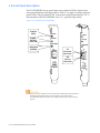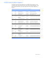
1
GE
Intelligent Platforms
Hardware Reference
PCI-5565PIORC*
Ultrahigh Speed Fiber-Optic Reflective Memory
with Interrupts
THE PCI-5565PIORC IS DESIGNED TO MEET THE EUROPEAN UNION (EU) RESTRICTION OF
HAZARDOUS SUBSTANCE (ROHS) DIRECTIVE (2002/95/EC) CURRENT REVISION.
Publication No: 500-9367855565-000 Rev. C
Document History
Hardware Reference Manual Document Number: 500-9367855565-000 Rev. C
March 30, 2010
Waste Electrical and Electronic Equipment (WEEE) Returns
GE is registered with an approved Producer Compliance Scheme (PCS) and, subject to suitable
contractual arrangements being in place, will ensure WEEE is processed in accordance with
the requirements of the WEEE Directive.
GE will evaluate requests to take back products purchased by our customers before
August 13, 2005 on a case by case basis. A WEEE management fee may apply.
Table of Contents
List of Figures . . . . . . . . . . . . . . . . . . . . . . . . . . . . . . . . . . . . . . . . . . . . . . . . . . . . . . . . . . . . . . . . . . . . . . . . . . . . . . . . . . 5
List of Tables . . . . . . . . . . . . . . . . . . . . . . . . . . . . . . . . . . . . . . . . . . . . . . . . . . . . . . . . . . . . . . . . . . . . . . . . . . . . . . . . . . . 6
Overview . . . . . . . . . . . . . . . . . . . . . . . . . . . . . . . . . . . . . . . . . . . . . . . . . . . . . . . . . . . . . . . . . . . . . . . . . . . . . . . . . . . . . . 8
1 • Handling and Installation . . . . . . . . . . . . . . . . . . . . . . . . . . . . . . . . . . . . . . . . . . . . . . . . . . . . . . . . . . . . . . . . . . . 17
1.1 Unpacking Procedures. . . . . . . . . . . . . . . . . . . . . . . . . . . . . . . . . . . . . . . . . . . . . . . . . . . . . . . . . . . . . . . . . . . . . . . . . .17
1.2 Handling Precaution. . . . . . . . . . . . . . . . . . . . . . . . . . . . . . . . . . . . . . . . . . . . . . . . . . . . . . . . . . . . . . . . . . . . . . . . . . . .17
1.3 Switch S1 and S2 Configuration. . . . . . . . . . . . . . . . . . . . . . . . . . . . . . . . . . . . . . . . . . . . . . . . . . . . . . . . . . . . . . . . . .18
1.3.1 Before Installation Switch S1 and S2 Configuration . . . . . . . . . . . . . . . . . . . . . . . . . . . . . . . . . . . . . . . . . .18
1.4 Physical Installation. . . . . . . . . . . . . . . . . . . . . . . . . . . . . . . . . . . . . . . . . . . . . . . . . . . . . . . . . . . . . . . . . . . . . . . . . . . . .21
1.5 Front Panel Description. . . . . . . . . . . . . . . . . . . . . . . . . . . . . . . . . . . . . . . . . . . . . . . . . . . . . . . . . . . . . . . . . . . . . . . . .22
1.5.1 LED Description . . . . . . . . . . . . . . . . . . . . . . . . . . . . . . . . . . . . . . . . . . . . . . . . . . . . . . . . . . . . . . . . . . . . . . . . . . .23
1.6 Cable Configuration. . . . . . . . . . . . . . . . . . . . . . . . . . . . . . . . . . . . . . . . . . . . . . . . . . . . . . . . . . . . . . . . . . . . . . . . . . . . .23
1.6.1 Connector Specification (Singlemode and Multimode): . . . . . . . . . . . . . . . . . . . . . . . . . . . . . . . . . . . . . . .23
2 • Theory of Operation . . . . . . . . . . . . . . . . . . . . . . . . . . . . . . . . . . . . . . . . . . . . . . . . . . . . . . . . . . . . . . . . . . . . . . . . 25
2.1
2.2
2.3
2.4
2.5
2.6
2.7
2.8
Basic Operation. . . . . . . . . . . . . . . . . . . . . . . . . . . . . . . . . . . . . . . . . . . . . . . . . . . . . . . . . . . . . . . . . . . . . . . . . . . . . . . . .25
Front Bezel LED Indicators. . . . . . . . . . . . . . . . . . . . . . . . . . . . . . . . . . . . . . . . . . . . . . . . . . . . . . . . . . . . . . . . . . . . . . .25
RFM-5565 Register Sets. . . . . . . . . . . . . . . . . . . . . . . . . . . . . . . . . . . . . . . . . . . . . . . . . . . . . . . . . . . . . . . . . . . . . . . . .26
Reflective Memory RAM. . . . . . . . . . . . . . . . . . . . . . . . . . . . . . . . . . . . . . . . . . . . . . . . . . . . . . . . . . . . . . . . . . . . . . . . .26
Interrupt Circuits. . . . . . . . . . . . . . . . . . . . . . . . . . . . . . . . . . . . . . . . . . . . . . . . . . . . . . . . . . . . . . . . . . . . . . . . . . . . . . . .27
Network Interrupts. . . . . . . . . . . . . . . . . . . . . . . . . . . . . . . . . . . . . . . . . . . . . . . . . . . . . . . . . . . . . . . . . . . . . . . . . . . . . .29
Redundant Transfer Mode of Operation. . . . . . . . . . . . . . . . . . . . . . . . . . . . . . . . . . . . . . . . . . . . . . . . . . . . . . . . . .29
Rogue Packet Removal Operation. . . . . . . . . . . . . . . . . . . . . . . . . . . . . . . . . . . . . . . . . . . . . . . . . . . . . . . . . . . . . . .30
3 • Programming . . . . . . . . . . . . . . . . . . . . . . . . . . . . . . . . . . . . . . . . . . . . . . . . . . . . . . . . . . . . . . . . . . . . . . . . . . . . . . 31
3.1 PCI Configuration Registers. . . . . . . . . . . . . . . . . . . . . . . . . . . . . . . . . . . . . . . . . . . . . . . . . . . . . . . . . . . . . . . . . . . . . .32
3.2 Local Configuration Registers. . . . . . . . . . . . . . . . . . . . . . . . . . . . . . . . . . . . . . . . . . . . . . . . . . . . . . . . . . . . . . . . . . . .41
3.3 RFM Control and Status Registers. . . . . . . . . . . . . . . . . . . . . . . . . . . . . . . . . . . . . . . . . . . . . . . . . . . . . . . . . . . . . . . .47
3.3.1 Board Revision Register . . . . . . . . . . . . . . . . . . . . . . . . . . . . . . . . . . . . . . . . . . . . . . . . . . . . . . . . . . . . . . . . . . . .48
3.3.2 Board ID Register . . . . . . . . . . . . . . . . . . . . . . . . . . . . . . . . . . . . . . . . . . . . . . . . . . . . . . . . . . . . . . . . . . . . . . . . . .48
3.3.3 Board Revision Build Register . . . . . . . . . . . . . . . . . . . . . . . . . . . . . . . . . . . . . . . . . . . . . . . . . . . . . . . . . . . . . .48
3.3.4 Node ID Register . . . . . . . . . . . . . . . . . . . . . . . . . . . . . . . . . . . . . . . . . . . . . . . . . . . . . . . . . . . . . . . . . . . . . . . . . .48
3.3.5 Local Control and Status Register 1 . . . . . . . . . . . . . . . . . . . . . . . . . . . . . . . . . . . . . . . . . . . . . . . . . . . . . . . . .48
3.3.6 Local Interrupt Control Registers . . . . . . . . . . . . . . . . . . . . . . . . . . . . . . . . . . . . . . . . . . . . . . . . . . . . . . . . . . .52
3.3.7 Network Target Data Register . . . . . . . . . . . . . . . . . . . . . . . . . . . . . . . . . . . . . . . . . . . . . . . . . . . . . . . . . . . . . .55
3.3.8 Network Target Node Register . . . . . . . . . . . . . . . . . . . . . . . . . . . . . . . . . . . . . . . . . . . . . . . . . . . . . . . . . . . . .55
3.3.9 Network Interrupt Command Register . . . . . . . . . . . . . . . . . . . . . . . . . . . . . . . . . . . . . . . . . . . . . . . . . . . . . .56
3.3.10 Interrupt 1 Sender Data FIFO . . . . . . . . . . . . . . . . . . . . . . . . . . . . . . . . . . . . . . . . . . . . . . . . . . . . . . . . . . . . . .56
3.3.11 Interrupt 1 Sender ID FIFO . . . . . . . . . . . . . . . . . . . . . . . . . . . . . . . . . . . . . . . . . . . . . . . . . . . . . . . . . . . . . . . .56
3.3.12 Interrupt 2 Sender Data FIFO . . . . . . . . . . . . . . . . . . . . . . . . . . . . . . . . . . . . . . . . . . . . . . . . . . . . . . . . . . . . . .57
3.3.13 Interrupt 2 Sender ID FIFO . . . . . . . . . . . . . . . . . . . . . . . . . . . . . . . . . . . . . . . . . . . . . . . . . . . . . . . . . . . . . . . .57
3.3.14 Interrupt 3 Sender Data FIFO . . . . . . . . . . . . . . . . . . . . . . . . . . . . . . . . . . . . . . . . . . . . . . . . . . . . . . . . . . . . . .57
3.3.15 Interrupt 3 Sender ID FIFO . . . . . . . . . . . . . . . . . . . . . . . . . . . . . . . . . . . . . . . . . . . . . . . . . . . . . . . . . . . . . . . .57
Table of Contents 3
3.4
3.5
3.6
3.7
3.3.16 Interrupt 4 Sender Data FIFO . . . . . . . . . . . . . . . . . . . . . . . . . . . . . . . . . . . . . . . . . . . . . . . . . . . . . . . . . . . . . .57
3.3.17 Interrupt 4 Sender ID FIFO . . . . . . . . . . . . . . . . . . . . . . . . . . . . . . . . . . . . . . . . . . . . . . . . . . . . . . . . . . . . . . . .57
Example of a Block DMA Operation for RFM-5565. . . . . . . . . . . . . . . . . . . . . . . . . . . . . . . . . . . . . . . . . . . . . . . .59
Example of a Scatter-Gather DMA Operation for RFM-5565. . . . . . . . . . . . . . . . . . . . . . . . . . . . . . . . . . . . . . .60
Example of a PCI PIO Sliding Window Operation for RFM-5565. . . . . . . . . . . . . . . . . . . . . . . . . . . . . . . . . . . .62
Example of Network Interrupt Handling. . . . . . . . . . . . . . . . . . . . . . . . . . . . . . . . . . . . . . . . . . . . . . . . . . . . . . . . . .64
3.7.1 Setup . . . . . . . . . . . . . . . . . . . . . . . . . . . . . . . . . . . . . . . . . . . . . . . . . . . . . . . . . . . . . . . . . . . . . . . . . . . . . . . . . . . . .64
3.7.2 Servicing Network Interrupts . . . . . . . . . . . . . . . . . . . . . . . . . . . . . . . . . . . . . . . . . . . . . . . . . . . . . . . . . . . . . . .64
Maintenance. . . . . . . . . . . . . . . . . . . . . . . . . . . . . . . . . . . . . . . . . . . . . . . . . . . . . . . . . . . . . . . . . . . . . . . . . . . . . . . . . . 65
Compliance Information . . . . . . . . . . . . . . . . . . . . . . . . . . . . . . . . . . . . . . . . . . . . . . . . . . . . . . . . . . . . . . . . . . . . . . . 66
4 PCI-5565PIORC Reflective Memory Board
List of Figures
Figure 1 Block Diagram of PCI-5565PIORC . . . . . . . . . . . . . . . . . . . . . . . . . . . . . . . . . . . . . . . . . . . . . . . . . . . . . . . . . . . . . . 11
Figure 2 Typical Reflective Memory Network . . . . . . . . . . . . . . . . . . . . . . . . . . . . . . . . . . . . . . . . . . . . . . . . . . . . . . . . . . . .12
Figure 1-1 S1 and S2 Location PCI-5565PIORC . . . . . . . . . . . . . . . . . . . . . . . . . . . . . . . . . . . . . . . . . . . . . . . . . . . . . . . . . . 20
Figure 1-2 Installing the PCI-5565PIORC . . . . . . . . . . . . . . . . . . . . . . . . . . . . . . . . . . . . . . . . . . . . . . . . . . . . . . . . . . . . . . . . .21
Figure 1-3 Front Panel of PCI-5565PIORC . . . . . . . . . . . . . . . . . . . . . . . . . . . . . . . . . . . . . . . . . . . . . . . . . . . . . . . . . . . . . . . .22
Figure 1-4 LC Type Fiber-Optic Cable Connector . . . . . . . . . . . . . . . . . . . . . . . . . . . . . . . . . . . . . . . . . . . . . . . . . . . . . . . .24
Figure 1-5 Example: Six Node Ring Connectivity PCI-5565PIORC . . . . . . . . . . . . . . . . . . . . . . . . . . . . . . . . . . . . . . . . . .24
Figure 2-1 Interrupt Circuitry Block Diagram . . . . . . . . . . . . . . . . . . . . . . . . . . . . . . . . . . . . . . . . . . . . . . . . . . . . . . . . . . . . .28
Figure 3-1 Block Diagram of the Network Interrupt Reception Circuitry . . . . . . . . . . . . . . . . . . . . . . . . . . . . . . . . . . .58
List of Figures 5
.
List of Tables
Table 1-1 Example Node ID Switch S2 RFM-5565 . . . . . . . . . . . . . . . . . . . . . . . . . . . . . . . . . . . . . . . . . . . . . . . . . . . . . . . . .19
Table 1-2 Switch S1 Configuration RFM-5565 . . . . . . . . . . . . . . . . . . . . . . . . . . . . . . . . . . . . . . . . . . . . . . . . . . . . . . . . . . . .19
Table 1-3 LED Descriptions . . . . . . . . . . . . . . . . . . . . . . . . . . . . . . . . . . . . . . . . . . . . . . . . . . . . . . . . . . . . . . . . . . . . . . . . . . . . .23
Table 1-4 Cable Specifications for Multimode and Singlemode . . . . . . . . . . . . . . . . . . . . . . . . . . . . . . . . . . . . . . . . . . . .23
Table 3-1 PCI Configuration Registers . . . . . . . . . . . . . . . . . . . . . . . . . . . . . . . . . . . . . . . . . . . . . . . . . . . . . . . . . . . . . . . . . . .32
Table 3-2 PCI Configuration ID Registers . . . . . . . . . . . . . . . . . . . . . . . . . . . . . . . . . . . . . . . . . . . . . . . . . . . . . . . . . . . . . . . . .32
Table 3-3 PCI Command Register . . . . . . . . . . . . . . . . . . . . . . . . . . . . . . . . . . . . . . . . . . . . . . . . . . . . . . . . . . . . . . . . . . . . . . .33
Table 3-4 PCI Status Register . . . . . . . . . . . . . . . . . . . . . . . . . . . . . . . . . . . . . . . . . . . . . . . . . . . . . . . . . . . . . . . . . . . . . . . . . . .34
Table 3-5 PCI Revision ID Register . . . . . . . . . . . . . . . . . . . . . . . . . . . . . . . . . . . . . . . . . . . . . . . . . . . . . . . . . . . . . . . . . . . . . . .34
Table 3-6 PCI Class Code Register . . . . . . . . . . . . . . . . . . . . . . . . . . . . . . . . . . . . . . . . . . . . . . . . . . . . . . . . . . . . . . . . . . . . . . .35
Table 3-7 PCI Cache Line Size Register . . . . . . . . . . . . . . . . . . . . . . . . . . . . . . . . . . . . . . . . . . . . . . . . . . . . . . . . . . . . . . . . . . .35
Table 3-8 PCI Latency Timer Register . . . . . . . . . . . . . . . . . . . . . . . . . . . . . . . . . . . . . . . . . . . . . . . . . . . . . . . . . . . . . . . . . . . .35
Table 3-9 PCI Header Type Register . . . . . . . . . . . . . . . . . . . . . . . . . . . . . . . . . . . . . . . . . . . . . . . . . . . . . . . . . . . . . . . . . . . . .35
Table 3-10 PCI Built-in Self Test Register . . . . . . . . . . . . . . . . . . . . . . . . . . . . . . . . . . . . . . . . . . . . . . . . . . . . . . . . . . . . . . . . .36
Table 3-11 PCI Base Address Register 0 for Access to Local Configuration Registers . . . . . . . . . . . . . . . . . . . . . . .36
Table 3-12 PCI Base Address Register 1 for Access to Local Configuration Registers . . . . . . . . . . . . . . . . . . . . . . .37
Table 3-13 PCI Base Address Register 2 for Access to RFM Control and Status Registers . . . . . . . . . . . . . . . . . . .37
Table 3-14 PCI Base Address Register 3 for Access to Reflective Memory . . . . . . . . . . . . . . . . . . . . . . . . . . . . . . . . . .38
Table 3-15 PCI Base Address Register 4 . . . . . . . . . . . . . . . . . . . . . . . . . . . . . . . . . . . . . . . . . . . . . . . . . . . . . . . . . . . . . . . . .38
Table 3-16 PCI Base Address Register 5 . . . . . . . . . . . . . . . . . . . . . . . . . . . . . . . . . . . . . . . . . . . . . . . . . . . . . . . . . . . . . . . . .39
Table 3-17 PCI Cardbus CIS Pointer Register . . . . . . . . . . . . . . . . . . . . . . . . . . . . . . . . . . . . . . . . . . . . . . . . . . . . . . . . . . . . .39
Table 3-18 PCI Subsystem Vendor ID Register . . . . . . . . . . . . . . . . . . . . . . . . . . . . . . . . . . . . . . . . . . . . . . . . . . . . . . . . . . .39
Table 3-19 PCI Subsystem ID Register . . . . . . . . . . . . . . . . . . . . . . . . . . . . . . . . . . . . . . . . . . . . . . . . . . . . . . . . . . . . . . . . . . .39
Table 3-20 PCI Expansion ROM Base Register . . . . . . . . . . . . . . . . . . . . . . . . . . . . . . . . . . . . . . . . . . . . . . . . . . . . . . . . . . . .39
Table 3-21 PCI Capability Pointer Register . . . . . . . . . . . . . . . . . . . . . . . . . . . . . . . . . . . . . . . . . . . . . . . . . . . . . . . . . . . . . . .40
Table 3-22 PCI Interrupt Line . . . . . . . . . . . . . . . . . . . . . . . . . . . . . . . . . . . . . . . . . . . . . . . . . . . . . . . . . . . . . . . . . . . . . . . . . . . .40
Table 3-23 PCI Interrupt Pin . . . . . . . . . . . . . . . . . . . . . . . . . . . . . . . . . . . . . . . . . . . . . . . . . . . . . . . . . . . . . . . . . . . . . . . . . . . . .40
Table 3-24 PCI Min_Gnt . . . . . . . . . . . . . . . . . . . . . . . . . . . . . . . . . . . . . . . . . . . . . . . . . . . . . . . . . . . . . . . . . . . . . . . . . . . . . . . . .40
Table 3-25 PCI Max_Lat . . . . . . . . . . . . . . . . . . . . . . . . . . . . . . . . . . . . . . . . . . . . . . . . . . . . . . . . . . . . . . . . . . . . . . . . . . . . . . . . .40
Table 3-26 Local Configuration and DMA Control Registers . . . . . . . . . . . . . . . . . . . . . . . . . . . . . . . . . . . . . . . . . . . . . . .41
Table 3-27 Mode/DMA Arbitration Register . . . . . . . . . . . . . . . . . . . . . . . . . . . . . . . . . . . . . . . . . . . . . . . . . . . . . . . . . . . . . .42
Table 3-28 Big/Little Endian Descriptor Register . . . . . . . . . . . . . . . . . . . . . . . . . . . . . . . . . . . . . . . . . . . . . . . . . . . . . . . . . .42
Table 3-29 Interrupt Control and Status Register . . . . . . . . . . . . . . . . . . . . . . . . . . . . . . . . . . . . . . . . . . . . . . . . . . . . . . . . .43
Table 3-30 INTCSR Interrupt Enables . . . . . . . . . . . . . . . . . . . . . . . . . . . . . . . . . . . . . . . . . . . . . . . . . . . . . . . . . . . . . . . . . . . .43
Table 3-31 INTCSR Interrupt Status . . . . . . . . . . . . . . . . . . . . . . . . . . . . . . . . . . . . . . . . . . . . . . . . . . . . . . . . . . . . . . . . . . . . . .43
Table 3-32 PCI Core/Features Revision ID . . . . . . . . . . . . . . . . . . . . . . . . . . . . . . . . . . . . . . . . . . . . . . . . . . . . . . . . . . . . . . . .44
Table 3-33 DMA Channel 0 Mode Register . . . . . . . . . . . . . . . . . . . . . . . . . . . . . . . . . . . . . . . . . . . . . . . . . . . . . . . . . . . . . . .44
Table 3-34 DMA Channel 0 PCI Address Register . . . . . . . . . . . . . . . . . . . . . . . . . . . . . . . . . . . . . . . . . . . . . . . . . . . . . . . . .44
Table 3-35 DMA Channel 0 Local Address Register . . . . . . . . . . . . . . . . . . . . . . . . . . . . . . . . . . . . . . . . . . . . . . . . . . . . . . .44
Table 3-36 DMA Channel 0 Transfer Size (Bytes) Register . . . . . . . . . . . . . . . . . . . . . . . . . . . . . . . . . . . . . . . . . . . . . . . . .45
6 PCI-5565PIORC Reflective Memory Board
Table 3-37 DMA Channel 0 Descriptor Pointer Register . . . . . . . . . . . . . . . . . . . . . . . . . . . . . . . . . . . . . . . . . . . . . . . . . . .45
Table 3-38 DMA Channel 0 Command/Status Register . . . . . . . . . . . . . . . . . . . . . . . . . . . . . . . . . . . . . . . . . . . . . . . . . . .45
Table 3-39 DMA Channel 0 PCI Dual Address Cycles Upper Address . . . . . . . . . . . . . . . . . . . . . . . . . . . . . . . . . . . . . . .46
Table 3-40 PCI PIO Direct Slave Local Address Range . . . . . . . . . . . . . . . . . . . . . . . . . . . . . . . . . . . . . . . . . . . . . . . . . . . .46
Table 3-41 PCI PIO Direct Slave Local Base Address (Remap) . . . . . . . . . . . . . . . . . . . . . . . . . . . . . . . . . . . . . . . . . . . . .46
Table 3-42 Memory Map of the Local Control and Status Registers . . . . . . . . . . . . . . . . . . . . . . . . . . . . . . . . . . . . . . .47
Table 3-43 Local Control and Status Register 1 . . . . . . . . . . . . . . . . . . . . . . . . . . . . . . . . . . . . . . . . . . . . . . . . . . . . . . . . . .48
Table 3-44 Local Interrupt Status Register . . . . . . . . . . . . . . . . . . . . . . . . . . . . . . . . . . . . . . . . . . . . . . . . . . . . . . . . . . . . . . .52
Table 3-45 Local Interrupt Enable Register . . . . . . . . . . . . . . . . . . . . . . . . . . . . . . . . . . . . . . . . . . . . . . . . . . . . . . . . . . . . . .55
Table 3-46 Network Interrupt Command Register . . . . . . . . . . . . . . . . . . . . . . . . . . . . . . . . . . . . . . . . . . . . . . . . . . . . . . . .56
List of Tables 7
Overview
The PCI‐5565PIORC* is the PCI‐based member of GE’s family of Reflective Memory real‐time fiber‐optic network products. Two or more PCI‐5565PIORCs, along with other members of this family, can be integrated into a network using standard fiber‐optic cables. Each board in the network is referred to as a “node.”
Reflective Memory allows computers, workstations, PLCs and other embedded controllers with different architectures and dissimilar operating systems to share data in real‐time. The 5565 family of Reflective Memory (referred to as RFM‐5565 in this manual) is fast, flexible and easy to operate. Data is transferred by writing to memory (SDRAM), which appears to reside globally in all boards on the network. Onboard circuitry automatically performs the data transfer to all other nodes with little or no involvement of any host processor. A block diagram of the PCI‐5565PIORC is shown in Figure 1 on page 11.
8 PCI-5565PIORC Reflective Memory Board
Features
Features include: • High speed, easy to use fiber‐optic network (2.12 GBaud serially)
• 33 MHz 64‐bit/32‐bit compatible PCI bus, 3.3 V or 5.0 V logic level
• 66 MHz 64‐bit/32‐bit compatible PCI bus, 3.3 V logic level
• No host processor involvement in the operation of the network
• Selectable Redundant Mode of Operation
• Up to 256 nodes
• Connectivity with multimode fiber up to 300 m, singlemode fiber up to
10 km
• Dynamic packet size, 4 to 64 bytes of data per packet
• Fiber network transfer rate 43 MByte/s to 170 MByte/s
• 128/256 MBytes SDRAM Reflective Memory with selectable parity
• Independent Direct Memory Access (DMA) channel
• Four general purpose network interrupts; each with 32 bits of data
• Configurable endian conversion for multiple CPU architectures on the same network
• Selectable PCI PIO window size from 2 MByte to 64 MByte to full installed memory size
• Operating System support: Windows® 2000, Windows XP, Linux® and VxWorks®
• RoHS Compliant
PCI Local Bus Compliance
The PCI‐5565PIORC complies with requirements of the PCI Local Bus Specification, version 2.2.
Vendor and Device Identification
The PCI Configuration register reserved for the vendor ID has the value of $114A, which designates GE. The PCI Configuration register reserved for the device ID has the value of $5565, which is GE’s board type.
Subsystem Vendor ID and Subsystem ID
The PCI Configuration register reserved for the subsystem vendor ID has the value of $1556, which designates PLD applications. The PCI Configuration register reserved for the subsystem ID has the value of $0080, which is the PLD Applications PCI‐X core identification number.
Overview 9
Comparison of the PCI-5565PIORC and the VMIPCI-5565*
The classic VMIPCI‐5565* contains several components which have been combined into a single FPGA (Field Programmable Gate Array) in the PCI‐5565PIORC. The components that were combined include a PCI interface device by PLX Technologies, three separate smaller FPGAs, a transmit FIFO, and a receive FIFO. The PCI‐5565PIORC adds greater design flexibility and improved performance over the classic VMIPCI‐5565 in at least three areas. 1. The PCI‐5565PIORC’s DMA burst and PIO single read access rates have an improvement over the classic VMIPCI‐5565.
2. The PCI‐5565PIORC’s access bandwidth for the onboard SDRAM memory has doubled, improving the overall throughput.
3. The PCI‐5565PIORC is field upgradeable as new features are added.
The classic VMIPCI‐5565 contained a group of control registers within the PLX device as well as a separate group of RFM specific control registers located in an FPGA. Because the two registers groups physically reside in separate devices, they are accessed through different regions of memory. The PCI‐5565PIORC, on the other hand, contains both groups of registers within the same FPGA. The two groups could have been combined. However to provide software continuity and backward compatibility, the two register groups have been maintained separately as in the classic VMIPCI‐5565. Further, the individual bit functions within the registers, where applicable, are still compatible.
The PCI‐5565PIORC does not include a second DMA engine.
10 PCI-5565PIORC Reflective Memory Board
Block Diagram
Figure 1 Block Diagram of PCI-5565PIORC
Fiber-Optic Network
Optics
2.125 GHz
SERDES
16-bit
106.25 MHz
Rx
Tx
FIFO
FIFO
32-bit Data
Memory
Main FPGA
4-bit Parity
133 MHz
PCI Core
32/64-bit at 33/66 MHz
PCI bus
Overview 11
Figure 2 Typical Reflective Memory Network
VMIVME-5565
VM
IV
5565ME
PCI-5565PIORC
NODE 0
PCI WorkStation
with
PCI-5565PIORC
VMEbus Chassis
with
VMIVME-5565
PMC-5565PIORC
VMEbus Chassis
with
PMC-5565PIORC
Up to 300m
between nodes
for multimode
Up to 10km
between nodes
for single mode
12 PCI-5565PIORC Reflective Memory Board
NODE 255
NODE 1
References
Refer to PCI Local Bus Specification for a detailed explanation of the PCI Local bus from the following source:
PCI Local Bus Specification, Rev. 2.2
PCI Special Interest Group
P.O. Box 14070
Portland, OR 97214
(800) 433‐5177 (U.S.)
(503) 797‐4207 (International)
(503) 234‐6762 (FAX)
For information on PLD Applications’ PCI‐X IP Core, contact them at:
United States
PLD Applications, Inc.
2570 North First St. 2nd floor
San Jose, CA 95131‐1036
(408) 273 4530 or (866) 513 0362
Fax: (408) 273 4555
France (Corporate Headquarters)
PLD Applications
Europarc Pichaury A2 ‐ 1330, rue Guillibert
13856 Aix‐en‐Provence Cedex 3 ‐ France
Tel: +33 442 393 600
Fax: +33 442 394 902
Overview 13
Organization
This manual is composed of the following chapters:
Overview provides a general description of the PCI‐5565PIORC, and General Safety terms and symbols.
Chapter 1 Handling and Installation describes unpacking and installation of the hardware.
Chapter 2 Theory of Operation describes the product’s features and functionality.
Chapter 3 Programming describes PCI Configuration Registers and other registers for programming and installation.
Maintenance provides GE’s contact information relative to the care and maintenance of the unit.
Compliance provides the applicable information regarding regulatory compliance.
14 PCI-5565PIORC Reflective Memory Board
Safety Summary
The following general safety precautions must be observed during all phases of the operation, service and repair of this product. Failure to comply with these precautions or with specific warnings elsewhere in this manual violates safety standards of the design, manufacture, and intended use of this product. GE assumes no liability for the customerʹs failure to comply with these requirements.
Ground the
System
To minimize shock hazard, the chassis and system cabinet must be connected to an electrical ground. A three‐conductor AC power cable should be used. The power cable must either be plugged into an approved three‐contact electrical outlet or used with a three‐contact to two‐contact adapter with the grounding wire (green) firmly connected to an electrical ground (safety ground) at the power outlet.
Do Not Operate in
an Explosive
Atmosphere
Do not operate the system in the presence of flammable gases or fumes. Operation of any electrical system in such an environment constitutes a definite safety hazard.
Keep Away from
Live Circuits
Operating personnel must not remove product covers. Component replacement and internal adjustments must be made by qualified maintenance personnel. Do not replace components with power cable connected. Under certain conditions, dangerous voltages may exist even with the power cable removed. To avoid injuries, always disconnect power and discharge circuits before touching them.
Do Not Service or
Adjust Alone
Do not attempt internal service or adjustment unless another person capable of rendering first aid and resuscitation is present.
Do Not Substitute
Parts or Modify
System
Because of the danger of introducing additional hazards, do not install substitute parts or perform any unauthorized modification to the product. Return the product to GE for service and repair to ensure that safety features are maintained.
Dangerous
Procedure
Warnings
Warnings, such as the example below, precede only potentially dangerous procedures throughout this manual. Instructions contained in the warnings must be followed.
WARNING
Dangerous voltages, capable of causing death, are present in this system.
Use extreme caution when handling, testing and adjusting.
Overview 15
Warnings,
Cautions
and Notes
WARNING
WARNING denotes a hazard. It calls attention to a procedure, practice, or
condition, which, if not correctly performed or adhered to, could result in
injury or death to personnel.
CAUTION
CAUTION denotes a hazard. It calls attention to an operating procedure,
practice, or condition, which, if not correctly performed or adhered to, could
result in damage to or destruction of part or all of the system.
NOTE
NOTE denotes important information. It calls attention to a procedure, practice, or condition which
is essential to highlight.
TIP
Tip denotes a bit of expert information.
LINK
This is link text .
16 PCI-5565PIORC Reflective Memory Board
1 • Handling and Installation
This chapter describes the installation and configuration of the board. Cable configuration and board layout are illustrated in this chapter.
1.1 Unpacking Procedures
Any precautions found in the shipping container should be observed. All items should be carefully unpacked and thoroughly inspected for damage that might have occurred during shipment. The board(s) should be checked for broken components, damaged printed circuit board(s), heat damage and other visible contamination. All claims arising from shipping damage should be filed with the carrier and a complete report sent to GE Customer Care. 1.2 Handling Precaution
Some of the components assembled on GE’s products may be sensitive to electrostatic discharge and damage may occur on boards that are subjected to a high‐energy electrostatic field. When the board is placed on a bench for configuring, etc., it is suggested that conductive material should be placed under the board to provide a conductive shunt. Unused boards should be stored in the same protective boxes in which they were shipped.
Handling and Installation 17
1.3 Switch S1 and S2 Configuration
Prior to installing the RFM‐5565 in a host system, the desired node ID must be set using switch S2. Each node in the network must have a unique node ID. See Figure 1‐1 on page 20 for the location of switch S2. Switch S2 corresponds to 8 node ID select signal lines. The 8 node ID select lines permit any binary node ID from 0 to $FF (255 decimal). Switch S2 position 1 corresponds to the least significant node ID line and switch S2 position 8 corresponds to the most significant node ID line. Placing switch S2 in the OFF position sets the binary node ID line low (0), while placing switch S2 in the ON position sets the binary node ID line high (1). Table 1‐1 on page 19 provides examples of possible node IDs.
1.3.1 Before Installation Switch S1 and S2 Configuration
NOTE
ALL nodes on the ring MUST be configured for the SAME transfer mode: either redundant or nonredundant transfer mode. A mismatch of this setting will result in certain packets being removed
from the ring, and that data will be lost.
NOTE
No more than one node on the ring should be configured with Rogue Master 0 enabled. Certain
packets will be removed from the ring when two or more nodes are configured with Rogue
Master 0 enabled, and that data will be lost.
NOTE
No more than one node on the ring should be configured with Rogue Master 1 enabled. Certain
packets will be removed from the ring when two or more nodes are configured with Rogue
Master 1 enabled, and that data will be lost.
Prior to installing the RFM‐5565 in the host system, switch S1 must be configured for the appropriate mode of operation. Switch S1 controls six functions on the board. Settings on Switch S1 should only be changed while power is off.
1. S1 position 1 selects the non‐redundant (OFF position) or redundant net‐
work transfer modes.
2. S1 position 2 selects between the low network usage (ON position) of the classic 5565 boards or the higher performance achievable on this board (OFF position).
3. S1 positions 3 and 4 select the PCI window size for PIO memory accesses. The default (when both switch positions 3 and 4 are OFF) is to use the full installed memory size. The reduced memory window size choices are 64 MByte, 16 MByte or 2 MByte.
4. S1 position 5 enables (ON position) or disables the Rogue Master 0 function.
5. S1 position 6 enables (ON position) or disables the Rogue Master 1 function.
6. S1 position 8 selects between the factory default control logic (ON position) or the most recent control logic flashed to the board (OFF position).
S1 position 7 is currently reserved and should not be used (left in the OFF position).
18 PCI-5565PIORC Reflective Memory Board
.
NOTE
S1 position 8 should be set in the ON position only when a flash update of the control logic has
failed. After a successful flash update of the control logic, S1 position 8 should be set in the OFF
position.
Table 1-1 Example Node ID Switch S2 RFM-5565
S2
Position 8
S2
Position 7
S2
Position 6
S2
Position 5
S2
Position 4
ON
ON
ON
OFF
OFF
S2
Position 3
S2
Position 2
S2
Position 1
Node ID
Hex (Dec.)
ON
ON
OFF
OFF
ON
ON
ON
ON
$FF (255)
OFF
OFF
OFF
OFF
ON
OFF
OFF
$80 (128)
OFF
OFF
OFF
OFF
$40 (64)
OFF
OFF
ON
OFF
OFF
OFF
OFF
OFF
$20 (32)
OFF
OFF
OFF
ON
OFF
OFF
OFF
OFF
$10 (16)
OFF
OFF
OFF
OFF
ON
OFF
OFF
OFF
$8 (8)
OFF
OFF
OFF
OFF
OFF
ON
OFF
OFF
$4 (4)
OFF
OFF
OFF
OFF
OFF
OFF
ON
OFF
$2 (2)
OFF
OFF
OFF
OFF
OFF
OFF
OFF
ON
$1 (1)
OFF
OFF
OFF
OFF
OFF
OFF
OFF
OFF
$0 (0)
Factory Default: S2 positions 1 through 8 OFF
Table 1-2 Switch S1 Configuration RFM-5565
Position 1 OFF (non-redundant mode)
Position 1 ON (redundant mode)
Position 2 OFF (higher performance achievable)
Position 2 ON (low network usage)
Position 5 OFF (disables Rogue Master 0)
Position 5 ON (enables Rogue Master 0)
Position 6 OFF (disables Rogue Master 1)
Position 6 ON (enables Rogue Master 1)
Position 8 OFF (most recent control logic)
Factory Defaults
Position 8 ON (original factory control logic) Positions 1-8 OFF
PCI Window Size
S1 Position 3
S1 Position 4
Default
Off
Off
64 MByte
On
Off
16 MByte
Off
On
2 MByte
On
On
Handling and Installation 19
Figure 1-1 S1 and S2 Location PCI-5565PIORC
20 PCI-5565PIORC Reflective Memory Board
.
1.4 Physical Installation
CAUTION
Do not install or remove the board while power is applied.
Host PCI compatible sites vary widely in appearance and board installation procedures. GE recommends examining the host system installation procedures prior to installing this board. The following procedure outlines the installation of the PCI‐5565PIORC onto a suitable motherboard with an available PCI connector.
1. Open the system chassis. Ensure that the node ID has been set prior to instal‐
lation. Also setup the board for the desired mode of operation. See Section Switch S1 and S2 Configuration on page 18.
2. Install the PCI‐5565PIORC firmly into the PCI connectors (refer to Figure 1‐2 on page 21 for installation of the PCI‐5565PIORC). Install the screw to secure the PCI‐5565PIORC to the chassis.
3. Close the system chassis, apply power.
Figure 1-2 Installing the PCI-5565PIORC
PCI-5565PIORC
PCI-5565PIORC
STATUS
SIG. DET
OWN DAT
A
TX
RX
VMIC
VMIPC
I
5565
Side View
115
Isometric View
NOTE
The PCI-5565PIORC is designed to interface with any suitable PCI compliant motherboard using a
direct PCI bus interface, compliant with V2.2 of the PCI signalling specification as defined by IEEE
P1386.1 Draft 2.0.
Handling and Installation 21
1.5 Front Panel Description
The PCI‐5565PIORC has an optical transceiver and three LEDs located on the front panel illustrated in the figure below. Table 1‐3 on page 23 outlines the front panel’s LEDs. The port labeled “RX” is the receiver and the port labeled “TX” is the transmitter. The PCI‐5565PIORC uses “LC” type fiber‐optic cables.
Figure 1-3 Front Panel of PCI-5565PIORC
STATUS
(RED)
SIGNAL
DETECT
(YELLOW)
STATUS
STATU
S
SIG. DET
SIG. DE
T
OWN DATA
OWN DATA
(GREEN)
TX
RX
PCI
5565
PIORC
CAUTION
OWN D
ATA
"TX"
Transmitter
Connection
"RX"
Receiver
Connection
When fiber-optic cables are not connected, the supplied dust caps need to be
installed to keep dust and dirt out of the optics. Do not power up the
PCI-5565PIORC without the fiber-optic cables installed. This could cause eye
injuries.
22 PCI-5565PIORC Reflective Memory Board
.
TX
RX
PCI
5565
PIOR
C
1.5.1 LED Description
Table 1-3 LED Descriptions
LED
Color
Description
Status
Red
User defined board status indicator.
Signal Detect
Yellow
Indicates optical network connection.
Own Data
Green
Indicates when own data is received.
The status LED’s power up default state is ON. The status LED is a user defined board indicator and can be toggled ON or OFF by writing to Bit 31 of the Control and Status register. The signal detect LED turns ON if the receiver detects light and can be used as a simple method of checking that the optical network is properly connected to the receiver. The Own Data LED is turned ON when the board detects its own data returning over the network. The default setting is OFF.
1.6 Cable Configuration
The RFM‐5565 is available with a multimode or singlemode fiber‐optic interface. Figure 1‐4 on page 24 is an illustration of the “LC” type multimode or singlemode fiber‐optic connector. Table 1-4 Cable Specifications for Multimode and Singlemode
Specification
Singlemode
Multimode
Core Diameter
8.3 ±1 μM
62.5 ±3 μM
Cladding Diameter
125 ±2
μM
125 ±2 μM
Jacket Outer Diameter
3.0 mm ±.1 mm
3.0 mm ±.1 mm
Attenuation
0.8 dB/Km (max) at 1310nm
4.0 dB/Km (max) at 850nm
Bandwidth
N/A
160 to 300 MHz-Km (min) at 850 nm
UL
Type OFNR, CSA type OFN FT4
Type OFNR, CSA type OFN FT4
1.6.1 Connector Specification (Singlemode and Multimode):
• Compatible with LC standard and JIS C 5973 compliant
• Ceramic ferrule
• Temperature range: ‐20° C to +85° C
Handling and Installation 23
Figure 1-4 LC Type Fiber-Optic Cable Connector
0.84 (21.23)
(4.5mm)
0.49
(1.25)
Dimensions: inches (mm)
Figure 1-5 Example: Six Node Ring Connectivity PCI-5565PIORC
Node 1
Node 3
STATUS
STATUS
STATUS
SIG. DE
SIG. DE
SIG. DE
T
OWN DA
TA
T
OWN DA
TA
TX
TX
RX
Node 6
T
OWN DA
TA
TX
RX
RX
PCI
5565
PIOR
C
PCI
5565
PIOR
C
Node 5
PCI
5565
PIOR
C
Node 4
STATUS
STATUS
STATUS
SIG. DE
SIG. DE
SIG. DE
T
OWN DA
TA
TX
RX
PCI
5565
PIOR
C
24 PCI-5565PIORC Reflective Memory Board
.
Node 2
T
OWN DA
TA
TX
RX
PCI
5565
PIOR
C
T
OWN DA
TA
TX
RX
PCI
5565
PIOR
C
2 • Theory of Operation
The following sections describe the functionality of the RFM‐5565 Reflective Memory board. A description of the major sub‐circuits and their operation is included. This section will also occasionally mention Control and Status registers related to operations. To see a detailed description of these Control and Status registers please refer to Chapter 3, Programming‚ on page 31 of this manual.
2.1 Basic Operation
Each RFM‐5565 node (any 5565 Reflective Memory board) in the network is interconnected using fiber‐optic cables in a daisy chain loop. The transmitter of the first board must be connected to the receiver of the second board. The transmitter of the second board is connected to the receiver of the third, and so on, until the loop is completed back at the receiver of the first board. Alternatively, any node can be connected to the ring network using one or more ACC‐5595* Reflective Memory Hubs. It is important that the ring network be complete (i.e., every receiver and transmitter must be connected). The RFM‐5565 will not transmit packets if the receiver does not detect a signal or it has lost synchronization (e.g., the cable is damaged). Each node must have a unique node ID, which is set using switch S2 (i.e. no two nodes should have the same node ID). The order of the node IDs is unimportant.
A transfer of data over the network is initiated by a write to onboard SDRAM from the host system. The write can be as simple as a PIO target write, or it can be due to a DMA cycle by the resident DMA engine. While the write to the SDRAM is occurring, circuitry on the RFM‐5565 automatically writes the data and other pertinent information into the transmit FIFO. From the transmit FIFO, the transmit circuit retrieves the data and puts it into a variable length packet of 4 to 64 bytes that is transmitted over the fiber‐optic interface to the receiver of the next board.
The receiver then checks the packet for errors. When the error free data is received, the receive circuit opens the packet and stores the data in the board’s receive FIFO. From the receive FIFO, another circuit writes the data into the local onboard SDRAM at the same relative location in memory as the originating node. This circuit also simultaneously routes the data into the board’s own transmit FIFO. From there, the process is repeated until the data returns to the receiver of the originating node. At the originating node, the data packet is removed from the network. 2.2 Front Bezel LED Indicators
The RFM‐5565 has three LED indicators located on the bezel. The top red LED is a status indicator; its power up default state is ON. The status LED may be toggled OFF or ON by writing to Bit 31 of the LCSR1 register, which indicates a user defined board status. The middle yellow LED is the signal detect indicator. The signal detect LED turns ON if the receiver detects light. It can be used as a simple method of checking that the optical network is properly connected to the receiver. The bottom green LED is the OWN DATA indicator. When a board detects its own data returning on the network, it turns this LED ON.
Theory of Operation 25
2.3 RFM-5565 Register Sets
To go beyond the simple target read and write operation of the board, the user must understand and manipulate bits within three register sets. The three register sets are referred to as:
• PCI Configuration Registers
• Local Configuration Registers
• RFM Control and Status Registers
PCI Configuration Registers – This set of registers is predefined by the PCI Local Bus Specification and is standard for all PCI and PCI Express devices. This register set contains the Vendor ID, Device ID, Subsystem Vendor ID and Base Address registers. The PCI Configuration Registers are first initialized and then modified as needed by the PCI bus system BIOS. The register set is rarely altered by the user, but the ability to read these registers, particularly the Base Address Registers, will be necessary to locate the other two sets of registers.
Local Configuration Registers – Base Address Register 0 has the starting address for register memory space accesses and Base Address Register 1 has the starting address for register IO space accesses. Some Local Configuration Registers pertinent to the RFM‐5565’s operation include the Interrupt Control and Status Register (INTCSR) and the DMA Control Registers. RFM Control and Status Registers – The RFM Control and Status Registers implement the functions unique to the RFM‐5565 Reflective Memory board. These functions include RFM operation status, detailed control of the RFM sources for the PCI interrupt, and network interrupt access. These registers are accessed at locations offset from the address contained in Base Address Register 2.
2.4 Reflective Memory RAM
This board is available with 128 or 256 MByte of onboard Reflective Memory SDRAM. The SDRAM starts at the location specified in Base Address Register 3. Unlike the previous versions of Reflective Memory products, the RFM Control and Status Registers do NOT replace the first $40 locations of RAM. The offset address range is $0 to $7FFFFFF for the 128 MByte and $0 to $FFFFFFF for the 256 MByte option. 26 PCI-5565PIORC Reflective Memory Board
2.5 Interrupt Circuits
The RFM‐5565 has a single interrupt output (INTA#). One or more events on the RFM‐5565 board can cause the interrupt. The sources of the interrupt can be individually enabled and monitored through several registers.
The interrupt circuitry of the RFM‐5565 is arranged in two tiers. The primary tier of interrupts is enabled and monitored by the Local Configuration Register’s INTCSR at offset $68. The sources for monitoring the primary tier interrupts include:
1. DMA Ch 0 Done
2. Local Interrupt Input (LINTi#) The primary tier interrupt source (1) is used during DMA cycles and must be configured in the DMA registers.
The other primary tier interrupt source (2) is the Local Interrupt Input (LINTi#). All secondary tier interrupts are funneled through the LINTi#. Second tier interrupts include several operational status bits, faults, and network interrupts. The second tier interrupts are selected and monitored through the two RFM Control and Status Registers referred to as the Local Interrupt Status Register (LISR) and the Local Interrupt Enable Register (LIER). For a detailed description of these two registers refer to Chapter 3, Programming‚ on page 31. A block diagram of the main interrupt circuitry is shown in Figure 2‐1 on page 28.
Theory of Operation 27
Figure 2-1 Interrupt Circuitry Block Diagram
Network
Receiver
Circuitry
RFM Control and Status Registers
(per Base Address Register 2)
Network
Interrupt FIFO's
RFM
Fault/Status
Events
4
Local Interrupt Enable Register (LIER)
(Offset $14)
Local Interrupt Status Register (LISR)
(Offset $10)
Second Tier Interrupts
+
LINT#
RFM Control and Status Registers
(per Base Address Register 0 or 1)
DMA 0 Done
Bits 11 and 15
Bits 18 and 21
Interrupt Control and Status Register (INTCSR)
(Offset $68)
Primary Tier Interrupts
Host Interrupt (INTA#)
28 PCI-5565PIORC Reflective Memory Board
2.6 Network Interrupts
The RFM‐5565 is capable of passing interrupt packets, as well as data packets, over the network. The network interrupt packets can be directed to a specific node or broadcast globally to all nodes on the network. Each network interrupt packet contains the sender’s node ID, the destination node ID, the interrupt type and 32 bits of user defined data.
The types of network interrupts include four general purpose interrupts and a reset node request interrupt. Node specific interrupts are sent by configuring three RFM Control and Status registers. Each receiving node evaluates the interrupt packets as they pass through. If a general purpose interrupt is directed to that node, then the sender’s node ID is stored in the appropriate Sender ID FIFO (one of four). Each Sender ID FIFO is 127 locations deep. The accompanying data will be stored in a companion 127 locations deep data FIFO.
If enabled through the LISR, LIER and INTCSR registers, any of the network interrupts can also generate a host PCI interrupt at each receiving node.
The reset node request interrupt is not stored in a FIFO like the four general purpose interrupts. Furthermore, it does not cause an immediate reset of the board. Instead, it sets a bit in the LISR register, which will result in a PCI interrupt if enabled. The actual board reset should be performed by the host system in an orderly fashion. However, the user application could use this network interrupt for any purpose.
2.7 Redundant Transfer Mode of Operation
The RFM‐5565 is capable of operating in a redundant transfer mode. The board is configured for redundant mode when switch S1 position 1 is in the ON position. In the redundant transfer mode, each packet transfers twice, regardless of the packet size. The receiving circuitry of each node on the network evaluates each of the redundant transfers. If no errors are detected in the first transfer, it is used to update the onboard memory and the second transfer is discarded. However, if the first transfer contains an error, the second transfer is used to update the onboard memory provided it has no transmission errors. If errors are detected in both transfers, the transfers will not be used and the data is completely removed from the network. Redundant transfer mode reduces the chance that any data is dropped from the network. However, the redundant transfer mode also reduces the network data transfer rate. The single Dword (Double‐word = 4 bytes) transfer rate drops from the non‐redundant rate of 43 MByte/s to approximately 20 MByte/s. The 16 Dword (64 byte) transfer rate drops from the non‐redundant rate of 170 MByte/s to the redundant rate of 85 MByte/s.
Theory of Operation 29
2.8 Rogue Packet Removal Operation
A rogue packet is a packet that does not belong to any node on the network. Recalling the basic operation of Reflective Memory, one node originates a packet on the network in response to a memory write from the host. The packet is transferred around the network to all nodes until it returns to the originating node. It is a requirement that the originating node remove the packet from the network. If, however, the packet is erroneously altered as it passes through another node, or if the originating node begins to malfunction, then the originating node may fail to recognize the packet as its own and will not remove it from the network. In this case, the packet will continue to traverse the network as a “rogue packet.” Rogue packets are extremely rare. A rogue packet could be created when turning a node’s power on or off while connected to a 5595 Hub. It could also occur when connecting or disconnecting fiber cables. A rogue packet might be created if any node in the network overflows a network FIFO. Their existence could indicate a malfunctioning board due to true component failure, or due to operation in an overly harsh environment. Normally, the solution is to isolate and replace the malfunctioning board and/or improve the environment. However, some users prefer to tolerate sporadic rogue packets rather than halt the system for maintenance provided the rogue packets are removed from the network.
To provide tolerance for rogue packet faults, the RFM‐5565 contains circuitry that allows it to operate as one of two Rogue Masters. A rogue master marks each packet as it passes through from another node. If the same packet returns to the rogue master a second time, the Rogue Master recognizes that it is a rogue packet and removes it from the network (after the rogue packet has affected every node). When a rogue packet is detected, a rogue packet fault flag is set in the LISR. The assertion of the rogue packet fault bit may optionally assert a PCI interrupt to inform the host that the condition exists. Two rogue masters, Rogue Master 0 and Rogue Master 1, are provided to cross check each other. Rogue Master 0 is enabled by placing switch S1 position 5 in the ON position. Rogue Master 1 is enabled by placing switch S1 position 6 in the ON position. Just as two boards in a network should not have the same node ID, two boards in the same network should not be set as the same Rogue Master. Otherwise, one of the two will erroneously remove packets marked by the other. 30 PCI-5565PIORC Reflective Memory Board
3 • Programming
Basic target write and read operations of the RFM‐5565 require little or no software. The board powers up in a functional mode. The user will need to access the PCI Configuration registers (Base Address Register 0, 1, 2 and 3) to learn where the system BIOS has located the other register sets and the Reflective Memory.
The location of the register sets and the Reflective Memory varies from system to system, and can even vary from slot to slot within a system. For operations beyond the basic setup, such as enabling or disabling interrupts or performing DMA cycles, the user must know the specific bit assignments of the registers within the three register sets. That information is provided in this chapter.
The three register sets are:
• PCI Configuration Registers
• Local Configuration Registers
• RFM Control and Status Registers
Programming 31
3.1 PCI Configuration Registers
The PCI Configuration registers are located in 256 bytes of the PCI Configuration Space, which follows a template defined by the PCI Specification v2.2. The first 64 bytes of the PCI Configuration Space are composed of a fully predefined header. Within that header region, each device implements only the necessary and relevant registers. However, all registers and bit functions within the header region, that are present, must comply with the definitions of the PCI Specification. Beyond the first 64 byte boundary, each device can implement additional device unique registers. Although the PCI Configuration registers are accessible at all times, they are rarely altered by the user.
Table 3-1 PCI Configuration Registers
Address (Hex)
31..24
23..16
15..8
7..0
00
Device ID
Vendor ID
04
Status Register
Command Register
08
Class Code
0C
BIST
Header Type
Revision ID
Latency Timer
10
Base Address Register 0
14
Base Address Register 1
18
Base Address Register 2
1C
Base Address Register 3
20
Base Address Register 4
24
Base Address Register 5
28
Cardbus CIS Pointer
2C
Subsystem Device ID
30
Cache Line Size
Subsystem Vendor ID
Expansion ROM Base Address
34
Reserved
38
CAP. Pointer
Reserved
3C
MAX Latency
Minimum Grant Interrupt Pin
40..7C
Reserved
80..FC
User Registers
Interrupt Line
NOTE
All registers can be accessed as a Byte, Word or Double-word request.
Table 3-2 PCI Configuration ID Registers
PCI Configuration ID: Offset $00
Bit
Description
Read
Write
Value after
PCI Reset
15:0
Vendor ID.
Identifies manufacturer of device.
Yes
No
$114A
31:16
Device ID.
Identifies particular device.
Yes
No
$5565
32 PCI-5565PIORC Reflective Memory Board
Table 3-3 PCI Command Register
PCI Command: Offset $04
Bit
Description
Read
Write
*Value after
PCI Reset
0
I/O Space.
Writing a one (1) allows the device to respond to I/O Space
accesses.
Writing a zero (0) disables the device from responding to I/O
Space accesses.
Yes
Yes
0
1
Memory Space.
Writing a one (1) allows device to respond to Memory Space
accesses.
Writing a zero (0) disables the device from responding to
Memory Space accesses.
Yes
Yes
0
2
Master Enable.
Writing a one (1) allows the device to behave as a bus master.
Writing a zero (0) disables the device from generating bus
master accesses.
Yes
Yes
0
3
Special Cycle.
Not Supported
Yes
No
0
4
Reserved
N/A
N/A
0
5
VGA Palette Snoop.
Not Supported
Yes
No
0
6
Parity Error Response.
Writing a zero (0) indicates parity error is ignored and the
operation continues.
Writing a one (1) indicates parity checking is enabled.
Yes
Yes
0
7
Wait Cycle Control.
Controls whether a device does address/data stepping.
A zero (0) indicates the device never does stepping.
A one (1) indicates the device always does stepping.
(NOTE: Hardwired to zero (0).)
Yes
No
0
8
SERR# Enable.
Writing a one (1) enables SERR# driver.
Writing a zero (0) disables SERR# driver.
Yes
Yes
0
9
Reserved
N/A
N/A
0
10
Interrupt Disable:
When set (1), this bit disables the Reflective Memory from
asserting its interrupt pin.
When not set (0), interrupts are generated normally.
Yes
Yes
0
15:11
Reserved
Yes
No
$0
*NOTE: This register will be altered by the system BIOS during the system boot process (e.g., $0107).
Programming 33
Table 3-4 PCI Status Register
PCI Status: Offset $06
Bit
Description
Read
Write
Value after
PCI Reset
2:0
Reserved
Yes
No
$0
3
Yes
Interrupt Status.
Set by the Reflective Memory when the function would
normally assert an interrupt pin, regardless of interrupt disable
bit state.
No
0
4
New Capabilities Functions Support.
Hardwired to a one (1). The Reflective Memory implements a
capabilities list.
Yes
No
1
5
66 MHz Capable.
If set to one (1), this device supports 66 MHz PCI clock
environment.
Yes
No
1
6
User Definable Functions.
If set to one (1), this device supports user definable functions.
Read-only from the PCI bus.
Yes
No
0
7
Fast Back-to-Back Capable.
A one (1) indicates an adapter can accept fast back-to-back
transactions. (NOTE: Hardwired to zero (0).)
Yes
No
0
8
Master Data Parity Error Detected.
Set by the Reflective Memory acting as a master when it
detects a data parity error, if parity error response bit is set.
Yes
Yes/Clr
0
10:9
DEVSEL# Timing.
Hardwired to Binary (10) Devsel# timing is slow
Yes
No
10
11
Target Abort.
When set to one (1), indicates the Reflective Memory has
signaled a Target Abort.
Writing a one (1) clears this bit to zero (0).
Yes
Yes/Clr
0
12
Received Target Abort.
When set to one (1), indicates the Reflective Memory has
received a Target Abort signal.
Writing a one (1) clears this bit to zero (0).
Yes
Yes/Clr
0
13
Received Master Abort.
When set to one (1), indicates the Reflective Memory has
received a Master Abort signal.
Writing a one (1) clears this bit to zero (0).
Yes
Yes/Clr
0
14
Signal System Error.
When set to one (1), indicates the Reflective Memory has
reported a system error on SERR#.
Writing a one (1) clears this bit to zero (0).
Yes
Yes/Clr
0
15
Detected Parity Error.
Yes
When set to one (1), indicates the Reflective Memory has
detected a PCI bus parity error, even if parity error handling is
disabled (the Parity Error Response bit in the Command register
is clear).
Writing a one (1) clears this bit to zero (0)
Yes/Clr
0
Table 3-5 PCI Revision ID Register
PCI Revision ID: Offset $08
Bit
Description
7:0
Revision ID. Revision of board Yes
34 PCI-5565PIORC Reflective Memory Board
Read
Write
Value after
PCI Reset
No
Current Rev#
Table 3-6 PCI Class Code Register
PCI Class Code: Offset $09
Bit
Description
Read
Write
Value after
PCI Reset
7:0
Register Level Programming Interface. None defined.
Yes
No
$0
15:8
Subclass Code
Yes
No
$80
23:16
Base Class Code
Yes
No
$02
Base Class Code of $02 equals Network Controller. Subclass Code of $80 equals other network controller.
Table 3-7 PCI Cache Line Size Register
PCI Cache Line Size: Offset $0C
Bit
Description
Read
7:0
System Cache Line Size. Specified in units of 32-bit words Yes
(8 or 16 Dwords).
Write
*Value after
PCI Reset
Yes
$0
*NOTE: This register can be altered by the system BIOS during the system boot process.
Table 3-8 PCI Latency Timer Register
PCI Latency Timer: Offset $0D
Bit
Description
Read
7:0
PCI Bus Latency Timer. Specified amount of time (in units of Yes
PCI bus clocks) the Reflective Memory, as a bus master can
burst data on the PCI bus.
Write
*Value after
PCI Reset
Yes
$40
*NOTE: This register can be altered by the system BIOS during the system boot process.
Table 3-9 PCI Header Type Register
PCI Header Type: Offset $0E
Write
Value after
PCI Reset
Yes
Configuration Layout Type. Specifies layout of bits $10
through $3F in Configuration Space. Only one encoding, $0,
is defined. All other encodings are reserved.
No
$0
Yes
No
0
Bit
Description
6:0
7
Header Type.
Writing a one (1) indicates multiple functions.
Writing a zero (0) indicates single function.
Read
Programming 35
Table 3-10 PCI Built-in Self Test Register
PCI Built-in Self Test: Offset $0F
Bit
Description
Read
Write
Value after
PCI Reset
3:0
BIST Pass/Failed.
Writing $0 indicates a device passed its test.
Non-$0 values indicate a device failed its test. Device-specific
failure codes can be encoded in a non-$0 value.
Yes
No
$0
5:4
Reserved.
Yes
No
00
6
Yes
PCI BIST Interrupt Enable. The PCI bus writes a one (1) to
enable BIST, which generates an interrupt to the Local bus. The
Local bus resets this bit when BIST is complete. The software
should fail device if BIST is not complete after two seconds.
Refer to the Runtime registers for interrupt Control and Status.
Yes
0
7
BIST Support.
Returns a one (1) if device supports BIST.
Returns a zero (0) if device is not BIST-compatible.
Yes
No
0
PCI Base Address Register 0 contains the starting address for memory mapped accesses to the Local Configuration Registers, which include the interrupt Control and Status and the DMA Registers. The value in this register is loaded by the system BIOS. Table 3-11 PCI Base Address Register 0 for Access to Local Configuration Registers
PCIBAR0: Offset $10
Write
*Value after
PCI Reset
Yes
Memory Space Indicator.
Writing zero (0) indicates the register maps into Memory Space.
Writing a one (1) indicates the register maps into I/O Space.
(NOTE: Hardcoded to zero (0).)
No
0
Register Location. Values:
00 - Locate anywhere in 32-bit Memory Address Space.
01 - Locate below 1 MByte Memory Address Space.
10 - Locate anywhere in 64-bit Memory Address Space.
11 - Reserved
(NOTE: Hardcoded to 00.)
Yes
No
00
3
Prefetchable. Writing a one (1) indicates there are no side
effects on reads. (NOTE: Hardcoded to zero (0).)
Yes
No
0
7:4
Memory Base Address. Memory Base Address for access to
Local Configuration registers (requires 256 bytes).
(NOTE: Hardcoded to $0.)
Yes
No
$0
31:8
Memory Base Address. Memory Base Address for access to
Local Configuration registers.
Yes
Yes
$0
Bit
Description
0
2:1
Read
*NOTE: This register will be altered by the system BIOS during the system boot process.
36 PCI-5565PIORC Reflective Memory Board
PCI Base Address Register 1 contains the starting address for I/O mapped accesses to Local Configuration Registers. The value in this register is loaded by the system BIOS.
Table 3-12 PCI Base Address Register 1 for Access to Local Configuration Registers
PCIBAR1: Offset $14
Bit
Description
Read
Write
*Value after
PCI Reset
0
Memory Space Indicator.
A zero (0) indicates the register maps into Memory Space.
A one (1) indicates the register maps into I/O Space.
(NOTE: Hardcoded to one (1).)
Yes
No
1
1
Reserved.
Yes
No
0
7:2
I/O Base Address. Base Address for I/O access to Local
Configuration registers (requires 256 bytes).
(NOTE: Hardcoded to $0.)
Yes
No
$0
31:8
I/O Base Address. I/O Base Address for access to Local
Configuration registers.
Yes
Yes
$0
*NOTE: This register will be altered by the system BIOS during the system boot process.
PCI Base Address Register 2 contains the starting address for memory mapped accesses to the RFM Control and Status Registers. The value in this register is loaded by the system BIOS. Table 3-13 PCI Base Address Register 2 for Access to RFM Control and Status Registers
PCIBAR2: Offset $18
Bit
Description
Read
Write
*Value after
PCI Reset
0
Memory Space Indicator.
A zero (0) indicates the register maps into Memory Space.
A one (1) indicates the register maps into I/O Space.
Yes
No
0
2:1
Register Location. Values:
00 - Locate anywhere in 32-bit Memory Address Space.
01 - Locate below 1 MByte Memory Address Space.
10 - Locate anywhere in 64-bit Memory Address Space.
11 - Reserved
If I/O Space, Bit 1 is always 0 and Bit 2 is included in the base
address.
Yes
Mem: No I/O:
Bit 1 no,
Bit 2 yes
00
3
Prefetchable (If Memory Space).
A one (1) indicates there are no side effects on reads.
If I/O Space, Bit 3 is included in the base address.
Yes
Mem: No I/O:
Yes
0
31:4
Memory Base Address. Memory Base Address for access to
RFM registers.
Yes
Yes
$0
*NOTE: This register will be altered by the system BIOS during the system boot process.
Programming 37
PCI Base Address Register 3 contains the starting address for PIO memory mapped accesses to the Reflective Memory RAM. The value in this register is loaded by the system BIOS. It depends on both the amount of installed SDRAM and the settings of S1 switch positions 3 and 4. The address offset range is: $0 to $01FFFFF for the 2 MByte window setting,
$0 to $0FFFFFF for the 16 MByte window setting,
$0 to $3FFFFFF for the 64 MByte window setting,
$0 to $7FFFFFF for the 128 MByte SDRAM option, and
$0 to $FFFFFFF for the 256 MByte option.
Table 3-14 PCI Base Address Register 3 for Access to Reflective Memory
PCIBAR3: Offset $1C
Write
*Value after
PCI Reset
No
0
Mem: No I/O
Bit 1 no,
Bit 2 yes
00
Yes
Prefetchable (If Memory Space).
Writing a one (1) indicates there are no side effects on reads.
Does not affect operation of the Reflective Memory. The
associated Bus Region Descriptor register controls prefetching
functions of this address space. If I/O Space, Bit 3 is included in
the base address.
Mem: No
I/O: Yes
0
Memory Base Address. Memory Base Address for access to
SDRAM.
Yes
$0
Bit
Description
Read
0
Memory Space Indicator. Writing zero (0) indicates the register Yes
maps into Memory Space. Writing a one (1) indicates the
register maps into I/O Space.
2:1
Register Location. Values:
00 - Locate anywhere in 32-bit Memory Address Space.
01 - Locate below 1 MByte Memory Address Space.
10 - Locate anywhere in 64-bit Memory Address Space.
11 - Reserved
If I/O Space, Bit 1 is always 0 and Bit 2 is included in the base
address.
3
31:4
Yes
Yes
*NOTE: This register will be altered by the system BIOS during the system boot process.
NOTE
While examining the contents of the PCI Configuration Registers, the user may notice that Base
Address Register 4 contains a non-zero value and may mistakenly believe that this value specifies a
set of useful functions. Actually the registers within Base Address Register 4 are a set of special
diagnostic registers for the PLD Applications PCI-X core. These registers should be considered
reserved and remain unaltered by the user.
Table 3-15 PCI Base Address Register 4
PCIBAR4: Offset $20
Bit
Description
Read
Write
Value after
PCI Reset
31:0
Reserved.
Yes
No
$0
38 PCI-5565PIORC Reflective Memory Board
Table 3-16 PCI Base Address Register 5
PCIBAR5: Offset $24
Bit
Description
Read
Write
Value after
PCI Reset
31:0
Reserved.
Yes
No
$0
Table 3-17 PCI Cardbus CIS Pointer Register
PCI Cardbus CIS Pointer: Offset $28
Bit
Description
Read
Write
Value after
PCI Reset
31:0
Cardbus Information Structure Pointer for PCMCIA. Not Supported.
Yes
No
$0
Table 3-18 PCI Subsystem Vendor ID Register
PCI Subsystem Vendor ID: Offset $2C
Bit
Description
Read
15:0
Subsystem Vendor ID (unique add-in board Vendor ID). Yes
Write
*Value after
PCI Reset
No
$1556
*NOTE: The value $1556 denotes a PLD Application.
Table 3-19 PCI Subsystem ID Register
PCI Subsystem ID: Offset $2E
Bit
Description
Read
Write
*Value after
PCI Reset
15:0
Subsystem ID (unique add-in board device ID).
Yes
No
$0080
*NOTE: The value $0080 denotes a PLD Application PCI-X core.
Table 3-20 PCI Expansion ROM Base Register
PCI Expansion ROM Base: Offset $30
Write
*Value after
PCI Reset
Yes
Address Decode Enable.
A one (1) indicates a device accepts accesses to the Expansion ROM address.
A zero (0) indicates a device does not accept accesses to Expansion ROM
space. Should be set to zero (0) if there is no Expansion ROM. Works in
conjunction with EROMRR[0].
No
0
10:1
Reserved
Yes
No
$0
31:11
Expansion ROM Base Address (upper 21 bits).
Yes
Yes
$0
Bit
Description
0
Read
*NOTE: PCI Expansion ROM and related registers are not applicable to the Reflective Memory.
Programming 39
Table 3-21 PCI Capability Pointer Register
Capability Pointer: Offset $34
Write
Value after
PCI Reset
New Capability Pointer. Offset into PCI Configuration Space for the location Yes
of the first item in the New Capabilities Linked List.
No
$78
Reserved
No
$0
Bit
Description
7:0
31:8
Read
Yes
Table 3-22 PCI Interrupt Line
PCI Interrupt Line: PCIILR, Offset $3C
Bit
Description
Read
Write
*Value after
PCI Reset
7:0
Interrupt Line Routing Value. Value indicates which input of the system
interrupt controller(s) is connected to each interrupt line of the device.
Yes
Yes
$0
*NOTE: This register will be altered by the system BIOS during the system boot process.
Table 3-23 PCI Interrupt Pin
PCI Interrupt Pin: PCIIPR, Offset $3D
Bit
Description
Read
Write
Value after
PCI Reset
7:0
Interrupt Pin Register. Indicates which interrupt pin the
device uses. The following values are decoded (the
Reflective Memory supports only INTA#).
1 = INTA#
2 = INTB#
3 = INTC#
4 = INTD#
Yes
No
$1
Table 3-24 PCI Min_Gnt
PCI Min_Gnt: PCIMGR, Offset $3E
Bit
Description
Read
Write
Value after
PCI Reset
7:0
Min_Gnt. Specifies how long a burst period a device
needs, assuming a clock rate of 33 MHz. Value is a
multiple of ¼ µsec increments.
Yes
No
$0
Table 3-25 PCI Max_Lat
PCI Max_Lat: PCIMLR, Offset $3F
Bit
Description
Read
Write
Value after
PCI Reset
7:0
Max_Lat. Specifies how often the device must gain
access to the PCI bus. Value is a multiple of ¼ µsec
increments.
Yes
No
$0
NOTE
The RFM-5565 does not support the optional Power Management, Hot Swap and Vital features of
the PCI Specification.
40 PCI-5565PIORC Reflective Memory Board
3.2 Local Configuration Registers
The Local Configuration Registers are memory cycle accessible at the offsets from the value stored in Base Address Register 0. The registers at offsets $00 to $FF are also I/O cycle accessible at the offsets from the value stored in Base Address Register 1. The offsets are specified below. Table 3-26 Local Configuration and DMA Control Registers
PCI
(Offset from
Base Address)
Register Name
Writable
$00-$07
Reserved
N/A
$08
MARBR (same as $AC)
Y
$0C
Big/Little Endian Descriptor
Y
$10-$67
Reserved
N/A
$68
INTCSR
Y
$70
Reserved
N/A
$74
PCI H Rev
Y
$78
Reserved
N/A
$80
DMA Channel 0 Mode
Y
$84
DMA Channel 0 PCI Address
Y
$88
DMA Channel 0 Local Address
Y
$8C
DMA Channel 0 Transfer Byte Count
Y
$90
DMA Channel 0 Descriptor Pointer
Y
$94-$A7
Reserved
N/A
$A8
DMA CSR 0
Y
$AC
MARBR (same as $08)
Y
$B0
Reserved
N/A
$B4
DMA Channel 0 PCI DAC Upper Address
Y
$B8-$EF
Reserved
N/A
$F0
PCI PIO Address Range
N
$F4
PCI PIO Base Address (Remap)
Y
$F8-$1FF
Reserved
N/A
NOTE
To ensure software compatibility with other RFM-5565 boards using the PLX 9656 and to ensure
compatibility with future enhancements, write zero (0) to all unused bits.
Programming 41
Table 3-27 Mode/DMA Arbitration Register
MARBR: BAR0/1 Offset $08 or $AC
Bit
Description
Read
Write
Value after
PCI Reset
23:0
Reserved
Yes
No
$040000
24
Yes
Delayed Read Mode.
When set to a one (1), the RFM-5565 operates in Delayed
Transaction mode for PCI reads. The RFM-5565 issues a retry to the
PCI Host and fetches read data.
Yes
0
25
Reserved
Yes
No
1
31:26
Reserved
Yes
No
$00
Table 3-28 Big/Little Endian Descriptor Register
BIGEND: BAR0/1 Offset $0C
Bit
Description
Read
Write
Value after
PCI Reset
4:0
Reserved
Yes
No
$00
5
PCI PIO RFM Address Space Big Endian Mode (Address Invariance). Yes
Writing a one (1) specifies use of Big Endian data ordering for PCI
accesses to the RFM Address Space.
Writing a zero (0) specifies Little Endian ordering.
Yes
0
6
Reserved
Yes
No
0
7
DMA Channel 0 Big Endian Mode (Address Invariance).
Writing a one (1) specifies use of Big Endian data ordering for DMA
Channel 0 accesses to the RFM Address Space.
Writing a zero (0) specifies Little Endian ordering.
Yes
Yes
0
42 PCI-5565PIORC Reflective Memory Board
Table 3-29 Interrupt Control and Status Register
INTCSR: BAR0/1 Offset $68
Bit
Description
Read
Write
Value after
PCI Reset
7:0
Reserved
Yes
No
$00
8
PCI Interrupt Enable. Writing a one (1) enables PCI interrupts.
Yes
Yes
1
10:9
Reserved
Yes
No
0
11
Local Interrupt Input Enable.
Writing a one (1) enables a local interrupt (i.e., RFM interrupts) to
assert a host Interrupt.
Yes
Yes
0
14:12
Reserved
Yes
No
0
15
Local Interrupt Input Active.
Yes
When set to a one (1), indicates the Local interrupt input is active.
No
0
16
Reserved
Yes
No
1
17
Reserved
Yes
No
0
18
Local DMA Channel 0 Interrupt Enable.
Writing a one (1) enables DMA Channel 0 interrupts.
Clearing the DMA status bit also clears the interrupt.
Yes
Yes
0
20:19
Reserved
Yes
No
0
21
DMA Channel 0 Interrupt Active.
Yes
Reading a one (1) indicates the DMA Channel 0 interrupt is active.
No
0
23:22
Reserved
Yes
No
$0
27:24
Reserved
Yes
No
$f
31:28
Reserved
Yes
No
$0
The PCI Interrupt Enable (Bit 8) functions as a global PCI interrupt enable. It must be set high (1) in addition to other enable bits before any primary or secondary tier interrupt source will result in a PCI interrupt.
Table 3‐30 on page 43 summarizes the INTCSR Interrupt Enables that pertain to RFM‐5565 operation.
Table 3-30 INTCSR Interrupt Enables
Enable the interrupt source:
Set the following Bit high (1):
Global PCI interrupt enable for all sources
8
Any second tier int. through Local Int. Input (LINTi#) 11
Local DMA Channel 0 interrupt
18
Table 3‐31 on page 43 summarizes the INTCSR Interrupt Status bits that pertain to RFM‐5565 operation.
Table 3-31 INTCSR Interrupt Status
To check the assertion of the following interrupt source:
Check for a high (1) at Bit:
Any second tier int. through Local Int. Input (LINTi#)
15
Local DMA Channel 0 interrupt
21
Programming 43
Table 3-32 PCI Core/Features Revision ID
PCIHREV: BAR0/1 Offset $74
Bits
Description
Read
7:0
PCI Core/Features Revision ID. This value is read by the Yes
RFM-5565 driver to determine the features of this board.
Write
Value after
PCI Reset
No
Current Rev#
Table 3-33 DMA Channel 0 Mode Register
DMAMODE0: BAR0/1 Offset $80
Read
Value after
PCI Reset
Bit
Description
Write
1:0
Local Bus Width. An 11 indicates a 32-bit bus width.
Yes
No
11
6:2
Reserved
Yes
No
$00
7
Continuous Burst Enable. A one (1) enables Continuous Burst
mode.
Yes
No
1
8
Local Burst Enable. A one (1) indicates Local Bursting.
Yes
No
1
9
Scatter-Gather Mode. Writing one (1) indicates DMA ScatterGather mode is enabled. For Scatter-Gather mode, the DMA
descriptors are loaded from memory in PCI Address space.
Writing zero (0) indicates DMA Block mode is enabled.
Yes
Yes
0
10
Done Interrupt Enable. A one (1) enables an interrupt when done. Yes
No
1
16:11
Reserved
Yes
No
$00
17
DMA Channel 0 Interrupt Select. A one (1) routes the DMA
Channel 0 interrupt to the PCI bus interrupt.
Yes
No
1
31:18
Reserved
Yes
No
$00
Table 3-34 DMA Channel 0 PCI Address Register
DMAPADR0: BAR0/1 Offset $84
Bits
Description
Read
Write
Value after
PCI Reset
31:0
PCI Address Register. Indicates from where in PCI
Memory space DMA transfers (read or write) start.
Yes
Yes
$0
Table 3-35 DMA Channel 0 Local Address Register
DMALADR0: BAR0/1 Offset $88
Bits
Description
31:0
Local Address Register. Indicates from where in Local Yes
Memory space DMA transfers (read or write) start.
44 PCI-5565PIORC Reflective Memory Board
Read
Write
Value after
PCI Reset
Yes
$0
Table 3-36 DMA Channel 0 Transfer Size (Bytes) Register
DMASIZ0: BAR0/1 Offset $8C
Write
Value after
PCI Reset
DMA Transfer Size (Bytes). Indicates the number of bytes to transfer Yes
during a DMA operation.
Yes
$0
Reserved
No
$0
Bit
Description
22:0
31:23
Read
Yes
Table 3-37 DMA Channel 0 Descriptor Pointer Register
DMADPR0: BAR0/1 Offset $90
Bit
Description
Read
Write
Value after
PCI Reset
0
DMA Channel 0 Descriptor Location.
A one (1) indicates PCI Address space.
Yes
No
1
2:1
Reserved
N/A
N/A
0
3
Direction of Transfer.
Writing a one (1) indicates transfer from the RFM to the PCI bus.
Writing a zero (0) indicates transfer from the PCI bus to the RFM.
Yes
Yes
0
31:4
Channel 0 First Descriptor Address.
This field holds bits [31:4] of the first DMA descriptor address. The first
descriptor address must be aligned on a 16-byte boundary (i.e.,
address bits [3:0] are considered to be $0).
Yes
Yes
$0
Table 3-38 DMA Channel 0 Command/Status Register
DMACSR0: BAR0/1 Offset $A8
Bit
Description
Read
Write
Value after
PCI Reset
0
Channel 0 Enable.
Writing a one (1) enables channel to transfer data.
Writing a zero (0) disables the channel from starting a DMA
transfer.
Yes
Yes
0
1
Channel 0 Start.
Writing a one (1) causes channel to start transferring data if the
channel is enabled.
No
Yes/Set
0
2
Reserved
No
No
0
3
Channel 0 Clear Interrupt.
Writing a one (1) clears Channel 0 interrupts.
No
Yes/Clr
0
4
Channel 0 Inactive.
Reading a one (1) indicates a channel transfer is complete.
Reading a zero (0) indicates a channel transfer is not complete.
Yes
No
1
7:5
Reserved
Yes
No
000
Programming 45
Table 3-39 DMA Channel 0 PCI Dual Address Cycles Upper Address
DMADAC0: BAR0/1 Offset $B4
Bit
Description
Read
31:0
Upper 32 Bits of the PCI Dual Address Cycle PCI Address during Yes
DMA Channel 0 Cycles. If set to $0, the DMA performs a 32-bit
address DMA Channel 0 access.
Write
Value after
PCI Reset
Yes
$0
Table 3-40 PCI PIO Direct Slave Local Address Range
LAS1RR: BAR0/1 Offset $F0
Bit
Description
Read
Write
Value after
PCI Reset
0
Memory Space Indicator. A zero (0) indicates Local Address
Space 1 maps into PCI Memory space.
Yes
No
0
3:1
Reserved
Yes
No
$0
31:4
Range. Specifies which PCI Address bits to use for decoding a PCI Yes
access to Local Address Space 1. Each bit corresponds to a PCI
Address bit. Bit 31 corresponds to address bit 31. Write one (1) to
all bits that must be included in decode and zero (0) to all others.
(Used in conjunction with PCIBAR3).
No
$FFE0000
(for 2 MB)
$FF00000
(for 16 MB)
$FC00000
(for 64 MB)
$F800000
(for 128 MB)
$F000000
(for 256 MB)
NOTE: LAS1RR range must be power of 2. The LAS1RR range value is two’s complement of the range.
Table 3-41 PCI PIO Direct Slave Local Base Address (Remap)
LAS1BA: BAR0/1 Offset $F4
Write
Value after
PCI Reset
Local Address Space 1 Enable. A one (1) enables decoding of PCI Yes
addresses for PIO addresses for PIO Direct Slave access to Local
Address Space 1 (PCIBAR3).
No
1
3:1
Reserved
Yes
No
$0
31:4
Remap PCIBAR3 Base Address to Local Address Space 1 Base Yes
Address. The PCIBAR3 base address translates to the Local
Address Space 1 Base Address programmed in this register. A
Direct Slave access to an offset from PCIBAR3 maps to the same
offset from this Local Base Address.
Yes
$0
Bit
Description
0
NOTE: Remap Address value must be a multiple of the LAS1RR range.
46 PCI-5565PIORC Reflective Memory Board
Read
3.3 RFM Control and Status Registers
The RFM Control and Status Registers for the RFM‐5565 are memory cycle accessible at the offsets from the value stored in Base Address Register 2. The offsets are specified below. The space reserved for this group of registers is 64 bytes. Table 3-42 Memory Map of the Local Control and Status Registers
Offset
Mnemonic
Description
Access
Comments
$0
BRV
Board Revision
read only
Current board revision/model
$1
BID
Board ID Register
read only
BID is $65 for RFM-5565
$3..2
BRB
Board Revision Build
read only
Current board revision build
$4
NID
Node ID Register
read only
Set by 8 switches of S2
$7..5
--
Reserved
--
$B..8
LCSR1
Local Control & Status Reg. 1
read/write
$F..C
--
Reserved
--
$13..10
LISR
Local Interrupt Status Reg.
read/write
$17..14
LIER
Local Interrupt Enable Reg.
read/write
$1B..18
NTD
Network Target Data
read/write
32 Data bits for network target
$1C
NTN
Network Target Node
read/write
Target node ID for network Int.
Select Int type and initiate interrupt
Some bits reserved. Some bits read-only.
Some bits reserved. Some bits read-only.
$1D
NIC
Network Interrupt Command
read/write
$1F..1E
--
Reserved
--
$23..20
ISD1
Int. 1 Sender Data
read only
127 loc. By 32-bit FIFO for network Int. 1
$24
SID1
Int. 1 Sender ID
read/clear
127 loc. Deep FIFO/ write clears pointers
$27..25
--
Reserved
--
$2B..28
ISD2
Int. 2 Sender Data
read only
127 loc. By 32-bit FIFO for network Int. 2
$2C
SID2
Int. 2 Sender ID
read/clear
127 loc. Deep FIFO/ write clears pointers
$2F..2D
--
Reserved
--
$33..30
ISD3
Int. 3 Sender Data
read only
127 loc. By 32-bit FIFO for network Int. 3
$34
SID3
Int. 3 Sender ID
read/clear
127 loc. Deep FIFO/ write clears pointers
$37..35
--
Reserved
$3B..38
ISD4
Int. 4 Sender Data
read only
127 loc. By 32-bit FIFO for network Int. 4
127 loc. Deep FIFO/ write clears pointers
$3C
SID4
Int. 4 Sender ID
read/clear
$3F..3D
--
Reserved
--
Programming 47
3.3.1 Board Revision Register
Board Revision (BRV) BAR2 (Offset $0): An 8‐bit register used to represent revisions or model numbers. This register is read‐only.
3.3.2 Board ID Register
Board ID (BID) BAR2 (Offset $1): An 8‐bit register which contains an 8‐bit code unique to the RFM‐5565 type boards. The code is $65. This register is read‐only.
3.3.3 Board Revision Build Register
Board Revision Build (BRB) BAR2 (Offset $2): A 16‐bit register used to represent the build number for this specific revision. This register is read‐only.
3.3.4 Node ID Register
Node ID (NID) BAR2 (Offset $4): An 8‐bit register containing the node ID of the board. This register reflects the setting of the onboard switch S2 and is read‐only. Each board on a network must have a unique node ID.
3.3.5 Local Control and Status Register 1
Local Control and Status Register 1 (LCSR1) BAR2 (Offset $08): A 32‐bit register containing Reflective Memory control and status bits is described below.
Table 3-43 Local Control and Status Register 1
LCSR1: BAR2 Offset $08
Bit 31
Bit 30
Bit 29
Status LED
Transmitter
Disable
Bit 23
Bit 28
Bit 27
Bit 26
Bit 25
Dark-on-Dark Loopback
Enable
Enable
Local
Memory
Parity
Enable
Redundant
Rogue Master Rogue Master 0
Mode Enabled 1 Enabled
Enabled
Bit 22
Bit 21
Bit 20
Bit 19
Bit 18
Reserved
S1-4 PCI
Window
Switch 4
Config 1
Config 0
S1-3 PCI
Window
Switch 3
S1-2 Delay TX Offset 1
from PCI write
Offset 0
Bit 15
Bit 14
Bit 13
Bit 12
Bit 11
Bit 10
Bit 08
Bit 17
Bit 09
Bit 24
Bit 16
Reserved
Bit 07
Bit 06
Bit 05
TX FIFO Empty TX FIFO Almost Latched RX
Full
FIFO Full
Bit 04
Bit 03
Latched RX Latched
FIFO Almost Sync Loss
Full
Bit 02
Bit 01
Bit 00
RX Signal
Detect
Bad Data
Own Data
Local Control and Status Register 1 Bit Definitions
Bit 31: Status LED – The board contains a user defined RED status LED. Setting this bit low (0) turns OFF the LED. The default state of this bit after reset is high (1) and the LED will be ON.
Bit 30: Transmitter Disable – Setting this bit high (1) will manually turn OFF the board’s transmitter. The default state of this bit after reset is low (0) and the transmitter is enabled. When turning the board’s transmitter back ON by setting this bit 48 PCI-5565PIORC Reflective Memory Board
back to low (0), an unspecified amount of time must be allowed to provide for the turn‐on time of the optics.
Bit 29: Dark‐on‐Dark Enable – When this bit is set high (1), the board’s transmitter will be turned OFF if the board’s receiver does not detect a signal or if the receiver detects invalid data patterns. The dark‐on‐dark feature is useful in hub configurations. Bit 28: Loopback Enable – When this bit is set high (1), the fiber optic transmitter and receiver are disabled and the transmit signal is looped back to the receiver circuit internally. This allows basic functional testing with or without an external cable.
Bit 27:
Local Memory Parity Enable – When this bit is set high (1), parity checking is enabled when reading from the RFM‐5565 SDRAM. Note that parity works only on 32‐bit and 64‐bit accesses. Byte (8‐bit), Word (16‐bit), and 24‐bit memory write accesses are inhibited while parity is enabled.
Bit 26: Redundant Mode Enabled – When this bit is set high (1), redundant mode of network transfers has been enabled. This bit is read‐only. Redundant mode is enabled by setting switch S1 position 1 in the ON position.
Bit 25:
Rogue Master 1 Enabled – When this bit is set high (1), the board is operating as Rogue Master 1. This bit is read‐only. Rogue Master 1 operation is enabled by setting switch S1 position 6 in the ON position.
Bit 24:
Rogue Master 0 Enabled – When this bit is set high (1), the board is operating as Rogue Master 0. This bit is read‐only. Rogue Master 0 operation is enabled by setting switch S1 position 5 in the ON position.
Bit 23: Reserved – This bit is reserved.
Bits 22 and 19:
Window 1 and Window 0 – The PCI PIO window size is selected by setting S1 switch positions 3 and 4. Bit 19 (Window 0) is connected to S1 switch position 3 (‘1’ when ON, ‘0’ when OFF). Bit 22 (Window 1) is connected to S1 switch position 4 (‘1’ when ON, ‘0’ when OFF). These two bits indicate the memory PCI PIO window size as defined in the following table. The two bits are read only.
Window 1
Window 0
PCI PIO Window Size
0
0
default = installed memory size
0
1
64 MByte
1
0
16 MByte
1
1
2 MByte
Programming 49
Bits 21 and 20: Config 1 and Config 0 – These two bits indicate the installed memory size as defined in the following table. The two bits are read‐only.
Config 1
Config 0
Memory Size
0
0
64 MByte
0
1
128 MByte
1
0
256 MByte
1
1
Reserved
Bit 18: Delay TX from PCI Write – When this bit is set high (1), the board is operating with reduced PCI write bandwidth. This bit is read‐only. This mode is enabled by setting switch S1 position 2 in the ON position. Data received on the PCI bus will be delayed before it is written to memory or transmitted on the network. This prevents the node from using full network bandwidth. This setting is normally OFF.
Bits 17 and 16: Offset 1 and Offset 0 – When the host PCI system writes to the onboard memory and initiates a packet over the network, Offset 1 and Offset 0 will apply an offset to the network address as it is sent or received over the network. The offset does not appear on local access to the memory, and the offset does not alter network packets as they pass through the board. Offset 1 and Offset 0 provide four possible binary increments of 64 MByte each through the 256 MByte network address range. When the address and offset exceeds the 256 MByte network address range, the address bits beyond 256 MByte will be truncated. This causes the write to wrap around into a lower memory location. Offsets 1 and 0’s bits correspond to the network address bits A27 and A26 respectively.
Offset 1
Offset 0
Offset Applied
0
0
$0
0
1
$4000000
1
0
$8000000
1
1
$C000000
Bits 15 through 08: Reserved – These bits are reserved.
Bit 07: 50 PCI-5565PIORC Reflective Memory Board
TX FIFO Empty – A logic high (1) indicates the TX FIFO is currently empty. This bit provides immediate status only (not latched) and is read‐only.
Bit 06: TX FIFO Almost Full – A logic high (1) indicates the TX FIFO is currently almost full. This bit provides immediate status only (not latched) and is read‐only. Periodic assertion of this bit is normal.
Bit 05: Latched RX FIFO Full – A logic high (1) indicates the RX FIFO has experienced a full condition at least once. This bit is read‐only within this register. To clear this condition write to the corresponding bit within the Local Interrupt Status Register. NOTE
The occurrence of the Latched RX FIFO Full signal is a fault condition due to a board malfunction
and indicates that the received data may have been lost.
Bit 04: Latched RX FIFO Almost Full – A logic high (1) indicates the RX FIFO is operating at the maximum acceptable rate. Under normal operating conditions, this event should not occur. This bit is read‐only within this register. To clear this condition, write to the corresponding bit within the Local Interrupt Status Register. Bit 03: Latched Sync Loss – A logic high (1) indicates the receiver circuitry has detected the loss of a valid signal at least once since the last time the flag has been cleared. Under normal operating conditions, this event should not occur and may indicate a loss of data. A logic high may indicate the receiver’s link was intentionally or unintentionally disconnected.
Bit 02: RX Signal Detect – A logic high (1) indicates the board receiver is currently detecting light. This bit provides immediate status only (not latched) and is read‐only.
Bit 01: Bad Data – A logic high (1) indicates the board receiver circuit has detected bad (invalid) data at least once since power up or since the flag had previously been cleared. Under normal operating conditions, this event should not occur and may indicate a loss of data. This bit is read‐only within this register. To clear this condition, write to the corresponding bit within the Local Interrupt Status Register.
Bit 00: Own Data – A logic high (1) indicates the board has detected the return of its own data packet at least once since this bit has previously been cleared. This bit serves as an indicator that the link is intact. The Own Data bit should be set any time a write to the onboard memory occurs or any time network interrupt is initiated. This bit is both read and write accessible.
Programming 51
3.3.6 Local Interrupt Control Registers
The RFM‐5565 contains a number of sources for the interrupt. The second tier of interrupts is controlled by two registers called the LISR as shown in Table 3‐44 on page 52 and the LIER shown in Table 3‐45 on page 55. All Local Interrupts are logically “ORed” together into the single interrupt called the LINTi#. The LINTi# line is, in turn, controlled by Bit 11 of the Local Configuration register (INTCSR at offset $68 to Base address 0). The control and status of local interrupts are implemented in the two local registers (LISR and LIER). The bit functions of these two registers mirror each other. Local Interrupt Status Register
Local Interrupt Status Register (LISR) BAR2 (Offset $10): This is a 32‐bit register containing a group of interrupt status flags. The LIER contains a corresponding group of enables. Before any local interrupt can cause an interrupt on the LINTi# line, the Status Bit, its Enable and the Global Enable must be asserted.
Table 3-44 Local Interrupt Status Register
LISR: BAR2 Offset $10
Bit 31
Bit 30
Bit 29
Bit 28
Bit 27
Bit 26
Bit 25
Bit 24
Bit 18
Bit 17
Bit 16
Bit 10
Bit 09
Bit 08
Reserved
Bit 23
Bit 22
Bit 21
Bit 20
Bit 19
Reserved
Bit 15
Bit 14
Bit 13
Bit 12
Auto Clear
Flag
Global
Interrupt
Enable
Memory
Local
Write
Memory
Parity Error Inhibit
Latched Sync RX FIFO Full RX FIFO
Loss
Almost Full
Bad Data
Bit 07
Bit 06
Bit 05
Bit 03
Bit 02
Bit 01
Bit 00
Pending
Net. Int. 4
Rogue Packet TX FIFO Full Reserved
Fault
Reset Node
Request
Pending
Net. Int. 3
Pending
Net. Int. 2
Pending
Net. Int. 1
Bit 04
Bit 11
Local Interrupt Control Register Bit Definitions
Bits 31 through 16: Reserved ‐ These bits are reserved.
Bit 15: Auto Clear Flag – This bit is a read‐only status indicator of the corresponding bit in the LIER Register. When this bit is high (1), the Global Interrupt Enable (Bit 14) will automatically be cleared as this register (LISR) is being read. Clearing the Global Interrupt Enable de‐asserts the LINTi# and, in turn, releases the PCI Interrupt.
Bit 14: Global Interrupt Enable – This bit must be set high (1) in addition to any interrupt flag and its associated enable bit in the LIER before the LINTi# line is asserted and a PCI interrupt can result. If the Auto Clear enable bit in the LIER is 52 PCI-5565PIORC Reflective Memory Board
set high (1), the Global Interrupt Enable bit will automatically be cleared as this register (LISR) is being read. This bit is read and write accessible with this register and thus allows a single read‐modify‐write operation to service the local interrupts.
Bit 13: Local Memory Parity Error ‐ When this bit is high (1), one or more parity errors have been detected on local memory accesses. This bit is latched. Once set, it must be cleared by writing a zero to this bit location. Note that Bit 27 of the LCSR1 must be set high before parity is active. Also note that parity works only on 32‐bit and 64‐bit accesses. Word (16‐bit) and byte (8‐bit) memory write accesses are inhibited.
Bit 12: Memory Write Inhibited ‐ When this bit is high (1), an 8‐bit byte, a 16‐bit word, or a 24‐bit write to local memory was attempted and inhibited while the board was in the parity enabled mode. This bit is latched. Once set, it must be cleared by writing a zero to this bit location.
Bit 11: Latched Sync Loss – When this bit is high (1), the receiver circuit has lost synchronization with the incoming signal one or more times. This bit is latched. Once set, it must be cleared by writing a zero to this bit location. The assertion of the Latched Sync Loss usually indicates the receiver link was or is disconnected, either intentionally or unintentionally, and data may have been lost. This event will also occur if the upstream node tied to the receiver is powered off or is disabled.
Bit 10: RX FIFO Full – When this bit is high (1), the RX FIFO has been full one or more times. This bit is latched. Once set, it must be cleared by writing a zero to this bit location. This is a fault condition and data may have been lost.
NOTE
This condition should not occur during normal operation. Bit 10 is for diagnostic purposes only.
Bit 09: RX FIFO Almost Full – When this bit is high (1), the RX FIFO has been almost full one or more times. This bit is latched. Once set, it must be cleared by writing a zero to this bit location. The assertion of the RX FIFO Almost Full bit indicates the receiver circuit is operating at maximum capacity. If it does occur, the PCI bus master should temporarily suspend all write and read operations to the board.
Bit 08: Bad Data – When this bit is high (1), the receiver circuit has detected invalid data one or more times. This bit is latched. Once set, it must be cleared by writing a zero to this bit location.
Programming 53
Bit 07: Pending Net. Int. 4 – When this bit is high (1), one or more type 4 network interrupts have been received. To see the sender data and sender node ID, read the Interrupt Sender Data 4 (ISD4) FIFO at offset $38 and the Interrupt Sender ID (SID4) at offset $3C respectively.
Bit 06:
Rogue Packet Fault ‐ When this bit is set high (1), the board is operating as either Rogue Master 1 or 0 and has detected and removed a rogue packet. This bit is latched. Once set, it must be cleared by writing a zero (0) to this bit location.
Bit 05:
TX FIFO Full ‐ When this bit is high (1), the TX FIFO has been full one or more times. This bit is latched. Once set, it must be cleared by writing a zero (0) to this bit location. This is a fault condition and data may have been lost.
NOTE
This condition should not occur during normal operation. Bit 05 is for diagnostic purposes only.
Bit 04: Reserved ‐ This bit is reserved.
Bit 03: Reset Node Request – When this bit is high (1), another node on the network has requested that the local PCI bus master reset this board. The RFM‐5565 does not reset itself automatically.
Bit 02: Pending Net. Int. 3 – When this bit is high (1), one or more type 3 network interrupts have been received. To see the sender data and sender node ID(s), read the Interrupt Sender Data 3 (ISD3) FIFO at offset $30 and the Interrupt Sender ID (SID3) FIFO at offset $34 respectively.
Bit 01: Pending Net. Int. 2 – When this bit is high (1), one or more type 2 network interrupts have been received. To see the sender data and sender node ID(s), read the Interrupt Sender Data 2 (ISD2) FIFO at offset $28 and the Interrupt Sender ID (SID2) FIFO at offset $2C respectively.
Bit 00: Pending Net. Int. 1 – When this bit is high (1), one or more type 1 network interrupts have been received. To see the sender data and sender node ID(s), read the Interrupt Sender Data 1 (ISD1) FIFO at offset $20 and the Interrupt Sender ID (SID1) FIFO at offset $24 respectively.
54 PCI-5565PIORC Reflective Memory Board
Local Interrupt Enable Register
Local Interrupt Enable Register (LIER) BAR2 (Offset $14): A 32‐bit register containing a group of interrupt enables corresponding to the status bits in LISR.
Table 3-45 Local Interrupt Enable Register
LIER: BAR2 Offset $14
Bit 31
Bit 30
Bit 29
Bit 28
Bit 27
Bit 26
Bit 25
Bit 24
Bit 18
Bit 17
Bit 16
Reserved
Bit 23
Bit 22
Bit 21
Bit 20
Bit 19
Reserved
Bit 15
Bit 14
Bit 13
Bit 09
Bit 08
Auto Clear
Enable
Reserved
Enable Int on Enable Int Enable Int Enable Int
Local Memory on Memory on Latched on RX FIFO
Write Inhibit Sync Loss Full
Parity Error
Enable Int
on RX FIFO
Almost Full
Enable Int
on Bad
Data
Bit 07
Bit 06
Bit 05
Bit 01
Bit 00
Enable Int Enable Int on Enable Int on
on Pending Rogue Packet TX FIFO Full
Fault
Net. Int. 4
Bit 12
Bit 11
Bit 10
Bit 04
Bit 03
Bit 02
Reserved
Enable Int
on Reset
Node
Request
Enable Int Enable Int Enable Int
on Pending on Pending on Pending
Net. Int. 3 Net. Int. 2 Net. Int. 1
3.3.7 Network Target Data Register
Network Target Data (NTD) BAR2 (Offset $18): A 32‐bit register containing the data associated with one of the four network interrupts that will be sent to the target (destination) node. Writing data to this register does not initiate the actual interrupt; only writing to the Network Interrupt Command (NIC) register will do so. The NTD register is both read and write accessible.
3.3.8 Network Target Node Register
The Network Target Node (NTN) BAR2 (Offset $1C): An 8‐bit register containing the node ID of the target (destination) node. Writing to the NTN register does not initiate the actual network interrupt. This register is both read and write accessible. The NTN register can be written or read with the Network Interrupt Command Register as a single 16‐bit word.
Programming 55
3.3.9 Network Interrupt Command Register
Network Interrupt Command (NIC) BAR2 (Offset $1D): An 8‐bit register containing a four‐bit code that defines the type of network interrupt issued. See Table 3‐46 on page 56 for a definition of the possible codes. The NIC is both read and write accessible. Only writing to the NIC register will initiate the network interrupt. The network interrupt is transmitted in order following after all previously written data.
Table 3-46 Network Interrupt Command Register
NIC: BAR2 Offset $1D
NIC[3,2,1,0]
Function
X000
Reset Node Request (sets LISR Bit 03 only, the user application must perform the
actual reset
X001
Network Interrupt 1 (stored in a 127 deep FIFO at the receiving node)
X010
Network Interrupt 2 (stored in a 127 deep FIFO at the receiving node)
X011
Network Interrupt 3 (stored in a 127 deep FIFO at the receiving node)
X100
Reserved (Setting to this type will only set the OWN DATA bit in the LCSR1)
X101
Reserved (Setting to this type will only set the OWN DATA bit in the LCSR1)
X110
Reserved (Setting to this type will only set the OWN DATA bit in the LCSR1)
X111
Network Interrupt 4 (stored in a 127 deep FIFO at the receiving node)
1XXX
Global enable. Send to all nodes regardless of NTN Register
The NTD, NTN and the NIC registers described above are used to generate network interrupts. Four pairs of registers described below are involved with receiving those network interrupts.
3.3.10 Interrupt 1 Sender Data FIFO
Interrupt 1 Sender Data FIFO (ISD1) BAR2 (Offset $20): A 32‐bit FIFO containing up to 127 Dwords of data, which has been sent to this node in type 1 network interrupt packets. The function of the 32 bits of data is user defined. The ISD1 is a 127 location deep FIFO, but it is coupled and slaved to the companion FIFO SID1. Essentially, there is only one address pointer for both FIFOs and that pointer is only affected by access to the SID1 FIFO. For this reason, each location within the data (ISD1) FIFO can be read multiple times without incrementing the address pointer, while reading the companion SID1 FIFO increments the pointer for both FIFOs. For this same reason, the user must read the data (ISD1) before the Sender ID (SID1) or the corresponding data will be lost.
3.3.11 Interrupt 1 Sender ID FIFO
Interrupt 1 Sender ID FIFO (SID1) BAR2 (Offset $24): An 8‐bit FIFO containing the Node ID corresponding to the data in ISD1. Each time one node issues a network interrupt, it includes its own node ID as part of the packet. At each other network node, the interrupt packet is evaluated. If the network interrupt is directed to that node, and if the network interrupt is of type 1, then the sender’s node ID is stored in a 127 location deep FIFO called the Interrupt 1 Sender ID FIFO or SID1. Like any normal FIFO, each time the SID1 is read, the FIFO address pointer automatically increments to the next location in the FIFO. Therefore, each sender ID can only be read once from the SID1 FIFO. Writing any data to the SID1 FIFO causes the SID1 FIFO to be set to empty. Note that the value of zero is NOT a true indicator that the FIFO is empty since zero is also a valid node ID. To see if 56 PCI-5565PIORC Reflective Memory Board
network interrupts are pending, examine bits 07, 02, 01 and 00 in the LISR register. 3.3.12 Interrupt 2 Sender Data FIFO
Interrupt 2 Sender Data FIFO (ISD2) BAR2 (Offset $28): A 32‐bit FIFO functioning just like ISD1, except it responds only to type 2 network interrupts.
3.3.13 Interrupt 2 Sender ID FIFO
Interrupt 2 Sender ID FIFO (SID2) BAR2 (Offset $2C): An 8‐bit FIFO functioning just like SID1, except it responds only to type 2 network interrupts. 3.3.14 Interrupt 3 Sender Data FIFO
Interrupt 3 Sender Data FIFO (ISD3) BAR2 (Offset $30): A 32‐bit FIFO functioning just like ISD1, except it responds only to type 3 network interrupts.
3.3.15 Interrupt 3 Sender ID FIFO
Interrupt 3 Sender ID FIFO (SID3) BAR2 (Offset $34): An 8‐bit FIFO functioning just like SID1, except it responds only to type 3 network interrupts. 3.3.16 Interrupt 4 Sender Data FIFO
Interrupt 4 Sender Data FIFO (ISD4) BAR2 (Offset $38): A 32‐bit FIFO functioning just like ISD1, except it responds only to type 4 network interrupts.
3.3.17 Interrupt 4 Sender ID FIFO
Interrupt 4 Sender ID FIFO (SID4) BAR2 (Offset $3C): An 8‐bit FIFO functioning just like SID1, except it responds only to type 4 network interrupts.
Programming 57
Figure 3-1 Block Diagram of the Network Interrupt Reception Circuitry
Network
Input
Transmitter
Circuitry
Receiver
Circuitry
Network
Output
Interrupt Detection and Routing Circuitry
Network
Interrupt 1
Sender ID
FIFO
127 Loc.
x
8 Bits
Read
Address
Pointer 1
Network
Interrupt 1
Data
FIFO
127 Loc.
x
32 Bits
Network
Interrupt 2
Sender ID
FIFO
127 Loc.
x
8 Bits
Network
Interrupt 2
Data
FIFO
127 Loc.
x
32 Bits
Network
Interrupt 3
Sender ID
FIFO
127 Loc.
x
8 Bits
Read
Address
Pointer 3
Read
Address
Pointer 2
PCI Interrupt Interface
Host Interrupt
58 PCI-5565PIORC Reflective Memory Board
Network
Interrupt 3
Data
FIFO
127 Loc.
x
32 Bits
Network
Interrupt 4
Sender ID
FIFO
127 Loc.
x
8 Bits
Read
Address
Pointer 4
Network
Interrupt 4
Data
FIFO
127 Loc.
x
32 Bits
3.4 Example of a Block DMA Operation for RFM-5565
1. Base Address Register 0 stores the starting address of the Local Control and Configuration registers, which include the DMA Control registers. The value in this register is PCIBAR0.
2. There are six DMA registers that must be configured to set up the DMA cycle. These DMA registers will remain unchanged after the DMA cycle.
DMA channel 0 mode setting:
Bit 9 set to 0 indicates the use of normal Block DMA (not Scatter/Gather mode).
DMAMODE0 at PCIBAR0 + offset $80
DMA channel 0 PCI starting address: Set to the starting address of the PC memory (for either source or destination transfer).
DMAPADR0 at PCIBAR0 + offset $84
DMA channel 0 local starting address:
Set to the starting address of the local (RFM) memory (for either source or destination transfers).
NOTE: The first local (RFM) memory location is at $0.
DMALADR0 at PCIBAR0 + offset $88 DMA channel 0 transfer size: Set to the number of bytes to be transferred (maximum $7FFFFF).
DMASIZ0 at PCIBAR0 + offset $8C
DMA channel 0 Descriptor Pointer:
Set to $0 for PCI‐to‐Local or set to $8 for Local‐to‐PCI.
DMADPR0 at PCIBAR0 + offset $90
DMA channel 0 PCI DAC upper address:
This register is set to $0 when using 32‐bit addresses.
DMADAC0 at PCIBAR0 + offset $B4
3. To initiate and monitor the transfer, access DMACSR0 as follows:
DMA channel 0 Command/Status register: DMACSR0 at PCIBAR0 + offset $A8.
Write $0003 to start the transfer, then poll the same register. When Bit 4 is high (1), the DMA cycle is complete.
NOTE
Polling read cycles take priority over the DMA cycles. Overly aggressive polling will slow the DMA
transfer. Rather than polling for the DMA done condition, the user can choose to enable the PCI
interrupt on DMA done by setting Bit 18 of the INTCSR at offset $68 to high (1). Once the interrupt is
enabled, the user software routine waits for the interrupt to occur.
4. After the DMA is finished, clear the DMA completion bit with a write to DMACSR0 as follows. This is necessary when using DMA interrupts.
DMA channel 0 Command/Status register:
DMACSR0 at PCIBAR0 + offset $A8.
Write $8 to clear the DMA completion bit before attempting another DMA.
Programming 59
3.5 Example of a Scatter-Gather DMA Operation for RFM-5565
Scatter‐Gather DMA transfer is a mode usually used to perform large data transfers separated into multiple smaller pages or blocks. Note that a data page must not cross a 4 GByte address boundary. The DMA descriptor pointer is the address for a chained list of page descriptors.
Each page descriptor defines the address and size of a data block plus a pointer to the next descriptor block. The descriptors are automatically fetched when needed and then data is read/written to the corresponding page. The descriptor chain is processed until the data transfer is finished or the end of the descriptor chain is reached, whichever comes first.
Page descriptor blocks cannot be mapped in 64‐bit addressing space. The first descriptor must be on a 16‐byte boundary. For best performance, each descriptor block should be aligned on a 16‐byte or 8‐byte boundary.
A descriptor chain must be created in PCI 32‐bit memory space before starting a Scatter‐Gather DMA. Each descriptor in the chain has this format:
1st Dword: Lower 32‐bit PCI Address for Data (each page must be aligned on an 8‐byte boundary),
2nd Dword: Upper 32‐bit PCI Address for Data ($0 for 32‐bit addressing), 3rd Dword: Number of bytes to transfer to/from PCI Address (each page size must be a multiple of 8 bytes),
4th Dword: PCI Address of Next Descriptor (write $1 in this field to denote end of chain)
Also, keep a total for the size of all data blocks pointed to by the chain. This total length value must be written to the DMA transfer size register.
1. Base Address Register 0 stores the starting address of the Local Control and Configuration registers, which include the DMA Control registers. The value in this register is PCIBAR0.
2. There are six DMA registers that must be configured to set up the DMA cycle. These registers will remain unchanged after the DMA cycle.
60 PCI-5565PIORC Reflective Memory Board
DMA channel 0 mode setting:
Bit 9 set to 1 indicates the use of Scatter‐
Gather DMA (not normal Block mode).
DMAMODE0 at PCIBAR0 + offset $80
DMA channel 0 PCI starting address: This register is unused during Scatter‐
Gather DMA.
DMAPADR0 at PCIBAR0 + offset $84
DMA channel 0 local starting address:
Set to the starting address of the local (RFM) memory (for either source or destination transfers).
NOTE: The first local (RFM) memory location is at $0.
DMALADR0 at PCIBAR0 + offset $88
DMA channel 0 transfer size: Set to the total number of bytes to be transferred in all blocks (maximum $7FFFFF).
DMASIZ0 at PCIBAR0 + offset $8C
DMA channel 0 Descriptor Pointer:
Set bits 31:4 to the PCI Address of the first DMA Scatter‐Gather descriptor location.
DMADPR0 at PCIBAR0 + offset $90
Set bit‐3 to 0 for PCI‐to‐Local
or set bit‐3 to 1 for Local‐to‐PCI.
DMA channel 0 PCI DAC upper address:
This register is unused during Scatter‐
Gather DMA.
DMADAC0 at PCIBAR0 + offset $B4
3. To initiate and monitor the transfer, access DMACSR0 as follows:
DMA channel 0 Command/Status register: DMACSR0 at PCIBAR0 + offset $A8.
Write $0003 to start the transfer, then poll the same register. When Bit 4 is high (1), the DMA cycle is complete.
NOTE
Polling read cycles take priority over the DMA cycles. Overly aggressive polling will slow the DMA
transfer. Rather than polling for the DMA done condition, the user can choose to enable the PCI
interrupt on DMA done by setting Bit 18 of the INTCSR at offset $68 to high (1). Once the interrupt is
enabled, the user software routine waits for the interrupt to occur.
4. After the DMA is finished, clear the DMA completion bit with a write to DMACSR0 as follows. This is necessary when using DMA interrupts.
DMA channel 0 Command/Status register:
DMACSR0 at PCIBAR0 + offset $A8.
Write $8 to clear the DMA completion bit before attempting another DMA.
Programming 61
3.6 Example of a PCI PIO Sliding Window Operation for RFM-5565
RFM‐5565 cards are currently available with 128 or 256 MByte of installed memory. Under some circumstances, it is useful to reduce the PCI memory address space window size. For example, a BIOS may have difficulty dividing the address space into enough windows with appropriate granularity for all of the installed devices. In another example, the operating system may not be able to assign resources for all of the drivers loaded. Reducing the PCI window size allows the RFM‐5565 to use a smaller footprint on the PCI bus address space.
However, changing the PCI PIO window size does not affect other functions of the card. All of the installed memory on the card can be updated by data packets on the Reflective Memory network. For example, a 256 MByte card will reflect every value written in the 256 MByte Reflective Memory network address space. Also, the RFM‐5565 DMA engine can be used to access every byte of the memory installed on the card. It is also possible to move (remap) the PCI PIO window to access every byte of the memory installed on the card using PIO accesses.
Here is a brief description of selecting the PCI memory window size. There are four possible choices: 2 MByte, 16 MByte, 64 MByte or use the default full memory size. Two switches on S1 are used to configure the PCI memory window size. The switch settings should only be changed while the power is off. Use S1 switch positions 3 and 4 to select one of the four window sizes. Bits 20 and 21 of RFM register LCSR1 (PCIBAR2 Offset $08) indicate the full installed memory size. Bit 19 of LCSR1 is connected to S1 switch position 3 and bit 22 of LCSR1 is connected to S1 switch position 4. Both bits 19 and 22 can be read by software (‘1’ when on, ‘0’ when off). The table below lists the number of PCI PIO window selections available with various RFM‐5565 memory options.
PCI PIO
Window
Size
Switch S1
Position 4
Switch S1
Position 3
LCSR1
bit-22
LCSR1
bit-19
Number of
PIO Windows
with 64 MByte
Number of
PCI Windows
with 128 MByte
Number of
PIO Windows
with 256 MByte
Default
Off
Off
0
0
1
1
1
64 MByte
Off
On
0
1
1
2
4
16 MByte
On
Off
1
0
4
8
16
2 MByte
On
On
1
1
32
64
128
Two registers in PCIBAR0 are used to implement the PCI PIO Sliding Windows. The LAS1BA register (Direct Slave Local Address Space 1 Range, PCIBAR0 Offset $F0) is read‐only. It is determined by switch settings and the installed memory option. The LAS1RR (Remap) register (Direct Slave Local Address Space 1 Local Base Address, PCIBAR0 Offset $F4) is writeable in bits 27:21. The 32‐bit register masks off invalid upper and lower bits based on switch and installed memory settings (defaults to $00000001).
Consider this example with a PCI PIO window set to 2 MByte. First, the firmware will set the range register to $FFE00000 to indicate a 2 MByte PCI PIO window. Next, the system (BIOS) will set the PCI Base Address (PCIBAR3) on a 2 MByte boundary. For example, the BIOS could set the PCIBAR3 to $F7600000 (allowing a PCI window up to $F77FFFFF). This serves as the PCI Base Address for PIO access to the local Reflective Memory address space. The firmware also defaults setting the Remap Value to 0 at the beginning of the installed memory address 62 PCI-5565PIORC Reflective Memory Board
space. This gives the user application PIO access to the Reflective Memory locations $00000000 up to $001FFFFF. The user application can set the Local Base Address (Remap) register pointing to any valid window in the installed memory. For example, the user application can write $00200000 to the Remap register to access the second 2 MByte PCI PIO window. The register value will be $00200001 since bit‐0 is hardwired to 1. This gives the user application PIO access to the Reflective Memory locations $00200000 up to $003FFFFF. The user application uses the same PCIBAR3 window ranging from $F7600000 up to $F77FFFFF.
NOTE
After writing a new value to the LAS1BA remap register, the user application should read the
LAS1BA remap register before accessing the new window. This ensures the new window mapping
has taken effect and subsequent memory accesses will be to the new memory window.
In summary, register LAS1RR is the range register corresponding to the size of the PCI window and is read‐only. Register LAS1BA is the writeable base address register. It is used to remap or offset the PCI PIO window to access other sections of the installed memory. The RFM‐5565 firmware prevents the user from entering an invalid Remap Value. The value written must be a multiple of the PCI window size. For example, using a PCI window size of 2 MByte with 64 MByte of installed memory means there are 32 valid base address settings from $00000000 to $03E00000, incrementing by $00200000 (all other bits are masked off when written). Also, a 64 MByte card with a 64 MByte window has no valid base address settings other than the default 0.
Since the PCI window size and the Remap register only affect PCI PIO accesses, DMA (Local‐to‐PCI and PCI‐to‐Local) can be used normally to transfer up to $7FFFFF bytes with another location on the PCI bus regardless of the Remap value.
Programming 63
3.7 Example of Network Interrupt Handling
The following is an example of the steps necessary to set up the RFM‐5565 to generate a PCI interrupt in response to one of the four basic network interrupts. This example also lists the steps necessary to service that interrupt. When using this example, it is advisable to examine Figure 2‐1 on page 28 and Figure 3‐1 on page 58 to obtain a visual sense of the circuitry involved.
3.7.1 Setup
1. Clear any prior unscheduled interrupts in the SID1 FIFO by writing zero (0) to the SID1 at PCIBAR2 + offset $24.
2. Clear any prior unscheduled interrupts in the SID2 FIFO by writing zero (0) to the SID2 at PCIBAR2 + offset $2C.
3. Clear any prior unscheduled interrupts in the SID3 FIFO by writing zero (0) to the SID3 at PCIBAR2 + offset $34.
4. Clear any prior unscheduled interrupts in the SID4 FIFO by writing zero (0) to the SID4 at PCIBAR2 + offset $3C.
5. Using a read‐modify‐write operation, set Bit 07, Bit 02, Bit 01 and Bit 00 high (1) in the LIER register at PCIBAR2 + offset $14. This allows any one of the four basic network interrupts to assert the onboard signal LINTi#, provided the global enable in the LISR is also high (1).
6. Write the value $4000 to the LISR register at PCIBAR2 + offset $10. The value $4000 sets the Global Interrupt Enable (Bit 14) high (1) and clears any unre‐
lated sources. You may prefer to use a read‐modify‐write operation if other sources in the LISR are to remain unchanged.
7. Using a read‐modify‐write operation, set Bit 8 and Bit 11 high (1) in the INTCSR register at PCIBAR0 + offset $68. Bit 8 is the PCI Interrupt Enable and Bit 11 is the Local Interrupt Input (LINTi#) Enable. 3.7.2 Servicing Network Interrupts
Read the INTCSR register at PCIBAR0 + offset $68. Verify that the Local Interrupt Input Active (Bit 15) is high (1). If Bit 15 is not high, or if another interrupt source within the INTCSR has priority, then the user’s interrupt service routine would take different steps from this point on.
Read the LISR register at PCIBAR2 + offset $10. Determine if the Pending Network Interrupt 4 (Bit 07), the Pending Network Interrupt 3 (Bit 02), the Pending Network Interrupt 2 (Bit 01), or the Pending Network Interrupt 1 (Bit 00) is high (1).
Assuming, for example, the previous step indicates Network Interrupt 2 is pending, read the Interrupt 2 Sender Data FIFO at PCIBAR2 + offset $28 and place the value in the desired user location. If the user is not passing data with the interrupt, then this step is unnecessary and may be skipped.
Read the Interrupt 2 Sender ID FIFO at PCIBAR2 + offset $2C and place the value in the desired user location. This value is the node ID of the source of the network interrupt. Provided that there are no additional network interrupts stored in the Sender ID FIFO, the act of reading this value will de‐assert the Pending Network Interrupt 2 bit (Bit 01) in the LISR, which in turn de‐asserts the LINTi# line. De‐
asserting the LINTi# line will de‐assert the PCI interrupt.
64 PCI-5565PIORC Reflective Memory Board
Maintenance
If a GE product malfunctions, please verify the following: 1. Software version resident on the product
2. System configuration
3. Electrical connections
4. Jumper or configuration options
5. Boards are fully inserted into their proper connector location
6. Connector pins are clean and free from contamination
7. No components or adjacent boards were disturbed when inserting or remov‐
ing the board from the chassis
8. Quality of cables and I/O connections
If products must be returned, contact GE for a Return Material Authorization (RMA) Number. This RMA Number must be obtained prior to any return from Customer Care.
GE Customer Care is available at: 1‐800‐433‐2682 in North America,
or +1‐780‐401‐7700 for international calls. Or, visit our website www.ge‐ip.com
Maintenance Prints
User level repairs are not recommended. The drawings and diagrams in this manual are for reference purposes only.
Maintenance 65
Compliance Information
This chapter provides the applicable information regarding regulatory compliance for the PCI‐5565PIORC.
CE
GE has evaluated the PCI‐5565PIORC has met the requirements for compliance to the following standards:
• BS EN55024
• BS EN55022, Class A
• IEC61000‐4‐2
• IEC61000‐4‐3
International Compliance
It has also met the following international levels.
European Union
• BS EN55024 (1998 w A1:01 & A2: 03)
• CISPR22, EN55022 (Class A)
• CISPR11, EN55011(Class A, Group 1)
United States
• FCC Part 15, Subpart B, Section 109, Class A
• CISPR 22 (1997), Class A
• ANSI C63.4 (2003) method
Australia/New Zealand
• AS/NZS CISPR 22 (2002) Class A using:
• EN55022 (1998) Class A
Japan
• VCCI (April 2005) Class A using:
• CISPR 22 (1997) Class A
• ANSI C63.4 (2003) method
Canada
• ICES‐003 Class A using:
• CISPR 22 (1997) Class A
• ANSI C63.4 (2003) Method
66 PCI-5565PIORC Reflective Memory Board
FCC Part 15
This device complies with Part 15 of the FCC Rules. Operation is subject to the following two conditions: (1) this device may not cause harmful interference, and (2) this device must accept any interference received, including interference that may cause undesired operation.
FCC Class A
NOTE
This equipment has been tested and found to comply with the limits for a Class A digital device,
pursuant to Part 15 of the FCC Rules. These limits are designed to provide reasonable protection
against harmful interference when the equipment is operated in a commercial environment. This
equipment generates, uses, and can radiate radio frequency energy and, if not installed and used
in accordance with the instruction manual, may cause harmful interference to radio
communications. Operation of this equipment in a residential area is likely to cause harmful
interference in which case the user will be required to correct the interference at his own expense.
CAUTION
Changes or modifications not expressly approved by the party responsible for
compliance could void the user’s authority to operate the equipment.
Canadian Regulations
The PCI‐5565PIORC Class A digital apparatus complies with Canadian ICES‐003.
NOTE
Any equipment tested and found compliant with FCC Part 15 for unintentional radiators or
EN55022 (previously CISPR 22) satisfy ICES-003.
Compliance 67
.
© 2010 GE Intelligent Platforms Embedded
Systems, Inc. All rights reserved.
GE Intelligent Platforms
Information Centers
* indicates a trademark of GE Intelligent
Platforms, Inc. and/or its affiliates. All other
trademarks are the property of their respective
owners.
Americas:
1 800 322 3616 or 1 256 880 0444
Confidential Information - This document
contains Confidential/Proprietary Information
of GE Intelligent Platforms, Inc. and/or its
suppliers or vendors. Distribution or
reproduction prohibited without permission.
THIS DOCUMENT AND ITS CONTENTS ARE
PROVIDED "AS IS", WITH NO REPRESENTATIONS
OR WARRANTIES OF ANY KIND, WHETHER
EXPRESS OR IMPLIED, INCLUDING BUT NOT
LIMITED TO WARRANTIES OF DESIGN,
MERCHANTABILITY, OR FITNESS FOR A
PARTICULAR PURPOSE. ALL OTHER LIABILITY
ARISING FROM RELIANCE UPON ANY
INFORMATION CONTAINED HEREIN IS
EXPRESSLY DISCLAIMED.
Asia Pacific:
86 10 6561 1561
Additional Resources
For more information, please visit
the GE Intelligent Platforms Embedded
Systems web site at:
www.ge-ip.com
Europe, Middle East and Africa:
Germany
+49 821 5034-0
UK
+44 1327 359444
Publication No. 500-9367855565-000 Rev.C