1
GE Fanuc Automation
Programmable Control Products
IC697VAL301
32-Channel 12-bit Analog Output Board with Built-in-Test (BIT)
User’s Manual
GFK-2058
514-000436-000 A
December 2001
GFL-002
Warnings, Cautions, and Notes
as Used in this Publication
Warning
Warning notices are used in this publication to emphasize that hazardous voltages,
currents, temperatures, or other conditions that could cause personal injury exist in this
equipment or may be associated with its use.
In situations where inattention could cause either personal injury or damage to
equipment, a Warning notice is used.
Caution
Caution notices are used where equipment might be damaged if care is not taken.
Note
Notes merely call attention to information that is especially significant to understanding and
operating the equipment.
This document is based on information available at the time of its publication. While efforts
have been made to be accurate, the information contained herein does not purport to cover all
details or variations in hardware or software, nor to provide for every possible contingency in
connection with installation, operation, or maintenance. Features may be described herein
which are not present in all hardware and software systems. GE Fanuc Automation assumes no
obligation of notice to holders of this document with respect to changes subsequently made.
GE Fanuc Automation makes no representation or warranty, expressed, implied, or statutory
with respect to, and assumes no responsibility for the accuracy, completeness, sufficiency, or
usefulness of the information contained herein. No warranties of merchantability or fitness for
purpose shall apply.
The following are trademarks of GE Fanuc Automation North America, Inc.
Alarm Master
CIMPLICITY
CIMPLICITY 90–ADS
CIMSTAR
Field Control
GEnet
Genius
Helpmate
Logicmaster
Modelmaster
Motion Mate
ProLoop
PROMACRO
PowerMotion
PowerTRAC
Series 90
Series Five
Series One
©Copyright 2001 GE Fanuc Automation North America, Inc.
All Rights Reserved
Series Six
Series Three
VersaMax
VersaPro
VuMaster
Workmaster
Contents
Chapter 1
Introduction, Description, and Specifications ......................................... 1-1
Reference Material and Other GE Fanuc Manuals................................................... 1-1
General Description ................................................................................................. 1-2
Functional Description ............................................................................................. 1-3
Safety Summary ....................................................................................................... 1-4
Chapter 2
Configuration and Installation.................................................................. 2-1
Physical Installation ................................................................................................. 2-2
Before Applying Power: Checklist .......................................................................... 2-3
Base Address Configuration..................................................................................... 2-4
Calibration................................................................................................................ 2-9
Connector Descriptions .......................................................................................... 2-13
Chapter 3
Programming.............................................................................................. 3-1
Introduction to Controlling the Analog Output Board ............................................. 3-2
Control and Status Register Descriptions................................................................. 3-3
Initialization ............................................................................................................. 3-4
Controlling the Analog Outputs ............................................................................... 3-8
Testing the Analog Output Channels (BIT) ............................................................. 3-9
Program Example................................................................................................... 3-13
Chapter 4
Theory of Operation .................................................................................. 4-1
Internal Functional Organization ............................................................................. 4-2
VMEbus Interface .................................................................................................... 4-3
Analog Outputs ........................................................................................................ 4-6
Analog Output Buffers and Switches....................................................................... 4-8
Data RAM and Refresh Logic.................................................................................. 4-9
Built-in-Test (BIT) Multiplexers and ADC Logic ................................................. 4-12
Built-in Power Converter ....................................................................................... 4-14
Chapter 5
GFK-2058
Maintenance................................................................................................ 5-1
iii
Chapter
Introduction, Description, and Specifications
1
This manual describes the installation and operation of the IC697VAL301 32-Channel 12-bit
Analog Output Board with Built-in-Test (BIT).
Reference Material and Other GE Fanuc Manuals
For a detailed explanation of the VMEbus and its characteristics, “The VMEbus Specification” is
available from:
VITA
VMEbus International Trade Association
7825 East Gelding Dr., No. 104
Scottsdale, AZ 85260
(480) 951-8866
FAX: (480) 951-0720
Internet: www.vita.com
The following Application and Configuration Guides are available from GE Fanuc to assist in the
selection, specification, and implementation of systems based upon GE Fanuc’s products:
GFK-2058
Analog I/O Products (Built-in-Test)
Configuration Guide (catalog number
GFK-2084)
Provides assistance in configuring analog I/O
subsystems based on GE Fanuc’s analog I/O
products, including common designs, which offer a
wide variety of solutions.
Connector and I/O Cable Application
Guide (catalog number GFK-2085)
Describes I/O connections that can be used with
GE Fanuc’s VMEbus products. Includes connector
compatibility information and examples.
1-1
1
General Description
The 32-Channel 12-bit Analog Output (AO) Board, with the Built-in-Test (BIT), features outputs
that can be tested on-line or off-line with an on-board Analog-to-Digital Converter (ADC). This
self-contained testing feature means this board does not require any special backplanes or analog
input boards to test it. BIT permits verification of all active components by routing the analog
outputs through analog input multiplexers to the on-board ADC.
The 32 analog outputs can supply 10 mA of drive current over the full output range of ±10 V. Each
output has a Sample-and-Hold buffer (S&H), and are protected from shorts and transients. The
outputs can be unipolar or bipolar in jumper-selectable ranges up to ±10 V. Each channel has an
output switch which disconnects the buffer from the field. The output switches do not compromise
the board's accuracy (output impedance is 0.1 :KHQWKHERDUGLVSRZHUHG-up or after a system
reset, these switches are open and the buffers are disconnected from the field. The switches are
under software control and can be opened or closed at any time.
A brief overview of the principal features of this board illustrates the flexibility and the
performance that is available with the Analog Output Board:
1-2
•
32 analog output channels with 10 mA drive capability.
•
Resident 12-bit ADC and DAC.
•
Output ranges are jumper-selectable as 0 to +5 V, 0 to +10 V, ±2.5 V, ±5 V, ±10 V.
•
Output accuracy is 0.05 percent.
•
Program-controlled off-line operation of analog outputs.
•
BIT input data format is programmable as either binary, offset binary, or two's
complement.
•
Outputs are protected against line transients and short circuits.
•
Front-panel user LED.
•
Double height Eurocard form factor.
•
Individually coded/keyed front panel VME DIN connector.
•
Extended ground pin bus connectors.
IC697VAL301 32-Channel 12-bit Analog Output Board with Built-in-Test (BIT)
User’s Manual – December 2001
GFK-2058
1
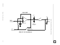
Functional Description
The analog outputs on this board will supply up to 10 mA of drive current, and can be operated offline for both loopback testing and for single-point analog output applications. Built-in-Test of all
active components is provided by looping back the analog outputs with multiplexers and switches.
These circuits are used to check either the on-line or the off-line analog outputs. The outputs
support several operating voltage ranges. The range is selected by the user via jumpers. The scan
rate is program controlled, and can be increased to provide an improved response for complex
output functions. Figure 1-1 below is a block diagram of the board.
Cxx
BIT
MULTIPLEXERS
+15 V
V
M
E
b
u
s
+5 V
BUS
INTERFACE
LOGIC
POWER
CONVERTER
-15 V
ADC
OUTPUT
DATA RAM AND
REFRESH LOGIC
DAC
ANALOG
DISTRIBUTOR
OUTPUT
BUFFERS WITH
HOLD CAPS
P3
Axx
Figure 1-1: Analog Output Board Block Diagram
GFK-2058
Chapter 1 Introduction, Description, and Specifications
1-3
1
Safety Summary
Warning
The following general safety precautions must be observed during all phases of this
operation, service, and repair of this product. Failure to comply with these precautions or
with specific warnings elsewhere in this manual violates safety standards of design,
manufacture, and intended use of this product. GE Fanuc assumes no liability for the
customer’s failure to comply with these requirements.
Ground the System
To minimize shock hazard, the chassis and system cabinet must be connected to an electrical
ground. A three-conductor AC power cable should be used. The power cable must either be
plugged into an approved three-contact electrical outlet or used with a three-contact to two-contact
adapter with the grounding wire (green) firmly connected to an electrical ground (safety ground) at
the power outlet.
Do Not Operate in an Explosive Atmosphere
Do not operate the system in the presence of flammable gases or fumes. Operation of any electrical
system in such an environment constitutes a definite safety hazard.
Keep Away from Live Circuits
Operating personnel must not remove product covers. Component replacement and internal
adjustments must be made by qualified maintenance personnel. Do not replace components with
power cable connected. Under certain conditions, dangerous voltages may exist even with the
power cable removed. To avoid injuries, always disconnect power and discharge circuits before
touching them.
Do Not Service or Adjust Alone
Do not attempt internal service or adjustment unless another person, capable of rendering first aid
and resuscitation, is present.
Do Not Substitute Parts or Modify System
Because of the danger of introducing additional hazards, do not install substitute parts or perform
any unauthorized modification to the product. Return the product to GE Fanuc for service and
repair to ensure that safety features are maintained.
1-4
IC697VAL301 32-Channel 12-bit Analog Output Board with Built-in-Test (BIT)
User’s Manual – December 2001
GFK-2058
Chapter
Configuration and Installation
2
This chapter provides configuration and installation instructions for the Analog Output Board, and
is divided into the following sections:
Physical Installation
Before Applying Power: Checklist
Base Address Configuration
Calibration
Connector Descriptions
Caution
Some of the components assembled on GE Fanuc products can be sensitive
to electrostatic discharge and damage can occur on boards that are
subjected to a high-energy electrostatic field. When the board is placed on a
bench for configuring, etc., it is suggested that conductive material be placed
under the board to provide a conductive shunt. Unused boards should be
stored in the same protective boxes in which they were shipped.
Upon receipt, any precautions found in the shipping container should be observed. All items should
be carefully unpacked and thoroughly inspected for damage that might have occurred during
shipment. The board(s) should be checked for broken components, damaged printed circuit
board(s), heat damage, and other visible contamination. All claims arising from shipping damage
should be filed with the carrier and a complete report sent to GE Fanuc together with a request for
advice concerning the disposition of the damaged item(s).
GFK-2058
2-1
2
Physical Installation
Caution
Do not install or remove board while power is applied.
De-energize the equipment and insert the board into an appropriate slot of the chassis. While
ensuring that the board is properly aligned and oriented in the supporting board guides, slide the
board smoothly forward against the mating connector until firmly seated.
2-2
IC697VAL301 32-Channel 12-bit Analog Output Board with Built-in-Test (BIT)
User’s Manual – December 2001
GFK-2058
2
Before Applying Power: Checklist
Before installing the board in a VMEbus system, check the following items to ensure that the board
is ready for the intended application.
GFK-2058
•
Have the sections pertaining to programming and theory, chapters 3 and 4, been reviewed
and applied to system requirements?
•
Review “Factory-Installed Jumpers” and Table 2-1 on page 2-4 to verify that all factoryinstalled jumpers are in place. To change the board address or address modifier response,
refer to “Board Address Selection (J5 and J7)” on page 2-6.
•
Have the I/O cables, with the proper mating connectors, been connected to the output
connector P3? Refer to “Connector Descriptions” on page 2-13 for a description of the P3
connector.
•
Calibration has been performed at the factory. If recalibration is required, refer to
“Calibration” on page 2-9.
Chapter 2 Configuration and Installation
2-3
2
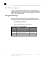
Base Address Configuration
Control of the Analog Output Board’s base address and I/O access mode is determined by field
replaceable, on-board jumpers. This section describes the use of these jumpers, and their effects on
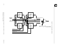
board performance. The locations and functions of all Analog Output Board jumpers are shown in
Figure 2-1 on page 2-5 and Table 2-1 below.
Factory-Installed Jumpers
Each Analog Output Board is configured at the factory with the specific jumper arrangement
shown in Table 2-1 below. The factory configuration establishes the following functional baseline
for the Analog Output Board, and ensures that all essential jumpers are installed.
•
Base short I/O address is set at 0000 HEX.
•
I/O access mode is short supervisory.
•
Analog output and loopback ranges are set to ±10 V full scale.
Table 2-1. Jumper Functions and Factory Configuration
Jumper Name
2-4
Jumper Function
Factory Configuration
J7
ADDRESS DECODE OF Bit A07
INSTALLED
J6
NONPRIVILEGED/SUPERVISORY I/O
OMITTED
J5
ADDRESS DECODE OF Bits A08 to A15
INSTALLED
J4
LOOPBACK VOLTAGE RANGE
INSTALLED AT 1-2
J3
LOOPBACK VOLTAGE POLARITY
INSTALLED AT 1-2
J2
OUTPUT VOLTAGE POLARITY
INSTALLED AT 2-3
J1
OUTPUT VOLTAGE RANGE
OMITTED
IC697VAL301 32-Channel 12-bit Analog Output Board with Built-in-Test (BIT)
User’s Manual – December 2001
GFK-2058
2
Figure 2-1: Jumper and Calibration Point Locations
321
J4
J3
R15
123
TP3
R14
R13
U2
P1
J7
J6
U20
R3
AD8
A15
J5
U19
TP2
R2
TP1
R1
J2
123
U1
J1
123
A2
P3
P2
A1
GFK-2058
Chapter 2 Configuration and Installation
2-5
2
Board Address Selection (J5 and J7)
Jumpers J5 and J7 permit the Analog Output Board to be located on any 64-byte boundary within
the short I/O address space. The short I/O address space consists of all the addresses between
NNNN0000 HEX and NNNNFFFF HEX*. The Analog Output Board address is defined by nine
lines, address bits A07 through A15. Six additional lines are used for programming the on-board
registers (see Chapter 3 for more details).
In programming the board’s base address, an installed jumper equals zero (0), and an omitted
jumper equals one (1). Figure 2-2 below shows an example base address as well as the factoryconfigured base address.
Figure 2-2: Base Address Selection
A07
A07
J7
J7
A15
A15
A08
J5
A08
J5
(Factory Configuration)
Example Base Address
NNNN8E80 HEX
Board Modifier Selection (J6)
The I/O access mode is programmed by selecting the responding state of the address modifier AM2
with jumper J6. Short supervisory access is the factory configuration and is selected by omitting the
jumper. Short nonprivileged access is selected by installing the jumper. Figure 2-3 below shows the
jumper location for the two different accesses.
*The value NNNN depends on the make and model of the CPU board used.
Figure 2-3: Address Modifier Selection
J6
Short Supervisory
(Factory Configuration)
2-6
J6
Short Nonprivileged
IC697VAL301 32-Channel 12-bit Analog Output Board with Built-in-Test (BIT)
User’s Manual – December 2001
GFK-2058
2
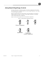
Analog Output Voltage Range (J1 and J2)
The output voltage range is controlled by jumper J1. The factory configuration is the maximum
full-scale range of 20 V. To change this value to 10 V, place a jumper in position 1-2. For a range
of 5 V, place a jumper in position 2-3.
Bipolar or unipolar operation of the analog outputs is selected with jumper J2. The board uses
unipolar operations if a jumper is in position 1-2. If the jumper is in position 2-3, the outputs
operate in bipolar mode (factory configuration).
Figure 2-4 below shows the jumper locations for the different configurations.
Figure 2-4: Analog Output Voltage Range Selection
J1
J1
20 V
(Factory Configuration)
J2
Unipolar Mode
GFK-2058
Chapter 2 Configuration and Installation
10 V
J1
5V
J2
Bipolar Mode
(Factory Configuration)
2-7
2
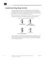
Loopback Input Voltage Range (J3 and J4)
The loopback multiplexers drive an ADC (Analog-to-Digital Converter chip). The loopback
voltage range and polarity must be the same as the output voltage range. If not, the ADC produces
the wrong values. These conditions are controlled by jumpers J3 and J4. As with the outputs, the
maximum full-scale range is 20 V. To modify the full-scale range for 5 V or 10 V, place the jumper
at J4 in position 2-3. For 20 V operations, put the jumper in position 1-2.
Bipolar or unipolar operation is selected with jumper J3. When J3’s jumper is in position 1-2, the
board operates in the bipolar mode. For unipolar voltages, place the jumper in position 2-3.
Figure 2-5: Loopback Input Voltage Range Selection
J3
J3
Unipolar Mode
Bipolar Mode
(Factory Configuration)
J4
20 V
(Factory Configuration)
J4
10 V or 5 V
Do not take readings of any output channel that was updated less than 3.4 msec before or you will
read the old value of the outputs. The sequencer needs this time to refresh the output S&H buffer.
Also, give the loopback multiplexer 5 msec after a start convert command before reading the ADC
to give the multiplexer time to settle.
2-8
IC697VAL301 32-Channel 12-bit Analog Output Board with Built-in-Test (BIT)
User’s Manual – December 2001
GFK-2058
2
Calibration
Before delivery from the factory, the Analog Output Board is fully calibrated and conforms to all
specifications for bipolar operations. Should recalibration be required, perform the procedures in
“Analog Output Calibration Procedure” on page 2-11 and “Loopback Input Calibration Procedure”
on page 2-12 with the equipment listed in “Equipment Required” below. The locations of all
adjustments and test points are shown in Figure 2-6 on page 2-10.
As delivered from the factory, all calibration adjustments are sealed against accidental movement.
However, the seals are easily broken for recalibration. All adjustments should be resealed with a
suitable fast-curing sealing compound after recalibration has been completed.
Note
Do not install or remove this board with power applied to the system.
Equipment Required
GFK-2058
•
Digital Voltmeter (DVM) − A meter with ±1.0000 VDC and
±10.000 VDC ranges, 5 or more digits, accuracy of ±0.005 percent, and 10 MΩ minimum
input impedance.
•
Chassis − VMEbus backplane or equivalent with J1 and J2 connectors, a VMEbus master
controller, a +5 VDC ±0.25 VDC power supply, and one slot allocated for testing the
Analog Output Board.
•
Extender board − One VMEbus extender board.
•
Test cables − Test cables for the equipment listed above.
Chapter 2 Configuration and Installation
2-9
2
Figure 2-6: Calibration and Test Points
3
2
1
J4
J3
1
2
3
U22
R15
R14
R13 TP3
U2
U20
R3
TP2
R2
U19
TP1
R1
1
2
3
J2
U1
1
2
3
2-10
J1
IC697VAL301 32-Channel 12-bit Analog Output Board with Built-in-Test (BIT)
User’s Manual – December 2001
GFK-2058
2
Analog Output Calibration Procedure
1.
Install the Analog Output Board on the extender board in the VMEbus backplane.
2.
Remove any jumper from J1. (This sets the outputs to 20 V full scale.)
3.
Place the jumper at J2 to the 2-3 position. (This is the bipolar setting.)
4.
Apply power to the backplane and allow a minimum ten minute
warm-up time before proceeding.
5.
Connect the digital voltmeter’s positive (+) lead to TP2 and its negative (-) lead to TP1.
6.
Write the 16-bit value 0000 HEX to all of the analog output channels. These registers
begin at offset address 40 HEX and stop at offset 7E HEX.
7.
Adjust R1 for a digital voltmeter indication of 0.0000 ±0.0010 VDC.
8.
Write the 16-bit value 07FF HEX to all of the analog output channels. These registers
begin at offset address 40 HEX and stop at offset 7E HEX.
9.
Adjust R2 for a digital voltmeter indication of +9.9951 ±0.0010 VDC.
(If the board is to be used in the Unipolar mode, perform steps 10, 11, and 12.)
10. Move the J2 jumper to the 2-1 position, and place a jumper on J1 in the 1-2 position.
11. Write the 16-bit value 0800 HEX to all of the analog output channels.
12. Adjust R3 for a digital voltmeter indication of 0.0000 ±0.0010 VDC.
13. For optimum performance, the gain may be adjusted. To make this adjustment, perform
steps 8 and 9 above. Calibration of the analog outputs is complete. Remove power and all
test connections. Restore the board to its original configuration.
GFK-2058
Chapter 2 Configuration and Installation
2-11
2
Loopback Input Calibration Procedure
1.
Perform the Analog Output Calibration Procedure before performing the Loopback Input
Calibration.
2.
Place the jumper at J4 in the 1-2 position. (This is the 20 V range.)
3.
Place the jumper at J3 in the 1-2 position. (This is the bipolar setting.)
4.
Write the 16-bit value 0000 HEX to all of the analog output channels. These registers
begin at offset address 40 HEX and stop at offset 7E HEX.
5.
Write the 16-bit value 7840 HEX to the CSR at offset address 02 HEX.
6.
While reading the ADC (a 16-bit word at offset address 04 HEX), adjust R15 (BIPOLAR
OFFSET) for a reading of 0000 ±0001 HEX.
7.
Write the 16-bit value 0FFF HEX to all of the analog output channels. These registers
begin at offset address 40 HEX and stop at offset 7E HEX.
8.
While reading the ADC (a 16-bit word at offset address 04 HEX), adjust R14 (GAIN
ADJ) for an ADC indication that alternates between 0FFE and 0FFF HEX.
9.
Repeat steps d through h until no further adjustments are required.
(If the board is to be used in the Unipolar mode perform steps 10, 11, 12, and 13.)
10. Move jumper J3 to the 2-3 position. (UNIPOLAR OPERATION.)
11. Write the 16-bit value 0000 HEX to all of the output channels. These registers begin at
offset 40 HEX and end at offset 7E HEX.
12. Write the 16-bit value 7840 HEX to the CSR at offset address 02 HEX.
13. While reading the ADC, adjust R13 (UNIPOLAR ZERO ADJUST) for an ADC indication
of 0000 ±1 HEX.
14. For optimum performance, the gain may be adjusted. To make this adjustment, perform
steps 8 and 8 above. Calibration of the loopback inputs is complete. Restore the board to
its original configuration.
Note
Steps 5, 6, and 8 (as well as steps 12 and 13) may require a program to make
these adjustments.
2-12
IC697VAL301 32-Channel 12-bit Analog Output Board with Built-in-Test (BIT)
User’s Manual – December 2001
GFK-2058
2
Connector Descriptions
Two 96-pin DIN connectors, P1 and P2 (Figure 2-1 on page 2-5), provide the VMEbus connections
to the Analog Output Board. P1 contains the address, data and control lines, and all additional
signals necessary to control the VMEbus functions related to the board. P2 provides some
additional power connections for the board. A 64-pin DIN connector (P3) is used to connect the
analog outputs to the user’s system. The orientation of the P3 connector is shown in Figure 2-7 on
page 2-14, and the signal assignments are listed in Table 2-2 below. A twisted-pair ribbon cable
with an overall shield is recommended for applications involving low-level signals in environments
with a high degree of electrical noise.
Table 2-2: P3 Pin Channel Assignments.
Pin No.
GFK-2058
Row A Assignment
Row C Assignment
1
CH00
GND
2
CH01
GND
3
CH02
GND
4
CH03
GND
5
CH04
GND
6
CH05
GND
7
CH06
GND
8
CH07
GND
9
CH08
GND
10
CH09
GND
11
CH10
GND
12
CH11
GND
13
CH12
GND
14
CH13
GND
15
CH14
GND
16
CH15
GND
17
CH16
GND
18
CH17
GND
19
CH18
GND
20
CH19
GND
21
CH20
GND
22
CH21
GND
23
CH22
GND
24
CH23
GND
25
CH24
GND
26
CH25
GND
27
CH26
GND
28
CH27
GND
29
CH28
GND
30
CH29
GND
31
CH30
GND
32
CH31
GND
Chapter 2 Configuration and Installation
2-13
2
Figure 2-7: P3 Connector Pinout
A
C
32
31
30
29
28
27
26
25
24
23
22
21
20
19
18
17
16
15
14
13
12
11
10
9
8
7
6
5
4
3
2
1
PC Board
2-14
IC697VAL301 32-Channel 12-bit Analog Output Board with Built-in-Test (BIT)
User’s Manual – December 2001
GFK-2058
Chapter
Programming
3
This chapter contains programming instructions for the Analog Output Board, and is divided into
the following sections:
GFK-2058
Introduction to Controlling the Analog Output Board
Control and Status Register Descriptions
Initialization
Controlling the Analog Outputs
Testing the Analog Output Channels (BIT)
Program Example
3-1
3
Introduction to Controlling the Analog Output Board
Communication with the Analog Output (AO) Board takes place through 64 contiguous 16-bit
register locations mapped into the VMEbus short I/O address space. The short I/O address space
consists of all locations within the address range from NNNN0000 HEX to NNNNFFFF HEX*.
The functions of the board’s registers are summarized in Table 3-1 on page 3-5. These functions
will be discussed in more detail later in this section.
The base address of the board holds the Board Identification Register. It is a read-only register that
has a fixed value (17xx HEX). This register can be used by system initialization or automatic
system configuration software. All of the other registers on the board are offset from the address
assigned to this register.
* The value of NNN depends on the make and model of the controlling CPU.
3-2
IC697VAL301 32-Channel 12-bit Analog Output Board with Built-in-Test (BIT)
User’s Manual – December 2001
GFK-2058
3
Control and Status Register Descriptions
The Control and Status Register (CSR) is located at offset address 02
HEX. It contains all of the flags necessary to control and monitor the following board operations:
•
Analog outputs on-line/off-line status
•
Analog outputs refresh rate
•
Digital-to-Analog (D/A) conversion
•
Built-in-Test (BIT) and A/D control
•
Analog input channel selection (Built-in-Test only)
•
Front panel LED
•
A/D and D/A enable/disable (Scan HALT)
The CSR is 16 bits long and is detailed in Table 3-2 on page 3-6. The function of each control bit
and status flag is described in detail subsequently in the associated programming discussions.
GFK-2058
Chapter 3 Programming
3-3
3
Initialization
When SYSTEM RESET is applied to the board, the Control Register and all converter flags are
cleared to the LOW state ("zero"). This places the board in a known state. The D/A output
sequencer is stopped and the A/D converter is disabled. The data format is offset binary, standard
settling time, the LED is ON, and the outputs are disconnected from the external circuits. In this
condition, the board is ready to perform loopback tests. After the system RESET is removed, the
D/A sequencer starts and the A/D converter is enabled. The A/D and the D/A can be disabled under
software control. Setting the SCAN HALT bit to a "one" disables the A/D and the D/A. This bit
must be cleared before normal operation can begin.
3-4
IC697VAL301 32-Channel 12-bit Analog Output Board with Built-in-Test (BIT)
User’s Manual – December 2001
GFK-2058
3
Table 3-1: Analog Output Board Register Map
GFK-2058
Offset Address in HEX
Register Name
Access Mode
00
BOARD ID
READ (17XX HEX)
02
CSR
READ/WRITE
04
ADC
READ
06 to 3E
(RESERVED)
------------
40
D/A OUTPUT 00
READ/WRITE
42
D/A OUTPUT 01
READ/WRITE
44
D/A OUTPUT 02
READ/WRITE
46
D/A OUTPUT 03
READ/WRITE
48
D/A OUTPUT 04
READ/WRITE
4A
D/A OUTPUT 05
READ/WRITE
4C
D/A OUTPUT 06
READ/WRITE
4E
D/A OUTPUT 07
READ/WRITE
50
D/A OUTPUT 08
READ/WRITE
52
D/A OUTPUT 09
READ/WRITE
54
D/A OUTPUT 10
READ/WRITE
56
D/A OUTPUT 11
READ/WRITE
58
D/A OUTPUT 12
READ/WRITE
5A
D/A OUTPUT 13
READ/WRITE
5C
D/A OUTPUT 14
READ/WRITE
5E
D/A OUTPUT 15
READ/WRITE
60
D/A OUTPUT 16
READ/WRITE
62
D/A OUTPUT 17
READ/WRITE
64
D/A OUTPUT 18
READ/WRITE
66
D/A OUTPUT 19
READ/WRITE
68
D/A OUTPUT 20
READ/WRITE
6A
D/A OUTPUT 21
READ/WRITE
6C
D/A OUTPUT 22
READ/WRITE
6E
D/A OUTPUT 23
READ/WRITE
70
D/A OUTPUT 24
READ/WRITE
72
D/A OUTPUT 25
READ/WRITE
74
D/A OUTPUT 26
READ/WRITE
76
D/A OUTPUT 27
READ/WRITE
78
D/A OUTPUT 28
READ/WRITE
7A
D/A OUTPUT 29
READ/WRITE
7C
D/A OUTPUT 30
READ/WRITE
7E
D/A OUTPUT 31
READ/WRITE
Chapter 3 Programming
3-5
3
Table 3-2: CSR Bit Definitions
MSB
Bit D15
Short
Settling
or New
Data
Rdy
Bit D14
Bit D13
Bit D12
Bit D11
Bit D10
Bit D09
Bit D08
LED
Control
Start a
Conversion
or
Converter
Busy
Two’s
Complement
Control
Outputs
On-Line
Control
Not
Used
Not
Used
Fast
Refresh
LSB
Bit 07
Bit D06
Bit D05
Bit D04
Bit D03
Bit D02
Bit D01
Bit D00
Not
Used
Start
Settling
or
Settling
Busy
Scan
Halt
MUX A4
MUX A3
MUX A2
MUX A1
MUX A0
Control and Status Register Bit Definitions
3-6
Bit D15:
Short Settling or New Data Rdy – Writing a "one" here reduces the
time assigned for loopback settling from 5 to 3 msec. Reading a "one"
here indicates that loopback data is ready for the host to read.
Bit D14:
LED Control – This bit turns the LED ON with a logic "zero" and OFF
with a logic "one".
Bit D13:
Start a Conversion or Converter Busy – Writing a "one" here and at
D06 begins a loopback conversion. Reading a "zero" tells the host that a
conversion is done.
Bit D12:
Two’s Complement Control – When a "one" is written here, the data
is in offset binary form. When a "zero" is written here, the data is in
two's complement form.
Bit D11:
Outputs On-Line Control – When this bit is a "one", the output
buffers are driving the cable and loopback buffers monitor the P3 pins.
When it is a "zero", the outputs are disconnected from the cable and the
loopback buffers monitor the output amps.
Bit D10:
Not used.
Bit D09:
Not Used.
Bit D08:
Fast Refresh – This speeds up the DAC control logic when a "one" is
written here, so the outputs get updated faster.
Bit D07:
Not Used.
IC697VAL301 32-Channel 12-bit Analog Output Board with Built-in-Test (BIT)
User’s Manual – December 2001
GFK-2058
3
Bit D06:
Start Settling or Settling Busy – Writing a "one" here and at D13
begins a loopback conversion. Reading a "zero" tells the host that the
signal settling time is done.
Bit D05:
Scan Halt – Writing a "one" here will stop the output sequencer and
disable the A/D converter. This bit must be cleared before normal
operations can begin.
Bit D04:
MUX A4* – Loopback (input channel select) multiplexer control line.
Bit D03:
MUX A3 – Loopback (input channel select) multiplexer control line.
Bit D02:
MUX A2 – Loopback (input channel select) multiplexer control line.
Bit D01:
MUX A1 – Loopback (input channel select) multiplexer control line.
Bit D00:
MUX A0 – Loopback (input channel select) multiplexer control line.
* The MUX signals are address lines. A decoder takes the state of these lines and selects the
loopback buffer to convert.
GFK-2058
Chapter 3 Programming
3-7
3
Controlling the Analog Outputs
The 16 analog output channels appear to the controlling processor as 16 consecutive 16-bit words
in the address space assigned to the Analog Output Board. The register map shown in Table 3-1 on
page 3-5 lists the board-relative (or offset) address of each output channel. Each Analog Output
Register supports both read and write operations, eliminating the need for corresponding "shadow"
latches in the processor Random Access Memory (RAM) space.
Writing to the Outputs
Output voltage data is recognized in the Analog Output Registers as right-justified 12-bit binary
data. When offset binary data is written to a register, the upper four bits, D12 to D15, are ignored
and not retained for read back. If the board is using two’s complement data, then these bits contain
the sign of the output data. Each output responds to a new code within 3.4 msec after the code is
written to the Output Register (0.85 msec in the FAST REFRESH MODE). Be sure to give the
board ample time to update the output before reading its value in a loopback test.
FAST REFRESH
Setting the FAST REFRESH control bit (Table 3-2 on page 3-6) HIGH reduces the analog output
REFRESH time from the default value of 3.4 to 0.85 msec. The FAST REFRESH MODE raises
the output Nyquist frequency (maximum output signal frequency) from approximately 300 Hz to
about 1.2 kHz. This is done by reducing the settling time given to the various circuits in the output
channels. The FAST REFRESH MODE reduces the accuracy of the outputs. They are not given
enough time to settle to their most accurate levels.
3-8
IC697VAL301 32-Channel 12-bit Analog Output Board with Built-in-Test (BIT)
User’s Manual – December 2001
GFK-2058
3
Testing the Analog Output Channels (BIT)
Built-in-Test (BIT) provisions provide loopback testing of the outputs. These capabilities permit
self-contained, board-level verification of performance. The testing is controlled by seven bits in
the CSR. They are the MUX Address lines, the start conversion, and start settling bits. The ONLINE signal controls the source of the test voltage. The two’s complement bit dictates the format of
the data. BIT is available at any time. The user picks a channel to monitor and orders a conversion.
After 5 msec, the ADC is read and the read data is compared to the written data to determine the
"health" of the channel. If an error is detected, the front panel LED can be used to locate the board
in a system for troubleshooting.
Loopback Testing of the Outputs
The five least significant bits in the CSR, D00 through D04, and bit D11 are used to select the
source of the voltage used in the loopback (BIT) test. D00 through D04 are the loopback
multiplexer select lines MUX A0 through MUX A4. They select the input to be tested. Bit D11, the
outputs on-line control, selects where the input sample will be made. When this bit is low the
loopback test buffers monitor the analog output buffers. If this bit is high, the test buffers monitor
the output pins of P3. The loopback multiplexers are always enabled to prevent the ADC from
trying to convert a high impedance input instead of a voltage. By routing the analog outputs
through these loopback multiplexers, the operation of all the components on the Analog Output
Board can be verified.
ADC Controls and Flags
All timing operations for the ADC are performed by an on-board controller.
User control of the converter consists of the following control bits, flags, and
registers. The control bits and flags in the CSR are summarized in Table 3-2 on page 3-6.
They are restated here for clarity.
Table 3-3 CSR Bit Functions
Control Bits
a.
SHORT SETTLING H . . .
D15 *
b.
EN START CONV H . . . .
D13 *
c.
TWO’s COMPL L . . . . . .
D12
d.
START SETTLING H…
D06 *
* Effective only upon writing ("strobed").
Flags (Status Register)
a.
NEW DATA RDY H . . . . . D15 *
b.
CONV BUSY H . . . . . . . .
D13
c.
SETTLING BUSY H . . . .
D06
* Set when data is available in the ADC Data Register.
GFK-2058
Chapter 3 Programming
3-9
3
The START SETTLING and START CONV controls are essentially strobes. They are effective
only at the moment of writing to the Control Register. Although supplied as two separate control
bits, they must be written to the register simultaneously along with the operating mode (TWO’s
COMPL L and SHORT SETTLING H bits) and the input channel selection. Thus, a single write to
the CSR can start a conversion. Once started, the user simply waits 5 msec and then reads the
ADC. The NEW DATA RDY bit can be used as a pass or fail indicator. Polling this bit (or any
other bit on the board) will degrade the loopback readings.
For example, to convert the signal of Channel 0, with the outputs on-line using offset binary data
format, write 7840 HEX to the CSR. The low 5 bits select the output channel to monitor (Channel 0
in this case). The upper 4 bits start the conversion and select the data format. Now wait 5 msec to
give the multiplexers time to settle. In this time, the host can do whatever it wants. The ADC is
read next via the Converter Data Register (CDR). To check Channel 12, write 784C HEX to the
CSR.
The CDR is a 16-bit read-only register at relative address 04 HEX. It is used to store the ADC data.
Data in this register is 12 bits, right-justified. D12 through D15 are always "zero" in the binary data
format, and are sign extensions in the two’s complement data format. The data format depends
upon the state of the TWO’s COMP L control bit in the CSR. Converter output codes that are
produced at major points within the full-scale ranges shown are summarized in Table 3-4.
Table 3-4 Data Codes for Some Selected Output Voltages
UNIPOLAR RANGE
INPUT
+5 V
VFSR=5 V
STRAIGHT BINARY
+10 V
VFSR=10 V
D15*
D00
HEX
–––––––––––––––––––––––––––––––––––––––––––––––––––––––––––––––––––––––––––––––––––––––––––––––––––
+FS-1 LSB
3/4 FS
1/2 FS
1/4 FS
1 LSB
ZERO
3-10
+4.9988 V
+3.7500 V
+2.5000 V
+1.2500 V
+0.0012 V
0.0000 V
+9.9976 V
+7.5000 V
+5.0000 V
+2.5000 V
+0.0024 V
0.0000 V
0000 1111 1111 1111
0000 1100 0000 0000
0000 1000 0000 0000
0000 0100 0000 0000
0000 0000 0000 0001
0000 0000 0000 0000
IC697VAL301 32-Channel 12-bit Analog Output Board with Built-in-Test (BIT)
User’s Manual – December 2001
FFF
C00
800
400
001
000
GFK-2058
3
BIPOLAR RANGE
OFFSET BINARY
–––––––––––––––––––––––––––––––––––––––––––––––––––––––––––––––––––––––––––––––––––––––––––––––––––
INPUT
±5 V
VFSR=10 V
±10 V
VFSR=20 V
D15*
D00
HEX
–––––––––––––––––––––––––––––––––––––––––––––––––––––––––––––––––––––––––––––––––––––––––––––––––––
+FS-1 LSB
+3/4 FS
+1/2 FS
+1/4 FS
+1 LSB
ZERO
-1/4 FS
-1/2 FS
-3/4 FS
-FS+1 LSB
-FS
+4.9976 V
+3.7500 V
+2.5000 V
+1.2500 V
+0.0024 V
0.0000 V
- 1.2500 V
- 2.5000 V
- 3.7500 V
- 4.9976 V
- 5.0000 V
BIPOLAR RANGE
+9.9951 V
+7.5000 V
+5.0000 V
+2.5000 V
+0.0048 V
0.0000 V
- 2.5000 V
- 5.0000 V
- 7.5000 V
- 9.9951 V
- 10.000 V
0000 1111 1111 1111
0000 1110 0000 0000
0000 1100 0000 0000
0000 1010 0000 0000
0000 1000 0000 0001
0000 1000 0000 0000
0000 0110 0000 0000
0000 0100 0000 0000
0000 0010 0000 0000
0000 0000 0000 0001
0000 0000 0000 0000
FFF
E00
C00
A00
801
800
600
400
200
001
000
2’s COMPLEMENT
–––––––––––––––––––––––––––––––––––––––––––––––––––––––––––––––––––––––––––––––––––––––––––––––––––
INPUT
±5 V
VFSR=10 V
±10 V
VFSR=20 V
D15*
D00
HEX
–––––––––––––––––––––––––––––––––––––––––––––––––––––––––––––––––––––––––––––––––––––––––––––––––––
+FS-1 LSB
+3/4 FS
+1/2 FS
+1/4 FS
+1 LSB
ZERO
-1/4 FS
-1/2 FS
-3/4 FS
-FS+1 LSB
-FS
+4.9976 V
+3.7500 V
+2.5000 V
+1.2500 V
+0.0024 V
0.0000 V
- 1.2500 V
- 2.5000 V
- 3.7500 V
- 4.9976 V
- 5.0000 V
+9.9951 V
+7.5000 V
+5.0000 V
+2.5000 V
+0.0048 V
0.0000 V
- 2.5000 V
- 5.0000 V
- 7.5000 V
- 9.9951 V
- 10.000 V
0000 0111 1111 1111
0000 0110 0000 0000
0000 0100 0000 0000
0000 0010 0000 0000
0000 0000 0000 0001
0000 0000 0000 0000
1111 1110 0000 0000
1111 1100 0000 0000
1111 1010 0000 0000
1111 1000 0000 0001
1111 1000 0000 0000
7FF
600
400
200
001
000
E00
C00
A00
801
800
STRAIGHT BINARY: VO = VFSR (D1 ÷ 4096), D1 = Dec. equiv. of HEX value
OFFSET BINARY: VO = VFSR (D1 ÷ 4096) - (VFSR ÷ 2). D2 = Dec. equiv. of HEX value
2’s COMPLEMENT: VO = VFSR (D2 ÷ 4096) - (VFSR ÷ 2). D2 = Dec. equiv. of (HEX value ⊕ $800)
* = Zero (binary) or extended sign (2’s comp); ⊕ = Exclusive OR’d with.
GFK-2058
Chapter 3 Programming
3-11
3
For any offset binary converter output code (BIPOLAR RANGE), the associated output voltage is
obtained with the expressions:
OUTPUT (Volts) = (-EFSR/2 )+ (EFSR X [OUTPUT DATA IN DECIMAL] /4096).
The output voltage for a straight binary code (UNIPOLAR RANGE) is:
OUTPUT (Volts) = +EFSR X [OUTPUT DATA IN DECIMAL] / 4096.
Where EFSR is the full-scale range voltage. (E.g.: EFSR = 10 V for the ±5 V range.)
For example, the output voltage for a HEX value of 51A is found like this:
1.
Convert 51A (HEX) to its decimal equivalent, which is 1306.
2.
Identify the Range you are using, for example ±5 V. This range uses the bipolar equation
with EFSR = 10 V.
3.
Compute the result by substituting these numbers in the equation
OUTPUT (Volts) = -(10/2) + (10 x (1306/4096)) = -5 + (10 x .32) = -1.81 V.
3-12
IC697VAL301 32-Channel 12-bit Analog Output Board with Built-in-Test (BIT)
User’s Manual – December 2001
GFK-2058
3
Program Example
The following is a sample program to perform some simple board operations. The program is
written in C.
/*
**
*/
VMIVME 4132 sample code header file
typedef unsigned short word;
#define VME_SHORT_IO 0xfbff0000
#define vmic4132_base_address 0x0000
struct
word
word
word
word
word
};
vmivme4132 {
bid;
csr;
adc;
reserved[29];
dac[32];
/*
/*
/*
/*
/*
/* data type of word */
/* Force Cpu short io */
/* Jumper Field J5 & J7 */
board ID register */
control status register */
ADC converter data register */
unused - reserved */
DAC channels 0 - 31 */
typedef struct vmivme4132 vmic4132_reg;
#define SHORT_SETTLING
#define LED_OFF
#define START_CONVERT
#define TWOS_COMPLEMENT0x1000
#define OUTPUTS_ONLINE
#define FAST_REFRESH
#define START_SETTLING
#define SCAN_HALT
0x8000 /* CSR control bits (write) */
0x4000
0x2000
0x1000
0x0800
0x0100
0x0040
0x0020
#define NEW_DATA_READY
#define CONVERTER_BUSY
#define SETTLING_BUSY
0x8000 /* CSR status bits (read) */
0x2000
0x0040
/*
VMIVME 4132 sample code
#include
"x4132.h"
/* 4132 function declarations
word
word
void
word
*/
*/
read_id(vmic4132_reg * board);
read_csr(vmic4132_reg * board);
write_dac(word chan,word data,vmic4132_reg * board);
read_adc(word chan,word ctrl,vmic4132_reg * board);
main()
{
word board_id,status,adc_cword,data_in;
/* init pointer to 4132 board */
vmic4132_reg * vmic4132;
vmic4132 = (vmic4132_reg *)(VME_SHORT_IO+vmic4132_base_address);
vmic4132->csr = LED_OFF | OUTPUTS_ONLINE;
/* init dac outputs */
board_id = read_id(vmic4132);
/* read board id register */
status
/* read control/status register */
= read_csr(vmic4132);
write_dac(0,0x100,vmic4132);
/* write dac channel 0 with 100 hex */
/* init adc control word and read back dac output with adc converter */
adc_cword = LED_OFF | START_CONVERT | OUTPUTS_ONLINE | START_SETTLING;
data_in = read_adc(0,adc_cword,vmic4132);
data_in = read_adc(0,adc_cword,vmic4132);
}
GFK-2058
/* end main */
Chapter 3 Programming
3-13
3
/*
**
*/
4132 function primitives
word read_id(vmic4132_reg * board)
{
return board->bid;
}
word read_csr(vmic4132_reg * board)
{
return board->csr;
}
void write_dac(word chan,word data,vmic4132_reg * board)
{
board->dac[chan] = data;
}
word read_adc(word chan,word ctrl,vmic4132_reg * board)
{
board->csr = (ctrl+chan);
while (!(board->csr & NEW_DATA_READY)); /* test new data ready bit
return board->adc;
}
3-14
IC697VAL301 32-Channel 12-bit Analog Output Board with Built-in-Test (BIT)
User’s Manual – December 2001
*/
GFK-2058
Chapter
Theory of Operation
4
This chapter describes the internal organization of the Analog Output Board, reviews the general
principles of operation, and is divided into the following sections:
GFK-2058
Internal Functional Organization
VMEbus Interface
Channel Control Logic
Analog Outputs
Analog Output Buffers and Switches
Data RAM and Refresh Logic
Built-in-Test (BIT) Multiplexers and ADC Logic
Built-in Power Converter
4-1
4
Internal Functional Organization
The Analog Output Board is designed to operate in a standard VMEbus system. The board contains
a 12-bit Digital-to-Analog Converter (DAC), dedicated on-board registers to store the output data,
sample-and-hold buffers (S&H) to place the voltage on the cable, and loopback analog switches to
support Built-in-Test features. The BIT uses an on-board Analog-to-Digital Converter (ADC);
therefore, no additional equipment is needed to test this board. The Analog Output Board is a
flexible I/O element in a VMEbus system, which offers Built-in-Test and off-line operating
features not found in many other products.
The Analog Output Board is divided into the following functional categories, as illustrated in
Figure 1-1 on page 1-3. All of these functions will be discussed in detail in this section of the
manual.
4-2
•
VMEbus Interface
•
Analog Outputs (DAC and Analog Distributor)
•
Analog Output Buffers and Switches
•
Data RAM and Refresh Logic
•
BIT Multiplexers and ADC Logic
•
Power Converter
IC697VAL301 32-Channel 12-bit Analog Output Board with Built-in-Test (BIT)
User’s Manual – December 2001
GFK-2058
4
VMEbus Interface
The board’s Analog Output Data Registers are memory mapped as 32 (decimal) 16-bit words.
These registers store the value of the output voltage for the associated output channel. These
registers are contiguous, and are located 40 (HEX) offset from the base address of the board. The
board occupies 128 bytes of the VMEbus short I/O address space and may be user-located on any
128-byte boundary in this region. The board can be user-configured to respond to short supervisory
or short nonprivileged bus access. The board supports two additional registers for a user interface.
These registers are the Board ID and the Control and Status Registers. Figure 4-1 on page 4-5 is a
block diagram of the bus interface logic.
The board monitors the VMEbus. During any data transfer, the board-selection comparator
determines if there is a match between the on-board selection jumpers (shown in Figure 4-1 on
page 4-5) and the address and address modifier lines on the backplane. If there is no match, all
VMEbus control signals are ignored. If there is a match, the appropriate board response will occur.
The open-collector DTACK interface signal is then asserted (driven LOW). Subsequent removal of
the read or write command by the Central Processing Unit (CPU) causes the board-generated
DTACK signal to return to the OFF state, terminating the data transfer cycle. Although some of the
registers on the board are read only, the board will respond to a write command at these locations.
However, the data written will be lost.
After the board decides it is to respond, the following three groups of VMEbus signals control the
board:
•
Data Bus lines D00 to D15
•
Address lines A01, A02, A03, A04, A05, and A06
•
Bus Control Signals:
1.
WRITE*
2.
DS0* and DS1*
3.
SYS CLK
Data Bus lines are bi-directional and move data to or from the board through a pair of 8-bit data
transceivers. They are controlled by board-select, the WRITE* line, and the data strobes (DS0* and
DS1*). The data transceivers serve as a buffer between the internal data bus, which interconnects
all data devices on the board, and the VMEbus. Although the board will respond to byte operations,
word transfers are recommended. Byte transfers can cause erratic behavior in the outputs.
Address lines A01 through A06 map the 64 Data Registers into a 128-byte range within the
VMEbus address space (Chapter 3). The control signals determine whether data is to be moved to
the board (a write cycle) or from the board (a read cycle), provide the necessary data strobes (DS0,
DS1), and supply a 16 MHz clock (SYS CLK) for use by the on-board timers. However, the SYS
RESET input overrides all of the board's functions, resets all the timers and clears all of the flags in
the CSR. A Board ID Register located at the base address of the board has a fixed value of 17 HEX
in the even byte location. This register can be used by automatic system configuration software, to
identify the board in a system. The CSR is located at an offset of 02 from the base address of the
board.
GFK-2058
Chapter 4 Theory of Operation
4-3
4
The interface logic determines the bus control of the board, but the CSR contains the board-level
operating controls and status flags for the system. Static controls (such as the LED ON line) are
stored in the Control Register and are used primarily to establish the operating mode of the board.
Status flags (such as NEW DATA RDY), necessary for monitoring and controlling the analog input
multiplexer and the ADC, are read through the Status Register. The Control and Status Registers
are referred to collectively as the Control and Status Register or CSR, since they are at the same
address. The WRITE* signal determines which one is accessed, while most of the Control Register
outputs can be monitored directly through the Status Register.
In the CSR, three of the control lines are strobes. These signals are START CONV H, SHORT
SETTLING H, and START SETTLING H. They are valid only during the write operation to the
CSR. Once written, these signals become status flags for the Analog-to-Digital Converter. The host
CPU can monitor these lines to determine when the ADC is done and data is ready to be read.
Each of the 32 analog output channels is controlled by writing a 12-bit right-justified data word
into a dedicated 16-bit read/write register. The 32 analog Output Control Registers constitute the
VME port of a 32-word dual-port memory. The other memory port is controlled by the analog
output refresh logic. The data format and the two’s complement control bit must be consistent.
4-4
IC697VAL301 32-Channel 12-bit Analog Output Board with Built-in-Test (BIT)
User’s Manual – December 2001
GFK-2058
GFK-2058
Chapter 4 Theory of Operation
AM5 to AM0
9
2
2
1
BOARDSELECT
LOGIC
1 1
6
2
AM2
A15
A07
BOARD
BASE
ADDRESS
SELECTION
JUMPERS
A15 to A07
BD SELC L (BOARD-SELECTED)
BOARD
CONTROL
LOGIC
A6 to A1
9
BUS
CTRL
LINES
2
ENB
8
BD
CTRL
LINES
WRITEL
BD ID
CSR
RAM
ADC
CLK
RESET
DTACK
WRITE
SELECT LINES
CONTROL LINES
Figure 4-1: Interface Logic
V ME b u s
6
ALL SIGNALS (EXCEPT CLK) ARE ACTIVE LOW
16
D15 to D00
DATA
XCVRS
16
TO BOARD REGISTERS
IDB15 to IDB00
4
4-5
4
Analog Outputs
Each analog output has its own sample-and-hold buffer and a control switch. The analog outputs
are updated (refreshed) periodically from the dual-port memory by the refresh control logic, as
illustrated in Figure 4-2 on page 4-7. Each output receives an update once every 3.4 msec in the
default refresh mode. A program-controlled FAST REFRESH control bit can be used to reduce the
refresh cycle time to approximately 0.85 msec, thereby raising the maximum output sampling rate
from 294 Hz to 1.18 kHz. These rates assume there is no loopback activity on the board.
Digital-to-Analog Converter (DAC)
All 32 analog outputs are serviced by a single 12-bit DAC. The DAC is controlled by the refresh
control logic. As long as the ADC is not converting a voltage, this circuitry will periodically
transfer data from the dual-port memory’s refresh port to the DAC. Simultaneously the logic
connects the DAC to the appropriate section of the analog output demultiplexer (analog
distributor). The analog output data is placed in the dual-port memory by the controlling processor
through the VMEbus port.
Analog Distributor
The analog distributor consists of the following elements:
•
A one of 32 output channel decoder
•
Low charge injection analog demultiplexer (4 one of eight decoders)
•
Thirty-two capacitive storage elements and buffers
The one of 32 decoder receives the same five address lines used to select the dual-port memory
location used to update the DAC. In this manner, the converted analog level is always routed by the
distributor section to the output buffer which corresponds to the dual-port memory location being
updated. The upper two bits are decoded to yield a select line to choose the correct demultiplexer.
The three lower bits are used to select the output to pass through the decoder. Figure 4-3 on page 410 shows the 1 of 32 decoder logic.
After allowing the DAC to settle, the refresh logic enables (turns ON) the demultiplexer. The
converted voltage level is transferred to the corresponding storage capacitor. Approximately 100
msec of settling time is provided by the REFRESH logic for the sample-and-hold buffer. Then the
demultiplexer is disabled and the next channel in the REFRESH sequence is accessed. During
ADC conversions the refresh logic is disabled. This is to prevent the digital noise generated by this
logic from injecting errors in the loopback data. When the ADC is converting a voltage, a 15 µsec
(maximum) delay will be added to the output update time.
4-6
IC697VAL301 32-Channel 12-bit Analog Output Board with Built-in-Test (BIT)
User’s Manual – December 2001
GFK-2058
GFK-2058
12
OUTPUT
DATA STATIC
RAM
IDB11 to IDB00
2
12
ANALOG
DISTRIBUTOR
DAC
DAC
OUTPUT
32
Axx
Cxx
Figure 4-2: Analog Output Control Logic
Chapter 4 Theory of Operation
P3
TP2
5
CTRL LINES
RAM A4 to A0
7
6
REG’D A6 to A1
DAC CTRL
AND REFRESH
LOGIC
7
BD CTRL LINES
4
4-7
4
Analog Output Buffers and Switches
Voltage levels processed by the analog distributor and stored by the sample-and-hold caps are
buffered and then switched to the P3 connector for routing through the system I/O cables. The
output buffers are low leakage, precision operational amplifiers which can supply 10 mA of drive
current over the full available output voltage range of ±10 V. These buffers can withstand sustained
short circuits to ground without damage. Figure 4-4 on page 4-11 shows the S&H buffer with its
protection circuit and the switches used to control the output connector and the loopback test
voltage source.
The output switches can disconnect the output buffers from P3 for off-line testing and for low
impedance, single-point analog I/O system applications. To eliminate the effect of switch resistance
on the output impedance, the inverting (sense) input of each output buffer is switched between the
load and line side of the output switch during on-line and off-line operations. Thus, the output
impedance is the switch resistance divided by the open loop gain of the op-amp. Clamping diodes
protect the buffers and switches from line transients by preventing voltage excursions beyond the
±15 V supply rails.
4-8
IC697VAL301 32-Channel 12-bit Analog Output Board with Built-in-Test (BIT)
User’s Manual – December 2001
GFK-2058
4
Data RAM and Refresh Logic
The dual-port memory which services the analog outputs is organized as a 16-bit wide 32-column
array. Each location can be accessed from either of two ports. The random access VME port is used
by the VMEbus host to load the analog output digital codes into the memory. The digital codes are
then transferred sequentially through the DAC port to the Digital-to-Analog Converter. There they
are converted into voltage levels and subsequently distributed to the appropriate analog output
channel.
The dual-port memory is controlled by the REFRESH control logic which derives its timing from
the 16 MHz system clock. The REFRESH control logic supervises all data transfers between the
memory and the DAC, and controls the distribution of the analog voltages to the outputs. Because
the dual-port memory must be accessed through both the VME and DAC ports, arbitration logic is
employed during the transfer of data to the DAC to ensure that only one port is active at any time.
The REFRESH control logic sequences through the output channels from 0 to 31. It writes the
channel’s digital data to the DAC at the same time it selects the correct output S&H buffer. It then
performs the necessary time delays for each part of the logic (DAC, multiplexer, and output
amplifier) to settle to the updated value. It also arbitrates the access to the RAM. When the
VMEbus wants to access this RAM, it makes sure the output logic is in a state that will tolerate the
interruption. The VMEbus then places the bus data into the RAM and signals the board interface
logic when the transfer is done (scanning is then resumed).
When the loopback ADC is performing a conversion, the REFRESH control logic is stopped,
thereby preventing it from generating noise which gets into the loopback ADC’s input. This noise
can cause a large error in the input voltage, making the host erroneously think that the board has
failed. By freezing the REFRESH logic, the noise is eliminated. This will add up to 15 µsec to the
3.4 msec update rate for each conversion (a .44 percent increase). This impact should not be a
problem for the outputs, because the READ software should give 5 msec of settling time for the
loopback multiplexers.
GFK-2058
Chapter 4 Theory of Operation
4-9
4
4-10
S0 to S2
ENB
OUTPUT
SELECT
LINES
1 to 8
MUX
8
S0 to S2
ENB
DISTR CH 00 to CH 31
3
8
8
DAC
OUTPUT
S0 to S2
STRB OUT 31 H
STRB OUT 23 H
STRB OUT 15 H
STRB OUT 07 H
S0 to S2
1 to 8
MUX
1 to 8
MUX
ENB
ENB
8
ONE OF 32 OUTPUT BUFFERS
Figure 4-3: Analog Output Distribution
IC697VAL301 32-Channel 12-bit Analog Output Board with Built-in-Test (BIT)
User’s Manual – December 2001
1 to 8
MUX
GFK-2058
GFK-2058
+15 V
P3
Axx
FROM
ANALOG
DISTRIBUTION
ON-OFF-LINE
SWITCH
HOLD CAP
-15 V
PROTECTION
DIODES
TO
BIT
BUFFERS
BIT MONITOR
SELECT SWITCH
ONE OF 32 CHANNELS
Cxx
Figure 4-4: Simplified Output Buffers and Switches
Chapter 4 Theory of Operation
S&H AMP
4
4-11
4
Built-in-Test (BIT) Multiplexers and ADC Logic
The signal routing paths and multiplexers involved in the board’s loopback testing are shown in
Figure 4-5 on page 4-13. The 32 analog outputs are switched by the output monitor demultiplexer
onto a single line. This line is connected to a buffer and then to the on-board Analog-to-Digital
Converter (ADC). This arrangement permits any one of the analog outputs to be tested by the
ADC. It also verifies the operation of the analog input multiplexers by exercising them with known
signal levels.
By routing the analog outputs through the test demultiplexers, all of the active components on the
board are exercised in a "loopback" arrangement. The controlling processor can perform a
loopback test in either the on-line or off-line mode by sending a voltage-level code to a specific
output channel and then verifying that the ADC produces the correct code for the output voltage
sent (see Chapter 3 for more details).
Converter Controls and Status Flags
A conversion sequence is initiated by a single write to the CSR placing a "one" in the START
SETTLING and the START CONV control bits and the channel to be converted. The last five bits
contain the input channel information. The conversion sequence is composed of the following
consecutive time intervals:
•
Settling Delay
•
Tracking Interval
•
Analog-to-Digital (A/D) Conversion
All ADC timing intervals discussed in this section are performed automatically by the on-board
controller. The host writes the CSR with the start settling and the start convert bits set and the
desired channel. This will switch the demultiplexer to the desired channel and start the settling
process. The host now waits 5 msec for the board’s multiplexers to settle to the new voltage. During
this time keep any digital activity to this board to a minimum. After the data ready bit has been set
in the CSR, the host can read the data.
4-12
IC697VAL301 32-Channel 12-bit Analog Output Board with Built-in-Test (BIT)
User’s Manual – December 2001
GFK-2058
GFK-2058
Chapter 4 Theory of Operation
12
ADC
TEST
SIGNAL
32
FROM BIT MONITOR
SWITCHES
1 of 32
4
CTRL
LOGIC
1 OF 32
MULTIPLEXER
7
Figure 4-5: Simplified BIT Logic
IDB800
to
IBD11
4
4-13
4
Built-in Power Converter
Electrical power for the Analog Output Board analog network is supplied by two DC-to-DC
converters shown in Figure 4-6 below. These converters transform the +5 V logic power into
regulated and isolated ±15 VDC power, with a load capacity of approximately 600 mA on each 15
V bus. Thus, the user only needs a +5 V power supply when using this board.
Figure 4-6: DC-to-DC Converters
P1
+15 V
3
5V
AGND
8
A1
-15 V
P2
3
A2
4
4-14
IC697VAL301 32-Channel 12-bit Analog Output Board with Built-in-Test (BIT)
User’s Manual – December 2001
GFK-2058
Chapter
Maintenance
5
This chapter provides information relative to the care and maintenance of the Analog Output Board
product.
If the product malfunctions, verify the following:
•
Software
•
System configuration
•
Electrical connections
•
Jumper or configuration options
•
Boards fully inserted into their proper connector location
•
Connector pins are clean and free from contamination
•
No components of adjacent boards are disturbed when inserting or removing the board
from the VMEbus card cage
•
Quality of cables and I/O connections
User level repairs are not recommended. Contact GE Fanuc for a Return Material Authorization
(RMA) Number. This RMA Number must be obtained prior to any return.
GFK-2058
5-1