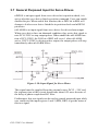
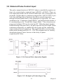
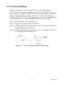
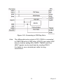
1
PCI-1220U 2-axis Universal PCI Stepping/ Pulse-type Servo Motor Control Card User Manual Copyright This documentation and the software included with this product are copyrighted 2009 by Advantech Co., Ltd. All rights are reserved. Advantech Co., Ltd. reserves the right to make improvements in the products described in this manual at any time without notice. No part of this manual may be reproduced, copied, translated or transmitted in any form or by any means without the prior written permission of Advantech Co., Ltd. Information provided in this manual is intended to be accurate and reliable. However, Advantech Co., Ltd. assumes no responsibility for its use, nor for any infringements of the rights of third parties which may result from its use. Acknowledgments PC-LabCard is a trademark of Advantech Co., Ltd. IBM and PC are trademarks of International Business Machines Corporation. MS-DOS, Windows®, Microsoft® Visual C++ and Visual BASIC are trademarks of Microsoft® Corporation. Intel® and Pentium® are trademarks of Intel Corporation. Delphi and C++Builder are trademarks of Inprise Corporation. CE notification The PCI-1220U, developed by ADVANTECH CO., LTD., has passed the CE test for environmental specifications when shielded cables are used for external wiring. We recommend the use of shielded cables. This kind of cable is available from Advantech. Please contact your local supplier for ordering information. Printed in Taiwan PCI-1220U User Manual ii September 2009 Product Warranty (2 years) Advantech warrants to you, the original purchaser, that each of its products will be free from defects in materials and workmanship for two years from the date of purchase. This warranty does not apply to any products which have been repaired or altered by persons other than repair personnel authorized by Advantech, or which have been subject to misuse, abuse, accident or improper installation. Advantech assumes no liability under the terms of this warranty as a consequence of such events. Because of Advantech’s high quality-control standards and rigorous testing, most of our customers never need to use our repair service. If an Advantech product is defective, it will be repaired or replaced at no charge during the warranty period. For out-of-warranty repairs, you will be billed according to the cost of replacement materials, service time and freight. Please consult your dealer for more details. If you think you have a defective product, follow these steps: 1. Collect all the information about the problem encountered. (For example, CPU speed, Advantech products used, other hardware and software used, etc.) Note anything abnormal and list any onscreen messages you get when the problem occurs. 2. Call your dealer and describe the problem. Please have your manual, product, and any helpful information readily available. 3. If your product is diagnosed as defective, obtain an RMA (return merchandize authorization) number from your dealer. This allows us to process your return more quickly. 4. Carefully pack the defective product, a fully-completed Repair and Replacement Order Card and a photocopy proof of purchase date (such as your sales receipt) in a shippable container. A product returned without proof of the purchase date is not eligible for warranty service. 5. Write the RMA number visibly on the outside of the package and ship it prepaid to your dealer. iii Technical Support and Assistance Step 1. Visit the Advantech web site at www.advantech.com/support where you can find the latest information about the product. Step 2. Contact your distributor, sales representative, or Advantech's customer service center for technical support if you need additional assistance. Please have the following information ready before you call: - Product name and serial number - Description of your peripheral attachments - Description of your software (operating system, version, application software, etc.) - A complete description of the problem - The exact wording of any error messages Packing List Before setting up the system, check that the items listed below are included and in good condition. If any item does not accord with the table, please contact your dealer immediately. • PCI-1220U • Companion CD-ROM (DLL driver included) • User Manual Safety Precaution - Static Electricity Follow these simple precautions to protect yourself from harm and the products from damage. 1. To avoid electrical shock, always disconnect the power from your PC chassis before you work on it. Don't touch any components on the CPU card or other cards while the PC is on. 2. Disconnect power before making any configuration changes. The sudden rush of power as you connect a jumper or install a card may damage sensitive electronic components. PCI-1220U User Manual iv Contents Chapter 1 Introduction ..................................................... 2 1.1 1.2 1.3 1.4 Chapter 2 Installation ....................................................... 8 2.1 2.2 2.3 Chapter Features ............................................................................. 2 Applications ...................................................................... 5 Installation Guide .............................................................. 5 Accessories........................................................................ 6 Unpacking ......................................................................... 8 Driver Installation ............................................................. 9 Installation Instructions ..................................................... 9 3 Signal Connections ........................................ 12 3.1 3.2 I/O Connector Pin Assignments...................................... 12 Location of Jumpers and DIP switch .............................. 12 3.3 Output Pulse Definition................................................... 17 3.4 General Purposed Output ................................................ 19 3.5 Over Traveling Limit Switch Input................................. 19 3.6 Deceleration/Instantaneous Stop Switch Input ............... 21 3.7 General Purposed Input for Servo Drives ....................... 22 3.8 Encoder Input .................................................................. 23 3.9 External Pulse Control Input ........................................... 25 3.10 Emergency Stop Input (EMG) ........................................ 26 3.11 3.12 External Power Input (VEX)........................................... 26 Interrupt Setting............................................................... 27 Figure 3.1:I/O Connector Pin Assignments ................. 13 Table 3.1:I/O Connector Signal Description ............... 14 Figure 3.2:Location of Jumpers & DIP Switch ........... 16 Table 3.2:BoardID register .......................................... 16 Table 3.3:BoardID setting ............................................ 16 Figure 3.3:Output Signal Loop for Drive Pulses ......... 17 Table 3.4:JP1~4 Jumpers ............................................. 17 Figure 3.4:Photo Coupler Input Interface .................... 18 Figure 3.5:Line Driver Input Interface ........................ 18 Figure 3.6:General Purpose Output ............................. 19 Figure 3.7:Movement Limit Input Signals .................. 20 Figure 3.8:Photo Sensor in the Limit Input Signal ...... 20 Figure 3.9:Deceleration/Instantaneous Stop Input ....... 21 Figure 3.10:Input Signal for Servo Motor ................... 22 Figure 3.11:Circuit Diagram of Encoder Feedback ..... 23 Figure 3.12:Differential-output Line Driver ................ 24 Figure 3.13:Open Collector Output Encoder ............... 24 Figure 3.14:External Drive Operation Signals ............ 25 Figure 3.15:Example of Connecting to Jog ................. 25 Figure 3.16:Emergency Stop Input Signal ................... 26 Table 3.5:Jumper Settings of JP5 ................................ 26 Figure 3.17:Circuit Diagram of Interrupt Setting ........ 27 v Table of Contents 3.13 3.14 3.15 3.16 Connection Examples for Motor Drivers ........................ 28 3.13.1 Connection to Step Motor Drivers ............................... 28 Figure 3.18:Connecting to KR515M Drive ................. 28 Figure 3.19:Connecting to UPK Step Drive ................ 29 3.13.2 Connection to Servo Motor Drivers ............................. 30 Figure 3.20:MINAS X Series AC Servo Motor Drive 30 Field Wiring Considerations ........................................... 31 I/O Signal Timing............................................................ 32 3.15.1 Power On RESET ........................................................ 32 Figure 3.21:Timing Diagram of Power On Reset ........ 32 3.15.2 Individual Axis Driving ............................................... 32 Figure 3.22:Individual Axis Driving ........................... 32 3.15.3 Interpolation Driving ................................................... 33 Figure 3.23:Timing Diagram of Interpolation Driving 33 3.15.4 Input Pulse Timing ....................................................... 33 Figure 3.24:Quadrature Pulse of Encoder Input .......... 33 Figure 3.25:Timing Diagram of Up/Down Pulse Input 33 3.15.5 Instantaneous Stop Timing .......................................... 34 Figure 3.26:External Instantaneous Stop Signal .......... 34 Figure 3.27:Instantaneous Stop Instruction ................. 34 3.15.6 Deceleration Stop Timing ............................................ 34 Figure 3.28:External Deceleration/Stop Signal ........... 34 Figure 3.29:Deceleration/Stop Instruction ................... 34 TTL Level Position Compare Output.............................. 35 Table 3.6:Jumper Settings of JP6 ................................ 35 Appendix A Specifications ................................................. 38 A.1 A.2 A.3 A.4 A.5 A.6 Axes........................................ 38 Digital Input/Output ........................... 39 Input Pulse for Encoder Interface ................. 39 External Signals Driving ........................ 40 Other Functions ............................... 40 General ............................................................................ 41 Appendix B Block Diagram ............................................... 44 Appendix C Wiring with Third-Party Motor Drivers .... 46 Figure C.1:Mitsubishi MR-J2S Series Motor Driver ... 46 Figure C.2:Oriental LIMO EZMC Motor Driver ........ 47 Figure C.3:Panasonic MINAS-A Series Motor Driver 48 Figure C.4:Yaskawa SGDM Series Motor Driver ....... 49 PCI-1220U User Manual vi CHAPTER 1 2 Introduction This chapter introduces PCI-1220U and lists features and specifications. Chapter 1 Introduction PCI-1220U 2-axis Stepping/Pulse-type Servo Motor Control Card is designed for general-purpose motion applications. The card simplifies stepping and pulse-type servo motor control. The cards’ intelligent NOVA MCX312 motion ASIC builds in a variety of motion control functions, such as 2-axis linear interpolation, 2-axis circular interpolation, T/S-curve acceleration/deceleration rate and more. PCI-1220U performs motion control functions without processor load during driving. For advanced applications, we supply Windows DLL drivers and user-friendly examples to decrease your programming load. Moreover, through a free bundled motion utility, you can complete configuration and diagnosis easily. 1.1 Features PCI-1220U provides users with the most requested motor control functions as seen below: • Independent 2-axis motion control • Support hand wheel and jog function • 2-axis linear interpolation function • 2-axis circular interpolation function • Continuous interpolation function • Programmable T/S-curve acceleration and deceleration • Up to 4MPPS pulse output for each axis • Two pulse output types: Up/Down or Pulse/Direction • Up to 1 MHz encoder input for each axis • Two encoder pulse input types: A/B phase or Up/Down • Position management and software limit switch function • BoardID Switch • Free Motion Utility bundled for configuration and diagnosis • "Go home” functions • Universal PCI Bus for both 3.3 and 5 V PCI slots PCI-1220U User Manual 2 The Advantech PCI-1220U offers the following main features: Individual Control for 2 Axes Each of the axes has identical capabilities, and is controlled by the same method of operation with constant speed, trapezoidal or S-curve driving. Programmable T/S-curve Acceleration and Deceleration Each of four axes can be preset individually with S-curve or trapezoidal acceleration/deceleration rates. When using S-curve acceleration to control driving speed, output pulse is generated in parabolic-shaped acceleration or deceleration curves, and the triangular curve phenomenon will not occur through the NOVA MCX-312-motion ASIC design concept. Linear and Circular Interpolation Two axes can be used to execute linear interpolation driving and circular arc interpolation control. The interpolation speed range is from 1 PPS to 4 MPPS. Powerful Position Management Function Each axis is equipped with a 32-bit logical position counter and a 32-bit real position counter. The logical position counter counts the axis’ pulse output number and the real position counter is recorded with the feedback pulse from the outside encoder or linear scale. Speed Control The speed range of the pulse output is from 1PPS to 4MPPS for constant speed, trapezoidal or S-curve acceleration/deceleration driving. The accuracy of the frequency of the pulse output is less than +/- 0.1% (at CLK=16 MHz). The speed of driving pulse output can be freely changed during the driving. Continuous Interpolation Different interpolation methods can be used continuously, for example: Linear interpolationÆCircular interpolationÆLinear interpolation. The maximum driving speed of performing continuous interpolation is 2 MPPS. 3 Chapter 1 Constant Vector Speed Control This function performs a constant vector speed. During the interpolation driving, MCX312 can set a 1.414 times pulse cycle for 2-axis simultaneous pulse output that keeps constant speed during driving. Multi-card Axes Interpolation This function performs a linear interpolation of multi-axis using several cards. Through connector CN2, a master card will output synchronous pulses of interpolation drive to slave cards. One Master card can support up to two Slave1 cards and two Slave2 cards. The setting of Master, Slave1, and Slave2 can be done via Jumpers 7~10. Compare Register and Software Limit Each axis has two 32-bit compare registers for logical position counter and real position counter. The comparison result can be read from the status registers. The comparison result can be notified by an interrupt signal. These registers can be also functioned as software limits. Driving by External Signal It is possible to control each axis by external signals. The +/- direction fixed pulse driving and continuous driving can be also performed through the external signals. This function is used for JOG or teaching modes, and will share the CPU load. Input/ Output Signal Each axis has 2 points of general input signals. Besides, there are ORG and EZ signals for high-speed near-by home search, home search and zphase search during the home returning. Each axis is with 4 output points for general output. Servo Motor Feedback Signals Each axis includes input pins for servo feedback signals such as in-positioning, close loop positioning control and servo alarm. PCI-1220U User Manual 4 Interrupt Signals Interrupt signals can be generated when: (1) the start/finish of a constant speed drive during the trapezoidal driving, (2) the end of driving, and (3) the compare result higher/lower the border-lines of the position counter. An interrupt signal can be also generated during the interpolation driving. Real Time Monitoring During the driving, the present status such as logical position, real position, drive speed, acceleration / deceleration, status of accelerating / decelerating and constant driving can be read. 1.2 Applications • Precise X-Y position control • Precise rotation control • Packaging and assembly equipment • Machine control with up to 2 axes • Semiconductor pick and place and testing equipment • Other stepping/pulse-type servo motor applications 1.3 Installation Guide Before you install your PCI-1220U card, please make sure you have the following necessary components: • PCI-1220U Motion Card • PCI-1220U Startup Manual • Driver Software Advantech PCI-1220U DLL drivers (Included in the CD-ROM) • Motion Utility Advantech PCI-1220U Motion Utility (Included in the CD-ROM) • Personal computer or workstation with a PCI-bus slot After you have got the necessary components and maybe some accessories for enhanced operation of your Motion card, you can then begin the installation procedure. 5 Chapter 1 1.4 Accessories Advantech offers a complete set of accessory products to support the PCI-1220U card. These accessories include: Wiring Cable • PCL-10152 The PCL-10152 shielded cable is specially designed for PCI-1220U card to provide higher resistance to noise. To achieve a better signal quality, the signal wires are twisted in such away as to form a “twisted-pair cable”, reducing cross talk and noise from other signal sources. Wiring Boards • ADAM-3952 The ADAM-3952 is a 50-pin SCSI wiring terminal module for DIN-rail mounting. This terminal module can allow easy yet reliable access to individual pin connections for the PCI-1220U card. PCI-1220U User Manual 6 CHAPTER 2 12202 Installation This chapter gives users a package item checklist, proper instructions about unpacking and step-by-step procedures for both driver and card installation. Chapter 2 Installation 2.1 Unpacking After receiving your PCI-1220U package, please inspect its contents first. The package should contain the following items: • PCI-1220U Card • Companion CD-ROM (DLL driver included) • User Manual The PCI-1220U card harbors certain electronic components vulnerable to electrostatic discharge (ESD). ESD could easily damage the integrated circuits and certain components if preventive measures are not carefully paid attention to. Before removing the card from the antistatic plastic bag, you should take following precautions to ward off possible ESD damage: • Touch the metal part of your computer chassis with your hand to discharge static electricity accumulated on your body. Or one can also use a grounding strap. • Touch the antistatic bag to a metal part of your computer chassis before opening the bag. • Take hold of the card only by the metal bracket when removing it out of the bag. After taking out the card, you should first: • Inspect the card for any possible signs of external damage (loose or damaged components, etc.). If the card is visibly damaged, please notify our service department or the local sales representative immediately. Avoid installing a damaged card into your system. Also pay extra caution to the following to ensure proper installation: • Avoid physical contact with materials that could hold static electricity such as plastic, vinyl and Styrofoam. • Whenever you handle the card, grasp it only by its edges. DO NOT TOUCH the exposed metal pins of the connector or the electronic components. PCI-1220U User Manual 8 2.2 Driver Installation We recommend you install the software driver before installing the PCI1220U module, since this will guarantee a smooth installation process. The 32-bit DLL driver Setup program for the PCI-1220U module is included on the companion CD-ROM that is shipped with your module package. For further information on driver-related issues, an online version of the Device Drivers Manual is available by accessing the following path: Start\Programs\Advantech Automation \Device Manager\Device Driver’s Manual 2.3 Installation Instructions The PCI-1220U can be installed in any PCI slot in the computer. However, refer to the computer user's manual to avoid any mistakes and danger before you follow the installation procedure below: 1. Turn off your computer and any accessories connected to the computer. Warning!TURN OFF your computer power supply whenever you install or remove any card, or connect and disconnect cables. 2. Disconnect the power cord and any other cables from the back of the computer. 3. Remove the cover of the computer. 4. Select an empty +3.3/+5V PCI slot. Remove the screw that secures the expansion slot cover to the system unit. Save the screw to secure the interface card retaining bracket. 5. Carefully grasp the upper edge of the PCI-1220U. Align the hole in the retaining bracket with the hole on the expansion slot and align the gold striped edge connector with the expansion slot socket. Press the card into the socket gently but firmly. Make sure the card fits the slot tightly. 6. Secure the PCI-1220U by screwing the mounting bracket to the back panel of the computer. 7. Attach any accessories to the card. 8. Replace the cover of your computer and connect the cables you removed in step 2. 9. Turn the computer power on. 9 Chapter 2 PCI-1220U User Manual 10 3 CHAPTER 2 Signal Connections This chapter provides useful information about how to connect input and output signals to the PCI-1220U via the I/O connector. Chapter 3 Signal Connections 3.1 I/O Connector Pin Assignments The I/O connector on the PCI-1220U is a 50-pin connector that enables you to connect to accessories with the PCL-10152 shielded cable. Figure 3.1 shows the pin assignments for the 50-pin I/O connector on the PCI-1220U, and Table 3-1 shows its I/O connector signal description. Note The PCL-10152 shielded cable is especially designed for the PCI-1220U to reduce noise in the analog signal lines. 3.2 Location of Jumpers and DIP switch Figure 3.2 shows the names and locations of jumpers and DIP switch on the PCI-1220U. There are ten jumpers, JP1 to JP10 on the PCI-1220U. Please refer to Section 3.4 Output Pulse Definition and Section 3.11 Emergency Stop Input for more information about JP1~4 and JP5 configurations. BoardID Switch PCI-1220U has have a built-in DIP switch (SW1), which is used to define each card’s unique identifier for the Motion Utility. You can determine the BoardID identifier on the register as shown in Table 3-2. When there are multiple cards on the same chassis, this BoardID setting is useful for identifying each card’s device number. We set the BoardID switch of PCI-1220U to 0 at the factory. If you need to adjust it to another number, set SW1 by referring to Table 3.3. PCI-1220U User Manual 12 Figure 3.1: I/O Connector Pin Assignments 13 Chapter 3 Table 3.1: I/O Connector Signal Description Signal Name Reference Direction Description VEX EMG XLMT+ XLMTXIN0 XIN1 XORG YLMT+ YLMTYIN0 YIN1 YORG XINPOS XALARM XECAP XECAN XECBP XECBN XEZ+ XEZYINPOS YALARM YECAP YECAN YECBP YECBN YEZ+ YEZXEXOP+ XEXOPYEXOP+ YEXOPGND XOUT0 GND PCI-1220U User Manual Input Input Input Input Input Input Input Input Input Input Input Input Input Input Input Input Input Input Input Input Input Input Input Input Input Input Input Input Input Input Input Input Output 14 External Power (12~24VDC) Emergency Stop (for all axes) + Direction Limit at X axis - Direction Limit at X axis General Input at X axis General Input at X axis Home Signal Input at X axis + Direction Limit at Y axis - Direction Limit at Y axis General Input at Y axis General Input at Y axis Home Signal Input at Y axis In-Position input at X axis Servo Error at X axis Encoder Phase A at X axis Encoder Phase A at X axis Encoder Phase B at X axis Encoder Phase B at X axis Encoder Phase Z at X axis Encoder Phase Z at X axis In-Position input at Y axis Servo Error at Y axis Encoder Phase A at Y axis Encoder Phase A at Y axis Encoder Phase B at Y axis Encoder Phase B at Y axis Input Encoder Phase Z at Y axis Encoder Phase Z at Y axis Jog at the + Direction of X axis Jog at the - Direction of X axis Jog at the + Direction of Y axis Jog at the - Direction of Y axis Ground General Output at X axis (CMP+) Table 3.1: I/O Connector Signal Description (continued) XOUT1 XOUT2 GND GND Output Output XOUT3 XP+P GND GND Output Output XP+N GND Output XP-P GND Output XP-N GND Output GND YOUT0 YOUT1 YOUT2 GND GND GND Output Output Output YOUT3 YP+P GND GND Output Output YP+N GND Output YP-P GND Output YP-N GND Output 15 General Output at X axis (CMP-) General Output at X axis (Server On) General Output at X axis Output pulse CW/Pulse+ of Xaxis Output pulse CW/ Pulse- of Xaxis Output pulse CCW/DIR+ of Xaxis Output pulse CCW/DIR- of Xaxis Ground General Output at Y axis (CMP) General Output at Y axis General Output at Y axis (Server on) General Output at Y axis (Reset) Output pulse CW/Pulse+ of Yaxis Output pulse CW/ Pulse- of Yaxis Output pulse CCW/DIR+ of Yaxis Output pulse CCW/DIR- of Yaxis Chapter 3 Figure 3.2: Location of Jumpers & DIP Switch Table 3.2: BoardID register SW1 Board ID register Base Add.+12h 3 2 1 0 Abbreviation BDID3 BDID2 BDID1 BDID ID0: the least significant bit (LSB) of Board ID ID3: the most significant bit (MSB) of Board ID Table 3.3: BoardID setting Board ID setting (SW1) Board ID (Dec.) Switch Position ID3 ID2 ID1 ID0 *0 z z z z 1 z z z 14 z 15 = Off z= On * = default : PCI-1220U User Manual 16 3.3 Output Pulse Definition The output pulse command of PCI-1220U is from MCX312 chip. The pulse command has two types. One is in Up/Down mode and another is in Pulse/Direction mode. While nP+P is differential from nP+N and nP-P is differential from nP-N. After system reset, the nP+P and nP-P is low level, and this invert output (nP+N, nP-N) is high level, and the de-fault setting of pulse output mode is Up/Down. User can change the output mode into Pulse/Direction mode by writing specified command system register. Figure 3.3: Output Signal Loop for Drive Pulses From the circuit shown above (Figure 3-3), the default output mode is differential output. For single ended output use, user can change jumpers JP1~4 to +5V. Note that you should prevent from the noise interference when using jumpers JP1~4 to output internal +5V to external device. Table 3.4: JP1~4 Jumpers Jumper JP1 JP2 JP3 JP4 Output Signal XP+P XP-P YP+P YP-P IC Output (Line Drive Output) Pin2 and Pin3 short (Default) +5V Output Pin1 and Pin2 short The following figure 3-4 and 3-5 show the examples of input circuitry connection for both photo coupler and motor driver respectively. 17 Chapter 3 Figure 3.4: Photo Coupler Input Interface Figure 3.5: Line Driver Input Interface PCI-1220U User Manual 18 3.4 General Purposed Output The general purposed output nOUT3/DSND, nOUT2/ASND, nOUT1/ CMPM, and nOUT0/CMPP are from MCX312, and each output signal is OFF status after system reset. Figure 3.6: General Purpose Output General purposed output signals used in motor drives can clear error counter, alarm reset, stimulus off, etc., or select acceleration/deceleration for driving, position counter, and the status of comparison register as your output during driving. 3.5 Over Traveling Limit Switch Input Note: When the axis/axes is/are about to stop (in the deceleration stage), the axis/axes will not stop totally but keep moving at a very low speed if you use S-curve acceleration/deceleration to control speed under the “Point to Point” and “Line Profile(interpolation)” drive mode (positioning operation, specify a target position) on the conditions below: The hardware limit is activated and the Limited Switch Operation Mode is set to “Slow Down then Stop” (WR2/ D2=1). The software limit is enabled and activated (WR3/D, 1=1). The Limited Switch Function of IN1 and IN2 are enabled (WR1/D5, 3, 1=1). 19 Chapter 3 Over traveling limit switches are used for system protection. This input signal is connected to the limit input of MCX312 through the connection of photo coupler and RC filter. When the limit switch is applied, the external power VEX DC12~24V will source the photo coupler, and then the nLMTP in MCX312 will be low level. This enables the over traveling function if the desired level of nLMTP is set to low. Figure 3.7: Movement Limit Input Signals The response time of this circuit should take about 0.2 ~ 0.4 msec because of the delay of photo coupled and RC filter. The following figure 3-8 is an example of photo sensor used in the case of over traveling limit switch input. When writing D3 bit of register2 (XWR2) into 0 to set the limit switch is low active in X-axis, the following figure can work normally. Figure 3.8: Photo Sensor in the Limit Input Signal PCI-1220U User Manual 20 3.6 Deceleration/Instantaneous Stop Switch Input Note: When the axis/axes is/are about to stop (in the deceleration stage), the axis/axes will not stop totally but keep moving at a very low speed if you use S-curve acceleration/deceleration to control speed under the “Point to Point” and “Line Profile(interpolation)” drive mode (positioning operation, specify a target position) on the conditions below: The hardware limit is activated and the Limited Switch Operation Mode is set to “Slow Down then Stop” (WR2/ D2=1). The software limit is enabled and activated (WR3/D, 1=1). The Limited Switch Function of IN1 and IN2 are enabled (WR1/D5, 3, 1=1). There are three input signals (nIN0, nIN1, nORG) that can make the motor drives deceleration or stop. EZ is used in phase Z interface of encoder feedback and nIN0, nIN1 are used as input signals near the original point. If run mode is active, the output of driving pulse is terminated after those signals are enabled; The deceleration occurs during acceleration/deceleration, and it will be stopped immediately during constant drive. All the signals become invalid after reset. For example, when setting the D7 and D6 of XWR1 register to 1 and 0 (ORG is low active), the drive will be terminated in the case of the limit switch is on and xORG is low. Furthermore, these input signals can be used as general purposed input because user can get the level by reading the input register status (RR4, RR5). Figure 3.9: Deceleration/Instantaneous Stop Input The response time of this circuit should take about 0.25 msec because of the delay of photo coupled and RC filter. 21 Chapter 3 3.7 General Purposed Input for Servo Drives nINPOS is an input signal from servo drives for in-position check, it is active after the servo drives finish a position command. Users can enable/ disable this pin. When enable this function, the n-DRV bit in RR0 will change to 0 after servo drives finish the in-position check and nINPOS pin active. nALARM is an input signal from servo drives for drives alarm output. When servo drives have an abnormal condition, they active this signal to note PCI-1220U to stop output pulses. When enable the nALARM function of PCI-1220U, the D14 bit of RR2 will set to 1 after nALARM active. If PCI-1220U is driving pulses output, the output pulses will stop immediately when nALARM active. Figure 3.10: Input Signal for Servo Motor This signal must be supplied from the external source DC12 ~ 24V, and the response time of this circuit should take about 0.25 msec because of the delay of photo coupled and RC filter. Furthermore, this two signals can be used as general purposed input while user could read the input register 1 and 2 (RR4, RR5) to get the status of this two signal. PCI-1220U User Manual 22 3.8 Encoder Input When feedback the encoder signals, connect nECAP to phase A of encoder output. And nECAN to phase A, nECBP to phase B, nECBN to phase B. nIN0P to phase Z and nIN0N to phase Z. The default setting of position feedback of PCI-1220U is quadrature input. Up/Down pulses feedback is available after setting the input pule mode. nIN0P/N is used for encoder phase Z signal feedback and also can be used as general purposed input or instantaneous stop input. Figure 3.11: Circuit Diagram of Encoder Feedback From the circuit diagram above, PCI-1220U uses high speed photo coupler for isolation. The encoder output can be differential mode or opencollector mode. When n***P is high and n***N is low, the real feedback signal (n***) to MCX312 is low. The maximum possible A/B phase feedback frequency is about 1 MHz. 23 Chapter 3 The following diagram is an example of the connection for encoder with differential-output linear driver. Figure 3.12: Differential-output Line Driver The following figure is an example of connection for the encoder with open-collector output. Figure 3.13: Open Collector Output Encoder PCI-1220U User Manual 24 3.9 External Pulse Control Input The pulses output function of MCX312 chip is controlled by register setting or by external pulse command input (nEXOP+, nEXOP-). There are two output pulse mode for the external control pin. One is fixed pulse output mode, and the other is continuous output mode. In PCI-1220U, it provides Jog and Hand wheel functions that allow you driving motors through external Hand wheel or Jog equipment. In Jog mode, it is corresponding to the “Continuous Output Mode,” and in Hand wheel mode, it is corresponding to the “Fixed Pulse Output Mode.” These functions are progressed without CPU involved on host PC. When the input signal is enabled during fixed pulse drive, the pulse specified will be output. When continuous output drive is enabled, the drive pulse will be continually output at the period of signal Low. This signal should be used in combination with external power DC12 ~ 24V. The response time of circuitry should take about 10 msec because of the delay of photo coupled and RC filter. Figure 3.14: External Drive Operation Signals Figure 3.15: Example of Connecting to Jog 25 Chapter 3 3.10 Emergency Stop Input (EMG) When emergency stop input signal is enabled, the output of the drive pulse for all axes will be stopped, and error bit of main status register will be set to 1. The operation of emergency stop input is positive or negative triggered can be determined by JP5 on the board. Figure 3.16: Emergency Stop Input Signal This signal should be used in combination with external power DC12 ~ 24V. The response time of circuitry should take about 0.25 msec because of the delay of photo coupled and RC filter. Table 3.5: Jumper Settings of JP5 Jumper JP5 Emergency stop function enabled when emerPin 1 and Pin 2 short gency stop signal (EMG) and external GND short (Default) Emergency stop function enabled when emerPin 2 and Pin 3 short gency stop signal (EMG) and external GND open Note Please check if EMG and GND are short or not when the card could not work properly. 3.11 External Power Input (VEX) External power is necessary for all input signals of each axis. Please apply DC12~24V voltage as your need. Current consumption of each point for input signal is DC12V = 3.3 mA, DC24V = 7 mA. PCI-1220U User Manual 26 3.12 Interrupt Setting When the interrupt occurs from MCX312, the interrupt signal of MCX312 will be changed from high to low. Because the PCI bus interrupt is high level sensitive, the PCI-1220U inverse the signal and latch the signal to adapt the PCI bus INTA. The Fig- 3.17 shows the interrupt structure of the PCI-1220U. We suggest users who want to program their own interrupt service routine (ISR) should follow the procedures: Step 1: When interrupt occurs. (Hardware) Step 2: Program will jump to ISR. (Software) Step 3: In ISR program the first thing have to do is clear interrupt for preventing hanging up the PCI bus. Step 4: In ISR program the last thing have to do is read nRR3 of MCX312 for accepting next interrupt occurs. Figure 3.17: Circuit Diagram of Interrupt Setting 27 Chapter 3 3.13 Connection Examples for Motor Drivers 3.13.1 Connection to Step Motor Drivers The following figure is an example of PCI-1220U connected to 5-phase micro-step motor drives, KR515M manufactured by TECHNO company. Figure 3.18: Connecting to KR515M Drive Note JP1~4 of PCI-1220U are set to +5V output side, +5V output for output terminals XP+P and XP-P. Setting JP1~4 as single-ended output will output +5V of PCI1220U to external devices, this will induce noise back to PCI-1220U. So, be careful when connection. Connect XOUT0 to H. O. (Hold off) can control the drive to hold. Connect XOUT1 to D.S. can control the resolution of micro-step drive. Which will be controlled by setting D8, D9 of WR3 in MCX312. And, read the RR4,5 to know the status of XEZ+/-. The following figure is an example of PCI-1220U connected to UPK step drive manufactured by ORIENTAL company. PCI-1220U User Manual 28 Figure 3.19: Connecting to UPK Step Drive Note The differential pulse output of PCI-1220U is connected to CW/CCW input of UPK drive. XOUT0 can control UPK drive to hold by setting D8 of WR3. TIMING and Over HEAT signals can be read back by reading RR4,5. It is better to use a twisted pair cable for long connections. 29 Chapter 3 3.13.2 Connection to Servo Motor Drivers The figure shown below is an example of PCI-1220U connected to MINAS X series AC servo motor drive. Figure 3.20: MINAS X Series AC Servo Motor Drive Note The servo drive must be set in pulse-control drive mode and the type of pulse input is CW/CCW mode. This connection is not well for pulse/ direction mode because the timing is not match. PCI-1220U User Manual 30 It is optional to connect encoder A/B phase feedback signal. If connect to encoder signal, user can read the real position from PCI-1220U. If the environment has high noise or the connection is long, we recommend you to use twist pair cable for servo drives. 3.14 Field Wiring Considerations When you use the PCI-1220U to acquire data from outside, noises in the environment might significantly affect the accuracy of your measurements if due cautions are not taken. The following measures will be helpful to reduce possible interference running signal wires between signal sources and the PCI-1220U. • The signal cables must be kept away from strong electromagnetic sources such as power lines, large electric motors, circuit breakers or welding machines, since they may cause strong electromagnetic interference. Keep the analog signal cables away from any video monitor, since it can significantly affect a data acquisition system. • If the cable travels through an area with significant electromagnetic interference, you should adopt individually shielded, twisted-pair wires as the analog input cable. This type of cable has its signal wires twisted together and shielded with a metal mesh. The metal mesh should only be connected to one point at the signal source ground. • Avoid running the signal cables through any conduit that might have power lines in it. • If you have to place your signal cable parallel to a power line that has a high voltage or high current running through it, try to keep a safe distance between them. Or you should place the signal cable at a right angle to the power line to minimize the undesirable effect. • The signals transmitted on the cable will be directly affected by the quality of the cable. In order to ensure better signal quality, we recommend that you use the PCL-10152 shielded cable. 31 Chapter 3 3.15 I/O Signal Timing 3.15.1 Power On RESET Figure 3.21: Timing Diagram of Power On Reset • Output pulses (nP ± P, nP ± N) for drive control and general purpose output signals (nOUT0 ~ 3) for I/O control will be determined after 250 nsec from power on reset. • User can access PCI-1220U only after 500 nsec from power-on reset. 3.15.2 Individual Axis Driving Figure 3.22: Individual Axis Driving • The maximum time to output command pulse after first pulse command is about 650nsec. • When pulse/direction mode, the direction signal will valid after 275 nsec and pulse output will vaild after 375 nsec after direction signal. PCI-1220U User Manual 32 3.15.3 Interpolation Driving Figure 3.23: Timing Diagram of Interpolation Driving • After interpolation command is enable, the first pulse will be outputted in 775 nsec. • If using pulse/direction mode, direction signal (nP-P) is valid in ± 125 nsec of high-level pulse signal. 3.15.4 Input Pulse Timing Quadrature Pulse of Encoder Input Figure 3.24: Quadrature Pulse of Encoder Input • The minimum difference time between A/B phases is 200 nsec. UP/DOWN Pulse Input Figure 3.25: Timing Diagram of Up/Down Pulse Input • Minimum UP/DOWN pulse width: 130 nsec. • Minimum Increased/Decreased Pulse Interval: 130 nsec . • Minimum UP/DOWN pulse period: 260 nsec. 33 Chapter 3 3.15.5 Instantaneous Stop Timing External Instantaneous Stop Signal Figure 3.26: External Instantaneous Stop Signal • When external stop signal is enabled during driving, up to 400 µ SEC + 1 pulse will be output, and then stopped. Instantaneous Stop Instruction Figure 3.27: Instantaneous Stop Instruction • When the Stop instruction is issued during driving, at most one pulse will be output, and then stopped. 3.15.6 Deceleration Stop Timing External Deceleration/Stop Signal Figure 3.28: External Deceleration/Stop Signal • When external deceleration signal is enabled during driving, up to 400 µ SEC + 2 pulses will be output, and then stopped. Deceleration/Stop Instruction Figure 3.29: Deceleration/Stop Instruction • When the Deceleration/Stop instruction is issued during driving, at most two pulses will be output, and then stopped. PCI-1220U User Manual 34 3.16 TTL Level Position Compare Output This is a special design for the customers who can use the position compare output to synchronize with other vision devices. For PCI-1220U, the position compare output channels are nOUT0 and nOUT1, and it is opencollector type output. In which the nOUT0 and nOUT1 represent the different direction of position compare separately. For PCI-1220U, we provide an integrated option for the position compare output. By selecting with JP6, you can choose the XOUT0 pin as original design as PCI1220U, or TTL level output. While the JP6 is in “CMP” position, the output of XOUT0 is (XOUT0 XOUT1). With this special design you can get the compared result in both increment and decrement direction through one unified pin. Table 3.6: Jumper Settings of JP6 Jumper JP6 The XOUT0 is defined as the pulse out- XOUT0, Pin 1 and Pin 2 put channel for the incremental position short (Default) compare mechanism. And it’s open-collector type output. It’s a design only for PCI-1220U. The position compare signal for both directions will output from XOUT0, and the output level of XOUT0 is TTL level. 35 CMP, Pin 2 and Pin 3 short Chapter 3 PCI-1220U User Manual 36 APPENDIX A 2 Specifications Appendix A Specifications A.1 Axes Axes 2 2-axis Linear Interpolation Range For each axis: -8,388,608 ~ 8,388,607 Speed 1 PPS ~ 4 MPPS Precision ± 0.5 LSB Range For each axis: -8,388,608 ~ 8,388,607 Speed 1 PPS ~ 4 MPPS Precision ± 1 LSB Continuous Interpolation Speed 1 PPS ~ 2 MPPS Single Axis Movement Output Signal* nP+P/N, nP-P/N Range -8,388,608 ~ 8,388,607 Precision ± 0.1 % Change of Acceleration for S curve 954 ~ 31.25 x 10⁹ PPS/sec2 Acceleration/ Deceleration 125 ~ 500 x 106 PPS/sec Initial Velocity 1 PPS ~ 4 MPPS Drive Speed 1 PPS ~ 4 MPPS (Can be changed during driving) Number of Output Pulses Fixed pulse driving: 0 ~ 16,777,215 Pulse Output Type Pulse/Direction (1-pulse, 1-direction type) or Up/Down (2-pulse type) Output Signal Modes Differential line driving output / Single-ended output Speed Curve T/S curve acceleration/deceleration 2-axis Circular Interpolation Note *: “n” represents the axis (X, Y, Z or U) that is concerned PCI-1220U User Manual 38 A.2 Digital Input/Output Input Signals General Purpose Output Over Traveling Limit Switch Input* nLMT+, nLMT- General Input Signal* nIN0~1 Input Signal for Servo Motor Drives* nALARM (servo alarm); nINPOS (position command completed) Emergency Stop EMG - one emergency stop input Max. Input Frequency 4 kHz Input Voltage (VEX = 24V) (Support dry/wet contact) Logic 0 21~24 VDC ; open(dry contact) Logic 1 0~16 VDC; closed (dry contact) Protection 2,500 VDC photo coupler isolation Output Signal* nOUT0 ~ 3 Output Voltage Open Collector 5 ~ 40 VDC Sink Current 200 mA max./channel Protection 2,500 VDC photo coupler isolation A.3 Input Pulse for Encoder Interface Input Signals nECAP/N, nECBP/N, nEZ+, nEZ- Encoder Pulse Input Type Quadrature (A/B phase) or Up/Down Counts per Encoder Cycle x1, x2, x4 (A/B phase only) Max. Input Frequency 1 MHz Input Voltage Low 0 ~ 2 VDC High 5 ~ 30 VDC Protection 2,500 VDC Isolation Protection 39 Appendix A A.4 External Signals Driving Input Signals nEXOP+, nEXOP- Max. Input Frequency 100 Hz Input Voltage (VEX = 24V) (Support dry/wet contact) Logic 0 21~24 VDC ; open(dry contact) Logic 1 0~16 VDC; closed (dry contact) Driving Mode Fixed pulse driving or continuous driving. Supports hand wheel and Jog. Protection 2,500 VDC Isolation Protection A.5 Other Functions Position Counter Comparison Register Interrupt Functions (Excluding Interpolation) Range of Command Position Counter (for output pulse) -2,147,438,648 ~ +2,147,438,647 Range of Actual Position Counter (for input pulse) -2,147,438,648 ~ +2,147,438,647 COMP+ Register Range -2,147,438,648 ~ +2,147,438,647 COMP- Register Range -2,147,438,648 ~ +2,147,438,647 Interrupt Condition (All conditions could be enabled/disabled individually) Position Counter => COMPPosition Counter < COMPPosition Counter < COMP+ Position Counter => COMP+ BoardID 4-bit DIP switch, ID: 0~15 PCI-1220U User Manual 40 A.6 General I/O Connector Type 50-pin SCSI-II female Dimensions 175 x 100 mm (6.9” x 3.9”) Power Consumption Typical. 300 mA @ 5 V Max. 600 mA @ 5 V External Power Voltage DC +12 ~ 24 V Temperature Operating 0 ~ 60° C (32 ~ 140° F) (refer to IEC 68-2-1,2) Relative Humidity 5~95% RH non-condensing (refer to IEC 68-2-3) Certifications CE certified Storage -20 ~ 85° C (-4 ~ 185° F) 41 Appendix A PCI-1220U User Manual 42 APPENDIX B 2 Block Diagram Appendix B Block Diagram PCI-1220U User Manual 44 C APPENDIX 2 Wiring with Third-Party Motor Drivers Appendix C Wiring with Third-Party Motor Drivers Figure C.1: Mitsubishi MR-J2S Series Motor Driver PCI-1220U User Manual 46 Figure C.2: Oriental LIMO EZMC Motor Driver 47 Chapter C Figure C.3: Panasonic MINAS-A Series Motor Driver PCI-1220U User Manual 48 Figure C.4: Yaskawa SGDM Series Motor Driver 49 Chapter C PCI-1220U User Manual 50