1
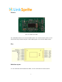
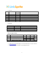
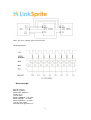
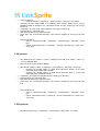
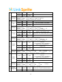
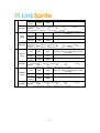
LinkSprite RFID Reader/Writer Module
(ISO14443 Proximity cards standard)
HY502F
User Manual
December 2009
1
Brief Introduction
HY502 series of RFID reader/writer modules are based on non-contact card reader ASCI chip
compatible with ISO14443 standard. It uses 600nm CMOS EEPROM technology, supports
ISO14443 typeA protocol, and also supports the MIFARE standard encryption algorithm. The
chipset integrates analog modulation and demodulation circuits, only requires minimal peripheral
circuits to function. The module supports UART interface, I2C interface, and SPI interface. The
digital circuits has dual working voltages mode, TTL and CMOS. The HY502 module is targeting
water, electricity, gas meters, vending machines, access control, elevators, drinking fountains,
telephone billing system or other identification card reader system applications.
Users can simply select the desired interfaces to harvest the full operation of the system and do
not need to struggle with the complicated radio base station design.
HY502 series supports Mifare One S50, S70, Ultra Light & Mifare Pro, FM11RF08 and other
compatible cards. It can be set to automatically find cards, by default, to automatically find cards.
HY502 series is a low-power modules, wide-voltage 2.7 ~ 5.5V, using an integrated module with
embedded antenna can significantly reduce PCB size.
Features
o Supports three interfaces at the same time:
o UART serial interface
o SPI Interface
o IIC interface
o Automatically detect the card close to the antenna area, and generate an interrupt signal
to the host MCU.
o Employ chipset of ISO14434A standard, and support MIFARE standard encryption
algorithm;
o Working voltage is between 2.7V- 5.5V, has TTL/CMOS voltage modes.
o Use industrial-grade high-performance processor, built-in hardware watchdog, with high
reliability;
o Anti-jamming processing and excellent EMC performance;
o A few simple commands can cover the complicated underlying read and write card
operations.
2
Pictures
Size: 57.8mm X 34.5mm
The embedded antenna can read cards within 0-6cm. The external antenna, which can be
connected to J2 by disconnecting the 4 short soldering point, can read cards within 0-10cm.
Pins
Definition of pins:
J1 is the connectors from module to host MCU, J2 is the connector for external antenna.
3
J1 connector:
Pins
Name
J1-1
J1-2
J1-3
J1-4
J1-5
J1-6
J1-7
J1-8
J1-9
RXD/SCL
TXD/SDA/MISO
MOSI
NSS
RST
M1
SIG
VCC
GND
IO type
(TTL/CMO
S Voltage)
I/O
I/O
I/O
I
I
I
O
Power
Ground
Description
UART receive or clock line for IIC and SPI
UART send or data line for IIC, MISO for SPI
MOSI for SPI
Slave selection for SPI
Reset, and active low. Floating is okay
Interface selection bit 1
Interrupt signal, 0 means card is present
Positive terminal of power
Ground
J2 connector:
Pin
J2-1
J2-2
J2-3
J2-4
J2-5
J2-6
Name
GND
TX1
GND
TX2
GND
RX
Description
Ground
Sending antenna 1
Ground
Sending antenna 2
Ground
Receive antenna
Electrical specification:
Charater
Parameter
TSTR
TOP
Environment or storage temperature
Operating temperature
Vcc
Operating voltages
Icc1
TRST
Operating current
Minimum reset pulse duration
•
•
Minimu
m
-40
-25
3
4.5
7
1.6
Typical
+25
3.3*
5
54
Maximu
m
+150
+85
3.6
5.5
120
Unit
o
C
C
o
V
mA
us
In UART mode, the operating voltage is 5V. If want to work under 3.3V, please contact us
at [email protected]
If not specified, BOD is 2.7V. BOD is 4V if specifically work at 5V.
4
Selection of interface:
HY502 supports UART, IIC and SPI at the same time. The selection of interface is one by
setting the voltage level of NSS and M1.
Pins
M1 NSS
Interface
UART
11
IIC
10
SPI
01
The change of interface can be done when the module is in operation. But due to the
interference, the process needs 4ms. To guarantee the reliability, we recommend to add a
delay of 20ms.
Definition of interface pins at different mode:
Pin
Mode
IIC
SPI
UART
J1-1
RXD/SCL
SCL
SCL
RXD
J1-2
TXD/SDA/MISO
SDA
MISO
TXD
J1-3
MOSI
A0
MOSI
X
J1-4
NSS
0
1
1
J1-5
M1
1
0
1
Note: 0 means low voltage, 1 means high voltage, x means “don’t care”.
UART interface
The default baud rate is 19200bps. Power on default is automatically scan for card, and don’t
need the host to frequently issue scan for card command. When card is present, SIG will
send an interrupt signal, and then host MCU can use scan for card command to read the
serial number of the card.
The following two diagrams show how HY502 is connected to host MCU and PC. A RS232
level shifter is needed when connecting to PC. The RST signal can be left floating, and will
automatically reset on power cycle.
5
Connection between MCU and HY502.
Connection between PC and HY502 using a RS232 or RS485 signal level shifter.
IIC interface
•
•
•
•
•
Only require 2 wire
7 bit programmable address, and can support up to 127 module
Data rate can be as high as 400kHz.
Noise suppression circuit can support glitch with duration shorter than 50ns.
Internal pull-up resistors
Connection between MCU and HY502.
6
R1 and R2 are pull-up resistors. The normal value is 10k. The driving capability is 400pF without
additional driver.
IIC timing diagram:
The bus timing diagram is shown below. The SDA must be kept stable logical signal when SCL is
high. Logical high is data 1 and logical low is data 0. The data can only be changed when the
SCL is logical low.
SPI interface
•
•
•
•
3-wire synchronous data transfer
Write jam protection
Wake up call from bus
Master and salve
7
NSS is the slave selection signal, and active low.
SPI timing diagram:
Driver example
#include "main.h"
#include "hy502.h"
#define KEY_PRESS 0
sbit M1 =P1^3;
// mode define
#define UMODE 0 // uart mode
#define IMODE 1 // iic mode
#define SMODE 2 // spi mode
// mode select funtion
void modset(unsigned char xx)
8
{
if(xx==0) //uart
{
M1=1;
NSS=1;
}
else if(xx==1) //iic
{
M1=1;
NSS=0;
}
else if(xx==2) //SPI
{
M1=0;
NSS=1;
}
}
/************************** main function start here *******************************/
void main()
{
uchar idata cStatus;
uchar BusMode;
InitializeSystem(); // Init
Reset_HY502();
// LED_YELLOW=0; //test led
LED_GREEN=0;
delay_10ms(50);
// LED_YELLOW=1;
LED_GREEN=1; //LED light 0.5s
beep(2); //test buzz
//----- test key------//
if(KEY1==KEY_PRESS) splash(1);
if(KEY2==KEY_PRESS) splash(2);
if(KEY3==KEY_PRESS) splash(3);
if(KEY4==KEY_PRESS) splash(4);
if(KEY1==KEY_PRESS)
{
BusMode=UMODE; // Select UART
}
else if(KEY2==KEY_PRESS)
{
BusMode=IMODE ; // Select IIC
{
a0=1;
a1=0;
a2=1;
}
}
else if(KEY3==KEY_PRESS)
{
BusMode=SMODE ; // Select SPI
}
modset(BusMode); // Set interface mode
9
delay_10ms(50);
//-----------------main loop ---------------//
while (1)
{
// KeyPress(); process key
// add your code here
//check command tag
if (g_bReceCommandOk)
{
g_bReceCommandOk = FALSE;
if(BusMode==IMODE)
{
cStatus=cmd_process_iic();
if(cStatus)
{
cStatus=0;
}
}
else if(BusMode==SMODE)
{
cStatus=cmd_process_spi();
if(cStatus)
{
cStatus=0;
}
}
else
{
// cStatus=cmd_process_uart();
if(cStatus)
{
cStatus=0;
UartSend(g_cReceBuf); // Send data to uart.
// add your code here
}
}
Interface Communication Protocols
1. UART protocol
•
•
1 start bit + 8 data bit + 1 stop bit
Baud rate: 19200
10
•
•
•
•
•
•
•
Command format:
o Command header + length byte + command byte + data field + check byte
Command header: 0XAA 0xBB, if the following data contains 0xAA, please add an
additional 0x00 to distinguish the command header, but the length byte will not be
increased.
Length byte: the byte length from length byte to last byte of data field.
Command byte: command code
Data field: the data for the command code
Check byte: the accumulated XOR byte value from the length byte to last byte of data
field.
Return data format:
o Success: Command header + length byte + command byte + data field + check
byte
o Failed: :Command header + length byte + inverted command byte + data field +
check byte
2. IIC protocol
•
•
•
•
•
•
•
•
The 4MSB of the IIC address is 1010, ie, 0xA0, the four LSB of IIC address can be set
set using A2A1A0+W/R.
Data rate of IIC communication: 400kbps
Data format: (Address+W/R) + length byte + command byte + data field + check byte
o Example, the module address is 0xA0, Write command, W/R=0, so the write
command will be: 0xA0 +0x0 = 0xA00
o Example, the module address is 0xA0, Read command, W/R=1, so the read
command will be: 0xA0+0x1= 0xA1
Length byte: the length from length byte to the last byte of data field
Command byte: the command code
Data field: the data for the command code
Check byte: the accumulated XOR byte value from the length byte to last byte of data
field.
Return data format:
o Success: Command header + length byte + command byte + data field + check
byte
o Failed: Command header + length byte + inverted command byte + data field +
check byte
3. SPI protocol
•
Data format: Status byte + length byte + command byte + data field + check byte
11
•
•
•
•
•
•
Status byte: the status byte of the bus. A status byte will be sent in the beginning of
sending operation.
Length byte: the length from length byte to the last byte of data field
Command byte: the command code
Data field: the data for the command code
Check byte: the accumulated XOR byte value from the length byte to last byte of data
field.
Return data format:
o Success: Command header + length byte + command byte + data field + check
byte
o Failed: Command header + length byte + inverted command byte + data field +
check byte
Command table and return value (UART is used as example, IIC and SPI
will not include the command header 0xAA 0xBB)
Note: Unless specified, all numbers are hex.
ID
Command
Name
Module
Control
1
Status
Send
Return
Send:
Example
Length
Byte
0x03
0x02
aabb
Command header
Return:
Set card
IDLE
2
Example
0x02
Success
0x02
Return
Fail
0x02
Return
Send:
aabb
Command header
Return:
Set
automatic
Send
0x11
1 byte control byte, software power
dropping mode, nonzero will exit soft
power dropping mode, and 0x00 will
enter soft power dropping mode
0x11
03
length byte
0x03
11
00
12
command code data field check byte
02
length byte
11
command code
0x12
13
check byte
When this command is executed, the
card will be set to be idle. For reactivation, card needs to be removed
from antenna area, and move back.
0x12
0xED
02
length byte
aabb
Command header
3
Data and Description
aabb
Command header
Send
Command
Code
02
length byte
12
10
command code check byte
12
command code
0x13
12
10
check byte
1 byte data field, 0x01 to turn on
automatic scan, and 0x00 to turn off
scan
Example
Success
0x02
Return
Fail
0x02
Return
Send:
aabb
Command header
Return:
4
Example
02
Command header
Return:
Example
Send
Read
block
6
Example
Send
7
Example
Return:
8
Wallet
Initializatio
n
19
check byte
This function includes scan card, anticollision, and select the card
0x20
4 byte data: the serial number of the card
02
20
22
command code check byte
06
length byte
0x0A
20
command code
92BF7259
data field
20
check byte
0x21
1 byte key tag+ 1 byte block number + 6
byte key
Key tag: 0x00 – PICC_AYTHENT1A
0x01 – PICC_AUTHENT1B
0x21
16 byte data
0xDE
0a
length byte
aabb
21
length byte
00 08 ffffffffffff 23
command code
12
0x1A
data
21
command code
check byte
00112233445566778899AA00BBCCDDEEFF
data field
33
check byte
1 byte key tag+ 1 byte block number + 6
byte key
Key tag: 0x00 – PICC_AYTHENT1A
0x01 – PICC_AUTHENT1B
0x22
0x22
0xDD
1a
22
length byte
command code
aabb
Command header
04 00
data field
0x20
aabb
Command header
19
command code
length byte
Success
0x02
Return
Fail
0x02
Return
Send:
aabb
1b
0xDF
Success
0x12
Return
Fail
0x02
Return
Send:
aabb
Return:
19
command code check byte
04
0x02
Command header
Write
block
02
length byte
Command header
11
check byte
0xe6
aabb
Command header
10
No data field
2 byte data field, card type
S50 card: 0x0400, S70: 0x0200.
0x19
length byte
Command header
00
13
command code
0x19
Success
0x06
Return
Fail
0x02
Return
Send:
aabb
Return:
13
command code data field check byte
length byte
Send
0x02
Success
0x04
Return
Fail
0x02
Return
Send:
aabb
Send
5
03
aabb
Command header
Scan for
card
0xEC
length byte
Command header
Read card
type
0x13
02
length byte
00 08 ffffffffffff
22
command code
Send
0x0E
0x23
Success
0x02
0x23
13
00112233445566778899AA00BBCCDDEEFF
data
30
check byte
20
check byte
1 byte key tag+ 1 byte block number + 6
byte key + 4 bytes init wallet amount
Return
Fail
Return
Send:
Example
0x02
aabb
Send
9
Example
0x0A
Command header
Send
Deposit
money
10
Example
Withdraw
money
11
Example
24
0x0E
27
11110000
data
24
command code
check byte
11110000
data
22
check byte
1 byte key tag+ 1 byte block number + 6
byte key+ 4 bytes wallet amount (LSB in
the front)
0x25
0x25
0xDA
0e
25
length byte
aabb
command code
02
0x0E
Command header
00 09 ffffffffffff
command code
06
length byte
25
length byte
command code
00 08 ffffffffffff
11110000
data
22
check byte
27
check byte
1 byte key tag+ 1 byte block number + 6
byte key+ 4 bytes wallet amount (LSB in
the front)
0x26
Success
0x02
Return
Fail
0x02
Return
Send:
aabb
Return:
4 bytes wallet amount (LSB in the front)
0a
Command header
Send
0x24
0xDB
Success
0x02
Return
Fail
0x02
Return
Send:
aabb
Return:
21
check byte
1 byte key tag+ 1 byte block number + 6
byte key
length byte
Command header
check byte
23
command code
24
11110000
data
0x24
aabb
Command header
00 08 ffffffffffff
command code
02
length byte
Success
0x06
Return
Fail
0x02
Return
Send:
aabb
Return:
23
length byte
aabb
Command header
Read
wallet
0e
Command header
Return:
0xDC
0x26
0xD9
0e
26
length byte
aabb
Command header
command code
02
length byte
14
26
command code
00 08 ffffffffffff
11110000
data
24
check byte
21
check byte
LinkSprite Technologies, Inc.
Add:1410 Cannon Mountain Dr, Longmont, CO 80503
Tel: 720-204-8599
Email:[email protected]
Technical questions: [email protected]
Web:www.linksprite.com
15