1
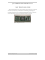
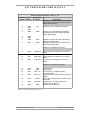
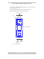
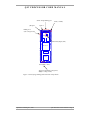
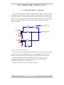
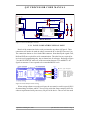
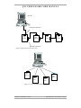
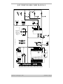
QIC PROCESSOR CORE
V16
U SER ' S M ANUAL
© QUANSER CONSULTING INC., 2002
QIC
How to contact Quanser Consulting:
(905) 940-3575
Telephone
(905) 940-3576
Facsimile
80 Esna Park Drive
Markham, ON
Canada L3R 2K8
Mail
http://www.quanser.com/qic/ Web
mailto://[email protected]
mailto://[email protected]
mailto://[email protected]
Information about QIC
Support for QIC
General information
User's Manual
QIC is a trademark of Quanser Consulting, Inc.
PIC, and PIC16F877 are a trademarks of Microchip Technology Inc.
Other brands and their products are trademarks or registered trademarks of their respective holders
and should be noted as such.
© 2002 Quanser Consulting Inc.
All rights reserved. This work may not be translated or copied in whole or in part without the
written permission of the copyright holder, except under the terms of the associated software
license agreement. No part of this manual may be photocopied or reproduced in any form.
The use of general descriptive names, trade names, trademarks, etc. in this publication, even if the
former are not especially identified, is not to be taken as a sign that such names as understood by
the Trade Marks and Merchandise Marks Act, may accordingly be used freely by anyone.
Printed in Canada.
© Quanser Consulting Inc., 2002
Indexes - Page II
QIC
TABLE OF CONTENTS
1 INTRODUCTION ........................................................................................................1
2 QIC PROCESSOR CORE ...........................................................................................2
2.1 Processor Core Features........................................................................................3
2.2 Processor Core Pin Names.....................................................................................4
2.3 Processor Core Pin Locations...............................................................................4
3 QIC PROCESSOR CORE ACCESSORIES ............................................................10
3.1 In-Circuit Serial Programming Hardware........................................................10
3.1.2 High-Voltage Programming...........................................................................11
3.1.2.1 High-Voltage Programming Procedure...............................................................12
3.1.3 Low-Voltage Programming............................................................................12
3.1.3.1 Low-Voltage Programming Procedure................................................................12
3.2 On-Board Serial Support.....................................................................................15
3.2.1 RS232 Compatible Serial Port.......................................................................16
3.2.2 QIC-Link Serial Port......................................................................................17
4 SUPPORT SOFTWARE ............................................................................................20
4.1 Using the QIC Loader..........................................................................................20
4.1.1 High Voltage Programming............................................................................21
4.1.2 Low Voltage Programming............................................................................21
4.2 Using the QIC Bootloader....................................................................................23
5 SCHEMATICS ............................................................................................................25
5.1 QIC Processor Core – V16...................................................................................26
© Quanser Consulting Inc., 2002
Indexes - Page III
QIC
FIGURE INDEX
Index of Figures
Figure 1. The QIC Processor Core. ....................................................................................2
Figure 2. The QIC Processor Core – Pin names and functions. .........................................5
Figure 3. In-circuit serial programming support circuitry. ...............................................11
Figure 4. Serial pin locations. ...........................................................................................13
Figure 5. Serial programming and connection setup details. ...........................................14
Figure 6. Serial interface logical diagram. .......................................................................15
Figure 7. The serial interface circuitry. ............................................................................16
Figure 8. Serial interface to PC wiring. ............................................................................16
Figure 9. QIC Link network connections. ........................................................................18
Figure 10. "Star" network topology of QIC Link. ............................................................19
Figure 11. QIC Loader window. Select a file by clicking on Browse. .............................20
Figure 12. Programmer error message. .............................................................................22
Figure 13. Typical error message encountered during programming. .............................22
Figure 14. PIC Downloader interface window. ................................................................24
© Quanser Consulting Inc., 2002
Indexes - Page IV
QIC
INDEX OF TABLES
Index of Tables
Table 1. Pinout description for pins 1 - 18.
Table 2. Pinout description for pins 19 - 36
Table 3. Serial / Programming port connections.
Table 4. QIC Link serial port connections.
Table 5. High-Voltage programming support connections.
© Quanser Consulting Inc., 2002
6
7
8
8
9
Indexes - Page V
QIC PROCESSOR CORE MANUAL
1 INTRODUCTION
The QIC suite of development components is aimed at simplifying the development of
microcontroller-based applications. By integrating several commonly used functions into
one convenient package, development time is greatly reduced. The user can quickly
commence development of the external interfaces and the software, rather than spend
time building the base microcontroller system. Using the QIC system as a reference
design can greatly reduce implementation time of your designs.
The QIC system consists of two main hardware components. The first is the QIC
Processor Core. This component hosts the microcontroller and the associated
components to facilitate communications and programming. The second component is
the QIC Carrier Board, which hosts an array of interfaces and signal conditioning
options. Several different carrier boards are available, and are suited to different
applications. Together, the two boards form an excellent reference design for many
projects such as robotics, controllers, and various signal processing applications.
© Quanser Consulting Inc., 2002
Introduction - Page 1
QIC PROCESSOR CORE MANUAL
2 QIC PROCESSOR CORE
Based on the PIC16F87X series of microcontrollers, the QIC Processor Core offers all
the features of the processor, plus the added ease of interfacing, programming and
prototyping. Designed to fit into a standard prototyping breadboard, the QIC allows the
user to design interface circuitry on a breadboard to quickly test new ideas.
Figure 1. The QIC Processor Core.
© Quanser Consulting Inc., 2002
QIC Processor Core - Page 2
QIC PROCESSOR CORE MANUAL
2.1 PROCESSOR CORE FEATURES
Designed around the PIC16F877 microcontroller, the QIC Processor Core allows the
user to take advantage of the vast amounts of freely available source code on the Internet.
No special tools are required to program the processor core – the programming support
hardware is already included. The user just needs to use the QIC Loader to download a
new program. The code can be compiled using any of the available compilers for the
PIC16FXXX series of microcontrollers.
Based on the Microchip PIC16F877
8K Flash program memory
368 bytes RAM
256 bytes EEPROM memory
14 hardware interrupts
3 hardware timers
10 bit A/D (8 channels)
10 bit PWM (2 channels)
RS 232 compatible serial port – connects directly to the PC
In-circuit serial programming support hardware built in
On board reset switch.
Single +5V supply required
© Quanser Consulting Inc., 2002
QIC Processor Core - Page 3
QIC PROCESSOR CORE MANUAL
2.2 PROCESSOR CORE PIN NAMES
Figure 2 shows the location of the pins and their associated names for the QIC
Processor Core. For detailed information on the PIC microcontroller, programming, and
special function details, refer to the Microchip website, at http://www.microchip.com.
Document number 30292c provides detailed programming information on the
PIC16F87X series of microcontrollers. In most instances, the signal from the
microcontroller is directly available on the pins of the QIC Processor Core. Please refer
to the schematics section for details on this.
2.3 PROCESSOR CORE PIN LOCATIONS
Figure 2 also shows the pin locations and their numbering. Note how the pins are offset
in their alignment to prevent the QIC Processor Core from being inserted incorrectly.
The pins are numbered consecutively, from 1, counter clockwise from the top left.
© Quanser Consulting Inc., 2002
QIC Processor Core - Page 4
QIC PROCESSOR CORE MANUAL
Serial / Programming port
RTS
PIN 36
GND
DTR
CTS
TXD
RXD
PIN 1
RB0/INT
VCC
RB1
RD7/PSP7
RD6/PSP6
RB2
RB3/PGM
RD5/PSP5
RB4
RD4/PSP4
RB5
RD3/PSP3
RD2/PSP2
RB6/PGC
PB7/PGD
RD1/PSP1
RD0/PSP0
PE0/RD/AN5
PIN 28
JP1 (Programming Jumper)
PIN 10
RE1/WR/AN6
RE2/CS/AN7
RA0/AN0
CLK
RC7/RX/DT
RA1/AN1
RA2/AN2/VREF-
RC6/TX/CK
RA3/AN3/VREF+
RC4/SDI/SDA
RA4/T0CKL
RC3/SCK/SCL
RC2/CCP1
RC5/SD0
RA5/SS/AN4
GND
RC1/T1OSO/CCP2
JP2
High-Voltage
Programming
Header
GND
QICRx
QICTx
VHVP
GND
RC0/T1OSO/T1CKI
PIN 19
QIC Link
Serial Port
Figure 2. The QIC Processor Core – Pin locations and functions.
© Quanser Consulting Inc., 2002
QIC Processor Core - Page 5
QIC PROCESSOR CORE MANUAL
QIC Core Pin Descriptions – Pins 1 – 18
QIC Pin
Number
Pin
Name
Alternate
Names
1
2
3
4
RB0
RB1
RB2
RB3
INT
Also serves as an external interrupt pin.
PGM
Applying +5V volts will allow low voltage
programming when the configuration bits
are set appropriately.
5
6
7
RB4
RB5
RB6
PGC
8
RB7
PGD
Interrupt-on-change pin. Also used as the
serial programming clock
Interrupt-on-change pin. Also used as the
serial programming data
Description
PORTB is a bi-directional I/O port. The pins
on this port can be programmed to use the
internal weak pull ups.
PORTE is a bi-directional I/O port.
9
RE0
/RD, AN5
Read control for the slave port, or analog
input 5
10
RE1
/WR, AN6
11
RE2
/CS, AN7
Write control for the slave port, or analog
input 6
Chip select for the slave port, or analog
input 7
PORTA is a bi-directional I/O port
12
13
14
RA0
RA1
RA2
AN0
AN1
AN2, VREF-
15
RA3
AN3, VREF+
16
RA4
T0CKI
17
RA5
/SS, AN4
18
GND
GND
Analog input 0
Analog input 1
Analog input 2, or negative analog
reference voltage
Analog input 3, or positive analog reference
voltage
Clock input to Timer0 timer / counter. (open
drain type)
Analog input 4, or slave select for the
synchronous serial port
Ground / power return pin
Table 1. Pinout description for pins 1 - 18.
© Quanser Consulting Inc., 2002
QIC Processor Core - Page 6
QIC PROCESSOR CORE MANUAL
QIC Core Pin Descriptions – Pins 19 – 36
QIC Pin
Number Pin Name
19
20
RC0
RC1
21
RC2
22
RC3
23
RC4
24
25
RC5
RC6
26
RC7
27
CLK
Alternate
Names
Description
PORTC is a bi-directional I/O port
T1OSO, T1CKI Timer1 oscillator output or Timer1 clock input
T1OSI, CCP2 Timer1 oscillator input or Capture 2
input/Compare 2 output/PWM2 output
Capture 1 input, Compare 1 output/PWM1
CCP1
output
Synchronous serial clock input/output for SPI
SCK, SCL
and I2C modes
SPI data in in SPI mode, or data I/O in I2C
SDI, SDA
mode
SDO
SPI data out in SPI mode
USART Asynchronous transmit or
TX, CK
synchronous clock
USART Asynchronous receive or
RX, DT
synchronous data
Processor clock source. This is an external
clock (20MHz) for use with external
peripherals
PORTD is a bi-directional I/O port. It also
serves as the parallel slave port when
interfacing to a microprocessor bus
28
29
30
31
32
33
34
35
RD0
RD1
RD2
RD3
RD4
RD5
RD6
RD7
36
VCC
+5VDC Power
Table 2. Pinout description for pins 19 - 36
© Quanser Consulting Inc., 2002
QIC Processor Core - Page 7
QIC PROCESSOR CORE MANUAL
Serial / Programming Port Pin Descriptions
Pin Number
1
2
3
4
5
6
Pin Name
Description
RxD
PC Receive data line (RS232 level). Data
from the QIC is transmitted on this line to
the PC
TxD
PC Transmit data line (RS232 level). Data
is received by the QIC on this line from the
PC
DTR
PC Data Terminal Ready line. Used for
programming purposes
PC Clear To Send line. Used for
CTS
programming purposes
RTS
PC Ready To Send line. Used for
programming purposes
GND
Ground line
Table 3. Serial / Programming port connections.
QIC Link Pin Descriptions
Pin Number Pin Name
Description
1
QIC Link Rx Data transmitted from other QIC modules
is sent to the serial port, bypassing the QIC
(RS232 level). This data is seen by the
host only.
2
QIC Link Tx Data received at the serial port is
retransmitted via this pin to other QIC
modules (RS232 level). The data appears
as if it came from the host directly.
3
GND
Ground connection.
Table 4. QIC Link serial port connections.
© Quanser Consulting Inc., 2002
QIC Processor Core - Page 8
QIC PROCESSOR CORE MANUAL
High Voltage Programming Pin Descriptions
Pin Number
1
2
Pin Name
Description
+12VDC input for high-voltage
VHVP
programming.
Ground connection for high-voltage
GND
programming
Table 5. High-Voltage programming support connections.
3 QIC PROCESSOR CORE ACCESSORIES
To simplify the development process, the QIC Processor Core has built in serial
support and in-circuit programming support. This section has detailed information on
these two interfaces.
3.1 IN-CIRCUIT SERIAL PROGRAMMING HARDWARE
To make programming of the QIC Processor Core easier, the circuitry required for incircuit serial programming has been included directly on the board. The circuitry is
designed to allow for in-circuit serial programming when required, but to leave the
programming pins available for other functions when the device is not being
programmed. To enable this dual configuration, a jumper, JP1 is used to select between
programming mode and normal operation. In the event that the programming pins (RB6
and RB7) are not required for the user's application, the jumper can be left in place
without affecting the normal operation of the system. In effect, installing the jumper
(JP1) connects the pins RB6 and RB7 to the in-circuit serial programming hardware.
Removing the jumper connects pin RB6 to pin 7 of the QIC core, and pin RB7 to pin 8 of
the QIC core. Figure 3 shows the circuit details that achieve this functionality.
© Quanser Consulting Inc., 2002
QIC Processor Core - Page 9
QIC PROCESSOR CORE MANUAL
VCC
R3
10k
U4A
1
2
VCC
SN7407
R4
10k
VCC
JP2
1
2
U4B
3
VCC
TX
DTR
CTS
RTS
GND
SN7407
+12V
DP1
R5
10k
R8
10k
R1
U4C
6
5
U3
12
13
VCC
SN7407
PC
R6
10k
RB7X
U4D
9
8
VCC
SN7407
R7
10k
U4E
11
10
U4F
13
JP1
1
2
SN7407
Program
RB6X
2
1
5
3
6
11
10
9
7
X0
X1
X
Y0
Y1
Y
Z0
Z1
Z
100
1
1
2
3
4
5
6
R2
10k
14
MCLR
S1
MA152WKCT-ND
15
RB7
RB7
4
RB6
RB6
RESET
C1
1uf
2
J1
4
INH
A
B
C
VEE
MC14053B
12
QIC Programmer
SN7407
Figure 3. In-circuit serial programming support circuitry.
3.1.1
3.1.2 HIGH-VOLTAGE PROGRAMMING
Programming voltage is applied to header JP2 (see Figure 5). +12VDC should be
applied to pin 1, and the ground for the external source should be connected to pin 2.
Refer to Figure 3 for details. Applying the voltage at this connector supplies the required
high voltage signal to put the PIC16F877 into the programming mode. The voltage for
high voltage programming can be obtained from any regulated external power source.
Using the QIC Loader, the user can quickly program the device with their own code. In
addition, the user can write their own programmer to use the on-board in-circuit serial
programming hardware. Microchip has documents detailing in-circuit serial
programming of the 16F877 processor.
Please note that the PIC16F877 will be put into programming mode when both RB6
and RB7 are held low, and MCLR is brought up to the required high voltage
programming voltage. This condition is most easily obtained by setting up the high
voltage programming voltage, holding RB6 and RB7 low, and waiting for the user to
© Quanser Consulting Inc., 2002
QIC Processor Core - Page 10
QIC PROCESSOR CORE MANUAL
press the reset button on the QIC Processor Core. This procedure guarantees that when
the reset button is released the PIC16F877 will go into the program mode.
3.1.2.1H I G H -V O LT A G E P R O G R A M M I N G P R O C E D U R E .
Install a jumper on JP1, shorting the pins together.
Apply +12V to JP2. +12VDC should be on pin 1, ground (GND) on pin 2.
Connect the programming cable to J1, the programming/serial port.
Start the programming software and follow the directions.
3.1.3 LOW- VOLTAGE P ROGRAMMING
With the configuration register of the PIC16F877 set appropriately, it is possible to
program the device using only +5VDC. By default, when fully erased, the PIC16F877
will allow low-voltage programming (LVP)1. To put the PIC16F877 into low-voltage
programming mode, the user will need to apply +5VDC to the PGM pin (RB3), or pin 4
of the QIC Processor Core (see Figure 5). Note that when in this mode, RB3 cannot be
used for any other purpose. In effect, this pin is lost to the user under software control.
The only function of the pin is to put the PIC16F877 into low-voltage programming
mode when the LVP bit of the configuration register is set2. As with the high-voltage
programming mode, the user can either use the QIC Loader, or write their own software
to program the device. Microchip has documents detailing in-circuit serial programming
of the 16F877 processor.
Please note that the PIC16F877 will enter programming mode when both RB6 and
RB7 are held low, and +5VDC is applied to the PGM pin (pin 4 of the QIC core). With
these conditions present, pressing the reset button will guarantee that the PIC16F877 will
enter programming mode when the reset switch is released.
3.1.3.1L O W -V O LT A G E P R O G R A M M I N G P R O C E D U R E
Install a jumper on JP1, shorting the pins together.
1 Please consult the Microchip document,"EEPROM Memory Programming Specification"
document number 30262c (30262c.pdf, www.microchip.com )
2 Note that if the LVP (low voltage programming) bit is cleared – disabling LVP – this method
of programming will no longer be available. The user will have to resort to high-voltage
programming.
© Quanser Consulting Inc., 2002
QIC Processor Core Accessories - Page 11
QIC PROCESSOR CORE MANUAL
Apply +5VDC to the PGM pin (pin 4 of the QIC core). A good source for this is
the power going to pin 36, VCC.
Connect the programming cable to J1, the programming/serial port.
Start the programming software and follow the directions.
Serial / Programming port
RXD
TXD
DTR
CTS
RTS
GND
PIN 1
Programmer
HVP Enable
RESET
JP1 (Programming Jumper)
Q
PIC16F877
20MHz
QICTx
QICRx
GND
GND
VHVP
RS232
JP2
High-Voltage
Programming
Header
QIC Link
Serial Port
Figure 4. Serial pin locations.
© Quanser Consulting Inc., 2002
QIC Processor Core Accessories - Page 12
QIC PROCESSOR CORE MANUAL
Serial / Programming port
QIC pin 1
VCC (+5VDC)
J1 pin 1
PGM, pin 4
(low-voltage mode)
Programmer
HVP Enable
RESET
Short this jumper (JP1)
Q
PIC16F877
20MHz
RS232
JP2 (GND, +12V)
Apply programming voltage here.
(High – voltage mode)
Figure 5. Serial programming and connection setup details.
© Quanser Consulting Inc., 2002
QIC Processor Core Accessories - Page 13
QIC PROCESSOR CORE MANUAL
3.2 ON-BOARD SERIAL SUPPORT
The on-board serial interface is shown in logical format in Figure 6. With an external
connection to J1, the serial port connector, the device will be able to communicate with
the QIC Processor Core. Signals transmitted from the PC (TxD) are received by the PIC
on RC7, which is connected directly to the microcontroller's USART. Using the USART
allows for the greatest flexibility in serial support, while minimizing the required
software overhead.
1
3
PIC Tx
PIC Tx (RC6 pin 25)
2
TTL > RS232
J1
PC RxD
PC TxD
1
2
3
4
5
6
GND
PIC Rx
PIC Rx (RC7 pin 26)
RS232 > TTL
GND
PC
J2
Tx
Rx
GND
1
2
3
QICLink Rx
QICLink Tx
RS232 > TTL
QICLink
GND
TTL > RS232
Figure 6. Serial interface logical diagram.
Similarly, serial data is shifted out of the USART on RC6, and is sent to the PC's RxD
pin on the serial port. The serial interface uses a combined RS232 to TTL / TTL to
RS232 converter to provide the proper signal levels for the PC and the PIC16F877.
The QIC Link port echoes the serial data received at J1 on connector J2.By
connecting additional devices, to the QIC Link port, they will also be able to
communicate with the host PC (or host device).
The full serial interface schematic is shown in Figure 7.
© Quanser Consulting Inc., 2002
QIC Processor Core Accessories - Page 14
QIC PROCESSOR CORE MANUAL
J1
1
2
3
4
5
6
RxD
TxD
RC6
DP2
MA152WACT-ND
RC7
V+
V-
PC
J2
1
2
3
U1
QICT
QICR
13
8
11
10
1
3
QICLink
C7
1 uf
R1 IN
R2 IN
T1 IN
T2 IN
C1+
C1 -
R1 OUT
R2 OUT
T1 OUT
T2 OUT
C2+
C2 -
12
9
14
7
4
5
C5
1 uf
C8
1 uf
C6
1 uf
VCC
MAX232CWE
RS232 Interface
Figure 7. The serial interface circuitry.
3.2.1 RS232 COMPATIBLE SERIAL PORT
Details of the connections for the serial port interface are shown in Figure 8. These
connections will need to be made in order to connect the PC to the QIC Processor Core.
The connections shown are for a female DB9 connector. Note that only the signals TxD,
RxD and GND are required for serial communications. The other lines are required for
in-circuit serial programming only, but are shown here for reference. Referring to Figure
7, the MAX232CWE IC takes care of the conversions between TTL and RS232. All
signals at connector J1 are expected to be at standard RS232 levels.
RB0
RB1
RB2
RB3
RB4
RB5
RB6
RB7
RE0
RE1
RE2
RA0
RA1
RA2
RA3
RA4
RA5
GND
QIC Motherboard
Programmer
PIC16F877
20MHz
RS232
HVP Enable
RESET
1
6
To PC
1
6
2RxD
7RTS
3TxD
8CTS
4DTR
9
5GND
DB-9 Pins Signal Description
--------------------------------------------2
(1)RxD Transmit to PC
3
(2)TxD Receive from PC
4
(3)DTR Data In from PC
8
(4)CTS Data Out to PC
7
(5)RTS Clock from PC
5
(6)GND Ground
VCC
RD7
RD6
RD5
RD4
RD3
RD2
RD1
RD0
CLK
RC7
RC6
RC5
RC4
RC3
RC2
RC1
RC0
DB9
Figure 8. Serial interface to PC wiring.
When writing software to use the serial port, the user must be careful to specify RC6
for transmitting serial data, and RC7 for receiving serial data. Some compilers allow for
software implemented serial ports on any I/O pins of the device. The user will also need
© Quanser Consulting Inc., 2002
QIC Processor Core Accessories - Page 15
QIC PROCESSOR CORE MANUAL
to take care of the RS232 to TTL level conversion. RS232 level signals should not be
directly applied to any pins except the serial port interface or the QIC Link interface.
3.2.2 QIC- LINK SERI AL PORT
The QIC Link serial port is intended to facilitate multi-device communications. The
topology of the communication network is "host-to-slave". What this means is that the
host PC can communicate with any of the QIC Processor Core modules. The QIC cores
can in turn talk to the host PC. Refer to Figure 6 and Figure 7 for details on the
implementation of this circuit.
Figure 9 details the network connections necessary to link several QIC Processor Core
boards together. Although it appears that data flows through the previous QIC core
in the network chain, this is not the case. QIC cores connected in this manner will only
be able to talk directly to the host PC. Other QIC cores will not see the serial
communications data. However, every QIC on the network will see serial
communications sent from the host PC. For this reason, the user will need to
implement some type of protocol to manage the network traffic. Each QIC Processor
Core on the network will need to be assigned an address so that it can determine if the
data being sent is intended for it. Many different methods exist for implementing this
type of network negotiation. The exact type of protocol used will depend on the actual
application requirements.
© Quanser Consulting Inc., 2002
QIC Processor Core Accessories - Page 16
QIC PROCESSOR CORE MANUAL
Host PC
Serial port connection
QIC
Core 1
QIC
Core 2
QIC
Core 3
QIC
Core 4
QIC Link connection
Figure 9. QIC Link network connections.
QIC
Core 1
QIC
Core 2
QIC
Core 4
QIC
Core 3
Figure 10. "Star" network topology of QIC Link.
© Quanser Consulting Inc., 2002
QIC Processor Core Accessories - Page 17
QIC PROCESSOR CORE MANUAL
© Quanser Consulting Inc., 2002
QIC Processor Core Accessories - Page 18
QIC PROCESSOR CORE MANUAL
4 SUPPORT SOFTWARE
Programming of the QIC Processor Core can be achieved in a variety of ways. Using the
included support software such as the QIC Loader and the QIC Bootloader, the user can
quickly develop and test new applications. Depending on the end use of the application,
the user may choose the QIC Loader approach over the QIC Bootloader approach or
vise-versa.
4.1 USING THE QIC LOADER
The QIC Loader approach allows programming of the QIC Processor Core while it is
still in the user's circuit. Using the loader approach is the more traditional of the
programming methods in that the programmer erases the entire memory contents of the
device and rewrites it with the user's new code. Using this approach, all areas of the
memory space can be modified; code memory, data EEPROM memory, and
configuration memory. Since this method allows setting of the code protection bits in the
configuration memory registers, it is usually the preferred method for final product
deployment.
Figure 11. QIC Loader window. Select a file by clicking on
Browse.
Programming can be accomplished using either high-voltage or low voltage mode.
Depending on the programming mode selected, follow the appropriate procedure below.
© Quanser Consulting Inc., 2002
Support Software - Page 19
QIC PROCESSOR CORE MANUAL
4.1.1 HIGH VOLTAGE PROGRAMMING
Install a jumper on JP1, shorting the pins together.
Apply +12V to JP2. +12VDC should be on pin 1, ground (GND) on pin 2.
Connect the programming cable to J1, the programming/serial port. The other end of
the cable should connect to the serial port of the PC.
Apply power to the QIC Processor Core.
Start the QIC Loader and select an Intel Hex formatted file to load.
Make sure that the correct serial port is selected. The default port is COM1. Select a
different one by selecting Setup -> Serial Port and selecting from the available
choices.
Click the Write button to begin the programming process.
Follow the directions on the screen. The Reset button referred to on the screen is the
reset button on the QIC Processor Core.
A dialog will appear confirming the success or failure of the programming procedure.
4.1.2 LOW VO LTAGE PROGRAMMING
Install a jumper on JP1, shorting the pins together.
Apply +5VDC to the PGM pin (pin 4 of the QIC core). A good source for this is the
power going to pin 36, VCC.
Connect the programming cable to J1, the programming/serial port. The other end of
the cable should connect to the serial port of the PC.
Apply power to the QIC Processor Core.
Start the QIC Loader and select an Intel Hex formatted file to load.
Make sure that the correct serial port is selected. The default port is COM1. Select a
different one by selecting Setup -> Serial Port and selecting from the available
choices.
Click the Write button to begin the programming process.
Follow the directions on the screen. The Reset button referred to on the screen is the
reset button on the QIC Processor Core.
© Quanser Consulting Inc., 2002
Support Software - Page 20
QIC PROCESSOR CORE MANUAL
A dialog will appear confirming the success or failure of the programming procedure.
In most cases, the programming will complete successfully. However, there are times
when errors will occur. The error message shown in Figure 12 typically means that the
PC cannot detect the hardware. This error will occur before the programming begins.
Figure 12. Programmer error message.
Typical causes of this are:
Serial cable unplugged from the PC or the QIC Processor Core
Wrong serial port selected in the QIC Loader
Power is not applied to the QIC Processor Core.
Damaged serial cable
The causes listed above should be checked to remedy the problem before trying to
continue.
Other errors may occur during the programming procedure. The error shown in Figure
13 is indicative of a programming error.
Figure 13. Typical error message encountered
during programming.
© Quanser Consulting Inc., 2002
Support Software - Page 21
QIC PROCESSOR CORE MANUAL
Typical causes of this are:
Serial communications error; check symptoms of failed hardware first.
Jumper JP1 has not been installed for programming.
No programming voltage applied for high-voltage programming, or PGM voltage not
present for low-voltage programming.
Reset button not pressed when requested by the software.
Code protection bits are set in the configuration memory area. Erase the entire device
before continuing.
Processor is faulty or damaged.
Use of the programming software is fairly straight-forward. There are additional tools
for viewing the program and data memory, as well as for erasing an PIC16F877 and
restoring to its default condition.
4.2 USING THE QIC BOOTLOADER
The QIC Bootloader approach takes advantage of the processor's ability to reprogram
its own code space. To start, a small program called the bootloader is programmed into
the device using the QIC Loader. This bootloader occupies a very small portion of the
code space near the top of memory. Once loaded, upon processor reset, the bootloader
looks for a serial "signature" at the serial port. If it receives this signature, it then goes
into the bootloading mode, otherwise, it begins executing the previously loaded user
code. In the bootloading mode, an Intel Hex type file is transferred to the device using a
standard serial protocol. Typically, a serial terminal program such as Hyperterminal or
the PIC Downloader can be used to send a new file. The previously installed bootloader
receives the code and reprograms the PIC. This method is extremely useful for rapid
development of new designs.
In order to use the bootloader, the bootloader code must be downloaded to the
processor first. Otherwise, the bootloading will not be possible. Once the bootloader is
installed, neither high-voltage programming, nor low-voltage programming will be
required. For this reason, the user may wish to disable the low-voltage programming
© Quanser Consulting Inc., 2002
Support Software - Page 22
QIC PROCESSOR CORE MANUAL
option by setting the appropriate configuration bits. Once the bootloader code is loaded
into the program memory, only the serial port connections will be required. To use the
PIC Downloader, start the program and select an Intel Hex formatted file for download.
Search for this file by clicking the search button, or pressing F2.
Figure 14. PIC Downloader interface window.
Once the file is loaded, press Write (or F4) to begin the programming process. The
reset button on the QIC Processor Core should be pressed at this time. After a brief
pause, the download will commence.
If problems arise during the programming process, check the following list of possible
causes.
Make sure the serial cable is attached, and that power is applied.
Be certain that the bootloader code has already been written to the device using either
high-voltage or low voltage programming.
Verify that the serial port and the baud rate are correct for the bootloader that is being
used.
© Quanser Consulting Inc., 2002
Support Software - Page 23
QIC PROCESSOR CORE MANUAL
5 SCHEMATICS
The schematics provided in this section are for user reference only. The schematics
are Copyright Quanser Consulting Inc. 2002. The information contained here may not be
used for commercial purposes without the consent of Quanser Consulting Inc. Use of the
circuitry for educational purposes only is permitted, provided that the user has purchased
one QIC Processor Core for each circuit that is constructed. For information on licensing
the QIC Processor Core for commercial or other purposes, please contact Quanser
Consulting Inc.
Quanser Consulting Inc.
80 Esna Park Drive,
Units 1,2,3
Markham, Ontario
Canada
L3R 2R6
Tel : +1 (905) 940 - 3575
www.quanser.com
mailto://[email protected]
5.1 QIC PROCESSOR CORE – V16
© Quanser Consulting Inc., 2002
Schematics - Page 24
QIC PROCESSOR CORE MANUAL
TxD
DTR
1
3
9
6
R5
10k
VCC
CTS
RTS
11
13
U4A
SN7407
U4B
SN7407
U4C
SN7407
U4D
SN7407
U4E
SN7407
U4F
SN7407
2
4
5
8
10
12
VCC
R3
10k
VCC
R4
10k
VCC
R6
10k
J1
JP1
1
2
VCC
R7
10k
QICT
QICR
GND
RxD
TxD
DTR
CTS
RTS
GND
Program
1
2
3
4
5
6
PC
J2
1
2
3
QICLink
RB7X
RB6X
12
13
2
1
5
3
6
11
10
9
7
U3
Z
Y
X
Y0
Y1
X0
X1
Z0
Z1
INH
A
B
C
VEE
VCC
C3
0.1uF
MC14053B
C2
0.1uF
RB7
RB6
C4
0.1uF
V+
VCC
1
2
JP2
+12V
C5
1 uf
S1
RESET
V-
C6
1 uf
C1
1uf
R8
10k
Quanser Consulting Inc. QIC
MA152WKCT-ND
DP1
R2
10k
VCC
14
15
4
DB-9 Pins Signal Description
--------------------------------------------2
RxD Transmit to PC
3
TxD Receive from PC
4
DTR Data In from PC
8
CTS Data Out to PC
7
RTS Clock from PC
5
GND Ground
R1
100
RA0
RA1
RA2
RA3
RA4
RA5
RB0
RB1
RB2
RB3
RB4
RB5
RB6
RB7
TXA
QICR
TxD
RC7
TXA
C7
1 uf
14
2
3
4
5
6
7
8
36
37
38
39
41
42
43
44
1
17
28
40
U2
2
C10
22p
OSC2/CLKOUT
RC0/T1OSO/T1CKI
RC1/T1OSI/CCP2
RC2/CCP1
RC3/SCK/SCL
RC4/SDI/SDA
RC5/SDO
RC6/TX/CK
RC7/RX/DT
RD0/PSP0
RD1/PSP1
RD2/PSP2
RD3/PSP3
RD4/PSP4
RD5/PSP5
RD6/PSP6
RD7/PSP7
RE0/RD
RE1/WR
RE2/CS
20 MHz
C9
22p Y1
1
OSC1/CLKIN
MCLR/VPP
RA0
RA1
RA2
RA3
RA4/T0CKI
RA5/SS
RB0/INT
RB1
RB2
RB3
RB4
RB5
RB6
RB7
NC
NC
NC
NC
DP2
R1 OUT
R2 OUT
T1 OUT
T2 OUT
C2+
C2 -
MA152WACT-ND
MAX232CWE
R1 IN
R2 IN
T1 IN
T2 IN
C1+
C1 -
U1
PIC16F877-20I/L
13
8
11
10
1
3
12
9
14
7
4
5
15
16
18
19
20
25
26
27
29
21
22
23
24
30
31
32
33
9
10
11
CLK
RC0
RC1
RC2
RC3
RC4
RC5
RC6
RC7
RD0
RD1
RD2
RD3
RD4
RD5
RD6
RD7
RE0
RE1
RE2
RC6
TXB
TXB
RC7
QICT
RxD
C8
1 uf
1
2
3
4
5
6
7
8
9
10
11
RB0
RB1
RB2
RB3
RB4
RB5
RB6X
RB7X
RE0
30
31
RE1 12
RE2 13
RA0 14
RA1 15
RA2 16
RA3 17
RA4 18
RA5 19
GND20
RC0 21
RC1 22
RC2 23
RC3 24
RC4 25
RC5 26
RC6 27
RC7 28
CLK 29
RD0 32
RD1 33
RD2 34
RD3 35
RD4 36
RD5 37
RD6 38
RD7 39
VCC 40
H1
QIC
Schematics - Page 25
© Quanser Consulting Inc., 2002
1
2
QIC PROCESSOR CORE MANUAL
Alphabetical Index
breadboard 2
compiler 3
High-Voltage Programming Procedure
In-Circuit 10
Low-Voltage Programming Procedure
manual II
Microchip 4
PIC16F877 3
PIC16F87X 2
pin locations 4
Pinout 6
Pinout 7
pins 4
port II
programming 4
programming mode 11
QIC 1p.
QIC Processor Core 1
Quanser II
RB6 10
RB7 10
schematics 4
Serial Programming 10
Serial Support 15
translate II
© Quanser Consulting Inc., 2002
12
12
Schematics - Page 26