1
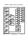
Bring-up and Performance ® Enhancement of IBM 5x86C Microprocessor-Based Systems Using PUZZLE.EXE Application Note Authors: Doug Massey and Andy Anderson Revision Summary: This is the initial release of this document. This document gives an FAE or a system designer a step-by-step method for bringing up a board with an IBM 5x86C microprocessor and optimizing performance of the processor using a distributed program called PUZZLE.EXE. At each step there are hints and notes to provide assistance. There are several documents that are very useful for bringing up a board although it's possible to get started without some of them. At some point, the engineer will want to collect all of these documents: User's Manual for the Motherboard Chipset Manual for the Motherboard Schematic for the Motherboard PUZZLE.EXE (A DOS program distributed by the x86 Applications Dept.) M1SC.EXE (A DOS program distributed by the x86 Applications Dept.) IBM 5x86C Microprocessor Databook IBM 5x86C Microprocessor BIOS Writer's Guide Guide for Adapting Intel® DX4 Design for IBM 5x86C Microprocessor There have been a few instances where boards have yielded slightly different results and this process isn't completely foolproof, but the vast majority of boards can follow these instructions step-by-step to reach the first plateau of performance maximization. The flow diagram on the following page depicts the first of two steps that a system de- signer or a field application engineer can use to maximize the overall performance of a system that uses IBM's 5x86C microprocessor. After reaching 1.75 or 1.76 seconds with puzzle, the next step is to maximize the performance of a more sophisticated CPU-only benchmark. benchmarks we prefer to use is CPUMark16, from Ziff-Davis' PCBench 9.0. One of the This bench- mark measures the performance of the microprocessor and the memory subsystem. If the steps in the flow diagram are completed successfully, performance optimization should next focus on the memory subsystem components - L2 cache and DRAM. Page 1 of 5 September 22, 1995 Fax #40036 Initial Board and BIOS Verification Using PUZZLE.EXE Board boots w/IBM >20 seconds See Note 4 or Intel® DX2 or DX4 processor. 3.02 seconds See Note 5 Set jumpers for IBM 5x86C -- 2.80 seconds See Note 6 See Note 1 2.37 seconds Does board boot to No BIOS information See Note 7 Double check jumpers See Note 2 screen? 2.03 seconds See Note 8 Yes BIOS update needed, Does BIOS No 1.92 seconds See Notes 8/9 but continue for now. BIOS may not configure recognize IBM 5x86C? chipset and IBM 5x86C correctly. 1.86 seconds See Notes 8/10 Yes 1.76 seconds Contact x86 Does the board boot to DOS? No Application Department for assistance SUCCESS! Initial performance optimization for IBM 5x86C is complete. Run PUZZLE.EXE See Note 3 If possible, continue IBM 5x86C optimization with a more sophisticated What is the total benchmark ELAPSED TIME shown on the PUZZLE display? Page 2 of 5 September 22, 1995 Fax #40036 Notes: Caution: In all cases you should consult the table of required settings in the IBM 5x86C BIOS Writer's Guide and the errata notice that applies to your hardware revision level before enabling or disabling any performance related features. 1. Setting jumpers for a 5x86C microprocessor is probably the most difficult task that this document will cover, mainly because it is always different from board to board. The IBM 5x86C microprocessor has many pins in common with both the IBM and the Intel DX2 and DX4 microprocessors (see the three conversion guides for details), but there are always some differences that need to be taken into account. The IBM 5x86C microprocessor has more features than these other microprocessors and requires a few more signals to implement them. The differences between processors are usually accommodated by jumpers on the motherboard. These jumpers define the function of particular pins, thereby letting the engineer determine how he would like the I/O pins to be configured. The information required to switch the I/O to the IBM 5x86C microprocessor definition is sometimes contained in the User's Manual. If this is so for the board you are working with, follow the directions explicitly and try to boot the system. If the User's Manual doesn't mention the 5x86C microprocessor, it is still possible to determine the correct jumper settings by combining the information in the User's Manual (i.e., settings for DX2 or DX4), the Conversion Guides, and the board schematic. For example, the CLKMUL pin is the same on the IBM 5x86C microprocessor as the Intel DX4. If the User's Manual uses JP10 to define CLKMUL for the iDX4, then that's the pin that should be used for the 5x86C microprocessor. 2. Other factors besides pin assignments can cause problems with the system boot. Be sure that bus frequency, jumperable wait states, CPU voltage, and other similar parameters are within specifications. Wherever possible, be conservative during the initial boot of the system and try to enhance performance after the system has booted. For instance, change the 33 MHz bus to 25 MHz if you think the motherboard might be having problems at the higher frequency. 3. The target speed is 1.75 seconds (or 1.76 -- the times vary by up to one hundredth of a second). If your time is higher, then there is something fundamental that is degrading the performance of the 5x86C microprocessor. The time returned by PUZZLE can be used as a diagnostic tool to determine what the problem is. Note that all the times referenced in this document are for 33/100 MHz, unless otherwise stated. PUZZLE can also be used as a general tool to fine-tune performance at other frequencies, but the associated times returned by PUZZLE will have to be scaled according to the internal frequency. 4. If the time is grossly slow (about 27 or 28 seconds), the L1 Reboot, go into the BIOS screen and enable Page 3 of 5 cache hasn't been enabled. the L1 cache (in write-back mode, if you September 22, 1995 Fax #40036 can), and try it again. If your BIOS doesn't support write-back mode for the L1, use M1SC.EXE to change it from WT to WB (see note 9 below). 5. If the time is 3.02 seconds or higher, the L1 cache is in write-through cache is turned off. Go to BIOS and set the L2 cache (Note: in write-back second target mode and the L2 L1 cache to write-back mode, and enable the mode, the L2 cache isn't needed to achieve the 1.75 speed for PUZZLE, but it will be needed to maximize performance against other benchmarks). Reboot and try PUZZLE with these new settings. 6. If the time is around 2.80 or 2.85 seconds, the chip is running 33/66 MHz instead of 33/100 MHz. There is a pin to the 5x86C processor (R17 for the PGA package and pin 11 for the QFP package) multiplier the called CLKMUL that determines, at power up, what clock processor will use for its internal frequency. Presently, setting this GND puts the chip in 2x mode, setting it to VDD puts the chip in hardwired for some boards, and jumper-selectable for jumper selectable and you can switch to 3x mode. others. oscilloscope. Use the motherboard pin to This is Hopefully, your board is Do so and rerun PUZZLE. 7. If the time is 2.37, 2.47, 2.58, or 2.69, the chip is running 25/75 might like to verify this with the motherboard 3x mode. instead of 33/100. You jumper setting definitions or with an user's guide to change the bus speed to 33/100 and run PUZZLE again. 8. If the time is 2.03 or less, you're getting close. with the L1 cache enabled. You are definitely running 33/100 MHz, There is still some fine level adjusting to be done though. The grid below shows the PUZZLE times achieved with and without some of these adjustments. You should be able to find your time on the grid and immediately identify your problem. L1 Cache Mode BTB Status Puzzle Time =========== ========= =========== Write-Back Enabled 1.75 Write-Back Disabled 1.86 Write-Through Enabled 1.92 Write-Through Disabled 2.03 9. The L1 Cache Mode can be changed in BIOS on most boards. If your board doesn't support this option in BIOS, use M1SC.EXE to enable the write-back pins and set the chip to write-back mode: Run M1SC.EXE from the DOS prompt. Page down three times to find the Configuration Control Register screen. Change the second-to-last bit of CCR2 (WBAK) to a "1". write-back mode. This enables the pins used in If the bit is already a 1, skip this and the next step. Press "F3" to write the value to the on-chip register. Page up to get back to the Control Registers screen. Page 4 of 5 September 22, 1995 Fax #40036 Switch to write-back mode by changing the NW bit in CR0 to a "1". Press "F3" to save the value. Press "ESC" to exit. 10. The BTB (Branch Target Buffer) can also be enabled with M1SC.EXE. The process is similar: Run M1SC.EXE from the DOS prompt. Page down three times to get to the Configuration Control Registers. Change the four MAPEN bits in CCR3 to "0001". If these are already set to "0001", skip this and the next step. Press "F3" to write the value to the on-chip register. Page down twice to get to the Performance Control screen. Change the last two bits (RStack and BTB) in PCR0 to 1's. Press "F3" to save the values and "ESC" to quit IBM Corporation 1995. All rights reserved. IBM and the IBM logo are registered trademarks of International Business Machines Corporation. IBM Microelectronics is a trademark of the IBM Corp. All other product and company names are trademarks/registered trademarks of their respective holders. 1995 IBM Corp. This document may contain preliminary information and is subject to change by IBM without notice. IBM makes no representations or warranties that the use of the information or applications herein shall be free of third party intellectual property claims and assumes no responsibility or liability from any use of the information contained herein. Nothing in this document shall operate as an express or implied license or indemnity under the intellectual property rights of IBM or third parties. The products described in this document are not intended for use in implantation or other direct life support applications where malfunction may result in physical harm or injury to persons. NO WARRANTIES OF ANY KIND, INCLUDING BUT NOT LIMITED TO THE IMPLIED WARRANTIES OF MERCHANTABILITY OR FITNESS FOR A PARTICULAR PURPOSE ARE OFFERED IN THIS DOCUMENT. All performance data contained in this publication was obtained in a specific environment, and is presented as an illustration. The results obtained in other operating environments may vary. Page 5 of 5 September 22, 1995 Fax #40036