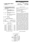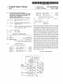
1
US006615302B1
(12) United States Patent
(10) Patent N0.:
US 6,615,302 B1
(45) Date of Patent:
Sep. 2, 2003
Birns
(54)
USE OF BUFFER-SIZE MASK IN
6,304,908 B1 * 10/2001 Kalajan .................... .. 709/229
CONJUNCTION WITH ADDRESS POINTER
6,357,014 B1
*
3/2002
Correia . . . . . . .
. . . .. 713/502
T0 DETECT BUFFER_FULL AND BUFFER_
6,430,164 B1 :
8/2002
Jones et al. . . . . .
. . . .. 370/313
A
6,496,885 B1
DEVICE THAT EMPLOYS
RECONFIGURABLE MESSAGE BUFFERS
12/2002 Smart 6[ 8.1. .............. .. 710/100
FOREIGN PATENT DOCUMENTS
W0
(75) Inventor: ggegEdward Birns, Cupertino, CA
W0 8806317 A1 *
8/1988
........... .. G06F/9/46
* Cited by examiner
Primary Examiner—Paul R. Myers
(73) Assignee: Koninklijke Philips Electronics N.V.,
( * ) Notice:
Eindhoven (NL)
(57)
Subject to any disclaimer, the term of this
A
atent is extended or adusted under 35
'
mlcmcotttmuer that Supports a plurahty of message
objects, and that mcludes a CAN processor core, a plurality
£3 S C 154(k)) by 407 dag/S
' '
ABSTRACT
of message buffers associated With respective ones of the
'
message objects, a CAN/CAL module that processes incom
(21)
A 1 N
(22)
Filed,
(60)
Related US Application Data
Provisional application NO_ 60/154,022’ ?led on Sep 15’
address pointer. The CAN/CAL module includes a message
handling function that transfers successive frames of the
1999.
current incoming message to the message buffer associated
pp‘
09/630 290
0':
ing messages that include a plurality of frames and a
’
l
lit Y of messa g e ob'ect
re g isters , includin g at least one
Pura
1
Aug 1 2000
buffer size register that contains a message buffer size value,
’
and at least one buffer location register that contains an
(51) Int. c1.7 .............................................. .. G06F 13/14
Cl-
(58)
llggivaesgssstzgeoglgg’i
. . . . . . . . . . . . . . . . . . . . . . . . . . . . . . . . . ..
address pointer
increment
IE:if;tiki?gfn‘ggglileagfgzsag
function~
T‘he
module
Fleld 0f Search ............................... .. 710/240, 116,
further includes a frame Status detection function, and a
710/305> 121; 709/229; 713/502; 365/244>
230'08> 240; 711/109> 202; 700/1
buffer-status detection function that retrieves the incre
mented address pointer value, retrieves the message buffer
_
(56)
size va ue rom t e at east one
References Cited
'
1
f
h
1
u er size re ister associate
b ff
'
g‘
j
d
With the designated receive message object, and decodes the
retrieved message buffer size value into a buffer-size mask,
U.S. PATENT DOCUMENTS
and determines a message buffer-fullness status of the mes
5,179,708 A
*
1/1993 Gyllstrom et a1. ........ .. 709/314
sage buffer associated With the designated receive message
5,323,385 A
5,444,643 A
*
*
6/1994 Jurewicz et al.
8/1995 Haussler et al.
object using the retrieved incremented address pointer value
5,506,966 A
*
4/1996
5,627,840 A
5,893,162 A
*
*
5/1997 Hundertmark et al. .... .. 714/726
4/1999 Lau et al. ................. .. 711/153
370/300
702/122
and the buffer-size mask.
Ban ......................... .. 709/314
37 Claims, 7 Drawing Sheets
T53
I I
TiMERO
‘
TIMERT
. 54
WATCHDOG
4
;
TIMER
I
U.S. Patent
Sep. 2, 2003
Sheet 1 0f 7
US 6,615,302 B1
__
STANDARD
Bus sor CANID rrrrr IDE r0 DLC
DabFie'd
0.8,...,64-brts
CRO
CR0 ACK ACK ror rrs Bus Idle
. DEL 7-bits 3-brts
1-brt 1-brt 1-brt
Idle r-nrr rr-birs r~r>rrr-brrr-r1rr 4-r1rr (0'1r-~~8BYIBS) 15-bits DEL
bedgsor
BaselD srrrr r05 Extended
r0 rrrrr r1
1-bb11-MSBS 18-LSBS 1-bit 1-brt'
e
r0 DLC
DataField
CR5
CRC ACK ACK
_
EXTENDED
RTR RemoteTransmitRequest
SRR SubstituteRemoteRequest
IDE ID Extension
r1, r0 “reserved" bits
DLC DataLengthCode (0,1, 8)
IFS InterFrameSpace
FIG. 1
CANbus
CAN
CAL Messa e-C
Data Frame
B-Byte ------ - -g ---- - -
g-gyre ....... _. 833%
CAL Message-D
8-Byte
------- -
- -
8-Byte
-------------------------- - -
8-Byte
U.S. Patent
Sep. 2, 2003
Sheet 2 0f 7
US 6,615,302 B1
K20
E """""""""" "3'4' _______________ u
3
CORE DATA BUS
:
XA CPU CORE
;
;
PROGRAM BUS
24x 32KBYTES
i
ROM/EPROM
;
DATA RAM
:
I
MEMORY
4*’: ENGINE
H
3O
1
:
'
MMRs
i
l
4O
421
CORE
" """""
<-:___> PORTSO-B
;
61/
E
,'
I
:51
4+
SPI
N——>:
‘*—.
I
' 53
TIMERO J»
4.,
I
‘T ’
A54
i
:
<:——>
4+ TIMERZ <:—
‘.
i
:
,
-'——-r>;
.
20B CAN/DLL
i
UARTO
g;
A/
=
'. ,
,- ------------- -~ 38
I
TX .
g
4-»
x28 /36
.
:
RX
41
BUS
MMR BUS
:
;
l
i
XRAIVI
' '
47> INTERFACE
:
:
:
i
27
EXTERNAL
ADDRESS/
DATABUS
5
SFRBUS
DAT
26x 1024 BYTES
x22
‘
X43
:
:
i
I
‘L '
‘-77
<—>
4+
WATCHDOG
:
NNER
-
55
i
g
E
:
i
U.S. Patent
Sep. 2, 2003
Sheet 3 0f 7
US 6,615,302 B1
MMRs
MMR name
I R/W? | Reset
[Access
|Address0tlset
[Description
Message Object Registers (n = 0 - 3i)
MnMlDH
R/W
x....x00b
Word only
000n4ngngnrng0000bln0hl MessagenMatchlD High
MnMlDL
R/W
xxxxh
Word only
000n4n3n2n1ng0010b (n2h) Message n Match lD Low
MnMSKH
R/W
x....x000b Word only
000n4n3ngn1rig0100b0l4hl MessagenMask High
MnMSKL
R/W
xxxxh
000n4n3n2n1ng0tt0bm6h) MessagenMaskLow
MnClL
R/W
00000xxxb Byte/Word
MnBLR
MoBSZ
MnFCR
R/W
R/W
R/W
xxxxh
Word only
00000xxxb Byte/Word
00xxxxxxb Byte/Word
MessagenButterLocalion
MessagenBulterSize
MessagenFragmentation Count
MCPLL
MCPLH
CANlNTFtG
MCIR
MElR
FESlR
R/C
R/C
R/C
R0
R0
R/C
0000b
0000h
0000h
0000b
0000h
0000h
FEENR
R/W
0000h
ByleANord
Byte/Word
Byte/Word
Message Complete Low
Message Complete High
CAN Interrupt Flag Register
Message Complete lnlo Reg.
Message Error lnlo Register
Frame Error Status Register
SCP/SPI Conliguration
SCP/SPI Data
SCP/SPI Control and Status
Word only
000ll4ll3ll2ll1ltgl000blh8h) MessagenControl
000ll4ll3ll2ll1llQl0l0bUtAh)
000040302010011000 (nCh)
000n4n3ngn1nglll0b(nEhl
ClC Registers
Byte/Word
224h
Byte/Word
226h
Byte/Word
228h
Byte/Word
229h
22Ah
22Ch
22Eh
Frame Error Enable Register
SPICFC
R/W
0000h
SCP/SPl Registers
Byte/Word 260h
SPIBATA
SPICS
R/W
R/W
00h
00h
Byte/Word
Byte/Word
CANCMR
CANSTR
CANBTR
R/W
R/O
R/W
0th
00h
00h
Byte/Word
Byte/Word
Byte/Word
TXERC
RXERC
EWLR
ECCR
ALCR
RTXDTM
GClL
R/W
R/W*
R/W*
Byte/Word
Byte/Word
Byte/Word
Byte/Word
Byte/Word
Byte/Word
Byte/Word
Byte/Word
273h
274h
275h
R/W
00h
00h
00h
96h
0000h
0000h
0000h
0000b
XRAMB
R/W
FEh
Byte/Word
290h
XRAM Base Address
MBXSR
MIFBTRL
MIFBTRH
R/W
R/W
R/W
FFh
EFh
FFh
Byte/Word
Byte/Word
Byte/Word
29th
292h
293h
Msg. Butt/XRAM Seg. Reg.
MlF Bus liming Reg. Low
MlF Bus liming Reg. High
R/W
R0
R0
W0
262h
263h
CCB Registers
270h
276h
278h
27Ah
27Ch
27Eh
MIF Registers
Legend: R/W : Read &Write, R0 = Read Only, W0 = Writ
CAN Reset mode, x = undetined atter reset.
27th
272h
CAN Command Register
CAN Status Register
CAN Bus liming Reg. (low)
CAN Bus Timing Reg. (high)
ix Error Counter
Rx Error Counter
Error Warning Limit Register
Error Code Capture Register
Arbitration Lost Capture Reg.
RiX Beta Test Mode
Global Control Byte
U.S. Patent
Sep. 2, 2003
US 6,615,302 B1
Sheet 4 0f 7
Data Memory Segment 0
OOFFFFh
_1_|_l_LLl_LI
Otf~Chip
4K Bytes
MMR Space
IITIIItI
MMR Base Address
Off-Chip
512 BytesT
XRAM Base Address
Off-Chip
OOOBFFh
_I_LJ_.LLL_LI
Off-Chip Data Memory
(Scratch Pad)
n-rTn-n'
OOOOOOh
MMR Space
Ottset FFFh ——>
Ottset 1FFh ———>
512 Bytes Object Registers
<— Offset OOOh
U.S. Patent
Sep. 2, 2003
Sheet 5 0f 7
US 6,615,302 B1
Segment xy in Data
Memory Space
xyFFFFh _________I
object HT Object 0 Message Buffer
Buffer size
F123
F116 315
50
XRAM
[_-——__— 4—
512 Bytes
2120
me @115
a8 a7
a0
l——"' <—— MBXSR[7:0] XRAMB[7:1]0
00h
I
xyOOOOh
Segment xy in Data
Memory Space
xyFFFFh —___l
e23
a16 a15
<— MBXSR[7:0]
a0
MnBLR
OblectnT Object 0 Message Buffer
XRAM
512 Bytes
Buffer size
|
XRAM
323
a16 H15
a8 a7
[--—--_-<— MBXSR[7:0] XRAMBMO
l
xyOOOOh
a0
000
U.S. Patent
Sep. 2, 2003
Sheet 6 6f 7
US 6,615,302 B1
Object n Match lD Field (MnMlDH and lVlnMlDL)
|
Mid28-Mid18
| Mid17-Mid10 | Mid9-Mid2 l Midi |lVlidO | MIDE]
Object n Mask Field (MnMSKH and MnMSKL)
|
Msk28-Mskl8 IMsklY-MsklOl Msk9—-Msk2 [Mskl |l\/lsk0|
Screener lD Field (assembled from incoming bit-stream)
|CANlD.28—CANlD.l8|DataBytel[7:O]\DataByte2[7:0ll x | x ||DE|
Object 0 Match ID Field (MnMlDH and MnMlDL)
l
Mid28—Midl8
[Mien-Mimi Mid9-Mid2 [Midi IMidOIll/llDEl
Object n Mask Field (MnMSKH and MnMSKL)
|
Msk28-Msk18 | Msk17- Msk10| Msk9~~Msk2 | Mskl l MskOI
Screener lD Field (assembled from incoming bit-stream)
|
CAN lD.28 - CAN lD.O
FIG. 10
I lDE |
U.S. Patent
Sep. 2, 2003
Sheet 7 0f 7
US 6,615,302 B1
Benn
ttttttt‘éty‘t
Data Byte 2
Data Byte 3
ADDRESS
Data Byte DLC
Data Byte 2 (next)
Data Byte 3 (next)
FIG. 11
Frame'mo
Data Byte 1
Data Byte 2
Data Byte DLC
Framelnto (next)
Data Byte 1 (next)
Data Byte 2 (next)
FIG. 12
DIRECTION OF
INCREASING
ADDRESS
US 6,615,302 B1
1
2
USE OF BUFFER-SIZE MASK IN
CONJUNCTION WITH ADDRESS POINTER
TO DETECT BUFFER-FULL AND BUFFER
ROLLOVER CONDITIONS IN A CAN
DEVICE THAT EMPLOYS
RECONFIGURABLE MESSAGE BUFFERS
that ful?lls this need in the art. The XA-C3 is the neWest
member of the Philips XA(eXtended Architecture) family of
high performance 16-bit single-chip microcontrollers. It is
believed that the XA-C3 is the ?rst chip that features
hardWare CAL support.
The XA-C3 is a CMOS 16-bit CAL/CAN 2.0B micro
controller that incorporates a number of different inventions,
including the present invention. These inventions include
This application claims the full bene?t and priority of
US. Provisional Application Serial No. 60/154,022, ?led on
Sep. 15, 1999, the disclosure of Which is fully incorporated
novel techniques and hardWare for ?ltering, buffering,
handling, and processing CAL/CAN messages, including
herein for all purposes.
the automatic assembly of multi-frame fragmented mes
sages With minimal CPU intervention, as Well as for man
BACKGROUND OF THE INVENTION
The present invention relates generally to the ?eld of data
communications, and more particularly, to the ?eld of serial
communications bus controllers and microcontrollers that
incorporate the same.
aging the storage and retrieval of the message data, and the
memory resources utiliZed therefor. In particular, the XA-C3
15
CAN module has the unique ability to track and reassemble
the packets constituting a fragmented message, completely
in hardWare, only interrupting the CPU (processor core)
once a complete, multi-frame message is received and
CAN (Control Area Network) is an industry-standard,
assembled. This tremendously reduces the processor band
tWo-Wire serial communications bus that is Widely used in
Width required for message handling, thereby signi?cantly
automotive and industrial control applications, as Well as in
increasing available bandWidth for other tasks, so that sys
medical devices, avionics, office automation equipment,
tem performance is greatly enhanced.
consumer appliances, and many other products and appli
The present invention relates to a scheme employed by
cations. CAN controllers are currently available either as
the XA-C3 microcontroller to handle a message buffer full
stand-alone devices adapted to interface With a microcon
25
condition in such a manner that ensures no loss of data,
troller or as circuitry integrated into or modules embedded
programmers) have developed numerous high-level CAN
While minimiZing the required processor intervention. More
particularly, the present invention relates to a particular
Application Layers (CALs) Which eXtend the capabilities of
implementation of this scheme, including speci?c tech
the CAN While employing the CAN physical layer and the
CAN frame format, and adhering to the CAN speci?cation.
CALs have heretofore been implemented primarily in
softWare, With very little hardWare CAL support.
Consequently, CALs have heretofore required a great deal of
niques for detecting the message buffer full condition and for
determining the number of data bytes stored in a message
buffer.
host CPU intervention, thereby increasing the processing
The present invention encompasses A CAN microcontrol
ler that supports a plurality of message objects, and that
in a microcontroller chip. Since 1986, CAN users (softWare
overhead and diminishing the performance of the host CPU.
SUMMARY OF THE INVENTION
35
Thus, there is a need in the art for a CAN hardWare
includes a processor core that runs CAN applications, a
implementation of CAL functions normally implemented in
plurality of message buffers associated With respective ones
of the message objects, a CAN/CAL module that processes
incoming messages that include a plurality of frames, each
softWare in order to offload these tasks from the host CPU
to the CAN hardWare, thereby enabling a great savings in
host CPU processing resources and a commensurate
frame having a maXimum number n of data bytes, and a
improvement in host CPU performance. One of the most
demanding and CPU resource-intensive CAL functions is
message management, Which entails the handling, storage,
and processing of incoming CAL/CAN messages received
over the CAN serial communications bus and/or outgoing
plurality of message object registers associated With each of
45
CAL/CAN messages transmitted over the CAN serial com
munications bus. CAL protocols, such as DeviceNet,
CANopen, and OSEK, deliver long messages distributed
over many CAN frames, Which methodology is sometimes
referred to as “fragmented” or “segmented” messaging. The
process of assembling such fragmented, multi-frame mes
sages has heretofore required a great deal of host CPU
intervention. In particular, CAL softWare running on the host
CPU actively monitors and manages the buffering and
processing of the message data, in order to facilitate the
the message objects, including at least one buffer siZe
register that contains a message buffer siZe value that
speci?es the siZe of the message buffer associated With that
message object, and at least one buffer location register that
contains an address pointer that points to an address of the
storage location in the message buffer associated With that
message object Where the neXt data byte of the current
incoming message is to be stored.
The CAN/CAL module includes a message handling
function that transfers successive frames of the current
incoming message to the message buffer associated With a
selected one of the message objects designated as a receive
assembly of the message fragments or segments into com
message object for the current incoming message an address
pointer increment function that, in response to a transfer of
the current data byte to the message buffer associated With
plete messages.
the designated receive message object, increments the
Based on the above and foregoing, it can be appreciated
that there presently eXists a need in the art for a hardWare
softWare in order to offload these tasks from the host CPU,
address pointer to the address of the storage location in that
message buffer Where the neXt data byte of the current
incoming message is to be stored.
The CAN/CAL module further includes a frame status
thereby enabling a great savings in host CPU processing
detection function that detects Whether or not the current
55
implementation of CAL functions normally implemented in
resources and a commensurate improvement in host CPU
performance.
The assignee of the present invention has recently devel
oped a neW microcontroller product, designated “XA-C3”,
65
frame of the current incoming message is the ?nal frame of
the current incoming message. The CAN/CAL module also
includes a buffer-status detection function that, each time
that the address pointer is incremented, retrieves the incre
US 6,615,302 B1
4
3
mented address pointer value, retrieves the message buffer
In the presently preferred embodiment, the CAN/CAL
siZe value from the at least one buffer siZe register associated
With the designated receive message object, and decodes the
module further includes a message-complete interrupt gen
erator function that generates a message-complete interrupt
retrieved message buffer siZe value into a buffer-size mask
comprised of a plurality X of bits, Where X is equal to a
to the processor core in response to the frame status detec
prescribed number of alloWable buffer siZes, and Wherein y
bits of the buffer-size mask have a ?rst logic state and the
remaining X-y bits have a second logic state, Where 2y equals
the retrieved message buffer siZe value, in terms of number
of bytes; and, determines a message buffer-fullness status of
the message buffer associated With the designated receive
10
message object using the retrieved incremented address
pointer value and the message buffer-size mask.
gramming the address pointer associated With that message
In a present implementation, the buffer-status detection
buffer to point to a selected base address.
function determines a ?rst buffer-fullness state of the mes
sage buffer associated With the designated receive message
object by logically OR’ing each of the X LSBs of the
15
sponding bit of the buffer-size mask, to thereby produce X
OR results, and then logically AND’ing the X OR results, to
thereby produce a ?rst single-bit AND result, Where the ?rst
logic state is ‘0’ and the second logic state is ‘1’. A ‘ 1’ value
of the ?rst single-bit AND result corresponds to the ?rst
buffer-fullness state of the message buffer associated With
25
detection function determines a second buffer-fullness state
processor core is provided With tWo options as to hoW to
respond to the message buffer-full interrupt. Under the ?rst
option, in response to the message buffer-full interrupt, the
current CAN application reads the entire contents of the
designated receive message buffer, and then transfers the
is less than the maXimum number n of data bytes, using the
retrieved incremented address pointer value and the message
buffer-size mask.
read-out entire contents to another storage location in the
Additionally, in the present implementation, the buffer
35
data memory space, thereby freeing up the designated
receive message buffer to store the at least one remaining
frame of the current incoming message. Under the second
option, the current CAN application, in response to the
message buffer-full interrupt, modi?es the base address of
designated receive message object by logically AND’ing the
?rst Z ones of the X OR results to produce a second single-bit
AND result, Where 2x'z=n. A ‘1’ value of the second single
bit AND result corresponds to the second buffer-fullness
state of the message buffer associated With the designated
receive message object. Preferably, the buffer-status detec
the designated receive message buffer by replacing the
current base address With a neW base address, Whereby the
designated receive message buffer consists of a ?rst buffer
tion function declares a message buffer-full condition if the
value of the second single-bit AND result is ‘1’, and the
current frame of the current incoming message is not the
?nal frame of the current incoming message.
The CAN/CAL module preferably further includes a
current incoming message that have already been stored in
the message buffer associated With the designated receive
message object, resets the address pointer contained in the at
least one buffer location register associated With the desig
nated receive message object to the base address, Writes the
current byte count into the message buffer associated With
the designated receive message object, in the storage loca
tion corresponding to the base address, and generates a
message buffer-full interrupt.
Preferably, the current CAN application running on the
of the message buffer associated With the designated receive
message object by determining Whether the number of
available bytes of remaining storage capacity in the message
buffer associated With the designated receive message object
status detection function determines the second buffer
fullness state of the message buffer associated With the
In the presently preferred embodiment, the message
buffer-full interrupt generator function determines a current
byte count that indicates the number of data bytes of the
retrieved incremented address pointer value With a corre
the designated receive message object.
Also, in the present implementation, the buffer-status
tion function detecting that the current frame of the current
incoming message is the ?nal frame of the current incoming
message.
Preferably, the siZe of each message buffer can be selected
by the user by programming a selected message buffer siZe
value into the at least one message buffer siZe register
associated With that message buffer, and the base address of
each message buffer can be selected by the user by pro
45
current byte count computation function that determines the
current byte count by logically AND’ing each of the X LSBs
of the retrieved incremented address pointer value With the
inverse of the corresponding bit of the buffer-size mask, and
an address pointer reset function that logically ANDs each of
the X LSBs of the retrieved incremented address pointer
value With the corresponding bit of the buffer-size mask, and
portion starting With the current base address, and a second
buffer portion starting With the neW base address.
Preferably, the current CAN application, in response to
the message-complete interrupt, retrieves a ?rst number of
the data bytes of the current incoming message from the ?rst
buffer portion, and retrieves a second number of the data
bytes of the current incoming message from the second
buffer portion, Where the ?rst number is the current byte
count.
BRIEF DESCRIPTION OF THE DRAWINGS
These and various other aspects, features, and advantages
Writes the resultant value back into the at least one buffer 55
of the present invention Will be readily understood With
location register associated With the designated receive
message object.
reference to the folloWing detailed description of the inven
tion read in conjunction With the accompanying draWings, in
Which:
The CAN/CAL module further includes a message buffer
full interrupt generator function that generates a message
FIG. 1 is a diagram illustrating the format of a Standard
CAN Frame and the format of an EXtended CAN Frame;
buffer-full interrupt to the processor core in response to a
declaration of a message buffer-full condition.
FIG. 2 is a diagram illustrating the interleaving of CAN
Data Frames of different, unrelated messages;
FIG. 3 is a high-level, functional block diagram of the
In the presently preferred embodiment, the frame status
detection function detects Whether the current frame of the
current incoming message is the ?nal frame of the current
header portion of the current frame of the current incoming
XA-C3 microcontroller;
FIG. 4 is a table listing all of the Memory Mapped
message.
Registers (MMRs) provided by the XA-C3 microcontroller;
incoming message by deriving that information from the
65
US 6,615,302 B1
5
6
FIG. 5 is a diagram illustrating the mapping of the overall
data memory space of the XA-C3 microcontroller;
FIG. 6 is a diagram illustrating the MMR space contained
Match ID: A 30-bit ?eld pre-speci?ed by the user to Which
the incoming Screener ID is compared. Individual Match
IDs for each of 32 Message Objects are programmed by
the user into designated Memory Mapped Registers
Within the overall data memory space of the XA-C3 micro
5
controller;
FIG. 7 is a diagram illustrating formation of the base
address of the on-chip XRAM of the XA-C3
microcontroller, With an object n message buffer mapped
into off-chip data memory;
FIG. 8 is a diagram illustrating formation of the base
address of the on-chip XRAM of the XA-C3
microcontroller, With an object n message buffer mapped
Mask: A 29-bit ?eld pre-speci?ed by the user Which can
override (Mask) a Match ID comparison at any particular
bit (or, combination of bits) in an Acceptance Filter.
1O
Screen for multiple acknoWledged CAL/ CAN Frames and
15
a Standard CAN Frame;
FIG. 10 is a diagram illustrating the Screener ID Field for
an Extended CAN Frame;
thus minimiZe the number of Receive Objects that must
be dedicated to such loWer priority Frames. This ability to
Mask individual Message Objects is an important neW
CAL feature.
CAL: CAN Application Layer. A generic term for any
high-level protocol Which extends the capabilities of CAN
While employing the CAN physical layer and the CAN
FIG. 11 is a diagram illustrating the message storage
format for fragmented CAL messages; and,
FIG. 12 is a diagram illustrating the message storage
format for fragmented CAN messages.
DETAILED DESCRIPTION OF THE
PREFERRED EMBODIMENT
Individual Masks, one for each Message Object, are
programmed by the user in designated MMRs. Individual
Mask patterns assure that single Receive Objects can
into the on-chip XRAM,
FIG. 9 is a diagram illustrating the Screener ID Field for
(MMRs).
?ame format, and Which adheres to the CAN speci?ca
tion. Among other things, CALs permit transmission of
Messages Which exceed the 8 byte data limit inherent to
CAN Frames. This is accomplished by dividing each
message into multiple packets, With each packet being
25
The present invention is described beloW in the context of
a particular implementation thereof, i.e., in the context of the
XA-C3 microcontroller manufactured by Philips Semicon
transmitted as a single CAN Frame consisting of a maxi
mum of 8 data bytes. Such messages are commonly
referred to as “segmented” or “fragmented” messages.
The individual CAN Frames constituting a complete
ductors. Of course, it should be clearly understood that the
present invention is not limited to this particular
fragmented message are not typically transmitted in a
implementation, as any one or more of the various aspects
and features of the present invention disclosed herein can be
Frames of different, unrelated messages are interleaved on
the CAN bus, as is illustrated in FIG. 2
utiliZed either individually or any combination thereof, and
in any desired application, e.g., in a stand-alone CAN
Fragmented Message: A lengthy message (in excess of 8
bytes) divided into data packets and transmitted using a
controller device or as part of any other microcontroller or 35
sequence of individual CAN Frames. The speci?c Ways
that sequences of CAN Frames construct these lengthy
messages is de?ned Within the context of a speci?c CAL.
The XA-C3 microcontroller automatically re-assembles
contiguous fashion, but rather, the individual CAN
system.
The folloWing terms used herein in the context of describ
ing the preferred embodiment of the present invention (i.e.,
the XA-C3 microcontroller) are de?ned as folloWs:
these packets into the original, lengthy message in hard
Ware and reports (via an interrupt) When the completed
Standard CAN Frame: The format of a Standard CAN Frame
(re-assembled) message is available as an associated
Receive Message Object.
is depicted in FIG. 1.
Message Buffer: A block of locations in XA Data memory
Where incoming (received) messages are stored or Where
Extended CAN Frame: The format of an Extended CAN
Frame is also depicted in FIG. 1.
Acceptance Filtering: The process a CAN device imple
45
ments in order to determine if a CAN frame should be
outgoing (transmit) messages are staged.
MMR: Memory Mapped Register. An on-chip command/
accepted or ignored and, if accepted, to store that frame in
control/status register Whose address is mapped into XA
a pre-assigned Message Object.
Message Object: A Receive RAM buffer of pre-speci?ed
siZe (up to 256 bytes for CAL messages) and associated
Data memory space and is accessed as Data memory by
the XAprocessor. With the XA-C3 microcontroller, a set
of eight dedicated MMRs are associated With each Mes
sage Object. Additionally, there are several MMRs Whose
With a particular Acceptance Filter or, a Transmit RAM
buffer Which the User preloads With all necessary data to
bits control global parameters that apply to all Message
transmit a complete CAN Data Frame. AMessage Object
Objects.
can be considered to be a communication channel over
Which a complete message, or a succession of messages, 55
can be transmitted.
CAN Arbitration ID: An 11-bit (Standard CAN 2.0 Frame)
or 29-bit (Extended CAN 2.0B Frame) identi?er ?eld
With reference noW to FIG. 3, there can be seen a
high-level block diagram of the XA-C3 microcontroller 20.
The XA-C3 microcontroller 20 includes the folloWing func
tional blocks that are fabricated on a single integrated circuit
placed in the CAN Frame Header. This ID ?eld is used to
(IC) chip packaged in a 44-pin PLCC or a 44-pin LQFP
arbitrate Frame access to the CAN bus. Also used in
package:
Acceptance Filtering for CAN Frame reception and
an XA CPU Core 22, that is currently implemented as a
16-bit fully static CPU With 24-bit program and data address
range, that is upWardly compatible With the 80C51
architecture, and that has an operating frequency of up to 30
Transmit Pre-Arbitration.
Screener ID: A 30-bit ?eld extracted from the incoming
message Which is then used in Acceptance Filtering. The
Screener ID includes the CAN Arbitration ID and the IDE
bit, and can include up to 2 Data Bytes. These 30 extracted
bits are the information quali?ed by Acceptance Filtering.
65
MHZ;
a program or code memory 24 that is currently imple
mented as a 32K ROM/EPROM, and that is bi-directionally
US 6,615,302 B1
7
8
coupled to the XA CPU Core 22 via an internal Program bus
description of the various message management and other
functions that are automatically performed by the CAL/
CAN module 77 during operation of the XA-C3 microcon
troller 20 after it has been properly set-up by the user.
FolloWing these sections, a more detailed description of the
particular invention to Which this application is directed is
25. Amap of the code memory space is depicted in FIG. 4;
a Data RAM 26 (internal or scratch pad data memory) that
is currently implemented as a 1024 Byte portion of the
overall XA-C3 data memory space, and that is
bi-directionally coupled to the XA CPU Core 22 via an
internal DATA bus 27;
provided.
Set-up/Programming Procedures
an on-chip message buffer RAM or XRAM 28 that is
currently implemented as a 512 Byte portion of the overall
XA-C3 data memory space Which may contain part or all of
As an initial matter, the user must map the overall XA-C3
10
the CAN/CAL (Transmit & Receive Object) message buff
ers;
a Memory Interface (MIF) unit 30 that provides interfaces
to generic memory devices such as SRAM, DRAM, ?ash,
ROM, and EPROM memory devices via an eXternal
address/data bus 32, via an internal Core Data bus 34, and
via an internal MMR bus 36;
15
data memory space, as illustrated in FIG. 5. In particular,
subject to certain constraints, the user must specify the
starting or base address of the XRAM 28 and the starting or
base address of the MMRs 40. The base address of the
MMRs 40 can be speci?ed by appropriately programming
Special Function Registers (SFRs) MRBL and MRBH. The
base address of the XRAM 28 can be speci?ed by appro
priately programming the MMRs designated MBXSR and
XRAMB (see FIG. 4).
a DMA engine 38 that provides 32 CAL DMA Channels;
a plurality of on-chip Memory Mapped Registers
The user can place the 4 KByte space reserved for MMRs
(MMRs) 40 that are mapped to the overall XA-C3 data
memory space—a 4K Byte portion of the overall XA-C3
data memory space is reserved for MMRs. These MMRs
include 32 (Message) Object or Address Pointers and 32 ID
Screeners or Match IDs, corresponding to the 32 CAL
40 anyWhere Within the entire 16 Mbyte data memory space
supported by the XA architecture, other than at the very
bottom of the memory space (i.e., the ?rst 1 KByte portion,
starting address of 000000h), Where it Would con?ict With
Message Objects. A complete listing of all MMRs is pro
vided in the Table depicted in FIG. 5;
the on-chip Data RAM 26 that serves as the internal or
25
alWays start at a 4K boundary. The reset values for MRBH
and MRBL are OFh and FOh, respectively. Therefore, after a
reset, the MMR space is mapped to the uppermost 4K Bytes
of Data Segment 0Fh, but access to the MMRs 40 is
a 2.0B CAN/DLL Core 42 that is the CAN Controller
Core from the Philips SJA1000 CAN (2.0A/B) Data Link
Layer (CDLL) device (hereinafter referred to as the “CAN
Core Block” (CCB)); and,
disabled. The ?rst 512 Bytes (offset 000h—1FFh) of MMR
space are the Message Object Registers (eight per Message
an array of standard microcontroller peripherals that are
Object) for objects n=0—31, as is shoWn in FIG. 6.
The base address of the XRAM 28 is determined by the
bi-directionally coupled to the XA CPU Core 22 via a
Special Function Register (SFR) bus 43. These standard
microcontroller peripherals include Universal Asynchro
nous Receiver Transmitter (UART) 49, an SPI serial inter
scratch-pad memory. The 4 KBytes of MMR space Will
35
face (port) 51, three standard timers/counters With toggle
contents of the MMRs designated MBXSR and XRAMB, as
is shoWn in FIGS. 7 and 8. As previously mentioned, the 512
output capability, namely, Timer 0 & Timer 1 included in
Byte XRAM 28 is Where some (or all) of the 32 (RX/TX)
message buffers (corresponding to Message Objects
Timer block 53, and Timer 2 included in Timer block 54, a
n=0—31) reside. The message buffers can be extended off
Watchdog Timer 55, and four 8-bit I/O ports, namely, Ports
0—3 included in block 61, each of Which has 4 programmable
output con?gurations.
chip to a maXimum of 8 KBytes. This off-chip expansion
capability can accommodate up to thirty-tWo, 256-Byte
message buffers. Since the uppermost 8 bits of all message
The DMA engine 38, the MMRs 40, and the CCB 42 can
collectively be considered to constitute a CAN/CAL module
77, and Will be referred to as such at various times through
buffer addresses are formed by the contents of the MBXSR
register, the XRAM 28 and all 32 message buffers must
reside in the same 64K Byte data memory segment. Since
out the folloWing description. Further, the particular logic
45
elements Within the CAN/CAL module 77 that perform
“message management” and “message handling” functions
Will sometimes be referred to as the “message management
engine” and the “message handler”, respectively, at various
times throughout the folloWing description. Other nomen
clature Will be de?ned as it introduced throughout the
folloWing description.
As previously mentioned, the XA-C3 microcontroller 20
automatically implements, in hardWare, many message man
agement and other functions that Were previously only
implemented in softWare running on the host CPU (or not
the XA-C3 microcontroller 20 only provides address lines
A0—A19 for accessing eXternal memory, all eXternal
memory addresses must be Within the loWest 1 MByte of
address space. Therefore, if there is eXternal memory in the
system into Which any of the 32 message buffers Will be
mapped, then all 32 message buffers and the XRAM 28 must
also be mapped entirely into that same 64K Byte segment,
Which must be beloW the 1 MByte address limit.
After the memory space has been mapped, the user can
set-up or de?ne up to 32 separate Message Objects, each of
55
Which can be either a Transmit (TX) or a Receive (RX)
Message Object. A RX Message Object can be associated
implemented at all), including transparent, automatic
either With a unique CAN ID, or With a set of CAN IDs
re-assembly of up to 32 concurrent, interleaved, multi
frame, fragmented CAL messages. For each application that
Which share certain ID bit ?elds. As previously mentioned,
each Message Object has its oWn reserved block of data
memory space (up to 256 Bytes), Which is referred to as that
Message Object’s message buffer. As Will be seen, both the
siZe and the base address of each Message Object’s message
buffer is programmable.
As previously mentioned, each Message Object is asso
is installed to run on the host CPU (i.e., the XA CPU Core
22), the user (softWare programmer) must set-up the hard
Ware for performing these functions by programming certain
ones of the MMRs and SFRs in the manner set forth in the
XA-C3 Functional Speci?cation and XA-C3 CAN Transport
Layer Controller User Manual. The register programming
procedures that are most relevant to an understanding of the
present invention are described beloW, folloWed by a
65
ciated With a set of eight MMRs 40 dedicated to that
Message Object. Some of these registers function differently
for TX Message Objects than they do for RX Message
US 6,615,302 B1
9
10
Objects. These eight MMRs 40 are designated “Message
In particular, the user can con?gure (program) the GCTL
Object Registers” (see FIG. 4).
register in order to specify the high-level CAL protocol (if
any) being used (e.g., DeviceNet, CANopen, or OSEK); in
The names of these eight MMRs 40 are:
order to enable or disable automatic acknoWledgment of
CANopen Frames (CANopen auto-acknowledge); and, in
1.
MnMIDH
2.
MnMIDL
Message n Match ID LoW
3.
MnMSKH
Message n Mask High
4.
5.
6.
7.
MnMSKL
MnCTL
MnBLR
MnBSZ
Message
Message
Message
Message
8.
MnFCR
Message n Fragment Count Register
order to specify Which of tWo transmit (TX) pre-arbitration
schemes/policies is to be utiliZed (i.e., either TX pre
arbitration based on CAN ID, With the object number being
Message n Match ID High
n
n
n
n
Mask LoW
Control
Buffer Location Register
Buffer Size
Where n ranges from 0 to 31 (i.e., corresponding to 32
independent Message Objects).
used as a secondary tie-breaker, or TX pre-arbitration based
on object number only).
Receive Message Objects and the Receive Process
During reception (i.e., When an incoming CAN Frame is
being received by the XA-C3 microcontroller 20), the CAN/
CAL module 77 Will store the incoming CAN Frame in a
15
In general, the user de?nes or sets up a Message Object
temporary (13-Byte) buffer, and determine Whether a
complete, error-free CAN frame has been successfully
received. If it is determined that a complete, error-free CAN
by con?guring (programming) some or all of the eight
MMRs dedicated to that Message Object, as Will be
described beloW. Additionally, as Will be described beloW,
Frame has been successfully received, then the CAN/CAL
module 77 Will initiate Acceptance Filtering in order to
the user must con?gure (program) the global GCTL register,
Whose bits control global parameters that apply to all
determine Whether to accept and store that CAN Frame, or
to ignore/discard that CAN Frame.
Message Objects.
Acceptance Filtering
In general, because the XA-C3 microcontroller 20 pro
vides the user With the ability to program separate Match ID
In particular, the user can specify the Match ID value for
each Message Object to be compared against the Screener
IDs extracted from incoming CAN Frames for Acceptance
25
and Mask ?elds for each of the 32 independent Message
Filtering. The Match ID value for each Message Object n is
speci?ed in the MnMIDH and MnMIDL registers associated
previously, the Acceptance Filtering process performed by
With that Message Object n. The user can mask any Screener
ID bits Which are not intended to be used in Acceptance
“match and mask” technique. The basic objective of this
Filtering, on an object-by-object basis, by Writing a logic ‘1’
in the desired (to-be-masked) bit position(s) in the appro
priate MnMSKH and/or MnMSKL registers associated With
each particular Message Object n. The user is responsible,
Acceptance Filtering process is to determine Whether a
Screener ID ?eld of the received CAN Frame (eXcluding the
“don’t care” bits masked by the Mask ?eld for each Message
Object) matches the Match ID of any enabled one of the 32
on set-up, for assigning a unique message buffer location for
each Message Object n. In particular, the user can specify the
least signi?cant 16 bits of the base address of the message
Objects, on an object-by-object basis, as described
the XA-C3 microcontroller 20 can be characteriZed as a
Message Objects that has been designated a Receive Mes
35
buffer for each particular Message Object n by programming
the MnBLR register associated With that Message Object n.
The upper 8 bits of the 24-bit address, for all Message
Objects, are speci?ed by the contents of the MBXSR
register, as previously discussed, so that the message buffers
for all Message Objects reside Within the same 64 KByte
memory segment. The user is also responsible, on set-up, for
specifying the siZe of the message buffer for each Message
Object n. In particular, the user can specify the siZe of the
message buffer for each particular Message Object n by
programming the MnBSZ register associated With that Mes
sage Object n. The top location of the message buffer for
each Message Object n is determined by the siZe of that
message buffer as speci?ed in the corresponding MnBSZ
sage Object. If there is a match betWeen the received CAN
Frame and more than one Message Object, then the received
CAN Frame Will be deemed to have matched the Message
Message
Object With
Storage
the loWest object number
Each incoming (received) CAN Frame that passes Accep
tance Filtering, Will be automatically stored, via the DMA
engine 38, into the message buffer for the Receive Message
45
Object that particular CAN Frame Was found to have
matched. In an eXemplary implementation, the message
buffers for all Message Objects are contained in the XRAM
28.
Message Assembly
In general, the DMA engine 38 Will transfer each accepted
CAN Frame from the 13-byte pre-buffer to the appropriate
register.
message buffer (e.g., in the XRAM 28), one Word at a time,
starting from the address pointed to by the contents of the
The user can con?gure (program) the MnCTL register
associated With each particular Message Object n in order to
enable or disable that Message Object n, in order to de?ne
38 transfers a byte or a Word, it has to request the bus. In this
regard, the MIF unit 30 arbitrates betWeen accesses from the
MBXSR and MnBLR registers. Every time the DMA engine
or designate that Message Object n as a TX or RX Message 55 XA CPU Core 22 and from the DMA engine 38. In general,
bus arbitration is done on an “alternate” policy. After a DMA
Object; in order to enable or disable automatic hardWare
assembly of fragmented RX messages (i.e., automatic frag
bus access, the XA CPU Core 22 Will be granted bus access,
if requested. After an XA CPU bus access, the DMA engine
mented message handling) for that Message Object n; in
order to enable or disable automatic generation of a
38 Will be granted bus access, if requested. (HoWever, a
Message-Complete Interrupt for that Message Object n; and,
burst access by the XA CPU Core 22 cannot be interrupted
in order to enable or not enable that Message Object n for
by a DMA bus access).
Once bus access is granted by the MIF unit 30, the DMA
engine 38 Will Write data from the 13-byte pre-buffer to the
appropriate message buffer location. The DMA engine 38
Remote Transmit Request (RTR) handling. In CANopen and
OSEK systems, the user must also initialiZe the MnFCR
register associated With each Message Object n.
As previously mentioned, on set-up, the user must con
?gure (program) the global GCTL register, Whose bits
control global parameters that apply to all Message Objects.
65
Will keep requesting the bus, Writing message data sequen
tially to the appropriate message buffer location until the
Whole accepted CAN Frame is transferred. After the DMA
US 6,615,302 B1
11
12
engine 38 has successfully transferred an accepted CAN
register has its FRAG bit set to ‘1’ (i.e., automatic frag
mented message assembly is enabled for that particular
Receive Message Object), then the CAN Frames that match
Frame to the appropriate message buffer location, the con
tents of the message buffer Will depend upon Whether the
message that the CAN Frame belongs to is a non-fragmented
(single frame) message or a fragmented message. Each case
is described beloW:
that particular Receive Message Object Will be stored
sequentially in the message buffer for that particular Receive
Message Object using the format shoWn in FIG. 12.
Non-Fragmented Message Assembly
When Writing message data into a message buffer asso
For Message Objects that have been set up With automatic
ciated With a Message Object n, the DMA engine 38 Will
fragmented message handling disabled (not enabled—i.e.,
generate addresses automatically starting from the base
address of that message buffer (as speci?ed in the MnBLR
register associated With that Message Object n). Since the
the FRAG bit in the MnCTL register for that Message
Object is set to ‘0’), the complete CAN ID of the accepted
CAN Frame (Which is either 11 or 29 bits, depending on
siZe of that message buffer is speci?ed in the MnBSZ
Whether the accepted CAN Frame is a Standard or Extended
register associated With that Message Object n, the DMA
CAN Frame) is Written into the MnMIDH and MnMIDL
registers associated With the Message Object that has been
deemed to constitute a match, once the DMA engine 38 has
15
successfully transferred the accepted CAN Frame to the
message buffer associated With that Message Object. This
Will permit the user application to see the eXact CAN ID
Which resulted in the match, even if a portion of the CAN ID
Was masked for Acceptance Filtering. As a result of this
mechanism, the contents of the MnMIDH and MnMIDL
Will Wrap around by generating addresses starting from the
base address of that message buffer again. Some time before
this happens, a Warning interrupt Will be generated so that
registers can change every time an incoming CAN Frame is
accepted. Since the incoming CAN Frame must pass
through the Acceptance Filter before it can be accepted, only
the bits that are masked out Will change. Therefore, the
criteria for match and mask Acceptance Filtering Will not
engine 38 can determine When it has reached the top location
of that message buffer. If the DMA engine 38 determines
that it has reached the top location of that message buffer,
and that the message being Written into that message buffer
has not been completely transferred yet, the DMA engine 38
25
the user application can take the necessary action to prevent
data loss.
The message handler Will keep track of the current
address location of the message buffer being Written to by
the DMA engine 38, and the number of bytes of each CAL
message as it is being assembled in the designated message
change as a result of the contents of the MnMIDH and
MnMIDL registers being changed in response to an accepted
incoming CAN Frame being transferred to the appropriate
buffer. After an “End of Message” for a CAL message is
message buffer.
plete CAL message and the Byte Count into the designated
message buffer via the DMA engine 38, and then generate an
interrupt to the XA CPU Core 22 indicating that a complete
message has been received.
decoded, the message handler Will ?nish moving the com
Fragmented Message Assembly
For Message Objects that have been set up With automatic
fragmented message handling enabled (i.e., With the FRAG
bit in the MnCTL register for that Message Object set to ‘1’),
masking of the 11/29 bit CAN ID ?eld is disalloWed. As
such, the CAN ID of the accepted CAN Frame is knoWn
unambiguously, and is contained in the MnMIDH and
MnMIDL registers associated With the Message Object that
35
has been deemed to constitute a match. Therefore, there is no
received (exclusive of fragmentation information bytes) plus
need to Write the CAN ID of the accepted CAN Frame into
the MnMIDH and MnMIDL registers associated With the
Message Object that has been deemed to constitute a match.
As subsequent CAN Frames of a fragmented message are
received, the neW data bytes are appended to the end of the
previously received and stored data bytes. This process
the Byte Count at location 00 Which Will contain the total
number of informational data bytes stored.
It is noted that there are several speci?c user set-up/
programming procedures that must be folloWed When invok
45
Under CAL protocols DeviceNet, CANopen, and OSEK,
if a Message Object is an enabled Receive Message Object,
and its associated MnCTL register has its FRAG bit set to ‘1’
(i.e., automatic fragmented message assembly is enabled for
that particular Receive Message Object), then the ?rst data
byte (Data Byte 1) of each received CAN Frame that
matches that particular Receive Message Object Will be used
In order to transmit a message, the XA application pro
gram must ?rst assemble the complete message and store it
55
data byte (Data Byte 2) and proceed in the previously
described manner until a complete multi-frame message has
been received and stored in the appropriate message buffer.
This message storage format is illustrated in FIG. 11. The
message handler hardWare Will use the fragmentation infor
mation contained in Data Byte 1 of each CAN Frame to
facilitate this process.
Under the CAN protocol, if a Message Object is an
enabled Receive Message Object, and its associated MnCTL
ing automatic hardWare assembly of fragmented OSEK and
CANopen messages. These and other particulars can be
found in the XA-C3 CAN Transport Layer Controller User
Manual that is part of the parent Provisional Application
Serial No. 60/154,022, the disclosure of Which has been
fully incorporated herein for all purposes.
Transmit Message Objects and the Transmit Process
continues until a complete multi-frame message has been
received and stored in the appropriate message buffer.
to encode fragmentation information only, and thus, Will not
be stored in the message buffer for that particular Receive
Message Object. Thus, message storage for such “FRAG
enabled” Receive Message Objects Will start With the second
Since Data Byte 1 of each CAN Frame contains the
fragmentation information, it Will never be stored in the
designated message buffer for that CAN Frame. Thus, up to
seven data bytes of each CAN Frame Will be stored. After
the entire message has been stored, the designated message
buffer Will contain all of the actual informational data bytes
in the designated message buffer for the appropriate Trans
mit Message Object n. The message header (CAN ID and
Frame Information) must be Written into the MnMIDH,
MnMIDL, and MnMSKH registers associated With that
Transmit Message Object n. After these steps are completed,
the XA application is ready to transmit the message. To
initiate a transmission, the object enable bit (OBJiEN bit)
of the MnCTL register associated With that Transmit Mes
sage Object n must be set, eXcept When transmitting an
Auto-AcknoWledge Frame in CANopen. This Will alloW this
ready-to-transmit message to participate in the pre
65
arbitration process. In this connection, if more than one
message is ready to be transmitted (i.e., if more than one
Transmit Message Object is enabled), a TX Pre-Arbitration
US 6,615,302 B1
14
13
process Will be performed to determine Which enabled
to the associated transmit message buffer. This can be
Transmit Message Object Will be selected for transmission.
There are tWo TX Pre-Arbitration policies Which the user can
accomplished by polling the OBJiEN bit of the MnCTL
register of the associated Transmit Message Object.
choose betWeen by setting or clearing the PreiArb bit in the
3. Clear the OBJiEN bit of the MnCTL register of the
GCTL register.
After a TX Message Complete interrupt is generated in
associated Transmit Message Object While that Transmit
Message Object is still in TX Pre-Arbitration.
response to a determination being made by the message
handler that a completed message has been successfully
transmitted, the TX Pre-Arbitration process is “reset”, and
begins again. Also, if the “Winning” Transmit Message
Object subsequently loses arbitration on the CAN bus, the
TX Pre-Arbitration process gets reset and begins again. If
there is only one Transmit Message Object Whose OBJiEN
bit is set, it Will be selected regardless of the TX Pre
Arbitration policy selected.
Once an enabled Transmit Message Object has been
selected for transmission, the DMA engine 38 Will begin
retrieving the transmit message data from the message buffer
associated With that Transmit Message Object, and Will
begin transferring the retrieved transmit message data to the
10
In the ?rst tWo cases above, the pending transmit message
Will be transmitted completely before the neXt transmit
message gets transmitted. For the third case above, the
transmit message Will not be transmitted. Instead, a transmit
message With neW content Will enter TX Pre-Arbitration.
There is an additional mechanism that prevents corruption
of a message that is being transmitted. In particular, if a
15
transmission is ongoing for a Transmit Message Object, the
user Will be prevented from clearing the OBJiEN bit in the
MnCTL register associated With that particular Transmit
Message Object.
CAN/CAL Related Interrupts
The CAN/CAL module 77 of the XA-C3 microcontroller
CCB 42 for transmission. The same DMA engine and
20 is presently con?gured to generate the folloWing ?ve
address pointer logic is used for message retrieval of trans
different Event interrupts to the XA CPU Core 22:
mit messages as is used for message storage of receive
messages, as described previously. Further, message buffer
location and siZe information is speci?ed in the same Way,
as described previously. In short, When a transmit message
25
3. RX Buffer Full
4. Message Error
is retrieved, it Will be Written by the DMA engine 38 to the
CCB 42 sequentially. During this process, the DMA engine
38 Will keep requesting the bus; When bus access is granted,
the DMA engine 38 Will sequentially read the transmit
5. Frame Error
For single-frame messages, the “Message Complete” con
dition occurs at the end of the single frame. For multi-frame
message data from the location in the message buffer cur
(fragmented) messages, the “Message Complete” condition
rently pointed to by the address pointer logic; and, the DMA
engine 38 Will sequentially Write the retrieved transmit
occurs after the last frame is received and stored. Since the
XA-C3 microcontroller 20 hardWare does not recogniZe or
message data to the CCB 42. It is noted that When preparing
a message for transmission, the user application must not
include the CAN ID and Frame Information ?elds in the
transmit message data Written into the designated message
35
buffer, since the Transmit (TX) logic Will retrieve this
information directly from the appropriate MnMIDH,
MnMIDL, and MnMSKH registers.
handle fragmentation for transmit messages, the TX Message
Complete condition Will alWays be generated at the end of
each successfully transmitted frame.
As previously mentioned, there is a control bit associated
With each Message Object indicating Whether a Message
Complete condition should generate an interrupt, or just set
a “Message Complete Status Flag” (for polling) Without
The XA-C3 microcontroller 20 does not handle the trans
mission of fragmented messages in hardWare. It is the user’s
responsibility to Write each CAN Frame of a fragmented
message to the appropriate message buffer, enable the asso
ciated Transmit Message Object for transmission, and Wait
1. RX Message Complete
2. TX Message Complete
generating an interrupt. This is the INTiEN bit in the
MnCTL register associated With each Message Object n.
There are tWo 16-bit MMRs 40, MCPLH and MCPLL,
45
Which contain the Message Complete Status Flags for all 32
Message Objects. When a Message Complete (TX or RX)
for a completion before Writing the neXt CAN Frame of that
fragmented message to the appropriate message buffer. The
user application must therefore transmit multiple CAN
condition is detected for a particular Message Object, the
corresponding bit in the MCPLH or MCPLL register Will be
Frames one at a time until the Whole multi-frame, frag
set. This Will occur regardless of Whether the INTiEN bit
mented transmit message is successfully transmitted.
is set for that particular Message Object (in its associated
MnCTL register), or Whether Message Complete Status
Flags have already been set for any other Message Objects.
In addition to these 32 Message Complete Status Flags,
HoWever, by using multiple Transmit Message Objects
Whose object numbers increase sequentially, and Whose
CAN IDs have been con?gured identically, several CAN
there is a TX Message Complete Interrupt Flag and an RX
Frames of a fragmented transmit message can be queued up
and enabled, and then transmitted in order.
To avoid data corruption When transmitting messages,
there are three possible approaches:
55
and [0], respectively, of an MMR 40 designated
CANINTFLG, Which Will generate the actual Event inter
rupt requests to the XA CPU Core 22. When an End-of
Message condition occurs, at the same moment that the
1. If the TX Message Complete interrupt is enabled for the
Message Complete Status Flag is set, the appropriate TX or
RX Message Complete Interrupt ?ip-?op Will be set pro
vided that INTiEN=1 for the associated Message Object,
and provided that the interrupt is not already set and pend
transmit message, the user application Would Write the
neXt transmit message to the designated transmit message
buffer upon receipt of the TX Message Complete interrupt.
Once the interrupt ?ag is set, it is knoWn for certain that
the pending transmit message has already been transmit
ted.
2. Wait until the OBJiEN bit of the MnCTL register of the
associated Transmit Message Object clears before Writing
Message Complete Interrupt Flag, corresponding to bits [1]
mg.
65
Further details regarding the generation of interrupts and
the associated registers can be found in the XA-C3 Func
tional Speci?cation and in the XA-C3 CAN Transport Layer
US 6,615,302 B1
15
16
Controller User Manual, both of Which are part of the parent
depicted in FIG. 4. As Was previously described, the con
tents of this register are subsequently used as the eight MSBs
Provisional Application Serial No. 60/154,022, the disclo
sure of Which has been fully incorporated herein for all
of address for all DMA accesses to any of the message
buffers. This register also establishes the memory page in
Which the XRAM 28 resides.
The second step is to program the base address (16 bits)
purposes.
Message Buffers
As Was previously described in detail hereinabove, the
XA-C3 microcontroller 20 supports up to 32 separate and
for each individual message buffer into the MnBLR asso
ciated With that message buffer. These 16-bit address values
independent Message Objects, each of Which is set-up or
de?ned by virtue of the user (programmer) con?guring
initially speci?ed by the user/programmer constitute the
(programming) some or all of the eight MMRs 40 dedicated
base addresses of the 32 respective message buffers Within
to that Message Object. In the XA-C3 microcontroller 20,
each of the 32 Message Objects is assigned its oWn block of
the 64 Kbyte memory page speci?ed in the MBXSR register
address space in data memory, Which serves as its message
buffers can be placed apart from one another, as there is no
for all message buffers. It should be noted that the message
buffer for data storage. The siZe and location of each
message buffer is programmable, and thus, recon?gurable
“on the ?y” by the user/programmer. The message buffers
requirement that the message buffer space be continuous
15
(i.e., that the message buffers reside in physically contiguous
locations Within the data memory space). Further, it should
can be positioned in any desired location Within the overall
data memory space addressable by the XA-C3 microcon
troller 20, Which is presently con?gured to be a 16 Mbyte
placed in off-chip memory, and others in the on-chip XRAM
28. In the XA-C3 microcontroller 20, it is required that each
overall memory space. These message buffers can be located
message buffer start at a binary boundary for its siZe (i.e., the
in the XRAM 28 and/or in any off-chip portion of the overall
8 LSBs must be Zero for a 256-byte message buffer, the 7
LSBs must be Zero for a 128-byte message buffer, etc.).
DMA access to each of the message buffers is achieved by
using the 8 bits stored in the MBXSR register as the 8 MSBs
of the address of that message buffer, and the 16 bits stored
in the MnBLR register for that message buffer as the 16
LSBs of the address of that message buffer. The base address
also be noted that some or all of the message buffers can be
data memory space.
The location of the message buffer associated With each
Message Object n is established by programming the MMR
40 designated MnBLR associated With that Message Object,
i.e., by programming the Message n Buffer Location Reg
25
ister. The siZe of the message buffer associated With each
Message Object is established by programming the MMR 40
designated MnBSZ associated With that Message Object,
i.e., by programming the Message n Buffer SiZe Register. In
initially programmed by the user into the MnBLR register
for that message buffer is the address of the ?rst (bottom)
the XA-C3 microcontroller 20, alloWable buffer siZes are 2,
4, 8, 16, 32, 64, 128, or 256 bytes. Users can select the siZe
location of that message buffer. When the ?rst frame of a
neW receive message arrives, the CAN/CAL module 77
hardWare Writes a semaphore code into this bottom location
of each message buffer based on the anticipated length of the
before beginning to store actual data bytes, starting at the
incoming message, or they can conserve memory by delib
erately specifying smaller buffers at the eXpense of increased
35
neXt location in that message buffer. At the end of the neW
receive message (or When a buffer-full condition is
detected), the CAN/CAL module 77 hardWare computes the
total number of bytes actually stored in that message buffer,
processor intervention to handle more frequent buffer-full
conditions. In the XA-C3 microcontroller 20, Direct
Memory Access (DMA) (i.e., the DMA engine 38) is used
and Writes this value into the bottom location of that
to enable the XA-C3 CAN/CAL module 77 to directly
access the 32 message buffers Without interrupting the
XA-C3 processor (CPU) core 22.
The XA-C3 CAN/CAL module 77 uses the values pro
grammed into the buffer siZe registers MnBSZ to reserve the
message buffer. The processor (i.e., the XA CPU Core 22)
can then read this value and determine precisely hoW many
additional bytes must be read and processed.
Each time a neW byte of data must be Written to (for
receive messages) or retrieve from (for transmit messages)
designated number of bytes of storage for each Message
Object n. For Receive Message Objects, this ?eld is also
used by logic in the XA-C3 CAN/CAL module 77 to
calculate the total number of bytes that have actually been
stored in the message buffers, and to identify When a
45
current address pointer for the associated Message Object.
The DMA engine 38 concatenates the 8 MSBs stored in the
global Message Buffer Segment Register (i.e., the MBXSR
register) and the 16 LSBs stored in the MnBLR register for
buffer-full condition is reached. Each time a byte of data is
stored in a message buffer associated With a Message Object
n, the XA-C3 CAN/CAL module 77 concurrently accesses
the MnBSZ and MnBLR registers associated With that
that message buffer to form a complete 24-bit message
buffer address. The DMA engine 38 then passes this address
to the Memory Interface (MIF) unit 30, along With a ?ag
Message Object. Logic incorporated Within the XA-C3
CAN/CAL module 77 decodes the buffer siZe for that
Message Object and compares the decoded buffer siZe to the
address pointer to determine current byte count and avail
able space left in that Message Object’s message buffer.
The present implementation of the XA-C3 microcontrol
ler 20 requires that all of the 32 message buffers reside
Within the same 64 Kbyte memory segment (or “page”). The
indicating that the DMA engine 38 requires access to the
memory. As soon as the current set of XA-C3 processor
55
as the MBXSR register, Which is one of the CCB Registers
memory accesses are completed, the MIF unit 30 Will
initiate a memory read or Write to the address provided by
the DMA engine 38, and then permit the DMA engine 38 to
perform the required data transfer to/from the desired mes
sage buffer. DMA accesses are typically done tWo bytes at
user may position the message buffers Within any of the 256
pages in the overall XA-C3 data memory space (i.e., 256x64
Kbytes=16 Mbytes). Programming the locations of the mes
sage buffers is accomplished in tWo steps.
The ?rst step is to program the page number in Which all
of the message buffers reside into the MMR 40 designated
a message buffer, the DMA engine 38 reads the MnBLR
register for that message buffer in order to retrieve the
65
a time (i.e., as a 16-bit operation). HoWever, 8-bit operations
are employed When there is only a single byte to be
transferred.
As soon as the requested DMA operation is completed,
the DMA engine 38 increments the 16-bit address value
stored in the MnBLR register associated With that message
buffer (by one or tWo, depending upon Whether a one byte
or tWo byte access Was performed), and Writes this value
US 6,615,302 B1
17
18
back into the MnBLR register for that message buffer. Thus,
the MnBLR registers, along With the associated increment
logic Within the DMA engine 38, effectively function as a set
of 32 binary “counters”. Thus, at any given time, each
MnBLR register contains the address Which Will be used for
automatic fragmented message assembly is enabled for that
particular Receive Message Object), then the CAN Frames
that match that particular Receive Message Object Will be
stored sequentially in the message buffer for that particular
Receive Message Object using the format shoWn in FIG. 12.
the neXt data access to the message buffer associated With
When Writing message data into a message buffer asso
the Message Object n. In this manner, the MnBLR register
ciated With a Message Object n, the DMA engine 38 Will
for each message buffer serves as an address-pointer.
generate addresses automatically starting from the base
address of that message buffer (as speci?ed in the MnBLR
register associated With that Message Object n). Since the
pointer. These address-pointer ?elds are also readable at any
time by the processor under softWare control.
The above-described approach to message storage also
siZe of that message buffer is speci?ed in the MnBSZ
provides an extremely quick and ef?cient means of freeing
register associated With that Message Object n, the DMA
up a message buffer When a message completes or When a
engine 38 can determine When it has reached the top location
of that message buffer.
There is no guarantee that an incoming message Will not
contain more data bytes than can be held by the designated
message buffer, i.e., there is no guarantee that the pro
message buffer is full. The softWare can respond to a
message-complete interrupt or a buffer-full interrupt by
simply repositioning the message-buffer space for that par
ticular Message Object to someWhere else in the message
buffer memory space. This is accomplished by performing a
single Write operation to modify the buffer base-address
15
grammed buffer siZe speci?ed in the MnBLR register Will be
suf?cient to hold all frames of the incoming message. This
Will alWays be the case for messages Which eXceed the
maXimum buffer siZe, Which in the case of the current
version of the XA-C3 microcontroller 20 is 256 bytes. This
speci?ed in the appropriate MnBLR register (i.e., “address
pointer”). This is essentially the eXtent of a very short
interrupt handling routine. These interrupts must be handled
quickly because the message buffer must be freed-up for
buffer-full condition can also occur in cases Where the length
subsequent message reception. Interrupt response is particu
larly critical if many completed messages are stacked up and
need to be dealt With at once. Once this buffer repositioning
of the eXpected message can not be predicted in advance of
25
is accomplished, the hardWare is immediately ready to
the expense of increased processor intervention to handle
more frequent buffer-full conditions.
receive a neW message over that Message Object “channel”
(or, the continuation of the current message, in the case of a
buffer-full interrupt). The memory space that Was previously
designated as the message buffer for that Message Object n
still contains the previously-received message data, but this
space noW becomes just part of the long-term data memory
space. The message information stored in this long-term data
memory space can then be processed by the softWare at its
leisure.
This same buffer repositioning technique can be
As previously stated, the XA-C3 microcontroller 20 is
designed to handle a message buffer full condition in such a
manner that ensures no loss of data, While minimiZing the
required processor intervention, utiliZing the folloWing
35
scheme.
The ?rst requirement for message buffer full handling is
that there be no loss of message data. Waiting until the
designated message buffer actually ?lls up before interrupt
ing the processor core (i.e., the XA CPU Core 22) is too late
employed for Transmit Messages to facilitate fragmentation.
to ensure no loss of data. The DMA operation can not be
halted While the processor core 22 responds to a buffer-full
Unlike the receive case, the XA-C3 CAN/CAL Module 77
does not automatically assemble fragmented outgoing mes
interrupt. All data bytes in the currently received frame must
sages. It is incumbent upon the softWare to “load” a neW
message frame each time the previous frame is transmitted.
Using the XA-C3 microcontroller 20 message storage
scheme, hoWever, the softWare can construct an entire
fragmented message prior to enabling transmission. As each
frame is transmitted, the processor (XA CPU Core 22) only
needs to reposition the buffer (again, using a single Write
its receipt. The user may also elect to conserve memory
resources by deliberately specifying smaller buffer siZes at
45
be transferred quickly in order to alloW the XA-C3 CAN/
CAL module 77 to handle the folloWing incoming message.
In accordance With the present invention, as implemented
in the XA-C3 microcontroller 20, this problem is solved
(i.e., this ?rst requirement is met) by de?ning a message
operation) to point to the location of the neXt frame. This is
buffer full condition as folloWs: if, after a complete frame is
received and stored, there are less than seven bytes remain
much faster than competing devices, Which require the
ing in the designated message buffer, and additional frames
processor to move up to 13 bytes of data from memory to a
are eXpected for that message, the designated message buffer
is considered to be full, and RX Buffer-Full Interrupt is
generated. If no additional frames are eXpected for that
message, an RX Message-Complete Interrupt is generated
instead.
The rationale for this approach is that since a message
dedicated transmit buffer.
It Will be appreciated that With the above-described mes
sage buffer scheme of the present invention, each message
buffer can be regarded as a separate FIFO having an inde
pendently programmable buffer length, Which provides a
revolutionary approach to storing sequential messages of
varying lengths Without any CPU intervention.
55
frame can contain up to seven data bytes, there is the
potential for the neXt frame to over?oW the message buffer
if less than seven byte of storage remain available for
message data storage. The processor core 22 must intervene
at this point to ensure that a buffer over?oW does not actually
THE PRESENT INVENTION
As described hereinabove, each incoming (received)
CAN Frame that passes Acceptance Filtering Will be auto
occur. The speci?c mechanism employed by the XA-C3
matically stored, via the DMA engine 38, into the message
buffer for the Receive Message Object that particular CAN
microcontroller 20 to accomplish this scheme Will noW be
described.
More particularly, When a message frame is received by
the XA-C3 CAN/CAL module 77 and passes one of the
Frame Was found to have matched, Without interrupting the
XA CPU Core 22. Under the CAN protocol, if a Message
Object is an enabled Receive Message Object, and its
associated MnCTL register has its FRAG bit set to ‘1’ (i.e.,
65
input acceptance ?lters, it is passed onto the DMA engine
38. DMA access to each of the message buffers is achieved
US 6,615,302 B1
19
20
by using the 8 bits stored in the MBXSR register as the 8
MSBs of the address of that message buffer, and the 16 bits
stored in the MnBLR register for that message buffer as the
16 LSBs of the address of that message buffer. The base
address initially programmed by the user into the MnBLR
register for that message buffer is the address of the ?rst
(bottom) location of that message buffer. When the ?rst
In response to a buffer-full condition, logic in the XA-C3
CAN/CAL module 77 performs the folloWing steps:
1. The current byte count is derived from the contents of
the MnBLR and MnBSZ registers;
2. The address pointer for the associated Message Object
n is reset to the bottom (“0”) location of the designated
message buffer, i.e., the current value of the MnBLR register
associated With that message buffer is replaced With the base
address initially programmed by the user into the MnBLR
register associated With that message buffer;
frame of a neW receive message arrives, the CAN/CAL
module 77 hardWare Writes a semaphore code into this
bottom location before beginning to store actual data bytes,
starting at the neXt location in that message buffer. At the end
of the neW receive message (or When a buffer-full condition
is detected), the CAN/CAL module 77 hardWare computes
the total number of bytes actually stored in that message
buffer, and Writes this value into the bottom location of that
message buffer. The processor (i.e., the XA CPU Core 22)
3. The current byte count is Written into the “0” location
(i.e., base address) of the designated message buffer, and
then the address pointer (the value in the MnBLR register)
15
the designated message buffer starting at this location; and,
4. An RX Buffer-Full Interrupt is generated.
can then read this value and determine precisely hoW many
additional bytes must be read and processed.
As soon as the requested DMA operation is completed,
the DMA engine 38 increments the 16-bit address value
stored in the MnBLR register associated With that message
The XA CPU Core 22 noW has a sufficient period of time
(i.e., at least the time required for another complete frame to
be transmitted across the CAN bus) to take action to free up
the message buffer. With the XA-C3 microcontroller 20, the
softWare is provided With tWo options as to hoW to respond
buffer (by one or tWo, depending upon Whether a one byte
or tWo byte access Was performed), and Writes this value
back into the MnBLR register for that message buffer. Thus,
the MnBLR registers, along With the associated increment
logic Within the DMA engine 38, effectively function as a set
of 32 binary “counters”. Thus, at any given time, each
MnBLR register contains the address Which Will be used for
to this RX Buffer-Full Interrupt, namely:
25
1. Read the entire contents of the message buffer and
move them to elseWhere in the data memory, thereby freeing
up memory space for the remaining frames of the incoming
message; or,
the neXt data access to the message buffer associated With
2. Reposition the message buffer for the associated Mes
the Message Object n. In this manner, the MnBLR register
sage Object by modifying its base address in the associated
MnBLR register.
If option 1 is selected, the softWare Will read and retrieve
for each message buffer serves as an address-pointer. These
address-pointer ?elds are also readable at any time by the
processor under softWare control.
Each time a byte of data is stored in a message buffer
associated With a Message Object n, the XA-C3 CAN/CAL
module 77 concurrently accesses the MnBSZ and MnBLR
is incremented to the neXt buffer address. The data bytes of
the neXt frame of the incoming message Will be Written into
the current byte count from the bottom location of the
35
designated message buffer. Subsequent data bytes of the
incoming message Will be Written into the designated mes
registers associated With that Message Object. Logic incor
sage buffer at buffer location “1”. Once an End-of-Message
porated Within the XA-C3 CAN/CAL module 77 decodes
the buffer siZe for that Message Object and compares the
decoded buffer siZe (the value in the associated MnBSZ
register) to the address pointer (i.e., the current address value
in the associated MnBLR register) to determine current byte
count and available space left in that Message Object’s
condition (or another buffer-full condition) occurs, the neW
byte count (re?ecting any additional bytes received and
stored) Will be Written into buffer location “0” and a neW
interrupt to the processor core 22 Will be generated. At that
point, the softWare can read those remaining data bytes.
If option 2 is selected, the data bytes already received Will
remain Where they are, i.e., in the ?rst portion of memory
message buffer.
After the last byte of each frame of the incoming message
has been Written into the designated message buffer for that
message, logic Within the CAN/CAL module 77 checks to
45
referred to as the “?rst buffer portion”). Subsequent data
bytes of the incoming message Will be Written into the neW
message buffer memory space pointed to by the neW base
determine Whether or not this is the ?nal frame of the
incoming message. This information is derived from an
address in the associated MnBLR register (hereinafter
referred to as the “second buffer portion”). The processor
core 22 can Wait until the entire message is completed (i.e.,
encoded ?eld contained in the header portion of the incom
ing message that is transmitted as part of the frame, and
stored in a ?ip-?op. If the received frame is not the ?nal
until after the ?nal frame is received and stored), and then
retrieve and process the entire message at once. In this case,
frame of the incoming message, then a check must be made
for a buffer-full condition (as de?ned above). This is accom
plished by logic Within the CAN/CAL module 77 determin
ing the number of bytes that remain available for message
data storage in the designated message buffer, by subtracting
55
the LSBs of the current address pointer (i.e., the current
address value in the MnBLR register) from the buffer-size
value (i.e., the value in the MnBSZ register), and comparing
the result to “7”. If seven bytes or more remain available for
message data storage in the designated message buffer, then
there is de?nitely suf?cient space to store at least one more
frame, so no buffer-full condition eXists. If less than seven
bytes remain available for message data storage in the
designated message buffer, then a buffer-full condition is
declared.
previously designated for that message buffer (hereinafter
the bottom location of the ?rst buffer portion Will identify
the number of data bytes stored therein, and the bottom
location of the second buffer portion Will identify the num
ber of data bytes stored therein. This mechanism makes it
extremely easy for the processor to assemble the entire
message. It Will be appreciated by those skilled in the
pertinent art that option 2 can be implemented using very
feW instructions, thereby resulting in a much more ef?cient
interrupt service routine.
As previously described, the XA-C3 microcontroller 20
permits the user to allocate different amounts of storage area
65
for each of the message buffers by programming the asso
ciated MnBSZ registers. The amount of storage area
reserved for each message buffer is termed its “buffer siZe”.
US 6,615,302 B1
21
22
Allowable buffer sizes are binary multiples (i.e., 2, 4, 8, 16,
-continued
. . . 256). With the current, speci?c implementation of the
XA-C3 microcontroller 20, the maximum allowable buffer
BUFFER SIZE
siZe is 256 bytes, but, in general, the maximum allowable
buffer siZe can be extended to any other buffer siZe required
or desired for a particular design or application. With the
32
64
128
256
current, speci?c implementation of the XA-C3 microcon
troller 20, the buffer-size ?eld in the MnBSZ registers is a
3-bit ?eld, since there are a total of only 8 allowable buffer
bytes
bytes
bytes
bytes
BUFFER-SIZE MASK
11100000
11000000
10000000
00000000
siZes, i.e., 2, 4, 8, 16, 32, 64, 128, or 256 bytes. Of course,
As will be readily appreciated by those skilled in the
wider ?elds would be used for designs permitting more
allowable buffer siZes.
As was also previously described, the XA-C3 microcon
troller also permits the user to position each of the message
15
pertinent art, the Zero bits in the buffer-size mask correspond
to the bit positions of the LSBs of the address pointer which
are required to be set to ‘0’ in order to point to the starting
location of a message buffer having the decoded buffer siZe.
In generic terms, the total number of bits x of the buffer-size
mask is equal to the number of allowable buffer siZes; the
number y of bits of the buffer-size mask equal to ‘0’ is such
that 2y=the decoded buffer siZe value, in terms of number of
bytes. In this connection, it will be noted that as the DMA
20
engine 38 increments the address pointer, only the y lower
order bits (or, y LSBs) thereof are affected, as the higher
buffers to any desired location within the overall XA-C3
data memory space (on-chip and/or off-chip), subject to one
additional constraint, which is that all message buffers must
be located on a binary boundary for its particular buffer siZe,
i.e., for a 256-byte message buffer, the 8 LSBs of the base
address of that message buffer (speci?ed as the “address
pointer” ?eld in the associated MnBLR register associated
with that message buffer) must all be Zero; for a 128-byte
message buffer the 7 LSBs of the base address of that
message buffer (speci?ed as the “address pointer” ?eld in the
associated MnBLR register associated with that message
buffer) must all be Zero; for a 64-byte message buffer the 6
LSBs of the base address of that message buffer (speci?ed
as the “address pointer” ?eld in the associated MnBLR
order bits thereof are never modi?ed by the hardware. For
example, in the case of a 32-byte message buffer, only the 5
LSBs will ever toggle.
25
detects a message buffer-full condition in the following
described manner:
register associated with that message buffer) must all be
Zero; for a 32-byte message buffer the 5 LSBs of the base
address of that message buffer (speci?ed as the “address
30
register associated with that message buffer) must all be
35
40
Zero; for a 4-byte message buffer the 2 LSBs of the base
address of that message buffer (speci?ed as the “address
full, i.e., no additional data bytes of storage area remain
available. This condition will herein be referred to as an
45
that the number of data bytes of storage are that remain
available in the message buffer is less than the maxi
mum number of bytes that can potentially be included
50
(“address pointer”) stored in the MnBLR register associated
55
Z ones of the x OR results from step 3 above to produce
a second single-bit AND result, where 2"'Z=the maxi
60
2
4
8
16
bytes
bytes
bytes
bytes
BUFFER-SIZE MASK
11111110
11111100
11111000
11110000
in a ?ame of an incoming message. This latter condi
tion will hereinafter be referred to as, simply, the
“buffer-full condition”.
4. When the frame status detection function within the
CAN/CAL module 77 determines that the current
frame of the incoming message is not the ?nal frame of
the current incoming message, the message buffer-?ll
detection logic proceeds by logically AND’ing the ?rst
allowable buffer siZes, as described above. The resultant
buffer siZe mask decoding table is as follows:
BUFFER SIZE
“actual buffer-full condition”, to distinguish it from the
previously-de?ned “buffer-full condition”, which is
with a current receive-enabled Message Object, the corre
sponding buffer-size value from the associated MnBSZ
register is retrieved and decoded into a “buffer siZe mask”.
In the current, speci?c implementation of the XA-C3 micro
controller 20, this mask is 8 bits wide, because there are 8
buffer-full detection logic retrieves the buffer siZe value
from the associated MnBSZ register, and decodes that
buffer siZe value into an x-bit buffer-size mask, and also
retrieves that address pointer.
2. Logically OR’ing each of the x LSBs of the retrieved
address pointer with a corresponding bit of the x-bit
buffer-size mask, to thereby produce x OR results.
3. Logically AND’ing the x OR results, to thereby pro
duce a ?rst single-bit AND result. When the ?rst
single-bit AND result is ‘1’, the message buffer asso
ciated with the Message Object n is actually completely
pointer” ?eld in the associated MnBLR register associated
with that message buffer) must all be Zero; and, for a 2-byte
message buffer the 1 LSB of the base address of that
message buffer (speci?ed as the “address pointer” ?eld in the
associated MnBLR register associated with that message
buffer) must all be Zero.
In accordance with the present invention, each time that
the DMA engine 38 increments the 16-bit address value
1. Each time that the address pointer contained in the
MnBLR register associated with a Message Object n is
incremented by the DMA engine 38, the message
pointer” ?eld in the associated MnBLR register associated
with that message buffer) must all be Zero; for a 16-byte
message buffer the 4 LSBs of the base address of that
message buffer (speci?ed as the “address pointer” ?eld in the
associated MnBLR register associated with that message
buffer) must all be Zero; for an 8-byte message buffer the 3
LSBs of the base address of that message buffer (speci?ed
as the “address pointer” ?eld in the associated MnBLR
In further accordance with the present invention, message
buffer-full detection logic within the CAN/CAL module 77
mum number of bytes that can be contained in a frame
of an incoming message. In the present case, x is 8 and
Z is 5, and X-Z is 3, so that when the second single-bit
AND result is ‘1’, there are at most 8 (i.e., 2"'Z=23)
bytes of storage area that remain available in the
65
message buffer under consideration. Thus, a buffer-full
condition is declared when the second single-bit AND
result is ‘1’.
US 6,615,302 B1
24
23
buffer associated With the designated receive mes
In further accordance With the present invention, current
byte count computation logic Within the CAN/CAL module
sage object, increments the address pointer to the
address of the storage location in that message buffer
Where the neXt data byte of the current incoming
message is to be stored;
77 computes the total number of bytes stored in a designated
receive message buffer by simply logically AND’ing each
LSB of the address pointer contained in the associated
MnBLR register With the inverse of the corresponding bit in
a ?ame status detection function that detects Whether or
not the current ?ame of the current incoming mes
the associated buffer-size mask, i.e., Byte-Count(n)=[addri
pointer(n) AND NOT mask(n)], Where n=7 . . . 0, in the
sage is the ?nal ?ame of the current incoming
current, speci?c implementation of the XA-C3 microcon
message; and,
troller 20. The value Byte-Count(n) Will indicate hoW many
times the address pointer has been incremented aWay from
the bottom location of that message buffer (i.e., from the
10
designated receive message object, and decodes
15
the retrieved message buffer siZe value into a
buffer-size mask comprised of a plurality X of bits,
Where X is equal to a prescribed number of alloW
able buffer siZes, and Wherein y bits of the buffer
siZe mask have a ?rst logic state and the remaining
X-y bits have a second logic state, Where 2y equals
the retrieved message buffer siZe value, in terms of
not have modi?ed them anyWay. In accordance With the
number of bytes; and,
present invention, address pointer reset logic Within the
CAN/CAL module 77 logically ANDs each of the LSBs of
the address pointer With the corresponding bit of the asso
ciated buffer-size mask, and Writes the resultant value back
each time that the address pointer is incremented,
retrieves the incremented address pointer value,
retrieves the message buffer siZe value from the at
least one buffer siZe register associated With the
base address storage location).
When the end-of-message condition is detected (i.e., the
currently received frame is the ?nal frame of the incoming
message), or When the buffer rollover point is reached, the
address pointer must be reset to its original programmed
value (i.e., the base address). By de?nition, the y LSBs of the
of the address pointer, Where 2y=the buffer siZe value, must
be cleared to ‘0’. The remaining higher-order bits of the
address pointer must be left alone, since the hardWare Would
a buffer-status detection function that:
determines a message buffer-fullness status of the
25
into the associated MnBLR register as the neW address
pointer value (Which Will be the same as the initially
message buffer associated With the designated
receive message object using the retrieved incre
mented address pointer value and the message
buffer-size mask.
[addripointer(n) AND mask(n)], Where n=7 . . . 0, in the
2. The CAN microcontroller as set forth in claim 1,
Wherein the buffer-status detection function determines a
?rst buffer-fullness state of the message buffer associated
current, speci?c implementation of the XA-C3 microcon
With the designated receive message object by:
programmed base address), i.e., NeW Addripointer(n)=
troller 20.
logically OR’ing each of the X LSBs of the retrieved
incremented address pointer value With a correspond
ing bit of the buffer-size mask, to thereby produce X OR
Although the present invention has been described in
detail hereinabove in the conteXt of a speci?c preferred
embodiment/implementation, it should be clearly under
stood that many variations, modi?cations, and/or alternative
results; and,
logically AND’ing the X OR results, to thereby produce a
embodiments/implementations of the basic inventive con
cepts taught herein Which may appear to those skilled in the
pertinent art Will still fall Within the spirit and scope of the
present invention, as de?ned in the appended claims.
What is claimed is:
1. A CAN microcontroller that supports a plurality of
?rst single-bit AND result;
Wherein the ?rst logic state is 0’ and the second logic
state is ‘1’; and,
Wherein a ‘1’ value of the ?rst single-bit AND result
corresponds to the ?rst buffer-fullness state of the
message buffer associated With the designated receive
message objects, comprising:
message object.
a processor core that runs CAN applications;
a plurality of message buffers associated With respective
ones of the message objects;
a CAN/CAL module that processes incoming messages
that include a plurality of frames, each frame having a
maXimum number n of data bytes;
a plurality of message object registers associated With
45
3. The CAN microcontroller as set forth in claim 2,
Wherein the buffer-status detection function determines a
second buffer-fullness state of the message buffer associated
With the designated receive message object by determining
Whether the number of available bytes of remaining storage
capacity in the message buffer associated With the desig
nated receive message object is less than the maXimum
number n of data bytes, using the retrieved incremented
address pointer value and the message buffer-size mask.
each of the message objects, including:
at least one buffer siZe register that contains a message
buffer siZe value that speci?es the siZe of the mes
4. The CAN microcontroller as set forth in claim 3,
sage buffer associated With that message object; and,
Wherein the buffer-status detection function declares a mes
at least one buffer location register that contains an 55 sage buffer-full condition if the determined number of
address pointer that points to an address of the
storage location in the message buffer associated
With that message object Where the neXt data byte of
the current incoming message is to be stored;
Wherein the CAN/CAL module includes:
a message handling function that transfers successive
available bytes is less than the maXimum number n of data
bytes, and the current frame of the current incoming mes
sage is not the ?nal frame of the current incoming message.
5. The CAN microcontroller as set forth in claim 1,
Wherein the buffer-status detection function determines the
buffer-fullness state of the message buffer associated With
the designated receive message object by determining
?ames of the current incoming message to the mes
sage buffer associated With a selected one of the
Whether the number of available bytes of remaining storage
capacity in the message buffer associated With the desig
message objects designated as a receive message
object for the current incoming message;
an address pointer increment function that, in response
to a transfer of the current data byte to the message
65
nated receive message object is less than the maXimum
number n of data bytes, using the retrieved incremented
address pointer value and the message buffer-size mask.