1
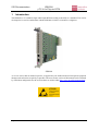
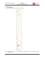
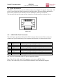
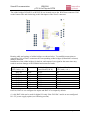
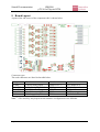
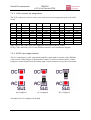
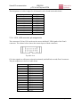
SIS Documentation
SIS8900
µTCA for Physics RTM
SIS8900
µTCA FOR PHYSICS RTM
User Manual
SIS GmbH
Harksheider Str. 102A
22399 Hamburg
Germany
Phone: ++49 (0) 40 60 87 305 0
Fax:
++49 (0) 40 60 87 305 20
email: [email protected]
http://www.struck.de
Version: SIS8900-M-1-1-V102 as of 01.03.12
Page 1 of 21
SIS Documentation
SIS8900
µTCA for Physics RTM
Revision Table:
Revision
1.00
1.01
1.02
Page 2 of 21
Date
25.11.11
21.12.11
01.03.12
Modification
Initial release
Photograph and extensions
J310, J320 connector contact layout added
SIS Documentation
SIS8900
µTCA for Physics RTM
- Table of contents
1
2
3
4
5
6
7
8
Table of contents ....................................................................................................................................... 3
Introduction .............................................................................................................................................. 4
Design ...................................................................................................................................................... 5
2.1
Functionality ..................................................................................................................................... 5
2.2
Block Diagram .................................................................................................................................. 5
LEDs ........................................................................................................................................................ 6
3.1
µRTM LEDs ..................................................................................................................................... 6
3.2
SMD LEDs........................................................................................................................................ 6
Front panel ................................................................................................................................................ 7
4.1
RJ45 Connectors................................................................................................................................ 8
4.1.1
J201 RJ45 Clock Connector ...................................................................................................... 8
4.1.2
J202 RJ45 Data Connector ..................................................................................................... 10
4.2
Coaxial Analog Input Signal Connectors .......................................................................................... 13
Board Layout .......................................................................................................................................... 14
RTM management................................................................................................................................... 15
Appendix ................................................................................................................................................ 16
7.1
Power Consumption......................................................................................................................... 16
7.2
Ordering options .............................................................................................................................. 16
7.3
AMC / Zone 3 connectors J101 and J102 ......................................................................................... 17
7.3.1
J101 connector pin assignments................................................................................................ 17
7.3.2
J102 connector pin assignments................................................................................................ 18
7.3.3
AC/DC input stage selection..................................................................................................... 18
7.3.4
J310, J320 connector pin assignments....................................................................................... 19
Index....................................................................................................................................................... 21
Page 3 of 21
SIS Documentation
1
SIS8900
µTCA for Physics RTM
Introduction
The SIS8900 is a 10 channel single ended input RTM according to the MTCA.4 standard. The card as
developed to be used in combination with the SIS8300 125 MS/s 16-bit MTCA.4 digitizer.
SIS8900
As we are aware, that no manual is perfect, we appreciate your feedback and will incorporate proposed
changes and corrections as quickly as possible. The most recent version of this manual can be obtained
by email from [email protected], the revision dates are online under http://www.struck.de/manuals.html .
Page 4 of 21
Struck Documentation
2
SIS8900
µTCA for Physics RTM
Design
The SIS8900 card is a signal conditioning input card for the SIS8300 digitizer.
2.1 Functionality
The key properties of the SIS8900 card are listed below.
MTCA.4 µRTM board
IPMI port expander (µRTM management)
10 channel analog signal input with coaxial connectors
coaxial connectors LEMO (optional FBM)
channels alternatively AC or DC stage via solder bridges (assembly option)
inputs to SIS8300 DC stage with single ended to differential conversion via
operational amplifier or inputs to SIS8300 AC stage with single ended to differential
conversion via transformer
3 differential clock inputs with RJ45 connectors
3 or 4 (assembly option) buffered differential I/O with RJ45 connector
Access to 6 digital inputs and 6 digital outputs via two pin headers
2.2 Block Diagram
A simplified block diagram of the SIS8900 is shown below.
Page 5 of 21
Struck Documentation
SIS8900
µTCA for Physics RTM
3 LEDs
3.1 µRTM LEDs
The µRTM LEDs are implemented according to the standard.
3.2 SMD LEDs
A number of surface mount red LEDs are on the SIS8900 to visualize part of the board status.
LED designator
D200
D203
D300
D400
D401
Page 6 of 21
LED comment
LC-POW Fail
D+5V
D+2.5V
A+5.5V
A-5.5V
Function
RJ45 current limiter power fail
D+5V present
D+2.5V present
A+5.5V present
A-5.5V present
Struck Documentation
SIS8900
µTCA for Physics RTM
4 Front panel
A sketch of the SIS8900 front panel is shown below.
Note: channel indexing for AC configuration (swapped for DC case in conjunction with
SIS8300 V2)
Page 7 of 21
Struck Documentation
SIS8900
µTCA for Physics RTM
4.1 RJ45 Connectors
Two RJ45 connectors are present for differential clock and digital I/O signals. Optionally +5V
power can be supplied to both connectors as stuffing option. A current limiter guarantees a
short circuit protected power and the current is limited to 250mA per connector.
The drawing with the pin count and the orientation of both connectors is shown below.
Front view
4.1.1 J201 RJ45 Clock Connector
The clock input signals are fed from the RJ45 connector directly to the Zone3 connector
without any signal conditioning. Pin assignment and function are shown in table below
Pin
1
2
3
4
5
6
7
8
Signal Name
CLK0CLK0+
CLK_POW
CLK1CLK1+
CLK_GND
CLK2CLK2+
Function
Clock 0, negative signal of differential pair
Clock 0, positive signal of differential pair
+5V power supply, positive line (assembly option)
Clock 1, negative signal of differential pair
Clock 1, positive signal of differential pair
+5V power supply, ground line (assembly option)
Clock 2, negative signal of differential pair
Clock 2, positive signal of differential pair
Pin 3 and 6 are connected to the +5V power supply by default
Note: The CLK0, CLK1 and CLK2 signals are referred to as RTM_CLK0,
RTM_CLK1 and RTM_CLK2 in the SIS8300 manual's clock distribution diagram.
Page 8 of 21
Struck Documentation
SIS8900
µTCA for Physics RTM
To configure optionally +5V power at J201 Pin 3 and 6 there are two 0603 solder bridges at
bottom side below the RJ45 Clock Connector designated as R201E and R201F.
Settings of both solder bridges are shown below. To establish state closed a solder bridge
(0 Ohm 0603 resistors) must be installed.
Designator
R201E
R201F
R201E
R201F
Setting/State
open
open
closed
closed
Function
J201 Pin 3 unconnected
J201 Pin 6 unconnected
J201 Pin 3 connected to positive line of
+5V power supply
J201 Pin 6 connected to negative line of
+5V power supply (Ground)
R201E and R201F are in state closed by default
don’t connect +5V power supply option to J201 pins if you are unsure that the opposite part
of RJ45 Connection is compatible, otherwise may result in serious damage of the SIS8900
and connected cards
Page 9 of 21
Struck Documentation
SIS8900
µTCA for Physics RTM
4.1.2 J202 RJ45 Data Connector
The RJ45 data I/Os are buffered LVDS signals linked to the Zone3 connector.
Pin assignment and function are shown in the table below.
Pin
1
2
3
4
5
6
7
8
Signal
DATA3+
DATA3DATA2+ (or)
DATA_POW
DATA1+
DATA1DATA2- (or)
DATA_GND
DATA0+
DATA0-
Function
Data 3, positive signal of differential pair
Data 3, negative signal of differential pair
Data 2, positive signal of differential pair or
+5V power supply, positive line (assembly option)
Data 1, positive signal of differential pair
Data 1, negative signal of differential pair
Data 2, negative signal of differential pair or
+5V power supply, ground line (assembly option)
Data 0, positive signal of differential pair
Data 0, negative signal of differential pair
Pin 3 and 6 are connected to the +5V power supply by default
All data signals can be routed either to input or output signals of the Zone3 connector.
The connections are established with solder bridges.
The solder bridges R310(P,N) to R313(P,N) are located next to the RJ45 data connector J202
on the top side and connecting to the data outputs of the Zone3 connector.
Page 10 of 21
Struck Documentation
SIS8900
µTCA for Physics RTM
The solder bridges R320(P,N) to R323(P,N) are located next to the RJ45 data connector J202
on the bottom side and connecting to the data inputs of the Zone3 connector.
Routing table and settings of solder bridges are shown below. To establish connections to
appropriate I/Os of Zone3 connector the corresponding solder bridges (0Ohm 0603 resistors)
must be installed.
Installation of the solder bridges for both in- and output of one signal at the same time may
result in serious damage of the SIS8900 and connected cards.
Signals on RJ45 /
J202, both (+ & -)
DATA0
DATA0
DATA1
DATA1
DATA2
DATA2
DATA3
DATA3
Connection
as
Input
Output
Input
Output
Input
Output
Input
Output
Solder bridges,
install both (P & N)
R310
R320
R311
R321
R312
R322
R313
R323
Signals on Zone3 connector
J101, both (+ & -)
D0
D6
D1
D7
D2 (*)
D8 (*)
D3
D9
DATA0, DATA1 are configured as inputs and DATA3 as output by default
(*) this DATA bit can be used for digital I/O only if the J202 Pin 3 and 6 are not configured
for +5V power supply option (see following section)
Page 11 of 21
Struck Documentation
SIS8900
µTCA for Physics RTM
To configure J202 Pin 3 and 6 for optionally +5V power supply or use for digital I/O there are
four 0603 solder bridges located at bottom side near the RJ45 Data Connector designated as
R202E, R202F, R202G, R202H.
Settings of solder bridges are shown below. To establish state closed solder bridges
(0 Ohm 0603 resistors) must be installed.
Solder bridges
R202E, R202F
closed
Solder bridges
R202G, R202H
open
open
closed
open
open
Function
J202 Pin 3 and 6 connected to
+5V power supply option
J202 Pin 3 and 6 connected to
digital I/O logic as DATA2
J202 Pin 3 and 6 unconnected
R202E, R202F are in state closed and R202G, R202H are in state open by default
only one of these three configurations shown in table above is allowed
don’t connect +5V power supply option to J202 pins if you are unsure that the opposite part
of RJ45 Connection is compatible, otherwise may result in serious damage of the SIS8900
and connected cards
Page 12 of 21
Struck Documentation
SIS8900
µTCA for Physics RTM
4.2 Coaxial Analog Input Signal Connectors
The front panel analog input connector can be stuffed with two different connector types.
Designators of the connectors for channel 1..10 are LEMO1, LEMO11, LEMO21 through
LEMO91.
Manufacturer
LEMO
FCT
Part Number
Description
EPL.00.250.NTN Elbow female print socket, brass nickel-plated
FBM001P154MR Female print socket, gold over nickel-plated
Analog Input for both, DC or AC configuration, is designed to accept a maximum peak to
peak signal level of +1V…-1V into 50 Ohms in combination with the SIS8300 digitizer (in
default configuration). In AC configuration the analog input signal is AC coupled to the
internal logic.
Page 13 of 21
Struck Documentation
SIS8900
µTCA for Physics RTM
5 Board Layout
A print of the silk screen of the component side is shown below.
Connector types
The used connectors are listed in the table below.
Designator
LEMO1 …
J201, J202
J310, J320
J101, J102
J100
Function
Coaxial Analog Input
RJ45, Clock, Digital I/O
LVDS-Bus Test Loop
Zone3 Conn. to AMC
Male key guide µTCA
Manufacturer
LEMO or FCT
ERNI
MOLEX
ERNI
TYCO
Part Number
(See chapter 4.2)
133268
87831-1420
204781
1469265-3 (*)
Note (*): The used Key may depend on the hardware configuration of the SIS8900
Page 14 of 21
Struck Documentation
SIS8900
µTCA for Physics RTM
6 RTM management
The SIS8900 RTM is compliant to the PICMG MTCA.4 specification. It has an on board I²C
EEProm (on address 0x50) and a NXP PCF8574-compatible port expander (on address
0x7C).
The table below lists the port expander connection map for normal operation:
Port pin
P0
P1
P2
P3
P4
P5
P6
P7
Function
HotSwap Switch (low active)
LED Blue (low active)
LED Red (low active)
LED Green (low active)
PowerGood (low active)
Reset (low active) (but not used)
PowerEnable (low active)
EEprom Write Protect
The EEprom contains any relevant device information (FRU records) about the RTM (refer to
PICMG AMC.0). Additionally the EEprom contains the new record types defined in PICMG
MTCA.4.
RTM record contains Zone 3 Identifier record listed in the table below.
Supported Zone 3 Identifier Records (Interface Identifier OEM):
IANA PEN (Private
enterprise number)
0x0092BD (37565)
Zone 3 OEM record
Descripton
0x83000001
SIS8300 Zone3 - v1
compatibility
Page 15 of 21
Struck Documentation
SIS8900
µTCA for Physics RTM
7 Appendix
7.1 Power Consumption
The currents drawn by the SIS8900 are listed in the table below.
Voltage
3,3 V
12 V
Current
< 30 mA
to be measured yet
These currents are typical values during normal operation.
7.2 Ordering options
The SIS8900 is available with two types of coaxial connectors as listed below.
Struck part number
00031
04290
Page 16 of 21
Coaxial Connectors
EPL.00.250.NTN
FBM001P154MR
Manufacturer
LEMO
FCT
Struck Documentation
SIS8900
µTCA for Physics RTM
7.3 AMC / Zone 3 connectors J101 and J102
J101 and J102 are 90 pin right angle male connectors providing 30 contact pairs each (60
signal contacts and 30 ground contacts). Every contact pair is surrounded by a “L” shaped
male shield blade. The shielding contact is designated with the names of the corresponding
signal pair (signal pin a and b is affiliated with shielding contact ab e.g.). The scheme below
shows the connector contact layout as seen from the rear side of the board.
Front view
7.3.1 J101 connector pin assignments
The J101 connector routes the 10 channels differential analog output signals of the single
ended to differential conversion stages and ground to the AMC. The shorthand “TF” in the
signal names stands for signals from the AC coupled transformer stages. In the same fashion
“PA” stands for the DC coupled operational amplifier stage.
Col
Row
10
9
8
7
6
5
4
3
2
1
ef
f
e
cd
d
c
ab
b
a
GND
GND
GND
GND
GND
GND
GND
GND
GND
GND
CH1_PACH2_TFCH3_PACH4_TFCH5_PACH6_TFCH7_PACH8_TFCH9_PACH10_TF-
CH1_PA+
CH2_TF+
CH3_PA+
CH4_TF+
CH5_PA+
CH6_TF+
CH7_PA+
CH8_TF+
CH9_PA+
CH10_TF+
GND
GND
GND
GND
GND
GND
GND
GND
GND
GND
GND
GND
GND
GND
GND
GND
GND
GND
GND
GND
GND
GND
GND
GND
GND
GND
GND
GND
GND
GND
GND
GND
GND
GND
GND
GND
GND
GND
GND
GND
CH1_TFCH2_PACH3_TFCH4_PACH5_TFCH6_PACH7_TFCH8_PACH9_TFCH10_PA-
CH1_TF+
CH2_PA+
CH3_TF+
CH4_PA+
CH5_TF+
CH6_PA+
CH7_TF+
CH8_PA+
CH9_TF+
CH10_PA+
Note: The front panel print PA channel assignment is correct for SIS8300_V1. The
SIS8300_V2 channel assignment was optimized for better routing and is in reverse order.
Channel 1 has changed to Channel 10 and so on.
Page 17 of 21
Struck Documentation
SIS8900
µTCA for Physics RTM
7.3.2 J102 connector pin assignments
The J102 connector is used to route power, data and system management pins to the AMC
board.
Col
Row
10
9
8
7
6
5
4
3
2
1
ef
f
e
cd
d
c
ab
b
a
GND
GND
GND
GND
GND
GND
GND
GND
GND
GND
GND
CLK1GND
GND
D11D8D5D2nc
nc
GND
CLK1+
GND
GND
D11+
D8+
D5+
D2+
nc
nc
GND
GND
GND
GND
GND
GND
GND
GND
GND
GND
GND
GND
CLK2GND
D10D7D4D1SCL
SDA
GND
GND
CLK2+
GND
D10+
D7+
D4+
D1+
MP+3.3V
PS#
GND
GND
GND
GND
GND
GND
GND
GND
GND
GND
GND
CLK0GND
GND
D9D6D3D0PWR+12V
PWR+12V
GND
CLK0+
GND
GND
D9+
D6+
D3+
D0+
PWR+12V
PWR+12V
Note: The CLK0, CLK1 and CLK2 signals are referred to as RTM_CLK0,
RTM_CLK1 and RTM_CLK2 in the SIS8300 manual's clock distribution diagram.
7.3.3 AC/DC input stage selection
The AC (transformer) or DC (operational amplifier) input path is selected on the SIS8900
card via 0603 solder bridges as illustrated for channel 1 on the screenshots below. Solder
bridges are located right beside the analog input coaxial connector on top side of the board.
not configured
AC configured
all channel are DC configured by default
Page 18 of 21
DC configured
Struck Documentation
SIS8900
µTCA for Physics RTM
The designators of solder bridges for all channels can be found in the table below.
Analog input channel
1
2
3
4
5
6
7
8
9
10
Designator
SW1
SW11
SW21
SW31
SW41
SW51
SW61
SW71
SW81
SW91
7.3.4 J310, J320 connector pin assignments
The connectors J310 an J320 can be used to access buffered LVDS signals of the Zone3
connector. The scheme below shows the contact layout of both connectors.
Top side view
J310 data signals are all inputs (onboard terminated) and buffered towards Zone3 connector.
The pin assignment is shown in table below
Pin
1
2
3
4
5
6
7
8
9
10
11
12
13
14
Signal
DATA0+
DATA0DATA1+
DATA1DATA2+
DATA2GND
GND
DATA3+
DATA3DATA4+
DATA4DATA5+
DATA5-
Page 19 of 21
Struck Documentation
SIS8900
µTCA for Physics RTM
J320 data signals are all outputs and buffered from the Zone3 connector towards J320. The
pin assignment is shown in the table below
Pin
1
2
3
4
5
6
7
8
9
10
11
12
13
14
Signal
DATA6+
DATA6DATA7+
DATA7DATA8+
DATA8GND
GND
DATA9+
DATA9DATA10+
DATA10DATA11+
DATA11-
J310 and J320 can be connected via flat cable connection to establish a test loop between the
lower and upper six data lines. Note, that those data lines are the same lines connected to front
panel RJ45 connector J202 via solder bridges. Don’t use signals of both connectors at the
same time, otherwise serious damage to the SIS8900 and connected cards may result.
Page 20 of 21
Struck Documentation
SIS8900
µTCA for Physics RTM
8 Index
+5V 10
12 V 16
3,3 V 16
AC 5, 17, 18
AMC.0 15
Appendix 16
Block diagram 5
board layout 14
CLK_0_N 8
CLK_0_P 8
CLK_1_N 8
CLK_1_P 8
CLK_2_N 8
CLK_2_P 8
CLK_GND 8
CLK_POW 8
clock
input 13
Clock 5
connector types 14
D0 11
D1 11
D2 11
D200 6
D203 6
D3 11
D300 6
D400 6
D401 6
D6 11
D7 11
D8 11
D9 11
DATA_0 12
DATA_1 12
DATA_2 12
DATA_3 12
DATA_GND 10
DATA_POW 10
DC 5, 17, 18
design 5
FCT 16
front panel 7
FRU 15
functionality 5
Harlink 8, 10
IANA 15
IANA PEN 15
introduction 4
IPMI 5
J101 12, 17
J102 18
J202 12, 20
J310 19, 20
J320 19, 20
LED 6
LEDs
AMC 6
SMD 6
LEMO 16
LVDS 8, 10
MTCA.4 4, 15
NXP 15
operational amplifier 17
ordering options 16
PA 17
PCF8574 15
PEN 15
port expander 5
Power Consumption 16
R310 11
R311 11
R312 11
R313 11
R320 11
R321 11
R322 11
R323 11
RJ45 20
RTM 15
RTM connectors 17
RTM management 15
SIS8900 4
SMA 13
TF 17
transformer 17
Zone 3 17
Zone 3 connector 20
Page 21 of 21