1
1 Tutorial
1
Contents
1
Tutorial
1
Glossary
1.1 Initial setup of the development environment .
1.1.1 components . . . . . . . . . . . . . . . .
1.1.2 installation . . . . . . . . . . . . . . . .
1.1.3 verification of successful installation . .
1.1.4 first steps with the xme-software for nios
Bibliography
.
.
.
.
.
.
.
.
.
.
.
.
.
.
.
.
.
.
.
.
.
.
.
.
.
.
.
.
.
.
.
.
.
.
.
.
.
.
.
.
.
.
.
.
.
.
.
.
.
.
.
.
.
.
.
.
.
.
.
.
.
.
.
.
.
.
.
.
.
.
.
.
.
.
.
.
.
.
.
.
3
1
1
1
1
2
19
2
Glossary
BSP Board Support Package. 14
CPU Central Processing Unit. 14
HDL Hardware Description Language. 8
IDE Integrated Development Environment. 13
IP Intellectual Property. 1, 4
JTAG Joint Test Action Group. 5
LED Light Emitting Diode. 6
PIO Parallel I/O. 15
SVN Subversion. 2
xme/chromosome a modular middleware architecture for cyber-physical systems. 2
3
Glossary
1.1 Initial setup of the development environment
1.1.1 components
Development means creation of a hardware description for the FPGA and writing software for the created hardware. Altera Corporation provides the necessary tools, which are
Quartus II and the Nios2SBT, to achieve this.
1.1.2 installation
Please note that this installation description applies to installing the Altera Design Suite
v12 on Windows7 64bit only. To install all the required software, Altera Corporation
provides a Free Download package at its website, called ”Altera Design Suite (Altera Installer)”. This is a installer package, which downloads all selected installation components
during the installation process from the internet. To start the installation, execute the installer package as an administrative user (right-click and select ”run as administrator”).
This step is very important, as your USB-Blaster will not work if you installed the software
as a low-privileged user.
If the installer asks you to select the desired components, deselect everything and only
select
• Quartus II Web Edition (Free) (includes Nios2SBT)
• Cyclone IV E in the Device Families category
If you are running Quartus II v12.0 on a 64bit machine, you might still have difficulties
finding the USB Blaster hardware in the Programmer tool. Altera does not ship the 64bit
JTAG-Server with the QuartusII Web-Edition. To resolve this issue, install the standalone
Programmer Software from https://www.altera.com/download/software/prog-software,
which contains a 64bit Programmer and JTAG-Server. (update: as of Quartus II v12.1, you
do not need to separately install the standalone Programmer)
Altera offers a paid (Quartus II Subscription Edition) and a free (Quartus II Web Edition)
version of its Quartus development suite. The free version includes most of the features for
beginners or even professionals. One striking difference are the missing Intellectual Property (IP) license files for several more complex components. These components, which are
not fully licensed to free edition users include, but are not limited to NiosII/s or NiosII/f
processors (the NiosII/e processor does not require a license), the DDR RAM controller or
the tse ethernet MAC component.
1.1.3 verification of successful installation
designing an FPGA
To verify that your installation was successful, this tutorial, which is based on [4] and [1]
will guide you through your first steps in the Quartus II environment. You will create your
first Nios II CPU on your FPGA. Please note that Altera has removed the SOPC-builder
from Quartus II v12 on, which means that for designing the CPU core, [4] is no longer
usable. To verify that you have a working set-up, please follow the steps described in [2].
1
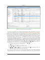
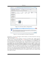
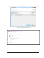
Glossary
Figure 1.1: Component selection in the Altera Installer
It is of particular importance to use the correct names for the components, as references to
these names have to be consistent.
1.1.4 first steps with the xme-software for nios
In this section, all the steps to create a executable binary for the DE2-115 development board
are described. All steps in this tutorial are based on the Altera Software in version 12.0
sp1. If you have a different software version, the same steps may apply but some screens
or identifiers may differ drom this description. First of all, make sure that you have a copy
of the xme/chromosome Subversion (SVN). We will refer to the root of this SVN tree as
¡svn-root¿.
designing your hardware
This section gives you a quick introduction into the main QuartusII features and on how
to build a simple NiosII hardware design with QuartusII. It is based on [2]. This introduction uses QuartusII v12.1 64-Bit on a Windows machine and creates a demo project for the
DE2-115 development board. For different Quartus versions or FPGAs, please take care to
change this description at the corresponding sections.
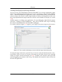
2
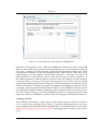
Glossary
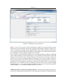
Figure 1.2: page 1 of the QuartusII New Project Wizard
basic QuartusII project setup We assume that you have started an instance of QuartusII.
Begin by creating a new QuartusII project, by selecting File/New from the menubar and
choosing ”‘New Quartus II Project”’ from the window, which opens. This starts the New
Project Wizard. Fill in your project name and the top-level design entity name (remember
this name carefully and name your top component exactly like this). Now you just have
to choose the working directory for this project (QuartusII will not create a folder within
the working directory, so choose an empty folder). Your project settings should like like
figure 1.2) now. If you have checked your input, you can continue by choosing the ”‘Next
¿”’ button. You can skip the Add Files Wizard page by selecting ”‘Next ¿”’ again. On
page three, you have to select your exact model of FPGA device. Choosing your FPGA
device with caution as a wrong device setting could cause damage to the hardware. For
the DE2-115 development board that was used for this introduction, we had to choose the
”‘EP4CE115F29C7”’ device (see figure 1.3). To be sure, which device is used in your board,
check the label on the FPGA chip (see figure 1.4). You can skip page four by selecting
”‘Next ¿”’. Page five will give you a summary of your project settings. Finish the New
Project Wizard with ”‘Finish”’.
designing the NiosII system First of all, we have to create our Processor Block. This can
be either be accomplished by using SOPC Builder or Qsys. Qsys is the newer of them, so we
are using Qsys in this introduction. Qsys can be used to create a NiosII system, including
components such as timers or memory. This is exactly what we are doing now.
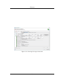
3
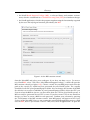
Glossary
Figure 1.3: page 3 of the QuartusII New Project Wizard
A NiosII system requires memory to store instructions and data. To keep the design simple, we are choosing On-Chip memory for our design. On the left of the Qsys window,
you have a Component Library, which gives you a selection of all available components
for your system. Choose ”‘Memory and Memory Controllers”’/”’On-Chip”’/”’On-Chip
Memory (RAM or ROM)”’ from the Component Library and double-click on it, to add it
to your system. A new window opens, which lets you choose the parameters for your new
component. Change the total memory size to 200480 bytes (see figure 1.5). 20 kiB should
be enough for our small demonstration system. Click Finish to add the On-Chip Memory
to the system. It will appear in the System Contents list of Qsys.
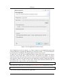
Next, add the NiosII processor core to the system by choosing ”‘Embedded Processors”’/”’Nios
II Processor”’ from the Component Library. The NiosII parameter window opens and you
have to choose a NiosII core variant. More complex cores give performance advantages
and have useful functions. For out tutorial, we do not need any special functionality and
can choose the smallest core version, ”‘Nios II/e”’. Nios II/e is the only core variant, which
does not need any IP and thus can be used without time limitation in the free Web Edition
of Quartus. In the bottom part of the NiosII parameter window, you can see some error
messages, letting you know that the exception and reset vector memory are not set. Ignore
these error messages for now and add the processor core by clicking the Finish button.
Figure 1.6 shows the parameter window (ignore the Reset Vector and Exception Vector
settings for now).
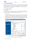
Now you should have three components in the System Components list:
• the clock source clk 0 (this component was automatically generated for you)
4
Glossary
Figure 1.4: label of the FPGA chip
• the On-Chip Memory onchip memory2 0
• the NiosII CPU core nios2 qsys 0
To connect components to each other, you can toggle the connection state between components by clicking the semi-transparent dots in the Connections column of the System
Contents list. Connect the clk port of the clk 0 component to the clk1 port of the On-Chip
Memory by clicking on the dot in the clk1 row. Connect the clock source clk of the clk 0
component to the Clock Input of your NiosII processor in the same way. Connect the
clk reset port from the clock source to the reset1 port of your memory and to the reset n port
of the processor. Now connect the processor with the memory block, by connecting the
s1 port of the memory to both the data master and instruction master ports of the processor.
This finishes the first stage of wiring.
After connecting the memory to the CPU, we can fix the processor errors we encountered
before. Double-click on the processor component in the System Contents list to open the
processor parameter window again. set both options, Reset vector memory and Exception
vector memory to your onchip memory2 0.s1 component. The final NiosII settings in the parameter window should look like figure 1.6.
To be able to flash and debug our applications later on, we add a Joint Test Action Group
(JTAG) component to our system: Add the JTAG UART component from ”‘Interface Protocols”’/”’Serial”’/”’JTAG UART”’ in the Component Library. Do not change any settings
in the parameter window and add the component by selecting the Finish button. Connect
the clk port of the jtag uart 0 component to clk 0 of your clock source and reset to clk reset.
Connect the JTAG’s avalon jtag slave port to the data master port of your CPU.
To be able to generate a BSP for our system later on, we need to have an Interval Timer
in our system. Add ”‘Peripherals”’/”’Microcontroller Peripherals”’/”’Interval Timer”’ to
the system. Choose Full-features from the Presets setting and add the component through
the Finish button. Connect clk and reset to your clk 0 component and connect the s1 port to
the data master port of the NiosII CPU.
The system ID component can identify our generated system and thus protect it from accidentally flashing software, which is not intended for this system. The component can
be found at ”‘Peripherals”’/”’Debug and Performance”’/”’System ID Peripheral”’. When
adding the System ID component, add a (randomly chosen) 32bit ID into the 32 bit System
ID field. This value will identify your system (but is not important for us in this example).
5
Glossary
Figure 1.5: On-Chip Memory parameters
Connect the sysid qsys 0 component to the clock source and the CPU’s data master port.
Our system cannot communicate with its surroundings yet. We want it to be able to control Light Emitting Diodes (LEDs) to let us know if the program is working. To control the
LEDs, we need a connection to the LEDs on the board. Add ”‘Peripherals”’/”’Microcontroller
Peripherals”’/”’PIO (Parallel I/O)”’ to the system. The parameter window appears. Do
not change any settings, as the default value configures the PIO as an 8 bit output device.
As we referring to this component later in the software design process, we give it a new
name. Right-click on the pio 0 component, select the Rename option and enter led pio as its
new name. Connect clk and reset to the clock source and connect s1 to the data master port
of the processor. To export the external connection port of the led pio component, doubleclick in the Export column of the external connection row.
The PIO component finishes the list of components that are needed for this basic NiosII
system. Now it is time to remove the errors from our Qsys system. By just adding all
the components to the system, Qsys automatically assign base address 0x00000000 to all
of them. This creates conflicts, as a memory address can only be used by one component.
Qsys provides a function to automatically create a non-conflicting memory assignment. To
run this function, select ”‘System”’/”’Assign Base Addresses”’ from the menubar.
Finally, the only warnings remaining apply to the Interrupts of the system. Low interrupt
numbers mean high priorities in NiosII systems. We assign a low priority (i.e. a high interrupt number) to the JTAG component. You can assign an interrupt to the JTAG component
by clicking on the semi-transparent dot in the IRQ column of the jtag uart 0 component.
Type the number 16 into the connection point. Set the interrupt number of the timer 0 component to 1 by applying the same procedure to the timer 0 component.
6
Glossary
Figure 1.6: NiosII processor parameters
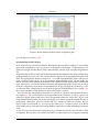
Figure 1.7 gives an overview of all the components, which are used in this Qsys system.
It also shows the connections between the components (black dots and lines on the left visualize a connection). Further, the Interrupt numbers for the JTAG and Timer components
are set (compare column IRQ). Base Addresses in this figure were automatically assigned.
The assignment can be checked in columns Base and End.
Once your Qsys system design is finished, you can start generating it (similar to compiling
source code). Open the Generation tab in Qsys, leave all settings at their default values and
click the Generate button. Qsys will ask you if you want to save your system. Answer Yes
and save the system in your QuartusII project directory. The Generate window will show
the generation output. Generation can last several minutes, depending on the system design and your host computer’s performance. When the status bar in the Generate window
turns green, your system has been successfully generated. Your Generate window should
look like figure 1.8. Close the Generation window and exit Qsys to return to QuartusII.
Congratulations, you are finished with the processor system.
adding the NiosII system to the QuartusII project The newly generated processor system has to be integrated into QuartusII. You can design FPGA hardware in QuartusII either
7
Glossary
Figure 1.7: an overview of Qsys system
textually by using VHDL or by using the Verilog language. But QuartusII also lets you design systems without having to use one of the Hardware Description Languages (HDLs).
Instead you can design your system graphically. This is what we are doing here to keep
things simple. Select File/New... from the menubar and select Block Diagram/Schematic File
in the New window. Create the new Block Diagram file by clicking OK. Save the new Block
Diagram file with the ”‘File/Save As...”’ command. Use the same name for this entity as
you used for your project (see section 1.1.4). We want to create an instance of the NiosII
system, that we created in section 1.1.4. Double-click on an empty space in the newly
created Block File. The Symbol window appears. In the Libraries pane on the left of the
window, choose your NiosII system, by selecting ”‘Project/qsys nios system”’. Create the
NiosII instance by clicking OK. Place the NiosII block in your Block Diagram file with your
mouse pointer. You can see three wires leaving the qsys nios system:
• clk clk, the clock input to the NiosII system
• reset reset n, the reset input to the NiosII system
• led pio external connection export[7..0], the output of the led pio component. This is an
8-bit wide wire, as can be seen by the [7..0] range.
Now we have to connect these wires with input and output pins. in the toolbar of the Block
Diagram file, open the menu of the Pin Tool option and select Input. Now you should have
8
Glossary
Figure 1.8: output of succesful generation
an Pin hovering below your mouse pointer. Place it next to your NiosII system block, so
that the clk clk wire connects to your pin. Press the menu of the Pin Tool again, but this time
select Output from the toolbar. Place the output pin next to your NiosII block. Select it (by
using the Selection Tool from the toolbar) and rotate the output pin by 180 degrees. You can
do that by right-clicking on the output pin and selecting ”‘Rotate by Degrees/Rotate Left
180”’. connect the output pin to the led pio external connection export[7..0] wire. You can
easily distinguish input and output pins by their shape. Double-click on an empty space in
the Block Diagram file again, but this time add ”‘c:/altera/12.1/quartus/libraries/primitives/other/vcc
Place the VCC pin next to your NiosII block and connect the VCC pin with the reset reset n
wire using the Orthogonal Node Tool from the toolbar. Take care to draw the Orthogonal Node line precisely from the reset reset n wire to the connection of the VCC pin. You
should have a small square at the VCC pin and the NiosII block, visualizing an electrical
link (the visualization appears only if you have selected the Orthogonal Node line).
Right-click on the output pin and open the Properties window of the output pin. Rename
the output pin, by typing LEDG[7..0] in the Pin name(s) field. Rename the input pin, which
is connected to the clk clk wire, to CLOCK 50 in the same way.
Now that all the pins for the hardware design are known, a mapping to the hardware pins
of the FPGA chip has to be created. QuartusII has to detect all the pins in our hardware
design, thus we have to start the first steps of a compilation run first. To do so, select ”‘Processing/Start/Start Analysis & Elaboration”’ from the menubar. A new Compilation Report
tab opens. If the compilation was successful, a window labeled Analysis & Elaboration was
successful appears.
If you have encounter an error, particularly the error ”‘Node instance ¡instance name¿
instantiates undefined entity <entity name>”’, then QuartusII might not find your NiosII
system synthesis files (the compiled files or the NiosII system). In this case, you should add
them manually by selecting ”‘Project/Add/Remove Files in Project...”’ from the menubar.
Press the button with ... written on it, to select the files you want to add. Add the main .v
file, which describes your NiosII block from <quartusII project dir>/<niosII system name>/synthesis/<nios
and click the Add button. also add all the files contained in the <quartusII project dir>/<niosII system nam
folder. After adding all the files to the project, the window should look like figure 1.9. close
the window wuth the OK button. Your Analysis & Elaboration should finish without any
9
Glossary
Figure 1.9: project file setup window for QuartusII
issues.
If Analysis & Elaboration has indexed your hardware design, you can proceed to assign
hardware positions to the pins in your hardware design. Open the Pin Planner by selecting
”‘Assignments/Pin Planner”’ from the menubar. At the bottom of the Pin Planner window, there is a list with all the pins in your design. Assign a location on the FPGA chip for
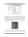
each of the pins (Nodes in Pin Planner) by clicking on the empty cells in the Location column. According to [3], the pin locations can be looked up in table 1.1. After assigning the
Locations, the Pin Planner window should look like figure 1.10. You can close Pin Planner
and your hardware design is finished.
To finally generate your hardware design, choose ”‘Processing/Start Compilation”’ from
Node Name
CLOCK 50
LEDG[0]
LEDG[1]
LEDG[2]
LEDG[3]
LEDG[4]
LEDG[5]
LEDG[6]
LEDG[7]
Location
PIN Y2
PIN E21
PIN E22
PIN E25
PIN E24
PIN H21
PIN G21
PIN G22
PIN E21
Table 1.1: pin assignments for the DE2-115 board
the menubar. This process might take several minutes, depending on your machine and
hardware design. If your Compilation finishes without errors, you just created your first
FPGA hardware design! You can proceed and program your FPGA chip with this hard-
10
Glossary
Figure 1.10: Pin Planner with locations assigned to pins
ware design (see section 1.1.4).
programming the FPGA chip
Now that you have created a hardware description for your FPGA and have successfully
generated/compiled it, you can proceed to program your design. Programming your
hardware design onto the FPGA can be done from the console or by using the Programmer
UI.
Programming the FPGA chip will keep the hardware description in the chip until the next
programming or power loss. This means that the chip has to be programmed again each
time the development board is turned on. To avoid reprogramming upon each power
cycle, the FPGA chip can be set to an automatic programming mode. In this mode, the
FPGA will take the hardware description from a flash memory and program itself upon
start. But there is a restriction to this automatic programming mode: It can only be used,
if all the components used in the current hardware design are properly licensed (e.g., the
tse ethernet MAC component is not licensed in Quartus II Web Edition). See section 1.1.2
for a short summary of the differences between Quartus versions.
You can start the Programmer manually or even fire it up from your Quartus instance
(see figure 1.11 for a screenshot of the Programmer main window). To do so, open your
hardware design project and select Tools/Programmer from the menu bar. If you start
Programmer from Quartus, the hardware design you want to program should already be
preselected. Otherwise, you can use the Add File... button to add your .sof file. If your
FPGA chip is not selected yet, you can use the Add Device... button to select your FPGA
chip. Make sure to select the correct chip number, otherwise you risk damaging your hardware.
If you are using a non-licensed component in your hardware design, you can still use that
component, but can only use it while your FPGA is connected to your Computer running
11
Glossary
Figure 1.11: the main window of Programmer
Figure 1.12: the time limitation warning of Programmer
Programmer. A message will appear, which reminds you of that situation (the message
might look like figure 1.12).
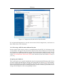
Now you need to set your USB Blaster connection to the FPGA chip. Simply click the
Hardware Setup... button and window like 1.13 will show up. If you are using USB Blaster
for programming (on DE2-115 boards, you are using USB Blaster), your USB Blaster will
show up in the list of Available hardware items. Select if from the Currently selected hardware dropdown list, close the Hardware Setup window and you sould be ready to start
programming. The Start button should be enabled, if you have added a .sof file, if you
have selected a FPGA device and if your USB Blaster is selected. Start programming the
clicking that button. The progress bar should show Success after programming finished
successfully. This means that your hardware design was programmed onto the FPGA
chip. If you are using non-licensed (time-limited) components, a popup window will appear after successful programming (TODO: link to screenshot here). Leave this window
open and keep the FPGA chip connected to your computer until you have finished using
your hardware design.
12
Glossary
Figure 1.13: The hardware setup window of Programmer
Sometimes you could have issues with your USB Blaster hardware detection. If your USB
Blaster is not selected (from your previous programming), try to select it again in the Hardware Setup... window. If it does not show up in the list of Available hardware items, check
your physical connection to your development board. Make sure the USB cable is connected properly to your computer and the FPGA hardware. Also make sure, that your
FPGA hardware is connected to a power source and the power switch is turned on. If
the USB programmer is still not shown in the list, close the hardware selection window
and open it again (you may need to repeat this procedure several times). In fact, simply
retrying the failed operation helps in many cases for the Programmer (not only the issues,
which are listed here). Another way to get the Programmer working is to select Auto Detect
or turning your development board off and on again. If your USB Blaster did never show
up in the list of available hardware components, there might be a driver issue on your system. This could be, because you ran the installation process as a non-privileged user. Also
make sure, that your USB Blaster is enlisted in Device Manager (on Windows machines).
setting up the BSP
After finishing all hardware related aspects of this introduction into the DE2-115 FPGA,
we are ready to start working on the software. Typically, NiosII applications are developed using the Nios2SBT (NiosII Software Build Tools), a modified version of the eclipse
Integrated Development Environment (IDE). NiosII applications usually consist of two
parts:
13
Glossary
• the NiosII Board Support Package (BSP), a software library and runtime environment, which is customized to a Central Processing Unit (CPU) in a hardware design.
• the NiosII application, which is the program implementing the functionality required
by the user and relying on functions provided by the BSP
Figure 1.14: the BSP creation wizard
Start the Nios2SBT and select your workspace if you have not done so yet. To create a
new NiosII BSP, select ”‘File/New/Nios II Board Support Package”’, which will open the
BSP creation wizard (see figure 1.14). Choose a name for your BSP project and select the
path to the .sopcinfo file, which has been generated for your NiosII system. The .sopcfile
should be located in your QuartusII project folder. You can change the location of the BSP
(be default, it is saved in a subfolder of your QuartusII project folder). Select the CPU you
want to create the BSP for (in case you have more than one CPU in your NiosII system). A
BSP can only be generated for one CPU at once. If you have more CPUs in one hardware
design, you have to create a BSP for each processor. Confirm your selection by pressing
the Finish button of the BSP creation wizard. Your BSP project will appear in the Project
Explorer of the Nios2SBT. Now we are creating the actual NiosII application project, which
uses the BSP, that we just created. Choose ”‘File/New/Nios II Application”’ to open the
14
Glossary
Figure 1.15: the application creation wizard
Nios II Application wizard (see figure 1.15). Enter a name for your application project and
select the BSP for your project (the BSP that you created in section 1.1.4). Create the project
by selecting the Finish button. The project appears in the Project Explorer.
To add a new source file to the application project, right-click on the application project
and select ”‘New/Source File”’. In the New Source File window (see figure 1.16), enter a
name for the Source File and click Finish to create your file. Every project has to contain a
main function, which is the entry point to your application. Start by creating this function
and adding code to it. Listing 1.1 shows how a basic main function could look like. It
demonstrates the output of text to the console by using
1
printf("Hello from Nios II!\n");
and controls the LEDs, that we connected via a Parallel I/O (PIO) component by using
1
IOWR_ALTERA_AVALON_PIO_DATA(PIO_LED_BASE, count & 0x01);
. You created your first NiosII software application.
15
Glossary
Figure 1.16: the BSP creation wizard
1
2
3
#include <stdio.h>
#include <system.h>
#include "altera_avalon_pio_regs.h"
4
5
6
7
8
9
10
11
12
13
14
15
16
17
18
int main() {
printf("Hello from Nios II!\n");
int count = 0;
int delay;
while (1) {
IOWR_ALTERA_AVALON_PIO_DATA(LED_PIO_BASE, count & 0x01);
delay = 0;
while (delay < 2000000) {
delay++;
}
count++;
}
return 0;
}
Listing 1.1: example implementation of a main function
16
Glossary
executing NiosII projects on the target hardware
You can execute your NiosII project from the Nios2SBT. To execute the application, rightclick on the application project in the Project Explorer and choose ”‘Run As/Nios II Hardware”’. This will compile your application, create a downloadable image, download the
software image and execute it on the target hardware. Before executing, please make sure
that you programmed the target hardware with the correct Hardware Design (see section
1.1.4).
Another option is to debug your application. To start debugging, right-click the project
and select ”‘Debug As/Nios II Hardware”’. This will execute the same steps as running
the software and additionally start Nios2SBT’s debugger.
if a window similar to figure 1.17 appears, your Target Connection setup may be incorrect.
Figure 1.17: the window indicating an error with the target connection path
To setup the target connection, open the Target Connection tab and click the Refresh Connections button. Select a Processor to execute your target on and a Byte Stream Device, through
which text output will be transferred (see 1.18). Confirm your selection with Apply and
start Debugging your software with Debug. This finishes the tutorial on how to run your
first Nios II Application.
17
Glossary
Figure 1.18: choosing the target connection
18
Bibliography
[1] Altera. My First Nios II Software Tutorial. Altera Corporation, 101 Philip Drive,
Assinippi Park, Norwell, Massachusetts 02061 USA, January 2010.
[2] Altera. Nios II Hardware Development Tutorial. Altera Corporation, 101 Innovation
Drive, San Jose, CA 95134, May 2011.
[3] Terasic Technologies Inc. DE2-115 User Manual. Terasic, 2010.
[4] terasIC. My First Nios II for Altera DE2-115 Board. Terasic Technologies, Gongdao 5th
Rd, East Dist, Hsinchu City, 30070. Taiwan.
19