1
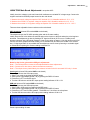
High Performance 160-10 Meter SSB - CW Transceiver
Owner’s Manual
Rev 2.6.5 March 21, 2008
Designed by
Juha Niinkoski OH2NLT and Matti Hohtola OH7SV
Manual by Pete Meier WK8S
2
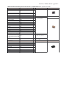
Table of Contents
INTRODUCTION....................................................................................................................................................................... 3
FEATURES ................................................................................................................................................................................ 3
SPECIFICATIONS ......................................................................................................................................................................... 4
USING THIS MANUAL ........................................................................................................................................................................ 5
ASSEMBLY SUGGESTIONS ....................................................................................................................................................... 5
TOOLS..................................................................................................................................................................................... 5
SMD CONSTRUCTION TIPS AND TECHNIQUES.......................................................................................................................... 6
Toothpick and Bee’s Wax Method.................................................................................................................................... 6
Tweezer Method................................................................................................................................................................ 7
Doofus Method.................................................................................................................................................................. 7
Alternate methods of SMD construction. .......................................................................................................................... 8
DDS – CONTROL – DISPLAY BOARD.................................................................................................................................... 10
MAIN BOARD .............................................................................................................................................................................. 14
FILTER BOARD .......................................................................................................................................................................... 15
POLYPHASE BOARDS............................................................................................................................................................... 15
TWO BAND PA BOARD............................................................................................................................................................. 16
CONNECTOR BOARD ............................................................................................................................................................... 18
ALL BAND PA BOARD .............................................................................................................................................................. 19
RF FILTER BOARD FOR ALL BANDS ................................................................................................................................... 20
CABINET AND FINAL ASSEMBLY......................................................................................................................................... 21
FLAT CABLES WITH DIMENSIONS ........................................................................................................................................... 22
OPERATION ................................................................................................................................................................................ 23
CIRCUIT DESCRIPTIONS ........................................................................................................................................................ 24
DDS CONTROL BOARD ........................................................................................................................................................... 24
MAIN BOARD............................................................................................................................................................................ 28
TWO BAND PA BOARD ............................................................................................................................................................ 31
POLYPHASE BOARD ................................................................................................................................................................. 33
FILTER BOARD ........................................................................................................................................................................ 33
VOICE MEMORY OPTION ........................................................................................................................................................... 34
EXTERNAL KEYBOARD ............................................................................................................................................................. 35
ADJUSTMENTS........................................................................................................................................................................... 36
DDS / CONTROL BOARD ......................................................................................................................................................... 36
MAIN BOARD............................................................................................................................................................................ 38
2 BAND PA BOARD .................................................................................................................................................................. 39
ALL BAND PA BOARD .............................................................................................................................................................. 40
MEMORY OPTION ...................................................................................................................................................................... 41
PARTS LISTS ........................................................................................................................................................... APPENDIX A
SCHEMATICS.......................................................................................................................................................... APPENDIX B
BLOCK DIAGRAM ................................................................................................................................................. APPENDIX C
BOARD LAYOUT (PARTS PLACEMENT) .........................................................................................................APPENDIX D
TROUBLESHOOTING ........................................................................................................................................... APPENDIX E
SERIAL COMMUNICATIONS PROTOCOL ...................................................................................................... APPENDIX F
BOOT LOADER INSTRUCTIONS........................................................................................................................APPENDIX G
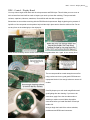
Introduction
JUMA TRX2 is a high performance HF transceiver for SSB and CW with high dynamic range. It
uses a quadrature sampling technique for modulation and demodulation with a low noise phasing
method. The JUMA TRX2 uses a DDS controlled VFO for excellent frequency stability and signal
purity. An internal microcontroller is controlling all functions of the transceiver.
JUMA TRX2 is available as a kit with two kit alternatives:
1. The discrete kit with components and bare circuit boards.
2. The modular kit with assembled and tested boards.
The enclosure is machined and printed in both kit alternatives.
A completely assembled transceiver is also available with the help of JUMA community.
Additionally there will be two models: The two band model TRX2 for 80m and 40m ham bands and
the all ham band model TRX2A with a general coverage receiver. The two band model can be
upgraded any time into the all band model by adding related modules. Several add on option modules
are also available for both models.
Features
The two band model frequency coverage is 2
MHz...8 MHz
The all band model has all ham bands, RX
100 kHz-30 MHz
Transmit modes LSB, USB, CW and tune
Output RF power 10 W
Built in keyer: Dot priority, Iambic A, Iambic
B and straight modes
Click-less CW keying with adaptive 'VOX' time
Three filters: Wide, Medium and Narrow with
a good shape factor
Filters are user adjustable
Outstanding Dynamic Range and good
sensitivity.
Configurable features
AGC Slow/Fast
LPF corner frequency setting
Speech Processor ON/OFF
Mic connector input level MIC/LINE
Excellent AGC with slow and fast modes
Dual DDS controlled VFOs with a split TX/RX
function
First class optical VFO encoder with 480
steps per revolution
7 digit frequency display, 10 Hz display
resolution
Three selectable VFO tuning speeds
Slow/Fast/Very Fast
VFO lock feature
RIT with it's own tuning knob
Graphical S-meter range S1...S9+40 dBm
Non volatile memory for VFOs, modes,
settings and calibration
Keyer Dot priority/Iambic-A/B/Straight
RS232 mode TRX2/Yaesu CAT/Test functions
Display brightness/contrast
Option Modules
Voice memory plug in - Ext control unit for voice memory - Noise blanker plug in
Service/calibration mode
Reference oscillator software calibration
S-meter software scaling
FWD power meter software scaling
Firmware
The most recent software updates will be
available and users can easily upgrade the
firmware without any special tools with the
build in flasher utility and a PC serial cable.
The control software (firmware) is written in
the C programming language. Source code
will be available for experimenters.
Acknowledge tones length setting
Reload factory settings
Power supply
Nominal supply voltage 13.8 VDC (range 11
VDC...15 VDC)
Nominal supply current RX 0.4 A, TX 2.5 A
Dimensions:
Width 182 mm, Height 60 mm, Depth 185 mm
3
JUMA TRX2 and JUMA TRX2A SPECIFICATIONS* 2007-10-28
GENERAL
RECEIVER
Frequency range, Two Band model TRX2:
RX: 2 MHz...8 MHz, TX: 2 MHz...8 MHz.
Sensitivity: Typical -130 dBm
Frequency range, All Band model TRX2A:
RX: 100 kHz...30 MHz, TX: 1.8 MHz...30 MHz.
Tuning step sizes: 10 Hz, 100 Hz
(10 kHz @ very fast setting).
Modes: LSB, USB, CW.
IMD3 dynamic range: Typical range more than
100 dB.
S-Meter: Graphical LCD bar display, S9 = 50 uV,
range S1...S9+40 dB (-121 dBm...-33 dBm).
Filters: Three adjustable filters, default
bandwidths 2.3 kHz, 1.7 kHz and 700 Hz. Filters
are independent of the transmit modes.
VFOs: A and B VFOs with split function, one
tuning knob.
RIT: Tuning range ± 1 kHz. Separate RIT knob.
Front panel connector: Jack stereo connector
3.5 mm for electret mic input or line level input
(selectable by the CONFIC) and PTT.
Image and IF rejection: No image frequency
response, no IF frequency response.
(baseband IF demodulation).
Rear panel connectors: Phones/speaker output,
CW-paddle/key/keyer input, RS-232, AUX for
PTT in/KEY out or audio I/Q output. All
connectors 3.5 mm stereo jack type sockets.
Configurable RX functions: Slow/fast AGC,
adjustable filters, squelch function (alternative
function of the CW speed knob).
TRANSMITTER
Antenna connection: BNC connector in the rear
panel, nominal impedance 50 ohms.
Display: Blue/white LCD with adjustable contrast
and brightness. Main display: S meter, MODE,
FILTER, frequency, VFO, VFO step. Alternate
display pages: RF output power, SWR, supply
voltage, PA drain current.
General configurable functions: LCD contrast,
LCD brightness, RS232 protocol select.
Service mode functions: Frequency, voltage
meter, S meter, FWD/REV power, ID current
calibration. Acknowledge beep settings. Factory
settings restore.
Software updating: HEX files can be uploaded
by means of the boot loader via RS232 interface.
Supply: Voltage 13.8 V (11 V...15 V)
Current TX 2.5 A typical, RX 0.4 A typical,
depending on the LCD brightness.
Dimensions: Width 182 mm, height 60 mm,
depth 185 mm.
Weight: 1.2 kg
Output Power: Nominal 10 W
SSB transmit bandwidth: Nominal 2.4 kHz
CW Rise/Fall Time: Nominal 5 ms
SSB carrier suppression: Typically better than
60 dB.
Speech processor: Microphone audio
processing with 6 dB/oct high frequency preemphasis.
CW offset/sidetone: Fixed 700 Hz
MIC/PTT: Front stereo 3.5 mm jack mic
connector with electret excitation (tip), PTT
(ring). Ext. PTT in rear panel (aux).
Configurable TX functions: Speech processor
on/off, AF input mic/line, keyer: Dot priority,
Iambic A, Iambic B and straight.
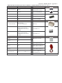
OPTIONS
TRX2-VM Voice Memory: 10 memory banks
Banks 1-9; Capacity 10 seconds each
Bank 10; Capacity 120 seconds
*Specifications subject to change
TRX2-KB1 External Keyboard,
TRX2-NB Noise Blanker.
4
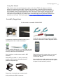
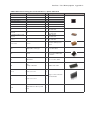
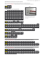
Assembly Suggestions
Using This Manual
This manual uses a pictorial approach, same as the Juma TRX2 web pages, to aid the
builder in constructing this radio. The Part Lists provide an inventory check-list and for
some part lists, if noted, a logical order of assembly is suggested. Please note the printed
circuit boards (PCB) may be revised over time. Be sure to note revision listing at the top
of the Part Lists matches the PCB revision you are working with. Updates and additional
information not provided in this manual such as building tips and hi-resolution pictures are
available on the Juma TRX2 web pages at http://www.nikkemedia.fi/juma-trx2/
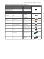
Assembly Suggestions
Tools needed to assemble JUMA TRX2
A temperature controlled anti-static soldering iron or
soldering station with a small to medium tip.
Small side cutter, small pliers, medium size Phillips
screwdriver and small to medium adjustable wrench.
Small to medium diameter (0.2...0.5 mm) solder wire with
"no clean" type flux. Lead-free solder wire is ok but is not
as easy to use as the conventional wire.
Small, straight or curved tweezers used for SMD
Assembly.
Solder wick (e.g. width 1.5...3mm) for removing
possible tin short circuits solder paths between
pads and component legs.
Simple loop or forehead loop to see the details
during soldering the SMD components
Digital multimeter with at least voltage, current and
resistance ranges. Capacitance measuring is a
"nice to have" feature.
Also consider using small containers such as empty
butter containers or muffin pans to hold and organize
the parts for each section as you build.
5
Assembly Suggestions
SMD Construction Tips and Techniques
Most hobbyists cannot afford the expensive tools and soldering equipment professionals’ use for
Surface Mount Device (SMD) construction. Thankfully, many low cost alternatives exist. Here we
offer just a few.
SMD components can be extremely small and difficult to handle. Therefore, it is important you take
into consideration your workspace. It needs to be well lighted. I suggest, if possible, you obtain a
natural or full spectrum lamp which provides better color definition useful for such fine work. This
type of lighting is sometimes called Tru-light such as the Ott-Lite brand and can be obtained at hobby
or craft stores.
The next most important thing is to decide on your construction technique. Consideration must be
given as to how you will control the small components as some are the size of a freckle or mole on the
back of your hand.
Toothpick and Bee’s Wax Method
I have successfully used bee’s wax and a wooden toothpick for several SMD projects. The principal
here is to flatten the point of the toothpick then add a very tiny piece of bee’s wax to the end to pick up
and hold components. Here are the steps.
1. Tin the pc board pad(s) where you will be working. Important: use very little solder!
2. Pick up the component using the “waxed” end of the toothpick and place it on the pad.
3. Hold the component down with the toothpick and solder tack one side or leg of it.
4. The component should now be stable so put the toothpick aside and solder the other side.
5. Now return to the first side and re-solder if necessary.
Tip: For ICs use the above technique but solder tack the opposite corner pins before setting the
toothpick aside and soldering the remaining pins.
Tip: For non-ESD soldering irons the tip must be grounded to the pcb using the technique shown here.
This will help avoid causing internal breakup of MOS devices.
6
Assembly Suggestions
Tweezer Method
1. Pre-solder one pad (very lightly)
2. Hold with tweezers and melt solder again.
3. Solder the other end of component
4. The SMD component is fully installed.
Tip 1: Use very fine (small gauge) solder, a narrow soldering iron tip and a tiny amount of solder!
Tip 2: Use gentle pressure on tweezers to avoid pinching and “shooting” the device across the room.
Tip 3: For ICs or transistors solder tack the opposite corner pins first before setting the tweezers aside
and soldering the remaining pins.
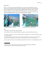
Doofus Method
Using a doofus allows you to use both hands for soldering. The doofus is a home made device using a
coat hanger or a fine wire and some weights to hold the component in place. The technique used is the
same as Bee’s wax method outlined above but you have both hands free for the solder work. Here are
some pictures to give you a better idea. Notice the baking pan use to keep parts contained.
Here is just one of many good sites for such tips: http://www.al7fs.us/AL7FS5ATSprint2.html
7
Assembly Suggestions
Alternate methods of SMD construction.
The following method are mentioned as alternate means to building with SMD. These methods must
be used with extreme caution to avoid permanent and un-repairable damage to circuit boards and
components. These methods allow soldering of all components at one time by having you place the
components on the pc board using solder paste and then “baking” the board to “flow” the solder.
Convection Oven and Solder Paste often called the Cash Olsen Method
http://www.hpsdr.com/Public/Projects/SMT/SMT.html
This method uses a convection oven and solder paste.
Pros: It’s fast and clean with reduced chances of parts being lost in the carpet.
Cons: If not done correctly irreversible damage to both pc board and components can be done.
Electric beverage warmer (coffee cup heater) and Solder Paste
http://www.zianet.com/erg/SMT_Soldering.html
This method utilizes the same technique as the Convection Oven but uses safer, lower temperatures.
Pros: It fast with reduced chance of pc board or component damage (lower heat).
Cons: Still possible to damage pc board and components and requires additional purchase of a hot air
embossing tool for secondary heating to complete solder flow.
Pictorial example of right and wrong application of this hot air & solder paste technique:
http://www.zianet.com/erg/Kisses_and_Pies.html
Hot Air Re-Work Station and solder paste
Using a hot air re-work station is another relatively inexpensive approach, similar to the above
techniques. The method is the same but you work with fewer components at a time. It is more like
normal soldering except you use solder paste instead of solder wire, hot air instead of a hot iron and
need only one hand. The benefit of this method is you work at your own pace, do one or more
components at a time, and take breaks whenever because the hot air tool heats up in about 30
seconds. Hot Air Re-Work Stations can be found starting under $100 on eBay and elsewhere.
Step 1: Place a small amount of solder paste on the component pads or a bead of paste across an
IC’s set of pads. (See http://www.zianet.com/erg/Kisses_and_Pies.html for details on
correct method)
Step 2: Place component onto/into paste on top the pads. Don’t worry about aligning the
component perfectly, close is good enough. The components will ‘magically’ align
themselves when the heated air is applied.
Step 3: Hold the hot air tool centered over the top of component at about 2 inches (or a little less)
with the air stream flowing straight downward for about 3 seconds. Watch as the
component wiggles into perfect alignment and the solder flows.
Step 4: Inspect your work. If a misalignment occurs or you need to change/ remove a part, simply
re-heat the part while using a tool to grab and move it. Be very careful to keep your fingers
out of the hot air stream.
8
Assembly Suggestions
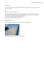
Parts Inventory and Identification
As in any project, you need to gather your parts and inventory them. Since the parts in this kit are so
small you will need the aid of a magnifying lens or jeweler’s loop, a good light source and parts list
found in this manual. The kit’s parts will arrive packed in marked bags.
Tip: Keep the components in their marked bags until you are ready to install them.
Some bags will contain different type of components that will be identified by stickers that include
both the corresponding marking codes such as resistors or semiconductors and their values e.g.:
1k5 = 1501
BAV99 = A7
or
or
4k7 = 4701
2N7002 = 702
It’s important to understand the markings on the components ( e.g. A7 ) may differ from kit to kit.
This happens because different manufacturers use different marking codes and we may substitute a
component with a compatible one from a different maker. Regardless, the code printed on the part’s
sticker will be valid for each kit
Hint: Using the Part Lists (with its component pictures) along with the bag stickers will help identify
the uncommon and/or smaller unmarked parts such as capacitors and inductors.
Problems
Most problems will occur because of poor soldering (opens or shorts across pads), wrong component
installed or the component was placed improperly (wrong polarity).
TIPS TO AVOID MISTAKES
Go slow and be systematic when soldering. Visually identify each component under good light and
magnification and ensure its proper placement (e.g. polarity). Mark off the parts list for each
component when you have completed its installation and visual check.
9
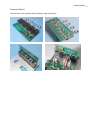
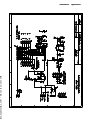
DDS – Control – Display Board
DDS – Control – Display Board
You may wish to begin solder work with the microprocessor and DDS chips. This will allow you more room to
work at board level and it will be easier to inspect your work up close after soldering. Then proceed with
resistors, capacitors, inductors, transistors, ICs and finish with the taller components.
Shown here are some hints to working with the DDS Board microprocessor. Begin by placing a tiny amount of
liquid flux or flux compound over the pads to help hold the chip in place and to allow the solder to flow. Do not
use any force on the soldering tip to the chips pins.
When finished soldering remove excess solder using a fine grade solder wick. Again, do not use any force.
The next step would be to wash away the excess flux
using a solvent such as a good grade PCB cleaner or
isopropanol alcohol. Use enough solvent to remove all
residue.
Carefully inspect your work under magnification and
good lighting after the cleaning. If you have to do
corrections, apply flux to the area that needs resoldering or solder removal. Make all possible
corrections before you install Oscillator IC5 and pin
header J19.
Next you begin the install of the various switches,
pushbuttons and DDS board connectors.
10
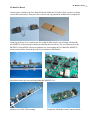
DDS – Control – Display Board
DDS – Control – Display Board
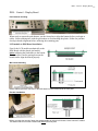
Push buttons mounting
When ready to mount the push buttons, use the front plate to align the buttons before you begin to
solder. Limit soldering time with the pin headers to avoid melting the plastic. Solder one pin then
check pin header alignment before soldering the remaining pins.
LCD module to DDS Board installation
First fix the LCD module mechanically to the
DDS Board with the placed pin headers
before soldering the pin headers to the boards.
This is to allow correct spacing between the
boards and to align the boards properly.
MIC socket mounting
Before soldering the MIC connector to the DDS board it must be fastened to the front plate.
Encoder installation
Before mounting the encoder, flatten the toothed washer to reduce its thickness. Use a hammer if needed.
This washer will mount on the encoder shaft behind the front plate.
11
DDS – Control – Display Board
DDS – Control – Display Board
Front Plate mounting
Mount the front plate and tighten the MIC connector to the plate. Also tighten the encoder-mounting nut. Before
tightening the nut check the lock washer thickness that the encoder fits perfectly between the board and the
front panel. When necessary uninstall the tooth washer and bang it slightly to a suitable thickness. Remember
the flattened lock washer goes behind the front plate. Now you can solder the MIC connector and encoder.
Regulator mounting
Prepare the power regulator for mounting as shown here bend the legs in a U shape. Solder as shown.
Knob mounting
When installing the potentiometer knobs use a piece of paper between the plate and the knob.
This is an easy way to control spacing so the knobs rotate freely.
12
DDS – Control – Display Board
DDS – Control – Display Board
Regulator chassis mounting
Audio Jumper position
If the Voice Memory option is not installed place
a jumper into the pin header J8, use pins 1-2.
Do not install the jumper J4 for the normal use.
It is intended for the bootloader and test purposes.
If the jumper J4 is installed you can not switch
OFF TRX2 with the PWR button.
Suggested MIC wiring
13
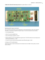
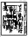
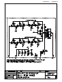
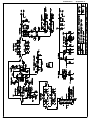
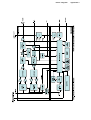
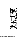
Main Board
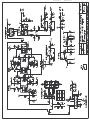
14
Main Board
There are a lot of parts to solder on the Main Board. You may prefer to begin with the ICs first to
allow you more working room at the board surface, then proceed to resistors and caps and finish with
the taller components. This board is not too densely populated which will make it easier to construct.
Below are pictures of how you will mount the main board in the case. Note the crimp terminals are
soldered to the board ground pads where holes are provided for them. Typically, the crimp terminals
will fit nicely through the holes so they are just flush with the bottom of the pcb.
Mounting Main Board to side rails
Ground Jumper for test measurements
Tips:
A few things to which the builder must pay attention
Note in the picture (above on right) the DDS power regulator mounts to the Main board solder lug.
C22 and C23 are the larger 1206 size caps and positioned close together so use caution when installing so they
do not short together.
Use caution when soldering the trimmer resistors at R26, R28 and R56. Do not use a hot air tool with these.
The plastic bodies of these pots will not tolerate a stream of hot air from a rework station for long.
Always, keep the solder time short when installing the pin headers and sockets to avoid damaging their plastic.
Visual Inspection
Carefully inspect your work for any missed solder joints or solder bridges using a bright light
under magnification. If all looks well proceed to the next board.
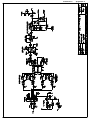
Filter Board & Polyphase Board
Filter Board
Construction of this board is not difficult and with fewer parts to solder. Proceed slowly and inspect
your work as you go.
Tips
Here are some cautions for builders.
This board use two sets of 100n (0.1uF) capacitors which are different types. Don’t mix them.
The parts bags are marked clearly but the builder may need to pay close attention to avoid mistakes.
C3, C5, C10, C12 are COG type and are physically thicker.
The second set is X7R type as the bag identifies them.
They are used for C16,C17, C18, C19, C20.
Polyphase Boards
These boards are also simple to construct and should not present problems.
Mount foam pads to top cover to secure Polyphase board.
15
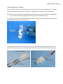
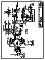
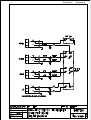
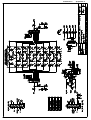
Two Band PA Board
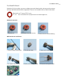
Two Band PA Board
Solder the ICs first to allow you more working room at the board surface, then proceed to resistors
and caps and finish with the taller components. There are two toroidal coils to wind for this board.
Both coils are 17 turn on T25-2 cores.
L3, L4 1uH, Core Amidon T25-2 (red) turns 0.4 mm enamel copper wire
Additional instruction
1. Wind the coil
2. Presolder wires with a hot iron
3. Fold the wires for surface soldering
SWR transformer modification
1. Saw or file slots on both sides
2. The slots are ready
3. Break up the plastic wall off
4. One plastic wall is now off
5. Break up the other plastic wall
6.Thread wire through the toroid
Transformer mounting
16
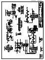
Two Band PA Board
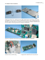
Two Band PA Mosfet Installation
Bend legs as shown. Use a small screw driver shaft to help form the curved bends. Then mount
the MOSFETs to the rear plate with the provided hardware as shown. The set of holes next to the
MOSFETs (shown filled with screws and nuts) are for mounting the All Band PA MOSFETs and
are not used here. Insert the provided screws and nuts to fill this hole.
Attach the completed PA board to the rear panel and then solder the PA MOSFETs.
Solder the Power and RF wiring
Completed Two Band PA and Connector board.
17
Connector Board
Connector Board
Fix the sockets to the rear panel before soldering to align with the plate.
18
All Band PA Board
All Band PA Board
Construction is similar to the Two Band PA Board. Solder the ICs first to allow you more working
room at the board surface, then proceed to resistors and caps and finish with the taller components.
Bend legs as shown. Use a small screw driver shaft to help form the curved bends. Then mount
the MOSFETs to the rear plate with the provided hardware as shown. The set of holes next to the
MOSFETs ( shown filled with screws and nuts) are for mounting the Two Band PA MOSFETs
and are not used here. Insert the provided screw and nut to fill this hole.
Mount the board to the rear panel and solder the MOSFETs PA.
Another view of PA FET mounting.
Completed All Band PA and Connector board..
19
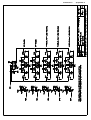
RF Filter Board
RF Filter Board for All Bands
Solder the ICs first to allow you more working room at the board surface, then proceed to resistors
and caps and finish with the taller components. Limit soldering time with the relays and use
caution when soldering near them so not to melt their plastic casing. Solder only one pin of the pin
headers, check for proper alignment then solder the remaining pins.
.
Front view of RF Filter Board
Rear view of RF Filter Board
There are six toroidal coils to be wind for the RF board, L28 – L33 on T25-2 cores.
L32 and L33
L30 and L31
250nH, Core Amidon T25-2
(red)
9 turns 0.4 mm enamel
copper wire
500nH, Core Amidon T25-2
(red)
12 turns 0.4 mm enamel
copper wire
L28 and L29
1uH, Core Amidon T25-2 (red)
17 turns 0.4 mm enamel
copper wire
Additional instruction
1. Wind the coil (see details
above)
2. Presolder the wires with a
hot iron
3. Fold the wires for surface
soldering
20
Cabinet and Final Assembly
Cabinet and Final Assembly
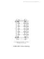
You may need to drill and countersink the necessary holes for the speaker including four (4) countersink holes for mounting the speaker. Refer to the Speaker Holes Drawing at end of Appendix D.
Tip: Proceed slow and careful when drilling the speaker holes to prevent scratching or chipping the
top cover paint. A hand countersink tool can be use to finish the holes nicely.
You may need to drill countersink holes for the cabinet side rails for mounting the front panel which
uses flat-head screws into countersunk holes.
Crimp the power wire leads to terminals. Insert the terminals into the connectors until they lock in
place. The red (positive) power wire/terminal goes into the “squared barrel” side of the connectors.
21
Flat Cable Dimensions
JUMA TRX2 Flat Cables with Dimensions
10-9-07
Measure and carefully cut ribbon cables to length before crimping the end connectors.
Note the position of the end connectors – some are on opposite sides of the cable.
The base flat cables for all Juma TRX2 models
Two band cable – (note the connector positions)
All band cables – (note the connector positions)
22
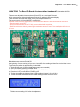
Operation
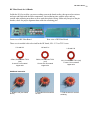
Operation
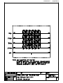
Main Display view
Shown here are some of the information the TRX2 LCD can
display.
Middle Filter engaged in LSB mode
RIT engaged with Wide Filter
Narrow Filter engaged in CW mode
VFO B engaged in USB mode (notice no signal present)
23
Circuit Descriptions – DDS Control Board
Circuit Descriptions
JUMA-TRX2 DDS Control Board
General
Key functions of the JUMA-TRX2 DDS / Control board are:
- provide user interface functions with LCD display, buttons, and potentiometers
- generate user interface tones and CW side tone
- provide I/Q LO frequency to the JUMA-TRX2 main board
- provide clock frequency to main board SCAF filters
- measure analog input signals from main and PA board and
- read and process VFO encoder
- provide digital control signals for main and PA board control
- provide RS232 serial interface to external equipment
- provide CW keyer functions
Key components of the DDS / control board are dsPIC30F6014A microcontroller.
2*16 character LCD display, high resolution optical encoder, pushbutton switches, potentiometers,
AD9851 DDS chip, 30MHz reference oscillator and RS232 driver chip.
These components and over 3000 lines of software code stored in dsPIC30F6014A
Flash memory form JUMA-TRX2 control unit.
Voltage regulator / power switch
Main operating voltage of the DDS / control board is +5VDC. The 5V is generated from the power feed
(about +14VDC) with the linear regulator. The linear regulator’s benefit is low noise emission. Less
wanted characteristics are poor efficiency and high heat dissipation. In the JUMA-TRX2 the DDS board
+5VDC regulator is mounted to the enclosure’s aluminum frame to ensure maximum heat dispersion.
Power on is implemented with push button, FET switch and software. This combination enables us to
use power switch button in multiple ways (see operating instructions). Software can detect the power
switch push button state (PWR-SW signal). The push button also activates FET switch directly. This
function is needed to get board power on and software running. When the software is running, the
power FET switch is kept on with the power on digital output signal (PWR-ON). The power on signal is
also connected to the main board to operate power switches there. When the user has decided to turn
the JUMA-TRX2 off, software executes the power down tasks and then removes power on signal
(PWR-ON).
LCD display
2 by16 character LCD module is used to implement the JUMA-TRX2 user interface display. A few
special fonts are loaded into the LCD display’s RAM character generator to allow graphic S-meter
display. The LCD module power feed is filtered with a simple RC filter to reduce RF noise.
Contrast and backlight adjustment
The LCD module contrast voltage and LED backlight current are generated with a PWM type DAC.
PWM DAC’s are formed with software, dsPIC30F6014A PWM outputs and few other components; the
RC filter and buffer amplifier (IC3A) for the contrast voltage and the RC filter and current generator
(IC11A and Q3) for the LCD back light. Typical control voltage value is about 0,5V. Back light current
can be adjusted from 0 to about 100mA. Normal value is between 20 to 50mA.
24
Circuit Descriptions – DDS Control Board
Push button switches
User interface push button switches SW1 to SW6 are connected to dsPIC30F6014A digital inputs. All of
these inputs are kept high (1) with pull up resistors. When a switch is pressed input state goes low (0).
The push button functions are defined in the software logic.
VFO encoder
High-resolution optical encoder is mounted to the DDS board. The main usage of this encoder is VFO
tuning. The encoder is also used in various user interfaces configuration functions. The encoder
generates two logic level signals, which are quadrature phased. Phasing allows software to detect the
direction of rotation. Both encoder signals are connected to dsPIC30F6014A interrupt pins. Encoder
processing is done in software with interrupts to get smooth and reliable operation even when encoder is
rotated in high speed.
Analog inputs
Seven analog signals are measured with dsPIC30F6014A A/D converter. The A/D converters reference
voltage is derived directly from AVDD +5V supply. The DDS board voltage regulator is a “generic” 7805
part. However, good quality parts should be used here to maintain analog measurement accuracy. The
DDS boards +5V supply voltage should be 5V+/- 0,05V or better.
Signal descriptions
Potentiometer
Two front panel potentiometers (CW SPEED and RIT) are directly connected to dsPIC30F6014A analog
inputs. With this arrangement software can read potentiometer positions in numeric format.
FWD-PWR and REW_PWR
The PA board contains SWR bridge, power peak detectors and a buffer amplifier. Amplifier outputs are
scaled so that 10W are about 2,05V at analog input.
ID (drain current)
PA board contains measurement shunt resistors, power peak detectors and a buffer amplifier. Amplifier
output is scaled to produce 1,21V/A at analog input.
S-METER
Main board audio AGC circuit generates S-meter voltage. S9 corresponds to about 1V at analog input.
BATT (JUMA-TRX2 power feed voltage)
This measurement is taken from DDS board power supply input with a voltage divider. 14V input generate
3,25V at analog input
Tone generator
User interface tones and CW side tone are generated with dsPIC30F6014A timer system.
Tone signal is delivered as a 5V-logic signal to main board where it is conditioned, filtered and summed to
the audio chain.
SCAF filter clock generator
Switched capacitor (SCAF) filters are used in the JUMA-TRX2 RX and TX chains. The SCAF filter is a low
pass filter which response is defined with filter clock frequency. Filter clocks are generated with
dsPIC30F6014A timer system. See JUMA-TRX2 operating instructions for filter adjustments.
25
Circuit Descriptions – DDS Control Board
Digital control signals
Several digital control signals are read and generated by JUMA-TRX2 control software. Some of these
signals are directly connected to dsPIC30F6014A general-purpose digital I/O pins. Additional digital siginal
are generated locally in the main board and in the all-band model filter board. These digital outputs are
controlled via the SPI bus.
Directly connected I/O signals
PTT in / out
From PPT_IN signal JUMA-TRX2 control software finds out when TX is on and performs needed
operations. PTT_OUT signal enables software controlled TX. This is needed for CW keyer operation.
DASH / DOT
DASH and DOT are the key state inputs for keyer software. Inputs are sampled with 1ms interval.
KEY
Key output controls the CW modulator in the main board. CW keyer software and tune mode logic drives
this signal.
SPI bus to main and PA boards
Four signals form the SPI bus. SPI_SDI, SPI_SDO, SPI_CLK and SPI_LATHC. SPI_SDI is
not used. SPI signals are controlled by dsPIC30F6014A SPI I/O block and TRX2 control software. To
minimize RF noise SPI bus is active only when a change is needed in the main or PA board outputs state.
Main board SPI bus controlled digital outputs
SSB/CW Select main board SSB or CW operating mode
SB-SELECT Select sideband LSB or USB
NAR Select SSB or CW band pass filter
FAST-AGC Select AGC speed
PROC-ON Select TX speech processor ON / OFF
NB Select noise blanker option ON / OFF
MIC/LINE Select Mic input signal level
7M Select 3,5 or 7 MHz RF filters in two-band PA board
All band Filter and PA board digital outputs
Output I/O register is located in the RF FILTER BOARD but two of the control signals are connected to
the PA board.
B0, B1, B2 Three bit binary coded filter select. See filter board schematics for details
ATT-0, ATT-1 Two-bit binary coded RF attenuator control for the PA board,
See schematics for details.
DDS LO
The Analog Devices AD9851 DDS chip is used for LO frequency generation. The JUMA-TRX2
commutating mixer needs four different states (quadrants) per one LO cycle. AD9851 DDS digital output
is 2 * LO frequency. AD9851 output and output complement signals are used to clock IC7A and IC7B flipflops. Flip-flops are connected so that output is a quadrature signal (I/Q) for the RX and TX mixers. In the
main board, analog switch IC8 is used to select the order of LO-A and LO-B signals going to the mixers.
Order of the LO signals selects the desired sideband.
26
Circuit Descriptions – DDS Control Board
DDS LO (continued)
The AD9851 DDS chip is clocked with 30MHz reference oscillator. Reference clock frequency is
multiplied by six to get the required 180MHz internal clock rate for the DDS chip. The DDS chip is
controlled by the JUMA-TRX2 control software via the serial bus. For details see software source code
and Analog Devices AD9851 data sheet. Analog Devices have also published very good application
notes and DDS tutorials in their www pages.
30MHz Reference oscillator
A good quality crystal oscillator is needed for the 30MHz-reference frequency generation. Most important
parameter is the phase noise of the oscillator. This is important because frequency and also errors are
multiplied by a factor of 6 inside the DDS chip. Frequency accuracy is not so important because it can be
corrected with the JUMA-TRX2 calibration setup. Good thermal stability is however required. There are
two decals (places) in the DDS printed circuit board for 30MHz oscillators. One is for the surface mount
version and another the through hole version. This makes easier to find good oscillator components. Of
course only one is populated here. DsPIC30F6014A is also clocked with this reference oscillator. The
current software version operates with a 30MHz clock. The 30MHz frequency is connected to the micro
controller via 0R jumper R54. For future use there is the possibility to install a flip flop IC6 and get 7,5MHz
external clock rate for the dsPIC30F6014A micro controller. This “low frequency” clock is needed if the
dsPIC30F6014A internal PLL is used for clock frequency generation. With internal PLL , the 120MHz
clock rate can be produced. This is needed if software performs heavy DSP operations.
Mic/line input
Microphone input is designed so that a electrete microphone can be directly connected into it.
Microphone input can also accept other kinds of signal source. Input sensitivity level can be controlled
with software. Microphone input is a 3,5mm stereo jack. The tip is the microphone and the Ring is the
PTT signal.
RS232 interface
DsPIC30F6014A UARTs are buffered with RS232 transceiver IC10. UART #1 is connected via the main
board and connector board to the JUMA-TRX2 back plane. This RS232 I/O can be used for PC/Terminal
connection or for the JUMA External keyboard connection. See operation instructions and software
source code for details. UART #2 is connected to pin header J1 and reserved for future use.
Option board connectors
Behind the DDS board there are connectors (pin headers) J5, J8 and J7. These connectors are for
various option boards
Connector J5 provides access to microphone / line input circuit.
Connector J8 provides access to the audio out path. If no option board is installed there should be jumper
between J8-1 and J8-2 connecting RX audio to AF gain potentiometer.
Connector J7 provides digital I/O control and supplies power to the option board. For future use the
dsPIC30F6014A DCI interface (codec interface) is also wired to J7.
Connector J19 (ICD2 connector) is for the Microchip ICD2 debugger / programmer. ICD2 is needed if
there is no on-board flasher available or if it is corrupted. See the Microchip www pages for details.
27
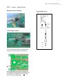
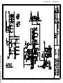
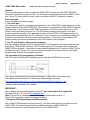
Circuit Descriptions – Main Board
JUMA-TRX2 Main Board
11/25/07
General
JUMA TRX2 is using the quadrature sampling technique for demodulation and modulation with the low
noise phasing method. The main board handles all the RF and AF exciter functions for reception and
transmission.
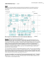
Block diagram of the JUMA TRX2 exciter, the main board and the DDS board
RX section (Refer to the main board schematics page 1)
The antenna RF signal, without any RF amplification, goes directly to the wide band transformer T1 to
achieve good dynamic range. The transformer T1 transforms the unbalanced 50 ohm antenna signal into
the 200 ohm balanced signal. This signal is fed to the doubly balanced demodulator (RX mixer) IC1 which is
a high speed, low ohmic analog multiplexer controlled by dual local oscillator signals which are shifted by 90
degrees. These local oscillator signals I and Q are coming from the DDS board. The demodulator IC1 is
sampling the antenna signal into the four sampling capacitors C4, C5, C6, C7. The signals in these
capacitors are in baseband frequency range i.e. < 15 kHz and all the capacitors have equal signal content,
but the phase of these four signals are different, which are 0, 90, 180 and 270 degrees, called I and Q
signals and their complement signals.
The I and Q signals are amplified in the differential preamplifiers A1 and A2. The gain of these preamplifiers
are set precise to equal each other by using 0.1% feedback resistors R3 - R8. The preamplifiers are feeding
the RX polyphase module which proportionally delays the Q signal by 90 degrees compared to the I signal.
(Read more of the polyphase module in its own description). The signals after the polyphase is buffered and
further amplified by the instrumentation type amplifier A3 and A4-A.
The output of the amplifier A4-A is demodulated SSB audio signal at the band width of 15 kHz. The signal is
st
st
then filtered in the SSB/CW 1 filter module. This 1 filter has two band pass ranges, 300 Hz…2.5 kHz for
SSB and 300 Hz…1kHz for CW. The width is selected by the pin 5 in the filter module. (Read more of the
1st filter module in its own description section).
28
Circuit Descriptions – Main Board
st
After the 1 filter the signal is fed to the AGC circuit which consists of the variable gain amplifier A4-B, the
full wave signal rectifier amplifier A6 and the AGC rise and fall timing components R44, R45, R46, R47,
R67, C34 and C35. In the fast AGC mode the MOSFET TR6 is used to connect the resistor R67 in parallel
with the timing circuit. The AGC control voltage which is coming from the timing components defines the
resistance of the feedback FET TR4 and thus defining the gain of the AGC variable gain amplifier. Signal
for the S meter is processed from the AGC control voltage by the DC amplifier A7. Nominal S meter output
voltage is 1 V with a S9 (50uV) signal and 2 V with a S9+40 dB signal. The threshold of the AGC is defined
by the trimmer resistor. The adjustment can be done by means of a 50uV (S9) antenna signal and by
turning the trimmer R53 until the S meter reading is 1 V. S9 reading is in the middle in graphical LCD bar,
marked with two dots.
The output audio level of the variable gain amplifier A4-B is regulated to the range of 5 mV…10 mV which is
amplified by the post amplifier A5-A to a suitable 200 mV…500 mV level for the Switched Capacitor Filter
(SCAF) IC10. The SCAF is a variable 8th-Order, Elliptic lowpass filter. The corner frequency is defined by
the clock frequency coming from the CPU in the DDS board. Thus the final RX selectivity can be set by the
user. The output from the SCAF is fed to the AF GAIN potentiometer located in the DDS board and fed
back the speaker amplifier A12 in the main board.
The CW sidetone and the acknowledge tones coming from the DDS board are summed to the AF signal in
the post amplifier by the resistor R52.
Additionally there are I/Q buffer amplifiers A13-A and A13-B for the I and Q signals at a bandwidth of ±15
kHz. This signal is available in the rear panel AUX connector by selecting corresponding AUX select jumper
positions. The I/Q output can be used for a software demodulation by feeding the I/Q signals to a PC via a
sound card input.
TX section (Refer to the main board schematics page 2)
The AF signal from the microphone is fed to the amplifier A8-A which acts also as user switch selectable
speech processor. The mic input is designed for an electret type microphone with a direct two wire
connection. The electret bias is fed by the resistors R62 and R61. If a dynamic microphone is preferred the
bias should eliminated by adding a 470 nF capacitor in series with the dynamic microphone "hot" wire. The
speech processor is using a soft clipping to form a logarithmic type of compressor. When the processor is
engaged the high frequency pre-emphasis is magnified which will emphasize high tones to get a more
penetrating SSB transmission. The mic input can be switched to the line signal level mode for e.g. digimode reception. The line signal level can be matched to the audio source e.g. sound card by changing the
value of the resistor R82.
The audio signal from the mic amplifier is filtered by the highpass filter A8-B at 300 Hz and by the SCAF
lowpass filter IC9 at 2.6 kHz. Then the signal is split into the differential signals by the amplifiers A9-A and
A9-B. The gain of the SSB drive is adjusted by the trimmer resistor R26. Then the audio signal is the fed to
the TX polyphase module which splits the signal in to the two phases I and Q and their complements. The I
and Q signals are buffered by the TX driver amplifies A10 and A11. The gain of these TX drivers are set
precisely to equal each other by using 0.1% feedback resistors R16, R17, R18, R21, R22, R23. The I and Q
signals are fed to the SSB modulator IC2 (TX mixer) which is a high speed, low ohmic analog multiplexer
controlled by dual local oscillator signals which are shifted by 90 degrees. The output of the modulator is
SSB RF signal on the local oscillator frequency at the nominal level of 6 dBm (~4 mW)
The other half of the TX mixer IC2 is used for the CW modulator. It generates carrier on the local oscillator
frequency. The carrier level is defined by the constant DC current generator TR1. The constant DC current
level and thus the CW drive is defined by the trimmer resistor R28. The keying envelope is defined by the
capacitor C19 with the reflected RF impedance of 100 ohms. Nominal rise/fall time is 5 ms. The CW rise
and fall times can be customized by changing the value of the capacitor C19 if desired.
Control section (Refer to the main board schematics page 3)
The control section includes the power ON/OFF switch and the voltage regulators for 10 V and 5 V. The
Power ON/OFF MOSFET switch TR7 is controlled by the DDS board via the MOSFET TR8. The rare 13.8
V (+V) is used directly for the speaker amplifier. The 10 volt from the low drop regulator REG2 is used for all
the OPAMPS and the reference (midpoint 5 V) is made by the resistor divider R83 and R58 and filtered with
the capacitor C76. The 5 volt from the regulator REG1 is used for all the logic circuits including the RX and
TX demodulator muxers.
29
Circuit Descriptions – Main Board
The functions of the main board are controlled by the shift register IC6. The functions are:
Sideband selection
•
st
1 filter width
•
AGC speed
•
Speech processor ON/OFF
•
Noise blanker ON/OFF (option board)
•
AF input level (mic/line)
•
80 m / 40 m band selection in two band model (change point frequency 4 MHz)
•
The shift register is driven by the DDS board with the serial SPI bus including data, clock and latch signals.
The clock signal is filtered with R95 and C91 and squared with the Schmitt trigger inverter IC7. The SPI
signals with the cascade output are fed to the second shift register in the RF filter board for RF bandpass
and PA lowpass filter selection. See more of the SPI principle in its own document
The analog muxer IC8 is used to swap the I and Q signals coming from the DDS board. The order of the I
and Q signals defines the sideband (LSB or USB). The swapping is controlled by the shift register IC6 pin 1.
The quad NAND IC4 controls the transmit, receive and the mode of operation by using the PTT and
sideband input signals.
The AUX selector jumper block defines the rear panel AUX connector signals. The alternatives are I/Q
output or PTT in/KEY out, see schematics for the jumper positions. The PTT input can be used e.g. for a
foot switch PTT. When the key input is grounded the rig switches to the TX state. The PTT signal is wired
on the main board to the 5 volt via the 4k7 R71 and it requires 1 mA sink current to operate. The Key out
can be used e.g. for a linear amplifier control. The key output is implement by the open drain MOSFET
TR10 capable of sink max 0.1 A current at a max voltage of +50 V. Note, the key output can not be used in
a negative voltage control.
The resistor and capacitor block marked "TONE LPF" is a passive lowpass filter for the sidetone and
acknowledge tones coming from the DDS board. The resistors R87 and R88 keep the DC level in the
middle during tone breaks to achieve a smooth audio tone output.
Adjustments
There are three trimmer resistors on the main board, the AGC threshold (R53), the SSB transmit gain (R26)
and the CW carrier level (R28). See the instructions in the main board adjustment document.
30
Juma TRX-2 Two Band PA Board Description
Circuit Descriptions – Two Band PA Board
General
The JUMA TRX2 two band PA board is a 10 W linear amplifier for 80 m and 40 m ham bands. The board
includes also the band pass RF filters, PA lowpass filters and SWR bridge.
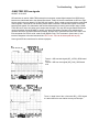
JUMA TRX2 two band PA board block diagram
The bandpass filters
The band pass filters are used both in transmission and reception. The filters are implemented using SMD
inductors and capacitors and switched by the SMD relay RL3. The band switching crossover frequency is 4
MHz and it is controlled with the MOSFET TR7 with "7M" signal coming from the DDS board. See the circuit
diagram "BPF FILTERS".
Simulated response of the bandpass filters. Blue for 80 m, red for 40 m
31
Circuit Descriptions – Two Band PA Board
The driver and the final amplifier
The input of the driver MOSFET TR1 is terminated with a 51 ohm resistor R1. The single ended driver
operates in class A with the nominal bias current 130 mA which is regulated with NPN transistor TR6. The
resistor R3 and the capacitor C3 in the source of the driver MOSFET are used to equalize the RF gain in
both of the bands. The RF transformer T1 converts the driver output to the balanced signal which is feeding
the final amplifier MOSFETs TR2 and TR3 in push-pull configuration. The nominal output power is 10 watts.
The final stage bias current, nominal 100 mA per MOSFET, is adjusted by the trimmers R4 and R7. The
resistors R17 and R21 in the sources of the final MOSFETs are used to sense the drain current. The
voltage is across the sense resistor is proportional to the drain current. The sense voltage is amplified with
the DC amplifier A2-A and fed to the AD converter in the DDS board, thus the drain current can be
monitored with the LCD.
The lowpass filters
The final stage is followed by the lowpass filters for 80 m and 40 m. The corner frequencies are 4 MHz and
8 MHz correspondingly. These lowpass filters are also in the signal path during reception to provide
additional filtering. The 80 m lowpass filters is implemented by using SMD inductors L1 and L2 and the 40
m filter is using two small iron powder toroids L3 and L4. The switching crossover frequency is 4 MHz.
The SWR bridge
The SWR bridge is between the lowpass filter and the antenna. The transformer T3 is sensing the output
RF current and the transformer T4 is sensing the output RF voltage. These signals are combined and
rectified for relative forward and reverse voltages. The DDS board calculates the forward RF power and the
SWR which can be seen in LCD. The SWR indication is calculated and displayed regardless of the transmit
mode, thus the SWR can be indicated also during SSB transmission.
T/R switching and the bias supply
The small MOSFETs TR4 and TR5 are driving the antenna relay RL1 and the bias supply. The bias supply
voltage is regulated with the shunt regulator consisting of the reference diode Z1 and the diodes D2 and
D3. The purpose of the diodes is to achieve a negative temperature compensation for the bias voltage.
DC supply input
The DC supply for the TRX2 is coming via the PA board. The supply input is protected with the fuse F1 and
with the diode D10 against over current and reverse polarity.
Adjustments
See the separate two band PA board adjustment instruction document; it includes important notes to avoid
excessive MOSFET drain current and the fuse blow.
32
JUMA TRX2 Polyphase Board description
Circuit Descriptions – Polyphase Board - Filter Board
In the JUMA TRX2 there are two identical polyphase modules. Both of these plug-in modules are plugged
into the main board. One module is in the RX section and the other is in the TX section. The purpose of
the polyphase modules is to suppress the unwanted side band in the direct conversion method by means
of phase shift. There are no adjustable parts. In the RX section the polyphase is fed by quadrature I - Q
audio signals with the complement signals coming from the QSD muxer. The phases of these four fed
signals are 0, 90, 180 and 270 degrees. The Q signal is delayed by 90 degrees from the I signal. After
summing the signals the unwanted side band is in opposite 180 degree phase and thus suppressed.
Correspondingly in the TX section the singe phase audio
signal is split into the I - Q and the complement signals.
These signals are fed to the commutating TX muxer which
provides a SSB RF signal.
There are no adjustments to the polyphase module. The
unwanted side band suppression is optimized for 300 Hz...3
kHz range by simulation. The absolute values of the
components are not critical but the performance of the
polyphase depends on the deviation of the components in
each "column" within the circuit. The design is done so that
when using the specified components the unwanted side
band attenuation is very good (better than 50 dB). The
deviation comes mainly from the capacitor, the resistors are
the more accurate 1% type. The performance can be
optimized, if desired, to a superb level (60 dB...70 dB) by
screening close values of the components in each "column".
TRX-2 Filter Board Description
General
The JUMA TRX2 filter board is plug-in module on the
main board. It is a low noise, wide dynamic range filter
st
used as the 1 bandpass filter in the RX audio path. The
gain is 0 dB. The total noise is 3 V rms and the
maximum signal is 3 Vrms, thus the dynamic range is
120 dB. The filter board includes two filters, the wider for
SSB and the narrow for the CW. The final selectivity in
the JUMA TRX2 is defined by the post SCAF filter which
is user adjustable.
JUMA TRX2 filter board block diagram
The circuit description (See the filter board schematics)
There are two similar circuits on the board, one for the wider filter and the other for the narrow filter. Only
the component values are different in these two filters. The two filter inputs are driven in parallel and the
output is selected by means of the analog muxer IC1. This selection is controlled by the "NAR" signal. The
first filter stages (A1-A, A2-A) act as combined active highpass/lowpass filters and the next stages (A1-B,
A2-B) are additional active lowpass filters. The 6 dB rolloff frequencies are 300 Hz for the highpass and
1000 Hz/2700 Hz lowpass respectively.
33
Circuit Descriptions – Voice Memory Option Board
JUMA-TRX2 Voice memory option OH2NLT 22.08.2007
Function
The voice memory option is a JUMA TRX2 plug in module which includes audio record and playback functions.
It can record from the microphone or from the receiver. Playback can be sent to the band or to the local
speaker.
Purpose
The voice memory option can be used to transmit pre recorded voice messages e.g. in contest operation or in
other similar situations. Recorded voice from the receiver can be listened afterwards via local speaker or the
message can be transmitted back to the air.
Record/playback control
The record, playback and transmit functions can be controlled by means of the JUMA TRX2-KB external
keyboard option or by means of the Windows software (Compatibility Win 9x, 2k, XP or higher). The license for
the OH7SV Windows software is granted when purchasing the voice memory option kit.
Memory capacity
10 memory banks. Banks 1…9: Capacity 10 seconds each. Bank 10: Capacity 120 seconds.
General
Voice Memory option for the JUMA-TRX2 is an add-on board. The board can be attached behind the
JUMA-TRX DDS/control board. The key component of the voice memory board is the ISD17240 voice
recorder chip. Detailed description of the ISD17240 chip and its operation can be found from ISD17240
data sheet and application notes found at URL: http://www.winbondusa.com/en/content/view/160/290/
In the control software ISD17240 memory is divided into 10 sections. One is about 120s long and
others are shorter, about 11s each. Control functions for al the memories are the same. In this
application ISD17240 chip is clocked for 8kHz audio sample rate. The 8kHz sample rate is more than
adequate for high quality SSB voice storage.
Operation
The JUMA-TRX2 voice memory board is powered from DDS board 5V regulated power supply. The
key component of the voice memory board is Winbond ISD17240 voice recorder chip. The JUMATRX2 dsPIC30F6014A controller via the SPI bus controls the ISD17240 chip. Other components are
CMOS switch and an operation amplifier. With these components and an internal ISD17240 features al
required audio paths can be formed. In normal operation The JUMA-TRX2 RX audio is routed through
ISD17240 chip to audio amplifier. ISD17240 internal microphone amplifier is connected in parallel with
JUMA-TRX2 microphone input to allow recording from the microphone. Op amp and a CMOS switch is
used to connect the JUMA-TRX 2 RX signal to the JUMA-TRX2 microphone input and override the
microphone signal for RX recording. The same audio path is also used to TX selected memory location
(play to the band). ISD17240 internal switches are used to break the audio path and play selected
memory content to the JUMA-TRX2 speaker. The JUMA-TRX2 voice memory board also contains one
led for debug purposes. Led LD1 shows which command ISD17240 has received and is executing.
This indication is useful information in case of troubleshooting.
Commands
See JUMA-TRX2 control software documentation for available control commands.
34
Circuit Descriptions – External Keyboard Option
JUMA KB1 External Keyboard description OH2NLT 17.01.2008
General
JUMA-KB1 is a device intended to use with JUMA-TRX2 voice memory option. Keyboard hardware is not
limited to be used only with JUMA-TRX2 or control JUMA-TRX2 voice memory option. JUMA-KB1
operation depends on software loaded in to the keyboard microcontroller.
Operation
The circuit is designed to consume so little power that whole keyboard can be powered from serial
(RS232) interface receive signal. Receive signal idle state is about –9VDC and active state about +9VDC.
KB1 power supply is designed to utilize both polarity input voltages and produce about 4,5VDC regulated
operating voltage for the microcontroller. Microcontroller is a low power PIC16F628A clocked with
1,832MHz clock. Microcontroller consumes about 700uA and rest of the circuit about the same amount of
current. Please see circuit diagram for details.
Software v1.01 for JUMA-TRX2 voice memory control
10 buttons + Shift are functional with this software version. Populating the shift button (SW11) is optional. Five left
side buttons transmits JUMA-TRX2 voice memory commands. Five right side buttons transmits numbers from 0 to
4. If shift button (SW11) is installed and pressed right side buttons transmit numbers from 5 to 9. With external
keyboard you can give all JUMA-TRX2 voice memory commands except E (erase all) command. Software source
code is also available if you want to learn more about JUMA External Keyboard operation or modify it for your own
needs.
JUMA-KB1 Button functions
M
mic rec
4,
9 w shift
R
RX rec
3,
8 w shift
P
play message
2,
7 w shift
T
TX message
1,
6 w shift
S
Stop
0,
5 w shift
Please see voice memory documentation for voice memory operation.
The KB1 option is new and just being released. Here are some photos of the KB1 board and drawings
of how it might look when completed. (See parts list for parts supplied)
35
Adjustments – DDS Control Board
Adjustments
JUMA-TRX2 DDS / Control Board Adjustments
I/Q phase balance trimmer
With trimmer R42 in the DDS board I/Q phase balance can be fine adjusted. I/Q phase balance has direct
influence to the unwanted sideband rejection. Theoretically digital signals driving the mixer switch should be
phased 90 degrees off each other. Order of I and Q signals (which is leading) selects LSB or USB. This
switching is done in the main board. Practical circuits are not perfect and require I/O phase balance fine
tuning to get the best possible unwanted sideband attenuation.
I/Q phase balance adjustment is simple:
Select your favorite operating band and feed a S9 (50uV) CW signal to the antenna connector. Switch to
the other sideband. The signal should disappear. Adjust R42 to find minimum value. You may perform this
check / adjustment also with other frequencies (bands). Adjustment is not exactly the same for all
frequencies and you may have to compromise for which best suits your listening needs. I/Q balance also
affects TX unwanted sideband rejection. It is enough to do this adjustment with the RX but if you wish you
can check TX sideband rejection with a dummy load and another receiver.
Software adjustments (calibrations)
There are several adjustments or calibrations done in the DDS board control software. Calibration values
are stored in the dsPIC30F6014A microcontroller non volatile memory (EEPROM). In the very first startup
when the EEPROM memory is ”empty” default values are written to the EEPROM. These default values are
so close that you can operate the JUMA-TRX2 without doing any calibration adjustments.
If you like to fine tune your JUMA-TRX2 continue reading.
Calibration adjustments possible:
Set reference oscillator frequency
Power supply voltage meter
Indicator tones (Beep) length
S-meter scaling
FWD Power meter scaling
Drain current (ID) meter scaling
Return to the ”factory default” values
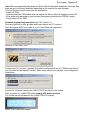
Selecting Service Mode (do the calibrations)
When powering on the JUMA-TRX2 keep the PWR button pressed until you see the text Service Mode on
the LCD display. Release the button. Now you are in the Service Mode. With the DISPLAY button you can
walk through calibration menus. With the FAST button you can save calibration values and exit to normal
operating mode. If you want to leave Service Mode without saving do a normal Power Off with the PWR
button.
Set reference oscillator frequency
When doing this calibration the JUMA-TRX2 should be in its normal operating temperature.
Method 1.
Measure the 30MHz reference oscillator output with a precision frequency counter. Multiply the result by six
(AD9851 internal clock) and dial this value in with the VFO knob. For example: If you measure
29.999.850Hz multiply this with 6 = 179.999.100Hz and dial this value in. Default value is 180.000.000Hz
36
Adjustments – DDS Control Board
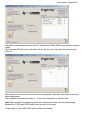
Power supply voltage meter
Measure the JUMA-TRX2 supply voltage with an accurate DVM. With the VFO knob adjust the voltage
reading on the LCD display as close to the DVM reading as possible. The Calibration value is also shown
on the LCD display. Default Cal Mult (calibration multiplier) value is 132.
Example display on JUMA-TRX2:
Supply = 13.82
Cal mult = 132
Indicator tones (Beep) length
You can adjust the JUMA-TRX2 user interface indicator tone length. The long beep is always ten times
longer than short. If you dial in 0 (zero) no tones are played. Maximum value is 100ms. Default value is
50ms.
S-meter scaling
S-meter adjustment is a iterative process where main board AGC threshold trimmer R53 and S-meter
scaling values are adjusted to get correct and accurate S-meter reading. Please see main board
adjustment procedure for details. If necessary you can check DDS S-meter board operation by applying
1VDC voltage to J3-pin8. S-meter should read S9 with this voltage. When this adjustment is done
correctly your JUMA-TRX2 S-meter shows true S-units and decibels.
FWD Power meter scaling
With this adjustment you can fine tune the JUMA-TRX2 output power display to show actual RF power
output. Connect accurate watt meter and dummy load to your JUMA-TRX2. Select first TUNE mode and
then PWR meter display. Push PTT and read the JUMA-TRX2 display and the external Watt meter.
Example:
External meter reads 9W and the JUMA meter reads 8W and the calibration value is 23.
Divide 9/8 = 1,125 and correct the calibration value with this value.
The new calibration value is 23 * 1,125 = 25,875.
Go back into the Service Mode and dial in the new calibration value 26.
Save this and recheck the readings.
Drain current (ID) meter scaling
This adjustment is not necessary but if you like to check and calibrate your JUMA-TRX2 PA ID current
display do the following: First go to normal operating TUNE mode and then select ID current display.
Push PTT, read the JUMA-TRX2 ID current display and with a DVM measure the voltage across drain
resistors R17, R21 (two band model) or resistor 23, 24 (all band model) on the PA board. All band PA
board jumper J7 should be in the PA position. Calculate the actual drain current from the voltage = U / R.
If you measured 0,209v divide it with the R17or R21 value. 0,209V / 0,11R = 1,9A. Go to the Service
Mode again and, if necessary, correct the ID scaling Cal mult (calibration multiplier) value. This value is
used to scale the voltage over drain resistors to drain current. This procedure is the same as in the power
meter scaling. See also the PA board tuning instructions and particularly the bias current adjustments.
Return to the ”factory default” values
In case you want to return to ”factory default” values, select on the LCD display: Push
FAST long = Factory defaults. Press the FAST button for about five seconds (a long press).
37
Adjustments – Main Board
JUMA TRX2 Main Board Adjustments Last update 2007Initially check the voltages on the main board with multimeter at a suitable DC voltage range. Connect the
negative test lead to the GND jumper located on the main board.
1. Measure the supply voltage at capacitor C65. Nominal 13.8 V. Allowable variation is 12 V...15 V.
2. Measure the nominal 5 V regulator voltage at capacitor C63. Allowable variation is 4.8 V...5.2 V.
3. Measure the nominal 10 V regulator voltage at capacitor C64. Allowable variation is 9.5 V...10.5 V.
There are three adjustable trimmer resistors on the main board.
AGC threshold (trimmer R53 marked AGC on the board)
This adjustment sets the RX AGC operating point and the S-meter reading.
Initially listen the RX noise without an antenna and turn the trimmer to the point where the noise begins to
attenuate. Fine adjustment is done by feeding a RF signal at S9 level (50 uV rms or -73 dBm) to the
antenna connector with a RF signal generator. Listen to the carrier at approx 1 kHz pitch and turn the AGC
trimmer so that the graphical S-meter reading in LCD indicates S9 (two dots in the middle of the S-meter
bar). If a signal generator is not available the fine adjustment can be done by listening to a suitable signal
on a band and comparing the S-meter reading to another RX.
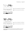
Graphical S-meter reading S9
Notes for the Carrier gain and the SSB gain adjustments
Note 1. The PA board bias currents must be adjusted before these adjustments
Note 2. Connect a 50 ohm dummy load to the antenna connector
Note 3. The simple dummy load made by the resistors included in the kit can stand 10 W only 1 minute
Carrier gain (trimmer R28 marked CAR on the board)
This adjustment sets the CW output power
1. Select Tune mode by pushing the MODE button
2. Select power output display (PWR--.-W) by pushing the DISPLAY button
3. Press the mic PTT to transmit carrier
4. Turn the CAR trimmer until the RF output power reading indicates 10 W ± 1 W
SSB gain (trimmer R26 marked SSB on the board)
This adjustment sets the SSB output power
1. Select LSB or USB mode by pushing the MODE button
2. Select power output display (PWR--.-W) by pushing the DISPLAY button
3. Press the mic PTT and vocalize aaaaaa... at a distance of 1 inch from the microphone
4. Turn the SSB trimmer until the RF output power reading indicates 10 W ±1 W
Power output reading 10 watts
38
Adjustments – Two Band PA Board
JUMA TRX2 Two Band PA Board Adjustments (two band model) Last update 2007-1014 OH7SV
There are two adjustable trimmer resistors (R4 and R7) on the two band PA board.
All the measurements during the adjustment is done by using the LCD current display
These trimmers define the bias current of the power amplifier MOSFETs.
The bias current is 0.10 A per MOSFET, totally 0.20 A.
Important notes before the adjustments, to avoid excessive MOSFET drain current and the fuse blow
- Keep the supply power OFF
- Initially turn the trimmers R4 and R7 fully counter-clockwise for zero bias
- Double-check the zero bias by measuring the resistance across C5 and C7 the reading should be below
10 ohms.
Bias adjustments trimmers (R4 and R7)
Note. The trimmers are multi-turn models. When turning the trimmers the bias current is not increasing in
the beginning. Continue turning until you see an increase of the reading and then fine tune the bias current.
Typical trimmer position is approximately in the middle.
1. Switch ON the power (Current limited power supply recommended)
2. Select CW mode by pushing the MODE button
3. Select Drain Current display (ID -.--A) by pushing the DISPLAY button
4. Press the mic PTT to activate the PA bias current
5. Turn the trimmer R4 clockwise until the LCD ID reading indicates 0.10 A ± 0.02 A
6. Turn the trimmer R7clockwise until the LCD ID reading indicates 0.20 A ± 0.02 A
The bias current reading 0.20 A after the adjustment
39
Adjustments – All Band PA Board
JUMA TRX2 All Band PA Board Adjustments Last update 2008-01-12 OH7SV
There are four adjustable trimmer resistors (R6, R9, R15, R18) on the all band PA board.
These trimmers define the bias current of the driver and power amplifier MOSFETs.
All the measurements during the adjustment is done by using the LCD current display.
The driver stage bias current is 2 x 0.03 A = totally 0.06A and the final stage bias current is 2 x 0.10 A =
totally 0.20 A
Important notes before the adjustments, to avoid excessive MOSFET drain current and the fuse blow
- Keep the supply power OFF
- Initially turn the trimmers R6, R9, R15, and R18
fully counter-clockwise for zero bias
- Double-check the zero bias by measuring the resistance across C5, C7, C12, and C14, the reading
should be below 10 ohms.
Driver stage bias current adjustment See the picture (next page)
Note. The trimmers are multiturn models. When turning the trimmers the bias current is not increasing in the
beginning. Continue turning until you see an increase of the reading and then fine tune the bias current.
Typical trimmer position is approximately in the middle.
1. Set the drain current selector jumper J7 (shown next page) on the board in to the DRV position
2. Switch ON the power (Current limited power supply recommended)
3. Select CW mode by pushing the MODE button
4. Select Drain Current display (ID -.--A) by pushing the DISPLAY button
5. Press the mic PTT to activate the bias current
6. Turn the trimmer R6 clockwise until the LCD ID reading indicates 0.03 A ± 0.01 A
7. Turn the trimmer R9 clockwise until the LCD ID reading indicates 0.06 A ± 0.01 A
Driver stage bias current reading 0.06 A after the adjustment
Final stage bias adjustment See the picture (next page)
Note. The trimmers are multi-turn models. When turning the trimmers the bias current is not increasing in
the beginning. Continue turning until you see an increase of the reading and then fine tune the bias current.
Typical trimmer position is approximately in the middle.
1. Set the drain current selector jumper J7 (shown next page) on the board in to the PA position
2. Switch ON the power (Current limited power supply recommended)
3. Select CW mode by pushing the MODE button
4. Select Drain Current display (ID -.--A) by pushing the DISPLAY button
5. Press the mic PTT to activate the bias current
6. Turn the trimmer R15 clockwise until the LCD ID reading indicates 0.10 A ± 0.02 A
7. Turn the trimmer R18 clockwise until the LCD ID reading indicates 0.20 A ± 0.02 A
Finally leave the drain current selector jumper in to the PA position
Final stage bias current reading 0.20 A after the adjustment
40
Adjustments – All Band PA Board
JUMA TRX2 All Band PA Board Adjustments Last update 2008-01-12 OH7SV
Equalizing the RF output on each band
On the all band PA board there is an input attenuator (IC1 and related resistors), which can be adjusted
individually on each band to equalize the output RF power. This can be done with the user interface.
1. Go to the desired band ?
2. Select Tune mode by MODE button
3. Select PWR display by DISPLAY button ?
4. While pushing the mic PTT keep PWR button (green) down. The LCD will show the current output power
and the gain in decibels e.g. -1 dB ?
5. Turn the VFO knob until the LCD shows desired output RF power (approx. 10W) ?
6. Release the PTT and PWR buttons
This PA gain setting is saved individually at all 9 ham bands to the non-volatile memory when you switch
OFF the TRX2A.
41
Memory Option
JUMA TRX2 Memory Option
JUMA-TRX2 Voice Memory option has the following features
•
•
•
•
•
Recording from microphone
Recording from JUMA-TRX2 receiver
Playing a recording with JUMA-TRX2 speaker as output
Transmitting a recording in LSB or USB
Stop an operation at any time
Memory capacity
•
Memories 1...9
10 seconds capacity each
Memory 10
120 seconds capacity
Hardware installation of the JUMA-TRX2 Voice Memory option
•
•
Install JUMA-TRX2 Voice Memory option board into the pin headers on DDS board inside the JUMA-TRX2.
Note, remove the audio jumper from pin header J8 (pins 1-2) before inserting the option board..
Connect the RS-232 cable between the JUMA-TRX2 and the PC. See the cable wiring diagram.
JUMA TRX2 RS-232 cable wiring diagram
JUMA-TRX2 settings
Go to the JUMA configuration pages with a long CONFIG button push. Go to the RS232 page with short
pushes and select "RS232 = VoiceMem" with VFO knob.
Instructions to use the JUMA-TRX2 Voice Memory control Windows control software
•
•
•
•
Select a com port from the Com menu. Com setting will be saved for the next session
Select a function (MIC record, RX record, Play or Transmit) by clicking the corresponding button
Click a memory number to activate the operation
Click Stop to cancel an operation if needed
A beep tone will be heard from Juma speaker when a command is received.
Alternatively all the operations can be activated by keyboard (small or caps)
•
•
•
•
•
•
MIC record
RX record
Play
Transmit
Stop
Memory
M
R
P
T
S
1,2,3,4,5,6,7,8,9,0
Updating the Voice Memory Windows software version
•
•
Uninstall any older version of the software by using Windows Add/Remove Programs in Control Panel
Install the new version by running setup of the new version
42
Part Lists – DDS Control Board
Appendix A
Appendix A
Parts Lists
JUMA-TRX2 DDS board part list for PCB Rev. B, update 2007-12-04
Part number
R54
R31, R32
R1, R21, R22, R44, R49,
R50
R45, R102, R38, R4, R5,
R6, R7, R12, R8
R10, R15
R19, R20, R29
R2
R23, R33
R46
R28, R16, R25, R51, R11,
R3, R34, R60, R61, R62,
R63, R64, R65, R52, R35,
R48, R36, R37, R47, R26,
R53
Value / type
Qty Description
0R
10R
1
2
Resistor SMD size 0805
Resistor SMD size 1206
10R
6
Resistor SMD 1%, 0805
100R
9
Resistor SMD 1%, 0805
200R
1k
3k9
4k7
6k8
2
3
1
2
1
Resistor SMD 1%, 0805
Resistor SMD 1%, 0805
Resistor SMD 1%, 0805
Resistor SMD 1%, 0805
Resistor SMD 1%, 0805
10k
21 Resistor SMD 1%, 0805
R27, R55
R17, R18, R13, R14, R39,
R41, R43, R66, R67
R40
33k
2
Resistor SMD 1%, 0805
100k
9
Resistor SMD 1%, 0805
470k
1
Resistor SMD 1%, 0805
R42
100k
1
Multi turn SMD side adjust
trimmer resitor, Bourns 3214J
or 3224J series
C16
C8
C15
C17, C18
C7,C19
C30
C28, C5, C13, C26
1p
2p2
3p3
22p
10p
100p
1n
1
1
1
2
2
1
4
Ceramic 0805 C0G
Ceramic 0805 C0G
Ceramic 0805 C0G
Ceramic 0805 C0G
Ceramic 0805 C0G
Ceramic 0805 C0G
Ceramic 0805 X7R or C0G
C66, C44, C43, C42, C41,
C48, C6, C62, C49, C50,
C51, C52, C1, C31, C2, C3,
100n
C27, C12, C10, C11, C20,
C29, C9, C4, C25, C24,
C23, C22, C21
29 Ceramic 0805 X7R
C53, C65, C70, C71
2u2/16V
4
Ceramic 0805
C67
4u7/6V Case style A
1
Tantalum Capacitor SMD
C14
10V/35V Case style D
1
Tantalum Capacitor SMD
L3, L7, L8
470nH, Q=35 EPCOS
B82498B3471J
3
L1, L2
600ohm @ 100MHz
2
D1
BAV70 SOT-23
1
Q2
IRLML5203TRPBF SOT-23
1
Q1, Q4
2N7002 SOT-23
2
Q3
IRFR110 DPAK
1
Inductor SMD Case size
0805
Ferrite bead SMD Case size
0805
Diode dual
or similar SOT-23 common
cathode Si-diode
or Si2307DS or Si2309DS
MOSFET P-type
Rds < 0.5 ohm
MOSFET N-type
or similar, Rds < 10 ohm
MOSFET N-type
Note
Part Lists – DDS Control Board
JUMA-TRX2 DDS board part list for PCB Rev. B, update 2007-12-04
Part number
Value / type
Qty Description
IC7
74AC74, SO14
1
D Flip Flop
IC3, IC11
LMV358 SO-8
2
Dual OPAMP
IC1
AD9851BRSZ
or AD9851BRS
1
DDS, package SSOP28
IC6
74LVC2G80 SSOP
0
D Flip Flop
IC10
HIN232ACB, Intersil
or ST232CD ST Microelectronics, or
MAX232ACSE Maxim
1
RS232 driver, SO16
IC9
Microchip dsPIC30F6014A-30 I/PF
1
Microcontroller / DSP
IC2
30MHz,5V, 91SMO package
0
Low noise oscilator
IC5
30MHz, 5V, DIP14 package
1
Low noise oscilator
J2, J3
2x8 e.g. snippet of
Tyco Electronics 5-826632-0
or MOLEX 90131-0775
2
Pin header 2.54 mm pitch
pin lenghth max 6.7 mm
J1
2x2 e.g. snippet of
Tyco Electronics 5-826632-0
or MOLEX 90131-0775
1
Pin header 2.54 mm pitch
pin lenghth 6.7 mm
J5, J8
1x3
2
Pin header 2.54 mm pitch
pin lenghth max 6.7 mm
J19
1x6
1
J7
1x14
1
J4
1x2
1
For test/programming
operations power on jumper.
Pin header 2.54 mm pitch
pin lenghth max 6.7 mm
Pin header 2.54 mm pitch
pin lenghth max 6.7 mm
Jumper
Pitch 2.54 mm
2
Insert into J8 pins 1-2
For audio path back to board.
Second one is for J4. Do
not instal it for normal
operation.
LCD1
Everbouquet MC1602C8-SBLWU,
Blue or
Everbouquet MC1602C8-FBLWU,
Black
1
LCD module 2 x 16 with LED
back light
12'o clock type
Appendix A
Note
Not assembled,
only for future use
7,5MHz clock for CPU PLL
Install IC2 or IC5, not both!
e.g. snippet of
Harwin M20-9992046
or MOLEX 90120-0784
Part Lists – DDS Control Board
JUMA-TRX2 DDS board part list for PCB Rev. B, update 2007-12-04
Part number
Value / type
Qty Description
Nut
M2.5
4
For LCD mounting
Low profile pin header
1 x 16,
Samtec BBL-116-G-E
1
For LCD module connection,
LCD side
Low profile header socket
1 x 16,
Samtec SL-116-G-19
1
For LCD module connection,
DDS board side
Tinned copper wire
0.5 mm, L approx 300 mm
1
Alternative LCD connection
R9, R24, R30
100k Bourns 3310Y-001-104L
3
Miniature potentiometer
SW10
Avago Technologies
HRPG-ASCA#11R
Resolution 120CPR
1
Optical Rotary Encoder
SW1, SW2, SW3, SW4,
SW5, SW6
ITT Cannon D6R10LFS
6
Push Button Switch
SW7
ITT Cannon D6R50LFS
1
Push Button Switch
Spacer screw
M3, L=12 mm
e.g. Ettinger 05.13.123
or 05.13.121
or Harwin R30-3001202
4
For DDS board installation
into the front panel
Tooth lock washer
M3
4
Nut
M3
4
For spacer screw
J6
3.5 mm stereo jack socket
Lumberg KBL4
or Schurter 4832.2300
1
OBS! Fix into the the front
panel before soldering
IC4
7805 TO220
Enclosure Al profile as heat sink
1
Voltage regulator
Machine screw
M3 x 6
1
Phillips pan head
For 7805 regulator mounting
Square nut
M3
1
Or a snippet of rack nut list
for IC4 7805 regulator
mounting
PCB
JUMA-TRX2-dds PCB Rev.B
1 PCB
Total 182
Appendix A
Note
For LCD module and DDS board
interconnection
Part Lists – Main Board
Appendix A
JUMA-TRX2 main board part list for PCB Rev. B, update 2007-12-04
Part number
R102 R103 R29 R56
R45 R78 R89 R94 R97 R98 R99 R100 R106 R107
R19 R20 R24 R25 R104
R60
R44 R46 R55 R61 R95
R2
R32 R33 R34 R35 R64 R65 R66 R84 R85 R86 R87 R88
R1 R27 R40 R43 R62 R71 R105 R108 R109
R39 R54 R58 R68 R69 R70 R72 R73 R74 R79 R80 R83
R101
R31
R57
R36 R92 R93 R96
R9 R10 R11 R12 R13 R14 R15 R30 R48 R49 R50 R51
R75 R76 R77 R81 R90 R91
R37
R38 R52 R59 R63 R82
R67
R41 R42
R47
4R7
100R
180R
470R
1k
1k5
2k2
4k7
Value / type
Qty Description
4 SMD resistor 1% size 1206
10
5
1
5
1
12
9
10k
13
16k
27k
47k
1
1
4
100k
18
330k
470k
1M
2M2
4M7
1
5
1
2
1
R3 R6
200R/0.1%
2
R4 R5 R7 R8 R16 R17 R18 R21 R22 R23
2k70/0.1%
10
R28
100R
1
R26 R53
50k
2
C29 C44
C28 C91
C88
C39 C47 C71
C93
47p
100p
220p
1n
4n7
2
2
1
3
1
SMD resistor 0.1%
Case size Mini Melf MMA0204
Multi turn SMD trimmer Bourns
3214W or 3214X or 3224W or
3224X series or Vishay TSM4YJ
or TSM4YL series
Ceramic size 1206 X7R or C0G
Ceramic size 1206 X7R or C0G
Ceramic size 1206 X7R or C0G
Ceramic size 1206 X7R or C0G
Ceramic size 1206 X7R or C0G
C3 C8 C9 C10 C11 C43 C67 C78 C79 C81 C82 C89 C92 10n
13 Ceramic size 1206 X7R
C45
C1 C18 C20 C27 C30 C31 C32 C33 C37 C40 C48 C50
C51 C52 C53 C54 C55 C56 C57 C58 C59 C60 C61 C62
C65 C66 C68 C69 C70 C72 C73 C74 C75 C77 C80 C83
C84 C85 C86 C87
C21
C35
22n
1
100n
40 Ceramic size 1206 X7R
220n
1u
1
1
C4 C5 C6 C7 C12 C13 C14 C15
47n
8
C22 C23 C24 C25
10u
4
Ceramic size 1206 X7R
Ceramic size 1206 X7R
Ceramic size 1206 X7R
Ceramic size 1206 C0G Murata
GRM31M5C1H473JA01D
Farnell code 8820201
Ceramic size 1206 Y5V/10V
Note
Part Lists – Main Board
Appendix A
JUMA-TRX2 main board part list for PCB Rev. B, update 2007-12-04
Part number
Value / type
Qty Description
C2 C16 C17 C26 C36 C38 C46 C49 C63 C64 C94
C34
C19 C42 C76
C41
4u7/16V
10u/16V
47u/16V
100u/10V
11
1
3
1
Tantal size B
Tantal size C
Tantal size D
Tantal size D
D1 D2 D3 D4 D5
TR1
TR3 TR4 TR5 TR9 TR11
TR6 TR8 TR10
TR7
IC9 IC10
A1 A2 A3 A4
A5 A8 A9 A13
A6 A7
A10 A11
A12
REG1 REG2
BAV99
BC856B
SST112
2N7002
IRLML5203
MAX7400
LT1113
TL082
TLC277
LT1364
LM386
LP2951
5
1
5
3
1
2
4
4
2
2
1
2
Dual diode SOT23
PNP transitor SOT23
JFET P-type SOT23
MOSFET N-type SOT23
MOSFET P-type SOT23
SCAF filter SO8
Low noise JFET OPAMP SO8
JFET OPAMP SO8
CMOS OPAMP SO8
High drive OPAMP SO8
SPKR AMP S08
Voltage regulator SO8
IC3 IC7
NC7S14
2
Iinverter Schmitt SOT23-5
IC4
74HC132
1
Quad NAND Schmitt SO14
IC1 IC2 IC8
FST3253 Fairchild
3
Bus switch SO16
OBS! 74CBT3253 can not
be used
IC6
74HC595D
1
Shift reg SO16
T1
WURTH 744-205
1
RF transformer
(signal filter with 4 windings)
POLYPHASE1 POLYPHASE2
Header socket 1x10
2
J6
Header socket 1x8
1
FILTER1
Header socket 1x6
1
J1 J2 J3
Pin header 2x8
3
J4
Pin header 2x5
1
J5
Pin header 2x3
1
Jumper
Pitch 2.54 mm
2
For AUX output coding
Snippet of tinned copper wire
Diameter 0.5-0.8mm
Length 30 mm
1
U-jumper for measuring GND
PCB JUMA TRX2
Main board Rev. B
1
Total parts qantity
255
Snippet of Fisher BL5.36Z
Farnell 9728910
Snippet of Tyco Electronics 5826632-0, Farnell 3418560
or MOLEX 90131-0775, Farnell
9733680
Note
Part Lists – Filter Board
Appendix A
JUMA-TRX2 filter board part list for PCB Rev. B, update 2007-10-16
Part number
Value / type
Qty Description
Resistor SMD 1%
2
size 1206
1
R1 R8
470R
R12
620R
R2
1k
1
R9
1k2
1
R5 R10
1k5
2
R3
3k9
1
R11
6k8
1
R4 R15 R16 R17
10k
4
R13 R14
13k
2
R6 R7
33k
2
R18 R19 R20
100k
3
C7 C14
2n2
2
C4 C11
4n7
2
C6 C13
10n
2
C3 C5 C10 C12
100n
4
C16 C17 C18 C19 C20
100n
5
C1 C2 C8 C9
470n
4
C15
100u/10V or more
1
Tantal SMD capacitor
size D
TR1
2N7002
1
MOSFET N-type SOT-23
or similar Rds < 10 ohm
A1 A2
LT1113
2
Opamp, J-FET, low noise,
SO-8
IC1
4052
or Philips 74HC4052
1
CMOS multiplexer SO16
X1
1 x 6 pin header, e.g. snippet of
Tyco Electronics 5-826631-0,
Farnell 3418479
or Molex 90121-0784,
Farnell 9733566
1
Angled pin header,
pitch 2.54 mm,
pin lenght 6.7 mm
PCB
JUMA-TRX2-filter PCB Rev.B
1
PCB
Total Qty 46
Ceramic SMD capacitor
size 1206 C0G
Ceramic SMD capacitor
size 1206 C0G
Ceramic SMD capacitor
size 1206 C0G
Ceramic SMD capacitor
size 1206 C0G
SMD capacitor
size 1206 X7R
SMD capacitor
size 1206 X7R
Note
Part Lists – Polyphase Board - Connector Board
Appendix A
JUMA-TRX2 polyphase board part list for PCB Rev. A, update 2007-10-16
Part number
R1 R11 R21 R31
820R 1%
Value / type
pcs Description
4 Resistor SMD size 1206
R2 R12 R22 R32
1k50 1%
4
R3 R13 R23 R33
2K70 1%
4
R4 R14 R24 R34
5K10 1%
4
R5 R15 R25 R35
9K10 1%
4
R6 R16 R26 R36
16K0 1%
4
C1 C11 C21 C31
C2 C12 C22 C32
C3 C13 C23 C33
C4 C14 C24 C34
C5 C15 C25 C35
C6 C16 C26 C36
47n COG 5%
MURATA GRM31M5C1H473JA01D
Farnell 8820201
24 Ceramic SMD size 1206
X1
1x10, e.g. snippet of
Tyco Electronics 5-826631-0,
Farnell 3418479
or Molex 90121-0784, Farnell
9733566
1
Angled pin header,
pitch 2.54 mm,
pin lenght 6.7 mm
PCB
TRX2 FILTER PCB Rev. A
1
PCB
Note
Total 50
JUMA-TRX2 connector board part list for PCB Rev. A, update 2007-10-16
Part number
Value / type
pcs Description
R1 R2 R3 R4
100R
4
Resistor SMD size 1206
C1 C2 C3 C4 C5 C6 C7
1n
7
Ceramic 1206 XR7 or NP0
L1 L2 L3
>200 ohm @ 100MHz, I > 200 mA
e.g. Murata BLM31B601S
3
Ferrite bead SMD
Case size 1206
J1
2x5 Pin Header
e.g. snippet of Tyco Electronics
5-826632-0
1
Pin header 2.54 mm pitch
pin lenghth 6.7 mm
J2
1x2 Pin Header
e.g. snippet of Tyco Electronics
5-826632-0
1
Pin header 2.54 mm pitch
pin lenghth 6.7 mm
X1 X2 X3 X4
OBS! Assemble into the the rear
panel during soldering to align the
connectors mechanically
4
3.5 mm stereo jack socket
Schurter 4832-2320 or 4832232, Farnell 152204
PCB
JUMA-TRX2-connector PCB Rev.A
1
PCB
Note
Part Lists – Two Band PA Board Appendix A
JUMA-TRX2 Two Band PA board part list for PCB Rev. A, update 2007-12-04 (install the parts in this order)
Part number
R17 R21
R3
R5 R6
R1
R11 R12 R13 R16 R29
R2, R20
R8 R15 R18 R19 R22 R23
R24 R31
R9 R10 R14 R25 R26 R27
R28
R4 R7
C14 C15 C16 C17 C29
C26
Value / type
0R22
e.g. Phycomp 235051912207
4R7
6R8
51R
100R
1k
Qty Description
Resistor size 1206 / 0.5W
2
Farnell 8067600
1 Resistor size 1206
2
1
5
2
10k
8
100k
7
10k
2
Multi turn SMD trimmer Bourns
3214W or 3214X or 3224W or
3224X series or Vishay TSM4YJ
or TSM4YL series
390p
680p
5
1
Ceramic size 1206 C0G
Ceramic size 1206 C0G
C10 C11 C12 C13 C30 C31 820p
6
Ceramic size 1206 C0G
C32 C33 C38 C39 C40 C41 1n
6
Ceramic size 1206 X7R or C0G
C20 C23
C3
2
1
Ceramic size 1206 C0G
Ceramic size 1206 X7R or C0G
1n5
4n7
C1 C2 C4 C5 C6 C7 C8 C9
C18 C19 C21 C22 C25 C27 100n
C28 C34 C42 C43 C44
19
C24, C35, C36, C37
4
Tantal SMD size B
D1 D2 D3 D4 D5 D6 D7 D8
BAV99
D9
9
Double diode SOT23
Z1
LM4040-2.5 SOT-23
1
TR4, TR7
2N7002
2
TR5
BSS84
1
TR6
BC846B
1
D10
LL4002G
1
Diode 1A, size melf
Or similar 1A SMD diode
TR1
IRFR110
1
MOSFET N-type D-PAK
A1 A2
TLC277CD
2
OPAMP CMOS SO8
4u7/16V
Voltage Reference 2.5V
or LM385M3-2.5 SOT-23
MOSFET N-type SOT23
or similasr Rds < 10 ohm
MOSFET P-type SOT23
or similasr Rds < 10 ohm
Transistor NPN
or similar HFE > 150
Picture
Note! Turn the trimmers initially
to zero bias, see instructions.
Part Lists – Two Band PA Board Appendix A
JUMA-TRX2 Two Band PA board part list for PCB Rev. A, update 2007-12-04 (install the parts in this order)
Part number
Value / type
Qty Description
L8 L10
1uH
2
SMD inductor size 1210 or 1812
L5 L7 L9
2u2H
3
SMD inductor size 1210 or 1812
L6
4u7H
1
SMD inductor size 1210 or 1812
T1
TDK signal filter
ZJYS51R5-M4PA or
ZJYS51R5-M4PA-01
1
RF transformer
Farnell code 9621334
T2
Wurth signal filter
type 744-205
1
RF transformer
RL1 RL2 RL3
NEC EB2-12V
or Omron G6H-2F-12V
or Nais TQ2SA-12V
or Takamisawa AS12W-K
3
SMD Relay
L1, L2
2u2
2
SMD inductor size 2220
J1
Snippet of Tyco Electronics 5826632-0, Farnell 3418560
or MOLEX 90131-0775, Farnell
9733680
1
PIN HEADER 2 x 8
F1
T 2.5A
e.g. WICKMANN 19396 2.5A
2
PCB miniature fuse
Note, another fuse is for spare
Bend the legs to L-shapes
RFC
Small ferrite bead e.g. Amidon FB43-101 outer diameter 3.5 mm, inner
diameter 1.3 mm, length 3.5 mm
1
RF choke, range 1uH…10uH
(wire through a ferrite bead)
See pictures
T3 T4
Signal filter SBT-0180W
Farnell 9265791
2
SWR transformer
See the modification
instructions
L3, L4
1uH
2
Amidon T25-2 toroid core
17 turns 0.4 mm cu wire
See the winding instruction
Enamel copper wire
Diameter 0.4 mm (AWG 26 or 27)
1
80 cm enamel copper wire
for the toroidal inductors
TR2 TR3
IRFI520N
2
MOSFET N-type FULL-PAK
Fixed to the rear Alu panel
See pictures for fixing
1
JUMA TRX2 PA PCB REV A
PCB
Picture
Part Lists – All Band PA Board Appendix A
JUMA-TRX2 All Band PA board part list Rev. A2, update 2008-03-10 (install the parts in this order)
Part number
R11 R12 R23 R24
Value / type
0R22
e.g. Phycomp 235051912207
4R7
12R
16R
47R
91R
Qty Description
Resistor size 1206 / 0.5W
4
Farnell 8067600
1 Resistor size 1206 1% (or 5%)
2
1
1
2
100R
10
270R
470R
820R
1k
1k5
3k3
4K7
2
2
2
1
1
1
2
10k
10
R43
R4 R46
R49
R1
R10 R13
R7 R8 R16 R17 R26 R27
R32 R33 R54 R58
R48 R50
R45 R47
R42 R44
R57
R40
R3
R2 R39
R14 R25 R36 R37 R38 R41
R51 R52 R55 R56
R28 R29 R30 R31 R34 R35
R53
R5
100k
7
NIL
0
Not installed
R19 R22 R20 R21
33R
4
SMD resitor 1%
Case size Mini Melf MMA0204
R6 R9 R15 R18
10k
4
Multi turn SMD side adjust
trimmer resistor Bourns
3214J, 3214G, 3224J or 3224G
C2
NIL
0
Not installed
C24 C25 C26 C27 C39 C40 1n
6
Ceramic size 1206 X7R or C0G
C1 C3 C4 C5 C6 C7 C8 C9
C10 C11 C12 C13 C14 C15
C16 C17 C18 C19 C20 C21
100n
C22 C23 C30 C31 C32 C33
C34 C35 C36 C37 C38 C42
C43 C45
34 Ceramic size 1206 X7R
C28 C29 C41 C44
4u7/16V
4
Tantal SMD size B
L1 L4
>200 ohm @ 100MHz, I > 200 mA
e.g. Murata BLM31B601S
2
Ferrite bead SMD
Case size 1206
L2 L3 L5 L6
220nH
4
SMD inductor size 1210
TR1
BFG591
1
Wide band NPN transistor
SOT223
D1 D2
D3 D4 D5 D6 D7 D8
BAT54S
BAV99
2
6
Z1
LM4040-2.5 SOT-23
1
TR6
2N7002
1
TR7
IRLML5203
1
Double Schottky diode SOT23
Double diode SOT23
Voltage Reference 2.5V
or LM385M3-2.5 SOT-23
MOSFET N-type SOT23
or similasr Rds < 10 ohm
MOSFET P-type SOT23
or similasr Rds < 1 ohm
Picture
Note! Turn the trimmers initially
to zero bias, see instructions.
Part Lists – All Band PA Board Appendix A
JUMA-TRX2 All Band PA board part list Rev. A2, update 2008-03-10 (install the parts in this order)
Part number
Value / type
Qty Description
D9
LL4002G
1
Diode 1A, size melf
Or similar 1A SMD diode
TR2 TR3
IRFR110
2
MOSFET N-type D-PAK
A1 A2
TLC277CD
2
OPAMP CMOS SO8
IC1
FST3253 Fairchild
1
Bus switch SO16
T1 T2
TDK signal filter
ZJYS51R5-M4PA or
ZJYS51R5-M4PA-01
2
RF transformer
Farnell code 9621334
T3
Wurth signal filter
type 744-205
1
RF transformer
RL1
NEC UD2-12NU
or Panasonic AGQ200A12
1
SMD Relay
J1
Snippet of Tyco Electronics 5826632-0, Farnell 3418560
or MOLEX 90131-0775, Farnell
9733680
1
PIN HEADER 2 x 8
J2
Snippet of Tyco Electronics 5826632-0, Farnell 3418560
or MOLEX 90131-0775, Farnell
9733680
1
PIN HEADER 2 x 5
J7
e.g. snippet of
Harwin M20-9992046 or
MOLEX 90120-0784
1
PIN HEADER 1 x 3
Jumper
Pitch 2.54 mm
2
F1
T 2.5A wired fuse
e.g. WICKMANN 19396 2.5A
2
PCB miniature fuse
Note, another fuse is for spare
Bend the legs for soldering
L7
Small ferrite bead outer diameter 3.5
mm, inner diameter 1.3 mm, length
4…8 mm or two shorter
1
RF choke, inductance range
0.5uH…10uH (wire through a
ferrite bead)
See pictures
T4 T5
Signal filter SBT-0180W
Farnell 9265791
2
SWR transformer
See the modication
instructions
Tinned copper wire
Diameter 0.5 mm - 0.8 mm
100 mm
IRFI510G
2
MOSFET N-type FULL-PAK
Bent the legs and fix to the rear
panel before soldering. See
instructions
1
JUMA TRX2 ALL BAND PA PCB
TR4 TR5
PCB
Picture
Drain current selection jumper
For L7, T4 and T5
Part Lists – RF Filter Board
Appendix A
JUMA-TRX2 RF Filter Board part list for PCB Rev. A, update 2008-03-19 (Install in this order)
Part number
R8
R1 R4 R11 R12 R13 R14 R15 R16
R17
R3 R6
R2 R5
R7 R9 R10
Value / type
100R
Qty Description
1 SMD resistor size 1206
10k
9
15k
47k
100k
2
2
3
47p
82p
100p
180p
390p
680p
820p
1n2
1n5
1n8
2n2
2n7
4n7
10n
1
1
4
7
7
1
6
1
2
4
1
2
3
6
100n
24 Ceramic size 1206 X7R
C52 C55 C58 C61 C64 C67 C70
C73 C76 C79
NIL
0
Not assembled
L21 L23
L18 L20
L22
L15 L17 L19
L12 L14 L16
L9 L11 L13
L6 L8 L10
L3 L5 L7
L1 L2 L4
330n
470n
680n
1u
2u2
4u7
10u
22u
47u
2
2
1
3
3
3
3
3
3
SMD inductor size 1210
C46
C37
C75 C77 C78 C80
C32 C36 C38 C69 C71 C72 C74
C27 C31 C33 C63 C65 C66 C68
C22
C26 C28 C57 C59 C60 C62
C17
C21 C23
C51 C53 C54 C56
C12
C16 C18
C7 C11 C13
C1 C2 C3 C4 C6 C8
C5 C9 C10 C14 C15 C19 C20 C24
C25 C29 C30 C34 C35 C39 C40
C41 C42 C43 C44 C45 C47 C48
C49 C50
SMD ceramic capacitor
size 1206 C0G (NP0)
Note
Part Lists – RF Filter Board
JUMA-TRX2 RF Filter Board part list for PCB Rev. A, update 2008-03-19 (Install in this order)
Part number
D1 D2 D3 D4 D5
BAV99
TR1 TR2 TR3 TR4 TR5
2N7002
IC3 IC5
NC7S14
2
Iinverter Schmitt SOT23-5
IC1 IC2
FST3253 Fairchild
2
Bus switch SO16
IC4
74HC595D
1
Shift reg SO16
IC6
4028
1
1-of-10 decoder SO16
RL1 RL2 RL3 RL4 RL5
NEC UD2-12NU
or Panasonic AGQ200A12
5
SMD Relay
J3
Snippet of Tyco Electronics 5826632-0, Farnell 3418560
or MOLEX 90131-0775, Farnell
9733680
1
PIN HEADER 2 x 5
J1 J2
Snippet of Tyco Electronics 5826632-0, Farnell 3418560
or MOLEX 90131-0775, Farnell
9733680
2
PIN HEADER 2 x 8
L26 L27
2u2
2
SMD inductor size 2220
L24 L25
4u7
2
L32 L33
250n
2
Amidon T25-2 iron pwder core
9 turns diameter 0.4 mm cu
L30 L31
500n
2
Amidon T25-2 iron pwder core
12 turns diameter 0.4 mm cu
L28 L29
1u
2
Amidon T25-2 iron pwder core
17 turns diameter 0.4 mm cu
Enamel copper wire
Diameter 0.4 mm (AWG 26 or 27)
1
3 meters of copper wire
for toroidal inductors
1
JUMA TRX2 RF FILTER PCB
PCB
Value / type
Qty Description
5 Double diode SOT23
MOSFET N-type SOT23
5
or similasr Rds < 10 ohm
Appendix A
Note
See the instructions
Part Lists – Voice Memory Option
Appendix A
JUMA-TRX2 voice memory part list for PCB Rev. C, update 2008-02-29
Part number
R5
Value / type
pcs Description
1 Resistor SMD size 0805
100R
R2
1k
1
R4
3k3
1
R6 R7 R9 R16 R17
10k
5
R12
18k
1
R1
75k
1
R3 R13 R22 R23
100k
4
C6
1n
1
C24 C25
47n
2
C1 C4 C5 C7 C8 C13 C14
C20 C21
100n
9
C3 C11
10u
2
C2 C17 C18
4u7/10V
3
Tanatlum SMD capacitor
size B
LD1
LGM670JM or similar type
1
Green LED, 0805
IC2
TLC277
1
Dual opamp, CMOS SO-8
or TLC272
IC1
ISD17240SY
1
Voice recorder, SO28
IC4
4066
or Philips 74HC4066
1
CMOS switch SO14
J5, J8
Header socket 1x3
2
SMD capacitor
size 0805 X7R
SMD capacitor
size 0805 X7R
SMD capacitor
size 0805 X7R
SMD capacitor
size 1206 Y5V
Snippet of Fisher BL5.36Z
Farnell 9728910
J7
Header socket 1x14
1
PCB
JUMA-TRX2-Voice Memory PCB
Rev.C
1
Total Qty 39
Note
Part Lists – External Keyboard Option
Appendix A
JUMA KB1 external keyboard partlist Rev. C, OH2NLT, 2008-02-29
Part number
R2
0R / jumper
Value / type
Qty Description
1 Resistor SMD size 0805
R13 R20
1k
2
R1 R14
10k
2
R3 R4 R5 R6 R7 R8 R9 R10
100k
R11 R12 R15 R17 R18
13
R16 R19
270k
2
R21
1M
1
C1 C10
1n
2
C3 C5 C6 C11
100n
4
C7 C8
33p
2
C2 C4 C9
47u/10V or more
3
Tanatlum SMD capacitor
size C
D1 D2 D3
BAT54S
3
Shotky diode, SO23
Q1
IRLML5203TRPBF SOT-23
1
or Si2307DS or Si2309DS
MOSFET P-type
Rds < 0.5 ohm
Q2
2N7002
1
MOSFET N-type SOT-23
or similar Rds < 10 ohm
IC3
LP2951
1
Voltage regulator SO8
IC1
PIC16F628A-I/P
1
Microcontroller, DIP18
Note
SMD capacitor
size 0805 X7R
SMD capacitor
size 0805 X7R
SMD capacitor
size 0805 NP0
Installed with socket, see pictures
IC2
CD40106
1
CMOS hex inverter, schmit
trigger SO14
Part Lists – External Keyboard Option
Appendix A
JUMA KB1 external keyboard partlist Rev. C, OH2NLT, 2008-02-29
Part number
Value / type
Qty
Description
Note
X1
1,8432MHz Xtal
1
HC49
J3
3,5mm jack
1
3.5 mm stereo jack socket
Schurter 4832-2320 or 4832232, Farnell 152204
IC1 socket
18-pin DIP IC socket, flexible pins
1
See pictures
SW9
ITT Cannon D6R50LFS
1
Push Button Switch Green
SW4
ITT Cannon D6R40LFS
1
Push Button Switch Red
SW1, SW2, SW3, SW5,
SW6, SW7, SW8, SW10
ITT Cannon D6R10LFS
8
Push Button Switch Grey
SW11 SW12
Not installed
0
Enclosure
BOX Enclosures 40-12-NO-R-BL
1
40 Series Shell Case with
End Panel
Optional rubber boot
(not icluded in the kit)
BOX Enclosures 40-RBT-LBL
1
Protective Boot w/Integrated
Farnell code 495-3710
tilt bar
Countersunk machine screw M3 x 20
4
Board to box fixing
Nut
M3
12
PCB
JUMA-KB PCB Rev.C
1
Total Qty 71
Farnell code 495-3654
Part Lists – Electromechanical Parts
JUMA-TRX2 Electromechanical part list, update 2007-10-16
Part
Value
Enclosure
Hammond 1402D
1
Housing
Original front and rear pltes
are not used.
Front panel
Al 1.5 mm natural anodized
1
Milled and silk printed
JUMA TRX2 front panel
Rear panel
Al 1.5 mm natural anodized
1
Milled and silk printed panel
JUMA TRX2 rear panel
1
BNC nut mount type
with solder lug
Antenna connector
Qty Description
DC PWR connector
JST LR-02-2V
1
DC socket
Male crimp pins
JST 0.5–2.0
2
for DC socket
DC PWR connector
JST LP-02-1V
1
DC plug
Female crimp sockets
JST 0.5–2.0
2
for DC plug
Knob cap
Elma 040-1020
3
9 mm
Knob
Elma 021-1220
3
9 mm, shaft 1/8"
Knob cap
Bulgin KX30/28/10/3
1
28 mm
Knob
Bulgin KX26/28/61/3
1
28 mm, shaft 1/4"
M3 x 6
Countersunk machine screw E.g. NETTLEFOLDS
MS06030006081FA
8
Front panel to DDS board
and speaker fixing
4
Front panel to enclosure Alprofile fixing
(rear panel is fixed to Al
profile with original Hammond
pan head self tapping
skrews)
Countersunk self tapping
screw
NO4 x 1/4"
E.g. NETTLEFOLDS
420004025081FA
Pan head machine screw
Pozidriv No1
M3 x 6
8
PA mosfets to rear panel
(two for extra holes)
and main board to Al profile
fixing
Nylon washer
M3
2
PA mosfets fixing
(or thin spring washer)
Pan head machine screw
Pozidriv No1
M3 x 12 mm
4
PA-board to rear panel fixing
Circular spacer
Circular M3 x 6mm
4
PA-board to rear panel fixing
Appendix A
Notes
Part Lists – Electromechanical Parts
JUMA-TRX2 Electromechanical part list, update 2007-10-16
Part
Value
Qty Description
Tooth lock washer
M3
14
Nut
M3
14
Crimp terminal
M4 1.0-2.6 mm2 (A18-6)
4
For main board fastening into
the side Al profile.
See pictures
Square nut
M3
4
For main board fastening into
the side Al profile.
See pictures
IDC socket
6
2 x 8 pitch 2.54 mm
IDC socket
2
2 x 5 pitch 2.54 mm
Ribbon cable
length approx 200mm
1
16-way, pitch 0.05"
Ribbon cable
length approx 100mm
1
10-way, pitch 0.05"
Speaker
diameter 50 mm
1
8 ohm
Connector
1 row 2 way
1
For internal speaker
connector
2
For internal speaker
connector
1
For internal speaker cable
Crimp socket
Two pole cable
250 mm, 2 x 0.5mm2
With 1n cap solderd in the
terminals
Electret microphone
Capsule e.g. C6
1
Switch (PTT)
Closing contact
1
For PTT use in simple mic
15 mm x 100 mm
1
For simple mic mechanics
2 wires + shield, 1 meter
1
Mic cable
3.5 mm stereo
1
For mic cable
1.5 m, 2 x 1.5mm2
1
DC power cable
Red-black
Solder 3 pcs 150 ohm resistors in
parallel for 50 ohm dummy load.
Do not use wire wound resistors
3
150 ohm 2W e.g. metal oxide
resistor
Vero board
Mic cable
Plug
Two pole cable
Optional parts
Power resistors for a
dummy load
Notes
Appendix A
Schematics
Appendix B
Schematics
Appendix B
Schematics
Appendix B
Schematics
Appendix B
Schematics
Appendix B
Schematics
Appendix B
Schematics
Appendix B
Schematics
Appendix B
Schematics
Appendix B
Schematics
Appendix B
Schematics
Appendix B
Schematics
Appendix B
Schematics
Appendix B
trx2_ext_buttons_c.sch-1 - Tue Jan 15 22:13:33 2008
Schematics
Appendix B
Block Diagram
Appendix C
Board Layout
Appendix D
Board Layout
Appendix D
Board Layout
Appendix D
Board Layout
Appendix D
Board Layout
Appendix D
Board Layout
Appendix D
Board Layout
Appendix D
Board Layout
Appendix D
Board Layout
Appendix D
Board Layout
Appendix D
Board Layout
Appendix D
Board Layout
Appendix D
Board Layout
Appendix D
Board Layout
Appendix D
Board Layout
Appendix D
Board Layout
Appendix D
KB1 Keyboard Drawing Appendix D
2 8 .0
1 0 .8
3 .6
1 6 .6
1 4 .0
1 4 .0
7 8 .0
1 4 .0
1 4 .0
1 2 .6
3 .6
1 0 .8
7 .8
3 4 .0
7 .8
4 c o u n te r s u n k h o le s D = 3 .5 m m
1 0 h o le s D = 9 .0 m m
J U M A K B 1 h o le s d r a w in g
Speaker Holes Drawing
4 0 m m
4 s p e a k e r fix in g h o le s
d ia m e te r 3 .5 m m
6 m m c o u n te r s in k
1 6 v o ic e
( + 8 o p tio
d ia m e te r
fin is h th e
h o le
n a l
3 .5
e d g
2 2 m m
8 m m
s
h o le s )
m m
e s
8 m m
4 0 m m
8 m m
8 m m
8 m m
8 m m
8 m m
8 m m
8 m m
8 m m
4 5 m m
T O P C O V E R
F R O N T
J U M A T R X 2 S P E A K E R H O L E S
T O P V IE W
2 0 0 8 -0 1 -2 6 O H 7 S V
Appendix D
Troubleshooting Appendix E
JUMA TRX2 Main board voltage table (last update 2008-02-07)
All values are typical DC voltages measures with a high ohmic (>1M) volt meter ("x" in table means don't care)
Conditions: Receive state, Mode LSB, f = 3.7 MHz, Filter WID, AGC slow, Speechproc OFF, NB OFF, MIC input, dummy load
REG
REG1
REG2
IN
OUT
Pin 8
Pin 1
13-14 4.8-5.2
13-14 9.6-10.4
NOTE!
The "5" volt in OPAMP table is a half of the "10 volt" supply voltage,
e.g. if the REG2 out is 10.2 V, the "10" is 10.2 and the "5" is 5.1 V.
OUT
ININ+
GND
IN+
INOUT
OPAMP
Pin 1
Pin 2
Pin 3
Pin 4
Pin 5
Pin 6
Pin 7
A1
5
5
5
0
5
5
5
A2
5
5
5
0
5
5
5
A3
5
5
5
0
5
5
5
A4
5
5
5
0
5
5
5
A5
5
5
5
0
5
5
5
A6
x
1-4
1-4
0
1-4
1-4
x
A7
2-8
1-4
1-4
0
1-4
1-4
<50mV
A8
5
5
5
0
5
5
5
A9
5
5
5
0
5
5
5
A10
5
5
5
0
5
5
5
A11
5
5
5
0
5
5
5
A13
5
5
5
0
5
5
5
It is recommended to use a series resistor in the
positive lead to avoid possible RF influence to
the reading. Suitable resitor value is 4k7…22k.
The resistor in not needed when measuring
pure DC signals.
Vcc
Pin 6
13-14
Pin 7
7
Pin 8
1.3
* Depends on mode, config settings or band. See schematics.
IC
Pin 1
Pin 2
Pin 3
Pin 4
Pin 5
Pin 6
IC1
0
~2
1.2
1.2
1.2
1.2
IC2
5
~2
x
x
x
x
IC6
5*
0*
0*
0*
0*
5*
IC8
0
5*
~2.5
x
~2.5
x
Pin 7
1.2
x
0*
~2
GND
Pin 8
0
0
0
0
Pin 9
1.2
x
x
~2
Pin 10
1.2
0
5
x
Pin 11
1.2
0
5
~2.5
Pin 12
1.2
x
0
x
Pin 13
1.2
x
0
~2.5
Pin 14
~2
~2
0
5
* Depends on mode. See schematics.
IC
Pin 1
Pin 2
Pin 3
Pin 4
IC4
5
5
0
0
Pin 5
0*
Pin 6
5
GND
Pin 7
0
Pin 8
5
Pin 9
0
Pin 10
5*
Pin 11
0*
Pin 12
5*
Pin 13
5*
Vcc
Pin 14
5
* Depends on SSB/CW
IC
Pin 1
Pin 2
IC9
2.5
1.5
IC10
2.5
1.5
Pin 6
2.5
2.5
Pin 7
5*
5
Pin 8
~2.5
~2.5
AMP
A12
IC
IC3
IC7
Pin 1
1.3
Pin 1
x
x
Pin 2
0
Pin 2
0
0
Pin 3
0
GND
Pin 4
0
Vcc
Pin 8
10
10
10
10
10
10
10
10
10
10
10
10
Pin 5
6-8
GND
Pin 3
0
0
Vcc
Pin 4
5
5
Pin 5
2.5
2.5
GND
Pin 3
0
0
Pin 4
5
5
Vcc
Pin 5
5
5
Pin 15
0
5
5
0
Vcc
Pin 16
5
5
5
5
Pin 15
5
5
Pin 16
5
5
Pin 15
5
5
Pin 16
5
5
Conditions: Transmit state, Mode LSB, f = 3.7 MHz, Filter WID, AGC slow, Speechproc OFF, NB OFF, MIC input, dummy load
IC
IC4
Pin 1
0
Pin 2
0
Pin 3
5
Pin 4
5
Pin 5
0
Pin 6
5
Pin 7
0
Pin 8
0
Pin 9
5
Pin 10
5
Pin 11
0
Pin 12
5
Pin 13
5
Pin 14
5
IC
IC1
IC2
Pin 1
5
0
Pin 2
~2
~2
Pin 3
x
1.2
Pin 4
x
1.2
Pin 5
x
1.2
Pin 6
x
1.2
Pin 7
1.2
1.2
Pin 8
0
0
Pin 9
1.2
x
Pin 10
x
0
Pin 11
x
0
Pin 12
x
0
Pin 13
x
0
Pin 14
~2
~2
Conditions: Transmit state, Mode CW, f = 3.7 MHz, Filter WID, AGC slow, Speechproc OFF, NB OFF, MIC input, dummy load
IC
IC4
Pin 1
0
Pin 2
0
Pin 3
5
Pin 4
5
Pin 5
5
Pin 6
0
Pin 7
0
Pin 8
5
Pin 9
5
Pin 10
0
Pin 11
5
Pin 12
0
Pin 13
0
Pin 14
5
IC
IC1
IC2
IC3
Pin 1
5
5
x
Pin 2
~2
~2
0/5
Pin 3
x
x
0
Pin 4
x
x
5/0
Pin 5
x
x
5
Pin 6
x
x
Pin 7
1.2
1.2
Pin 8
0
0
Pin 9
1.2
~0/0.7
Pin 10
x
0
Pin 11
x
0
Pin 12
x
~0/1.4
Pin 13
x
~0/1.4
Pin 14
~2
~2
(n/m = PTT/ Key down)
Troubleshooting
Appendix E
JUMA TRX2 Filter board voltage table (last update 2007-11-02)
All values are typical DC voltages measures with a high ohmic (>1M) volt meter ("x" in table means don't care)
Conditions: Receive state, Mode LSB, f = 3.7 MHz, Filter WID, AGC slow, Speechproc OFF, NB OFF, MIC input, dummy load
The "5" volt in OPAMP table is a half of the "10 volt" supply voltage,
e.g. if the 10 V supply is 10.2V, the "10V" is 10.2 and the "5" is 5.1 V.
OUT
ININ+
GND
IN+
INOUT
OPAMP
Pin 1 Pin 2
Pin 3
Pin 4
Pin 5
Pin 6
Pin 7
A1
5
5
5
0
5
5
5
A2
5
5
5
0
5
5
5
IC
IC1
Pin 1
0
Pin 2
0
Pin 3
x
Pin 4
0
Pin 5
0
Pin 6
0
Pin 7
0
Vcc
Pin 8
10
10
Pin 8
0
Pin 9
0
Pin 10 Pin 11
10
0
0 (NAR)
Pin 12
5
Pin 13
5
Pin 14
5
Pin 15
0
Pin 16
10
Troubleshooting
Appendix E
JUMA-TRX2 SPI bus signals
OH2NLT 29.10.2007
SPI serial bus is used in JUMA-TRX2 transceiver to transport several digital outputs from DDS/control
board to the main board and to the all band filter board. Totally 16 bits are transmitted via SPI bus. Eight
bits are used in the main board. IC6 74HC595 shift register / latch is used to receive and drive main board
control signals. If all band RF filter board is present there is another 74HC595 shift register for the filter
board control signals. See schematics and functional description for actual control output usage. JUMATRX2 SPI bus is active only when some output state changes. This way SPI bus generated interference
can be minimized. Changing MODE or tuning very fast across whole coverage is the easiest way to
generate SPI traffic for bus measurement purpose. Another way to generate continuous SPI traffic is via
test commands. Set TRX-2 serial -mode to test (RS232=Test). Give command c (lower case c) from
terminal. Response to the terminal should be: SPI Tx cont. Test can be interrupted with any key.
Some typical SPI bus waveforms for reference purpose.
Trace A = SPI bus latch-signal (SPI_LATCH), DDS board
J2-11
Trace B = SPI bus clock signal (SPI_CLK),, DDS board
J2-8
Trace A = detail view of the 1,46us wide SPI_LATCH signal
It is rather difficult to see without memory oscilloscope
Troubleshooting
Appendix E
Trace A = SPI bus latch signal (SPI_LATCH), DDS board
J2-11
Trace B = SPI bus data signal (SPI_SDO), DDS board
J2-6
Trace A = SPI bus clock signal (SPI_CLK), DDS board
J2-8
Trace B = SPI bus data signal (SPI_SDO),, DDS board
J2-6
Note: Clock signal is filtered and inverted in the main board (IC7 and R95/C91) and in the RF filter
board (IC3 and R8/C46). If you are doing fault finding clock signal should be checked also from
74HC595 pin # 11.
Troubleshooting
Appendix E
Example of bad SPI_CLK signal. Wrong (too high) value
of capacitor C91.
Trace A = SPI bus clock signal (SPI_CLK), main board
IC7-2
Trace B = main board IC7-4, no signal
Example of good SPI_CLK signal.
Trace A = SPI bus clock signal (SPI_CLK), main board
IC7-2
Trace B = SPI bus clock signal (SPI_CLK), main board
IC7-/ IC6-11
Serial Protocol
Appendix F
JUMA-TRX2 serial protocol description
OH2NLT 22.08.2007
JUMA-TRX2 serial interface protocol can be selected from TRX2 user setup. Long push of DISPLAY button gives
setup menu for the user. Short pushes of the DISPLAY button walks through various JUMA-TRX2 setups. Stop at
RS232 = xxxxx selection. Now you can select desired serial protocol with VFO knob. Long push of the DISPLAY
button leaves the setup menu. All the setup changes are immediately effective and stored to the EEPROM
memory during next power off sequence. In all serial protocol modes the default serial settings are 9600-8-n-1.
Available JUMA-TRX2 serial protocols
JUMA-TRX2 protocol
JUMA-TRX2 external keyboard protocol
JUMA-TRX2 test commands
Yaesu CAT emulation
Not yet defined and implemented in JUMA-TRX2 software version 1.01
JUMA-TRX2 external keyboard protocol
This is simple one direction control protocol for JUMA-TRX2 voice memory option control. Commands can be
sent to JUMA-TRX2 with JUMA external keyboard or a PC program. If voice memory option card is not installed
these commands have no effect. Response messages are echoed to serial interface for debug purposes. This
feature is useful if PC with a terminal program is connected to the JUMA-TRX2 serial interface. Voice memory
action is also showed on the JUMA-TRX2 LCD display.
First a command is selected and then a memory location number where the action is addressed.
Available commands (capital letters) Actions and their definitions.
P
T
R
M
S
E
Selects play mode. Stored message is played from JUMA-TRX2 speaker
Selects transmit mode. Stored message is transmitted with current TX settings.
Selects record mode. Audio with current RX settings is recorded (stored) to selected memory location.
Selects record from microphone mode. Audio from JUMA-TRX2 microphone is recorded (stored) to
selected memory location.
Stops current action immediately. Play, TX and record commands can be stopped with this command
before EOM (end of the memory) is reached.
Erase all. This command is not normally used. Erase all command deletes all messages and removes all
EOM markers.
Memory numbers
0 to 9 After an action is selected a memory number that can be from 0 to 9 defines the voice memory location
and starts selected action.
Examples
Record message from microphone to memory location 1.
Select M for microphone input
Select 1 for memory #1 and start recording
Press S to stop recording
Play message from memory location 1.
Press P to play
Select 1 for memory #1 and start playback
Playback stops when whole message is played.
Playback action can also be stopped with S command.
JUMA-TRX2 test commands
Various different test commands are provided for JUMA-TRX2 hardware functionality testing. These commands
are not needed or used during normal JUMA-TRX2 operation. Test commands are good help in troubleshooting.
Below is a very brief description of available commands. User should see program source code listing for
particular command functional details. Commands are single letter commands given from PC terminal. Please
note that small and capital letters are different commands.
Available commands in JUMA-TRX2 software v1.01
Serial Protocol
Appendix F
I info, SW version etc
A convert and print all analog inputs
E dump EEPROM content
C clear EEPROM factory default reset counter
W writes from PC terminal to JUMA-TRX2 LCD display
B LCD bar graph test
s mute audio, stop SCAF filter clocking
S audio on, start SCAF filter clocking
p print CW speed pot & S-meter A/D conversion values
d print some internal VFO select logic values
o print reference oscillator calibration value
m print internal timing ms counter value
t write test data to SPI bus
c continous test data write to SPI bus
+ increase multiband PA RF attenuator value
- decrease multiband PA RF attenuator value
f print SPI bus control data
Z intentional divide by zero, CPU error trap test
A convert and print all analog inputs
Do A/D conversion for all analog inputs and print raw conversion result values.
E dump EEPROM content
Dump EEPROM contents. Dump contains stored user defaults and calibration constants.
C clear EEPROM factory default reset counter
JUMA-TRX2 software keeps track how many factory default resets have occurred. This
counter is shown (printed to the serial interface) on every start up. This counter can be
reset to zero with this command.
W writes from PC terminal to JUMA-TRX2 LCD display
Write characters from PC terminal to the JUMA-TRX2 LCD display. W-command is useful help to test
LCD compatibility and general operation. Test loop can be stopped with Esc character.
B LCD bar graph test
Runs bar graph display up and down on the JUMA-TRX2 LCD display. This test verifies LCD display
module soft font compatibility. Any character from PC terminal will stop the test loop.
s mute audio, stop SCAF filter clocking
Mute JUMA-TRX2 audio. Stopping JUMA-TRX2 main board SCAF filter clocks generates mute.
S audio on, start SCAF filter clocking
Restart JUMA-TRX2 main board SCAF filter clocks. Opens the audio path.
p print CW speed pot & S-meter A/D conversion values
Print CW speed potentiometer value and S-meter value.
d prints some internal VFO select logic values
Print some internal variables used in VFO select logic.
o prints reference oscillator calibration value
Print DDS reference oscillator calibration value. Nominal value is 180000000Hz
m print internal timing ms counter value
Print internal 1ms tick counter value. Can be used to verify JUMA-TRX2 software timing.
t writes test data to SPI bus
Write once 0x5501 test data to the SPI bus. This command can be used to verify SPI bus I/O functions in
the main board and multiband PA board.
c continuous test data write to SPI bus
Same as t-command but writes continuously increasing test data word to the SPI bus. Test loop can be
stopped with sending any character from PC terminal.
+ increase multiband PA RF attenuator value
- decreace multiband PA RF attenuator value
Increase or decrease multiband PA board RF attenuator value.
f print SPI bus control data
Print current SPI bus control data. Data correspond current main board and multi band PA SPI I/O state.
Z intentional divide by zero, CPU error trap test
Performs intentional divide by zero that causes CPU error trap. Command is used to test error trap logic.
Yaesu CAT emulation
Serial Protocol
Appendix F
Some Yaesu CAT control protocol commands are implemented in the JUMA-TRX2 software. There is no
exact 1:1 match in JUMA-TRX2 functionality and the original Yaesu FT897 CAT specification. Essential
commands such as set frequency, read frequency, read s-meter, set mode etc are implemented.
Implementation of these essential commands allows JUMA-TRX2 to be controlled by rig control programs.
Particular rig control program must be set to Yaesu FT897 control mode.
Implemented Yaesu CAT commands
0x03 Read RX frequency and mode
0xE7 Read RX status (S-meter)
0xF7 Read TX status
0x02 Set split on
0x82 Set split off
0x81 Toggle VFO select
0x07 Set operating mode bits
0x01 Set operating frequency
0x08 PTT on
0x88 PTT off
0x00 VFO lock on
0x88 VFO lock off
For more details see JUMA-TRX2 software source code and Yaesu CAT specification.
Boot Loader
JUMA TRX2 Boot loader
Appendix G
OH2NLT & OH7SV last update 26.01.2008
General
The boot loader allows a user to update the JUMA-TRX2 firmware into the dsPIC30F6014A
flash memory without any special tools. The firmware is programmed through the RS232 serial
port. Only a PC with a serial com port, serial com cable and the PC software is needed.
How it operates
The boot loader is two part program.
1. The client part
The client part is a piece of software programmed into the JUMA-TRX2 control processor (to the
top part memory of the dsPIC30F6014A). The firmware coming with the JUMA TRX2 kit includes
this client part. Every time the JUMA-TRX2 is powered on the boot loader checks if the VFO
button is held down during the start up. This VFO button pressing is the signal for the boot
loader to start the procedure. The message is written into the TRX2 LCD display and the boot
loader starts to negotiate with the PC connection. If the connection is not established within few
seconds the boot loader starts the normal control program. A start without pressing the VFO
button transfers the control immediately to the TRX2 normal control program.
2. The PC side Graphics User Interface program
The user interface program (GUI) is located in the PC and it transfers the firmware file from the
hard disk to TRX2 via the serial port. The PC side program (GUI) must be started before the
JUMA-TRX2 boot loader. A successful communications between the PC and the JUMA-TRX2 is
indicated on the PC screen. The user can select a firmware file (juma-trx2.hex) to load (flash
programming) and start the programming cycle.
The preparations for programming a firmware
Get a PC with the Windows XP operating system and with a RS232 serial com port.
Get a serial com cable with a D9 female connector – JUMA-TRX2 3.5mm jack plug.
Get Ingenia dsPICbootloader PC software by downloading it from here
(http://www.nikkemedia.fi/juma-trx2/bootloader/ingeniadsPICbootloader1.1.zip)
Install the dsPICbootloader PC software.
IMPORTANT!
After installing the Ingenia bootloader into the PC you must replace the original file
(ibl_dspiclist.xml) with this file ibl_dspiclist.xml
Note! This xml file is compatible only with the Ingenia bootloader version 1.1.
The xml file is typically located in the hard disk folder:
C:\Program Files\Ingenia\ingeniadsPICbootloader
Get a JUMA-TRX2 firmware hex file (juma-trx2_Vxxx.hex) what you like to program into your
JUMA-TRX2. The latest firmware file can be downloaded from JUMA TRX2 site.
Connect the serial com cable between the PC and the JUMA TRX2.
Boot Loader Appendix G
Note! Before programming write down the Service Mode calibration parameters, because they
might be set to the factory deafaults depending on the extent of the new firmware.
Go to the Service mode to write down the parameters:
- Switch off TRX2
- Push and keep the PWR button down as long as the Service Mode is displayed in the LCD
- Write down each parameter in each service mode page by pushing the DISPLAY button
- Finally switch off the TRX2
Firmware programming instructions (for GUI Version1.1)
Close any terminal or other program which can reserve the PC com port.
Start the ingenia dsPIC bootloader in your PC and follow the instructions.
Switch OFF the JUMA TRX2
Configure the PC com port if needed. Normally the default baud rate of 115200 works fine but
you can select a lower speed if needed. When ready with the com settings, click configuration
done button.
Now the PC software is waiting the JUMA-TRX2 Flash Writer to be started.
Start up (power on) JUMA-TRX2 while keeping VFO button pressed.
You should see the text below in the JUMA TRX2 LCD display.
JUMA TRX2 Flash writer started
Boot Loader Appendix G
Successful communication between the PC software and JUMA-TRX2 brings the above screen
visible.
Click the open HEX file button and select the hex file from your hard disk (for example jumatrx2.hex).
After selection of the hex file, the start write button appears. Click start write button to start the
flash programming.
The programming should take about 5...15 seconds, depending on the baud rate.
Note! After successful programming you have to disconnect power from the power supply
because the TRX2 green PWR button does not work in this state.
Finally switch on the JUMA TRX2 and test the new firmware.
Boot Loader Appendix G
Troubleshooting
How to test the serial communication
Start Hyperterminal or any other terminal program in your PC. Configure the com port in use to
9600-8-N. Connect RS232 cable to JUMA-TRX2. Power up JUMA-TRX2 (normal power on
start). You should see following text at terminal screen:
Copyright Juha Niinikoski, OH2NLT
JUMA-TRX2 Firmware v1.02, Test release / 230108
System Clock = 7500 kHz
EEPROM checksums, Cal = 0, Def Cs = 0, Factory default resets = 1
TRX-2 voice memory option found (ISD17240 chip)
Select RS232 = Test from Juma TRX2 config pages. Now you can try commands from terminal.
I (capital I) should print the software version
E(capital e) should dump JUMA-TRX2 configuration EEPROM content
Other commands. See JUMA-TRX2 user manual and software source code listing.
JUMA-TRX2 boot loader software
Normally you don't need to program the boot loader software, because it is included in the TRX2
kit firmware. You need to program the boot loader only if you have an "empty" dsPIC30F6014A
chip. The boot loader can be programmed into the dsPIC chip with Mplab ICD tool or equivalent
programmer. Boot loader code is based on Ingenia dsPIC bootloader firmware but modified for
the JUMA-TRX2. When programming an "empty" dsPIC30F6014A chip you should keep the
PWR button pressed all the time or install Jumper J4 in the DDS board to keep power on during
programming because the JUMA-TRX2 power switch is software controlled.
Some tips for your own firmware
If you are compiling your own firmware for JUMA-TRX2 special linking loader script for Microchip
C30 compiler should be used. There must always be a jump to the user code start at absolute
program memory address 0x100.
.text __CODE_BASE :
{
/*
** Generate extra goto __reset for boot loader. OH2NLT 050106
** Boot loader allways jump to start address 0x100
*/
SHORT(ABSOLUTE(__reset));
SHORT(0x04);
SHORT((ABSOLUTE(__reset) >> 16) & 0x7F);
SHORT(0);
*(.handle);
*(.libc) *(.libm) *(.libdsp); /* keep together in this order */
*(.lib*);
*(.text);
} >program
For more details see the provided JUMA-TRX2 source code and Mplab project files.
Alternative programming method
You can also program the JUMA-TRX2 firmware with Microchip ICD 2 tool or other programmer
without the boot loader. However if you do this, the boot loader is erased from dsPIC30F6014A
flash memory and it must be reprogrammed if needed later. For the initial loads a special hex file
is available including both the boot loader and the firmware. See TRX2 technical page.