1
IBM
PPC403GCX Embedded Controller
User’s Manual
13H6947
Second Edition (May 1998)
This edition of IBM PPC403GCX Embedded Controller User’s Manual applies to the IBM
PPC403GCX 32-bit embedded controller, as well as to subsequent IBM PowerPC 400 embedded controllers until otherwise indicated in new versions or technical newsletters.
The following paragraph does not apply to the United Kingdom or any country where such provisions are inconsistent with local law: INTERNATIONAL BUSINESS MACHINES CORPORATION PROVIDES THIS MANUAL “AS IS” WITHOUT WARRANTY OF ANY KIND, EITHER
EXPRESSED OR IMPLIED, INCLUDING, BUT NOT LIMITED TO, THE IMPLIED WARRANTIES OF
MERCHANTABILITY AND FITNESS FOR A PARTICULAR PURPOSE. Some states do not allow
disclaimer of express or implied warranties in certain transactions; therefore, this statement
may not apply to you.
IBM does not warrant that the products in this publication, whether individually or as one or more
groups, will meet your requirements or that the publication or the accompanying product descriptions
are error-free.
This publication could contain technical inaccuracies or typographical errors. Changes are periodically
made to the information herein; these changes will be incorporated in new editions of the publication.
IBM may make improvements and/or changes in the product(s) and/or program(s) described in this
publication at any time.
It is possible that this publication may contain references to, or information about, IBM products
(machines and programs), programming, or services that are not announced in your country. Such references or information must not be construed to mean that IBM intends to announce such IBM products, programming, or services in your country. Any reference to an IBM licensed program in this
publication is not intended to state or imply that you can use only IBM’s licensed program. You can use
any functionally equivalent program instead.
No part of this publication may be reproduced or distributed in any form or by any means, or stored in a
data base or retrieval system, without the written permission of IBM.
Requests for copies of this publication and for technical information about IBM products should be
made to your IBM Authorized Dealer or your IBM Marketing Representative.
Address comments about this publication to:
IBM Corporation
Department YM5A
P.O. Box 12195
Research Triangle Park, NC 27709
IBM may use or distribute whatever information you supply in any way it believes appropriate without
incurring any obligation to you.
Copyright International Business Machines Corporation 1993 - 1997. All rights reserved.
Printed in the United States of America.
4321
Notice to U.S. Government Users–Documentation Related to Restricted Rights –Use, duplication, or
disclosure is subject to restrictions set forth in GSA ADP Schedule Contract with IBM Corporation.
Patents and Trademarks
IBM may have patents or pending patent applications covering the subject matter in this publication.
The furnishing of this publication does not give you any license to these patents. You can send license
inquiries, in writing, to the IBM Director of Licensing, IBM Corporation, 208 Harbor Drive, Stamford, CT
06904, United States of America.
The following terms are trademarks of IBM Corporation:
PPC403GCX
IBM
PowerPC
PowerPC Architecture
PowerPC Embedded Controllers
RISCWatch
RISCTrace
OS Open
TestBench
The following terms are trademarks of other companies:
UNIX is a registered trademark in the United States and other countries licensed exclusively
through X/Open Company Limited.
Windows is a trademark of Microsoft Corporation.
Other terms which are trademarks are the property of their respective owners.
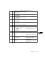
Contents
1Contents
About This Book ............................................................................ xxix
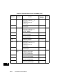
Overview ........................................................................................... 1-1
PPC403GCX Overview ........................................................................................................ 1-1
PowerPC Architecture .......................................................................................................... 1-2
The PPC403GCX as a PowerPC Implementation .......................................................... 1-3
PPC403GCX Features ......................................................................................................... 1-4
RISC Core ....................................................................................................................... 1-5
Execution Unit (EXU) ................................................................................................. 1-5
Memory Management Unit (MMU) ............................................................................. 1-6
Instruction Cache Unit (ICU) ...................................................................................... 1-7
Data Cache Unit (DCU) .............................................................................................. 1-8
Bus Interface Unit (BIU) .................................................................................................. 1-8
External Interfaces to DRAM, SRAM, ROM, and I/O ................................................. 1-8
RISC Core Interface ................................................................................................... 1-9
DMA Interface ............................................................................................................ 1-9
On-Chip Peripheral Bus Interface .............................................................................. 1-9
External Bus Master Interface .................................................................................. 1-10
DMA Controller .............................................................................................................. 1-10
Asynchronous Interrupt Controller ................................................................................ 1-11
Serial Port ..................................................................................................................... 1-12
Debug Port .................................................................................................................... 1-12
Data Types .................................................................................................................... 1-12
Register Set Summary .................................................................................................. 1-13
General Purpose Registers ...................................................................................... 1-13
Special Purpose Registers ....................................................................................... 1-13
Machine State Register ............................................................................................ 1-13
Condition Register .................................................................................................... 1-13
Device Control Registers .......................................................................................... 1-13
Memory Mapped Input/Output .................................................................................. 1-13
Addressing Modes ........................................................................................................ 1-14
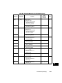
Programming Model ........................................................................ 2-1
Chapter Overview ................................................................................................................
Memory Organization and Addressing .................................................................................
Double-Mapping ..............................................................................................................
Supported Memory ..........................................................................................................
Storage Attribute Regions ...............................................................................................
Physical Address Map .....................................................................................................
PPC403GCX Register Set ...................................................................................................
General Purpose Registers .............................................................................................
Special Purpose Registers ..............................................................................................
Count Register (CTR) .................................................................................................
Link Register (LR) ......................................................................................................
Ver 0.04, 5/07/97
Preliminary
Contents
2-1
2-2
2-2
2-3
2-3
2-4
2-6
2-6
2-7
2-8
2-8
v
Processor Version Register (PVR) ............................................................................ 2-9
Special Purpose Register General (SPRG0-SPRG3) .............................................. 2-10
Fixed Point Exception Register (XER) ..................................................................... 2-10
Condition Register (CR) ................................................................................................ 2-13
CR Fields after Compare Instructions ...................................................................... 2-14
The CR0 Field .......................................................................................................... 2-14
Machine State Register ................................................................................................ 2-15
Device Control Registers .............................................................................................. 2-16
Memory Mapped Input/Output Registers ...................................................................... 2-16
Data Types and Alignment ................................................................................................ 2-17
Alignment for Storage Reference Instructions .............................................................. 2-17
Alignment for Cache Control Instructions ..................................................................... 2-18
Little Endian Mode ............................................................................................................. 2-19
Non-processor Memory Access in Little-Endian ........................................................... 2-24
Control of Endian Mode ................................................................................................ 2-25
Instruction Queue .............................................................................................................. 2-26
Branching Control .............................................................................................................. 2-27
AA Field on Unconditional Branches ............................................................................ 2-27
AA Field on Conditional Branches ................................................................................ 2-27
BI Field on Conditional Branches ................................................................................. 2-27
BO Field on Conditional Branches ................................................................................ 2-27
Branch Prediction ......................................................................................................... 2-29
Speculative Fetching ......................................................................................................... 2-30
Architectural Overview of Speculative Accesses .......................................................... 2-30
Speculative Accesses on PPC403GCX ........................................................................ 2-31
Pre-Fetch Distance from an Unresolved Branch ..................................................... 2-31
Pre-Fetch of Branch to Count / Branch to Link ........................................................ 2-32
Fetching Past an Interrupt-Causing / Returning Instruction ..................................... 2-32
Fetching Past tw or twi Instructions ......................................................................... 2-33
Fetching Past an Unconditional Branch ................................................................... 2-33
Suggested Location of Memory-Mapped Hardware ................................................ 2-33
Summary ...................................................................................................................... 2-34
Privileged Mode Operation ................................................................................................ 2-35
Background and Terminology ....................................................................................... 2-35
MSR Bits and Exception Handling ................................................................................ 2-35
Privileged Instructions ................................................................................................... 2-36
Privileged SPRs ............................................................................................................ 2-37
Privileged DCRs ........................................................................................................... 2-37
Context, Execution, and Storage Synchronization ............................................................ 2-37
Context Synchronization ............................................................................................... 2-38
Execution Synchronization ........................................................................................... 2-40
Storage Synchronization ............................................................................................... 2-41
Instruction Set Summary ................................................................................................... 2-42
Instructions Specific to PowerPC Embedded Controller ............................................... 2-43
Storage Reference Instructions .................................................................................... 2-43
Arithmetic and Logical Instructions ............................................................................... 2-44
Comparison Instructions ............................................................................................... 2-44
vi
PPC403GCX User’s Manual
Preliminary
Ver 0.04, 5/07/97
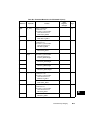
Branch Instructions .......................................................................................................
Condition Register Logical Instructions .........................................................................
Rotate and Shift Instructions .........................................................................................
Cache Control Instructions ............................................................................................
Interrupt Control Instructions .........................................................................................
TLB Management Instructions ......................................................................................
Processor Management Instructions .............................................................................
2-45
2-45
2-46
2-46
2-47
2-47
2-47
Memory and Peripheral Interface ................................................... 3-1
Memory Interface Signals .................................................................................................... 3-2
Address Bus When Idle ................................................................................................... 3-3
Access Priorities .................................................................................................................. 3-4
Function During Processor Wait State ................................................................................. 3-4
Memory Banks Supported ................................................................................................... 3-5
Parity on Memory Transfers ................................................................................................. 3-6
Bank Register High (BRH0–BRH7) ................................................................................ 3-6
Attachment to the Bus .......................................................................................................... 3-7
Bus Width after Reset ..................................................................................................... 3-7
Alternative Bus Attachment ............................................................................................. 3-8
Address Bit Usage ............................................................................................................... 3-9
Storage Attribute Control ............................................................................................... 3-10
SRAM / DRAM / OPB Addresses .................................................................................. 3-10
External Memory Location ............................................................................................ 3-11
The SRAM Interface .......................................................................................................... 3-12
Signals .......................................................................................................................... 3-12
SRAM Read Example .............................................................................................. 3-16
SRAM Write Example ............................................................................................... 3-17
WBE Signal Usage ................................................................................................... 3-18
Device-Paced Transfers ................................................................................................ 3-18
SRAM Device-Paced Read Example ....................................................................... 3-21
SRAM Device-Paced Write Example ....................................................................... 3-23
SRAM Burst Mode ........................................................................................................ 3-25
SRAM Burst Read Example ..................................................................................... 3-27
SRAM Burst Write Example ..................................................................................... 3-29
Bank Registers for SRAM Devices ............................................................................... 3-31
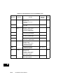
The DRAM Interface ......................................................................................................... 3-36
Signals .......................................................................................................................... 3-36
FPM DRAM Non-Burst Read Example .................................................................... 3-42
FPM DRAM Burst Read Examples .......................................................................... 3-43
EDO DRAM Read Examples .................................................................................... 3-45
DRAM Non-Burst Write Example ............................................................................. 3-47
DRAM Burst Write Examples ................................................................................... 3-48
DRAM CAS Before RAS Refresh Example .............................................................. 3-50
Bank Registers for DRAM Devices ............................................................................... 3-51
Alternate Refresh Mode ................................................................................................ 3-57
Immediate Refresh ................................................................................................... 3-58
Self Refresh Mode .................................................................................................... 3-58
Example of DRAM Connection ..................................................................................... 3-60
Ver 0.04, 5/07/97
Preliminary
Contents
vii
Note about SIMMs ...................................................................................................
Address Bus Multiplex for DRAM .................................................................................
The On-Chip Peripheral Bus Interface ..............................................................................
External Bus Master Interface ...........................................................................................
External Bus Arbitration ................................................................................................
DRAM Three-state Mode ........................................................................................
DRAM Accesses by an External Bus Master ................................................................
External Master Single Transfers .............................................................................
External Master Burst Transfers ..............................................................................
3-60
3-61
3-65
3-65
3-67
3-70
3-72
3-73
3-75
DMA Operations ............................................................................... 4-1
Overview .............................................................................................................................. 4-2
DMA Operations .................................................................................................................. 4-3
DMA Signals ................................................................................................................... 4-4
DMA Timing Parameters ................................................................................................ 4-6
Buffered Mode Transfers ................................................................................................ 4-7
Buffered Transfer from Memory to Peripheral ........................................................... 4-9
Buffered Transfer from Peripheral to Memory ......................................................... 4-12
Fly-By Mode Transfers ................................................................................................. 4-15
Fly-by Transfer from Memory to Peripheral ............................................................. 4-17
Fly-By Burst .................................................................................................................. 4-19
Fly-By Burst, Memory to Peripheral ......................................................................... 4-20
Fly-By Burst, Peripheral to Memory ......................................................................... 4-23
Memory-to-Memory Mode Transfers ............................................................................ 4-24
Memory-to-Memory Transfers Initiated by Software ................................................ 4-26
Device-Paced Memory-to-Memory Transfers .......................................................... 4-28
Memory-to-Memory Line Burst Mode ...................................................................... 4-29
Packing and Unpacking of Data ................................................................................... 4-30
Chained Operations ...................................................................................................... 4-30
Chaining Example -- Quick Start of Transfer ........................................................... 4-31
Chaining Example -- No Setup Race ....................................................................... 4-32
DMA Transfer Priorities ................................................................................................ 4-33
Parity on DMA Transfers .............................................................................................. 4-34
Interrupts ....................................................................................................................... 4-35
Errors ............................................................................................................................ 4-36
DMA Registers .................................................................................................................. 4-37
DMA Channel Control Register (DMACR0-DMACR3) ................................................. 4-37
DMA Status Register (DMASR) .................................................................................... 4-40
DMA Destination Address Register (DMADA0-DMADA3) ............................................ 4-41
DMA Source/Chained Address Register (DMASA0-DMASA3) .................................... 4-42
DMA Count Register (DMACT0-DMACT3) ................................................................... 4-43
DMA Chained Count Register (DMACC0-DMACC3) ................................................... 4-43
Reset and Initialization .................................................................... 5-1
Core, Chip, and System Resets ..........................................................................................
Core Reset ......................................................................................................................
Chip Reset ......................................................................................................................
System Reset .................................................................................................................
viii
PPC403GCX User’s Manual
Preliminary
5-1
5-1
5-2
5-2
Ver 0.04, 5/07/97
Behavior of the Reset Line ......................................................................................... 5-2
Processor State After Reset ................................................................................................ 5-3
Register Contents After A Reset .......................................................................................... 5-4
Signal States During Reset .................................................................................................. 5-7
DRAM Controller Behavior During Reset ............................................................................. 5-8
Effect of Reset on the TLB ................................................................................................... 5-9
Initial Processor Sequencing ............................................................................................... 5-9
Initialization Requirements ................................................................................................... 5-9
Notes on Bank Register Initialization ............................................................................ 5-10
Initialization Code Example ........................................................................................... 5-10
Interrupts, Exceptions, and Timers ................................................ 6-1
Interrupts and Exceptions .................................................................................................... 6-2
Architectural Definitions and Behavior ............................................................................ 6-2
Behavior of the PPC403GCX Implementation ................................................................ 6-4
Critical and Non-Critical Exceptions ........................................................................... 6-6
Exception Handling Registers .............................................................................................. 6-8
Machine State Register (MSR) ....................................................................................... 6-8
Save/Restore Register 0 and 1 (SRR0 - SRR1) ........................................................... 6-10
Save/Restore Register 2 and 3 (SRR2 - SRR3) ........................................................... 6-11
Exception Vector Prefix Register (EVPR) ..................................................................... 6-12
Exception Syndrome Register (ESR) ............................................................................ 6-12
Data Exception Address Register (DEAR) .................................................................... 6-15
Critical Interrupt Pin Exception ........................................................................................... 6-15
Machine Check Exceptions ................................................................................................ 6-17
Bus Error Reporting ...................................................................................................... 6-17
Bus Error Syndrome Register (BESR) .................................................................... 6-17
Bus Error Address Register (BEAR) ........................................................................ 6-19
Instruction Machine Check Handling ............................................................................. 6-20
Data Machine Check Handling ...................................................................................... 6-22
Data Storage Exception ..................................................................................................... 6-23
Instruction Storage Exception ............................................................................................ 6-25
External Interrupt Exception ............................................................................................... 6-26
External Interrupt Control .............................................................................................. 6-27
External Interrupt Enable Register (EXIER) ............................................................ 6-27
External Interrupt Status Register (EXISR) ............................................................. 6-29
Input/Output Configuration Register (IOCR) ............................................................ 6-31
External Interrupt Handling ........................................................................................... 6-34
Alignment Exception .......................................................................................................... 6-35
Program Exceptions ........................................................................................................... 6-36
System Call Exception ....................................................................................................... 6-37
Programmable Interval Timer Exception ............................................................................ 6-38
Fixed Interval Timer Exception .......................................................................................... 6-39
Watchdog Timer Exception ................................................................................................ 6-40
Data TLB Miss Exception ................................................................................................... 6-41
Instruction TLB Miss Exception .......................................................................................... 6-42
Debug Exception Handling ................................................................................................ 6-43
Timer Architecture .............................................................................................................. 6-44
Ver 0.04, 5/07/97
Preliminary
Contents
ix
Timer Clocks .................................................................................................................
Time Base (TBHI, TBLO, TBHU, TBLU) .......................................................................
Comparison with PowerPC Architecture Time Base ................................................
Programmable Interval Timer (PIT) ..............................................................................
Fixed Interval Timer (FIT) .............................................................................................
Watch Dog Timer (WDT) ..............................................................................................
Timer Status Register (TSR) ........................................................................................
Timer Control Register (TCR) .......................................................................................
6-45
6-45
6-47
6-49
6-50
6-51
6-54
6-55
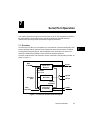
Serial Port Operation ....................................................................... 7-1
Overview ............................................................................................................................. 7-1
SPU Operating Mode Selection ...................................................................................... 7-2
Normal Mode ............................................................................................................. 7-2
Internal Loopback Mode ............................................................................................ 7-2
Automatic Echo Mode ................................................................................................ 7-2
SPU Handshaking I/O Pair Selection ............................................................................. 7-2
SPU Registers ................................................................................................................ 7-3
SPU Operations ................................................................................................................... 7-5
SPU Baud Rate Generator ............................................................................................. 7-5
SPU Transmitter ............................................................................................................. 7-6
Pattern Generation Mode ........................................................................................... 7-7
Transmitter Stop/Pause Mode ................................................................................... 7-7
Transmitter Line Break Generation ............................................................................ 7-8
Transmitter DMA Mode .............................................................................................. 7-8
Transmitter Interrupts ................................................................................................. 7-8
SPU Receiver ................................................................................................................. 7-9
Receiver Control of RTS .......................................................................................... 7-10
Receiver DMA Mode ............................................................................................... 7-11
Receiver Interrupts ................................................................................................... 7-11
SPU Register Descriptions ................................................................................................ 7-12
Baud Rate Divisor Registers ......................................................................................... 7-12
Serial Port Control Register (SPCTL) ........................................................................... 7-13
Serial Port Handshake Status Register (SPHS) ........................................................... 7-14
Serial Port Line Status Register (SPLS) ....................................................................... 7-15
Serial Port Receive Buffer (SPRB) ............................................................................... 7-16
Serial Port Receiver Command Register (SPRC) ........................................................ 7-16
Serial Port Transmit Buffer (SPTB) ............................................................................... 7-17
Serial Port Transmit Command Register (SPTC) ......................................................... 7-18
Instruction and Data Caches ........................................................... 8-1
Instruction Cache Unit .........................................................................................................
Instruction Cache Operations .........................................................................................
Instruction Cacheability Control ......................................................................................
Cache Synonyms for Instruction Relocation ...................................................................
Instruction Cache Coherency .........................................................................................
Data Cache Unit ..................................................................................................................
Data Cache Operations ..................................................................................................
Data Cache Write Strategy .............................................................................................
x
PPC403GCX User’s Manual
Preliminary
8-1
8-3
8-3
8-4
8-5
8-6
8-7
8-7
Ver 0.04, 5/07/97
Copy-back Strategy .................................................................................................... 8-7
Write-thru Strategy ..................................................................................................... 8-8
Data Cacheability Control ............................................................................................... 8-8
Data Cache Coherency ................................................................................................... 8-9
Cache Instructions ............................................................................................................... 8-9
ICU Instructions ............................................................................................................... 8-9
DCU Instructions ............................................................................................................. 8-9
Cache Debugging Features ............................................................................................... 8-11
ICU Debugging .............................................................................................................. 8-12
DCU Debugging ............................................................................................................ 8-13
Memory Management ...................................................................... 9-1
Translation ........................................................................................................................... 9-1
Virtual to Real Address Translation ................................................................................. 9-2
Translation Lookaside Buffer (TLB) ..................................................................................... 9-3
Unified TLB ..................................................................................................................... 9-4
Shadow Instruction TLB (ITLB) ....................................................................................... 9-5
ITLB Consistency ....................................................................................................... 9-7
TLB Fields ....................................................................................................................... 9-7
Page Identification Fields ........................................................................................... 9-7
Translation Fields ....................................................................................................... 9-8
Access Control Fields ................................................................................................. 9-9
Storage Attribute Fields .............................................................................................. 9-9
TLB Operations .................................................................................................................. 9-11
Exceptions ..................................................................................................................... 9-11
Data Storage Exception ........................................................................................... 9-11
Instruction Storage Exception .................................................................................. 9-12
Data TLB Miss Exception ......................................................................................... 9-12
Instruction TLB Miss Exception ................................................................................ 9-12
Page Reference and Change Recording ...................................................................... 9-13
TLB Reload ................................................................................................................... 9-13
TLB Search Instruction (tlbsx / tlbsx.) ....................................................................... 9-14
TLB Read/Write Instructions (tlbre / tlbwe) ............................................................... 9-14
TLB Invalidate Instruction (tlbia) ............................................................................... 9-14
TLB Sync Instruction (tlbsync) .................................................................................. 9-14
Access Protection .............................................................................................................. 9-15
Virtual-mode Access Protection .................................................................................... 9-15
TID Protection .......................................................................................................... 9-15
EX Protection ........................................................................................................... 9-15
WR Protection .......................................................................................................... 9-16
Zone Protection ........................................................................................................ 9-16
Real-mode Access Protection ....................................................................................... 9-18
Protection Bounds Registers .................................................................................... 9-19
Access Protection for Cache Instructions ..................................................................... 9-20
Access Protection for String Instructions ...................................................................... 9-21
Real Mode Control of WIMG Storage Attributes ................................................................ 9-22
Storage Attribute Control Registers .............................................................................. 9-22
Data Cache Write-thru Register (DCWR) ................................................................. 9-22
Ver 0.04, 5/07/97
Preliminary
Contents
xi
Data Cache Cacheability Register (DCCR) ............................................................. 9-24
Instruction Cache Cacheability Register (ICCR) ...................................................... 9-26
Storage Guarded Register (SGR) ............................................................................ 9-28
Debugging ...................................................................................... 10-1
Development Tool Support ................................................................................................ 10-1
Debug Modes .................................................................................................................... 10-1
Internal Debug Mode .................................................................................................... 10-2
External Debug Mode ................................................................................................... 10-2
Real-time Trace Debug Mode ....................................................................................... 10-2
Bus Status Debug Mode ............................................................................................... 10-3
Processor Control .............................................................................................................. 10-3
Processor Status ............................................................................................................... 10-4
Debug Events .................................................................................................................... 10-5
Debug Registers ................................................................................................................ 10-6
Debug Control Register (DBCR) ................................................................................... 10-7
Note on DAC Size Fields ......................................................................................... 10-7
Debug Status Register (DBSR) ................................................................................. 10-10
Data Address Compare Registers (DAC1–DAC2) ..................................................... 10-12
DAC Applied to Cache Instructions ........................................................................ 10-12
DAC Applied to String Instructions ......................................................................... 10-14
Instruction Address Compare (IAC1–IAC2) ................................................................ 10-14
Debug Interfaces ............................................................................................................. 10-15
Trace Status Port ........................................................................................................ 10-15
Trace Status Signals .............................................................................................. 10-15
Trace Status Connector ......................................................................................... 10-16
IEEE 1149.1 Test Access Port (JTAG) ....................................................................... 10-17
JTAG Connector .................................................................................................... 10-17
JTAG Instructions .................................................................................................. 10-19
JTAG Boundary Scan Chain .................................................................................. 10-19
Instruction Set ................................................................................ 11-1
Instruction Formats ............................................................................................................ 11-1
Pseudocode ...................................................................................................................... 11-2
Register Usage .................................................................................................................. 11-5
add ..................................................................................................................................... 11-6
addc ................................................................................................................................... 11-7
adde ................................................................................................................................... 11-8
addi .................................................................................................................................... 11-9
addic ................................................................................................................................ 11-10
addic. ............................................................................................................................... 11-11
addis ................................................................................................................................ 11-12
addme .............................................................................................................................. 11-13
addze ............................................................................................................................... 11-14
and ................................................................................................................................... 11-15
andc ................................................................................................................................. 11-16
andi. ................................................................................................................................. 11-17
andis. ............................................................................................................................... 11-18
xii
PPC403GCX User’s Manual
Preliminary
Ver 0.04, 5/07/97
b .......................................................................................................................................
bc .....................................................................................................................................
bcctr .................................................................................................................................
bclr ...................................................................................................................................
cmp ..................................................................................................................................
cmpi .................................................................................................................................
cmpl .................................................................................................................................
cmpli .................................................................................................................................
cntlzw ...............................................................................................................................
crand ................................................................................................................................
crandc ..............................................................................................................................
creqv ................................................................................................................................
crnand ..............................................................................................................................
crnor .................................................................................................................................
cror ...................................................................................................................................
crorc .................................................................................................................................
crxor .................................................................................................................................
dcbf ..................................................................................................................................
dcbi ..................................................................................................................................
dcbst ................................................................................................................................
dcbt ..................................................................................................................................
dcbtst ...............................................................................................................................
dcbz .................................................................................................................................
dccci .................................................................................................................................
dcread ..............................................................................................................................
divw ..................................................................................................................................
divwu ................................................................................................................................
eieio .................................................................................................................................
eqv ...................................................................................................................................
extsb ................................................................................................................................
extsh ................................................................................................................................
icbi ....................................................................................................................................
icbt ...................................................................................................................................
iccci ..................................................................................................................................
icread ...............................................................................................................................
isync .................................................................................................................................
lbz ....................................................................................................................................
lbzu ..................................................................................................................................
lbzux .................................................................................................................................
lbzx ...................................................................................................................................
lha ....................................................................................................................................
lhau ..................................................................................................................................
lhaux ................................................................................................................................
lhax ..................................................................................................................................
lhbrx .................................................................................................................................
lhz ....................................................................................................................................
lhzu ..................................................................................................................................
Ver 0.04, 5/07/97
Preliminary
Contents
11-19
11-20
11-27
11-31
11-36
11-37
11-38
11-39
11-40
11-41
11-42
11-43
11-44
11-45
11-46
11-47
11-48
11-49
11-50
11-51
11-52
11-54
11-56
11-58
11-60
11-62
11-63
11-64
11-65
11-66
11-67
11-68
11-70
11-72
11-74
11-76
11-77
11-78
11-79
11-80
11-81
11-82
11-83
11-84
11-85
11-86
11-87
xiii
lhzux ................................................................................................................................ 11-88
lhzx .................................................................................................................................. 11-89
lmw .................................................................................................................................. 11-90
lswi ................................................................................................................................... 11-91
lswx .................................................................................................................................. 11-93
lwarx ................................................................................................................................ 11-95
lwbrx ................................................................................................................................ 11-96
lwz ................................................................................................................................... 11-97
lwzu ................................................................................................................................. 11-98
lwzux ................................................................................................................................ 11-99
lwzx ................................................................................................................................ 11-100
mcrf ................................................................................................................................ 11-101
mcrxr .............................................................................................................................. 11-102
mfcr ................................................................................................................................ 11-103
mfdcr .............................................................................................................................. 11-104
mfmsr ............................................................................................................................. 11-106
mfspr .............................................................................................................................. 11-107
mtcrf ............................................................................................................................... 11-109
mtdcr .............................................................................................................................. 11-111
mtmsr ............................................................................................................................. 11-113
mtspr .............................................................................................................................. 11-114
mulhw ............................................................................................................................ 11-116
mulhwu .......................................................................................................................... 11-117
mulli ............................................................................................................................... 11-118
mullw ............................................................................................................................. 11-119
nand ............................................................................................................................... 11-120
neg ................................................................................................................................. 11-121
nor ................................................................................................................................. 11-122
or ................................................................................................................................... 11-123
orc .................................................................................................................................. 11-124
ori ................................................................................................................................... 11-125
oris ................................................................................................................................. 11-126
rfci .................................................................................................................................. 11-127
rfi .................................................................................................................................... 11-128
rlwimi ............................................................................................................................. 11-129
rlwinm ............................................................................................................................ 11-130
rlwnm ............................................................................................................................. 11-133
sc ................................................................................................................................... 11-134
slw ................................................................................................................................. 11-135
sraw ............................................................................................................................... 11-136
srawi .............................................................................................................................. 11-137
srw ................................................................................................................................. 11-138
stb .................................................................................................................................. 11-139
stbu ................................................................................................................................ 11-140
stbux .............................................................................................................................. 11-141
stbx ................................................................................................................................ 11-142
sth .................................................................................................................................. 11-143
xiv
PPC403GCX User’s Manual
Preliminary
Ver 0.04, 5/07/97
sthbrx .............................................................................................................................
sthu ................................................................................................................................
sthux ..............................................................................................................................
sthx ................................................................................................................................
stmw ...............................................................................................................................
stswi ...............................................................................................................................
stswx ..............................................................................................................................
stw ..................................................................................................................................
stwbrx .............................................................................................................................
stwcx. .............................................................................................................................
stwu ................................................................................................................................
stwux ..............................................................................................................................
stwx ................................................................................................................................
subf ................................................................................................................................
subfc ..............................................................................................................................
subfe ..............................................................................................................................
subfic ..............................................................................................................................
subfme ...........................................................................................................................
subfze ............................................................................................................................
sync ................................................................................................................................
tlbia ................................................................................................................................
tlbre ................................................................................................................................
tlbsx ................................................................................................................................
tlbsync ............................................................................................................................
tlbwe ...............................................................................................................................
tw ...................................................................................................................................
twi ...................................................................................................................................
wrtee ..............................................................................................................................
wrteei .............................................................................................................................
xor ..................................................................................................................................
xori .................................................................................................................................
xoris ...............................................................................................................................
11-144
11-145
11-146
11-147
11-148
11-149
11-150
11-152
11-153
11-154
11-156
11-157
11-158
11-159
11-160
11-162
11-163
11-164
11-165
11-166
11-167
11-168
11-170
11-171
11-172
11-174
11-177
11-180
11-181
11-182
11-183
11-184
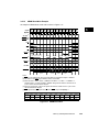
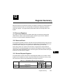
Register Summary ......................................................................... 12-1
Reserved Registers ...........................................................................................................
Reserved Fields .................................................................................................................
General Purpose Registers ................................................................................................
Machine State Register and Condition Register ................................................................
Special Purpose Registers .................................................................................................
Device Control Registers ...................................................................................................
Memory Mapped I/O Registers .........................................................................................
Alphabetical Register Listing ..............................................................................................
12-1
12-1
12-1
12-2
12-2
12-4
12-7
12-7
Signal Descriptions ....................................................................... 13-1
Instruction Summary ...................................................................... A-1
Instruction Set and Extended Mnemonics – Alphabetical ................................................... A-1
Instructions Sorted by Opcode .......................................................................................... A-42
Ver 0.04, 5/07/97
Preliminary
Contents
xv
Instruction Formats ............................................................................................................ A-50
Instruction Fields ........................................................................................................... A-50
Instruction Format Diagrams ........................................................................................ A-53
Instructions By Category ............................................................... B-1
Instruction Set Summary – Categories ................................................................................ B-1
Instructions Specific to PowerPC Embedded Controllers .................................................... B-2
Privileged Instructions ......................................................................................................... B-4
Assembler Extended Mnemonics ........................................................................................ B-7
Storage Reference Instructions ......................................................................................... B-32
Arithmetic and Logical Instructions .................................................................................... B-37
Condition Register Logical Instructions ............................................................................. B-42
Branch Instructions ............................................................................................................ B-43
Comparison Instructions .................................................................................................... B-44
Rotate and Shift Instructions ............................................................................................. B-45
Cache Control Instructions ................................................................................................ B-47
Interrupt Control Instructions ............................................................................................. B-48
TLB Management Instructions ........................................................................................... B-49
Processor Management Instructions ................................................................................. B-51
Instruction Timing and Optimization ............................................. C-1
Background Information ..................................................................................................... C-1
Superscalar Operation ................................................................................................... C-1
Folding Defined .............................................................................................................. C-1
Branch Folding ............................................................................................................... C-2
Coding Guidelines .............................................................................................................. C-3
Condition Register Bits for Boolean Variables ............................................................... C-3
CR Logical Instructions for Compound Branches .......................................................... C-3
Floating Point Emulation ................................................................................................ C-3
Data Cache Usage ........................................................................................................ C-4
Instruction Cache Usage ............................................................................................... C-4
Dependency Upon CR ................................................................................................... C-4
Dependency Upon LR and CTR .................................................................................... C-5
Load Latency ................................................................................................................. C-5
Branch Prediction .......................................................................................................... C-5
Alignment ....................................................................................................................... C-6
Instruction Timings ............................................................................................................. C-7
General Rules ................................................................................................................ C-7
Branch and CR Logical Opcodes .................................................................................. C-7
Branch Prediction .......................................................................................................... C-8
String Opcodes .............................................................................................................. C-8
Data Cache Loads and Stores ...................................................................................... C-9
Instruction Cache Misses ............................................................................................... C-9
Detailed Folding Rules ..................................................................................................... C-10
Instruction Classifications for Folding .......................................................................... C-10
Instructions That Can Be Folded ................................................................................. C-11
Fold Blocking Rules For CR Logical and mcrf Instructions .......................................... C-11
Fold Blocking Rules For Branch Instructions ............................................................... C-11
xvi
PPC403GCX User’s Manual
Preliminary
Ver 0.04, 5/07/97
Fold Blocking During Debug ........................................................................................ C-13
Index .................................................................................................. X-1
Ver 0.04, 5/07/97
Preliminary
Contents
xvii
xviii
PPC403GCX User’s Manual
Preliminary
Ver 0.04, 5/07/97
Figures
1Figures
Figure 1-1.
Figure 2-1.
Figure 2-2.
Figure 2-3.
Figure 2-4.
Figure 2-5.
Figure 2-6.
Figure 2-7.
Figure 2-8.
Figure 2-9.
Figure 2-10.
Figure 3-1.
Figure 3-2.
Figure 3-3.
Figure 3-4.
Figure 3-5.
Figure 3-6.
Figure 3-7.
Figure 3-8.
Figure 3-9.
Figure 3-10.
Figure 3-11.
Figure 3-12.
Figure 3-13.
Figure 3-14.
Figure 3-15.
Figure 3-16.
Figure 3-17.
Figure 3-18.
Figure 3-19.
Figure 3-20.
Figure 3-21.
Figure 3-22.
Figure 3-23.
Figure 3-24.
Figure 3-25.
Figure 3-26.
Figure 3-27.
PPC403GCX Block Diagram ............................................................................ 1-4
PPC403GCX Address Map .............................................................................. 2-5
General Purpose Register (R0-R31) ................................................................ 2-6
Count Register (CTR) ....................................................................................... 2-8
Link Register (LR) ............................................................................................. 2-8
Processor Version Register (PVR) ................................................................... 2-9
Special Purpose Register General (SPRG0-SPRG3) .................................... 2-10
Fixed Point Exception Register (XER) ........................................................... 2-10
Condition Register (CR) ................................................................................. 2-13
PPC403GCX Data types ................................................................................ 2-17
PPC403GCX Instruction Queue ..................................................................... 2-26
BIU Interfaces ................................................................................................... 3-1
Grouping of External BIU Signals ..................................................................... 3-3
Bank Register High (BRH0–BRH7) ................................................................. 3-6
Attachment of Devices of Various Widths to the PPC403GCX Data Bus ......... 3-7
Usage of Address Bits ...................................................................................... 3-9
Parameter Definitions -- SRAM Single Transfer ............................................. 3-14
Parameter Definitions -- SRAM Burst Mode ................................................... 3-15
SRAM Read .................................................................................................... 3-16
SRAM Write .................................................................................................... 3-17
Available Ready modes and latch times ......................................................... 3-20
SRAM Read Extended with Ready, SOR = 0 ................................................. 3-21
SRAM Read Extended with Ready, SOR = 1 ................................................. 3-22
SRAM Write Extended with Ready, SOR = 0 ................................................. 3-23
SRAM Write Extended with Ready, SOR = 1 ................................................. 3-24
SRAM Burst Read .......................................................................................... 3-27
SRAM Burst Read, SOR=1 ............................................................................ 3-28
SRAM Burst Write ........................................................................................... 3-29
SRAM Burst Write with Wait and Hold, SOR = 1 ............................................ 3-30
Bank Registers - SRAM Configuration (BR0–BR7) ....................................... 3-31
Parameter Definitions -- FPM DRAM and EDO Write .................................... 3-39
Parameter Definitions -- EDO DRAM, Parameter FAC = 0 ............................ 3-40
Parameter Definitions -- EDO DRAM, Parameter FAC > 0 ............................ 3-41
FPM DRAM Single-Transfer Read ................................................................. 3-42
FPM DRAM 3-2-2-2 Read .............................................................................. 3-43
FPM DRAM 2-1-1-1 Read .............................................................................. 3-44
EDO DRAM 3-1-1-1 Read .............................................................................. 3-45
EDO DRAM 2-1-1-1 Read .............................................................................. 3-46
Ver 0.04, 5/07/97
Preliminary
Figures
xix
Figure 3-28.
Figure 3-29.
Figure 3-30.
Figure 3-31.
Figure 3-32.
Figure 3-33.
Figure 3-34.
Figure 3-35.
Figure 3-36.
Figure 3-37.
Figure 3-38.
Figure 3-39.
Figure 4-1.
Figure 4-2.
Figure 4-3.
Figure 4-4.
Figure 4-5.
Figure 4-6.
Figure 4-7.
Figure 4-8.
Figure 4-9.
Figure 4-10.
Figure 4-11.
Figure 4-12.
Figure 4-13.
Figure 4-14.
Figure 4-15.
Figure 4-16.
Figure 4-17.
Figure 4-18.
Figure 4-19.
Figure 4-20.
Figure 4-21.
Figure 4-22.
Figure 6-1.
Figure 6-2.
Figure 6-3.
Figure 6-4.
Figure 6-5.
Figure 6-6.
xx
DRAM Single Transfer Write .......................................................................... 3-47
DRAM 3-2-2-2 Burst Write ............................................................................. 3-48
DRAM 2-1-1-1 Burst Write ............................................................................. 3-49
DRAM Refresh Timing, CAS Before RAS, 1 Bank ......................................... 3-50
Bank Registers - DRAM Configuration (BR4–BR7) ...................................... 3-51
DRAM Alternate Refresh modes: Immediate and Self ................................... 3-57
Example of DRAM Connection ....................................................................... 3-60
Sample PPC403GCX / External Bus Master System ..................................... 3-66
HoldReq/HoldAck Bus Arbitration .................................................................. 3-68
Refresh Request before and after HoldAck .................................................... 3-71
External Bus Master Read Using the Internal DRAM Controller .................... 3-74
Burst Write to 3-2-2-2 Page Mode DRAM ...................................................... 3-76
DMA Controller Block Diagram ........................................................................ 4-2
PPC403GCX DMA Controller Interfaces .......................................................... 4-4
Overview of Buffered Mode Transfers .............................................................. 4-7
DMACR Setting for Buffered DRAM Read, Peripheral Write ........................... 4-9
Buffered Mode Transfer from a 32-bit 2-1-1-1 DRAM to a 32-bit Peripheral .. 4-11
DMACR Setting for Buffered Peripheral Read, DRAM Write ......................... 4-12
Buffered Mode Transfer from a 32-bit Peripheral to a 32-bit DRAM .............. 4-14
Overview of Fly-by Mode DMA Transfer ........................................................ 4-15
DMACR Setting for Fly-By Memory Read, Peripheral Write .......................... 4-17
Fly-By Transfer from 3-cycle DRAM to a 32-bit Peripheral ............................ 4-18
DMA Fly-by Burst; 2-1-1-1 DRAM; 2 Transfers .............................................. 4-22
DMA Fly-by Burst; 3-2-2-2 DRAM; Single Transfers ...................................... 4-23
Overview of Memory-to-memory Mode DMA Transfer ................................... 4-24
DMACR Setting for Memory-to-Memory Transfer .......................................... 4-26
Memory-to-Memory Line Burst, 2-1-1-1 DRAM .............................................. 4-29
DMA Transfer Priorities .................................................................................. 4-33
DMA Channel Control Registers (DMACR0-DMACR3) ................................ 4-37
DMA Status Register (DMASR) .................................................................... 4-40
DMA Destination Address Registers (DMADA0-DMADA3) ........................... 4-41
DMA Source Address Registers (DMASA0-DMASA3) .................................. 4-42
DMA Count Registers (DMACT0-DMACT3) .................................................. 4-43
DMA Chained Count Registers (DMACC0-DMACC3) ................................... 4-43
Machine State Register (MSR) ........................................................................ 6-8
Save / Restore Register 0 (SRR0) ................................................................ 6-10
Save / Restore Register 1 (SRR1) ................................................................ 6-10
Save / Restore Register 2 (SRR2) ................................................................ 6-11
Save / Restore Register 3 (SRR3) ................................................................ 6-11
Exception Vector Prefix Register (EVPR) ...................................................... 6-12
PPC403GCX User’s Manual
Preliminary
Ver 0.04, 5/07/97
Figure 6-7.
Figure 6-8.
Figure 6-9.
Figure 6-10.
Figure 6-11.
Figure 6-12.
Figure 6-13.
Figure 6-14.
Figure 6-15.
Figure 6-16.
Figure 6-17.
Figure 6-18.
Figure 6-19.
Figure 6-20.
Figure 7-1.
Figure 7-2.
Figure 7-3.
Figure 7-4.
Figure 7-5.
Figure 7-6.
Figure 7-7.
Figure 7-8.
Figure 7-9.
Figure 7-10.
Figure 7-11.
Figure 8-1.
Figure 8-2.
Figure 8-3.
Figure 8-4.
Figure 8-5.
Figure 9-1.
Figure 9-2.
Figure 9-3.
Figure 9-4.
Figure 9-5.
Figure 9-6.
Figure 9-7.
Figure 9-8.
Figure 9-9.
Figure 9-10.
Exception Syndrome Register (ESR) ............................................................ 6-13
Data Exception Address Register (DEAR) ..................................................... 6-15
Bus Error Syndrome Register (BESR) ............................................................ 6-18
Bus Error Address Register (BEAR) ............................................................... 6-19
External Interrupt Enable Register (EXIER) .................................................. 6-27
External Interrupt Status Register (EXISR) ................................................... 6-29
Input/Output Configuration Register (IOCR) .................................................. 6-31
Relationship of Timer Facilities to Base Clock ................................................ 6-44
Time Base Register (TBHI, TBHU) ................................................................. 6-46
Time Base Register (TBLO, TBLU) ................................................................ 6-46
Programmable Interval Timer (PIT) ................................................................ 6-50
Watchdog State Machine ................................................................................ 6-52
Timer Status Register (TSR) ......................................................................... 6-54
Timer Control Register (TCR) ........................................................................ 6-55
Serial Port Functional Block Diagram ............................................................... 7-1
SPU Registers and Buffers ............................................................................... 7-4
Baud Rate Divisor High Register (BRDH) ...................................................... 7-12
Baud Rate Divisor Low Register (BRDL) ........................................................ 7-12
Serial Port Control Register (SPCTL) ............................................................. 7-13
Serial Port Handshake Register (SPHS) ........................................................ 7-14
Serial Port Line Status Register (SPLS) ......................................................... 7-15
Serial Port Receive Buffer (SPRB) ................................................................. 7-16
Serial Port Receiver Command Register (SPRC) .......................................... 7-16
Serial Port Transmit Buffer (SPTB) ................................................................. 7-17
Serial Port Transmitter Command Register (SPTC) ....................................... 7-18
Instruction Cache Organization ........................................................................ 8-1
Instruction Flow ................................................................................................. 8-2
Data Cache Organization ................................................................................. 8-6
Cache Debug Control Register (CDBCR) ....................................................... 8-11
Instruction Cache Debug Data Register (ICDBDR) ........................................ 8-12
Effective to Real Address Translation Flow ...................................................... 9-3
TLB Entries ....................................................................................................... 9-4
ITLB/UTLB Address Resolution ....................................................................... 9-6
Process ID (PID) ............................................................................................. 9-15
Zone Protection Register (ZPR) .................................................................... 9-17
Bounds Registers (PBL1, PBL2, PBU1, PBU2) .............................................. 9-19
Data Cache Write-thru Register (DCWR) ...................................................... 9-23
Data Cache Cacheability Register (DCCR) ................................................... 9-24
Instruction Cache Cacheability Register (ICCR) ............................................ 9-26
Storage Guarded Register (SGR) .................................................................. 9-28
Ver 0.04, 5/07/97
Preliminary
Figures
xxi
Figure 10-1.
Figure 10-2.
Figure 10-3.
Figure 10-4.
Figure 10-5.
Figure 10-6.
Figure 12-1.
Figure 12-2.
Figure 12-3.
Figure 12-4.
Figure 12-5.
Figure 12-6.
Figure 12-7.
Figure 12-8.
Figure 12-9.
Figure 12-10.
Figure 12-11.
Figure 12-12.
Figure 12-13.
Figure 12-14.
Figure 12-15.
Figure 12-16.
Figure 12-17.
Figure 12-18.
Figure 12-19.
Figure 12-20.
Figure 12-21.
Figure 12-22.
Figure 12-23.
Figure 12-24.
Figure 12-25.
Figure 12-26.
Figure 12-27.
Figure 12-28.
Figure 12-29.
Figure 12-30.
Figure 12-31.
Figure 12-32.
Figure 12-33.
Figure 12-34.
xxii
Debug Control Register (DBCR) ................................................................... 10-7
Debug Status Register (DBSR) ................................................................... 10-10
Data Address Compare Registers (DAC1–DAC2) ....................................... 10-12
Instruction Address Compare (IAC1–IAC2) ................................................. 10-14
Trace Status Connector ............................................................................... 10-16
JTAG Connector (top view) Physical Layout ................................................ 10-17
Bus Error Address Register (BEAR) .............................................................. 12-8
Bus Error Syndrome Register (BESR) .......................................................... 12-9
Bank Registers - SRAM Configuration (BR0–BR7) ..................................... 12-10
Bank Registers - DRAM Configuration (BR4–BR7) .................................... 12-12
Baud Rate Divisor High Register (BRDH) .................................................... 12-14
Baud Rate Divisor Low Register (BRDL) ..................................................... 12-15
Bank Register High (BRH0–BRH7) .............................................................. 12-16
Cache Debug Control Register (CDBCR) .................................................... 12-17
Condition Register (CR) ............................................................................... 12-18
Count Register (CTR) ................................................................................... 12-19
Data Address Compare Registers (DAC1–DAC2) ....................................... 12-20
Debug Control Register (DBCR) ................................................................. 12-21
Debug Status Register (DBSR) ................................................................... 12-24
Data Cache Cacheability Register (DCCR) ................................................. 12-26
Data Cache Write-thru Register (DCWR) .................................................... 12-28
Data Exception Address Register (DEAR) ................................................... 12-30
DMA Chained Count Registers (DMACC0-DMACC3) ................................. 12-31
DMA Channel Control Registers (DMACR0-DMACR3) .............................. 12-32
DMA Count Registers (DMACT0-DMACT3) ................................................ 12-35
DMA Destination Address Registers (DMADA0-DMADA3) ......................... 12-36
DMA Source Address Registers (DMASA0-DMASA3) ................................ 12-37
DMA Status Register (DMASR) .................................................................. 12-38
Exception Syndrome Register (ESR) .......................................................... 12-40
Exception Vector Prefix Register (EVPR) .................................................... 12-42
External Interrupt Enable Register (EXIER) ................................................ 12-43
External Interrupt Status Register (EXISR) ................................................. 12-45
General Purpose Register (R0-R31) ............................................................ 12-47
Instruction Address Compare (IAC1–IAC2) ................................................. 12-48
Instruction Cache Cacheability Register (ICCR) ......................................... 12-49
Instruction Cache Debug Data Register (ICDBDR) ...................................... 12-51
Input/Output Configuration Register (IOCR) ............................................... 12-52
Link Register (LR) ........................................................................................ 12-55
Machine State Register (MSR) .................................................................... 12-56
Protection Bound Lower Register (PBL1-PBL2) .......................................... 12-58
PPC403GCX User’s Manual
Preliminary
Ver 0.04, 5/07/97
Figure 12-35.
Figure 12-36.
Figure 12-37.
Figure 12-38.
Figure 12-39.
Figure 12-40.
Figure 12-41.
Figure 12-42.
Figure 12-43.
Figure 12-44.
Figure 12-45.
Figure 12-46.
Figure 12-47.
Figure 12-48.
Figure 12-49.
Figure 12-50.
Figure 12-51.
Figure 12-52.
Figure 12-53.
Figure 12-54.
Figure 12-55.
Figure 12-56.
Figure 12-57.
Figure 12-58.
Figure 12-59.
Figure A-1.
Figure A-2.
Figure A-3.
Figure A-4.
Figure A-5.
Figure A-6.
Figure A-7.
Figure A-8.
Figure A-9.
Protection Bound Upper Register (PBU1-PBU2) .......................................... 12-59
Process ID (PID) ........................................................................................... 12-60
Programmable Interval Timer (PIT) .............................................................. 12-61
Processor Version Register (PVR) ............................................................... 12-62
Storage Guarded Register (SGR) ................................................................ 12-63
Serial Port Control Register (SPCTL) ........................................................... 12-65
Serial Port Handshake Register (SPHS) ...................................................... 12-66
Serial Port Line Status Register (SPLS) ....................................................... 12-67
Serial Port Receive Buffer (SPRB) ............................................................... 12-68
Serial Port Receiver Command Register (SPRC) ........................................ 12-69
Special Purpose Register General (SPRG0-SPRG3) .................................. 12-70
Serial Port Transmit Buffer (SPTB) ............................................................... 12-71
Serial Port Transmitter Command Register (SPTC) ..................................... 12-72
Save / Restore Register 0 (SRR0) ............................................................... 12-73
Save / Restore Register 1 (SRR1) ............................................................... 12-74
Save / Restore Register 2 (SRR2) ............................................................... 12-75
Save / Restore Register 3 (SRR3) ............................................................... 12-76
Time Base High Register (TBHI) .................................................................. 12-77
Time Base High User-mode (TBHU) ............................................................ 12-78
Time Base Low Register (TBLO) .................................................................. 12-79
Time Base Low User-mode (TBLU) .............................................................. 12-80
Timer Control Register (TCR) ....................................................................... 12-81
Timer Status Register (TSR) ........................................................................ 12-82
Fixed Point Exception Register (XER) .......................................................... 12-83
Zone Protection Register (ZPR) ................................................................... 12-84
I Instruction Format ........................................................................................ A-53
B Instruction Format ...................................................................................... A-53
SC Instruction Format .................................................................................... A-53
D Instruction Format ...................................................................................... A-53
X Instruction Format ..................................................................................... A-54
XL Instruction Format .................................................................................... A-55
XFX Instruction Format .................................................................................. A-55
XO Instruction Format .................................................................................... A-55
M Instruction Format ...................................................................................... A-55
Ver 0.04, 5/07/97
Preliminary
Figures
xxiii
xxiv
PPC403GCX User’s Manual
Preliminary
Ver 0.04, 5/07/97
Tables
1Tables
Table 2-1.
Table 2-2.
Table 2-3.
Table 2-4.
Table 2-5.
Table 2-6.
Table 2-7.
Table 2-8.
Table 2-9.
Table 2-10.
Table 2-11.
Table 2-12.
Table 2-13.
Table 2-14.
Table 2-15.
Table 2-16.
Table 2-17.
Table 2-18.
Table 2-19.
Table 2-20.
Table 2-21.
Table 3-1.
Table 3-2.
Table 3-3.
Table 3-4.
Table 3-5.
Table 3-6.
Table 3-7.
Table 3-8.
Table 3-9.
Table 3-10.
Table 3-11.
Table 4-1.
Table 4-2.
Table 4-3.
Table 4-4.
Table 4-5.
Table 4-6.
Special Purpose Register (SPR) List ............................................................... 2-7
XER-Updating Arithmetic Instructions ........................................................... 2-11
Device Control Register (DCR) List ............................................................... 2-16
Memory-Mapped I/O (MMIO) List .................................................................. 2-16
Address Alteration in Little-Endian Mode ........................................................ 2-22
Bits of the BO Field ........................................................................................ 2-28
Conditional Branch BO Field ......................................................................... 2-28
SRAM Mapping .............................................................................................. 2-34
Privileged Instructions .................................................................................... 2-36
PPC403GCX Instruction Set Summary ......................................................... 2-42
Instructions Specific to PowerPC Embedded Controller ................................ 2-43
Storage Reference Instructions ..................................................................... 2-43
Arithmetic and Logical Instructions ................................................................ 2-44
Comparison Instructions ................................................................................ 2-44
Branch Instructions ........................................................................................ 2-45
Condition Register Logical Instructions ......................................................... 2-45
Rotate and Shift Instructions .......................................................................... 2-46
Cache Control Instructions ............................................................................ 2-46
Interrupt Control Instructions ......................................................................... 2-47
TLB Management Instructions ....................................................................... 2-47
Processor Management Instructions ............................................................. 2-47
SRAM And DRAM Banks Supported ................................................................ 3-5
Restrictions on Bank Starting Address .......................................................... 3-11
Usage of WBE0:WBE3 vs Bus Width ............................................................ 3-18
RR Field for Normal Refresh Mode ............................................................... 3-56
RR Field for Alternate Refresh Mode ............................................................. 3-56
Multiplexed Address Outputs ......................................................................... 3-61
DRAM Multiplex for 8 bit Bus ......................................................................... 3-62
DRAM Multiplex for 16 bit Bus ....................................................................... 3-63
DRAM Multiplex for 32 bit Bus ....................................................................... 3-64
Signal States During Hold Acknowledge ........................................................ 3-69
XSize0:1 Bit Definitions .................................................................................. 3-72
Sample DMACR Settings for Buffered Transfer ............................................. 4-9
Sample DMACR Settings for Buffered Transfer ........................................... 4-12
Sample DMACR Settings for Fly-By Transfer ............................................... 4-17
Sample DMACR Settings for Fly-By Burst .................................................... 4-20
Sample DMACR Settings for Memory-to-Memory Transfer ......................... 4-26
Packing / Unpacking Support ......................................................................... 4-30
Ver 0.04, 5/07/97
Preliminary
Tables
xxv
Table 5-1.
Table 5-2.
Table 5-3.
Table 5-4.
Table 5-5.
Table 5-6.
Table 6-1.
Table 6-2.
Table 6-3.
Table 6-4.
Table 6-5.
Table 6-6.
Table 6-7.
Table 6-8.
Table 6-9.
Table 6-10.
Table 6-11.
Table 6-12.
Table 6-13.
Table 6-14.
Table 6-15.
Table 6-16.
Table 6-17.
Table 6-18.
Table 6-19.
Table 6-20.
Table 6-21.
Table 6-22.
Table 7-1.
Table 7-2.
Table 7-3.
Table 7-4.
Table 7-5.
Table 7-6.
Table 8-1.
Table 9-1.
Table 9-2.
Table 10-1.
Table 10-2.
Table 10-3.
xxvi
Processor Configuration After a Reset ............................................................ 5-3
Contents of Machine State Register After Reset ............................................. 5-4
Contents of Special Purpose Registers After Reset ........................................ 5-5
Contents of Serial Port Registers After Reset ................................................. 5-5
Contents of Device Control Registers After Reset .......................................... 5-6
Signal States During Reset .............................................................................. 5-7
PPC403GCX Exception Priorities ................................................................... 6-5
Exception Vector Offsets .................................................................................. 6-7
ESR Alteration by Various Exceptions .......................................................... 6-14
Register Settings during Critical Interrupt Exceptions ................................... 6-16
ESR Usage for Instruction Machine Checks ................................................. 6-20
Register Settings during Instruction Machine Check ..................................... 6-21
Register Settings during Data Machine Check .............................................. 6-22
Register Settings during Data Storage Exceptions ....................................... 6-24
Register Settings during Instruction Storage Exceptions .............................. 6-26
Register Settings during External Interrupt Exceptions ................................. 6-34
Register Settings during Alignment Exceptions ............................................ 6-35
ESR Usage for Program Exceptions ............................................................. 6-36
Register Settings during Program Exceptions ............................................... 6-36
Register Settings during System Call Exceptions ......................................... 6-37
Register Settings during Programmable Interval Timer Exceptions .............. 6-38
Register Settings during Fixed Interval Timer Exceptions ............................. 6-39
Register Settings during Watchdog Timer Exceptions .................................. 6-40
Register Settings during Data TLB Miss Exceptions ..................................... 6-41
Register Settings during Instruction TLB Miss Exceptions ............................ 6-42
SRR2 during Debug Exceptions ..................................................................... 6-43
Register Settings during Debug Exceptions .................................................. 6-43
Time Base Comparison ................................................................................. 6-48
SPU Operating Mode Selection ....................................................................... 7-2
Serial Port Register Addresses, Names, and Access Modes .......................... 7-3
Baud Rate Divisor Selection ............................................................................. 7-6
TxReady / TxEmpty Status Representation ..................................................... 7-6
DMA Mode / Interrupt Enable Field Representation ......................................... 7-8
DMA Mode / Interrupt Enable Field Representation ....................................... 7-11
Sources of Cacheability Control ....................................................................... 8-4
TLB Fields Related to Page Size .................................................................... 9-8
Protection Applied to Cache Instructions ...................................................... 9-21
DAC Applied to Cache Instructions ............................................................. 10-13
JTAG Port Summary .................................................................................... 10-17
JTAG Connector Signals ............................................................................. 10-18
PPC403GCX User’s Manual
Preliminary
Ver 0.04, 5/07/97
Table 10-4.
Table 11-1.
Table 11-2.
Table 11-3.
Table 11-4.
Table 11-5.
Table 11-6.
Table 11-7.
Table 11-8.
Table 11-9.
Table 11-10.
Table 11-11.
Table 11-12.
Table 11-13.
Table 11-14.
Table 11-15.
Table 11-16.
Table 11-17.
Table 11-18.
Table 11-19.
Table 11-20.
Table 11-21.
Table 11-22.
Table 11-23.
Table 11-24.
Table 11-25.
Table 11-26.
Table 11-27.
Table 11-28.
Table 11-29.
Table 11-30.
Table 11-31.
Table 11-32.
Table 11-33.
Table 12-1.
Table 12-2.
Table 12-3.
Table 12-4.
Table 13-1.
Table 13-2.
JTAG Instructions ......................................................................................... 10-19
Operator Precedence ..................................................................................... 11-4
Extended Mnemonics for addi ....................................................................... 11-9
Extended Mnemonics for addic ................................................................... 11-10
Extended Mnemonics for addic. .................................................................. 11-11
Extended Mnemonics for addis ................................................................... 11-12
Extended Mnemonics for bc, bca, bcl, bcla ................................................. 11-21
Extended Mnemonics for bcctr, bcctrl .......................................................... 11-28
Extended Mnemonics for bclr, bclrl .............................................................. 11-32
Extended Mnemonics for cmp ..................................................................... 11-36
Extended Mnemonics for cmpi .................................................................... 11-37
Extended Mnemonics for cmpl .................................................................... 11-38
Extended Mnemonics for cmpli .................................................................... 11-39
Extended Mnemonics for creqv ................................................................... 11-43
Extended Mnemonics for crnor .................................................................... 11-45
Extended Mnemonics for cror ...................................................................... 11-46
Extended Mnemonics for crxor .................................................................... 11-48
Extended Mnemonics for mfdcr ................................................................. 11-105
Extended Mnemonics for mfspr ................................................................. 11-108
Extended Mnemonics for mtcrf .................................................................. 11-110
Extended Mnemonics for mtdcr ................................................................. 11-112
Extended Mnemonics for mtspr ................................................................. 11-115
Extended Mnemonics for nor, nor. ............................................................. 11-122
Extended Mnemonics for or, or. ................................................................. 11-123
Extended Mnemonics for ori ...................................................................... 11-125
Extended Mnemonics for rlwimi, rlwimi. ..................................................... 11-129
Extended Mnemonics for rlwinm, rlwinm. .................................................. 11-130
Extended Mnemonics for rlwnm, rlwnm. .................................................... 11-133
Extended Mnemonics for subf, subf., subfo, subfo. ................................... 11-159
Extended Mnemonics for subfc, subfc., subfco, subfco. ............................ 11-161
Extended Mnemonics for tlbre ................................................................... 11-169
Extended Mnemonics for tlbwe .................................................................. 11-173
Extended Mnemonics for tw ...................................................................... 11-176
Extended Mnemonics for twi ...................................................................... 11-179
PPC403GCX General Purpose Registers ...................................................... 12-1
PPC403GCX Special Purpose Registers ...................................................... 12-2
PPC403GCX Device Control Registers ......................................................... 12-4
PPC403GCX Memory Mapped I/O Registers ................................................. 12-7
PPC403GCX Signal Descriptions .................................................................. 13-1
Signals Ordered by Pin Number ................................................................... 13-10
Ver 0.04, 5/07/97
Preliminary
Tables
xxvii
Table A-1.
Table A-2.
Table B-1.
Table B-2.
Table B-3.
Table B-4.
Table B-5.
Table B-6.
Table B-7.
Table B-8.
Table B-9.
Table B-10.
Table B-11.
Table B-12.
Table B-13.
Table B-14.
Table C-1.
Table C-2.
Table C-3.
xxviii
PPC403GCX Instruction Syntax Summary ..................................................... A-2
PPC403GCX Instructions by Opcode ........................................................... A-42
PPC403GCX Instruction Set Summary ........................................................... B-1
Instructions Specific to PowerPC Embedded Controllers ............................... B-2
Privileged Instructions ..................................................................................... B-4
Extended Mnemonics for PPC403GCX .......................................................... B-7
Storage Reference Instructions ..................................................................... B-32
Arithmetic and Logical Instructions ................................................................ B-37
Condition Register Logical Instructions ......................................................... B-42
Branch Instructions ........................................................................................ B-43
Comparison Instructions ................................................................................ B-44
Rotate and Shift Instructions ......................................................................... B-45
Cache Control Instructions ............................................................................ B-47
Interrupt Control Instructions ......................................................................... B-48
TLB Management Instructions ...................................................................... B-49
Processor Management Instructions ............................................................. B-51
CTR and LR Updating Instructions ............................................................... C-10
CR Updating Instructions ............................................................................. C-10
Foldable Instructions .................................................................................... C-11
PPC403GCX User’s Manual
Preliminary
Ver 0.04, 5/07/97
About This Book
About This Book
This user’s manual provides the architectural overview, programming model, and detailed
information about the registers and the instruction set of the IBM™ PPC403GCX 32-bit
RISC embedded controller.
The PPC403GCX™ RISC embedded controller features :
•
PowerPC Architecture™
•
Single-cycle execution for most instructions
•
Buffered, fly-by, or memory-to-memory four-channel DMA
•
Direct-connect DRAM (with EDO and FPM), SRAM, ROM and I/O interfaces
•
On-chip 16KB instruction cache and 8KB copy-back data cache
•
Clock generation logic that enables core clock to run twice the system clock speed
•
Byte parity generation and checking on memory and DMA transfers
•
Serial and JTAG ports
•
Controller for one critical and five noncritical interrupt lines
•
Extensive development tool support
Who Should Use This Book
This book is for system hardware and software developers, and for application developers
who need to understand the PPC403GCX. The audience should understand embedded
system design, operating systems, RISC processing, and design for testability.
Ver 0.04, 5/07/97
Preliminary
About This Book
xxix
How to Use This Book
This book describes the PPC403GCX device architecture, programming model, external
interfaces, internal registers, and instruction set. This book contains the following chapters:
Chapter 1
Chapter 2
Chapter 3
Chapter 4
Chapter 5
Chapter 6
Chapter 7
Chapter 8
Chapter 9
Chapter 10
Chapter 11
Chapter 12
Chapter 13
Appendix A
Appendix B
Appendix C
Overview
Programming Model
Memory and Peripheral Interface
DMA Operations
Reset and Initialization
Interrupts, Exceptions, and Timers
Serial Port Operation
Instruction and Data Caches
Memory Management
Debugging
Instruction Set
Register Summary
Signal Descriptions
Instruction Summary
Instructions By Category
Instruction Timing and Optimization
To assist in accessing material in these chapters, the book contains:
on page v
on page xix
on page xxv
on page X-1
xxx
Table of Contents
List of Figures
List of Tables
Index
PPC403GCX User’s Manual
Preliminary
Ver 0.04, 5/07/97
Conventions
The following is a brief list of notational conventions frequently used in this manual. Also see
Section 11.2 on page 11-2.
Active_Low
An overbar indicates an active-low signal.
0x1f
Hexadecimal numbers
0b1001
Binary numbers
FLD
A named field.
FLDb
A bit in a named field.
RA, RS, . . .
A general purpose register (GPR).
(RA)
The contents of a GPR.
(RA|0)
The contents of a GPR or the value 0.
REGb
A bit in a named register.
REGb:b
A range of bits in a named register.
REGb,b, . . .
A list of bits, by number or name, in a named register.
REG[FLD]
A field of a named register.
CRFLD
The field in the condition register pointed to by a field of an instruction.
24s
The sign bit is replicated (sign-extended) 24 times.
xx
Bit positions which are don’t-cares.
Related Publications
The following publications contain related information:
• PowerPC PPC403GCX Data Sheet, SC09 3033 00
To obtain copies of this publication, call the IBM PowerPC Literature Center at
(800) POWERPC.
• PowerPC Architecture (Customer Reorder Number 52G7487)
To obtain copies of this publication, call the IBM Advanced Workstation Division
Customer Fulfillment Center at (800) IBM-MIRS.
Ver 0.04, 5/07/97
Preliminary
About This Book
xxxi
xxxii
PPC403GCX User’s Manual
Preliminary
Ver 0.04, 5/07/97
1
2
1
Overview
3
4
1Overview
This chapter presents the IBM PowerPC PPC403GCX 32-bit RISC embedded controller
(PPC403GCX) as a specific implementation of the PowerPC Architecture. After a brief
overview of the features of the PPC403GCX, this chapter discusses the layered
organization of the PowerPC Architecture. The chapter then discusses how the
PPC403GCX implements a variation of the PowerPC Architecture that has been optimized
for embedded control applications. PPC403GCX compliance with the PowerPC Architecture
is discussed. Finally, the major functional units, instruction types, and register types of the
PPC403GCX are discussed, along with a block diagram to illustrate principal external
interfaces and internal flow of data and control signals.
The PPC403GCX 32-bit RISC embedded controller offers high performance and functional
integration with low power consumption. The PPC403GCX RISC CPU executes at sustained
speeds approaching one CPU cycle per instruction. On-chip caches and integrated DRAM
and SRAM control functions reduce chip count and design complexity in systems, while
improving system throughput. Features of the PPC403GCX include:
•
6
7
8
1.1 PPC403GCX Overview
•
5
9
10
PowerPC RISC fixed-point CPU and PowerPC User Instruction Set Architecture
•
Thirty-two 32-bit general purpose registers
•
Branch prediction and folding
•
Single-cycle execution for most instructions
•
Hardware multiplier and divider for faster integer arithmetic
•
Enhanced string and multiple-word handling
11
12
13
Glueless interfaces to DRAM, SRAM, ROM, and peripherals
A
•
32-bit data bus with odd byte parity
•
Addressing for 512MB of external memory and MMIO
•
Support for a wide range of memory timing parameters
•
Support for direct connection of byte, halfword, and fullword devices
Ver 0.04, 5/07/97
Preliminary
B
Overview
C
1-1
I
1
2
•
3
4
5
6
Memory Management Unit
•
MMU is precache (cache tags are physical addresses)
•
64-entry fully associative TLB with software replacement
•
Each entry independently programmable to 1 of 8 page sizes (1K - 16M by powers
of 4)
•
16 protection zones
•
Separate instruction cache and write-back data cache, both two-way set-associative
•
Minimized interrupt latency
•
Clock generation logic that enables core clock to run twice the system clock speed
•
Individually programmable on-chip controllers for:
7
8
9
•
•
Four DMA channels
•
DRAM, SRAM, and ROM banks
•
Peripherals
•
Serial port
•
External interrupts
Flexible interface to external bus masters
10
1.2
11
12
13
PowerPC Architecture
The PowerPC Architecture comprises three levels of standards:
• PowerPC User Instruction Set Architecture, including the base user-level instruction set,
user-level registers, programming model, data types, and addressing modes.
• PowerPC Virtual Environment Architecture, describing the memory model, cache model,
cache-control instructions, address aliasing, and related issues. While accessible from
the user level, these features are intended to be accessed from within library routines
provided by the system software.
A
• PowerPC Operating Environment Architecture, including the memory management
model, supervisor-level registers, and the exception model.
B
The first two levels of standards represent the instruction set and facilities available to the
application programmer. The third level includes features such as system-level instructions
which are not directly accessible by user applications.
C
I
The PowerPC Architecture helps to maximize cross-platform portability of applications
1-2
PPC403GCX User’s Manual
Preliminary
Ver 0.04, 5/07/97
1
developed for PowerPC processors, by guaranteeing application code compatibility across
all PowerPC implementations. This is accomplished via compliance with the first level of
architectural standard, the PowerPC User Instruction Set Architecture, which is common for
all PowerPC implementations.
2
3
1.2.1
The PPC403GCX as a PowerPC Implementation
The PPC403GCX implements the PowerPC User Instruction Set Architecture, user-level
registers, programming model, data types, and addressing modes for 32-bit fixed-point
operations. This PowerPC architectural standard specifies the instruction set and registers
that should be provided to support user-level programs. The PPC403GCX is fully compliant
with specifications for 32-bit implementations of the PowerPC User Instruction Set
Architecture. The 64-bit operations are not supported, nor are the floating point operations.
Both of these kinds of operations are trapped and can be emulated in software.
Most of the architected features of the PPC403GCX are compatible with the specifications
for the PowerPC Virtual Environment and Operating Environment Architectures, as specified
for compute processors such as the 600 family of PowerPC processors. In addition to these
standard features, the PPC403GCX provides a number of optimizations and extensions to
these levels of the architecture. The full architecture of the PPC403GCX is defined by the
IBM PowerPC Embedded Environment specifications, together with the PowerPC User
Instruction Set Architecture.
The primary differences between the PowerPC Architecture and the IBM PowerPC
Embedded Environment are the following:
4
5
6
7
8
9
•
A simplified memory management mechanism, with enhancements for embedded
applications.
•
An enhanced, dual-level interrupt structure.
•
An architected Device Control Register (DCR) address space for integrated system
control functions (such as the DMA controller).
11
•
The addition of several instructions to support these modified and extended resources.
12
10
Finally, some of the specific implementation features of the PPC403GCX are beyond the
scope of the architecture. These features are included to enhance performance, integrate
functionality, and/or reduce system complexity in embedded control applications. Some of
the details of these implementation features are discussed in Section 1.3 (PPC403GCX
Features).
13
A
B
C
Ver 0.04, 5/07/97
Preliminary
Overview
1-3
I
1
2
3
4
1.3
PPC403GCX Features
The PPC403GCX consists of a highly pipelined processor core and several peripheral
interface units: the Bus Interface Unit (BIU), the Memory Management Unit (MMU), the DMA
controller, the serial port, the on-chip peripheral bus (OPB), the asynchronous interrupt
controller, and the JTAG/debug port. The PowerPC User Instruction Set Architecture, device
control registers, and special purpose registers provide a high degree of user control over
configuration and operation of the functional units, both interface and core.
Data Bus
SRAM/ROM
Control
Address Bus
5
DRAM Control
6
SRAM Controller DRAM Controller
7
OPB
Controller
Bus Interface Unit
8
Serial
Port
9
DMA
Control
10
4-Channel
DMA
Controller
11
Instruction
Cache
Data
Cache
Serial
Data &
Control
Memory
Management Unit
12
13
On-chip
Peripheral
Bus (OPB)
Critical &
General
Interrupts
A
Interrupt
Controller
JTAG
Port
Execution Unit
Debug
Interface
Timers
Figure 1-1. PPC403GCX Block Diagram
B
C
I
1-4
PPC403GCX User’s Manual
Preliminary
Ver 0.04, 5/07/97
1
1.3.1
RISC Core
The RISC core comprises four tightly-coupled functional units: the data cache unit (DCU),
the instruction cache unit (ICU), the memory management unit (MMU), and the execution
unit (EXU). Each cache unit consists of a data array, tag array, and control logic for cache
management and addressing. The MMU provides address translation, protection functions,
and storage attribute control for embedded applications; the MMU includes a fullyassociative 64-entry Translation Lookaside Buffer (TLB). The EXU consists of general
purpose registers (GPRs), special purpose registers (SPRs), ALU and multiplier, timers,
instruction decoder, and the control logic required to manage instruction execution and EXU
data flow.
1.3.1.1
2
3
4
5
Execution Unit (EXU)
The EXU handles instruction fetching, decoding and execution, queue management, branch
prediction, and branch folding. The instruction cache unit passes instructions to the queue in
the EXU or, in the event of a cache miss, requests a fetch from external memory through the
bus interface unit (BIU).
Data transfers to and from the EXU are handled through the bank of 32 GPRs, each 32 bits
wide. Load and store instructions move data operands between the GPRs and the data
cache unit, except in the cases of noncacheable data or cache misses. In such cases the
DCU passes the address for the data read or write to the BIU. To minimize overhead in
handling cache misses and noncacheable operands, a bypass is available from the BIU,
which interfaces to the external memory being accessed, to the EXU.
6
7
8
9
In addition to 32 GPRs, the EXU contains status and special purpose registers that can be
read or written by executing programs. Some registers are only accessible while the
processor is in supervisor state, while others can be accessed in both user and supervisor
states.
10
A robust set of timer facilities is integrated into the EXU. Four timer facilities are provided:
11
• A 64-bit time base register
12
• A 32-bit count-down programmable interval timer with auto-reload
• A fixed interval timer with four selectable intervals
13
• A watchdog timer with four selectable intervals and built-in reset
The frequency of the time base and other timer facilities is derived from a clock input which
may be programmed to connect either to the SysClk input or to an independent TimerClk
input. By default the core runs at the SysClk input frequency and can be programmed to run
at 2X the SysClk input frequency by setting the Input/Output Configuration Register Clock
Doubled Core Enable (IOCR[2XC]) bit.
A simple memory protection mechanism in the EXU allows system software to manage two
regions of memory where writing will be disallowed. Each region is one or more 4KB pages
starting on a 4KB boundary. Once enabled, the protection mechanism generates a precise
Ver 0.04, 5/07/97
Preliminary
Overview
1-5
A
B
C
I
1
2
3
4
5
protection exception if a write to the region is attempted.
Dual-level exception prioritization logic in the EXU prioritizes exception sources. When an
enabled exception is detected, an interrupt occurs and the processor suspends the current
instruction stream and begins executing an exception handling routine.
Exceptions are categorized as either critical or noncritical. Critical exceptions have higher
priority than noncritical exceptions, and are not automatically disabled when an interrupt due
to a noncritical exception occurs. Critical exceptions include debug exceptions, machine
checks, a critical-interrupt-pin input, and the watchdog timer exception. Noncritical
exceptions include those caused by instruction execution, asynchronous external
exceptions, and programmable and fixed interval timer exceptions.
6
Debug facilities in the PPC403GCX are divided between the RISC core and the JTAG/debug
unit external to the core. The JTAG/debug unit contains a standard JTAG state machine,
together with boundary scan logic and other resources accessible through the external
JTAG interface.
7
1.3.1.2
8
9
The PPC403GCX MMU provides address translation, protection functions, and storage
attribute control for embedded applications. The MMU supports demand paged virtual
memory as well as a variety of other management schemes that depend on precise control
of logical to physical address mapping and flexible memory protection. Together with
appropriate system level software, the MMU provides the following functions:
10
11
12
13
A
B
C
I
Memory Management Unit (MMU)
•
Translation of the 4GB logical address space into physical addresses
•
Independent enable of Instruction and Data translation/protection
•
Page level access control via the translation mechanism
•
Software control of page replacement strategy
•
Additional control over protection via zones
•
Storage attributes for cache policy and speculative memory access control
The Translation Lookaside Buffer (TLB) is the hardware resource that controls translation
and protection. It consists of 64 entries, each specifying a page to be translated. The TLB is
fully associative, meaning that a given page entry can be placed anywhere in the TLB. The
translation function of the MMU occurs pre-cache; therefore, PPC403GCX cache tags and
indexing use physical addresses.
The establishment and replacement of TLB entries is completely managed by software. This
gives system software significant flexibility in implementing a custom page replacement
strategy. For example, several entries in the TLB could be reserved via software for globally
accessible static mappings, reducing TLB thrashing or translation delays. Several
instructions are available for system software to manage TLB entries. These instructions are
privileged and require the software to be executing in supervisor state. TLB instructions are
1-6
PPC403GCX User’s Manual
Preliminary
Ver 0.04, 5/07/97
1
provided to move TLB entry fields to and from GPRs.
The MMU divides logical storage into pages. Eight page sizes (1K, 4K, 16K, 64K, 256K, 1M,
4M, 16M) are simultaneously supported, such that, at any given time, the TLB may contain
entries for any combination of page sizes. In order for a logical to physical translation to
exist, a valid entry for the page containing the logical address must be in the TLB.
Addresses for which no TLB entry exists cause TLB-Miss exceptions.
2
3
As a performance enhancement, there are 4 instruction-side TLB entries kept in a shadow
array managed by hardware. This array is intended to avoid TLB contention with load/store
operations. Replacement and invalidation of these entries is managed completely by
hardware. No system software action is required. The shadow array can be thought of as a
level 1 instruction-side TLB, with the main TLB serving as a level 2 instruction-side and a
level 1 data-side TLB.
4
When address translation is enabled, the translation mechanism provides a basic level of
protection. Physical addresses not mapped by a page entry are inaccessible when
translation is enabled. Read access is implied by the existence of the valid entry in the TLB.
The EX and WR bits in the TLB entry further define levels of access for the page, by
permitting Execute and Write access, respectively. The Zone Protection Register (ZPR)
adds additional flexibility by allowing the capability to override TLB access controls (for
example, the ZPR provides a means of denying read access to application programs). This
facility is used by system software to classify storage by type and easily change access by
type without manipulation of individual TLB entries.
6
When translation is disabled, a simple memory protection mechanism in the MMU, referred
to as the Protection Bounds mechanism, allows system software to manage two
programmable regions of memory. Each region is specified as a multiple of aligned 4KB
pages. Once enabled, the protection mechanism prevents write access to these regions,
generating a precise protection exception if a write to the region is attempted.
1.3.1.3
5
7
8
9
10
11
Instruction Cache Unit (ICU)
The instruction cache is used to minimize access time for frequently executed instructions.
Instruction lines from cacheable memory regions can be prefetched into the ICU. The ICU
buffers a line of four 32-bit words from the bus interface unit, prior to placing the line into the
cache during each fill.
The ICU contains a two-way set-associative 16KB cache memory. Each of the two sets is
organized as 512 lines of 16 bytes each.
12
13
The ICU can send two instructions (eight bytes) per CPU cycle to the execution unit,
enabling branch and condition-register-logical instructions to execute in the same cycle with
other instructions without emptying the instuction pipeline.
A
A separate bypass path is available to handle cache-inhibited instructions and to improve
performance during line fill operations.
B
C
Ver 0.04, 5/07/97
Preliminary
Overview
1-7
I
1
2
3
4
5
6
7
8
9
10
11
12
13
A
B
1.3.1.4
Data Cache Unit (DCU)
The data cache unit is used to minimize access latency for frequently used data in external
memory. The cache features byte-writeability to improve the performance of byte and
halfword store operations.
The DCU contains a two-way set-associative 8KB copy-back cache memory. Each of the
two cache sets is organized as 256 lines of 16 bytes each.
The DCU manages data transfers between external memory and the general-purpose
registers. DCU operations employ a copy-back (store-in) strategy to update cached data
and maintain coherency with external memory. A copy-back cache updates only the data
cache, not external memory, during store operations. A cache line is written to external
memory only if the line has been modified and is to be removed from the cache to make
room for other data.
A separate bypass path is available to handle non-cacheable loads and to improve
performance during line fill operations.
1.3.2
Bus Interface Unit (BIU)
The BIU provides the control functions for all data transfers between external memory or the
internal On-Chip Peripheral Bus (OPB) and the processor core. In addition, the BIU
arbitrates access for the DMA controller to the external bus and OPB bus for peripheral
transfers. The BIU also supports attachment of an external bus master, allowing the external
master to use the internal DRAM controller in the BIU to access DRAM.
1.3.2.1
External Interfaces to DRAM, SRAM, ROM, and I/O
The BIU provides a 32-bit external data bus, supporting direct connection of 8-, 16-, and 32bit memory banks and I/O devices. A 24-bit external address bus is provided, plus four loworder byte-enables for a total of 64MB addressability per device or memory bank. In
addition, eight decoded device-select signals are available, giving 512MB total
addressability for a combination of DRAM, SRAM, ROM, and memory-mapped I/O devices.
A maximum of four memory banks can be configured as DRAM. The other four configurable
interfaces must be programmed as SRAM, ROM, or I/O devices. Odd parity generation and
checking is supported for each byte of the data bus. The parity signals are multiplexed with
the trace signals. Byte Parity is enabled by the Input/Output Configuration Register
(IOCR[RDM]=1) bit.
Bank Registers are provided to configure the properties of each of the eight banks. These
configurable properties include device width; setup, wait, and hold cycle timings; devicepaced or programmed wait states; device size (1MB-64MB); DRAM refresh and precharge
rates; DRAM extended data out and fast page mode; parity checking and others. See
Chapter 3 (Memory and Peripheral Interface) for a complete discussion of the external
memory interfaces.
C
I
1-8
PPC403GCX User’s Manual
Preliminary
Ver 0.04, 5/07/97
1
1.3.2.2
RISC Core Interface
The interface from the BIU to the RISC core includes a 32-bit data bus to the ICU and DCU
for line fills, a 32-bit data bus from the DCU for line flushes, and separate 32-bit internal
address buses from the ICU and DCU. Line fills and flushes are handled as burst transfers
of 16 bytes, with four bytes transferred to or from the ICU or DCU per cycle. If the external
device is less than 32 bits wide, data is packed or unpacked within the BIU so all data
transfers between the BIU and the core are 32 bits wide (unless the request is for a byte or
half-word).
It is selectable whether line fills occur target word first or occur sequentially. Target-word-first
line fills allow the ICU or DCU to receive the required instruction or data as quickly as
possible, and allow the instruction stream to move on with minimum probability of stalling
the processor. The BIU reads words up to the end of the 16-byte line and then wraps back to
the first word of the line, continuing until the line is filled.
Sequential line fill reads words sequentially into the 16-byte line, starting with the first word
of the line, regardless of where the target address was on the line.
Halfword and word data transfer requests from the RISC core are address-aligned on the
operand-size boundary. Unaligned data transfer requests from the executing program are
detected and cause an alignment exception, thus allowing software to emulate the
unaligned access.
1.3.2.3
DMA Interface
The interface between the BIU and the DMA controller consists of a 32-bit address bus and
related control signals. The data flow for DMA transfers is handled by the BIU, which does
data buffering and packing/unpacking if it is required during a DMA transfer.
1.3.2.4
On-Chip Peripheral Bus Interface
The On-chip Peripheral Bus (OPB) is an internal 32-bit address and 32-bit data bus for onchip peripheral integration. In the PPC403GCX, the serial port is the only device attached to
it.
The OPB architecture supports direct attachment of 8-, 16-, and 32-bit devices, using a
dynamic bus sizing scheme. All transfers are device-paced, with time-out detection handled
within the BIU. The bus supports transfer rates of up to one transfer (four bytes) per cycle.
Transfers from the processor or cache are received by the BIU from the ICU or DCU; these
result in transfers on the OPB when the addresses correspond to the OPB address space.
In addition, DMA operations to devices on the OPB can be performed, with the device
communicating either as a peripheral under control of the DMA controller or as a memory or
MMIO device under control of the BIU.
2
3
4
5
6
7
8
9
10
11
12
13
A
B
C
Ver 0.04, 5/07/97
Preliminary
Overview
1-9
I
1
2
3
4
5
6
7
8
9
10
11
12
13
A
B
C
I
1.3.2.5
External Bus Master Interface
The PPC403GCX provides support for an external bus master to take control of the external
bus from the BIU. By default, the BIU monitors the external bus master interface for requests
to the DRAM that is controlled by the DRAM controller internal to the BIU. If the external
master makes such a transfer request, the BIU handles the control signals to the DRAM,
such as the RAS/CAS lines and the output and write enables, leaving the address and data
buses under control of the external master.
The BIU supports external DRAM transfers of byte, halfword, and word sizes, as well as
burst transfers at the width of the memory device. Page crossing is detected internally and
the BIU adds the appropriate precharge time and RAS cycle necessary to cross into the
next page. Page crossing is detected only as the page boundary is approached sequentially
from below (in steps of byte, half-word, or word size that match the programmed bus width).
The BIU also handles DRAM refresh, holding off external master burst transfers until refresh
is completed.
The BIU can also be programmed to hold the DRAM interface outputs in a high impendance
state to allow the use of fully functional external masters, or if the external master does not
require the use of the internal DRAM controller. This mode is enabled via the Input/Output
Configuration Register Enable Dram three-state (IOCR[EDT]=1) bit.
While an external master has control of the bus, the BIU does not monitor for requests to the
SRAM that is controlled by the SRAM controller internal to the BIU. The BIU places the
SRAM control lines in a high impedance state, so that external logic or the external master
may drive those control lines.
1.3.3
DMA Controller
The DMA controller provides four independent channels, each of which can perform three
types of data transfers. Buffered DMA transfers data between memory and a peripheral,
passing the data to a buffer in the BIU and then back out. Fly-by DMA passes data between
memory and a peripheral without passing through the BIU data buffer. Memory-to-memory
transfers use the BIU data buffer, with the option of device-paced memory-to-memory DMA
to interface between memories of varying access times. Fly-by and memory-to-memory
transfers can operate in burst mode.
Each DMA channel has an associated control register, a source address register, a
destination address register, a transfer count register, and a chained count register.
Chaining, which allows uninterrupted transition from one DMA transfer to the next, is
supported on each DMA channel. Peripheral set-up cycles, wait cycles, and hold cycles can
be programmed into each DMA channel control register. Each DMA channel control register
contains a bit to control parity checking for buffered peripheral-to-memory DMA transfers.
The other DMA transfers use the Bank Register High for parity generation and checking.
The DMA status register holds the status of all four channels.
Each DMA channel uses three signals: DMAR, DMAA, and EOT/TC. An external peripheral
may request a DMA transaction by asserting DMAR. If the DMA channel is enabled, the
1-10
PPC403GCX User’s Manual
Preliminary
Ver 0.04, 5/07/97
1
PPC403GCX responds to the DMA request by asserting an active level on the DMAA pin
when the DMA transfer begins. The PPC403GCX DMA controller holds an active level on
the DMAA pin while the transfer is in progress.
The signal DMADXFER is available to support burst-mode fly-by transfers between memory
and peripheral. DMADXFER is active in the last cycle of each transfer (hence it is active
continuously during single-cycle transfers). DMADXFER, when ORed with the processor
input clock SysClk, yields an appropriate signal to indicate that data has been latched (on
writes to memory) or that data is available to be latched (on reads from memory).
If the DMA channel is operating in buffered mode, the PPC403GCX reads data from a
memory location or peripheral device, buffers the data, and then transfers the data to a
peripheral device or memory location. If the DMA channel is operating in fly-by mode, the
PPC403GCX provides the address and control signals for the memory and DMAA is used
as the read/write transfer strobe for the peripheral. When EOT/TC is programmed as an
input, an external device may terminate the DMA transfer at any time by putting an active
level on this pin. When programmed as an output, the EOT/TC pin is set to an active level by
the PPC403GCX to signify that the DMA transaction is in its last transfer cycle. The DMA
control register is used to program the direction of the EOT/TC pins.
2
3
4
5
6
7
Software initiated memory-to-memory transfers are supported. If the memory has burst
capability, this is supported by line-burst memory-to-memory mode, which transfers data in
16-byte bursts.
8
1.3.4
9
Asynchronous Interrupt Controller
The PPC403GCX includes an on-chip interrupt controller. This controller accepts the
asynchronous interrupt inputs and presents them to the core as a single interrupt signal. The
sources of asynchronous interrupts are external signals, DMA channels, the serial port, and
the JTAG/debug unit.
Each of the five non-critical external interrupt inputs is individually configurable as negative
or positive polarity, and as edge-triggered or level-sensitive. This configuration is
programmed in the input/output configuration register (IOCR) in the BIU.
An external critical interrupt pin is also provided. This pin is always negative active, and edge
triggered.
The interrupt controller provides an enable register to allow system software to enable or
disable interrupts from each source, whether on- or off-chip. Each input from an interrupt
source is represented in a status register and associated with the corresponding bit of an
enable register. Any sources which are active and enabled are collected and sent to the
RISC core as a single interrupt input. The interrupt mechanism within the core then
prioritizes this asynchronous interrupt input with all other exception sources such as timer
interrupts or program exceptions.
10
11
12
13
A
B
C
Ver 0.04, 5/07/97
Preliminary
Overview
1-11
I
1
2
3
4
5
6
7
1.3.5
The PPC403GCX serial port is capable of supporting RS232 standard serial
communication, as well as high-speed execution (bit speed at a maximum of one-sixteenth
of the SysClk processor clock rate). The clock which drives the serial port can be derived
from SysClk or from an external clock source at the TimerClk pin (maximum of one-half the
SysClk rate).
The PPC403GCX serial port contains many features found only on advanced
communications controllers, including the capability of being a peripheral for DMA transfers.
An internal loopback mode supports diagnostic testing without requiring external hardware.
An auto echo mode is included to retransmit received bits to the external device. Autoresynchronization after a line break and false start bit detection are also provided, as well as
operating modes that allow the serial port to react to handshaking line inputs or control
handshaking line outputs without software interaction.
The serial port may also be programmed for use as a pattern generator. In this mode, the
serial port transmitter may be used for pulse width modulation.
1.3.6
8
9
10
11
12
13
A
B
C
I
Serial Port
Debug Port
Debug is supported by the JTAG port. The IEEE 1149.1 Test Access Port, commonly called
JTAG (Joint Test Action Group), is an architectural standard which is described in IEEE
standards document 1149.1. The standard provides a method for accessing internal
facilities on a chip using a four or five signal interface. The JTAG port was originally designed
to support scan-based board testing. The JTAG boundary-scan register allows testing of
circuitry external to the chip, primarily the board interconnect. Alternatively, the JTAG bypass
register can be selected when no other test data register needs to be accessed during a
board-level test operation
The PPC403GCX JTAG port has been enhanced to allow for the attachment of a debug tool
such as the RISCWatch™ 400 product from IBM Microelectronics. Through the JTAG test
access port, a debug workstation can single-step the processor and interrogate internal
processor state to facilitate software debugging. The enhancements comply with the IEEE
1149.1 specification for vendor-specific extensions, and are therefore compatible with
standard JTAG hardware for boundary-scan system testing.
1.3.7
Data Types
PPC403GCX operands are bytes, halfwords, or words. Multiple words or strings of bytes
can be transferred using the load/store multiple/string instructions. CPU instructions operate
on signed and unsigned numbers.
The address of a multi-byte operand is always the lowest memory address occupied by that
operand. Byte ordering may be selected to be either Big Endian (the lowest memory
address of an operand contains its most significant byte) or Little Endian (the lowest
memory address of an operand contains its least significant byte). Endian mode can be set
to automatically change when entering and leaving an interrupt handler.
1-12
PPC403GCX User’s Manual
Preliminary
Ver 0.04, 5/07/97
1
1.3.8
Register Set Summary
The PPC403GCX contains general purpose registers (GPRs), special purpose registers
(SPRs), the machine state register (MSR), the condition register (CR), and device control
registers (DCRs). In addition, while not strictly considered registers, memory-mapped input/
output (MMIO) is available for peripheral control. See Chapter 12 (Register Summary) for a
detailed register listing.
1.3.8.1
2
3
4
General Purpose Registers
The PPC403GCX contains 32 GPRs, each of 32 bits. The contents of these registers can be
transferred from memory using load instructions and stored to memory using store
instructions. GPRs are specified as operands in many PPC403GCX instructions.
5
1.3.8.2
6
Special Purpose Registers
SPRs contain status and control for resources within the RISC core. Only the Time Base
High User-mode (TBHU), the Time Base Low User-mode (TBLU), the Fixed-point Exception
(XER), the Link (LR), and the Count (CTR) registers can be accessed by problem-state
programs. Access to all other SPRs is privileged. SPRs are accessed using mtspr and
mfspr instructions.
1.3.8.3
10
11
12
Device Control Registers
Device control registers exist outside the RISC core and contain status and controls for the
BIU, DMA controller, and asynchronous interrupt controller. DCRs are accessed using
mtdcr and mfdcr instructions. Access to all DCRs is restricted to supervisor-mode
programs.
1.3.8.6
9
Condition Register
The PPC403GCX contains a 32-bit condition register (CR). Instructions are provided to
perform logical operations on CR bits and to test CR bits.
1.3.8.5
8
Machine State Register
The PPC403GCX contains a 32-bit machine state register (MSR). The contents of a GPR
can be written to the MSR using the mtmsr instruction, and the MSR contents can be read
into a GPR using the mfmsr instruction.
1.3.8.4
7
13
A
Memory Mapped Input/Output
Control registers associated with devices on the On-Chip Peripheral Bus are Memory
Mapped I/O registers. On PPC403GCX, the serial port is controlled by MMIO.
B
C
Ver 0.04, 5/07/97
Preliminary
Overview
1-13
I
1
2
3
1.3.9
Addressing Modes
The addressing modes of the PPC403GCX allow efficient retrieval and storage of data that
is closely spaced in memory. These modes relieve the processor from repeatedly loading a
GPR with an address for each piece of data regardless of the proximity of the data in
memory.
4
In the base plus displacement addressing mode, the effective address is formed by adding a
displacement to a base address contained in a GPR (or to an implied base of 0). The
displacement is an immediate field in the instruction.
5
In the indexed addressing mode, the effective address is formed by adding an index
contained in a GPR to a base address contained in a GPR (or to an implied base of 0).
6
The base plus displacement and the indexed addressing modes also have a “with update“
mode. In the “with update” mode, the effective address calculated for the current operation is
saved in the base GPR, and can be used as the base in the next operation.
Table 1-1.
7
8
9
10
11
12
13
A
B
C
I
1-14
PPC403GCX User’s Manual
Preliminary
Ver 0.04, 5/07/97
1
2
2
Programming Model
3
4
2Programming Model
2.1 Chapter Overview
5
This chapter covers a wide range of topics of potential interest to a programmer using the
PPC403GCX. These topics include:
6
•
Memory organization, beginning on page 2-2.
•
Commonly used registers, beginning on page 2-6. Other registers are covered in
their respective topic chapters (for example, DMA registers in the DMA chapter). All
registers are summarized in chapter 12.
•
Data types and alignment, beginning on page 2-17.
•
Little Endian mode, beginning on page 2-19.
•
Instruction queue, beginning on page 2-26.
•
Branching control, beginning on page 2-27.
•
Speculative fetching, beginning on page 2-30.
•
Privileged-mode operation, beginning on page 2-35.
•
Context, execution, and storage synchronization, beginning on page 2-37.
•
Instructions summarized by category, beginning on page 2-42. Also see chapter 11
(details of each instruction), appendix A (alphabetical short-form description of
each instruction, and each extended mnemonic), and appendix B (short-form
descriptions of instructions, by category).
7
8
9
10
11
12
13
A
B
C
Ver 0.04, 5/07/97
Preliminary
Programming Model
2-1
I
1
2
2.2
Memory Organization and Addressing
2.2.1
3
4
5
6
7
8
9
10
11
Double-Mapping
The processor core of the PPC403GCX has a 32 bit address bus, hence a 4 gigabyte (GB)
address space. The processor interfaces to external memory and on-chip peripherals via a
Bus Interface Unit (BIU). The BIU imposes addressing restrictions. Perhaps the most
fundamental of these restrictions: the high-order address bit 0 is not presented to external
memory, and also not decoded by the BIU for determining chip select usage (for SRAM) or
RAS usage (for DRAM). Therefore, a given block of external memory can be addressed with
bit 0 either set or cleared; there are two addresses available for every external memory
location. Address bit 0 does participate in determining the storage attributes of any address
(via the real-mode storage attribute registers such as the DCCR and the SGR, or via the
TLB entries).
In virtual mode (address translation enabled), it is possible to set up multiple effective
addresses, each with its own set of storage attributes, that all map to the same real address.
Thus, the same region of real memory can be accessed in multiple fashions (cacheable and
non-cacheable, for example) simply by setting up multiple entries in the TLB. Because of
this, when in virtual mode, it is not necessary to rely on the dual-mapping that results from
the BIU ignoring bit 0.
In real mode (address translation disabled), the storage attribute control registers (DCCR,
ICCR, DCWR, and SGR) exercise memory attribute control on regions on 128 megabyte
boundaries. Address bit 0 does participate in the selection of storage attributes via the
storage attribute control registers. Therefore, there are exactly two effective addresses (in
real mode) which can be used to access the same memory, specifically, a pair of addresses
that differ only in bit 0. It is possible to program any of these registers such that its attribute is
applied for one of these two addresses, and not for the other. Here is an example use of
double-mapping with separate cacheability control based on the programming of the DCCR
and ICCR:
Cacheability regions are on 128 megabyte boundaries. For this example, assume the
region from 0x7000 0000 to 0x77FF FFFF, which would be external SRAM.
12
This region would also be addressed as 0xF000 0000 to 0xF7FF FFFF. The same
external memory would be the target, but the cacheability need not be the same.
Assume that the DCCR and the ICCR have been set up such that data accesses to
0x7000 0000 to 0x77FF FFFF are non-cacheable, while both data and instruction
accesses to 0xF000 0000 to 0xF7FF FFFF are cacheable.
13
A
To access external memory hardware, one of the Bank Registers must be programmed.
Suppose for this example that one megabyte of external SRAM memory has been
defined to the PPC403GCX at locations from 0x7000 0000 to 0x700F FFFF (and therefore also accessible as 0xF000 0000 to 0xF00F FFFF) by programming Bank Register
B
C
I
2-2
PPC403GCX User’s Manual
Preliminary
Ver 0.04, 5/07/97
1
BR1 appropriately. That would produce a Chip Select signal (CS1) on any external
access to addresses in that one megabyte range. Note that accesses to these
addresses may not produce a Chip Select if the address is cacheable, because the
access may be satisfied internally to the PPC403GCX by the cache.
2
Suppose that only part of the one megabyte range is populated by normal program
memory from which one would read instructions and read and write data. Cacheable
access is correct and normal for such memory, so it would be accessed using
addresses in the 0xF000 0000 to 0xF00F FFFF range.
Suppose further that part of the one megabyte range is occupied by memory-mapped
hardware of some type, or by shared memory. In such cases, it is mandatory that a Chip
Select occurs, so that accesses reach the actual hardware, not a cache image of the
hardware. Therefore, non-cacheable access is appropriate, using addresses in the
0x7000 0000 to 0x700F FFFF range.
The program can interleave accesses to the cacheable area of this example (instruction
fetching, data reads or writes) with access to the non-cacheable area (data reads or
writes) with zero time devoted to switching of the cacheability attributes. The access
mode is determined soley by the address used.
2.2.2
The remaining 3.0 GB is reserved. A portion of it has been set aside for use by on-chip
peripherals. This processor family is intended to support custom ASICs which may make
use of this large internal memory space. For the PPC403GCX, the Serial Port controller is
the only peripheral within this address space. Portions of the 3.0 GB may be made available
for external use by future implementations with different external bus configurations.
Storage attributes in general include cacheability, cache write-thru policy, guarding against
speculative memory accesses, and memory coherency in multi-processor environments.
The PPC403GCX provides control mechanisms for each of these attributes (since
PPC403GCX does not support multi-processor environments, the support for memory
coherency is without effect).
When the PPC403GCX is operating in virtual mode (address translation is enabled), each of
these attributes is controlled by the WIMG fields in the TLB entry for each memory page.
W controls write-thru policy, I controls cacheability, M controls memory coherency, and
G controls guarding against speculative accesses. The size of memory pages, and hence
the size of storage attribute regions, may be any of eight choices (1K, 4K, 16K, 64K, 256K,
Preliminary
5
6
7
9
10
11
12
Storage Attribute Regions
Ver 0.04, 5/07/97
4
8
Supported Memory
Up to 256 megabytes (MB) of external SRAM may be attached (ROM and MMIO are treated
as SRAM). Simultaneously, up to 256 MB of DRAM may be attached. As shown in
Figure 2-1 (PPC403GCX Address Map) and as explained in Section 2.2.1 and in
Section 3.7 (Address Bit Usage) on page 3-9, a 256 MB SRAM region and a 256 MB DRAM
region are each double-mapped into the 4 GB memory space, consuming a total of 1 GB.
2.2.3
3
Programming Model
2-3
13
A
B
C
I
1
2
3
4
5
6
7
8
9
10
11
12
13
A
B
1M, 4M, or 16M). Multiple sizes may be in effect simultaneously, on different pages.
When the PPC403GCX is operating in real mode (address translation is disabled), storage
attributes are controlled by storage attribute control registers: DCWR (write-thru policy),
DCCR (cacheability for loads and stores), ICCR (cacheability for fetches), and SGR
(guarding against speculative accesses). In this mode, the size of storage attribute regions
is fixed at 128MB.
In real mode, the address map of the PPC403GCX is divided into 32 storage attribute
regions. Each region is 128MB, defined by address bits A0:A4. Everywhere within a given
128MB region, the storage attributes are the same. The attributes in each different 128MB
region are set independently.
2.2.4
Physical Address Map
The memory map of the PPC403GCX is divided by the type of memory accessible. This is
defined by address bits A1:A3. If A1:A3 = 0b000, the attached memory must be external
DRAM. If A1:A3 = 0b111, the attached memory must be external SRAM (or equivalent, like
ROM or memory-mapped hardware). As described in Section 2.2.1, each of these memorytype regions appears twice in the memory map. Figure 2-1 shows that two pairs of DRAM
regions (0, 1, and 16,17) physically overlap and that two pairs of SRAM regions (14,15 and
30, 31) physically overlap. The region numbering in Figure 2-1 is based upon 128MB
boundaries.
Four regions (0, 1, and 16,17) have been reserved for external DRAM devices. Within the
DRAM regions a total of four banks of devices are supported (the total of DRAM and SRAM
banks may not exceed eight). Each DRAM bank supports direct attachment of devices up to
64MB. Each bank can be configured for 8, 16, or 32-bit devices. For individual DRAM banks,
the bank size, the bank starting address, the number of wait states, the RAS to CAS timing,
RAS precharge cycles, the use of an external address multiplexer (required for external bus
masters), and the refresh rate are user programmable.
Four regions (14,15 and 30, 31) have been reserved for external SRAM devices. Within the
SRAM regions a total of eight banks of devices are supported (the total of DRAM and SRAM
banks may not exceed eight). Each SRAM bank supports direct attachment of devices up to
64 MB. Each bank can be configured for 8, 16, or 32-bit devices. For each SRAM bank, the
bank size, the bank starting address, number of wait states, and timings of the chip selects,
write enables, and output enables are all user programmable.
Writing to the DRAM and SRAM bank registers allows the user to change the characteristics
of individual memory banks. Reading the contents of the SRAM and DRAM bank registers
allows the user to examine the current configuration of each bank. The contents and use of
the SRAM and DRAM bank registers are discussed in Chapter 3.
Addresses for which A1:A3 are neither 0b000 nor 0b111 are either internal to the
PPC403GCX (on the On-chip Peripheral Bus) or they are reserved. Twenty-four regions
(2-13, and 18-29) are in this category.
C
I
2-4
PPC403GCX User’s Manual
Preliminary
Ver 0.04, 5/07/97
1
Figure 2-1 shows the memory map for the PPC403GCX and the device types supported in
each region. Each region in the figure is a storage attribute region, as described above.
ADDRESS
ADDRESS REGIONS
0xFFFF FFFF
0xF000 0000
Regions 30 - 31
2
3
FUNCTION
SRAM/ROM/PIA Access
(double-mapping of 14-15)
4
0xEFFF FFFF
0x9000 0000
Reserved
Regions
18 - 29
0x8FFF FFFF
0x8000 0000
0x7FFF FFFF
5
Regions 16 - 17
DRAM Access
(double-mapping of 0-1)
Regions 14 - 15
SRAM/ROM/PIA Access
(double-mapping of 30-31)
0x7000 0000
0x6FFF FFFF
Reserved
Regions 9 - 13
6
7
Reserved
0x4800 0000
0x47FF FFFF
Region 8
0x4000 0000
0x3FFF FFFF
Regions 2 - 7
8
Reserved and
Serial Port
9
Reserved
0x1000 0000
0x0FFF FFFF
Regions 0 - 1
0x0000 0000
DRAM Access
(double-mapping of 16-17)
10
11
Figure 2-1. PPC403GCX Address Map
12
13
A
B
C
Ver 0.04, 5/07/97
Preliminary
Programming Model
2-5
I
1
2
3
4
5
6
7
8
9
2.3
PPC403GCX Register Set
With the exception of the serial port registers, all registers contained in the PPC403GCX are
architected as 32-bits. The registers can be grouped into categories based on their access
mode: general purpose registers (GPR), device control registers (DCR), special purpose
registers (SPR), the machine state register (MSR), the condition register (CR), and memory
mapped input/output registers (MMIO). Some of the more commonly used registers are
discussed in this chapter. Other registers are covered in their respective topic chapters (for
example, DMA registers in the DMA chapter). All registers are summarized alphabetically in
chapter 12, with cross-references to the pages where further discussion may be found.
For all registers with fields marked as reserved, the reserved fields should be written as
zero and read as undefined. That is, when writing to a register with a reserved field, write
a zero to that field. When reading from a register with a reserved field, ignore that field.
Good coding practice is to perform the initial write to a register with reserved fields as
described in the preceding paragraph, and to perform all subsequent writes to the register
using a read-modify-write strategy. That is, read the register, alter desired fields with logical
instructions, and then write the register.
2.3.1
General Purpose Registers
The PPC403GCX contains 32 General Purpose Registers (GPRs), each of 32 bits. The
contents of these registers can be transferred from memory via load instructions and stored
to memory via store instructions. GPRs are also referenced by most integer instructions.
See Table 12-1 on page 12-1 for the numbering of the GPRs.
10
31
0
11
Figure 2-2. General Purpose Register (R0-R31)
12
0:31
General Purpose Register data
13
A
B
C
I
2-6
PPC403GCX User’s Manual
Preliminary
Ver 0.04, 5/07/97
1
2.3.2
Special Purpose Registers
Special Purpose Registers (SPRs) are on-chip registers that exist architecturally inside the
processor core and are part of the PowerPC Embedded Architecture. They are accessed
with the mtspr (move to special purpose register) and mfspr (move from special purpose
register) instructions which are defined in Chapter 11.
Special purpose registers control the use of the debug facilities, the timers, the interrupts,
the protection mechanism, real-mode storage attributes, the memory management unit, and
other architected processor resources. Table 12-2 on page 12-2 shows the mnemonic,
name, and number for each SPR.
The only SPRs that are not privileged are the Time Base High User-mode (TBHU), the Time
Base Low User-mode (TBLU), the Link Register (LR), the Count Register (CTR), and the
Fixed-point Exception Register (XER). All other SPRs are privileged for both read and write.
See Section 2.9 (Privileged Mode Operation) on page 2-35 for further discussion.
2
3
4
5
6
Table 2-1. Special Purpose Register (SPR) List
CDBCR
see Chapter 8
CTR
see Chapter 2
DAC1
DAC2
DCCR
DCWR
DEAR
ESR
IAC1
IAC2
DBCR
DBSR
see Chapter 10
8
see Chapter 9
EVPR
see Chapter 6
see Chapter 10
ICCR
see Chapter 9
ICDBDR
see Chapter 8
LR
PBL1
7
9
see Chapter 2
PBL2
PBU1
PBU2
see Chapter 9
PID
see Chapter 9
PIT
see Chapter 6
PVR
see Chapter 2
SGR
10
11
see Chapter 9
SPRG0
SPRG1
SPRG2
SPRG3
see Chapter 2
SRR0
SRR1
SRR2
SRR3
see Chapter 6
TBHI
TBHU
TBLO
TBLU
see Chapter 6
TCR
TSR
12
see Chapter 6
XER
see Chapter 2
ZPR
see Chapter 9
13
A
B
C
Ver 0.04, 5/07/97
Preliminary
Programming Model
2-7
I
1
2
3
4
5
6
2.3.2.1
Count Register (CTR)
CTR is loaded via the mtspr instruction. After loading, the register may be used in two ways.
The register contents may be a loop count, which can be automatically decremented and
tested by certain branch instructions. This construct yields zero-overhead looping.
Alternatively, the register contents may be a target address for the branch-to-counter
instruction. This allows absolute-addressed branching to anywhere in the 4 GB memory
space.
31
0
Figure 2-3. Count Register (CTR)
0:31
Count
(Count for branch conditional with decrement.
Address for branch-to-counter instructions)
7
2.3.2.2
8
9
10
11
12
LR may be loaded via the mtspr instruction, or via any of the branch instructions which have
the LK bit set to 1. These branch instructions load LR with the address of the instruction
following the branch instruction (4 + address of the branch instruction), so that the LR
contents may be used as a return address for a subroutine which was entered via the
branch. In either case, the register contents may be a target address for the branch-to-linkregister instruction. This allows absolute-addressed branching to anywhere in the 4 GB
memory space.
In all cases where the contents of LR represent an instruction address, LR30:31 are ignored
and assumed zero, since all instructions must be word-aligned. However, if LR is written
using mtspr and then read using mfspr, all 32 bits will be returned as written.
31
0
13
A
Link Register (LR)
Figure 2-4. Link Register (LR)
0:31
Link Register Contents
If (LR) represents an instruction address,
then LR30:31 should be zero.
B
C
I
2-8
PPC403GCX User’s Manual
Preliminary
Ver 0.04, 5/07/97
1
2.3.2.3
Processor Version Register (PVR)
The PVR is a read-only register which identifies the processor by Version and Revision
numbers. Software may be written which has features that depend on an exact identification
of the target processor. Such software can select the proper features dynamically by
examining the PVR.
The PVR may be read using the mfspr instruction. The PVR is privileged. See Section 2.9
(Privileged Mode Operation) on page 2-35 for further discussion.
CL
FAM
0
11 12
15 16
MEM
23 24
3
4
5
MAJ
19 20
2
27 28
CFG
31
6
MIN
Figure 2-5. Processor Version Register (PVR)
0:11
FAM
Processor family.
Indicates a particular PowerPC family,
such as 4xx or 6xx.
0x002 for the 4xx family.
7
12:15
MEM
Family member.
Indicates a specific family member, such
as 403 or 601.
0 for the PPC403GCX
8
16:19
CL
Core level.
Identifues a specific processor core.
0 for the PPC403GCX
9
20:23
CFG
Configuration.
Identifies a specific processor
configuration
02 for the PPC403GCX
10
24:27
MAJ
Major change level.
Identifies a specific major processor
change,
= 0x00 for the PPC403GCX
11
28:31
MIN
Minor change level.
Identifies a specific minor processor
change.
0x00 for the PPC403GCX
This field may change bacause of minor
processor updates. However, except for
the value of this field, such changes do
not affect this book.
12
13
A
B
C
Ver 0.04, 5/07/97
Preliminary
Programming Model
2-9
I
1
2
3
4
2.3.2.4
Special Purpose Register General (SPRG0-SPRG3)
These four registers are provided as temporary storage locations. As an example, a
supervisor routine may save the contents of a GPR to an SPRG, and later restore the GPR
from it. This would be faster than the standard save/restore to a memory location. These
registers are written using the mtspr instruction and read using the mfspr instruction.
The SPRGs are privileged for both read and write. See Section 2.9 (Privileged Mode
Operation) on page 2-35 for further discussion.
5
31
0
6
Figure 2-6. Special Purpose Register General (SPRG0-SPRG3)
7
0-31
8
2.3.2.5
9
Overflow and carry conditions from arithmetic operations are recorded in the XER. The
Summary Overflow (SO) field does not indicate that an overflow occurred on the most
recent arithmetic operation, but that one occurred sometime in the past. The only ways to
reset SO to zero are via the mtspr instruction or the mcrxr instruction. The TBC field may
be loaded (using mtspr) with a byte count for load-string and store-string instructions.
10
11
SO
0
12
13
General Data
(Privileged user-specified, no hardware usage.)
Fixed Point Exception Register (XER)
CA
1
2
TBC
24 25
3
31
OV
Figure 2-7. Fixed Point Exception Register (XER)
0
SO
Summary Overflow
0 - no overflow has occurred
1 - overflow has occurred
May be set by mtspr or by arithmetic
instructions with the “OE” option (see Table 2-2
on page 2-11).
May be reset by mtspr or by mcrxr.
1
OV
Overflow
0 - no overflow has occurred
1 - overflow has occurred
May be set by mtspr or by arithmetic
instructions with the “OE” option (see Table 2-2
on page 2-11).
May be reset by mtspr, by mcrxr, or by
arithmetic instructions with the “OE” option.
A
B
C
I
2-10
PPC403GCX User’s Manual
Preliminary
Ver 0.04, 5/07/97
1
Figure 2-7. Fixed Point Exception Register (XER) (cont.)
2
CA
Carry
0 - carry has not occurred
1 - carry has occurred
3:24
25:31
May be set by mtspr or by arithmetic
instructions that update CA (see Table 2-2 on
page 2-11).
May be reset by mtspr, by mcrxr, or by
arithmetic instructions that update CA.
reserved
TBC
Transfer Byte Count
2
3
4
Used by lswx and stswx.
Written by mtspr
specifying the XER.
5
6
Table 2-2. XER-Updating Arithmetic Instructions
Update XER[CA]
addc
addc.
addco
addco.
adde
adde.
addeo
addeo.
addic
addic.
addme
addme.
addmeo
addmeo.
addze
addze.
addzeo
addzeo.
subfc
subfc.
subfco
subfco.
subfe
subfe.
subfeo
subfeo.
subfic
subfme
subfme.
subfmeo
subfmeo.
subfze
subfze.
subfzeo
subfzeo.
Update XER[OV]
Set XER[SO]
addo
addo.
addco
addco.
addeo
addeo.
addmeo
addmeo.
addzeo
addzeo.
divwo
divwo.
divwuo
divwuo.
7
mullwo
mullwo.
nego
nego.
subfo
subfo.
subfco
subfco.
subfeo
subfeo.
subfmeo
subfmeo.
subfzeo
subfzeo.
8
9
10
11
12
13
A
B
C
Ver 0.04, 5/07/97
Preliminary
Programming Model
2-11
I
1
2
There are numerous special cases associated with the use of the XER bits. The detailed
discussion which follows should help clarify these:
XER[SO]
Summary overflow; set to 1 when an instruction causes XER[OV] to
be set to 1, except for mtspr(XER), which sets XER[SO,OV] to the
value of bit positions 0 and 1 in the source register, respectively.
Once set, XER[SO] is not reset until an mtspr(XER) is executed with
data that explicitly puts a 0 in the SO bit, or until an mcrxr instruction
is executed.
XER[OV]
6
Overflow; set to indicate whether or not an instruction that updates
XER[OV] produces a result that “overflows” the 32-bit target register.
XER[OV] = 1 indicates overflow. For arithmetic operations, this
occurs when an operation has a carry-in to the high-order bit of the
instruction result that does not equal the carry-out of the high-order
bit (that is, the exclusive-or of the carry-in and the carry-out is 1).
7
The following instructions set XER[OV] differently.The specific
behavior is indicated in the instruction descriptions.
3
4
5
• Move instructions
8
mcrxr, mtspr(XER)
• Multiply and divide instructions
9
mullwo, mullwo., divwo, divwo., divwuo, divwuo.
XER[CA]
10
Carry; set to indicate whether or not an instruction that updates
XER[CA] produces a result that has a carry-out of the high-order bit.
XER[CA] = 1 indicates a carry.
The following instructions set XER[CA] differently.The specific
behavior is indicated in the instruction descriptions.
11
• Move instructions
mcrxr, mtspr(XER)
12
13
• Shift-algebraic operations
sraw, srawi
XER[TBC]
Transfer Byte Count.
This field provides a byte count for the lswx and stswx instructions.
A
This field is updated by mtspr(XER).
B
C
I
2-12
PPC403GCX User’s Manual
Preliminary
Ver 0.04, 5/07/97
1
2.3.3
Condition Register (CR)
The Condition Register (CR) is a 32-bit register that is broken into eight 4-bit fields as shown
in Figure 2-8. The CR reflects the results of some operations (as indicated in the instruction
descriptions in Chapter 11). The CR provides a mechanism for testing and conditional
branching. Fields of the CR can be set in one of the following ways:
•
Specified fields can be set by a move to the CR from a GPR (mtcrf instruction).
•
A specified field can be set by a move to the CR from another CR field (mcrf instruction)
or from the XER (mcrxr instruction).
•
CR field 0 can be set as the implicit result of various fixed point instructions.
•
A specified field can be set as the result of a Compare instruction.
If any of the fields CR0-CR7 are set as the result of a Compare instruction, then the
interpretation of the bits in that field will be as discussed in Section 2.3.3.1. Field CR0 is
altered implicitly by numerous instructions, hence the interpretation of CR0 is discussed
further in Section 2.3.3.2 below.
0
CR2
CR1
3
4
7
8
CR4
CR3
11 12
15 16
CR5
19 20
CR6
23 24
4
6
7
8
9
CR7
27 28
3
5
In addition to the field-oriented instructions discussed above, instructions are provided to
perform logical operations upon individual CR bits (the CR-logical instructions), and to test
individual CR bits (the branch conditional instructions).
CR0
2
31
10
Figure 2-8. Condition Register (CR)
0:3
CR0
Condition Register Field 0
4:7
CR1
Condition Register Field 1
8:11
CR2
Condition Register Field 2
12:15
CR3
Condition Register Field 3
16:19
CR4
Condition Register Field 4
20:23
CR5
Condition Register Field 5
24:27
CR6
Condition Register Field 6
28:31
CR7
Condition Register Field 7
11
12
13
A
B
C
Ver 0.04, 5/07/97
Preliminary
Programming Model
2-13
I
1
2
3
4
5
6
7
8
9
10
11
2.3.3.1
Compare instructions are used to compare the values of two 32-bit numbers. There are two
types of compare instructions, arithmetic and logical, which are distinguished by the
interpretation given to the 32-bit numbers. For arithmetic compares, the numbers are
considered to be signed (two’s complement, where 31 bits are significant; hi-order bit is a
sign bit). For logical compares, the numbers are considered to be unsigned (all 32 bits are
significant; no sign bit). As an example, consider the comparison of 0 with 0xFFFF FFFF. In
an arithmetic compare, 0 is larger; in a logical compare, 0xFFFF FFFF is larger.
Compare instructions can direct the results of the comparison to any CR field, via the BF
field (bits 6:8) of the instruction. The first data operand of a compare instruction is always
the contents of a GPR. The second data operand can be the contents of a GPR, or can be
immediate data derived from the IM field (bits 16:31) of the instruction. See the instruction
descriptions (page 11-36 through page 11-39) for precise details. After a compare, the CR
field specified by BF is updated and can be interpreted as follows:
LT (bit 0)
The first operand is less than the second operand.
GT (bit 1)
The first operand is greater than the second operand.
EQ (bit 2)
The first operand is equal to the second operand.
SO (bit 3)
Summary overflow; a copy of XER[SO].
2.3.3.2
A
B
C
I
The CR0 Field
After compare instructions with BF field of 0, the CR0 field is interpreted as shown in
Section 2.3.3.1 above. The “dot” forms of arithmetic and logical instructions also alter CR0
(see Table C-2, CR Updating Instructions, on page C-10 for a list of instructions that alter the
condition register). After most fixed-point instructions that update CR[CR0], the bits of CR0
are interpreted as follows:
LT (bit 0)
Less than 0; set if the high-order bit of the 32-bit result is 1.
GT (bit 1)
Greater than 0; set if the 32-bit result is non-zero and the high-order bit of
the result is 0.
EQ (bit 2)
Equal to zero; set if the 32-bit result is 0.
SO (bit 3)
Summary overflow; a copy of XER[SO] at instruction completion.
12
13
CR Fields after Compare Instructions
The CR[CR0]LT, GT, EQ subfields are set as the result of an algebraic comparison of the
instruction result to 0, regardless of the type of instruction that sets CR[CR0]. If the
instruction result is 0, the EQ subfield is set to 1. If the result is not 0, whether the LT subfield
or the GT subfield is set depends on the value of the high order bit of the instruction result.
With respect to the updating of CR[CR0], the high-order bit of an instruction result is
considered a sign bit, even for instructions that produce results that are not usually thought
of as signed. For example, logical instructions such as and., or., and nor. update
CR[CR0]LT, GT, EQ via this arithmetic comparison to 0, although the result of such a logical
2-14
PPC403GCX User’s Manual
Preliminary
Ver 0.04, 5/07/97
1
operation is often not actually an arithmetic result.
2
Note that if an arithmetic overflow occurs, the “sign” of an instruction result indicated by
CR[CR0]LT, GT, EQ may not represent the “true” (infinitely precise) algebraic result of the
instruction that set CR0.
For example, if an add. instruction adds two large positive numbers and the magnitude of
the result cannot be represented as a two’s-complement number in a 32-bit register, an
overflow occurs and CR[CR0]LT, SO are set, although the infinitely precise result of the add is
positive.
3
4
Adding the largest 32-bit twos-complement negative number, x'80000000', to itself results in
an arithmetic overflow and x'00000000' is recorded in the target register. CR[CR0]EQ, SO is
set, indicating a result of 0, but the infinitely precise result is negative.
5
The CR[CR0]SO subfield is a copy of XER[SO]. Instructions that do not alter the XER[SO] bit
cannot cause an overflow, but even for these instructions CR[CR0]SO is a copy of XER[SO].
6
Some instructions set CR[CR0] differently or do not specifically set any of the subfields.
These instructions include:
7
• Compare instructions
8
cmp, cmpi, cmpl, cmpli
• CR logical instructions
9
crand, crandc, creqv, crnand, crnor, cror, crorc, crxor, mcrf
• Move CR instructions
10
mtcrf, mcrxr
• stwcx
The instruction descriptions provide detailed information about how the listed instructions
alter CR[CR0]. Table C-2 on page C-10 summarizes the operations that affect the CR.
11
2.3.4
12
Machine State Register
The PPC403GCX contains one 32-bit Machine State Register (MSR). The contents of this
register can be written from a GPR via the move to machine state register (mtmsr)
instruction and read into a GPR via the move from machine state register (mfmsr)
instruction. The MSR[EE] bit (External Interrupt Enable) may be set/cleared atomically using
the wrtee or wrteei instructions. The MSR controls important chip functions such as the
enabling/disabling of interrupts and debugging exceptions. Power management is possible
through software control of the Wait State Enable bit within the MSR. The MSR contents are
automatically saved, altered, and restored by the interrupt-handling mechanism. For further
discussion, see Section 6.2 (Exception Handling Registers) on page 6-8.
13
A
B
C
Ver 0.04, 5/07/97
Preliminary
Programming Model
2-15
I
1
2
3
2.3.5
Device Control Registers
Device Control Registers (DCRs) are on-chip registers that exist architecturally outside the
processor core and thus are not actually part of the PowerPC Embedded Architecture. They
are accessed with the mtdcr (move to device control register) and mfdcr (move from device
control register) instructions which are defined in Chapter 11.
4
DCRs control the use of the DRAM/SRAM banks, the I/O configuration, and the DMA
channels. They also hold status/address for bus errors. Table 12-3 on page 12-4 shows the
mnemonic, name, and number for each DCR.
5
All DCRs are privileged for both read and write. See Section 2.9 (Privileged Mode
Operation) on page 2-35 for further discussion.
Table 2-3. Device Control Register (DCR) List
6
7
8
9
BEAR
BESR
BR0
BR1
BR2
BR3
see Chapter 3
BR4
BR5
BR6
BR7
see Chapter 3
BRH0
BRH1
BRH2
BRH3
see Chapter 3
BRH4
BRH5
BRH6
BRH7
see Chapter 3
DMACC0
DMACC1
DMACC2
DMACC3
see Chapter 4
DMACR0
DMACR1
DMACR2
DMACR3
see Chapter 4
DMACT0
DMACT1
DMACT2
DMACT3
see Chapter 4
DMADA0
DMADA1
DMADA2
DMADA3
see Chapter 4
DMASA0
DMASA1
DMASA2
DMASA3
DMASR
EXISR
10
11
12
see Chapter 6
2.3.6
see Chapter 4
see Chapter 4
EXIER
IOCR
see Chapter 6
Memory Mapped Input/Output Registers
The registers associated with peripherals on the On-Chip Peripheral Bus (OPB) are
Memory-Mapped I/O (MMIO) registers. The serial port on the PPC403GCX is such a
peripheral. Load and store instructions are used to access all MMIO registers. Table 12-4 on
page 12-7 shows the mnemonic, name, and number (address) for each Memory Mapped
I/O Register.
Table 2-4. Memory-Mapped I/O (MMIO) List
13
SPLS
SPHS
BRDH
BRDL
SPTC
SPRB
SPTB
SPCTL
SPRC
A
see Chapter 7
see Chapter 7
see Chapter 7
B
C
I
2-16
PPC403GCX User’s Manual
Preliminary
Ver 0.04, 5/07/97
1
2.4
Data Types and Alignment
PPC403GCX operands are bytes, halfwords, or words. Figure 2-9 shows the data types and
their bit and byte definitions.
The address of a multi-byte operand is always the lowest memory address occupied by that
operand. Byte ordering may be selected to be either Big Endian (the lowest memory
address of an operand contains its most significant byte) or Little Endian (the lowest
memory address of an operand contains its least significant byte). See Section 2.5, Little
Endian Mode, on page 2-19 for discussion of the related behavior of PowerPC processors.
All instructions are word objects, and are word-aligned (the byte address is divisible by 4).
Data at an operand location may be represented in two’s complement notation or in
unsigned integer format. This is independent of alignment issues.
The method of calculating the effective address (EA) for each of the Storage Reference and
Cache Control instructions is detailed in the description of those instructions. See
Chapter 11 (Instruction Set).
byte 0
bit
byte 1
31
byte 1
0
bit
0
BYTE
7
11
7
12
13
Data is moved to and from storage by the Storage Reference instructions (see page 2-43).
All data operands referenced by the Storage Reference instructions (loads/stores) must be
aligned on a corresponding operand-size boundary. In addition, the effective address
calculated by each load/store instruction must also reference the corresponding operandsize boundary.
The data targets of instructions are of type and alignment that depend upon the instruction.
Load-word and store-word instructions have word targets, word aligned. Load-multiple-word
and store-multiple-word instructions may have multiple consecutive targets, each of which is
Preliminary
6
10
Alignment for Storage Reference Instructions
Ver 0.04, 5/07/97
5
HALF-WORD
Figure 2-9. PPC403GCX Data types
2.4.1
4
9
15
byte 0
3
8
WORD
byte 3
0
byte 0
bit
byte 2
2
Programming Model
2-17
A
B
C
I
1
2
3
4
5
6
7
a word, and word aligned.
Load-halfword and store-halfword instructions have halfword targets, halfword aligned.
Load-byte and store-byte instructions have byte targets, byte aligned (that is, any
alignment). Load-string and store-string instructions may have multiple consecutive targets,
each of which is a byte.
An alignment exception is taken for a Storage Reference instruction whenever the
calculated EA does not match the required data alignment for that instruction, indicating
either a coding error involving improper data alignment and/or address calculation, or the
need for software emulation of the unaligned access in the exception handler.
When an attempt is made to perform any store-type access (including dcbz but not dcbi nor
dccci) to a region where the write-thru data caching is indicated (either by the DCWR in real
mode or by the W-bit of the TLB entry in virtual mode), an alignment exception will be taken.
The PPC403GCX data cache does not provide write-thru operation. The alignment
exception provides the opportunity for system software to emulate the write-thru function.
2.4.2
Alignment for Cache Control Instructions
8
The Cache Control instructions (see page 2-46) also have EAs calculated during their
execution. These instructions operate on cache lines, which are four words in length. For
these instructions, the last four bits of the EA are ignored, so no alignment restrictions exist.
9
An alignment exception is taken when attempting to execute the dcbz instruction either to a
non-cacheable area or to a write-thru area, in order to allow software to emulate the dcbz
instruction semantics in the exception handler. This exception results from the noncacheable or write-thru nature of the storage, not from the EA alignment.
10
11
12
13
A
B
C
I
2-18
PPC403GCX User’s Manual
Preliminary
Ver 0.04, 5/07/97
1
2.5
Little Endian Mode
Objects may be loaded from or stored to memory in byte, halfword, word, or (for
implementations that include hardware for double-precision floating point or for 64-bit
instructions, but not PPC403GCX) doubleword units. For a particular data length, the
loading and storing operations are symmetric; a store followed by a load of the same data
object will yield an unchanged value. There is no information in the process about the order
in which the bytes which comprise the multi-byte data object are stored in memory.
If a stored multi-byte object is probed by reading its component bytes one at a time using
load-byte instructions, then the storage order may be perceived. If such probing shows that
the lowest memory address contains the most significant byte of the multi-byte scalar, the
next higher sequential address the next least significant byte, and so on, then the multi-byte
object is stored in Big-Endian form. Alternatively, if the probing shows that the lowest
memory address contains the least significant byte of the multi-byte scalar, the next higher
sequential address the next most significant byte, and so on, then the multi-byte object is
stored in Little-Endian form.
To understand Endian handling in a PowerPC system, it is very important to keep in mind
the probing concept discussed above. In PowerPC, the objective is for a processor to be
able to run an Endian-sensitive program (one that tests its long data objects by probing
them with shorter data objects) and have that program obtain its expected results. This is a
processor-centric view. Memory, as perceived by the processor using its various load and
store instructions, can be set to appear to be either Little-Endian or Big-Endian (under
control of MSR bits that will be discussed in Section 2.5.2). If the PowerPC system is
configured as Little-Endian, and the memory is probed by an external means (for example, a
logic analyzer directly examining the memory), it will be seen that the memory is NOT
organized as Little-Endian (nor as Big-Endian). This has consequences that will be
discussed further when using memory-mapped hardware or when using external-master
data transfers with other processors.
A PowerPC system can implement the appearance of Little-Endian behavior only within
aligned doublewords (eight byte blocks whose lowest address is an integer multiple of
eight). The memory location after a store of byte, halfword, word, or doubleword objects
(using byte, halfword, word, or doubleword store instructions, respectively) is illustrated in
the following example borrowed from the PowerPC Architecture reference. Note that the
doubleword object is included here for reference only; the PPC403GCX does not support
doubleword operations.
2
3
4
5
6
7
8
9
10
11
12
13
A
B
C
Ver 0.04, 5/07/97
Preliminary
Programming Model
2-19
I
1
2
Consider this C-language structure:
struct {
3
4
5
int a;
/* 0x1112_1314 word */
long long b;
/* 0x2122_2324_2526_2728 doubleword */
char *c;
/* 0x3132_3334 word */
char d[7];
/* ‘A’,’B’,’C’,’D’,’E’,’F’,’G’ array of bytes */
short e;
/* 0x5152 halfword */
int f;
/* 0x6162_6364 word */
} s;
6
7
In Big-Endian, which is the reset-default state of a PowerPC processor, memory looks as
follows after the structure is stored (in these tables, addresses are shaded, data is not):
8
9
10
11
12
11
12
13
14
00
01
02
03
04
05
06
07
21
22
23
24
25
26
27
28
08
09
0A
0B
0C
0D
0E
0F
31
32
33
34
’A’
’B’
’C’
’D’
10
11
12
13
14
15
16
17
‘E’
’F’
’G’
51
52
18
19
1A
1B
1C
1D
1E
1F
61
62
63
64
20
21
22
23
13
A
B
C
I
2-20
PPC403GCX User’s Manual
Preliminary
Ver 0.04, 5/07/97
1
In a true Little-Endian memory system (NOT in the memory of a PowerPC processor in
Little-Endian mode), memory looks as follows after the structure is stored:
3
14
13
12
11
00
01
02
03
04
05
06
07
28
27
26
25
24
23
22
21
08
09
0A
0B
0C
0D
0E
0F
34
33
32
31
’A’
’B’
’C’
’D’
10
11
12
13
14
15
16
17
‘E’
’F’
’G’
52
51
18
19
1A
1C
1D
1E
1F
1B
64
63
62
61
20
21
22
23
2
4
5
6
7
8
With a PowerPC processor in Little-Endian mode, memory looks as follows after the
structure is stored:
11
12
13
14
00
01
02
03
04
05
06
07
21
22
23
24
25
26
27
28
08
09
0A
0B
0C
0D
0E
0F
‘D’
’C’
’B’
’A’
31
32
33
34
10
11
12
13
14
15
16
17
51
52
’G’
’F’
’E’
1A
1B
1C
1D
1E
1F
61
62
63
64
18
20
19
21
22
9
10
11
12
13
23
Note that, viewed from memory, the last case is neither Big-Endian nor Little-Endian. It will
now be shown how this case was obtained, and how this case appears to be a Little-Endian
memory, when viewed from the processor.
In the Little-Endian mode, the three low-order bits of the address are altered at the interface
between the processor and the memory subsystem. The processor is “unaware” of these
alterations; all address computation activities of the processor (incrementing of the
Ver 0.04, 5/07/97
Preliminary
Programming Model
2-21
A
B
C
I
1
2
Instruction Address Register, computation of Effective Address, computation of new address
on Load-with-Update instructions, etc) proceed unchanged from the Big-Endian case. The
alteration, described in Table 2-5, depends upon the size of data object being transferred.
3
Table 2-5. Address Alteration in Little-Endian Mode
4
Data
length
(bytes)
5
6
Address alteration
Type of load or store
1
XOR with 0b111
byte
2
XOR with 0b110
halfword
4
XOR with 0b100
word
8
no change
doubleword (for reference only)
7
Here is a verbal description of the behavior of the alteration, in all cases restricted to the
bytes within an aligned doubleword:
8
•
Words reverse position (within the doubleword) for all word, halfword, and byte
accesses.
•
Halfwords reverse position (within each word) for all halfword and byte accesses.
•
Bytes reverse position (within each halfword) for all byte accesses.
9
10
That this results in a Little-Endian system as viewed from the processor will now be shown
using the first word in the example structure for illustation. A word-store of 0x1112_1314 in a
(true) Little-Endian system would produce the following in memory:
11
12
14
13
12
11
00
01
02
03
13
A
B
C
I
2-22
PPC403GCX User’s Manual
Preliminary
Ver 0.04, 5/07/97
1
This may be probed with a word-load, two halfword-loads, or four byte-loads. These results
would be produced:
Word-load from address 00
0x1112_1314
Halfword-load from address 00
0x1314
Halfword-load from address 02
0x1112
Byte-load from address 00
0x14
Byte-load from address 01
0x13
Byte-load from address 02
0x12
Byte-load from address 03
0x11
2
3
4
5
6
For the PowerPC Little-Endian mode to be considered equivalent to the true Little-Endian
memory, the values returned to the processor must match those shown for the true LittleEndian case.
7
A word-store of 0x1112_1314 in a PowerPC system in Little-Endian mode would produce
the following in memory:
8
11
12
13
14
04
05
06
07
9
10
This may be probed with a word-load, two halfword-loads, or four byte-loads. These results
would be produced:
Word-load from (processor) address 00
hits memory address 04
0x1112_1314
Halfword-load from (processor)address 00
hits memory address 06
0x1314
Halfword-load from (processor) address 02
hits memory address 04
0x1112
Byte-load from (processor) address 00
hits memory address 07
0x14
Byte-load from (processor) address 01
hits memory address 06
0x13
Byte-load from (processor) address 02
hits memory address 05
0x12
Byte-load from (processor) address 03
hits memory address 04
0x11
11
12
13
A
B
This example shows that the processor sees precisely the correct results for a Little-Endian
system. The processor is unaware that the data was stored in “unexpected” places in
Ver 0.04, 5/07/97
Preliminary
Programming Model
2-23
C
I
1
2
memory.
2.5.1
3
4
Non-processor Memory Access in Little-Endian
The system designer must be aware of this “unexpected” relocation of data in the memory
system of a PowerPC processor in Little-Endian mode, if it is desired to equip the system
with any feature which observes the memory directly (without going through the processor).
As a specific example, suppose that it is desired to have a memory-mapped hardware
device at address 00 in the Little-Endian system of our structure-storage example. The
expected result would be
5
14
13
12
11
6
00
01
02
03
7
The actual result would be
8
00
01
02
03
04
05
06
07
11
12
13
14
04
05
06
07
9
10
11
12
13
If the device were physically connected at memory address 00, a word-store to address 00
would miss the device entirely. If the device were connected at memory address 04, then it
would be accessed by a word-store to address 00, but the bytes would be in the wrong
order. Anyone connecting directly to the memory system of a PowerPC processor in LittleEndian mode (not accessing the data via the processor) must keep such effects in mind.
Another class of example does not involve memory-mapped hardware. If code or data is
brought into memory using either DMA or the External Bus Master, that information reaches
memory directly, without application of Little Endian address processing by the
PPC403GCX. If the PPC403GCX is to process that code or data as Little Endian, it is
necessary that the information be pre-ordered at its source to take into account the
PowerPC Little Endian address modifications that have been described in this section.
A
B
C
I
2-24
PPC403GCX User’s Manual
Preliminary
Ver 0.04, 5/07/97
1
2.5.2
Control of Endian Mode
The selection of Endian mode in which the PPC403GCX operates is controlled by two bits in
the Machine State Register, MSR[LE] and MSR[ILE]. The current operational mode of the
processor is described by MSR[LE]. If MSR[LE] = 1, the processor is executing in LittleEndian mode, otherwise it is in Big-Endian mode.
When the processor takes an interrupt, the MSR value prior to the interrupt is saved in either
SRR1 or SRR3, depending on the type of interrupt. Then the contents of the Interrupt Little
Endian bit, MSR[ILE], replaces the contents of the Little Endian mode bit, MSR[LE].
Therefore, the PPC403GCX can automatically switch Endian modes when entering an
interrupt handler. On leaving the interrupt handler, using an rfi or rfci instruction, as
appropriate, the original value of MSR[LE] will be restored from SRR1 or SRR3. Hence,
PPC403GCX can also automatically switch Endian modes when leaving an interrupt
handler. This mode-switching capability makes it reasonable for an operating system written
in one Endian mode to support application programs written in the other mode.
The PPC403GCX resets to Big-Endian mode, MSR[LE] = 0 and MSR[ILE] = 0.
2
3
4
5
6
7
8
9
10
11
12
13
A
B
C
Ver 0.04, 5/07/97
Preliminary
Programming Model
2-25
I
1
2
3
4
5
6
2.6
Instruction Queue
Some of the discussion in this manual requires the definition of the elements of the
PPC403GCX instruction queue. See Figure 2-10. Instructions reach the queue via the
Instruction Cache unit, regardless of cacheability. Instructions immediately drop to the
lowest available queue location. If the queue was previously empty, an entering instruction
will drop directly to decode (DCD). By convention, the passage of an instruction from DCD
to one of the main execution units (EXE) is referred to as Dispatch.
Superscalar operation requires the presence of at least two instructions in the queue. If
superscalar operation takes place, it occurs via the passage of the second instruction from
the IQ1 stage to the limited-function execution unit (EXE*). This passage is conventionally
referred to as Folding. PPC403GCX requires in-order execution, therefore it is required that
Dispatch of the predecessor instruction in DCD occur simultaneously with the Folding of the
instruction in IQ1.
7
Memory
8
Instruction Cache
9
IQ3
10
IQ2
11
IQ1
12
DCD
13
Folding
A
Dispatch
EXE*
EXE
limited execute units
main execute units
B
Figure 2-10. PPC403GCX Instruction Queue
C
I
2-26
PPC403GCX User’s Manual
Preliminary
Ver 0.04, 5/07/97
1
2.7
2.7.1
Branching Control
2
AA Field on Unconditional Branches
The unconditional branches (b, ba, bl, bla) carry the displacement to the branch target
address as a 26 bit value (the 24 bit LI field right-extended with two zeroes). This
displacement is always regarded as a signed 26-bit number, hence it covers a range of
±32 megabytes. For the relative (AA=0) forms (b, bl), the target address is the Current
Instruction Address (the address of the branch instruction) plus the (signed) displacement.
3
For the absolute (AA=1) forms (ba, bla), the target address is zero plus the (signed)
displacement. If the sign bit (LI[0]) is zero, the displacement is naturally interpreted as the
actual target address. If the sign bit is one, the address is “below zero” (wraps to high
memory). For example, if the displacement is 0x3FF FFFC (the 26-bit representation of
negative four), the target address is 0xFFFF FFFC (zero minus four bytes, or four bytes
from the top of memory).
5
2.7.2
For the absolute (AA=1) forms (bca, bcla), the target address is zero plus the (signed)
displacement. If the sign bit (BD[0]) is zero, the displacement is naturally interpreted as the
actual target address. If the sign bit is one, the address is “below zero” (wraps to high
memory). For example, if the displacement is 0xFFFC (the 16-bit representation of negative
four), the target address is 0xFFFF FFFC (zero minus four bytes, or four bytes from the top
of memory).
BI Field on Conditional Branches
Conditional branch instructions may optionally test one bit of the Condition Register. The bit
to be tested (bit 0-31) is specified by the value of the BI field. The content of the BI field is
meaningless unless bit 0 of field BO is zero.
2.7.4
BO Field on Conditional Branches
Conditional branch instructions may optionally test one bit of the Condition Register. The
option is selected if BO[0]=0; if BO[0]=1, the CR does not participate in the branch condition
test. If selected, the condition is satisfied (branch can occur) if CR[BI]=BO[1].
Conditional branch instructions may optionally decrement the Count Register (CTR) by one,
and after the decrement, test the CTR value. The option is selected if BO[2]=0. If selected,
BO[3] specifies the condition that must be satisfied to allow a branch to occur. If BO[3]=0,
Ver 0.04, 5/07/97
Preliminary
6
7
AA Field on Conditional Branches
The conditional branches (bc, bca, bcl, bcla) carry the displacement to the branch target
address as a 16 bit value (the 14 bit BD field right-extended with two zeroes). This
displacement is always regarded as a signed 16-bit number, hence it covers a range of
±32 kilobytes. For the relative (AA=0) forms (bc, bcl), the target address is the Current
Instruction Address (the address of the branch instruction) plus the (signed) displacement.
2.7.3
4
Programming Model
2-27
8
9
10
11
12
13
A
B
C
I
1
2
3
then CTR≠0 is required for a branch to occur. If BO[3]=1, then CTR=0 is required for a
branch to occur.
If BO[2]=1, the contents of CTR are left unchanged, and the CTR does not participate in the
branch condition test.
Table 2-6 summarizes the usage of the bits of the BO field. BO[4] will be further discussed in
Section 2.7.5.
4
Table 2-6. Bits of the BO Field
BO Bit
Description
5
BO[0]
6
Condition Register Test Control
0 - test CR bit specified by BI field for value specified by BO[1]
1 - do not test CR
BO[1]
Condition Register Test Value
0 - if BO[0]=0, test for CR[BI]=0
1 - if BO[0]=0, test for CR[BI]=1
7
BO[2]
Counter Test Control
0 - decrement CTR by one, then test CTR for value specified by BO[3]
1 - do not change CTR, do not test CTR
8
BO[3]
Counter Test Value
0 - if BO[2]=0, test for CTR≠0
1 - if BO[2]=0, test for CTR=0
9
BO[4]
Branch Prediction Reversal
0 - apply standard branch prediction
1 - reverse the standard branch prediction
10
11
Table 2-7 lists specific BO field contents, and the resulting actions. In Table 2-7, “z”
represents a mandatory value of zero, and “y” is a branch prediction option discussed in
Section 2.7.5.
Table 2-7. Conditional Branch BO Field
BO Value
12
13
A
B
C
I
2-28
Description
0000y
Decrement the CTR, then branch if the decremented CTR≠0 and CR[BI]=0.
0001y
Decrement the CTR, then branch if the decremented CTR=0 and CR[BI]=0.
001zy
Branch if CR[BI]=0.
0100y
Decrement the CTR, then branch if the decremented CTR≠0 and CR[BI]=1.
0101y
Decrement the CTR, then branch if the decremented CTR=0 and CR[BI]=1.
011zy
Branch if CR[BI]=1.
1z00y
Decrement the CTR, then branch if the decremented CTR≠0.
1z01y
Decrement the CTR, then branch if the decremented CTR=0.
1z1zz
Branch always.
PPC403GCX User’s Manual
Preliminary
Ver 0.04, 5/07/97
1
2.7.5
Branch Prediction
In the PPC403GCX, the fetcher attempts to bring instructions from memory (which may be
slow) into the instruction queue (where they are immediately available for use) in advance of
actual need. Conditional branches present a problem to the fetcher; the branch may be
taken, or the branch may simply fall through to the next sequential instruction. The fetcher
must predict which will occur, in advance of the actual execution of the branch instruction.
The fetcher’s decision may be wrong, in which case time will be lost while the correct
instruction is brought into the instruction queue. This section discusses how the fetcher’s
decision (called a branch prediction) is made, and how software may alter the prediction
process.
The “standard” branch prediction is defined as follows:
Predict the branch to be taken if ((BO[0] & BO[2]) | s) = 1,
where “s” is bit 16 of the instruction (the sign bit of the displacement for all bc forms,
and zero for all bclr and bcctr forms).
2
3
4
5
6
(BO[0] & BO[2]) = 1 only when the conditional branch is in fact testing nothing (“branch
always” condition). Obviously, the branch should be predicted taken for this case.
7
If the branch is testing anything, then (BO[0] & BO[2]) = 0 and the standard prediction is
controlled entirely by “s”. The standard prediction for this case derives from considering the
relative form of bc, used at the end of a loop to control the number of times that the loop is
executed. The branch is taken on all passes through the loop except the last one, so it is
best if the branch is predicted taken. The branch target is the beginning of the loop, so the
branch displacement is negative and s=1. Because this situation is so common, the
standard prediction is that the branch is taken if s=1.
8
If branch displacements are positive, then s=0, and the branch is predicted not taken. If the
branch instruction is any form of bclr or bcctr except the “branch always” form, then s=0,
and the branch is predicted not taken.
There is a peculiar consequence of this prediction algorithm for the absolute forms of bc
(bca and bcla). As discussed in Section 2.7.2, if s=1, the branch target is in high memory. If
s=0, the branch target is in low memory. Since these are absolute-addressing forms, there is
no reason to treat high and low memory differently. Nevertheless, for the high memory case
the standard prediction is taken, and for the low memory case the standard prediction is not
taken.
BO[4] is the prediction reversal bit. If BO[4]=0, then the standard prediction will be applied.
If BO[4]=1, then the reverse of the standard prediction will be applied. For those cases in
Table 2-7 where BO[4]=y, it is permissible for software to reverse the standard prediction.
This should only be done when the standard prediction is likely to be wrong. Note that for the
“branch always” condition, reversal of the standard prediction is not allowed.
PowerPC Architecture specifies that PowerPC assemblers will provide a means for the
programmer to conveniently control branch prediction. For any conditional branch
mnemonic, a suffix may be added to the mnemonic to control prediction, as follows:
Ver 0.04, 5/07/97
Preliminary
Programming Model
9
10
11
12
13
A
B
C
2-29
I
1
2
3
4
5
6
7
8
9
10
11
12
13
A
B
C
I
+
Predict branch to be taken
−
Predict branch to be not taken
For example, bcctr+ will cause BO[4] to be selected appropriately to force the branch to be
predicted taken.
2.8
Speculative Fetching
The following is an explanation of the PPC403GCX pre-fetching mechanism, and the
situations which software needs to be aware of to protect against errant accesses to
“sensitive” memory or I/O devices.
2.8.1
Architectural Overview of Speculative Accesses
PowerPC Architecture permits implementations to perform speculative accesses to memory,
either for instruction fetching, or for data loads. A speculative access is defined as an access
which is not required by a sequential execution model. For example, pre-fetching
instructions beyond an unresolved conditional branch is a speculative fetch -- if the actual
branch direction is in the opposite direction from the prediction, the actual program
execution never needed the instructions from the predicted path. The same would be true
for a super-scalar implementation that performs out-of-order execution, if it attempts to
speculatively execute a load instruction that is past an unresolved branch.
PowerPC Architecture also defines the concept of “guarded” storage, from which
speculative accesses are not allowed (actually, they are only allowed under certain
circumstances, such as the storage is a “hit” in the cache).
The processor must determine the branch path that will be taken, prior to accessing
guarded instructions or data beyond the branch. The specification of the “guarded” attribute
of storage is typically controlled via the virtual memory mechanism (eg, a page table entry).
There are several situations in which it is necessary to protect the system from the
processor making speculative accesses. The simplest example can be illustrated by
considering a memory-mapped I/O device, with a status register that is automatically reset
when it is read. Serial ports are an example, where reading the receive buffer auto-resets
the RxRdy bit in the status register. In situations such as these, if the processor
speculatively loads from these registers, when an intervening branch or interrupt may take
the program flow away from the code containing the load instruction and then back again,
upon return and re-reading the status register, the wrong result will be obtained. Similarly, if
the program code itself exists in memory “right next to” the I/O device (say code goes from
0x0000 0000 to 0x0000 0FFF, and the I/O device is at 0x0000 1000), then pre-fetching past
the end of the code can “hit” the I/O device.
Another example of a need for guarded storage: protection from pre-fetching past the “end”
of memory. The fetcher will attempt to keep fetching past the last valid address, likely getting
machine checks on the fetches to invalid addresses. While these machine checks do not
actually get reported as an exception unless execution is attempted of the instruction at the
2-30
PPC403GCX User’s Manual
Preliminary
Ver 0.04, 5/07/97
1
invalid address, some systems may still suffer from the attempt to access such an invalid
address (eg, an external memory controller may log the error).
Thus, the PowerPC Architecture provides for a mechanism by which the system software
can protect those areas of the address space that are mapped to sensitive devices,
guarding them from accesses that are not actually required by the program flow. Note that
for cachable storage, the Architecture specifically allows for the accessing of the entire
cache block containing the referenced storage, even in guarded storage.
2.8.2
2
3
4
Speculative Accesses on PPC403GCX
The PPC403GCX does not perform out-of-order execution, thus speculative loads are never
executed.
5
The PPC403GCX provides means to control speculative instruction fetching. In real mode,
speculative fetching may be disallowed on 128MB regions by the Storage Guarded Register.
When a region is guarded (speculative fetching disallowed) in real mode, pre-fetching is
blocked until the pipeline is empty. The fetch request is completely resolved (no longer
speculative) before it is issued. There is a considerable performance penalty for executing
from guarded storage in real mode, so guarding should be used only when required. Note
that, following a reset, the PPC403GCX is operating in real mode with all of storage
guarded.
6
In virtual mode, speculative fetching may be disallowed on memory page size regions,
which can be as small as 1KB or as large as 16MB, via the “G” bit in the TLB entry. When a
region is guarded in virtual mode, a pre-fetch to the region will cause an Instruction Storage
Exception. Pre-fetch to unguarded regions will proceed normally.
7
8
9
It is possible for designers of system software and system hardware to avoid problems from
speculative fetching, without using the Guarded Storage attributes described above. In order
to guard against speculative instruction fetches to sensitive devices without using the
Guarded attribute, the designers need to be aware of a number of details regarding the
PPC403GCX implementation.
10
2.8.2.1
12
Pre-Fetch Distance from an Unresolved Branch
The instruction pre-fetcher will speculatively fetch down the predicted branch path (either
taken or sequential). The maximum distance down an unresolved branch path that the
fetcher can access is 7 instructions (28 bytes). This corresponds to the unresolved branch in
the DCD stage of the instruction queue (see Section 2.6 on page 2-26 for discussion of the
instruction queue), with the next 3 instructions in IQ1-IQ3, and the Instruction Cache Unit
(ICU) requesting the 4th subsequent instruction, which is at the start of a cache line
containing the 4th-7th instructions, all of which get accessed if the address is cachable. If
the address is non-cachable (as controlled by the ICCR), then only the 1st - 4th instructions
get accessed.
11
13
A
B
C
Ver 0.04, 5/07/97
Preliminary
Programming Model
2-31
I
1
2
3
4
5
6
7
8
9
2.8.2.2
When predicting that a Branch to the CTR or a Branch to the LR (bctr / blr) instruction will
be taken, the fetcher will not attempt to access the address contained in the CTR/LR if there
is a CTR/LR updating instruction ahead of the branch in the instruction queue, up to DCD
(see Section 2.6 for discussion of the instruction queue). In such a case, the fetcher
recognizes that the CTR/LR contains “wrong” data, which could be some random value
leftover from a previous use of the CTR/LR, and could likely be pointing to an invalid
address or an I/O device. In these cases, the fetcher will wait for the CTR/LR updating
instruction to enter EXE, at which time the “correct” CTR/LR contents are known, and the
fetcher can use this value in the prediction. In this manner, the fetcher can be prevented
from speculatively accessing a completely “random” address. The fetcher will only access
up to 7 instructions down the sequential path past an unresolved branch or down the taken
path of a relative or absolute branch, or at the contents of the CTR/LR when the CTR/LR
contents are known to be correct.
2.8.2.3
handler:
A
B
C
I
aaa
bbb
rfi
11
13
Fetching Past an Interrupt-Causing / Returning Instruction
There is an exception to the rule regarding the branch to CTR/LR:
if there is a bctr / blr instruction just past one of the interrupt-causing or interrupt-returning
instructions sc, rfi, or rfci, the fetcher does not prevent speculatively fetching past these
instructions. In other words, these interrupt-causing and interrupt-returning instructions are
not considered by the fetcher when deciding whether to predict down a branch path.
Instructions after an rfi, for example, are considered to be on the determined branch path.
To understand the implications of this situation, consider the code sequence:
10
12
Pre-Fetch of Branch to Count / Branch to Link
subroutine: bctr
When executing the interrupt handler, the fetcher doesn’t recognize the rfi as a break in the
program flow, and speculatively fetches the target of the bctr, which is really the first
instruction of a subroutine that has not been called. Therefore, the CTR may contain an
invalid pointer.
To protect against such a pre-fetch, the software should insert an unconditional branch hang
(b $) just after the rfi. This will prevent the hardware from pre-fetching the wrong “target” of
the bctr.
Consider also the above code sequence, except the rfi instruction is replaced by an sc
instruction. The purpose of the system call is to get the CTR initialized with the appropriate
value for the bctr to branch to upon return from the system call. It is undesirable to use the
same technique as rfi, since the sc handler is going to return to the instruction following the
sc, which can’t be a branch hang. Instead, software could put a mtctr just before the sc,
putting a non-sensitive address in the CTR to be used as the prediction address prior to the
2-32
PPC403GCX User’s Manual
Preliminary
Ver 0.04, 5/07/97
1
sc executing. An alternative would be to put a mfctr/mtctr between the sc and the bctr,
with the mtctr again preventing the fetcher from speculatively accessing the address
contained in the CTR prior to initialization.
2
2.8.2.4
3
Fetching Past tw or twi Instructions
The interrupt-causing instructions tw and twi do not require the special handling described
in Section 2.8.2.3. These instructions are typically used by debuggers, which implement
software breakpoints by substituting a trap instruction for whatever instruction was originally
at the breakpoint address. In a code sequence mtlr followed by blr (or mtctr followed by
bctr), replacement of mtlr (mtctr) by tw or twi would leave LR (CTR) uninitialized, so it
would not be appropriate to fetch from the blr (bctr) target address. This situation is
common, and the fetcher is designed to prevent the problem. No fetching to LR or CTR
targets will occur while tw or twi is in the queue or in the EXE stage.
2.8.2.5
5
6
Fetching Past an Unconditional Branch
When an unconditional branch is in the pre-fetch queue, the fetcher will recognize that the
sequential instructions following the branch are unnecessary. These sequential addresses
will not be accessed from memory; instead, addresses at the branch target will be
accessed.
Therefore, placing an unconditional branch just prior to the start of a sensitive address
space (for example, at the “end” of a memory area that borders an I/O device) will guarantee
that sequential fetching will not occur into that sensitive area.
2.8.2.6
4
Suggested Location of Memory-Mapped Hardware
The preferred method of protecting memory-mapped hardware from inadvertent access is
to use virtual mode, with the hardware isolated to pages with G = 1. These pages may be as
small as 1KB. Code should never be included in these pages.
7
8
9
10
11
In real mode, the preferred protection method is to isolate memory-mapped hardware into
regions which have been set as guarded via the SGR. Code should never be included in
these regions. The disadvantage of this approach, compared to guarded pages in virtual
mode, is that each real-mode guarded region consumes 128MB of the address space.
12
Protection of memory-mapped hardware also can be achieved by proper positioning of code
and hardware in the address space, as discussed below.
13
The dual-mapped SRAM regions of the PPC403GCX operating in real mode (as discussed
in Section 2.2.1) are illustrated in Table 2-8. The system designer has the option of mapping
all of his I/O devices and all of his ROM and SRAM, anywhere into these regions. The BIU
bank registers break the SRAM region into pieces ranging in size from 1MB to 64MB. All 8
BIU banks could be programmed as 1MB banks inside one 128MB region, or they can be
mixed/matched as desired. Obviously, only two 64MB banks could be mapped into one of
A
B
C
Ver 0.04, 5/07/97
Preliminary
Programming Model
2-33
I
1
2
the 128MB regions.
Table 2-8. SRAM Mapping
0x7000 0000 - 0x77FF FFFF (ICCR / DCCR / SGR bit 14)
3
dual mapped as
128 Mbyte Region A
0xF000 0000 - 0xF7FF FFFF (ICCR / DCCR / SGR bit 30)
4
AND
0x7800 0000 - 0x7FFF FFFF (ICCR / DCCR / SGR bit 15)
5
6
7
8
9
10
11
dual mapped as
128 Mbyte Region B
0xF800 0000 - 0xFFFF FFFF (ICCR / DCCR / SGR bit 31)
One way to avoid the problem of cacheable instruction fetches colliding with I/O devices
meant to be accessed as non-cacheable would be to put all ROM/SRAM code devices in the
128MB Region B, and put all I/O devices in the 128MB Region A. This allows for 128MB of
actual SRAM (uses two BIU bank registers), and leaves six more BIU bank registers to
select I/O devices in Region A.
If the system is setup in this way, addresses in Region A should only be used by load/store
instructions accessing the I/O devices, so no speculative fetches would occur. Region A
could be set as Guarded via the SGR; no performance penalty would result, since by design
there is no possibility of pre-fetching from this region. Accesses in Region B would be for
code and program data; speculative fetches in Region B can never hit addresses in
Region A. Note that, using this hardware organization, the use of the SGR to protect
Region A is completely redundant and optional.
The use of these regions may be reversed (code in Region A and I/O devices in Region B) if
Region B is set as Guarded in the SGR. Pre-fetching from the top of Region A may attempt
to speculatively access the bottom of Region B, but Guarding will prevent the pre-fetch from
occuring. The performance penalty is slight, under the assumption that code infrequently
executes near the top of Region A.
12
2.8.3
13
In summary, software needs to take the following actions to prevent speculative fetches from
being made into sensitive data areas:
Summary
A
•
Protect against “random” accesses to “bad” values in the LR/CTR on blr / bctr
branches coming after rfi/rfci/sc instructions, putting an appropriate instruction(s) after
the rfi/rfci/sc instruction. See 2.8.2.3 above.
B
•
Protect against “running past” the end of memory into a bordering I/O device by putting
an unconditional branch at the end of the memory area. See 2.8.2.5 above.
C
I
2-34
PPC403GCX User’s Manual
Preliminary
Ver 0.04, 5/07/97
1
•
Recognize that a maximum of 7 words (28 bytes) can be prefetched past an unresolved
conditional branch, either down the target path or the sequential path. See 2.8.2.1
above.
•
Of course, software should not code branches with known unsafe targets (either instruction-counter relative or LR/CTR based), on the assumption that they are “protected” by
always guaranteeing that their direction is “not-taken”. The pre-fetcher is allowed to
assume that if the branch “might” be taken, then it is safe to fetch down the target path.
2.9
2.9.1
Privileged Mode Operation
3
4
5
Background and Terminology
In the PowerPC architecture, there are a number of terms used to describe the concept of a
“privileged” mode. The mode in which the processor is “privileged” to execute ALL
instructions is referred to as both “Privileged Mode” and “Supervisor State”. The opposite
state, in which the processor is NOT allowed to execute certain instructions, is called both
“User Mode” and “Problem State”. These terms are used in pairs:
Privileged
Privileged Mode
User Mode
Supervisor State
Problem State
6
7
8
Non-privileged
9
The architecture uses the abbreviation “PR” for the MSR bit that controls the mode/state.
When MSR[PR] = 1, the processor is in Problem State, and when MSR[PR] = 0, the
processor is in Supervisor State.
2.9.2
2
10
11
MSR Bits and Exception Handling
The attempt to execute a privileged instruction while MSR[PR] = 1 will cause a privileged
violation form of Program Exception (see Section 6.9 on page 6-36), and thus vector to
offset 0x0700.
The current value of the MSR[PR] bit is saved in the SRR1/SRR3 (along with all the other
MSR bits) upon any interrupt, and the MSR[PR] bit is then set to b’0’, in all cases. This
means that all exception handlers operate in Supervisor State, and can execute all
instructions.
The Exception Syndrome Register (ESR) distinguishes different types of Program
Exceptions. ESR[PPR] is set when the exception was caused by a Privileged violation.
Software is not required to clear this ESR bit.
12
13
A
B
C
Ver 0.04, 5/07/97
Preliminary
Programming Model
2-35
I
1
2
2.9.3
Privileged Instructions
The following instructions are privileged instructions, and are not allowed to be executed
when MSR[PR] = 1:
3
Table 2-9. Privileged Instructions
dcbi
4
dccci
dcread
5
icbt
iccci
6
icread
mfdcr
mfmsr
7
mfspr
8
For all SPRs except TBHU, TBLU, LR,
CTR, and XER. See Section 2.9.4
mtdcr
mtmsr
9
mtspr
For all SPRs except LR, CTR, and XER.
See Section 2.9.4
rfci
10
rfi
tlbia
11
tlbre
tlbsx
12
tlbsx.
tlbsync
13
tlbwe
A
wrteei
wrtee
B
C
I
2-36
PPC403GCX User’s Manual
Preliminary
Ver 0.04, 5/07/97
1
2.9.4
Privileged SPRs
The only SPRs that are not privileged are the Time Base High User-mode (TBHU), the Time
Base Low User-mode (TBLU), the Link Register (LR), Count Register (CTR), and the Fixedpoint Exception Register (XER). TBHU and TBLU are valid only for read access. All other
SPRs are privileged, for both read and write.
The PowerPC Architecture follows a convention that SPR numbers with the high-order bit of
the 10-bit SPR number field being a b’1’ are privileged. Because of the unusual coding of
the SPR field in the machine code of the mtspr / mfspr instructions, this statement leaves
room for confusion. The following example is intended to clarify the situation:
2
3
4
5
SPR number = 26 decimal, b’00000 11010’, x’01A’
Assembler coding for this SPR: mfspr r5,26
The machine code for the instruction contains the following representation of the
SPR number: b’11010 00000’. Note that the two 5-bit fields are reversed in the
machine code, for compatibility with the earlier Power architecture.
Privileged SPRs are indicated by the high-order bit of the machine coding, which is actually
the “middle” bit of the SPR number.
For the example above, the SPR number was x’01A’. The second hex digit (‘1’) is
odd, therefore this SPR is privileged.
Privileged DCRs
9
10
The mtdcr / mfdcr instructions themselves are privileged, for all cases. Thus, all DCRs are
privileged.
2.10 Context, Execution, and Storage Synchronization
The following is a discussion of synchronization in general, and of the supporting operations
in the PPC403GCX in particular. The reader is also referred to discussions in the PowerPC
Architecture (section numbers refer to the First Edition of the PowerPC Architecture):
Section 5.7.1
Section 7.2.1
Section 7.3
Section 9.7
Appendix L
7
8
When considering the SPR number as a hexadecimal number, if the second digit of the
three digit hex number is odd (ie, 1,3,5,7,9,B,D,F), then that SPR is privileged.
2.9.5
6
Storage Access Ordering;
Instruction Cache Instructions;
Enforce In-order Execution of I/O Instruction;
Synchronization;
Synchronization Requirements for Special Registers.
11
12
13
A
B
C
Ver 0.04, 5/07/97
Preliminary
Programming Model
2-37
I
1
2
2.10.1 Context Synchronization
1)
Context Synchronizing Operations in the PPC403GCX include:
3
sc
rfi
4
rfci
exceptions in general (interrupts)
isync
5
2)
6
A) All instructions prior to the context synch op complete in the context that existed
prior to the context synch op; and
7
8
B) All instructions after the context synch op complete in the context that exists after
the context synch op.
3)
9
11
For PPC403GCX and the PowerPC Embedded Controller family in general, the
contents of DCRs (Device Control Registers, such as the DMA Control Registers and
the Bank Registers) are not considered part of the processor “context” that is managed
by a context synch op. DCRs belong to the peripherals of the processor, and as such
can be considered analogous to memory-mapped registers, in that their context is
managed in a manner similar to that of memory contents.
12
13
Finally, the architecture specifically allows for the Machine Check exception to be
exempted from the context synchronization control. This means that it is possible for an
instruction that is encountered prior in the instruction stream to the context synch op, to
subsequently cause a Machine Check exception after the context synch op and
additional instructions have completed.
A
B
4)
I
“Context” as referred to above includes all processor context that is defined in the
PowerPC Architecture. This includes the context of all architected registers, both GPRs
and SPRs.
However, “context” specifically does not include memory contents. A context synch op
does not guarantee that subsequent instructions “observe” the memory context
established by previous instructions. To provide “memory-synchronization”, one must
use either the eieio instruction (to guarantee memory access ordering on the processor
issuing the eieio) or the sync instruction (to guarantee system memory ordering to all
processors in a multiprocessor configuration). Note that on PPC403GCX, eieio and
sync are implemented identically. See Section 2.10.3 on page 2-41.
10
C
Context synchronization requires that:
Here are a few specific scenarios which illustrate the application of the caveats to the
context synchronization requirements described in (3) above:
2-38
PPC403GCX User’s Manual
Preliminary
Ver 0.04, 5/07/97
1
A) Instruction sequence:
2
STORE non-cachable to address XYZ
isync
3
XYZ instruction
In this sequence, the isync does not guarantee that the XYZ instruction will be
fetched after the STORE has occurred to memory. Thus there is no guarantee
which XYZ instruction will execute: the “old” version or the new (STORE’d) version.
B) Instruction sequence:
5
STORE non-cachable to address XYZ
isync
6
MTDCR to remove memory bank containing XYZ in BIU
In this sequence, there is no guarantee that the STORE will occur through the BIU
prior to the mtdcr changing the BIU Bank Register. Thus, it is possible that the
STORE may cause a machine-check due to a non-configured address error.
5)
As an example of what context synchronization accomplishes, consider an interrupt that
changes the PowerPC Endian mode. An interrupt is a context synchronizing operation.
Any interrupt causes the MSR to be updated; its old value is saved in SRR1 or SRR3.
The MSR[ILE] bit is copied to MSR[LE]. The MSR is part of the processor context; the
context synchronizing operation guarantees that all instructions that precede the
interrupt complete using the pre-interrupt value of the MSR[LE]; all instructions that
follow the interrupt complete using the post-interrupt value.
Consider, on the other hand, some code that uses the mtmsr instruction to change the
value of the MSR[LE] bit, which changes the PowerPC Endian mode. In this case, the
bit is simply changed while the rest of the context remains the same. It’s possible, for
example, that pre-fetched instructions expect to access Big-Endian objects after the
mtmsr has changed the Endian mode to PowerPC Little-Endian. This could cause
problems. To prevent such problems, the code should execute a context
synchronization operation, such as isync, immediately after the mtmsr instruction.
6)
So, given the scenarios in (4) above, how does software ensure that memory/DCR
contents get synchronized in the instruction stream? Through the use of the eieio or
sync instructions. These instructions guarantee “storage ordering”, such that all
subsequent memory accesses “observe” the results of all previous memory accesses.
Note that neither eieio nor sync guarantee that instruction prefetching is done after the
eieio/sync. They do not cause the pre-fetch queues to be purged and instructions to be
re-fetched. See Section 2.10.3 for further discussion of sync and eieio. Instruction
Cache state is considered part of the “context”, and thus requires a context synch op to
guarantee ordering of I-cache accesses. Hence, the following sequence is required for
self-modifying code:
Ver 0.04, 5/07/97
Preliminary
4
Programming Model
2-39
7
8
9
10
11
12
13
A
B
C
I
1
2
3
4
to change D-cache contents
dcbst
to “flush” the new storage contents from D-cache to memory
sync
to guarantee the dcbst completes before the following instructions
begin
icbi
“context-changing” op, invalidates I-cache contents.
isync
“context-synch” op, causes re-fetch using new I-cache context, and
new memory context (due to previous sync).
In a similar manner, if software wishes to ensure that all storage accesses are complete
prior to executing a mtdcr to change a Bank Register (example 4B above), software
must issue a sync after all storage accesses and before the mtdcr. Likewise, if software
wishes to ensure that all instruction fetches after the mtdcr use the new Bank Register
contents, software must issue an isync after the mtdcr, and before the first instruction
that should be fetched in the new context.
5
6
7
STORE
7)
8
9
10
isync is used to guarantee all subsequent instructions are fetched and executed using
the context established by all previous instructions. isync is context synchronizing.
isync causes all pre-fetched instructions to be discarded and re-fetched. In addition to
the self-modifying code sequence use of isync in (6), here is an example involving
debug exceptions:
mtdbcr
setup IAC event
isync
wait for new DBCR context to be established
XYZ
this instruction is at the IAC address; isync was necessary to
guarantee the IAC event to happen at the execution of this
instruction
11
2.10.2 Execution Synchronization
12
For completeness, consider the definition of “execution synchronizing” as it relates to
“context synchronization”, as this concept is related to these scenarios.
13
Execution Synchronization is architecturally a subset of Context Synchronization. Execution
synch specifically guarantees the rule described in 2A, but not the rule described in 2B,
above. Execution synch ensures all prior instructions execute in the old context, but
subsequent instructions may execute in the new or old context (indeterminate).
A
There are three execution synch ops in PPC403GCX:
mtmsr
B
sync
eieio
C
I
Since mtmsr is itself execution synchronizing, it guarantees that prior instructions complete
2-40
PPC403GCX User’s Manual
Preliminary
Ver 0.04, 5/07/97
1
using the old MSR value (consider the example given in the second paragraph of (5) above).
However, to guarantee that subsequent instructions use the new MSR value, we have to
insert a Context synch op, such as isync.
Note that the architecture makes a “special” requirement that the MSR[EE] bit be, in effect,
context synchronizing. This means that if a mtmsr turns on the EE bit, and an external
interrupt is pending, the architecture requires that the exception be taken before the next
instruction after the mtmsr is executed. PPC403GCX meets this requirement by preventing
any instructions from “folding” onto the mtmsr (see Section 2.23 for a definition and
discussion of folding). The mtmsr is not in general context synchronizing however, so the
PPC403GCX does not, for example, discard prefetched instructions and re-fetch.
Finally, while sync and eieio are execution synchronizing, they are also more restrictive in
their requirement of memory ordering. Stating that an op is execution synchronizing does
not imply the storage ordering. This is an additional specific requirement of sync/eieio.
2
3
4
5
6
2.10.3 Storage Synchronization
sync is used to guarantee that all previous storage references are completed with respect to
the PPC403GCX, prior to letting the sync instruction complete (and hence, prior to any
subsequent instructions beginning execution). sync is execution synchronizing.
An example of the use of sync:
stw (store to I/O device)
7
8
9
sync (wait for store to actually complete off chip)
mtbr7 (disable access to device)
eieio is used to guarantee the order of storage accesses. All storage accesses prior to eieio
will complete prior to any storage accesses after the eieio. It may be necessary to force
storage ordering on a processor that, for example, normally re-orders loads ahead of stores.
Example of the use of eieio:
stb X (store to I/O device, address X; this resets a status bit in the device)
10
11
12
eieio (Guarantee stb X completes before next instruction)
lbz Y (load from I/O device, address Y; this is the status reg that gets
updated by the stb X. eieio was necessary, since the
read/write addresses were different but in fact affected each other)
The PPC403GCX implements both sync and eieio identically, in the manner described
above for sync. In general, PowerPC architecture defines sync as able to function across all
processors in a multiprocessor environment, and eieio to function only within its executing
processor. The PPC403GCX is designed as a uniprocessor; for this implementation, sync
will not guarantee memory ordering across multiprocessors.
13
A
B
C
Ver 0.04, 5/07/97
Preliminary
Programming Model
2-41
I
1
2
3
4
5
6
7
8
9
10
2.11 Instruction Set Summary
Table 2-10 summarizes the instruction categories in the PPC403GCX instruction set. The
instructions within each category are discussed in the subsequent sections. The Register
Transfer Language descriptions of each instruction are contained in Chapter 11. Appendix A
contains an alphabetical listing of all instructions, with short-form descriptions of syntax and
function. Appendix B contains the same descriptions as Appendix A, but grouped by
instruction categories as defined here.
In addition to the instruction mnemonics supported directly by hardware, the PowerPC
Architecture defines a large number of extended mnemonics, which are intended to allow
programs to be more readable. Each extended mnemonic translates directly into the
mnemonic of some hardware instruction, typically with carefully specified operands. As an
example, the PowerPC Architecture does not define a “shift right word immediate”
instruction, because it is unnecessary. The desired result can be accomplished using the
“rotate left word immediate then AND with mask” instruction (rlwinm). However, the
operands required to do the job are not obvious, so an extended mnemonic is defined:
srwi RA,RS,n
which is an extended mnemonic for
rlwinm RA,RS,32-n,n,31
These extended mnemonics transfer the problem of remembering unusual operand
combinations from the programmer to the assembler. They allow the use of mnemonics that
properly reflect the programmer’s intentions, thus making the code more readable.
Extended mnemonics are documented in this manual in three places. In Chapter 11, under
each hardware mnemonic are listed all extended mnemonics which translate into that
hardware form. In Appendix A, extended mnemonics are listed alphabetically with the
hardware mnemonics, not differentiating between the two. In Appendix B, all extended
mnemonics are isolated in a single table (Table B-4 on page B-7).
Table 2-10. PPC403GCX Instruction Set Summary
11
12
13
A
B
C
I
Instruction Category
Base Instructions
Storage Reference
load, store
Arithmetic / Logical
add, subtract, negate, multiply, divide, and, or, xor, nand, nor, xnor, sign
extension, count leading zeros, andc, orc
Comparison
compare algebraic, compare logical, compare immediate
Branch
branch, branch conditional, branch to LR, branch to CTR
CR Logical
crand, crnor, crxnor, crxor, crandc, crorc, crnand, cror, cr move
Rotate/Shift
rotate and mask, rotate and insert, shift left, shift right
Cache Control
invalidate, touch, zero, flush, store, read
Interrupt Control
write to external interrupt enable bit, move to/from machine state register, return
from interrupt, return from critical interrupt
TLB Management
invalidate, read entry, write entry, search, synchronize
2-42
PPC403GCX User’s Manual
Preliminary
Ver 0.04, 5/07/97
1
Table 2-10. PPC403GCX Instruction Set Summary (cont.)
Instruction Category
Processor
Management
2
Base Instructions
system call, synchronize, trap, move to/from Device Control Registers, move
to/from Special Purpose Registers, move to/from Condition Register, move
to/from Machine State Register
3
2.11.1 Instructions Specific to PowerPC Embedded Controller
4
In order to facilitate functions required of processors used in embedded real-time
applications, the PowerPC Embedded Controller family defines instructions beyond those
found in the PowerPC Architecture. Table 2-11 summarizes all such instructions which are
present in the PPC403GCX.
5
6
Table 2-11. Instructions Specific to PowerPC Embedded Controller
dccci
dcread
icbt
iccci
icread
mfdcr
mtdcr
rfci
tlbre
tlbsx
tlbsx.
tlbwe
wrtee
wrteei
7
8
9
2.11.2 Storage Reference Instructions
The PPC403GCX uses load and store instructions to transfer data between memory and the
general purpose registers. Load and store instructions operate on byte, halfword and word
data. The Storage Reference instructions also support loading or storing multiple registers,
character strings, and byte-reversed data. Table 2-12 shows the Storage Reference
instructions available for use in the PPC403GCX.
Table 2-12. Storage Reference Instructions
LOADS
Byte
lbz
lbzu
lbzux
lbzx
Halfword
Algebraic
lha
lhau
lhaux
lhax
Halfword
lhbrx
lhz
lhzu
lhzux
lhzx
lmw
lswi
lswx
Word
lwarx
lwbrx
lwz
lwzu
lwzux
lwzx
Byte
stb
stbu
stbux
stbx
Halfword
sth
sthbrx
sthu
sthux
sthx
Multiple
and
String
stmw
stswi
stswx
11
12
STORES
Multiple
and
String
10
Word
stw
stwbrx
stwu
stwux
stwx
stwcx.
13
A
B
C
Ver 0.04, 5/07/97
Preliminary
Programming Model
2-43
I
1
2
3
4
5
2.11.3 Arithmetic and Logical Instructions
Table 2-13 shows the set of arithmetic and logical instructions supported by the
PPC403GCX. Arithmetic operations are performed on integer or ordinal operands stored in
registers. Instructions using two operands are defined in a three operand format where the
operation is performed on the operands stored in two registers and the result is placed in a
third register. Instructions using one operand are defined in a two operand format where the
operation is performed on the operand in one register and the result is placed in another
register. Several instructions also have immediate formats in which one operand is coded as
part of the instruction itself. Most arithmetic and logical instructions offer the programmer the
ability to optionally set the condition code register based on the outcome of the instruction.
The instructions whose mnemonics end in “.” (for example, add.) are the forms which will set
the condition register.
6
Table 2-13. Arithmetic and Logical Instructions
ARITHMETIC
7
8
9
10
add
add.
addo
addo.
addc
addc.
addco
addco.
adde
adde.
addeo
addeo.
addi
addic
addic.
addis
addme
addme.
addmeo
addmeo.
addze
addze.
addzeo
addzeo.
divw
divw.
divwo
divwo.
divwu
divwu.
divwuo
divwuo.
mulhw
mulhw.
mulhwu
mulhwu.
mulli
mullw
mullw.
mullwo
mullwo.
neg
neg.
nego
nego.
LOGICAL
subf
subf.
subfo
subfo.
subfc
subfc.
subfco
subfco.
subfe
subfe.
subfeo
subfeo.
subfic
subme
subme.
submeo
submeo.
subfze
subfze.
subfzeo
subfzeo.
and
and.
andc
andc.
andi.
andis.
cntlzw
cntlzw.
eqv
eqv.
nor
nor.
extsb
extsb.
or
or.
orc
orc.
ori
oris
extsh
extsh.
nand
nand.
xor
xor.
xori
xoris
11
2.11.4 Comparison Instructions
12
13
Comparison instructions perform arithmetic or logical comparisons between two operands
and set one of the eight condition code register fields (see Section 2.3.3 on page 2-13)
based on the outcome of the comparison. Table 2-14 shows the comparison instructions
supported by the PPC403GCX.
Table 2-14. Comparison Instructions
A
cmp
cmpi
cmpl
cmpli
B
C
I
2-44
PPC403GCX User’s Manual
Preliminary
Ver 0.04, 5/07/97
1
2.11.5 Branch Instructions
The architecture provides conditional and unconditional branches to any storage location.
The conditional branch instructions provide a capability to test the condition codes set by a
prior instruction and branch accordingly. In addition, conditional branch instructions may
also decrement and test the Count Register as part of determining the branch condition and
may save the return address in the link register.The target address for a branch may be a
displacement from the current instruction’s address, or may be contained in the link or count
registers, or may be an absolute address.
Table 2-15. Branch Instructions
UNCONDITIONAL
b
ba
bl
bla
2
3
4
5
CONDITIONAL
bc
bca
bcl
bcla
bcctr
bcctrl
bclr
bclrl
6
7
8
2.11.6 Condition Register Logical Instructions
Condition Register Logical instructions allow the user to combine the results of several
comparisons without incurring the overhead of conditional branching. These instructions
may significantly improve code performance if multiple conditions are tested prior to making
a branch decision. Table 2-16 summarizes the Condition Register Logical Instructions.
9
10
Table 2-16. Condition Register Logical Instructions
crand
crandc
creqv
crnand
11
crnor
cror
crorc
crxor
mcrf
12
13
A
B
C
Ver 0.04, 5/07/97
Preliminary
Programming Model
2-45
I
1
2
3
2.11.7 Rotate and Shift Instructions
Rotate and shift instructions rotate and shift operands which are stored in the general
purpose registers. Rotate instructions also include the capability to mask rotated operands.
Table 2-17 shows the rotate and shift instructions available for the PPC403GCX.
Table 2-17. Rotate and Shift Instructions
4
ROTATE
rlwimi
rlwimi.
rlwinm
rlwinm.
rlwnm
rlwnm.
5
6
7
8
9
SHIFT
slw
slw.
sraw
sraw.
srawi
srawi.
srw
srw.
2.11.8 Cache Control Instructions
Cache control instructions allow the user to indirectly control the contents of the data and
instruction caches. The user may fill, flush, invalidate and zero blocks (16-byte lines) in the
data cache. The user may also invalidate congruence classes in both caches and invalidate
and fill individual lines in the instruction cache.
Table 2-18. Cache Control Instructions
DCACHE
10
dcbf
dcbi
dcbst
dcbt
dcbtst
dcbz
dccci
11
12
ICACHE
icbi
icbt
iccci
icread
dcread
13
A
B
C
I
2-46
PPC403GCX User’s Manual
Preliminary
Ver 0.04, 5/07/97
1
2.11.9 Interrupt Control Instructions
2
The interrupt control instructions allow the user to move data between general purpose
registers and the machine state register, return from interrupts and enable or disable
maskable external interrupts. Table 2-19 shows the Interrupt control instruction set.
3
Table 2-19. Interrupt Control Instructions
4
mfmsr
mtmsr
rfi
rfci
wrtee
wrteei
5
2.11.10 TLB Management Instructions
6
The TLB management instructions read and write entries of the TLB array in the MMU,
search the TLB array for an entry which will translate a given address, invalidate all TLB
entries, and synchronize TLB updates with other processors.
7
Table 2-20. TLB Management Instructions
8
tlbia
tlbre
tlbsx
tlbsx.
tlbsync
tlbwe
9
10
2.11.11 Processor Management Instructions
The processor management instructions are used to move data between the general
purpose registers and special control registers in the PPC403GCX and also provide traps,
system calls and synchronization controls to the user.
12
Table 2-21. Processor Management Instructions
eieio
isync
sync
mcrxr
mfcr
mfdcr
mfspr
11
mtcrf
mtdcr
mtspr
sc
tw
twi
13
A
B
C
Ver 0.04, 5/07/97
Preliminary
Programming Model
2-47
I
1
2
3
4
5
6
7
8
9
10
11
12
13
A
B
C
I
2-48
PPC403GCX User’s Manual
Preliminary
Ver 0.04, 5/07/97
1
2
3
Memory and Peripheral Interface
4
3Memory and Peripheral Interface
The PPC403GCX memory and peripheral interface provides direct processor bus
attachment for most memory and peripheral devices. The interface minimizes the amount of
external glue logic needed to communicate with memory and peripheral devices, reducing
the embedded system device count, circuit board area, and cost.
For example, to eliminate off-chip address decoding for chip selects, the PPC403GCX
provides eight programmable chip selects that enable system designers to locate memory
and peripherals in the PPC403GCX memory map. Chip select timing and associated control
signals are programmable, as are setup, wait and hold times.
The Bus Interface Unit (BIU) is the internal structure controlling the interface between the
PPC403GCX and memory and peripherals. The BIU controls the interfaces between
storage (both addresses which are external to the PPC403GCX and addresses which are
internal on the On-chip Peripheral Bus) and users of that storage (the processor core, the
internal DMA controller, an external bus master). The BIU interfaces to main storage and
peripherals and the OPB interface to internal peripherals are discussed in this chapter.
Together, the structure of the BIU and the manner in which the caches are controlled by the
DCCR and ICCR determine the memory map of the PPC403GCX. See Section 2.2
(Memory Organization and Addressing) on page 2-2 for a discussion of the memory map.
DMA
Controller
Controls
BIU
Instruction
Cache
Data
Ext Master
Interface
Controls
SRAM
Interface
Controls
DRAM
Interface
Controls
Address
Data
Cache
Register Interface
Data
BR0:BR3
(SRAM only)
Processor
DCR Bus
BR4:BR7
(SRAM/DRAM)
BRH0:BRH7
(byte parity)
BESR
(error status)
Data
Preliminary
5
6
7
8
9
10
11
External
Master
12
Memory
and
Memorymapped
Peripherals
13
A
Parity
BEAR
(error address)
B
Figure 3-1. BIU Interfaces
Ver 0.04, 5/07/97
3
Memory and Peripheral Interface
C
3-1
I
1
2
3
4
5
6
3.1 Memory Interface Signals
Figure 3-2 shows that external signals from the PPC403GCX can be grouped within
categories. Because the physical interface to static random access memory (SRAM), read
only memory (ROM) and memory-mapped I/O are similar, one group of BIU signals
attaches these devices to the PPC403GCX (the SRAM interface). Another group of signals
supports direct attachment of dynamic random access memory (DRAM) devices. The
groups share several common signals.
Some signals have different meanings, depending on whether the PPC403GCX is the bus
master. The signals shown in Figure 3-2 assume that the PPC403GCX is the bus master.
See Section 3.11 (External Bus Master Interface) and Figure 3-35 for signal usage when an
external master is involved.
Block data movement under the control of the PPC403GCX DMA Controller still utilizes the
BIU, with the PPC403GCX as bus master. Chapter 4 (DMA Operations) and Figure 4-2
describe the DMA signals, and show their relation to the BIU and its signals.
7
8
9
10
11
12
13
A
B
C
I
3-2
PPC403GCX User’s Manual
Preliminary
Ver 0.04, 5/07/97
1
Bus Interface Unit
Bank Reg High
BRH0:BHR7
Bank Register 0
Bank Register 1
Bank Register 2
Bank Register 3
Bank Register 4
Bank Register 5
Bank Register 6
Bank Register 7
2
DP0:DP3
A6:A29
D0:D31
R/W
Error
BootW
BusError
OE/BLast
WBE0/A4
WBE1/A5
WBE2/A30
WBE3/A31
Ready
CS0:CS3
3
Common Signals
4
5
6
SRAM / ROM /
Peripheral Signals
7
CS4/RAS3
CS5/RAS2
CS6/RAS1
CS7/RAS0
CAS0:CAS3
DRAMWE
DRAMOE
AMuxCAS
8
DRAM Signals and
Common Chip Selects
10
11
Figure 3-2. Grouping of External BIU Signals
3.1.1
9
12
Address Bus When Idle
When the Address Bus goes idle, its behavior is determined by the Address Three-state
Control Bit (IOCR[ATC]). If IOCR[ATC] = 0, when the Address Bus goes idle, it goes to a hiimpedance state (Three-state). If IOCR[ATC] = 1, when the Address Bus goes idle, it:
•
Holds the last value in all non-Bus Master operations.
•
For Bus Master operations, goes hi-impedance 1 cycle before HoldAck to 1 cycle after
HoldAck.
•
Byte Enables behave the same as the address bus, except that Byte Enables go to the
inactive state instead of their last state.
13
A
B
C
Ver 0.04, 5/07/97
Preliminary
Memory and Peripheral Interface
3-3
I
1
2
3
4
3.2
Access Priorities
The BIU is the single pathway to external memory for a number of potentially competing
memory requests. For example: the fetcher, via the instruction cache (ICU), may be
attempting to read instructions from memory while the data cache (DCU) is attempting to
store data into memory. While both of these things are occurring, the DRAM controller of the
BIU may need to refresh a DRAM bank, to maintain the validity of data there. The BIU
performs arbitration among such requests.
The arbitration priority for access to BIU resources is, from highest to lowest:
1)
5
Note that DRAM Refresh may overlap with any SRAM access and will occur without any performance impact to the SRAM access. Any DRAM access will wait for
the Refresh to finish before gaining access to the bus.
6
7
2)
External Bus Master high-priority.
3)
DMA high-priority.
4)
Cache-inhibited DCU read; cache-inhibited DCU write; DCU line fill.
8
Note that only one data-side request may be presented to the BIU at any given
time.
9
5)
11
13
6)
DCU line flush.
7)
DMA low-priority.
8)
External Bus Master low-priority.
3.3
Function During Processor Wait State
If the PPC403GCX is in Wait State (MSR[WE] = 1), the processor is not executing
instructions, hence it is not generating bus requests to the BIU. However, the BIU is still fully
operational. In particular, note the following:
A
•
The DRAM controller will continue to generate DRAM refresh normally.
•
DMA operations (based on DMA channel setup that occurred prior to entering Wait
State) will function normally.
•
If an External Master wishes to take the bus while the PPC403GCX is in Wait State,
the BIU will support that request.
B
C
I
Cache-inhibited ICU read; ICU line fill.
Note that only one instruction-side request may be presented to the BIU at any
given time.
10
12
DRAM Refresh.
3-4
PPC403GCX User’s Manual
Preliminary
Ver 0.04, 5/07/97
1
3.4
Memory Banks Supported
The PPC403GCX memory interface supports up to eight external RAM/ROM banks and
peripheral devices in non-overlapping addresses. Four of the banks have dedicated chip
select logic (SRAM interface). Another four banks have multiplexed chip select/row address
select (CS/RAS) lines; these banks are shared by the SRAM and the DRAM controllers.
2
3
The minimum size of a memory region which can be defined for a bank is 1MB. The
maximum size is 64MB.
4
Table 3-1 shows the possible combinations of supported devices. Note that up to four DRAM
banks are supported in the DRAM regions. If no DRAM is used, all eight chip selects can be
programmed into the SRAM region.
5
Table 3-1. SRAM And DRAM Banks Supported
Number of SRAM Banks
Number of DRAM Banks
4
4
5
3
6
2
7
1
8
0
6
7
8
9
The BIU contains eight bank registers, as shown in Figure 3-2. Each bank register controls a
CS or CS/RAS signal. For example, bank register 0 controls CS0, bank register 6 controls
the shared signal CS6/RAS1, and bank register 7 controls the shared signal CS7/RAS0.
Bank registers 0-3 can control SRAM only. Bank registers 4-7 can control DRAM, in addition
to controlling SRAM. For bank registers 4-7, the setting of bit 31 in each bank register
determines which type of memory is configured.
10
11
12
13
A
B
C
Ver 0.04, 5/07/97
Preliminary
Memory and Peripheral Interface
3-5
I
1
2
3
4
5
6
7
8
9
3.5
Parity on Memory Transfers
The PPC403GCX supports four odd parity bits, one per byte of the data bus, which can be
enabled for all external memory transfers and external buffered DMA transfers. DP0:DP3
are the data parity pins for the processor, one pin for each byte of the data bus. When
enabled by software, odd parity is generated or checked by the parity generators/checkers
only on those bytes which are actually read. Odd parity means that there is an odd number
of high inputs on the eight corresponding data bus pins and parity pins.
The parity signals are multiplexed with the trace outputs and therefore, the trace outputs are
not available when parity is enabled. Data parity is generated on all the write data cycles
with the same timing as the data driven by the processor, with the exception of DMA
buffered operations, which are handled differently. Odd parity must be driven back to the
processor on these pins with the same timings as read information to ensure that the correct
parity check status is indicated by the processor.
The values read on these pins could affect program execution if a parity error is detected.
Parity errors are reported in the BESR and BEAR registers (see Section 6.4.1 on
page 6-17). For a discussion on parity checking on DMA data transfers, see Section 4.2.10
on page 4-34.
All four byte parity bits are enabled as a group via the IOCR[RDM] bit which controls the
selection of byte parity on trace outputs. When parity is enabled via this bit, IOCR[RDM]=1,
byte parity is generated on outbound data operations. The Bank Register High (BRH0–
BRH7) controls parity checking for each bank memory region as described in the following
section.
10
3.5.1
11
Bank Registers for SRAM and DRAM devices are discussed in Section 3.8.4 and
Section 3.9.2 respectively. The PPC403GCX comes with an additional Bank Register High
(BRH0–BRH7) which contain one bit each to control parity checking for each bank (banks
[0:7]) as described in Figure 3-3.
12
13
Bank Register High (BRH0–BRH7)
PCE
0
1
31
Figure 3-3. Bank Register High (BRH0–BRH7)
A
0
B
C
I
1:31
3-6
PCE
Parity Check Enabled
0 Parity check disabled for associated
bank
1 Parity check enabled for associated
bank
If parity checking is enabled, all read
operations from the external bus will be
checked for correct odd parity. Only those
bytes which are actually read will be
checked for parity.
Reserved
PPC403GCX User’s Manual
Preliminary
Ver 0.04, 5/07/97
1
3.6
Attachment to the Bus
Byte-wide, halfword-wide, and word-wide devices can all be attached to the data bus.
Regardless of which bank register controls the devices, and regardless of whether the
devices are SRAM or DRAM, the devices share the same address and data bus. Different
bank registers activate different control lines (SRAM or DRAM). These control lines, which
differentiate among separate devices and among types of devices, may informally be
considered to be a separate control bus.
As shown in Figure 3-4, devices of different widths attached to the data bus are “left justified”
toward the byte 0 side of the bus. Byte devices always are attached to byte 0, halfword
devices to byte 0 and byte 1, while word devices use the entire data bus.
2
3
4
5
On byte or halfword write operations, the unused bytes of the data bus are in Hi-Z state.
3.6.1
6
Bus Width after Reset
In general, the configuration of bank registers to allow the PPC403GCX to support various
device widths is a software task. At reset, however, enough configuration must be defined by
hardware to allow boot code to run (normally from a small ROM in high memory). A default
setup is defined for bank register BR0, which supports the slowest possible ROM/SRAM
configuration. The device width for this default configuration is determined at reset by the
BootW input signal.
Byte
Device
Halfword Device
Byte
Device
Byte
Device
8
9
10
11
12
Fullword Device
D16:D23
Fullword Device
D08:D15
Fullword Device
D00:D07
Halfword Device
BootW is sampled while the Reset signal is active and again after Reset is deactivated to
determine the width of the boot ROM. For an 8-bit boot ROM width, the BootW pin should be
tied to 0. For a 32-bit boot ROM width, this pin should be tied to 1. For a 16-bit boot ROM
width, the BootW pin should be tied to the Reset pin.
7
13
A
D24:D31
B
Figure 3-4. Attachment of Devices of Various Widths to the PPC403GCX Data Bus
C
Ver 0.04, 5/07/97
Preliminary
Memory and Peripheral Interface
3-7
I
1
2
3
4
5
6
7
3.6.2
Alternative Bus Attachment
Devices are “left justified” on the bus under the assumption that the PPC403GCX is the sole
source of control signals to the devices. That assumption is consistent with the PPC403GCX
design, which attempts to minimize the number of external components required. However,
if a large number of byte and halfword devices are attached to the system, the capacitive
loading on byte 0 (and byte 1, if many halfword devices are used) will be much larger than
the loading on bytes 2 and 3, possibly resulting in unacceptable timing performance on
byte 0 or byte 1.
If a bank register is configured as word-wide, then byte-wide devices may be attached to the
bus in any byte lane (and accessed using byte loads and stores). External logic may be
required to develop additional control signals if the data bus is utilized in this manner.
Similarly, if a bank register is configured as word-wide, then halfword-wide devices may be
attached to the bus in the byte 0 / byte 1 lane, or in the byte 2 / byte 3 lane, and accessed
using halfword loads and stores. Again, external logic may be required to develop additional
control signals if the data bus is utilized in this manner.
8
9
10
11
12
13
A
B
C
I
3-8
PPC403GCX User’s Manual
Preliminary
Ver 0.04, 5/07/97
1
3.7
Address Bit Usage
Note from Figure 3-2 that, although the PPC403GCX address bus is 32 bits as defined by
the PowerPC Architecture, only 24 address bits (A6:29) are presented externally on the
PPC403GCX. The 24 address bits, combined with the four decoded low-order write-byte
enables and eight chip selects, can address 512MB of main storage.
Figure 3-5 illustrates the relationship between portions of the 32-bit address and several
memory-controlling registers.
2
3
4
5
ICCR
0
0
31
6
DCCR
7
1
0
31
8
(address bits 0 − 31)
A
0
1
2
3
4
5
6
7
B
8
9
1
0
1
1
1
2
•
•
9
3
1
•
10
C
(for BR4 - BR7)
see Section 3.7.3 on page 3-11
11
see Section 3.7.2 on page 3-10
12
BRn
0
7 8
10
13
31
Figure 3-5. Usage of Address Bits
A
B
C
Ver 0.04, 5/07/97
Preliminary
Memory and Peripheral Interface
3-9
I
1
2
3
4
5
6
7
3.7.1
Storage Attribute Control
The 4 gigabyte total address space (32 bits) is divided into 32 regions of 128 megabytes
each for purposes of storage attribute control in real mode (address translation disabled).
The storage attributes available on PPC403GCX are cacheability (controlled by the DCCR
and ICCR), write-through (controlled by the DCWR), and speculative access (controlled by
the SGR).
The 32 values (0-31) of address bits 0:4 (labelled “A” in Figure 3-5) are the region numbers.
Each value of “A” has associated with it one bit in each storage attribute control register. The
value of the associated bit determines the storage attribute for that 128 megabyte region.
See Section 2.2.4 (Physical Address Map) on page 2-4 for further discussion of the regions,
and see Section 9.5.1 (Storage Attribute Control Registers) on page 9-22 for details of the
registers.
3.7.2
SRAM / DRAM / OPB Addresses
Access to external memory of the PPC403GCX occurs via the Bus Interface Unit (BIU). The
BIU is a memory controller providing numerous services (examples include wait-state
generation and DRAM refresh). The BIU also imposes some addressing restrictions:
8
1)
All SRAM (and devices such as PROM that use similar control signals) must have
address[1:3]=b’111’.
9
2)
All DRAM must have address[1:3]=b’000’.
3)
Any address for which address[1:3] is neither b’000’ nor b’111’ is reserved, on the
On-Chip Peripheral Bus (OPB).
10
11
12
13
A
To inform the BIU of the characteristics of the attached external devices, one or more Bank
Registers must be programmed. The PPC403GCX contains eight Bank Registers, BR0BR7. Four of these (BR0 - BR3) can control only SRAM-like devices. The other four (BR4 BR7) can control either SRAM or DRAM devices.
BR0-3 can control only memory with address[1:3] = b’111’, which must be SRAM-like
devices. BR4-7 can control memory with either address[1:3] = b’111’ (SRAM-like devices) or
address[1:3] = b’000’ (DRAM devices), depending on the setting of BRn[31]. Addresses with
address[1:3] not equal to either b’111’ or b’000’ cannot be controlled by any Bank Register.
Let BRn refer to the particular Bank Register programmed for an address range. The
following must be true:
1)
If the bank register is any of BR0 - BR3, only SRAM is supported.
It must be true that address[1:3]=b’111’.
For BR0 - BR3, BRn[31] is Reserved. If read, it will return 0 regardless of what
value was written to it.
2)
If the bank register is any of BR4 - BR7, the following apply:
B
C
I
A) If address[1:3]=b’111’ (the SRAM case), then must have BRn[31]=1.
3-10
PPC403GCX User’s Manual
Preliminary
Ver 0.04, 5/07/97
1
B) If address[1:3]=b’000’ (the DRAM case), then must have BRn[31]=0.
3)
If address[1:3] is neither b’000’ nor b’111’, then it is not appropriate to program a
Bank Register for this address. This address is reserved for internal use, and Bank
Registers are only for external addresses. Neither the SRAM nor the DRAM
controller will be activated by this address, and a machine check exception will be
generated (by the timeout error) if there is no device on the OPB at that address.
In Figure 3-5, the field “B” depicts the dependence of BRn[31] on address[1:3] for BR4 BR7.
3.7.3
Each Bank Register controls the characteristics of one contiguous block of external memory,
where only address bits 1:31 are considered. Address[0] is not presented externally by the
PPC403GCX, but address[0] may influence storage attributes (see Section 3.7.1 on
page 3-10). Address[1:3] will be b’000’ or b’111’ , and (for BR4 - BR7) BRn[31] will reflect
this selection (see Section 3.7.2 on page 3-10). Address[4:11] of the starting (lowest)
address of the contiguous block is reflected in BRn[0:7], as described below. This is
represented by field “C” of Figure 3-5.
The contiguous block of memory that is described by the Bank Register must be selected to
be one of the seven sizes shown in Table 3-2. The starting address of the block must be
aligned on a boundary that is an integer multiple of the selected size. Bits of A[4:11] shown
as “0” in Table 3-2 must be zero in the starting address.
Table 3-2 illustrates field BRn[0:7], which is used to specify the starting address of the block
controlled by the bank. Bits shown as “v” are bits which are permitted to be non-zero in
A[4:11] of the block starting address. Bits of BRn[0:7] shown as “v” are compared to the bits
shown as “v” in A[4:11] to determine whether or not a given address is controlled by Bank
Register BRn. Bits of BRn[0:7] shown as “X” are ignored in the comparison.
Table 3-2. Restrictions on Bank Starting Address
Size Select
BRn[8:10]
3
4
5
External Memory Location
Size
(megabytes)
2
Bank Addr Sel
BRn[0:7]
Bank Starting
Address
A[4:11]
1
b’000’
b’v v v v v v v v ’
b’vvvv vvvv’
2
b’001’
b’v v v v v v v X’
b’vvvv vvv0’
4
b’010’
b’v v v v v v XX’
b’vvvv vv00’
8
b’011’
b’v v v v v XXX’
b’vvvv v000’
16
b’100’
b’v v v v XXXX’
b’vvvv 0000’
32
b’101’
b’v v v X XXXX’
b’vvv0 0000’
64
b’110’
b’v v XX XXXX’
b’vv00 0000’
6
7
8
9
10
11
12
13
A
B
C
Ver 0.04, 5/07/97
Preliminary
Memory and Peripheral Interface
3-11
I
1
2
3
4
5
More than one Bank Register is used when multiple blocks of memory must be described.
This could occur because the blocks are not contiguous or because the blocks (even if
contiguous) require different memory characteristics (for example, one block is fast memory
and another is slow memory). It is an error to have more than one Bank Register describe
the same address.
3.8
The SRAM Interface
The SRAM interface provides control signals for the direct attachment of SRAM, ROM, and
peripherals which have an SRAM-like interface.
3.8.1
6
Five sets of signals are dedicated to the SRAM interface:
7
8
9
10
Signals
CS0:CS7
Chip selects
R/W
Read/not write
OE/BLast
Output enable/Burst Last
WBE0:WBE3/BE0:BE3
Read/Write byte enables
Ready
An input to allow an external source to control SRAM wait timing
The timings of the occurrence of CS, OE/BLast, and WBE/BE signals are programmable via
the Bank Register bit fields and IOCR[BEM], as follows:
11
•
CS may become active either 0 or 1 clock cycle (BRn[CSN]) after the address becomes
valid.
12
•
OE/BLast is an output that either functions as OE if IOCR[BEM]=0 (reset default) or
BLast if IOCR[BEM]=1.
13
A
B
If IOCR[BEM]=0 OE may become active either 0 or 1 clock cycle (BRn[OEn]) after CS
becomes active.
If IOCR[BEM] =1 BLast is active during the last transfer of an SRAM burst operation. It
will be active throughout the entire last transfer, and will deactivate during the
programmed Hold time. In certain specific instances, however, the BLast output will only
be guaranteed to be active during the last cycle of the last transfer of the DMA Flyby
Burst:
When a DMA Flyby Burst operation is attempted by a request from a higher priority
DMA channel.
C
I
3-12
PPC403GCX User’s Manual
Preliminary
Ver 0.04, 5/07/97
1
When the DMA request signal is deasserted in the middle of a DMA Flyby Burst
operation.
For non-burst transfers, BLast is active during each transfer and inactive during the Hold
cycles.
•
The Data Bus may be driven with valid data either 0 or 1 clock cycle (BRn[OEn]) after
CS becomes active on write operations.
•
WBE0:3/BE0:3 are either write byte enables (IOCR[BEM]=0) or read/write enables
(IOCR[BEM]=1).
WBE0:3 may become active either 0 or 1 clock cycle (BRn[WBN]) after CS
becomes active.
4
6
WBE0:3 may become inactive either 0 or 1 clock cycle (BRn[WBF]) before CS
becomes inactive.
If IOCR[BEM]=1, BE0:3 are read/write byte enables that have timing identical to the
address bus and the (BRn[WBN]) and (BRn[WBF]) parameters are ignored.
•
3
5
If IOCR[BEM]=0, WBE0:3 are write byte enables and
•
2
7
For non-burst accesses, CS becomes inactive 1 + (BRn[TWT] or Transfer Wait Time)
cycles after the address becomes valid, where 0 ≤ TWT ≤ 63.
8
For burst accesses, on the first transfer of the burst, CS becomes inactive
1 + (BRn[FWT] or First Wait Time) cycles after the address becomes valid, where
0 ≤ FWT ≤ 15. On all transfers beyond the first, CS becomes inactive 1 + (BRn[BWT] or
Burst Wait Time) cycles after the address becomes valid, where 0 ≤ BWT ≤ 3.
9
TWT, FWT, BWT, CSon, OEon, WBEon, and WBEoff are not independent.
Let DLYon = 1 if OEon = 1 or WBEon = 1, otherwise DLYon = 0.
Then it is required that (TWT ≥ CSon + DLYon + WBEoff) for non-burst transfers,
and that (FWT ≥ CSon + DLYon + WBEoff) and (BWT ≥ WBEoff) for burst transfers.
10
11
•
Hold time may be programmed from 0 to 7 cycles. During Hold time, the address bus is
driven and all control signals are inactive. The data bus is driven for the Hold time if the
operation is a write.
12
•
If the PPC403GCX is bus master and the bus is idle, then SRAM control signals CS,
OE/BLast, and WBE0:3/BE0:3 will be held inactive.
13
The relationship of these control signals, and the parameters controlling them, are illustrated
in Figure 3-6 for single transfers and in Figure 3-7 for burst transfers.
A
B
C
Ver 0.04, 5/07/97
Preliminary
Memory and Peripheral Interface
3-13
I
1
2
3
4
SysClk
A6:A29(1)
WBE2/A30
WBE3/A31
R/W
Valid Addr
1 + TWT (0 ≤ TWT ≤ 63)
Hold (0 ≤ TH ≤ 7)
CSon
0
0
1
7
CSn
5
OEon
0
1
OE
6
BLast(3)
WBEon
7
0
1
WBEoff
1
0
WBE0:3(2)
8
BE0:3(3)
Valid BE
OEon
9
10
11
12
D0:D31(4)
DP0:DP3(5)
0
1
Valid Data - Write
Notes:
(1) WBE(2:3) are address bits (30:31) if the Bus Width is programmed as Byte or Halfword.
(2) See Table 3-3 for WBEn signal definition based on Bus Width.
(3) WBE signals will be read/write byte enables and OE will be BLast output if IOCR[BEM] = 1
When programmed as read/write byte enables, these outputs will indicate valid bytes of the
bus for both read and write operations. In addition, the timing of these outputs will match the
timing of the address bus, and the WBEon and WBEoff parameters will be ignored.
(4) Data Bus illustrated for Write operations.
(5) Data Parity generated when IOCR[RDM] = 11
13
Figure 3-6. Parameter Definitions −− SRAM Single Transfer
A
B
C
I
3-14
PPC403GCX User’s Manual
Preliminary
Ver 0.04, 5/07/97
1
2
SysClk
A6:A29(1)
WBE2/A30
WBE3/A31
R/W
Valid First Addr
Valid Next Addr
1 + FWT (0 ≤ FWT ≤ 15)
3
Valid Next Addr
1 + BWT (0 ≤ BWT ≤ 3)
1 + BWT (0 ≤ BWT ≤ 3)
CSon
Hold (0≤TH≤7)
0
0
1
7
4
CSn
5
OEon
0
1
OE
6
BLast(3)
WBEon
0
WBEoff
1
1
0
WBEoff
1
WBEoff
0
1
7
0
WBE0:3(2)
BE0:3(3)
Valid First BE
Valid Next BE
Valid Next BE
Valid Next Data
Valid Next Data
8
OEon
0
D0:D31(4)
DP0:DP3(5)
9
1
Valid First Data
10
Notes:
(1) WBE(2:3) are address bits (30:31) if the Bus Width is programmed as Byte or Halfword.
(2) See Table 3-3 for WBEn signal definition based on Bus Width.
(3) WBE signals will be read/write byte enables and OE will be BLast output if IOCR[BEM] = 1.
When programmed as read/write byte enables, these outputs will indicate valid bytes of the
bus for both read and write operations. In addition, the timing of these outputs will match the
timing of the address bus, and the WBEon and WBEoff parameters will be ignored.
(4) Data Bus illustrated for Write operations.
(5) Data Parity generated when IOCR[RDM] = 11
11
12
13
Figure 3-7. Parameter Definitions −− SRAM Burst Mode
A
B
C
Ver 0.04, 5/07/97
Preliminary
Memory and Peripheral Interface
3-15
I
1
2
3
3.8.1.1
SRAM Read Example
Figure 3-8 shows the timing of chip select, output enable, write-byte enables, the address
bus and data bus relative to the SysClk for a read cycle from SRAM, ROM, or peripheral
devices. Two different accesses are illustrated, each with different timing parameters. This
results from the sharing of the bus by devices defined in different bank registers.
Cycle
4
1
2
3
4
5
6
7
8
9
SysClk
5
1 + TWT (TWT=00011)
A6:A29
6
Hold=01
TWT=00000
Hold=00
Valid
Valid
R/W
CSon=0 CSon=1
CSn
7
CSon=0 CSon=1,0 CSon=1
OEon=0 OEon=0,1 OEon=1
OE
8
9
BLast(2)
WBE0:WBE3
BE0:BE3(2)
BE
Valid BE
CSon=0 CSon=1,0 CSon=1
OEon=0 OEon=0,1 OEon=1
10
D0:D31
Data In
Data In
11
Notes:
(1) The cycle of dead time shown in cycle 7 is used to illustrate that two independent transfers are
occurring. The dead time is not guaranteed, and when bus utilization is high, will not be present.
(2) WBE signals will be read/write byte enables and OE will be BLast output if IOCR[BEM] = 1.
See Figure 3-6 on page 3-14.
12
First Transfer:
Bank Register Settings
13
Seq Line
Fills
Burst
Enable
Bus
Width
Ready
Enable
TWT
CSon
OEon
WEon
WEoff
Transfer
Hold
Bit 13
Bit 14
Bits 15:16
Bit 17
Bits 18:23
Bit 24
Bit 25
Bit 26
Bit 27
Bits 28:30
x
0
xx
0
000011
0/1
0/1
x
x
001
Seq Line
Fills
Burst
Enable
Bus
Width
Ready
Enable
TWT
CSon
OEon
WEon
WEoff
Transfer
Hold
Bit 13
Bit 14
Bits 15:16
Bit 17
Bits 18:23
Bit 24
Bit 25
Bit 26
Bit 27
Bits 28:30
x
0
xx
0
000000
0
0
x
x
000
Second Transfer:
A
Bank Register Settings
B
Figure 3-8. SRAM Read
C
I
3-16
PPC403GCX User’s Manual
Preliminary
Ver 0.04, 5/07/97
1
3.8.1.2
SRAM Write Example
Figure 3-9 shows the timing of chip select, output enable, write-byte enables, the address
bus and data bus relative to the SysClk for a write cycle to SRAM or peripheral. Two different
accesses are illustrated, each with different timing parameters. This results from the sharing
of the bus by devices defined in different bank registers. Note that the cycle when the data
bus turns on is determined by the CSon and OEon parameters.
Cycle
1
2
3
4
5
6
7
8
2
3
4
9
SysClk
1 + TWT (TWT=00011)
A6:A29
Hold=01
5
TWT=00000
Hold=00
Valid
6
Valid
R/W
CSon=0 CSon=1
7
CSn
OE
8
BLast(2)
CSon=0 CSon=1,0 CSon=1
WEon=0 WEon=0,1 WEon=1
WEoff=1 WEoff=0
WBE0:WBE3
BE0:BE3(2)
9
BE
Valid BE
CSon=0 CSon=1,0 CSon=1
OEon=0 OEon=0,1 OEon=1
D0:D31
Data Out
10
Data Out
Notes:
(1) The cycle of dead time shown in cycle 7 is used to illustrate that two independent transfers are
occurring. The dead time is not guaranteed, and when bus utilization is high, will not be present.
(2) WBE signals will be read/write byte enables and OE will be BLast output if IOCR[BEM] = 1.
See Figure 3-6 on page 3-14.
11
12
First Transfer:
Bank Register Settings
Seq Line
Fills
Burst
Enable
Bus
Width
Ready
Enable
TWT
CSon
OEon
WEon
WEoff
Transfer
Hold
Bit 13
Bit 14
Bits 15:16
Bit 17
Bits 18:23
Bit 24
Bit 25
Bit 26
Bit 27
Bits 28:30
x
0
xx
0
000011
0/1
0/1
0/1
0/1
001
Seq Line
Fills
Burst
Enable
Bus
Width
Ready
Enable
TWT
CSon
OEon
WEon
WEoff
Transfer
Hold
Bit 13
Bit 14
Bits 15:16
Bit 17
Bits 18:23
Bit 24
Bit 25
Bit 26
Bit 27
Bits 28:30
x
0
xx
0
000000
0
0
0
0
000
13
Second Transfer:
A
Bank Register Settings
B
Figure 3-9. SRAM Write
Ver 0.04, 5/07/97
Preliminary
Memory and Peripheral Interface
C
3-17
I
1
2
3
3.8.1.3
WBE Signal Usage
The write byte enable outputs, WBE0:WBE3, select the bytes to be written in a memory
write access. The usage of these lines varies, controlled by the bus width programmed into
the bank register describing the memory region.
Table 3-3. Usage of WBE0:WBE3 vs Bus Width
4
Bus Width
(bytes)
5
6
WBE0 Usage
WBE1 Usage
WBE2 Usage
WBE3 Usage
1
write byte enable 1 (inactive)
A30
A31
2
hi-byte
write enable
lo-byte
write enable
A30
A31
4
byte 0
write enable
byte 1
write enable
byte 2
write enable
byte 3
write enable
7
•
For memory regions defined as eight-bit regions, WBE2 and WBE3 are address bits
A30 and A31 and WBE0 is the write enable line.
8
•
For memory regions defined as 16-bit regions, WBE2 is address bit A30, WBE3 is
address bit A31, and WBE0 and WBE1 are the high byte and low byte write enables.
•
For memory regions defined as 32-bit regions, WBE0 through WBE3 are the write byte
enables corresponding to bytes 0 through 3 on the data bus, respectively.
•
WBE signals will be read/write byte enables if IOCR[BEM] = 1. When programmed as
read/write byte enables, these outputs will indicate valid bytes of the bus for both read
and write operations. In addition, the timing of these outputs will match the timing of the
address bus, and the WBEon and WBEoff parameters will be ignored.
9
10
11
12
13
A
3.8.2
Device-Paced Transfers
For device-paced transfers, the SRAM interface can operate in two distinct modes: With
Sampling On Ready enabled and Sampling On Ready disabled. The selection of these
modes is controlled by register bit IOCR[SOR]. When Sampling On Ready is enabled
(IOCR[SOR] = 1), a Ready signal that is sampled active indicates the cycle in which data is
to be transferred and terminates the WAIT time. When Sampling On Ready is disabled
(IOCR[SOR] = 0), a Ready signal that is sampled active causes the data transfer to occur on
the next cycle, which is an additional cycle of WAIT time. The reset default is IOCR[SOR] =
0.
IOCR [SOR]
B
Enable Sampling data on READY
0 Disable Sampling on READY
1 Enable Sampling on READY
C
I
3-18
PPC403GCX User’s Manual
Preliminary
Ver 0.04, 5/07/97
1
The ready signal (Ready) is an input which allows the insertion of externally generated
(device-paced) wait states. Ready is monitored only when the Bank Register is programmed
with Ready Enable = 1. Note:
•
For burst disabled banks, BRn[BME]=0, sampling of the Ready input starts BRn[TWT]
cycles after the beginning of the transfer. Sampling continues once per cycle until either
Ready is high when sampled or a timeout occurs (see below). For examples, see
Figure 3-11 (SRAM Read Extended with Ready, SOR = 0) on page 3-21 and
Figure 3-13 (SRAM Write Extended with Ready, SOR = 0) on page 3-23.
When IOCR[SOR] = 0, and BRn[TWT] = 0, Ready Enable and the Ready input are
ignored, and single-cycle transfers will occur.
3
4
5
When IOCR[SOR] = 1, and BRn[TWT] = 0, Ready is sampled in the first cycle of the
operation. If Ready is active, the transfer takes place in a single cycle. If Ready is not
active, the SRAM interface continues with Wait cycles until Ready is active, or a timeout
(if not disabled) occurs.
•
2
For burst enabled banks, BRn[BME]=1, sampling of the Ready input starts FWT cycles
after the beginning of the first transfer of a burst, and starts BWT cycles after the
beginning of subsequent transfers of the burst. Sampling continues once per cycle until
either Ready is high when sampled or a timeout occurs (see below).
When IOCR[SOR] = 0, if BRn[FWT] = 0 or BRn[BWT] = 0, Ready Enable and the
Ready input are ignored, and single-cycle transfers will occur.
6
7
8
9
When IOCR[SOR] = 1, if BRn[FWT] = 0 or BRn[BWT] = 0, Ready is sampled in the first
cycle of the operation. If Ready is active, the transfer takes place in a single cycle. If
Ready is not active, the SRAM interface continues with Wait cycles until Ready is active,
or a timeout (if not disabled) occurs.
10
•
When IOCR[SOR] = 1, if the hold time is programmed as zero (BRn[TH] = 0), then the
programming is ignored and treated as a hold of one cycle (BRn[TH] = 1).
11
•
When IOCR[SOR] = 1, if the Write Byte Enable Off parameter is programmed as one
(BRn[WBF] = 1), then the programming is ignored and treated as if the parameter were
zero (BRn[WBF] = 0). This means that write byte enables become inactive when chip
select becomes inactive.
12
The Ready input can be synchronous or asynchronous.
13
•
•
If IOCR[ARE] = 0, then Ready is synchronous. Data is latched one cycle after
Ready is sampled high (if IOCR[SOR] = 0) or during the cycle in which Ready is
sampled high (if IOCR[SOR] = 1), and there are setup and hold time requirements
on the Ready signal with respect to SysClk.
A
B
C
Ver 0.04, 5/07/97
Preliminary
Memory and Peripheral Interface
3-19
I
1
•
2
3
4
5
•
The PPC403GCX may be programmed to wait only a limited time for the Ready signal
to arrive, or it may be programmed for unlimited wait.
•
If IOCR[PTD] = 0 and 128 cycles elapse from the start of the device-paced transfer
without the PPC403GCX receiving the Ready response from the device, a Bus
Timeout error will occur. Depending on the nature of the bus access, this will be
either an Instruction Machine Check (see Section 6.4.2 on page 6-20) or a Data
Machine Check (see Section 6.4.3 on page 6-22).
•
If IOCR[PTD] = 1, no Bus Timeout occurs on external accesses.
6
7
If IOCR[ARE] = 1, then Ready is asynchronous. Data is latched three cycles after
Ready is sampled high (if IOCR[SOR] = 0) or two cycles after Ready is sampled
high (if IOCR[SOR] = 1). The asynchronous ready mode is implemented in such a
manner that the setup time requirement is effectively removed, but the minimum
hold time becomes one clock cycle. This ensures that if the input to Ready ‘misses’
the input sampling window at the rising edge of SysClk it will be detected at the next
clock edge.
Figure 3-10 demonstrates an example of Available Ready modes and latch times:
8
9
Cycle
1
2
3
4
5
6
SysClk
10
2
2
Ready
11
Data
0
1
3
2
3
Normal Asynchronous
IOCR[ARE]=1, IOCR[SOR=0], BRx[RE]=1
12
Normal Synchronous
IOCR[ARE]=0, IOCR[SOR]=0, BRx[RE]=1
SOR Synchronous
IOCR[ARE]=0, IOCR[SOR]=1, BRx[RE]=1
13
A
3
Notes:
(1) Diagram assumes wait time expired in cycle 1 and Ready is being sampled
(2) Arrow indicates Ready is sampled
(3) Arrows indicate data being latched
B
Figure 3-10. Available Ready modes and latch times
C
I
3-20
PPC403GCX User’s Manual
Preliminary
Ver 0.04, 5/07/97
1
3.8.2.1
SRAM Device-Paced Read Example
Figure 3-11 shows the timing of the address bus, chip select, data bus and output enable,
and write-byte enables, burst last and read/write byte enables relative to the system clock
(SysClk) for a read cycle from SRAM, ROM, or peripheral device, extended by Ready.
Cycle
1
2
3
4
5
6
7
2
3
8
4
SysClk
TWT=00010
A6:A29
Sample Ready
Last Cycle
Hold=01
5
Valid
6
R/W
CSon=0
CSon=1
CSn
7
CSon=0 CSon=1,0 CSon=1
OEon=0 OEon=0,1 OEon=1
OE
BLast(1)
8
WBE0:WBE3
BE0:BE3(1)
9
Valid BE
CSon=0 CSon=1,0 CSon=1
OEon=0 OEon=0,1 OEon=1
Latch Data
Ready Synchronous
D0:D31
Data In
10
Ready(2,3)
Ready
Not Ready
Notes:
(1) WBE signals will be read/write byte enables and OE will be BLast output if IOCR[BEM] = 1.
See Figure 3-6 on page 3-14.
(2) The Ready input can be synchronous or asynchronous based on the setting of IOCR[ARE].
If synchronous (IOCR[ARE] = 0), data is captured one cycle after Ready is sampled active.
If asynchronous (IOCR[ARE] = 1), data is captured three cycles after Ready is sampled active.
(3) If the Ready input has not been sampled active within 128 cycles from the start of the bus operation,
and IOCR[PTD] = 0, the operation will terminate and a timeout error will be posted.
Burst
Enable
Bus
Width
Ready
Enable
TWT
CSon
OEon
WEon
WEoff
Transfer
Hold
Bit 13
Bit 14
Bits 15:16
Bit 17
Bits 18:23
Bit 24
Bit 25
Bit 26
Bit 27
Bits 28:30
x
0
xx
1
000010
0/1
0/1
x
x
001
12
13
A
Bank Register Settings
Seq Line
Fills
11
B
Figure 3-11. SRAM Read Extended with Ready, SOR = 0
C
Ver 0.04, 5/07/97
Preliminary
Memory and Peripheral Interface
3-21
I
1
2
3
Figure 3-12 illustrates the same situation as the preceding figure, except that Sample On
Ready mode is active (IOCR[SOR] = 1). In this mode, data is captured when Ready is
sampled high, and the hold cycle begins immediately. If the hold time is programmed as
zero (BRn[TH] = 0), this programming is ignored and a hold of one cycle is executed.
Cycle
4
1
2
3
4
5
6
7
SysClk
TWT=00010
5
Sample Ready
Hold=01
Last Cycle
A6:A29
6
Valid
R/W
CSon=0
CSon=1
CSon=0
OEon=0
CSon=1,0
OEon=0,1
CSn
7
CSon=1
OEon=1
OE
8
9
BLast(1)
WBE0:WBE3
BE0:BE3(1)
CSon=0
OEon=0
10
CSon=1,0
OEon=0,1
Latch Data
Ready Synchronous
CSon=1
OEon=1
D0:D31
Data In
Ready(2,3)
11
12
13
Ready
Not Ready
Notes:
(1) WBE signals will be read/write byte enables and OE will be BLast output if IOCR[BEM] = 1.
See Figure 3-6 on page 3-14.
(2) The Ready input can be synchronous or asynchronous based on the setting of IOCR[ARE].
If synchronous (IOCR[ARE] = 0), data is captured the cycle that Ready is sampled active.
If asynchronous (IOCR[ARE] = 1), data is captured two cycles after Ready is sampled active.
(3) If the Ready input has not been sampled active within 128 cycles from the start of the bus operation,
and IOCR[PTD] = 0, the operation will terminate and a timeout error will be posted.
A
Bank Register Settings
B
Seq Line
Fills
Burst
Enable
Bus
Width
Ready
Enable
TWT
CSon
OEon
WEon
WEoff
Transfer
Hold
Bit 13
Bit 14
Bits 15:16
Bit 17
Bits 18:23
Bit 24
Bit 25
Bit 26
Bit 27
Bits 28:30
x
0
xx
1
000010
0/1
0/1
x
x
001
Figure 3-12. SRAM Read Extended with Ready, SOR = 1
C
I
3-22
PPC403GCX User’s Manual
Preliminary
Ver 0.04, 5/07/97
1
3.8.2.2
SRAM Device-Paced Write Example
Figure 3-13 shows the timing of the address bus, chip select, data bus and output enable,
and write-byte enables, burst last and read/write byte enables relative to the system clock
(SysClk) for a write cycle to SRAM or peripheral device, extended by Ready.
Cycle
1
2
3
4
5
6
7
8
Last Cycle
Hold=01
2
3
4
SysClk
TWT=00010
A6:A29
Sample Ready
5
Valid
6
R/W
CSon=0
CSon=1
CSn
7
OE
BLast(1)
CSon=0 CSon=1,0 CSon=1
WEon=0 WEon=0,1 WEon=1
WEoff=1
8
WEoff=0
WBE0:WBE3
BE0:BE3(1)
9
Valid BE
CSon=0 CSon=1,0 CSon=1
OEon=0 OEon=0,1 OEon=1
D0:D31
10
Data Out
Ready(2)
11
Ready
Not Ready
Notes:
(1) WBE signals will be read/write byte enables and OE will be BLast output if IOCR[BEM] = 1.
See Figure 3-6 on page 3-14.
(2) If the Ready input has not been sampled active within 128 cycles from the start of the bus operation,
and IOCR[PTD] = 0, the operation will terminate and a timeout error will be posted.
12
13
Bank Register Settings
Seq Line
Fills
Burst
Enable
Bus
Width
Ready
Enable
TWT
CSon
OEon
WEon
WEoff
Transfer
Hold
Bit 13
Bit 14
Bits 15:16
Bit 17
Bits 18:23
Bit 24
Bit 25
Bit 26
Bit 27
Bits 28:30
x
0
xx
1
000010
0/1
0/1
0/1
0/1
001
A
B
Figure 3-13. SRAM Write Extended with Ready, SOR = 0
C
Ver 0.04, 5/07/97
Preliminary
Memory and Peripheral Interface
3-23
I
1
2
Figure 3-14 illustrates the same situation as the preceding figure, except that Sample On
Ready mode is active (IOCR[SOR] = 1). Note that the Write Byte Enable Off parameter
(BRn[WBF]) will be ignored and treated as if zero in this mode.
3
Cycle
4
1
2
3
4
5
6
7
SysClk
TWT=00010
5
Sample Ready
Hold=01
Last Cycle
A6:A29
Valid
R/W
6
CSon=0
CSon=1
CSon=0
WEon=0
CSon=1,0
WEon=0,1
CSn
7
OE
BLast(1)
8
CSon=1
WEon=1
WBE0:WBE3
9
BE0:BE3(1)
10
D0:D31
11
12
Valid BE
CSon=0
OEon=0
CSon=1,0
OEon=0,1
CSon=1
OEon=1
Data Out
Ready(2)
Ready
Not Ready
Notes:
(1) WBE signals will be read/write byte enables and OE will be BLast output if IOCR[BEM] = 1.
See Figure 3-6 on page 3-14.
(2) If the Ready input has not been sampled active within 128 cycles from the start of the bus operation,
and IOCR[PTD] = 0, the operation will terminate and a timeout error will be posted.
13
Bank Register Settings
A
B
Seq Line
Fills
Burst
Enable
Bus
Width
Ready
Enable
TWT
CSon
OEon
WEon
WEoff
Transfer
Hold
Bit 13
Bit 14
Bits 15:16
Bit 17
Bits 18:23
Bit 24
Bit 25
Bit 26
Bit 27
Bits 28:30
x
0
xx
1
000010
0/1
0/1
0/1
0/1
001
Figure 3-14. SRAM Write Extended with Ready, SOR = 1
C
I
3-24
PPC403GCX User’s Manual
Preliminary
Ver 0.04, 5/07/97
1
3.8.3
SRAM Burst Mode
SRAM Burst Mode is controlled by the Burst Mode Enable bit of the SRAM bank registers.
When enabled, this mode activates bursting for all cache line fills and flushes, bus master
burst operations, DMA flyby burst DMA memory-to-memory line burst operations, and all
packing and unpacking operations. Some important information about SRAM Burst Mode:
•
For non-burst transfers with burst mode enabled, CS becomes inactive 1 + FWT
cycles after the address becomes valid, where 0 ≤ FWT ≤ 15.
•
During burst transactions, CS becomes inactive 1 + BWT cycles after the last
address becomes valid, where 0 ≤ BWT ≤ 3.
•
FWT, BWT, CSon, OEon, WBEon, and WBEoff are not independent.
Let DLYon = 1 if OEon = 1 or WBEon = 1, otherwise DLYon = 0.
Then it is required that (FWT ≥ CSon + DLYon + WBEoff) and (BWT ≥ WBEoff).
•
•
3
4
5
CSon, OEon, WBEon parameters apply only to the first transfer of a burst. WBEoff
applies to all transfers of a burst.
•
2
Hold time may be programmed from 0 to 7 cycles. During Hold time, the address
bus is driven and all control signals are inactive. The data bus is driven for the Hold
time if the operation is a write.
Non-Burst transfers with burst mode enabled will use the FWT parameter and will
follow each transfer with the programmed Hold time.
6
7
8
9
Burst Write operations are possible using the same wait timing parameters as a
Burst Read. For the first transfer of a write operation, the data bus is driven based
on the parameters CSon and OEon. After the first transfer, the data bus is
immediately driven with the next data to be bursted.
10
•
Bursting of back-to-back sequential BIU requests (treating sequential requests as
one request for which continual bursting is possible) is not supported.
11
•
The Byte Enable Mode (enabled by register bit IOCR[BEM] = 1) causes the OE
SRAM output to be replaced with the BLast (Burst Last) signal, which is active
during the last transfer of the SRAM Burst operation. It is active throughout the
entire last transfer, and deactivates during the programmed Hold time. In certain
specific instances, however, the BLast output will only be guaranteed to be active
during the last cycle of the last transfer of the DMA Flyby Burst:
12
13
When a DMA Flyby Burst operation is attempted by a request from a higher priority DMA channel.
A
When the DMA request signal is deasserted in the middle of a DMA Flyby
Burst operation.
B
C
Ver 0.04, 5/07/97
Preliminary
Memory and Peripheral Interface
3-25
I
1
For non-Burst transfers in Byte Enable Mode, the BLast signal is active during each
transfer, and is inactive during Hold cycles. The signal is inactive in all other cycles.
Note that the reset default is Byte Enable Mode disabled (IOCR[BEM] = 0).
2
•
3
4
•
5
The Ready input can be synchronous or asynchronous.
•
If IOCR[ARE] = 0, then Ready is synchronous. Data is latched one cycle after
Ready is sampled high (if IOCR[SOR] = 0) or during the cycle in which Ready is
sampled high (if IOCR[SOR] = 1), and there are setup and hold time requirements
on the Ready signal with respect to SysClk.
•
If IOCR[ARE] = 1, then Ready is asynchronous. Data is latched three cycles after
Ready is sampled high (if IOCR[SOR] = 0) or two cycles after Ready is sampled
high (if IOCR[SOR] = 1). The asynchronous ready mode is implemented in such a
manner that the setup time requirement is effectively removed, but the minimum
hold time becomes one clock cycle. This ensures that if the input to Ready ‘misses’
the input sampling window at the rising edge of SysClk it will be detected at the next
clock edge.
•
The PPC403GCX may be programmed to wait only a limited time for the Ready
signal to arrive, or it may be programmed for unlimited wait.
6
7
8
9
Sampling of the Ready input starts FWT cycles after the beginning of the first
transfer of a burst, and then BWT cycles after the beginning of subsequent
transfers of a burst. Sampling continues once per cycle until either Ready is high
when sampled or a timeout occurs (see below).
10
•
If IOCR[PTD] = 0 and 128 cycles elapse from the start of the device-paced
transfer without the PPC403GCX receiving a Ready response from the device,
a Bus Timeout error occurs. Depending on the nature of the bus access, this is
either an Instruction Machine Check (see Section 6.4.2 on page 6-20) or a
Data Machine Check (see Section 6.4.3 on page 6-22).
•
IF IOCR[PTD] = 1, no Bus Timeout occurs on external accesses.
11
12
13
A
B
C
I
3-26
PPC403GCX User’s Manual
Preliminary
Ver 0.04, 5/07/97
1
3.8.3.1
SRAM Burst Read Example
2
An example of SRAM burst mode read is shown in Figure 3-15.
1
Cycle
2
3
4
5
6
7
8
9
3
10
SysClk
4
A6:A29(1)
WBE2/A30
WBE3/A31
A0
A1
A2
A3
5
R/W
CSon=0 CSon=1
CSn
CSon=0
OEon=0
CSon=1,0
OEon=0,1
6
CSon=1
OEon=1
OE
7
BLast(5)
WBE0:3(2)
8
BE0:3(5)
Valid BE
CSon=0
OEon=0
CSon=1,0
OEon=0,1
BE
BE
Valid BE
9
CSon=1
OEon=1
D0:D31
D0
BUSERR
D1
Error ?
FWT + 1
Cycles
D2
D3
Error ?
Error ?
Error ?
BWT + 1
Cycles
BWT + 1
Cycles
BWT + 1
Cycles
10
Hold
11
Notes:
(1) WBE(2:3) are address bits (30:31) if the Bus Width is programmed as Byte or Halfword.
(2) See Table 3-3 for WBEn signal definition based on Bus Width.
(3) Must have FWT ≥ CSon + OEon. All signals will retain the values shown in cycle 4 until
the wait interval has elapsed.
(4) If Hold is programmed ≥ 001 then all signals will retain the values shown in cycle 8 until
the hold interval has elapsed.
(5) WBE signals will be BE signals, and OE will be BLast output if IOCR[BEM] = 1
12
13
Bank Register Settings
Seq Line
Fills
Burst
Enable
Bus
Width
Ready
Enable
Bit 13
Bit 14
Bits 15:16
Bit 17
1
1
xx
0
FWT
BWT
Bits 18:21 Bits 22:23
0002
00
CSon
OEon
WEon
WEoff
Transfer
Hold
Bit 24
Bit 25
Bit 26
Bit 27
Bits 28:30
0/1
0/1
x
x
001
A
B
Figure 3-15. SRAM Burst Read
C
Ver 0.04, 5/07/97
Preliminary
Memory and Peripheral Interface
3-27
I
1
2
Figure 3-16 illustrates the same situation as the preceding figure, except that Sample On
Ready mode is active (IOCR[SOR] = 1). Note that Ready does not extend wait time.
3
1
Cycle
2
3
4
5
6
7
8
9
10
SysClk
4
A6:A29(1)
WBE2/A30
WBE3/A31
5
A0
A1
A2
A3
R/W
CSon=0 CSon=1
CSn
6
CSon=0
OEon=0
CSon=1,0
OEon=0,1
CSon=1
OEon=1
OE
7
8
BLast(5)
WBE0:3(2)
BE0:3(5)
Valid BE
BE
BE
Valid BE
Latch Data
CSon=0
OEon=0
9
10
CSon=1,0
OEon=0,1
CSon=1
OEon=1
D0:D31
BUSERR
12
13
D1
Error ?
Wait
Cycles
11
Ready Synchronous
D0
D2
Error ?
D3
Error ?
Burst
Cycles
Burst
Cycles
Error ?
Burst
Cycles
Hold
Ready
Ready
Ready
Ready
Ready
Notes:
(1) WBE(2:3) are address bits (30:31) if the Bus Width is programmed as Byte or Halfword.
(2) See Table 3-3 for WBEn signal definition based on Bus Width.
(3) WAIT must be programmed ≥ CSon + OEon. If WAIT is ≥ CSon + OEon then all signals
will retain the value shown in cycle 4 until the wait interval has elapsed.
(4) If Hold is programmed ≥ 001 then all signals will retain the values shown in cycle 8 until
the hold interval has elapsed.
(5) WBEoff programmed to a 1 will be ignored
Bank Register Settings
A
B
Seq Line
Fills
Burst
Enable
Bus
Width
Ready
Enable
Bit 13
Bit 14
Bits 15:16
Bit 17
1
1
xx
1
FWT
BWT
Bits 18:21 Bits 22:23
0003
00
CSon
OEon
WEon
WEoff
Transfer
Hold
Bit 24
Bit 25
Bit 26
Bit 27
Bits 28:30
0/1
0/1
x
0
001
Figure 3-16. SRAM Burst Read, SOR=1
C
I
3-28
PPC403GCX User’s Manual
Preliminary
Ver 0.04, 5/07/97
1
3.8.3.2
SRAM Burst Write Example
2
An example of SRAM burst mode write is shown in Figure 3-17.
1
Cycle
2
3
4
5
6
7
8
9
10
11
12
13
14
3
15
SysClk
4
A6:A29(1)
WBE2/A30
WBE3/A31
A0
A1
A2
A3
5
R/W
CSon=0 CSon=1
CSn
6
OE
BLast(5)
7
CSon=0 CSon=1,0 CSon=1
WEon=0 WEon=0,1 WEon=1
WEoff=1
WEoff=1
WEoff=1
WEoff=1 WEoff=0
WBE0:3(2)
BE0:3(5)
Valid BE
BE
BE
8
Valid BE
CSon=0 CSon=1,0 CSon=1
OEon=0 OEon=0,1 OEon=1
D0:D31
D0
BUSERR
Error ?
FWT + 1
Cycles
D1
D2
D3
Error ?
Error ?
Error ?
BWT + 1
Cycles
BWT + 1
Cycles
BWT + 1
Cycles
9
10
Hold
Notes:
(1) WBE(2:3) are address bits (30:31) if the Bus Width is programmed as Byte or Halfword.
(2) See Table 3-3 for WBEn signal definition based on Bus Width.
(3) Must have FWT ≥ CSon + DLYon + WBEoff, where DLYon = 1 if OEon = 1 or WBEon = 1,
otherwise DLYon = 0. Must have BWT ≥ WBEoff. All signals will retain the values shown in
cycle 4 until the wait interval has elapsed.
(4) If Hold is programmed ≥ 001 then all signals will retain the values shown in cycle 13 until
the hold interval has elapsed.
(5) WBE signals will be BE signals, and OE will be BLast output if IOCR[BEM] = 1
11
12
13
Bank Register Settings
Seq Line
Fills
Burst
Enable
Bus
Width
Ready
Enable
Bit 13
Bit 14
Bits 15:16
Bit 17
1
1
xx
0
FWT
BWT
Bits 18:21 Bits 22:23
0100
01
CSon
OEon
WEon
WEoff
Transfer
Hold
Bit 24
Bit 25
Bit 26
Bit 27
Bits 28:30
0/1
0/1
0/1
0/1
001
A
B
Figure 3-17. SRAM Burst Write
C
Ver 0.04, 5/07/97
Preliminary
Memory and Peripheral Interface
3-29
I
1
2
Figure 3-18 illustrates the same situation as the preceding figure, except that Sample On
Ready mode is active (IOCR[SOR] = 1). Note that Ready extends first wait by one cycle.
3
Cycle
1
2
3
4
5
6
7
8
9
10
11
12
13
14
15
SysClk
4
A6:A29(1)
WBE2/A30
WBE3/A31
5
A0
A1
A2
A3
R/W
CSon=0 CSon=1
CSn
6
OE
BLast(5)
7
CSon=0 CSon=1,0 CSon=1
WEon=0 WEon=0,1 WEon=1
WBE0:3(2)
8
BE0:3(5)
Valid BE
BE
BE
Valid BE
CSon=0 CSon=1,0 CSon=1
OEon=0 OEon=0,1 OEon=1
9
D0:D31
D0
BUSERR
Error ?
10
Wait
Cycles
D1
D2
D3
Error ?
Error ?
Error ?
Burst
Cycles
Burst
Cycles
Burst
Cycles
Hold
Ready
11
12
13
Ready
Ready
Ready
Ready
Notes:
Not Ready
(1) WBE(2:3) are address bits (30:31) if the Bus Width is programmed as Byte or Halfword.
(2) See Table 3-3 for WBEn signal definition based on Bus Width.
(3) Must program WAIT ≥ CSon + DLYon + WBEoff, where DLYon = 1 if OEon = 1 or WBEon = 1,
otherwise DLYon = 0. When so programmed, all signals will retain the values shown in
cycle 3 until the wait interval has elapsed.
(4) If Hold is programmed ≥ 001 then all signals will retain the values shown in cycle 12 until
the hold interval has elapsed.
Bank Register Settings
A
B
Seq Line
Fills
Burst
Enable
Bus
Width
Ready
Enable
Bit 13
Bit 14
Bits 15:16
Bit 17
1
1
xx
1
First
Wait
Burst
Wait
Bits 18:21 Bits 22:23
0100
10
CSon
OEon
WEon
WEoff
Transfer
Hold
Bit 24
Bit 25
Bit 26
Bit 27
Bits 28:30
0/1
0/1
0/1
0
001
Figure 3-18. SRAM Burst Write with Wait and Hold, SOR = 1
C
I
3-30
PPC403GCX User’s Manual
Preliminary
Ver 0.04, 5/07/97
1
3.8.4
Bank Registers for SRAM Devices
Four bank registers (BR0 through BR3) control SRAM devices only and four bank registers
(BR4 through BR7) can control either SRAM or DRAM devices. When configured to control
SRAM-like devices, BR0-BR7 control chip selects CS0:CS7, respectively.
Figure 3-19 shows the fields of BR0 - BR3 (which control only SRAM-like devices), and also
shows the fields of BR4 - BR7 when these registers are configured to control SRAM-like
devices. Section 3.9.2 will describe the usage of BR4 - BR7 for DRAM devices.
Bits 0:13,15:16 of the bank register have the same usage, whether for SRAM or DRAM. For
BR4 - BR7, bit 31 controls the interpretation of bits 14,17:30. If bit 31 has value 1, then the
SRAM definition is used. If bit 31 has value 0, then the DRAM definition is used.
On power up, BR0 is initialized for a valid SRAM device at addresses 0xFFF0 0000 0xFFFF FFFF (equivalent to 0x7FF0 0000 - 0x7FFF FFFF; see Section 2.2.1, DoubleMapping, on page 2-2). BR1-BR7 are initialized to invalid SRAM devices, so they must be
further set up by software before use. The system then attempts to boot from a ROM at
address 0xFFFF FFFC. Chapter 5 (Reset and Initialization) contains detailed information
about register parameters at reset and at power-up.
BU
BAS
0
7
RE
BME
TWT
21 22 23 24 25 26 27 28
10 11 12 13 14 15 16 17 18
8
BS
SLF
BW
CSN WBN
FWT
BWT
BAS
Base Address Select
8:10
BS
Bank Size
000 - 1 MB bank
001 - 2 MB bank
010 - 4 MB bank
011 - 8 MB bank
100 - 16 MB bank
101 - 32 MB bank
110 - 64 MB bank
111 - Reserved
11:12
13
BU
SLF
3
4
5
6
7
8
TH
30 31
OEN WBF
SD
9
10
Figure 3-19. Bank Registers - SRAM Configuration (BR0–BR7)
0: 7
2
Specifies the starting address of the SRAM
bank.
11
12
13
Bank Usage
00 - Disabled, invalid, or unused bank
01 - Bank is valid for read only (RO)
10 - Bank is valid for write only (WO)
11 - Bank is valid for read/write (R/W)
A
B
Sequential Line Fills
0 - Line fills are Target Word First
1 - Line fills are Sequential
C
Ver 0.04, 5/07/97
Preliminary
Memory and Peripheral Interface
3-31
I
1
2
Figure 3-19. Bank Registers - SRAM Configuration (BR0–BR7) (cont.)
14
BME
Burst Mode Enable
0 - Bursting is disabled
1 - Bursting is enabled
15:16
BW
Bus Width
00 - 8-bit bus
01 - 16-bit bus
10 - 32-bit bus
11 - Reserved
5
17
RE
Ready Enable
0 - Ready pin input is disabled
1 - Ready pin input is enabled
Used for deviced paced transfers
6
18:23
TWT
Transfer Wait
Wait states on all transfers when field BME=0.
18:21
FWT
First Wait
Wait states for non-burst transfers or first transfer of a burst when field BME=1.
22:23
BWT
Burst Wait
Wait states on non-first transfers of a burst when
field BME=1.
24
CSN
Chip Select On Timing
0 - Chip select is valid when address is valid
1 - Chip select is valid one SysClk cycle after address is valid
25
OEN
Output Enable On TIming
0 - Output Enable is valid when
chip select is valid
1 - Output Enable is valid one SysClk cycle
after chip select is valid
Controls when the data bus goes active,
for writes as well as reads.
26
WBN
Write Byte Enable On Timing
0 - Write byte enables are valid when
Chip Select is valid
1 - Write byte enables are valid one SysClk
cycle after chip select is valid
Ignored when IOCR[BEM]=1
27
WBF
Write Byte Enable Off Timing
0 - Write byte enables become inactive
when chip select becomes inactive
1 - Write byte enables become inactive
one SysClk cycle before chip select
becomes inactive
Ignored when IOCR[BEM]=1
28:30
TH
Transfer Hold
Contains the number of hold cycles inserted at
the end of a transfer. Hold cycles insert idle bus
cycles between transfers to enable slow peripherals to remove data from the data bus before
the next transfer begins.
reserved, for BR0-BR3
(For BR0-BR3, on a write, this bit is ignored;
on a read, a zero is returned.)
SRAM - DRAM Selection, for BR4-BR7
0 - DRAM usage.
1 - SRAM usage.
(For BR4-BR7 in SRAM configuration,
this bit must be 1.)
3
4
7
8
9
10
11
12
13
A
B
31
C
I
3-32
SD
PPC403GCX User’s Manual
For cache line fills and flushes, bus master burst
operations, DMA flyby burst and DMA memoryto-memory line burst operations, and all packing
and unpacking operations
Preliminary
Ver 0.04, 5/07/97
1
•
The BAS field (bits 0:7) sets the base address for a SRAM device. The BAS field is
compared to bits 4:11 of the effective address. If the effective address is within the
range of a BAS field, the associated bank is enabled for the transaction. Fields BS and
BAS are not independent. See Section 3.7.3 on page 3-11, including Table 3-2
(Restrictions on Bank Starting Address).
Multiple bank registers inadvertently may be programmed with the same base address
or as overlapping banks. An attempt to use such overlapping banks is reported as a
Non-Configured error to the Data Cache, Instruction Cache, or DMA Controller
(whichever originated the access). No external access will be attempted. This error may
result in a Machine Check exception. See Section 6.4.2 (Instruction Machine Check
Handling) on page 6-20 and Section 6.4.3 (Data Machine Check Handling) on
page 6-22. If the error occurred during a DMA access, an External Interrupt may result.
See Section 4.2.12 (Errors) on page 4-36.
•
•
The BS field (bits 8:10) sets the number of bytes which the bank may access,
beginning with the base address set in the BAS field. Fields BS and BAS are not
independent. See Section 3.7.3 on page 3-11, including Table 3-2 (Restrictions on Bank
Starting Address).
The BU field (bits 11:12) specify unused chip selects and protect banks of physical
devices from read or write accesses.
When any access is attempted to an address within the range of the BAS field, and the
bank is designated as invalid in the BU field, and there is no other bank with BU marked
as valid which matches the address, then a Non-configured Error occurs. (A Nonconfigured Error also occurs if there is no bank that matches the address, regardless of
BU field values.) When a write access is attempted to an address within the range of the
BAS field, and the bank is designated as Read-Only, a BIU protection error occurs.
Also, when a read access is attempted to an address within the range of the BAS field,
and the bank is designated as Write-Only, a BIU protection error occurs. If the
transaction is an instruction fetch, an Instruction Machine Check exception may occur
(see Section 6.4.2, Instruction Machine Check Handling, on page 6-20). If the
transaction is a data access, a Data Machine Check exception will occur (see
Section 6.4.3, Data Machine Check Handling, on page 6-22). If the error occurred
during a DMA access, an External Interrupt may result. See Section 4.2.12 (Errors) on
page 4-36.
•
The SLF field (bit 13) controls incoming data order on line fills. If “1”, then all line fills
will be in sequential order (first word transferred is the first word of the cache line,
whether or not the target address is the first word of the cache line). If “0”, then all fills
will be in target-word-first order (first word transferred is the word at the target address,
then the following sequential addresses to the highest address in the cache line, then
sequentially from the first word of the cache line, until the entire line is transferred).
Line flushes are always transferred in sequential order, regardless of the state of the
SLF field. All packing and unpacking of bytes or halfwords within a word are always
transferred in sequential order, regardless of the state of the SLF field.
Ver 0.04, 5/07/97
Preliminary
Memory and Peripheral Interface
3-33
2
3
4
5
6
7
8
9
10
11
12
13
A
B
C
I
1
2
•
The BME field (bit 14) controls bursting for cache line fills and flushes, bus master
burst operations, DMA flyby burst, DMA memory-to-memory line burst operations, and
all packing and unpacking operations. If “1” , then bursting is enabled. When bursting is
enabled, the parameters Chip Select On (CSN), Output Enable On (OEN), and Write
Byte Enable On (WBN) are valid only for the first transfer. First Wait (FWT) applies
during the first transfer of the burst, while Burst Wait (BWT) applies during all remaining
transfers of the burst. If Burst Wait is programmed ≥ 1 cycle, then it is valid to program
Write Byte Enable Off (WBF) to one. If WBF = 1, then the Write Byte Enable signals will
turn off during the last cycle of each transfer (first transfer as well as each burst
transfer).
•
The BW field (bits 15:16) controls the width of bank accesses. If the BW field is b‘00’,
the bank is assumed to have an 8-bit data bus; b‘01’ indicates a 16-bit data bus; b‘10’
indicates a 32-bit data bus. Figure 3-4 shows how devices of various widths are
attached to the PPC403GCX data bus.
•
The RE field (bit 17) controls the use of the Ready input signal. If the field is 0, the
Ready input is ignored; no additional wait states are inserted into bus transactions. If
the field is 1, the Ready input is examined after the wait period expires; additional wait
states are inserted if the Ready input is 0. The number of wait states in each transaction
is determined by the TW field in the register and activation of the Ready input. See
Section 3.8.2 on page 3-18 for additional information and restrictions for device paced
transfers.
•
The TWT field (bits 18:23) specifies the number of wait states to be taken by each
transfer to the SRAM bank. The number of cycles from address valid to the deassertion
of CS is (1 + TWT), where 0 ≤ TWT ≤ 63. This field is used when-burst transfers are
disabled(field BME = 0).
•
The FWT field (bits 18:21) specifies the number of wait states to be taken by the first
access to the SRAM bank when burst transfers are enabled (field BME = 1). The
number of cycles from address valid to address invalid on the first access is (1 + FWT),
where 0 ≤ FWT ≤ 15. See Section 3.8.3 on page 3-25 for further discussion of SRAM/
ROM burst mode.
•
The BWT field (bits 22:23) specifies the number of wait states to be taken by accesses
beyond the first to the SRAM bank during a burst transfer (field BME = 1). On burst
accesses except for the last, the number of cycles from address valid to the next valid
address on each burst access is (1 + BWT), where 0 ≤ BWT ≤ 3. On the last burst
access, the number of cycles from address valid to the deassertion of CS is (1 + BWT),
where 0 ≤ BWT ≤ 3. See Section 3.8.3 on page 3-25 for further discussion of SRAM/
ROM burst mode.
•
The CSN field (bit 24) specifies the chip select turn on delay (CSon). The chip select
signal may turn on coincident with the address or be delayed by 1 clock cycle.
3
4
5
6
7
8
9
10
11
12
13
A
B
C
I
3-34
PPC403GCX User’s Manual
Preliminary
Ver 0.04, 5/07/97
1
•
•
•
•
•
The OEN field (bit 25) specifies the output enable turn on delay (OEon), which is when
the output enable signal should be asserted for read operations relative to the chip
select signal. If 0, the signal will be asserted coincident with the chip select. If 1, the OE
signal will be delayed by 1 clock cycle. This signal is also used on write operations to
control the turn-on of the data bus. If 0, the data bus will be driven coincident with the
chip select. If 1, the data bus will be driven 1 clock cycle after the chip select is
activated. If IOCR[BEM] = 1, OE becomes BLast (see Section 3.8.3 on page 3-25 for a
description of BLast and its timing). While OEN does not affect the timing of BLast it still
controls turn-on of the data bus during write operations.
2
3
4
The WBN field (bit 26) specifies the write enable turn on delay (WBEon), which is
when the write byte enables should be asserted relative to the chip select signal. If 0,
then the WBE signal will turn on coincident with the chip select. If 1, then the WBE
signal will be delayed 1 clock cycle from the chip select. If IOCR[BEM] = 1, WBE0:3
become BE0:3 for all SRAM banks and the timing is identical to the address; WBN has
no effect.
5
The WBF field (bit 27) specifies the write enable turn off time (WBEoff), which is when
the write byte enables are deasserted, relative to the deassertion of the chip select
signal. If the bit is 0, then WBE will turn off coincident with the chip select signal. If the
bit is 1, then WBE will turn off one cycle before the turn-off of the chip select signal. It is
invalid to set the WBF = 1 if the Wait parameter is equal to 0. If IOCR[BEM] = 1, WBF
has no effect.
7
The TH field (bits 28:30) specify the number of SysClk cycles (0 through 7) that the
bus is held after the deassertion of CS. During these cycles, the address bus and data
bus are active and R/W is valid during the Hold time; chip select, output enable, and
write byte enables are inactive. If Ready mode is used (field RE = 1) along with Sample
on Ready (IOCR[SOR] = 1), the TH field must be set to at least 1 (see Section 3.8.2 on
page 3-18 for more information on device paced transfers).
The SD field (bit 31) specifies the usage (SRAM or DRAM) of the bank register, for
bank registers BR4-BR7, which have dual usage. For those registers, SD = 1 indicates
SRAM and SD = 0 indicates DRAM. For BR0-BR3, only SRAM usage is defined, and
field SD is reserved (always 0).
6
8
9
10
11
12
13
A
B
C
Ver 0.04, 5/07/97
Preliminary
Memory and Peripheral Interface
3-35
I
1
2
3
4
3.9
The DRAM Interface
PPC403GCX supports Extended Data Out (EDO) DRAM in addition to conventional Fast
Page Mode (FPM) DRAM. EDO DRAM provides both a reduced cycle time for subsequent
data accesses within a single page of memory and extended data availability time during
each access of a burst. This allows either a faster access time or increased data set-up time
during DRAM read accesses. The selection of FPM DRAM interface timings or EDO DRAM
interface timings is controlled by register bit IOCR[EDO]. By setting this bit to ‘1’ all DRAM
banks will use EDO DRAM timings. The reset default is FPM DRAM interface timings.
IOCR[EDO]
5
EDO DRAM Enable
0 Normal DRAM interface timings
1 EDO DRAM timings enabled on all DRAM
banks
6
Note:
7
8
9
•
It is not possible to have EDO and non-EDO DRAM banks active at the same time.
•
It is not valid to have EDO mode enabled, IOCR[EDO]=1, and DRAM read on CAS
mode enabled, IOCR[DRC]=1 (used in FPM transfers) at the same time.
3.9.1
Signals
Five sets of signals are dedicated to the DRAM interface:
10
RAS0:RAS3
Row address selects for each DRAM bank
CAS0:CAS3
Column address selects for bytes 0 through 3 of all DRAM
banks
DRAMOE
DRAM output enable for all DRAM banks
DRAMWE
DRAM write enable for all DRAM banks
AMuxCAS
An output used to control column address selection by an
external mux
11
12
13
A
Many of the timing parameters associated with these signals are programmable. The
following discussion details the relations among these signals and the programmable
options that are available:
B
•
RAS becomes active approximately 1/2 clock cycle after the row address becomes
valid. More specifically, the row address is driven off the rising edge of SysClk and RAS
is driven relative to the subsequent fall of SysClk.
C
I
3-36
PPC403GCX User’s Manual
Preliminary
Ver 0.04, 5/07/97
1
•
Early RAS Mode activates the RAS line slightly earlier than normal (approximately
1/4 cycle after the address becomes valid), under control of BRn[ERM]. Using Early
RAS Mode will reduce the available address setup time, but will allow more DRAM
access time. Early RAS Mode applies to both read and write operations, and in
page mode as well as non-page mode. Early RAS Mode will not affect the RAS
output during refresh cycles. Early RAS Mode is defined for read operations in
Figure 3-23, and further illustrated for reads in Figure 3-24 and Figure 3-27. Early
RAS Mode is defined for write operations in Figure 3-28, and further illustrated for
writes in Figure 3-30.
Caution for users of Early RAS Mode:
•
•
•
If a DRAM bank is programmed to use the Early RAS Mode feature (DRAM bank
register bit 14 is set to 1), no access to this bank may occur within 700 nsec from
any of the following:
2
3
4
5
6
•
the deactivation of Reset;
•
any change of SysClk frequency, including the restart of SysClk from a stopped
state (change of SysClk duty cycle does not require access restrictions);
7
•
enabling normal-power operation by clearing IOCR[SPD] to 0.
8
No use of Early RAS Mode may occur while the chip is in the power-reduced mode
set by IOCR[SPD] = 1. This power-reduced mode is intended for achieving
minimum chip power dissipation in a clock-stopped state; it is not intended for use
during normal chip operation.
9
CAS activation is programmable; CAS may be activated either 1 or 2 clock cycles after
RAS becomes valid. During page mode transfers, CAS becomes active 1/2 cycle after
the column address becomes valid.
10
CAS becomes inactive when RAS becomes inactive, on a single transfer or on the last
transfer of a burst. CAS becomes inactive when the address changes for burst transfers
other than the last. On EDO DRAM read, CAS will stay active approximately half a cycle
longer than RAS at the end of a single transfer or on the last transfer of a burst.
11
•
On FPM DRAM read only, the PPC403GCX may be programmed to latch data from
the data bus either on the rise of SysClk (normal operation) or on the rising edge of
CAS. Latching data on the rising edge of CAS (DRAM Read on CAS) provides
more time for the memory to present the data to the PPC403GCX. The DRAM
Read on CAS feature is under the control of IOCR[DRC]. DRAM Read on CAS
must not be used if the PPC403GCX is in EDO mode (IOCR[EDO] = 1). The
relationship of these signals and the parameters controlling them are illustrated in
Figure 3-20, Figure 3-21, and Figure 3-22.
12
13
A
B
C
Ver 0.04, 5/07/97
Preliminary
Memory and Peripheral Interface
3-37
I
1
•
2
3
4
•
DRAMOE, DRAMWE, and AMuxCAS are activated at the beginning of the cycle in
which CAS is activated. DRAMOE, DRAMWE, and AMuxCAS are deactivated
coincident with the deactivation of RAS. Like CAS, however, on EDO DRAM read,
DRAMOE will be held active approximately half cycle longer than RAS.
•
RAS Precharge is the interval from the deassertion of RAS to the earliest time when
RAS may be again asserted. Precharge is selectable as either 1.5 or 2.5 cycles.
5
6
During EDO DRAM read operations, the data will be latched from the data bus
either with the fall of SysClk or with the activation of the next CAS, depending on
the programming of the first access time (FAC), and whether the access is burst or
non-burst. Note that the external SysClk is duty cycle corrected, so ‘fall of SysClk’
refers to the internal duty cycle corrected version. Refer to Figure 3-26 and
Figure 3-27 for specific EDO read timing and illustration of the cycles where data is
latched.
Note that using Early RAS Mode will reduce the available precharge time by 1/4 cycle.
7
8
If the PPC403GCX is the bus master, then the column address lines and R/W are
maintained valid for either 1 or 2 cycles following the deassertion of RAS.
•
If the PPC403GCX is bus master and the bus is idle, then CS4/RAS3 - CS7/RAS0,
CAS0 - CAS3, DRAMOE, DRAMWE, and AMuxCAS are held inactive.
9
10
11
12
13
A
B
C
I
3-38
PPC403GCX User’s Manual
Preliminary
Ver 0.04, 5/07/97
1
Figure 3-20 illustrates the timing parameter definitions for Fast Page Mode (FPM) DRAM
access (either read or write), and for EDO DRAM write access.
3
SysClk
A11:A29
R/W
2
Row Addr
First Col Addr
Next Addr
Next Addr
First Access
Burst Access
Burst Access
= 2 + RCT + FAC
(0 ≤ FAC ≤ 3)
= 1 + BAC
(0 ≤ BAC ≤ 3)
= 1 + BAC
(0 ≤ BAC ≤ 3)
4
Precharge
PCC
0
5
1
RASn
RCT
0
1
FAC
0
3
BAC
0
3
BAC
0
6
3
CAS0:3
DRAMOE
DRAMWE
7
AMuxCAS
8
Figure 3-20. Parameter Definitions −− FPM DRAM and EDO Write
9
10
11
12
13
A
B
C
Ver 0.04, 5/07/97
Preliminary
Memory and Peripheral Interface
3-39
I
1
2
Figure 3-21 illustrates the timing parameter definitions for EDO DRAM read access when
the First Access parameter (FAC) is zero. When FAC = 0, the burst parameter BAC is
ignored and treated as zero (see Section 3.9.2 on page 3-51).
3
Note in particular the alteration of CAS and OE timing between this case and the case
illustrated in Figure 3-22.
4
SysClk
A11:A29
R/W
5
Row Addr
Column
Next
Next
First Access
Burst
Burst
= 2 + RCT
Access
Access
Precharge
PCC
6
0
1
RASn
RCT
7
0
1
CAS0:3
8
9
DRAMOE
AMuxCAS
Figure 3-21. Parameter Definitions −− EDO DRAM, Parameter FAC = 0
10
11
12
13
A
B
C
I
3-40
PPC403GCX User’s Manual
Preliminary
Ver 0.04, 5/07/97
1
Figure 3-22 illustrates the timing parameter definitions for EDO DRAM read access when
the First Access parameter (FAC) is greater than zero.
Note in particular the alteration of CAS and OE timing between this case and the case
illustrated in Figure 3-21.
3
SysClk
A11:A29
R/W
2
4
Row Addr
Column
Next Addr
Next Addr
First Access
Burst Access
Burst Access
= 2 + RCT + FAC
(1 ≤ FAC ≤ 3)
= 1 + BAC
(0 ≤ BAC ≤ 3)
= 1 + BAC
(0 ≤ BAC ≤ 3)
5
Precharge
PCC
0
6
1
RASn
RCT
0
1
FAC
1
3
BAC
0
3
BAC
0
7
3
CAS0:3
8
DRAMOE
AMuxCAS
9
Figure 3-22. Parameter Definitions −− EDO DRAM, Parameter FAC > 0
10
11
12
13
A
B
C
Ver 0.04, 5/07/97
Preliminary
Memory and Peripheral Interface
3-41
I
1
2
3
3.9.1.1
FPM DRAM Non-Burst Read Example
Figure 3-23 illustrates the timing of a single (non-burst) Fast Page Mode DRAM read.
All available settings of the Early RAS Mode and of the DRAM Read on CAS features are
illustrated in this figure. DRAM Read on CAS only applies to DRAM read operations, and
only in Fast Page Mode (not EDO).
4
1
Cycle
2
5
4
3
6
SysClk
5
RAS
A11:29
6
CAS
Row
Prechg
Column
R/W
Early RAS Mode (bit 14)
RASn
7
8
1 (early)
0 (normal)
CAS0:3
DRAMOE
DRAMWE
Read on SysClk (IOCR[DRC] = 0)
9
D0:31
Read on CAS (IOCR[DRC] = 1)
Data
AMuxCAS
10
Bank Register Settings
11
Seq Line
Fills
Early
RAS
Bus
Width
External
Mux
RAS/CAS
Timing
Page
Mode
First
Access
Burst
Access
Pre-chg
Cycles
Refresh
RAS
Refresh
Rate
Bit 13
Bit 14
Bits 15:16
Bit 17
Bit 18
Bit 20
Bit 21:22
Bit 23:24
Bit 25
Bit 26
Bits 27:30
x
0/1
10
0
0
0
00
xx
0
x
xxxx
12
Figure 3-23. FPM DRAM Single-Transfer Read
13
A
B
C
I
3-42
PPC403GCX User’s Manual
Preliminary
Ver 0.04, 5/07/97
1
3.9.1.2
FPM DRAM Burst Read Examples
2
Figure 3-24 illustrates the timing of a 3-2-2-2 burst DRAM read.
Early RAS Mode and DRAM Read on CAS features are not illustrated here, but they may be
used if desired. DRAM Read on CAS only applies to DRAM read operations, and only in
Fast Page Mode (not EDO).
Cycle
1
2
3
4
5
6
7
8
10
9
4
12
11
SysClk
RAS
A11:29
Row
CAS1
CAS2
CAS3
CAS4
Column 1
Column 2
Column 3
Column 4
3
5
Prechg
6
R/W
Early RAS Mode (bit 14) = 0
RASn
7
CAS0:3
DRAMOE
DRAMWE
8
Read on SysClk (IOCR[DRC] = 0)
D0:31
Data
Data
Data
Data
9
AMuxCAS
10
Bank Register Settings
Seq Line
Fills
Early
RAS
Bus
Width
External
Mux
RAS/CAS
Timing
Page
Mode
First
Access
Burst
Access
Pre-chg
Cycles
Refresh
RAS
Refresh
Rate
Bit 13
Bit 14
Bits 15:16
Bit 17
Bit 18
Bit 20
Bit 21:22
Bit 23:24
Bit 25
Bit 26
Bits 27:30
x
0
10
0
0
1
01
01
0
x
xxxx
11
12
Figure 3-24. FPM DRAM 3-2-2-2 Read
13
A
B
C
Ver 0.04, 5/07/97
Preliminary
Memory and Peripheral Interface
3-43
I
1
2
3
Figure 3-25 illustrates the timing of a 2-1-1-1 burst DRAM read.
Note that the Early RAS Mode and DRAM Read on CAS features are illustrated here. DRAM
Read on CAS only applies to DRAM read operations, and only in Fast Page Mode (not
EDO).
1
Cycle
4
2
8
7
3
4
5
6
CAS1
CAS2
CAS3
CAS4
Col 1
Col 2
Col 3
Col 4
SysClk
RAS
5
A11:29
Row
Precharge
R/W
6
Early RAS Mode (bit 14) = 1
RASn
CAS0:3
7
DRAMOE
DRAMWE
Read on CAS (IOCR[DRC] = 1)
8
9
D0:31
Data
Data
Data
Data
AMuxCAS
Note:
The RAS timing illustrated in cycle 8 assumes that the transfer which follows will utilize
Early RAS Mode. Note that Precharge time has been reduced slightly.
10
11
Bank Register Settings
12
Seq Line
Fills
Early
RAS
Bus
Width
External
Mux
RAS/CAS
Timing
Page
Mode
First
Access
Burst
Access
Pre-chg
Cycles
Refresh
RAS
Refresh
Rate
Bit 13
Bit 14
Bits 15:16
Bit 17
Bit 18
Bit 20
Bit 21:22
Bit 23:24
Bit 25
Bit 26
Bits 27:30
x
1
10
0
0
1
00
00
0
x
xxxx
Figure 3-25. FPM DRAM 2-1-1-1 Read
13
A
B
C
I
3-44
PPC403GCX User’s Manual
Preliminary
Ver 0.04, 5/07/97
1
3.9.1.3
EDO DRAM Read Examples
Figure 3-26 illustrates the timing of a EDO DRAM 3-1-1-1 burst read, followed by a one-wait
single transfer EDO DRAM read. Cycles 9 and 10 in the figure are inserted only for clarity of
the drawing; they need not be idle cycles. Note that the second transfer is not necessarily in
the same bank as the first transfer. Early RAS Mode is not illustrated here, but may be used
if desired.
2
3
4
•
If EDO is selected (IOCR[EDO] = 1), then all DRAM banks are EDO.
•
If IOCR[EDO] = 1, then must have DRAM Read on CAS disabled (IOCR[DRC] = 0).
5
Cycle
1
2
3
4
5
6
7
8
9
10 11 12 13 14 15 16
6
SysClk
RAS
A11:29
CAS1
Row
Col 1
CAS2 CAS3 CAS4
Prechg
RAS
Col 2 Col 3 Col 4
CAS
Row
Prechg
7
Column
R/W
Early RAS Mode (bit 14) = 0
RASn
8
CAS0:3
9
DRAMOE
DRAMWE
Read on fall of CAS
D0:31
D1
D2
D3
D4
10
Data
Read on fall of internal SysClk (see note)
AMuxCAS
11
Note:
The external clock SysClk is internally duty-cycle-corrected. References to falling edges of
SysClk are references to the duty-cycle-corrected version.
12
First Transfer:
Bank Register Settings
Seq Line
Fills
Early
RAS
Bus
Width
External
Mux
RAS/CAS
Timing
Page
Mode
First
Access
Burst
Access
Pre-chg
Cycles
Refresh
RAS
Refresh
Rate
Bit 13
Bit 14
Bits 15:16
Bit 17
Bit 18
Bit 20
Bit 21:22
Bit 23:24
Bit 25
Bit 26
Bits 27:30
x
0
xx
0
0
1
01
00
0
x
xxxx
Seq Line
Fills
Early
RAS
Bus
Width
External
Mux
RAS/CAS
Timing
Page
Mode
First
Access
Burst
Access
Pre-chg
Cycles
Refresh
RAS
Refresh
Rate
Bit 13
Bit 14
Bits 15:16
Bit 17
Bit 18
Bit 20
Bit 21:22
Bit 23:24
Bit 25
Bit 26
Bits 27:30
x
0
xx
0
0
x
01
00
0
x
xxxx
13
Second Transfer:
A
Bank Register Settings
B
Figure 3-26. EDO DRAM 3-1-1-1 Read
Ver 0.04, 5/07/97
Preliminary
Memory and Peripheral Interface
C
3-45
I
1
2
3
4
Figure 3-27 illustrates the timing of a EDO DRAM 2-1-1-1 burst read, followed by a zero-wait
single transfer EDO DRAM read. Cycles 8 and 9 in the figure are inserted only for clarity of
the drawing; they need not be idle cycles. Note that the second transfer is not necessarily in
the same bank as the first transfer. Early RAS mode is illustrated here, although its use is
not required for these types of transfers.
•
If EDO is selected (IOCR[EDO] = 1), then all DRAM banks are EDO.
•
If IOCR[EDO] = 1, then must have DRAM Read on CAS disabled (IOCR[DRC] = 0).
5
Cycle
1
2
3
4
CAS1
CAS2
5
6
7
8
9
10
11
RAS
CAS
12
13
14
SysClk
6
RAS
A11:29
7
Row
Col 1
Col 2
CAS3 CAS4
Col 3
Prechg
Col 4
Row
Prechg
Column
R/W
Early RAS Mode (bit 14) = 1
RASn
8
CAS0:3
DRAMOE
9
10
DRAMWE
Read on fall of internal SysClk (see note)
D0:31
D1
D2
D3
D4
Data
AMuxCAS
Note:
The external clock SysClk is internally duty-cycle-corrected. References to falling edges of
SysClk are references to the duty-cycle-corrected version.
11
First Transfer:
Bank Register Settings
12
13
Seq Line
Fills
Early
RAS
Bus
Width
External
Mux
RAS/CAS
Timing
Page
Mode
First
Access
Burst
Access
Pre-chg
Cycles
Refresh
RAS
Refresh
Rate
Bit 13
Bit 14
Bits 15:16
Bit 17
Bit 18
Bit 20
Bit 21:22
Bit 23:24
Bit 25
Bit 26
Bits 27:30
x
1
xx
0
0
1
00
00
0
x
xxxx
Seq Line
Fills
Early
RAS
Bus
Width
External
Mux
RAS/CAS
Timing
Page
Mode
First
Access
Burst
Access
Pre-chg
Cycles
Refresh
RAS
Refresh
Rate
Bit 13
Bit 14
Bits 15:16
Bit 17
Bit 18
Bit 20
Bit 21:22
Bit 23:24
Bit 25
Bit 26
Bits 27:30
x
1
xx
0
0
x
00
00
0
x
xxxx
Second Transfer:
Bank Register Settings
A
B
Figure 3-27. EDO DRAM 2-1-1-1 Read
C
I
3-46
PPC403GCX User’s Manual
Preliminary
Ver 0.04, 5/07/97
1
3.9.1.4
DRAM Non-Burst Write Example
Figure 3-28 illustrates the timing of a single (non-burst) DRAM write. This figure applies to
both Fast Page Mode and EDO DRAM.
3
All available settings of the Early RAS Mode feature are illustrated in this figure.
1
Cycle
2
5
4
3
4
6
SysClk
RAS
A11:29
CAS
Row
2
5
Prechg
Column
6
R/W
Early RAS Mode (bit 14)
RASn
1 (early)
0 (normal)
7
CAS0:3
DRAMOE
8
DRAMWE
D0:31
Data
9
AMuxCAS
Bank Register Settings
Seq Line
Fills
Early
RAS
Bus
Width
External
Mux
RAS/CAS
Timing
Page
Mode
First
Access
Burst
Access
Pre-chg
Cycles
Refresh
RAS
Refresh
Rate
Bit 13
Bit 14
Bits 15:16
Bit 17
Bit 18
Bit 20
Bit 21:22
Bit 23:24
Bit 25
Bit 26
Bits 27:30
x
0/1
10
0
0
0
00
xx
0
x
xxxx
10
11
Figure 3-28. DRAM Single Transfer Write
12
13
A
B
C
Ver 0.04, 5/07/97
Preliminary
Memory and Peripheral Interface
3-47
I
1
2
3
3.9.1.5
DRAM Burst Write Examples
Figure 3-29 illustrates the timing of a 3-2-2-2 burst DRAM write. This figure applies to both
Fast Page Mode and EDO DRAM.
The Early RAS Mode feature is not illustrated here, but it may be used if desired.
4
Cycle
1
2
3
4
5
6
7
8
10
9
12
11
SysClk
5
RAS
A11:29
6
Row
CAS1
CAS2
CAS3
CAS4
Column 1
Column 2
Column 3
Column 4
Data
Data
Data
Prechg
R/W
RASn
7
CAS0:3
DRAMOE
8
9
DRAMWE
D0:31
Data
AMuxCAS
Bank Register Settings
10
11
Seq Line
Fills
Early
RAS
Bus
Width
External
Mux
RAS/CAS
Timing
Page
Mode
First
Access
Burst
Access
Pre-chg
Cycles
Refresh
RAS
Refresh
Rate
Bit 13
Bit 14
Bits 15:16
Bit 17
Bit 18
Bit 20
Bit 21:22
Bit 23:24
Bit 25
Bit 26
Bits 27:30
x
0
10
0
0
1
01
01
0
x
xxxx
Figure 3-29. DRAM 3-2-2-2 Burst Write
12
13
A
B
C
I
3-48
PPC403GCX User’s Manual
Preliminary
Ver 0.04, 5/07/97
1
Figure 3-30 illustrates the timing of a 2-1-1-1 burst DRAM write. This figure applies to both
Fast Page Mode and EDO DRAM.
2
Note that the Early RAS Mode feature is illustrated here.
3
1
Cycle
2
8
7
3
4
5
6
CAS1
CAS2
CAS3
CAS4
Col 1
Col 2
Col 3
Col 4
4
SysClk
RAS
A11:29
Row
Prechg
5
R/W
Early RAS Mode (bit 14) = 1
RASn
6
CAS0:3
DRAMOE
7
DRAMWE
D0:31
Data
Data
Data
Data
8
AMuxCAS
9
Bank Register Settings
Seq Line
Fills
Early
RAS
Bus
Width
External
Mux
RAS/CAS
Timing
Page
Mode
First
Access
Burst
Access
Pre-chg
Cycles
Refresh
RAS
Refresh
Rate
Bit 13
Bit 14
Bits 15:16
Bit 17
Bit 18
Bit 20
Bit 21:22
Bit 23:24
Bit 25
Bit 26
Bits 27:30
x
1
10
0
0
1
00
00
0
x
xxxx
10
Figure 3-30. DRAM 2-1-1-1 Burst Write
11
12
13
A
B
C
Ver 0.04, 5/07/97
Preliminary
Memory and Peripheral Interface
3-49
I
1
2
3
3.9.1.6
DRAM CAS Before RAS Refresh Example
Figure 3-31 illustrates CAS-before-RAS refresh. See page 3-55 for a discussion of the
controls for this mode of refresh.
Note that Early RAS Mode does not affect the activation of RAS during refresh. RAS is
always activated 1 cycle following the activation of CAS during a refresh operation.
4
Cycle
5
1
2
3
4
5
6
SysClk
RASactive=0
6
PreChg=0
A6:A29
R/W
7
RASn
CAS0:3
8
DRAMOE
DRAMWE
9
D0:31
10
Figure 3-31. DRAM Refresh Timing, CAS Before RAS, 1 Bank
11
12
13
A
B
C
I
3-50
PPC403GCX User’s Manual
Preliminary
Ver 0.04, 5/07/97
1
3.9.2
Bank Registers for DRAM Devices
Four bank registers (BR4 through BR7) can control either SRAM or DRAM devices. When
configured to control DRAM devices, BR4 - BR7 control row address select (RAS) lines
RAS3 through RAS0, respectively.
Figure 3-32 shows the fields of BR4 - BR7 when these registers are configured to control
DRAM-like devices. Section 3.8.4 describes the usage of BR4 - BR7 for SRAM devices.
Bits 0:13,15:16 of the bank register have the same usage, whether for SRAM or DRAM. For
BR4 - BR7, bit 31 controls the interpretation of bits 14,17:30. If bit 31 has value 1, then the
SRAM definition is used. If bit 31 has value 0, then the DRAM definition is used.
BAS
0
BU
7
IEM
ERM
ARM
RAR
BAC
10 11 12 13 14 15 16 17 18 19 20 21 22 23 24 25 26 27
8
BS
SLF
BW
RCT
PM FAC
2
3
4
5
RR
30 31
PCC
SD
6
7
Figure 3-32. Bank Registers - DRAM Configuration (BR4–BR7)
0: 7
BAS
Base Address Select
8:10
BS
Bank Size
000 - 1 MB bank
001 - 2 MB bank
010 - 4 MB bank
011 - 8 MB bank
100 - 16 MB bank
101 - 32 MB bank
110 - 64 MB bank
111 - Reserved
11:12
13
14
15:16
BU
SLF
ERM
BW
8
Specifies the starting address of the DRAM
bank.
9
10
11
Bank Usage
00 - Disabled, invalid, or unused bank
01 - Bank is valid for read only (RO)
10 - Bank is valid for write only (WO)
11 - Bank is valid for read/write (R/W)
12
Sequential Line Fills
0 - Line fills are Target Word First
1 - Line fills are Sequential
13
Early RAS Mode
0 - normal RAS activation (approximately 1/2 cycle following address valid)
1 - early RAS activation (approximately 1/4 cycle following address valid)
A
Bus Width
00 - 8-bit bus
01 - 16-bit bus
10 - 32-bit bus
11 - Reserved
B
C
Ver 0.04, 5/07/97
Preliminary
Memory and Peripheral Interface
3-51
I
1
Figure 3-32. Bank Registers - DRAM Configuration (BR4–BR7) (cont.)
2
17
IEM
Internal / External Multiplex
0 - Address bus multiplexed internally
1 - Address bus multiplexed externally
18
RCT
4
RAS Active to CAS Active Timing
0 - CAS becomes active one SysClk cycle after RAS becomes active
1 - CAS becomes active two SysClk cycles after RAS becomes active
19
ARM
Alternate Refresh Mode
0 - Normal refresh
1 - Immediate or Self refresh
5
20
PM
Page Mode
0 - Single accesses only, Page Mode not supported
1 - Page Mode burst access supported
21:22
FAC
First Access Timing
00 - First Wait = 0 SysClk cycles
01 - First Wait = 1 SysClk cycles
10 - First Wait = 2 SysClk cycles
11 - First Wait = 3 SysClk cycles
First Access time is 2 + FAC if RCT = 0.
First Access time is 3 + FAC if RCT = 1.
23:24
BAC
Burst Access Timing
00 - Burst Wait = 0 SysClk cycles
01 - Burst Wait = 1 SysClk cycles
10 - Burst Wait = 2 SysClk cycles
11 - Burst Wait = 3 SysClk cycles
Burst Access time is 1 + BAC.
3
6
7
8
If an external bus master is used, an external
multiplexer must also be used.
(Use alternate values of field RR.)
Note: if FAC = 0, BAC is ignored and
treated as 0.
9
25
PCC
Precharge Cycles
0 - One and one-half SysClk cycles
1 - Two and one-half SysClk cycles
10
26
RAR
RAS Active During Refresh
0 - One and one-half SysClk cycles
1 - Two and one-half SysClk cycles
27:30
RR
Refresh Interval
See Table 3-4 for bit values assigned to various
refresh intervals.
If field ARM=1, use Table 3-5.
31
SD
SRAM - DRAM Selection
0 - DRAM usage.
1 - SRAM usage.
Must be 0 for DRAM configuration.
11
12
13
A
B
•
The BAS field (bits 0:7) select the address for the DRAM bank. These bits are
compared to bits 4:11 of an effective address in the DRAM address region. Address bits
A1:A3 must contain 0 for DRAM accesses. Address bits A0:A4 determine the
cacheability of the memory region. Fields BS and BAS are not independent. See
Section 3.7.3 on page 3-11, including Table 3-2 (Restrictions on Bank Starting
Address).
C
I
3-52
PPC403GCX User’s Manual
Preliminary
Ver 0.04, 5/07/97
1
Multiple bank registers inadvertently may be programmed with the same base address
or as overlapping banks. An attempt to use such overlapping banks is reported as a
Non-Configured error to the Data Cache, Instruction Cache, or DMA Controller
(whichever originated the access). No external access will be attempted. This error may
result in a Machine Check exception. See Section 6.4.2 (Instruction Machine Check
Handling) on page 6-20 and Section 6.4.3 (Data Machine Check Handling) on
page 6-22. If the error occurred during a DMA access, an External Interrupt may result.
See Section 4.2.12 (Errors) on page 4-36.
•
•
4
5
The BU field (bits 11:12) specify unused chip selects and protect banks of physical
devices from read or write accesses.
6
The SLF field (bit 13) controls incoming data order on line fills. If “1”, then all line fills
will be in sequential order (first word transferred is the first word of the cache line,
whether or not the target address is the first word of the cache line). If “0”, then all fills
will be in target-word-first order (first word transferred is the word at the target address,
then the following sequential addresses to the highest address in the cache line, then
sequentially from the first word of the cache line, until the entire line is transferred).
Line flushes are always transferred in sequential order, regardless of the state of the
SLF field. All packing and unpacking of bytes or halfwords within a word are always
transferred in sequential order, regardless of the state of the SLF field.
•
3
The BS field (bits 8:10) sets the number of bytes which the bank may access,
beginning with the base address set in the BAS field. Fields BS and BAS are not
independent. See Section 3.7.3 on page 3-11, including Table 3-2 (Restrictions on Bank
Starting Address).
When any access is attempted to an address within the range of the BAS field, and the
bank is designated as invalid in the BU field, and there is no other bank with BU marked
as valid which matches the address, then a Non-configured Error occurs. (A Nonconfigured Error also occurs if there is no bank that matches the address, regardless of
BU field values.) When a write access is attempted to an address within the range of the
BAS field, and the bank is designated as Read-Only, a BIU protection error occurs.
Also, when a read access is attempted to an address within the range of the BAS field,
and the bank is designated as Write-Only, a BIU protection error occurs. If the
transaction is an instruction fetch, an Instruction Machine Check exception may occur
(see Section 6.4.2, Instruction Machine Check Handling, on page 6-20). If the
transaction is a data access, a Data Machine Check exception will occur (see
Section 6.4.3, Data Machine Check Handling, on page 6-22). If the error occurred
during a DMA access, an External Interrupt may result. See Section 4.2.12 (Errors) on
page 4-36.
•
2
The ERM field (bit 14) alters the timing of when RASn becomes active. In Early RAS
Mode (ERM = 1), RASn becomes active approximately 1/4 cycle after address valid,
while in the standard (ERM = 0) mode, RASn becomes active approximately 1/2 cycle
after address valid. Early RAS Mode provides more row address access time for the
DRAM device.
Ver 0.04, 5/07/97
Preliminary
Memory and Peripheral Interface
3-53
7
8
9
10
11
12
13
A
B
C
I
1
3
Related to the ERM field usage is the usage of IOCR[DRC] (bit 26 of the IOCR). If
DRC = 1, values from the data bus are latched on the rise of CAS, which provides a
longer access time than the standard (DRC = 0) mode. This provides more time for data
to arrive from memory on every transfer (first and all burst transfers) of a read. Both of
these timing enhancements are used to provide additional DRAM access time.
4
The use of these enhancements is illustrated for single transfers in Figure 3-23 on
page 3-42 and in Figure 3-28 on page 3-47, and for burst transfers in Figure 3-24 on
page 3-43 and in Figure 3-30 on page 3-49.
2
•
The BW field (bits 15:16) controls the width of bank accesses. If the BW field is b‘00’,
the bank is assumed to have an 8-bit data bus; b‘01’ indicates a 16-bit data bus; b‘10’
indicates a 32-bit data bus. Figure 3-4 shows how devices of various widths are
attached to the PPC403GCX data bus.
6
•
The IEM field (bit 17) allows system designers to configure an external address
multiplexer to allow external bus masters to access DRAM.
7
•
The RCT field (bit 18) controls the time from RAS activation to CAS activation during
an access. If RCT = 0, the time will be 1 system clock period. If RCT = 1, the time will be
2 system clock periods.
5
8
9
10
RCT = 1 extends the time that the row address is presented to the DRAM.
•
The ARM field (bit 19) enables refresh modes other than the standard automatic
refresh based on elapsed cycles (see the discussion of the RR field on page 3-55 and
the discussion of Alternate Refresh Mode in Section 3.9.3 on page 3-57). If ARM = 0,
standard automatic DRAM refresh is in effect.
•
The PM field (bit 20) controls burst DRAM operation, where on accesses beyond the
first, the row address is not re-specified. When PM = 1, burst access is allowed under
the Page Mode or EDO DRAM protocol (each new column addresses is latched by the
falling edge of CAS). When PM = 0, all accesses are single transfers (both row and
column addresses supplied for each transfer).
•
The FAC field (bits 21:22) specifies first access wait time. This parameter is in effect on
any access in which the row address is specified (single transfer, or first transfer of a
burst). The period where CAS is active is extended by a number of cycles equal to the
FAC field. The access time is (2 + FAC) if field RCT = 0, or (3 + FAC) if field RCT = 1.
•
The BAC field (bits 23:24) specifies burst access wait time. This parameter is in effect
on any access in which the row address is not specified (transfers other than the first
while in page mode, field PM = 1). The period where CAS is active will be extended by a
number of cycles equal to the BAC field. The access time is (1 + BAC).
11
12
13
A
B
C
I
3-54
PPC403GCX User’s Manual
Preliminary
Ver 0.04, 5/07/97
1
ACCESS CYCLE RESTRICTIONS:
If the first-access field FAC = b’00’, then the burst-access field BAC will be ignored and
treated as b’00’. This prevents the use of DRAM specifications where the first access
time is 2 cycles and the burst access times are ≥ 2 cycles. For example 2-1-1-1 DRAM
specification is allowed, but 2-2-2-2 and 2-3-3-3 are not.
•
•
•
The PCC field (bit 25) controls RAS pre-charge, which is the minimum time which must
be allowed between the deactivation of RAS on one access and the activation of RAS
on the next access to the DRAM device. When the pre-charge parameter is set to ‘0’ the
pre-charge time is 1.5 cycle, and when set to ‘1’ the pre-charge will be 2.5 cycles. These
times are measured from the deassertion of RAS until the earliest time when RAS may
be reasserted.
3
4
5
Note that using Early RAS Mode (ERM = 1) will reduce the pre-charge time by 1/4
cycle.
6
The RAR field (bit 26) controls the RAS active time during CAS-before-RAS refresh
operation. RAR = 0 results in RAS active time of 1.5 system cycles, and RAR = 1
results in RAS active time of 2.5 cycles. This parameter allows flexibility in optimizing
system performance.
7
The RR field (bits 27:30) selects the CAS before RAS refresh rate. DRAM refresh is
transparent to the user. Refresh rates are selectable from 64 SysClk cycles to 6144
SysClk cycles, as shown in Table 3-4. A refresh completes in four clock cycles (if
RAR = 0) or five clock cycles (if RAR = 1).
If field ARM=1 (Alternate Refresh Mode selected), use Table 3-5 to define the RR field
values used with the alternate refresh action. See Section 3.9.3 on page 3-57 for a full
discussion of Alternate Refresh Mode.
•
2
The SD field (bit 31) specifies the usage (SRAM or DRAM) of the bank register, for
bank registers BR4-BR7, which have dual usage. For those registers, SD = 1 indicates
SRAM and SD = 0 indicates DRAM. For BR0-BR3, only SRAM usage is defined, and
field SD is reserved (always 0).
8
9
10
11
12
13
A
B
C
Ver 0.04, 5/07/97
Preliminary
Memory and Peripheral Interface
3-55
I
1
2
3
4
Table 3-4. RR Field for Normal Refresh Mode
Value
Interval
Refresh Period
(µsec)
Refresh Period
(µsec)
SysClk=33 MHz
SysClk=25 MHz
0000
No refresh
0001
Reserved
0010
64 SysClk cycles
1.92
2.56
0011
96 SysClk cycles
2.88
3.84
0100
128 SysClk cycles
3.84
5.12
0101
192 SysClk cycles
5.76
7.68
7
0110
256 SysClk cycles
7.68
10.24
0111
384 SysClk cycles
11.52
15.36
8
1000
512 SysClk cycles
15.36
20.48
1001
768 SysClk cycles
23.04
30.72
1010
1024 SysClk cycles
30.72
40.96
1011
1536 SysClk cycles
46.08
61.44
1100
2048 SysClk cycles
61.44
81.92
1101
3072 SysClk cycles
92.16
122.88
1110
4096 SysClk cycles
122.88
163.84
1111
6144 SysClk cycles
184.32
245.76
5
6
9
10
11
12
Table 3-5. RR Field for Alternate Refresh Mode
Value
13
A
Action
0001
Immediate Refresh
0010
Self Refresh -- Hold RAS
0100
Self Refresh -- Hold CAS
0110
Self Refresh -- Hold RAS and CAS
B
C
I
3-56
PPC403GCX User’s Manual
Preliminary
Ver 0.04, 5/07/97
1
3.9.3
Alternate Refresh Mode
BRn[ARM] is the Alternate Refresh Mode bit. When ARM = 0, refresh for this bank is done
normally at the rate programmed in the DRAM Refresh Rate field of the bank register.
2
When ARM = 1, Alternate Refresh Mode is enabled. In Alternate Refresh Mode, the DRAM
Refresh Rate field now indicates either Immediate Refresh or Self Refresh.
3
While in the Alternate Refresh mode, the internal refresh request generator will be ignored
and it is up to the software to either put the device in Self Refresh mode, or use the
Immediate Refresh to meet the refresh requirements of the device.
4
Software must ensure that there are no DRAM accesses while any bank is in the Alternate
Refresh Mode. If the Alternate Refresh mode bit is set and a DRAM access is attempted, a
Non-Configured error will occur. Figure 3-33 demonstrates an example of two DRAM
alternate refresh modes: Self Refresh and Immediate Refresh.
5
Cycle
1
2
3
4
5
6
7
8
9
10 11 12 13 14 15 16
6
7
ProcClk1
MTBR72
MTBR73
NOP
MTBR74
MTBR65
MTBR66
8
NOP
SysClk
A6:A29
WBE2/A30
WBE3/A31
9
10
RAS0
RAS1
11
CAS0:3
12
DramWE,
DramOE
Self Refresh
13
Immediate Refresh
Notes:
(1) Proc Clk is the internal system clock with IOCR[2XC] bit set, enabling 2X clocking
(2) BR7[ARM] is set, BR7[RR] = b’0100
(3) BR7[ARM] is set, BR7[RR] = b’0110
(4) BR7[ARM] is clear, BR7[RR] = b’xxxx
(5) BR6[ARM] is set, BR6[RR] = b’0001
(6) BR6[ARM] is clear, BR6[RR] = b’xxxx
A
B
Figure 3-33. DRAM Alternate Refresh modes: Immediate and Self
C
Ver 0.04, 5/07/97
Preliminary
Memory and Peripheral Interface
3-57
I
1
2
3
4
3.9.3.1
Immediate Refresh is a means of using the refresh controller internal to the PPC403GCX to
perform DRAM refresh, with the time of refresh occurrence determined by software rather
than determined automatically by the BIU. In Alternate Refresh mode, refresh does not
occur unless activated by software. Once the Immediate Refresh mode is activated,
refreshes continue until the Alternate Refresh Mode bit is reset by software. Immediate
Refresh behaves according to the following rules:
•
The DRAM controller and its configuration registers, BR4-BR7, are read and written
by software at the execution clock rate, while the DRAM controller operates and
utilizes the contents of these registers at SysClk. For each SysClk cycle that the
Alternate Refresh Mode is set, and the Refresh Rate field is programmed to 0001
the refresh request latch in the DRAM controller is set. When the PPC403GCX is
operating in clock doubled mode, IOCR[2XC]=1, two execution cycles can be
required to ensure that the DRAM controller sets the request latch. If the mode is
set for more than one SysClk cycle, then one or more refreshes may occur and will
continue to occur until the Alternate Refresh mode bit is reset. Since the Immediate
Refresh mode is setting the refresh request latch in the DRAM controller, there may
be one additional refresh performed after exiting the Alternate Refresh mode.
•
If more than one refresh request is active, BR7 has the highest priority, followed by
BR6, then BR5, and finally BR4. If BR7’s Immediate Refresh mode remains active
for a long period of time, then no other bank will be refreshed during this time. To
avoid this problem, the bank which requires Immediate Refresh mode should be
attached to one of the lower priority banks so that the other bank of DRAM will have
higher priority and will continue to get refreshed at the rate programmed.
5
6
7
8
9
10
3.9.3.2
11
12
13
Self Refresh Mode
Several DRAMs available today provide support for self-refresh mode. In this mode the RAS
and CAS signals are held active and the DRAM device performs the row refreshes internally.
No data accesses are allowed during this time and the output of the device remains HiZ. The
advantage of using self refresh mode is that the power dissipation of the DRAM device is 30
to 40 times less than when the device is in the active mode. Thus, for those applications
which run on battery power and have long intervals where the DRAMs are not accessed, the
power requirement of the system can be significantly reduced.
•
A
B
Self Refresh Mode is supported by providing code the ability to activate the RAS
and CAS signals and hold them on for extended periods of time. To accomplish this,
the Alternate Refresh mode bit is set in the DRAM bank control register and one of
the following codes is set into the Refresh Rate field of the same bank control
register:
0010 - This code causes the RAS signal for that bank of DRAM to be activated and
remain active until either the Refresh Rate field is changed or the Alternate refresh
mode bit is reset.
C
I
Immediate Refresh
3-58
PPC403GCX User’s Manual
Preliminary
Ver 0.04, 5/07/97
1
•
•
0100 - This code causes all 4 CAS signals to be activated and remain active until
either the Refresh Rate field is changed or the Alternate Refresh mode bit is reset.
2
0110 - This code causes the RAS signal for that bank of DRAM to be activated as
well as all 4 CAS signals. These signals will remain active until either the Refresh
Rate field is changed or the Alternate refresh mode bit is reset.
3
These three operations activate the RAS or CAS signals regardless of any DRAM
access that is in progress or pending. However, if PPC403GCX is in clock doubled
mode, IOCR[2XC]=1, one no-op must be executed between the instructions that
activate the RAS signals and the CAS signals in order to guarantee that RAS drops
one cycle after CAS. It is up to the code to ensure that no accesses occur to any
DRAM bank if any bank is in the self refresh mode. If a DRAM access does occur
while in the Alternate Refresh mode then a Non-Configured error will occur.
Other DRAM banks that are active while one bank is in Self Refresh mode may be
attempting to perform refresh cycles. These refresh attempts will occur normally
except that the RAS and CAS signals that are being held active for Self Refresh will
continue to be held active without regard for the refresh attempt by the other DRAM
bank(s).
For a discussion of the behavior of the DRAM control signals during reset, and the effect of
Self Refresh during reset, see Section 5.5 on page 5-8.
4
5
6
7
8
9
10
11
12
13
A
B
C
Ver 0.04, 5/07/97
Preliminary
Memory and Peripheral Interface
3-59
I
1
2
3
3.9.4
Example of DRAM Connection
The following example shows the connections for three banks of DRAM. In the example,
BR7 has been configured as a 32-bit DRAM composed of byte devices. BR6 has been
configured as 8-bit DRAM. BR5 has been configured as 16-bit DRAM composed of byte
devices. Figure 3-34 illustrates the use of RAS, CAS, and Data Bus lines necessary to
achieve this configuration.
4
PPC403GCX
5
(BR7 as
32 bit)
6
(BR6 as
8 bit)
RAS 0
Byte
0
RAS 1
Byte
0
RAS 2
Byte
0
Byte
1
Byte
2
Byte
3
7
(BR5 as
16 bit)
8
CAS 3
d0-d7
DATA BUS
10
A
B
d8-d15
d16-d23
d24-d31
Figure 3-34. Example of DRAM Connection
11
13
Byte
1
CAS 2
9
12
CAS 0
CAS 1
3.9.4.1
Note about SIMMs
It is common for DRAM to be supplied in SIMM packages, which may be either one-sided or
two-sided. Comment is required about two-sided SIMMs. An 8MB SIMM will be used for
illustration.
A SIMM carrying 8MB of DRAM will be labelled as an 8MB SIMM, regardless of whether it is
one-sided or two-sided. However, the two-sided SIMM will actually be two nearly separate
4MB memories. While the two sides will share many bus pins, for simplicity of connection,
each side will have a separate RAS pin. The separate RAS pin forces each side to be
connected to a separate PPC403GCX DRAM bank (at 4MB per bank), just as if the sides
were entirely separate packages. The one-sided SIMM will have only one RAS pin, so that
all 8MB can be accessed using only one bank, instead of two.
C
I
3-60
PPC403GCX User’s Manual
Preliminary
Ver 0.04, 5/07/97
1
3.9.5
Address Bus Multiplex for DRAM
Addresses are presented to DRAM in two sequential transfers. The first portion of the
address is presented with the RAS strobe, then the second portion with the CAS strobe. It is
not, in general, required for the same number of address bits to be transferred in each
portion.
2
3
Assuming that the Bank Register of the PPC403GCX has been configured for Internal
Multiplex (field IEM=0), the PPC403GCX will multiplex the internal address bits a6-a31 onto
the external address pins A11-A29 as shown in Table 3-6.
4
Table 3-6. Multiplexed Address Outputs
5
PPC403GCX
Pin Name
Logical Addr
During RAS
Logical Addr
During CAS
A29
a22
a31
A28
a21
a30
A27
a20
a29
A26
a19
a28
A25
a18
a27
A24
a17
a26
A23
a16
a25
A22
a15
a24
A21
a14
a23
A20
a13
a22
A19
a12
a21
A18
a13
a12
A17
a12
a11
A16
a11
a10
A15
a10
a9
A14
a9
a8
A13
a8
a7
A12
a7
a6
A11
a6
xx
6
7
8
9
10
11
12
13
A
B
C
Ver 0.04, 5/07/97
Preliminary
Memory and Peripheral Interface
3-61
I
1
2
3
The above information has been combined with bus width and DRAM size to produce
Table 3-7 through Table 3-9, which explicitly define how to connect the PPC403GCX to a
wide variety of DRAMs. The tables show the external address pins of the PPC403GCX, the
pins of the memory device to which they should be wired, and the logical address bit carried
on each line in both the RAS and CAS cycles. There are separate tables for 8 bit, 16 bit, and
32 bit bus width (as defined in Bank Register field BW).
4
5
6
7
8
9
10
11
Table 3-7. DRAM Multiplex for 8 bit Bus
PPC403GCX
Pin Name
DRAM Addr
Pin Name
Logical Addr
During RAS
Logical Addr
During CAS
A29
p0
a22
a31
A28
p1
a21
a30
A27
p2
a20
a29
A26
p3
a19
a28
A25
p4
a18
a27
A24
p5
a17
a26
A23
p6
a16
a25
A22
p7
a15
a24
A21
p8
a14
a23
A18
p9
a13
a12
A16
p10
a11
a10
XX for 2 meg
A14
p11
a9
a8
XX for 8 meg
A12
p12
a7
a6
XX for 32 meg
12
Meg Meg Meg
1
2,4 8,16
Meg
32,
64
XX This position is a DON’T CARE since the DRAM will take only the ROW address for this pin.
13
A
B
C
I
3-62
PPC403GCX User’s Manual
Preliminary
Ver 0.04, 5/07/97
1
2
Table 3-8. DRAM Multiplex for 16 bit Bus
PPC403GCX
Pin Name
DRAM Addr
Pin Name
Logical Addr
During RAS
Logical Addr
During CAS
A28
p0
a21
a30
A27
p1
a20
a29
A26
p2
a19
a28
A25
p3
a18
a27
A24
p4
a17
a26
A23
p5
a16
a25
A22
p6
a15
a24
A21
p7
a14
a23
A20
p8
a13
a22
A17
p9
a12
a11
XX for 1 meg
A15
p10
a10
a9
XX for 4 meg
A13
p11
a8
a7
xx for 16 meg
A11
p12
a6
XX for 64 meg
Meg Meg
1,2 4,8
Meg
Meg
16,
64
32
3
4
5
6
7
8
9
10
XX This position is a DON’T CARE since the DRAM will take only the ROW address for this pin.
11
12
13
A
B
C
Ver 0.04, 5/07/97
Preliminary
Memory and Peripheral Interface
3-63
I
1
2
3
4
5
6
7
8
Table 3-9. DRAM Multiplex for 32 bit Bus
PPC403GCX
Pin Name
DRAM Addr
Pin Name
Logical Addr
During RAS
Logical Addr
During CAS
A27
p0
a20
a29
A26
p1
a19
a28
A25
p2
a18
a27
A24
p3
a17
a26
A23
p4
a16
a25
A22
p5
a15
a24
A21
p6
a14
a23
A20
p7
a13
a22
A19
p8
a12
a21
A16
p9
a11
a10
XX for 2 meg
A14
p10
a9
a8
XX for 8 meg
A12
p11
a7
a6
XX for 32 meg
9
10
Meg Meg Meg
1
2,4 8,16
Meg
32,
64
XX This position is a DON’T CARE since the DRAM will take only the ROW address for this pin.
11
12
13
A
B
C
I
3-64
PPC403GCX User’s Manual
Preliminary
Ver 0.04, 5/07/97
1
3.10 The On-Chip Peripheral Bus Interface
The PPC403GCX OPB is a synchronous device-paced bus that attaches on-chip
peripherals to the processor core. The OPB comprises a 32-bit data bus, a 32-bit address
bus, and control signals. The bus can support single-cycle data transfers between on-chip
peripherals and the core.
The OPB is connected to the BIU, which is always the bus master of the OPB. Requests for
data transfers on the OPB can originate from the instruction cache, the data cache, or DMA,
and are arbitrated by the BIU. The BIU controls all handshaking and data movement
required to complete a transfer accepted by the BIU.
2
3
4
5
3.11 External Bus Master Interface
The PPC403GCX supports a shared bus protocol which allows external bus masters to take
control of the PPC403GCX external buses and SRAM/DRAM control signals. Furthermore,
the PPC403GCX provides support for external bus masters to access the local DRAM,
using the DRAM controller internal to the PPC403GCX. Data transfers during an external
master tenure move data between memory and the external master without regard to the
PPC403GCX’s cache contents. Software techniques, therefore, must be used to ensure
data coherency between the cache and external memory. In addition, if data parity checking
is enabled for a bank, BRHn[PCE]=1, no parity generation or checking is performed during
the external master transfer to the associated memory region.
Figure 3-35 shows a sample interconnection among a PPC403GCX, one DRAM bank and
one external bus master. Only one DRAM bank is shown, but the bus master could access
as many as four DRAM banks local to the PPC403GCX. Also, with the appropriate
arbitration logic, multiple bus masters may be used in a PPC403GCX system.
The internal/external multiplexer bit (bit 17) in the bank register for this DRAM bank must be
set for an external multiplexer. Also, as shown in Figure 3-35, the system designer must
provide a multiplexer to generate the DRAM row and column address from the address
output by the external master. The multiplexer is controlled by the AMuxCAS output from the
PPC403GCX. Signals for external bus arbitration are described in the next section.
6
7
8
9
10
11
12
13
A
B
C
Ver 0.04, 5/07/97
Preliminary
Memory and Peripheral Interface
3-65
I
1
2
HoldReq
HoldReq
TestC/HoldPri
3
4
Priority
HoldAck
HoldAck
BusReq/
DMADXFER
BusReq
R/W
R/W
XREQ
DMAR3/XREQ
DMAA3/XACK
EOT3/TC3/XSize0
OE/BLast/XSize1
D0:31
WBE0/A4,
WBE1/A5
5
6
XACK
XSIZE0:1
DATA0:31
ADDR4:5
A6:29
WBE2/A30,
WBE3/A31
7
AMuxCAS
8
ADDR6:31
Mux
External Bus Master
(Flow direction for address
shown for External Master
in control.)
RAS0
9
CAS0:3
DRAMWE
DRAM
Bank 0
DRAMOE
10
PPC403GCX
Figure 3-35. Sample PPC403GCX / External Bus Master System
11
12
13
A
B
C
I
3-66
PPC403GCX User’s Manual
Preliminary
Ver 0.04, 5/07/97
1
3.11.1 External Bus Arbitration
To gain control of the bus from the PPC403GCX, the external bus master requests the bus
by placing an active level on the PPC403GCX HoldReq input. The PPC403GCX indicates
that it has relinquished the bus to the external bus master by placing an active level on the
HoldAck output.
The priority signal HoldPri is used to control bus master HoldReq priority. When the HoldPri
input is low, the bus master HoldReq has the highest priority in arbitration over a load, store,
instruction fetch, or DMA request (the PPC403GCX completes any bus operations currently
in progress prior to processing this request). When the HoldPri input is high, the bus master
HoldReq has the lowest priority. A low priority HoldReq will not gain control of the bus if any
of the following is true:
1)
Any other valid request is pending. See Section 3.2 (Access Priorities) on page 3-4
for the list of possible requests.
2)
Any bus transfer is in progress.
3)
Within 3 cycles following a previous operation. (The 3 cycle blockage is designed to
allow successive line fills to continue uninterrupted.)
While the external bus master has control of the bus, if the PPC403GCX has a bus
operation pending, the PPC403GCX will request to regain control of the bus by activating
the BusReq pin.
To relinquish the bus, the external bus master places an inactive level on the HoldReq input.
All of the external bus master mode signals are qualified with the HoldAck output signal.
When HoldAck is active, multiplexed PPC403GCX signals such as EOT3/TC3/XSize0, OE/
BLast/XSize1, DMAR3/XREQ, and DMAA3/XACK support external bus master access to
PPC403GCX DRAM. The following outputs are placed in high impedance during HoldAck:
the data bus D0:31, the address bus A6:29, R/W, WBE0:3, OE, CS0:3, and CS4:7 unless
programmed as RAS3:0. In addition, if IOCR[EDT] = 1, RAS0:3, CAS0:3, DRAMOE, and
DRAMWE are also high impedance during HoldAck. For additional discussion of this mode
see Section 3.11.1.1 on page 3-70.
Note:
The bus master interface is a synchronous interface. Signals must be presented with
timing that is appropriate with respect to the system clock (SysClk) that is input to the
PPC403GCX. See the PPC403GCX Data Sheet for the pertinent setup and hold times.
2
3
4
5
6
7
8
9
10
11
12
13
A
B
C
Ver 0.04, 5/07/97
Preliminary
Memory and Peripheral Interface
3-67
I
1
2
Figure 3-36 shows the timing for the HoldReq/HoldAck signals:
3
Cycle
1
2
3
4
5
6
7
8
9
10
SysClk
HoldReq
4
HoldPri
5
Valid - HoldPri Intput
HoldAck(4)
6
7
8
9
10
BusReq
DMADXFER Output
XREQ(5)
DMAR3 Input
XACK
DMAA3 Output
Valid - BusReq Output
Valid - XREQ Input
Valid - XACK Output
DMADXFER
DMAR3 Input
DMAA3 Output
A6:29, D0:31
Valid - 403 Master
Valid - Ext Master
403
CS0:3,(1,2,3)
CS4:7/RAS3:0
Valid - 403 Master
Valid - Ext Master
403
R/W,(3)
EOT3/TC3/XSize0,
OE/XSize1,
WBE0/A4,WBE1/A5,
WBE2/A30,WBE3/A31
Valid - 403 Master
Valid - Ext Master
403
RAS/CAS/ (6)
DRAMOE/DRAMWE
Valid - 403 Master
Valid - Ext Master
403
Notes:
11
(1) CS0:3 and CS4:7/RAS3:0 which are programmed as ROM, SRAM, or I/O require
an external pull-up to hold the signals inactive during cycles 6 and 8.
(2) CS4:7/RAS3:0 will continue to be driven by the processor during the HoldAck state
if that bank control register is programmed as DRAM and IOCR[EDT]=0.
(3) These signals are driven inactive by the processor one cycle before HoldAck is activated and
in the same cycle as HoldAck is deactivated.
(4) If HoldPri = 0:
HoldAck is activated by the processor when HoldReq is active and the previous
processor bus access has been completed.
If HoldPri = 1:
HoldAck is activated by the processor when HoldReq is active and no other request
is pending within 3 cycles from the previous PPC403GCX-initiated transfer.
(5) XREQ must be driven inactive by the external bus master in cycle 8 until the HoldAck signal
is deactivated by the processor.
(6) DRAM signals three-stated only if IOCR[EDT] = 1. Otherwise they may be active depending on
operation being performed by PPC403GCX.
12
13
A
B
Figure 3-36. HoldReq/HoldAck Bus Arbitration
C
I
3-68
PPC403GCX User’s Manual
Preliminary
Ver 0.04, 5/07/97
1
The following table summarizes the states of signals on output pins when HoldAck is
active.
2
Table 3-10. Signal States During Hold Acknowledge
Signal Names
A6:29
AMuxCAS
BusReq
CAS0:3
Floating (set to input mode)
Operable (see note 1)
Operable (see note 1)
Operable (see note 2)
CS0:3
CS4:7/RAS3:0
D0:31
DMAA0:2
Floating
CS floating, RAS operable (see note 2)
Floating (external master drives bus)
Inactive (high)
DMAA3/XAck
DRAMOE
DRAMWE
DTR/RTS
Operable (see note 1)
Operable (see note 2)
Operable (see note 2)
Operable (see note 1)
Error
HoldAck
OE
Reset
R/W
TC0:2
TC3
TDO
TS0:2
TS3:6/DP3:0
WBE0:3
XmitD
3
State When HoldAck Active
4
5
6
7
8
Operable (see note 1)
Active
Floating (input for XSize1)
Floating unless initiating system reset
9
Floating (set to input)
Inactive (high)
Floating (input for XSize0)
Operable (see note 1)
10
Operable (see note 1)
Operable (see note 2,3)
Operable (inputs for A4:5, A30:31)
Operable (see note 1)
11
12
Note:
1. Signal may be active while HoldAck is asserted, depending on the operation being performed by the
PPC403GCX.
2. If IOCR[EDT] = 1, this signal is floating during HoldAck. If IOCR[EDT] = 0, this signal may be active while
HoldAck is asserted, depending on the operation being performed by the PPC403GCX.
3. No parity generation or checking is performed during external master transfer.
13
A
B
C
Ver 0.04, 5/07/97
Preliminary
Memory and Peripheral Interface
3-69
I
1
2
3
4
5
3.11.1.1 DRAM Three-state Mode
The typical assumption when an external master is used with the PPC403GCX is that the
internal DRAM controller of the PPC403GCX will remain responsible for DRAM
management. This occurs when IOCR[EDT] = 0. External bus master operation while the
PPC403GCX controls DRAM is discussed in Section 3.11.2 (DRAM Accesses by an
External Bus Master) on page 3-72. The remainder of the present section discusses
operation when the external bus master is given responsiblility for DRAM management.
To allow the use of full-function external bus masters which also provide refresh control, the
Enable DRAM Three-state on HoldAck mode is available. When this mode is enabled,
IOCR[EDT] = 1, the following occurs:
•
6
Before entering HoldAck:
The rules described in Section 3.11.1 apply here. However, because the DRAM
controller relinquishes control of the RAS, CAS, DRAMWE lines it cannot continue
to perform refreshes during the external master tenure. Therefore , if HoldReq is
asserted while the internal DRAM controller is starting or in the middle of a refresh
operation, HoldAck is delayed until all DRAM refreshes are complete. Since there
are at most 5 SysClk cycles per refresh, the worse case delay of HoldAck is 20
SysClk cycles (which occurs when all four DRAM banks have refreshes pending).
7
8
•
While in HoldAck:
9
The following additional signals are three-stated: RAS0:3, CAS0:3, DRAMOE, and
DRAMWE.
10
XREQ is ignored, hence the external master has complete responsibility for DRAM
management during HoldAck.
The internal DRAM controller still generates refresh requests, but they are blocked
and queued until the external master releases control of the bus.
11
12
The PPC403GCX does not generate BusReq in response to the internal DRAM
controller’s refresh request.
•
Any queued refreshes are serviced immediately. The DRAM controller is occupied
with these refreshes for at most 20 SysClk cycles.
13
A
B
When leaving HoldAck:
As a general rule, when an external bus master takes control with IOCR[EDT] = 1, the
external master should immediately refresh the DRAM, since there is no way to know how
long it has been since the last DRAM refresh. It is also the responsibility of the external
master to continue refreshing the DRAM at appropriate intervals until it returns control of the
bus to the PPC403GCX.
C
I
3-70
PPC403GCX User’s Manual
Preliminary
Ver 0.04, 5/07/97
1
Figure 3-37 illustrates a refresh request before and after HoldAck, when IOCR[EDT] = 1.
Cycle
1
2
3
4
5
6
7
8
9
10 11 12 13 14 15 16
2
3
SysClk
4
A6:A291
WBE2/A30
WBE3/A31
5
HoldReq
HoldAck
6
RAS3
RAS2
7
CAS0:3
8
DRAMOE,
DRAMWE,
R/W,
EOT3/TC3/
XSize0,
OE/XSize1,
WBE0:3
9
10
Bank 4 refresh request gets
in just before HoldAck
External master has control
of bus.
Refreshes held off until out
of HoldAck
Bank 5 refresh counter
expired while in HoldAck.
Refresh of bank as soon
as out of HoldAck
11
Note 1:
Three-stating of DRAM during External Master transactions is enabled, IOCR[EDT] = 1.
12
Figure 3-37. Refresh Request before and after HoldAck
13
A
B
C
Ver 0.04, 5/07/97
Preliminary
Memory and Peripheral Interface
3-71
I
1
2
3
4
5
3.11.2 DRAM Accesses by an External Bus Master
In a typical system design, the PPC403GCX DRAM controller remains responsible for
system DRAM, to maintain consistency of DRAM refresh, even when the external master
controls the bus. In this case (which is enabled by IOCR[EDT ]= 0), a method is needed for
the external master to transfer data to and from DRAM which is under control of the
PPC403GCX. This is provided by the XREQ / XACK protocol described in this section.
Since this protocol only applies to DRAM, the high-order address bits which identify the
DRAM address space are assumed, and not transferred.
Note: (If IOCR[EDT] = 1, XREQ is ignored, and the external bus master has complete
responsibility for DRAM management during HoldAck.)
7
A valid request cycle is defined as any cycle in which XREQ is active and the BIU is idle or
in the last cycle of a previous bus master request (last cycle of precharge for single
transfers; last cycle of CAS for burst transfers). While in the HoldAck state any number of
cycles may elapse prior to asserting XREQ in a valid request cycle.Transfer direction (R/W),
transfer size (XSize0:1), and transfer address are communicated from the External Master
to the PPC403GCX during valid request cycles, as described in the following paragraphs.
8
While the external bus is in the HoldAck state, the R/W input signal is sampled by the
PPC403GCX during a valid request cycle. The R/W signal is used by the PPC403GCX to
determine the direction of the transfer and whether to activate DRAMOE or DRAMWE.
6
9
10
The EOT3[TC3][XSize0] and OE[BLast][XSize1] input signals are also sampled by the
PPC403GCX during any valid request cycle. These signals are used by the PPC403GCX to
determine the size of the transfer and whether the request is for a single transfer or a burst
transfer. Table 3-11 describes the XSize0:1 definitions, along with the Bus Width bit settings
in the corresponding bank register:
Table 3-11. XSize0:1 Bit Definitions
11
XSize0:1
12
13
A
B
C
I
Bus Width
Operation
00
00, 01, or 10
Byte Transfer
01
00, 01, or 10
Halfword Transfer
10
00, 01, or 10
Fullword Transfer
11
00
Burst Byte Transfer
11
01
Burst Halfword Transfer
11
10
Burst Fullword Transfer
For single transfers, any width (byte, halfword, or word) of external data may be exchanged
with any width of memory device; if the transfer size is greater than the bus width, the
PPC403GCX will initiate a burst transfer at the bus width, returning an XACK for each
transaction. For burst transfers, the width of the external data must be the same as the width
of the memory device.
3-72
PPC403GCX User’s Manual
Preliminary
Ver 0.04, 5/07/97
1
When the external bus is in the HoldAck state, a set of input signals including WBE0[A4],
WBE1[A5], A6:A11, A22:A29, WBE2[A30], WBE3[A31], are sampled by the PPC403GCX
during any valid request cycle. Address bus bits 4:11 are compared to the bank control
registers bits 0:7, BRn[BAS] to determine which DRAM bank the external request will use. If
the address presented does not correspond to a configured DRAM bank, the PPC403GCX
will not accept the request and therefore XACK will not be returned. The address is always
assumed to be in the DRAM region, so bits 0:3 are unnecessary. When a burst transfer is in
progress, address bits 22:31 are used to detect a page crossing. Bits 30:31 are used to
select the proper CAS signals.
While HoldAck is active, XACK (the DMAA3[XACK] output) indicates to the external bus
master that this cycle is a data transfer cycle. In the case of a read operation, this indicates
that data is available for the external bus master to latch. In the case of a write operation,
this indicates that the data has been written into the DRAM.
2
3
4
5
6
3.11.2.1 External Master Single Transfers
To request a transfer, the external bus master places an active level on the PPC403GCX
transfer request (XREQ) input and provides the full address (A4-31) of the memory location
on the address bus, the direction of the transfer (R/W), and the transfer size (XSize0:1).
The PPC403GCX receives the address from the external bus master and compares the
address to the contents of the bank registers to determine which bank will be accessed.
With this information and the direction of the transfer, the PPC403GCX can begin the DRAM
transfer.
The PPC403GCX responds with XACK during the last cycle of the transfer to indicate that
the data is available to be latched in the case of a read, or that the DRAM has captured the
data in the case of a write.
7
8
9
10
11
12
13
A
B
C
Ver 0.04, 5/07/97
Preliminary
Memory and Peripheral Interface
3-73
I
1
2
Figure 3-38 illustrates an external master single-transfer read (data flows from DRAM to the
external master).
3
4
Cycle
1
2
3
SysClk
Ext Bus Master
4
5
6
7
8
9
XREQ
BSEL
RAS
CAS
CAS
10
11
Pre-Chg
HoldReq
HoldAck
5
DMAR3/XREQ
6
EOT3/TC3/XSize0,
OE/XSize1
R/W
10
DMAA3/XACK
7
WBE0/A4,
WBE1/A5,
A6:29,
WBE2/A30,
WBE3/A31
8
9
Valid - Ext Master Addr
D0:31
DRAM Data
DRAM control
AMuxCAS
RASn
10
CAS0:3
DRAMOE
11
DRAMWE
Notes:
12
(1) For multiple transfers, the next valid request would be cycle 9 if HOLDREQ had remained active.
Bank Register Settings
13
A
Seq Line
Fills
Early
RAS
Bus
Width
External
Mux
RAS/CAS
Timing
Page
Mode
First
Access
Burst
Access
Pre-chg
Cycles
Refresh
RAS
Refresh
Rate
Bit 13
Bit 14
Bits 15:16
Bit 17
Bit 18
Bit 20
Bit 21:22
Bit 23:24
Bit 25
Bit 26
Bits 27:30
x
x
10
1
0
0
01
xx
0
x
xxxx
Figure 3-38. External Bus Master Read Using the Internal DRAM Controller
B
C
I
3-74
PPC403GCX User’s Manual
Preliminary
Ver 0.04, 5/07/97
1
3.11.2.2 External Master Burst Transfers
To request the first transfer of the burst, the external bus master places an active level on the
PPC403GCX transfer request (XREQ) input and provides the full address (A4-31) of the
memory location on the address bus, the direction of the transfer (R/W), and XSize0:1. The
burst transfer is indicated by XSize0:1 = b’11’, which conveys no information about the
transfer size. For burst transfers, the transfer size is required to be the same as the bus width
defined in the bank register associated with the transfer address.
The PPC403GCX receives the address from the external bus master and compares the
address to the contents of the bank registers to determine which bank will be accessed.
With this information and the direction of the transfer, the PPC403GCX begins the DRAM
transfer.
During a burst transfer, XACK goes active during each transfer to indicate that the data is
available to be latched in the case of a read, or that the DRAM has captured the data in the
case of a write. For transfers beyond the first, the External Master must present the new
address (and for writes, the new data) on the rise of SysClk when XACK = 0.
For subsequent transfers of the burst, the PPC403GCX examines XREQ and XSize0:1
during the valid request cycle, the last cycle of CAS active. If XREQ is found to be active with
XSize0:1 = b’11’, the next transfer of the burst begins. The valid request cycle during CAS
active which finds XREQ to be inactive or which finds XSize0:1 ≠ b’11’ begins the last
transfer of the burst. The number of transfers during the burst will be one plus the number of
valid request cycles in which XREQ is active and XSize0:1 = b’11’.
Address bits A22:31 for each burst transfer are latched in the BIU so that the BIU can
determine whether a page boundary will be crossed during the transfer. Page cross
detection is done only for sequentially incrementing addresses. Refresh requests are
delayed by 16 data transfers before interrupting a burst. This is a feature of the BIU that
ensures PPC403GCX line fills and flushes are not interrupted. To a bus master, a page
cross or a refresh appears as an extended delay between XACK occurrences; a bus master
does not need to have explicit knowledge of these events.
2
3
4
5
6
7
8
9
10
11
12
13
A
B
C
Ver 0.04, 5/07/97
Preliminary
Memory and Peripheral Interface
3-75
I
1
2
Figure 3-39 illustrates an external master burst write (data flows from the external master to
DRAM).
3
4
1 2 3 4 5 6 7 8 9 10 11 12 13 14 15 16 17 18 19
Cycle
SysClk
Ext Bus Master
XREQ
BSEL RAS
CAS0 CAS0 CAS1 CAS1 CAS2 CAS2 CAS3 CAS3 PreChg
HoldReq
HoldAck
5
DMAR3/XREQ(2)
6
EOT3/TC3/XSize0,
OE/XSize1(1,2)
R/W
11
11
11
DMAA3/XACK
7
8
9
WBE0/A4,
WBE1/A5,
A6:29,
WBE2/A30,
WBE3/A31
Valid - Ext Master A0
A1
A2
A3
D0:31
Valid - Ext Master D0
D1
D2
D3
DRAM control
AMuxCAS
RASn
10
CAS0:3
DRAMOE
DRAMWE
11
Notes:
12
(1) XSize0:1 = (11) indicates a burst transfer at the width of the DRAM device.
(2) The burst is terminated in cycle 12 by deasserting the XREQ signal. A burst may also be terminated by
deasserting either XSize0 or XSize1. Note that the number of data transfers is equal to the number
of XREQs plus one.
Bank Register Settings
13
A
Seq Line
Fills
Early
RAS
Bus
Width
External
Mux
RAS/CAS
Timing
Page
Mode
First
Access
Burst
Access
Pre-chg
Cycles
Refresh
RAS
Refresh
Rate
Bit 13
Bit 14
Bits 15:16
Bit 17
Bit 18
Bit 20
Bit 21:22
Bit 23:24
Bit 25
Bit 26
Bits 27:30
x
x
10
1
0
1
01
01
0
x
xxxx
Figure 3-39. Burst Write to 3-2-2-2 Page Mode DRAM
B
C
I
3-76
PPC403GCX User’s Manual
Preliminary
Ver 0.04, 5/07/97
1
2
4
DMA Operations
3
4
4DMA Operations
Direct Memory Access (DMA) allows faster data transfer between memory and peripherals
than that which is possible under program control. Using DMA leaves the processor core
free to execute instructions, with no contention for the bus if the core is executing from
cache. DMA is useful when the overhead associated with the DMA controller setup is
minimal when compared to the time it would take to move the data using load and store
instructions executing under program control.
This chapter presents an overview of the DMA features of the PPC403GCX, followed by
detailed discussions of DMA operations, signals, and registers.
5
6
7
8
9
10
11
12
13
A
B
C
Ver 0.04, 5/07/97
Preliminary
DMA Operations
4-1
I
1
2
3
4
5
6
7
4.1 Overview
The PPC403GCX contains a four-channel DMA controller which handles data transfers
between memory and peripherals and from memory to memory. The DMA controller is
tightly integrated with the BIU, using dataflow elements of the BIU to perform buffering,
memory access control, and packing/unpacking.
Each channel is an independent controller (hardware sequencer) containing a set of
registers needed for a data transfer operation. Each channel contains a control register, a
source address register, a destination address register, and a transfer count register. Each
channel supports chained DMA operations; therefore, it contains a chained count register,
and its source address register functions as the chained address register. All DMA
channels report their status to the single DMA Status Register, as shown in Figure 4-1.
Each DMA Channel Control Register is used to initialize the DMA channel and enable DMA
transfers and interrupts. The DMA Count Register is initialized with the number of transfers
in the DMA transaction. The DMA Destination Address Register is used to specify the
address of the memory in buffered and fly-by mode DMA transfers. Once the channel’s
registers are configured and the channel is enabled, the DMA channel may begin
transferring data.
8
Channel Control
Register
Channel 0
9
10
11
DMAR0
Count Register
Destination Address
Register
Chained
Count Register
Source / Chained
Address Register
DMAA0
EOT0/TC0
DMAR1
12
DMAA1
Channel 1
EOT1/TC1
13
DMAR2
Status
Register
DMAA2
Channel 2
EOT2/TC2
A
DMAR3/XReq
DMAA3/XAck
Channel 3
B
EOT3/TC3/XSize0
Figure 4-1. DMA Controller Block Diagram
C
I
4-2
PPC403GCX User’s Manual
Preliminary
Ver 0.04, 5/07/97
1
4.2
DMA Operations
2
The DMA controller operates in three modes: buffered, fly-by, and memory-to-memory.
•
•
Buffered
•
Each channel supports data transfers between memory and peripherals where the
peripherals may be internal or external to the PPC403GCX.
•
PPC403GCX latches data in the BIU and re-drives.
•
Allows for different width/speed memory and peripheral.
•
PPC403GCX will pack/unpack to meet memory/peripheral width requirements.
•
4
5
Fly-by
•
Each channel supports transfers between memory and external peripherals.
•
PPC403GCX provides address & controls; data driven directly by peripheral/
memory.
•
6
7
Data “flies by” the PPC403GCX without intervention.
•
Fastest possible transfer (no buffering latency).
•
Devices/memory must be of equal width.
3
8
9
Memory-to-memory
•
Each channel supports data transfers between memory locations which may be
located in different memory banks.
10
•
Can be initiated by software or hardware.
•
Data is buffered in the BIU of the PPC403GCX.
11
The PPC403GCX serial port unit (SPU) can also be used either as source or destination for
DMA transfers. DMA transfers to or from the SPU are discussed in the chapter on serial port
operations.
12
13
A
B
C
Ver 0.04, 5/07/97
Preliminary
DMA Operations
4-3
I
1
2
4.2.1
DMA Signals
The DMA controller uses both dedicated DMA signals and the external memory and
peripheral controls in the bus interface unit (BIU), as shown in Figure 4-2.
3
DMAR0:2
4
PPC403GCX
5
DMA
Controller
(4 Channels)
6
Address
DMAR3/XReq
DMAA0:2
DMAA3/XAck
EOT0:2/TC0:2
EOT3/TC3/XSize0
Control
A6:29
To/From
7
DP0:3
BIU
On-Chip
Peripheral
Bus
BusReq/DMADXFER
RAS0:3
8
DRAM
9
D0:31
R/W
Controller
CAS0:3
DRAMOE
DRAMWE
AMuxCAS
10
SRAM, ROM, I/O
Controller
11
A
B
C
I
OE/BLast/XSize1
WBE0:3
Ready
12
13
CS0:7
Figure 4-2. PPC403GCX DMA Controller Interfaces
Figure 4-1 shows the individual DMA channels and their associated signals. Note that the
Channel 3 signals are multiplexed; their function depends on whether the PPC403GCX is
bus master (the signal HoldAck is inactive) or another device is the bus master (HoldAck is
active). If HoldAck is active, the signals function as bus master signals. At all other times,
they function as DMA channel 3 control signals.
When the PPC403GCX is the bus master, the three signals DMAR, DMAA, and EOT/TC are
used with each DMA channel. An external device or internal peripheral may request a DMA
transaction by placing a 0 on a channel’s DMA request pin, DMAR. If the DMA channel is
enabled via the channel control register, the PPC403GCX responds to the DMA request by
4-4
PPC403GCX User’s Manual
Preliminary
Ver 0.04, 5/07/97
1
asserting an active level on the DMAA pin when the DMA transfer begins. The PPC403GCX
DMA controller holds an active level on the DMAA pin while the transfer is in progress.
The DMA Request input (DMAR) is double-latched for metastability protection on detecting
an activation of request. (Turn-off of DMAR is recognized in the first cycle following
deactivation.) Observe that due to the metastability protection, DMAR must be held active
for a minimum of two cycles in order for the BIU to arbitrate and initiate the memory-transfer
portion of the DMA cycle.
Arbitration by the BIU determines when a DMA Request will be honored. The general rule of
BIU arbitration is this: the BIU arbitrates in the last cycle of a data transfer in order to
determine the operation which will begin in the following cycle. (Keep in mind the 2-cycle
latency in the BIU recognition of the activation of DMAR.)
To prevent a second transfer from taking place, the peripheral must deassert the DMAR line
during the Acknowledge cycle. In buffered memory-to-peripheral transfers, if wait and hold
times are set to zero, one hold cycle is added to give the peripheral time to deactivate
DMAR.
When programmed as the terminal count output, the EOT/TC pin will be lowered to a 0 by
the PPC403GCX to signify that the DMA transaction transfer count has reached 0. When the
EOT/TC is programmed as an end-of-transfer input, an external device may terminate the
DMA transfer at any time by placing an active level on the EOT/TC pin. The direction of the
DMA channel’s end-of-transfer/terminal count EOT/TC pin is programmable via the DMA
Channel Control Register.
If the DMA channel is operating in fly-by mode, the PPC403GCX provides the address and
control signals for the memory and DMAA is used as the read/write transfer strobe for the
peripheral.
When HoldAck is not active, the signal DMADXFER is defined. DMADXFER controls burstmode fly-by DMA transfers between memory and peripherals. DMADXFER is not
meaningful unless a DMA Acknowledge signal (DMAA0:DMAA31) is active. For transfer
rates slower than one transfer per cycle, DMADXFER is active for one cycle when one
transfer is complete and the next one starts. For transfer rates of one transfer per cycle,
DMADXFER remains active throughout the transfer. Note that DMADXFER will not go active
on burst mode Fly-by DMA transfers using device paced SRAM memory with SOR mode
enabled.
2
3
4
5
6
7
8
9
10
11
12
13
A
B
C
Ver 0.04, 5/07/97
Preliminary
DMA Operations
4-5
I
1
2
3
4.2.2
Timing on the memory-access portion of DMA transfers is dictated by the parameters of the
BIU bank register associated with the memory address. The DMA Channel Control
Registers provide the following additional timing parameters:
•
4
Setup, DMACRn[PSC], valid for buffered and fly-by modes:
Setup is the delay between the time that the DMA channel is granted control of the bus
by the BIU (an internal control path on the PPC403GCX) and the time that the channel
activates DMA Acknowledge to the peripheral. DMACRn[PSC] SysClk cycles of setup
time will be inserted between the time DMAR is accepted (on a peripheral read) or the
data bus is driven (on a peripheral write) and DMAA is asserted for the peripheral part
of the transfer.
5
6
A practical use of the Setup parameter is to prevent bus collisions in scenarios in which
other bus devices may be late in removing their data from the bus. A typical system can
manage potential collisions between memory and other SRAM-like devices by
programming OEn=1 in the BIU bank register. (DRAM has an inherent delay analogous
to OEn due to the time it takes the DRAM controller to activate DRAMOE.) When DMA
transfers are intermixed with these other bus operations, Setup delay can be used to
provide a delay analogous to that provided by OEn in SRAM operations.
7
8
•
9
10
DMA Timing Parameters
Wait, DMACRn[PWC], valid for buffered mode only:
Wait simply lengthens the duration of the active DMA Acknowledge signal. DMAA stays
active for (DMACRn[PWC] + 1) SysClk cycles.
•
Hold, DMACRn[PHC], valid for buffered mode only:
Hold prevents subsequent BIU operations from starting on the cycle following the
peripheral transfer cycle (the cycle following the deactivation of DMA Acknowledge).
This applies for DMA writes to the memory access portion of the DMA transfer, and for
DMA reads to the initiation of the next outstanding BIU bus operation following the end
of the DMA transfer.
11
12
There will be DMACRn[PHC] SysClk cycles between the time that DMAA becomes
inactive until the bus is available for the next bus access. During this period, the address
bus, the data bus, and the control signals remain active.
13
A
B
C
I
4-6
PPC403GCX User’s Manual
Preliminary
Ver 0.04, 5/07/97
1
4.2.3
Buffered Mode Transfers
All four channels support buffered mode transfers and chained transfers in this mode.
Figure 4-3 shows that, in buffered mode, the PPC403GCX buffers the data during transfers
between memory and a peripheral. The numbers in Figure 4-3 refer to the sequence of
operations, not necessarily to the bus cycles of a DMA transfer.
The diagram illustrates that the PPC403GCX BIU latches the data during the first half of the
DMA transfer, then turns the data bus around and drives the data during the second half of
the transfer.
2
3
4
5
Memory
Data
Data
3
4
Peripheral
1
Address
6
4
7
DMAR
PPC403GCX
DMAA
2
8
a) Memory to Peripheral Transfer
9
Memory
Data
Data
4
3
Peripheral
10
1
2
11
DMAR
Address
4
PPC403GCX
DMAA
12
b) Peripheral to Memory Transfer
13
Figure 4-3. Overview of Buffered Mode Transfers
A
B
C
Ver 0.04, 5/07/97
Preliminary
DMA Operations
4-7
I
1
2
3
4
5
6
7
8
9
10
11
The transfer width of the peripheral portion of the DMA transfer is dependent on the
programming of the DMACRn[PW] field. The transfer size programmed into DMACRn[PW]
must match the width of the peripheral. (The DMA controller does not pack/unpack during
transfers to/from the peripheral.)
The transfer width during the memory portion of the DMA transfer is dependent on the
programming of the associated BIU bank register BRx[BW]. (This is the setting normally
used by the BIU for all memory operations to that memory location - whether initiated by
DMA operations or loads/stores, etc.)
If the peripheral and the memory use data transfers of different widths, the PPC403GCX
performs the necessary packing and unpacking of data during the memory portion of the
transaction. The transfer size must be programmed to be equal to the peripheral width
(packing and unpacking is only performed during the memory portion of the transfer). For
example, a byte peripheral transfer to word memory would cause the BIU to perform a byte
access to the word-wide memory. A word-wide peripheral transfer to byte-wide memory
would cause the BIU to perform four byte memory accesses in order to perform the packing/
unpacking (the BIU would perform this operation as a burst if the memory bank was set up
to allow it).
The value programmed in the DMA count register is interpreted as the number of transfers
of the bus width specified in DMACRn[PW], not the total number of bytes. The maximum
number of bytes that can be transferred in a single programming (non-chained mode) of a
DMA channel is (4 bytes/transfer X 64K transfers) = 256K bytes.
Prior to transferring any data, the DMA channel must be configured and enabled for buffered
mode and the transfer characteristics of the peripheral must be programmed in the DMA
Channel Control Register. Also, the DMA Count Register must be initialized with the number
of transfers in the DMA transaction and the DMA Destination Address Register for the
channel must be written with the address where the data will be transferred. If chaining is
desired for a channel, there are optional methods for programming the DMA Chained Count
Register and the DMA Source/Chained Address Register; see Section 4.2.8 (Chained
Operations) on page 4-30.
12
13
A
B
C
I
4-8
PPC403GCX User’s Manual
Preliminary
Ver 0.04, 5/07/97
1
4.2.3.1
Buffered Transfer from Memory to Peripheral
In this example, the memory access is from a 32-bit wide, 2-1-1-1 access DRAM bank and
the PPC403GCX provides the necessary signals to the DRAM bank. The timing parameters
used for the DRAM bank are programmed in the corresponding DRAM bank register. If the
width of the memory is smaller than the width of the peripheral, the PPC403GCX will read
the necessary bytes from the memory, pack them into one peripheral-sized data item and
transfer that item to the peripheral.
The DMA channel control register determines the buffered operation to be performed, width
and direction of the transfer, and other configuration settings. Figure 4-4 presents the bit
settings for a buffered read from a 32-bit memory, followed by a write to a 32-bit peripheral
with no setup, hold, or wait cycle requirements:
CE
1
TD
1
CIE
SAI
PW
0
0
10
PL
0
DAI
x
TM
1
00
CP
PWC
0 0
00
0000
PHC
000
ETD
PSC
1
0
CH
0
0 0
29
0
Reserved
8
9
Table 4-1. Sample DMACR Settings for Buffered Transfer
Name
5
7
Table 4-1 describes the bit settings used in this example of a buffered transfer:
Bit
4
31
ECE PCE
Figure 4-4. DMACR Setting for Buffered DRAM Read, Peripheral Write
3
6
TCE BME TCD
1
2
Description
10
0
CE
Channel Enable
1 - Channel is enabled for DMA operation
1
CIE
Channel Interrupt Enable
1 - All DMA interrupts from this channel (end-of-transfer, terminal count reached) are enabled.
2
TD
Transfer Direction (Valid only for buffered mode and fly-by mode, don’t care in memory-to-memory
mode)
0 - Transfers are from memory to peripheral
11
12
3
PL
Peripheral Location
0 - Peripheral is external to the PPC403GCX
4:5
PW
Peripheral Width
10 - Word (32-bits)
6
DAI
Destination Address Increment
0 - Hold the destination address (do not increment)
7
SAI
Source Address Increment (valid only during memory-to memory moves, don’t care in other modes).
8
CP
Channel Priority
1 - Channel has high priority for the external or internal bus
Transfer Width is the same as Peripheral Width.
13
A
B
C
Ver 0.04, 5/07/97
Preliminary
DMA Operations
4-9
I
1
2
Table 4-1. Sample DMACR Settings for Buffered Transfer (cont.)
Bit
Name
9:10
TM
Transfer Mode
00 - Buffered mode DMA
11:12
PSC
Peripheral Setup Cycles (in this example, zero)
13:18
PWC
Peripheral Wait Cycles (in this example, zero)
19:21
PHC
Peripheral Hold Cycles (in this example, zero)
22
ETD
End-of-Transfer / Terminal Count (EOT/TC) Pin Direction
1 - The EOT/TC pin is programmed as a terminal count (TC) output. When programmed as TC and the
terminal count is reached, this signal will go active the cycle after DMAA goes inactive.
23
TCE
Terminal Count Enable
1 - Channel stops when terminal count reached.
24
CH
Chaining Enable
0 - DMA Chaining is disabled
25
BME
Burst Mode Enable
0 - Channel does not burst to memory.
(In all modes except fly-by and M2M line burst,
must have BME = 0.)
26
ECE
EOT Chain Mode Enable
0 - Channel will stop when EOT is active.
(ETD must be programmed for EOT)
27
TCD
TC Chain Mode Disable
0 - If Chaining is enabled, channel will chain when TC reaches zero.
28
PCE
Parity Check Enable
0 - Disable Parity Check
3
4
5
6
7
8
9
10
11
12
13
A
B
Description
29:31
Parity Check is ignored. If parity checking is
needed on this type of transfer, the BRH[PCE] bit
must be set to 1. See Section 4.2.10 on page 434 for further details.
reserved
To complete channel configuration, the count register is loaded with the transfer count and
the beginning address is loaded in the destination address register. Full descriptions of the
DMA channel control, count, and destination address registers are presented in Section
Section 4.3 on page 4-37.
Once the DMA channel is configured, the peripheral initiates a transfer by placing a 0 on the
DMAR pin for that channel. The DMAR signal is double latched inside the PPC403GCX for
metastability protection. For that reason the DMA read from memory begins two cycles after
the request is placed on DMAR.
When the transfer is from a memory to a peripheral as shown in Figure 4-3a, the
PPC403GCX first reads in a data item from memory. Then the PPC403GCX begins the
peripheral transfer cycle by writing that data to the peripheral, using the DMAA pin as the
transfer strobe.
C
I
4-10
PPC403GCX User’s Manual
Preliminary
Ver 0.04, 5/07/97
1
Figure 4-5 shows the best case timing for a buffered mode transfer from DRAM to a
peripheral.
2
The R/W signal is active throughout this cycle and, because no hold time has been
programmed for this peripheral, so is DMAA. Note that the address bus is placed in high
impedance during the peripheral transfer cycle.
3
Cycle
1
2
3
4
5
6
7
4
8
SysClk
5
DMAR
6
DMAA
A6:A29
Row
D0:31
Column
Valid
7
Valid
RASn
8
CAS0:3
9
DRAMOE
R/W
Memory Cycle
10
Peripheral Cycle
Figure 4-5. Buffered Mode Transfer from a 32-bit 2-1-1-1 DRAM to a 32-bit Peripheral
To prevent a second transfer from taking place, the peripheral must deassert the DMAR pin
during the DMAA cycle. The timing for removing the DMAR signal is governed by the
programming of the wait and transfer hold bits in the DMA Control Register.
In Buffered Memory to Peripheral transfers, if the Wait and Hold times are zero, one Hold
cycle is added to give the peripheral time to deactivate DMAR.
11
12
13
A
B
C
Ver 0.04, 5/07/97
Preliminary
DMA Operations
4-11
I
1
2
3
4
5
4.2.3.2
Buffered Transfer from Peripheral to Memory
To set up a transfer from peripheral to memory, assuming the same device widths and
timings, the TD field must be set to 1 in the channel control register. Other bit settings
remain unchanged, and the DMACR is loaded with the revised configuration. Again, the
count and destination address registers must be loaded with the transfer count and the
beginning memory address, respectively. Figure 4-4 presents the bit settings for a buffered
transfer from a 32-bit peripheral. If parity checking is desired on this type of transfer, the
DMACR[PCE] bit should be set to 1.
CE
1
6
TD
1
CIE
SAI
PW
1
0
10
PL
0
DAI
x
TM
1
00
CP
PWC
0 0
00
0000
PHC
000
TCE BME TCD
1
ETD
PSC
1
0
CH
0
0 0
7
9
10
13
A
Table 4-2. Sample DMACR Settings for Buffered Transfer
Bit
Name
I
Description
0
CE
Channel Enable
1 - Channel is enabled for DMA operation
1
CIE
Channel Interrupt Enable
1 - All DMA interrupts from this channel (end-of-transfer, terminal count reached) are enabled.
2
TD
Transfer Direction (Valid only for buffered mode and fly-by mode, don’t care in memory-to-memory
mode)
1 - Transfers are from peripheral to memory
3
PL
Peripheral Location
0 - Peripheral is external to the PPC403GCX
4:5
PW
Peripheral Width
10 - Word (32-bits)
6
DAI
Destination Address Increment
0 - Hold the destination address (do not increment)
7
SAI
Source Address Increment (valid only during memory-to memory moves, don’t care in other modes).
8
CP
Channel Priority
1 - Channel has high priority for the external or internal bus
9:10
TM
Transfer Mode
00 - Buffered mode DMA
11:12
PSC
Peripheral Setup Cycles (in this example, zero)
13:18
PWC
Peripheral Wait Cycles (in this example, zero)
B
C
Reserved
Table 4-2 describes the bit settings used in this example of a buffered transfer:
11
12
31
ECE PCE
Figure 4-6. DMACR Setting for Buffered Peripheral Read, DRAM Write
8
29
1
4-12
PPC403GCX User’s Manual
Transfer Width is the same as Peripheral Width.
Preliminary
Ver 0.04, 5/07/97
1
Table 4-2. Sample DMACR Settings for Buffered Transfer (cont.)
Bit
Name
2
Description
19:21
PHC
Peripheral Hold Cycles (in this example, zero)
22
ETD
End-of-Transfer / Terminal Count (EOT/TC) Pin Direction
1 - The EOT/TC pin is programmed as a terminal count (TC) output. When programmed as TC and the
terminal count is reached, this signal will go active the cycle after DMAA goes inactive.
23
TCE
Terminal Count Enable
1 - Channel stops when terminal count reached.
24
CH
Chaining Enable
0 - DMA Chaining is disabled
25
BME
Burst Mode Enable
0 - Channel does not burst to memory.
(In all modes except fly-by and M2M line burst,
must have BME = 0.)
26
ECE
EOT Chain Mode Enable
0 - Channel will stop when EOT is active.
(ETD must be programmed for EOT)
27
TCD
TC Chain Mode Disable
0 - If Chaining is enabled, channel will chain when TC reaches zero.
28
PCE
Parity Check Enable
1 - Enable Parity Check
3
4
5
6
7
If parity checking is enabled, all read operations from the external bus will be checked
for correct odd parity. Only those bytes
which are actually read will be checked for
parity. See Section 4.2.10 on page 4-34 for fur-
8
ther details.
29:31
9
reserved
10
11
12
13
A
B
C
Ver 0.04, 5/07/97
Preliminary
DMA Operations
4-13
I
1
2
3
4
5
Figure 4-7 shows the timing for a buffered mode transfer from a peripheral to DRAM. The
peripheral initiates the transfer by placing a 0 on DMAR. The PPC403GCX places a 0 on the
DMAA pin to request data from the peripheral. The peripheral responds by placing data on
the data bus.
In this example, no hold or wait cycles have been programmed into the peripheral, so the
peripheral must remove the data after one SysClk cycle. The R/W is active throughout this
cycle and since no hold time has been programmed for this peripheral, so is DMAA. The
PPC403GCX then writes the data to a 32-bit, 2-1-1-1 access DRAM bank, and the
PPC403GCX provides the necessary signals to the DRAM bank.
Note that the address bus is placed in high impedance during the peripheral cycle of the
transfer. To prevent a second transfer from taking place, the peripheral must deassert the
DMAR pin as shown in Figure 4-7.
6
Cycle
7
1
2
3
4
5
6
7
8
SysClk
DMAR
8
9
DMAA
A6:A29
Row
D0:31
DP0:DP3
10
Data
Column
Data
RASn
CAS0:3
11
DRAMWE
R/W
12
Peripheral Cycle
13
Memory Cycle
Figure 4-7. Buffered Mode Transfer from a 32-bit Peripheral to a 32-bit DRAM
A
B
C
I
4-14
PPC403GCX User’s Manual
Preliminary
Ver 0.04, 5/07/97
1
4.2.4
Fly-By Mode Transfers
All four channels support fly-by mode transfers and chained transfers in this mode. Figure 48 shows that, in fly-by mode, the PPC403GCX does not buffer the data during transfers
between memory and a peripheral. The numbers in Figure 4-8 refer to the sequence of
operations, not necessarily to the bus cycles of a DMA transfer.
The diagram illustrates that the PPC403GCX BIU does not latch the data during the DMA
transfer, but the data is driven directly by the memory and latched by the peripheral, or
driven directly by the peripheral and latched by the memory, depending on the direction of
transfer. Unlike buffered mode transactions where the PPC403GCX must read and then
write the data, the PPC403GCX data bus off-chip drivers are three-stated during the entire
fly-by transaction.
2
3
4
5
6
Data
Memory
Peripheral
3
2
7
3
1
Address
8
DMAR
PPC403GCX
DMAA
9
a) Memory to Peripheral Transfer
Data
Memory
10
Peripheral
3
Address
11
2
1
3
DMAR
PPC403GCX
12
DMAA
13
b) Peripheral to Memory Transfer
Figure 4-8. Overview of Fly-by Mode DMA Transfer
A
B
C
Ver 0.04, 5/07/97
Preliminary
DMA Operations
4-15
I
1
2
3
4
5
6
7
8
9
10
In fly-by mode transfers from memory to a peripheral, the PPC403GCX provides address
and control signals to the memory and a control signal to the peripheral. The PPC403GCX
enables the output from the memory and when the valid data is on the data bus, the
PPC403GCX signals the peripheral to accept the data.
During fly-by mode transfers from a peripheral to memory, the PPC403GCX signals to the
peripheral when to place data on the data bus and the PPC403GCX provides the address
and control signals to write the data to the correct memory address.
The transfer width of the peripheral portion of the DMA transfer is dependent on the
programming of the DMACRn[PW] field. The transfer size programmed into DMACRn[PW]
must match the width of the peripheral. The bus width for the memory portion of the transfer
is described by the associated BIU bank register BRx[BW]. Since data is not packed or
unpacked during fly-by transfers, the bus width of the memory must equal the peripheral
width.
The value programmed in the DMA count register is interpreted as the number of transfers
of the bus width specified in DMACRn[PW], not the total number of bytes. The maximum
number of bytes that can be transferred in a single programming (non-chained mode) of a
DMA channel is (4 bytes/transfer X 64K transfers) = 256K bytes.
Prior to transferring any data, the DMA channel must be configured and enabled for fly-by
mode and the transfer characteristics of the peripheral must be programmed in the DMA
Channel Control Register. Also, the DMA Count Register must be initialized with the number
of transfers in the DMA transaction and the DMA Destination Address Register for the
channel must be written with the address where the data will be transferred. If chaining is
desired for a channel, there are optional methods for programming the DMA Chained Count
Register and the DMA Source/Chained Address Register; see Section 4.2.8 (Chained
Operations) on page 4-30.
11
12
13
A
B
C
I
4-16
PPC403GCX User’s Manual
Preliminary
Ver 0.04, 5/07/97
1
4.2.4.1
Fly-by Transfer from Memory to Peripheral
2
In this example, the PPC403GCX performs a DMA Fly-By transfer from a 32-bit 3-cycle
DRAM memory to a 32-bit peripheral as shown in Figure 4-10. Figure 4-9 shows the
channel control register settings for this transfer:
CE
1
TD
1
CIE
SAI
PW
0
0
10
PL
0
DAI
x
TM
1
01
CP
PWC
0 0
xx
xxxx
PHC
xxx
TCE BME TCD
1
ETD
PSC
3
1
0
CH
0
0 0 0 29
31
ECE PCE
Figure 4-9. DMACR Setting for Fly-By Memory Read, Peripheral Write
4
5
Reserved
6
Table 4-3 describes the bit settings for each field in this DMACR:
7
Table 4-3. Sample DMACR Settings for Fly-By Transfer
Bit
Name
Description
8
0
CE
Channel Enable
1 - Channel is enabled for DMA operation
1
CIE
Channel Interrupt Enable
1 - All DMA interrupts from this channel (end-of-transfer, terminal count reached) are enabled.
2
TD
Transfer Direction (Valid only for buffered mode and fly-by mode, don’t care in memory-to-memory
mode)
0 - Transfers are from memory to peripheral
3
PL
Peripheral Location
0 - Peripheral is external to the PPC403GCX
4:5
PW
Peripheral Width
10 - Word (32-bits)
6
DAI
Destination Address Increment
0 - Hold the destination address (do not increment)
7
SAI
Source Address Increment (valid only during memory-to memory moves, don’t care in other modes).
8
CP
Channel Priority
1 - Channel has high priority for the external or internal bus
9:10
TM
Transfer Mode
01 - Fly-by mode DMA
11:12
PSC
Peripheral Setup Cycles (in this example, zero)
13:18
PWC
Peripheral Wait Cycles (don’t care, not used in fly-by mode)
19:21
PHC
Peripheral Hold Cycles (don’t care, not used in fly-by mode)
9
Transfer Width is the same as Peripheral Width.
10
11
12
13
A
B
C
Ver 0.04, 5/07/97
Preliminary
DMA Operations
4-17
I
1
2
Table 4-3. Sample DMACR Settings for Fly-By Transfer (cont.)
Bit
Name
22
ETD
End-of-Transfer / Terminal Count (EOT/TC) Pin Direction
1 - The EOT/TC pin is programmed as a terminal count (TC) output. When programmed as TC and the
terminal count is reached, this signal will go active the cycle after DMAA goes inactive.
23
TCE
Terminal Count Enable
1 - Channel stops when terminal count reached.
24
CH
Chaining Enable
0 - DMA Chaining is disabled
25
BME
Burst Mode Enable
0 - Channel does not burst to memory.
(In all modes except fly-by and M2M line burst,
must have BME = 0.)
26
ECE
EOT Chain Mode Enable
0 - Channel will stop when EOT is active.
(ETD must be programmed for EOT)
27
TCD
TC Chain Mode Disable
0 - If Chaining is enabled, channel will chain when TC reaches zero.
28
PCE
Parity Check Enable
0 - Parity Check disabled
3
4
5
6
7
8
Description
29:31
reserved
Cycle
9
Parity Check is ignored as it is not available in this
mode
1
2
3
4
5
6
7
8
SysClk
10
DMAR
DMAA
11
A6:A29
D0:31
12
Row
Column
Data
RASn
13
A
CAS0:3
DRAMOE
DRAMWE
B
R/W
Figure 4-10. Fly-By Transfer from 3-cycle DRAM to a 32-bit Peripheral
C
I
4-18
PPC403GCX User’s Manual
Preliminary
Ver 0.04, 5/07/97
1
Once the DMA channel is configured, the peripheral initiates a transfer by placing a 0 on the
PPC403GCX DMAR pin. When the transfer is from a memory to a peripheral as shown in
Figure 4-8a on page 4-15, the PPC403GCX outputs the correct control signals to the
memory so that the memory can output one data item. The PPC403GCX places a 0 on the
DMAA pin while the memory access is in progress; the peripheral captures the data on the
rise of DMAA.
When the transfer is from peripheral to memory, the peripheral drives the data bus while
DMAA is low.
4.2.5
Fly-By Burst
Fly-By Burst transfers allow the DMA channel to use the burst capability of a memory
device. In Fly-By Burst Mode transfers, the PPC403GCX provides addresses and control
signals to the memory and control signals to the peripheral.
Once the DMA channel is configured, the peripheral initiates a transfer by placing a “0” on
the DMAR pin for that channel. The PPC403GCX accesses the memory using the
parameters in the BIU Bank Register corresponding to the DMA memory address. The
PPC403GCX signals the peripheral to accept/place data on the bus using DMAA and
DMADXFER. If the memory is capable and DMAR remains active, the subsequent transfers
to/from memory will be accessed using the memory burst parameters. Transfers continue in
burst mode until DMAR is deasserted or until there is a higher priority request.
The features of Fly-By Burst Mode are summarized in the following:
3
4
5
6
7
8
9
•
Continuous burst, up to 64k words.
•
Additional peripheral signal DMADXFER for burst transfers. The output DMADXFER is
multiplexed with the BusReq output signal. If the HoldAck signal is active the BusReq
signal is gated to the output. If the HoldAck signal is inactive, then the DMADXFER signal is gated to the output.
DMADXFER is active in the last cycle of each transfer (hence it is active continuously
during single-cycle transfers). DMADXFER must be qualified with the DMAA signal by
the external peripheral, since DMADXFER will be activated in the last cycle of all
transfers, not just DMA transfers. DMADXFER, when ORed with the processor input
clock SysClk, yields an appropriate signal to indicate that data has been latched (on
writes to memory) or that data is available to be latched (on reads from memory).
•
2
10
11
12
13
Transfers from Peripheral to Memory:
•
Peripheral drives data bus while DMAA is active. DMAA can remain active for
multiple transfers.
A
•
DMADXFER (ORed with SysClk) is active during one cycle to indicate to the
peripheral when one transfer is complete and the next one starts. The peripheral
provides new data for the next transfer in the following cycle if DMAA is still active.
B
•
DMADXFER can remain active to indicate a new transfer every cycle.
C
Ver 0.04, 5/07/97
Preliminary
DMA Operations
4-19
I
1
2
•
Transfers from Memory to Peripheral:
3
•
Peripheral is selected when DMAA is active. DMAA can remain active for multiple
transfers.
•
DMADXFER (ORed with SysClk) is active during one cycle to indicate to the
peripheral when one transfer is complete and the next one starts. The peripheral
latches data when at the end of the cycle when DMADXFER (ORed with SysClk) is
active.
•
DMADXFER can remain active to indicate a new transfer every cycle.
4
5
Note that DMADXFER will not go active on burst mode Fly-by DMA transfers using device
paced SRAM memory with SOR mode enabled.
6
4.2.5.1
7
CE
1
8
Fly-By Burst, Memory to Peripheral
TD
1
CIE
SAI
PW
0
0
10
PL
0
DAI
x
TM
1
01
CP
PWC
0 0
xx
xxxx
PSC
PHC
xxx
TCE BME TCD
1
ETD
1
0
CH
0 0 0 29
1
31
ECE PCE
9
Table 4-4 describes the bit settings for each field in this DMACR:
10
Table 4-4. Sample DMACR Settings for Fly-By Burst
Bit
11
12
Name
0
CE
Channel Enable
1 - Channel is enabled for DMA operation
1
CIE
Channel Interrupt Enable
1 - All DMA interrupts from this channel (end-of-transfer, terminal count reached) are enabled.
2
TD
Transfer Direction (Valid only for buffered mode and fly-by mode, don’t care in memory-to-memory
mode)
0 - Transfers are from memory to peripheral
3
PL
Peripheral Location
0 - Peripheral is external to the PPC403GCX
4:5
PW
Peripheral Width
10 - Word (32-bits)
6
DAI
Destination Address Increment
0 - Hold the destination address (do not increment)
7
SAI
Source Address Increment (valid only during memory-to memory moves, don’t care in other modes).
13
A
B
Description
Transfer Width is the same as Peripheral Width.
C
I
4-20
PPC403GCX User’s Manual
Preliminary
Ver 0.04, 5/07/97
1
Table 4-4. Sample DMACR Settings for Fly-By Burst (cont.)
Bit
Name
2
Description
8
CP
Channel Priority
1 - Channel has high priority for the external or internal bus
9:10
TM
Transfer Mode
01 - Fly-by mode DMA
11:12
PSC
Peripheral Setup Cycles (in this example, zero)
13:18
PWC
Peripheral Wait Cycles (don’t care, not used in fly-by mode)
19:21
PHC
Peripheral Hold Cycles (don’t care, not used in fly-by mode)
22
ETD
End-of-Transfer / Terminal Count (EOT/TC) Pin Direction
1 - The EOT/TC pin is programmed as a terminal count (TC) output. When programmed as TC and the
terminal count is reached, this signal will go active the cycle after DMAA goes inactive.
23
TCE
Terminal Count Enable
1 - Channel stops when terminal count reached.
24
CH
Chaining Enable
0 - DMA Chaining is disabled
25
BME
Burst Mode Enable
1 - Channel will burst to memory.
(In all modes except fly-by and M2M line burst,
must have BME = 0.)
26
ECE
EOT Chain Mode Enable
0 - Channel will stop when EOT is active.
(ETD must be programmed for EOT)
27
TCD
TC Chain Mode Disable
0 - If Chaining is enabled,
channel will chain when TC reaches zero.
28
PCE
Parity Check Enable
0 - Parity Check disabled
29:31
3
4
5
6
7
8
9
Parity Check is ignored as it is not available in this
mode
10
reserved
11
12
13
A
B
C
Ver 0.04, 5/07/97
Preliminary
DMA Operations
4-21
I
1
2
Cycle
3
1
2
3
4
5
6
7
Column
Column
8
SysClk
DMAR
4
DMAA
A6:A29
5
Row
D0:31
Data
Data
RASn
6
CAS0:3
7
DRAMOE
DRAMWE
8
9
R/W
DMADXFER
Figure 4-11. DMA Fly-by Burst; 2-1-1-1 DRAM; 2 Transfers
10
11
12
13
A
B
C
I
4-22
PPC403GCX User’s Manual
Preliminary
Ver 0.04, 5/07/97
1
4.2.5.2
Fly-By Burst, Peripheral to Memory
The following example is a DMA Fly-By Burst from the peripheral to the memory. This is the
opposite transfer direction from the previous example, hence DMACR[TD] = 1 for this
example. All other DMACR fields are unchanged.
For this example, the memory speed is 3-2-2-2 (instead of the 2-1-1-1 of the previous
example). The difference of memory speeds is handled entirely in BIU bank register
settings, not in DMA controls.
Cycle
1
2
3
4
5
6
7
2
3
4
5
8
SysClk
6
DMAR
DMAA
A6:A29
Row
D0:31
7
Column
Data
8
RASn
9
CAS0:3
DRAMOE
10
DRAMWE
R/W
11
DMADXFER
12
Figure 4-12. DMA Fly-by Burst; 3-2-2-2 DRAM; Single Transfers
13
A
B
C
Ver 0.04, 5/07/97
Preliminary
DMA Operations
4-23
I
1
2
3
4
4.2.6
Memory-to-Memory Mode Transfers
All four channels support memory-to-memory mode transfers. Chained transfers are not
allowed in this mode. Figure 4-13 shows that, in memory-to-memory mode, the
PPC403GCX buffers the data during transfers between one area of memory and another.
The numbers in Figure 4-13 refer to the sequence of operations, not necessarily to the bus
cycles of a DMA transfer.
The diagram illustrates that the PPC403GCX BIU latches the data during the first half of the
DMA transfer, then turns the data bus around and drives the data during the second half of
the transfer.
5
6
Memory
Data
Data
1
2
Memory
7
Address
8
Address
PPC403GCX
1
2
a) Memory-to-memory Transfer
9
10
Memory
Data
Data
2
3
Memory
1
11
3
DMAR
Address
PPC403GCX
12
2
Address
b) Device-Paced Memory-to-memory Transfer
13
Figure 4-13. Overview of Memory-to-memory Mode DMA Transfer
A
B
C
I
4-24
PPC403GCX User’s Manual
Preliminary
Ver 0.04, 5/07/97
1
Memory-to-memory moves can be initiated either by software or by an external device. If
initiated via software, the transfer will begin as soon as the channel is configured and
enabled for memory-to-memory move. If memory-to-memory moves are initiated by
hardware (also known as device-paced memory-to-memory move), the user configures the
channel for memory-to-memory move and transfers begin when an external device places
an active request on the channel request line. For memory-to-memory transfers, one block
of data is read from the source memory address and it is written to the destination address.
The transfer width is set by the programming of the DMACRn[PW] field. The bus width
during each portion (source or destination) of the DMA transfer is set by the programming of
the associated BIU bank register BRx[BW] for that memory address. If the setting of
DMACRn[PW] and the memory bus width are not identical, the PPC403GCX performs the
necessary packing and unpacking of data. For example, a byte transfer to word memory
would cause the BIU to perform a byte access to the word-wide memory. A word-wide
transfer to byte-wide memory would cause the BIU to perform four byte memory accesses in
order to perform the packing/unpacking (the BIU would perform this operation as a burst if
the memory bank was set up to allow it).
The value programmed in the DMA count register is interpreted as the number of transfers
of the width specified in DMACRn[PW], not the total number of bytes. The maximum number
of bytes that can be transferred in a single programming of a DMA channel (for memory-tomemory modes other than the software-initiated memory-to-memory line mode) is (4 bytes/
transfer X 64K transfers) = 256K bytes. For memory-to-memory line mode, the maximum is
(4 words/transfer X 64K transfers) = 256K words.
Prior to transferring any data, the DMA channel must be configured and enabled for
memory-to-memory mode and the transfer characteristics must be programmed in the DMA
Channel Control Register. The DMA Count Register must be initialized with the number of
transfers in the DMA transaction and the DMA Destination Address Register for the channel
must be written with the address where the data will be transferred. The DMA Source/
Chained Address Register must be written with the source memory address for the transfer.
If parity checking is needed on this type of transfer, the BRH[PCE] bit must be set to 1.
2
3
4
5
6
7
8
9
10
11
12
13
A
B
C
Ver 0.04, 5/07/97
Preliminary
DMA Operations
4-25
I
1
2
3
4
4.2.6.1
Memory-to-Memory Transfers Initiated by Software
The DMA channel must be configured for memory-to-memory mode via programming the
DMA Channel Control Register. Also, the DMA Count and the DMA Destination Address
Registers must be initialized. Chaining is not allowed for Memory-to-Memory transfers.
DMACRn[PW] may be programmed for byte, halfword, word, or line transfers. See
Section 4.2.6.3 (Memory-to-Memory Line Burst Mode) on page 4-29 for additional
information on line transfers.
5
Memory-to-memory transfers initiated by software do not require DMAR and DMAA. This
example presents transfers of 32-bit blocks between two memories, which may be either
DRAM or SRAM. The memory interfaces are configured in the respective BIU bank
registers, not in the DMA registers.
6
Figure 4-14 shows the channel control register settings for this transfer:
CE
7
1
TD
1
x
CIE
8
SAI
PW
0
10
PL
1
DAI
1
TM
1
10
CP
PWC
x x
xx
xxxx
PSC
PHC
xxx
TCE BME TCD
1
ETD
1
0
CH
0
0 0 0
29
31
ECE PCE
Figure 4-14. DMACR Setting for Memory-to-Memory Transfer
Reserved
9
Table 4-5 describes the bit settings for each field in this DMACR:
10
Table 4-5. Sample DMACR Settings for Memory-to-Memory Transfer
Bit
11
12
13
A
Description
0
CE
Channel Enable
1 - Channel is enabled for DMA operation
1
CIE
Channel Interrupt Enable
1 - All DMA interrupts from this channel (end-of-transfer, terminal count reached) are enabled.
2
TD
Transfer Direction (Valid only for buffered mode and fly-by mode, don’t care in memory-to-memory
mode)
3
PL
Peripheral Location
0 - Peripheral is external to the PPC403GCX
4:5
PW
Peripheral Width
10 - Word (32-bits)
6
DAI
Destination Address Increment
1 - Increment the destination address by:
1 - if the transfer width is one byte (8-bits),
2 - if the transfer width is a halfword (16-bits), or
4 - if the transfer width is a word (32-bits)
after each transfer in the transaction.
B
C
I
Name
4-26
PPC403GCX User’s Manual
Transfer Width is the same as Peripheral Width.
Preliminary
Ver 0.04, 5/07/97
1
Table 4-5. Sample DMACR Settings for Memory-to-Memory Transfer (cont.)
Bit
7
Name
SAI
2
Description
Source Address Increment (valid only during memory-to memory moves, don’t care in other modes)
1 - Increment the source address by:
1 - if the transfer width is one byte (8-bits),
2 - if the transfer width is a halfword (16-bits), or
4 - if the transfer width is a word (32-bits)
after each transfer in the transaction.
8
CP
Channel Priority
1 - Channel has high priority for the external or internal bus
9:10
TM
Transfer Mode
10 - Software initiated memory-to-memory mode DMA
11:12
PSC
Peripheral Setup Cycles (don’t care)
13:18
PWC
Peripheral Wait Cycles (don’t care)
19:21
PHC
Peripheral Hold Cycles (don’t care)
22
ETD
End-of-Transfer / Terminal Count (EOT/TC) Pin Direction
23
TCE
Terminal Count Enable
24
CH
Chaining Enable
0 - DMA Chaining is disabled
25
BME
Burst Mode Enable
0 - Channel does not burst to memory.
(In all modes except fly-by and M2M line burst,
must have BME = 0.)
26
ECE
EOT Chain Mode Enable
0 - Channel will stop when EOT is active.
(ETD must be programmed for EOT)
27
TCD
TC Chain Mode Disable
0 - If Chaining is enabled,
channel will chain when TC reaches zero.
28
PCE
Parity Check Enable
0 - Parity Check disabled
29:31
3
4
5
6
7
8
9
10
Parity Check is ignored. If parity checking is
needed on this type of transfer, the BRH[PCE] bit
must be set to 1.
reserved
11
12
13
A
B
C
Ver 0.04, 5/07/97
Preliminary
DMA Operations
4-27
I
1
2
3
4
5
6
7
8
4.2.6.2
Device-Paced Memory-to-Memory Transfers
A device-paced transfer between memories is performed at the request of an external
processor or bus master. This transfer mode is similar to the software-initiated memory-tomemory transfer except for the TM field setting (TM = 11). The transfer count, destination
address, and source address registers must also be initialized.
DMACRn[PW] = b’11’ (transfer width is a line), which is permissible for software-initiated
memory-to-memory transfers, is not allowed for Device-Paced Memory-to-Memory
transfers. Device-Paced Memory-to-Memory is specifically designed to transfer data
between a memory-mapped peripheral and memory. Therefore, only word, halfword, or byte
transfers are allowed.
Once the DMA channel is configured for this mode, the external device initiates a transfer by
placing a 0 on the PPC403GCX DMAR pin. The PPC403GCX outputs the correct control
signals to the source memory so that the memory can output data. The PPC403GCX buffers
and then outputs the data to the destination memory address.
Note that as long as the controlling device places an active signal on DMAR, transfers will
continue. To terminate a device paced memory-to-memory transfer, the controlling device
must deassert DMAR one SysClk cycle before the last cycle in the current transfer. Packing
and/or unpacking of data is completed if the widths of the memory devices are not equal.
9
10
11
12
13
A
B
C
I
4-28
PPC403GCX User’s Manual
Preliminary
Ver 0.04, 5/07/97
1
4.2.6.3
Memory-to-Memory Line Burst Mode
Memory-to-memory (M2M) burst allows the DMA channel to use the burst capability of a
memory device. In M2M Line Burst transfers, 16 bytes of data starting at the source address
are read into the PPC403GCX buffer and then written out to the destination memory
address. The PPC403GCX accesses the memory using the parameters in the BIU Bank
Register corresponding to the memory address. If the memory device has a bus width of a
word, 4 words will be accessed in burst mode. If the memory device has a bus width of a
halfword, 8 halfwords will be accessed in burst mode. If the memory device has a bus width
of a byte, 16 bytes will be accessed in burst mode. The PPC403GCX handles packing and/
or unpacking of data if the widths of the memory devices are not equal.
M2M Line Burst is only supported for M2M transfers initiated by software (no Device Paced
transfers).
2
3
4
5
6
The features of M2M Line Burst mode are summarized in the following:
•
Line burst only. Each transfer request is for 4 words, 8 halfwords, or 16 bytes.
•
Maximum transfer count 64K lines, 256K words.
•
Addresses must be quadword aligned.
•
BIU handles packing/unpacking.
7
8
9
1
Cycle
2
3
4
5
RAS
CAS
CAS
CAS
Row
Col 1
Col 2
Col 3
9
10
11
12
13
CAS Prechg RAS
CAS
CAS
CAS
CAS
Prechg
Col 4
Col 1
Col 2
Col 3
Col 4
6
7
8
14
SysClk
A11:29
Row
10
11
R/W
Early RAS Mode
RASn
Early RAS Mode
12
CAS0:3
DRAMOE
DRAMWE
13
Latch on CAS Mode
D0:31
Data
Data
Data
Data
Data
Data
Data
Data
A
AMuxCAS
Figure 4-15. Memory-to-Memory Line Burst, 2-1-1-1 DRAM
B
C
Ver 0.04, 5/07/97
Preliminary
DMA Operations
4-29
I
1
2
3
4
4.2.7
Packing and Unpacking of Data
In transfers between a peripheral and memory, the width of the peripheral is considered
inviolate. The transfer width to the peripheral will be the Peripheral Width (byte, halfword, or
word), as specified in DMACR[PW]. The DMA controller of the PPC403GCX allows this data
to be successfully transfered to memory of width different from the peripheral width. This is
accomplished by packing or unpacking the data while it is in transit (packing and unpacking
is only supported on the memory side of the transfer). Table 4-6 shows the packing /
unpacking options that are supported.
Table 4-6. Packing / Unpacking Support
5
Memory
Size
6
Peripheral
Width
Transfer
Size
Pack / Unpack
Byte
Byte
Byte
Not required.
Halfword
Byte
Byte
Allowed if memory is Byte writeable.
7
Word
Byte
Byte
Allowed if memory is Byte writeable.
Byte
Halfword
Halfword
Packing / Unpacking occurs.
Data in memory must be halfword aligned.
8
Halfword
Halfword
Halfword
Not required.
Word
Halfword
Halfword
Allowed if memory is Byte or Halfword writeable.
Data in memory must be halfword aligned.
Byte
Word
Word
Packing / Unpacking occurs.
Data in memory must be word aligned.
Halfword
Word
Word
Packing / Unpacking occurs.
Data in memory must be word aligned.
Word
Word
Word
Not required.
9
10
11
12
13
A
4.2.8
Chained Operations
The DMA channels also support DMA data chaining. Data chaining can only be used with
buffered and fly-by mode transfers. In either mode, the PPC403GCX will begin transferring
data between the memory and the peripheral until one of these Chaining Conditions is
detected:
•
The channel will chain when the Transfer Count reaches zero AND Chaining is enabled
AND TC Chain Mode is enabled.
•
The channel will chain when EOT is active AND EOT Chain Mode is enabled AND
Chaining is enabled.
B
Immediately upon completion of the transfers, the count register is reloaded with a new
count value (from the DMACC) and the address register is reloaded with the a new address
(from the DMASA). Transfers then continue uninterrupted.
C
Chaining will stop when any of these Terminating Conditions are detected:
I
4-30
PPC403GCX User’s Manual
Preliminary
Ver 0.04, 5/07/97
1
•
•
The channel will stop when the Transfer Count reaches zero AND (Terminal Count is
enabled AND Chaining is disabled OR Terminal Count is enabled AND TC Chain mode
is disabled).
2
The channel always sets Terminal Count status whenever TC=0 and the channel does
not chain.
3
The channel will stop when the EOT is active AND EOT Chain Mode is disabled AND
EOT/TC Direction is set for EOT.
4
The following Special Conditions should be noted:
•
5
Channel does not chain when the Transfer Count =0.
If DMACR(27)=1, TC Chain Mode Disable, the channel will not chain when TC=0.
•
•
Channel does not stop when the Transfer Count = 0.
6
If DMACR(23)=0, TC Enable control bit, Terminal Count is disabled and the channel will
not stop when the Transfer Count = 0. The channel will continue to transfer data and the
Transfer Count will wrap past zero.
7
Channel does not chain when EOT is active.
If the Chaining Enable bit is not set and the channel is configured to chain when EOT is
active the channel will not chain. The channel will continue to transfer data until some
other condition is met.
4.2.8.1
9
Chaining Example -- Quick Start of Transfer
In this example, a normal DMA transfer is initiated, and then the chaining operation is set up
while the first transfer is in progress. This approach minimizes the time required to get data
moving. If the first block is short, then this approach would run the risk that the first transfer
would complete before the chained transfer could be set up.
•
8
10
11
Start a normal DMA operation.
12
1)
Status register has been cleared.
2)
Load the DMADA with the memory address of the transfer.
3)
Load the DMACT with the transfer count.
4)
Enable the channel by mtdcr DMACR. The Chaining Enable in the DMACR does
not need to be, and should not be set.
5)
Load the DMASA with the chained memory address.
6)
Load the DMACC with the chained transfer count. This will set the Chaining Enable
in the DMACR.
13
A
B
C
Ver 0.04, 5/07/97
Preliminary
DMA Operations
4-31
I
1
2
3
7)
When a Chaining Condition is detected, the DMACT is loaded with the DMACC and
the DMADA is loaded with the DMASA. The Chaining Status bit is set in the
DMASR.
8)
The Chaining Status bit will cause an interrupt if interrupts are enabled.
9)
If the software wants to continue the chain, the Chain Status bit in the DMASR must
be reset. The sequence can then be repeated starting at step 5 above.
4
4.2.8.2
5
6
Chaining Example -- No Setup Race
In this example, both the first and second transfers are set up before the first transfer begins.
This guarantees proper function regardless of the length of the first block, at the cost of
slightly longer time before any data moves.
1)
Status register has been cleared.
2)
Load the DMADA with the memory address of the transfer.
3)
Load the DMACT with the transfer count.
8
4)
Load the DMASA with the chained memory address.
5)
Load the DMACC with the chained transfer count.
9
6)
Enable the channel by mtdcr DMACR. The Chaining Enable in the DMACR should
be set by the word that was written to the DMACR. Go to Step 9 below.
7)
Load the DMASA with the chained memory address.
8)
Load the DMACC with the chained transfer count. This will set the Chaining Enable
in the DMACR.
9)
When a Chaining Condition is detected, the DMACT is loaded with the DMACC and
the DMADA is loaded with the DMASA. The Chaining Status bit is set in the
DMASR.
7
10
11
12
13
10) The Chaining Status bit will cause an interrupt if interrupts are enabled.
11) If the software wants to continue the chain, the Chain Status bit in the DMASR must
be reset. The sequence can then be repeated starting at step 7 above.
A
B
C
I
4-32
PPC403GCX User’s Manual
Preliminary
Ver 0.04, 5/07/97
1
4.2.9
DMA Transfer Priorities
Two priority rankings determine the functional priority of the DMA channels and the transfers
they perform. The first ranking depends on the setting of the channel priority (CP) field in the
DMACR. A transfer on a high-priority channel takes precedence over a low-priority transfer.
Transfers of the same priority are ranked in order by channel number, channel 0 having
highest priority.
The BIU recognizes the DMA channel priority (either high or low priority). A high-priority
DMA transfer executes at a higher priority than a data or instruction cache operation, while
cache operations take precedence over low-priority DMA transfers. See Section 3.2 (Access
Priorities) on page 3-4 for a full listing of BIU arbitration priorities.
The BIU arbitrates in the last cycle of a data transfer in order to determine the operation
which will begin in the following cycle. DMA transactions are “interruptable” every time the
BIU re-arbitrates. The progress of a given DMA transfer is decided dynamically, depending
on other pending BIU operations first, and then on ranking of the channels within the DMA
controller.
High Priority Class
(Highest priority for
Channel 0 Decreasing Priority
2
3
4
5
6
7
8
Channel 1
external bus)
9
Channel 2
Channel 3
10
Low Priority Class
Channel 0 Decreasing Priority
(Lowest priority for
Channel 1
11
external bus)
Channel 2
12
Channel 3
13
Figure 4-16. DMA Transfer Priorities
A
B
C
Ver 0.04, 5/07/97
Preliminary
DMA Operations
4-33
I
1
2
3
4
5
6
7
4.2.10 Parity on DMA Transfers
In addition to the parity functions described in Section 3.5 on page 3-6 parity is also
available on buffered DMA transfers. When enabled by software, odd parity is generated or
checked by the parity generators/checkers on DMA buffered memory-to-memory transfers
and on DMA buffered transfers between memory and peripherals. Fly-by transfers do not
support parity.
Data parity is generated on all DMA write data cycles with slightly longer delays than the
data driven by the processor. Odd parity must be driven back to the processor on these pins
with the same timings as read information to ensure that the correct parity check status is
indicated by the processor.
The values read on these pins could affect program execution if a parity error is detected
(see Section 4.2.12). Parity errors are reported in the BESR and BEAR registers (see
Section 6.4.1 on page 6-17).
DMA transfer is configured with parity checking via the IOCR[RDM] bit. Memory regions for
DMA buffered memory-to-memory transfers or DMA buffered transfers between memory
and peripherals are configured with parity checking via BRH[PCE] bit. In addition, DMA
transfer is configured with parity checking via DMACR[PCE] bit.
8
9
10
11
12
13
A
B
C
I
4-34
PPC403GCX User’s Manual
Preliminary
Ver 0.04, 5/07/97
1
4.2.11 Interrupts
For each DMA channel, the DMA Channel Control Register (DMACR) is used to initialize the
DMA channel and enable DMA interrupts. As shown in Figure 4-17 below,
DMACRn[CIE] = 1 will enable DMA interrupts for DMA channel “n”. Each channel enabled in
its DMACR can generate interrupts for end-of-transfer, terminal-count, errors, or chaining.
For any DMA channel for which interrupts are enabled, interrupts will occur in the following
circumstances:
•
3
4
Channels with chaining
Channel_X_Interrupt =Channel_X_Interrupt_Enable &
((TC_Enable & Transfer_Count=0)
OR
(EOT(Active) & EOT_Chain_Mode(Disabled))
OR
Channel_X_Error
OR
Channel_X_Chaining_Status);
•
2
Channels without chaining
Channel_X_Interrupt =Channel_X_Interrupt_Enable &
((TC_Enable & Transfer_Count=0)
OR
(EOT(Active) & EOT_Chain_Mode(Disabled))
OR
Channel_X_Error);
All DMA interrupts are presented to the processor as EXTERNAL interrupts. As such, they
also must be enabled by the processor’s control mechanisms for external interrupts, in
addition to enabling them at the source via the DMACR. In chapter 6, see the discussion of
the External Interrupt Enable Register (EXIER), fields D0IE:D3IE. Also in chapter 6, see the
discussion of the Machine State Register (MSR), field EE.
5
6
7
8
9
10
11
12
13
A
B
C
Ver 0.04, 5/07/97
Preliminary
DMA Operations
4-35
I
1
2
3
4
5
6
7
8
9
10
11
12
4.2.12 Errors
If an error occurs during a DMA transfer on channel “n”, the channel will be disabled and the
error will be recorded in the DMASR Error Status bit for this channel (DMASR[RIn]). If the
DMA Control Register for this channel has been programmed to present interrupts to the
processor (DMACRn[CIE] = 1) and if the External Interrupt Enable Register has been
programmed to enable DMA interrupts from this channel (EXIER[DnIE] = 1), then an
External Interrupt will occur.
Whether or not interrupts are enabled, errors during DMA transfers are recorded in the Error
Status bits (RI0:RI3) of the DMASR. The error may have been posted from the BIU (bus
protection errors, non-configured bank errors, the bus error input pin, and bus timeout
errors), or from the DMA controller (unaligned address errors). To determine the type of
error, examine BESR[DMES], the DMA Error Status bit of the Bus Error Syndrome Register.
If no subsequent bus error has occurred between the time of the original DMA error and the
time when the BESR is examined, then the following is true:
•
If BESR[DMES] = 0, then the error is an Unaligned Address error posted by the DMA
controller.
•
If BESR[DMES] = 1, then a bus error has occurred. The bus error is more fully specified
by the RWS and ET fields of the BESR. The address of the bus error is recorded in the
BEAR.
If an additional bus error occurs following the DMA error but prior to the examination of the
BESR by the DMA error handling routine, it may not be possible to identify the cause of the
original error. Any error which is posted to the BESR clears all bits set by previous errors.
The first Data Machine Check error (which is an error on a D-cache transaction) will lock the
BESR and BEAR to preserve information about that error. However, Instruction Machine
Check errors (which are errors on I-cache transactions) and DMA errors do not lock the
BESR. Therefore, information which details the cause of a DMA error can be overwritten.
Parity errors associated with DMA or any other read operations will be flagged in the BESR,
with the address of the error captured in the BEAR. The DMA unit will request one additional
transfer after a parity error is detected. For more information on Parity Error reporting see
Section 6.4.1 on page 6-17.
13
A
B
C
I
4-36
PPC403GCX User’s Manual
Preliminary
Ver 0.04, 5/07/97
1
4.3
DMA Registers
2
All DMA registers are device control registers and are accessed via move to/from device
control register (mtdcr/mfdcr) instructions. The detailed functions of each register are
discussed in the following subsections.
4.3.1
3
DMA Channel Control Register (DMACR0-DMACR3)
The DMA Channel Control Registers, DMACR0-3, are four 32-bit registers (one for each
DMA channel) which set up and enable their respective DMA channels. Prior to executing
DMA transfers, each Channel Control Register must be initialized and enabled. This is
accomplished via a move to device control register (mtdcr) instruction. The contents of the
DMA Channel Control Register may also be read into a general purpose register by using a
move from device control register (mfdcr) instruction.
The DMA channels are enabled and the transfer mode, direction, width and the peripheral
location (internal or external) are all programmed via the Channel Control Register. Also,
transfer parameters such as peripheral set-up, wait and hold times are programmed in the
Channel Control Register. Figure 4-17 shows the DMACR bit definitions.
4
5
6
7
Conditions which dictate stopping a channel (see Section 4.2.8 on page 4-30) will cause the
Channel Enable bit (DMACRn[CE]) to be cleared by hardware.
8
When chaining occurs, the Chaining Enable bit (DMACRn[CH]) will be cleared by hardware.
When the Chained Count Register (DMACCn) is written, the Chaining Enable bit will be set
by hardware.
9
CE
0
TD
1
CIE
2
SAI
PW
3
4
5
PL
6
DAI
7
TM
8
CP
PWC
9 10 11 12 13
PSC
PHC
18 19
10
TCE BME TCD
21 22 23 24 25 26 27 28 29
ETD
CH
ECE
31
11
PCE
12
Figure 4-17. DMA Channel Control Registers (DMACR0-DMACR3)
0
1
2
CE
CIE
TD
Channel Enable
0 Channel is disabled
1 Channel is enabled for DMA operation
(Hardware clears this bit when channel
stopping conditions are satisfied.)
13
Channel Interrupt Enable
0 Disable DMA interrupts from this channel to the processor
1 All DMA interrupts from this channel (end-of-transfer, terminal count reached) are
enabled.
A
Transfer Direction (Valid only for buffered mode and fly-by mode, don’t care in memoryto-memory mode)
0 Transfers are from memory to peripheral
1 Transfers are from peripheral to memory
B
C
Ver 0.04, 5/07/97
Preliminary
DMA Operations
4-37
I
1
2
Figure 4-17. DMA Channel Control Registers (DMACR0-DMACR3) (cont.)
3
PL
3
4:5
PW
4
5
Peripheral Width
00 Byte (8 bits)
01 Halfword (16-bits)
10 Word (32-bits)
11 M2M line (16 bytes)
Internal peripherals are those on the OPB
Buffered Mode DMA only. (TM = 00)
Transfer Width equals Peripheral Width.
Memory-to-memory transfer initiated by
software only.
6
DAI
Destination Address Increment
0 Hold the destination address (do not increment)
1 Increment the destination address after each transfer in the transaction by:
1, if the transfer width is a byte (8 bits)
2, if the transfer width is a halfword (16 bits)
4, if the transfer width is a word (32 bits)
7
SAI
Source Address Increment (valid only during memory-to memory moves, don’t care in
other modes)
0 Hold the source address (do not increment)
1 Increment the source address after each transfer in the transaction by:
1, if the transfer width is a byte (8 bits)
2, if the transfer width is a halfword (16 bits)
4, if the transfer width is a word (32 bits)
8
CP
Channel Priority
0 Channel has low priority for the external or internal bus
1 Channel has high priority for the external or internal bus
9:10
TM
Transfer Mode
00 Buffered mode DMA
01 Fly-by mode DMA
10 Software initiated memory-to-memory
mode DMA
11 Hardware initiated (device-paced)
memory-to-memory mode DMA
6
7
Peripheral Location
0 Peripheral is external to the
PPC403GCX
1 Peripheral is internal to PPC403GCX
8
9
10
11
12
11:12
13
A
B
PSC
Peripheral Setup Cycles
00 No cycles for setup time will be
inserted during DMA transfers
01 One SysClk cycle of setup time is
inserted
10 Two SysClk cycles of setup time are
inserted
11 Three SysClk cycles of setup time are
inserted
External peripheral only (PL = 0)
Zero, one, two, or three cycles of setup
time are between the time DMAR is
accepted (on a peripheral read) or the
data bus is driven (on a peripheral write)
and DMAA is asserted for the peripheral
part of the transfer in buffered and fly-by
modes.
C
I
4-38
PPC403GCX User’s Manual
Preliminary
Ver 0.04, 5/07/97
1
Figure 4-17. DMA Channel Control Registers (DMACR0-DMACR3) (cont.)
13:18
19:21
22
23
24
PWC
PHC
ETD
TCE
CH
2
Peripheral Wait Cycles
The value (0–0x3F) of the PWC field determines the number of SysClk cycles that
DMAA remains active after the first full SysClk cycle DMAA is active. For example, if
PWC = 000101, DMAA is active for six SysClk cycles.
3
Peripheral Hold Cycles
The value (0–7) of the PHC field bits determines the number of SysClk cycles between
the time that DMAA becomes inactive until the bus is available for the next bus access.
During this period, the address bus, the data bus and control signals remain active.
End-of-Transfer/Terminal Count (EOT/TC)
Pin Direction
0 The EOT/TC pin is programmed as an EOT input.
1 The EOT/TC pin is programmed as an TC output. When programmed as TC and TC
is reached, TC goes active the cycle after DMAA goes inactive.
Terminal Count (TC) Enable
0 Channel does not stop when TC is reached.
1 Channel stops when TC is reached.
5
6
7
Chaining Enable
0 DMA chaining is disabled
1 DMA chaining is enabled for this
channel
Hardware clears this bit when chaining
occurs and sets this bit when DMACC is
written.
25
BME
Burst Mode Enable
0 Channel does not burst to memory.
1 Channel will burst to memory.
In all modes except fly-by and M2M line
burst, BME must be 0.
26
ECE
EOT Chain Mode Enable
0 Channel stops when EOT is active.
1 If Chaining is enabled, channel will
chain when EOT is active.
ETD must be programmed for EOT.
27
TCD
TC Chain Mode Disable
0 If Chaining is enabled, the channel chains when TC reaches 0.
1 Channel does not chain when TC reaches 0.
28
PCE
Parity Check Enable
0 Disable parity checking (valid only in
buffered peripheral-to memory
transfers).
1 Enable parity checking (valid only in
buffered peripheral-to memory
transfers).
29:31
4
8
9
10
11
If parity checking is enabled, all read
operations from the external bus will be
checked for correct odd parity. Only those
bytes which are actually read will be
checked for parity. See Section 4.2.10 on
page 4-34 for further details.
12
13
A
Reserved
B
C
Ver 0.04, 5/07/97
Preliminary
DMA Operations
4-39
I
1
2
3
4
5
6
4.3.2
DMA Status Register (DMASR)
The DMA Status Register is a 32-bit register which contains the status of terminal count,
EOT, bus errors, and internal or external DMA requests for all DMA channels.
Status registers are normally considered to be set via hardware, and read and cleared via
software. Reading DMASR is done using the mfdcr instruction. Clearing is done by writing a
word to DMASR using mtdcr with a 1 in any bit position that is to be cleared and 0 in all
other bit positions. The write-data to the status register is not direct data, but a mask. A “1”
causes the bit to be cleared, and a “0” has no effect.
CS0 CS2
0
1
2
4
3
CS1 CS3
7
8
5
TS1
6
RI0
7
TS3
8
RI2
CT0
IR1
IR3
ER1
ER3 CB1 CB3 CT2
9 10 11 12 13 14 15 16 17 18 19 20 21 22 23 24 25 26 27 28
RI1
RI3
IR0
IR2
ER0
31
ER2 CB0 CB2 CT1 CT3
Figure 4-18. DMA Status Register (DMASR)
0:3
CS0:
CS3
Channel 0-3 Terminal Count (TC) Status
0 TC has not been reached in the
Transfer Count Register for channels
0-3, respectively.
1 TC has been reached in the Transfer
Count Register for channels
0-,respectively.
TC is set when Transfer Count reaches 0
and the channel does not chain.
4:7
TS0:
TS3
Channel 0-3 End-0f-Transfer Status
0 End of transfer has not been requested
for channels 0-3, respectively.
1 End of transfer has been requested for
channels 0-3, respectively.
Valid only if EOT/TC is programmed for
EOT
8:11
RI0:
RI3
Channel 0-3 Error Status
0 No error.
1 Error.
BIU errors:
- Bus Protection.
- Non-configured Bank.
- Bus Error Input.
- Time-out Check.
- Parity Error.
9
10
TS2
TS0
11
12
13
DMA errors:
- Unaligned Address.
A
12
CT0
Chained Transfer on Channel 0.
0 No chained transfer has occurred.
1 Chaining has occurred.
B
13:16
IR0:
IR3
Internal DMA Request
0 No internal DMA request pending.
1 A DMA request from an internal device is pending.
C
I
4-40
PPC403GCX User’s Manual
Preliminary
Ver 0.04, 5/07/97
1
Figure 4-18. DMA Status Register (DMASR) (cont.)
17:20
ER0:
ER3
External DMA Request
0 No external DMA request pending
1 A DMA request from an external device is pending.
21:24
CB0:
CB3
Channel Busy
0 Channel not currently active.
1 Channel currently active.
25:27
CT1:
CT3
Chained Transfer on Channel 1-3.
0 No chained transfer has occurred.
1 Chaining has occurred.
3
4
5
Reserved
28:31
4.3.3
2
6
DMA Destination Address Register (DMADA0-DMADA3)
The DMA Destination Address Register is a 32-bit register which contains the memory
address for buffered or fly-by mode transfers. For memory-to-memory mode transfers, the
DMA Destination Address Register contains the memory destination address. When a
channel is operating in chained mode, the DMA Destination Address Register initially
contains the memory transfer address. Figure 4-1 shows that when the transfer count
reaches zero, the DMA Destination Address register is loaded with the contents of the
Source/Chained Address Register. Figure 4-19 shows the DMADA bit definitions.
In all DMA modes, if DMACR[DAI] = 1, the DMADA is incremented by 1, 2, or 4, depending
on the Transfer Width (Peripheral Width). If the Transfer Width is Byte, the address is always
incremented by 1. If the Transfer Width is Halfword and the starting address is halfword
aligned, the address is incremented by 2. If the Transfer Width is Halfword and the starting
address is NOT halfword aligned, the Error bit is set for that channel and no transfer occurs.
If the Transfer Width is Word and the starting address is word aligned, the address is
incremented by 4. If the Transfer Width is Word and the starting address is NOT word
aligned, the Error bit is set for that channel and no transfer occurs.
7
8
9
10
11
12
31
0
A
Figure 4-19. DMA Destination Address Registers (DMADA0-DMADA3)
0:31
Memory address for transfers between memory and peripherals or destination address
for memory-to-memory transfers.
The contents of the DMA Destination Address Register can be accessed via the move to/
Ver 0.04, 5/07/97
Preliminary
DMA Operations
13
4-41
B
C
I
1
2
from device control register (mtdcr/mfdcr) instructions.
4.3.4
3
4
5
6
7
8
9
10
The DMA Source/Chained Address Register is a 32-bit register which is only used in
memory-to-memory move mode for any channel or when chaining has been enabled in
buffered or fly-by mode. In memory-to-memory move mode, the DMA Source/Chained
Address Register contains the source memory address for the next transfer. If chaining is
enabled (via the chaining enable bit in DMA Channel Control Register), the DMA Source/
Chained Address Register contains the address which is written into the DMA Destination
Address register when the terminal count is reached.
In memory-to-memory mode, if DMACR[SAI] = 1, the DMASA is incremented by 1, 2, or 4,
depending on the Transfer Width (Peripheral Width). If the Transfer Width is Byte, the
address is always incremented by 1. If the Transfer Width is Halfword and the starting
address is halfword aligned, the address is incremented by 2. If the Transfer Width is
Halfword and the starting address is NOT halfword aligned, the Error bit is set for that
channel and no transfer occurs. If the Transfer Width is Word and the starting address is
word aligned, the address is incremented by 4. If the Transfer Width is Word and the starting
address is NOT word aligned, the Error bit is set for that channel and no transfer occurs.
The DMA Source/Chained Address Register can be accessed via move to/from device
control register (mtdcr/mfdcr) instructions with the appropriate DCR number. Figure 4-20
shows the DMASA bit definitions.
31
0
11
12
DMA Source/Chained Address Register (DMASA0-DMASA3)
Figure 4-20. DMA Source Address Registers (DMASA0-DMASA3)
0:31
Source address for memory-to-memory transfers or replacement contents for
destination address for chained transfers.
13
A
B
C
I
4-42
PPC403GCX User’s Manual
Preliminary
Ver 0.04, 5/07/97
1
4.3.5
DMA Count Register (DMACT0-DMACT3)
The DMA Count Register is a 32-bit register of which only 16 bits are implemented. The
DMA Count Register contains the number of transfers left in the DMA transaction for its
respective channel. The maximum number of transfers is 64K and each transfer can be 1, 2,
or 4 bytes as programmed in the DMA Channel Control Register. The maximum count of
64K transfers is programmed by writing a value of 0 to the DMACT. The DMA Count Register
can be accessed via move to/from device control register (mtdcr/mfdcr) instructions using
the appropriate DCR number. Figure 4-21 shows the DMA Count Register bit definitions.
2
3
4
5
0
31
15 16
6
Figure 4-21. DMA Count Registers (DMACT0-DMACT3)
0:15
Reserved
16:31
Number of Transfers remaining.
7
8
4.3.6
DMA Chained Count Register (DMACC0-DMACC3)
When chaining is enabled for Channel 0:3, the DMA Chained Count Register contains the
number of transfers in the next DMA transaction for Channel 0:3. When the current DMA
transaction is complete, the contents of the Channel 0:3 Count Register are loaded with the
contents of DMACC0:3. When chaining is disabled for Channel 0:3, the DMA Chained Count
Register is not used. The DMA Chained Count Register can be accessed via move to/from
device control register (mtdcr/mfdcr) instructions. The Chaining Enable bit of the DMA
Control Register (DMACR0:3[24]) is set when the DMACC0:3 is written via mtdcr. Figure 422 shows the DMACC bit definitions.
9
10
11
12
0
31
15 16
A
Figure 4-22. DMA Chained Count Registers (DMACC0-DMACC3)
0:15
reserved
16:31
Chained Count.
13
B
C
Ver 0.04, 5/07/97
Preliminary
DMA Operations
4-43
I
1
2
3
4
5
6
7
8
9
10
11
12
13
A
B
C
I
4-44
PPC403GCX User’s Manual
Preliminary
Ver 0.04, 5/07/97
1
2
5
Reset and Initialization
3
4
5Reset and Initialization
This chapter describes the three types of processor resets, the initial state of the processor
after each type of reset, and the minimum initialization code required to begin executing
application code. Initialization of external system components or system-specific chip
facilities may need to be performed in addition to the basic initilization code described in this
chapter.
6
7
5.1 Core, Chip, and System Resets
The PPC403GCX has three reset modes: core reset, chip reset and system reset. A core
reset affects the resources within the core but not most peripherals outside the core. A core
reset is the only reset which preserves the contents of the bank registers. A chip reset
affects all resources contained in the chip but does not drive the reset pin on the
PPC403GCX. A system reset is similar to a chip reset, however, the reset pin is driven active
to initiate a reset of components external to the PPC403GCX.
Each type of reset may be generated internal to the chip by a debug tool or other code
utilizing the Debug Control Register, or by the second expiration of the Watchdog Timer if it
is enabled in the Timer Control Register. Each type of reset may be generated externally by
a JTAG-based debug tool. System Reset may also be initiated external to the chip via the
Reset signal.
For all reset modes, the MSR[CE,EE,ME,DE,PE] bits are all cleared to 0 to disable
exceptions until reset processing is complete. MSR[DR,IR] are cleared to 0 to disable
address translation. MSR[PR] is cleared to 0 to place the processor in supervisor state. The
processor begins execution at address 0xFFFF FFFC.
Section 5.3 (Register Contents After A Reset) on page 5-4 details the register bits affected
by each type of reset. Each reset mode is further described in the following subsections.
5.1.1
5
Core Reset
8
9
10
11
12
13
A
Resets the processor core, including the data and instruction caches.
The reset does not alter the DMA Controller, Bus Interface Unit, or Serial Port
configurations. The BIU state machine is reset, the DMA channels are placed in an inactive
state, and the Data Side Machine Check status bit in the BESR is cleared.
B
The contents of external DRAM is preserved since refreshes continue during the reset.
C
Ver 0.04, 5/07/97
Preliminary
Reset and Initialization
5-1
I
1
2
3
4
5.1.2
Chip Reset
Resets the entire chip including the core, caches, DMA Controller, Bus Interface Unit, and
Serial Port.
The contents of external DRAM is not preserved since refreshes stop during and after the
reset.
5.1.3
System Reset
Resets the entire chip with the same effect as Chip Reset.
5
6
If the system reset is generated internal to the chip, the Reset signal is driven active for a
minimum of 2048 clock cycles. Logic external to the chip is required to maintain the active
level on the Reset pin for a total of at least 2048 clock cycles at POR.
5.1.3.1
7
System Reset behavior of the PPC403GCX is as follows:
1)
Upon recognizing a system reset, initiated by either software or the falling edge of
the externally asserted Reset line, the processor will drive the Reset line active for
2048 clocks (61.4 uS @ 33.33 MHz).
2)
The processor will stop driving the Reset output after 2048 cycles and will then wait
until the Reset line rises to its inactive state.The processor will retain the value of
the boot width pin (BootW) from two clocks before the Reset is sensed as inactive.
3)
Once the external Reset line is inactive (as seen by the PPC403GCX), the processor will wait 32 more clocks before activating the core logic for the first instruction
fetch from address 0xFFFF FFFC. This time will allow 960 ns (@ 33.33 Mhz) for
other receivers on the Reset line to react to the removal of Reset. BootW will be
sampled by the processor for the second time during this interval.
8
9
10
11
12
Behavior of the Reset Line
Some things to consider:
•
Systems must still provide a power-on reset (POR) function to activate Reset.
During POR, the number of cycles that the processor will drive the Reset line varies
(from 1 to 2048).
•
Reset is an open-drain line with an external pullup resistor that can be over-driven
by the processor’s pull-down driver. Systems with circuits that control the Reset line
external to the processor should not drive the Reset line inactive within the first
2048 clocks of a reset sequence or they will be contending with the processor on
the Reset line.
13
A
B
C
I
5-2
PPC403GCX User’s Manual
Preliminary
Ver 0.04, 5/07/97
1
5.2
Processor State After Reset
2
Table 5-1 describes the processor configuration after a core, chip or system reset.
Table 5-1. Processor Configuration After a Reset
Chip Resource
Core Reset Configuration
3
Chip Reset or System Reset Configuration
Bus Behavior
Address three-state
Byte Enable Mode
Parity/Trace Output
Device-Paced Timeout
Asynchronous Ready
Sample Ready
DRAM Read
DRAM Three-state
EDO DRAM Timings
4
Unchanged
Unchanged
Unchanged
Unchanged
Unchanged
Unchanged
Unchanged
Unchanged
Unchanged
Three-state when bus idle
WBE pins are Write Byte Enables
Disabled
Timeout is possible
Data latched the cycle after Ready detected
Data latched the cycle after Ready detected
Latch data on rise of SysClk
Three-state disabled
Disabled
Caches
Disabled
Disabled
DMA
Channels Disabled
Channels Disabled
EOT/TC Configured as EOT
Guarded Storage Attribute
All storage is guarded
All storage is guarded
Interrupts (External & Critical)
Disabled
Disabled
Unchanged
Unchanged
Unchanged
Unchanged
Unchanged
Unchanged
Unchanged
Unchanged
Unchanged
Unchanged
Unchanged
Unchanged
Unchanged
Unchanged
0xFF
1MB
Set by BootW signal during most recent System Reset
Disabled
63 cycles
1 CycleTurn-On Delay
1 Cycle Turn-On Delay
1 Cycle Turn-On Delay
1 Cycle Advance Turn-off
7 Cycles
Target Word First
Disabled
Read and Write
SRAM
Memory Banks 1 - 7
Unchanged
Disabled
Power Dissipation
Unchanged
Normal
Processor Mode
Supervisor Mode
Supervisor Mode
Protection / Translation
Disabled
Disabled
Real-Time Debug Mode
Unchanged
Trace Status outputs disabled
Core Clock Speed
Unchanged
Core clock runs at system clock speed
5
6
7
8
Memory Bank 0
Bank Address
Bank Size
Bus Width
Ready
Transfer Wait
Chip Select
Output Enable
Write Byte Enable
Write Byte Enable
Transfer Hold
Line Fills
Burst Mode
Bank Usage
Memory Type
9
10
11
12
13
A
B
C
Ver 0.04, 5/07/97
Preliminary
Reset and Initialization
5-3
I
1
Table 5-1. Processor Configuration After a Reset (cont.)
2
Chip Resource
Core Reset Configuration
Chip Reset or System Reset Configuration
Serial Port
3
Receive Buffer Status
Transmit Buffer Status
Transmit Shifter Status
Loopback
Auto-echo
Data Terminal Ready
Request to Send
Receiver
Transmitter
Serial Clock
Unchanged
Unchanged
Unchanged
Unchanged
Unchanged
Unchanged
Unchanged
Unchanged
Unchanged
Unchanged
Empty
Empty
Empty
Unchanged
Disabled
Inactive
Inactive
Disabled
Disabled
System Clock
Timer Clock Source
Unchanged
System Clock
Wait State
Disabled
Disabled
Watchdog Timer Reset
Disabled
Disabled
4
5
6
7
5.3
8
9
Register Contents After A Reset
The initial processor state is a controlled by the register contents after a reset. The initial
register contents varies with the type of reset that has occured.
In general, the contents of SPRs are undefined after a core, chip, or system reset. The
contents of DCRs and MMIO Registers are unchanged after a core reset and undefined
after a chip or system reset. The exceptions to these rules are shown in the following tables.
10
Table 5-2. Contents of Machine State Register After Reset
11
12
Register
MSR
13
A
Bits
13 – WE
14 – CE
15 – ILE
16 – EE
17 – PR
19 – ME
22 – DE
26 – IR
27 – DR
28 – PE
29 – PX
31 – LE
Core Reset
0
0
0
0
0
0
0
0
0
0
0
0
System
Reset
Chip Reset
0
0
0
0
0
0
0
0
0
0
0
0
0
0
0
0
0
0
0
0
0
0
0
0
Comment
Wait State Disabled
Critical Interrupts Disabled
Interrupt Big Endian
External Interrupts Disabled
Supervisor Mode
Machine Check Interrupt Disabled
Debug Interrupts Disabled
Instruction Translation Disabled
Data Translation Disabled
Protection Disabled
Protection Inclusive
Big Endian
B
C
I
5-4
PPC403GCX User’s Manual
Preliminary
Ver 0.04, 5/07/97
1
Table 5-3. Contents of Special Purpose Registers After Reset
Register
Bits
Core Reset
System
Reset
Chip Reset
2
Comment
3
DBCR
0 : 31
0
0
0
DBSR
22 : 23
01
10
11
Most recent reset.
DCCR
0 : 31
0x00000000
0x00000000
0x00000000
Data Cache disabled
ESR
0 : 31
0x00000000
0x00000000
0x00000000
No exception syndromes
ICCR
0 : 31
0x00000000
0x00000000
0x00000000
Instruction Cache disabled
PVR
0 : 31
0x00201400
0x00201400
0x00201400
Processor version.
The Minor Change Level field (last hex
digit of the PVR value) may change due to
minor processor updates. Except for the
value of this field, such changes do not
impact this document.
SGR
0 : 31
0xFFFFFFFF
0xFFFFFFFF
0xFFFFFFFF
Real-mode storage is guarded.
TCR
2:3
9
00
0
00
0
00
0
Watchdog Timer reset disabled
Auto-Reload of PIT disabled
TSR
2:3
Copy of TCR
bits 2:3
Copy of TCR
bits 2:3
Copy of TCR
bits 2:3
If Reset Caused by Watchdog Timer
Undefined
Undefined
Undefined
After Power-up
Unchanged
Unchanged
Unchanged
If Reset not caused by Watchdog Timer
4
5
6
7
8
9
Table 5-4. Contents of Serial Port Registers After Reset
Register
Bits
Core Reset
System
Reset
Chip Reset
10
Comment
SPLS
0
5
6
Unchanged
Unchanged
Unchanged
0
1
1
0
1
1
Receive Buffer Not Full
Transmitter Buffer Empty
Transmitter Shifter Empty
SPCTL
0
1
2
3
Unchanged
Unchanged
Unchanged
Unchanged
0
Unchanged
0
0
0
Unchanged
0
0
Auto-echo Disabled
Loop Back Mode Unchanged
Data Terminal Ready Inactive
Request To Send Inactive
SPRC
0
Unchanged
0
0
Disable Receiver
SPTC
0
7
Unchanged
Unchanged
0
0
0
0
Disable Transmitter
Disable Pattern Generation Mode
11
12
13
A
B
C
Ver 0.04, 5/07/97
Preliminary
Reset and Initialization
5-5
I
1
2
3
Table 5-5. Contents of Device Control Registers After Reset
Register
Bits
System
Reset
Chip Reset
Comment
BESR
0
0
0
0
No Data Bus Error
BR0
0 : 31
Unchanged
0xFF183FFE
0xFF183FFE
If Byte Boot Width at the time of the most
recent System Reset.
Unchanged
0xFF18BFFE
0xFF18BFFE
If Half-word Boot Width at the time of the
most recent System Reset.
Unchanged
0xFF193FFE
0xFF193FFE
If Full-word Boot Width at the time of the
most recent System Reset.
Unchanged
0xFF003FFE
0xFF003FFE
If Byte Boot Width at the time of the most
recent System Reset.
Unchanged
0xFF00BFFE
0xFF00BFFE
If Half-word Boot Width at the time of the
most recent System Reset.
Unchanged
0xFF013FFE
0xFF013FFE
If Full-word Boot Width at the time of the
most recent System Reset.
Unchanged
0xFF003FFF
0xFF003FFF
If Byte Boot Width at the time of the most
recent System Reset.
Unchanged
0xFF00BFFF
0xFF00BFFF
If Half-word Boot Width at the time of the
most recent System Reset.
Unchanged
0xFF013FFF
0xFF013FFF
If Full-word Boot Width at the time of the
most recent System Reset.
4
5
BR1 - 3
0 : 31
6
7
BR4 - 7
0 : 31
8
9
10
Core Reset
DMACR
0-3
0
22
0
Unchanged
0
0
0
0
DMA Channels Disabled
Configure EOT/TC as EOT.
IOCR
12
13
16
17
18
19
20
21
24
26
27 : 28
29
30
Unchanged
Unchanged
Unchanged
Unchanged
Unchanged
Unchanged
Unchanged
Unchanged
Unchanged
Unchanged
Unchanged
Unchanged
Unchanged
0
0
0
0
0
0
0
0
0
0
0
0
0
0
0
0
0
0
0
0
0
0
0
0
0
0
Disable tri-stating of DRAM outputs
Disable sampling on READY
Normal DRAM interface timings
Core runs at system clock speed
Three-state ABus when idle
Normal power operation
WBE pins are Write Byte Enables
Timeout possible on device-paced access
Data latched cycle after Ready detected
Latch Data Bus on SysClk
Trace Status outputs disabled
Timer Clock Source = SysClk
Serial Port Clock Source = SysClk
11
12
13
A
B
C
I
5-6
PPC403GCX User’s Manual
Preliminary
Ver 0.04, 5/07/97
1
5.4
Signal States During Reset
The following table summarizes the states of signals on output pins when Reset is active.
Table 5-6. Signal States During Reset
Signal Names
Floating
Inactive (low)
Inactive (low)
Inactive (high)
CS0:3
CS4:7/RAS3:0
D0:31
DMAA0:2
Floating
Floating
Floating
Inactive (high)
DMAA3/XAck
DRAMOE
DRAMWE
DTR/RTS
Inactive (high)
Inactive (high)
Inactive (high)
Inactive (high)
R/W
TC0:2
TC3
TDO
TS0:2
TS3:6
DP0:3
WBE0:3
XmitD
3
State When Reset Active
A6:29
AMuxCAS
BusReq
CAS0:3
Error
HoldAck
OE
Reset
2
4
5
6
7
8
Inactive (low)
Inactive (low)
Floating
Floating unless initiating system reset
9
Floating
Floating (set to input)
Floating (set to input)
Floating
10
11
Inactive (low)
Floating
Floating
Floating
Inactive (high)
12
The assertion of Reset with the SysClk non-switching will put all of the I/O’s in the state
defined in Table 5-6 above. As long as the SysClk remains non-switching, the chip will not
enter the system reset state with the exception of the JTAG interface logic which will go the
reset or idle state even though the SysClk remains off.
By stopping the switching of the SysClk input and activating the Reset input, the chip will
dissipate the minimum amount of power.
13
A
B
C
Ver 0.04, 5/07/97
Preliminary
Reset and Initialization
5-7
I
1
2
3
4
5
6
7
8
5.5
DRAM Controller Behavior During Reset
If the Reset input to the chip is asserted with the SysClk input operating, the chip will enter
the system reset state. While the Reset input is asserted, the RAS signals will be HiZ and
the CAS signals will go to the inactive state. After the Reset input is deasserted, the CAS
signals will remain inactive, and the RAS signals will change from HiZ to Inactive.
If the Reset input to the chip is asserted with the SysClk input in either the ‘1’ or ‘0’ state and
not switching, the RAS signals will switch from the previous state, either logic ‘1’ or ‘0’ to the
HiZ state. The CAS signals will remain unchanged and will continue to drive either a ‘1’ or ‘0’
as controlled by whatever operation was in progress when the clock stopped. If the SysClk
remains non-switching and the Reset input is deasserted, the RAS signals will switch from
the HiZ state back to the previous state before the Reset input was activated. The CAS
signals will remain unchanged and will continue to drive either logic ‘0’ or ‘1’ as defined by
the bank register.
By stopping the switching of the SysClk input and activating the Reset input, the chip will
dissipate the minimum amount of power. If it is desired to continue to keep the DRAM device
in the Self Refresh mode while in this state, a pull-down will be required on the RAS output
for the DRAM bank. This will hold the RAS signal active while the Reset input is active. Note
that this will also activate the RAS signal during normal system reset and therefore an active
pull-down may be required by the system.
Caution for users of Early RAS Mode:
9
•
10
11
12
•
13
If a DRAM bank is programmed to use the Early RAS Mode feature (DRAM bank register bit 14 is set to 1), no access to this bank may occur within 700 nsec from any of the
following:
•
the deactivation of Reset;
•
any change of SysClk frequency, including the restart of SysClk from a stopped
state (change of SysClk duty cycle does not require access restrictions);
•
enabling normal-power operation by clearing IOCR[SPD] to 0.
No use of Early RAS Mode may occur while the chip is in the power-reduced mode set
by IOCR[SPD] = 1. This power-reduced mode is intended for achieving minimum chip
power dissipation in a clock-stopped state; it is not intended for use during normal chip
operation.
A
B
C
I
5-8
PPC403GCX User’s Manual
Preliminary
Ver 0.04, 5/07/97
1
5.6
•
•
5.7
Effect of Reset on the TLB
2
No access to the TLB may occur within 700 nsec from any of the following:
•
the deactivation of Reset;
•
any change of SysClk frequency, including the restart of SysClk from a stopped
state (change of SysClk duty cycle does not require access restrictions);
•
enabling normal-power operation by clearing IOCR[SPD] to 0.
3
No access to the TLB may occur while the chip is in the power-reduced mode set by
IOCR[SPD] = 1. This power-reduced mode is intended for achieving minimum chip
power dissipation in a clock-stopped state; it is not intended for use during normal chip
operation.
Initial Processor Sequencing
After any type of reset, the processor begins by fetching the word at address 0xFFFF FFFC
and attempting to execute it. Since the only memory configured immediately after reset is
the upper 1MB bank (0xFFF00000 - 0xFFFFFFFF) the instruction at 0xFFFFFFFC must be
a branch instruction. The branch must be to initialization code in the upper 1MB bank.
The system must provide memory in the upper 1MB bank region which must be either nonvolatile or initialized by some mechanism, external to the processor, prior to a reset. The
upper 1MB bank configuration after reset is 63 wait states, one cycle of address to chip
select delay, one cycle of chip select to output enable delay, and seven cycles of hold time.
The bus width (8-, 16-, or 32-bit) is controlled by the BootW signal.
4
5
6
7
8
9
10
There are no processor restrictions on when the initial bank configurations can be modified
after the reset has occurred. There may, however, be restrictions due to the memory devices
in the system.
11
5.8
12
Initialization Requirements
When a reset is performed, the processor is initialized to a minimum configuration to start
executing initialization code. Initialization code is necessary to complete the processor and
system configuration. The initialization code described in this section is the minimum
recommended for configuring the processor to run application code.
A
Initialization code should configure the following processor resources.
• Enable Bus Status Mode if logic analyzer debug is required. See Section 10.2.4 (Bus
Status Debug Mode) on page 10-3 for more detail.
B
• Initialize DCWR to non-write-thru, to avoid alignment exceptions on store operations
(must be done before first store).
• Program all memory and I/O bank configuration registers.
Ver 0.04, 5/07/97
Preliminary
Reset and Initialization
13
C
5-9
I
1
2
• Invalidate the i-cache and d-cache.
• Enable cacheability for appropriate memory regions.
• Turn off guarded attribute (SGR) as appropriate for memory regions.
3
4
5
6
7
8
• Initialize system memory as required by the operating system or application code.
• Initialize processor registers as needed by the system.
• Initialize off-chip system facilities.
• Dispatch the operating system or application code.
5.8.1
As shown in Table 5-1, hardware initializes Bank Register 0 for slow memory, and initializes
the other bank registers in a disabled state. For optimum performance, the initialization code
should reprogram the bank configuration register for the high memory bank as soon as
possible. In some systems, the high memory bank devices may allow for the bank register
configuration to change while the memory is being accessed. In this case, the initialization
code can reprogram the high memory bank immediately. There are cases where the
memory devices cannot be reprogrammed while they are being accessed. In these cases,
the code to perform the bank reconfiguration must either be contained entirely within the
instruction cache or in another configured bank.
•
9
10
Notes on Bank Register Initialization
An example where special precautions are not required:
If software is reprogramming between valid states of a given bank register (for example,
if the hardware is fast ROM on BR1, both slow and fast bank register settings are valid),
then no special precautions are required.
•
An example where special precautions are required:
Suppose that the processor is running from one memory (say slow PROM from BR0)
and that it is desired to switch to an entirely separate memory that covers the same (or
larger) memory address range (say SRAM on BR3). If program was being fetched via
BR0, then the code must allow for a time interval when both BR0 and BR3 are invalid
(since a machine check would result if both were valid on the same accessed address
at the same time). A probable way to accomplish this would be for the code to cache
itself, then disable BR0, and then enable BR3 with appropriate settings. During the time
when both BR0 and BR3 were disabled, all required memory addresses must already
be valid in the cache.
11
12
13
A
5.8.2
B
This section presents an example of initialization code to illustrate the steps that should be
taken to initialize the processor before the operating system or user programs are executed.
It is presented in pseudo-code with function calls similar to PPC403GCX mnemonics.
Specific implementations may require different ordering of these sections to ensure proper
operation.
C
I
5-10
Initialization Code Example
PPC403GCX User’s Manual
Preliminary
Ver 0.04, 5/07/97
1
/* —————————————————————————————————————
/*
PPCPPC403GCX Initialization Pseudo Code
/* —————————————————————————————————————
@0xFFFFFFFC:
/* Initial instruction fetch from 0xFFFFFFFC
ba(init_code);
/* branch from initial fetch address to init_code
*/
*/
*/
*/
*/
@init_code:
*/
/* Start of initialization psuedo code
/* ———————————————————————————————————— */
/* Enable bus status mode now if logic analyzer trace of boot code is desired.
*/
/* ———————————————————————————————————— */
mtdcr(IOCR, 8);
/* may omit if boot-code trace not needed.
/* ————————————————————————————————————
/* Enable core clock doubling a minimum of 20 cycles prior to enabling caches and
memory translation
/* ————————————————————————————————————
mtdcr(IOCR, 4000);
3
4
5
*/
*/
*/
*/
*/
*/
/* ———————————————————————————————————— */
/* Clear DCWR to avoid alignment exceptions on stores.
*/
/* ———————————————————————————————————— */
mtspr(DCWR, 0);
/* ————————————————————————————————————
/* Configure system memory.
/* ————————————————————————————————————
/* ————————————————————————————————————
/* NOTE :
/*
/* If bank 0 memory can be configured while being accessed then start by
/* reconfiguring bank 0 then configure banks 1-7 as necessary.
/*
/* If bank 0 memory cannot be configured while being accessed,
/* then start by configuring banks 1-7 as required,
/* and then configure bank 0. Bank 0 can be configured by
/* executing bank 0 configuration code in one of the other configured
/* banks or by executing bank 0 configuration code that is guarenteed to be in the
/* cache. The example shown below uses another bank to reconfigure bank 0.
/*
/* ————————————————————————————————————
2
*/
*/
*/
*/
*/
*/
*/
*/
*/
*/
*/
*/
*/
*/
*/
*/
*/
6
7
8
9
10
11
12
13
A
B
C
Ver 0.04, 5/07/97
Preliminary
Reset and Initialization
5-11
I
1
2
/*————————————————————————— */
/* Reconfigure bank 0 if allowed
*/
/*————————————————————————— */
3
if (configuring bank 0 while accessing bank 0 is allowed)
mtdcr(BR0, bank_0_configuration);
4
5
6
7
8
9
10
11
12
13
A
B
/*————————————————————————— */
/* configure banks 1-7 if they exist
*/
/*————————————————————————— */
if (bank_1_exists)
mtdcr(BR1, bank_1_configuration);
if (bank_2_exists)
mtdcr(BR2, bank_2_configuration);
if (bank_3_exists)
mtdcr(BR3, bank_3_configuration);
if (bank_4_exists)
mtdcr(BR4, bank_4_configuration);
if (bank_5_exists)
mtdcr(BR5, bank_5_configuration);
if (bank_6_exists)
mtdcr(BR6, bank_6_configuration);
if (bank_7_exists)
mtdcr(BR7, bank_7_configuration);
/*————————————————————————— */
/* Reconfigure bank 0 if necessary
*/
/*————————————————————————— */
if (configuring bank 0 while accessing bank 0 is NOT allowed)
{
move_code(&another_bank, ( mtdcr(BR0, bank_0_configuration) );
move_code(&another_bank + 4, ( blr);
bla(&another_bank);
/* branch to bank 0 configuration code and save */
/* the return point
*/
}
/*————————————————————————————————————— */
/* Invalidate both caches and enable cacheability
*/
/*————————————————————————————————————— */
C
I
5-12
PPC403GCX User’s Manual
Preliminary
Ver 0.04, 5/07/97
1
/* ————————————————————————— */
/* Invalidate the instruction cache
*/
/* ————————————————————————— */
address = 0;
for (line = 0; line < 512; line++)
{
iccci(address);
address += 16;
}
2
*/
*/
3
/* iccci instruction invalidates congruence class */
/* point to the next congruence class
*/
4
/* start at first line
/* the i-cache has 512 congruence classes
5
/* ————————————————————————— */
/* Invalidate the data cache
*/
/* ————————————————————————— */
address = 0;
for (line = 0; line <256; line++)
{
dccci(address);
address += 16;
}
/* start at first line
/* the d-cache has 256 congruence classes
6
*/
*/
/* dccci instruction invalidates congruence class */
/* point to the next congruence class
*/
/* ————————————————————————— */
/* Enable cacheability
*/
/* ————————————————————————— */
7
8
9
mtspr(DCCR, d_cache_cacheability);/* enable d-cache
mtspr(ICCR, i_cache_cacheability); /* enable i-cache
*/
*/
10
/* ————————————————————————————————————
/* Clear guarded attribute for max performance.
/* Can do as early as desired (e.g., before caches invalidated).
/* ————————————————————————————————————
*/
*/
*/
*/
11
12
mtspr(SGR, 0);
/* ————————————————————————————————————
/* Load operating system and/or application code, including exception handlers,
/* into memory.
/*
/* The example assumes that the system and/or application code is loaded
/* immediately after the cache is initialized.
/* The example assumes that the source and destination regions do not overlap.
/* ————————————————————————————————————
*/
*/
*/
*/
*/
*/
*/
*/
13
A
B
C
Ver 0.04, 5/07/97
Preliminary
Reset and Initialization
5-13
I
1
2
3
4
5
6
7
8
9
10
11
12
13
A
B
C
I
while (not_done)
{
lmw(4, &code);
stmw(4, &new_location);
dcbst(&new_location);
icbi(&new_location);
inc(&code);
inc(&new_location);
}
sync();
/* repeat until all code has been loaded.
*/
/* load 4 word into 4 registers
*/
/* store 4 words to d-cache
*/
/* store cache block to physical memory
*/
/* clear any obsolete code from i-cache
*/
/* increment the code address by 4 words
*/
/* increment the new_location addr by 4 words */
/* allow all stores to complete
*/
/*————————————————————————— */
/* Store the last block (may have been unaligned)
*/
/*————————————————————————— */
dcbst(&new_location);
sync();
icbi(&new_location);
isync();
/* store cache block to physical memory
/* allow store to complete
/* clear any obsolete code from i-cache
/* clear any obsolete code from queue
*/
*/
*/
*/
/*————————————————————————————————————— */
/* Establish machine state and on-chip facilities. This order MUST be followed.
*/
/*————————————————————————————————————— */
/* Configure :
/*
/*
/*
/*
watchdog timer
serial port clocks
external interrupt polarity
external interrupt edge/level sensitivity
serial port pin assignments
*/
*/
*/
*/
*/
mtdcr(IOCR,io_configuration);
/* configure I/O
*/
/*————————————————————————— */
/* Initialize and configure the Serial Port
*/
/*————————————————————————— */
stb(BRDH_addr, 0);
stb(BRDL_addr, 0);
stb(SPLS_addr, 0x78);
stb(SPHS_addr, 0xff);
stb(SPCTL_addr, 0);
stb(SPRC_addr, 0);
stb(SPTC_addr, 0);
stb(BRDH_addr, baud_rate_high);
stb(BRDL_addr, baud_rate_low);
5-14
PPC403GCX User’s Manual
/* clear Serial Port baud rate divisor high
*/
/* clearSerial Port baud rate divisor low
*/
/* clear error bits in Serial Port line status
*/
/* clear error bits in Serial Port handshake status*/
/* clear Serial Port control register
*/
/* clear Serial Port receiver command register */
/* clear Serial Port transmitter command register */
/* program desired baud rate divisor, high
*/
/* program desired baud rate divisor, low
*/
Preliminary
Ver 0.04, 5/07/97
1
stb(SPCTL_addr, serial_port_config);/* configure serial port
/* transmitter and receiver may be
/* enabled any time after a interrupt service
/* routine is available
*/
*/
*/
*/
3
/* ————————————————————————— */
/* Initialize and configure DMA facilities
*/
/* ————————————————————————— */
mtdcr(DMASR,0xFFFFFFFF);
/* clear DMA status register
if (channel 0 used)
{
if (memory-to-memory mode)
{
mtdcr(DMASA0, &source_addr); /* initialize source memory address
mtdcr(DMADA0, &source_addr); /* initialize destination address
mtdcr(DMACT0, transfer_count); /* initialize transfer count
}
else if ( (buffered mode || fly-by mode) && chaining enabled)
{
mtdcr(DMASA0, &count_addr); /* initialize chaining terminal count address
mtdcr(DMACC0, chained_count); /* initialize chained transfer count
mtdcr(DMADA0, &source_addr); /* initialize memory transfer address
mtdcr(DMACT0, transfer_count); /* initialize transfer count
}
else if ( (buffered mode || fly-by mode) && !chaining enabled)
{
mtdcr(DMADA0, &source_addr); /* initialize memory address
mtdcr(DMACT0, transfer_count); /* initialize transfer count
}
mtdcr(DMACR0, channel_control);/* initialize channel control
4
*/
5
6
*/
*/
*/
Ver 0.04, 5/07/97
Preliminary
Reset and Initialization
7
8
*/
*/
*/
*/
9
10
*/
*/
*/
}
if (channel 1 used)
{
if (memory-to-memory mode)
{
mtdcr(DMASA1, &source_addr); /* initialize source memory address
mtdcr(DMADA1, &source_addr); /* initialize destination address
mtdcr(DMACT1, transfer_count); /* initialize transfer count
}
else if ( (buffered mode || fly-by mode) && !chaining enabled)
{
2
11
12
13
*/
*/
*/
A
B
C
5-15
I
1
mtdcr(DMADA1, &source_addr); /* initialize memory address
mtdcr(DMACT1, transfer_count); /* initialize transfer count
2
3
}
mtdcr(DMACR1, channel_control); /* initialize channel control
if (channel 2 used)
Repeat steps in channel 1 for channel 2
5
if (channel 3 used)
Repeat steps in channel 1 for channel 3
6
/*————————————————————————— */
/* Initialize and configure external interrupts
*/
/*————————————————————————— */
8
9
mtdcr(EXISR, 0xFFFFFFFF);
/* clear external interrupt status register
mtdcr(EXIER, external_interrupt_configuration); /* enable external interrupts
11
12
13
A
B
C
I
*/
*/
/*————————————————————————— */
/* set the exception vector prefix
*/
/*————————————————————————— */
mtspr(EVPR, prefix_addr);
10
*/
}
4
7
*/
*/
/* initialize exception vector prefix
*/
/*————————————————————————— */
/* initialize and configure timer facilties
*/
/*————————————————————————— */
mtspr(TBLO, 0);
mtspr(PIT, 0);
mtspr(TSR, 0xFFFFFFFF);
mtspr(TCR, timer_enable);
mtspr(TBHI, time_base_h);
mtspr(TBLO, time_base_l);
mtspr(PIT, pit_count);
/* reset time base low first to avoid ripple
/* clear pit so no pit indication after TSR cleared
/* clear timer status register
/* enable desired timers
/* set time base, hi first to catch possible ripple
/* set time base, low
/* set desired pit count
/*—————————————————————————
/* Initialize Exceptions in the Machine State Register
/*
/* Exceptions must be enabled immediately after timer
/* facilities to avoid missing a timer exception.
/*
5-16
PPC403GCX User’s Manual
*/
*/
*/
*/
*/
*/
*/
*/
*/
*/
*/
*/
*/
Preliminary
Ver 0.04, 5/07/97
1
/* The MSR also controls the user/supervisor mode,
/* protection mode, translation, and the wait state.
/* These modes must be initialized by the operating
/* system or application code.
/*
/* If enabling translation, code must initialize the TLB.
/*
/* —————————————————————————
*/
*/
*/
*/
*/
*/
*/
*/
2
3
4
mtmsr(machine_state);
/* ———————————————————————————————————— */
/* initialization of non-processor facilities should be performed at this time
*/
/* ———————————————————————————————————— */
/* ———————————————————————————————————— */
/* branch to operating system or application code
*/
/* ———————————————————————————————————— */
ba(&code_load_address);
Figure 5-1.
5
6
7
8
9
10
11
12
13
A
B
C
Ver 0.04, 5/07/97
Preliminary
Reset and Initialization
5-17
I
1
2
3
4
5
6
7
8
9
10
11
12
13
A
B
C
I
5-18
PPC403GCX User’s Manual
Preliminary
Ver 0.04, 5/07/97
1
2
6
Interrupts, Exceptions, and Timers
3
4
6Interrupts, Exceptions, and Timers
PPC403GCX exceptions are generated by signals from internal and external peripherals,
instructions, the internal timer facility, debug events, or error conditions. Six external
interrupt pins are provided on the PPC403GCX; one critical interrupt and five general
purpose, individually maskable interrupts.
This chapter begins by defining the terminology of exceptions in Section 6.1 (Interrupts and
Exceptions) on page 6-2.
Table 6-2 (Exception Vector Offsets) on page 6-7 lists the various exceptions which may be
handled by the PPC403GCX in the order of their exception vector offsets. This chapter
provides detailed discussion of each exception in that same order. Table 6-2 may be used as
an index to the detailed discussions.
Finally, the timer facilities of the PPC403GCX are detailed in Section 6.17 (Timer
Architecture) on page 6-44.
Many registers are associated with exception handling and control. Discussion of these
registers is distributed through the chapter. The general-use exception handling registers
MSR, SRR0-3, EVPR, ESR, and DEAR are discussed in Section 6.2 (Exception Handling
Registers) on page 6-8 . The machine-check handling registers BESR and BEAR are
discussed in Section 6.4.1 (Bus Error Reporting) on page 6-17. The external-interrupt and
configuration registers EXIER, EXISR, and IOCR are discussed in Section 6.7.1 (External
Interrupt Control) on page 6-27. The timer handling registers TSR and TCR are discussed in
Section 6.17 (Timer Architecture) on page 6-44.
5
6
7
8
9
10
11
12
13
A
B
C
Ver 0.04, 5/07/97
Preliminary
Interrupts, Exceptions, and Timers
6-1
I
1
2
6.1 Interrupts and Exceptions
3
An interrupt is the action in which the processor saves its old context (MSR and instruction
pointer) and begins execution at a pre-determined interrupt-handler address, with a
modified MSR. Exceptions are the events which will, if enabled, cause the processor to
take an interrupt.
4
6.1.1
5
Precise interrupts are those for which the instruction pointer saved by the interrupt must be
either the address of the excepting instruction or the address of the next sequential
instruction. Imprecise interrupts are those for which it is possible (not required, just
possible) for the saved instruction pointer to be something else, possibly prohibiting
guaranteed software recovery.
6
7
8
9
Note that precise and imprecise are defined under the assumption that the interrupts are
unmasked (enabled to occur) at the time of the occurrence of the exception. Consider an
exception that would cause a precise interrupt, if the interrupt were enabled at the time of
the exception, but which occurs while the interrupt is masked. Some exceptions of this type
can cause the interrupt to occur later, immediately upon enabling. In such a case, the
interrupt would not be considered precise with respect to the enabling instruction, but
imprecise (“delayed precise”) with respect to the cause of the exception.
Asynchronous interrupts are caused by events which are independent of instruction
execution. All asynchronous interrupts are precise, and the following rules apply:
1)
All instructions prior to the one whose address is reported to the exception handling
routine (in the save/restore register) have completed execution. However, some
storage accesses generated by these preceding instructions may not have
completed.
2)
No subsequent instruction has begun execution, including the instruction whose
address is reported to the exception handling routine.
10
11
12
Architectural Definitions and Behavior
Synchronous interrupts are those which are caused directly by the execution (or attempted
execution) of instructions. Synchronous interrupts may be either precise or imprecise.
For synchronous precise interrupts, the following rules apply:
13
A
B
1)
The save/restore register addresses either the instruction causing the exception or
the immediately following instruction. Which instruction is addressed can be
determined from the interrupt type and status bits.
2)
All instructions preceding the instruction causing the exception have completed
execution. However, some storage accesses generated by these preceding
instructions may not have completed.
C
I
6-2
PPC403GCX User’s Manual
Preliminary
Ver 0.04, 5/07/97
1
3)
The instruction causing the exception may appear not to have begun execution
(except for causing the exception), may have partially completed, or may have
completed, depending on the interrupt type.
4)
No subsequent instruction has begun execution.
2
3
Imprecise interrupts are all synchronous and the following rules apply:
1)
The save/restore register addresses either the instruction that caused the exception
or some instruction following the instruction that caused the exception.
4
2)
All instructions preceding the instruction addressed by the save/restore register
have completed execution.
5
3)
If an instruction (the “interrupt-forcing” instruction) causes an exception which
generates an interrupt (for example, an alignment exception), the context
synchronizing mechanism is required to force the handling of imprecise interrupts
from prior instructions, before handling the interrupt from the interrupt-forcing
instruction. On entrance to the handler for such an imprecise interrupt, the save/
restore register addresses the interrupt-forcing instruction (not the instruction which
caused the imprecise interrupt). The interrupt-forcing instruction may have been
partially executed, but it will not have completed.
4)
If an execution synchronizing instruction other than sync or isync is executed, the
execution synchronizing mechanism is required to force the handling of imprecise
interrupts from prior instructions, before completing the execution synchronizing
instruction. On entrance to the handler for such an imprecise interrupt, the save/
restore register addresses the execution synchronizing instruction (not the
instruction which caused the imprecise interrupt). The execution synchronizing
instruction appears not to have begun execution (except for its forcing the imprecise
interrupt).
If the execution synchronizing instruction was either sync or isync, then the save/
restore register may address either the sync or isync instruction or the following
instruction.
5)
6)
If the imprecise interrupt is not forced by either the context synchronizing
mechanism or the execution synchronizing mechanism, then the instruction
addressed by the save/restore register has not begun execution, if it is not the
excepting instruction.
Machine Check interrupts are a special case. They are typically caused by some kind of
hardware or storage subsystem failure, or by an attempt to access an invalid address. A
machine check may be caused indirectly by the execution of an instruction, but not be
recognized and/or reported until long after the processor has executed past the instruction
which caused the machine check. As such, machine check interrupts cannot properly be
Preliminary
Interrupts, Exceptions, and Timers
7
8
9
10
11
12
13
No instruction following the instruction addressed by the save/restore register has
begun execution.
Ver 0.04, 5/07/97
6
6-3
A
B
C
I
1
2
thought as synchronous, nor as precise or imprecise. They are handled as critical class
interrupts (see Section 6.1.2.1 on page 6-6). In the case of machine check, the following
general rules apply:
3
4
1)
No instruction after the one whose address is reported to the machine check
handler in the save/restore register has begun execution.
2)
The instruction whose address is reported to the machine check handler in the
save/restore register, and all prior instructions, may or may not have completed
successfully. All the prior instructions which are ever going to complete have done
so already, and have done so within the context existing prior to the machine check
interrupt. No further interrupt (other than possible additional machine checks) will
occur as a result of those instructions.
5
6
7
8
9
10
11
12
13
A
B
C
I
6.1.2
Behavior of the PPC403GCX Implementation
Except for machine checks, all PPC403GCX exceptions are handled precisely. Precise
handling implies that the address of the excepting instruction (synchronous exceptions other
than System Call) or the address of the next instruction to be executed (asynchronous
exceptions and the System Call synchronous exception) is passed to the exception handling
routine. Precise handling also implies that all instructions prior to the instruction whose
address is reported to the exception-handling routine have completed execution and that no
subsequent instruction has begun execution. The specific instruction whose address is
reported may not have begun execution or may have partially completed, as specified for
each exception type. Asynchronous imprecise exceptions include data-side machine
checks. Synchronous precise exceptions include most debug exceptions, program
exceptions, protection bounds violations, data storage exceptions, TLB-miss exceptions,
system calls, alignment exceptions, and instruction-side machine checks. Asynchronous
precise exceptions include the critical interrupt exception, external interrupts, internal
peripherals, internal timer facility exceptions, and some debug events.
Instruction Machine Checks (an error while attempting to fetch an instruction from external
memory) require further explanation. The fetch request, if it is to cacheable memory and if it
misses in the instruction cache, will cause an instruction cache line fill (four words). Any
words of the line that are specifically requested by the fetcher, and passed to it prior to the
word upon which the error occurs, will execute without causing an exception. Any words
from that line which are provided including and after the word upon which the error was
reported, will cause an exception upon attempted execution. After the four words of the
instruction cache line have been received from memory, if any of the words were in error, the
entire cache line is discarded (words for which an error are reported are not maintained in
the instruction cache).
It would be improper to declare an exception at the time that an erroneous word is passed to
the fetcher, because the address is possibly the result of an incorrect speculation by the
fetcher. It is quite possible that no attempt will actually be made to execute an instruction
from the erroneous address. If execution is attempted, an exception will occur at that time.
The exception will be a machine check, but it will be precise (with respect to the attempted
6-4
PPC403GCX User’s Manual
Preliminary
Ver 0.04, 5/07/97
1
execution). The execution will be suppressed, SRR2 will contain the erroneous address, and
the ESR will indicate the type of Instruction Machine Check. This exception is clearly
asynchronous to the actual erroneous memory access; it is handled as synchronous with
respect to the attempted execution from the erroneous address.
In the PPC403GCX, only one exception is handled at any one time. If multiple exceptions
occur simultaneously, they are handled in the priority order shown in Table 6-1.
Exception Type
Causing Conditions
5
1
Machine Check — D-side
External bus error, non-configured memory error, bank protection
violation, or time-out during data-side access
2
Debug — IAC
IAC Debug Event when in Internal Debug Mode
3
Machine Check — I-side
Attempted execution of instruction for which external bus error, nonconfigured memory error, bank protection violation, or time-out
occurred during fetch
4
Debug — UDE, EXC
UDE or EXC Debug Event when in Internal Debug Mode
5
Critical Interrupt Pin
Interrupt from the CINT pin
6
Watchdog Timer — First Timeout
Posting of an enabled first time-out of the watchdog timer in the
TSR
7
ITLB Miss
Attempted execution of an instruction at an address and process ID
for which a valid matching entry was not found in the TLB.
8
Instruction Storage Exception —
(ZPR-field) = 0
Instruction translation is active, execution access to the translated
address is not permitted because ZPR[ZSEL] = 0 in user mode,
and an attempt is made to execute the instruction
9
Instruction Storage Exception —
EX = 0
Instruction translation is active, execution access to the translated
address is not permitted because EX = 0, and an attempt is made
to execute the instruction
Instruction Storage Exception —
G=1
Instruction translation is active, the page is marked Guarded, and
an attempt is made to execute the instruction
Program Exception
Attempted execution of illegal instructions, TRAP instruction, or
privileged instruction in problem state
System Call
Execution of the system call (sc) instruction
DTLB Miss
Valid matching entry for the effective address and process ID of an
attempted data access is not found in the TLB
Data Storage Exception —
Protection Bounds
Data translation is not active and violation of the addresses defined
by the protection bound registers occurs
12
Data Storage Exception —
(ZPR-field) = 0
Data translation is active and data-side access to the translated
address is not permitted because ZPR[ZSEL] = 0 in user mode
13
Data Storage Exception — WR = 0
Data translation is active and write access to the translated address
is not permitted because WR = 0
10
11
3
4
Table 6-1. PPC403GCX Exception Priorities
Priority
2
6
7
8
9
10
11
12
13
A
B
C
Ver 0.04, 5/07/97
Preliminary
Interrupts, Exceptions, and Timers
6-5
I
1
2
Table 6-1. PPC403GCX Exception Priorities (cont.)
14
Alignment Exception
Misaligned data accesses and dcbz to non-cacheable addresses.
Any string or multiple instruction in Little Endian mode.
Any store access to write-thru storage (including dcbz, but not dcbi
or dccci).
15
Debug — IC, BT, TIE, DAC
IC, BT, TIE, or DAC Debug Event when in Internal Debug Mode
16
External Interrupt Input
Interrupts from the DMA channels, serial port, JTAG port, and external interrupt pins
17
Fixed Interval Timer
Posting of an enabled Fixed Interval Timer interrupt in the TSR
5
18
Programmable Interval Timer
Posting of an enabled Programmable Interval Timer interrupt in the
TSR
6
6.1.2.1
3
4
7
8
9
10
11
12
13
A
B
C
I
Critical and Non-Critical Exceptions
The PPC403GCX processes exceptions as non-critical and critical. Four exceptions are
defined as critical: machine check exceptions, debug exceptions, exceptions caused by an
active level on the critical interrupt pin and the first time-out from the watchdog timer. For
clarity, exception handling for critical interrupts is discussed after the following discussion of
non-critical exception handling.
When a non-critical exception is taken, Save/Restore Register 0 (SRR0) is written with the
address of the excepting instruction (most synchronous exceptions) or the next sequential
instruction to be processed (asynchronous exceptions and system call). If the PPC403GCX
was executing a multi-cycle instruction (load/store multiple, load/store string, multiply or
divide), the instruction is terminated and its address written in SRR0. When load multiple
and load string instructions are terminated, the addressing registers are not updated; this is
to ensure that the instructions can be restarted (if the addressing registers were in the range
of registers to be loaded, this would be an invalid form in any event). Some of the target
registers of the load multiple or load string may have been written; when the instruction is
restarted, they will simply be written again. Similarly, some of the target memory of store
multiple or store string may have been written, and will be rewritten when the instruction is
restarted. Save/Restore Register 1 (SRR1) is written with the contents of the Machine State
Register (MSR). The MSR is then updated to reflect the new context of the machine. The
new MSR contents take effect beginning with the first instruction of the exception handling
routine.
Exception handling routine instructions are fetched at an address determined by the
exception type. The address of the exception handling routine is formed from the
concatenation of the high-order 16-bits of the Exception Vector Prefix Register (EVPR) and
the exception vector offset. The contents of the EVPR are indeterminate on power-up and
must be initialized by the user via the move to special purpose register (mtspr) instruction.
Table 6-2 shows the exception vector offsets for different exception types. Note that there
may be multiple sources of the same exception type; exceptions of the same type are
mapped to the same exception vector, regardless of source. In these cases, the exception
handling routine must examine specific status registers to determine the exact source of the
exception.
6-6
PPC403GCX User’s Manual
Preliminary
Ver 0.04, 5/07/97
1
At the end of the exception handling routine, execution of a return from interrupt (rfi)
instruction forces the contents of SRR0 and SRR1 to be written into the program counter
and the MSR, respectively. Execution then begins at the address in the program counter.
2
The four critical exceptions are processed in a similar manner. When a critical exception is
taken, SRR2 and SRR3 hold the next sequential address to be processed when returning
from the exception, and the contents of the MSR, respectively. At the end of the critical
exception handling routine, execution of the return from critical interrupt (rfci) forces the
contents of SRR2 and SRR3 to be written into the program counter and the MSR,
respectively.
3
Table 6-2. Exception Vector Offsets
5
Offset (hex)
0100
Exception Type
Exception Class
Category
Page
Critical Interrupt Pin
Asynchronous Precise
Critical
Machine Check — D-side
Machine Check, Imprecise
Critical
Machine Check — I-side
Machine Check, Precise
Critical
Data Storage Exception —
Protection Bounds
(MSR[DR]=0)
Synchronous Precise
Non-critical
Data Storage Exception —
(ZPR-field) = 0 or WR = 0
(MSR[DR]=1)
Synchronous Precise
Non-critical
0400
Instruction Storage Exception
Synchronous Precise
Non-critical
6-25
0500
External Interrupt
Asynchronous Precise
Non-critical
6-26
0600
Alignment Exception
Synchronous Precise
Non-critical
6-35
0700
Program
Synchronous Precise
Non-critical
6-36
0C00
System Call
Synchronous Precise
Non-critical
6-37
1000
Programmable Interval Timer
Asynchronous Precise
Non-critical
6-38
1010
Fixed Interval Timer
Asynchronous Precise
Non-critical
6-39
1020
Watchdog Timer
Asynchronous Precise
Critical
6-40
1100
Data TLB Miss
Synchronous Precise
Non-critical
6-41
1200
Instruction TLB Miss
Synchronous Precise
Non-critical
6-42
Synchronous Precise
Critical
2000
Debug Exception — IC, BT, TIE,
IA1, IA2, DR1, DW1, DR2, DW2
Debug Exception — UDE, EXC
Asynchronous Precise
Critical
0200
4
6
6-15
6-17
0300
7
8
6-23
9
10
11
12
13
6-43
A
B
C
Ver 0.04, 5/07/97
Preliminary
Interrupts, Exceptions, and Timers
6-7
I
1
2
6.2
Exception Handling Registers
Several registers which are routinely involved in exception handling are discussed in this
section. These registers are:
3
•
the Machine State Register (MSR), which carries the active machine state
information;
4
•
the Save/Restore Registers (SRR0-SRR3), which preserve the machine state on
entering the handler;
5
•
the Exception Vector Prefix Register (EVPR), which participates in defining the
location of the handler;
•
the Exception Syndrome Register (ESR), which helps specify the cause of
synchronous exceptions;
•
the Data Exception Address Register (DEAR), which carries the operand address
of certain synchronous exceptions.
6
7
8
9
10
11
12
6.2.1
Machine State Register (MSR)
The Machine State Register (MSR) is a 32-bit register that holds the current context of the
PPC403GCX. If a non-critical interrupt is taken, the contents of the MSR are automatically
written in Save/Restore Register 1 (SRR1). If a critical interrupt is taken, the contents of the
MSR are written in Save/Restore Register3 (SRR3). When a return from interrupt (rfi) or
return from critical interrupt (rfci) instruction is executed, the contents of the MSR are
restored from SRR1 or SRR3, respectively. Figure 6-1 shows the MSR bit definitions and
describes the function of each MSR bit.
The contents of the MSR can be read into general purpose registers via the move from
machine state register (mfmsr) instruction. The contents of a general purpose register can
be written to the MSR via the move to machine state register (mtmsr) instruction. The
MSR(EE) bit (External Interrupt Enable) may be set/cleared atomically using the wrtee or
wrteei instructions.
WE
13
A
ME
DE
EE
DR
PX
LE
25 26 27 28 29 30 31
IR
PE
Figure 6-1. Machine State Register (MSR)
0:12
13
C
I
PR
12 13 14 15 16 17 18 19 20 21 22 23
0
CE
B
ILE
6-8
reserved
WE
Wait State Enable
0 - The processor is not in the wait state and continues processing.
1 - The processor enters the wait state and remains in the wait state until an exception
is taken or the PPC403GCX is reset or an external debug tool clears the WE bit.
PPC403GCX User’s Manual
Preliminary
Ver 0.04, 5/07/97
1
Figure 6-1. Machine State Register (MSR) (cont.)
14
CE
Critical Interrupt Enable
0 - Critical exceptions are disabled.
1 - Critical exceptions are enabled.
CE controls these interrupts:
critical interrupt pin,
watchdog timer first time-out.
15
ILE
Interrupt Little Endian
0 - Interrupt handlers execute
in Big-Endian mode.
1 - Interrupt handlers execute
in Little-Endian mode.
MSR(ILE) is copied to MSR(LE) when an
interrupt is taken.
External Interrupt Enable
0 - Asynchronous exceptions are disabled.
1 - Asynchronous exceptions are enabled.
EE controls these interrupts:
non-critical external, DMA,
serial port, JTAG serial port,
programmable interval timer,
fixed interval timer.
16
17
EE
PR
ME
20:21
22
5
6
Problem State
0 - Supervisor State — all instructions allowed.
1 - Problem State — privileged instructions disallowed.
7
Machine Check Enable
0 - Machine check exceptions are disabled
1 - Machine check exceptions are enabled
DE
8
Debug Exception Enable
0 - Debug exceptions are disabled
1 - Debug exceptions are enabled
9
reserved
26
IR
Instruction Relocate
0 - Instruction address translation is off
1 - Instruction address translation is on
27
DR
Data Relocate
0 - Data address translation is off
1 - Data address translation is on
28
PE
Protection Enable
0 - Protection exceptions are disabled
1 - Protection exceptions are enabled —
PX
10
11
12
treated as 0 if MSR[DR] = 1
13
Protection Exclusive Mode
0 - Protection mode is inclusive as defined in Section 9.4.2 on page 9-18
1 - Protection mode is exclusive as defined in Section 9.4.2 on page 9-18
A
reserved
30
31
4
reserved
23:25
29
3
reserved
18
19
2
LE
Little Endian
0 - Processor executes in Big-Endian mode.
1 - Processor executes in Little-Endian mode.
B
C
Ver 0.04, 5/07/97
Preliminary
Interrupts, Exceptions, and Timers
6-9
I
1
2
3
4
6.2.2
Save/Restore Register 0 and 1 (SRR0 - SRR1)
Save/Restore Registers 0 and 1 are two 32-bit registers which hold the interrupted context
of the machine when a non-critical interrupt is processed. Save/Restore Register 0 (SRR0)
is written with the 32-bit effective address of the instruction which was to be executed next at
the time the exception occurred. Save/Restore Register 1 (SRR1) is written with the
contents of the Machine State Register. At the end of the exception processing routine,
executing a return from interrupt (rfi) instruction restores the program counter and the
machine state register from SRR0 and SRR1, respectively. Figure 6-2 shows the bit
definitions for SRR0.
5
29 30 31
0
6
Figure 6-2. Save / Restore Register 0 (SRR0)
7
0:29
SRR0 receives an instruction address when a non-critical interrupt is taken;
the Program Counter is restored from SRR0 when rfi is executed.
30:31
reserved
8
Figure 6-3 shows the bit definitions for SRR1
9
10
WE
0
12
A
ME
DE
EE
DR
PX
LE
25 26 27 28 29 30 31
IR
PE
Figure 6-3. Save / Restore Register 1 (SRR1)
0:31
13
PR
12 13 14 15 16 17 18 19 20 21 22 23
CE
11
ILE
SRR1 receives a copy of the MSR when a non-critical interrupt is taken;
MSR is restored from SRR1 when rfi is executed.
The contents of SRR0 and SRR1 can be written into general purpose registers via the move
from special purpose register (mfspr) instruction. The contents of general purpose registers
can be written to SRR0 and SRR1 via the move to special purpose register (mtspr)
instruction.
B
C
I
6-10
PPC403GCX User’s Manual
Preliminary
Ver 0.04, 5/07/97
1
6.2.3
Save/Restore Register 2 and 3 (SRR2 - SRR3)
SRR2 and SRR3 are two 32-bit registers which hold the interrupted context of the machine
when a critical interrupt occurs. Save/Restore Register 2 (SRR2) is written with the 32-bit
effective address of the instruction which was to be executed next at the time the exception
occurred. Save/Restore Register 3 (SRR3) is written with the contents of the Machine State
Register. At the end of the exception processing routine, executing a return from critical
interrupt (rfci) instruction restores the program counter and the machine state register from
SRR2 and SRR3, respectively. Figure 6-4 shows the SRR2 bit definitions.
29 30 31
0
SRR2 receives an instruction address when a critical interrupt is taken;
the Program Counter is restored from SRR2 when rfci is executed.
30:31
reserved
CE
ILE
PR
ME
DE
EE
DR
PX
LE
9
25 26 27 28 29 30 31
IR
10
PE
Figure 6-5. Save / Restore Register 3 (SRR3)
0:31
5
8
12 13 14 15 16 17 18 19 20 21 22 23
0
4
7
Figure 6-5 shows the bit definitions for SRR3
WE
3
6
Figure 6-4. Save / Restore Register 2 (SRR2)
0:29
2
11
SRR3 receives a copy of the MSR when a critical interrupt is taken;
MSR is restored from SRR3 when rfci is executed.
12
The contents of SRR2 and SRR3 can be written into general purpose registers via the move
from special purpose register (mfspr) instruction. The contents of general purpose registers
can be written to SRR2 and SRR3 via the move to special purpose register (mtspr)
instruction.
13
A
B
C
Ver 0.04, 5/07/97
Preliminary
Interrupts, Exceptions, and Timers
6-11
I
1
2
3
6.2.4
Exception Vector Prefix Register (EVPR)
The EVPR is a 32-bit register whose high-order 16 bits contain the prefix for the address of
the exception processing routines. The 16-bit exception vector offsets (shown in Table 6-2
on page 6-7) are concatenated to the right of the high-order 16-bits of the EVPR to form the
32-bit address of the exception processing routine. Figure 6-6 shows the EVPR bit
definitions.
4
5
0
Figure 6-6. Exception Vector Prefix Register (EVPR)
6
7
8
9
10
11
12
31
15 16
0:15
Exception Vector Prefix
16:31
reserved
The contents of the EVPR can be written into a general purpose register via the move from
special purpose register (mfspr) instruction. The contents of a general purpose register can
be written to the EVPR via the move to special purpose register (mtspr) instruction.
6.2.5
Exception Syndrome Register (ESR)
The ESR is a 32-bit register whose bits help to specify the exact cause of various
synchronous exceptions. These exceptions include Instruction Machine Checks, Program
Exceptions, Data Storage Exceptions, Instruction Storage Exceptions, and Data TLB Miss
Exceptions. See Section 6.4.2 on page 6-20 and for a discussion of Instruction Machine
Checks. See Section 6.9 on page 6-36 for a discussion of Program Exceptions. The ESR
does not need to be reset by exception-handling software; however, it is recommended to
reset ESR in Instruction Machine Check handlers (see Section 6.4.2 on page 6-20 for
discussion).
The contents of the ESR can be written into a general purpose register via the move from
13
A
B
C
I
6-12
PPC403GCX User’s Manual
Preliminary
Ver 0.04, 5/07/97
1
special purpose register (mfspr) instruction. Figure 6-7 shows the ESR bit definitions.
IMCP IMCB PIL
0
1
2
3
4
2
PTR DST
5
6
7
8
31
9 10
3
DIZ
IMCN IMCT PPR
4
Figure 6-7. Exception Syndrome Register (ESR)
0
IMCP
Instruction Machine Check - Protection
0 - BIU Bank Protection Error did not occur.
1 - BIU Bank Protection Error occurred.
5
1
IMCN
Instruction Machine Check - Non-configured
0 - BIU Non-configured Error did not occur.
1 - BIU Non-configured Error occurred.
6
2
IMCB
Instruction Machine Check - Bus Error
0 - BIU Bus Error did not occur.
1 - BIU Bus Error occurred.
7
Instruction Machine Check - Timeout
0 - BIU Timeout Error did not occur.
1 - BIU Timeout Error occurred.
8
3
IMCT
4
PIL
Program Exception - Illegal
0 - Illegal Instruction Program Exception did not occur.
1 - Illegal Instruction Program Exception occurred.
5
PPR
Program Exception - Privileged
0 - Privileged Instruction Program Exception did not occur.
1 - Privileged Instruction Program Exception occurred.
6
PTR
Program Exception - Trap
0 - Trap Program Exception did not occur.
1 - Trap Program Exception occurred.
9
10
11
reserved
7
8
DST
Data Storage Exception / D-Miss — Store Operations
0 - Excepting instruction was not a store. (also 0 for Protection Bounds exception)
1 - Excepting instruction was a store (includes dcbz, dcbi, dccci).
12
9
DIZ
Data / Instruction Storage Exception — Zone Fault
0 - Excepting condition was not a zone fault.
1 - Excepting condition was a zone fault (any user-mode storage access instruction, except dcbt or
dcbtst, executed in user mode with translation enabled and with (ZPR field) = 00).
13
10:31
reserved
A
In general, the ESR bits are set to indicate the kind of precise interrupt that occurred, with
other bits being cleared. The exceptions to this are the I-side Machine Check (IMC) bits.
Since IMCs can occur without the interrupt being taken (MSR[ME] = 0), these bits are
“accumulated” even when other ESR-setting exceptions (Data Storage, Program,
Ver 0.04, 5/07/97
Preliminary
Interrupts, Exceptions, and Timers
6-13
B
C
I
1
2
3
4
5
DTLB-miss) are occurring. Thus, Data Storage and Program exceptions leave the IMC bits
alone, but clear the Data Storage and Program bits that are not associated with the specific
Data Storage or Program interrupt that is occurring. Likewise, enabled IMC (MSR[ME] = 1)
will set the appropriate IMC bit, clear the other IMC bits, and clear the Data Storage and
Program bits. If the IMC occurs but is disabled (MSR[ME] = 0), then it sets the appropriate
IMC bits but leaves the Data Storage and Program bits alone. If an IMC occurs while
MSR[ME]=0, and the instruction upon which an IMC is occurring also is some other kind of
ESR-setting instruction (Program, Data Storage, DTLB-miss, or Instruction Storage
exception), then the IMC bits of the ESR will be set to indicate the type of IMC, and the other
ESR bits will be set/cleared to indicate the kind of other exception. These scenarios are
summarized in Table 6-3.
6
Table 6-3. ESR Alteration by Various Exceptions
Scenario
7
8
9
10
11
ESR[0:3]
ESR[4:6]
ESR[8:9]
Program exception w/o IMC
left alone
set to type
cleared
DSE/D-miss/ISE w/o IMC
left alone
cleared
set to type
Enabled IMC
set to type
cleared
cleared
Disabled IMC, no others
set to type
left alone
left alone
Disabled IMC + Program exception/DSE/D-miss/ISE
set to type
set to type
cleared
Disabled IMC + DSE/D-miss/ISE
set to type
cleared
set to type
If a particular instruction causes both a Program exception and one of DSE/D-miss/ISE (eg,
dcbi privileged exception + DSE Zone error), then the architected prioritization occurs
(program exception wins) and this indicates which situation to look for in Table 6-3.
Likewise, an enabled IMC occurring in combination with any of the other exceptions always
wins the prioritization, and thus the third entry in Table 6-3 above would apply.
12
13
A
B
C
I
6-14
PPC403GCX User’s Manual
Preliminary
Ver 0.04, 5/07/97
1
6.2.6
Data Exception Address Register (DEAR)
The Data Exception Address Register (DEAR) is a 32-bit register which contains the
address of the access where one of the following synchronous precise exceptions occurred:
alignment exception, data TLB miss, or data storage exception. Figure 6-8 shows the DEAR
bit definitions.
2
3
4
31
0
5
Figure 6-8. Data Exception Address Register (DEAR)
0:31
6
Address of Data Exception (synchronous)
The contents of the DEAR can be written into a general purpose register via the move from
special purpose register (mfspr) instruction. The contents of a general purpose register can
be written into the DEAR via the move to special purpose register (mtspr) instruction.
6.3
Critical Interrupt Pin Exception
An external source requests a Critical Interrupt by creating a negative transition on the
Critical Interrupt pin (CINT). Prior to the transition, CINT must be at a high level for at least
one SysClk cycle. Then CINT must be driven low for at least one SysClk cycle. When the
processor detects that a negative transition has occurred on CINT, the bit EXISR[CIS] is set.
The critical exception will be recognized if enabled by MSR[CE] and by EXIER[CIE].
Note: MSR[CE] also enables the Watchdog Timer (WDT) first-time-out exception. However, after the occurrence of the WDT interrupt, control is passed to a different exception
vector than for the critical pin interrupt. See Section 6.13 on page 6-40.
Because the Critical Interrupt Pin is enabled via EXIER[CIE] in addition to MSR[CE], the
Critical Interrupt Pin may be disabled temporarily (via EXIER), without disabling the
Watchdog Interrupt. Since only privileged operating system code can change the EXIER,
application code may not disable any external interrupts, including the Critical Interrupt Pin.
Because the status of the Critical Interrupt Pin is maintained in EXISR[CIS], code that runs
with MSR[CE] disabled (typically Machine Check, Watchdog, Debug, and Critical Interrupt
Pin handlers) may poll EXISR[CIS] to see if an event has occurred.
After detecting a Critical Interrupt and if no synchronous precise exceptions are outstanding,
the PPC403GCX immediately takes the Critical Interrupt Exception and stores the address
of the next instruction to be executed in SRR2. Simultaneously, the current contents of the
MSR are saved in SRR3. The MSR Critical Interrupt Enable bit (MSR[CE]) is reset to 0 to
disable another Critical interrupt or the Watchdog Timer first time-out from interrupting the
Ver 0.04, 5/07/97
Preliminary
Interrupts, Exceptions, and Timers
6-15
7
8
9
10
11
12
13
A
B
C
I
1
2
3
4
5
6
critical interrupt exception handler before SRR2 and SRR3 have been saved. The MSR
Debug Exception Enable bit (MSR[DE]) is reset to 0 to disable debug exceptions during the
critical interrupt exception handler. The MSR is also written with the other values shown in
Table 6-4. The high-order 16 bits of the program counter are then written with the contents of
the EVPR and the low-order 16 bits of the program counter are written with 0x0100.
Exception processing begins at the address in the program counter.
Once inside the exception handling routine and after saving the contents of SRR2/SRR3,
Critical Interrupts may be re-enabled by setting the MSR[CE] = 1. The critical interrupt
handler must explicitly clear EXISR[CIS] prior to re-enabling MSR[CE]. Clearing is done by
writing a word to EXISR using mtdcr with a 1 in any bit position that is to be cleared and 0 in
all other bit positions. The write-data to the status register is not direct data, but a mask. A
“1” causes the bit to be cleared, and a “0” has no effect.
Executing the return from critical interrupt instruction (rfci) restores the contents of the
program counter and the MSR from SRR2 and SRR3, respectively and the PPC403GCX
resumes execution at the address contained in the program counter.
7
8
Table 6-4. Register Settings during Critical Interrupt Exceptions
SRR2
Written with the address of the next instruction to be executed
SRR3
Written with the contents of the MSR
MSR
WE, PR, CE, EE, DE, PE ← 0
ME, PX ← unchanged
DR, IR ← 0
ILE ← unchanged
LE ← ILE
PC
EVPR[0:15] || 0x0100
EXISR
CIS ← 1
9
10
11
12
13
A
B
C
I
6-16
PPC403GCX User’s Manual
Preliminary
Ver 0.04, 5/07/97
1
6.4
Machine Check Exceptions
When an external bus error, timeout, BIU non-configured error, BIU protection error, or parity
error occurs on an instruction fetch, and execution of that instruction is subsequently
attempted, an Instruction Machine Check (IMC) exception will occur.
When an external bus error, timeout, BIU non-configured error, BIU protection error, or parity
error occurs while attempting data accesses, a Data Machine Check (DMC) exception will
occur. When a data access causes the machine check, the address which caused the
machine check is written into the Bus Error Address Register (BEAR).
6.4.1
6.4.1.1
•
•
3
4
5
Bus Error Reporting
Bus Error Syndrome Register (BESR)
The BESR is a 32-bit register whose bits identify machine check errors on data operations
and the type of error. See Section 6.4.3 (Data Machine Check Handling) on page 6-22 for
further discussion on data-side machine checks. Software should clear the BESR before
executing the return from critical interrupt (rfci).
•
2
On data-side bus errors, the address of the error will be placed in the BEAR and the
description of the error will be placed in the BESR (assuming that these registers are
not locked by the prior occurrence of a Data Machine Check). This information will be
locked (cannot be overwritten by subsequent error events) until BESR is cleared by
software.
On instruction-fetching errors and DMA errors, the address of the error will be placed in
the BEAR and the description of the error will be placed in the BESR (assuming that
these registers are not locked by the prior occurrence of a Data Machine Check).
However, information placed in the BEAR and BESR because of errors during
instruction fetching or during DMA transactions is not locked in those registers, and will
be overwritten if any subsequent error occurs.
It is possible to have both a parity error and a bus error on a single transfer. If the bus
error and parity error are botth activated as a result of a DCU access, then the bus error
will be detected first and the BESR and the BEAR will be updated and locked with the
bus error in the type field. Both the bus error and parity error will be reported to the EXE
but the error type field will not indicate a parity error.
If the bus error and parity error are both activated as a result of a ICU or DMA access,
the bus error will be detected first and will set the BEAR and BESR with the bus error.
Then, in the next cycle, the parity error is detected and this will again set the BEAR and
BESR to indicate a parity error. Both errors will be reported to the ICU and DMA, however, the BESR will indicate a parity error only.
6
7
8
9
10
11
12
13
A
B
C
Ver 0.04, 5/07/97
Preliminary
Interrupts, Exceptions, and Timers
6-17
I
1
2
3
The contents of the BESR can be written into a general purpose register via the move from
device control register (mfdcr) instruction. Figure 6-9 shows the BESR bit definitions.
DSES RWS
0
4
5
6
7
8
1
2
3
DMES
4 5
6
31
ET
Figure 6-9. Bus Error Syndrome Register (BESR)
0
DSES
Data-Side Error Status
0 No data-side error
1 Data-side error
1
DMES
DMA Error Status
0 No DMA operation error
1 DMA operation error
2
RWS
Read/Write Status
0 Error operation was a Write
1 Error operation was a Read
3:5
ET
Error Type
000 Protection violation (write to Readonly bank, or read from Write-only
bank)
001 Parity error
010 Access to a non-configured bank
011 Reserved
100 Bus error
101 Reserved
110 Bus time-out
111 Reserved
9
10
11
6:31
If BESR3:4 ≠ 00, BESR5 is ignored. It is
not valid to have a parity error for these
cases because no data is being read.
Reserved
12
13
A
B
C
I
6-18
PPC403GCX User’s Manual
Preliminary
Ver 0.04, 5/07/97
1
6.4.1.2
Bus Error Address Register (BEAR)
The Bus Error Address register is a 32-bit register which contains the address of the access
where a data access bus error occurred. The BEAR is written the first time a data access
bus error occurs and its contents are locked until the Bus Error Syndrome Register (BESR)
is cleared. Figure 6-10 shows the BEAR bit definitions.
•
On data-side bus errors, the address of the error will be placed in the BEAR and the
description of the error will be placed in the BESR (assuming that these registers are
not locked by the prior occurrence of a Data Machine Check). This information will be
locked (cannot be overwritten by subsequent error events) until BESR is cleared by
software.
•
On instruction-fetching errors and DMA errors, the address of the error will be placed in
the BEAR and the description of the error will be placed in the BESR (assuming that
these registers are not locked by the prior occurrence of a Data Machine Check).
However, information placed in the BEAR and BESR because of errors during
instruction fetching or during DMA transactions is not locked in those registers, and will
be overwritten if any subsequent error occurs.
•
Precise address capture in the BEAR when a parity error occurs will only apply to
devices with at least one cycle of hold time. Since the error is not detected until the
DValid cycle, the BEAR will be loaded from the Areg, and at that point if the device
timings did not include one hold cycle, the Areg may get updated to the next accepted
address.
The BEAR is a device control register and its contents can be written into a general purpose
register via the move from device control register (mfdcr) instruction.
31
0
3
4
5
6
7
8
9
10
11
12
Figure 6-10. Bus Error Address Register (BEAR)
0:31
2
Address of Bus Error (asynchronous)
13
A
B
C
Ver 0.04, 5/07/97
Preliminary
Interrupts, Exceptions, and Timers
6-19
I
1
2
3
4
5
6
7
8
9
10
11
12
6.4.2
Instruction Machine Check Handling
When a machine check occurs on an instruction fetch, and execution of that instruction is
subsequently attempted, an Instruction Machine Check (IMC) exception will occur. If
enabled by MSR[ME], the processor will report the IMC by vectoring to the Machine Check
handler (offset 0x0200), and setting a bit in the Exception Syndrome Register (ESR) to
differentiate IMC from Data Machine Check, and to indicate the cause of the IMC. Taking the
vector automatically clears the MSR[ME] bit.
The address of the error will be placed in the BEAR and the cause of the error will be placed
in the BESR (assuming that these registers are not locked by the prior occurrence of a Data
Machine Check). However, information placed in the BEAR and BESR because of errors
during instruction fetching is not locked in those registers, and will be overwritten if any
subsequent error occurs.
Note that it would be improper to declare an Instruction Machine Check exception at the
time of occurrence of the error at the BIU, because the address is possibly the result of an
incorrect speculation by the fetcher. It is possible that no attempt will actually be made to
execute an instruction from the erroneous address. If execution is attempted, an exception
will occur at that time.
When a machine check occurs on an instruction fetch, the erroneous instruction is never
written to the I-cache. The fetch request, if it is to cacheable memory and if it misses in the
instruction cache, will cause an instruction cache line fill (four words). Any words of the line
that are specifically requested by the fetcher, and passed to it prior to the word upon which
the error occurs, will execute without causing an exception. Any words from that line which
are provided including and after the word upon which the error was reported, will cause an
exception upon attempted execution. After the four words of the instruction cache line have
been received from memory, if any of the words were in error, the entire cache line is
discarded.
The bits of the ESR which differentiate various causes of IMC are shown in Table 6-5. The
ESR does not need to be reset by the IMC interrupt handler, but it is recommended to reset
the ESR to avoid confusion. This is discussed further below. In addition, the Error output
from the PPC403GCX will be active when any of the bits ESR[0:3] are set, or when
BESR[DSES] is set. To reset the Error output, all these bits must be cleared.
Table 6-5. ESR Usage for Instruction Machine Checks
13
Bit
A
B
Mnemonic
Exception Cause
ESR[0]
IMCP
Protection
ESR[1]
IMCN
Non-configured
ESR[2]
IMCB
Bus Error
ESR[3]
IMCT
Timeout
C
I
6-20
PPC403GCX User’s Manual
Preliminary
Ver 0.04, 5/07/97
1
The Instruction Machine Check bits in the ESR will be set, even if the MSR[ME] = 0. This
means that if Instruction Machine Checks are occurring while running in code that has
MSR[ME] disabled, then the type of IMC will be recorded in the ESR, but no interrupt will
occur. Software running with MSR[ME] disabled can sample the ESR to determine if IMCs
have occurred during the disabled execution.
When MSR[ME] is re-enabled, if a new IMC exception occurs, then its type will be recorded
in the ESR and the Machine Check interrupt will be invoked. However, re-enabling MSR[ME]
will not cause a Machine Check interrupt to occur simply due to the presence of the ESR bit
indicating the type of the IMC that occurred while MSR[ME] was disabled. The IMC must
occur while MSR[ME] is enabled for the Machine Check interrupt to be taken. Software
should, in general, clear the ESR bits prior to returning from a Machine Check interrupt, to
avoid any ambiguity when handling subsequent Machine Check or Program exceptions.
2
3
4
5
See Section 6.2.5 on page 6-12 for a discussion of ESR handling when other synchronous
exceptions occur in combination with either enabled or disabled IMC.
6
When a Instruction Machine Check exception occurs (even if disabled by MSR[ME] = 0), the
PPC403GCX places an active signal on the PPC403GCX Error pin. This pin will remain
active until ESR[0:3] are cleared (note also that the pin will be activated by Data Machine
Check, controlled by BESR[DSES]).
7
When an Instruction Machine Check interrupt occurs, the PPC403GCX stores the address
of the excepting instruction in SRR2. Simultaneously, the current contents of the MSR are
written into SRR3.
The MSR Machine Check Enable bit (MSR[ME]) is reset to 0 to disable another machine
check from interrupting the machine check exception handling routine. The other MSR bits
are written with the values shown in Table 6-6. The high-order 16 bits of the program counter
are then written with the contents of the EVPR and the low-order 16 bits of the program
counter are written with 0x0200. Exception processing begins at the new address in the
program counter. Executing the return from critical interrupt instruction (rfci) restores the
contents of the program counter and the MSR from SRR2 and SRR3, respectively.
Table 6-6. Register Settings during Instruction Machine Check
SRR2
Written with the address that caused the machine check.
SRR3
Written with the contents of the MSR
MSR
WE, PR, CE, EE, ME, DE, PE ← 0
PX ← unchanged
DR, IR ← 0
ILE ← unchanged
LE ← ILE
PC
EVPR[0:15] || 0x0200
ESR
Written with cause of Instruction Machine Check.
8
9
10
11
12
13
A
B
C
Ver 0.04, 5/07/97
Preliminary
Interrupts, Exceptions, and Timers
6-21
I
1
2
3
4
5
6
7
8
9
10
11
12
13
6.4.3
When a machine check occurs while attempting data accesses, a Data Machine Check
(DMC) exception will occur. When a data access causes the machine check, the address
which caused the machine check is written into the Bus Error Address Register (BEAR).
The first data-side error locks its address into the BEAR; if further data-side errors occur
before the first is handled, their addresses are lost. The cause of a data-side check is
recorded in the Bus Error Syndrome Register (BESR). The BEAR remains locked until the
BESR is cleared. If enabled by MSR[ME], the processor will report the DMC by vectoring to
the Machine Check handler (EVPR[0:15] || 0x0200). Taking the vector automatically clears
the MSR[ME] bit. BESR[DSES] is the actual source of the DMC; it must be cleared by
software before executing the return from critical interrupt (rfci) or before otherwise reenabling MSR[ME].
There is a significant difference between instruction-side and data-side error handling which
must be appreciated in order to write a successful interrupt handler for data-side machine
checks. On the instruction-side, a valid/invalid flag accompanies the instruction which has
been fetched from memory. If an IMC occurred while obtaining that instruction, then an
(erroneous) instruction will enter the processor (pre-fetch queue), but at all times it will be
recognized as invalid. On the data-side, there is no valid/invalid flag associated with data
items. If a DMC occurs, invalid data can enter the data cache, and not be recognizable as
invalid data. The interrupt handler for the DMC must take corrective action (such as
invalidating the cache line) to protect against the use of invalid data.
When a Data Machine Check exception occurs (even if disabled by MSR[ME] = 0), the
PPC403GCX places an active signal on the PPC403GCX Error pin. This pin will remain
active until BESR[DSES] is cleared (note also that the pin will be activated by Instruction
Machine Check, controlled by ESR[0:3]).
When a Machine Check interrupt occurs, the PPC403GCX stores the address of the next
sequential instruction in SRR2. Simultaneously, the current contents of the MSR are written
into SRR3.
The MSR Machine Check Enable bit (MSR[ME]) is reset to 0 to disable another machine
check from interrupting the machine check exception handling routine. The other MSR bits
are written with the values shown in Table 6-7. The high-order 16 bits of the program counter
are then written with the contents of the EVPR and the low-order 16 bits of the program
counter are written with 0x0200. Exception processing begins at the new address in the
program counter. Executing the return from critical interrupt instruction (rfci) restores the
contents of the program counter and the MSR from SRR2 and SRR3, respectively.
A
B
Data Machine Check Handling
Table 6-7. Register Settings during Data Machine Check
SRR2
Written with the address of the next sequential instruction.
SRR3
Written with the contents of the MSR
C
I
6-22
PPC403GCX User’s Manual
Preliminary
Ver 0.04, 5/07/97
1
Table 6-7. Register Settings during Data Machine Check (cont.)
3
PC
EVPR[0:15] || 0x0200
BEAR
Written with the address that caused the Machine Check.
BESR
Written with type of machine check.
6.5
2
WE, PR, CE, EE, ME, DE, PE ← 0
PX ← unchanged
DR, IR ← 0
ILE ← unchanged
LE ← ILE
MSR
4
5
Data Storage Exception
The Data Storage exception is generated when the desired access to the effective address
is not permitted for any of the following reasons:
•
In Problem State with data translation enabled
•
•
•
Data store or dcbz to an effective address with the WR bit clear and
(ZPR field) ≠ 11. (The privileged instructions dcbi and dccci are treated as
“stores”, but will cause privileged Program exceptions, rather than Data Storage exceptions.)
7
8
9
10
In Supervisor State with data translation enabled
•
•
A zone fault, which is any user-mode storage access (data load, store, icbi,
dcbz, dcbst, or dcbf) with an effective address with (ZPR field) = 00. (dcbt
and dcbtst will no-op in this situation, rather than cause an exception. The
instructions dcbi, dccci, icbt, and iccci, being privileged, cannot cause zone
fault Data Storage exceptions.)
6
Data store, dcbi, dcbz, or dccci to an effective address with the WR bit clear
and (ZPR field) other than 11 or 10.
11
In either Problem or Supervisor State with data translation disabled and
MSR[PE] = 1, a Protection Bounds error is detected.
12
A Protection Bounds error occurs when a “store” access is attempted to an address
in a protected region. These include data cache operations dcbz and dcbi, but not
dccci. Protected regions are defined by the two pairs of Protection Bound Upper
and Lower registers and the Protection Exclusive Mode bit MSR[PX]. Protection is
enabled by the MSR[PE] bit. A Protection Bounds error can only occur when data
translation is disabled (MSR[DR]=0). If data translation is enabled, then the
Protection Bounds mechanism is disabled, regardless of the state of MSR[PE].
13
See Section 9.4.2 (Real-mode Access Protection) on page 9-18 for a detailed
discussion.
A
B
C
Ver 0.04, 5/07/97
Preliminary
Interrupts, Exceptions, and Timers
6-23
I
1
2
3
4
5
6
7
8
9
Programming Note:
The icbi, icbt, and iccci instructions are treated as loads from the addressed byte with
respect to address translation and protection. Instruction cache ops use MSR[DR], not
MSR[IR], to determine translation of their operands. Instruction Storage Exceptions and
Instruction-side TLB Miss Exceptions are associated with the fetching of instructions,
not with the execution of instructions. Data Storage Exceptions and Data TLB Miss
Exceptions are associated with the execution of instruction cache ops.
When a data storage exception is detected, the PPC403GCX suppresses the instruction
causing the exception and writes the instruction address in SRR0. The Data Exception
Address Register (DEAR) is written with the data address that caused the access violation.
Exception Syndrome Register (ESR) bits are written as shown in Table 6-8 to provide further
information about the error. The current contents of the MSR are written into SRR1, and
MSR bits are then written with the values shown in Table 6-8.
The high-order 16 bits of the program counter are then written with the contents of the
EVPR and the low-order 16 bits of the program counter are written with 0x0300. Exception
processing begins at the new address in the program counter. Executing the return from
interrupt instruction (rfi) restores the contents of the program counter and the MSR from
SRR0 and SRR1, respectively, and the PPC403GCX resumes execution at the new program
counter address.
For instructions that can simultaneously generate Program Exceptions (privileged
instructions executed in Problem State) and Data Storage Exceptions, the Program
Exception has priority.
The following registers will be modified to the specified values:
10
11
Table 6-8. Register Settings during Data Storage Exceptions
SRR0
Set to the effective address of the instruction causing the data storage exception
SRR1
Set to the value of the MSR at the time of the exception
MSR
WE, PR, EE, PE ← 0
CE, ME, DE, PX ← unchanged
DR, IR ← 0
ILE ← unchanged
LE ← ILE
PC
EVPR[0:15] || 0x0300
DEAR
Set to the effective address of the failed access
ESR
DST ← 1
12
13
A
if excepting operation is a store operation (includes dcbi, dcbz, and dccci). Not set for
Protection Bounds exception.
DIZ ← 1
if access failure due to a zone protection fault (ZPR field value of 00 in User State)
DST, DIZ ← 0 for Protection Bounds exception.
See Section 6.2.5 on page 6-12 for details of ESR operation.
B
C
I
6-24
PPC403GCX User’s Manual
Preliminary
Ver 0.04, 5/07/97
1
6.6
Instruction Storage Exception
The Instruction Storage Exception is generated when instruction translation is active and
execution is attempted for an instruction whose fetch access to the effective address is not
permitted for any of the following reasons:
•
•
2
3
In Problem State
4
•
Instruction fetch from an effective address with (ZPR field) = 00.
•
Instruction fetch from an effective address with the EX bit clear and
(ZPR field) ≠ 11.
•
Instruction fetch from an effective address contained within a Guarded region
(G=1).
In Supervisor State
•
Instruction fetch from an effective address with the EX bit clear and (ZPR field)
other than 11 or 10.
•
Instruction fetch from an effective address contained within a Guarded region
(G=1).
The SRR0 register will save the address of the instruction causing the Instruction Storage
exception.
The Exception Syndrome Register (ESR) will be set to indicate the following conditions:
5
6
7
8
9
•
If ESR[DIZ] = 1, then the excepting condition was a zone fault, which is the
attempted execution of an instruction address which was fetched in user-mode with
(ZPR field) = 00.
10
•
If ESR[DIZ] = 0, then the excepting condition was either EX = 0 or G = 1.
11
The exception is precise with respect to the attempted execution of the instruction. Program
flow will vector to EVPR[0:15] || 0x0400.
12
13
A
B
C
Ver 0.04, 5/07/97
Preliminary
Interrupts, Exceptions, and Timers
6-25
I
1
2
3
The following registers will be modified to the specified values:
Table 6-9. Register Settings during Instruction Storage Exceptions
SRR0
Set to the effective address of the instruction for which execute access was not permitted
SRR1
Set to the value of the MSR at the time of the exception
MSR
WE, PR, EE, PE ← 0
CE, ME, DE, PX ← unchanged
DR, IR ← 0
ILE ← unchanged
LE ← ILE
PC
EVPR[0:15] || 0x0400
ESR
DIZ ← 1
Note:
4
5
6
7
8
9
10
11
12
6.7
if access failure due to a zone protection fault (ZPR field value of 00 in User State)
the absence of the above bit would indicate the exception occured because the EX bit
was clear in an otherwise accessible zone or instruction fetch from a Guarded Region.
See Section 6.2.5 on page 6-12 for details of ESR operation.
External Interrupt Exception
Four groups of events trigger external interrupt exceptions: serial port interrupts, JTAG serial
port interrupts, DMA interrupts, and active signals on the external interrupt pins. All
interrupting events from these groups are acccumulated as a single External Interrupt to the
processor. Individual events are configured and enabled by the IOCR and EXIER registers,
and reported by the EXISR register. See Section 6.7.1 (External Interrupt Control) on
page 6-27 for details on these registers. As a group, all External Interrupts are enabled by
the bit MSR[EE].
Note:
the MSR[EE] bit also enables the occurrence of Programmable Interval Timer (PIT) and
Fixed Interval Timer (FIT) interrupts. However, after the occurrence of these timer interrupts, control is passed to different exception vectors than for the interrupts discussed in
the preceding paragraph. Therefore, these timer exceptions are discussed separately.
See Section 6.11 (Programmable Interval Timer Exception) on page 6-38 and
Section 6.12 (Fixed Interval Timer Exception) on page 6-39.
13
A
B
C
I
6-26
PPC403GCX User’s Manual
Preliminary
Ver 0.04, 5/07/97
1
6.7.1
6.7.1.1
External Interrupt Control
2
External Interrupt Enable Register (EXIER)
This 32-bit register contains enable bits for the six external hardware interrupt pins, the DMA
channel interrupts, the JTAG serial port interrupts, and the serial port interrupts. All sources
of external interrupt are enabled globally by MSR[EE]. Enabling an interrupt source by
setting the bit in the EXIER which corresponds to that source will cause an interrupt to occur
if the corresponding bit in the EXISR is already set and MSR[EE] is set.
The serial port, JTAG Serial Port and DMA interrupt sources may be enabled by their
respective control registers, in addition to the EXIER. Interrupt sources attached to external
interrupt pins also may have enable bits located off-chip in the devices attached to those
pins. For an interrupt to occur from any of these sources, all of the associated enable bits (in
source-specific registers either on or off the chip, in the EXIER, and the MSR[EE]) must be
set.
Figure 6-11 shows the bit definitions for the External Interrupt Enable Register.
SRIE JRIE D0IE D2IE
CIE
0 1
3 4
5
6
7
8
3
4
5
6
7
E0IE E2IE E4IE
26 27 28 29 30 31
9 10 11 12
STIE JTIE D1IE D3IE
8
E1IE E3IE
9
Figure 6-11. External Interrupt Enable Register (EXIER)
0
CIE
1:3
Critical Interrupt Enable
0 - Critical Interrupt Pin interrupt disabled
1 - Critical Interrupt Pin interrupt enabled
10
reserved
11
4
SRIE
Serial Port Receiver Interrupt Enable
0 - Serial port receiver interrupt disabled
1 - Serial port receiver interrupt enabled
5
STIE
Serial Port Transmitter Interrupt Enable
0 - Serial port transmitter interrupt disabled
1 - Serial port transmitter interrupt enabled
6
JRIE
JTAG Serial Port Receiver Interrupt Enable
0 - JTAG serial port receiver interrupt disabled
1 - JTAG serial port receiver interrupt enabled
7
JTIE
JTAG Serial Port Transmitter Interrupt Enable
0 - JTAG serial port transmitter interrupt disabled
1 - JTAG serial port transmitter interrupt enabled
8
D0IE
DMA Channel 0 Interrupt Enable
0 - DMA Channel 0 interrupt disabled
1 - DMA Channel 0 Interrupt enabled
12
13
A
B
C
Ver 0.04, 5/07/97
Preliminary
Interrupts, Exceptions, and Timers
6-27
I
1
2
Figure 6-11. External Interrupt Enable Register (EXIER) (cont.)
9
D1IE
DMA Channel 1 Interrupt Enable
0 - DMA Channel 1 interrupt disabled
1 - DMA Channel 1 interrupt enabled
10
D2IE
4
DMA Channel 2 Interrupt Enable
0 - DMA Channel 2 interrupt disabled
1 - DMA Channel 2 interrupt enabled
11
D3IE
DMA Channel 3 Interrupt Enable
0 - DMA Channel 3 interrupt disabled
1 - DMA Channel 3 interrupt enabled
5
12:26
3
reserved
27
E0IE
External Interrupt 0 Enable
0 - Interrupt from External Interrupt 0 pin disabled
1 - Interrupt from External Interrupt 0 pin enabled
28
E1IE
External Interrupt 1 Enable
0 - Interrupt from External Interrupt 1 pin disabled
1 - Interrupt from External Interrupt 1 pin enabled
29
E2IE
External Interrupt 2 Enable
0 - Interrupt from External Interrupt 2 pin disabled
1 - Interrupt from External Interrupt 2 pin enabled
30
E3IE
External Interrupt 3 Enable
0 - Interrupt from External Interrupt 3 pin disabled
1 - Interrupt from External Interrupt 3 pin enabled
31
E4IE
External Interrupt 4 Enable
0 - Interrupt from External Interrupt 4 pin disabled
1 - Interrupt from External Interrupt 4 pin enabled
6
7
8
9
10
11
The contents of the EXIER can be written into a general purpose register via the move from
device control register (mfdcr) instruction. The contents of a general purpose register can
be written to the EXIER via the move to device control register (mtdcr) instruction.
12
13
A
B
C
I
6-28
PPC403GCX User’s Manual
Preliminary
Ver 0.04, 5/07/97
1
6.7.1.2
External Interrupt Status Register (EXISR)
This 32-bit register contains the status of the five external hardware interrupts, the DMA
channel interrupts, the JTAG serial port interrupts, and the serial port interrupts. When one
of these interrupts occurs, the bit corresponding to the interrupt is set in the EXISR.
Figure 6-12 shows the EXISR bit definitions.
Status registers are normally set via hardware, and read and cleared via software. Reading
EXISR is done using the mfdcr instruction. Clearing is done by writing a word to EXISR
using mtdcr with a 1 in any bit position that is to be cleared and 0 in all other bit positions.
The write-data to the status register is not direct data, but a mask. A “1” causes the bit to be
cleared, and a “0” causes the existing bit value to be retained.
External hardware interrupts are enabled via the External Interrupt Enable Register
(EXIER). The DMA channel interrupts, the JTAG serial port interrupts, and the serial port
interrupts may be enabled via the EXIER and must also be enabled by the interrupt enable
bits in their respective control registers. Asserting an interrupt input on the PPC403GCX
causes the corresponding bit in the EXISR to be set, independent of whether the interrupt is
enabled in the EXIER.
SRIS JRIS D0IS D2IS
CIS
0 1
3 4
5
6
7
8
E0IS E2IS E4IS
26 27 28 29 30 31
9 10 11 12
STIS JTIS D1IS D3IS
E1IS E3IS
Figure 6-12. External Interrupt Status Register (EXISR)
0
CIS
4
SRIS
Serial Port Receiver Interrupt Status
0 - No interrupt pending from the serial port receiver
1 - Interrupt pending from the serial port receiver
STIS
Serial Port Transmitter Interrupt Status
0 - No interrupt pending from the serial port transmitter
1 - Interrupt pending from the serial port transmitter
6
JRIS
JTAG Serial Port Receiver Interrupt Status
0 - No interrupt pending from the JTAG serial port receiver
1 - Interrupt pending from the JTAG serial port receiver
7
JTIS
JTAG Serial Port Transmitter Interrupt Status
0 - No interrupt pending from the JTAG serial port transmitter
1 - Interrupt pending from the JTAG serial port transmitter
8
D0IS
DMA Channel 0 Interrupt Status
0 - No interrupt pending from DMA Channel 0
1 - Interrupt pending from DMA Channel 0
Preliminary
4
5
6
7
8
9
11
5
Ver 0.04, 5/07/97
3
10
Critical Interrupt Status
0 - No interrupt pending from the critical interrupt pin
1 - Interrupt pending from the critical interrupt pin
reserved
1:3
2
Interrupts, Exceptions, and Timers
12
13
A
B
C
6-29
I
1
2
Figure 6-12. External Interrupt Status Register (EXISR) (cont.)
9
D1IS
DMA Channel 1 Interrupt Status
0 - No interrupt pending from DMA Channel 1
1 - Interrupt pending from DMA Channel 1
10
D2IS
4
DMA Channel 2 Interrupt Status
0 - No interrupt pending from DMA Channel 2
1 - Interrupt pending from DMA Channel 2
11
D3IS
DMA Channel 3 Interrupt Status
0 - No interrupt pending from DMA Channel 3
1 - Interrupt pending from DMA Channel 3
5
12:26
3
reserved
27
E0IS
External Interrupt 0 Status
0 - No interrupt pending from External Interrupt 0 pin
1 - Interrupt pending from External Interrupt 0 pin
28
E1IS
External Interrupt 1 Status
0 - No interrupt pending from External Interrupt 1 pin
1 - Interrupt pending from External Interrupt 1 pin
29
E2IS
External Interrupt 2 Status
0 - No interrupt pending from External Interrupt 2 pin
1 - Interrupt pending from External Interrupt 2 pin
30
E3IS
External Interrupt 3 Status
0 - No interrupt pending from External Interrupt 3 pin
1 - Interrupt pending from External Interrupt 3 pin
31
E4IS
External Interrupt 4 Status
0 - No interrupt pending from External Interrupt 4 pin
1 - Interrupt pending from External Interrupt 4 pin
6
7
8
9
10
11
12
13
A
B
C
I
The external interrupt pins may be programmed via the Input/Output Configuration Register
(IOCR) as either edge or level triggered and as positive or negative polarity. To clear
external interrupts that have been programmed as edge triggered, the exception handling
routine must write a 1 to the corresponding bit in the EXISR using the mtdcr instruction. For
example, to clear external interrupt 4 which has been programmed as edge triggered, the
exception handler must write a 1 to EXISR[E4IS]. (Note that the Critical Interrupt Pin is
always edge triggered, therefore its interrupt handler must clear EXISR[CIS] in this same
manner.)
For a level sensitive interrupt, the EXISR bit follows the level of the associated interrupt input
pin. To clear external interrupts that have been programmed as level sensitive, the exception
handling routine must clear the interrupt at the interrupting device, and no clearing of the
EXISR is necessary.
All interrupts posted from internal sources are level sensitive. Therefore, to clear interrupts
from the DMA channels, the serial port, and the JTAG serial port, the exception handling
routine must clear the corresponding bit in the corresponding status register, and no
clearing of the EXISR is necessary.
6-30
PPC403GCX User’s Manual
Preliminary
Ver 0.04, 5/07/97
1
6.7.1.3
Input/Output Configuration Register (IOCR)
The IOCR is a 32-bit register which allows the user to program some external multifunction
pins in the PPC403GCX. The IOCR contains two bits for each of the non-critical interrupt
pins. These bits allow the user to program the polarity of each interrupt pin as positive or
negative active and as either edge or level sensitive. Figure 6-13 shows the IOCR bit
definitions.
Note that the Critical Interrupt pin is not defined in the IOCR. The Critical Interrupt pin is
always negative active, and edge triggered. An external source requests a Critical Interrupt
by creating a negative transition on the Critical Interrupt pin (CINT). Prior to the transition,
CINT must be at a high level for at least one SysClk cycle. Then CINT must be driven low for
at least one SysClk cycle.
The IOCR is a device control register and its contents can be written into a general purpose
register via the move from device control register (mfdcr) instruction. The contents of a
general purpose register can be written to the IOCR via a move to device control register
(mtdcr) instruction.
E1T
E0T
0
1
E0L
2
E4T
E2T E3T
3
E1L
4
5
E2L
6
7
8
E3L
EDT
EDO ATC BEM
ARE
RDM
SOR
2XC SPD PTD
DRC
3
4
5
6
7
SCS
9 10 11 12 13 14 15 16 17 18 19 20 21 22 23 24 25 26 27 28 29 30 31
E4L
2
8
TCS SPC
9
Figure 6-13. Input/Output Configuration Register (IOCR)
0
E0T
External Interrupt 0 Triggering
0 External Interrupt 0 pin is level-sensitive
1 External Interrupt 0 pin is edge-triggered
10
1
E0L
External Interrupt 0 Active Level
0 External Interrupt 0 pin is negative level/edge triggered
1 External Interrupt 0 pin is positive level/edge triggered
11
2
E1T
External Interrupt 1 Triggering
0 External Interrupt 1 pin is level-sensitive
1 The External Interrupt 1 pin is edge-triggered
12
3
E1L
External Interrupt 1 Active Level
0 External Interrupt 1 pin is negative level/edge triggered
1 External Interrupt 1 pin is positive level/edge triggered
13
4
E2T
External Interrupt 2 Triggering
0 External Interrupt 2 pin is level-sensitive
1 The External Interrupt 2 pin is edge-triggered
A
5
E2L
External Interrupt 2 Active Level
0 External Interrupt 2 pin is negative level/edge triggered
1 External Interrupt 2 pin is positive level/edge triggered
B
C
Ver 0.04, 5/07/97
Preliminary
Interrupts, Exceptions, and Timers
6-31
I
1
2
Figure 6-13. Input/Output Configuration Register (IOCR) (cont.)
6
E3T
External Interrupt 3 Triggering
0 External Interrupt 3 pin is level-sensitive
1 The External Interrupt 3 pin is edge-triggered
7
E3L
External Interrupt 3 Active Level
0 External Interrupt 3 pin is negative level/edge triggered
1 External Interrupt 3 pin is positive level/edge triggered
8
E4T
External Interrupt 4 Triggering
0 External Interrupt 4 pin is negative level/edge triggered
1 External Interrupt 4 pin is positive level/edge triggered
9
E4L
External Interrupt 4 Active Level
0 External Interrupt 4 pin is negative level/edge triggered
1 External Interrupt 4 pin is positive level/edge triggered
3
4
5
6
Reserved
10:11
7
12
EDT
Enable DRAM Three-state in External Bus Master Mode
0 Disable Tri-stating of DRAM outputs
1 Enable tri-stating of DRAM outputs
8
13
SOR
Enable Sampling data on READY
0 Disable Sampling on READY
1 Enable Sampling on READY
9
14:15
Reserved
16
EDO
EDO DRAM Enable
0 Normal DRAM interface timings
1 EDO DRAM timings enabled on all
DRAM banks
17
2XC
Clock Doubled Core Enable
0 Core runs at system clock speed
1 Core runs at 2X system clock speed
18
ATC
Address Three-state Control
0 Three-state when idle
1 Drive previous value when idle
19
SPD
Static Power Disable
0 Normal operation
1 Low power operation
10
11
12
13
(For DRAM read operations only)
Note: Early RAS Mode and TLB array
disabled
A
20
BEM
Byte Enable Mode — SRAM accesses
0 WBE pins are Write Byte Enables
1 WBE pins are Read/Write Byte Enables (with altered timings of Write Byte Enables)
B
21
PTD
Device-Paced Timeout Disable — SRAM accesses with BRn[RE] = 1
0 Timeout occurs if Ready does not occur within 128 cycles
1 No timeout occurs on external accesses
C
22:23
I
6-32
Reserved
PPC403GCX User’s Manual
Preliminary
Ver 0.04, 5/07/97
1
Figure 6-13. Input/Output Configuration Register (IOCR) (cont.)
24
ARE
2
Asynchronous Ready Enable — SRAM accesses with BRn[RE] = 1
0 Data is latched one cycle after Ready is sampled high: setup time required
1 Data is latched three cycles after Ready is sampled high: no setup requirement
3
Reserved
25
(For DRAM read operations only)
26
DRC
DRAM Read on CAS
0 Latch data bus on rising edge of SysClk
1 Latch data bus on rising edge of CAS
(on the deactivation of CAS); provides
more time for data to arrive
27:28
RDM
Real-Time Debug Mode
00 Trace Status Outputs/Parity I/O Disabled
01 Program Status and Bus Status; Parity Disabled
10 Program Status and Trace Output; Parity Disabled
11 Byte Parity on Trace Pins; Trace Status Outputs Disabled
4
5
6
29
TCS
Timer Clock Source
0 Clock source is the SysClk pin
1 Clock source is the TimerClk pin
7
30
SCS
Serial Port Clock Source
0 Clock source is the SysClk pin
1 Clock source is the SerClk pin
8
31
SPC
Serial Port Configuration
0 DSR/DTR
1 CTS/RTS
9
10
11
12
13
A
B
C
Ver 0.04, 5/07/97
Preliminary
Interrupts, Exceptions, and Timers
6-33
I
1
2
3
4
5
6
7
8
9
10
11
6.7.2
After detecting an External Interrupt event and if the External Interrupt exception is the
highest priority exception condition present, the PPC403GCX immediately takes the
External Interrupt exception and stores the address of the next sequential instruction in
SRR0. Simultaneously, the current contents of the MSR are saved in SRR1. The MSR
External Interrupt Enable bit (MSR[EE]) is then reset to 0. This disables other External
Interrupts from interrupting the exception handler before SRR0 and SRR1 are saved. The
MSR is also written with the other values shown in Table 6-10. The high-order 16 bits of the
program counter are then written with the contents of the EVPR and the low-order 16 bits of
the program counter are written with 0x0500. Exception processing begins at the address in
the program counter.
Once inside the exception handling routine, the device requesting the External Interrupt can
be determined by examining the External Interrupt Status Register (EXISR). Clearing bits
set in the EXISR by the serial port, JTAG, and DMA interrupts requires writing bits in the
status registers for each of those devices. Clearing level-triggered interrupts generated via
the External Interrupt pins requires resetting the external interrupt source to remove the
interrupt.
Note:
To insure that the External Interrupt pin status is properly reflected in the EXISR,
devices generating level-triggered interrupts must maintain the active level of the
interrupt pin until reset by the exception handler.
Clearing edge-triggered interrupts generated via the external interrupt pins requires clearing
the associated bits in the EXISR. Clearing is done by writing a word to EXISR using mtdcr
with a 1 in any bit position that is to be cleared and 0 in all other bit positions. The write-data
to the status register is not direct data, but a mask. A “1” causes the bit to be cleared, and a
“0” has no effect.
Executing the return from interrupt instruction (rfi) restores the contents of the program
counter and the MSR from SRR0 and SRR1, respectively. The PPC403GCX resumes
execution at the address in the program counter.
12
13
Table 6-10. Register Settings during External Interrupt Exceptions
SRR0
Written with the address of the next instruction to be executed
SRR1
Written with the contents of the MSR
MSR
WE, PR, EE, PE ← 0
CE, ME, DE, PX ← unchanged
DR, IR ← 0
ILE ← unchanged
LE ← ILE
PC
EVPR[0:15] || 0x0500
EXISR
Written to indicate all pending External Interrupts
A
B
External Interrupt Handling
C
I
6-34
PPC403GCX User’s Manual
Preliminary
Ver 0.04, 5/07/97
1
6.8
Alignment Exception
Alignment Exceptions are caused by misaligned data accesses, by stores (including dcbz
but not dcbi nor dccci) to write-thru storage, or by attempting to execute a dcbz instruction
against a non-cacheable area. Also, if the processor is in Little Endian mode, the execution
of any string/multiple instruction will cause an Alignment Exception. In general, the
alignment exception handler is expected to emulate the failing operation.
2
3
The PPC403GCX data cache does not provide write-thru operation. The alignment
exception provides the opportunity for system software to emulate the write-thru function.
4
Execution of the instruction causing the alignment exception is suppressed, and SRR0 is
written with the address of that instruction. The Data Exception Address Register (DEAR) is
written with the address that caused the alignment exception and the current contents of the
MSR are saved into SRR1. The MSR bits are written with the values shown in Table 6-11.
The high-order 16 bits of the program counter are then written with the contents of the EVPR
and the low-order 16 bits of the program counter are written with 0x0600. Exception
processing begins at the new address in the program counter. Executing the return from
interrupt instruction (rfi) restores the contents of the program counter and the MSR from
SRR0 and SRR1, respectively and the PPC403GCX resumes execution at the address
contained in the program counter.
5
Programming Note:
There is no means to disable an alignment exception. Therefore, exception handlers
should save SRR0 and SRR1 as soon as possible, to avoid inadvertent overwrites of
these registers by alignment exceptions that occur within the handler.
Table 6-11. Register Settings during Alignment Exceptions
SRR0
Written with the address of the instruction causing the alignment exception
SRR1
Written with the contents of the MSR
MSR
WE, PR, EE, PE ← 0
CE, ME, DE, PX ← unchanged
DR, IR ← 0
ILE ← unchanged
LE ← ILE
6
7
8
9
10
11
12
PC
EVPR[0:15] || 0x0600
DEAR
Written with the address that caused the alignment violation
13
A
B
C
Ver 0.04, 5/07/97
Preliminary
Interrupts, Exceptions, and Timers
6-35
I
1
2
3
4
6.9
Program Exceptions
Program Exceptions are caused by attempting to execute an illegal operation, by executing
a trap instruction with conditions satisfied, or by attempting to execute a privileged
instruction while in the problem state. The ESR bits that differentiate these situations (see
Table 6-12) are mutually exclusive: when a Program Exception occurs, the appropriate bit is
set and the others are cleared. These exceptions are not maskable. The ESR does not need
to be reset by the Program Exception interrupt handler.
Table 6-12. ESR Usage for Program Exceptions
5
Bit
6
7
8
9
10
11
12
Mnemonic
Exception Cause
ESR[4]
PIL
Illegal
ESR[5]
PPR
Privileged
ESR[6]
PTR
Trap
When execution of an illegal instruction is attempted, or when execution of a privileged
instruction is attempted in problem state, the PPC403GCX does not execute the instruction
and stores the address of the excepting instruction in SRR0.
Trap instructions can be used as a program exception and/or as a debug event (see
Section 10.5 on page 10-5 for definition of debug events). When a trap instruction is
detected as a program exception, the PPC403GCX stores the address of the trap instruction
in SRR0. See tw on page 11-174 and twi on page 11-177 for a detailed discussion of the
behavior of trap instructions with various exceptions enabled.
The current contents of the MSR are written into SRR1. The MSR bits are written with the
values shown in Table 6-13. The high-order 16 bits of the program counter are then written
with the contents of the EVPR and the low-order 16 bits of the program counter are written
with 0x0700. Exception processing begins at the new address in the program counter.
Executing the return from interrupt instruction (rfi) restores the contents of the program
counter from SRR0 and the MSR from SRR1, and the PPC403GCX resumes execution at
the address contained in the program counter.
Table 6-13. Register Settings during Program Exceptions
13
A
B
SRR0
Written with the address of the instruction causing the program exception
SRR1
Written with the contents of the MSR
MSR
WE, PR, EE, PE ← 0
CE, ME, DE, PX ← unchanged
DR, IR ← 0
ILE ← unchanged
LE ← ILE
PC
EVPR[0:15] || 0x0700
ESR
Written with the type of the Program Exception.
(See Table 6-3 and Table 6-12)
C
I
6-36
PPC403GCX User’s Manual
Preliminary
Ver 0.04, 5/07/97
1
6.10 System Call Exception
System call interrupts occur when a system call (sc) instruction is executed. The
PPC403GCX stores the address of the instruction following the sc in SRR0. The current
contents of the MSR are written into SRR1. The MSR bits are written with the values shown
in Table 6-14. The high-order 16 bits of the program counter are then written with the
contents of the EVPR and the low-order 16 bits of the program counter are written with
0x0C00. Exception processing begins at the new address in the program counter. Executing
the return from interrupt instruction (rfi) restores the contents of the program counter and
the MSR from SRR0 and SRR1, respectively and the PPC403GCX resumes execution at
the address contained in the program counter.
2
3
4
5
Table 6-14. Register Settings during System Call Exceptions
SRR0
Written with the address of the next instruction to be executed
SRR1
Written with the contents of the MSR
MSR
WE, PR, EE, PE ← 0
CE, ME, DE, PX ← unchanged
DR, IR ← 0
ILE ← unchanged
LE ← ILE
PC
6
7
8
EVPR[0:15] || 0x0C00
9
10
11
12
13
A
B
C
Ver 0.04, 5/07/97
Preliminary
Interrupts, Exceptions, and Timers
6-37
I
1
2
3
4
5
6
7
8
9
6.11 Programmable Interval Timer Exception
For a discussion of the timer facilities of the PPC403GCX, see Section 6.17 (Timer
Architecture) on page 6-44. The Programmable Interval Timer is discussed in Section 6.17.3
on page 6-49.
The PPC403GCX initiates a Programmable Interval Timer (PIT) interrupt after detecting a
time-out from the PIT if the exception is enabled via TCR[PIE] and MSR[EE]. Time-out is
considered to be detected when, at the beginning of a cycle, TSR[PIS] = 1 (for the PIT
exception, this will be the cycle after the PIT decrements on a PIT count of one). The
PPC403GCX immediately takes the exception, and the address of the next sequential
instruction is saved in SRR0. Simultaneously, the current contents of the MSR are written
into SRR1 and the MSR is written with the values shown in Table 6-15.
The high-order 16 bits of the program counter are then written with the contents of the
EVPR and the low-order 16 bits of the program counter are written with 0x1000. Exception
processing begins with this program counter address. To clear the PIT interrupt, the
exception handling routine must clear the PIT interrupt bit TSR[PIS]. Clearing is done by
writing a word to TSR using mtspr with a 1 in any bit position that is to be cleared and 0 in
all other bit positions. The write-data to the status register is not direct data, but a mask. A
“1” causes the bit to be cleared, and a “0” has no effect.
Executing the return from interrupt instruction (rfi) restores the contents of the program
counter and the MSR from SRR0 and SRR1 respectively and the PPC403GCX resumes
execution at the address contained in the program counter.
Table 6-15. Register Settings during Programmable Interval Timer Exceptions
10
11
12
SRR0
Written with the address of the next instruction to be executed
SRR1
Written with the contents of the MSR
MSR
WE, PR, EE, PE ← 0
CE, ME, DE, PX ← unchanged
DR, IR ← 0
ILE ← unchanged
LE ← ILE
PC
EVPR[0:15] || 0x1000
TSR
Set to indicate type of timer event.
13
A
B
C
I
6-38
PPC403GCX User’s Manual
Preliminary
Ver 0.04, 5/07/97
1
6.12 Fixed Interval Timer Exception
2
For a discussion of the timer facilities of the PPC403GCX, see Section 6.17 (Timer
Architecture) on page 6-44. The Fixed Interval Timer is discussed in Section 6.17.4 on
page 6-50.
The PPC403GCX initiates a Fixed Interval Timer (FIT) interrupt after detecting a time-out
from the FIT if the exception is enabled via TCR[FIE] and MSR[EE]. Time-out is considered
to be detected when, at the beginning of a cycle, TSR[FIS] = 1 (for the FIT exception, this
will be the second cycle after the 0→1 transition of the appropriate time-base bit). The
PPC403GCX immediately takes the exception, and the address of the next sequential
instruction is saved in SRR0. Simultaneously, the current contents of the MSR are written
into SRR1 and the MSR is written with the values shown in Table 6-16.
The high-order 16 bits of the program counter are then written with the contents of the
EVPR and the low-order 16 bits of the program counter are written with 0x1010. Exception
processing begins with this program counter address. To clear the FIT interrupt, the
exception handling routine must clear the FIT interrupt bit TSR[FIS]. Clearing is done by
writing a word to TSR using mtspr with a 1 in any bit position that is to be cleared and 0 in
all other bit positions. The write-data to the status register is not direct data, but a mask. A
“1” causes the bit to be cleared, and a “0” has no effect.
Executing the return from interrupt instruction (rfi) restores the contents of the program
counter and the MSR from SRR0 and SRR1, respectively and the PPC403GCX resumes
execution at the contents of the program counter.
3
4
5
6
7
8
9
Table 6-16. Register Settings during Fixed Interval Timer Exceptions
SRR0
Written with the address of the next instruction to be executed
SRR1
Written with the contents of the MSR
MSR
WE, PR, EE, PE ← 0
CE, ME, DE, PX ← unchanged
DR, IR ← 0
ILE ← unchanged
LE ← ILE
PC
EVPR[0:15] || 0x1010
TSR
Set to indicate type of timer event.
10
11
12
13
A
B
C
Ver 0.04, 5/07/97
Preliminary
Interrupts, Exceptions, and Timers
6-39
I
1
2
3
4
5
6
6.13 Watchdog Timer Exception
For a discussion of the timer facilities of the PPC403GCX, see Section 6.17 (Timer
Architecture) on page 6-44. The Watchdog Timer (WDT) is discussed in Section 6.17.5 on
page 6-51.
The PPC403GCX initiates a Watchdog interrupt after detecting the First Timeout from the
WDT, if the exception is enabled via TCR[WIE] and MSR[CE]. First Timeout is defined as the
occurrence of a 0→1 transition of the appropriate time-base bit while TSR[ENW] = 1 and
TSR[WIS] = 0. The timeout will be detected the second cycle after the 0→1 transition of the
appropriate time-base bit. The PPC403GCX immediately takes the exception, and the
address of the next sequential instruction is saved in SRR2. Simultaneously, the current
contents of the MSR are written into SRR3 and the MSR is written with the values shown in
Table 6-17.
8
The high-order 16 bits of the program counter are then written with the contents of the
EVPR and the low-order 16 bits of the program counter are written with 0x1020. Exception
processing begins with this program counter address. To clear the WDT interrupt, the
exception handling routine must clear the WDT interrupt bit TSR[WIS]. Clearing is done by
writing a word to TSR using mtspr with a 1 in any bit position that is to be cleared and 0 in
all other bit positions. The write-data to the status register is not direct data, but a mask. A
“1” causes the bit to be cleared, and a “0” has no effect.
9
Executing the return from critical interrupt instruction (rfci) restores the contents of the
program counter and the MSR from SRR2 and SRR3 respectively and the PPC403GCX
resumes execution at the contents of the program counter.
7
10
11
Table 6-17. Register Settings during Watchdog Timer Exceptions
SRR2
Written with the address of the next instruction to be executed
SRR3
Written with the contents of the MSR
MSR
WE, PR, CE, EE, DE, PE ← 0
ME, PX ← unchanged
DR, IR ← 0
ILE ← unchanged
LE ← ILE
PC
EVPR[0:15] || 0x1020
TSR
Set to indicate type of timer event.
12
13
A
B
C
I
6-40
PPC403GCX User’s Manual
Preliminary
Ver 0.04, 5/07/97
1
6.14 Data TLB Miss Exception
The Data TLB Miss Exception is generated if data translation is enabled and a valid TLB
entry matching the effective address and PID is not present. The address of the instruction
generating the untranslatable effective data address is saved in the SRR0 register. In
addition, the hardware will also save the data address which missed in the TLB in the Data
Exception Address Register (DEAR).
3
4
The Exception Syndrome Register (ESR) will be set to indicate the following:
•
2
Whether the excepting operation was a store (includes dcbz, dcbi, dccci).
5
The exception is precise. Program flow will vector to EVPR[0:15] || 0x1100.
The following registers will be modified to the specified values:
6
Table 6-18. Register Settings during Data TLB Miss Exceptions
SRR0
Set to the address of the instruction generating the effective address for which no valid translation
exists.
SRR1
Set to the value of the MSR at the time of the exception
MSR
WE, PR, EE, PE ← 0
CE, ME, DE, PX ← unchanged
DR, IR ← 0
ILE ← unchanged
LE ← ILE
7
8
9
PC
EVPR[0:15] || 0x1100
DEAR
Set to the effective address of the failed access
ESR
DST ← 1
if excepting operation is a store operation (includes dcbi, dcbz, and dccci).
See Section 6.2.5 on page 6-12 for details of ESR operation.
10
Programming Note:
Data TLB Miss exceptions can happen any time data translation is active. Therefore,
insure that SRR0 and SRR1 are saved before enabling translation in an exception
handler.
11
12
13
A
B
C
Ver 0.04, 5/07/97
Preliminary
Interrupts, Exceptions, and Timers
6-41
I
1
2
6.15 Instruction TLB Miss Exception
3
The Instruction TLB Miss Exception is generated if instruction translation is enabled and
execution is attempted for an instruction for which a valid TLB entry matching the effective
address and PID for the instruction fetch is not present. The SRR0 register will save the
address of the instruction whose fetch caused the TLB miss.
4
The exception is precise with respect to the attempted execution of the instruction. Program
flow will vector to EVPR[0:15 || 0x1200.
The following registers will be modified to the specified values:
5
6
Table 6-19. Register Settings during Instruction TLB Miss Exceptions
SRR0
Set to the address of the instruction for which no valid translation exists.
SRR1
Set to the value of the MSR at the time of the exception
MSR
WE, PR, EE, PE ← 0
CE, ME, DE, PX ← unchanged
DR, IR ← 0
ILE ← unchanged
LE ← ILE
PC
EVPR[0:15] || 0x1200
7
8
9
Programming Note:
Instruction TLB Miss exceptions can happen any time instruction translation is active.
Therefore, insure that SRR0 and SRR1 are saved before enabling translation in an
exception handler.
10
11
12
13
A
B
C
I
6-42
PPC403GCX User’s Manual
Preliminary
Ver 0.04, 5/07/97
1
6.16 Debug Exception Handling
Debug exceptions can be either synchronous or asynchronous. The following debug events
generate synchronous exceptions: instruction address compare (IA1, IA2; as a group these
are called IAC), data address compare (DR1, DW1, DR2, DW2; as a group these are called
DAC), trap with condition satisfied (TIE), branch taken (BT), and instruction completion (IC).
These debug events generate asynchronous exceptions: unconditional debug event (UDE),
and exceptions (EXC). Each of these conditions is discussed in Section 10.5 (Debug
Events) on page 10-5.
For debug events, SRR2 is written with an address, which varies with the type of debug
event, as shown in this table:
2
3
4
5
Table 6-20. SRR2 during Debug Exceptions
Debug Event
6
Address Saved in SRR2
IAC
DAC
TIE
BT
Address of instruction which caused the event
7
IC
Address of instruction after the instruction which caused the event
8
UDE
Address of next instruction to be executed at time of UDE
EXC
Interrupt vector address of the initial exception which caused the EXC debug event
9
In all cases, SRR3 is written with the contents of the MSR and the MSR is written with the
values shown in Table 6-21.
For all debug interrupts, the high-order 16 bits of the program counter are then written with
the contents of the EVPR and the low-order 16 bits of the program counter are written with
0x2000. Exception processing begins at the new address in the program counter. Executing
the return from critical interrupt instruction (rfci) restores the contents of the program
counter and the MSR from SRR2 and SRR3, respectively and the PPC403GCX resumes
execution at the address contained in the program counter.
10
11
12
Table 6-21. Register Settings during Debug Exceptions
SRR2
Written with the address of an instruction.
SRR3
Written with the contents of the MSR
MSR
WE, PR, CE, EE, DE, PE ← 0
ME, PX ← unchanged
DR, IR ← 0
ILE ← unchanged
LE ← ILE
PC
EVPR[0:15] || 0x2000
DBSR
Set to indicate type of debug event.
Ver 0.04, 5/07/97
Preliminary
13
(See Table 6-20 on page 6-43.)
A
B
C
Interrupts, Exceptions, and Timers
6-43
I
1
2
3
4
5
6.17 Timer Architecture
The PPC403GCX provides four timer facilities: a Time Base, a Programmable Interval
Timer, a Fixed Interval Timer, and a Watchdog Timer. These facilities may be used to
support time-of-day and data logging functions, to support peripherals which require service
on a rigid schedule, to support general system maintenance, and to enable system recovery
from faulty software or hardware.
If the PPC403GCX is in Wait State (MSR[WE] = 1), the timer facilities continue to function.
Therefore, the system’s timekeeping and error recovery functions remain available. Timer
interrupts may be used as a means of exiting Wait State.
6
7
TIME BASE (incrementer)
IOCR[TCS] = 1
TBLO (32 bits)
0
31
TBHI (32 bits)
0
31
TimerClk input
IOCR[TCS] = 0
WDT events:
8
bit 3
(229 clocks)
bit 7
(225 clocks)
1x clk
SysClk input
bit 11 (221 clocks)
bit 15
9
2x clk
(217 clocks)
X2
IOCR[2XC] = 1
FIT events:
bit 11 (221 clocks)
10
bit 15 (217 clocks)
bit 19 (213 clocks)
bit 23 (29 clocks)
11
12
IOCR[2XC] = 0
PIT (decrementer)
0
PIT event:
(32 bits)
31
zero detect
13
Execution Units
A
B
Figure 6-14. Relationship of Timer Facilities to Base Clock
C
I
6-44
PPC403GCX User’s Manual
Preliminary
Ver 0.04, 5/07/97
1
6.17.1 Timer Clocks
The four timer facilities all utilize the same frequency as a base clock. The relationship of
these facilities to the base clock is illustrated in Figure 6-14.
2
The base clock frequency may be selected from either the SysClk input or from a separate
TimerClk input. Selection is controlled by bit 29 of the IOCR. If the separate TimerClk input
is used, its frequency must be no more than half of the SysClk input frequency. Further, both
the low portion and the high portion of the timer clock signal must be at least as long as the
entire period of the SysClk signal.
3
The CPU core execution units can run at 1X or 2X the frequency of the SysClk input.
Following initialization or reset, the core runs at 1X the SysClk frequency. The selection of
CPU core speed is controlled by register bit IOCR[2XC]. When this bit is set to ‘1’ the core
runs at 2X the SysClk frequency.
5
In order for the timers to run at 2X the SysClk frequency, the Timer Clock Source needs to
be the SysClk input, which means that the register bit IOCR[TCS] needs to be set to ‘0’.
When IOCR[TCS] = 0 and IOCR[2XC] = 1, the timers are clocked at 2X the frequency of the
SysClk input.
IOCR[2XC]
Clock Doubled Execution
0 CPU core runs at SysClk input frequency
1 CPU core runs at 2X SysClk input frequency
IOCR[TCS]
Timer Clock Source
0 Clock source is the SysClk input:
IOCR[2XC] = 0 Timers run 1X SysClk frequency
IOCR[2XC] = 1 Timers run 2X SysClk frequency
1 Clock source is the TimerClk input
4
6
7
8
9
10
11
6.17.2 Time Base (TBHI, TBLO, TBHU, TBLU)
The PPC403GCX implements a 64-bit time base, accessed via two 32-bit registers TBHI
and TBLO. The Time Base increments once for each period of the time base clock, as
discussed above. Software access to the Time Base is via mtspr and mfspr instructions.
12
All access to the time base registers TBHI and TBLO is privileged.
User-mode read-only access to the Time Base is provided by reading from different SPR
numbers. Specifically, read-only access to TBHI is accomplished by reading TBHU, and
read-only access to TBLO is accomplished by reading TBLU. Both TBHU and TBLU are
read using mfspr instructions. An mtspr to these registers is boundedly undefined.
The period of the 64-bit Time Base is approximately 23397 years with a 25 MHz time base
clock. The Time Base does not generate any interrupts, even when it wraps. It is assumed
for most applications that the Time Base will be set once at system reset, and only read
thereafter. Note that the Fixed Interval Timer and the Watchdog Timer (discussed below) are
driven by 0→1 transitions of selected bits of TBLO. Transitions caused by software alteration
Ver 0.04, 5/07/97
Preliminary
Interrupts, Exceptions, and Timers
6-45
13
A
B
C
I
1
2
of TBLO using mtspr will have the same effect as would transitions caused by normal
incrementing.
Figure 6-15 illustrates TBHI(TBHU), and Figure 6-16 illustrates TBLO(TBLU).
3
4
31
0
5
Figure 6-15. Time Base Register (TBHI, TBHU)
0:31
Time High
6
Current count, high-order.
(Note: TBHU is a read-only access vehicle to
the time base register TBHI. It is not possible for
the contents of TBHU and TBHI to differ.)
7
8
9
31
0
Figure 6-16. Time Base Register (TBLO, TBLU)
10
0:31
Time Low
Current count, low-order.
(Note: TBLU is a read-only access vehicle to
the time base register TBLO. It is not possible
for the contents of TBLU and TBLO to differ.)
11
12
13
A
B
C
I
6-46
PPC403GCX User’s Manual
Preliminary
Ver 0.04, 5/07/97
1
6.17.2.1 Comparison with PowerPC Architecture Time Base
The Time Base of the PPC403GCX has essentially the same functionality as the Time Base
defined in the PowerPC Architecture, but the two are not the same. This section will highlight
the differences, as an aid to porting code.
For the PowerPC Architecture:
2
3
•
The PowerPC Architecture defines a 64-bit time base, which may be accessed as a pair
of 32-bit registers. Different register numbers are used for read access (user or
privileged mode) and write access (privileged mode).
4
•
The PowerPC Architecture provides for a mftb (move from time base) instruction for
user-mode read access to the time base. The register numbers used with this
instruction to specify the time base registers (0x10C and 0x10D) are not SPR numbers.
However, the mftb instruction opcode differs from the mfspr opcode by only one bit.
The PowerPC Architecture allows an implementation to ignore this bit and handle the
mftb instruction as mfspr. Accordingly, these register numbers may not be used for
other SPRs. Further, PowerPC compilers are not free to use the mftb opcode with
register numbers other than those specified in the PowerPC Architecture as readaccess time base registers (0x10C and 0x10D).
5
•
The PowerPC Architecture does not provide for privileged-mode-only read access of
the time base (by definition, the user-mode read access mechanism is also available in
privileged mode).
•
The PowerPC Architecture provides privileged-mode write access to the time base
using mtspr instructions with SPR numbers 0x11C and 0x11D.
•
•
7
8
9
10
For the PPC403GCX:
•
6
The PPC403GCX defines a 64-bit time base, which may be accessed as a pair of 32-bit
registers. Different register numbers are used for read access (user or privileged mode)
and write access (privileged mode). In addition, the PPC403GCX allows read access (in
privileged mode only) at the same register number as the write access.
The PPC403GCX provides user-mode and privileged-mode read access to the time
base via mfspr instructions with SPR numbers 0x3CD and 0x3CC. The PPC403GCX
provides privileged-mode-only read access via mfspr instructions with SPR numbers
0x3DD and 0x3DC. The PPC403GCX does not implement the mftb instruction; an
attempt to use it will result in a Program Exception for illegal opcode.
The PPC403GCX provides privileged-mode write access to the time base using mtspr
instructions with SPR numbers 0x3DD and 0x3DC.
These differences are detailed in the following table:
11
12
13
A
B
C
Ver 0.04, 5/07/97
Preliminary
Interrupts, Exceptions, and Timers
6-47
I
1
2
Table 6-22. Time Base Comparison
PowerPC Architecture
3
Access
Instructions
4
mftbu RT
5
6
0x10D
Access
Restrictions
Read-Only
Access
Instructions
mftbhu RT
Extended mnemonic
for
Extended mnemonic
for
mftb RT,TBU
mfspr RT,TBHU
mttbu RS
Upper
32 bits
Reg
Number
PPC403GCX
0x11D
Extended mnemonic
for
Privileged;
Write-Only
mtspr TBU,RS
mftbhi RT
Reg
Number
Access
Restrictions
0x3CC
Read-Only
0x3DC
Privileged;
Read
Extended mnemonic
for
mfspr RT,TBHI
Privileged;
Write
mttbhi RS
Extended mnemonic
for
7
mtspr TBHI,RS
mftb RT
8
Lower
32 bits
Read-Only
mftblu RT
Extended mnemonic
for
mftb RT,TBL
mfspr RT,TBLU
mttbl
9
0x10C
Extended mnemonic
for
Extended mnemonic
for
0x11C
Privileged;
Write-Only
mtspr TBL,RS
10
mftblo RT
0x3CD
Read-Only
0x3DD
Privileged;
Read
Extended mnemonic
for
mfspr RT,TBLO
mttblo RS
Extended mnemonic
for
Privileged;
Write
mtspr TBLO,RS
11
12
13
A
B
C
I
6-48
PPC403GCX User’s Manual
Preliminary
Ver 0.04, 5/07/97
1
6.17.3 Programmable Interval Timer (PIT)
The PIT is a 32-bit register, that decrements at the same rate as the time base. The PIT is
read/written via mfspr/mtspr. Writing to the PIT using mtspr simultaneously writes to a
hidden reload register. Reading the PIT using mfspr returns the current PIT contents; there
is no mechanism to read the content of the hidden reload register. When written to a nonzero value, the PIT begins decrementing. A PIT event occurs when a decrement occurs on a
PIT count of one. When the PIT event occurs, the following things happen:
1)
If the PIT is in auto-reload mode (TCR[ARE]=1), the PIT reloads with the last value that
was written to the PIT using a mtspr instruction. The decrement from one immediately
causes the reload; an intermediate PIT content of zero does not occur.
If the PIT is not in auto-reload mode (TCR[ARE]=0), decrement from one simply causes
a PIT content of zero.
2)
Timer Status Register bit TSR[PIS] is set.
3)
If enabled by Timer Control Register bit TCR[PIE] and MSR[EE], a PIT Interrupt is
taken. See Section 6.11 for details of register behavior under the PIT interrupt.
2
3
4
5
6
7
The interrupt handler will be expected to reset TSR[PIS] via software. This is done by writing
a word to TSR using mtspr with a 1 in bit TSR[PIS] (and any other bits that are to be
cleared) and 0 in all other bits. The write-data to the status register is not direct data, but a
mask. A “1” causes the bit to be cleared, and a “0” has no effect.
8
9
Forcing the PIT to 0 using the mtspr instruction will NOT cause the PIT interrupt; however,
decrementing which was in progress at the instant of the mtspr instruction may cause the
appearance of an interrupt. To eliminate the PIT as a source of interrupts, write a 0 to
TCR[PIE] (PIT Interrupt Enable bit).
10
If it is desired to eliminate all PIT activity, the procedure is:
11
1)
Write 0 to TCR[PIE]. This will prevent PIT activity from causing interrupts.
2)
Write 0 to TCR[ARE] to disable the PIT auto-reload feature.
12
3)
Write 0 to PIT. This will halt PIT decrementing. While this action will not cause a PIT
interrupt to become pending, a near simultaneous decrement may have done so.
13
4)
Write 1 to TSR[PIS] (PIT Interrupt Status bit). This action will clear TSR[PIS] to 0 (see
Section 6.17.6). This will clear any PIT interrupt which may be pending. Because the
PIT is frozen at zero, no further PIT events are possible.
If the auto-reload feature is disabled (TCR[ARE]=0), then once the PIT decrements to zero,
it will stay there until software reloads it using the mtspr instruction.
On any reset, TCR[ARE] is cleared to zero. This disables the auto-reload feature.
Ver 0.04, 5/07/97
Preliminary
Interrupts, Exceptions, and Timers
A
B
C
6-49
I
1
2
3
Figure 6-17 illustrates the PIT.
31
0
4
Figure 6-17. Programmable Interval Timer (PIT)
0:31
Programmed Interval Remaining
(the number of clocks remaining until the PIT event)
5
6
7
6.17.4 Fixed Interval Timer (FIT)
The FIT is a mechanism for providing timer interrupts with a repeatable period, to facilitate
system maintenance. It is similar in function to an auto-reload PIT, except that there are
fewer selections of interrupt period available. The FIT exception occurs on 0→1 transitions
of selected bits from the time base, per the following table:
8
TCR[FP]
0,0
9
0,1
1,0
10
11
12
13
1,1
Period
(Time Base clocks)
TBLO Bit
23
19
15
11
29 clocks
Period
(33 Mhz clock)
15.52 µsec
2
13
clocks
248.2 µsec
2
17
clocks
3.972 msec
2
21
clocks
63.55 msec
The FIT exception is logged by TSR[FIS] as a pending interrupt. A FIT Interrupt will occur if
TCR[FIE] and MSR[EE] are enabled. See Section 6.12 for details of register behavior under
the FIT interrupt.
The interrupt handler must reset TSR[FIS] via software. This is done by writing a word to
TSR using mtspr with a 1 in bit TSR[FIS] (and any other bits that are to be cleared) and 0 in
all other bits. The write-data to the status register is not direct data, but a mask. A “1” causes
the bit to be cleared, and a “0” has no effect.
A
B
C
I
6-50
PPC403GCX User’s Manual
Preliminary
Ver 0.04, 5/07/97
1
6.17.5 Watch Dog Timer (WDT)
The Watchdog Timer is a facility intended to aid system recovery from faulty software or
hardware. Watchdog timeouts occur on 0→1 transitions of selected bits from the time base,
per the following table:
TCR[WP]
TBLO Bit
Period
(Time Base clocks)
Period
(33 Mhz clock)
0,0
15
217 clocks
3.972 msec
0,1
11
221 clocks
63.55 msec
1,0
7
225 clocks
1.017 sec
1,1
3
229 clocks
16.27 sec
2
3
4
5
6
When a WDT timeout occurs while TSR[WIS] = 0 and TSR[ENW] = 1, a WDT Interrupt
occurs if enabled by TCR[WIE] and MSR[CE]. See Section 6.13 for details of register
behavior under the Watchdog interrupt.
7
The interrupt handler must reset TSR[WIS] via software. This is done by writing a word to
TSR using mtspr with a 1 in bit TSR[WIS] (and any other bits that are to be cleared) and 0 in
all other bits. The write-data to the status register is not direct data, but a mask. A “1” causes
the bit to be cleared, and a “0” has no effect.
When a WDT timeout occurs while TSR[WIS] = 1 and TSR[ENW] = 1, a hardware reset
occurs if enabled by a non-zero value of TCR[WRC]. The assumption is that TSR[WIS] was
not cleared because the processor was unable to execute the Watchdog handler, leaving
reset as the only available means to restart the system. Note that once TCR[WRC] has been
set to a non-zero value, it cannot be reset by software; this feature prevents errant software
from disabling the WDT reset capability.
A more thorough view of Watchdog behavior is afforded by the following figure and table,
which describe the Watchdog state machine. The numbers in parentheses in the figure refer
to the discussion of modes of operation which follows the table.
8
9
10
11
12
13
A
B
C
Ver 0.04, 5/07/97
Preliminary
Interrupts, Exceptions, and Timers
6-51
I
1
2
Timeout, no interrupt
3
(2) SW Loop
ENW,WIS = 0,0
ENW,WIS = 1,0
4
(1) Interrupt
Handler
5
(3) SW Loop
Timeout, WDT interrupt
will occur if enabled
(2) Interrupt
Handler
6
Timeout, no interrupt
ENW,WIS = 0,1
Timeout
ENW,WIS = 1,1
7
If WRC ≠ 00, then
{
RESET, including
WRS ← WRC
WRC ← 00
}
Figure 6-18. Watchdog State Machine
8
9
Enable Next WDT
TSR[ENW]
10
WDT Status
TSR[WIS]
Action when timer interval expires
0
0
Set Enable Next Watchdog (TSR[ENW]=1).
0
1
Set Enable Next Watchdog (TSR[ENW]=1).
11
1
0
Set Watchdog interrupt status bit (TSR[WIS]=1).
If Watchdog interrupt is enabled (TCR[WIE]=1) and MSR[CE] is
enabled, then interrupt.
12
1
1
Cause Watchdog reset action specified by TCR[WRC].
Reset will copy pre-reset TCR[WRC] into TSR[WRS], and clear
TCR[WRC].
13
A
B
C
I
The controls described in the above table imply three different modes of operation that a
programmer might select for the Watchdog timer. Each of these modes assumes that
TCR[WRC] has been set to allow processor reset by the Watchdog facility:
1)
Always take the Watchdog interrupt when pending, and never attempt to prevent its
occurrence. (This is the mode described in the above text.)
1)
Clear TSR[WIS] in the watchdog handler.
2)
Never use TSR[ENW].
6-52
PPC403GCX User’s Manual
Preliminary
Ver 0.04, 5/07/97
1
2)
Always take Watchdog interrupt when pending, but avoid when possible. (Assumes
either that a recurring code loop of reliable duration exists outside the interrupt handlers
or that a FIT interrupt handler is operational, either of which clears TSR[ENW] more
frequently than the watchdog period.)
1)
2)
3)
2
Clear TSR[ENW] to 0 in loop or in FIT handler.
3
To clear TSR[ENW], use mtspr to write a 1 to TSR[ENW] (and to any other bits that
are to be cleared), with 0 in all other bit locations.
4
Clear TSR[WIS] in WDT handler (not an expected event).
Never take the Watchdog interrupt. (Assumes that a recurring code loop of reliable
duration exists outside the interrupt handlers or that a FIT interrupt handler is
operational. This method only guarantees one Watchdog period before reset occurs.)
1)
Clear TSR[WIS] in the loop or in FIT handler.
2)
Never use TSR[ENW].
5
6
7
8
9
10
11
12
13
A
B
C
Ver 0.04, 5/07/97
Preliminary
Interrupts, Exceptions, and Timers
6-53
I
1
2
3
4
5
6
6.17.6 Timer Status Register (TSR)
The TSR may be accessed for read, or for write-to-clear.
Status registers are normally considered to be set via hardware, and read and cleared via
software. Reading TSR is done using the mfspr instruction. Clearing is done by writing a
word to TSR using mtspr with a 1 in any bit position that is to be cleared and 0 in all other bit
positions. The write-data to the status register is not direct data, but a mask. A “1” causes
the bit to be cleared, and a “0” has no effect.
ENW
0
WRS
1
2
FIS
3
WIS
4
5
PIS
7
8
9
10
31
6
Figure 6-19. Timer Status Register (TSR)
0
ENW
Enable Next Watchdog
0 - Action on next Watchdog event is to set
TSR[0].
1 - Action on next Watchdog event is governed
by TSR[1].
1
WIS
Watchdog Interrupt Status
0 - No Watchdog interrupt is pending.
1 - Watchdog interrupt is pending.
2:3
WRS
Watchdog Reset Status
00 - No Watchdog reset has occurred.
01 - Core reset has been forced by the Watchdog.
10 - Chip reset has been forced by the Watchdog.
11 - System reset has been forced by the Watchdog.
4
PIS
PIT Interrupt Status
0 - No PIT interrupt is pending.
1 - PIT interrupt is pending.
5
FIS
FIT Interrupt Status
0 - No FIT interrupt is pending.
1 - FIT interrupt is pending.
11
12
13
6:31
(See Section 6.17.5 on page 6-51)
reserved
A
B
C
I
6-54
PPC403GCX User’s Manual
Preliminary
Ver 0.04, 5/07/97
1
6.17.7 Timer Control Register (TCR)
2
The TCR controls PIT, FIT, and WDT options.
TCR[WRC] are cleared to zero by all forms of processor reset (see Chapter 5, Reset and
Initialization, on page 5-1 for discussion of types of processor reset). These bits are set only
by software; however, hardware does not allow software to clear these bits once they have
been set. Once software has written a 1 to one of these bits, that bit remains a 1 until a reset
(of any type) occurs. This is to prevent errant code from disabling the Watchdog reset
function.
TCR[ARE] is cleared to zero by all forms of processor reset. This disables the auto-reload
feature of the PIT.
WP
0
1
WIE
2
3
4
WRC
FP
5
PIE
6
7
9
2:3
WP
WRC
7
FIE
9
Watchdog Reset Control
00 - No Watchdog reset will occur.
01 - Core reset will be forced by the Watchdog.
10 - Chip reset will be forced by the Watchdog.
11 - System reset will be forced by the
Watchdog.
WIE
Watchdog Interrupt Enable
0 - DisableWDT interrupt.
1 - Enable WDT interrupt.
5
PIE
PIT Interrupt Enable
0 - Disable PIT interrupt.
1 - Enable PIT interrupt.
6:7
FP
FIT Period
00 - 29 clocks
01 - 213 clocks
10 - 217 clocks
11 - 221 clocks
FIE
8
Watchdog Period
00 - 217 clocks
01 - 221 clocks
10 - 225 clocks
11 - 229 clocks
4
8
5
31
10
Figure 6-20. Timer Control Register (TCR)
0:1
4
6
ARE
8
3
TCR[WRC] resets to 00.
This field may be set by software, but cannot be
cleared by software (except by a softwareinduced reset).
10
11
12
13
A
FIT Interrupt Enable
0 - Disable FIT interrupt.
1 - Enable FIT interrupt.
B
C
Ver 0.04, 5/07/97
Preliminary
Interrupts, Exceptions, and Timers
6-55
I
1
2
3
Figure 6-20. Timer Control Register (TCR) (cont.)
9
10:31
ARE
Auto Reload Enable
0 - Disable auto reload.
1 - Enable auto reload.
(disables on reset)
reserved
4
5
6
7
8
9
10
11
12
13
A
B
C
I
6-56
PPC403GCX User’s Manual
Preliminary
Ver 0.04, 5/07/97
1
2
7
Serial Port Operation
3
4
7Serial Port Operation
This chapter describes the asynchronous serial port on the on-chip peripheral bus (OPB) of
the PPC403GCX. The following sections discuss the serial port hardware elements,
operations and operating modes, and details of registers and buffers.
5
6
7.1 Overview
The serial port unit (SPU) runs at speeds up to one-sixteenth of the external (SysClk) clock
rate and provides features typically found on advanced serial communications controllers,
including DMA peripheral support, internal loopback mode, automatic echo mode, and
automatic handshaking capability on both receive and transmit operations.
The SPU comprises three main elements: receiver, transmitter, and baud rate generator, as
shown in Figure 7-1:
7
8
9
Data
To OPB
RecvD
DTR/RTS
Serial Port
Receiver
10
11
Baud Rate
Clock x 16
Automatic
Echo
SysClk
Baud Rate
Generator
12
SerClk
13
Internal
Loopback
Serial Port
Transmitter
Data
From OPB
A
XmitD
DSR/CTS
B
Figure 7-1. Serial Port Functional Block Diagram
C
Ver 0.04, 5/07/97
Preliminary
Serial Port Operation
7-1
I
1
2
3
7.1.1
SPU Operating Mode Selection
The SPU can be configured to operate in normal, loopback, or automatic echo mode by
setting the Loopback Mode (LM) bits in the Serial Port Control (SPCTL) register, as
indicated in Table 7-1:
Table 7-1. SPU Operating Mode Selection
4
Mode
5
6
7.1.1.1
7
8
10
Normal
LM = 00
Internal Loopback
LM = 01
Automatic Echo
LM = 10
Normal Mode
In Normal Mode, the SPU performs like a standard UART. Bytes of data are received and
transmitted via the RecvD and XmitD lines respectively. Handshaking interaction between
the SPU and external devices occurs directly via the DTR/RTS and DSR/CTS I/Os.
7.1.1.2
9
SPCTL Register Bit Settings
Internal Loopback Mode
In internal loopback mode, data being transmitted is internally routed to the receiver. The
DTR/RTS outputs from the receiver are also internally routed to the DSR/CTS inputs of the
transmitter. Externally, the XmitD and DTR/RTS outputs are held in their inactive states, and
any transitions on the RecvD and DSR/CTS inputs are ignored. Note that in this mode of
operation, both the transmitter and the receiver must be enabled.
11
7.1.1.3
12
In automatic echo mode, as each bit of data is received on the RecvD input, it is
retransmitted on the XmitD output with a delay of one SysClk cycle. Thus the transmitter is
acting in a ‘pass-through’ mode, implying that any errors in the data stream are also
transmitted as they are seen. Note that in this mode the receiver must be enabled and the
transmitter disabled. All handshaking signals will operate as they do in normal mode.
13
7.1.2
A
B
Automatic Echo Mode
SPU Handshaking I/O Pair Selection
As shown in Figure 7-1, the DTR/RTS handshaking outputs and DSR/CTS handshaking
inputs are multiplexed. The Serial Port Configuration (SPC) bit in the IOCR determines the
function of the pin. To select the DTR/DSR I/O pair, a 0 must be written to the SPC bit, and
to select the RTS/CTS I/O pair, a 1 must be written to the SPC bit.
C
I
7-2
PPC403GCX User’s Manual
Preliminary
Ver 0.04, 5/07/97
1
7.1.3
SPU Registers
Serial Port registers are memory mapped and thus are accessed via load/store instructions
at the address of the register. Since the SPU is a byte device, its registers are eight bits and
are usually accessed using load byte and store byte instructions. Load/store half-word and
word instructions can also access the serial port registers. When these instructions are
used, the bus interface unit (BIU) breaks register accesses into discrete byte operations.
Table 7-2 shows the memory-mapped addresses for the user-accessible registers in the
serial port. Note that although logically the SPRB and SPTB are separate registers, they are
mapped to the same physical address.
Name
0x4000 0000
Serial Port Line Status Register
0x4000 0001
Reserved
0x4000 0002
Serial Port Handshake Status Register
0x4000 0003
Reserved
0x4000 0004
Mnemonic
3
4
5
Table 7-2. Serial Port Register Addresses, Names, and Access Modes
Memory Mapped
I/O Address
2
Access Modes
SPLS
Read/Write
SPHS
Read/Write
Baud Rate Divisor High Register
BRDH
Read/Write
0x4000 0005
Baud Rate Divisor Low Register
BRDL
Read/Write
0x4000 0006
Serial Port Control Register
SPCTL
Read/Write
0x4000 0007
Serial Port Receiver Command Register
SPRC
Read/Write
0x4000 0008
Serial Port Transmitter Command Register
SPTC
Read/Write
0x4000 0009
Serial Port Receive/Transmit Buffer
SPRB/
SPTB
SPRB is read only
SPTB is write only
6
7
8
9
10
Figure 7-2 represents the serial port registers as they relate to the individual components
within the SPU.
11
12
13
A
B
C
Ver 0.04, 5/07/97
Preliminary
Serial Port Operation
7-3
I
1
2
SPCTL
3
OPB
Receiver
4
SPRC
RecvD
5
SPRSR
SPRB
Clock
Source
Baud
Rate
Clock
x 16
Transmitter
Baud Rate
Generator
SPTC
BRDH
SPTB
BRDL
SPTSR
6
XmitD
7
SPLS
8
9
10
11
12
13
A
B
C
I
SPHS
Figure 7-2. SPU Registers and Buffers
The Serial Port Control Register (SPCTL) controls the overall operation of the serial port. It
provides the data frame format to the transmitter and receiver (number of data/stop bits and
parity generation/detection), controls the state of the DTR and RTS signals (Active/Inactive),
and specifies the SPU mode of operation (Normal, Internal Loopback, Auto Echo).
The Line Status Register (SPLS) and Handshake Status Register (SPHS) gather status
information for the serial port. The SPLS contains status information for the receiver
(RxReady, Parity, Framing and Overrun Errors, and Line Break Detection) and the
transmitter (TxReady and TxEmpty). The SPHS contains the status of the input handshake
signals (CTS/DSR Inactive).
The Baud Rate Generator contains the two baud rate divisor registers, BRDH and BRDL.
Although both baud rate registers are 8-bit registers, only the least significant four bits of the
BRDH are implemented. The contents of these registers are concatenated to form a 12-bit
divisor which is used to derive the frequency at which to transmit and receive data through
the SPU.
The serial port transmitter consists of an eight-bit transmit buffer (SPTB), a parallel-to-serial
shift register (SPTSR), and a command register (SPTC). The SPTC contains control
information specific to the transmitter such as the transmitter enable, DMA mode and
interrupt enables, line break generation enable, pattern generation mode enable, and autohandshaking enable (Stop/Pause on CTS input). Data to be transmitted is loaded into the
SPTB until the data is transferred into the SPTSR when transmission begins. The
7-4
PPC403GCX User’s Manual
Preliminary
Ver 0.04, 5/07/97
1
transmitter reports SPTSR and SPTB full/empty status, reflected as TxEmpty and TxReady
respectively in the SPLS register. The transmitter also provides the status of the
handshaking inputs for the SPHS register.
The serial port receiver consists of an eight-bit receive buffer (SPRB), a serial-to-parallel
shift register (SPRSR), and a command register (SPRC). The SPRC contains control
information specific to the receiver such as the receiver enable, DMA mode and interrupt
enables, and auto-handshaking enable (hw/sw control of the RTS output). When a data byte
has been received by the SPRSR, provided that no errors were detected, it is transferred to
the SPRB and SPRB full status (reflected in RxReady) is reported to the SPLS register.
Data characters that contain errors are discarded and the error condition (framing, parity,
overrun or line breaks) is posted in the SPLS register.
For a complete bit description of these registers, refer to Section 7.3, “SPU Register
Descriptions”.
7.2
7.2.1
2
3
4
5
6
SPU Operations
7
SPU Baud Rate Generator
The frequency used to transmit and receive data through the SPU is derived from the Baud
Rate Generator Clock input and the contents of the baud rate divisor registers. The Baud
Rate Generator Clock input can come from either the external system clock (SysClk) or an
external clock source from the SerClk input pin. To select SysClk as the Baud Rate
Generator Clock input, the serial port clock source (SCS) bit in the Input/Output
Configuration Register (IOCR) is set to 0. Setting the SCS bit to 1 forces the external clock
source on the SerClk input pin to be selected as the Baud Rate Generator Clock. Note that
in this case, the SerClk external clock source frequency must be less than one-half of the
SysClk frequency.
The baud rate generator divides the rate of the Baud Rate Generator Clock by the value
obtained by the concatenated value of the two baud rate divisor registers, BRDH and BRDL,
resulting in a clock frequency 16 times faster than the desired baud rate. As shown in
Figure 7-1, the output from the baud rate generator drives the transmitter and receiver baud
rate inputs. Those inputs are then divided by 16 internally to the receiver and the transmitter
to generate the required Baud Rate Clock frequency.
The baud rate for the serial port can be calculated via the following equation:
Baud Rate =
1
16
×
Clock Source
(BRDH || BRDL) + 1
8
9
10
11
12
13
A
where Clock Source is the frequency of either SysClk or SerClk (based on the setting of the
SCS bit of the IOCR register).
B
Table 7-3 shows selected contents of the baud rate divisor registers and the resulting baud
rates when a 3.6864 MHz clock input is applied to the SerClk input and the external clock
C
Ver 0.04, 5/07/97
Preliminary
Serial Port Operation
7-5
I
1
2
input is selected in the SCS bit of the IOCR.
Table 7-3. Baud Rate Divisor Selection
BRDH Contents
3
4
5
6
7
8
9
10
11
7.2.2
BRDL Contents
Baud Rate
0x02
0xFF
300
0x00
0xBF
1200
0x00
0x5F
2400
0x00
0x2F
4800
0x00
0x17
9600
0x00
0x0B
19200
0x00
0x05
38400
SPU Transmitter
As mentioned previously, the main components of the serial port transmitter are an eight-bit
transmit buffer (SPTB), a parallel-to-serial shift register (SPTSR), and a command register
(SPTC). To enable the transmitter, the ET bit of the SPTC must be set to 1. If ET is set to 0,
the transmitter is disabled, no data is transmitted, and no interrupts (DSR inactive, CTS
inactive, Transmit Buffer Ready, or Transmitter Shift Register Empty) are requested. If ET is
reset to 0 during transmission, the transmission immediately terminates and the XmitD
output is driven to 1.
Transmit Buffer Ready (TxReady) and Transmit Shift Register Empty (TxEmpty) are the only
two bits in the SPLS register that reflect transmitter status (represented by bits TBR and
TSR respectively). The following table describes what the possible combinations of these
status bits represent:
Table 7-4. TxReady / TxEmpty Status Representation
12
TxReady
TxEmpty
Meaning
1
1
Transmitter is idle; no data in transmit buffer
Note that this is the transmitter status out of reset
0
1
Transmitter is idle; data was either just loaded into transmit
buffer, or is being held there due to handshaking line loss.
A
1
0
Transmitter is transmitting a character; no new data loaded into
transmit buffer
B
0
0
Transmitter is transmitting a character; next character waiting in
transmit buffer
13
C
I
Data to be transmitted is first loaded into the SPTB; TxReady will update from a logic 1 to a
7-6
PPC403GCX User’s Manual
Preliminary
Ver 0.04, 5/07/97
1
logic 0. If the transmitter is enabled, DSR/CTS is active, and the SPTSR is empty
(TxEmpty = 1), the data is immediately transferred to the SPTSR, causing TxEmpty to
update from a logic 1 to a logic 0, and TxReady to return to a value of logic 1, indicating that
the SPTB is ready to be loaded with another piece of data. When a piece of data is
transferred to the SPTSR, the appropriate, start, stop and parity bits are added, and the
transmission of the character begins immediately. Note that for 7-data bit frame formats, the
least significant 7 bits of the SPTB are transmitted, least-significant-bit first.
While the transmitter is shifting out the current piece of data, the SPTB may be loaded with
the next piece of data. When transmission of the current piece of data completes, and
assuming the DSR/CTS input has not gone inactive during that character’s transmission, the
next piece of data will be transferred to the SPTSR and the process repeats. Note that
TxEmpty stays at a value of logic 0 until either a handshaking error is flagged, or no more
characters are loaded into the SPTB.
7.2.2.1
3
4
5
6
Pattern Generation Mode
Pattern Generation Mode (PGM) is enabled by the PGM bit in the SPTC, SPTC[PGM] = 1.
When PGM is enabled, the serial port transmitter will operate basically the same as when
PGM is disabled, except that the generation of start and stop bits during character
transmissions are suppressed. Thus the SPU will essentially become a pattern generator,
where only the 7 or 8 data bits and parity bit (if enabled) will be transmitted. This allows the
serial port transmitter to be used for pulse width modulation with duty cycle variation
controlled by frame size, baud rate, and data pattern.
7.2.2.2
2
7
8
9
Transmitter Stop/Pause Mode
10
How the SPU responds to the DSR/CTS handshaking input depends on which input it
functionally represents and the value of the Stop/Pause Enable (SPE) bit of the SPTC
register. Recall that the function of the DSR/CTS input is selected via the SPC bit of the
IOCR. Assume that the SPC bit of the IOCR is a logic 1, indicating that DSR/CTS
represents a CTS handshaking input.
11
The SPE bit in the SPTC determines whether the transmitter enters either pause mode or
stop mode based on the status of the CTS handshaking input. When SPE is set to 0, the
transmitter enters pause mode. If the CTS handshaking input goes inactive during the
transmission of a character, the transmitter will finish the transmission of the character and
then wait for the CTS input line to return to its active state before continuing operations. Note
that the CTS inactive status bit in the SPHS register will be set, but in this mode the
transmitter does not wait for the bit to be cleared before continuing.
When SPE is set to 1, the transmitter enters stop mode. In this case, if the CTS
handshaking input goes inactive the transmitter will also finish the transmission of the
current character and flag the error in the SPHS register, but this time it will suspend its
operation until both the CTS handshaking input returns to its active state and the CTS
inactive status bit has been cleared in the SPHS register.
Preliminary
Serial Port Operation
13
A
B
If the serial port uses DSR/CTS as a DSR signal (SPC of IOCR = logic 0), losing the DSR
Ver 0.04, 5/07/97
12
7-7
C
I
1
2
3
4
5
6
7
signal always forces the serial port transmitter into a stop mode of operation until the DSR
Inactive bit in the SPHS is reset to 0 and the DSR input is active.
7.2.2.3
Transmitter Line Break Generation
Setting the Transmit Break (TB) bit of the SPTC to a logic 1 forces a continuous stream of
zeros on the XmitD output, assuming that the transmitter is enabled. The SPU transmitter
will continue to transmit break characters until the TB bit is reset to a logic 0.
Setting the TB bit to 1 should only be done when the serial port transmitter is idle. Forcing
the transmission of break characters when the serial port transmitter is active has undefined
results.
7.2.2.4
Transmitter DMA Mode
The DMA Mode/Interrupt Enable (DME) field of the SPTC controls the use of the serial port
transmitter as a DMA destination, as well as the enable/masking of the TxReady (TBR)
interrupt. The following table describes what the bit settings represent:
Table 7-5. DMA Mode / Interrupt Enable Field Representation
8
DME
00
SPU transmitter disabled as a DMA destination device
TxReady (TBR) interrupt generation disabled
01
SPU transmitter disabled as a DMA destination device
TxReady (TBR) interrupt generation enabled
10
SPU transmitter used as a destination for DMA Channel 2
11
SPU transmitter used as a destination for DMA Channel 3
9
10
11
12
13
Meaning
When the transmitter is used as a destination for DMA transfers, requests are made to the
appropriate DMA channel whenever TxReady in the SPLS register is a logic 1. The DMA
responds to the request by providing another character to transfer to the SPTB. To operate
in this mode, the appropriate DMA Channel Control Register (DMACRn) must be configured
to accept DMA requests from an internal source. Setting the Peripheral Location (PL) bit of
the DMACRn to a logic 1 configures DMA channel to accept DMA requests from the serial
port.The DMA channel must be in buffered mode (TM = 00).
A
7.2.2.5
B
The serial port transmitter interrupts can be generated based on three conditions: TxReady
(TBR) or TxEmpty (TSR) being active in the SPLS register, or a handshaking error (DIS or
CIS) is flagged in the SPHS register. Each of these conditions have separate interrupt
enables in the SPTC.
C
As mentioned in Table 7-5 above, setting the DME field of the SPTC to a value of 0b01
I
7-8
Transmitter Interrupts
PPC403GCX User’s Manual
Preliminary
Ver 0.04, 5/07/97
1
enables TxReady interrupt generation. Thus an interrupt will be generated whenever the
SPTB is ready to be loaded with new data. The TIE bit of the SPTC is the enable for
generating interrupts based on TxEmpty. When TxEmpty and TIE are both ones, the SPU
will raise the transmitter interrupt request to the asynchronous interrupt controller unit to
indicate that character transmission has completed. Similarly, the Error Interrupt Enable
(EIE) bit of the SPTC enables interrupt requests when either a DSR or CTS inactive error is
flagged, indicating that the DSR/CTS handshaking signal became inactive during the
transmission of a character.
When a transmitter interrupt request to the asynchronous interrupt controller occurs, the
Serial Port Transmitter Interrupt Status (STIS) bit of the External Interrupt Status Register
(EXISR) is set. Note however that the exception will only be processed if the Serial Port
Transmitter Interrupt Enable (STIE) bit of the External Interrupt Enable Register (EXIER)
and the External Interrupt Enable (EE) bit of the Machine State Register (MSR) are also set.
7.2.3
2
3
4
5
6
SPU Receiver
The main components of the SPU receiver are an eight-bit receive buffer (SPRB), a serialto-parallel shift register (SPRSR), and a command register (SPRC). To enable the receiver,
the ER bit of the SPRC must be set to one. When the serial port receiver is enabled, data
received from the RecvD pin is input to the SPRSR. If a character is received without errors,
the character is transferred from the SPRSR to the SPRB and the RxReady (RBR) bit in the
SPLS is set. Note that if the data frame is configured for seven bits, the most significant bit of
the byte loaded from the SPRB is set to 0 and the received data occupies the rest of the
byte. The RBR bit of the SPLS register is reset to 0 when the data byte in the SPRB is read
by the processor.
7
If errors are detected during the reception of a character, then the error condition (Parity
Error, Framing Error, Overrun Error or Line Break Detect) is posted in the SPLS register and
the data byte discarded. Parity Errors are detected when the received parity of a data frame
does not match the expected parity of the data frame. This causes the Parity Error (PE) bit
of the SPLS register to be set. Framing errors imply that the first stop bit of the received data
frame was a zero. When this error is detected, the Framing Error (FE) bit of the SPLS
register is set. Note that framing errors are also flagged when a line break is detected.
10
A line break is detected when a character is received and all of the bits of the frame,
including data, parity and stop bits are zeros. This condition will cause the Line Break (LB)
bit of the SPLS is set to 1. Note that line breaks are only detected on character boundaries.
If a line break begins within a character, a framing error is detected. If the line break
condition persists for the time equivalent to receiving another character, the line break error
is detected. After a line break is detected, the serial port receiver begins searching for the
end of the line break, defined as a period of logic one equivalent to the time required to
receive one data bit of a frame. When the end of the line break is detected, receiver
operation continues normally.
There are two cases where the SPRSR receives a character without errors but that
character is not transferred to the SPRB and is instead held in the SPRSR. The first is when
Ver 0.04, 5/07/97
Preliminary
Serial Port Operation
7-9
8
9
11
12
13
A
B
C
I
1
2
3
4
the SPRB is full and the second is if there are any receiver errors (noted earlier) posted in
the SPLS register. The character being held in the SPRSR will not be moved into the SPRB
until application software either removes the character currently in the SPRB by performing
a read operation, or clears the error condition(s) in the SPLS register. Errors are cleared
from the SPLS register by writing a logic 1 to the appropriate bit. Note that an Overrun Error
occurs when the SPRSR is holding a valid character (it cannot move into the SPRB due to
the conditions mentioned) and another character starts to be received. In this event, the
character in the SPRSR is overwritten with the new character and the Overrun Error (OE) bit
in the SPLS register is set.
5
7.2.3.1
6
Recall that the function of the DTR/RTS handshaking output is selected via the SPC bit of
the IOCR. Assume that the SPC bit of the IOCR is a logic 1, indicating that DTR/RTS
represents a RTS handshaking output.
7
8
Receiver Control of RTS
The Pause Mode Enable (PME) of bit of the SPRC register determines if the spu receiver
will be given control of the state of the RTS handshaking output. If the PME bit is set to 0,
software controls the RTS output via the RTS bit in the SPCTL register. If the PME bit is set
to 1, the receiver hardware controls the RTS output, provided that the RTS bit in the SPCTL
register is set active. In this mode, the serial port receiver attempts to pause the sending
device (prevent it from sending characters in order to give the processor a chance to catch
up) by driving the RTS output inactive if one of two conditions exist:
9
1)
The SPRB is full (RBR of SPLS register = 1) and there are only six more bits of the
incoming character left to be received.
10
2)
Any of the receiver error bits are set in the SPLS register (Parity, Framing, Overrun
errors, or Line Break Detection).
11
12
13
The RTS output is driven active again once the condition that drove the RTS output inactive
is removed. Note that when receiver pause mode is enabled, hardware control can be
blocked by setting the RTS bit in the SPCTL register to a logic 0, thus forcing the value of the
RTS handshaking output to be inactive.
If the serial port uses DTR/RTS as a DTR signal (SPC of IOCR = logic 0), software will
always have control over the output based on the value specified for the DTR bit in the
SPCTL register.
A
B
C
I
7-10
PPC403GCX User’s Manual
Preliminary
Ver 0.04, 5/07/97
1
7.2.3.2
Receiver DMA Mode
The DMA Mode / Interrupt Enable (DME) field of the SPRC register controls the use of the
serial port receiver as a DMA source, as well as the enable/masking of the RxReady (RBR)
interrupt. The following table describes what the bit settings represent:
Table 7-6. DMA Mode / Interrupt Enable Field Representation
DME
3
4
Meaning
00
SPU receiver disabled as a DMA source
RxReady (RBR) interrupt generation disabled
01
SPU receiver disabled as a DMA source
RxReady (RBR) interrupt generation enabled
10
SPU receiver used as a source for DMA Channel 2
11
SPU receiver used as a source for DMA Channel 3
5
6
When the receiver is used as a source for DMA transfers, requests are made to the
appropriate DMA channel whenever RxReady in the SPLS register is a logic 1. The DMA
responds to the request by reading the data from the SPRB. To operate in this mode, the
appropriate DMA Channel Control Register (DMACRn) must be configured to accept DMA
requests from an internal source. Setting the Peripheral Location (PL) bit of the DMACRn to
1 configures the DMA channel to accept DMA requests from the serial port.The DMA
channel must be in buffered mode (TM = 00).
7.2.3.3
2
7
8
9
10
Receiver Interrupts
The serial port receiver interrupts are generated based on two conditions: RxReady (RBR)
or any of the receiver errors (PE, FE, OE, LB) being active in the SPLS register. Both of
these conditions have separate interrupt enables in the SPRC register.
As mentioned in Table 7-5 above, setting the DME field in the SPRC register to a value of
0b01 enables RxReady interrupt generation. Thus an interrupt request will be sent to the
asynchronous interrupt control unit whenever the SPRB has received a new character.
Similarly, the Error Interrupt Enable (EIE) bit of the SPRC register enables an interrupt
request whenever a framing, parity, overrun error, or line break is detected.
When a receiver interrupt request to the asynchronous interrupt controller occurs, the Serial
Port Receiver Interrupt Status (SRIS) bit of the External Interrupt Status Register (EXISR) is
set. Note however that the exception will only be processed if the Serial Port Receiver
Interrupt Enable (SRIE) bit of the External Interrupt Enable Register (EXIER) and the
External Interrupt Enable (EE) bit of the Machine State Register (MSR) are also set.
11
12
13
A
B
C
Ver 0.04, 5/07/97
Preliminary
Serial Port Operation
7-11
I
1
2
3
4
5
7.3
SPU Register Descriptions
The following sections provide a complete bit description of the 9 addressable SPU
registers.
7.3.1
Baud Rate Divisor Registers
The BRDH and BRDL registers store a divisor for reducing the rate of the input clock source
to a convenient baud rate. The contents of the BRDH are concatenated with the contents of
the BRDL to form a 12-bit divisor. The baud rate calculation using the 12-bit divisor is
described in Section 7.2.1., “SPU Baud Rate Generator”. Figure 7-3 shows the BRDH fields.
6
0
7
8
4
7
Figure 7-3. Baud Rate Divisor High Register (BRDH)
0:3
reserved
4:7
Divisor High Bits
The four most significant bits of the baud
rate divisor; concatenated with the contents of the BRDL.
9
10
3
Figure 7-4 shows the BRDL field.
11
0
7
12
Figure 7-4. Baud Rate Divisor Low Register (BRDL)
13
0:7
Divisor Low Bits
The eight least significant bits of the baud
rate divisor; concatenated with the contents of the BRDH.
A
B
C
I
7-12
PPC403GCX User’s Manual
Preliminary
Ver 0.04, 5/07/97
1
7.3.2
Serial Port Control Register (SPCTL)
The SPCTL configures the serial port for normal mode, internal loopback mode, and
automatic echo mode. This register also controls the activity of the DTR/RTS signal and the
frame format of the serial transfers. Figure 7-5 shows the SPCTL fields.
LM
0
1
RTS
2
DTR
3
DB
5
3
SB
PE
4
2
6
4
7
PTY
5
Figure 7-5. Serial Port Control Register (SPCTL)
0:1
2
3
4
5
6
7
LM
DTR
RTS
DB
PE
PTY
SB
6
Loopback Modes
00 - Normal Operation
01 - Internal Loopback Mode
10 - Automatic Echo Mode
11 - Reserved
7
Data Terminal Ready
0 - DTR signal is inactive
1 - DTR signal is active
8
Request To Send
0 - RTS signal is inactive
1 - RTS is active
9
Data Bits
0 - 7 Data bits
1 - 8 Data bits
When DB = 0, a data frame contains the
least significant seven bits (bits 1:7) in the
SPTB or the SPRB.
10
Parity Enable
0 - No parity
1 - Parity enabled
When PE = 0, parity detection and generation are disabled for the serial port
receiver and transmitter.
11
Parity
0 - Even parity
1 - Odd parity
When PTY = 0, even parity is used in parity detection and generation. When PTY =
1, odd parity is used.
12
Stop Bits
0 - One stop bit
1 - Two stop bits
When SB = 0, one stop bit is transmitted
at the end of each data frame. When SB =
1, two stop bits are transmitted. In either
case, the receiver will only check the first
stop bit to detect the end of a received
data frame.
13
A
B
C
Ver 0.04, 5/07/97
Preliminary
Serial Port Operation
7-13
I
1
2
7.3.3
Serial Port Handshake Status Register (SPHS)
The SPHS reports the status of the DSR or CTS signal while the serial port transmitter is
enabled. Figure 7-6 shows the SPHS bits.
3
DIS
4
0
1
2
7
CS
5
Figure 7-6. Serial Port Handshake Register (SPHS)
0
DIS
DSR Input Inactive Error:
0 - DSR input is active
1 - DSR input has gone inactive
To reset the DIS bit, the application software must store a 1 in this bit location at
the address of the SPHS.
1
CS
CTS Input Inactive Error:
0 - CTS input is active
1 - CTS input has gone inactive
To reset the CS bit, the application software must store a 1 in this bit location at
the address of the SPHS.
6
7
8
2:7
reserved
9
10
11
12
13
A
B
C
I
7-14
PPC403GCX User’s Manual
Preliminary
Ver 0.04, 5/07/97
1
7.3.4
Serial Port Line Status Register (SPLS)
The SPLS reflects the status of the serial port receiver and transmitter, and it reports errors
detected in a received character. The bits in the SPLS are reset to 0 by writing a 1 to the bit
positions using a store instruction. Writing a 0 to a bit position does not affect the bit value.
Figure 7-7 shows the SPLS bits.
OE
RBR
0
1
2
FE
LB
3
PE
4
6
7
5
TBR
Figure 7-7. Serial Port Line Status Register (SPLS)
0
1
2
3
4
5
6
RBR
FE
OE
PE
LB
TBR
TSR
7
3
4
TSR
5
2
Receive Buffer Ready
0 - Receive buffer is not full
1 - Receive buffer is full
Reset by hardware when received data is
read from the SPRB into a GPR using a
load instruction or during chip reset; can
be reset by software
Framing Error
0 - No framing error detected
1 - Framing error detected
Must be reset by software
Overrun Error
0 - No overrun error detected
1 - Overrun error detected
Must be reset by software
Parity Error
0 - No parity error detected
1 - Parity error detected
Must be reset by software
Line Break
0 - No line break detected
1 - Line break detected
Must be reset by software
Transmit Buffer Ready
0 - Transmit buffer is full (not ready)
1 - Transmit buffer is empty and ready
TBR is set to 1 whenever the SPTSR is
loaded with a character from the SPTB.
TBR is reset to 0 when a new character is
stored in the SPTB.
Transmitter Shift Register Ready
0 - Transmitter Shift Register is full
1 - Transmitter Shift Register is empty
TSR is set to 1 whenever the SPTSR is
empty. TSR is reset to 0 when a new character is transferred from the SPTB into the
SPTSR and remains reset as characters
are transmitted.
6
7
8
9
10
11
12
13
A
reserved
B
C
Ver 0.04, 5/07/97
Preliminary
Serial Port Operation
7-15
I
1
2
7.3.5
Serial Port Receive Buffer (SPRB)
Figure 7-8 shows the SPRB field.
3
0
7
4
Figure 7-8. Serial Port Receive Buffer (SPRB)
5
0:7
6
7.3.6
7
Received Data
Serial Port Receiver Command Register (SPRC)
The SPRC controls the serial port receiver. Figure 7-9 shows the fields in the SPRC.
ER
8
0
EIE
1
2
3
DME
9
4
5
7
PME
Figure 7-9. Serial Port Receiver Command Register (SPRC)
0
ER
Enable Receiver
0 - Disable receiver
1 - Enable receiver
1:2
DME
DMA Mode, Interrupt Enable
00 - DMA is disabled; RBR interrupt is disabled
01 - DMA is disabled; RBR interrupt is enabled
10 - DMA is enabled; Receiver is source for DMA channel 2
11 - DMA is enabled; Receiver is source for DMA channel 3
13
3
EIE
Error Interrupt Enable
0 - Receiver error interrupt disabled
1 - Receiver error interrupts enabled
A
4
PME
Pause Mode Enable
0 - RTS is controlled by software
1 - RTS is controlled by hardware
B
5:7
10
11
12
For the serial port receiver to operate, ER
must be set to 1. If ER is reset to 0, the
serial port receiver is disabled, no data is
shifted into the SPRSR, and no serial port
receiver interrupts are active.
reserved
C
I
7-16
PPC403GCX User’s Manual
Preliminary
Ver 0.04, 5/07/97
1
7.3.7
Serial Port Transmit Buffer (SPTB)
The SPTB holds characters to be transmitted using the SPTSR. If the serial port transmitter
is enabled and the SPTSR is empty, data loaded into the SPTB is loaded into the SPTSR
and transmitted.
When data is loaded from the SPTB into the SPTSR, then SPLS[TBR] is set to 1 and
SPLS[TSR] is reset to 0.
2
3
4
Figure 7-10 shows the SPTB field.
5
0
7
6
Figure 7-10. Serial Port Transmit Buffer (SPTB)
0:7
Transmit Data
7
Data to be transmitted by the SPTSR
8
9
10
11
12
13
A
B
C
Ver 0.04, 5/07/97
Preliminary
Serial Port Operation
7-17
I
1
2
7.3.8
Serial Port Transmit Command Register (SPTC)
Figure 7-11 shows the SPTC fields.
3
0
4
5
TIE SPE PGM
ET
1 2
DME
3 4
EIE
5 6 7
TB
Figure 7-11. Serial Port Transmitter Command Register (SPTC)
0
ET
Enable Transmitter:
0 - Disable transmitter
1 - Enable transmitter
1:2
DME
DMA Mode, Interrupt Enable
00 - DMA disabled; TBR interrupt disabled
01 -DMA disabled; TBR interrupt enabled
10 - DMA enabled; serial port transmitter is DMA channel 2 destination
11 - DMA enabled; serial port transmitter is DMA channel 3 destination
8
3
TIE
Transmitter Empty Interrupt Enable
0 - Transmitter shift register empty interrupt disabled
1 - Transmitter shift register empty interrupt enabled
9
4
EIE
Transmitter Error Interrupt Enable:
0 - Transmitter shift register error interrupt disabled
1 - Transmitter shift register error interrupt enabled
10
5
SPE
Stop/Pause on CTS Inactive
0 - Pause mode when CTS is inactive
1 - Stop mode when CTS is inactive
11
6
TB
Transmit Break
0 - Disable break character generation
1 - Enable break character generation
12
7
PGM
Pattern Generation Mode
0 - Disable pattern generation
1 - Enable pattern generation
6
7
(Chip Reset or System Reset clears to 0.)
(Chip Reset or System Reset clears to 0.)
13
A
B
C
I
7-18
PPC403GCX User’s Manual
Preliminary
Ver 0.04, 5/07/97
1
2
8
Instruction and Data Caches
3
4
8Instruction and Data Caches
The PPC403GCX incorporates two internal caches, a 16KB instruction cache and a 8KB
data cache. The Instruction Cache Unit (ICU) stores instructions to be passed as needed to
the instruction queue in the Execution Unit (EXU). The Instruction Cache is used to
minimize the access time of frequently executed instructions.
The Data Cache Unit (DCU) stores data blocks to be passed as needed between the EXU
and external memory banks. The Data Cache is used to minimize the access time of
frequently used data items in memory. The cache features byte-writeability to improve the
performance of byte and halfword operations.
5
6
7
8.1 Instruction Cache Unit
8
The ICU contains a two-way set-associative 16KB cache memory. Each of the two ways is
organized as 512 lines of 16 bytes (4 instructions) each. As shown in Figure 8-1, tag ways A
and B store address bits A0:21 for each instruction line in cache ways A and B.
9
The next nine bits of each instruction address (A19:27) serve as the index to the cache array.
Two cache lines that correspond to the same line index (one in each way) are referred to as
a congruence class.
10
Tags (2-way Set)
11
Instructions (2-way Set)
Way A
Way B
Way A (4 words/line)
Way B (4 words/line)
A0:21 Line 0A
A0:21 Line 0B
Line 0A
Line 0B
A0:21 Line 1A
A0:21 Line 1B
Line 1A
Line 1B
∑
∑
∑
∑
∑
∑
∑
∑
∑
∑
∑
∑
A0:21 Line 510A
A0:21 Line 510B
Line 510A
Line 510B
A0:21 Line 511A
A0:21 Line 511B
Line 511A
Line 511B
12
13
A
B
Figure 8-1. Instruction Cache Organization
C
Ver 0.04, 5/07/97
Preliminary
Instruction and Data Caches
8-1
I
1
2
3
4
When a cache line is to be allocated, the side of the cache to receive the line is determined
by using a Least Recently Used (LRU) policy. The index, determined by the instruction
address, selects a congruence class. Within a congruence class, the line which is marked
as Least-Recently-Used (LRU), via an LRU bit in the tag array, is replaced. The LRU bit is
then set to identify as Least-Recently-Used the line opposite the line just filled.
As illustrated in Figure 8-2, the processor is capable, under some circumstances, of
executing more than one instruction at a time. The ICU can send two instructions per cycle
to the execution unit. This enables the incoming flow of instructions to keep pace with the
execution rate.
5
Instructions from BIU
6
Address to BIU
7
Tag
Arrays
8
9
Bypass Path
Instruction
Arrays
Address from Fetcher
10
Q3
Q2
Instruction Queue
11
Q1
Q0 (Decode)
12
Exe Folded
13
A
B
Exe Normal
Figure 8-2. Instruction Flow
A separate bypass path is available to handle cache-inhibited instructions and to improve
performance during line fill operations. If a request from the fetcher causes an entire line to
be obtained from memory, the queue does not have to wait for the entire line to reach the
cache. As soon as the target word (the word requested by the fetcher) is available, it is sent
via the bypass path to the queue, while the line fill continues.
C
I
8-2
PPC403GCX User’s Manual
Preliminary
Ver 0.04, 5/07/97
1
8.1.1
Instruction Cache Operations
The instruction cache is used to minimize access latency for frequently executed
instructions. Instruction lines from cacheable memory regions are copied into the instruction
cache, from which they can be accessed by the fetcher far more quickly than they can be
obtained from memory. Cache lines are loaded either target-word-first or sequentially,
controlled by bank register bit BRn[SLF] (see discussion on page 3-53). Target-word-first fills
start at the requested fullword, continue to the end of the line, and then wrap around to fill
the remaining fullwords at the beginning of the line. Sequential fills start at the first word of
the cache line and proceed sequentially to the last word of the line.
Cache line fills will always run to completion, even if the instruction stream branches away
from the rest of the line. The ICU buffers a full four-word line from the BIU, prior to placing
the line into the cache during each fill. The initially requested instruction will be forwarded
directly to the Instruction Dispatcher immediately upon receipt from the BIU. While the line
buffer is filling, the ICU may service requests for additional instructions that hit in the cache.
As the requested instructions are received from the BIU, they will be forwarded to the
execution unit before the line is filled in the cache, if they are currently being requested by
the fetcher. The filled line will always be placed in the Instruction Cache unless an external
memory subsystem error (an Instruction Machine Check) occurs during the fill. The
movement of the entire cache line from the buffer into the cache takes place in one clock
cycle.
During one clock cycle, the cache can send either a single instruction or an aligned
doubleword containing two instructions to the execution unit. Cache hits are sent as
doublewords, while instructions arriving by the bypass path are sent as single words. The
maximum execution rate is two instructions per cycle, so the bandwidth from the ICU of two
instructions per cycle is ordinarily sufficient to keep the queue full.
8.1.2
Instruction Cacheability Control
When instruction address translation is disabled, cacheability for fetching is controlled by the
Instruction Cache Cacheability Register (ICCR). A “1” in the ICCR means that caching is
enabled (opposite of the meaning of the “I” bit in the TLB). Each bit in the ICCR controls
cacheability on a 128MB region (see Section 9.5.1.3 on page 9-26).
When data translation is disabled, cacheability for the effective address of the operand of
instruction cache ops is determined by the ICCR, not the DCCR.
When instruction address translation is enabled (MSR[IR] = 1), cacheability for fetching is
controlled by the “I” bit in the TLB entry for the memory page. If I = 1, then caching is
inhibited. Cacheability is controlled separately for each page, which can range in size from
1KB to 16MB. Note that MSR[IR] controls fetching behavior only; instruction cache ops
(icbi, icbt, icci, icread) are trated as loads from the addressed byte with respect to address
translation and protection. Therefore, they use MSR[DR], not MSR[IR], to determine
translation of their operands.
2
3
4
5
6
7
8
9
10
11
12
13
A
B
C
Ver 0.04, 5/07/97
Preliminary
Instruction and Data Caches
8-3
I
1
2
The sources of cacheability control are summarized in Table 8-1 below.
Table 8-1. Sources of Cacheability Control
3
Translation State
MSR[IR]
MSR[DR]
For Instruction
Fetching
For I-cache
Operands
For D-cache
Operands
0
0
ICCR
ICCR
DCCR
0
1
ICCR
TLB
TLB
1
0
TLB
ICCR
DCCR
1
1
TLB
TLB
TLB
4
5
6
7
8
9
10
11
12
13
A
B
C
I
Cacheability Control Source
The performance of the PPC403GCX is significantly lower while executing in cache disabled
regions.
Programming Note:
If a data block corresponding to the effective address exists in the instruction cache, but
the effective address is non-cacheable, fetches to that address are considered
programming errors (the cache block should previously have been invalidated). The
only instructions that may legitimately access this effective address in the instruction
cache are the cache management instructions icbi, icbt, iccci, and icread.
Following system reset, address translation is disabled and all ICCR bits are reset to zero so
that no memory regions are cacheable. Before regions can be designated as cacheable in
the ICCR, it is necessary to execute the iccci instruction 512 times, once for each
congruence class in the cache array. This invalidates all 512 congruence classes prior to
enabling the cache. The ICCR can then be reconfigured and the ICU can begin normal
operation.
8.1.3
Cache Synonyms for Instruction Relocation
The following information applies only if the MMU is being used, instruction relocation is
active, MSR[IR]=1, and 1KB or 4KB page sizes are used (see Section 9.1 on page 9-1 for
additional discussion on address translation).
To increase performance during instruction fetches from cache, the PPC403GCX accesses
the cache and translates the address in the same cycle. The address is translated and the
cache tags for the selected congruence class are read in parallel during the first portion of
the cycle, while the tags are compared to the translated address and the instruction selected
from the appropriate side in the second portion of the cycle. As long as the cache set size
(cache size divided by associativity) is the same or smaller than the physical page size, the
bits used to access the congruence class and the bits that are translated are disjoint and the
congruence class selection and address translation can occur in parallel.
8-4
PPC403GCX User’s Manual
Preliminary
Ver 0.04, 5/07/97
1
For example, the PPC403GCX has a cache set size of 8KB (16KB instruction cache / 2
way). Thus 13 bits (address bits A19-A31) are needed to select a byte within the set. The
minimum MMU page size is 1KB, meaning that the lowest order 10 bits (A22-A31) select a
byte within the page and thus are not translated. This causes an overlap in bits 19:21,
introducing the notion of cache synonyms.
2
3
If multiple effective addresses map to the same real page, the information may appear
multiple times in cache. For 1KB pages, effective addresses matching in bits A0-A18 and
A22-A27, but differing in bits 19:21 may have cache synonyms. For 4KB pages, effective
addresses differing in bit 19 may be affected.
4
The practical effect of this situation occurs when a real instruction page with multiple virtual
mappings exists in the cache in multiple places and must be cast out of the cache.
5
For 1KB pages, each effective address differing in bits 19:21 must be cast out of cache via
icbi instruction, individually (up to 8 per cache line in the page). For 4KB pages, each
effective address differing in bit 19 must be cast out (up to 2 per cache line in the page). For
larger pages, there are no synonyms and casting out any of the multiple effective addresses
removes the physical information from the cache.
8.1.4
Instruction Cache Coherency
The Instruction Cache does not perform any “snooping” of external memory or the Data
Cache; therefore, it is necessary for the programmer to follow a set of special procedures for
Instruction Cache synchronization if either self-modifying code is used or if storage
containing instructions gets updated by a peripheral device. A code example illustrates the
necessary steps for self-modifying code. This example assumes that addr1 is both data and
instruction cacheable and that no cache synonyms (see Section 8.1.3) are present.
stw
regN, addr1
# the data in regN is to become an instruction at addr1
dcbst
addr1
# forces data from the data cache to memory
sync
icbi
isync
7
8
9
10
11
# wait until the data actually reaches the memory
addr1
6
# the previous value at addr1 might already be in
the instruction cache; invalidate in the cache
12
# the previous value at addr1 might already have been
pre-fetched into the queue; invalidate the queue
so that the instruction must be re-fetched
13
A
B
C
Ver 0.04, 5/07/97
Preliminary
Instruction and Data Caches
8-5
I
1
2
3
4
5
8.2
Data Cache Unit
The DCU manages data transfers between external cacheable memory and the generalpurpose registers in the execution unit.
The DCU contains a two-way set-associative 8KB copy-back cache memory. Each of the
two ways is organized as 256 lines of 16 bytes each. As shown in Figure 8-3, tag ways A
and B store address bits A0:19 for each data line in cache ways A and B.
The next eigh bits of each instruction address (A20:27) serve as the index to the cache array.
Two cache lines that correspond to the same line index (one in each way) are referred to as
a congruence class.
Tags (2-way Set)
6
7
8
9
12
13
Way A
Way B
Way A (16 bytes/line)
Way B (16 bytes/line)
A0:19 Line 0A
A0:19 Line 0B
Line 0A
Line 0B
A0:19 Line 1A
A0:19 Line 1B
Line 1A
Line 1B
∑
∑
∑
∑
∑
∑
∑
∑
∑
∑
∑
∑
A0:19 Line 254A
A0:19 Line 254B
Line 254A
Line 254B
A0:19 Line 255A
A0:19 Line 255B
Line 255A
Line 255B
Figure 8-3. Data Cache Organization
10
11
Data (2-way Set)
When a cache line is to be allocated, the side of the cache to receive the line is determined
by using a Least Recently Used (LRU) policy. The index, determined by the data address,
selects a congruence class. Within a congruence class, the line which is marked as LeastRecently-Used (LRU), via an LRU bit in the tag array, is replaced. The LRU bit is then set to
identify as Least-Recently-Used the line opposite the line just filled.
Since the DCU is a copy-back cache, allocation of cache lines occurs on cache misses
during either store or load operations.
A separate bypass path is available to handle cache-inhibited data operations and to
improve performance during line fill operations.
A
B
C
I
8-6
PPC403GCX User’s Manual
Preliminary
Ver 0.04, 5/07/97
1
8.2.1
Data Cache Operations
The data cache unit is used to minimize access latency for frequently used data in external
memory. The DCU supports byte-writeability to improve the performance of byte and
halfword store operations.
Cache flushing (copying data in the cache that has been updated by the processor to main
storage) and filling (loading requested data from main storage into the cache) are triggered
by Load, Store and Cache Control Instructions executed by the processor. Cache flushes
are always sequential, starting at the first word of the cache block and proceeding
sequentially to the end of the block.
Cache lines are loaded either target-word-first or sequentially, controlled by bank register bit
BRn[SLF] (see discussion on page 3-53). Target-word-first fills start at the requested
fullword, continue to the end of the line, and then wrap around to fill the remaining fullwords
at the beginning of the line. Sequential fills start at the first word of the cache line and
proceed sequentially to the last word of the line. The words are placed into the cache as
received, and the line is marked valid when the fourth word is filled. The GPRs receive the
requested byte, halfword, or fullword of data immediately upon being received from main
storage via a cache bypass mechanism, so that the program does not have to wait for the
completion of the entire line fill. Subsequent requests to the cache line being filled are also
forwarded. Subsequent load or store instructions that hit in the cache (to any line except the
one being filled) can be serviced during the line fill, in cycles in which a word is not being
received from the BIU.
Cache lines are always flushed or filled in their entirety, even if the program does not request
the rest of the bytes in the line, and even if an external memory subsystem error (Data
Machine Check) occurs during the flush or fill operation.
8.2.2
8.2.2.1
2
3
4
5
6
7
8
9
10
Data Cache Write Strategy
11
Copy-back Strategy
PPC403GCX DCU operations employ a copy-back (store-in) strategy to update cached data
and maintain coherency with external memory. A copy-back cache updates only the data
cache, not external memory, during store operations. Only data lines that have been
modified are flushed to external memory, and then only when it is necessary to free up
locations for incoming lines, or when the lines are explicitly written using dcbf or dcbst
instructions. Cache flushes are always sequential, starting at the first word of the cache
block and proceeding sequentially to the end of the block.
A copy-back strategy is contrasted with a write-thru strategy, in which stores are written
simultaneously to the cache and to the memory. The copy-back strategy used by the
PPC403GCX minimizes the amount of external bus activity, and avoids unnecessary
contention for the external bus between the Instruction Cache and the Data Cache.
12
13
A
B
C
Ver 0.04, 5/07/97
Preliminary
Instruction and Data Caches
8-7
I
1
2
3
4
5
6
7
8
9
10
11
12
13
A
B
8.2.2.2
Write-thru Strategy
A write-thru strategy may make it easier to maintain coherency between cache and memory,
at the expense of slower execution of cacheable stores. While the PPC403GCX does not
provide write-thru caching in hardware, it does provide a storage attribute that selects writethru. If write-thru is selected, alignment exceptions occur on any store-type accesses
(except dcbi and dccci) to allow software to emulate the write-thru function. In real mode,
data cache write-thru may be controlled on 128MB regions via the Data Cache Write-thru
Register (DCWR); see Section 9.5.1.1 on page 9-22. In virtual mode, data cache write-thru
policy is controlled on memory page size regions by the “W” bit in the TLB entry.
Programming Note:
The PowerPC Architecture does not support memory models in which write-thru is
enabled and caching is inhibited.
Note that PPC403GCX hardware does not initialize DCWR on power-up or reset. Software
must initialize (DCWR) ← 0 prior to the first store operation to avoid alignment exceptions.
8.2.3
Data Cacheability Control
When data address translation is disabled, cacheability is controlled by the Data Cache
Cacheability Register (DCCR). A “1” in the DCCR means that caching is enabled (opposite
of the meaning of the “I” bit in the TLB). Each bit in the DCCR controls cacheability on a
128MB region (see Section 9.5.1.2 on page 9-24).
When data address translation is enabled, cacheability is controlled by the “I” bit in the TLB
entry for the memory page. If I = 1, then caching is inhibited. Cacheability is controlled
separately for each page, which can range in size from 1KB to 16MB.
The sources of cacheability control are summarized in Table 8-1 on page 8-4.
Programming Note:
If a data block corresponding to the effective address exists in the cache, but the
effective address is non-cacheable, loads and stores (including dcbz) to that address
are considered programming errors (the cache block should previously have been
flushed). The only instructions that may legitimately access this effective address in the
data cache are the cache management instructions dcbf, dcbi, dcbst, dcbt, dcbtst,
dccci, and dcread.
Following system reset, address translation is disabled and all DCCR bits are reset to zero
so that no memory regions are cacheable. Before regions can be designated as cacheable
in the DCCR, it is necessary to execute the dccci instruction 256 times, once for each
congruence class in the cache array. This invalidates all 256 congruence classes prior to
enabling the cache. The DCCR can then be reconfigured and the DCU can begin normal
operation.
C
I
8-8
PPC403GCX User’s Manual
Preliminary
Ver 0.04, 5/07/97
1
8.2.4
Data Cache Coherency
The Data Cache does not provide any snooping facilities; therefore, the application program
must make careful use of disabled regions and cache control instructions in order to ensure
proper operation of the cache in systems where external devices are capable of accessing
memory.
8.3
3
4
Cache Instructions
8.3.1
2
ICU Instructions
5
The following instructions are used to control instruction cache operations. For details on
these instructions, see chapter 10, “Instruction Set”. In the PPC403GCX, a block is
implemented as one cache line of 16 bytes. A cache line is the unit of storage affected by all
cache block instructions.
6
•
7
icbi
Instruction cache block invalidate.
This instruction is issued to invalidate an individual line.
•
icbt
8
Instruction cache block touch.
A block fill is initiated by issuing this instruction. This instruction may be used to pre-load
execution-time-sensitive code into the cache, prior to the first attempt to execute the
code. This is a privileged-mode instruction.
•
iccci
Instruction cache congruence class invalidate.
A congruence class of two lines is invalidated by issuing this instruction. This is a privileged-mode instruction.
Because iccci can cause TLB-miss exceptions, it is not recommended to use iccci
when MSR[DR] = 1; if it is used, care should be taken that the specific operand address
will not cause an exception.
•
icread
Data cache flushes and fills are triggered by load, store and cache control instructions
executed by the processor. Cache control instructions are provided to fill, flush, or invalidate
cache lines. The following instructions are used to control data cache operations. For details
on these instructions, see chapter 10, “Instruction Set”.
Preliminary
11
13
A
DCU Instructions
Ver 0.04, 5/07/97
10
12
instruction cache read.
This is a debugging instruction which reads either an instruction cache tag entry, or an
instruction word from an instruction cache line. The behavior of the instruction is controlled by bits in the CDBCR (see Section 8.4 on page 8-11). This is a privileged-mode
instruction.
8.3.2
9
Instruction and Data Caches
8-9
B
C
I
1
2
•
•
•
•
•
data cache block store.
dcbt
data cache block touch.
dcbtst
data cache block touch for store.
This instruction functions identically to the dcbt instruction on the PPC403GCX, and is
provided for compatibility with compilers and other tools.
9
•
dcbz
data cache block set to zero.
This instruction causes a line in the cache to be filled with zeros and marked as modified. If the line is not currently in the cache (and the address is marked as cacheable
and non-write-thru), the line is established, filled with zeros, and marked as modified
without actually filling the line from external memory. If the line is marked as either noncacheable or write-thru, an alignment exception results.
11
•
dccci
data cache congruence class invalidate.
A congruence class of two lines is invalidated by issuing this instruction. This is a privileged-mode instruction.
13
Because dccci can cause data storage and TLB-miss exceptions, it is not
recommended to use dccci when MSR[DR] = 1; if it is used, care should be taken that
the specific operand address will not cause an exception.
A
•
B
dcbst
This instruction causes a cacheable line to be filled into the cache, if not already there. If
the address is noncacheable, this instruction is a no-op.
8
12
data cache block invalidate.
This instruction causes a line, if found in the cache and marked as modified, to be
stored to external memory. If the line is not marked as modified, no action is performed.
Lines in the cache are not invalidated by this instruction. This operation is performed
regardless of whether the address is marked as cacheable.
6
10
dcbi
This instruction causes a line, if found in the cache, to be invalidated without regard to
cacheability status. The invalidation is performed without flushing any modified data to
memory. This is a privileged-mode instruction.
4
7
data cache block flush.
This instruction causes a line, if found in the cache and marked as modified, to be
flushed to external memory; the line is then marked invalid. This operation is performed
regardless of whether the address is marked as cacheable.
3
5
dcbf
dcread
data cache read.
This is a debugging instruction which reads either a data cache tag entry, or a data word
from a data cache line. The behavior of the instruction is controlled by bits in the
CDBCR. This is a privileged-mode instruction.
C
I
8-10
PPC403GCX User’s Manual
Preliminary
Ver 0.04, 5/07/97
1
8.4
Cache Debugging Features
To aid in the debug of cache problems, special resources are provided. For ICU debug, the
icread instruction and the ICDBDR special purpose register are provided (see Section 8.4.1
on page 8-12). For DCU debug, the dcread instruction is provided (see Section 8.4.2 on
page 8-13). Both the icread and the dcread instructions are controlled by the CDBCR
special purpose register.
2
3
4
0
26 27 28
CIS
30 31
CSS
6
Figure 8-4. Cache Debug Control Register (CDBCR)
0:26
27
reserved
CIS
28:30
31
5
CSS
7
Cache Information Select
0 - Information is cache Data
1 - Information is cache Tag
reserved
8
Cache Side Select
0 - Cache side is A
1 - Cache side is B
9
10
11
12
13
A
B
C
Ver 0.04, 5/07/97
Preliminary
Instruction and Data Caches
8-11
I
1
2
3
8.4.1
ICU Debugging
The icread instruction (detailed description on page 11-74) is a debugging tool for reading
the instruction cache entries for the congruence class specified by EA19:27. The cache
information will be read into the Instruction Cache Debug Data Register (ICDBDR), from
where it can subsequently be moved into a GPR via a mfspr instruction.
4
31
0
5
Figure 8-5. Instruction Cache Debug Data Register (ICDBDR)
6
7
8
9
0:31
11
12
see icread, page 11-74
If (CDBCR[CIS] = 0), the information will be one word of instruction cache data from the
addressed line. The word is specified by EA28:29. If (CDBCR[CSS] = 0), the data will be from
the A-side, otherwise from the B-side.
If (CDBCR[CIS] = 1), the information will be the cache tag. If (CDBCR[CSS] = 0), the tag will
be from the A-side, otherwise from the B-side. Instruction cache tag information is placed
into the ICDBDR as follows:
0:21
10
Instruction Cache Information
TAG
reserved
22:26
27
V
Cache Line Valid
0 - Not valid
1 - Valid
reserved
28:30
31
Cache Tag
LRU
Least Recently Used
0 - A side least-recently-used
1 - B side least-recently-used
13
A
B
C
I
8-12
PPC403GCX User’s Manual
Preliminary
Ver 0.04, 5/07/97
1
8.4.2
DCU Debugging
The dcread instruction (detailed description on page 11-60) is a debugging tool for reading
the data cache entries for the congruence class specified by EA20:27. The cache information
will be read into a General Purpose Register.
If (CDBCR[CIS] = 0), the information will be one word of data-cache data from the
addressed line. The word is specified by EA28:29 (an alignment exception will result if
EA30:31 ≠ 00). If (CDBCR[CSS] = 0), the data will be from the A-side, otherwise from the Bside.
If (CDBCR[CIS] = 1), the information will be the cache tag. If (CDBCR[CSS] = 0), the tag will
be from the A-side, otherwise from the B-side. Data cache tag information is placed into the
GPR as follows:
0:19
TAG
2
3
4
5
6
Cache Tag
reserved
20:25
26
D
Cache Line Dirty
0 - Not dirty
1 - Dirty
7
27
V
Cache Line Valid
0 - Not valid
1 - Valid
8
reserved
9
28:30
31
LRU
Least Recently Used
0 - A side least-recently-used
1 - B side least-recently-used
10
Note:
“Dirty” means that the cache line has been accessed via a store instruction since it was
established, and could possibly be inconsistent with external memory.
11
12
13
A
B
C
Ver 0.04, 5/07/97
Preliminary
Instruction and Data Caches
8-13
I
1
2
3
4
5
6
7
8
9
10
11
12
13
A
B
C
I
8-14
PPC403GCX User’s Manual
Preliminary
Ver 0.04, 5/07/97
1
2
9
Memory Management
3
4
9Memory Management
The PPC403GCX Memory Management Unit (MMU) provides address translation and
protection functions for embedded applications. Together with appropriate system level
software, the MMU provides the following functions:
•
Translation of 4GB logical address space into physical addresses
•
Independent enable of Instruction and Data translation / protection
•
Page level access control via the translation mechanism
•
Software control of page replacement strategy
•
Additional virtual-mode control over protection via zones
•
Real-mode write protection mechanism
5
6
7
8
9
9.1 Translation
The instruction unit generates all instruction addresses; these addresses are both for
sequential instruction fetches and addresses that correspond to a change in program flow
(branches and interrupts). The integer unit generates addresses for data accesses. Both
instruction and data effective addresses are translated by the MMU, yielding real addresses
which are sent to the storage subsystem. In particular, both the instruction and data cache
are accessed with real addresses.
The PPC403GCX MMU supports demand paged virtual memory as well as a variety of
other management schemes that depend on precise control of logical to physical address
mapping and flexible memory protection. Translation misses and protection faults cause
precise exceptions. Sufficient information is available to correct the fault and restart the
faulting instruction.
The MMU divides logical storage into pages. The page represents the granularity of logical
address translation and protection control. Eight page sizes (1K, 4K, 16K, 64K, 256K, 1M,
4M, 16M) are simultaneously supported. In order for a logical to physical translation to exist,
a valid entry for the page containing the logical address must be in the TLB (Translation
Lookaside Buffer). Addresses for which no TLB entry exists cause TLB-Miss exceptions.
Translation is activated via bits in the MSR (Machine State Register). The IR (Instruction
Relocate) bit activates the translation mechanism for instruction accesses, and the DR
Ver 0.04, 5/07/97
Preliminary
Memory Management
10
11
12
13
A
B
C
9-1
I
1
2
3
(Data Relocate) bit activates the translation mechanism for data accesses. These bits may
be specified independently and changed at any time by a program in supervisor state. Note
that IR and DR are cleared and the processor is placed in the supervisor state by any
exception. Any subsequent discussion about translation or protection will assume that the
appropriate IR or DR bit in the MSR is set. (See Section 8.1.3 on page 8-4 for special
considerations when using a page size of 1KB or 4KB)
4
9.1.1
5
A program references memory using the effective address computed by the processor when
it executes a load, store, branch, or cache instruction, and when it fetches the next
instruction. The effective address is translated to a real address according to the procedures
described in this section. The memory subsystem uses the real address for the access.
6
7
Virtual to Real Address Translation
In the translation process, the effective address and an 8-bit process ID are used to create a
40-bit virtual address. This address is used to locate the associated entry in the Translation
Lookaside Buffer (TLB). The TLB contains pointers to the location in physical memory
where the data referred to by the virtual address is contained. See Figure 9-1.
8
9
10
11
12
13
A
B
C
I
9-2
PPC403GCX User’s Manual
Preliminary
Ver 0.04, 5/07/97
1
2
32 bit Effective Address
PID Register
[0:n-1]
Effective Page Address
[0:23]
3
[n:31]
Offset
[24:31]
4
PID
[0:7]
40 bit Virtual Address
PID
[8:n+7]
Effective Page Address
5
[n+8:39]
Offset
6
7
Unified TLB
64-entry fully associative array
[0:n-1]
NOTE: “n” is determined by page size.
See Table 9-1 on page 9-8.
8
[n:31]
Real Page Number
Offset
9
10
32 bit Real Address
Figure 9-1. Effective to Real Address Translation Flow
9.2
11
Translation Lookaside Buffer (TLB)
12
The TLB is the hardware resource that controls translation, protection, and storage
attributes. The instruction and data units share a unified 64-entry, fully-associative TLB.
Fully associative means that a given page entry can be placed anywhere in the TLB.
Maintenance of TLB entries is under software control. System level software completely
determines TLB entry replacement strategy and the format and use of any page state
information. The TLB entry contains all the information required to identify the page, to
specify the translation and protection controls, and to specify the storage attributes.
Subsequent sections describe the fields in detail.
13
A
B
Caution for TLB users:
•
No access to the TLB may occur within 700 nsec from any of the following:
C
Ver 0.04, 5/07/97
Preliminary
Memory Management
9-3
I
1
2
3
•
6
7
8
the deactivation of Reset;
•
any change of SysClk frequency, including the restart of SysClk from a stopped
state (change of SysClk duty cycle does not require access restrictions);
•
enabling normal-power operation by clearing IOCR[SPD] to 0.
No access to the TLB may occur while the chip is in the power-reduced mode set by
IOCR[SPD] = 1. This power-reduced mode is intended for achieving minimum chip
power dissipation in a clock-stopped state; it is not intended for use during normal chip
operation.
4
5
•
9.2.1
Unified TLB
The main Unified TLB (UTLB) contains a HI (Tag) portion and a LO (Data) portion with 64
entries each. The Tag portion contains 34 bits per entry, and the Data portion contains 32
bits per entry. In normal operation with translation enabled, the UTLB Tag portion compares
some or all of the Effective Address bits EA0:21 with some or all of the Effective Page
Number bits EPN0:21 based on the Size bits SIZE0:2. 64 entries are simultaneously checked
for a match. If an entry matches, the corresponding Data portion of the UTLB provides the
Real Page Number (RPN), access control bits (ZSEL, EX, WR), and storage attributes (W, I,
M, G). It is considered a programming violation if multiple entries match during a TLB lookup, and the results of such a look-up are undefined.
9
10
PID
(Process ID)
0
23 24
31
ID
11
TLBHI
(TAG entry)
12
0
21 22 24 25 26
SIZE V
EPN
13
33
TID
TLBLO
(DATA entry)
0
A
21 22 23 24
EX WR
RPN
B
27 28 29 30 31
ZSEL W I M G
Figure 9-2. TLB Entries
C
I
9-4
PPC403GCX User’s Manual
Preliminary
Ver 0.04, 5/07/97
1
The virtual address space has also been extended by adding an 8-bit Process ID (PID)
register and an associated Translation ID (TID) field in the TLB which is also compared
during the TLB look-up. See Section 9.4.1.1 (TID Protection) on page 9-15 for a discussion
of the PID.
The Tag and Data entries are written by copying information from the GPRs and the PID,
using the tlbwe instruction (see page 11-172). The Tag and Data entries are read by
copying information to GPRs and the PID, using the tlbre instruction (see page 11-168).
Software can also search for specific entries using the tlbsx instruction (see page 11-170).
9.2.2
Shadow Instruction TLB (ITLB)
As a performance enhancement, there are 4 instruction-side TLB entries kept in a shadow
array managed by hardware. This array, called the Instruction TLB (ITLB), is intended to
avoid TLB contention between instruction accesses to the TLB and load/store operations.
Replacement and invalidation of these entries is managed by hardware during routine
execution (see Section 9.2.2.1, ITLB Consistency, on page 9-7 for details).
The ITLB is a four-entry fully-associative array which can be thought of as a level-1
instruction-side TLB, with the main TLB serving as a level-2 instruction-side and a level-1
data-side TLB. The ITLB is used only by instruction fetch accesses for storing instruction
address translations. Each ITLB entry contains the translation information for a page. The
processor uses the ITLB for address translation of instruction accesses when MSR[IR] = 1.
The instruction unit accesses the ITLB independently of the rest of the MMU. Accesses to
the ITLB are transparent to the executing program, except that hits in the ITLB contribute to
a higher overall instruction throughput by allowing data translations to occur in parallel.
Therefore, when instruction accesses hit in the ITLB, the address translation mechanisms in
the UTLB are available for use by data accesses simultaneously.
The Shadow ITLB automatically requests a new entry from the UTLB when an ITLB miss is
encountered. A 2-cycle penalty occurs at each ITLB miss that is also a UTLB hit; the penalty
is larger if it is also a UTLB miss. A round robin replacement algorithm is used to replace
existing entries with new entries.
2
3
4
5
6
7
8
9
10
11
12
13
A
B
C
Ver 0.04, 5/07/97
Preliminary
Memory Management
9-5
I
1
2
Figure 9-3 illustrates the relation of ITLB and UTLB in address translation:
I-Side Effective Address
Generated
3
4
Relocation Enabled
(MSRIR=1)
5
Relocation Disabled
(MSRIR=0)
Perform Look-up
in ITLB
No Translation
6
ITLB
Hit
7
8
D-Side Effective Address
Generated
ITLB
Miss
Extract Real Address
from ITLB
9
Relocation Enabled
(MSRDR=1)
Relocation Disabled
(MSRDR=0)
A
Continue Access
To I-Cache
Perform Look-up
in UTLB
10
A = Arbitrates ITLB Misses
with D-Side Accesses
11
UTLB
Hit
No Translation
UTLB
Miss
Extract Real Address
from UTLB
12
I-Side TLB Miss
or
D-Side TLB Miss
13
I-Side
Access
Route Address
To ITLB
A
D-Side
Access
Continue Access
To D-Cache
Figure 9-3. ITLB/UTLB Address Resolution
B
C
I
9-6
PPC403GCX User’s Manual
Preliminary
Ver 0.04, 5/07/97
1
9.2.2.1
ITLB Consistency
The processor assists in maintaining the integrity of the entries in the ITLB by invalidating
the entire contents under certain conditions. The conditions under which this will happen
are:
•
isync instruction
•
processor context switch (all interrupts, rfi, rfci)
A typical example would be the manipulation of the TLB by an operating system within an
interrupt handler for a TLB-miss. On entry to the interrupt handler, the ITLB was invalidated
and translation was disabled. If the operating system simply made the TLB-updates and
returned from the handler (rfi), then no additional explicit software action would be required
to synchronize the ITLB.
If, instead, the operating system re-enabled translation within the handler, and then
performed TLB-updates within the handler, those updates would not be effective in the ITLB
until the rfi to return from the handler. For those TLB-updates to be reflected in the ITLB
within the handler, an isync must be issued after the TLB-updates are done. Failure to
properly synchronize the ITLB can cause unexpected behavior.
Programming Note:
A good rule-of-thumb is to follow any software manipulation of the translation
mechanism while translation is active by a context synchronizing operation, usually
isync.
5
6
7
8
9
10
11
TLB Fields
Each TLB entry describes a page that is eligible for translation and access controls. Fields in
the TLB entry fall into four categories: information required to identify the page to the
hardware translation mechanism; control information specifying the translation; access
control information; and storage attribute control information.
9.2.3.1
3
4
Essentially, the ITLB is only invalidated when a context synchronizing event occurs. These
include all interrupts (including sc instruction execution) and the instructions rfi, rfci, and
isync. If software performs updates to the translation/protection mechanism (main TLB,
PID, ZPR, or MSR) and wishes to synchronize these updates with the ITLB, then software
must perform the necessary context synch.
9.2.3
2
Page Identification Fields
When an effective address is presented to the MMU for processing, the MMU applies
several selection criteria to each TLB entry to select the appropriate entry. Although it is
possible to place multiple entries into the TLB that match a specific effective address and
PID, this is considered a programming error and the results are undefined. The following
fields in a TLB entry identify a page. Except as noted, all comparisons must succeed to
validate an entry for subsequent processing.
Ver 0.04, 5/07/97
Preliminary
Memory Management
9-7
12
13
A
B
C
I
1
2
EPN — Effective Page Number (22 bits)
This field is compared to some number of bits 0:21 of the Effective Address (EA)
presented to the MMU. The exact comparison depends on the page size and is
specified in Table 9-1 below:
3
Table 9-1. TLB Fields Related to Page Size
4
SIZE
Field
Page Size
5
6
7
8
9
10
11
12
13
A
B
I
EPN to EA
Comparison
RPN Bits
Required = 0
1KB
000
22
EPN0:21 ↔ EA0:21
none
4KB
001
20
EPN0:19 ↔ EA0:19
RPN20:21 = 0
16KB
010
18
EPN0:17 ↔ EA0:17
RPN18:21 = 0
64KB
011
16
EPN0:15 ↔ EA0:15
RPN16:21 = 0
256KB
100
14
EPN0:13 ↔ EA0:13
RPN14:21 = 0
1MB
101
12
EPN0:11 ↔ EA0:11
RPN12:21 = 0
4MB
110
10
EPN0:9 ↔ EA0:9
RPN10:21 = 0
16MB
111
8
EPN0:7 ↔ EA0:7
RPN8:21 = 0
SIZE — Page Size (3 bits)
Selects 1 of 8 page sizes, 1KB through 16MB; see Table 9-1 above.
V — Valid (1 bit)
This bit indicates that this TLB entry is valid and may be used for translation. The
presence of a valid TLB entry implies read access unless overridden by zone
protection. The valid bit for a single TLB entry can be written with a TLB write instruction
(tlbwe) or all entries can be flash invalidated by a TLB Invalidate All instruction (tlbia).
TID — Translation ID (8 bits)
This field is loaded from the PID register during a TLB write (tlbwe) operation. The value
of the TID field is compared with the value of the Process ID (PID) register (see
Figure 9-4 on page 9-15) during TLB accesses, as an extension to the effective
address. This mechanism provides a convenient way to associate a translation with one
of 255 unique software entities, typically a process or thread maintained by system level
software. A TID value of 0x00 disables the TID/PID comparison and can be used to
identify a TLB entry as valid for all processes, i.e. the current value of the PID is
irrelevant for a TLB entry with a TID value of 0x00.
9.2.3.2
C
“n” Bits
Compared
Translation Fields
After a TLB entry has been identified as matching the effective address and (possibly) the
9-8
PPC403GCX User’s Manual
Preliminary
Ver 0.04, 5/07/97
1
PID, the following field defines how the effective address will be translated:
RPN — Real Page Number (22 bits)
The RPN bits are used to replace some (or all) of EA0:21, according to page size. For
example, a 16K page uses EA0:17 for comparison. The translation mechanism replaces
EA0:17 with RPN0:17 to form the physical address, and EA18:31 carries forward to
become the real page offset. See Figure 9-1 on page 9-3.
3
4
NOTE: Software is required to set all unused bits of RPN (as determined by
page size) to 0. See Table 9-1 on page 9-8.
9.2.3.3
2
5
Access Control Fields
ZSEL — Zone Select (4 bits)
This field selects one of 16 zone fields (Z0-Z15) from the Zone Protection Register
(ZPR). The ZPR field bits are used to modify the access protection specified by the V,
EX, and WR bits of the TLB entry and is described in detail in Section 9.4.1.4 (Zone
Protection) on page 9-16.
6
7
EX — Execute Enable (1 bit)
When set, instruction execution is allowed at addresses within this page. ZPR settings
may override the EX bit; see Section 9.4.1.4 (Zone Protection) on page 9-16.
8
WR — Write Enable (1 bit)
When set, store operations are permitted to addresses within this page. ZPR settings
may override the WR bit; see Section 9.4.1.4 (Zone Protection) on page 9-16.
9
9.2.3.4
10
Storage Attribute Fields
W — Write Through (1 bit)
When an access is designated as write-through (W=1), if the data is in cache, a store
operation updates the cached copy of the data and the external memory location.
Contrast this with a copy-back policy, which updates the memory location only when the
cache line is cast out. In PPC403GCX the data cache does not support write-through
operation; therefore, when the W bit is active, a store operation will cause an alignment
exception, allowing software to emulate this function.
In real mode, the function of the “W” bit is handled by the Data Cache Write-thru
Register (DCWR).
11
12
13
Note that the write-through attribute only applies to the data cache.
Note that the PowerPC Architecture does not support memory models in which writethrough is enabled and caching is inhibited. It is considered a programming error to use
these memory models. The results of this programming error are boundedly undefined.
I — Inhibited (1 bit)
If I=1, the memory access is completed by referencing the location in main memory,
bypassing the chip cache. During the access, the accessed location is not put into the
Ver 0.04, 5/07/97
Preliminary
Memory Management
9-9
A
B
C
I
1
2
3
4
5
6
7
8
9
10
11
cache.
In real mode, the function of the “I” bit is handled by the Instruction Cache Cacheability
Register (ICCR) and the Data Cache Cacheability Register (DCCR). In these real-mode
registers, the polarity of the bit is reversed (“1” is cacheable, rather than inhibited).
Note that the PowerPC Architecture does not support memory models in which writethrough is enabled and caching is inhibited. It is considered a programming error to use
these memory models. The results of this programming error are boundedly undefined.
It is considered a programming error if the target location of a load, store, dcbz, or fetch
access to caching inhibited storage is in the cache. The results of this programming
error are boundedly undefined. It is not considered a programming error for the target
locations of other cache management instructions to caching inhibited storage to be in
the cache.
M — Memory Coherent (1 bit)
Architecturally, for implementations that support multiprocessing, this storage attribute
bit is provided to allow improved performance in systems where hardware-enforced
coherency is relatively slow, and software is able to enforce the required coherency.
When M=0, the processor does not enforce data coherency. When M=1, the processor
enforces data coherency and the corresponding access is considered to be a global
access. PPC403GCX does not provide multi-processor support nor hardware support
for cache coherency; the “M” bit is implemented, but has no effect.
G — Guarded (1 bit)
When set, indicates that the hardware may not speculatively access the location for
prefetch or out-of-order load access. This facility is typically used to protect MemoryMapped I/O from inadvertent access. Attempted execution of an instruction from an
address for which G = 1 while instruction translation is enabled will produce an
Instruction Storage exception.
In real mode, the function of the “G” bit is handled by the Storage Guarded Register (SGR).
12
13
A
B
C
I
9-10
PPC403GCX User’s Manual
Preliminary
Ver 0.04, 5/07/97
1
9.3
TLB Operations
9.3.1
2
Exceptions
The processor relies on the exception processing mechanism for the implementation of the
paged virtual memory environment and for enforcing protection of designated memory
areas.
Whenever an enabled exception (an interrupt) occurs, the processor clears both the
MSR[IR] and MSR[DR] bits. Therefore, at least at the beginning of all exception handlers,
the processor operates in real mode for instruction accesses and data accesses. Note that
when address translation is disabled (MSR[IR] = 0 and MSR[DR] = 0) for a particular access
(fetch, load, or store), the effective address is treated as the real address and is passed
directly to the memory subsystem (including caches) as a direct address. Such direct
addresses bypass all memory protection checks of the MMU except for Protection Bounds
checking (see Section 9.4.2 on page 9-18).
The MMU generates the following exceptions:
9.3.1.1
5
6
Data Storage Exception
8
9
In Problem State (MSR[PR]=1)
•
•
•
4
7
A Data Storage exception is generated when data translation is active and the desired
access to the effective address is not permitted for any of the following reasons:
•
3
Data load, store, icbi, dcbz, dcbst, or dcbf with an effective address with
(ZPR field) = 00. (dcbt and dcbtst will no-op in this situation, rather than cause
an exception. Privileged instructions cannot cause (ZPR field) = 00 Data
Storage exceptions.)
Data store or dcbz to an effective address with the WR bit clear and
(ZPR field) ≠ 11. (The privileged instructions dcbi and dccci are treated as
“stores”, but will cause Program exceptions, rather than Data Storage
exceptions.)
10
11
12
In Supervisor State (MSR[PR]=0)
•
Data store, dcbi, dcbz, or dccci to an effective address with the WR bit clear
and (ZPR field) other than 11 or 10.
See Section 9.4.1.4 on page 9-16 for a detailed discussion of the Zone Protection
mechanism. See Section 6.5 on page 6-23 for a detailed discussion of the Data Storage
exception.
13
A
B
C
Ver 0.04, 5/07/97
Preliminary
Memory Management
9-11
I
1
2
3
9.3.1.2
An Instruction Access Exception is generated when instruction translation is active and
execution is attempted for an instruction whose fetch access to the effective address is not
permitted for any of the following reasons:
•
4
5
6
•
7
8
9
10
11
Instruction Storage Exception
In Problem State (MSR[PR]=1)
•
Instruction fetch from an effective address with (ZPR field) = 00.
•
Instruction fetch from an effective address with the EX bit clear and
(ZPR field) ≠ 11.
•
Instruction fetch from an effective address contained within a Guarded region
(G=1).
In Supervisor State (MSR[PR]=0)
•
Instruction fetch from an effective address with the EX bit clear and (ZPR field)
other than 11 or 10.
•
Instruction fetch from an effective address contained within a Guarded region
(G=1).
See Section 9.4.1.4 on page 9-16 for a detailed discussion of the Zone Protection
mechanism. See Section 6.6 on page 6-25 for a detailed discussion of the Instruction
Storage exception.
9.3.1.3
Data TLB Miss Exception
The Data TLB Miss Exception is generated if data translation is enabled and a valid TLB
entry matching the effective address and PID is not present. The exception applies to data
access instructions and cache ops (excluding cache touch instructions).
See Section 6.14 on page 6-41 for a detailed discussion.
12
9.3.1.4
13
The Instruction TLB Miss Exception is generated if instruction translation is enabled and
execution is attempted for an instruction for which a valid TLB entry matching the effective
address and PID for the instruction fetch is not present.
A
Instruction TLB Miss Exception
See Section 6.15 on page 6-42 for a detailed discussion.
B
C
I
9-12
PPC403GCX User’s Manual
Preliminary
Ver 0.04, 5/07/97
1
9.3.2
Page Reference and Change Recording
When performing physical page management, it is useful to know whether a given physical
page has been referenced or altered. Note that this may be more involved than whether a
given TLB entry has been used to reference or alter memory, since multiple TLB entries may
translate to the same physical page. If it is necessary to replace the contents of some
physical page with other contents, a page which has been “referenced” (accessed for any
purpose) is more likely to be maintained than a page which has never been referenced. If
the contents of a given physical page are to be replaced, then the contents of that page
must be written to the backing store before replacement, if anything in that page has been
changed. Software must maintain records to control this process.
Similarly, when performing TLB management, it is useful to know whether a given TLB entry
has been referenced. When making a decision about which entry to cast-out of the TLB, an
entry which has been referenced is more likely to be maintained in the TLB than an entry
which has never been referenced.
The PPC403GCX does not maintain hardware reference bits, but TLB-miss exceptions may
be used to allow software to maintain reference information for a TLB entry and for its
associated physical page. The entry is built, with its Valid bit and its WR bit off, and the index
and effective page number of the entry are retained by software. The first attempt of
application code to use the page will cause a miss exception (because the entry is marked
invalid). The miss handler records the reference to the TLB entry and to the associated
physical page in a software table, and then turns on the Valid bit (note that the Valid bit itself
may be regarded as a reference bit for the TLB entry). Subsequent read accesses to the
page via this TLB entry will proceed normally.
In a demand-paged environment, when the contents of a physical page are to be replaced, if
any storage in that physical page has been altered, then the backing storage must be
updated. The information that a physical page is dirty is typically recorded in a “change” bit
for that page.
The PPC403GCX does not maintain hardware change bits, but Data Storage exceptions
may be used to allow software to maintain change information for a physical page. For the
example just given for reference recording, the first write access to the page via the TLB
entry, after the entry has been made valid, will create a WR = 0 Data Storage exception. The
miss handler records the change to the physical page in a software table, and then turns on
the WR bit. All subsequent accesses to the page via this TLB entry will proceed normally.
9.3.3
2
3
4
5
6
7
8
9
10
11
12
13
TLB Reload
The processor does not imply any format for the page tables or the page table entries.
Software has significant flexibility in implementing a custom replacement strategy. For
example, it is possible for software is to “lock” TLB entries that correspond to frequently
used storage, so that those entries are never cast out of the TLB, and TLB-miss exceptions
to those pages never occur.
The TLB reload (tablewalk) function is performed in software with some hardware assist.
Ver 0.04, 5/07/97
Preliminary
Memory Management
9-13
A
B
C
I
1
2
3
4
5
This hardware assist consists of:
•
Automatic storage of the missed effective address in the SRR0 register for I-side
miss or in DEAR for D-side miss.
•
Instructions for reading, writing, searching, and invalidating the TLB, as described
briefly in the following sections:
9.3.3.1
TLB Search Instruction (tlbsx / tlbsx.)
The TLB search instruction (tlbsx RT,RA,RB) is used for locating entries in the TLB (to find
the TLB entry associated with an exception, or to locate candidate entries to cast out). This
instruction searches through the UTLB array looking for a matching entry. The value to be
matched is the effective address, EA = (RA|0)+(RB).
6
If found, an index of the entry is placed in bits 26:31 of RT. Register RT can then be used as
the source register for a tlbre or tlbwe instruction, to read or write the entry itself. If the
match was not found, the contents of RT are undefined.
7
In the case of the TLB search (tlbsx. RT,RA,RB) instruction, the condition register CR0[EQ]
bit is set based on whether the entry is found (1 = found, 0 = not found).
See the instruction description on page 11-170 for details.
8
9
10
9.3.3.2
TLB Read/Write Instructions (tlbre / tlbwe)
The TLB entries can be accessed using the (tlbre RT,RA,WS) and the (tlbwe RS,RA,WS)
instructions for reading and writing respectively. Separate extended mnemonics are
available for each high/low half of the TLB entry. The high portion corresponds to the TAG
and is associated with WS=0, and the low portion corresponds to the DATA and is
associated with WS=1. See the instruction descriptions on page 11-168 (tlbre) and on
page 11-172 (tlbwe) for details.
11
9.3.3.3
12
The TLB Invalidate All (tlbia) instruction is used to invalidate all entries of the TLB by
resetting the valid bit while leaving all other bits unchanged. See the instruction description
on page 11-167 for details.
13
A single TLB entry may be invalidated by writing a “0” into the entry’s Valid bit using the
tlbwe instruction.
A
B
9.3.3.4
TLB Invalidate Instruction (tlbia)
TLB Sync Instruction (tlbsync)
The TLB sync (tlbsync) instruction, is used to guarantee that all TLB operations have
completed for all processors in a multi-processor system. PPC403GCX provides no
multiprocessor support, so this instruction performs no function. The instruction is included
to facilitate code portability.
See the instruction description on page 11-171 for details.
C
I
9-14
PPC403GCX User’s Manual
Preliminary
Ver 0.04, 5/07/97
1
9.4
Access Protection
9.4.1
2
Virtual-mode Access Protection
For MMU access protection to be in effect, at least one of MSR[IR] or MSR[DR] must be
active. MSR[IR] enables protection on instruction fetches (which are inherently read-only).
MSR[DR] enables protection on data accesses (loads and stores).
3
4
9.4.1.1
TID Protection
The first level of access protection afforded by the MMU is the Translation ID (TID) field of
the TLB entry. This 8 bit field, if non-zero, is compared to the contents of the Process ID
(PID) register (see Figure 9-4 below). These must match (in addition to successful
comparison of effective address) in a valid TLB entry if any access is to be allowed. In typical
use, it is assumed that a Supervisor State program (such as a real-time operating system)
set the PID register prior to enabling the Problem State program which is subject to access
control.
If the TID is zero, then the associated memory page is accessible to all programs,
regardless of their Process ID. This feature allows for common code or data to be shared by
multiple processes. This common area is still subject to all of the other access protection
mechanisms described below.
5
6
7
8
9
23 24
0
31
10
11
Figure 9-4. Process ID (PID)
0:23
reserved
24:31
Process ID
12
EX Protection
13
9.4.1.2
If MSR[IR] = 1, then instruction fetches are subject to MMU translation, and are afforded
MMU access protection. The fetch activity is inherently read-only, so write protection is not
needed. Instead, using the EX bit of the TLB, a memory page is marked as executable
(contains instructions) or not executable (contains data or memory-mapped control
hardware).
If an instruction is pre-fetched from a memory page for which EX = 0, the instruction will be
tagged as an error. If the processor subsequently attempts to execute this instruction, an
Ver 0.04, 5/07/97
Preliminary
Memory Management
9-15
A
B
C
I
1
2
3
Instruction Storage Exception will result. This exception is precise with respect to the
attempted execution. If the fetcher discards the instruction without attempting to execute it,
no exception will result.
The Zone Protection (see Section 9.4.1.4 below) can alter the execution protection.
9.4.1.3
4
5
6
7
WR Protection
If MSR[DR] = 1, then data loads and stores are subject to MMU translation, and are afforded
MMU access protection. The existence of a TLB entry describing a memory page implies
read access; write access is controlled by the WR bit of the TLB entry.
If a store (including dcbz, dcbi, or dccci) is made to an effective address that has WR = 0,
a Data Storage Exception will result. This exception is precise.
The Zone Protection (see Section 9.4.1.4 below) can alter the write protection. In addition,
Zone Protection is the only mechanism to prevent read access of a page defined by a TLB
entry.
9.4.1.4
Zone Protection
8
Each TLB entry contains a 4-bit Zone Select (ZSEL) field. A zone is an arbitrary identifier for
grouping TLB entries (memory pages) for purposes of protection. Up to 16 different groups
(zones) may be defined. Any one group may have any number of member pages.
9
Each zone is associated with a 2-bit field in the Zone Protection Register (ZPR). The values
of the field define how protection will be applied to every page which is a member of that
zone. The protection attributes of every page in the zone may be altered by changing the
value in the ZPR. Without the ZPR mechanism, the change would require finding, reading,
altering, and rewriting the TLB entry for each page in the zone, individually. The ZPR
provides a much faster means of altering the protection for groups of memory pages.
10
11
12
13
A
B
C
I
9-16
PPC403GCX User’s Manual
Preliminary
Ver 0.04, 5/07/97
1
The ZSEL values 0 − 15 select ZPR fields Z0 − Z15, respectively. The fields are defined
within the ZPR as follows:
Z2
Z0
0
1
2
3
4
5
Z1
Z4
6
7
Z3
8
Z10
Z8
Z6
Z12
2
3
Z14
9 10 11 12 13 14 15 16 17 18 19 20 21 22 23 24 25 26 27 28 29 30 31
Z5
Z7
Z9
Z11
Z13
5
Figure 9-5. Zone Protection Register (ZPR)
0:1
Z0
TLB Page Access Control for all pages in this Zone.
EX (Execute Enable) and WR (Write Enable) are bits from the TLB entry which translates the effective address and PID.
In Problem State (MSR[PR] = 1)
00 - no access
01 - access governed by EX and WR
10 - access governed by EX and WR
11 - access as if EX and WR both set
2:3
Z1
see description of Z0
4:5
Z2
see description of Z0
6:7
Z3
see description of Z0
8:9
Z4
see description of Z0
10:11
Z5
see description of Z0
12:13
Z6
see description of Z0
14:15
Z7
see description of Z0
16:17
Z8
see description of Z0
18:19
Z9
see description of Z0
20:21
Z10
see description of Z0
22:23
Z11
see description of Z0
24:25
Z12
see description of Z0
26:27
Z13
see description of Z0
28:29
Z14
see description of Z0
30:31
Z15
see description of Z0
4
Z15
In Supervisor State (MSR[PR] = 0)
00 - access governed by EX and WR
01 - access governed by EX and WR
10 - access as if EX and WR both set
11 - access as if EX and WR both set
6
7
8
9
10
11
12
13
A
B
While it may be quite normal for EX and WR values to be identical for all member pages of a
Ver 0.04, 5/07/97
Preliminary
Memory Management
9-17
C
I
1
2
3
4
5
6
group, this is not required. The ZPR field alters the protection defined by the EX and WR
bits, on a page-by-page basis, as shown in Figure 9-5. An application program (presumed to
be running in the Problem State) may have access as defined by EX and WR of the
individual pages, or no access (denies loads as well as stores and execution), or complete
access.
The only available mechanism to deny read access to a page defined by an otherwise valid
TLB entry is for ZPR[ZSEL] = “00”. The EX and WR bit definitions do not allow for read
protection. Note that the icbi instruction is considered a load with respect to access
protection; executed in user-mode, it will cause a Data Storage Exception if MSR[DR] = 1
and a ZPR field of ‘00’ is associated with the effective address.
For a given ZPR field value, a program in Supervisor State always has equal or greater
access than a program in Problem State. The Supervisor can never be denied read (load)
access for a valid TLB entry.
9.4.2
7
8
9
Real-mode Access Protection
The PPC403GCX contains a real-mode write-protection mechanism based on Protection
Bounds registers. This mechanism can be used to define regions of memory where writes
are not permitted.
The Protection Bounds mechanism only applies to real-mode operation (MSR[DR] = 0). If
MSR[DR] = 1, the Protection Bounds mechanism is disabled, regardless of the state of
MSR[PE].
•
10
Two pairs of Bounds Registers are provided to protect against inadvertent write access:
PBL1 / PBU1 and PBL2 / PBU2.
These register pairs indicate a memory range for which access protection is provided.
The PX bit in the Machine State Register (MSR) specifies whether the range registers
are “inclusive” (write access is allowed only INSIDE the two ranges) or “exclusive” (write
access is allowed only OUTSIDE the two ranges). PX=1 means “exclusive”.
11
12
Situations may be set up where the regions overlap, but the following rules hold: In
“exclusive” mode, write access WITHIN EITHER region gives a Protection Exception. In
“inclusive” mode, write access OUTSIDE BOTH regions gives a Protection Exception.
13
The comparison is as follows: PBL <= EA < PBU, where EA is the Effective Address of
the write access. Notice that this includes the PBL but excludes the PBU in the region.
The Bound Registers are 20-bit registers, which get compared to the upper 20 bits of
the EA. This means that the protected region is a multiple of 4K bytes.
A
•
B
C
I
All of memory is open to Read access. Only Write access is protected by Bounds
Registers.
In addition, the BIU Bank Registers offer read and write protection to critical devices, via
an asynchronous, imprecise Machine Check. See the discussion of the BU field on
page 3-33 or page 3-53.
9-18
PPC403GCX User’s Manual
Preliminary
Ver 0.04, 5/07/97
1
•
The MSR Protection Enable bit (MSR[PE]) enables the bounds protection mechanism.
When MSR[PE] = 0, protection is disabled and R/W access is enabled for ALL of
memory.
2
The MSR[PE] bit is automatically reset upon any interrupt, giving the interrupt handler
access to all of memory.
3
•
At processor reset, the values of the MSR[PX] and the MSR[PE] bit are 0, as are the
rest of the exception enable bits in the MSR.
•
Protection Bounds Exceptions are a form of Data Storage Exception. Protection
Bounds Exceptions are precise; the bounds violation is recognized before the
instruction is executed, and the execution is suppressed. See Section 6.5 (Data Storage
Exception) on page 6-23 for details of the exception handling.
9.4.2.1
4
5
6
Protection Bounds Registers
7
0
31
19 20
9
Figure 9-6. Bounds Registers (PBL1, PBL2, PBU1, PBU2)
0-19
Bound Address (address bits 0:19)
20-31
reserved
8
10
11
12
13
A
B
C
Ver 0.04, 5/07/97
Preliminary
Memory Management
9-19
I
1
2
9.4.3
•
3
Access Protection for Cache Instructions
Architecturally the instructions dcbi and dcbz are treated as “stores” since they can
change data (or cause loss of data by invalidating a dirty line). Both instructions can
cause protection bounds Data Storage Exceptions, if data translation is disabled.
If data translation is enabled, both dcbi and dcbz can cause WR = 0 data storage
exceptions. dcbz can cause the (ZPR-field) = 00 data storage exception when executed
in user mode; dcbi cannot, since it is a privileged instruction.
4
•
5
6
The dccci instruction may also be considered a “store” since it can change data by
invalidating a dirty line; however, dccci is not address-specific (it affects an entire
congruence class regardless of the operand address of the instruction). Because it is
not address-specific, it will not cause bounds exceptions. To restrict possible damage
from an instruction which can change data and yet avoids the protection mechanism,
the dccci instruction is privileged.
7
If data translation is enabled, dccci can cause WR = 0 data storage exceptions (the
operand is treated as if it were address-specific). dccci cannot cause (ZPR-field) = 00
data storage exceptions, since it is a privileged instruction.
8
Because dccci can cause data storage and TLB-miss exceptions, it is not
recommended to use dccci when MSR[DR] = 1; if it is used, care should be taken that
the specific operand address will not cause an exception.
9
•
10
Touch instructions are considered “speculative” loads; therefore, if a (ZPR-field) = 00
data storage exception would otherwise result from the execution of dcbt or dcbtst, the
instruction becomes a no-op and the exception does not occur. Similarly, TLB-miss
exceptions do not occur for these instructions.
11
•
Architecturally dcbf and dcbst are treated as “loads”. Flushing or storing a line from the
cache is not architecturally considered a “store” since the store has already been done
to update the cache and the dcbf or dcbst is only updating the main memory’s copy.
Therefore, neither dcbf nor dcbst can cause protection bounds or WR = 0 Data
Storage Exceptions. Since neither of these instructions is privileged, they can both
cause (ZPR-field) = 00 data storage exceptions, if data translation is enabled.
•
dcread is a “load” from a non-specific address, and is privileged. Therefore, it does not
receive bounds protection, and cannot cause (ZPR-field) = 00 or WR = 0 data storage
exceptions.
•
icbi and icbt are considered “loads”, and so do not receive bounds protection and
cannot cause WR = 0 data storage exceptions. icbi can cause (ZPR-field) = 00 data
storage exceptions, if data translation is enabled. Since icbt is privileged, it cannot
cause (ZPR-field) = 00 data storage exceptions.
12
13
A
B
C
I
Architecturally dcbt and dcbtst are treated as “loads” since they do not change data;
therefore there is no bounds protection on these instructions and they cannot cause
WR = 0 data storage exceptions.
9-20
PPC403GCX User’s Manual
Preliminary
Ver 0.04, 5/07/97
1
•
The iccci instruction cannot change data, because an instruction cache line cannot be
a dirty line. The iccci instruction is not address-specific, hence it is not eligible for
bounds protection. The iccci instruction is privileged. It will not cause either
(ZPR-field) = 00 or WR = 0 data storage exceptions.
Because iccci can cause TLB-miss exceptions, it is not recommended to use iccci
when MSR[DR] = 1; if it is used, care should be taken that the specific operand address
will not cause an exception.
•
icread is a “load” from a non-specific address, and is privileged. Therefore, it does not
receive bounds protection, and cannot cause (ZPR-field) = 00 or WR = 0 data storage
exceptions.
2
3
4
5
6
Table 9-2. Protection Applied to Cache Instructions
Possible Protection Exception
Instruction
Bounds Exception
Zone Exception
7
WR = 0 Exception
dcbf
No
Yes
No
dcbi
Yes
No
Yes
dcbst
No
Yes
No
dcbt
No
No (instruction no-ops)
No
dcbtst
No
No (instruction no-ops)
No
dcbz
Yes
Yes
Yes
dccci
No
No
Yes
dcread
No
No
No
icbi
No
Yes
No
icbt
No
No
No
iccci
No
No
No
icread
No
No
No
8
9
10
11
12
13
9.4.4
Access Protection for String Instructions
The stswx instruction with the string length equal to zero (XER[TBC] = 0) is a no-op. The
stswx will not cause a Bounds Protection error when the the XER[TBC] = 0.
A
When data translation is enabled and XER[TBC] = 0, neither lswx nor stswx can cause
either (ZPR-field) = 00 or WR = 0 data storage exceptions or TLB-miss exceptions.
B
C
Ver 0.04, 5/07/97
Preliminary
Memory Management
9-21
I
1
2
3
4
5
6
7
8
9
10
11
12
13
9.5
Real Mode Control of WIMG Storage Attributes
The WIMG bits appear in the TLB entry and provide storage attributes for translated
memory accesses. The PPC403GCX implementation provides additional SPR registers to
allow for specification of these storage attributes on a 128MB granularity of real memory
addresses when translation is disabled. These registers divide the 4GB real memory
address space into thirty-two 128MB sections such that storage attribute control register
bit 0 controls the lowest 128MB region, bit 1 the next 128MB region, etc.
Note that the PPC403GCX does not present bit 0 of the real address externally for use in
the physical address. This allows two real addresses, possibly programmed with different
storage attributes, to reference the same external physical memory. See Section 2.2.1
(Double-Mapping) on page 2-2 and Section 2.2.4 (Physical Address Map) on page 2-4 for
further discussion.
9.5.1
Storage Attribute Control Registers
The following four 32-bit registers are defined to control storage attributes in real mode.
When the translation is enabled, these registers are ignored, and the WIMG bits in the TLB
are used.
9.5.1.1
Data Cache Write-thru Register (DCWR)
The DCWR controls the Write-thru (W) storage attribute in real mode (data translation
disabled), for the D-cache. Write-thru is not applicable to the I-cache. Each bit of this 32-bit
register controls the W attribute for a 128MB region of real storage, as selected by address
bits 0:4.
Note that the data cache on PPC403GCX does not support write-thru mode, and an
alignment exception will occur on any store-type access (including dcbz but not dcbi nor
dccci) to W=1 storage. The alignment exception provides system software the opportunity
to emulate the write-thru function. See Section 6.8 on page 6-35 for details of the alignment
exception. Note that PPC403GCX hardware does not initialize DCWR on power-up or reset.
Software must initialize (DCWR) ← 0 prior to the first store operation if alignment exceptions
are to be avoided.
Note that the PowerPC Architecture does not support memory models in which write-thru is
enabled and caching is inhibited.
This SPR is valid for read and write, and is privileged.
A
B
C
I
9-22
PPC403GCX User’s Manual
Preliminary
Ver 0.04, 5/07/97
1
2
W0
0
W2
1
W1
2
W6
W4
3
4
W3
5
6
W5
W8
W10 W12 W14 W16 W18 W20 W22 W24 W26 W28 W30
8
9 10 11 12 13 14 15 16 17 18 19 20 21 22 23 24 25 26 27 28 29 30 31
7
W7
W9
3
W11 W13 W15 W17 W19 W21 W23 W25 W27 W29 W31
4
Figure 9-7. Data Cache Write-thru Register (DCWR)
0
W0
0 = copy-back;
1 = write-thru
0x0000 0000 --- 0x07FF FFFF
1
W1
0 = copy-back;
1 = write-thru
0x0800 0000 --- 0x0FFF FFFF
2
W2
0 = copy-back;
1 = write-thru
0x1000 0000 --- 0x17FF FFFF
3
W3
0 = copy-back;
1 = write-thru
0x1800 0000 --- 0x1FFF FFFF
4
W4
0 = copy-back;
1 = write-thru
0x2000 0000 --- 0x27FF FFFF
5
W5
0 = copy-back;
1 = write-thru
0x2800 0000 --- 0x2FFF FFFF
6
W6
0 = copy-back;
1 = write-thru
0x3000 0000 --- 0x37FF FFFF
7
W7
0 = copy-back;
1 = write-thru
0x3800 0000 --- 0x3FFF FFFF
8
W8
0 = copy-back;
1 = write-thru
0x4000 0000 --- 0x47FF FFFF
9
W9
0 = copy-back;
1 = write-thru
0x4800 0000 --- 0x4FFF FFFF
10
W10
0 = copy-back;
1 = write-thru
0x5000 0000 --- 0x57FF FFFF
11
W11
0 = copy-back;
1 = write-thru
0x5800 0000 --- 0x5FFF FFFF
12
W12
0 = copy-back;
1 = write-thru
0x6000 0000 --- 0x67FF FFFF
13
W13
0 = copy-back;
1 = write-thru
0x6800 0000 --- 0x6FFF FFFF
14
W14
0 = copy-back;
1 = write-thru
0x7000 0000 --- 0x77FF FFFF
15
W15
0 = copy-back;
1 = write-thru
0x7800 0000 --- 0x7FFF FFFF
16
W16
0 = copy-back;
1 = write-thru
0x8000 0000 --- 0x87FF FFFF
17
W17
0 = copy-back;
1 = write-thru
0x8800 0000 --- 0x8FFF FFFF
18
W18
0 = copy-back;
1 = write-thru
0x9000 0000 --- 0x97FF FFFF
19
W19
0 = copy-back;
1 = write-thru
0x9800 0000 --- 0x9FFF FFFF
20
W20
0 = copy-back;
1 = write-thru
0xA000 0000 --- 0xA7FF FFFF
21
W21
0 = copy-back;
1 = write-thru
0xA800 0000 --- 0xAFFF FFFF
22
W22
0 = copy-back;
1 = write-thru
0xB000 0000 --- 0xB7FF FFFF
23
W23
0 = copy-back;
1 = write-thru
0xB800 0000 --- 0xBFFF FFFF
24
W24
0 = copy-back;
1 = write-thru
0xC000 0000 --- 0xC7FF FFFF
Ver 0.04, 5/07/97
Preliminary
Memory Management
5
6
7
8
9
10
11
12
13
A
B
C
9-23
I
1
2
3
4
5
Figure 9-7. Data Cache Write-thru Register (DCWR) (cont.)
25
W25
0 = copy-back;
1 = write-thru
0xC800 0000 --- 0xCFFF FFFF
26
W26
0 = copy-back;
1 = write-thru
0xD000 0000 --- 0xD7FF FFFF
27
W27
0 = copy-back;
1 = write-thru
0xD800 0000 --- 0xDFFF FFFF
28
W28
0 = copy-back;
1 = write-thru
0xE000 0000 --- 0xE7FF FFFF
29
W29
0 = copy-back;
1 = write-thru
0xE800 0000 --- 0xEFFF FFFF
30
W30
0 = copy-back;
1 = write-thru
0xF000 0000 --- 0xF7FF FFFF
31
W31
0 = copy-back;
1 = write-thru
0xF800 0000 --- 0xFFFF FFFF
6
9.5.1.2
7
Each bit controls the Inhibited (I) attribute for a 128MB region of real memory, for data
accesses. A ‘1’ means cacheable. Note that the polarity of this bit is opposite that of the ‘I’
bit from the TLB entry.
Data Cache Cacheability Register (DCCR)
8
When data address translation is disabled, cacheability for the effective address of the
operand of instructions (other than instruction cache ops) is determined by the DCCR. For
the operands of instruction cache ops, the ICCR is used.
9
Note that the PowerPC Architecture does not support memory models in which write-thru is
enabled and caching is inhibited.
10
11
12
13
Following system reset, all DCCR bits are reset to zero so that no memory regions are
cacheable. Before memory regions can be designated as cacheable in the DCCR, it is
necessary to execute the dccci instruction 256 times, once for each congruence class in the
cache array. This invalidates all 256 congruence classes prior to enabling the cache. The
DCCR can then be reconfigured and the DCU can begin normal operation.
Each bit of the DCCR represents the cacheability state of a 128MB region of the effective
address space. When a DCCR bit is set to one, the memory region corresponding to that bit
is allowed to be cached. Data blocks in cacheable regions can be placed in the data cache
and reused by the execution unit without causing external memory accesses.
S0
S2
0
A
1
S1
2
S6
S4
3
4
S3
B
5
6
S5
S8
7
S7
8
S10
S12
S14
S16
S18
S20
S22
S24
S26
S28
S30
9 10 11 12 13 14 15 16 17 18 19 20 21 22 23 24 25 26 27 28 29 30 31
S9
S11
S13
S15
S17
S19
S21
S23
S25
S27
S29
S31
Figure 9-8. Data Cache Cacheability Register (DCCR)
0
S0
0 = noncacheable;
1 = cacheable
0x0000 0000 --- 0x07FF FFFF
C
I
9-24
PPC403GCX User’s Manual
Preliminary
Ver 0.04, 5/07/97
1
Figure 9-8. Data Cache Cacheability Register (DCCR) (cont.)
1
S1
0 = noncacheable;
1 = cacheable
0x0800 0000 --- 0x0FFF FFFF
2
S2
0 = noncacheable;
1 = cacheable
0x1000 0000 --- 0x17FF FFFF
3
S3
0 = noncacheable;
1 = cacheable
0x1800 0000 --- 0x1FFF FFFF
4
S4
0 = noncacheable;
1 = cacheable
0x2000 0000 --- 0x27FF FFFF
5
S5
0 = noncacheable;
1 = cacheable
0x2800 0000 --- 0x2FFF FFFF
6
S6
0 = noncacheable;
1 = cacheable
0x3000 0000 --- 0x37FF FFFF
7
S7
0 = noncacheable;
1 = cacheable
0x3800 0000 --- 0x3FFF FFFF
8
S8
0 = noncacheable;
1 = cacheable
0x4000 0000 --- 0x47FF FFFF
9
S9
0 = noncacheable;
1 = cacheable
0x4800 0000 --- 0x4FFF FFFF
10
S10
0 = noncacheable;
1 = cacheable
0x5000 0000 --- 0x57FF FFFF
11
S11
0 = noncacheable;
1 = cacheable
0x5800 0000 --- 0x5FFF FFFF
12
S12
0 = noncacheable;
1 = cacheable
0x6000 0000 --- 0x67FF FFFF
13
S13
0 = noncacheable;
1 = cacheable
0x6800 0000 --- 0x6FFF FFFF
14
S14
0 = noncacheable;
1 = cacheable
0x7000 0000 --- 0x77FF FFFF
15
S15
0 = noncacheable;
1 = cacheable
0x7800 0000 --- 0x7FFF FFFF
16
S16
0 = noncacheable;
1 = cacheable
0x8000 0000 --- 0x87FF FFFF
17
S17
0 = noncacheable;
1 = cacheable
0x8800 0000 --- 0x8FFF FFFF
18
S18
0 = noncacheable;
1 = cacheable
0x9000 0000 --- 0x97FF FFFF
19
S19
0 = noncacheable;
1 = cacheable
0x9800 0000 --- 0x9FFF FFFF
20
S20
0 = noncacheable;
1 = cacheable
0xA000 0000 --- 0xA7FF FFFF
21
S21
0 = noncacheable;
1 = cacheable
0xA800 0000 --- 0xAFFF FFFF
22
S22
0 = noncacheable;
1 = cacheable
0xB000 0000 --- 0xB7FF FFFF
23
S23
0 = noncacheable;
1 = cacheable
0xB800 0000 --- 0xBFFF FFFF
24
S24
0 = noncacheable;
1 = cacheable
0xC000 0000 --- 0xC7FF FFFF
25
S25
0 = noncacheable;
1 = cacheable
0xC800 0000 --- 0xCFFF FFFF
26
S26
0 = noncacheable;
1 = cacheable
0xD000 0000 --- 0xD7FF FFFF
27
S27
0 = noncacheable;
1 = cacheable
0xD800 0000 --- 0xDFFF FFFF
28
S28
0 = noncacheable;
1 = cacheable
0xE000 0000 --- 0xE7FF FFFF
29
S29
0 = noncacheable;
1 = cacheable
0xE800 0000 --- 0xEFFF FFFF
30
S30
0 = noncacheable;
1 = cacheable
0xF000 0000 --- 0xF7FF FFFF
2
3
4
5
6
7
8
9
10
11
12
13
A
B
C
Ver 0.04, 5/07/97
Preliminary
Memory Management
9-25
I
1
2
3
Figure 9-8. Data Cache Cacheability Register (DCCR) (cont.)
31
S31
9.5.1.3
1 = cacheable
0 = noncacheable;
0xF800 0000 --- 0xFFFF FFFF
Instruction Cache Cacheability Register (ICCR)
4
Each bit controls the Inhibited (I) attribute for a 128MB region of real memory, for instruction
fetches. A ‘1’ means cacheable. Note that the polarity of this bit is opposite that of the ‘I’ bit
from the TLB entry.
5
When instruction address translation is disabled, the ICCR determines cacheability for
instruction fetching.
6
When data address translation is disabled, cacheability for the effective address of the
operand of instruction cache ops is determined by the ICCR, not the DCCR.
7
8
9
10
11
Following system reset, all ICCR bits are reset to zero so that no memory regions are
cacheable. Before regions can be designated as cacheable in the ICCR, it is necessary to
execute the iccci instruction 512 times, once for each congruence class in the cache array.
This invalidates all 512 congruence classes prior to enabling the cache. The ICCR can then
be reconfigured and the ICU can begin normal operation.
Each bit of the ICCR, shown in Figure 9-9, represents the cacheability state of a 128MB
region of the effective address space. When an ICCR bit is set to one, the memory region
corresponding to that bit is allowed to be cached. Instructions fetched from that region are
placed in the instruction cache, where they can be accessed as needed by the execution
unit.
S0
S2
0
1
S1
2
S6
S4
3
4
S3
12
5
6
S5
S8
7
S7
8
S10
S12
S14
S16
S18
S20
S22
S24
S26
S28
9 10 11 12 13 14 15 16 17 18 19 20 21 22 23 24 25 26 27 28 29 30 31
S9
S11
S13
S15
S17
S19
S21
S23
S25
S27
S0
0 = noncacheable;
1 = cacheable
0x0000 0000 --- 0x07FF FFFF
1
S1
0 = noncacheable;
1 = cacheable
0x0800 0000 --- 0x0FFF FFFF
2
S2
0 = noncacheable;
1 = cacheable
0x1000 0000 --- 0x17FF FFFF
3
S3
0 = noncacheable;
1 = cacheable
0x1800 0000 --- 0x1FFF FFFF
4
S4
0 = noncacheable;
1 = cacheable
0x2000 0000 --- 0x27FF FFFF
5
S5
0 = noncacheable;
1 = cacheable
0x2800 0000 --- 0x2FFF FFFF
6
S6
0 = noncacheable;
1 = cacheable
0x3000 0000 --- 0x37FF FFFF
C
7
S7
0 = noncacheable;
1 = cacheable
0x3800 0000 --- 0x3FFF FFFF
I
9-26
A
B
S29
S31
Figure 9-9. Instruction Cache Cacheability Register (ICCR)
0
13
S30
PPC403GCX User’s Manual
Preliminary
Ver 0.04, 5/07/97
1
Figure 9-9. Instruction Cache Cacheability Register (ICCR) (cont.)
8
S8
0 = noncacheable;
1 = cacheable
0x4000 0000 --- 0x47FF FFFF
9
S9
0 = noncacheable;
1 = cacheable
0x4800 0000 --- 0x4FFF FFFF
10
S10
0 = noncacheable;
1 = cacheable
0x5000 0000 --- 0x57FF FFFF
11
S11
0 = noncacheable;
1 = cacheable
0x5800 0000 --- 0x5FFF FFFF
12
S12
0 = noncacheable;
1 = cacheable
0x6000 0000 --- 0x67FF FFFF
13
S13
0 = noncacheable;
1 = cacheable
0x6800 0000 --- 0x6FFF FFFF
14
S14
0 = noncacheable;
1 = cacheable
0x7000 0000 --- 0x77FF FFFF
15
S15
0 = noncacheable;
1 = cacheable
0x7800 0000 --- 0x7FFF FFFF
16
S16
0 = noncacheable;
1 = cacheable
0x8000 0000 --- 0x87FF FFFF
17
S17
0 = noncacheable;
1 = cacheable
0x8800 0000 --- 0x8FFF FFFF
18
S18
0 = noncacheable;
1 = cacheable
0x9000 0000 --- 0x97FF FFFF
19
S19
0 = noncacheable;
1 = cacheable
0x9800 0000 --- 0x9FFF FFFF
20
S20
0 = noncacheable;
1 = cacheable
0xA000 0000 --- 0xA7FF FFFF
21
S21
0 = noncacheable;
1 = cacheable
0xA800 0000 --- 0xAFFF FFFF
22
S22
0 = noncacheable;
1 = cacheable
0xB000 0000 --- 0xB7FF FFFF
23
S23
0 = noncacheable;
1 = cacheable
0xB800 0000 --- 0xBFFF FFFF
24
S24
0 = noncacheable;
1 = cacheable
0xC000 0000 --- 0xC7FF FFFF
25
S25
0 = noncacheable;
1 = cacheable
0xC800 0000 --- 0xCFFF FFFF
26
S26
0 = noncacheable;
1 = cacheable
0xD000 0000 --- 0xD7FF FFFF
27
S27
0 = noncacheable;
1 = cacheable
0xD800 0000 --- 0xDFFF FFFF
28
S28
0 = noncacheable;
1 = cacheable
0xE000 0000 --- 0xE7FF FFFF
29
S29
0 = noncacheable;
1 = cacheable
0xE800 0000 --- 0xEFFF FFFF
30
S30
0 = noncacheable;
1 = cacheable
0xF000 0000 --- 0xF7FF FFFF
31
S31
0 = noncacheable;
1 = cacheable
0xF800 0000 --- 0xFFFF FFFF
2
3
4
5
6
7
8
9
10
11
12
13
A
B
C
Ver 0.04, 5/07/97
Preliminary
Memory Management
9-27
I
1
2
9.5.1.4
Storage Guarded Register (SGR)
5
The SGR controls the Guarded (G) storage attribute in real mode, for both instruction and
data storage. Each bit of this 32-bit register controls the G attribute for a 128MB region of
real storage, as selected by address bits 0:4. This attribute is used to prevent speculative
accesses to non-well-behaved regions of storage, such as memory-mapped I/O devices.
This attribute has no effect on data accesses in PPC403GCX, since PPC403GCX does not
perform speculative loads or stores. For instruction fetches, the memory access to a
guarded region will be held off until the execution pipeline is empty, guaranteeing that the
access is necessary and therefore not speculative. For this reason, performance is
degraded when executing out of guarded regions, and software should avoid marking
regions of instruction storage as guarded unnecessarily.
6
This SPR is valid for read and write. Out of reset, this register is set to 0xFFFF FFFF,
marking all of storage as guarded. For maximum performance, system software should
clear the guarded attribute of appropriate regions as soon as possible.
3
4
7
In instruction translate mode (MSR[IR] = 1), the G attribute comes from the TLB entry, and
attempting to execute from a guarded region in translate mode will cause an Instruction
Storage exception. See Section 6.6 (Instruction Storage Exception) on page 6-25 for more
information.
8
G0
9
G2
0
1
G1
2
3
4
G3
10
11
12
13
A
B
C
I
G6
G4
5
6
G5
G8
7
8
G7
G10
G12
G14
G16
G18
G20
G22
G24
G26
G28
G30
9 10 11 12 13 14 15 16 17 18 19 20 21 22 23 24 25 26 27 28 29 30 31
G9
G11
G13
G15
G17
G19
G21
G23
G25
G27
G29
G31
Figure 9-10. Storage Guarded Register (SGR)
0
G0
0 = normal;
1 = guarded
0x0000 0000 --- 0x07FF FFFF
1
G1
0 = normal;
1 = guarded
0x0800 0000 --- 0x0FFF FFFF
2
G2
0 = normal;
1 = guarded
0x1000 0000 --- 0x17FF FFFF
3
G3
0 = normal;
1 = guarded
0x1800 0000 --- 0x1FFF FFFF
4
G4
0 = normal;
1 = guarded
0x2000 0000 --- 0x27FF FFFF
5
G5
0 = normal;
1 = guarded
0x2800 0000 --- 0x2FFF FFFF
6
G6
0 = normal;
1 = guarded
0x3000 0000 --- 0x37FF FFFF
7
G7
0 = normal;
1 = guarded
0x3800 0000 --- 0x3FFF FFFF
8
G8
0 = normal;
1 = guarded
0x4000 0000 --- 0x47FF FFFF
9
G9
0 = normal;
1 = guarded
0x4800 0000 --- 0x4FFF FFFF
10
G10
0 = normal;
1 = guarded
0x5000 0000 --- 0x57FF FFFF
11
G11
0 = normal;
1 = guarded
0x5800 0000 --- 0x5FFF FFFF
9-28
PPC403GCX User’s Manual
Preliminary
Ver 0.04, 5/07/97
1
Figure 9-10. Storage Guarded Register (SGR) (cont.)
12
G12
0 = normal;
1 = guarded
0x6000 0000 --- 0x67FF FFFF
13
G13
0 = normal;
1 = guarded
0x6800 0000 --- 0x6FFF FFFF
14
G14
0 = normal;
1 = guarded
0x7000 0000 --- 0x77FF FFFF
15
G15
0 = normal;
1 = guarded
0x7800 0000 --- 0x7FFF FFFF
16
G16
0 = normal;
1 = guarded
0x8000 0000 --- 0x87FF FFFF
17
G17
0 = normal;
1 = guarded
0x8800 0000 --- 0x8FFF FFFF
18
G18
0 = normal;
1 = guarded
0x9000 0000 --- 0x97FF FFFF
19
G19
0 = normal;
1 = guarded
0x9800 0000 --- 0x9FFF FFFF
20
G20
0 = normal;
1 = guarded
0xA000 0000 --- 0xA7FF FFFF
21
G21
0 = normal;
1 = guarded
0xA800 0000 --- 0xAFFF FFFF
22
G22
0 = normal;
1 = guarded
0xB000 0000 --- 0xB7FF FFFF
23
G23
0 = normal;
1 = guarded
0xB800 0000 --- 0xBFFF FFFF
24
G24
0 = normal;
1 = guarded
0xC000 0000 --- 0xC7FF FFFF
25
G25
0 = normal;
1 = guarded
0xC800 0000 --- 0xCFFF FFFF
26
G26
0 = normal;
1 = guarded
0xD000 0000 --- 0xD7FF FFFF
27
G27
0 = normal;
1 = guarded
0xD800 0000 --- 0xDFFF FFFF
28
G28
0 = normal;
1 = guarded
0xE000 0000 --- 0xE7FF FFFF
29
G29
0 = normal;
1 = guarded
0xE800 0000 --- 0xEFFF FFFF
30
G30
0 = normal;
1 = guarded
0xF000 0000 --- 0xF7FF FFFF
31
G31
0 = normal;
1 = guarded
0xF800 0000 --- 0xFFFF FFFF
2
3
4
5
6
7
8
9
10
11
12
13
A
B
C
Ver 0.04, 5/07/97
Preliminary
Memory Management
9-29
I
1
2
3
4
5
6
7
8
9
10
11
12
13
A
B
C
I
9-30
PPC403GCX User’s Manual
Preliminary
Ver 0.04, 5/07/97
1
2
10
Debugging
3
4
10Debugging
This chapter provides an overview of the debug facilities of the PPC403GCX processor. The
PPC403GCX debug facilities include debug modes for the various types of debugging
encountered during hardware and software development. Also included are debug events
which allow the developer to control the debug process. The debug modes and debug
events are controlled using debug registers in the chip. The debug registers can be
accessed either through software running on the processor or through the JTAG port. The
debug interfaces include the JTAG port as well as a Trace Status port. The JTAG port can
also be used for board test.
The debug modes, events, controls, and interfaces provide a powerful combination of debug
facilities for a wide range of hardware and software development tools.
10.1 Development Tool Support
The OS Open Real-time Operating System Debugger product from IBM is an example of an
operating system-aware debugger, implemented using software traps.
The RISCWatch 400 product from IBM is an example of a development tool that uses the
External Debug Mode, Debug Events, and the JTAG port to implement a hardware and
software development tool. The RISCTrace™ feature of RISCWatch 400, combined with a
logic analyzer, is an example of a development tool that uses the Real-time Trace Debug
Mode of the processor to perform real-time instruction tracing.
5
6
7
8
9
10
11
Logic analyzers from Hewlett Packard and Tektronix provide PPC403GCX disassembler
support and support for the RISCTrace feature of RISCWatch 400.
12
10.2 Debug Modes
13
There are four debug modes in the PPC403GCX. Each mode supports different types of
debug tools commonly used in embedded systems development. Internal Debug Mode
supports ROM monitors, External Debug Mode supports emulators, Real-time Trace Debug
Mode supports cache reconstruction tools, and Bus Status Debug Mode supports logic
analyzers (external bus activity debug). Multiple modes can be enabled simultaneously,
except for Real-time Trace Debug Mode and Bus Status Mode. The events which initiate
Internal and External Debug Modes and Real-time Trace Mode are defined in the Debug
A
B
C
Ver 0.04, 5/07/97
Preliminary
Debugging
10-1
I
1
2
3
4
5
6
7
8
9
10
11
12
13
A
B
Control Register (DBCR). Real-time Trace and Bus Status Debug Modes are enabled by the
Input/Output Configuration Register (IOCR).
10.2.1 Internal Debug Mode
Internal Debug Mode supports accessing all architected processor resources, setting
hardware and software breakpoints, and monitoring processor status. While in this mode,
debug events can generate debug exceptions, which can interrupt normal program flow so
that monitor software can collect processor status and alter processor resources.
Internal Debug Mode relies on exception handling software at a dedicated interrupt vector,
running in the processor, and an external communications path to debug software. It is used
while the processor is executing instructions and enables debugging of application or
operating system related problems.
Access to debugger software executing in the processor, while in internal debug mode, is
through a communications port on the processor board, such as a serial port.
10.2.2 External Debug Mode
External Debug Mode supports stopping, starting, and stepping the processor, accessing all
architected processor resources, setting hardware and software breakpoints, and
monitoring processor status. Access to the processor, while in External Debug Mode, is
through the JTAG port. While in this mode, debug events can be used to cause the
processor to become architecturally frozen. While the processor is frozen, normal
instruction execution stops and all architected resources of the processor can be accessed
and altered. External bus activity (DMA, DRAM refresh, serial port, etc.), if active, will
continue while in External Debug Mode.
An external debugger is considered to be a privileged user. It is given access to all
resources (registers and opcodes) in order to facilitate program debug. Therefore, the
occurrence of a privileged exception is prevented when a privileged instruction is executed
by the JTAG mechanism while the processor is in Problem State. Storage access is still
governed by MSR[PR] (storage access is not forced to privileged mode) while in External
Debug Mode; therefore, it may be necessary for the debugger to modify either MSR or TLB
values to access protected memory.
External Debug Mode only relies on internal processor resources and therefore can be used
to debug both system hardware and software problems. It can also be used for software
development on systems without a control program or to debug control program problems.
10.2.3 Real-time Trace Debug Mode
Real-time Trace Debug Mode supports tracing the instruction stream being executed out of
the instruction cache in real-time. While in this mode, debug events can be used to start the
broadcast of trace information. This mode does not alter the performance of the processor.
C
I
10-2
PPC403GCX User’s Manual
Preliminary
Ver 0.04, 5/07/97
1
Real Time Trace Mode must be enabled in the Input / Output Configuration Register (IOCR).
When not needed, Real Time Trace Mode should be left disabled to reduce chip I/O power.
2
The Trace Status signals provide trace information while in Real-time Trace Debug Mode.
3
10.2.4 Bus Status Debug Mode
Bus Status Debug Mode supports analysis of external bus activity via a logic analyzer
attached to the processor. While in this mode, bus activity qualifiers are provided using the
Trace Status signals. This mode does not alter the performance of the processor.
To enable Bus Status Mode, the Real-Time Debug Mode bits (IOCR[RDM]) must be set to
b’01’ (see Section 6.7.1.3 on page 6-31). To debug bus activity of boot code using a logic
analyzer, the very first lines of the boot code must enable Bus Status Mode. When not
needed, Bus Status Mode should be left disabled to reduce chip I/O power.
10.3 Processor Control
This section describes the debug facilities available for controlling the processor. Not all of
these facilities are available in all debug modes.
Block Folding
The folding (dual dispatch) of instructions in the instruction queue
can be blocked using the JTAG debug port.
Instruction Step
The processor can be stepped one instruction at a time while it is
stopped using the JTAG debug port.
Instruction Stuff
While the processor is stopped, instructions can be stuffed into
the processor and executed using the JTAG debug port.
Halt
The processor can be stopped by activating the external HALT
signal. This signal can be used to stop the processor on an
external event, such as a logic analyzer trigger. Activating this
signal causes the processor to become architecturally frozen.
While frozen, normal instruction execution stops and all
architected resources of the processor can be accessed and
altered via the JTAG port. Normal execution continues after this
signal is deactivated.
Stop
The processor can be stopped using the JTAG debug port.
Activating a stop causes the processor to become architecturally
frozen. While frozen, normal instruction execution stops and all
architected resources of the processor can be accessed and
altered via the JTAG port. Normal execution continues after this
bit is reset.
4
5
6
7
8
9
10
11
12
13
A
B
C
Ver 0.04, 5/07/97
Preliminary
Debugging
10-3
I
1
2
3
Reset
The processor can be reset either using the external reset pin,
using the JTAG debug port, or using the DBCR. There are three
different resets that can be activated using the JTAG debug port:
core, chip, and system reset (see Chapter 5 on page 5-1).
Freeze Timers
The timer resources can be controlled using the JTAG debug port
or the DBCR. The timers can either be allowed to run, frozen
always, or frozen when a debug event occurs.
Debug Events
Debug events are used to trigger a debug operation to take place.
The operation depends on the debug mode. Debug events are
only applicable to External, Internal, and Trace debug modes. For
more information and a list of debug events see Section 10.5.
Trap Instructions
There are two trap instructions, tw and twi, included in the
instruction set. These instructions, along with debug events, can
be used to implement software breakpoints.
4
5
6
7
8
9
10.4 Processor Status
The processor execution status, exception status, and most recent reset can be monitored.
Execution Status
The execution status of the processor can be monitored by using
the Trace Status signals when the processor is in Bus Status
Mode or Trace Status Mode, or by using the JTAG debug port.
Either of these resources can be used to determine if the
processor is stopped, waiting, or running.
Exception Status
The status of pending synchronous exceptions can be monitored
using the JTAG debug port.
Most Recent Reset
The type of the most recent reset can be determined by reading
the DBSR, either via the JTAG port or by using an mfspr
instruction in software.
10
11
12
13
A
B
C
I
10-4
PPC403GCX User’s Manual
Preliminary
Ver 0.04, 5/07/97
1
10.5 Debug Events
Debug events are used to trigger a debug operation to take place. While in Internal Debug
Mode, the processor generates a debug exception when a debug event occurs. In External
Debug Mode, the processor stops when a debug event occurs. In Real-Time Trace Debug
Mode, the processor begins broadcasting trace information on the Trace Status signals
when a debug event occurs. Debug events have no effect on Bus Status Debug Mode.
Debug events are controlled by the Debug Control Register (DBCR).
Branch Taken
Data Address
Compare
Exception
The Branch Taken debug event will occur prior to the execution of
a branch instruction where the branch direction is determined to
be taken. Branch Taken will not cause a debug event if
MSR[DE] = 0 in Internal Debug Mode.
The Data Address Compare debug event will occur prior to the
execution of an instruction that accesses a data address that
matches the contents of one of the two Data Address Compare
Registers. Via the DBCR, the data address compare can be set
up to occur on reads and/or writes, from byte addresses, or from
any byte within halfword, word, or quad-word addresses.
The Exception debug event occurs after an exception is taken.
Exception debug events include the critical class of exceptions
unless in Internal Debug Mode. Critical Exceptions will not cause
a debug event if MSR[DE] = 0 in Internal Debug Mode.
Instruction Address
Compare
The Instruction Address Compare debug event occurs prior to the
execution of an instruction at an address that matches the
contents of one of the two Instruction Address Compare
Registers.
Instruction
Completion
The Instruction Completion debug event occurs after the
completion of any instruction. Instruction Completion will not
cause a debug event if MSR[DE] = 0 in Internal Debug Mode.
Trap
The Trap debug event occurs prior to the execution of a trap
instruction where the conditions are such that the trap will occur.
Unconditional
The Unconditional debug event occurs immediately upon being
set using the JTAG debug port.
2
3
4
5
6
7
8
9
10
11
12
13
A
A simple debug event is the detection of a single item from the list above (for example,
perform the debug operation when a read is detected from a certain address).
In addition to these simple debug events, the PPC403GCX can be set to detect compound
debug events. A compound debug event is a specified sequence of simple debug events (for
B
C
Ver 0.04, 5/07/97
Preliminary
Debugging
10-5
I
1
2
3
4
5
example, perform the debug operation on the first branch taken after a read is detected from
a certain address three times).
DBCR[FER] records the number of enabled “first” debug events which must occur before a
debug operation is performed. If DBCR[FER] ≠ 0 when a debug event occurs, then it is
decremented, and execution resumes without a debug operation being performed. If
DBCR[FER] = 0 when a debug event occurs, this event is recorded in the DBSR. A debug
operation will then occur if no “second” debug event has been enabled in the DBCR, or if
this event is a “second” debug event that has been enabled in the DBCR. If there is an
enabled second debug event, and this event is not of its type, then execution resumes
without a debug operation.
To clarify the operation of compound debug events, the following outline describes the logic
that is followed when executing code with debug events enabled:
6
1)
Execute code, waiting for a debug event to be detected by hardware. When a debug
event is detected, go to 2.
7
2)
Is count of First Events Remaining zero (DBCR[FER] = 0) ?
8
9
12
13
A
B
C
I
No: decrement DBCR[FER] and go to 1.
•
Yes: go to 3
3)
Set DBSR bit corresponding to this debug event.
4)
Is any “Second” debug event enabled in DBCR[SBT,SED,STD,SIA,SDA] ?
10
11
•
5)
•
No: perform a debug operation, as specified in Section 10.5, then go to 1.
•
Yes: go to 5.
Is this event an enabled “Second” debug event in DBCR[SBT,SED,STD,SIA,SDA] ?
•
No: go to 1.
•
Yes: perform a debug operation, as specified in Section 10.5, then go to 1.
10.6 Debug Registers
This section describes debug related registers that are accessible to code running on the
processor. These registers are intended for use by debug tools, not by application code. Use
of these registers by application code may cause unexpected results.
Debug events are controlled by debug tools such as RISCWatch 400, OS Open, and
OpenBIOS from IBM. Such debug tools are designed assuming that they have complete
ownership of the PPC403GCX debug resources. Application code which also uses the
debug resources may render the debug tools non-functional.
10-6
PPC403GCX User’s Manual
Preliminary
Ver 0.04, 5/07/97
1
10.6.1 Debug Control Register (DBCR)
This register is designed to be used by development tools such as debuggers, not by
application software. This register is privileged, hence unavailable in user mode. Using this
register can cause unexpected results such as program hangs and processor resets.
The Debug Control Register (DBCR) is used to enable debug events, reset the processor,
control timer operation during debug events, enable JTAG serial interrupts, and set the
debug mode of the processor.
10.6.1.1 Note on DAC Size Fields
The Data Address Compare (DAC) debug event can be set to react to any byte in a larger
block of memory, in addition to reacting to a precise address match. The Data Address
Compare Size fields (D1S and D2S) allow DAC debug events to react to any byte in a
halfword (field = 01 — Ignore 1 least significant bit), any byte in a word (field = 10 — Ignore
2 least significant bits), or any byte in a cache line of four words (field = 11 — Ignore 4 least
significant bits). These capabilities are in addition to exact address compare (field = 00 —
Compare All Bits).
The addresses for DAC are the operand addresses (effective addresses) of storage
operations. As an example, suppose that it is desired to react to all accesses to byte 3 of a
word-aligned target. DAC set for precise compare would fail to recognize access to that byte
via either word or halfword operations, since that byte address is not the effective address of
the operation. In such a case, the DAC Size field must be set for a wider capture range (for
example, ignore 2 least significant bits if word operations to the non-word-aligned byte are to
be detected). This wider capture range can result in excess debug events (events that are
within the specified capture range, but reflect operations to bytes other than the desired
byte). These excess debug events must be handled by software.
2
3
4
5
6
7
8
9
10
11
EDM
0
BT
RST
1
IDM
2
3
4
5
IC
FT
TDE
6
EDE
7
IA2 D1W
D2R
D2S
SBT
STD
SDA
JII
12 13 14 15 16 17 18 19 20 21 22 23 24 25 26 27 28 29 30 31
8
FER
IA1 D1R
D1S
SED
D2W
SIA
JOI
12
13
Figure 10-1. Debug Control Register (DBCR)
0
EDM
External Debug Mode
0 - Disable
1 - Enable
1
IDM
Internal Debug Mode
0 - Disable
1 - Enable
A
B
C
Ver 0.04, 5/07/97
Preliminary
Debugging
10-7
I
1
2
Figure 10-1. Debug Control Register (DBCR) (cont.)
2:3
RST
3
4
Reset
00 - No Action
01 - Core Reset
10 - Chip Reset
11 - System Reset
WARNING : Writing 01, 10, or 11 to these bits will cause a processor reset to occur.
4
IC
Instruction Completion Debug Event
0 - Disable
1 - Enable
(Instruction Completion will not cause a
debug event if MSR[DE] = 0 in Internal
Debug Mode)
5
BT
Branch Taken Debug Event
0 - Disable
1 - Enable
(Branch Taken will not cause a debug
event if MSR[DE] = 0 in Internal Debug
Mode)
6
EDE
Exception Debug Event
0 - Disable
1 - Enable
(Critical Exceptions will not cause a debug
event if MSR[DE] = 0 in Internal Debug
Mode)
7
TDE
TRAP Debug Event
0 - Disable
1 - Enable
8:12
FER
First Events Remaining
13
FT
Freeze Timers On Debug Event
0 - Free-run Timers
1 - Freeze Timers
14
IA1
Instruction Address Compare 1 Enable
0 - Disable
1 - Enable
15
IA2
Instruction Address Compare 2 Enable
0 - Disable
1 - Enable
16
D1R
Data Address Compare 1 Read Enable
0 - Disable
1 - Enable
17
D1W
Data Address Compare 1 Write Enable
0 - Disable
1 - Enable
18 : 19
D1S
Data Address Compare 1 Size
00 - Compare All Bits
01 - Ignore 1 least significant bit
10 - Ignore 2 least significant bits
11 - Ignore 4 least significant bits
5
6
7
8
9
10
11
12
13
A
B
Action on Debug Events is enabled when
FER = 0. If FER ≠ 0, a Debug Event
causes FER to decrement.
(halfword)
(word)
(quadword, or cache line)
C
I
10-8
PPC403GCX User’s Manual
Preliminary
Ver 0.04, 5/07/97
1
Figure 10-1. Debug Control Register (DBCR) (cont.)
20
D2R
Data Address Compare 2 Read Enable
0 - Disable
1 - Enable
21
D2W
Data Address Compare 2 Write Enable
0 - Disable
1 - Enable
22 : 23
D2S
Data Address Compare 2 Size
00 - Compare All Bits
01 - Ignore 1 least significant bit
10 - Ignore 2 least significant bits
11 - Ignore 4 least significant bits
2
3
4
5
(halfword)
(word)
(quadword, or cache line)
6
reserved
24
25
SBT
Second Branch Taken Debug Event
0 - Disable
1 - Enable
26
SED
Second Exception Debug Event
0 - Disable
1 - Enable
27
STD
Second TRAP Debug Event
0 - Disable
1 - Enable
28
SIA
Second Instruction Address Compare
Enable
0 - Disable
1 - Enable
(Uses address register IAC2.)
7
8
9
10
29
SDA
Second Data Address Compare Enable
0 - Disable
1 - Enable
(Uses DBCR fields D2R, D2W, and D2S,
and address register DAC2.)
30
JOI
JTAG Serial Outbound Interrupt Enable
0 - Disable
1 - Enable
(not a debug event)
31
JII
JTAG Serial Inbound Interrupt Enable
0 - Disable
1 - Enable
(not a debug event)
11
12
13
A
B
C
Ver 0.04, 5/07/97
Preliminary
Debugging
10-9
I
1
2
3
4
5
6
10.6.2 Debug Status Register (DBSR)
This register is designed to be used by development tools such as debuggers, not by
application software. This register is privileged, hence unavailable in user mode. Using this
register can cause unexpected results.
The Debug Status Register (DBSR) contains status on Debug Events, the JTAG Serial
Buffers, and the most recent reset . The status is obtained by reading the register. The
status bits are normally set by debug events, by any of three types of reset, and by writing
and reading the JTAG Serial Buffers.
Individual bits of the DBSR can be cleared to 0 by a write to this register with a 1 in the bit
positions to be cleared and a 0 in the bit positions that are to remain unaltered.
EXC UDE
IC
0
7
1
BT
2
3
TIE
8
4
IA2
5
IA1
6
DW1 DW2
7
DR1
8
9 10 11 12
DR2
IDE
JIO
21 22 23 24
MRR
28 29 30 31
JIF
JOE
Figure 10-2. Debug Status Register (DBSR)
0
IC
Instruction Completion Debug Event
0 = Event Didn’t Occur
1 = Event Occurred
1
BT
Branch Taken Debug Event
0 = Event Didn’t Occur
1 = Event Occurred
2
EXC
Exception Debug Event
0 = Event Didn’t Occur
1 = Event Occurred
3
TIE
TRAP Instruction Debug Event
0 = Event Didn’t Occur
1 = Event Occurred
4
UDE
Unconditional Debug Event
0 = Event Didn’t Occur
1 = Event Occurred
5
IA1
Instruction Address Compare 1 Debug Event
0 = Event Didn’t Occur
1 = Event Occurred
6
IA2
Instruction Address Compare 2 Debug Event
0 = Event Didn’t Occur
1 = Event Occurred
9
10
11
12
13
A
B
C
I
10-10
PPC403GCX User’s Manual
Preliminary
Ver 0.04, 5/07/97
1
Figure 10-2. Debug Status Register (DBSR) (cont.)
7
DR1
Data Address Read Compare 1 Debug Event
0 = Event Didn’t Occur
1 = Event Occurred
8
DW1
Data Address Write Compare 1 Debug Event
0 = Event Didn’t Occur
1 = Event Occurred
9
DR2
Data Address Read Compare 2 Debug Event
0 = Event Didn’t Occur
1 = Event Occurred
10
DW2
Data Address Write Compare 2 Debug Event
0 = Event Didn’t Occur
1 = Event Occurred
11
IDE
Imprecise Debug Event
0 = Event Didn’t Occur
1 = Debug Event Occurred while MSR[DE] = 0
12:21
22:23
2
3
4
5
6
7
reserved
MRR
24:28
Most Recent Reset
00 = No Reset Occurred since these bits
last cleared by software.
01 = Core Reset
10 = Chip Reset
11 = System Reset
These two bits are set to one of three values when a reset occurs.
These two bits are undefined at power-up.
8
9
reserved
29
JIF
JTAG Serial Inbound Buffer Full
0 = Empty
1 = Full
This bit is set to 1 when the JSIB is written.
This bit is cleared to 0 when the JSIB is
read.
30
JIO
JTAG Serial Inbound Buffer Overrun
0 = No Overrun
1 = Overrun Occurred
This bit is set to 1 when a second write to
the JSIB via the JTAG port is done without
an intervening read via software.
31
JOE
JTAG Serial Outbound Buffer Empty
0 = Full
1 = Empty
This bit is set to 1 when the JSOB is read
via the JTAG port.
This bit is cleared to 0 by writing to the
JSOB via software.
10
11
12
13
A
B
C
Ver 0.04, 5/07/97
Preliminary
Debugging
10-11
I
1
2
3
4
5
6
7
8
10.6.3 Data Address Compare Registers (DAC1–DAC2)
The PPC403GCX has the capability to take a debug event upon loads, stores, or cache
operations to either of two addresses. The addresses are defined in the DAC1 and DAC2
registers. The fields D1R and D1W of the DBCR control the Data Address 1 debug event,
and D2R and D2W control the Data Address 2 debug event.
The address in DAC1 specifies an exact byte address for the Data Address 1 event;
however, it may be desired to take a debug event on any byte within a half-word (that is,
ignore one least significant bit of DAC1), or to take a debug event on any byte within a word
(that is, ignore two least significant bits of DAC1), or to take a debug event on any byte within
a quad-word (that is, ignore four least significant bits of DAC1). These options are controlled
by the D1S field in the DBCR. Similarly, the D2S field of the DBCR controls these options for
DAC2.
The addresses for DAC are the operand addresses (effective addresses) of storage
operations. As an example, suppose that it is desired to react to all accesses to byte 3 of a
word-aligned target. DAC set for precise compare would fail to recognize access to that byte
via either word or halfword operations, since that byte address is not the effective address of
the operation. In such a case, the DAC Size field must be set for a wider capture range (for
example, ignore 2 least significant bits if word operations to the non-word-aligned byte are to
be detected). This wider capture range can result in excess debug events (events that are
within the specified capture range, but reflect operations to bytes other than the desired
byte). These excess debug events must be handled by software.
9
10
31
0
11
Figure 10-3. Data Address Compare Registers (DAC1–DAC2)
0:31
Data Address Compare, Byte Address
12
13
A
B
C
I
Data Address Compare Size fields of
DBCR determine byte, halfword, or word
usage.
10.6.3.1 DAC Applied to Cache Instructions
This section describes the Data Address Compare (DAC) debug events as they apply to
cache instructions.
Architecturally the instructions dcbi and dcbz are treated as “stores” since they can change
data (or cause loss of data by invalidating a dirty line); therefore they can cause DAC-Write
debug events.
The dccci instruction may also be considered a “store” since it can change data by
invalidating a dirty line; however, dccci is not address-specific (it affects an entire
10-12
PPC403GCX User’s Manual
Preliminary
Ver 0.04, 5/07/97
1
congruence class regardless of the operand address of the instruction). Because it is not
address-specific, it will not cause DAC debug events.
Architecturally dcbt, dcbtst, dcbf, dcbst are treated as “loads” since they do not change
data. Flushing or storing a line from the cache is not architecturally considered a “store”
since the store has already been done to update the cache and the dcbf or dcbst is only
updating the main memory’s copy.
dcbt and dcbtst can cause DAC-Read debug events, if the effective address is cacheable.
If the address is non-cacheable, these instructions are no-ops and will not cause DAC
debug events.
If data translation is enabled and the effective address of either dcbt or dcbtst encounters a
Data Storage Exception due to a TLB miss or a zone fault, the instruction becomes a no-op.
Under this condition, these instructions still can cause DAC-Read debug events.
Although dcbf and dcbst are architecturally treated as “loads”, they can create DAC-Write
debug events (not DAC-Read). In a debug environment, the fact that main memory (external
memory) is being written is considered to be the event of interest.
Even though dcread is not address-specific (it affects an entire congruence class
regardless of the operand address of the instruction), it will cause DAC-Read debug events.
All instruction-cache operations (icbi, icbt, iccci, and icread) are architecturally treated as
“loads”. These instructions will not cause DAC debug events on PPC403GCX.
2
3
4
5
6
7
8
9
Table 10-1. DAC Applied to Cache Instructions
10
Possible Data Address Compare (DAC) Debug Event
Instruction
DAC-Read
DAC-Write
dcbf
No
Yes
dcbi
No
Yes
dcbst
No
Yes
dcbt
Yes (if cacheable)
No
dcbtst
Yes (if cacheable)
No
dcbz
No
Yes
dccci
No
No
dcread
Yes
No
icbi
No
No
icbt
No
No
iccci
No
No
Ver 0.04, 5/07/97
Preliminary
11
12
13
A
B
C
Debugging
10-13
I
1
Table 10-1. DAC Applied to Cache Instructions (cont.)
2
Possible Data Address Compare (DAC) Debug Event
Instruction
DAC-Read
3
icread
No
DAC-Write
No
4
10.6.3.2 DAC Applied to String Instructions
5
The stswx instruction with the string length equal to zero (XER[TBC] field) is a no-op. The
lswx instruction with the string length equal to zero will alter the RT contents with undefined
data, as allowed by the architecture. Neither stswx nor lswx with zero length will cause a
DAC debug event since storage is not accessed by these instructions.
6
7
8
10.6.4 Instruction Address Compare (IAC1–IAC2)
The PPC403GCX has the capability to take a debug event upon an attempt to execute an
instruction from either of two addresses. The addresses, which must be word aligned, are
defined in the IAC1 and IAC2 registers. The IA1 field of the DBCR controls the Instruction
Address 1 debug event, and IA2 controls the Instruction Address 2 debug event.
29 30 31
0
9
Figure 10-4. Instruction Address Compare (IAC1–IAC2)
10
0:29
Instruction Address Compare, Word Address
30:31
reserved
(omit 2 lo-order bits of complete address)
11
12
13
A
B
C
I
10-14
PPC403GCX User’s Manual
Preliminary
Ver 0.04, 5/07/97
1
10.7 Debug Interfaces
The PPC403GCX processor has three debug interfaces that can be used to support both
hardware and software development.
Trace Status Port
The Trace Status port provides real-time trace information and
bus status information. This port is designed to support logic
analyzers and development tools.
Serial Port
The serial port can be used for applications and it can also be
used to support ROM monitor debuggers. For more information
on the serial port see Chapter 7.
JTAG Debug Port
The JTAG debug port complies with the IEEE 1149.1 Test Access
Port standard. It also includes enhancements to support debug.
The enhancements comply with the IEEE 1149.1 specification for
vendor-specific extensions, and are therefore compatible with
standard JTAG hardware for boundary-scan system testing.
10.7.1 Trace Status Port
The PPC403GCX implements a Trace Status interface to support the tracing of code
running in real-time. This interface is designed to be connected to a high speed data
collection device such as a logic analyzer. A software tool, such as RISCWatch, with trace
capability, such as RISCTrace, can use the data collected from this port to trace code
running on the processor. The result is a trace of the code executed, including code that was
executed out of the instruction cache if it was enabled.
2
3
4
5
6
7
8
9
10
10.7.1.1 Trace Status Signals
There are 7 Trace Status signals, TS0 - TS6, which are active high outputs from the
PPC403GCX. They are designed to be sampled on the rising edge of the processor clock
when IOCR[2XC]=0. TS3, TS4, TS5, and TS6 Trace Status signals are multiplexed with Data
Parity signals, DP3, DP2, DP1, and DP0 respectively (for a functional description of these
multiplexed signals see “Signal Descriptions.” on page 13-1).
11
12
13
A
B
C
Ver 0.04, 5/07/97
Preliminary
Debugging
10-15
I
1
2
3
10.7.1.2 Trace Status Connector
A 20-pin male 2x10 header connector is suggested for connecting to the Trace Status port.
This connector definition matches the requirements of the RISCTrace feature of
RISCWatch, used with logic analyzers from Hewlett-Packard and Tektronix. The connector is
shown in Figure 10-5. The connector should be placed as close as possible to the
PPC403GCX to ensure signal integrity.
4
5
PROCESSOR
SIGNAL
6
7
8
9
10
11
12
HP
PROCESSOR
LABEL
SIGNAL
HP
LABEL
NC
NC
1
o o
2
CLK2
NC
SysClk
CLK1 3
o o
4
D15
NC
NC
D14
5
o o
6
D13
NC
NC
D12
7
o o
8
D11
NC
NC
D10
9
o o
10
D9
NC
NC
D8
11
o o
12
D7
NC
TS0
D6
13
o o
14
D5
TS1
TS2
D4
15
o o
16
D3
TS3/DP3
TS4/DP2
D2
17
o o
18
D1
TS5/DP1
TS6/DP0
D0
19
o o
20
GND
GND
3M Part Number 3592-6002 or equivalent
13
Figure 10-5. Trace Status Connector
A
B
C
I
10-16
PPC403GCX User’s Manual
Preliminary
Ver 0.04, 5/07/97
1
10.7.2 IEEE 1149.1 Test Access Port (JTAG)
The IEEE 1149.1 Test Access Port, commonly called JTAG (Joint Test Action Group), is an
architectural standard which is described in IEEE standards document 1149.1. The
standard provides a method for accessing internal facilities on a chip using a four or five
signal interface. The JTAG port was originally designed to support scan-based board
testing. The JTAG port has been enhanced to allow for the attachment of a debug tool such
as the RISCWatch 400 product from IBM. Please refer to the IEEE 1149.1 Test Access Port
standards document for more information on the JTAG port.
2
3
4
Table 10-2. JTAG Port Summary
JTAG Signals
The JTAG port implements the four required JTAG signals: TCLK,
TMS, TDI, and TDO. It does not implement the optional TRST
signal.
JTAG Clock
Requirements
The frequency of the TCLK signal can range from DC up to 1/2
the frequency of the processor clock.
JTAG Reset
Requirements
The JTAG debug port logic is reset at the same time as a system
reset. When a system reset is performed the JTAG TAP Controller
returns to the Test-Logic Reset state.
5
6
7
8
10.7.2.1 JTAG Connector
A 16-pin male 2x8 header connector is suggested for connecting to the JTAG port. This
connector definition matches the requirements of the RISCWatch 400 debugger from IBM.
The connector is shown in Figure 10-6 and the signals are shown in Table 10-3 on page 1018. The connector should be placed as close as possible to the PPC403GCX to ensure
signal integrity. Note that position 14 does not contain a pin.
1
9
10
11
2
12
13
0.1"
A
KEY
15
16
B
0.1"
Figure 10-6. JTAG Connector (top view) Physical Layout
C
Ver 0.04, 5/07/97
Preliminary
Debugging
10-17
I
1
2
Table 10-3. JTAG Connector Signals
Connector
Pin
3
1
4
5
6
7
PPC403GCX
I/O
Out
Description
TDO
JTAG Test Data Out
2
nc
reserved
3
TDI1
JTAG Test Data In
4
nc
reserved
5
nc
reserved
6
+POWER2
Processor Power OK
7
TCK3
JTAG Test Clock
nc
reserved
TMS1
JTAG Test Mode Select
10
nc
reserved
11
HALT3
Processor Halt
In
In
8
9
8
Signal
In
In
9
12
nc
reserved
13
nc
reserved
10
14
key
The pin at this position should be removed.
15
nc
reserved
16
GND
Ground
11
12
1)
It is suggested that a 10K Ohm pullup resistor be connected to this signal. The pullup
resistor will reduce chip power consumption. It is not required.
2)
The +POWER signal is sourced from the target development board and is used as a
status signal to indicate that the processor is operational. This signal does not supply
power, either to the RISCWatch 400 hardware or to the processor. The active level on
this signal may be either +5V or +3.3V (note that the PPC403GCX may have either +5V
or +3.3V I/O, but the processor itself may be powered only by +3.3V). A series resistor
(1K ohm or less) should be used to provide short circuit current limiting protection.
3)
It is required that a 10K Ohm pullup resistor be connected to this signal. The pullup
resistor will ensure proper chip operation when these inputs are not used.
13
A
B
C
I
10-18
PPC403GCX User’s Manual
Preliminary
Ver 0.04, 5/07/97
1
10.7.2.2 JTAG Instructions
The JTAG port implements the extest, sample/preload, and bypass instructions as specified
by the IEEE 1149.1 standard. Invalid instructions behave as the bypass instruction and
there are four private instructions.
Table 10-4. JTAG Instructions
Instruction
Code
Comments
Extest
0000
Per IEEE 1149.1 standard.
Sample/Preload
0001
Per IEEE 1149.1 standard.
JTAG 3
0011
Private
JTAG 5
0101
Private
JTAG 7
0111
Private
JTAG B
1011
Private
Bypass
1111
Per IEEE 1149.1 standard.
5
6
7
8
9
10
10.7.2.3 JTAG Boundary Scan Chain
Boundary Scan Description Language (BSDL), IEEE 1149.1b-1994, is a supplement to
IEEE 1149.1-1990 and IEEE 1149.1a-1993 Standard Test Access Port and Boundary-Scan
Architecture. It is a subset of the IEEE 1076-1993 Standard VHSIC Hardware Description
Language (VHDL). BSDL allows a rigorous description of testability features in components
which comply with the standard. It is used by Automated Test Pattern Generation tools for
package interconnect tests and by Electronic Design Automation tools for Synthesized Test
Logic and Verification. The language provides for robust extensions which can be used for
internal Test Generation and to write software for Hardware Debug and Diagnostics.
The primary sections of BSDL include the Logical Port Description, the Physical Pin Map,
the Instruction Set and the Boundary Register Description.
The Logical Port Description is used to assign meaningful symbolic names to the pins of the
chip. Each pin has a logical type of in, out, inout, buffer or linkage which defines the logical
direction of signal flow.
The Physical Pin Map correlates the logical ports of the chip to the physical pins of a specific
package. It is possible to have several Physical Pin Maps within a single BSDL description
where each map is given a unique name.
Preliminary
3
4
Note: JTAG Reset (TRST) is on the same pin as Chip Reset. When performing Boundary
Scan tests, please ensure that the Reset pin is not activated.
Ver 0.04, 5/07/97
2
Debugging
10-19
11
12
13
A
B
C
I
1
2
3
4
5
6
7
The Instruction Set statements describe the bit patterns which must be shifted into the
Instruction Register of the chip in order to place the chip into the various test modes defined
by the standard. It also allows for the description of instructions which are unique to the
chip.
The Boundary Register Description is a list of each cell or shift stage of the Boundary
Register. Each cell has a unique number where the cell numbered ‘0’ is the closest to the
Test Data Out (TDO) pin and the cell with the highest number is closest to the Test Data In
(TDI) pin. Each cell has additional information associated with it. This information includes
a cell type, the logical port associated with the cell, the logical function of the cell, the safe
value, the control cell number, the disable value and the result value.
The BSDL for the PPC403GCX included in this chapter may be used by PCB design and
test engineers for the purposes described in the IEEE 1149.1 standard. Both the BSDL and
the conformance of the chip to the standard were verified by TestBench, an IBM EDA tool.
--- BSDL Autogen -- by TestBench
-- Boundary Scan Description Language (BSDL) for
-- PowerPC 403 GCX Embedded Controller (12/18/96)
--
8
9
10
11
12
13
A
B
C
I
entity PPC403GCX is
generic (PHYSICAL_PIN_MAP : string := "PQFP_160");
port (
A6:
A7:
A8:
A9:
A10:
A11:
A12:
A13:
A14:
A15:
A16:
A17:
A18:
A19:
A20:
A21:
A22:
A23:
A24:
A25:
A26:
A27:
A28:
A29:
AMuxCAS:
BootW:
10-20
inout
inout
inout
inout
inout
inout
out
out
out
out
out
out
out
out
out
out
inout
inout
inout
inout
inout
inout
inout
inout
out
in
bit;
bit;
bit;
bit;
bit;
bit;
bit;
bit;
bit;
bit;
bit;
bit;
bit;
bit;
bit;
bit;
bit;
bit;
bit;
bit;
bit;
bit;
bit;
bit;
bit;
bit;
PPC403GCX User’s Manual
Preliminary
Ver 0.04, 5/07/97
1
BusError:
BusReq_DMADXFER:
CAS0:
CAS1:
CAS2:
CAS3:
CINT:
CS0:
CS1:
CS2:
CS3:
CS4_RAS3:
CS5_RAS2:
CS6_RAS1:
CS7_RAS0:
D0:
D1:
D2:
D3:
D4:
D5:
D6:
D7:
D8:
D9:
D10:
D11:
D12:
D13:
D14:
D15:
D16:
D17:
D18:
D19:
D20:
D21:
D22:
D23:
D24:
D25:
D26:
D27:
D28:
D29:
D30:
D31:
DMAA0:
DMAA1:
DMAA2:
DMAA3_XACK:
DMAR0:
Ver 0.04, 5/07/97
in
out
out
out
out
out
in
out
out
out
out
out
out
out
out
inout
inout
inout
inout
inout
inout
inout
inout
inout
inout
inout
inout
inout
inout
inout
inout
inout
inout
inout
inout
inout
inout
inout
inout
inout
inout
inout
inout
inout
inout
inout
inout
out
out
out
out
in
bit;
bit;
bit;
bit;
bit;
bit;
bit;
bit;
bit;
bit;
bit;
bit;
bit;
bit;
bit;
bit;
bit;
bit;
bit;
bit;
bit;
bit;
bit;
bit;
bit;
bit;
bit;
bit;
bit;
bit;
bit;
bit;
bit;
bit;
bit;
bit;
bit;
bit;
bit;
bit;
bit;
bit;
bit;
bit;
bit;
bit;
bit;
bit;
bit;
bit;
bit;
bit;
Preliminary
2
3
4
5
6
7
8
9
10
11
12
13
A
B
C
Debugging
10-21
I
1
2
3
4
5
6
7
8
9
10
11
12
13
A
B
C
I
DMAR1:
DMAR2:
DMAR3_XREQ:
DRAMOE:
DRAMWE:
DSR_CTS:
DTR_RTS:
EOT_TC0:
EOT_TC1:
EOT_TC2:
EOT_TC3_XSize0:
Error:
GND1:
GND2:
GND3:
GND4:
GND5:
GND6:
GND7:
GND8:
GND9:
GND10:
GND11:
GND12:
GND13:
GND14:
GND15:
GND16:
GND17:
GND18:
GND19:
Halt:
HoldAck:
HoldReq:
INT0:
INT1:
INT2:
INT3:
INT4:
IVR:
OE_XSize1_BLast:
R_W:
Ready:
RecvD:
Reset:
SerClk:
SysClk:
TCK:
TDI:
TDO:
TMS:
TS0:
10-22
in
in
in
out
out
in
out
inout
inout
inout
inout
out
linkage
linkage
linkage
linkage
linkage
linkage
linkage
linkage
linkage
linkage
linkage
linkage
linkage
linkage
linkage
linkage
linkage
linkage
linkage
in
out
in
in
in
in
in
in
linkage
inout
inout
in
in
in
in
in
in
in
out
in
out
bit;
bit;
bit;
bit;
bit;
bit;
bit;
bit;
bit;
bit;
bit;
bit;
bit;
bit;
bit;
bit;
bit;
bit;
bit;
bit;
bit;
bit;
bit;
bit;
bit;
bit;
bit;
bit;
bit;
bit;
bit;
bit;
bit;
bit;
bit;
bit;
bit;
bit;
bit;
bit;
bit;
bit;
bit;
bit;
bit; --inout
bit;
bit;
bit;
bit;
bit;
bit;
bit;
PPC403GCX User’s Manual
Preliminary
Ver 0.04, 5/07/97
1
TS1:
TS2:
TS3_DP3:
TS4_DP2:
TS5_DP1:
TS6_DP0:
TestA:
TestB:
TestC_HoldPri:
TestD:
TimerClk:
VDD1:
VDD2:
VDD3:
VDD4:
VDD5:
VDD6:
VDD7:
VDD8:
VDD9:
VDD10:
VDD11:
VDD12:
VDD13:
VDD14:
WBE0_A4_BE0:
WBE1_A5_BE1:
WBE2_A30_BE2:
WBE3_A31_BE3:
XmitD:
);
out
out
inout
inout
inout
inout
in
in
in
in
in
linkage
linkage
linkage
linkage
linkage
linkage
linkage
linkage
linkage
linkage
linkage
linkage
linkage
linkage
inout
inout
inout
inout
out
bit;
bit;
bit;
bit;
bit;
bit;
bit;
bit;
bit;
bit;
bit;
bit;
bit;
bit;
bit;
bit;
bit;
bit;
bit;
bit;
bit;
bit;
bit;
bit;
bit;
bit;
bit;
bit;
bit;
bit
2
3
4
5
6
7
8
9
10
use STD_1149_1_1994.all;
11
attribute COMPONENT_CONFORMANCE of PPC403GCX:
entity is "STD_1149_1_1993";
-- the following PIN_MAP statement was generated
attribute PIN_MAP of PPC403GCX : entity is PHYSICAL_PIN_MAP;
constant PQFP_160:
" GND1
" DMAR0
" DMAR1
" DMAR2
" DMAR3_XREQ
" TCK
" TMS
" TDI
" Halt
" GND2
" BootW
" BusError
Ver 0.04, 5/07/97
12
PIN_MAP_STRING :=
:
1," &
:
2," &
:
3," &
:
4," &
:
5," &
:
6," &
:
7," &
:
8," &
:
9," &
: 10," &
: 11," &
: 12," &
Preliminary
13
A
B
C
Debugging
10-23
I
1
2
3
4
5
6
7
8
9
10
11
12
13
A
B
C
I
"
"
"
"
"
"
"
"
"
"
"
"
"
"
"
"
"
"
"
"
"
"
"
"
"
"
"
"
"
"
"
"
"
"
"
"
"
"
"
"
"
"
"
"
"
"
"
"
"
"
"
"
10-24
Ready
HoldReq
GND3
TDO
TS0
TS1
TS2
VDD1
VDD2
SysClk
TestA
TestB
TimerClk
SerClk
RecvD
DSR_CTS
GND4
GND5
INT0
INT1
INT2
INT3
INT4
CINT
TestC_HoldPri
TestD
IVR
VDD3
GND6
D0
D1
D2
D3
D4
D5
D6
VDD4
GND7
D7
D8
D9
D10
D11
D12
D13
D14
GND8
GND9
VDD5
D15
D16
D17
:
:
:
:
:
:
:
:
:
:
:
:
:
:
:
:
:
:
:
:
:
:
:
:
:
:
:
:
:
:
:
:
:
:
:
:
:
:
:
:
:
:
:
:
:
:
:
:
:
:
:
:
13,"
14,"
15,"
16,"
17,"
18,"
19,"
20,"
21,"
22,"
23,"
24,"
25,"
26,"
27,"
28,"
29,"
30,"
31,"
32,"
33,"
34,"
35,"
36,"
37,"
38,"
39,"
40,"
41,"
42,"
43,"
44,"
45,"
46,"
47,"
48,"
49,"
50,"
51,"
52,"
53,"
54,"
55,"
56,"
57,"
58,"
59,"
60,"
61,"
62,"
63,"
64,"
&
&
&
&
&
&
&
&
&
&
&
&
&
&
&
&
&
&
&
&
&
&
&
&
&
&
&
&
&
&
&
&
&
&
&
&
&
&
&
&
&
&
&
&
&
&
&
&
&
&
&
&
PPC403GCX User’s Manual
Preliminary
Ver 0.04, 5/07/97
1
"
"
"
"
"
"
"
"
"
"
"
"
"
"
"
"
"
"
"
"
"
"
"
"
"
"
"
"
"
"
"
"
"
"
"
"
"
"
"
"
"
"
"
"
"
"
"
"
"
"
"
"
D18
D19
D20
D21
VDD6
GND10
D22
D23
D24
D25
D26
D27
D28
D29
D30
VDD7
GND11
D31
TS6_DP0
TS5_DP1
TS4_DP2
TS3_DP3
XmitD
DTR_RTS
VDD8
GND12
Reset
A6
A7
A8
A9
A10
A11
A12
A13
VDD9
GND13
GND14
A14
A15
A16
A17
A18
A19
A20
A21
GND15
A22
A23
A24
A25
A26
Ver 0.04, 5/07/97
:
:
:
:
:
:
:
:
:
:
:
:
:
:
:
:
:
:
:
:
:
:
:
:
:
:
:
:
:
:
:
:
:
:
:
:
:
:
:
:
:
:
:
:
:
:
:
:
:
:
:
:
65,"
66,"
67,"
68,"
69,"
70,"
71,"
72,"
73,"
74,"
75,"
76,"
77,"
78,"
79,"
80,"
81,"
82,"
83,"
84,"
85,"
86,"
87,"
88,"
89,"
90,"
91,"
92,"
93,"
94,"
95,"
96,"
97,"
98,"
99,"
100,"
101,"
102,"
103,"
104,"
105,"
106,"
107,"
108,"
109,"
110,"
111,"
112,"
113,"
114,"
115,"
116,"
&
&
&
&
&
&
&
&
&
&
&
&
&
&
&
&
&
&
&
&
&
&
&
&
&
&
&
&
&
&
&
&
&
&
&
&
&
&
&
&
&
&
&
&
&
&
&
&
&
&
&
&
Preliminary
2
3
4
5
6
7
8
9
10
11
12
13
A
B
C
Debugging
10-25
I
1
2
3
4
5
6
7
8
9
10
11
12
13
"
"
"
"
"
"
"
"
"
"
"
"
"
"
"
"
"
"
"
"
"
"
"
"
"
"
"
"
"
"
"
"
"
"
"
"
"
"
"
"
"
"
"
"
A27
A28
A29
VDD10
GND16
WBE0_A4_BE0
WBE1_A5_BE1
WBE2_A30_BE2
WBE3_A31_BE3
OE_XSize1_BLast
R_W
EOT_TC0
VDD11
GND17
EOT_TC1
EOT_TC2
EOT_TC3_XSize0
HoldAck
BusReq_DMADXFER
Error
DRAMOE
DRAMWE
AMuxCAS
VDD12
GND18
CAS0
CAS1
CAS2
CAS3
CS7_RAS0
CS6_RAS1
CS5_RAS2
VDD13
GND19
CS4_RAS3
CS3
CS2
CS1
CS0
DMAA0
DMAA1
DMAA2
DMAA3_XACK
VDD14
:
:
:
:
:
:
:
:
:
:
:
:
:
:
:
:
:
:
:
:
:
:
:
:
:
:
:
:
:
:
:
:
:
:
:
:
:
:
:
:
:
:
:
:
117,"
118,"
119,"
120,"
121,"
122,"
123,"
124,"
125,"
126,"
127,"
128,"
129,"
130,"
131,"
132,"
133,"
134,"
135,"
136,"
137,"
138,"
139,"
140,"
141,"
142,"
143,"
144,"
145,"
146,"
147,"
148,"
149,"
150,"
151,"
152,"
153,"
154,"
155,"
156,"
157,"
158,"
159,"
160 "
&
&
&
&
&
&
&
&
&
&
&
&
&
&
&
&
&
&
&
&
&
&
&
&
&
&
&
&
&
&
&
&
&
&
&
&
&
&
&
&
&
&
&
;
A
B
C
I
attribute
attribute
attribute
attribute
TAP_SCAN_IN of TDI: signal is true;
TAP_SCAN_MODE of TMS: signal is true;
TAP_SCAN_OUT of TDO: signal is true;
TAP_SCAN_CLOCK of TCK: signal is (10.0e6,BOTH);
attribute COMPLIANCE_PATTERNS of PPC403GCX: entity is
10-26
PPC403GCX User’s Manual
Preliminary
Ver 0.04, 5/07/97
1
"(SysClk,TestA,TestB,Reset)"
"(0011)";
&
2
attribute INSTRUCTION_LENGTH of PPC403GCX: entity is 4;
3
attribute INSTRUCTION_OPCODE of PPC403GCX: entity is
"BYPASS (1111)," &
"SAMPLE (0001)," &
"JTAG3(0011),JTAG5(0101),JTAG7(0111),JTAGB(1011),"&
"EXTEST (0000)";
4
attribute INSTRUCTION_CAPTURE of PPC403GCX: entity is "0001";
5
attribute INSTRUCTION_PRIVATE of PPC403GCX: entity is
"JTAG3,JTAG5,JTAG7,JTAGB";
6
attribute BOUNDARY_LENGTH of PPC403GCX: entity is 132;
-- cell type portname
function safe cntl dis res
attribute BOUNDARY_REGISTER of PPC403GCX: entity is
"0 (BC_1,
DSR_CTS,
input,
X
),"
"1 (BC_1,
RecvD,
input,
X
),"
"2 (BC_1,
SerClk,
input,
X
),"
"3 (BC_1,
DTR_RTS,
output3, 0, 12, 0, Z),"
"4 (BC_1,
XmitD,
output3, 0, 12, 0, Z),"
"5 (BC_1,
*,
control, 0
),"
"6 (BC_1,
*,
control, 0
),"
"7 (BC_1,
*,
control, 0
),"
"8 (BC_1,
*,
control, 0
),"
"9 (BC_1,
*,
control, 0
),"
"10 (BC_1, *,
control, 0
),"
"11 (BC_1, *,
control, 0
),"
"12 (BC_1, *,
control, 0
),"
"13 (BC_1, *,
control, 0
),"
"14 (BC_1, *,
control, 0
),"
"15 (BC_1, DMAA3_XACK,
output3, 0, 12, 0, Z),"
"16 (BC_1, DMAA2,
output3, 0, 12, 0, Z),"
"17 (BC_1, DMAA1,
output3, 0, 12, 0, Z),"
"18 (BC_1, DMAA0,
output3, 0, 12, 0, Z),"
"19 (BC_1, CS0,
output3, 0, 13, 0, Z),"
"20 (BC_1, CS1,
output3, 0, 13, 0, Z),"
"21 (BC_1, CS2,
output3, 0, 13, 0, Z),"
"22 (BC_1, CS3,
output3, 0, 13, 0, Z),"
"23 (BC_1, CS4_RAS3,
output3, 0, 12, 0, Z),"
"24 (BC_1, CS5_RAS2,
output3, 0, 11, 0, Z),"
"25 (BC_1, CS6_RAS1,
output3, 0, 10, 0, Z),"
"26 (BC_1, CS7_RAS0,
output3, 0,
9, 0, Z),"
"27 (BC_1, CAS3,
output3, 0, 13, 0, Z),"
"28 (BC_1, CAS2,
output3, 0, 13, 0, Z),"
"29 (BC_1, CAS1,
output3, 0, 13, 0, Z),"
"30 (BC_1, CAS0,
output3, 0, 13, 0, Z),"
"31 (BC_1, AMuxCAS,
output3, 0, 12, 0, Z),"
Ver 0.04, 5/07/97
Preliminary
7
&
&
&
&
&
&
&
&
&
&
&
&
&
&
&
&
&
&
&
&
&
&
&
&
&
&
&
&
&
&
&
&
8
9
10
11
12
13
A
B
C
Debugging
10-27
I
1
2
3
4
5
6
7
8
9
10
11
12
13
A
B
C
I
"32
"33
"34
"35
"36
"37
"38
"39
"40
"41
"42
"43
"44
"45
"46
"47
"48
"49
"50
"51
"52
"53
"54
"55
"56
"57
"58
"59
"60
"61
"62
"63
"64
"65
"66
"67
"68
"69
"70
"71
"72
"73
"74
"75
"76
"77
"78
"79
"80
"81
"82
"83
10-28
(BC_1,
(BC_1,
(BC_1,
(BC_1,
(BC_1,
(BC_6,
(BC_6,
(BC_6,
(BC_6,
(BC_6,
(BC_6,
(BC_6,
(BC_6,
(BC_6,
(BC_6,
(BC_6,
(BC_6,
(BC_6,
(BC_6,
(BC_6,
(BC_6,
(BC_6,
(BC_6,
(BC_1,
(BC_1,
(BC_1,
(BC_1,
(BC_1,
(BC_1,
(BC_1,
(BC_1,
(BC_1,
(BC_1,
(BC_6,
(BC_6,
(BC_6,
(BC_6,
(BC_6,
(BC_6,
(BC_6,
(BC_6,
(BC_6,
(BC_6,
(BC_6,
(BC_6,
(BC_6,
(BC_6,
(BC_6,
(BC_6,
(BC_6,
(BC_6,
(BC_6,
DRAMWE,
DRAMOE,
Error,
BusReq_DMADXFER,
HoldAck,
EOT_TC3_XSize0,
EOT_TC2,
EOT_TC1,
EOT_TC0,
R_W,
OE_XSize1_BLast,
WBE3_A31_BE3,
WBE2_A30_BE2,
WBE1_A5_BE1,
WBE0_A4_BE0,
A29,
A28,
A27,
A26,
A25,
A24,
A23,
A22,
A21,
A20,
A19,
A18,
A17,
A16,
A15,
A14,
A13,
A12,
A11,
A10,
A9,
A8,
A7,
A6,
TS3_DP3,
TS4_DP2,
TS5_DP1,
TS6_DP0,
D31,
D30,
D29,
D28,
D27,
D26,
D25,
D24,
D23,
output3,
output3,
output3,
output3,
output3,
bidir,
bidir,
bidir,
bidir,
bidir,
bidir,
bidir,
bidir,
bidir,
bidir,
bidir,
bidir,
bidir,
bidir,
bidir,
bidir,
bidir,
bidir,
output3,
output3,
output3,
output3,
output3,
output3,
output3,
output3,
output3,
output3,
bidir,
bidir,
bidir,
bidir,
bidir,
bidir,
bidir,
bidir,
bidir,
bidir,
bidir,
bidir,
bidir,
bidir,
bidir,
bidir,
bidir,
bidir,
bidir,
PPC403GCX User’s Manual
0, 13, 0, Z),"
0, 13, 0, Z),"
0, 12, 0, Z),"
0, 12, 0, Z),"
0, 12, 0, Z),"
0,
5, 0, Z),"
0,
6, 0, Z),"
0,
7, 0, Z),"
0,
8, 0, Z),"
0, 13, 0, Z),"
0, 13, 0, Z),"
0, 13, 0, Z),"
0, 13, 0, Z),"
0, 13, 0, Z),"
0, 13, 0, Z),"
0, 14, 0, Z),"
0, 14, 0, Z),"
0, 14, 0, Z),"
0, 14, 0, Z),"
0, 14, 0, Z),"
0, 14, 0, Z),"
0, 14, 0, Z),"
0, 14, 0, Z),"
0, 14, 0, Z),"
0, 14, 0, Z),"
0, 14, 0, Z),"
0, 14, 0, Z),"
0, 14, 0, Z),"
0, 14, 0, Z),"
0, 14, 0, Z),"
0, 14, 0, Z),"
0, 14, 0, Z),"
0, 14, 0, Z),"
0, 14, 0, Z),"
0, 14, 0, Z),"
0, 14, 0, Z),"
0, 14, 0, Z),"
0, 14, 0, Z),"
0, 14, 0, Z),"
0, 85, 0, Z),"
0, 86, 0, Z),"
0, 102, 0, Z),"
0, 103, 0, Z),"
0, 85, 0, Z),"
0, 85, 0, Z),"
0, 85, 0, Z),"
0, 85, 0, Z),"
0, 85, 0, Z),"
0, 85, 0, Z),"
0, 85, 0, Z),"
0, 85, 0, Z),"
0, 86, 0, Z),"
&
&
&
&
&
&
&
&
&
&
&
&
&
&
&
&
&
&
&
&
&
&
&
&
&
&
&
&
&
&
&
&
&
&
&
&
&
&
&
&
&
&
&
&
&
&
&
&
&
&
&
&
Preliminary
Ver 0.04, 5/07/97
1
"84 (BC_6,
"85 (BC_1,
"86 (BC_1,
"87 (BC_6,
"88 (BC_6,
"89 (BC_6,
"90 (BC_6,
"91 (BC_6,
"92 (BC_6,
"93 (BC_6,
"94 (BC_6,
"95 (BC_6,
"96 (BC_6,
"97 (BC_6,
"98 (BC_6,
"99 (BC_6,
"100 (BC_6,
"101 (BC_6,
"102 (BC_1,
"103 (BC_1,
"104 (BC_6,
"105 (BC_6,
"106 (BC_6,
"107 (BC_6,
"108 (BC_6,
"109 (BC_6,
"110 (BC_6,
"111 (BC_1,
"112 (BC_1,
"113 (BC_1,
"114 (BC_1,
"115 (BC_1,
"116 (BC_1,
"117 (BC_1,
"118 (BC_1,
"119 (BC_1,
"120 (BC_1,
"121 (BC_1,
"122 (BC_1,
"123 (BC_1,
"124 (BC_1,
"125 (BC_1,
"126 (BC_1,
"127 (BC_1,
"128 (BC_1,
"129 (BC_1,
"130 (BC_1,
"131 (BC_1,
D22,
*,
*,
D21,
D20,
D19,
D18,
D17,
D16,
D15,
D14,
D13,
D12,
D11,
D10,
D9,
D8,
D7,
*,
*,
D6,
D5,
D4,
D3,
D2,
D1,
D0,
TestD,
TestC_HoldPri,
CINT,
INT4,
INT3,
INT2,
INT1,
INT0,
TimerClk,
TS2,
TS1,
TS0,
HoldReq,
Ready,
BusError,
BootW,
Halt,
DMAR3_XREQ,
DMAR2,
DMAR1,
DMAR0,
bidir,
control,
control,
bidir,
bidir,
bidir,
bidir,
bidir,
bidir,
bidir,
bidir,
bidir,
bidir,
bidir,
bidir,
bidir,
bidir,
bidir,
control,
control,
bidir,
bidir,
bidir,
bidir,
bidir,
bidir,
bidir,
input,
input,
input,
input,
input,
input,
input,
input,
input,
output3,
output3,
output3,
input,
input,
input,
input,
input,
input,
input,
input,
input,
0,
0
0
0,
0,
0,
0,
0,
0,
0,
0,
0,
0,
0,
0,
0,
0,
0,
0
0
0,
0,
0,
0,
0,
0,
0,
X
X
X
X
X
X
X
X
X
0,
0,
0,
X
X
X
X
X
X
X
X
X
86, 0, Z),"
),"
),"
86, 0, Z),"
86, 0, Z),"
86, 0, Z),"
86, 0, Z),"
86, 0, Z),"
86, 0, Z),"
102, 0, Z),"
102, 0, Z),"
102, 0, Z),"
102, 0, Z),"
102, 0, Z),"
102, 0, Z),"
102, 0, Z),"
102, 0, Z),"
103, 0, Z),"
),"
),"
103, 0, Z),"
103, 0, Z),"
103, 0, Z),"
103, 0, Z),"
103, 0, Z),"
103, 0, Z),"
103, 0, Z),"
),"
),"
),"
),"
),"
),"
),"
),"
),"
12, 0, Z),"
12, 0, Z),"
12, 0, Z),"
),"
),"
),"
),"
),"
),"
),"
),"
)";
&
&
&
&
&
&
&
&
&
&
&
&
&
&
&
&
&
&
&
&
&
&
&
&
&
&
&
&
&
&
&
&
&
&
&
&
&
&
&
&
&
&
&
&
&
&
&
2
3
4
5
6
7
8
9
10
11
12
13
A
B
end PPC403GCX;
C
Ver 0.04, 5/07/97
Preliminary
Debugging
10-29
I
1
2
3
4
5
6
7
8
9
10
11
12
13
A
B
C
I
10-30
PPC403GCX User’s Manual
Preliminary
Ver 0.04, 5/07/97
1
2
11
3
Instruction Set
4
11Instruction Set
5
Figure 11-1.
Descriptions of the PPC403GCX instructions follow. Each description contains these
elements:
•
•
•
•
•
•
•
6
Instruction names (mnemonic and full)
Instruction syntax
Instruction format diagram specific to the individual instruction
Pseudocode description of the instruction operation
Prose description of the instruction operation
Registers altered
Architecture notes identifying the associated PowerPC Architecture component
7
8
Where appropriate, instruction descriptions list invalid instruction forms and provide
programming notes.
9
11.1 Instruction Formats
10
For a more complete discussion of instruction formats, including a summary of instruction
field usage and a compilation of general instruction format diagrams appropriate to the
PPC403GCX, see Section A.3 on page A-50.
11
Instructions are four bytes long. Instruction addresses are always word-aligned.
Instruction bits 0 through 5 always contain the primary opcode. Many instructions have an
extended opcode in another field. The remaining instruction bits contain additional fields. All
instruction fields belong to one of the following categories:
• Defined
These instructions contain values, such as opcodes, that cannot be altered. The
instruction format diagrams specify the values of defined fields.
12
13
A
• Variable
These fields contain operands, such as general purpose register selectors and immediate
values, that may vary from execution to execution. The instruction format diagrams specify
the operands in variable fields.
B
C
Ver 0.04, 5/07/97
Preliminary
Instruction Set
11-1
I
1
2
3
• Reserved
Bits in a reserved field should be set to 0. In the instruction format diagrams, reserved
fields are shaded.
4
If any bit in a defined field does not contain the expected value, the instruction is illegal and
an illegal instruction exception occurs. If any bit in a reserved field does not contain 0, the
instruction form is invalid and its result is architecturally undefined. The PPC403GCX
executes all invalid instruction forms without causing an illegal instruction exception.
5
11.2 Pseudocode
6
The pseudocode that appears in the instruction descriptions provides a semi-formal
language for describing instruction operations.
The pseudocode uses the following notation:
←
Assignment
∧
AND logical operator
¬
NOT logical operator
∨
OR logical operator
9
⊕
Exclusive-OR (XOR) logical operator
+
Twos complement addition
10
–
Twos complement subtraction, unary minus
×
Multiplication
÷
Division yielding a quotient
%
Remainder of an integer division; (33 % 32) = 1.
||
Concatenation
=, ≠
Equal, not equal relations
<, >
Signed comparison relations
7
8
11
12
13
A
B
u
u
<, >
Unsigned comparison relations
if...then...else...
Conditional execution; if condition then a else b, where a and b
represent one or more pseudocode statements. Indenting indicates
the ranges of a and b. If b is null, the else does not appear.
do
Do loop. “to” and “by” clauses specify incrementing an iteration
variable; “while” and “until” clauses specify terminating conditions.
Indenting indicates the range of the loop.
C
I
11-2
PPC403GCX User’s Manual
Preliminary
Ver 0.04, 5/07/97
1
leave
Leave innermost do loop or do loop specified in a leave statement.
n
A decimal number
x'n'
A hexadecimal number
b'n'
A binary number
FLD
An instruction field
FLDb
A bit in an instruction field
FLDb:b
A range of bits in an instruction field
FLDb,b, . . .
A list of bits, by number or name, in a named field
REGb
A bit in a named register
REGb:b
A range of bits in a named register
REGb,b, . . .
A list of bits, by number or name, in a named register
REG[FLD]
A field in a named register
REG[FLD, FLD . . .]
A list of fields in a named register
GPR(r)
General Purpose Register r, where 0 ≤ r ≤ 31.
(GPR(r))
The contents of General Purpose Register r, where 0 ≤ r ≤ 31.
DCR(DCRN)
A DCR specified by the DCRF field in a mfdcr or mtdcr instruction
SPR(SPRN)
An SPR specified by the SPRF field in a mfspr or mtspr instruction
RA, RB, . . .
GPRs
(Rx)
The contents of a GPR, where x is A, B, S, or T
(RA|0)
The contents of the register RA or 0, if the RA field is 0.
c0:3
A four-bit object used to store condition results in compare
instructions.
nb
The bit or bit value b is replicated n times.
xx
Bit positions which are don’t-cares.
CEIL(x)
Least integer ≥ x.
EXTS(x)
The result of extending x on the left with sign bits.
PC
Program counter.
RESERVE
Reserve bit; indicates whether a process has reserved a block of
storage.
2
3
4
5
6
7
8
9
10
11
12
13
A
B
C
Ver 0.04, 5/07/97
Preliminary
Instruction Set
11-3
I
1
2
3
CIA
Current instruction address; the 32-bit address of the instruction
being described by a sequence of pseudocode. This address is used
to set the next instruction address (NIA). Does not correspond to any
architected register.
NIA
Next instruction address; the 32-bit address of the next instruction to
be executed. In pseudocode, a successful branch is indicated by
assigning a value to NIA. For instructions that do not branch, the NIA
is CIA +4.
MS(addr, n)
The number of bytes represented by n at the location in main storage
represented by addr.
EA
Effective address; the 32-bit address, derived by applying indexing or
indirect addressing rules to the specified operand, that specifies an
location in main storage.
ROTL((RS),n)
Rotate left; the contents of RS are shifted left the number of bits
specified by n.
MASK(MB,ME)
Mask having 1’s in positions MB through ME (wrapping if MB > ME)
and 0’s elsewhere.
instruction(EA)
An instruction operating on a data or instruction cache block
associated with an effective address.
4
5
6
7
8
9
The following table lists the pseudocode operators and their associativity in descending
order of precedence:
Table 11-1. Operator Precedence
10
Operators
Associativity
REGb, REG[FLD], function evaluation Left to right
11
12
13
nb
Right to left
¬, – (unary minus)
Right to left
×, ÷
Left to right
+, –
Left to right
||
Left to right
=, ≠, <, >, <, >
Left to right
∧, ⊕
Left to right
∨
Left to right
←
None
u
A
B
u
C
I
11-4
PPC403GCX User’s Manual
Preliminary
Ver 0.04, 5/07/97
1
2
11.3 Register Usage
Each instruction description lists the registers altered by the instruction. Some register
changes are explicitly detailed in the instruction description (for example, the target register
of a load instruction). Other registers are changed, with the details of the change not
included in the instruction description. This category frequently includes the Condition
Register (CR) and the Fixed-point Exception Register (XER). For discussion of CR, see
Section 2.3.3 on page 2-13. For discussion of XER, see Section 2.3.2.5 on page 2-10.
3
4
5
6
7
8
9
10
11
12
13
A
B
C
Ver 0.04, 5/07/97
Preliminary
Instruction Set
11-5
I
1
add
Add
2
3
4
5
6
add
Add
add
add.
addo
addo.
RT,RA,RB
RT,RA,RB
RT,RA,RB
RT,RA,RB
31
RT
6
0
(OE=0, Rc=0)
(OE=0, Rc=1)
(OE=1, Rc=0)
(OE=1, Rc=1)
RA
11
RB
16
OE
21
266
22
Rc
31
(RT) ← (RA) + (RB)
The sum of the contents of register RA and the contents of register RB is placed into
register RT.
Registers Altered
• RT
7
• CR[CR0]LT, GT, EQ, SO if Rc contains 1
• XER[SO, OV] if OE contains 1
8
Architecture Note
This instruction is part of the PowerPC User Instruction Set Architecture.
9
10
11
12
13
A
B
C
I
11-6
PPC403GCX User’s Manual
Preliminary
Ver 0.04, 5/07/97
addc
1
Add Carrying
addc
Add Carrying
addc
addc.
addco
addco.
RT,RA,RB
RT,RA,RB
RT,RA,RB
RT,RA,RB
31
RT
6
0
2
(OE=0, Rc=0)
(OE=0, Rc=1)
(OE=1, Rc=0)
(OE=1, Rc=1)
RA
11
RB
16
3
OE
21
10
Rc
22
31
(RT) ← (RA) + (RB)
u
if (RA) + (RB) > 232 – 1 then
XER[CA] ← 1
else
XER[CA] ← 0
4
5
6
The sum of the contents of register RA and register RB is placed into register RT.
XER[CA] is set to a value determined by the unsigned magnitude of the result of the add
operation.
Registers Altered
7
8
• RT
• XER[CA]
9
• CR[CR0]LT, GT, EQ, SO if Rc contains 1
• XER[SO, OV] if OE contains 1
10
Architecture Note
This instruction is part of the PowerPC User Instruction Set Architecture.
11
12
13
A
B
C
Ver 0.04, 5/07/97
Preliminary
Instruction Set
11-7
I
1
adde
Add Extended
2
3
4
5
6
7
8
adde
Add Extended
adde
adde.
addeo
addeo.
RT,RA,RB
RT,RA,RB
RT,RA,RB
RT,RA,RB
31
(OE=0, Rc=0)
(OE=0, Rc=1)
(OE=1, Rc=0)
(OE=1, Rc=1)
RT
6
0
RA
11
RB
16
OE
21
138
22
Rc
31
(RT) ← (RA) + (RB) + XER[CA]
u
if (RA) + (RB) + XER[CA] > 232 – 1 then
XER[CA] ← 1
else
XER[CA] ← 0
The sum of the contents of register RA, register RB, and XER[CA] is placed into register RT.
XER[CA] is set to a value determined by the unsigned magnitude of the result of the add
operation.
Registers Altered
• RT
• XER[CA]
9
• CR[CR0]LT, GT, EQ, SO if Rc contains 1
• XER[SO, OV] if OE contains 1
10
Architecture Note
This instruction is part of the PowerPC User Instruction Set Architecture.
11
12
13
A
B
C
I
11-8
PPC403GCX User’s Manual
Preliminary
Ver 0.04, 5/07/97
addi
1
Add Immediate
addi
Add Immediate
addi
2
RT,RA,IM
14
0
RT
6
RA
11
3
IM
16
31
(RT) ← (RA|0) + EXTS(IM)
4
If the RA field is 0, the IM field, sign-extended to 32 bits, is placed into register RT.
If the RA field is nonzero, the sum of the contents of register RA and the contents of the IM
field, sign-extended to 32 bits, is placed into register RT.
Registers Altered
5
6
• RT
Programming Note
To place an immediate, sign-extended value into the GPR specified by the RT field, set the
RA field to 0.
7
8
Architecture Note
This instruction is part of the PowerPC User Instruction Set Architecture.
9
Table 11-2. Extended Mnemonics for addi
Mnemonic
la
Operands
RT, D(RA)
Function
10
Other
Registers
Changed
11
Load address. (RA ≠ 0)
D is an offset from a base address that is
assumed to be (RA).
(RT) ← (RA) + EXTS(D)
Extended mnemonic for
addi RT,RA,D
li
RT, IM
Load immediate.
(RT) ← EXTS(IM)
Extended mnemonic for
addi RT,0,IM
subi
RT, RA, IM
Subtract EXTS(IM) from (RA|0).
Place result in RT.
Extended mnemonic for
addi RT,RA,−IM
12
13
A
B
C
Ver 0.04, 5/07/97
Preliminary
Instruction Set
11-9
I
1
addic
Add Immediate Carrying
2
addic
Add Immediate Carrying
addic
3
RT,RA,IM
12
RT
0
4
5
6
7
8
6
RA
11
IM
16
31
(RT) ← (RA) + EXTS(IM)
u
if (RA) + EXTS(IM) > 232 – 1 then
XER[CA] ← 1
else
XER[CA] ← 0
The sum of the contents of register RA and the contents of the IM field, sign-extended to 32
bits, is placed into register RT.
XER[CA] is set to a value determined by the unsigned magnitude of the result of the add
operation.
Registers Altered
• RT
• XER[CA]
Architecture Note
9
This instruction is part of the PowerPC User Instruction Set Architecture.
10
Table 11-3. Extended Mnemonics for addic
11
Mnemonic
subic
12
Operands
RT, RA, IM
Other
Registers
Changed
Function
Subtract EXTS(IM) from (RA).
Place result in RT.
Place carry-out in XER[CA].
Extended mnemonic for
addic RT,RA,−IM
13
A
B
C
I
11-10
PPC403GCX User’s Manual
Preliminary
Ver 0.04, 5/07/97
addic.
1
Add Immediate Carrying and Record
addic.
Add Immediate Carrying and Record
addic.
13
0
2
RT,RA,IM
RT
6
RA
11
3
IM
16
31
(RT) ← (RA) + EXTS(IM)
u
if (RA) + EXTS(IM) > 232 – 1 then
XER[CA] ← 1
else
XER[CA] ← 0
4
5
The sum of the contents of register RA and the contents of the IM field, sign-extended to 32
bits, is placed into register RT.
XER[CA] is set to a value determined by the unsigned magnitude of the result of the add
operation.
6
7
Registers Altered
• RT
8
• XER[CA]
• CR[CR0]LT, GT, EQ, SO
9
Programming Note
addic. is one of three instructions that implicitly update CR[CR0] without having an RC field.
The other instructions are andi. and andis..
10
Architecture Note
11
This instruction is part of the PowerPC User Instruction Set Architecture.
12
Table 11-4. Extended Mnemonics for addic.
Mnemonic
subic.
Operands
RT, RA, IM
Function
Subtract EXTS(IM) from (RA).
Place result in RT.
Place carry-out in XER[CA].
Extended mnemonic for
addic. RT,RA,−IM
Other
Registers
Changed
13
CR[CR0]
A
B
C
Ver 0.04, 5/07/97
Preliminary
Instruction Set
11-11
I
1
addis
Add Immediate Shifted
2
addis
Add Immediate Shifted
addis
3
RT,RA,IM
15
RT
0
4
5
6
RA
6
11
(RT) ← (RA|0) + (IM ||
16
IM
16
31
0)
If the RA field is 0, the IM field is concatenated on its right with sixteen 0-bits and placed into
register RT.
If the RA field is nonzero, the contents of register RA are added to the contents of the
extended IM field. The sum is stored into register RT.
Registers Altered
• RT
7
Programming Note
8
An addi instruction stores a sign-extended 16-bit value in a GPR. An addis instruction
followed by an ori instruction stores an arbitrary 32-bit value in a GPR, as shown in the
following example:
9
addis
RT, 0, high 16 bits of value
ori
RT, RT, low 16 bits of value
Architecture Note
10
This instruction is part of the PowerPC User Instruction Set Architecture.
11
Table 11-5. Extended Mnemonics for addis
12
Mnemonic
13
A
Operands
lis
RT, IM
subis
RT, RA, IM
Other
Registers
Changed
Function
Load immediate shifted.
(RT) ← (IM || 160)
Extended mnemonic for
addis RT,0,IM
Subtract (IM || 160) from (RA|0).
Place result in RT.
Extended mnemonic for
addis RT,RA,−IM
B
C
I
11-12
PPC403GCX User’s Manual
Preliminary
Ver 0.04, 5/07/97
addme
1
Add to Minus One Extended
addme
Add to Minus One Extended
addme
addme.
addmeo
addmeo.
RT,RA
RT,RA
RT,RA
RT,RA
31
0
RT
6
2
(OE=0, Rc=0)
(OE=0, Rc=1)
(OE=1, Rc=0)
(OE=1, Rc=1)
OE
RA
11
3
16
234
Rc
21 22
31
(RT) ← (RA) + XER[CA] + (–1)
u
if (RA) + XER[CA] + 0xFFFF FFFF > 232 – 1 then
XER[CA] ← 1
else
XER[CA] ← 0
4
5
6
The sum of the contents of register RA, XER[CA], and –1 is placed into register RT.
XER[CA] is set to a value determined by the unsigned magnitude of the result of the add
operation.
Registers Altered
7
8
• RT
• XER[CA]
9
• CR[CR0]LT, GT, EQ, SO if Rc contains 1
• XER[SO, OV] if OE contains 1
10
Invalid Instruction Forms
• Reserved fields
11
Architecture Note
This instruction is part of the PowerPC User Instruction Set Architecture.
12
13
A
B
C
Ver 0.04, 5/07/97
Preliminary
Instruction Set
11-13
I
1
addze
Add to Zero Extended
2
addze
Add to Zero Extended
3
addze
addze.
addzeo
addzeo.
4
0
5
6
7
8
RT,RA
RT,RA
RT,RA
RT,RA
31
(OE=0, Rc=0)
(OE=0, Rc=1)
(OE=1, Rc=0)
(OE=1, Rc=1)
RT
6
RA
11
16
OE
21 22
202
Rc
31
(RT) ← (RA) + XER[CA]
u
if (RA) + XER[CA] > 232 – 1 then
XER[CA] ← 1
else
XER[CA] ← 0
The sum of the contents of register RA and XER[CA] is placed into register RT.
XER[CA] is set to a value determined by the unsigned magnitude of the result of the add
operation.
Registers Altered
• RT
• XER[CA]
9
• CR[CR0]LT, GT, EQ, SO if Rc contains 1
• XER[SO, OV] if OE contains 1
10
Invalid Instruction Forms
• Reserved fields
11
Architecture Note
This instruction is part of the PowerPC User Instruction Set Architecture.
12
13
A
B
C
I
11-14
PPC403GCX User’s Manual
Preliminary
Ver 0.04, 5/07/97
and
1
AND
and
AND
and
and.
RA,RS,RB
RA,RS,RB
2
(Rc=0)
(Rc=1)
3
31
0
RS
6
RA
11
RB
16
28
Rc
31
21
4
(RA) ← (RS) ∧ (RB)
The contents of register RS is ANDed with the contents of register RB and the result is
placed into register RA.
5
Registers Altered
6
• RA
• CR[CR0]LT, GT, EQ, SO if Rc contains 1
7
Architecture Note
This instruction is part of the PowerPC User Instruction Set Architecture.
8
9
10
11
12
13
A
B
C
Ver 0.04, 5/07/97
Preliminary
Instruction Set
11-15
I
1
andc
AND with Complement
2
andc
AND with Complement
andc
andc.
RA,RS,RB
RA,RS,RB
(Rc=0)
(Rc=1)
3
31
0
4
5
RS
6
RA
11
RB
16
60
21
Rc
31
(RA) ← (RS) ∧ ¬(RB)
The contents of register RS is ANDed with the ones complement of the contents of register
RB; the result is placed into register RA.
Registers Altered
6
• RA
7
Architecture Note
• CR[CR0]LT, GT, EQ, SO if Rc contains 1
This instruction is part of the PowerPC User Instruction Set Architecture.
8
9
10
11
12
13
A
B
C
I
11-16
PPC403GCX User’s Manual
Preliminary
Ver 0.04, 5/07/97
andi.
1
AND Immediate
andi.
AND Immediate
andi.
2
RA,RS,IM
28
0
RS
6
RA
11
3
IM
16
31
(RA) ← (RS) ∧ (160 || IM)
The IM field is extended to 32 bits by concatenating 16 0-bits on its left. The contents of
register RS is ANDed with the extended IM field; the result is placed into register RA.
4
5
Registers Altered
• RA
6
• CR[CR0]LT, GT, EQ, SO
Programming Note
The andi. instruction can test whether any of the 16 least-significant bits in a GPR are 1bits.
7
andi. is one of three instructions that implicitly update CR[CR0] without having an Rc field.
The other instructions are addic. and andis..
8
Architecture Note
9
This instruction is part of the PowerPC User Instruction Set Architecture.
10
11
12
13
A
B
C
Ver 0.04, 5/07/97
Preliminary
Instruction Set
11-17
I
1
andis.
AND Immediate Shifted
2
andis.
AND Immediate Shifted
andis.
3
29
0
4
5
6
7
RA,RS,IM
RS
RA
6
(RA) ← (RS) ∧ (IM ||
11
16
IM
16
31
0)
The IM field is extended to 32 bits by concatenating 16 0-bits on its right. The contents of
register RS are ANDed with the extended IM field; the result is placed into register RA.
Registers Altered
• RA
• CR[CR0]LT, GT, EQ, SO
Programming Note
The andis. instruction can test whether any of the 16 most-significant bits in a GPR are 1bits.
8
andis. is one of three instructions that implicitly update CR[CR0] without having an Rc field.
The other instructions are addic. and andi..
9
Architecture Note
This instruction is part of the PowerPC User Instruction Set Architecture.
10
11
12
13
A
B
C
I
11-18
PPC403GCX User’s Manual
Preliminary
Ver 0.04, 5/07/97
b
1
Branch
b
Branch
b
ba
bl
bla
target
target
target
target
18
0
2
(AA=0, LK=0)
(AA=1, LK=0)
(AA=0, LK=1)
(AA=1, LK=1)
3
LI
AA LK
6
30
4
31
If AA = 1 then
LI ← target6:29
NIA ← EXTS(LI || 20)
else
LI ← (target – CIA)6:29
NIA ← CIA + EXTS(LI || 20)
if LK = 1 then
(LR) ← CIA + 4
PC ← NIA
5
6
7
The next instruction address (NIA) is the effective address of the branch. The NIA is formed
by adding a displacement to a base address. The displacement is obtained by
concatenating two 0-bits to the right of the LI field and sign-extending the result to 32 bits.
8
If the AA field contains 0, the base address is the address of the branch instruction, which is
also the current instruction address (CIA). If the AA field contains 1, the base address is 0.
9
Program flow is transferred to the NIA.
10
If the LK field contains 1, then (CIA + 4 ) is placed into the LR.
Registers Altered
11
• LR if LK contains 1
Architecture Note
12
This instruction is part of the PowerPC User Instruction Set Architecture.
13
A
B
C
Ver 0.04, 5/07/97
Preliminary
Instruction Set
11-19
I
1
bc
Branch Conditional
2
3
bc
Branch Conditional
bc
bca
bcl
bcla
4
16
0
5
6
7
8
9
BO,BI,target
BO,BI,target
BO,BI,target
BO,BI,target
(AA=0, LK=0)
(AA=1, LK=0)
(AA=0, LK=1)
(AA=1, LK=1)
BO
6
BI
11
AA LK
BD
30 31
16
if BO2 = 0 then
CTR ← CTR – 1
if (BO2 = 1 ∨ ((CTR = 0) = BO3)) ∧ (BO0 = 1 ∨ (CRBI = BO1)) then
if AA = 1 then
BD ← target16:29
NIA ← EXTS(BD || 20)
else
BD ← (target – CIA)16:29
NIA ← CIA + EXTS(BD || 20)
else
NIA ← CIA + 4
if LK = 1 then
(LR) ← CIA + 4
PC ← NIA
If bit 2 of the BO field contains 0, the CTR is decremented.
The BI field specifies a bit in the CR to be used as the condition of the branch.
10
11
12
13
A
The next instruction address (NIA) is the effective address of the branch. The NIA is formed
by adding a displacement to a base address. The displacement is obtained by
concatenating two 0-bits to the right of the BD field and sign-extending the result to 32 bits.
If the AA field contains 0, the base address is the address of the branch instruction, which is
also the current instruction address (CIA). If the AA field contains 1, the base address is 0.
The BO field controls options that determine when program flow is transferred to the NIA.
The BO field also controls Branch Prediction, a performance-improvement feature. See
Section 2.7.4 and Section 2.7.5 for a complete discussion.
If the LK field contains 1, then (CIA + 4 ) is placed into the LR.
Registers Altered
• CTR if BO2 contains 0
• LR if LK contains 1
B
C
I
Architecture Note
This instruction is part of the PowerPC User Instruction Set Architecture.
11-20
PPC403GCX User’s Manual
Preliminary
Ver 0.04, 5/07/97
bc
1
Branch Conditional
2
Table 11-6. Extended Mnemonics for bc, bca, bcl, bcla
Mnemonic
bdnz
Operands
target
Function
4
Decrement CTR.
Branch if CTR ≠ 0.
Extended mnemonic for
bc 16,0,target
5
bdnza
Extended mnemonic for
bca 16,0,target
bdnzl
Extended mnemonic for
bcl 16,0,target
(LR) ← CIA + 4.
bdnzla
Extended mnemonic for
bcla 16,0,target
(LR) ← CIA + 4.
bdnzf
cr_bit, target
7
8
Extended mnemonic for
bca 0,cr_bit,target
bdnzfl
Extended mnemonic for
bcl 0,cr_bit,target
(LR) ← CIA + 4.
bdnzfla
Extended mnemonic for
bcla 0,cr_bit,target
(LR) ← CIA + 4.
cr_bit, target
6
Decrement CTR.
Branch if CTR ≠ 0 AND CRcr_bit = 0.
Extended mnemonic for
bc 0,cr_bit,target
bdnzfa
bdnzt
3
Other
Registers
Changed
9
10
Decrement CTR.
Branch if CTR ≠ 0 AND CRcr_bit = 1.
Extended mnemonic for
bc 8,cr_bit,target
11
bdnzta
Extended mnemonic for
bca 8,cr_bit,target
bdnztl
Extended mnemonic for
bcl 8,cr_bit,target
(LR) ← CIA + 4.
bdnztla
Extended mnemonic for
bcla 8,cr_bit,target
(LR) ← CIA + 4.
12
13
A
B
C
Ver 0.04, 5/07/97
Preliminary
Instruction Set
11-21
I
1
2
bc
Branch Conditional
Table 11-6. Extended Mnemonics for bc, bca, bcl, bcla (cont.)
Mnemonic
Operands
Other
Registers
Changed
Function
3
bdz
target
4
5
6
bdza
Extended mnemonic for
bca 18,0,target
bdzl
Extended mnemonic for
bcl 18,0,target
(LR) ← CIA + 4.
bdzla
Extended mnemonic for
bcla 18,0,target
(LR) ← CIA + 4.
bdzf
cr_bit, target
7
8
9
11
12
13
B
C
I
Extended mnemonic for
bca 2,cr_bit,target
bdzfl
Extended mnemonic for
bcl 2,cr_bit,target
(LR) ← CIA + 4.
bdzfla
Extended mnemonic for
bcla 2,cr_bit,target
(LR) ← CIA + 4.
11-22
cr_bit, target
Decrement CTR.
Branch if CTR = 0 AND CRcr_bit = 1.
Extended mnemonic for
bc 10,cr_bit,target
bdzta
Extended mnemonic for
bca 10,cr_bit,target
bdztl
Extended mnemonic for
bcl 10,cr_bit,target
(LR) ← CIA + 4.
bdztla
Extended mnemonic for
bcla 10,cr_bit,target
(LR) ← CIA + 4.
beq
A
Decrement CTR.
Branch if CTR = 0 AND CRcr_bit = 0.
Extended mnemonic for
bc 2,cr_bit,target
bdzfa
bdzt
10
Decrement CTR.
Branch if CTR = 0.
Extended mnemonic for
bc 18,0,target
[cr_field,] target
Branch if equal.
Use CR0 if cr_field is omitted.
Extended mnemonic for
bc 12,4∗cr_field+2,target
beqa
Extended mnemonic for
bca 12,4∗cr_field+2,target
beql
Extended mnemonic for
bcl 12,4∗cr_field+2,target
(LR) ← CIA + 4.
beqla
Extended mnemonic for
bcla 12,4∗cr_field+2,target
(LR) ← CIA + 4.
PPC403GCX User’s Manual
Preliminary
Ver 0.04, 5/07/97
bc
Branch Conditional
Table 11-6. Extended Mnemonics for bc, bca, bcl, bcla (cont.)
Mnemonic
bf
Operands
cr_bit, target
Other
Registers
Changed
Function
4
Extended mnemonic for
bca 4,cr_bit,target
bfl
Extended mnemonic for
bcl 4,cr_bit,target
LR
bfla
Extended mnemonic for
bcla 4,cr_bit,target
LR
[cr_field,] target
6
7
Extended mnemonic for
bca 4,4∗cr_field+0,target
bgel
Extended mnemonic for
bcl 4,4∗cr_field+0,target
LR
bgela
Extended mnemonic for
bcla 4,4∗cr_field+0,target
LR
[cr_field,] target
9
10
Extended mnemonic for
bca 12,4∗cr_field+1,target
bgtl
Extended mnemonic for
bcl 12,4∗cr_field+1,target
LR
bgtla
Extended mnemonic for
bcla 12,4∗cr_field+1,target
LR
[cr_field,] target
8
Branch if greater than.
Use CR0 if cr_field is omitted.
Extended mnemonic for
bc 12,4∗cr_field+1,target
bgta
ble
5
Branch if greater than or equal.
Use CR0 if cr_field is omitted.
Extended mnemonic for
bc 4,4∗cr_field+0,target
bgea
bgt
2
3
Branch if CRcr_bit = 0.
Extended mnemonic for
bc 4,cr_bit,target
bfa
bge
1
11
12
Branch if less than or equal.
Use CR0 if cr_field is omitted.
Extended mnemonic for
bc 4,4∗cr_field+1,target
13
A
blea
Extended mnemonic for
bca 4,4∗cr_field+1,target
blel
Extended mnemonic for
bcl 4,4∗cr_field+1,target
LR
blela
Extended mnemonic for
bcla 4,4∗cr_field+1,target
LR
B
C
Ver 0.04, 5/07/97
Preliminary
Instruction Set
11-23
I
1
2
bc
Branch Conditional
Table 11-6. Extended Mnemonics for bc, bca, bcl, bcla (cont.)
Mnemonic
Operands
Other
Registers
Changed
Function
3
blt
[cr_field,] target
4
5
6
blta
Extended mnemonic for
bca 12,4∗cr_field+0,target
bltl
Extended mnemonic for
bcl 12,4∗cr_field+0,target
(LR) ← CIA + 4.
bltla
Extended mnemonic for
bcla 12,4∗cr_field+0,target
(LR) ← CIA + 4.
bne
[cr_field,] target
7
8
9
11
12
13
B
C
I
Extended mnemonic for
bca 4,4∗cr_field+2,target
bnel
Extended mnemonic for
bcl 4,4∗cr_field+2,target
(LR) ← CIA + 4.
bnela
Extended mnemonic for
bcla 4,4∗cr_field+2,target
(LR) ← CIA + 4.
[cr_field,] target
11-24
Branch if not greater than.
Use CR0 if cr_field is omitted.
Extended mnemonic for
bc 4,4∗cr_field+1,target
bnga
Extended mnemonic for
bca 4,4∗cr_field+1,target
bngl
Extended mnemonic for
bcl 4,4∗cr_field+1,target
(LR) ← CIA + 4.
bngla
Extended mnemonic for
bcla 4,4∗cr_field+1,target
(LR) ← CIA + 4.
bnl
A
Branch if not equal.
Use CR0 if cr_field is omitted.
Extended mnemonic for
bc 4,4∗cr_field+2,target
bnea
bng
10
Branch if less than.
Use CR0 if cr_field is omitted.
Extended mnemonic for
bc 12,4∗cr_field+0,target
[cr_field,] target
Branch if not less than.
Use CR0 if cr_field is omitted.
Extended mnemonic for
bc 4,4∗cr_field+0,target
bnla
Extended mnemonic for
bca 4,4∗cr_field+0,target
bnll
Extended mnemonic for
bcl 4,4∗cr_field+0,target
(LR) ← CIA + 4.
bnlla
Extended mnemonic for
bcla 4,4∗cr_field+0,target
(LR) ← CIA + 4.
PPC403GCX User’s Manual
Preliminary
Ver 0.04, 5/07/97
bc
Branch Conditional
Table 11-6. Extended Mnemonics for bc, bca, bcl, bcla (cont.)
Mnemonic
bns
Operands
[cr_field,] target
Function
Other
Registers
Changed
4
Extended mnemonic for
bca 4,4∗cr_field+3,target
bnsl
Extended mnemonic for
bcl 4,4∗cr_field+3,target
(LR) ← CIA + 4.
bnsla
Extended mnemonic for
bcla 4,4∗cr_field+3,target
(LR) ← CIA + 4.
[cr_field,] target
bnul
Extended mnemonic for
bcl 4,4∗cr_field+3,target
(LR) ← CIA + 4.
bnula
Extended mnemonic for
bcla 4,4∗cr_field+3,target
(LR) ← CIA + 4.
8
10
11
Extended mnemonic for
bca 12,4∗cr_field+3,target
bsol
Extended mnemonic for
bcl 12,4∗cr_field+3,target
(LR) ← CIA + 4.
bsola
Extended mnemonic for
bcla 12,4∗cr_field+3,target
(LR) ← CIA + 4.
cr_bit, target
9
Branch if summary overflow.
Use CR0 if cr_field is omitted.
Extended mnemonic for
bc 12,4∗cr_field+3,target
bsoa
bt
6
7
Extended mnemonic for
bca 4,4∗cr_field+3,target
[cr_field,] target
5
Branch if not unordered.
Use CR0 if cr_field is omitted.
Extended mnemonic for
bc 4,4∗cr_field+3,target
bnua
bso
2
3
Branch if not summary overflow.
Use CR0 if cr_field is omitted.
Extended mnemonic for
bc 4,4∗cr_field+3,target
bnsa
bnu
1
12
13
Branch if CRcr_bit = 1.
Extended mnemonic for
bc 12,cr_bit,target
A
bta
Extended mnemonic for
bca 12,cr_bit,target
btl
Extended mnemonic for
bcl 12,cr_bit,target
(LR) ← CIA + 4.
btla
Extended mnemonic for
bcla 12,cr_bit,target
(LR) ← CIA + 4.
B
C
Ver 0.04, 5/07/97
Preliminary
Instruction Set
11-25
I
1
2
bc
Branch Conditional
Table 11-6. Extended Mnemonics for bc, bca, bcl, bcla (cont.)
Mnemonic
Operands
Other
Registers
Changed
Function
3
bun
[cr_field,] target
4
5
6
Branch if unordered.
Use CR0 if cr_field is omitted.
Extended mnemonic for
bc 12,4∗cr_field+3,target
buna
Extended mnemonic for
bca 12,4∗cr_field+3,target
bunl
Extended mnemonic for
bcl 12,4∗cr_field+3,target
(LR) ← CIA + 4.
bunla
Extended mnemonic for
bcla 12,4∗cr_field+3,target
(LR) ← CIA + 4.
7
8
9
10
11
12
13
A
B
C
I
11-26
PPC403GCX User’s Manual
Preliminary
Ver 0.04, 5/07/97
bcctr
1
Branch Conditional to Count Register
bcctr
Branch Conditional to Count Register
bcctr
bcctrl
BO,BI
BO,BI
2
(LK=0)
(LK=1)
3
19
0
BO
6
BI
11
528
16
21
LK
31
4
if BO2 = 0 then
CTR ← CTR – 1
if (BO2 = 1 ∨ ((CTR = 0) = BO3)) ∧ (BO0 = 1 ∨ (CRBI = BO1)) then
NIA ← CTR0:29 || 20
else
NIA ← CIA + 4
if LK = 1 then
(LR) ← CIA + 4
PC ← NIA
5
6
7
The BI field specifies a bit in the CR to be used as the condition of the branch.
The next instruction address (NIA) is the target address of the branch. The NIA is formed by
concatenating the 30 most significant bits of the CTR with two 0-bits on the right.
The BO field controls options that determine when program flow is transferred to the NIA.
The BO field also controls Branch Prediction, a performance-improvement feature. See
Section 2.7.4 and Section 2.7.5 for a complete discussion.
If the LK field contains 1, then (CIA + 4 ) is placed into the LR.
8
9
10
Registers Altered
• CTR if BO2 contains 0
• LR if LK contains 1
11
Invalid Instruction Forms
• Reserved fields
• If bit 2 of the BO field contains 0, the instruction form is invalid, but the pseudocode
applies. If the branch condition is true, the branch is taken; the NIA is the contents of the
CTR after it is decremented.
12
13
Architecture Note
A
This instruction is part of the PowerPC User Instruction Set Architecture.
B
C
Ver 0.04, 5/07/97
Preliminary
Instruction Set
11-27
I
1
bcctr
Branch Conditional to Count Register
2
Table 11-7. Extended Mnemonics for bcctr, bcctrl
3
Mnemonic
4
5
Branch unconditionally,
to address in CTR.
Extended mnemonic for
bcctr 20,0
bctrl
Extended mnemonic for
bcctrl 20,0
7
[cr_field]
8
bfctr
9
cr_bit
bgectr
10
11
[cr_field]
12
bgtctr
[cr_field]
13
A
blectr
B
blectrl
C
I
11-28
[cr_field]
(LR) ← CIA + 4.
Branch if greater than,
to address in CTR.
Use CR0 if cr_field is omitted.
Extended mnemonic for
bcctr 12,4∗cr_field+1
Extended mnemonic for
bcctrl 12,4∗cr_field+1
bgtctrl
(LR) ← CIA + 4.
Branch if greater than or equal,
to address in CTR.
Use CR0 if cr_field is omitted.
Extended mnemonic for
bcctr 4,4∗cr_field+0
Extended mnemonic for
bcctrl 4,4∗cr_field+0
bgectrl
(LR) ← CIA + 4.
Branch if CRcr_bit = 0,
to address in CTR.
Extended mnemonic for
bcctr 4,cr_bit
Extended mnemonic for
bcctrl 4,cr_bit
bfctrl
(LR) ← CIA + 4.
Branch if equal,
to address in CTR.
Use CR0 if cr_field is omitted.
Extended mnemonic for
bcctr 12,4∗cr_field+2
Extended mnemonic for
bcctrl 12,4∗cr_field+2
beqctrl
Other
Registers
Changed
Function
bctr
beqctr
6
Operands
(LR) ← CIA + 4.
Branch if less than or equal,
to address in CTR.
Use CR0 if cr_field is omitted.
Extended mnemonic for
bcctr 4,4∗cr_field+1
Extended mnemonic for
bcctrl 4,4∗cr_field+1
PPC403GCX User’s Manual
(LR) ← CIA + 4.
Preliminary
Ver 0.04, 5/07/97
bcctr
Branch Conditional to Count Register
Table 11-7. Extended Mnemonics for bcctr, bcctrl (cont.)
Mnemonic
bltctr
Operands
[cr_field]
Function
Extended mnemonic for
bcctrl 12,4∗cr_field+0
[cr_field]
bngctr
Extended mnemonic for
bcctrl 4,4∗cr_field+2
[cr_field]
Extended mnemonic for
bcctrl 4,4∗cr_field+1
[cr_field]
Extended mnemonic for
bcctrl 4,4∗cr_field+0
[cr_field]
Extended mnemonic for
bcctrl 4,4∗cr_field+3
[cr_field]
6
7
(LR) ← CIA + 4.
8
9
(LR) ← CIA + 4.
10
11
(LR) ← CIA + 4.
Branch if not summary overflow,
to address in CTR.
Use CR0 if cr_field is omitted.
Extended mnemonic for
bcctr 4,4∗cr_field+3
bnsctrl
bnuctr
5
Branch if not less than,
to address in CTR.
Use CR0 if cr_field is omitted.
Extended mnemonic for
bcctr 4,4∗cr_field+0
bnlctrl
bnsctr
(LR) ← CIA + 4.
Branch if not greater than,
to address in CTR.
Use CR0 if cr_field is omitted.
Extended mnemonic for
bcctr 4,4∗cr_field+1
bngctrl
bnlctr
4
Branch if not equal,
to address in CTR.
Use CR0 if cr_field is omitted.
Extended mnemonic for
bcctr 4,4∗cr_field+2
bnectrl
12
13
(LR) ← CIA + 4.
A
Branch if not unordered,
to address in CTR.
Use CR0 if cr_field is omitted.
Extended mnemonic for
bcctr 4,4∗cr_field+3
Extended mnemonic for
bcctrl 4,4∗cr_field+3
bnuctrl
2
3
Branch if less than,
to address in CTR.
Use CR0 if cr_field is omitted.
Extended mnemonic for
bcctr 12,4∗cr_field+0
bltctrl
bnectr
Other
Registers
Changed
1
B
(LR) ← CIA + 4.
C
Ver 0.04, 5/07/97
Preliminary
Instruction Set
11-29
I
1
2
bcctr
Branch Conditional to Count Register
Table 11-7. Extended Mnemonics for bcctr, bcctrl (cont.)
Mnemonic
Operands
Other
Registers
Changed
Function
3
bsoctr
[cr_field]
4
Extended mnemonic for
bcctrl 12,4∗cr_field+3
bsoctrl
5
btctr
cr_bit
6
7
8
bunctrl
9
[cr_field]
(LR) ← CIA + 4.
Branch if CRcr_bit = 1,
to address in CTR.
Extended mnemonic for
bcctr 12,cr_bit
Extended mnemonic for
bcctrl 12,cr_bit
btctrl
bunctr
Branch if summary overflow,
to address in CTR.
Use CR0 if cr_field is omitted.
Extended mnemonic for
bcctr 12,4∗cr_field+3
(LR) ← CIA + 4.
Branch if unordered,
to address in CTR.
Use CR0 if cr_field is omitted.
Extended mnemonic for
bcctr 12,4∗cr_field+3
Extended mnemonic for
bcctrl 12,4∗cr_field+3
(LR) ← CIA + 4.
10
11
12
13
A
B
C
I
11-30
PPC403GCX User’s Manual
Preliminary
Ver 0.04, 5/07/97
bclr
1
Branch Conditional to Link Register
bclr
Branch Conditional to Link Register
bclr
bclrl
BO,BI
BO,BI
2
(LK=0)
(LK=1)
3
19
0
BO
6
16
BI
11
16
LK
21
31
if BO2 = 0 then
CTR ← CTR – 1
if (BO2 = 1 ∨ ((CTR = 0) = BO3)) ∧ (BO0 = 1 ∨ (CRBI = BO1)) then
NIA ← LR0:29 || 20
else
NIA ← CIA + 4
if LK = 1 then
(LR) ← CIA + 4
PC ← NIA
4
5
6
7
If bit 2 of the BO field contains 0, the CTR is decremented.
The BI field specifies a bit in the CR to be used as the condition of the branch.
The next instruction address (NIA) is the target address of the branch. The NIA is formed by
concatenating the 30 most significant bits of the LR with two 0-bits on the right.
8
The BO field controls options that determine when program flow is transferred to the NIA.
The BO field also controls Branch Prediction, a performance-improvement feature. See
Section 2.7.4 and Section 2.7.5 for a complete discussion.
9
If the LK field contains 1, then (CIA + 4 ) is placed into the LR.
10
Registers Altered
11
• CTR if BO2 contains 0
• LR if LK contains 1
12
Invalid Instruction Forms
• Reserved fields
13
Architecture Note
This instruction is part of the PowerPC User Instruction Set Architecture.
A
B
C
Ver 0.04, 5/07/97
Preliminary
Instruction Set
11-31
I
1
bclr
Branch Conditional to Link Register
2
Table 11-8. Extended Mnemonics for bclr, bclrl
3
Mnemonic
4
5
6
7
8
Operands
blr
Branch unconditionally,
to address in LR.
Extended mnemonic for
bclr 20,0
blrl
Extended mnemonic for
bclrl 20,0
bdnzlr
Decrement CTR.
Branch if CTR ≠ 0,
to address in LR.
Extended mnemonic for
bclr 16,0
bdnzlrl
Extended mnemonic for
bclrl 16,0
bdnzflr
cr_bit
9
bdnztlr
11
bdnztlrl
12
A
(LR) ← CIA + 4.
Decrement CTR.
Branch if CTR ≠ 0 AND CRcr_bit = 0,
to address in LR.
Extended mnemonic for
bclr 0,cr_bit
cr_bit
(LR) ← CIA + 4.
Decrement CTR.
Branch if CTR ≠ 0 AND CRcr_bit = 1,
to address in LR.
Extended mnemonic for
bclr 8,cr_bit
Extended mnemonic for
bclrl 8,cr_bit
bdzlr
Decrement CTR.
Branch if CTR = 0,
to address in LR.
Extended mnemonic for
bclr 18,0
bdzlrl
Extended mnemonic for
bclrl 18,0
13
(LR) ← CIA + 4.
Extended mnemonic for
bclrl 0,cr_bit
bdnzflrl
10
Other
Registers
Changed
Function
(LR) ← CIA + 4.
(LR) ← CIA + 4.
B
C
I
11-32
PPC403GCX User’s Manual
Preliminary
Ver 0.04, 5/07/97
bclr
Branch Conditional to Link Register
Table 11-8. Extended Mnemonics for bclr, bclrl (cont.)
Mnemonic
bdzflr
Operands
cr_bit
Function
Extended mnemonic for
bclrl 2,cr_bit
cr_bit
beqlr
Extended mnemonic for
bclrl 10,cr_bit
[cr_field]
Extended mnemonic for
bclrl 12,4∗cr_field+2
cr_bit
Extended mnemonic for
bclrl 4,cr_bit
[cr_field]
Extended mnemonic for
bclrl 4,4∗cr_field+0
[cr_field]
6
7
(LR) ← CIA + 4.
8
9
(LR) ← CIA + 4.
10
(LR) ← CIA + 4.
11
Branch if greater than or equal,
to address in LR.
Use CR0 if cr_field is omitted.
Extended mnemonic for
bclr 4,4∗cr_field+0
bgelrl
bgtlr
5
Branch if CRcr_bit = 0,
to address in LR.
Extended mnemonic for
bclr 4,cr_bit
bflrl
bgelr
(LR) ← CIA + 4.
Branch if equal,
to address in LR.
Use CR0 if cr_field is omitted.
Extended mnemonic for
bclr 12,4∗cr_field+2
beqlrl
bflr
4
Decrement CTR.
Branch if CTR = 0 AND CRcr_bit = 1,
to address in LR.
Extended mnemonic for
bclr 10,cr_bit
bdztlrl
12
13
(LR) ← CIA + 4.
Branch if greater than,
to address in LR.
Use CR0 if cr_field is omitted.
Extended mnemonic for
bclr 12,4∗cr_field+1
Extended mnemonic for
bclrl 12,4∗cr_field+1
bgtlrl
2
3
Decrement CTR.
Branch if CTR = 0 AND CRcr_bit = 0
to address in LR.
Extended mnemonic for
bclr 2,cr_bit
bdzflrl
bdztlr
Other
Registers
Changed
1
A
B
(LR) ← CIA + 4.
C
Ver 0.04, 5/07/97
Preliminary
Instruction Set
11-33
I
1
2
bclr
Branch Conditional to Link Register
Table 11-8. Extended Mnemonics for bclr, bclrl (cont.)
Mnemonic
Operands
Other
Registers
Changed
Function
3
blelr
[cr_field]
4
bltlr
[cr_field]
6
7
[cr_field]
8
9
bnglr
11
[cr_field]
bnllr
13
[cr_field]
bnslr
B
bnslrl
(LR) ← CIA + 4.
Branch if not greater than,
to address in LR.
Use CR0 if cr_field is omitted.
Extended mnemonic for
bclr 4,4∗cr_field+1
(LR) ← CIA + 4.
Branch if not less than,
to address in LR.
Use CR0 if cr_field is omitted.
Extended mnemonic for
bclr 4,4∗cr_field+0
(LR) ← CIA + 4.
Extended mnemonic for
bclrl 4,4∗cr_field+0
bnllrl
A
Branch if not equal,
to address in LR.
Use CR0 if cr_field is omitted.
Extended mnemonic for
bclr 4,4∗cr_field+2
Extended mnemonic for
bclrl 4,4∗cr_field+1
bnglrl
12
(LR) ← CIA + 4.
Extended mnemonic for
bclrl 4,4∗cr_field+2
bnelrl
10
Branch if less than,
to address in LR.
Use CR0 if cr_field is omitted.
Extended mnemonic for
bclr 12,4∗cr_field+0
Extended mnemonic for
bclrl 12,4∗cr_field+0
bltlrl
bnelr
(LR) ← CIA + 4.
Extended mnemonic for
bclrl 4,4∗cr_field+1
blelrl
5
Branch if less than or equal,
to address in LR.
Use CR0 if cr_field is omitted.
Extended mnemonic for
bclr 4,4∗cr_field+1
[cr_field]
Branch if not summary overflow,
to address in LR.
Use CR0 if cr_field is omitted.
Extended mnemonic for
bclr 4,4∗cr_field+3
Extended mnemonic for
bclrl 4,4∗cr_field+3
(LR) ← CIA + 4.
C
I
11-34
PPC403GCX User’s Manual
Preliminary
Ver 0.04, 5/07/97
bclr
Branch Conditional to Link Register
Table 11-8. Extended Mnemonics for bclr, bclrl (cont.)
Mnemonic
bnulr
Operands
[cr_field]
Function
Extended mnemonic for
bclrl 4,4∗cr_field+3
[cr_field]
btlr
Extended mnemonic for
bclrl 12,4∗cr_field+3
cr_bit
Extended mnemonic for
bclrl 12,cr_bit
[cr_field]
(LR) ← CIA + 4.
5
6
7
(LR) ← CIA + 4.
Branch if CRcr_bit = 1,
to address in LR.
Extended mnemonic for
bclr 12,cr_bit
btlrl
bunlr
4
Branch if summary overflow,
to address in LR.
Use CR0 if cr_field is omitted.
Extended mnemonic for
bclr 12,4∗cr_field+3
bsolrl
8
(LR) ← CIA + 4.
9
Branch if unordered,
to address in LR.
Use CR0 if cr_field is omitted.
Extended mnemonic for
bclr 12,4∗cr_field+3
Extended mnemonic for
bclrl 12,4∗cr_field+3
bunlrl
2
3
Branch if not unordered,
to address in LR.
Use CR0 if cr_field is omitted.
Extended mnemonic for
bclr 4,4∗cr_field+3
bnulrl
bsolr
Other
Registers
Changed
1
10
(LR) ← CIA + 4.
11
12
13
A
B
C
Ver 0.04, 5/07/97
Preliminary
Instruction Set
11-35
I
1
cmp
Compare
2
cmp
Compare
cmp
3
BF,0,RA,RB
BF
31
0
4
5
6
7
8
9
10
RA
9
6
11
RB
16
0
21
31
c0:3 ← 40
if (RA) < (RB) then c0 ← 1
if (RA) > (RB) then c1 ← 1
if (RA) = (RB) then c2 ← 1
c3 ← XER[SO]
n ← BF
CR[CRn] ← c0:3
The contents of register RA are compared with the contents of register RB using a 32-bit
signed compare.
The CR field specified by the BF field is updated to reflect the results of the compare and the
value of XER[SO] is placed into the same CR field.
If instruction bit 31 contains 1, the contents of CR[CR0] are undefined.
Registers Altered
• CR[CRn] where n is specified by the BF field
Invalid Instruction Forms
• Reserved fields
Programming Note
11
12
The PowerPC Architecture defines this instruction as cmp BF,L,RA,RB, where L selects
operand size for 64-bit PowerPC implementations. For all 32-bit PowerPC implementations,
L = 0 is required (L = 1 is an invalid form); hence for PPC403GCX, use of the extended
mnemonic cmpw BF,RA,RB is recommended.
Architecture Note
13
This instruction is part of the PowerPC User Instruction Set Architecture.
Table 11-9. Extended Mnemonics for cmp
A
Mnemonic
B
cmpw
C
I
11-36
Operands
[BF,] RA, RB
Other
Registers
Changed
Function
Compare Word.
Use CR0 if BF is omitted.
Extended mnemonic for
cmp BF,0,RA,RB
PPC403GCX User’s Manual
Preliminary
Ver 0.04, 5/07/97
cmpi
1
Compare Immediate
cmpi
Compare Immediate
cmpi
2
BF,0,RA,IM
11
0
BF
6
RA
9
11
3
IM
16
31
c0:3 ← 40
if (RA) < EXTS(IM) then c0 ← 1
if (RA) > EXTS(IM) then c1 ← 1
if (RA) = EXTS(IM) then c2 ← 1
c3 ← XER[SO]
n ← BF
CR[CRn] ← c0:3
4
5
The IM field is sign-extended to 32 bits. The contents of register RA are compared with the
extended IM field, using a 32-bit signed compare.
6
The CR field specified by the BF field is updated to reflect the results of the compare and the
value of XER[SO] is placed into the same CR field.
7
Registers Altered
8
• CR[CRn] where n is specified by the BF field
Invalid Instruction Forms
9
• Reserved fields
Programming Note
10
The PowerPC Architecture defines this instruction as cmpi BF,L,RA,IM, where L selects
operand size for 64-bit PowerPC implementations. For all 32-bit PowerPC implementations,
L = 0 is required (L = 1 is an invalid form); hence for PPC403GCX, use of the extended
mnemonic cmpwi BF,RA,IM is recommended.
11
Architecture Note
12
This instruction is part of the PowerPC User Instruction Set Architecture.
13
Table 11-10. Extended Mnemonics for cmpi
Mnemonic
cmpwi
Ver 0.04, 5/07/97
Operands
[BF,] RA, IM
Function
A
Other
Registers
Changed
B
Compare Word Immediate.
Use CR0 if BF is omitted.
Extended mnemonic for
cmpi BF,0,RA,IM
Preliminary
C
Instruction Set
11-37
I
1
cmpl
Compare Logical
2
cmpl
Compare Logical
cmpl
3
BF,0,RA,RB
BF
31
0
4
5
6
7
8
9
10
6
RA
9
11
RB
16
32
21
31
c0:3 ← 0
u
if (RA) < (RB) then c0 ← 1
u
if (RA) > (RB) then c1 ← 1
if (RA) = (RB) then c2 ← 1
c3 ← XER[SO]
n ← BF
CR[CRn] ← c0:3
4
The contents of register RA are compared with the contents of register RB, using a 32-bit
unsigned compare.
The CR field specified by the BF field is updated to reflect the results of the compare and the
value of XER[SO] is placed into the same CR field.
If instruction bit 31 contains 1, the contents of CR[CR0] are undefined.
Registers Altered
• CR[CRn] where n is specified by the BF field
Invalid Instruction Forms
• Reserved fields
Programming Notes
11
12
The PowerPC Architecture defines this instruction as cmpl BF,L,RA,RB, where L selects
operand size for 64-bit PowerPC implementations. For all 32-bit PowerPC implementations,
L = 0 is required (L = 1 is an invalid form); hence for PPC403GCX, use of the extended
mnemonic cmplw BF,RA,RB is recommended.
Architecture Note
13
This instruction is part of the PowerPC User Instruction Set Architecture.
Table 11-11. Extended Mnemonics for cmpl
A
Mnemonic
B
cmplw
C
I
11-38
Operands
[BF,] RA, RB
Other
Registers
Changed
Function
Compare Logical Word.
Use CR0 if BF is omitted.
Extended mnemonic for
cmpl BF,0,RA,RB
PPC403GCX User’s Manual
Preliminary
Ver 0.04, 5/07/97
cmpli
1
Compare Logical Immediate
cmpli
Compare Logical Immediate
cmpli
BF
10
0
2
BF,0,RA,IM
6
RA
9
3
IM
16
11
31
c0:3 ← 40
u
if (RA) < (160 || IM) then c0 ← 1
u
if (RA) > (160 || IM) then c1 ← 1
if (RA) = (160 || IM) then c2 ← 1
c3 ← XER[SO]
n ← BF
CR[CRn] ← c0:3
4
5
The IM field is extended to 32 bits by concatenating 16 0-bits to its left. The contents of
register RA are compared with IM using a 32-bit unsigned compare.
6
The CR field specified by the BF field is updated to reflect the results of the compare and the
value of XER[SO] is placed into the same CR field.
7
Registers Altered
8
• CR[CRn] where n is specified by the BF field
Invalid Instruction Forms
9
• Reserved fields
Programming Note
The PowerPC Architecture defines this instruction as cmpli BF,L,RA,IM, where L selects
operand size for 64-bit PowerPC implementations. For all 32-bit PowerPC implementations,
L = 0 is required (L = 1 is an invalid form); hence for PPC403GCX, use of the extended
mnemonic cmplwi BF,RA,IM is recommended.
Architecture Note
10
11
12
This instruction is part of the PowerPC User Instruction Set Architecture.
13
Table 11-12. Extended Mnemonics for cmpli
Mnemonic
cmplwi
Operands
[BF,] RA, IM
Function
A
Other
Registers
Changed
B
Compare Logical Word Immediate.
Use CR0 if BF is omitted.
Extended mnemonic for
cmpli BF,0,RA,IM
C
Ver 0.04, 5/07/97
Preliminary
Instruction Set
11-39
I
1
cntlzw
Count Leading Zeros Word
2
cntlzw
Count Leading Zeros Word
cntlzw
cntlzw.
RA,RS
RA,RS
(Rc=0)
(Rc=1)
3
31
4
5
6
0
RS
6
26
RA
11
16
21
Rc
31
n ← 0
do while n < 32
if (RS)n = 1 then leave
n ← n + 1
(RA) ← n
The consecutive leading 0 bits in register RS are counted; the count is placed into register
RA.
The count ranges from 0 through 32, inclusive.
7
Registers Altered
• RA
8
• CR[CR0]LT, GT, EQ, SO if Rc contains 1
Invalid Instruction Forms
9
• Reserved fields
10
11
12
13
A
B
C
I
11-40
PPC403GCX User’s Manual
Preliminary
Ver 0.04, 5/07/97
crand
1
Condition Register AND
crand
Condition Register AND
crand
19
0
2
BT,BA,BB
BT
6
BA
11
3
257
BB
16
21
31
CRBT ← CRBA ∧ CRBB
The CR bit specified by the BA field is ANDed with the CR bit specified by the BB field; the
result is placed into the CR bit specified by the BT field.
4
5
Registers Altered
• CR
6
Invalid Instruction Forms
• Reserved fields
7
Architecture Note
This instruction is part of the PowerPC User Instruction Set Architecture.
8
9
10
11
12
13
A
B
C
Ver 0.04, 5/07/97
Preliminary
Instruction Set
11-41
I
1
crandc
Condition Register AND with Complement
2
crandc
Condition Register AND with Complement
crandc
3
19
0
4
5
6
7
8
BT,BA,BB
BT
6
BA
11
129
BB
16
21
31
CRBT ← CRBA ∧ ¬CRBB
The CR bit specified by the BA field is ANDed with the ones complement of the CR bit
specified by the BB field; the result is placed into the CR bit specified by the BT field.
Registers Altered
• CR
Invalid Instruction Forms
• Reserved fields
Architecture Note
This instruction is part of the PowerPC User Instruction Set Architecture.
9
10
11
12
13
A
B
C
I
11-42
PPC403GCX User’s Manual
Preliminary
Ver 0.04, 5/07/97
creqv
1
Condition Register Equivalent
creqv
Condition Register Equivalent
creqv
19
0
2
BT,BA,BB
BT
6
BA
11
3
289
BB
16
21
31
CRBT ← ¬(CRBA ⊕ CRBB)
The CR bit specified by the BA field is XORed with the CR bit specified by the BB field; the
ones complement of the result is placed into the CR bit specified by the BT field.
5
Registers Altered
• CR
6
Invalid Instruction Forms
• Reserved fields
7
Architecture Note
This instruction is part of the PowerPC User Instruction Set Architecture.
8
9
Table 11-13. Extended Mnemonics for creqv
Mnemonic
crset
Operands
bx
4
Function
Other
Registers
Changed
10
Condition register set.
Extended mnemonic for
creqv bx,bx,bx
11
12
13
A
B
C
Ver 0.04, 5/07/97
Preliminary
Instruction Set
11-43
I
1
crnand
Condition Register NAND
2
crnand
Condition Register NAND
crnand
3
19
0
4
5
6
BT,BA,BB
BT
6
BA
11
225
BB
16
21
31
CRBT ← ¬(CRBA ∧ CRBB)
The CR bit specified by the BA field is ANDed with the CR bit specified by the BB field; the
ones complement of the result is placed into the CR bit specified by the BT field.
Registers Altered
• CR
Invalid Instruction Forms
7
• Reserved fields
8
This instruction is part of the PowerPC User Instruction Set Architecture.
Architecture Note
9
10
11
12
13
A
B
C
I
11-44
PPC403GCX User’s Manual
Preliminary
Ver 0.04, 5/07/97
crnor
1
Condition Register NOR
crnor
Condition Register NOR
crnor
2
BT,BA,BB
19
BT
0
6
BA
11
3
33
BB
16
21
31
CRBT ← ¬(CRBA ∨ CRBB)
The CR bit specified by the BA field is ORed with the CR bit specified by the BB field; the
ones complement of the result is placed into the CR bit specified by the BT field.
5
Registers Altered
• CR
6
Invalid Instruction Forms
• Reserved fields
7
Architecture Note
This instruction is part of the PowerPC User Instruction Set Architecture.
8
9
Table 11-14. Extended Mnemonics for crnor
Mnemonic
crnot
4
Operands
bx, by
Function
Other
Registers
Changed
10
Condition register not.
Extended mnemonic for
crnor bx,by,by
11
12
13
A
B
C
Ver 0.04, 5/07/97
Preliminary
Instruction Set
11-45
I
1
cror
Condition Register OR
2
cror
Condition Register OR
cror
3
BT,BA,BB
19
BT
0
4
5
6
6
BA
11
449
BB
16
21
31
CRBT ← CRBA ∨ CRBB
The CR bit specified by the BA field is ORed with the CR bit specified by the BB field; the
result is placed into the CR bit specified by the BT field.
Registers Altered
• CR
Invalid Instruction Forms
7
• Reserved fields
8
This instruction is part of the PowerPC User Instruction Set Architecture.
Architecture Note
9
Table 11-15. Extended Mnemonics for cror
Mnemonic
Operands
Other
Registers
Changed
Function
10
crmove
11
bx, by
Condition register move.
Extended mnemonic for
cror bx,by,by
12
13
A
B
C
I
11-46
PPC403GCX User’s Manual
Preliminary
Ver 0.04, 5/07/97
crorc
1
Condition Register OR with Complement
2
crorc
Condition Register OR w h Complement
crorc
BT,BA,BB
19
0
it
BT
6
BA
11
16
3
417
BB
21
31
CRBT ← CRBA ∨ ¬CRBB
4
The condition register (CR) bit specified by the BA field is ORed with the ones complement
of the CR bit specified by the BB field; the result is placed into the CR bit specified by the BT
field.
5
Registers Altered
6
• CR
Invalid Instruction Forms
7
• Reserved fields
Architecture Note
8
This instruction is part of the PowerPC User Instruction Set Architecture.
9
10
11
12
13
A
B
C
Ver 0.04, 5/07/97
Preliminary
Instruction Set
11-47
I
1
crxor
Condition Register XOR
2
crxor
Condition Register XOR
crxor
3
BT,BA,BB
19
BT
0
4
5
6
6
BA
11
193
BB
16
21
31
CRBT ← CRBA ⊕ CRBB
The CR bit specified by the BA field is XORed with the CR bit specified by the BB field; the
result is placed into the CR bit specified by the BT field.
Registers Altered
• CR
Invalid Instruction Forms
7
• Reserved fields
8
This instruction is part of the PowerPC User Instruction Set Architecture.
Architecture Note
9
Table 11-16. Extended Mnemonics for crxor
Mnemonic
Operands
Other
Registers
Changed
Function
10
crclr
11
bx
Condition register clear.
Extended mnemonic for
crxor bx,bx,bx
12
13
A
B
C
I
11-48
PPC403GCX User’s Manual
Preliminary
Ver 0.04, 5/07/97
dcbf
1
Data Cache Block Flush
dcbf
Data Cache Block Flush
dcbf
2
RA,RB
31
0
RA
6
11
16
3
86
RB
21
31
4
EA ← (RA|0) + (RB)
DCBF(EA)
An effective address is formed by adding an index to a base address. The index is the
contents of register RB. The base address is 0 if the RA field is 0 and is the contents of
register RA otherwise.
If the data block corresponding to the effective address is in the data cache and marked as
modified (stored into), the data block is copied back to main storage and then marked invalid
in the data cache. If the data block is not marked as modified, it is simply marked invalid in
the data cache. The operation is performed whether or not the effective address is marked
as cacheable.
If the data block at the effective address is not in the data cache, no operation is performed.
If instruction bit 31 contains 1, the contents of CR[CR0] are undefined.
Registers Altered
5
6
7
8
9
• None
Invalid Instruction Forms
10
• Reserved fields
Exceptions
11
This instruction is considered a “load” with respect to Data Storage exceptions. See
Section 9.4.3 (Access Protection for Cache Instructions) on page 9-20 for further
discussion.
12
This instruction is considered a “store” with respect to data address compare (DAC) debug
exceptions. See Section 10.6.3.1 (DAC Applied to Cache Instructions) on page 10-12 for
further discussion.
13
Architecture Note
A
This instruction is part of the PowerPC Virtual Environment Architecture.
B
C
Ver 0.04, 5/07/97
Preliminary
Instruction Set
11-49
I
1
dcbi
Data Cache Block Invalidate
2
dcbi
Data Cache Block Invalidate
dcbi
3
RA,RB
31
RA
0
4
5
6
7
8
6
11
470
RB
16
21
31
EA ← (RA|0) + (RB)
DCBI(EA)
An effective address is formed by adding an index to a base address. The index is the
contents of register RB. The base address is 0 if the RA field is 0 and is the contents of
register RA otherwise.
If the data block at the effective address is in the data cache, the data block is marked
invalid, regardless of whether or not the effective address is marked as cacheable. If
modified data existed in the data block prior to the operation of this instruction, that data is
lost.
If the data block at the effective address is not in the data cache, no operation is performed.
If instruction bit 31 contains 1, the contents of CR[CR0] are undefined.
Registers Altered
9
• None
Invalid Instruction Forms
10
• Reserved fields
Programming Notes
11
Execution of this instruction is privileged.
Exceptions
12
13
A
This instruction is considered a “store” with respect to Data Storage exceptions. See
Section 9.4.3 (Access Protection for Cache Instructions) on page 9-20 for further
discussion.
This instruction is considered a “store” with respect to data address compare (DAC) debug
exceptions. See Section 10.6.3.1 (DAC Applied to Cache Instructions) on page 10-12 for
further discussion.
Architecture Note
B
This instruction is part of the PowerPC Operating Environment Architecture.
C
I
11-50
PPC403GCX User’s Manual
Preliminary
Ver 0.04, 5/07/97
dcbst
1
Data Cache Block Store
dcbst
Data Cache Block Store
dcbst
2
RA,RB
31
0
RA
6
11
16
3
54
RB
21
31
4
EA ← (RA|0) + (RB)
DCBST(EA)
An effective address is formed by adding an index to a base address. The index is the
contents of register RB. The base address is 0 if the RA field is 0, and is the contents of
register RA otherwise.
5
If the data block at the effective address is in the data cache and marked as modified, the
data block is copied back to main storage and marked as unmodified in the data cache.
6
If the data block at the effective address is in the data cache, and is not marked as modified,
or if the data block at the effective address is not in the data cache, no operation is
performed.
7
The operation specified by this instruction is performed whether or not the effective address
is marked as cacheable.
8
If instruction bit 31 contains 1, the contents of CR[CR0] are undefined.
9
Registers Altered
• None
10
Invalid Instruction Forms
• Reserved fields
11
Exceptions
This instruction is considered a “load” with respect to Data Storage exceptions. See
Section 9.4.3 (Access Protection for Cache Instructions) on page 9-20 for further
discussion.
12
This instruction is considered a “store” with respect to data address compare (DAC) debug
exceptions. See Section 10.6.3.1 (DAC Applied to Cache Instructions) on page 10-12 for
further discussion.
13
A
Architecture Note
This instruction is part of the PowerPC Virtual Environment Architecture.
B
C
Ver 0.04, 5/07/97
Preliminary
Instruction Set
11-51
I
1
dcbt
Data Cache Block Touch
2
dcbt
Data Cache Block Touch
dcbt
3
31
0
4
RA,RB
RA
6
11
278
RB
16
21
31
EA ← (RA|0) + (RB)
DCBT(EA)
5
An effective address is formed by adding an index to a base address. The index is the
contents of register RB. The base address is 0 when the RA field is 0, and is the contents of
register RA otherwise.
6
If the data block at the effective address is not in the data cache and the effective address is
marked as cacheable, the block is read from main storage into the data cache.
7
If the data block at the effective address is in the data cache, or if the effective address is
marked as non-cacheable, no operation is performed.
8
This instruction is not allowed to cause Data Storage Exceptions or Data TLB Miss
Exceptions. If execution of the instruction would otherwise cause such an exception, then no
operation is performed, and no exception occurs.
If instruction bit 31 contains 1, the contents of CR[CR0] are undefined.
9
10
Registers Altered
• None
Invalid Instruction Forms
11
• Reserved fields
12
The dcbt instruction allows a program to begin a cache block fetch from main storage before
the program needs the data. The program can later load data from the cache into registers
without incurring the latency of a cache miss.
Programming Notes
13
A
B
C
I
11-52
PPC403GCX User’s Manual
Preliminary
Ver 0.04, 5/07/97
dcbt
1
Data Cache Block Touch
2
Exceptions
This instruction is considered a “load” with respect to Data Storage exceptions. See
Section 9.4.3 (Access Protection for Cache Instructions) on page 9-20 for further
discussion.
3
This instruction is considered a “load” with respect to data address compare (DAC) debug
exceptions. See Section 10.6.3.1 (DAC Applied to Cache Instructions) on page 10-12 for
further discussion.
4
Architecture Note
5
This instruction is part of the PowerPC Virtual Environment Architecture.
6
7
8
9
10
11
12
13
A
B
C
Ver 0.04, 5/07/97
Preliminary
Instruction Set
11-53
I
1
dcbtst
Data Cache Block Touch for Store
2
dcbtst
Data Cache Block Touch for Store
dcbtst
3
31
0
4
RA,RB
RA
6
11
246
RB
16
21
31
EA ← (RA|0) + (RB)
DCBTST(EA)
5
An effective address is formed by adding an index to a base address. The index is the
contents of register RB. The base address is 0 if the RA field is 0 and is the contents of
register RA otherwise.
6
If the data block at the effective address is not in the data cache and the effective address is
marked as cacheable, the data block is loaded into the data cache.
7
If the effective address is marked as non-cacheable, or if the data block at the effective
address is in the data cache, no operation is performed.
8
This instruction is not allowed to cause Data Storage Exceptions or Data TLB Miss
Exceptions. If execution of the instruction would otherwise cause such an exception, then no
operation is performed, and no exception occurs.
9
10
11
If instruction bit 31 contains 1, the contents of CR[CR0] are undefined.
Registers Altered
• None
Invalid Instruction Forms
• Reserved fields
Programming Notes
12
The dcbtst instruction allows a program to begin a cache block fetch from main storage
before the program needs the data. The program can later store data from GPRs into the
cache block, without incurring the latency of a cache miss.
13
Architecturally, dcbtst brings data into the cache in “Exclusive” mode, which allows the
program to alter the cached data. “Exclusive” mode is part of the MESI protocol for multiprocessor systems, and is not implemented on the PPC403GCX. The implementation of the
dcbtst instruction on the PPC403GCX is identical to the implementation of the dcbt
instruction.
A
B
C
I
11-54
PPC403GCX User’s Manual
Preliminary
Ver 0.04, 5/07/97
dcbtst
1
Data Cache Block Touch for Store
2
Exceptions
This instruction is considered a “load” with respect to Data Storage exceptions. See
Section 9.4.3 (Access Protection for Cache Instructions) on page 9-20 for further
discussion.
3
This instruction is considered a “load” with respect to data address compare (DAC) debug
exceptions. See Section 10.6.3.1 (DAC Applied to Cache Instructions) on page 10-12 for
further discussion.
4
Architecture Note
5
This instruction is part of the PowerPC Virtual Environment Architecture.
6
7
8
9
10
11
12
13
A
B
C
Ver 0.04, 5/07/97
Preliminary
Instruction Set
11-55
I
1
dcbz
Data Cache Block Set to Zero
2
dcbz
Data Cache Block Set to Zero
dcbz
3
31
0
4
RA,RB
RA
6
11
1014
RB
16
21
31
EA ← (RA|0) + (RB)
DCBZ(EA)
5
An effective address is formed by adding an index to a base address. The index is the
contents of register RB. The base address is 0 if the RA field is 0 and is the contents of
register RA otherwise.
6
If the data block at the effective address is in the data cache and the effective address is
marked as cacheable and non-write-through, the data in the cache block is set to 0.
7
If the data block at the effective address is not in the data cache and the effective address is
marked as cacheable and non-write-through, a cache block is established and set to 0. Note
that nothing is read from main storage, as described in the programming note below.
8
If the effective address is marked as non-cacheable or as write-through, an alignment
exception occurs.
If instruction bit 31 contains 1, the contents of CR[CR0] are undefined.
9
10
11
Registers Altered
• None
Invalid Instruction Forms
• Reserved fields
12
13
A
B
C
I
11-56
PPC403GCX User’s Manual
Preliminary
Ver 0.04, 5/07/97
dcbz
1
Data Cache Block Set to Zero
Programming Notes
2
Because the dcbz instruction can establish an address in the data cache without copying
the contents of that address from main storage, the address established may be invalid with
respect to the storage subsystem. A subsequent operation may cause the address to be
copied back to main storage to make room for a new data block. A machine check exception
could result.
3
If dcbz is attempted to an effective address which is marked as non-cacheable, the software
alignment exception handler should emulate the instruction by storing zeros to the block in
main storage. Note: if a data block corresponding to the effective address exists in the
cache, but the effective address is non-cacheable, dcbz to that address is considered a
programming error (see Section 8.2.3 on page 8-8).
4
5
If dcbz is attempted to an effective address which is marked as write-through, the software
alignment exception handler should emulate the instruction by storing zeros to the block in
main storage. An effective address which is marked as write-through should also be marked
as cacheable; when dcbz is attempted to such an address, the alignment exception handler
should maintain coherency of cache and memory.
6
Exceptions
8
If dcbz is attempted to an effective address which is marked as non-cacheable or as writethrough, an alignment exception occurs.
7
9
This instruction is considered a “store” with respect to Data Storage exceptions. See
Section 9.4.3 (Access Protection for Cache Instructions) on page 9-20 for further
discussion.
This instruction is considered a “store” with respect to data address compare (DAC) debug
exceptions. See Section 10.6.3.1 (DAC Applied to Cache Instructions) on page 10-12 for
further discussion.
10
11
Architecture Note
12
This instruction is part of the PowerPC Virtual Environment Architecture.
13
A
B
C
Ver 0.04, 5/07/97
Preliminary
Instruction Set
11-57
I
This instruction is specific to the PowerPC Embedded Controller family
1
dccci
Data Cache Congruence Class Invalidate
2
dccci
Data Cache Congruence Class Invalidate
dccci
3
31
0
4
5
RA,RB
RA
6
11
454
RB
16
21
31
EA ← (RA|0) + (RB)
DCCCI(EA)
An effective address is formed by adding an index to a base address. The index is the
contents of register RB. The base address is 0 if the RA field is 0 and is the contents of
register RA otherwise.
6
Both cache lines in the congruence class specified by EA20:27 are invalidated, whether or
not they match the effective address. If modified data existed in the cache congruence class
prior to the operation of this instruction, that data is lost.
7
The operation specified by this instruction is performed whether or not the effective address
is marked as cacheable.
8
If instruction bit 31 contains 1, the contents of CR[CR0] are undefined.
Registers Altered
9
• None
Invalid Instruction Forms
10
• Reserved fields
Programming Note
11
Execution of this instruction is privileged.
12
This instruction is intended for use in the power-on reset routine to invalidate the entire data
cache tag array before enabling the data cache. A series of dccci instruction should be
executed, one for each congruence class. Cacheability can then be enabled.
13
A
B
C
I
11-58
PPC403GCX User’s Manual
Preliminary
Ver 0.04, 5/07/97
This instruction is specific to the PowerPC Embedded Controller family
dccci
1
Data Cache Congruence Class Invalidate
2
Exceptions
The execution of a dccci instruction can cause a Data TLB Miss Exception, at the specified
effective address, in spite of the non-specific intent of that effective address.
This instruction is considered a “store” with respect to Data Storage exceptions. See
Section 9.4.3 (Access Protection for Cache Instructions) on page 9-20 for further
discussion.
This instruction will not cause data address compare (DAC) debug exceptions. See
Section 10.6.3.1 (DAC Applied to Cache Instructions) on page 10-12 for further discussion.
Architecture Note
This instruction is specific to the PowerPC Embedded Controller family; it is not described in
PowerPC Architecture. Programs using this instruction may not be portable to other PowerPC
implementations.
3
4
5
6
7
8
9
10
11
12
13
A
B
C
Ver 0.04, 5/07/97
Preliminary
Instruction Set
11-59
I
This instruction is specific to the PowerPC Embedded Controller family
1
dcread
Data Cache Read
2
dcread
Data Cache Read
dcread
3
RT,RA,RB
31
RT
0
4
5
6
RA
11
486
RB
16
21
31
EA ← (RA|0) + (RB)
if ( (CDBCR[CIS] = 0) ∧ (CDBCR[CSS] = 0) ) then (RT) ← (d-cache data, side A)
if ( (CDBCR[CIS] = 0) ∧ (CDBCR[CSS] = 1) ) then (RT) ← (d-cache data, side B)
if ( (CDBCR[CIS] = 1) ∧ (CDBCR[CSS] = 0) ) then (RT) ← (d-cache tag, side A)
if ( (CDBCR[CIS] = 1) ∧ (CDBCR[CSS] = 1) ) then (RT) ← (d-cache tag, side B)
6
An effective address is formed by adding an index to a base address. The index is the
contents of register RB. The base address is 0 if the RA field is 0 and is the contents of
register RA otherwise.
7
This instruction is a debugging tool for reading the data cache entries for the congruence
class specified by EA20:27. The cache information will be read into the General Purpose
Register RT.
8
9
10
If (CDBCR[CIS] = 0), the information will be one word of data-cache data from the
addressed congruence class. The word is specified by EA28:29 (EA0:19 are ignored; an
alignment exception will result if EA30:31 ≠ 00). If (CDBCR[CSS] = 0), the data will be from
the A-side, otherwise from the B-side.
If (CDBCR[CIS] = 1), the information will be a cache tag from the addressed congruence
class (EA0:19 and EA28:29 are ignored; an alignment exception will result if EA30:31 ≠ 00). If
(CDBCR[CSS] = 0), the tag will be from the A-side, otherwise from the B-side. Data cache
tag information is placed into register RT as follows:
0:19
11
TAG
20:25
reserved
26
D
Cache Line Dirty
0 - Not dirty
1 - Dirty
27
V
Cache Line Valid
0 - Not valid
1 - Valid
12
13
reserved
28:30
A
B
Cache Tag
31
LRU
Least Recently Used
0 - A side least-recently-used
1 - B side least-recently-used
If instruction bit 31 contains 1, the contents of CR[CR0] are undefined.
C
I
11-60
PPC403GCX User’s Manual
Preliminary
Ver 0.04, 5/07/97
This instruction is specific to the PowerPC Embedded Controller family
dcread
1
Data Cache Read
2
Registers Altered
• RT
3
Invalid Instruction Forms
• Reserved fields
4
Programming Note
Execution of this instruction is privileged.
5
Exceptions
An alignment exception will result if EA30:31 ≠ 00.
6
The execution of a dcread instruction can cause a Data TLB Miss Exception, at the
specified effective address, in spite of the non-specific intent of that effective address.
7
This instruction is considered a “load” with respect to Data Storage exceptions. See
Section 9.4.3 (Access Protection for Cache Instructions) on page 9-20 for further
discussion.
This instruction is considered a “load” with respect to data address compare (DAC) debug
exceptions. See Section 10.6.3.1 (DAC Applied to Cache Instructions) on page 10-12 for
further discussion.
Architecture Note
This instruction is specific to the PowerPC Embedded Controller family; it is not described in
PowerPC Architecture. Programs using this instruction may not be portable to other PowerPC
implementations.
8
9
10
11
12
13
A
B
C
Ver 0.04, 5/07/97
Preliminary
Instruction Set
11-61
I
1
divw
Divide Word
2
divw
Divide Word
3
divw
divw.
divwo
divwo.
4
0
5
6
7
8
9
10
RT,RA,RB
RT,RA,RB
RT,RA,RB
RT,RA,RB
31
(OE=0, Rc=0)
(OE=0, Rc=1)
(OE=1, Rc=0)
(OE=1, Rc=1)
RT
6
OE
21 22
RB
RA
11
16
491
Rc
31
(RT) ← (RA) ÷ (RB)
The contents of register RA are divided by the contents of register RB. The quotient is
placed into register RT.
Both the dividend and the divisor are interpreted as signed integers. The quotient is the
unique signed integer that satisfies:
dividend = (quotient × divisor) + remainder
where the remainder has the same sign as the dividend and its magnitude is less than that
of the divisor.
If an attempt is made to perform (x'8000 0000' ÷ –1) or (n ÷ 0), the contents of register RT
are undefined; if the Rc also contains 1, the contents of CR[CR0] are undefined. Either
invalid division operation sets XER[OV, SO] to 1 if the OE field contains 1.
Registers Altered
• RT
• CR[CR0]LT, GT, EQ, SO if Rc contains 1
• XER[OV, SO] if OE contains 1
11
Programming Note
The 32-bit remainder can be calculated using the following sequence of instructions:
12
13
divw
RT,RA,RB
# RT = quotient
mullw
RT,RT,RB
# RT = quotient × divisor
subf
RT,RT,RA
# RT = remainder
The sequence does not calculate correct results for the invalid divide operations.
A
Architecture Note
This instruction is part of the PowerPC User Instruction Set Architecture.
B
C
I
11-62
PPC403GCX User’s Manual
Preliminary
Ver 0.04, 5/07/97
divwu
1
Divide Word Unsigned
divwu
Divide Word Unsigned
divwu
divwu.
divwuo
divwuo.
RT,RA,RB
RT,RA,RB
RT,RA,RB
RT,RA,RB
31
0
RT
6
2
(OE=0, Rc=0)
(OE=0, Rc=1)
(OE=1, Rc=0)
(OE=1, Rc=1)
RA
11
RB
16
3
OE
21 22
459
Rc
31
4
(RT) ← (RA) ÷ (RB)
5
The contents of register RA are divided by the contents of register RB. The quotient is
placed into register RT.
6
The dividend and the divisor are interpreted as unsigned integers. The quotient is the
unique unsigned integer that satisfies
dividend = (quotient × divisor) + remainder
If an attempt is made to perform (n ÷ 0), the contents of register RT are undefined; if the Rc
also contains 1, the contents of CR[CR0] are also undefined. The invalid division operation
also sets XER[OV, SO] to 1 if the OE field contains 1.
7
8
Registers Altered
9
• RT
• CR[CR0]LT, GT, EQ, SO if Rc contains 1
• XER[OV, SO] if OE contains 1
10
Programming Note
The 32-bit remainder can be calculated using the following sequence of instructions
divwu
RT,RA,RB
11
# RT = quotient
mullwu
RT,RT,RB
# RT = quotient × divisor
subf
RT,RT,RA
# RT = remainder
12
This sequence does not calculate the correct result if the divisor is zero.
13
Architecture Note
This instruction is part of the PowerPC User Instruction Set Architecture.
A
B
C
Ver 0.04, 5/07/97
Preliminary
Instruction Set
11-63
I
1
eieio
Enforce In Order Execution of I/O
2
eieio
Enforce In Order Execution of I/O
eieio
3
854
31
0
6
21
31
4
The eieio instruction ensures that all loads and stores preceding an eieio instruction
complete with respect to main storage before any loads and stores following the eieio
instruction access main storage.
5
If instruction bit 31 contains 1, the contents of CR[CR0] are undefined.
Registers Altered
6
• None
Invalid Instruction Forms
7
8
9
10
11
• Reserved fields
Programming Note
Architecturally, eieio orders storage access, not instruction completion. Therefore, nonstorage operations after eieio could complete before storage operations that were before
eieio. The sync instruction guarantees ordering of both instruction completion and storage
access. For the PPC403GCX, the eieio instruction is implemented to behave as a sync
instruction. To write code which is portable between various PowerPC implementations,
programmers should use the mnemonic which corresponds to the desired behavior.
Architecture Note
This instruction is part of the PowerPC Virtual Environment Architecture.
12
13
A
B
C
I
11-64
PPC403GCX User’s Manual
Preliminary
Ver 0.04, 5/07/97
eqv
1
Equivalent
eqv
Equivalent
eqv
eqv.
RA,RS,RB
RA,RS,RB
2
(Rc=0)
(Rc=1)
3
31
0
RS
6
RA
11
RB
16
284
21
Rc
31
4
(RA) ← ¬((RS) ⊕ (RB))
The contents of register RS are XORed with the contents of register RB; the ones
complement of the result is placed into register RA.
5
Registers Altered
6
• RA
• CR[CR0]LT, GT, EQ, SO if Rc contains 1
7
Architecture Note
This instruction is part of the PowerPC User Instruction Set Architecture.
8
9
10
11
12
13
A
B
C
Ver 0.04, 5/07/97
Preliminary
Instruction Set
11-65
I
1
extsb
Extend Sign Byte
2
extsb
Extend Sign Byte
extsb
extsb.
3
31
0
4
5
RA,RS
RA,RS
(Rc=0)
(Rc=1)
RS
6
RA
11
954
16
21
Rc
31
(RA) ← EXTS(RS)24:31
The least significant byte of register RS is sign-extended to 32 bits by replicating bit 24 of the
register into bits 0 through 23 of the result. The result is placed into register RA.
Registers Altered
6
• RA
7
Invalid Instruction Forms
• CR[CR0]LT, GT, EQ, SO if Rc contains 1
• Reserved fields
8
Architecture Note
This instruction is part of the PowerPC User Instruction Set Architecture.
9
10
11
12
13
A
B
C
I
11-66
PPC403GCX User’s Manual
Preliminary
Ver 0.04, 5/07/97
extsh
1
Extend Sign Halfword
extsh
Extend Sign Halfword
extsh
extsh.
RA,RS
RA,RS
31
0
RS
6
2
(Rc=0)
(Rc=1)
RA
11
922
16
21
Rc
31
3
4
(RA) ← EXTS(RS)16:31
The least significant halfword of register RS is sign-extended to 32 bits by replicating bit 16
of the register into bits 0 through 15 of the result. The result is placed into register RA.
5
Registers Altered
6
• RA
• CR[CR0]LT, GT, EQ, SO if Rc contains 1
Invalid Instruction Forms
7
• Reserved fields
8
Architecture Note
This instruction is part of the PowerPC User Instruction Set Architecture.
9
10
11
12
13
A
B
C
Ver 0.04, 5/07/97
Preliminary
Instruction Set
11-67
I
1
icbi
Instruction Cache Block Invalidate
2
icbi
Instruction Cache Block Invalidate
icbi
3
31
0
4
RA,RB
RA
6
11
982
RB
16
21
31
EA ← (RA|0) + (RB)
ICBI(EA)
5
An effective address is formed by adding an index to a base address. The index is the
contents of register RB. The base address is 0 if the RA field is 0 and is the contents of
register RA otherwise.
6
If the instruction block at the effective address is in the instruction cache, the cache block is
marked invalid.
7
If the instruction block at the effective address is not in the instruction cache, no operation is
performed.
8
9
The operation specified by this instruction is performed whether or not the effective address
is marked as cacheable.
If instruction bit 31 contains 1, the contents of CR[CR0] are undefined.
Registers Altered
• None
10
Invalid Instruction Forms
• Reserved fields
11
12
13
Programming Note
Instruction cache ops use MSR[DR], not MSR[IR], to determine translation of their
operands.
When data translation is disabled, cacheability for the effective address of the operand of
instruction cache ops is determined by the ICCR, not the DCCR.
A
B
C
I
11-68
PPC403GCX User’s Manual
Preliminary
Ver 0.04, 5/07/97
icbi
1
Instruction Cache Block Invalidate
Exceptions
2
Instruction Storage Exceptions and Instruction-side TLB Miss Exceptions are associated
with the fetching of instructions, not with the execution of instructions. Exceptions that occur
during the execution of instruction cache ops cause data-side exceptions (Data Storage
Exceptions and Data TLB Miss Exceptions).
3
This instruction is considered a “load” with respect to Data Storage exceptions. See
Section 9.4.3 (Access Protection for Cache Instructions) on page 9-20 for further
discussion.
4
This instruction is considered a “load” with respect to data address compare (DAC) debug
exceptions. See Section 10.6.3.1 (DAC Applied to Cache Instructions) on page 10-12 for
further discussion.
5
6
Architecture Note
This instruction is part of the PowerPC Virtual Environment Architecture.
7
8
9
10
11
12
13
A
B
C
Ver 0.04, 5/07/97
Preliminary
Instruction Set
11-69
I
This instruction is specific to the PowerPC Embedded Controller family
1
icbt
Instruction Cache Block Touch
2
icbt
Instruction Cache Block Touch
icbt
3
31
0
4
RA,RB
RA
6
11
262
RB
16
21
31
EA ← (RA|0) + (RB)
ICBT(EA)
5
An effective address is formed by adding an index to a base address. The index is the
contents of register RB. The base address is 0 if the RA field is 0 and is the contents of
register RA otherwise.
6
If the instruction block at the effective address is not in the instruction cache, and is marked
as cacheable, the instruction block is loaded into the instruction cache.
7
If the instruction block at the effective address is already in the instruction cache, or if the
effective address is marked as non-cacheable, no operation is performed.
8
This instruction is not allowed to cause Data Storage Exceptions or Data TLB Miss
Exceptions. If execution of the instruction would otherwise cause such an exception, then no
operation is performed, and no exception occurs.
If instruction bit 31 contains 1, the contents of CR[CR0] are undefined.
9
10
Registers Altered
• None
Invalid Instruction Forms
11
• Reserved fields
12
Execution of this instruction is privileged.
13
A
Programming Notes
This instruction allows a program to begin a cache block fetch from main storage before the
program needs the instruction. The program can later branch to the instruction address and
fetch the instruction from the cache without incurring the latency of a cache miss.
Instruction cache ops use MSR[DR], not MSR[IR], to determine translation of their
operands.
When data translation is disabled, cacheability for the effective address of the operand of
instruction cache ops is determined by the ICCR, not the DCCR.
B
C
I
11-70
PPC403GCX User’s Manual
Preliminary
Ver 0.04, 5/07/97
This instruction is specific to the PowerPC Embedded Controller family
icbt
1
Instruction Cache Block Touch
Exceptions
2
Instruction Storage Exceptions and Instruction-side TLB Miss Exceptions are associated
with the fetching of instructions, not with the execution of instructions. Exceptions that occur
during the execution of instruction cache ops cause data-side exceptions (Data Storage
Exceptions and Data TLB Miss Exceptions).
3
This instruction is not allowed to cause Data TLB Miss Exceptions. If execution of the
instruction would otherwise cause such an exception, then no operation is performed, and
no exception occurs.
4
This instruction is considered a “load” with respect to Data Storage exceptions. See
Section 9.4.3 (Access Protection for Cache Instructions) on page 9-20 for further
discussion.
5
This instruction is considered a “load” with respect to data address compare (DAC) debug
exceptions. See Section 10.6.3.1 (DAC Applied to Cache Instructions) on page 10-12 for
further discussion.
Architecture Note
This instruction is specific to the PowerPC Embedded Controller family; it is not described in
PowerPC Architecture. Programs using this instruction may not be portable to other PowerPC
implementations.
6
7
8
9
10
11
12
13
A
B
C
Ver 0.04, 5/07/97
Preliminary
Instruction Set
11-71
I
This instruction is specific to the PowerPC Embedded Controller family
1
iccci
Instruction Cache Congruence Class Invalidate
2
iccci
Instruction Cache Congruence Class Invalidate
iccci
3
RA,RB
31
0
4
RA
6
11
966
RB
16
21
31
EA ← (RA|0) + (RB)
ICCCI(EA)
5
An effective address is formed by adding an index to a base address. The index is the
contents of register RB. The base address is 0 if the RA field is 0 and is the contents of
register RA otherwise.
6
Both cache lines in the congruence class specified by EA19:27 are invalidated, whether or
not they match the effective address.
7
The operation specified by this instruction is performed whether or not the effective address
is marked cacheable.
If instruction bit 31 contains 1, the contents of CR[CR0] are undefined.
8
Registers Altered
• None
9
Invalid Instruction Forms
• Reserved fields
10
11
12
13
A
Programming Notes
Execution of this instruction is privileged.
This instruction is intended for use in the power-on reset routine to invalidate the entire
instruction cache tag array before enabling the instruction cache. A series of iccci
instructions should be executed, one for each congruence class. Cacheability can then be
enabled.
Instruction cache ops use MSR[DR], not MSR[IR], to determine translation of their
operands.
When data translation is disabled, cacheability for the effective address of the operand of
instruction cache ops is determined by the ICCR, not the DCCR.
B
C
I
11-72
PPC403GCX User’s Manual
Preliminary
Ver 0.04, 5/07/97
This instruction is specific to the PowerPC Embedded Controller family
iccci
1
Instruction Cache Congruence Class Invalidate
Exceptions
2
Instruction Storage Exceptions and Instruction-side TLB Miss Exceptions are associated
with the fetching of instructions, not with the execution of instructions. Exceptions that occur
during the execution of instruction cache ops cause data-side exceptions (Data Storage
Exceptions and Data TLB Miss Exceptions).
3
The execution of an iccci instruction can cause a Data TLB Miss Exception, at the specified
effective address, in spite of the non-specific intent of that effective address.
4
This instruction is considered a “load” with respect to Data Storage exceptions. See
Section 9.4.3 (Access Protection for Cache Instructions) on page 9-20 for further
discussion.
5
This instruction is considered a “load” with respect to data address compare (DAC) debug
exceptions. See Section 10.6.3.1 (DAC Applied to Cache Instructions) on page 10-12 for
further discussion.
6
Architecture Note
7
This instruction is specific to the PowerPC Embedded Controller family; it is not described in
PowerPC Architecture. Programs using this instruction may not be portable to other PowerPC
implementations.
8
9
10
11
12
13
A
B
C
Ver 0.04, 5/07/97
Preliminary
Instruction Set
11-73
I
This instruction is specific to the PowerPC Embedded Controller family
1
icread
Instruction Cache Read
2
icread
Instruction Cache Read
icread
3
RA,RB
31
RA
0
4
5
6
7
8
9
10
11
12
6
998
RB
16
21
31
EA ← (RA|0) + (RB)
if ( (CDBCR{CIS] = 0) ∧ (CDBCR[CSS] = 0) ) then (ICDBDR) ← (i-cache data, side A)
if ( (CDBCR{CIS] = 0) ∧ (CDBCR[CSS] = 1) ) then (ICDBDR) ← (i-cache data, side B)
if ( (CDBCR{CIS] = 1) ∧ (CDBCR[CSS] = 0) ) then (ICDBDR) ← (i-cache tag, side A)
if ( (CDBCR{CIS] = 1) ∧ (CDBCR[CSS] = 1) ) then (ICDBDR) ← (i-cache tag, side B)
An effective address is formed by adding an index to a base address. The index is the
contents of register RB. The base address is 0 if the RA field is 0 and is the contents of
register RA otherwise.
This instruction is a debugging tool for reading the instruction cache entries for the
congruence class specified by EA19:27. The cache information will be read into the
Instruction Cache Debug Data Register (ICDBDR), from where it can be read into a GPR via
mficdbdr.
If (CDBCR[CIS] = 0), the information will be one word of instruction cache data from the
addressed congruence class. The word is specified by EA28:29 (EA0:18 and EA30:31 are
ignored). If (CDBCR[CSS] = 0), the data will be from the A-side, otherwise from the B-side.
If (CDBCR[CIS] = 1), the information will be a cache tag from the addressed congruence
class (EA0:18 and EA28:31 are ignored). If (CDBCR[CSS] = 0), the tag will be from the Aside, otherwise from the B-side. Instruction cache tag information is placed in the ICDBDR
as follows:
0:21
TAG
22:26
27
31
Cache Tag
reserved
V
Cache Line Valid
0 - Not valid
1 - Valid
28:30
13
11
reserved
LRU
Least Recently Used
0 - A side least-recently-used
1 - B side least-recently-used
A
If instruction bit 31 contains 1, the contents of CR[CR0] are undefined.
B
C
I
Registers Altered
• ICDBDR
11-74
PPC403GCX User’s Manual
Preliminary
Ver 0.04, 5/07/97
This instruction is specific to the PowerPC Embedded Controller family
icread
1
Instruction Cache Read
2
Invalid Instruction Forms
• Reserved fields
3
Programming Note
Execution of this instruction is privileged.
The instruction pipeline will not automatically wait for data from icread to arrive at ICDBDR
before attempting to use the contents of that register. Therefore, insert at least one
instruction between icread and mficdbdr:
icread r5,r6
nop
mficdbdr r7
4
5
# read cache information
# minimum separation
# move information to GPR
6
Instruction cache ops use MSR[DR], not MSR[IR], to determine translation of their
operands.
When data translation is disabled, cacheability for the effective address of the operand of
instruction cache ops is determined by the ICCR, not the DCCR.
7
Exceptions
8
Instruction Storage Exceptions and Instruction-side TLB Miss Exceptions are associated
with the fetching of instructions, not with the execution of instructions. Exceptions that occur
during the execution of instruction cache ops cause data-side exceptions (Data Storage
Exceptions and Data TLB Miss Exceptions).
9
The execution of an iccci instruction can cause a Data TLB Miss Exception, at the specified
effective address, in spite of the non-specific intent of that effective address.
10
This instruction is considered a “load” with respect to Data Storage exceptions. See
Section 9.4.3 (Access Protection for Cache Instructions) on page 9-20 for further
discussion.
11
This instruction is considered a “load” with respect to data address compare (DAC) debug
exceptions. See Section 10.6.3.1 (DAC Applied to Cache Instructions) on page 10-12 for
further discussion.
12
Architecture Note
13
This instruction is specific to the PowerPC Embedded Controller family; it is not described in
PowerPC Architecture. Programs using this instruction may not be portable to other PowerPC
implementations.
A
B
C
Ver 0.04, 5/07/97
Preliminary
Instruction Set
11-75
I
1
isync
Instruction Synchronize
2
isync
Instruction Synchronize
isync
3
4
5
6
7
150
19
0
21
6
31
The isync instruction is a context synchronizing instruction.
The isync instruction provides an ordering function for the effects of all instructions
executed by the processor. Executing isync insures that all instructions preceding the isync
instruction have completed before the isync instruction completes, except that storage
accesses caused by those instructions need not have completed. No subsequent
instructions are initiated by the processor until after the isync instruction completes. Finally,
execution of isync causes the processor to discard any prefetched instructions, with the
effect that subsequent instructions will be fetched and executed in the context established by
the instructions preceding the isync instruction.
The isync instruction has no effect on caches.
If instruction bit 31 contains 1, the contents of CR[CR0] are undefined.
8
Registers Altered
• None
9
Invalid Instruction Forms
• Reserved fields
10
11
12
13
Programming Note
See the discussion of context synchronizing instructions in Section 2.10.1 on page 2-38.
The following code example illustrates the necessary steps for self-modifying code. This
example assumes that addr1 is both data and instruction cacheable.
stw
regN, addr1
# the data in regN is to become an instruction at addr1
dcbst
addr1
# forces data from the data cache to memory
sync
icbi
A
# wait until the data actually reaches the memory
addr1
isync
# the previous value at addr1 might already be in
the instruction cache; invalidate in the cache
# the previous value at addr1 might already have been
pre-fetched into the queue; invalidate the queue
so that the instruction will be re-fetched
B
Architecture Note
C
I
This instruction is part of the PowerPC Virtual Environment Architecture.
11-76
PPC403GCX User’s Manual
Preliminary
Ver 0.04, 5/07/97
lbz
1
Load Byte and Zero
lbz
Load Byte and Zero
lbz
34
0
2
RT,D(RA)
RT
6
RA
11
3
D
31
16
EA ← (RA|0) + EXTS(D)
(RT) ← 240 || MS(EA,1)
4
An effective address is formed by adding a displacement to a base address. The
displacement is obtained by sign-extending the 16-bit D field to 32 bits. The base address is
0 if the RA field is 0 and is the contents of register RA otherwise.
5
The byte at the effective address is extended to 32 bits by concatenating 24 0-bits to its left.
The result is placed into register RT.
6
Registers Altered
7
• RT
Architecture Note
8
This instruction is part of the PowerPC User Instruction Set Architecture.
9
10
11
12
13
A
B
C
Ver 0.04, 5/07/97
Preliminary
Instruction Set
11-77
I
1
lbzu
Load Byte and Zero with Update
2
lbzu
Load Byte and Zero with Update
lbzu
3
5
6
7
8
9
RT
35
6
0
4
RT,D(RA)
RA
11
D
31
16
EA ← (RA|0) + EXTS(D)
(RA) ← EA
(RT) ← 240 || MS(EA,1)
An effective address is formed by adding a displacement to a base address. The
displacement is obtained by sign-extending the 16-bit D field to 32 bits. The base address is
0 if the RA field is 0 and is the contents of register RA otherwise. The effective address is
placed into register RA.
The byte at the effective address is extended to 32 bits by concatenating 24 0-bits to its left.
The result is placed into register RT.
Registers Altered
• RA
• RT
Invalid Instruction Forms
• RA=RT
• RA=0
10
Architecture Note
This instruction is part of the PowerPC User Instruction Set Architecture.
11
12
13
A
B
C
I
11-78
PPC403GCX User’s Manual
Preliminary
Ver 0.04, 5/07/97
lbzux
1
Load Byte and Zero with Update Indexed
lbzux
Load Byte and Zero with Update Indexed
lbzux
31
0
2
RT,RA,RB
RT
6
RA
11
3
119
RB
16
21
31
EA ← (RA|0) + (RB)
(RA) ← EA
(RT) ← 240 || MS(EA,1)
4
An effective address is formed by adding an index to a base address. The index is the
contents of register RB. The base address is 0 if the RA field is 0 and is the contents of
register RA otherwise. The effective address is placed into register RA.
5
The byte at the effective address is extended to 32 bits by concatenating 24 0-bits to its left.
The result is placed into register RT.
6
If instruction bit 31 contains 1, the contents of CR[CR0] are undefined.
7
Registers Altered
• RA
8
• RT
Invalid Instruction Forms
9
• Reserved fields
• RA=RT
10
• RA=0
Architecture Note
11
This instruction is part of the PowerPC User Instruction Set Architecture.
12
13
A
B
C
Ver 0.04, 5/07/97
Preliminary
Instruction Set
11-79
I
1
lbzx
Load Byte and Zero Indexed
2
lbzx
Load Byte and Zero Indexed
lbzx
3
31
0
4
RT,RA,RB
RT
6
RA
11
87
RB
16
21
31
EA ← (RA|0) + (RB)
(RT) ← 240 || MS(EA,1)
5
An effective address is formed by adding an index to a base address. The index is the
contents of register RB. The base address is 0 if the RA field is 0 and is the contents of
register RA otherwise.
6
The byte at the effective address is extended to 32 bits by concatenating 24 0-bits to its left.
The result is placed into register RT.
If instruction bit 31 contains 1, the contents of CR[CR0] are undefined.
7
Registers Altered
• RT
8
9
10
Invalid Instruction Forms
• Reserved fields
Architecture Note
This instruction is part of the PowerPC User Instruction Set Architecture.
11
12
13
A
B
C
I
11-80
PPC403GCX User’s Manual
Preliminary
Ver 0.04, 5/07/97
lha
1
Load Halfword Algebraic
lha
Load Halfword Algebraic
lha
42
0
2
RT,D(RA)
RT
6
RA
11
3
D
31
16
EA ← (RA|0) + EXTS(D)
(RT) ← EXTS(MS(EA,2))
4
An effective address is formed by adding a displacement to a base address. The
displacement is obtained by sign-extending the 16-bit D field to 32 bits. The base address is
0 if the RA field is 0 and is the contents of register RA otherwise. The EA must be halfwordaligned (a multiple of 2). If it is not, it will cause an alignment exception.
5
The halfword at the effective address is sign-extended to 32 bits and placed into register RT.
6
Registers Altered
7
• RT
Architecture Note
8
This instruction is part of the PowerPC User Instruction Set Architecture.
9
10
11
12
13
A
B
C
Ver 0.04, 5/07/97
Preliminary
Instruction Set
11-81
I
1
lhau
Load Halfword Algebraic with Update
2
lhau
Load Halfword Algebraic with Update
lhau
3
5
6
RT
43
6
0
4
RT,D(RA)
RA
11
D
31
16
EA ← (RA|0) + EXTS(D)
(RA) ← EA
(RT) ← EXTS(MS(EA,2))
An effective address is formed by adding a displacement to a base address. The
displacement is obtained by sign-extending the 16-bit D field to 32 bits. The base address is
0 when the RA field is 0 and is the contents of register RA otherwise. The EA must be
halfword-aligned (a multiple of 2). If it is not, it will cause an alignment exception. The
effective address is placed into register RA.
The halfword at the effective address is sign-extended to 32 bits and placed into register RT.
7
8
9
Registers Altered
• RA
• RT
Invalid Instruction Forms
• RA=RT
• RA=0
10
Architecture Note
This instruction is part of the PowerPC User Instruction Set Architecture.
11
12
13
A
B
C
I
11-82
PPC403GCX User’s Manual
Preliminary
Ver 0.04, 5/07/97
lhaux
1
Load Halfword Algebraic with Update Indexed
2
lhaux
Load Halfword Algebraic with Update Indexed
lhaux
RT,RA,RB
31
0
RT
6
RA
11
3
375
RB
16
21
31
EA ← (RA|0) + (RB)
(RA) ← EA
(RT) ← EXTS(MS(EA,2))
4
An effective address is formed by adding an index to a base address. The index is the
contents of register RB. The base address is 0 if the RA field is 0 and is the contents of
register RA otherwise. The EA must be halfword-aligned (a multiple of 2). If it is not, it will
cause an alignment exception. The effective address is placed into register RA.
The halfword at the effective address is sign-extended to 32 bits and placed into register RT.
If instruction bit 31 contains 1, the contents of CR[CR0] are undefined.
5
6
7
Registers Altered
• RA
8
• RT
Invalid Instruction Forms
9
• Reserved fields
• RA=RT
10
• RA=0
Architecture Note
11
This instruction is part of the PowerPC User Instruction Set Architecture.
12
13
A
B
C
Ver 0.04, 5/07/97
Preliminary
Instruction Set
11-83
I
1
lhax
Load Halfword Algebraic Indexed
2
lhax
Load Halfword Algebraic Indexed
lhax
3
31
0
4
RT,RA,RB
RT
6
RA
11
343
RB
16
21
31
EA ← (RA|0) + (RB)
(RT) ← EXTS(MS(EA,2))
5
An effective address is formed by adding an index to a base address. The index is the
contents of register RB. The base address is 0 if the RA field is 0 and is the contents of
register RA otherwise. The EA must be halfword-aligned (a multiple of 2). If it is not, it will
cause an alignment exception.
6
The halfword at the effective address is sign-extended to 32 bits and placed into register RT.
If instruction bit 31 contains 1, the contents of CR[CR0] are undefined.
7
Registers Altered
• RT
8
9
10
Invalid Instruction Forms
• Reserved fields
Architecture Note
This instruction is part of the PowerPC User Instruction Set Architecture.
11
12
13
A
B
C
I
11-84
PPC403GCX User’s Manual
Preliminary
Ver 0.04, 5/07/97
lhbrx
1
Load Halfword Byte-Reverse Indexed
lhbrx
Load Halfword Byte-Reverse Indexed
lhbrx
31
0
2
RT,RA,RB
RT
6
RA
11
3
790
RB
16
21
31
EA ← (RA|0) + (RB)
(RT) ← 160 || MS(EA +1,1) || MS(EA,1)
4
An effective address is formed by adding an index to a base address. The index is the
contents of register RB. The base address is 0 if the RA field is 0 and is the contents of
register RA otherwise. The EA must be halfword-aligned (a multiple of 2). If it is not, it will
cause an alignment exception.
5
The halfword at the effective address is byte-reversed. The resulting halfword is extended to
32 bits by concatenating 16 0-bits to its left. The result is placed into register RT.
6
If instruction bit 31 contains 1, the contents of CR[CR0] are undefined.
7
Registers Altered
8
• RT
Invalid Instruction Forms
9
• Reserved fields
Architecture Note
10
This instruction is part of the PowerPC User Instruction Set Architecture.
11
12
13
A
B
C
Ver 0.04, 5/07/97
Preliminary
Instruction Set
11-85
I
1
lhz
Load Halfword and Zero
2
lhz
Load Halfword and Zero
lhz
3
40
0
4
5
6
7
RT,D(RA)
RT
6
RA
11
D
31
16
EA ← (RA|0) + EXTS(D)
(RT) ← 160 || MS(EA,2)
An effective address is formed by adding a displacement to a base address. The
displacement is obtained by sign-extending the 16-bit D field to 32 bits. The base address is
0 if the RA field is 0 and is the contents of register RA otherwise. The EA must be halfwordaligned (a multiple of 2). If it is not, it will cause an alignment exception.
The halfword at the effective address is extended to 32 bits by concatenating 16 0-bits to its
left. The result is placed into register RT.
Registers Altered
• RT
8
9
Architecture Note
This instruction is part of the PowerPC User Instruction Set Architecture.
10
11
12
13
A
B
C
I
11-86
PPC403GCX User’s Manual
Preliminary
Ver 0.04, 5/07/97
lhzu
1
Load Halfword and Zero with Update
lhzu
Load Halfword and Zero with Update
lhzu
RT
41
6
0
2
RT,D(RA)
RA
11
3
D
31
16
EA ← (RA|0) + EXTS(D)
(RA) ← EA
(RT) ← 160 || MS(EA,2)
4
An effective address is formed by adding a displacement to a base address. The
displacement is obtained by sign-extending the 16-bit D field to 32 bits. The base address is
0 if the RA field is 0 and is the contents of register RA otherwise. The EA must be halfwordaligned (a multiple of 2). If it is not, it will cause an alignment exception. The effective
address is placed into register RA.
The halfword at the effective address is extended to 32 bits by concatenating 16 0-bits to its
left. The result is placed into register RT.
5
6
7
Registers Altered
8
• RA
• RT
9
Invalid Instruction Forms
• RA=RT
10
• RA=0
Architecture Note
11
This instruction is part of the PowerPC User Instruction Set Architecture.
12
13
A
B
C
Ver 0.04, 5/07/97
Preliminary
Instruction Set
11-87
I
1
lhzux
Load Halfword and Zero with Update Indexed
2
lhzux
Load Halfword and Zero with Update Indexed
lhzux
3
RT,RA,RB
31
0
4
5
6
7
8
RT
6
RA
11
311
RB
16
21
31
EA ← (RA|0) + (RB)
(RA) ← EA
(RT) ← 160 || MS(EA,2)
An effective address is formed by adding an index to a base address. The index is the
contents of register RB. The base address is 0 if the RA field is 0 and is the contents of
register RA otherwise. The EA must be halfword-aligned (a multiple of 2). If it is not, it will
cause an alignment exception. The effective address is placed into register RA.
The halfword at the effective address is extended to 32 bits by concatenating 16 0-bits to its
left. The result is placed into register RT.
If instruction bit 31 contains 1, the contents of CR[CR0] are undefined.
Registers Altered
• RA
• RT
9
10
Invalid Instruction Forms
• Reserved fields
• RA=RT
• RA=0
11
Architecture Note
This instruction is part of the PowerPC User Instruction Set Architecture.
12
13
A
B
C
I
11-88
PPC403GCX User’s Manual
Preliminary
Ver 0.04, 5/07/97
lhzx
1
Load Halfword and Zero Indexed
lhzx
Load Halfword and Zero Indexed
lhzx
31
0
2
RT,RA,RB
RT
6
RA
11
3
279
RB
16
21
31
EA ← (RA|0) + (RB)
(RT) ← 160 || MS(EA,2)
4
An effective address is formed by adding an index to a base address. The index is the
contents of register RB. The base address is 0 if the RA field is 0 and is the contents of
register RA otherwise. The EA must be halfword-aligned (a multiple of 2). If it is not, it will
cause an alignment exception.
The halfword at the effective address is extended to 32 bits by concatenating 16 0-bits to its
left. The result is placed into register RT.
If instruction bit 31 contains 1, the contents of CR[CR0] are undefined.
5
6
7
Registers Altered
8
• RT
Invalid Instruction Forms
9
• Reserved fields
Architecture Note
10
This instruction is part of the PowerPC User Instruction Set Architecture.
11
12
13
A
B
C
Ver 0.04, 5/07/97
Preliminary
Instruction Set
11-89
I
1
lmw
Load Multiple Word
2
lmw
Load Multiple Word
lmw
3
5
6
7
RT
46
6
0
4
RT,D(RA)
RA
11
D
31
16
EA ← (RA|0) + EXTS(D)
r ← RT
do while r ≤ 31
if ((r ≠ RA) ∨ (r = 31)) then
(GPR(r)) ← MS(EA,4)
r ← r + 1
EA ← EA + 4
An effective address is formed by adding a displacement to a base address. The
displacement is obtained by sign-extending the 16-bit D field in the instruction to 32 bits. The
base address is 0 if the RA field is 0 and is the contents of register RA otherwise. The EA
must be word-aligned (a multiple of 4). If it is not, it will cause an alignment exception.
8
A series of consecutive words starting at the effective address are loaded into a set of
consecutive GPRs, starting with register RT and continuing to and including GPR(31).
Register RA is not altered by this instruction (unless RA is GPR(31), which is an invalid form
of this instruction). The word which would have been placed into register RA is discarded.
9
Registers Altered
• RT through GPR(31).
10
Invalid Instruction Forms
• RA is in the range of registers to be loaded, including the case where RA = RT = 0.
11
Architecture Note
This instruction is part of the PowerPC User Instruction Set Architecture.
12
13
A
B
C
I
11-90
PPC403GCX User’s Manual
Preliminary
Ver 0.04, 5/07/97
lswi
1
Load String Word Immediate
lswi
Load String Word Immediate
lswi
31
0
2
RT,RA,NB
RT
6
RA
11
3
597
NB
16
21
31
EA ← (RA|0)
if NB = 0 then
CNT ← 32
else
CNT ← NB
n ← CNT
RFINAL ← ((RT + CEIL(CNT/4) – 1) % 32)
r ← RT – 1
i ← 0
do while n > 0
if i = 0 then
r ← r + 1
if r = 32 then
r ← 0
if ((r ≠ RA) ∨ (r = RFINAL)) then
(GPR(r)) ← 0
if ((r ≠ RA) ∨ (r = RFINAL)) then
(GPR(r)i:i+7) ← MS(EA,1)
i ← i + 8
if i = 32 then
i ← 0
EA ← EA + 1
n ← n – 1
4
5
6
7
8
9
10
An effective address is determined by the RA field. If the RA field contains 0, the effective
address is 0. Otherwise, the effective address is the contents of register RA.
A byte count CNT is determined by examining the NB field. If the NB field is 0, the byte count
is CNT = 32. Otherwise, the byte count is CNT = NB.
A series of CNT consecutive bytes in main storage, starting with the byte at the effective
address, are loaded into CEIL(CNT/4) consecutive GPRs, four bytes per GPR, until the byte
count is exhausted. Bytes are placed into GPRs with the byte having the lowest address
loaded into the most significant byte. Bit positions to the right of the last byte loaded in the
last GPR used are set to 0.
The set of consecutive registers loaded starts at register RT, continues through GPR(31)
and wraps to register 0, loading until the byte count is exhausted, which occurs in register
RFINAL. Register RA is not altered (unless RA = RFINAL, which is an invalid form of this
instruction). Bytes which would have been loaded into register RA are discarded.
11
12
13
A
B
If instruction bit 31 contains 1, the contents of CR[CR0] are undefined.
C
Ver 0.04, 5/07/97
Preliminary
Instruction Set
11-91
I
1
lswi
Load String Word Immediate
2
Registers Altered
• RT and subsequent GPRs as described above.
3
Invalid Instruction Forms
4
• Reserved fields
• RA is in the range of registers to be loaded
5
• RA = RT = 0
Architecture Note
6
This instruction is part of the PowerPC User Instruction Set Architecture.
7
8
9
10
11
12
13
A
B
C
I
11-92
PPC403GCX User’s Manual
Preliminary
Ver 0.04, 5/07/97
lswx
1
Load String Word Indexed
lswx
Load String Word Indexed
lswx
31
0
2
RT,RA,RB
RT
6
RA
11
3
533
RB
16
21
31
EA ← (RA|0) + (RB)
CNT ← XER[TBC]
n ← CNT
RFINAL ← ((RT + CEIL(CNT/4) – 1) % 32)
r ← RT – 1
i ← 0
do while n > 0
if i = 0 then
r ← r + 1
if r = 32 then
r ← 0
if (((r ≠ RA) ∧ (r ≠ RB)) ∨ (r = RFINAL)) then
(GPR(r)) ← 0
if (((r ≠ RA) ∧ (r ≠ RB)) ∨ (r = RFINAL)) then
(GPR(r)i:i+7) ← MS(EA,1)
i ← i + 8
if i = 32 then
i ← 0
EA ← EA + 1
n ← n – 1
4
5
6
7
8
9
An effective address is formed by adding an index to a base address. The index is the
contents of register RB. The base address is 0 if the RA field is 0 and is the contents of
register RA otherwise.
10
A byte count CNT is obtained from XER[TBC].
11
A series of CNT consecutive bytes in main storage, starting with the byte at the effective
address, are loaded into CEIL(CNT/4) consecutive GPRs, four bytes per GPR, until the byte
count is exhausted. Bytes are placed into GPRs with the byte having the lowest address
loaded into the most significant byte. Bit positions to the right of the last byte loaded in the
last register used are set to 0.
12
The set of consecutive GPRs loaded starts at register RT, continues through GPR(31), and
wraps to register 0, loading until the byte count is exhausted, which occurs in register
RFINAL. Register RA is not altered (unless RA = RFINAL, which is an invalid form of this
instruction). Register RB is not altered (unless RB = RFINAL, which is an invalid form of this
instruction). Bytes which would have been loaded into registers RA or RB are discarded.
13
A
B
If XER[TBC] is 0, the byte count is 0 and the contents of register RT are undefined.
If instruction bit 31 contains 1, the contents of CR[CR0] are undefined.
C
Ver 0.04, 5/07/97
Preliminary
Instruction Set
11-93
I
1
lswx
Load String Word Indexed
2
Registers Altered
• RT and subsequent GPRs as described above.
3
Invalid Instruction Forms
4
• Reserved fields
• RA or RB is in the range of registers to be loaded.
5
• RA = RT = 0
Programming Note
6
If XER[TBC] is 0 the contents of register RT are undefined.
7
The PowerPC Architecture states that, if XER[TBC] = 0 and if accessing the EA would
otherwise cause a precise data exception (if not for the zero length), then lswx will be
treated as a no-op and the exception will not occur. Data Storage Exceptions and Data TLB
Miss Exceptions are examples of precise data exceptions.
8
However, the architecture makes no statement regarding imprecise exceptions related to
lswx with XER[TBC] = 0. The PPC403GCX will generate an imprecise exception (Machine
Check) on this instruction under these circumstances:
9
The instruction passes all protection checking; and
the address is cacheable; and
the address misses in the D-cache (resulting in a line fill request to the BIU); and
the address encounters some form of memory subsystem error (non-configured, etc).
10
Architecture Note
11
This instruction is part of the PowerPC User Instruction Set Architecture.
12
13
A
B
C
I
11-94
PPC403GCX User’s Manual
Preliminary
Ver 0.04, 5/07/97
lwarx
1
Load Word and Reserve Indexed
lwarx
Load Word and Reserve Indexed
lwarx
31
0
2
RT,RA,RB
RT
6
RA
11
3
20
RB
16
21
31
EA ← (RA|0) + (RB)
RESERVE ← 1
(RT) ← MS(EA,4)
4
An effective address is formed by adding an index to a base address. The index is the
contents of register RB. The base address is 0 if the RA field is 0 and is the contents of
register RA otherwise. The EA must be word-aligned (a multiple of 4). If it is not, it will cause
an alignment exception.
The word at the effective address is placed into register RT.
If instruction bit 31 contains 1, the contents of CR[CR0] are undefined.
5
6
7
Execution of the lwarx instruction sets the reservation bit.
Registers Altered
8
• RT
9
Invalid Instruction Forms
• Reserved fields
10
Programming Note
The reservation bit can be set to 1 only by the execution of the lwarx instruction. When
execution of the stwcx. instruction completes, the reservation bit will be 0, independent of
whether or not the stwcx. instruction sent (RS) to memory. CR[CR0]EQ must be examined
to determine if (RS) was sent to memory. It is intended that lwarx and stwcx. be used in
pairs in a loop, to create the effect of an atomic operation to a memory area which is a
semaphore between asynchronous processes.
loop:
lwarx
“alter”
stwcx.
bne loop
# read the semaphore from memory; set reservation
# change the semaphore bits in register as required
# attempt to store semaphore; reset reservation
# an asynchronous process has intervened; try again
All usage of lwarx and stwcx. (including usage within asynchronous processes) should be
paired as shown in this example. If the asynchronous process in this example had paired
lwarx with any store other than stwcx. then the reservation bit would not have been cleared
in the asynchronous process, and the code above would have overwritten the semaphore.
11
12
13
A
B
Architecture Note
C
This instruction is part of the PowerPC User Instruction Set Architecture.
Ver 0.04, 5/07/97
Preliminary
Instruction Set
11-95
I
1
lwbrx
Load Word Byte-Reverse Indexed
2
lwbrx
Load Word Byte-Reverse Indexed
lwbrx
3
31
0
4
5
6
7
8
9
10
RT,RA,RB
RT
6
RA
11
534
RB
16
21
31
EA ← (RA|0) + (RB)
(RT) ← MS(EA+3,1) || MS(EA+2,1) || MS(EA+1,1) || MS(EA,1)
An effective address is formed by adding an index to a base address. The index is the
contents of register RB. The base address is 0 if the RA field is 0 and is the contents of
register RA otherwise. The EA must be word-aligned (a multiple of 4). If it is not, it will cause
an alignment exception.
The word at the effective address is byte-reversed: the least significant byte becomes the
most significant byte, the next least significant byte becomes the next most significant byte,
and so on. The resulting word is placed into register RT.
If instruction bit 31 contains 1, the contents of CR[CR0] are undefined.
Registers Altered
• RT
Invalid Instruction Forms
• Reserved fields
Architecture Note
This instruction is part of the PowerPC User Instruction Set Architecture.
11
12
13
A
B
C
I
11-96
PPC403GCX User’s Manual
Preliminary
Ver 0.04, 5/07/97
lwz
1
Load Word and Zero
lwz
Load Word and Zero
lwz
RT
32
6
0
2
RT,D(RA)
RA
11
3
D
31
16
EA ← (RA|0) + EXTS(D)
(RT) ← MS(EA,4)
4
An effective address is formed by adding a displacement to a base address. The
displacement is obtained by sign-extending the 16-bit D field to 32 bits. The base address is
0 if the RA field is 0 and is the contents of register RA otherwise. The EA must be wordaligned (a multiple of 4). If it is not, it will cause an alignment exception.
5
The word at the effective address is placed into register RT.
6
Registers Altered
7
• RT
Architecture Note
8
This instruction is part of the PowerPC User Instruction Set Architecture.
9
10
11
12
13
A
B
C
Ver 0.04, 5/07/97
Preliminary
Instruction Set
11-97
I
1
lwzu
Load Word and Zero with Update
2
lwzu
Load Word and Zero with Update
lwzu
3
33
0
4
5
6
7
8
9
RT,D(RA)
RT
6
RA
11
D
31
16
EA ← (RA|0) + EXTS(D)
(RA) ← EA
(RT) ← MS(EA,4)
An effective address is formed by adding a displacement to a base address. The
displacement is obtained by sign-extending the 16-bit D field to 32 bits. The base address is
0 if the RA field is 0 and is the contents of register RA otherwise. The EA must be wordaligned (a multiple of 4). If it is not, it will cause an alignment exception. The effective
address is placed into register RA.
The word at the effective address is placed into register RT.
Registers Altered
• RA
• RT
Invalid Instruction Forms
• RA=RT
• RA=0
10
11
Architecture Note
This instruction is part of the PowerPC User Instruction Set Architecture.
12
13
A
B
C
I
11-98
PPC403GCX User’s Manual
Preliminary
Ver 0.04, 5/07/97
lwzux
1
Load Word and Zero with Update Indexed
lwzux
Load Word and Zero with Update Indexed
lwzux
31
0
2
RT,RA,RB
RT
6
RA
11
16
3
55
RB
21
31
EA ← (RA|0) + (RB)
(RA) ← EA
(RT) ← MS(EA,4)
4
An effective address is formed by adding an index to a base address. The index is the
contents of register RB. The base address is 0 if the RA field is 0 and is the contents of
register RA otherwise. The EA must be word-aligned (a multiple of 4). If it is not, it will cause
an alignment exception. The effective address is placed into register RA.
The word at the effective address is placed into register RT.
If instruction bit 31 contains 1, the contents of CR[CR0] are undefined.
5
6
7
Registers Altered
• RA
8
• RT
Invalid Instruction Forms
9
• Reserved fields
• RA=RT
10
• RA=0
Architecture Note
11
This instruction is part of the PowerPC User Instruction Set Architecture.
12
13
A
B
C
Ver 0.04, 5/07/97
Preliminary
Instruction Set
11-99
I
1
lwzx
Load Word and Zero Indexed
2
lwzx
Load Word and Zero Indexed
lwzx
3
31
0
4
RT,RA,RB
RT
6
RA
11
23
RB
21
16
31
EA ← (RA|0) + (RB)
(RT) ← MS(EA,4)
5
An effective address is formed by adding an index to a base address. The index is the
contents of register RB. The base address is 0 if the RA field is 0 and is the contents of
register RA otherwise. The EA must be word-aligned (a multiple of 4). If it is not, it will cause
an alignment exception.
6
The word at the effective address is placed into register RT.
If instruction bit 31 contains 1, the contents of CR[CR0] are undefined.
7
Registers Altered
• RT
8
9
10
Invalid Instruction Forms
• Reserved fields
Architecture Note
This instruction is part of the PowerPC User Instruction Set Architecture.
11
12
13
A
B
C
I
11-100
PPC403GCX User’s Manual
Preliminary
Ver 0.04, 5/07/97
mcrf
1
Move Condition Register Field
mcrf
Move Condition Register Field
mcrf
BF
19
0
2
BF,BFA
6
BFA
9
11
3
0
14
21
31
m ← BFA
n ← BF
(CR[CRn]) ← (CR[CRm])
4
The contents of the CR field specified by the BFA field are placed into the CR field specified
by the BF field.
5
Registers Altered
6
• CR[CRn] where n is specified by the BF field.
Invalid Instruction Forms
7
• Reserved fields
8
Architecture Note
This instruction is part of the PowerPC User Instruction Set Architecture.
9
10
11
12
13
A
B
C
Ver 0.04, 5/07/97
Preliminary
Instruction Set
11-101
I
1
mcrxr
Move to Condition Register from XER
2
mcrxr
Move to Condition Register from XER
mcrxr
3
BF
BF
31
0
6
512
21
9
31
n ← BF
(CR[CRn]) ← XER0:3
XER0:3 ← 40
4
5
The contents of XER0:3 are placed into the CR field specified by the BF field. XER0:3 are
then set to 0.
6
This transfer is positional, by bit number, so the mnemonics associated with each bit are
changed. See the following table for clarification.
7
8
9
10
Bit
XER Usage
CR Usage
0
SO
LT
1
OV
GT
2
CA
EQ
3
reserved
SO
If instruction bit 31 contains 1, the contents of CR[CR0] are undefined.
Registers Altered
• CR[CRn] where n is specified by the BF field.
• XER[SO, OV, CA]
11
Invalid Instruction Forms
• Reserved fields
12
13
Architecture Note
This instruction is part of the PowerPC User Instruction Set Architecture.
A
B
C
I
11-102
PPC403GCX User’s Manual
Preliminary
Ver 0.04, 5/07/97
mfcr
1
Move From Condition Register
mfcr
Move From Condition Register
mfcr
RT
31
0
2
RT
3
19
11
6
21
31
(RT) ← (CR)
4
The contents of the CR are placed into register RT.
If instruction bit 31 contains 1, the contents of CR[CR0] are undefined.
5
Registers Altered
• RT
6
Invalid Instruction Forms
7
• Reserved fields
Architecture Note
8
This instruction is part of the PowerPC User Instruction Set Architecture.
9
10
11
12
13
A
B
C
Ver 0.04, 5/07/97
Preliminary
Instruction Set
11-103
I
This instruction is specific to the PowerPC Embedded Controller family
1
mfdcr
Move from Device Control Register
2
3
4
5
mfdcr
Move from Device Control Register
mfdcr
RT,DCRN
31
0
RT
6
323
DCRF
11
21
31
DCRN ← DCRF5:9 || DCRF0:4
(RT) ← (DCR(DCRN))
The contents of the DCR specified by the DCRF field are placed into register RT. See
Table 12-3 (PPC403GCX Device Control Registers) on page 12-4 for a listing of DCR
mnemonics and corresponding DCRN and DCRF values.
If instruction bit 31 contains 1, the contents of CR[CR0] are undefined.
6
7
8
9
Registers Altered
• RT
Invalid Instruction Forms
• Reserved fields
• Invalid DCRF values
Programming Note
Execution of this instruction is privileged.
10
The DCR number (DCRN) specified in the assembler language coding of the mfdcr
instruction refers to an actual DCR number (see Table 12-3 on page 12-4). The assembler
handles the unusual DCR number encoding to generate the DCRF field.
11
Architecture Note
12
This instruction is specific to the PowerPC Embedded Controller family; it is not described in
PowerPC Architecture. Programs using this instruction may not be portable to other PowerPC
implementations.
13
A
B
C
I
11-104
PPC403GCX User’s Manual
Preliminary
Ver 0.04, 5/07/97
This instruction is specific to the PowerPC Embedded Controller family
mfdcr
1
Move from Device Control Register
2
Table 11-17. Extended Mnemonics for mfdcr
Mnemonic
mfbear
mfbesr
mfbr0
mfbr1
mfbr2
mfbr3
mfbr4
mfbr5
mfbr6
mfbr7
mfdmacc0
mfdmacc1
mfdmacc2
mfdmacc3
mfdmacr0
mfdmacr1
mfdmacr2
mfdmacr3
mfdmact0
mfdmact1
mfdmact2
mfdmact3
mfdmada0
mfdmada1
mfdmada2
mfdmada3
mfdmasa0
mfdmasa1
mfdmasa2
mfdmasa3
mfdmasr
mfexisr
mfexier
mfiocr
Operands
RT
Function
3
Other
Registers
Changed
4
Move from device control register DCRN.
Extended mnemonic for
mfdcr RT,DCRN
5
See Table 12-3 on page 12-4 for listing of
valid DCRN values.
6
7
8
9
10
11
12
13
A
B
C
Ver 0.04, 5/07/97
Preliminary
Instruction Set
11-105
I
1
mfmsr
Move From Machine State Register
2
3
4
5
6
mfmsr
Move From Machine State Register
mfmsr
RT
31
RT
0
6
83
11
21
31
(RT) ← (MSR)
The contents of the MSR are placed into register RT.
If instruction bit 31 contains 1, the contents of CR[CR0] are undefined.
Registers Altered
• RT
Invalid Instruction Forms
7
• Reserved fields
Programming Note
8
Execution of this instruction is privileged.
Architecture Note
9
This instruction is part of the PowerPC Operating Environment Architecture.
10
11
12
13
A
B
C
I
11-106
PPC403GCX User’s Manual
Preliminary
Ver 0.04, 5/07/97
mfspr
1
Move From Special Purpose Register
mfspr
Move From Special Purpose Register
mfspr
31
0
2
RT,SPRN
RT
6
339
SPRF
11
21
31
SPRN ← SPRF5:9 || SPRF0:4
(RT) ← (SPR(SPRN))
3
4
The contents of the SPR specified by the SPRF field are placed into register RT. See
Table 12-2 (PPC403GCX Special Purpose Registers) on page 12-2 for a listing of SPR
mnemonics and corresponding SPRN and SPRF values.
If instruction bit 31 contains 1, the contents of CR[CR0] are undefined.
5
6
Registers Altered
• RT
7
Invalid Instruction Forms
• Reserved fields
8
• Invalid SPRF values
Programming Note
9
Execution of this instruction is privileged if instruction bit 11 is ‘1‘. See Section 2.9.4
(Privileged SPRs) on page 2-37 for further discussion.
The SPR number (SPRN) specified in the assembler language coding of the mfspr
instruction refers to an actual SPR number (see Table 12-2 on page 12-2). The assembler
handles the unusual SPR number encoding to generate the SPRF field. Also, see
Section 2.9.4 for a discussion of the encoding of Privileged SPRs.
10
11
Architecture Note
12
This instruction is part of the PowerPC User Instruction Set Architecture.
13
A
B
C
Ver 0.04, 5/07/97
Preliminary
Instruction Set
11-107
I
1
mfspr
Move From Special Purpose Register
2
Table 11-18. Extended Mnemonics for mfspr
3
Mnemonic
4
mfcdbcr
mfctr
mfdac1
mfdac2
mfdbsr
mfdccr
mfdcwr
mfdear
mfesr
mfevpr
mfiac1
mfiac2
mficcr
mficdbdr
mflr
mfpbl1
mfpbl2
mfpbu1
mfpbu2
mfpid
mfpit
mfpvr
mfsgr
mfsprg0
mfsprg1
mfsprg2
mfsprg3
mfsrr0
mfsrr1
mfsrr2
mfsrr3
mftbhi
mftbhu
mftblo
mftblu
mftcr
mftsr
mfxer
mfzpr
5
6
7
8
9
10
11
12
Operands
RT
Other
Registers
Changed
Function
Move from special purpose register SPRN.
Extended mnemonic for
mfspr RT,SPRN
See Table 12-2 on page 12-2 for listing of
valid SPRN values.
13
A
B
C
I
11-108
PPC403GCX User’s Manual
Preliminary
Ver 0.04, 5/07/97
mtcrf
1
Move to Condition Register Fields
mtcrf
Move to Condition Register Fields
mtcrf
31
0
2
FXM,RS
RS
FXM
3
144
11 12
6
20 21
31
mask ← 4(FXM0) || 4(FXM1) || ... || 4(FXM6) || 4(FXM7)
(CR) ← ((RS) ∧ mask) ∨ ((CR) ∧ ¬mask)
4
Some or all of the contents of register RS are placed into the CR as specified by the FXM
field.
Each bit in the FXM field controls the copying of 4 bits in register RS into the corresponding
bits in the CR. The correspondence between the bits in the FXM field and the bit copying
operation is shown in the following table:
FXM Bit Number
Bits Controlled
0
0:3
1
4:7
2
8:11
3
12:15
4
16:19
5
20:23
6
24:27
7
28:31
5
6
7
8
9
10
11
If instruction bit 31 contains 1, the contents of CR[CR0] are undefined.
Registers Altered
12
• CR
Invalid Instruction Forms
13
• Reserved fields
Architecture Note
A
This instruction is part of the PowerPC User Instruction Set Architecture.
B
C
Ver 0.04, 5/07/97
Preliminary
Instruction Set
11-109
I
1
mtcrf
Move to Condition Register Fields
2
Table 11-19. Extended Mnemonics for mtcrf
3
Mnemonic
4
mtcr
Operands
RS
Other
Registers
Changed
Function
Move to Condition Register.
Extended mnemonic for
mtcrf 0xFF,RS
5
6
7
8
9
10
11
12
13
A
B
C
I
11-110
PPC403GCX User’s Manual
Preliminary
Ver 0.04, 5/07/97
This instruction is specific to the PowerPC Embedded Controller family
mtdcr
1
Move To Device Control Register
mtdcr
Move To Device Control Register
mtdcr
31
0
2
DCRN,RS
RS
6
451
DCRF
11
21
31
DCRN ← DCRF5:9 || DCRF0:4
(DCR(DCRN)) ← (RS)
3
4
The contents of register RS are placed into the DCR specified by the DCRF field. See
Table 12-3 (PPC403GCX Device Control Registers) on page 12-4 for a listing of DCR
mnemonics and corresponding DCRN and DCRF values.
5
If instruction bit 31 contains 1, the contents of CR[CR0] are undefined.
6
Registers Altered
• DCR(DCRN)
7
Invalid Instruction Forms
• Reserved fields
8
• Invalid DCRF values
Programming Note
9
Execution of this instruction is privileged.
The DCR number (DCRN) specified in the assembler language coding of the mtdcr
instruction refers to an actual DCR number (see Table 12-3 on page 12-4). The assembler
handles the unusual DCR number encoding to generate the DCRF field.
10
Architecture Note
11
This instruction is specific to the PowerPC Embedded Controller family; it is not described in
PowerPC Architecture. Programs using this instruction may not be portable to other PowerPC
implementations.
12
13
A
B
C
Ver 0.04, 5/07/97
Preliminary
Instruction Set
11-111
I
This instruction is specific to the PowerPC Embedded Controller family
1
mtdcr
Move To Device Control Register
2
Table 11-20. Extended Mnemonics for mtdcr
3
Mnemonic
4
mtbear
mtbesr
mtbr0
mtbr1
mtbr2
mtbr3
mtbr4
mtbr5
mtbr6
mtbr7
mtdmacc0
mtdmacc1
mtdmacc2
mtdmacc3
mtdmacr0
mtdmacr1
mtdmacr2
mtdmacr3
mtdmact0
mtdmact1
mtdmact2
mtdmact3
mtdmada0
mtdmada1
mtdmada2
mtdmada3
mtdmasa0
mtdmasa1
mtdmasa2
mtdmasa3
mtdmasr
mtexisr
mtexier
mtiocr
5
6
7
8
9
10
11
12
Operands
RS
Other
Registers
Changed
Function
Move to device control register DCRN.
Extended mnemonic for
mtdcr DCRN,RS
See Table 12-3 on page 12-4 for listing of
valid DCRN values.
13
A
B
C
I
11-112
PPC403GCX User’s Manual
Preliminary
Ver 0.04, 5/07/97
mtmsr
1
Move To Machine State Register
mtmsr
Move To Machine State Register
mtmsr
2
RS
31
0
RS
6
146
11
21
31
(MSR) ← (RS)
3
4
The contents of register RS are placed into the MSR.
If instruction bit 31 contains 1, the contents of CR[CR0] are undefined.
5
Registers Altered
• MSR
6
Invalid Instruction Forms
• Reserved fields
7
Programming Note
The mtmsr instruction is privileged and execution synchronizing.
8
Architecture Note
9
This instruction is part of the PowerPC Operating Environment Architecture.
10
11
12
13
A
B
C
Ver 0.04, 5/07/97
Preliminary
Instruction Set
11-113
I
1
mtspr
Move To Special Purpose Register
2
3
4
5
mtspr
Move To Special Purpose Register
mtspr
SPRN,RS
31
RS
0
6
467
SPRF
11
21
31
SPRN ← SPRF5:9 || SPRF0:4
(SPR(SPRN)) ← (RS)
The contents of register RS are placed into the SPR specified by the SPRF field. See
Table 12-2 (PPC403GCX Special Purpose Registers) on page 12-2 for a listing of SPR
mnemonics and corresponding SPRN and SPRF values.
If instruction bit 31 contains 1, the contents of CR[CR0] are undefined.
6
7
8
9
10
11
Registers Altered
• SPR(SPRN)
Invalid Instruction Forms
• Reserved fields
• Invalid SPRF values
Programming Note
Execution of this instruction is privileged if instruction bit 11 is ‘1‘. See Section 2.9.4
(Privileged SPRs) on page 2-37 for further discussion.
The SPR number (SPRN) specified in the assembler language coding of the mtspr
instruction refers to an actual SPR number (see Table 12-2 on page 12-2). The assembler
handles the unusual SPR number encoding to generate the SPRF field. Also, see
Section 2.9.4 for a discussion of the encoding of Privileged SPRs.
Architecture Note
12
This instruction is part of the PowerPC User Instruction Set Architecture.
13
A
B
C
I
11-114
PPC403GCX User’s Manual
Preliminary
Ver 0.04, 5/07/97
mtspr
1
Move To Special Purpose Register
2
Table 11-21. Extended Mnemonics for mtspr
Mnemonic
mtcdbcr
mtctr
mtdac1
mtdac2
mtdbsr
mtdccr
mtdcwr
mtesr
mtevpr
mtiac1
mtiac2
mticcr
mticdbdr
mtlr
mtpbl1
mtpbl2
mtpbu1
mtpbu2
mtpid
mtpit
mtsgr
mtsprg0
mtsprg1
mtsprg2
mtsprg3
mtsrr0
mtsrr1
mtsrr2
mtsrr3
mttbhi
mttblo
mttcr
mttsr
mtxer
mtzpr
Operands
RS
Function
3
Other
Registers
Changed
4
Move to special purpose register SPRN.
Extended mnemonic for
mtspr SPRN,RS
5
See Table 12-2 on page 12-2 for listing of
valid SPRN values.
6
7
8
9
10
11
12
13
A
B
C
Ver 0.04, 5/07/97
Preliminary
Instruction Set
11-115
I
1
mulhw
Multiply High Word
2
mulhw
Multiply High Word
mulhw
mulhw.
RT,RA,RB
RT,RA,RB
(Rc=0)
(Rc=1)
3
31
0
4
5
6
7
8
9
RT
6
RA
11
RB
16
75
21
Rc
31
prod0:63 ← (RA) × (RB) (signed)
(RT) ← prod0:31
The 64-bit signed product of registers RA and RB is formed. The most significant 32 bits of
the result is placed into register RT.
Registers Altered
• RT
• CR[CR0]LT, GT, EQ, SO if Rc contains 1
Programming Note
The most significant 32 bits of the product, unlike the least significant 32 bits, may differ
depending on whether the registers RA and RB are interpreted as signed or unsigned
quantities. The mulhw instruction generates the correct result when these operands are
interpreted as signed quantities. The mulhwu instruction generates the correct result when
these operands are interpreted as unsigned quantities.
Architecture Note
10
This instruction is part of the PowerPC User Instruction Set Architecture.
11
12
13
A
B
C
I
11-116
PPC403GCX User’s Manual
Preliminary
Ver 0.04, 5/07/97
mulhwu
1
Multiply High Word Unsigned
mulhwu
Multiply High Word Unsigned
mulhwu
mulhwu.
RT,RA,RB
RT,RA,RB
31
0
RT
6
2
(Rc=0)
(Rc=1)
RA
11
RB
16
11
21
Rc
31
3
4
prod0:63 ← (RA) × (RB) (unsigned)
(RT) ← prod0:31
The 64-bit unsigned product of registers RA and RB is formed. The most significant 32 bits
of the result are placed into register RT.
Registers Altered
5
6
• RT
• CR[CR0]LT, GT, EQ, SO if Rc contains 1
7
Programming Note
The most significant 32 bits of the product, unlike the least significant 32 bits, may differ
depending on whether the registers RA and RB are interpreted as signed or unsigned
quantities. The mulhw instruction generates the correct result when these operands are
interpreted as signed quantities. The mulhwu instruction generates the correct result when
these operands are interpreted as unsigned quantities.
8
9
Architecture Note
10
This instruction is part of the PowerPC User Instruction Set Architecture.
11
12
13
A
B
C
Ver 0.04, 5/07/97
Preliminary
Instruction Set
11-117
I
1
mulli
Multiply Low Immediate
2
mulli
Multiply Low Immediate
mulli
3
7
0
4
RT,RA,IM
RT
6
RA
11
IM
16
31
prod0:47 ← (RA) × EXTS(IM) (signed)
(RT) ← prod16:47
5
The 48-bit signed product of register RA and the sign-extended IM field is formed. Both
register RA and the IM field are interpreted as signed quantities. The least significant 32 bits
of the product are placed into register RT.
6
Registers Altered
• RT
7
8
Programming Note
The least significant 32 bits of the product are correct, regardless of whether register RA
and field IM are interpreted as signed or unsigned numbers.
Architecture Note
9
This instruction is part of the PowerPC User Instruction Set Architecture.
10
11
12
13
A
B
C
I
11-118
PPC403GCX User’s Manual
Preliminary
Ver 0.04, 5/07/97
mullw
1
Multiply Low Word
mullw
Multiply Low Word
mullw
mullw.
mullwo
mullwo.
RT,RA,RB
RT,RA,RB
RT,RA,RB
RT,RA,RB
31
RT
6
0
2
(OE=0, Rc=0)
(OE=0, Rc=1)
(OE=1, Rc=0)
(OE=1, Rc=1)
RA
11
RB
16
3
OE
21
235
22
Rc
31
prod0:63 ← (RA) × (RB) (signed)
(RT) ← prod32:63
4
5
The 64-bit signed product of register RA and register RB is formed. The least significant 32
bits of the result is placed into register RT.
If the signed product cannot be represented in 32 bits and OE=1, XER[SO, OV] are set to 1.
Registers Altered
6
7
• RT
• CR[CR0]LT, GT, EQ, SO if Rc contains 1
8
• XER[SO, OV] if OE=1
Programming Note
The least significant 32 bits of the product are correct, regardless of whether register RA
and register RB are interpreted as signed or unsigned numbers. The overflow indication is
correct only if the operands are regarded as signed numbers.
9
10
Architecture Note
11
This instruction is part of the PowerPC User Instruction Set Architecture.
12
13
A
B
C
Ver 0.04, 5/07/97
Preliminary
Instruction Set
11-119
I
1
nand
NAND
2
nand
NAND
nand
nand.
RA,RS,RB
RA,RS,RB
(Rc=0)
(Rc=1)
3
31
0
4
5
RS
6
RA
11
RB
16
476
21
Rc
31
(RA) ← ¬((RS) ∧ (RB))
The contents of register RS is ANDed with the contents of register RB; the ones
complement of the result is placed into register RA.
Registers Altered
6
• RA
7
Architecture Note
• CR[CR0]LT, GT, EQ, SO if Rc contains 1
This instruction is part of the PowerPC User Instruction Set Architecture.
8
9
10
11
12
13
A
B
C
I
11-120
PPC403GCX User’s Manual
Preliminary
Ver 0.04, 5/07/97
neg
1
Negate
neg
Negate
neg
neg.
nego
nego.
RT,RA
RT,RA
RT,RA
RT,RA
31
0
RT
6
2
(OE=0, Rc=0)
(OE=0, Rc=1)
(OE=1, Rc=0)
(OE=1, Rc=1)
RA
11
16
3
OE
21 22
104
Rc
31
(RT) ← ¬(RA) + 1
4
5
The twos complement of the contents of register RA are placed into register RT.
Registers Altered
6
• RT
• CR[CR0]LT, GT, EQ, SO if Rc contains 1
7
• XER[CA, SO, OV] if OE=1
Invalid Instruction Forms
8
• Reserved fields
Architecture Note
9
This instruction is part of the PowerPC User Instruction Set Architecture.
10
11
12
13
A
B
C
Ver 0.04, 5/07/97
Preliminary
Instruction Set
11-121
I
1
nor
NOR
2
nor
NOR
nor
nor.
RA,RS,RB
RA,RS,RB
(Rc=0)
(Rc=1)
3
31
RS
0
4
5
6
RB
RA
11
16
124
21
Rc
31
(RA) ← ¬((RS) ∨ (RB))
The contents of register RS is ORed with the contents of register RB; the ones complement
of the result is placed into register RA.
Registers Altered
6
• RA
7
Architecture Note
• CR[CR0]LT, GT, EQ, SO if Rc contains 1
This instruction is part of the PowerPC User Instruction Set Architecture.
8
Table 11-22. Extended Mnemonics for nor, nor.
9
Mnemonic
10
not
11
not.
Operands
RA, RS
Other
Registers
Changed
Function
Complement register.
(RA) ← ¬(RS)
Extended mnemonic for
nor RA,RS,RS
Extended mnemonic for
nor. RA,RS,RS
CR[CR0]
12
13
A
B
C
I
11-122
PPC403GCX User’s Manual
Preliminary
Ver 0.04, 5/07/97
or
1
OR
or
OR
or
or.
RA,RS,RB
RA,RS,RB
2
(Rc=0)
(Rc=1)
3
31
RS
0
6
RA
11
RB
16
444
Rc
31
21
4
(RA) ← (RS) ∨ (RB)
The contents of register RS is ORed with the contents of register RB; the result is placed
into register RA.
5
Registers Altered
6
• RA
• CR[CR0]LT, GT, EQ, SO if Rc contains 1
7
Architecture Note
This instruction is part of the PowerPC User Instruction Set Architecture.
8
Table 11-23. Extended Mnemonics for or, or.
Mnemonic
mr
Operands
RT, RS
Function
9
Other
Registers
Changed
10
Move register.
(RT) ← (RS)
Extended mnemonic for
or RT,RS,RS
Extended mnemonic for
or. RT,RS,RS
mr.
11
CR[CR0]
12
13
A
B
C
Ver 0.04, 5/07/97
Preliminary
Instruction Set
11-123
I
1
orc
OR with Complement
2
orc
OR with Complement
orc
orc.
RA,RS,RB
RA,RS,RB
(Rc=0)
(Rc=1)
3
31
0
4
5
RS
6
RA
11
RB
16
412
21
Rc
31
(RA) ← (RS) ∨ ¬(RB)
The contents of register RS is ORed with the ones complement of the contents of register
RB; the result is placed into register RA.
Registers Altered
6
• RA
• CR[CR0]LT, GT, EQ, SO if Rc contains 1
7
Architecture Note
This instruction is part of the PowerPC User Instruction Set Architecture.
8
9
10
11
12
13
A
B
C
I
11-124
PPC403GCX User’s Manual
Preliminary
Ver 0.04, 5/07/97
ori
1
OR Immediate
ori
OR Immediate
ori
2
RA,RS,IM
24
0
RS
6
RA
11
3
IM
16
31
(RA) ← (RS) ∨ (160 || IM)
The IM field is extended to 32 bits by concatenating 16 0-bits on the left. Register RS is
ORed with the extended IM field; the result is placed into register RA.
5
Registers Altered
• RA
6
Architecture Note
This instruction is part of the PowerPC User Instruction Set Architecture.
7
Table 11-24. Extended Mnemonics for ori
Mnemonic
nop
4
Operands
Function
8
Other
Registers
Changed
9
Preferred no-op,
triggers optimizations based on no-ops.
Extended mnemonic for
ori 0,0,0
10
11
12
13
A
B
C
Ver 0.04, 5/07/97
Preliminary
Instruction Set
11-125
I
1
oris
OR Immediate Shifted
2
oris
OR Immediate Shifted
oris
3
25
0
4
5
6
7
RA,RS,IM
RS
RA
6
(RA) ← (RS) ∨ (IM ||
11
16
IM
16
31
0)
The IM Field is extended to 32 bits by concatenating 16 0-bits on the right. Register RS is
ORed with the extended IM field and the result is placed into register RA.
Registers Altered
• RA
Architecture Note
This instruction is part of the PowerPC User Instruction Set Architecture.
8
9
10
11
12
13
A
B
C
I
11-126
PPC403GCX User’s Manual
Preliminary
Ver 0.04, 5/07/97
This instruction is specific to the PowerPC Embedded Controller family
rfci
1
Return From Critical Interrupt
2
rfci
Return From Critical Interrupt
rfci
51
19
0
21
6
31
(PC) ← (SRR2)
(MSR) ← (SRR3)
3
4
The program counter (PC) is restored with the contents of SRR2 and the MSR is restored
with the contents of SRR3.
Instruction execution returns to the address contained in the PC.
5
6
Registers Altered
• MSR
7
Programming Note
Execution of this instruction is privileged.
Architecture Note
8
This instruction is specific to the PowerPC Embedded Controller family; it is not described in
PowerPC Architecture. Programs using this instruction may not be portable to other PowerPC
implementations.
9
10
11
12
13
A
B
C
Ver 0.04, 5/07/97
Preliminary
Instruction Set
11-127
I
1
rfi
Return From Interrupt
2
rfi
Return From Interrupt
rfi
3
4
5
6
50
19
0
6
21
31
(PC) ← (SRR0)
(MSR) ← (SRR1)
The program counter (PC) is restored with the contents of SRR0 and the MSR is restored
with the contents of SRR1.
Instruction execution returns to the address contained in the PC.
Registers Altered
• MSR
7
Invalid Instruction Forms
• Reserved fields
8
Programming Note
Execution of this instruction is privileged.
9
Architecture Note
This instruction is part of the PowerPC Operating Environment Architecture.
10
11
12
13
A
B
C
I
11-128
PPC403GCX User’s Manual
Preliminary
Ver 0.04, 5/07/97
rlwimi
1
Rotate Left Word Immediate then Mask Insert
rlwimi
Rotate Left Word Immediate then Mask Insert
rlwimi
rlwimi.
RA,RS,SH,MB,ME
RA,RS,SH,MB,ME
20
RS
0
6
2
(Rc=0)
(Rc=1)
RA
11
SH
16
MB
ME
21
26
Rc
3
31
r ← ROTL((RS), SH)
m ← MASK(MB, ME)
(RA) ← (r ∧ m) ∨ ((RA) ∧ ¬m)
4
The contents of register RS are rotated left by the number of bit positions specified in the SH
field. A mask is generated, having 1-bits starting at the bit position specified in the MB field
and ending in the bit position specified by the ME field, with 0-bits elsewhere.
If the starting point of the mask is at a higher bit position than the ending point, the 1-bits
portion of the mask wraps from the highest bit position back around to the lowest. The
rotated data is inserted into register RA, in positions corresponding to the bit positions in the
mask that contain a 1-bit.
Registers Altered
5
6
7
8
• RA
• CR[CR0]LT, GT, EQ, SO if Rc contains 1
9
Architecture Note
This instruction is part of the PowerPC User Instruction Set Architecture.
10
Table 11-25. Extended Mnemonics for rlwimi, rlwimi.
Mnemonic
inslwi
Operands
RA, RS, n, b
Function
Extended mnemonic for
rlwimi. RA,RS,32−b,b,b+n−1
RA, RS, n, b
12
Insert from left immediate. (n > 0)
(RA)b:b+n−1 ← (RS)0:n−1
Extended mnemonic for
rlwimi RA,RS,32−b,b,b+n−1
inslwi.
insrwi
11
Other
Registers
Changed
13
CR[CR0]
A
Insert from right immediate. (n > 0)
(RA)b:b+n−1 ← (RS)32−n:31
Extended mnemonic for
rlwimi RA,RS,32−b−n,b,b+n−1
Extended mnemonic for
rlwimi. RA,RS,32−b−n,b,b+n−1
insrwi.
B
CR[CR0]
C
Ver 0.04, 5/07/97
Preliminary
Instruction Set
11-129
I
1
rlwinm
Rotate Left Word Immediate then AND with Mask
2
rlwinm
Rotate Left Word Immediate then AND with Mask
rlwinm
rlwinm.
3
RA,RS,SH,MB,ME
RA,RS,SH,MB,ME
21
RS
0
4
5
6
7
6
(Rc=0)
(Rc=1)
RA
11
SH
16
MB
ME
21
26
Rc
31
r ← ROTL((RS), SH)
m ← MASK(MB, ME)
(RA) ← r ∧ m
The contents of register RS is rotated left by the number of bit positions specified in the SH
field. A mask is generated, having 1-bits starting at the bit position specified in the MB field
and ending in the bit position specified by the ME field with 0-bits elsewhere.
If the starting point of the mask is at a higher bit position than the ending point, the 1-bits
portion of the mask wraps from the highest bit position back around to the lowest. The
rotated data is ANDed with the generated mask; the result is placed into register RA.
Registers Altered
8
• RA
9
Architecture Note
• CR[CR0]LT, GT, EQ, SO if Rc contains 1
This instruction is part of the PowerPC User Instruction Set Architecture.
10
Table 11-26. Extended Mnemonics for rlwinm, rlwinm.
11
Mnemonic
12
clrlwi
13
clrlwi.
Operands
RA, RS, n
Other
Registers
Changed
Function
Clear left immediate. (n < 32)
(RA)0:n−1 ← n0
Extended mnemonic for
rlwinm RA,RS,0,n,31
Extended mnemonic for
rlwinm. RA,RS,0,n,31
CR[CR0]
A
B
C
I
11-130
PPC403GCX User’s Manual
Preliminary
Ver 0.04, 5/07/97
rlwinm
Rotate Left Word Immediate then AND with Mask
Table 11-26. Extended Mnemonics for rlwinm, rlwinm. (cont.)
Mnemonic
clrlslwi
Operands
RA, RS, b, n
Function
Extended mnemonic for
rlwinm. RA,RS,n,b−n,31−n
RA, RS, n
extlwi
Extended mnemonic for
rlwinm. RA,RS,0,0,31−n
RA, RS, n, b
Extended mnemonic for
rlwinm. RA,RS,b,0,n−1
RA, RS, n, b
Extended mnemonic for
rlwinm. RA,RS,b+n,32−n,31
RA, RS, n
Extended mnemonic for
rlwinm. RA,RS,n,0,31
RA, RS, n
7
CR[CR0]
8
9
CR[CR0]
10
11
CR[CR0]
12
Rotate left immediate.
(RA) ← ROTL((RS), n)
Extended mnemonic for
rlwinm RA,RS,n,0,31
rotlwi.
rotrwi
6
Extract and right justify immediate. (n > 0)
(RA)32−n:31 ← (RS)b:b+n−1
(RA)0:31−n ← 32−n0
Extended mnemonic for
rlwinm RA,RS,b+n,32−n,31
extrwi.
rotlwi
5
CR[CR0]
Extract and left justify immediate. (n > 0)
(RA)0:n−1 ← (RS)b:b+n−1
(RA)n:31 ← 32−n0
Extended mnemonic for
rlwinm RA,RS,b,0,n−1
extlwi.
extrwi
4
Clear right immediate. (n < 32)
(RA)32−n:31 ← n0
Extended mnemonic for
rlwinm RA,RS,0,0,31−n
clrrwi.
13
CR[CR0]
A
Rotate right immediate.
(RA) ← ROTL((RS), 32−n)
Extended mnemonic for
rlwinm RA,RS,32−n,0,31
Extended mnemonic for
rlwinm. RA,RS,32−n,0,31
rotrwi.
2
3
Clear left and shift left immediate.
(n ≤ b < 32)
(RA)b−n:31−n ← (RS)b:31
(RA)32−n:31 ← n0
(RA)0:b−n−1 ← b−n0
Extended mnemonic for
rlwinm RA,RS,n,b−n,31−n
clrlslwi.
clrrwi
Other
Registers
Changed
1
B
CR[CR0]
C
Ver 0.04, 5/07/97
Preliminary
Instruction Set
11-131
I
1
2
rlwinm
Rotate Left Word Immediate then AND with Mask
Table 11-26. Extended Mnemonics for rlwinm, rlwinm. (cont.)
Mnemonic
Operands
Other
Registers
Changed
Function
3
slwi
RA, RS, n
4
Extended mnemonic for
rlwinm. RA,RS,n,0,31−n
slwi.
5
srwi
6
7
srwi.
Shift left immediate. (n < 32)
(RA)0:31−n ← (RS)n:31
(RA)32−n:31 ← n0
Extended mnemonic for
rlwinm RA,RS,n,0,31−n
RA, RS, n
CR[CR0]
Shift right immediate. (n < 32)
(RA)n:31 ← (RS)0:31−n
(RA)0:n−1 ← n0
Extended mnemonic for
rlwinm RA,RS,32−n,n,31
Extended mnemonic for
rlwinm. RA,RS,32−n,n,31
CR[CR0]
8
9
10
11
12
13
A
B
C
I
11-132
PPC403GCX User’s Manual
Preliminary
Ver 0.04, 5/07/97
rlwnm
1
Rotate Left Word then AND with Mask
rlwnm
Rotate Left Word then AND with Mask
rlwnm
rlwnm.
RA,RS,RB,MB,ME
RA,RS,RB,MB,ME
23
RS
0
6
2
(Rc=0)
(Rc=1)
RA
11
RB
16
MB
Rc
ME
21
3
31
26
r ← ROTL((RS), (RB)27:31)
m ← MASK(MB, ME)
(RA) ← r ∧ m
4
The contents of register RS is rotated left by the number of bit positions specified by the
contents of register RB bits 27 through 31. A mask is generated having 1-bits starting at the
bit position specified in the MB field and ending in the bit position specified by the ME field
with 0-bits elsewhere.
If the starting point of the mask is at a higher bit position than the ending point, the ones
portion of the mask wraps from the highest bit position back around to the lowest. The
rotated data is ANDed with the generated mask and the result is placed into register RA.
Registers Altered
5
6
7
8
• RA
• CR[CR0]LT, GT, EQ, SO if Rc contains 1
9
Architecture Note
This instruction is part of the PowerPC User Instruction Set Architecture.
10
Table 11-27. Extended Mnemonics for rlwnm, rlwnm.
Mnemonic
rotlw
Operands
RA, RS, RB
Function
11
Other
Registers
Changed
12
Rotate left.
(RA) ← ROTL((RS), (RB)27:31)
Extended mnemonic for
rlwnm RA,RS,RB,0,31
Extended mnemonic for
rlwnm. RA,RS,RB,0,31
rotlw.
13
CR[CR0]
A
B
C
Ver 0.04, 5/07/97
Preliminary
Instruction Set
11-133
I
1
sc
System Call
2
3
4
5
6
7
8
9
10
11
12
sc
System Call
sc
1
17
6
0
30
31
(SRR1) ← (MSR)
(SRR0) ← (PC)
PC ← EVPR0:15 || x'0C00'
(MSR[WE, EE, PR, PE, DR, IR]) ← 0
(MSR[LE]) ← (MSR[ILE])
A system call exception is generated. The contents of the MSR are copied into SRR1 and
(4 + address of sc instruction) is placed into SRR0.
The PC is then loaded with the exception vector address. The exception vector address is
calculated by concatenating the high halfword of the Exception Vector Prefix Register
(EVPR) to the left of 0x0C00.
The MSR[WE, PR, EE, PE, DR, IR] bits are set to 0, and MSR[ILE] is copied to MSR[LE].
Program execution continues at the new address in the PC.
The sc instruction is context synchronizing.
Registers Altered
• SRR0
• SRR1
• MSR[WE, EE, PR, PE, DR, IR, LE]
Invalid Instruction Forms
• Reserved fields
Architecture Note
This instruction is part of the PowerPC User Instruction Set Architecture.
13
A
B
C
I
11-134
PPC403GCX User’s Manual
Preliminary
Ver 0.04, 5/07/97
slw
1
Shift Left Word
slw
Shift Left Word
slw
slw.
RA,RS,RB
RA,RS,RB
31
0
RS
6
2
(Rc=0)
(Rc=1)
RA
11
RB
16
24
21
Rc
3
31
n ← (RB)27:31
r ← ROTL((RS), n)
if (RB)26 = 0 then
m ← MASK(0, 31 – n)
else
m ← 320
(RA) ← r ∧ m
4
5
The contents of register RS are shifted left by the number of bits specified by bits 27 through
31 of register RB. Bits shifted left out of the most significant bit are lost, and 0-bits are
supplied to fill vacated bit positions on the right. The result is placed into register RA.
If bit 26 of register RB contains a one, register RA is set to zero.
Registers Altered
6
7
8
• RA
• CR[CR0]LT, GT, EQ, SO if Rc contains 1
9
Architecture Note
This instruction is part of the PowerPC User Instruction Set Architecture.
10
11
12
13
A
B
C
Ver 0.04, 5/07/97
Preliminary
Instruction Set
11-135
I
1
sraw
Shift Right Algebraic Word
2
sraw
Shift Right Algebraic Word
sraw
sraw.
3
RA,RS,RB
RA,RS,RB
31
RS
0
4
5
6
(Rc=0)
(Rc=1)
6
RA
11
RB
16
792
21
Rc
31
n ← (RB)27:31
r ← ROTL((RS), 32 – n)
if (RB)26 = 0 then
m ← MASK(n, 31)
else
m ← 320
s ← (RS)0
(RA) ← (r ∧ m) ∨ (32s ∧ ¬m)
XER[CA] ← s ∧ ((r ∧ ¬m) ≠ 0)
7
The contents of register RS are shifted right by the number of bits specified by bits 27
through 31 of register RB. Bits shifted out of the least significant bit are lost. Bit 0 of register
RS is replicated to fill the vacated positions on the left. The result is placed into register RA.
8
If register RS contains a negative number and any 1-bits were shifted out of the least
significant bit position, XER[CA] is set to 1; otherwise, it is set to 0.
9
10
If bit 26 of register RB contains 1, register RA and XER[CA] are set to bit 0 of register RS.
Registers Altered
• RA
• XER[CA]
• CR[CR0]LT, GT, EQ, SO if Rc contains 1
11
12
Architecture Note
This instruction is part of the PowerPC User Instruction Set Architecture.
13
A
B
C
I
11-136
PPC403GCX User’s Manual
Preliminary
Ver 0.04, 5/07/97
srawi
1
Shift Right Algebraic Word Immediate
srawi
Shift Right Algebraic Word Immediate
srawi
srawi.
RA,RS,SH
RA,RS,SH
31
0
RS
6
2
(Rc=0)
(Rc=1)
RA
11
SH
16
824
21
Rc
3
31
n ← SH
r ← ROTL((RS), 32 – n)
m ← MASK(n, 31)
s ← (RS)0
(RA) ← (r ∧ m) ∨ (32s ∧ ¬m)
XER[CA] ← s ∧ ((r ∧ ¬m)≠0)
4
5
The contents of register RS are shifted right by the number of bits specified in the SH field.
Bits shifted out of the least significant bit are lost. Bit 0 of register RS is replicated to fill the
vacated positions on the left. The result is placed into register RA.
6
If register RS contains a negative number and any 1-bits were shifted out of the least
significant bit position, XER[CA] is set to 1; otherwise, it is set to 0.
7
Registers Altered
8
• RA
• XER[CA]
9
• CR[CR0]LT, GT, EQ, SO if Rc contains 1
Architecture Note
10
This instruction is part of the PowerPC User Instruction Set Architecture.
11
12
13
A
B
C
Ver 0.04, 5/07/97
Preliminary
Instruction Set
11-137
I
1
srw
Shift Right Word
2
srw
Shift Right Word
srw
srw.
3
31
0
4
5
6
7
8
RA,RS,RB
RA,RS,RB
(Rc=0)
(Rc=1)
RS
6
RA
11
RB
16
536
21
Rc
31
n ← (RB)27:31
r ← ROTL((RS), 32 – n)
if (RB)26 = 0 then
m ← MASK(n, 31)
else
m ← 320
(RA) ← r ∧ m
The contents of register RS are shifted right by the number of bits specified by bits 27
through 31 of register RB. Bits shifted right out of the least significant bit are lost, and 0-bits
are supplied to fill the vacated bit positions on the left. The result is placed into register RA.
If bit 26 of register RB contains a one, register RA is set to 0.
Registers Altered
• RA
9
10
• CR[CR0]LT, GT, EQ, SO if Rc contains 1
Architecture Note
This instruction is part of the PowerPC User Instruction Set Architecture.
11
12
13
A
B
C
I
11-138
PPC403GCX User’s Manual
Preliminary
Ver 0.04, 5/07/97
stb
1
Store Byte
stb
Store Byte
stb
2
RS,D(RA)
38
0
RS
6
RA
11
3
D
31
16
EA ← (RA|0) + EXTS(D)
MS(EA, 1) ← (RS)24:31
4
An effective address is formed by adding a displacement to a base address. The
displacement is obtained by sign-extending the 16-bit D field to 32 bits. The base address is
0 when the RA field is 0, and is the contents of register RA otherwise.
5
The least significant byte of register RS is stored into the byte at the effective address in
main storage.
6
Registers Altered
7
• None
Architecture Note
8
This instruction is part of the PowerPC User Instruction Set Architecture.
9
10
11
12
13
A
B
C
Ver 0.04, 5/07/97
Preliminary
Instruction Set
11-139
I
1
stbu
Store Byte with Update
2
stbu
Store Byte with Update
stbu
3
39
0
4
RS,D(RA)
RS
6
RA
11
D
31
16
EA ← (RA|0) + EXTS(D)
MS(EA, 1) ← (RS)24:31
(RA) ← EA
5
An effective address is formed by adding a displacement to a base address. The
displacement is obtained by sign-extending the 16-bit D field to 32 bits. The base address is
0 when the RA field is 0, and is the contents of register RA otherwise.
6
The least significant byte of register RS is stored into the byte at the effective address in
main storage.
7
The effective address is placed into register RA.
8
• RA
Registers Altered
Invalid Instruction Forms
9
RA = 0
Architecture Note
10
This instruction is part of the PowerPC User Instruction Set Architecture.
11
12
13
A
B
C
I
11-140
PPC403GCX User’s Manual
Preliminary
Ver 0.04, 5/07/97
stbux
1
Store Byte with Update Indexed
stbux
Store Byte with Update Indexed
stbux
31
0
2
RS,RA,RB
RS
6
RA
11
RB
16
247
21
31
EA ← (RA|0) + (RB)
MS(EA, 1) ← (RS)24:31
(RA) ← EA
3
4
An effective address is formed by adding an index to a base address. The index is the
contents of register RB. The base address is 0 when the RA field is 0, and is the contents of
register RA otherwise.
5
The least significant byte of register RS is stored into the byte at the effective address in
main storage.
6
The effective address is placed into register RA.
7
If instruction bit 31 contains 1, the contents of CR[CR0] are undefined.
Registers Altered
8
• RA
Invalid Instruction Forms
9
• Reserved fields
• RA = 0
10
Architecture Note
This instruction is part of the PowerPC User Instruction Set Architecture.
11
12
13
A
B
C
Ver 0.04, 5/07/97
Preliminary
Instruction Set
11-141
I
1
stbx
Store Byte Indexed
2
3
4
5
6
7
stbx
Store Byte Indexed
stbx
RS,RA,RB
31
0
RS
6
RA
11
RB
16
215
21
31
EA ← (RA|0) + (RB)
MS(EA, 1) ← (RS)24:31
An effective address is formed by adding an index to a base address. The index is the
contents of register RB. The base address is 0 when the RA field is 0, and is the contents of
register RA otherwise.
The least significant byte of register RS is stored into the byte at the effective address in
main storage.
If instruction bit 31 contains 1, the contents of CR[CR0] are undefined.
Registers Altered
• None
8
Invalid Instruction Forms
• Reserved fields
9
Architecture Note
This instruction is part of the PowerPC User Instruction Set Architecture.
10
11
12
13
A
B
C
I
11-142
PPC403GCX User’s Manual
Preliminary
Ver 0.04, 5/07/97
sth
1
Store Halfword
sth
Store Halfword
sth
2
RS,D(RA)
44
0
RS
6
RA
11
3
D
31
16
EA ← (RA|0) + EXTS(D)
MS(EA, 2) ← (RS)16:31
4
An effective address is formed by adding a displacement to a base address. The
displacement is obtained by sign-extending the 16-bit D field to 32 bits. The base address is
0 when the RA field is 0 and is the contents of register RA otherwise. The EA must be
halfword-aligned (a multiple of 2). If it is not, it will cause an alignment exception.
5
The least significant halfword of register RS is stored into the halfword at the effective
address in main storage.
6
Registers Altered
7
• None
8
Architecture Note
This instruction is part of the PowerPC User Instruction Set Architecture.
9
10
11
12
13
A
B
C
Ver 0.04, 5/07/97
Preliminary
Instruction Set
11-143
I
1
sthbrx
Store Halfword Byte-Reverse Indexed
2
3
4
sthbrx
Store Halfword Byte-Reverse Indexed
sthbrx
RS,RA,RB
31
0
RS
6
RA
11
RB
16
918
21
31
EA ← (RA|0) + (RB)
MS(EA, 2) ← (RS)24:31 || (RS)16:23
5
An effective address is formed by adding an index to a base address. The index is the
contents of register RB. The base address is 0 when the RA field is 0, and is the contents of
register RA otherwise. The EA must be halfword-aligned (a multiple of 2). If it is not, it will
cause an alignment exception.
6
The least significant halfword of register RS is byte-reversed. The result is stored into the
halfword at the effective address in main storage.
7
8
9
If instruction bit 31 contains 1, the contents of CR[CR0] are undefined.
Registers Altered
• None
Invalid Instruction Forms
• Reserved fields
Architecture Note
10
This instruction is part of the PowerPC User Instruction Set Architecture.
11
12
13
A
B
C
I
11-144
PPC403GCX User’s Manual
Preliminary
Ver 0.04, 5/07/97
sthu
1
Store Halfword with Update
sthu
Store Halfword with Update
sthu
45
0
2
RS,D(RA)
RS
6
RA
11
3
D
31
16
EA ← (RA|0) + EXTS(D)
MS(EA, 2) ← (RS)16:31
(RA) ← EA
4
An effective address is formed by adding a displacement to a base address. The
displacement is obtained by sign-extending the 16-bit D field to 32 bits. The base address is
0 when the RA field is 0, and is the contents of register RA otherwise. The EA must be
halfword-aligned (a multiple of 2). If it is not, it will cause an alignment exception.
The least significant halfword of register RS is stored into the halfword at the effective
address in main storage.
5
6
7
The effective address is placed into register RA.
Registers Altered
8
• RA
Invalid Instruction Forms
9
• RA = 0
Architecture Note
10
This instruction is part of the PowerPC User Instruction Set Architecture.
11
12
13
A
B
C
Ver 0.04, 5/07/97
Preliminary
Instruction Set
11-145
I
1
sthux
Store Halfword with Update Indexed
2
3
4
5
6
7
sthux
Store Halfword with Update Indexed
sthux
RS,RA,RB
31
0
RS
6
RA
11
RB
16
439
21
31
EA ← (RA|0) + (RB)
MS(EA, 2) ← (RS)16:31
(RA) ← EA
An effective address is formed by adding an index to a base address. The index is the
contents of register RB. The base address is 0 when the RA field is 0, and is the contents of
register RA otherwise. The EA must be halfword-aligned (a multiple of 2). If it is not, it will
cause an alignment exception.
The least significant halfword of register RS is stored into the halfword at the effective
address in main storage.
The effective address is placed into register RA.
If instruction bit 31 contains 1, the contents of CR[CR0] are undefined.
8
Registers Altered
• RA
9
Invalid Instruction Forms
• Reserved fields
10
• RA=0
Architecture Note
11
This instruction is part of the PowerPC User Instruction Set Architecture.
12
13
A
B
C
I
11-146
PPC403GCX User’s Manual
Preliminary
Ver 0.04, 5/07/97
sthx
1
Store Halfword Indexed
sthx
Store Halfword Indexed
sthx
31
0
2
RS,RA,RB
RS
6
RA
11
RB
16
407
21
31
EA ← (RA|0) + (RB)
MS(EA, 2) ← (RS)16:31
3
4
An effective address is formed by adding an index to a base address. The index is the
contents of register RB. The base address is 0 when the RA field is 0, and is the contents of
register RA otherwise. The EA must be halfword-aligned (a multiple of 2). If it is not, it will
cause an alignment exception.
5
The least significant halfword of register RS is stored into the halfword at the effective
address in main storage.
6
If instruction bit 31 contains 1, the contents of CR[CR0] are undefined.
7
Registers Altered
• None
8
Invalid Instruction Forms
• Reserved fields
9
Architecture Note
This instruction is part of the PowerPC User Instruction Set Architecture.
10
11
12
13
A
B
C
Ver 0.04, 5/07/97
Preliminary
Instruction Set
11-147
I
1
stmw
Store Multiple Word
2
stmw
Store Multiple Word
stmw
3
47
0
4
5
6
7
8
RS,D(RA)
RS
6
RA
11
D
31
16
EA ← (RA|0) + EXTS(D)
r ← RS
do while r ≤ 31
MS(EA, 4) ← (GPR(r))
r ← r + 1
EA ← EA + 4
An effective address is formed by adding a displacement to a base address. The
displacement is obtained by sign-extending the 16-bit D field to 32 bits. The base address is
0 when the RA field is 0, and is the contents of register RA otherwise. The EA must be wordaligned (a multiple of 4). If it is not, it will cause an alignment exception.
The contents of a series of consecutive registers, starting with register RS and continuing
through GPR(31), are stored into consecutive words in main storage starting at the effective
address.
Registers Altered
9
• None
Architecture Note
10
This instruction is part of the PowerPC User Instruction Set Architecture.
11
12
13
A
B
C
I
11-148
PPC403GCX User’s Manual
Preliminary
Ver 0.04, 5/07/97
stswi
1
Store String Word Immediate
stswi
Store String Word Immediate
stswi
31
0
2
RS,RA,NB
RS
6
RA
11
NB
16
725
21
31
EA ← (RA|0)
if NB = 0 then
n ← 32
else
n ← NB
r ← RS – 1
i ← 0
do while n > 0
if i = 0 then
r ← r + 1
if r = 32 then
r ← 0
MS(EA,1) ← (GPR(r)i:i+7)
i ← i + 8
if i = 32 then
i ← 0
EA ← EA + 1
n ← n – 1
3
4
5
6
7
8
An effective address is determined by the RA field. If the RA field contains 0, the effective
address is 0; otherwise, the effective address is the contents of register RA.
A byte count is determined by the NB field. If the NB field contains 0, the byte count is 32;
otherwise, the byte count is the NB field.
The contents of a series of consecutive GPRs (starting with register RS, continuing through
GPR(31), wrapping to GPR(0), and continuing to the final byte count) are stored into main
storage starting at the effective address. The bytes in each GPR are accessed starting with
the most significant byte. The byte count determines the number of transferred bytes.
9
10
11
12
If instruction bit 31 contains 1, the contents of CR[CR0] are undefined.
Registers Altered
13
• None
Architecture Note
A
This instruction is part of the PowerPC User Instruction Set Architecture.
B
C
Ver 0.04, 5/07/97
Preliminary
Instruction Set
11-149
I
1
stswx
Store String Word Indexed
2
3
4
5
6
7
8
9
10
11
stswx
Store String Word Indexed
stswx
RS,RA,RB
31
0
RS
6
RA
11
RB
16
661
21
31
EA ← (RA|0) + (RB)
n ← XER[TBC]
r ← RS – 1
i ← 0
do while n > 0
if i = 0 then
r ← r + 1
if r = 32 then
r ← 0
MS(EA, 1) ← (GPR(r)i:i+7)
i ← i + 8
if i = 32 then
i ← 0
EA ← EA + 1
n ← n – 1
An effective address is formed by adding an index to a base address. The index is the
contents of register RB. The base address is 0 when the RA field is 0, and is the contents of
register RA otherwise.
A byte count is contained in XER[TBC].
The contents of a series of consecutive GPRs (starting with register RS, continuing through
GPR(31), wrapping to GPR(0), and continuing to the final byte count) are stored starting at
the effective address. The bytes in each GPR are accessed starting with the most significant
byte. The byte count determines the number of transferred bytes.
If instruction bit 31 contains 1, the contents of CR[CR0] are undefined.
12
Registers Altered
13
Invalid Instruction Forms
• None
• Reserved fields
A
B
C
I
11-150
PPC403GCX User’s Manual
Preliminary
Ver 0.04, 5/07/97
stswx
1
Store String Word Indexed
2
Programming Note
If XER[TBC] contains 0, the stswx instruction transfers no bytes; the instruction will be
treated as a no-op.
The PowerPC Architecture states that, if XER[TBC] = 0 and if accessing the EA would
otherwise cause a precise data exception (if not for the zero length), then stswx will be
treated as a no-op and the exception will not occur. Data Storage Exceptions and Data TLB
Miss Exceptions are examples of precise data exceptions.
However, the architecture makes no statement regarding imprecise exceptions related to
stswx with XER[TBC] = 0. The PPC403GCX will generate an imprecise exception (Machine
Check) on this instruction under these circumstances:
The instruction passes all protection checking; and
the address is cacheable; and
the address misses in the D-cache (resulting in a line fill request to the BIU); and
the address encounters some form of memory subsystem error (non-configured, etc).
Architecture Note
This instruction is part of the PowerPC User Instruction Set Architecture.
3
4
5
6
7
8
9
10
11
12
13
A
B
C
Ver 0.04, 5/07/97
Preliminary
Instruction Set
11-151
I
1
stw
Store Word
2
stw
Store Word
stw
3
RS,D(RA)
36
0
4
RS
6
RA
11
D
31
16
EA ← (RA|0) + EXTS(D)
MS(EA, 4) ← (RS)
5
An effective address is formed by adding a displacement to a base address. The
displacement is obtained by sign-extending the 16-bit D field to 32 bits. The base address is
0 when the RA field is 0, and is the contents of register RA otherwise. The EA must be wordaligned (a multiple of 4). If it is not, it will cause an alignment exception.
6
The contents of register RS are stored at the effective address.
Registers Altered
7
8
• None
Architecture Note
This instruction is part of the PowerPC User Instruction Set Architecture.
9
10
11
12
13
A
B
C
I
11-152
PPC403GCX User’s Manual
Preliminary
Ver 0.04, 5/07/97
stwbrx
1
Store Word Byte-Reverse Indexed
stwbrx
Store Word Byte-Reverse Indexed
stwbrx
31
0
2
RS,RA,RB
RS
6
RA
11
RB
16
662
21
31
EA ← (RA|0) + (RB)
MS(EA, 4) ← (RS)24:31 || (RS)16:23 || (RS)8:15 || (RS)0:7
3
4
An effective address is formed by adding an index to a base address. The index is the
contents of register RB. The base address is 0 when the RA field is 0, and is the contents of
register RA otherwise. The EA must be word-aligned (a multiple of 4). If it is not, it will cause
an alignment exception.
5
The contents of register RS are byte-reversed: the least significant byte becomes the most
significant byte, the next least significant byte becomes the next most significant byte, and
so on. The result is stored into word at the effective address.
6
If instruction bit 31 contains 1, the contents of CR[CR0] are undefined.
7
Registers Altered
8
• None
Invalid Instruction Forms
9
• Reserved fields
Architecture Note
10
This instruction is part of the PowerPC User Instruction Set Architecture.
11
12
13
A
B
C
Ver 0.04, 5/07/97
Preliminary
Instruction Set
11-153
I
1
stwcx.
Store Word Conditional Indexed
2
3
4
5
6
7
8
stwcx.
Store Word Conditional Indexed
stwcx.
RS,RA,RB
31
0
RS
6
RA
11
RB
16
150
21
1
31
EA ← (RA|0) + (RB)
if RESERVE = 1 then
MS(EA, 4) ← (RS)
RESERVE ← 0
(CR[CR0]) ← 20 || 1 || XERso
else
(CR[CR0]) ← 20 || 0 || XERso
An effective address is formed by adding an index to a base address. The index is the
contents of register RB. The base address is 0 when the RA field is 0, and is the contents of
register RA otherwise. The EA must be word-aligned (a multiple of 4). If it is not, it will cause
an alignment exception.
If the reservation bit contains 1 when the instruction is executed, the contents of register RS
are stored into the word at the effective address and the reservation bit is cleared. If the
reservation bit contains 0 when the instruction is executed, no store operation is performed.
CR[CR0] is set as follows:
9
10
11
12
13
A
B
• CR[CR0]LT, GT are cleared
• CR[CR0]EQ is set to the state of the reservation bit at the start of the instruction
• CR[CR0]SO is set to the contents of the XER[SO] bit.
Programming Note
The reservation bit can be set to 1 only by the execution of the lwarx instruction. When
execution of the stwcx. instruction completes, the reservation bit will be 0, independent of
whether or not the stwcx. instruction sent (RS) to memory. CR[CR0]EQ must be examined
to determine if (RS) was sent to memory. It is intended that lwarx and stwcx. be used in
pairs in a loop, to create the effect of an atomic operation to a memory area which is a
semaphore between asynchronous processes.
loop:
lwarx
“alter”
stwcx.
bne loop
# read the semaphore from memory; set reservation
# change the semaphore bits in register as required
# attempt to store semaphore; reset reservation
# an asynchronous process has intervened; try again
All usage of lwarx and stwcx. (including usage within asynchronous processes) should be
paired as shown in this example. If the asynchronous process in this example had paired
lwarx with any store other than stwcx. then the reservation bit would not have been cleared
in the asynchronous process, and the code above would have overwritten the semaphore.
C
I
11-154
PPC403GCX User’s Manual
Preliminary
Ver 0.04, 5/07/97
stwcx.
1
Store Word Conditional Indexed
2
Registers Altered
• CR[CR0]LT, GT, EQ, SO
3
Architecture Note
This instruction is part of the PowerPC User Instruction Set Architecture.
4
5
6
7
8
9
10
11
12
13
A
B
C
Ver 0.04, 5/07/97
Preliminary
Instruction Set
11-155
I
1
stwu
Store Word with Update
2
stwu
Store Word with Update
stwu
3
37
0
4
5
6
RS,D(RA)
RS
6
RA
11
D
31
16
EA ← (RA|0) + EXTS(D)
MS(EA, 4) ← (RS)
(RA) ← EA
An effective address is formed by adding a displacement to a base address. The
displacement is obtained by sign-extending the 16-bit D field to 32 bits. The base address is
0 when the RA field is 0, and is the contents of register RA otherwise. The EA must be wordaligned (a multiple of 4). If it is not, it will cause an alignment exception.
The contents of register RS are stored into the word at the effective address.
7
The effective address is placed into register RA.
8
• RA
Registers Altered
Invalid Instruction Forms
9
• RA = 0
Architecture Note
10
This instruction is part of the PowerPC User Instruction Set Architecture.
11
12
13
A
B
C
I
11-156
PPC403GCX User’s Manual
Preliminary
Ver 0.04, 5/07/97
stwux
1
Store Word with Update Indexed
stwux
Store Word with Update Indexed
stwux
31
0
2
RS,RA,RB
RS
6
RA
11
RB
16
183
21
31
EA ← (RA|0) + (RB)
MS(EA, 4) ← (RS)
(RA) ← EA
3
4
An effective address is formed by adding an index to a base address. The index is the
contents of register RB. The base address is 0 when the RA field is 0, and is the contents of
register RA otherwise. The EA must be word-aligned (a multiple of 4). If it is not, it will cause
an alignment exception.
The contents of register RS are stored into the word at the effective address.
The effective address is placed into register RA.
5
6
7
If instruction bit 31 contains 1, the contents of CR[CR0] are undefined.
Registers Altered
8
• RA
Invalid Instruction Forms
9
• Reserved fields
• RA = 0
10
Architecture Note
This instruction is part of the PowerPC User Instruction Set Architecture.
11
12
13
A
B
C
Ver 0.04, 5/07/97
Preliminary
Instruction Set
11-157
I
1
stwx
Store Word Indexed
2
3
4
5
stwx
Store Word Indexed
stwx
RS,RA,RB
31
0
RS
6
RA
11
RB
16
151
21
31
EA ← (RA|0) + (RB)
MS(EA,4) ← (RS)
An effective address is formed by adding an index to a base address. The index is the
contents of register RB. The base address is 0 when the RA field is 0, and is the contents of
register RA otherwise. The EA must be word-aligned (a multiple of 4). If it is not, it will cause
an alignment exception.
6
The contents of register RS are stored into the word at the effective address.
7
Registers Altered
If instruction bit 31 contains 1, the contents of CR[CR0] are undefined.
• None
8
Invalid Instruction Forms
• Reserved fields
9
Architecture Note
This instruction is part of the PowerPC User Instruction Set Architecture.
10
11
12
13
A
B
C
I
11-158
PPC403GCX User’s Manual
Preliminary
Ver 0.04, 5/07/97
subf
1
Subtract From
subf
Subtract From
subf
subf.
subfo
subfo.
RT,RA,RB
RT,RA,RB
RT,RA,RB
RT,RA,RB
31
RT
6
0
2
(OE=0, Rc=0)
(OE=0, Rc=1)
(OE=1, Rc=0)
(OE=1, Rc=1)
RA
11
RB
16
3
OE
21
40
Rc
22
31
(RT) ← ¬(RA) + (RB) + 1
The sum of the ones complement of register RA, register RB, and 1 is stored into register
RT.
4
5
6
Registers Altered
• RT
7
• CR[CR0]LT, GT, EQ, SO if Rc contains 1
• XER[SO, OV] if OE contains 1
8
Architecture Note
This instruction is part of the PowerPC User Instruction Set Architecture.
9
Table 11-28. Extended Mnemonics for subf, subf., subfo, subfo.
Mnemonic
sub
Operands
RT, RA, RB
Function
10
Other
Registers
Changed
11
Subtract (RB) from (RA).
(RT) ← ¬(RB) + (RA) + 1.
Extended mnemonic for
subf RT,RB,RA
sub.
Extended mnemonic for
subf. RT,RB,RA
CR[CR0]
subo
Extended mnemonic for
subfo RT,RB,RA
XER[SO, OV]
subo.
Extended mnemonic for
subfo. RT,RB,RA
CR[CR0]
XER[SO, OV]
12
13
A
B
C
Ver 0.04, 5/07/97
Preliminary
Instruction Set
11-159
I
1
subfc
Subtract From Carrying
2
3
4
5
6
7
8
subfc
Subtract From Carrying
subfc
subfc.
subfco
subfco.
RT,RA,RB
RT,RA,RB
RT,RA,RB
RT,RA,RB
31
(OE=0, Rc=0)
(OE=0, Rc=1)
(OE=1, Rc=0)
(OE=1, Rc=1)
RT
6
0
RA
11
RB
16
OE
21
8
Rc
22
31
(RT) ← ¬(RA) + (RB) + 1
u
if ¬(RA) + (RB) + 1 > 232 – 1 then
XER[CA] ← 1
else
XER[CA] ← 0
The sum of the ones complement of register RA, register RB, and 1 is stored into register
RT.
XER[CA] is set to a value determined by the unsigned magnitude of the result of the subtract
operation.
Registers Altered
• RT
9
• XER[CA]
• CR[CR0]LT, GT, EQ, SO if Rc contains 1
10
• XER[SO, OV] if OE contains 1
11
12
13
A
B
C
I
11-160
PPC403GCX User’s Manual
Preliminary
Ver 0.04, 5/07/97
subfc
1
Subtract From Carrying
2
Architecture Note
This instruction is part of the PowerPC User Instruction Set Architecture.
3
Table 11-29. Extended Mnemonics for subfc, subfc., subfco, subfco.
Mnemonic
subc
Operands
RT, RA, RB
Function
Other
Registers
Changed
4
Subtract (RB) from (RA).
(RT) ← ¬(RB) + (RA) + 1.
Place carry-out in XER[CA].
Extended mnemonic for
subfc RT,RB,RA
5
subc.
Extended mnemonic for
subfc. RT,RB,RA
CR[CR0]
subco
Extended mnemonic for
subfco RT,RB,RA
XER[SO, OV]
subco.
Extended mnemonic for
subfco. RT,RB,RA
CR[CR0]
XER[SO, OV]
6
7
8
9
10
11
12
13
A
B
C
Ver 0.04, 5/07/97
Preliminary
Instruction Set
11-161
I
1
subfe
Subtract From Extended
2
3
4
5
6
7
8
subfe
Subtract From Extended
subfe
subfe.
subfeo
subfeo.
RT,RA,RB
RT,RA,RB
RT,RA,RB
RT,RA,RB
31
(OE=0, Rc=0)
(OE=0, Rc=1)
(OE=1, Rc=0)
(OE=1, Rc=1)
RT
6
0
RA
11
RB
16
OE
21
136
Rc
22
31
(RT) ← ¬(RA) + (RB) + XER[CA]
u
if ¬(RA) + (RB) + XER[CA] > 232 – 1 then
XER[CA] ← 1
else
XER[CA] ← 0
The sum of the ones complement of register RA, register RB, and XER[CA] is placed into
register RT.
XER[CA] is set to a value determined by the unsigned magnitude of the result of the subtract
operation.
Registers Altered
• RT
9
• XER[CA]
• CR[CR0]LT, GT, EQ, SO if Rc contains 1
10
11
• XER[SO, OV] if OE contains 1
Architecture Note
This instruction is part of the PowerPC User Instruction Set Architecture.
12
13
A
B
C
I
11-162
PPC403GCX User’s Manual
Preliminary
Ver 0.04, 5/07/97
subfic
1
Subtract From Immediate Carrying
subfic
Subtract From Immediate Carrying
subfic
8
0
2
RT,RA,IM
RT
6
RA
11
3
IM
16
31
(RT) ← ¬(RA) + EXTS(IM) + 1
u
if ¬(RA) + EXTS(IM) + 1 > 232 – 1 then
←
1
XER[CA]
else
XER[CA] ← 0
4
5
The sum of the ones complement of RA, the IM field sign-extended to 32 bits, and 1 is
placed into register RT.
XER[CA] is set to a value determined by the unsigned magnitude of the result of the subtract
operation.
6
7
Registers Altered
• RT
8
• XER[CA]
Architecture Note
9
This instruction is part of the PowerPC User Instruction Set Architecture.
10
11
12
13
A
B
C
Ver 0.04, 5/07/97
Preliminary
Instruction Set
11-163
I
1
subfme
Subtract from Minus One Extended
2
3
4
5
6
subfme
Subtract from Minus One Extended
subfme
subfme.
subfmeo
subfmeo.
RT,RA
RT,RA
RT,RA
RT,RA
31
(OE=0, Rc=0)
(OE=0, Rc=1)
(OE=1, Rc=0)
(OE=1, Rc=1)
RT
6
0
OE
RA
11
16
21
232
22
Rc
31
(RT) ← ¬(RA) – 1 + XER[CA]
u
if ¬(RA) + 0xFFFF FFFF + XER[CA] > 232 – 1 then
XER[CA] ← 1
else
XER[CA] ← 0
The sum of the ones complement of register RA, –1, and XER[CA] is placed into register RT.
7
XER[CA] is set to a value determined by the unsigned magnitude of the result of the subtract
operation.
8
Registers Altered
9
• RT
• CR[CR0]LT, GT, EQ, SO if Rc contains 1
• XER[SO, OV] if OE contains 1
• XER[CA]
10
Invalid Instruction Forms
• Reserved fields
11
Architecture Note
This instruction is part of the PowerPC User Instruction Set Architecture.
12
13
A
B
C
I
11-164
PPC403GCX User’s Manual
Preliminary
Ver 0.04, 5/07/97
subfze
1
Subtract from Zero Extended
subfze
Subtract from Zero Extended
subfze
subfze.
subfzeo
subfzeo.
RT,RA
RT,RA
RT,RA
RT,RA
31
RT
6
0
2
(OE=0, Rc=0)
(OE=0, Rc=1)
(OE=1, Rc=0)
(OE=1, Rc=1)
OE
RA
11
3
16
21
200
Rc
22
31
(RT) ← ¬(RA) + XER[CA]
u
if ¬(RA) + XER[CA] > 232 – 1 then
XER[CA] ← 1
else
XER[CA] ← 0
4
5
6
The sum of the ones complement of register RA and XER[CA] is stored into register RT.
XER[CA] is set to a value determined by the unsigned magnitude of the result of the subtract
operation.
Registers Altered
7
8
• RT
• XER[CA]
9
• CR[CR0]LT, GT, EQ, SO if Rc contains 1
• XER[SO, OV] if OE contains 1
10
Invalid Instruction Forms
• Reserved fields
11
Architecture Note
This instruction is part of the PowerPC User Instruction Set Architecture.
12
13
A
B
C
Ver 0.04, 5/07/97
Preliminary
Instruction Set
11-165
I
1
sync
Synchronize
2
sync
Synchronize
sync
3
4
598
31
0
6
21
31
Synchronize System
5
The sync instruction guarantees that all instructions initiated by the processor preceding the
sync instruction will complete before the sync instruction completes, and that no
subsequent instructions will be initiated by the processor until after sync completes. When
sync completes, all storage accesses initiated by the processor prior to sync will have been
completed with respect to all mechanisms that access storage.
6
If instruction bit 31 contains 1, the contents of CR[CR0] are undefined.
Registers Altered
7
8
9
10
11
• None.
Invalid Instruction Forms
• Reserved fields
Programming Note
Architecturally, eieio orders storage access, not instruction completion. Therefore, nonstorage operations after eieio could complete before storage operations that were before
eieio. The sync instruction guarantees ordering of both instruction completion and storage
access. For the PPC403GCX, the eieio instruction is implemented to behave as a sync
instruction. To write code which is portable between various PowerPC implementations,
programmers should use the mnemonic which corresponds to the desired behavior.
Architecture Note
12
This instruction is part of the PowerPC User Instruction Set Architecture.
13
A
B
C
I
11-166
PPC403GCX User’s Manual
Preliminary
Ver 0.04, 5/07/97
tlbia
1
TLB Invalidate All
2
tlbia
TLB Invalidate All
tlbia
31
0
370
6
31
21
All of the entries in the TLB are invalidated and become unavailable for translation by
clearing the valid (V) bit in the TLBHI portion of each TLB entry. The rest of the fields in the
TLB entries are unmodified.
3
4
5
Registers Altered
6
• None.
Invalid Instruction Forms
7
• None.
Programming Note
This instruction is privileged. Translation is not required to be active during the execution of
this instruction. The effects of the invalidation are not guaranteed to be visible to the
programming model until the completion of a context synchronizing operation.
Architecture Note
This instruction is part of the PowerPC Operating Environment Architecture.
8
9
10
11
12
13
A
B
C
Ver 0.04, 5/07/97
Preliminary
Instruction Set
11-167
I
This instruction is specific to the PowerPC Embedded Controller family
1
tlbre
TLB Read Entry
2
3
4
5
6
7
tlbre
TLB Read Entry
tlbre
RT, RA, WS
31
RT
0
6
RA
11
WS
16
946
21
31
if WS4 = 1
(RT) ← TLBLO[(RA)26:31]
else
(RT) ← TLBHI[(RA)26:31]
(PID) ← TID from TLB[(RA)26:31]
The contents of the selected TLB entry are placed into register RT (and possibly into PID).
Bits 26:31 of the contents of RA are used as an index into the TLB.
The WS field specifies which portion (TLBHI or TLBLO) of the entry is loaded into RT. If
TLBHI is being accessed, the PID SPR is set to the value of the TID field in the TLB entry.
If the WS field is not 0 or 1, the instruction form is invalid and the result is undefined.
If (RA)0:25 ≠ 0, the results are undefined.
8
If instruction bit 31 contains 1, the contents of CR[CR0] are undefined.
Registers Altered
9
• RT
• PID (if WS = 0)
10
Invalid Instruction Forms
• Reserved fields
11
• Invalid WS value
12
13
A
B
C
I
11-168
PPC403GCX User’s Manual
Preliminary
Ver 0.04, 5/07/97
This instruction is specific to the PowerPC Embedded Controller family
tlbre
1
TLB Read Entry
2
Programming Notes
This instruction is privileged. Translation is not required to be active during the execution of
this instruction.
The contents of RT after the execution of this instruction are interpreted as follows:
If WS = 0 (TLBHI):
4
RT[0:21] ← EPN[0:21]
RT[22:24] ← SIZE[0:2]
RT[25] ← V
RT[26:31] ← 0
PID[24:31] ← TID[0:7]; (note that the TID is copied to the PID, not to RT)
5
6
If WS = 1 (TLBLO):
RT[0:21] ← RPN[0:21]
RT[22:23] ← EX,WR
RT[24:27] ← ZSEL[0:3]
RT[28:31] ← WIMG
7
8
Architecture Note
This instruction is specific to the PowerPC Embedded Controller family; it is not described in
PowerPC Architecture. Programs using this instruction may not be portable to other PowerPC
implementations.
Table 11-30. Extended Mnemonics for tlbre
Mnemonic
tlbrehi
tlbrelo
3
Operands
RT, RA
RT, RA
Function
9
10
Other
Registers
Changed
11
Load TLBHI portion of the selected TLB
entry into RT.
Load the PID register with the contents of
the TID field of the selected TLB entry.
(RT) ← TLBHI[(RA)]
(PID) ← TLB[(RA)]TID
Extended mnemonic for
tlbre RT,RA,0
12
13
Load TLBLO portion of the selected TLB
entry into RT.
(RT) ← TLBLO[(RA)]
Extended mnemonic for
tlbre RT,RA,1
A
B
C
Ver 0.04, 5/07/97
Preliminary
Instruction Set
11-169
I
This instruction is specific to the PowerPC Embedded Controller family
1
tlbsx
TLB Search Indexed
2
tlbsx
TLB Search Indexed
tlbsx
tlbsx.
RT,RA,RB
RT,RA,RB
(Rc=0)
(Rc=1)
3
31
4
5
6
7
8
9
10
0
RT
6
RA
11
RB
16
914
21
Rc
31
EA ← (RA|0) + (RB)
if Rc = 1
CR[CR0]LT ← 0
CR[CR0]GT ← 0
CR[CR0]SO ← XER[SO}
if Valid TLB entry matching EA and PID is in the TLB then
(RT) ← Index of matching TLB Entry
if Rc = 1
CR[CR0]EQ ← 1
else
(RT) Undefined
if Rc = 1
CR[CR0]EQ ← 0
An effective address is formed by adding an index to a base address. The index is the
contents of register RB. The base address is 0 if the RA field is 0 and is the contents of
register RA otherwise.
The TLB is searched for a valid entry which translates EA and PID. See Section 9.2.3.1
(Page Identification Fields) on page 9-7 for details. The record bit (Rc) specifies whether the
results of the search will affect CR[CR0] as shown above. The intention is that CR[CR0]EQ
can be tested after a tlbsx. instruction if there is a possibility that the search may fail.
11
Registers Altered
12
Invalid Instruction Forms
• CR[CR0]LT, GT, EQ, SO if Rc contains 1
• None.
13
A
Programming Note
This instruction is privileged. Translation is not required to be active during the execution of
this instruction.
Architecture Note
B
This instruction is specific to the PowerPC Embedded Controller family; it is not described in
PowerPC Architecture. Programs using this instruction may not be portable to other PowerPC
implementations.
C
I
11-170
PPC403GCX User’s Manual
Preliminary
Ver 0.04, 5/07/97
tlbsync
1
TLB Synchronize
2
tlbsync
TLB Synchronize
tlbsync
31
0
566
21
6
31
The tlbsync instruction is provided in the PowerPC architecture to support synchronization
of TLB operations among the processors of a multi-processor system. On PPC403GCX, this
instruction performs no operation, and is provided to facilitate code portability.
3
4
5
Registers Altered
6
• None.
Invalid Instruction Forms
7
• None.
Programming Notes
This instruction is privileged. Translation is not required to be active during the execution of
this instruction.
Since PPC403GCX does not support tightly-coupled multi-processor systems, tlbsync
performs no operation.
Architecture Note
8
9
10
This instruction is part of the PowerPC Operating Environment Architecture.
11
12
13
A
B
C
Ver 0.04, 5/07/97
Preliminary
Instruction Set
11-171
I
This instruction is specific to the PowerPC Embedded Controller family
1
tlbwe
TLB Write Entry
2
3
4
5
6
7
tlbwe
TLB Write Entry
tlbwe
RS , RA, WS
31
0
RS
6
RA
11
WS
16
978
21
31
if WS4 = 1
TLBLO[(RA)26:31] ← (RS)
else
TLBHI[(RA)26:31] ← (RS)
TID of TLB[(RA)26:31] ← (PID)24:31
The contents of the selected TLB entry are replaced with the contents of register RS (and
possibly PID).
Bits 26:31 of the contents of RA are used as an index into the TLB.
The WS field specifies which portion (TLBHI or TLBLO) of the entry is replaced from RS. For
instructions that specify TLBHI, the TID field in the TLB entry is supplied from PID24:31.
If the WS field is not 0 or 1, the instruction form is invalid and the result is undefined.
8
If (RA)0:25 ≠ 0, the results are undefined.
If instruction bit 31 contains 1, the contents of CR[CR0] are undefined.
9
Registers Altered
• None.
10
Invalid Instruction Forms
• Reserved fields
11
• Invalid WS value
12
13
A
B
C
I
11-172
PPC403GCX User’s Manual
Preliminary
Ver 0.04, 5/07/97
This instruction is specific to the PowerPC Embedded Controller family
tlbwe
1
TLB Write Entry
2
Programming Notes
This instruction is privileged. Translation is not required to be active during the execution of
this instruction.
The effects of the update are not guaranteed to be visible to the programming model until
the completion of a context synchronizing operation. For example, updating a zone selection
field within the TLB while in supervisor code should be followed by an isync instruction (or
other context synchronizing operation) to guarantee that the desired translation and
protection domains are used.
3
4
5
The TLB fields are written from RS by this instruction as follows:
If WS = 0 (TLBHI):
EPN[0:21] ← RS[0:21]
SIZE[0:2] ← RS[22:24]
V ← RS[25]
TID[0:7] ← PID[24:31]; (note that the TID is written from the PID, not RS)
6
7
If WS = 1 (TLBLO):
RPN[0:21] ← RS[0:21]
EX,WR ← RS[22:23]
ZSEL[0:3] ← RS[24:27]
WIMG← RS[28:31]
8
9
Architecture Note
This instruction is specific to the PowerPC Embedded Controller family; it is not described in
PowerPC Architecture. Programs using this instruction may not be portable to other PowerPC
implementations.
11
Table 11-31. Extended Mnemonics for tlbwe
Mnemonic
tlbwehi
tlbwelo
Ver 0.04, 5/07/97
Operands
RS, RA
RS, RA
Function
Other
Registers
Changed
12
Write TLBHI portion of the selected TLB
entry from RS.
Write the TID field of the selected TLB entry
from the PID register.
TLBHI[(RA)] ← (RS)
TLB[(RA)]TID ← (PID)24:31
Extended mnemonic for
tlbwe RS,RA,0
13
A
Write TLBLO portion of the selected TLB
entry from RS.
TLBLO[(RA)] ← (RS)
Extended mnemonic for
tlbwe RS,RA,1
Preliminary
10
B
C
Instruction Set
11-173
I
1
tw
Trap Word
2
tw
Trap Word
tw
TO,RA,RB
3
31
TO
0
if (
4
((RA)
((RA)
((RA)
((RA)
((RA)
5
6
7
•
(RB) ∧ TO0
(RB) ∧ TO1
(RB) ∧ TO2
(RB) ∧ TO3
(RB) ∧ TO4
=
=
=
=
=
1)
1)
1)
1)
1)
4
RB
16
21
31
∨
∨
∨
∨
) then TRAP (see details below)
If TRAP is not enabled as a debug event (DBCR[TDE] = 0 or DBCR[EDM,IDM] = 0,0):
TRAP will cause a Program interrupt. See Section 6.9 (Program Exceptions) on
page 6-36 and Section 6.2.5 (Exception Syndrome Register (ESR)) on page 6-12 for
further information.
(SRR0) ← address of tw instruction
(SRR1) ← (MSR)
(ESR[PTR]) ← 1
(MSR[WE, EE, PR, PE, DR, IR]) ← 0
(MSR[LE]) ← (MSR[ILE])
PC ← EVPR0:15 || x'0700'
9
10
•
If TRAP is enabled as an External debug event (DBCR[TDE] = 1 and DBCR[EDM] = 1):
TRAP will go to the Debug Stop state, to be handled by an external debugger with
hardware control over the PPC403GCX.
11
(DBSR[TIE]) ← 1
12
In addition, if TRAP is also enabled as an Internal debug event (DBCR[IDM] = 1)
and Debug Exceptions are disabled (MSR[DE] = 0), then an imprecise event will
be reported by setting (DBSR[IDE]) ← 1
13
B
<
>
=u
<
u
>
11
Register RA is compared with register RB. If any comparison condition selected by the TO
field is true, a TRAP occurs. The behavior of a TRAP depends upon the Debug Mode of the
processor, as described below:
8
A
RA
6
PC ← address of tw instruction
•
If TRAP is enabled as an Internal debug event and not an External debug event
(DBCR[TDE] = 1 and DBCR[EDM,IDM] = 0,1) and Debug Exceptions are enabled
(MSR[DE] = 1):
TRAP will cause a Debug interrupt. See Section 6.16 (Debug Exception Handling) on
page 6-43 for further information.
C
I
11-174
PPC403GCX User’s Manual
Preliminary
Ver 0.04, 5/07/97
tw
1
Trap Word
2
(SRR2) ← address of tw instruction
(SRR3) ← (MSR)
(DBSR[TIE]) ← 1
(MSR[WE, EE, PR, PE, CE, DE, DR, IR]) ← 0
(MSR[LE]) ← (MSR[ILE])
PC ← EVPR0:15 || x'2000'
•
3
If TRAP is enabled as an Internal debug event and not an External debug event
(DBCR[TDE] = 1 and DBCR[EDM,IDM] = 0,1) and Debug Exceptions are disabled
(MSR[DE] = 0):
TRAP will report the debug event as an imprecise event and will cause a Program
interrupt. See Section 6.9 (Program Exceptions) on page 6-36 and Section 6.2.5
(Exception Syndrome Register (ESR)) on page 6-12 for further information.
(SRR0) ← address of tw instruction
(SRR1) ← (MSR)
(ESR[PTR]) ← 1
(DBSR[TIE,IDE]) ← 1,1
(MSR[WE, EE, PR, PE, DR, IR]) ← 0
(MSR[LE]) ← (MSR[ILE])
PC ← EVPR0:15 || x'0700'
4
5
6
7
8
9
If instruction bit 31 contains 1, the contents of CR[CR0] are undefined.
10
Registers Altered
• None
11
Invalid Instruction Forms
• Reserved fields
12
Programming Note
13
This instruction is inserted into the execution stream by a debugger to implement
breakpoints, and is not typically used by application code.
Architecture Note
A
This instruction is part of the PowerPC User Instruction Set Architecture.
B
C
Ver 0.04, 5/07/97
Preliminary
Instruction Set
11-175
I
1
tw
Trap Word
2
Table 11-32. Extended Mnemonics for tw
3
Mnemonic
4
Operands
trap
Other
Registers
Changed
Function
Trap unconditionally.
Extended mnemonic for tw 31,0,0
tweq
5
RA, RB
Trap if (RA) equal to (RB).
Extended mnemonic for tw 4,RA,RB
twge
Trap if (RA) greater than or equal to (RB).
Extended mnemonic for tw 12,RA,RB
twgt
Trap if (RA) greater than (RB).
Extended mnemonic for tw 8,RA,RB
twle
Trap if (RA) less than or equal to (RB).
Extended mnemonic for tw 20,RA,RB
twlge
Trap if (RA) logically greater than or equal to
(RB).
Extended mnemonic for tw 5,RA,RB
twlgt
Trap if (RA) logically greater than (RB).
Extended mnemonic for tw 1,RA,RB
9
twlle
Trap if (RA) logically less than or equal to
(RB).
Extended mnemonic for tw 6,RA,RB
10
twllt
Trap if (RA) logically less than (RB).
Extended mnemonic for tw 2,RA,RB
twlng
Trap if (RA) logically not greater than (RB).
Extended mnemonic for tw 6,RA,RB
twlnl
Trap if (RA) logically not less than (RB).
Extended mnemonic for tw 5,RA,RB
twlt
Trap if (RA) less than (RB).
Extended mnemonic for tw 16,RA,RB
twne
Trap if (RA) not equal to (RB).
Extended mnemonic for tw 24,RA,RB
twng
Trap if (RA) not greater than (RB).
Extended mnemonic for tw 20,RA,RB
twnl
Trap if (RA) not less than (RB).
Extended mnemonic for tw 12,RA,RB
6
7
8
11
12
13
A
B
C
I
11-176
PPC403GCX User’s Manual
Preliminary
Ver 0.04, 5/07/97
twi
1
Trap Word Immediate
twi
Trap Word Immediate
twi
3
TO
0
6
if (
2
TO,RA,IM
((RA)
((RA)
((RA)
((RA)
((RA)
<
>
=u
<u
>
RA
11
EXTS(IM) ∧ TO0
EXTS(IM) ∧ TO1
EXTS(IM) ∧ TO2
EXTS(IM) ∧ TO3
EXTS(IM) ∧ TO4
=
=
=
=
=
3
IM
16
1)
1)
1)
1)
1)
31
∨
∨
∨
∨
) then TRAP (see details below)
4
5
Register RA is compared with the IM field, which has been sign-extended to 32 bits. If any
comparison condition selected by the TO field is true, a TRAP occurs. The behavior of a
TRAP depends upon the Debug Mode of the processor, as described below:
•
If TRAP is not enabled as a debug event (DBCR[TDE] = 0 or DBCR[EDM,IDM] = 0,0):
TRAP will cause a Program interrupt. See Section 6.9 (Program Exceptions) on
page 6-36 and Section 6.2.5 (Exception Syndrome Register (ESR)) on page 6-12 for
further information.
(SRR0) ← address of twi instruction
(SRR1) ← (MSR)
(ESR[PTR]) ← 1
(MSR[WE, EE, PR, PE, DR, IR]) ← 0
(MSR[LE]) ← (MSR[ILE])
PC ← EVPR0:15 || x'0700'
•
7
8
9
10
If TRAP is enabled as an External debug event (DBCR[TDE] = 1 and DBCR[EDM] = 1):
TRAP will go to the Debug Stop state, to be handled by an external debugger with
hardware control over the PPC403GCX.
(DBSR[TIE]) ← 1
11
12
In addition, if TRAP is also enabled as an Internal debug event (DBCR[IDM] = 1)
and Debug Exceptions are disabled (MSR[DE] = 0), then an imprecise event will
be reported by setting (DBSR[IDE]) ← 1
13
PC ← address of twi instruction
•
6
If TRAP is enabled as an Internal debug event and not an External debug event
(DBCR[TDE] = 1 and DBCR[EDM,IDM] = 0,1) and Debug Exceptions are enabled
(MSR[DE] = 1):
A
TRAP will cause a Debug interrupt. See Section 6.16 (Debug Exception Handling) on
page 6-43 for further information.
B
C
Ver 0.04, 5/07/97
Preliminary
Instruction Set
11-177
I
1
twi
Trap Word Immediate
2
(SRR2) ← address of twi instruction
(SRR3) ← (MSR)
(DBSR[TIE]) ← 1
(MSR[WE, EE, PR, PE, CE, DE, DR, IR]) ← 0
(MSR[LE]) ← (MSR[ILE])
PC ← EVPR0:15 || x'2000'
3
4
5
6
7
8
•
If TRAP is enabled as an Internal debug event and not an External debug event
(DBCR[TDE] = 1 and DBCR[EDM,IDM] = 0,1) and Debug Exceptions are disabled
(MSR[DE] = 0):
TRAP will report the debug event as an imprecise event and will cause a Program
interrupt. See Section 6.9 (Program Exceptions) on page 6-36 and Section 6.2.5
(Exception Syndrome Register (ESR)) on page 6-12 for further information.
(SRR0) ← address of twi instruction
(SRR1) ← (MSR)
(ESR[PTR]) ← 1
(DBSR[TIE,IDE]) ← 1,1
(MSR[WE, EE, PR, PE, DR, IR]) ← 0
(MSR[LE]) ← (MSR[ILE])
PC ← EVPR0:15 || x'0700'
9
10
Registers Altered
11
Programming Note
12
13
• None
This instruction is inserted into the execution stream by a debugger to implement
breakpoints, and is not typically used by application code.
Architecture Note
This instruction is part of the PowerPC User Instruction Set Architecture.
A
B
C
I
11-178
PPC403GCX User’s Manual
Preliminary
Ver 0.04, 5/07/97
twi
1
Trap Word Immediate
2
Table 11-33. Extended Mnemonics for twi
Mnemonic
tweqi
twgei
Operands
RA, IM
3
Other
Registers
Changed
Function
Trap if (RA) equal to EXTS(IM).
Extended mnemonic for twi 4,RA,IM
4
Trap if (RA) greater than or equal to
EXTS(IM).
Extended mnemonic for twi 12,RA,IM
5
twgti
Trap if (RA) greater than EXTS(IM).
Extended mnemonic for twi 8,RA,IM
twlei
Trap if (RA) less than or equal to EXTS(IM).
Extended mnemonic for twi 20,RA,IM
twlgei
Trap if (RA) logically greater than or equal to
EXTS(IM).
Extended mnemonic for twi 5,RA,IM
7
twlgti
Trap if (RA) logically greater than EXTS(IM).
Extended mnemonic for twi 1,RA,IM
8
twllei
Trap if (RA) logically less than or equal to
EXTS(IM).
Extended mnemonic for twi 6,RA,IM
9
twllti
Trap if (RA) logically less than EXTS(IM).
Extended mnemonic for twi 2,RA,IM
twlngi
Trap if (RA) logically not greater than
EXTS(IM).
Extended mnemonic for twi 6,RA,IM
twlnli
Trap if (RA) logically not less than
EXTS(IM).
Extended mnemonic for twi 5,RA,IM
twlti
Trap if (RA) less than EXTS(IM).
Extended mnemonic for twi 16,RA,IM
twnei
Trap if (RA) not equal to EXTS(IM).
Extended mnemonic for twi 24,RA,IM
twngi
Trap if (RA) not greater than EXTS(IM).
Extended mnemonic for twi 20,RA,IM
twnli
Trap if (RA) not less than EXTS(IM).
Extended mnemonic for twi 12,RA,IM
6
10
11
12
13
A
B
C
Ver 0.04, 5/07/97
Preliminary
Instruction Set
11-179
I
This instruction is specific to the PowerPC Embedded Controller family
1
wrtee
Write External Enable
2
wrtee
Write External Enable
wrtee
3
RS
RS
31
0
4
6
131
11
21
31
MSR[EE] ← (RS)16
The MSR[EE] is set to the value specified by bit 16 of register RS.
5
If instruction bit 31 contains 1, the contents of CR[CR0] are undefined.
6
• MSR[EE]
Registers Altered
Invalid Instruction Forms:
7
• Reserved fields
Programming Note
8
Execution of this instruction is privileged.
This instuction is used to provide atomic update of MSR[EE]. Typical usage is:
9
10
11
12
mfmsr
Rn
wrteei
0
• • • • • • • • • • •
wrtee
Rn
#save EE in Rn[16]
#turn off EE
#code with EE disabled
#restore EE without affecting other MSR changes
that may have occurred during the disabled code
Architecture Note
This instruction is specific to the PowerPC Embedded Controller family; it is not described in
PowerPC Architecture. Programs using this instruction may not be portable to other PowerPC
implementations.
13
A
B
C
I
11-180
PPC403GCX User’s Manual
Preliminary
Ver 0.04, 5/07/97
This instruction is specific to the PowerPC Embedded Controller family
wrteei
1
Write External Enable Immediate
wrteei
Write External Enable Immediate
wrteei
2
E
E
31
6
0
16 17
3
163
21
31
MSR[EE] ← E
4
The MSR[EE] is set to the value specified by the E field.
If instruction bit 31 contains 1, the contents of CR[CR0] are undefined.
5
Registers Altered
6
• MSR[EE]
Invalid Instruction Forms:
7
• Reserved fields
Programming Note
8
Execution of this instruction is privileged.
This instuction is used to provide atomic update of MSR[EE]. Typical usage is:
mfmsr
Rn
wrteei
0
• • • • • • • • • • •
wrtee
Rn
9
#save EE in Rn[16]
#turn off EE
#code with EE disabled
#restore EE without affecting other MSR changes
that may have occurred during the disabled code
10
Architecture Note
11
This instruction is specific to the PowerPC Embedded Controller family; it is not described in
PowerPC Architecture. Programs using this instruction may not be portable to other PowerPC
implementations.
12
13
A
B
C
Ver 0.04, 5/07/97
Preliminary
Instruction Set
11-181
I
1
xor
XOR
2
xor
XOR
xor
xor.
RA,RS,RB
RA,RS,RB
(Rc=0)
(Rc=1)
3
31
0
4
5
RS
6
RA
11
RB
16
316
21
Rc
31
(RA) ← (RS) ⊕ (RB)
The contents of register RS are XORed with the contents of register RB; the result is placed
into register RA.
Registers Altered
6
• CR[CR0]LT, GT, EQ, SO if Rc contains 1
• RA
7
Architecture Note
This instruction is part of the PowerPC User Instruction Set Architecture.
8
9
10
11
12
13
A
B
C
I
11-182
PPC403GCX User’s Manual
Preliminary
Ver 0.04, 5/07/97
xori
1
XOR Immediate
xori
XOR Immediate
xori
2
RA,RS,IM
26
0
RS
6
RA
11
3
IM
16
31
(RA) ← (RS) ⊕ (160 || IM)
The IM field is extended to 32 bits by concatenating 16 0-bits on the left. The contents of
register RS are XORed with the extended IM field; the result is placed into register RA.
4
5
Registers Altered
• RA
6
Architecture Note
This instruction is part of the PowerPC User Instruction Set Architecture.
7
8
9
10
11
12
13
A
B
C
Ver 0.04, 5/07/97
Preliminary
Instruction Set
11-183
I
1
xoris
XOR Immediate Shifted
2
xoris
XOR Immediate Shifted
xoris
3
27
0
4
5
6
7
RA,RS,IM
RS
RA
6
(RA) ← (RS) ⊕ (IM ||
11
16
IM
16
31
0)
The IM field is extended to 32 bits by concatenating 16 0-bits on the right. The contents of
register RS are XORed with the extended IM field; the result is placed into register RA.
Registers Altered
• RA
Architecture Note
This instruction is part of the PowerPC User Instruction Set Architecture.
8
9
10
11
12
13
A
B
C
I
11-184
PPC403GCX User’s Manual
Preliminary
Ver 0.04, 5/07/97
1
2
12
3
Register Summary
4
12Register Summary
With the exception of the serial port registers, all registers contained in the PPC403GCX are
architected as 32-bits. Table 12-1 through Table 12-4 define the addressing required to
access the registers. The pages following these tables define the bit usage within each
register.
5
12.1 Reserved Registers
7
6
Any register numbers not listed in the tables which follow are reserved, and should be
neither read nor written. These reserved register numbers may be used for additional
functions on future PowerPC Embedded Controllers.
8
12.2 Reserved Fields
9
For all registers with fields marked as reserved, the reserved fields should be written as zero
and read as undefined. That is, when writing to a register with a reserved field, write a zero
to that field. When reading from a register with a reserved field, ignore that field.
Good coding practice is to perform the initial write to a register with reserved fields as
described in the preceding paragraph, and to perform all subsequent writes to the register
using a read-modify-write strategy. That is, read the register, alter desired fields with logical
instructions, and then write the register.
10
11
12
12.3 General Purpose Registers
The PPC403GCX contains 32 General Purpose Registers (GPRs). The contents of these
registers can be loaded from memory using load instructions and stored to memory using
store instructions. GPRs are also addressed by all integer instructions.
Table 12-1. PPC403GCX General Purpose Registers
GPR Number
Mnemonic
R0–R31
Register Name
General Purpose Register 0–31
Ver 0.04, 5/07/97
Preliminary
Decimal
0–31
A
B
Hex
0x0–0x1F
13
Access
Read/Write
Register Summary
12-1
C
I
1
2
3
4
5
6
7
8
9
10
12.4 Machine State Register and Condition Register
Because these registers are accessed using special instructions, they do not require
addressing..
12.5 Special Purpose Registers
Special Purpose Registers (SPRs), which are part of the PowerPC Embedded Architecture,
are accessed using the mtspr and mfspr instructions. SPRs control the use of the debug
facilities, timers, interrupts, storage control attributes, and other architected processor
resources.
Table 12-2 shows the mnemonics, names, and numbers of the SPRs. The columns under
“SPRN” list the register numbers used as operands in assembler language coding of the
mfspr and mtspr instructions. The column labeled “SPRF” lists the corresponding fields
contained in the machine code of mfspr and mtspr. The SPRN field contains two five-bit
subfields of the SPRF field; the subfields are reversed in the machine code for the mfspr
and mtspr instructions (SPRN ← SPRF5:9 || SPRF0:4) for compatibility with the POWER
Architecture. Note that the assembler handles the special coding transparently.
Except for the Link Register (LR), the Count Register (CTR), and the Fixed-point Exception
Register (XER), all SPRs are privileged. See Section 2.9.4, “Privileged SPRs,” on p. 2-37.
Table 12-2 lists the SPRs, their mnemonics and names, their numbers (SPRN) and the
corresponding SPRF numbers, and access. All SPR numbers not listed are reserved, and
should be neither read nor written. SPRs are used to control the use of the debug facilities,
the timers, interrupts, storage attributes, and other architected processor resources.
All SPR numbers not listed are reserved, and should be neither read nor written.
11
Table 12-2. PPC403GCX Special Purpose Registers
SPRN
12
Mnemonic
Register Name
Decimal
Hex
SPRF
(Field)
Access
Mode
CDBCR
Cache Debug Control Register
983
0x3D7
0x2FE
Read/Write
Privileged
CTR
Count Register
9
0x009
0x120
Read/Write
User
DAC1
Data Address Compare 1
1014
0x3F6
0x2DF
Read/Write
Privileged
DAC2
Data Address Compare 2
1015
0x3F7
0x2FF
Read/Write
Privileged
DBCR
Debug Control Register
1010
0x3F2
0x25F
Read/Write
Privileged
B
DBSR
Debug Status Register
1008
0x3F0
0x21F
Read/Clear
Privileged
DCCR
Data Cache Cacheability Register
1018
0x3FA
0x35F
Read/Write
Privileged
C
DCWR
Data Cache Write-thru Register
954
0x3BA
0x35D
Read/Write
Privileged
13
A
I
12-2
PPC403GCX User’s Manual
Preliminary
Ver 0.04, 5/07/97
1
2
Table 12-2. PPC403GCX Special Purpose Registers (cont.)
SPRN
Mnemonic
Register Name
Decimal
Hex
SPRF
(Field)
Access
Mode
DEAR
Data Error Address Register
981
0x3D5
0x2BE
Read/Write
Privileged
ESR
Exception Syndrome Register
980
0x3D4
0x29E
Read/Write
Privileged
EVPR
Exception Vector Prefix Register
982
0x3D6
0x2DE
Read/Write
Privileged
IAC1
Instruction Address Compare 1
1012
0x3F4
0x29F
Read/Write
Privileged
IAC2
Instruction Address Compare 2
1013
0x3F5
0x2BF
Read/Write
Privileged
ICCR
Instruction Cache Cacheability
Register
1019
0x3FB
0x37F
Read/Write
Privileged
ICDBDR
Instruction Cache Debug Data
Register
979
0x3D3
0x27E
Read Only
Privileged
LR
Link Register
8
0x008
0x100
Read/Write
User
PBL1
Protection Bound Lower 1
1020
0x3FC
0x39F
Read/Write
Privileged
PBL2
Protection Bound Lower 2
1022
0x3FE
0x3DF
Read/Write
Privileged
PBU1
Protection Bound Upper 1
1021
0x3FD
0x3BF
Read/Write
Privileged
PBU2
Protection Bound Upper 2
1023
0x3FF
0x3FF
Read/Write
Privileged
PID
Process ID
945
0x3B1
0x23D
Read/Write
Privileged
PIT
Programmable Interval Timer
987
0x3DB
0x37E
Read/Write
Privileged
PVR
Processor Version Number
287
0x11F
0x3E8
Read Only
Privileged
SGR
Storage Guarded Register
953
0x3B9
0x33D
Read/Write
Privileged
SPRG0
SPR General 0
272
0x110
0x208
Read/Write
Privileged
SPRG1
SPR General 1
273
0x111
0x228
Read/Write
Privileged
SPRG2
SPR General 2
274
0x112
0x248
Read/Write
Privileged
SPRG3
SPR General 3
275
0x113
0x268
Read/Write
Privileged
SRR0
Save/Restore Register 0
26
0x01A
0x340
Read/Write
Privileged
SRR1
Save/Restore Register 1
27
0x01B
0x360
Read/Write
Privileged
SRR2
Save/Restore Register 2
990
0x3DE
0x3DE
Read/Write
Privileged
SRR3
Save/Restore Register 3
991
0x3DF
0x3FE
Read/Write
Privileged
TBHI
Time Base High
988
0x3DC
0x39E
Read/Write
Privileged
TBHU
Time Base High User-mode
972
0x3CC
0x19E
Read Only
User
3
4
5
6
7
8
9
10
11
12
13
A
B
C
Ver 0.04, 5/07/97
Preliminary
Register Summary
12-3
I
1
2
Table 12-2. PPC403GCX Special Purpose Registers (cont.)
SPRN
3
4
5
6
7
8
9
Mnemonic
Register Name
Decimal
Hex
SPRF
(Field)
Access
Mode
TBLO
Time Base Low
989
0x3DD
0x3BE
Read/Write
Privileged
TBLU
Time Base Low User-mode
973
0x3CD
0x1BE
Read Only
User
TCR
Timer Control Register
986
0x3DA
0x35E
Read/Write
Privileged
TSR
Timer Status Register
984
0x3D8
0x31E
Read/Clear
Privileged
XER
Fixed Point Exception Register
1
0x001
0x020
Read/Write
User
ZPR
Zone Protection Register
944
0x3B0
0x21D
Read/Write
Privileged
12.6 Device Control Registers
Device Control Registers (DCRs) are on-chip registers that are architecturally outside of the
processor core. They are accessed with the mtdcr (move to device control register) and
mfdcr (move from device control register) instructions which are defined in Chapter 11. In
Table 12-3, the column “DCRN” lists register Numbers, which are used in the instruction
mnemonics. The column “DCRF” lists the corresponding Fields, which are used in the
instruction itself. These are related by ( DCRN ← DCRF5:9 || DCRF0:4 ) as shown in the
mtdcr and mfdcr instruction descriptions.
10
The mtdcr and mfdcr instructions are privileged for all DCR numbers. Therefore, access to
all DCRs is privileged. See Section 2.9 (Privileged Mode Operation) on page 2-35 for further
discussion of privileged operation.
11
DCRs are used to control, configure, and hold status for the various integrated peripherals,
such as the DMA controller and the interrupt controller.
All DCR numbers not listed are reserved, and should be neither read nor written.
12
13
A
B
Table 12-3. PPC403GCX Device Control Registers
DCRN (Number)
Mnemonic
Register Name
Decimal
Hex
DCRF
(Field)
Access
BEAR
Bus Error Address Register
144
0x090
0x204
Read Only
BESR
Bus Error Syndrome Register
145
0x091
0x224
Read/Write
BR0
Bank Register 0
128
0x080
0x004
Read/Write
BR1
Bank Register 1
129
0x081
0x024
Read/Write
BR2
Bank Register 2
130
0x082
0x044
Read/Write
C
I
12-4
PPC403GCX User’s Manual
Preliminary
Ver 0.04, 5/07/97
1
2
Table 12-3. PPC403GCX Device Control Registers (cont.)
DCRN (Number)
Mnemonic
Register Name
Decimal
Hex
DCRF
(Field)
Access
BR3
Bank Register 3
131
0x083
0x064
Read/Write
BR4
Bank Register 4
132
0x084
0x084
Read/Write
BR5
Bank Register 5
133
0x085
0x0A4
Read/Write
BR6
Bank Register 6
134
0x086
0x0C4
Read/Write
BR7
Bank Register 7
135
0x087
0x0E4
Read/Write
BRH0
Bank Register High 0
112
0x070
0x203
Read/Write
BRH1
Bank Register High 1
113
0x071
0x223
Read/Write
BRH2
Bank Register High 2
114
0x072
0x243
Read/Write
BRH3
Bank Register High 3
115
0x073
0x263
Read/Write
BRH4
Bank Register High 4
116
0x074
0x283
Read/Write
BRH5
Bank Register High 5
117
0x075
0x2A3
Read/Write
BRH6
Bank Register High 6
118
0x076
0x2C3
Read/Write
BRH7
Bank Register High 7
119
0x077
0x2E3
Read/Write
DMACC0
DMA Chained Count 0
196
0x0C4
0x086
Read/Write
DMACC1
DMA Chained Count 1
204
0x0CC
0x186
Read/Write
DMACC2
DMA Chained Count 2
212
0x0D4
0x286
Read/Write
DMACC3
DMA Chained Count 3
220
0x0DC
0x386
Read/Write
DMACR0
DMA Channel Control Register 0
192
0x0C0
0x006
Read/Write
DMACR1
DMA Channel Control Register 1
200
0x0C8
0x106
Read/Write
DMACR2
DMA Channel Control Register 2
208
0x0D0
0x206
Read/Write
DMACR3
DMA Channel Control Register 3
216
0x0D8
0x306
Read/Write
DMACT0
DMA Count Register 0
193
0x0C1
0x026
Read/Write
DMACT1
DMA Count Register 1
201
0x0C9
0x126
Read/Write
DMACT2
DMA Count Register 2
209
0x0D1
0x226
Read/Write
DMACT3
DMA Count Register 3
217
0x0D9
0x326
Read/Write
DMADA0
DMA Destination Address Reg. 0
194
0x0C2
0x046
Read/Write
DMADA1
DMA Destination Address Reg. 1
202
0x0CA
0x146
Read/Write
DMADA2
DMA Destination Address Reg. 2
210
0xD2
0x246
Read/Write
Ver 0.04, 5/07/97
Preliminary
Register Summary
12-5
3
4
5
6
7
8
9
10
11
12
13
A
B
C
I
1
2
Table 12-3. PPC403GCX Device Control Registers (cont.)
DCRN (Number)
3
4
5
6
7
Mnemonic
Register Name
Decimal
Hex
DCRF
(Field)
Access
DMADA3
DMA Destination Address Reg. 3
218
0x0DA
0x346
Read/Write
DMASA0
DMA Source Address Register 0
195
0x0C3
0x066
Read/Write
DMASA1
DMA Source Address Register 1
203
0x0CB
0x166
Read/Write
DMASA2
DMA Source Address Register 2
211
0x0D3
0x266
Read/Write
DMASA3
DMA Source Address Register 3
219
0x0DB
0x366
Read/Write
DMASR
DMA Status Register
224
0x0E0
0x007
Read/Clear
EXIER
External Interrupt Enable Register
66
0x042
0x042
Read/Write
EXISR
External Interrupt Status Register
64
0x040
0x002
Read/Clear
IOCR
Input/Output Configuration Register
160
0x0A0
0x005
Read/Write
8
9
10
11
12
13
A
B
C
I
12-6
PPC403GCX User’s Manual
Preliminary
Ver 0.04, 5/07/97
1
12.7 Memory Mapped I/O Registers
2
The control/status/data registers for the serial port (attached to the OPB) are memory
mapped. These registers are shown in the table below. Load and store instructions are used
to access the serial port registers.
3
All addresses not shown in this table, and not in the DRAM space (0x0000 0000 0x0FFF FFFF) or the SRAM space (0xF000 0000 - 0xFFFF FFFF), are reserved, and
should be neither read nor written.
4
Table 12-4. PPC403GCX Memory Mapped I/O Registers
Mnemonic
Register Name
Address
5
Access
BRDH
Baud Rate Divisor High
0x4000 0004
Read/Write
BRDL
Baud Rate Divisor Low
0x4000 0005
Read/Write
SPCTL
Serial Port Control
0x4000 0006
Read/Write
SPHS
Serial Port Handshake Status
0x4000 0002
Read/Clear
SPLS
Serial Port Line Status
0x4000 0000
Read/Clear
SPRB
Serial Port Receive Buffer
0x4000 0009
Read Only
SPRC
Serial Port Receiver Command
0x4000 0007
Read/Write
SPTB
Serial Port Transmit Buffer
0x4000 0009
Write Only
SPTC
Serial Port Transmitter Command
0x4000 0008
Read/Write
6
7
8
9
10
12.8 Alphabetical Register Listing
The following pages list the registers (including memory-mapped registers) available in the
PPC403GCX. For each register, the following information is supplied:
• Register name and mnemonic.
11
12
• Register type (for SPR, DCR, MMIO).
• Register number (for SPR, DCR) or address (for MMIO).
• Diagram illustrating the register fields (all register fields have mnemonics, unless there
is only one field).
• Table detailing the register fields, giving field mnemonic, field bit location, field name,
and the function associated with various field values.
13
A
B
C
Ver 0.04, 5/07/97
Preliminary
Register Summary
12-7
I
1
2
BEAR
DCR 0x90 Read-Only
(see also Section 6.4.1.2 on page 6-19)
3
4
5
31
0
Figure 12-1. Bus Error Address Register (BEAR)
0:31
Address of Bus Error (asynchronous)
6
7
8
9
10
11
12
13
A
B
C
I
12-8
PPC403GCX User’s Manual
Preliminary
Ver 0.04, 5/07/97
BESR
1
DCR 0x91
(see also Section 6.4.1.1 on page 6-17)
2
DSES RWS
3
0
1
2
3
DMES
4 5
6
31
4
ET
5
Figure 12-2. Bus Error Syndrome Register (BESR)
0
1
2
3:5
DSES
DMES
RWS
ET
6:31
Data-Side Error Status
0 No data-side error
1 Data-side error
6
DMA Error Status
0 No DMA operation error
1 DMA operation error
7
Read/Write Status
0 Error operation was a Write
1 Error operation was a Read
8
Error Type
000 Protection violation (write to Readonly bank, or read from Write-only
bank)
001 Parity error
010 Access to a non-configured bank
011 Reserved
100 Bus error
101 Reserved
110 Bus time-out
111 Reserved
If BESR3:4 ≠ 00, BESR5 is ignored. It is
not valid to have a parity error for these
cases because no data is being read.
9
10
11
Reserved
12
13
A
B
C
Ver 0.04, 5/07/97
Preliminary
Register Summary
12-9
I
1
2
BR0–BR7 (SRAM Configuration)
DCR 0x80–0x87(see also Section 3.8.4 on page 3-31)
0
7
4
5
6
11
SLF
TH
21 22 23 24 25 26 27 28
FWT
BWT
30 31
OEN WBF
BAS
Base Address Select
8:10
BS
Bank Size
000 1MB bank
001 2MB bank
010 4MB bank
011 8MB bank
100 16MB bank
101 32MB bank
110 64MB bank
111 Reserved
11:12
BU
Bank Usage
00 Disabled, invalid, or unused bank
01 Bank is valid for read only (RO)
10 10 - Bank is valid for write only (WO)
11 Bank is valid for read/write (R/W)
13
SLF
Sequential Line Fills
0 Line fills are target word first
1 Line fills are sequential
14
BME
Burst Mode Enable
0 Bursting is disabled
1 Bursting is enabled
15:16
BW
Bus Width
00 8-bit bus
01 16-bit bus
10 32-bit bus
11 Reserved
17
RE
Ready Enable
0 Ready pin input is disabled
1 Ready pin input is enabled
Used for Device Paced Transfers
18:23
TWT
Transfer Wait
Wait states on all non-burst transfers.
Used if field BME=0.
A
B
C
I
BW
CSN WBN
0: 7
12
13
TWT
SD
Figure 12-3. Bank Registers - SRAM Configuration (BR0–BR7)
8
10
RE
BME
10 11 12 13 14 15 16 17 18
8
BS
7
9
BU
BAS
3
12-10
PPC403GCX User’s Manual
Specifies the starting address of the
SRAM bank.
For cache line fills and flushes, bus master
burst operations, DMA flyby burst and
DMA memory-to-memory line burst
operations, and all packing and unpacking
operations
Preliminary
Ver 0.04, 5/07/97
BR0–BR7 (SRAM Configuration)
2
Figure 12-3. Bank Registers - SRAM Configuration (BR0–BR7) (cont.)
18:21
FWT
First Wait
Wait states on first tranfer of a burst.
Used if field BME = 1.
22:23
BWT
Burst Wait
Wait states on non-first transfers of a
burst.
Used if field BME = 1.
24
CSN
Chip Select On Timing
0 Chip select is valid when address is valid
1 Chip select is valid one SysClk cycle after address is valid
25
OEN
Output Enable On TIming
0 Output Enable is valid when chip select
is valid
1 Output Enable is valid one SysClk cycle
after chip select is valid
1
3
4
Controls when the data bus goes active,
for writes and reads.
5
6
26
WBN
Write Byte Enable On Timing
0 Write byte enables are valid when Chip Select is valid
1 Write byte enables are valid one SysClk cycle after chip select is valid
7
27
WBF
Write Byte Enable Off Timing
0 Write byte enables become inactive when chip select becomes inactive
1 Write byte enables become inactive one SysClk cycle before chip select becomes
inactive
8
28:30
TH
Transfer Hold
31
SD
Contains the number of hold cycles
inserted at the end of a transfer. Hold
cycles insert idle bus cycles between
transfers to enable slow peripherals to
remove data from the data bus before the
next transfer begins.
9
10
11
Reserved for BR0–BR3
For BR0–BR3, on a write, this bit is
ignored; on a read, 0 is returned.
SRAM/DRAM Selection, for BR4-BR7
0 DRAM usage.
1 SRAM usage.
For BR4-BR7 in SRAM configuration, this
bit must be 1.
12
13
A
B
C
Ver 0.04, 5/07/97
Preliminary
Register Summary
12-11
I
1
2
BR4–BR7 (DRAM Configuration)
DCR 0x84–0x87
(see also Section 3.9.2 on page 3-51)
3
4
BAS
0
BU
7
ARM
BAC
RAR
RR
10 11 12 13 14 15 16 17 18 19 20 21 22 23 24 25 26 27
8
BS
5
IEM
ERM
SLF
BW
RCT
PM FAC
SD
PCC
Figure 12-4. Bank Registers - DRAM Configuration (BR4–BR7)
0: 7
BAS
Base Address Select
8:10
BS
Bank Size
000 1MB bank
001 2MB bank
010 4MB bank
011 8MB bank
100 16MB bank
101 32MB bank
110 64MB bank
111 Reserved
11:12
BU
Bank Usage
00 Disabled, invalid, or unused bank
01 Bank is valid for read only (RO)
10 Bank is valid for write only (WO)
11 Bank is valid for read/write (R/W)
13
SLF
Sequential Line Fills
0 Line fills are target word first
1 Line fills are sequential
12
14
ERM
Early RAS Mode
0 Normal RAS activation (approximately one-half cycle following address valid)
1 Early RAS activation (approximately one-fourth cycle following address valid)
13
15:16
BW
Bus Width
00 8-bit bus
01 16-bit bus
10 32-bit bus
11 Reserved
17
IEM
Internal / External Multiplex
0 Address bus multiplexed internally
1 Address bus multiplexed externally
6
7
8
9
10
11
30 31
A
B
Specifies the starting address of the
DRAM bank.
If an external bus master is used, an
external multiplexer must also be used.
C
I
12-12
PPC403GCX User’s Manual
Preliminary
Ver 0.04, 5/07/97
BR4–BR7 (DRAM Configuration)
2
Figure 12-4. Bank Registers - DRAM Configuration (BR4–BR7) (cont.)
18
19
RCT
ARM
RAS Active to CAS Active Timing
0 CAS becomes active one SysClk
cycleafter RAS becomes active
1 CAS becomes active two SysClk cycles
after RAS becomes active
Alternate Refresh Mode
0 - Normal refresh
1 - Immediate or Self refresh
3
4
(Use alternate values of field RR.)
5
20
PM
Page Mode
0 Single accesses only, Page Mode not supported
1 Page Mode burst access supported
21:22
FAC
First Access Timing
00 First Wait = 0 SysClk cycles
01 First Wait = 1 SysClk cycle
10 First Wait = 2 SysClk cycles
11 First Wait = 3 SysClk cycles
First Access time is 2 + FAC if RCT = 0.
First Access time is 3 + FAC if RCT = 1.
Burst Access Timing
00 Burst Wait = 0 SysClk cycles
01 Burst Wait = 1 SysClk cycle
10 Burst Wait = 2 SysClk cycles
11 Burst Wait = 3 SysClk cycles
Burst Access time is 1 + BAC.
23:24
BAC
25
PCC
Precharge Cycles
0 One and one-half SysClk cycles
1 Two and one-half SysClk cycles
26
RAR
RAS Active During Refresh
0 One and one-half SysClk cycles
1 Two and one-half SysClk cycles
27:30
RR
Refresh Interval
31
SD
SRAM/DRAM Selection
0 DRAM usage.
1 SRAM usage.
1
6
7
8
Note: If FAC = 0, BAC is ignored and
treated as zero.
9
10
See Table 3-4 on page 3-56 for bit values
assigned to various refresh intervals.
If field ARM=1, use Table 3-5 on page 356.
11
12
Must be 0 for DRAM configuration.
13
A
B
C
Ver 0.04, 5/07/97
Preliminary
Register Summary
12-13
I
1
2
BRDH
MMIO 0x4000 0004
(see also Section 7.1.3 on page 7-3 and Section 7.2.1 on page 7-5)
3
0
4
5
6
3
4
7
Figure 12-5. Baud Rate Divisor High Register (BRDH)
0:3
Reserved
4:7
Divisor High Bits
The four most significant bits of the baud
rate divisor; concatenated with the
contents of the BRDL.
7
8
9
10
11
12
13
A
B
C
I
12-14
PPC403GCX User’s Manual
Preliminary
Ver 0.04, 5/07/97
BRDL
1
2
MMIO 0x4000 0005
(see also Section 7.1.3 on page 7-3 and Section 7.2.1 on page 7-5)
3
0
7
4
Figure 12-6. Baud Rate Divisor Low Register (BRDL)
0:7
Divisor Low Bits
The eight least significant bits of the baud
rate divisor; concatenated with the
contents of the BRDH.
5
6
7
8
9
10
11
12
13
A
B
C
Ver 0.04, 5/07/97
Preliminary
Register Summary
12-15
I
1
2
BRH0–BRH7 (Bank Register High)
DCR 0x70–0x77
(see also Section 3.5.1 on page 3-6)
3
4
PCE
0
1
31
5
Figure 12-7. Bank Register High (BRH0–BRH7)
0
6
7
1:31
PCE
Parity Check Enabled
0 Parity check disabled for associated
bank
1 Parity check enabled for associated
bank
If parity checking is enabled, all read
operations from the external bus will be
checked for correct odd parity. Only those
bytes which are actually read will be
checked for parity.
Reserved
8
9
10
11
12
13
A
B
C
I
12-16
PPC403GCX User’s Manual
Preliminary
Ver 0.04, 5/07/97
CDBCR
1
2
SPR 0x3D7
(see also Section 8.4 on page 8-11)
3
0
26 27 28
CIS
30 31
CSS
5
Figure 12-8. Cache Debug Control Register (CDBCR)
0:26
27
Reserved
CIS
28:30
31
4
CSS
Cache Information Select
0 Information is cache data
1 Information is cache tag
6
Reserved
7
Cache Side Select
0 Cache side is A
1 Cache side is B
8
9
10
11
12
13
A
B
C
Ver 0.04, 5/07/97
Preliminary
Register Summary
12-17
I
1
2
CR
(see also Section 2.3.3 on page 2-13)
3
CR0
0
CR2
CR1
3
4
7
8
CR4
CR3
11 12
15 16
CR5
19 20
CR6
23 24
CR7
27 28
31
4
5
6
7
8
Figure 12-9. Condition Register (CR)
0:3
CR0
Condition Register Field 0
4:7
CR1
Condition Register Field 1
8:11
CR2
Condition Register Field 2
12:15
CR3
Condition Register Field 3
16:19
CR4
Condition Register Field 4
20:23
CR5
Condition Register Field 5
24:27
CR6
Condition Register Field 6
28:31
CR7
Condition Register Field 7
9
10
11
12
13
A
B
C
I
12-18
PPC403GCX User’s Manual
Preliminary
Ver 0.04, 5/07/97
CTR
1
2
SPR 0x009
(see also Section 2.3.2.1 on page 2-8)
3
31
0
4
Figure 12-10. Count Register (CTR)
0:31
Count
Used as count for branch conditional with
decrement instructions, or as an address
for branch-to-counter instructions
5
6
7
8
9
10
11
12
13
A
B
C
Ver 0.04, 5/07/97
Preliminary
Register Summary
12-19
I
1
2
DAC1–DAC2
SPR 0x3F6-0x3F7
(see also Section 10.6.3 on page 10-12)
3
31
0
4
Figure 12-11. Data Address Compare Registers (DAC1–DAC2)
5
0:31
Data Address Compare, Byte Address
Data Address Compare Size fields of
DBCR determine byte, halfword, or word
usage.
6
7
8
9
10
11
12
13
A
B
C
I
12-20
PPC403GCX User’s Manual
Preliminary
Ver 0.04, 5/07/97
DBCR
2
SPR 0x3F2
(see also Section 10.6.1 on page 10-7)
EDM
0
BT
RST
1
2
3
IDM
4
5
IC
FT
TDE
6
7
EDE
IA2 D1W
D2R
D2S
SBT
STD
SDA
JII
12 13 14 15 16 17 18 19 20 21 22 23 24 25 26 27 28 29 30 31
8
FER
IA1 D1R
D1S
SED
D2W
SIA
JOI
1
2:3
EDM
IDM
RST
3
4
5
Figure 12-12. Debug Control Register (DBCR)
0
1
External Debug Mode
0 Disable
1 Enable
6
Internal Debug Mode
0 Disable
1 Enable
7
Reset
00 No Action
01 Core Reset
10 Chip Reset
11 System Reset
8
Attention: Writing 01, 10, or 11 to this field causes a processor reset.
9
4
IC
Instruction Completion Debug Event
0 Disable
1 Enable
Instruction Completion do not cause a
debug event if MSR[DE] = 0 is in Internal
Debug Mode
5
BT
Branch Taken Debug Event
0 Disable
1 Enable
Branch Taken do not cause a debug event
if MSR[DE] = 0 in Internal Debug Mode
6
EDE
Exception Debug Event
0 Disable
1 Enable
Critical exceptions do not cause a debug
event if MSR[DE] = 0 is in Internal Debug
Mode
7
TDE
TRAP Debug Event
0 Disable
1 Enable
8:12
FER
First Events Remaining
13
FT
Freeze Timers On Debug Event
0 Free-run Timers
1 Freeze Timers
10
11
12
13
Action on debug events is enabled when
FER = 0. If FER ≠ 0, a debug event
causes FER to decrement.
A
B
C
Ver 0.04, 5/07/97
Preliminary
Register Summary
12-21
I
1
DBCR
2
Figure 12-12. Debug Control Register (DBCR) (cont.)
14
IA1
Instruction Address Compare (IAC) 1
Enable
0 Disable
1 Enable
4
15
IA2
IAC2 Enable
0 Disable
1 Enable
5
16
D1R
Data Address Compare (DAC) 1 Read
Enable
0 Disable
1 Enable
17
D1W
DAC1 Write Enable
0 Disable
1 Enable
18 :
19
D1S
DAC1 Size
00 Compare All Bits
01 Ignore one least significant bit
10 Ignore two least significant bits
11 Ignore two least significant bits
3
6
7
8
20
D2R
DAC2 Read Enable
0 Disable
1 Enable
21
D2W
DAC2 Write Enable
0 Disable
1 Enable
22 :
23
D2S
DAC2 Size
00 Compare All Bits
01 Ignore one least significant bit
10 Ignore two least significant bits
11 Ignore two least significant bits
9
10
11
12
24
Halfword
Word
Quadword, or cache line
reserved
25
SBT
Second Branch Taken Debug Event
0 Disable
1 Enable
26
SED
Second Exception Debug Event
0 Disable
1 Enable
27
STD
Second TRAP Debug Event
0 Disable
1 Enable
13
A
B
Halfword
Word
Quadword, or cache line
C
I
12-22
PPC403GCX User’s Manual
Preliminary
Ver 0.04, 5/07/97
DBCR
2
Figure 12-12. Debug Control Register (DBCR) (cont.)
28
29
30
31
SIA
SDA
JOI
JII
1
Second IAC Enable
0 Disable
1 Enable
(Uses address register IAC2.)
Second DAC Enable
0 Disable
1 Enable
Uses DBCR fields D2R, D2W, and D2S,
and address register DAC2.
JTAG Serial Outbound Interrupt Enable
0 Disable
1 Enable
Not a debug event
JTAG Serial Inbound Interrupt Enable
0 Disable
1 Enable
Not a debug event
3
4
5
6
7
8
9
10
11
12
13
A
B
C
Ver 0.04, 5/07/97
Preliminary
Register Summary
12-23
I
1
2
3
4
DBSR
SPR 0x3F0 Read/Clear
(see also Section 10.6.2 on page 10-10)
EXC UDE
IC
0
1
BT
2
3
TIE
5
12
13
A
B
7
DR1
8
9 10 11 12
DR2
IDE
IC
Instruction Completion Debug Event
0 Event didn’t occur
1 Event occurred
1
BT
Branch Taken Debug Event
0 Event didn’t occur
1 Event occurred
2
EXC
Exception Debug Event
0 Event didn’t occur
1 Event occurred
3
TIE
TRAP Instruction Debug Event
0 Event didn’t occur
1 Event occurred
4
UDE
Unconditional Debug Event
0 Event didn’t occur
1 Event occurred
5
IA1
Instruction Address Compare 1 Debug Event
0 Event didn’t occur
1 Event occurred
6
IA2
Instruction Address Compare 2 Debug Event
0 Event didn’t occur
1 Event occurred
7
DR1
Data Address Read Compare 1 Debug Event
0 Event didn’t occur
1 Event occurred
8
DW1
Data Address Write Compare 1 Debug Event
0 Event didn’t occur
1 Event occurred
9
DR2
Data Address Read Compare 2 Debug Event
0 Event didn’t occur
1 Event occurred
8
11
IA1
6
0
7
10
5
DW1 DW2
JIO
21 22 23 24
MRR
28 29 30 31
JIF
JOE
Figure 12-13. Debug Status Register (DBSR)
6
9
4
IA2
C
I
12-24
PPC403GCX User’s Manual
Preliminary
Ver 0.04, 5/07/97
DBSR
2
Figure 12-13. Debug Status Register (DBSR) (cont.)
10
11
DW2
IDE
MRR
30
31
3
Imprecise Debug Event
0 Event didn’t occur
1 Event occurred while MSR[DE] = 0
4
Most Recent Reset
00 No reset occurred since these bits last
cleared by software.
01 Core Reset
10 Chip Reset
11 System Reset
This field is set to one of three values
when a reset occurs, and is undefined at
power-up.
JIF
JIO
JOE
5
6
7
Reserved
24:28
29
Data Address Write Compare 2 Debug Event
0 Event didn’t occur
1 Event occurred
Reserved
12:21
22:23
1
JTAG Serial Inbound Buffer Full
0 Empty
1 Full
This bit is set to 1 when the JSIB is
written.
This bit is cleared to 0 when the JSIB is
read.
8
JTAG Serial Inbound Buffer Overrun
0 No Overrun
1 Overrun Occurred
This bit is set to 1 when a second write to
the JSIB via the JTAG port is done without
an intervening read via software.
9
JTAG Serial Outbound Buffer Empty
0 Full
1 Empty
This bit is set to 1 when the JSOB is read
via the JTAG port.
This bit is cleared to 0 by writing to the
JSOB via software.
10
11
12
13
A
B
C
Ver 0.04, 5/07/97
Preliminary
Register Summary
12-25
I
1
2
3
DCCR
SPR 0x3FA
(see also Section 9.5.1.2 on page 9-24)
S0
S2
0
4
5
6
7
8
9
10
11
12
13
A
B
1
S1
3
4
S3
S6
5
6
S5
S8
7
S7
8
S10
S12
S14
S16
S18
S20
S22
S24
S26
S28
S30
9 10 11 12 13 14 15 16 17 18 19 20 21 22 23 24 25 26 27 28 29 30 31
S9
S11
S13
S15
S17
S19
S21
S23
S25
S27
S29
S31
Figure 12-14. Data Cache Cacheability Register (DCCR)
0
S0
0 Noncacheable
1 Cacheable
0x0000 0000 –0x07FF FFFF
1
S1
0 Noncacheable
1 Cacheable
0x0800 0000 –0x0FFF FFFF
2
S2
0 Noncacheable
1 Cacheable
0x1000 0000 –0x17FF FFFF
3
S3
0 Noncacheable
1 Cacheable
0x1800 0000 –0x1FFF FFFF
4
S4
0 Noncacheable
1 Cacheable
0x2000 0000 –0x27FF FFFF
5
S5
0 Noncacheable
1 Cacheable
0x2800 0000 –0x2FFF FFFF
6
S6
0 Noncacheable
1 Cacheable
0x3000 0000 –0x37FF FFFF
7
S7
0 Noncacheable
1 Cacheable
0x3800 0000 –0x3FFF FFFF
8
S8
0 Noncacheable
1 Cacheable
0x4000 0000 –0x47FF FFFF
9
S9
0 Noncacheable
1 Cacheable
0x4800 0000 –0x4FFF FFFF
10
S10
0 Noncacheable
1 Cacheable
0x5000 0000 –0x57FF FFFF
11
S11
0 Noncacheable
1 Cacheable
0x5800 0000 –0x5FFF FFFF
12
S12
0 Noncacheable
1 Cacheable
0x6000 0000 –0x67FF FFFF
13
S13
0 Noncacheable
1 Cacheable
0x6800 0000 –0x6FFF FFFF
14
S14
0 Noncacheable
1 Cacheable
0x7000 0000 –0x77FF FFFF
C
I
2
S4
12-26
PPC403GCX User’s Manual
Preliminary
Ver 0.04, 5/07/97
DCCR
2
Figure 12-14. Data Cache Cacheability Register (DCCR) (cont.)
15
S15
0 Noncacheable
1 Cacheable
0x7800 0000 –0x7FFF FFFF
16
S16
0 Noncacheable
1 Cacheable
0x8000 0000 –0x87FF FFFF
17
S17
0 Noncacheable
1 Cacheable
0x8800 0000 –0x8FFF FFFF
18
S18
0 Noncacheable
1 Cacheable
0x9000 0000 –0x97FF FFFF
19
S19
0 Noncacheable
1 Cacheable
0x9800 0000 –0x9FFF FFFF
20
S20
0 Noncacheable
1 Cacheable
0xA000 0000 –0xA7FF FFFF
21
S21
0 Noncacheable
1 Cacheable
0xA800 0000 –0xAFFF FFFF
22
S22
0 Noncacheable
1 Cacheable
0xB000 0000 –0xB7FF FFFF
23
S23
0 Noncacheable
1 Cacheable
0xB800 0000 –0xBFFF FFFF
24
S24
0 Noncacheable
1 Cacheable
0xC000 0000 –0xC7FF FFFF
25
S25
0 Noncacheable
1 Cacheable
0xC800 0000 –0xCFFF FFFF
26
S26
0 Noncacheable
1 Cacheable
0xD000 0000 –0xD7FF FFFF
27
S27
0 Noncacheable
1 Cacheable
0xD800 0000 –0xDFFF FFFF
28
S28
0 Noncacheable
1 Cacheable
0xE000 0000 –0xE7FF FFFF
29
S29
0 Noncacheable
1 Cacheable
0xE800 0000 –0xEFFF FFFF
30
S30
0 Noncacheable
1 Cacheable
0xF000 0000 –0xF7FF FFFF
31
S31
0 Noncacheable
1 Cacheable
0xF800 0000 –0xFFFF FFFF
1
3
4
5
6
7
8
9
10
11
12
13
A
B
C
Ver 0.04, 5/07/97
Preliminary
Register Summary
12-27
I
1
2
3
DCWR
SPR 0x3BA
(see also Section 9.5.1.1 on page 9-22)
W0
W2
0
4
1
W1
2
W4
3
4
W3
7
8
9
10
11
12
13
A
B
6
W5
W10 W12 W14 W16 W18 W20 W22 W24 W26 W28 W30
8
9 10 11 12 13 14 15 16 17 18 19 20 21 22 23 24 25 26 27 28 29 30 31
7
W7
W9
W11 W13 W15 W17 W19 W21 W23 W25 W27 W29 W31
0
W0
0 Copy-back
1 Write-thru
0x0000 0000 –0x07FF FFFF
1
W1
0 Copy-back
1 Write-thru
0x0800 0000 –0x0FFF FFFF
2
W2
0 Copy-back
1 Write-thru
0x1000 0000 –0x17FF FFFF
3
W3
0 Copy-back
1 Write-thru
0x1800 0000 –0x1FFF FFFF
4
W4
0 Copy-back
1 Write-thru
0x2000 0000 –0x27FF FFFF
5
W5
0 Copy-back
1 Write-thru
0x2800 0000 –0x2FFF FFFF
6
W6
0 Copy-back
1 Write-thru
0x3000 0000 –0x37FF FFFF
7
W7
0 Copy-back
1 Write-thru
0x3800 0000 –0x3FFF FFFF
8
W8
0 Copy-back
1 Write-thru
0x4000 0000 –0x47FF FFFF
9
W9
0 Copy-back
1 Write-thru
0x4800 0000 –0x4FFF FFFF
10
W10
0 Copy-back
1 Write-thru
0x5000 0000 –0x57FF FFFF
11
W11
0 Copy-back
1 Write-thru
0x5800 0000 –0x5FFF FFFF
12
W12
0 Copy-back
1 Write-thru
0x6000 0000 –0x67FF FFFF
13
W13
0 Copy-back
1 Write-thru
0x6800 0000 –0x6FFF FFFF
14
W14
0 Copy-back
1 Write-thru
0x7000 0000 –0x77FF FFFF
C
I
5
W8
Figure 12-15. Data Cache Write-thru Register (DCWR)
5
6
W6
12-28
PPC403GCX User’s Manual
Preliminary
Ver 0.04, 5/07/97
DCWR
2
Figure 12-15. Data Cache Write-thru Register (DCWR) (cont.)
15
W15
0 Copy-back
1 Write-thru
0x7800 0000 –0x7FFF FFFF
16
W16
0 Copy-back
1 Write-thru
0x8000 0000 –0x87FF FFFF
17
W17
0 Copy-back
1 Write-thru
0x8800 0000 –0x8FFF FFFF
18
W18
0 Copy-back
1 Write-thru
0x9000 0000 –0x97FF FFFF
19
W19
0 Copy-back
1 Write-thru
0x9800 0000 –0x9FFF FFFF
20
W20
0 Copy-back
1 Write-thru
0xA000 0000 –0xA7FF FFFF
21
W21
0 Copy-back
1 Write-thru
0xA800 0000 –0xAFFF FFFF
22
W22
0 Copy-back
1 Write-thru
0xB000 0000 –0xB7FF FFFF
23
W23
0 Copy-back
1 Write-thru
0xB800 0000 –0xBFFF FFFF
24
W24
0 Copy-back
1 Write-thru
0xC000 0000 –0xC7FF FFFF
25
W25
0 Copy-back
1 Write-thru
0xC800 0000 –0xCFFF FFFF
26
W26
0 Copy-back
1 Write-thru
0xD000 0000 –0xD7FF FFFF
27
W27
0 Copy-back
1 Write-thru
0xD800 0000 –0xDFFF FFFF
28
W28
0 Copy-back
1 Write-thru
0xE000 0000 –0xE7FF FFFF
29
W29
0 Copy-back
1 Write-thru
0xE800 0000 –0xEFFF FFFF
30
W30
0 Copy-back
1 Write-thru
0xF000 0000 –0xF7FF FFFF
31
W31
0 Copy-back
1 Write-thru
0xF800 0000 –0xFFFF FFFF
1
3
4
5
6
7
8
9
10
11
12
13
A
B
C
Ver 0.04, 5/07/97
Preliminary
Register Summary
12-29
I
1
2
DEAR
SPR 0x3D5 Read/Write
(see also Section 6.2.6 on page 6-15)
3
4
5
31
0
Figure 12-16. Data Exception Address Register (DEAR)
0:31
Address of Data Exception (synchronous)
6
7
8
9
10
11
12
13
A
B
C
I
12-30
PPC403GCX User’s Manual
Preliminary
Ver 0.04, 5/07/97
DMACC0-DMACC3
1
2
DCR 0xC4, 0xCC, 0xD4, 0xDC
(see also Section 4.3.6 on page 4-43)
3
0
31
15 16
4
Figure 12-17. DMA Chained Count Registers (DMACC0-DMACC3)
0:15
Reserved
16:31
Chained Count.
5
6
7
8
9
10
11
12
13
A
B
C
Ver 0.04, 5/07/97
Preliminary
Register Summary
12-31
I
1
2
3
4
DMACR0–DMACR3
DCR 0xC0, 0xC8, 0xD0, 0xD8
(see also Section 4.3.1 on page 4-37)
CE
0
TD
1
CIE
5
2
3
PL
5
6
DAI
7
8
CP
PWC
9 10 11 12 13
PSC
21 22 23 24 25 26 27 28 29
ETD
CH
ECE
31
PCE
Channel Enable
0 Channel is disabled
1 Channel is enabled for DMA operation
1
CIE
Channel Interrupt Enable
0 Disable DMA interrupts from this channel to the processor
1 All DMA interrupts from this channel (end-of-transfer, terminal count reached) are
enabled.
2
TD
Transfer Direction (Valid only for buffered mode and fly-by mode, don’t care in memoryto-memory mode)
0 Transfers are from memory to peripheral
1 Transfers are from peripheral to memory
3
PL
Peripheral Location
0 Peripheral is external to the
PPC403GCX
1 Peripheral is internal to PPC403GCX
4:5
PW
11
Peripheral Width
00 Byte (8 bits)
01 Halfword (16-bits)
10 Word (32-bits)
11 M2M line (16 bytes)
12
(Hardware clears this bit when channel
stopping conditions are satisfied.)
Internal peripherals are those on the OPB
Transfer Width equals Peripheral Width.
Memory-to-memory transfer initiated by
software only.
6
DAI
Destination Address Increment
0 Hold the destination address (do not increment)
1 Increment the destination address after each transfer in the transaction by:
1, if the transfer width is a byte (8 bits)
2, if the transfer width is a halfword (16 bits)
4, if the transfer width is a word (32 bits)
7
SAI
Source Address Increment (valid only during memory-to memory moves, don’t care in
other modes)
0 Hold the source address (do not increment)
1 Increment the source address after each transfer in the transaction by:
1, if the transfer width is a byte (8 bits)
2, if the transfer width is a halfword (16 bits)
4, if the transfer width is a word (32 bits)
13
B
C
I
18 19
TCE BME TCD
CE
10
A
PHC
0
7
9
4
TM
Figure 12-18. DMA Channel Control Registers (DMACR0-DMACR3)
6
8
SAI
PW
12-32
PPC403GCX User’s Manual
Preliminary
Ver 0.04, 5/07/97
DMACR0–DMACR3
2
Figure 12-18. DMA Channel Control Registers (DMACR0-DMACR3) (cont.)
8
9:10
11:12
CP
TM
PSC
Channel Priority
0 Channel has low priority for the external or internal bus
1 Channel has high priority for the external or internal bus
3
Transfer Mode
00 Buffered mode DMA
01 Fly-by mode DMA
10 Software initiated memory-to-memory mode DMA
11 Hardware initiated (device-paced) memory-to-memory mode DMA
Peripheral Setup Cycles
00 No cycles for setup time will be
inserted during DMA transfers
01 One SysClk cycle of setup time is
inserted
10 Two SysClk cycles of setup time are
inserted
11 Three SysClk cycles of setup time are
inserted
1
4
Zero, one, two, or three cycles of setup
time are between the time DMAR is
accepted (on a peripheral read) or the
data bus is driven (on a peripheral write)
and DMAA is asserted for the peripheral
part of the transfer in buffered and fly-by
modes.
5
6
7
13:18
PWC
Peripheral Wait Cycles
The value (0–0x3F) of the PWC field determines the number of SysClk cycles that
DMAA remains active after the first full SysClk cycle DMAA is active. For example, if
PWC = 000101, DMAA is active for six SysClk cycles.
19:21
PHC
Peripheral Hold Cycles
The value (0–7) of the PHC field bits determines the number of SysClk cycles between
the time that DMAA becomes inactive until the bus is available for the next bus access.
During this period, the address bus, the data bus and control signals remain active.
22
ETD
End-of-Transfer/Terminal Count (EOT/TC) Pin Direction
0 The EOT/TC pin is programmed as an EOT input.
1 The EOT/TC pin is programmed as an TC output. When programmed as TC and TC
is reached, TC goes active the cycle after DMAA goes inactive.
11
12
23
TCE
Terminal Count (TC) Enable
0 Channel does not stop when TC is reached.
1 Channel stops when TC is reached.
24
CH
Chaining Enable
0 DMA chaining is disabled
1 DMA chaining is enabled for this
channel
Hardware clears this bit when chaining
occurs and sets this bit when DMACC is
written.
25
BME
Burst Mode Enable
0 Channel does not burst to memory.
1 Channel will burst to memory.
In all modes except fly-by and M2M line
burst, BME must be 0.
26
ECE
EOT Chain Mode Enable
0 Channel stops when EOT is active.
1 If Chaining is enabled, channel will
chain when EOT is active.
ETD must be programmed for EOT.
Ver 0.04, 5/07/97
Preliminary
8
9
10
13
A
B
C
Register Summary
12-33
I
1
DMACR0–DMACR3
2
Figure 12-18. DMA Channel Control Registers (DMACR0-DMACR3) (cont.)
27
TCD
TC Chain Mode Disable
0 If Chaining is enabled, the channel chains when TC reaches 0.
1 Channel does not chain when TC reaches 0.
28
PCE
Parity Check Enable
0 Disable parity checking on buffered
peripheral-to-memory transfers.
1 Enable parity checking on buffered
peripheral-to-memory transfers.
3
4
5
29:31
If parity checking is enabled, all read
operations from the external bus will be
checked for correct odd parity. Only those
bytes which are actually read will be
checked for parity. See Section 4.2.10 on
page 4-34 for further details.
Reserved
6
7
8
9
10
11
12
13
A
B
C
I
12-34
PPC403GCX User’s Manual
Preliminary
Ver 0.04, 5/07/97
DMACT0–DMACT3
1
2
DCR 0xC1, 0xC9, 0xD1, 0xD9
(see also Section 4.3.5 on page 4-43)
3
0
31
15 16
Figure 12-19. DMA Count Registers (DMACT0-DMACT3)
0:15
Reserved
16:31
Number of Transfers remaining.
4
5
6
7
8
9
10
11
12
13
A
B
C
Ver 0.04, 5/07/97
Preliminary
Register Summary
12-35
I
1
2
DMADA0-DMADA3
DCR 0xC2, 0xCA, 0xD2, 0xDA
(see also Section 4.3.3 on page 4-41)
3
4
5
6
31
0
Figure 12-20. DMA Destination Address Registers (DMADA0-DMADA3)
0:31
Memory address for transfers between memory and peripherals or destination address
for memory-to-memory transfers.
7
8
9
10
11
12
13
A
B
C
I
12-36
PPC403GCX User’s Manual
Preliminary
Ver 0.04, 5/07/97
DMASA0-DMASA3
1
2
DCR 0xC3, 0xCB, 0xD3, 0xDB
(see also Section 4.3.4 on page 4-42)
3
31
0
5
Figure 12-21. DMA Source Address Registers (DMASA0-DMASA3)
0:31
4
Source address for memory-to-memory transfers or replacement contents for
destination address for chained transfers.
6
7
8
9
10
11
12
13
A
B
C
Ver 0.04, 5/07/97
Preliminary
Register Summary
12-37
I
1
2
3
4
DMASR
DCR 0xE0 Read / Clear
(see also Section 4.3.2 on page 4-40)
CS0 CS2
0
1
2
4
3
CS1 CS3
5
TS1
6
7
TS3
8
RI2
CT0
IR1
IR3
ER1
ER3 CB1 CB3 CT2
9 10 11 12 13 14 15 16 17 18 19 20 21 22 23 24 25 26 27 28
RI1
RI3
IR0
IR2
ER0
31
ER2 CB0 CB2 CT1 CT3
0:3
CS0:
CS3
Channel 0-3 Terminal Count (TC) Status
0 TC has not been reached in the
Transfer Count Register for channels
0-3, respectively.
1 TC has been reached in the Transfer
Count Register for channels
0-,respectively.
TC is set when Transfer Count reaches 0
and the channel does not chain.
4:7
TS0:
TS3
Channel 0-3 End-0f-Transfer Status
0 End of transfer has not been requested
for channels 0-3, respectively.
1 End of transfer has been requested for
channels 0-3, respectively.
Valid only if EOT/TC is programmed for
EOT
8:11
RI0:
RI3
Channel 0-3 Error Status
0 No error.
1 Error.
BIU errors:
- Bus Protection.
- Non-configured Bank.
- Bus Error Input.
- Time-out Check.
- Parity Error.
7
9
5
RI0
Figure 12-22. DMA Status Register (DMASR)
6
8
TS2
TS0
10
11
DMA errors:
- Unaligned Address.
12
12
CT0
Chained Transfer on Channel 0.
0 No chained transfer has occurred.
1 Chaining has occurred.
13
13:16
IR0:
IR3
Internal DMA Request
0 No internal DMA request pending.
1 A DMA request from an internal device is pending.
A
17:20
ER0:
ER3
External DMA Request
0 No external DMA request pending
1 A DMA request from an external device is pending.
B
21:24
CB0:
CB3
Channel Busy
0 Channel not currently active.
1 Channel currently active.
C
I
12-38
PPC403GCX User’s Manual
Preliminary
Ver 0.04, 5/07/97
DMASR
2
Figure 12-22. DMA Status Register (DMASR) (cont.)
25:27
CT1:
CT3
28:31
1
Chained Transfer on Channel 1-3.
0 No chained transfer has occurred.
1 Chaining has occurred.
3
Reserved
4
5
6
7
8
9
10
11
12
13
A
B
C
Ver 0.04, 5/07/97
Preliminary
Register Summary
12-39
I
1
2
ESR
SPR 0x3D4
(see also Section 6.2.5 on page 6-12)
3
IMCP IMCB PIL
4
0
1
2
3
4
PTR DST
5
6
7
8
IMCN IMCT PPR
31
9 10
DIZ
5
Figure 12-23. Exception Syndrome Register (ESR)
6
0
IMCP
Instruction Machine Check - Protection
0 BIU Bank Protection Error did not occur.
1 BIU Bank Protection Error occurred.
7
1
IMCN
Instruction Machine Check - Non-configured
0 BIU Non-configured Error did not occur.
1 BIU Non-configured Error occurred.
8
2
IMCB
Instruction Machine Check - Bus Error
0 BIU Bus Error did not occur.
1 BIU Bus Error occurred.
9
3
IMCT
Instruction Machine Check - Timeout
0 BIU Timeout Error did not occur.
1 BIU Timeout Error occurred.
10
4
PIL
Program Exception - Illegal
0 Illegal Instruction Program Exception did not occur.
1 Illegal Instruction Program Exception occurred.
11
5
PPR
Program Exception - Privileged
0 Privileged Instruction Program Exception did not occur.
1 Privileged Instruction Program Exception occurred.
12
6
PTR
Program Exception - Trap
0 Trap Program Exception did not occur.
1 Trap Program Exception occurred.
13
7
Reserved
8
DST
Data Storage Exception / D-Miss — Store Operations
0 Excepting instruction was not a store. (also 0 for Protection Bounds exception)
1 Excepting instruction was a store (includes dcbz, dcbi, dccci).
9
DIZ
Data / Instruction Storage Exception — Zone Fault
0 Excepting condition was not a zone fault.
1 Excepting condition was a zone fault (any user-mode storage access instruction,
except dcbt or dcbtst, executed in user mode with translation enabled and with
(ZPR field) = 00).
A
B
C
I
12-40
PPC403GCX User’s Manual
Preliminary
Ver 0.04, 5/07/97
ESR
2
Figure 12-23. Exception Syndrome Register (ESR) (cont.)
10:31
1
Reserved
3
4
5
6
7
8
9
10
11
12
13
A
B
C
Ver 0.04, 5/07/97
Preliminary
Register Summary
12-41
I
1
2
EVPR
SPR 0x3D6
(see also Section 6.2.4 on page 6-12)
3
4
0
5
6
31
15 16
Figure 12-24. Exception Vector Prefix Register (EVPR)
0:15
Exception Vector Prefix
16:31
Reserved
7
8
9
10
11
12
13
A
B
C
I
12-42
PPC403GCX User’s Manual
Preliminary
Ver 0.04, 5/07/97
EXIER
2
DCR 0x42
(see also Section 6.7.1.1 on page 6-27)
CIE
0 1
SRIE JRIE D0IE D2IE
3 4
5
6
7
8
9 10 11 12
E0IE E2IE E4IE
E1IE E3IE
4
5
Figure 12-25. External Interrupt Enable Register (EXIER)
CIE
3
26 27 28 29 30 31
STIE JTIE D1IE D3IE
0
1
Critical Interrupt Enable
0 Critical Interrupt Pin interrupt disabled
1 Critical Interrupt Pin interrupt enabled
6
Reserved
1:3
4
SRIE
Serial Port Receiver Interrupt Enable
0 Serial port receiver interrupt disabled
1 Serial port receiver interrupt enabled
7
5
STIE
Serial Port Transmitter Interrupt Enable
0 Serial port transmitter interrupt disabled
1 Serial port transmitter interrupt enabled
8
6
JRIE
JTAG Serial Port Receiver Interrupt Enable
0 JTAG serial port receiver interrupt disabled
1 JTAG serial port receiver interrupt enabled
9
7
JTIE
JTAG Serial Port Transmitter Interrupt Enable
0 JTAG serial port transmitter interrupt disabled
1 JTAG serial port transmitter interrupt enabled
10
8
D0IE
DMA Channel 0 Interrupt Enable
0 DMA Channel 0 interrupt disabled
1 DMA Channel 0 Interrupt enabled
11
9
D1IE
DMA Channel 1 Interrupt Enable
0 DMA Channel 1 interrupt disabled
1 DMA Channel 1 interrupt enabled
12
10
D2IE
DMA Channel 2 Interrupt Enable
0 DMA Channel 2 interrupt disabled
1 DMA Channel 2 interrupt enabled
13
11
D3IE
DMA Channel 3 Interrupt Enable
0 DMA Channel 3 interrupt disabled
1 DMA Channel 3 interrupt enabled
12:26
A
B
reserved
C
Ver 0.04, 5/07/97
Preliminary
Register Summary
12-43
I
1
EXIER
2
Figure 12-25. External Interrupt Enable Register (EXIER) (cont.)
27
E0IE
External Interrupt 0 Enable
0 Interrupt from External Interrupt 0 pin disabled
1 Interrupt from External Interrupt 0 pin enabled
28
E1IE
External Interrupt 1 Enable
0 Interrupt from External Interrupt 1 pin disabled
1 Interrupt from External Interrupt 1 pin enabled
29
E2IE
External Interrupt 2 Enable
0 Interrupt from External Interrupt 2 pin disabled
1 Interrupt from External Interrupt 2 pin enabled
30
E3IE
External Interrupt 3 Enable
0 Interrupt from External Interrupt 3 pin disabled
1 Interrupt from External Interrupt 3 pin enabled
31
E4IE
External Interrupt 4 Enable
0 Interrupt from External Interrupt 4 pin disabled
1 Interrupt from External Interrupt 4 pin enabled
3
4
5
6
7
8
9
10
11
12
13
A
B
C
I
12-44
PPC403GCX User’s Manual
Preliminary
Ver 0.04, 5/07/97
EXISR
2
DCR 0x40 Read / Clear
(see also Section 6.7.1.2 on page 6-29)
CIS
0 1
SRIS JRIS D0IS D2IS
3 4
5
6
7
8
E0IS E2IS E4IS
E1IS E3IS
4
5
Figure 12-26. External Interrupt Status Register (EXISR)
CIS
3
26 27 28 29 30 31
9 10 11 12
STIS JTIS D1IS D3IS
0
1
Critical Interrupt Status
0 - No interrupt pending from the critical interrupt pin
1 - Interrupt pending from the critical interrupt pin
6
Reserved
1:3
4
SRIS
Serial Port Receiver Interrupt Status
0 - No interrupt pending from the serial port receiver
1 - Interrupt pending from the serial port receiver
7
5
STIS
Serial Port Transmitter Interrupt Status
0 - No interrupt pending from the serial port transmitter
1 - Interrupt pending from the serial port transmitter
8
6
JRIS
JTAG Serial Port Receiver Interrupt Status
0 - No interrupt pending from the JTAG serial port receiver
1 - Interrupt pending from the JTAG serial port receiver
9
7
JTIS
JTAG Serial Port Transmitter Interrupt Status
0 - No interrupt pending from the JTAG serial port transmitter
1 - Interrupt pending from the JTAG serial port transmitter
10
8
D0IS
DMA Channel 0 Interrupt Status
0 - No interrupt pending from DMA Channel 0
1 - Interrupt pending from DMA Channel 0
11
9
D1IS
DMA Channel 1 Interrupt Status
0 - No interrupt pending from DMA Channel 1
1 - Interrupt pending from DMA Channel 1
12
10
D2IS
DMA Channel 2 Interrupt Status
0 - No interrupt pending from DMA Channel 2
1 - Interrupt pending from DMA Channel 2
13
11
D3IS
DMA Channel 3 Interrupt Status
0 - No interrupt pending from DMA Channel 3
1 - Interrupt pending from DMA Channel 3
12:26
A
B
reserved
C
Ver 0.04, 5/07/97
Preliminary
Register Summary
12-45
I
1
EXISR
2
Figure 12-26. External Interrupt Status Register (EXISR) (cont.)
27
E0IS
External Interrupt 0 Status
0 - No interrupt pending from External Interrupt 0 pin
1 - Interrupt pending from External Interrupt 0 pin
28
E1IS
External Interrupt 1 Status
0 - No interrupt pending from External Interrupt 1 pin
1 - Interrupt pending from External Interrupt 1 pin
29
E2IS
External Interrupt 2 Status
0 - No interrupt pending from External Interrupt 2 pin
1 - Interrupt pending from External Interrupt 2 pin
30
E3IS
External Interrupt 3 Status
0 - No interrupt pending from External Interrupt 3 pin
1 - Interrupt pending from External Interrupt 3 pin
31
E4IS
External Interrupt 4 Status
0 - No interrupt pending from External Interrupt 4 pin
1 - Interrupt pending from External Interrupt 4 pin
3
4
5
6
7
8
9
10
11
12
13
A
B
C
I
12-46
PPC403GCX User’s Manual
Preliminary
Ver 0.04, 5/07/97
GPR
1
2
(see also Section 2.3.1 on page 2-6)
3
31
0
4
Figure 12-27. General Purpose Register (R0-R31)
0:31
5
General Purpose Register data
6
7
8
9
10
11
12
13
A
B
C
Ver 0.04, 5/07/97
Preliminary
Register Summary
12-47
I
1
2
IAC1-IAC2
SPR 0x3F4-0x3F5
(see also Section 10.6.4 on page 10-14)
3
29 30 31
0
4
5
6
Figure 12-28. Instruction Address Compare (IAC1–IAC2)
0:29
Instruction Address Compare (IAC), word
address
30:31
Reserved
Omit two low order bits of complete
address
7
8
9
10
11
12
13
A
B
C
I
12-48
PPC403GCX User’s Manual
Preliminary
Ver 0.04, 5/07/97
ICCR
1
2
SPR 0x3FB
(see also Section 9.5.1.3 on page 9-26)
3
S0
S2
0
1
S1
2
S4
3
S3
4
S6
5
6
S5
S8
7
8
S7
S10
S12
S14
S16
S18
S20
S22
S24
S26
S28
S30
9 10 11 12 13 14 15 16 17 18 19 20 21 22 23 24 25 26 27 28 29 30 31
S9
S11
S13
S15
S17
S19
S21
S23
S25
S27
S29
S31
5
Figure 12-29. Instruction Cache Cacheability Register (ICCR)
0
S0
0 Noncacheable
1 Cacheable
0x0000 0000 –0x07FF FFFF
1
S1
0 Noncacheable
1 Cacheable
0x0800 0000 –0x0FFF FFFF
2
S2
0 Noncacheable
1 Cacheable
0x1000 0000 –0x17FF FFFF
3
S3
0 Noncacheable
1 Cacheable
0x1800 0000 –0x1FFF FFFF
4
S4
0 Noncacheable
1 Cacheable
0x2000 0000 –0x27FF FFFF
5
S5
0 Noncacheable
1 Cacheable
0x2800 0000 –0x2FFF FFFF
6
S6
0 Noncacheable
1 Cacheable
0x3000 0000 –0x37FF FFFF
7
S7
0 Noncacheable
1 Cacheable
0x3800 0000 –0x3FFF FFFF
8
S8
0 Noncacheable
1 Cacheable
0x4000 0000 –0x47FF FFFF
9
S9
0 Noncacheable
1 Cacheable
0x4800 0000 –0x4FFF FFFF
10
S10
0 Noncacheable
1 Cacheable
0x5000 0000 –0x57FF FFFF
11
S11
0 Noncacheable
1 Cacheable
0x5800 0000 –0x5FFF FFFF
12
S12
0 Noncacheable
1 Cacheable
0x6000 0000 –0x67FF FFFF
13
S13
0 Noncacheable
1 Cacheable
0x6800 0000 –0x6FFF FFFF
Ver 0.04, 5/07/97
Preliminary
4
6
7
8
9
10
11
12
13
A
B
C
Register Summary
12-49
I
1
ICCR
2
3
4
5
6
7
8
9
10
Figure 12-29. Instruction Cache Cacheability Register (ICCR) (cont.)
14
S14
0 Noncacheable
1 Cacheable
0x7000 0000 –0x77FF FFFF
15
S15
0 Noncacheable
1 Cacheable
0x7800 0000 –0x7FFF FFFF
16
S16
0 Noncacheable
1 Cacheable
0x8000 0000 –0x87FF FFFF
17
S17
0 Noncacheable
1 Cacheable
0x8800 0000 –0x8FFF FFFF
18
S18
0 Noncacheable
1 Cacheable
0x9000 0000 –0x97FF FFFF
19
S19
0 Noncacheable
1 Cacheable
0x9800 0000 –0x9FFF FFFF
20
S20
0 Noncacheable
1 Cacheable
0xA000 0000 –0xA7FF FFFF
21
S21
0 Noncacheable
1 Cacheable
0xA800 0000 –0xAFFF FFFF
22
S22
0 Noncacheable
1 Cacheable
0xB000 0000 –0xB7FF FFFF
23
S23
0 Noncacheable
1 Cacheable
0xB800 0000 –0xBFFF FFFF
24
S24
0 Noncacheable
1 Cacheable
0xC000 0000 –0xC7FF FFFF
25
S25
0 Noncacheable
1 Cacheable
0xC800 0000 –0xCFFF FFFF
26
S26
0 Noncacheable
1 Cacheable
0xD000 0000 –0xD7FF FFFF
27
S27
0 Noncacheable
1 Cacheable
0xD800 0000 –0xDFFF FFFF
28
S28
0 Noncacheable
1 Cacheable
0xE000 0000 –0xE7FF FFFF
29
S29
0 Noncacheable
1 Cacheable
0xE800 0000 –0xEFFF FFFF
30
S30
0 Noncacheable
1 Cacheable
0xF000 0000 –0xF7FF FFFF
31
S31
0 Noncacheable
1 Cacheable
0xF800 0000 –0xFFFF FFFF
11
12
13
A
B
C
I
12-50
PPC403GCX User’s Manual
Preliminary
Ver 0.04, 5/07/97
ICDBDR
1
2
SPR 0x3D3 Read-Only
(see also Section 8.4.1 on page 8-12)
3
31
0
4
Figure 12-30. Instruction Cache Debug Data Register (ICDBDR)
0:31
Instruction Cache Information
5
see icread, page 11-74
6
7
8
9
10
11
12
13
A
B
C
Ver 0.04, 5/07/97
Preliminary
Register Summary
12-51
I
1
2
3
IOCR
DCR 0xA0
(see also Section 6.7.1.3 on page 6-31)
E1T
E0T
0
4
1
E0L
2
E4T
E2T E3T
3
E1L
5
4
5
E2L
6
7
8
E3L
EDT
EDO ATC BEM
ARE
RDM
SCS
9 10 11 12 13 14 15 16 17 18 19 20 21 22 23 24 25 26 27 28 29 30 31
E4L
SOR
2XC SPD PTD
DRC
TCS SPC
Figure 12-31. Input/Output Configuration Register (IOCR)
0
E0T
External Interrupt 0 Triggering
0 External Interrupt 0 pin is level-sensitive
1 External Interrupt 0 pin is edge-triggered
1
E0L
External Interrupt 0 Active Level
0 External Interrupt 0 pin is negative level/edge triggered
1 External Interrupt 0 pin is positive level/edge triggered
2
E1T
External Interrupt 1 Triggering
0 External Interrupt 1 pin is level-sensitive
1 The External Interrupt 1 pin is edge-triggered
3
E1L
External Interrupt 1 Active Level
0 External Interrupt 1 pin is negative level/edge triggered
1 External Interrupt 1 pin is positive level/edge triggered
4
E2T
External Interrupt 2 Triggering
0 External Interrupt 2 pin is level-sensitive
1 The External Interrupt 2 pin is edge-triggered
5
E2L
External Interrupt 2 Active Level
0 External Interrupt 2 pin is negative level/edge triggered
1 External Interrupt 2 pin is positive level/edge triggered
6
E3T
External Interrupt 3 Triggering
0 External Interrupt 3 pin is level-sensitive
1 The External Interrupt 3 pin is edge-triggered
7
E3L
External Interrupt 3 Active Level
0 External Interrupt 3 pin is negative level/edge triggered
1 External Interrupt 3 pin is positive level/edge triggered
8
E4T
External Interrupt 4 Triggering
0 External Interrupt 4 pin is negative level/edge triggered
1 External Interrupt 4 pin is positive level/edge triggered
9
E4L
External Interrupt 4 Active Level
0 External Interrupt 4 pin is negative level/edge triggered
1 External Interrupt 4 pin is positive level/edge triggered
6
7
8
9
10
11
12
13
A
B
10:11
Reserved
C
I
12-52
PPC403GCX User’s Manual
Preliminary
Ver 0.04, 5/07/97
IOCR
2
Figure 12-31. Input/Output Configuration Register (IOCR) (cont.)
12
13
EDT
SOR
Enable DRAM Three-state in External Bus Master Mode
0 Disable tri-stating of DRAM outputs
1 Enable tri-stating of DRAM outputs
3
Enable Sampling data on READY
0 Disable Sampling on READY
1 Enable Sampling on READY
4
Reserved
14:15
16
EDO
EDO DRAM Enable
0 Normal DRAM interface timings
1 EDO DRAM timings enabled on all
DRAM banks
17
2XC
Clock Doubled Execution Enable
0 Core runs at SysClk input frequency
1 Core runs at 2X SysClk input frequency
18
ATC
Address Three-state Control
0 Three-state when idle
1 Drive previous value when idle
19
SPD
Static Power Disable
0 Normal operation
1 Low power operation
20
21
BEM
PTD
ARE
6
7
8
9
Note: Early RAS Mode and TLB array
disabled
Byte Enable Mode — SRAM accesses
0 WBE pins are Write Byte Enables
1 WBE pins are Read/Write Byte Enables (with altered timings of Write Byte Enables)
10
Device-Paced Timeout Disable — SRAM accesses with BRn[RE] = 1
0 Timeout occurs if Ready does not occur within 128 cycles
1 No timeout occurs on external accesses
11
12
Asynchronous Ready Enable — SRAM accesses with BRn[RE] = 1
0 Data is latched one cycle after Ready is sampled high: setup time required
1 Data is latched three cycles after Ready is sampled high: no setup requirement
13
Reserved
25
26
5
(For DRAM read operations only)
Reserved
22:23
24
1
DRC
DRAM Read on CAS
0 Latch data bus on rising edge of SysClk
1 Latch data bus on rising edge of CAS
(on the deactivation of CAS); provides
more time for data to arrive
(For DRAM read operations only)
A
B
C
Ver 0.04, 5/07/97
Preliminary
Register Summary
12-53
I
1
IOCR
2
Figure 12-31. Input/Output Configuration Register (IOCR) (cont.)
27:28
RDM
4
Real-Time Debug Mode
00 Trace Status Outputs/Parity I/O Disabled
01 Program Status and Bus Status; Parity Disabled
10 Program Status and Trace Output; Parity Disabled
11 Byte Parity on Trace Outputs; Trace Status Outputs Disabled
29
TCS
5
Timer Clock Source
0 Clock source is the SysClk input
1 Clock source is the TimerClk input
30
SCS
6
Serial Port Clock Source
0 Clock source is the SysClk pin
1 Clock source is the SerClk pin
31
SPC
Serial Port Configuration
0 DSR/DTR
1 CTS/RTS
3
7
8
9
10
11
12
13
A
B
C
I
12-54
PPC403GCX User’s Manual
Preliminary
Ver 0.04, 5/07/97
LR
1
2
SPR 0x008
(see also Section 2.3.2.2 on page 2-8)
3
31
0
4
Figure 12-32. Link Register (LR)
0:31
Link Register Contents
If (LR) represents an instruction address,
then LR30:31 should be zero.
5
6
7
8
9
10
11
12
13
A
B
C
Ver 0.04, 5/07/97
Preliminary
Register Summary
12-55
I
1
2
MSR
(see also Section 6.2.1 on page 6-8)
3
WE
PR
ME
DE
12 13 14 15 16 17 18 19 20 21 22 23
0
4
CE
5
EE
DR
PX
LE
25 26 27 28 29 30 31
IR
PE
Figure 12-33. Machine State Register (MSR)
0:12
6
ILE
reserved
13
WE
7
Wait State Enable
0 - The processor is not in the wait state and continues processing.
1 - The processor enters the wait state and remains in the wait state until an exception
is taken or the PPC403GCX is reset or an external debug tool clears the WE bit.
14
CE
8
Critical Interrupt Enable
0 - Critical exceptions are disabled.
1 - Critical exceptions are enabled.
CE controls these interrupts:
critical interrupt pin,
watchdog timer first time-out.
15
ILE
Interrupt Little Endian
0 - Interrupt handlers execute
in Big-Endian mode.
1 - Interrupt handlers execute
in Little-Endian mode.
MSR(ILE) is copied to MSR(LE) when an
interrupt is taken.
16
EE
External Interrupt Enable
0 - Asynchronous exceptions are
disabled.
1 - Asynchronous exceptions are enabled.
EE controls these interrupts:
non-critical external, DMA,
serial port, JTAG serial port,
programmable interval timer,
fixed interval timer.
17
PR
Problem State
0 - Supervisor State — all instructions allowed.
1 - Problem State — privileged instructions disallowed.
9
10
11
12
reserved
18
13
A
B
19
ME
reserved
20:21
22
23:25
Machine Check Enable
0 - Machine check exceptions are disabled
1 - Machine check exceptions are enabled
DE
Debug Exception Enable
0 - Debug exceptions are disabled
1 - Debug exceptions are enabled
reserved
C
I
12-56
PPC403GCX User’s Manual
Preliminary
Ver 0.04, 5/07/97
MSR
2
Figure 12-33. Machine State Register (MSR) (cont.)
26
27
28
29
IR
DR
PE
PX
Instruction Relocate
0 - Instruction address translation is off
1 - Instruction address translation is on
3
Data Relocate
0 - Data address translation is off
1 - Data address translation is on
4
Protection Enable
0 - Protection exceptions are disabled
1 - Protection exceptions are enabled —
5
treated as 0 if MSR[DR] = 1
Protection Exclusive Mode
0 - Protection mode is inclusive as defined in Section 9.4.2 on page 9-18
1 - Protection mode is exclusive as defined in Section 9.4.2 on page 9-18
6
reserved
30
31
1
LE
7
Little Endian
0 - Processor executes in Big-Endian mode.
1 - Processor executes in Little-Endian mode.
8
9
10
11
12
13
A
B
C
Ver 0.04, 5/07/97
Preliminary
Register Summary
12-57
I
1
2
PBL1–PBL2
SPR 0x3FC, 0x3FE
(see also Section 9.4.2 on page 9-18)
3
0
31
19 20
4
5
Figure 12-34. Protection Bound Lower Register (PBL1-PBL2)
0-19
Lower Bound Address (address bits 0:19)
20-31
Reserved
6
7
8
9
10
11
12
13
A
B
C
I
12-58
PPC403GCX User’s Manual
Preliminary
Ver 0.04, 5/07/97
PBU1-PBU2
1
2
SPR 0x3FD, 0x3FF
(see also Section 9.4.2 on page 9-18)
3
0
31
19 20
4
Figure 12-35. Protection Bound Upper Register (PBU1-PBU2)
0-19
Upper Bound Address (address bits 0:19)
20-31
reserved
5
6
7
8
9
10
11
12
13
A
B
C
Ver 0.04, 5/07/97
Preliminary
Register Summary
12-59
I
1
2
PID
SPR 0x3B1
(see also Section 9.4.1.1 on page 9-15)
3
4
5
6
23 24
0
31
Figure 12-36. Process ID (PID)
0:23
reserved
24:31
Process ID
7
8
9
10
11
12
13
A
B
C
I
12-60
PPC403GCX User’s Manual
Preliminary
Ver 0.04, 5/07/97
PIT
1
2
SPR 0x3DB
(see also Section 6.11 on page 6-38)
3
31
0
4
Figure 12-37. Programmable Interval Timer (PIT)
0:31
Programmed Interval Remaining
(the number of clocks remaining until the
PIT event)
5
6
7
8
9
10
11
12
13
A
B
C
Ver 0.04, 5/07/97
Preliminary
Register Summary
12-61
I
1
2
PVR
SPR 0x11F Read-Only
(see also Section 2.3.2.3 on page 2-9)
3
0
11 12
4
5
CL
FAM
15 16
MEM
MAJ
19 20
23 24
CFG
27 28
31
MIN
Figure 12-38. Processor Version Register (PVR)
0:11
FAM
Processor family.
Indicates a particular PowerPC family,
such as 4xx or 6xx.
0x002 for the 4xx family.
12:15
MEM
Family member.
Indicates a specific family member, such
as 403 or 601.
0 for the PPC403GCX
16:19
CL
Core level.
Identifues a specific processor core.
1 for the PPC403GCX
8
20:23
CFG
Configuration.
Identifies a specific processor
configuration
4 for the PPC403GCX
9
24:27
MAJ
Major change level.
Identifies a specific major processor
change,
0 for the PPC403GCX
10
28:31
MIN
Minor change level.
Identifies a specific minor processor
change.
0 for the PPC403GCX
This field may change bacause of minor
processor updates. However, except for
the value of this field, such changes do
not affect this book.
6
7
11
12
13
A
B
C
I
12-62
PPC403GCX User’s Manual
Preliminary
Ver 0.04, 5/07/97
SGR
2
SPR 0x3B9
(see also Section 9.5.1.4 on page 9-28)
G0
G2
0
1
G1
2
G6
G4
3
4
G3
5
6
G5
G8
7
8
G7
G10
G12
1
G14
G16
G18
G20
G22
G24
G26
G28
G30
3
9 10 11 12 13 14 15 16 17 18 19 20 21 22 23 24 25 26 27 28 29 30 31
G9
G11
G13
G15
G17
G19
G21
G23
G25
G27
G29
G31
5
Figure 12-39. Storage Guarded Register (SGR)
0
G0
0 Normal
1 Guarded
0x0000 0000 –0x07FF FFFF
1
G1
0 Normal
1 Guarded
0x0800 0000 –0x0FFF FFFF
2
G2
0 Normal
1 Guarded
0x1000 0000 –0x17FF FFFF
3
G3
0 Normal
1 Guarded
0x1800 0000 –0x1FFF FFFF
4
G4
0 Normal
1 Guarded
0x2000 0000 –0x27FF FFFF
5
G5
0 Normal
1 Guarded
0x2800 0000 –0x2FFF FFFF
6
G6
0 Normal
1 Guarded
0x3000 0000 –0x37FF FFFF
7
G7
0 Normal
1 Guarded
0x3800 0000 –0x3FFF FFFF
8
G8
0 Normal
1 Guarded
0x4000 0000 –0x47FF FFFF
9
G9
0 Normal
1 Guarded
0x4800 0000 –0x4FFF FFFF
10
G10
0 Normal
1 Guarded
0x5000 0000 –0x57FF FFFF
11
G11
0 Normal
1 Guarded
0x5800 0000 –0x5FFF FFFF
12
G12
0 Normal
1 Guarded
0x6000 0000 –0x67FF FFFF
13
G13
0 Normal
1 Guarded
0x6800 0000 –0x6FFF FFFF
4
6
7
8
9
10
11
12
13
A
B
C
Ver 0.04, 5/07/97
Preliminary
Register Summary
12-63
I
1
SGR
2
3
4
5
6
7
8
9
10
Figure 12-39. Storage Guarded Register (SGR) (cont.)
14
G14
0 Normal
1 Guarded
0x7000 0000 –0x77FF FFFF
15
G15
0 Normal
1 Guarded
0x7800 0000 –0x7FFF FFFF
16
G16
0 Normal
1 Guarded
0x8000 0000 –0x87FF FFFF
17
G17
0 Normal
1 Guarded
0x8800 0000 –0x8FFF FFFF
18
G18
0 Normal
1 Guarded
0x9000 0000 –0x97FF FFFF
19
G19
0 Normal
1 Guarded
0x9800 0000 –0x9FFF FFFF
20
G20
0 Normal
1 Guarded
0xA000 0000 –0xA7FF FFFF
21
G21
0 Normal
1 Guarded
0xA800 0000 –0xAFFF FFFF
22
G22
0 Normal
1 Guarded
0xB000 0000 –0xB7FF FFFF
23
G23
0 Normal
1 Guarded
0xB800 0000 –0xBFFF FFFF
24
G24
0 Normal
1 Guarded
0xC000 0000 –0xC7FF FFFF
25
G25
0 Normal
1 Guarded
0xC800 0000 –0xCFFF FFFF
26
G26
0 Normal
1 Guarded
0xD000 0000 –0xD7FF FFFF
27
G27
0 Normal
1 Guarded
0xD800 0000 –0xDFFF FFFF
28
G28
0 Normal
1 Guarded
0xE000 0000 –0xE7FF FFFF
29
G29
0 Normal
1 Guarded
0xE800 0000 –0xEFFF FFFF
30
G30
0 Normal
1 Guarded
0xF000 0000 –0xF7FF FFFF
31
G31
0 Normal
1 Guarded
0xF800 0000 –0xFFFF FFFF
11
12
13
A
B
C
I
12-64
PPC403GCX User’s Manual
Preliminary
Ver 0.04, 5/07/97
SPCTL
2
MMIO 0x4000 0006
(see also Section 7.3.2 on page 7-13)
LM
0
1
RTS
2
DTR
3
4
DB
5
3
SB
PE
6
7
4
PTY
Figure 12-40. Serial Port Control Register (SPCTL)
0:1
LM
1
5
Loopback Modes
00 - Normal Operation
01 - Internal Loopback Mode
10 - Automatic Echo Mode
11 - Reserved
6
2
DTR
Data Terminal Ready
0 - DTR signal is inactive
1 - DTR signal is active
7
3
RTS
Request To Send
0 - RTS signal is inactive
1 - RTS is active
8
4
DB
Data Bits
0 - 7 Data bits
1 - 8 Data bits
When DB = 0, a data frame contains the
least significant seven bits (bits 1:7) in the
SPTB or the SPRB.
9
5
PE
Parity Enable
0 - No parity
1 - Parity enabled
When PE = 0, parity detection and
generation are disabled for the serial port
receiver and transmitter.
10
6
PTY
Parity
0 - Even parity
1 - Odd parity
When PTY = 0, even parity is used in
parity detection and generation. When
PTY = 1, odd parity is used.
11
7
SB
Stop Bits
0 - One stop bit
1 - Two stop bits
When SB = 0, one stop bit is transmitted at the
end of each data frame. When SB = 1, two stop
bits are transmitted. In either case, the receiver
will only check the first stop bit to detect the end
of a received data frame.
12
13
A
B
C
Ver 0.04, 5/07/97
Preliminary
Register Summary
12-65
I
1
2
SPHS
MMIO 0x4000 0002 Read / Clear
(see also Section 7.3.3 on page 7-14)
3
DIS
4
0
1
2
7
CS
5
Figure 12-41. Serial Port Handshake Register (SPHS)
6
0
DIS
DSR Input Inactive Error:
0 - DSR input is active
1 - DSR input has gone inactive
To reset the DIS bit, the application
software must store a 1 in this bit location
at the address of the SPHS.
7
1
CS
CTS Input Inactive Error:
0 - CTS input is active
1 - CTS input has gone inactive
To reset the CS bit, the application
software must store a 1 in this bit location
at the address of the SPHS.
8
2:7
reserved
9
10
11
12
13
A
B
C
I
12-66
PPC403GCX User’s Manual
Preliminary
Ver 0.04, 5/07/97
SPLS
1
2
MMIO 0x4000 0000 Read / Clear
(see also Section 7.3.4 on page 7-15)
3
OE
RBR
0
1
2
FE
LB
3
PE
4
TSR
5
6
4
7
TBR
5
Figure 12-42. Serial Port Line Status Register (SPLS)
6
0
RBR
Receive Buffer Ready
0 - Receive buffer is not full
1 - Receive buffer is full
Reset by hardware when received data is
read from the SPRB into a GPR using a
load instruction or during chip reset; can
be reset by software
1
FE
Framing Error
0 - No framing error detected
1 - Framing error detected
Must be reset by software
7
2
OE
Overrun Error
0 - No overrun error detected
1 - Overrun error detected
Must be reset by software
8
3
PE
Parity Error
0 - No parity error detected
1 - Parity error detected
Must be reset by software
9
4
LB
Line Break
0 - No line break detected
1 - Line break detected
Must be reset by software
10
5
TBR
Transmit Buffer Ready
0 - Transmit buffer is full (not ready)
1 - Transmit buffer is empty and ready
TBR is set to 1 whenever the SPTSR is
loaded with a character from the SPTB.
TBR is reset to 0 when a new character is
stored in the SPTB.
Transmitter Shift Register Ready
0 - Transmitter Shift Register is full
1 - Transmitter Shift Register is empty
TSR is set to 1 whenever the SPTSR is
empty. TSR is reset to 0 when a new
character is transferred from the SPTB
into the SPTSR and remains reset as
characters are transmitted.
6
TSR
7
11
12
13
A
reserved
B
C
Ver 0.04, 5/07/97
Preliminary
Register Summary
12-67
I
1
2
SPRB
MMIO 0x4000 0009 Read-Only
(see also Section 7.3.5 on page 7-16)
3
4
0
5
7
Figure 12-43. Serial Port Receive Buffer (SPRB)
0:7
Received Data
6
7
8
9
10
11
12
13
A
B
C
I
12-68
PPC403GCX User’s Manual
Preliminary
Ver 0.04, 5/07/97
SPRC
1
2
MMIO 0x4000 0007
(see also Section 7.3.6 on page 7-16)
3
ER
0
EIE
1
2
3
DME
4
5
4
7
PME
5
Figure 12-44. Serial Port Receiver Command Register (SPRC)
0
ER
Enable Receiver
0 - Disable receiver
1 - Enable receiver
1:2
DME
DMA Mode, Interrupt Enable
00 - DMA is disabled; RBR interrupt is disabled
01 - DMA is disabled; RBR interrupt is enabled
10 - DMA is enabled; Receiver is source for DMA channel 2
11 - DMA is enabled; Receiver is source for DMA channel 3
3
EIE
Error Interrupt Enable
0 - Receiver error interrupt disabled
1 - Receiver error interrupts enabled
4
PME
Pause Mode Enable
0 - RTS is controlled by software
1 - RTS is controlled by hardware
5:7
For the serial port receiver to operate, ER
must be set to 1. If ER is reset to 0, the
serial port receiver is disabled, no data is
shifted into the SPRSR, and no serial port
receiver interrupts are active.
6
7
8
9
10
11
reserved
12
13
A
B
C
Ver 0.04, 5/07/97
Preliminary
Register Summary
12-69
I
1
2
SPRG0-SPRG3
SPR 0x110-0x113
(see also Section 2.3.2.4 on page 2-10)
3
4
5
6
31
0
Figure 12-45. Special Purpose Register General (SPRG0-SPRG3)
0-31
General Data
(Privileged user-specified, no hardware
usage.)
7
8
9
10
11
12
13
A
B
C
I
12-70
PPC403GCX User’s Manual
Preliminary
Ver 0.04, 5/07/97
SPTB
1
2
MMIO 0x4000 0009 Write-Only
(see also Section 7.3.7 on page 7-17)
3
0
4
7
5
Figure 12-46. Serial Port Transmit Buffer (SPTB)
0:7
Transmit Data
Data to be transmitted by the SPTSR
6
7
8
9
10
11
12
13
A
B
C
Ver 0.04, 5/07/97
Preliminary
Register Summary
12-71
I
1
2
SPTC
MMIO 0x4000 0008
(see also Section 7.3.8 on page 7-18)
3
TIE SPE PGM
ET
4
0
1 2
DME
3 4
EIE
5 6 7
TB
5
Figure 12-47. Serial Port Transmitter Command Register (SPTC)
6
0
ET
Enable Transmitter:
0 - Disable transmitter
1 - Enable transmitter
7
1:2
DME
DMA Mode, Interrupt Enable
00 - DMA disabled; TBR interrupt disabled
01 -DMA disabled; TBR interrupt enabled
10 - DMA enabled; serial port transmitter is DMA channel 2 destination
11 - DMA enabled; serial port transmitter is DMA channel 3 destination
3
TIE
Transmitter Empty Interrupt Enable
0 - Transmitter shift register empty interrupt disabled
1 - Transmitter shift register empty interrupt enabled
4
EIE
Transmitter Error Interrupt Enable:
0 - Transmitter shift register error interrupt disabled
1 - Transmitter shift register error interrupt enabled
5
SPE
Stop/Pause on CTS Inactive
0 - Pause mode when CTS is inactive
1 - Stop mode when CTS is inactive
6
TB
Transmit Break
0 - Disable break character generation
1 - Enable break character generation
7
PGM
Pattern Generation Mode
0 - Disable pattern generation
1 - Enable pattern generation
8
9
10
11
12
13
(Chip Reset or System Reset clears to 0.)
(Chip Reset or System Reset clears to 0.)
A
B
C
I
12-72
PPC403GCX User’s Manual
Preliminary
Ver 0.04, 5/07/97
SRR0
1
2
SPR 0x01A
(see also Section 6.2.2 on page 6-10)
3
29 30 31
0
5
Figure 12-48. Save / Restore Register 0 (SRR0)
0:29
SRR0 receives an instruction address when a non-critical interrupt is taken;
the Program Counter is restored from SRR0 when rfi is executed.
30:31
reserved
4
6
7
8
9
10
11
12
13
A
B
C
Ver 0.04, 5/07/97
Preliminary
Register Summary
12-73
I
1
2
SRR1
SPR 0x01B
(see also Section 6.2.2 on page 6-10)
3
WE
4
0
ILE
PR
ME
DE
12 13 14 15 16 17 18 19 20 21 22 23
CE
EE
DR
PX
LE
25 26 27 28 29 30 31
IR
PE
5
Figure 12-49. Save / Restore Register 1 (SRR1)
6
0:31
SRR1 receives a copy of the MSR when a non-critical interrupt is taken;
MSR is restored from SRR1 when rfi is executed.
7
8
9
10
11
12
13
A
B
C
I
12-74
PPC403GCX User’s Manual
Preliminary
Ver 0.04, 5/07/97
SRR2
1
2
SPR 0x3DE
(see also Section 6.2.3 on page 6-11)
3
29 30 31
0
5
Figure 12-50. Save / Restore Register 2 (SRR2)
0:29
SRR2 receives an instruction address when a critical interrupt is taken;
the Program Counter is restored from SRR2 when rfci is executed.
30:31
reserved
4
6
7
8
9
10
11
12
13
A
B
C
Ver 0.04, 5/07/97
Preliminary
Register Summary
12-75
I
1
2
SRR3
SPR 0x3DF
(see also Section 6.2.3 on page 6-11)
3
WE
4
0
ILE
PR
ME
DE
12 13 14 15 16 17 18 19 20 21 22 23
CE
DR
PX
LE
25 26 27 28 29 30 31
EE
IR
PE
5
Figure 12-51. Save / Restore Register 3 (SRR3)
6
0:31
SRR3 receives a copy of the MSR when a critical interrupt is taken;
MSR is restored from SRR3 when rfci is executed.
7
8
9
10
11
12
13
A
B
C
I
12-76
PPC403GCX User’s Manual
Preliminary
Ver 0.04, 5/07/97
TBHI
1
2
SPR 0x3DC
(see also Section 6.17.2 on page 6-45)
3
31
0
5
Figure 12-52. Time Base High Register (TBHI)
0:31
Time High
4
Current count, high-order.
6
7
8
9
10
11
12
13
A
B
C
Ver 0.04, 5/07/97
Preliminary
Register Summary
12-77
I
1
2
TBHU
SPR 0x3CC Read-Only
(see also Section 6.17.2 on page 6-45)
3
4
5
6
31
0
Figure 12-53. Time Base High User-mode (TBHU)
0:31
Time High
Current count, high-order.
(Note: TBHU is a read-only access
vehicle to the time base register TBHI. It
is not possible for the contents of TBHU
and TBHI to differ.)
7
8
9
10
11
12
13
A
B
C
I
12-78
PPC403GCX User’s Manual
Preliminary
Ver 0.04, 5/07/97
TBLO
1
2
SPR 0x3DD
(see also Section 6.17.2 on page 6-45)
3
31
0
5
Figure 12-54. Time Base Low Register (TBLO)
0:31
Time Low
4
Current count, low-order.
6
7
8
9
10
11
12
13
A
B
C
Ver 0.04, 5/07/97
Preliminary
Register Summary
12-79
I
1
2
TBLU
SPR 0x3CD Read-Only
(see also Section 6.17.2 on page 6-45)
3
4
5
6
31
0
Figure 12-55. Time Base Low User-mode (TBLU)
0:31
Time Low
Current count, low-order.
(Note: TBLU is a read-only access
vehicle to the time base register TBLO. It
is not possible for the contents of TBLU
and TBLO to differ.)
7
8
9
10
11
12
13
A
B
C
I
12-80
PPC403GCX User’s Manual
Preliminary
Ver 0.04, 5/07/97
TCR
1
2
SPR 0x3DA
(see also Section 6.17.7 on page 6-55)
.
3
WP
0
1
WIE
2
3
4
WRC
FP
5
PIE
6
ARE
7
8
9
31
10
FIE
4
5
Figure 12-56. Timer Control Register (TCR)
0:1
2:3
WP
WRC
Watchdog Reset Control
00 - No Watchdog reset will occur.
01 - Core reset will be forced by the
Watchdog.
10 - Chip reset will be forced by the
Watchdog.
11 - System reset will be forced by the
Watchdog.
4
WIE
Watchdog Interrupt Enable
0 - DisableWDT interrupt.
1 - Enable WDT interrupt.
5
PIE
PIT Interrupt Enable
0 - Disable PIT interrupt.
1 - Enable PIT interrupt.
6:7
FP
FIT Period
00 - 29 clocks
01 - 213 clocks
10 - 217 clocks
11 - 221 clocks
8
9
FIE
ARE
10:31
6
Watchdog Period
00 - 217 clocks
01 - 221 clocks
10 - 225 clocks
11 - 229 clocks
7
TCR[WRC] resets to 00.
This field may be set by software, but
cannot be cleared by software (except by
a software-induced reset).
9
10
11
12
13
FIT Interrupt Enable
0 - Disable FIT interrupt.
1 - Enable FIT interrupt.
Auto Reload Enable
0 - Disable auto reload.
1 - Enable auto reload.
8
A
(disables on reset)
B
reserved
C
Ver 0.04, 5/07/97
Preliminary
Register Summary
12-81
I
1
2
TSR
SPR 0x3D8 Read / Clear
(see also Section 6.17.6 on page 6-54)
3
ENW
4
0
WRS
1
2
3
WIS
5
FIS
4
5
31
6
PIS
Figure 12-57. Timer Status Register (TSR)
6
0
ENW
Enable Next Watchdog
0 - Action on next Watchdog event is to set
TSR[0].
1 - Action on next Watchdog event is
governed
by TSR[1].
8
1
WIS
Watchdog Interrupt Status
0 - No Watchdog interrupt is pending.
1 - Watchdog interrupt is pending.
9
2:3
WRS
Watchdog Reset Status
00 - No Watchdog reset has occurred.
01 - Core reset has been forced by the Watchdog.
10 - Chip reset has been forced by the Watchdog.
11 - System reset has been forced by the Watchdog.
4
PIS
PIT Interrupt Status
0 - No PIT interrupt is pending.
1 - PIT interrupt is pending.
5
FIS
FIT Interrupt Status
0 - No FIT interrupt is pending.
1 - FIT interrupt is pending.
7
10
11
12
6:31
(See Section 6.17.5 on page 6-51)
reserved
13
A
B
C
I
12-82
PPC403GCX User’s Manual
Preliminary
Ver 0.04, 5/07/97
XER
1
2
SPR 0x001
(see also Section 2.3.2.5 on page 2-10)
3
SO
0
CA
1
2
TBC
31
24 25
3
4
OV
5
Figure 12-58. Fixed Point Exception Register (XER)
6
0
SO
Summary Overflow
0 - no overflow has occurred
1 - overflow has occurred
May be set by mtspr or by arithmetic
instructions with the “OE” option (see
Table 2-2 on page 2-11).
May be reset by mtspr or by mcrxr.
1
OV
Overflow
0 - no overflow has occurred
1 - overflow has occurred
May be set by mtspr or by arithmetic
instructions with the “OE” option (see
Table 2-2 on page 2-11).
May be reset by mtspr, by mcrxr, or by
arithmetic instructions with the “OE”
option.
Carry
0 - carry has not occurred
1 - carry has occurred
May be set by mtspr or by arithmetic
instructions that update CA (see Table 2-2
on page 2-11).
May be reset by mtspr, by mcrxr, or by
arithmetic instructions that update CA.
2
CA
8
9
10
reserved
3:24
25:31
7
TBC
Transfer Byte Count
11
Used by lswx and stswx.
Written by mtspr
specifying the XER.
12
13
A
B
C
Ver 0.04, 5/07/97
Preliminary
Register Summary
12-83
I
1
2
ZPR
SPR 0x3B0
(see also Section 9.4.1.4 on page 9-16)
3
Z0
4
0
1
Z2
2
3
4
Z1
5
Z4
6
7
Z3
8
Z6
Z10
Z8
Z12
Z14
9 10 11 12 13 14 15 16 17 18 19 20 21 22 23 24 25 26 27 28 29 30 31
Z5
Z7
Z9
Z11
Z13
Z15
5
Figure 12-59. Zone Protection Register (ZPR)
6
0:1
Z0
7
TLB Page Access Control for all pages in this Zone.
EX (Execute Enable) and WR (Write Enable) are bits from the TLB entry which
translates the effective address and PID.
In Problem State (MSR[PR] = 1)
00 - no access
01 - access governed by EX and WR
10 - access governed by EX and WR
11 - access as if EX and WR both set
8
2:3
Z1
see description of Z0
4:5
Z2
see description of Z0
6:7
Z3
see description of Z0
8:9
Z4
see description of Z0
10:11
Z5
see description of Z0
11
12:13
Z6
see description of Z0
14:15
Z7
see description of Z0
12
16:17
Z8
see description of Z0
18:19
Z9
see description of Z0
20:21
Z10
see description of Z0
22:23
Z11
see description of Z0
24:25
Z12
see description of Z0
26:27
Z13
see description of Z0
28:29
Z14
see description of Z0
30:31
Z15
see description of Z0
9
10
13
A
B
In Supervisor State (MSR[PR] = 0)
00 - access governed by EX and WR
01 - access governed by EX and WR
10 - access as if EX and WR both set
11 - access as if EX and WR both set
C
I
12-84
PPC403GCX User’s Manual
Preliminary
Ver 0.04, 5/07/97
1
2
13
Signal Descriptions
3
4
13Signal Descriptions
Table 13-1 lists the PPC403GCX signals, ordered by signal name. Table 13-2 lists the
PPC403GCX signals, ordered by pin number.
5
Active-low signals are shown with overbars: CAS0. Multiplexed signals are alphabetized under
the first (unmultiplexed) signal names on the same pins.
6
Table 13-1. PPC403GCX Signal Descriptions
Signal Name
A6
Pin
92
I/O Type
I/O
7
Function
Address Bus Bit 6.
When the PPC403GCX is bus master, this is an address output from the
PPC403GCX.
When the PPC403GCX is not bus master, this is an address input from the
external bus master, to determine bank register usage.
See Section 3.1.1 on page 3-3 for behavior when bus is idle.
8
9
A7
93
I/O
Address Bus Bit 7.
See description of A6.
A8
94
I/O
Address Bus Bit 8.
See description of A6.
See description of A6.
A9
95
I/O
Address Bus Bit 9.
A10
96
I/O
Address Bus Bit 10.
See description of A6.
A11
97
I/O
Address Bus Bit 11.
See description of A6.
A12
98
O
Address Bus Bit 12.
When the PPC403GCX is bus master, this is an address output from the
PPC403GCX.
A13
99
O
Address Bus Bit 13. See description of A12.
A14
103
O
Address Bus Bit 14. See description of A12.
A15
104
O
Address Bus Bit 15. See description of A12.
A16
105
O
Address Bus Bit 16. See description of A12.
A17
106
O
Address Bus Bit 17. See description of A12.
A18
107
O
Address Bus Bit 18. See description of A12.
A19
108
O
Address Bus Bit 19. See description of A12.
A20
109
O
Address Bus Bit 20. See description of A12.
A21
110
O
Address Bus Bit 21. See description of A12.
10
11
12
13
A
B
C
Ver 0.04, 5/07/97
Preliminary
Signal Descriptions
13-1
I
1
2
Table 13-1. PPC403GCX Signal Descriptions (cont.)
Signal Name
Pin
I/O Type
A22
112
I/O
Address Bus Bit 22.
When the PPC403GCX is bus master, this is an address output from the
PPC403GCX.
When the PPC403GCX is not bus master, this is an address input from the
external bus master, to determine page crossings.
See Section 3.1.1 on page 3-3 for behavior when bus is idle.
A23
113
I/O
Address Bus Bit 23.
See description of A22.
A24
114
I/O
Address Bus Bit 24.
See description of A22.
A25
115
I/O
Address Bus Bit 25.
See description of A22.
A26
116
I/O
Address Bus Bit 26.
See description of A22.
A27
117
I/O
Address Bus Bit 27.
See description of A22.
A28
118
I/O
Address Bus Bit 28.
See description of A22.
A29
119
I/O
Address Bus Bit 29.
See description of A22.
AMuxCAS
139
O
DRAM External Address Multiplexer Select. AMuxCAS controls the select
logic on an external multiplexer. If AMuxCAS is low, the multiplexer should
select the row address for the DRAM and when AMuxCAS is 1, the multiplexer
should select the column address.
BootW
11
I
Boot-up ROM Width Select. BootW is sampled while the Reset pin is active
and again after Reset becomes inactive to determine the width of the boot-up
ROM. If this pin is tied to logic 0 when sampled on reset, an 8-bit boot width is
assumed. If BootW is tied to 1, a 32-bit boot width is assumed. For 16-bit boot
widths, this pin should be tied to the Reset pin.
BusError
12
I
Bus Error Input. A logic 0 input to the BusError pin by an external device
signals to the PPC403GCX that an error occurred on the bus transaction.
BusError is only sampled during the data transfer cycle or the last wait cycle of
the transfer.
BusReq/
DMADXFER
135
O
Bus Request. While HoldAck is active, BusReq is active when the
PPC403GCX has a bus operation pending and needs to regain control of the
bus.
DMA Data Transfer. When HoldAck is not active, DMADXFER indicates a
valid data transfer cycle.
For DMA use, DMADXFER controls burst-mode fly-by DMA transfers
between memory and peripherals. DMADXFER is not meaningful unless a
DMA Acknowledge signal (DMAA0:DMAA3) is active. For transfer rates
slower than one transfer per cycle, DMADXFER is active for one cycle
when one transfer is complete and the next one starts. For transfer rates of
one transfer per cycle, DMADXFER remains active throughout the transfer.
CAS0
142
O
DRAM Column Address Select 0.
banks.
CAS0 is used with byte 0 of all DRAM
CAS1
143
O
DRAM Column Address Select 1.
banks.
CAS1 is used with byte 1 of all DRAM
CAS2
144
O
DRAM Column Address Select 2.
banks.
CAS2 is used with byte 2 of all DRAM
3
4
5
6
7
8
9
10
11
12
13
A
B
C
I
Function
13-2
PPC403GCX User’s Manual
Preliminary
Ver 0.04, 5/07/97
1
Table 13-1. PPC403GCX Signal Descriptions (cont.)
Signal Name
Pin
I/O Type
2
Function
CAS3
145
O
DRAM Column Address Select 3.
banks.
CINT
36
I
Critical Interrupt. To initiate a critical interrupt, the user must maintain a logic 0
on the CINT pin for a minimum of one SysClk clock cycle followed by a logic 1
on the CINT pin for at least one SysClk cycle.
CS0
155
O
SRAM Chip Select 0.
select for that bank.
Bank register 0 controls an SRAM bank, CS0 is the chip
CS1
154
O
SRAM Chip Select 1.
Same function as CS0 but controls bank 1.
CS2
153
O
SRAM Chip Select 2.
Same function as CS0 but controls bank 2.
CS3
152
O
SRAM Chip Select 3.
Same function as CS0 but controls bank 3.
CS4/RAS3
151
O
Chip Select 4/ DRAM Row Address Select 3. When bank register 4 is
configured to control an SRAM bank, CS4/RAS3 functions as a chip select.
When bank register 4 is configured to control a DRAM bank, CS4/RAS3 is the
row address select for that bank.
CS5/RAS2
148
O
Chip Select 5/ DRAM Row Address Select 2.
but controls bank 5.
Same function as CS4/RAS3
CS6/RAS1
147
O
Chip Select 6/ DRAM Row Address Select 1.
but controls bank 6.
Same function as CS4/RAS3
CS7/RAS0
146
O
Chip Select 7/ DRAM Row Address Select 0.
but controls bank 7.
Same function as CS4/RAS3
D0
42
I/O
Data bus bit 0 (Most significant bit)
D1
43
I/O
Data bus bit1
D2
44
I/O
Data bus bit 2
D3
45
I/O
Data bus bit 3
D4
46
I/O
Data bus bit 4
D5
47
I/O
Data bus bit 5
D6
48
I/O
Data bus bit 6
D7
51
I/O
Data bus bit 7
D8
52
I/O
Data bus bit 8
D9
53
I/O
Data bus bit 9
D10
54
I/O
Data bus bit 10
D11
55
I/O
Data bus bit 11
D12
56
I/O
Data bus bit 12
D13
57
I/O
Data bus bit 13
D14
58
I/O
Data bus bit 14
D15
62
I/O
Data bus bit 15
Ver 0.04, 5/07/97
Preliminary
CAS3 is used with byte 3 of all DRAM
3
4
5
6
7
8
9
10
11
12
13
A
B
C
Signal Descriptions
13-3
I
1
2
3
4
5
6
7
8
9
10
11
Table 13-1. PPC403GCX Signal Descriptions (cont.)
Signal Name
Pin
I/O Type
D16
63
I/O
Data bus bit 16
D17
64
I/O
Data bus bit 17
D18
65
I/O
Data bus bit 18
D19
66
I/O
Data bus bit 19
D20
67
I/O
Data bus bit 20
D21
68
I/O
Data bus bit 21
D22
71
I/O
Data bus bit 22
D23
72
I/O
Data bus bit 23
D24
73
I/O
Data bus bit 24
D25
74
I/O
Data bus bit 25
D26
75
I/O
Data bus bit 26
D27
76
I/O
Data bus bit 27
D28
77
I/O
Data bus bit 28
D29
78
I/O
Data bus bit 29
D30
79
I/O
Data bus bit 30
D31
82
I/O
Data bus bit 31
DMAA0
156
O
DMA Channel 0 Acknowledge. DMAA0 has an active level when a transaction
is taking place between the PPC403GCX and a peripheral.
DMAA1
157
O
DMA Channel 1 Acknowledge.
See description of DMAA0
DMAA2
158
O
DMA Channel 2 Acknowledge.
See description of DMAA0
DMAA3 / XACK
159
O
DMA Channel 3 Acknowledge / External Master Transfer Acknowledge.
When the PPC403GCX is bus master, this signal is DMAA3; see description of
DMAA0.
When the PPC403GCX is not the bus master, this signal is XACK, an output
from the PPC403GCX which has an active level when data is valid during an
external bus master transaction.
DMAR0
2
I
DMA Channel 0 Request. External devices request a DMA transfer on
channel 0 by putting a logic 0 on DMAR0.
DMAR1
3
I
DMA Channel 1 Request.
See description of DMAR0
DMAR2
4
I
DMA Channel 2 Request.
See description of DMAR0
DMAR3 / XREQ
5
I
DMA Channel 3 Request / External Master Transfer Request.
When the PPC403GCX is the bus master, this signal is DMAR3; see
description of DMAR0.
When the PPC403GCX is not the bus master, this signal is the XREQ input.
The external bus master places a logic 0 on XREQ to initiate a transfer to the
DRAM controlled by the PPC403GCX DRAM controller.
12
13
A
Function
B
C
I
13-4
PPC403GCX User’s Manual
Preliminary
Ver 0.04, 5/07/97
1
Table 13-1. PPC403GCX Signal Descriptions (cont.)
Signal Name
DRAMOE
Pin
137
I/O Type
O
2
Function
DRAM Output Enable. DRAMOE has an active level when either the
PPC403GCX or an external bus master is reading from a DRAM bank. This
signal enables the selected DRAM bank to drive the data bus.
DRAMWE
138
O
DRAM Write Enable. DRAMWE has an active level when either the
PPC403GCX or an external bus master is writing to a DRAM bank.
DSR / CTS
28
I
Data Set Ready / Clear to Send. The function of this pin as either DSR or
CTS is selec