1
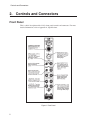
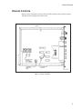
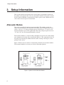
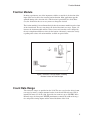
Model 2126
Constant Fraction
Discriminator
9231701B
User’s Manual
Copyright 2005, Canberra Industries, Inc. All rights reserved.
The material in this document, including all information, pictures,
graphics and text, is the property of Canberra Industries, Inc. and
is protected by U.S. copyright laws and international copyright
conventions.
Canberra expressly grants the purchaser of this product the right
to copy any material in this document for the purchaser’s own use,
including as part of a submission to regulatory or legal authorities
pursuant to the purchaser’s legitimate business needs.
No material in this document may be copied by any third party, or
used for any commercial purpose, or for any use other than that
granted to the purchaser, without the written permission of
Canberra Industries, Inc.
Canberra Industries, 800 Research Parkway, Meriden, CT 06450
Tel: 203-238-2351 FAX: 203-235-1347 http://www.canberra.com
The information in this document describes the product as
accurately as possible, but is subject to change without notice.
Printed in the United States of America.
Table of Contents
1. Introduction . . . . . . . . . . . . . . . . . . . . . . . . . . . . . 1
2. Controls and Connectors . . . . . . . . . . . . . . . . . . . . . . 2
Front Panel . . . . . . . . . . . . . . . . . . . . . . . . . . . . . . . . . . . . . . . . . . . . . 2
Internal Controls. . . . . . . . . . . . . . . . . . . . . . . . . . . . . . . . . . . . . . . . . . . 3
3. Setup Information . . . . . . . . . . . . . . . . . . . . . . . . . . 4
Attenuator Module . . . . . . . . . . . . . . . . . . . . . . . . . . . . . . . . . . . . . . . . . 4
Fraction Module . . . . . . . . . . . . . . . . . . . . . . . . . . . . . . . . . . . . . . . . . . . 5
Count Rate Range . . . . . . . . . . . . . . . . . . . . . . . . . . . . . . . . . . . . . . . . . . 5
The Modes. . . . . . . . . . . . . . . . . . . . . . . . . . . . . . . . . . . . . . . . . . . . . . 6
Output Width Range. . . . . . . . . . . . . . . . . . . . . . . . . . . . . . . . . . . . . . . . . 7
Standard/Alternate Power Supplies . . . . . . . . . . . . . . . . . . . . . . . . . . . . . . . . . 8
Standard Setup. . . . . . . . . . . . . . . . . . . . . . . . . . . . . . . . . . . . . . . . . . . . 8
4. Operation. . . . . . . . . . . . . . . . . . . . . . . . . . . . . . . 9
Input Signals. . . . . . . . . . . . . . . . . . . . . . . . . . . . . . . . . . . . . . . . . . . . . 9
Operating Mode . . . . . . . . . . . . . . . . . . . . . . . . . . . . . . . . . . . . . . . . . . 10
Constant Fraction (CF) Mode . . . . . . . . . . . . . . . . . . . . . . . . . . . . . . . . . 10
Constant Fraction With Slow Risetime Reject (SR) Mode . . . . . . . . . . . . . . . . . . 10
Leading Edge (LE) Mode . . . . . . . . . . . . . . . . . . . . . . . . . . . . . . . . . . . 11
Delay Cable . . . . . . . . . . . . . . . . . . . . . . . . . . . . . . . . . . . . . . . . . . . . 11
Walk Trim . . . . . . . . . . . . . . . . . . . . . . . . . . . . . . . . . . . . . . . . . . . . . 11
Threshold Adjustment . . . . . . . . . . . . . . . . . . . . . . . . . . . . . . . . . . . . . . . 13
Outputs and Width Control . . . . . . . . . . . . . . . . . . . . . . . . . . . . . . . . . . . . 13
5. Circuit Description . . . . . . . . . . . . . . . . . . . . . . . . . 15
Power Supply . . . . . . . . . . . . . . . . . . . . . . . . . . . . . . . . . . . . . . . . . . . 15
Constant Fraction and Threshold Circuits . . . . . . . . . . . . . . . . . . . . . . . . . . . . . 15
A. Specifications . . . . . . . . . . . . . . . . . . . . . . . . . . . 18
Inputs . . . . . . . . . . . . . . . . . . . . . . . . . . . . . . . . . . . . . . . . . . . . . . . . 18
Outputs . . . . . . . . . . . . . . . . . . . . . . . . . . . . . . . . . . . . . . . . . . . . . . . 18
Front Panel Controls . . . . . . . . . . . . . . . . . . . . . . . . . . . . . . . . . . . . . . . . 18
Internal Controls . . . . . . . . . . . . . . . . . . . . . . . . . . . . . . . . . . . . . . . . . . 19
Performance . . . . . . . . . . . . . . . . . . . . . . . . . . . . . . . . . . . . . . . . . . . . 19
Typical Cable Lengths (RG-58) . . . . . . . . . . . . . . . . . . . . . . . . . . . . . . . . . . 20
Power Requirements . . . . . . . . . . . . . . . . . . . . . . . . . . . . . . . . . . . . . . . . 20
Physical . . . . . . . . . . . . . . . . . . . . . . . . . . . . . . . . . . . . . . . . . . . . . . 20
B. Installation Considerations . . . . . . . . . . . . . . . . . . . . 21
ii
1. Introduction
The Model 2126 is a 200 MHz Constant Fraction Discriminator in a single width
NIM. It has independent controls for threshold, walk, output pulse width, and operating mode, and provides maximum flexibility for use in any timing application.
The 2126 is fully dc coupled and provides two operating modes for use over a wide
range of input count rates. In the standard operating mode, the 2126 operates to 150
MHz with the front panel potentiometer controlling both the output width and the
internal dead time. Alternatively, a special high rate operating mode can be selected
which provides operation to 200 MHz (typically 250 MHz) with fixed output width
and dead time.
The 50 Ω input of the 2126 accepts negative pulses with amplitudes up to –5 V. Input
protection is provided for inputs outside the expected range. An internal jumper can
connect a X2 attenuator to each input to extend the input range to –10 V. A plug-in
module provides a means of changing the constant fraction (factory set to 40%). In addition to its normal Constant Fraction (CF) timing mode, the 2126 provides a Constant
Fraction with Slow Risetime Reject (SR) timing mode. the SR mode rejects the slow
rise time signals characteristic of some detectors, thus improving timing performance.
Two independent fast negative timing outputs and two independent positive timing
outputs are provided. This provides maximum flexibility for most timing applications.
In addition, a front panel LED indicates the presence of input signals.
The 2126 can operate from standard NIM bin ±12 V and ±24 V power supplies. If a
±6 V power supply is available, the 2126 can be configured to use those supplies for
most of its power requirements.
1
Controls and Connectors
2. Controls and Connectors
Front Panel
This is a brief description of the 2126’s front panel controls and connectors. For more
detailed information, refer to Appendix A, Specifications.
Figure 1 Front Panel
2
Internal Controls
Internal Controls
Figure 2 shows the internal layout of the 2126. The function of the internal controls
and their normal configuration is illustrated.
Figure 2 Internal Controls
3
Setup Information
3. Setup Information
This section describes the function of the various jumpers and modules mounted on
the printed circuit board of the 2126. Any adjustments should be made prior to installing the 2126 in a NIM bin or connecting the 2126 to a power source. Remove the left
cover of the 2126 to expose the circuit board.
Attenuator Module
The 2126 is provided with an input attenuator module. This module provides the
choice of no attenuation or X2 attenuation of the input signal. The input range of the
2126 is –5 mV to –5 V. If the peak input signal is expected to be –5 V or less, no attenuation should be selected. For applications where the peak input signal is between
–5 V and –10 V, the X2 attentuation should be selected.
The attenuator module is a small assembly containing two resistors and a short jumper
wire mounted near the front of the circuit board (Figure 2). The attenuation factor can
be changed by removing the module from the socket, rotating it 180 degrees, and replacing it in the socket.
Figure 3 illustrates the two choices of attenuation provided by the attenuator module.
The attenuator modules are factory set to the no attenuation position.
Figure 3 Options for the Attenuator Module
4
Fraction Module
Fraction Module
In timing experiments, one of the important variables to consider is the fraction of the
input signal used to derive the constant fraction function. Most applications provide
optimum timing with a fraction of 0.4. This fraction is provided by the 2126. However, the 2126 offers the user an easy means to change the fraction.
The fraction module is located immediately below the attenuator module near the front
of the circuit board. The user can change the desired fraction in two ways. Figure 4 illustrates the fraction module and lists values for two resistors that can be changed by
the user to implement different values for the fraction. Alternately, contact the factory
regarding other values of fraction modules available on special order.
Figure 4 Constant Fractiion Module, Including
Resistor Values for Field Changes
Count Rate Range
Two count rate ranges are provided on the 2126. The user can select the desired count
rate range by moving a jumper mounted on the circuit board. NOrmal range (NO) is
intended for most uses of the 2126. It provides for count rates up to 150 MHz. In the
NOrmal range, the front panel WIDTH potentiometer controls the width of the negative and positive timing outputs and the internal deadtime of the 2126.
5
Setup Information
In certain extremely high rate applications, the user should select the High Rate range
(HR). This range provides for usable count rates of greater than 200 MHz. However,
certain precautions should be observed in using the HR range of the 2126. In this
range, the front panel WIDTH potentiometer is inactive. The width of the negative
timing outputs and the internal deadtime of the 2126 are internally set at approximately 2 ns. The input signal should be approximately 2 ns in width and show a clean
return to the baseline in order to fully utilize the speed of the HR mode of the 2126.
In addition, the user should verify that companion NIM modules used with the 2126 in
its HR range are capable of accepting negative NIM inputs of 2 ns width. The NO/HR
jumper is located just to the right of A2 on the circuit board. See Figure 2. NO is the
upper position of the jumper. HR is the lower position of the jumper. The 2126 is
shipped in the NO position.
The Modes
The 2126 provides three operating modes: Constant Fraction (CF), Constant Fraction
with Slow Reject (SR), and Leading Edge (LE). Refer to “Operating Mode” on page
10 for a description of the modes.
• The Constant Fraction (CF) mode is intended for use with detectors such as fast
plastic detectors which exhibit fast rise time outputs with little risetime
variation.
• The Constant Fraction with Slow Risetime Reject (SR) mode is often used with
germanium detectors which exhibit a wide range of rise time variation.
• The Leading Edge mode is used with detectors which provide fast outputs with
little amplitude or risetime variation.
CF and SR Modes
Both Constant Fraction (CF) and Constant Fraction with Slow Risetime reject (SR)
modes use the internal fraction module supplied with the 2126. To use either mode,
verify that the fraction module is properly installed in its socket near the front of the
circuit board. Figure 4 shows the proper installation of the fraction module. With the
fraction module installed, the front panel Mode Switch allows selection of Constant
Fraction (CF) mode or Constant Fraction with Slow Risetime reject (SR).
LE Mode
To select the Leading Edge Mode, remove the Constant Fraction module from its
socket near the front of the board and replace it with the Leading Edge module. A
socket is provided near the bottom of the circuit board to hold the unused module. The
front panel Mode Switch should be set to Leading Edge (LE). Figure 5 shows the
proper installation of the Leading Edge module.
6
Output Width Range
Figure 5 Leadilng Edge Module
Table 1 summarizes the module and switch settings for the three operating modes.
Table 1 Operating Mode Summary
Operating Mode
Module
Front Panel
Switch
Constant Fraction
Fraction
CF
Constant Fraction with
Slow Risetime Reject
Fraction
SR
Leading Edge
Leading Edge
LE
Output Width Range
Two ranges of adjustment are provided for the front panel WIDTH potentiometer.
Since the WIDTH potentiometer controls the output widths as well as the 2126’s internal dead time, the proper range for the WIDTH adjustment should be selected. Use X1
for fast plastic detectors and most sodiurn iodide detectors. Detectors that provide input signals of 100 ns width or greater, or that cause baseline perterbations extending
longer than 100 ns, should use the X5 range. The X1/X5 jumper is located below A2
on the circuit board. See Figure 2. X1 is to the right and X5 is to the left. The X1/X5
jumper is shipped in the X1 position.
7
Setup Information
Standard/Alternate Power Supplies
The 2126 can operate from NIM bins equipped with the standard ±12V and +24 V
power supplies as well as those with the optional –6 V power supply. Since the 2126
draws current is excess of the single-width NIM module limit when connected to a
±12 V supply, operation of the 2126 from ±6 V will reduce the current drawn to
within the single-width module limits. If a ±6 V power supply is available, set the input power jumpers to the 6 V position, otherwise use the 12 V position. See Figure 2.
The 6 V position for both jumpers is towards the bottom of the module and is labeled
‘B’. The 12 V position is toward the top of the module and is labeled ‘A’.
Standard Setup
The Model 2126 is shipped from the factory in the standard configuration:
8
Attenuator module
:
X1 (no attenuation)
Fraction module
:
Constant Fraction, F = 0.4
Timing range
:
NO (normal)
Operating mode
:
CF (constant fraction)
Output width range
:
X1 (1–100 ns)
Power supply
:
±12 V
Input Signals
4. Operation
The 2126 is intended to be operated in a NIM bin equipped with a power supply providing ±12 V and ±24 V. Alternately, a NIM bin providing +12 V, ±24 V and ±6 V
can be used. See “Standard/Alternate Power Supplies” (page 8). For lab bench testing,
a NIM power supply extension cable may be used. However, excessive voltage drops
in the extension cable may be encountered due to the relatively high current requirements of the 2126. For use in experiments, secure installation in a NIM bin is recommended. The NIM bin power supply should be off when the 2126 or other NIM are
installed or removed from the NIM bin.
Input Signals
Typical input signals to the 2126 are generated by a scintillation detector using a
photomultipiier tube or a solid state detector with a charge sensitive preamp and timing filter amplifier. Such signals are negative going from a baseline of ground.
Risetimes can vary from 1 ns to greater than 100 ns, and widths from 1 ns to greater
than 500 ns. For the laboratory test bench, a logic pulser can be used as an input to the
2126. See Figure 6 for a typical input signal produced by a logic pulser.
Figure 6 Typical Input Signal Produced by a Logic Pulser
9
Operation
Operating Mode
Selection of operating mode depends or the requirements of the given experiment.
Some general compromises worth considering are discussed in the following paragraphs.
Constant Fraction (CF) Mode
In the Constant Fraction (CF) mode, timing is derived from a comparison between a
fixed ratio (40% in the 2126) and the peak amplitude of each successive pulse. This instantaneous self-reference yields a time mark that is theoretically independent of the
pulse height, as contrasted to the behavior of the leading edge mode. In the 2126, the
ratio reference signal is taken internally, and the full amplitude pulse is delayed for the
comparison by an external cable connected between the two front panel DELAY connectors.
When the length of this external cable is chosen to generate a time delay less than the
rise time of the input pulse, the resulting time mark is stabilized for both amplitude
and rise time variations of that pulse. This is the basis for ARC (Amplitude and Rise
time Compensated) timing.
The compromise in Constant Fraction (and also ARC) timing is the ability to provide
proper delays for the rise time of the input pulse considering either rate and pileup effects or the distortions introduced by varying wavefront shapes due to charge collection deficit, ballistic effects, or trapping effects in the detector. It is these
accommodations that lead to empirical determinations of the optimum delay cable
length for a given detector and setup.
Constant Fraction With Slow Risetime Reject (SR) Mode
In the Constant Fraction with Slow Risetime reject (SR) mode, a further accommodation is offered for the longer rise times of solid state detectors. The timing mark for the
Constant Fraction is derived from the slightly delayed pulse, with the presumption that
the THRESHOLD level has been set quite low and this level is exceeded prior to the
derivation of the timing mark.
In the case of solid state detectors, where long varying wavefronts of the input pulse
are common, a relatively short delay cable is frequently used and the above timing
premise may not be satisfied. In that case, the amplitude discriminator keyed to the
THRESHOLD setting may switch late, and the resulting timing will represent some
mix of the intended Constant Fraction timing with Leading Edge timing. This effect
causes either tailing or a satellite peak in a time spectrum.
In the SR mode, a logic alternation causes rejection of pulses which do not exceed the
THRESHOLD prior to the derived Constant Fraction timing mark. The result is enhanced timing resolution due to elimination of the Leading Edge errors, but with some
loss of counting efficiency.
10
Delay Cable
Leading Edge (LE) Mode
The Leading Edge mode is used less often than the two Constant Fraction modes. It is
typically used for detectors with fast risetimes and little amplitude variation. Since the
Constant Fraction function is disabled when the 2126 is used in Leading Edge mode,
amplitude and risetime variation can introduce timing walk. If the input signals are all
essentially of the same amplitude and risetime, the Leading Edge mode can offer good
timing performance.
Delay Cable
The delay cable used to set the Constant Fraction timing mark should provide a delay
less than the known rise time of the applied input pulse for full compensation of both
amplitude and rise time variations (for a fixed shape). For fast and moderately fast detector pulses (up to 10 ns rise time) a delay of nominally 75% of the rise time is most
effective. For solid state detectors, a delay of 40% of the pulse rise time is commonly
used for the reasons given above.
The internal delay of the 2126 is 0.3 ns, and this must be corrected by picking a suitable cable. For example, if the detector rise time is 4 ns, a 3 ns delay would be recommended. The external cable length, estimated on the basis of 4.8 ns per meter for
RG-58 cable, would be:
L=
External Delay Total Delay − Internal Delay
=
4.8
4.8
L=
3.0 − 0.3 ns
= 56.3 cm ( ≈ 22 in.)
4.8 ns / m
Walk Trim
The adjustment of the amplitude sensitive variation of the timing mark (time walk) in
the Constant Fraction and CFRR modes remains a less exact procedure. Proper adjustment is possible only when the dc offset present on the input to the 2126 is less than
±6 mV dc. Thus detector leakage or dark current errors must be minimized before attempting adjustment.
11
Operation
Laboratory trimming of the unit can be demonstrated by using a suitable pulse generator with a known fast, clean wavefront and a delay chosen as discussed above. A very
broadband 50 ohm attenuator, such as the Hewlett Packard HP-3496, or one whose
time walk is very precisely known, should be used. An externally triggered oscilloscope capable of displaying at least 1 ns/division is also necessary. Step attenuations
should be then yield a stable time position of the 2126's output signal when starting
from a reference –5 V peak pulse input. Care must be taken that the pulse generator
offset is small and does not change for different attenuatcr settings. The WALK
ADJUST trimming potentiometer can be used to find the best adjustment of the finite
time walk over a narrower amplitude range as desired.
When the 2126 is used with the intended detector, timing resolution may be trimmed
experimentally by successive measurements in the setup at hand. A qualitative monitoring is available by monitoring the front panel INSPECT output with an oscilloscope. For fast detectors, the output should indicate an attenuated logic low ECL level
(approx. –0.19 V dc, into 50 Ω) where noise just disappears into this level and pulses
are seen as transitions to logic high ECL (approx. –0.085 V do into 50 Ω). Reference
Figure 7.
Figure 7 Walk Inspect Wave Form Using Plastic Detectors
12
Threshold Adjustment
For slower detectors, a noise band between the ECL levels may be seen, with transitions to ECL logic high and low of about equal intensity. Reference Figure 8.
Figure 8 Walk Inspect Wave Form for Slow Detectors
Threshold Adjustment
The 2126 threshold adjustment can be used as a lower level control to select the
threshold above which input pulses will generate an. output signal. A front panel test
point is provided to allow easy measurement of the selected threshold voltage. As a
general rule of thumb, select a threshold voltage as high as possible while not excluding input signals of interest. Unless experimental conditions dictate otherwise, do not
use minimum settings of the threshold, since input signals often show ringing or baseline perterbations which may generate unwanted outputs.
Outputs and Width Control
The 2126's negative logic outputs are intended to drive 50 ohm loads through any reasonable length of suitable 50 ohm coaxial cable (such as RG-58). Figure 9 shows the
typical negative output pulse shapes into 50 ohm loads, with the WIDTH control set to
minimum. For optimum performance, terminate unused negative outputs in 50 ohms.
13
Operation
Figure 9 Typical Negative Output Pulses Into 50 Ohms Load
Since the WIDTH control also sets the DEAD TIME following a given pulse in the
NOrmal count rate range, the user should set this control consistent with the pulse rate
requirements of the given experiment. In the minimum (fully counterclockwise) position of the WIDTH control, a count rate in excess of 150 MHz can be expected for the
NOrmal mode of the 2126. The WIDTH control off the 2126 is inoperative in the
High Rate mode.
The 2126's positive logic outputs are designed to drive relatively high impedance
loads with logic levels of nominally 0 and +5 V. Since this type of output is inherently
slower than current mode outputs (the negative outputs), the positive outputs may not
provide proper logic transitions at the high count rates the 2126 is capable of.
14
Power Supply
5. Circuit Description
The 2126 is a high performance Constant Fraction Discriminator in a single width
NIM. It also includes a power supply circuit to provide logic power to the unit. This
section describes the operation of both the power supply and the Constant Fraction
Discriminator.
Power Supply
The 2126 consists primarily of ECL logic which uses a supply voltage of –5.2 V. In
addition, a TTL supply voltage of +5.0 V is required. Two methods of obtaining these
voltages are provided, selectable by a jumper plug. When the 2126 is used in a NIM
bin with the standard supply voltages of ±12 V and +24 V, the logic supply voltages
of –5.2 and +5.0 V are provided by adjustable three-terminal regulators. Q1 and 02,
together with their associated circuitry, provide stable well-regulated logic voltages. If
a ±6 V NIM power supply is available, the circuit board’s jumpers can be set to provide the required logic voltages directly from the +6 V supplies. In each case, a diode
(D1 for +6 V, D2 for –6 V) drops the power supply voltages to the logic voltages required by the 2126. In either case, the –2 V ECL pull-down voltage is provided by an
additional three-terminal regulator (Q3), operating from the –5.2 V logic supply.
Constant Fraction and Threshold Circuits
The input signal is applied directly to pin 10 of the threshold comparator. Dl provides
a temperature compensated voltage which is divided to produce –1 V across the
threshold potentiometer (RV1). The wiper voltage of RV1, which varies from –5 mV
to –1 V, is applied to pin 10 of the threshold comparator.
The constant fraction function is implemented at the inputs of the ultrafast comparator
A4b. The input attenuator module is a X2 attenuator that maintains the proper 50 ohm
input impedance. It can be rotated to provide no attenuation (short between the input
and pin 5 of the fraction module) or X2 attenuation (100 ohms between the input and
pin 5 of the fraction module). The fraction module serves to attenuate both the prompt
and delayed inputs to the constant fraction comparator (A4b) while providing the
proper 50 ohm input impedance. The prompt input to A4b (pin 8) is attenuated more
than the delayed input (pin 7) resulting in the fraction f = 0.4. This combination of attenuation and delay provides the following signals at the inputs of the constant fraction
comparator:
pin 8: 0.3 input amplitude, prompt
pin 7: 0.67 input amplitude, delayed by cable selected
15
Circuit Description
See Figure 5.1 which illustrates the signals associated with the constant fraction and
threshold comparators.
Prior to the application of an input signal, the inverting output of A4b (pin 2) can be in
either logic state depending on the offset voltage applied to A4b pin 8 by the WALK
ADJUST potentiometer. Upon application of an input signal, A4b pin 8 initially is
lower than A4b pin 7, driving the inverting output A4b (pin 2) to a logic high. When
the delayed signal arrives at A4b pin 7, it causes this pin to become more negative
than A4b pin 8 which causes the inverting output (A4b pin 2) to fall to a logic low.
The timing of this low-going signal is input amplitude independent. The inverting out put of the threshold comparator (A4a pin 15) is normally a logic high. When an input
signal is applied, the inverting output of A4a goes to a logic low when the input signal
crosses the selected threshold voltage. This logic transition occurs ahead of the output
from the constant fraction comparator since the input to the constant fraction output is
delayed by the front panel delay cable. Thus, the 10H209 OR/NOR (A3b) gate has a
high input from the threshold comparator and an indeterminant input from the constant
fraction comparator prior to the application of an input signal. When an input is applied, A3b pin 7 goes low if the threshold is crossed. Shortly later, A3b pin 5 goes low
due to the constant fraction comparator. The inverting output ofA3b (pin 3) goes high
when the constant fraction comparator fires if the threshold was crossed. This logic
signal is the clock to the ultra fast 11C70D flip-flop A2.
When the 2126 is used in the Constant Fraction mode, the D input of A2 (pin 11) is
held at a logic low by A3a pin 14. After the preceding signal was processed, A2 was
left in the SET state with the 0 output high and the Q output low. When the clock signal arrives at A2 pin 7 from A3 pin 3, the D flip-flop is RESET by clocking in the low
at A2 pin 11, the outputs are active and the channel is unable to process further inputs.
A2 is SET via the HR or NO jumper, thus terminating the outputs and the internal
deadtime. In the NOrmal mode of operation, the Q output of A2 is pulled down by the
current source consisting of Q9 and associated bias resistors. The line driver/receiver
A1a senses the falling edge of A2 pin 2 and drives the SET input of A2 high, thereby
SETting A2 and terminating the output. The front panel WIDTH potentiometer varies
the current source Q9 and thus varies the rate of fall of A2 pin 2. Thus, the width of
the one-shot formed from A2 is varied. In the High Rate mode, the current source Q9
and A1a are bypassed. The rising edge of A2 Q is coupled directly to the SET input of
A2. Thus, the propagation delays associated with A2 determine the output widths and
the internal dead time.
In the Slow Reject mode, the circuit functions virtually the same. The D input of A2 is
driven by A3a pin 14, which now has a low going logic signal driven by the threshold
comparator through A3a. A slight delay is provided by R14 and C7. For fast rise time
signals, the D input of A2 is low before the clock drives pin 7 high. However, slow
rise time signals cause the threshold comparator to fire slightly later. For these slow
rise time signals, the falling edge of the signal at A2 pin 11 arrives after the clock at
pin 7 and a high is clocked into the flip-flop. Since the flip-flop is already SET, no
change occurs at its output and the input signal is ignored.
16
Constant Fraction and Threshold Circuits
In the Leading Edge mode, the Constant Fraction comparator (A4b) is disabled in a
state that permits the Leading Edge comparator (A4a) to generate the clock for
flip-flop A2.
The line driver/receiver A1b is driven by the Q output of A2 and serves to drive the
two independent negative outputs differentially. It also toggles A1c, the one-shot driving the front panel LED. The negative output transistors are conventional differential
switches with the collectors driving the 50 ohm outputs directly.
Figure 10 Timing Signals
17
Specifications
A. Specifications
Inputs
INPUT – Accepts –5 mV to –5 V (–10 mV to –10 V with internal X2 attenuator) linear pulses; rise time ≥1 ns; Zin = 50 Ω, dc coupled; front panel BNC connector protected to ±100 V (duration limited).
DELAY – Two BNC connectors between which a delay cable is connected to form the
internal constant fraction signal. Recommended lengths are based upon RG-58 cable
propagation delay of ≈4.8 ns/m (1.5 ns/ft) to provide a delay of ≈ 0.2 trise for germanium detectors and ≈ 0.8 trise for most other detector types.
Outputs
WALK INSPECT – Displays output signal of zero-crossing discriminator for use in
trimming time walk; Zout = 50 Ω; front panel BNC connector.
NEGATIVE OUTPUTS – Two independent negative current outputs, each providing
–16 mA into 50 Ω; rise time ≈ 1 ns; pulse width controlled by WIDTH potentiometer
in Normal mode; 2 ns nominal in High Rate mode; dc coupled; front panel BNC connectors.
POSITIVE OUTPUTS – Two independent positive voltage outputs, each providing
2 V minimum into 50 Ω, rise time ≤10 ns; pulse width controlled by WIDTH potentiometer in Normal mode, undefined in High Rate mode; dc coupled; front panel BNC
connectors.
Front Panel Controls
THRESHOLD – Front panel 10-turn potentiometer to set acceptance threshold for input pulses; range –5 mV to –1 V.
TIMING MODE – Front panel three-position rotary switch to select constant fraction
with slow rise time reject (SR), basic constant fraction timing (CF), or leading edge
timing (LE) modes of operation.
WALK ADJUST – Front panel potentiometer to compensate walk of the internal
zero-crossing discriminator.
18
Internal Controls
WIDTH – Front panel 10-turn potentiometer to vary internal dead time and width of
negative outputs in Normal mode; range ≈2–100 ns or ≈ 10–500 ns as determined by
internal jumper. Inoperative in High Rate mode.
Internal Controls
ATTENUATION – Board-mounted DIP jumper selects no attenuation or X2 attenuation of input signal.
FRACTION – Board-mounted DIP jumper selects value of constant fraction; 0.4 standard, other values available by special order.
OPERATING MODE – Board-mounted jumper selects NOrmal (NO), or High Rate
(HR) operating mode.
OUTPUT WIDTH RANGE – Board-mounted jumper selects ≈2–100 ns (X1) or
10–500 ns (X5) output WIDTH range.
POWER SUPPLY – Board-mounted jumpers select ±12 V or ±6 V as input power for
2126 logic.
Performance
DYNAMIC RANGE – 1000:1.
WALK – ±50 ps (±30 ps typical) for a 1 ns rise time pulse over a 100:1 dynamic range
(referenced to –5 V) in the CF mode.
COUNTING RATE – Normal mode to 150 MHz, as limited by dead time; High Rate
mode to 200 MHz.
PULSE PAIR RESOLUTION – Normal mode <7 ns, as limited by dead time; High
Rate mode ≤5 ns.
THRESHOLD STABILITY – ≥±0.02%/°C (±200 ppm/°C).
TEMPERATURE RANGE – 0 to +50 °C.
THRESHOLD LINEARITY – ±0.25% integral.
19
Specifications
Typical Cable Lengths (RG-58)
For Plastic, NaI, and SSB detectors – 0.3 to 1.0 m (1.0 to 3.3 ft).
For Planar Ge Detectors – 1.0 to 2.0 m (3.3 to 6.6 ft).
For Coaxial Ge Detectors – 2.0 to 4.0 m (6.6 to 13 ft).
Power Requirements
Power jumpers set to ±12 V:
+12 V dc – 30 mA
–12 V dc – 350 mA*
Power jumpers set to ±6 V:
+12 V dc – 0 mA
–12 V dc – 12 mA
+6 V dc – 30 mA
–6 V dc – 340 mA*
*Exceeds the normal NIM power allotment of 167 mA for a single-width module.
Physical
SIZE – Standard single width NIM module 3.43 x 22.12 cm (1.35 x 8.71 in.).
NET WEIGHT – 0.9 kg (2.0 lb).
SHIPPING WEIGHT – 1.8 kg (4.0 lb).
20
B. Installation Considerations
This unit complies with all applicable European Union requirements.
Compliance testing was performed with application configurations commonly used for
this module; i.e. a CE compliant NIM Bin and Power Supply with additional CE compliant application-specific NIM were racked in a floor cabinet to support the module
under test.
During the design and assembly of the module, reasonable precautions were taken by
the manufacturer to minimize the effects of RFI and EMC on the system. However,
care should be taken to maintain full compliance. These considerations include:
• A rack or tabletop enclosure fully closed on all sides with rear door access
• Single point external cable access
• Blank panels to cover open front panel Bin area
• Compliant grounding and safety precautions for any internal power distribution
• The use of CE compliant accessories such as fans, UPS, etc.
Any repairs or maintenance should be performed by a qualified Canberra service
representative. Failure to use exact replacement components, or failure to reassemble
the unit as delivered, may affect the unit’s compliance with the specified EU
requirements.
21
Notes
22
Canberra (we, us, our) warrants to the customer (you, your) that for a period of ninety (90) days from the date of
shipment, software provided by us in connection with equipment manufactured by us shall operate in accordance
with applicable specifications when used with equipment manufactured by us and that the media on which the
software is provided shall be free from defects. We also warrant that (A) equipment manufactured by us shall be
free from defects in materials and workmanship for a period of one (1) year from the date of shipment of such
equipment, and (B) services performed by us in connection with such equipment, such as site supervision and
installation services relating to the equipment, shall be free from defects for a period of one (1) year from the date of
performance of such services.
If defects in materials or workmanship are discovered within the applicable warranty period as set forth above, we
shall, at our option and cost, (A) in the case of defective software or equipment, either repair or replace the
software or equipment, or (B) in the case of defective services, reperform such services.
LIMITATIONS
EXCEPT AS SET FORTH HEREIN, NO OTHER WARRANTIES OR REMEDIES, WHETHER STATUTORY,
WRITTEN, ORAL, EXPRESSED, IMPLIED (INCLUDING WITHOUT LIMITATION, THE WARRANTIES OF
MERCHANTABILITY OR FITNESS FOR A PARTICULAR PURPOSE) OR OTHERWISE, SHALL APPLY. IN NO
EVENT SHALL CANBERRA HAVE ANY LIABILITY FOR ANY SPECIAL, EXEMPLARY, PUNITIVE, INDIRECT
OR CONSEQUENTIAL LOSSES OR DAMAGES OF ANY NATURE WHATSOEVER, WHETHER AS A RESULT
OF BREACH OF CONTRACT, TORT LIABILITY (INCLUDING NEGLIGENCE), STRICT LIABILITY OR
OTHERWISE. REPAIR OR REPLACEMENT OF THE SOFTWARE OR EQUIPMENT DURING THE
APPLICABLE WARRANTY PERIOD AT CANBERRA'S COST, OR, IN THE CASE OF DEFECTIVE SERVICES,
REPERFORMANCE AT CANBERRA'S COST, IS YOUR SOLE AND EXCLUSIVE REMEDY UNDER THIS
WARRANTY.
EXCLUSIONS
Our warranty does not cover damage to equipment which has been altered or modified without our written
permission or damage which has been caused by abuse, misuse, accident, neglect or unusual physical or
electrical stress, as determined by our Service Personnel.
We are under no obligation to provide warranty service if adjustment or repair is required because of damage
caused by other than ordinary use or if the equipment is serviced or repaired, or if an attempt is made to service or
repair the equipment, by other than our Service Personnel without our prior approval.
Our warranty does not cover detector damage due to neutrons or heavy charged particles. Failure of beryllium,
carbon composite, or polymer windows, or of windowless detectors caused by physical or chemical damage from
the environment is not covered by warranty.
We are not responsible for damage sustained in transit. You should examine shipments upon receipt for evidence
of damage caused in transit. If damage is found, notify us and the carrier immediately. Keep all packages,
materials and documents, including the freight bill, invoice and packing list.
When purchasing our software, you have purchased a license to use the software, not the software itself. Because
title to the software remains with us, you may not sell, distribute or otherwise transfer the software. This license
allows you to use the software on only one computer at a time. You must get our written permission for any
exception to this limited license.
BACKUP COPIES
Our software is protected by United States Copyright Law and by International Copyright Treaties. You have our
express permission to make one archival copy of the software for backup protection. You may not copy our
software or any part of it for any other purpose.
Revised 1 Apr 03