1
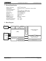
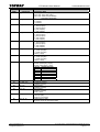
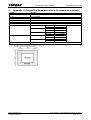
TOPWAY displays
[email protected]
www.topwaydisplays.eu
LMT057DNAFWU-AAN
LCD Module User Manual
Rev.
0.1
0.2
0.3
0.4
0.5
0.6
Prepared by:
Checked by:
Approved by:
Date:
Date:
Date:
Descriptions
Preliminary New release
Typing Correction in Dot Pitch
Typing Correction in 6.3.3 Opcode [82] discription
Jumper Setting Correction
Typing Correction in 6.1 & 6.3,Add 6.4
Update General Specification
ZZZWRSZD\GLVSOD\VHX
LQIR#WRSZD\GLVSOD\VHX
Release Date
2007-04-13
2007-04-20
2007-05-17
2007-06-08
2008-09-28
2009-06-22
Document Name: LMT057DNAFWU-AAN-Manual-Rev0.6
Page: 1 of 17
TOPWAY
LCD Module User Manual
LMT057DNAFWU-AAN
Table of Content
1.
General Specification .............................................................................................................. 3
2.
Block Diagram.......................................................................................................................... 3
2.1
Terminal Functions................................................................................................................................................. 4
3.
2.1.1
MCU Terminal (K1, 8bit-Data, 1bit-Add) ..................................................................... 4
2.1.2
RS232 Terminal (K3)................................................................................................... 4
Absolute Maximum Ratings.................................................................................................... 5
4.
Electrical Characteristics........................................................................................................ 5
4.1
DC Characteristics (MCU terminal) ........................................................................................................................ 5
4.2
LED Backlight Circuit Characteristics..................................................................................................................... 5
4.3
AC Characteristics ................................................................................................................................................. 5
5.
Optical Characteristics............................................................................................................ 6
6.
Function Specifications .......................................................................................................... 7
6.1
Hard-wired Setting ................................................................................................................................................. 7
6.2
VR setting .............................................................................................................................................................. 7
6.3
Command Packet Format ...................................................................................................................................... 8
6.3.1
6.3.2
6.3.3
6.3.4
6.4
Command Packet Format ........................................................................................... 8
Opcode Group............................................................................................................. 8
Opcode Description..................................................................................................... 8
Registers Table ......................................................................................................... 10
UART Serial Host Communication Packet Format............................................................................................... 15
7.
Precautions of using LCD Modules ..................................................................................... 16
8.
Appendix A <Inspection items and criteria for appearance defect>................................. 17
ZZZWRSZD\GLVSOD\VHX
LQIR#WRSZD\GLVSOD\VHX
Document Name: LMT057DNAFWU-AAN-Manual-Rev0.6
Page: 2 of 17
TOPWAY
LCD Module User Manual
LMT057DNAFWU-AAN
1. General Specification
Display Technology :
Display Mode :
Screen Size(Diagonal) :
Outline Dimension :
Active Area :
Number of dots :
Dot Pitch :
Pixel Configuration :
Backlight :
Surface Treatment :
Viewing Direction :
Operating Temperature :
Storage Temperature :
a-Si TFT active matrix
TN Type Full Color / Transmissive / Normal White
5.7”
155.2 x 109.0 x 12.7 MAX. (mm)
(see attached drawing for details)
115.2 x 86.4 (mm)
320 x 3 (RGB) x 240
0.12 x 0.36 (mm)
RGB Stripe
LED
Anti-Glare Treatment
12 o’clock
-20 ~ +70°C
-30 ~ +80°C
K3
TxD, RxD
VDD, VSS
RS232 I/F
(optional)
256kx8
FLASH ROM
(optional)
64kx16
SRAM
LCD
Controller
K1
D0 – D7
A1,
/RESET, /CS
WAIT
/WR0, /RD
VDD
VSS
VCOM Circuit
320(x3) x 240 pixels
TFT Panel
Source Driver with TCON
HX8218 or equivalent
Power Circuit
Backlight Supply
ZZZWRSZD\GLVSOD\VHX
LQIR#WRSZD\GLVSOD\VHX
Gate Driver
HX8615 or equivalent
2. Block Diagram
Backlight Circuit
Document Name: LMT057DNAFWU-AAN-Manual-Rev0.6
Page: 3 of 17
TOPWAY
2.1
2.1.1
Pin
No.
1
2
3
4
5
LCD Module User Manual
LMT057DNAFWU-AAN
Terminal Functions
MCU Terminal (K1, 8bit-Data, 1bit-Add)
Pin
I/O
Descriptions
Name
VSS
Power Input
Power Supply GND (0V)
VDD
Power Input
Positive Power Supply
A1
Input
Register Select
A1=LOW: Accessing Address F004 (command package port)
A1=High: Accessing Address F006 (data and status port)
6
/CS
Input
Chip Select Inputs
7
/RESET
Input
Reset Signal Input
/CS=LOW: Data IO is enabled
/RESET=LOW: Reset
/RESET=HIGH: Normal
8
:
15
16
17
D0
:
D7
WAIT
/RD
Bi-directional
I/O
8-bit bi-directional data bus
Output
Input
Wait Signal
Read enable input, active LOW
18
19
20
/WR0
NC
NC
Input
-
Write enable input, active LOW
No connection, leave open
No connection, leave open
2.1.2 RS232 Terminal (K3)
Pin Pin
I/O
No. Name
1,2
Tx
Output
3,4
Rx
Input
5,6
VSS
Power
7,8
9,10
NC
VDD
Power
ZZZWRSZD\GLVSOD\VHX
LQIR#WRSZD\GLVSOD\VHX
Descriptions
Data Output
(to pin2 of PC RS232C<9pin D-connector>)
Data Input
(to pin3 of PC RS232C<9pin D-connector>)
Power (0V) and Signal ground
(to pin5 of PC RS232C<9pin D-connector>)
No connection, leave open
Positive Power Supply
Document Name: LMT057DNAFWU-AAN-Manual-Rev0.6
Page: 4 of 17
TOPWAY
LCD Module User Manual
LMT057DNAFWU-AAN
3. Absolute Maximum Ratings
Items
Supply Voltage
Input Voltage
Operating Temperature
Storage Temperature
Symbol
VDD
VIN
TOP
TST
Min.
-0.3
-0.3
-20
-30
Max.
5.5
5.5
70
80
Unit
V
V
°C
°C
Condition
VSS = 0V
VSS = 0V
No Condensation
No Condensation
Cautions:
Any Stresses exceeding the Absolute Maximum Ratings may cause substantial damage to the device. Functional
operation of this device at other conditions beyond those listed in the specification is not implied and prolonged exposure
to extreme conditions may affect device reliability.
4. Electrical Characteristics
4.1
DC Characteristics (MCU terminal)
Items
Operating Voltage
Input High Voltage
Input Low Voltage
Output High Voltage
Output Low Voltage
Operating Current
Symbol
VDD
VIH
VIL
VOH
VOL
IDD
MIN.
4.8
3.0
VSS
2.6
-
TYP.
5.0
260
MAX.
5.2
VDD
0.6
0.6
600
VSS=0V, VDD =5.0V, TOP =25°C
Unit Applicable Pin
VDD
V
Input pins, Bi-direction pins
V
Input pins, Bi-direction pins
V
Bi-direction pins (*1)
V
Bi-direction pins (*2)
V
mA VDD
Note:
*1. IOH=-3.0mA
*2. IOL= 3.0mA
4.2
LED Backlight Circuit Characteristics
Items
Forward Voltage
Forward Current
Life Time
Uniformity
Symbol
VfBLA
IfBLA
-
MIN.
75
TYP.
12.4
20000
80
VBLK1=VBLK2= 0V, IfBLA1+IfBLA2=60mA, TOP=25°C
MAX.
Unit Note
V
BLA1, BLA2
100
mA BLA1+BLA2
hr
%
Cautions:
Exceeding the recommended driving current could cause substantial damage to the backlight and shorten its lifetime.
BLA1
BLK1
BLA2
BLK2
No. of LED = 4x4=16 pcs
4.3 AC Characteristics
Please refer to LCD controller datasheet for details.
ZZZWRSZD\GLVSOD\VHX
LQIR#WRSZD\GLVSOD\VHX
Document Name: LMT057DNAFWU-AAN-Manual-Rev0.6
Page: 5 of 17
TOPWAY
LCD Module User Manual
LMT057DNAFWU-AAN
5. Optical Characteristics
Light source: C light, using CMO TN LC + Polarizer
reference only
Item
Brightness
Transmittance
Contrast Ratio
White Color Chromaticity(X)
White Color Chromaticity(Y)
Response Time Rise
Response Time Fall
Viewing Angle(Φ=180°)
Viewing Angle(Φ=0°)
Viewing Angle(Φ=90°)
Viewing Angle(Φ=270°)
NTSC Ratio
Symbol
Tr
CR
WX
WY
TR
TF
θl
Θr
Θu
θd
S
MIN.
200
150
0.282
0.299
-
TYP.
250
8.6
250
0.313
0.338
15
35
15
45
15
35
50%
MAX.
0.342
0.359
30
50
-
UNIT
nit
%
ms
ms
deg
deg
deg
deg
-
Note.
(*1)
CR≥10 (*2)
CR≥10 (*2)
CR≥10 (*2)
CR≥10 (*2)
Note:
*1. Definition of Contrast Ratio
The contrast ratio could be calculate by the following expression:
Contrast Ratio (CR) = L63 / L0
Where : L63=Luminance of gray level 63
L0=Luminance of gray level 0
CR=CR at middle point of the LCD panel.
*2 Definition of Viewing Angle
ZZZWRSZD\GLVSOD\VHX
LQIR#WRSZD\GLVSOD\VHX
Document Name: LMT057DNAFWU-AAN-Manual-Rev0.6
Page: 6 of 17
TOPWAY
LCD Module User Manual
LMT057DNAFWU-AAN
6. Function Specifications
6.1
Hard-wired Setting
The following is the list of Jumpers on the LCD module:
Note: Never try to change the reserved jumper. It may damage the system
Interface
Mode
8bit-data
1bit-address
RS232C
interface
interface
terminal
JP1
JP3
JP4,
JP5
JP25
JP26
K1
OPEN
CLOSE
OPEN
OPEN
CLOSE
K3
OPEN
CLOSE
OPEN
CLOSE CLOSE
JP27
Note
OPEN Default setting
OPEN
6.2 VR setting
P6, P4 adjust the VCOM signal on K5 (LCD terminal).
Check point: C12-positive terminal to GND
VCOM should be swing between +3.5V and –1.5V (typ.)
Note,
as VCOM signal generated by POL signal form LCD module,
it must connect the LCD module for the adjustment.
P5
adjust the VGL, output on K5 (LCD terminal).
Check-point: C15-negative terminal to GND
VGL should be –10V(typ.)
Note,
the power supply is controlled by display power on command.
it must init the controller for the adjustment
ZZZWRSZD\GLVSOD\VHX
LQIR#WRSZD\GLVSOD\VHX
Document Name: LMT057DNAFWU-AAN-Manual-Rev0.6
Page: 7 of 17
TOPWAY
LCD Module User Manual
LMT057DNAFWU-AAN
6.3 Command Packet Format
All commands are organized in packet with a 1 byte “Opcode” followed by optional parameters /
data up to 64 bytes.
6.3.1 Command Packet Format
Opcode (1 byte) Parameters / Data (up to 64 bytes)
For multi-byte parameter/data, send LSB (low byte)first, MSB (highest byte) last.
6.3.2 Opcode Group
00 - 0F Reserved for Serial Communication
10 - 1F 2D Hardware-acceleration: Fonts Drawing Operations
20 - 2F 2D Hardware-acceleration: Geometric Drawing Operations
30 - 3F Audio Operations
40 - 4F Reserved
50 - 5F Reserved
60 - 6F Communication
70 - 7F Reserved
80 - 8F System Control
F0 – FF Reserved for serial mode synchronization
6.3.3
Opcode Description
Opcode
(HEX)
00
Operations
Parameters / Data
Set “Control & Status The value of this data (one byte) will be directly written to the Control & Status
Port” of the
register.
Command Interpreter
10
charset_config
12
set_print_coord
14
set_font_fgcolor
15
set_font_bgcolor
16
17
show_char
show_string
ZZZWRSZD\GLVSOD\VHX
LQIR#WRSZD\GLVSOD\VHX
Character Set (1 byte):
00: Built in 8x8 ASCII
01: 8x8 CGRAM (Embedded RAM)
02: 8x16 CGRAM (Embedded RAM)
03: 16x16 CGRAM (Embedded RAM)
04: 16x16 GB2312-80 (External ROM)
05: 16x16 BIG5 (External ROM)
06: 8x8 Custom 8-bit encoding (External ROM)
07: 8x8 Custom 16-bit encoding (External ROM)
Character Print Coordinates (4 bytes)
- x (2 bytes)
- y (2 bytes)
For Mono LCD, x = (multiple of 8) – 1
For Color LCD, no restriction on the value of x coordinate
Character Foreground Color (2 bytes)
(same as td_fgcolor, with opcode = (20 HEX))
Mono LCD: 1bpp, 2bpp, 4bpp
Color LCD: 16-bit TFT (5R:6G:5B)
12-bit STN (4R:4G:4B)
Character Background Color (2 bytes)
Mono LCD: 1bpp, 2bpp, 4bpp
Color LCD: 16-bit TFT (5R:6G:5B)
12-bit STN (4R:4G:4B)
Display Character (1 or 2 bytes)
Display String
- Character count (1 byte)
(0 ≤ character count ≤ 63)
- String (≤ 63 bytes)
Document Name: LMT057DNAFWU-AAN-Manual-Rev0.6
Page: 8 of 17
TOPWAY
Opcode
(HEX)
20
Operations
td_fgcolor
23
draw_pixel
24
draw_line
26
draw_rect
27
fill_rect
28
draw_circle
29
fill_circle
60
set_baud
80
81
refresh_setting
set_mem_ptr
82
read_reg
83
write_reg
84
write_mem
8F
mem_clk_en
ZZZWRSZD\GLVSOD\VHX
LQIR#WRSZD\GLVSOD\VHX
LCD Module User Manual
LMT057DNAFWU-AAN
Parameters / Data
Set Foreground Color (2 bytes)
Mono LCD: 1bpp, 2bpp, 4bpp
Color LCD: 16-bit TFT (5R:6G:5B)
12-bit STN (4R:4G:4B)
Draw Pixel
- x (2 bytes)
- y (2 bytes)
Draw Line
- x_start (2 bytes)
- y_start (2 bytes)
- x_end (2 bytes)
- y_end (2 bytes)
Draw Hollow Rectangle (Box)
- x_start (2 bytes)
- y_start (2 bytes)
- x_end (2 bytes)
- y_end (2 bytes)
Fill Rectangle (Box)
- x_start (2 bytes)
- y_start (2 bytes)
- x_end (2 bytes)
- y_end (2 bytes)
Draw Circle
- x_center (2 bytes)
- y_center (2 bytes)
- radius (1 byte)
Fill Circle
- x_center (2 bytes)
- y_center (2 bytes)
- radius (1 byte)
Set baud rate
- divisor (lower byte) (1 byte)
- divisor (upper byte) (1 byte)
Divisor RS232 baud rate
1047
110
24
4800
12
9600 <default>
6
19200
3
38400
2
57600
1
115200
N/A
Set memory pointer
- address (3 bytes)
Read register
- address (2 bytes)
Write register
- address (2 bytes)
- data (1 byte)
Write memory
- count (1 byte)
- data (up to 63 bytes)
Enable memory clock
“69 45 61 67 6C 65” (6 bytes in HEX)
Document Name: LMT057DNAFWU-AAN-Manual-Rev0.6
Page: 9 of 17
TOPWAY
6.3.4
LCD Module User Manual
LMT057DNAFWU-AAN
Registers Table
Register
(HEX)
F000
R/W
Read
Reset
Value
1000 0000
Descriptions
Chip ID Port Always read back 80 (HEX)
Write “DE FC 0B” (HEX) to enable memory clock, same as command with
OPCODE “8F”.
Chip Revision Port
Always read back 00 (HEX) for iEM8000
Command Packet Port Writing of Command Packets.
Port for writing control or reading status
Bit[7:4] : Reserved
Bit[3] : DISPLAY ON / OFF
0=DISPLAY ON
1=DISPLAY OFF
Bit[2:1] : Reserved
Bit[0] : End of Command, Write “1” after each command packet
Bit[7:1] : Reserved
Bit[0] : FIFO full
Read “1” if Command FIFO is full.
Hosts must read this bit = “0” before writing to Command Packet
Port.
Bit[7:6] : External SRAM Select
Bit[7:6] = 11: Required setting
- 64Kx16 external SRAM connected
Bit[5] : Horizontal TFT Pulse Polarity
0: Active low
1: Active high
Bit[4] : Vertical TFT Pulse Polarity
0: Active low
1: Active high
Bit[3] : STN Panel I/F Data Width
0: 4-bit single
1: 8-bit single
Bit[2] : Color Mode Select
0: Monochrome
1: Color
Bit[1:0] : Color Depth Select
If Monochrome (Bit[2] = 0)
00: 1 bit-per-pixel
01: 2 bit-per-pixel
10: 4 bit-per-pixel
11: Reserved
If Color (Bit[2] = 1)
00: 16 bit-per-pixel (TFT panel)
01: 12 bit-per-pixel (CSTN panel)
10: Reserved
11: Reserved
Bit[7] : Reserved
Bit[6:0] : Panel Horizontal Character Count – 1,
Panel Horizontal Character Count[8:0] supports horizontal panel size up to
128 characters or 1024 pixels.
Write
Read
only
Write
only
Write
xxxx 1xx0
Read
xxxx xxx0
F080
Read /
Write
0000 0000
F081
Read /
Write
F082
Read /
Write
Read /
Write
0000 0000
Bit[7:0] : Panel Line Count - 1 bit[7:0]
xxxx xxx0
Read /
Write
Read /
Write
0000 0000
Bit[7:1] : Reserved
Bit[0] : Panel Line Count – 1 bit[8],
Panel Line Count[8:0] supports vertical panel size up to 512 lines.
Bit[7:0] :
Display Start Position X Coordinate – 1 bit[7:0]
Bit[7:2] : Reserved
Bit[1:0] :
Display Start Position X Coordinate – 1 bit[9:8]
F001
F004
F006
F083
F084
F085
ZZZWRSZD\GLVSOD\VHX
LQIR#WRSZD\GLVSOD\VHX
0000 0000
-
x000 0000
xxxx xx00
Document Name: LMT057DNAFWU-AAN-Manual-Rev0.6
Page: 10 of 17
TOPWAY
Register
(HEX)
F086
F087
R/W
Read /
Write
Read /
Write
LCD Module User Manual
Reset
Value
0000 0000
xxxx xx00
F088
Read /
Write
0000 0000
F089
Read /
Write
0000 0000
F08A
Read /
Write
x000 0000
F08B
Read /
Write
xx00 0000
F08C
Read /
Write
xxxx 0000
F08D
Read /
Write
xxxx 0000
F08E
Read /
Write
0000 000x
ZZZWRSZD\GLVSOD\VHX
LQIR#WRSZD\GLVSOD\VHX
LMT057DNAFWU-AAN
Descriptions
Bit[7:0]
Display Start Position Y Coordinate – 1 bit[7:0]
Bit[7:2] : Reserved
Bit[1:0] :
Display Start Position Y Coordinate – 1 bit[9:8]
Display Start Position (X,Y) is for panning of the view port on a virtual display.
LCD_LUT1
Bit[7:4] : for Gray level 3
Bit[3:0] : for Gray level 2
LCD_LUT0
Bit[7:4] : for Gray level 1
Bit[3:0] : for Gray level 0
Bit[7] : Reserved
Bit[6:0] : Virtual Display Character count – 1
It supports horizontal virtual size up to 128 characters or 1024 pixels.
Bit[7:6] : Reserved
Bit[5:0] : WF count for STN panels
000000: WF pin toggles every frame
000001: WF pin toggles every 2 LP pulses
000010: WF pin toggles every 3 LP pulses ………
…………………………………………………….
111111: WF pin toggles every 64 LP pulses
Bit[7:4] : Reserved
Bit[3:0] : Horizontal non-display period
0000: 2 characters (16 pixels)
0001: 3 characters (24 pixels) ………………….
…………………………………………………..
1111: 17 characters (136 pixels)
Bit[7:4] : Reserved
Bit[3:0] : Vertical non-display period
0000: 1 line
0001: 2 lines ……………………………………...
……………………………………………………
1111: 16 lines
Bit[7:4] : Pixel Clock Divider
0000: 24 MHz (divided by 1)
0001: 12 MHz (divided by 2)
0010: 8 MHz (divided by 3)
0011: 6MHz (divided by 4) ……………………
………………………………………………….
1111: 1.5MHz (divided by 16)
Bit[3] : Display Blank
0: Normal
1: Blank
Bit[2] : Display Invert
0: Normal
1: Invert
Bit[1] : LCD_ON Polarity
0: LCD_ON pin active low
1: LCD_ON pin active high
Bit[0] : Reserved
Document Name: LMT057DNAFWU-AAN-Manual-Rev0.6
Page: 11 of 17
TOPWAY
Register
(HEX)
F08F
R/W
Read /
Write
LCD Module User Manual
Reset
Value
x000 0000
F090
Read /
Write
xx00 0000
F091
Read /
Write
xx00 0000
F092
Read /
Write
xxx0 0000
F093
Read /
Write
Read /
Write
0000 0000
F095
Read /
Write
xx00 0000
F096
Read /
Write
xxx0 0000
F094
ZZZWRSZD\GLVSOD\VHX
LQIR#WRSZD\GLVSOD\VHX
xx00 0000
LMT057DNAFWU-AAN
Descriptions
Bit[7] : Reserved
Bit[6:0] : Number of frames to start – 1
Maximum 128 frames
(see section 2.15.1 for detail)
Bit[7:6] : Reserved
Bit[5:0] : Horizontal Front Porch for TFT panels
000000: 1 pixel
000001: 2 pixels ………………………………...
…………………………………………………..
111111: 64 pixels
Bit[7:6] : Reserved
Bit[5:0] : Horizontal Back Porch for TFT panels
000000: 1 pixel
000001: 2 pixels ………………………………...
…………………………………………………..
111111: 64 pixels
Bit[7:5] : Reserved
Bit[4:0] : Horizontal Pulse Width for TFT panels
00000: 1 pixel
00001: 2 pixels ……………………….………...
…………………………………………………..
11111: 32 pixels
Bit[7:0] : Scratch Pad register
Bit[7:6] : Reserved
Bit[5:0] : Vertical Front Porch for TFT panels
000000: 1 line
000001: 2 lines ………….……………………...
…………………………………………………..
111111: 64 lines
Bit[7:6] : Reserved
Bit[5:0] : Vertical Back Porch for TFT panels
000000: 1 line
000001: 2 lines …….…………………………...
…………………………………………………..
111111: 64 lines
Bit[7:5] : Reserved
Bit[4:0] : Vertical Pulse Width for TFT panels
00000: 1 line
00001: 2 lines …………..…………….………...
…………………………………………………..
11111: 32 lines
Document Name: LMT057DNAFWU-AAN-Manual-Rev0.6
Page: 12 of 17
TOPWAY
Register
(HEX)
F100
F102
F103
F104
F105
F106
F107
F108
F109
F10A
F10B
F10C
F10D
F10E
F10F
F142
F143
F144
F180
F181
F182
F183
R/W
Read /
Write
Read /
Write
Read /
Write
Read /
Write
Read /
Write
Read /
Write
Read /
Write
Read /
Write
Read /
Write
Read /
Write
Read /
Write
Read /
Write
Read /
Write
LCD Module User Manual
Reset
Value
00xx xx00
LMT057DNAFWU-AAN
0000 0000
Descriptions
Bit[7] – Enable / Disable
0: Disable Sprite
1: Enable Sprite
Bit[6] – Transparency
0: Transparency disable
1: Transparency enable
When enabled: Sprite data = 00 becomes transparent and LCD background
will be displayed instead.
Bit[5:2] – Reserved
Bit[1:0] – Sprite Modes Select
01: Sprite with 2 bit-per-pixel
00, 10, 11: Reserved
Bit[7:0] - SP_LUT0L[7:0]
0000 0000
Bit[7:0] - SP_LUT0H[7:0]
0000 0000
Bit[7:0] - SP_LUT1L[7:0]
0000 0000
Bit[7:0] - SP_LUT1H[7:0]
0000 0000
Bit[7:0] - SP_LUT2L[7:0]
0000 0000
Bit[7:0] - SP_LUT2H[7:0]
0000 0000
Bit[7:0] - SP_LUT3L[7:0]
0000 0000
Bit[7:0] - SP_LUT3H[7:0]
0000 0000
Write
Only
Write
Only
Write
Only
0000 0000
Read
Only
Read
Only
Read
Only
Read
Only
0000 0000
Bit[7:0] – Sprite Horizontal Pixel Count – 1
Maximum 256 pixels
Bit[7:0] – Sprite Vertical Line Count – 1
Maximum 256 lines
Bit[7:0] –
Sprite Horizontal Start Position bit[7:0]
Bit[7:2] – Reserved
Bit[1:0] - Sprite Horizontal Start Position bit[9:8]
Sprite Horizontal Start Position bit[9:0] is measured in pixels and counted from
left to right of the edge of the panel display (i.e. not virtual display).
Bit[7:0] –
Sprite Vertical Start Position bit[7:0]
Bit[7:1] – Reserved
Bit[0] - Sprite Vertical Start Position bit[8]
Sprite Vertical Start Position bit[8:0] is measured in lines and counted from top
to bottom of the edge of the panel display (i.e. not virtual display).
Bit[7:0] –
Sprite / overlay storage starting address bit[7:0]
Bit[7:0] –
Sprite / overlay storage starting address bit[15:8]
Bit[7:2] – Reserved
Bit[1:0] –
Sprite / overlay storage starting address bit[17:16]
This is the starting address to put the sprite/overlay image
Bit[7:0] – Background Color bit[7:0]
0000 0000
Bit[7:0] –Background Color bit[15:8]
0000 0000
Bit[7:0] – Foreground Color bit[7:0]
0000 0000
Bit[7:0] –Foreground Color bit[15:8]
Read /
Write
Read /
Write
ZZZWRSZD\GLVSOD\VHX
LQIR#WRSZD\GLVSOD\VHX
0000 0000
0000 0000
xxxx xx00
0000 0000
xxxx xxx0
0000 0000
0000 0000
Document Name: LMT057DNAFWU-AAN-Manual-Rev0.6
Page: 13 of 17
TOPWAY
Register
(HEX)
F500
R/W
Read /
Write
LCD Module User Manual
Reset
Value
1110 1110
F501
Read /
Write
0000 0000
F504
Read /
Write
xxxx 1110
F505
Read /
Write
0000 0000
F6C4
Read /
Write
xx11 0011
ZZZWRSZD\GLVSOD\VHX
LQIR#WRSZD\GLVSOD\VHX
LMT057DNAFWU-AAN
Descriptions
CS0 Configuration Port – Pulse Width
Bit[7:4] : Write Cycle Pulse Width
0000: 1 memory clock (24 MHz -> 41.6ns)
0001: 2 memory clocks
…………………………………………….
1110:15 memory clocks
1111: Reserved
Bit[3:0] : Read Cycle Pulse Width
0000: 1 memory clock (24 MHz -> 41.6ns)
0001: 2 memory clocks
……………………………………………
1110:15 memory clocks
1111: Reserved
CS0 Configuration Port – Control
Bit[7] : Enable bit
0:Disable CS0
1:Enable CS0
Bit[6] : Memory data bus width
0: 8-bit memory data bus width
1: 16-bit memory data bus width
Bit[5] : 16-bit SRAM option
0:two 8-bit SRAMs
1:one 16-bit SRAM
Bit[4] : Reserved
Bit[3] : CS0 assertion time relative to address assertion.
0:CS0 and address assert at the same time
1:CS0 lags address by 1 memory clock.
Bit[2] : CS0 Negation Timing
0:CS0 and Address negate at the same time
1:CS0 leads Address by 1 memory clock in write access.
Bit[1] : Write Enable Assertion Time
0: Write Enable and Address Assert at the same time.
1: Write Enable lags Address by 1 memory clock.
Bit[0] : Write Enable Negation Time
0: Write Enable and Address negate at the same time.
1: Write Enable leads Address by 1 memory clock.
CS1 Configuration Port – Pulse Width
Bit[7:4] : Reserved
Bit[3:0] : Read Cycle Pulse Width
0000: 1 memory clock (24 MHz -> 41.6ns)
0001: 2 memory clocks
0001: 3 memory clocks
………………………………………………
1101:14 memory clocks
1110:15 memory clocks
1111: Reserved
CS1 Configuration Port – Control
Bit[7] : Enable bit
0:Disable CS1
1:Enable CS1
Bit[6] : Memory data bus width
0: 8-bit memory data bus width
1: 16-bit memory data bus width
Bit[5] : Reserved
Bit[4] : Reserved
Bit[3] : CS1 assertion time relative to address assertion.
0:CS1 and Address assert at the same time
1:CS1 lags Address by 1 memory clock.
Bit[2] : CS1 Negation Timing
0:CS1 and Address negate at the same time
1:CS1 leads Address by 1 memory clock in write access.
Bit[1:0] : Reserved
Set Memory Clock Divide
Bit[7:6] = Reserved
Bit[5:0] = 010000 to set 24MHz memory clock for proper operations
Document Name: LMT057DNAFWU-AAN-Manual-Rev0.6
Page: 14 of 17
TOPWAY
LCD Module User Manual
LMT057DNAFWU-AAN
6.4 UART Serial Host Communication Packet Format
In UART serial host mode, each communication packet starts with a byte of “FF” and ended with
“FE”. Length of parameters (one byte) is also required into the packet. An Acknowledge Packet will
be sent back to the UART serial host by the T8000 once the command is finished execution.
UART Serial host Communication Packet Format
Sequence
No of byte
Content
1
1
0xFF (hex) <START BYTE>
2
1
Opcode
3
1
Length of Parameters
4
1 to 64
Parameters / Data (up to 64bytes)
5
1
0xFE (hex) <END BYTE>
Note: A “FF” bytes sequence of length equal to or more than 65 will cause re-synchronization.
UART Serial host re-synchronization Packet Format
Sequence
No of byte
Content
1
0xFF (hex)
Equal or
more than 65
2
0xFF (hex)
:
:
:
:
Note: A “FF” bytes sequence of length equal to or more than 65 will cause re-synchronization.
For commands required read data (Opcode 82) from the T8000, it will send read data embedded in
the Acknowledge Packet automatically when data is ready.
UART Serial host Acknowledge Packet Format,
without “register read data”
Sequence
1
No of byte
1
Content
0x00 (hex)
UART Serial host Acknowledge Packet Format,
with “register read data”
Sequence
1
2
ZZZWRSZD\GLVSOD\VHX
LQIR#WRSZD\GLVSOD\VHX
No of byte
1
1
Content
Register read data
0x00 (hex)
Document Name: LMT057DNAFWU-AAN-Manual-Rev0.6
Page: 15 of 17
TOPWAY
LCD Module User Manual
LMT057DNAFWU-AAN
7. Precautions of using LCD Modules
Mounting
- Mounting must use holes arranged in four corners or four sides.
- The mounting structure so provide even force on to LCD module. Uneven force (ex. Twisted stress)
should not applied to the module. And the case on which a module is mounted should have sufficient
strength so that external force is not transmitted directly to the module.
- It is suggested to attach a transparent protective plate to the surface in order to protect the polarizer.
It should have sufficient strength in order to the resist external force.
- The housing should adopt radiation structure to satisfy the temperature specification.
- Acetic acid type and chlorine type materials for the cover case are not desirable because the former
generates corrosive gas of attacking the polarizer at high temperature and the latter causes circuit
break by electro-chemical reaction.
- Do not touch, push or rub the exposed polarizers with glass, tweezers or anything harder than HB
pencil lead. Never rub with dust clothes with chemical treatment. Do not touch the surface of
polarizer for bare hand or greasy cloth.(Some cosmetics deteriorate the polarizer.)
- When the surface becomes dusty, please wipe gently with absorbent cotton or other soft materials
like chamois soaks with petroleum benzine. Normal-hexane is recommended for cleaning the
adhesives used to attach front / rear polarizers. Do not use acetone, toluene and alcohol because
they cause chemical damage to the polarizer.
- Wipe off saliva or water drops as soon as possible. Their long time contact with polarizer
Operating
- The spike noise causes the mis-operation of circuits. It should be within the ±200mV level (Over and
under shoot voltage)
- Response time depends on the temperature.(In lower temperature, it becomes longer.)
- Brightness depends on the temperature. (In lower temperature, it becomes lower.) And in lower
temperature, response time(required time that brightness is stable after turned on) becomes longer.
- Be careful for condensation at sudden temperature change. Condensation makes damage to
polarizer or electrical contacted parts. And after fading condensation, smear or spot will occur.
- When fixed patterns are displayed for a long time, remnant image is likely to occur.
- Module has high frequency circuits. Sufficient suppression to the electromagnetic interference shall
be done by system manufacturers. Grounding and shielding methods may be important to minimized
the interference
Electrostatic Discharge Control
Since a module is composed of electronic circuits, it is not strong to electrostatic discharge. Make certain
that treatment persons are connected to ground through wrist band etc. And don’t touch interface pin
directly.
Strong Light Exposure
Strong light exposure causes degradation of polarizer and color filter.
Storage
When storing modules as spares for a long time, the following precautions are necessary.
- Store them in a dark place. Do not expose the module to sunlight or fluorescent light. Keep the
temperature between 5°C and 35°C at normal humidity.
- The polarizer surface should not come in contact with any other object. It is recommended that they
be stored in the container in which they were shipped.
Protection Film
- When the protection film is peeled off, static electricity is generated between the film and polarizer.
This should be peeled off slowly and carefully by people who are electrically grounded and with well
ion-blown equipment or in such a condition, etc.
- The protection film is attached to the polarizer with a small amount of glue. If some stress is applied
to rub the protection film against the polarizer during the time you peel off the film, the glue is apt
tore main on the polarizer. Please carefully peel off the protection film without rubbing it against the
polarizer.
- When the module with protection film attached is stored for a long time, sometimes there remains a
very small amount of glue still on the polarizer after the protection film is peeled off.
- You can remove the glue easily. When the glue remains on the polarizer surface or its vestige is
recognized, please wipe them off with absorbent cotton waste or other soft material like chamois
soaked with normal-hexane.
Transportation
The LCD modules should be no falling and violent shocking during transportation, and also should avoid
excessive press, water, damp and sunshine.
ZZZWRSZD\GLVSOD\VHX
LQIR#WRSZD\GLVSOD\VHX
Document Name: LMT057DNAFWU-AAN-Manual-Rev0.6
Page: 16 of 17
TOPWAY
8.
LCD Module User Manual
LMT057DNAFWU-AAN
Appendix A <Inspection items and criteria for appearance defect>
Items
Open Segment or Common
Criteria
Short
Wrong Viewing Angle
Decliners
Contrast Ration Uneven
Crosstalk
White spots
Not permitted
Not permitted
Not permitted
According to the limit specimen
According to the limit specimen
Max 6 spots allowed
X>1 pixel
A-area
Not permitted
B-area
Max. 1 allowed
1/2 pixel<X≤1 pixel A-area
Not permitted
B-area
Max. 2 allowed
X≤1/2 pixel
A-area
Max. 1 allowed
B-area
Max. 4 allowed
X>1 pixel
A-area
Not permitted
B-area
Max. 2 allowed
X≤1/2 pixel
A-area
Max. 1 allowed
B-area
Max. 4 allowed
Apparent vertical horizontal line defects are not permitted
Black Sport
Line Defect
Note:
1.
2.
Not permitted
On Pixel include 3 dots (RedDot + GreenDot + BlueDot)
Definition of Panel “A-area” and “B-area”
ZZZWRSZD\GLVSOD\VHX
LQIR#WRSZD\GLVSOD\VHX
Document Name: LMT057DNAFWU-AAN-Manual-Rev0.6
Page: 17 of 17