1
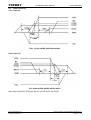
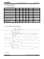
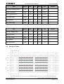
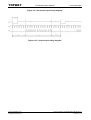
TOPWAY displays [email protected] www.topwaydisplays.eu LMT070DICFWD LCD Module User Manual Rev. 0.1 0.2 0.3 Prepared by: Checked by: Approved by: Date: Date: Date: Descriptions Preliminary release Refine 8(Appendix) Refine 6.1 Timing Characteristics ZZZWRSZD\GLVSOD\VHX LQIR#WRSZD\GLVSOD\VHX Release Date 2010-09-07 2010-10-30 2012-02-09 Document Name: LMT070DICFWD-Manual-Rev0.3 Page: 1 of 12 TOPWAY LCD Module User Manual LMT070DICFWD Table of Content 1. Applications ........................................................................................................................... 3 2. General Specification ............................................................................................................ 3 3. Terminal Function (Input Terminal) ...................................................................................... 4 4. Absolute Maximum Ratings .................................................................................................. 5 5. Electrical Characteristics ...................................................................................................... 5 5.1 DC Characteristics ................................................................................................................................................. 5 5.2 Current Consumption ............................................................................................................................................. 5 5.3 LED Backlight Circuit Characteristics..................................................................................................................... 5 5.4 Power Sequence.................................................................................................................................................... 6 6. AC Characteristics................................................................................................................. 7 6.1 Timing Characteristics............................................................................................................................................ 7 6.2 Input Clock and Data Timing Diagram ................................................................................................................... 7 6.3 Timing .................................................................................................................................................................... 7 6.4 Data Input Format .................................................................................................................................................. 8 6.5 Optical Characteristics ......................................................................................................................................... 10 7. Precautions of using LCD Modules .................................................................................... 11 8. Appendix A <Inspection items and criteria for appearance defect> ................................ 12 ZZZWRSZD\GLVSOD\VHX LQIR#WRSZD\GLVSOD\VHX Document Name: LMT070DICFWD-Manual-Rev0.3 Page: 2 of 12 TOPWAY LCD Module User Manual LMT070DICFWD 1. Applications This Module is designed for portable DVD, GPS car TV & PMP(portable multimedia player) application which require high quality flat panel displays. It is also a good substitute for many outmoded CSTN module in the industrial application. This product is composed of a TFT-LCD panel, driver ICs, FPC and LED backlight unit. 2. General Specification Signal Interface : Display Technology : Display Mode : Screen Size(Diagonal) : Outline Dimension : Active Area : Number of dots : Pixel Pitch : Pixel Configuration : Backlight : Surface Treatment : Viewing Direction : Operating Temperature : Storage Temperature : ZZZWRSZD\GLVSOD\VHX LQIR#WRSZD\GLVSOD\VHX Digital 24-bits RGB a-Si TFT active matrix TN Type Full Color / Transmissive / Normal White 7.0” 164.9 x 100.0 x 5.7 (mm) (see attached drawing for details) 154.08 x 85.92 (mm) 800 x 3 (RGB) x 480 0.0642 x 0.179 (mm) RGB Stripe LED Anti-Glare Treatment 6 o’ clock -20 ~ +70°C -30 ~ +80°C Document Name: LMT070DICFWD-Manual-Rev0.3 Page: 3 of 12 TOPWAY LCD Module User Manual LMT070DICFWD 3. Terminal Function (Input Terminal) Pin No. 1 2 3 4 5 6 7 8 9 10 11 12 : 19 20 : 27 28 : 35 36 37 38 39 40 41 42 43 44 45 46 47 48 49 50 Pin Name VLED+ VLED+ VLEDVLEDGND VCOM DVDD MODE DE VS HS B7 : B0 G7 : G0 R7 : R0 GND DCLK GND L/R U/D VGH VGL AVDD RESET NC VCOM DITHB GND NC NC I/O Descriptions Power Positive Backlight Power Supply Power Negative Backlight Power Supply Power Input Power Input Input Input Input Power GND (0V) Common voltage Power for Digital Circuit DE/SYNC mode select (*1) Data input enable Vertical Sync Input Horizontal Sync Input Input 8bit Data for Blue Input 8bit Data for Green Input 8bit Data for Red Power Input Power Input Input Power Power Power Input Input Input Power - Power GND (0V) Sample clock(*2) Power GND (0V) Left / right selection (*3) Up/down selection (*3) Gate ON Voltage Gate OFF Voltage Power for Analog Circuit Global reset pin (*4) No connection Common Voltage Dithering function (*5) Power GND (0V) No connection Note: * 1: DE/SYNC mode select. Normally pull high. When select DE mode, MODE=”1”, VS and HS must pull high. When select SYNC mode, MODE= “0”, DE must be grounded. * 2: Data shall be latched at the falling edge of DCLK. * 3: Selection of scanning mode Setting of scan control input U/D L/R GND DVDD DVDD GND GND GND DVDD DVDD Scanning direction Up to down, left to right Down to up, right to left Up to down, right to left Down to up, left to right *4: Global reset pin. Active low to enter reset state. Suggest to connect with an RC reset circuit for stability. Normally pull high. *5: Dithering function enable control, normally pull high. When DITHB=”1”,Disable internal dithering function, When DITHB=”0”,Enable internal dithering function, ZZZWRSZD\GLVSOD\VHX LQIR#WRSZD\GLVSOD\VHX Document Name: LMT070DICFWD-Manual-Rev0.3 Page: 4 of 12 TOPWAY LCD Module User Manual LMT070DICFWD 4. Absolute Maximum Ratings Items Power voltage Operating Temperature Storage Temperature Symbol DVDD AVDD VGH VGL VGH -VGL TOP TST Min. -0.3 6.5 -0.3 -20.0 -20 -30 Max. 5.0 13.5 40.0 0.3 40.0 70 80 Unit V V V V V C C Condition No Condensation No Condensation Note: *1. This rating applies to all parts of the module. And should not be exceeded. *2. The operating temperature only guarantees operation of the circuit. The contrast, response speed, and the other specification related to electro-optical display quality is determined at the room temperature, TOP=25. *3. Ambient temperature when the backlight is lit (reference value) *4. Any Stresses exceeding the Absolute Maximum Ratings may cause substantial damage to the device. Functional operation of this device at other conditions beyond those listed in the specification is not implied and prolonged exposure to extreme conditions may affect device reliability. 5. Electrical Characteristics 5.1 DC Characteristics Items Power voltage Input signal voltage Input logic high voltage Input logic low voltage Symbol DVDD AVDD VGH VGL VCOM VIH VIL Min. 3.0 10.2 15.3 -7.7 3.6 0.7VDD 0 Typ. 3.3 10.4 16.0 -7.0 3.8 - Max. 3.6 10.6 16.7 -6.3 4.0 DVDD 0.3DVDD Unit V V V V V V V Remark *2 *3 Note: *1.Be sure to apply DVDD and VGL to the LCD first, and then apply VGH. *2: DVDD setting should match the signals output voltage (refer to Note 3) of customer’ s system board. *3: DCLK,HS,VS,RESET,U/D, L/R,DE,R0~R7,G0~G7,B0~B7,MODE,DITHB. 5.2 Current Consumption Items Symbol IGH IGL Current for Driver IDVDD IAVDD 5.3 Min. - Typ. 0.2 0.2 4.0 20 Max. 1.0 1.0 10 50 Unit mA mA mA mA Remark VGH = 16.0V VGL = -7.0V DVDD=3.3V AVDD=10.4V TYP. 9.6 100.0 MAX. 10.5 - Unit V mA Note If=100mA LED Backlight Circuit Characteristics Top=25℃ Items Forward Voltage Forward Current Symbol VfBLA IfBLA MIN. 9.0 - Cautions: Exceeding the recommended driving current could cause substantial damage to the backlight and shorten its lifetime. ZZZWRSZD\GLVSOD\VHX LQIR#WRSZD\GLVSOD\VHX Document Name: LMT070DICFWD-Manual-Rev0.3 Page: 5 of 12 TOPWAY LCD Module User Manual LMT070DICFWD 5.4 Power Sequence 5.4.1 Power on: DVDD →VGL→AVDD→VGH→Data→B/L 5.4.2 Power off: B/L →Data→VGH→AVDD →VGL→DVDD Note :Data include R0~R7,B0~B7,G0~G7,U/D,L/R,DCLK,HS,VS,DE. ZZZWRSZD\GLVSOD\VHX LQIR#WRSZD\GLVSOD\VHX Document Name: LMT070DICFWD-Manual-Rev0.3 Page: 6 of 12 TOPWAY LCD Module User Manual LMT070DICFWD 6. AC Characteristics 6.1 Timing Characteristics Item Symbol MIN. TYP. MAX. Unit HS setup time Thst 8 - - ns HS hold time Thhd 8 - - ns VS setup time Tvst 8 - - ns VS hold time Tvhd 8 - - ns Data setup time Tdsu 8 - - ns Data hole time Tdhd 8 - - ns DE setup time Tesu 8 - - ns DVDD Power On Slew rate TPOR - - 20 ms DCLK cycle time Tcph 20 - - DCLK pulse duty Tcwh 40 50 60 ns % Remark From 0 to 90% DVDD Note: For the details of the timing, please see the Driver IC data sheet. 6.2 Input Clock and Data Timing Diagram 6.3 Timing ZZZWRSZD\GLVSOD\VHX LQIR#WRSZD\GLVSOD\VHX Document Name: LMT070DICFWD-Manual-Rev0.3 Page: 7 of 12 TOPWAY Item LCD Module User Manual LMT070DICFWD Symbol MIN. TYP. MAX. Unit Horizontal Display Area thd - 800 - DCLK DCLK Frequency fclk 26.4 33.3 46.8 MHz th 862 1056 1200 DCLK thpw 1 - 40 DCLK HS Blanking thb 46 46 46 DCLK HS Front Porch thfp 16 210 354 DCLK Symbol MIN. TYP. MAX. Unit Vertical Display Area tvd - 480 - TH VS period time tv 510 525 650 TH VS pulse width tvpw 1 - 20 TH VS Blanking tvb 23 23 23 TH VS Front Porch tvfp 7 22 147 TH One Horizontal Line HS pulse width Item 6.4 Remark Remark Data Input Format ZZZWRSZD\GLVSOD\VHX LQIR#WRSZD\GLVSOD\VHX Document Name: LMT070DICFWD-Manual-Rev0.3 Page: 8 of 12 TOPWAY LCD Module User Manual LMT070DICFWD Figure 6-2-1 Horizontal input timing diagram. Figure 6-2-2 Vertical input timing diagram. ZZZWRSZD\GLVSOD\VHX LQIR#WRSZD\GLVSOD\VHX Document Name: LMT070DICFWD-Manual-Rev0.3 Page: 9 of 12 TOPWAY 6.5 LCD Module User Manual LMT070DICFWD Optical Characteristics Item Viewing angle (CR≥10) Response Time Contrast ratio Color chromaticlty Luminance Luminance uniformity Symbol Condition MIN. TYP. MAX. θL 9 o’ clock 60 70 - θR 3 o’ clock 60 70 - θT 12 o’ clock 40 50 - θB 6 o’ clock 60 70 - Tf - 10 20 msec Tr - 15 30 msec 400 500 - - 0.26 0.31 0.26 - WY 0.28 0.33 0.38 - L - 250 - cd/m YU 70 75 - % CR WX Normal o θ=0 UNIT Note. degree *2 *3 *1 2 *4 *4 Note: *1. Definition of Contrast Ratio The contrast ratio could be calculate by the following expression: Contrast Ratio (CR) = Luminanc with all pixels white / Luminance with all pixels black *2 Definition of Viewing Angle *3 Definition of response time *4 Definition of Luminance Uniformity Luminance uniformity (Lu)= Min. Luminance form pt1~pt9 / Max Luminance form Pt1~pt9 ZZZWRSZD\GLVSOD\VHX LQIR#WRSZD\GLVSOD\VHX Document Name: LMT070DICFWD-Manual-Rev0.3 Page: 10 of 12 TOPWAY LCD Module User Manual LMT070DICFWD 7. Precautions of using LCD Modules Mounting - Mounting must use holes arranged in four corners or four sides. - The mounting structure so provide even force on to LCD module. Uneven force (ex. Twisted stress) should not applied to the module. And the case on which a module is mounted should have sufficient strength so that external force is not transmitted directly to the module. - It is suggested to attach a transparent protective plate to the surface in order to protect the polarizer. It should have sufficient strength in order to the resist external force. - The housing should adopt radiation structure to satisfy the temperature specification. - Acetic acid type and chlorine type materials for the cover case are not desirable because the former generates corrosive gas of attacking the polarizer at high temperature and the latter causes circuit break by electro-chemical reaction. - Do not touch, push or rub the exposed polarizers with glass, tweezers or anything harder than HB pencil lead. Never rub with dust clothes with chemical treatment. Do not touch the surface of polarizer for bare hand or greasy cloth.(Some cosmetics deteriorate the polarizer.) - When the surface becomes dusty, please wipe gently with absorbent cotton or other soft materials like chamois soaks with petroleum benzine. Normal-hexane is recommended for cleaning the adhesives used to attach front / rear polarizers. Do not use acetone, toluene and alcohol because they cause chemical damage to the polarizer. - Wipe off saliva or water drops as soon as possible. Their long time contact with polarizer Operating - The spike noise causes the mis-operation of circuits. It should be within the ± 200mV level (Over and under shoot voltage) - Response time depends on the temperature.(In lower temperature, it becomes longer.) - Brightness depends on the temperature. (In lower temperature, it becomes lower.) And in lower temperature, response time(required time that brightness is stable after turned on) becomes longer. - Be careful for condensation at sudden temperature change. Condensation makes damage to polarizer or electrical contacted parts. And after fading condensation, smear or spot will occur. - When fixed patterns are displayed for a long time, remnant image is likely to occur. - Module has high frequency circuits. Sufficient suppression to the electromagnetic interference shall be done by system manufacturers. Grounding and shielding methods may be important to minimized the interference Electrostatic Discharge Control Since a module is composed of electronic circuits, it is not strong to electrostatic discharge. Make certain that treatment persons are connected to ground through wrist band etc. And don’ t touch interface pin directly. Strong Light Exposure Strong light exposure causes degradation of polarizer and color filter. Storage When storing modules as spares for a long time, the following precautions are necessary. - Store them in a dark place. Do not expose the module to sunlight or fluorescent light. Keep the temperature between 5°C and 35°C at normal humidity. - The polarizer surface should not come in contact with any other object. It is recommended that they be stored in the container in which they were shipped. Protection Film - When the protection film is peeled off, static electricity is generated between the film and polarizer. This should be peeled off slowly and carefully by people who are electrically grounded and with well ion-blown equipment or in such a condition, etc. - The protection film is attached to the polarizer with a small amount of glue. If some stress is applied to rub the protection film against the polarizer during the time you peel off the film, the glue is apt tore main on the polarizer. Please carefully peel off the protection film without rubbing it against the polarizer. - When the module with protection film attached is stored for a long time, sometimes there remains a very small amount of glue still on the polarizer after the protection film is peeled off. - You can remove the glue easily. When the glue remains on the polarizer surface or its vestige is recognized, please wipe them off with absorbent cotton waste or other soft material like chamois soaked with normal-hexane. Transportation The LCD modules should be no falling and violent shocking during transportation, and also should avoid excessive press, water, damp and sunshine. ZZZWRSZD\GLVSOD\VHX LQIR#WRSZD\GLVSOD\VHX Document Name: LMT070DICFWD-Manual-Rev0.3 Page: 11 of 12 TOPWAY LCD Module User Manual LMT070DICFWD 8. Appendix <Inspection items and criteria for appearance defect> 8.1 Bright/Dark Dots: Defect Type Specification Major Minor Bright Dots N≤ 2 ● Dark Dots N≤ 3 ● Total Bright and Dark Dots N≤ 4 ● Note: 1. The definition of dot: The size of a defective dot over 1/2 of whole dot is regarded as one defective dot. 2. Bright dot: Dots appear bright and unchanged in size in which LCD panel is displaying under black pattern. 3. Dark dot: Dots appear dark and unchanged in size in which LCD panel is displaying under pure red, green, blue pattern. ZZZWRSZD\GLVSOD\VHX LQIR#WRSZD\GLVSOD\VHX Document Name: LMT070DICFWD-Manual-Rev0.3 Page: 12 of 12