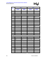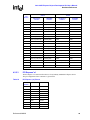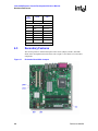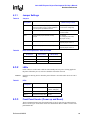
1
Intel® 945G Express Chipset
Development Kit
User’s Manual
April 2007
Reference #308823-002
®
Intel 945G Express Chipset Development Kit User’s Manual
Contents
®
INFORMATION IN THIS DOCUMENT IS PROVIDED IN CONNECTION WITH INTEL PRODUCTS. EXCEPT AS PROVIDED IN INTEL’S
TERMS AND CONDITIONS OF SALE FOR SUCH PRODUCTS, INTEL ASSUMES NO LIABILITY WHATSOEVER, AND INTEL
DISCLAIMS ANY EXPRESS OR IMPLIED WARRANTY RELATING TO SALE AND/OR USE OF INTEL PRODUCTS, INCLUDING
LIABILITY OR WARRANTIES RELATING TO FITNESS FOR A PARTICULAR PURPOSE, MERCHANTABILITY, OR INFRINGEMENT OF
ANY PATENT, COPYRIGHT, OR OTHER INTELLECTUAL PROPERTY RIGHT.
Intel Corporation may have patents or pending patent applications, trademarks, copyrights, or other intellectual property rights that relate to
the presented subject matter. The furnishing of documents and other materials and information does not provide any license, express or
implied, by estoppel or otherwise, to any such patents, trademarks, copyrights, or other intellectual property rights.
Intel products are not intended for use in medical, life-saving, life-sustaining, critical control or safety systems, or in nuclear-facility
applications. Intel may make changes to specifications and product descriptions at any time, without notice.
Designers must not rely on the absence or characteristics of any features or instructions marked "reserved" or "undefined." Intel reserves
these for future definition and shall have no responsibility whatsoever for conflicts or incompatibilities arising from future changes to them.
®
The Intel 945G Express Chipset Development Kit User’s Manual may contain design defects or errors known as errata which may cause
the product to deviate from published specifications. Current characterized errata are available on request.
This document and the software described in it are furnished under license and may only be used or copied in accordance with the terms of
the license. The information in this document is furnished for informational use only, is subject to change without notice, and should not be
construed as a commitment by Intel Corporation. Intel Corporation assumes no responsibility or liability for any errors or inaccuracies that
may appear in this document or any software that may be provided in association with this document. Except as permitted by such license,
no part of this document may be reproduced, stored in a retrieval system, or transmitted in any form or by any means without the express
written consent of Intel Corporation.
Contact your local Intel sales office or your distributor to obtain the latest specifications and before placing your product order.
Copies of documents which have an order number and are referenced in this document, or other Intel literature, may be obtained by calling
1-800-548-4725, or by visiting Intel's website at http://www.intel.com.
AlertVIEW, AnyPoint, AppChoice, BoardWatch, BunnyPeople, CablePort, Celeron, Chips, CT Connect, CT Media, Dialogic, DM3,
EtherExpress, ETOX, FlashFile, i386, i486, i960, iCOMP, InstantIP, Intel, Intel logo, Intel386, Intel486, Intel740, IntelDX2, IntelDX4,
IntelSX2, Intel Create & Share, Intel GigaBlade, Intel InBusiness, Intel Inside, Intel Inside logo, Intel NetBurst, Intel NetMerge, Intel
NetStructure, Intel Play, Intel Play logo, Intel SingleDriver, Intel SpeedStep, Intel StrataFlash, Intel TeamStation, Intel Xeon, Intel XScale,
IPLink, Itanium, LANDesk, LanRover, MCS, MMX, MMX logo, Optimizer logo, OverDrive, Paragon, PC Dads, PC Parents, PDCharm,
Pentium, Pentium II Xeon, Pentium III Xeon, Performance at Your Command, RemoteExpress, Shiva, SmartDie, Solutions960, Sound
Mark, StorageExpress, The Computer Inside., The Journey Inside, TokenExpress, Trillium, VoiceBrick, Vtune, and Xircom are trademarks
or registered trademarks of Intel Corporation or its subsidiaries in the United States and other countries.
®
®
† Hyper-Threading Technology (HT Technology) requires a computer system with an Intel Pentium 4 processor supporting HT
Technology and an HT Technology-enabled chipset, BIOS, and operating system. Performance will vary depending on the specific
hardware and software you use. See http://www.intel.com/info/hyperthreading/ for more information including which processors support HT
Technology.
*Other names and brands may be claimed as the property of others.
Copyright © Intel Corporation 2007. All rights reserved.
2
Reference #308823
®
Intel 945G Express Chipset Development Kit User’s Manual
Contents
Contents
1
1.1
1.2
1.3
1.4
1.4.1
1.4.2
1.5
1.6
About This Manual ..........................................................................................................6
Content Overview..............................................................................................................6
Text Conventions ..............................................................................................................6
Glossary of Terms and Acronyms......................................................................................7
Support Options ................................................................................................................9
Electronic Support Systems...............................................................................................9
Additional Technical Support .............................................................................................9
Product Literature..............................................................................................................9
Related Documents......................................................................................................... 10
2.1
2.1.1
2.1.2
2.2
2.3
2.3.1
2.4
2.4.1
2.4.2
2.5
2.5.1
2.5.2
2.5.3
Development Kit Features............................................................................................. 11
Overview......................................................................................................................... 11
®
Intel 945G Express Platform Features and Benefits ....................................................... 12
Development Kit Features Summary ............................................................................... 13
Development Kit Hardware Lists...................................................................................... 14
Software Key Features .................................................................................................... 14
AMI* BIOS....................................................................................................................... 14
Processor Features and Operation .................................................................................. 15
Intel® Pentium® 4 Processor 551...................................................................................... 15
Intel® Celeron® D Processor 341...................................................................................... 16
Intel® 945G Express Chipset Features and Operation...................................................... 16
Intel® 945G Memory Controller Hub ((G)MCH)................................................................. 17
Intel® I/O Controller Hub 7 (ICH7) .................................................................................... 19
Power Management ........................................................................................................ 21
3.1
3.2
3.3
3.3.1
3.3.2
3.3.3
3.3.4
3.3.5
3.4
3.4.1
3.4.2
3.4.3
3.4.4
Setting Up the Development Kit ................................................................................... 23
Overview......................................................................................................................... 23
Additional Hardware and Software Required.................................................................... 23
Setting up the Evaluation Board....................................................................................... 24
Memory Configurations ................................................................................................... 25
Audio Subsystem Configurations ..................................................................................... 28
LAN Subsystem Configurations ....................................................................................... 29
Intel® Active Management Technology (Optional) ............................................................ 31
Configuring the BIOS....................................................................................................... 32
Error Messages and Beep Codes .................................................................................... 32
Speaker .......................................................................................................................... 32
BIOS Beep Codes ........................................................................................................... 32
BIOS Error Messages...................................................................................................... 33
Port 80h POST Codes..................................................................................................... 33
4.1
4.1.1
4.1.2
4.2
4.2.1
4.2.2
4.3
4.3.1
4.3.2
4.3.3
4.4
Hardware References.................................................................................................... 38
Overview......................................................................................................................... 38
Board Layout................................................................................................................... 39
Back Panel Connectors ................................................................................................... 41
Primary Features............................................................................................................. 41
Core Components ........................................................................................................... 42
Expansion Slots and Sockets .......................................................................................... 42
Secondary Features ........................................................................................................ 46
Jumper Settings .............................................................................................................. 47
LEDs............................................................................................................................... 47
Front Panel Header (Power up and Reset) ...................................................................... 47
Headers .......................................................................................................................... 48
2
3
4
Reference #308823
3
®
Intel 945G Express Chipset Development Kit User’s Manual
Contents
4.4.1
4.4.2
4.4.3
4.4.4
4.4.5
4.4.6
4.4.7
4.4.8
4.4.9
4.5
Evaluation Board Headers............................................................................................... 48
ATX Power Connectors ................................................................................................... 49
IDE Connector................................................................................................................. 50
SATA Pinout ................................................................................................................... 50
Fan Connectors............................................................................................................... 51
Front Panel USB Header ................................................................................................. 51
Front Panel Audio Header ............................................................................................... 51
Front Panel Header ......................................................................................................... 52
Serial Port Header........................................................................................................... 52
Thermal Considerations................................................................................................... 53
Figures
Figure 1
Figure 2
Figure 3
Figure 4
Figure 5
Figure 6
Figure 7
Figure 8
Figure 9
Figure 10
Figure 11
Figure 12
Figure 13
Figure 14
Figure 15
Figure 16
®
Intel 945G/ICH7 Platform Block Diagram ....................................................................... 11
Memory Channel and DIMM Configuration ...................................................................... 27
Dual Channel (Interleaved) Mode Configuration with 2x DIMMs....................................... 27
Dual Channel (Interleaved) Mode Configuration with 3x DIMMs....................................... 27
Dual Channel (Interleaved) Mode Configuration with 4x DIMMs....................................... 28
Single Channel (Asymmetric) Mode Configuration with 1x DIMM ..................................... 28
Single Channel (Asymmetric) Mode Configuration with 3x DIMMs ................................... 28
Back Panel Audio Connector Options for 8-channel Audio Subsystem............................. 29
LAN Connector LED locations ......................................................................................... 30
Evaluation Board Layout.................................................................................................. 38
Evaluation Board Major Components............................................................................... 39
Back Panel I/O Connectors.............................................................................................. 41
Evaluation Board Main Jumpers ...................................................................................... 46
Front Panel Header ......................................................................................................... 48
Processor Heat Sink for Omni-Directional Airflow............................................................. 53
Localized High Temperature Zones ................................................................................. 54
Tables
Table 1
Table 2
Table 3
Table 4
Table 5
Table 6
Table 7
Table 8
Table 9
Table 10
Table 11
Table 12
Table 13
4
Intel Literature Centers ......................................................................................................9
Related Documents......................................................................................................... 10
Key Features and Benefits of the Intel® 945G Express Platform....................................... 12
Development Kit Features Summary ............................................................................... 13
Effects of Power Switch Pressing Duration ...................................................................... 22
Back Panel Task (Audio) ................................................................................................. 29
LAN Connector LED Status ............................................................................................. 30
Beep Codes .................................................................................................................... 32
Error Messages............................................................................................................... 33
Port 80h POST Code Ranges.......................................................................................... 33
Port 80h POST Codes..................................................................................................... 34
Typical Port 80h POST Sequence ................................................................................... 36
Evaluation Board Components ........................................................................................ 39
Reference #308823
®
Intel 945G Express Chipset Development Kit User’s Manual
Contents
Table 14
Table 15
Table 16
Table 17
Table 18
Table 19
Table 20
Table 21
Table 22
Table 23
Table 24
Table 25
Table 26
Table 27
Table 28
Table 29
Table 30
Table 31
Table 32
Back Panel I/O Connectors.............................................................................................. 41
Core Components ........................................................................................................... 42
Expansion Slots and Sockets .......................................................................................... 42
Intel® sDVO to PCI Express* Connector Mapping for MEC Cards .................................... 43
PCI Express* (x1) Pinout ................................................................................................. 45
Jumpers .......................................................................................................................... 47
Boot Select Options for J3601 and J3602 ........................................................................ 47
LEDs............................................................................................................................... 47
Front Panel Jumper Setting ............................................................................................. 48
Evaluation Board Headers............................................................................................... 48
2x12 ATX Power Connector ............................................................................................ 49
2x2 Auxiliary 12V Power Connector................................................................................. 49
IDE Connector................................................................................................................. 50
SATA Pinout ................................................................................................................... 50
Fan Connectors............................................................................................................... 51
Front Panel USB Header ................................................................................................. 51
Front Panel Audio Header ............................................................................................... 51
Front Panel Header (J7J2) .............................................................................................. 52
Serial Port Header (J2B1)................................................................................................ 52
Revision History
Date
Revision
April 2007
002
Description
Updated Section 2.2 to reflect that heat sink fan is pre
installed.
Updated Section 3.3 to add safety warning.
August 2005
Reference #308823
001
Initial release
5
®
Intel 945G Express Chipset Development Kit User’s Manual
About This Manual
1
About This Manual
This user’s manual describes the use of the Intel® 945G® Express Chipset Development
Kit. This manual has been written for OEMs, system evaluators, and embedded system
developers. All jumpers, headers, LED functions, and their locations on the board, along
with subsystem features and POST codes, are defined in this document.
For the latest information about the Intel® 945G® Express Chipset Development Kit
reference platform, visit:
http://developer.intel.com/design/intarch/devkits/index.htm
For design documents related to this platform, such as schematics and bill of materials,
please contact your Intel field sales representative.
1.1
Content Overview
Chapter 1: About This Manual
Description of conventions used in this manual. The last few sections explain how to obtain
literature and contact customer support.
Chapter 2: Development Kit Features
Describes development kit features and board capability. This includes the information on
the processor features, component features and operation, and overall development kit
board capability.
Chapter 3: Setting Up the Development Kit Board
Complete instructions on how to configure the evaluation board and processor assembly by
setting jumpers, connecting peripherals, providing power, and configuring the BIOS.
Chapter 4: Hardware Reference
Description of jumper settings and functions, board debug capabilities, and pinout
information for connectors.
1.2
Text Conventions
The following notations may be used throughout this manual.
6
#
The pound symbol (#) appended to a signal name indicates that the signal is
active low.
Variables
Variables are shown in italics. Variables must be replaced with correct values.
Instructions
Instruction mnemonics are shown in uppercase. When you are programming,
instructions are not case sensitive. You may use either upper case or lower case.
Numbers
Hexadecimal numbers are represented by a string of hexadecimal digits
followed by the character H. A zero prefix is added to numbers that begin with A
through F (e.g., FF is shown as 0FFH). Decimal and binary numbers are
represented by their customary notations. (That is, 255 is a decimal number and
1111 1111 is a binary number. In some cases, the letter B is added for clarity.)
Reference #308823
®
Intel 945G Express Chipset Development Kit User’s Manual
About This Manual
Units of Measure
The following abbreviations are used to represent units of measure:
A
amps, amperes
GByte
gigabytes
KByte
kilobytes
KΩ
kilo-ohms
mA
milliamps, milliamperes
MByte
megabytes
MHz
megahertz
ms
milliseconds
mW
milliwatts
ns
nanoseconds
pF
picofarads
W
watts
V
volts
Signal Names
Signal names are shown in uppercase. When several signals share a common
name, an individual signal is represented by the signal name followed by a
number, while the group is represented by the signal name followed by a
variable (n). For example, the lower chip-select signals are named CS0#, CS1#,
CS2#, and so on; they are collectively called CSn#. A pound symbol (#)
appended to a signal name identifies an active-low signal. Port pins are
represented by the port abbreviation, a period, and the pin number (e.g., P1.0).
1.3
Glossary of Terms and Acronyms
This section defines conventions and terminology used throughout this document.
Term
Description
nd
ADD2+ Card
Advanced Digital Display Card – 2 Generation. Provides digital display options for
an Intel graphics controller that supports ADD2+ cards. It plugs into a x16 PCI
Express* connector but uses the multiplexed SDVO interface. The card adds Video
In capabilities. This card will not work with an Intel graphics controller that supports
DVO and ADD cards. It will function as an ADD2 card in an ADD2-supported
system, but Video In capabilities will not work.
ACPI
Advanced Configuration and Power Interface
BLT
Block Level Transfer
Core
The internal base logic in the (G)MCH
CRT
Cathode Ray Tube
DBI
Dynamic Bus Inversion
DDR
Double Data Rate SDRAM memory technology
DDR2
A second generation Double Data Rate SDRAM memory technology
DMI
(G)MCH-Intel ICH7 Direct Media Interface
DVI
Digital Video Interface. Specification that defines the connector and interface for
digital displays.
FSB
Front Side Bus.Synonymous with host or processor bus.
Full Reset
Full reset is when PWROK is de-asserted. Warm reset is when both RSTIN# and
PWROK are asserted.
Reference #308823
®
7
®
Intel 945G Express Chipset Development Kit User’s Manual
About This Manual
Term
GMCH
Graphics Memory Controller Hub. Component that contains the processor interface,
DRAM controller, x16 PCI Express port (typically, the external graphics interface),
®
and integrated graphics device (IGD). It communicates with the Intel I/O Controller
Hub 7 (ICH7) and other I/O controller hubs over the DMI interconnect. In this
®
document GMCH refers to the Intel 82945G GMCH component.
Host
This term is used synonymously with processor.
®
Digital Video Out port. Term used for the first generation of Intel Graphics
Controller’s digital display channels. Digital display data is provided in a parallel
nd
format. This interface is not electrically compatible with the 2 generation digital
display channel discussed in this document – SDVO.
Intel ICH7
®
Seventh generation I/O Controller Hub component that contains additional
functionality compared to previous ICHs. The I/O Controller Hub component
contains the primary PCI interface, LPC interface, USB2, ATA-100, and other I/O
functions. It communicates with the (G)MCH over a proprietary interconnect called
Direct Media Interface (DMI).
LCD
Liquid Crystal Display.
LVDS
Low Voltage Differential Signaling. A high speed, low power data transmission
standard used for display connections to LCD panels.
MCH
Memory Controller Hub. Component that contains the processor interface, DRAM
controller, and x16 PCI Express port (typically, the external graphics interface). It
communicates with the I/O controller hub (ICH7) and other I/O controller hubs over
the DMI interconnect. In this document MCH refers to the 82945P MCH component.
MEC
Media Expansion Card, also known as ADD2+ card. Refer to ADD2+ term for
description.
PCI Express
Third Generation input/output graphics attach called PCI Express Graphics. PCI
Express is a high-speed serial interface whose configuration is software compatible
with the existing PCI specifications. The specific PCI Express implementation
intended for connecting the (G)MCH to an external Graphics Controller is a x16 link
and replaces AGP.
Primary PCI
The Primary PCI is the physical PCI bus that is driven directly by the ICH7
component. Communication between Primary PCI and the (G)MCH occurs over
DMI. Note that the Primary PCI bus is not PCI Bus 0 from a configuration
standpoint.
SDVO
Serial Digital Video Out. A digital display channel that serially transmits digital
display data to an external SDVO device. The SDVO device accepts this serialized
format and then translates the data into the appropriate display format (i.e., TMDS,
LVDS, TV-Out). This interface is not electrically compatible with the previous digital
display channel (DVO). For the 82945G GMCH, it will be multiplexed on a portion of
the x16 graphics PCI Express interface.
SDVO Device
Third party codec that uses SDVO as an input. May have a variety of output
formats, including DVI, LVDS, HDMI, TV-Out, etc.
SMI
System Management Interrupt. SMI is used to indicate any of several system
conditions (such as, thermal sensor events, throttling activated, access to System
Management RAM, chassis open, or other system state related activity).
UMA
Unified Memory Architecture. Describes an integrated graphics device using system
memory for its frame buffers.
Intel DVO
8
Description
Reference #308823
®
Intel 945G Express Chipset Development Kit User’s Manual
About This Manual
1.4
Support Options
1.4.1
Electronic Support Systems
Intel’s site on the World Wide Web (http://www.intel.com/) provides up-to-date technical
information and product support. This information is available 24 hours a day, 7 days a
week, providing technical information whenever you need it.
Product documentation is provided online in a variety of web-friendly formats at:
http://appzone.intel.com/literature/index.asp
1.4.2
Additional Technical Support
If you require additional technical support, please contact your field sales representative or
local distributor.
1.5
Product Literature
Product literature can be ordered from the following Intel literature centers:
Table 1
Intel Literature Centers
Location
Telephone Number
U.S. and Canada
1-800-548-4725
U.S. (from overseas)
708-296-9333
Europe (U.K.)
44(0)1793-431155
Germany
44(0)1793-421333
France
44(0)1793-421777
Japan (fax only)
81(0)120-47-88-32
Reference #308823
9
®
Intel 945G Express Chipset Development Kit User’s Manual
About This Manual
1.6
Related Documents
Table 2
Related Documents
Document Title
®
®
302351
®
®
302352
®
®
302553
®
®
302353
Intel Celeron D Processors 335, 330, 325, and 320
Specification Update
®
®
302354
LGA775 Socket Mechanical Design Guide
302666
Voltage Regulator Down (VRD) 10.1 Design Guide for Desktop
LGA775 Socket
302356
Intel Pentium 4 Processor 570/571, 560/561, 550/551,
540/541, 530/531 and 520/521 Supporting Hyper-Threading
†
Technology Datasheet: On 90nm in 775-land LGA Package
®
and supporting Intel Extended Memory 64 Technology
Intel Pentium 4 Processor on 90 nm Process Specification
Update
Intel Pentium 4 Processor on 90 nm Process in the 775-Land
LGA Package Thermal and Mechanical Design Guidelines
Intel Celeron D Processors 335, 330, 325, and 320
Datasheet
®
302822
®
302823
®
307502
®
307503
®
307504
®
307013
®
307014
®
307015
Intel Pentium 4 Processor in the 775-Land LGA Package for
Embedded Applications Thermal Design Guide
Intel Celeron D Processor in the 775-Land LGA Package for
Embedded Applications Thermal Design Guide
Intel 945G/945P Express Chipset Family Datasheet
Intel 945G/P Express Chipset Family Memory Controller Hub
Specification Update
Intel 945G/P Express Chipset Family Thermal and Mechanical
Design Guidelines
Intel I/O Controller Hub 7 (ICH7) Family Datasheet
Intel I/O Controller Hub 7 (ICH7) Specification Update
Intel I/O Controller Hub 7 (ICH7) Thermal Design Guidelines:
®
For the Intel 82801GB ICH7 and 82801GR ICH7R I/O
Controller Hubs
10
Order Number
PCI Local Bus Specification, Rev. 2.3
http://www.pcisig.com/specifications
PCI Express Specification, Rev 1.0a, July 22, 2002
http://www.pcisig.com/specifications
Reference #308823
®
Intel 945G Express Chipset Development Kit User’s Manual
Development Kit Features
2
Development Kit Features
2.1
Overview
This chapter provides a platform overview of the Intel® 945G Express Chipset platform.
The Intel® 945G Express Chipset is designed for use with the Intel® Pentium® 4 Processor
551 and Intel® Celeron® D Processor 341. Each chipset contains two components: the
Intel® 82945G GMCH (or MCH) for the host bridge, and Intel® I/O Controller Hub 7
(ICH7) Family for the I/O subsystem.
Figure 1 shows an example system block diagram for the 945G Express Chipset.
Figure 1
®
Intel 945G/ICH7 Platform Block Diagram
Processor
533/800 MHz FSB
Intel
®
945G Express Chipset
Analog Display
VGA
System Memory
MEC
Display
Channel A
®
DDR2
Intel 82945G GMCH
SDVO
Display
OR
Display
Graphics Card
Channel B
DDR2
PCI Express
x16 Graphics
DMI Interface
USB 2.0
8 ports, 480 Mb/s
Power Management
IDE
Clock Generation
4 SATA Ports
LAN Connect
Intel
®
ICH7 Family
AC '97 / Intel® High
Definition Audio CODECs
System Management (TCO)
SMBus 2.0 / I2C*
PCI Express* x1
PCI Express
Gigabit Ethernet
PCI Bus
GPIO
SPI BIOS
Other ASICs
(Optional)
LPC Interface
Super I/O
TPM
(Optional)
Flash BIOS
Reference #308823
11
®
Intel 945G Express Chipset Development Kit User’s Manual
Development Kit Features
2.1.1
Intel® 945G Express Platform Features and Benefits
The 945G Express platform is designed to support several processor types: Intel® Pentium®
4 Processor on 90nm Process in the 775-land LGA Package and the Intel® Celeron® D
Processor. The only processor included in this development kit will be the Pentium 4
processor.
The Intel 945G Express Chipset includes the Intel® 82945G (G)MCH and Intel® 82801GB
ICH7 or Intel® 82801GR ICH7R (not offered in the development kit).
The following table lists the major features present on the Intel® 945G Express platform.
Section 2.1.2 will summarize the development kit features.
Table 3
®
Key Features and Benefits of the Intel 945G Express Platform
Features
®
®
†
800/533 MHz FSB
Supports the Intel Pentium 4 Processor with HT Technology and
®
®
the Intel Celeron D Processor (not offered in this development kit) in
the LGA775 socket, with scalability for future processor innovations.
PCI Express Interface
The PCI Express x16 graphics interface delivers more than 3.5 times
the bandwidth over a traditional AGP 8X interface and supports the
latest high-performance graphics cards. The PCI Express x1 I/O ports
offer 3.5 times the bandwidth over traditional PCI architecture,
delivering faster access to peripheral devices and networking.
®
Delivers rich visual color and picture clarity without the need for
additional discrete graphics cards.
®
Integrated audio support enables premium home theater sound and
delivers advanced features such as multiple audio streams and jack
re-tasking. The Dolby* PC Entertainment Experience is available
®
exclusively on systems with Intel High Definition Audio.
®
Provides quicker file access with RAID 0, 5, and 10, and protection
against data loss from a hard disk drive failure with RAID 1, 5, and 10.
This feature requires the ICH7R (not offered in the development kit).
Intel Active Management
Technology
®
Enables remote, down-the-wire management of out-of-band
networked systems regardless of system state. Helps improve IT
efficiency, asset management and system security and availability.
Serial ATA (SATA-II) 1.5/3 Gb/s
High-speed storage interface supports faster transfer rate for
improved data access.
Dual Channel DDR2,
533/667 MHz
Delivers up to 10.7 GB/s of bandwidth and 4 GB memory
addressability for faster system responsiveness and support of 64-bit
computing.
Intel Graphics Media
Accelerator (GMA) 950
Intel High Definition
Audio
Intel Matrix Storage
Technology
®
Intel Flex Memory
Technology
12
Benefits
Facilitates easier upgrades by allowing different memory sizes to be
populated and remain in dual-channel mode.
Reference #308823
®
Intel 945G Express Chipset Development Kit User’s Manual
Development Kit Features
2.1.2
Development Kit Features Summary
This section summarizes the actual development kit features.
Table 4
Development Kit Features Summary
Form Factor
microATX (9.60 x 9.60 inches)
Processor
Intel Pentium 4 Processor 551 in the 775-land LGA package
®
®
Supports a 533/800 MHz front side bus
†
Hyper-Threading Technology (HT Technology)
®
Intel Extended Memory 64 Technology (EM64T)
Memory
DDR2 533/667 dual-channel system memory interface (DIMM sockets)
Four 240-pin DDR2 SDRAM DIMM sockets (two per channel)
Support for unbuffered, non-ECC DDR2 SDRAM modules
Supports 128 MB to 4 GB of system memory
256 Mbit, 512 Mbit, or 1 Gbit technology
®
Chipset
Intel 945G Express Chipset, consisting of:
®
• Intel 82945G Graphics Memory Controller Hub ((G)MCH)
®
• Intel 82801GB I/O Controller Hub 7 (ICH7)
Video
Option of either using integrated graphics system or external PCI Express
graphics port:
®
Intel GMA950 integrated graphics subsystem
®
Supports Intel Media Expansion Card (MEC, also known as ADD2+) for
additional digital display such as DVI, LVDS, etc. depending on the media
expansion card features.
Supports external PCI Express (x16) graphics card
®
Audio
Intel High Definition Audio subsystem:
8-channel (7.1) audio subsystem and two S/PDIF digital audio outputs
using the Realtek* ALC882 audio codec.
Legacy I/O Control
Legacy I/O controller for diskette drive, serial, parallel, and PS/2 ports
Peripheral Interfaces
Four SATA 1.5/3.0 Gb/s ports
One Parallel ATA IDE interface with UDMA 33, ATA-66/100 support
Six Universal Serial Bus (USB) 2.0 ports
PS/2-style keyboard and PS/2 mouse (6-pin mini-DIN) connectors
One VGA connector provides access to integrated graphics
Six audio connectors (Line-in, Line-out, MIC-in, Surround L/R, Surround
L/R Rear, Center) driven by Intel High Definition Audio
Two Audio SPDIF connectors
One parallel port
One diskette drive interface
®
LAN Support
Gigabit (10/100/1000 Mbits/s) LAN subsystem using the Intel 82573E
Gigabit Ethernet Controller
BIOS
Support for Advanced configuration and power interface (ACPI), plug and
play, and SMBIOS
AMI system BIOS
Expansion
Capabilities
Two conventional PCI bus connectors
One PCI Express x16 bus add-in card connector
One PCI Express x1 bus add-in card connector
Reference #308823
13
®
Intel 945G Express Chipset Development Kit User’s Manual
Development Kit Features
Hardware Monitor
Subsystem
Hardware monitoring and fan control ASIC
Voltage sense to detect out of range power supply voltages
Thermal sense to detect out of range thermal values
Three fan connectors
Three fan sense inputs used to monitor fan activity
Fan speed control
2.2
Development Kit Hardware Lists
The following hardware is included in the development kit:
• 1x Intel® 945G Express Chipset Development Kit reference board.
2.3
•
1x Intel® Pentium® 4 Processor 551 with HT Technology (at 3.4 GHz)
•
1x Pre-installed CPU fan heat sink
•
•
•
2x 512 MByte DDR2 533 unbuffered DIMMs
1x Pre-programmed and installed firmware hub
1x Pre-installed Type 2032, socketed 3V lithium coin cell battery
•
•
1x Pre-installed (G)MCH heat sink
1x Pre-installed ICH7 heat sink
•
•
Jumper (for board power-on)
1x Intel® 945G Express Chipset Development Kit Software CD-ROM
Software Key Features
The software in the kit was chosen to facilitate development of real-time applications based
on the components used in the evaluation board. The driver CD included in the kit contains
all of the software drivers necessary for basic system functionality under the following
operating systems: Microsoft* Windows* 2000/XP/XP Embedded, and Linux*.
Note:
While every care was taken to ensure the latest version of drivers were provided on the
enclosed CD at time of publication, newer revisions may be available. Updated drivers for
Intel components can be found at: http://developer.intel.com/design/intarch/devkits.
For all third party components, please contact the appropriate vendor for updated drivers.
Note:
Software in the kit is provided free by the vendor and is only licensed for evaluation
purposes.
Refer to the documentation in the evaluation kit for further details on any terms and
conditions that may be applicable to the granted licenses. Customers using the tools that
work with Microsoft products must license those products. Any targets created by those
tools should also have appropriate licenses. Software included in the kit is subject to
change. Refer to http://developer.intel.com/design/intarch/devkits for details on additional
software from other third-party vendors.
2.3.1
AMI* BIOS
This development kit ships pre-installed with AMI BIOS pre-boot firmware from AMI.
AMI BIOS provides an industry-standard BIOS platform to run most standard operating
systems, including Windows 2000/XP/XP Embedded, Linux, and others.
14
Reference #308823
®
Intel 945G Express Chipset Development Kit User’s Manual
Development Kit Features
2.4
Processor Features and Operation
The following section provides a detailed view at processor features and operation.
2.4.1
Intel® Pentium® 4 Processor 551
The main different between the Pentium 4 processor 550 and the 551 is that the 551
supports Intel® Extended Memory 64 Technology (EM64T), while the 550 does not. The
rest of the features are the same.
The Intel Pentium 4 processor 551 supports Intel® Extended Memory 64 Technology
(EM64T) as an enhancement to the IA-32 Intel® Architecture. This enhancement enables
the processor to execute operating systems and applications written to take advantage of
EM64T features. With appropriate 64-bit supporting hardware and software, platforms
based on an Intel processor supporting EM64T can use extended virtual and physical
memory.
In addition to supporting all the existing Streaming SIMD Extensions 2 (SSE2), there are
13 new instructions that further extend the capabilities of Intel processor technology. These
new instructions, called Streaming SIMD Extensions 3 (SSE3), enhance the performance
of optimized applications for the digital home such as video, image processing, and media
compression technology.
The processor’s Intel NetBurst® microarchitecture front side bus uses a split-transaction,
deferred reply protocol. The NetBurst microarchitecture FSB uses source-synchronous
transfer (SST) of address and data to improve performance by transferring data four times
per bus clock. Along with the 4x data bus, the address bus can deliver addresses two times
per bus clock and is referred to as a “double-clocked” or 2x address bus. Features of the
processor include:
•
Binary compatible with applications running on previous members of the Intel
microprocessor line
•
•
•
NetBurst microarchitecture
System bus frequency at 533/800 MHz
775-Land LGA Package
•
•
Supports EM64T Technology
Rapid Execution Engine: arithmetic logic units (ALUs) run at twice the processor
core frequency
Supports Hyper-Threading Technology (HT Technology)
•
•
Hyper Pipelined Technology
⎯ Advance Dynamic Execution
⎯ Very deep out-of-order execution
•
•
Enhanced branch prediction
16 KByte Level 1 data cache
•
1 MByte Advanced Transfer Cache (on-die, full-speed Level 2 (L2) cache) with 8way associatively and Error Correcting Code (ECC)
•
144 Streaming SIMD Extensions 2 (SSE2) and 13 Streaming SIMD Extensions 3
(SSE3) instructions.
•
Enhanced floating point and multimedia unit for enhanced video, audio, encryption,
and 3D performance
•
Power management capabilities
Reference #308823
15
®
Intel 945G Express Chipset Development Kit User’s Manual
Development Kit Features
⎯ System Management mode
⎯ Multiple low-power states
•
2.4.2
Note:
Optimized for 32-bit applications running on advanced 32-bit operating systems
Intel® Celeron® D Processor 341
This processor is not available in this development kits
The Intel® Celeron® D Processor provides exceptional value and balanced performance
with efficient power usage. It is binary compatible with previous Intel Architecture
processors. Features of the processor include:
2.5
•
Binary compatible with applications running on previous members of the Intel
microprocessor line
•
•
•
NetBurst microarchitecture
Support EM64T Technology
System bus frequency at 533 MHz
•
Rapid Execution Engine: Arithmetic Logic Units (ALUs) run at twice the processor
core frequency.
•
Hyper Pipelined Technology
⎯ Advance Dynamic Execution
⎯ Very deep out-of-order execution
•
Enhanced branch prediction
•
•
16 KByte Level 1 data cache
256 KByte Advanced Transfer Cache (on-die, full-speed Level 2 (L2) cache) with 8way associatively and Error Correcting Code (ECC)
•
144 Streaming SIMD Extensions 2 (SSE2) and 13 Streaming SIMD Extensions 3
(SSE3) instructions.
•
Power Management capabilities
⎯ System Management mode
⎯ Multiple low-power states
•
Optimized for 32-bit applications running on advanced 32-bit operating systems
Intel® 945G Express Chipset Features and
Operation
The Intel 945G Express Chipset platform is designed based on the 32-bit IA-32 Intel®
Architecture.
The MCH connects to the processor as shown in Figure 1. The primary role of an MCH in
a system is to manage the flow of information between its interfaces: the processor
interface (FSB), the system memory interface (DRAM controller), the integrated graphics
interface, the external graphics interface (PCI Express), and the I/O controller through the
DMI interface. This includes arbitrating between the four interfaces when each initiates
transactions. The ICH7 will provide extensive I/O support. The functions and capabilities
include PCI Express, PCI, Serial ATA, USB, IDE, and much more.
16
Reference #308823
®
Intel 945G Express Chipset Development Kit User’s Manual
Development Kit Features
2.5.1
Intel® 945G Memory Controller Hub ((G)MCH)
The Intel® 945G Express Chipset (G)MCH provides the processor interface optimized for
Intel Pentium 4 Processors, system memory interface, DMI, and internal/external graphics.
It provides flexibility and scalability in graphics and memory subsystem performance. The
following sections describe the reference board’s implementation of the Intel 945G Express
Chipset (G)MCH features.
•
•
1202 FCBGA package (34 mm x 34 mm)
533/800 MHz processor system bus
•
•
•
32-bit host bus addressing
12 deep in-order queue
Processor support for the Pentium 4 Processor with HT Technology in the 775-Land
LGA Package and the Celeron D Processor.
•
System memory controller (DDR2 implemented)
⎯ Supports Dual Channel or Single Channel operation
⎯ Four DIMM slots (2 DIMM per channel)
⎯ DDR2 533/667 MHz
•
•
Direct Media Interface (DMI)
Integrated graphics based on the Intel® Graphics Media Accelerator 950
⎯ Directly supports on-board VGA connector
⎯ Supports resolutions up to 2048 x 1536 @ 75 Hz refresh.
SDVO interface via Media Expansion Card connector provides maximum display
flexibility
⎯ Operates in Single Channel and Dual Channel modes.
⎯ Flat panels up to 2048x1536 @ 60 Hz or digital CRT/HDTV at 1920x1080
@ 8 Hz.
⎯ Dual independent display options with digital display.
•
2.5.1.1
System Memory
The customer reference board supports DDR2 533/667 MHz main memory. Four 240-pin
DIMM connectors (two per channel) on the board support unbuffered, non-ECC, single and
double-sided DDR2 400/533 MHz DIMMs. These DIMMs provide the ability to use up to
1 Gbit technology for a maximum of 4 GBytes system memory.
The system memory controller will operate in three modes: Single Channel, Dual Channel,
and Virtual Single Channel. Best performance is obtained in Dual Channel mode. In order
to run in Dual Channel mode, both channels must contain the same total amount of
memory. It is not necessary to have identical DIMM configurations. For more information
on how to configure the system memory, refer to Section 3.3.1, “Memory Configurations.”
2.5.1.2
Direct Media Interface (DMI)
The Intel 945G Express MCH’s Direct Media Interface (DMI) provides a high-speed bidirectional chip-to-chip interconnect for communication with the Intel® ICH7 or ICH7R
(not included with the development kit).
2.5.1.3
PCI Express* x16 Graphic Interface
The (G)MCH contains one 16-lane (x16) PCI Express port intended for an external PCI
Express graphics card. The PCI Express port is compliant to the PCI Express Base
Reference #308823
17
®
Intel 945G Express Chipset Development Kit User’s Manual
Development Kit Features
Specification, Revision 1.0a. The x16 port operates at a frequency of 2.5 Gbits/s on each
lane while employing 8b/10b encoding, and supports a maximum theoretical bandwidth of
4 GBytes/s in each direction. The 82945G (G)MCH multiplexes the PCI Express interface
with two Intel® SDVO ports. Features of the (G)MCH include:
•
One 16-lane PCI Express port intended for Graphics Attach, compatible to the PCI
Express Base Specification, Revision 1.0a.
•
•
A base PCI Express frequency of 2.5 Gbits/s only.
Raw bit-rate on the data pins of 2.5 Gbits/s, resulting in a real bandwidth per pair of
250 MBytes/s given the 8b/10b encoding used to transmit data across this interface.
Maximum theoretical realized bandwidth on the interface of 4 GBytes/s in each
direction simultaneously, for an aggregate of 8 Gbits/s when x16 PCI Express
extended configuration space. The first 256 bytes of configuration space is aliased
directly to the PCI compatibility configuration space. The remaining portion of the
fixed 4 KByte block of memory-mapped space above the first 256 bytes (starting at
100h) is known as extended configuration space.
•
2.5.1.4
•
PCI Express Enhanced Addressing Mechanism. This mechanism accesses the device
configuration space in a flat memory mapped fashion.
•
•
Automatic discovery, negotiation, and training of link out of reset.
Supports traditional PCI style traffic (asynchronous snooped, PCI ordering).
•
Supports traditional AGP style traffic (asynchronous non-snooped, PCI Expressrelaxed ordering).
•
Hierarchical PCI-compliant configuration mechanism for downstream devices (i.e.,
normal PCI 2.3 Configuration space as a PCI-to-PCI bridge).
•
Supports “static” lane numbering reversal. This method of lane reversal is controlled
by a hardware reset strap, and reverses both the receivers and transmitters for all
lanes (e.g., TX15->TX0, RX15->RX0). This method is transparent to all external
devices and is different than lane reversal as defined in the PCI Express
specification. In particular, link initialization is not affected by static lane reversal.
Intel® Graphics Media Accelerator 950 (Intel® GMA950)
The 82945G (G)MCH provides an integrated graphics device (IGD) delivering cost
competitive 3D, 2D, and video capabilities. The (G)MCH contains an extensive set of
instructions supporting:
•
•
•
3D operations
Block Level Transfer (BLT) and Stretch BLT operations
Motion compensation, overlay, and display control
The (G)MCH’s video engines support video conferencing and other video applications.
The (G)MCH does not support a dedicated local graphics memory interface; it may only be
used in a UMA configuration. The (G)MCH also has the capability to support external
graphics accelerators via the PCI Express Graphics (PEG) port but cannot work
concurrently with the integrated graphics device.
High bandwidth access to data is provided through the system memory port. The (G)MCH
also provides 3D hardware acceleration for BLTs. The 2D BLTs are considered a special
case of 3D transfers and use the 3D acceleration. The BLT engine provides the ability to
copy a source block of data to a destination and perform raster operations (e.g., ROP1,
ROP2, and ROP3) on the data using a pattern, and/or another destination. Performing these
common tasks in hardware reduces processor load, and thus improves performance.
18
Reference #308823
®
Intel 945G Express Chipset Development Kit User’s Manual
Development Kit Features
2.5.1.5
Analog and Serial Digital Video Out (SDVO) Displays
The (G)MCH provides interfaces to a progressive scan analog monitor and two SDVO
ports (multiplexed with PCI Express x16 graphics port signals) capable of driving an MEC
card. The digital display channels are capable of driving a variety of SDVO devices (e.g.,
TMDS, TV-Out). Note that SDVO only works with the integrated graphics device (IGD).
The MEC card adds Video-In capabilities. The (G)MCH provides two multiplexed SDVO
ports that are capable of driving up to 200 MHz pixel clock each. The (G)MCH can make
use of these digital display channels via a media expansion card.
The (G)MCH SDVO ports can each support a single-channel SDVO device. If both ports
are active in single-channel mode, they can have different display timing and data.
Alternatively, the SDVO ports can be combined to support dual channel devices,
supporting higher resolutions and refresh rates. The (G)MCH is compliant with DVI
Specification 1.0. When combined with a DVI-compliant external device and connector,
the (G)MCH has a high-speed interface to a digital display (e.g., flat panel or digital CRT).
The (G)MCH supports Hot Plug and Display for the PCI Express x16 graphics port. This is
not supported for MEC cards. Features of the (G)MCH SDVO include:
2.5.2
•
•
•
SDVO ports supported in single, single-combined, or dual operation modes
Analog display support
400 MHz integrated 24-bit RAMDAC
•
•
Up to 2048x1536 @ 75 Hz refresh
Hardware color cursor support
•
•
•
DDC2B-compliant interface
Dual independent display options with digital display
Multiplexed digital display channels (supported with MEC card)
•
•
Two channels multiplexed with PCI Express port
200 MHz dot clock on each 12-bit interface
•
•
Can combine two channels to form one larger interface
Supports flat panels up to 2048x1536 @ 60 Hz or digital CRT/HDTV at 1920x1080
@ 85 Hz
•
Supports Hot Plug and Display
•
•
Supports TMDS transmitters or TV-Out encoders
MEC card utilizes PCI Express graphics x16 connector
•
Three display control interfaces (I2C/DDC) multiplexed on PCI Express port
Intel® I/O Controller Hub 7 (ICH7)
The ICH7 provides extensive I/O support. The following sub-sections provide an overview
of the ICH7 capabilities.
Direct Media Interface
Direct Media Interface (DMI) is the chip-to-chip connection between the Memory
Controller Hub / Graphics Memory Controller Hub ((G)MCH) and I/O Controller Hub 7
(ICH7). This high-speed interface integrates advanced priority-based servicing, which
allows concurrent traffic and true isochronous transfer capabilities. Base functionality is
completely software-transparent, permitting current and legacy software to operate
normally.
Reference #308823
19
®
Intel 945G Express Chipset Development Kit User’s Manual
Development Kit Features
PCI Express* Interface
The ICH7 has 4x PCI Express root ports (ports 1-4), supporting the PCI Express Base
Specification, Revision 1.0a. PCI Express root ports 1-4 can be statically configured as four
x1 ports or ganged together to form one x4 port. Each root port supports 2.5 Gb/s
bandwidth in each direction (5 Gb/s concurrent).
Serial ATA (SATA) Controller
The ICH7 has an integrated SATA host controller that supports independent DMA
operation on four ports and supports data transfer rates of up to 3.0 Gb/s (300 MB/s). The
SATA controller for this development kit contains the legacy mode using I/O space
operation.
The ICH7 supports the Serial ATA Specification, Revision 1.0a. The ICH7 also supports
optional sections of the Serial ATA II: Extensions to Serial ATA 1.0 Specification,
Revision 1.0.
IDE Interface (Bus Master Capability and Synchronous DMA Mode)
The fast IDE interface supports up to two IDE devices providing an interface for IDE hard
disks and ATAPI devices. Each IDE device can have independent timings. The IDE
interface supports PIO IDE transfers up to 16 MB/s and Ultra ATA transfers up to 100
MB/s. It does not consume any legacy DMA resources. The IDE interface integrates
16x32-bit buffers for optimal transfers.
The ICH7’s IDE system contains a single, independent IDE signal channel that can be
electrically isolated. There are integrated series resistors on the data and control lines.
PCI Interface
The ICH7 PCI interface provides a 33 MHz, Revision 2.3 implementation. The ICH7
integrates a PCI arbiter that supports up to six external PCI bus masters in addition to the
internal ICH7 requests. This allows for combinations of up to six PCI down devices and
PCI slots.
Low Pin Count (LPC) Interface
The ICH7 implements an LPC Interface as described in the LPC 1.1 Specification. The
LPC bridge function of the ICH7 resides in PCI Device 31:Function 0. In addition to the
LPC bridge interface function, D31:F0 contains other functional units including DMA,
interrupt controllers, timers, power management, system management, GPIO, and RTC.
Serial Peripheral Interface (SPI)
The ICH7 implements an SPI Interface as an alternative interface for the BIOS flash
device. An SPI flash device can be used as a replacement for the firmware hub.
Universal Serial Bus (USB) Controller
The ICH7 contains an Enhanced Host Controller Interface (EHCI) host controller that
supports USB Hi-Speed signaling. Hi-Speed USB 2.0 allows data transfers up to 480 Mb/s,
which is up to 40 times faster than full-speed USB. The ICH7 also contains four Universal
Host Controller Interface (UHCI) controllers that support USB full-speed and low-speed
signaling.
The ICH7 supports eight USB 2.0 ports. All eight ports are Hi-Speed, full-speed, and lowspeed capable. ICH7’s port-routing logic determines whether a USB port is controlled by
one of the UHCI controllers or by the EHCI controller.
20
Reference #308823
®
Intel 945G Express Chipset Development Kit User’s Manual
Development Kit Features
GPIO
Various general purpose inputs and outputs are provided for custom system design. The
number of inputs and outputs varies depending on ICH7 configuration.
System Management Bus (SMBus 2.0)
The ICH7 contains an SMBus host interface that allows the processor to communicate with
SMBus slaves. This interface is compatible with most I2C devices. Special I2C commands
are implemented.
The ICH7’s SMBus host controller provides a mechanism for the processor to initiate
communications with SMBus peripherals (slaves). Also, the ICH7 supports slave
functionality, including the Host Notify protocol. Hence, the host controller supports eight
command protocols of the SMBus interface (see the System Management Bus
Specification, Version 2.0): Quick Command, Send Byte, Receive Byte, Write Byte/Word,
Read Byte/Word, Process Call, Block Read/Write, and Host Notify.
Intel® Active Management Technology
Intel® AMT is the next generation of client manageability via the wired network. Intel®
AMT is a set of advanced manageability features developed as a direct result of IT
customer feedback gained through Intel market research.
2.5.3
Power Management
Power management is implemented at several levels, including:
• Software support through Advanced Configuration and Power Interface (ACPI)
•
2.5.3.1
Hardware support:
⎯ Power connector
⎯ Fan connectors
⎯ LAN wake capabilities
⎯ Instantly Available PC technology
⎯ Resume on Ring
⎯ Wake from USB
⎯ Wake from PS/2 Devices
⎯ Power Management Event signal (PME#) wake-up support
Advanced Configuration and Power Interface (ACPI)
ACPI gives the operating system direct control over the power management and Plug and
Play functions of a computer. The use of ACPI with this board requires an operating
system that provides full ACPI support. ACPI features include:
•
•
•
Plug and Play (including bus and device enumeration)
Power management control of individual devices, add-in boards (some add-in boards
may require an ACPI-aware driver), video displays, and hard disk drives
Methods for achieving less than 15-watt system operation in the power-on/standby
sleeping state
•
•
A soft-off feature that enables the operating system to power-off the computer
Support for multiple wake-up events
•
Support for a front panel power and sleep mode switch
Table 5 lists the system states based on how long the power switch is pressed, depending
on how ACPI is configured with an ACPI-aware operating system.
Reference #308823
21
®
Intel 945G Express Chipset Development Kit User’s Manual
Development Kit Features
Table 5
Effects of Power Switch Pressing Duration
If the system is in this state…
Off
…and the power switch
is pressed for
Less than 4 seconds
(ACPI G2/G5 – soft off)
On
Less than 4 seconds
More than 4 seconds
(ACPI G1 – sleeping state)
22
Fail safe power-off
(ACPI G2/G5 – soft off)
Less than 4 seconds
(ACPI G1 – sleeping state)
Sleep
Soft-off/Standby
(ACPI G1 – sleeping state)
(ACPI G0 – working state)
Sleep
Power-on
(ACPI G0 – working state)
(ACPI G0 – working state)
On
…the system enters this
state
Wake-up
(ACPI G0 – working state)
More than 4 seconds
Power-off
(ACPI G2/G5 – soft off)
Reference #308823
®
Intel 945G Express Chipset Development Kit User’s Manual
Setting Up the Development Kit
3
Setting Up the Development Kit
This section identifies the evaluation kit basic board’s set up and operation. Please refer to
Chapter 4 for the board layout, jumper setting location, and the component reference
designator.
3.1
Overview
The evaluation board consists of a baseboard populated with one Intel® Pentium® 4
Processor 551 with HT Technology†, the Intel® 945G Express Chipset, and other system
board components and peripheral connectors.
Note:
The evaluation board is shipped as an open system allowing for maximum flexibility in
changing hardware configuration and peripherals. Since the board is not in a protective
chassis, take extra precaution when handling and operating the system.
3.2
Additional Hardware and Software Required
Before you set up and configure your evaluation board, you may want to gather some
additional hardware and software.
VGA Monitor
You can use any standard VGA or multi-resolution monitor. The setup instructions in this
section assume that you are using a standard VGA monitor.
Keyboard
You will need a PS/2 style or USB keyboard.
Mouse
You will need a PS/2 style or USB mouse.
Hard Drives, Floppy Drives, and Compact Disk Drives
You can connect up to four SATA drives and two IDE devices (master and slave) to the
evaluation board. A floppy drive or compact disk drive may be used to load the OS. No
drives or cables are included in the kit; the user must provide them as necessary. All the
storage devices may be attached to the board simultaneously.
Video Adapter
Integrated video is provided on the back panel of the system board. Alternately, users can
choose to use any standard PCI video adapter or use the included MEC video adapter (not
included in this development kit). It is the user’s responsibility to install the appropriate
drivers and correctly configure any software for video adapters used. Check the BIOS for
the proper video settings.
Note:
The MEC connector is similar to the industry standard PCI Express x16 connector.
Reference #308823
23
®
Intel 945G Express Chipset Development Kit User’s Manual
Setting Up the Development Kit
Power Supply
The evaluation board requires the use of a standard desktop ATX power supply with a
minimum of 250 W output. The power supply selected must also provide an auxiliary 2x2
12 V connector.
Other Devices and Adapters
The evaluation board functions much like a standard desktop computer motherboard. Most
PC-compatible peripherals can be attached and configured to work with the board.
3.3
Setting up the Evaluation Board
Once the hardware described in the previous section is gathered, follow the steps below to
set up the evaluation board. This manual assumes you are familiar with the basic concepts
involved in installing and configuring PC hardware.
Note:
To locate items discussed in the procedure below, please refer to Chapter 4.
1.
Create a safe work environment. Make sure you are in a static-free environment
before removing any components from their anti-static packaging. The evaluation
board is susceptible to electrostatic discharge damage, and such damage may cause
product failure or unpredictable operation.
2.
Inspect the contents of your kit. Check for damage that may have occurred during
shipment. Contact your sales representative if any items are missing or damaged.
Caution:
Connecting the wrong cable or reversing the cable can damage the evaluation board and
may damage the device being connected. Since the board is not in a protective chassis, use
caution when connecting cables to this product.
Caution:
Do not connect the power supply to the board until all other steps have been completed.
The last step in the installation process must be to plug the AC cord to the power supply.
Standby voltage is constantly applied to the board. Therefore, do not insert or remove any
hardware unless the system is unplugged.
Note:
The evaluation board is a microATX form factor. An ATX chassis may be used if a
protected environment is desired.
3.
Check the jumper settings (refer to Section 4.3.1). Jumper J6J3 is used to clear the
CMOS memory. Make sure this jumper is set for normal operation.
4.
Populate hardware component to the evaluation board. Make sure the following
hardware is populated on your evaluation board. Please refer to Section 3.3.1 for
more detail on the memory configurations.
a. 1x 3.4 GHz Intel® Pentium® 4 Processor 551
b. 1x CPU thermal solution
c. At least one 256 MByte DDR2 533 DIMM or 1x 256 MByte DDR2 400 DIMM
24
5.
Install CPU fan heat sink.
6.
Install a SATA or IDE hard disk drive.
7.
Connect any additional storage devices to the evaluation board.
8.
Connect a floppy drive (optional).
Reference #308823
®
Intel 945G Express Chipset Development Kit User’s Manual
Setting Up the Development Kit
a. Insert a floppy cable into J3J1 (be sure to orient pin 1 correctly).
b. Connect the other end of the ribbon cable to the floppy drive.
c. Connect a power cable to the floppy drive.
9.
Connect the keyboard and mouse.
10. Connect a PS/2-style or USB mouse and keyboard (see Figure 3 on page 29 for
connector locations).
Note:
J1A1 (on the baseboard) is a stacked PS/2 connector. The bottom connector is for the
keyboard and the top is for the mouse.
11. Connect the monitor through the VGA connector.
12. (Optional) Install the MEC card.
13. (Optional) Connect the audio speakers. Please refer to Section 3.3.2 for more detail
on audio setup.
14. (Optional) Connect an Ethernet cable. Please refer to Section 3.3.3 for more detail
on the LAN subsystem.
15. Connect the power supply.
a. Connect a standard ATX power supply to the evaluation board. Make sure the
power supply is not plugged into electrical outlet turned off).
b. Insert the ATX board connector of the power supply cord into the J2J1 power
supply header on the evaluation board.
c. Insert the +12 V power connector of the power supply cord into the J3B2 +12 V
header on the evaluation board.
d. After connecting the power supply board connectors, plug the power supply
cord into the electrical outlet.
16. Power up the board. Use jumper on J7J3, pin 6-8 (Section 4.1.2.3) to power up the
board. Turn on the power to the monitor and evaluation board. Ensure that the fan
sink on the processor is operating.
3.3.1
Memory Configurations
The Intel® 945G MCH supports two types of memory organization:
Dual Channel (Interleaved) Mode
This mode offers the highest throughput for real-world applications. Dual channel mode is
enabled when the installed memory capacities of both DIMM channels are equal.
Technology and device width can vary from one channel to the other but the installed
memory capacity for each channel must be equal. If different speed DIMMs are used
between channels, the slowest memory timing will be used.
Single Channel (Asymmetric) Mode
This mode is equivalent to single channel bandwidth operation for real-world applications.
This mode is used when only a single DIMM is installed or the memory capacities are
unequal. Technology and device width can vary from one channel to the other. If different
speed DIMMs are used between channels, the slowest memory timing will be used.
Figure 2 illustrates the memory channel and DIMM configuration.
Reference #308823
25
®
Intel 945G Express Chipset Development Kit User’s Manual
Setting Up the Development Kit
26
Reference #308823
®
Intel 945G Express Chipset Development Kit User’s Manual
Setting Up the Development Kit
Figure 2
Memory Channel and DIMM Configuration
3.3.1.1
Dual Channel (Interleaved) Mode Configurations
Figure 3 shows a dual channel configuration using two DIMMs. In this example, the
DIMM 0 sockets of both channels are populated with identical DIMMs.
Figure 3
Dual Channel (Interleaved) Mode Configuration with 2x DIMMs
Figure 4 shows a dual channel configuration using 3 DIMMs. In this example, the
combined capacity of the two DIMMs in Channel A equal the capacity of the single DIMM
in the DIMM 0 socket of Channel B.
Figure 4
Dual Channel (Interleaved) Mode Configuration with 3x DIMMs
Figure 5 shows a dual channel configuration using 4 DIMMs. In this example, the
combined capacity of the 2x DIMMs in Channel A equals the combined capacity of the 2x
DIMMs in Channel B. Also, the DIMMs are matched between DIMM 0 and DIMM 1 of
both channels.
Reference #308823
27
®
Intel 945G Express Chipset Development Kit User’s Manual
Setting Up the Development Kit
Figure 5
Dual Channel (Interleaved) Mode Configuration with 4x DIMMs
3.3.1.2
Single Channel (Asymmetric) Mode Configurations
Figure 6 shows a single channel configuration using 1x DIMM. In this example, only the
DIMM 0 socket of Channel A is populated. Channel B is not populated.
Figure 6
Single Channel (Asymmetric) Mode Configuration with 1x DIMM
Figure 7 shows a single channel configuration using 3x DIMMs. In this example, the
combined capacity of the 2x DIMMs in Channel A does not equal the capacity of the single
DIMM in the DIMM 0 socket of Channel B.
Figure 7
Single Channel (Asymmetric) Mode Configuration with 3x DIMMs
3.3.2
Audio Subsystem Configurations
The board supports the Intel® High Definition Audio subsystem based on the Realtek
ALC882 audio codec. The ALC882 series provides 8 channels of DAC (Digital to Analog
Converter) that simultaneously support 7.1 sound playback.
28
Reference #308823
®
Intel 945G Express Chipset Development Kit User’s Manual
Setting Up the Development Kit
The board contains audio connectors on the back panel and two channels of independent
stereo sound output at the side of the board. The functions of the back panel audio
connectors are dependent on the 8-channel audio subsystem, as describe in Section 3.3.2.2.
For more information such as specification, schematic, layout and driver on the ALC882
audio codec, please refer to the Realtek web site: www.realtek.com.tw.
3.3.2.1
8-Channel (7.1) Audio Subsystem
Figure 8 shows the back panel audio connector for the 8-Channel (7.1) Audio Subsystem.
The 8-channel (7.1) audio subsystem includes the following:
•
•
Figure 8
Intel® 82801G I/O Controller Hub 7 (ICH7)
Realtek ALC882 audio codec
Back Panel Audio Connector Options for 8-channel Audio Subsystem
Table 6 lists the back panel (audio) tasks.
Table 6
Back Panel Task (Audio)
Symbols
3.3.3
Task
C
S/PDIF Out
F
S/PDIF In
K
Surround Rear L/R
J
Surround L/R
M
Center / LFE
O
Line In
P
Front / Line Out
N
Mic In
LAN Subsystem Configurations
The LAN subsystem consists of the following:
•
Physical layer interface device. The development kit includes the following LAN
device:
⎯ Intel® 82573E for Gigabit (10/100/1000 Mbits/sec) Ethernet LAN
connectivity
•
RJ-45 LAN connector with integrated status LEDs.
Reference #308823
29
®
Intel 945G Express Chipset Development Kit User’s Manual
Setting Up the Development Kit
3.3.3.1
Gigabit LAN Subsystem
The Gigabit (10/100/1000 Mbits/sec) LAN subsystem includes the Intel® 82573E Gigabit
Ethernet Controller and an RJ-45 LAN connector with integrated status LEDs.
The 82573E controller supports the following features:
3.3.3.2
•
•
•
PCI Express link
10/100/1000 IEEE 802.3 compliant
Compliant to IEEE 802.3x flow control support
•
•
TCP, IP, UDP checksum offload
Transmit TCP segmentation
•
•
•
Advanced packet filtering
Full device driver compatibility
PCI Express Power Management support
•
•
Jumbo frame support
Intel® Active Management Technology
•
Alert Standard Format (ASF) 2.0
RJ-45 LAN Connector with Integrated LEDs
Two LEDs are built into the RJ-45 LAN connector (as shown in Figure 9). Table 7
describes the LED states when the board is powered up and the Gigabit LAN subsystem is
operating.
Figure 9
LAN Connector LED locations
Table 7
LAN Connector LED Status
LED
Left
Right
30
Color
Green
LED State
Condition
Off
LAN link is not established.
On
LAN link is established.
Blinking
LAN activity is occurring.
N/A
Off
10 Mbits/sec data rate is selected.
Green
On
100 Mbits/sec data rate is selected.
Yellow
On
1000 Mbits/sec data rate is selected.
Reference #308823
®
Intel 945G Express Chipset Development Kit User’s Manual
Setting Up the Development Kit
3.3.4
Intel® Active Management Technology (Optional)
Intel Active Management Technology (AMT) offers IT organizations tamper-resistant and
persistent management capabilities. Specifically, Intel® AMT is a hardware-based solution
that offers encrypted and persistent asset management and remote diagnostics and/or
recovery capabilities for networked platforms. With Intel AMT, IT organizations can easily
get accurate platform information, and can perform remote updating, diagnostics,
debugging, and repair of a system, regardless of the state of the operating system and the
power state of the system. Intel AMT enables IT organizations to discover, heal, and
protect all of their computing assets, regardless of system state in the manner described
below.
Discovering Hardware and Software Computing Assets
•
Intel AMT stores hardware and software asset information in non-volatile memory
and allows IT to read the asset information anytime, even if the PC is off.
•
Users cannot remove or prevent IT organization access to the information because it
does not rely on software agents.
Healing Systems Remotely, Regardless of the Operating System or System State
•
Intel AMT provides out-of-band diagnostics and recovery capabilities for IT
organizations to remotely diagnose and repair PCs after software, operating system,
or hardware failures.
•
Alerting and event logging help IT organizations detect and diagnose problems
quickly to reduce end-user downtime.
Protecting the Enterprise against Malicious Software Attacks
•
Intel AMT helps IT organizations keep software versions and virus protection
consistent and up-to-date across the enterprise.
•
Version information is stored in non-volatile memory for access anytime by thirdparty software to check and, if necessary, wake a system to perform off-hours
updates.
Key Features of Intel AMT
•
•
•
Reference #308823
Secure Out of Band (OOB) system management that allows remote management of
PCs regardless of system power or operating system state.
⎯ SSL3.1/TLS encryption
⎯ HTTP authentication
⎯ TCP/IP
⎯ HTTP web GUI
⎯ XML/SOAP API
Remote troubleshooting and recovery that can significantly reduce desk-side visits
and potentially increase efficiency of IT technical staff.
⎯ System event log
⎯ IDE-Redirection or PXE boot; network drive or remote CD boot
⎯ Serial over LAN (SoL)
⎯ OOB diagnostics
⎯ Remote control
⎯ Remote BIOS update
Proactive alerting that decreases downtime and minimizes time to repair.
⎯ Programmable policies
31
®
Intel 945G Express Chipset Development Kit User’s Manual
Setting Up the Development Kit
•
•
3.3.5
⎯ Operating system lock-up alert
⎯ Boot failure alert
⎯ Hardware failure alerts
Third-party non-volatile storage that prevents users from removing critical inventory,
remote control, or virus protection agents.
⎯ Nonvolatile storage for agents
⎯ Tamper-resistant
Remote hardware and software asset tracking that eliminates time-consuming
manual inventory tracking, which also reduces asset accounting costs.
⎯ E-Asset Tag
⎯ Hardware/software inventory
Configuring the BIOS
AMI BIOS is pre-loaded on the evaluation board. You may need to change the BIOS to
enable hard disks, floppy disks, or other supported features. You can use the setup program
to modify BIOS settings and control special features of the system. Setup options are
configured through a menu-driven user interface. For AMI BIOS POST codes, visit:
http://www.ami.com. BIOS updates periodically may be posted to the Intel web site at:
http://developer.intel.com/design/intarch/devkits/.
3.4
Error Messages and Beep Codes
This section discusses the error messages and the beep codes when the board fails to boot
up. This includes:
•
•
•
3.4.1
Speaker
BIOS beep codes
BIOS error messages
Speaker
The board-mounted speaker provides audible error code (beep code) information during
POST. For information about the location of the onboard speaker refer to Figure 11.
3.4.2
BIOS Beep Codes
Whenever a recoverable error occurs during POST, the BIOS “beeps” as described in the
following table.
Table 8
Beep Codes
Type
Pattern
Frequency
Memory error
Three long beeps
1280 Hz
Thermal warning
Four beeps, alternating high and low tones
High tone: 2000 Hz
Low tone: 1600 Hz
32
Reference #308823
®
Intel 945G Express Chipset Development Kit User’s Manual
Setting Up the Development Kit
3.4.3
BIOS Error Messages
The table below show the lists of BIOS error messages and brief description of each.
Table 9
Error Messages
Error Message
3.4.4
Explanation
CMOS Battery Low
The battery may be losing power. Replace the battery soon.
CMOS Checksum Bad
The CMOS checksum is incorrect. CMOS memory may have been
corrupted. Run setup to reset values.
Memory Size Decreased
Memory size has decreased since the last boot. If no memory was
removed, then memory may be bad.
No Boot Device Available
The system did not find a device to boot.
Port 80h POST Codes
During POST, the BIOS generates diagnostic progress codes (POST codes) to I/O port 80h.
If POST fails, execution stops and the last POST code generated is left at port 80h. This
code is useful for determining the point where an error occurred.
Displaying the POST-codes requires a PCI bus add-in card, often called a POST card. The
POST card can decode the port and display the contents on a medium such as a sevensegment display.
Note:
The POST card must be installed in PCI bus connector 1.
The following tables provide information about POST codes generated by the BIOS: POST
code ranges, the POST codes themselves, and the POST sequence.
Table 10
Port 80h POST Code Ranges
Range
00 – 0F
Category/Subsystem
Debug codes: Can be used by any PEIM/driver for debug.
10 – 1F
Host Processors: 1F is an unrecoverable CPU error.
20 – 2F
Memory/Chipset: 2F is no memory detected or no useful memory detected.
30 – 3F
Recovery: 3F indicated recovery failure.
40 – 4F
Reserved for future use.
50 – 5F
I/O Buses: PCI, USB, ISA, ATA, etc. 5F is an unrecoverable error. Start with PCI.
60 – 6F
Reserved for future use (for new buses).
70 – 7F
Output Devices: All output consoles. 7F is an unrecoverable error.
80 – 8F
Reserved for future use (new output console codes).
90 – 9F
Input devices: Keyboard/Mouse. 9F is an unrecoverable error.
A0 – AF
Reserved for future use (new input console codes).
B0 – BF
Boot devices, including fixed and removable media. BF is an unrecoverable error.
C0 – CF
Reserved for future use.
D0 – DF
Boot device selection.
Reference #308823
33
®
Intel 945G Express Chipset Development Kit User’s Manual
Setting Up the Development Kit
Range
Table 11
Category/Subsystem
E0–FF / F0–FF
Processor exception.
E0 – EE
Miscellaneous codes.
EF boot/S3
Resume failure.
Port 80h POST Codes
POST Code
Description of POST Operation
Host Processor
10
Power-on initialization of the host processor (boot strap processor).
11
Host processor cache initialization (including APs).
12
Starting application processor initialization.
13
SMM initialization.
Chipset
21
Initializing a chipset component.
Memory
22
Reading SPD from memory DIMMs.
23
Detecting presence of memory DIMMs.
24
Programming timing parameters in memory controller and DIMMs.
25
Configuring memory.
26
Optimizing memory settings.
27
Initializing memory, such as ECC init.
28
Testing memory.
PCI Bus
50
Enumerating PCI buses.
51
Allocating resources to PCI bus.
52
Hot Plug PCI controller initialization.
53–57
Reserved for PCI bus.
USB
58
Resetting USB bus.
59
Reserved for USB.
ATA/ATAPI/SATA
5A
Resetting PATA/SATA bus and all devices.
5B
Reserved for ATA.
SMBus
5C
Resetting SMBUS.
5D
Reserved for SMBUS.
Local Console
34
70
Resetting the VGA controller.
71
Disabling the VGA controller.
Reference #308823
®
Intel 945G Express Chipset Development Kit User’s Manual
Setting Up the Development Kit
POST Code
72
Description of POST Operation
Enabling the VGA controller.
Remote Console
78
Resetting the console controller.
79
Disabling the console controller.
7A
Enabling the console controller.
Keyboard (PS/2 or USB)
90
Resetting keyboard.
91
Disabling keyboard.
92
Detecting presence of keyboard.
93
Enabling keyboard.
94
Clearing keyboard input buffer.
95
Instructing keyboard controller to run self test (PS/2 only).
Mouse (PS/2 or USB)
98
Resetting mouse.
99
Disabling mouse.
9A
Detecting presence of mouse.
9B
Enabling mouse.
Fixed Media
B0
Resetting fixed media.
B1
Disabling fixed media.
B2
Detecting presence of a fixed media (IDE hard drive detection etc.).
B3
Enabling/configuring a fixed media.
Removable Media
B8
Resetting removable media.
B9
Disabling removable media.
BA
Detecting presence of a removable media (IDE, CD-ROM detection, etc.).
BC
Enabling/configuring a removable media.
BDS
Dy
Trying boot selection y (y=0 to 15).
PEI Core
E0
Started dispatching PEIMs (emitted on first report of
EFI_SW_PC_INIT_BEGIN and EFI_SW_PEI_PC_HANDOFF_TO_NEXT).
E2
Permanent memory found.
E1, E3
Reserved for PEI/PEIMs.
DXE Core
E4
Entered DXE phase.
E5
Started dispatching drivers.
E6
Started connecting drivers.
Reference #308823
35
®
Intel 945G Express Chipset Development Kit User’s Manual
Setting Up the Development Kit
POST Code
Description of POST Operation
DXE Drivers
E7
Waiting for user input.
E8
Checking password.
E9
Entering BIOS setup.
EA
TBD – Flash Update.
EB
Calling Legacy Option ROMs.
EE
TBD – Calling INT 19. One beep unless silent boot is enabled.
EF
TBD – Unrecoverable boot failure/S3 resume failure.
Runtime Phase / EFI OS Boot
F4
Entering Sleep state.
F5
Exiting Sleep state.
F8
EFI boot service ExitBootServices ( ) has been called.
F9
EFI runtime service SetVirtualAddressMap ( ) has been called.
FA
EFI runtime service ResetSystem ( ) has been called.
PEIMs / Recovery
Table 12
30
Crisis Recovery has initiated per user request.
31
Crisis Recovery has initiated by software (corrupt flash).
34
Loading recovery capsule.
35
Handing off control to the recovery capsule.
3F
Unable to recover.
Typical Port 80h POST Sequence
POST
36
Code Description
21
Initializing a chipset component.
22
Reading SPD from memory DIMMs.
23
Detecting presence of memory DIMMs.
25
Configuring memory.
28
Testing memory.
34
Loading recovery capsule.
E4
Entered DXE phase.
12
Starting Application processor initialization.
13
SMM initialization.
50
Enumerating PCI buses.
51
Allocating resourced to PCI bus.
92
Detecting the presence of the keyboard.
90
Resetting keyboard.
94
Clearing keyboard input buffer.
95
Keyboard self-test.
Reference #308823
®
Intel 945G Express Chipset Development Kit User’s Manual
Setting Up the Development Kit
POST
Code Description
EB
Calling video BIOS.
58
Resetting USB bus.
5A
Resetting PATA/SATA bus and all devices.
92
Detecting the presence of the keyboard.
90
Resetting keyboard.
94
Clearing keyboard input buffer.
5A
Resetting PATA/SATA bus and all devices.
28
Testing memory.
90
Resetting keyboard.
94
Clearing keyboard input buffer.
E7
Waiting for user input.
01
INT 19.
00
Ready to boot.
Reference #308823
37
®
Intel 945G Express Chipset Development Kit User’s Manual
Hardware References
4
Hardware References
4.1
Overview
This section provides reference information on the hardware, including locations of
evaluation board components, connector pinout information and jumper settings. Figure 10
and Figure 11 provide an overview of the Intel® 945G Express Chipset motherboard.
Figure 10
38
Evaluation Board Layout
Reference #308823
®
Intel 945G Express Chipset Development Kit User’s Manual
Hardware References
4.1.1
Board Layout
Figure 11 shows the location of the major components.
Figure 11
Evaluation Board Major Components
The table below describes the lists of components identified above.
Table 13
Evaluation Board Components
Item / Callout
from Figure 11
Description
A
Audio codec
B
Front panel audio connector
C
Ethernet device
D
PCI Conventional bus add-in card connectors [2]
E
PCI Express x16 bus add-in card connector
F
Back panel connectors
Reference #308823
39
®
Intel 945G Express Chipset Development Kit User’s Manual
Hardware References
Item / Callout
from Figure 11
40
Description
G
+12V power connector (ATX12V)
H
Rear chassis fan connector
I
LGA775 processor socket
J
Intel 82945G (G)MCH
K
Processor fan connector
L
DIMM Channel A sockets[2]
M
DIMM Channel B sockets[2]
O
Legacy I/O controller
P
Power connector
Q
Diskette drive connector
R
Parallel ATA IDE connector
S
Battery
T
Front chassis fan connector
U
BIOS setup configuration jumper block
V
Serial ATA connectors [4]
W
Auxiliary front panel power LED connector
X
Front panel connector
Y
Front panel USB connectors
AA
Intel 82801GB I/O Controller Hub 7 (ICH7)
BB
SPI flash device socket
EE
Speaker
FF
PCI Express x1 bus add-in card connector
GG
Serial port header
®
®
Reference #308823
®
Intel 945G Express Chipset Development Kit User’s Manual
Hardware References
4.1.2
Back Panel Connectors
The illustration below shows the location of the back panel connectors for boards equipped
with the 8-channel (7.1) audio subsystem. The back panel connectors are color-coded. The
figure legend (Table 14) lists the colors used (when applicable).
Figure 12
Back Panel I/O Connectors
Table 14
Back Panel I/O Connectors
Item/Callout
from Figure 12
4.2
Description
A
PS/2 mouse port [green]
B
PS/2 keyboard port [purple]
C
S/PDIF digital audio output
D
S/PDIF digital audio input
E
Parallel port [burgundy]
F
VGA port
G
4x USB port
H
RJ45 LAN connector
I
2x USB port
J
Surround L/R audio port
K
Surround rear L/R audio port
M
Center audio port
N
MIC in
O
Line in
P
Front / line out
Primary Features
This section will discuss the reference designator for the core component, expansion slots,
processor socket, and PCI Express connector.
Table 15 and 16 on the next page list the major board components.
Reference #308823
41
®
Intel 945G Express Chipset Development Kit User’s Manual
Hardware References
4.2.1
Core Components
Table 15
Core Components
Reference
Designator
Component Description
J3E1
LGA775 processor socket
U4E1
Intel 945G (G)MCH
U6F1
Intel ICH7
U6A1
Intel 82573E 10/100/1000 Mbps Networking Silicon
U6J1
Firmware hub
U4B1
Clock Generator CK410
U1J1
Super I/O
®
®
®
4.2.2
Expansion Slots and Sockets
Table 16
Expansion Slots and Sockets
Reference
Designator
4.2.2.1
Slot/Socket Description
J3E1
LGA775 processor socket
J4G1
DDR2 – Channel A – DIMM[0] slot
J4G2
DDR2 – Channel A – DIMM[1] slot
J4H1
DDR2 – Channel B – DIMM[0] slot
J4H2
DDR2 – Channel B – DIMM[1] slot
J5C1
PCI Express x16 / MEC
J5B1
PCI slot 1
J6B1
PCI slot 2
J6C1
PCI Express slot 1
U6J1
Firmware hub
XBT5H1
Battery
Detail
Table 17
Table 18
LGA775 Processor Socket
The Land Grid Array (LGA) 775 socket on the evaluation board differs from previous CPU
sockets. The socket is released in a two-step process. First, lift the cam lever. Next, lift the
load plate by pressing on the small metal tab at the end of the socket. Please view the
enclosed installation instructions prior to inserting a CPU as the socket can be easily
damaged.
42
Reference #308823
®
Intel 945G Express Chipset Development Kit User’s Manual
Hardware References
4.2.2.2
PCI Express* x16 / MEC Slot
The PCI Express x16 slot is following the industry PCI Express x16 connector standard.
Table 17 shows the signals for PCI Express x16 or MEC (sDVO).
Table 17
®
Intel sDVO to PCI Express* Connector Mapping for MEC Cards
Side B
Pin
Number
PCI Express
Function
Side A
sDVO/MEC
Function
PCI Express
Function
sDVO/MEC
Function
1
12 V
12 V
PRSNT1#
NC
2
12 V
12 V
12V
12V
3
RSVD
RSVD
12V
12V
4
GND
GND
GND
GND
5
SMCLK
NC
JTAG2 (TCK)
NC
6
SMDAT
NC
JTAG3 (TDI)
JTAG3 (TDI)
7
GND
GND
JTAG4 (TDO)
JTAG4 (TDO)
8
3.3 V
3.3 V
JTAG5 (TMS)
NC
9
JTAG1 (TRST#)
NC
3.3 V
3.3 V
10
3.3 VAUX
3.3 VAUX
3.3 V
3.3 V
11
WAKE#
WAKE#
PERST#
PERST#
Key
12
RSVD
RSVD
GND
GND
13
GND
GND
REFCLK+
REFCLK+
14
PET0+ (or PETp0)
PET0+ (or PETp0)
REFCLK-
REFCLK-
15
PET0- (or PETn0)
PET0- (or PETn0)
GND
GND
16
GND
GND
PER0+ (or PERp0)
PER0+ (or PERp0)
17
PRSNT2#
sDVO_CtrlClk
PER0- (or PERn0)
PER0- (or PERn0)
18
GND
GND
GND
GND
End of x1 Connector
19
PET1+ (or PETp1)
NC
RSVD
RSVD
20
PET1- (or PETn1)
NC
GND
GND
21
GND
GND
PER1+ (or PERp1)
NC
22
GND
GND
PER1- (or PERn1)
NC
23
PET2+ (or PETp2)
NC
GND
GND
24
PET2- (or PETn2)
NC
GND
GND
25
GND
GND
PER2+ (or PERp2)
NC
26
GND
GND
PER2- (or PERn2)
NC
27
PET3+ (or PETp3)
NC
GND
GND
28
PET3- (or PETn3)
NC
GND
GND
29
GND
GND
PER3+ (or PERp3)
NC
Reference #308823
43
®
Intel 945G Express Chipset Development Kit User’s Manual
Hardware References
Side B
Pin
Number
PCI Express
Function
Side A
sDVO/MEC
Function
PCI Express
Function
sDVO/MEC
Function
30
RSVD
RSVD
PER3- (or PERn3)
NC
31
PRSNT2#
sDVO_CtrlData
GND
GND
32
GND
GND
RSVD
RSVD
33
PET4+ (or PETp4)
NC
RSVD
RSVD
34
PET4- (or PETn4)
NC
GND
GND
35
GND
GND
PER4+ (or PERp4)
NC
36
GND
GND
PER4- (or PERn4)
NC
37
PET5+ (or PETp5)
NC
GND
GND
38
PET5- (or PETn5)
NC
GND
GND
39
GND
GND
PER5+ (or PERp5)
NC
40
GND
GND
PER5- (or PERn5)
NC
41
PET6+ (or PETp6)
NC
GND
GND
42
PET6- (or PETn6)
NC
GND
GND
43
GND
GND
PER6+ (or PERp6)
NC
44
GND
GND
PER6- (or PERn6)
NC
45
PET7+ (or PETp7)
NC
GND
GND
46
PET7- (or PETn7)
NC
GND
GND
47
GND
GND
PER7+ (or PERp7)
NC
48
PRSNT2#
ADD2+_Enable
PER7- (or PERn7)
NC
49
GND
GND
GND
GND
End of x4 Connector
End of x8 Connector
44
50
PET8+ (or PETp8)
SDVOC_Clk+
RSVD
RSVD
51
PET8- (or PETn8)
SDVOC_Clk-
GND
GND
52
GND
GND
PER8+ (or PERp8)
NC
53
GND
GND
PER8- (or PERn8)
NC
54
PET9+ (or PETp9)
SDVOC_Blue+
GND
GND
55
PET9- (or PETn9)
SDVOC_Blue-
GND
GND
56
GND
GND
PER9+ (or PERp9)
NC
57
GND
GND
PER9- (or PERn9)
NC
58
PET10+ (or PETp10)
SDVOB_Green+
GND
GND
59
PET10- (or PETn10)
SDVOB_Green-
GND
GND
60
GND
GND
PER10+ (or PERp10)
NC
61
GND
GND
PER10- (or PERn10)
NC
62
PET11+ (or PETp11)
SDVOB_Red+
GND
GND
63
PET11- (or PETn11)
SDVOB_Red-
GND
GND
Reference #308823
®
Intel 945G Express Chipset Development Kit User’s Manual
Hardware References
Side B
Pin
Number
Side A
PCI Express
Function
sDVO/MEC
Function
PCI Express
Function
sDVO/MEC
Function
64
GND
GND
PER11+ (or PERp11)
NC
65
GND
GND
PER11- (or PERn11)
NC
66
PET12+ (or PETp12)
SDVOB_Clk+
GND
GND
67
PET12- (or PETn12)
SDVOB_Clk-
GND
GND
68
GND
GND
PER12+ (or PERp12)
NC
69
GND
GND
PER12- (or PERn12)
NC
70
PET13+ (or PETp13)
SDVOB_Blue+
GND
GND
71
PET13-(or PETn13)
SDVOB_Blue-
GND
GND
72
GND
GND
PER13+ (or PERp13)
NC
73
GND
GND
PER13- (or PERn13)
NC
74
PET14+ (or PETp14)
SDVOB_Green+
GND
GND
75
PET14- (or PETn14)
SDVOB_Green-
GND
GND
76
GND
GND
PER14+ (or PERp14)
NC
77
GND
GND
PER14- (or PERn14)
NC
78
PET15+ (or PETp15)
SDVOB_Red+
GND
GND
79
PET15- (or PETn15)
SDVOB_Red-
GND
GND
80
GND
GND
PER15+ (or PERp15)
NC
81
PRSNT2#
NC
PER15- (or PERn15)
NC
82
RSVD
RSVD
GND
GND
End of x16 Connector
4.2.2.3
PCI Express* x1
The PCI Express x1 connectors allow the use of any industry standard PCI Express device.
The pin configuration of the connectors is given below:
Table 18
PCI Express* (x1) Pinout
Pin
Number
Side B
Side A
1
12 V
PRSNT1#
2
12 V
12V
3
12 V
12V
4
GND
GND
5
SMCLK
JTAG2
6
SMDAT
JTAG3
7
GND
JTAG4
8
3.3 V
JTAG5
9
JTAG1
3.3 V
10
3.3 VAUX
3.3 V
Reference #308823
45
®
Intel 945G Express Chipset Development Kit User’s Manual
Hardware References
Pin
Number
11
Side B
WAKE#
Side A
PWRGD
Key
12
RSVD
GND
13
GND
REFCLK+
14
HSOP0
REFCLK-
15
HSON0
GND
16
GND
HSIP1
17
PRSNT2#
HSIN1
18
GND
GND
End of x1 Connector
4.3
Secondary Features
This section provides a detailed description of the various jumpers, headers, and LEDs
found on the development kit board. Please refer to Figure 13 and Table 19 to locate these
components.
Figure 13
46
Evaluation Board Main Jumpers
Reference #308823
®
Intel 945G Express Chipset Development Kit User’s Manual
Hardware References
4.3.1
Jumper Settings
Table 19
Jumpers
Reference
Designators
J1J1
J6J3
Description
Comments
(default settings in bold)
Force On— Slot occupied jumper for tricking
the CPU socket to there is a CPU installed so
user can power up VREGs and clock.
Clear CMOS jumper
1-2 Normal operation
2-3 Clocks and voltage only
1-2 Normal operation
2-3 Clear CMOS
J6J4
Config mode jumper and BIOS recovery
jumper
1-2 Normal
2-3 Configure (safe mode)
No jumper: recovery
J3601
Boot method jumpers selection (GNT5)
Refer to Table 20 for details:
Populate jumper means “0”.
J3602
Boot method jumpers selection (GNT4)
Refer to Table 20 for details:
Populate jumper means “0”.
Table 20
Boot Select Options for J3601 and J3602
Boot Select
4.3.2
GNT5 (J3601)
GNT4 (J3602)
SPI
0
1
PCI
1
0
LPC (FWH)
1
1
LEDs
Power LEDs are on the board to indicate when standby and core power is being applied to
the planes. When they are on, no devices should be inserted or removed.
Caution:
Table 21
Inserting or removing devices when the power LEDs are on could result in device or board
damage.
LEDs
Reference
Designator
CR6H1
Description
Power LED
Comments
Green – full on (S0)
Yellow – sleep (S3)
4.3.3
CR3J1
5V Standby LED
Green
CR7J1
Hard Drive Activity LED
Green
Front Panel Header (Power up and Reset)
The development kit board uses front panel header (J7J2) for powering-up and board reset.
Please refer to Figure 14 and Table 22 for more information. Refer to Table 31 for the front
panel header lists.
Reference #308823
47
®
Intel 945G Express Chipset Development Kit User’s Manual
Hardware References
Figure 14
Front Panel Header
Table 22
Front Panel Jumper Setting
Reference
Designators
J7J2
Description
Comments
Jumper used for power up and reset.
6-8: power up
7-5 or 7-8: reset
4.4
Headers
4.4.1
Evaluation Board Headers
Table 23
Evaluation Board Headers
Reference
Designator
48
Description
Detail
Comments
J2J1
2x12 ATX power connector
Table 24
J3B2
2x2 Auxiliary 12V power
connector
Table 25
J5J3
IDE connector
Table 26
J6J1
SATA connector
Table 27
Connected to SATA port:0
J6J2
SATA connector
Table 27
Connected to SATA port:1
J6H3
SATA connector
Table 27
Connected to SATA port:2
J6H4
SATA connector
Table 27
Connected to SATA port:3
J5J1
Chassis fan connector
Table 28
May use standard 3 pin connector
J1F2
Chassis fan connector
Table 28
May use standard 3 pin connector
J4B1
CPU fan connector
Table 28
May use standard 3 pin connector
J3J1
Floppy drive connector
J7J2
Front panel header
Table 31
J7H2
Front panel USB header
Table 29
J6A2
Front panel Audio
Table 30
J6B2
CD audio header
J6H2
Intruder detection header
J2B1
Serial port header
Table 32
Reference #308823
®
Intel 945G Express Chipset Development Kit User’s Manual
Hardware References
4.4.2
ATX Power Connectors
Table 24
2x12 ATX Power Connector
Table 25
2x2 Auxiliary 12V Power Connector
Pin
Signal
1
Ground
2
Ground
3
+12 V
4
+12 V
Reference #308823
49
®
Intel 945G Express Chipset Development Kit User’s Manual
Hardware References
4.4.3
IDE Connector
Table 26
IDE Connector
4.4.4
SATA Pinout
Table 27
SATA Pinout
Pin
50
Signal
1
GND
2
TXP
3
TXN
4
GND
5
RXN
6
RXP
7
GND
Reference #308823
®
Intel 945G Express Chipset Development Kit User’s Manual
Hardware References
4.4.5
Fan Connectors
Table 28
Fan Connectors
Pin
Signal
1
GND
2
Ground
3
RPM
4
Control
4.4.6
Front Panel USB Header
Table 29
Front Panel USB Header
4.4.7
Front Panel Audio Header
Table 30
Front Panel Audio Header
Pin
Reference #308823
Signal
Pin
Signal
1
Port 1 Audio Right
2
Ground
3
Port 1 Audio Left
4
Power
5
Port 2 Audio Right
6
Audio Return Right
7
Jack Sense
8
Empty
9
Port 2 Audio Left
10
Audio Return Left
51
®
Intel 945G Express Chipset Development Kit User’s Manual
Hardware References
4.4.8
Front Panel Header
Table 31
Front Panel Header (J7J2)
4.4.9
Serial Port Header
Table 32
Serial Port Header (J2B1)
Pin
52
Signal
1
DCD
2
RXD
3
TXD
4
DTR
5
GND
6
DSR
7
RTS
8
CTS
9
RI
Reference #308823
®
Intel 945G Express Chipset Development Kit User’s Manual
Hardware References
4.5
Thermal Considerations
The development kit is shipped with a heat sink/fan thermal solution for installation on the
processor. This thermal solution has been tested in an open-air environment at room
temperature and is sufficient for evaluation purposes. The designer must ensure that
adequate thermal management is provided for any customer-derived designs.
A chassis with a maximum internal ambient temperature of 38° C at the processor fan inlet
is required. Use a processor heat sink that provides omni-directional airflow (similar to the
type shown below) to maintain required airflow across the processor voltage regulator area.
Figure 15
Processor Heat Sink for Omni-Directional Airflow
Ensure that proper airflow is maintained in the processor voltage regulator circuit. Failure
to do so may result in damage to the voltage regulator circuit. The processor voltage
regulator area (item A in Figure 16) can reach a temperature of up to 85° C in an open
chassis.
Figure 16 shows the locations of the localized high temperature zones.
To find out more on the processor heat sink installation guidelines, please visit the
following website:
http://www.intel.com/cd/channel/reseller/asmona/eng/products/box_processors/desktop/proc_dsk_p4/technical_reference/100617.htm
Reference #308823
53
®
Intel 945G Express Chipset Development Kit User’s Manual
Hardware References
Figure 16
54
Localized High Temperature Zones
Reference #308823