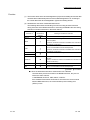
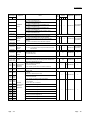
1
• SAFETY PRECAUTIONS •
(Read these precautions before using this product.)
Before using this product, please read this manual and the relevant manuals carefully and pay full
attention to safety to handle the product correctly.
The instructions given in this manual are concerned with this product. For the safety instructions of the
programmable controller system, please read the user's manual of the CPU module to use.
In this manual, the safety precautions are classified into two levels: " ! WARNING" and " ! CAUTION".
! WARNING
Indicates that incorrect handling may cause hazardous conditions,
resulting in death or severe injury.
! CAUTION
Indicates that incorrect handling may cause hazardous conditions,
resulting in minor or moderate injury or property damage.
Under some circumstances, failure to observe the precautions given under " ! CAUTION" may lead to
serious consequences.
Observe the precautions of both levels because they are important for personal and system safety.
Make sure that the end users read this manual and then keep the manual in a safe place for future
reference.
[Design Precautions]
!
WARNING
• For the operation status of each station at communication error in each station, refer to the
respective manual for each station.
The communication error may result in an accident due to incorrect output or malfunction.
• When changing data of a running programmable controller from a peripheral connected to the
CPU module or from an external device such as a personal computer connected to an intelligent
function module, configure an interlock circuit in the program to ensure that the entire system
will always operate safely.
For other controls to a running programmable controller (such as program modification or
operating status change), read relevant manuals carefully and ensure the safety before the
operation.
Especially, in the case of a control from an external device to a remote programmable controller,
immediate action cannot be taken for a problem on the programmable controller due to a
communication failure. To prevent this, configure an interlock circuit in the program, and
determine corrective actions to be taken between the external device and CPU module in case
of a communication failure.
A-1
A-1
[Design Precautions]
!
WARNING
• Do not write data into the "system area" of the buffer memory of intelligent function modules.
Also, do not use any "use prohibited" signals as an output signal to an intelligent function
module from the CPU module.
Writing data into the "system area" or outputting a signal for " use prohibited" may cause a
programmable controller system malfunction.
[Design Precautions]
!
CAUTION
• Do not install the control lines or communication cables together with the main circuit lines or
power cables.
Keep a distance of 100mm between them.
Failure to do so may result in malfunction due to noise.
[Installation Precautions]
!
WARNING
• Shut off the external power supply for the system in all phases before mounting or removing the
module. Failure to do so may result in electric shock or cause the module to fail or malfunction.
[Installation Precautions]
!
CAUTION
• Use the programmable controller in an environment that meets the general specifications
described in "Safety Guidelines", the manual supplied with the CPU module or head module.
Failure to do so may result in electric shock, fire, malfunction, or damage to or deterioration of
the product.
• To interconnect modules, engage the respective connectors and securely lock the module joint
lever. Incorrect interconnection may cause malfunction, failure, and drop.
• Do not directly touch any conductive parts and electronic components of the module. Doing so
can cause malfunction or failure of the module.
A-2
A-2
[Wiring Precautions]
!
WARNING
• Shut off the external power supply for the system in all phases before wiring.
Failure to do so may result in electric shock or cause the module to fail or malfunction.
• After installation and wiring, attach the included terminal cover to the product before turning it on
for operation. Failure to do so may result in electric shock.
[Wiring Precautions]
!
CAUTION
• Use applicable solderless terminals and tighten them within the specified torque range. If any
spade solderless terminal is used, it may be disconnected when a screw on the terminal block
comes loose, resulting in failure.
• Connectors for external device connection must be crimped or pressed with the tool specified by
the manufacturer, or must be correctly soldered.
Incomplete connections could result in short circuit, fire, or malfunction.
• Securely connect the connector to the module.
• Place the cables in a duct or clamp them.
If not, dangling cable may swing or inadvertently be pulled, resulting in damage to the module or
cables or malfunction due to poor contact.
• Check the interface type and correctly connect the cable.
Incorrect wiring (connecting the cable to an incorrect interface) may cause failure of the module
and external device.
• Tighten the terminal block screw within the specified torque range.
Undertightening can cause short circuit, fire, or malfunction. Overtightening can damage the
screw and/or module, resulting in drop, short circuit, fire, or malfunction.
• When disconnecting the cable from the module, do not pull the cable by the cable part.
For the cable with connector, hold the connector by hand and pull it out. For the cable
connected to the terminal block, loosen the terminal block screws.
Failure to do so may result in malfunction and damage to the module or cable.
• Prevent foreign matter such as dust or wire chips from entering the module.
Such foreign matter can cause a fire, failure, or malfunction.
• A protective film is attached to the top of the module to prevent foreign matter, such as wire
chips, from entering the module during wiring. Do not remove the film during wiring. Remove it
for heat dissipation before system operation.
A-3
A-3
[Startup/Maintenance Precautions]
!
WARNING
• Do not touch any terminal while power is on. Doing so will cause electric shock or malfunction.
• Shut off the external power supply for the system in all phases before cleaning the module or
retightening the terminal block screw. Failure to do so may result in electric shock.
[Startup/Maintenance Precautions]
!
CAUTION
• Do not disassemble or modify the modules. Doing so may cause failure, malfunction, injury, or a
fire.
• Shut off the external power supply for the system in all phases before connecting or
disconnecting the module. Failure to do so may cause the module to fail or malfunction.
• Tighten the terminal block screw within the specified torque range.
Undertightening can cause drop of the component or wire, short circuit, or malfunction.
Overtightening can damage the screw and/or module, resulting in drop, short circuit, or
malfunction.
• After the first use of the module (including a display unit), the number of module
connections/disconnections is limited to 50 times. Exceeding the limit (IEC 61131-2 compliant)
may cause malfunction.
• Before handling the module, touch a conducting object such as a grounded metal to discharge
the static electricity from the human body.
Failure to do so may cause the module to fail or malfunction.
A-4
A-4
[Operation Precautions]
!
CAUTION
• When controlling a running programmable controller (especially, changing data, program
modification, and operation status change) from an external device such as a personal
computer connected to an intelligent function module, read the relevant user's manual carefully
and ensure the safety before the operation. Incorrect data change, program modification, and
status control may cause malfunction of the system, mechanical damage, or accidents.
• While set values in the buffer memory are being registered to the flash ROM in the module, do
not turn off the power to the module and do not reset the CPU module. Doing so will affect the
flash ROM data, and setting to the buffer memory and registration to the flash ROM need to be
performed again. Also, it may cause failure or malfunction of the module.
[Disposal Precautions]
!
CAUTION
• When disposing of this product, treat it as industrial waste.
A-5
A-5
• CONDITIONS OF USE FOR THE PRODUCT •
(1) Mitsubishi programmable controller ("the PRODUCT") shall be used in conditions;
i) where any problem, fault or failure occurring in the PRODUCT, if any, shall not lead to any major or
serious accident; and
ii) where the backup and fail-safe function are systematically or automatically provided outside of the
PRODUCT for the case of any problem, fault or failure occurring in the PRODUCT.
(2) The PRODUCT has been designed and manufactured for the purpose of being used in general
industries.
MITSUBISHI SHALL HAVE NO RESPONSIBILITY OR LIABILITY (INCLUDING, BUT NOT LIMITED
TO ANY AND ALL RESPONSIBILITY OR LIABILITY BASED ON CONTRACT, WARRANTY, TORT,
PRODUCT LIABILITY) FOR ANY INJURY OR DEATH TO PERSONS OR LOSS OR DAMAGE TO
PROPERTY CAUSED BY the PRODUCT THAT ARE OPERATED OR USED IN APPLICATION
NOT INTENDED OR EXCLUDED BY INSTRUCTIONS, PRECAUTIONS, OR WARNING
CONTAINED IN MITSUBISHI'S USER, INSTRUCTION AND/OR SAFETY MANUALS, TECHNICAL
BULLETINS AND GUIDELINES FOR the PRODUCT.
("Prohibited Application")
Prohibited Applications include, but not limited to, the use of the PRODUCT in;
y Nuclear Power Plants and any other power plants operated by Power companies, and/or any other
cases in which the public could be affected if any problem or fault occurs in the PRODUCT.
y Railway companies or Public service purposes, and/or any other cases in which establishment of a
special quality assurance system is required by the Purchaser or End User.
y Aircraft or Aerospace, Medical applications, Train equipment, transport equipment such as Elevator
and Escalator, Incineration and Fuel devices, Vehicles, Manned transportation, Equipment for
Recreation and Amusement, and Safety devices, handling of Nuclear or Hazardous Materials or
Chemicals, Mining and Drilling, and/or other applications where there is a significant risk of injury to
the public or property.
Notwithstanding the above, restrictions Mitsubishi may in its sole discretion, authorize use of the
PRODUCT in one or more of the Prohibited Applications, provided that the usage of the PRODUCT is
limited only for the specific applications agreed to by Mitsubishi and provided further that no special
quality assurance or fail-safe, redundant or other safety features which exceed the general
specifications of the PRODUCTs are required. For details, please contact the Mitsubishi
representative in your region.
A-6
A-6
INTRODUCTION
Thank you for purchasing the Mitsubishi MELSEC-L series programmable controller.
This manual describes the functions of the LJ71C24 and LJ71C24-R2 serial communication modules
(hereinafter referred to as the C24) and programming.
Before using the equipment, please read this manual and the related manuals carefully to develop full
familiarity with the functions and performance of the MELSEC-L series programmable controller you have
purchased, so as to ensure correct use.
When applying the following program examples to the actual system, make sure to examine the applicability
and confirm that it will not cause system control problems.
Please make sure that the end user read this manual.
REMARKS
• Unless otherwise specified, in the program examples introduced in this manual,
I/O numbers X/Y00 to X/Y1F are assigned to the C24.
When using the program samples, I/O number must be assigned.
For I/O number assignment, refer to the following manual.
MELSEC-L CPU Module User's Manual (Function Explanation, Program
Fundamentals)
• Operating procedures are explained using GX Works2.
When using GX Developer or GX Configurator-SC, refer to Appendix 4.
A-7
A-7
COMPLIANCE WITH THE EMC AND LOW VOLTAGE DIRECTIVES
(1) Method of ensuring compliance
To ensure that Mitsubishi programmable controllers maintain EMC and Low Voltage Directives when
incorporated into other machinery or equipment, certain measures may be necessary. Please refer to
the manual included with the CPU module or base unit.
The CE mark on the side of the programmable controller indicates compliance with EMC and Low
Voltage Directives.
(2) Additional measures
No additional measures are necessary for the compliance of this product with EMC and Low Voltage
Directives.
A-8
A-8
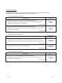
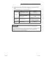
RELEVANT MANUALS
Basic specifications, functions, and usage of special functions can be confirmed in this manual.
In addition, use the following manuals according to the intended use.
(1) Relevant manuals for the C24
Manual number
(model code)
Manual name
MELSEC-Q/L Serial Communication Module User's Manual (Application)
Specifications and operating procedures for the special module functions, the settings for special
functions, and data-communication with target devices
SH-080007
(13JL87)
(Sold separately)
MELSEC-Q/L MELSEC Communication Protocol Reference Manual
MELSEC communication protocol that is used for communication with target devices by reading and
writing data to the CPU module.
SH-080008
(13JF89)
(Sold separately)
(2) CPU module user's manual
Manual number
(model code)
Manual name
MELSEC-L CPU Module User's Manual (Hardware Design, Maintenance and Inspection)
Specifications of the CPU modules, power supply modules, display unit, SD memory cards, and
batteries, information on how to establish a system, maintenance and inspection, and troubleshooting
SH-080890ENG
(13JW10)
(Sold separately)
MELSEC-L CPU Module User's Manual (Function Explanation, Program Fundamentals)
Functions and devices of the CPU module, and programming
SH-080889ENG
(13JZ35)
(Sold separately)
(3) Head module user's manual
Manual number
(model code)
Manual name
MELSEC-L CC-Link IE Field Network Head Module User's Manual
Specifications of the head module, procedures prior to operation, system configurations, setting and
wiring, settings, and troubleshooting
SH-080919ENG
(13JZ48)
(Sold separately)
A-9
A-9
(4) Operating manual
Manual number
(model code)
Manual name
GX Works2 Version1 Operating Manual (Common)
System configuration, parameter settings, and online operations (common to Simple project and
Structured project) of GX Works2
SH-080779ENG
(13JU63)
(Sold separately)
GX Works2 Version1 Operating Manual (Intelligent Function Module)
System configuration, parameter settings, and online operations (common to Simple project and
Structured project) of GX Works2
SH-080921ENG
(13JU69)
(Sold separately)
GX Developer Version 8 Operating Manual
Operating methods of GX Developer, such as programming, printing, monitoring, and debugging
SH-080373E
(13JU41)
(Sold separately)
A - 10
A - 10
CONTENTS
SAFETY PRECAUTIONS..............................................................................................................................A- 1
CONDITIONS OF USE FOR THE PRODUCT .............................................................................................A- 6
INTRODUCTION............................................................................................................................................A- 7
COMPLIANCE WITH THE EMC AND LOW VOLTAGE DIRECTIVES.......................................................A- 8
RELEVANT MANUALS .................................................................................................................................A- 9
CONTENTS....................................................................................................................................................A-11
TERMS ...........................................................................................................................................................A-17
PACKING LIST...............................................................................................................................................A-19
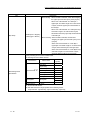
1 SERIAL COMMUNICATION MODULE FUNCTIONALITY
2 PART NAMES
3 SPECIFICATIONS
3.1 General Specifications ............................................................................................................................ 33.2 Performance Specifications .................................................................................................................... 33.2.1 Number of parameter settings ......................................................................................................... 33.3 Function List ............................................................................................................................................ 33.3.1 Basic functions ................................................................................................................................. 33.3.2 Additional functions .......................................................................................................................... 33.4 List of Input/Output Signals..................................................................................................................... 3-
1
1
3
4
4
5
7
4 PROCEDURES PRIOR TO OPERATION
5 SYSTEM CONFIGURATION
5.1 Overall Configuration .............................................................................................................................. 55.2 Applicable Systems................................................................................................................................. 55.2.1 Restrictions when the C24 is installed to the head module............................................................ 55.3 Systems that can be Configured and Functions .................................................................................... 5-
1
3
3
4
6 SETTING AND WIRING
6.1 Installation Environment and Position of the Module............................................................................. 6- 1
6.1.1 Handling precautions ....................................................................................................................... 6- 1
6.2 External Wiring with RS-232 Interface ................................................................................................... 6- 2
6.2.1 RS-232 connector specifications ..................................................................................................... 6- 2
6.2.2 RS-232 cable specification .............................................................................................................. 6- 6
6.2.3 Connecting the RS-232 interface (full-duplex communications) .................................................... 6- 7
6.3 External Wiring with RS-422/485 Interface ............................................................................................ 6- 9
6.3.1 RS-422/485 terminal block specifications ....................................................................................... 6- 9
6.3.2 RS-422/485 cable specifications ..................................................................................................... 6-10
6.3.3 Connection method for the RS-422/485 interface .......................................................................... 6-11
A - 11
A - 11
6.3.4 Precautions when transferring data using RS-422/485 circuit ....................................................... 6-16
6.3.5 Enabling or disabling echo back of the RS-422/485 interface........................................................ 6-19
6.4 Individual Station Test............................................................................................................................. 6-21
6.4.1 ROM/RAM/switch test...................................................................................................................... 6-22
6.4.2 Self-loopback test............................................................................................................................. 6-25
6.5 Loopback Test......................................................................................................................................... 6-28
7 SETTINGS FOR THE C24
7.1 Adding the C24 to Projects ..................................................................................................................... 7- 2
7.2 List of Setting Items for C24 ................................................................................................................... 7- 3
7.3 Switch Setting.......................................................................................................................................... 7-11
7.3.1 Transmission Setting........................................................................................................................ 7-12
7.3.2 Communication rate setting ............................................................................................................. 7-14
7.3.3 Communication protocol setting ...................................................................................................... 7-15
7.3.4 Station number setting ..................................................................................................................... 7-16
7.3.5 Setting and data flow in linked operation......................................................................................... 7-17
7.3.6 Precautions....................................................................................................................................... 7-19
7.4 Various Parameter Settings and Writing to the Flash ROM.................................................................. 7-20
7.4.1 Parameter setting ............................................................................................................................. 7-21
7.4.2 Writing to the flash ROM.................................................................................................................. 7-23
7.5 Auto Refresh ........................................................................................................................................... 7-25
7.5.1 Setting method for auto refresh ....................................................................................................... 7-26
7.6 Intelligent Function Module Interrupt Pointer Setting............................................................................. 7-27
7.7 Monitor/Test ............................................................................................................................................ 7-29
8 DATA COMMUNICATION USING THE MC PROTOCOL
8.1 Data Communication .............................................................................................................................. 88.1.1 Formats and applications of the data communication frames........................................................ 88.1.2 MC protocol system setting ............................................................................................................. 88.1.3 Support for the LCPU remote password function ........................................................................... 88.2 Utilizing the MX Component ................................................................................................................... 8-
2
2
3
4
5
9 DATA COMMUNICATION USING THE PREDEFINED PROTOCOL
9.1 Data Communication Procedure ............................................................................................................ 9- 3
9.2 Communication Type of Protocols ......................................................................................................... 9- 6
9.3 Packet Elements ..................................................................................................................................... 9- 7
9.4 Executing Condition of Predefined Protocol Communication................................................................ 9-27
9.5 Programming Example ........................................................................................................................... 9-31
9.5.1 System configuration/wiring example.............................................................................................. 9-31
9.5.2 Communication data ........................................................................................................................ 9-32
9.5.3 Communication settings................................................................................................................... 9-33
10 DATA COMMUNICATION USING THE NONPROCEDURAL PROTOCOL
10.1 Data Reception from the External Device.......................................................................................... 10- 2
10.1.1 Receiving methods....................................................................................................................... 10- 2
10.1.2 The receive area and the received data list ................................................................................ 10- 6
A - 12
A - 12
10.1.3 Sequence program for data reception......................................................................................... 10-11
10.1.4 How to detect and check the reception errors ............................................................................ 10-14
10.1.5 Receive data clear ....................................................................................................................... 10-17
10.1.6 Received data count and receive complete code settings ......................................................... 10-23
10.2 Sending Data to the External Device ................................................................................................. 10-26
10.2.1 Transmission methods................................................................................................................. 10-26
10.2.2 Arrangement and contents of the transmission area and the transmission data ...................... 10-27
10.2.3 Sequence program for transmission data ................................................................................... 10-29
10.2.4 How to detect and confirm transmission errors........................................................................... 10-33
10.3 Data Communications Precautions.................................................................................................... 10-35
11 DATA COMMUNICATION USING THE BIDIRECTIONAL PROTOCOL
11.1 Data Reception from the External Device.......................................................................................... 11- 2
11.1.1 Receiving methods....................................................................................................................... 11- 2
11.1.2 Arrangement and contents of the receive area and the receive data ........................................ 11- 4
11.1.3 Sequence program for data reception......................................................................................... 11-10
11.1.4 How to detect and check the reception errors ............................................................................ 11-13
11.1.5 Receive data clear ....................................................................................................................... 11-14
11.2 Sending Data to the External Device ................................................................................................. 11-15
11.2.1 Transmission methods................................................................................................................. 11-15
11.2.2 Arrangement and contents of the transmission area and the transmission data ...................... 11-16
11.2.3 Sequence program for data transmission ................................................................................... 11-19
11.2.4 How to detect and confirm transmission errors........................................................................... 11-23
11.3 Processing when Simultaneous Transmission Performed During Full-Duplex Communication ..... 11-25
11.3.1 Processing when simultaneous transmissions occur ................................................................. 11-25
11.3.2 Communication data processing when simultaneous transmissions occur .............................. 11-26
11.4 Data Communications Precautions.................................................................................................... 11-28
12 DEDICATED INSTRUCTIONS
12.1 Dedicated Instruction List and Available Devices .............................................................................. 12- 1
12.2 G(P).ONDEMAND .............................................................................................................................. 12- 3
12.3 G(P).CPRTCL ..................................................................................................................................... 12- 7
12.3.1 Functional protocol....................................................................................................................... 12-14
12.4 G(P).OUTPUT..................................................................................................................................... 12-15
12.5 G.INPUT.............................................................................................................................................. 12-19
12.6 G(P).BIDOUT ...................................................................................................................................... 12-23
12.7 G(P).BIDIN .......................................................................................................................................... 12-27
12.8 G(P).SPBUSY ..................................................................................................................................... 12-31
12.9 ZP.CSET (Receive data clear) ........................................................................................................... 12-33
13 DEBUG SUPPORT FUNCTION
13.1 Circuit Trace ........................................................................................................................................ 13- 1
13.1.1 Procedure for the circuit trace...................................................................................................... 13- 2
13.1.2 Execution of the circuit trace........................................................................................................ 13- 3
13.1.3 Circuit trace option setting ........................................................................................................... 13- 5
13.2 State Monitor ....................................................................................................................................... 13- 7
13.3 Protocol Execution Log Display Storage Function (for Predefined Protocol only) ........................... 13-12
13.3.1 Checking with GX Works2 ........................................................................................................... 13-13
A - 13
A - 13
13.3.2 Checking with the buffer memory................................................................................................ 13-15
14 MAINTENANCE AND INSPECTION
14.1 Inspection Items .................................................................................................................................. 14- 1
14.2 When Replacing Modules................................................................................................................... 14- 2
14.2.1 Procedure of C24 replacement and re-registration of data ........................................................ 14- 2
15 TROUBLESHOOTING
15.1 Checking the Status of the C24.......................................................................................................... 15- 1
15.1.1 Checking the H/W LED information............................................................................................. 15- 2
15.1.2 Checking the H/W switch information.......................................................................................... 15- 6
15.1.3 Reading the RS-232 control signal status................................................................................... 15- 9
15.1.4 Reading the data communication status (Transmission sequence status) ............................... 15-10
15.1.5 Reading the switch setting status ................................................................................................ 15-11
15.1.6 How to read the current operation status .................................................................................... 15-13
15.2 Error Code........................................................................................................................................... 15-15
15.2.1 How to check the error codes ...................................................................................................... 15-15
15.2.2 Error code list ............................................................................................................................... 15-19
15.2.3 A compatible 1C frame communications error code list ............................................................. 15-31
15.2.4 Error code list while modem function is used.............................................................................. 15-32
15.3 Troubleshooting by Symptom............................................................................................................. 15-34
15.3.1 The "RUN" LED is turned OFF .................................................................................................... 15-36
15.3.2 The "RD" LED does not blink even after message transmission from the external device....... 15-37
15.3.3 No response message is returned even though the external device transmitted a message
and the "RD" LED blinked............................................................................................................ 15-38
15.3.4 Transmission request does not make the "SD" LED blink ......................................................... 15-39
15.3.5 Read request signal does not turn ON even though the external device transmitted
a message and the "RD" LED was blinking ................................................................................ 15-40
15.3.6 The CPRTCL instruction execution is not completed although the "RD" LED blinked.............. 15-41
15.3.7 Communication error "NAK" ........................................................................................................ 15-42
15.3.8 Communication error "C/N" ......................................................................................................... 15-42
15.3.9 Communication error "P/S".......................................................................................................... 15-43
15.3.10 Communication error "PRO."..................................................................................................... 15-44
15.3.11 Communication error "SIO" ....................................................................................................... 15-45
15.3.12 Communication error "CH1 ERR." or "CH2 ERR." ................................................................... 15-46
15.3.13 Communication is intermittent ................................................................................................... 15-48
15.3.14 Undecodable data are transmitted or received......................................................................... 15-50
15.3.15 Whether the communication error is caused on the C24 or external device is unclear .......... 15-51
15.3.16 Communication is not available via the modem ....................................................................... 15-52
15.3.17 Communication is not available with the ISDN sub-address.................................................... 15-52
15.3.18 Constant cycle transmission is not performed normally ........................................................... 15-53
15.3.19 Condition agreement transmission is not performed normally ................................................. 15-53
15.3.20 Data cannot be received due to by an interrupt program ......................................................... 15-53
15.3.21 Data cannot be written to the flash ROM .................................................................................. 15-53
15.3.22 Troubleshooting on the protocol setting data reading/writing................................................... 15-54
15.3.23 The "ERR." LED is lit ................................................................................................................. 15-54
15.4 Initializing Error Information of the Serial Communication Module ................................................... 15-55
15.5 Clearing the Programmable Controller CPU Information .................................................................. 15-59
A - 14
A - 14
APPENDIXES
Appendix 1 Buffer Memory ......................................................................................................................App.- 1
Appendix 2 How to Confirm the Serial No. and Function Version..........................................................App.-21
Appendix 3 Differences between L Series C24 and Q Series C24........................................................App.-22
Appendix 3.1 Specification comparisons.............................................................................................App.-22
Appendix 3.2 Precautions for utilizing programs.................................................................................App.-22
Appendix 4 When Using GX Developer or GX Configurator-SC ...........................................................App.-23
Appendix 4.1 Compatible software packages .....................................................................................App.-23
Appendix 4.2 Specification comparisons.............................................................................................App.-23
Appendix 4.3 Operation comparison ...................................................................................................App.-24
Appendix 4.3.1 Operation of GX Developer .............................................................................. App.-24
Appendix 4.3.2 Operation of GX Configurator-SC .................................................................... App.-28
Appendix 5 Operation Image and Data Structure of Predefined Protocol .............................................App.-31
Appendix 5.1 Operation image of each communication type of protocol...........................................App.-31
Appendix 5.1.1 When communication type is "Send only"........................................................ App.-31
Appendix 5.1.2 When communication type is "Receive only" ................................................... App.-33
Appendix 5.1.3 When communication type is "Send & receive" ............................................... App.-35
Appendix 5.2 Verification operation of receive packet ........................................................................App.-37
Appendix 5.3 Data examples of packet elements...............................................................................App.-38
Appendix 5.3.1 Length............................................................................................................... App.-38
Appendix 5.3.2 Non-conversion variable................................................................................... App.-40
Appendix 5.3.3 Conversion variable.......................................................................................... App.-42
Appendix 5.3.4 Check code....................................................................................................... App.-45
Appendix 5.3.5 Non-verified reception ...................................................................................... App.-54
Appendix 6 Communication Example when the C24 Is Used Installed to the Head Module................App.-55
Appendix 6.1 Restrictions for programming ........................................................................................App.-55
Appendix 6.2 System configuration example ......................................................................................App.-56
Appendix 6.3 Parameter setting...........................................................................................................App.-61
Appendix 6.3.1 Master station setting ....................................................................................... App.-61
Appendix 6.3.2 Head module setting......................................................................................... App.-63
Appendix 6.4 Execution program example of the predefined protocol...............................................App.-64
Appendix 6.5 Sending/receiving data using the nonprocedural or bidirectional protocol ..................App.-69
Appendix 6.5.1 Receiving data using the nonprocedural or bidirectional protocol.................... App.-69
Appendix 6.5.2 Sending data using the nonprocedural or bidirectional protocol ...................... App.-72
Appendix 7 Processing Time ...................................................................................................................App.-76
Appendix 8 ASCII-Code List ....................................................................................................................App.-79
Appendix 9 Usage Example of MX Component .....................................................................................App.-80
Appendix 10 Setting Value Recording Sheet..........................................................................................App.-87
Appendix 11 External Dimensions...........................................................................................................App.-89
A - 15
A - 15
INDEX
REVISIONS
WARRANTY
A - 16
A - 16
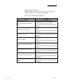
TERMS
Unless otherwise specified, this manual uses the following terms.
Term
Q series C24
C24
L series C24
Description
Another term for the MELSEC-Q series serial communication module
Another term for the MELSEC-L series serial communication module
QnA series serial communication
module
Another term for the MELSEC-QnA series serial communication module
A series computer link module
Another term for the MELSEC-A series serial communication module
QCPU
Another term for the MELSEC-Q series CPU module
CPU module
Abbreviation for the MELSEC-L series CPU module
LCPU
Another term for the MELSEC-L series CPU module
QnACPU
Another term for the MELSEC-QnA series CPU module
ACPU
Another term for the MELSEC-A series CPU module
Head module
Abbreviation for the LJ72GF15-T2 CC-Link IE Field Network head module
Display unit
A liquid crystal display to be attached to the CPU module
Intelligent function module
A MELSEC-L series module that has functions other than input or output, such as A/D converter
module and D/A converter module
Special function module
A MELSEC-QnA/A series modules that has functions other than input or output, such as A/D
converter module and D/A converter module
GX Works2
GX Developer
Product name of the software package for the MELSEC programmable controllers
GX Configurator-SC
A setting and monitoring tool added in GX Developer (for serial communication modules)
MX Component
An active X control library for serial communication
MC protocol
Abbreviation for the MELSEC communication protocol, a protocol to access a CPU module from
a target device in the Ethernet or serial communication
A compatible 1C frame
(Formats 1 to 4)
One of the message formats for the C24 for performing communication using the MC protocol
and ASCII data.
This is the same message format as when communicating using the dedicated protocol for the A
series computer link modules.
Device memory read/write operations for the QCPU and LCPU are allowed within the device
range of the AnACPU.
QnA compatible 2C frame
(Formats 1 to 4)
One of the message formats for the C24 for performing communication using the MC protocol
and ASCII data.
This is the same message format as the communication frame using the dedicated protocol for
the QnA series serial communication modules.
• QnA compatible 2C frame (Formats 1 to 4): QnA simplified frame (Formats 1 to 4)
QnA compatible 3C frame
(Formats 1 to 4)
QnA compatible 4C frame
(Formats 1 to 4)
One of the message formats for the C24 for performing communication using the MC protocol
and ASCII data.
This is the same message format as the communication frame using the dedicated protocol for
the QnA series serial communication modules.
• QnA compatible 3C frame (Formats 1 to 4): QnA frame (Formats 1 to 4)
• QnA compatible 4C frame (Formats 1 to 4): QnA extension frame (Formats 1 to 4)
QnA compatible 4C frame
(Format 5)
One of the message formats for the C24 for performing communication using the MC protocol
and binary code data.
This is the same message format as the communication frame using the dedicated protocol for
the QnA series serial communication modules.
• QnA compatible 4C frame (Format 5): QnA extension frame (Format 5)
Predefined protocol
One of the data communication functions available for the C24.
In data communication between the C24 and a target device, data can be sent and received by
using a protocol of the target device.
This must be set in GX Works2 or GX Configurator-SC (Predefined protocol support function).
A - 17
A - 17
Term
Description
Predefined protocol support function
A function available in GX Works2 and GX Configurator-SC (Predefined protocol support
function), which includes:
• Registration of the protocol appropriate to each target device
• Writing protocol setting data to or reading them from the flash ROM of the C24
• Debug support function
Nonprocedural protocol
A user's communication procedure and one of the data communication functions for
communicating any data between the CPU module and a target device.
Bidirectional protocol
A communication procedure for the C24 and one of the data communication functions for
communicating any data between the CPU module and a target device
Data communication function
Generic term for the MC protocol, predefined protocol, nonprocedural protocol, and bidirectional
protocol
Buffer memory
The memory of an intelligent function module and special function module used to store data
(such as setting values and monitored values) for communication with a CPU module.
Packet
A data string used for communication with target devices by the predefined protocol.
Multidrop connection
A name of the connection when multiple target devices or other C24 are connected in a 1:n or
m:n mode using the RS-422/485 interface of the C24.
Message send function
(Printer function)
This function registers character data (messages) to be sent to target devices (mainly printers) in
the C24 as a user frame in advance, and sends the registered data for multiple user frames using
the nonprocedural protocol.
User frame
Data name when the fixed format portion of messages to be sent or received between the C24
and a target device is registered in the module and used for sending and receiving data. (The
contents of a user frame data should conform to the specifications of the target device).
The data array of the head and tail sections of a message (transmission control code, C24 station
number, sum check, fixed data, etc.) to be sent and received is registered in the C24 before use.
This type of data is used in the on-demand function of the MC protocol and the data
communication function with the nonprocedural protocol.
Independent operation
A mode of interface operation to communicate data with target devices using a function specified
in each communication protocol setting. The interfaces of two C24s do not interact.
Linked operation
The operation mode of each of the two interfaces of C24s that are connected to target devices
and linked to one another in order to send/receive data to/from the target devices.
The two interfaces communicate data using the same data-communication function (MC protocol
(identical type) or nonprocedural protocol) and the same transmission specifications. (Linked
operation using the predefined protocol or bidirectional protocol is not allowed.)
BUFRCVS
Abbreviation for Z.BUFRCVS
CPRTCL
Abbreviation for G.CPRTCL or GP.CPRTCL
CSET
Abbreviation for ZP.CSET
GETE
Abbreviation for G.GETE or GP.GETE
INPUT
Abbreviation for G.INPUT
ONDEMAND
Abbreviation for G.ONDEMAND or GP.ONDEMAND
OUTPUT
Abbreviation for G.OUTPUT or GP.OUTPUT
PRR
Abbreviation for G.PRR or GP.PRR
PUTE
Abbreviation for G.PUTE or GP.PUTE
SPBUSY
Abbreviation for G.SPBUSY or GP.SPBUSY
UINI
Abbreviation for ZP.UINI
User's Manual (Application)
Abbreviation for the Serial Communication Module User's Manual (Application)
A - 18
A - 18
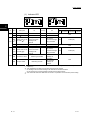
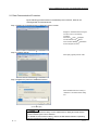
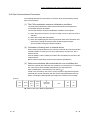
PACKING LIST
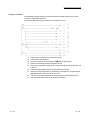
The following items are included in the package of the C24.
Before use, check that all the items are included.
(1) LJ71C24
Before Using the Product
LJ71C24
A set of terminating resistors
Terminating resistor for
RS-422 communication,
330 1/4W 2
(Orange-Orange-Brown, Gold)
A - 19
Terminating resistor for
RS-485 communication,
110 1/2W 2
(Brown-Brown-Brown, Gold)
"CAUTION" note
A - 19
(2) LJ71C24-R2
Before Using the Product
LJ71C24-R2
A - 20
A - 20
MEMO
A - 21
A - 21
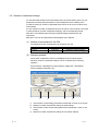
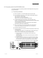
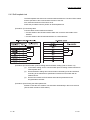
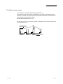
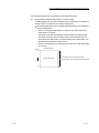
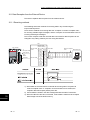
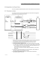
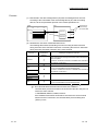
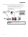
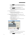
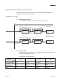
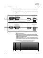
1 SERIAL COMMUNICATION MODULE FUNCTIONALITY
1 SERIAL COMMUNICATION MODULE FUNCTIONALITY
The C24 performs data communication with another device connected by an RS-232
or RS-422/485 line, using any of the following four protocols.
Through a modem or terminal adapter, a public line (analog/digital) can be used for
data communication with a remotely located device.
1
(1) MELSEC Communication protocol (hereinafter referred to as MC
protocol)
Data can be read from or written into the CPU module device memory from the
other external device.
Use this protocol when controlling the operation of CPU modules from the
external device side.
Refer to the MELSEC-Q/L MELSEC Communication Protocol Reference Manual
for the details.
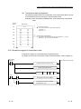
ENQ
Sam
check
code
1-1
Command
ETX
Characters
Characters
Sam
check
code
STX
1-1
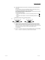
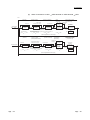
1 SERIAL COMMUNICATION MODULE FUNCTIONALITY
(2) Predefined protocol
Data can be transferred in accordance with a protocol for the external device.
The same data communication can be performed in the nonprocedural protocol
explained in (3). However, the following shows the convenient functions when
comparing this protocol and the nonprocedural protocol.
• Sequence programs can be reduced since the GX Works2 predefined protocol
support function allows simple protocol setting.
• Writing registered protocol setting data to the flash ROM reduces the volume of
the program to be written to the CPU module.
1-2
1-2
1
1 SERIAL COMMUNICATION MODULE FUNCTIONALITY
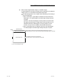
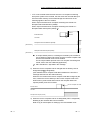
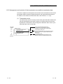
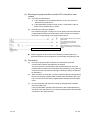
(3) Nonprocedural protocol
Fixed or variable length messages can be received in accordance with the
external device specifications.
Nonprocedural protocol enables communication between an external device and
the CPU module by freely setting the data format and transmission control
procedures.
It is used for the data communication using the protocols of external devices,
such as measuring instruments, barcode readers, etc.
Send
Any data
Any data
Receive
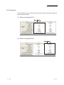
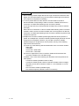
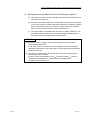
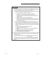
(4) Bidirectional protocol
The bidirectional protocol enables communication between an external device
and the CPU module using the data format and communication control
procedures for the bidirectional protocol.
Use this protocol to check if the communication is successfully completed.
The data communication is performed as follows.
1) External device sends data to the C24
When receiving data
Data
ENQ length
Sum
check
code
Any data
When normal
When abnormal
ACK
Error
code
NAK
2) The C24 notifies whether the data
communication has been completed
normally by a response message.
1-3
1-3
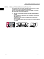
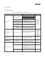
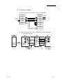
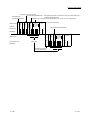
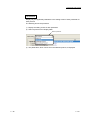
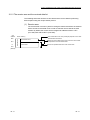
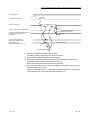
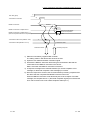
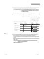
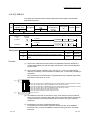
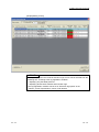
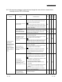
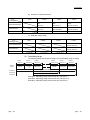
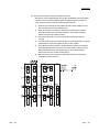
2 PART NAMES
2 PART NAMES
This chapter shows part names of the C24.
LJ71C24
5)
2
1)
2)
3)
6)
4)
5)
LJ71C24-R2
5)
1)
2)
2)
6)
4)
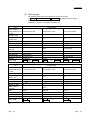
No.
1)
2-1
5)
Name
Description
Indicator LED
Indicator LED (For details, refer to (1).)
2)
RS-232 interface
RS232 interface for serial communication with external
devices (D-Sub 9 pin female)
3)
RS-422/485 interface
RS422/485 interface for serial communication with external
devices (2-piece terminal block)
4)
Serial number display
Displays the serial number of the rating plate.
5)
Module joint lever
Hooks to fix the module connection.
6)
DIN rail hook
Hooks to install to DIN rails.
2-1
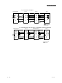
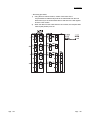
2 PART NAMES
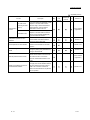
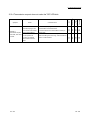
(1) Indicator LED
2
Applicable protocol
CH
LED
Description
On
RUN Normal operation
—
ERR. Error (
CH1
1)
NEU. Neutral status on the
( 3) CH1 side ( 2)
SD
Transmission status
RD
Reception status
SD
RD
Transmission status
Reception status
Off
Normal
—
Faulty or reset
Error has occurred
—
Normal
Waiting for MC
protocol command
message to be
received
—
MC protocol
command message
being processed
Data being transmitted
Data being received
NEU. Neutral status on the
( 3) CH2 side ( 2)
CH2
Flashing
Waiting for MC
protocol command
message to be
received
MC
Valid
Data not transmitted
MC protocol
command message
being processed
Data being transmitted
MC command
message not
transmitted
Data being received
MC command
message not
received
Predefined
Valid
Invalid (Off)
Valid
Data not received
—
NonBidirectional
procedural
Valid
Invalid (Off)
Valid
1 This LED turns on when an error occurs at C24 hardware or during data communication. (Refer to
chapter 15.)
2 This LED displays the data communication status via the MC protocol.
On: Waiting for the command message to be received from the external device.
Off: Processing the command message received from the external device.
3 This LED is also valid when "MELSOFT Connection" is specified in communication protocol setting.
2-2
2-2
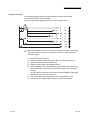
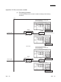
3 SPECIFICATIONS
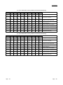
3 SPECIFICATIONS
This chapter explains the general specifications, performance specifications, function
list, and I/O signals.
3.1 General Specifications
For the general specifications of C24, refer to "Safety Guidelines", the manual supplied
with the CPU module or head module.
The latest manuals in PDF can be downloaded from the MELFANSweb.
3
3.2 Performance Specifications
The following shows the C24 performance specifications.
For the transmission specifications when communicating via the modem function, refer
to both Section 3.2. and User's Manual (Application).
(1) Transmission specification
Model name
Item
LJ71C24
LJ71C24-R2
CH1
RS-232-compliance
(D-sub 9 pin female)
RS-232-compliance
(D-sub 9 pin female)
CH2
RS-422/485-compliance
(2-piece terminal block)
RS-232-compliance
(D-sub 9 pin female)
Interface
Line (
1)
Full-duplex/half-duplex communications
MC protocol communication
Communication
system
Half-duplex communications
Predefined protocol
communication
Full-duplex/half-duplex communications
Nonprocedural protocol
communication
Full-duplex/half-duplex communications
Bidirectional protocol
communication
Full-duplex/half-duplex communications
Synchronization method
Transmission speed
Data format
50
300
600
1200
2400
4800
9600
14400
19200
28800
38400
57600
115200
230400
(bps)
• Transmission speed 230400 bps is available for only CH1. (Not available for CH2)
• Total transmission speed of two interfaces is available up to 230400 bps.
• Total transmission speed of two interfaces is available up to 115200 bps when the communication data
monitoring function is used.
Start bits
1
Data bits
7/8
Parity bits
1 (vertical parity) or none
Stop bits
Access cycle
Start-stop synchronization method
1/2
MC protocol communication
Processes one request during the END processing of the CPU module of the station with the C24.
Number of scans that must be processed/number of link scans depends on the contents of the request.
(Refer to the MELSEC-Q/L MELSEC Communication Protocol Reference Manual)
Predefined protocol
communication
Sends or receives data when requested with the dedicated instruction (CPRTCL).
Nonprocedural protocol
communication,
Bidirectional protocol
communication
Sends each time a send request is issued. Can receive at any time.
(Continued on next page)
3-1
3-1
3 SPECIFICATIONS
(Continued from preceding page)
Model name
Item
Error detection
LJ71C24
LJ71C24-R2
Parity check
Selected for all protocols and when this check is enabled, ODD or EVEN is selected by a parameter.
Sum check code
For the MC or bidirectional protocol, selected by a parameter.
For the predefined protocol, whether or not a sum check code is needed depends on the selected protocol.
For the nonprocedural protocol, selected in the user frame.
RS-232
Transmission control
3
RS-422/485
DTR/DSR control
Enabled
Disabled
RS/CS control
Enabled
Disabled
CD(DCD) signal control
Enabled
Disabled
DC1/DC3 (Xon/Xoff) control
DC2/DC4 control
Enabled
Enabled
• DTR/DSR signal control and DC code control are selected by the user.
Line configuration
of connection
(External device
side: CPU module
side)
RS-232
1:1
1:1, 1:n, n:1, m:n
—
MC protocol
communication
1:1
1:1
Predefined protocol
communication
1:1
1:1
Nonprocedural
protocol
communication
1:1
1:1
Bidirectional
protocols
communication
1:1
1:1
MC protocols
communication
1:1, 1:n, m:n
RS-422/485
RS232
Line configuration
of data
communication
(External device
side: CPU module
side)
RS422/
485
Transmission
distance (Overall
distance)
1:1
Predefined protocol
communication
1:1, n:1
Nonprocedural
protocol
communication
1:1, 1:n, n:1
Bidirectional
protocols
communication
1:1
RS-232
RS-422/485
—
Maximum 15 m
Maximum 15 m
Maximum 1200 m
(overall distance)
—
Flash ROM write count
Maximum 100,000 times to the same area
Number of occupied I/O points
32 points (I/O assignment: Intelli: 32 points)
5V DC internal current consumption
0.39A
External dimensions
Weight
0.26A
90 (H)×28.5 (W)×95 (D)[mm]
0.17Kg
0.14Kg
1 Set to transfer data with external devices using a full-duplex communication system when the C24 is
started. For switching to a half-duplex communication system, refer to the User's Manual (Application).
3-2
3-2
3 SPECIFICATIONS
3.2.1 Number of parameter settings
For the parameter settings of the initial setting and auto refresh setting of the C24, set
parameters (including the parameters for other intelligent function modules) not to
exceed the maximum number of parameters that can be set for a CPU module or the
head module.
For the maximum number of parameters that can be set for a CPU module or the head
module (maximum number of parameter settings), refer to the following manual.
MELSEC-L CPU Module User's Manual (Hardware Design, Maintenance and
Inspection)
MELSEC-L CC-Link IE Field Network Head Module User's Manual
(1) Number of parameters for the C24
The following number of parameters can be set for one C24.
Initial setting
Auto refresh setting
LJ71C24
Target module
0 (Not used)
50 (Maximum number of settings)
LJ71C24-R2
0 (Not used)
51 (Maximum number of settings)
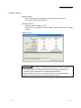
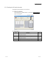
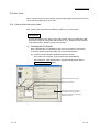
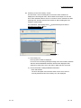
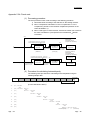
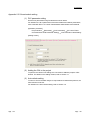
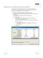
(2) Checking method
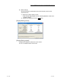
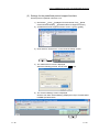
The number of parameters set for the intelligent function module and the
maximum number of parameter settings can be confirmed by the following
operation.
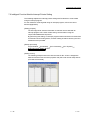
Project window [Intelligent Function Module]
Function Module Parameter List].
1)
1)
2)
3)
4)
3-3
2)
Right click
3)
[Intelligent
4)
Total number of initial setting parameters marked with a check on the screen
Maximum number of parameter settings of initial settings
Total number of auto refresh setting parameters marked with a check on the
screen
Maximum number of parameter settings of auto refresh settings
3-3
3 SPECIFICATIONS
3.3 Function List
3.3.1 Basic functions
The following shows the basic functions of the C24.
Function
Description
Reference
Executes batch read/write in bit/word units.
Reading/writing from/to the
device memory of the CPU
module
Executes monitoring of device memory.
Executes batch read/write of multiple blocks.
Executes read/write by extension designation.
Accesses other stations via network system.
Communication with MC
protocol
Reading/writing from/to the
buffer memory of the C24
Executes reading/writing from/to the buffer
memory of the C24.
Reading/writing from/to the
buffer memory of intelligent
function modules
Executes reading/writing from/to the buffer
memory of intelligent function modules.
Reading/writing from/to
sequence program files and
parameter files
Controlling the status of the
CPU module
(such as remote RUN/STOP)
Communication with
predefined protocol
Data transmission/reception
Executes reading/writing from/to program files
and parameter files stored in the CPU module.
Chapter 8,
MELSEC-Q/L
MELSEC
Communication
Protocol
Reference
Manual
Executes status control of the CPU module.
Executes remote RUN/STOP/PAUSE/latch
clear/reset operations from external devices.
Executes data transmission/reception with the
appropriate protocol for each external device.
The external device side protocol can be easily
selected, or created/edited from the predefined
protocol library of GX Works2.
Chapter 9,
Appendixes 5,
GX Works2
Version1
Operating
Manual
(Intelligent
Function Module)
Communication with
nonprocedural protocol
Data transmission/reception in
any format
Data communication can be made in any
format appropriate to specifications of external
devices (measuring devices, personal
computers etc.).
Chapter 10
Communication with
bidirectional protocol
Data transmission/reception in
any format
Any data transmission/reception can be made
with message formats and transmission control
procedures for the bidirectional protocol.
Chapter 11
Circuit trace
Debug support function
State monitor
Protocol execution log storage
function
3-4
This function traces communication data and
control signal between the C24 and device
controller.
Section 13.1
This function monitors the signal,
communication error information, and operation
setting switch of the C24.
The protocol execution status is also monitored
during the predefined protocol communication.
Section 13.2
This function checks the detailed predefined
protocol execution status and results for each
channel.
Section 13.3
3-4
3 SPECIFICATIONS
3.3.2 Additional functions
The following shows the additional functions of the C24.
The following abbreviations appear in the protocol column of the function list.
MC: MC protocol
Pd: Predefined protocol
Non: Nonprocedural protocol
Bi: Bidirectional protocol
(
: Applicable protocol)
Protocol
Function
Description
Reference
MC
Communication with ASCII code
Pd
Executes the communication with an A compatible 1C
frame.
Executes the communication with a QnA compatible
4C frame.
Monitoring CPU modules
(Programmable controller CPU
monitoring function)
Monitors the operating status of CPU modules and the
data in the device memory.
The CPU module status and the device memory data
can be sent to the external device at fixed intervals,
when an error occurs in the machine equipment, or
when certain conditions are satisfied.
Turning on/off input signals of the
C24 from an external device (global
function)
Turns on/off input signals of the C24 from an external
device.
Data transmission from a CPU
module to an external device (ondemand function)
Data can be sent from the programmable controller
CPU to the external devices in each frame format of
the MC protocol.
Data transmission/reception by the
user frame
Registers the fixed format portion of messages sent
and received between C24 and an external device in
the module. That portion can be used when sending
and receiving data.
To make the data reception faster, reads the reception
data by interrupt programs.
ASCII data transmission/reception
by ASCII-BIN conversion
Communication can be made with ASCII code data
since the C24 executes ASCII-BIN conversion.
Data transmission/reception by
specifying transparent code
In data communication with external devices, one-byte
data for transmission control of the external device
side can be sent/received as an user data.
Communication via public network,
etc.
(Modem function)
Data communication is performed via public line with a
remotely located external device.
Data communication with MC protocol, nonprocedural
protocol, and bidirectional protocol are available.
3-5
Bi
Executes the communication with QnA compatible
2C/3C/4C frames.
Communication with binary code
Data reception by interrupt
programs
Non
Chapter 8,
MELSEC-Q/L
MELSEC
Communication
Protocol
Reference
Manual
User's manual
(Application)
User's manual
(Application)
3-5
3 SPECIFICATIONS
(
Function
Transmission
control
Description
DC code control
(including Xon/Xoff
control)
This control notifies the availability of data
reception in the host station and the
effective range of sent/received data to
external devices, using the data for
transmission control in the C24.
DTR/DSR control
This control notifies the availability of data
reception in the host station to external
devices, using the ER(DTR)/DR(DSR)
signal of the RS-232 interface.
MC
Nonproced
Bidirectional
ural
protocol
protocol
: Applicable protocol)
Pd
Reference
User's manual
(Application)
Independent operation of each
interface
Two interfaces of the C24 perform data
communication with external devices
without connecting each other.
Section 7.3
Linked operation of each interface
All data received from one of the two
interfaces is transmitted from the other
interface.
Section 7.3.5
Parameter registrations to the flash
ROM
Initial values of the buffer memory can be
changed by setting each parameter and
writing to the flash ROM.
Section 7.4
Remote password check function
Checks the password in the C24 when a
remote user accesses to the LCPU with
the modem function. This function
prevents unauthorized accesses to the
LCPU.
User's manual
(Application)
Enabling or disabling echo back of
the RS-422/485 interface
When data are sent through RS-485 (2wire type) from the RS-422/485 interface,
the same data are also sent to RDA or
RDB in the host station. Whether to
receive the returned data or not (discard)
can be specified.
Section 6.3.5
3-6
3-6
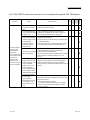
3 SPECIFICATIONS
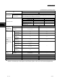
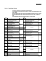
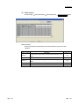
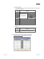
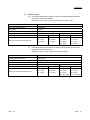
3.4 List of Input/Output Signals
This section describes the input/output signals of the C24.
The following I/O signal assignment is based on the case where the start I/O No. of the
C24 is "0000".
Device numbers starting with X indicate input signals from the C24 to the CPU module.
Device numbers starting with Y indicate output signals from the CPU module to the
C24.
The following table lists the input/output signals for the CPU module.
Device
number
Signal description
X0
1
CH1 Transmission normal completion
ON: Normal completion
X1
1
CH1 Transmission abnormal completion
ON: Abnormal completion
X2
1
CH1 Transmission processing
ON: Transmission in progress
X3
2
CH1 Reception data read request
ON: Requesting read
X4
2
CH1 Reception abnormal detection
ON: Abnormal detection
X5
1
CH1 Protocol execution completion
ON: Execution completed
X6
3
CH1 Mode switching
ON: Switching
X7
1
CH2 Transmission normal completion
ON: Normal Completion
X8
1
CH2 Transmission abnormal completion
ON: Abnormal completion
X9
1
CH2 Transmission processing
ON: Transmission in progress
XA
2
CH2 Reception data read request
ON: Requesting read
XB
2
CH2 Reception abnormal detection
ON: Abnormal detection
XC
1
CH2 Protocol execution completion
ON: Execution completed
XD
3
CH2 Mode switching
ON: Switching
XE
CH1 ERR. occurrence
ON: Error occurring
Reference
—
Section 10.1
Section 11.1
Device
number
Y0
CH1 Transmission request
ON: Requesting transmission
Y1
CH1 Reception data read completion
ON: Data read completed
Y2
CH1 Mode switching request
ON: Requesting switch
Y3
CH1 Protocol execution request
ON: Requesting execution
Y5
User's Manual
(Application)
Y6
Section 10.1
Section 11.1
Use prohibited
Y7
CH2 Transmission request
ON: Requesting transmission
Y8
CH2 Reception data read completion
ON: Data read completed
Y9
CH2 Mode switching request
ON: Requesting switch
YA
CH2 Protocol execution request
ON: Requesting execution
YC
User's Manual
(Application)
YD
Use prohibited
YE
CH1 ERR.clear request
ON: Requesting error clear
YF
CH2 ERR. clear request
ON: Requesting error clear
Section 15.4
CH2 ERR. occurrence
ON: Error occurring
X10
Modem initialization completion
ON: Initialization completed
Y10
Modem initialization request (standby request)
ON: Requesting initialization
X11
Dialing
ON: Dial in progress
Y11
Connection request
ON: Requesting connection
X12
Connection
ON: Connection in progress
Y12
Modem disconnection request
ON: Requesting disconnection
X13
Initialization/connection abnormal completion
ON: Initialization/ connection abnormally completed
Y13
X14
Modem disconnection complete
ON: Disconnection completed
Y14
Use prohibited
X16
—
Use prohibited
Y17
Flash ROM read request
ON: Requesting
X18
1 Flash ROM write completion
ON: Completed
Y18
Flash ROM write request
ON: Requesting
Y19
Flash ROM system setting write request
ON: Requesting
3-7
—
User's Manual
(Application)
—
—
—
Y16
ON: Completed
X19
—
Y15
1 Flash ROM read completion
—
—
User's Manual
(Application)
X17
Flash ROM system setting write completion
ON: Completed
User's Manual
(Application)
Section 15.4
XF
X15
—
YB
—
User's Manual
(Application)
Reference
Y4
—
—
Signal description
—
3-7
3 SPECIFICATIONS
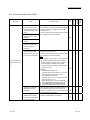
Device
number
Signal description
X1A
CH1 Global signal
ON: Output instructed
X1B
CH2 Global signal
ON: Output instructed
X1C
System setting default completion
ON: Completed
ON: Ready
Reference
Device
number
MELSEC-Q/L
MELSEC
Communication
Protocol
Reference
Manual
Y1A
—
Y1C
Section 9.4
Y1D
Y1B
X1D
6 Predefined protocol ready
X1E
4 C24 ready ON: Accessible
—
Y1E
X1F
Watchdog timer error (WDT error)
5
ON : Module error occurred
OFF: Module being normally operated
—
Y1F
Signal description
Reference
Use prohibited
—
System setting default request
ON: Requesting
Use prohibited
—
—
1 The device does not turn on/off by execution of a dedicated instruction when a
function that corresponds to the input signal is used.
2 The device does turn on/off by execution of a dedicated instruction when a function
that corresponds to the input signal is used (from ON to OFF: Data read completed).
3 The mode switching (X6/XD) turns ON when the following function is executed.
• Mode switching, transmission sequence initialization, reception data clear (by
buffer memory), user frame use enable/disable designation, UINI instruction,
programmable controller CPU information clear
While the mode switching (X6/XD) is ON, do not issue a communication request to
the target interface. (The communication processing of the C24 is stopped while
the mode switching (X6/XD) is ON.)
4 The C24 ready indicates whether or not it is possible to access the C24 from the CPU
module.
Use it as an interlock signal for a sequence program.
5 Restart the CPU module when the watchdog timer error is turned on.
If the error still occurs after restarting, refer to Section 15.3.1 to take corrective
actions.
6 Predefined protocol ready (X1D) is a signal that turns on when predefined protocol
communication becomes ready.
IMPORTANT
(1) Do not use any "use prohibited" signals as an output signal to the CPU
module.
Doing so may cause malfunction of the programmable controller system.
(2) If the modem function is not used, X10 to X16 and Y10 to Y16 cannot be used.
3-8
3-8
4 PROCEDURES PRIOR TO OPERATION
4 PROCEDURES PRIOR TO OPERATION
This chapter explains the procedures required before starting the operation.
4
1 The same communication is available using the predefined protocol. By the Predefined protocol, programs
can be created easily, and the number of steps can be drastically reduced.
4-1
4-1
4 PROCEDURES PRIOR TO OPERATION
MEMO
4
4-2
4-2
5 SYSTEM CONFIGURATION
5 SYSTEM CONFIGURATION
This chapter explains the system configuration and the number of applicable modules
of the C24.
5.1 Overall Configuration
(1) When installing the C24 to the CPU module
Display unit
(optional)
Power supply module
RS-232 adapter
(optional)
CPU module
LJ71C24
END cover
5
1
1: For the RS-232 adapter, refer to the following.
MELSEC-L CPU Module User's Manual (Hardware Design, Maintenance
and Inspection)
(2) When installing the C24 to the head module
5-1
5-1
5 SYSTEM CONFIGURATION
(3) System examples
(a) Connecting two external devices to the C24
Connect external devices such as a GOT and a barcode reader to one C24.
Data can be exchanged between a GOT and a device such as a barcode
reader via the C24.
1: For the RS-232 adapter, refer to the following manual.
MELSEC-L CPU Module User's Manual (Hardware Design,
Maintenance and Inspection)
5
(b) Connecting an external device and multiple C24s
Connect multiple C24s to a personal computer in a multidrop network.
From the personal computer, data in each CPU module can be written or
read via each C24.
For the combinations of external devices and the C24, refer to Section 5.3.
RS-232
1
1
1
RS-485
RS-485
1: For the RS-232 adapter, refer to the following manual.
MELSEC-L CPU Module User's Manual (Hardware Design,
Maintenance and Inspection)
5-2
5-2
5 SYSTEM CONFIGURATION
5.2 Applicable Systems
(1) Applicable CPU modules and No. of modules
Refer to the following.
MELSEC-L CPU Module User's Manual (Hardware Design, Maintenance and
Inspection)
MELSEC-L CC-Link IE Field Network Head Module User's Manual
(2) Supported software packages
(a) Setting and monitoring tools
Refer to the following.
MELSEC-L CPU Module User's Manual (Hardware Design, Maintenance
and Inspection)
MELSEC-L CC-Link IE Field Network Head Module User's Manual
(b) Communication support tools for external devices
Item Name
Model
Remark
ActiveX control library.
MX Component
SWnD5C-ACT(-E)
The "n" in the model name is 0 or greater. ( 1)
1 Depending on the version of MX Component used, different versions of the C24 are supported.
For details, refer to the manual of MX Component.
5.2.1 Restrictions when the C24 is installed to the head module
For restrictions when the C24 is installed to the head module, refer to Appendix 6.1.
5-3
5-3
5 SYSTEM CONFIGURATION
5.3 Systems that can be Configured and Functions
The following describes the system configurations and available functions when using
the C24.
(1) System configurations
System configurations (combinations of the C24 and external device) for data
communication are shown below.
(a) External device and C24 with 1:1 system configuration
RS-232/422
(b) External device and C24 with n:1 system configuration
RS-485
5-4
5-4
5 SYSTEM CONFIGURATION
(c)
External device and C24 with 1:n system configuration
(d)
External device and C24 with m:n system configuration
RS-485
RS-232
RS-485
RS-485
5-5
RS-485
RS-485
5-5
5 SYSTEM CONFIGURATION
(2) Correspondence between the data communication functions and
system configurations
The following shows system configurations that can use the data communication
functions of the C24.
(a) Communication using the MC protocol
(
System configuration
(External device: C24)
Function
1:1
n:1
1:n
: Available,
: Not available)
Reference
m:n
CPU module device memory read/write
Chapter 8,
MELSEC-Q/L MELSEC
Communication Protocol Reference
Manual
Intelligent function module buffer memory read/write
Sequence program read/write
CPU module status control (remote RUN, STOP, etc.)
On-demand function
User's Manual (Application)
MELSEC-Q/L MELSEC
Communication Protocol Reference
Manual
Global function
Programmable controller CPU monitoring function
User's Manual (Application)
(b) Communication using the predefined protocol
( : Available,
System configuration
(External device: C24)
Function
1:1
n:1
1:n
: Not available)
Reference
m:n
Chapter 9
Data transmission/reception
GX Works2 Version1 Operating Manual
(Intelligent Function Module)
(c) Communication using the nonprocedural protocol
( : Available,
Function
System configuration
(External device: C24)
1:1
Data transmission/receiving in arbitrary format
n:1
1:n
: Not available)
Reference
m:n
Chapter 10
Data transmission/receiving with user frames
Programmable controller CPU monitoring function
Reading received data using interrupt programs
User's Manual (Application)
Sending/receiving ASCII data using ASCII-BIN conversion
5-6
5-6
5 SYSTEM CONFIGURATION
(d) Communication using the bidirectional protocol
( : Available,
Function
System configuration
(External device: C24)
1:1
Data transmission/receiving
n:1
1:n
: Not available)
Reference
m:n
Chapter 11
Reading received data using interrupt programs
Sending/receiving ASCII data using ASCII-BIN conversion
User's Manual (Application)
In general, if data communication is performed using a system configuration of
other than 1:1 connection mode, the following points should be well noted.
• Avoid simultaneous transmission
• Discard the received data other than that addressed to the local station.
5-7
5-7
6 SETTING AND WIRING
6 SETTING AND WIRING
This chapter explains the setting and wiring methods in the system for using the C24.
6.1 Installation Environment and Position of the Module
For the installation environment and position of the module, refer to the following
manual.
MELSEC-L CPU Module User's Manual (Hardware Design, Maintenance and
Inspection)
MELSEC-L CC-Link IE Field Network Head Module User's Manual
6.1.1 Handling precautions
When using the C24, note the following points.
(1) Do not drop the C24 or subject it to heavy impact since its case is made of resin.
(2) Tighten the screws such as terminal screws within the following torque ranges.
Screw
RS-422/485 terminal block screw (M3
screw)
6
RS-422/485 terminal block mounting screws
(M3.5 screw)
Tightening torque range
Remarks
0.42 to 0.58 N • m
-
0.66 to 0.89 N • m
Screw hole depth:
RS-232 cable connector screw (M2.6 screw)
0.20 to 0.39 N • m
L=3.2mm or less
(Internal length from
the surface)
6-1
6-1
6 SETTING AND WIRING
6.2 External Wiring with RS-232 Interface
This section explains the specifications of RS-232 and how to connect with external
devices.
6.2.1 RS-232 connector specifications
The following shows the specifications of the RS-232 connector that connects the C24
to an external device.
(1) The control signals are described below. (The pin numbers of the connector are
enclosed in parentheses.)
1) CD(DCD) signal (1)
• The C24 operates according to the setting of the CD terminal check.
Full-duplex
communication
Half-duplex
communication
CD terminal check enabled
CD terminal check disabled
• The C24 performs send and receive
• The C24 performs send and receive
processing when the CD(DCD) signal
processing regardless of the ON/OFF status
(receive carrier detection) is ON.
of the CD(DCD) signal.
• If the CD(DCD) signal is turned off during
• Data communications is possible with an
data communication, the C24 initializes the
external device that cannot turn the
transmission sequence.
CD(DCD) signal ON/OFF.
User's Manual (Application)
Setting impossible.
The CD terminal check can be set in GX Works2 as follows.
"For designation of communication
"Various_Control_Specification" screen
"CD terminal check designation (for RS-232)"
control"
2) RD(RXD) signal (2)
This is a signal to receive data.
3) SD(TXD) signal (3)
This is a signal to send data.
6-2
6-2
6
6 SETTING AND WIRING
4) ER(DTR) signal (4)
• When communicating data using the nonprocedural protocol, the C24 turns
this signal on or off (on when data is receivable) depending on the amount
of unused memory in the OS area allocated for receive data storage, if
DTR/DSR control is being performed.
Read the receive data from the sequence program, as the receive data is
stored in the OS area when the ER(DTR) signal is OFF.
If DTR/DSR control is not performed, the ER(DTR) signal is always ON.
• If an MC protocol or bidirectional protocol is performing data communication,
this signal turns ON when communications is enabled.
5) DR(DSR) signal (6)
• During DTR/DSR control, if this signal is OFF, the C24 does not send data
to the external device.
Be sure that this signal is always ON when the external device is ready to
receive.
• If DTR/DSR control is not performed, the DR(DSR) signal status is ignored.
6) RS(RTS) signal (7)
• The C24 turns ON/OFF this signal as shown below.
• While the communication system is full-duplex communication, the C24 turns
ON the RS(RTS) signal when the C24 ready (X1E) is ON.
• When the communication system is half-duplex communication, the C24
turns on the RS(RTS) signal when it sends the data to an external device.
• The RS(RTS) signal does not turn OFF even when the receive data cannot
be stored in the C24.
7) CS(CTS) signal (8)
• The C24 does not send data to an external device when this signal is OFF.
• Be sure that this signal is always ON when the external device is ready to
receive.
8) CI(RI) signal (9)
• The CI(RI) signal is used when the modem status is monitored on the C24
side. Connect the modem as necessary.
The CI(RI) signal is not necessary when the modem is not connected.
6-3
6-3
6 SETTING AND WIRING
(2) The ON and OFF states of each signal indicate the following conditions:
(Output side)
(Input side)
ON
5 V to 15 V DC,
3 V to 15 V DC
OFF
–15 V to –5 V DC,
–15 V to –3 V DC
(3) Interface connector
The following RS-232 interface connector is used for the C24.
• DDK Ltd.
9-pin D-sub (female) screw type (Mating screw M2.6)
17L-10090-27 (D9AC) (-FA)
The following table shows the suitable connector shell for the RS-232 connector.
Type
Connector shell
Model
17JE-23090-02(D8A)(-CG)
1
1: Manufactured by DDK Ltd.
(4) Tightening torque
For details on the tightening torque for the RS-232 interface connector, refer to
Section 6.1.1.
6-4
6-4
6 SETTING AND WIRING
REMARKS
(1) Confirmation of RS-232 control signal status
Each status of the control signals, ER(DTR), DR(DSR), RS(RTS) and
CD(DCD) can be confirmed in RS-232 control signal status (address:
254H/264H).
Buffer memory address
Bit position
CH1 side
CH2 side
264H
254H
b0
RS(RTS)
b1
DR(DSR)
b2
ER(DTR)
b3
CD(DCD)
b4
CS (CTS)
b5
CI(RI)
b6 to b15
—
(2) Designation of RS and DTR signal status
Normally, the ON/OFF status of the RS(RTS) or ER(DTR) signal is set by the
C24.
To specify the ON/OFF status of the RS(RTS) or ER(DTR) signal, turn
ON/OFF the corresponding bit of the RS or DTR signal status designation
1 2 3 4
(address: 92H /132H).
1 The RS(RTS) signal is controlled by the C24 in the following cases. (Ignore setting contents.)
• When data are communicated with half-duplex communication
• When communication time and the RS and CS signals are controlled by the modem function
2 The ER(DTR) signal is controlled by the C24 in the following cases. (Ignore setting contents.)
• When the DTR and DSR signals are controlled
• When data are communicated by the modem function
3 After writing data to the buffer memory, a lag of 0 to 20ms occurs until they are reflected in the
signal.
4 When a functional protocol, RS/DTR signal status specification (protocol No. 204 to 207), is
executed with the CPRTCL instruction, the corresponding bit of the RS/DTR signal status
specification (address: 92H/132H) turns on or off.
For details of the functional protocol, refer to Section 12.3.1.
POINT
Control the RS(RTS) and ER(DTR) signals with the system that includes the C24.
Controlling the RS(RTS) and ER(DTR) signals by the user may cause data
communication errors.
6-5
6-5
6 SETTING AND WIRING
6.2.2 RS-232 cable specification
Use a cable conforming to the RS-232 standard with 15m or shorter in length.
Diameter
Type
Material
Temperature rating
AWG28 to 24
Stranded
Copper
60°C or more
[Recommended cable]
• Oki Electric Cable Co., Ltd.
7/0.127 P HRV-SV ( : Specify the number of pairs. For 13 pairs 7/0.127 13P
HRV-SV)
6-6
6-6
6 SETTING AND WIRING
6.2.3 Connecting the RS-232 interface (full-duplex communication)
The following shows the connection precautions and connection examples when using
the C24 RS-232 interface for full-duplex communication.
(1) Connection precautions
(a) Refer to Appendix 11 for the bend radius of the connection cable.
(b) Do not install the control lines or communication cables together with the
main circuit lines or power cables.
Keep a distance of 100mm between them.
Failure to do so may result in malfunction due to noise.
(c) Connect the external device according to its specifications.
(d) Ground the shield at only one point.
(e) Connect the FG signal wire and shield as follows.
Connection on the C24 side
Notes
Do not short the FG and SG signal wires of
FG signal
Connect to the C24 connector housing
the cable.
When the FG and SG signal wires are
Shield
Connect to the FG terminal of the external
connected inside the external device, do not
device or the C24 connector housing
connect the FG signal to the C24.
(f) When normal data communication is not obtained due to external noise,
perform the wiring as follows:
1) Connect the FG terminals on the external device and the C24 using the
shield of the connection cable.
2) Signals other than SG must be connected to the SG signals with the
twisted pair cables.
6-7
6-7
6 SETTING AND WIRING
(2) Connection examples
(a) Connection example with an external device capable of turning on and off the
CD(DCD) signal (Pin No. 1)
The CD terminal check setting is set according to the specification of the external
device. When wiring shown above, DTR/DSR control or DC code control are
available.
(b) Connection example with an external device not capable of turning on and off
the CD(DCD) signal (Pin No. 1)
1) Connection example 1
When wiring shown above, DTR/DSR control or DC code control are available.
2) Connection example 2
When wiring shown above, DC code control are available.
POINT
If the CPU module and an external device cannot be communicated, try to perform
data communication as a connection test, using the wiring connection in
Connection example 2.
If data can be communicated using the wiring connection shown in Connection
example 2, rewire after checking the interface specifications on the external device
side.
6-8
6-8
6 SETTING AND WIRING
6.3 External Wiring with RS-422/485 Interface
This section explains the specifications of RS-422/485 and how to connect them with
external devices.
6.3.1 RS-422/485 terminal block specifications
The following shows the specifications of the RS-422 connector and RS-422/485
terminal block that connect to an external device.
SDA
SG
Mnemonic
Signal name
SDA
SDB
RDA
RDB
SG
FG
FG
Send data (+)
Send data (–)
Receive data (+)
Receive data (–)
Signal ground
Frame ground
Frame ground
C24
Signal direction
External device
SDB
(FG)
RDA
(FG)
RDB
LJ71C24
(1) The following describes the control signals.
1) SDA, SDB signals
These are signals to send data from the C24 to the external device.
2) RDA, RDB signals
These are signals for the C24 to receive data from the external device.
(2) Terminating resistor
Connect the termination resistor referring section 6.3.3.
(3) Suitable crimp-on terminals
Use 1.25-3 for the solderless terminal to be attached on the terminal block.
Use the UL certified crimp-on terminal. For crimping the terminal, use the tools
recommended by the crimp-on terminal manufactures. Crimp-on terminals with
insulation sleeves cannot be used.
(4) Tightening torque
For details on the tightening torque for the RS-422/485 terminal block, refer to
Section 6.1.1.
6-9
6-9
6 SETTING AND WIRING
6.3.2 RS-422/485 cable specifications
The following shows the RS-422/485 cable specification.
(1) Use a cable that satisfies the following specification for the RS-422/485 cable
(cable to connect the C24 terminal block) within 1200m in length.
Item
Description
Cable type
Shielded cable
Number of pairs
3
Conductor resistance (20 °C)
Insulation resistance
/km or less
88.0
- km or more
10000 M
Dielectric strength
500 V DC, 1 minute
Electrostatic capacitance (1 kHz)
60nF/km or less on average
Characteristic impedance (100 kHz)
110 ± 10
2
2
Recommended conductor size
0.2 mm to 0.75 mm
Diameter
AWG22 to AWG16
Type
Stranded
Material
Copper
Temperature rating
60°C or more
[Recommended cable]
SPEV (SB)-MPC-0.2 3P ..... (MITSUBISHI CABLE INDUSTRIES, Ltd.)
SPEV (SB)-0.2 3P ..... ..... ...(MITSUBISHI CABLE INDUSTRIES, Ltd.)
SPEV (SB)-0.3 3P .... ..... ....(MITSUBISHI CABLE INDUSTRIES, Ltd.)
The recommended cables above have the same electrical characteristics, but
different external diameter and internal wire colors.
(2) The total distance must be within 1200 m when two or more device are connected
in a 1:n or m:n configuration.
6 - 10
6 - 10
6 SETTING AND WIRING
6.3.3 Connection method for the RS-422/485 interface
The following explains the connection precautions and examples when using the C24
RS-422/485 interface.
(1) Connection precautions
(a) Refer to Appendix 11 for the bend radius of the connection cable.
(b) Do not install the control lines or communication cables together with the
main circuit lines or power cables.
Keep a distance of 100mm between them.
Failure to do so may result in malfunction due to noise.
(c) The RS-422/485 interface terminal block uses M3 terminal screws.
Use the 1.25-3 solderless terminal. Solderless terminal with insulation sleeve
cannot be used for terminal blocks.
It is recommended to cover the wire connection part of the solderless
terminal with a mark tube or insulation tube.
(d) When connecting the C24 SG and FG signals to the external device,
connect them according to the specifications of the external device.
(e) Ground the shield at only one point.
(f) Connect the shield of the connection cable to the FG terminal on either of the
connected devices.
If normal data communication is not obtained due to external noise even if
wiring is made as explained above, perform wiring as follows:
1) Connect between the FG of both stations with the shield of the
connection cable.
On the external device side, however, follow the instruction manual of
the external device.
2) Connect the (FG) of the C24 side to the FG terminal at the power supply
module of the station which has the C24 installed, or to the FG terminal of
the control panel on which the C24 programmable controller installed.
3) Connect nnA and nnB of each signal in the connection cable as a pair.
External device
C24
SDA
SG
SDB
FG
SDA
RDA
SDB
RDB
RDA
SDA
RDB
RDA
FG
RDB
SDB
SG
SG
(FG)
FG
(FG)
Shield
Correspondence of the RS-422/485 terminal block and signal position.
6 - 11
6 - 11
6 SETTING AND WIRING
(g) Terminating resistors must be set (or connected) for both terminal stations
on the line.
On the C24 side, connect the terminating resistor (included with the C24)
according to the specifications of the external device.
On the external device side, connect, or set a terminating resistor according
to the instruction manual of the external device.
(C24-side terminal resistor)
• For RS-422 communications, connect the terminating resistor of "330
1/4 W".
• For RS-485 communications, connect the terminating resistor of "110
1/2 W".
Differences between these terminating resistors
330 Ω
Orange Orange Brown Gold
110 Ω
Brown Brown Brown Gold
(h) If data cannot be communicated with the external device at all, check the
polarity of the external device. If the polarities of the C24 and the external
device do not match, reverse the polarity of each signal on either device side
and connect the devices with the cable so that the data may be
communicated.
(i) Unify the connection of devices to the RS-422/485 interface of C24 (including
the 1:n, n:1 and m:n connections ) to either RS-422 or RS-485.
6 - 12
6 - 12
6 SETTING AND WIRING
(2) Connection examples
(a) External device and C24 with 1:1 system configuration
Terminating
resistor
R
C24
External device
Signal name
Signal name
SDA
RDA
SDB
RDB
RDA
RDB
SDA
SG
RSA
Terminating
resistor
R
SDB
FG
RSB
FG
CSA
CSB
SG
FG
(b) External device and C24 with 1:n (multidrop) system configuration
1) Connection example
6 - 13
6 - 13
6 SETTING AND WIRING
2) Connection example 2
External device
C24 1)
C24 2)
SDA
SDA
SDA
SDA
SDB
SDB
SDB
SDB
RDA
RDA
RDA
RDA
RDB
RDB
RDB
RDB
SG
SG
SG
SG
R
R
FG
FG
R
R
FG
FG
RS-422/485
cable
RS-422/485
cable
C24n
RS-422/485
cable
R
Terminating
resistor
(c) External device and C24 with n:1 (multidrop) system configuration
External device 1)
R
C24 1)
External device 2)
C24n
SDA
SDA
SDA
SDA
SDB
SDB
SDB
SDB
RDA
RDA
RDA
RDA
RDB
RDB
RDB
SG
SG
SG
FG
FG
RS-422/485
cable
R
SG
FG
RS-422/485
cable
FG
RS-422/485
cable
R
6 - 14
RDB
Terminating
resistor
6 - 14
6 SETTING AND WIRING
(d) External device and C24 with m:n (multidrop) system configuration
1) Connection example 1
External device 2)
External device 1)
RS-232
SD
SD
RD
RS-232
RD
C24 1)
C24 2)
SD
SD
RD
RD
C24n
R
SDA
SDA
SDB
SDB
SDB
RDA
RDA
RDA
RDB
RDB
SG
SG
FG
SDA
R
RDB
SG
FG
RS-422/485
cable
FG
RS-422/485
cable
R
Linked
operation
Linked
operation
Terminating
resistor
2) Connection example 2
External device 1)
R
C24 1)
External device 2)
C24n
SDA
SDA
SDA
SDA
SDB
SDB
SDB
SDB
RDA
RDA
RDA
RDA
RDB
RDB
RDB
SG
SG
SG
FG
FG
FG
RS-422/485
cable
RS-422/485
cable
R
SG
FG
RS-422/485
cable
R
6 - 15
RDB
Terminating
resistor
6 - 15
6 SETTING AND WIRING
6.3.4 Precautions when transferring data using RS-422/485 circuit
The following precautions must be observed when transferring data with an external
device through the C24 RS-422/485 interface.
Take the following into account when the transferring data with the external device.
(1) Error receive data countermeasures at external device during RS422/485 connection
If the external device may receive erroneous data, install a pull-up or pull-down
resistor to the external device as follows.
Installing a pull-up or pull-down resistor (resistance value criteria: approx. 4.7 k
1/4 W) can prevent the reception of erroneous data.
RDA 4.7kΩ 1/4W
RDB
Terminating
resistor
4.7kΩ 1/4W
+
-
Receive data
External device
POINT
When there is a pull-up or pull-down resistor on the external device, erroneous data
is not received.
REMARKS
The following describes the case when a pull-up or pull-down resistor is not installed
to the external device.
When no station is sending, the send line becomes high impedance and noise, etc.
may cause the send line to change and the external device to receive erroneous
data.
In this case, there is probably a parity error or framing error.
Therefore, skip the erroneous data.
Since the first data during data reception is fixed in the following cases, also skip the
receive data until the fixed head data is received.
• When using the MC protocol to send data, the first data is fixed according to the
frame and format the user uses.
• When transferring data using user frames with nonprocedural protocol or
bidirectional protocol, the first data is determined according to the user frame that
the user registers to the C24.
6 - 16
6 - 16
6 SETTING AND WIRING
(2) RS-422/485 interface operation
1) RS-422-485 interface structure
The following illustration shows the structure of the C24 RS-422/485 interface
driver (send)/receiver (receive).
SDA
Driver
Send data
SDB
RDA
Output control input ( 1)
Receiver
Receive data
1 "Output control input" (also called send gate) of
the driver (send) section of the illustration at
the left determines whether or not data from
SDA/SDB is output to the outside.
RDB
2) RS-422/485 interface operation
When the "Output control input" in the illustration above is ON, the interface
enters the low impedance state (state in which data can be sent).
When the "Output control input" is OFF, the interface enters the high
impedance state (state in which data cannot be sent).
3) Timing to start sending and to complete the transmission processing of the
C24
• Timing to start sending
During data transmission, the C24 outputs the actual data after sending a
mark of 2 characters or longer, after the high impedance set by the
operations described in 1) and 2) is reset.
• Transmission processing completion timing
The following times are necessary as H/W gate OFF time from the time that
data transmission is completed until transmission processing is completed
(the state changes to the high impedance state). (The transmission rate set
in the C24 is the object.)
When the transmission rate is 600 bps or higher : Data transfer time of
less than 1 bit.
When the transmission rate is 50 bps, 300 bps : several ms
6 - 17
6 - 17
6 SETTING AND WIRING
POINT
(1)
When the external device and the C24 connected in n:1 and m:n
configurations
When the send signal of each device is connected as shown below, if the
"Output control input" is turned ON at two or more devices, the relevant
devices output (send) data at the same time.
For the external device to transfer data normally:
• "Output control input" must be turned ON only when sending data.
• "Output control input" must be turned OFF when not sending data.
The C24 side automatically controls the output control input.
External device or converter
SDA
Send data
Output control input
Receive
data
SDB
RDA
RDB
SDA
SDB
RDA
RDB
Send data
Output control input
C24
Receive
data
SDA
SDB
RDA
RDB
(2)
6 - 18
Send data
Output control input
C24
Receive
data
When two interfaces are in linked operation (refer to Section 7.3.5) in the C24,
the transmission time for one character becomes equal to the hardware gate
off time of the C24.
(The C24 turns OFF the gate after the one-character send time.)
6 - 18
6 SETTING AND WIRING
6.3.5 Enabling or disabling echo back of the RS-422/485 interface
The following describes the enabling and disabling of the echo back.
This function can be used for CH2 of the LJ71C24.
The echo back of the LJ71C24 is defined as the function that, when data are sent
through RS-485 (2-wire type) from the RS-422/485 interface, the same data are also
sent to RDA or RDB of the LJ71C24.
Whether to receive the returned data or not (discard) can be specified.
Sending data
LJ71C24
Target device
SDA
SDA
SDB
SDB
RDA
RDA
RDB
RDB
Receives or not receive
(discards) the data.
(1) Application
1)
2)
Disabling the echo back will eliminate the processing for ignoring
unnecessary data, which has been programmed for nonprocedural protocol
communication.
When the same message format is used for request (command) and
response in the predefined protocol communication, proper communication
with the other device can be performed by disabling the echo back.
(2) Setting method
1)
2)
Setting by GX Works2
Configure the setting in the following item.
"Various_Control_Specification" screen
"For designation of communication
control"
"Echo back allow/prohibit designation (for RS-422/485 I/F)"
For details, refer to Section 7.2.
Setting by the sequence program
Store either of the following values in the echo back enable/disable setting
area (address: 450(1C2H)). (Default: 0)
Setting value
0: Enable echo back
Description
When the LJ71C24 sends data, it also receives the
sent data in its own RDA or RDB.
When the LJ71C24 sends data, it does not receive the
1: Disable echo back
sent data in its own RDA or RDB. (The data are
discarded.)
6 - 19
6 - 19
6 SETTING AND WIRING
[Example of a setting in sequence program]
Send command
T0
H0
MOV
K1
D0
Set echo back to "Disable".
H1C2
D0
K1
Set the value in the echo back
enable/disable setting area
(address: 450 (1C2H)).
Data transmission program
POINT
The echo back enable/disable setting must be done before sending data.
Any setting changed during transmission does not take effect.
6 - 20
6 - 20
6 SETTING AND WIRING
6.4 Individual Station Test
After installing the C24 to a system, check the switch setting and operation of the C24
at first.
The individual station test consists of the following two tests.
(1) ROM/RAM/switch test
Checks the contents of the memory of the C24 and the switch settings set with
GX Works2.
(2) Self-loopback test
Checks the communication between the C24 and CPU modules and the
operation of the communication function of the C24.
POINT
(1)
(2)
(3)
(4)
(5)
6 - 21
When a problem occurs during data communication with an external device, perform
an individual station test to check whether or not there is any problem in the
operation of the C24.
In order to avoid problems, set the CPU module to STOP status during the individual
station test.
Cable removal and reconnection before and after the Self-loopback test should be
performed with the power to the C24-connected station turned off.
To restart data communication with an external device after an individual station
test, check the specifications of the devices used before defining various settings
and reconnecting cables.
If an error occurs even though the correct settings have been made for the C24
through an individual station test, please consult your local Mitsubishi service center
or representative, explaining a detailed description of the problem.
6 - 21
6 SETTING AND WIRING
6.4.1 ROM/RAM/switch test
A ROM/RAM/switch test checks the contents of the memory of the C24 and the switch
settings set with GX Works2.
Perform a ROM/RAM/switch test with the procedure described below.
(Procedure 1) Communication protocol setting and transmission setting (refer to Section 7.3)
(1) In the switch setting, set the communication protocol setting on the CH2 side to
"ROM/RAM/Switch test".
(2) Set the communication protocol setting on the CH1 side to the number used for
data communication with an external device following the test.
(3) Set the transmission settings and communication rate settings for the two
interfaces to match the specifications used when communicating data with an
external device.
(4) Set the CPU module to STOP status and write the parameters to the CPU
module.
(Procedure 2) Performing ROM/RAM/switch test
Restart or reset the CPU module. The test starts automatically in about one second.
(Set the CPU module to the STOP status.)
6 - 22
6 - 22
6 SETTING AND WIRING
(Procedure 3) Checking results of ROM/RAM/switch test
(1) When the result of the test is normal
The CH1 NEU LED turns on and the ERR LED turns off.
(2) When the result of the test is abnormal
The CH1 NEU LED turns on and the ERR LED turns on.
(Procedure 4) Ending a ROM/RAM/switch test
(1) When the result of the test is normal
(a) Perform an Self-loopback test.
Perform the test operation according to Section 6.4.2.
(b) Start the data communication with external devices.
1) Set the switch settings on GX Works2 according to in Section 7.3.
2) Turn off the power to the station on which the C24 is installed and connect
the communication cable with an external device.
3) Turn on the power to the station on which the C24 is installed.
(2) When the result of the test was abnormal
Check the contents of the error in the following items in the "Intelligent Function
Module Monitor" screen of GX Works2.
6 - 23
6 - 23
6 SETTING AND WIRING
Item
Current
value
Status
When linked
operation setting
CH
SIO
1 (ON)
CH
PRO.
1 (ON)
CH
P/S
1 (ON)
CH
C/N
1 (ON)
When
independent
operation setting
CH
NEU.
1 (ON)
Test completed
CH
ERR.
Setting
station
number
Transmission setting
error
Protocol setting error
Transmission setting
error
Corrective action
Check the set values (refer to
Section 7.3) and perform the
test again. ( 1)
Protocol setting error
-
1 (ON)
CH1: RAM error
CH2: ROM error
Check the module installation
status and perform the test
again. ( 1)
Error
Out of the setting station number range
Check the set values (refer to
Section 7.3.4) and perform the
test again. ( 1)
1 When an error occurs even after performing the test again, consult your local
Mitsubishi service center or representative.
6 - 24
6 - 24
6 SETTING AND WIRING
6.4.2 Self-loopback test
The Self-loopback test checks the communication between the C24 and CPU modules
and the operation of the communication function of the C24.
Also, tests two interfaces of the C24 at once.
Follow the procedure below to perform an Self-loopback test.
(Procedure 1) Connecting cable
Connect cables to two interfaces as follows.
• Connect cables to the RS-232 interface within the connector and install it to the
interface.
• Connect cables to the RS-422/485 interface on a terminal block.
(Procedure 2) Communication protocol setting and transmission setting (refer to Section 7.3)
(1) In the switch setting, set the communication protocol setting of both interfaces to
"Self-loopback test".
(2) Set transmission settings and communication rate setting of the two interfaces
according to the transmission specification for data communication with an
external device.
(3) Set the CPU module to STOP status and write the parameters to the
Programmable controller.
(Procedure 3) Performing the Self-loopback test
Restart or reset the CPU module. The test starts automatically in about one second.
(Set the CPU module to STOP status.)
6 - 25
6 - 25
6 SETTING AND WIRING
(Procedure 4) Checking the results of an Self-loopback test
(1) When the result of the test is normal
If the ERR. LED turns off and the LED status of the CH1 and CH2 are as follows
for over 5 seconds, the result is normal.
CH1
(2)
CH2
NEU.LED
Flashing
OFF
SD LED
Flashing
Flashing
RD LED
Flashing
Flashing
When the result of the test is abnormal
The ERR. LED turns on.
(Procedure 5) Ending the Self-loopback test
(1) When the result of the test is normal
Start the data communication with external devices by the following procedure.
1) Set the switch settings on GX Works2 according to the procedure specified
in Section 7.3.
2) Turn off the power to the station on which the C24 is installed and connect
the communication cable with an external device.
3) Turn on the power to the station on which the C24 is installed.
(2)
6 - 26
When the result of the test is abnormal
Check the contents of the error in the following items in the "Intelligent Function
Module Monitor" screen of GX Works2.
6 - 26
6 SETTING AND WIRING
Item
CH
When the "Current Value" is 1 (ON)
Corrective action
Error in the CPU module.
Remove errors in the CPU module.
Insufficient power supply capacity.
Examine the power supply capacity.
Module is not connected correctly.
Reinstall the module properly.
C/N
Check each module and remove the
Error in the cable, CPU module, or
cause of the error.
the C24.
Reconnect the cable correctly.
Reinstall the module properly.
CH
6 - 27
ERR.
CH1: CH1 side communication error
Reconnect the cable correctly.
CH2: CH2 side communication error
Examine the test wiring connection.
6 - 27
6 SETTING AND WIRING
6.5 Loopback Test
A loopback test performs a communication test using the loopback test function of the
MC protocol, in order to check the connection between the C24 and an external device,
the communication function of each device, and the operation of the communication
program of the external device.
(Procedure 1) Connecting the C24 to an external device
Turn off the power to the station on which the C24 is installed and connect a
communication cable to an external device to perform data communication using the
MC protocol (Refer to Sections 6.2 and 6.3).
(Procedure 2) Switch setting with GX Works2
(1) Set the switch settings with GX Works2 as shown in Section 7.3 and write the
parameters to the CPU module in order to perform data communication using the
MC protocol.
(2)
The following shows an example of the settings when performing a loopback test
on the interface on the CH1 side.
Item
Transmission
Setting
Setting value
Operation setting
Independent
Data Bit
7
Parity Bit
Exist
Odd/even parity
Odd
Stop bit
1
Sum check code
None
Online Change
Enable
Setting modifications
Disable
Communication rate setting
9600bps
Communication protocol setting
MC protocol (Format 1)
Station number setting
0
(Procedure 3) Performing a loopback test
(1) Set the CPU module to the STOP status, and turn on or reset the CPU module
(communication is enabled for approx. one second).
(2)
6 - 28
Create a program for a loopback test on the external device side and send a
command message such as the following to the C24.
The commands used are as follows:
• When performing communication test in an A compatible 1C frame:
TT command (For an example, refer to the next page)
• When performing communication test in a QnA compatible frame:
0619 command
When performing communication tests in a QnA compatible frame, refer to the
following.
MELSEC-Q/L MELSEC Communication Protocol Reference Manual
6 - 28
6 SETTING AND WIRING
(Procedure 4) Checking loopback test result
Check on the external device whether the data received from the C24 in response to
the data received from the external device matches the data sent from the external
device.
(The C24 sends back to the external device the received data, as is.)
(1)
When the result of the test is normal
The data received from the C24 in response to the data received from the
external device matches the data sent from the external device.
(2)
When the result of the test is abnormal
The data received from the C24 in response to the data received from the
external device does not match the data sent from the external device.
(Procedure 5) Ending the loopback test
(1) When the result of the test is normal
Perform the following procedure according to the function used, and start data
communication.
• Set the switch settings with GX Works2. (Refer to Section 7.3)
• Turn on the station on which the C24 is installed.
(2)
When the result of the test is abnormal
Confirm the following items, and take the corrective actions.
Item
Corrective action
Examine the wiring connection of the
connection cable.
Check if the wiring connection of the connection cable is
correct.
(Refer to Sections 6.2 and 6.3)
Examine the C24 switch settings.
Check if the C24 switch settings (such as Transmission
Setting and Communication rate setting) match the
settings on the external device. (Refer to Section 7.3)
Check the error detection of the C24.
Check the error and take the corrective actions.
(Refer to Chapter 15)
An example of control procedure when the TT command is used in the loopback test
mentioned in Procedure 3.
(Station number: 00, sum check code: Exist)
6 - 29
6 - 29
6 SETTING AND WIRING
TT (ACPU common command)
(Data name)
CPU module side
Two characters (hexadecimal)
H L
H
L
0 5 A B C D E
7
8
37H
38H
30H 30H 35H 41H 42H 43H 44H 45H
Character A part
(In the case of Format 1)
S
T
The
same data
X
Character length
05H 30H 30H 46H 46H 54H 54H
0
Sum check
code
PC No.
0 0 F F T T
(Example)
Loopback data
The same
data as those
in Character
length
Station No.
H L H L
Character length
Q
PC No.
N
Command
External
device side
E
Station No.
(Data name)
Message wait
Two characters (hexadecimal) … Designate the number of characters (1 to 254) of return data to be
sent immediately afterward.
Designate with a character string consisting of "0" to "9" and "A" to "F" (upper case)
Start data sent
by the external device
Loopback data
The same
data as those
in character
A part
HL HL HL
02H 30H 30H 46H 46H 30H 35H41H 42H 43H 44H 45H
Start data to be sent by
the CPU module side
Sum check
code
T
X
0 0 F F 0 5 AB C DE
(Example)
6 - 30
E
03H
H
L
A
3
41H
33H
Character B part
6 - 30
7 SETTINGS FOR THE C24
7 SETTINGS FOR THE C24
The switch settings, parameter settings, monitor/test and others for the C24 are
performed by GX Works2.
The same settings can be configured in GX Developer and GX Configurator-SC.
For details, refer to Appendix 4.
Refer to the User’s Manual (Application) when performing the remote password
settings.
7
7-1
7-1
7 SETTINGS FOR THE C24
7.1 Adding the C24 to Projects
[Setting purpose]
Add the C24 to projects with GX Works2 to perform various settings.
[Startup procedure]
Display the "New Module" screen.
Project window [Intelligent Function Module]
Right click
[New Module]
[Setting screen]
[Setting description]
Item name
Module Selection
Mount Position
Title Setting
7-2
Settings
Module Type
Set "Serial Communication".
Module Name
Select the module model name to connect.
(Example: LJ71C24)
Mounted Slot No.
Set the slot No. where the module is
connected.
Specify start XY
address
The start I/O signal (hexadecimal) of the
target module corresponding to the mounted
slot No. is set. It can be set arbitrarily.
Title
Enter any title.
7
7-2
7 SETTINGS FOR THE C24
7.2 List of Setting Items for C24
This section explains the items to be set in GX Works2 to perform the data
communication with external devices.
Before performing the following settings, add the C24 to the GX Works2 project and
set the I/O range.
For details, refer to Section 7.1.
Parameter setting items
The following abbreviations appear in the protocol column of the function list.
MC: MC protocol
Pd: Predefined protocol
Non: Nonprocedural protocol
Bi: Bidirectional protocol
(1) Switch Setting
Set the transmission specifications and communication protocols with external
devices.
Always perform this setting. For details, refer to Section 7.3.
(2) Various_Control_Specification
Set the transmission specification with external devices.
( : Applicable protocol)
Setting items
Signal setting
RTS (RS) signal status designation
DTR (ER) signal status designation
Protocol
MC Non Bi
Pd
Reference
Section 6.2.1
Transmission control
DC1/DC3 control
DC2/DC4 control
For designation of transmission control
DC1 code
DC3 code
User's Manual
(Application)
DC2 code
DC4 code
Word/byte units designation
For designation of communication control
CD terminal check designation (for RS-232)
Communication system designation (for RS-232)
For half- duplex communications control
designation
7-3
Simultaneous transmission priority/non-priority designation
Retransmission time transmission method designation
Chapter 10
Chapter 11
Section 6.2.1
User's Manual
(Application)
7-3
7 SETTINGS FOR THE C24
( : Applicable protocol)
Setting items
For designation of transmission control
For designation of data communication
time monitoring
For designation of on-demand function
For designation of transmission area
For data reception
For designation of reception area
MC Non Bi
Pd
Receive data
—
—
—
Transmission data
—
—
—
—
No-reception monitoring time (timer 0) designation
—
Response monitoring time (timer 1) designation
—
Transmission monitoring time (timer 2) designation
Buffer memory head address designation
—
—
—
Data length designation
—
—
—
Transmission buffer memory head address designation
—
—
Transmission buffer memory length designation
—
—
Received data count designation
—
—
—
Receive complete code designation
—
—
—
Receive buffer memory head address designation
—
Receive buffer memory length designation
—
For conversion designation
ASCII-BIN conversion designation (for Nonprocedural,
Bidirection)
Receive interrupt-issued designation
User's Manual
(Application)
User's Manual
(Application)
Chapter 10
Chapter 11
—
—
—
—
—
—
—
For designation of communication control Echo back allow/prohibit designation (for RS-422/485 I/F)
Interrupt designation
Section 11.3.1
—
—
For designation of transmission wait time Message wait time designation
Reference
User's Manual
(Application)
Section 6.3.5
Transmission control start free area designation
For transmission control designation
Transmission control end free area designation
Nonprocedural and non reception monitoring time format
designation
—
—
—
Communication data monitoring designation
Full stop designation
Communication data monitoring function Timer 0 errors at occurrence stop designation
User's Manual
(Application)
Monitor buffer head address designation
Monitor buffer size designation
For designation of transparent code
Transmission transparent
code designation (1st)
Transparent code
—
Additional code
—
—
Receive transparent code
designation
Transparent code
—
—
Additional code
—
—
Transmission transparent
code designation
(No.2 to No.10)
Transparent code
—
—
Additional code
For designation of protocol execution log Execution log options designation
7-4
—
—
—
—
Section 13.3
7-4
7 SETTINGS FOR THE C24
(3) PLC_Monitoring_Function
Set the programmable controller CPU monitoring function.
( : Applicable protocol)
Setting items
MC Non Bi
Pd
Cycle time units designation
—
—
Cycle time designation (programmable controller CPU monitoring cycle
time)
—
—
Programmable controller CPU monitoring function designation
—
—
Transmission pointer designation (for fixed cycle transmission and
nonprocedural data transmission)
—
—
—
Output count designation (for fixed cycle transmission and
nonprocedural data transmission)
—
—
—
—
—
Number of registered word blocks designation
—
—
Number of registered bit blocks designation
—
—
Programmable controller CPU abnormal monitoring
designation
—
—
Monitoring device designation
—
—
Head device No. designation
—
—
Read point designation
—
—
Monitoring condition designation
(judgment condition designation)
—
—
Monitoring condition value
designation
—
—
Data No. for connection designation (for fixed cycle transmission)
For designation of
programmable controller
CPU monitoring function
Block monitoring
devices
Programmable
controller CPU
abnormal
monitoring
designation
7-5
User's Manual
(Application)
Transmission pointer designation
(for condition agreement
transmission and nonprocedural
data transmission)
—
—
Output count designation (for
condition agreement transmission
and nonprocedural data
transmission)
—
—
Data No. for connection
designation (for condition
agreement transmission and
nonprocedural data transmission)
—
—
Block monitoring
Same as the No. 1 block
devices No. 2 to
monitoring device
10
—
—
Transmission pointer designation (for condition
agreement transmission and nonprocedural data
transmission)
—
—
Output count designation (for condition agreement
transmission and nonprocedural data transmission)
—
—
Data No. for connection designation (for condition
agreement transmission)
—
—
No. 1 block
monitoring
device
Reference
7-5
7 SETTINGS FOR THE C24
(4) Modem_Function
Set for the data communication with the modem functions.
( : Applicable protocol)
Protocol
Setting items
For designation of modem function-1
For designation of modem function -2
For designation of modem function -3
For remote password function
For callback function
Data for modem initialization
Data for modem connection
Pd
Modem connection channel designation
—
Number of connection retries designation
—
Connection retry interval designation
—
Initialization/connection timeout designation
—
Number of initialization retries designation
—
Data No. for initialization designation
—
Data No. for connection designation
—
MELSOFT connection designation
—
No - communication interval time designation
—
RS/CS control yes/no designation
—
Auto modem initialization designation
—
Modem initialization time DR (DSR) signal valid/invalid
designation
—
Circuit disconnect wait time (programmable controller CPU
watch use)
—
—
Remote password mismatch notification count designation
—
—
—
Remote password mismatch notification accumulated count
designation
—
—
—
Callback function designation
—
—
—
Callback denial notification accumulated count designation
—
—
—
Data No. for callback designation 1 to 10
—
—
Initialization command
—
User control command
—
Modem initialization data
No.2501 to 2529
Same as Modem
initialization data No.2500
—
External line dialing number
—
Line types
—
Telephone number
—
Comment
—
Same as Modem connection
data No.3000
—
Data for modem connection
No. 3000
Reference
User's Manual
(Application)
—
Modem initialization data
No.2500
Data for modem connection
No. 3001 to 3029
7-6
MC Non Bi
7-6
7 SETTINGS FOR THE C24
(5) User_Register_Frame_Content
Register user frames.
( : Applicable protocol)
Setting items
User frame
Protocol
MC Non Bi
Pd
—
—
Registration frame No.1000 to No.1199
Reference
User's Manual
(Application)
(6) User_Register_Frame_Specification
Specify user frames.
( : Applicable protocol)
Setting items
For designation of on-demand user frame
Protocol
MC Non Bi
Pd
First frame No. designation 1
—
—
—
First frame No. designation 2
—
—
—
Last frame No. designation 1
—
—
—
—
—
—
—
—
—
Last frame No. designation 2
User frame use enable/disable designation
For designation of receive user frame
For user frame being transmitted
designation
For designation of user frame receiving
method
7-7
First frame No. designation 1 to 4
—
—
—
Last frame No. designation 1 to 4
—
—
—
CR/LF output designation
—
—
—
Output head pointer designation
—
—
—
Output count designation
—
—
—
Output frame No. designation
—
—
—
User frame receive format designation 1 to 100
—
—
—
Exclusive format-1 received data count designation 1 to 4
—
—
—
Reference
User's Manual
(Application)
7-7
7 SETTINGS FOR THE C24
(7) Auto_Refresh
Set the device on the CPU module side to refresh the data of the buffer memory.
For details, refer to Section 7.5.
(a) Transfer to CPU
User frame being transmitted
Setting items
Reference
User frame being transmitted
User's Manual
(Application)
SD.WAIT
SIO
LED ON status and
communication error status on
CH1 side
PRO.
P/S
C/N
NAK
ACK.
NEU.
For confirmation of LED ON status and
communication error status
SD.WAIT
SIO
Section 13.2
Section 15.1.1
PRO.
LED ON status and
communication error status on
CH2 side
P/S
C/N
NAK
ACK.
NEU.
CH2 ERR.
CH1 ERR.
Communication protocol status (current)
Operation setting
Data Bit
Parity Bit
For confirmation of transmission control
status
Odd/even parity
Transmission status (current)
Stop bit
Section 15.1.2
Sum check code
Online Change
Setting modifications
Communication rate
RTS (RS)
DSR (DR)
Control signal status
RS-232 control signal status
DTR (ER)
CD
Section 6.2.1
Section 15.1.3
CS (CTS)
RI (CI)
Transmission sequence status (For confirmation of MC protocol
communication status)
For confirmation of communication result
On-demand execution result
Data transmission result
Data reception result
7-8
Section 15.1.4
MELSEC-Q/L
MELSEC
Communication
Protocol Reference
Manual
Chapter 10
Chapter 11
7-8
7 SETTINGS FOR THE C24
Setting items
Reference
MC protocol transmission error code
For confirmation of communication result
MELSEC-Q/L
MELSEC
Communication
Protocol Reference
Manual
User's Manual
(Application)
Receive user frame (nth)
Programmable controller CPU monitoring function operation status
Programmable controller CPU monitoring
function
Programmable controller CPU monitoring function execution result
(current)
Programmable controller CPU monitoring function number of transmission
User's Manual
(Application)
Monitoring condition arrival block No.
For Flash ROM access
Registration/read/delete result storage
Section 7.4.2
Section 14.2.1
CH1 Communication protocol setting
No.
CH1 Communication rate setting
CH1 Setting change prohibit time mode
switching
For confirmation of switch setting and mode
switching
Switch setting error and mode
switching error status
CH2 Communication protocol setting
No.
Section 15.1.6
CH2 Communication rate setting
CH2 Setting change prohibit time mode
switching
Setting station No.
Linked operation setting
For confirmation of user frame
Number of registered user frames
Appendix 1
For confirmation of flash ROM write result
Flash ROM system parameters write result
Appendix 1
Modem function error code
For confirmation of modem function
Modem function sequence status
Number of data registration for connection
Number of data registration for initialization
Accumulated count of unlock process normal completion
For remote password function
User's Manual
(Application)
Accumulated count of unlock process abnormal completion processing
Accumulated count of lock process based on circuit disconnection
For receive data
Predefined protocol function control data
specification
Checking predefined protocol function
execution status
7-9
Reception area
Chapter 10
Chapter 11
Reception area (User free area)
Appendix 1
Reception area (User free area 2)
Appendix 1
Execution result
Result of the executions
Appendix 1
Matched receive packet No. 1 to 8
Execution status
Predefined protocol function error code
Appendix 1
Number of protocol executions
7-9
7 SETTINGS FOR THE C24
(b) Transfer to the Intelligent Function Module
Setting items
For transmission data
Predefined protocol function control data
specification
7 - 10
Reference
Transmission area
Chapter 10
Chapter 11
Transmission area (User free area)
Appendix 1
Transmission area (User free area 2)
Appendix 1
Number of continuous executions
Execution protocol No. designation 1 to 8
Appendix 1
7 - 10
7 SETTINGS FOR THE C24
7.3 Switch Setting
[Setting purpose]
Set the transmission specifications and communication protocols for
communication with external devices.
[Startup procedure]
Display the "Switch Setting" screen.
Project window [Intelligent Function Module]
Setting]
Module model name
[Switch
[Setting screen]
POINT
• When GX Works2 or a GOT is connected to the C24 on a 1:1 (one-to-one) basis:
The switch setting is not required for accessing or monitoring an LCPU. (If the
switches are not set, MELSOFT Connection mode will be active.)
• When GX Works2 or a GOT is connected to the C24 on a 1:n (multidrop) basis:
Refer to the GX Works2 Version1 Operating Manual (Common).
7 - 11
7 - 11
7 SETTINGS FOR THE C24
7.3.1 Transmission Setting
Set the transmission specification with external devices.
(1) Operation setting
The following two types of operations can be set.
(a) Independent operation
Two interfaces of the C24 perform data communication with external devices
independently.
(b) Linked operation
All data received from one of the two interfaces are transmitted from the
other interface.
For the settings of linked operation and data flow, refer to Section 7.3.5.
(2) Data bit
This sets the bit length for one character in data communicated with an external
device according to the specifications of the external device.
If "7" is set, the data are communicated by ignoring the most significant bit (8th
bit).
When data communication is performed using Format 5 of the MC protocol (for
binary code communication), it is necessary to set it to 8 bits when processing
the sum check code with the bidirectional protocol.
(3) Parity bit
This sets whether the parity bit (vertical parity) should be odd parity or even parity
when adding the parity bit (vertical parity), according to the specifications of the
external device.
The addition of the parity bit to the transmission data and the checking of the
parity bit of receive data are performed by the C24.
(4) Even/odd parity
This sets whether the parity bit (vertical parity) should be odd parity or even parity
when adding the parity bit (vertical parity), according to the specifications of the
external device.
(5) Stop bit
This sets the stop bit length for one character in data communicated with an
external device, according to the specifications of the external device.
(6) Sum check code
This sets whether or not a sum check code is added to transmission and
reception messages of each frame and format during data communication using
the MC or bidirectional protocol, according to the specifications of the external
device.
For an explanation of the message configuration and sum check code when a
sum check code is added, refer to the applicable explanation of each protocol.
7 - 12
7 - 12
7 SETTINGS FOR THE C24
(7) Online change
This sets whether or not data transmitted using the MC protocol is written to the
CPU module from an external device while the CPU module is running,
according to the system specifications.
When online change is prohibited (disabled), the data is not written and an NAK
message is returned if the external device requests the CPU module to write data
while it is running.
The available functions differ depending on the setting values when the online
change is enabled.
Check in the "write allow setting" and "write prohibit" columns in the command list
of the MELSEC-Q/L MELSEC Communication Protocol Reference Manual.
(8) Setting modifications
This sets whether or not the following actions are enabled after starting up the
C24.
• Specifications, and the switching mode of each interface
• Writing data to the flash ROM (writing the system setting values and user
frame)
7 - 13
7 - 13
7 SETTINGS FOR THE C24
7.3.2 Communication rate setting
Set the communication rate for the data communication with external devices.
The following is the setting value list.
Communication rate
(unit: bps)
50
14400
300
19200
600
28800
1200
38400
2400
57600
4800
115200
9600
230400
1
1 Communication rate of 230,400 bps is available for only CH1.
(1) Precautions
• The transmission speed of the interface, whose communication protocol setting
is set to "MELSOFT Connection", is automatically set to "Auto Setting". In this
case, the data is transmitted at the speed set on GX Works2.
Set "Auto Setting" for the other interface to which no external device is
connected.
• When connecting external devices to both of two interfaces
Perform the setting so that the total of the communication speed of two
interfaces do not exceed 230,400 bps.
• When connecting an external device to either of two interfaces
The maximum of 230,400 bps is available when the external device is
connected to CH1.
The maximum of 115,200 bps is available when the external device is
connected to CH2.
7 - 14
7 - 14
7 SETTINGS FOR THE C24
7.3.3 Communication protocol setting
Set the communication protocol for the data communication with external devices.
The following shows the setting value list.
Setting items
MELSOFT Connection
Setting contents
For connection to MELSOFT products
MELSOFT communication rate and transmission specifications are
automatically set.
Format 1
Format 2
MC protocol
Format 3
Set for communication with ASCII code in the specified format of an A
compatible 1C frame or QnA compatible 2C/3C/4C frames
Format 4
Format 5
Nonprocedural protocol
Bidirectional protocol
For linked operation setting
Predefined Protocol
ROM/RAM/Switch test
Self-loopback test
7 - 15
Set for communication with binary code in a QnA compatible 4C frame
Set for communication using nonprocedural protocol
Set for communication using bidirectional protocol
Set to CH1 side when CH1 and CH2 interfaces are used in linked
operation (operated with the communication protocol of the CH2 side).
For details, refer to Section 7.3.5.
Set for communication using predefined protocol
Set for self-diagnosis of the modules
Set for checking operation of each interface of the modules
7 - 15
7 SETTINGS FOR THE C24
7.3.4 Station number setting
This setting is for communication using the MC protocol.
When several serial communication modules are connected on the same line with
multidrop connection, specify the serial communication module to communicate with
external devices by the station number.
Set the station numbers from 0 to 31.
Set the station number to 0 when the system configuration of the external device and
the CPU module is 1:1.
C24
External device
Station 0
7 - 16
Station 1
Station 2
Station 31
7 - 16
7 SETTINGS FOR THE C24
7.3.5 Setting and data flow in linked operation
In linked operation, all data received from one of the two interfaces are transmitted
from the other interface.
The linked operation is available only for the LJ71C24. It is not available for the
LJ71C24-R2.
POINT
When two interfaces are in linked operation, the transmission time for one
character becomes equal to the hardware gate off time of the L series.
(1) Setting
For the linked operation, set the related switches as follows.
For details of the switch setting, refer to Sections 7.3.1. to 7.3.4.
—
Settings
CH1 side
CH2 side
Operation setting
Independent
Linked
Data bit
Set each switch on both
CH1 and CH2 sides to the
same specification.
Set each switch on both
CH1 and CH2 sides to the
same specification.
Match the external device.
Match the external device.
Communication protocol setting
For linked operation setting
Set to any of the followings
• MELSOFT Connection
• MC protocol
• Nonprocedural protocol
Station number setting
(Common to CH1 and 2: 0 to 31)
Set according to Section 7.3.4.
Transmission Setting
:
Setting modifications
Communication rate setting
Settings
(2) The data flow in linked operation
Two interfaces operate linked together using functions defined with the
communication protocol setting on the CH2 side (MC protocol in the same format
or a nonprocedural protocol) within the transmission specifications set in the
respective transmission settings.
C24 (data flow in linked operation)
CH1
CH1
CH2
CH2
Transmits only 1ch
to a designated
CH side.
2ch
(a) When setting the CH2 side to Nonprocedural protocol
Exclusive control of the received data is necessary when data is
communicated using the nonprocedural protocol since all the connected
stations receive the data.
7 - 17
7 - 17
7 SETTINGS FOR THE C24
(b) When setting the CH2 side to MC protocol
When data communication is performed using the MC protocol, only the
C24 having the station number designated in the message performs the
process designated by the command.
Furthermore, when data communication is performed using QnA
compatible 2C/3C/4C frames of the MC protocol, the header information for
linked operation is added to messages directed to other stations linked by
multidrop connection.
1) Processing performed by the C24 connected to an external device
• The header information is added to the command messages received
from the external device that are directed to other stations and sends
them to the stations through the other interface.
• The header information is deleted from the response messages
received from other stations and sends them to the external device
using the other interface.
(The header information is also sent during m:n connection.)
2) Operation of the accessed station
The accessed station processes the request contained in the command
message, adds the header information to a response message, and
sends it using the interface that received the command message.
REMARKS
The following describes the header information that is added by the C24 to a
message in linked operation.
1) When communicating with ASCII code (Formats 1 to 4)
The following 13- or 15-character header information is added immediately
before the control code (ENQ/STX/ACK/NAK) at the start of each message
(13 characters for Formats 1, 3 and 4; 15 characters for Format 2).
2) When communicating in binary mode (Format 5)
The following 10-byte header information is added immediately before the
control code (DLE + STX) at the start of each message.
"STX" in Format 3
H L H L
H L H -
-
L H L H L
H L H L
Header information (13/15 characters)
L H
L H
D S
L T
E X
No. of data bytes
System data
Module station No.
for link station
Module I/O No. for
link station
Station No.
D S
L T
E X
System data
Frame ID No.
E
N
Q
Block No.
System data
Module station No.
for link station
Module I/O No. for
link station
Station No.
Frame ID No. for link
Block No.
E
N
Q
Frame ID No. for link
(In binary code communication)
(In ASCII code communication)
Existence in Format 2
L H
Header information (10 byte)
(3) Restrictions
Do not use the above settings for the following cases, because linked operation
cannot be performed.
1) When using the LJ71C24-R2.
2) When an external device is not connected to either of the interfaces.
3) When using the predefined or bidirectional protocol.
4) When communicating data using the modem function.
7 - 18
7 - 18
7 SETTINGS FOR THE C24
7.3.6 Precautions
For the interface that is not used for communication (no cable connection), define the
switch settings as follows.
(1) When not using the CH1
(2) When not using the CH2
7 - 19
7 - 19
7 SETTINGS FOR THE C24
7.4 Various Parameter Settings and Writing to the Flash ROM
Initial values of the buffer memory can be changed by setting and writing various
parameters to the flash ROM.
Set various parameters according to the system in use.
7 - 20
7 - 20
7 SETTINGS FOR THE C24
7.4.1 Parameter setting
This section explains the procedures to set each parameter.
By setting parameters in a programming tool, parameter settings by sequence
programs are not necessary.
(1) Displaying each parameter setting screen
Select [Intelligent Function Module] Module model name from the Project
window, and select either of the parameter setting items.
Parameter setting items
(2) Setting
Set the parameters from each parameter setting screen.
For setting details of each item, refer to the function list in Section 7.2.
1) Select this item
2) An explanation of
the selected item is
displayed.
7 - 21
7 - 21
7 SETTINGS FOR THE C24
REMARKS
Display only the applicable parameters in the setting screen of each parameter for
each protocol.
The following shows the procedure.
1) Display the setting screen of each parameter.
2) Select a protocol from "Display Filter".
Select a protocol.
3) The parameters, which can be set in the selected protocol, is displayed.
7 - 22
7 - 22
7 SETTINGS FOR THE C24
7.4.2 Writing to the flash ROM
This section explains the procedure to write the contents set in Section 7.4.1. to a flash
ROM.
(1) Displaying the screen for writing to the flash ROM
Display the "Flash ROM Operation" screen by the following procedure.
[Online] [Write to PLC…]
(2) Selecting a module and the parameters to be written
(a) In the "PLC Module" tab, select the "Target" check box of "Intelligent
Function Module (Initial Setting/Auto Refresh)".
(b) In the "PLC Module" tab, select the "Valid" check box of "LC71C24" and the
"Target" check box of "Memory for Read and Write".
7 - 23
7 - 23
7 SETTINGS FOR THE C24
(3) Executing data writing
Click the Execute button to write the data.
As the following dialog box appears, click the Yes button.
IMPORTANT
Collectively write data to the flash ROM from GX Works2 before the system is
started.
(Writing to the flash ROM normally takes approximately one to three seconds.
However, note that sometimes it may take approximately one to two minutes.)
If writing to flash ROM is executed when the system is operating, the following
functions are stopped while writing.
• Communication with external devices
• Execution of dedicated instructions
• Accessing the C24 from GX Works2
7 - 24
7 - 24
7 SETTINGS FOR THE C24
7.5 Auto Refresh
This section explains the procedures of the auto refresh setting.
The auto refresh settings are used to automatically store information stored in the
C24's buffer memory into a specified device of the CPU module.
By setting the auto refresh, the read and write processing of the buffer memories on
the program are not necessary.
7 - 25
7 - 25
7 SETTINGS FOR THE C24
7.5.1 Setting method for auto refresh
(1) Displaying the screen for auto refresh
For the method for displaying the screen, refer to Section 7.4.1.
Buffer memory and description of the item selected on the screen are displayed.
(2) Setting auto refresh
Set a CPU module device that stores the information in the setting item field.
Applicable devices are any of X, Y, M, L, B, T, C, ST, D, W, R, and ZR.
(3) Writing setting values
Execute the writing of auto refresh settings to the CPU module, by Write to PLC.
For details of Write to PLC, refer to the GX Works2 Version1 Operating Manual
(Common).
(4) Enabling setting values
Enable the auto refresh settings by turning the power OFF
the CPU module.
7 - 26
ON or by resetting
7 - 26
7 SETTINGS FOR THE C24
7.6 Intelligent Function Module Interrupt Pointer Setting
The following explains the interrupt pointer setting with GX Works2 to receive data
using an interrupt program.
For the method for receiving data using an interrupt program, refer to the User's
Manual (Application).
[Setting purpose]
The interrupt pointer sets the information to read the receive data with an
interrupt program of the CPU module during communication using the
nonprocedural/bidirectional protocol.
By performing this setting, an interrupt program starts when data is received from
an external communicating device, and the reading of data received by the CPU
module becomes possible.
[Startup procedure]
Project window
[Parameter]
[PLC Parameter]
[PLC System]
Interrupt Pointer Setting button
[Setting screen]
The following example shows the case the start I/O No. of C24 is assigned to
0000 and the C24 uses the interrupt pointer I50 (CH1 side receive data) and I51
(CH2 side receive data).
7 - 27
7 - 27
7 SETTINGS FOR THE C24
[Setting description]
(1) Interrupt Pointer Start No. : PLC Side
Set the start number of the interrupt pointer (Ixx) for use in the sequence program.
The setting range is from 50 to 255.
(2) Interrupt Pointer Count : PLC Side
Set the number of units of interrupt pointers (I) for use in the sequence program.
(3) Start I/O No. : Intelligent Module Side
Set the start I/O No. for the C24.
(4) Start SI No. : Intelligent Module Side
1) Assign control numbers (SI) on the C24 side to the interrupt pointers (Ixx)
used in the sequence program.
2) Set the start SI No. of the interrupt control numbers.
3) The interfaces for data reception corresponding to the interrupt control
numbers are as follows:
SI No.0: for interface on the CH1 side
SI No.1: for interface on the CH2 side
7 - 28
7 - 28
7 SETTINGS FOR THE C24
7.7 Monitor/Test
The "Intelligent Function Module Monitor" screen is used to perform various operations,
including the monitoring of the C24's operating status and setting values, and the
testing of its output signals.
The monitor/test operations can be performed only via online operation.
For details, refer to the GX Works2 Version1 Operating Manual (Intelligent Function
Module).
7 - 29
7 - 29
7 SETTINGS FOR THE C24
MEMO
7 - 30
7 - 30
8 DATA COMMUNICATION USING THE MC PROTOCOL
8 DATA COMMUNICATION USING THE MC PROTOCOL
MC protocol is a communication method for the Mitsubishi programmable controller.
Using this protocol, the external devices can read or write device data and programs
from or to the CPU module.
The C24 automatically returns a response message based on requests from external
devices. Thus, sequence programs are not required for response messages.
For details of the MC protocol, refer to the MELSEC-Q/L MELSEC Communication
Protocol Reference Manual.
ENQ
Sam
check
code
Command
ETX
Characters
Characters
Sam
check
code
STX
(1) CPU module device memory read/write
This function reads and writes data from/to the access target CPU module device
memory and intelligent function module buffer memory.
For the accessible range, refer to the MELSEC-Q/L MELSEC Communication
Protocol Reference Manual.
(2) Sequence programs and parameters read/write
This function reads and writes program files and parameter files stored in the
CPU module.
(3) Remote control of the CPU module
This function performs remote RUN/STOP/PAUSE/latch clear/reset operations.
8
8-1
8-1
8 DATA COMMUNICATION USING THE MC PROTOCOL
8.1 Data Communication
8.1.1 Formats and applications of the data communication frames
The MC protocol uses the following communication frames for data communication.
The external device must communicate data in the data format appropriate to the MC
protocol.
Available communication frame
Code of communication
QnA compatible 3C frame Formats 1 to 4
ASCII code
QnA compatible 4C frame Format 5
Binary code
QnA compatible 2C frame
A compatible 1C frame
Formats 1 to 4
Reference
data
ASCII code
MELSEC-Q/L MELSEC
Communication Protocol
Reference Manual
(1) QnA compatible 3C and QnA compatible 4C frames
These frames are mainly used to access all devices and files of the Q/L/QnACPU
from the external device.
It is also possible to access ACPU devices.
(2) QnA compatible 2C frame
This frame can access the device memory of LCPU station (host station) on
which the L series C24 is connected and Q/L/QnACPU stations linked by
multidrop connection.
(3) A compatible 1C frame
This frame has the same message structure as when accessing the
programmable controller CPU using an A series computer link module.
POINT
The message format and control procedure are the same as when accessing the
programmable controller using the conventional modules listed below.
• A series computer link module
• QnA series serial communication module
• Q series C24
The external device side can access the L series C24 with a program used for
accessing the programmable controller via a conventional module.
8-2
8-2
8
8 DATA COMMUNICATION USING THE MC PROTOCOL
8.1.2 MC protocol system setting
Perform the system setting for data communication using the MC protocol by GX
Works2.
(1) Switch setting
Set the transmission specification, the communication protocol with external
devices and others.
Always perform this setting.
For the communication protocol setting, select one from the MC protocols
(Formats 1 to 5).
Configure other settings according to the system being used.
For details of the settings, refer to Chapter 7.
(2) Parameter settings
Initial values of buffer memory can be changed by setting each parameter and
writing to the flash ROM.
Set each parameter to match the system used.
For the items that can be set by MC protocol, refer to Section 7.2.
For the method for displaying the screen, refer to Section 7.4.1.
8-3
8-3
8 DATA COMMUNICATION USING THE MC PROTOCOL
8.1.3 Support for the LCPU remote password function
The remote password function prevents unauthorized access to the LCPU.
To enable this function, set the remote password to an LCPU.
For details, refer to the User's Manual (Application).
8-4
8-4
8 DATA COMMUNICATION USING THE MC PROTOCOL
8.2 Utilizing the MX Component
MX Component is an ActiveX control library that supports various types of
communication paths between IBM PC/AT compatible personal computers and
programmable controllers.
By using MX Component, the system can be configured for each user. Furthermore,
the communication program for the external device can be created without considering
the detailed MC protocol (transmission/reception procedures).
For details, refer to the operating manual and programming manual of MX Component.
For the procedure for creating programs and sample programs using MX Component,
refer to Appendix 9.
8-5
8-5
9 DATA COMMUNICATION USING THE PREDEFINED PROTOCOL
9 DATA COMMUNICATION USING THE PREDEFINED PROTOCOL
Data can be transferred between the CPU module and an external device with a
protocol appropriate to the external device (such as a measuring instrument and a
barcode reader).
Device or buffer memory data can be taken into communication packets, and thereby
this protocol communication is suitable for data that may change every transmission.
The protocol setting required to communicate with the external device is configured in
GX Works2.
Protocols can be selected from the predefined protocol library offered or can be
arbitrarily created and edited.
9
For the protocol setting method, refer to the following manual.
GX Works2 Version1 Operating Manual (Intelligent Function Module)
9-1
9-1
9 DATA COMMUNICATION USING THE PREDEFINED PROTOCOL
POINT
The following are the maximum numbers of protocols and packets that can be
registered.
• Protocols: Up to 128
• Packets: Up to 256
However, some packets to be registered may cause capacity shortage. In this
case, the maximum numbers of packets above may not be registered.
The usage rate of the packet data area can be confirmed on the "Protocol Setting"
screen in GX Works2.
For details, refer to the GX Works2 Version1 Operating Manual (Intelligent
Function Module).
9
9-2
9-2
9 DATA COMMUNICATION USING THE PREDEFINED PROTOCOL
9.1 Data Communication Procedure
By the following procedure taken in Predefined protocol function, data can be
exchanged with an external device.
Step 1: Display the "Predefined Protocol Support Function" screen.
Display the "Predefined Protocol Support
Function" screen in the following
procedure.
GX Works2
[Tool]
[Intelligent
Function Module Tool]
[Serial
Communication Module]
[Predefined
Protocol Support Function]
Step 2: Create a new file.
Select [File]
[New] and click "Add".
Step 3: Register the protocol of the external device.
Select "Predefined Protocol Library" or
"Add New" on the "Add Protocol" dialog
box.
(To the next page)
POINT
Selecting "User Protocol Library" on the "Add Protocol" dialog box reads out the
protocol saved by the user in advance.
For details on User Protocol Library, refer to the GX Works2 Version1 Operating
Manual (Intelligent Function Module).
9-3
9-3
9 DATA COMMUNICATION USING THE PREDEFINED PROTOCOL
(From the previous page)
Step 4: Set the items required for the data communication.
(a) When selecting "Predefined Protocol Library".
Select a protocol from the predefined
protocol library.
Specify the send or receive data storage
area.
(b) When selecting "Add New"
Click "Element Unset" on the "Protocol
Setting" screen.
Set the packet configuration to
send/receive in the "Packet Setting"
screen.
(To the next page)
9-4
9-4
9 DATA COMMUNICATION USING THE PREDEFINED PROTOCOL
(From the previous page)
Step 5: Write the protocol setting data to the flash ROM.
Display the "Module Write" screen in the
following procedure.
[Module Read/Write]
[Write to Module]
Select a target module, and write the
protocol setting data to the flash ROM.
Step 6: Execute the protocol with a dedicated instruction.
CPRTCL Predefined
execution protocol
command ready
Set values are in the
Send data storage area.
Protocol No.1 is specified.
Protocol is executed.
Normal completion flag
ON
With a dedicated instruction (CPRTCL),
execute the protocol that was written to
the flash ROM.
Error completion flag ON
Error code is stored.
Step 7: Confirm the protocol execution in the protocol execution log.
In the Protocol execution log list,
information of the executed protocol, such
as protocol name, start time and date,
end time and date, execution result, can
be monitored.
9-5
9-5
9 DATA COMMUNICATION USING THE PREDEFINED PROTOCOL
9.2 Communication Type of Protocols
Send packets to other devices and receive packets from other devices at the time of
process execution are registered in a protocol.
The following shows an example of a packet configuration. For details of packet
elements, refer to Section 9.3.
Data division
Header
Station No.
Command
Length of
read data
Read data
Check code
Terminator
Maximum length: 2048 bytes
The predefined protocol function communicates with other devices using the following
procedures (communication types). For the operation image of each communication
type, refer to Appendix 5.
Communication
type name
Send only
Receive only
Description
Sends a send packet once. One send packet is required.
Receives a packet if it matches any of up to 16 defined receive
packets. One or more receive packets are required.
Sends a send packet, and then receives a packet if it matches any of
Send & receive
up to 16 defined receive packets. One send packet and one or more
receive packets are required.
9-6
9-6
9 DATA COMMUNICATION USING THE PREDEFINED PROTOCOL
9.3 Packet Elements
A packet consists of packet elements.
Up to 32 elements can be placed in a packet, and the maximum data length is 2048
bytes per packet.
The following shows the details of the packet elements. Also, refer to Appendix 5.3 for
an example of packet element data.
(1) Header
Use this element when a specific code/character string exists at the beginning of
a packet.
• When sending: Sends a specified code and character string.
• When receiving: Verifies a header and receive data.
The following table is the items.
Item
Element Name
Code Type
Description
Remark
Set a name of the element.
-
Select a data type of the setting value.
-
ASCII String/ASCII Control Code/HEX
Set data within 1 to 50 bytes.
Code type
Setting Value
ASCII String
Setting range
20H to 7FH
ASCII Control Code 00H to 1FH, and 7FH of control code
HEX
00H to FFH of hexadecimal data
(Setting example)
ASCII String
: "ABC"
ASCII Control Code: STX
HEX
: FFFF
POINT
y Only one Header can be placed in a packet.
y A Header can be placed only at the beginning of a packet.
9-7
9-7
9 DATA COMMUNICATION USING THE PREDEFINED PROTOCOL
(2) Static Data
Use this element when a specific code/character string such as command exists
in a packet.
y When sending: Sends a specified code and character string.
y When receiving: Verifies the receive data.
Multiple Static Data elements can be placed to desired positions in the data
division.
The items are the same as ones explained in Section 9.3 (1) in this section.
(3) Terminator
This element indicates the end of a packet. Use this element when a
code/character string indicating the end of the packet is included.
The following table lists the items.
Item
Element Name
Code Type
Description
Remark
Set a name of the element.
-
Set a data type of the setting value.
-
ASCII String/ASCII Control Code/HEX
Set data within 1 to 50 bytes.
Code type
Setting Value
ASCII String
Setting range
20H to 7FH
ASCII Control Code 00H to 1FH, and 7FH of control code
HEX
00H to FFH of hexadecimal data
(Setting example)
ASCII String
: "ABC"
ASCII Control Code: STX
HEX
: FFFF
POINT
y Only one Terminator can be placed in a packet.
y Only a Check code and Static Data can be placed behind a terminator.
9-8
9-8
9 DATA COMMUNICATION USING THE PREDEFINED PROTOCOL
(4) Length
Use this element when an element indicating the data length is included in a
packet.
y When sending: Calculates the data length of a specified range, and adds the
result to a send packet.
y When receiving: Verifies the data (setting value) corresponds to the length in
the receive data as the data length of a specified range.
The following table shows the items.
Item
Description
Element Name
Remark
Set a name of the element.
-
Select a format of the data length.
Code Type
-
ASCII Hexadecimal/ASCII Decimal/HEX
Select the data length on the line.
Data Length
-
The range is 1 to 4.
When sending: Sends a calculated length,
Forward Direction
(Upper Byte
from the upper byte.
Lower Byte) When receiving: Receives data, from the
upper byte.
When sending: Sends a calculated length,
Reverse Direction
(Lower Byte
Data Flow
from the lower byte.
Upper Byte) When receiving: Receives data, from the
lower byte.
When sending: Sends a calculated length
Not settable when
"Data Length" is 1
byte
swapping the upper byte and
Byte Swap (by Word)
lower byte by word.
When receiving: Receives data swapping the
upper byte and lower byte by
word.
Calculating
Range
9-9
Start
End
Set the starting element number of the calculating range.
The range is 1 to 32.
Set the ending element number of the calculating range.
-
The range is 1 to 32.
9-9
9 DATA COMMUNICATION USING THE PREDEFINED PROTOCOL
POINT
y Only one Length can be placed in a packet.
y When there is no element other than a Length, an element error occurs.
y When the number of digits of calculation result is greater than that specified in
"Data Length", digits greater than the specified digit are omitted (ignored).
Example) When "2 bytes" is specified in "Data Length" and the calculation result
is "123 bytes", the data length is considered as "23".
y When any of a Non-conversion variable (Variable length), Conversion variable
(Variable number of data), Conversion variable (Fixed number of data/Variable
number of digits 1), and Non-verified reception (Variable number of characters)
is placed behind a Length and they are not included in the calculation range of
the Length, place any of the following data immediate after the Non-conversion
variable (Variable length), Conversion variable (Variable length) or Non-verified
reception.
Static Data
Terminator
Check code + Static Data
Check code + Terminator
y When "Code Type" is "ASCII Hexadecimal", a corresponding packet is regarded
as a mismatch packet if a string except for "0"-"9" "A"-"F" "a"-"f" is received.
y When "Code Type" is "ASCII Decimal", a corresponding packet is regarded as a
mismatch packet if a string except for "0"-"9" is received.
1: Excluding a case where "Number of data" is '1' and "Delimiter" is not 'No delimiter'.
9 - 10
9 - 10
9 DATA COMMUNICATION USING THE PREDEFINED PROTOCOL
(5) Non-conversion Variable
Use this element to send the data in the device memory of a CPU module or
buffer memory as a part of a send packet, or store a part of a receive packet to
the device memory of a CPU module device or buffer memory.
The following lists the items.
Item
Element Name
Description
Set a name of the element.
Fixed Length
Fixed Length/Variable
Length
Sends and receives the data whose length is fixed.
When sending: Specifies the data length at the time of the
Variable Length
protocol execution and sends data.
When receiving: Receives data of which the length is variable.
Set the length of data to be sent and received.
Data Length/ Maximum
(For the variable length data, set the maximum data length that can be specified to the data
Data Length
length storage area.)
The range is 1 to 2048.
When sending: Sends each one word (2 bytes) data in the data
storage area in the order of the lower byte to the
Lower Byte + Upper Byte
upper byte.
When receiving: Stores the receive data to the data storage area
in the order of the lower byte to the upper byte.
Unit of Stored Data
When sending: Sends each lower byte of data in the data storage
area.
Lower Bytes Only
The C24 ignores data in the upper byte.
When receiving: Stores the receive data to each lower byte in the
data storage area.
The C24 stores 00H in the upper byte.
9 - 11
9 - 11
9 DATA COMMUNICATION USING THE PREDEFINED PROTOCOL
Item
Description
When sending: When "Enable" is selected, sends data swapping
the upper byte and lower byte by word (2 bytes).
When "Unit of Stored Data" is "Lower Byte +
Upper Byte" and "Data Length" is an odd number
of bytes, sends the upper byte at transmission of
the last byte.
When "Unit of Stored Data" is "Lower Bytes Only"
and "Data Length" is an odd number of bytes,
Byte Swap
Disable (lower
upper)/
Enable (upper
lower)
sends data without any byte swap at transmission
of the last byte.
When receiving: When 'Enable' is selected, receives data
swapping the upper byte and lower byte by word
(2 bytes).
When "Unit of Stored Data" is "Lower Byte +
Upper Byte" and "Data Length" is an odd number
of bytes, stores the last byte to the upper byte.
When "Unit of Stored Data" is "Lower Bytes Only"
and "Data Length" is an odd number of bytes,
stores the last byte without any byte swap.
Specify a starting device to store variable value.
The following lists the available devices.
Classification
Data Storage Area
Internal User
1,
Specification
Device
Device name
2
symbol
Input Relay
X
Output Relay
Y
Internal Relay
M
Latch Relay
L
Link Relay
B
Data Register
D
Link Register
W
File Register
File Register
Buffer memory
G device
R
2
ZR
G
1: Do not set local devices.
2: Set within the device range specified in the following screen.
Project window
9 - 12
[Parameter]
[PLC Parameter]
[Device]
9 - 12
9 DATA COMMUNICATION USING THE PREDEFINED PROTOCOL
The following explains the configuration of the data storage area.
(a)
When "Fixed Length/Variable Length" is "Fixed Length"
An area starting from the device number which is specified on the Element
setting screen is considered as the data storage area.
The data storage area to be occupied varies depending on the setting of
"Unit of Stored Data".
y When "Lower Byte + Upper Byte" is selected, the same size as the
data length is occupied.
(However, when the data length of a send packet is an odd number,
the upper byte (lower byte for "Byte Swap") of the last device is not
sent. When the data length of a receive packet is an odd number, the
last data is stored with one byte of 00H.)
y When "Lower Bytes Only" is selected, twice the size of the data length
is occupied.
(Word)
+0
Specified device
Data storage area
Send packet: Users store the send data
Receive packet: The C24 stores the receive data
+n
9 - 13
9 - 13
9 DATA COMMUNICATION USING THE PREDEFINED PROTOCOL
(b)
(Word)
+0
When "Fixed Length/Variable Length" is "Variable Length"
An area starting from the device number which is specified on the Element
Setting screen +1 is considered as the data storage area.
The data storage area to be occupied varies depending on the setting of
"Unit of Stored Data".
y When "Lower Byte + Upper Byte" is selected, the same size as the
data length + one word (length for the data length storage area) are
occupied.
(However, when the data length of a send packet is an odd number,
the upper byte (lower byte for "Byte Swap") of the last device is not
transmitted. When the data length of a receive packet is an odd
number, one byte of 00H is added to the last data and stored.)
y When "Lower Bytes Only" is selected, twice size of the data length +
one word (length for the data length storage area) are occupied.
Specified device
Data length storage area*1
Send packet: Users store the send data length (data length on the line)
Receive packet: The C24 stores the receive data length (data length on the line)
+1
Data storage area
Send packet: Users store the send data
Receive packet: The C24 stores the receive data
+n
*1 The unit of data length is byte.
9 - 14
9 - 14
9 DATA COMMUNICATION USING THE PREDEFINED PROTOCOL
POINT
y When receiving variable length data whose length exceeds the "Maximum data
length", the C24 stores data as long as the maximum data length and omits the
rest. (A protocol completes successfully.)
y In receive packet data from other devices, the C24 needs to be able to
discriminate data corresponding to a Non-conversion variable from those of a
Terminator or a Static Data following a Non-conversion variable.
The receive process may not be performed normally if they cannot be classed.
(Example)
When value of a Terminator or value of a Static Data following a Non-conversion
variable is used in a Non-conversion variable, the C24 recognizes it as data of a
Terminator or a Static Data following a Non-conversion variable and performs the
verify/receive process.
y Multiple Non-conversion variable (Fixed length) elements can be placed in a
packet, and multiple Non-conversion variable (Variable length) elements can also
be placed in a send packet. However, only one Non-conversion variable
(Variable length) can be placed in a receive packet, and any of the following
requirements need to be met.
(a) Place any of the following data immediate after a Non-conversion variable
Static Data
Terminator
Check code + Static Data
Check code + Terminator
(b) Place a Length before a Non-conversion variable and include the Nonconversion variable in the calculation range.
In addition, two or more of the following four elements cannot be placed in the
same packet.
Conversion variable (Variable number of data)
Conversion variable (Fixed number of data and Variable number of digits)
(Excluding a case where "Number of data" is '1' and "Delimiter" is not 'No
delimiter'.)
Non-conversion variable (Variable length)
Non-verified reception (Variable number of characters)
9 - 15
9 - 15
9 DATA COMMUNICATION USING THE PREDEFINED PROTOCOL
(6) Conversion Variable
This element converts the numerical data in the device memory of a CPU module
or buffer memory to an ASCII string and sends it, or converts the receive data
(ASCII string) to the numerical data and stores it to the device memory of a CPU
module or buffer memory.
The following lists the items.
Item
At receiving
Conversion
HEX
ASCII
Converts numeric value stored in the data storage
area to ASCII decimal.
HEX
Converts numeric value stored in the data storage
ASCII Hexadecimal area to ASCII hexadecimal.
ASCII Decimal
HEX
ASCII Hexadecimal
Fixed Number of Data
Treats receive data as ASCII decimal, converts it
area.
Treats receive data as ASCII hexadecimal,
converts it to numeric value, and stores it to the
data storage area.
Fixes the number of data to be sent and received.
the time of the protocol execution
Variable Number of Data
and sends the data.
When receiving: Receives data of which the
number is variable.
Number of Data/
Maximum Number of
Data
9 - 16
-
to numeric value, and stores it to the data storage
When sending: Specifies the number of data at
Fixed Number of Data/
Data
-
Decimal
HEX
Variable Number of
Remark
Set a name of the element.
At sending
Element Name
Description
For Variable
number of digits,
delimiters are
required.
Set the number of data to be sent and received.
(For "Variable Number of Data", set the maximum number of data that can
be specified to the data length storage area.)
-
The range is 1 to 256.
9 - 16
9 DATA COMMUNICATION USING THE PREDEFINED PROTOCOL
Item
Description
Remark
Set the number of digits per one send and receive
data.
1 to 10
When the number of digits of data is less than the
-
specified number of digits, upper digits are filled
with blank-padded characters.
When sending: Sends only the data division
Number of Digits of
converted to an ASCII string in
Data
variable length.
Variable Number of
When receiving: Receives only an ASCII string of
the data division in variable
Digits
-
length.
When the maximum data length
is set to 2 or greater, blankpadded characters are required.
Select a character used to fill upper digits when
Blank-padded
Character
"Number of Digits of Data" is not "Variable
0/Space
Number of Digits" and the number of digits of
-
send/receive data is less than the specified
number of digits.
Select how many words are manipulated as one data in the data storage
Conversion Unit
area.
-
For 'Word', converts data manipulating one word as one data.
For 'Double word', converts data manipulating two words as one data.
Select whether to add signs to date in the data
Sign
Unsigned/Signed
storage area. This item can be set when
"Conversion" is "HEX
Decimal
ASCII Decimal" or "ASCII
-
HEX".
Select the sign character for positive value on line.
This item can be set when "Conversion" is "HEX
Sign Character
None/+/0/Space
ASCII Decimal" or "ASCII Decimal
HEX",
and "Sign" is "Signed".
-
The sign character for negative value is fixed to "".
Number of Decimals
No Decimal Point/
Select the decimal point position of data on line.
Variable Point/
This item can be set when "Conversion" is "HEX
1 to 9
Delimiter
Data Storage Area
Specification
9 - 17
ASCII Decimal" or "ASCII Decimal
No Delimiter/
Select the delimiter inserted after one data.
Comma/
A delimiter is not added to the end of data when
Space
the number of data is 2 or more.
Specify a starting device to store variable value.
-
HEX".
-
-
9 - 17
9 DATA COMMUNICATION USING THE PREDEFINED PROTOCOL
The following explains the configuration of the data storage area.
(a)
When "Fixed Number of Data/Variable Number of Data" is "Fixed Number
of Data"
An area starting from the device number which is specified on the Element
setting screen is considered as the data storage area.
Specified device
(Word)
+0
Data storage area
Send packet: Users store the send data
Receive packet: The C24 stores the receive data
+n
(b)
When "Fixed Number of Data/Variable Number of Data" is "Variable
Number of Data"
An area starting from the device number which is specified on the Element
setting screen +1 is considered as the data storage area.
Specified device
(Word)
+0
Data quantity storage area
Send packet: Users store the number of the send data
Receive packet: The C24 stores the number of the receive data
+1
Data storage area
Send packet: Users store the send data
Receive packet: The C24 stores the receive data
+n
(c)
Occupied size in data storage area
The size occupied in the data storage area varies depending on the
settings of "Conversion Unit" and "Number of Digits of Data".
Setting item
Conversion
Number of
Unit
Decimals
per one data
No Decimal point
Word
(fixed point)
Variable point
Double
Word
9 - 18
Occupied size in
data storage area
No Decimal point
(fixed point)
Variable point
Reference for data storage area
configuration
1 word
(d) Data storage area configuration 1)
2 words
(d) Data storage area configuration 2)
2 words
(d) Data storage area configuration 3)
4 words
(d) Data storage area configuration 4)
9 - 18
9 DATA COMMUNICATION USING THE PREDEFINED PROTOCOL
(d)
Data storage area configuration
The following shows the data storage area configuration per one data.
1)
"Conversion Unit": Word,
"Number of Decimals": No decimal Point (fixed point) No Decimal
Point (fixed point)
Data storage area
0h
2)
Numeric data
"Conversion Unit": Word,
"Number of Decimals": Variable point
For "Variable Point", the decimal point position is set in the data
storage area.
Data storage area
0h
Numeric data
1h
Decimal point position
In the decimal point position area, the decimal point position is set as
follows.
Send/receive data
Numeric data
(number of digits is 10)
Decimal point position
12345
12345(3039H)
1(1H)
1234.5
12345(3039H)
10(0AH)
123.45
12345(3039H)
100(64H)
12.345
12345(3039H)
1000(3E8H)
1.2345
12345(3039H)
10000(2710H)
3)
"Conversion Unit": Doubleword
"Number of Decimals": No Decimal Point (fixed point) No Decimal
Point (fixed point)
Data storage area
0h
1h
9 - 19
Numeric data
(L)
(H)
9 - 19
9 DATA COMMUNICATION USING THE PREDEFINED PROTOCOL
4)
"Conversion Unit": Doubleword,
"Number of Decimals": Variable Point
For 'Variable Point', the decimal point position is set in the data storage
area.
Data storage area
0h
(L)
Numeric data
1h
(H)
(L)
2h
Decimal point position
3h
(H)
In the decimal point position area, the decimal point position is set as
follows.
Send/receive data
Numeric data
(number of digits is 10)
Decimal point position
1234567890
1234567890(499602D2H)
1(1H)
123456789.0
1234567890(499602D2H)
10(0AH)
12345678.90
1234567890(499602D2H)
100(64H)
1234567890(499602D2H)
1000(3E8H)
1234567.890
:
:
1.234567890
(e)
1234567890(499602D2H)
1000000000(3B9ACA00H)
Range of value that can be used in the data storage area
The following table shows the range of value that can be used in the data
storage area.
Conversion
Sign
Conversion unit
Word
Unsigned
HEX
:
ASCII decimal
ASCII decimal
Double word
Word
HEX
Signed
Range of value
0 to 65535 (0H to FFFFH)
0 to 4294967295
(0H to FFFFFFFFH)
-32768 to 32767
(8000H to FFFFH, 0H to 7FFFH)
-2147483648 to 2147483647
Double word
(80000000H to FFFFFFFFH,
0H to 7FFFFFFFH)
HEX
ASCII hexadecimal
ASCII hexadecimal
9 - 20
HEX
Word
0H to FFFFH
Double word
0H to FFFFFFFFH
9 - 20
9 DATA COMMUNICATION USING THE PREDEFINED PROTOCOL
POINT
An error may occur in any of the following cases.
y When "Conversion" is "ASCII Hexadecimal HEX", an ASCII BIN conversion
error (7F20H) may occur if a string except for '0'-'9' 'A'-'F' 'a'-'f' is received.
y When "Conversion" is "ASCII Decimal HEX", an ASCII BIN conversion error
(7F20H) may occur if a string except for '0'-'9' is received. However, the following
are exempt from the ASCII BIN conversion error.
Item
Sign/Sign
Character
C24 operation
When "Signed" is selected, a sign character can be received.
BIN conversion error (7F20H) may occur when a
However, an ASCII
sign character which is not at the beginning of a unit of data is received.
When any other than "No decimal point" is selected, '. ' (a period) can be
received.
Number of
Decimals
However an ASCII
BIN conversion error (7F20H) may occur when '. '
(a period) which is not at the specified digit is received.
An ASCII
BIN conversion error (7F20H) may also occur when
"variable point" is selected and '. ' (a period) which is at the beginning or
end of a unit of data is received.
When any other than "No delimiter" is selected, a delimiter can be
Delimiter
received.
However an ASCII
BIN conversion error (7F20H) may occur when a
delimiter which is not at a boundary of data is received.
y When "Number of Digits of Data" is "Variable Number of Digits", an invalid
number of digits error (7D19H) may occur if the number of digits of receive data
exceeds the upper limit shown below.
Conversion unit
Word
Double word
Upper limit of the number of
Conversion
ASCII decimal
HEX
ASCII hexadecimal
ASCII decimal
the receive data
Maximum 5 digits
HEX
Maximum 4 digits
HEX
Maximum 8 digits
HEX
ASCII hexadecimal
Maximum 10 digits
y When "Number of Decimals" is 'Variable Point' in a send packet, a decimal point
position designation error (7D21H) may occur if the decimal point position is
greater than the number of digits.
9 - 21
9 - 21
9 DATA COMMUNICATION USING THE PREDEFINED PROTOCOL
POINT
[For the fixed number of data]
y When "Number of Digits of Data" is "Variable Number of Digits", an invalid
number of digits error (7D19H) may occur if the number of digits of receive data is
0.
[For the variable number of data]
y A too few digits error (7D18H) may occur if data of which number of digits are
fewer than the digits specified in "Number of Digits of Data" are received.
(Example for the case that the setting of "Number of Digits of Data" is 4)
Conversion variable
Receive Data
"1"
"2"
"3"
Terminator
ETX
It is considered as an error that a
'Conversion variable' of the receive data
ends up with three digits while the setting of
"Number of Digits of Data" is four digits.
y When receiving data of which the number exceeds the "Maximum number of
data", the C24 stores data as many as the maximum number of data and omits
the rest. (A protocol completes successfully.)
y In receive packet data from other devices, The C24 needs to be able to
discriminate data corresponding to a Conversion variable from those of a
Terminator or a Static Data following a Conversion variable. The receive process
may not be performed normally if they cannot be classed.
(Example)
When a terminator or a fixed data value immediately after the Conversion
variable data is used as a Conversion variable, the C24 identifies it as the
terminator the fixed data value immediately after the Conversion variable data
and executes verification and reception.
9 - 22
9 - 22
9 DATA COMMUNICATION USING THE PREDEFINED PROTOCOL
POINT
To place a Conversion variable in a packet, the following requirements need to be
met.
(1) To place Conversion variable in send packet
Multiple Conversion variable elements can be placed in one packet, and they
can be placed in desired positions in the data division.
(2) To place Conversion variable in receive packet
Multiple Conversion variable elements can be placed in one packet in the
cases other than [Variable Number of Data] and (a) - 1) of [Fixed Number of
Data].
[Variable Number of Data]
Only one Conversion variable can be placed in one packet, and any of the
following 1) and 2) need to be met.
1) For discriminating the data length of a Conversion variable, any of the
following items is placed immediate after the Conversion variable.
Static Data
Terminator
Check code + Static Data
Check code + Terminator
2) A "Length" is placed before a Conversion variable. (The Conversion
variable needs to be included in the calculating range.)
[Fixed number of data]
(a) Variable number of digits
1) When the number of data is 2 or more, or the number of data is 1 with
no delimiter, only one Conversion variable can be placed in a packet and
it needs to be placed in the order mentioned in [Variable number of
data].
2) When a Conversion variable (the number of data is 1, with delimiter, and
variable number of digits) and the following four elements are placed in
the same packet, these four elements need to be placed behind the
Conversion variable (the number of data is 1, with delimiter, and variable
number of digits).
Conversion variable (variable number of data)
Conversion variable (fixed number of data and variable number of digits)
(The case of (a) – 1. Excluding a case where "Number of Data" is '1' and
"Delimiter" is not "No Delimiter".)
Non-conversion variable (variable length)
Non-verified reception (variable number of characters)
Note that two or more of these four elements cannot be placed in the
same packet.
(b) Fixed number of digits (1 to 10)
1) When a Conversion variable (variable decimal point) and the four
elements mentioned in (a) – 2), these elements need to be placed
behind the Conversion variable (variable decimal point).
2) When a Conversion variable (unsigned) and the four elements
mentioned in (a) – 2), these elements need to be placed behind the
Conversion variable (unsigned).
9 - 23
9 - 23
9 DATA COMMUNICATION USING THE PREDEFINED PROTOCOL
(7) Check Code
Use this element when an element indicating check code data is included in a
packet.
The C24 automatically calculates a specified check code at timing of
sending/receiving, and adds it to a send packet or detects an error of a receive
packet.
The following table lists the items.
Item
Element Name
Processing Method
Description
Set a name of the element.
-
Select a calculating method.
Horizontal parity/Sum check/16-bit CRC (for MODBUS)
ASCII Hexadecimal
Code Type
Remark
ASCII Decimal
When sending: Select a format in which a
calculated check code is sent.
When receiving: Select a format in which data
HEX
are received.
Not settable when
"Processing Method"
is "16-bit CRC (for
MODBUS)"
Not settable when
Data Length
Select the data length on the line (byte).
"Processing Method"
The range is 1 to 4.
is "16-bit CRC (for
MODBUS)"
When sending: Sends a calculated check
Forward direction
(Upper byte
Lower byte)
code, from the upper byte.
When receiving: Manipulates receive data as a
check code, from the upper
Not settable when
byte.
"Processing Method"
When sending: Sends a calculated check
Data Flow
code, from the upper byte.
Reverse direction
(Lower byte
Upper byte)
When receiving: Manipulates receive data as a
check code, from the upper
is "16-bit CRC (for
MODBUS)", or when
the "Data Length" is
set to "1 (byte)".
byte.
Effective only if the data length
is 2 to 4 (bytes).
9 - 24
9 - 24
9 DATA COMMUNICATION USING THE PREDEFINED PROTOCOL
Item
Description
Remark
When sending: Sends a calculated check code
swapping the upper byte and
lower byte by word.
When receiving: Manipulates receive data as a
Data Flow
Byte swap (by word)
check code swapping the
upper byte and lower byte by
word.
Effective only if the data length
Not settable when
"Processing Method"
is "16-bit CRC (for
MODBUS)" or when
the "Data Length" is
set to "1 (byte)".
is 4 bytes.
Not settable when
Complement
Select the complement calculation.
"Processing Method"
Calculation
No complement calculation/One's complement/Two's complement
is "16-bit CRC (for
MODBUS)"
Calculating
Range
Start
End
Select the starting element number of the calculating range.
The range is 1 to 32.
Select the ending element number of the calculating range.
-
The range is 1 to 32.
POINT
y When "Code Type" is "ASCII Hexadecimal", an ASCII BIN conversion error
(7F20H) may occur if a string except for '0'-'9' 'A'-'F' 'a'-'f' is received.
y When "Code Type" is "ASCII Decimal", an ASCII BIN conversion error (7F20H)
may occur if a string except for '0'-'9' is received.
y Only one Check code can be placed in a packet.
y Packet elements placed behind a Check code cannot be included in the
calculating range.
y A Check code cannot be included in the calculated range.
y When a calculated check code (Sum check/Horizontal parity/16-bit CRC) does
not match a received check code, a sum check error (7F24H) may occur.
y One or more elements are required before a Check code.
9 - 25
9 - 25
9 DATA COMMUNICATION USING THE PREDEFINED PROTOCOL
(8) Non-verified Reception
Use this element when receive data include data not needed.
The C24 skips characters as many as the specified number if a receive packet
includes a Non-verified reception.
The following table lists the items.
Item
Element Name
Description
Set a name of the element.
Set this item when the number of
0
Data Length
Remark
(variable number of characters)
characters not to be verified varies in
each of communication.
1 to 2048
Set the number of characters not to be
(specified number of characters)
verified.
-
POINT
y When "Data Length" is '0', the following requirements need to be met.
(1) Only one Non-verified reception can be placed in a packet.
(2) Include a Non-verified reception in the calculating range of a Length.
Otherwise, place any of the following data immediate after a Non-verified
reception.
Static Data
Terminator
Check code + Static Data
Check code + Terminator
(3) Two or more of the following four elements cannot be placed in the same
packet.
Conversion variable (Variable number of data)
Conversion variable (Fixed number of data and Variable number of digits)
(Excluding a case where "Number of Data" is '1' and "Delimiter" is not "No
Delimiter".)
Non-conversion variable (Variable length)
Non-verified reception (Variable number of characters)
y In receive packet data from other devices, the C24 needs to be able to
discriminate data corresponding to a Non-verified reception from those of a
Terminator or a Static Data following a Non-verified reception.
(Example)
When value of a Terminator or value of a Static Data following a Non-verified
reception is used in a Non-verified reception, the C24 recognizes it as data of a
Terminator or a Static Data following a Non-verified reception and perform the
verify/receive process.
9 - 26
9 - 26
9 DATA COMMUNICATION USING THE PREDEFINED PROTOCOL
9.4 Executing Condition of Predefined Protocol Communication
The predefined protocol communication can be executed when the predefined protocol
ready (X1D) is on.
Use the signal as an interlock signal when executing the predefined protocol
communication in the sequence program.
This signal turns ON only when the communication protocol setting is set to predefined
protocol.
(1) ON/OFF timing of the predefined protocol ready (X1D)
After the protocol setting data is written to a flash ROM, X1D turns off while
checking the written data.
X1D turns on when the written data are normal.
Performed by user
Write protocol setting data to
flash ROM
Predefined protocol
ready (X1D)
Power ON
Checking time
Performed by C24
Turns ON if the protocol
setting data are normal.
Checks the protocol
setting data.
Turns OFF while checking.
Error on CH1/2 (XE/XF)
OFF
9 - 27
9 - 27
9 DATA COMMUNICATION USING THE PREDEFINED PROTOCOL
(2) Timing for executing the UINI instruction or mode switching request
signal (Y2/Y9) 1
(a) Timing for executing mode switching request signal (Y2/Y9)
Communication protocol before change:
CH1 and CH2 are other than the predefined protocol mode.
Communication protocol after change:
CH1 or CH2 is the predefined protocol mode.
Mode switching request
(Y2/Y9)
Mode switching
(X6/XD)
ON
Predefined protocol ready
(X1D)
OFF
CH1 or CH2 is the predefined
protocol mode
CH1 and CH2 are other than
predefined protocol mode
Communication protocol before change:
CH1 or CH2 is the predefined protocol mode.
Communication protocol after change:
CH1 or CH2 is the predefined protocol mode.
Mode switching request
(Y2/Y9)
Mode switching
(X6/XD)
Predefined protocol ready
(X1D)
ON
CH1 or CH2 is the predefined
protocol mode
ON
CH1 or CH2 is the predefined
protocol mode
Communication protocol before change:
CH1 or CH2 is the predefined protocol mode.
Communication protocol after change:
CH1 and CH2 are other than the predefined protocol mode.
Mode switching request
(Y2/Y9)
Mode switching
(X6/XD)
Predefined protocol ready
(X1D)
ON
CH1 or CH2 is the predefined
protocol mode
OFF
CH1 and CH2 are other than predefined
protocol mode
1: Based on either of the following condition; the protocol setting data
written to the flash ROM are normal, or the protocol setting data are
not written to the flash ROM.
9 - 28
9 - 28
9 DATA COMMUNICATION USING THE PREDEFINED PROTOCOL
(b) Timing for executing the UINI instruction
Communication protocol before change:
CH1 and CH2 are other than the predefined protocol mode.
Communication protocol after change:
CH1 or CH2 is the predefined protocol mode.
END
processing
END
processing
END
processing
END
processing
Sequence program
UINI instruction execution
UINI instruction
ON
Completion device
OFF
ON
Status indication
device at completion
OFF
Mode switching
signal (X6/XD)
OFF
Predefined protocol
ready (X1D)
OFF
Error
completion
Normal
completion
One scan
ON
ON
CH1 and CH2 are other than
predefined protocol mode
CH1 or CH2 is the
predefined protocol mode
Setting processing
C24
Communication disabled
Communication protocol before change:
CH1 or CH2 is the predefined protocol mode.
Communication protocol after change:
CH1 or CH2 is the predefined protocol mode.
END
processing
END
processing
END
processing
END
processing
Sequence program
UINI instruction execution
UINI instruction
ON
Completion device
OFF
Status indication
device at completion
OFF
Mode switching
signal (X6/XD)
OFF
Error
ON completion
ON
Predefined protocol
ready (X1D)
C24
ON
Normal
completion
One scan
ON
CH1 or CH2 is the
predefined protocol mode
CH1 or CH2 is the
predefined protocol mode
Setting processing
Communication disabled
9 - 29
9 - 29
9 DATA COMMUNICATION USING THE PREDEFINED PROTOCOL
Communication protocol before change:
CH1 or CH2 is the predefined protocol mode.
Communication protocol after change:
CH1 and CH2 are other than the predefined protocol mode.
9 - 30
9 - 30
9 DATA COMMUNICATION USING THE PREDEFINED PROTOCOL
9.5 Programming Example
This section explains the programming examples and setting examples of the
predefined protocol function.
GX Works2 is used for the settings. Serial communication module LJ71C24 and
Mitsubishi inverter (FREQROL-A700, described as inverter or FR-A700 hereafter) as a
connection target device are used in this setting example.
9.5.1 System configuration/wiring example
The system configuration and wiring example are as follows.
(1) System configuration example
In the example, the LJ71C24 is assigned to the I/O numbers X/Y00 to X/Y1F and
connected to external device in 1:1 via RS-422/485.
For details of the system configuration, refer to Chapter 5.
9 - 31
9 - 31
9 DATA COMMUNICATION USING THE PREDEFINED PROTOCOL
9.5.2 Communication data
In the program example, the predefined protocol communication described below is
performed between LJ71C24 and the target device.
(1) Target device and protocols
Connect the LJ71C24 and the inverter and read out the operation mode values of
the inverter.
Set the inverter station number to CPU device (D300) and send it, and store the
operation mode value in CPU device (D201).
CPU
FREQROL-A700
CPU
Device
Set the inverter
station number
in the CPU device
(D300)
Store the operation
mode value
in the CPU device
(D201)
D300
Inverter
station number
D300
Terminator
D201
Operation
mode value
Check
code
Inverter
station number
Header
D201
Header
Operation
mode value
Manufacturer
Check
code
Terminator
Mitsubishi Electric
Device name
FR-A700
Protocol name
H7B:RD Operation Mode
(2) Storage devices for send/receive data, buffer memory assignment
Specify the device memory of a CPU module and buffer memory as the data
storage areas as shown in the table below, and send/receive data.
Packet name
H7B:RD Operation Mode
NOR:RD Data(4 Digits Data)
ERR:NAK Response
9 - 32
Element name
Inverter Station Number
Inverter Station Number
Read Data
Inverter Station Number
Error Code
Packet type
Send packet
Receive packet
Receive packet
Data storage area
specification
D300
D200
D201
D202
D203
9 - 32
9 DATA COMMUNICATION USING THE PREDEFINED PROTOCOL
9.5.3 Communication settings
(1) Settings on GX Works2
This section explains the settings required for executing the predefined protocol
communication on GX Works2.
For details, refer to Chapter 7.
(a) Addition of new modules and I/O assignment
For adding new modules, add an intelligent function module to a project.
For I/O assignment settings, set each module type and I/O signal range.
1) Display the "New Module" screen.
Project window [Intelligent function module] Right click [New
Module]
2) Set the following items and click the OK button.
[Display/Setting screen]
[Display/Setting details]
Item
Setting details
Module
Module Type
Set "Serial communication module".
Selection
Module Name
Set "LJ71C24".
Mounted Slot No.
Set "0".
Specify start XY address
Set "0000".
Mount Position
3) Display the screen to set the I/O assignment.
Project window [Parameters] [PLC parameters]
setting]
[PLC system
I/O assignment
4) Set the start I/O number to "0020", and click the End setup button.
For details of setting method for the start I/O number, refer to the
MELSEC-L CPU Module User's Manual (Function Explanation, Program
Fundamentals).
9 - 33
9 - 33
9 DATA COMMUNICATION USING THE PREDEFINED PROTOCOL
(b) Switch settings
Set the transmission specifications and communication protocols with
external devices.
1) Display the "Switch Setting" screen.
Project window [Intelligent Function Module]
[Switch Setting]
2) Set items as follows and click the OK button.
Module model name
[Display/Setting screen]
[Display/Setting details]
Configure the settings for CH2 as the screen above.
For CH1, the default values can be used.
9 - 34
9 - 34
9 DATA COMMUNICATION USING THE PREDEFINED PROTOCOL
(2) Settings for the predefined protocol support functions
Set the protocol explained in Section 9.5.2.
1) GX Works2 [Tool] [Intelligent Function Module Tool] [Serial
Communication Module] [Predefined Protocol Support Function]
2) "Predefined Protocol Support Function" screen [File] [New]
3) Click "Add" for "Protocol No." in the "Protocol Setting" screen.
4) The "Add Protocol" screen is displayed.
Select the following protocol, and click the OK button.
5) The "Protocol Setting" screen is displayed.
Click the cell under "Packet Setting" (displayed in red) of "Packet Name"
H7B:RD Operation Mode.
9 - 35
9 - 35
9 DATA COMMUNICATION USING THE PREDEFINED PROTOCOL
6) In the "Packet Setting" screen, click the cell under "Element Setting"
(displayed in red) of "Element No." 2.
Click
7) In the "Element Setting" (Conversion Variable) screen, enter D300 to
"Send Data Storage Area" and click the OK button.
8) The packet setting for "Packet Name" H7B:RD Operation Mode is
completed in the "Packet Setting" screen. Click the Close button.
9 - 36
9 - 36
9 DATA COMMUNICATION USING THE PREDEFINED PROTOCOL
9) Configure the packet settings for "Packet Name" NOR:RD Data (4 Digits
Data) and ERR:NAK Response with the same procedure as 5) to 8).
Set the following values for the data storage area.
Packet name
Element number
NOR:RD Data (4 Digits Data)
ERR:NAK Response
2
Element name
Data storage area specification
Inverter Station Number
D200
3
Read Data
D201
2
Inverter Station Number
D202
3
Error Code
D203
(3) Writing data to module
1) "Predefined Protocol Support Function" screen
[Write to Module]
[Module Read/Write]
2) Select the following module and click the Execute button.
3) The following confirmation message is displayed when writing the
protocol setting data to the module is completed.
9 - 37
9 - 37
9 DATA COMMUNICATION USING THE PREDEFINED PROTOCOL
(4) Executing the protocols (program example)
Create a program with the dedicated instruction (CPRTCL instruction) using GX
Works2.
Switch the CPU to RUN, and execute the registered protocol by the dedicated
instruction (CPRTCL instruction).
The following table shows the devices to be used.
(a) I/O signal of LJ71C24
Predefined protocol ready: X1D
(b) Devices used in program example
Device
Purpose
Device
Purpose
X20
CPRTCL instruction execution command
M1
Status display device at completion
D300
Inverter Station Number designation device
M101
Normal completion flag
M102
Error completion flag
D100
Error code storing device
-
-
D10
D12
M0
CPRTCL Predefined
execution protocol
command ready
Execution result storing device for the
CPRTCL instruction
Execution protocol number designation
device
Completion device
Stores set values in the
Send data storage area.
Protocol No.1 is specified.
Protocol is executed.
Communicated at CH2.
Normal completion flag
ON
Error completion flag ON
Error code is stored.
Receive data are stored to the receive data storage area (D200 to D203)
that is set to the receive packet.
9 - 38
9 - 38
9 DATA COMMUNICATION USING THE PREDEFINED PROTOCOL
(5) Checking protocol execution result
(a) Check on the "Circuit Trace" screen.
The send/receive packets and communication control signals can be
checked from the displayed trace result.
For details, refer to Section 13.1.
(b) Check on the "Protocol execution log".
1) Display the "Protocol execution log" screen.
"Predefined Protocol Support Function" screen
Function] [Protocol Execution Log]
2) The protocol execution result can be checked.
9 - 39
[Debugging Support
9 - 39
9 DATA COMMUNICATION USING THE PREDEFINED PROTOCOL
POINT
The logs displayed in the "Protocol execution log" screen can be selected from
the following according to the log registration condition.
• Only the failed protocols are displayed.
• The execution status and log of all protocols are displayed.
For the selecting method of the log registration condition, refer to Section 13.3.
9 - 40
9 - 40
10 DATA COMMUNICATION USING THE NONPROCEDURAL PROTOCOL
10 DATA COMMUNICATION USING THE NONPROCEDURAL PROTOCOL
Nonprocedural protocol enables to send and receive data between a CPU module and
an external device, using the data format and transmission control procedure set by
user.
A sequence program for data communication is required on the CPU module side.
Use this protocol for data communication using any given data format.
Send
Any data
Any data
Receive
POINT
The predefined protocol is recommended for data communication appropriate to
the protocol of the external device, such as a measuring instrument or barcode
reader.
Communication programs using the nonprocedural protocol can be easily replaced
with those of the predefined protocol by the predefined protocol support function of
GX Works2.
With the predefined protocol, programs can be run only by starting communication
according to the specified protocol, and this can reduce the number of steps
considerably.
For the communication using the predefined protocol, refer to Chapter 9.
10
10 - 1
10 - 1
10 DATA COMMUNICATION USING THE NONPROCEDURAL PROTOCOL
10.1 Data Reception from the External Device
This section explains data reception from the external device.
10.1.1 Receiving methods
The following shows the methods for receiving data in any format using the
nonprocedural protocol.
There are two methods for receiving data: the "reception via receive complete code"
for receiving variable length messages, and the "reception via received data count" for
receiving fixed length messages.
The receive complete code and received data count used for data reception can be
changed to any setting values by the user using GX Works2.
C24
CPU module
1)
Reception data
read request
2) 3)
INPUT
instruction
Receive area
(buffer memory)
10
Receive data
(00H) (0AH)
count
Receive data
A
(41H)
STX
(02H)
C
(43H)
B
(42H)
E
(45H)
D
(44H)
G
(47H)
F
(46H)
ETX
(03H)
H
(48H)
Receive complete
External device
code
Head data
S
T
X
A
B
C
D
E
F
G
H
E
T
X
(02H) (41H) (42H) (43H) (44H) (45H) (46H) (47H) (48H) (03H)
Send data
1) When data are received from the external device using either "reception via
receive complete code" or "reception via received data count" method, the
reception data read request (X3/XA) turns ON.
2) Control data are stored in the device designated with the INPUT instruction.
3) When the INPUT instruction is executed, receive data is read from the reception
data storage area of the buffer memory.
10
10 - 2
10 - 2
10 DATA COMMUNICATION USING THE NONPROCEDURAL PROTOCOL
(1) Data reception by receive complete code (for variable length
reception)
(a) This method is used to send data by adding the receive complete code set in
the C24 at the completion of setting the message from the external device.
(b) When the C24 receives the receive complete code data preset in GX Works2
by the user, it sends a receive data read request to the sequence program.
The read request from the C24 allows the sequence program to read the
receive data up to the receive complete code received from the external
device.
(c) The receive complete code can be changed to match the specifications of the
external device. An arbitrary 1-character (1-byte) code within the 00H to FFH
range can be designated.
(d) The C24 issues a receive data read request to the CPU module as follows,
according to the set value of the receive end code.
1) When receive complete code not changed (Default value: 0D0AH)
(CR+LF is added to the end of the message and sent from the external
device.)
• If LF is received within the time set in the no-reception monitoring time
(timer 0) after CR is received, the C24 stores the receive data up to
CR+LF to the buffer memory receive data storage area and turns on
the reception data read request (X3/XA) to the CPU module.
External device
C
R
Timer 0
set time
L
F
C24 side
Reception data read request (X3/XA)
10 - 3
10 - 3
10 DATA COMMUNICATION USING THE NONPROCEDURAL PROTOCOL
• If LF is not received within the time set in the non reception monitoring
time (timer 0) after CR is received, the C24 stores the received data up to
CR to the buffer memory receive data storage area and turns on the
following signals to the CPU module.
When nonprocedural and non reception monitoring time format is 0:
Reception abnormal detection (X4/XB)
When nonprocedural and non reception monitoring time format is 1:
Reception data read request (X3/XA) 1
External device
C24 side
[Format is 0]
[Format is 1]
C
R
Timer 0
set time
( 2)
Reception abnormal detection (X4/XB)
Reception data read request (X3/XA)
1 In nonprocedural protocol, a message is received by the increase in
non reception monitoring time (timer 0) if the received complete code
and the received data count are not decided.
For the nonprocedural protocol at the non reception monitoring time
format, refer to the User's Manual (Application).
2 CR is handled as 1-byte data in the message.
2) When the receive complete code is changed and an arbitrary code is
designated (00
H designated)
(User defined receive complete code data is added to the end of the
message and sent from the external device).
When the C24 receives the receive complete code data changed by the
user, it stores the receive data up to the receive complete code to the
buffer memory receive area and turned on the reception data read
request (X3/XA) to the CPU module.
Receive complete code data
External device
C24 side
Reception data request (X3/XA)
3) When the receive complete code is not designated (FFFFH designated)
Reading by the received data count is enabled.
Refer to (2) for a description of reading by the received data count.
10 - 4
10 - 4
10 DATA COMMUNICATION USING THE NONPROCEDURAL PROTOCOL
(2) Reception by received data count (For fixed length reception)
(a) This method is used to receive messages of the same length (size) from the
external device every time.
(b) When the C24 receives data of the received data count preset in GX Works2
by the user, it sends a reception data read request to the sequence program.
Upon a read request by the C24, sequence program data can be read for
the amount of the data received from the external device.
(c) The received data count default value is set to 511 (words). However, it can
be changed within the size of the receive data storage area depending on
the data contents exchanged with the external device.
POINT
(1) When the receive complete code and received data count are set to GX
Works2, both become valid.
In this case, if the C24 receives the receive complete code before receiving
data that are equivalent to the receive data count, Reception data read request
(X3/XA) is set to ON.
(2) The receive complete code and received data count can be changed in the
following items of GX Works2.
[Various_Control_Specification] screen "For data reception" "Receive
complete code designation" or "Received data count designation"
For details, refer to Section 7.2.
10 - 5
10 - 5
10 DATA COMMUNICATION USING THE NONPROCEDURAL PROTOCOL
10.1.2 The receive area and the received data list
The following shows the list of the receive area and the receive data for performing
data reception using the nonprocedural protocol.
(1) Receive area
The receive area is a memory area for storing the data received from the external
device and the receive data count in order to read the receive data to the CPU
module. By default, the receive area is assigned to addresses 600H to 7FFH
(CH1 side) and A00H to BFFH (CH2 side).
600H
601H
to
Buffer memory
Receive area
CH1
address
Receive data count
Receive data
• The receive data count units (word/byte) depends on the value
specified with GX Works2.
• Writes the receive data storage count when the CPU module
is requested to read the receive data.
• Stores the specified data area of the receive data.
7FFH
(Default)
10 - 6
10 - 6
10 DATA COMMUNICATION USING THE NONPROCEDURAL PROTOCOL
POINT
(1) The position and size of the receive area in the buffer memory can be changed
with the GX Works2 in accordance with the specifications of the external
device and the receive data length. (Refer to Section 7.2)
(a) When changing the position and size of the receive area in the buffer
memory with GX Works2, specify as follows:
1) [Various_Control_Specification] screen "For designation of
reception area" "Receive buffer memory head address designation"
Designate the starting address for the area to be used as the receive
area in the user setting area (address: 400H to 1AFFH, 2600H to
3FFFH).
2) [Various_Control_Specification] screen "For designation of
reception area" "Receive buffer memory length designation"
Designate by address the length of the area (0001H to 1A00H) to be
used as the receive area in the user setting area (address: 400H to
1AFFH, 2600H to 3FFFH).
(b) When changing the position and size of the receive area in the buffer
memory, if any of the functions below are used concurrently, make sure
that the addresses of the receive area do not overlap with the buffer
memory addresses assigned for storing transmission/receive data with the
functions.
1) MC protocol buffer memory read/write function
2) MC protocol on-demand function
3) Predefined protocol function (transmission/reception data storage
area)
4) Nonprocedural protocol transmission/receive function
5) Bidirectional protocol transmission/receive function
6) Communication data monitoring function
(2) Set the size of data per data transmission from the external device to the C24
so that it is equal to or smaller than the size of the receive data storage area in
the buffer memory.
(Receive data storage area) ≥ (Size of data in any data section to be sent from
the external device)
To transmit data whose size is larger than the receive data storage area,
increase the receive area, or divide the transmission data before sending.
10 - 7
10 - 7
10 DATA COMMUNICATION USING THE NONPROCEDURAL PROTOCOL
(2) Receive data list
The following describes the data list when data received from an external device
is stored to the receive area.
1) The receive message is stored to the C24 buffer memory (receive data
storage area).
2) The data is stored to the receive data storage area in the order of low
address (L) (H), next address (L) (H).
Under the following conditions, when the receive data count is an odd
byte, 00H is stored in the upper byte of the final data storage position:
• When the unit for the received data count is designated in bytes.
• When data reception is performed using the receive complete code.
(Example) When receive data "ABCDEFG123" was stored (The receive area
is the default.)
C24
CH1
address
Buffer memory
600H
601H
602H
Head
OS area
From external device
"321GFEDCBA"
603H
604H
605H
( 1)
Receive data count storage area
5 or 10
(B)
42H
(D)
44H
(F)
46H
(1)
31H
(3)
33H
(A)
41H
(C)
43H
(E)
45H
(G)
47H
(2)
32H
Receive data storage area
The receive data are stored
in the order of low address (L)
next address (L) (H)
as they were received.
(H),
606H
1 The OS area of the C24 shown in the above figure is the memory (8448
bytes) that temporarily stores the data to be received while a request for
the reading of the receive data is being made to the CPU module. (The
user cannot read the receive data in the OS area).
When the sequence program finishes reading the receive data in the
buffer memory in response to the read request, the receive data in the
OS area, and any succeeding receive data, is stored successively in the
receive area of the buffer memory when the next read request is issued.
Also, when the OS area's free space, which stores the receive data, is
reduced to 64 bytes default value or less, a request to discontinue data
reception from the external device is issued by the following transmission
control (the RS(RTS) signal does not turn OFF):
• When DTR control is set, the ER(DTR) signal turns OFF.
• When DC1/DC3 control is set, DC3 is sent.
When there is no more free space in the OS area to store receive data,
an SIO error occurs and the SIO information bit in the LED ON status
and communication error status (address: 201H/202H) in the buffer
memory turns ON. In that case, succeeding receive data is discarded
until a free space becomes available in the OS area.
For more details on the transmission control, refer to the User's
Manual (Application).
10 - 8
10 - 8
10 DATA COMMUNICATION USING THE NONPROCEDURAL PROTOCOL
REMARKS
(1) Data reception when: Receive data storage area > Receive data
length
The following control is performed.
(Example) When the receive area for the CH1 side interface is at addresses
600H to 7FFH (default values) and data of 511 words or less is
received by the CH1 side interface.
Complete code
100 words
External device
C24 side
Reception data read
request X3
Sequence program
INPUT
Read data count: 100 words
(2) Data reception when: Receive data storage area < Receive data
length
Since the following control is performed, data link processing is required in the
sequence program.
1) Reception using the complete code
(Example) When the receive area for the CH1 side interface is at
addresses 600H to 7FFH (default values), and data of 534
words is received by the CH1 side interface.
Complete code
External device
511 words
23 words
C24 side
Reception data read request X3
Sequence program
10 - 9
INPUT
INPUT
Read data count:
511 words
Read data count:
23 words
10 - 9
10 DATA COMMUNICATION USING THE NONPROCEDURAL PROTOCOL
2) Reception by received data count
If a specified receive data count is too large for the receive data storage
area, Receive buffer memory length (address: A7H/147H, default: 512
words) minus 1 is used as the receive data count instead.
(Receive data storage area) > (Data length received from external device)
(Example) When 550 words of data is received through the CH1 interface
in three parts when the CH1 interface receive area consists of
addresses 600H to 7FFH (default value)
1st data
External device
511 words
2nd data
39 words
472 words
3rd data
78 words
433 words
117 words
C24 side
Reception data read
request X3
Sequence program
10 - 10
INPUT
INPUT
Read data....
1st 511 words
Read data....
1st 39 words and
2nd 472 words
INPUT
10 - 10
10 DATA COMMUNICATION USING THE NONPROCEDURAL PROTOCOL
10.1.3 Sequence program for data reception
This section explains the sequence program for data reception.
For details on the INPUT instruction for data reception, refer to Chapter 12.
1 When the completion device is off, execute the INPUT instruction. If the INPUT
instruction is executed when the completion device is on, data may not be
received properly.
1) Start the self-station programmable controller CPU.
The values specified with GX Works2 are stored in the C24.
2) When the amount of data specified by the received data count or data containing
the receive complete code is received from the external device, the reception data
read request (X3) turns ON.
3) After the control data for the INPUT instruction is stored in the device, the
sequence program executes the INPUT instruction and reads the receive data.
Before executing the INPUT instruction, check that the INPUT instruction complete
device (M0) is off.
10 - 11
10 - 11
10 DATA COMMUNICATION USING THE NONPROCEDURAL PROTOCOL
4) The INPUT instruction complete device turns ON when the reading of receive data
is completed.
When the complete device + 1 (abnormal completion signal) turns ON, the error
code is stored in the control data completion status (S1 + 1).
(Program example)
When the C24 I/O signals are from X/Y00 to X/Y1F:
1)
2)
3)
4)
5)
Specify the receive channel.
Clear the reception result and receive data count storage device to 0.
Specify the allowable receive data count.
Store the receive data in the specified device.
After completed, the receive data within the allowable receive data count (userspecified) is read from the receive data storage area in the buffer memory.
Once the INPUT instruction is executed, the read completion signal (M0) specified
by user turns ON for one scan.
6) The receive data of the receive data count is transferred to D110.
7) The abnormal completion flag is reset by an external command.
10 - 12
10 - 12
10 DATA COMMUNICATION USING THE NONPROCEDURAL PROTOCOL
C24
Address
258H
Buffer memory
Data reception result
For normal completion
D0
D1
D2
D3
D10
to
Dm
Interface number
Reception result
Receive data count
Allowable receive data count
(1)
(0)
(n)
(10)
600H
601H
to
Receive data count
Receive data
7FFH
Receive data
to
Receive data
For abnormal completion
D0
D1
D2
D3
Interface number
(1)
(other than 0)
Reception result
(n)
Receive data count
Allowable receive data count (10)
D10
to
Dx
Receive data
When the receive data count is larger than the
allowable receive data count, only the data up to
the allowable receive data count will be stored
and the excess data will be discarded.
From the buffer memory (address 258H)
From the buffer memory (address 600H)
Data received prior to an error occurrence will be
stored in the receive data storage device.
to
Receive data
POINT
(1) Receive data can also be read using interrupt programs.
For details on reading receive data with interrupt programs, refer to the User's
Manual (Application).
Note that if the reading of data received from the same interface is to be
performed, it is not possible to combine the reading of data received by the
main program and reading of data received by the interrupt program.
Accordingly, either of the above program to read the data received.
(2) The SPBUSY instruction is used to read the execution status when using a
dedicated instruction. (Refer to Chapter 12.)
(3) More than one INPUT instruction cannot be executed simultaneously.
Execute the next INPUT instruction only after the execution of the first INPUT
instruction is completed.
(4) When the communication data count is set in word units, and if the received
data count is an odd byte when requesting the reading of received data to the
CPU module, the receive data count is processed as follows:
Receive data count = Receive data byte count/2 …Fractions following the
decimal point are rounded up
Also, 00H is stored in the higher byte of the final data storage position in the
receive area where receive data is stored.
10 - 13
10 - 13
10 DATA COMMUNICATION USING THE NONPROCEDURAL PROTOCOL
10.1.4 How to detect and check the reception errors
This section explains how to detect and confirm errors that may occur when receiving
data from external devices.
The following items are considered as the primary causes of errors that may occur
during data reception.
Cause of reception error
A transmission error occurred due to noise.
A timeout for the no-reception monitoring (timer 0) occurred.
Received data that could not be converted using the ASCII-BIN conversion.
Received data larger than the size that could be stored in the OS area of the C24.
Reference
Section 6.2, Section 6.3
User's Manual (Application)
Section 6.1.2
(1) Confirmation using the sequence program
(a) Detecting a reception error
The following device and input signals turn ON.
• INPUT instruction complete device + 1
• Reception abnormal detection (X4/XB)
• ERR. occurrence (XE/XF)
(b) Checking a reception error
The reception error code can be checked using the INPUT instruction
control data ((S1) + 1).
Or, it can be checked by reading the data reception result (address:
258H/268H).
POINT
For details on how to check the error code contents and corrective actions, refer to
Chapter 15.
10 - 14
10 - 14
10 DATA COMMUNICATION USING THE NONPROCEDURAL PROTOCOL
(2) Confirmation using GX Works2, display unit, or indicator LED of
C24
The following methods are available for confirmation.
Item
"Module's Detailed Information"
screen
GX Works2
"Error History" screen
"Intelligent Function Module
Monitor" screen
Reference
Chapter 15
Chapter 15
GX Works2 Version1 Operating
Manual
(Intelligent Function Module)
MELSEC-L CPU Module User's
Display unit
Buffer memory monitor
Manual (Function Explanation,
Program Fundamentals)
Indicator LED
of C24
ERR LED turns on
Chapter 15
(3) Precautions
The following shows the precautions of reception data in case of errors.
(a) Storing receive data
The receive data for which an error was detected is discarded and only the
normally received data is stored in the C24.
Thus, there may be missing data among the data that has been read to the
CPU module when a reception error occurs.
(b) Reading receive data
When receive data is read to the CPU module by turning the reception
abnormal detection (X4/XB) ON, the data that was normally received prior to
the error detection is read. Read and discard receive data as needed.
10 - 15
10 - 15
10 DATA COMMUNICATION USING THE NONPROCEDURAL PROTOCOL
C24
CPU module
Reception
abnormal
detection
Receive area
(buffer memory)
Receive data
count
3
(00H) (03H
A
STX
(41H) (02H)
B
C
(43H) (42H)
E
D
(45H) (44H)
Receive data
INPUT
instruction
Reception error causing data
Receive complete
code
Head data
STX A
B
C
D
E
F
G
H ETX
(02H) (41H) (42H) (43H) (44H) (45H) (46H) (47H) (48H) (03H)
Transmission data
External device
C24 ready (X1E)
Reception data read request (X3)
Reception abnormal detection (X4)
INPUT instruction
INPUT
INPUT instruction complete device
INPUT instruction complete device + 1
(normal completion/abnormal
completion)
Receive data count (address: 600H)
1 scan
n
3
Receive data (addresses: 601H to)
Receive data
ERR LED turns on
Reception abnormal
detection data
Data reception
When the data of "G" or later in the reception message shown in the figure above is
received normally, the data is stored in the C24 OS area.
The receive data stored in the OS area will be read to the CPU module in the next
read operation.
10 - 16
10 - 16
10 DATA COMMUNICATION USING THE NONPROCEDURAL PROTOCOL
10.1.5 Receive data clear
For the data reception by a nonprocedural protocol, if the transmission of data from a
transmitting device is interrupted due to trouble occurring, it may be necessary for the
data received up to the present time are cleared in the receiving device and for the
data to be received again from the start.
The methods for clearing reception data in the C24 are shown below. Either method
may be used to clear received data as necessary.
1) Clear the reception data by the dedicated instruction "CSET." (Refer to (2)).
2) Write to/read from the receive data clear request (address: A8H/148H). (FROM/TO
instruction) (Refer to (3)).
3) Clear the reception data by GX Works2 (Refer to (4)).
REMARKS
When transmitting data to an external device from the C24, do not execute a clear
request of the receive data by FROM/TO instruction or GX Works2.
If a receive data clear request is executed when transmitting data to an external
device, The C24 stops data transmission and terminates the dedicated instruction
for transmission abnormally. (The transmission completed signal does not turn ON.)
If a receive data clear request is executed during data reception, the data received
up to that point are cleared.
(1) Receive data clear processing
The C24 performs the following processing when the receive data clear is
performed.
• The data received up to that point can be ignored.
• The receive data count up to the current point is "0".
(The receive area in the buffer memory is not initialized).
• Set to the status prior to the start of data reception.
10 - 17
10 - 17
10 DATA COMMUNICATION USING THE NONPROCEDURAL PROTOCOL
(2) Procedure for clearing the reception data by the dedicated
instruction "CSET"
This instruction clears the reception data up to the present without interrupting
the data transmission processing.
(Procedure for clearing) ··· In the case of the CH1 side interface
1) Execute the CSET instruction
If the CSET instruction is executed while the reception data read request
(X3/XA) or reception abnormal detection signal (X4/XB) is turned on, the
CSET instruction is kept waiting until the signal is turned off.
2) The receive data clear processing is executed to the OS area of the C24
(Refer to Section 10.1.2).
The following is a program example of clearing the reception data by the
dedicated instruction "CSET."
Set the execution type
Set the request type
(Receive data clear)
Execute the receive
data clear
Normal completion
Abnormal completion
Reset the complete flag by
external command
10 - 18
10 - 18
10 DATA COMMUNICATION USING THE NONPROCEDURAL PROTOCOL
(3) Receive data clear procedure using FROM/TO instruction
Write and read Receive data clear request (address: A8 H/148H) using the
procedure described below.
When resuming data communication with an external device, resume it after
completing the receive data clear processing with the C24.
Depending on the data communication system, it may be necessary to restart
data communications with the external device after notifying the external device
from the CPU module that resumption of communications is possible.
(Clear Procedure)· ··When the CH1 side interface is used.
(1) While none of receiving, sending, and receive data clearing is being
performed, with the TO instruction, "1" is written to Receive data clear
request (address: A8H).
(2) Receive data clear processing is performed for the C24’s OS area (Refer to
Section 10.1.2).
(3) When receive data clear processing is completed, Receive data clear
request (address: A8H) becomes "0".
The following pages show an example of a program to clear receive data with the
FROM/TO instruction.
Create a program that contains the contacts (such as user flags) indicating the
following statuses in the TO instruction.
• Contacts indicating that the reception data read request (X3/XA) and reception
abnormal detection (X4/XB) are OFF
• Contact indicating that no dedicated instruction (OUTPUT/PRR/INPUT) is
currently being executed
• Contact indicating that receive data clear processing is not currently being
performed
Send request
execution disabled
(2)
Dedicated instruction
for sending execution
disabled, too
C24 side
Receive data
clear request
(address: A8H)
"0"
"1"
Receive
data clear
processing
(3)
"0"
(1)
CPU module
(Program)
10 - 19
TO instruction
(Write "1" to address A8H)
10 - 19
10 DATA COMMUNICATION USING THE NONPROCEDURAL PROTOCOL
(Example) The following is an example program for clearing received data with the FROM/TO instructions while
send/receive processing is performed using dedicated instructions (OUTPUT/INPUT).
(If the C24 input/output signal is X/Y000 to X/Y01F.)
10 - 20
10 - 20
10 DATA COMMUNICATION USING THE NONPROCEDURAL PROTOCOL
Send
Receive Receive
request data clear data clear
acknowl- in progress
edgement
send processing
10 - 21
10 - 21
10 DATA COMMUNICATION USING THE NONPROCEDURAL PROTOCOL
(4) Receive data clear command procedure using GX Works2
1) Register C24 to "Intelligent Function Module Monitor".
For the operating method of GX Works2, refer to the GX Works2 Version 1
Operating Manual (Intelligent Function Module).
2) Set "CH
Receive data clear request" of "For Data Receiving" to "Requested".
3) The receive data is cleared.
10 - 22
10 - 22
10 DATA COMMUNICATION USING THE NONPROCEDURAL PROTOCOL
10.1.6 Received data count and receive complete code settings
(1) Setting method before receiving data
The following default values have been set for the received data count and
receive complete code that are used for data reception with the nonprocedural
protocol.
The received data count and the receive complete code setting value can be
changed by the sequence program before data receive processing. (Refer to (3))
The default value can be changed in the following items of GX Works2.
[Various_Control_Specification] screen "For data reception" "Receive
complete code designation" or "Received data count designation"
For details, refer to Section 7.2.
Default
Setting data
Allowable range
value
Received data
511 (1FFH)
count
Buffer memory address where
the setting value is stored
Less than the size of the
A4H/144H
receive data storage area
0000H to 00FFH
Receive
0D0AH
complete code
(CR+LF)
Remarks
Unit is in accordance with the
word/byte units designation
When any code is set
A5H/145H
FFFFH
When there is no receive
complete code
(2) Setting method after receiving data
Other than through the setting using GX Works2 or the TO instruction at the
startup of the C24, the received data count and receive complete code setting
values can be changed even after data communication has started if the timing is
as shown in the chart below.
The following describes the procedure for changing setting values for data
reception via the nonprocedural protocol after the start of data communication,
and for the resumption of data reception processing. Specifically, the module
restrictions are explained, along with the timing and procedure for changing the
setting values.
(a)
How to receive data
Reception using a dedicated instruction (INPUT) or an interrupt program
( 1) cannot be performed. (Transmission using a dedicated instruction
(OUTPUT) can be performed.) Data must be received using the FROM
instruction in the main program.
The following describes the I/O signals. (A program example is shown on
the following page.)
1 For details on the data reception using interrupt programs, refer to the
User's Manual (Application).
I/O signal
CH1 side CH2 side
Reception
10 - 23
Device that turns ON/OFF
Signal name
X3
XA
Reception data read request
X4
XB
Reception abnormal detection
Y1
Y8
Reception data read completion
CPU
module
C24
Timing
(Only when normal)
(Only when abnormal)
10 - 23
10 DATA COMMUNICATION USING THE NONPROCEDURAL PROTOCOL
POINT
When the reception abnormal detection (X4/XB) turns ON, read the error code from
the buffer memory below, and then check the type of error and take corrective
action based on the information found in Chapter 15.
• Data reception result (addresses: 258H/268H)
(b)
Setting values that can be changed
Of the initial settings from GX Works2 stored in the buffer memory, only the
following setting values can be changed after data communication has
started.
• Received data count designation (addresses: A4H/144H)
• Receive complete code designation (addresses: A5H/145H)
(c)
Timing and procedure for changing the setting values
1)
Timing of change
To change the receive complete code and received data count after
data communication has started, change the setting when the status of
the I/O signals relating to the reading of receive data is as follows.
• Reception data read request (X3/XA) or reception abnormal
detection (X4/XB): ON
• Reception data read completion (X1/Y8): OFF
2) Change procedure
When data reception from an external device causes the reception
data read request (X3/XA)/reception abnormal detection (X4/XB) to
turn ON, turn ON the reception data read completion (Y1/Y8) after
performing the following.
• Read the receive data.
• Change the setting values for the receive complete code and the
received data count.
(Example) When reading data received in the CH1 side interface
External
device side
Data 1
Data 2
Data read request using
setting value -A/-1
CPU module side
Reception data read
request
(X3)
1)
Reads
receive data
2)
Reception data read
completion
(Y1)
Received data count designation
(address: A4H)
Receive complete code designation
(address: A5H)
10 - 24
Data read request using
setting value -B/-2
Reads
receive data 3) 5)
4)
Setting value-A
Setting value-B
Setting value-1
Setting value-2
10 - 24
10 DATA COMMUNICATION USING THE NONPROCEDURAL PROTOCOL
(Program example: I/O signals for the C24 are from X/Y00 to X/Y1F)
Read request
1)
2)
Reads receive data count.
( 1)
2)
3)
4)
5)
10 - 25
Reads the data that is equal to the receive
data count.
Change the setting value for the received
data count as needed.
Change the setting value for the receive
complete code as needed.
Turns ON the reception data read
completion (Y1).
1 When unit is in bytes
10 - 25
10 DATA COMMUNICATION USING THE NONPROCEDURAL PROTOCOL
10.2 Sending Data to the External Device
This section explains data transmission from the CPU module to the external device.
10.2.1 Transmission methods
The following shows how to send data in any format using the nonprocedural protocol.
CPU module
Transmission data
STX
A
(02H) (41H)
B
C
D
E
F
G
H
ETX
(42H)
(43H)
(44H)
(45H)
(46H)
(47H)
(48H)
(03H)
C24
Transmission area
(buffer memory)
Transmission
data count
Transmission
data
1) 2)
OUTPUT instruction
10
(00H)
A
(41H)
C
(43H)
(0AH)
STX
(02H)
B
(42H)
E
(45H)
D
(44H)
G
(47H)
F
(46H)
ETX
(03H)
H
(48H)
3)
Transmission data
ETX
H
(03H) (48H)
A
(41H)
STX
(03H)
External device
Contents
CH1/CH2
Control timing
Transmission instruction
OUTPUT instruction
completion device
OUTPUT instruction
OUTPUT
1) Transmission data is stored in the device designated with the OUTPUT instruction.
2) Control data is stored in the device designated with the OUTPUT instruction.
3) When the OUTPUT instruction is executed, the C24 sends the amount of data
designated by the transmission data count from the transmission data area to the
external device in ascending order of the transmission data area addresses.
10 - 26
10 - 26
10 DATA COMMUNICATION USING THE NONPROCEDURAL PROTOCOL
10.2.2 Arrangement and contents of the transmission area and the transmission data
This section explains the arrangement and contents of the transmission area and the
transmission data for performing data transmission using the nonprocedural protocol.
(1) Transmission area
The transmission area is a memory area for storing the data and the data count
that are transmitted from the CPU module to the external device via the C24. By
default, the transmission area is assigned to addresses 400H to 5FFH (CH1 side)
and 800H to 9FFH (CH2 side).
CH1 side
address
401H
to
Transmission
area
400H
Buffer memory
5FFH
(Default setting)
10 - 27
Transmission data count
designation
Transmission data
designation
• The unit of transmission data count (words/bytes)
is in accordance with the word/byte units
designation in GX Works2.
• The transmission data count designated with the
OUTPUT instruction is written.
• The transmission data designated with the OUTPUT
instruction is written.
10 - 27
10 DATA COMMUNICATION USING THE NONPROCEDURAL PROTOCOL
POINT
(1) The position and size of the transmission area in the buffer memory can be
changed with GX Works2 in accordance with the specifications of the external
device and the received data length.
(a) When changing the position and size of the transmission area in the buffer
memory with GX Works2, specify as follows:
1) [Various_Control_Specification] screen "For designation of
transmission area" "Transmission buffer memory head address
designation"
Designate the starting address for the area to be used as the
transmission area in the setting area (address: 400H to 1AFFH, 2600H
to 3FFFH).
2) [Various_Control_Specification] screen "For designation of
transmission area" "Transmission buffer memory length
designation"
Designate by addresses the length of the area (0001H to 1A00H) to be
used as the transmission area in the setting area (address: 400H to
1AFFH, 2600H to 3FFFH).
(b) When changing the position and size of the receive area in the buffer
memory, if any of the functions below are used concurrently, make sure
that the addresses of the transmission area do not overlap with the buffer
memory addresses assigned for storing transmission/receive data with the
functions.
1) MC protocol buffer memory read/write function
2) MC protocol on-demand function
3) Predefined protocol function (transmission/reception data storage
area)
4) Nonprocedural protocol transmission/receive function
5) Bidirectional protocol transmission/receive function
6) Communication data monitoring function
(2) Set the size of data per data transmission from the CPU module to the external
device so that it is smaller than the size of the transmission data designated
area in the buffer memory.
(Transmission data designation area) ≥ (Size of arbitrary data portion to be
sent from the CPU module)
To transmit data whose size is larger than the transmission data designation area,
increase the transmission area, or divide the transmission data before sending.
10 - 28
10 - 28
10 DATA COMMUNICATION USING THE NONPROCEDURAL PROTOCOL
(2) Transmission data arrangement
The following example shows an arrangement of the transmission data to be sent
to the external device when storing it in the transmission area.
(Example) When transmitting "ABCDEFG123" (The transmit area is the default
value.)
CH1 side
address
Buffer memory
1)
400H
5 or 10
(B)
401H
402H
403H
404H
405H
406H
42H
(A)
41H
(D)
(C)
44H
43H
(F)
(E)
46H
45H
(1)
(G)
31H
47H
(3)
(2)
33H
32H
(5)
(4)
34H
35H
Transmission data count
In accordance with the word/byte units designation
Word units....5
Bytes units....10
2)
Transmission data designation
Sequentially store the transmission data to low address (L) → (H), next
address (L) → (H), in the order of transmission.
10.2.3 Sequence program for transmission data
A sequence program for transmission data is explained below.
For details on the OUTPUT instruction used for data transmission, refer to Chapter 12.
Transmission
instruction
(In the case of the CH1 side)
Create transmission data from D11
Create control data from D0
G.OUTPUT
M0
Un
D0
D11
M0
M1
Processing for normal completion
M1
Processing for abnormal completion
(retransmission, etc.)
10 - 29
10 - 29
10 DATA COMMUNICATION USING THE NONPROCEDURAL PROTOCOL
C24 ready (X1E)
1)
2)
Transmission instruction
3)
OUTPUT instruction
OUTPUT
4)
OUTPUT instruction complete device
ON when transmission
abnormal completion
OUTPUT instruction complete device + 1
(normal completion/abnormal
completion)
Transmission data count
designation (address: 400H)
1 scan
0
n
Transmission data
Transmission data
designation (address: 401H to)
Transmitting data
1) Starts the host station programmable controller.
The setting values in GX Works2 are stored in the C24.
2) Inputs the user data transmission command signal.
3) Executes the OUTPUT instruction after storing the transmission data and the
control data for the OUTPUT instruction in the device.
Data is sent when the OUTPUT instruction is executed.
4) When the C24 transmission processing completes, the completion device for the
OUTPUT instruction turns ON.
When the completion device + 1 (abnormal completion signal) turns ON, the error
code is stored in the control data completion status (S1+1).
10 - 30
10 - 30
10 DATA COMMUNICATION USING THE NONPROCEDURAL PROTOCOL
(Program example)
When C24 I/O signals are from X/Y00 to X/Y1F:
1)
2)
3)
4)
5)
6)
7)
8)
9)
1)
2)
3)
4)
5)
6)
7)
8)
9)
10 - 31
Transmission command is converted into pulse.
Transmission data is stored.
Specify the number of the interface (CH ) that sends the data.
Clear the transmission result storage device to 0.
Specify the transmission data count in word units. (Specify K10 when the unit is
bytes.)
The transmission data stored in the specified device is sent.
After the OUTPUT instruction is executed, the transmission complete signal (M0)
specified by user turns ON for one scan.
The error code of the transmission result storage device is saved to D101.
The completion flag is reset by an external command.
10 - 31
10 DATA COMMUNICATION USING THE NONPROCEDURAL PROTOCOL
C24
Address
257H
Buffer memory
Data transmission result
For normal completion
D0
D1
D2
Interface number
Transmission result
Transmission data count
(0001H)
(0000H)
(0005H)
Transmission data
(4241H)
to
(0A0DH)
400H
401H
to
D11
to
D15
D0
D1
D2
D11
to
D15
For abnormal completion
Interface number
(0001H)
Transmission result (other than 0000H)
Transmission data count
(0005H)
Transmission data
Transmission data count designation
Transmission data designation
5FFH
From buffer memory (address 257H)
(4241H)
to
(0A0DH)
POINT
(1) The SPBUSY instruction is used to read the execution status when using a
dedicated instruction. (Refer to Chapter 12.)
(2) More than one OUTPUT instruction cannot be executed simultaneously.
Execute the next OUTPUT instruction only after the execution of the first
OUTPUT instruction is completed.
10 - 32
10 - 32
10 DATA COMMUNICATION USING THE NONPROCEDURAL PROTOCOL
10.2.4 How to detect and confirm transmission errors
This section explains how to detect and confirm errors that may occur when sending
data to external devices.
The following items are considered as the primary causes of errors that may occur
during data transmission.
Cause of reception error
A timeout occurred for the transmission monitoring time (timer 2).
Designated number of transmission data was larger than the size that could be stored in the
transmission area.
Reference
User's Manual (Application)
Section 6.2.2
(1) Confirmation using the sequence program
(a) Detecting a transmission error
The following device and input signal turn ON.
• OUTPUT instruction complete device + 1
• ERR. occurrence (XE/XF)
(b) Confirming a transmission error
The transmission error code can be checked using the OUTPUT instruction
control data ((S1) + 1).
Or, it can be checked by reading the data transmission result (address:
257H/267H).
POINT
For details on how to check the error code contents and corrective actions, refer to
Chapter 15.
10 - 33
10 - 33
10 DATA COMMUNICATION USING THE NONPROCEDURAL PROTOCOL
(2) Confirmation using GX Works2, display unit, or indicator LED of
C24
The following shows how to confirm the errors.
Item
"Module's Detailed Information"
screen
GX Works2
"Error History" screen
"Intelligent Function Module
Monitor" screen
Reference
Chapter 15
Chapter 15
GX Works2 Version 1 Operating
Manual
(Intelligent Function Module)
MELSEC-L CPU Module User's
Display unit
Buffer memory monitor
Manual (Function Explanation,
Program Fundamentals)
Indicator LED
of C24
ERR LED turns on
Chapter 15
POINT
When a transmission error occurs, the CPU module may not transmit all the
designated data.
It is recommended that data communications be performed by establishing a user
arbitrary communication procedure that can check normal transmission by
reception of a response to data transmission.
10 - 34
10 - 34
10 DATA COMMUNICATION USING THE NONPROCEDURAL PROTOCOL
10.3 Data Communications Precautions
The following describes the precautions to be taken during nonprocedural protocol
data communications.
(1) The C24 transmission sequence initialization conditions
The initial status indicates the status where transmission has stopped and
receive data has been discarded.
The C24 transmission sequence initialization conditions are as follows.
1) When the power is turned on, the CPU module is reset, or the C24 mode is
switched
2) When the receive data was cleared.
3) When the CD(DCD) signal was turned off when data communications were
performed by setting CD terminal check enable during full-duplex
communications through the RS-232 interface.
(2) Generation of framing error in external device
When nothing is transmitted from the C24 to the external device through the RS422/485 interface, a framing error may be generated by the noise etc, in the
external device.
Send an arbitrary code to identify the head of the send data from the C24 to the
external device.
Before data communication check the C24 interface specifications.
(3) Data communications with external device over a multidrop link
When the external device and the CPU module are connected by a 1:n multidrop
link, each C24 receives the data transmitted by the external device.
With a multidrop link, receive data by user frame ( 1).
If data is not received by user frame, create a sequence program that ignores
(discards) the receive data other than the receive data addressed to the host
station, including the data indicating the target CPU module in the message.
(Example)
STX
Space
Station
No. 0
Station
No. 2
(02H)
(20H)
(32H)
(32H)
Data length
(BIN data)
Data
CR
LF
(0DH)
(0AH)
1 Refer to the User's Manual (Application).
10 - 35
10 - 35
10 DATA COMMUNICATION USING THE NONPROCEDURAL PROTOCOL
(4) Retry processing for data reception errors
The data when reception error occurred is discarded and only the data for the
normal reception is taken into the C24.
For this reason, the reception message may be missing data if an error occurs.
To assure the correct transmission and reception of data it is recommended that
a normal/error response message is received and a response message reception
timeout check is conducted for the data transmitted between the CPU module
and the external device and that measures be taken when an error message is
received or when an error timeout occurs, such as retransmitting the data
(transmission retry).
10 - 36
10 - 36
11 DATA COMMUNICATION USING THE BIDIRECTIONAL PROTOCOL
11 DATA COMMUNICATION USING THE BIDIRECTIONAL PROTOCOL
This communication enables data transfer between an external device and a CPU
module using the data format and transmission control procedure for the bidirectional
protocol.
The feature of this data communication is that a response message is sent from the
data receiving side to the data sending side, informing if the communication was
completed.
Use this to check if the data communication was completed normally.
Sequence programs for sending and receiving data are required on the CPU module
side.
1) External device sends data to the C24
When receiving data
Data
ENQ length
Sum
check
code
Any data
When normal
When abnormal
ACK
Error
code
NAK
2) The C24 notifies whether the data
communication has been completed
normally by a response message.
POINT
Communication programs using the bidirectional protocol can be easily replaced
with those of the predefined protocol by the predefined protocol support function of
GX Works2.
With the predefined protocol, programs can be run only by starting communication
according to the specified protocol, and this can reduce the number of steps
considerably.
For the communication using the predefined protocol, refer to Chapter 9.
11 - 1
11 - 1
11
11 DATA COMMUNICATION USING THE BIDIRECTIONAL PROTOCOL
11.1 Data Reception from the External Device
11
This section explains the data reception from the external device.
11.1.1 Receiving methods
The following shows how to receive data sent from the external device using the
bidirectional protocol. Since the size of each message received is recognized using the
"data length" information contained in the message, messages of any size can be sent
from the external device.
CPU module
C24
Sequence
program
Buffer memory
External
device
Receive area
2)
Read request
(When normal)
1)
Arbitrary data
ENQ Data length
Data area
Sum check code
(When abnormal) (00H to FFH)
3)
Read
(BIDIN
instructions)
2)
Ignored
Error code
Arbitrary data
(00H to FFH)
Contents
Reception data read request
NAK
4)
ACK
CH1/CH2
Control Timing
X3/XA
BIDIN instruction completion device
BIDIN instruction
11 - 2
BIDIN
11 - 2
11 DATA COMMUNICATION USING THE BIDIRECTIONAL PROTOCOL
1) When the control code ENQ is received, the C24 starts data reception processing.
When the data specified by the data length is received, the C24 ends the reception
processing of that data.
When sum check is enabled in the switch setting of GX Works2, the C24 checks
whether the message is normal or abnormal using the sum check code received
immediately after the message and the sum check code calculated by internal
processing.
When sum check is disabled in the switch setting of GX Works2, messages are
not checked using the sum check codes.
2) If the message has normally been received, the reception data read request
(X3/XA) turns ON.
If an error has been detected when receiving the message, the C24 sends an
abnormal end response (NAK message) to the external device.
The reception data read request will not be sent to the CPU module.
(The reception abnormal detection (X4/XB) does not come on.)
3) Control data is stored in the device designated with the BIDIN instruction and then
the BIDIN instruction is executed.
Receive data is read from the receive area of the buffer memory.
4) When the BIDIN instruction has been executed, the C24 sends a normal end
response (ACK message) to the external device.
11 - 3
11 - 3
11 DATA COMMUNICATION USING THE BIDIRECTIONAL PROTOCOL
11.1.2 Arrangement and contents of the receive area and the receive data
This section shows the arrangement and contents of the receive area and the receive
data for performing data reception using the bidirectional protocol.
(1) Receive area
The receive area is a memory that stores the received data length (receive data
count) and data area received from an external device.
The receive area is assigned to addresses 600H to 7FFH (CH1 side) and A00H to
BFFH (CH2 side) at initial setting.
600H
601H
to
7FFH
(Default)
11 - 4
Buffer memory
Receive area
CH1
address
• The units of data length (word/byte) is in accordance
with the word/byte units designation in GX Works2.
Receive data count
• Data length
The contents of data length of the received
message are stored.
Receive data
• Data area
The contents of the data area of the received
message are stored in ascending address order.
11 - 4
11 DATA COMMUNICATION USING THE BIDIRECTIONAL PROTOCOL
POINT
(1) The position and size of the receive area in the buffer memory can be changed
with GX Works2 in accordance with the specifications of the external device
and the received data length. (Refer to Section 7.2.)
(a) When changing the position and size of the receive area in the buffer
memory with GX Works2, specify as follows:
1) Receive buffer memory head address designation
Designate the starting address for the area to be used as the receive
area in the user setting area (address: 400H to 1AFFH, 2600H to
3FFFH).
2) Receive buffer memory length designation
Designate by addresses the length of the area (0001H to 1A00H) to be
used as the receive area in the user setting area (address: 400H to
1AFFH, 2600H to 3FFFH).
(b) When changing the position and size of the receive area in the buffer
memory, if any of the functions below are used concurrently, make sure
that the addresses of the receive area do not overlap with the buffer
memory addresses assigned for storing transmission/receive data with the
functions.
1) MC protocol buffer memory read/write function
2) MC protocol on-demand function
3) Predefined protocol function (Transmission/reception data storage
area)
4) Nonprocedural protocol transmission/receive function
5) Bidirectional protocol transmission/receive function
6) Communication data monitoring function
(2) Set the size of data per data transmission from the CPU module to the external
device to be smaller than the size of the transmission data designation area in
the buffer memory.
(Transmission data designation area) ≥ (Size of data portion to be sent from
the CPU module)
To transmit data whose size is larger than the transmission data designation
area, increase the transmission area, or divide the transmission data before
sending.
11 - 5
11 - 5
11 DATA COMMUNICATION USING THE BIDIRECTIONAL PROTOCOL
(2) Arrangement of receive data
The following example illustrates the arrangement of data received from the
external device when it is stored in the receive area.
1) The receive message is stored to the C24 buffer memory (receive data
storage area).
2) The data is stored to the receive data storage area in the order of low
address (L) (H), next address (L) (H).
If the received data is "ABCDEFG123", it will be stored as shown below (for
the CH1 side):
C24
Receive area
(buffer memory)
Receive
data count
Receive
data
(00H)
B
(42H)
D
(44H)
F
(46H)
1
(31H)
3
(33H)
5
(05H)
A
(41H)
C
(43H)
E
(45H)
G
(47H)
2
(32H)
Receive data
Data
length
ENQ (0005H)
L
H
A
B
C
D
E
F
G
1
2
3
Sum
check
code
L
H
05H 00H 41H 42H 43H 44H 45H 46H 47H 31H 32H 33H 77H 02H
Transmission data (Response message)
ACK
06H
External device
(Normal completion)
When the data length unit is in bytes, 00H is stored in the higher byte of the
last data storage position in the receive area when the data length of the
message is an even byte.
(3) Contents of receive data
The contents of receive data, including the receive data as indicated in
Section 11.2.2, are explained below.
(a) Control codes
The types of control codes are shown in the table below.
Signal
name
Code
(hexadecimal)
Contents
ENQ
05H
Enquiry
Application
Code for starting data transmission.
ACK
06H
Acknowledge
Response code to the opposite side when data was
received normally.
NAK
15H
Negative
Acknowledge
Response code to the opposite side when data could
not be received normally. (Error code is sent
immediately after the response code.)
1) For data communication from the external device to the C24
The C24 checks and processes the control code received.
It cannot be read from the sequence program.
2) For data communication from the C24 to the external device
The control code to be transmitted is added by the C24.
11 - 6
11 - 6
11 DATA COMMUNICATION USING THE BIDIRECTIONAL PROTOCOL
(b) Data length
This indicates the number of bytes or words for the data portion of the
message.
The unit of data length (words/bytes) is in accordance with the word/byte
units designation in GX Works2.
1) For data communication from the external device to the C24
The C24 checks the length of the data received.
When the reception is normal, the C24 stores the receive data in the
receive data storage area of the C24 buffer memory, assigning the first
byte as the lower byte (L).
2) For data communication from the C24 to the external device
The length of the transmission data is the number of the transmission
data designated by the sequence program using the BIDOUT instruction.
The C24 sends this value as is from the lower byte (L).
(c) Data portion
This consists of an array of original one-byte data to be transmitted to the
external device side, which can handle 00H to FFH code data.
1) For data communication from the external device to the C24
If the receive data portion is normal, the C24 takes the codes as is and
stores them in the receive data storage area in sequence, beginning with
the youngest address.
The storage size is in accordance with the data length in the message
(Refer to item (b) above) and the word/byte units designation in GX
Works2.
2) For data communication from the C24 to the external device
The transmission data portion is the number of the transmission data
designated by the sequence program using the BIDOUT instruction.
The C24 sends the transmission data using the existing codes until the
transmission data count is reached in accordance with the word/byte
units designation in GX Works2 to the transmission data designation
area.
11 - 7
11 - 7
11 DATA COMMUNICATION USING THE BIDIRECTIONAL PROTOCOL
(d) Sum check code
The sum check code expresses the numeric value for the lower two bytes
(16 bits) of the results (sum) from the addition of the data length and the
data portion in the message as binary code data.
When "Exist" is specified for "Sum check code" in the Transmission Setting
of GX Works2, it is necessary to add a sum check code at the end of the
message.
1) For data communication from the external device to the C24
The C24 checks and processes the sum check code received.
It cannot be read from the sequence program.
When "None" is specified for "Sum check code", once a data portion of
message corresponding to the data length is received, the succeeding
data received will be ignored up to the control code that follows (Refer to
(a)).
The following example shows the contents of a sum check code in the
message.
2) For data communication from the C24 to the external device
The sum check code to be transmitted is calculated and added by the
C24. When "None" is specified, no sum check code is transmitted.
(Example) The following shows the sum check code when "ABCDEFGHIJ " and the numeric value 100 are sent as data
(when the unit is in bytes).
Arbitrary data
Data
E
N
Q
External device side
Data
length
(000CH)
L
A
B
C
D
E
F
G
H
I
100
J
(0064H)
H
L
H
Sum
check
code
L
H
05H 0CH 00H 41H 42H 43H 44H 45H 46H 47H 48H 49H 4AH 64H 00H 27H 03H
C24 side
0CH + 00H + 41H + 42H + 43H + 44H + 45H + 46H +
47H + 48H + 49H + 4AH + 64H + 00H
Added value = 0327H
(H)
to
b15
Contents of 0327H memory
0
0
0
0
0
03H
(L)
to
b8 b7
0
1
1
0
0
1
0
0
b1 b0
1
1
1
27H
(L)
11 - 8
(H)
11 - 8
11 DATA COMMUNICATION USING THE BIDIRECTIONAL PROTOCOL
(e) Error code
The error code indicates the definition of the error during NAK response.
(For details on the error codes, refer to Chapter 15.)
1) For data communication from the external device to the C24
For error codes from the external device, transmit the codes specified by
the user.
The error codes (0022H to 005FH) that are not used by the C24 can be
used.
The C24 stores the received error codes as a completion status in the
control code for the BIDOUT instruction.
They are also stored in Data transmission result (address: 257H).
2) For data communication from the C24 to the external device
The error codes are added by the C24.
When an error code is transmitted, the C24 writes the same error code
in Data reception result (address: 258H).
11 - 9
11 - 9
11 DATA COMMUNICATION USING THE BIDIRECTIONAL PROTOCOL
11.1.3 Sequence program for data reception
This section explains the sequence program for data reception.
For details on the BIDIN instruction for data reception, refer to Chapter 10.
X3 Read request
(CH1)
Create control data from D0
G.BIDIN
M0
Un
D0
D10
M0
M1
Processing for normal completion
(stores receive data, etc.)
1)
C24 ready (X1E)
2)
Reception data read
request (X3)
3)
BIDIN instruction
BIDIN
4)
BIDIN instruction complete device
BIDIN instruction complete device +1
(Normal completion)
Receive data count (address: 600H)
One scan
(OFF)
m
n
Receive data
Receive data(address: 601H to 7FFH)
Data reception
Response transmission
1) Start the host station programmable controller.
The values specified with GX Works2 are stored in the C24.
2) When data is received from the external device, Reception data read request (X3)
turns ON.
3) After the control data for the BIDIN instruction is stored in the device, the sequence
program executes the BIDIN instruction and reads the receive data.
4) When the reading of receive data is completed, a response message (ACK
message when the operation was completed normally) is sent and the device that
has completed the BIDIN instruction turns ON.
11 - 10
11 - 10
11 DATA COMMUNICATION USING THE BIDIRECTIONAL PROTOCOL
(Program example)
When C24 I/O signals are from X/Y00 to X/Y1F:
1)
2)
3)
4)
5)
6)
7)
1)
2)
3)
4)
Specify the receive channel.
Clear the receive data count storage device to 0.
Specify the allowable receive data count.
The receive data within the allowable receive data count (user-specified) is read
from the receive data storage area in the buffer memory.
Specify the transmission data count in word units. (Specify K10 when the unit is
bytes.)
5) After the BIDIN instruction execution, the read completion signal (M0) specified by
user turns ON for one scan.
6) The receive data of the receive data count is transferred to D110.
7) The completion flag is reset by an external command.
11 - 11
11 - 11
11 DATA COMMUNICATION USING THE BIDIRECTIONAL PROTOCOL
C24
Address Buffer memory
258H
Data reception result
For normal completion
D0
D1
D2
D3
Interface number
Reception result
Receive data count
Allowable receive data count
D10 Receive data
to
D m Receive data
(1)
(0)
(n)
(10)
600H
601H
to
Receive data count
Receive data
7FFH
to
When the received data count is larger than the
allowable received data count, only the data up to
the allowable received data count will be stored
and the excess data will be discarded.
POINT
(1) Receive data can also be read using interrupt programs.
For more details on reading receive data with interrupt programs, refer to the
User's Manual (Application).
Note that if the reading of data received from the same interface is to be
performed, it is not possible to combine the reading of data received by the
main program and reading of data received by the interrupt program.
Accordingly, either of the above program to read the data received.
(2) The SPBUSY instruction is used to read the execution status when using a
dedicated instruction. (Refer to Chapter 12.)
(3) More than one BIDIN instruction cannot be executed simultaneously.
Execute the next BIDIN instruction only after the execution of the first BIDIN
instruction is completed.
(4) If the communication data count is set in byte units and the receive data count
is an odd byte when requesting the reading of receive data to the CPU
module, 00H is stored in the higher byte of the final data storage position in the
receive data storage area.
11 - 12
11 - 12
11 DATA COMMUNICATION USING THE BIDIRECTIONAL PROTOCOL
11.1.4 How to detect and check the reception errors
This section explains how to detect and confirm errors that may occur when receiving
data from external devices.
The following items are considered as the primary causes of errors that may occur
during data reception.
Cause of reception error
A transmission error occurred due to noise.
Reference
Section 6.2, Section 6.3
A timeout occurred for the no-reception monitoring time (timer 0).
A timeout occurred for the transmission monitoring time (timer 2).
User's Manual (Application)
Data that could not be converted with the ASCII-BIN conversion was detected.
Received the data length that was too long to store in the receive area.
Simultaneous transmissions occurred.
Section 11.1.2
Section 11.3
(1) Confirmation using the sequence program
(a) Detecting the occurrence of a reception error
ERR. occurrence (XE/XF) is on.
(b) Confirming a reception error
The receive error code is confirmed and read in data reception result
(address: 258H/268H).
POINT
For details of how to check the error code contents and corrective actions, refer to
Chapter 15.
11 - 13
11 - 13
11 DATA COMMUNICATION USING THE BIDIRECTIONAL PROTOCOL
(2) Confirmation using GX Works2, display unit and indicator LED of
C24
The following shows how to confirm the errors.
Item
GX Works2
Reference
"Module's Detailed Information" screen
Chapter 15
"Error History" screen
Chapter 15
"Intelligent Function Module Monitor"
screen
GX Works2 Version1
Operating Manual
(Common)
MELSEC-L CPU Module
Display unit
Buffer memory monitor
User's Manual (Function
Explanation, Program
Fundamentals)
Indicator LED of C24
ERR LED turns on
Chapter 15
(3) Precautions
The following shows the precautions of receive data when a reception error
occurs.
1) All of the receive data for which an error was detected is ignored and a
response message indicating an abnormal completion (NAK message) is
sent to the external device.
If an error has been detected when receiving the message, the C24 does
not send the reception data read request to the CPU module.
2) The receive area in the buffer memory will contain the data received normally
just prior to the error occurrence. (Data will not be rewritten.)
11.1.5 Receive data clear
Data communications using the bidirectional protocol must be performed after a
response message is received in reply to the preceding data transmission.
If the C24 detects an error while receiving data, it sends an NAK message (response
message) to the external device after the data reception completion and ignores the
data being received when the error was detected.
Therefore, the receive data does not have to be cleared.
11 - 14
11 - 14
11 DATA COMMUNICATION USING THE BIDIRECTIONAL PROTOCOL
11.2 Sending Data to the External Device
This section explains the data transmission from the CPU module to an external device.
11.2.1 Transmission methods
The following shows the method of sending data to the external device through data
communication using the bidirectional protocol.
CPU module
C24
Sequence
program
Buffer memory
1)
Write
(BIDOUT
instruction)
External
device
Transmission area
Any data
3)
2)
Data
Sum check code Data portion
Data length ENQ
(00H to FFH)
(00H to FFH)
4)
(When normal)
ACK
5)
Transmission
completed
Contents
NAK
CH1/CH2
Error code
(When abnormal)
Control timing
Send instruction
BIDOUT instruction
completion device
BIDOUT instruction
BIDOUT
1) Data such as control data and transmission data are stored in the device designated
with the BIDOUT instruction and then the BIDOUT instruction is executed.
2) The transmission data count and transmission data are written into the
transmission area of the buffer memory.
3) The C24 sends data by adding the control code ENQ at the beginning of the data.
When "Exist" is specified for "Sum check code" in Switch Setting of GX Works2,
the C24 adds the sum check code calculated by internal processing to the end
of the message and then transmits the message.
When "None" is specified in the Switch Setting of GX Works2, no sum check
code is sent.
4) A response for the data transmission (for normal completion: ACK message; for
abnormal completion: NAK message) is received.
5) The execution of the BIDOUT instruction completes with the transmission
processing completion of the C24.
11 - 15
11 - 15
11 DATA COMMUNICATION USING THE BIDIRECTIONAL PROTOCOL
11.2.2 Arrangement and contents of the transmission area and the transmission data
This section explains the arrangement and contents of the transmission area and the
transmission data for performing data transmission using the bidirectional protocol.
For details on the contents of transmission data, refer to Section 11.1.2 (3).
(1) Transmission area
The transmission area is a memory area for storing the data and the data count
that are transmitted from the CPU module to the external device via the C24.
By default, the transmission area is assigned to addresses 400H to 5FFH (CH1
side) and 800H to 9FFH (CH2 side).
400H
401H
to
5FFH
(Default)
11 - 16
Buffer memory
Transmission
area
CH1 side
address
Transmission data count
designation area
Transmission data
designation area
• The unit of transmission data count
(words/bytes) is in accordance with the
word/byte units designation in GX Works2.
• Transmission data count
The transmission data count designated with the
BIDOUT instruction is written, and sent as the
data length.
• Transmission data
The transmission data designated with the
BIDOUT instruction is written and then sent.
11 - 16
11 DATA COMMUNICATION USING THE BIDIRECTIONAL PROTOCOL
POINT
(1) The position and size of the transmission area in the buffer memory can be
changed with GX Works2 in accordance with the specifications of the external
device and the transmission data length. (Refer to Section 7.2.)
(a) When changing the position and size of the transmission area in the buffer
memory with GX Works2, designate as follows:
1) Transmission buffer memory head address designation
Designate the starting address for the area to be used as the
transmission area in the user setting area (address: 400H to 1AFFH,
2600H to 3FFFH).
2) Transmission buffer memory length designation
Designate by addresses the length of the area (0001H to 1A00H) to be
used as the transmission area in the user setting area (address: 400H
to 1AFFH, 2600H to 3FFFH).
(b) When changing the position and size of the receive area in the buffer
memory, if any of the functions below are used concurrently, make sure
that the addresses of the transmission area do not overlap with the buffer
memory addresses assigned for storing transmission/receive data with the
functions.
1) MC protocol buffer memory read/write function
2) MC protocol on-demand function
3) Predefined protocol function (transmission/reception data storage
area)
4) Nonprocedural protocol transmission/receive function
5) Bidirectional protocol transmission/receive function
6) Communication data monitoring function
(2) Set the size of data per data transmission from the CPU module to the external
device to be smaller than the size of the transmission data designation area in
the buffer memory.
(Transmission data designation area) ≥ (Size of data portion to be sent from
the CPU module)
To transmit data whose size is larger than the transmission data designation
area, increase the transmission area, or divide the transmission data before
sending.
11 - 17
11 - 17
11 DATA COMMUNICATION USING THE BIDIRECTIONAL PROTOCOL
(2) Transmission data arrangement
The following example shows an arrangement of the transmission data to be sent
to the external device when storing it in the transmission area.
(Example) When "ABCDEFG123" is sent:
C24
Transmission area
(buffer memory)
Transmission
data count
designation
Transmission
data designation
(00H)
B
(42H)
D
(44H)
F
(46H)
1
(31H)
3
(33H)
5
(05H)
A
(41H)
C
(43H)
E
(45H)
G
(47H)
2
(32H)
Transmission data
Sum
check
code
3
2
1
G
F
E
D
C
B
A
Data
length
(0005H) ENQ
H
L
H
L
02H 77H 33H 32H 31H 47H 46H 45H 44H 43H 42H 41H 00H 05H
Receive data (response message)
ACK
06H
External device
(Normal completion)
11 - 18
11 - 18
11 DATA COMMUNICATION USING THE BIDIRECTIONAL PROTOCOL
11.2.3 Sequence program for data transmission
A sequence program for data transmission is explained below.
For details on the BIDOUT instruction for data transmission, refer to Chapter 12.
Transmission
instruction
(In the case of the CH1 side)
Create transmission data from D11
Create control data from D0
G.BIDOUT
M0
Un
D0
D11
M0
M1
Processing for normal completion
M1
Processing for abnormal completion
(retransmission, etc.)
11 - 19
11 - 19
11 DATA COMMUNICATION USING THE BIDIRECTIONAL PROTOCOL
1)
C24 ready (X1E)
2)
Transmission instruction
3)
BIDOUT instruction
BIDOUT
4)
BIDOUT instruction complete device
ON when transmission
abnormal completion
BIDOUT instruction complete device + 1
(Normal completion/abnormal completion)
Transmission data count (address: 400H)
1 scan
0
Transmission data (address: 401H to)
n
Transmission data
Data transmission
Receiving response
1) Starts the host station programmable controller.
The setting values in GX Works2 are stored in the C24.
2) Inputs the user data transmission instruction signal.
3) Executes the BIDOUT instruction after storing the transmission data and the
control data for the BIDOUT instruction in the device.
Data is sent when the BIDOUT instruction is executed.
4) A response message for the data transmission (for normal completion: ACK
message; for abnormal completion: NAK message) is received.
5) When the response is received, the C24 transmission processing completes and
the device that has completed the BIDOUT instruction turns ON.
When the BIDOUT instruction ends abnormally due to the reception of an NAK
message, the complete device +1 (abnormal completion signal) turns ON and the
error code is stored in the control data completion status (S1+1).
11 - 20
11 - 20
11 DATA COMMUNICATION USING THE BIDIRECTIONAL PROTOCOL
(Program example)
When C24 I/O signals are from X/Y00 to X/Y1F:
1)
2)
3)
4)
5)
6)
7)
8)
9)
1)
2)
3)
4)
5)
6)
7)
8)
9)
11 - 21
Transmission command is converted into pulse.
Transmission data is stored.
Specify the number of the interface (CH ) that sends the data.
Clear the transmission result storage device to 0.
Specify the transmission data count word units. (Specify K10 when the unit is
bytes.)
The transmission data stored in the specified device is sent.
After the BIDOUT instruction is executed, the transmission complete signal (M0)
specified by user turns ON for one scan.
The error code of the transmission result storage device is saved to D101.
The completion flag is reset by an external command.
11 - 21
11 DATA COMMUNICATION USING THE BIDIRECTIONAL PROTOCOL
C24
Address Buffer memory
257H
Data transmission result
For normal completion
D0
D1
D2
Interface number
Transmission result
Transmission data count
D11
to Transmission data
D15
(0001H)
(0000H)
(0005H)
(4241H)
to
(0A0DH)
400H
401H
to
Transmission data count designation
Transmission data designation
5FFH
For abnormal completion
D0
D1
D2
(0001H)
Interface number
Transmission result (other than 0000H)
Transmission data count
(0005H)
D11
to
Transmission data
D15
From buffer memory (address 257H)
(4241H)
to
(0A0DH)
POINT
(1) The SPBUSY instruction is used to read the execution status when using a
dedicated instruction. (Refer to Chapter 10.)
(2) More than one BIDOUT instruction cannot be executed simultaneously.
Execute the next BIDOUT instruction only after the execution of the first
BIDOUT instruction is completed.
11 - 22
11 - 22
11 DATA COMMUNICATION USING THE BIDIRECTIONAL PROTOCOL
11.2.4 How to detect and confirm transmission errors
This section explains how to detect and confirm errors that may occur when sending
data to external devices.
The following items are considered as the primary causes of errors that may occur
during data transmission.
Cause of transmission error
A transmission error occurred due to noise.
Reference
Section 6.2, Section 6.3
A timeout occurred for the no-reception monitoring time (timer 0).
A timeout occurred for the response monitoring time (timer 1).
A timeout occurred for the transmission monitoring time (timer 2).
User's Manual (Application)
Data that could not be converted with the ASCII-BIN conversion was detected.
Designated the transmission data count that exceeded the transmission area size.
Simultaneous transmissions occurred.
Section 11.2.2
Section 11.3
(1) Confirmation using the sequence program
(a) Detecting a transmission error
The following device and input signal turn ON.
• BIDOUT instruction complete device + 1
• ERR. occurrence (XE/XF)
(b) Confirming a transmission error
The transmission error code can be checked using the BIDOUT instruction
control data ((S1) + 1).
Or, it can be checked by reading the data transmission result (address:
257H/267H).
POINT
For details of how to check the error code contents and corrective actions, refer to
Chapter 11.
11 - 23
11 - 23
11 DATA COMMUNICATION USING THE BIDIRECTIONAL PROTOCOL
(2) Confirmation using GX Works2, display unit and indicator LED of
C24
The following shows how to confirm the errors.
Item
GX Works2
Reference
"Module's Detailed Information" screen
Chapter 15
"Error History" screen
Chapter 15
"Intelligent Function Module Monitor"
screen
GX Works2 Version1
Operating Manual
(Common)
MELSEC-L CPU Module
Display unit
Buffer memory monitor
User's Manual (Function
Explanation, Program
Fundamentals)
Indicator LED of C24
11 - 24
ERR LED turns on
Chapter 15
11 - 24
11 DATA COMMUNICATION USING THE BIDIRECTIONAL PROTOCOL
11.3 Processing when Simultaneous Transmission Performed During Full-Duplex
Communication
This section explains the processing when simultaneous transmissions occur in fullduplex communication.
11.3.1 Processing when simultaneous transmissions occur
This section explains the processing performed by the C24 when the external device and
the C24 transmit at the same time during data communications using the bidirectional
protocol.
Since the external device and the C24 do not transmit at the same time during half-duplex
communications (refer to User's Manual (Application)), this section does not have to be
read.
When an external device and the C24 transmit at the same time, the C24 processing
depends on the setting.
"Various_Control_Specification" screen "For designation of transmission control"
"Receive data" or "Transmission data"
The values, set to "Receive data" and "Transmission data" are stored in the following
areas of the buffer memory.
Simultaneous transmission data valid/invalid designation (addresses: 9BH/13BH)
The C24 communication data processing for each setting is described in Section
11.3.2
Setting contents
with GX Works2
Transmission data: Valid
Receive data: Valid
Transmission data: Invalid
Receive data: Valid
Transmission data: Valid
Receive data: Invalid
Transmission data: Invalid
Receive data: Invalid
Value set to buffer
memory
(Address 9BH/13BH)
C24 processing contents
Message transmit processing
Message receive processing
0000H
Waits to receive the response message (1)-2)
while checking time-out after data
transmission (1)-1) is complete.
Posts normal end or abnormal end according
to whether or not the CPU module received a
response message through the buffer
memory.
Transmits a response message (2)-2)
after data reception (2)-1) is complete.
Posts the receive data and receive result
to the CPU module through the buffer
memory.
0100H
Posts a simultaneous transmission error to the
CPU module through the buffer memory after
data transmission (1)-1).
Does not wait for a response massage (1)-2) in
reply to data transmission (1)-1).
Transmits a response message (2)-2)
after data reception (2)-1) is complete.
Posts the receive data and receive result
to the CPU module through the buffer
memory.
0001H
Waits to receive the response message (1)-2)
while checking time-out after data
transmission (1)-1) is complete.
Posts normal end or abnormal end according to
whether or not the CPU module received a
response message through the buffer memory.
Ignores data reception (2)-1) and
discards the received data.
Does not transmit a response message
(2)-2).
Does not inform the CPU module that
data was received.
Posts a simultaneous transmission error to the
CPU module through the buffer memory after
data transmission (1)-1).
Does not wait to a response massage (1)-2) in
reply to data transmission (1)-1).
Ignored data reception (2)-1) and
discards the receive data.
Does not transmit a response message
(2)-2).
Does not inform the CPU module that
data was received.
0101H
(n)-m) is the number showing the correspondence with the messages in the illustration shown in Section 11.3.2
11 - 25
11 - 25
11 DATA COMMUNICATION USING THE BIDIRECTIONAL PROTOCOL
11.3.2 Communication data processing when simultaneous transmissions occur
Examples of the C24 communication data processing for the "Transmission data" and
"Receive data" settings by GX Works2 are explained.
(1) Transmission: Valid, Receive: Valid
2)-1
E
N
Q
External device
C24 side
E
N
Q
1)-2
Sum check
code
Arbitrary data
A
C
K
Sum check
code
Arbitrary data
Time check
(timer 1)
1)-1
A
C
K
2)-2
POINT
When the entire message of 2)-1 was received while transmitting the message of
1)-1 in the illustration:
• The C24 turns ON Receive read request (X3/X4) of 2)-1 after sending all of 1)-1.
(2) Transmission: Invalid, Receive: Valid
2)-1
E
N
Q
External device
C24 side
E
N
Q
Sum check
code
Arbitrary data
Arbitrary data
Ignores the receive
data of 1)-1.
(Generates a simultaneous
transmission error.)
A
C
K
Sum check
code
1)-1
2)-2
(3) Transmission: Valid, Receive: Invalid
1)-1
E
N
Q
External device
C24 side
E
N
Q
Arbitrary data
1)-2
Sum check
code
Arbitrary data
Sum check
code
Time check
(timer 1)
A
C
K
Ignores the receive
data of 2)-1.
1)-1
11 - 26
11 - 26
11 DATA COMMUNICATION USING THE BIDIRECTIONAL PROTOCOL
(4) Transmission: Invalid, Receive: Invalid
2)-1
E
N
Q
External device
C24 side
E
N
Q
Sum check
code
Arbitrary data
Arbitrary data
Sum check
code
Ignores the receive
data of 1)-1.
Generates a simultaneous
transmission error.
Ignores the receive data of 2)-1.
1)-1
REMARKS
Time-check timer 1 (response monitoring time) shown in the illustration is described
in the User's Manual (Application).
POINT
When the transmission control (refer to User's Manual (Application)) is performed
with "Transmission data" set to "Valid" and "Receive data" set to "Valid", the C24
performs message transmission and message reception processing as described
below.
During message transmission processing, time check by timer 1 (response
monitoring time) is performed.
1) Message transmission (1)-1 in the illustration)
• When the C24 receives a terminate transmission request (DC3
received/DR(DSR) signal OFF) from the external device during message
transmission, the C24 terminates data transmission.
• When the C24 receives the ready to send signal (DC1 received/DR(DSR)
signal ON), the C24 restarts data transmission.
2) Message reception
• If the C24 cannot send a response message to the external device in
response to message reception because the external device issued a
terminate transmission request (DC3 received/DR(DSR) signal OFF), the
C24 transmits the response message after it receives the ready to send
signal (DC1 received/DR(DSR) signal ON) from the external device.
11 - 27
11 - 27
11 DATA COMMUNICATION USING THE BIDIRECTIONAL PROTOCOL
11.4 Data Communications Precautions
The following shows the precautions when performing data communications using the
bidirectional protocol.
(1) When the transmission sequence is in the initial status, it indicates that data
transmission and reception processing has not been started.
The C24 transmission sequence is initialized in the following cases.
• The power is turned on, the CPU module is reset.
• When operating, or the mode is switched.
• When a response message (ACK, NAK, etc.) was received in reply to data
transmission.
• When a response message (ACK, NAK, etc.) was transmitted in reply to data
reception.
• When the CD(DCD) signal was turned off during data communications using
Check CD terminal in full-duplex communications through the RS-232 interface.
(2) As a data transmission procedure, data transmission from the external device or
the C24 should be performed after a response for the immediately preceding data
transmission has been received.
(3) Specify the same units of data length (words/bytes) of the messages to be
transmitted between an external device and the CPU module.
The CPU modules can be set using the GX Works2 word/byte units designation.
Make the length of the data area in the message to be transmitted and received
the size of the C24 buffer memory transmission data designation area and receive
data storage area, or less.
(4) NAK code response
1) Response from the C24 to external device
After the error detection message reception complete, it transmits the NAK
code to the external device.
2) Response from external device to the C24
Transmit the error code (0022H to 005FH) immediately after the NAK response.
11 - 28
11 - 28
11 DATA COMMUNICATION USING THE BIDIRECTIONAL PROTOCOL
POINT
(1) Perform error processing according to the error code received immediately
after the NAK message at the device that received NAK as the response
message after data transmission.
Chapter 15 shows the error codes that are transmitted from the C24.
(2) If the C24 receives an NAK response while transmitting data to an external
device, it completes data transmission, then reads the NAK, perform abnormal
completion.
(3) If the C24 detects an error while receiving data, it ignores the receive data
corresponding to the data length.
If the data length is abnormal, the C24 ignores all the data up to the receive
message head data (ENQ, etc.) received thereafter.
(5) External device time-out check
When checking time-out up to reception of the response message at the external
device during data transmission from external device to the C24, make the timeout time the time shown below, or longer.
(CPU module maximum scan time 2) + 100 ms
(6) External device framing error
When nothing is transmitted from the C24 to the external device though the RS422/485 interface, a framing error may be generated in the external device.
Make the external device skip the data up to transmission of the head data (ENQ,
NAK, etc.) of the message from the C24.
Before communicating data through the RS-422/485 interface, check C24
specifications given in Section 6.3.
(7) Data bit settings
When adding a sum check code to a message, set the data bits to 8 bits using the
Transmission Setting of the GX Works2.
For more details on the data bit settings, refer to Section 7.3.1.
11 - 29
11 - 29
12 DEDICATED INSTRUCTIONS
12 DEDICATED INSTRUCTIONS
Dedicated instructions are used to simplify programming when using intelligent function
module functions.
This chapter describes the LCPU dedicated instructions used for the C24.
12 12.1 Dedicated Instruction List and Available Devices
(1) Dedicated instruction list
The following table lists the dedicated instructions explained in this chapter.
Application
Dedicated
instruction
On-demand function
transmission
ONDEMAND
Predefined protocol
communication
CPRTCL
Nonprocedural protocol
communication
Bidirectional protocol
communication
OUTPUT
INPUT
BIDOUT
BIDIN
1
1
1
1
Communication status
confirmation
SPBUSY
Receive data clear
CSET
Description of function
1
Sends data using the on-demand function of the MC
protocol.
Executes the protocol setting data written to the flash ROM
using the predefined protocol support function of GX
Works2.
Sends data for the specified data count.
Reference
Section 12.2
Section 12.3
Section 12.4
Reads received data.
Section 12.5
Sends data for the designated data count.
Section 12.6
Reads received data.
Section 12.7
Reads the status of data transmission/reception via a
dedicated instruction.
Perform the receive data clear without stopping the
transmission processing during the nonprocedural protocol.
Section 12.8
Section 12.9
POINT
Do not change data values (control data, request data, etc.) designated by a
dedicated instruction until the execution of the dedicated instruction is completed.
1 To change the following values preset in the buffer memory for use of
dedicated instructions, use GX Works2 or execute the CSET instruction
(Initial setting) before starting data exchange. (Refer to User's Manual
(Application).)
• Word/byte units designation (address: 96H/136H)
• Buffer memory head address designation for on-demand function
designation (address: A0H/140H)
• Transmission buffer memory head address designation (address: A2H/
142H)
• Transmission buffer memory length designation (address: A3H/143H)
• Receive buffer memory head address designation (address: A6H/146H)
• Receive buffer memory length designation (address: A7H/147H)
The dedicated instructions are executed based on the values preset in the
buffer memory at module startup or those that have been changed by the
CSET instruction (Initial setting).
12 - 1
12 - 1
12 DEDICATED INSTRUCTIONS
(2) Available devices
The following devices are available for the dedicated instructions:
Internal devices
Bit
1
X, Y, M, L, F, V, B
Word
T, ST, C, D, W
File register
R, ZR
Constant
2
K, H
12
1 Word device bit designation can be used as bit data.
Word device bit designation is done by designating Word device . Bit No. .
(Specify the bit number in hexadecimal.)
For example, bit 10 of D0 is D0.A .
Note that timer (T), retentive timer (ST), and counter (C) cannot be specified with
D0.A .
2 Available devices are given in each of the Constant field.
12 - 2
12 - 2
12 DEDICATED INSTRUCTIONS
12.2 G(P).ONDEMAND
Data can be sent using the on-demand function of the MC protocol.
Applicable device
Setting
Internal device
data
(System, user)
Bit
Link direct device
File register
Word
Intelligent function
J \
Bit
Index register
module device
Zn
U \G
Word
(S1)
—
—
(S2)
—
—
Constant
Others
—
(D)
[Instruction
code]
[Executing
condition]
Command
G.ONDEMAND
G.ONDEMAND
Un
(S1)
(S2)
(D)
GP.ONDEMAND
Un
(S1)
(S2)
(D)
Command
GP.ONDEMAND
Setting data
Setting data
Description
Start I/O signal of the module
(00 to FE: Top two-digit when I/O signals are expressed in 3-digit.)
Un
(S1)
Head number of the devices in which control data is stored.
(S2)
Head number of the devices in which transmission data is stored.
(D)
Bit device number to be turned on at completion of execution.
Set by
Data type
User
BIN16-bit
User, system
User
Device name
System
Bit
The file register per local device and program cannot be used as the set data.
Control data
Device
Item
Setting data
(S1) + 0
Transmission channel
• Set transmission channel
1: Channel 1 (CH1 side)
2: Channel 2 (CH2 side)
(S1) + 1
Transmission result
• Result read by an ONDEMAND instruction is stored.
0: Normal
Other than 0: Error code 1
(S1) + 2
Transmission data count
• Set the transmission data count.
2
Setting range
Set by 3
1, 2
User
—
System
1 or more
User
1 For error codes relating to abnormal completion, refer to Chapter 15.
2 When setting "Word/byte units designation" by GX Works2, set the number of bytes
when bytes are designated and set the number of words when words are
designated.
3 The settings are done by either of the following:
• User : Data set by the user before executing the ONDEMAND instructions.
• System : The CPU module stores the execution result of the ONDEMAND
instructions.
12 - 3
12 - 3
12 DEDICATED INSTRUCTIONS
Function
(1) Data stored in the device designated in (S2) and succeeding devices are sent
according to the control data of the device designated in (S1) and succeeding
devices, via the on-demand function of the MC protocol of the module designated in
Un.
C24
LCPU
b15
to
Channel to be
used is set by
the control data.
b0
(S2)+ 0
+1
+2
Send
Channel 1
Send
Channel 2
(2) Simultaneous execution of dedicated instructions
The following table shows the handling for when executing another instruction
during execution of the ONDEMAND instruction or executing the ONDEMAND
instruction during execution of another instruction in the same channel.
Instruction 1
Availability of
simultaneous
execution
Handling of simultaneous execution
ONDEMAND
• The next instruction will be ignored until the active instruction has
been completed.
(However, simultaneous execution is available when channels to
be used are not the same.)
CSET
• Dedicated instructions simultaneous execution error (7FF0H)
occurs in the dedicated instruction attempted later.
(However, simultaneous execution is available when channels to
be used are not the same.)
PUTE
GETE
SPBUSY
UINI
⎯
• Dedicated instructions simultaneous execution error (7FF0H)
occurs in the dedicated instruction attempted later.
: Available
: Not available
1 Since the dedicated instructions shown below use a different
communication protocol from that for the ONDEMAND instruction, they are
not used in the same channel.
• OUTPUT, PRR, INPUT, BIDOUT, BIDIN, BUFRCVS, CPRTCL
If the dedicated instructions shown above are used in the same channel
with the ONDEMAND instruction, the communication protocol setting error
(7FF2H) occurs. (Except for the BUFRCVS instruction)
12 - 4
12 - 4
12 DEDICATED INSTRUCTIONS
(3) Whether an ONDEMAND instruction was completed or failed can be checked by
the completion device ((D)) or status display device at completion ((D)+1).
(a) Completion device
: Turns on at the END processing of the scan where
the ONDEMAND instruction is completed, and turns
off at the next END processing.
(b) Status display device
at completion
: Turns on and off depending on the completion status
of the ONDEMAND instruction.
• Normal completion : Remains OFF.
• Abnormal completion: Turns on at the END
processing of the scan where
the ONDEMAND instruction
is completed, and turns off at
the next END processing.
[Operation during execution of an ONDEMAND instruction]
Sequence
program
END
processing
END
processing
Execution of ONDEMAND
instruction
ONDEMAND
instruction
Completion device
END
processing
END
processing
Completion of reading user frame
by ONDEMAND instruction
ON
OFF
ON
Status display device OFF
at completion
Abnormal
completion
Normal
completion
One scan
Error
(1) When a dedicated instruction is failed, the abnormal completion signal, (D)+1,
turns on and the error code is stored in the transmission result (S1)+1.
In case of operation errors, Error flag (SM0) turns on and the error code is stored
in SD0.
Refer to one of the following manuals according to the error code, and check and
correct the error.
<Error code>
4FFFH or less: MELSEC-L CPU Module User's Manual (Hardware Design,
Maintenance and Inspection)
7000H or later: Section 15.2
12 - 5
12 - 5
12 DEDICATED INSTRUCTIONS
Program example
A program that sends data stored in D10 to D11 using an on-demand transmission
When input/output signals of the C24 are from X/Y00 to X/Y1F
1)
2)
3)
4)
5)
6)
7)
8)
9)
10)
11)
1) On-demand transmission command is converted into pulse.
2) Set the transmission channel to CH1.
3) Set the send data count to 2 words.
4) Set the transmission data to D10 to D11.
5) Reset the normal completion flag.
6) Reset the abnormal completion flag.
7) Set the transmission ready flag.
8) On-demand transmission is executed.
9) Normal completion
10) Abnormal completion
11) Reset the transmission ready flag.
POINT
(1) The status of communication via dedicated instructions can be read by the
SPBUSY instruction.
(2) Designate the storage capacity of transmission data (stored in D10 to D11 in
the program example above) and data length (stored in D2 in the program
example above) within the range of the buffer memory the user has assigned
for an on-demand function.
12 - 6
12 - 6
12 DEDICATED INSTRUCTIONS
12.3 G(P).CPRTCL
Protocols and functional protocols written to the flash ROM with the predefined
protocol support function of GX Works2 can be executed.
For details of the functional protocol, refer to Section 12.3.1.
Applicable device
Setting
Internal device
data
(System, user)
Bit
Word
File
register
Link direct device
J \
Bit
Intelligent function
Index register Constant
module device
Zn
U \G
Word
K, H
Others
n1
—
—
—
n2
—
—
—
(S)
—
—
—
—
—
—
—
(D)
[Executing
condition]
[Instruction code]
Command
G.CPRTCL
G.CPRTCL
Un
n1
n2
(S)
(D)
GP.CPRTCL
Un
n1
n2
(S)
(D)
Command
GP.CPRTCL
Setting data
Setting
data
Un
Description
Start I/O signal of the module
(00 to FE: Upper 2 digits when I/O signals are expressed in 3-digit.)
Set by
Data type
User
BIN16-bit
Channel to communicate with other devices.
n1
1: Channel 1 (CH1 side)
User
2: Channel 2 (CH2 side)
BIN16-bit
Device name
BIN16-bit
n2
Number of consecutive protocol executions (1 to 8)
User
(S)
Start number of the device in which control data are stored.
User, system
Device name
(D)
Bit device number to be turned ON at completion of execution.
System
Bit
Device name
The file register per local device and program cannot be used as the setting data.
12 - 7
12 - 7
12 DEDICATED INSTRUCTIONS
Control data
Device
Item
Setting data
Setting range Set by
*1
y The execution result of the G(P). CPRTCL instruction is
stored.
(S) + 0
Execution result
When executing multiple protocols, the execution result of
*2
the protocol executed at last is stored.
—
System
1 to 8
System
0: Normal
*3
Other than 0: Error code
y The number of executions is stored.
(S) + 1
Number of executions
Protocols with errors are included in the count.
When settings of the setting data and control data contain
an error, "0" is stored.
y Set the first protocol number or functional protocol number
(S) + 2
*4
to be executed.
:
Execution protocol
:
1 to 128,
:
number designation
:
201 to 207
User
y Set the 8th protocol number or functional protocol number
(S) + 9
*4
to be executed.
y When the communication type of the first protocol
executed is "Receive only" or "Send & receive", the
matched receive packet number is stored.
When the communication type is "Send only", "0" is
(S) + 10
stored.
If the error occurs to the first protocol executed, "0" is
stored.
*4
When the functional protocol is executed, "0" is stored.
:
:
:
Verification match
:
0, 1 to 16
receive packet number y When the communication type of the 8th protocol
System
executed is "Receive only" or "Send & receive", the
matched receive packet number is stored.
When the communication type is "Send only", "0" is
(S) + 17
stored.
If the error occurs to the 8th protocol executed, "0" is
stored.
When the number of the executed protocols is less than 8,
"0" is stored.
*4
When the functional protocol is executed, "0" is stored.
*1: The following are the descriptions of terms in the column.
y User : Data set by the user before executing the CPRTCL instructions.
y System: The CPU module stores the execution result of the CPRTCL instructions.
*2: When executing multiple protocols, if an error occurs to the nth protocol, the
protocols after the nth protocol are not executed.
*3: For error codes relating to abnormal completion, refer to Chapter 15.
*4: For details of the functional protocol, refer to Section 12.3.1.
12 - 8
12 - 8
12 DEDICATED INSTRUCTIONS
Function
(1) The protocol setting data written to the flash ROM are executed by the module
designated in Un.
The protocol is executed according to the control data stored in the device
designated in (S) and the following devices.
The channel designated in n1 is used.
(2) Protocols are executed consecutively for the number of times designated in n2
(maximum: 8) in one instruction execution.
(3) Simultaneous execution of dedicated instructions
The following table shows the processing when executing another instruction
during execution of the CPRTCL instruction or executing the CPRTCL instruction
during execution of another instruction in the same channel.
Instruction*1
CPRTCL
Availability of
simultaneous
execution
Processing of simultaneous execution
y The next instruction will be ignored until the active instruction is
completed.
(However, simultaneous execution is available when channels to
be used are not the same.)
PUTE
GETE
⎯
SPBUSY
UINI
y Dedicated instructions simultaneous execution error (7FF0H)
occurs in the dedicated instruction attempted later.
: Available
: Not available
*1: Since the dedicated instructions shown below use a different communication
protocol from that for the CPRTCL instruction, they are not used in the same
channel.
y ONDEMAND, OUTPUT, PRR, BIDOUT, INPUT, BIDIN, BUFRCVS, CSET
If the dedicated instructions shown above are used in the same channel with the
CPRTCL instruction, the communication protocol setting error (7FF2H) occurs.
(Except for the BUFRCVS instruction)
12 - 9
12 - 9
12 DEDICATED INSTRUCTIONS
(4) Whether a CPRTCL instruction was completed normally or abnormally can be
checked by the completion device ((D)) or status display device at completion
((D)+1).
(a) Completion device: Turns ON at the END processing of the scan where the
CPRTCL instruction is completed, and turns OFF at the
next END processing.
(b) Status display device
at completion
: Turns ON and off depending on the completion status of
the CPRTCL instruction.
y Normal completion : OFF with no change.
y Error completion
: Turns ON at the END
processing of the scan where
the CPRTCL instruction is
completed, and turns OFF at
the next END processing.
[Operation during execution of the CPRTCL instruction]
END
END
END
END
Sequence program
Execution of
CPRTCL instruction
CPRTCL instruction
Completion of
sending by
CPRTCL instruction
ON
Completion device
OFF
ON
Status display device
at completion
Error
completion
OFF
Normal
completion
One scan
POINT
The following describes how to check the execution status of protocols.
(1) Checking with the buffer memory
Use the protocol execution status (address: 4041H/4051H).
For details, refer to Appendix 1.
(2) Checking with GX Works2
Open the "Predefined Protocol Function" tab in the "State Monitor" screen.
For details, refer to Section 13.2.
12 - 10
12 - 10
12 DEDICATED INSTRUCTIONS
Error
(1) When a dedicated instruction is failed, the status display device at completion
((D)+1) turns ON and the error code is stored in the execution result ((S)+0).
In case of operation errors, Error flag (SM0) turns ON and the error code is stored
in SD0.
Refer to the following according to the error code, and check and correct the error.
<Error code>
4FFFH or less: MELSEC-L CPU Module User's Manual (Hardware Design,
Maintenance and Inspection)
7000H or later: Section 15.2
Program example
For the program example of the CPRTCL instruction, refer to Section 9.5.
12 - 11
12 - 11
12 DEDICATED INSTRUCTIONS
Cancellation of protocol execution
A protocol can be cancelled during its execution.
This function is used to end the protocol execution forcibly when a communication
error occurs with the other device.
This function is available for the predefined protocol mode only.
(1) Execution method for cancellation request
Execute a cancellation request from the sequence program.
The corresponding buffer memories are shown in the following table.
Address
Name
Decimal (Hex)
CH1
CH2
16448
16464
Protocol cancellation
(4040H)
(4050H)
specification
Setting value
0: No cancellation specification
1: Cancellation request (Specified by User)
2: Cancel completed (set by C24N)
(2) Operation after execution of cancellation request
(a) Operation of dedicated instruction (CPRTCL instruction)
y The operation fails and the error code is stored in the execution result
((S)+0).
y When executing multiple protocols consecutively, if the cancellation is
requested to the nth protocol, the nth protocol is ended forcibly and the
protocols after the nth protocol are not executed.
(b) Operation of C24
y If the cancellation is requested when protocols are not executed, the
cancellation is completed in no-operation.
y If the cancellation is requested when the communication protocol setting is
other than the communication protocol mode, the value of the cancellation
designation area is ignored.
POINT
When the protocol with the communication type of "Send & receive" is cancelled,
execute the receive data clear after the cancellation.
When the response from the other device is slow, and data are received after the
cancellation, the receive data remains in the OS area (receive data area).
For details of the receive data clear, refer to Section 10.1.5.
12 - 12
12 - 12
12 DEDICATED INSTRUCTIONS
(3) Program example
The following is a program in which a cancellation is requested to the protocol
being executed when the start I/O number of the C24 is 0000.
Devices used by user
Device
Purpose
M100
Cancellation request command flag
M101
Cancellation request flag
M110
Turns ON during execution of the CPRTCL instruction.
U0\G16448
Cancellation designation area
Cancellation request
Set a flag for cancellation request
Cancellation completed
Reset a flag for cancellation request
12 - 13
12 - 13
12 DEDICATED INSTRUCTIONS
12.3.1 Functional protocol
The following functions are available by executing functional protocols with the
CPRTCL instruction.
y Receive data clear
y Send/receive data monitoring start/stop
y RS/DTR signal condition designation
(1) Setting
Specify the functional protocol number of the function to be executed in the
control data ((S)+2 to (S)+9) of the CPRTCL instruction.
For details of the CPRTCL instruction, refer to Section 12.3.
(2) List of functional protocols
The following table shows the list of functional protocols described in this section.
Protocol
number
Protocol type
201
Receive data clear
202
Send/Receive data monitoring start
Keyword
*1
Receive Data
Clear
Reference
(a) in this section
Send/Recv
Monitor Start
Send/Recv
203
Send/Receive data monitoring stop
204
Turns ER (DTR) signal ON
DTR ON
205
Turns ER (DTR) signal OFF
DTR OFF
206
Turns RS(RTS) signal ON
RS ON
207
Turns RS(RTS) signal OFF
RS OFF
(b) in this section
Monitor Stop
(c) in this section
1: Character strings that are stored to the protocol name of the protocol
execution log when functional protocols are executed.
(a) Receive data clear
Receive data in the OS area are cleared.
(b) Send/Receive data monitoring start/stop
Start or stop of send/receive data monitoring is specified.
When the functional protocol (202, 203) is executed, a monitoring start
command (0001H) or monitoring stop command (0000H) is set for
send/receive data monitoring designation (address: 2018H/2118H) in the C24.
For details of send/receive monitoring, refer to the User's Manual (Application).
(c) RS/DTR signal status specification
ON/OFF status of the RS(RTS)/ER(DTR) signal is specified.
When the functional protocol (204 to 207) is executed, corresponding bits of
the RS/DTR signal status designation (address: 92H/132H) are turned
ON/OFF in the C24.
For details of RS/DTR signal status designation, refer to Section 6.2.1.
12 - 14
12 - 14
12 DEDICATED INSTRUCTIONS
12.4 G(P).OUTPUT
Data can be sent in any user-defined message format using the nonprocedural
protocol.
Applicable device
Setting
Internal device
data
(System, user)
Bit
Link direct device
J \
File register
Word
Bit
Intelligent function
Index register
module device
Constant
Zn
U \G
Word
(S1)
—
—
(S2)
—
—
Others
—
(D)
[Instruction
code]
[Executing
condition]
Command
G.OUTPUT
G.OUTPUT
Un
(S1)
(S2)
(D)
GP.OUTPUT
Un
(S1)
(S2)
(D)
Command
GP.OUTPUT
Setting data
Setting data
Description
Un
Start I/O signal of the module
(00 to FE: Top two-digit when I/O signals are expressed in 3-digit.)
(S1)
Head number of the devices in which control data is stored.
(S2)
Head number of the devices in which transmission data is stored.
(D)
Bit device number to be turned on at completion of execution.
Set by
Data type
User
BIN16-bit
User, system
User
System
Device name
Bit
The file register per local device and program cannot be used as the setting data.
Control data
Device
Item
(S1) + 0
Transmission channel
(S1) + 1
Transmission result
(S1) + 2
Transmission data count
Setting data
• Set transmission channel
1: Channel 1 (CH1 side)
2: Channel 2 (CH2 side)
• Transmission result by an OUTPUT instruction are
stored.
0:
Normal
Other than 0: Error code 1
• Set the transmission data count.
2
Setting range
Set by 3
1, 2
User
—
System
1 or more
User
1 For error codes relating to abnormal completion, refer to Chapter 15.
2 When setting "Word/byte units designation" by GX Works2, set the number of bytes
when bytes are designated and set the number of words when words are
designated and set the number of words when words are selected as the unit types.
3 The settings are done by either of the following:
• User : Data set by the user before executing the OUTPUT instructions.
• System : The CPU module stores the execution result of the OUTPUT
instructions.
12 - 15
12 - 15
12 DEDICATED INSTRUCTIONS
Function
(1) Data stored in the device designated in (S2) and succeeding devices are sent
according to the control data of the device designated in (S1) and succeeding
devices, via the nonprocedural protocol of the module specified in Un.
C24
LCPU
b15
to
Channel to be
used is set by
the control data.
b0
(S2)+ 0
+1
+2
Send
Channel 1
Send
Channel 2
(2) Simultaneous execution of dedicated instructions
The following table shows the handling for when executing another instruction
during execution of the OUTPUT instruction or executing the OUTPUT instruction
during execution of another instruction in the same channel.
Instruction 1
Handling of simultaneous execution
• The next instruction will be ignored until the active instruction has
been completed.
(However, simultaneous execution is available when channels to
be used are not the same.)
⎯
OUTPUT
INPUT
• Dedicated instructions simultaneous execution error (7FF0H)
occurs in the dedicated instruction attempted later.
(However, simultaneous execution is available when channels to
be used are not the same.)
PRR
CSET
PUTE
GETE
BUFRCVS
SPBUSY
UINI
Availability of
simultaneous
execution
⎯
• Dedicated instructions simultaneous execution error (7FF0H)
occurs in the dedicated instruction attempted later.
: Available
: Not available
1 Since the dedicated instructions shown below use a different
communication protocol from that for the OUTPUT instruction, they are not
used in the same channel.
• ONDEMAND, BIDOUT, BIDIN, CPRTCL
If the dedicated instructions shown above are used in the same channel
with the OUTPUT instruction, the communication protocol setting error
(7FF2H) occurs.
12 - 16
12 - 16
12 DEDICATED INSTRUCTIONS
(3) Whether an OUTPUT instruction was completed or failed can be checked by the
completion device ((D)) or status display device at completion ((D)+1).
(a) Completion device: Turns on at the END processing of the scan where the
OUTPUT instruction is completed, and turns off at the
next END processing.
(b) Status display device
at completion
: Turns on and off depending on the completion status
of the OUTPUT instruction.
• Normal completion : Off with no change.
• Abnormal completion: Turns on at the END
processing of the scan where
the OUTPUT instruction is
completed, and turns off at
the next END processing.
[Operation during execution of an OUTPUT instruction]
END
END
Sequence
processing
processing
program
Execution of OUTPUT
instruction
END
processing
END
processing
Completion of transmission by
the OUTPUT instruction
OUTPUT instruction
ON
Completion device
OFF
Abnormal
ON completion
Status display device
at completion
OFF
Normal
completion
One scan
Error
(1) When a dedicated instruction is failed, the abnormal completion signal, (D)+1,
turns on and the error code is stored in the transmission result (S1)+1.
In case of operation errors, Error flag (SM0) turns on and the error code is stored
in SD0.
Refer to the following according to the error code, and check and correct the error.
<Error code>
4FFFH or less: MELSEC-L CPU Module User's Manual (Hardware Design,
Maintenance and Inspection)
7000H or later: Section 15.2
12 - 17
12 - 17
12 DEDICATED INSTRUCTIONS
Program example
The following example shows a program that sends any data stored in D11 to D15
using the nonprocedural protocol.
When input/output signals of the C24 are from X/Y00 to X/Y1F:
1)
2)
3)
4)
5)
6)
7)
8)
9)
1)
2)
3)
4)
5)
6)
7)
8)
9)
12 - 18
Transmission command is converted into pulse.
Transmission data is stored.
Specify the number of the interface (CH ) that sends the data.
Clear the transmission result storage device to 0.
Specify the transmission data count in word units. (Specify K10 when the unit
is bytes.)
The transmission data stored in the specified device is sent.
After the OUTPUT instruction is executed, the transmission complete signal
(M0) specified by user turns ON for one scan.
The error code of the transmission result storage device is saved to D101.
The completion flag is reset by an external command.
12 - 18
12 DEDICATED INSTRUCTIONS
12.5 G.INPUT
Data can be received in any user-defined message format using the nonprocedural
protocol.
Applicable device
Setting
Internal device
data
(System, user)
Bit
Link direct device
J \
File register
Word
Bit
Intelligent function
Index register
module device
Zn
U \G
Word
(S)
—
—
(D1)
—
—
Constant
Others
—
(D2)
[Instruction
code]
[Executing
condition]
Setting data
Command
Un
G.INPUT
G.INPUT
Setting data
(S)
Description
Un
Start I/O signal of the module
(00 to FE: Top two-digit when I/O signals are expressed in 3-digit.)
(D1)
(D2)
Set by
Data type
User
BIN16-bit
(S)
Head number of the devices in which control data is stored.
User, system
(D1)
Head number of the devices in which receive data is stored.
System
(D2)
Bit device number to be turned on at completion of execution.
System
Device name
Bit
The file register per local device and program cannot be used as the setting data.
Control data
Device
Item
Setting data
(S) + 0
Receive channel
• Set receive channel
1: Channel 1 (CH1 side)
2: Channel 2 (CH2 side)
(S) + 1
Reception result
• Reception result by an INPUT instruction are stored.
0:
Normal
Other than 0: Error code 1
(S) + 2
Receive data count
• Receive data count is stored.
(S) + 3
Allowable number of
receive data
• Set the allowable number of words for received data
that can be stored in (D1).
2
Setting range
Set by 3
1, 2
User
—
System
—
System
1 or more
User
(0 or more)
POINT
(1) The command of G.INPUT cannot be converted into pulse.
(2) G.INPUT should be executed while the read request of the input/output signal
is turned on.
12 - 19
12 - 19
12 DEDICATED INSTRUCTIONS
1 For error codes relating to abnormal completion, refer to Chapter 15.
2 When setting "Word/byte units designation" by GX Works2, set the number of bytes
when bytes are designated and set the number of words when words are
designated.
3 The settings are done by either of the following:
• User : Data set by the user before executing the INPUT instructions.
• System : The CPU module stores the execution result of the INPUT instructions.
Function
(1) The function stores in the device designated in (D1) and succeeding devices the
data received with the nonprocedural protocol of the module designated in Un,
according to the control data of the device designated in (S) and succeeding
devices.
(2) When the number of data actually received exceeds the allowable receive data
count specified by (S)+3, only the receive data within the allowable receive data
count is stored, and the remaining receive data is discarded. (The dedicated
instructions are completed normally.)
In this case, the allowable receive data count is stored in the receive data count
((S)+2).
(3) Simultaneous execution of dedicated instructions
The following table shows the handling for when executing another instruction
during execution of the INPUT instruction or executing the INPUT instruction
during execution of another instruction in the same channel.
Instruction 1
Availability of
simultaneous execution
OUTPUT
PRR
⎯
INPUT
CSET
PUTE
GETE
BUFRCVS
SPBUSY
UINI
Handling of simultaneous execution
(the right column)
• The next instruction will be ignored until the active instruction has been completed.
(However, simultaneous execution is available when channels to be used are not the same.)
[When instructions are executed in order of INPUT
CSET]
• Dedicated instructions simultaneous execution error (7FF0H) occurs in the CSET instruction.
(However, simultaneous execution is available when channels to be used are not the same.)
[When instructions are executed in order of CSET
INPUT]
• Simultaneous execution is available.
⎯
INPUT instruction and BUFRCVS instruction cannot be used at the same time.
(However, simultaneous execution is available when channels to be used are not the same.)
⎯
• Dedicated instructions simultaneous execution error (7FF0H) occurs in the dedicated
instruction attempted later.
: Available
: Not available
1 Since the dedicated instructions shown below use a different
communication protocol from that for the INPUT instruction, they are not
used in the same channel.
• ONDEMAND, BIDOUT, BIDIN, CPRTCL
If the dedicated instructions shown above are used in the same channel
with the INPUT instruction, the communication protocol setting error
(7FF2H) occurs.
12 - 20
12 - 20
12 DEDICATED INSTRUCTIONS
(4) Whether an INPUT instruction was completed or failed can be checked by the
completion device ((D2)) or status display device at completion ((D2)+1).
(a) Completion device: Turns on at the END processing of the scan where the
INPUT instruction is completed, and turns off at the next
END processing.
(b) Status display device
at completion
: Turns on and off depending on the completion status
of the INPUT instruction.
• Normal completion : Off with no change.
• Abnormal completion: Turns on at the END
processing of the scan where
the INPUT instruction is
completed, and turns off at
the next END processing.
Error
(1) When a dedicated instruction is failed, the abnormal completion signal (D2)+1,
turns on and the error code is stored in the reception result (S)+1.
In case of operation errors, Error flag (SM0) turns on and the error code is stored
in SD0.
Refer to the following according to the error code, and check and correct the error.
<Error code>
4FFFH or less: MELSEC-L CPU Module User's Manual (Hardware Design,
Maintenance and Inspection)
7000H or later: Section 15.2
12 - 21
12 - 21
12 DEDICATED INSTRUCTIONS
Program example
The following example shows a program that stores data received via the
nonprocedural protocol in D10 and later.
When the input/output signals of the C24 are from X/Y00 to X/Y1F:
1 When the completion device is off, execute the INPUT instruction. If the INPUT
instruction is executed when the completion device is on, data may not be
received properly.
1)
2)
3)
4)
5)
6)
7)
12 - 22
Specify the receive channel.
Clear the reception result and receive data count storage device to 0.
Specify the allowable receive data count.
Store the receive data in the specified device.
After completed, the receive data within the allowable receive data count
(user-specified) is read from the receive data storage area in the buffer
memory.
Once the INPUT instruction is executed, the read completion signal (M0)
specified by user turns ON for one scan.
The receive data of the receive data count is transferred to D110.
The abnormal completion flag is reset by an external command.
12 - 22
12 DEDICATED INSTRUCTIONS
12.6 G(P).BIDOUT
Data can be sent using the bidirectional protocol.
Applicable device
Setting
Internal device
data
(System, user)
Bit
Link direct device
File register
Word
Intelligent function
J \
Bit
Index register
module device
U \G
Word
Constant
Zn
(S1)
—
—
(S2)
—
—
Others
—
(D)
[Instruction
code]
[Executing
condition]
Command
G.BIDOUT
G.BIDOUT
Un
(S1)
(S2)
(D)
GP.BIDOUT
Un
(S1)
(S2)
(D)
Command
GP.BIDOUT
Setting data
Setting data
Description
Start I/O signal of the module
(00 to FE: Top two-digit when I/O signals are expressed in 3-digit.)
Un
(S1)
Head number of the devices in which control data is stored.
(S2)
Head number of the devices in which transmission data is stored.
(D)
Bit device number to be turned on at completion of execution.
Set by
Data type
User
BIN16-bit
User, system
User
System
Device name
Bit
The file register per local device and program cannot be used as the setting data.
Control data
Device
Item
Setting data
(S1) + 0
Transmission channel
• Set transmission channel
1: Channel 1 (CH1 side)
2: Channel 2 (CH2 side)
(S1) + 1
Transmission result
• Transmission result by a BIDOUT instruction are stored.
0:
Normal
Other than 0: Error code 1
(S1) + 2
Transmission data count • Set the transmission data count.
2
Setting range
Set by 3
1, 2
User
—
System
1 or more
User
1 For error codes relating to abnormal completion, refer to Chapter 15.
2 When setting "Word/byte units designation" by GX Works2, set the number of bytes
when bytes are designated and set the number of words when words are
designated.
3 The settings are done by either of the following:
• User : Data set by the user before executing the BIDOUT instructions.
• System : The CPU module stores the execution result of the BIDOUT
instructions.
12 - 23
12 - 23
12 DEDICATED INSTRUCTIONS
Function
(1) The function sends data stored in the device designated in (S2) and succeeding
devices according to the control data of the device designated in (S1) and
succeeding devices, via the bidirectional protocol of the module designated in Un.
(2) Simultaneous execution of dedicated instructions
The following table shows the handling for when executing another instruction
during execution of the BIDOUT instruction or executing the BIDOUT instruction
during execution of another instruction in the same channel.
Instruction 1
Availability of
simultaneous
execution
Handling of simultaneous execution
• The next instruction will be ignored until the active instruction has
been completed.
(However, simultaneous execution is available when channels to
be used are not the same.)
BIDOUT
BIDIN
⎯
CSET
• Dedicated instructions simultaneous execution error (7FF0H)
occurs in the dedicated instruction attempted later.
(However, simultaneous execution is available when channels to
be used are not the same.)
PUTE
GETE
BUFRCVS
SPBUSY
UINI
⎯
• Dedicated instructions simultaneous execution error (7FF0H)
occurs in the dedicated instruction attempted later.
: Available
: Not available
1 Since the dedicated instructions shown below use a different
communication protocol from that for the BIDOUT instruction, they are not
used in the same channel.
• ONDEMAND, OUTPUT, PRR, INPUT, CPRTCL
If the dedicated instructions shown above are used in the same channel
with the BIDOUT instruction, the communication protocol setting error
(7FF2H) occurs.
(3) Whether a BIDOUT instruction was completed normally or abnormally can be
checked by the completion device ((D)) or status display device at completion
((D)+1).
(a) Completion device: Turns on at the END processing of the scan where the
BIDOUT instruction is completed, and turns off at the next
END processing.
(b) Status display device
at completion
: Turns on and off depending on the completion status
of the BIDOUT instruction.
• Normal completion : Off with no change.
• Abnormal completion: Turns on at the END
processing of the scan where
the BIDOUT instruction is
completed, and turns off at
the next END processing.
12 - 24
12 - 24
12 DEDICATED INSTRUCTIONS
[Operation during execution of a BIDOUT instruction]
END
END
Sequence
processing
processing
program
Execution of BIDOUT
instruction
END
processing
END
processing
Completion of transmission by
a BIDOUT
BIDOUT instruction
ON
Completion device
OFF
ON
Status display device OFF
at completion
Abnormal
completion
Normal
completion
One scan
Error
(1) When a dedicated instruction is completed, the abnormal completion signal (D)+1,
turns on and the error code is stored in the transmission result (S1)+1.
In case of operation errors, Error flag (SM0) turns on and the error code is stored
in SD0.
Refer to the following according to the error code, and check and correct the error.
<Error code>
4FFFH or less: MELSEC-L CPU Module User's Manual (Hardware Design,
Maintenance and Inspection)
7000H or later: Section 15.2
Program example
The following example shows a program that sends any data stored in D11 to D15
using the bidirectional protocol.
When the input/output signals of the C24 are from X/Y00 to X/Y1F:
12 - 25
12 - 25
12 DEDICATED INSTRUCTIONS
1)
2)
3)
4)
5)
6)
7)
8)
9)
1)
2)
3)
4)
5)
6)
7)
8)
9)
12 - 26
Transmission command is converted into pulse.
Transmission data is stored.
Specify the number of the interface (CH ) that sends the data.
Clear the transmission result storage device to 0.
Specify the transmission data count in word units. (Specify K10 when the unit
is bytes.)
The transmission data stored in the specified device is sent.
After the BIDOUT instruction is executed, the transmission complete signal
(M0) specified by user turns ON for one scan.
The error code of the transmission result storage device is saved to D101.
The completion flag is reset by an external command.
12 - 26
12 DEDICATED INSTRUCTIONS
12.7 G(P).BIDIN
Data can be received using the bidirectional protocol.
Applicable device
Setting
data
Internal device
(System, user)
Bit
File register
Word
Link direct device
J \
Bit
Word
Intelligent function
Index register
Constant
module device
Zn
U \G
(S)
—
—
(D1)
—
—
Others
—
(D2)
[Instruction
code]
[Executing
condition]
Command
G.BIDIN
G.BIDIN
Un
(S)
(D1)
(D2)
GP.BIDIN
Un
(S)
(D1)
(D2)
Command
GP.BIDIN
Setting data
Setting data
Description
Un
Start I/O signal of the module
(00 to FE: Top two-digit when I/O signals are expressed in 3-digit.)
Set by
Data type
User
BIN16-bit
(S)
Head number of the devices in which control data is stored.
User, system
(D1)
Head number of the devices in which receive data is stored.
System
(D2)
Bit device number to be turned on at completion of execution.
System
Device name
Bit
The file register per local device and program cannot be used as the setting data.
Control data
Device
Item
Setting data
(S) + 0
Receive channel
• Set receive channel
1: Channel 1 (CH1 side)
2: Channel 2 (CH2 side)
(S) + 1
Reception result
• Reception result by a BIDIN instruction are stored.
0:
Normal
Other than 0: Error code 1
(S) + 2
Receive data count
• The number of data received is stored.
(S) + 3
Allowable number of
receive data
• Set the allowable number of words for received data that
can be stored in (D1).
2
(1 or more)
Setting range
Set by 3
1, 2
User
—
System
—
System
1 or more
User
POINT
G (P).BIDIN should be executed while the read request of the input/output signal is
turned on.
1 For error codes relating to abnormal completion, refer to Chapter 15.
2 When setting "Word/byte units designation" by GX Works2, set the number of
bytes when bytes are designated and set the number of words when words are
designated as the unit types.
3 The settings are done by either of the following:
• User : Data set by the user before executing the BIDIN instructions.
• System : The CPU module stores the execution result of the BIDIN instructions.
12 - 27
12 - 27
12 DEDICATED INSTRUCTIONS
Function
(1) The function stores in the device designated in (D1) and succeeding devices the data
received via the bidirectional protocol of the module designated in Un, according to
the control data of the device designated in (S) and succeeding devices.
(2) Simultaneous execution of dedicated instructions
The following table shows the handling for when executing another instruction
during execution of the BIDIN instruction or executing the BIDIN instruction during
execution of another instruction in the same channel.
Instruction 1
Availability of
simultaneous
execution
Handling of simultaneous execution
⎯
BIDOUT
BIDIN
• The next instruction will be ignored until the active instruction has
been completed.
(However, simultaneous execution is available when channels to
be used are not the same.)
CSET
• Dedicated instructions simultaneous execution error (7FF0H)
occurs in the dedicated instruction attempted later.
(However, simultaneous execution is available when channels to
be used are not the same.)
PUTE
⎯
GETE
BUFRCVS
SPBUSY
UINI
BIDIN instruction and BUFRCVS instruction cannot be used at the
same time.
(However, simultaneous execution is available when channels to be
used are not the same.)
⎯
• Dedicated instructions simultaneous execution error (7FF0H)
occurs in the dedicated instruction attempted later.
: Available
: Not available
1 Since the dedicated instructions shown below use a different
communication protocol from that for the BIDIN instruction, they are not
used in the same channel.
• ONDEMAND, OUTPUT, PRR, INPUT, CPRTCL
If the dedicated instructions shown above are used in the same channel
with the BIDIN instruction, the communication protocol setting error
(7FF2H) occurs.
12 - 28
12 - 28
12 DEDICATED INSTRUCTIONS
(3) Whether a BIDIN instruction was completed normally can be checked by the
completion device ((D2)) or status display device at completion ((D2)+1).
(a) Completion device: Turns on at the END processing of the scan where the
BIDIN instruction is completed normally, and turns off at
the next END processing.
(b) Status display device at completion: Does not change when left off.
[Operation during execution of a BIDIN instruction]
END
END
Sequence
processing
processing
program
Execution of BIDIN instruction
BIDIN
instruction
END
processing
END
processing
Completion of reception by
BIDIN instruction
ON
Completion device
OFF
Status display device
at completion
OFF
One scan
Error
(1) In case of operation errors, Error flag (SM0) turns on and the error code is stored
in SD0.
Refer to the following according to the error code, and check and correct the error.
<Error code>
4FFFH or less: MELSEC-L CPU Module User's Manual (Hardware Design,
Maintenance and Inspection)
7000H or later: Section 15.2
Program example
The following example shows a program that receives any data using the bidirectional
protocol and stores that data in D10 or later.
The input/output signals of the C24 are from X/Y00 to X/Y1F:
12 - 29
12 - 29
12 DEDICATED INSTRUCTIONS
1)
2)
3)
4)
5)
6)
7)
1)
2)
3)
4)
5)
6)
7)
12 - 30
Specify the receive channel.
Clear the receive data count storage device to 0.
Specify the allowable receive data count.
Store the receive data in the specified device.
After completed, the receive data within the allowable receive data count
(user-specified) is read from the receive data storage area in the buffer
memory.
Once the BIDIN instruction is executed, the read completion signal (M0)
specified by user turns ON for one scan.
The receive data of the receive data count is transferred to D110.
The abnormal completion flag is reset by an external command.
12 - 30
12 DEDICATED INSTRUCTIONS
12.8 G(P).SPBUSY
This instruction reads the status of data transmission and reception executed with
dedicated instructions.
Applicable device
Setting
Internal device
data
(System, user)
Bit
Link direct device
J \
File register
Word
Bit
Intelligent function
module device
Word
Index register
U \G
Zn
Constant
Others
—
(D)
[Executing
condition]
[Instruction
code]
Command
G.SPBUSY
G.SPBUSY
Un
(D)
GP.SPBUSY
Un
(D)
Command
GP.SPBUSY
Setting data
Setting data
Set by
Data type
Un
Start I/O signal of the module
(00 to FE: Top two-digit when I/O signals are expressed in 3-digit.)
Description
User
BIN16-bit
(D)
Head number of devices in which the read communication status is
stored.
System
Device name
Function
(1) The function reads the execution status of a dedicated instruction directed to a
module designated by the start I/O signal, and stores it in the device designated
by (D) or later.
(2) The execution status is stored in (D) in the form of "1" at the corresponding bit
when the processing of each instruction is started, and "0" when the processing is
completed.
The processing of each instruction is completed when the completion flag of each
instruction is turned from on to off.
b15 to b6 b5 b4 b3b2b1 b0
(D) + 0
Stores the execution status of ONDEMAND, OUTPUT, PRR, and BIDOUT instructions directed to channel 1.
Stores the execution status of INPUT and BIDIN instructions directed to channel 1.
Stores the execution status of ONDEMAND, OUTPUT, PRR, and BIDOUT instructions directed to channel 2.
Stores the execution status of INPUT and BIDIN instructions directed to channel 2.
Stores the execution status of GETE and PUTE instructions.
Stores the CPRTCL instruction execution status of channel 1.
Stores the CPRTCL instruction execution status of channel 2.
(D) + 1
0
(Always stores "0".)
(3) The SPBUSY instruction is executed for every scan while the read command is
ON, if the system is executing during ON. And, the instruction will be executed for
a single scan when the read command rises from OFF to ON, if the system is
starting up.
(4) Simultaneous execution of dedicated instructions
It is possible to execute another instruction during execution of the SPBUSY
instruction and to execute the SPBUSY instruction during execution of another
instruction.
12 - 31
12 - 31
12 DEDICATED INSTRUCTIONS
Error
(1) In case of operation errors, the error flag (SM0) turns on and the error code is
stored in SD0.
Refer to the following according to the error code, and check and correct the error.
<Error code>
4FFFH or less: MELSEC-L CPU Module User's Manual (Hardware Design,
Maintenance and Inspection)
7000H or later: Section 15.2
Program example
A program that reads the communication status of a target module.
When input/output signals of the C24 are from X/Y00 to X/Y1F
The function reads the communication status of
a target module and stores it in a device.
12 - 32
12 - 32
12 DEDICATED INSTRUCTIONS
12.9 ZP.CSET (Receive data clear)
Applicable device
Setting
Internal device
data
(System, user)
Bit
Link direct device
File register
J \
Word
Bit
Intelligent function
module device
Word
Index register Constant
Zn
U \G
K, H
Others
—
—
(S1)
—
(S2)
—
—
(D1)
—
—
(D2)
—
[Instruction
code]
[Executing
condition]
[Instruction
form]
ZP.CSET
Setting data
ZP.CSET
Setting data
Un
(S1)
Description
Un
Start I/O signal of the module
(00 to FE: Top two-digit when I/O signals are expressed in 3-digit.)
(S1)
Number of the channel that demands to clear receiving data.
1: Channel 1 (CH1 side)
2: Channel 2 (CH2 side)
(S2)
Head number of the device that stores the control data.
(D1)
Dummy
(D2)
Head number of the bit device at the host station that turns on for one scan
at the completion of the instruction.
(D2) + 1 also turns on at an abnormal completion.
(S2)
(D1)
(D2)
Set by
Data type
User
BIN16-bit
User, System
Device name
—
Device name
System
Bit
Each of file registers for local device and program cannot be used as the setting data.
Control data
Device
Setting range
Set by
Execution type
Select 0.
0
User
(S2) + 1
Complete status
The execution result at the completion of the instruction is stored.
0: Normal
Other than 0: Error code
—
System
(S2) + 2
Request type
Specify the request.
4: Receive data clear request
4
User
For system
Use prohibited
(including for other purposes such as programming)
—
System
(S2) + 0
(S2) + 3
to
(S2) + 111
Item
Setting data
REMARKS
(1) Refer to the "Error" explanation on the following page for details on errors
caused by wrong data specifications by the user.
(2) The setting sides are partitioned as follows:
• User : Data set by the user before executing the dedicated instruction.
• System : The CPU module stores the execution result of the dedicated
instructions.
12 - 33
12 - 33
12 DEDICATED INSTRUCTIONS
Function
(1) This function clears reception data in the OS area. It does not clear the user data
reception area in the buffer memory.
(2) If the CSET instruction is executed while the reception data read request (X3/XA)
or reception abnormal detection signal (X4/XB) is turned on, the CSET instruction
is kept waiting until the signal is turned off.
(3) Simultaneous execution of dedicated instructions
The following table shows the handling for when executing another instruction
during execution of the CSET instruction or executing the CSET instruction during
execution of another instruction in the same channel.
Instruction 1
ONDEMAND
OUTPUT
PRR
BIDOUT
BIDIN
Availability of
simultaneous
execution
Handling of simultaneous execution
• Dedicated instructions simultaneous execution error (7FF0H)
occurs in the dedicated instruction attempted later.
(However, simultaneous execution is available when channels to
be used are not the same.)
[When instructions are executed in order of INPUT
INPUT
• The next instruction will be ignored until the active instruction has
been completed.
(However, simultaneous execution is available when channels to
be used are not the same.)
CSET
PUTE
GETE
BUFRCVS
SPBUSY
UINI
CSET]
• Dedicated instructions simultaneous execution error (7FF0H)
occurs in the CSET instruction.
(the right column)
(However, simultaneous execution is available when channels to
be used are not the same.)
[When instructions are executed in order of CSET
INPUT]
• Simultaneous execution is available.
⎯
• Dedicated instructions simultaneous execution error (7FF0H)
occurs in the dedicated instruction attempted later.
: Available
: Not available
1 The same channel cannot be used for the CPRTCL and CSET instructions
because different communication protocols are used for them.
Using these instructions on the same channel will cause a communication
protocol setting error (7FF2H).
12 - 34
12 - 34
12 DEDICATED INSTRUCTIONS
(4) The status of the CSET instruction, whether it is being executed or completed
normally/abnormally, can be checked by the complete device (D2) specified by
the setting data.
(a) Complete device ((D2) + 0)
This device turns on at the End processing of the scan at which the CSET
instruction is completed and turns off at the next End processing.
(b) Complete device ((D2) + 1)
It turns on/off by the status at which the CSET instruction is completed.
• At normal completion: It is kept turned off and does not change.
• At abnormal completion: It turns on at the END processing of the scan at
which the CSET instruction is completed and
turns off at the next END processing.
[Operation at execution of CSET instruction]
Sequence program
CSET instruction
Scan
End
processing
Scan
End
processing
Scan
End
processing
Execution of instruction
Complete device
At abnormal completion
Complete device+1
C24
Setting processing
Error
(1) If the dedicated instruction is abnormally completed, the error flag (SM0) turns on
and the error code is stored in SD0.
Refer to the following according to the error code, and check/take action according
to the error.
<Error code>
4FFFH or less: MELSEC-L CPU Module User's Manual (Hardware Design,
Maintenance and Inspection)
7000H or later: Section 15.2
12 - 35
12 - 35
12 DEDICATED INSTRUCTIONS
Program example
This is an example of a program that clears reception data on the C24 side.
It is assumed that the input/output signals of the C24 are X/Y00 to X/Y1F.
1)
2)
3)
4)
5)
3
6)
7)
1)
2)
3)
4)
5)
6)
7)
12 - 36
Set the execution type.
Set the request type (Reception data clear)
Execute the reception data clear
Normal completion
Abnormal completion
The error code in the completion status storage device is saved in D300.
The completion flag is reset by an external command.
12 - 36
13 DEBUG SUPPORT FUNCTION
13 DEBUG SUPPORT FUNCTION
The debug support functions are designed to support the debugging of communication
processing between the C24 and external device.
The following functions are available to ease system startup work.
• Circuit trace
• State monitor
• Protocol execution log display storage function (for predefined protocol only)
13.1 Circuit Trace
13
The communication data and communication control signal between the C24 and
external device are traced.
Send/receive packet data
and communication
control signal states
Stored in the
buffer memory.
C24 buffer memory
Data are read from
the buffer memory.
Trace data are displayed.
Data are
stored.
GX Works2
Receive
Data
Data
Send
13 - 1
13 - 1
13 DEBUG SUPPORT FUNCTION
13.1.1 Procedure for the circuit trace
The following shows the procedure for the circuit trace.
Start of circuit trace
Start circuit trace from GX Works2.
13
Communicating with the external device
Stop circuit trace in GX Works2.
Circuit trace results are displayed.
Confirm send/receive packet data and
communication control signals.
End of circuit trace
13 - 2
13 - 2
13 DEBUG SUPPORT FUNCTION
13.1.2 Execution of the circuit trace
The trace data is stored in the monitor buffer to trace the communication data and
communication signal status.
[Basic operation]
1. GX Works2 [Tool] [Intelligent Function Module Tool]
Communication Module] [Circuit Trace]
[Serial
2. Click the Module Selection button to select the module to trace in the
"Module Selection (Circuit Trace)" screen.
Click the OK button.
3. Select the channel to trace from "Channel Selection" and click the
Start Trace button.
4. When the monitor buffer is full or the Stop Trace button is clicked, the trace
data are displayed.
5. Confirm the send/receive packets and communication control signals from the
displayed trace result.
13 - 3
13 - 3
13 DEBUG SUPPORT FUNCTION
[Display/Setting screen]
[Display/Setting details]
Item
Trace Result
Currently Displayed Data
Find Packet Data… button
Communication control signals
Display/Setting details
—
Displays the model name, measurement time, and extraction date/time of
the module on which the circuit trace is executed.
Select the display format of the send/receive packets.
The hexadecimal or ASCII code can be selected.
The RS(RTS), ER(DTR), DR(DSR), CS(CTS), and CD(DCD) signal status
and receive error are displayed as described below.
• RS, ER, DSR, CS and CD signals
All signals are displayed with blue lines -.
When signal is ON :
When signal is OFF :
When the obtained data does not have signal information, the signal is
displayed as an OFF status.
• Receive error
Three different errors of overrun error, parity error, and framing error are
displayed.
Open Trace File button
Save Trace File button
Close button
13 - 4
Overrun error:
Parity error :
(Green)
(Light Blue)
Framing error:
(Purple)
Reads and displays the trace data saved in the personal computer.
Saves the trace data obtained by the circuit trace to the personal
computer.
Closes the Circuit Trace screen.
13 - 4
13 DEBUG SUPPORT FUNCTION
13.1.3 Circuit trace option setting
In the circuit trace option setting, the following two items can be set.
• The monitor buffer area starting address and size of the C24 that stores the circuit
trace data (hereinafter referred to as the monitor buffer area)
• Whether the circuit trace is stopped or continued when the timer 0 time out error
occurs
[Basic operation]
1. Display the "Circuit trace" screen in the following procedure.
GX Works2 [Tool] [Intelligent Function Module Tool] [Serial
Communication Module] [Circuit Trace].
2. Click the Option… button.
13 - 5
13 - 5
13 DEBUG SUPPORT FUNCTION
3. In the "Circuit Trace Option" screen, set "Start Address", "Size", and "Stop
Setting" of the monitor buffer area, and click the OK button.
[Display/Setting details]
Item
Circuit Trade Data Storage Area Setting
Start Address
Display/Setting details
—
Set the starting address of the monitor buffer area.
Input the setting in hexadecimal.
• Input range
CH1/CH2: 2600H to 3FFDH (C00H to 1AFDH for the user setting area)
Size
Set the size of the monitor buffer area.
Input the setting in hexadecimal.
• Input range
CH1/CH2: 3 to 1A00 words (3 to F00 words for the user setting area)
Set the maximum address
1
for the trace data storage space to be in the
range between 2602H to 3FFFH. (C02H to 1AFFH for the user setting area)
Note that the range of this value is checked at start of the circuit trace
when using the user free area.
Stop Setting
—
Stop by occurrence of timer 0 time-out
Set whether or not the circuit trace is stopped when the timer 0 time out
error
error occurs.
1 The maximum address for the trace data storage space is calculated by the following formula.
Maximum address for the trace data storage space = "Start Address" + "Size" – 1
13 - 6
13 - 6
13 DEBUG SUPPORT FUNCTION
13.2 State Monitor
The following items are monitored.
• Signals of the C24
• Communication error information
• Operation setting switches
• Protocol execution status during the predefined protocol communication
[Basic operation]
1. Display the "Predefined Protocol Support Function" screen.
For the method for displaying it, refer to Section 9.1.
2. Display the "Module Selection" screen in the following procedure.
"Predefined Protocol Support Function" screen [Debugging Support
Function] [Module Selection]
3. Select the I/O address and channel of the module to be debugged, and press
the Set button.
4. As the OK button is clicked, the module information is set.
5. Display the "State Monitor" screen in the following procedure.
"Predefined Protocol Support Function" screen [Debugging Support
Function] [State Monitor]
13 - 7
13 - 7
13 DEBUG SUPPORT FUNCTION
(1) "Signal" tab
[Display/Setting screen]
[Display/Setting details]
Item
13 - 8
Display/Setting details
X signal state monitor
Displays the ON/OFF status of the X signals.
Y signal state monitor
Displays the ON/OFF status of the Y signals.
RS-232 signal monitor
Displays the ON/OFF status of the RS-232 control signals.
13 - 8
13 DEBUG SUPPORT FUNCTION
(2) "Error Information" tab
[Display/Setting screen]
[Display/Setting details]
Item
Display/Setting details
Communications Error Status Displays the communication error status.
Switch Setting, Mode
Switching Error
Communication Result
Error Reset button
13 - 9
Displays the switch setting and/or mode selection error status.
Displays the error status of the communication result.
This button is valid when the CH1 ERR. occurrence (XE) or CH2
ERR. occurrence (XF) is ON, and resets the error information.
13 - 9
13 DEBUG SUPPORT FUNCTION
(3) "Operation Setting Switch" tab
[Display/Setting screen]
[Display/Setting details]
Item
Switch Setting Status for The
Operation
13 - 10
Display/Setting details
Displays the operation switch setting status.
Mode Switch
Displays the predefined protocol setting.
Station Switch
Displays the station number setting.
13 - 10
13 DEBUG SUPPORT FUNCTION
(4) "Predefined Protocol Function" tab
[Display/Setting screen]
[Display/Setting details]
Item
Execution Status
Displays the protocol execution status.
Protocol Cancel Designation
Displays the protocol cancel designation status.
Predefined Protocol Function
Error Code
13 - 11
Display/Setting details
Displays the error code of the result from the error completion.
13 - 11
13 DEBUG SUPPORT FUNCTION
13.3 Protocol Execution Log Display Storage Function (for Predefined Protocol only)
This function checks the detailed predefined protocol execution status and results for
each channel. Up to 32 protocol execution logs can be checked.
If the number of the stored logs exceeds 32, the oldest log will be overwritten.
The protocol execution log can be checked in the following method.
• Checking with GX Works2
• Checking with the buffer memory
POINT
Do not perform the above two methods at the same time.
The latest execution logs are not in the buffer memory while they are being updated
in GX Works2.
13 - 12
13 - 12
13 DEBUG SUPPORT FUNCTION
13.3.1 Checking with GX Works2
Check the protocol execution logs and protocol execution results in the "Protocol
execution log" screen of GX Works2.
[Basic operation]
1. Select a module to debug.
1) Display the "Predefined Protocol Support Function" screen.
For the method for displaying it, refer to Section 9.1.
2) Display the "Module Selection" screen in the following procedure.
"Predefined Protocol Support Function" screen [Debugging Support
Function] [Module Selection]
3) Select the I/O address and channel of the module to be debugged, and
click the Set button.
4) As the OK button is clicked, the module information is set.
2. Execute the CPRTCL instruction.
3. Display the "Protocol execution log" screen in the following procedure.
"Predefined Protocol Support Function" screen [Debugging Support
Function] [Protocol Execution Log]
13 - 13
13 - 13
13 DEBUG SUPPORT FUNCTION
[Display/Setting screen]
POINT
The logs displayed in the "Protocol execution logs" screen can be selected from the
following two, according to the log registration condition.
• Displaying only the failed protocols.
• Displaying all execution statuses and execution logs.
The log registration condition can be set in "Execution log options" in the
"Various_Control_Specification" screen of GX Works2.
13 - 14
13 - 14
13 DEBUG SUPPORT FUNCTION
13.3.2 Checking with the buffer memory
Check the protocol execution logs in the execution log storage area.
[Basic operation]
1. The log registration condition can be set by the execution log option
specification for the buffer memory (address: 40E2H/40F2H).
b15
Buffer memory address :
40E2H/40F2H
b0
0
1/0
Log registration condition
0(OFF) : Register failed protocols
only.
1(ON) : Register all protocol
execution states and results.
2. Execute the CPRTCL instruction.
3. Check the protocol execution logs stored in the execution log storage area
(address: 4102H to 4701H (CH1), 4802H to 4E01H (CH2)).
For details, refer to Appendix 1.
13 - 15
13 - 15
14 MAINTENANCE AND INSPECTION
14 MAINTENANCE AND INSPECTION
14.1 Inspection Items
This section explains the inspection items of the C24.
1) Check if the terminating resistors and cables are connected securely.
2) Verify that the terminal screws and the terminal block installation screws are
securely tightened.
For items other than the listed above, perform inspection according to the inspection
items listed in the user's manual of the CPU module, in order to always use the system
in the optimal condition.
POINT
Be sure to read through the Safety Precautions in the beginning of this manual
regarding the C24 inspection and maintenance.
14 - 1
14 - 1
14
14 MAINTENANCE AND INSPECTION
14.2 When Replacing Modules
When replacing the C24 and LCPU, it becomes necessary to register the following
data again for the module to be replaced.
• C24: System setting data in the flash ROM
• LCPU: PLC parameters (I/O assignment, switch setting, etc.)
Please read the following manual before replacing the module, and make sure to pay
attention to safety and handle the module properly during the operation.
MELSEC-L CPU Module User's Manual (Hardware Design, Maintenance and
Inspection)
14.2.1 Procedure of C24 replacement and re-registration of data
14
The following shows the procedure of C24 replacement and re-registration of data.
For the method of LCPU replacement and re-registration of data, refer to the following
manual.
MELSEC-L CPU Module User's Manual (Hardware Design, Maintenance and
Inspection)
(1) Reading system setting data of C24
Read the system setting data from the target memory (flash ROM or buffer
memory).
1) Display the "Online Data Operation" screen.
[Online] [Read from PLC]
2) Select the "Intelligent Function Module (Buffer Memory)" tab.
The following screen is displayed.
(a)
(d) (c) (b)
(e)
3) Select "Read". ((a) in the illustration)
14 - 2
14 - 2
14 MAINTENANCE AND INSPECTION
4) Click the Detail button ((b) in the illustration) and select the target
memory to read in the "Target to Read and Write Detail Setting" screen.
5) Select the "Target" check box in the "Memory for Read and Write". ((c) in
the illustration)
6) Select the "valid" check box of the C24. ((d) in the illustration)
7) Click the Execute button. ((e) in the illustration)
8) After reading data from the Programmable controller, save the project.
For the method for saving the project, refer to the GX Works2 Version1
Operating Manual (Common).
(2) Replacement of the C24
1) Disconnect the cables and the module itself.
2) Replace the C24 and start up the C24 according to "Chapter 4
PROCEDURES PRIOR TO OPERATION".
(3) Register the system setting data to the flash ROM of the C24
1) Read the project saved in (1) 8).
For the method for reading the project, refer to the GX Works2 Version1
Operating Manual (Common).
2) Display the "Online Data Operation" screen.
[Online] [Write to PLC]
3) Select the "Intelligent Function Module (Buffer Memory)" tab in the
"Online Data Operation" screen.
The following screen is displayed.
(a)
(c) (b)
(d)
4) Select "Write". ((a) in the illustration)
5) Select the "Target" check box in the "Memory for Read and Write". ((b)
in the illustration)
6) Select the "Valid" check box of the C24. ((c) in the illustration)
7) Click the Execute button. ((d) in the illustration)
14 - 3
14 - 3
15 TROUBLESHOOTING
15 TROUBLESHOOTING
This chapter explains the corrective actions when an error occurs in the C24and the
error codes.
For the trouble shooting from the display unit, refer to MELSEC-L CPU Module User's
Manual (Hardware Design, Maintenance and Inspection).
15.1 Checking the Status of the C24
This section explains how to check the status of communication between the C24 and
external devices, the transmission status, and the switch setting status.
This checking is performed with GX Works2.
15
15 - 1
15 - 1
15 TROUBLESHOOTING
15.1.1 Checking the H/W LED information
The transmission status and communications error status of the C24 can be checked.
(Contents of 201H/202H of the buffer memory are displayed.)
When a communication error occurs, take corrective action according to Section 15.3.
POINT
Each of the communications error status, SIO, PRO., P/S, C/N, CH1 ERR. and
CH2 ERR., turns on when an error occurs, and keeps its on-status even after the
communication returns to normal.
Initialize the error information as necessary.
For details, refer to Section 15.4.
(1) Method for displaying
Select [Diagnostics]
[System Monitor…] and click the H/W Information
button in GX Works2.
H/W LED Information
15
CH1 side
CH2 side
CH2 side
CH1 side
15 - 2
15 - 2
15 TROUBLESHOOTING
(2) Screen items
(a) SD WAIT
Indicates "Transmission wait status".
Value
0001(ON)
Status
Description
Waiting for data
Data cannot be sent to the external device by the
transmission
transmission control of the C24 (waiting for data
transmission).
• The transmission cannot be started.
• A terminate transmission request (DC3 received/
DR(DSR) signal off) is received from the external
device during message transmission.
0000(OFF)
Data
transmission
start
The transmission became available, and the data
transmission is started/resumed.
(b) SIO
Indicates "SIO error status".
Value
0001(ON)
Status
Overrun or
Description
Overrun or framing error occurred.
framing error
occurred.
Keeps its on-status even after the communication
returns to normal. Initialize the error information as
necessary.
For details, refer to Section 15.1.2.
OS area is full.
No free space is available in the OS area, and the
receive data was discarded.
Keeps its on-status even after the communication
returns to normal. Initialize the error information as
necessary.
For details, refer to Section 15.1.2.
0000(OFF)
15 - 3
Normal
-
15 - 3
15 TROUBLESHOOTING
(c) PRO.
Indicates "Character error status".
Value
0001(ON)
Status
Error occurred.
Description
Character error occurred.
Keeps its on-status even after the communication
returns to normal. Initialize the error information as
necessary.
For details, refer to Section 15.1.2.
0000(OFF)
Normal
-
(d) P/S
Indicates "Status of parity error or sum check error".
Value
0001(ON)
Status
Error occurred.
Description
Parity error or sum check error occurred.
Keeps its on-status even after the communication
returns to normal. Initialize the error information as
necessary.
For details, refer to Section 15.1.2.
0000(OFF)
Normal
-
(e) C/N
Indicates "Access status with the CPU module".
Value
0001(ON)
Status
Error occurred.
Description
• An external device issued a data read request to
the CPU module when online change is set to
prohibit in the switch settings by GX Works2.
For functions that cannot be used when online
change is set to prohibit, refer to the explanation
section in each command list of the Reference
Manual.
• An error has occurred during access between the
C24 and the CPU module.
Keeps its on-status even after the communication
returns to normal. Initialize the error information as
necessary.
For details, refer to Section 15.1.2.
0000(OFF)
Normal
-
(f) NAK
Indicates "Abnormal completion status".
Value
0001(ON)
0000(OFF)
15 - 4
Status
Description
Abnormal
The C24 that could not receive data normally sent a
completion
response message (NAK message) to the external
transmission
device to notice the abnormal completion.
Normal
The C24 that could receive data normally sent a
completion
response message (ACK message) to the external
transmission
device to notice the normal completion.
15 - 4
15 TROUBLESHOOTING
(g) ACK.
Indicates "Normal completion status".
Value
0001(ON)
0000(OFF)
Status
Description
Normal
When the C24 could receive data normally, the C24
completion
sent a response message (ACK message) to the
transmission
external device to notice the normal completion.
Abnormal
When the C24 could not receive data normally, the
completion
C24 sent a response message (NAK message) to the
transmission
external device to notice the abnormal completion.
(h) NEU.
Indicates "Neutral status".
NEU. is valid when a communication protocol on CH side is set to use the
MC protocol.
When the communication protocol is set to other than the MC protocol, the
status of NEU. is off.
Value
Status
Description
0001(ON)
Neutral
Waiting for command message to be received.
0000(OFF)
Command
Command message being received.
reception
(i) CH2 ERR.
Indicates "Error occurrence status on CH2 side".
Value
0001(ON)
Status
Description
• Switch setting error
The errors in the left column occurred
• Mode switching error
on the CH2 side.
• Transmission error
• Reception error
Keeps its on-status even after the
• On-demand error
communication returns to normal.
• Flash ROM write error
Initialize the error information as
• Flash ROM write count over
necessary.
limit error
0000(OFF)
For details, refer to Section 15.1.2.
Normal
-
(j) CH1 ERR.
Indicates "Error occurrence status on CH1 side".
Value
0001(ON)
Status
Description
• Switch setting error
The errors in the left column occurred
• Mode switching error
on the CH1 side.
• Transmission error
• Reception error
Keeps its on-status even after the
• On-demand error
communication returns to normal.
• Flash ROM write error
Initialize the error information as
• Flash ROM write count over
necessary.
limit error
0000(OFF)
15 - 5
Normal
For details, refer to Section 15.1.2.
-
15 - 5
15 TROUBLESHOOTING
15.1.2 Checking the H/W switch information
The details of switch information can be monitored.
(1) Method for displaying
Select [Diagnostics]
[System Monitor…] and click the H/W Information
button in GX Works2.
H/W switch Information
(2) Screen items
Item
1 CONFIG
Description
Displays the communication rate setting and transmission
setting on the CH1 side.
CH1 MODE
2 CONFIG
Displays the communication protocol setting on the CH1 side.
Displays the communication rate setting and transmission
setting on the CH2 side.
15 - 6
Reference
(a)
(b)
(a)
CH2 MODE
Displays the communication protocol setting on the CH2 side.
(b)
ST NO.
Displays the station number setting.
(c)
15 - 6
15 TROUBLESHOOTING
(a) 1 CONFIG, 2 CONFIG
The following shows the communication rate setting and transmission
setting of the CH1 side (1 CONFIG) and CH2 side (2 CONFIG).
Bit
Item
Description
b0
Operation setting
OFF (0): Independent
ON (1): Linked
b1
Data Bit
OFF (0): 7
ON (1): 8
b2
Parity Bit
OFF (0): None
ON (1): Exist
b3
Even/odd parity
OFF (0): Odd
ON (1): Even
b4
Stop bit
OFF (0): 1
ON (1): 2
b5
Sum check code
OFF (0): None
ON (1): Exist
b6
Online Change
OFF (0): Disable
ON (1): Enable
b7
Setting modifications
OFF (0): Disable
ON (1): Enable
b8 to b11
Communication rate
(unit: bps)
50
: 0FH, 300
: 00H,
600
: 01H, 1200 : 02H,
2400 : 03H, 4800 : 04H,
9600 : 05H, 14400 : 06H,
19200 : 07H, 28800 : 08H,
38400 : 09H, 57600 : 0AH,
115200: 0BH, 230400: 0CH (
b12 to b15
For the system
All 0
1)
1 230400 bps can be used via CH1 only.
15 - 7
15 - 7
15 TROUBLESHOOTING
(b) CH1 MODE, CH2 MODE
The following shows the communication protocol setting of CH1 side (CH1
MODE) and CH2 side (CH2 MODE).
Setting
Description
number
0H
Communication with MELSOFT Connection
1H
2H
3H
4H
5H
Format 1
Communication
with MC protocol
Format 2
Format 3
Format 4
Format 5
6H
Communication with nonprocedural protocol
7H
Communication with bidirectional protocol
8H
For linked operation setting
9H
Communication with predefined protocol
EH
ROM/RAM/Switch test
FH
Self-loopback test
(c) ST NO.
This number displays the host station number used for MC protocol.
Setting
number
0 to 31
(0H to 1FH)
15 - 8
Description
Host station number used for MC protocol
15 - 8
15 TROUBLESHOOTING
15.1.3 Reading the RS-232 control signal status
This section explains how to read the control signal status stored in the buffer memory
during communication using RS-232 interface.
When using GX Works2, check in the "Intelligent Function Module Monitor" screen.
(Refer to the GX Works2 Version1 Operating Manual (Intelligent Function Module).)
When a transmission problem occurs, read operation is executed to check the signal
on/off status of the RS-232 interface.
(1) RS-232 control signal status (address: 254H/264H)
The RS-232 control signal status is stored as follows.
REMARKS
(1) For details on signals for RS-232, refer to Section 6.2.1.
(2) Signals output from the C24 side (RS(RTS) and ER(DTR)) are controlled by the
operating system (OS) of the C24.
They cannot be directly controlled by the sequence program.
(3) There is a maximum delay of 100 ms in signal status stored in the buffer
memory above.
(2) Example of a program that reads from RS-232 control signal status
(address: 254H/264H)
The following shows an example of a program that reads the RS-232 control
signal status.
(input/output signals X/Y00 to X/Y1F of the C24)
Example of FROM instruction
15 - 9
15 - 9
15 TROUBLESHOOTING
15.1.4 Reading the data communication status (Transmission sequence status)
This section explains how to read the current status of the data communication using
the MC protocol stored in the buffer memory.
When using GX Works2, check in the "Intelligent Function Module Monitor" screen.
(Refer to the GX Works2 Version1 Operating Manual (Intelligent Function Module).)
When a transmission problem occurs, read operation is executed to check the status
of the data communication using the MC protocol.
(1) Transmission sequence status (address: 255H/265H)
The status of data communication using the MC protocol is stored as a numeric
value as shown below.
b15
Buffer memory address
b0
to
255H
0 to 9
(Information on the CH1 side)
265H
0 to 9
(Information on the CH2 side)
The following shows the correspondence between the numerical values in the
transmission sequence status storage area and the data communication status.
E
N
Q
External
device
Station
number HL
Request from an external device
Message wait
ACK
or
NAK
Request
to CPU
C24
Response
from
CPU
Stored
value
0
1
3
2
"6"
"1"..."6" is repeated afterward.
4
5
6
Values 7 to 9 are stored when "mode switching" or "initialization
of transmission sequence" is performed.
REMARKS
When the target interface is not set to use the MC protocol, "0" is stored in the
transmission sequence status (address: 255H/265H).
(2) Example of a program that reads from transmission sequence
status (address: 255H/265H)
The following shows an example of a program that reads from the transmission
sequence status.
(input/output signals X/Y00 to X/Y1F of the C24)
Example of FROM instruction
Read command
b15
15 - 10
Reads the status of data communication
on the CH1 side from address 255H.
Reads the status of data communication
on the CH2 side from address 265H.
to
b0
D0
0
The CH1 side is waiting to receive a command message.
D1
4
CH2 is accessing the programmable controller
CPU upon reception of a command message.
15 - 10
15 TROUBLESHOOTING
15.1.5 Reading the switch setting status
This section explains how to read the switch setting status of the C24.
When using GX Works2, check in the "Intelligent Function Module Monitor" screen.
(Refer to the GX Works2 Version1 Operating Manual (Intelligent Function Module).)
REMARKS
(1) The switch settings can be changed when the mode is switched or when the
UINI instruction is executed. (The station No. setting can be changed only when
the UINI instruction is executed.)
For details, refer to the User's Manual (Application).
For how to read the current operating status after the mode is switched or the
UINI instruction is completed, refer to Section 15.1.6.
(2) For details of the switch setting, refer to Section 7.3 and Section 15.1.2.
(1) Setting status storage area
The switch settings by GX Works2 and setting error information are stored in
different areas of the buffer memory shown below.
1) Station No. (switch setting) (address: 200H)
b15
Buffer memory address
b0
to
200H
0 to 31
(Station number)
2) Switch setting error and mode switching error status (address: 203H)
b15 b14 b13 b12 b11 b10 b9
Buffer memory address
203H
b8
b7
1/0 1/0
b6
1/0
CH2
Ignore (including b2 and b6)
Station number of C24 is
outside the range.
Linked operation setting error
(Refer to Section 7.3.5)
b5
b4
b3
b2
1/0 1/0 1/0
b1 b0
1/0 1/0
CH2 CH2 CH1
CH1 CH1
Communication protocol number on
CH side is outside the range.
Communication rate on CH side
is outside the range.
Mode switching request was
issued when the setting
modification allow/prohibit was
set to prohibit.
(1: Error, 0: Normal)
3) Communication protocol status (address: 250H/260H)
b15
Buffer memory address
b0
to
250H
0 to 9
(Information on the CH1 side)
260H
0 to 7,9
(Information on the CH2 side)
4) Transmission setting status (address: 251H/261H)
b15 b14 b13 b12 b11 b10 b9
Buffer memory address
b7
b6
b5
b4
b3
b2
b1
b0
251H
0
0
0
0
1/0 1/0 1/0 1/0 1/0 1/0 1/0 1/0 1/0 1/0 1/0 1/0 (Information on the CH1 side)
261H
0
0
0
0
1/0 1/0 1/0 1/0 1/0 1/0 1/0 1/0 1/0 1/0 1/0 1/0 (Information on the CH2 side)
For the system
15 - 11
b8
Transmission
speed setting
Setting modification
allow/prohibit
Operation setting
Data bit setting
15 - 11
15 TROUBLESHOOTING
(2) Example of a program that reads from the setting status storage
area
The following shows an example of a program that reads the setting of various
switches of the C24 from the setting status.
For details on ERR. occurrence (XE/XF) of the input/output signals used in the
program, refer to Section 15.4 (3).
(input/output signals X/Y00 to X/Y1F of the C24)
Example of FROM instruction
Reads error description from address 203H.
Reads station number setting and switch
setting description from address 200H.
Reads communication protocol setting and
transmission setting description on the CH1
side from addresses 250H to 251H.
Reads communication protocol setting and
transmission setting description on CH2
from addresses 260H to 261H.
Restarts the C24 after checking the error code and resetting switches.
b15b14b13b12 b11b10 b9 b8 b7 b6 b5 b4 b3 b2 b1 b0
D0 0 0 0 0 0 0 0 0 0 0 0 0 0 0 0 1 Error description (1: Communication protocol number setting error)
D1 0 0 0 0 0 0 0 0 0 0 0 0 0 0 0 0 Setting station number of the C24 (0).
D2 0 0 0 0 0 0 0 0 0 0 0 0 1 0 0 1
D3 0 0 0 0 0 1 0 1 0 0 0 0 1 0 1 0
D4 0 0 0 0 0 0 0 0 0 0 0 0 0 0 0 1
D5 0 0 0 0 0 1 0 1 0 1 1 0 1 0 1 0
CH1 side
Setting communication protocol number AH (set prohibited).
(transmission setting description)
CH2 side
Setting communication protocol number 1H (MC protocol (Format 1)).
(transmission setting description)
Displays communication protocol number setting error status on the CH1 side
15 - 12
15 - 12
15 TROUBLESHOOTING
15.1.6 How to read the current operation status
This section explains how to read the current operation status of the C24.
When using GX Works2, check in the "Intelligent Function Module Monitor" screen.
(Refer to the GX Works2 Version1 Operating Manual (Intelligent Function Module).)
REMARKS
• The status of the switch settings by GX Works2 can be checked by performing
read operations as described in Section 15.1.5.
• Refer to Section 7.3 for the switch settings.
(1) Operation mode status storage area
The current operation status of the C24 is stored into the following buffer memory
areas.
1) Station No. (instruction setting) (address: 24FH)
to
b15
Buffer memory address
24FH
b0
(Station No.)
0 to 31
2) Communication protocol status (address: 252H/262H)
b15
Buffer memory address
252
b0
to
H
262H
0 to 9
(Information on the CH1 side)
0 to 7,9
(Information on the CH2 side)
Mode number currently operating
3) Transmission status (address : 253H/263H)
b15 b14 b13 b12 b11 b10 b9
Buffer memory address
b8
b7
b6
b5
b4
b3
b2
b1 b0
253H
0
0
0
0
1/0 1/0 1/0 1/0 1/0 1/0 1/0 1/0 1/0 1/0 1/0 1/0
(Information on the CH1 side)
263H
0
0
0
0
1/0 1/0 1/0 1/0 1/0 1/0 1/0 1/0 1/0 1/0 1/0 1/0
(Information on the CH2 side)
For the system
Operation setting
Transmission
speed setting
Data bit setting
Parity bit setting
Even/odd parity setting
Stop bit setting
Sum check code setting
Online Change setting
Setting modification allow/prohibit
15 - 13
15 - 13
15 TROUBLESHOOTING
(2) Example of a program that reads from the current setting status
storage area
The following shows an example of a program that reads from the switch setting
status for current operation of the C24.
For details regarding ERR. occurrence (XE/XF) used in the program, refer to
Section 15.4 (3).
(input/output signals X/Y00 to X/Y1F of the C24)
Example of FROM instruction
Reads error description from address 203H.
Reads CH1 side communication protocol
status and transmission status from
addresses 252H to 253H.
Reads CH2 side communication protocol
status and transmission status from
addresses 262H to 263H.
Reads station No. from address 24FH.
After checking error codes and changed setting values, designate
the correct setting values and switch mode.
Communication protocol
b15b14b13b12 b11b10 b9 b8 b7 b6 b5 b4 b3 b2 b1 b0
D0
0
0
0
0
0
0
0
0
0
0
0
0
0
0
1
0
D1
0
0
0
0
0
0
0
0
0
0
0
0
0
1
1
0
D2
0
0
0
0
1
1
1
1
0
0
0
0
1
0
1
0
D3
0
0
0
0
0
0
0
0
0
0
0
0
0
0
0
1
D4
0
0
0
0
0
1
0
1
0
1
1
0
1
0
1
0
D5
0
0
0
0
0
0
0
0
0
0
0
0
0
0
0
1
Error description (2: Communication rate error)
Setting communication protocol number 6H (nonprocedural protocol).
CH1 side (transmission setting description)
CH2 side Setting communication protocol number 1H (MC protocol (Format 1)).
(transmission setting description)
Station No. 1 being set.
Indicates the communication rate setting error on the CH1 side.
15 - 14
15 - 14
15 TROUBLESHOOTING
15.2 Error Code
When a trouble such as external device communication failure has occurred, the error
cause can be identified by an error code.
15.2.1 How to check the error codes
Error codes can be checked on GX Works2. (Refer to (1) in this section.)
REMARKS
By using GX Works2, error history of the entire system can be checked even after
errors were cleared by turning the power off to on, or by resetting the CPU module
or the head module. (Refer to (1) (b) in this section.)
(1) Checking with GX Works2
Error codes that are corresponding to the errors occurred in the C24 can be
checked by following either procedure (a) or (b) described below.
(a) Checking on the "Module's Detailed Information" screen
Error code, error contents, and corrective action are displayed.
On GX Works2, select [Diagnostics]
[System Monitor] and click the
Detailed Information button.
Displays the latest error code.
Displays error history.
Displays description of the error
code that is currently selected
under Error history and corrective
action for the error.
15 - 15
15 - 15
15 TROUBLESHOOTING
(b) Checking on the "Error History" screen
On this screen, errors including those occurred in other modules are
displayed in chronological order, and the data can be output in a CSV file.
Error code and date and time of error occurrence can be checked even after
powering OFF and then ON the CPU module or after resetting the CPU
module or head module.
On GX Works2, select [Diagnostics]
[System Monitor] and click the
System Error History button.
1)
2)
3)
1) Error History List
Error log of the module is displayed.
For errors occurred during initial processing of the CPU module, the date
and time will be 0000/00/00 00:00:00, therefore the displayed order
under Error history list is not in the order in which the error occurred.
2) Error and Solution, Intelligent Module Information
• Error and Solution
The error description and corrective action for the error, which is
currently selected under "Error History List", are displayed.
15 - 16
15 - 16
15 TROUBLESHOOTING
• Intelligent Module Information
The status of the C24 when the error, which is currently selected
under "Error History List", had occurred is displayed.
For the C24, the following will be displayed.
Item
Channel where error occurs
Description
Channel on which an error has occurred.
Communication error and LED ON status of the
LED ON status, communication error
channel on which an error has occurred.
status
(Value of the buffer memory address 201H/202H is
displayed.)
Communication protocol status at the occurrence of
Communication protocol status
the error.
(Value of the buffer memory address 252H/262H is
displayed.)
Transmission status at the occurrence of the error.
Transmission status
(Value of the buffer memory address 253H/263H is
displayed.)
RS-232 control signal status at the occurrence of
Control signal status
the error.
(Value of the buffer memory address 254H/264H is
displayed.)
Transmission sequence status at the occurrence of
MC protocol transmission sequence
the error.
status
(Value of the buffer memory address 255H/265H is
displayed.)
Nonprocedural protocol Receive user
frame
Receive user frame at the occurrence of the error.
(Value of the buffer memory address 25BH/26BH is
displayed.)
Protocol execution status at the occurrence of the
Predefined protocol Execution status
error.
(Value of the buffer memory address 4041H/4051H
is displayed.)
Predefined protocol Number of protocol
executions
15 - 17
Protocol No. at the occurrence of the error.
(Value of the buffer memory address 4103H/4803H
is displayed.)
15 - 17
15 TROUBLESHOOTING
3)
Create CSV File… button
Click this button to output the module error history in a CSV file.
POINT
(1) If errors have frequently occurred in the C24, "*HST.LOSS*" may be displayed
instead of error codes in the Error Code column.
(Example)
If too many "*HST.LOSS*" are displayed, increase the number of errors to be
collected per scan in the "PLC RAS" tab of the "PLC Parameter" dialog box.
For setting, refer to the user's manual (Function Explanation, Program
Example) for the CPU module used.
(2) When the same errors consecutively occurred, only the error code for the first
occurred is displayed on the "Error History" screen.
15 - 18
15 - 18
15 TROUBLESHOOTING
15.2.2 Error code list
The following shows the error codes, error contents, and corrective actions for errors
that are generated during data communication.
(" " in the table is the error code when the target CPU module is not a Q/L/QnACPU.)
The signal name in the following table indicates the CH side LED on status or
communication error status that is stored into buffer memory address 201H/202H when
an error occurs.
The CH side LED on status and communication error status can be confirmed by
System monitor and Intelligent function module monitor function of GX Works2. (Refer
to Section 15.1.1.)
For errors without a corresponding signal name entered to errors generated with the
MC protocol communication, "NAK" comes on.
Error code
(Hexadecimal)
Error
4000H
to
4FFFH
7101H
7102H
Error detected by
CPU module
System error
Description
⎯
• The OS of the C24 detected some
error.
Signal
name
Corrective action
⎯
• Take corrective actions, referring to the
troubleshooting section of the User's
Manual (Hardware Design,
Maintenance and Inspection) for the
CPU module used.
• If this error occurs during CPRTCL
instruction execution, identify the CPU
module error, and correct the CPU
device No. that is specified in the Nonconversion or Conversion variable data
storage area.
⎯
(
1)
• Increase the Response monitoring time
(timer 1).
C/N • Perform a Self-loopback test, and check
if the data communication with the CPU
module can be performed.
7103H
Programmable
controller access
error
• Cannot communicate with the CPU
module.
7104H
to
7116H
System error
• The OS of the C24 detected some
error.
Request data error
• The request exceeded the limit of
processing points that are
predetermined for each command and
• Check and correct the external device
allowed for one transmission.
transmit message and restart data
• A word device was designated in a bit
communications.
units command.
PRO. • If no error is found in the device range,
• The requested range exceeded the last
clear the programmable controller CPU
device number.
information and retry. (Refer to Section
CPU module's last device No.
15.5.)
Head device No. + Number of
device points (in message sent
from external device)
System error
• The OS of the C24 detected some
error.
7140H
7141H
7142H
Device name error
• A device that cannot be designated by
the given command was designated.
7143H
Device No. error
• The head device No. is out of range.
15 - 19
Protocol
NonBiPreMC proce- direcdefined
dural
tional
⎯
⎯
(
(
1)
1)
• Check and correct the external device
transmit message and restart data
communications.
PRO. • If no error is found in the device name,
clear the programmable controller CPU
information and retry. (Refer to Section
15.5.)
• Check and correct the external device
transmit message and restart data
PRO.
communications.
15 - 19
15 TROUBLESHOOTING
Error code
(Hexadecimal)
7144H
7145H
7146H
7147H
7148H
7149H
714AH
714BH
714CH
714DH
714EH
Error
Description
Signal
name
Corrective action
Protocol
NonBiPreMC proce- direcdefined
dural
tional
• Monitoring was requested before the
• Write the device to be monitored before
PRO.
device to be monitored was written.
issuing a monitor request.
• The written PC No. and PC No. in the
C/N • Check the transmit message from the
monitor request are different.
external device, correct it, and restart
• The written CPU model name and the
data communications.
Monitor CPU model
CPU monitor name in the monitor
C/N
• Rewrite the monitor data.
name error
request are different.
Written number of
• Check and correct the external device
• The written number of monitoring points
monitoring points
PRO.
transmit message and restart data
exceeds the designated range.
overrun error
communications.
Monitor data write
error
Monitor PC No.
error
Extension R block
No. error
• A nonexistent extension file register
block No. was designated.
• Check and correct the designated block
• A block No. being used as an extension PRO.
No. and restart data communications.
comment area, sampling trace area, or
status latch area was designated.
System error
• The OS of the C24 detected some
error.
Cannot execute a
command during
RUN
• A write command was designated when
disable online change was set.
• Parameter or sequence program was
written during RUN.
System error
• The OS of the C24 detected some
error.
Unusable command • An unusable command is issued to the
error
access target CPU module.
⎯
• The OS of the C24 detected some
error.
System error
7151H
PC No. designation • A PC No. other than "FF" or "0 to 120
error
(00H to 78H)" was designated.
7152H
System error
• The OS of the C24 detected some
error.
7153H
Frame length error
• The request exceeded the limit of the
processing points that are
predetermined for each command
and allowed for one transmission.
7154H
System error
• The OS of the C24 detected some
error.
7155H
Unwritten monitor
data error
• Monitoring was requested before
monitor data was written.
7156H
System error
• The OS of the C24 detected some
error.
7160H
Programmable
controller access
error
• CPU model name cannot be confirmed.
7161H
to
7163H
System error
• The OS of the C24 detected some
error.
15 - 20
1)
• Change the setting to enable online
change and restart data
C/N
communications.
• Stop the CPU module and restart data
communications
⎯
(
1)
• Check and correct the external device
transmit message and restart data
communications.
C/N • If no error is found in the command,
clear the programmable controller CPU
information and retry. (Refer to Section
15.5.)
• The written monitor network No. and the
Monitor network No.
monitor request network No. are
C/N
error
different.
7150H
(
⎯
C/N
⎯
• Check and correct the other station
access valid module No. in the network
parameters, and restart data
communications.
• Rewrite the monitor data.
(
1)
• Check and correct the external device
transmit message and restart data
communications.
(
1)
• Modify the setting of the transmit
message from the external device so
that the request will not exceed the limit
CHn
of the processing points that are
ERR.
allowed for one transmission and
predetermined for each MC protocol
command. Then, retry communications.
⎯
PRO.
⎯
C/N
⎯
(
1)
• Write the device to be monitored before
issuing a monitor request.
(
1)
• If there is an error in the CPU module,
remove the CPU module error and
restart data communications.
(
1)
15 - 20
15 TROUBLESHOOTING
Error code
(Hexadecimal)
Error
Description
7164H
Request error
• Either the request or the device
designation method is wrong.
7166H
System error
• The OS of the C24 detected some
error.
7167H
Cannot execute a
command during
RUN
7168H
C/N
• If there is an error in the CPU module,
remove the CPU error and restart data
communications.
• The OS of the C24 detected some
error.
7171H
7172H
7173H
7D00H
7D01H
7D02H
• A device that cannot be designated was
designated.
• Written number of monitoring points is
incorrect. For example, [0] was
designated.
• Monitor data was written for a CPU
Monitor data write
other than a Q/L/QnACPU using QnA
error
compatible 2C/3C/4C frame.
• In control data of the CPRTCL
Protocol No. setting
instruction, the protocol No. is out of
error
range.
• The number of protocols to be executed
Continuous protocol
continuously, which is specified with an
execution count
argument in the CPRTCL instruction, is
setting error
out of range.
A compatible 1C
frame error
Protocol not-ready
error
15 - 21
(
1)
• Monitor data was not written using QnA
PRO.
compatible 2C/3C/4C frame.
• Rewrite monitor data.
• Monitor data was not written using A
PRO.
compatible 1C frame.
• A nonexistent device was designated.
• Device that cannot be specified by the
PRO.
corresponding command was
designated.
• Number of access points exceeded the
range.
7170H
⎯
MC
Protocol
NonBiPreproce- direcdefined
dural
tional
1)
• Stop the CPU module and restart data
communications.
System error
Device error
(
C/N
716AH
to
716CH
716FH
⎯
• A command that cannot be executed
during RUN was designated.
• Cannot communicate normally with the
CPU module.
716EH
⎯
• Check the transmission
message/request from the external
device, make the necessary
corrections, and send again.
• A write command was designated when
disable online change was set.
CPU module error
Monitor data write
error
Corrective action
• Change the setting to enable online
change and restart data
C/N
communications.
• Set the CPU module to STOP, and retry
communications.
7169H
716DH
Signal
name
• The CPRTCL instruction was executed
while Predefined protocol ready (X1D)
is OFF.
• The CPRTCL instruction was executed
during protocol setting data writing.
• The CPRTCL instruction was executed
with abnormal protocol setting data.
PRO.
PRO.
• Check and correct the external device
transmit message and restart data
communications.
PRO.
PRO.
• For a CPU other than Q/L/QnACPU,
use the A compatible 1C frame to write
the monitor data.
CHn
• Correct the protocol No.
ERR.
CHn • Correct the number of protocols to be
ERR.
executed continuously.
• Confirm Predefined protocol ready
(X1D) turned ON before executing the
CPRTCL instruction.
• Do not execute the CPRTCL instruction
during writing of protocol setting data.
CHn
(Set the CPU module to STOP before
writing protocol setting data.)
ERR.
• Write the protocol setting data again to
the C24, and then execute the CPRTCL
instruction.
• If this error persists even after rewriting,
replace the module.
15 - 21
15 TROUBLESHOOTING
Error code
(Hexadecimal)
Error
Description
• The protocol No. specified in control
data for the CPRTCL instruction is not
registered to the C24.
• The CPRTCL instruction was executed
with no protocol setting data written.
Signal
name
7D10H
Protocol
unregistered error
7D11H
Protocol
simultaneous
execution error
7D12H
Transmission
monitoring timeout
error
7D13H
Receive wait
timeout error
• Receive wait time has timed out.
Response
monitoring timeout
error
• Response monitoring time (timer 1) has
timed out during transmission.
• Data to be sent to the external device
CHn
were not acquired from the CPU
ERR.
module within the Response monitoring
time (timer 1).
Response
monitoring timeout
error
• Response monitoring time (timer 1) has
timed out during reception.
• Data received from the external device CHn
were not stored into the CPU module
ERR.
within the Response monitoring time
(timer 1).
7D16H
Protocol cancel
request error
• A cancel request was accepted during
protocol execution, and the CPRTCL
instruction failed.
CHn
• The CPRTCL instruction failed because ERR.
protocol setting data were written during
CPRTCL instruction execution.
7D17H
Packet size error
• A packet of more than 2048 bytes was
received.
7D14H
7D15H
15 - 22
• The CPRTCL instruction and CH1
protocol execute request (Y3) or CH2
protocol execute request (YA) were
executed simultaneously in the same
channel.
• Transmission monitoring time has timed
out.
Although the transmission was retried
the specified number of times, it did not
succeed.
CHn
ERR.
CHn
ERR.
CHn
ERR.
CHn
ERR.
CHn
ERR.
Corrective action
MC
Protocol
NonBiPreproce- direcdefined
dural
tional
• Check if the specified protocol No. is
correct.
• Check the Protocol registration area
(buffer memory: 4091H to 4098H) to
see if the specified protocol No. is
registered.
• Write the protocol setting data, and then
execute the CPRTCL instruction.
• Correct the program not to execute the
CPRTCL instruction and CH1 protocol
execute request (Y3)/CH2 protocol
execute request (YA) simultaneously in
the same channel.
• Check if the transmission is interrupted
due to some reason such as DTR
control.
• Check if the CS signal is ON.
• Check the cables for disconnection.
• Check if the reception is interrupted due
to some reason such as DTR control.
• Check the cables for disconnection.
• Check the sending device for an error.
• Using the circuit trace function
(communication data monitoring
function), check if:
1) Transmissions from the external
device are interrupted.
2) Any data are missing due to a
receive error.
3) An error exists in the data (packet)
sent from the other device.
• Increase the Response monitoring time
(timer 1) value. (Default: 5 seconds)
• If an error has occurred in the CPU
module, refer to the troubleshooting
section of the User's Manual (Hardware
Design, Maintenance and Inspection)
for the CPU module and take corrective
actions.
• Increase the Response monitoring time
(timer 1) value. (Default: 5 seconds)
• If an error has occurred in the CPU
module, refer to the troubleshooting
section of the User's Manual (Hardware
Design, Maintenance and Inspection)
for the CPU module and take corrective
actions.
• Check the cancelled Predefined
protocol in the CPRTCL instruction’s
control data (execution count result),
and eliminate the cause of the
cancellation.
• If necessary, clear the error information
by error clear request (YE/YF).
• To prevent coincidental execution of the
CPRTCL instruction, set the CPU
module to STOP before writing the
protocol setting data.
• Check the data length of the packet
sent from the device.
• Divide the packet data into several parts
and send them separately.
15 - 22
15 TROUBLESHOOTING
Error code
(Hexadecimal)
Error
Description
Corrective action
MC
Protocol
NonBiPreproce- direcdefined
dural
tional
• When data are received by the protocol
• Correct the data sent from the device.
including a packet that contains a
conversion variable (variable number of CHn • Check the packet format of the external
data), the number of digits
ERR.
device to see if the number of digits is
corresponding to the variable is
set correctly.
insufficient.
• When data are received by the protocol
including a packet that contains a
• Correct the data sent from the device.
conversion variable (variable number of
CHn • Check the packet format of the external
data and variable number of digits), the
device to see if the number of digits is
ERR.
corresponding data is 0 bytes (0 digits)
set correctly.
or exceeds the maximum number of
digits.
• Check the data sent from the external
device to see if:
1) The Length value is correct or not.
• In the data received from the external
2) Any of the data corresponding to the
CHn
device, the Length value does not
conversion variable is missing or
match the data length of the conversion ERR.
not.
variable(s).
• Check the packet format of the external
device to see if the conversion variable
is set correctly.
• Check the data sent from the external
device.
• Check the packet format of the external
• When the protocol used for data
device to see if the conversion size is
reception includes a packet that
set correctly.
CHn
contains a conversion variable, a value
1) If it exceeds the range for word data,
ERR.
of the data for the conversion variable
change the conversion size setting
exceeds the range allowed for the C24.
to Double word.
2) If it exceeds the range for doubleword data, change the element to
Non-conversion variable.
• Check the maximum allowable data
length, and specify the maximum length
• The value set in the data length storage
or less in the data length storage area.
CHn
area or the data quantity storage area is
• Check the maximum allowable data
ERR.
out of range.
quantity, and specify the maximum
quantity or less in the data quantity
storage area.
• An out-of-range decimal point position
• Correct the decimal point position.
is set when the number of decimals is
• Check the number of digits setting, and
CHn
set to Variable point.
set the decimal point position so that
ERR.
• The number of decimals is larger than
the number of decimals is less than the
the number of digits for each data.
number of digits.
7D18H
Too few digits error
7D19H
Invalid number of
digits error
7D1AH
Data length error
7D1BH
Value range error
7D20H
Data length setting
error, data quantity
setting error
7D21H
Decimal point
position error
7E00H
to
7E05H
System error
7E06H
Buffer memory
address setting error
7E07H
System error
7E08H
Currently
inexecutable error
7E09H
7E0AH
System error
7E40H
Command error
• A nonexistent command or
subcommand was designated.
7E41H
Data length error
• A data length exceeding the number of
points that can communicate during
random read/write was designated.
15 - 23
Signal
name
• The OS of the C24 detected some
error.
• Transmit/receive buffer memory
addresses are in the special
applications area.
• The OS of the C24 detected some
error.
• The UINI instruction was executed
during execution of the programmable
controller CPU information clear.
• The OS of the C24 detected some
error.
⎯
(
⎯
• Change the buffer memory addresses so
that they are outside the special
applications area.
⎯
(
⎯
• Execute the UINI instruction while the
programmable controller CPU
information clear is not executed.
⎯
(
1)
1)
1)
• Check and correct the external device
transmit message and restart data
communications.
• Check and correct the external device
PRO.
transmit message and restart data
communications.
PRO.
15 - 23
15 TROUBLESHOOTING
Error code
(Hexadecimal)
Error
Description
•
7E42H
Error count error,
protocol setting
data write error
•
•
•
7E43H
Device error
•
•
Signal
name
Corrective action
• Modify the setting of the transmit
message from the external device so
that the request will not exceed the limit
Number of processing points exceeds
of processing points that are allowed for
the range allowed for the command.
one transmission and predetermined for
Protocol setting data were written to the PRO.
each MC protocol command. Then,
C24 that does not support the
retry communications.
predefined protocol function.
• When using the predefined protocol
function, use a C24 that supports the
function.
A nonexistent device was designated.
Device that cannot be specified by the
• Check and correct the external device
corresponding command was
PRO.
transmit message and restart data
designated.
communications.
The head device No. is out of range.
• Increase the Response monitoring time
A response message was not returned
(timer 1).
within the response monitoring time
C/N
• When accessing another station's CPU,
(timer 1) monitoring time.
check if the routing parameters match.
The OS of the C24 detected some
⎯ ( 1)
error.
• Do not send requests continuously from
The next request was received before a
the external device.
response message was returned for the PRO. • Adjust the Response monitoring time
preceding request.
(timer 1) to the timeout time set for the
external device.
7E44H
Timer 1 time-out
error
7E46H
System error
7E47H
Continuous request
error
7E48H
to
7E4CH
System error
• The OS of the C24 detected some
error.
7E4DH
Error during data
transmission
• Mode switching was executed during
data transmission.
7E4EH
System error
• The OS of the C24 detected some
error.
7E4FH
Device point count
error
• Access point count is incorrect.
PRO.
7E50H
User frame No.
designation error
7E51H
Unwritten user
frame error
7E52H
User frame
overwrite error
• A written frame No. overwrite request
was issued.
• Change the write destination to an
unwritten frame No.
PRO.
• When overwriting, delete the given No.
beforehand.
7E53H
User frame access
data error
• A nonexistent command was
designated in a subcommand.
• Byte count exceeding the number of
bytes that can be requested was
designated.
PRO.
• Check and correct the external device
transmit message and restart data
communications.
7E54H
• Flash ROM Write Enable/Protection
Status is set to Write Enable.
Modification allowed
• In the Switch Setting, Setting
error
Modifications is set to Disable.
PRO.
• Select Protection for the Flash ROM
Write Enable/Protection Status.
• Select Enable for the Setting
Modifications in the Switch Setting.
7E55H
User frame data
error
• There is an error in the user frame
variable data.
PRO.
• Check and correct the external device
transmit message and restart data
communications.
7E56H
System error
• The OS of the C24 detected some
error.
⎯
15 - 24
•
•
Protocol
NonBiPreMC proce- direcdefined
dural
tional
⎯
CHn
ERR.
⎯
(
1)
• Make arrangements between the target
device and CPU module so that mode
switching is not executed during data
transmission.
(
1)
• Check and correct the external device
transmit message and restart data
communications.
• Check and correct the external device
• A user frame No. outside the range was
transmit message and restart data
PRO.
designated.
communications.
• Recheck the frame No.
• Write the frame beforehand.
• An unwritten user frame No. was
• Change the frame No. and restart data
PRO.
designated.
communications.
• Recheck the frame No.
(
1)
15 - 24
15 TROUBLESHOOTING
Error code
(Hexadecimal)
Error
7E57H
Flash ROM write
error
7E58H
Mode modification
error
7E59H
Flash ROM write
count over limit error
Description
• Writing to the flash ROM failed.
• Power is turned off during writing to
Flash ROM.
• There is an error in the mode No. or
transmission specifications after
changing the mode.
• Writing to flash ROM was performed
1000 times after power-on.
Signal
name
Corrective action
⎯
or
• Re-execute the write operation.
• If the error occurs after rewriting,
CHn
replace the module.
ERR.
• Check and correct the external device’s
transmit message and restart data
PRO.
communications.
• Check the switch setting.
⎯
or
• Review the program.
• Write “0” to the Flash ROM write count
area (address: 2401H) in the buffer
memory and restart data
communications.
• Writing to flash ROM was performed
100,000 times.
CHn • When the number of writes reached
ERR.
100,000, replace the module.
• The programmable controller CPU
monitoring function is registered for the
communication protocol that does not
support the function.
CHn • Correct the communication protocol
ERR.
setting.
7E5EH
Programmable
controller CPU
monitoring function
registration error
7E5FH
I/O number error on • I/O number of requested module is
requested module
incorrect.
⎯
• Correct the I/O number of the module to
which data is sent.
7E60H
• Programmable controller CPU
Device monitoring
duplicate registration monitoring registration was performed
twice.
error
⎯
• Cancel the programmable controller
CPU monitoring and perform the
programmable controller CPU
monitoring registration again.
7E61 H
Cycle time units
range error
• Cycle time units setting is out of range.
⎯
• Correct the cycle time units setting.
7E62 H
Programmable
controller CPU
monitoring function
error
• Setting of the programmable controller
CPU monitoring function is out of range.
⎯
• Correct the setting of the programmable
controller CPU monitoring function.
7E63 H
Transmission
measure setting
error
• Incorrect transmission method is set for
the programmable controller CPU
monitoring.
⎯
• Correct the setting of the transmission
method for the programmable controller
CPU monitoring.
7E64 H
Registration point
range error
• Registration point (word/bit) is out of
range.
⎯
• Correct the number of registration
points (word/byte).
7E65 H
Programmable
controller CPU
abnormality
monitoring number
error
• Setting of the programmable controller
CPU abnormality monitoring is out of
range.
⎯
• Correct the setting of the programmable
controller CPU abnormality monitoring.
7E66 H
Monitoring condition
• Setting of the monitoring condition is out
error of monitoring
of range.
device
⎯
• Correct the monitoring condition.
7E67 H
Programmable
controller CPU
abnormality
monitoring error
⎯
• Correct the programmable controller
CPU abnormality monitoring setting
(fixed value).
7E68H
• The transmission condition (condition
Transmission
condition range error agreement transmission) setting is out
of range.
of monitoring device
⎯
• Correct the transmission condition
(condition agreement transmission).
7E69H
Programmable
controller CPU
abnormality
monitoring error
• The programmable controller CPU
abnormality monitoring setting (fixed
value) is out of range.
⎯
• Correct the programmable controller
CPU abnormality monitoring setting
(fixed value).
7E6AH
Monitoring device
read point range
error
• Read points of monitoring device is out
of range.
⎯
• Correct the monitoring device read
points.
Programmable
controller CPU
abnormality
monitoring error
• The programmable controller CPU
abnormality monitoring setting (fixed
value) is out of range.
⎯
7E6BH
7E6CH
7E6DH
15 - 25
• The programmable controller CPU
abnormality monitoring setting (fixed
value) is out of range.
Protocol
NonBiPreMC proce- direcdefined
dural
tional
⎯
⎯
• Correct the programmable controller
CPU abnormality monitoring setting
(fixed value).
15 - 25
15 TROUBLESHOOTING
Error code
(Hexadecimal)
7E6EH
Error
System error
Description
• The OS of the C24 detected some
error.
Signal
name
Corrective action
⎯
(
1)
7E6FH
Modem connection
error
• Modem is connected to an incorrect
channel.
⎯
• Correct the setting of the destination
channel to which data or notification is
sent with the modem function.
7E70H
CPU module error
• The communication with the CPU
module was not performed normally.
C/N
• If there is an error in the CPU module,
eliminate the error on the CPU module
side and communicate again.
System error
• The OS of the C24 detected some
error.
⎯
(
7EC3H
Double send
request error
• A send request was sent again during
processing of the send request.
⎯
• Provide an interlock for send requests.
7EC4H
Transmission data
count error
Transmission/
receive buffer
setting error
• Data exceeding the transmit buffer
memory size was transmitted.
• Transmit/receive buffer settings are out
of range.
⎯
• Make the transmission data count
smaller than the transmit buffer size.
• Increase the transmission buffer
memory length designation value.
• Designate the first address and size of
transmission/receipt buffer in the free
area range of the user.
7EC5H
Flash ROM access
error
• Write to flash ROM was requested
when the setting modifications is set to
disable.
⎯
• When writing to the flash ROM, set the
switch setting described on the left to
enable and restart the C24.
7EC6H
Flash ROM access
error
• There is an error in the Flash ROM
read/write request contents.
⎯
• Check the read/write request data and
designate the correct data.
7F00H
System error
• The OS of the C24 detected some
error.
⎯
(
7E73H ,
7E81H
to
7E8EH
Protocol
NonBiPreMC proce- direcdefined
dural
tional
1)
7EC1H
7EC2H
7F01H
Buffer full error
• The next data was received before
processing of the previous data was
completed.
⎯
7F20 H
System error
BIN
ASCII
conversion error
15 - 26
• The OS of the C24 detected some
error.
• Perform handshake between the
external device and C24.
• Do not send requests continuously from
the external device.
• Multiple requests was simultaneously
issued for one channel.
7F02H
to
7F06H
1)
⎯
(
1)
• While nonprocedural or bidirectional
protocol is used, an ASCII code that
cannot be converted to binary code was
received.
• Check and correct the external device
transmit message and restart data
communications.
• While nonprocedural or bidirectional
protocol is used, an odd number of
bytes of data was received during data
communications using ASCII
BIN
conversion.
• While nonprocedural or bidirectional
protocol is used and when data are
converted between ASCII and binary,
always transmit data in units of even
bytes.
• When data are received by a
PRO.
conversion variable of the predefined
• If the predefined protocol was edited,
protocol function, the data
check if the following values match the
corresponding to the conversion
packet format of the external device:
variable cannot be converted to binary
1) Conversion variable and sign
character
numbers.
2) Number of decimals
• When data are received by an error
3) Delimiter
check code (ASCII hexadecimal or
4) Number of digits
ASCII decimal) of the predefined
5) Code type of error check code
protocol function, the data
6) Data length
corresponding to the error check code
cannot be converted to binary numbers.
15 - 26
15 TROUBLESHOOTING
Error code
(Hexadecimal)
Description
Signal
name
7F21 H
Receive header
area error
• There is an error in the command
(frame) part.
• An ASCII code that cannot be
converted to binary code was received.
PRO.
7F22 H
Command error
• A nonexistent command, subcommand,
• Check and correct the external device
transmit message and restart data
or device was designated.
PRO.
communications.
• The remote password length is wrong.
7F23H
MC protocol
message error
• There is no data (ETX, CR-LF, etc.)
following the character area, or
designation was incorrect.
Error
7F24H
Sum check error
• The sum check code calculated does
not match the sum check code
received.
• The horizontal parity code calculated
does not match the horizontal parity
code received.
• The calculated error check code does
not match the received error check
code.
7F25H
Data length error
• The length of the received data
exceeds the receive area size.
7F26H
Command error
7F30H
System error
7F31H
Simultaneous
transmission error
7F32H
System error
7F40H
Time-out error
7F41H
7F42H
7F50H
to
7F54H
7F60H
to
7F66H
System error
15 - 27
PRO.
P/S
CHn
ERR.
Corrective action
Protocol
NonBiPreMC proce- direcdefined
dural
tional
• Check and correct the external device
transmit message and restart data
communications.
• Check and correct the external device
transmit message and restart data
communications.
• Check the sum check code of the
external device.
• Check the horizontal parity code
calculated of the external device.
• Check CRC-16 of the external device.
• If the predefined protocol was edited,
check if the following values match the
packet format of the external device:
1) Processing method or code type of
the error check code
2) Data length
3) Data flow
4) Complement calculation
5) Calculating range
• Correct the "data length" that is
transmitted from the external device.
• Change the "word/byte units" setting to
“byte units”.
• Increase the receive buffer memory
length designation value.
• Perform the communication after the
unlock processing is normally
completed.
• Another command was received before
CHn
an unlock processing while the remote
ERR.
password is registered.
• The OS of the C24 detected some
⎯ ( 1)
error.
• Perform processing according to the
predefined arrangement with the
external device.
• The C24 and an external device started
⎯ • When necessary, change the
transmissions simultaneously.
simultaneous transmission data
valid/invalid designation setting.
(address: 9BH/13BH)
• The OS of the C24 detected some
⎯ ( 1)
error.
• Check if data was dropped from the
• No reception watchdog timer (timer 0)
receive data.
PRO.
time-out occurred.
• Check if DTR control, etc. interrupted
reception.
• Check the status of the external device,
• Response watchdog timer (timer 1)
⎯
and restart data communications, as
time-out occurred.
required.
• Transmit watchdog timer (timer 2) time• Check if DTR control, etc. interrupted
⎯
out occurred.
transmission.
• The OS of the C24 detected some
error.
⎯
(
1)
15 - 27
15 TROUBLESHOOTING
Error code
(Hexadecimal)
7F67H
7F68H
Error
Description
Overrun error
• The C24 received the next data before
it completed receive processing of the
previous data.
Framing error
• Data does not match the stop bit
setting.
• A malfunction occurred in the network
because the power source of the
partner station was on or off.
• Noise occurs in the network.
• When the multidrop was connected,
data was transmitted simultaneously by
multiple devices.
Signal
name
Protocol
NonBiPreMC proce- direcdefined
dural
tional
• Decrease the data transmission rate
and restart data communications.
• Check whether a temporary stop has
occurred in the station to which the C24
is installed. (It can be checked at special
SIO
register SD1005.) If a temporary stop has
occurred, remove its cause.
• Perform the registration, read, and
delete to the flash ROM while the data
communication is not performed.
• Match the C24 and external device
settings.
• Clear the error information according to
the ERR. clear request (YE/YF).
In addition, when communicating data
with the nonprocedural protocol,
SIO
execute the INPUT instruction, and
read and discard the unnecessary data.
• Measure the noise.
• When connecting the multidrop, remove
the interlock so that data will not be
transmitted simultaneously by multiple
devices.
7F69H
Parity error
• Data does not match the parity bit
setting.
• A malfunction occurred in the network
because the power source of the
partner station was on or off.
• Noise occurs in the network.
• When the multidrop was connected,
data was transmitted simultaneously by
multiple devices.
7F6AH
Buffer full error
• OS receive buffer overflowed and
receive data was skipped.
7F6BH
CD(DCD) signal
control error
• Data was received when CD(DCD)
signal is OFF when "CD terminal check
designation" set to "Check".
7F6CH
Transmission error
• Data cannot be sent because the line is CHn
not connected.
ERR.
15 - 28
Corrective action
P/S
SIO
CHn
ERR.
• Match the C24 and external device
settings.
• Clear the error information according to
the ERR. clear request (YE/YF).
In addition, when communicating data
with the nonprocedural protocol,
execute the INPUT instruction, and
read and discard the unnecessary data.
• Measure the noise.
• When connecting the multidrop, remove
the interlock so that data will not be
transmitted simultaneously by multiple
devices.
• Use DTR and DC control and perform
data communications so that the buffer
does not become full. (Perform RS ⋅ CS
control when the modem function is
used.)
• If the Reception data read request
signal was turned ON, execute reading
immediately.
• Recheck the CD(DCD) signal control of
the external device.
(Send while the CD(DCD) signal is ON.)
• Set "Not check" and perform
communication.
• Transmit data after line connection
processing on the interface side that
uses the modem function.
15 - 28
15 TROUBLESHOOTING
Error code
(Hexadecimal)
Error
Description
Signal
name
Corrective action
Protocol
NonBiPreMC proce- direcdefined
dural
tional
7F91H
to
7F96H
7F98H
to
7F9AH
7F9DH
7F9EH
7FA0H
to
7FA3H
7FA8H
7FAAH
to
7FADH
System error
• The OS of the C24 detected some
error.
⎯
(
1)
7FAFH
to
7FB2H
7FB5H
7FB6H
7FB8H
to
7FBCH
7FC0H
to
7FC4H
7FC7H
7FC8H
• Check the predefined protocol in
Protocol setting data error information
• The predefined protocol setting written
(buffer memory: 4086H to 4089H),
to the C24 is in any of the following
correct and write it again to the C24,
states.
Protocol setting data
CHn
and execute the CPRTCL instruction.
1) The predefined protocol has an error.
error
ERR. • Check the version of the C24, and use
2) Unsupported function is included in
the predefined protocol function within
the setting.
the range of supported functions.
3) Set data is corrupted.
• If this error persists even after rewriting,
replace the module.
7FC9H
to
7FCFH
System error
7FD0H
to
7FE5H
Refer to the error code list for use of the modem function, and take corrective action. (Refer to Section 15.2.4.)
7FE6H
Remote password
error
7FE7H
7FE8H
7FE9H
7FEFH
• The OS of the C24 detected some
error.
• Remote passwords do not match.
⎯
⎯
(
1)
• Check the remote password and
communicate again.
• The remote password is not registered.
• A remote password processing
• The remote password processing
command is not necessary when a
command was received on the interface
remote password is not registered.
CHn
side where the modem function is not
Remote password
• Unlock the remote password by
ERR.
used.
error
MELSOFT. Alternatively, change the
• The MELSOFT Connection is selected
Communication protocol setting of the
in the Communication protocol setting
corresponding channel to MC protocol.
on the corresponding CH.
• Clear the storage area of the
• The number of remote password
CHn
Remote password
accumulated count of unlock process
mismatch exceeded the value
abnormal completion processing
ERR.
error
designated at the address 200DH.
(address: 22FCH) to 0.
Refer to the error code list for use of the modem function, and take corrective action. (Refer to Section 15.2.4.)
• After correcting the switch setting, write
• There is an error in the switch setting by CHn
parameters to the CPU module and
Switch setting error
MELSOFT.
ERR.
reboot it.
15 - 29
15 - 29
15 TROUBLESHOOTING
Error code
(Hexadecimal)
Error
Description
Signal
name
Corrective action
7FF0H
Dedicated
instructions
simultaneous
execution error
• Executed dedicated instructions
simultaneously.
⎯
• Do not use dedicated instructions
simultaneously.
7FF1H
Control data error
• Setting value is incorrect.
• Setting value is out of range.
⎯
• Correct the setting value in the control
data.
7FF2H
Communication
protocol setting
error
• Instruction cannot be executed with the
current communication protocol.
⎯
• Correct the setting value of the
communication protocol.
7FF3H
to
7FF4H
System error
• The OS of the C24 detected some
error.
⎯
(
7FF5H
Processing
cancelled due to
mode switching,
transmission
sequence
initialization, etc.
• The processing in operation was
cancelled due to execution of the
following:
Mode switching, transmission sequence
initialization, receive data clear (by
buffer memory), user frame use
enable/disable designation, UINI
instruction, programmable controller
CPU information clear
⎯
• Do not execute these functions during
any other processing.
7FF7H
Simultaneous
access error
• Multiple external devices accessed a
remote station on the same network at
the same time.
⎯
• Multiple external devices must not
access a remote station on the same
network at the same time.
System error
• The OS of the C24 detected some
error.
⎯
(
7FF8H
7FFFH
Protocol
NonBiPreMC proce- direcdefined
dural
tional
1)
1)
B000H
to
BFFFH
Errors detected by
the CC-Link
module
⎯
⎯
• Take corrective action, referring to the
CC-Link Master/Local Module User's
Manual.
D000H
to
DFFFH
Errors detected by
the CC-Link IE
Field Network
module
⎯
⎯
• Take corrective actions, referring to the
user's manual of the CC-Link IE Field
Network.
1 Take corrective actions in the following procedure.
1) Check whether the C24, power supply module, and CPU module are installed
correctly.
2) Check whether the operating environment of the C24 is within the general
specifications range of the CPU module.
3) Check whether the power supply capacity is sufficient or not.
4) Check whether the hardware of the C24 and CPU module are normal
according to the manuals of the corresponding modules.
If any module is faulty, please consult your local Mitsubishi service center or
representative.
5) If the problem cannot be solved through the above steps, please consult your
local Mitsubishi service center or representative, explaining a detailed
description of the problem.
15 - 30
15 - 30
15 TROUBLESHOOTING
15.2.3 A compatible 1C frame communications error code list
The following table lists the error code, error contents, and corrective action for errors
generated during A compatible 1C frame communications.
Error code
(Hexadecimal)
Error
Signal
name
Error Contents
Corrective action
Protocol
NonBiPreMC proce- direcdefined
dural
tional
• Change the setting to enable online
change and restart data
C/N
communications.
• Stop the CPU and restart data
communications.
00H
• A write command was designated when
disable online change was set.
Disable during RUN
• Parameter or sequence program was
written during RUN.
01H
Parity error
• The data does not match the parity bit
setting.
P/S
• Match the C24 and external device
settings.
02H
Sum check error
• The sum check calculated by the C24
and the transmitted sum check are not
the same.
P/S
• Check the external device sum check.
03H
Protocol error
• Received message that is different from
• Check and correct the external device
the control procedure with the
PRO.
transmit message and restart data
communication protocol setting.
communications.
04H
Framing error
• The data does not match the stop bit
setting.
SIO
• Match the C24 and external device
settings.
05H
Overrun error
• The next data was received before the
C24 received all the preceding data.
SIO
• Decrease the transmission rate and
restart data communications.
06H
• Designation method error in part of a
message.
• A command that does not exist was
designated.
Character area error
• The number of processing points is
outside the range for the command.
• A device that does not exist was
designated.
PRO.
• Check and correct the external device
transmit message and restart data
transmission.
07H
Character error
• Received data that cannot be used.
08H
Programmable
controller access
error
• The CPU module cannot communicate
with the C24.
C/N
• Replace the CPU module with a CPU
module that can communicate with the
C24.
10H
PC No. error
• The PC No. is not "FF", or a station No.
set in the network parameters.
C/N
• Check and correct the external device
transmit message and restart data
communications.
11H
Mode error
• An error was detected upon access to
the CPU module.
⎯
• Send again.
• Conduct Self-loopback test and check the
C24.
12H
Special function
• A special function module does not
module designation
exist at the specified position.
error
C/N
• Check and correct the external device
transmit message and restart data
communications.
21H
Special function
module bus error
C/N
• Check the error and take corrective action
according to the manual of the
corresponding module.
42H
Other errors
PRO.
• An error was detected upon access to a
special function module at the specified
position.
Refer to
POINT .
POINT
• If an error occurs during A compatible 1C frame communications, the C24 adds a 2character error code (00H to 10H, 42H) to the "NAK" code and returns the "NAK" code
to the external device and stores the error code (equivalent to QnA compatible
2C/3C/4C frame error code) to buffer memory address 25AH (CH1) or 26AH (CH2).
The exact error contents can be checked by reading the value stored to the
buffer memory.
Refer to Section 15.2 for a detailed description of the error codes.
15 - 31
15 - 31
15 TROUBLESHOOTING
15.2.4 Error code list while modem function is used
The following describes the error codes, contents and corrective actions for errors
(including errors at the abnormal completion) that may occur while the C24 modem
function is used.
The error codes for the modem function are stored in the modem function error code
(address : 221H(545)).
Error code
(Hexadecimal)
Error
Error Contents
Signal name
Corrective action
7FD0H
There is an error in the designation of the notification
execution.
Set 0 or 1 to the notification execution designation.
Check if the C24 supports the notification function.
7FD1H
There is an error in the designation of the number of
connection retries.
Set the number of connection retries in the range of 1
to 5.
7FD2H
There is an error in the designation of the connection
retry interval.
Set the connection retry interval in the range of 90 to
300 (s).
7FD3H
Modern function
error
There is an error in the initialization/connection timeout designation.
CHn ERR.
Set the initialization/connection time-out in the range of
1 to 60 (s).
7FD4H
There is an error in the designation of the number of
initialization retries.
Set the number of initialization retries in the range of 1
to 5.
7FD5H
There is an error in the designation of the data number
for initialization.
Designate the registered data number for initialization,
or 0.
There is an error in the data for connection designated
by the data number for connection.
Recheck the pager receiver designation.
7FD6H
7FD7H
7FD8H
System error
The OS of the C24 detected some error.
Recheck the dialing number of the external line.
⎯
(
1)
7FD9H
Line connection or notification was performed during
communication by the modem function.
Complete the communication by the modem function,
and then perform line connection or notification.
7FDAH
There is an error in the designation of the data number
for connection.
Designate a registered number for the data for
connection.
7FDBH
There is an error in the designation of the MELSOFT
connection.
Set 0 to 1 to the MELSOFT connection designation.
7FDCH
There is an error in the data for connection designated
by the data number for connection.
Recheck the waiting time for the notification-message
part of the message transmission.
7FDDH
Modern function
error
7FDEH
A connection time-out error occurred.
Modem connection channel number is not designated.
7FE0H
Designated value of modem connection channel is
incorrect.
• Recheck the telephone number in the data for
connection.
• Check if the destination is ready for a connection.
• Recheck the set value of the connection time-out.
• Recheck the initialization command.
• Check if there is any problem with the modem/TA by
seeing the operation manual of the modem/TA.
• Connect the modem/TA to the C24.
• Check the connection cable by seeing the operation
manual of the modem/TA.
• Check if the C24 is faulty or not, following the
procedure shown under 1.
Connection to the modem/TA was unsuccessful, or
the modem/TA is not connected.
7FDFH
15 - 32
CHn ERR.
⎯
Set 1 to 2 to the modem connection channel
designation.
15 - 32
15 TROUBLESHOOTING
Error code
(Hexadecimal)
Error
Error Contents
Signal name
There is an error in the designation of the user frame
number.
• Recheck the user frame number.
• Designate the registered user frame number.
• Register the designated data for initialization.
There is an error in the designation of the output head
pointer.
• Designate the output head pointer in the range of 1
to 100.
• Designate the position (n-th position) where the data
for initialization number is designated.
• Designate the data for initialization number at the
designated position
(n-th position).
There is an error in the designation of the output frame
number.
• Designate a registered data for initialization number
within the range of the designated number of
outputs from the location of the output head pointer.
7FE1H
7FE2H
Modern function
error
Corrective action
CHn ERR.
7FE3H
There is an error in the designation of the number of
registered data bytes.
• Designate the data for initialization in the range of 1
to 78.
• Designate 80 for the data for connection.
7FE4H
There is an error in the data for connection.
• Recheck the message length of the message for
notification.
7FE5H
There is an error in the designation of the nocommunication interval time.
• Designate the no-communication interval time in the
range of 0 to 120.
7FE8H
The number of remote password mismatch exceeded
the value designated at the address 200DH.
• Clear the Accumulated count of unlock process
abnormal completion processing (address: 22FCH)
to 0.
7FE9H
Callback denial exceeded the value designated at the
address 2002H.
• Clear the callback denial accumulated count
(address: 22F1H) to 0.
1 Take corrective actions in the following procedure.
1) Check whether the C24, power supply module, and CPU module are installed
correctly.
2) Check whether the operating environment of the C24 is within the general
specifications range of the CPU module.
3) Check whether the power supply capacity is sufficient or not.
4) Check whether the hardware of the C24 and CPU module are normal
according to the manuals of the corresponding modules.
If any module is faulty, please consult your local Mitsubishi service center or
representative.
5) If the problem cannot be solved through the above steps, please consult your
local Mitsubishi service center or representative, explaining a detailed
description of the problem.
15 - 33
15 - 33
15 TROUBLESHOOTING
15.3 Troubleshooting by Symptom
This following shows troubleshooting of trouble generated during communications
between the C24 and external device according to the trouble symptom.
When trouble occurs, first confirm the status of the C24 and check the relevant item in
the table below.
Protocol
Symptom
Symptom description
Cannot communicate via modem
( 1)
Bidirectional
Predefined
Reference
• "RUN" LED turned off.
Section 15.3.1
• "RD" does not blink even through an external device
is transmitting a message.
Section 15.3.2
• An external device transmitted a message and "RD"
blinked, but the C24 did not return a response
message.
Section 15.3.3
LED turns on/off (check according to • "SD" does not blink even after a send request was
Chapter 2)
made.
Communication errors occurred
(check according to Section 15.2.1)
Dedicated
Nonprocedural
Section 15.3.4
• An external device transmitted a message and "RD"
blinked, but the C24 did not turn ON the read
request.
Section 15.3.5
• The CPRTCL instruction is not completed even
though "RD" was blinking.
Section 15.3.6
• "ERR." LED turns on.
Section 15.3.23
• The "NAK" was turned ON.
Section 15.3.7
• The "C/N" was turned ON.
Section 15.3.8
• The "P/S" was turned ON.
Section 15.3.9
• The "PRO." was turned ON.
Section 15.3.10
• The "SIO" was turned ON.
Section 15.3.11
• The "CH1 ERR." or "CH2 ERR." was turned ON.
Section 15.3.12
• Communications are intermittently established and
lost.
Section 15.3.13
• Data that cannot be decoded was transmitted and
received.
Section 15.3.14
• Whether the cause of the communications error is in
the C24 or the external device is unknown.
Section 15.3.15
• Cannot communicate via modem.
Section 15.3.16
• Cannot communicate with ISDN sub-address.
Section 15.3.17
• Does not operate in the cycle time designated in the
constant cycle transmission setting.
Section 15.3.18
The programmable controller CPU
monitoring function does not operate
• Does not operate in the cycle time designated in
in the designated cycle time.
condition agreement transmission setting.
Section 15.3.19
Cannot receive by an interrupt
program
• Cannot receive data.
Section 15.3.20
Cannot perform initial setting
• Cannot write setting value in flash ROM of the C24.
Section 15.3.21
1 If an error occurs while performing data exchange using the modem function
described in User's Manual (Application), first check the following items and
confirm whether or not the error is caused by the modem/TA connection.
If an error relating to the modem function is occurring, perform necessary
corrective actions for each cause according to the reference sections given below:
• Check the ON/OFF status of current I/O signals of the C24.
• Check the storage status for error codes related to the modem function.
• Check the ON/OFF status of the DR terminal of the modem/TA. (Refer to the
manual for the modem/TA.)
15 - 34
15 - 34
15 TROUBLESHOOTING
REMARKS
The following are precautionary notes when exchanging data with an external device
via one of the C24 interfaces.
(1) When the power supply to the C24 or external device is started, the remote
device that is connected may generate a reception error.
(2) If the remote device that is connected starts up while data is being transmitted,
the remote device side will generate a reception error.
(3) When the C24 error LED turns on because a reception error has occurred, turn
off the light if necessary in accordance with Section 15.4.
Also, if a reception error has occurred on the external device side, handle the
error by seeing to the operating manual for the external device.
Handle the occurrence of a reception error on the C24 side using the
following corrective actions.
• When communicating with the MC protocol
The C24 will disregard the received data or returns a response message
indicating an abnormal termination if it detects a reception error after
receiving the head data of the command message in the set format. If the
reception error is detected before the head data of the command message
in the set format is received, the received data will be disregarded.
• When communicating using nonprocedural protocol
If the C24 detects a reception error, the reception abnormal detection
(X4/XB) turns ON.
Perform procedures such as detection of reception error or clearing
received data as required by following the explanations found in Sections
10.1.4 and 10.1.5.
• When communicating using bidirectional protocol
When the C24 detects a reception error after the head data of a
communication message for bidirectional protocol is received, it returns a
response message indicating an abnormal termination.
If the reception error is detected before the head data of the
communication message for bidirectional protocol is received, the
received data will be disregarded.
• When communicating using the predefined protocol
If a reception error occurs, an error code is stored in the Data reception
result area (address: 258H/268H) of the C24.
Reception error codes can be also checked with the communication data
monitoring function.
Take actions such as detecting a reception error or clearing the received
data, if necessary.
For details of the communication data monitoring function, refer to the
User’s Manual (Application).
15 - 35
15 - 35
15 TROUBLESHOOTING
Predefined
Corrective action
Nonprocedural
Cause
Bidirectional
Symptom
MC
15.3.1 The "RUN" LED is turned OFF
• A transmission setting • Set the switch by GX Works2 correctly and
switch is set to an
after writing to the CPU module reset the
unusable position.
CPU.
• Remove the cause of the CPU module error
and reset the CPU.
Note
• CPU module error.
• During the C24 and external device
loopback test, the minimum parameters
file must be written to the CPU module
• The C24 "RUN" LED
turned off.
beforehand.
• Power module 5 V
current capacity is
insufficient.
• Extraneous noise
caused the C24 to
abnormal operation.
• Calculate the 5 V current drain of each
installed module. If the current capacity is
insufficient, check power module selection.
• Check if the shielded twisted pair cable is 2point ground.
• When ground is used with other devices,
ground the C24 independently.
• The module is not
installed properly.
15 - 36
• Check if the module is installed properly.
• Lock the module joint lever properly.
15 - 36
15 TROUBLESHOOTING
Predefined
Corrective action
Nonprocedural
Cause
Bidirectional
Symptom
MC
15.3.2 The "RD" LED does not blink even after message transmission from the external
device
• Check if the C24 and external RD(RXD) and
• Signal lines are not
connected correctly.
SD(TXD) signal lines are cross connected.
• Use the external device OPEN statement to
check if the opened port and the cable
connection port are matched.
• Connect the wiring so that the "DR(DSR)",
"CS(CTS)", and other transmission control
• "RD" does not blink
• External device
even through an
transmission control
external device is
signals are not turned
transmitting a
ON.
signals are ready.
Note
• Since the control signal specifications
depend on the device, connect the wiring
by seeing the instruction manual of the
message.
device used.
• If the message
passes through a
modem or others, the • Check the specification of the modem and
signal is interrupted at recheck the settings and wiring
one of the intervening
devices.
15 - 37
15 - 37
15 TROUBLESHOOTING
Predefined
Corrective action
Nonprocedural
Cause
Bidirectional
Symptom
MC
15.3.3 No response message is returned even though the external device transmitted a
message and the "RD" LED blinked
• Check if the communication protocol is set correctly.
• Check if the mode was switched without using the
buffer memory mode switching area.
• Communication protocol is Note
set incorrectly.
• The communication protocol setting contents and
the communication protocol in the current operation
can be checked at communication protocol status
(address: 250H/260 H).
• When "Check CD
terminal" was set, the CD
terminal was turned OFF.
• An external device
transmitted a
message and "RD"
blinked, but the C24
did not return a
response message.
("NEU." remains on
and "SD" does not
blink)
• Since the message is initialized (skipped reading)
when the CD terminal is turned OFF when "Check CD
terminal" is set, change the wiring so that the CD
terminal remains on all the time.
• Check if the external device sent a message matched
to the protocol and format.
• Use the communication monitoring function to check
• The header byte of the
the message from the external device.
message is not data
needed by the set protocol Note
and format.
• The C24 skips all the messages transmitted until the
header byte set for each protocol and format (for
example, "ENQ (05H)" for Format 1) is received.
• The C24 station No.
setting and message
station No. designation do
not match.
• Check the C24 station No. setting and message
station No. designation.
• Use the communication monitoring function to check
the message from the external device.
Note
• When the station No. designation is host station
after the header byte set for each protocol and
format is received, the C24 performs receive
processing.
• Set, or shorten, the monitoring time and retransmit
the message from the external device and determine
the trouble from the contents of the time-out error.
Note
• The C24 data
communications
monitoring time is set to
"Infinite wait", or the
monitoring time is too long.
• The path setting of the
CPU module to be
accessed is incorrect.
15 - 38
• Error detection by watchdog timers (timer 0 to timer
2) is possible in the following cases.
• When part of a message is skipped.
• When transmission from an external device is
interrupted.
• When a link error was generated while accessing
another station over a CC-Link IE Controller
Network
Refer to User's Manual (Application) for a detailed
description of the monitoring time.
Check the path of the CPU module to be accessed
and set the path again.
15 - 38
15 TROUBLESHOOTING
• Due to the OFF status of
the CS(CTS) signal, the
C24 cannot transmit data
to the external device.
• Although a
transmission request
• Due to transmission
was made, "SD" does
control (DTR or DC
not blink.
control), the external
device cannot receive
data.
15 - 39
Predefined
Corrective action
Nonprocedural
Cause
Bidirectional
Symptom
MC
15.3.4 Transmission request does not make the "SD" LED blink
• While the CS(CTS) signal is OFF, the C24 does not
transmit data to the external device.
It must be ON when the external device is ready to
receive data.
• Wait until the external device is ready to receive data.
• When the waiting time is too long, check the external
device or cable condition.
15 - 39
15 TROUBLESHOOTING
• Communication protocol
is set incorrect.
Predefined
Corrective action
Nonprocedural
Cause
Bidirectional
Symptom
MC
15.3.5 Read request signal does not turn ON even though the external device transmitted a
message and the "RD" LED was blinking
• Check if the communication protocol is set correctly.
• Check if the mode was switched without using the buffer
memory mode switching area.
Note
• The communication protocol setting contents and the
communication protocol in the current operation can be
checked at communication protocol status (address:
250H/260H).
• Since messages are skipped when the CD terminal is
• When "Check CD
terminal" was set, the CD turned OFF when "Check CD terminal" is set, change the
wiring so that the CD terminal remains on all the time.
terminal was turned off.
• When DC control is
selected, the necessary
DC codes are not
transmitted.
• An external device
transmitted a
message and "RD"
blinked, but the read
request signal
(X3/XA) was not
turned ON.
• The end code was not
received, or fixed length
data was not received.
• Check if a message is transmitted without transmitting
"DC1 (11H)" after the external device transmits "DC3
(13H)" during DC1/DC3 external control.
• Check if the next message is transmitted without adding
"DC2 (12H)" after the external device transmits "DC4
(14H)" during DC2/DC4 external control.
• Use the communication monitoring function to check the
message from the external device.
• Check if the end code set at the C24 and the end code
transmitted from the external device are the same.
• Check if the external device transmitted the fixed length
designated at the C24.
• Check if the trailer frame was transmitted during
communications by user frame.
• Use the communication monitoring function to check the
message from the external device.
Note
• When the send data from the external device is correct,
take the corrective action described in Sections 15.3.11
and 15.3.12.
• The C24 setting and
message format do not
match.
• The C24 data
communications
monitoring time is set to
"Infinite wait", or the
monitoring time is too
long.
15 - 40
• The data count basics, message format, etc. depend on
the following settings.
• ASCII-BIN conversion enable/disable
• Transparent code setting
• User frame setting
For details of the operation according to the set contents
and setting of each item, refer to the relevant section.
• Set, or shorten, the monitoring time and retransmit the
message from the external device and determine the
trouble from the contents of the time-out error.
Note
• Error detection by the watchdog timer (timer 0 to timer 2)
is possible in the following cases.
• When part of a message is skipped.
• When transmission from an external device is
interrupted.
For details of the monitoring time, refer to the User's
Manual (Application).
15 - 40
15 TROUBLESHOOTING
• Incorrect protocol No. is
specified in the control
data.
Predefined
Corrective action
Nonprocedural
Cause
Bidirectional
Symptom
MC
15.3.6 The CPRTCL instruction execution is not completed although the "RD" LED blinked
• Check the protocol No. specified in the control data for the
CPRTCL instruction for an error.
• The CD terminal is OFF • If the CD terminal is OFF with "CD terminal check
when "CD terminal check enabled" set, messages will not be read. Change the
wiring so that the terminal status is always ON.
enabled" is set.
• The user-edited protocol • Check the packet format of the external device, and
correct the protocol setting.
setting in the predefined
protocol support function (1) Check for an error in the element type or element order
in the packet setting.
of GX Works2 is
(2) Check for an error in each element setting item (Code
inconsistent with the
type, Data length, Data flow, Calculating range, etc.)
packet format of the
external device.
• When the CPRTCL
• Using the circuit trace of the predefined protocol support
instruction was
function of GX Works2, check for the data being
executed for the
• The C24 has not received transmitted from the external device.
protocol with
• When proper data are being transmitted from the external
the expected packet.
Communication type
device, take action according to Section 15.3.12 or
set to "Receive Only"
15.3.13.
or "Send and
• The C24 has cleared the • If data could be received before protocol execution,
Receive", "RD"
disable the "Clear OS area (receive data area) before
data received before the
blinked, but the
protocol execution. (In the protocol execution" setting in the "Protocol Detailed
instruction execution
Setting" screen of GX Works2 predefined protocol support
"Protocol Detailed
was not completed.
function.
Setting" screen of GX
Works2 predefined
protocol support function,
"Clear OS area (receive
data area) before protocol
execution" is enabled.)
• The C24 data
communications
monitoring time is set to
"Infinite Wait", or the
monitoring time is too
long.
15 - 41
• Set monitoring time or shorten the specified time, and
then transmit data from the external device to find a cause
from the timeout error.
• Part of the messages is not read.
• Transmission from the external device is interrupted.
• Perform cancel processing to complete the CPRTCL
instruction execution.
15 - 41
15 TROUBLESHOOTING
Predefined
Corrective action
Nonprocedural
Cause
Bidirectional
Symptom
MC
15.3.7 Communication error "NAK"
• Refer to section that
describes the
communication error
signal ("C/N", "P/S",
• Take corrective action corresponding to the
"PRO", "SIO") that are
contents of the error.
turned on simultaneously
when the "NAK" signal is
turned on.
• Communication error Note
signal "NAK" turned
Since the error code is added to "NAK" and is transmitted from the C24 to the external device
on.
when the "NAK" signal is turned on, take the corrective action described in the error code list
(refer to Section 15.2.2).
Since the error code added when "NAK" is transmitted is stored to the C24 buffer memory
shown below, it can also be checked at the C24.
Error code storage buffer memory address
CH1 side
25AH
CH2 side
26AH
• PC No. designated local
Predefined
Corrective action
Nonprocedural
Cause
Bidirectional
Symptom
MC
15.3.8 Communication error "C/N"
• Change the PC No. to local station (FF), or a
station (FF), or a station
station No. set with the network parameter
other than a station No.
and restart data communications.
set with the network
• Communication error
signal "C/N" turned
on.
parameters.
• Routing parameters
• Check the routing parameters and set them
between CPU module
up to the communication destination CPU
with the C24 and
module.
communication
destination CPU module
are not set.
15 - 42
15 - 42
Bidirectional
Nonprocedural
Predefined
Nonprocedural
Predefined
Corrective action
Bidirectional
Cause
MC
Symptom
MC
15 TROUBLESHOOTING
• An error was generated on • Check the error contents from the state of
the CC-Link IE Controller
SB and SW related to the CC-Link IE
Network.
Controller Network with the GX Works2
monitor, etc. and perform the checks and
• The local station CPU
module on the CC-Link IE
take the corrective action described in the
Controller Network
CC-Link IE Controller Network reference
generated an error.
manual.
• Module installation address • Change the transmit message designation
• Communication
designation during
data.
error signal "C/N"
communications with
turned on.
intelligent function module
is incorrect.
• A command that cannot be • Stop the CPU module and restart data
transmitted during RUN
(sequence program,
parameters, etc.) was
communications.
• Enable the "Online Change" by command
and restart data communications.
transmitted, or "Online
Change" is disabled by
setting.
15.3.9 Communication error "P/S"
Symptom
Cause
Corrective action
• Data does not match the • Check the C24 and external device data format
parity bit setting.
• Sum check codes do
not match.
and match the settings.
• Check if the sum check code transmitted from
the external device is correct. (Recalculate)
• When CH1 and CH2 are • When using CH1 and CH2 independently, check
• Communication
error signal "P/S"
turned on.
used in the linked mode,
that the C24 is not in the linked mode.
the cable is not
• When using CH1 and CH2 in the linked mode,
connected to one of the
also connect the cable to both of the interfaces.
Note
interface.
• If the cable is not connected to one of the
interfaces when CH1 and CH2 are used in
the linked mode, noise may enter and the
data may be destroyed and "Data cannot be
decoded" or "Communications error cause"
may occur.
15 - 43
15 - 43
15 TROUBLESHOOTING
Predefined
Corrective action
Nonprocedural
Cause
Bidirectional
Symptom
MC
15.3.10 Communication error "PRO."
• Check the C24 communication protocol setting and
• Communications were
the message from the external device and match the
performed with a control
settings, or correct the message and restart data
procedure different from the
communications.
C24 communication protocol
• Use the communication monitoring function to check
setting.
the message from the external device.
• Some of the data are
different from the control
procedure.
• Designated command does
not exist.
• The device No. designation
is not the character count
corresponding to the
command.
• Check and correct the external device message and
• The characters in the
restart data communications.
message include a data
other than the "A to Z", "0 to • Use the communication monitoring function to check
the message from the external device.
9", "(SP)", and control data.
Note
• Only the data "0 to 9" and "A to F" can be handled
as character area data during communications
using an MC protocol (ASCII mode). Therefore,
when transmitting a character string as data,
convert the ASCII code of each character string to
2-byte binary code.
Examples)
• Transmitting the character "G"
The ASCII code for the character "G" is 47H and
is transmitted as the two bytes 34H, 37H.
• Transmitting the character "A"
The ASCII code for "A" is 41H and is transmitted
as the two bytes 34H, 31H.
• Communication error
signal "PRO." turned
on.
If the ASCII code 41H for the character
"A" is transmitted unchanged, the C24
ASCII-BIN conversion will convert it to
AH (10) and pass it to the CPU module.
15 - 44
• A device No. outside the
designated range was
designated.
• When specifying a device, check "Device setting" of
the parameters written to the CPU module and
correct it to a device No. within the designated range
and restart data communications.
• A remote RUN/STOP
request was issued while
remote STOP was applied
from another module.
• Check if remote STOP is applied from another
module and restart data communications.
15 - 44
15 TROUBLESHOOTING
Predefined
Corrective action
Nonprocedural
Cause
Bidirectional
Symptom
MC
15.3.11 Communication error "SIO"
• Data does not match the • Check if the C24 and external device settings
stop bit setting.
are the same.
• Transmission rate is too • Decrease the transmission rate and restart
data communications.
fast and the next data is
transmitted before the
C24 completes
processing of the receive
data.
• Data larger than the
receive buffer size was
received.
• Use DTR and DC control and interrupt
transmission before the buffer becomes full.
Perform RS and CS control when the modem
function is used.
• Increase the transmission interval and provide
an ample CPU module read processing time.
Note
• Communication
error signal "SIO"
turned on.
• The nonprocedural protocol stores the data
received up to first the end code received,
or fixed length data, to the nonprocedural
receive buffer memory and turns on the
Read Request signal to the CPU module.
If the next data is sent while the Read
Request signal is ON, the data is
temporarily stored to the OS receive buffer.
When the OS receive buffer becomes full,
the C24 skips the rest of the data and turns
on the "SIO" LED.
• With a multidrop link, two • Connect the external devices and the C24 in a
or more devices
1:1 configuration and perform a
transmitted data at the
communications test. Since data is
same time.
transmitted simultaneously from two or more
devices with a multidrop link when normal
communications among all the devices is
possible, interlock the devices so that cannot
transmit simultaneously.
15 - 45
15 - 45
15 TROUBLESHOOTING
• There is an error in the
Predefined
Corrective action
Nonprocedural
Cause
Bidirectional
Symptom
MC
15.3.12 Communication error "CH1 ERR." or "CH2 ERR."
• Read the error code from the buffer memory
communication protocol or
and check the error contents and change
transmission setting.
the switch setting to the correct setting.
• There is an error in the on- • Read the error code from the buffer memory
line mode switching
and check the error contents and correct the
designation.
designation contents.
• On-demand execution
generated an error.
• Read the error code from the buffer memory
and check the error contents and correct the
designation contents.
• "ERR." LED turns on.
• The C24 detected an error • Read the error code from the buffer memory
while transmitting data.
and take the corrective action corresponding
to the error contents.
• The C24 detected an error • Read the error code from the buffer memory
while receiving data.
and take the corrective action corresponding
to the error contents.
• The receive data clear
• Read the execution result (error code) of
request is executed during
control data of the dedicated instruction for
the dedicated instruction
which the abnormal completion signal has
execution.
turned on, and take the corrective action
corresponding the error contents.
• The communication
protocol mode is set to
• Set the communication protocol mode to
"Predefined protocol mode".
other than "Predefined
protocol mode".
• No protocol setting data
• Write the protocol setting data from the
have been written to the
predefined protocol support function of GX
C24.
Works2, and then execute the CPRTCL
instruction.
• When the predefined
protocol is executed,
the "ERR." LED turns
on.
• The protocol
of GX Works2, read the protocol setting
protocol No. specified in
from the C24.
the control data for the
On the protocol selection screen, check the
CPRTCL instruction is not
registered protocol and protocol No. for an
registered.
error.
• To the same channel,
multiple CPRTCL
instructions were
concurrently executed.
• Incorrect control data are
specified for the CPRTCL
instruction.
15 - 46
• By the predefined protocol support function
corresponding to the
• Correct the sequence program so that, upon
completion of one CPRTCL instruction
execution, another is executed.
• Correct the control data for the CPRTCL
instruction.
15 - 46
• The user-edited protocol
Predefined
Corrective action
Nonprocedural
Cause
Bidirectional
Symptom
MC
15 TROUBLESHOOTING
• Check the packet format of the external
setting in the predefined
device, and correct the protocol setting.
protocol support function
(1) When a conversion variable exists in the
of GX Works2 is
receive packet, check for an error in the
inconsistent with the
setting of Conversion, Sign character,
packet format of the
Number of decimals, Delimiter, or Number
external device.
of digits.
(2) When an error check code exists in the
receive packet, check for an error in the
setting of Processing method, Code type,
Data length, Data flow, Complement
• When the predefined
calculation, or Calculating range.
protocol is executed,
(3) When Length exists in the receive packet
the "ERR." LED turns
and a conversion variable is included in the
on.
calculating range of the Length, check for
an error in Code type, Data length, Data
flow, or Calculating range set for the
Length.
• An expected packet was
• Using the circuit trace (communication data
not received, and a
monitoring function) of the predefined
monitoring timeout error
protocol support function of GX Works2,
occurred.
check for the data being transmitted from
the external device.
• A communication error
• Confirm the error by the system monitor,
occurs.
and remove the cause of the error.
REMARKS
When the "ERR." LED is turned on, an error code is stored in the following buffer
memory.
Error code storage buffer memory
Error cause
Address
CH1
Switch setting error
Switch setting error and mode switching
error status
203H
Mode switching error
Name
CH2
On-demand execution error
256H
266H
On-demand execution result
Data transmission error
257H
267H
Data transmission result
Data receive error
258H
268H
Modern function error
MC protocol transmission error
221H
25AH
Data reception result
Modern function error code
26AH
MC protocol transmission error code
Monitoring device error
2205H
2305H
Programmable controller CPU monitoring
function execution result
Predefined protocol function error
4042H
4052H
Predefined protocol function error code
For details of the error codes, refer to Section 15.2.
15 - 47
15 - 47
15 TROUBLESHOOTING
• With a multidrop link, two or
more devices transmitted
data at the same time.
• The signal cable wiring
connection is faulty.
Predefined
Corrective action
Nonprocedural
Cause
Bidirectional
Symptom
MC
15.3.13 Communication is intermittent
• Connect the external devices and the C24 in a 1:1
configuration and perform a communications test.
Since data is transmitted simultaneously from two or
more devices with a multidrop link when normal
communications among all the devices is possible,
interlock the external devices so that they do not
transmit simultaneously.
• Replace the cable, or make the connections firm.
• When "Check CD terminal" is • Change the wiring so that the CD(DCD) signal
remains ON all the time, or change the setting to "Do
set, the CD(DCD) signal is
not check CD terminal".
turned on/off repeatedly.
• Communications are
intermittently
established and lost.
( 1)
• When half-duplex
• Control the external device so that the ON/OFF
communications is selected,
timing of each signal is matched.
the ON/OFF timing of each
Refer to User's Manual (Application).
signal is not matched.
• Requested processing of the
next transmission before the
processing of the current
• Make sure to obtain handshake in the sequence
transmission is completed.
program.
• Requested processing of the
next reception before the
processing of the current
reception is completed.
• Communication via modem
is disrupted.
• Since communication via modem may be disrupted
due to low line quality or instantaneous interruption,
create a sequence program for reconnecting the line
in case of unexpected line disruption.
If this symptom occurs frequently, reduce the
communication speed of the modem, and retry the
communication.
• The data sent from the C24
• Disable the echo back in the Echo back
are received back on the
enable/disable setting before communication.
RS-422/485 interface (CH2)
side.
1 The following explains how to take corrective actions when a normal exit response
message cannot be received upon sending of a command message.
(a) When a response message of abnormal end is received
1) When an external device sent a command message and received an
abnormal end response message, take corrective action with the error
according to the error code in the response message (refer to Section
15.2.2).
15 - 48
15 - 48
15 TROUBLESHOOTING
2) When the following problem occurs at the time of access to other station
CPU module, clear the programmable controller CPU information and
retry. (Refer to Section 15.5.)
• Accessible device range is narrowed. (Error code: 7140H)
• Some of commands and/or devices cannot be used.
(Error code: 7142H, 714DH)
(b) When response messages cannot be received
Change the setting value for the response monitoring time (timer 1, default
value is 5 seconds).
(Refer to the User's Manual (Application).)
If response messages still cannot be received after changing the setting value,
check the communication protocol setting of the corresponding interface, the
ON status of the indicator LED, and the connection cable.
(c) When the first part of a response message cannot be received
Increase the setting value of the message wait time (the default value is 0 ms).
(Refer to the User's Manual (Application).)
If response messages still cannot be received after increasing the setting
value, it is necessary to reduce the processing time from the end of
transmission processing to the start of reception processing on the external
device side.
15 - 49
15 - 49
15 TROUBLESHOOTING
• With a multidrop link,
Predefined
Corrective action
Nonprocedural
Cause
Bidirectional
Symptom
MC
15.3.14 Undecodable data are transmitted or received
• Connect the external devices and the C24 in a
two or more devices
1:1 configuration and perform a
transmitted data at the
communications test.
same time.
Since data is transmitted simultaneously from
two or more devices with a multidrop link when
normal data communications among all the
devices is possible, interlock the external
devices so that they do not transmit
simultaneously.
• Data does not match
the parity bit setting.
• Match the C24 and external device parity bit
settings.
Note
• If the setting of one side is data bit length 7
• Data does not match
the parity bit setting.
parity, the number of transmission/receive
and receive without generating an error.
decoded was
received
other side is data length 8 bits and without
bits will be the same and the data will sent
• Data that cannot be
transmitted and
bits and with parity and the setting of the
• Transmission rate
settings do not match.
• With a multidrop link,
the terminating resistor
is not connected
correctly.
• When CH1 and CH2
are used to the linked
mode, there is an
interface without cable
connection.
• Match the C24 and external device
transmission rates.
• Check if the terminating resistor (110
330
or
in the case of the C24) is connected to
the stations at both ends of the link.
• When using CH1 and CH2 independently,
check that the C24 is not in the linked mode.
• When using CH1 and CH2 in the linked
mode, also connect the cable to both of the
interfaces.
Note
• If the cable is not connected to one of the
interfaces when CH1 and CH2 are used in
the linked mode, noise may enter and
destroy the data and "Data cannot be
decoded" or "Communication error cause"
may occur.
15 - 50
15 - 50
15 TROUBLESHOOTING
Predefined
Corrective action
Nonprocedural
Cause
Bidirectional
Symptom
MC
15.3.15 Whether the communication error is caused on the C24 or external device is unclear
• Test the C24 as described below to check
where the cause is.
1) Check the hardware.
• The C24 must be installed firmly.
• The pins of the C24 must not be bent or
otherwise abnormal.
2) Test the C24 alone. (Refer to Section 6.4.)
• ROM/RAM/switch test must not
generate any errors.
• Self-loopback test must not generate
any errors.
3) Check the state of the CPU module.
• There must not be any errors that stop
the CPU module operation.
Note
• Whether the
communications error
cause is in the C24 or
an external device is
unclear.
15 - 51
⎯
• The following methods are available for
testing if normal communications are
possible with the C24 alone.
1) With one C24, set CH1 and CH2 to the
nonprocedural protocol and connect the
wiring the same as for the self-loopback
test and transmit data from one channel
and receive the transmitted data at the
other channel. If the transmitted data
and the received data are the same,
transmit and receive processing is
performed normally.
2) When two C24 are available, set one
C24 to the nonprocedural protocol and
the other C24 to the MC protocol and
transmit an MC protocol message from
the nonprocedural protocol station. If the
MC protocol station returns the transmit
message normally, transmit and receive
processing is normal.
15 - 51
15 TROUBLESHOOTING
15.3.16 Communication is not available via the modem
Symptom
Cause
• A modem initialization error occurs.
• Auto modem initialization
cannot be executed.
• Data cannot be
communicated with GX
Works2 supporting the
C24.
NonBidirectional
procedural
Predefined
protocol
protocol
MC
NonBidirectional
procedural
protocol
protocol
• Check the error code and execute
processing accordingly.
• There is an error in the switch settings in
GX Works2.
• Review the switch settings. Set it to
match the local station modem and the
TA.
• Communication protocol setting is
incorrect.
• Set the communication protocol to MC
protocol, Format 5.
• Transmission setting does not match the
• Review the transmission setting.
external device.
• Communication rate does not match the
• Review the communication rate setting.
external device.
• The GX Works2 does not
• There was an error in the GX Works2
receive the callback
connection system.
signals from the C24.
• When performing Auto
(callback: during fixed/
during designated
number) from GX
Works2, connection to
the C24 is refused.
MC
• Modem connection channel designation • Set Modem connection channel
is not performed.
designation.
• The product is not supported by GX
Works2.
• Callback connections
from GX Works2 are
refused by the C24.
Corrective action
• Confirm the GX Works2 S/W version.
• Check the GX Works2 connection
system.
• Set the connection system on "callback
reception waiting" and connect.
• There is an error in the GX Works2
side’s modem settings.
• Set the modem’s settings on "Auto
Reception."
• There s an error in the GX Works2
connection system.
• Check the GX Works2 connection
system.
• Correct the C24’s settings.
• There is an error in the connection
system’s telephone No.
• Check the telephone No.
• Change the telephone No. to the data
for callback.
• There is an error in the C24 setting
value.
• Set the callback function designation on
the setting 1 to 3.
• There is an error in the GX Works2
connection system.
• Check the GX Works2 connection
system.
• Check the C24’s settings.
• Check the telephone No.
• There is an error in the telephone No. of
• Change the telephone No. to the data
the connection system.
for callback.
• It is possible to connect
• The timer value for the status of the
from GX Works2, but
modem used or the line is short.
callback from C24 cannot
be performed.
• There is a problem with the modem
specifications or settings.
• Adjust each of the timer values for the
callback function on the GX Works2
side. (Line callback cancel wait time,
callback delay time)
• Check the modem’s specifications and
settings.
15.3.17 Communication is not available with the ISDN sub-address
Symptom
Cause
• Sub-address is incorrect.
• Data cannot be
• Modem does not support ISDN subcommunicated with ISDN
address.
sub-address
• Sub-address is incorrectly partitioned.
15 - 52
Corrective action
Predefined
• Review the sub-address.
• Use modem that supports ISDN subaddress.
• Review how to partition the sub-address
using the TA manual.
15 - 52
15 TROUBLESHOOTING
15.3.18 Constant cycle transmission is not performed normally
Symptom
• Does not operate in the
cycle time designated in
the constant cycle
transmission setting
Cause
Corrective action
• The setting value of the constant cycle
transmission is incorrect.
• Review the constant cycle transmission
setting.
• The cycle time is affected by some
causes.
• Remove the causes or designate the
cycle time anticipating the causes.
NonBidirectional
procedural
protocol
protocol
Predefined
MC
NonBidirectional
procedural
protocol
protocol
Predefined
MC
NonBidirectional
procedural
protocol
protocol
Predefined
MC
NonBidirectional
Predefined
procedural
protocol
protocol
MC
15.3.19 Condition agreement transmission is not performed normally
Symptom
• Does not operate in the
cycle time designated in
condition agreement
transmission setting
Cause
Corrective action
• The setting value of the condition
agreement transmission is incorrect.
• Review the condition agreement
transmission setting.
• The cycle time is affected by some
causes.
• Remove the causes or designate the
cycle time anticipating the causes.
15.3.20 Data cannot be received due to by an interrupt program
Symptom
Cause
Corrective action
• Interrupt issuance was not designated.
• Designate interrupt issuance.
• Receiving by instruction other than
BUFRCVS.
• Use BUFRCVS instruction to receive
interrupt data.
• Cannot receive data with
• "PLC Parameter" - "PLC System" - or
• Review "L Parameter Setting" - "PC
the interrupt program
"Interrupt Pointer Setting" are not set on
System" - "Interrupt Pointer Setting" on
the CPU module side, or the settings
the CPU module side
are incorrect.
15.3.21 Data cannot be written to the flash ROM
Symptom
• Cannot write data to
Flash ROM
Cause
• Flash ROM write allow/prohibit was not
set to allow.
Corrective action
• Set flash ROM write allow/prohibit to
allow.
• Setting modification is not enabled in the • Set "Enable" in the switch setting by GX
switch settings by GX Works2.
Works2.
• The C24 was turned off during writing to
the flash ROM.
• The data written to the
flash ROM are not valid.
15 - 53
• Communication with GX Works2 was
interrupted during writing to the flash
ROM.
• Write the data again to the flash ROM.
• When data is written to the
Programmable controller, C24 of the
"Intelligent Function Module" tab is not
set as a target memory on the "Online
Data Operation" screen.
• Check the procedure for writing data to
the flash ROM, and write the data to the
flash ROM again. (refer to Section 7.4.2)
15 - 53
15 TROUBLESHOOTING
15.3.22 Troubleshooting on the protocol setting data reading/writing
Symptom
• The "ERR." LED turns on
when protocol setting
data are written to the
C24.
Cause
• The user-edited protocol setting in the
predefined protocol support function of
GX Works2 has an error.
Or, function data not supported by the
C24 are included in the protocol setting
data.
Corrective action
MC
NonBidirectional
procedural
Predefined
protocol
protocol
MC
NonBidirectional
procedural
Predefined
protocol
protocol
• In Protocol setting data error information
(buffer memory: 4086H to 4089H), locate
the error part (protocol No, packet No, or
element No.) and correct it. Check the
protocol setting for an error paying
attention to the following, and write
corrected data to the C24 again.
(1) When an error was detected in the
user-edited protocol
Check if the following condition for
element placement are satisfied in the
packet setting or not:
If any elements of 1) and 2) are in the
same packet, 1) must be placed before
2).
1)• Conversion variable (fixed number
of data, fixed number of digits (1 to
10), no signed character)
• Conversion variable (fixed number
of data, fixed number of digits (1 to
10), variable decimal point)
• Conversion variable (fixed number
of data, variable number of digits,
number of data is 1, delimiter set)
2)• Non-conversion variable (variable
length)
• Conversion variable (variable
number of data)
• Conversion variable (fixed number
of data, variable number of digits,
number of data is 1, no delimiter)
• Conversion variable (fixed number
of data, variable number of digits,
number of data is 2 or more)
• Non-verified reception (variable
number of characters)
(2) When function data not supported by
the C24 are included in the protocol
setting data
Check the version of the C24 to
confirm supported functions.
Set the protocol within the range of
supported functions if any unsupported
function is applied.
15.3.23 The "ERR." LED is lit
Symptom
Cause
• A communication error has occurred.
Corrective action
• Check the error and remove the cause
according to Section 15.2.
• Switch settings of the C24 are incorrect. • Review the switch settings of the C24.
• "ERR." LED is lit
• The communication protocol mode is set • For communication in the predefined
to "Predefined protocol mode", and
protocol mode, change the setting to
linked operation is set for two interfaces. separate operations.
• The C24 is powered off while data are
written to the flash ROM.
15 - 54
• Write the data to the flash ROM again.
15 - 54
15 TROUBLESHOOTING
15.4 Initializing Error Information of the Serial Communication Module
This section explains the ERR. LED ON factors and the error code initialization (clear)
for the C24.
(1) ERR. LED ON factors
When any of the following errors occurs, its error code is stored in the buffer
memory corresponding to the interface (CH) where the error occurred, and the
ERR. LED turns on.
Error code storage buffer memory
Error cause
Address
CH1
Switch setting error
203H
Mode switching error
Name
CH2
Applicable protocol
MC
PreNonBidirectional
defined
procedural
Switch setting error and mode switching
error status
On-demand execution error
256H
266H
On-demand execution result
Data transmission error
257H
267H
Data transmission result
Data reception error
258H
268H
Data reception result
MC protocol transmission error
025AH
026AH MC protocol transmission error code
Monitoring device error
2205H
2305H
Predefined protocol function error
4042H
4052H Predefined protocol function error code
Programmable controller CPU monitoring
function execution result
(2) Turning off the ERR. LED and initializing the error codes by GX
Works2
(a) When turning off the ERR. LED and initializing the error codes
By turning on the CH ERR. clear request in the "Intelligent Function
Module Monitor" screen, the ERR. LED of the C24 turns off and the stored
error codes are initialized.
(b) When initializing the communication error information
By making the CH LED off, Communication error clear request on the
"Intelligent Function Module Monitor" screen, the LEDs (ERR., NEU.) of the
C24 turn off and the communication error information is initialized.
(3) Turning off the ERR. LED and initializing the error codes by
sequence program
(a) Input signals used to notify of error occurrences and output signals used to
initialize the error code
I/O signal
Input signal
Output signal
Name of status information
XE
CH1 ERR. occurrence
Description/function
Turns on upon error occurrence in CH1 interface.
XF
CH2 ERR. occurrence
Turns on upon error occurrence in CH2 interface.
YE
CH1 ERR. clear request
Turns on when initializing error code of interface on CH1 side.
YF
CH2 ERR. clear request
Turns on when initializing error code of interface on CH2 side.
Initialization of error code is continuously performed when ERR. clear request
(YE/YF) is on.
POINT
The CHn side error information can be initialized by the LED off, Communication
error clear request (address: 0H/1H). By using the ERR. clear request (YE/YF), the
error codes stored in the above buffer memory can further be initialized (cleared).
However, protocol execution logs are not cleared even if the ERR. clear request
(YE/YF) is used.
15 - 55
15 - 55
15 TROUBLESHOOTING
(b) Initializing communication error information by writing
Communication error information can be initialized by writing "1" to the
corresponding bit in the communication error clear request and to turn LED
off (address: 0H/1H).
The indicator LED and communication error information may be turned
on/off in the following cases:
• NEU. to NAK turn on/off depending on the status.
• C/N to SIO turn on when errors occur and keep the ON-status even
after the operation returns to normal.
1) Communication error clear request and to turn LED off (address: 0H/1H)
The contents of the error information corresponding to each bit in this
request area are the same as those for the LED ON status and
communication error status (address: 201H/202H).
For more details, refer to Section 15.1.1 (1).
The following describes the correspondence between the LED OFF
request areas and the LED ON status storage areas:
• Communication error clear request for CH1 and to turn LED off
(address: 0H) LED ON status and communication error status on
CH1 side (address: 201H)
• Communication error clear request for CH1 and to turn LED off
(address: 0H) LED ON status and communication error status on
CH1 side (address: 201H)
2) Example of a program for turning off indicator LED
The following shows an example of a program that issues an
initialization request for all the communication error information of CH1
and CH2.
(Input/output signals X/Y00 to X/Y1F of C24)
Example of TO instruction
Turn off command
Writes 00FFH to
address 0H and C0FFH
to address 1H.
POINT
(1) Initialization requests are valid only when write operation is performed.
The initialization requests clear all data in the LED ON status and
communication error status (address: 201H/202H) at the same time.
Furthermore, when initialization of error information on the CH1 and CH2 sides
is requested, ERR. occurrence (XE/XF) also turns off.
(2) Data written to the communication error clear request and to turn LED off
(address: 0H/1H) is cleared after initialization processing.
(3) If errors persist even after completion of the initialization processing, the
corresponding communication error information is stored again and the
corresponding bit in the LED ON status and communication error status
(address: 201H/202H) turns on (1).
15 - 56
15 - 56
15 TROUBLESHOOTING
(c) Examples of programs that initialize indicator LED and communication error
information
The following shows examples of a program that reads error codes when
errors described in (1) above occur in an interface on the CH1 side and
initializes the indicator LED and communication error information.
Incorporate the necessary part of the program.
(Input/output signals X/Y00 to X/Y1F of C24)
1) When data is communicated using the MC protocol
Reads LED and communication error
information from address 201H.
Reads switch setting error description from address 203H.
Reads data transmission/reception
results from address 256H to 258H.
Writes initialization request such as for displayed LED to
address 0H.
Requests initialization of error information on the CH1
side and clearing of error codes in the buffer memory.
Turn off/clear
command
Check the error codes and take corrective actions according to Section 15.2.
2) When data is communicated using the predefined protocol
Reads LED and communication error information from
address 201H.
Reads switch setting error data from address 203H.
Reads data transmission/reception results from address
257H to 258H.
Reads predefined protocol function error data.
Turn off/clear
command
Writes initialization request such as for displayed LED to
address 0H.
Requests initialization of error information on the CH1
side and clearing of error codes in the buffer memory.
Check the error codes and take corrective actions according to Section 15.2.
3)
When data is communicated using the nonprocedural or bidirectional
protocol
Reads LED and communication error information from
address 201H.
Reads switch setting error description from address 203H.
Turn off/clear
command
Reads data transmission/reception results from address
257H to 258H.
Writes initialization request such as for displayed LED to
address 0H.
Requests initialization of error information on the CH1
side and clearing of error codes in the buffer memory.
Check the error codes and take corrective actions according to Section 15.2.
15 - 57
15 - 57
15 TROUBLESHOOTING
REMARKS
When data is communicated using the MC protocol, the ERR. LED may not be
turned on if the C24 sends an NAK message to the external device in response to
the command message.
Error codes corresponding to the error content when the NAK message is sent back
to the external device are stored in the following areas. (When communicating with
an A compatible 1C frame, the error codes differ from the transmission error code.)
When checking error codes transmitted by the CPU module, incorporate the
following program (in the case of the interface on the CH1 side).
Read command
Reads transmission error codes from address 25AH.
Clears error codes.
Check the error codes and take corrective actions according to Section 15.2.
15 - 58
15 - 58
15 TROUBLESHOOTING
15.5 Clearing the Programmable Controller CPU Information
This section explains how to clear the programmable controller CPU information.
(1) Programmable controller CPU information
(a)
This is the information about the access target CPU module type used in
MC protocol communications.
The C24 obtains this information from the access target CPU module at the
time of initial access, and stores it inside the C24.
(b)
The programmable controller CPU information is cleared in the following
cases:
• When the programmable controller is powered OFF and then ON, or
when the CPU module is reset
• When the programmable controller CPU information clear request is
executed
(2) If the programmable controller CPU information has not been
correctly obtained
The following problems may occur:
• Accessible device range is narrowed. (Error code: 7140H)
• Some of commands and/or devices cannot be used. (Error code: 7142H,
714DH), etc.
In the above case, execute the programmable controller CPU information clear
request.
POINT
If initial access is made at startup of the access target CPU module or while the
network is unstable, the programmable controller CPU information may not be
correctly acquired.
(3) Operation of the programmable controller CPU information clear
request
(a)
Write "4C43H" to the programmable controller CPU information clear
request (address: 80H). (Set by the user)
b15
Buffer memory address
to
b0
(Default: 0000H)
80H
Write 4C43H
0000H: No request (Set by C24)
4C43H: Requested
(b)
The programmable controller CPU information clear processing of the C24
1
is executed.
(c)
Upon completion of the clear processing, "0000H" is written to the
programmable controller CPU information clear request (address: 80H).
(Set by the C24)
Clear request
Buffer memory address: 80H
0000H
4C43H
0000H
Clear processing
1 The transmission sequence status (address: 255H/265H) is also initialized.
15 - 59
15 - 59
15 TROUBLESHOOTING
(4) Executing the programmable controller CPU information clear
request
(a)
Executing from GX Works2
1) In the "Intelligent Function Module Monitor" screen, set "4C43H" to
buffer memory address 80H.
2) In the Buffer Memory Batch monitor screen, check that the value in
buffer memory address 80H is "0000H".
(b)
Executing from sequence program
In the following program, turning on the clear request command clears the
programmable controller CPU information of the C24 that is connected in
the position corresponding to I/O signal X/Y00 to X/Y1F.
\
Clear
request
command
Programmable controller CPU information
clear request
Turns ON the interlock signal for
communication stop during clear
processing. 1
\
Data communication processing
After completing clear processing, turns
OFF the interlock signal for communication
stop. 1
Interlock signal
for communication
stop ( 1)
1 Create a program in which data communication processing will not be
performed while the interlock signal for communication stop (M100) is ON.
(5) Precautions
15 - 60
(a)
Execute the programmable controller CPU information clear after
communication with the external device is stopped.
And, do not perform communication with the external device during the
programmable controller CPU information clear processing. (If any data are
received from the external device during the clear processing, the data will
be discarded.)
(b)
When a modem is connected, cut off the line linked with the external device
before executing the programmable controller CPU information clear. (The
line is cut off at execution of the programmable controller CPU information
clear.)
(c)
Do not execute the UINI instruction during the programmable controller
CPU information clear.
If the programmable controller CPU information clear is attempted during
execution of the UINI instruction, the clear processing will be executed after
completion of the UINI instruction.
15 - 60
APPENDIXES
APPENDIXES
Appendix 1 Buffer Memory
The buffer memory is the memory of the C24 used for storing data sent to or received
from the CPU module. (Setting values, monitor values, etc.)
Initial values are set to the buffer memory.
When changing the initial values, set the parameters in GX Works2 and write them to
the flash ROM.
For details, refer to (3).
(1) Structure of the buffer memory
A buffer memory consists of a user area and a system area, as shown below.
(a) User area
1) This is the area where users write/read data.
2) The user area consists of areas for storing setting values for data
communication, for actual data communication, and for storing
communication status and communication error information.
3) Data read/write to the user area should be performed following the
instructions in the corresponding detailed reference page.
(b) System area
This area is used by the C24 system.
App.
(2) List of buffer memory assignments
A buffer memory is configured with 16 bits per address.
Name, default value, etc. of each address of the buffer memory is shown in the
lists on the following pages.
1) Abbreviations in the Protocol column
MC : MC protocol
Pd : Predefined protocol
Non : Nonprocedural protocol
Bi : Bidirectional protocol
2) Meaning of symbols shown in the Protocol column
The following symbols are assigned to protocols related to the setting
values of a corresponding area and to areas used for controlled with user
settings, and indicate what kind of access is allowed to the area in question.
RW : Area where it is possible to read/write from/to the CPU module
and an external device.
R : Area where only reading is possible from the CPU module and an
external device.
– : System area used by the system or area not used by the
corresponding protocol.
3) Meaning of symbols shown in the Registration column
Indicates whether or not it is possible to use a value in the corresponding
area by registering it to the flash ROM of the C24.
Allowed
: Area that can be registered and used.
Not allowed : Area that cannot be registered.
App. - 1
App. - 1
APPENDIXES
(3) Procedure for writing the buffer memory to the flash ROM
(a)
Displaying the screen for writing to the flash ROM
Open the "Flash ROM Operation" screen by the following procedure.
Parameter setting screen [Tool] [Flash ROM Operation]
(b)
Executing the write operation to the flash ROM
Select "Request of Flash ROM Write" in the Execution Item area and click
the Execute button.
POINT
• Check if "Flash ROM Write Enable/Protection Status" is set to "Write Enable",
before executing the write operation to the flash ROM.
• If "Write Protection" is displayed, select "Flash ROM Write Enable" in the
Execution Item area and click the Execute button.
App. - 2
(c)
Enabling the set value
Reset the CPU module.
The set values written to the flash ROM is written into the buffer memory of
the module.
(d)
Disabling the write operation to the flash ROM
Set "Flash ROM Write Enable/Protection Status" to "Write Protection" in the
"Flash ROM Operation" dialog box or "sequence program", and click the
Execute button.
App. - 2
App.
APPENDIXES
IMPORTANT
Do not write data in the "System area" of the buffer memory.
If data is written to any of the system areas, the programmable controller system
may malfunction.
Some of the user areas are partially system areas. Care must be taken when
performing read/write to the buffer memory.
POINT
To use the dedicated instructions, change the following initial settings (default
values) for data communications by registration operation from GX Works2 or by
the CSET instruction for the sequence program.
1) Initial settings for communication using the MC protocol
• Setting the unit of data length sent by the on-demand function
"Word/byte units designation" (addresses: 150 (96H)/310 (136H))
• Setting the buffer memory used by the on-demand function
"Buffer memory head address designation" (addresses: 160 (A0H)/320
(140H))
"Transmission buffer memory length designation" (addresses: 163
(A3H)/323 (143H))
2) Initial settings for communication using the nonprocedural/bidirectional
protocols
• Setting the unit of data length to be sent and received
"Word/byte units designation" (addresses: 150 (96H)/310 (136H))
• Setting the transmission area
"Transmission buffer memory head address designation" (addresses:
162 (A2H)/322 (142H))
"Transmission buffer memory length designation" (addresses: 163
(A3H)/323 (143H))
• Setting the reception area
"Receive buffer memory head address designation" (addresses: 166
(A6H)/326 (146H))
"Receive buffer memory length designation" (addresses: 167 (A7H)/327
(147H))
For details on the registration operation by GX Works2, refer to Section 7.4.
For details on the CSET instruction, refer to the User's Manual
(Application).
App. - 3
App. - 3
APPENDIXES
Address
Decimal (Hex) Application
CH1
CH2
0
(0H)
Initial
value
Name
MC Non
Bi
Registration
Reference
Not allowed
Section 15.1.1
Section 15.4
Not allowed
—
Pd
Communication error clear request for CH1 and to turn LED off
0: ON, No initialization request
1: OFF, Initialization requested
SD WAIT (b0)
C/N (b4)
—
SIO (b1))
NAK (b5)
PRO. (b2)
ACK. (b6)
P/S (b3)
NEU. (b7)
For LED
For system (b8) to (b15)
and
communica Communication error clear request for CH2 and to turn LED off
tion error
0: ON, No initialization request
clear
1: OFF, Initialization requested
1
(1H)
—
Protocol
SD WAIT (b0)
NAK (b5)
SIO (b1)
ACK. (b6)
PRO. (b2)
P/S (b3)
NEU. (b7)
CH2 ERR. (b14)
C/N (b4)
CH1 ERR. (b15)
0
RW
For system (b8) to (b13)
Register/read/delete instructions
2
(2H)
0: No request
2: Read request
3
(3H)
4
(4H)
1: Register request
3: Delete request
Frame No. direction
0: No designation
Other than 0: Frame No.
Registration/read/delete result storage
For Flash
ROM
access
5
(5H)
0: Normal completion
Other than 0: Abnormal
completion
0
: No designation
Other than 0: Registered data (maximum 80 bytes)
Modem connection channel designation
For
designation
of modem
0: Non
1: CH1
function-1
47
(2FH)
Use
prohibited
48
(30H)
Number of connection retries designation
1 to 5: Number of retries
Connection retry interval designation
90 to 300: Connection retry interval (unit: s)
Initialization/connection timeout designation
1 to 60: Timeout (unit: s)
Number of initialization retries designation
1 to 5: Number of retries
Data No. for initialization designation
0H
: Send initialization data designated by the
For
designated area of the user frame for
designation
transmission.
of modem
7D0H to 801FH: Data No. for initialization
function-1 Data No. for connection designation
0H
: No designation
BB8H to 801FH: Data No. for connection
MELSOFT connection designation
0: Do not connect.
1: Connect.
No - communication interval time designation
0
: Wait infinitely
1 to 120: No communication interval (Waiting time for line
disconnection) (unit: min.)
RS · CS control yes/no designation
0: No control
1: Controlled
51
(33H)
52
(34H)
53
(35H)
54
(36H)
55
(37H)
56
(38H)
App. - 4
—
User frame
46
(2EH)
50
(32H)
RW
0
: No designation
Other than 0: Number of data bytes registered (maximum 80
bytes)
6 to 45
(6H to 2DH)
49
(31H)
0
Number of data bytes registered designation
Section 7.2
2: CH2
0
RW
System area
—
Allowed
User's Manual
(Application)
—
3
180
60
3
Section 7.2
7D0H
RW
—
Allowed
User's Manual
(Application)
0
30
1
App. - 4
APPENDIXES
Address
Decimal (Hex)
CH1 CH2
Application
Initial
value
Name
57 to 127
Use prohibited System area
(39H to 7FH)
For
programmable Programmable controller CPU information clear request
128
controller CPU 0000H: No request
(80H)
information
4C43H: Requested
clear
Protocol
MC Non
Bi
Registration
Reference
Pd
—
0
—
RW
Not allowed
129 to 143
Use prohibited System area
(81H to 8FH)
Section 15.5
—
Switching mode no. designation (0001H to 0007H, 0009H, 00FFH)
304
144
(90H) (130H)
0000H: No designation
0006H: Nonprocedural protocol
0001H: MC protocol (Format 1)
0007H: Bidirectional protocol
0002H: MC protocol (Format 2)
0009H: Predefined protocol
0003H: MC protocol (Format 3)
00FFH: MELSOFT Connection
0004H: MC protocol (Format 4)
0005H: MC protocol (Format 5)
Transmission specifications after switching designation
Designates transmission specifications (below) after switching
when b15 of this area is 1 (ON).
For designation
of mode
switching
305
145
(91H) (131H)
Operation setting (b0)
0: Independent
1: Linked
Data Bit (b1)
0: 7 bit
1: 8 bit
Parity Bit (b2)
0: None
1: Exist
Odd/even parity (b3)
0: Odd
1: Even
Stop bit (b4)
0: 1 bit
1: 2 bit
Sum check code (b5)
0: None
1: Exist
Online Change (b6)
Setting modifications (b7)
0: Disable
0: Disable
1: Enable
1: Enable
Communication rate (b8 to b11)
50 bps to 230400 bps
For system (b12 to b14)
All 0
Section 7.3
0
RW
Not allowed
0005H
RW
Allowed
User's Manual
(Application)
Transmission specifications after switching (b15) designation
0: Match settings in MELSOFT
1: Match settings in this area
RS and DTR signal status designation
0: Off 1: On
306
146
Signal setting
RS(RTS) signal (b0)
(92H) (132H)
ER(DTR) signal (b2)
For system (b1), (b3) to (b15)
Section 6.2.1
DTR/DSR(ER/DR), DC control designation
307
147
(93H) (133H)
• Transmission control (b0)
0: DTR/DSR control
1: DC code control
• DC1/DC3 control (b8)
0: No control
1: Controlled
• DC2/DC4 control (b9)
0: No control
1: Controlled
For designation DC1/DC3(Xon/Xoff) code designation
of transmission • DC1 code (b0 to b7)
308
148
control
00H to FFH: DC1 code
(94H) (134H)
• DC3 code (b8 to b15)
00H to FFH: DC3 code
0
Section 7.2
RW
User's Manual
(Application)
1311H
Allowed
DC2/DC4 code designation
309
149
(95H) (135H)
• DC2 code (b0 to b7)
00H to FFH: DC2 code
• DC4 code (b8 to b15)
00H to FFH: DC4 code
310
Word/byte units designation
150
0: Word units
1: Byte units
(96H) (136H) For
designation of
communicatio
151
311 n control
CD terminal check designation (for RS-232)
(97H) (137H)
0: Check
1: No check
App. - 5
1412H
0
1
RW
RW
—
Chapter 10
Chapter 11
Section 7.2
Section 6.2.1
Section 7.2
App. - 5
APPENDIXES
Address
Decimal (Hex)
CH1
CH2
Application
Name
For designation Communication system designation (for RS-232)
312
of communication
(138H)
0: Full duplex communication
1: Half-duplex communication
control
For half- duplex Simultaneous transmission priority/non-priority designation
313
153
communications
0: Priority
(99H) (139H)
control
1 to 125: Non-priority (transmission wait time, unit: 100 ms)
314 designation (RS- Retransmission time transmission method designation
154
(9AH) (13AH) 232)
0: Do not resend.
1: Resend.
152
(98H)
Simultaneously transmission data valid/invalid designation
For designation
315
155
of communication
(9BH) (13BH)
control
316
156
(9CH) (13CH)
For designation
157
317 of data
(9DH) (13DH) communication
time monitoring
318
158
(9EH) (13EH)
• Receive data valid/invalid (b0)
0: Valid
1: Invalid
• Transmission data valid/invalid (b8)
0: Valid
1: Invalid
No-reception monitoring time (timer 0) designation
: Wait infinitely
0H
28H to FA0H: Monitoring time (unit: byte)
Response monitoring time (timer 1) designation
: Wait infinitely
0H
1H to BB8H: Monitoring time (unit: 100 ms)
Transmission monitoring time (timer 2) designation
0H
: Wait infinitely
1H to BB8H: Monitoring time (unit: 100 ms)
159
(9FH)
319
Use prohibited
(13FH)
System area
160
(A0H)
320
(140H)
Buffer memory head address designation
(400H to 1AFFH, 2600H to 3FFFH)
For designation
of on-demand
function
161
(A1H)
321
(141H)
162
(A2H)
322
For designation
(142H)
of transmission
323 area
163
(A3H)
164
(A4H)
(143H)
324
(144H)
For data
reception
165
(A5H)
325
(145H)
166
(A6H)
167
(A7H)
168
(A8H)
326
(146H) For designation
of reception area
327
(147H)
328 For data
(148H) reception
169
(A9H)
329
(149H)
330
170
For designation
(AAH) (14AH)
of on-demand
331 user frame
171
(ABH) (14BH)
172
332
(ACH) (14CH)
333
173
(ADH) (14DH) For designation
174 to
334 to of receive user
frame
177
337
(AEH to (14EH to
B1H)
151H)
App. - 6
Initial
value
Protocol
MC Non Bi
Reference
0
RW
Chapter 11
Section 7.2
Allowed
User's Manual
(Application)
0
—
RW —
0H
RW
—
32H
(5 s)
—
RW
Section 7.2
708H
(3
min.)
RW
Allowed
RW
RW
User's Manual
(Application)
—
—
CH1:
400H
CH2:
800H
Section 7.2
RW
Data length designation
(0000H to 3400H)
MELSEC-Q/L
MELSEC
Communication
Protocol
Reference
Manual
—
0
Transmission buffer memory head address designation
(400H to 1AFFH, 2600H to 3FFFH)
Transmission buffer memory length designation
(0001H to 1A00H)
Received data count designation
0001H to 33FEH: Received data count
Receive complete code designation
FFFFH : No designation for receive complete code
0H to FFH: Receive complete code
Receive buffer memory head address designation
(400H to 1AFFH, 2600H to 3FFFH)
Receive buffer memory length designation
(0001H to 1A00H)
Receive data clear request
0: No request
1: Requested
First frame No. designation 1st
0: No designation
Other than 0: Designated
First frame No. designation 2nd
0: No designation
Other than 0: Designated
Last frame No. designation 1st
0: No designation
Other than 0: Designated
Last frame No. designation 2nd
0: No designation
Other than 0: Designated
User frame use enable/disable designation
0: Do not use
1: Use
2: Data communication possible (C24 set)
First frame No. designation 1st (1st to 4th)
0H: No designation
Registration
Pd
1H or more: Head frame No.
CH1:
400H
CH2:
800H
RW
200H
Allowed
1FFH
Chapter 10
Chapter 11
Section 7.2
Section 10.1.5
0D0A
—
H:
— RW
(CR+
LF)
CH1:
600H
CH2:
RW
A00H
200H
—
0
—
Not allowed
Section 7.2
RW —
0
User's Manual
(Application)
—
Allowed
Section 7.2
— RW
User's Manual
(Application)
App. - 6
APPENDIXES
Address
Decimal (Hex)
CH1 CH2
Application
Initial
value
Name
178 to 338 to For designation Last frame No. designation (1st to 4th)
181
341
0H: No designation
1H or more: Last frame No.
(B2H to (152H to of receive user
0: No transmission
B5H)
155H) frame
1 or more: Output frame No.
designation
User frame being transmitted
0
: Not send
1 to 100: User frame being transmitted (nth)
CR/LF output designation
0: Do not send.
1: Send.
Output head pointer designation
For user frame
0: No designation
1 to 100: Send from nth
being
Output count designation
transmitted
0: No designation
1 to 100: Output n
designation
Output frame No. designation (A maximum of 100 can be specified)
0H: No transmission 1H to C01FH: Designated
User frame
342
182
being
(B6H) (156H)
transmitted
343
183
(B7H) (157H)
344
184
(B8H) (158H)
185
345
(B9H) (159H)
186 to 346 to
445
285
(BAH to (15AH to
11DH) 1BDH)
• Transparent code (b0 to b7)
00H to FFH: Transparent code
• Additional code (b8 to b15)
01H to FFH: Additional code
For designation
of transparent
Receive transparent code designation
code
: No designation
0000H
Other than 0000H: Designated (below)
449 For conversion
289
(121H) (1C1H) designation
—
291 to
303
(123H
to
12FH)
For
communication
450 control
(1C2H) specification
—
RW
Allowed
0
R
Not allowed
Section 7.2
—
0
— —
User's Manual
(Application)
RW
RW
Allowed
—
Section 7.2
Section 7.2
0
Allowed
—
RW
—
• Transparent code (b0 to b7)
00H to FFH: Transparent code
• Additional code (b8 to b15)
01H to FFH: Additional code
ASCII-BIN conversion designation
0: No conversion
User's Manual
(Application)
Section 7.2
User's Manual
(Application)
1: Convert
System area
—
Echo back enable/disable setting for RS-422/485 interface
0: Enable echo back
1: Disable echo back
0
RW
451 to
511
(1C3H Use prohibited System area
to
1EFH)
512
(200H)
Reference
Transmission transparent code designation 1st
0000H
: No designation
Other than 0000H: Designated (below)
447
287
(11FH) (1BFH)
290
(122H)
Registration
MC Non Bi Pd
1: 0DH
2: 0AH
3: 0H
4: 0H
For designation Message wait time designation
446
286
of transmission
(11EH) (1BEH)
0: No wait time
1H to FH: Wait time (unit: 10 ms)
wait time
448
288
(120H) (1C0H)
Protocol
Allowed
Section 6.3.5
—
Depends
For
confirmation of
Station No. (switch setting)
station No.
setting status
on
parameter
setting
LED ON status and communication error status on CH1 side
0: LED OFF, no error
513
(201H)
514
(202H)
App. - 7
SD WAIT (b0)
SIO
(b1)
PRO.
(b2)
P/S
(b3)
For system (b8) to (b15)
1: LED ON, error
C/N
NAK
ACK.
NEU.
(b4)
(b5)
(b6)
(b7)
For
confirmation of
LED ON status
LED ON status and communication error status on CH2 side
and
1: LED ON, error
communication 0: LED OFF, no error
SD WAIT (b0)
NAK
(b5)
error status
SIO
(b1)
ACK.
(b6)
PRO.
(b2)
NEU.
(b7)
P/S
(b3)
CH2.ERR. (b14)
C/N
(b4)
CH1 ERR. (b15)
For system (b8) to (b13)
R
Depends
Section 7.3
Not allowed Section 15.1.1
Section 15.1.5
on
module
status
App. - 7
APPENDIXES
Address
Decimal (Hex)
CH1
CH2
515
(203H)
Application
For confirmation
of switch setting
and mode
switching
516
(204H)
Name
Switch setting error and mode switching error status
0: No error
Other than 0: Switch setting error and mode switching error
CH1 Communication protocol setting No. (b0)
0: Normal
1: Error
CH1 Communication rate setting (b1)
0: Normal
1: Error
CH1 Setting change prohibit time mode switching (b3)
0: Normal
1: Error
CH2 Communication protocol setting No. (b4)
0: Normal
1: Error
CH2 Communication rate setting (b5)
0: Normal
1: Error
CH2 Setting change prohibit time mode switching (b7)
0: Normal
1: Error
Setting station No. (b14)
0: Normal
1: Error
Linked operation setting (b15)
0: Normal
1: Error
0: No registration
517 to 541 For confirmation
(205H to 21DH) of user frame
544
(220H)
0
Bi
Registration
Reference
Pd
Section 7.3
Not allowed Section 15.1.1
Section 15.1.5
R
1 to 200: Number of registered frames
0: No registration
1: Registered
Bit corresponding to registration No. is 0(OFF)/1(ON).
Registration No.3E8H (1000) : Address 205H (b0) to
Registration No. 4AFH (1199) : Address 211H (b7)
Depen
—
ds on
registra
R
—
Not allowed
tion
status
User's Manual
(Application)
—
Use prohibited
System area
For confirmation
of flash ROM
write result
Flash ROM system parameters write result
0
: Normal completion
Other than 1 (error code) : Abnormal completion
RW
Modem function error code (error code when modem function is
being used)
Not allowed
—
RW
0
: Normal completion
Other than 1 (error code) : Abnormal completion
Modem function sequence status
7: Modem disconnected
0: Idle
8: Callback Request reception waiting
1: Waiting for initialization
9: Callback Modem disconnect
2: Initializing modem
waiting
3: Waiting
10: Callback Delay time waiting
4: Checking password
11: Callback Reconnecting
5: Communicating
12: Callback Rechecking password
546
(222H)
For confirmation
of modem
function
548 to 549
(224H to 225H)
550
(226H)
551 to 552
(227H to 228H)
553 to 590
Use prohibited
(229H to 24EH)
App. - 8
MC Non
Number of registered default registration frames (for system)
545
(221H)
547
(223H)
Protocol
Number of registered user frames
User frame registration status (for confirmation of registration No.)
542
(21EH)
543
(21FH)
Initial
value
0
Number of data registration for connection
0: No registration
1 to 30: Number of registrations
Data registration status for connection
(for confirmation of registration No.)
0: No registration
Number of data registration for initialization
1 to 30: Number of registrations
Data registration status for initialization
(for confirmation of registration No.)
0: No registration
1: Registered
Bit corresponding to registration No. is 0(OFF)/1(ON).
Registration No.9C4H (2500) : Address 227H (b0) to
Registration No. 9E1H (2529) : Address 228H (b13)
System area
R
User's Manual
(Application)
1: Registered
Bit corresponding to registration No. is 0(OFF)/1(ON).
Registration No. BB8H (3000) : Address 224H (b0) to
Registration No. BD5H (3029) : Address 225H (b13)
0: No registration
— Not allowed
Depen
ds on
registra
tion
status.
—
App. - 8
APPENDIXES
Address
Decimal (Hex)
CH1
CH2
591
(24FH)
592
608
(250H) (260H)
593
609
(251H) (261H)
594
610
(252H) (262H)
595
611
(253H) (263H)
596
612
(254H) (264H)
597
613
(255H) (265H)
598
614
(256H) (266H)
599
615
(257H) (267H)
600
616
(258H) (268H)
601
617
(259H) (269H)
App. - 9
Application
For confirmation
of station No.
setting status
Name
Initial
value
Protocol
MC Non Bi
Registration
Reference
Not allowed
Section 7.3
Section 15.1.6
Pd
Depen
Station No. (instruction setting)
(0 to 31)
ds on
R
module
status
Communication protocol status (switch setting)
5: MC protocol (Format 5)
0: MELSOFT Connection
6: Nonprocedural protocol
1: MC protocol (Format 1)
7: Bidirectional protocol
2: MC protocol (Format 2)
8: (For linked operation)
3: MC protocol (Format 3)
9: Predefined protocol
4: MC protocol (Format 4)
Transmission setting status (switch setting)
1: Linked
0: Independent
Operation setting
(b0)
1: 8 bit
0: 7 bit
Data Bit
(b1)
1: Exist
0: None
Parity Bit
(b2)
1: Even
0: Odd
Odd/even parity
(b3)
1: 2 bit
0: 1 bit
Stop bit
(b4)
1: Exist
0: None
Sum check code
(b5)
1: Enable
0: Disable
Online Change
(b6)
1: Enable
0: Disable
Setting modifications (b7)
Communication rate (b8 to b11)
50 bps to 230400 bps
For confirmation
For system (b12 to b15)
All 0
of transmission
Communication protocol status (current)
control status
5: MC protocol (Format 5)
0: MELSOFT Connection
6: Nonprocedural protocol
1: MC protocol (Format 1)
7: Bidirectional protocol
2: MC protocol (Format 2)
8: (For linked operation)
3: MC protocol (Format 3)
9: Predefined protocol
4: MC protocol (Format 4)
Transmission status (current)
1: Linked
0: Independent
Operation setting
(b0)
1: 8 bit
0: 7 bit
Data Bit
(b1)
1: Exist
0: None
Parity Bit
(b2)
1: Even
0: Odd
Odd/even parity
(b3)
1: 2 bit
0: 1 bit
Stop bit
(b4)
1: Exist
0: None
Sum check code
(b5)
1: Enable
0: Disable
Online Change
(b6)
1: Enable
0: Disable
Setting modifications (b7)
Communication rate (b8 to b11)
50 bps to 230400 bps
For system (b12 to b15)
All 0
RS-232 control signal status
0: OFF status
1: ON status
Control signal
RS(RTS) (b0)
ER(DTR) (b2)
CS(CTS) (b4)
status
DR(DSR) (b1)
CD(DCD) (b3)
CI(RI) (b5)
Not used (b6 to b15) All 0
Transmission sequence status (For confirmation of MC protocol
communication status)
0: Waiting for receiving command message
1: Receiving command message
2: Command message reception complete
3: Waiting to access CPU module
4: Accessing CPU module
5: CPU module access complete
6: Response message transmission
For confirmation
On-demand execution result
of communication
0
: Normal completion
result
1 or more: Abnormal completion (error code)
Data transmission result
0
: Normal completion
1 or more: Abnormal completion (error code)
Data reception result
0
: Normal completion
1 or more: Abnormal completion (error code)
System area (Use prohibited)
Depen
ds on
Section 7.3
Section 15.1.5
param
eter
setting
R
Not allowed
Depen
Section 7.3
Section 15.1.6
ds on
module
status
Depen
ds on
R
signal
Section 15.1.3
status
R
—
Section 15.1.4
Not allowed
0
RW
—
Chapter 10
Chapter 11
RW
—
App. - 9
APPENDIXES
Address
Decimal (Hex)
CH1
CH2
Application
Name
MC protocol transmission error code
(excludes A compatible 1C frame communication)
For confirmation
0: No error
1 or more: Transmission error code
of communication Receive user frame (nth)
603
619 result
0
: Not received
(25BH) (26BH)
1 to 4: Combination of user frame No. designations for reception
message
Initial
value
602
618
(25AH) (26AH)
604 to
620 to
607
1023
(25CH (26CH to Use prohibited
to 25FH) 3FFH)
1025 to 2049 to
1535
2559
(401H to (801H to Transmission/
5FFH)
9FFH)
Transmission data designation
0: No designation
RW
—
—
Not allowed
0
—
R
—
—
1 or more: Number of send data
Data to be sent to an external device
Receive data count (Number of data for which read is requested)
0: No receive data
Reference
—
Transmission data count designation
0
RW
Not allowed
Chapter 10
Chapter 11
0
RW
Not allowed
—
Not allowed
User's Manual
(Application)
1 or more: Number of receive data
1537 to 2561 to
2047
3071
(601H to (A01H to
BFFH)
7FFH)
Receive data
3072 to 6911
(C00H to 1AFFH)
User setting area (3840 words)
Determined by the user.
Data received from an external device
For user
6912 to 6952
(1B00H to 1B28H)
6953 to 6993
(1B29H to 1B51H)
6994 to 7034
(1B52H to 1B7AH)
7035 to 7075
(1B7BH to 1BA3H)
7076 to 7116
(1BA4H to 1BCCH)
7117 to 7157
(1BCDH to 1BF5H)
7158 to 7198
(1BF6H to 1C1EH)
7199 to 7239
(1C1FH to 1C47H)
7240 to 7280
(1C48H to 1C70H)
7281 to 7321
(1C71H to 1C99H)
7322 to 7362
For designation
(1C9AH to 1CC2H)
of user
7363 to 7403
(1CC3H to 1CEBH) registration data
7404 to 7444
(1CECH to 1D14H)
7445 to 7485
(1D15H to 1D3DH)
7486 to 7526
(1D3EH to 1D66H)
7527 to 7567
(1D67H to 1D8FH)
7568 to 7608
(1D90H to 1DB8H)
7609 to 7649
(1DB9H to 1DE1H)
7650 to 7690
(1DE2H to 1E0AH)
7691 to 7731
(1E0BH to 1E33H)
7732 to 7772
(1E34H to 1E5CH)
7773 to 7813
(1E5DH to 1E85H)
App. - 10
Registration
System area
1024 2048
(400H) (800H)
receive area
1536 2560
( 2)
(600H) (A00H)
Protocol
MC Non Bi Pd
For registration No. 8001H
For registration No. 8002H
For registration No. 8003H
For registration No. 8004H
For registration No. 8005H
For registration No. 8006H
For registration No. 8007H
For registration No. 8008H The user registration area has the following combined uses, with
data written by the user according to the purpose of use by the
For registration No. 8009H TO instruction, etc.
For registration No. 800AH Refer to each explanation item concerning the configuration of
each area, the data written, etc.
For registration No. 800BH (1) If data communications is being carried out by user
registration frame.
For registration No. 800CH
• User registration frame
For registration No. 800DH (2) If data communications is being carried out by the modem
function.
For registration No. 800EH
• Initialization Data
For registration No. 800FH
• Connection Data
For registration No. 8010H
For registration No. 8011H
For registration No. 8012H
For registration No. 8013H
For registration No. 8014H
For registration No. 8015H
For registration No. 8016H
App. - 10
APPENDIXES
Address
Decimal (Hex)
CH1
CH2
Application
Name
Initial
value
Protocol
Registration
Reference
MC Non Bi Pd
7814 to 7854
(1E86H to 1EAEH)
7855 to 7895
(1EAFH to 1DE7H)
7896 to 7936
(1ED8H to 1F00H)
7937 to 7977
(1F01H to 1F29H) For designation
7978 to 8018
(1F2AH to 1F52H) of user
registration data
8019 to 8059
(1F53H to 1F7BH)
8060 to 8100
(1F7CH to 1FA4H)
8101 to 8141
(1FA5H to 1FCDH)
8142 to 8182
(1FCEH to 1FF6H)
For registration No. 8017H The user registration area has the following combined uses, with
For registration No. 8018H data written by the user according to the purpose of use by the
TO instruction, etc.
For registration No. 8019H
Refer to each explanation item concerning the configuration of
For registration No. 801AH each area, the data written, etc.
(1) If data communications is being carried out by user
User's Manual
Not allowed
For registration No. 801BH
registration frame.
(Application)
• User registration frame
For registration No. 801CH
(2) If data communications is being carried out by the modem
For registration No. 801DH
function.
• Initialization Data
For registration No. 801EH
• Connection Data
For registration No. 801FH
8183 to 8191
Use prohibited
(1FF7H to 1FFFH)
System area
8192
(2000H)
8193
(2001H)
System
designation
For callback
function
8194
(2002H)
8195 to 8198
(2003H to 2006H) Use prohibited
8199
(2007H)
8200
(2008H)
8201
(2009H)
For designation
of modem
function -2
8202 to 8203
(200AH to
Use prohibited
200BH)
8204
(200CH)
8205
(200DH)
8206
(200EH)
8207
(200FH)
For remote
password
function
For designation
of modem
function -3
8456 to
8463
(2108H Use prohibited
to
210FH)
Flash ROM write allow/prohibit designation
0: Write prohibited
1: Write allowed
Callback function designation
0H: Auto
1H: Callback connection (during fixed)·····························(Setting 4)
3H: Callback connection (during designated number)·····(Setting 5)
7H: Callback connection
(during max. designated number is 10)·····················(Setting 6)
9H: Auto/Callback connection (during fixed)·····················(Setting 1)
BH: Auto/Callback connection
(during designated number)·······································(Setting 2)
FH: Auto/Callback connection
(during max. designated number is 10)·····················(Setting 3)
Callback denial notification accumulated count designation
0H: Not specified
1H to FFFFH: Notification accumulated number count
0
RW
Auto modem initialization designation
0: Do not auto initialize 1: Auto initialize
Modem initialization time DR (DSR) signal valid/invalid designation
0: Do not ignore DR(DSR) signal.
1: Ignore DR(DSR) signal.
Complete signal handling for modem function designation
0: Do not turn on/off X13 to X16.
1: Turn on/off X13 to X16.
—
RW
Allowed
1
RW
—
Section 7.2
User's Manual
(Application)
Not allowed
1
—
0
RW
Circuit disconnect wait time (programmable controller CPU watch
use)
0000H to FFFFH: Wait time (unit: s)
0
—
—
RW
Allowed
Section 7.2
User's Manual
(Application)
Allowed
Section 7.2
User's Manual
(Application)
—
System area
System area
Section 7.2
User’s Manual
(Application)
0
1
8209
8465
(2011H) (2111H) Use prohibited
Allowed
—
Remote password mismatch notification accumulated count
designation
0H: No designation
1H to FFFFH: Cumulative times of notification
Receive interrupt-issued designation
0: Do not issue interrupt.
1: Issue interrupt.
Section 7.4.2
1
System area
Remote password mismatch notification count designation
0H: No designation
1H to FFFFH: Notification times
Not allowed
0
System area
8208
8464 Interrupt
(2010H) (2110H) designation
App. - 11
—
0
—
RW
—
Allowed
User's Manual
(Application)
—
App. - 11
APPENDIXES
Address
Decimal (Hex)
CH1
CH2
Application
Name
Transmission control start free area designation
64 to 4,095: transmission control start free area
Transmission control end free area designation
8211
8467
For transmission
263 to 4096: transmission control end free area
(2013H) (2113H)
control
Nonprocedural and non reception monitoring time format
designation
designation
8212
8468
8210
8466
(2012H) (2112H)
(2014H) (2114H)
8213 to
8215
(2015H
to
2017H)
0: Format-0
8469 to
8471
(2115H Use prohibited
to
2117H)
8216
8472
(2018H) (2118H)
Communication
8217
8473
data monitoring
(2019H) (2119H)
function
Initial
value
Reference
User’s Manual
(Application)
RW
263
Allowed
0
— RW
User’s Manual
(Application)
—
1: Format-1
—
System area
Communication data monitoring designation
0000H: No monitor/stopped monitor designation
0001H: Monitor start designation
0002H: Monitoring (C24 is a set.)
1002H: Monitoring stopped (C24 is set.)
100FH: Monitor setting error (C24 is a set.)
Data optional designation
0: Off 1: On
Full stop designation (b0)
Timer 0 errors at occurrence stop designation (b2)
For system (b1), (b3) to (b15)
0
0
Monitor buffer head address designation
(400H to 1AFDH,2600H to 3FFDH)
CH1:
2600H
CH2:
3300H
8219
(201BH)
8220 to
8223
(201CH
to
201FH)
8224 to
8227
(2020H
to
2023H)
8228 to
8231
(2024H
to
2027H)
8232 to
8239
(2028H
to
202FH)
8475
(211BH)
8476 to
8479
(211CH
to
211FH)
8480 to
8483
(2120H
to
2123H)
8484 to
8487
(2124H
to
2127H)
8488 to
8495
(2128H
to
212FH)
Monitor buffer size designation
(0003H to 1A00H)
0D00H
8240 to
8248
(2030H
to
2038H)
8496 to
8504 For designation
(2130H of transparent
to
code
2138H)
Allowed
User’s Manual
(Application)
Allowed
Section 7.2
User's Manual
(Application)
Allowed
Section 7.2
User's Manual
(Application)
Allowed
User's Manual
(Application)
RW
—
System area
User frame receive format designation (1st to 4th)
For designation
of user frame
receiving method
Use prohibited
8249 to 8505 to
8511
8255
(2039H (2139H Use prohibited
to
to
203FH) 213FH)
8256
8512
(2040H) (2140H)
0: Format-0,
1: Format-1
0
— RW
—
Exclusive format-1 received data count (1st to 4th)
0 or more: Exclusive format-1 received data count
System area
Transmission transparent code designation (2nd to 4th)
:No designation
0000H
:Designated (below)
Other than 0000H
• Transparent code (b0 to b7)
: Transparent code
00H to FFH
• Additional code (b8 to b15)
: Additional code
01H to FFH
—
0
—
RW
—
—
System area
Cycle time units designation
0: 100 ms
1: s
2: min
Cycle time designation
8257
8513
0H
: No designation
(2041H) (2141H) For designation
1H to FFFFH: Programmable controller CPU monitoring cycle
of programmable
time
controller CPU
Programmable controller CPU monitoring function designation
8258
8514 monitoring
0: Do not use the function.
1: Fixed cycle transmission
(2042H) (2142H) function
2: Condition agreement transmission
Programmable controller CPU monitoring transmission measure
8515
8259
designation
(2043H) (2143H)
0: Data transmission (device data and CPU status data)
App. - 12
Registration
MC Non Bi Pd
64
8218
8474
(201AH) (211AH)
Use prohibited
Protocol
2
5H
R
—
0
0
App. - 12
APPENDIXES
Address
Decimal (Hex)
CH1
CH2
Name
Application
Transmission pointer designation (For fixed cycle transmission and
data transmission)
0: No designation
8260
8516
1 to 100: Output head point (send from the nth)
(2044H) (2144H)
Send the user frames designated in the following transmission
For designation
frame No. designation areas from the designated pointer position.
of programmable
(addresses: CH1 side = BAH to 11DH, CH2 side = 15AH to 1BDH)
controller CPU
Output count designation (for fixed cycle transmission and data
monitoring
transmission)
8517
8261
(2045H) (2145H) function
0: No designation
1 to 100:Output count (designate the number of frame transmissions.)
Data No. for connection designation (for fixed cycle transmission)
8262
8518
0: No designation
(2046H) (2146H)
0BB8H to 0BD5H, 8001H to 801FH: Data No. for connection
8263 to 8519 to
8268
8524
(2047H to (2147H to Use prohibited
204CH) 2149H)
Initial
value
Protocol
Registration
Reference
Allowed
User's Manual
(Application)
MC Non Bi Pd
—
R
0
—
R
—
System area
Number of registered word blocks designation
It is possible to
0
: No designation
1 to 10: Number of blocks of word devices
designate a
maximum of 10
Number of registered bit blocks designation
blocks in total.
0
: No designation
1 to 10: Number of blocks of bit devices
Programmable controller CPU abnormal monitoring designation
0: Do not monitor.
1: Monitor.
8269
8225
(204DH) (214DH)
8270
8226
(204EH) (214EH)
8271
8527
(204FH) (214FH)
Monitoring device designation
0: No designation
90H to CCH: Device code
Head device No. designation
0 or more: Head device No.
8272
8528
(2050H) (2150H)
8273 to 8529 to
8274
8530
(2051H to (2151H to
2052H) 2152H)
Read point designation
0: No designation
1 or more: Number to read points
Monitoring condition designation (judgment condition
designation)
8276
8532
(2054H) (2154H)
0: No designation
1 or more: Monitoring condition
For designation
Monitoring condition value designation
8277
8533 of programmable
At bit device
0: OFF 1: ON
(2055H) (2155H) controller CPU
No. 1
At word device 0 to FFFFH: Monitoring condition value
block
monitoring
monitoring Transmission pointer designation (for condition
function
agreement transmission and nonprocedural data
device
R
8275
8531
(2053H) (2153H)
—
Allowed
User's Manual
(Application)
Block
monitoring
The structure of each area is the same as the first block monitoring device area
devices
Refer to *1 for the details of each area.
No. 2 to
10
Allowed
User's Manual
(Application)
transmission)
0: No designation
1 to 100: Output head point (send from nth)
Send the user frames designated in the following
transmission frame No. designation areas from the
designated pointer position.
(address: CH1 side = BAH to 11DH, CH2 side = 15AH
to 1BDH)
8534
8278
(2056H) (2156H)
Output count designation (for condition agreement
transmission and nonprocedural data transmission)
1 to 100: Output count (designate the number
of frame transmissions)
Data No. for connection designation (for condition
agreement transmission)
0BB8H to 0BD5H, 8001H to 801FH: Data No. for
connection
8535
8279
(2057H) (2157H)
8280
8536
(2058H) (2158H)
8281 to 8537 to
8361
8617
(2059H to (2159H to
20A9H) 21A9H)
0
—
R
R
8362 to 8618 to
8421
8677
(20AAH to (21AAH to
20E5H)
Use prohibited
System area
—
21E5H)
App. - 13
App. - 13
APPENDIXES
Address
Decimal (Hex)
CH1
CH2
Application
Name
Transmission pointer designation (for condition
agreement transmission and nonprocedural data
transmission)
0: No designation
1 to 100: Output head point (send from nth)
8422
8678
Send the user frames designated in the following
(20E6H) (21E6H)
transmission frame No. designation areas from
the designated pointer position.
For designation Programmable
(address: CH1 side = BAH to 11DH, CH2 side =
of programmable controller CPU
15AH to 1BDH)
controller CPU
abnormal
Output count designation (for condition agreement
monitoring
monitoring
transmission and nonprocedural data transmission)
8679 function
8423
designation
0: No designation
(20E7H) (21E7H)
1 to 100: Output count (designate the number of
frame transmissions)
8424
8425 to 8681 to
8447
8703
Use prohibited
(20E9H to (21E9H to
20FFH) 21FFH)
Use Prohibited
8449 (2101H)
8450 (2102H)
8451 (2103H)
8452 (2104H)
For callback
8453 (2105H)
function
8454 (2106H)
8455 (2107H)
8456 (2108H)
8457 (2109H)
8458 (210AH)
8704 to 8960 to
8963
8707
Use prohibited
(2200H to (2300H to
2203H)
2303H)
8964
8965
(2205H) (2305H)
8710
8966
Programmable
controller CPU
monitoring
function
(2206H) (2306H)
8711
8967
(2207H) (2307H)
8712 to 8968 to
8943
9215
Use prohibited
(2208H to (2308H to
22EFH) 23FFH)
App. - 14
Reference
—
Allowed
User's Manual
(Application)
R
0
—
R
System area
—
System area
Data No. for callback designation 1
0BB8H to 0BD5H, 8001H to 801FH: Data number for callback.
Data No. for callback designation 2
Data No. for callback designation 3
Data No. for callback designation 4
Data No. for callback designation 5
Data No. for callback designation 6
Data No. for callback designation 7
Data No. for callback designation 8
Data No. for callback designation 9
Data No. for callback designation 10
—
0
R
W
—
Allowed
Section 7.2
User’s Manual
(Application)
—
System area
Programmable controller CPU monitoring function operation status
0: Not executed (waiting for registration of programmable
controller CPU monitoring)
1: Wait for programmable controller CPU monitoring time
(Waiting to access CPU module)
2: Accessing CPU module
3: Sending monitoring results
(2204H) (2304H)
8709
Registration
MC Non Bi Pd
0: No designation
0BB8H to 0BD5H, 8001H to 801FH: Data No. for
connection
(20E8H) (21E8H)
8708
Protocol
Data No. for connection designation (for condition
agreement transmission)
8680
8448 (2100H)
Initial
value
Programmable controller CPU monitoring function execution result
(current)
0: Normal completion
1 or more: Abnormal completion (error code)
0
R
—
Not allowed
Programmable controller CPU monitoring function number of
transmission
User's Manual
(Application)
0: Not executed
1 or more: Number of transmissions
Monitoring condition arrival block No.
0
: The monitoring condition is not enabled for any block
1 to 10: Registration order of word/bit block (nth)
4096 : CPU abnormal monitoring block
The latest block No. for which monitoring condition is enabled is
stored.
System area
—
App. - 14
APPENDIXES
Address
Decimal (Hex)
CH1
CH2
Application
Name
8944 (22F0H)
Callback permit accumulated count
0 or more: Accumulated count
8945 (22F1H)
Callback denial accumulated count
0 or more: Accumulated count
8946 (22F2H)
For callback
function
Auto (callback) connection permit accumulated count
0 or more: Accumulated count
8947 (22F3H)
Auto (callback) connection denial accumulated count
0 or more: Accumulated count
8948 (22F4H)
Accumulated count of callback receive procedure cancel
0 or more: Accumulated count
8949 to 8954
(22F5H to 22FAH) Use prohibited
8955 (22FBH)
8956(22FCH)
For the remote
password
function
8957 to 8958
Use prohibited
(22FDH to 22FEH)
Initial
value
0
Accumulated count of unlock process abnormal completion
processing
0 or more: Accumulated count of abnormal completion
9216(2400H)
Use prohibited
System area
9217(2401H)
For flash ROM
write count
housing
Flash ROM write count
0 to 1000: Write count
0
0
Not allowed
0
Number of continuous executions
0: Protocol unexecuted
1 to 8: Number of protocols to be executed continuously
0
16385 16417
Use prohibited
(4001H) (4021H)
System area
16386 16418
(4002H) (4022H)
Execution result
0: Normal
Other than 0: abnormal (error code)
16387 16419
(4003H) (4023H)
Result of the executions
0: Protocol unexecuted
1 to 8: Number of continuous protocol executions
16388 16420
(4004H) (4024H)
Execution protocol No. designation 1
0: No instruction
1 to 128, 201 to 207: Protocol No.
—
RW
0
User setting area 2 (6656 words)
(Transmission/receiving data monitoring function default buffer)
Usage is determined by the user.
App. - 15
—
RW
User's Manual
(Application)
Not allowed
User's Manual
(Application)
—
9728 to 16383
For user
(2600H to 3FFFH)
Predefined
User's Manual
(Application)
—
System area
16421
protocol function
(4025H)
control data
16422
(4026H) specification
16423
(4027H)
16424
(4028H)
16425
(4029H)
16426
(402AH)
16427
(402BH)
Not allowed
—
9218 to 9427
Use prohibited
(2402H to 25FFH)
16389
(4005H)
16390
(4006H)
16391
(4007H)
16392
(4008H)
16393
(4009H)
16394
(400AH)
16395
(400BH)
—
RW
System area
8959(22FFH)
specification
Reference
Accumulated count of unlock process normal completion
0 or more: Accumulated count of normal completion
Accumulated count of lock process based on circuit disconnection
0 or more: Accumulated count of lock process based on circuit
disconnection
Predefined
Registration
MC Non Bi Pd
System area
For the remote
password
function
16384 16416 protocol function
(4000H) (4020H) control data
Protocol
R
Not allowed
—
—
Not allowed
—
RW Not allowed
—
RW
—
—
0
—
0
—
Not allowed
—
RW Not allowed
—
R
Execution protocol No. designation 2
Execution protocol No. designation 3
Execution protocol No. designation 4
Execution protocol No. designation 5
Execution protocol No. designation 6
Execution protocol No. designation 7
Execution protocol No. designation 8
App. - 15
APPENDIXES
Address
Decimal (Hex)
CH1
CH2
Application
16429
(402DH)
16430
(402EH)
16431
(402FH)
16432
(4030H)
16433
(4031H)
16434
(4032H)
16435
(4033H)
16436 to
16447
(4034H to
403FH)
Protocol
Registration
Reference
Not allowed
—
MC Non Bi Pd
Matched receive packet No. 2
Matched receive packet No. 3
Predefined
protocol function
Matched receive packet No. 4
control data
specification
Matched receive packet No. 5
—
0
R
Matched receive packet No. 6
Matched receive packet No. 7
Matched receive packet No. 8
Use prohibited
Predefined
16448 16464 protocol function
(4040H) (4050H) control data
specification
16449 16465
(4041H) (4051H)
Protocol cancel
0: No cancel instruction
1: Cancel request (set by user)
2: Cancel completed (set by C24)
0
—
Execution status
0: Unexecuted
1: Waiting for transmission
2: Sending
3: Waiting for data reception
4: Receiving
5: Completed
0
—
Number of protocol executions
0: No log
1 to 65535: Number of executions
16467
(4043H) (4053H)
—
System area
Checking
predefined
protocol function
Predefined protocol function error code
16450 16466 execution status
0: Normal
(4042H) (4052H)
Other than 0: Error (error code)
16451
Initial
value
Matched receive packet No. 1
0: No matched receive packet
1 to 16: Matched receive packet No.
16396 16428
(400CH) (402CH)
16397
(400DH)
16398
(400EH)
16399
(400FH)
16400
(4010H)
16401
(4011H)
16402
(4012H)
16403
(4013H)
16404 to
16415
(4014H to
401FH)
Name
RW Not allowed
GX Works2
Version 1
Operating
Manual
(Intelligent
Function
Module)
R
Section 13.2
Section 15.2
Not allowed
0
—
R
0
—
R
—
16452 to 16468 to
16463
16479
(4044H to (4054H to
404FH)
Use prohibited
System area
—
Use prohibited
System area
—
405FH)
16480 to 16517
(4060H to 4085H)
16518(4086H)
Protocol No.
1 to 128: Protocol No.
65535: Unidentified
0
—
R
16519(4087H)
Setting type
0: Packet setting or element setting
1: Protocol detailed setting
65535: Not specified
0
—
R
16520(4088H)
16521(4089H)
App. - 16
Protocol setting
data error
information
Packet No.
0: Send packet
1 to 16: Receive packet
65535: Unidentified
Valid when the Setting type value is 0.
0
—
R
Element No.
1 to 32: Element No.
65535: Unidentified
Valid when the Setting type value is 0.
0
—
R
Not allowed
Section 9.3
Section 15.2.2
App. - 16
APPENDIXES
Address
Decimal (Hex)
CH1
CH2
16522 to 16527
(408A H to 408FH
Application
Use prohibited
Initial
value
Checking
protocol setting
data
16537 to 16607
Use prohibited
(4099H to 40DFH)
16608 to 16624 to
16609
16625
Use prohibited
(40E0H to (40F0H to
40E1H)
40F1H)
Protocol
0
4091 H
4092 H
4093 H
4094 H
4095 H
4096 H
4097 H
4098 H
0
—
R
—
System area
—
Number of stored protocol execution logs
0: No log
1 to 32: Number of stored logs
0
16641
18433
(4101H)
(4801H)
Protocol execution log write pointer
0: No log
1 to 32: Latest protocol execution log No.
0
16642
(4102H)
18434
(4802H)
System area (use prohibited)
18435
(4803H)
Protocol No.
0: No log
1 to 128: Protocol No.
201 to 207: Functional protocol No.
App. - 17
Chapter 9
—
18432
(4800H)
18468
(4824H)
R
System area
16640
(4100H)
16676
(4124H)
Reference
Not allowed
System area
16660 to 18452 to
16675
18467
(4114H to (4814H to
4123H)
4823H)
—
Each bit indicates the corresponding protocol No.
b15 b14 b13
b2 b1 b0
4 3 2 1
16 15 14
32 31 30 29
19 18 17
48 47 46 45
35 34 33
64 63 62
51 50 49
80 79 78
67 66 65
83 82 81
96 95 94
100 99 98 97 0: Not registered
112 111 110
116 115 114 113 1: Registered
128 127 126
16611 to 16627 to
16623
16639
(40E3H (40F3H Use prohibited
to
to
40EFH) 40FFH)
16644 to 18436 to
Checking
16659
18451
(4104H to (4804H to protocol
4113H)
4813H) execution logs
Registration
Pd
Protocol registration
0: Not registered
1: Registered
The bit corresponding to each protocol No. turns on or off.
Execution log options
0: Error logs of failed protocol executions are stored.
1: Execution states and logs of all protocols are stored.
16643
(4103 H)
MC Non Bi
—
16610
16626
execution log
(40E2H) (40F2H)
specification
Protocol
System area
Number of registered protocols
0: No registration
1 to 128: Number of registrations
16528
(4090H)
16529 to 16536
(4091H to 4098H)
Name
0
RW
Allowed
Section 13.3
Not allowed
Section 13.3
—
—
—
R
R
—
0
—
R
Not allowed
External device model
0: Protocol unexecuted
Other than 0: External device model
(Up to 32 bytes are stored in ASCII
codes.)
0
Execution
Protocol name
log 1
0: No protocol executed
Other than 0: Protocol name
(Up to 32 bytes in ASCII codes are
stored.)
Communication type
0: Protocol unexecuted
1: Send only
2: Receive only
3: Send and receive
14: Functional protocol
15: Unregistered protocol
—
—
R
—
R
Not allowed
—
R
Not allowed
Chapter 9
Section 13.3
Section 12.3
0
App. - 17
APPENDIXES
Address
Decimal (Hex)
CH1
CH2
16677
18469
(4125H)
(4825H)
Application
Initial
value
Name
0
—
R
—
R
16679
(4127H)
18471
(4827H)
Matched packet No.
0: Error occurred, or Communication type of the
executed protocol is “Send only”.
1 to 16: Matched packet No.
0
16680
(4128H)
18472
(4828H)
Number of retries
0: No retry
1 to 10: Number of retries
0
16681
(4129H)
18473
(4829H)
System area (Use prohibited)
16684
(412CH)
16685
(412DH)
R
Execution result
0: Normal
Other than 0 (error code): Error
(4826H)
18474
(482AH)
b15
to
b8 b7
to
b0
Month (01H to 12H)
Year (00H to 99H), last 2 digits
0: No log
Upper 8 bits: Hour
Lower 8 bits: Day
18475
(482BH)
b15
Start
time
and
date
b8 b7
to
to
Hour (00H to 23H)
Day (01H to 31H)
b0
0: No log
Upper 8 bits: Second
Lower 8 bits: Minute
b15
b8 b7
b0
Second (00H to 59H)
Minute (00H to 59H)
Not allowed
—
R
0
—
R
0
—
R
0
—
R
Not allowed Section 13.3
0: No log
Lower 8 bits: First 2 digits of year
Lower 8 bits: Day of week
18477
(482DH)
Chapter 9
Section 13.3
Section 12.3
—
0: No log
Upper 8 bits: Month
Lower 8 bits: Last 2 digits of year
Execution
log 1
—
Reference
Not allowed
(4126H)
Checking
protocol
18476
(482CH) execution log
Pd
0
18470
16683
(412BH)
Registration
MC Non Bi
Execution status
0: Unexecuted
1: Waiting for transmission
2: Sending
3: Waiting for reception
4: Receiving
5: Completed
16678
16682
(412AH)
Protocol
b15
to
b8 b7
to
b0
Year (00H to 99H), first 2 digits Day of week (00H to 06H)
0
—
R
0
—
R
0
—
R
0
—
R
0
—
R
00H (Sunday) to 06H (Saturday)
16686
(412EH)
16687
(412FH)
16688
(4130H)
16689
(4131H)
0: No log
Upper 8 bits: Month
Lower 8 bits: Last 2 digits of year
18478
(482EH)
b15
0: No log
Upper 8 bits: Hour
Lower 8 bits: Day
18479
(482FH)
18480
(4830H)
18481
(4831H)
to
b8 b7
to
b0
Month (01H to 12H)
Year (00H to 99H), last 2 digits
b15
End
time
and
date
to
b8 b7
to
Day (01H to 31H)
Hour (00H to 23H)
b0
0: No log
Upper 8 bits: Second
Lower 8 bits: Minute
b15
to
b8 b7
to
b0
Second (00H to 59H)
Minute (00H to 59H)
0: No log
Lower 8 bits: First 2 digits of year
Lower 8 bits: Day of week
b15
to
b8 b7
to
b0
Year (00H to 99H), first 2 digits Day of week (00H to 06H)
Not allowed Section 13.3
00H (Sunday) to 06H (Saturday)
App. - 18
App. - 18
APPENDIXES
Address
Decimal (Hex)
CH1
CH2
16690 to 18482 to
18177
19969
(4132H to (4832H to
4701H)
4E01H)
18178 to 19970 to
18429
20223
(4702H to (4E02H to
47FDH)
4EFFH)
20224 to 20479
(4F00H to 4FFFH)
Application
Name
Checking
protocol
execution log
Execution
log 2 to 32
Use prohibited
System area
Same as Execution log 1
20480 to 24575
(5000H to 5FFFH)
Send/receive
area for prePredefined protocol function buffer
defined protocol
function
24576 to 32767
(6000H to 7FFFH)
Use prohibited
System area
Initial
value
0
Protocol
Registration
MC Non Bi
Pd
—
R
Reference
Not allowed Section 13.3
—
0
—
RW Not allowed
GX Works2
Version 1
Operating
Manual
(Intelligent
Function
Module)
—
1 (a) and (b) in the following section show assignments of block monitoring device
areas No. 1 to No.10 for the programmable controller CPU monitoring function
(CH1 side: 8272 to 8361 (2050H to 20A9H), CH2 side: 8528 to 8617 (2150H to
21A9H)).
2 The area can be used as a user setting area (the send and receive data storage
areas).
App. - 19
App. - 19
APPENDIXES
(a) [CH1 side buffer memory address: decimal (hexadecimal)]
N-th block monitoring device
5
6
7
1
2
3
4
8272
(2050H)
8281
(2059H)
8290
(2062H)
8299
(206BH)
8308
(2074H)
8317
(207DH)
8273 to
8274
(2051H to
2052H)
8282 to
8283
(205AH to
205BH)
8291 to
8292
(2063H to
2064H)
8300 to
8301
(206CH to
206DH)
8309 to
8310
(2075H to
2076H)
8275
(2053H)
8284
(205CH)
8293
(2065H)
8302
(206EH)
8376
(2054H)
8277
(2055H)
8278
(2056H)
8385
(205DH)
8286
(205EH)
8287
(205FH)
8294
(2066H)
8295
(2067H)
8296
(2068H)
8279
(2057H)
8288
(2060H)
8280
(2058H)
8289
(2061H)
Name
8
9
10
8326
(2086H)
8335
(208FH)
8344
(2098H)
8353
(20A1H)
Monitoring device designation
8318 to
8319
(207EH to
207FH)
8327 to
8328
(2087H to
2088H)
8336 to
8337
(2090H to
2091H)
8345 to
8346
(2099H to
209AH)
8354 to
8355
(20A2H to
20A3H)
Head device No. designation
8311
(2077H)
8320
(2080H)
8329
(2089H)
8338
(2092H)
8347
(209BH)
8356
(20A4H)
Designation of number of points read
8303
(206FH)
8304
(2070H)
8305
(2071H)
8312
(2078H)
8313
(2079H)
8314
(207AH)
8321
(2081H)
8322
(2082H)
8323
(2083H)
8330
(208AH)
8331
(208BH)
8332
(208CH)
8339
(2093H)
8340
(2094H)
8341
(2095H)
8348
(209CH)
8349
(209DH)
8350
(209EH)
8357
(20A5H)
8358
(20A6H)
8359
(20A7H)
Monitoring condition designation (Judgment
condition designation)
8297
(2069H)
8306
(2072H)
8315
(207BH)
8324
(2084H)
8333
(208DH)
8342
(2096H)
8351
(209FH)
8360
(20A8H)
Designation of number of outputs (for
conditional transmission, data transmission)
8298
(206AH)
8307
(2073H)
8316
(207CH)
8325
(2085H)
8334
(208EH)
8343
(2097H)
8352
(20A0H)
8361
(20A9H)
Designation of data No. for connection
(for conditional transmission)
Monitoring condition value designation
Transmission pointer designation (for
conditional transmission, data transmission)
(b) [CH2 side buffer memory address: decimal (hexadecimal)]
N-th block monitoring device
5
6
7
1
2
3
4
8528
(2150H)
8537
(2159H)
8546
(2162H)
8555
(216BH)
8564
(2174H)
8573
(217DH)
8529 to
8530
(2151H to
2152H)
8538 to
8539
(215AH to
215BH)
8547 to
8548
(2163H to
2164H)
8556 to
8557
(216CH to
216DH)
8565 to
8566
(2175H to
2176H)
8531
(2153H)
8540
(215CH)
8549
(2165H)
8558
(216EH)
8532
(2154H)
8541
(215DH)
8550
(2166H)
8533
(2155H)
8542
(215EH)
8534
(2156H)
8543
(215FH)
8544
(2160H)
8545
(2161H)
8535
(2157H)
8536
(2158H)
App. - 20
Name
8
9
10
8582
(2186H)
8591
(218FH)
8600
(2198H)
8609
(21A1H)
Monitoring device designation
8574 to
8575
(217EH to
217FH)
8583 to
8584
(2187H to
2188H)
8592 to
8593
(2190H to
2191H)
8601 to
8602
(2199H to
219AH)
8610 to
8611
(21A2H to
21A3H)
Head device No. designation
8567
(2177H)
8576
(2180H)
8585
(2189H)
8594
(2192H)
8603
(219BH)
8612
(21A4H)
Designation of number of points read
8559
(216FH)
8568
(2178H)
8577
(2181H)
8586
(218AH)
8595
(2193H)
8604
(219CH)
8613
(21A5H)
Monitoring condition designation (Judgment
condition designation)
8551
(2167H)
8560
(2170H)
8569
(2179H)
8578
(2182H)
8587
(218BH)
8596
(2194H)
8605
(219DH)
8614
(21A6H)
Monitoring condition value designation
8552
(2168H)
8553
(2169H)
8554
(216AH)
8561
(2171H)
8562
(2172H)
8563
(2173H)
8570
(217AH)
8571
(217BH)
8572
(217CH)
8579
(2183H)
8580
(2184H)
8581
(2185H)
8588
(218CH)
8589
(218DH)
8590
(218EH)
8597
(2195H)
8598
(2196H)
8599
(2197H)
8606
(219EH)
8607
(219FH)
8608
(21A0H)
8615
(21A7H)
8616
(21A8H)
8617
(21A9H)
Transmission pointer designation (for
conditional transmission, data transmission)
Designation of number of outputs (for
conditional transmission, data transmission)
Designation of data No. for connection
(for conditional transmission)
App. - 20
APPENDIXES
Appendix 2 How to Confirm the Serial No. and Function Version
For how to check the serial No. and function version, refer to the MELSEC-L CPU
Module User's Manual (Hardware Design, Maintenance and Inspection).
MELSEC-L CC-Link IE Field Network Head Module User's Manual
App. - 21
App. - 21
APPENDIXES
Appendix 3 Differences between L Series C24 and Q Series C24
Appendix 3.1 Specification comparisons
The following shows the specification comparisons between the L series C24 and Q
series C24.
For the function comparisons between LCPU and QnUCPU, refer to the following.
MELSEC-L CPU Module User's Manual (Hardware Design, Maintenance and
Inspection)
Item
Notification function
Difference
L series C24
Q series C24
No available
Available
Appendix 3.2 Precautions for utilizing programs
When utilizing the program used in the Q series system for the L series system, refer
to the precautions for utilizing the program described in the following manual.
MELSEC-L CPU Module User's Manual (Function Explanation, Program
Fundamentals)
App. - 22
App. - 22
APPENDIXES
Appendix 4 When Using GX Developer or GX Configurator-SC
Appendix 4.1 Compatible software packages
Refer to the following manual.
MELSEC-L CPU Module User's Manual (Hardware Design, Maintenance and
Inspection)
Appendix 4.2 Specification comparisons
The following shows the specification comparisons between GX Works2 and GX
Developer, GX Configurator-SC.
Software package
Function
Description
Protocol FB support function
The man-hours for creating programs can be shortened by converting
needed sequence programs for data communication processing to FB
(function block).
Also, the time to start up programs can be shortened by monitoring and
analyzing communication data on the communication circuit.
For details, refer to the GX Configurator-SC Version2 Operating Manual
(Protocol FB Support Function).
System monitor
Detailed information on the intelligent function module can be acquired.
That information enables to shorten the recovering process time after
error occurrences.
For details, refer to the GX Works2 Version1 Operating Manual
(Common).
TEL function
After connecting the circuit from MELSOFT, this function enables the
access to LCPU from MELSOFT, by reconnection (callback) to the
circuit from the C24 side.
For details, refer to the User’s Manual (Application).
GX Works2
: Can be used
App. - 23
GX Developer,
GX Configurator-SC
: Cannot be used
App. - 23
APPENDIXES
Appendix 4.3 Operation comparison
Appendix 4.3.1 Operation of GX Developer
When using GX Developer, the setting and confirmation can be configured in the
following screens.
Screen name
Application
Set the type and I/O signal range of each
I/O Assignment
module to be connected.
Set the transmission specifications and
Switch Setting
communication protocols with external devices.
Intelligent function module
Configure the settings to read the receive data
Interrupt pointer setting
using the interrupt program of the CPU module.
Reference
This section (1)
This section (2)
This section (3)
(1) I/O assignment
GX Developer
[PLC Parameter]
I/O Assignment
Set "Type", "Model Name", "Points", and "Start XY".
App. - 24
App. - 24
APPENDIXES
(2) Switch setting
GX Developer
[PLC Parameter]
[I/O Assignment]
Switch Setting button
[Setting details]
Set the transmission specifications and communication protocols of each
interface.
Switch number
Switch 1
Switch 2
Switch 3
App. - 25
Description
Transmission speed setting and transmission setting on CH1
side
Communication protocol setting on CH1 side
Transmission speed setting and transmission setting on CH2
side
Reference
(a)
(b)
(a)
Switch 4
Communication protocol setting on CH2 side
(b)
Switch 5
Station number settings on CH1 and CH2 sides
(c)
App. - 25
APPENDIXES
(a) Switch 1, Switch 3
The following shows the communication rate setting and transmission
setting of the CH1 side (Switch 1) and CH2 side (Switch 3).
Bit
Item
Description
b0
Operation setting
OFF (0): Independent
ON (1): Linked
b1
Data Bit
OFF (0): 7
ON (1): 8
b2
Parity Bit
OFF (0): None
ON (1): Exist
b3
Even/odd parity
OFF (0): Odd
ON (1): Even
b4
Stop bit
OFF (0): 1
ON (1): 2
b5
Sum check code
OFF (0): None
ON (1): Exist
b6
Online Change
OFF (0): Disable
ON (1): Enable
b7
Setting modifications
OFF (0): Disable
ON (1): Enable
b8 to b11
Communication rate
(unit: bps)
50
: FH, 300
: 0H,
600
: 1H, 1200 : 2H,
2400 : 3H, 4800 : 4H,
9600 : 5H, 14400 : 6H,
19200 : 7H, 28800 : 8H,
38400 : 9H, 57600 : AH,
115200: BH, 230400: CH (
b12 to b15
For the system
All 0
1)
1 230400bps can be used via CH1 only.
App. - 26
App. - 26
APPENDIXES
(b) Switch 2, Switch 4
The following shows the communication protocol setting of CH1 side (Switch
2) and CH2 side (Switch 4).
Setting
Description
number
0H
Communication with MELSOFT Connection
1H
2H
3H
4H
Format 1
Communication with
MC protocol
Format 2
Format 3
Format 4
5H
Format 5
6H
Communication with nonprocedural protocol
7H
Communication with bidirectional protocol
8H
For linked operation setting
9H
Communication with predefined protocol
EH
ROM/RAM/Switch test
FH
Self-loopback test
(c) Switch 5
This number displays the local station number used for MC protocol.
Setting
Description
number
0 to 31
(0H to 1FH)
Local station number used for MC protocol
(3) Intelligent function module Interrupt pointer setting
GX Developer
[PLC Parameter]
[PLC System]
Interrupt Pointer Setting
App. - 27
App. - 27
APPENDIXES
Appendix 4.3.2 Operation of GX Configurator-SC
When using GX Configurator-SC to set C24 parameters, display methods such as
setting screens vary from those of GX Works2.
In this section, the screen displaying methods of GX Configurator-SC are explained.
Also, since the setting contents are the same as GX Works2, refer to Chapter 7.
When using GX Configurator-SC, configure the settings in the following screens.
Screen name
Flash ROM setting
Select monitor/test module
Application
Change the initial values of the C24 buffer memory
to register them to the flash ROM.
Monitor the operating status and set values of the
C24 and test its output signals.
Configure the setting to automatically transfer the
Auto refresh setting
data in the C24 buffer memory to the CPU module
device.
App. - 28
App. - 28
APPENDIXES
GX Developer screen
[Tools] – [Intelligent function utility] – [Start]
Select a target intelligent function
module screen
When used via online operation
When auto refresh is set
1) To the next page
2) To the next page
Flash ROM settings screen
When used via offline operation
Select [Tools] – [Flash ROM setting] from the menu bar.
Select the module type and
module model name.
App. - 29
To each setting screen
App. - 29
APPENDIXES
1) When using online operation
2) When setting auto refresh
Auto refresh
Select [Online] – [Monitor/Test] from the menu bar.
Select monitor/test module screen
Enter "Start I/O No.", and select "Module type"
and "Module model name".
Auto refresh setting screen
Monitor/Test
Select a module to be monitored/tested.
Monitor/Test screen
App. - 30
App. - 30
APPENDIXES
Appendix 5 Operation Image and Data Structure of Predefined Protocol
Appendix 5.1 Operation image of each communication type of protocol
In the predefined protocol function, communication with other devices is performed
through the communication type 'Send only', 'Receive only', or 'Send & receive'. This
section describes the respective operation images.
Appendix 5.1.1 When communication type is "Send only"
The specified packet is sent once.
Send data
C24
Terminator
Data
Command Station No.
Header
Other
device
The operation image of "Send only" is as follows.
(1) Normal completion
LCPU Execute dedicated
instruction (G(P).CPRTCL)
Completion device
OFF at normal completion
Status display device
at completion
C24
Send packet
Other device
App. - 31
Send packet
App. - 31
APPENDIXES
(2) Error completion (transmission monitoring timeout error)
Example of setting)
Standby time: 0, Retry interval: 0, Monitoring time: other than 0
Error occurs
LCPU Execute dedicated
instruction
(G(P).CPRTCL)
Completion device
ON at
error completion
Status display device
at completion
t : Transmission monitoring time
C24
Cannot send a packet
Other device
App. - 32
App. - 32
APPENDIXES
Appendix 5.1.2 When communication type is "Receive only"
When data are received from other devices, the process completes when the receive
data matches the receive packet and the receiving process is performed.
The operation image of "Receive only" is as follows.
(1) Normal completion
Store verification-matched
receive packet number
(1 to 16)
LCPU
Execute dedicated
instruction
(G(P).CPRTCL)
Completion device
Status display device
at completion
(Receive
buffer clear)
* Only if it is specified
Receive packet
C24
Verification
match
Other device
App. - 33
Receive packet
App. - 33
APPENDIXES
(2) Error completion (receive wait timeout error)
Error occurs
LCPU
Execute dedicated
instruction
(G(P).CPRTCL)
Completion device
ON at error
completion
Status display device
at completion
(Receive
buffer clear)
C24
* Only if it is specified
t: Receive waiting time
Verification
mismatch
Other device
Receive packet
Receive packet
POINT
• When variables are included in receive packet elements, variable parts are not
verified.
• With multiple receive packet specifications, receive data are verified with
registered receive packet information starting from information of the first
registered packet, in the registration order. Once the receive data match one of
them, the receiving process is performed and the following verification is
cancelled.
• The number of a receive packet which is matched in the verification is stored in
the control data of the dedicated instruction (CPRTCL instruction).
App. - 34
App. - 34
APPENDIXES
Appendix 5.1.3 When communication type is "Send & receive"
The specified packet is sent, and the execution status changes to Waiting for receive
data status after the sending process completes normally. Then data are received from
other devices, and the process completes when the receive data matches the receive
packet and the receiving process is performed.
The operation image of "Send & receive" is as follows.
(1) Normal completion
LCPU
Store verification-matched
receive packet number
(1 to 16)
Execute dedicated
instruction
(G(P).CPRTCL
Completion device
OFF at normal
completion
Status display device
at completion
(Receive
buffer clear)
Start waiting for receive data
* Only if it is specified
Send packet
C24
Receive packet
Verification match
Other device
App. - 35
Send packet
Receive packet
App. - 35
APPENDIXES
(2) Error completion (receive wait timeout error)
LCPU
Error occurs
Execute dedicated
instruction
(G(P).CPRTCL
Completion device
ON at error
completion
Status display device
at completion
(Receive
buffer clear)
* Only if it is specified
C24
t: Receive waiting time
Send packet
Verification
mismatch
Send packet
Other device
Receive
packet
Receive
packet
POINT
• When variables are included in receive packet elements, variable parts are not
verified.
• With multiple receive packet specifications, receive data are verified with
registered receive packet information starting from information of the first
registered packet, in the registration order. Once the receive data match one of
them, the receiving process is performed and the following verification is
cancelled.
• The number of a receive packet that is matched in the verification is stored in the
control data of the dedicated instruction (CPRTCL instruction).
App. - 36
App. - 36
APPENDIXES
Appendix 5.2 Verification operation of receive packet
The following shows the C24 operation when data that are different from the specified
receive packet are received.
Receive data prior to the different data are discarded. Data are compared again from
the start of the receive packet, and once the data are matched with the receive packet,
the data receiving operation is processed.
Specified
receive packet
STX
’1’
’2’
Same Same Same
Receive data
STX
’1’
’2’
’3’
’4’
’5’
’6’
ETX
Same Different
’3’
STX
’1’
’2’
’3’
’3’
’4’
’5’
’6’
ETX
’4’
’5’
’6’
Discarded
Specified
receive packet
STX
’1’
Same Same
Receive data
App. - 37
STX
’1’
’2’
Same Same Same Same Same Same
’2’
’3’
’4’
’5’
’6’
ETX
Verification match
App. - 37
ETX
APPENDIXES
Appendix 5.3 Data examples of packet elements
This section describes the processing procedures and practical data examples of
elements that can be placed in a packet.
Appendix 5.3.1 Length
(1) Processing procedure
The C24 processes Length according to the following procedure.
C24
(Data flow)
(Code type)
Forward direction (upper byte
Reverse direction (lower byte
lower byte)
upper byte)
Swapping
send data
Sending data
HEX
Byte swap (by word)
*Only when
the data length
specification is 4 bytes
(Data flow)
Forward direction (upper byte
Reverse direction(lower byte
Receiving data
Byte swap (by word)
*Only when the data length
specification is 4 bytes
(Data length)
(Calculating range)
Bin ASCII
conversion of
length value
ASCII hexadecimal
ASCII decimal
(Code type)
lower byte)
upper byte)
Swapping
receive data
Calculated
length value
(Data length)
(Complement calculation)
HEX
ASCII hexadecimal
ASCII decimal
ASCII Bin
conversion of
length value
Received
length value
(2) Data example
The following shows examples in the case where the calculated value of length is
258 bytes in decimal (258 is 102H).
(a) Data flow is 'Forward direction'
Data length
1 byte
Code type
ASCII hexadecimal
ASCII decimal
HEX
App. - 38
2 bytes
3 bytes
4 bytes
"2"
"02"
"102"
"0102"
(32H)
(30H 32H)
(31H 30H 32H)
(30H 31H 30H 32 H)
"8"
"58"
"258"
"0258"
(38H)
(35H 38H)
(32H 35H 38H)
(30H 32H 35H 38H)
02H
0102H
000102H
00000102H
App. - 38
APPENDIXES
(b) Data flow is 'Reverse direction'
Data length
Code type
1 byte
ASCII hexadecimal
ASCII decimal
HEX
2 bytes
3 bytes
4 bytes
"20"
"201"
"2010"
(32H 30H)
(32H 30H 31H)
(32H 30H 31H 30H)
"85"
"852"
"8520"
(38H 35H)
(38H 35H 32H)
(38H 35H 32H 30H)
0201H
020100H
02010000H
(c) Data flow is 'Byte swap'
Data length
Code type
1 byte
2 bytes
3 bytes
4 bytes
"1020"
ASCII hexadecimal
(31H 30H 32H 30H)
"2085"
ASCII decimal
(32H 30H 38H 35H)
HEX
00000201H
(3) Calculating range
The following shows specification examples of the calculating range of Length.
Packet
format
Example 1
Example 2
Example 3
Packet
element 1
Packet
element 2
Packet
element 3
Packet
element n-2
Packet
element n-1
Packet
element n
Header
Length
Static data
Variable
Terminator
Check code
Calculating range when specifying 1 to n
Calculating range when specifying 3 to (n-2)
Calculating range when specifying 3 to n
Example 1: Calculating range when its start is 1 and end is n.
Example 2: Calculating range when its start is 3 and end is n-2.
Example 3: Calculating range when its start is 3 and end is n.
App. - 39
App. - 39
APPENDIXES
Appendix 5.3.2 Non-conversion variable
(1) Processing procedure
The C24 processes Non-conversion variable according to the following
procedure.
C24
(Byte swap)
(Fixed length/Variable length)
(Data length/Maximum data length)
(Unit of stored data)
When "Byte swap" is ’Disable’
Unit of
stored data
D0
Data
storage
area
Lower bytes only
Lower byte + Upper byte
D1
’B’
(42h)
’A’
(41h)
D0
00h
’D’
’C’
D1
00h
(44h)
(43h)
D2
00h
D3
00h
’A’
(41h)
’B’
(42h)
’C’
(43h)
’D’
(44h)
"ABCD"
Disable byte swap
Sending data
Swapping
send data
"ABCD"
"ABCD"
CPU device
G device
C24
ignores data of upper bytes
Send data
Enable byte swap
"BADC"
When "Byte swap" is ’Enable’
Unit of
stored data
D0
Data
storage
area
Lower bytes only
Lower byte + Upper byte
D1
’A’
(41h)
’B’
(42h)
D0
00h
’C’
’D’
D1
00h
(43h)
(44h)
D2
00h
D3
00h
’B’
(42h)
’A’
(41h)
’D’
(44h)
’C’
(43h)
C24
ignores data of upper bytes
(Byte swap)
(Fixed length/Variable length)
(Data length/Maximum data length)
(Unit of stored data)
When "Byte swap" is ’Disable’
Unit of
stored data
D0
Data
storage
area
D1
’B’
(42h)
’D’
(44h)
’A’
D0
00h
’C’
D1
00h
D2
00h
D3
00h
(41h)
(43h)
"ABCD"
Disable byte swap
Receiving data
"ABCD"
Enable byte swap
CPU device
G device
Swapping
receive data
"ABCD"
Lower bytes only
Lower byte + Upper byte
’A’
(41h)
’B’
(42h)
’C’
(43h)
’D’
(44h)
C24
stores 00h to upper bytes
Receive data
"BADC"
When "Byte swap" is ’Enable’
Unit of
stored data
D0
Data
storage
area
Lower bytes only
Lower byte + Upper byte
D1
’A’
(41h)
’B’
(42h)
D0
00h
’C’
’D’
D1
00h
D2
00h
D3
00h
(43h)
(44h)
’B’
(42h)
’A’
(41h)
’D’
(44h)
’C’
(43h)
C24
stores 00h to upper bytes
App. - 40
App. - 40
APPENDIXES
(2) Data example
(a)
The following table shows data to be stored in the data storage area when
the string of send data is 'ABCD'
(Reference: A=41H, B=42H, C=43H, and D=44H in ASCII code)
Item
Description
Fixed length/Variable length
Fixed length
Data length
4 bytes
Start address of data storage area
D0
Unit of stored data
Lower byte + Upper byte
Byte swap
Disable
Data to be stored in data storage area
(b)
D0 = 0042H
D1 = 0042H
D1 = 0041H
D1 = 4344H
D2 = 0043H
D2 = 0044H
D3 = 0044H
D3 = 0043H
The following table shows data to be stored in the data storage area when
the string of send data is 'EFG'
(Reference: E=45H, F=46H, and G=47H in ASCII code)
Description
Data length
3 bytes
Start address of data storage area
D0
App. - 41
D0 = 0041H
D0 = 4142H
Fixed length
Data to be stored in data storage area
Enable
D1 = 4443H
Fixed length/Variable length
Byte swap
Disable
D0 = 4241H
Item
Unit of stored data
Lower bytes only
Enable
Lower byte + Upper byte
Disable
Enable
Lower bytes only
Disable
Enable
D0 = 0045H
D0 = 0046H
D0 = 4645H
D0 = 4546H
D1 = 0046H
D1 = 0045H
D1 = 0047H
D1 = 4700H
D2 = 0047H
D2 = 0047H
D3 = (Any data)
D3 = (Any data)
App. - 41
APPENDIXES
Appendix 5.3.3 Conversion variable
(1) Processing procedure
The C24 processes Conversion variable according to the following procedure.
(a)
When "Conversion" is 'HEX
HEX'
ASCII hexadecimal' or 'ASCII hexadecimal
C24
(Delimiter)
(Number of digits)
(Blank-padded character)
Digits are filled
Variable number of digits
No delimiter
Sending data
"00001234,"
Adding
a delimiter
(Fixed number of data/
Variable number of data)
(Conversion unit)
CPU device
G device
Adding
blank-padded
characters
Bin ASCII
conversion of
Digits are not filled (Blank-padded character : 0)
send data
Digits are not filled (Blank-padded character : space)
When "Number of digits" is
’8’ and "Blank-padded character" is ’0’
"00001234" "1234"
"1234" 1234h
Comma,
space
When "Delimiter" is ’ , ’
"00001234,"
(Conversion)
"00001234"
Send data
(numeric data)
When "Conversion unit" is ’Word’
D0
1234h
(Data length/Maximum data length)
(Delimiter)
(Number of digits)
(Blank-padded character)
"00001234,"
CPU device
G device
Deleting
blank-padded
Blank-padded
characters
characters are
included
When "Number of digits" is
’8’ and "Blank-padded character" is ’0’
"00001234"
"00001234" "1234"
Deleting
Comma,
a delimiter
space
When "Delimiter" is ’ , ’
"00001234,"
(Fixed number of data/
Variable number of data)
(Conversion unit)
No blank-padded character
Variable number of digits
No delimiter
Receiving data
(Conversion)
ASCII bin
conversion of
receive data
Receive data
(numeric data)
When "Conversion unit" is ’Word’
"1234"
1234h
D0
1234h
(Data length/Maximum data length)
Blank-padded characters
At data sending, upper digits are filled with data specified in "Blankpadded character" when the number of digits is less than that specified
in "Number of send digits of data".
At data receiving, either of '0' or '_ (space) ' is processed as a blankpadded character, regardless of the setting of "Blank-padded character".
(Example) Setting of "Number of receive digits of data" is '6'
('_' indicates a space character in the table)
App. - 42
No.
Receive data
Operation of C24
1
000120
Considers its starting 3 digits as blank-padded characters.
2
_ _ 0120
Considers its starting 3 digits as blank-padded characters.
3
0 _ 0120
Considers its starting 3 digits as blank-padded characters.
4
_ _ _ 120
Considers its starting 3 digits as blank-padded characters.
5
00012 _
Considers it to be an ASCII
bin conversion error (7F20H).
6
_ _ _ 12 _
Considers it to be an ASCII
bin conversion error (7F20H).
7
0001 _ 0
Considers it to be an ASCII
bin conversion error (7F20H).
App. - 42
APPENDIXES
(b)
When "Conversion" is 'HEX
ASCII decimal' or 'ASCII decimal
HEX'
C24
(Delimiter)
(Number of digits)
(Blank-padded character)
Digits are filled
Variable number of digits
No delimiter
Sending data
Adding
a delimiter
"-_ _12.34,"
When "Delimiter" is ’ , ’
"-_ _12.34, "
"-_ _12.34"
(Number of decimals)
Comma,
space
Adding
blank-padded
characters
(Sign)
(Sign character)
(Conversion)
Bin ASCII
conversion of
send data
No decimal point
Adding
a decimal point
Digits are not filled
(Blank-padded character : 0)
Digits are not filled
(Blank-padded character : space)
Bin ASCII
conversion of
send data
Adding a sign
character
1 to 10
Variable point
When "Number of digits" is ’6’
When "Number of decimals" is ’2’
and "Blank-padded character" is ’Space’
"-_ _12.34"
"-12.34"
"-12.34"
(Fixed number of data/
Variable number of data)
(Conversion unit)
ASCII decimal
(Unsigned)
CPU device
G device
Send data
ASCII decimal (numeric data)
(Signed)
When "Conversion unit" is ’Word’
D0
"-1234"
"-1234"
-1234
(FB2Eh)
-1234
(Data length/Maximum data length)
(Delimiter)
No blank-padded character
Variable number of digits
No delimiter
Receiving data
"-_ _12.34,"
Comma,
space
(Number of digits)
(Blank-padded character)
(Number of decimals)
(Sign)
(Sign character)
(Conversion)
ASCII decimal
(Unsigned)
No decimal point
Deleting
blank-padded
characters
Deleting
a decimal point ASCII decimal
Blank-padded
1 to 10
characters are
(Signed)
Variable point
included
When "Delimiter" is ’ , ’
When "Number of digits" is ’6’
When "Number of decimals" is ’2’
and "Blank-padded character" is ’Space’
Deleting
a delimiter
"-_ _12.34,"
"-_ _12.34"
"-_ _12.34"
"-12.34"
"-12.34"
"-1234"
(Fixed number of data/
Variable number of data)
(Conversion unit)
ASCII bin
conversion of
receive data
CPU device
G device
Deleting
a sign character
ASCII bin
conversion of
receive data
Receive data
(numeric data)
When "Conversion unit" is ’Word’
"-1234"
-1234
D0
-1234
(FB2Eh)
(Data length/Maximum data length)
App. - 43
App. - 43
APPENDIXES
(2) Data example
The following table shows send data when a packet consists
of Header Conversion variable Terminator and data stored in the data
storage area is D0=837 (0345H), D1=18 (0012H).
(Reference: 120345H =1180485 in decimal form)
Item
Setting Details
Fixed number of
data/Variable number Fixed number of data
Fixed number of data
Fixed number of data
1
1
1
D0
D0
D0
Word
Word
Word
of data
Number of data
Start address of data
storage area
Conversion unit
Conversion
HEX
Number of digits
5
5
Variable number of digits
0
Space
- (Not settable)
Sign
Unsigned
Signed
Signed
Sign character
- (Not settable)
+
+
Number of decimals
No decimal point
2
No decimal point
Delimiter
No delimiter
Comma
Comma
Header 00837 Terminator
Header +_ _ 8.37, Terminator
Header +837, Terminator
Blank-padded
character
Send data
1
ASCII decimal
HEX
Item
ASCII decimal
HEX
ASCII decimal
Setting Details
Fixed number of
data/Variable number Fixed number of data
Fixed number of data
Fixed number of data
1
2
2
D0
D0
D0
Conversion unit
Double word
Word
Word
Conversion
HEX
HEX
Number of digits
10
5
5
0
Space
0
of data
Number of data
Start address of data
storage area
Blank-padded
character
ASCII decimal
ASCII decimal
HEX
ASCII decimal
Sign
Signed
Unsigned
Signed
Sign character
+
- (Not settable)
+
Number of decimals
8
No decimal point
2
Delimiter
No delimiter
No delimiter
Comma
Header +00.01180485
Header _ _ 837 _ _ _18
Header +008.37, +000.18
Terminator
Terminator
Terminator
Send data
1
1: "_" indicates a blank.
App. - 44
App. - 44
APPENDIXES
Appendix 5.3.4 Check code
(1) Processing procedure
The C24 processes Check code according to the following procedure.
1) Calculates value according to the selection of "Processing method".
2) When "Complement calculation" is 'One's complement' or 'Two's
complement', performs a 2-word-wise complement operation on the
value calculated in 1).
3) When "Code type" is 'ASCII decimal', extracts the lowest one word from
the value calculated in 2) and performs the hexadecimal decimal
conversion.
C24
(Data flow)
(Code type)
Forward direction (upper byte lower byte)
Reverse direction (lower byte upper byte)
Swapping
send data
Sending data
HEX
Bin ASCII
conversion of
length value
Byte swap (by word)
*Only when the data
length specification is
4 bytes
(Data flow)
Byte swap (by word)
*Only when the data length
specification is 4 bytes
Calculated
length value
ASCII hexadecimal
ASCII decimal
(Code type)
Forward direction (upper byte lower byte)
Reverse direction (lower byte upper byte)
Receiving data
(Processing method)
(Data length)
(Calculating range)
(Complement calculation)
(Processing method)
(Data length)
(Calculating range)
(Complement calculation)
Calculated
check code
HEX
Checking
ASCII Bin
conversion of
length value
Swapping
receive data
ASCII hexadecimal
ASCII decimal
Received
check code
(2) Procedure for calculating horizontal parity
The following show procedures for calculating horizontal parities using the
following sample data.
STX
"Q"
"J"
"7"
"1"
"C"
"2"
"4"
"N"
Horizontal
parity
ETX
Calculating range
(For the data shown above)
"Q"
(51 H)
"J"
(4AH)
"7"
(37 H)
"1"
(31 H)
"C"
(43 H)
"2"
(32 H)
"4"
(34 H)
"N"
(4EH)
ETX
(03 H)
0101 0001
XOR
0100 1010 ==
0001 1011
XOR
0011 0111 =
0010 1100
XOR
0011 0001 =
0001 1101
XOR
0100 0011 =
0101 1110
XOR
0011 0010 =
0110 1100
XOR
0011 0100 =
0101 1000
XOR
0100 1110 =
0001 0110
XOR
0000 0011 = 0001 0101 (Binary)
Horizontal parity = 1
App. - 45
5
(Hexadecimal)
App. - 45
APPENDIXES
(a) Data flow: Forward direction
1) "Complement calculation" is 'No complement calculation'
(15H in hexadecimal is 21 in decimal)
Data length
Code type
1 byte
2 bytes
3 bytes
4 bytes
ASCII
"5"
"15"
"015"
"0015"
hexadecimal
(35H)
(31H 35H)
(30H 31H 35H)
(30H 30H 31H 35H)
"1"
"21"
"021"
"0021"
(31H)
(32H 31H)
(30H 32H 31H)
(30H 30H 32H 31H)
15H
0015H
000015H
00000015H
ASCII decimal
HEX
2) "Complement calculation" is 'One's complement'
(One's complement of 0000 0015H is FFFF FFEAH)
When "Code type" is 'ASCII decimal', the last one word is extracted
and converted from hexadecimal to decimal.
(FFEAH in hexadecimal is 65514 in decimal)
Data length
Code type
1 byte
2 bytes
3 bytes
4 bytes
ASCII
"A"
"EA"
"FEA"
"FFEA"
hexadecimal
(41H)
(45H 41H)
(46H 45H 41H)
(46H 46H 45H 41H)
"4"
"14"
"514"
"5514"
(34H)
(31H 34H)
(35H 31H 34H)
(35H 35H 31H 34H)
EAH
FFEAH
FFFFEAH
FFFFFFEAH
ASCII decimal
HEX
3) "Complement calculation" is 'Two's complement'
(Two's complement of 0000 0015H is FFFF FFEBH)
When "Code type" is 'ASCII decimal', the last one word is extracted
and converted from hexadecimal to decimal.
(FFEBH in hexadecimal is 65515 in decimal)
Data length
Code type
1 byte
2 bytes
3 bytes
4 bytes
ASCII
"B"
"EB"
"FEB"
"FFEB"
hexadecimal
(42H)
(45H 42H)
(46H 45H 42H)
(46H 46H 45H 42H)
"5"
"15"
"515"
"5515"
(35H)
(31H 35H)
(35H 31H 35H)
(35H 35H 31H 35H)
EBH
FFEBH
FFFFEBH
FFFFFFEBH
ASCII decimal
HEX
App. - 46
App. - 46
APPENDIXES
(b)
Code type
Data flow: Reverse direction
1) "Complement calculation" is 'No complement calculation'
(15H in hexadecimal is 21 in decimal)
Data length
1 byte
2 bytes
3 bytes
4 bytes
ASCII
"51"
"510"
"5100"
hexadecimal
(35H 31H)
(35H 31H 30H)
(35H 31H 30H 30H)
ASCII decimal
HEX
2)
Code type
"12"
"120"
"1200"
(31H 32H)
(31H 32H 30H)
(31H 32H 30H 30H)
1500H
150000H
15000000H
"Complement calculation" is 'One's complement'
(One's complement of 0000 0015H is FFFF FFEAH)
When "Code type" is 'ASCII decimal', the last one word is extracted
and converted from hexadecimal to decimal.
(FFEAH in hexadecimal is 65514 in decimal)
Data length
1 byte
2 bytes
3 bytes
4 bytes
ASCII
"AE"
"AEF"
"AEFF"
hexadecimal
(41H 45H)
(41H 45H 46H)
(41H 45H 46H 46H)
ASCII decimal
HEX
3)
Code type
"41"
"415"
"4155"
(34H 31H)
(34H 31H 35H)
(35H 35H 31H 34H)
EAFFH
EAFFFFH
EAFFFFFFH
"Complement calculation" is 'Two's complement'
(Two's complement of 0000 0015H is FFFF FFEBH)
When "Code type" is 'ASCII decimal', the last one word is extracted
and converted from hexadecimal to decimal.
(FFEBH in hexadecimal is 65515 in decimal)
Data length
1 byte
2 bytes
3 bytes
4 bytes
ASCII
"BE"
"BEF"
"BEFF"
hexadecimal
(42H 45H)
(42H 45H 46H)
(42H 45H 46H 46H)
"51"
"515"
"5155"
(35H 31H)
(35H 31H 35H)
(35H 31H 35H 35H)
EBFFH
EBFFFFH
EBFFFFFFH
ASCII decimal
HEX
App. - 47
App. - 47
APPENDIXES
(c) Data flow: Byte swap
1) "Complement calculation" is 'No complement calculation'
(15H in hexadecimal is 21 in decimal)
Code type
Data length
1 byte
2 bytes
3 bytes
4 bytes
ASCII
"0051"
hexadecimal
(30H 30H 35H 31H)
"0012"
ASCII decimal
(30H 30H 31H 32H)
HEX
00001500H
2)
Code type
"Complement calculation" is 'One's complement'
(One's complement of 0000 0015H is FFFF FFEAH)
When "Code type" is 'ASCII decimal', the last one word is extracted
and converted from hexadecimal to decimal.
(FFEAH in hexadecimal is 65514 in decimal)
Data length
1 byte
2 bytes
3 bytes
4 bytes
ASCII
"FFAE"
hexadecimal
(46H 46H 41H 45H)
"5541"
ASCII decimal
(35H 35H 34H 31H)
HEX
FFFFEAFFH
3)
Code type
"Complement calculation" is 'Two's complement'
(Two's complement of 0000 0015H is FFFF FFEBH)
When "Code type" is 'ASCII decimal', the last one word is extracted
and converted from hexadecimal to decimal.
(FFEBH in hexadecimal is 65515 in decimal)
Data length
1 byte
2 bytes
3 bytes
4 bytes
ASCII
"FFBE"
hexadecimal
(46H 46H 42H 45H)
ASCII decimal
HEX
App. - 48
"5551"
(35H 35H 35H 31H)
FFFFEBFFH
App. - 48
APPENDIXES
(3) Procedure for calculating sum check
The following show procedures for calculating sum check codes using the
following sample data.
STX
"Q"
"J"
"7"
"1"
"C"
"2"
"4"
"N"
ETX
Sum
check
Calculating range
(For the data shown above)
Sum check = 51H + 4AH + 37H + 31H + 43H + 32H + 34H + 4EH + 03H = 1FDH
(a) Data flow: Forward direction
1) "Complement calculation" is 'No complement calculation'
(1FDH in hexadecimal is 509 in decimal)
Data length
Code type
1 byte
2 bytes
3 bytes
4 bytes
ASCII
"D"
"FD"
"1FD"
"01FD"
hexadecimal
(44H)
(46H 44H)
(31H 46H 44H)
(30H 31H 46H 44H)
"9"
"09"
"509"
"0509"
(39H)
(30H 39H)
(35H 30H 39H)
(30H 35H 30H 39H)
FDH
01FDH
0001FDH
000001FDH
ASCII decimal
HEX
2)
"Complement calculation" is 'One's complement'
(One's complement of 0000 01FDH is FFFF FE02H)
When "Code type" is 'ASCII decimal', the last one word is extracted
and converted from hexadecimal to decimal.
(FF02H in hexadecimal is 65026 in decimal)
Data length
Code type
1 byte
2 bytes
3 bytes
4 bytes
ASCII
"2"
"02"
"E02"
"FE02"
hexadecimal
(32H)
(30H 32H)
(45H 30H 32H)
(46H 45H 30H 32H)
"6"
"26"
"026"
"5026"
(36H)
(32H 36H)
(30H 32H 36H)
(35H 30H 32H 36H)
02H
FE02H
FFFE02H
FFFFFE02H
ASCII decimal
HEX
3)
"Complement calculation" is 'Two's complement'
(Two's complement of 0000 01FDH is FFFF FE03H)
When "Code type" is 'ASCII decimal', the last one word is extracted
and converted from hexadecimal to decimal.
(FE03H in hexadecimal is 65027 in decimal)
Data length
Code type
1 byte
2 bytes
3 bytes
4 bytes
ASCII
"3"
"03"
"E03"
"FE03"
hexadecimal
(33H)
(30H 33H)
(45H 30H 33H)
(46H 45H 30H 33H)
"7"
"27"
"027"
"5027"
(37H)
(32H 37H)
(30H 32H 37H)
(35H 30H 32H 37H)
03H
FE03H
FFFE03H
FFFFFE03H
ASCII decimal
HEX
App. - 49
App. - 49
APPENDIXES
(b) Data flow: Reverse direction
1) "Complement calculation" is 'No complement calculation'
(1FDH in hexadecimal is 509 in decimal)
Code type
Data length
1 byte
2 bytes
3 bytes
4 bytes
ASCII
"DF"
"DF1"
"DF10"
hexadecimal
(44H 46H)
(44H 46H 31H)
(44H 46H 31H 30H)
"90"
"905"
"9050"
(39H 30H)
(39H 30H 35H)
(39H 30H 35H 30H)
FD01H
FD0100H
FD010000H
ASCII decimal
HEX
2)
Code type
"Complement calculation" is 'One's complement'
(One's complement of 0000 01FDH is FFFF FE02H)
When "Code type" is 'ASCII decimal', the last one word is extracted
and converted from hexadecimal to decimal.
(FF02H in hexadecimal is 65026 in decimal)
Data length
1 byte
2 bytes
3 bytes
4 bytes
ASCII
"20"
"20E"
"20EF"
hexadecimal
(32H 30H)
(32H 30H 45H)
(32H 30H 45H 46H)
"62"
"620"
"6205"
(36H 32H)
(36H 32H 30H)
(36H 32H 30H 35H)
02FEH
02FEFFH
02FEFFFFH
ASCII decimal
HEX
3)
Code type
"Complement calculation" is 'Two's complement'
(Two's complement of 0000 01FDH is FFFF FE03H)
When "Code type" is 'ASCII decimal', the last one word is extracted
and converted from hexadecimal to decimal.
(FE03H in hexadecimal is 65027 in decimal)
Data length
1 byte
2 bytes
3 bytes
4 bytes
ASCII
"30"
"30E"
"30EF"
hexadecimal
(30H 33H)
(33H 30H 45H)
(33H 30H 45H 46H)
"72"
"720"
"7205"
(37H 32H)
(37H 32H 30H)
(37H 32H 30H 35H)
03FEH
03FEFFH
03FEFFFFH
ASCII decimal
HEX
App. - 50
App. - 50
APPENDIXES
(c) Data flow: Byte swap
1) "Complement calculation" is 'No complement calculation'
(1FDH in hexadecimal is 509 in decimal)
Code type
Data length
1 byte
2 bytes
3 bytes
4 bytes
ASCII
"10DF"
hexadecimal
(31H 30H 44H 46H)
"5090"
ASCII decimal
(35H 30H 39H 30H)
HEX
0000FD01H
2)
Code type
"Complement calculation" is 'One's complement'
(One's complement of 0000 01FDH is FFFF FE02H)
When "Code type" is 'ASCII decimal', the last one word is extracted
and converted from hexadecimal to decimal.
(FF02H in hexadecimal is 65026 in decimal)
Data length
1 byte
2 bytes
3 bytes
4 bytes
ASCII
"EF20"
hexadecimal
(45H 46H 32H 30H)
"0562"
ASCII decimal
(30H 35H 36H 32H)
HEX
FFFF02FEH
3)
Code type
"Complement calculation" is 'Two's complement'
(Two's complement of 0000 01FDH is FFFF FE03H)
When "Code type" is 'ASCII decimal', the last one word is extracted
and converted from hexadecimal to decimal.
(FE03H in hexadecimal is 65027 in decimal)
Data length
1 byte
2 bytes
3 bytes
4 bytes
ASCII
"EF30"
hexadecimal
(45H 46H 33H 30H)
ASCII decimal
HEX
App. - 51
"0572"
(30H 35H 37H 32H)
FFFF03FEH
App. - 51
APPENDIXES
(4) Procedure for calculating 16-bit CRC (for MODBUS)
This is a check system that is used only when data are sent/received in the RTU
mode of the MODBUS protocol. The data length of CRC is fixed to 2 bytes (16
bits), and the CRC is calculated every 1 byte (8 bits) from the start of the
calculating range according to the following procedure.
1)
2)
3)
4)
5)
6)
7)
8)
Load a 16-bit register whose bits are all '1'.
Exclusive OR (XOR) the first 1 byte (8 bits) of the calculating range
with 8 bits in above 1).
Shift the result of 2) one bit right.
If the latest significant bit in above 2) is '1', exclusive OR (XOR) the
result of 3) with the generator polynomial (A001H). If the last bit is '0',
shift the result of 2) one bit right (operation described in 3)) without the
exclusive OR (XOR) operation.
Repeat steps 3) and 4) until 8 shifts have been performed.
Exclusive OR (XOR) the result of 5) with the next 1 byte (8 bits).
Repeat step 2) through 6) until all bytes have been processed.
The final result is CRC value.
When the CRC value is placed in a packet, the lower 8 bits are set first,
and then the upper 8 bits are set.
For the specific example of calculation, refer to the table on the next page.
App. - 52
App. - 52
APPENDIXES
The following show the example of 16-bit CRC (for MODBUS) calculation.
Packet example:
Station No.
Function code
02H
07H
16-bit CRC
41H
12H
Procedure example of 16-bit CRC (for MODBUS) of a packet example above:
CRC error checking procedure
(Load a 16-bit register whose bits are all '1')
16-bit register (MSB)
1111
1111
1111
0000
0010
1111
1111
1111
1101
02H (Station number)
Exclusive OR (XOR)
Flag
1111
Shift 1
0111
1111
1111
1110
Generator polynomial
1010
0000
0000
0001
Exclusive OR (XOR)
1101
1111
1111
1111
1) to 2)
1
3) to 4)
Shift 2
0110
1111
1111
1111
Generator polynomial
1010
0000
0000
0001
Exclusive OR (XOR)
1100
1111
1111
1110
Shift 3
0110
0111
1111
1111
0
Shift 4
0011
0011
1111
1111
1
Generator polynomial
1010
0000
0000
0001
Exclusive OR (XOR)
1001
0011
1111
1110
Shift 5
0100
1001
1111
1111
0
Shift 6
0010
0100
1111
1111
1
Generator polynomial
1010
0000
0000
0001
Exclusive OR (XOR)
1000
0100
1111
1110
Shift 7
0100
0010
0111
1111
0
Shift 8
0010
0001
0011
1111
1
Generator polynomial
1010
0000
0000
0001
Exclusive OR (XOR)
1000
0001
07H (Function code)
Exclusive OR (XOR)
1000
0001
0011
1110
0000
0111
0011
1001
1
0100
0000
1001
1100
Generator polynomial
1010
0000
0000
0001
Exclusive OR (XOR)
1110
0000
1001
1101
Shift 2
0111
0000
0100
1110
Generator polynomial
1010
0000
0000
0001
Exclusive OR (XOR)
1101
0000
0100
1111
Shift 3
0110
1000
0010
0111
Generator polynomial
1010
0000
0000
0001
Exclusive OR (XOR)
1100
1000
0010
0110
Shift 4
0110
0100
0001
0011
0
1
1
1
1
7)
Shift 5
0011
0010
0000
1001
Generator polynomial
1010
0000
0000
0001
Exclusive OR (XOR)
1001
0010
0000
1000
Shift 6
0100
1001
0000
0100
0
Shift 7
0010
0100
1000
0010
0
Shift 8
0001
0010
0100
0001
0
App. - 53
12H
41H
5)
6)
Shift 1
CRC value
Calculating
procedure
8)
App. - 53
APPENDIXES
(5) Calculating range of Check code
The following shows specification examples of the calculating range of Check
code.
Packet
element 1
Packet
element 2
Packet
element n-2
Packet
element n-1
Packet
element n
Header
Static data
Non-conversion
variable
Terminator
Check code
Packet
format
Calculating range when specifying 1 to (n-1)
Example 1
Calculating range when specifying 2 to (n-1)
Example 2
Calculating range when specifying 2 to (n-2)
Example 3
Example 1: Calculating range when its start is 1 and end is n-1.
Example 2: Calculating range when its start is 2 and end is n-1.
Example 3: Calculating range when its start is 2 and end is n-2.
Appendix 5.3.5 Non-verified reception
The following shows a usage example of Non-verified reception.
Example of format of packet from other device
1 byte
STX
2 bytes
2 bytes
5 bytes
5 bytes
Identification
code
Country
code
Manufacturer
code
Product code
Variable
number of
characters
1 byte
ETX
Data
to be read
When the data are not needed by
the user and data contents and/or
the number of character vary
Data needed by the user
Set a Non-verified
reception element
Example of packet setting
1 byte
2 bytes
Variable
number of
characters
1 byte
Header
Conversion
variable
Non-verified reception (variable number of characters)
Terminator
Using a Non-verified reception element has the following advantages in the case of the
packet format shown above.
y The only necessary data can be stored in the device memory of a CPU module and
buffer memory.
y A single protocol (packet) can handle receive packets that includes data whose
contents vary each time.
App. - 54
App. - 54
APPENDIXES
Appendix 6 Communication Example when the C24 Is Used Installed to the Head Module
This section explains the parameter setting and programming using system
configuration examples.
For the parameter setting of the head module and details on cyclic transmission, refer
to the following manual.
MELSEC-L CC-Link IE Field Network Head Module User's Manual
MELSEC-Q CC-Link IE Field Network Master/Local Module User's Manual
Appendix 6.1 Restrictions on programming
The following are restrictions when the C24 is used with the head module.
(1) Restrictions on creating programs
When the C24 is used with the head module, instructions for the C24 cannot be
used. Use the X/Y signals.
(2) Restrictions on MC protocol communication
The following shows the commands available when accessing the head module
using MC protocol.
Available function
Function
Batch read, batch write
Device memory
reading/writing
*1
Random read, test (random write)
Monitor data registration, monitor
Multiple blocks batch read, multiple blocks batch write
Buffer memory
reading/writing
Intelligent function
module buffer memory
reading/writing
Reading/writing of the C24 buffer memory
Reading/writing of the designated
intelligent function module buffer memory
1 Devices that can be used are different depending on whether the C24 is
connected to a CPU module or head module.
For details, refer to the MELSEC-L CC-Link IE Field Network Head Module
User's Manual.
App. - 55
App. - 55
APPENDIXES
Appendix 6.2 System configuration example
(1) System configuration
The following is a system configuration for the program examples in this section.
App. - 56
App. - 56
APPENDIXES
(2) Data communication procedure when the C24 is connected to the
head module
The control is performed using the network parameter setting (refresh parameter
setting) of the master station and the C24 auto refresh setting of the intelligent
device station (head module).
When the C24 is connected to the head module, dedicated instructions cannot
be used.
To communicate with an external device, set data to be sent to the head module
device or the C24 buffer memory in advance, and turn on the Y signal.
The following shows the send data flow in data communication between the C24
and external devices, based on the system configuration example in Section 6.2
(1).
App. - 57
App. - 57
APPENDIXES
(a) Data communication using the predefined protocol
Set send or receive data storage area on the "Predefined Protocol Support
Function" screen of the predefined protocol support function in advance.
Then, communicate the data in the following procedures.
1)
2)
3)
4)
5)
6)
App. - 58
Write the send data to the link register W of the CPU module to store
the send data in the head module device.
Write the number of continuous executions of the protocol and the
execution protocol No. to the link register W of the CPU module to
write them to the C24 buffer memory.
Execute the protocol by receiving the protocol execution request
(Y3/YA).
The data received from the external device is transferred from the head
module device to the link register W of the CPU module.
Using the auto refresh function, results and the number of executions
of the predefined protocol and cross-checked receive packet number
are transferred from the C24 buffer memory to the head module
device and then to the CPU module device.
After execution of the protocol is completed, the protocol execution
completion (X5/XC) turns on.
App. - 58
APPENDIXES
(b) Data communication using the nonprocedural or bidirectional protocol
• Sending procedure
1) Write the send data to the link register W of the CPU module to write
the send data to the C24 buffer memory.
2) Issue a send request by receiving the send request (Y0/Y7).
3) After execution of the send request is completed, the transmission
normal completion (X0/X7) turns on.
App. - 59
App. - 59
APPENDIXES
• Receiving procedure
1) Using the auto refresh function, results of execution of the
nonprocedural or bidirectional protocol are transferred from the C24
buffer memory to the head module device and then to the link register
W of the CPU module.
2) When the data from the external device is received, the reception data
read request (X3/XA) turns on.
App. - 60
App. - 60
APPENDIXES
Appendix 6.3 Parameter setting
Appendix 6.3.1 Master station setting
(1) Network parameter setting
Set the network parameters using GX Works2 as shown below.
For the network configuration setting, refer to (2) in this section. For the refresh
parameters, refer to (3) in this section.
[Operation procedure]
Project window [Parameter] [Network Parameter] [Network
Parameter Setting the Number of MELSECNET/CC IE/Ethernet Cards]
[Setting screen]
(2) Network configuration setting
In "Network Configuration Setting", set the following network parameters.
App. - 61
App. - 61
APPENDIXES
(3) Refresh parameter setting
In "Refresh Parameter", set the following network parameters.
App. - 62
App. - 62
APPENDIXES
Appendix 6.3.2 Head module setting
(1) PLC parameter setting
Set the PLC parameters using GX Works2 as shown below.
For details on the PLC parameters of the head module and network parameters,
refer to the MELSEC-L CC-Link IE Field Network Head Module User's Manual.
[Operation procedure]
Project window [Parameter] [PLC Parameter] [CC-Link IE Field
Communication Head Parameter Setting] "Communication Head Setting"
[Setting screen]
(2) Adding the C24 to the project
To perform the various C24 settings, the C24 must be added to projects of GX
Works2. For details on the adding method, refer to Section 7.1.
(3) Auto refresh setting
To send or receive the data using the nonprocedural or bidirectional protocol, the
auto refresh must be set.
For details on the auto refresh setting, refer to Section 7.5.
App. - 63
App. - 63
APPENDIXES
Appendix 6.4 Execution program example of the predefined protocol
The following shows a program example when connecting an external device
(temperature control module) to CH2 of the C24 and executing the pre-defined
protocol using the auto refresh function and X/Y signal.
(1) Setting for the C24 installed to the head module
Configure the switch settings and predefined protocol settings of the C24 to the
head module.
To use the program example in this section, set as follows.
(a)
Switch setting
Set transmission specifications and communication protocols for
communication with external devices.
The following is an example of the predefined protocol setting using CH2.
[Operation procedure]
Project window [Intelligent Function Module]
[Switch Setting]
[LJ71C24]
[Setting screen]
App. - 64
App. - 64
APPENDIXES
(b)
Various Control Specification
On the "Various_Control_Specification" screen, set "1: Prohibited" in "Echo
back allow/prohibit designation".
For details on the echo back allow/prohibit, refer to Section 6.3.5.
[Operation procedure]
Project window [Intelligent Function Module]
[Various_Control_Specification]
[LJ71C24]
[Setting screen]
App. - 65
App. - 65
APPENDIXES
(c)
Auto refresh setting
Set the auto refresh to transfer the information stored in the C24 buffer
memory to the specified device of the head module automatically.
[Operation procedure]
Project window [Intelligent Function Module]
[Auto_Refresh]
[LJ71C24]
[Setting screen]
App. - 66
App. - 66
APPENDIXES
(d)
Predefined protocol setting
Set the predefined protocol as shown below.
(When using the EJ1 0601H:RD Controller Status in the MELSEC
predefined protocol library)
For details on predefined protocol support function, refer to Section 9.1.
[Operation procedure]
1) [Tool] [Intelligent Function Module Tool] [Serial Communication
Module] [Predefined Protocol Support Function]
2) [Predefined Protocol Support Function] screen [File] [New]
[Setting screen]
Packet Name
Element No.
Element Name
Data Storage Area
Specification
0601H:RD Controller Status
NOR/0601H:RD Controller
Status
02
Communication Unit No.
Set W0.
02
Communication Unit No.
Set W1000.
08
Operation Status
Set W1001.
09
Related Information
Set W1002.
ERR/0601H:RD Controller
02
Communication Unit No.
Set W1000.
Status
07
Response Code
Set W1003.
ERR: Command Finished
02
Communication Unit No.
Set W1000.
Abnormally
04
End Code
Set W1004.
App. - 67
App. - 67
APPENDIXES
(2) Program example
The following shows the program that executes the predefined protocol from CH2
of the C24 when M1000 is turned ON.
[I/O signals of the C24]
Device
X100C
X101D
Purpose
Device
CH2 protocol execution
Y100A
completion
Predefined protocol ready
Purpose
CH2 protocol execution
request
—
—
[Link special relay (SB), link special register (SW)]
Device
Purpose
SB0049
Data link status of host
station
Device
SW00B0.0
Purpose
Data link status of each
station (Station number 1)
Checks the data link status of station No.1
(head module).
Converts the execution command
into pulses.
Execution completion flag
Instructs EJ1status reading on CH2.
Specifies number of consecutive
executions.
Initializes protocol execution No.1 to No.8.
Specifies protocol No.
Turns on CH2 protocol execution request.
CH2 protocol execution result
Turns off CH2 protocol execution request.
CH2 protocol execution result obtained
Number of protocol requests
Number of protocol completions
The data in the temperature control module is stored in the following devices in
the master station CPU module.
Device
App. - 68
Description
W1000
Communication Unit No.
W1001
Operation Status
W1002
Related Information
W1003
Response Code
W1004
End Code
App. - 68
APPENDIXES
Appendix 6.5 Sending/receiving data using the nonprocedural or bidirectional protocol
Appendix 6.5.1 Receiving data using the nonprocedural or bidirectional protocol
The following shows a program example of connecting an external device (personal
computer) to CH1 of the C24 and receiving data by nonprocedural and bidirectional
protocols, using auto refresh and X/Y signals.
(1) Setting of the C24 installed to the head module
Perform the switch setting and communication protocol setting for the C24 to the
head module.
To use the program example in this section, set as follows.
(a)
Switch setting
Set the transmission specifications and communication protocols with the
external device.
The following is an example of the nonprocedural protocol setting using
CH1.
For the bidirectional protocol, set the communication protocol to the
bidirectional protocol.
[Operation procedure]
Project window [Intelligent Function Module]
Setting]
[LJ71C24]
[Switch
[Setting screen]
App. - 69
App. - 69
APPENDIXES
(b)
Auto refresh setting
Configure the auto refresh settings to transfer the information stored in the
C24 buffer memory to the specified device in the head module
automatically.
For details on the transmission/receive area, refer to Chapter 10 or 11.
[Operation procedure]
Project window [Intelligent Function Module]
Refresh]
[LJ71C24]
[Auto
[Setting screen]
App. - 70
App. - 70
APPENDIXES
(2) Program example
The following shows the program example of receiving data using the
nonprocedural protocol.
[I/O signals of the C24]
Device
X1003
X1004
Purpose
CH1 Reception data read
request
CH1 Reception error
detection
Device
Y1001
Purpose
CH1 Reception data read
completion
—
—
[Link special relay (SB), link special register (SW)]
Device
SB0049
Purpose
Data link status of host
station
Device
SW00B0.0
Purpose
Data link status of each
station (Station number 1)
The data received in the C24 is transferred to the master station CPU module
and stored in the following devices.
(In the program example above, the receive data count is stored in D0, and the
receive data corresponding to the receive data count are transferred from W1001
to D1.)
Device
W1000
W1001 to W11FF
Description
Receive data count
Receive data
In the example above, data are not read out when a reception error is detected.
For the bidirectional protocol, programs for the reception error detection are not
required.
App. - 71
App. - 71
APPENDIXES
Appendix 6.5.2 Sending data using the nonprocedural or bidirectional protocol
The following shows a program example of connecting an external device (personal
computer) to CH1 of the C24 and sending data by nonprocedural and bidirectional
protocols, using auto refresh and X/Y signals.
(1) Setting of the C24 installed to the head module
Perform the switch setting and auto refresh setting for the C24 on the head
module.
To use the program example in this section, set as follows.
(a)
Switch setting
Set switch settings such as transmission specifications and communication
protocols with external devices.
The following is an example of the nonprocedural protocol setting using
CH1.
For the bidirectional protocol, set the communication protocol to the
bidirectional protocol.
[Operation procedure]
Project window [Intelligent Function Module]
[Switch Setting]
[LJ71C24]
[Setting screen]
App. - 72
App. - 72
APPENDIXES
(b)
Auto refresh setting
Configure the auto refresh settings to transfer the information stored in the
C24 buffer memory to the specified device by the head module
automatically.
For details on the transmission/receive area, refer to Chapter 10 or 11.
[Operation procedure]
Project window [Intelligent Function Module]
Refresh]
[LJ71C24]
[Auto
[Setting screen]
App. - 73
App. - 73
APPENDIXES
(2) Program example
The following shows a data transmission image and a program example when
sending data using the nonprocedural protocol.
[I/O signals of the C24]
Device
X1000
X1001
Purpose
CH1 Transmission
completion
CH1 Transmission error
Device
Purpose
Y1000
CH1 Transmission request
—
—
[Link special relay (SB), link special register (SW)]
Device
SB0049
App. - 74
Purpose
Data link status of host
station
Device
SW00B0.0
Purpose
Data link status of each
station (Station number 1)
App. - 74
APPENDIXES
By transferring the send data count to W0 and transferring the send data for the
send data count from W1 in the master station CPU module, the data is stored in
the C24 device installed to the following head module.
Device
W0
W1 to W1FF
Content
Send data count
Send data
The example in the previous page does not include a program for turning OFF
"M1000: Data transmission instruction".
Turn OFF "M1000: Data transmission instruction" when the normal or abnormal
transmission signal is turned ON.
App. - 75
App. - 75
APPENDIXES
Appendix 7 Processing Time
(1) Time required to process communication using the nonprocedural
protocol (guideline)
The processing time for the Output and Input instructions can be estimated by
the following formula. Note, however, that the processing time may become
longer depending on other communication functions (e.g., communication using
the MC protocol) and special functions (e.g., ASCII-binary conversion,
transmission control) that are used at the same time.
The value obtained from the following formula is considered to be the processing
time taken for reception or transmission only when CH1 only is used (RS-232
connection).
(a) Output instruction
Tp = St + (Dle/Cr 1000 + 0.07) Ds + T1
Tp ( 1) : The time from the start of execution of the Output instruction
to the End processing of the sequence scan at the
completion of the Output instruction execution (ms)
St
: Scan time
Dle
: Data length of 1 byte at data transmission (number of bits)
Cr
: Communication rate (bps)
Ds
: Number of bytes of transmission data
T1
: C24 T1 = 3.0
1 This stands for the time range of processing (Tp).
Start of the Output
instruction execution
Step 0
Start of the End processing of
the scan at the completion of
the Output instruction execution
Tp
END
Sequence program
Transmission command
OUTPUT
Output instruction
One scan
Output instruction
complete device
C24 side
Transmission data
External device side
[Calculation example]
Estimate the time required to process the Output instruction when
transmitting 100 bytes of data using the nonprocedural protocol with C24.
(Unit: ms)
• Scan time
: 10 ms
• Data length
: 10 bits (1 start bit, 8 data bits, 1 stop bit, no parity
bit)
• Communication rate : 19200 bps
10 + (10/19200
App. - 76
1000 + 0.07)
100 + 3.0
72.08 (ms)
App. - 76
APPENDIXES
(b) Input instruction
Tp = Sr + 0.09 Dr + T2
Tp ( 1) : Time from the start of execution of the Input instruction to the
End processing of the sequence scan at the completion of
the Input instruction execution (ms)
Sr
: Scan time
Dr
: Number of bytes of reception data
T2
: C24 T2 = 7.0
1 This stands for the time range of processing (Tp).
[Calculation example]
The time required to process the Input instruction when receiving 100 bytes
of data using the nonprocedural protocol with C24. (Unit: ms)
• Scan time : 10 ms
10 + 0.09 100 + 7.0 26.00 (ms)
2 Indicates the time from when the C24 receives data on the line until
Reception data request (X3) turns on, when receiving 30-bytes data at
one channel.
3 When DX3 (direct mode) is used, the C24 is accessed at the time of
the instruction execution on the program. DX3 speeds up reading input
compared to X3 (refresh mode). For differences between modes, refer
to the user’s manual (function explanation, program fundamentals) of
the CPU module used.
App. - 77
App. - 77
APPENDIXES
(2) Processing time of dedicated instructions
The following table shows the operation processing time (rough standard) of
each dedicated instruction.
The operation processing time differs slightly depending on the system
configuration and communication protocol.
Processing time (unit: ms)
Instruction
name
L02CPU
Instruction execution condition
L26CPU-BT
ONDEMAND
48.8
48.3
OUTPUT
23.8
23.5
PRR
24.3
23.9
INPUT
1.2
1.2
Transmission speed
19200 bps
Data size: 8
Stop bit: 1
Parity: none
—
Transmission/receive
(registered) data count
40 bytes
Others
Send in Format 3
40 bytes
—
40 bytes
8 bytes
5 frames
—
Execute instruction after
40 bytes have been
received.
40 bytes
BIDOUT
29.6
29.5
—
40 bytes
—
BIDIN
26.6
26.4
—
40 bytes
—
PUTE
485.7
493.6
—
40 bytes
—
GETE
1.3
1.1
—
40 bytes
SPBUSY
0.2
0.2
—
—
CSET
1.4
1.2
—
—
BUFRCVS
UINI
CPRTCL
App. - 78
0.2
0.2
418.9
413.6
19200 bps
—
40 bytes
—
—
Transmission/receive
buffer setting
—
—
—
Instruction processing time varies by external device and/or protocol.
App. - 78
APPENDIXES
Appendix 8 ASCII-Code List
The ASCII-code list is shown below. (7-bit codes)
The codes marked are used as C24 control codes. (DC codes 11H to 14H can be
changed by the user.)
MSD
LSD
0
000
0
0000
1
0001
2
0010
3
4
1
2
3
4
5
6
7
001
010
011
100
101
110
111
SP
0
@
P
‚
p
DLE
NUL
DC1
!
1
A
Q
a
q
STX
DC2
"
2
B
R
b
r
0011
ETX
DC3
#
3
C
S
c
s
0100
EOT
DC4
$
4
D
T
d
t
5
0101
ENQ
NAK
%
5
E
U
e
u
6
0110
ACK
SYN
&
6
F
V
f
v
7
0111
BEL
ETB
/
7
G
W
g
w
8
1000
BS
CAN
(
8
H
X
h
x
9
1001
HT
EM
)
9
I
Y
y
A
1010
SUB
*
:
J
Z
i
j
B
1011
ESC
+
;
K
[
k
{
C
1100
D
1101
E
1110
F
1111
SOH
LF
VT
1
z
FS
,
<
L
\
l
|
GS
⎯
=
M
]
m
}
SO
RS
.
>
N
n
~
SI
US
/
?
O
o
DEL
FF
CR
1 Shown as transmission sequence initialization command (CL) in the MELSECQ/L MELSEC Communication Protocol Reference Manual
App. - 79
App. - 79
APPENDIXES
Appendix 9 Usage Example of MX Component
This section explains the procedure for creating programs and sample programs using
MX Component.
(1) Procedure for creating programs
The procedure for creating programs is outlined below.
The usage procedure below uses Visual Basic .NET 2003 as an example.
R
1)
Perform the communication settings from a IBM
PC/AT compatible personal computer to the
programmable controller by following the wizard.
(Some types of controls are set only by programs
without using the wizard.)
The wizard allows the user to perform the settings
required for the communication such as logical
station number, connected module type, and
programmable controller to be connected.
2)
Paste the ACT control icon onto the form and assign
the logical station number set in step 1 to the property
of the pasted control.
3)
Use the functions provided by the software to write a
program that reads the device data.
↓
↓
↓
Completed
App. - 80
App. - 80
APPENDIXES
(2) Sample program
The following sample program reads D0 to D4 (five points) of the target
programmable controller using the logical station number.
(a) When Visual Basic is used
1) Screen example (Form1)
R
Text1
' Enter the logical station number.
Command1 or Button1
' Connect to the communication line.
Command2 or Button2
' Read the device data.
Command3 or Button3
' Cut the communication line.
ACT control (ActEasy IF)
' ACT control for utility setting type
(b)
Program example
For each development software, the program examples are described
below.
1) Visual Basic .NET 2003
2) Visual C++ .NET 2003
3) Visual Basic 6.0
4) Visual C++ 6.0
R
R
R
R
1)
When Visual Basic .NET 2003 is used
R
Private Sub Command1_Click(ByVal sender As System.Object, ByVal e As System.EventArgs) Handles
Command1.Click
'***********************************
' Connection
'***********************************
Dim rtn As Integer
'Get LogicalstationNumber
AxActEasyIF1.ActLogicalStationNumber = Val(Text1.Text)
'Connection
rtn = AxActEasyIF1.Open()
If rtn = 0 Then
MsgBox("The connection was successful")
Else
MsgBox("Connection Error :" & Hex(rtn))
End If
End Sub
App. - 81
App. - 81
APPENDIXES
Private Sub Command2_Click(ByVal sender As System.Object, ByVal e As System.EventArgs) Handles
Command2.Click
'***********************************
' Read
'***********************************
Dim rtn As Integer
Dim idata(5) As Short
'D0-D4 are read
rtn = AxActEasyIF1.ReadDeviceBlock2("D0", 5, idata(0))
If rtn = 0 Then
MsgBox("D0-D4 = " & idata(0) & "," & idata(1) & "," & idata(2) & "," & idata(3) & "," & idata(4))
Else
MsgBox("Read Error :" & Hex(rtn))
End If
End Sub
Private Sub Command3_Click(ByVal sender As System.Object, ByVal e As System.EventArgs) Handles
Command3.Click
'***********************************
' Disconnection
'***********************************
Dim rtn As Integer
'Disconnection
rtn = AxActEasyIF1.Close()
If rtn = 0 Then
MsgBox("The disconnection was successful")
Else
MsgBox("Disconnection Error :" & Hex(rtn))
End If
End Sub
2)
®
When Visual C++ .NET 2003 is used
//**************************
//
Connection
//**************************
private: System::Void button1_Click(System::Object * sender, System::EventArgs * e)
{
int iRet;
// Get LogicalstationNumber
axActEasyIF1->ActLogicalStationNumber=Convert::ToInt32(textBox1->Text);
// Connection
iRet = axActEasyIF1->Open();
if( iRet == 0 ){
MessageBox::Show( "The connection was successful" );
} else {
MessageBox::Show( String::Format( "Connection Error:0x{0:x8} [HEX]", __box(iRet) ) );
}
}
App. - 82
App. - 82
APPENDIXES
//**************************
//
Read
//**************************
private: System::Void button2_Click(System::Object * sender, System::EventArgs * e)
{
int iRet;
short sData[5];
String* szMessage= "";
String* lpszarrData[];
int iNumber;
String* szReadData;
// D0-D4 are read
iRet = axActEasyIF1->ReadDeviceBlock2( "D0", 5, sData );
if( iRet == 0 ){
lpszarrData = new String * [ 5 ];
lpszarrData[0] = "D0-D4 = ";
// Storage of data to display the results
for( iNumber = 0 ; iNumber < 5 ; iNumber++ )
{
lpszarrData[ iNumber ] = sData[ iNumber ].ToString();
}
szReadData = String::Join(",",lpszarrData);
MessageBox::Show(String::Format("D0-D4 = {0}",szReadData));
} else {
MessageBox::Show( String::Format( "Read Error:0x{0:x8} [HEX]", __box(iRet) ) );
}
}
//**************************
//
Disconnection
//**************************
private: System::Void button3_Click(System::Object * sender, System::EventArgs * e)
{
int iRet;
// Disconnection
iRet = axActEasyIF1->Close();
if( iRet == 0 ){
MessageBox::Show( "The disconnection was successful" );
} else {
MessageBox::Show( String::Format( "Disconnection Error:0x{0:x8} [HEX]", __box(iRet) ) );
}
}
App. - 83
App. - 83
APPENDIXES
3)
®
When Visual Basic 6.0 is used
Private Sub Command1_Click()
'***********************************
' Connection
'***********************************
Dim rtn As Long
'Get LogicalstationNumber
ActEasyIF1.ActLogicalStationNumber = Val(Text1.Text)
'Connection
rtn = ActEasyIF1.Open()
If rtn = 0 Then
MsgBox "The connection was successful"
Else
MsgBox "Connection Error :" & Hex(rtn)
End If
End Sub
Private Sub Command2_Click()
'***********************************
' Read
'***********************************
Dim rtn As Long
Dim idata(5) As Integer
'D0-D4 are read
rtn = ActEasyIF1.ReadDeviceBlock2("D0", 5, idata(0))
If rtn = 0 Then
MsgBox "D0-D5 = " & idata(0) & "," & idata(1) & "," & idata(2) & "," & idata(3) & "," & idata(4)
Else
MsgBox "Read Error :" & Hex(rtn)
End If
End Sub
Private Sub Command3_Click()
'***********************************
' Disconnection
'***********************************
Dim rtn As Long
'Disconnection
rtn = ActEasyIF1.Close()
If rtn = 0 Then
MsgBox "The disconnection was successful"
Else
MsgBox "Disconnection Error :" & Hex(rtn)
End If
End Sub
App. - 84
App. - 84
APPENDIXES
4)
®
When Visual C++ 6.0 is used
//**************************
//
Connection
//**************************
void CVCDlg::OnOpen()
{
long lRet;
CString szMessage;
// Reflects the logical station No. set in the text box to variables.
UpdateData();
// Get LogicalstationNumber
m_actEasyIf.SetActLogicalStationNumber( m_lLogicalStationNumber );
// Connection
lRet = m_actEasyIf.Open();
if( lRet == 0 ){
MessageBox( "The connection was successful" );
} else {
szMessage.Format( "Connection Error : %x", lRet );
MessageBox( szMessage );
}
}
//**************************
//
Read
//**************************
void CVCDlg::OnRead()
{
long lRet;
short sData[5];
CString szMessage;
// D0-D4 are read
lRet = m_actEasyIf.ReadDeviceBlock2( "D0", 5, sData );
if( lRet == 0 ){
szMessage.Format( "D0-D5 = %d,%d,%d,%d,%d",
sData[0],sData[1],sData[2],sData[3],sData[4] );
MessageBox( szMessage );
} else {
szMessage.Format( "Read Error : %x", lRet );
MessageBox( szMessage );
}
}
App. - 85
App. - 85
APPENDIXES
//**************************
//
Disconnection
//**************************
void CVCDlg::OnClose()
{
long lRet;
CString szMessage;
// Disconnection
lRet = m_actEasyIf.Close();
if( lRet == 0 ){
MessageBox( "The disconnection was successful" );
} else {
szMessage.Format( "Disconnection Error : %x", lRet );
MessageBox( szMessage );
}
}
App. - 86
App. - 86
APPENDIXES
Appendix 10 Setting Value Recording Sheet
The following sheet is for recording parameter setting values set by GX Works2.
Use as many copies as needed.
In order to review the setting values of parameters, print them out using the parameter
printing function of GX Works2 to use it as the setting value recording sheet.
[Module No.
]
Recording sheet 1 (Intelligent function module interrupt pointer setting)
GX Works2
Data item name
setting screen
Intelligent
Function Module
PLC Side
Setting data
Setting value
Interrupt Pointer Start No.
Interrupt Pointer Count
Interrupt Pointer
Intelligent
Start I/O No.
Setting
Module Side
Start SI No.
2 (fixed)
Remarks
Input format: Decimal
Input format: Hexadecimal
0 (fixed)
Input format: Decimal
Recording sheet 2 (Remote password setting)
GX Works2
Data item name
setting screen
Password
Remote
Setting
Password
Password
Setting
Active Module
Setting
App. - 87
Setting data
Setting value
Password
Model Name
Start XY
Remarks
Input format: Character strings
LJ71C24
Input format: Selection
Input format: Hexadecimal
App. - 87
APPENDIXES
Recording sheet 3 (Switch setting)
GX Works2 setting
Data item name
screen
Operation setting
Data Bit
Transmission
Setting
Parity Bit
Set data
Setting value
1
Independent
Linked
7
8
None
Exist
2
3
Even/odd parity
4
CH1 side
Odd
Even
Stop bit
1
2
Sum check code
None
Exist
Online Change
Disable
Enable
Setting modifications
Disable
Enable
CH2 side
Independent
50
300
600
1200
2400
4800
Communication rate setting
9600
(unit: bps)
14400
19200
Switch Setting
28800
38400
57600
115200
230400
—
MELSOFT Connection
Format 1
Format 2
MC
protocol
Communication protocol setting
Format 3
Format 4
Format 5
Nonprocedural protocol
Bidirectional protocol
For linked operation setting
Predefined protocol
ROM/RAM/Switch test
Self-loopback test
Station number setting (Common to CH 1, 2: 0 to 31)
1 Always set to Independent on the CH1 side.
2 Do not include parity bit.
3 Vertical parity
4 Valid only when parity bit is set to Yes.
App. - 88
App. - 88
APPENDIXES
Appendix 11 External Dimensions
4
10
45
Outside cable diameter
4
(1) LJ71C24
90
R2
( 2)
(45)
DIN rail center
R1
( 1)
4
r1
( 3)
4
95
118
28.5
(Unit: mm)
1 R1 (bend radius near the terminal) : Cable outside diameter 4
2 R2 (bend radius near the connector) : Cable outside diameter 4
3 r1 (bend radius near the crimp-on terminal) : Connectable without bending
excessively
4
(2) LJ71C24-R2
4
10
R2
( 1)
(45)
DIN rail center
90
45
Outside cable diameter
4
4
95
4
28.5
(Unit: mm)
1 R2 (bend radius near the connector) : Cable outside diameter
App. - 89
4
App. - 89
INDEX
Ind
[A]
[E]
A compatible 1C frame............................... 8- 2
Additional functions of the C24 .................. 3- 5
Applicable systems..................................... 5- 3
ASCII-code list .......................................App-79
Auto refresh ............................................... 7-25
Echo back...................................................6-19
ER signal .....................................................6- 3
ERR. LED.................................................15-55
Error code list ...........................................15-19
Even/odd parity ..........................................7-12
Execution log options (buffer memory) ...13-15
Execution log options (GX Works2) ........13-14
External dimensions.............................. App-89
[B]
BIDIN........................................................ 12-27
Bidirectional protocol ................................ 11- 1
BIDOUT ................................................... 12-23
Buffer memory ........................................App- 1
[F]
Full-duplex communication ......................11-25
Functional protocol...................................12-14
[C]
C/N ............................................................ 15- 4
Cancellation of protocol execution.......... 12-12
CD terminal check specification (for RS-232)
.................................................................... 6- 2
CH1 ERR, CH2 ERR................................ 15- 5
CI signal ...................................................... 6- 3
Circuit trace............................................... 13- 1
Communication protocol setting................ 7-15
Communication rate .................................. 7-14
Communications system ............................ 3- 1
Confirmation of LED on status and
communication error status..................... 15-17
Conversion variable................................... 9-16
CPRTCL.................................................... 12- 7
Crimp-on terminal ....................................... 6- 9
CSET (Receive data clear) ..................... 12-33
CS signal..................................................... 6- 3
CTS signal .................................................. 6- 3
[H]
Data bit....................................................... 7-12
Data communication function..................... 5- 6
Data format ................................................. 3- 1
Data reception by receive complete code
(nonprocedural) ........................................ 10- 3
Debug support function ............................ 13- 1
Dedicated instructions .............................. 12- 1
DR signal .................................................... 6- 3
DSR signal.................................................. 6- 3
DTR signal .................................................. 6- 3
[L]
H/W gate OFF time ....................................6-17
Header.........................................................9- 6
How to detect and confirm transmission errors
(nonprocedural)........................................10-33
(bidirectional)............................................11-23
How to detect reception error
(nonprocedural)........................................10-14
(bidirectional)............................................11-13
How to read the switch setting status......15-11
[I]
I/O assignment settings ..............................7- 2
Independent operation ...............................7-12
Indicator LED.............................................. 2- 2
Individual station test..................................6-21
Initializing error information......................15-55
INPUT.......................................................12-19
Interrupt pointer setting ..............................7-27
[D]
Index - 1
Length..........................................................9- 9
Linked operation.........................................7-17
List of functions of the C24 .........................3- 4
[M]
MC protocol .................................................8- 1
m:n system configuration............................5- 5
Modem functions.........................................7- 6
Module error history .................................15-18
Monitor/test.................................................7-29
Index - 1
Receive data clear (nonprocedural) ........10-17
(bidirectional) ............11-14
Received data count ................................10-23
Receive data (nonprocedural) ..................10- 8
(bidirectional).......................11- 6
Receiving methods (nonprocedural) ........10- 2
(bidirectional) ............11- 2
Remote password function .........................8- 4
RI signal...................................................... 6- 3
ROM/RAM/switch test................................6-22
RS-232 interface (connection method) ......6- 7
RS-232 interface specifications ..................6- 2
RS-422/485 interface (connection method)
....................................................................6-11
RS-422/485 interface specifications...........6- 9
RS signal .....................................................6- 3
RTS signal...................................................6- 3
RXD signal ..................................................6- 2
"RUN"LED ................................................15-36
Multidrop link.............................................. 5- 2
MX Component......................................App-80
Ind
[N]
n:1 system configuration ............................ 5- 4
NAK........................................................... 15- 4
Non-conversion variable ........................... 9-11
Nonprocedural protocol............................ 10- 1
Non-verified reception ............................... 9-26
Number of parameter settings ................... 3- 3
Number of protocol executions .............App-16
[O]
ONDEMAND............................................. 12- 3
Operation of GX Configurator-SC.........App-28
Operation of GX Developer...................App-24
OUTPUT .................................................. 12-15
[P]
P/S ............................................................ 15- 4
Packet ......................................................... 9- 7
Parity bit ..................................................... 7-12
Part names ................................................. 2- 1
Predefined protocol .................................... 9- 1
Predefined protocol library ........................ 9- 4
PRO. ......................................................... 15- 4
Procedures prior to operation .................... 4- 1
Processing time .....................................App-76
Programmable controller CPU monitoring
function ....................................................... 7- 5
Protocol execution log display storage function
................................................................. 13-12
[S]
"SD"LED ...................................................15-39
SD signal .....................................................6- 2
Self-loopback test.......................................6-25
Simultaneous transmissions....................11-25
SIO.............................................................15- 3
SPBUSY...................................................12-31
State monitor .............................................13- 7
Static data....................................................9- 8
Station number setting ...............................7-16
Stop bit .......................................................7-12
Sum check code.........................................7-12
Switch setting .............................................7-11
System configuration ..................................5- 1
System error history.................................15-16
[Q]
QnA compatible 2C frame.......................... 8- 2
QnA compatible 3C frame.......................... 8- 2
QnA compatible 4C frame.......................... 8- 2
[R]
RD signal ................................................... 6- 2
Reading the data communication status
................................................................. 15-10
Reading the RS-232 control signal status
.................................................................. 15- 9
Receive area (nonprocedural) ................. 10- 8
(bidirectional) ...................... 11- 4
Receive complete code........................... 10-23
Index - 2
[T]
Terminating resistor ...................................6-12
Terminator ...................................................9- 8
Transmission area (nonprocedural) ........10-27
(bidirectional) ............11-16
Transmission data (nonprocedural).........10-29
(bidirectional) ............11-18
Transmission methods (nonprocedural)
..................................................................10-26
(bidirectional) .....11-15
Transmission Setting .................................7-12
Transmission specification..........................3- 1
Index - 2
Troubleshooting........................................ 15- 1
TXD signal .................................................. 6- 2
[U]
User register frame specification ............... 7- 7
[V]
Various control specification ...................... 7- 3
[W]
Writing to the flash ROM .......................... 7-23
[1]
1:1 system configuration ............................ 5- 4
1:n system configuration ............................ 5- 5
Index - 3
Index - 3
REVISIONS
The manual number is given on the bottom left of the back cover.
Print date
January, 2010
April, 2010
Manual number
SH(NA)-080894ENG-A First edition
SH(NA)-080894ENG-B Addition
Revision
Sections 5.2.1, Appendix 6
Correction
SAFETY PRECAUTIONS, RELEVANT MANUALS, TERMS,
Sections 3.1, 3.2.1, 3.4, Chapter 4, Sections 5.1, 5.2, 6.1, 7.4.2,
Chapter 10, 11, Sections 15.2.2, Appendixes 1 and 2
Chenge of section No.
Appendix 6 to 10
September, 2010 SH(NA)-080894ENG-C Correction
Appendix 7 to 11
Sections 7.2, 9.4, 13.2, 15.2.1, 15.3.21,
April, 2011
Appendixes 6.2, 6.4, 6.5, 6.5.1, 6.5.2
SH(NA)-080894ENG-D Correction
Sections 6.2 to 6.3.2, 9.1, 10.1.1, 10.1.3, 12.5, Appendixes 7
Japanese manual version SH-080879-D
This manual confers no industrial property rights or any rights of any other kind, nor does it confer any patent
licenses. Mitsubishi Electric Corporation cannot be held responsible for any problems involving industrial property
rights which may occur as a result of using the contents noted in this manual.
© 2010 MITSUBISHI ELECTRIC CORPORATION
WARRANTY
Please confirm the following product warranty details before using this product.
1. Gratis Warranty Term and Gratis Warranty Range
If any faults or defects (hereinafter "Failure") found to be the responsibility of Mitsubishi occurs during use of the product
within the gratis warranty term, the product shall be repaired at no cost via the sales representative or Mitsubishi Service
Company.
However, if repairs are required onsite at domestic or overseas location, expenses to send an engineer will be solely at
the customer’s discretion. Mitsubishi shall not be held responsible for any re-commissioning, maintenance, or testing onsite that involves replacement of the failed module.
[Gratis Warranty Term]
The gratis warranty term of the product shall be for one year after the date of purchase or delivery to a designated
place.
Note that after manufacture and shipment from Mitsubishi, the maximum distribution period shall be six (6) months, and
the longest gratis warranty term after manufacturing shall be eighteen (18) months. The gratis warranty term of repair
parts shall not exceed the gratis warranty term before repairs.
[Gratis Warranty Range]
(1) The range shall be limited to normal use within the usage state, usage methods and usage environment, etc.,
which follow the conditions and precautions, etc., given in the instruction manual, user's manual and caution labels
on the product.
(2) Even within the gratis warranty term, repairs shall be charged for in the following cases.
1. Failure occurring from inappropriate storage or handling, carelessness or negligence by the user. Failure caused
by the user's hardware or software design.
2. Failure caused by unapproved modifications, etc., to the product by the user.
3. When the Mitsubishi product is assembled into a user's device, Failure that could have been avoided if functions
or structures, judged as necessary in the legal safety measures the user's device is subject to or as necessary
by industry standards, had been provided.
4. Failure that could have been avoided if consumable parts (battery, backlight, fuse, etc.) designated in the
instruction manual had been correctly serviced or replaced.
5. Failure caused by external irresistible forces such as fires or abnormal voltages, and Failure caused by force
majeure such as earthquakes, lightning, wind and water damage.
6. Failure caused by reasons unpredictable by scientific technology standards at time of shipment from Mitsubishi.
7. Any other failure found not to be the responsibility of Mitsubishi or that admitted not to be so by the user.
2. Onerous repair term after discontinuation of production
(1) Mitsubishi shall accept onerous product repairs for seven (7) years after production of the product is discontinued.
Discontinuation of production shall be notified with Mitsubishi Technical Bulletins, etc.
(2) Product supply (including repair parts) is not available after production is discontinued.
3. Overseas service
Overseas, repairs shall be accepted by Mitsubishi's local overseas FA Center. Note that the repair conditions at each FA Center may
differ.
4. Exclusion of loss in opportunity and secondary loss from warranty liability
Regardless of the gratis warranty term, Mitsubishi shall not be liable for compensation of damages caused by any cause
found not to be the responsibility of Mitsubishi, loss in opportunity, lost profits incurred to the user by Failures of Mitsubishi
products, special damages and secondary damages whether foreseeable or not, compensation for accidents, and
compensation for damages to products other than Mitsubishi products, replacement by the user, maintenance of on-site
equipment, start-up test run and other tasks.
5. Changes in product specifications
The specifications given in the catalogs, manuals or technical documents are subject to change without prior notice.
Microsoft, Windows, Windows NT, and Windows Vista are registered trademarks of Microsoft Corporation in the United
States and other countries.
Pentium is a trademark of Intel Corporation in the United States and other countries.
Ethernet is a trademark of Xerox Corporation.
Other company names and product names used in this document are trademarks or registered trademarks of respective
companies.
VS-VIEW
Copyright (c) 2001 ComponentOne LLC
VS-FlexGrid Pro
Copyright (c) 2000 VideoSoft Corporation
SPREAD
Copyright (c) 1996 FarPoint Technologies, Inc.
SH(NA)-080894ENG-D
MITSUBISHI ELECTRIC
HEADQUARTERS
EUROPEAN REPRESENTATIVES
EUROPEAN REPRESENTATIVES
MITSUBISHI ELECTRIC EUROPE B.V.
EUROPE
German Branch
Gothaer Straße 8
D-40880 Ratingen
Phone: +49 (0)2102 / 486-0
Fax: +49 (0)2102 / 486-1120
MITSUBISHIELECTRICEUROPEB.V.-org.sl. CZECH REP.
Czech Branch
Avenir Business Park, Radlická 714/113a
CZ-158 00 Praha 5
Phone: +420 - 251 551 470
Fax: +420 - 251-551-471
MITSUBISHI ELECTRIC EUROPE B.V.
FRANCE
French Branch
25, Boulevard des Bouvets
F-92741 Nanterre Cedex
Phone: +33 (0)1 / 55 68 55 68
Fax: +33 (0)1 / 55 68 57 57
MITSUBISHI ELECTRIC EUROPE B.V.
IRELAND
Irish Branch
Westgate Business Park, Ballymount
IRL-Dublin 24
Phone: +353 (0)1 4198800
Fax: +353 (0)1 4198890
MITSUBISHI ELECTRIC EUROPE B.V.
ITALY
Italian Branch
Viale Colleoni 7
I-20041 Agrate Brianza (MB)
Phone: +39 039 / 60 53 1
Fax: +39 039 / 60 53 312
MITSUBISHI ELECTRIC EUROPE B.V.
POLAND
Poland Branch
Krakowska 50
PL-32-083 Balice
Phone: +48 (0)12 / 630 47 00
Fax: +48 (0)12 / 630 47 01
MITSUBISHI ELECTRIC EUROPE B.V.
RUSSIA
52, bld. 3 Kosmodamianskaya nab 8 floor
RU-115054 Мoscow
Phone: +7 495 721-2070
Fax: +7 495 721-2071
MITSUBISHI ELECTRIC EUROPE B.V.
SPAIN
Spanish Branch
Carretera de Rubí 76-80
E-08190 Sant Cugat del Vallés (Barcelona)
Phone: 902 131121 // +34 935653131
Fax: +34 935891579
MITSUBISHI ELECTRIC EUROPE B.V.
UK
UK Branch
Travellers Lane
UK-Hatfield, Herts. AL10 8XB
Phone: +44 (0)1707 / 27 61 00
Fax: +44 (0)1707 / 27 86 95
MITSUBISHI ELECTRIC CORPORATION
JAPAN
Office Tower “Z” 14 F
8-12,1 chome, Harumi Chuo-Ku
Tokyo 104-6212
Phone: +81 3 622 160 60
Fax: +81 3 622 160 75
MITSUBISHI ELECTRIC AUTOMATION, Inc.
USA
500 Corporate Woods Parkway
Vernon Hills, IL 60061
Phone: +1 847 478 21 00
Fax: +1 847 478 22 53
GEVA
AUSTRIA
Wiener Straße 89
AT-2500 Baden
Phone: +43 (0)2252 / 85 55 20
Fax: +43 (0)2252 / 488 60
TECHNIKON
BELARUS
Oktyabrskaya 19, Off. 705
BY-220030 Minsk
Phone: +375 (0)17 / 210 46 26
Fax: +375 (0)17 / 210 46 26
ESCO DRIVES & AUTOMATION
BELGIUM
Culliganlaan 3
BE-1831 Diegem
Phone: +32 (0)2 / 717 64 30
Fax: +32 (0)2 / 717 64 31
Koning & Hartman b.v.
BELGIUM
Woluwelaan 31
BE-1800 Vilvoorde
Phone: +32 (0)2 / 257 02 40
Fax: +32 (0)2 / 257 02 49
INEA RBT d.o.o.
BOSNIA AND HERZEGOVINA
Aleja Lipa 56
BA-71000 Sarajevo
Phone: +387 (0)33 / 921 164
Fax: +387 (0)33/ 524 539
AKHNATON
BULGARIA
4, Andrei Ljapchev Blvd., PO Box 21
BG-1756 Sofia
Phone: +359 (0)2 / 817 6000
Fax: +359 (0)2 / 97 44 06 1
INEA RBT d.o.o.
CROATIA
Losinjska 4 a
HR-10000 Zagreb
Phone: +385 (0)1 / 36 940 - 01/ -02/ -03
Fax: +385 (0)1 / 36 940 - 03
AutoCont C.S. s.r.o.
CZECH REPUBLIC
Technologická 374/6
CZ-708 00 Ostrava-Pustkovec
Phone: +420 595 691 150
Fax: +420 595 691 199
Beijer Electronics A/S
DENMARK
Lykkegårdsvej 17
DK-4000 Roskilde
Phone: +45 (0)46/ 75 76 66
Fax: +45 (0)46 / 75 56 26
Beijer Electronics Eesti OÜ
ESTONIA
Pärnu mnt.160i
EE-11317 Tallinn
Phone: +372 (0)6 / 51 81 40
Fax: +372 (0)6 / 51 81 49
Beijer Electronics OY
FINLAND
Peltoie 37
FIN-28400 Ulvila
Phone: +358 (0)207 / 463 540
Fax: +358 (0)207 / 463 541
UTECO
GREECE
5, Mavrogenous Str.
GR-18542 Piraeus
Phone: +30 211 / 1206 900
Fax: +30 211 / 1206 999
MELTRADE Kft.
HUNGARY
Fertő utca 14.
HU-1107 Budapest
Phone: +36 (0)1 / 431-9726
Fax: +36 (0)1 / 431-9727
Beijer Electronics SIA
LATVIA
Ritausmas iela 23
LV-1058 Riga
Phone: +371 (0)784 / 2280
Fax: +371 (0)784 / 2281
Beijer Electronics UAB
LITHUANIA
Savanoriu Pr. 187
LT-02300 Vilnius
Phone: +370 (0)5 / 232 3101
Fax: +370 (0)5 / 232 2980
ALFATRADE Ltd.
MALTA
99, Paola Hill
Malta- Paola PLA 1702
Phone: +356 (0)21 / 697 816
Fax: +356 (0)21 / 697 817
INTEHSIS srl
MOLDOVA
bld. Traian 23/1
MD-2060 Kishinev
Phone: +373 (0)22 / 66 4242
Fax: +373 (0)22 / 66 4280
HIFLEX AUTOM.TECHNIEK B.V.
NETHERLANDS
Wolweverstraat 22
NL-2984 CD Ridderkerk
Phone: +31 (0)180 – 46 60 04
Fax: +31 (0)180 – 44 23 55
Koning & Hartman b.v.
NETHERLANDS
Haarlerbergweg 21-23
NL-1101 CH Amsterdam
Phone: +31 (0)20 / 587 76 00
Fax: +31 (0)20 / 587 76 05
Beijer Electronics AS
NORWAY
Postboks 487
NO-3002 Drammen
Phone: +47 (0)32 / 24 30 00
Fax: +47 (0)32 / 84 85 77
Fonseca S.A.
PORTUGAL
R. João Francisco do Casal 87/89
PT - 3801-997 Aveiro, Esgueira
Phone: +351 (0)234 / 303 900
Fax: +351 (0)234 / 303 910
Sirius Trading & Services srl
ROMANIA
Aleea Lacul Morii Nr. 3
RO-060841 Bucuresti, Sector 6
Phone: +40 (0)21 / 430 40 06
Fax: +40 (0)21 / 430 40 02
INEA RBT d.o.o.
SERBIA
Izletnicka 10
SER-113000 Smederevo
Phone: +381 (0)26 / 615 401
Fax: +381 (0)26 / 615 401
SIMAP s.r.o.
SLOVAKIA
Jána Derku 1671
SK-911 01 Trencín
Phone: +421 (0)32 743 04 72
Fax: +421 (0)32 743 75 20
PROCONT, spol. s r.o. Prešov
SLOVAKIA
Kúpelná 1/A
SK-080 01 Prešov
Phone: +421 (0)51 7580 611
Fax: +421 (0)51 7580 650
INEA RBT d.o.o.
SLOVENIA
Stegne 11
SI-1000 Ljubljana
Phone: +386 (0)1 / 513 8116
Fax: +386 (0)1 / 513 8170
Beijer Electronics AB
SWEDEN
Box 426
SE-20124 Malmö
Phone: +46 (0)40 / 35 86 00
Fax: +46 (0)40 / 93 23 01
Omni Ray AG
SWITZERLAND
Im Schörli 5
CH-8600 Dübendorf
Phone: +41 (0)44 / 802 28 80
Fax: +41 (0)44 / 802 28 28
GTS
TURKEY
Bayraktar Bulvari Nutuk Sok. No:5
TR-34775 Yukarı Dudullu-Ümraniye-İSTANBUL
Phone: +90 (0)216 526 39 90
Fax: +90 (0)216 526 3995
CSC Automation Ltd.
UKRAINE
4-B, M. Raskovoyi St.
UA-02660 Kiev
Phone: +380 (0)44 / 494 33 55
Fax: +380 (0)44 / 494-33-66
Systemgroup
UKRAINE
2 M. Krivonosa St.
UA-03680 Kiev
Phone: +380 (0)44 / 490 92 29
Fax: +380 (0)44 / 248 88 68
EURASIAN REPRESENTATIVES
TOO Kazpromavtomatika
Ul. Zhambyla 28
KAZ-100017 Karaganda
Phone: +7 7212 / 50 10 00
Fax: +7 7212 / 50 11 50
KAZAKHSTAN
MIDDLE EAST REPRESENTATIVES
ILAN & GAVISH Ltd.
ISRAEL
24 Shenkar St., Kiryat Arie
IL-49001 Petah-Tiqva
Phone: +972 (0)3 / 922 18 24
Fax: +972 (0)3 / 924 0761
GIRIT CELADON LTD
ISRAEL
12 H'aomanut Street
IL-42505 Netanya
Phone: +972 (0)9 / 863 39 80
Fax: +972 (0)9 / 885 24 30
CEG INTERNATIONAL
LEBANON
Cebaco Center/Block A Autostrade DORA
Lebanon - Beirut
Phone: +961 (0)1 / 240 430
Fax: +961 (0)1 / 240 438
AFRICAN REPRESENTATIVE
CBI Ltd.
Private Bag 2016
ZA-1600 Isando
Phone: + 27 (0)11 / 977 0770
Fax: + 27 (0)11 / 977 0761
SOUTH AFRICA
Mitsubishi Electric Europe B.V. /// FA - European Business Group /// Gothaer Straße 8 /// D-40880 Ratingen /// Germany
Tel.: +49(0)2102-4860 /// Fax: +49(0)2102-4861120 /// [email protected] /// www.mitsubishi-automation.com