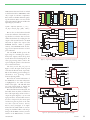
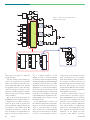
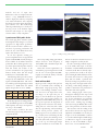
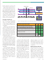
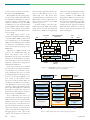
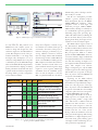
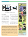
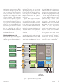
1
Xcell journal Issue 66 Fourth Quarter 2008 S O L U T I O N S F O R A P R O G R A M M A B L E W O R L D Automotive Innovators Hit HitHigh Top Gear in Driver Assistance with FPGA Platforms INSIDE Algorithm Developers Power New DA System on Xilinx Automotive FPGA Platform Engineer Turns Blown Engine into Hot Startup How to Beat Your Son at Guitar Hero Using Xilinx FPGA Tips and Tricks for Using FPGA Editor and SystemVerilog R www.xilinx.com/xcell/ Support Across The Board. ™ Technical Training Brings New Products to Life Engineering teams from Avnet Electronics Marketing and Xilinx spend countless hours crafting technical training programs tailored to meet an array of customer needs. With training opportunities that run the gamut from full-day, intensive design courses to short video demos of new tools, Avnet maximizes the time developers spend exploring new products and technologies. SpeedWay Design Workshops™ Participate in hands-on training classes that feature technical presentations from factory-trained Field Application Engineers (FAEs), along with hardware-based lab exercises that spotlight time-saving development tools. Workshop topics include general, embedded, DSP and serial I/O design. Attendees are eligible for discounted pricing on the featured development tools. Learn more about available Xilinx SpeedWay Design Workshops at www.em.avnet.com/xilinxspeedway » An Introduction to Xilinx® Embedded Development Kit (EDK) and the PowerPC® 440 — Part 1 & 2 NEW! » An Introduction to Xilinx® EDK and MicroBlaze™ — Part 1 & 2 » Creating FPGA-Based DSP Co-Processors On-Ramp Technical Sessions™ Engage in two-hour technical sessions, typically held over lunch at the customer’s facility, that meld tool demonstrations with instruction on specific technologies or design topics. Numerous technical sessions featuring Spartan® and Virtex® FPGAs are now available. Learn more about available Xilinx On-Ramp Technical Sessions at www.em.avnet.com/xilinxonramp » Xilinx® Spartan®-3A Configuration NEW! » Xilinx® Virtex®-5 FXT PowerPC® Processor » Embedded Processor Design Using the Project Navigator Design Flow Behind the Wheel Video Demos View short but detailed video demos of new development tools engineered by Avnet, which highlight the tools’ features and capabilities. Learn more about Behind the Wheel demos at www.em.avnet.com/drc FEATURED KITS » Xilinx® Virtex®-5 FXT Evaluation Kit » Xilinx® Spartan®-3A Evaluation Kit 1.800.332.8638 www.em.avnet.com Copyright© 2008, Avnet, Inc. All rights reserved. AVNET and the AV logo are registered trademarks of Avnet, Inc. All other brands are the property of their respective owners. L E T T E R F R O M T H E P U B L I S H E R Happy 20th Anniversary, Xcell Journal Readers! Xcell journal PUBLISHER Mike Santarini [email protected] 408-879-5270 EDITOR Jacqueline Damian ART DIRECTOR Scott Blair DESIGN/PRODUCTION Teie, Gelwicks & Associates 1-800-493-5551 ADVERTISING SALES Dan Teie 1-800-493-5551 [email protected] INTERNATIONAL Melissa Zhang, Asia Pacific [email protected] Christelle Moraga, Europe/ Middle East/Africa [email protected] Yumi Homura, Japan [email protected] SUBSCRIPTIONS All Inquiries www.xcellpublications.com REPRINT ORDERS 1-800-493-5551 www.xilinx.com/xcell/ Xilinx, Inc. 2100 Logic Drive San Jose, CA 95124-3400 Phone: 408-559-7778 FAX: 408-879-4780 www.xilinx.com/xcell/ © 2008 Xilinx, Inc. All rights reserved. XILINX, the Xilinx Logo, and other designated brands included herein are trademarks of Xilinx, Inc. All other trademarks are the property of their respective owners. The articles, information, and other materials included in this issue are provided solely for the convenience of our readers. Xilinx makes no warranties, express, implied, statutory, or otherwise, and accepts no liability with respect to any such articles, information, or other materials or their use, and any use thereof is solely at the risk of the user. Any person or entity using such information in any way releases and waives any claim it might have against Xilinx for any loss, damage, or expense caused thereby. wenty years ago this quarter, an applications engineer who had just joined Xilinx from AMD, with prior stints at Zilog and Fairchild, started a technical publication for Xilinx customers. He named it Xcell, “The Newsletter for Xilinx Programmable Gate Array Users.” Two decades later, that Xilinx legend, Peter Alfke, says he fashioned Xcell Journal after Fairchild’s now defunct magazine Progress. “In those days, FPGAs were a really new and unconventional technology, and we wanted to tell designers how to best use them,” said Alfke. “We used to issue Data Books once a year—this was, of course, before the Internet. So we decided to make Xcell Journal a quarterly applications update with a lot of technical detail, how-to content and innovative ideas, as well as silicon, tools and IP availability information.” Peter and his daughter Karen, at the time a Berkeley student, created the debut issue of Xcell in the fourth quarter of 1988. “She brought her Mac down to the office and she did the typesetting and layout for the first five issues,” said Alfke. The lead story reported on the company’s new Data Book, which contained complete data sheets for the XC2000 and XC3000 device families and for a military-grade version of the XC2000. Issue No. 1 also featured an article on DOS (“All DOS Are Not Created Equal”) and several pieces on the XACT FPGA design tool, the ISE® of its day. One story described XACT as “a large, demanding program, using interactive graphics, requiring megabytes of RAM”—a behemoth that pushed the IBM-PC, which at the time could address only 640 Peter’s Picks kbytes, “into uncharted water.” These older issues are fun to #11, 4Q93, page 31: “Reduce SPROM Standby Current to Zero” read, and not just for the sake of by grounding through LDC nostalgia. Alfke, still at Xilinx and #13, 2Q94, page 25: “Carry and Overflow: A Short Tutorial” still involved in applications and #17, 2Q95, page 30: “Manchester Decoder in Three CLBs” technical documentation, points out that some of the content #18, 3Q95, page 30: “Overshoot and Undershoot” remains fresh and somewhat useful #18, 3Q95, page 36: “Hold is a Four-Letter Word”— today. So, instead of blabbing hold-time, that is about how Xcell has evolved over #19, 4Q95, page 34: “User-Defined Schmitt Trigger” time, I’d like to honor the guy who with two pins, two resistors started an amazing legacy that we #21, 2Q96, page 35: “10-Digit Fully Synchronous BCD Counter @ 87 MHz” hope to continue for at least another 20 years. At right are Peter’s Picks #21, 2Q96, page 40: “A Look at Minimum Delays,” of the best of the oldies but goodies and why they are so elusive from issues 1 through 28. #22, 3Q96, page 28: “Power, Package and Performance” Pack rats will have no problem and how to trade off among them laying hands on them. For anyone #24, 1Q97, page 20: “Trouble-Free Switching Between Clocks,” who didn’t save every issue that with no glitches came your way, we’re in the process #24, 1Q97, page 21: “Demultiplexing 200-MHz Data Streams” of placing the content online. You’ll soon be able to find back #27, 4Q97, page 27: “Reduce EMI with a Spread-Spectrum Clock” issues at the Xcell Journal Archives #27, 4Q97, page 28: “The Dangers of Hot Plug-In” page. In the meantime, if you want #28, 1Q98, page 22: “PC-Board Design Considerations” a specific issue, e-mail me at [email protected] with the #28, 1Q98, page 28: “Self-Initiated Global Reset” heading “Xcell back issue request,” #28, 1Q98, page 29: “CMOS I/O Characteristics” and I’ll send you an electronic copy. T #28, 1Q98, page 33: Mike Santarini Publisher “Low-Power XC4002XL Achieves 400-MHz Performance” in a self-contained frequency counter OR Agilent Logic Analyzers Agilent Mixed Signal Oscilloscopes Up to 1.2 GHz timing, 667 MHz state, and 256 M deep memory 4 scope channels + 16 timing channels + Agilent FPGA Dynamic Probe Application software to increase visibility inside your FPGA = Fastest FPGA Debug Available 2ENogE!c_`gEN¢l3`ol!c!l<y!!gE`3<E)¢U]!`gE_3oEc!E`lEl!c !3`¤`§¥`]]E¢o¢l<`lU§Eg 2]!lUE`lEl!c yo)Eyo`l`lE3ol<¥`]o¢<E`Ul3]!lUE 2EN!E`!c)¢<E3o<ENo 29 9 !l<_ Start saving time now. Download FREE application information. www.agilent.com/find/fpgatools C O N T E N T S VIEWPOINTS XCELLENCE BY DESIGN APPLICATION FEATURES 16 Letter from the Publisher Happy 20th Anniversary, Xcell Journal Readers! ...4 Xpert Opinion Driver Assistance Systems Pose FPGA Opportunities...16 Xcellence in Automotive & ISM Building Automotive Driver Assistance System Algorithms with Xilinx FPGA Platforms...20 Security Video Analytics on Xilinx Spartan-3A DSP...28 Xcellence in New Applications A/V Monitoring System Rides Virtex-5...34 Xpectations FPGA Platforms: Silicon Was Just the Beginning...66 XCELLENCE IN AUTOMOTIVE & ISM Cover Story Driver Assistance Revs Up on Xilinx FPGA Platforms 8 20 34 FOURTH QUARTER 2008, ISSUE 66 THE XILINX XPERIENCE FEATURES Xperts Corner Verifying Xilinx FPGAs the Modern Way: SystemVerilog...40 48 Xplanation: FPGA 101 Extend the PowerPC Instruction Set for Complex-Number Arithmetic...44 Xperiment Using a Xilinx FPGA to Beat Your Son at Guitar Hero...48 Ask FAE-X Digital Duct Tape with FPGA Editor...54 Profiles of Xcellence Engineer Turns Blow-up Into Hot Automotive Electronics Startup...62 40 XTRA READING Xamples… A mix of new and popular application notes...58 Are You Xperienced? Embedded for success ...59 Xtra, Xtra The latest Xilinx tool updates and patches, as of Sept. 30, 2008...60 Tools of Xcellence A bit of news about our partners and their latest offerings...64 54 62 COVER STORY Driver Assistance Revs Up On Xilinx FPGA Platforms 8 Xcell Journal Fourth Quarter 2008 COVER STORY Automotive driver aid systems are rapidly evolving, thanks to ingenious engineering and programmable platforms. Fourth Quarter 2008 by Mike Santarini Publisher, Xcell Journal Xilinx, Inc. [email protected] It’s widely known that the use of automotive safety systems—seatbelts, followed by front-facing airbags, seatbelt pre-tensioners, antilock brakes and side airbags—has dramatically reduced injuries and lowered the fatality rate in vehicular accidents over the last 50 years. But now carmakers are going a step further, cranking up innovation in a relatively new class of system called driver assistance. DA stands poised to revolutionize the driving experience even as it further improves safety. And FPGA platforms (tools, IP, as well as silicon) are playing a key role in making it happen. “Driver assistance systems are systems companies are putting on vehicles to help make drivers better drivers,” said Paul Zoratti, automotive system architect and DA specialist at Xilinx. “DA systems provide drivers with information that either they look for or that is ‘pushed’ to them, in the form of a warning, to make driving safer and help drivers make informed choices about driving in all conditions.” What DA systems can do now—thanks largely to advances in electronics and the OEM innovations they have enabled—is pretty remarkable; what they may do in the future is amazing. Colin Barnden, Semicast’s principal analyst covering electronics in the automotive market, said that car manufacturers, their tier-one suppliers and academia have been researching DA system for many decades. But only over the last 10 years have electronic systems and design techniques advanced to the point where OEMs can readily and feasibly deploy them. “It’s amazing how far DA systems have come in such a short amount of time,” he said (see Barnden’s Xcellent Opinion column in this issue). There are many types of DA systems that OEMs, their suppliers and even aftermarket electronic control unit (ECU) makers are offering today and designing for tomorrow (see Figure 1). DA systems can help drivers park their cars effectively and maintain a safe distance from cars ahead. They can inform drivers about threats that perhaps they would otherwise not see, and aid them in safely changing lanes. Many of these systems started out just a few years ago as fairly simple technologies. But OEMs have rapidly devised more-sophisticated spins and are now in the process of integrating them into “sensor fusion technologies”—essentially, the merger of multiple DA systems, all operating independently off the output of the same, shared sensors. The goal is to supply drivers with more-accurate information about their surroundings, to help them make informed driving decisions and enrich the driving experience. In doing so, the systems require sophisticated compute technology—and a lot of it. That’s where FPGA platforms are starting to make a strong play. Rapid Evolution of Parking with DA Systems Around 10 years ago, OEMs launched their first foray into DA with convenience systems such as one for use when backing up. A back-up aid system is essentially a series of sensors in a car’s rear bumper that send an ultrasonic or radar signal to measure the distance to an object behind the vehicle. As drivers back up, the sensors typically trigger an audible beeping that increases in frequency as the vehicle nears the obstacle. The signal becomes a constant tone when the driver backs up to within four inches of the obstruction. “It’s a fantastic feature if you are driving a big vehicle such as a pickup and you want to know how close you are to another vehicle,” said Barnden. “But it’s the most basic system—there really isn’t any intelligence built into it. The driver is doing pretty much all the work. The system tells you if you are nearing something, but you ultimately decide if you want to get a bit closer or want to stop.” Back-up aid systems are the most commonly deployed, highest-volume form of DA that OEMs offer today. In 2007, Barnden said, carmakers put back-up aid systems in 5 million vehicles in Europe and 2 million in the United States, shipping a total of 10 million units worldwide (roughXcell Journal 9 COVER STORY Driver Assistance Features Awareness Warning Temporary Control Performance Performance Enhancement Enhancement Blind Spot Detection Lane Departure Warning Convenience Oriented Panic Brake Assist Sign Recognition Front Collision Warning Adaptive Cruise Control Pre-Crash Sensing Park Assist Back-up Aid Automated Parking Side Impact Detection Lane Change Assist Pedestrian Detection Safety Oriented Pedestrian Protection Night Vision Drowsy Driver Automatic Braking Lane Keeping Figure 1 – Automotive electronics companies are rapidly expanding the number, and advancing the maturity, of driver assistance (DA) systems available to consumers, thanks in part to FPGA platforms. ly one in six cars built in 2007 has the feature). “I expect that number will grow in all regions because it’s useful, fairly simple and inexpensive,” said Barnden. OEMs then took that technology a step further, adding intelligence to create a DA system called park assist. A camera situated somewhere in or near the vehicle’s rear license plate connects to the navigation display system in front of the driver’s seat. When drivers put the car in reverse, the navigation system automatically activates the camera so they can literally see how close they are to objects behind them. Some systems do some basic image recognition to put visual cues onto the screen so drivers know when to turn the wheel or how far they are from an obstruction. Barnden noted that five years ago, OEMs such as Mercedes and BMW started offering park assist systems on their highest-end models. Today, the technology is showing up in more-mainstream vehicles, especially SUVs, where owners may find it difficult to locate obstacles by glancing over their shoulders or looking in their rearview mirrors. Barnden said OEMs sold a total of 1 million units with park assist systems in 2007. The next evolution is automated parking. Lexus was the first to spin this type of DA system a few years ago, when the luxury carmaker made an automated parking 10 Xcell Journal system available on its LS-series vehicles. In an automated parking system, several near-range sensors—some ultrasonic and some cameras—are located all around the vehicle. As drivers cruise down the road, the system looks at gaps between parked cars and reports whether the space is big enough to get into. What’s more, the system goes even further. At the driver’s ultimate discretion and direction, it will take over the task altogether and automatically park the vehicle. “You push a button and the car will actually steer itself into the space,” said Barnden. “It’s absolutely crazy. You would think a car that could park itself would be 20 or 25 years away, but it’s actually being done by OEMs today.” A park assist system makes measurements in 360 degrees and instantly calculates how far it is from other objects on every side. “And the system knows the mechanics of parking, because the designers have programmed the algorithms for parking into the system. So it knows what directions it can turn the wheel, what direction it can move the front relative to the back of the vehicle and all those sorts of parameters,” said Barnden. OEMs in Japan are three to five years ahead of the rest of the world in this technology, but European carmakers are start- ing to introduce park assist as well, said Barnden. “It isn’t a feature that is too common in the U.S. yet, but it definitely will become more common,” he said. From its genesis in high-end vehicles, park assist is trickling down to smaller Japanese and European cars, and is proving extremely popular in cities, where parking spaces are difficult to find and tight to negotiate. “What’s even more remarkable is that park assist systems are unbelievably reliable and incredibly precise,” said Barnden. And it’s likely that as the technology becomes more common, owners will grow to trust that the system is able to consistently park more precisely than they can. “It’s often the case that if you give a computer just one task to do, it can typically do that task better than we can,” said Barnden. Nevertheless, one of the key attributes of DA is that the driver has the ultimate say in controlling the vehicle and can override the automated system. Rapid Evolution of Cruise Control Another segment of DA that has advanced rapidly over the last 10 years is cruise control. OEMs have offered standard cruise control for several decades, but those systems were not intelligent. With traditional cruise control, users push a button to set the speed of their automobile. However, if drivers are Fourth Quarter 2008 COVER STORY More-advanced adaptive cruise control systems will help drivers safely deal with stop-and-go traffic, adjusting to the rapid changes in speed while maintaining reasonable distances. not paying attention, their car will maintain that speed and possibly veer off the road or run into something straight ahead. Around eight years ago, Mercedes began to offer an intelligent DA system called adaptive cruise control in its S-class automobiles. A forward-facing radar measures the distance to the vehicle ahead. Drivers push a button to determine whether they want their automobile to maintain a headway of two, three or more seconds behind that car in front. The system will then adjust the car’s accelerator to maintain the user-specified gap. Barnden said that recently introduced second-generation adaptive cruise control systems actually control braking as well. “If another driver cuts in front of you too close, the system will apply a small amount of braking power to maintain that two- or three-second gap, keeping a safe distance behind that car,” he said. Likewise, if traffic grinds to a halt, the adaptive cruise control system will slow or stop the vehicle, still maintaining that same driver-specified distance from the car ahead. While admittedly more sophisticated than traditional cruise control, by DA standards adaptive cruise control is “one of the more basic advanced systems,” Barnden said. Even more-advanced adaptive cruise control systems will help drivers safely deal with stop-and-go traffic, adjusting to the rapid changes in speed while maintaining reasonable distances. “Some can do that now,” said Barnden. In 2007, he said, OEMs sold 1 million cars with adaptive cruise control systems. Barnden expects that number to grow substantially, especially in Europe and Japan, as the technology makes its way into mass deployment and becomes even more sophisticated. Indeed, OEMs and their suppliers are already revving up third-generation adapFourth Quarter 2008 tive cruise control that combines a camera with the radar system to ensure that the car is actually matching the speed of the vehicle in its lane, and to anticipate threats such as other drivers pulling into the driver’s lane, perhaps too closely. “Third-generation systems add more intelligence to better estimate what’s ahead and how much of a threat it is to you,” said Barnden. “And based on that, what is the probability that you can simply ignore it or sound a warning to take preventative action to avoid a crash.” Night Vision and Threat Assessment Another segment of DA systems aims to give drivers a clearer view of the road ahead. A prime example is night vision. Typically, these systems employ a camera with infrared illumination or thermalimaging technology and use the navigation system display of the automobile to show heat-sensitive or IR images to drivers. The systems are very useful for spotting people and animals in the road that you might not otherwise see in time to avoid a collision. Due to the current cost of night vision technology, OEMs typically offer systems only on their highest-end vehicles, such as the Mercedes S-class and BMW 7 series. However, as the technology evolves, the industry expects night vision systems to migrate to mainstream vehicles. OEMs sold 800,000 units with night vision technology worldwide in 2007, said Barnden, who expects that number will grow to 3 million units by 2015. Evolution of Lane Changing with DA Systems Yet another segment of DA that companies are rapidly innovating involves assisting drivers in changing lanes. OEMs have just started offering blindspot detection systems that use radar sensors or, in some cases, cameras located on Xcell Journal 11 COVER STORY As developers seek to use a given set of sensors to perform multiple DA tasks, DSP-only systems can’t do the job effectively. As a result, the role of FPGAs will expand. the side and rear of the automobile to monitor whether another car is approaching a driver’s blind spot. If so, the system will display a warning light to inform the driver that someone is there, perhaps reducing the amount of time drivers spend looking over their shoulders and allowing them to keep their eyes on the road ahead. Barnden is waiting to see if blind-spot detection will take off as a market. He notes that in 2007, the automotive industry sold 300,000 units. OEMs typically offer the systems only in high-end vehicles, such as the Audi Q7 luxury SUV. Barnden said that blind-spot detection becomes more compelling when OEMs combine it with other DA systems. For example, if a driver took his or her eyes off the road to double check what was going on in a blind spot, the adaptive cruise control would sense a slowdown and adjust the speed accordingly. “That’s why driver’s assistance is so interesting,” said Barnden. “There are all these things coming together that can really change the driving experience and provide some useful and helpful advice to the driver.” Barnden sees great growth potential in another emerging DA technology called lane departure warning—and great potential for FPGAs to power these systems. Lane departure warning systems typically use a camera module mounted on the rearview mirror to gather images of the road ahead. “Typically there is a DSP or, increasingly, an FPGA that is doing highspeed math to identify the white markings on the road to help users see what lane they are in relative to the road ahead,” said Barnden. And should the driver swerve into another lane accidentally, perhaps because he or she is sleepy or busy tuning the radio, the system would sound an audible warning, jiggle the driver’s seat or make the steering wheel vibrate. 12 Xcell Journal But the system will not send a warning if the driver first uses the turn indicators before changing lanes, Barnden notes. So in essence, the technology not only warns drivers if they are accidentally swerving into another lane, but also encourages good driving habits. OEMs today offer lane departure warning systems in their highest-end vehicles (Peugeot-Citron, BMW, Infineon, Cadillac and Buick), and in 2007, sold just under 1 million units. “I see that as one of the highest-growth segments going forward, growing to 17 million units over the next decade,” said Barnden. “I think one in every four vehicles will have the technology by 2015.” Like lane departure warning systems, another emerging DA technology, sign recognition, uses forward-facing cameras to read signs posted on the sides of the road. “For example, the system could see a speed indicator and detect that you’ve gone past the sign, and display on the dashboard that you are now in a 30-mph zone,” said Barnden. “Or it could display things you may have overlooked, such as ‘no right on red.’” Sign recognition systems are still largely in development and must overcome some big challenges before coming to market, Barnden said. For example, if you are driving past a series of signs grouped very closely together, the system may have to figure out how to prioritize which sign to display to the driver. One road sign could read “Speed Limit 35 mph,” for instance, and the next one, “Flooding Ahead.” Clearly, the system would need to display the more ominous of those two signs. “The technology could prove very useful,” said Barnden. “It’s an assistance system to inform the driver, but the liability still remains with the driver.” The Future: FPGA Platforms Drive Sensor Fusion While all these segments of DA systems have advanced rapidly over the course of the last 10 years, experts say the real innovation is just beginning. Indeed, those designing DA systems and other automotive electronics are in the process of combining many of these functions, for example using one set of sensors to perform multiple jobs and then connecting them with other ECUs in the automobile. The idea is to reduce system cost, along with the cost and heft of the wire harness that links these multiple systems—thereby cutting fuel consumption. Ultimately, that will make the automobile more affordable and environmentally friendlier. A key to fusing these advanced systems is the use of FPGA platforms. Many first- and second-generation systems that use ultrasonic, radar and camera-based sensor technologies have relied on DSPs, or DSPs in conjunction with FPGAs, to quickly perform the calculations needed to inform drivers of their surroundings. But as DA systems become more complex—and especially as developers seek to use a given set of sensors to perform multiple DA system tasks—experts say DSP-only systems can’t do the job effectively. As a result, the role of FPGAs will expand. For example, Xilinx’s Zoratti said that evolving a basic lane departure warning system to simultaneously evaluate the road ahead for sign recognition and oncoming headlamps requires a significant amount of compute power as well as advanced algorithm development. “Today, DSPs can perform the computing for less advanced systems,” said Zoratti. “But as the systems become more advanced, and especially as companies start using sensors to do multiple functions and interconnect them with other systems, DSPs just don’t have the compute horsepower. The Fourth Quarter 2008 COVER STORY OPB Arb CTRL CMOS Imager Comms I2C Diagnostics LVDS Format Decoding LDW App / Cam Ctrl Pixel Correction and/or Micro or DSP CoProcessor Co-Processor I/F Noise Reduction Filter CAN Controller Sharpening CAN PHY Mem Controller Edge Detect (Sobel) Line Tracker FLASH Digital Memory Mixed Signal uP or uC SDRAM or DDR Programmable IP Block SW Figure 2 – DA designers can integrate many advanced functions on a single Spartan-3E FPGA. parallel-processing resources offered by FPGAs provide a cost-efficient, scalable and flexible solution” (see Figure 2). According to analyst Barnden, sensor fusion is proceeding especially rapidly around the forward-facing camera. This camera is typically located behind the automobile’s rearview mirror and faces forward, peering out the front windshield. Today, OEMs are using it to perform lane departure warning. But in future automobiles, they would like to be able to team that camera with one radar sensor to handle adaptive cruise control, sign recognition and perhaps night vision, as well as lane departure warning and, maybe one day, a lane-keeping feature. To have one camera feeding images to several DA systems requires advanced computing. Having separate DSPs on a board somewhere in the system is cumbersome, demands multiple connections (making for a heavier wire harness) and introduces possible latency and reliability issues. But OEMs can use the parallel resources on one FPGA platform to do the job of several DSPs, to create a much more cost-effective, scalable and flexible FPGA-based fusion sensor system, Zoratti said. “Today’s lane departure warning systems can use VGA cameras with 640 x 480 resolution,” he said. “Systems will need Fourth Quarter 2008 twice that resolution soon, when we get to applications such as sign recognition.” Zoratti said DSP devices can’t keep up with that amount of data processing. “When you talk about multiple features, each of those features may require a different processing algorithm. That’s where FPGAs really offer a strong value proposition.” An ASIC might be an option, he went on, “but the problem is, in most cases we are in the infancy of the market, so you don’t know what your algorithm is ultimately going to be. FPGAs provide power, flexibility and scalability…because now you can take the strength of the FPGA and adjust it to whatever feature set a particular vehicle wants to have. It’s a platform design—one design that can be modified for multiple models of a vehicle and multiple class sets. Invest in one platform that you can scale yourself—activate and deactivate.” Tools and IP play a crucial role in helping designers to rapidly create innovations in DA system development. Xilinx and its many partner companies offer advanced IP blocks (see Figure 3) for many sophisticated FPGA-based DA applications. On page 20 of this issue, Zoratti and coauthors Daniele Bagni, Xilinx, and Roberto Marzotto, Embedded Vision Systems, describe how engineers at the two companies developed an FPGA-based platform design for Embedded Vision Systems’ lane departure warning image-processing algorithms using System Generator for DSP. TRW Conekt, a division of TRW Automotive, and Ibeo Automobile Sensor GmbH are two of the many companies that have evolved their technologies from DSP or other IC-based DA systems to advanced sensor fusion systems using Xilinx Automotive platform FPGAs. TRW offers a camera-based lane departure warning system that has just gone into production, but the company is currently developing a system that fuses lane departure warning with adaptive cruise control. The video camera in its current system resides behind the rearview mirror and faces forward. “We pick out the lane markings, and if the driver gets too close to them, we trigger the electric-powered steering system to give the steering wheel a small nudge,” said Martin Thompson, principal electronic engineer at Conekt. “It’s designed to feel like the sensation of touching a curbstone at the side of the road. The system helps drivers keep from straying from their lane—for example, if they are fatigued or lose concentration.” At the heart of the TRW system is a Conekt-programmed XA Spartan®-3E250 FPGA, which handles low-level image processing: edge detection and feature Xcell Journal 13 COVER STORY Video Interface & Conversion Image Enhancment Object Tracking Color Space Conversion (RGB, YUV, YCC, Bayer) Sharpening Motion Detection Format Decoding De-Interlacing (Motion Adaptive) Spatial Contrast Enhancement (Local Area Processing-LAP) FIR Filtering Multi-target Tracking Temporal Filtering Histogram Equalization Frame Buffer Control (Memory Controller) Thresholding Image Restoration Object Recognition Graphics / Video Display Noise Reduction (Spatial Filtering) Edge Detection (Sobel Kernel) Rate Conversion Image Stabilization Hough Transform Graphics Overlay (OpenGL) Gamma / Color Correction 2-D Correlation (Pattern Matching) (Spatial/Freq Convolution) Translate / Rotate / Zoom Non-uniformity Correction (NUC) Alpha Blending Graphics Acceleration Image Scaling / Conversion Bad Pixel Replacement (BPR) Picture-in-Picture Distortion Correction Image Fusion Display Controller Figure 3 – Xilinx and its partners offer many types of IP for the DA market. Shown are some of the varieties of image-processing functional IP available for vision-based DA. extraction. The product also uses an external microcontroller that Conekt may integrate into the FPGA for future versions, Thompson said. Positioned behind the rearview mirror, the system picks out white lines and estimates the geometry of the road ahead and the offset of the vehicle within the lane—how laterally the vehicle is positioned, its angle relative to the lane and how the lane is curving one way or the other. “That gives us the information we need for the lane departure system,” said Thompson. “But for the future, it can be fused with the data from the adaptive cruise control radar to select the vehicle that’s in your lane rather than it having to infer this from indirect measurements.” In addition, Conekt engineers are developing video obstacle detection. “Radar is very good at measuring distance. It isn’t so good at lateral-position measurements, because the radar return rarely comes off the middle of the vehicle–potentially, we don’t know which of the two corners it came off,” Thompson said. “Video is the opposite. We can determine the width and angle to the vehicle and fuse this with the radar distance measurement.” 14 Xcell Journal In addition, he said, “video allows Conekt to perform some classification: to identify if an object in front of the car is a pedestrian or a bicycle, for example.” Similarly, “a fused video-radar system could use dynamic classification of whether the vehicle is a car or a truck. The tracking system can make use of that assessment to improve its behavior,” said Thompson. Thompson pointed out some other advantages of fusing radar and camera sensors in one system. The radar sees through rain, falling snow and fog, while the video would deliver better information about the actual visual range of the driver (and presumably, the driver ahead) to help estimate a safe driving speed given the current weather and visibility conditions. At some point down the road, he said, fusion products could start to benefit existing collision-mitigation systems as well, so that if an accident looked inevitable, the system could activate the seatbelt pre-tensioners, prime the airbag and engage the brakes to start dissipating the collision energy earlier than is now possible. Beyond that capability comes collision avoidance, where the car autonomously takes some kind of action (possibly including steering as well as braking) to prevent a crash if it appears the driver isn’t going to. “That’s some time in the future, however,” Thompson said. Ibeo Automobile Sensor GmbH is another company using Xilinx FPGA platforms for its advanced DA systems. Director of sales Mario Brumm said the 10year-old company has developed a laser scanner with accompanying software that detects the environment around the car— other vehicles, pedestrians, bicycles—and measures their position and speed. Ibeo designed the system to provide adaptive cruise control for high-speed driving and traffic jam assistance. And in critical situations where, for example, a child darts out in front of you, the sensor can trigger braking to help avoid an accident. “We’ve developed hardware and the software, but I think the software will grow in importance over the next few years,” said Brumm. “We have some sensors in the market already for single applications, but our intent from the beginning is to use one sensor for multiple applications. The FPGA is a very important component in our design.” Fourth Quarter 2008 COVER STORY Prior to using an FPGA, Ibeo relied on an analog chip, “and we could use it to measure from up to 80 meters,” Brumm said. “But that isn’t good enough for adaptive cruise control, especially in Germany, where we tend to drive quite fast. Our customers told us that they needed it to measure 200 meters. It wasn’t possible with an analog system. The idea was to do it with digital and the core measurement.” Specifically, the analog system had a limited V-range (area and width that the sensor could detect). “With an analog system you also have more noise in the signal, and that means we could see objects up to 80 meters and no more,” said Brumm. “With the new FPGA system, if you have a big car or truck you will see up to 350 meters, which is absolutely unique for laser scanner systems. This is only possible because of the digital measurement, and it can detect very low energy.” Typically, said Brumm, these types of systems debut in luxury cars, such as the Mercedes S-class and BMW 7 series. “But our main goal is to bring down the cost so that these technologies can be widely deployed and available in all classes of cars,” he said. Brumm foresees great possibilities for merging laser technology with video. “Digital camera technology is nice because it allows you to see what’s going on with your own eyes, but it can have the same drawbacks too,” said Brumm. “For example, camera technology doesn’t work in the dark, so designers need to augment it with night vision, which can be expensive. And digital camera processing typically requires a lot more data processing than laser technology.” Lasers, for their part, are not “hindered by darkness or even fog,” he said. But cameras could eliminate some issues with laser scanners. For example, laser scanners have trouble distinguishing pedestrians from trees. Pairing a laser with a camera would allow the sensor to react appropriately, Brumm said. If, for example, it seemed unavoidable that the car was going to hit a tree, the system would send information to other sensors to protect the driver. And if it sensed the car were about to hit a pedestrian, it could send information to other sensors to help protect the potential victim, perhaps activating an airbag under or on the hood of the automobile. Fourth Quarter 2008 FPGAs are also playing a key role in aftermarket DA systems. PLX Devices, for example, developed its first product—an award-winning, user-customizable multifunctional gauge popular with car enthusiasts—with a Xilinx FPGA platform. The company then built Kiwi, a mainstream consumer product, which in a fun way helps drivers monitor their fuel efficiency. Xilinx devices are central in that design as well (learn more about PLX Devices and its CEO, Paul Lowchareonkul, in the Profile of Xcellence section in this issue). The End Market and Liability Restrictions While engineers have made leaps and bounds in developing ever more advanced DA systems over the last 10 years, just about everyone in this market is aware that each step of sensor fusion progress has to be tempered and well thought out to consider the real value to the driver as well as regional liability constraints. Indeed, the experts interviewed for this story, including Barnden, Zoratti, Brumm and Thompson, all noted that one of the reasons manufacturers in Europe and Japan are leading the way in DA development—and why consumers in those regions typically become the early adopters—is largely because legal liability is a much bigger issue in the United States. As a result, auto manufacturers are far more cautious in introducing new features into the U.S. market. Most of the DA systems discussed here are merely assistance features that provide the driver with information; ultimately, it’s the driver who is responsible for making the right decisions—and the driver who bears the liability. However, it’s not unforeseeable that as advanced sensor fusion technology progresses, many of these systems could be tied directly to safety systems. Some say the rapid evolution of DA systems is even a crucial step toward achieving the automotive industry’s holy grail of driving: the autonomous vehicle—a day, perhaps in the not too distant future, when cars can drive themselves and in doing so, alleviate traffic congestion and lower fuel consumption, while drastically reducing traffic-related injuries. FPGA Powered – That‘s it! FPGA-Module: TQM hydraXC – smallest, most universal Hardware Platform for Reconfigurable Computing • Based on XILINX Spartan 3, Virtex 4 and Virtex 5 technology • Ethernet 10/100, USB 2.0, RTC • SPI-, NAND-Flash, DDR2 / SDRAM • Size 2.13 Inch x 1.73 Inch (54 mm x 44 mm) • Programmable VCC IOs Embedded solution with TQM hydraXC for • Fast time to market • Economical series production • Highest flexibility • Hardware reduction :: Starter kits available :: Starter kit with module Email: [email protected] www.tq-group.com Infoline: (+49 ) 81 53 / 93 08 - 333 Xcell Journal 15 XPERT OPINION Driver Assistance Systems Pose FPGA Opportunities Invisible intelligence is coming soon to a car near you. by Colin Barnden Principal analyst Semicast [email protected] One of the most important issues in the automotive industry over the last 10 years has been the rapid adoption of safety systems. Features such as airbags, antilock braking and tire pressure monitoring have become increasingly common on many new vehicles, as drivers have become aware of their benefits and, in some cases, lawmakers have made installation mandatory to increase road safety and reduce fatalities. The emphasis on driver safety shows no signs of abating, and over the next decade, drivers will become increasingly familiar with a new generation of systems commonly referred to as “driver assistance.” Driver assistance systems differ subtly from conventional safety systems. Their primary purpose is to detect conditions that could potentially lead to an accident, and to either warn the driver accordingly or to take preemptive action. A conventional safety system such as the airbag, by contrast, serves as the “last line of defense” and is triggered only in the event of a crash. Perhaps the best introduction to the functions and utility of driver assistance systems is to look at everyday driving experiences and see how these devices can help in certain challenging conditions. 16 Xcell Journal Fourth Quarter 2008 XPERT OPINION Lane Departure Warning Let’s start with the commute home after an all-day meeting. Chances are you are not at your most alert and your thoughts are probably not all focused on the road ahead—so much so that while changing the play list on your iPod, you begin to drift out of your lane and move dangerously close to the adjacent vehicle. Left unchecked, this could be one commute you never finish. For assistance in such a situation, lane departure warning systems use sensors mounted in the front of the car to “see” the markings in the road ahead, combined with complex computers that do the high-speed math to detect the car’s position on the highway. Stay comfortably within the confines of your lane and all is well; stray too far to the left or right without using the indicators and the system will detect your lapse and automatically provide an audible warning. While lane departure warning may sound somewhat extravagant, there actually is a need. According to statistics from the National Highway Traffic Safety Administration, around 130,000 people are injured each year in the United States alone in accidents related to lane changing. No wonder, then, that automakers have already taken note of the safety benefits. As is often the case with new technology, a number of European carmakers are slightly ahead of the pack, offering lane departure warning on vehicles such as the Audi Q7 SUV and BMW 5-Series. In the United States, GM has already shipped Buicks and Cadillacs with such systems, and in Japan, both Nissan and Toyota have cars in production with lane departure warning. Blind Spots and Night Vision Take another scenario: Perhaps you’ve been out on the highway for an hour with the stereo blasting and the cruise control engaged. You go to overtake a truck, forget to check to see if it is safe to pull out and miss the compact in your mirror’s blind spot that was passing you at the same time. This is an accident that wouldn’t happen in a car with blind-spot monitoring, a technology that uses camera modules or even short-range radar to constantly peruse the blind spots to the left and right Fourth Quarter 2008 of your vehicle. You pull out to pass and the system will know there’s a vehicle in your blind spot, and warn you of the danger accordingly. Another driver assistance technology is designed to help out in the dark. Night vision assist is, as the name suggests, a system used at night to see objects ahead of the vehicle that are farther away than the illumination range of conventional front headlamps. Night vision assist systems use cameras with either IR illumination or prior to the impact by firing the seatbelt pretensioners to move the driver and front-seat passenger into an optimum safety position. Brisk Market Foreseen Table 1 presents the worldwide market for driver assistance systems in terms of system shipments. As can be seen, the intense interest in driver assistance systems is well justified when looking ahead to the forecast for future years. Shipments of lane departure Driver assistance systems differ subtly from conventional safety systems. Their primary purpose is to detect conditions that could potentially lead to an accident, and to either warn the driver accordingly or to take preemptive action. thermal imaging to project an enhanced image of the road ahead onto the screen in the center console. Intelligent Cruise Control Perhaps the most obviously useful example of driver assistance is intelligent cruise control. One of the greatest drawbacks of conventional cruise control is that this is a “set-and-forget” system and will, quite literally, drive the car into a wall if the driver is distracted or not paying attention to the road ahead. In contrast, intelligent cruise control typically uses radar to provide a real-time measurement of the distance to the object directly ahead of the vehicle, controlling the throttle and brakes to adjust the speed accordingly. Taking safety another step further, the most advanced systems feature predictive collision warning, which combines functions of intelligent cruise control with the airbag system. In the event that a crash is deemed imminent, the system takes action warning systems, for example, are set to rise to almost 11.5 million units in 2012, up from less than 1 million in 2007. Further, intelligent cruise control is expected to enjoy rapid adoption over the next five years, as this feature makes the transition from luxury cars to high-volume upperand midrange models. Overall, Semicast estimates shipments of driver assistance systems to pass 23 million in 2012, compared with about 3 million last year. The growth in unit shipments means a concomitant rise in semiconductor content. Table 2 presents the worldwide market for semiconductors in driver assistance systems in terms of revenue. Semicast forecasts that semiconductor revenue in driver assistance systems will grow at a CAGR approaching 33 percent from 2007 to 2012, from $229 million to $926 million. By comparison, the total automotive semiconductor market, which totaled $20 billion in 2007, is forecast to grow at around 5.5 percent a year, to $27 Xcell Journal 17 XPERT OPINION 2007 2008 2009 2010 2011 2012 CAGR Land Departure Warning 0.9 2.5 4.5 6.9 9.9 11.5 65.9% Blind Spot Monitoring 0.3 0.6 1.1 1.6 2.6 3.6 60.9% Night Vision Assist 0.8 1.3 1.4 1.9 1.9 2.4 24.4% Intelligent Cruise Control 1.1 1.7 2.6 3.6 4.9 6.1 41.8% Total 3.1 6.1 9.6 14.0 19.3 23.6 49.9% Table 1 – Driver Assistance System Shipments (MU) 2007 2008 2009 2010 2011 2012 CAGR MCU/MPU/DSP 54 94 136 182 232 260 36.8% ASIC/ASSP/Other Logic 12 28 46 63 82 89 49.8% FPGA 55 107 133 155 173 182 26.8% Optoelectronics 93 144 185 240 284 318 28.0% Other Semiconductors 15 28 39 54 67 77 38.2% 229 400 540 693 838 926 32.2% Total Table 2 – Worldwide Market for Semiconductors in Driver Assistance Systems ($M) billion by 2012. Clearly, driver assistance systems will be one of the highest-growth areas by far for automotive semiconductors over the next five years. The highest revenue growth for semiconductors in driver assistance systems is forecast for the optoelectronics category, where CCD and CMOS image sensors and millimeter-wave radar modules are likely to be the main drivers. The next-highest revenue growth is forecast for MCUs, MPUs and DSPs, where growth is mostly limited to 32-bit devices for high-end control. Opportunity for FPGAs Historically, whenever automotive OEMs needed a highly customized logic product to meet the demands of a specific application, they would automatically turn to an ASIC vendor to help them develop either a gate array or standard-cell-based product to meet their exact requirements. As ASIC development costs have risen and design times have extended over the last five years, 18 Xcell Journal automotive OEMs have been forced to consider other solutions. In some cases, semiconductor vendors have been successful in developing off-theshelf ASSPs that meet many of the generic needs in systems for, say, entertainment or navigation. In driver assistance systems, however, design changes are so frequent that an ASIC is rarely a suitable choice. Moreover, OEMs typically each have such complex and individual requirements that it is often not possible for semiconductor companies to develop suitable off-the shelf ASSPs that meet the cost, power or reliability goals of the application. To meet their needs in terms of cost, flexibility and time-to-market, automotive OEMs developing driver assistance systems are increasingly looking to FPGAs. While FPGAs have been used in the development and prototype stages of many automotive systems for the last 10 years, the design has typically involved an ASIC conversion prior to full-scale production, to minimize cost in high volume. However, as FPGA unit costs continue to come down, the technology becomes financially viable in designs up to much higher volume. Add in the unrivaled flexibility to make changes late into the design process and the excellent performance of FPGAs when configured to do the high-speed computational analysis required by many driver assistance systems, and you have a winning combination. As the data in Table 2 shows, Semicast does not forecast an end of ASICs and ASSPs in driver assistance systems anytime soon. ASIC/ASSP technology will continue to appeal over the long term, especially once the design requirements of the systems begin to stabilize. However, Semicast forecasts substantial revenue growth for FPGAs in driver assistance systems over the next five years, from $55 million in 2007 to $182 million in 2012, a growth rate exceeding 25 percent. The FPGA market in automotive applications is now accelerating at full throttle, with driver assistance the leader of the pack. To the average consumer, driver assistance systems may sound like unnecessary and expensive luxuries. Of course, much the same was said about airbags and antilock brakes when they were introduced, but their ability to reduce fatalities and injuries and improve road safety did not go unnoticed by lawmakers for long. The road forward for driver assistance systems looks assured, with vehicle makers increasingly using the technology to demonstrate their commitment to road safety. While these systems will not save lives in quite the same way that airbags and ABS do, they sure can help in a crisis. And as with all the best technology, you don’t even notice they are there until you need them—at which point, you’re grateful you had them. About the Author Colin Barnden is principal analyst for Semicast’s Automotive Electronics & Entertainment Systems Service. He has worked as a market analyst for 14 years and has researched and reported on the automotive industry since 1999. He holds a BS in electronic engineering from Aston University, England. Fourth Quarter 2008 ® ® Xilinx Spartan -3A Evaluation Kit Target Applications » General FPGA prototyping » MicroBlaze™ systems » Configuration development » USB-powered controller » Cypress® PSoC® evaluation Key Features » Xilinx XC3S400A-4FTG256C Spartan-3A FPGA » Four LEDs » Four CapSense switches » I2C temperature sensor » Two 6-pin expansion headers » 20 x 2, 0.1-inch user I/O header » 32 Mb Spansion® MirrorBit® The Xilinx® Spartan®-3A Evaluation Kit provides an easy-to-use, low-cost platform for experimenting and prototyping applications based on the Xilinx Spartan-3A FPGA family. Designed as an entry-level kit, first-time FPGA designers will find the board’s functionality to be straightforward and practical, while advanced users will appreciate the board’s unique features. NOR GL Parallel Flash » 128 Mb Spansion MirrorBit SPI FL Serial Flash Get Behind the Wheel of the Xilinx Spartan-3A Evaluation Kit and take a quick video tour to see the kit in action (Run time: 7 minutes). Ordering Information Part Number Hardware Resale AES-SP3A-EVAL400-G Xilinx Spartan-3A Evaluation Kit $39.00* USD (*Limit 5 per customer) Take the quick video tour or purchase this kit at: www.em.avnet.com/spartan3a-evl » USB-UART bridge » I2C port » SPI and BPI configuration » Xilinx JTAG interface » FPGA configuration via PSoC® Kit Includes » Xilinx Spartan-3A evaluation board » ISE® WebPACK™ 10.1 DVD » USB cable » Windows® programming application » Cypress MiniProg Programming Unit » Downloadable documentation and reference designs 1.800.332.8638 www.em.avnet.com Copyright© 2008, Avnet, Inc. All rights reserved. AVNET and the AV logo are registered trademarks of Avnet, Inc. All other brands are the property of their respective owners. Prices and kit configurations shown are subject to change. XCELLENCE IN AUTOMOTIVE & ISM Building Automotive Driver Assistance System Algorithms with Xilinx FPGA Platforms System Generator for DSP is a high-abstraction-level design tool that gives algorithm developers and system architects an efficient path from a Simulink-based algorithmic reference model to an FPGA hardware implementation without any need for HDL coding. by Daniele Bagni DSP Specialist Xilinx, Inc. [email protected] Roberto Marzotto Design Engineer Embedded Vision Systems, S.r.l. [email protected] Paul Zoratti Automotive Senior System Architect Xilinx, Inc. [email protected] The emerging market for automotive driver assistance systems (see cover story) requires high-performance digital signal processing as well as low device costs appropriate for a volume application. Xilinx® FPGA devices provide a platform with which to meet these two contrasting requirements. However, algorithm designers unfamiliar with FPGA implementation methods may be apprehensive about the perceived complexity of the move from a PC-based algorithmic model to an FPGA-based hardware prototype. They don’t need to be. A Xilinx tool, the System Generator for DSP, offers an efficient and straightforward method for transitioning from a PC-based model in Simulink® to a real-time FPGAbased hardware implementation. This high-abstraction-level design tool played a central role in a project conducted between engineers at Xilinx and Embedded Vision Systems. The goal of the project was to implement an image-processing algorithm applicable to an automotive lane departure warning system in a Xilinx FPGA using System Generator for DSP, with a focus on achieving overall high performance, low cost and short development time. Challenges in DA System Development Automotive driver assistance (DA) system engineers commonly use PC-based models to create the complex processing algorithms necessary for reliable performance in features such as adaptive cruise control, lane departure warning and pedestrian detection. Developers highly value the PCbased algorithm models, since such models allow them to experiment with, and quick- 20 Xcell Journal Fourth Quarter 2008 XCELLENCE IN AUTOMOTIVE & ISM ly evaluate, different processing options. However, in the end, a properly designed electronic hardware solution is necessary to realize economical high-volume production and deployment. Verifying algorithm performance consistency between deployable target hardware and the software algorithm model can be problematic for many developers. Moving from floating-point to fixed-point calculations (for example, employing different methods for trigonometric functions) can sometimes cause significant variation in the outputs between the reference software algorithm and the hardware implementation model. Further complicating the algorithm performance consistency problem for DA system developers is the fact that the input stimulus is very nondeterministic. For DA systems, which generally rely on inputs from remote sensing devices (cameras, radar and so on), the inputs are the incredibly diverse range of roadway and environmental conditions that drivers may encounter. Engineers may find designing a processing algorithm to adequately address all situations is extremely challenging, and verifying compliance between the software model and its electronic hardware implementation is critical. For many applications involving image processing, the parallel resources of Xilinx Spartan®-3 FPGA devices deliver higher performance per dollar than VLIW DSP platforms (see our paper in Xcell Journal issue 63: http://www.xilinx.com/publications/ xcellonline/xcell_63/xc_pdf/p16-19_63block.pdf ). However, some system designers still wrongly assume that the only way to program an FPGA is with a hardware description language such as VHDL, which many engineers don’t know. But in fact, this is no longer the case. Our design methodology, applying the Simulink modeling tool and the Xilinx System Generator for DSP FPGA synthesis tool, provided not only an easy, efficient way of implementing FPGA designs, but also a means of accelerating algorithm compliance testing with hardware-software co-simulation. Further, you don’t have to be familiar with an HDL to use System Generator. Fourth Quarter 2008 Lane Departure Warning Model Description The overall function of a lane departure warning (LDW) system is to alert the driver when the vehicle inadvertently strays from its highway lane. A camera in front of the host vehicle captures images of the roadway to identify markings that constitute the lane boundaries. The system continuously tracks those boundaries, as well as the host vehicle’s position relative to them. When the vehicle crosses the bounds of the lane, the system issues a warning. The automotive industry and academic world have widely adopted MATLAB® and Simulink as algorithm and systemlevel design tools. In particular, Simulink enables automotive algorithm engineers to quickly and easily develop a sophisticated DSP algorithm, thanks to its very high abstraction level and the tool’s graphical schematic entry. Figure 1 shows the top-level block diagram of our LDW system model, designed in Simulink. The green block, labeled Lane Detection, contains an image-preprocessing subsystem, the various stages of which we show in Figure 2. The purpose of the lane detection function is to extract those Testbench for Lane Detection Demo in System Generator RGB Line Frame Rate Ref I Display Out Hough 33 .2854 ROI frame _in Line RGB Line Repository hst _th EOF Enable eth _th Input Repository RGB Enable Lane Detection Count EOF Pts Count Pts Lane Tracking 1 Output 0 .01 Ref I percentage of pixels to be saturated (HST ) Departure Warning 1 0 .9 percentage of not edge pixels 1 frame _ in (ETH ) uT frame _in Hough Transpose 2 hst _ th hst _th 3 eth _ th -K - frame _out Boolean u T BW Hough Theta Transform Rho Transpose 1 eth_th Hough Rho_list Hough Transform Gain Line 1 Line Theta_list Enable 2 Enable Peak Detection FPGA Processing Matrix Viewer Pattern Search Figure 1 – LDW Simulink high-level block diagram Input Image Lane Marking Candidates ROI Cropping Morphological Operators Gaussian Noise Reduction Lane Marking Pattern Search Histogram Stretching Adaptive Threshold + Thinning H/V Gradients Extraction Magnitude and Phase Calculation Figure 2 – LDW preprocessing function chain Xcell Journal 21 XCELLENCE IN AUTOMOTIVE & ISM features of the roadway image most likely to represent lane boundaries. To improve the performance of the edge detection with respect to noise, the first stage of the pipeline is a 2-D 5x5 Gaussian noise reduction (GNR). The second stage is histogram stretching (HST), a technique developers use to enhance the contrast of the image, exploiting as much as possible the whole gray-level range. The third step, the horizontal/vertical gradient (HVG), enhances those pixels in which a significant change in local intensity is seen. Developers perform HVG by computing the 2-D 5x5 gradients of the image (via the 2-D Euclidean distance). The edge-thinning (ETH) block determines which points are edges by thresholding the gradient magnitude and applying non-maximum suppression to generate thin contours (one-pixel thick). The lane-marking pattern search (LMPS) acts as a filter, selecting a subset of edge points that display a particular configuration consistent with the lane markings, and removing spurious edge points that arise due to shadows, other vehicles, trees, signs and so on. The last step of the pipeline is a 3x3 morphological filtering (MRP) the system uses for the final cleaning of the lane-marking candidate’s map. In the Simulink model, we have implemented the various stages of the imagepreprocessing subsystem using a mixture of Simulink blockset functions and MATLAB blocks. Because of its ability to process large amounts of data through parallel hardware paths, an FPGA is wellsuited for the implementation of the lane detection function of our model. Therefore, we targeted this function as the starting point for transitioning the LDW Simulink design to an FPGA. With this partitioning, the FPGA performs the processing-intensive pixel-level analysis of each frame and reduces the data from a 10-bit gray-scale image to a simple binary image for our downstream processing. For the entire system design, we are targeting an XA Spartan-3A DSP 3400, but we could also fit the system on a smaller 3A DSP 1800 or a 3E 1600. 22 Xcell Journal System Generator Overview The System Generator for DSP design tool works within Simulink. It uses the Xilinx DSP blockset for Simulink and will automatically invoke the Xilinx CORE Generator™ tool to generate highly optimized netlists for the DSP building blocks. You can access the Xilinx DSP blockset via the Simulink Library browser, which you can, in turn, launch from the standard MATLAB toolbar. More than 90 DSP building blocks are available for constructing a DSP system, along with FIR filters, FFTs, FEC cores, embedded processing cores, memories, arithmetic, logical and bit-wise blocks. Every block is cycle- and bit-accurate and you can configure each of them for latency, area vs. speed performance optimization, number of I/O ports, quantization and rounding. Two blocks, called Gateway-In and Gateway-Out, define the boundary of the FPGA system from the Simulink simulation model. The Gateway-In block converts the floating-point input to a fixed-point number. Afterwards, the tool correctly manages all the bit growth in fixed-point resolution, depending on the mathematic operation you are implementing during the following functional stages. Since Simulink is built on top of MATLAB, System Generator allows the use of the full MATLAB language for input-signal generation and output analysis. You can use the From-Workspace and To-Workspace blocks from the Simulink Source and Sink libraries to read an input signal from a MATLAB variable (FromWorkspace) or to store a partial result of a signal to a MATLAB variable (ToWorkspace). Furthermore, you can set a lot of parameters of the System Generator blocks via MATLAB variables, thus allowing you to customize the design in sophisticated ways, just by updating a MATLAB script containing all such variables (you can assign MATLAB functions to the model and call them back before opening it, or even before starting or after stopping the simulation). Another important feature of System Generator for DSP is the hardware-software co-simulation. You can synthesize a portion of the design into the target FPGA board (hardware model), leaving the remaining part as a software model in the host PC. That allows you to make an incremental transition from software model to hardware implementation. The tool transparently creates and manages the communication infrastructure via Ethernet and shared memories (between the host PC and the target FPGA device). In such a way, when running a simulation, the part you’ve implemented in the hardware is really running on the target silicon device, while the software model emulates the rest in the host PC. You can use the shared memories to store, for example, the input image and the generated output image. The Ethernet communication provides enough bandwidth for pseudo-real-time processing. You can find more details in the user manual. The flexible partitioning between software model and hardware processing, combined with the hardware-software cosimulation capabilities, provides you with a powerful verification tool to measure compliance between the original softwareonly algorithm and the production-intent hardware implementation. You can use Simulink itself to compare the results of the software processed data to the hardware processed data. This functionality is especially useful in driver assistance applications, where the general system input images are nondeterministic. Now, let’s examine in detail how to model an image-processing algorithm in System Generator for DSP using as an example, for the sake of conciseness, the GNR, which is the first module of the image-preprocessing pipeline. System Generator Implementation of GNR Function Random variations in intensity values—aka noise—often corrupt images. Such variations have a Gaussian or normal distribution and are very common among different sensors—that is, CMOS cameras. Linearsmoothing filters are a good way to remove Gaussian and, in many cases, other types of noise as well. To achieve such functionality, we can implement a linear finite impulse response (FIR) filter using the weighted sum of the pixels in successive windows. Before starting the implementation of the Fourth Quarter 2008 XCELLENCE IN AUTOMOTIVE & ISM GNR System Generator block, we realized its behavioral model in MATLAB. It takes only a couple of code lines to implement. First, we have to calculate the kernel, specifying the mask size (5x5 in our case) and the sigma of the Gaussian. Then we can filter the input image by convolution: 3 phase _out phase _in eth _ th delay _ phase 2 hst _ th data _in 1 grad _h_in data _in data _out data _ in hg _out data _out edge _out data _in edge clean _out grad _v _in offset _in lmc data _in offset _out vs _in vs _ in magn vs _in gain _in phase cutoff _out erode _out magn vs _out cutoff _in 5 vs _out ArcTan hs _in vs _in hs _ in vs _out th _not _edges vs _in hs _out vs _out vs _out dilate _out hs _in vs _in valid _in valid _in 6 vs _in gain _out threshold hs _in valid _ in hs _in hs _out hs _in hs _out hs _out valid _out fip vs _out hs _out valid _in valid _in valid _in valid _out hs _out valid _out valid _out HVG fip 2 vs _ out hs _in fip valid _in GNR 1 edge _ out vg _out 4 3 hs _ out valid _out fip fip HST fip ETH valid _out 4 valid _ out LMPS MRP 7 fip n_mask = fspecial('gaussian', 5, 0.8); out_img = conv2(in_img, n_mask, 'same'); z-1 5 fip rst fip rst vs _out 2 vs_out hs _out 3 hs_out valid _out 4 valid _out Delay 1 rts_gen We can also use this behavioral model to tune the coefficients of the mask by testing the filter on real video data. It can also validate the hardware by verifying that the outputs of the System Generator for DSP subsystem are equal to the output of the MATLAB function, within a specified accuracy, since MATLAB works in floating-point and System Generator in fixedpoint arithmetic. The 2-D GNR module processes the input image in a streaming way (that is, line by line). Figure 3 shows the top-level System Generator block diagram for the entire preprocessing chain as well as the top-level diagram specific to the Gaussian noise reduction function. The data_in and data_out ports in Figure 3 receive the input stream of pixels and return the filtered stream, respectively. We use the remaining ports for timing synchronization and processing control between adjoining blocks. We based the internal architecture of the GNR block on two main subsystems, as highlighted by the yellow and blue blocks in the figure. We will drill down into each of these blocks to describe the details of the System Generator design. We needed the first main subsystem, the line buffer (shown in yellow), to buffer four lines of the input image stream in order to output the pixels aligned 5 x 5. For each input pixel I(u,v), the line buffer returns a 5x1 vector composed by the current pixel and the four previous pixels on the same row, that is [I(u,v-4); I(u,v-3); I(u,v-2); I(u,v-1); I(u,v)]. In Figure 4, we implemented the line buffer block via concatenating two dual-line buffers, each using a dual-port block RAM (a memory resource resident on the FPGA device), a counter Fourth Quarter 2008 z-1 vs _in Delay 2 z-1 hs _in Delay 3 z-1 valid _in Delay 4 ctrl _sig_buffer z-1 1 data _in L1 Y _in1 L2 Y _in2 DataIn Delay 5 2 vs_in ValidIn and z-1 3 hs_in valid _in L3 Y _in3 L4 Y _in4 L5 Y _in5 filtered 4 Logical reset Five Line Buffer (latency =6) and z-1 not z-1 z 1 data _out sync _inp 5x5 FIR (latency =7) -6 Delay 6 Logical 1 Inverter Figure 3 – Top-level preprocessing and Gaussian noise reduction diagrams The latency of this block is 6 -6 1 L1 z Delay 3 1 DataIn DataIn 2 ValidIn ValidIn Out1 z -3 2 L2 Delay 1 Out2 z -3 3 L3 Delay 2 reset 3 reset ValidOut DataIn Out1 4 L4 ValidIn Out2 5 L5 Dual Line Buffer Latency 3 reset ValidOut Terminator Dual Line Buffer 1 The latency of this block is 3 a 637 Constant2 or 3 reset z-1 Relational 0 Constant rst Logical b a=b z-1 out en hi cnt addra lo Counter Concat 1 datain DataIn 2 ValidIn dina A z-2 1 Delay2 Out1 wea 1 Constant1 -1 z hi lo Concat1 addrb dinb Delay z-1 B z-1 2 Delay4 Out2 web Delay1 Dual Port RAM latency =2 3 z-2 Delay3 ValidOut Figure 4 – System Generator implementation of a four-line buffer Xcell Journal 23 XCELLENCE IN AUTOMOTIVE & ISM addr z -2 ROM A counter addr z -2 reset _out addr z -2 ROM B sync 6 sync _ inp ROM C Figure 5 – System Generator implementation of FIR (convolution) filter synch counter and reset z -3 z -3 Delay 2 Delay 3 sel A0 Out 1 A1 Out 2 A2 Out 3 A3 Out 4 A4 In 1 1 Y _ in 1 4 tapsdelay 0 A6 Out 2 A7 Y _ in 2 Out 3 A8 1 4 tapsdelay B2 Out 2 B3 Out 3 B4 Out 4 B5 2 4 tapsdelay Out 1 B7 Out 2 B8 Out 3 C0 Out 4 C1 Out 1 C3 Out 2 C4 Out 3 C5 3 z -1 Down Sample -1 z a + b b AddSub 1 coeff _from _rom Out B P P mux _out d z -1 ↓9 q z en Sel DSP 48 Macro Register 2 (latency = 4 ) B -1 Down Sample 1 a -1 z a + b -1 z cast 1 filtered b Convert 1 AddSub 3 coeff _from _rom Out C mux _out P P d z -1 ↓9 q z en Sel C6 Out 4 4 tapsdelay ↓9 q a C2 In 1 5 Y _ in 5 -1 Register 1 (latency = 4 ) A B6 In 1 4 Y _ in 4 z DSP 48 Macro B1 Out 1 In 1 3 Y _ in 3 d en B0 Out 4 4 tapsdelay P mux _out Sel A5 Out 1 In 1 2 coeff _from _rom Out A DSP 48 Macro (latency = 4 ) C Register 4 z -1 Down Sample 2 -1 Delay 4 3 mux 9 (latency = 2 ) 1 sel [a:b] z-1 Slice 1 Delay 1 [a:b] Slice sel 2 d0 in 0 3 1 sel 4 in 0 in 1 in 2 in 3 out in 4 in 5 in 6 in 7 in 8 1 Out A 11 B0 12 B1 13 B2 14 B3 15 B4 16 B5 17 B6 18 B7 19 B8 mux 9 A (latency =2) for the memory addressing, some simple binary logic and registers to implement appropriate delays. The blue shading and the Xilinx logo indicate the System Generator primitive blocks, each of which corresponds to optimized synthesizable HDL code. Through this graphical interface, System Generator allows the algorithm developer to easily implement a DSP algorithm in hardware without having any knowledge of HDL coding techniques. We use the second main subsystem, the 5x5 FIR kernel (shown in blue in Figure 3), to implement the convolution operation. It receives in input a block of 25 pixels from the line buffer block, multiplies them by the 25 coefficients of the Gaussian mask and accumulates the result into a register. We show the details of the implementation in Figure 5. To fit the performance of the tar24 Xcell Journal d2 sel in 2 sel sel 2 A0 3 A1 4 A2 5 A3 6 A4 7 A5 8 A6 9 A7 10 A8 d1z-1 in 1 5 sel in 0 in 1 in 2 in 3 out in 4 in 5 in 6 in 7 2 Out B 20 C0 21 C1 22 C2 23 C3 24 C4 25 C5 26 C6 in 3 in 0 d3 d0 Mux sel d1 z -1 1 out d2 in 1 6 d0 in 4 7 in 2 in 5 8 in 3 d3 d1 z-1 Mux 6 d2 in 6 out in 4 3 Out C 9 in 7 d3 Mux 1 in 5 10 in 6 -1 z in 8 Delay in 7 in 8 in 8 mux 9 B (latency =2) mux 9 C latency =3 get device and to achieve a specified sample rate of 9 million samples per second (MSPS), we chose to use three multiplyaccumulators (which we implemented using the FPGA’s DSP48 programmable Multiply Accumulator functional units) in parallel. We dedicated each of them, at most, to nine multiplications, via time-division multiplexing (see the larger System Generator blocks in the top diagram of Figure 5). We split and stored the set of 25 coefficients of the mask in three ROMs that we implemented as distributed RAM (another memory resource the FPGA provides). In our implementation, we chose to fix the coefficients of the mask at compile time. However, we could have easily updated the design to accept these values as real-time inputs. In this way we could dynamically change the run-time intensity of the filtering based on environmental conditions. (Implementation Note: Because of the isotropic shape of the Gaussian, the kernel could be decomposed in two separable masks and the filtering could be obtained as two consecutive convolutions with 1x5 and 5x1 masks along the horizontal and vertical directions. Even though this approach would reduce the FPGA resources required, we didn’t adopt it to avoid losing generality and readability of the design.) Another powerful feature found in System Generator is the ability to apply a preload MATLAB function to customize the design before compilation. By setting parameters of the System Generator module (such as image resolution, FIR kernel values and the number of computational precision bits) and initializing the workspace signals we used during the run-time simulation, we can quickly and easily experiment with different processing Fourth Quarter 2008 XCELLENCE IN AUTOMOTIVE & ISM methods and sets of input data. Furthermore, after we completed the simulation, a Stop MATLAB function is called to display the results by computing some useful information and comparing the fixed-point results against the floatingpoint reference ones. This methodology allows algorithm developers to closely analyze any portion of the hardware implementation and compare it to the original software model to verify compliance. System Generator FPGA Synthesis Results Those developing driver assistance systems must implement their designs at a cost level appropriate for high-volume production. The die resources needed to achieve a certain level of processing performance will define the size of the FPGA device they require and, therefore, its cost. In our lane departure warning preprocessor implementation, we target the XA Spartan-3A DSP 3400, currently the largest device available in the Xilinx automotive product line. We took this approach to support future planned development activities with this model, but analysis of the resources consumed for the preprocessing function clearly shows that this design would fit into a much smaller device. The following table reports the resources occupied by the GNR block on the XA Spartan-3A DSP 3400 device. The estimation assumes gray-level input images at VGA resolution at a 30-Hz frame rate (which implies an input data rate of 9.2 MSPS). DSP48s 3 out of 126 2% BRAMs 3 out of 126 2% Slices 525 out of 23872 1% From the perspective of timing performance, the GNR design runs at 168.32-MHz clock frequency and accepts an input data rate of up to 18.72 MSPS. Total resources needed for the entire lane detection preprocessing subsystem are summarized below: DSP48s 12 out of 126 9% BRAMs 16 out of 126 12% Slices 2594 out of 23872 10% Fourth Quarter 2008 Figure 6 – LDW processing model outputs The corresponding timing-performance analysis showed a clock frequency of 128.24 MHz, with a maximum input data rate of 14.2 MSPS. Given these resource requirements, we estimated the preprocessing function would even fit into an XA Spartan-3E 500— roughly one-seventh the density of the XA Spartan-3A 3400A device. Results and Future Work Figure 6 provides a sample of the performance of our LDW system, including an FPGA-based image-preprocessing function for lane-marking candidate extraction. You can see the input frame in the two images on the right. The pair of images on the left illustrate the performance of the preprocessing function we implemented in the FPGA. The picture at the top left represents the magnitude of the edge detection function after thresholding. The one at the lower left is taken after the edge-thinning and lane-marking pattern search processes. Clearly, our LDW preprocessor is very effective at taking a roadway scene and reducing the data to only the primary lane-marking candidates. The yellow and red lines, respectively, in the top and lower-right images represent instantaneous and tracked esti- mations of the lane boundaries based on a simple, straight-line roadway model. In order to accurately predict the trajectory of the vehicle with respect to the lane boundaries, our future LDW system will use a curvature model. We are currently adopting a parabolic lane model in the object space, assuming the width of the lane is locally constant and is located on a flat ground plane. We can describe a parabolic lane model by creating four parameters incorporating the position, the angle and the curvature. Using a robust fitting technique, it is possible to estimate the four parameters for each frame of the video sequence. Noise, changing light, camera jitter, missing lane markings and tar strips could weaken the model extraction. To compensate for this information gap and make this phase more robust and reliable, the system needs a tracking stage. Tracking can be done using the Kalman filter in the space of the parameters of the lane model. The extraction and the tracking of the lane model are the next two stages we will implement in the FPGA soon. For this job we plan to use the AccelDSP™ synthesis tool, another Xilinx high-level DSP design tool. Because it supports a linear algebra library, we can use AccelDSP to implement a four- or six-state Kalman filter. Xcell Journal 25 XCELLENCE IN AUTOMOTIVE & ISM AccelDSP can also generate gates directly from MATLAB code and we can use it synergistically with System Generator for DSP. Furthermore, the AccelDSP synthesis tool is well suited for feasibility analysis and fast prototyping. It automatically quantizes the original floating-point MATLAB into fixed-point, and it maps the various MATLAB instructions into the FPGA resources. This is probably the easiest-to-use DSP tool that Xilinx provides to driver assistance algorithm designers and system architects. In short, algorithm designers and system architects working on driver assistance technology can nowadays rely on a highly sophisticated DSP design tool to build their reference algorithmic models, and then easily implement those models into Xilinx FPGA low-cost devices. The 26 Xcell Journal result is high quality, high performance and low cost simultaneously. One crucial feature of System Generator for DSP is the capability to implement a portion of the design into the silicon target device (of a specific board connected via Ethernet) while the remaining part runs on the host PC. Such a hardware-software cosimulation allows easy verification of the hardware behavior while also accelerating simulation speed. As you can see, we used the Xilinx System Generator for DSP to create an image-preprocessing pipeline for an LDW system. While in this discussion we only revealed some of the details of one of its modules, namely the GNR 2-D FIR filter, the entire lane detection preprocessing function (shown in Figure 2) took only 12 DSP48, 16 BRAM and 2,594 slices of an XA Spartan-3A DSP 3400 device, running at 128.24 MHz with an input data rate of 14.2 MSPS, 50 percent higher than what is needed by VGA image resolution. The whole algorithm design and FPGA implementation required a few weeks of work and did not necessitate the writing of any VHDL code. We look forward to continuing the project by implementing the extraction and tracking of the lane models in the AccelDSP design tool and then integrating such stages within the System Generator for DSP model. For further detail you can contact any of us by email. (The authors are grateful to professor Vittorio Murino of the computer science department at Verona University for his support and contributions.) Fourth Quarter 2008 More gates, more speed, more versatility, and of course, less cost — it’s what you expect from The Dini Group. This new board features 16 Xilinx Virtex-5 LX 330s (-1 or -2 speed grades). With over 32 Million ASIC gates (not counting memories or multipliers) the DN9000K10 is the biggest, fastest, ASIC prototyping platform in production. User-friendly features include: • 9 clock networks, balanced and distributed to all FPGAs • 6 DDR2 SODIMM modules with options for FLASH, SSRAM, QDR SSRAM, Mictor(s), DDR3, RLDRAM, and other memories • USB and multiple RS 232 ports for user interface • 1500 I/O pins for the most demanding expansion requirements Software for board operation includes reference designs to get you up and running quickly. The board is available “off-the-shelf ” with lead times of 2-3 weeks. For more gates and more speed, call The Dini Group and get your product to market faster. www.dinigroup.com • 1010 Pearl Street, Suite 6 • La Jolla, CA 92037 • (858) 454-3419 • e-mail: [email protected] XCELLENCE IN AUTOMOTIVE & ISM Security Video Analytics on Xilinx Spartan-3A DSP The processing requirements of video analytics take advantage of Xilinx FPGA parallelism, embedded and DSP processing. by Csaba Rekeczky co-CTO and Vice President Eutecus, Inc. [email protected] Joe Mallett Senior Product Line Manager Xilinx, Inc. [email protected] Akos Zarandy co-CTO and Vice President Eutecus, Inc [email protected] The processing bandwidth requirements for a wide range of security analytics applications are forcing companies to reconsider their approach to system hardware. A single video and imaging DSP processor is insufficient for performing some of the computationally intensive analytics operations at acceptable data rates. Also, no reliable and robust solution has been demonstrated that handles high-definition (HD) resolution at full video frame rates. This has forced systems engineers to consider either a multichip or an alternative single-chip system. Both solutions have advantages and disadvantages. 28 Xcell Journal A multichip system comprised of multiple DSPs generally offers designers a more familiar design flow, but has added PCB costs, takes up board/system space and can create system performance issues. A single-chip solution, on the other hand, would seemingly have cost, footprint and power advantages—but it could potentially present designers with a steeper learning curve, adding complexity and engineering cost to the design project and potentially delaying the product release. That was the dilemma we faced here at Eutecus, Inc., a video analytics company based in Berkeley, Calif., during the system specification phase of our next-generation analytics product, the Multi-core Video Analytics Engine (MVE™). We had implemented our first-generation product on Texas Instruments’ DaVinci Digital Media System-on-Chip platform. But for our second generation, we needed a bit more processing power and system integration. We quickly decided that a multidevice, DSP solution wasn’t cost- or system-effective. We needed a single-chip solution that would allow us to easily port the IP developed in our earlier product and add more to it for the MVE. With a bit of research, we found the Xilinx® Spartan®-3A DSP 3400A. The device provided 126 dedicated XtremeDSP™ DSP48A slices, had more than enough performance to accommodate our system requirements and came in at an attractive price. Further, our migration fears were quickly laid to rest when we realized that the Spartan-3A DSP was supported by the Xilinx Embedded Development Kit. The EDK allowed us to implement a dualprocessor hardware architecture, based on the Xilinx MicroBlaze™ embedded processor, similar to the dual-processor Fourth Quarter 2008 XCELLENCE IN AUTOMOTIVE & ISM hardware architecture we had been using on Texas Instruments’ DaVinci platform. With our device selected, we set out to create a single-chip analytics design by porting our existing DaVinci code base to the Xilinx dual-processor embedded system. We then created just the right set of accelerator blocks in the FPGA fabric to meet our exact performance requirements, which included processing high-definition video at full frame rates. The result was the MVE, which is sold into the aerospace/defense, machine vision and surveillance markets. Video Analytics Product Overview The Multi-core Video Analytics Engine relies on our InstantVision Embedded™ software and a specialized Cellular Multicore Video Analytics (C-MVA™) coprocessor equipped with many advanced features and capabilities. The latest version of the MVE/C-MVA is capable of handling HD resolution at video frame rates. It consumes less than 1 watt and executes multiple event-detection and classification algorithms fully in parallel. Figure 1 shows the output of a video analytics trafficmonitoring example, which classifies different types of vehicles, flow direction, lane changes and lane violations—all concurrently and marked by different colors. We designed the C-MVA coprocessor in such a way that we can significantly expand the complexity of its operations to support the analytics functions in the dense-object space, which is particularly challenging because it requires analysis of overlapping and incomplete objects/events. Applicationspecific DSPs offer extremely poor support for this type of feature as well as for processing scaling. Both are much more flexible within FPGAs. The 126 XtremeDSP DSP48A slices within the Xilinx Spartan-3A DSP 3400A FPGA are capable of 30 GMACs of DSP performance, so the device was well suited to the demanding cost and performance requirements of video analytics. The Xilinx FPGA also allowed us to add future video analytics functions and the associated event-detection examples, based on our customers’ needs. We’ve summarized them in Table 1. Fourth Quarter 2008 Resolution (pixnum) HD 1080p MVE/C-MVATMV3 921k HD 720p MVE/C-MVATMV2 77k QV GA MVE/C-MVATMV1 2073k 0.01 Power(W) 0.1 1 30 Multi-core Video Analytics Engine (MVATM) 3000 3000 Speed (Frames/sec) Figure 1 – Road map of the Multi-core Video Analytics Engine (MVE) and example application Event Detection Examples Enabled by C-MVA Ver. 1 Ver. 2 Ver. 3 Detect and count all moving persons, vehicles and other objects Detect, count and differentiate people, vehicles and other objects Detect objects moving in line with the specified motion flow/counterflow Detect and classify lost or stolen objects, entering-loitering in forbidden area, lane violation Detect and classify gestures, characteristic motion paths Detect and classify related behaviors within the crowd Table 1 – Supported video analytics functions for typical event detection applications Further, the Xilinx FPGA and ISE® Design Suite tools gave our analytics design teams more flexibility in customizing solutions for end customers. We can tailor the video analytics engines and system-on-chip (SoC) solutions quickly, by rapidly prototyping for both standard- and high-definition video processing. This allows us to efficiently use the available resources in the Spartan-3A DSP 3400A or the lower-cost Spartan-3A DSP 1800A FPGA device based on the customer’s needs. An FPGA solution has the added benefit of allowing us to create a variety of derivative end products that use the same hardware platform. Since we have designed multiple analytics accelerator engines using VHDL, we can integrate specific cores into the C-MVA coprocessor. This approach allowed our engineers to reuse our dualMicroBlaze embedded system to create a different FPGA programming file,resulting in an extremely scalable solution that we can easily tailor to a wide variety of analytics applications. Migrating from DaVinci to Xilinx FPGA Our previous-generation video analytics products were based on the TI DaVinci Digital Media System-on-Chip TMS320DM6446, which included both the ARM9x processor and the C64x+ DSP coprocessor. Our design used the ARM9x for communications and control and the C64x+ for the DSP processing for the analytics algorithms. However, that combined system could not address the processing requirements our second-generation Xcell Journal 29 XCELLENCE IN AUTOMOTIVE & ISM product would need. Thus, we turned to the Spartan-3A DSP FPGA family. We simplified the task of design migration by creating a Xilinx embedded system that included two MicroBlaze v7 soft-core processors running independently. This architecture allowed us to port the ARM and DSP processor code separately, which greatly simplified design migration. Figure 2 shows a block diagram of the Eutecus hardware system and the MVE-based reference SoC design. Our MVE engine consists of the InstantVision Embedded software running on the MicroBlaze (MB0), system control and communications on the MicroBlaze (MB1) and the C-MVA coprocessor, which we designed as a modular chain of hardware accelerator IP cores running in the FPGA fabric. Migrating our ARM and DSP code proved to be straightforward using the Xilinx ISE Design Suite and the MicroBlaze soft cores. One of the distinct advantages of our InstantVision cross-platform environment is that it was written in high-level, standard C/C++ language and required little modification. Once we ported the code, we validated that it had the correct functional behavior and identified any performance bottlenecks. Accelerating the C/C++ code that we initially developed for the TI processors proved to be the critical challenge, as we used several of the DaVinci C64x+ coprocessor accelerator blocks during the assembly-level optimization for this platform. We followed a series of steps in this transition, starting with initially replacing these blocks with high-level C functions. Eventually, we replaced the majority of these functions with equivalent accelerator blocks running on the FPGA fabric. From a functional point of view, our solution has three layers that comprise the MVE, which receives the standard-/highdefinition video flow as input data and then generates the event-detection metadata. This resultant metadata provides the object/event-tracking and classification results, along with several image flows for debugging purposes as the output of the analysis. We implemented functional 30 Xcell Journal blocks as either embedded software running on a MicroBlaze processor or specialized IP cores. We placed these specialized hardware accelerators into the FPGA fabric, and the complete chain of these accelerators comprises the C-MVA analytics coprocessor. As shown in Figure 3, the three algorithmic layers of the MVE video analytics engine consist of several main functional blocks, most of which we can significantly NTSC, ITU BT.656, GPIO (Video In-Out) Communication uP PLB accelerate by using specialized IP cores that rely on dynamic configuration of the resources available in the FPGA. We designed the C-MVA coprocessor based on these IP cores, so as to accelerate the processing front end and midlayer (see Figure 4) of the entire analytics algorithm. This modular approach, supported by Xilinx’s ISE Design Suite, allowed us to scale the system in terms of both performance and power consumption. Ext uP/ DSP IT Network Display FSL MB1 XOL JTAG DEBUG C-VIO XOL PLB XOL XOL DDR2 SOMA ETHERNET CLOCK & RESET SOMA MPMC MAILBOX UART DVI OUT SOMA FSL C-MVA CHAIN MB1 FSL OPB2PLB BRIDGE OPB MVETM C-MVA Back-End C-MVA Front-End Mid-Layer Figure 2 – Dual-MicroBlaze™ System-on-Chip (SoC) architecture MVE Engine coprocessor block diagram IP Cores (HW Accelerators) C-MVATM InstantVisionTM Embedded MicroBlaze (Embedded SW) MVETM Front-End Mid-Layer Back-End Scaling (Filtering/Interpolation) Contextual Feature Extraction Multi-Object Tracking Noise Filtering and Conditioning Event/Object Focused Windowing Spare-Time Signature Extraction Foreground-Background Separation Event/Object Focused Enhancement Event/Object Classification Morphological Shaping Event/Object Focused Feature Extraction Event Based Control (HW Accelerators Only) (Application Dependent Mapping) (Application Dependent Mapping) Video In Video/Event Out Figure 3 – Block diagram of the video analytics algorithm organization Fourth Quarter 2008 XCELLENCE IN AUTOMOTIVE & ISM .NET APP (VA Configuration) MVE - SoC WIN32 APP1 (User Def Cfg) .NET APP2 (User Def Cfg) MVE InstantVision Embedded Running on MB C-MVA IP Cores .NET API WIN32 API Video In Data Streaming/ Conversion Display and Video Out Data Streaming/ Conversion Communcation and Media Data Streaming DVI, GPIO UART, Ethernet Drivers (Serial/Ethernet) "Client" "Server" MVE Drivers (Serial/Ethernet) MVE ITUBT.656, ITUBT.1120 MVE Application (InstantVisionTM Embedded Figure 4 – MVE analytics engine, InstantVision and driver software Turbo-charging using FPGA Accelerator Blocks To truly realize the full potential of an FPGA-based video analytics system, we needed to design and integrate the video accelerator engines into the embedded base system. We anticipated several of the performance bottlenecks, so our design team had begun early development of a set of accelerators using VHDL. The code profiler, included as part of the Xilinx ISE Design Suite and the Embedded Development Kit, proved instrumental in helping us identify further performance bottlenecks and develop all the accelerator blocks we required for this design. Table 2 provides a comprehensive list of IP core families. C-MVA IP Core Family Ver. 1 Our development team, like those at many other companies, consisted of separate hardware and software developers. It was critical to the success of this project to maintain developer productivity by preserving sufficient abstraction between these two design domains. We streamlined this task using a feature in Xilinx Platform Studio, Create IP Wizard, which generates RTL templates and software driver files for hardware accelerator blocks. These templates include the interface logic the design required to access registers, DMA logic and FIFOs from the embedded system. Once we used the template to create the RTL, we placed the RTL into the embed- Ver. 2 Ver. 3 Function IPC-WSC Image flow, up/down scaling and windowing IPC-CNF Image flow conditioning and noise filtering, including gain control and contrast modification IPC-FBS Foreground-background separation IPC-BMF Binary morphological filtering, with size classification and contour-structure shaping IPC-SFE Multi-event/object signature and/or feature extraction IPC-EFE Event/object-focused enhancement IPC-EBC Application-specific event/object-based control InstantVision™ Embedded Algorithmic framework and specific modules for video flow analytics Table 2 – IP core families developed as special hardware accelerator blocks for three generations of MVE / C-MVA Fourth Quarter 2008 ded IP catalog, where a developer can further modify it as needed. Our IP core development procedure includes a generic, modular periphery block development flow for the PLB46MPMC-OPB-based backbone. These peripheries consist of both single- and multi-I/O prototypes (SIMO, MIMO, MISO models), allowing us to flexibly create a multithread coprocessor pipeline for demanding image flow processing algorithms. We achieved this by combining the IP cores in almost arbitrary order and configuring them during the design and customization of various analytics engines. The MVE analytics engine consists of the InstantVision Embedded software modules and the hardware accelerators that make up the C-MVA analytics coprocessor. We prototyped the MVE in a Xilinx Spartan-3A-DSP 3400A FPGA and created our SoC reference design. It includes all the required I/O functions for communication and data streaming (see Figure 2 for the complete hardware-firmware block diagram). This complete SoC reference design, encompassing not only the MVE analytics engine but also all the supporting I/O modules, uses 91 percent of the logic slices, 81 percent of the block RAMs and 32 percent of the DSP slices. Separating out the MVE analytics engine (excluding the MPMC-PLB part of the backbone and specialized I/O components) uses only 46 percent of the logic slices, 44 percent of the block RAMs and 23 percent of the DSP slices, thus making a migration path to the lower-cost Spartan3A-DSP 1800A FPGA device feasible. We designed all the IP cores of the CMVA coprocessor to complete their associated processing within a single clock cycle. This feature, combined with the asynchronous FSL interfaces, in turn allows the system integrator to drive the C-MVA coprocessor with a different clock domain from the rest of the system. Doing so allows the C-MVA to run at the lower pixel clock frequency while driving the backbone at a higher-frequency internal system clock, greatly reducing power consumption while maintaining the system’s performance requirements. Xcell Journal 31 XCELLENCE IN AUTOMOTIVE & ISM Video Analytics Sub-System PC/LapTop (e.g., IP Camera FPGA Processor Board) (Configuration, Testing) MVE - SoC FLASH Memory Xilinx Spartan-3A DSP 3SD3400A MVE (FW & SW) DDR Memory Video IN Video OUT ITU BT.656, DVI, ITU BT.1120 GPIO UART Interfaces (Serial Port) TCP / IP (Ethernet PHY) Meta Data MVE Config (SW Only) Pentium X86/ AMD Ethernet Figure 5 – Complete hardware-firmware-software reference design Customization, Packaging and System Integration To prove out and further develop the system, we created a security/surveillance demonstration along with all software layers, which allows users to rapidly integrate our product in their systems at various layers (see sidebar). The high-level block diagram of the complete SoC design, which encompasses hardware IP cores, firmware and software in a single reference design, is shown in Figure 4. We can combine system integration with flexible customization at varying levels within the hardware, firmware and software components. The server-level customization can include tailor-made SoC designs in FPGA, while at the client (configuration) level, modifications are applied to the WIN32 or .Net API layers. This scheme allows us and our customers to rapidly prototype various configuration and test interfaces. Users can build client-server communication on UART or TCP/IP to provide flexible configuration management, performance fine-tuning, status monitoring and firmware updating. Even though we’ve just finished our second-generation product, we’ve already begun to look at requirements for our third generation. Judging from our experience with this project, we’ll strongly consider Xilinx for the new one, especially as the company introduces reliable, newer and more advanced devices and DSP capabilities on the most advanced process technologies. Accelerating Development Using the XtremeDSP Video Starter Kit, Spartan-3A DSP Edition As part of our development and demonstration strategies, Eutecus created an MVE Video Analytics Development Kit to give users a rapid development and prototyping platform for FPGA-based video systems. Our development kit is built upon the XtremeDSP Video Starter Kit–Spartan-3A DSP Edition (http://www.xilinx.com/vsk_s3), which includes an FMC video I/O daughtercard, CMOS camera, cables and Xilinx development software. After migrating our MVE analytics engine, we were able to leverage this development platform and provide our MVE analytics solution to an existing community of video systems developers for evaluation and purchase with no added hardware costs. Developers who don’t already have a Video Starter Kit can easily buy one from a Xilinx distributor. Once programmed into the FPGA, the VSK will boot and begin performing the Eutecus analytics operations. The result is to give developers a quick and easy way to evaluate the performance, capabilities and cost of an FPGAbased video analytics system. 32 Xcell Journal Fourth Quarter 2008 X C E L L E N C E I N N E W A P P L I C AT I O N S A/V Monitoring System Rides Virtex-5 State-of-the-art FPGA forms the basis for a multi-input audio/video remote-monitoring application. by Manish Desai Project Lead – ASIC - FGPA eInfochips [email protected] The growing demand for high-end security systems with video monitoring for a variety of applications has fueled a need for embedded systems that can quickly capture multiple audio/video channels, process and compress the information and send it to a central monitoring system via a high-speed Internet connection or host PC interface. The new state-of-the-art Xilinx® Virtex®-5 FPGA offers an exciting opportunity for single- or few-chip solutions to such A/V monitoring applications, thanks to advanced features such as a high-end system and networking interface, built-in processor, high-speed serdes, advanced clock management and pre-bit deskew in the I/O blocks. It might seem as if all these sophisticated features could complicate the design process. But in fact, early-stage planning can streamline the job while ensuring effective usage of the FPGA’s available resources. 34 Xcell Journal Fourth Quarter 2008 X C E L L E N C E I N N E W A P P L I C AT I O N S Let’s examine some of the challenges of implementing designs in Virtex-5 FPGAs and delineate techniques to get the most out of its feature set, as demonstrated by a recent project. The process involved a number of steps, starting with choosing the right Virtex-5 for the application. Other concerns included clock requirement analysis, initial floor planning, core generation and IP integration, timing considerations and constraint definition, all the way to post-place-and-route timing analysis and timing fixes. The Virtex-5 FPGA’s hardwired macros proved central, as did its I/O blocks and source-synchronous design. For the sake of this article, we’ll assume that we’ve assembled the IP blocks and that they are either ready to use or already generated with CORE Generator™. Picking the Right Device for the Job Most audio/video capture devices support a single channel and generate source-synchronous digital in the Y/Cr/Cb data for- mat. Although DSPs are capable of capturing digital audio/video and can perform digital signal-processing tasks, they typically support only a few channels. Therefore, in this design we chose an FPGA, which proved to be a good alternative for both multiple-channel inputs and signal-processing tasks. Figure 1 shows a typical security/video monitoring system with a 3G/SD/HD/SDI video interface. For this design, the camera sends information in 3G-SDI format to the board, which in turn collects the data and converts it into 10-bit (Y/Cr/Cb formatted) source-synchronous video data (10/20-bit interface) at a maximum clock frequency of 145.5 MHz. It handles source-synchronous audio data at a maximum clock frequency of 96 kHz. We used the Virtex-5 to capture the video and audio data, and then synchronize it with the internal FPGA clock and store it in DDR memory. (The memory was 512 Mbytes and 32 bits wide, so the FPGA had to support expandability up to 2 Gbytes.) The internal logic of the FPGA performs compression (if enabled) and sends data over Ethernet; alternatively, it sends uncompressed data to the host PC for storage and further processing via the PCI/PCI Express® link. For our design, the FPGA had to support up to 10 digital audio/video sourcesynchronous input channels (20-bit source-synchronous Y/Cr/Cb data format), and it had to be configurable for the SD/HD data format. It also needed a PCI Express link with support for four lanes (default, one lane), single-channel 10/100/1,000 Ethernet, a DDR memory controller with interface capacity of 128 Mbytes to 1 Gbyte and an embedded microcontroller in the form of a soft core for configuration control. Other requirements included an A/V signal-processing and optional compression algorithm, a central control unit with an advanced DMA engine and one A/V output port connected to VGA or a standard TV. 3G SD – Video Monitoring Card Camera Module #1 3G/HD/ SD RX Camera Module #2 3G/HD/ SD RX Camera Module #3 Camera Module #4-10 Analog/Digital TV (for Local Monitoring) Video Data Video CLK Audio Data Audio CLK Video Data Video CLK Audio Data Audio CLK Video Data 3G/HD/ Video CLK SD RX Audio Data Audio CLK Audio-Video Data Capture Audio-Video Data Capture Audio-Video Data Capture Video Data 3G/HD/ Video CLK SD RX Audio Data Audio CLK Audio-Video Data Capture Audio Video Analog I/F AV o/p IF A S Y N C F I F O System Interface Controller [DMA Engine] Audio Video Signal Processing [Image Resize + OSD] + Compression (Optional) Embedded Micro Processor PCIE_IF to System Bus Bridge PC Interface (PCI/PCI-E) System Clock-Reset Network Controller DDR Controller 1000 BaseT PHY DDR Memory Host PC for Local Monitoring Figure 1 – Typical Video Monitoring System Block Fourth Quarter 2008 Xcell Journal 35 X C E L L E N C E I N N E W A P P L I C AT I O N S In looking over the data sheets from various FPGA vendors, it became clear that the FPGA that best suited our requirements was the Xilinx Virtex-5 XCVSX95T-FF1136. To meet these specifications, we had to consider several factors when implementing the design. Chief among them were clock requirement analysis, initial floor planning, core generation and IP integration, timing-constraint definition and post-place-and route timing analysis and timing fix. But the first decision was choice of the FPGA. Selection of the FPGA We based our selection on a number of factors. The device needed to meet our estimated I/O requirements, and it had to have an appropriate number of logic cells, a suitable block RAM size as well as a number of clock buffers and clock management devices such as phase-locked loops (PLLs), digital clock management (DCM) and multiply-accumulate blocks. In looking over the data sheets from various FPGA vendors, it became clear that the FPGA that best suited our requirements was the Xilinx Virtex-5 XCVSX95T-FF1136. The Virtex-5 contains all the design features we needed. It is equipped with 640 I/Os and an additional multi-gigabit transceiver (MGT) for PCI Express, along with Gigabit Ethernet media-access control (MAC) and RocketIO™ or an external PHY for local- and wide-area networking. A 3G-SDI receiver handles source-synchronous data capture. The PCI Express one-, four- or eight-lane interface links with a host PC for processing and storage requirements. The Virtex-5 also boasts a built-in soft-core processor for configuration control, high-speed multiply-accumulate units (multiple DSP48E blocks) for digital signal processing and compressionalgorithm deployment. Advanced clock management is accomplished by means of a global clock buffer, regional clock buffer and I/O clock buffer with clocking module—namely, a PLL and two DCMs. Finally, it offers asynchronous FIFO and 36 Xcell Journal digital signal processing through more than 200 block RAMs of 18 kbits. Clock Requirement Analysis Once we selected the FPGA, we began the design process by analyzing clocking requirements before mapping the signals to the I/O bank or I/O pins. Over the years, we’ve learned to do this step early—it often proves to be the most important part of the whole system design and plays a major role in determining overall performance. For the analysis of clock requirements, it is important to consider a few factors: • Does the FPGA have sufficient clockcapable I/O and global clock I/O lines? • Are there enough PLLs, DCMs and global clock buffers? • Does the global clock I/O/buffer support the maximum required frequency? For example, this design’s clocking requirements consisted of one global system clock running at 150 to 200 MHz with PLLs used by all internal logic for processing; one global clock with a PLL/DCM PCI Express link running at 250 MHz; one global clock buffer/PLL and DCM for the Ethernet MAC running at 250 MHz; 16 regional/local clock I/Os for the source-sync video clock running at 145 MHz; one global capture clock for audio data/clock signals (48 kHz/96 kHz); one regional clock-capable pin for the DDR memory interface running at 200 MHz, and one 200-MHz clock (generated by the PLL/DCM) for pre-bit deskew in I/O blocks. In total, we needed four to six global clock buffers and 16 local clock buffers. The FPGA XCVSX95T-FF1136 offers 20 global clock input pins and four clockcapable I/Os in each bank. The device has 14 banks with 40 pins, each supporting regional clock input buffers, and four banks containing 20 pins, each supporting global clock input buffers. You can directly connect the clock-capable pins of the I/O banks to regional or I/O buffers, and use them in specific or adjacent regions. In addition, each GTP/MGT has a referenceclock input pin. Initial Floor Planning After performing the clock analysis, we created an initial floor plan. This is a critical phase of the design, because the decisions made at this point will determine whether the final design is going to meet timing. The bank selection and pin assignment are important steps of floor planning. How you handle them depends on the placement of other components around the FPGA. The Virtex-5 FPGA has a total of 18 I/O banks on which to map various input/outputs. A few I/O banks support 20 input/outputs or 10 global clocks. Most of the other banks support 40 input/outputs, on which there are four input and eight output clock-capable pins. IOBANK #3 and IOBANK #4 each support 10 single-ended/differential global clock inputs. Each bank supports 20 pins. Any pins not used for clock/reset input can be employed for general-purpose I/O. Two other banks, IOBANK #1 and IOBANK #2, are close to the center of the FPGA and each supports 20 I/O pins. Xilinx dictates that you must map all single-ended clock inputs to positive global clock input pins. Meanwhile, the upper and lower halves of the FPGA consist of three clocking modules (CMTs): a PLL and two DCMs. We needed to ensure that we properly mapped all global clock signals that required a PLL in the upper and lower half of the device, such that the design had a direct connection from the global clock input buffers to the PLLs. We then used the remaining 14 I/O banks, supporting 40 I/O lines, in singleended/differential mode. Each bank consists of four single-ended and eight differential clock-capable pins. We could Fourth Quarter 2008 X C E L L E N C E I N N E W A P P L I C AT I O N S then map or connect the clock-capable pins to regional or I/O clock buffers. Normally, it is good to use these clockcapable pins and regional buffers (BUFR) to map source-synchronous clock inputs. The regional buffer has a lower skew and can access three regions (one where the regional buffer is located, one above and one below). But for bank selection of source-synchronous data, we prefer to use a single I/O bank. If we need additional I/O, it is better to use I/O banks for data signals that we’ve previously mapped to adjacent banks. (For package information, refer to ug195.pdf from the Xilinx Web site.) We followed several steps for the initial floor planning of the design. First, we placed the system clock in the upper half and then placed the audio capture (optional) clock in the lower half. We locked the CMT of each half for the I/O bank 3/4 requirements. This map ensures that each half is left with two PLL/DCMs (CMTs) that we can use for the PCI Express and Gigabit Ethernet MAC (SGMII) features. Because we mapped synchronous data to banks that consisted of regional clocks, we mapped 10 audio/video channel inputs on the remaining I/O banks. Each video channel consisted of 20 data lines, three control signals and video clock inputs. Meanwhile, each audio channel consisted of four data signals, three control signals and one audio clock signal. This made a total requirement of 32 signals with at least two clock-capable pins (the FPGA’s 14 banks can support 40 pins and four clockcapable pins). For this design, 10 A/V channels use 10 I/O banks. We mapped the video clock and audio clock to clock-capable pins to ensure we effectively used the regional and I/O clock buffers. Based on the PCB requirements, we selected for audio/video channels banks 5, 6, 13, 17, 18, 19, 20, 22 and 25. For DDR memory, the design supports a 32-bit data bus, 14 address lines and a few control lines. We needed 85 to 90 signals to map the DDR memory interface. As per the PCB layout, we used I/O banks 11, 23 and 15 to map all DDR I/O signals. Since DDR memory works on the system clock, we chose to map the read data strobe Fourth Quarter 2008 signal generated by the DDR to clockenabled I/O lines. Xilinx offers the PCI Express and Gigabit Ethernet (GbE) MAC as hard macros. The Xilinx CORE Generator tool generates the proper IP core with the combination of hard macro, block RAM and some advanced RTL logic to render the blocks usable. The tool also provides detailed constraints for pin mapping, the PLL/DCM and timing for a specific Xilinx FPGA. We advise using the recommended pin definitions as described in the release notes or UCF file that CORE Generator creates for your design. Also, you can use Xilinx’s Plan-Ahead™ tool to confirm or cross-check any pin mapping you’ve defined manually. Core Generation and IP Integration The task of generating cores with CORE Generator and integrating intellectual property can be tricky. Let’s examine some of the challenges involved in generating and integrating the CMT, ASYNC FIFO, block RAM, PCI Express, GbE MAC and DSP48E blocks. (For more detailed information on the PCI Express and GbE MAC blocks, visit the Xilinx Web site to make sure you have the most recent version of CORE Generator and the latest IP.) The Virtex-5 supports various configurations of clocking modules that you can generate with the CORE Generator utility. They include filter clock jitter PLLs, a PLLDCM pair with filter clock jitters, a PLLDCM pair or DCM for output dual-data rate (ODDR), a standard phase-shift clock DCM and dynamic clock-switching PLLs. To generate PLLs, you first need to see whether the input is single-ended or differential (in the example design, it is all singleended). Then you must determine whether clock jitter is appropriate (in our case, it was 120 picoseconds) and whether you’ve used the global buffer to buffer all the outputs. Each PLL can generate up to six different frequency clocks. In our case, the design needed four 200-MHz system clocks, each with 0, 90, 180 and 270 degrees of phase, and one audio capture clock of 19.048 MHz or 39.096 MHz. To drive clocks using ODDR flip-flops in source-synchronous outputs, we imple- mented a DCM that drives the ODDR flip-flops for forward clocking. This DCM runs in parallel to the DCM we used for internal clocking. We generated the ASYCN FIFO or block RAM using CORE Generator and supported ECC with interrupting logic on an embedded microprocessor core to perform data error detection. While generating the PCI Express core, we had to ensure the reference clock had the same performance as the PC motherboard’s PCI Express slot output (that is, 100 MHz). Also, we needed to define how many base address registers (BARs) the core needed and whether the BARs were memory mapped or I/O mapped. We used the BAR monitor, which helps in generating BAR hits, for address decoding. During the design of the bridge between PCI Express and the system local bus, we used the BARs—which act as memory or I/O region chip select—to access memory-mapped or I/O-mapped registers or block RAM. We designed the bridge logic in such a way as to make sure that the core and bus properly accessed all the register or block RAM. The Xilinx PCI Express core also has a default ROM expansion capability, and to accommodate it we had to implement an address and map inside the bridge. Bit position 6 of the BAR hit points in this expansion ROM area and the internal interface must respond to these BAR hits. If any of the above is missing, the host PC won’t get any response if it tries to communicate and perform a read transaction. It will enter an unknown state or generate an unrecoverable error. We used the CoreGen utility to generate the GbE MAC with an RGMII/SGMII external interface. We used the built-in GTP module to communicate with selected PHY devices. The GbE MAC supports the MDIO interface to configure external physical devices, a host interface and a 16bit single-channel client interface. The DSP48E block, for its part, is a 25x18-bit multiplier and 48-bit hardmacro accumulator. You can use it directly as an instance or, by mapping the multiplyaccumulate, add and subtract functionality Xcell Journal 37 X C E L L E N C E I N N E W A P P L I C AT I O N S The Virtex-5’s pre-bit deskew capability, which is built into all I/O blocks (IODELAY primitive), helped us to meet setup-and-hold requirements at input and output stage. implemented in RTL logic with Xilinx tools. We recommend using standard RTL logic to implement the multiply-accumulate, ADDR and multiplier. Include the design constraints during synthesis and placement and routing. For IP integration, be sure to have a separate clock-reset module for each FPGA. The asynchronous reset must be synchronous with each and every clock, both global and regional. Internally, the reset signal is asserted asynchronously and deasserted synchronously with respect to specific clocks, and its output is applied to the specific module to which the clock belongs. Make sure you have connected all the global input clocks to the PLL/DCM core generated by CoreGen. Also, be sure you’ve connected the regional clock to BUFR/BUFIO. In addition, to keep your placement-and-routing tool from using unnecessary routing resources, make sure you generate only the necessary reset signals. You need to ensure that PLL/DCM lock conditions are brought to external pins or to the configuration register. In our case, we only connected the 200-MHz system clock PLL lock to the I/O pins. Definition of the IOB (input, output or both input and output) synthesis and mapping constraints must be part of the FPGA’s top RTL module. We instantiated the topmost module of core logic inside the FPGA’s top module. It must communicate with the external interface via these IOB definitions only. IOB definitions consist of IBUF, OBUF, IBUFDS, OBUFDS and the like. Each in turn consists of supported userdefined parameters for IO_STANDARD (LVTTL, LVCMOS, etc). We used the instance definition of the above to map external I/O signals with the topmost RTL module signals. Since we were designing with highspeed source-synchronous inputs and out38 Xcell Journal puts, the Virtex-5’s pre-bit deskew capability, which is built into all I/O blocks (IODELAY primitive), helped us to meet setup-and-hold requirements at input and output stage. For source-synchronous inputs, the source-synchronous clock uses BUFIO or BUFR, and it introduces additional delay. To compensate for this delay, we drove data and clock inputs via an IODELAY instance that we configured in input delay mode with known delay counts. Changing the delay count value helped us meet timing requirements at the input stage. Similarly at the output stage, as synchronous clock signals are driven with data, we needed to make sure that data and clock signals were driven so as to meet the setup-and-hold of an FPGA or ASIC at the other end. We used IODELAY instances configured in an output delay mode with a known delay count value for both clock and data outputs. The IODELAY needs an IODELAYCTRL primitive instance at the top of the FPGA. The 200MHz input clocking to the IODELAYCTRL instance creates a delay count precision of 70 ps on IODELAY. Timing Consideration and Constraints Definitions After generating and implementing the IP, the next step was to perform timing. We constrained all the input clocks for period, jitter and input offset delays, and set all output delays with respect to the source clock and input-to-output delay. We then created the timing and placement constraints in Xilinx User Constraint Files (UCFs). We constrained all the input clocks to specific frequencies and also defined the jitter input using the following UCF code: NET “i_clk_200_s” TNM_NET = “IN_200_CLKGRP”; TIMESPEC “IN_200_CLKGRP” = PERIOD 5 ns HIGH 50% INPUT_JITTER 0.1 ns With respect to source-synchronous data, we can set the input clock to a 0degree phase shift or 180-degree phase shift, in the case of SDR, and 90-degree phase shift in case of DDR. Figure 2 shows the source-synchronous DDR data input timing with the clock at a 90-degree phase DDR Source Synchronous Data Input Timing Parameter tv Video ch1_data DATA_P DATA_N Video ch1_clk ts_p th ts_n tclk Figure 2 – Timing Diagram of DDR Inputs Fourth Quarter 2008 X C E L L E N C E I N N E W A P P L I C AT I O N S Timing Parameter Min (ns) Max (ns) Description Tclk 6.6 – Clock period ts_p (Setup Time) 0.5 1 Input Setup time for pos-edge of clock with respect to posedge ts_p (Setup Time) -1.5 -2.0 Input Setup time for neg-edge of clock with respect to posedge th (Hold Time) 0.5 – Input Hold time 1 1.5 Data Valid window tv (Data Valid Window) Table 1 – External Interface Input Timing Details shift. Table 1 shows the external interface input timing details. The following are constraints we applied for minimum timing values in UCF: NET “video_data_p0” OFFSET = OUT 3 ns AFTER “i_clk_video_in”; // Define MAXDELAY from Flip Flop to pad to be minimum (Say 0.1 ns to 0.2 ns), // Define Clock Net NET “video_data_p0_to_pad” MAXDELAY NET “i_video_ch1_clk” = 0.1 ns TNM_NET = “VIDEO_CH1_CLK” TIMESPEC “VIDEO_CH1_CLK” = PERIOD 6.8 ns HIGH 50% INPUT_JITTER 0.1 ns // Define Time Group for Rising and Falling (In case of DDR Inputs) TIMEGRP “VIDEO_CH1_CLK_R” = “VIDEO_CH1_CLK” RISING; TIMEGRP “VIDEO_CH1_CLK_F” = “VIDEO_CH1_CLK” FALLING; // Define Input Constraints. The OFFSET OUT doesn’t confirm that all outputs on all data and clock signals are exactly at 3 ns. The tool tries to meet timings with zero or positive slack (that is, less than 3 ns). Since many Virtex-5 designs use multiple asynchronous clocks, we then had to define the false paths in the design so those clocks would not be affected. We did this with the following constraints settings in a UCF. OFFSET = IN 0.5 ns VALID 1ns BEFORE “VIDEO_CH1_CLK” TIMEGRP // Define False Path. “VIDEO_CH1_CLK_R” NET “video_data_p0” OFFSET = IN -1.5 ns VALID 1ns BEFORE TNM_NET = “VIDEO_CH1_TIMGRP”; “VIDEO_CH1_CLK” TIMEGRP NET “core_clk_0” “VIDEO_CH1_CLK_F” TNM_NET = “CORE_CLK”; TIMESPEC TS_FROM_VIDEO_CH0_TO_CORE = For timing constraints on the PCI Express and Gigabit Ethernet MAC cores, we applied all timing and placement constraints for block RAM and PLL/DCM as defined in the CORE Generator example. We defined the output timings with respect to input clock or PLL-generated clocks in a UCF. // Define OFFSET OUT with respect to clock. Fourth Quarter 2008 FROM FFS (“VIDEO_CH1_TIMGRP”) TO FFS (“CORE_CLK”) TIG Post-P&R Timing Analysis and Timing Fix After placing and routing our design, we ran static timing analysis (STA) and timing simulation to see if we had any further timing errors. For STA, we ensured that the timing report covered all the constrained and unconstrained paths. By using an STA report, we can validate input/output tim- ing and internal system timings. To fix the input timing violations (setup and hold), we use IDELAY with the appropriate tap value to meet timing requirements. To fix output timing violations, we made sure the respective signal flip-flop was in IOB. To fix the internal logic timing, we used an FPGA editor to make changes to the floor plan and the design’s RTL code. We then ran timing simulation to catch errors that we didn’t detect during static timing analysis. The process involved generating a netlist compatible with the simulator we used during RTL simulation, and adding it to the Xilinx library path in timing simulation script. Timing simulation will catch errors that STA doesn’t. One critical example is an address collision in dual-port RAM that occurs when two logic blocks generate two asynchronous clock domains and addresses. Timing simulation also helps identify slow-changing signal or multicycle paths and multiclock domain paths in a design, thereby prompting designers to apply better timing constraints. That also helps fix timing issues in STA. The Virtex-5-based FPGA proved wellsuited for our video monitoring system requirements. The regional clock buffer and I/O clock buffers (with pre-bit deskew at IOB level using IODELAY) allowed us to support multichannel source-synchronous audio/video inputs. Moreover, the device’s PCI Express and Gigabit Ethernet MAC hard macros gave us global connectivity for remote monitoring. The end result was a cost-effective solution for our A/V remote-monitoring application. A bit of work at the early stage of design made it easy to meet timing closure. In our future design work, we will rely on early-stage planning to ensure the effective usage of the available resources of specific FPGAs. Defining global and regional clocks in detail and performing clock-requirement analysis and initial floor planning will make our flow more efficient, enabling us to rapidly design value-added products. For more information, contact eInfochips at [email protected]. Xcell Journal 39 XPERTS CORNER Verifying Xilinx FPGAs the Modern Way: SystemVerilog You can improve design quality and time-to-market by investing upfront in currently available verification tools and methodologies. by Stacey Secatch Senior Staff Design Engineer Xilinx, Inc. [email protected] Bryan Ramirez Senior Design Engineer Xilinx, Inc. [email protected] Running an “is it alive?” test and then instantly downloading an FPGA design to a board is no longer sufficient for system development. Due to the increasing complexity of modern FPGAs, designs now require the same level of functional verification that engineers once reserved solely for ASSPs and ASICs. The good news is that advanced verification techniques are ready for use in FPGA development and will improve the quality of your design right now. While it’s true that FPGA design entails no expensive masks to turn if you uncover a bug during system bring-up, ensuring that your design is correct before going to hardware is still critical to the success of your project. Finding and squashing bugs before heading to the lab will speed your overall design cycle and increase the likelihood of releasing your product on time, saving you and your customers money and frustration. 40 Xcell Journal Fourth Quarter 2008 XPERTS CORNER The Xilinx design team recently developed a new methodology and SystemVerilog infrastructure for verifying the Serial RapidIO™ LogiCORE™ (SRIO). In our latest release of the core, a new intelligent buffer automatically reorders and manages transaction priorities should your system need to retransmit packets. For this verification project in particular, our engineers used SystemVerilog (simulated using the Mentor Graphics® Questa™ tool) on top of standard AVM base classes (provided by Mentor Graphics) to verify the interactions between our newly designed Buffer LogiCORE and our existing Logical LogiCORE, while ensuring compliance to the applicable layers of the RapidIO standard. We think you’ll find it easy to make use of some of the advanced techniques we employed in our verification project as you develop new, portable, robust test benches of your own. We’ll also describe some assertion and functional coverage techniques we used to improve the quality of our design without even changing our test bench. Abstract Test Bench Development Transactions give us a way to track data movement and control events during simulation. One transaction class in the SRIO verification infrastructure represents RapidIO logical packets and contains member elements for each field. We also use transaction classes to represent other events and conditions within the core. For example, we use one scheduling class to indicate whether packets need to be replayed on the link interface, and another configuration class to represent read and write transactions on the host interface. SystemVerilog interfaces abstract core signals in order to provide simple connections between the test bench and the device under test (DUT). The only classes that communicate with core interfaces are the drivers (which convert transactions to vectors) and the monitors (which convert vectors back into transactions). Figure 1 depicts vector-based interfaces with solid dark lines. All other connections between elements are shown as hashed gray lines and represent transaction-based communications. When proFourth Quarter 2008 cessing the vector streams, the drivers and monitors use functions that are built into the transactions to translate between fields and data streams, as well as helper member functions such as comparisons. Using abstracted transactions allows you to focus on what your DUT is supposed to be doing, rather than how it does it. For example, the transaction representing a RapidIO packet allowed our test bench to move and operate on a single entity without requiring knowledge about how the packet entered or left the DUT. With transaction class definition complete, our next step was to specify how transactions travel through the core and how the test environment creates and consumes them. Individual test cases direct generators to create transactions and pass them along to drivers, as shown in Figure 1. Drivers and monitors contain protocol checkers to verify proper operation with external circuits. The main difference between the two classes is that drivers actively interface to the core, while monitors passively snoop what is happening. At the same time, functional coverage triggers measure what the test bench has exercised within the core. Generator Generator Generator LocalLink Driver Driver Driver At the end of a transaction sequence, the driver or monitor sends the transaction to the scoreboard, as shown in Figure 1. The scoreboard contains a reference model for the DUT to verify that it behaves as expected. Specifically, the reference model checks that the core correctly arbitrates between interfaces, constructs proper packets and retransmits packets correctly when required. The SRIO core uses Local Link interfaces, not only for external communication, but also among all of its top-level modules. An instance of a common monitor class checks each Local Link interface in order to catch problems as they occur within the core, rather than waiting for them to become visible on external interfaces. Using standard interfaces in your design detects potential problems in your circuit early, allowing for quicker debug. Flagging an error immediately eliminates the need to track the problem back through a sequence of events. Randomization and Coverage A solid test bench infrastructure is important, but it doesn’t do you any good without transactions that really exercise your LocalLink Monitor LocalLink Monitor Transmit Transmit to Link Transmit to Core Logical Core Buffer Receive from Core Receive LocalLink Monitor LocalLink Monitor Receive from Link LocalLink Driver Generator Scoreboard (reference model) Figure 1- Simplified diagram of the SRIO cores surrounded by the test bench. Solid dark lines represent vector-based interfaces, and hashed light lines represent transaction-based interfaces. Xcell Journal 41 XPERTS CORNER design. The old style would be to create a test plan and write a directed test to cover the functionality you care about. Unfortunately, advanced verification still requires a test plan. You can cover a lot of the functionality automatically by using the built-in constrained randomization of SystemVerilog. One benefit of randomization is the ability to hit hidden test points that you haven’t actually defined. After finding these new points, you can add them to your test plan to ensure the simulation environment exercises them. We used the randomization engine to automatically create valid packets with varying content, and to issue them against the core with any valid timing. This guarantees that we tested the core against any kind of packet, in any sequence, with any other kind of packet already active in the core. This methodology very quickly proved the core data path was able to handle any possible combination of packets and for the core control to handle any possible state. Defining Test Stimulus Completely random vectors will exercise the DUT, but won’t often provide challenging vectors for it to process. What’s needed is useful test stimulus. We recommend starting with very simple tests to check the basic functionality of your design. To illustrate, our very first test case sent only one packet in each direction. Sending a single packet verified that the communication between the logical and physical layers was correct, and that the test bench itself was working properly. Once that basic test worked, we turned on randomization. This changed packet content and size, as well as timing on all of the interfaces—a simple step to help us test more thoroughly. We then incrementally turned on increasingly complex tests to fully verify the core. This stair-step approach also allowed us to turn off some of the simpler tests and save simulation cycles as we progressed, as the more-advanced tests had already covered basic functionality. To quickly get to tests that were interesting, we set up test cases that constrained portions of randomization space. 42 Xcell Journal For example, to test interface arbitration within the transmit side of the Logical core, we used fork/join constructs to direct the generators in parallel. Each generator created transactions that we constrained to each of the logical transmit interfaces at or near the same time in simulation. This shortened the testing time, because we could simulate this functionality directly, without requiring the constraint solver to bring us there as part of random simulations. Once regressions were up and running, we examined our functional and code coverage data. As expected, there were coverage gaps. We wrote directed random tests targeting the areas that randomization didn’t adequately address. For example, we added a test case that changed data throttling on the user and link interfaces to simulate the buffer while mostly empty and mostly full. When closing coverage gaps, a hybrid approach using directed random test stimulus tends to be the most RTL source code effective. By focusing the random vectors toward the area of interest, the stimulus is more useful and the benefits of randomness are maintained. Immediate Adoption: Assertions and Coverage The SystemVerilog language is divided into verification and development components. Binding is a verification construct that connects one module to another. It allows verification code to directly observe register-transfer-level (RTL) synthesizable code without making any changes to the RTL source files. Binding enables you to start adding more-advanced verification features without having to fundamentally change your test bench. All you need do is create a new module with the verification constructs and “bind” it to your code. This whitebox testing method allows immediate identification of bug events, in addition to determining that desired testing events have occurred. Embedded assertions and coverage module e my_rtl m module my_rtl_bind #(parameter WIDTH = 8 8) #(parameter WIDTH = 8) (input clk, (input input rst, r input t clk, rst, output [WIDTH-1:0] d dout, input [WIDTH-1:0] dout, input [WIDTH-1:0] 1 0 din1, input [WIDTH-1:0] 1 0] din1, input [WIDTH-1:0] din2) input [WIDTH-1:0] 0] din2) // ensure no carryout lost yo always @(posedge c clk) begin if (rst) begin dout <= #`TCQ TC 0; end else begin n dout <= #`TCQ din1 + din2; T in // ensure all c combinations // of din1/din2 "signs" n1 wire din1_s in1_ = din1[WIDTH-1]; wire = din2[WIDTH-1]; ire din2_s d covergroup sign_bits @(posedge e clk) end coverpoint din1_s; coverpoint din2_s; end combos: cross din1_s, din2_s; , d Bind verification to source rc endgroup module top_bind H = 8) (); ) #(parameter WIDTH rp to inst t bind <your hierpath r my_rtl> > my_rtl_bind name for )) #(.WIDTH (WIDTH)) my_rtl_bound (.clk, .rst, .dout, .din1, .din2); // overflow w not no allowed // on dout wire wir [WIDTH:0] tmp = din1 + din2; property p_dout_over; @(posedge clk) tmp[WIDTH] == 1; endproperty ap_dout_over: assert property (p_dout_over) else $error("dout overflowed!"); endmodule endmodule Figure 2- Binding embedded assertions and coverage example for a simple adder. At the top-level simulation, also include “top_bind” as a simulation target. Fourth Quarter 2008 XPERTS CORNER For each RTL module, we created an embedded verification module containing assertions and functional coverage. We first copied the port declaration for each RTL module, but changed output ports to input ports. Then, we added parameters to the verification module for any parameters or local parameters that we needed access to. Finally, we added input ports corresponding to any internal signals we wanted to probe. The final step was a wrapper module to bind the verification modules to the existing RTL modules. The SystemVerilog bind keyword in combination with implicit connect-by-name made creating the wrapper module very simple. Note that SystemVerilog doesn’t allow implicit connections for parameters, so they must be explicitly called out as ports at this level. Hierarchical references allowed access to signals and parameters residing in submodules. This wrapper module becomes a secondary top-level module when simulating the design. Figure 2 shows this methodology at work on a simple adder example. You can also create any temporary signals you might need inside the verification module. Embedded Assertions, Functional Coverage We used SystemVerilog assertions to quickly detect any problems. Like internal monitors, assertions immediately find any bug that has been triggered, without requiring it to propagate to a port for analysis. SystemVerilog assertions are very flexible; we primarily focused on verifying correctly formed input (such as malformed packet demarcation and inconsistent control signals) and error detection (such as X detection and overflow conditions). The assert property in Figure 2 detects an overflow condition on the carry bit. We found embedded assertions to be most useful for detecting initial failing events to sequences that cause functional failures much later in simulation. They were even more useful when the failure happened in logic not related to the source of the issue. Assertions allowed the failure to immediately present itself durFourth Quarter 2008 ing simulation and be located in the incorrect source logic. In addition, we used SystemVerilog covergroups and cover properties to ensure that the test coverage for the DUT was adequate. In general, covergroups worked best to check signal values or when we wanted to ensure that combinations of values were available using cross-coverage (such as a discontinued packet with every possible priority). Cover properties excelled when we wanted to detect sequences of events, such as a discontinued packet immediately followed by a valid one. The covergroup in Figure 2 provides coverage for all permutations of the high bit of each addend seen in simulation. Embedded coverage was most useful in two situations. The first was to prove that internally generated sequences covered all possible values, since the test bench doesn’t directly control those sequences. The second was to prove that buffers were in all possible states during simulation (empty, full and every possible one-from-full configuration). Moreover, embedded coverage lets you fully measure the testing of coverage points created as a result of implementation details rather than specification requirements. You can improve the quality of your design by ensuring that you cover these points during testing. Looking forward, we’ll continue to use this base methodology on our LogiCORE IP cores while finding ways to integrate new verification techniques such as OVM (a new base class library developed jointly by Mentor Graphics and Cadence™). There are a lot of helpful books and white papers available about high-level test benches. For usable examples, we like the Writing Testbenches series by Janick Bergeron and the AVM Cookbook from Mentor Graphics Corporation. We found the SystemVerilog language reference manual to be irreplaceable. For details about the Serial RapidIO protocol, go to the trade association Web site at www.rapidio.org. For more information about the Xilinx Serial RapidIO LogiCORE and the new buffer design, go to www.xilinx.com/rapidio. Xcell Journal 43 X P L A N AT I O N : F P G A 101 Extend the PowerPC Instruction Set for Complex-Number Arithmetic Using the APU inside a Xilinx Virtex-5-FXT can ease the design of field-upgradable automotive multimedia systems. by Endric Schubert, Felix Eckstein, Joachim Foerster, Lorenz Kolb and Udo Kebschull Missing Link Electronics [email protected] Automotive multimedia systems face a serious technical challenge: how to achieve system upgradability over the product's lengthy life cycle? Cars and trucks have a typical lifetime of more than 10 years. That makes it difficult for automotive multimedia systems to keep pace with the rapidly changing standards in consumer electronics and mobile communications. In most cases, it is not sufficient (or even possible) to update only the multimedia software. Many applications, especially multimedia codecs, also require an increase in compute performance. Yet designing a system with “spare” compute power for later use is neither economical nor technically feasible, since many technology changes are simply not foreseeable. One solution is to upgrade the compute platform together with the software in such a way that the upgraded system provides sufficient computation power for the additional software processing load. If you build a system with a Xilinx® Virtex®-5 FXT device, you can give your design additional computation power by adding special-purpose compute operations to the PowerPC processor’s Auxiliary Processing Unit (APU). 44 Xcell Journal Fourth Quarter 2008 X P L A N AT I O N : F P G A 101 At Missing Link Electronics, a company working on reconfigurable platforms to link reliable automotive and aerospace electronics with the rapidly changing consumer and mobile-communications markets, we believe the PowerPC processor APU inside the Xilinx Virtex-5 FXT devices is a little gem. It provides embedded-systems designers with the same optimization powers traditionally available only to the “big guys” who build their own custom ASSP devices. Given what’s now available to Xilinx users, we think everyone should tap the APU to optimize their designs. Basics of Extending Instruction Set via the APU When designers want to optimize an embedded system, they typically do so by looking for ways to extend the instruction set of the microprocessor at the heart of their design. Traditionally, this is the best option when the complexity of the embedded system lies in the software portion of the design. You could also simply put new functionality in the design by adding dedicated hardware blocks. However, you’ll likely find that increasing the instructions holds some great advantages that complement hardware changes, but is somewhat easier for designers to implement. For example, by extending the instructions, you can optimize your design in finer granularity. Also, extending the instruction set typically does not interfere with memory access; thus, it has the potential to optimize the system’s overall performance. Even though individuals, companies and academic researchers have published papers on how to do it, extending an instruction set may seem like a “black art” to anyone new to this technique. But in reality, it isn’t that complex. Let’s examine how you can optimize your Virtex-5 FXT design by making some fairly simple additions to the PowerPC processor’s instruction set via the APU interface. In general, to extend the instruction set of an embedded microprocessor, you need to understand you are modifying both the software and the hardware. First, you are adding hardware blocks to your system to perform specialized computations. These Fourth Quarter 2008 computations execute in parallel in the FPGA fabric rather than sequentially in software. In Xilinx-speak, these hardware blocks are called Fabric Coprocessing Modules, or FCMs. You can write FCMs out of our design without increasing the CPU clock frequency (which may cause other headaches). The key reason to use the APU rather than connecting hardware blocks to the The PowerPC processor APU inside the Xilinx Virtex-5 FXT devices is a little gem. It provides embeddedsystems designers with the same optimization powers traditionally available only to the ‘big guys’ who build their own custom ASSP devices. in VHDL or Verilog, and they will end up in the FPGA fabric of the Virtex-5 FXT device. You can connect one or more FCM to the PowerPC processor APU interface. The next step is to adjust your software code to make use of those additional instructions. You have two options (assuming you are programming in C language). The first is to change the C compiler to automatically exploit cases where the use of the additional instructions would be beneficial. We’ll leave this option to the academics and certain folks working on ASSPs. The second, and more elegant, option is not to touch the compiler but instead use so-called compiler-known functions. This means that manually, in our software code, we’ll call a C macro or a C function that makes use of these additional instructions. Using either option, we must adjust the assembler so that it supports the new instructions. Fortunately, Xilinx includes a PowerPC compiler and assembler with the Embedded Development Kit (EDK) that already support these additional instructions. When the PowerPC encounters these new instructions, it quickly detects that they are not part of its own original instruction set and defers the handling of them to the APU. Xilinx has configured the APU to decode these instructions, provide the appropriate FCM with the operand data and then let the FCM perform the computation. If this is properly done, the software requires fewer instructions when running. Therefore, we can get more compute power microprocessor via the PLB bus is the superior bandwidth and lower latency between the PowerPC processor and the APU/FCM. Another advantage lies in the fact that the APU is independent of the CPU-to-peripheral interface and therefore does not add an extra load to the PLB bus, which the system needs for fast peripheral access. The APU provides various ways of interfacing between the PowerPC and the FCM. We can use a load-store method or the userdefined instruction (UDI) method. Chapter 12 of the Xilinx User Guide UG200 offers detailed descriptions of these techniques (http://www.xilinx.com/support/ documentation/user_guides/ug200.pdf ). In our example we’ll deploy the UDI method, because it provides the most control over the system, enabling the highest performance. The example design is available for download from our Web site, at http://www.missinglinkelectronics.com/ support/. Example Design Description By adding a UDI, we have extended the PowerPC processor’s instruction set to perform complex-number multiplications, a handy optimization for many multimedia decoding systems. The EDK diagram (see sidebar, Figure 1) shows the overall design, including how we connected the complexnumber multiplier FCM to the PowerPC processor via the APU, and how software can make use of it. We picked complex-number multiplication as an example because of its wide Xcell Journal 45 X P L A N AT I O N : F P G A 101 applicability in decoding streaming-media data, and because it clearly demonstrates how to make use of the APU by adding a special-purpose instruction. Complex-number multiplication is defined as multiplying two complex numbers, each having a real value and an imaginary value. (a_R + j a_I, where j*j = -1): (a_R + j a_I) * (b_R + j b_I) = (a_R * b_R - a_I * b_I) + j (a_I * b_R + a_R * b_I) For efficiency, the complex-number multiplication hardware block (cmplxmul), performs the multiplication in three stages. This saves hardware resources by using only two multipliers and two adders in this multicycle implementation. Figure 2 shows a block diagram (in sketch form) of the complex-number multiplication FCM. As the VHDL code in cmplxmul.vhd demonstrates, we perform the complexnumber multiplication in three clock cycles. In file cmplxmul.vhd we have implemented the FCM to perform this complex-number multiplication. File fcmcmul.vhd provides the FCM/APU interface wrapper to connect our FCM to the APU. As we will show in our step-by-step procedure (see sidebar), you can use this wrapper as a template to connect your own FCM to the APU when using the UDI method (the load-store method requires a different interconnect). We synthesized our design with Xilinx EDK/XPS 10.1.02 using Xilinx ISE® 10.1.02. We simulated and tested the design with ModelSim 6.3d SE. The PowerPC processor APU that resides within the Xilinx Virtex-5 FXT devices allows embedded engineers to accelerate their systems in a very efficient way, by adding special-purpose userdefined instructions for hardware acceleration and coprocessing. Using the example design described here as a starting point will show you that mastering the APU is straightforward, and can give your designs a major performance boost without the use of special tools. 46 Xcell Journal Step-by-Step Guide to Using the APU Here we present detailed information on how the engineers at Missing Link Electronics generated the necessary files for our example design, and how to use these files to reproduce the results on the Xilinx ML507 Evaluation Platform, which contains a Xilinx Virtex-5 XC5VFX70T device. We also show how to use this design as a starting point for your own APU-enhanced FPGA design. Step 1: Build Your Coprocessor Theoretically, you can build almost any coprocessor as long as it fits into your FPGA, but keep in mind that a user-defined instruction (UDI) can transport two 32-bit operands and one 32-bit result per cycle. Our coprocessor for complex-number multiplication is implemented in file src/cmplxmul.vhd. Step 2: Build the FCM Wrapper To be area-efficient, your coprocessor may need a multicycle behavior similar to ours. Therefore, you will need a state machine to implement a simple handshake protocol between the coprocessor and the Auxiliary Processing Unit (APU). In our example, we did this inside the wrapper “fcmcmul,” which we implemented in file src/fcmcmul.vhd. Inside the wrapper fcmcmul, we instantiated the complex-number multiplication hardware block cmplxmul, which becomes the Fabric Coprocessing Module (FCM). Thus, fcmcmul provides the interface we need to connect it to the APU. You can find a detailed description of those interface signals in Xilinx document UG200, starting at page 188. The important detail is the timing diagram for “Non-Autonomous Instructions with Early Confirm Back-to-Back” on page 216, which shows the protocol between the APU and the FCM. Step 3: Connect the FCM with the APU In general, you can connect your FCM to the APU in two ways: by using the Xilinx Platform Studio (XPS) graphical user interface, or by editing the .mhs file. We have found that when cutting and pasting a portion of an existing design into a new one, it is easiest to edit the .mhs file. So for this example, we connect the FCM/wrapper and the APU in file syn/apu/system.mhs. We suggest that you do the same. Just copy the section from “BEGIN fcmcmul” to “END” from our example and paste it into your .mhs file. To make it all work in XPS, you must also provide a set of files in a predefined file/directory structure. In our example, we have called the wrapper block fcmcmul; therefore, the file/directory structure looks like this: syn/apu/pcores/fcmcmul/data/fcmcmul_v2_1_0.mpd syn/apu/pcores/fcmcmul/data/fcmcmul_v2_1_0.pao syn/apu/pcores/fcmcmul/hdl/vhdl/fcmcmul.vhd syn/apu/pcores/fcmcmul/hdl/vhdl/cmplxmul.vhd The .mpd file contains the port declarations of the FCM. The .pao file provides the names of the blocks and files associated with the FCM, and XPS finds the VHDL source files for the coprocessor and the wrapper in the hdl/vhdl directory. You should replicate and adjust this tree as needed for your own APU-enhanced FPGA design. Step 4: Hardware Simulation We have provided the necessary files to test the APU example using ModelSim. As a prerequisite, and only if you have not done this yet, you must generate and compile the Xilinx Fourth Quarter 2008 X P L A N AT I O N : F P G A 101 simulation library. You can do this from the XPS menu XPS→ Simulation→ Compile Simulation Library. Then generate all RTL simulation files for the entire design from the XPS menu XPS→ Simulation→ Generate Simulation. Next, run the RTL simulation to verify your APU design—in particular, the handshake protocol between the APU, the wrapper and your coprocessor. The simulation shows the two possibilities for the APU delivering the operands in either one or two cycles (as explained in UG200, on page 216). Look for the signals FCMAPUDONE and FCMAPURESULTVALID. Step 5: Software Testing For the complex-number multiplication, we have written a small standalone program, syn/apu/aputest/aputest.c, that demonstrates the use of the APU and our coprocessor from a software point of view. This program configures the APU and defines the UDI. Then it runs a loop to compute the complex-number multiplication using our hardware coprocessor, compares it against the result of a software-only complex-number multiplication and provides a performance analysis. You must configure the PowerPC APU before it can function properly, in one of two ways: You can either click in XPS and enter the initialization values for certain control registers of the APU, or you can configure the APU directly from the software program that uses the APU. We feel the latter option is more explicit and robust. In our C source code file, you will find descriptive C macros and function calls to properly initialize the APU. Feel free to copy-and-paste into your program as needed Within the loop, we do complex-number multiplication first using the UDI and then using the software macro ComplexMult. We use our routines Start_Time and Stop_Time for performance analysis. The three calls UDI1FCM_GPR_GPR_GPR implement the three-cycle hardware complex-number multiplication. We define the C macro UDI1FCM_GPR_GPR_GPR in file syn/apu/ppc440_0/include/xpseudo_asm_gcc.h, which is a Xilinx EDK-generated file. We implement the C macro UDI1FCM_GPR_GPR_GPR via assembler mnemonic udi1fcm. Because Xilinx has patched the assembler, this udi1fcm mnemonic—though obviously not part of the original PowerPC 440 processor instruction set—is already a proper instruction the APU can handle. In our test case, aputest is the XPS software project that we compiled, assembled, linked and downloaded into the Virtex-5 FXT block RAM for execution by the PowerPC processor. Figure 1 – EDK processor system block diagram Step 6: Generate the FPGA Configuration Figure 2 – Complex-number multiplication coprocessor You can generate the FPGA configuration bit file from the XPS was so easy to design, you can do it on graph paper. menu XPS→ Hardware→ Generate Bit Stream. To save you some time, we have included a bit file for the Xilinx ML507 Development Platform. You can find it in Syn/apu/implementation/download.bit. Step 7: Execute the Example Design Download the FPGA configuration bit file, start the XPS debugger XMD (UART settings are 115200-8-N-1) and view the example design. The run-time it reports is 4,717 cycles for the software-only design and 1,936 cycles for the UDI hardware-accelerated complex-number multiplication. Thus, the acceleration is approximately 2.4 times, with the complex-number multiplication running with no timing optimizations at 50 MHz. Of course, if we were to use pipelining and increase parallelism, the coprocessor could run much faster, increasing the overall acceleration to five to ten times. Fourth Quarter 2008 Xcell Journal 47 XPERIMENT Using a Xilinx FPGA to Beat Your Son at Guitar Hero Electronically monitor the video signal from a Nintendo Wii console to operate a Guitar Hero game in real time. 48 Xcell Journal Fourth Quarter 2008 XPERIMENT by Michael Seedman Designer [email protected] This project started as a way to hang out with my 16-year-old son, Alex. “Dad, Guitar Hero rocks. We’ve got to get one”— simple words that would unknowingly set me on a quest to play that perfect game of Guitar Hero myself. Simple, I thought, because on and off, I’ve had a guitar in my hands for upwards of 45 years. How hard could this be? Surely I was capable of pressing a plastic fret button and a plastic strum button on a plastic guitar. Well, although my son and I started at the same level, it wasn’t long before he had moved up the difficulty scale and placed his initials on the top of the “high score” display of every song. Try as I might, there was just no way I could get my four fingers to the right place, at the right time, and play those five buttons on that plastic fret board anywhere close to the speed my son was able to do it. A quick search of YouTube confirmed my suspicions. Thousands of kids could beat me in their sleep. There was only one way I was going to beat Alex at this game—I was going to have to cheat. I was going to have to put my engineering background to work to build my surrogate. My first thoughts about a system to conquer Guitar Hero on my behalf were simple. Some kind of light sensors stuck to the front of the TV, connected to some kind of microcontroller-based computing platform, driving some kind of solenoids to actuate the physical buttons on the guitar. Rube Goldberg would have been proud. Many of my projects start as a kludge and get—well, let’s say refined over time. This one was no exception. It didn’t take long for my friend Steve to say, “Just look at the composite video signal and electronically operate the buttons,” quickly followed by another piece of advice: “Use a Xilinx FPGA as the computing engine.” It’s like building a project the old-fashioned way, Steve told me. “You go into your box of TTL parts and wire them together into any function you need, except you do it on your computer Fourth Quarter 2008 and you have an almost unlimited number of gates,” he said. “You want a 13-bit shift register, make one. You want a 5-bit adder, make one. Rewiring the project takes about 30 seconds. And everything works at gate speeds—no more counting cycles to see if you can get a task done in a certain period of time.” Steve, you see, is a video engineer who was responsible for building one of the first nonlinear editing systems in the 1980s. No self-respecting video guy would let anyone build a kludge system like the one I was describing. After doing some research, I found that not only can you build arbitrarily complex logic, but you could download a microprocessor core with code into the FPGA and get the best of all worlds. Long ago, gates were my crayons. But gates were expensive. They were packaged in their own plastic case with their own leads and in need of external connection, which was provided with a wire-wrap gun and a handful of Kynar-covered wire. It was time-consuming and error-prone. Changing the design was painful. Unwrap, wrap, unwrap, wrap. This was going to be different. Write some code, compile it, download it to the part and try it out. Need an 11-bit counter? Just write a few lines of code. Problem with the design? Redo it. Want to extend it? Don’t move it from the test bench to the prototype area, just download new code one more time. A full loop takes a couple of minutes. It’s not like this capability hasn’t been available for years—it’s just that I hadn’t tried it. I’ve been a microprocessor guy. Well, now I’ve tried it and I like it—a lot. Soon the system design was starting to take shape. Composite video in, a little analog processing and level shifting, an FPGA-based computing engine and drivers for the buttons. I know, I know—it’s a completely ridiculous project. Why waste time building a computer to play a computer video game? The enormity of commitment of both resources and time was baldly apparent. So as I have done countless times in the past, I simply disguised the exercise as a learning opportunity. Not knowing much about the inner details and intricacies of either com- posite video or FPGAs, I decided this was my kind of project. Not to mention, I’d get the chance to melt some solder. What is Guitar Hero? It’s an insidiously simple game that runs (in this case) on a Nintendo Wii. Guitar Hero has been a huge commercial success. The game comes with a plastic guitar that has Figure 1 – As the pucks move down the screen they expand, giving the graphic impression of coming toward you. I found scan line 198 was about the right place to look for pucks; notice the green puck passing through the scan. By having five instances of the puck locater running in the FPGA, the computer effortlessly found and stored the presence or absence of a puck. Its “highlight” signal generated the highlighted line. only five buttons on the neck and a plastic bar on the guitar body that you use to “strum” the instrument. When you start the game, you’re presented with a list of songs. After you select one—say, “Purple Haze”— a vanishing-point guitar neck appears down the center of the screen. Around it swirl animated graphics and a scoreboard. As you cross a line at the bottom of the guitar neck, the player’s job is to press the correct button or combination of buttons and hit the strum bar. Success gains you points at an ever-increasing multiplier, failure gets you an annoying sound and a multiplier reset. A whammy bar augments your score during sustained notes, and shaking the guitar at certain times during a song increases the point multiplier even further. It takes consistency to build big scores. Miss enough notes, and the game delivers a notice of failure along with degrading Xcell Journal 49 XPERIMENT We could build a system that could potentially turn Dad into a Guitar Hero master— the gaming equivalent to my real-life guitar heroes, Eric Johnson, Jimmy Page and Eddie Van Halen. But I had to surmount a few engineering hurdles first. boos from the (virtual) crowd. There’s nothing like a game of Guitar Hero to keep you humble. Sizing up the Design Challenge The Guitar Hero game is, in concept, a simple one. Video is presented on a monitor in two basic sections. By using a DVD recorder I was able to capture, frame by frame, a game being played. Upon review, it was easy to see the step-by-step progress the game makes. In general, there are two areas of the screen (see Figure 1). Down the center is the guitar neck, starting small at the top of the screen and getting progressively larger at the bottom, presented in just the same way as a vanishing-point drawing exercise you might have done in elementary school. On the left and right, graphics add excitement to the game, but they are extraneous and can be disregarded. Frets start at the top of the neck and travel down the screen, getting longer horizontally as they make their trek. Overlaid on the neck, and traveling at the same speed as the frets, are colored pucks that look like cream-centered doughnuts, tilted in perspective. Designed to signify necessary button presses, these colored pucks start from the top of the screen as small circles and get wider and wider as they move down, spreading out and expanding in diameter, to give the illusion of moving toward the player. As each puck approaches a corresponding cylinder at the bottom of the screen, if you’re fast enough to press the correct button on the plastic guitar neck and hit the strum bar at just the right moment, it will disappear inside. A small flame emanating from the cylinder signals success. Blow it and the sound of a muted guitar string echoes your failure as the multiplier counter resets. Blow it enough times and you’re booed off the stage by an angry crowd. It seemed to me that by sensing the presence or absence of a puck and timing its progression down the neck of the guitar, we could build a system that could poten50 Xcell Journal Figure 2 – Here’s the prototype of the analog board. It seems that I always make my prototype area just a little too small for the circuit I’m designing. Just as in software, “I’m not quite done, I have to add just one more section…” thus the two boards tacked together. The yellow RCA connectors in the middle of the board are video-in. The video signal moves down the center of the board, through sync separator and Zetex amp, to the row of resistors that shift the 5-V TTL levels to 3.3 V for the FPGA. The small header at the top right corner connects this board to the Digilent board (not shown). The board on the left is the 3.58-MHz color trap and comparator. The long white wire going from the bottom right to the middle left is video. tially turn Dad into a Guitar Hero master—the gaming equivalent to my real-life guitar heroes, Eric Johnson, Jimmy Page and Eddie Van Halen. But I had to surmount a few engineering hurdles first. Challenge No. 1: There’s no still spot on the screen you can look at to gather the important information. Guitar Hero isn’t like yesterday’s Pac-Man or Pong. Graphics are in motion all over the place. Overlaid frames of moving frets, lightning bolts, flashes of fire and strobes may make for exciting game play, but they were going to make finding those pucks difficult. I guess this would normally be the job for a frame store and a computer running complex algorithms, but buying or building a frame store was slightly out of the question. Finding those pucks was going to be the job of a single-pixel comparator. Yes, we could pick the line, and yes, we could pick the position on that line, but the only information available was going to be “is the signal above or below this value?” White, or less than white? Figure 2A – This is the completed PCB that my friend Steve laid out for the Digilent project. The connector on the left now plugs directly into the Digilent Nexys2 FPGA Demo board. Counterclockwise from there are the DB9 connector that drives the guitar, the optoisolator subassembly and the two video connectors—one for in and one for out. I’d say this board is a little cleaner than the prototype shown in Figure 2. Fourth Quarter 2008 XPERIMENT Finding a puck on the screen was like trying to find a doughnut on a conveyor belt by looking through a pinhole. By choosing an imaginary line right above the flame tips that jump from the cylinders at the bottom of the screen, we found a relatively quiet spot from which to watch for the white centers of the pucks. The only input to the system is a single, 1-volt peak-to-peak composite video signal containing all the information necessary to drive a video monitor. By separating the composite video into horizontal and vertical sync, I could control counters in the computing platform to locate any spot on the screen. Programmatically, I could say “look at line 198, position 1340, and tell me if it’s white or dark.” Composite video in, comparator out at a single spot (see Figure 2). I used a National LM1881 sync separator and a Zetex ZXFV089 video amplifier with dc restore to generate the timing signals for the computing platform. Between these two parts, I generated horizontal and vertical sync and a referenced copy of the original video signal. From here, the video signal takes two paths. Path one is through an op-ampbased adder, so that I could selectively add a small offset voltage before the video passed through an amplifier/buffer and out to a monitor. By using the computing platform to signal “highlight,” I could make areas of the screen lighter than normal. This came in handy when I was troubleshooting the system, since it let me highlight, for instance, “areas where the comparator sees high values” or “this is where I’m sampling the screen.” Path two is to a 3.58-MHz trap to remove the color information from the signal. Color information rides on top of luminance information, and all I wanted to do was look at the brightness of a spot on the screen. If I left the color information in the signal, the next stage would have had a very difficult time dealing with it. Next, it was on to a very fast (7nanosecond) comparator to generate the “white/not white” signal. Challenge No. 2: Controlling the plastic guitar. There are five buttons on the guitar’s neck and a strum bar in its body. Each of Fourth Quarter 2008 Figure 3 – The smaller green board is the guitar controller. Below it is the prototype board with the six optoisolators, used to electrically press the buttons on the guitar. The ribbon cable on the right goes to a DB9 connector mounted on the side of the guitar. Figure 4 – Here’s the entire AutoGuitarHero system. Counterclockwise from the left, boards include the Digilent USB interface, Digilent Spartan-3 FPGA demo board, driver board and analog interface board. The small board in the middle of the picture is used to attach scope probes to the system for troubleshooting. Notice the yellow video-in connector and the SMA video-out connector. Xcell Journal 51 XPERIMENT Now that I had a working hardware platform, it was time to write some code. I downloaded and installed ISE from the Xilinx site and got the USB interface up and running so I could program the Spartan-3. those six controls had to be operated under computer control. I disassembled the guitar body and poked around until I figured out which pads on the circuit board were driven by the various buttons. Six bits from the computing platform drove an LS244 with current-limiting resistors on the outputs. Optoisolators (see Figure 3) mounted on a small circuit board inside the guitar body drove each of the button pads. The computing platform and guitar body are connected together through a nine-conductor RS232 cable. Challenge No. 3: Having the analog section and I/O prototyped and debugged, my thoughts turned to picking the right computing platform. Since I was an FPGA novice, it had to be reasonably simple, really fast, really powerful, have a stable programming environment and should be something I could grow into and learn from. That’s when I found Digilent. Digilent is a great company, and they offer a Spartan-3®-based FPGA demo board that I thought would be perfect for the application. In fact, there are so many gates and so much I/O that I knew the board would be overkill—but as with all computing platforms today, you get a lot of bang for the buck. Challenge No. 4: A small matter of programming the system. Now that I had a working hardware platform, it was time to write some code (Figure 4). I downloaded and installed ISE® from the Xilinx site and got the USB interface up and running so I could program the Spartan-3. There’s a pretty steep learning curve before you can do anything useful, but once you get your head around the idea of designing with gates, it’s incredibly powerful. In the microprocessor world, everything happens sequentially. Set up this variable. Do this. Do this next. Then do this. If this happens, do something else. It’s systematic and progressive, and timing is important. “How long does it take to go through this loop?” 52 Xcell Journal The world of programmable logic is different. Everything happens in parallel—and at almost wire speed. No counting clock cycles. Everything just occurs at the same time. If you need a 13-bit counter, you write a line of code. If you need a six-input gate, you write a line of code. It’s fantastic, like reaching into a magical junk box and pulling out the perfect part. Need to build a divideby-50 million counter? Instead of wire-wrapping pin after pin to make one, just write a line of code. Didn’t get it right? No need for an unwrap tool—just rewrite the line. For instance, here’s the VHDL code to set up two counters: signal line_cnt:std_logic_vector(8 downto 0);9 bit counter 0 to 511 signal samp_cnt:std_logic_vector(12 downto 0);13 bit counter 0 to 8191 samp_cnt <= "0000000000000"; else samp_cnt <= samp_cnt + 1; end if; end if; end process; Everything in the design is driven off these two counters. We need the program to watch five spots on the screen for a puck. We ask the code to generate five instances of the following code: process(clk) begin if clk'event and clk = '1' then if v_sync = '1' then if samp_cnt = puck_center_y then if line_cnt = sense_line and window_in = '1' then Now, take a look at the VHDL code to count lines. It counts from 0 to 262 and then resets to zero each time vertical sync gets asserted: yellow_frame_latched <= 1; end if; end if; end if; end if; process(v_sync, burst, line_cnt) end process; begin if burst'event and burst = '0'then if v_sync = '0' then line_cnt <= "000000000"; else line_cnt <= line_cnt + 1; end if; end if; end process; Similarly, here’s the counter for position in a line. It counts from 0 to about 3,054 using the on-board 50-MHz clock, and then resets to zero at the beginning of each line: process(clk, samp_cnt, burst) begin if clk'event and clk = '1' then if burst = '0' then “If it’s the rising edge of clk (every 20 ns) and we’re not in reset, and if we’re in the right position (samp_cnt) and we’re on the right line (line_cnt), and if the comparator (window_in) has found a white spot, then there’s a puck in the right position on the screen. So store the event (in this case, yellow_frame_latched <= 1).” The actual algorithm is a bit more complicated, because a fret moving over that area will also meet the above criteria. Thus, the code watches five lines in a row and increments a counter for each line the comparator finds to be white. Then, later in the program, it checks to see the value of the counter. If just a fret passed the spot, there is a count of less than 3. If a puck passes the spot, the counter contains a value of 3 or greater. Fourth Quarter 2008 XPERIMENT At the end of every frame we store the results of the puck hunt in a shift register, clocked every frame (about 1/30th of a second). Notice how you can just copy this code four more times and have a six-deep x1 shift register running to store the puck information in time so we can offset the actual strum button press x/30th second to wait for the puck to be in proper position on the screen. process(v_sync) begin if v_sync'event and v_sync = '0' then for i in 0 to SR_SIZE - 2 loop shift_reg_y(i+1) <= shift_reg_y(i); end loop; Son of Guitar Hero I worked on this project on and off, in my spare time, for about three months. Each step was a learning experience. Before Guitar Hero, I had little hands-on knowledge of composite video, FPGAs, VHDL or much else this project took to complete. Afterwards, I can say that I know my way around Xilinx’s IDE, and I’ve learned how unbelievably powerful an FPGA can be. It’s a great environment and one that I plan on using in the future. In fact, after I posted the autoguitarhero.com Web site, the folks at Digilent noticed a marked increase in traffic to their site. They found out about the AutoGuitarHero project and wanted to use it in a demo. I agreed to supply them with a system they could show in a booth at an engineering show, and asked to be paid with store credit at Digilent. How’s that for commitment? shift_reg_y(0) <= yellow_frame_latched; end if; end process; Finally, we use the shift register tap 5 to see if we have to activate the strum bar. If there are pucks in this tap of the shift register, ping the strum bar. If not, check next time. process(clk, strum_stretched_srps_g, strum_stretched_srps_r, Figure 5 – Despite my best efforts, it didn’t take long for my son, Alex, to trump my best score, as seen in the telltale on-screen leader board, by using a little bit of (uncomputerized) body English. strum_stretched_srps_y, strum_stretched_srps_b, strum_stretched_srps_o) begin if clk'event and clk = '1'then strum_center <= strum_stretched_srps_g OR strum_stretched_srps_r OR strum_stretched_srps_y OR strum_stretched_srps_b OR strum_stretched_srps_o; end if; end process; Although the actual code is about 1,000 lines, the code I showed above does all the heavy lifting. There are some pulse stretchers and timing helpers in there too, but this is the core. Fourth Quarter 2008 At this point, the AutoGuitarHero has been taken apart and the various subassemblies are sitting in a box. Its work is done. I put my initials at the top of the leader board and they stayed there for almost a full day. For you see, I didn’t computerize the whammy bar or the guitar shake—and by operating the whammy bar and shaking the guitar correctly, you can earn more points. My wife and I went to dinner the evening that I completed the project and my son went up to my shop. He turned on the AutoGuitarHero, and operated the whammy bar and shook that guitar better than I ever could. When I got home, I found his initials, not mine, at the top of the screen (Figure 5). What’s a dad to do? For the complete blow-by-blow of how Michael Seedman built this project, visit his site www.autoguitarhero.com. Xcell Journal 53 A S K FA E - X Digital Duct Tape with FPGA Editor Xilinx Senior FAE Clayton Cameron shows us his tips and tricks for using his favorite tool in the ISE tool suite, FPGA Editor. by Clayton Cameron Senior field applications engineer Xilinx, Inc. [email protected] There comes a time in most design cycles where a little creativity—you might call it digital duct tape—is required to make your design work. Over the past eight years, I’ve seen some of the best engineers do truly amazing things with this approach, often using one essential tool: FPGA Editor. FPGA Editor allows you to see your implemented design and review it to determine if that is truly what you wanted at the FPGA fabric level—a must for any engineer or FAE. Let’s say you’re given a coworker’s design on which to make changes, and their HDL source is hard to understand or there are no source comments or documentation. Maybe you just want to lock down some clock logic but you don’t know the instance name or how to lock it in place. Certain tips and tricks for exploring the FPGA fabric and creating command line patches can help you meet fast-approaching deadlines. General Fabric Exploration One of the first things I normally do when Xilinx releases the tools for a new FPGA is open FPGA Editor and look at the FPGA fabric. You get there by going to the Xilinx → ISE → Accessories menu and clicking on the FPGA Editor icon or by typing fpga_editor at the command prompt. After the GUI is open, select New under 54 Xcell Journal Fourth Quarter 2008 A S K FA E - X the File menu. FPGA Editor will ask you for a design file name and a physical constraint file. At this point you have no design files, so enter anything for the design file name (for example, test.ncd) and select a part type you wish to review. FPGA Editor will use the same file name for the physical constraint file and load a blank design. Another option is to compile one of the provided ISE® tool suite example designs and load it into FPGA Editor for fabric review. Loading an example design will give you more details and make it easier to locate items of interest. To navigate FPGA Editor, you really only need to know two things: 1. How to zoom in and out using the CTRL / Shift key shortcuts. 2. How to zoom to selected items using the F11 key. To zoom in and out quickly without using the GUI buttons, simply hold down the Ctrl and Shift keys, and use the left mouse button to zoom in and the right one to zoom out. To find any item quickly, select it in the List window located in the upper-right corner of the GUI. Once you’ve located the desired item, hit F11. The Array window will zoom in on it. FPGA Editor has four main windows: List, World, Array and Block. The List window shows all the active items in your design. The pulldown menu at the top of this window will allow you to select its contents—that is, a list of placed or unplaced components, nets or unrouted nets, and so on. World’s view window gives you a look at the complete FPGA die at all times; this comes in handy if you are trying to determine how you previously routed a net. The Array window, meanwhile, is your active view of the fabric and logic. When you double click on any item within the Array view, the Block view will appear, offering a detailed look at the item or logic element of interest. You can duplicate any of these windows for easier navigation and editing of your design. In many cases it is handy to Fourth Quarter 2008 FPGA Editor allows you to see your implemented design and review it to determine if that is truly what you wanted at the FPGA fabric level– a must for any engineer or FAE. have a second Array window open to allow you to work on two different parts of the design at once. For example, let’s say you had to add a route between a global clock buffer and a flip-flop at the bottom of the chip. It’s much easier to do this if you have one Array window on the global clock buffer output and a second on the clock input of the flip-flop of interest. Otherwise, you will be zooming in and out to locate the source and destination of the route, which is not fun. On the right side of the FPGA Editor GUI is a button bar with 20 function buttons to help you view and edit your design. You can add more function buttons with your own functions by editing the fpga_editor.ini file located in the $XILINX/data directory. While reviewing your design, use the INFO button from time to time. It dumps all the information on the selected item to the Console window. This can come in handy, since you can highlight the data in the Console window and copy it for use elsewhere, such as writing UCF constrains. Once you have the basics down, you can start reviewing the fabric of the FPGA. I normally start my fabric review with the clocking logic. This would include the digital clock manager (DCM), phase-locked loop (PLL), global buffer (BUFG), regional clock buffer (BUFR), I/O buffer (BUFIO) and the different clock regions. (To alphabetize the items, go to the LIST window and click on the word Type.) Click on a DCM and hit F11. The ARRAY window will locate the selected DCM and zoom in on it. Go ahead and click on the DCM once and watch the Console win- dow at the bottom of the GUI as it produces something like this: comp “DCM_BASE_inst_star”, site “DCM_ADV_X0Y9”, type = DCM_ADV (RPM grid X73Y202) This is useful data. Copy and paste the above line into your UCF and make the following changes to lock down this DCM logic: INST “DCM_BASE_inst_star” LOC=DCM_ADV_X0Y9; Using this method, you can lock down almost anything in the FPGA. Here is another example for BUFG locking: comp “BUFG_inst_star”, site “BUFGCTRL_X0Y20”, type = BUFG (RPM grid X73Y124) INST “BUFG_inst_star” LOC=BUFGCTRL_X0Y20; Return to the List window again and highlight the same DCM. Double clicking on it will bring up the Block view of the DCM and show you all the settings and parameters. This is very powerful feature that can apply to any logic item within the fabric. If you select a slice and double click on it, you can see how that slice was routed and whether the carry chain or local flip-flop was used. The Block view contains a button bar with many more options. One worth noting is the F= button, which displays the complete configuration of the items used in Xcell Journal 55 A S K FA E - X that slice. For example, if you used a Lut6 and a flip-flop, the F= button would give you the Boolean equation for the LUT and the mode the flip-flop is configured for. It is one thing to read the Xilinx user guide; it’s another to see all the logic, switches and parameters spread out on your computer screen for review. Once you become familiar with where everything is located, you’ll be surprised at how it will help you write and verify your design. Scripting in Flow Patches FPGA Editor has the ability to record your actions while you edit a design in the GUI. You can save and even play them back to reproduce your work at a later date. This is extremely powerful when it comes to making “in flow” changes to your design at times when it’s not possible to change your RTL. Let’s say you’ve created a design with third-party IP or Xilinx encrypted IP, and it contains a global clock and a DCM that generates a clock call interface_clk. Then let’s assume the ASIC to which you’re interfacing has a reported erratum and cannot accept data on the rising edge of the interface_clk as advertised. How do you fix this problem? Well, you could alter your PCB and remove the broken ASIC or have the thirdparty IP team review altering the clock output logic to provide an interface_clk with a 90-degree phase shift. Both of these solutions are time-consuming and costly. A simpler suggestion would be to use FPGA Editor to record the actions and make the necessary changes to the interface_clk logic to provide the correct clock phase to the broken ASIC. Once you have an FPGA Editor script of the changes, you can play them back from your command line build script and continue your FPGA flow as normal. When the broken ASIC is fixed, you simply remove the FPGA Editor script playback from your build script and the interface_clk will return to its normal behavior. To begin hand-editing your design, you need to enable read/write privileges in FPGA Editor. Go to the menu bar and click on File → Main Properties. Under this menu, you can adjust the edit mode 56 Xcell Journal Figure 1 – The properties window allows the user to configure and name the selected logic item. from No logic change to Read/Write. Click Apply and you can now edit your design. The next step is to begin recording all your changes with FPGA Editor; simply go to the menu bar and click on Tools → Scripts → Begin Recording. FPGA Editor will prompt you for a script name (such as patch.scr). Once you’ve entered it, you can begin making the necessary changes to your design. It is always a good idea to run a design rules check (DRC) on your design to see if it raises any red flags. In my example design, I have 14 warnings that should be ignored. Next we will need to locate the DCM for the interface_clk and create another clock called DCM_clk90_out from that DCM’s 90-degree output. You will need to route that clock to a BUFG to use the global clock routing. To add a BUFG, simply find an unused BUFG location in the fabric, right-click on it and select Add. The tool will then prompt you to give the BUFG a name (clk90_bufg) and determine its type: BUFG (see Figure 1). Once you’ve created the new BUFG, you need to hook up its input and output to the desired locations. In this case, the DCM’s 90-degree output will drive the BUFG. To make this connection, in window Array1, click on the DCM’s 90degree output pad and in window Array2, click on the input pad of the BUFG while holding down the Ctrl key. Then release the Ctrl key, click your right mouse button and select Add. The tool will prompt you for a name of that new net connection. This in turn links the DCM and BUFG together via the new net (see Figure 2). The output of the clk90_bufg needs to replace the clock on an IOB that is driven by the original interface_clk. To remove Figure 2 – When hand routing between two logic items, use two Array windows for easy selection of the source and destination, as shown by the red triangles. Fourth Quarter 2008 A S K FA E - X select pin ‘OLOGIC_X0Y2.CLK’ select pin ‘BUFGCTRL_X0Y28.O’ add post attr net $NET_1 setattr net $NET_1 name clk90_bufg_out unselect -all drc save -w design “patch.ncd” “patch.pcf” exit end Figure 3 – The BUFG output net properties window shows the number of net connections and the fully routed net status. the IOB from the original clock domain, you need to locate the IOB, highlight the clock input pads and hit the Delete key to remove this connection. This will in turn allow us to connect the clock from our new clk90_bufg and complete the patch. To connect the output of the BUFG (clk90_bufg), highlight the output pad of the BUFG in window Array2 and select the clock inputs of the IOB in window Array1 while holding the Ctrl key. Release the Ctrl key and click the right mouse button to display the option menu and select Add. This makes the final connection between the BUFG output and the IOB that drives the newly created interface to the downstream ASIC, which in turn allows interface_clk90 to capture the transmitted data correctly. This completes the patch for the ASIC. Now you should rerun the DRC checker to make sure you didn’t introduce any new errors. Go to the menu bar and click on Tools → DRC → Run. Once your script is complete and error free, you need to go back to the menu bar and select Tool → Script → End Recording. This will stop and close the script for use the next time you wish to make any RTL changes and this ASIC patch is required. It’s a good idea to open Fourth Quarter 2008 the script file in a text editor and remove all the GUI Post and Unpost commands. These commands are not needed, and they make the script hard to read and review. The text below is the script for our ASIC patch. As you can see, it is fairly straightforward and easy to read. unselect -all setattr main edit-mode Read-Write add -s “BUFGCTRL_X0Y28” comp clk90_bufg ; setattr comp clk90_bufg type BUFG unselect -all select pin ‘BUFGCTRL_X0Y28.I0’ select pin ‘DCM_ADV_X0Y11.CLK90’ Take a look at the script and see if you can pick out the actions you did in the GUI. It’s important to understand that you can play back this script from the GUI (under the menu bar Tool → Scripts → Playback) or the command line. To play back your patch from your build script, simply add the following command: fpga_edline yourdesign.ncd yourdesign.pcf -p yourscript.scr You should execute this command after PAR, when the NCD and PCF files are completed. FPGA Editor truly is a power-user tool, although not everyone would want or need to use it in their designs. But when you need something special or you need to bend the rules a bit to get even more from your design, there is no other tool like it. Your FAE is the one who can show it to you, and demonstrate how FPGA Editor can help you with debug, verification and, of course, bending the rules. add post attr net $NET_0 setattr net $NET_0 name DCM_clk90_out unselect -all select pin ‘OLOGIC_X0Y2.CLK’ delete unselect -all select pin ‘ILOGIC_X0Y3.CLK’ delete unselect -all select pin ‘ILOGIC_X0Y3.CLK’ Clayton Cameron is a Senior FAE based in Toronto. He joined Xilinx in 2000, supporting telecom customers in the Ottawa office. As an FAE, Clayton greatly enjoys helping customers and solving problems. He also enjoys the diversity of his position and the variety of challenges he faces on a daily basis. In his spare time, he lets off steam in the gym, keeping physically and mentally fit. At home, he loves to spend time with his wife and two young children.. Xcell Journal 57 XAMPLES... Application Notes If you want to do a bit more reading about how our FPGAs lend themselves to a broad number of applications, we recommend these application notes. XAPP469: Spread-Spectrum Clocking Reception for Displays www.xilinx.com/support/documentation/application_notes/xapp469.pdf Display applications like flat panels and video players commonly use high-speed low-voltage differential signaling (LVDS) interfaces to transfer video data. To address electromagnetic compatibility (EMC) issues, designers can use spread-spectrum clocking to reduce the impact of the radiated energy these signals produce. When designers use a spread-spectrum clock as the source from which LVDS signals are derived, the radiated energy is spread across a range of frequencies, effectively reducing the peak energy at any one frequency. In this application note, Jim Tatsukawa shows that a spread-spectrum clock will drive the LVDS interfaces of Spartan®-3E and Extended Spartan-3A family devices with no adverse effects on a system’s performance. Tatsukawa explains how to estimate the maximum spread-spectrum clock modulation frequency for the digital clock manager (DCM) and describes a simple test setup to evaluate the effects of the spread-spectrum clock on a typical LVDS communications path. Note: This application note applies to Spartan-3E and Extended Spartan-3A family devices only. XAPP1117: Software Debugging Techniques for PowerPC 440 Processor Embedded Platforms www.xilinx.com/support/documentation/application_notes/xapp1117.pdf In this application note, Brian Hill discusses the use of the Xilinx Microprocessor Debugger (XMD) and the GNU software debugger (GDB) to debug software defects. Hill describes how you can use XMD to download executables to the system, to control running these applications with breakpoints and to examine or modify memory and CPU registers. He also explains how to use the GDB’s symbolic software debugger in concert with XMD. Doing so can streamline tasks that are normally cumbersome to perform with XMD alone. 58 Xcell Journal The note demonstrates how to use GDB to debug software locally (with a local process running on the same machine and operating system as GDB itself ) to connect to the GDB stub, also called GDB server, running within XMD. XMD automatically starts the GDB server after the user connects to the target processor. To use the application note effectively, get your hands on an ML507 board (www.xilinx.com/products/boards/ml507/reference_ designs.htm), which includes a Virtex®-5 FXT and, in turn, a PowerPC® (PPC) 440 processor core. The note includes a design implementation that Hill intentionally seeded with software defects. Hill then reviews how to find and fix these bugs and lists the best tools for the job. XAPP1052: Bus Master DMA Reference Design for the Xilinx Endpoint Block Plus Core for PCI Express www.xilinx.com/support/documentation/application_notes/xapp1052.pdf In this application note, Jake Wiltgen shows how to design and implement a bus master direct memory access (DMA) design for the endpoint block, plus wrapper core, for PCI Express® using the Virtex®-5 FPGA, which includes an integrated block for PCI Express. A bus master DMA (BMD) design moves data to and from host memory. By using one in your applications, your design can achieve higher throughput and performance, along with lower overall CPU utilization. Included in this BMD reference design is a DMA kernel mode driver, including source and Windows 32-bit software application, both provided by Avnet. The application note also includes instructions for installing both the driver and application. To view other Xilinx application notes, visit www.xilinx.com/support/documentation/application_notes.htm. Fourth Quarter 2008 ARE YOU XPERIENCED? Embedded for Success The Xilinx Customer Education group prepares you to take advantage of embedded FPGA design. by Stuart Elston Senior Manager, Customer Education Xilinx, Inc. [email protected] The programmable logic industry has come a long way from the world of glue logic that sits at the edge of the board. Today, FPGAs beat at the very heart of complex systems in many products and industries. Xilinx® FPGAs provide a new level of system design capabilities through soft MicroBlaze™ processors, hard PowerPC® processors and silicon-efficient architectural resources. The technology and tools are without doubt becoming more sophisticated, yet the business pressures of time-to-market, market longevity and product flexibility demand that designers capitalize on these technology advances immediately. Training and the proactive acquisition of skills are key. The Xilinx Customer Education group and its exclusive network of Authorized Training Providers are here to help. Complementary to our core FPGA classes, we offer four courses focused purely on embedded design, catering to both hardware and software engineers. Our Embedded Systems Development course brings experienced FPGA designers up to speed on developing embedded systems using the Xilinx Embedded Development Kit (EDK). The lectures and labs also delve into the features and capabilities of the Xilinx MicroBlaze soft processor and the PowerPC 440 processor. The hands-on labs provide experience in the development, debugging and simulation of an embedded system. More specifically, the course will introduce you to the various tools that encompass the EDK, and teach you to rapidly architect an embedded system containing a MicroBlaze or IBM PowerPC processor and Xilinx-supplied CoreConnect bus architecture IP by using the Base System Builder. You will use the Eclipsebased Software Development Kit (SDK) to Fourth Quarter 2008 and best practices are provided throughout to enable you to make good design decisions and keep your design cycles to a minimum. You will have enough practical information to get started developing the software platform for a Xilinx embedded system based on a PowerPC 440 or MicroBlaze processor. This course is aimed at software engineers. Embedded Open-Source Linux Development is a new, intermediate-level, twoday course that shows embedded-systems developers how to create an embedded open-source Linux operating system on a Xilinx development board. Hands-on experience ranges from building the environment to booting the system using a basic, single-processor system-on-chip design with Linux 2.6 from the Xilinx kernel tree. This course introduces embedded Linux components, open-source components, environment configurations, network components and debugging/profiling options for embedded Linux platforms. The primary focus is on embedded Linux development in conjunction with the Xilinx tool flow. Our Authorized Training Providers can provide these courses in your locale. Contact them for an up-to-date schedule by going to www.xilinx.com/support/training/atp.htm. develop software applications and debug software, and will create and integrate your own IP into the EDK environment. Our Advanced Features and Techniques of Embedded Systems Development course gives embedded-systems developers the necessary skills to develop complex systems. Building on skills gained in the Embedded Systems Development course, it teaches students to assemble and architect a complete embedded system, and to identify the steps involved in integrating user IP. You will use a Board Support Package to target multiple operating systems, apply advanced debugging techniques, design a flash memory-based system and boot load from flash, while applying various techniques to improve performance. The Embedded Systems Software Development course introduces you to software design and development for Xilinx embedded-processor systems. You will learn the basic tool use and concepts required for the software phase of the design cycle, after the hardware design is completed. Topics cover the design and implementation of the software platform for resource access and management, including device driver development and user application debugging and integration. Practical implementation tips Upcoming Conferences Conference In addition to offering training at multiple locations, we exhibit our technologies at several conferences. Date Location Convergence 2008 October 20-22, 2008 Detroit, MI SDR Forum October 26-30, 2008 Washington, DC Electronica 08 November 11-14, 2008 Munich, Germany MILCOM 2008 November 17-19, 2008 San Diego, CA Embedded Technology 2008 November 19-21, 2008 Yokohama, Japan InterBEE November 19-21, 2008 Chiba City, Japan CES 2009 January 8-11, 2009 Las Vegas, NV Mobile World Congress 2009 February 16-19, 2009 Barcelona, Spain Embedded World 2009 March 3-5, 2009 Nuremburg, Germany Embedded Systems Conference April 1-5, 2009 San Jose, CA Xcell Journal 59 XTRA, XTRA Xilinx Tool & IP Updates Xilinx is continually improving its products, IP and design tools as it strives to help designers work more effectively. Here we report on the most current updates to the flagship FPGA development environment, the ISE® Design Suite, as well as other design tools and IP. The latest service packs offer significant enhancements and new features. Keeping your installation of ISE up to date with these service packs will ensure the best results for your design. Updates are available from the Xilinx Download Center at www.xilinx.com/download. For more information on the ISE Design Suite or to download free 60-day evaluations of any of the products, visit www.xilinx.com/ise. Also, see the Tools of Xcellence section in this issue for news of IP, tools and development boards from Xilinx partners. Logic Design Tools ISE Foundation™ Software Description: The industry’s most complete programmable logic design solution Latest version number: 10.1.3 Date of latest release: September 2008 Previous release: 10.1.2 Download the latest patch: www.xilinx.com/download Revision highlights: Besides adding support for the new Virtex®-5 TXT FPGA Platform as well as quality improvements, Service Pack 3 provides enhancements to the ISE Project Navigator, Constraints Editor, CORE Generator™ System, Floorplan Editor and implementation tools. With Service Pack 3, the IBISWriter now provides updates to the IBIS models for the Virtex-5 family of FPGAs through XilinxUpdate. ISE Simulator Description: A complete, full-featured HDL simulator integrated with ISE Foundation Latest version number: 10.1.3 Date of latest release: June 2008 Previous release: 10.1.2 Download the latest patch: www.xilinx.com/download Revision highlights: Support for the new Virtex-5 TXT FPGA Platform and quality improvements 60 Xcell Journal ModelSIM Xilinx Edition III (MXE-III) Description: A low-cost version of the industry’s most popular simulation environment Latest version number: 6.3c Date of latest release: March 2008 Previous release: 6.2g Revision highlights: No new updates since the release of the ISE Design Suite 10.1. PlanAhead™ Description: A faster, more efficient FPGA design solution to help achieve your performance goals in less time Latest version number: 10.1.3 Date of latest release: September 2008 Previous release: 10.1.2 Download the latest patch: www.xilinx.com/download Revision highlights: Support for the new Virtex-5 TXT FPGA Platform and quality improvements ChipScope™ Pro and ChipScope Pro Serial I/O Toolkit Description: Real-time debug and verification tools for Xilinx FPGAs Latest version number: 10.1.3 Date of latest release: September 2008 Previous release: 10.1.2 Download the latest patch: www.xilinx.com/download Revision highlights: In addition to support for the new Virtex-5 TXT FPGA Platform and quality improvements, Service Pack 3 also improves the scroll bar in the Waveform viewer Bus/Signal column to adjust scroll and justify text. This new feature makes it easier to view signals and buses with extremely long hierarchical names. Support for the Virtex-5 TXT FPGA Platform is now available for all ChipScope Pro and ChipScope Pro Serial I/O Toolkit cores, including the IBERT core. In addition, Service Pack 3 also includes improvements to the ChipScope Pro Serial I/O Toolkit to determine the optimal Decision Feedback Equalizer settings for the Virtex-5 GTX RocketIO™ transceivers. ISE WebPACK™ Description: A free solution for your Xilinx CPLD or medium-density FPGA design Latest version number: 10.1.3 Date of latest release: September 2008 Previous release: 10.1.2 Download the latest patch: www.xilinx.com/webpack Revision highlights: The improvements described above in the revision highlights for ISE Foundation apply to all devices supported in ISE WebPACK. Embedded Design and DSP Tools Platform Studio and EDK (Embedded Development Kit) Description: An integrated development environment of embedded processing tools, MicroBlaze™ soft processor core, IP, software libraries and design generators Latest version number: 10.1.3 Date of latest release: September 2008 Previous release: 10.1.2 Download the latest patch: www.xilinx.com/download Revision highlights: In addition to quality improvements, Service Pack 3 includes Fourth Quarter 2008 XTRA, XTRA support in the EDK’s Base System Builder for the Virtex-5 FPGA ML510 Embedded Development Platform. Service Pack 3 also includes new IP cores in Platform Studio. In System Flash v1.00a simplifies access to the onboard flash memory for the nonvolatile Spartan®-3AN family of FPGAs, while TFT Controller 1.00a provides easy control of the text display on FPGA development boards. In addition, Agilent trace capture tools support early versions of the MicroBlaze soft processing core. Upgraded trace capability includes capture of new MicroBlaze instructions such as those for MMU, PID, FPU and FSL. System Generator for DSP Tool Kit Description: Enables development of high-performance DSP systems using products from The MathWorks, Inc. Latest version number: 10.1.3 Date of latest release: September 2008 Previous release: 10.1.2 Download the latest patch: www.xilinx.com/download Revision highlights: In addition to quality improvements, Service Pack 3 adds new support for the FFT 6.0 blockset in System Generator, providing up to 34 bits data and phase factor width. Other improvements support block floating-point scaling for streaming, pipelined and I/O architecture, and DSP48 abstraction for mathematical operators. Accumulators, AddSub and counter blocks can now be implemented using either a DSP48 or the original LUTbased implementation, providing design portability across all supported Xilinx devices. Thanks to enhanced printing support, users can now print directly from the WaveScope toolbar or file menu without having to perform manual screen captures. Finally, new IP version checking provides a warning if an IP core scheduled to be removed in a future version of System Generator for DSP is used. Fourth Quarter 2008 AccelDSP™ Option to System Generator for DSP Description: Enables a top-down MATLAB® language-based DSP design methodology Latest version number: 10.1.3 Date of latest release: September 2008 Previous release: 10.1.2 Download the latest patch: www.xilinx.com/download Revision highlights: In addition to quality improvements, Service Pack 3 includes the “use_logicore” directive, which tells AccelDSP to use an optimized LogiCORE™ for the specified operator in the design, allowing greater quality-of-results. Also, a new optional parameter called “enable” has been added to the “insertpipestage” directive. This allows you to specify whether or not an associated hierarchical directive is enabled or disabled. A new parameter called “register_output,” which has been added to the “memmap” directive, allows you to specify whether or not the output of the memory is registered. And a new parameter called “enable,” now added to the “insertpipestage” directive, lets you specify whether or not an associated hierarchical directive is enabled or disabled. In addition, new LogiCORE support is now available for Accumulator, Multiply Accumulator and Multiply Adder. Xilinx IP Updates Name of IP: ISE IP Update 10.1.3 Type of IP: All Targeted application: Xilinx develops IP cores and partners with third-party IP providers to decrease customer time-tomarket. The powerful combination of Xilinx FPGAs with IP cores provides functionality and performance similar to ASSPs, but with flexibility not possible with ASSPs. Latest version number: 10.1.3 Date of latest release: September 2008 Access the latest version: www.xilinx.com/download Informational URL: www.xilinx.com/ipcenter/coregen/ updates_101_ip3.htm Release Notes: www.xilinx.com/support/ documentation/user_guides/xtp025.pdf Installation Instructions: www.xilinx.com/ipcenter/coregen/ip_update_ install_instructions.htm Listing of all IP in this release: www.xilinx.com/ipcenter/coregen/ 101_3_datasheets.htm Revision highlights: Xilinx intellectual property (IP) cores, including LogiCORE IP cores, are delivered through software updates available from the Xilinx Download Center. The latest versions of IP products have been tested and are delivered with the current IP releases. In addition to quality improvements, Service Pack 3 ISE IP Update 10.1.3 provides new features, functionality and examples for many of the Xilinx LogiCORE IP cores. It includes optimized uplink and downlink baseband modules that contain complex functionality, including rate matching/dematching, assembly/reassembly, turbo codecs and CRC. These high-quality cores are production ready, enabling users to realize fast and efficient baseband designs in Xilinx FPGAs, while significantly reducing development effort. These cores are scalable from femto- to macrocell applications, and are designed to meet 3GPP LTE wireless specifications for both FDD and TDD variants. Learn more about the 3GPP LTE UL Channel Decoder at www.xilinx.com/ products/ipcenter/DO-DI-CHDECLTE.htm. Details of the 3GPP LTE DL Channel Encoder are available at http://www.xilinx.com/products/ipcenter/ DO-DI-CHENC-LTE.htm. Enhancements to existing IP cores: A new low-power implementation option has been added to the Block Memory Generator. Also in this release are updates to other popular CORE Generator IP cores, including the Memory Interface Generator (MIG); PCI 32, PCI 64 and PCI-X; Content Addressable Memory (CAM), and FFT v6.0. A number of cores now support the Virtex-5 TXT family of FPGAs. Among them are the Block Memory Generator, FIFO Generator, CAM, Virtex-5 RocketIO GTX Transceiver Wizard, Endpoint Block Plus Wrapper for PCI Express, 10 Gigabit Ethernet MAC, Virtex-5 Ethernet MAC Wrapper, XAUI, SPI-4.2 and FFT. Xcell Journal 61 PROFILES OF XCELLENCE Engineer Turns Blow-up Into Hot Automotive Electronics Startup A blown engine sparked the design of a novel air-to-fuel ratio gauge using a Xilinx FPGA. Ultimately, a new company grew up around it. Paul Lowchareonkul 62 Xcell Journal by Mike Santarini Publisher, Xcell Journal Xilinx, Inc. [email protected] It’s not just the universe that started with a big bang. So did one of the hottest new companies in Silicon Valley, PLX Devices, an automotive electronics startup that owes its existence to its founder’s blown engine. PLX’s latest product is a plug-in device that monitors gas usage and encourages fuel-efficient driving. Its first was an air-to-fuel ratio gauge that Paul Lowchareonkul, the 28-year-old CEO, crafted after ruining his car’s engine following a losing race with a Mercedes. Both are built on Xilinx FPGA platforms. Lowchareonkul, who had long nursed a passion for cars and for racing, drove a souped-up Honda Prelude during his years at UC Irvine, where he created his own double major in EE and computer engineering. One day he pulled up next to a brand-new Mercedes SLK-320 and challenged the driver to race. “I thought I had my car tuned perfectly and I thought I could beat him, but he beat me by a car length,” said Lowchareonkul. “I then went and bought a turbo charger for my car, but it wasn’t a perfect fit—it was for a different year of Prelude. I thought, ‘I’m an engineer, I can figure it out.’” So Lowchareonkul installed the turbo charger and raced a few times, upon which the engine promptly blew up. “It turns out it wasn’t tuned properly, and when I took the engine apart, the pistons were cracked,” he said. “I said to myself, ‘there has to be a way to monitor the safety of your engine.’” Lowchareonkul searched the Internet and found a few do-it-yourself fuel-toair ratio circuits for sale. “But they were ugly and not advanced, so I designed one that is sexy,” he said. With a Xilinx FPGA, he developed a gauge that users could plug into the OBD II/CAN port in their automobiles to get instantaneous readouts from their engines (all cars built after 1997 have OBDII ports). Fourth Quarter 2008 PROFILES OF XCELLENCE “I designed a circuit that controlled your car’s oxygen sensor, which monitors your air-to-fuel ratio,” Lowchareonkul said. “Essentially, if you are running too lean, meaning not enough gas, you can detonate the gas in your pistons too early, destroying the pistons. And if you are running too rich, meaning too much gas, you are wasting gas and losing a lot of power, dumping fuel out your exhaust. So this product measured the amount of oxygen to the point that people can tune their engine so precisely, they can squeeze every bit of horsepower out of their car.” The Cupertino, Calif., native was no newcomer to Xilinx platforms. His father, Teratum Lowchareonkul, is an engineer at Xilinx, and during his junior and senior years at college, the younger Lowchareonkul interned with the company under the tutelage of Xilinx veteran Bill Pabst. “During this internship, I learned how an FPGA works and all the interesting stuff you can do with one,” Lowchareonkul said. “What was neat about the internship was, I was given the opportunity to experiment and play around with the technology.” Turning a Blow-up into a Business After building that first gauge for his own use, he started selling a few of the systems to his classmates. Lowchareonkul then decided to see how his invention would do on eBay. “I sold it with no reserve, and the first one went for $600, which was around $300 below [the price of ] commercially offered sensors,” Lowchareonkul said. That sale marked the start of PLX Devices, Inc., which Lowchareonkul owns outright. He immediately began to develop a sophisticated product lineup, including a gauge that allows users to check 50 aspects of engine performance, including the fuelto-air ratio, as well as a multigauge system. All of the company’s more-advanced gauges are powered by Xilinx FPGA platforms. Lowchareonkul’s designs use an organic LED rather than a mechanical needle. This allows users to customize the display to suit their tastes, and to switch what aspect of engine performance they want to monitor using a keychain fob-type remote control. What’s more, the device can record data for Fourth Quarter 2008 a driving instance. For example, after a race (on a legally sanctioned track, of course), drivers can download the data to their PC to analyze their engine’s performance. The gauges have made a splash in the automotive market. In 2007, PLX won two awards (Best New Interior Product and Best New Mobile Electronics) at the Specialty Equipment Market Association conference, beating out products from PLX, the device both saves money and reduces emissions. This “green” focus has garnered widespread media coverage in print and on radio and TV for the Kiwi and PLX. “We’re also now signing deals with mainstream distributors, and Kiwi is available in mainstream stores—it’s a consumer product,” said Lowchareonkul. Lowchareonkul said Xilinx plays a critical role in PLX Devices’ products. “Because PLX Devices’ Kiwi, powered by a Xilinx FPGA, helps customers drive more fuel-efficiently. much larger, established companies. PLX gauges have also won 18 media awards. The latest offering, the Kiwi, catapults the company out of the auto enthusiast niche and into the consumer realm. The Kiwi—named for the green fruit and built around a Xilinx FPGA and OLED display—has arrived at a propitious moment. With gas prices spiraling ever upward, this system allows users to monitor their fuel efficiency and even awards a “Green Score” from 0 to 100 to promote fuel-efficient driving habits. “It’s a device that you can plug into your car in minutes,” Lowchareonkul said. “You plug it in, start driving and the device monitors your driving habits to make sure you are driving for gas efficiency.” The Kiwi keeps score based on four parameters: acceleration, drag, smoothness and deceleration. It also monitors miles per gallon in real time. The Kiwi comes with several tutorials to train drivers in how to get the most mileage out of every gallon. Thus, according to we used the FPGAs, we were able to create a design quickly to get into the market at the perfect time,” he said. So, now that the company is on the road to success, one might wonder if the CEO is looking for an automotive upgrade. He currently drives a souped-up Honda S2000, but like any auto buff, Lowchareonkul dreams of buying new wheels. The car of his fantasies isn’t a Porsche, Mercedes, BMW or Ferrari. Instead, Lowchareonkul said his next vehicle is going to be the all-electric Tesla. “I’m always looking for the next best thing, and the Tesla’s such an elegant design,” he said. “You don’t have to change the fluids, you don’t have a radiator and it has a very efficient electric motor. I want to get it so we can learn what to do with it.” If the last eight years have been any indicator, the highly driven Lowchareonkul will no doubt do something amazing. For more information on PLX’s products, visit www.plxdevices.com. Xcell Journal 63 TOOLS OF XCELLENCE Tools of Xcellence News and the latest products from Xilinx partners Avalon Bulks up IP Offerings for Optical Transport IP vendor Avalon Microelectronics (St. John’s, Newfoundland, Canada) recently expanded its intellectual-property lineup and now offers several cores for 40G, 10G and 2.5G Sonet/SDH and OTN optical transport. Avalon’s IP is mainly targeted at FPGA implementations. “The number of IP blocks we offer is hard to quantify, because our IP is arranged around application spaces and needs,” said CEO Wally Haas, who founded Avalon in 2004 after a stint at AMCC. “We have a full suite of IP for the 40G, 10G and 2.5G data rates.” The company offers framers, concatenated and channelized path processors, and packet-over-Sonet mappers to support SDH/Sonet applications. Its flagship product is an enhanced forward-error-correction (EFEC) core for 10G and 40G. “We have a core IP library that is tested and validated, and we have hardware platforms that we use to test these cores,” said Haas. “We customize these cores to create solutions for our customers.” For example, he said, “a 10G transponder would take a 10G client SDH or 10GE, and that can be transported over 10G OTN with FEC or EFEC cores. That’s one application where we combine a few pieces of IP to create a full product or to create a larger core, depending on our customer’s needs.” Haas said the company’s modular approach allows Avalon to take that same IP and configure it for a 40G muxsponder solution—create four 10G clients in Sonet or SDH, and aggregate those up to 40G with FEC or EFEC. Avalon initially made its mark offering an SFI-5 core. “What that does is make FPGA- or serdes-based products compliant to the SFI5 standard, which they normally aren’t,” said Haas. The company holds three patents on that IP, which Haas calls its “skew finder technology.” This patented technology uses a reference transceiver to relate skew by any transmitting serdes to any other transmitting serdes, he said. “We’ve deployed that in Virtex®-II Pro, Virtex®-4 and Virtex®-5 FPGAs.” The SFI-5 core is a soft core that users download in conjunction with control software. The company also offers netlisted and RTL versions of its IP, as well as single-project, single-site and multiproject, multisite licensing. Haas said that Avalon takes IP protection very seriously and has a full-time patent writer on staff. The company has thus far filed seven patents, he said. According to Haas, most IP licensing deals also require a small—usually very small—amount of integration services from Avalon. “We consider ourselves a product company,” said Haas. For more information, visit http://www.avalonmicro.ca/ about/mission/. Synopsys Prototyping Board Packs Virtex-5 LX330T; FXT Version Due The latest ASIC prototyping board from Synplicity, newly acquired by Synopsys Inc. (Mountain View, Calif.), features the Virtex®-5 LX330T FPGA, along with 1 Gbyte of on-board DDR2 memory. “We’ve laid it out in a way that later in the year, we can also offer a derivative of this system with a Virtex®-5 FXT device. And we already have [customer] interest in that,” said Juergen Jaeger, director of HAPS product marketing in the Synplicity business group at Synopsys. Released at the Design Automation Conference in Anaheim, Calif., in June, the High-performance ASIC Prototyping System (HAPS) 51T “provides users with a platform for all kinds of applications that incorporate high-speed interfaces,” Jaeger said. Along with the DDR2 memory, the board also includes 2M x 36-bit synchronous SRAM and 32M x 16-bit flash PROM. Jaeger said Synplicity started shipping the HAPS-51T board in mid-May. “We got the first orders for the boards before we even started the design. We see a lot of interest in this board, especially 64 Xcell Journal as an add-on to our FPGA motherboards to add a high-speed interface to the system,” he said. This is the first board to go beyond the company’s HAPSTrack connectors, Jaeger said. “In order to leverage the 24 RocketIO™ GTP channels in the Virtex-5 LX330T, we made a new connector, which we call the MGb [multigigabit] HAPS connector. Each MGb brings eight RocketIO channels out from the FPGA directly.” Designers can plug several daughterboards directly into the HAPS-51T, Jaeger said, including USB, Ethernet, PCI Express and video processing. They can also plug riser cards into the system to add more sockets. The system features three Vcco regions, which designers can individually set to 3.3, 2.5 or 1.8 volts. Designers can program the board configuration via JTAG, on-board flash PROM or SelectMAP, or they can buy an optional CompactFlash card from Synopsys. For more details on the product, including gate counts, go to www.synopsys.com. Fourth Quarter 2008 ® ® Xilinx Virtex -5 FXT Evaluation Kit Target Applications » PowerPC® 440 software development » General FPGA prototyping » Communications systems » Image processing Key Features » Xilinx XC5VFX30T-1FFG665 Virtex-5 FPGA » Eight LEDs » DIP switches » Four push-button switches » On-board 100 MHz LVTTL oscillator » User clock inputs via differential The Xilinx® Virtex®-5 FXT Evaluation Kit provides a development platform for exploring PowerPC® 440based architectures using Virtex-5 FXT FPGAs. This low-cost evaluation kit is ideal for both software and hardware developers and functions as an easyto-use, entry-level tool for code development and debug, as well as processor system prototyping and general FXT evaluation. SMA connectors Get Behind the Wheel of the Xilinx Virtex-5 FXT Evaluation Kit and take a quick video tour to see the kit in action (Run time: 7 minutes). Ordering Information Part Number Hardware Resale AES-V5FXT-EVL30-G Xilinx Virtex-5 FXT Evaluation Kit $395.00 USD Take the quick video tour or purchase this kit at: www.em.avnet.com/virtex5fxt-evl » EXP half expansion slot » System ACE™ module header » 64 MB DDR2 SDRAM » 16 MB Flash » RS-232 and USB-UART serial ports » 10/100/1000 Ethernet PHY » System ACE option » Xilinx JTAG interface » BPI configuration Kit Includes » Xilinx Virtex-5 FXT evaluation board » ISE® WebPACK™ 10.1 DVD » Wall-mount power supply (5 V) » Downloadable documentation and reference designs 1.800.332.8638 www.em.avnet.com Copyright© 2008, Avnet, Inc. All rights reserved. AVNET and the AV logo are registered trademarks of Avnet, Inc. All other brands are the property of their respective owners. Prices and kit configurations shown are subject to change. X P E C TAT I O N S Xilinx FPGA Platforms: Silicon Was Just the Beginning Demand for programmable logic is growing in a welter of new application realms. To seize these opportunities, Xilinx is working on all fronts to provide world-class silicon, tools and IP. by Victor Peng Senior Vice President, Xilinx Silicon Engineering Group Xilinx, Inc. [email protected] If you are a longtime customer of Xilinx, you’ll probably notice that the company has started to use the term “Xilinx® FPGA Platforms” with greater regularity. It isn’t just a marketing buzz phrase, but an expression that accurately captures the reality of what customers need today and what Xilinx is delivering. FPGA silicon is the engine of the platform, but it’s the combination of silicon, software and IP that delivers our full value proposition. The value lies in enabling you to design your innovative products and get them to market quickly, and to deal with multiple, changing product requirements and standards, at a cost that factors less than designing an ASIC. Increasingly, the job takes world-class software design tools and embedded development tools, highquality and reliable IP blocks, as well as world-class silicon. Over the course of my career, I’ve worked on many IC design projects and, like many of you, have witnessed the progress of FPGA technology from the user perspective. At first, FPGA capacity was too small to address many applications that ASICs were handling, so design groups used them as glue logic or to prototype low-complexity ASICs. As FPGAs grew in capacity, they found their way into more applications and shipped in more end products. But the devices remained too slow for some applications. 66 Xcell Journal Once vendors found ways to increase their clock rates, FPGAs really picked up momentum and their value proposition grew tremendously relative to the costly alternative of designing an ASIC. Vendors started to add a greater number of highspeed I/Os, including serdes, to their device families for a number of new applications. Then, a few years ago, FPGA vendors began to move into entirely new territory, offering tools to help embeddedsoftware engineers and algorithm developers to use FPGAs. The number of users from the embedded-software engineering and algorithm development spaces is steadily increasing year over year. Today, the FPGA business is at the dawning of a new age of growth as FPGA platforms become more sophisticated and more users realize the FPGA platform value proposition. Indeed, a wider variety of engineers are using FPGAs to design an ever-growing number of applications in wired and wireless communications, automotive and ISM, and aerospace and defense. Now that I’m at Xilinx, I’ve been very pleased to learn through many meetings with many of my former colleagues from the design world—and even former com- petitors—that there is increasing demand for FPGAs in applications I’m sure Xilinx’s founders only dreamed of. While I can’t reveal what those applications are, I can say that Xilinx is actively working on all fronts to seize new market opportunities, while actively building quality tools, IP, as well as state-of-the-art silicon to help our existing customers get their innovations to market quickly. Much of this demand is driven by the simple fact that ASICs are becoming increasingly too expensive and complex to design on the latest process technologies. But customers still want to differentiate their products, in both hardware and software, in ways that go beyond the possibilities most ASSP vendors can give them. They want to build a single product they can offer to multiple customers, and rapidly customize it to support changing and multiple standards and specific customer requirements. Thanks to their hardware and software programmability, FPGAs give designers the greatest mix of flexibility while meeting performance, capacity and, increasingly, power requirements for a growing number of applications. The wind is in our sails. We invite you to come along for the voyage. Fourth Quarter 2008 Proven Xilinx Power Solutions ® Texas Instruments offers complete power solutions with a full line of high-performance products. These products range from standard linear ICs to plug-in and integrated power solutions. And, TI makes designing easier by providing leading-edge support tools that will help you accelerate your time to market. For more information regarding FPGA power solutions, including downloadable reference designs and layout examples please consult the following websites: www.ti.com/xilinxfpga www.em.avnet.com/tifpgapower www.silica.com/tifpgapower The platform bar is a trademark of Texas Instruments. All other trademarks are the property of their respective owners. © 2008 TI PN 2096