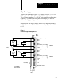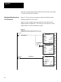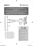
1
AllenBradley
Absolute Encoder
Module
(Cat. No. 1771-DE)
User
Manual
Table of Contents
Using This Manual . . . . . . . . . . . . . . . . . . . . . . . . . . . . . . .
11
Chapter Objectives . . . . . . . . . . . . . . . . . . . . . . . . . . . . . . . . . . .
What This Manual Contains . . . . . . . . . . . . . . . . . . . . . . . . . . . .
Audience . . . . . . . . . . . . . . . . . . . . . . . . . . . . . . . . . . . . . . . . . .
Warnings and Cautions . . . . . . . . . . . . . . . . . . . . . . . . . . . . . . .
Summary . . . . . . . . . . . . . . . . . . . . . . . . . . . . . . . . . . . . . . . . .
11
11
11
12
12
Introducing the Absolute Encoder Module . . . . . . . . . . . . .
21
Chapter Objectives . . . . . . . . . . . . . . . . . . . . . . . . . . . . . . . . . . .
Example Applications . . . . . . . . . . . . . . . . . . . . . . . . . . . . . . . . .
Module Functions . . . . . . . . . . . . . . . . . . . . . . . . . . . . . . . . . . . .
Compatible Processors . . . . . . . . . . . . . . . . . . . . . . . . . . . . . . .
Compatible Encoders . . . . . . . . . . . . . . . . . . . . . . . . . . . . . . . . .
State of Outputs Upon Loss of Input Power . . . . . . . . . . . . . . . . . .
Module Description . . . . . . . . . . . . . . . . . . . . . . . . . . . . . . . . . .
Electrostatic Discharge . . . . . . . . . . . . . . . . . . . . . . . . . . . . . . . .
Specifications . . . . . . . . . . . . . . . . . . . . . . . . . . . . . . . . . . . . . .
Summary . . . . . . . . . . . . . . . . . . . . . . . . . . . . . . . . . . . . . . . . .
21
21
21
22
22
22
23
25
26
27
Configuring and Installing Your Module . . . . . . . . . . . . . . .
31
Chapter Objectives . . . . . . . . . . . . . . . . . . . . . . . . . . . . . . . . . . .
Electrostatic Discharge . . . . . . . . . . . . . . . . . . . . . . . . . . . . . . . .
Setting Configuration Plugs . . . . . . . . . . . . . . . . . . . . . . . . . . . . .
Response to External Fault . . . . . . . . . . . . . . . . . . . . . . . . . . . . .
Keying . . . . . . . . . . . . . . . . . . . . . . . . . . . . . . . . . . . . . . . . . . .
Power Requirements . . . . . . . . . . . . . . . . . . . . . . . . . . . . . . . . .
WiringArm Connections . . . . . . . . . . . . . . . . . . . . . . . . . . . . . . .
Installing the Module . . . . . . . . . . . . . . . . . . . . . . . . . . . . . . . . . .
31
31
31
34
34
35
38
311
Module/Processor Communication . . . . . . . . . . . . . . . . . .
41
Chapter Objectives . . . . . . . . . . . . . . . . . . . . . . . . . . . . . . . . . . .
Block Transfer . . . . . . . . . . . . . . . . . . . . . . . . . . . . . . . . . . . . . .
Blocktransferwrite Data . . . . . . . . . . . . . . . . . . . . . . . . . . . . . .
WriteData Throughput Time . . . . . . . . . . . . . . . . . . . . . . . . . . . .
Blocktransferread Data . . . . . . . . . . . . . . . . . . . . . . . . . . . . . . .
Programming Example . . . . . . . . . . . . . . . . . . . . . . . . . . . . . . . .
Programming Considerations . . . . . . . . . . . . . . . . . . . . . . . . . . .
Summary . . . . . . . . . . . . . . . . . . . . . . . . . . . . . . . . . . . . . . . . .
41
41
41
44
44
45
47
47
ii
Table of Contents
Offset Feature . . . . . . . . . . . . . . . . . . . . . . . . . . . . . . . . . .
51
Offset Feature . . . . . . . . . . . . . . . . . . . . . . . . . . . . . . . . . . . . . .
Offset Words . . . . . . . . . . . . . . . . . . . . . . . . . . . . . . . . . . . . . . .
Programming Considerations with Offset . . . . . . . . . . . . . . . . . . .
51
52
56
Troubleshooting . . . . . . . . . . . . . . . . . . . . . . . . . . . . . . . .
61
Chapter Objectives . . . . . . . . . . . . . . . . . . . . . . . . . . . . . . . . . . .
Causes of Blocktransfer Errors . . . . . . . . . . . . . . . . . . . . . . . . . .
Errors Indicated by Diagnostic Bits . . . . . . . . . . . . . . . . . . . . . . .
Summary . . . . . . . . . . . . . . . . . . . . . . . . . . . . . . . . . . . . . . . . .
Blocktransfer Timing . . . . . . . . . . . . . . . . . . . . . . . . . . . . . . . . .
Blocktransfer Timing for PLC2 Family Processors . . . . . . . . . . . .
Blocktransfer Timing for PLC3 Family Processors . . . . . . . . . . . .
Application Considerations . . . . . . . . . . . . . . . . . . . . . . . . . . . . .
Application Considerations . . . . . . . . . . . . . . . . . . . . . . . . . . . . .
61
61
62
62
A1
A1
A8
B1
B1
Blocktransfer Ladder Diagram Examples . . . . . . . . . . . . .
C1
Bidirectional Blocktransfer for PLC2 Family Processors . . . . . . . .
Bidirectional Blocktransfer for PLC3 Processors . . . . . . . . . . . . .
Readonly Blocktransfer for PLC2 Family Processors . . . . . . . . .
C1
C4
C6
Bit and Word Descriptions of Block-transfer Data . . . . . . .
D1
Block-transfer-write Data . . . . . . . . . . . . . . . . . . . . . . . . . . . . . .
Block-transfer-read Data . . . . . . . . . . . . . . . . . . . . . . . . . . . . . .
D1
D2
Connection Diagrams for AllenBradley Encoders . . . . . .
E1
Connection Diagrams for AllenBradley Encoders . . . . . . . . . . . . .
0 to 359count, 10bit, BCD, Singleended Output . . . . . . . . . . . . .
0 to 255count, 8bit, Standard Gray, Singleended Output . . . . . . .
0 to 359count, 10bit, BCD, Singleended Output, Latching . . . . . .
E1
E1
E3
E4
Glossary . . . . . . . . . . . . . . . . . . . . . . . . . . . . . . . . . . . . . .
F1
Chapter
1
Using This Manual
Chapter Objectives
Read this chapter to familiarize yourself with this manual. It tells you
how to use the manual properly and efficiently.
What This Manual Contains
This manual contains 5 chapters and 6 appendices:
Audience
Chapter/
Appendix
Title
What's Covered
1
Using This Manual
Manual's purpose, audience, and contents
2
Introducing the Absolute
Encoder Module
Module description, features, and hardware
components
3
Configuring and Installing
Your Module
Feature selection and installation procedures
4
Module/Processor
Communication
Words and file parameters of blocktransfer
data
5
Offset Feature
Programming to compensate for shaft offset
6
Troubleshooting
Troubleshooting guide
A
Block-transfer Timing
Instructions for determining blocktransfer
timing
B
Application Consideration
Encoder shaft speed
C
Block-transfer Ladder
Diagram Examples
Examples of blocktransfer programming
D
Biat and Word Description
of Block-transfer Data
Details of blocktransfer file data
E
Glossary
F
Index
In this manual we assume that you know how to:
program and operate an Allen-Bradley programmable controller
program block-transfer instructions
11
Chapter 1
Using This Manual
If you do not know how to do either of these, read the user’s manual of
your processor. Refer to our Publications Index (publication SD499) for a
complete list of publications.
Warnings and Cautions
Throughout this manual we include special notes to alert you to possible
injury to personnel or damage to equipment under specific circumstances.
WARNING: tells you when people may be injured if
procedures are not followed properly.
CAUTION: tells you when machinery may be damaged if
procedures are not followed properly.
Summary
12
This chapter told you how to use this manual efficiently. The next chapter
introduces you to the absolute encoder module.
Chapter
2
Introducing the Absolute Encoder Module
Chapter Objectives
This chapter describes:
example applications of the absolute encoder module
functions of the module
Allen-Bradley processors compatible with the absolute encoder module
encoders you can use with the module
module specifications
Example Applications
The absolute encoder module is usually used for:
absolute-position feedback
high-speed response to position based on encoder values
immunity to loss of position from power loss or power interruptions
Module Functions
The Absolute Encoder Module (cat. no. 1771-DE) is an intelligent module
that provides high-speed response to machine position independently of
the programmable controller scan. It can:
monitor the position of an absolute encoder that has up to 12 bits
control up to eight high-current outputs based on comparisons between
encoder position and your preset values
provide throughput for all eight outputs in less than 200 us
communicate with the programmable controller through block transfers
return the status of outputs and the position of an absolute encoder to
the programmable controller
In addition, the module can switch 2A DC per output with no derating
when all outputs are on, allowing 16A continuous per module.
21
Chapter 2
Introducing the Absolute Encoder Module
Compatible Processors
You can use the absolute encoder module with any Allen-Bradley
programmable controller that uses block-transfer programming in both
local and remote 1771 I/O systems. Processors that are compatible with
the module include:
Mini PLC-2 (cat. no. 1772-LN3)
PLC-2/20 (cat. no. 1772-LP1, -LP2)
PLC-2/30 (cat. no. 1772-LP3)
PLC-3 (cat. no. 1775-L1, -L2)
Mini-PLC-2/15 (cat. no. 1772-LV)
Mini-PLC-2/05 (cat. no. 1772-LS, -LSP)
Compatible Encoders
You can use Allen-Bradley absolute encoders that use up to 12 bits with
the absolute encoder module. Allen-Bradley encoders with the following
bulletin numbers are compatible with the absolute encoder module:
Bulletin 845A
Bulletin 845B
Bulletin 845C
The module is also compatible with absolute encoders that have the
following specifications:
single-ended or differential encoder output signals
TTL-compatibility (output drivers)
capability of sinking 11mA (single-ended) or 18mA (differential) per
channel
BCD, natural binary, or standard Gray code format
State of Outputs Upon Loss of
Input Power
You can select the state in which the outputs will be if the module loses
input power. A configuration plug on the right printed-circuit board
allows the outputs to:
turn off
remain in their state at loss of input power
22
Chapter 2
Introducing the Absolute Encoder Module
Module Description
The next four sections give a description and specifications of the
absolute encoder module.
Status Indicators
The module has 10 LED status indicators (Figure 2.1):
Eight output status indicators (one for each output) light when the
corresponding output circuitry is energized.
One green ACTIVE indicator lights when the module is powered and
functioning.
One red FAULT indicator lights when the module detects a fault and
momentarily lights at power-up.
Figure 2.1
Status Indicators
Status Indicators
ABSOLUTE
ENCODER
MODULE
Active
0
1
2
3
4
5
6
7
Fault
Output status
Indicators
Output Fuses
The module has eight 3A rectifier fuses (one per output) located on the
right printed-circuit board. Figure 2.2 shows the fuse locations.
23
Chapter 2
Introducing the Absolute Encoder Module
Figure 2.2
Fuse Locations
F1
F2
F3
F4
F5
F6
F7
F8
Right Board
13303
Terminal Identification
Figure 2.3 identifies each terminal of the absolute encoder module. The
bit x/common terminals refer to:
not bit x terminals (uses with differential output encoders)
or
common terminals (used with single-ended output encoders)
24
Chapter 2
Introducing the Absolute Encoder Module
Figure 2.3
Terminal Identification
Left
Wiring
Arm
Bit 0
Bit 0 / Common
Bit 1
Bit 1 / Common
Bit 2
Bit 2 / Common
Bit 3
Bit 3 / Common
Bit 4
Bit 4 / Common
Bit 5
Bit 5 / Common
Bit 6
Bit 6 / Common
Bit 7
Bit 7 / Common
Bit 8
Bit 8 / Common
Bit 9
Bit 9 / Common
Input Supply
(+5V dc)
Right
Wiring
Arm
1
1
2
2
3
3
4
4
5
5
6
6
7
7
8
8
9
9
10
10
11
11
12
12
13
13
14
14
15
15
16
16
17
17
18
18
19
19
20
20
21
21
Output Supply (+5 to 24V dc)
Output 0
Output 1
Output 2
Output 3
Output Common (+5 to 24V dc)
Output Common (+5 to 24V dc)
Not Used
Output Supply (+5 to 24V dc)
Output 4
Output 5
Output 6
Output 7
Output Common (+5 to 24V dc)
Output Common (+5 to 24V dc)
Not Used
Bit 10
Bit 10 / Common
Bit 11
Bit 11 / Common
Input Common (+5V dc)
For Outputs
0-3
For Outputs
4-7
12832
Electrostatic Discharge
Electrostatic discharge can damage integrated circuits or semiconductors
in this module if you touch backplane connector pins. It can also damage
the module when you set configuration plugs or switches inside the
module. Avoid electrostatic discharge by observing the following
precautions:
Touch a grounded object to discharge yourself before handling the
module.
Do not touch the backplane connector or connector pins.
When you configure and replace internal components, do not touch
other circuit components inside the module. If available, use a
static-safe workstation.
When not in use, keep the module in its static-shield bag.
25
Chapter 2
Introducing the Absolute Encoder Module
CAUTION: Electrostatic discharge can degrade performance or
damage the module. Handle as stated above.
Specifications
26
Module Location
Any 1771I/O chassis; any 2slot I.O
group
Input Power Supply
+5V DC +0.25V (total output
voltage tolerance includes line
regulation, load regulation, drift,
and ripple)
Number of Inputs
Up to 12 encoder input bits per
module
Current Requirement
300mA (maximum)
Encoder Formats
BCD
Natural binary
Standard Gray
Number of Outputs
8
Digital Resolution
Up to one part in 4,095 with
natural binary and standard
Gray encoders
Up to one part in 999 with
BCD encoders
Output Current Rating
2A sourced per output (no
derating with all outputs on)
Hightrue Logic
From totem pole, open
collector, or differential line
drivers
Can select direction of
rotation of increasing position
for Gray code encoders
VA Rating
48W per output
384W per module
Input Voltage Range and Logic State
Logic 1: 1.7V DC
Logic 0:0.0V to 0.6V DC
Input and Output Isolation
1500V RMS
Input Current per Channel
(sunk by encoder device)
ll mA for singleended drivers
l8 mA for differential drivers
Output Power Supply
Selectable : +5 to +24V DC
Maximum input Frequency
50 KHz
Backplane Current
800 mA at 5V DC
Encoder Data Settling Time
100 ns
Output Fuses
3A rectifier fuses (Littelfuse
322003, Buss GBB003, or
equivalent)
Surge Rating
4A for l0 ms
Chapter 2
Introducing the Absolute Encoder Module
New Position Throughput Time
200 us
Environmental Conditions
Operating Temperature
0 to 60o C (32 to 140oF)
Storage Temperature
40 to 85oC (40 to 185oF)
Relative Humidity
5 to 95% (without
condensation)
New Writedata Throughput Time
4.7 ms
Keying (for slot 0 only)
Between 2 and 4
Between 26 and 28
Torque for wiring arm connections
9 inchpounds
Summary
This chapter described the absolute encoder module, its functions and
applications, and the processors and encoders with which it is compatible.
The next chapter tells you how to configure and install the module.
27
Chapter
3
Configuring and Installing Your Module
Chapter Objectives
This chapter tells you how to:
select module features by setting configuration plugs
power module input circuitry and output devices
key the module
make wiring arm connections
install the module
Electrostatic Discharge
Electrostatic discharge can damage integrated dircuits or semiconductors
in this module if you touch backplane connector pins. It can also damage
the module when you set configuration plugs or switches inside the
module. Avoid electrostatic discharge by observing the following
precautions:
Touch a grounded object to discharge yourself before handling the
module.
Do not touch the backplane connector or connector pins.
When you configure and replace internal components, do not touch
other circuit components inside the module. If available, use a
static-safe work station.
When not in use, keep the module in its static-shield bag.
CAUTION: Electrostatic discharge can degrade performance
or damage the module. Handle as stated above.
Setting Configuration Plugs
You can choose various module features by setting configuration plugs.
The module is factory-set for use with a BCD differential output encoder.
To access the configuration plugs, lay the module on its right side and
remove the cover.
The configuration plug sockets are labeled E1 through E15 on the left
printed-circuit board and E1 on the right printed-circuit board. Locate the
configuration plugs with the board positioned as shown in Figure 3.1 and
Figure 3.2. Each plug is inserted on two pins of a three-pin connector.
You change the position of the plugs in a left-right or up-down direction.
31
Chapter 3
Configuring and Installing Your Module
Figure 3.1
Configuration Plug Locations and Settings (Left Board)
E13 E14
E1
E2
E3
E4
E5
E6
E7
E8
E9
E15
E10
E11
E12
Left Board
Config
uration
Plug
E1
through
E12
E13
E14
E15
32
Right
13304
Configuration Plug Settings
Encoder Signal
Mode
Single
ended
Differ
ential
left
right
Gray Encoder
Rotational Direction
Encoder Format
Natural
Binary
Standard
Gray
BCD
left
left
right
left
left
left
Increasing
Position
Decreasing
Position
right
left
Chapter 3
Configuring and Installing Your Module
Figure 3.2
Configuration Plug Location and Settings (Right Board)
E1
Down
Right Board
Configuration
Configuration Plug Settings
Plug
State of Outputs After Loss
of Input Power Supply
E1
Turn
Off
Last
State
Up
Down
13305
Selecting Encoder Format and Input Signal Mode
Set configuration plugs E1 through E12 (on the left board) to match the
signal mode of each encoder input channel to the encoder. Set
configuration plugs E13 and E14 (also on the left board) to match the data
format of your encoder.
Selecting Encoder Rotational Direction
Use configuration plug E15 on the left board to indicate the direction of
shaft rotation that causes the absolute position to increase for Gray code
33
Chapter 3
Configuring and Installing Your Module
encoders. This is the same as selecting “high true” or “low true” inputs
from the Gray encoder.
Configuration plug E15 is factory-set in the right position. It gives an
increased count when the encoder rotates clockwise when looking at the
shaft. If your encoder shows a decreased count, change the plug to the
left position.
If your Gray
encoder has:
and E15 is in
this position
12 bits
right
an increased count
left
a decreased count
right
an increased count
left
a decreased count starting with 4,095
less than 12 bits
the encoder
shows:
This configuration plug does not affect BCD or binary encoders.
Selecting State of Outputs Upon Loss of Input Power
Use configuration plug E1 on the right board to choose the state of the
outputs if the module loses input power. The plug is factory-set for the
outputs to turn off if input power is lost (up position). If you want the
outputs to remain in their state at loss of input power, set the plug to the
down position.
Response to External Fault
Except for downloading programs or commands and reporting status, the
module operates independent of the host processor. In the event of a
processor or I/O communications fault, the module either continues
operation or its outputs turn off, depending on how you set the last state
switch of the chassis in which you place the module.
If you set the last state switch to turn outputs off, the module’s outputs are
turned off.
If you set the last state switch to hold outputs in last state, the module
continues operating.
Keying
34
Plastic keying bands are shipped with each I/O chassis. These bands
ensure that only a selected type of module can be placed in a particular
Chapter 3
Configuring and Installing Your Module
I/O chassis module slot. They also help to align the module with the
backplane connector.
Each module is slotted at its rear edge. The position of the keying bands
must correspond to these slots to allow insertion of the module. Position
the keying bands on the upper backplane connector between the numbers
at the right of the connectors. Keying bands are only used to key slot 0 of
the module. Figure 3.3 illustrates the encoder module keying positions
for slot 0.
Figure 3.3
Keying Positions
Upper Backplane
Connectors
2-slot I/O group
0
2
4
6
8
1
1
1
1
1
2
2
2
2
2
3
3
3
3
Keying
Bands
Left
Connector
Power Requirements
1
0
2
4
6
8
0
2
4
6
8
0
2
4
6
2
4
6
8
1
1
1
1
1
2
2
2
2
2
3
3
3
3
Right
Connector
0
2
4
6
8
0
2
4
6
8
0
2
4
6
12834
You must provide a minimum of two external power supplies: one to
power input circuitry and one to power output devices.
Input Power Supply
Connect a +5V DC power supply for the input circuitry between terminal
21 (+) of the left wiring arm and terminal 21 (-) of the right wiring arm.
Make sure the voltage is 5V DC +.25V. The input circuitry requires a
35
Chapter 3
Configuring and Installing Your Module
maximum of 300mA.
For the best system noise immunity, we recommend use of a separate,
linear regulated power supply for powering the input circuitry and the
encoder. You can use this supply for more than one absolute encoder
module or encoder, but do not use it for otehr 5V loads such as relays.
Make sure the power supply has enough additional current capacity for
the encoder.
We suggest you use extra shielded twisted pairs of wire in the encoder
input cable to power the encoder. If more than one extra pair of wires
remains, put them in parallel to reduce the voltage drop between the
power supply and the encoder Figure 3.4.
Do not source current, such as from a power supply, into the encoder
input terminals of the module. Doing so can damage input circuitry.
For the best system noise immunity, we recommend use of a separate,
linear regulated power supply for powering the input circuitry and the
encoder. You can use this supply for more than one absolute encoder
module or encoder, but do not use it for other 5V loads such as relays.
Make sure the power supply has enough additional current capacity for
the encoder.
Figure 3.4
Connecting Extra Pairs of Wires Between the Module and Encoder for Power Supply
Connections
+5V
Encoder
Terminal 21 of
Left Wiring Arm
Supply
Common
+
-
5V supply
Terminal 21 of
Right Wiring Arm
36
12835
Chapter 3
Configuring and Installing Your Module
Output Power Supply
To power the eight outputs (Figure 3.5), connect at least one +5 to +24V
DC supply to terminal 1 and terminal 6 (or 7) of the right wiring arm.
You can connect another +5 to +24V DC power supply between terminals
9 and 14 (or 15) of the right wiring arm if, for example, you need two
different load supply voltages.
If you need only one supply voltage, connect a wire between terminals 1
and 9 and connect another wire between terminal 6 (or 7) and terminal 14
(or 15).
Figure 3.5
Connection Diagram for Output Devices
Right
Wiring
Arm
1
+
2
+5 to 24V
DC User
Supply
+
3
4
5
-
-
6
DC Output
Devices
7
8
9
+
10
+5 to 24V
DC User
Supply
+
11
12
13
-
-
14
15
16
17
18
Input circuitry
19
20
21
(See Applicable
Codes and Laws)
Tie Wires
Here
Output Supply (+5 to 24V dc)
Output 0
Output 1
Output 2
Output 3
Output Common (+5 to 24V dc)
Output Common (+5 to 24V dc)
Not Used
Output Supply (+5 to 24V dc)
Output 4
Output 5
Output 6
Output 7
Output Common (+5 to 24V dc)
Output Common (+5 to 24V dc)
Not Used
Bit 10
Bit 10 / Common
Bit 11
Bit 11 / Common
Input Common (+5V dc)
For Outputs
0-3
For Outputs
4-7
12838
37
Chapter 3
Configuring and Installing Your Module
WiringArm Connections
We recommend the following Belden cable or its equivalent to connect
the encoder to the module (maximum 50 feet). Use extra twisted pairs to
connect power to the encoder.
No. of
No. of Twisted
Belden Cable No.
Encoder Bits
Pairs in Cable
18 AWG
20 AWG
8
9
9775
9875
10
11
9876
12
9776
9877
12
15
9777
9879
Important: Tighten wiring arm connections to 9 inch-pounds of torque.
WARNING: Do not remove the wiring-arm from an
operating module; it will cause the power-up bit status to
change unpredictably until a valid write to the module occurs.
If swing-arm power is lost, turn on the power-up bit and disable
all outputs until a valid write occurs.
Connecting a Singleended Output Encoder
Use Figure 3.6 to connect a single-ended output encoder. Connect the
signal line for bit 0 to terminal 1 of the left wiring arm. Connect its return
to terminal 2. Connect bit 1 signal line to terminal 3 and its return to
terminal 4. Continue in this way for all encoder channels.
If the encoder has less than 12 signal bits, jumper the unused input
terminals. For example, if you are using a 10-bit encoder, jumper
terminals 19 and 20 and terminals 17 and 18 on the right wiring arm.
38
Chapter 3
Configuring and Installing Your Module
Figure 3.6
Singleended Output Encoder Connection Diagram
Left
Wiring
Arm
Single-ended
Ouput Encoder
Bit 0
Common
Bit 1
Common
Bit 2
Common
Power Supply
Common
Other bit connections not shown. Continue in
this manner until you make all bit connections.
If the encoder uses less than 12 bits, jumper the
unused input terminals.
Right
Wiring
Arm
1
1
2
2
3
3
4
4
5
5
6
6
7
7
8
8
9
9
10
10
11
11
12
12
13
13
14
14
15
15
16
16
17
17
18
18
19
19
20
20
21
21
Output
Circuitry
Bit 10
Common
Bit 11
Common
From
Encoder
+
+5V dc Input Supply
12836
Connecting a Differential Output Encoder
Figure 3.7 is the connection diagram for a differential output encoder.
Connect the bit 0 signal line to terminal 1 and the bit 0 line to terminal 2.
Connect bit 1 to terminal 3 and the bit 1 line to terminal 4. Continue in
this way for all encoder channels.
If the encoder has less than 12 signal bits, jumper the unused input
terminals. For example, if you are using a 10-bit encoder, jumper
terminals 19 and 20 and terminals 17 and 18 on the right wiring arm.
39
Chapter 3
Configuring and Installing Your Module
Figure 3.7
Differential Output Encoder Connection Diagram
Left
Wiring
Arm
Differential
Ouput Encoder
Bit 0
Bit 0
Bit 1
Bit 1
Bit 2
Bit 2
Other bit connections not shown. Continue in
this manner until you make all bit connections.
If the encoder uses less than 12 bits, jumper the
unused input terminals.
Right
Wiring
Arm
1
1
2
2
3
3
4
4
5
5
6
6
7
7
8
8
9
9
10
10
11
11
12
12
13
13
14
14
15
15
16
16
17
17
18
18
19
19
20
20
21
21
Output
Circuitry
Bit 10
Bit 10
Bit 11
Bit 11
From
Encoder
+
+5V dc Input Supply
12837
Connecting Output Devices
Use Figure 3.5 to connect your output devices and supply(ies). Two
output commons are associated with each output group:
terminals 6 and 7 for outputs 0 through 3
terminals 14 and 15 for outputs 4 through 7
Terminals 6 and 7 are tied together internally, as are 14 and 15, so that
each output group can use either terminal for that particular group.
310
Chapter 3
Configuring and Installing Your Module
Installing the Module
Now that you’ve determined the power requirements, keying, and wiring
for your module, you can use the following procedure to install it.
Refer to the Programmable Controller Grounding and Wiring Guidelines
(pub. no. 1770-4.1) for proper grounding and wiring methods to install
your module.
WARNING: Remove power from the 1771 I/O chassis
backplane and wiring arm before installing or removing the
module.
Failure to remove power from the backplane or wiring arm could cause
module damage, degradation of performance, or injury.
Failure to remove power from the backplane could cause injury and/or
equipment damage due to possible unexpected operation.
WARNING: Install the module in the I/O chassis so that both
halves of the module are in the same I/O group. Failure to
observe this rule will result in faulty module operation and/or
damage to the module circuitry with possible injury to
personnel.
CAUTION: Do not force the module into a backplane
connector. If you can’t seat it with firm pressure, check the
alignment and keying. You can damage the connector or the
module if you force it into the connector.
1.
Remove power from the I/O chassis before inserting (or removing)
the module.
2.
Open the module locking latch on the I/O chassis and insert the
module into the slot keyed for it.
3.
Firmly press to seat the module into its backplane connector.
4.
Secure the module with the module locking latch.
311
Chapter 3
Configuring and Installing Your Module
Summary
312
This chapter told you how to select features and set configuration plugs on
the absolute encoder module, and described the power requirements,
keying, wiring, and installation of the module. In the next chapter you
will read about block-transfer file parameters.
Chapter
4
Module/Processor Communication
Chapter Objectives
This chapter describes file parameters for the block-transfer data files you
use to write data to and read data from the absolute encoder module.
Block Transfer
The absolute encoder module and the processor communicate through
block-transfer programming. Processors that use block-transfer
programming are listed below, along with the respective programming
manual. Refer to the latest edition of the programming manual for a
detailed description of block transfer.
Blocktransferwrite Data
Processor
Programming and Operations
Manual Publication Number
MiniPLC2
17726.8.4
MiniPLC2/15
17726.8.2
MiniPLC2/05
17726.8.6
PLC2/20
17726.8.1
PLC2/30
17726.8.3
PLC3
17726.4.1
You write data to the module in blocks. You can write 5, 10, 15 or 20
words in one block-transfer operation. Each block of five words is
associated with two outputs and is identical to each other in format:
words 1-5 - outputs 0 and 1
words 6-10 - outputs 2 and 3
words 11-15 - outputs 4 and 5
words 16-20 - outputs 6 and 7
The first word of each block is a control word. The last four words are
preset words. The formats of the write-data words and control word 1 are
shown in Figure 4.1 and are described here.
You can send a maximum of 20 words (four block of five words) in one
block-transfer operation. The number of words you send to the module
determines how many outputs it controls. If you want to change data for
41
Chapter 4
Module/Processor Communication
outputs 4 and 5 (and the module is controlling all eight outputs), you must
send 20 words to the module; you cannot send only the words associated
with outputs 4 and 5.
Figure 4.1
Format of Blocktransferwrite Data
17
16
Word #1 OE ZT
>
=
13
12
11
10
07
<
>
=
<
OE ZT
>
=
03
02
01
00
<
>
=
<
Control word
for Outputs 0 and 1
3
Preset 0B
4
Preset 1A
5
Preset 1B
>
=
<
>
=
<
OE ZT
>
=
<
>
=
<
Control word
for Outputs 2 and 3
7
Preset 2A
8
Preset 2B
9
Preset 3A
10
Preset 3B
>
=
<
>
=
<
OE ZT
>
=
<
>
=
<
Control word
for Outputs 4 and 5
12
Preset 4A
13
Preset 4B
14
Preset 5A
15
Preset 5B
16 OE ZT
>
=
<
>
=
<
OE ZT
>
=
<
>
=
<
Control word
for Outputs 6 and 7
17
Preset 6A
18
Preset 6B
19
Preset 7A
20
Preset 7B
COM for
Preset 1B
OE ZT
>
=
<
OE = Output Enable Bit
ZT = Zero Transition Bit
COM = Comparison Bits
42
05 04
Preset 0A
11 OE ZT
B. Format of Control
Word #1
06
2
6 OE ZT
A. Writedata Words
15 14
COM for
Preset 1A
>
=
<
COM for
Preset 0B
OE ZT
>
=
<
COM for
Preset 0A
>
=
<
12839
Chapter 4
Module/Processor Communication
Control Words
Each control word is associated with two outputs. The lower byte of
control word 1 is associated with output 0. Its format is as follows:
Bits 0 through 2 are the comparison bits for output 0, preset A (greater
than, less than, equal to, greater than or equal to, less than or equal to).
Bits 3 through 5 are the comparison bits for output 0, preset B.
Bit 6 is the zero transition (ZT) bit. Set this bit when an output is to be
energized during a transition through 0.
Bit 7 is the output enable (OE) bit. This bit is examined along with the
comparison made by the module between your presets and the absolute
position of the encoder in turning on a module’s output. Although
comparisons to the presets may be true, if you don’t set this bit the
output is not turned on.
The upper byte of control word 1 is associated with output 1. The format
of this byte is similar to the format of the lower byte:
Bits 10 through 12 are the comparison bits for output 1, preset A.
Bits 13 through 15 are the comparison bits for output 1, preset B.
Bit 16 is the ZT bit.
Bit 17 is the OE bit.
The remaining control words with their corresponding outputs are:
word 6 - outputs 2 and 3
word 11 - outputs 4 and 5
word 16 - outputs 6 and 7
Preset Words
The present words define preset values for turn-on and turn-off points of
the corresponding output. You program them in BCD. Each block of four
preset words is associated with two outputs and is identical in format to
that for outputs 0 and 1:
word 2 - preset A for output 0
word 3 - preset B for output 0
word 4 - preset A for output 1
word 5 - preset B for output 1
43
Chapter 4
Module/Processor Communication
WriteData Throughput Time
Thewrite-data throughput time is the time between the end of a
block-transfer-write operation and the module update of its outputs. The
module’s response time can vary, depending on the number of outputs it
controls, the type of absolute encoder you use, and if you have an offset
value. The worst case is 4.7 ms. Use the following table to determine the
module’s response time in milliseconds for your application.
Type of Encoder (with or without offset)
BCD without offset
BCD with offset
Gray code or binary without offset
Gray code or binary with offset
Blocktransferread Data
2
4
6
8
1.2
2.0
1.3
1.9
1.8
2.9
2.0
2.6
2.5
3.8
2.6
3.4
3.1
4.7
3.3
4.1
The processor reads data from the module and transfers it to its data table
in two read-data words. The module sends only two read-data words in
any one block-transfer-read operation. The format of these words is
shown in Figure 4.2 and is described here:
Figure 4.2
Format of Blocktransferread Data
Word 1
17 16 15 14 13 12 11 10 07 06 05 04 03 02 01 00
Status of outputs
0
Output 7
Output 6
Output 5
Output 4
Output 3
Output 2
Output 1
Output 0
Word 2
Code indicating which
preset is in non-BCD format
Non-BCD preset flag
Unused
Write-data-valid
Loss-of-input-power
Current Absolute Position (in BCD)
0
13070
The upper byte of 1 indicates the status of the eight outputs controlled
by the module. The module sets each bit when the corresponding
output is turned on. Refer to Appendix D for details of these bits.
The format of the lower byte of word 1 (by bit) is:
44
Chapter 4
Module/Processor Communication
Bit 7 is the loss-of-input-power bit. It is set when input power is
lost; it is reset when power is restored and bit 6 is reset.
Bit 6 is the write-data-valid bit. It is set at power-up and when the
processor changes from the program mode to the run mode; it is reset
when the module receives valid data in a block-transfer-write
operation.
Bit 5 is unused.
Bit 4 is the non-BCD preset flag. It is set when any preset is in
non-BCD format.
Bits 3 through 0 are a binary or hexadecimal code that indicates which
preset is not in BCD format. (Refer to Appendix D for the value of
these bits.) The module identifies each incorrect preset in the order
it finds them (one at a time). Once you correct a preset, the module
continues to identify any non-BCD preset.
Word 2 indicates the current absolute position of the encoder in BCD.
Programming Example
Presets are interpreted by the module as absolute numbers to be compared
to the absolute position of the encoder shaft; they are not interpreted as
degrees of shaft rotation.
Thus, if you have a 0 to 999-position encoder, you program presets for
output 3, for example, as:
Preset 3A = 200
Preset 3B = 402
There is no restriction on which mode of comparison you can use for
preset A or preset B.
In this example, we assume the use of a 0 to 359-position encoder when
referring to degrees of shaft rotation.
If you want to turn on output 0 between shaft positions 330 (preset A) and
005 (preset B), you set:
the “greater than” and “equal to” bits for preset A
the “less than” and “equal to” bits for preset B
the ZT bit
45
Chapter 4
Module/Processor Communication
the OE bit
Output 0 is turned on when the shaft position is greater than or equal to
330 or when the shaft position is less than or equal to 005.
If you don’t set the ZT bit in the above control word, when the encoder
shaft position is 002, for example, comparison B is true, comparison A is
not true, and the output is turned off. (At position 002, the shaft position
is less than or equal to 005, but it is not greater than or equal to 330.) You
must set the ZT bit when an output is to be energized during a transition
through 0.
Another way to energize output 0 between position 330 and 005 is to give
preset A a value of 006 and preset B a value of 329. Then you set:
the “less than” bit for preset A
the “greater than” bit for preset B
the ZT bit
OE bit
In either case, you must set bit 6 (ZT) to indicate that the output should be
on if either comparison A or comparison B is true.
Let’s continue this example and assume your application requirements for
outputs 0 and 1 are:
output 0 is to turn on at position 330 and turn off at position 005
output 1 is to turn on between position 007 and position 011
Once you define the presets for outputs 0 and 1, determine the comparison
bits for each preset, and enter the data into the data file, the block of data
you write to the module (five words) looks like this:
17
16
15
14
13
12
11
10
>
=
<
>
=
<
0
0
OE ZT
binary
BCD
digits
46
1
0
0
0
1
1
07
Bit #
06
05
04
03
02
01
00
OE ZT
>
=
<
>
=
<
Control
Word
Function
1
0
Control
Word
1
1
0
1
1
1
0
3
3
0
Preset 0A
0
0
0
5
Preset 0B
0
0
0
7
Preset 1A
0
0
1
1
Preset 1B
Chapter 4
Module/Processor Communication
Programming Considerations
When you specify the default block length (00), the following
considerations apply for PLC-2 family processors:
You can and should enable the read and write instructions in the same
scan (separate but equal input conditions).
The module decides which operation is performed first when both
instructions are enabled in the same scan.
Alternate operation is performed in a subsequent scan.
Do not operate on transferred data until the done bit is set.
When you examine the read and write files, 64 words appear to be moved;
however, the processor writes only 20 words and reads only two words in
any block-transfer operation.
WARNING: When the block lengths of bidirectional
block-transfer instructions are set to unequal values, do not
enable the rung containing the alternate instruction until the
done bit of the first transfer is set. If you enable them in the
same scan, the number of words transferred may not be the
number intended, invalid data could be operated upon in
subsequent scans, or output devices could be controlled by
invalid data. Unexpected and/or hazardous machine operation
could occur. Damage to equipment and/or personal injury could
result.
Summary
This chapter gave a description of the file parameters for programming
block-transfer-read and -write operations for the absolute encoder module.
It also gave several programming examples and considerations for use
with the absolute encoder module. The next chapter describes
troubleshooting the module.
47
Chapter
5
Offset Feature
Offset Feature
Offset is a new feature of the Absolute Encoder Module (cat. no.
1771-DE, revision B). Revision A modules do not have this feature.
Offset is the difference between the 0 position of the absolute encoder and
the 0 position of the machine shaft to which the encoder is connected.
You can program this value to compensate for such factors as machine
wear or improper mechanical setup. You do not have to disconnect your
equipment to realign the 0 position of the machine shaft with the 0
position of the absolute encoder.
Determining the Offset Value
You can find the offset value using either of two equations, depending on
whether you use the 0 machine position or the 0 encoder position as your
reference.
To calculate an offset value from a 0 encoder position, use this equation:
N -M = S
where N = number of encoder positions, M = machine position at encoder
0, and S = offset.
To calculate an offset value from a 0 machine position, use this equation:
E-N=S
where E = encoder position at machine 0, N = number of encoder
positions, and S = offset.
Let’s look at an example finding the offset value with reference to 0
encoder position and 0 machine position. Assume the following:
You have a 0 to 4,095-position encoder (4,096 positions)
The machine shaft is at position 512 when the encoder is at position 0
The encoder is at position 3,584 when the machine is at position 0
51
Chapter 5
Offset Programming
In this example, the 0 machine position is “ahead” of the 0 encoder
position. Depending on which equation you use (your reference point),
the offset value is either positive or negative.
Offset Value From 0 Encoder Position and From 0 Machine Position
0
3584
Encoder
0
512
Machine shaft
At encoder position 0, machine shaft position is 512.
The offset is +3,584.
At machine shaft position 0, encoder position is 3,584.
The offset is 512.
13522
The equation (from 0 encoder position) is:
4,096 - 512 = 3,584
The offset is +3,584.
The equation (from 0 machine position) is:
3,584 - 4,096 = -512
The offset is -512.
You get the same result from programming either +3,584 or -512.
Offset Words
52
Once you determine the offset value, you need to program two
write-block-transfer words. These are the last two words of the write-data
block that you send to the absolute encoder module. You program them in
BCD, as you do the preset values.
Chapter 5
Offset Programming
Format of Offset Words
17
16
15
14
13
12
S
11
10
7
6
5
4
3
2
1
0
Bit #
OFFSET VALUE
NO. OF ENCODER POSITIONS
The offset words are the last two words of the write-data block that you send
to the absolute encoder module.
If you are controlling
2 outputs
4 outputs
6 outputs
8 outputs
The offset words are:
words 6 and 7
words 11 and 12
words 16 and 17
words 21 and 22
S = sign bit. Set this bit if the offset has a negative value; reset the bit if
the offset has a positive value.
13523
The first offset word contains the value of the offset. Bit 17 of this word
is the sign bit. It indicates whether the offset is negative or positive. Set
bit 17 if the offset is negative; reset it if the offset is positive.
The second offset word is the number of positions of the encoder. If you
are using a 0 to 4,095-position encoder, your second offset word is 4,096.
Blocktransferwrite Data with Offset
The number of words you send to the module depends on the number of
outputs the module controls. The offset feature adds two words to the
total number of words you send to the module:
If the module
controls:
You send:
2 outputs
7 words
4 outputs
12 words
6 outputs
17 words
8 outputs
22 words
If the module is controlling eight outputs, your block-transfer-write data
now looks like this:
53
Chapter 5
Offset Programming
Figure 5.1
Format of Blocktransferwrite Data with Offset
17 16 15 14 13 12 11 10 07 06 05 04 03 02 01 00
Word #1 OE ZT > = < > = < OE ZT > = < > = <
2
3
Preset 0B
4
Preset 1A
5
Preset 1B
Control Word for
Outputs 2 and 3
Preset 2A
6 OE ZT >
7
A. Write-data words
=
< >
=
< OE ZT >
=
< >
=
<
8
Preset 2B
9
Preset 3A
10
12
Preset 3B
Control Word for
Outputs 4 and 5
Preset 4A
13
Preset 4B
14
Preset 5A
15
Preset 5B
Control Word for
Outputs 6 and 7
Preset 6A
11 OE ZT >
16 OE ZT >
17
=
=
< >
< >
=
=
< OE ZT >
< OE ZT >
=
=
< >
< >
=
=
<
<
18
Preset 6B
19
Preset 7A
20
Preset 7B
21
S
Offset Value
22
B. Format of control
word #1
Control Word for
Outputs 0 and 1
Preset 0A
No. of Encoder Positions
COM for
Preset 1B
OE ZT >
=
COM for
Preset 1A
< >
=
COM for
Preset 0B
< OE ZT >
=
OE = Output Enable Bit
ZT = Zero Transition Bit
COM = Comparison Bit
S = Offset Sign Bit
COM for
Preset 0A
< >
=
<
10698I
Blocktransferread Data with Offset
The upper byte of word 1 indicates the status of the eight outputs
controlled by the module. The module sets each bit when the
corresponding output is turned on.
The lower byte of word 1 (by bit) is:
54
Chapter 5
Offset Programming
Bit 7 is the loss-of-input-power bit. It is set when input power is lost; it
is reset when power is restored and bit 6 is reset.
Bit 6 is the write-data-valid bit. It is set at power-up and when the
processor changes from program mode to run mode; it is reset when the
module receives valid data in a block-transfer-write operation.
Bit 5 is the non-BCD offset flag. See the description of bit 0 and bit 1
below to identify the type of offset error.
Bit 4 is the non-BCD preset flag. It is set when a preset word is in
non-BCD format.
Bits 3 through 0 are a binary or hexadecimal code that indicates which
preset word is not in BCD format. Refer to Appendix D of the User’s
Manual for the value of these bits.
Bit 1 when set along with bit 5 identifies that the offset value is greater
than the number of encoder positions.
Bit 0 identifies which offset word is in non-BCD format when bit 5 is
also set.
- If bit 0 is set, the word containing the number of encoder positions is
in error.
- If bit 0 is reset, the word containing the offset value is in error.
The module identifies each non-BCD word in the order it finds them
(one at a time). Once you correct the format of one word, the
module continues to identify other non-BCD words.
Word 2 indicates the current position of the encoder, with the offset value,
in BCD.
Figure 5.2
Format of Blocktransferread Data With Offset
Word 1
17 16 15 14 13 12 11 10 07 06 05 04 03 02 01 00
Status of Outputs
Output 7
Output 6
Output 5
Output 4
Output 3
Output 2
Output 1
Output 0
Word 2 Current Absolute Position+ Offset (in BCD)
Code indicating which preset or
offset word is in non-BCD format
Non-BCD preset flag
Non-BCD offset flag
Write-data-valid
Loss-of-input-power
10216I
55
Chapter 5
Offset Programming
Programming Considerations
with Offset
The default block lengths (00) for block-transfer instructions are 20
block-transfer-write words and two block-transfer-read words. These are
the block lengths that transfer to and from the absolute encoder regardless
of whether you use the offset feature.
When you have an offset value and the module is controlling eight
outputs, for example, the number of words you send to the module is 22.
You must enter the numbers 22 and 2 for the block lengths of write and
read data. Do not enter the default block length in your instructions if you
use the module’s offset feature.
For PLC-2 family processors, do not enable the read- and
write-block-transfers in the same scan when you use the offset feature.
An example program enabling the instructions in separate scans follows.
WARNING: When the block lengths of bidirectional
block-transfer instructions are set to unequal values, do not
enable the rung containing the alternate instruction until the
done bit of the first transfer is set. If you enable them in the
same scan:
the number of words transferred may not be the number
intended
invalid data could be operated upon in subsequent scans
output devices could be controlled by invalid data
Unexpected and or hazardous machine operation could occur.
Damage to equipment and/or injury could result.
56
Chapter 5
Offset Programming
LADDER DIAGRAM DUMP
200
06
200
04
121
POWER-UP BIT
WRITE-DATA-VALID BIT
PUSHBUTTON TO CHANGE PRESETS
00
122
200
06
022
| |
06
READ
DONE
BIT
04
122
| |
07
FILE
DONE
BIT
122
044
07
15
077
00
077
L
OFF00
START
022
| |
07
077
U
OFF00
022
BLOCK XFER READ
EN
DATA ADDR:
0040
07
MODULE ADDR:
220
122
BLOCK LENGTH:
02
DN
FILE:
0200 - 0201
07
BUFFER FILE
122
| |
06
FILE TO FILE MOVE
COUNTER ADDR: 0044
POSITION:
001
FILE LENGTH:
002
FILE A:
0200-0201
FILE R:
0226-0227
RATE PER SCAN
002
BLOCK XFER READ
DATA ADDR:
0041
MODULE ADDR:
220
BLOCK LENGTH:
22
FILE:
0202 - 0227
FILE TO FILE MOVE
COUNTER ADDR: 0043
POSITION:
001
FILE LENGTH:
022
FILE A:
0202-0227
FILE R:
0200-0225
RATE PER SCAN
022
0044
EN
17
0044
DN
15
022
EN
06
122
DN
06
0043
EN
17
0043
DN
15
57
Chapter 5
Offset Programming
Rung 1
200/06 and 200/04 are returned in the read operation and latch
077/00. When 077/00 is latched, the module toggles between a
read operation and a write operation.
121/00 is optional and lets the processor initiate a
blocktransferwrite operation.
58
Rung 2
This rung examines the writedonebit (122/06) and the valid
BCD data bit (200/04) to unlatch 077/00 and begin the
readonly operation.
Rung 3
This rung contains the blocktransferread instruction,
conditioned by the read done bit and the write enable bit.
Rung 4
Use a filetofile move to buffer the read data. Use addresses
0226 and 0227 when making any data comparisons.
Rung 5
This rung contains the blocktransferwrite instruction,
conditioned by the write done bit and the read enable bit.
Rung 6
This rung is for display purposes only.
Chapter
6
Troubleshooting
Chapter Objectives
In this chapter you will read how to troubleshoot your absolute encoder
module using the ACTIVE (GREEN) and FAULT (red) indicators,
block-transfer rungs in your ladder program, and diagnostic bits in word 2
of the read-data file.
The following table lists problems indicated by LED changes, possible
causes, and recomended actions.
LED = ON
Indication
Description
Recommended Action
Normal operation; module should operate
when the PC goes into the RUN mode and
you send presets.
None
FAULT
Module is held reset at powerup; probable
malfunction in adapter module or processor
module.
Substitute adapter module, power supply, or
processor module.
ACTIVE
FAULT
Module has detected a hardware fault in its
powerup diagnostic routine.
Return module for repair.
ACTIVE
FAULT
Module is not receiving DC power from the
chassis backplane.
Check chassis power supply (ies).
ACTIVE
FAULT
ACTIVE
Causes of Blocktransfer Errors
@
@
@
@
LED = OFF
Observe the block-transfer rungs in your ladder diagram program. You
have a block-transfer error when you observe one or both of the
following:
The block-transfer error bits are intensified (PLC-3 processors).
The enable and done bits of block-transfer instructions do not intensify
or they remain intensified; they should alternately turn on (intensify)
and turn off.
Block-transfer errors are caused if one or more of the following are
incorrect:
The module’s location (rack, group, slot) in the I/O chassis must match
the rack, group, and slot of block-transfer instructions in the ladder
program.
61
Chapter 6
Troubleshooting
The block lengths of read- and write-block-transfer instructions should
be equal (PLC-2 family processors); or if they are different lengths, do
not enable the read and write instruction in the same scan.
Your conditioning instructions in block-transfer rungs allow the rungs
to turn off and on.
If you’re using a PLC-2/30 processor, set the scanner for block-transfer
operation.
If you’re using a PLC-3 processor, create block-transfer data files.
Errors Indicated by Diagnostic
Bits
Examine the diagnostic bits by displaying the read block of the
block-transfer-read instruction. Refer to the programming manual of your
processor for the procedure.
The lower byte of the first read-data word contains the diagnostic bits.
If this bit is set:
Summary
62
Then:
07
The module is not receiving +5V from the input power supply;
check the supply and the connections between the supply and
the module.
06
The module has not received any blocktransferwrite data;
check your blocktransfer instructions.
04
The module has examined all 16 presets (it has received write
data) and has found a preset that is not in BCD; check bits 03
through 00 for the error code to determine which word contains
the incorrect preset. See Appendix D for the error codes.
If you have followed the wiring and installation guidelines in chapter 3
and the block-transfer guidelines in chapter 4, you have minimized the
need to troubleshoot your encoder module. If you need to troubleshoot,
however, the information in this chapter can help you diagnose and
correct problems.
Appendix
A
Blocktransfer Timing
Blocktransfer Timing for PLC2
Family Processors
The time required for a block-transfer-read or -write operation for PLC-2
family processors depends on:
the system scan time(s)
the number of words to be transferred
the I/O configuration
the number of enabled block-transfer instructions in the ladder diagram
program during any program scan
A block-transfer module performs only one block-transfer operation per
I/O scan regardless of whether both read and write operations are
requested. When done, the module toggles from one operation to the
other in each program scan.
For a worst case calculation of the time between block transfers, assume
that the number of enabled block-transfer instructions during any program
scan is equal to the number of block-transfer modules in the system. Also
assume that the encoder module is transferring 20 words in a write
operation and two words in the alternate read operation.
The method of calculating the worst case time between block transfers is
covered for the following case: PLC-2/30 remote and local systems, a
PLC-3 system, and a Mini-PLC-2/l5 controller.
PLC2/30 (PLC2/20) Remote System
The system scan time for a remote PLC-2/30 or PLC-2/20 system is the
sum of the processor scan time, the processor I/O scan time (between
processor and remote distribution panel), and the remote distribution
panel I/O scan time. The remote distribution panel can process only one
block-transfer operation per remote distribution panel scan.
You can calculate the worst case time between transfers under normal
operating conditions in three steps.
1.
Calculate the system values that are determined by the system
configuration.
A1
Appendix A
Program Scan (PS) = (5 ms/1K words) x (number of program
words)
Processor I/O Scan (PIO) = (0.5 ms/rack number) x (declared rack
numbers)
Remote Distribution I/O Scan (RIO) = (7 ms/chassis) x (number of
chassis)
Number of Words Transferred (W) = 20 words for one write
operation, two words for one read operation
2.
Calculate the block-transfer time for a write operation (TW) and for
a read operation (TR).
TW = (PS + PIO + 2 RIO + 0.5W + 13) ms
TR = (PS + PIO + 2 RIO + 0.5W +4) ms
These equations are valid for up to 10,000 cable feet between the remote
distribution panel and remote I/O chassis for a baud rate of 57.6kBd or
5,000 cable feet at 115kBd.
3.
Calculate the worst case system time (ST) between transfers.
ST = Sum of transfer times of all block-transfer modules in a
system taken worst case (read or write)
Example 1
A PLC-2/30 programmable controller is controlling 4 I/O chassis
in a remote configuration with 1 assigned rack number per chassis
(Figure A.1). An encoder module is located in each chassis.
Assume the 2 words are transferred in each read operation, 20
words are transferred in each write operation, and that the ladder
diagram program contains 4K words. There are no other
block-transfer modules in the system.
A2
Appendix A
Figure A.1
PLC2/30 Remote System Example
1772-SD2
PLC-2/30
Rack 1
Rack 2
1
7
7
1
1
7
7
1
1
7
7
1
1
7
7
1
A
S
D
E
A
S
D
E
Rack 4
Rack 3
1
7
7
1
1
7
7
1
1
7
7
1
1
7
7
1
A
S
D
E
A
S
D
E
108121I
We want to find the worst case time between two consecutive
block-transfer-read operations from the same module in this system.
Solution:
Program length = 4K words (K = 1,024)
Number of chassis = 4 (1 assigned rack number/chassis)
A3
Appendix A
Number of block-transfer words = 2 words (read) or 20 words
(write)
1.
Calculate the system values.
Processor Scan Time (PS) = (5ms/1K words) x (4K words) = 20ms
Processor I/O Scan Time (PIO)=(0.5 ms/rack number) x (4 rack
numbers) = 2 ms
Remote Distribution I/O Scan Time (RIO) = (7 mx/chassis) x (4
chassis) = 28 ms
Number of Words Transferred = 2 (read) or 20 (write)
2.
3.
Calculate the block-transfer times for a write operation and for a read
operation.
TW
= (PS +PIO + 2(RIO) + 0.5W + 13) ms
=(20 + 2 + 2(28) + 0.5(20) + 13) ms
=101 ms (write)
TR
=(PS + PIO + 2(RIO) + 0.5W + 4) ms
=(20 + 2 + 2(28) + 0.5(2) + 4 ms
= 83 ms (read)
Calculate the worst case system time (ST) between 2 consecutive
block-transfer-read operations.
ST
=4TW + 4TR
=4(101) + 4(83)
= 736 ms
This is the worst case time between two consecutive block-transfer-read
operations in the 4-chassis remote configuration described in example 1
(one enabled encoder module in each chassis).
PLC2/30 Local System
The system scan time for a local PLC-2/30 system is the program scan
time plus the processor I/O scan time. Each block-transfer module is
updated during a program scan.
The calculation of the worst case time between transfers can be done in
three steps.
A4
Appendix A
1.
Calculate the system values that are determined by the system
configuration.
Program Scan (PS) = (5 ms/1K words) x (number of program
words)
Processor I/O Scan (PIO) = (1 ms/rack number) x (number of
declared rack numbers)
Number of words transferred (W) = 2 (read) or 20 (write)
2.
Calculate the block-transfer time (T) for the read or write operation.
T
3.
= 0.08 ms/word x number of words transferred
Calculate the worst case system time (ST) between transfers.
ST
=PS + PIO + T(1)(read) + T(2)(read) +T(3)(read) +...
PS + PIO + T(1)(write) + T(2)(write) + T(3)(write) +...
=2(PS + PIO) + T(1)(read) + T(2)(read) + T(3)(read) + ...
T(1)(write) + T(2)(write) + T(3)(write) + ...
Example 2
A PLC-2/30 programmable controller is controlling four I/O racks
in a local configuration. Assume one block-transfer module per
chassis and one assigned rack number per chassis (Figure A.2).
A5
Appendix A
Figure A.2
PLC2/30 Local System Example
PLC–2/30
Rack 1
Rack 3
1
7
7
1
1
7
7
1
1
7
7
1
1
7
7
1
A
L
D
E
A
L
D
E
Rack 2
Rack 4
1
7
7
1
1
7
7
1
1
7
7
1
1
7
7
1
A
L
D
E
A
L
D
E
10813-I
Solution:
Program length = 4K words
Number of chassis = 4 (1 assigned rack number per chassis)
Number of block-transfer words, W = 2 (read) or 20 (write)
1.
Calculate the system values.
Processor Scan Time (PS) = (5 ms/1K words) x (4K words) = 20
ms
A6
Appendix A
Processor I/O Scan Time (PIO) = (0.5 ms/rack number) x (4 rack
numbers) = 2 ms
Number of Words Transferred (W) = 2 (read) or 20 (write)
2.
Calculate the block-transfer times (T) for the read and write
operation.
T
T
3.
=0.08 ms/word x 2 words
= .16 ms (read)
=0.08 ms/word x 20 words
= 1.6 ms (write)
Calculate the worst case system time (ST) between 2 consecutive
block-transfer-read operations.
The module toggles to a read operation in the scan following completion
of the write operation and vice versa.
ST
=PS + PIO + T(1) + T(2) + T(3) + T(4)(writes)
PS + PIO + T(1) + T(2) + T(3) + T(4)(reads)
ST
=2PS + 2PIO + 4T(read) + 4T(write)
=2(20) + 2(2) + 4(.16) + 4(1.6)
=40 + 4 + .64 + 6.4
=51.04 ms
This is the worst case time between two consecutive block-transfer-read
operations in the 4-chassis local configuration described in example 2
(one enabled encoder module in each chassis).
MiniPLC2/15 Controller
The Mini-PLC-2/15 scan is 15 ms for 1K program. Its I/O scan time is 5
ms. Each block-transfer module is updated during a program scan.
You can calculate the worst case time between transfers in two steps.
The facts are:
Processor scan time (PS) = 15 ms/1K words
Processor I/O scan time (PIO) = 5 ms
Number of words transferred (W) = 2 (read) or 20 (write)
1.
Calculate the block-transfer time (T) for the read and write operation.
T
=0.08 ms/word x number of words transferred
A7
Appendix A
The same equation is used for read and write transfer times.
2.
Calculate the worst case system time (ST) between two
block-transfer-read operations.
ST
=PS + PIO + T(read) + PS + PIO = T(write)
Example 3
A Mini-PLC-2/15 programmable controller is communicating with
one encoder module in its I/O chassis. The ladder diagram
program contains 2K words.
Solution:
The facts are:
Program length = 2K words
Processor scan time (PS) = (15 ms/1K words) x (2K words) = 30
ms
Processor I/O scan time (PIO) = 5 ms
Number of words transferred (W) = 2 (read), 20 (write)
3.
Calculate the block-transfer time (T) for the read and write operation.
T
T
4.
=0.08 ms/word x 2 words (read)
=0.16 ms (read)
=0.08 ms/word x 20 words (write)
= 1.6 ms/(write)
Calculate the worst case system item (ST) between two consecutive
block-transfer-read operations.
ST
=PS + PIO + T(read) + PS + PIO + T(write)
=30 + 5 + .16 + 30 + 5 + 1.6
=71.76 ms
This is the worst case time between two consecutive block-transfer-read
operations for the Mini-PLC-2/15 controller.
Blocktransfer Timing for PLC3
Family Processors
The execution time required to complete a block-transfer-read or -write
operation with a PLC-3 family processor depends on the number of:
words of user program
active I/O channels on the scanner
A8
Appendix A
I/O chassis entries in the rack list for the channel
I/O channels on the scanner that contain bloc-transfer modules
block-transfer modules on the channel (if the I/O chassis containing a
block-transfer module appears more than once in the I/O chassis rack
list, count the module once each time the chassis appears in the rack
list).)
The typical time required for the encoder module to complete a
block-transfer-read/-write (bidirectional) depends on the program scan
and the scanner scan as follows:
Time [read/write] = program scan + 2(scanner scan)
Program Scan: The program scan is approximately 2.5 ms per 1K words
or user program when using examine on/off and block instructions.
Scanner Scan: The time required for the scanner to complete a re- or
write-block transfer depends on the number of other block-transfer
modules on the same scanner channel that are enabled simultaneously.
Block-transfer times typically are similar regardless of the type of
block-transfer module, the number of words transferred, or whether a read
or write operation is requested.
A block-transfer I/O channel is a channel that contains one or more
block-transfer modules located in any chassis connected to the channel.
An I/O chassis can appear more than once in a rack list of I/O chassis.
Count the chassis and the block-transfer module(s) that it contains as
often as it is listed.
The procedure for calculating block-transfer timing for a PLC-3 processor
is given here followed by an example calculation:
1.
Determine the number of active I/O channels on the scanner and the
number of I/O channels with block-transfer modules. Show the
number of:
block-transfer modules in each I/O chassis
block-transfer I/O channels
I/O chassis entries in the rack list for each block-transfer I/O
channel
active I/O channels per scanner
A9
Appendix A
2.
Determine the nominal block-transfer time.
3.
Compute the approximate scanner time for each block-transfer
channel.
4.
Compute the encoder re-/write-block-transfer time.
Example Computation
An example computation to determine the block-transfer timing with a
PLC-3 family processor follows. The example is based on these facts:
user program contains 20K words
channel 1 contains five I/O chassis with a total of seven block-transfer
modules including one encoder module
channel 2 contains two I/O chassis with no block-transfer modules
channel 3 contains two I/O chassis with one encoder module
channel 4 is made inactive through processor LIST
1.
Diagram the chassis connected in series to each channel (up to four)
of your scanner module. Then, fill in the information called for
below. Example values have been added.
Scanner
1
1
1
2
0
0
3
1
0
Make inactive through processor LIST
4
= I/O chassis
n
A10
2
= number of block-transfer
modules in chassis
1
2
Appendix A
Description
Number
Ch1
Ch2
Ch3
Ch4
Blocktransfer modules on each I/O
blocktransfer channel
7
0
1
0
I/O chassis on each blocktransfer
I/O channel (I/O chassis in rack list)
5
0
2
0
Active I/O channels
3
Blocktransfer I/O channels
2
2.
Determine a time from the table. Example values have been added.
Active I/O channels
containing one or more
blocktransfer modules
1
1
2
3
4
40
52
54
58
67
68
76
98
99
2
3
4
123
Time (ms)
Number of active I/O channels: 3
Number of active I/O channels containing one or more
block-transfer modules: 2
Time, from table: 68 ms
3.
Compute the scanner times for each block-transfer channel.
Example values have been added.
(CT = Channel Time).
CT=[Time] x [#BT modules] + [#I/O chassis - 1] x 9 ms
(table)
on BT channel
on BT channel
CT1 = [68] x [7] + [5-1] x 9
= [68] x [7] + [4] x 9
A11
Appendix A
= 476 + 36
= 512 ms
CT2 = Not a block-transfer channel
CT3 = [68] x [1] + 1 x 9
= 68 + 9
= 77 ms
CT4 = Not an active channel
4.
Compute the encoder read-/write-block-transfer time. Example
values have been added.
Program Scan:
Time (program)=2.5 ms/1K words x 20K words
=2.5 x 20
=50 ms
Scanner Scan:
Time (read or write) = 512 ms for channel 1 and 77 ms for channel 3
(from Step 3).
Read/Write
A12
Time
(encoder
module in
channel 1)
=Program scan + 2 [Scanner scan]
=50 + 2 [512]
=50 + 1024
=1074 ms
=1.1 seconds
Time
(encoder
module in
channel 3)
=Program scan + 2 [Scanner scan]
=50 + 2[77]
=204 ms
Appendix
B
Application Considerations
Application Considerations
The absolute encoder module can control outputs within a one-count
resolution (turn an output on at position 065 and off at position 066) if
shaft speed does not exceed a certain limit. This speed limit depends on
the number of outputs and the number of counts on the encoder. It can be
found from:
S = K/N
where S = maximum shaft speed for one-count resolution; K = a constant;
and N = number of counts on the encoder. The value of K depends on
whether you want to express shaft speed in revolutions per second (rps) or
revolutions per minute (rpm).
If you control:
Then K = (for rps)
OR
K=(for rpm)
8 outputs
5000
300,000
6 outputs
6493
389,610
4 outputs
9009
540,540
2 outputs
14,084
845,070
For example, if you control eight outputs with a 0 to 359-count encoder,
and the encoder shaft speed is given in revolutions per minute, the
equation is:
S =
300,000
360
= 833 rpm
The maximum encoder shaft speed at which you can control eight outputs
within a one-count resolution is 833 rpm.
Let’s consider two examples to show the importance of shaft speed,
number of outputs to be controlled, and number of encoder counts in
obtaining optimum module operation.
In both examples we use a 0 to 359-count encoder, all eight outputs are
under control, and the output is to turn on at position 000 and off at
position 001.
B1
Appendix B
In the first sample (Figure B.1), we assume that the encoder shaft is
turning close to the maximum allowable shaft sped according to the above
equation. The shaft is in each discrete position for only 220 us, giving
360 increments (or one revolution) every 79 ms. This is equal to about
758 rpm.
In the second example (Figure B.2), we assume a more typical shaft speed
of 60 rpm, or one revolution per second. The encoder spends about 2.8
ms in each discrete position.
Figure B.1
Encoder Operating Near Maximum Speed (758 RPM)
25 µs
(000)
(Shaft Position)
(001)
(002)
Encoder LSB
(Bit 0)
200 µs
New
Position
Throughput
Time
B
A
C D E
Output Bit
13306
B2
Appendix B
Figure B.2
Encoder Operating at Typical Speed (60 RPM)
400µs
(Shaft Position)
(000)
(001)
(002)
Encoder LSB
(Bit 0)
2.8 ms
New
Position
Throughput
Time
Output Bit
13307
The first waveform of Figure B.1 and Figure B.2 represents the least
significant bit (LSB), or bit 0, of a BCD or binary encoder. The LSB
changes with every change in encoder position (one increment of shaft
rotation). This bit has the highest input frequency of all encoder channels
because it changes state most often. Although the LSB on standard Gray
encoders does not toggle with each increment in shaft position, circuitry
on the module converts the Gray code to binary code to be used by the
module.
B3
Appendix B
The second waveform represents the new position throughput time of the
module. The third waveform represents an output programmed to turn on
an actuator device (waveform high) when the encoder position is 000 and
to turn it off (waveform low) when the encoder position is 001.
The new position throughput time of the module is based on the following
sequence of events:
a.
The encoder shaft increases one position.
b.
All 16 presets are compared to the encoder position.
c.
The module updates the outputs.
d.
The outputs are in the correct state for the given position, and
the scan period is complete.
e.
The module scan begins with the next increase in the encoder
shaft position and the process then repeats.
Let’s look at the first example, where the encoder is operating near
maximum speed and control is maintained over a one-count resolution.
Comparing the input and output waveforms, the output bit comes on when
the encoder position is almost 001 and turns off when the position is
almost 002. This is due to the time needed for the software comparison.
The second example shows waveforms for a speed of one revolution per
second. Control is easily maintained over a one-count resolution, and the
output appears to follow the input more closely.
In both examples, the module throughput time is the same, depending
only on the number of outputs to be controlled (see table below). But
with increasingly lower input frequencies (slower shaft speed), the delay
from change in input to output control is smaller compared to the input
period of an encoder increment.
B4
Appendix B
When
Controlling:
New Position
Throughput Time is:
8 outputs
200 us
6 outputs
154 us
4 outputs
111 us
2 outputs
71 us
You must take into account the fixed throughput time, the number of
outputs per module, and the number of increments between the preset
values when determining the appropriate machine preset values for a
design shaft speed. Due to the effects shown in the first example, you may
want to adjust the preset values to account for the throughput time. This
is important if the module is used near its maximum design speed.
If the maximum encoder shaft speed, determined from the above
equations, is too slow for your application, you should consider the
following.
If you increase the input speed slightly, you can still maintain control to a
one-count resolution. However, the encoder position value and the output
status read by the PC may not correspond. If, for example, you request an
output to turn on at position 100, for one PC scan the PC might see a
position value of 099 while the output-on bit is set. The comparisons will
be performed correctly, but the status of the outputs read by the PC may
not correspond to the encoder position value.
This may not matter in your application if you do not use the read-data in
your PC application program. However, if this is not acceptable, you may
be able to trade resolution for speed. Remember that the maximum shaft
speed depends on the number of encoder positions. A 0 to 4,095-count
encoder has a lower maximum rpm rating than a 0 to 359-count encoder.
Similarly, a 0 to 99-count encoder turns at an even higher rotational speed
to control within a one-count resolution.
You can also trade accuracy for speed. Suppose your application can
tolerate having an output come on anywhere between position 030 and
035 and go off between 045 and 050. The encoder shaft may be turning
fast enough to go through several positions during the module comparison
processing time:
The module reads position 028 during the first module scan and leaves
the output off.
B5
Appendix B
During the next scan the module reads position 032 and turns the output
on.
In this case you could program presets of 030 and 045 with the
understanding that the change of output could occur a few increments
after those positions.
Hardware RC filtering in the module input circuitry is designed to
attenuate high frequency noise spikes that may pass through the optoisolators. The maximum practical input frequency to the module input
terminals is limited to 50KHz.
B6
Appendix
C
Blocktransfer Ladder Diagram Examples
Bidirectional Blocktransfer for
PLC2 Family Processors
Figure C.1 illustrates the rungs you need to initiate a bidirectional
block-transfer operation using a PLC-2 family processor.
Figure C.1
Example Blocktransfer Rungs for PLC2 Family Processors
BLOCK XFER READ
0050
DATA ADDR:
470
MODULE ADDR:
02
BLOCK LENGTH:
24002677
FILE:
147
07
BUFFER FILE
READ DONE BIT
147
DN
07
FILE TO FILE MOVE
0061
COUNTER ADDR: 0061 EN
001
POSITION:
002 17
FILE LENGTH:
26002601
FILE A:
0061
FILE R:
25002501
RATE PER SCAN
002 DN
15
BLOCK XFER WRITE
DATA ADDR:
0051
MODULE ADDR:
470
BLOCK LENGTH:
00
FILE:
27002777
FOR DISPLAY PURPOSES ONLY
047
EN
07
047
EN
06
147
DN
06
FILE TO FILE MOVE
0060
COUNTER ADDR: 0060
EN
POSITION:
001
17
FILE LENGTH:
020
FILE A:
26002623
0060
FILE R:
27002723
RATE PER SCAN
020 DN
15
C1
Appendix C
Data Address: 0050/051
This is the first possible address in the timer/counter area of the data table.
Use the first available timer/counter address for your first block-transfer
module data address.
Module Address: 470
The module is located in rack 4, I/O group 7, slot 0. (Two-slot modules
are addressed as being in slot 0.)
Block Length: 00
Use the default value for the maximum number of words to read (two)
and write (20). Although both files appear to be 64 words long, only two
words are used for read operations and 20 words are used for write
operations. The remaining words are available for storage.
File: 2600/2700
This is the address of the first word of the read/write file.
Use a file-to-file move to buffer your read data. Use addresses 2500 and
2501 when making data comparisons.
Rung 4 is entered for display purposes only. You do not need this rung in
your program; it allows you to look at the read- and write-data files
simultaneously.
Figure C.2 shows example values entered in the read- and write-data files.
These values were chosen for a 0 to 359-count BCD encoder.
C2
Appendix C
Figure C.2
Example Readand Writedata File (PLC2 Family Processors)
HEXADECIMAL DATA MONITOR
FILE TO FILE MOVE
POSITION: 001
COUNTER ADDR: 060
FILE A:
2600 2623
FILE LENGTH:
020
FILE R: 2700 2723
POSITION
FILE A DATA
FILE R DATA
001
0200
9E9E
002
0054
0000
003
0000
0044
004
0000
0045
005
0000
0089
006
0000
9E9E
007
0000
0090
008
0000
0134
009
0000
0135
010
0000
0179
011
0000
9E9E
012
0000
0180
013
0000
0224
014
0000
0225
015
0000
0269
016
0000
9E9E
017
0000
0270
018
0000
0314
019
0000
0315
020
0000
0359
READDATA
FILE
WRITEDATA
FILE
In these file examples, word 1 in the read-data file indicates output 1 is
energized. Word 2 indicates that the current encoder position is 054.
C3
Appendix C
Thus, the current encoder position is between 045 and 089 (words 4 and
5), which are the presets for output 1.
Bidirectional Blocktransfer for
PLC3 Processors
Figure C.3 shows you how to program a bidirectional block-transfer
operation using a PLC-3 processor.
Figure C.4 gives example values entered in the write-data files and
displayed in the read-data files. The values were chosen for use with a
single-ended, 0 to 4,095-count binary encoder.
Figure C.3
Example Blocktransfer Rungs for PLC3 Processors
WB010:0040
15
READ DONE BIT
READ REQUEST
WB010:0040
17
WB010:0040
15
C4
BUFFER FILE
BTR
BLOCK XFER READ
RACK
:
002
GROUP :
3
MODULE :
0 = LOW
DATA:
FB015:0001
LENGTH =
0
CNTL:
FB010:0040
BTW
BLOCK XFER WRITE
RACK
:
002
GROUP :
3
MODULE :
0 = LOW
DATA:
FB015:0011
LENGTH =
0
CNTL:
FB010:0040
MVF
FILES FROM A TO R
A : FB015:0001
R : FB016:0001
C0110
COUNTER :
POS/LEN =
0/
2
MODE =
ALL/SCAN
CNTL
EN
12
CNTL
DN
15
CNTL
ER
13
CNTL
EN
02
CNTL
DN
05
CNTL
ER
03
C0110
EN
12
C0110
DN
15
C0110
ER
13
Appendix C
Use a file-to-file move to buffer the read data. Use B016:0001 (status)
and B016:0002 (position) for all data comparisons.
Rack: 002
The module is located in rack 2.
Group: 3
The module is located in I/O group 3.
Module: 0 = low
The module is in the low slot of the I/O group. (Two-slot modules are
addressed as being in slot 0.)
Data: FB015:0001/FB015:0011
This is the address of the first word of the read/write file.
Length: 0
Use the default value for the maximum number of words to read (two)
and write (20).
CNTL: FB010:0040/FB010:0040
This is the address of the block-transfer control file.
C5
Appendix C
Figure C.4
Example Readand Writedata Files (PLC3 Processors)
RADIX = %H
WORD #
START = WB015:0000
0
1
2
3
4
5
6
7
00000
0000
0200
0693
0000
0000
0000
0000
0000
00008
0000
0000
0000
9E9E
0000
0511
0512
1023
00016
9E9E
1024
1535
1536
2047
9E9E
2048
2559
00024
2560
3071
9E9E
3072
3583
3584
4095
0000
00032
0000
0000
0000
0000
0000
0000
0000
0000
00040
In this example:
Word 1 shows that output 1 is energized.
Word 2 indicates the current encoder position is 693.
The current position is between the presets for output 1 (words 14 and
15).
Readonly Blocktransfer for
PLC2 Family Processors
C6
Figure C.5 shows example rungs for a read-only block-transfer operation.
Use this example to optimize your block-transfer timing.
Appendix C
Figure C.5
Example Readonly Blocktransfer Program for PLC2 Family Processors
LADDER DIAGRAM DUMP
1
200
06
200
04
121
00
122
077
L
OFF00
START
POWER-UP BIT
WRITE-DATA-VALID BIT
PUSHBUTTON TO CHANGE PRESETS
200
077
U
OFF00
2
06
04
3
4
BLOCK XFER READ
READ
DONE
BIT
122
FILE
DONE
BIT
044
07
15
077
5
00
6
0040
DATA ADDR:
220
MODULE ADDR:
00
BLOCK LENGTH:
0200 - 0277
FILE:
BUFFER FILE
WRITE ENABLE BIT
022
EN
07
122
DN
07
FILE TO FILE MOVE
0044
COUNTER ADDR: 0044 EN
001
POSITION:
17
002
FILE LENGTH:
0200 - 0201 0044
FILE A:
FILE R:
0226 - 0227
DN
RATE PER SCAN
002
15
BLOCK XFER WRITE
DATA ADDR:
0041
MODULE ADDR:
220
BLOCK LENGTH:
00
FILE:
0202 - 0301
022
EN
06
122
DN
06
0043
FILE TO FILE MOVE
COUNTER ADDR: 0043 EN
POSITION:
001
17
FILE LENGTH:
020
FILE A:
0202 - 0225 0043
FILE R:
0200 - 0223 DN
RATE PER SCAN
020
15
This example is a read-only operation. Use it to increase the PC's update time
of the module's status.
C7
Appendix C
Rung 1
200/06 and 200/4 are returned in the read operation and latch
077/00. When 077/00 is latched, the module toggles between a
read operation and a write operation.
121/00 is optional and lets the processor initiate a
blocktransferwrite operation.
C8
Rung 2
This rung examines the writedonebit (122/06) and the valid
BCD data bit (200/04) to unlatch 077/00 and begin the
readonly operation.
Rung 3
This rung contains the blocktransferread instruction.
Rung 4
Use a filetofile move to buffer the read data. Use addresses
0226 and 0227 when making any data comparisons.
Rung 5
A blocktransferwrite is not done unless 077/00 is on.
Rung 6
This rung is for display purposes only.
Appendix
D
Bit and Word Descriptions of Block-transfer Data
Block-transfer-write Data
Control Word for Outputs 0 and 1
Bit No.
Title
Description
17
OE
Output enable bit - set this bit if you want
output 1 turned on when comparisons with
presets 1A and 1B are true.
16
ZT
Zero transition bit - set this bit when you want
output 1 energized during a transition through
position 000.
15
>
Comparison bit for preset 1B
14
=
Comparison bit for preset 1B
13
<
Comparison bit for preset 1B
12
>
Comparison bit for preset 1A
11
=
Comparison bit for preset 1A
10
<
Comparison bit for preset 1A
07
OE
Output enable bit - set this bit if you want
output 0 turned on when comparisons with
preset 1A and 1B are true.
06
ZT
Zero transition bit - set this bit when you want
output 0 energized during a transition through
position 000.
05
>
Comparison bit for preset 0B
04
=
Comparison bit for preset 0B
03
<
Comparison bit for preset 0B
02
>
Comparison bit for preset 0A
01
=
Comparison bit for preset 0A
00
<
Comparison bit for preset 0A
D1
Appendix D
Preset Words
Word
No.
Block-transfer-read Data
D2
Description
2
Preset value A for output 0
3
Preset value B for output 0
4
Preset value A for output 1
5
Preset value B for output 1
7
Preset value A for output 2
8
Preset value B for output 2
9
Preset value A for output 3
10
Preset value B for output 3
12
Preset value A for output 4
13
Preset value B for output 4
14
Preset value A for output 5
15
Preset value B for output 5
17
Preset value A for output 6
18
Preset value B for output 6
19
Preset value A for output 7
20
Preset value B for output 7
Read-data Words
Word No.
Bit No.
Description
1
17
Status of output 7
16
Status of output 6
15
Status of output 5
14
Status of output 4
13
Status of output 3
12
Status of output 2
11
Status of output 1
10
Status of output 0
07
Loss-of-input-power bit - bit is set when
input power is lost; it is reset when power is
restored and bit 6 is reset.
Appendix D
Word No.
2
Bit No.
Description
06
Write-data-valid bit - bit is set at power up
and when the processor changes from
program to run mode; it is reset when the
module receives valid write data.
05
Unused
04
Non-BCD preset flag - bit is set when any
preset is in non-BCD format.
03 through 00
These bits are binary or hexadecimal code
that indicates which of the 16 presets is not in
BCD format. Refer to the next section for
details of these bits.
17 through 00
Current absolute position of encoder in BCD
Value of Diagnostic Bits 00 through 03
If non-BCD
digit is in word:
Then it is
preset:
And the Hex
error code is:
And the binary
equivalent is:
2
0A
0
0000
3
0B
1
0001
4
1A
2
0010
5
1B
3
0011
7
2A
4
0100
8
2B
5
0101
9
3A
6
0110
10
3B
7
0111
12
4A
8
1000
13
4B
9
1001
14
5A
A
1010
15
5B
B
1011
17
6A
C
1100
18
6B
D
1101
D3
Appendix D
D4
If non-BCD
digit is in word:
Then it is
preset:
And the Hex
error code is:
And the binary
equivalent is:
19
7A
E
1110
20
7B
F
1111
Appendix
E
Connection Diagrams for AllenBradley Encoders
Connection Diagrams for
AllenBradley Encoders
Figures E.1 through Figure E.3 show you how to connect several
Allen-Bradley encoders to the absolute encoder module:
Figure E.1 shows you how to connect a Bulletin 845A encoder, 0 to
359-count, 10-bit, BCD, single-ended output encoder.
Figure E.2 shows you how to connect a Bulletin 845A encoder, 0 to
255-count, 8-bit, Standard Gray, single-ended output encoder.
Figure E.3 shows you the connections for a Bulletin 845C encoder, 0 to
359-count, 10-bit, BCD, single-ended output, latching encoder.
0 to 359count, 10bit, BCD,
Singleended Output
Follow these guidelines:
Make the wht/orn wire (pin V) an open connection.
The encoder counts up in a counterclockwise direction if you make the
wht/yel wire (pinQ) an open connection or if you connect it to +5V; if
you connect it to ground, the encoder counts up in a clockwise
direction.
Signal common wht/blk (pin W) and ground blk (pin X) are internally
connected on the encoder.
Jumper the unused most-significant-bit input terminals.
E1
Appendix E
Figure E.1
Connection Diagram for AllenBradley Encoder, Bulletin 845A (BCD)
Left
Wiring
Arm
(Pin R) BRN DECADE 1 - 1
(Pin K) ORN DECADE 1 - 2
(Pin E) YEL DECADE 1 - 4
(Pin A) GRN DECADE 1 - 8
(Pin B) BLU DECADE 2-1
(Pin G) VIO DECADE 2 - 2
(Pin C) GRAY DECADE 2 - 4
(Pin H) WHT DECADE 2 - 8
(Pin D) WHT / RED DECADE 3 - 1
(Pin J) WHT/BRN DECADE 3 - 2
(Pin Z) RED +5V dc
1771DE
1
2
3
4
5
6
7
8
9
10
11
12
13
14
15
16
17
18
19
20
21
Right
Wiring
Arm
1
2
3
4
5
6
7
8
9
10
11
12
13
14
15
16
17
18
19
20
21
(Pin X) BLK GND
(Pin W) WHT / BLK SIGNAL COM
+
-
+5V dc Input Supply
E2
Pin locations ( ) are shown for encoders
without colored wires.
13308
Appendix E
0 to 255count, 8bit, Standard
Gray, Singleended Output
Follow these guidelines:
Set configuration plug E15 on the absolute encoder module to the right
position for increasing position.
Signal common (pin X) and ground (pin W) are internally connected on
the encoder.
The encoder counts up in a clockwise direction when you connect pin J
instead of pin H.
Leave pins V and Q unconnected.
Jumper the unused most-significant-bit input terminals.
Figure E.2
Connection Diagram for AllenBradley Encoder, Bulletin 845A (Standard Gray)
Left
Wiring
Arm
Pin A G0
Pin B G1
Pin C G2
Pin D G3
Pin E G4
Pin F G5
Pin G G6
Pin H G7
Pin Z +5V dc
Pin X
Pin W
+
1771DE
Right
Wiring
Arm
1
1
2
2
3
3
4
4
5
5
6
6
7
7
8
8
9
9
10
10
11
11
12
12
13
13
14
14
15
15
16
16
17
17
18
18
19
19
20
20
21
21
Sig Com
Ground
-
+5V dc Input Supply
13309
E3
Appendix E
0 to 359count, 10bit, BCD,
Singleended Output, Latching
E4
Follow these guidelines:
The encoder counts up in a counterclockwise direction if you make pin
H an open connection or if you connect it to +5V; if you connect it to
ground, the encoder counts up in a clockwise direction.
Pins P, N, and V are internally connected on the encoder.
Pins U, Z, T, and M are internally connected on the encode.
Encoder output requires +5V DC; jumper pins P, N, and V to pin Y.
Leave pin L unconnected.
Ground pin X for normal operation.
Leave pins J, D, and Q unconnected.
Jumper the unused most-significant-bit input terminals.
Appendix E
Figure E.3
Connection Diagram for AllenBradley Encoder, Bulletin 845C (BCD)
1771DE
Left
Wiring
Arm
Pin S D1 - 1
Pin W D1 - 2
Pin R D1 - 4
Pin K D1 - 8
Pin E D2 - 1
Pin A D2 - 2
Pin F D2 - 4
Pin B D2 - 8
Pin G D3 - 1
Pin C D3 - 2
Pins P, N, V +5V dc
Pin X
+
Right
Wiring
Arm
1
2
3
4
5
6
7
8
9
10
11
12
13
14
15
16
17
18
19
20
21
1
2
3
4
5
6
7
8
9
10
11
12
13
14
15
16
17
18
19
20
21
Pins U, Z,T,M signal common
-
+5V dc Input Supply
13310
E5
Appendix
F
Glossary
This glossary defines terms pertaining to Allen–Bradley Absolute
Encoder Modules. For abroader glossary of programmable controller
words, refer to our Programmable Controller Terms (publication no.
PCGI–7.2).
ABSOLUTE ENCODER:
An encoder with a unique digital output code for each increment of shaft
rotation
BIDIRECTIONAL BLOCK TRANSFER:
The performance of alternating read and write operations between an
intelligent I/O module and the processor data table
DIFFERENTIAL OUTPUT ENCODER:
An encoder using differential line driver output devices that have a bit x
and bit x output signals
ENCODER DATA SETTLING TIME:
The time required for encoder data to settle to reflect a new position
GRAY CODE:
A binary numbering system modified so that only 1 bit changes as the
counting number increases.
MAXIMUM ENCODER SHAFT SPEED:
The maximum speed at which the encoder shaft can turn to give a
one–count resolution while controlling a particular number of outputs.
NEW POSITION THROUGHPUT TIME:
The time between a certain state being applied to the input terminals and
F1
Appendix F
the appropriate response occurring at the output terminals; it depends on
the number of outputs the module is controlling
NEW WRITE–DATA THROUGHPUT TIME:
The time between the end of a block–transfer–write operation and the
module update of outputs
ONE–COUNT RESOLUTION:
The ability of the module to perform within one increment of shaft
rotation; for example, turn on an output at position 007 and off at position
008
PRESET VALUE:
The value against which the absolute position of the encoder is compared
to control an output
SINGLE–ENDED OUTPUT ENCODER:
An encoder using single–ended (totem pole or open collector) output
devices that have bit x and common output signals. Each bit may have a
common terminal, or all common terminals may be tied to the power
supply ground or common terminal in the encoder.
F2
Index
Symbols
**Empty**, 21, 22, 39, D1
A
Application Considerations, B1
B
Block-tranfer-write Data, 41
Block-transfer Timing
PLC-2/15, A7
PLC-2/30 Local System, A4
PLC-2/30 Remote System, A1
PLC-3, A9
Block-transfer-read Data, D2
Block-transfer-read-Data, 44
C
Cabling, 38
Compatible Encoders, 22
Configuration Plugs, Location
Setting, 33
Settings, 32
Connections
Output Devices, 310
Power Supplies, 35
Control Words, 43, D1
D
Diagnostic Bits, D3
E
Encoder, 39
Format, 22, 33
Input Signal Mode, 33
Example Applications, 21
G
Glossary, F1
I
Installation, 311
K
Keying, 27, 34
M
Module Functions, 21
module throughput time, B4
O
one-count resolution, B1
P
Power Requirements
Input, 26
Output, 35
Output, 26, 37
Preset Words, 43, D2
Programming Considerations, 47
Programming Example, 45
S
Specifications, 26
State of Output Upon Less of Input Power,
22
Status Indicator, 23
T
Terminal Identification, 25
Troubleshooting, 61
F
Fuses, 23, 26
AllenBradley, a Rockwell Automation Business, has been helping its customers improve
productivity and quality for more than 90 years. We design, manufacture and support a broad
range of automation products worldwide. They include logic processors, power and motion
control devices, operator interfaces, sensors and a variety of software. Rockwell is one of the
world's leading technology companies.
Worldwide representation.
Argentina • Australia • Austria • Bahrain • Belgium • Brazil • Bulgaria • Canada • Chile • China, PRC • Colombia • Costa Rica • Croatia • Cyprus • Czech Republic • Denmark •
Ecuador • Egypt • El Salvador • Finland • France • Germany • Greece • Guatemala • Honduras • Hong Kong • Hungary • Iceland • India • Indonesia • Ireland • Israel • Italy •
Jamaica • Japan • Jordan • Korea • Kuwait • Lebanon • Malaysia • Mexico • Netherlands • New Zealand • Norway • Pakistan • Peru • Philippines • Poland • Portugal • Puerto
Rico • Qatar • Romania • Russia-CIS • Saudi Arabia • Singapore • Slovakia • Slovenia • South Africa, Republic • Spain • Sweden • Switzerland • Taiwan • Thailand • Turkey •
United Arab Emirates • United Kingdom • United States • Uruguay • Venezuela • Yugoslavia
AllenBradley Headquarters, 1201 South Second Street, Milwaukee, WI 53204 USA, Tel: (1) 414 3822000 Fax: (1) 414 3824444
Publication 1771-6.5.32 January 1986
PN 955096-76
Copyright 1986 AllenBradley Company, Inc. Printed in USA
Publication 1771-6.5.32 January 1986