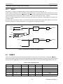
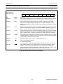
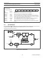
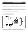
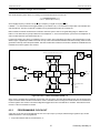
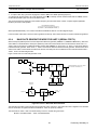
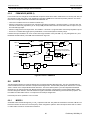
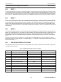
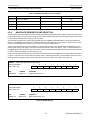
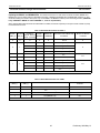
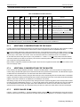
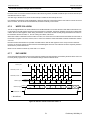
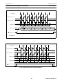
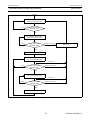
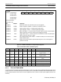
1
INTEGRATED CIRCUITS USER’S MANUAL P87C51MB2/P87C51MC2 80C51 8-bit microcontroller family with extended memory 64KB/96KB OTP with 2KB/3KB RAM Preliminary 2003 May 13 Version 0.96 Philips Semiconductors Philips Semiconductors P87C51Mx2 User Manual Extended Address Range Microcontroller P87C51Mx2 Table of Contents 1 INTRODUCTION ............................................................................................................................8 1.1 The 51MX CPU CORE ..........................................................................................................8 1.2 P87C51Mx2 microcontrollers.................................................................................................8 1.3 P87C51Mx2 Logic Symbol ..................................................................................................10 1.4 P87C51Mx2 Block Diagram ................................................................................................11 2 Memory Organization ....................................................................................................................12 2.1 Programmer’s Models and Memory Maps ...........................................................................12 2.2 Data Memory (DATA, IDATA, and EDATA).....................................................................14 2.2.1 Registers R0 - R7 ...................................................................................................14 2.2.2 Bit Addressable RAM............................................................................................14 2.2.3 Extended Data Memory (EDATA)........................................................................15 2.2.4 Stack.......................................................................................................................15 2.2.5 MX Control Register (MXCON) ...........................................................................17 2.2.6 General Purpose RAM...........................................................................................19 2.3 Special Function Registers (SFRs) .......................................................................................20 2.4 External Data Memory (XDATA) ........................................................................................21 2.5 High Data Memory (HDATA) .............................................................................................21 2.6 Program Memory (CODE) ...................................................................................................23 2.7 Universal Pointers.................................................................................................................24 3 51MX Instructions ..........................................................................................................................29 3.1 Instruction Set Summary ......................................................................................................31 3.2 51MX Operation Code Charts ..............................................................................................32 4 External Bus ....................................................................................................................................37 4.1 Multiplexed External Bus .....................................................................................................37 5 Interrupt Processing .......................................................................................................................39 6 P87C51Mx2 Ports, Power Control and Peripherals....................................................................43 6.1 Special Function Registers....................................................................................................43 6.2 P87C51Mx2 Ports.................................................................................................................46 6.2.1 Ports 0, 1, 2, 3 ........................................................................................................46 6.2.2 Port 4......................................................................................................................47 6.3 P87C51Mx2 Low Power Modes..........................................................................................47 6.3.1 Stop Clock Mode ...................................................................................................47 6.3.2 Idle Mode ...............................................................................................................47 6.3.3 Power-Down Mode................................................................................................47 6.3.4 Power-On Flag.......................................................................................................49 6.3.5 Low poWer eprom operation (LPEP) ...................................................................49 6.4 Timers/Counters 0 and 1.......................................................................................................49 6.4.1 Mode 0 ...................................................................................................................51 2 Preliminary 2003 May 13 Philips Semiconductors P87C51Mx2 User Manual Extended Address Range Microcontroller 6.5 6.6 6.7 6.8 6.9 P87C51Mx2 6.4.2 Mode 1 ...................................................................................................................52 6.4.3 Mode 2 ...................................................................................................................52 6.4.4 Mode 3 ...................................................................................................................53 Timer 2..................................................................................................................................53 6.5.1 Capture Mode ........................................................................................................55 6.5.2 Auto-Reload Mode (Up or Down Counter) ...........................................................56 6.5.3 Programmable Clock-Out ......................................................................................57 6.5.4 Baud Rate Generator Mode For UART 0 (Serial Port 0) ......................................58 6.5.5 Summary Of Baud Rate Equations ........................................................................59 6.5.6 PWM Mode (Mode 6)............................................................................................60 UARTS .................................................................................................................................60 6.6.1 Mode 0 ...................................................................................................................60 6.6.2 Mode 1 ...................................................................................................................61 6.6.3 Mode 2 ...................................................................................................................61 6.6.4 Mode 3 ...................................................................................................................61 6.6.5 SFR and Extended SFR Spaces .............................................................................61 6.6.6 Baud Rate Generator and Selection .......................................................................62 6.6.7 Framing Error ........................................................................................................65 6.6.8 Status Register .......................................................................................................66 6.6.9 More About UART Mode 1...................................................................................67 6.6.10 More About UART Modes 2 and 3 .......................................................................68 6.6.11 Examples of UART Data Transfer Using Different Modes ..................................68 6.6.12 Double Buffering ...................................................................................................69 6.6.13 Transmit Interrupts with Double Buffering ...........................................................70 6.6.14 The 9th Bit (Bit 8) in Double Buffering ................................................................71 6.6.15 Multiprocessor Communications ...........................................................................71 6.6.16 Automatic Address Recognition ............................................................................71 Serial Peripheral Interface (SPI) ...........................................................................................73 6.7.1 Typical SPI configurationS....................................................................................75 6.7.2 Configuring the SPI ...............................................................................................77 6.7.3 Additional considerations for The slave ................................................................78 6.7.4 Additional considerations for The master..............................................................78 6.7.5 Mode change on SS ...............................................................................................78 6.7.6 Write collision........................................................................................................79 6.7.7 Data mode ..............................................................................................................79 6.7.8 SPI clock prescaler select ......................................................................................81 Watchdog Timer ...................................................................................................................81 6.8.1 Watchdog Function................................................................................................81 6.8.2 Feed Sequence .......................................................................................................82 6.8.3 WDT Control .........................................................................................................82 6.8.4 WatchDog Reset Width .........................................................................................82 6.8.5 Reading from the WDCON SFR ...........................................................................83 6.8.6 Software Reset Via WatchDog Timer Feed Sequence ..........................................83 Additional Features...............................................................................................................85 6.9.1 Expanded Data RAM Addressing..........................................................................85 3 Preliminary 2003 May 13 Philips Semiconductors P87C51Mx2 User Manual Extended Address Range Microcontroller 6.10 P87C51Mx2 6.9.2 Dual Data Pointers .................................................................................................86 Programmable Counter Array (PCA) ...................................................................................86 6.10.1 PCA Capture Mode................................................................................................90 6.10.2 16-bit Software Timer Mode .................................................................................91 6.10.3 High Speed Output Mode ......................................................................................92 6.10.4 Pulse Width Modulator Mode................................................................................92 6.10.5 PCA Watchdog Timer ...........................................................................................93 4 Preliminary 2003 May 13 Philips Semiconductors P87C51Mx2 User Manual Extended Address Range Microcontroller P87C51Mx2 List of Figures Figure 1: P87C51Mx2 logic symbol .........................................................................................................11 Figure 2: P87C51Mx2 block diagram ...................................................................................................... 12 Figure 3: P87C51MB2/C2 programmer’s model and memory map ........................................................ 13 Figure 4: Return address storage on the stack (80C51 Mode).................................................................. 16 Figure 5: Extended return address storage on the stack............................................................................ 17 Figure 6: MX Configuration Register (MXCON) .................................................................................... 19 Figure 7: Internal data memory, lower 128 Bytes .................................................................................... 20 Figure 8: Standard SFR map for the P87C51Mx2.................................................................................... 21 Figure 9: Extended SFR map for the P87C51Mx2................................................................................... 22 Figure 10: External data memory access using indirect addressing with DPTR...................................... 23 Figure 11: External data memory access using indirect addressing with EPTR ...................................... 23 Figure 12: Code memory access using Indexed indirect addressing with the Program Counter ............. 24 Figure 13: Code memory access using indexed indirect addressing with DPTR ..................................... 25 Figure 14: Code memory access using indexed indirect addressing with EPTR ..................................... 25 Figure 15: Universal pointer registers ...................................................................................................... 26 Figure 16: Universal memory map ........................................................................................................... 27 Figure 17: Mapping of other addressing modes to universal pointer addressing ..................................... 28 Figure 18: Memory Access using Universal Pointer Addressing............................................................. 29 Figure 19: Example of external code memory read cycles using 23 address bits .................................... 39 Figure 20: Interrupt Enable Register IEN0............................................................................................... 41 Figure 21: Interrupt Enable Register IEN1............................................................................................... 41 Figure 22: Interrupt Priority Register IP0................................................................................................. 42 Figure 23: Interrupt Priority High Byte IP0H........................................................................................... 42 Figure 24: Interrupt Priority Register 1 .................................................................................................... 43 Figure 25: Interrupt Priority Register 1 High Byte................................................................................... 43 Figure 26: Power Control Register (PCON)............................................................................................. 49 Figure 27: Power Control Register A (PCONA) ...................................................................................... 50 Figure 28: Timer/Counter Mode Control Register (TMOD).................................................................... 51 Figure 29: Timer/Counter Control Register (TCON) ............................................................................... 52 Figure 30: Timer/Counter 0 or 1 in Mode 0 (13-Bit Counter).................................................................. 52 Figure 31: Timer/Counter 0 or 1 in Mode 1 (16-Bit Counter).................................................................. 53 Figure 32: Timer/Counter 0 or 1 in Mode 2 (8-Bit Auto-Reload)............................................................ 53 Figure 33: Timer/Counter 0 Mode 3 (Two 8-Bit Counters) ..................................................................... 54 Figure 34: Timer/Counter 2 (T2CON) Control Register .......................................................................... 55 Figure 35: Timer 2 Mode (T2MOD) Control Register............................................................................. 56 Figure 36: Timer 2 in Capture Mode ........................................................................................................ 56 Figure 37: Timer 2 in Auto Reload Mode (DCEN = 0)............................................................................ 57 Figure 38: Timer 2 in Auto Reload Mode (DCEN = 1)............................................................................ 58 Figure 39: Timer 2 in Baud Rate Generator Mode ................................................................................... 59 Figure 40: Timer 2 in PWM Mode ........................................................................................................... 61 Figure 41: BRGR0 Register...................................................................................................................... 63 Figure 42: BRGR1 Register...................................................................................................................... 63 5 Preliminary 2003 May 13 Philips Semiconductors P87C51Mx2 User Manual Extended Address Range Microcontroller P87C51Mx2 Figure 43: BRGCON Register.................................................................................................................. 65 Figure 44: Baud Rate Generations for UART 0 (Modes 1, 3) and UART 1 (Modes 1, 2, 3)................... 65 Figure 45: Serial Port Control Register (SnCON) .................................................................................... 66 Figure 46: Serial Port Status Register (SnSTAT) ..................................................................................... 68 Figure 47: Serial Port Mode 0 (Only Single Transmit Buffering Case Is Shown)................................... 69 Figure 48: Serial Port Mode 1 (Only Single Transmit Buffering Case Is Shown)................................... 70 Figure 49: Serial Port Mode 2 or 3 (Only Single Transmit Buffering Case Is Shown)............................ 70 Figure 50: Transmission with and without Double Buffering (8-Bit Case) ............................................ 71 Figure 51: Schemes used by P87C51Mx2 UARTs to detect "Given" and "Broadcast" addresses when multiprocessor communications is enabled .................................................................................................... 73 Figure 52: SPI Control register................................................................................................................. 75 Figure 53: SPI Status register definition................................................................................................... 76 Figure 54: SPI Data register...................................................................................................................... 76 Figure 55: SPI single master single slave configuration........................................................................... 77 Figure 56: SPI dual device configuration, where either can be a master or a slave ................................. 77 Figure 57: SPI single master multiple slaves configuration ..................................................................... 78 Figure 58: SPI slave transfer format with CPHA = 0 ............................................................................... 80 Figure 59: SPI slave transfer format with CPHA = 1 ............................................................................... 81 Figure 60: SPI master transfer format with CPHA = 0............................................................................. 81 Figure 61: SPI master transfer format with CPHA = 1............................................................................. 82 Figure 62: WDCON Register ................................................................................................................... 83 Figure 63: Watchdog Timer State Transitions.......................................................................................... 85 Figure 64: AUXR Register ....................................................................................................................... 86 Figure 65: AUXR1 Register ..................................................................................................................... 87 Figure 66: Programmable Counter Array (PCA)...................................................................................... 88 Figure 67: PCA Interrupt System ............................................................................................................. 89 Figure 68: CMOD: PCA Counter Mode Register .................................................................................... 89 Figure 69: PCA Counter Control Register................................................................................................ 90 Figure 70: CCAPMn: PCA Modules Compare/Capture Registers........................................................... 91 Figure 71: PCA Capture Mode ................................................................................................................. 92 Figure 72: PCA Compare Mode ............................................................................................................... 92 Figure 73: PCA High Speed Output Mode ............................................................................................... 93 Figure 74: PCA PWM Mode .................................................................................................................... 93 Figure 75: PCA Watchdog Timer (Module 4 only).................................................................................. 94 6 Preliminary 2003 May 13 Philips Semiconductors P87C51Mx2 User Manual Extended Address Range Microcontroller P87C51Mx2 List of Tables Table 76: Sizes of on-chip available memory segments for P87C51MB2 and P87C51MC2 .................. 14 Table 77: Selection of the working register bank (R0-R7)....................................................................... 15 Table 78: Instructions affected by extended address space ...................................................................... 30 Table 79: Enhancements to the 80C51 instruction set enabled by the prefix byte ................................... 31 Table 80: 51MXiInstruction set summary ................................................................................................ 32 Table 81: 51MX operation code chart: part 1........................................................................................... 34 Table 82: 51MX operation code chart: part 2........................................................................................... 35 Table 83: 51MX operation code chart: part 3........................................................................................... 36 Table 84: 51MX operation code chart: part 4........................................................................................... 37 Table 85: Summary of Interrupts.............................................................................................................. 40 Table 86: Special Function Registers ....................................................................................................... 44 Table 87: External Pin Status During Idle and Power Down Modes ....................................................... 48 Table 88: Timer 2 operating mode ........................................................................................................... 54 Table 89: Timer 2 Generated Commonly Used Baud Rates..................................................................... 60 Table 90: SFR/Extended SFR Locations for UARTs ............................................................................... 62 Table 91: Baud Rate Generation for UART 0 .......................................................................................... 64 Table 92: Baud Rate Generation for UART 1 ...........................................................................................64 Table 93: SPI Master and Slave Selection................................................................................................ 79 Table 94: WDT Prescale Selection ........................................................................................................... 84 Table 95: PCA Module Modes (CCAPMn Register) ............................................................................... 91 7 Preliminary 2003 May 13 Philips Semiconductors P87C51Mx2 User Manual Extended Address Range Microcontroller 1 INTRODUCTION 1.1 THE 51MX CPU CORE P87C51Mx2 Philips Semiconductor’s 51MX (Memory eXtension) core is based on an accelerated 80C51 architecture that executes instructions at twice the rate of standard 80C51 devices. The linear, unsegmented address space of the 51MX core has been expanded from the original 64 kilobytes (kB) limit to support up to 8 megabytes (MB) of program memory and 8 MB of data memory. It retains full program code compatibility to enable design engineers to reuse 80C51 development tools, eliminating the need to move to a new, unfamiliar architecture. The 51MX core retains 80C51 bus compatibility to allow for the continued use of 80C51-interfaced peripherals and Application-Specific Integrated Circuits (ASICs). However, by entering the Extended Addressing Mode in order to access either data or code beyond 64 kB, the bus interface changes. The 51MX core is completely backward compatible with the 80C51: code written for the 80C51 may be run on 51MX-based derivatives with no changes. Summary of differences between the classic 80C51 architecture and the 51MX core: • Program Counter: The Program Counter is extended to 23 bits. • Extended Data Pointer: A 23-bit Extended Data Pointer called the EPTR has been added in order to allow simple adjustment to existing assembly language programs that must be expanded to address more than 64 kB of data memory. • Stack: Two independent alternate Stack modes are added. The first causes addresses pushed onto the Stack by interrupts to be expanded to 23 bits. The second allows Stack extension into a larger memory space. • Instruction set: A small number of instructions have extended addressing modes to allow full use of extended code and data addressing. • Addressing Modes: A new addressing mode, Universal Pointer Mode, is added that allows accessing all of the data and code areas except for SFRs using a single instruction. This mode produces major improvements in size and performance of compiled programs. • Six clock cycles per machine cycle. The 51MX core is described in more details in the 51MX Architecture Reference. 1.2 P87C51MX2 MICROCONTROLLERS The P87C51Mx2 represents the first microcontroller based on the 51MX core. The P87C51MC2 features 96 kB of OTP program memory and 3 kB of data SRAM, while the P87C51MB2 has 64 kB of OTP and 2 kB of RAM. In addition, both devices are equipped with a Programmable Counter Array, a watchdog timer that can be configured to different time ranges, as well as two enhanced UARTs and SPI. The P87C51Mx2 provides greater functionality, increased performance, and overall lower system cost. By offering an embedded memory solution combined with the enhancements to manage the memory extension, the P87C51Mx2 eliminates the need for software workarounds. The increased program memory enables design engineers to develop more complex programs in a highlevel language like C, for example, without struggling to contain the program within the traditional 64 kB of program memory. These enhancements also greatly improve C language efficiency for code sizes below 64 kB. KEY FEATURES • 23-bit program memory space and 23-bit data memory space • 96 kB or 64 kB of on-chip OTP • 3 kB or 2 kB of on-chip RAM • Up to 24 MHz CPU clock with 6 clock cycles per machine cycle 8 Preliminary 2003 May 13 Philips Semiconductors P87C51Mx2 User Manual Extended Address Range Microcontroller P87C51Mx2 • Programmable Counter Array (PCA) • Stand alone full-duplex enhanced UART plus additional full-duplex enhanced UART that shares pins with Serial Peripheral Interface (SPI) KEY BENEFITS • Increases program/data address range to 8 MB each • Enhances performance and efficiency for C programs • Fully 80C51-compatible microcontroller • Provides seamless and compelling upgrade path from classic 80C51 • Preserves 80C51 code base, investment/knowledge, and peripherals & ASICs • Supported by 80C51 development and programming tools • The P87C51Mx2 makes it possible to develop applications at a lower cost and with a reduced time-to-market COMPLETE FEATURES • Fully static • Up to 24 MHz CPU clock with 6 clock cycles per machine cycle • 96 kB or 64 kB of on-chip OTP • 3 kB or 2 kB of on-chip RAM • 23-bit program memory space and 23-bit data memory space • Four interrupt priority levels • 34 I/O lines (5 ports) • Three Timers: Timer0, Timer1 and Timer2 • Two full-duplex enhanced UARTs with baud rate generator • Framing error detection • Automatic address recognition • Single Serial Peripheral Interface (SPI) that shares pins with the second UART • Power control modes with advanced peripheral power control • Clock can be stopped and resumed • Idle mode • Power down mode • Second DPTR register • Asynchronous port reset • Programmable Counter Array (PCA) (compatible with 8xC51Rx+) with five Capture/Compare modules • Low EMI (inhibit ALE) • Watchdog timer with programmable prescaler for different time ranges (compatible with 8xC66x with added prescaler) 80C51 COMPATIBILITY FEATURES OF THE 51MX CORE • 100% binary compatibility with the classic 80C51 so that existing code is completely reusable • Linear program and data address range expanded to support up to 8 MB each • Program counter and data pointers expanded to 23 bits • Stack pointer extended to 16 bits 9 Preliminary 2003 May 13 Philips Semiconductors P87C51Mx2 User Manual Extended Address Range Microcontroller P87C51MX2 LOGIC SYMBOL Address Bus 8-15 MOSI SPICLK Address Bus 16-22 PORT1 PORT3 RXD1 TXD1 P87C51Mx2 T2 T2EX ECI CEX0 CEX1 CEX2 CEX3 CEX4 PORT2 PORT0 RXD0 TXD0 INT0 INT1 T0 T1 WR RD VSS PORT4 MISO SS Data Bus VDD Address Bus 0-7 1.3 P87C51Mx2 RST XTAL2 EA/Vpp XTAL1 PSEN ALE/PROG Figure 1: P87C51Mx2 logic symbol 10 Preliminary 2003 May 13 Philips Semiconductors P87C51Mx2 User Manual Extended Address Range Microcontroller 1.4 P87C51Mx2 P87C51MX2 BLOCK DIAGRAM High Performance 80C51 CPU 96 kB/64 kB Code EPROM UART0 Internal Bus 3 kB/2 kB Data RAM Baud Rate Generator Port 4 UART1 Port 3 SPI Port 2 Timer0 Timer1 Port 1 Timer2 Port 0 PCA Programmable Counter Array Watchdog Timer Crystal or Resonator Oscillator Figure 2: P87C51Mx2 block diagram 11 Preliminary 2003 May 13 Philips Semiconductors P87C51Mx2 User Manual Extended Address Range Microcontroller P87C51Mx2 2 MEMORY ORGANIZATION 2.1 PROGRAMMER’S MODELS AND MEMORY MAPS The P87C51Mx2 retains all of the 80C51 memory spaces. Additional memory space has been added transparently as part of the means for allowing extended addressing. The basic memory spaces include code memory (which may be on-chip, off-chip, or both); external data memory; Special Function Registers; and internal data memory, which includes on-chip RAM, registers, and stack. Provision is made for internal data memory to be extended, allowing a larger processor stack. The P87C51Mx2 programmer’s model and memory map is shown in Figure 3. ECODE 7F:FFFFh Two 24-bit Universal Pointers R7 R6 R5 R3 R2 R1 HDATA 7E:FFFFh (includes XDATA) 23-bit Program Counter 23-bit Extended Data Pointer Two 16-bit DPTRs 16-bit Stack Pointer PSW B A 1FFh EDATA (includes DATA & IDATA) Extended Data Memory On-Chip and/or Off-Chip Code Memory On-Chip and/or Off-Chip Data Memory (stack and indirect addressing) 512 Byte On-Chip Extended SFRs 100h FFh IDATA (includes DATA) Special Function Registers CODE (directly addressable) XDATA (stack and indirect addressing) DATA 128 Byte On-Chip Data Memory 64 kB On-Chip Code Memory 80h 7Fh Four Register Banks R0 - R7 Data Memory Space (DATA, IDATA, EDATA) 00:0A00h 00:09FFh 2560 Bytes On-Chip Data Memory (P87C51MC2) XDATA (stack, direct and indirect addressing) 00:0000h 8 MB Code Memory Space 256 Byte On-Chip Data Memory 00:0600h 00:05FFh 1536 Bytes On-Chip Data Memory (P87C51MB2) 00h 00:0000h 8 MB - 64 kB External Data Memory Space (XDATA, HDATA) Figure 3: P87C51MB2/C2 programmer’s model and memory map 12 Preliminary 2003 May 13 Philips Semiconductors P87C51Mx2 User Manual Extended Address Range Microcontroller P87C51Mx2 Detailed descriptions of each of the various 51MX memory spaces may be found in the following summary. DATA 128 bytes of internal data memory space (00h...7Fh) accessed via direct or indirect addressing, using instructions other than MOVX and MOVC. All or part of the Stack may be in this area. IDATA Indirect Data. 256 bytes of internal data memory space (00h...FFh) accessed via indirect addressing using instructions other than MOVX and MOVC. All or part of the Stack may be in this area. This area includes the DATA area and the 128 bytes immediately above it. EDATA Extended Data. This is a superset of DATA and IDATA areas. Both P87C51MB2 and P87C51MC2 have 512 bytes of SRAM in EDATA memory. The added area may be accessed only as Stack and via indirect addressing using Universal Pointers. The Stack may reside in the extended area if enabled to do so. SFR Special Function Registers. Selected CPU registers and peripheral control and status registers, accessible only via direct addressing (addresses in range 80h...FFh). This includes the new 51MX extended SFRs. XDATA "External" Data. Duplicates the classic 80C51 64 kB memory space addressed via the MOVX instruction using the DPTR, EPTR, R0, or R1. On-chip XDATA can be disabled under program control. Also, XDATA may be placed in external devices. P87C51MB2 has 1536 bytes of on-chip XDATA memory space and P87C51MC2 has 2560 bytes of on-chip XDATA memory space. HDATA "High" Data. This is a superset of XDATA and may include up to 8,323,072 bytes (8 MB - 64 kB) of memory space addressed via the MOVX instruction using the EPTR, DPTR, R0, or R1. Non XDATA portion of HDATA is placed in external devices. CODE 64 kB of internal code memory space (0000h...FFFFh) used for program storage and data accessed via MOVC. ECODE Up to 8 MB of Code memory, accessed as part of program execution and via the MOVC instruction. All of these spaces except the SFR space may also be accessed through use of Universal Pointer addressing with the EMOV instruction. This feature is detailed in a subsequent section. Table 1: Sizes of on-chip available memory segments for P87C51MB2 and P87C51MC2 Size (Bytes) and MX Universal Memory Map Range Memory Type Description P87C51MB2 P87C51MC2 DATA data memory that can be addressed both directly and indirectly; can be used as stack 128 (7F:0000-7F:007F) 128 (7F:0000-7F:007F) IDATA superset of DATA; memory that can be addressed indirectly (where direct address for upper half is for SFR only); can be used as stack 256 (7F:0000-7F:00FF) 256 (7F:0000-7F:00FF) EDATA superset of DATA/IDATA; memory that can be addressed indirectly using Universal Pointers (PR0,1); can be used as stack 512 (7F:0000-7F:01FF) 512 (7F:0000-7F:01FF) XDATA memory (on-chip "External Data") that is accessed via the MOVX instructions using DPTR/EPTR 1536 (00:0000-00:05FF) 2560 (00:0000-00:09FF) CODE code memory used for program storage and data access using MOVC and EMOV 65536 (80:0000-80:FFFF) 65536 (80:0000-80:FFFF) code memory used for program storage; data access can be accomplished using Universal pointers (PR0,1) and EMOV 65536 (80:0000-80:FFFF) 98304 (80:0000-81:7FFF) ECODE 13 Preliminary 2003 May 13 Philips Semiconductors P87C51Mx2 User Manual Extended Address Range Microcontroller 2.2 P87C51Mx2 DATA MEMORY (DATA, IDATA, AND EDATA) The standard 80C51 internal data memory consists of 256 bytes of DATA/IDATA RAM, and is always entirely on-chip. In this space are the data registers R0 through R7, the default stack, a bit addressable RAM area, and general purpose data RAM. On the top of the DATA/IDATA memory space is a 256 bytes block of RAM that can be accessed as stack or via indirect addressing. Altogether this forms EDATA RAM of 512 bytes. The different portions of the data memory are accessed in different manners as described in the following sections. 2.2.1 REGISTERS R0 - R7 General purpose registers R0 through R7 allow quick, efficient access to a small number of internal data memory locations. For example, the instruction: MOV A,R0 uses one byte of code and executes in one machine cycle. Using direct addressing to accomplish the same result as in: MOV A,10h requires two bytes of code memory and executes in two machine cycles. Indirect addressing further requires setup of the pointer register, etc. These registers are “banked”. There are four groups of registers, any one of which may be selected to represent R0 through R7 at any particular time. Desired register bank is selected using bits RS1 and RS0 in PSW SFR. This feature may be used to minimize the time required for context switching during an interrupt service or a subroutine, or to provide more register space for complicated algorithms. The registers are no different from other internal data memory locations except that they can be addressed in "shorthand" notation as "R0", "R1", etc. Instructions addressing the internal data memory by other means, such as direct or indirect addressing, are quite capable of accessing the same physical locations as the registers in any of the four banks. Table 2: Selection of the working register bank (R0-R7) RS1 RS0 bank memory segment in DATA 0 0 Bank 0 00h...07h 0 1 Bank 1 08h...0Fh 1 0 Bank 2 10h...17h 1 1 Bank 3 18h...1Fh 2.2.2 BIT ADDRESSABLE RAM Internal data memory locations 20 hex through 2F hex may be accessed as both bytes and bits. This allows a convenient and efficient way to manipulate individual flag bits without using much memory space. The bottom bit of the byte at address 20h is bit number 00h, the next bit in the same byte is bit number 01h, etc. The final bit, bit 7 of the byte at address 2Fh, is bit number 7Fh (127 decimal). Bit numbers above this refer to bits in Special Function Registers. 14 Preliminary 2003 May 13 Philips Semiconductors P87C51Mx2 User Manual Extended Address Range Microcontroller P87C51Mx2 This code: SETB CPL JNB 20h.1 20h.2 20h.2, LABEL1 sets bit 1 at address 20 hex, complements bit 2 in the same byte, then branches if the second bit is not equal to 1. In an actual program, these bits would normally be given names and referred to by those names in the bit manipulation instructions. 2.2.3 EXTENDED DATA MEMORY (EDATA) The 51MX architecture allows for extension of the internal data memory space beyond the traditional 256 byte limit of classic 80C51s. This space can be used as an extended or alternative processor stack space, or can be used as general purpose storage under program control. Other than Stack Pointer based access to this space, which is automatic if Extended Stack Memory Mode is enabled (see the following Stack section), this memory is addressed only using the new Universal Pointer feature. Universal Pointers are described in a later section. Both P87C51MB2 and P87C51MC2 have 512 bytes of SRAM in EDATA memory. The whole available Extended Data Memory (EDATA) space can be accessed anytime regardless of the EAM[1:0] value using Universal Pointers and EMOV instruction. 2.2.4 STACK The processor stack provides a means to store interrupt and subroutine return addresses, as well as temporary data. The stack grows upwards, from lower addresses towards higher addresses. The current Stack Pointer always points to the last item pushed on the stack, unless the stack is empty. Prior to a push operation, the Stack Pointer is incremented, then data is written to memory. When the stack is popped, the reverse procedure is used. First, data is read from memory, then the Stack Pointer is decremented. The default configuration of the 51MX stack is identical to the classic 80C51 stack implementation. When interrupt or subroutine addresses are pushed onto the stack, only the lower 16 bits of the Program Counter are stored. This default 80C51 mode stack operation is shown in Figure 4. 0083h 0082h This figure applies to the ACALL and LCALL instructions in all modes (having ECRM=0). In 80C51 stack mode, it also applies to interrupt processing. PCH (PC.15-8) 0081h PCL (PC.7-0) 0080h 007Fh Final SP Value (after ACALL, LCALL or Interrupt) Initial SP Value (before ACALL, LCALL, or interrupt) Figure 4: Return address storage on the stack (80C51 Mode) 15 Preliminary 2003 May 13 Philips Semiconductors P87C51Mx2 User Manual Extended Address Range Microcontroller P87C51Mx2 There are three configuration options for the stack. For purposes of backward compatibility with the classic 80C51, all three additional modes are disabled by a chip reset. The first option, Extended Interrupt Frame Mode, causes interrupts to push the entire 23-bit Program Counter onto the stack (as three bytes), and the RETI instruction to pop all 23-bits as a return address, as shown in Figure 5. The upper bit of the stack byte containing the most significant byte of the Program Counter is forced to a "1" to be consistent with Universal Pointer addressing. Storing the full 23-bit Program Counter value is a requirement for systems that include more than 64 kB of program, since an interrupt could occur at any point in the program. The Extended Interrupt Frame Mode changes the operation of interrupts and the RETI instruction only, while other calls and returns are not affected. Special extended call and return instructions allow large programs to traverse the entire code space with full 23-bit return addresses. The Extended Interrupt Frame Mode is enabled by setting the EIFM bit in the MXCON register. This figure applies to interrupt services in Extended Interrupt Frame Mode, as well as the ECALL (also ACALL and LCALL when ECRM=1) instruction in all modes. The upper bit of the byte containing PCE is forced to a "1" in order to be consistent with Universal Pointers. 0083h PCE (PC.22-16) 0082h PCH (PC.15-8) 0081h PCL (PC.7-0) 0080h 007Fh Final SP Value (after ECALL or interrupt) Initial SP Value (before ECALL or interrupt) Figure 5: Extended return address storage on the stack The second stack option, Extended Stack Memory Mode, allows for stack extension beyond the 256 byte limit of the classic 80C51 family. Stack extension is accomplished by increasing the Stack Pointer to 16 bits in size and allowing it to address the entire EDATA memory rather than just the standard 256 byte internal data memory. Stack extension has no effect on the data that is stored on the stack, it will continue to be stored as shown on in figures 4 and 5. The Extended Stack Memory Mode is enabled by setting the ESMM bit in the MXCON register. The third stack option, Extended Call Return Mode, enables programming language compilers to optimize application’s code size crossing the 64 kB boundary. It is controlled with bit ECRM in MXCON register. When ECRM=1, all ACALL and LCALL instructions are going to execute as ECALL instruction, while RET instruction will behave as ERET. In this case ACALLs and LCALLs are going to last longer since their timing is now identical to ECALL; the same is with RET and ERET. If ECRM=0, routines called using ACALL and LCALL must be within 2 kB/64 kB block as the CALL instruction is, and these routines must end with RET instruction. Routines that are not in the same 64 kB code block can be called using ECALL only and must end with ERET. If ECRM=1, ACALL and LCALL will behave like ECALL, which will enable them to call subroutine located anywhere in 8 MB of the code space. Consequently, every RET instruction in this case performs like ERET in order to allow return to any location in the code space. 16 Preliminary 2003 May 13 Philips Semiconductors P87C51Mx2 User Manual Extended Address Range Microcontroller P87C51Mx2 Using Extended Call Return Mode saves code space since ACALL, LCALL and RET instructions require less bytes for coding than ECALL and ERET. Furthermore, we need to write desired subroutine only once and it can be placed and called without restrictions in the code space. However, having ECRM=1 will increase subroutine’s execution time, since all calls and returns made by ACALL, LCALL and RET will become longer. If the Stack Pointer is not initialized by software, the stack will begin at on-chip RAM address 8, just as for the 80C51. Also note that in Extended Stack Memory Mode, both MB2 and MC2 parts have 256 bytes of RAM on the top of DATA/IDATA space available for the stack. The stack mode bits ECRM, ESMM and EIFM are shown in Figure 6. Note that the stack mode bits are intended to be set once during program initialization and not altered after that point. Changing stack modes dynamically may cause stack synchronization problems. 2.2.5 MX CONTROL REGISTER (MXCON) MX family of microcontrollers was developed with an idea to provide 80C51 users with the part that will allow applications to grow in different directions. While improving a number of characteristics, it had to keep full compatibility with its predecessors. Two major areas for improvement were identified as microcontroller’s internal resources, and microcontroller’s interface to external world with address and data bus. MX2 part brings larger on-chip code and data space available, compared to previous 80C51 compatible microcontrollers. In order to enable these enhancements to be used, MX specific features had to be added, and consequently instruction set had to be enriched. MX Control Register (MXCON) determines mode of MX2’s operation. Although it is possible, change of this register during application’s execution is not advised. Structure of MXCON is shown in Figure 6. Total of three operational modes are available using bits EAM1 and EAM0. EAM1:0=00 After reset, bits EAM1:0=00 (default value) place MX2 part in fully pin-to-pin 80C51 binary compatible micro. Its interface with external world is with 16 bits wide address bus and 8 bits wide data bus. PC is 16 bits wide and therefor on-chip executable code can not go beyond 64 kB. Use of MX specific instructions that relay on PC (e.g. EMOV) is limited to values contained in the lowest 16 bits of PC: upper 7 bits are considered to be 0s. This is why EMOV instruction can not fetch content from internal code space above 64 kB boundary. Once code starts from on-chip code space, no external code can be executed; address bus enables access up to 64 kB of RAM only. EAM1:0=10 Mode determined with EAM1:0=10 enables on-chip code to go beyond 64 kB and, in case of MC2, utilize 96 kB of available code space. Interface to external memory is through standard 51 external bus: 16 bits address and 8 bits wide. In this configuration, PC is internally 23 bits wide and special attention is needed when EIFM (Extended Interrupt Frame) bit is configured. If executable on-chip code goes beyond 64 kB and this code can be interrupted, EIFM must be set to 1, since address of interrupted instruction might be of 01:xxxx type. Keeping EIFM=0 (in application when PC crosses 64 kB) will result in pushing of only 2 bytes of address to the stack. Consequently, after invoked interrupt service routine (ISR) is finished, RETI instruction will direct further code execution to 00:xxxx (due to popping only 2 bytes from the stack), which can result in unpredicted system behavior. If on-chip memory code space above 64 kB is used for storage of constants only (e.g. look-up-tables), EIFM can be 0, since any address of executed code can be represented with only two bytes. In this case it is sufficient to push only these two bytes onto the stack (which is default for MX2 part). Once code starts from on-chip code space, no external code can be executed; address bus enables access up to 64 kB of external RAM only. Due to only 16 bits wide address bus in this mode, even if EMOV instruction points to location above 64 kB, (e.g. yz:xxxx), external memory will recognize this as address under 64 kB (00:xxxx). EAM1:0=01 This mode differs from the previous one only in external bus structure: instead of 16 bits, outputted address is 23 bits wide. This enables MX2 to address up to 8 MB of code and 8 MB of data space independently. Now, microcontroller is capable of accessing external code space in case PC goes beyond 96 kB (part performs fetch from outside code space generating proper signals on ports 0, 2 and 3 when PC>96K). EIFM restrictions are the same as in EAM1:0=10 configuration. 17 Preliminary 2003 May 13 Philips Semiconductors P87C51Mx2 User Manual Extended Address Range Microcontroller P87C51Mx2 EAM1:0=11 Invalid value. MXCON Address: FFh (51MX Extended SFR Space) Not bit addressable 7 6 5 4 3 2 1 0 Reset Value: 00h - - - ECRM EAM1 EAM0 ESMM EIFM BIT SYMBOL MXCON.7 - 5 - MXCON.4 ECRM MXCON.3 - 2 EAM1:0 FUNCTION Reserved. Programs should not write a 1 to these bits. Enables the Extended CALL/RET Mode. When ECRM=0, an ACALL /LCALL will cause only the lower 16 bits of the PC to be pushed onto the stack, and a RET instruction will restore only the lower 16 bits of the PC. When ECRM=1, ACALLs and LCALLs behave like ECALL and RET is identical in execution with ERET. If ECRM=1, EAM[1:0]=10 or EAM[1:0]=01 must be selected, as well as EIFM=1. Enable one of 3 address/system configurations: External bus Comment EAM1:0 Internal organization 00 <64K 10 MX External bus is 80C51 compatible. There is no <64K (16 address/8 data) external code for MC2 since on-chip memory is >64K. 01 MX Port 2 is multiplexed externally (23 bit address). MX (23 address/8 data) 80C51 full compatibility mode (16-bit PC behavior). <64K (16 address/8 data) Invalid value. 11 MXCON.1 ESMM Enables the Extended Stack Memory Mode. When ESMM = 0, the Stack Pointer is 8 bits in width and the stack is located in the IDATA memory space. When ESMM = 1, the Stack Pointer is increased to 16-bits in width and the stack may be located anywhere in the EDATA space. ESMM is independent of ECRM, EAM[1:0] and EIFM bits. MXCON.0 EIFM Enables the Extended Interrupt Frame Mode. When EIFM = 0, an interrupt service will cause only the lower 16 bits of the PC to be pushed onto the stack, and an RETI instruction will restore only the lower 16 bits of the PC. When EIFM = 1, an interrupt service will cause all 23 bits of the PC to be pushed onto the stack, while an RETI instruction will restore all 23 bits of the PC. EIFM must be set to one if the application allows execution beyond the first 64 kB of code memory. Figure 6: MX Configuration Register (MXCON) EAM bits control access to CODE/ECODE and XDATA/HDATA space. EDATA memory space can fully be accessed anytime with EMOV instruction, regardless of the value of EAM bits. 18 Preliminary 2003 May 13 Philips Semiconductors P87C51Mx2 User Manual Extended Address Range Microcontroller 2.2.6 P87C51Mx2 GENERAL PURPOSE RAM Portions of the internal data memory that are not used in a particular application as registers, stack, or bit addressable locations may be considered general purpose RAM and used in any desired manner. The lower 128 bytes of the internal data memory (DATA) may be accessed using either direct or indirect addressing. Direct addressing incorporates the entire address within the instruction. For example, the instruction: MOV 31h,#10 will store the value 10 (decimal) in location 31 hex. Direct addresses above 128 will access the Special Function Registers rather than the internal data memory. Indirect addressing takes an address from either R0 or R1 of the current register bank and uses it to identify a location in the internal data memory. The entire 256 byte internal data memory space (IDATA) may be accessed using indirect addressing. For example, the instruction sequence: MOV MOV R0,#90h A,@R0 will cause the contents of location 90 hex to be loaded into the accumulator. It is typical with the classic 80C51 to cause the stack to be located in the upper area, leaving more general purpose RAM in the lower area that may be accessed using both direct and indirect addressing. With the 51MX, the stack may be extended and moved completely out of the lower 256 bytes of memory. 8 Bytes 7F 77 6F 67 5F 57 4F 47 3F 37 2F 27 1F 17 0F 07 bit 7F … … bit 0 bank 3 bank 2 bank 1 bank 0 78 70 68 60 58 50 48 40 38 30 28 20 18 10 08 00 Undedicated Area Bit Addressable Segment Register Banks Figure 7: Internal data memory, lower 128 Bytes 19 Preliminary 2003 May 13 Philips Semiconductors P87C51Mx2 User Manual Extended Address Range Microcontroller 2.3 P87C51Mx2 SPECIAL FUNCTION REGISTERS (SFRS) Special Function Registers (SFRs) provide a means for the processor to access internal control registers, peripheral devices, and I/O ports. An SFR address is always contained entirely within an instruction. The standard SFR space is 128 bytes in size. SFRs are implemented in each 51MX device as needed in order to provide control for peripherals or access to CPU features and functions. Undefined SFRs are considered "reserved" and should not be accessed by user programs. Sixteen addresses in the SFR space are both byte- and bit-addressable. The bit-addressable SFRs are those whose address ends in 0h or 8h (i.e. 80h, 88h,..., F8h). Bit addressing allows direct control and testing of bits in those SFRs. All 51MX devices also have additional 128 bytes of extended SFRs as discussed in the "51MX Architecture Reference". Figures 8 and 9 show the SFR and the Extended SFR maps for P87C51MB2/C2 parts. 0/8 1/9 2/A 3/B 4/C 5/D 6/E CH CCAP0H CCAP1H CCAP2H CCAP3H CCAP4H F8 IP1 F0 B E8 IEN1 CL CCAP0L CCAP1L ACC SPCFG SPCTL SPDAT CMOD CCAPM0 CCAPM1 D8 CCON PSW C8 T2CON FF IP1H E0 D0 7/F CCAP2L CCAP3L CCAP4L F7 EF E7 CCAPM2 CCAPM3 CCAPM4 DF D7 T2MOD R2CAPL R2CAPH TL2 TH2 CF C0 C7 B8 IP0 B0 P3 A8 IEN0 A0 P2 S0ADEN BF PCONA IP0H S0ADDR B7 AF AUXR1 WDTRST 98 S0CON 90 P1 88 TCON TMOD TL0 TL1 80 P0 SP DPL DPH A7 S0BUF 9F 97 TH0 TH1 AUXR 8F PCON 87 ↑ Bit Addressable SFRs Figure 8: Standard SFR map for the P87C51Mx2 Figure 9 shows the extended SFR map for the P87C51Mx2. 20 Preliminary 2003 May 13 Philips Semiconductors P87C51Mx2 User Manual Extended Address Range Microcontroller 0/8 1/9 2/A F8 P87C51Mx2 3/B 4/C 5/D 6/E 7/F SPE EPL EPM EPH MXCON FF F0 F7 E8 EF E0 E7 D8 DF D0 D7 C8 CF C0 P4 C7 B8 BF B0 B7 A8 AF A0 A7 98 9F 90 97 88 80 S0STAT S1CON S1BUF S1ADDR S1ADEN S1STAT BRGCON BRGR0 WDCON 8F BRGR1 87 ↑ Bit Addressable SFRs Figure 9: Extended SFR map for the P87C51Mx2 2.4 EXTERNAL DATA MEMORY (XDATA) The XDATA space on the 51MX is the same as the 64 kB external data memory space on the classic 80C51. On-chip XDATA memory can be disabled under program control via the EXTRAM bit in the AUXR register. Accesses above implemented on-chip XDATA will be routed to the external bus by default. If on-chip XDATA memory is disabled, all XDATA accesses will be routed to the external bus. P87C51MB2 has 1536 bytes of on-chip XDATA, while P87C51MC2 has 2560 bytes of on-chip XDATA memory. 2.5 HIGH DATA MEMORY (HDATA) The 51MX architecture supports up to an 8 MB data memory space, using 23-bit addressing. The entire 8 MB space except for the 64 kB EDATA space is called HDATA. The XDATA space comprises the lower 64 kB of HDATA. Data Pointers The 51MX adds an additional 23-bit Extended Data Pointer (EPTR) in order to allow a simple method of extending existing 80C51 programs to use more than 64 kB of data memory. If we want to access a single data byte from HDATA RAM located above the first 64 kB, EAM[1:0] bits in MXCON sfr must be set to EAM[1:0]=01. All 80C51 instructions that use the DPTR have an 51MX variant that uses the EPTR. The 23-bit EPTR is comprised of (in order) EPH, EPM, and EPL sfrs. Figures 10 and 11 show examples of indirect accesses to data memory using the DPTR and the EPTR respectively. Since the EPTR is a 23-bit value, the 8th bit of EPH is not used. If read, it returns a 1, like other unimplemented bits in sfrs. EPTR can be manipulated as 23-bit register or as three independent 8-bit registers. Use of the EPTR allows access to the entire HDATA space, including XDATA. 21 Preliminary 2003 May 13 Philips Semiconductors P87C51Mx2 User Manual Extended Address Range Microcontroller P87C51Mx2 At any point in time, one specific Data Pointer is active and is used by instructions that reference the DPTR. Active Data Pointer (DPTR) consists of a high byte (DPH sfr) and a low byte (DPL sfr) and its intended function is to hold 16-bit address; however, it may be manipulated as a 16-bit register or as two independent 8-bit registers. Selection of the active DPTR may be changed by altering the Data Pointer Select (DPS) bit. The DPS bit occupies the bottom bit of the AUXR1 register. The DPS bit applies only to the two DPTRs, not to the EPTR. In the indirect addressing mode, the currently active DPTR or the EPTR provides a data memory address for accessing the XDATA and HDATA space respectively. When the DPTR is used for addressing, only the XDATA space is available. When the EPTR is used for addressing, the entire HDATA space (which includes the XDATA space) may be accessed. If the EPTR value exceeds 7E:FFFF (the limit of HDATA), data accesses using EPTR will yield undefined results. The reason for limiting HDATA addresses is to keep the addressing uniform for EPTR addressing and Universal Pointer addressing (which is explained in a later section of this document). Example Instruction: External Data Memory MOVX @DPTR,A Data Pointers DPS 0 0 = A17Ch (00:A17Ch) 1 = 2962h Location 00:A17Ch: Accumulator 33h 33h Figure 10: External data memory access using indirect addressing with DPTR Example Instruction: External Data Memory MOVX A,@EPTR EPTR Location 01:1034h: Accumulator 3Bh 3Bh 01:1034h Figure 11: External data memory access using indirect addressing with EPTR 22 Preliminary 2003 May 13 Philips Semiconductors P87C51Mx2 User Manual Extended Address Range Microcontroller 2.6 P87C51Mx2 PROGRAM MEMORY (CODE) The 80C51, and thus the 51MX, are "Harvard" architectures, meaning that the code and data spaces are separated. If there is a single byte of executable code above 64 kB, EAM[1:0] bits in MXCON sfr must be set to EAM[1:0]=01 or EAM[1:0]=10. Also, if there is constant in CODE space above 64 kB boundary that is read by the application, EAM bits must be set to EAM[1:0]=01 or EAM[1:0]=10, too. The 51MX expands the 80C51 Program Counter to 23 bits, providing a contiguous, unsegmented linear code space that may be as large as 8 MB. On-chip space begins at code address 0 and extends to the limit of the on-chip code memory. Above that, code will be fetched from off-chip. The 51MX architecture allows for an external bus which supports: • Mixed mode (some code and/or data memory off-chip). • Single-chip operation (no external bus connection). • ROMless operation (no use of on-chip code memory). In some cases, code memory may be addressed as data. Extended instruction address modes provide access to the entire code space of 8 MB through the use of indexed indirect addressing. The currently active DPTR, the EPTR, a Universal Pointer, or the Program Counter may be used as the base address. Examples of the various code memory addressing modes are shown in figures 12 through 14. Following a reset, the 51MX begins code execution like a classic 80C51, at address 00:0000h. Similarly, the interrupt vectors are placed just above the reset address, starting at address 00:0003h. It is important to note that first instruction (located at address 0) should not be an EJMP instruction. EJMP is a 5 byte instruction and would overlap any instructions intended for the external interrupt 0 vector address residing at 00:0003. Example Instruction: Code Memory MOVC A,@A+PC Accumulator D3h PC 3E:97FFh + (3E:98D2h) Location 3E:98D2h: Accumulator 70h 70h Figure 12: Code memory access using Indexed indirect addressing with the Program Counter 23 Preliminary 2003 May 13 Philips Semiconductors P87C51Mx2 User Manual Extended Address Range Microcontroller P87C51Mx2 Example Instruction: Code Memory MOVC A,@A+DPTR executed at address 01:59B3 Accumulator A2h Upper 7 bits of Program Counter (01h) Data Pointers DPS 1 0 = C340h 1 = FF0Ch + (FFAEh) Location 01:FFAEh: Accumulator C1h C1h 01:FFAEh Figure 13: Code memory access using indexed indirect addressing with DPTR Example Instruction: Code Memory MOVC A,@A+EPTR Accumulator CDh EPTR 12:B109h + (12:B1D6h) Location 12:B1D6h: Accumulator 55h 55h Figure 14: Code memory access using indexed indirect addressing with EPTR 2.7 UNIVERSAL POINTERS A new addressing mode called Universal Pointer mode has been added to the 51MX, specifically for the purpose of greatly enhancing C language code density and performance. This addressing mode allows access to any of the on-chip or off-chip code and data spaces using one instruction, without the need to know in advance which of the different spaces the data will reside in. This includes the DATA, IDATA, EDATA, XDATA, HDATA, and CODE spaces. The SFR space is the only space that may not be accessed using the Universal Pointer mode. The Universal Pointer addressing mode uses a new set of pointer registers for two reasons. The first is that 24-bit pointers are needed in order to allow addressing both the 8 MB code space and the 8 MB data space. The other reason is that it is much more 24 Preliminary 2003 May 13 Philips Semiconductors P87C51Mx2 User Manual Extended Address Range Microcontroller P87C51Mx2 efficient to manipulate multi-byte pointer values in registers than it is in SFRs. C compilers typically already perform pointer manipulation in registers, then move the result to a Data Pointer for use. Two Universal Pointers are supported: PR0 and PR1. The pointer PR0 is composed of registers R1, R2, and R3 of the current register bank, while PR1 is composed of registers R5, R6, and R7 of the current register bank, as shown in Figure 15. PR0 MSB R3 R2 PR1 LSB MSB R1 R7 LSB R6 R5 Figure 15: Universal pointer registers In order to access all of the various memory spaces in a single unified manner, they must all be mapped into a new "view" that allows 16 MB of total memory space. This new view is called the Universal Memory Map. The XDATA space is placed at the bottom of this new address map. The HDATA space continues above XDATA. The standard internal data memory spaces (DATA and IDATA) are above HDATA, followed by the remainder of the EDATA space. Finally, the code memory occupies the top of the map. Thus, the most significant bit of the Universal Pointer determines whether code or data memory is accessed. By placing the XDATA space at the bottom of the Universal Memory Map, Universal Pointer addresses 00:0000 through 00:FFFF can correspond to the classic 80C51 external data memory space. This allows for full backward compatibility for code that does not need more than 64 kB of external data space. The Universal Memory Map is shown in Figure 16, while the standard view of the memory spaces and how they relate to Universal Pointer values are shown in Figure 17. The Universal Pointers are used only by a new 51MX instruction called EMOV. The EMOV instruction allows moving data via one of the Universal Pointers into or out of the accumulator. In either case, a displacement of 0, 1, 2, or 3 may also be specified, which is added to the pointer prior to its use. The displacement allows C compiler access of variables of up to 4 bytes in size (e.g. Long Integers) without the need to alter the pointer value. An example of Universal Pointer usage is shown in Figure 18. Note that it is not possible to store a value to the CODE area of the Universal Memory Map. Another new instruction is added to allow incrementing one of the Universal Pointers by a value from 1 to 4. This allows the pointer to be advanced past the last data element accessed, to the next data element. 25 Preliminary 2003 May 13 Philips Semiconductors P87C51Mx2 User Manual Extended Address Range Microcontroller P87C51Mx2 Memory Space Addressing Modes FF:FFFFh PC, PC relative addressing DPTR (lower 64 kB of Code) EPTR Universal Pointers: PR0, PR1 Up to 8 MB on-chip and/or off-chip program memory ECODE 81:0000h 80:FFFFh 64 kB on-chip and/or off-chip program memory CODE 80:0000h 7F:FFFFh Up to 64 kB - 256 bytes on-chip and/or off-chip data accessed as Stack and via Universal Pointer only Stack (SPE / SP) Universal Pointers: PR0, PR1 7F:0100h 7F:00FFh Upper 128 bytes on-chip indirectly addressed RAM 7F:0080h 7F:007Fh Lower 128 bytes EDATA IDATA DATA on-chip directly & indirectly addressed RAM 7F:0000h 7E:FFFFh Up to 8 MB - 128 kB data accessed via MOVX (generally off-chip data) HDATA 01:0000h 00:FFFFh XDATA R0, R1 Stack (SPE / SP) Universal Pointers: PR0, PR1 Direct addressing R0, R1 indirect Stack (SPE / SP) Universal Pointers: PR0, PR1 R0, R1 (lower 256 bytes on-chip, lower 64 kB off-chip via use of P2) DPTR (XDATA access only) EPTR (HDATA access) Universal Pointers: PR0, PR1 Up to 64 kB on-chip and/or off-chip data accessed via MOVX 00:0000h Figure 16: Universal memory map 26 Preliminary 2003 May 13 Philips Semiconductors P87C51Mx2 User Manual Extended Address Range Microcontroller P87C51Mx2 16 MB ECODE, CODE 8 MB DATA, IDATA, EDATA HDATA ECODE HDATA, XDATA EDATA CODE IDATA XDATA DATA 0 Standard Memory Map 24-bit Addressing using PR0 and PR1 Figure 17: Mapping of other addressing modes to universal pointer addressing 27 Preliminary 2003 May 13 Philips Semiconductors P87C51Mx2 User Manual Extended Address Range Microcontroller P87C51Mx2 Example Instruction: Universal Memory Map EMOV @PR0+1,A 1 PR0 12:C340h + (12:C341h) Location 12:C341h: Accumulator 39h 39h Figure 18: Memory Access using Universal Pointer Addressing Universal Pointers are designed primarily to facilitate addressing in Extended Addressing Mode, with the EAM bits in MXCON set to EAM[1:0]=01 or EAM[1:0]=10. However, Universal Pointers may still be used when EAM[1:0] = 00. In this case, Universal Pointer addressing can access only the bottom 64 kB of the Code space, the 64 kB XDATA space, and the 64 kB EDATA space. The Universal Pointer values that point to these areas do not change. When EAM[1:0] = 00, Universal Pointer accesses outside of these areas are not accessible and will return a value of FF hex. 28 Preliminary 2003 May 13 Philips Semiconductors P87C51Mx2 User Manual Extended Address Range Microcontroller 3 P87C51Mx2 51MX INSTRUCTIONS The 51MX instruction set is a a true binary-level superset of the classic 80C51, designed to be fully compatible with previously written 80C51 code. The changes to the instruction set are all related to the expanded address space. Some details of existing instructions have been altered, and some instructions have had an extended mode added. In the latter case, the alternate mode of the instruction is activated by preceding the instruction with a special one-byte prefix code, A5h. An important goal in the implementation of the 51MX was to keep the same timing relationship of existing 80C51 instructions to existing devices. Any 80C51 instruction executed on the 51MX will take the same number of machine cycles to execute. Table 3: Instructions affected by extended address space 80C51 Instruction Effect of Extended Addressing All relative branches Includes SJMP and all conditional branches. These instructions may cross a 64 kB boundary if they are located within branch range of the boundary. ACALL addr11 This instruction will cross a 64 kB boundary if it is located such that the next instruction in sequence is across the boundary. If ECRM=1 this instruction will act as MX’s specific ECALL. AJMP addr11 This instruction will cross a 64 kB boundary if it is located such that the next instruction in sequence is across the boundary. JMP @A+DPTR The lower 16-bits of the Program Counter are replaced with the value formed by the sum of the Accumulator and the active DPTR. This instruction will cross a 64 kB boundary if it is located such that the next instruction in sequence is across the boundary. MOVC A,@A+DPTR The address formed by replacing the lower 16-bits of the Program Counter with the value formed by the sum of the Accumulator and the active DPTR is used to access code memory. The PC value used is that of the instruction following MOVC. MOVC A,@A+PC The sum of the Accumulator and the 23-bit Program Counter forms the 23-bit address used to read the code memory. The PC value used is that of the instruction following MOVC. MOVX @DPTR,A The active DPTR points to an address in the 64 kB XDATA memory. MOVX A,@DPTR The active DPTR points to an address in the 64 kB XDATA memory. RET Replaces the lower 16 bits of the Program Counter with a 16-bit address from the Stack. This instruction will cross a 64 kB boundary if it is located such that the next instruction in sequence is across the boundary. If ECRM=1 this instruction will act as MX’s specific ERET. RETI When the Extended Interrupt Frame Mode is not enabled, this instruction replaces the lower 16 bits of the Program Counter with a 16-bit address from the Stack. This will cause a 64 kB boundary to be crossed if the instruction is located such that the next instruction in sequence is across the boundary. If the extended interrupt frame mode is enabled, a 23-bit address is loaded into the PC from the stack. LCALL addr16 Replaces the lower 16 bits of the Program Counter with the 16-bit address. This instruction will cross a 64 kB boundary if it is located such that the next instruction in sequence is across the boundary. If ECRM=1 this instruction will act as MX’s specific ECALL. LJMP Replaces the lower 16 bits of the Program Counter with the 16-bit address. This instruction will cross a 64 kB boundary if it is located such that the next instruction in sequence is across the boundary. addr16 29 Preliminary 2003 May 13 Philips Semiconductors P87C51Mx2 User Manual Extended Address Range Microcontroller P87C51Mx2 Table 4: Enhancements to the 80C51 instruction set enabled by the prefix byte 80C51 Instruction 51MX Effect Without Prefix 51MX Enhancement (these instructions use the prefix byte) 51MX Effect with Prefix LCALL addr16 Load a 16-bit address into the ECALL addr23 Program Counter. Load a 23-bit address into the Program Counter. LJMP addr16 Load a 16-bit address into the EJMP addr23 Program Counter. Load a 23-bit address into the Program Counter. @A+DPTR The lower 16-bits of the Program Counter are replaced with the sum of the JMP Accumulator and the active DPTR. The Program Counter is loaded with the value formed by the sum of the Accumulator and the EPTR. JMP @A+EPTR MOVC A,@A+DPTR Code memory is accessed using the address formed by replacing the lower 16-bits of MOVC A,@A+EPTR the Program Counter with the sum of the Accumulator and the active DPTR. Code memory is accessed using the address formed by the sum of the Accumulator and the EPTR. MOVX @DPTR,A The active DPTR points to an address in the 64 kB XDATA MOVX @EPTR,A memory. The EPTR points to an address anywhere in HDATA memory (not DATA, IDATA, or EDATA). MOVX A,@DPTR The active DPTR points to an address in the 64 kB XDATA MOVX A,@EPTR memory. The EPTR points to an address anywhere in HDATA memory (not DATA, IDATA, or EDATA). INC DPTR Increment the active Data Pointer. INC EPTR Increment the 23 bit EPTR. MOV DPTR,#data16 Load a 16-bit value into the active Data Pointer. MOV EPTR,#data23 Load a 23-bit value into the EPTR. Load a 16-bit address into the ERET Program Counter from the Stack. Load a 23-bit address into the Program Counter from the Stack. A,Rn Logically OR Register n to the EMOV A,@PRi+disp Accumulator. Load the Accumulator with the value from the Universal Memory Map at the address formed by PR0 or PR1plus the displacement (a value from 0 to 3). ANL A,Rn Logically AND Register n to the EMOV @PRi+disp,A Accumulator. Load the Universal Memory Map address formed by PR0 or PR1 plus the displacement (a value from 0 to 3) with the contents of the Accumulator. XRL A,Rn Exclusive OR Register n to the ADD Accumulator. Add an immediate data value from 1 to 4 to the specified Universal Pointer. This is a 24bit addition. RET ORL PRi,#data2 30 Preliminary 2003 May 13 Philips Semiconductors P87C51Mx2 User Manual Extended Address Range Microcontroller 3.1 P87C51Mx2 INSTRUCTION SET SUMMARY The following table summarizes the entire 51MX instruction set. The instructions are grouped by the type, and instructions that share operand formats are combined. 51MX extended instructions and operand combinations are designated by bold text. Table 5: 51MXiInstruction set summary Data Movement Arithmetic & Logic Program Control Bit Operations MOV XCH A,Rn A,direct A,@Ri ADD ADDC SUBB A,Rn A,direct A,@Ri A,#data rel SETB CLR CPL C Bit MOV A,#data Rn,A Rn,direct Rn,#data direct,A direct,Rn direct,direct direct,@Ri direct,#data @Ri,A @Ri,direct @Ri,#data DPTR,#data16 EPTR,#data23 JC JNC JZ JNZ SJMP INC DEC A Rn direct @Ri ANL ORL C,bit C,/bit JB JNB JBC bit,rel MOV C,bit bit,C MOVC MOVX A,@A+DPTR A,@A+PC A,@A+EPTR A,@Ri A,@DPTR @Ri,A @DPTR,A A,@EPTR @EPTR,A EMOV A,@PRi+disp @PRi+disp,A PUSH POP direct XCHD A,@Ri INC DPTR EPTR JMP @A+DPTR @A+EPTR ADD PRi,#data2 CJNE MUL DIV AB A,direct,rel A,#data,rel Rn,#data,rel @Ri,#data,rel DA CLR CPL RL RLC RR RRC SWAP A DJNZ Rn,rel direct,rel ACALL AJMP addr11 LCALL LJMP addr16 ANL ORL XRL A,Rn A,direct A,@Ri A,#data direct,A direct,#data EJMP ECALL addr23 RET RETI ERET NOP 31 Preliminary 2003 May 13 Philips Semiconductors P87C51Mx2 User Manual Extended Address Range Microcontroller 3.2 P87C51Mx2 51MX OPERATION CODE CHARTS This 51MX opcode chart consists of four pages. The first two pages are identical to a classic 80C51 opcode chart except that the A5h opcode is marked as the MX extended instruction prefix value. The third and fourth pages show instruction encoding that follows the A5h prefix. These instructions are unique to the 51MX, and are divided into several types as shown below. Contents of Each Table Entry: opcode bytes/cycles instruction mnemonic operand(s) 51MX Extended Instruction Types: Unmodified 80C51 Instruction These instructions are identical to classic 80C51 instructions and thus appear only on the first two pages of the opcode chart. New MX Instructions These instructions are new to the 51MX. All are related to the Universal Pointers. Extended Addressing Instructions These instructions incorporate extended addressing, and are modified versions of classic 80C51 instructions. Extended SFR Addressing These instructions allow access to the expanded SFR space. These are not actually new instructions, but are classic 80C51 instructions whose function are altered by the A5h opcode. Operand Definitions Used in the Tables: addr11 : 11-bit address bit : addressable bit #d8 : 8-bit immediate data addr16 : 16-bit address dir : direct address #d16 : 16-bit immediate data addr23 : 23-bit address rel8 : 8-bit relative address #d23 : 23-bit immediate data 32 Preliminary 2003 May 13 Philips Semiconductors P87C51Mx2 User Manual Extended Address Range Microcontroller P87C51Mx2 Table 6: 51MX operation code chart: part 1 00 1/1 10 NOP 01 2/2 11 AJMP addr11 02 3/2 14 2/1 06 15 1/1 1/1 1/1 19 1/1 0B 1A 1/1 1/1 1D 1/1 1E 1/1 1F 3D 1/1 3E 2F 4D 1/1 3F 5C 1/1 4E 1/1 1/1 4F ADDC A,R7 33 78 79 7A 7B 2/1 MOV R3,#d8 7C 2/1 MOV R4,#d8 7D 2/1 MOV R5,#d8 7E 2/1 MOV R6,#d8 1/1 XRL A,R7 2/1 MOV R2,#d8 1/1 6F 2/1 MOV R1,#d8 1/1 6E 2/1 MOV R0,#d8 XRL A,R6 1/1 ANL A,R7 1/1 XRL A,R5 1/1 5F 2/1 MOV @R1,#d8 1/1 6D ANL A,R6 1/1 ORL A,R7 77 XRL A,R4 1/1 5E 1/1 1/1 6C ANL A,R5 ORL A,R6 2/1 MOV @R0,#d8 XRL A,R3 1/1 5D 76 1/1 6B ANL A,R4 ORL A,R5 ADDC A,R6 1/1 ADD A,R7 1/1 1/1 XRL A,R2 1/1 3/2 MOV dir,#d8 1/1 6A ANL A,R3 ORL A,R4 1/1 1/1 5B 75 XRL A,R1 ANL A,R2 1/1 4C ADDC A,R5 ADD A,R6 1/1 DEC R7 1/1 2E 1/1 69 2/1 MOV A,#d8 XRL A,R0 1/1 5A ORL A,R3 ADDC A,R4 68 ANL A,R1 1/1 4B 1/1 59 ORL A,R2 1/1 3C ADD A,R5 DEC R6 1/1 INC R7 2D 4A ADDC A,R3 1/1 1/1 74 XRL A,@R1 ANL A,R0 ORL A,R1 1/1 3B ADD A,R4 1/1 49 ADDC A,R2 1/1 2C DEC R5 INC R6 3A ADD A,R3 1/1 1/1 67 2/2 1/2 JMP @A+DPTR XRL A,@R0 1/1 58 2/1 2/1 66 ANL A,@R1 1/1 73 XRL A,dir 1/1 57 ORL A,R0 ADDC A,R1 1/1 2B DEC R4 INC R5 0F 1/1 1C 39 ADD A,R2 DEC R3 1/1 0E 2A 48 65 ANL A,@R0 1/1 3/2 XRL A,#d8 2/1 56 ORL A,@R1 1/1 64 ANL A,dir 1/1 47 ADDC A,R0 1/1 55 ORL A,@R0 1/1 38 ADD A,R1 1/1 1B INC R4 0D 29 DEC R2 INC R3 0C 1/1 46 ADDC A,@R1 1/1 2/1 72 ORL C,bit XRL dir,#d8 2/1 2/2 ACALL addr11 2/1 63 ANL A,#d8 ORL A,dir 1/1 37 ADD A,R0 DEC R1 INC R2 1/1 28 45 ADDC A,@R0 ADD A,@R1 1/1 2/1 36 54 71 XRL dir,A 3/2 2/2 JNZ rel8 2/2 62 ANL dir,#d8 2/1 70 AJMP addr11 2/1 53 ORL A,#d8 ADDC A,dir 1/1 27 DEC R0 INC R1 0A 1/1 18 35 ADD A,@R0 DEC @R1 1/1 2/1 26 44 61 ANL dir,A 3/2 2/2 JZ rel8 2/2 52 ORL dir,#d8 2/1 60 ACALL addr11 2/1 43 ADDC A,#d8 ADD A,dir 1/1 17 INC R0 09 25 DEC @R0 INC @R1 08 2/1 16 34 51 ORL dir,A 1/1 2/2 JNC rel8 2/2 42 RLC A 2/1 50 AJMP addr11 1/2 33 ADD A,#d8 DEC dir INC @R0 07 24 41 RETI 1/1 2/2 JC rel8 2/2 32 RL A 1/1 40 ACALL addr11 1/2 23 DEC A INC dir 31 RET 1/1 3/2 JNB bit,rel8 2/2 22 RRC A 1/1 30 AJMP addr11 3/2 13 INC A 05 21 LCALL addr16 1/1 3/2 JB bit,rel8 2/2 12 RR A 04 20 ACALL addr11 LJMP addr16 03 3/2 JBC bit,rel8 7F 2/1 MOV R7,#d8 Preliminary 2003 May 13 Philips Semiconductors P87C51Mx2 User Manual Extended Address Range Microcontroller P87C51Mx2 Table 7: 51MX operation code chart: part 2 80 2/2 SJMP rel8 81 2/2 90 3/2 MOV DPTR,#d16 91 AJMP addr11 82 2/2 92 1/2 MOVC A,@A+PC 1/4 95 2/2 2/2 2/2 98 2/2 2/2 1/1 9E AD 9F 2/2 AF 2/2 MOV R7,dir D2 3/2 CJNE A,dir,rel8 C5 3/2 CJNE @R0,#d8,rel8 C6 B7 3/2 CJNE @R1,#d8,rel8 B8 3/2 CJNE R0,#d8,rel8 B9 3/2 CJNE R1,#d8,rel8 BA 3/2 CJNE R2,#d8,rel8 BB 3/2 CJNE R3,#d8,rel8 E4 1/1 1/1 1/1 1/1 D8 1/1 2/2 D9 XCH A,R1 E8 1/1 DA E9 1/1 DB 1/1 CF 2/2 ED 1/1 DF XCH A,R7 34 1/1 MOV R4,A 1/1 FD MOV A,R5 2/2 DJNZ R7,rel8 1/1 1/1 FC EF 1/1 MOV A,R7 1/1 MOV R5,A 3/2 CE 1/1 DE 2/2 EE 1/1 CJNE XCH DJNZ MOV R6,#d8,rel8 A,R6 R6,rel8 A,R6 3/2 CJNE R7,#d8,rel8 FB MOV A,R4 DJNZ R5,rel8 1/1 MOV R3,A BE BF FA MOV R2,A 1/1 2/2 EC 1/1 MOV R1,A MOV A,R3 DJNZ R4,rel8 1/1 DD F9 MOV A,R2 2/2 EB 1/1 MOV R0,A 1/1 DJNZ R3,rel8 1/1 DC F8 MOV A,R1 2/2 EA 1/1 MOV @R1,A 1/1 DJNZ R2,rel8 XCH A,R3 F7 MOV A,R0 2/2 1/1 MOV @R0,A 1/1 DJNZ R1,rel8 XCH A,R2 F6 MOV A,@R1 DJNZ R0,rel8 2/1 MOV dir,A 1/1 E7 1/1 F5 MOV A,@R0 XCHD A,@R1 XCH A,R0 F4 CPL A 2/1 E6 1/2 MOVX @R1,A MOV A,dir 1/1 D7 F3 CLR A E5 1/2 MOVX @R0,A 1/2 XCHD A,@R0 XCH A,@R1 CB E3 2/2 F2 MOVX A,@R1 3/2 D6 F1 ACALL addr11 1/2 DJNZ dir,rel8 1/1 1/2 MOVX @DPTR,A MOVX A,@R0 1/1 D5 XCH A,@R0 CA E2 DA A 2/1 C9 2/2 F0 AJMP addr11 1/1 D4 XCH A,dir C8 E1 SETB C 1/1 C7 2/2 2/1 D3 SWAP A 3/2 CD CJNE XCH R5,#d8,rel8 A,R5 MOV R6,dir 1/1 SUBB A,R7 C4 1/2 MOVX A,@DPTR SETB bit 1/1 2/2 BD AE D1 CLR C 3/2 CC CJNE XCH R4,#d8,rel8 A,R4 MOV R5,dir 1/1 C3 E0 ACALL addr11 2/1 2/2 BC MOV R4,dir SUBB A,R6 2/2 MOV dir,R7 AC SUBB A,R5 2/2 2/2 MOV R3,dir 1/1 9D MOV dir,R6 8F AB SUBB A,R4 2/2 2/2 MOV R2,dir 1/1 9C MOV dir,R5 8E AA SUBB A,R3 2/2 2/2 MOV R1,dir 1/1 9B MOV dir,R4 8D A9 SUBB A,R2 2/2 2/2 MOV R0,dir 1/1 9A MOV dir,R3 8C A8 SUBB A,R1 MOV dir,R2 8B 1/1 99 2/2 MOV @R1,dir SUBB A,R0 MOV dir,R1 8A B6 2/2 A7 1/1 3/2 CJNE A,#d8,rel8 A6 2/2 C2 2/2 POP dir CLR bit B4 B5 MOV @R0,dir 1/1 C1 CPL C 1/4 D0 AJMP addr11 2/1 B3 A5 -/(MX extension prefix) SUBB A,@R1 MOV dir,R0 89 1/1 97 1/2 A4 2/2 B2 INC DPTR SUBB A,@R0 MOV dir,@R1 88 2/1 96 B1 2/2 PUSH dir CPL bit MUL AB SUBB A,dir MOV dir,@R0 87 2/1 C0 ACALL addr11 2/1 A3 SUBB A,#d8 3/2 2/2 A2 2/2 ANL C,/bit MOV C,bit 1/2 MOVC A,@A+DPTR MOV dir,dir 86 2/2 94 B0 AJMP addr11 93 DIV AB 85 A1 MOV bit,C 83 2/2 ORL C,/bit ACALL addr11 ANL C,bit 84 2/2 A0 FE 1/1 MOV R6,A FF 1/1 MOV R7,A Preliminary 2003 May 13 Philips Semiconductors P87C51Mx2 User Manual Extended Address Range Microcontroller P87C51Mx2 Table 8: 51MX operation code chart: part 3 10 4/3 20 JBC bit,rel8 02 5/4 12 EJMP addr23 4/3 30 JB bit,rel8 5/4 22 ECALL addr23 4/3 JNB bit,rel8 42 2/4 3/2 52 ORL dir,A ERET 43 4/3 53 ORL dir,#d8 05 3/2 INC dir 15 3/2 DEC dir 25 3/2 ADD A,dir 35 3/2 45 ADDC A,dir 3/2 48 2/4 EMOV A,@PR0+0 49 2/4 EMOV A,@PR0+1 4A 2/4 EMOV A,@PR0+2 4B 2/4 EMOV A,@PR0+3 4C 2/4 EMOV A,@PR1+0 4D 2/4 EMOV A,@PR1+1 4E 2/4 EMOV A,@PR1+2 2/4 EMOV A,@PR1+3 35 62 4/3 55 63 72 3/2 65 58 2/4 EMOV @PR0+0,A 4/3 73 3/2 75 59 2/4 EMOV @PR0+1,A 5A 2/4 EMOV @PR0+2,A 5B 2/4 EMOV @PR0+3,A 5C 2/4 EMOV @PR1+0,A 5D 2/4 EMOV @PR1+1,A 5E 2/4 EMOV @PR1+2,A 2/4 EMOV @PR1+3,A XRL A,dir 68 3/3 ORL C,bit XRL dir,#d8 ANL A,dir 5F 3/2 XRL dir,A ANL dir,#d8 ORL A,dir 4F 3/2 ANL dir,A 2/2 JMP @A+EPTR 4/3 MOV dir,#d8 2/4 ADD PR0,#4 69 2/4 ADD PR0,#1 6A 2/4 ADD PR0,#2 6B 2/4 ADD PR0,#3 6C 2/4 ADD PR1,#4 6D 2/4 ADD PR1,#1 6E 2/4 ADD PR1,#2 6F 2/4 ADD PR1,#3 Preliminary 2003 May 13 Philips Semiconductors P87C51Mx2 User Manual Extended Address Range Microcontroller P87C51Mx2 Table 9: 51MX operation code chart: part 4 90 5/4 MOV EPTR,#d23 82 3/3 92 ANL C,bit 3/3 4/3 86 95 A2 A6 4/3 CJNE A,dir,rel8 C5 3/2 XCH A,dir D5 4/3 DJNZ dir,rel8 E5 3/2 MOV A,dir F5 3/2 MOV dir,A 3/3 A9 3/3 AA 3/3 MOV R2,dir 3/3 AB MOV dir,R3 3/3 MOV R3,dir 3/3 AC MOV dir,R4 3/3 MOV R4,dir 3/3 AD MOV dir,R5 3/3 MOV R5,dir 3/3 AE MOV dir,R6 3/3 MOV R6,dir 3/3 MOV dir,R7 3/2 SETB bit MOV R1,dir 3/3 8F 2/4 MOVX @EPTR,A 3/3 A8 MOV dir,R2 8E D2 F0 MOV R0,dir 3/3 8D 3/2 CLR bit 2/4 MOVX A,@EPTR 3/3 A7 MOV dir,R1 8C C2 E0 MOV @R1,dir 3/3 8B 3/2 3/3 POP dir 2/2 B5 MOV dir,R0 8A D0 MOV @R0,dir 3/3 89 B2 3/3 PUSH dir CPL bit 3/2 MOV dir,@R1 88 C0 INC EPTR MOV dir,@R0 87 3/2 A3 3/3 ANL C,/bit SUBB A,dir 3/3 B0 MOV C,bit 2/4 MOVC A,@A+EPTR MOV dir,dir 3/3 ORL C,/bit MOV bit,C 93 85 A0 AF 3/3 MOV R7,dir 36 Preliminary 2003 May 13 Philips Semiconductors P87C51Mx2 User Manual Extended Address Range Microcontroller 4 P87C51Mx2 EXTERNAL BUS The external bus provides address information to external devices and initiates code read, data read, or data write operations. In 51MX devices, the external bus duplicates the classic 80C51 multiplexed external bus, allowing increased address output to 23 bits. 4.1 MULTIPLEXED EXTERNAL BUS The 51MX external bus supports 8-bit data transfers and up to 23 address lines. The number of address lines available is configurable, and depends on the setting of the EAM bits in the MXCON register.The default for an unprogrammed part following reset is 16 address bits. This provides drop-in compatibility in existing 80C51 sockets. Software may write 01 to EAM[1:0] bits in MXCON, changing the default external bus configuration. Typically, this would be done a single time. It is not recommended to change the address configuration dynamically during program execution (for example: changing EAM[1:0]=01 to EAM[1:0]=00 changes external memory bus interface and prevents core from executing external code above the 64 kB boundary). When the full 23-bit address is multiplexed on Port 2 (when the EAM[1:0]=01 in MXCON), the high order address information (bits A22 through A16) must be latched externally in the same manner as the low order bits (A7 through A0) are latched on Port 0. The middle address bits (A15 through A8) appear on Port 2 after ALE goes low. If extended addressing is not enabled with EAM[1:0]=01, Port 2 behaves just as in case of classic 80C51. An example of Port 2 address multiplexing is shown in Figure 19. There are two special cases for Port 2 multiplexing when extended addressing is enabled: MOVX @Ri and MOVX @DPTR. These instructions do not supply a source for a full 23-bit external address. Where program memory is involved (jumps and MOVC), any "missing" address bits are supplied by the Program Counter (see Table 3). For MOVX, the additional bits are forced to zeroes to complete the address, since XDATA accessed with this instruction is on the very bottom of the data space (see Figure 3, Figure 16 and Figure 17). So, MOVX @Ri will output a 23-bit address composed of seven zeroes for the most significant bits of the address, Port 2 SFR contents for the middle byte of the address, and Ri contents for the bottom byte of the address. Similarly, MOVX @DPTR will output a 23-bit address composed of seven zeroes for the upper address and the current DPTR contents for the middle and bottom bytes of the address. Everything stated in this paragraph related to MOVX instructions is valid in case EAM[1:0]=01, since this is the only case when we have 23 bit wide external memory interface. Otherwise, external memory interface is only 16 bits wide. If we have single-chip application with code going beyond 64 kB but not exceeding internally available code memory size (i.e. MC2 based solution with up to 96 kB of code), and we want to preserve an old 51 bus interface, configuration EAM[1:0]=10 should be chosen. In this case, on-chip code will be able to cross 64 kB boundary but there will be no need for additional latch IC when external RAM/memory mapped I/O device is accessed. This configuration is especially suitable for applications wanting to reuse existing interface between the microcontroller and environment, while adding new portion of code that can fit into onchip code memory, but goes beyond 64 kilobytes. Software has to be written with special considerations if user’s application requires 23 bit wide address interface and accesses off-chip code. If an application is set in a way that the initial part of the code executed upon reset is off-chip, the instruction that sets the EAM bits in MXCON to EAM[1:0]=01 must be located at or below address 00FBh. This is to prevent the external bus from supplying a 16-bit address when a 23-bit address is required. If the Program Counter would reach address 0100h while EAM[1:0]=00, the apparent address (to external hardware that is pre-wired to expect a 23-bit address) would become 01:0100. Therefore EAM bits must be configured while the high byte and the middle byte of executed instruction address are 0, since in this case both 16 and 23 bit wide address interface access the same memory location. When application having 23 bit wide address interface with intention to use 51 interface toward memory mapped device is developed, some coding rules have to be applied. 23 bit address interface using external memory interface requires EAM[1:0]=01 configuration. If memory mapped device address is determined using address on P2 and RD/WR control lines, no changes in 37 Preliminary 2003 May 13 Philips Semiconductors P87C51Mx2 User Manual Extended Address Range Microcontroller P87C51Mx2 the code are required compared to the regular 51, since the device is going to be addressed using only the bottom 16 bits present on the 23 bit wide address bus. However, if memory mapped device uses falling edge on ALE control line to latch its 16 bit address, MOVX@Ri/DPTR instruction can not be used, but EMOV@PRi. Falling edge on ALE will enable address[7:0] to be fetched on P0, but at the same time bits address[22:16] will be present on P2. The right value that memory mapped device is expecting is available on falling edge of RD/ WR when address[15:8] bits are available on P2. In the system with 23 address bits, MOVX@Ri/DPTR instruction outputs leading zeros for address[22:16], which may cause problem for targeted device. In order to avoid this situation, instruction EMOV@PRi has to be used, with R3=R2 (when PR0 is used), or R7=R6 (when PR1 is used). By doing this, output on P2 will be the same both on falling edge of ALE and falling edge of RD/WR, and consequently memory mapped device will recognize its address when required. Detailed waveforms on external memory access can be found in the data sheet written for the desired MX part. S1 S2 S3 S4 S5 S6 S1 S2 ALE P2 high address middle address high address middle address P0 low address instruction data in low address instruction data in low address PSEN Figure 19: Example of external code memory read cycles using 23 address bits The standard control signals and their functions for the external bus are as follows: Signal name Function ALE Address Latch Enable. This signal directs an external address latch to store the multiplexed portion of the address for the next bus operation. This may be either a data address or a code address. PSEN Program Store Enable. Indicates that the processor is reading code from the bus. Typically connected to the Output Enable pin of external EPROMs or other memory devices. External bus addresses for code memory may range from 00:0000 through 7F:FFFF. In the Universal Memory Map, these correspond to addresses 80:0000 through FF:FFFF RD Read. The external data read strobe. Typically connected to the RD pin of external peripheral devices. WR Write. The write strobe for external data. Typically connected to the WR pin of external peripheral devices. External bus addresses for data memory may range from 00:0000 through 7E:FFFF, which matches Universal Memory Map addresses. If on-chip XDATA is enabled, it will cause an addressing discontinuity in the external data address space. The DATA and IDATA spaces are always on-chip, and therefore always create such an addressing discontinuity. 38 Preliminary 2003 May 13 Philips Semiconductors P87C51Mx2 User Manual Extended Address Range Microcontroller 5 P87C51Mx2 INTERRUPT PROCESSING The P87C51Mx2 uses a four priority level interrupt structure. This allows great flexibility in controlling the handling of the many interrupt sources. The P87C51Mx2 has eleven interrupt sources. Each interrupt source can be individually enabled or disabled by setting or clearing a bit in registers IEN0 or IEN1 respectively. The IEN0 register also contains a global disable bit, EA, which disables all interrupts at once. Each interrupt source can be individually programmed to one of four priority levels by setting or clearing bits in the IP0, IP0H, IP1, and IP1H registers. An interrupt service routine in progress can be interrupted by a higher priority interrupt, but not by another interrupt of the same or lower priority. The highest priority interrupt service cannot be interrupted by any other interrupt source. So, if two requests of different priority levels are received simultaneously, the request of higher priority level is serviced. Priority level "00" is the lowest possible one, while priority level "11" is the highest possible one. For example, priority level of Timer0 Interrupt is determined with bits PT0H and PT0. Content PT0H=1 and PT0=0 determine level 10, i.e. level 2. If requests of the same priority level are received simultaneously, an internal polling sequence determines which request is serviced. This is called the arbitration ranking. Note that the arbitration ranking is only used to resolve simultaneous requests of the same priority level. Table 10 summarizes the interrupt sources, flag bits, vector addresses, enable bits, priority bits, polling priority, and whether each interrupt may wake up the CPU from Power Down mode or not. Table 10: Summary of Interrupts Interrupt Flag Bit(s) Vector Address Interrupt Enable Bit(s) Interrupt Priority Polling Priority Power Down Wakeup External Interrupt 0 IE0 0003h EX0 (IEN0.0) IP0H.0, IP0.0 1 (highest) Yes Timer 0 Interrupt TF0 000Bh ET0 (IEN0.1) IP0H.1, IP0.1 2 No External Interrupt 1 IE1 0013h EX1 (IEN0.2) IP0H.2, IP0.2 3 Yes TF1 001Bh ET1 (IEN0.3) IP0H.3, IP0.3 4 No 0023h ES0/ES0R (IEN0.4) IP0H.4, IP0.4 6 No TF2, EXF2 002Bh ET2 (IEN0.5) IP0H.5, IP0.5 7 No CF, CCFn* 0033h EC (IEN0.6) IP0H.6, IP0.6 5 No 0053h ES1/ES1R (IEN1.0) IP1H.0, IP1.0 11 (lowest) No Description Timer 1 Interrupt Serial Port 0 Tx and Rx Serial Port 0 Rx 1,5 1 RI_0 Timer 2 Interrupt PCA interrupt Serial Port 1 Tx and Rx TI_0 & RI_05 2,6 TI_1 & RI_16 2 RI_1 Serial Port 0 Tx3 TI_0 003Bh ES0T (IEN1.1) IP1H.1, IP1.1 8 No 4 Serial Port 1 Tx TI_1 0043h ES1T (IEN1.2) IP1H.2, IP1.2 9 No SPI Interrupt SPI 004Bh ESPI (IEN1.3) IP1H.3, IP1.3 10 No Serial Port 1 Rx 1. S0STAT.5 = 0 selects combined Serial Port 0 Tx and Rx interrupt; S0STAT.5 = 1 selects Serial Port 0 Rx interrupt only (and TX interrupt will be different, see Note 3 below). 2. S1STAT.5 = 0 selects combined Serial Port 1 Tx and Rx interrupt; S1STAT.5 = 1 selects Serial Port 1 Rx interrupt only (and TX interrupt will be different, see Note 4 below). 3. This interrupt is used as Serial Port 0 Tx interrupt if and only if S0STAT.5 = 1, and is disabled otherwise. 4. This interrupt is used as Serial Port 1 Tx interrupt if and only if S1STAT.5 = 1, and is disabled otherwise. 5. If S0STAT.0 = 1, the following Serial Port 0 additional flag bits can cause this interrupt: FE_0, BR_0, OE_0. 6. If S1STAT.0 = 1, the following Serial Port 1 additional flag bits can cause this interrupt: FE_1, BR_1, OE_1. 39 Preliminary 2003 May 13 Philips Semiconductors P87C51Mx2 User Manual Extended Address Range Microcontroller P87C51Mx2 If the specific interrupt flag bit (Figure 10) is set (assuming corresponding interrupt is enabled), and appropriate bit in PCONA becomes 1 after this but before peripheral’s interrupt service routine is executed, that specific interrupt flag bit can not be cleared. Having 1 in PCONA disables write access to peripheral’s registers and consequently disables resetting of its interrupt flag. Therefore if observed peripheral can trigger an interrupt, it must be fully serviced before the peripheral is turned-off using PCONA. Otherwise, if interrupt flag is set and write access to peripheral’s registers is disabled based on PCONA, specific interrupt flag will not be cleared and will cause its interrupt to be serviced over and over again. IEN0 Address: A8h Bit addressable 7 6 5 4 3 2 1 0 EA EC ET2 ES0/ES0R ET1 EX1 ET0 EX0 Reset Value: 00h BIT SYMBOL FUNCTION IEN0.7 EA Interrupt Enable Bit: EA=1 interrupt(s) can be serviced, EA=0 interrupt servicing disabled. IEN0.6 EC PCA Interrupt Enable bit. IEN0.5 ET2 Timer 2 Interrupt Enable. IEN0.4 ES0/ES0R IEN0.3 ET1 Timer1 Overflow Interrupt Enable. IEN0.2 EX1 External Interrupt 1 Enable. IEN0.1 ET0 Timer 0 Overflow Interrupt Enable. IEN0.0 EX0 External Interrupt 0 Enable. Serial Port 0 Combined Tx/Rx Interrupt Enable (S0STAT.5 = 0)/Serial Port 0 Receive Interrupt Enable (S0STAT.5 = 1). Figure 20: Interrupt Enable Register IEN0 IEN1 Address: E8h Bit addressable 7 6 5 4 3 2 1 0 - - - - ESPI ES1T ES0T ES1/ES1R Reset Value: 00h BIT IEN1.7-4 SYMBOL - FUNCTION Reserved for future use. Should be set to 0 by user programs. IEN1.3 ESPI SPI Interrupt Enable. IEN1.2 ES1T If S1STAT.5 = 1, it is Serial Port 1 Transmit Interrupt Enable. If S1STAT.5 = 0, this interrupt is disabled anyway. IEN1.1 ES0T If S0STAT.5 = 1, it is Serial Port 0 Transmit Interrupt Enable. If S0STAT.5 = 0, this interrupt is disabled anyway. IEN1.0 ES1/ES1R Serial Port 1 Combined Tx/Rx Interrupt Enable (S1STAT.5 = 0)/Serial Port 1 Receive Interrupt Enable (S1STAT.5 = 1). Figure 21: Interrupt Enable Register IEN1 40 Preliminary 2003 May 13 Philips Semiconductors P87C51Mx2 User Manual Extended Address Range Microcontroller IP0 Address: B8h Bit addressable P87C51Mx2 7 6 5 4 3 2 1 0 - PPC PT2 PS0/PS0R PT1 PX1 PT0 PX0 Reset Value: 00h BIT SYMBOL FUNCTION IP0.7 - Reserved for future use. Should be set to 0 by user programs. IP0.6 PPC PCA Interrupt Priority bit Low Bit. IP0.5 PT2 Timer 2 Interrupt Priority Low Bit. IP0.4 PS0/PS0R Serial Port 0 Combined Tx/Rx Interrupt (S0STAT.5 = 0)/Receive Interrupt (S0STAT.5 = 1) Priority Low Bit. IP0.3 PT1 Timer 1 Interrupt Priority Low Bit. IP0.2 PX1 External Interrupt 1 Priority Low Bit. IP0.1 PT0 Timer 0 Interrupt Priority Low Bit. IP0.0 PX0 External Interrupt 0 Priority Low Bit. Figure 22: Interrupt Priority Register IP0 IP0H Address: B7H Not bit addressable 7 6 - PPCH 5 4 3 PT2H PS0H/PS0RH PT1H 2 1 0 PX1H PT0H PX0H Reset Value: 00h BIT SYMBOL FUNCTION IP0H.7 - Reserved for future use. Should be set to 0 by user programs. IP0H.6 PPCH PCA Interrupt Priority bit High Bit. IP0H.5 PT2H Timer 2 Interrupt Priority High Bit. IP0H.4 PS0H/PS0RH Serial Port 0 Combined Tx/Rx Interrupt (S0STAT.5 = 0)/Receive Interrupt (S0STAT.5 = 1) Priority High Bit. IP0H.3 PT1H Timer 1 Interrupt Priority High Bit. IP0H.2 PX1H External Interrupt 1 Priority High Bit. IP0H.1 PT0H Timer 0 Interrupt Priority High Bit. IP0H.0 PX0H External Interrupt 0 Priority High Bit. Figure 23: Interrupt Priority High Byte IP0H 41 Preliminary 2003 May 13 Philips Semiconductors P87C51Mx2 User Manual Extended Address Range Microcontroller IP1 Address: F8H Bit addressable P87C51Mx2 7 6 5 4 3 2 1 0 - - - - PSPI PS1T PS0T PS1/PS1R Reset Value: 00h BIT SYMBOL IP1.7-4 - FUNCTION Reserved for future use. Should be set to 0 by user programs. IP1.3 PSPI SPI Interrupt Priority Low Bit. IP1.2 PS1T Serial Port 1 transmit Interrupt (S1STAT.5 = 1) Priority Low Bit. IP1.1 PS0T Serial Port 0 transmit Interrupt (S0STAT.5 = 1) Priority Low Bit. IP1.0 PS1/PS1R Serial Port 1 combined Tx/Rx Interrupt (S1STAT.5 = 0)/receive Interrupt (S1STAT.5 = 1) Priority Low Bit. Figure 24: Interrupt Priority Register 1 IP1H Address: F7H Not bit addressable 7 6 5 4 3 2 - - - - PSPIH PS1TH 1 0 PS0TH PS1H/PS1RH Reset Value: 00h BIT IP1H.7-4 SYMBOL - FUNCTION Reserved for future use. Should be set to 0 by user programs. IP1H.3 PSPIH SPI Interrupt Priority High Bit. IP1H.2 PS1TH Serial Port 1 transmit Interrupt (S1STAT.5 = 1) Priority High Bit. IP1H.1 PS0TH Serial Port 0 transmit Interrupt (S0STAT.5 = 1) Priority High Bit. IP1H.0 PS1H/PS1RH Serial Port 1 combined Tx/RxInterrupt (S1STAT.5 = 0)/receive Interrupt (S1STAT.5 = 1) Priority High Bit. Figure 25: Interrupt Priority Register 1 High Byte 42 Preliminary 2003 May 13 Philips Semiconductors P87C51Mx2 User Manual Extended Address Range Microcontroller P87C51Mx2 6 P87C51MX2 PORTS, POWER CONTROL AND PERIPHERALS 6.1 SPECIAL FUNCTION REGISTERS Note: Special Function Registers (SFRs) accesses are restricted in the following ways: 1. User must NOT attempt to access any SFR locations not defined. 2. Accesses to any defined SFR locations must be strictly for the functions for the SFRs. 3. SFR bits labeled ’-’, ’0’ or ’1’ can ONLY be written and read as follows: - ’-’ MUST be written with ’0’, but can return any value when read (even if it was written with ’0’). It is a reserved bit and may be used in future derivatives. - ’0’ MUST be written with ’0’, and will return a ’0’ when read. - ’1’ MUST be written with ’1’, and will return a ’1’ when read. Table 11: Special Function Registers SYMBOL DESCRIPTION DIRECT ADDRESS BIT ADDRESS, SYMBOL, OR ALTERNATE PORT FUNCTION MSB E7 LSB E6 E5 E4 E3 E2 E1 Reset Value E0 ACC* Accumulator E0H 00H AUXR# Auxiliary Function Register 8EH - - - - - - EXTRAM AO 00H% AUXR1# Auxiliary Function Register 1 A2H - - - LPEP GF2 0 - DPS 00H% F7 F6 F5 F4 F3 F2 F1 F0 B* B Register F0H 00H BRGCON# Baud Rate Generator Control 85H‡ BRATE15 BRATE14 BRATE13 BRATE12 BRATE11 BRATE16 BRATE09 BRATE08 00H BRATE07 BRATE06 BRATE05 BRATE04 BRATE03 BRATE02 BRATE01 BRATE00 00H - - - - - - S0BRGS BRGEN 00H% BRGR0#§ Baud Rate Generator Rate Low 86H‡ BRGR1#§ Baud Rate Generator Rate High 87H‡ CCAP0H# Module 0 Capture High FAH XXH CCAP1H# Module 1 Capture High FBH XXH CCAP2H# Module 2 Capture High FCH XXH CCAP3H# Module 3 Capture High FDH XXH CCAP4H# Module 4 Capture High FEH XXH CCAP0L# Module 0 Capture Low EAH XXH CCAP1L# Module 1 Capture Low EBH XXH CCAP2L# Module 2 Capture Low ECH XXH CCAP3L# Module 3 Capture Low EDH XXH CCAP4L# Module 4 Capture Low EEH XXH CCAPM0# Module 0 Mode DAH - ECOM_0 CAPP_0 CAPN_0 MAT_0 TOG_0 PWM_0 ECCF_0 00H% CCAPM1# Module 1 Mode DBH - ECOM_1 CAPP_1 CAPN_1 MAT_1 TOG_1 PWM_1 ECCF_1 00H% CCAPM2# Module 2 Mode DCH - ECOM_2 CAPP_2 CAPN_2 MAT_2 TOG_2 PWM_2 ECCF_2 00H% CCAPM3# Module 3 Mode DDH - ECOM_3 CAPP_3 CAPN_3 MAT_3 TOG_3 PWM_3 ECCF_3 00H% CCAPM4# Module 4 Mode DEH - ECOM_4 CAPP_4 CAPN_4 MAT_4 TOG_4 PWM_4 ECCF_4 00H% 43 Preliminary 2003 May 13 Philips Semiconductors P87C51Mx2 User Manual Extended Address Range Microcontroller P87C51Mx2 Table 11: Special Function Registers (Continued) SYMBOL CCON*# DESCRIPTION PCA Counter Control BIT ADDRESS, SYMBOL, OR ALTERNATE PORT FUNCTION DIRECT ADDRESS MSB DF DE DD DC DB DA D9 D8 D8H CF CR - CCF4 CCF3 CCF2 CCF1 CCF0 LSB Reset Value 00H% CH# PCA Counter High F9H 00H CL# PCA Counter Low E9H 00H CMOD# PCA Counter Mode D9H DPTR CIDL WDTE - - - CPS1 CPS0 ECF Data Pointer (2 bytes) 00H% 00H DPH Data Pointer High 83H 00H DPL Data Pointer Low 82H 00H EPL# Extended Data Pointer Low FCH‡ 00H EPM# Extended Data Pointer Middle FDH‡ 00H ‡ 00H EPH# Extended Data Pointer High IEN0* Interrupt Enable 0 IEN1* Interrupt Enable 1 IP0* Interrupt Priority IP0H Interrupt Priority 0 High IP1* Interrupt Priority 1 IP1H Interrupt Priority 1 High MXCON# P0* FEH AF P1* A8H E8H AE AD AC AB AA A9 A8 ET1 EX1 ET0 EX0 EB EA E9 E8 EA EC ET2 ES0/ ES0R EF EE ED EC 00H - ESPI ES1T ES0T ES1/ ES1R BD BC BB BA B9 B8 PT1 PX1 PT0 PX0 00H PX0H 00H - - - BF BE 00H% B8H - PPC PT2 PS0/ PS0R B7H - PPCH PT2H PS0H/ PS0RH PT1H PX1H PT0H FF FE FD FC FB FA F9 F8 00H% F8H - - - - PSPI PS1T PS0T PS1/ PS1R F7H - - - - PSPIH PS1TH PS0TH PS1H/ PS1RH 00H% MX Control Register FFH‡ - - - ECRM EAM1 EAM0 ESMM EIFM 00H% 87 86 85 84 83 82 81 80 Port 0 80H AD7 AD6 AD5 AD4 AD3 AD2 AD1 AD0 97 96 95 94 93 92 91 90 CEX4 CEX3 CEX2 CEX1 CEX0 ECI T2EX T2 Port 1 90H 44 FFH FFH Preliminary 2003 May 13 Philips Semiconductors P87C51Mx2 User Manual Extended Address Range Microcontroller P87C51Mx2 Table 11: Special Function Registers (Continued) SYMBOL P2* P3* DESCRIPTION Port 2 Port 3 DIRECT ADDRESS BIT ADDRESS, SYMBOL, OR ALTERNATE PORT FUNCTION MSB LSB Reset Value A7 A6 A5 A4 A3 A2 A1 A0 AD15 AD14/ AD22 ADA13/ AD21 AD12/AD20 AD11/ AD19 AD10/ AD18 AD9/ AD17 AD8/ AD16 B7 B6 B5 B4 B3 B2 B1 B0 RD WR T1 T0 INT1 INT0 TxD0 RxD0 C7‡ C6‡ C5‡ C4‡ C3‡ C2‡ C1‡ C0‡ C0H‡ - - - - - - TxD1/SS RxD1/ MISO FFH SMOD1 SMOD0 - POF GF1 GF0 PD IDL 00H/10H& 00H A0H B0H P4*# Port 4 PCON# Power Control Register 87H PCONA Power Control Register A B5H PSW* Program Status Word D0H RCAP2H# Timer2 Capture High CBH RCAP2L# Timer2 Capture Low CAH - PCAPD - SPIPD BRGPD T2PD S1PD S0PD D7 D6 D5 D4 D3 D2 D1 D0 CY AC F0 RS1 RS0 OV F1 P FFH FFH 00H 00H 00H 9F 9E 9D 9C 9B 9A 99 98 SM0_0/ FE_0 SM1_0 SM2_0 REN_0 TB8_0 RB8_0 TI_0 RI_0 S0CON* Serial Port 0 Control S0BUF Serial Port 0 Data Buffer Register 99H xxH S0ADDR Serial Port 0 Address Register A9H 00H S0ADEN Serial Port 0 Address Enable B9H 00H S0STAT# Serial Port 0 Status 8CH‡ 98H DBMOD_ INTLO_0 0 CIDIS_0 DBISEL_0 FE_0 BR_0 OE_0 STINT_0 87‡ 86‡ 85‡ 84‡ 83‡ 82‡ 81‡ 80‡ SM0_1/ FE_1 SM1_1 SM2_1 REN_1 TB8_1 RB8_1 TI_1 RI_1 00H 00H% S1CON#* Serial Port 1 Control 80H‡ S1BUF# Serial Port 1 Data buffer Register 81H‡ XXH S1ADDR# Serial Port 1 Address Register 82H‡ 00H S1ADEN# Serial Port 1 Address Enable 83H‡ S1STAT# Serial Port 1 Status 84H‡ SP Stack Pointer (or Stack Pointer Low Byte When EDATA Supported) 81H SPE# Stack Pointer High 00H 00H DBMOD_ INTLO_1 1 CIDIS_1 DBISEL1 FE_1 BR_1 OE_1 STINT_1 FBH‡ 00H% 00H SPCFG# SPI Configuration Register E1H SPIF SPWCOL - - - - - - SPCTL# SPI Control register E2H SSIG SPEN DORD MSTR CPOL CPHA PSC1 PSC0 SPDAT# SPI Data E3H T2CON#* Timer2 Control Register C8H CF CE CD CC CB CA C9 C8 TF2 EXF2 RCLK TCLK EXEN2 TR2 C/T2 CP/RL2 45 00H 00H Preliminary 2003 May 13 Philips Semiconductors P87C51Mx2 User Manual Extended Address Range Microcontroller P87C51Mx2 Table 11: Special Function Registers (Continued) SYMBOL DESCRIPTION BIT ADDRESS, SYMBOL, OR ALTERNATE PORT FUNCTION DIRECT ADDRESS MSB - - ENT2 TF2DE T2GATE T2PWME T2OE LSB Reset Value DCEN 00H% T2MOD# Timer2 Mode Control C9H TH0 Timer 0 High 8CH 00H TH1 Timer 1 High 8DH 00H TH2 Timer 2 High CDH 00H TL0 Timer 0 Low 8AH 00H TL1 Timer 1 Low 8BH 00H TL2 Timer 2 Low CCH 00H 8F 8E 8D 8C 8B 8A 89 88 TCON* Timer Control Register 88H TF1 TR1 TF0 TR0 IE1 IT1 IE0 IT0 00H TMOD Timer 0 and 1 Mode 89H T1GATE T1C/T T1M1 T1M0 T0GATE T0C/T T0M1 T0M0 00H WDTRST# Watchdog Timer Reset A6H WDCON# 8FH‡ Watchdog Timer Control FFH - - - - - WDPRE2 WDPRE1 WDPRE0 00H% Notes: * SFRs are bit addressable. # SFRs are modified from or added to the 80C51 SFRs. ‡ Extended SFRs accessed by preceding the instruction with MX escape (opcode A5h). - Reserved bits, must be written with 0’s. & Power on reset is 10H. Other reset is 00H. % The unimplemented bits (labeled ’-’) in the SFRs are ’X’s (unknown) at all times. ’1’s should NOT be written to these bits, as they may be used for other purposes in future derivatives. The reset values shown for these bits are ’0’s although they are unknown when read. % The unimplemented bits (labeled ’-’) in the SFRs are ’X’s (unknown) at all times. ’1’s should NOT be written to these bits, as they may be used for other purposes in future derivatives. The reset values shown for these bits are ’0’s although they are unknown when read. 6.2 6.2.1 P87C51MX2 PORTS PORTS 0, 1, 2, 3 Ports 0, 1, 2, 3 are the same as the ports in a conventional 80C51 device. They are located at the same bit-addressable locations of 80H, 90H, A0H, and B0H in the conventional SFR space. Observed port’s output is logical and of port’s sfr and microcontroller’s peripheral that is using that port. In order to allow peripheral to fully control dedicated pin, corresponding bit(s) in port’s sfr must be 1. Otherwise, if some of port’s bits are 0s, output of peripherals using those pins will not be able to change output which is going to be low all the time, due to port bit’s 0. The only exception from this rule is PCA working in high-speed output mode. The last change, whichever it is (write access to P1 bits or toggle of PCA’s output) will result in change of level on appropriate pins. 46 Preliminary 2003 May 13 Philips Semiconductors P87C51Mx2 User Manual Extended Address Range Microcontroller 6.2.2 P87C51Mx2 PORT 4 The P87C51MA2/MB2/MC2 has a fifth I/O port (Port 4) that is shared with the second UART pins (RXD1 and TXD1) and two of the SPI pins (MISO and SS). This port is also bit addressable and can be accessed in the same manner as any other ports, except that the associated SFR is in the extended SFR space. Accesses to this SFR space is the same as those to the conventional SFR space except that the instructions must be preceded by an escape code (A5h) as mentioned in earlier section. 6.3 P87C51MX2 LOW POWER MODES 6.3.1 STOP CLOCK MODE The static design enables the clock speed to be reduced down to 0 MHz (stopped). When the oscillator is stopped, the RAM and Special Function Registers retain their values. This mode allows step-by-step utilization and permits reduced system power consumption by lowering the clock frequency down to any value. For lowest power consumption the Power Down mode is suggested. 6.3.2 IDLE MODE In the idle mode (see Table 11), the CPU puts itself to sleep while all of the on-chip peripherals stay active. The instruction to invoke the idle mode is the last instruction executed in the normal operating mode before the idle mode is activated. The CPU contents, the on-chip RAM, and all of the special function registers remain intact during this mode. Idle mode is entered by setting the IDL bit in the PCON register. There are two ways to terminate the Idle mode. Activation of any enabled interrupt will cause IDL to be cleared by hardware, terminating the Idle mode. The interrupt is serviced, and following RETI, the next instruction to be executed will be the one following the instruction that put the device into Idle. Hardware reset is the second way to exit Idle mode, and the processor continues in the same manner as in case of power-on reset. Hardware reset by default clears IDL bit to 0. Before reset really occurs and internal reset algorithm takes control, the part will execute several instructions after the point in code when the Idle mode was invoked, i.e. the device normally resumes program execution, from where it left off. On-chip hardware inhibits access to the internal RAM during this time, but access to the port pins is not inhibited, so, insertion of 3 NOP instructions is recommended following the instruction that invokes idle mode. To eliminate the possibility of unexpected outputs at the port pins in general, the instruction following the one that invokes Idle mode should not be the one that writes to a port pin or to external data RAM. 6.3.3 POWER-DOWN MODE To save even more power, a Power Down mode (see Table 11) can be invoked by software. In this mode, the oscillator is stopped and the instruction that invoked Power Down is the last instruction executed. This mode stops the oscillator in order to absolutely minimize power consumption. Power Down mode is entered by setting the PD bit in the PCON register. Table 12: External Pin Status During Idle and Power Down Modes MODE Program Memory ALE PSEN PORT 0 PORT 1 PORT 2 PORT 3 Idle Internal 1 1 Data Data Data Data Idle External 1 1 Float Data Address Data Power Down Internal 0 0 Data Data Data Data Power Down External 0 0 Float Data Data Data The processor can be made to exit Power Down mode via Reset or one of the external interrupt inputs (INT0, INT1 - configured to be level sensitive only). This will occur if the interrupt is enabled and its priority is higher than any interrupt currently in progress. 47 Preliminary 2003 May 13 Philips Semiconductors P87C51Mx2 User Manual Extended Address Range Microcontroller P87C51Mx2 While having the MX part in Power Down Mode and driving Reset high (or external interrupt line low), the oscillator dedicated analog subsystem inside of the microcontroller will be enabled. However, only when the wake-up pulse on reset/external interrupt line is ended, the rest of microcontroller will be supplied with the system clock, and continue to operate. The duration of an input pulse on reset/external interrupt pin in order to wake the part from Power Down Mode depends solely on external oscillator’s circuit components. At the end of wake-up procedure, reset/external interrupt line can be brought to non-active level as soon as input at XTAL1 pin achieves stable frequency, duty cycle and amplitude. If an external interrupt caused the part to wake up, execution of forced jump (that directs code execution to the proper interrupt service routine) will end Power Down Mode. By exiting Power Down mode via external interrupt, the core automatically clears the PD bit and thus enables a new entry into Power Down Mode. Once the interrupt is serviced, the next instruction to be executed after RETI will be the one following the instruction that put the device into Power Down Mode. External reset by default clears PD bit, and enables the next Power Down. In Power Down mode, the power supply voltage may be reduced to the RAM keep-alive voltage VRAM. This retains the RAM contents at the point where Power Down mode was entered. SFR contents are not guaranteed after VDD has been lowered to VRAM, since RAM and SFRs are built using different processes. Therefore it is recommended to wake up the processor via Reset in this case (since Reset redefines all SFRs - including PD bit, but doesn’t change on-chip RAM). VDD must be raised to within the operating range before the Power Down mode is exited. PCON Address: 87h BIT 6 SMOD1 SMOD0 Not bit addressable Reset Value: 7 5 4 3 2 1 0 - POF GF1 GF0 PD IDL 00?X0000B SYMBOL FUNCTION PCON.7 SMOD1 Baud Rate Control bit for serial port 0. When 0, the baud rate for UART 0 will be the input rate (T1 timer or baud rate generator, as determined by the BRGCON extended SFR) divided by two. When 1, the baud rate for UART 0 will be the input rate (T1 timer or baud rate generator). UART 1 is not affected by this bit. PCON.6 SMOD0 Framing Error Location. When 1, bit 7 of S0CON and S1CON will be used for framing error status for UART 0 and 1 respectively. When 0, these bits will function as SM0 for UARTs 0 and 1 respectively. PCON.5 - PCON.4 POF Power On Flag. Reset value = 1 for power-on reset only; all other reset sources POF=0. PCON.3 GF1 General purpose flag 1. May be read or written by user software, but has no effect on operation. PCON.2 GF0 General purpose flag 0. May be read or written by user software, but has no effect on operation. PCON.1 PD Power Down control bit. Setting this bit activates Power Down mode operation. Cleared when the Power Down mode is terminated (see text). PCON.0 IDL Idle mode control bit. Setting this bit activates Idle mode operation. Cleared when the Idle mode is terminated (see text). Reserved for future use. Should not be set to 1 by user programs. Figure 26: Power Control Register (PCON) P87C51Mx2 peripherals are designed with intention to reduce power consumption as much as possible. This includes option to put in power down mode peripherals independently using Power Control Register A - PCONA (Figure 27). Setting specific bit in PCONA will disable clock to desired peripheral and reduce its power consumption to absolute minimum. In this mode, peripheral’s SFR can be read at any time but the write operation to SFRs is disabled. Special measures are necessary to avoid race condition that may occur in case interrupt flag is set, peripheral is put in power down mode and interrupt service routine hasn’t been serviced yet. Details on this can be found in chapter discussing interrupts. 48 Preliminary 2003 May 13 Philips Semiconductors P87C51Mx2 User Manual Extended Address Range Microcontroller PCONA Address: B5h Not bit addressable Reset Value: BIT P87C51Mx2 7 6 5 4 3 2 1 0 - PCAPD - SPIPD BRGPD T2PD S1PD S0PD ?0?0000B SYMBOL FUNCTION PCON.7 - Reserved for future use. Should not be set to 1 by user programs. PCON.6 PCAPD PCON.5 - PCON.4 SPIPD SPI Power Down. When ’1’, the internal clock to SPI is disabled. Note that if PCON.1 is ’1’, SPI clock will be disabled regardless of this bit. PCON.3 BRGPD Baud Rate Generator (BRG) Power Down. When ’1’, the internal clock to BRG is disabled. Note that if PCON.1 is ’1’, BRG clock will be disabled regardless of this bit. PCON.2 T2PD Timer 2 (T2) Power Down. When ’1’, the internal clock to Timer 2 is disabled. Note that if PCON.1 is ’1’, Timer 2 clock will be disabled regardless of this bit. PCON.1 S1PD Serial Port 1(UART1) Power Down. When ’1’, the internal clock to UART1 is disabled. Note that if PCON.1 is ’1’, UART1 clock will be disabled regardless of this bit. PCON.0 S0PD Serial Port 1(UART0) Power Down. When ’1’, the internal clock to UART0 is disabled. Note that if PCON.1 is ’1’, UART0 clock will be disabled regardless of this bit. Programmable Counter Array (PCA) Power Down. When ’1’, the internal clock to PCA is disabled. Note that if PCON.1 is ’1’, PCA clock will be disabled regardless of this bit. Reserved for future use. Should not be set to 1 by user programs. Figure 27: Power Control Register A (PCONA) 6.3.4 POWER-ON FLAG The Power On Flag (POF) is set by on-chip circuitry when the VDD level on the P87C51Mx2 rises from 0V. The POF bit allows user to determine if the reset is the result of a power-on or a warm start after the powerdown. The POF bit can be cleared by software only. 6.3.5 LOW POWER EPROM OPERATION (LPEP) P87C51Mx2 family of microcontrollers contains some analog circuits that are not required when VDD is less than 3.6 V, but are required for a VDD greater than 3.6 V. The LPEP bit (AUXR.4), when set, will powerdown these analog circuits resulting in a reduced supply current. This bit should be set ONLY for applications that operate at a VDD less than 3.6 V. If LPEP=1 with VDD greater than 3.6 V, readings from internal ROM will be invalid and will result in part’s unpredictable behavior. 6.4 TIMERS/COUNTERS 0 AND 1 The two 16-bit Timer/Counter registers: Timer 0 and Timer 1 can be configured to operate either as timers or event counters (see Figure 28). In the "Timer" function, the register is incremented every machine cycle. Thus, one can think of it as counting machine cycles. Since a machine cycle consists of 6 oscillator periods, the count rate is 1/6 of the oscillator frequency. In the "Counter" function, the register is incremented in response to a 1-to-0 transition at its corresponding external input pin, T0 or T1. In this function, the external input is sampled once every machine cycle. When the samples show a high in one cycle and a low in the next cycle, the count is incremented. The new count value appears in the register in the machine cycle following the one in which the transition was detected. Since it takes 2 machine cycles (12 oscillator periods) for 1-to-0 transition to be recognized, the maximum count rate is 1/12 of the oscillator frequency. There are no restrictions on the duty cycle of the external input signal, but to ensure that a given level is sampled at least once before it 49 Preliminary 2003 May 13 Philips Semiconductors P87C51Mx2 User Manual Extended Address Range Microcontroller P87C51Mx2 changes, it should be held for at least one full machine cycle. In addition to the "Timer" or "Counter" selection, Timer 0 and Timer 1 have four operating modes from which to select. The "Timer" or "Counter" function is selected by control bits C/T in the Special Function Register TMOD. These two Timer/ Counters have four operating modes, which are selected by bit-pairs (M1, M0) in TMOD. Modes 0, 1, and 2 are the same for both Timers/Counters. Mode 3 is different. The four operating modes are described in the following text. TMOD Address: 89h Not bit addressable 7 6 5 4 3 2 1 0 T1GATE T1C/T T1M1 T1M0 T0GATE T0C/T T0M1 T0M0 Reset Source(s): Any source Reset Value: M1 00000000B T1/T0 Bits controlling Timer1/Timer0 GATE Gating control when set. Timer/Counter “x” is enabled only while “INTx” pin is high and “TRx” control pin is set. when cleared Timer “x” is enabled whenever “TRx” control bit is set. C/T Gating Timer or Counter Selector cleared for Timer operation (input from internal system clock.) Set for Counter operation (input from “Tx” input pin). M0 OPERATING MODE 0 0 0 8048 Timer “TLx” serves as 5-bit prescaler. 0 1 1 16-bit Timer/Counter “THx” and “TLx” are cascaded; there is no prescaler. 1 0 2 8-bit auto-reload Timer/Counter “THx” holds a value which is to be reloaded into "TLx” each time it overflows. 1 1 3 (Timer 0) TL0 is an 8-bit Timer/Counter controlled by the standard Timer 0 control bits. TH0 is an 8-bit timer only controlled by Timer 1 control bits. 1 1 3 (Timer 1) Timer/Counter 1 stopped. Figure 28: Timer/Counter Mode Control Register (TMOD) 50 Preliminary 2003 May 13 Philips Semiconductors P87C51Mx2 User Manual Extended Address Range Microcontroller TCON Address: 88h Bit addressable P87C51Mx2 7 6 5 4 3 2 1 0 TF1 TR1 TF0 TR0 IE1 IT1 IE0 IT0 Reset Source(s): Any reset Reset Value: 00000000B BIT SYMBOL FUNCTION TCON.7 TF1 Timer 1 overflow flag. Set by hardware on Timer/Counter overflow. Cleared by hardware when the processor vectors to Timer 1 Interrupt routine, or by software. TCON.6 TR1 Timer 1 Run control bit. Set/cleared by software to turn Timer/Counter 1 on/off. TCON.5 TF0 Timer 0 overflow flag. Set by hardware on Timer/Counter overflow. Cleared by hardware when the processor vectors to Timer 0 Interrupt routine, or by software. TCON.4 TR0 Timer 0 Run control bit. Set/cleared by software to turn Timer/Counter 0 on/off. TCON.3 IE1 Interrupt 1 Edge flag. Set by hardware when external interrupt 1 edge/low level is detected. Cleared by hardware when the interrupt is processed, or by software. TCON.2 IT1 Interrupt 1 Type control bit. Set/cleared by software to specify falling edge/low level that triggers external interrupt 1. TCON.1 IE0 Interrupt 0 Edge flag. Set by hardware when external interrupt 0 edge/low level is detected. Cleared by hardware when the interrupt is processed, or by software. TCON.0 IT0 Interrupt 0 Type control bit. Set/cleared by software to specify falling edge/low level that triggers external interrupt 0. Figure 29: Timer/Counter Control Register (TCON) 6.4.1 MODE 0 Putting either Timer into Mode 0 makes it look like an 8048 Timer, which is an 8-bit Counter with a fixed divide-by-32 prescaler. Figure 30 shows Mode 0 operation. Overflow Osc / 6 Tn Pin C/T = 0 TLn (5-bits) C/T = 1 THn (8-bits) TFn Interrupt Control TRn TnGate INTn Pin Figure 30: Timer/Counter 0 or 1 in Mode 0 (13-Bit Counter) In this mode, the Timer register is configured as a 13-bit register. As the count rolls over from all 1s to all 0s, it sets the Timer interrupt flag TFn. The count input is enabled to the Timer when TRn = 1 and either GATE = 0 or INTn = 1. (Setting GATE = 1 allows the Timer to be controlled by external input INTn, to facilitate pulse width measurements). TRn is a control bit in the Special Function Register TCON (Figure 29). The GATE bit is in the TMOD register. The 13-bit register consists of all 8 bits of THn and the lower 5 bits of TLn. The upper 3 bits of TLn are indeterminate and should be ignored. Setting the run flag (TRn) does not clear the registers. 51 Preliminary 2003 May 13 Philips Semiconductors P87C51Mx2 User Manual Extended Address Range Microcontroller P87C51Mx2 Mode 0 operation is the same for Timer 0 and Timer 1 (see Figure 29). There are two different GATE bits, one for Timer 1 (TMOD.7) and one for Timer 0 (TMOD.3). 6.4.2 MODE 1 Mode 1 is the same as Mode 0, except that all 16 bits of the timer register (THn and TLn) are used. See Figure 31. Overflow Osc / 6 Tn Pin C/T = 0 TLn (8-bits) C/T = 1 THn (8-bits) TFn Interrupt Control TRn TnGate INTn Pin Figure 31: Timer/Counter 0 or 1 in Mode 1 (16-Bit Counter) 6.4.3 MODE 2 Mode 2 configures the Timer register as an 8-bit Counter (TLn) with automatic reload, as shown in Figure 32. Overflow from TLn not only sets TFn, but also reloads TLn with the contents of THn, which must be preset by software. The reload leaves THn unchanged. Mode 2 operation is the same for Timer 0 and Timer 1. Osc / 6 Tn Pin C/T = 0 C/T = 1 Control TLn (8-bits) Overflow TFn Interrupt Reload TRn TnGate THn (8-bits) INTn Pin Figure 32: Timer/Counter 0 or 1 in Mode 2 (8-Bit Auto-Reload) 52 Preliminary 2003 May 13 Philips Semiconductors P87C51Mx2 User Manual Extended Address Range Microcontroller 6.4.4 P87C51Mx2 MODE 3 When Timer 1 is in Mode 3 it is stopped (holds its count). The effect is the same as setting TR1 = 0. Timer 0 in Mode 3 establishes TL0 and TH0 as two separate 8-bit counters. The logic for Mode 3 and Timer 0 is shown in Figure 33. TL0 uses the Timer 0 control bits: T0C/T, T0GATE, TR0, INT0, and TF0. TH0 is locked into a timer function (counting machine cycles) and takes over the use of TR1 and TF1 from Timer 1. Thus, TH0 now controls the “Timer 1” interrupt. Mode 3 is provided for applications that require an extra 8-bit timer. With Timer 0 in Mode 3, an P87C51Mx2 can look like it has an additional Timer. Note: When Timer 0 is in Mode 3, Timer 1 can be turned on and off by switching it into and out of its own Mode 3. It can still be used by the serial port as a baud rate generator, or in any application not requiring an interrupt. C/T = 0 Osc /6 T0 Pin Control C/T = 1 TL0 (8-bits) Overflow TH0 (8-bits) Overflow TF0 Interrupt TF1 Interrupt TR0 TnGate INT0 Pin Osc / 2 Control TR1 Figure 33: Timer/Counter 0 Mode 3 (Two 8-Bit Counters) 6.5 TIMER 2 Timer 2 is a 16-bit Timer/Counter which can operate as either an event timer or an event counter, as selected by C/T2 in the special function register T2CON. Timer 2 has five operating modes: Capture, Auto-reload (up or down counting), Clockout, Baud Rate Generator and PWM (Mode 6) which are selected according to Table 12 using T2CON and T2MOD (figures 34 and 35). Table 13: Timer 2 operating mode T2PWM RCLK+TCLK CP/RL2 TR2 T2OE MODE 0 0 0 1 0 16-BIT auto reload 0 0 1 1 0 16-bit capture 0 0 0 1 1 Programmable Clock-Out 0 1 X 1 0 Baud rate generator for UART 0 1 X X 1 0 PWM X X X 0 X off 53 Preliminary 2003 May 13 Philips Semiconductors P87C51Mx2 User Manual Extended Address Range Microcontroller T2CON Address: C8h Bit addressable Reset Value: 00h BIT P87C51Mx2 SYMBOL 7 6 5 4 3 2 1 0 TF2 EXF2 RCLK TCLK EXEN2 TR2 C/T2 CP/RL2 FUNCTION T2CON.7 TF2 Timer 2 overflow flag set by a Timer 2 overflow and must be cleared by software. TF2 will not be set when either RCLK or TCLK = 1 or when Timer 2 is in Clock-out Mode. T2CON.6 EXF2 Timer 2 external flag is set when Timer 2 is in capture, reload or baud-rate mode, EXEN2=1 and a negative transition on T2EX occurs. If Timer 2 interrupt is enabled EXF2=1 causes the CPU to vector to the Timer 2 interrupt routine. EXF2 must be cleared by software. T2CON.5 RCLK Receive clock flag. When set, causes the serial port 0 (UART 0) to use Timer 2 overflow pulses for its receive clock in modes 1 and 3 (unless SBRGS - BRGCON.1 is set to ’1’). RCLK = 0 causes Timer 1 overflow to be used for the receive clock. (See "UARTS"). T2CON.4 TCLK Transmit clock flag. When set, causes the serial port 0 (UART 0) to use Timer 2 overflow pulses for its transmit clock in modes 1 and 3 (unless SBRGS - BRGCON.1 is set to ’1’). TCLK = 0 causes Timer 1 overflows to be used for the transmit clock. (See "UARTS"). T2CON.3 EXEN2 Timer 2 external enable flag. When set, allows a capture or reload to occur as a result of a negative transition on T2EX if Timer 2 is not being used to clock the serial port. EXEN2 = 0 causes Timer 2 to ignore events at T2EX. T2CON.2 TR2 Start/stop control for Timer 2. A logic 1 enables the timer to run. T2CON.1 C/T2 Timer or counter select. (Timer 2) 0 = Internal timer (fOSC/6) 1 = External event counter (falling edge triggered; external clock’s max. rate=fOSC/12). T2CON.0 CP/RL2 Capture/Reload flag. When set, captures will occur on negative transitions at T2EX if EXEN2 = 1. When cleared, auto-reloads will occur either with Timer 2 overflows or negative transitions at T2EX when EXEN2 = 1. When either RCLK = 1 or TCLK = 1, this bit is ignored and the timer is forced to auto-reload on Timer 2 overflow. Figure 34: Timer/Counter 2 (T2CON) Control Register 54 Preliminary 2003 May 13 Philips Semiconductors P87C51Mx2 User Manual Extended Address Range Microcontroller T2MOD P87C51Mx2 Address: C9h Not bit addressable Reset Value: XX000000B BIT SYMBOL T2MOD.7-6 7 6 5 4 - - ENT2 3 2 TF2DE T2GATE T2PWME 1 0 T2OE DCEN FUNCTION - Reserved for future use. Should be set to 0 by user programs. T2MOD.5 ENT2 When set, pin P1.0(T2) is controlled by Timer 2 in PWM Mode. T2MOD.4 TF2DE T2MOD.3 T2GATE Gating control for Timer 2. When set, PWM is enabled only while T2EX pin is high and TR2=1. When cleared, PWM is enabled only when TR2=1. T2MOD.2 T2PWME Timer 2 PWM Enable. When set, Timer 2 is operating in PWM Mode. (PWM only) T2MOD.1 T2OE Timer 2 Output Enable bit. Used in programmable clock-out mode only. T2MOD.0 DCEN Down Count Enable bit. When set, this allows timer2 to be configured as an up/down counter. TF2 Interrupt Disabled. When set, disables TF2 to generate T2 interrupt (PWM only). Figure 35: Timer 2 Mode (T2MOD) Control Register 6.5.1 CAPTURE MODE In the Capture Mode there are two options which are selected by bit EXEN2 in T2CON. If EXEN2=0 Timer 2 is a 16-bit timer or counter (as selected by C/T2 in T2CON) which upon overflowing sets bit TF2, the Timer 2 overflow bit. The capture mode is illustrated in Figure 36: OSC ÷6 C/T2 = 0 TL2 (8-bit) TH2 (8-bit) TF2 CONTROL C/T2 = 1 T2 Pin TR2 Timer 2 Interrupt CAPTURE Transition Detector RCAP2L RCAP2H T2EX Pin EXF2 CONTROL EXEN2 Figure 36: Timer 2 in Capture Mode 55 Preliminary 2003 May 13 Philips Semiconductors P87C51Mx2 User Manual Extended Address Range Microcontroller P87C51Mx2 This bit can be used to generate an interrupt (by enabling the Timer 2 interrupt bit in the IEN0 register). If EXEN2=1, Timer 2 operates as described above, but with the added feature that a 1- to -0 transition at external input T2EX causes the current value in the Timer 2 registers, TL2 and TH2, to be captured into registers RCAP2L and RCAP2H, respectively. In addition, the transition at T2EX causes bit EXF2 in T2CON to be set, and EXF2 like TF2 can generate an interrupt (which vectors to the same location as Timer 2 overflow interrupt). The Timer 2 interrupt service routine can interrogate TF2 and EXF2 to determine which event caused the interrupt. There is no reload value for TL2 and TH2 in this mode. Even when a capture event occurs from T2EX, the counter keeps on counting T2 pin transitions or fosc/6 pulses. Since once loaded contents of RCAP2L and RCAP2H registers are not protected, once Timer2 interrupt is signalled it has to be serviced before new capture event on T2EX pin occurs. Otherwise, the next falling edge on T2EX pin will initiate reload of the current value from TL2 and TH2 to RCAP2L and RCAP2H and consequently corrupt their content related to previously reported interrupt. 6.5.2 AUTO-RELOAD MODE (UP OR DOWN COUNTER) In the 16-bit auto-reload mode, Timer 2 can be configured as either a timer or counter (via C/T2 in T2CON), then programmed to count up or down. The counting direction is determined by bit DCEN (Down Counter Enable) which is located in the T2MOD register (see Figure 35). When reset is applied, DCEN = 0 and Timer 2 will default to counting up. If the DCEN bit is set, Timer 2 can count up or down depending on the value of the T2EX pin. Figure 37 shows Timer 2 counting up automatically (DCEN = 0). OSC ÷6 C/T2 = 0 TL2 (8-bit) TH2 (8-bit) TF2 CONTROL C/T2 = 1 T2 Pin TR2 Timer 2 Interrupt RELOAD RCAP2L Transition Detector RCAP2H EXF2 T2EX Pin CONTROL EXEN2 Figure 37: Timer 2 in Auto Reload Mode (DCEN = 0) In this mode, there are two options selected by bit EXEN2 in T2CON register. If EXEN2=0, then Timer 2 counts up to 0FFFFH and sets the TF2 (Overflow Flag) bit upon overflow. This causes the Timer 2 registers to be reloaded with the 16-bit value in RCAP2L and RCAP2H. The values in RCAP2L and RCAP2H are preset by software means. 56 Preliminary 2003 May 13 Philips Semiconductors P87C51Mx2 User Manual Extended Address Range Microcontroller P87C51Mx2 Auto reload frequency when Timer 2 is counting up can be determined from this formula: SupplyFrequency ---------------------------------------------------------------------------------( 65536 – ( RCAP2H, RCAP2L ) ) where SupplyFrequency is either fosc/6 (C/T2=0) or frequency of signal on T2 pin (C/T2=1). If EXEN2 = 1, a 16-bit reload can be triggered either by an overflow or by a 1-to-0 transition at input T2EX. This transition also sets the EXF2 bit. The Timer 2 interrupt, if enabled, can be generated when either TF2 or EXF2 is 1. Microcontroller’s hardware will need three consecutive machine cycles in order to recognize falling edge on T2EX and set EXF2=1: in the first machine cycle pin T2EX has to be sampled as "1"; in the second machine cycle it has to be sampled as "0", and in the third machine cycle EXF2 will be set to 1. In Figure 38, DCEN=1 and Timer 2 is enabled to count up or down. This mode allows pin T2EX to control the direction of count. When a logic 1 is applied at pin T2EX Timer 2 will count up. Timer 2 will overflow at 0FFFFH and set the TF2 flag, which can then generate an interrupt, if the interrupt is enabled. This timer overflow also causes the 16-bit value in RCAP2L and RCAP2H to be reloaded into the timer registers TL2 and TH2. TOGGLE (DOWN COUNTING RELOAD VALUE) EXF2 OSC FFH FFH TL2 (8-bit) TH2 (8-bit) ÷6 C/T2 = 0 UNDERFLOW TF2 Timer 2 Interrupt OVERFLOW CONTROL C/T2 = 1 T2 Pin TR2 COUNT DIRECTION 1 = UP 0 = DOWN RCAP2L RCAP2H (UP COUNTING RELOAD VALUE) T2EX PIN Figure 38: Timer 2 in Auto Reload Mode (DCEN = 1) When a logic 0 is applied at pin T2EX this causes Timer 2 to count down. The timer will underflow when TL2 and TH2 become equal to the value stored in RCAP2L and RCAP2H. Timer 2 underflow sets the TF2 flag and causes 0FFFFH to be reloaded into the timer registers TL2 and TH2. The external flag EXF2 toggles when Timer 2 underflows or overflows. This EXF2 bit can be used as a 17th bit of resolution if needed. 6.5.3 PROGRAMMABLE CLOCK-OUT A 50% duty cycle clock can be programmed to come out on pin T2 (P1.0). This pin, besides being a regular I/O pin, has two additional functions. It can be programmed: 1. To input the external clock for Timer/Counter 2, or; 57 Preliminary 2003 May 13 Philips Semiconductors P87C51Mx2 User Manual Extended Address Range Microcontroller P87C51Mx2 2. To output a 50% duty cycle clock ranging from 122Hz to 8MHz at a 16MHz operating frequency. To configure the Timer/Counter 2 as a clock generator, bit C/T2 (in T2CON) must be cleared and bit T20E in T2MOD must be set. Bit TR2 (T2CON.2) also must be set to start the timer. The Clock-Out frequency depends on the oscillator frequency and the reload value of Timer 2 capture registers (RCAP2H, RCAP2L) as shown in this equation: OscillatorFrequency ---------------------------------------------------------------------------------------2x ( 65536 – ( RCAP2H, RCAP2L ) ) Where (RCAP2H,RCAP2L) = the content of RCAP2H and RCAP2L taken as a 16-bit unsigned integer. In the Clock-Out mode Timer 2 roll-overs will not generate an interrupt. This is similar to when it is used as a baud-rate generator. 6.5.4 BAUD RATE GENERATOR MODE FOR UART 0 (SERIAL PORT 0) When serial port 0 (UART 0) doesn’t use the independent baud rate generator (S0BRGS = 0, S0BRGS is BRGCON.1), bits TCLK and/or RCLK in T2CON allow the serial port 0 (UART 0) transmit and receive baud rates to be derived from either Timer 1 or Timer 2 (refer to the section on UARTS for details). Assume that S0BRGS = 0, when TCLK = 0, Timer 1 is used as the UART 0 transmit baud rate generator. When TCLK = 1, Timer 2 is used as the UART 0 transmit baud rate generator. RCLK has the same effect for the UART 0 receive baud rate. With these two bits, the serial port can have different receive and transmit baud rates – Timer 1, Timer 2 or baud rate generator. Figure shows Timer 2 in baud rate generator mode: ÷2 OSC C/T2 = 0 TL2 (8-bit) TH2 (8-bit) TX/RX Baud Rate (See section "Baud Rate Generator and Selection") CONTROL C/T2 = 1 T2 Pin RELOAD TR2 RCAP2L Transition Detector T2EX Pin EXF2 RCAP2H Timer 2 Interrupt CONTROL EXEN2 Figure 39: Timer 2 in Baud Rate Generator Mode The baud rate generation mode is like the auto-reload mode, when a rollover in TH2 causes the Timer 2 registers to be reloaded with the 16-bit value in registers RCAP2H and RCAP2L, which are preset by software. The baud rates in modes 1 and 3 are determined by Timer 2’s overflow rate given below: Modes 1 and 3 Baud Rates = Timer 2 Overflow Rate/16 58 Preliminary 2003 May 13 Philips Semiconductors P87C51Mx2 User Manual Extended Address Range Microcontroller P87C51Mx2 The timer can be configured for either “timer” or “counter” operation. In many applications, it is configured for “timer” operation (C/T2=0). Timer operation is different for Timer 2 when it is being used as a baud rate generator. Usually, as a timer it would increment every machine cycle (i.e., 1 / 6 the oscillator frequency). As a baud rate generator, it increments at the oscillator frequency. Thus the baud rate formula is as follows: Modes 1 and 3 Baud Rates = Oscillator Frequency / (16 X (65536 - (RCAP2H, RCAP2L))) Where: (RCAP2H, RCAP2L)= The content of RCAP2H and RCAP2L taken as a 16-bit unsigned integer. The Timer 2 as a baud rate generator mode is valid only if RCLK and/or TCLK = 1 in T2CON register. Note that a rollover in TH2 does not set TF2, and will not generate an interrupt. Thus, the Timer 2 interrupt does not have to be disabled when Timer 2 is in the baud rate generator mode. Also if the EXEN2 (T2 external enable flag) is set, a 1-to-0 transition in T2EX (Timer/counter 2 trigger input) will set EXF2 (T2 external flag) but will not cause a reload from (RCAP2H, RCAP2L) to (TH2,TL2). Therefore when Timer 2 is in use as a baud rate generator, T2EX can be used as an additional external interrupt, if needed. When Timer 2 is in the baud rate generator mode, one should not try to read or write TH2 and TL2. Under these conditions, a read or write of TH2 or TL2 may not be accurate. The RCAP2 registers may be read, but should not be written to, because a write might overlap a reload and cause write and/or reload errors. The timer should be turned off (clear TR2) before accessing the Timer 2 or RCAP2 registers. Table 13 shows commonly used baud rates and how they can be obtained from Timer 2. 6.5.5 SUMMARY OF BAUD RATE EQUATIONS Timer 2 is in baud rate generating mode. If Timer 2 is being clocked through pin T2(P1.0) the baud rate is: Baud Rate = Timer 2 Overflow Rate / 16 If Timer 2 is being clocked internally, the baud rate is: Baud Rate = fOSC / (16 x (65536 - (RCAP2H, RCAP2L))) Where fOSC = Oscillator Frequency To obtain the reload value for RCAP2H and RCAP2L, the above equation can be rewritten as: RCAP2H, RCAP2L = 65536 - fOSC / (16 x Baud Rate) Table 14: Timer 2 Generated Commonly Used Baud Rates Baud Rate Osc Freq Timer 2 RCAP2H RCAP2L 750K 12MHz FF FF 19.2K 12MHz FF D9 9.6K 12MHz FF B2 4.8K 12MHz FF 64 2.4K 12MHz FE C8 600 12MHz FB 1E 220 12MHz F2 AF 600 6MHz FD 8F 220 6MHz F9 57 59 Preliminary 2003 May 13 Philips Semiconductors P87C51Mx2 User Manual Extended Address Range Microcontroller 6.5.6 P87C51Mx2 PWM MODE (MODE 6) In this mode Timer 2 is changed to a 8 bit PWM with a full period of 256 timer clocks. Overflow from TL2 not only sets TF2, but also reloads TL2 with TH2 or 256 - TH2, depending on the state of PWM block. TH2 must be preset by software. The reload leaves TH2 unchanged. Additional characteristics of PWM block are: • TF2 is set in hardware and can be cleared in software only. • Duration of low period on T2 output is TH2, and TH2 is expected to be between 1 and 254. If ENT2 = 1 and TH2 = 255, low level will be continuously outputted on pin T2. Every PWM period that lasts 256 timer clocks starts with low output on T2 pin and ends with high output. • Duration of high period on T2 output is 256 - TH2. If ENT2 = 1 and TH2 = 0, high level will be continuously outputted on pin T2. • Even if T2 is controlled with toggle option by PWM block, it can be used anytime as ordinary I/O pin. If Timer2 interrupt is enabled, it can occur on either low to high transition of TF2 (if TF2DE = 0), or by setting EXF2 to 1 (as in Baud Rate Generator Mode). The PWM mode is illustrated in Figure 40. Osc / 6 T2 Pin TF2DE Control C/T = 0 TL2 (8-bits) Overflow TF2 C/T = 1 Reload TH2 on falling transition and (256-TH2) on rising transition TR2 T2GATE T2 Pin TH2 (8-bits) T2EX Pin EXF2 Toggle ENT2 Timer2 Interrupt EXEN2 Figure 40: Timer 2 in PWM Mode 6.6 UARTS The P87C51Mx2 includes two enhanced UARTs with one independent Baud Rate Generator. They are compatible with the enhanced UART based on the 8xC51Rx+ except the baud rate generator. The first UART (UART 0) can select Timer 1 overflow, Timer 2 overflow or the independent Baud Rate Generator. The second UART (UART 1) uses the independent Baud Rate Generator only to generate its baud rate. Besides the baud rate generation, enhancements over the standard 80C51 UART include Framing Error detection, automatic address recognition, selectable double buffering and several interrupt options. The two UARTs are called UART 0 and 1 to correspond to the serial port assignments. Each serial port can be operated in one of 4 modes: 6.6.1 MODE 0 Serial data enters and exits through RxD_n. TxD_n outputs the shift clock. Only 8 bits are transmitted or received, LSB first. The baud rate is fixed at 1/6 of the CPU clock frequency. UART configured to operate in this mode outputs serial clock on TxD line no matter wether it sends or receives data on RxD line. 60 Preliminary 2003 May 13 Philips Semiconductors P87C51Mx2 User Manual Extended Address Range Microcontroller 6.6.2 P87C51Mx2 MODE 1 10 bits are transmitted (through TxD) or received (through RxD): a start bit (logical 0), 8 data bits (LSB first), and a stop bit (logical 1). When data is received, the stop bit is stored in RB8_0/RB8_1 in Special Function Register S0CON/S1CON. For UART 0, the baud rate is variable and is determined by the Timer 1/2 (see T2CON.5-4) overflow rate or the Baud Rate Generator (described later in section on "Baud Rate Generator and Selection"). The Baud Rate Generator is the only source for baud rate for UART 1. 6.6.3 MODE 2 11 bits are transmitted (through TxD) or received (through RxD): start bit (logical 0), 8 data bits (LSB first), a programmable 9th data bit, and a stop bit (logical 1). When data is transmitted, the 9th data bit (TB8_n in SnCON) can be assigned the value of 0 or (e.g. the parity bit (P, in the PSW) could be moved into TB8_n). When data is received, the 9th data bit goes into RB8_n in Special Function Register S0CON/S1CON, while the stop bit is ignored. For UART 0, the baud rate is programmable to either 1 /16 or 1/32 of the CPU clock frequency, as determined by the SMOD1 bit in PCON. For UART 1, the baud rate is from the Baud Rate Generator. 6.6.4 MODE 3 11 bits are transmitted (through TxD) or received (through RxD): a start bit (logical 0), 8 data bits (LSB first), a programmable 9th data bit, and a stop bit (logical 1). In fact, Mode 3 is the same as Mode 2 in all respects except baud rate. For UART 0, the baud rate in Mode 3 is variable and is determined by the Timer 1/2 (see T2CON.5-4) overflow rate or the Baud Rate Generator (described later in section on "Baud Rate Generator and Selection"). Baud Rate Generator is the only source for baud rate for UART 1. In all four modes, transmission is initiated by any instruction that uses S0BUF/S1BUF as a destination register. Reception is initiated in Mode 0 by the condition RI_0/RI_1 = 0 and REN_0/REN_1 = 1. In all other modes reception is initiated by the incoming start bit if REN_0/REN_1 = 1. 6.6.5 SFR AND EXTENDED SFR SPACES The regular UART 0 SFRs and control bits are in the regular SFR space. However, extended control and UART 1 registers are in the MX extended SFR space. Table 15: SFR/Extended SFR Locations for UARTs Register Description SFR Location MX Extended SFR Location PCON Power Control 87H T2CON Timer2 Control C8H S0CON Serial Port 0 Control 98H S0BUF Serial Port 0 Data Buffer 99H S0ADDR Serial Port 0 Address A9H S0ADEN Serial Port 0 Address Enable B9H S0STAT Serial Port 0 Status 8CH S1CON Serial Port 1 Control 80H S1BUF Serial Port 1 Data Buffer 81H S1ADDR Serial Port 1 Address 82H S1ADEN Serial Port 1 Address Enable 83H 61 Preliminary 2003 May 13 Philips Semiconductors P87C51Mx2 User Manual Extended Address Range Microcontroller P87C51Mx2 Table 15: SFR/Extended SFR Locations for UARTs Register Description SFR Location MX Extended SFR Location S1STAT Serial Port 1 Status 84H BRGR1 Baud Rate Generator Rate High Byte 87H BRGR0 Baud Rate Generator Rate Low Byte 86H Baud Rate Generator Control 85H BRGCON 6.6.6 BAUD RATE GENERATOR AND SELECTION The P87C51Mx2 enhanced UARTs have one associated independent Baud Rate Generator. Baud rate generator implemented in P87C51Mx2 family of microcontrollers is the device that easily produces desired baud rate with higher resolution than it could be achieved with standard timers sourcing clocks for UARTs. The baud rate is determined by a baud-rate preprogrammed into the BRGR1 and BRGR0 SFRs in the extended SFR space. BRGR1.7-0 and BRGR0.7-0 together form a 16-bit baud rate divisor value (BRATE15-0) that works in a similar manner as Timer 1/2. If the baud rate generator is used, Timer 1/2 can be used for other timing functions. UART 0 can use either Timer 1/2 (see T2CON.5-4) or the baud rate generator output (as determined by BRGCON.1-0 in the extended SFR space), while UART 1 uses only the baud rate generator. Note that in UART 0, Timer 1 is further divided by 2 if the SMOD1 bit (PCON.7) is cleared. Timer 2 (for UART 0) and the independent Baud Rate Generator (for both UARTs) will be used as is, without the divided by 2 option (see Figure 44). UART 0 can have different baud rates for transmission and reception of data. In such application, one of the clocks must be based on Timer 1 while the second clock is derived from either Timer 2 or Baud rate generator. It is not possible to have Timer 2 and Baud rate generator supplying different baud rates at the same time for UART 0 (see Table 16 and Figure 44). BRGR0 Address: 86h (MX Extended SFR Space) Not bit addressable Reset Value: 00h 7 6 5 4 3 2 1 0 BRATE7 BRATE6 BRATE5 BRATE4 BRATE3 BRATE2 BRATE1 BRATE0 BIT SYMBOL FUNCTION BRGR0.7-0 BRATE7-0 Baud rate divisor bits 7-0. Figure 41: BRGR0 Register BRGR1 Address: 87h (MX Extended SFR Space) Not bit addressable Reset Value: 00h BIT BRGR1.7-0 7 6 5 4 3 2 1 0 BRATE15BRATE14BRATE13BRATE12BRATE11BRATE10 BRATE9 BRATE8 SYMBOL BRATE15-8 FUNCTION Baud rate divisor bits 15-8. Figure 42: BRGR1 Register 62 Preliminary 2003 May 13 Philips Semiconductors P87C51Mx2 User Manual Extended Address Range Microcontroller P87C51Mx2 Updating the BRGR1 and BRGR0 SFRs. The effective baud rate is a 16-bit value.The baud rate SFRs, BRGR1 and BRGR0 must only be loaded when the Baud Rate Generator is disabled (the BRGEN bit in the BRGCON register is ’0’). This avoids the loading of an interim value (when only one of BRGR1 and BRGR0 is written) to the baud rate generator. (CAUTION: If any of BRGR0 or BRGR1 is written if BRGEN = 1, result is unpredictable.) When selecting Baud Rate Generator and Baud Rate for UART0, bit T2CON.5 (RCLK) for reception and bit T2CON.4 (TCLK) for transmission are used. Table 16: Baud Rate Generation for UART 0 T2CON.5/4 PCON.7 S0CON.7 S0CON.6 (RCLK - Receive (SMOD1) (SM0_0) (SM1_0) TCLK - Transmit) 0 0 0 X BRGCON.1 (S0BRGS) Receive/Transmit Baud Rate for UART 0 Number of data bits in transfer X fOSC/6 8 X 0 0 X T1_rate/32* 0 1 X T1_rate/16* 1 X 0 T2_rate/16* 1 X 1 fOSC/(BRATE+16)* 1 1 0 X 0 X fOSC/32 1 0 X 1 X fOSC/16 0 0 X T1_rate/32* 0 1 X T1_rate/16* 1 X 0 T2_rate/16* 1 X 1 fOSC/(BRATE+16)* 1 1 8 8+1 8+1 * Receiver and transmit clocks can be different. Table 17: Baud Rate Generation for UART1 S1CON.7 (SM0_1) S1CON.6 (SM1_1) Baud Rate for UART 1 Number of data bits in transfer 0 0 fOSC/6 8 0 1 fOSC/(BRATE+16)* 0 * 8+1 /(BRATE+16)* 8+1 1 1 1 fOSC/(BRATE+16) fOSC 8 *UART 1 has the same receive and transmit baud rate. 63 Preliminary 2003 May 13 Philips Semiconductors P87C51Mx2 User Manual Extended Address Range Microcontroller P87C51Mx2 BRGCON Address: 85h (MX Extended SFR Space) Not bit addressable 7 6 5 4 3 2 Reset Value: 00h - - - - - - BIT SYMBOL BRGCON.7-2 - 1 0 S0BRGS BRGEN FUNCTION Reserved for future use. Should be set to 0 by user programs. BRGCON.1 S0BRGS (For UART 0 only) Used in combination with the RCLK and TCLK in deciding the receive and transmit baud rates to UART 0 in modes 1 & 3 (see Table 16 for details). BRGCON.0 BRGEN 0: Disable Baud Rate Generator; 1: Enable Baud Rate Generator. Baud rate SFRs (BRGR1 and BRGR0) can only be written when BRGEN is ’0’. Figure 43: BRGCON Register SMOD1 = 1 RCLK = 0 Timer 1 Overflow UART 0 Receive Baud Rate Modes 1 and 3 ÷2 SMOD1 = 0 RCLK = 1 TCLK = 0 S0BRGS = 1 Baud Rate Generator UART 0 Transmit Baud Rate Modes 1 and 3 Timer 2 Overflow TCLK = 1 S0BRGS = 0 UART 1 Receive and Transmit Baud Rate Modes 1, 2, and 3 Figure 44: Baud Rate Generations for UART 0 (Modes 1, 3) and UART 1 (Modes 1, 2, 3) 64 Preliminary 2003 May 13 Philips Semiconductors P87C51Mx2 User Manual Extended Address Range Microcontroller SnCON P87C51Mx2 S0CON: Address: 98h (Conventional SFR Space) S1CON: Address: 80h (MX Extended SFR Space) Bit addressable 7 Reset Value: 00h BIT 6 SM0_n/FE_n SM1_n SYMBOL SnCON.7 SM0_n/FE_n SnCON. 6 SM1_n 5 4 3 2 1 0 SM2_n REN_n TB8_n RB8_n TI_n RI_n FUNCTION The usage of this bit is determined by SMOD0 in the PCON register. If SMOD0 = 0, this bit is SM0_n, which with SM1_n, defines the serial port mode. If SMOD0 = 1, this bit is FE_n (Framing Error). FE _n is set by the receiver when an invalid stop bit is detected. Once set, this bit cannot be cleared by valid frames but can only be cleared by software. (Note: It is recommended to set up UART mode bits SM0_n and SM1_n before setting SMOD0 to ’1’.) With SM0_n, defines the serial port mode (see table below). UART Mode UART 0 Baud Rate UART 1 Baud Rate 00 0: shift register CPU clock/6 CPU clock/6 01 1: 8-bit UART Variable (see Table 16) Baud Rate Generator (see Table 17) 10 2: 9-bit UART CPU clock/32 or CPU clock/16 Baud Rate Generator (see Table 17) 11 3: 9-bit UART Variable (see Table 16) Baud Rate Generator (see Table 17) SM0_n, SM1_n SnCON.5 SM2_n Enables the multiprocessor communication feature in Modes 2 and 3. In Mode 2 or 3, if SM2_n is set to 1, then Rl_n will not be activated if the received 9th data bit (RB8_n) is 0. In Mode 1, if SM2_n = 1 then RI_n will not be activated if a valid stop bit was not received. In Mode 0, SM2_n should be 0. SnCON.4 REN_n Enables serial reception. Set by software to enable reception. Clear by software to disable reception. SnCON.3 TB8_n The 9th data bit that will be transmitted in Modes 2 and 3. Set or clear by software as desired. SnCON.2 RB8_n In Modes 2 and 3, is the 9th data bit that was received. In Mode 1, it SM2_n=0, RB8_n is the stop bit that was received. In Mode 0, RB8_n is undefined. SnCON.1 TI_n Transmit interrupt flag. Set by hardware at the end of the 8th bit time in Mode 0, or at the the stop bit (see description of INTLO_n bit in SnSTAT register) in the other modes, in any serial transmission. Must be cleared by software. SnCON.0 RI_n Receive interrupt flag. Set by hardware at the end of the 8th bit time in Mode 0, or approximately halfway through the stop bit time in Mode 1. For Mode 2 or Mode 3, if SMOD0 = 0, it is set near the middle of the 9th data bit (bit 8); if SMOD0 = 1, it is set nearly the middle of the stop bit. (See SM2_n for exceptions). Must be cleared by software. Figure 45: Serial Port Control Register (SnCON) 6.6.7 FRAMING ERROR Framing error (FE_n) is reported in the status register (SnSTAT). In addition, if SMOD0 (PCON.6) is 1, framing errors for UARTs 0 and 1 can be made available to the S0CON.7 and S1CON.7 respectively. If SMOD0 is 0, S0CON.7 and S1CON.7 are SM0 for UARTs 0 and 1 respectively. It is recommended that SM0_n and SM1_n (SnCON.7-6) are set up before SMOD0 is set to ’1’. It should also be noted that a break detect (setting of BR_n) also sets FE_n. 65 Preliminary 2003 May 13 Philips Semiconductors P87C51Mx2 User Manual Extended Address Range Microcontroller 6.6.8 P87C51Mx2 STATUS REGISTER Each of the enhanced UARTs contains a status register. The status register also contains some control bits: • DBMOD_n (n = 0, 1) - The enhanced UART includes double buffering. In order to be compatible with existing 80C51 devices, this bit is reset to ’0’ to disable double buffering. • INTLO_n - For modes 1, 2 and 3, the UART allows Tx interrupt to occur at the beginning or at the end of the STOP bit. This bit is reset to ’0’ to select Tx interrupt to be issued at the beginning of the STOP bit. Note that in the case of single buffering, if Tx interrupt occurs at the end of a STOP bit, a gap may exist before the next start bit. For UART mode 0, this bit must be cleared to ’0’. • CIDIS_n (n = 0, 1) - The UART can issue combined Tx/Rx interrupt (conventional 80C51 UART) or have separate Tx and Rx interrupts. This bit is reset to ’0’ to select combined interrupt. • DBISEL_n (n = 0, 1) - This bit is used only when the corresponding DBMOD_n = 1. If DBMOD_n = 0, this bit must be cleared to ’0’ for future compatibility. This bit controls the number of interrupts that can occur when double buffering is enabled. If ’0’, the number of Tx interrupts must be the same as the number of characters sent. If ’1’, an additional interrupt is sent at the beginning (INTLO_n = 0) or the end (INTLO_n = 1) of the STOP bit when there is no more data in the double buffer. This last interrupt can be used to indicate that all transmit operations are over. • STINT_n (n = 0,1) - If ’1’, FE_n, BR_n and OE_n can cause interrupt (refer to Figure 46). Bits DBMOD_n and DBISEL_n are discussed further in section "Double Buffering". INTLO_n behaves in the same manner regardless of single of double buffering, but the first interrupt occurs different. This topic is also covered in section "Double Buffering". CIDIS_n is not related to double buffering. 66 Preliminary 2003 May 13 Philips Semiconductors P87C51Mx2 User Manual Extended Address Range Microcontroller SnSTAT P87C51Mx2 S0STAT: Address: 8Ch (MX Extended SFR Space) S1STAT: Address: 84h (MX Extended SFR Space) 7 6 5 Not bit addressable 4 DBMOD_n INTLO_n CIDIS_n DBISEL_n Reset Value: 00h 3 2 1 0 FE_n BR_n OE_n STINT_n BIT SYMBOL FUNCTION SnSTAT.7 DBMOD_n 0: Double buffering disabled; 1: Double buffering enabled. SnSTAT. 6 INTLO_n Transmit interrupt position for UART mode 1, 2 or 3. 0: Tx interrupt is issued at the beginning of stop bit; 1: Tx interrupt is issued at end of stop bit. Must be ’0’ for mode 0. SnSTAT.5 CIDIS_n 0: Combined Tx/Rx interrupt for Serial Port n; 1: Rx and Tx interrupts are separate. SnSTAT.4 DBISEL_n Double buffering transmit interrupt select - used only if double buffering is enabled (DBMOD_n set to ’1’), must be ’0’ when double buffering is disabled: 0: There is only one transmit interrupt generated per character written to SnBUF. 1: One transmit interrupt is generated after each character written to SnBUF, and there is also one more transmit interrupt generated at the STOP bit of the last character sent (i.e., no more data in the buffer). Note that except for the first character written (when buffer is empty), the location of the transmit interrupt is determined by INTLO_n. When the first character is written, the transmit interrupt is generated immediately after the SnBUF is written. SnSTAT.3 FE_n Framing Error flag is set when the receiver fails to see a valid STOP bit at the end of the frame. It is also set with BR_n if a break is detected. Must be cleared by software. SnSTAT.2 BR_n Break Detect flag is set if a character is received with all bits (including STOP bit) being logic ’0’. Thus it gives a "Start of Break Detect" on bit 8 for Mode 1 and bit 9 for Modes 2 and 3. The break detect feature operates independently of the UARTs and provides the START of Break Detect status bit that a user program may poll. Cleared by software. SnSTAT.1 OE_n Overrun Error flag is set if a new character is received in the receiver buffer while it is still full, i.e., when bit 8 of a new byte is received while RI in SnCON is still set. If an overrun occurs, SnBUF retains the old data and the new character received is lost. Cleared by software. SnSTAT.0 STINT_n Status Interrupt Enable: 0: FE_n, BR_n, OE_n cannot cause any interrupt. 1: FE_n, BR_n, OE_n can cause interrupt. The interrupt used is shared with RI_n (CIDIS_n = 1) or combined TI_n/RI_n (CIDIS_n = 0). Figure 46: Serial Port Status Register (SnSTAT) 6.6.9 MORE ABOUT UART MODE 1 Reception is initiated by a detected 1-to-0 transition at RxD. For this purpose RxD is sampled at a rate of 16 times whatever baud rate has been established. When a transition is detected, the divide-by-16 counter is immediately reset to align its rollovers with the boundaries of the incoming bit times. The 16 states of the counter divide each bit time into 16ths. At the 7th, 8th, and 9th counter states of each bit time, the bit detector samples the value of RxD. The value accepted is the value that was seen in at least 2 of the 3 samples. This is done for noise rejection. If the value accepted during the first bit time is not 0, the receive circuits are reset and the unit goes back to looking for another 1-to-0 transition. This is to provide rejection of false start bits. If the start bit proves valid, it is shifted into the input shift register, and reception of the rest of the frame will proceed. 67 Preliminary 2003 May 13 Philips Semiconductors P87C51Mx2 User Manual Extended Address Range Microcontroller P87C51Mx2 The signal to load SBUF and RB8 (RB8_0 for UART 0 or RB8_1 for UART 1), and to set RI (RI_0 for UART 0 or RI_1 for UART 1), will be generated if, and only if, the following conditions are met at the time the final shift pulse is generated: (a) RI = 0, and (b) Either SM2 (SM2_0 for UART 0 or SM2_1 for UART 1) = 0, or the received stop bit = 1. If either of these two conditions is not met, the received frame is irretrievably lost. If both conditions are met, the stop bit goes into RB8, the 8 data bits go into SBUF, and RI is activated. 6.6.10 MORE ABOUT UART MODES 2 AND 3 Reception is performed in the same manner as in mode 1. The signal to load SBUF and RB8, and to set RI, will be generated if, and only if, the following conditions are met at the time the final shift pulse is generated: (a) RI = 0, and (b) Either SM2 = 0, or the received 9th data bit = 1. If either of these conditions is not met, the received frame is irretrievably lost, and RI is not set. If both conditions are met, the received 9th data bit goes into RB8, and the first 8 data bits go into SBUF. 6.6.11 EXAMPLES OF UART DATA TRANSFER USING DIFFERENT MODES Figures 47 to 49 show how single byte is transmitted over UART depending on the chosen mode Double buffering was not used in modes 1, 2 and 3. S1 ... S6 S1 ... S6 S1 ... S6 S1 ... S6 S1 ... S6 S1 ... S6 S1 ... S6 S1 ... S6 S1 ... S6 S1 ... S6 S1 ... S6 S1 ... S6 S1 ... S6 Write to SBUF Shift Transmit D0 RxD (Data Out) D1 D2 D3 D4 D5 D6 D7 TxD (Shift Clock) TI Write to SCON (Clear RI) RI Receive Shift RxD (Data In) D0 D1 D2 D3 D4 D5 D6 D7 TxD (Shift Clock) Figure 47: Serial Port Mode 0 (Only Single Transmit Buffering Case Is Shown) 68 Preliminary 2003 May 13 Philips Semiconductors P87C51Mx2 User Manual Extended Address Range Microcontroller P87C51Mx2 TX Clock Write to SBUF Shift Transmit TxD Start Bit D0 D1 D2 D3 D4 D5 D6 D7 Stop Bit TI INTLO_n = 0 INTLO_n = 1 RX Clock RxD ÷ 16 Reset Start Bit D0 D1 D2 D3 D4 D5 D6 D7 Stop Bit Receive Shift RI Figure 48: Serial Port Mode 1 (Only Single Transmit Buffering Case Is Shown) TX Clock Write to SBUF Shift Transmit TxD Start Bit D0 D1 D2 D3 D4 D5 D6 D7 TB8 Stop Bit TI INTLO_n = 0 INTLO_n = 1 RX Clock RxD ÷ 16 Reset Start Bit D0 D1 D2 D3 D4 D5 D6 D7 RB8 Stop Bit Receive Shift RI SMOD0 = 0 SMOD0 = 1 Figure 49: Serial Port Mode 2 or 3 (Only Single Transmit Buffering Case Is Shown) 6.6.12 DOUBLE BUFFERING When double buffering is enabled, UART temporarily stores in the buffer register the latest data written to SnBUF, while the current character is still being shifted out of the transmit shift register. The advantage of double buffering is utilized in applications where string of characters with only a single Stop Bit between them is about to be transmitted. In order to accomplish this original 80C51 UART would load the next character while the Stop Bit of the previous character was being sent. Double buffering allows the next character to be loaded at any time from the beginning of the Start bit to the end of the Stop Bit of the previous character (i.e. anytime while the previous data is being shifted out). Double buffering is enabled by setting the DBMOD_n (SnSTAT.7) SFR bit to ’1’. If double buffering is disabled (DBMOD_n = 0), the P87C51Mx2’s UART is fully compatible with the conventional 80C51 UART. 69 Preliminary 2003 May 13 Philips Semiconductors P87C51Mx2 User Manual Extended Address Range Microcontroller 6.6.13 P87C51Mx2 TRANSMIT INTERRUPTS WITH DOUBLE BUFFERING Without double buffering the transmit interrupt can be selected to occur at either the beginning or the end of the Stop Bit. The purpose of the interrupt is to let the user program know when the UART can accept another character. As a result, the timing of the interrupt has been changed when double buffering is enabled. When double buffering is enabled, an interrupt is generated each time data is transferred from the buffer register to the transmit shift register. Thus if the UART transmitter is idle (transmit shift register is empty), an interrupt will be generated as soon as the buffer register is loaded since this data will immediately be transferred into the transmit shift register. If the UART is transmitting a character when the buffer register is loaded, an interrupt will not occur until the beginning/end of the Stop Bit of the currently sent character (specified by INTLO_n bit in SnSTAT). Note that if the buffer is loaded anytime before the end of the Stop Bit, characters will be transmitted without extra Stop Bit time. Also if a character is loaded into the buffer during the stop bit, the interrupt will occur when the buffer is loaded. If DBISEL_n = 0, an interrupt occurs only when data is transferred from the buffer register to the transmit shift register: This way each character generates a single interrupt. UART’s behavior is identical if DBISEL_n = 1, as long as the stop bit in the transmit shift register and empty buffer register situation is not reached (i.e. the buffer register must be continuously filled to avoid this). If DBISEL_n = 1 and INTLO_n = 1, an interrupt will occur at the end of the Stop Bit of the last character sent from the serial shift register if the buffer register is empty. If DBISEL_n = 1 and INTLO_n = 0, an interrupt will be generated at the beginning of the Stop Bit of the last character sent from the serial shift register if the transmit buffer register is empty. Note that in this case if the transmit buffer is loaded before the end of the stop bit another interrupt will be generated and the UART will transmit this new character without lengthening the Stop Bit. TxDn Write to SnBUF Tx Interrupt Single Buffering (DBMOD_n/SnSTAT.7 = 0), Early Interrupt (INTLO_n/SnSTAT.6 = 0) is Shown TxDn Write to SnBUF Tx Interrupt Double Buffering (DBMOD_n/SnSTAT.7 = 1), Early Interrupt (INTLO_n/SnSTAT.6 = 0) is Shown, No Ending Tx Interrupt (DBISEL_n/SnSTAT.4 = 0) TxDn Write to SnBUF Tx Interrupt Double Buffering (DBMOD_n/SnSTAT.7 = 1), Early Interrupt (INTLO_n/SnSTAT.6 = 0) is Shown, With Ending Tx Interrupt (DBISEL_n/SnSTAT.4 = 1) Figure 50: Transmission with and without Double Buffering (8-Bit Case) 70 Preliminary 2003 May 13 Philips Semiconductors P87C51Mx2 User Manual Extended Address Range Microcontroller 6.6.14 P87C51Mx2 THE 9TH BIT (BIT 8) IN DOUBLE BUFFERING If double buffering is disabled and 9 bit of data are to be transmitted, bit TB8_n MUST be loaded before write access to SnBUF is performed, since write to SnBUF results in loading of all 9 transfer data bits into UART’s shift register. If double buffering is enabled, TB8_n MUST be updated before SnBUF is written, as TB8_n will be double-buffered together with SnBUF data. The operation described in the section "Transmit Interrupts with Double Buffering" becomes as follows: 1. 2. 3. 4. 5. 6. The double buffer is empty initially. The CPU writes to TB8. The CPU writes to SnBUF. The SnBUF/TB8 data is loaded to the shift register and a Tx interrupt is generated immediately. If there is more data, go to 7, else continue on 6. If there is no more data, then: - If DBISEL_n is ’0’, no more interrupt will occur. - If DBISEL_n is ’1’ and INTLO_n is ’0’, a Tx interrupt will occur at the beginning of the STOP bit of the data currently in the shift register (which is also the last data). - If DBISEL_n is ’1’ and INTLO_n is ’1’ (UART mode 1, 2 or 3), a Tx interrupt will occur at the end of the STOP bit of the data currently in the shift register (which is also the last data). 7. If there is more data, the CPU writes to TB8 again. 8. The CPU writes to SnBUF again. Then: - If INTLO_n is ’0’, the new data will be loaded and a Tx interrupt will occur at the beginning of the STOP bit of the data currently in the shift register. - If INTLO_n is ’1’ (UART mode 1, 2 or 3 only), the new data will be loaded and a Tx interrupt will occur at the end of the STOP bit of the data currently in the shift register. Go to 4. Note that if DBISEL_n is ’1’ and when the CPU is writing to SnBUF about the same time the STOP bit of the last data is shifted out, there can be an uncertainty of whether a Tx interrupt is generated already with the UART not knowing whether there is any more data following. 6.6.15 MULTIPROCESSOR COMMUNICATIONS UART modes 2 and 3 have a special provision for multiprocessor communications. In these modes, 9 data bits are received or transmitted. When data is received, the 9th bit is stored in RB8_n. The UART can be programmed so that when the stop bit is received, the serial port interrupt will be activated only if RB8_n = 1. This feature is enabled by setting bit SM2_n in SnCON. One way to use this feature in multiprocessor systems is as follows: When the master processor wants to transmit a block of data to one of several slaves, it first sends out an address byte which identifies the target slave. An address byte differs from a data byte in a way that the 9th bit is 1 in an address byte and 0 in the data byte. With SM2_n = 1, no slave will be interrupted by a data byte, i.e. the received 9th bit is 0. However, an address byte having the 9th bit set to 1 will interrupt all slaves, so that each slave can examine the received byte and see if it is being addressed or not. The addressed slave will clear its SM2_n bit and prepare to receive the data (still 9 bits long) that follow. The slaves that weren’t being addressed leave their SM2_n bits set and go on about their business, ignoring the subsequent data bytes. SM2_n has no effect in Mode 0, and in Mode 1 can be used to check the validity of the stop bit, although this is better done with the Framing Error flag. When UART receives data in mode 1 and SM2_n = 1, the receive interrupt will not be activated unless a valid stop bit is received. 6.6.16 AUTOMATIC ADDRESS RECOGNITION Automatic Address Recognition is a feature which allows the UART to recognize certain addresses in the serial bit stream by using hardware to make the comparisons. This feature saves a great deal of software overhead by eliminating the need for the software to examine every serial address which passes by the serial port. This feature is enabled for UARTn by setting the SM2_n bit in SnCON. In the 9 bit UART modes, mode 2 and mode 3, the Receive Interrupt flag (RI_n) will be automatically set when the received byte contains either the “Given” address or the “Broadcast” address. The 9 bit mode requires that the 9th information bit is a 1 to indicate that the received information is an address and not data. Using the Automatic Address Recognition feature allows a master to selectively communicate with one or more slaves by invoking the Given slave address or addresses. All of the slaves may be contacted by using the Broadcast address. Two Special 71 Preliminary 2003 May 13 Philips Semiconductors P87C51Mx2 User Manual Extended Address Range Microcontroller P87C51Mx2 Function Registers are used to define the slave’s address, SADDR, and the address mask, SADEN. SADEN is used to define which bits in the SADDR are to be used and which bits are “don’t care”. The SADEN mask can be logically ANDed with the SADDR to create the “Given” address which the master will use for addressing each of the slaves. Use of the Given address allows multiple slaves to be recognized while excluding others. MX2 part uses schemes presented in Figure 51 to determine if an "Given" or "Broadcast" address has been received or not. . rx_byte(7) saddr(7) saden(7) Given_address_match . . . rx_byte(0) saddr(0) saden(0) Logic used by P87C51Mx2 UARTs to detect "Given Address" in received data saddr(7) saden(7) rx_byte(7) Broadcast_address_match . . . saddr(0) saden(0) rx_byte(0) Logic used by P87C51Mx2 UARTs to detect "Given Address" in received data Figure 51: Schemes used by P87C51Mx2 UARTs to detect "Given" and "Broadcast" addresses when multiprocessor communications is enabled The following examples will help to show the versatility of this scheme: Slave 0 SADDR = 1100 0000 SADEN = 1111 1101 Given = 1100 00X0 Slave 1 SADDR = 1100 0000 SADEN = 1111 1110 Given = 1100 000X In the above example SADDR is the same and the SADEN data is used to differentiate between the two slaves. Slave 0 requires a 0 in bit 0 and it ignores bit 1. Slave 1 requires a 0 in bit 1 and bit 0 is ignored. A unique address for Slave 0 would be 1100 0010 since slave 1 requires a 0 in bit 1. A unique address for slave 1 would be 1100 0001 since a 1 in bit 0 will exclude slave 0. Both slaves can be selected at the same time by an address which has bit 0 = 0 (for slave 0) and bit 1 = 0 (for slave 1). Thus, both could be addressed with 1100 0000. 72 Preliminary 2003 May 13 Philips Semiconductors P87C51Mx2 User Manual Extended Address Range Microcontroller P87C51Mx2 In a more complex system the following could be used to select slaves 1 and 2 while excluding slave 0: Slave 0 SADDR = 1110 0000 SADEN = 1111 1001 Given = 1110 0XX0 Slave 1 SADDR = 1110 0000 SADEN = 1111 1010 Given = 1110 0X0X Slave 2 SADDR = 1110 0000 SADEN = 1111 1100 Given = 1110 00XX In the above example the differentiation among the 3 slaves is in the lower 3 address bits. Slave 0 requires that bit 0 = 0 and it can be uniquely addressed by 1110 0110. Slave 1 requires that bit 1 = 0 and it can be uniquely addressed by 1110 0101. Slave 2 requires that bit 2 = 0 and its unique address is 1110 0011. To select Slaves 0 and 1 and exclude Slave 2 use address 1110 0100, since it is necessary to make bit 2 = 1 to exclude slave 2. The Broadcast Address for each slave is created by taking the logical OR of SADDR and SADEN. Zeros in this result are treated as don’t-cares. In most cases, interpreting the don’t-cares as ones, the broadcast address will be FF hexadecimal. Upon reset SADDR and SADEN are loaded with 0s. This produces a given address of all “don’t cares” as well as a Broadcast address of all “don’t cares”. This effectively disables the Automatic Addressing mode and allows the microcontroller to use standard UART drivers which do not make use of this feature. 6.7 SERIAL PERIPHERAL INTERFACE (SPI) P87C51Mx2 provides another high-speed serial communication interface, Serial Peripheral Interface (the SPI interface). SPI is a simple, byte oriented, full-duplex, high-speed, synchronous communication bus with two operation modes: Master mode and Slave mode. Acting as a master, P87C51Mx2 operating at 24 MHz supports baud rates of up to 6 Mbit/s. During single byte transfer over SPI both the master and the slave simultaneously transmit (shift out) and receive (shift in) data. Master is the only one responsible in SPI system for transfer initialization, proper shifting and sampling of data. Every activity in the SPI environment is synchronized with serial clock line which is under master’s control. A slave select line allows master to select desired number of slaves it will exchange data with; slave devices not selected can not interfere ongoing bus activities. In systems with multiple masters, slave select line on the master device can be used to detect multiple master bus contention. There are four combinations (data modes) for sampling and shifting activities on data and clock lines in the SPI. Master can switch between any two of them at any time thus having ability to communicate with slaves supporting data transfer using different modes. Further chapters will give more details on this. The SPI interface requires four pins: SPICLK, MOSI, MISO and SS: • SPICLK, MOSI and MISO are typically tied together between two or more SPI devices. Data flows from master to slave on the MOSI (Master Out Slave In) pin and flows from slave to master on the MISO (Master In Slave Out) pin. The SPICLK signal is output in the master mode and is input in the slave mode. If the SPI system is disabled, i.e. SPEN (SPCTL.6) = 0 (reset value), these pins can be used as general purpose I/O pins, or be part of PCA or UART0. • SS is an optional slave select pin. In a typical configuration, an SPI master asserts one of its port pins to select one SPI device as the current slave. An SPI slave device uses its SS pin to determine whether it is selected or not. The SS is ignored if any of the following conditions are true: - If the SPI system is disabled, i.e. SPEN (SPCTL.6) = 0 (reset value) - If SPI is enabled but SS pin is not needed in such system, i.e. SSIG(SPCTL.7) = 1; in this case SS pin can be used as general purpose pin on P4 or as Tx line of UART1. Note that even if the SPI is configured as a master (MSTR = 1), it can still be converted to a slave by driving the SS pin low (if SSIG = 0). Should this happen, the SPIF bit (SPSTAT.7) will be set (see section "Mode change on SS"). 73 Preliminary 2003 May 13 Philips Semiconductors P87C51Mx2 User Manual Extended Address Range Microcontroller P87C51Mx2 S SPCTL 7 6 5 4 3 2 1 0 SSIG SPEN DORD MSTR CPOL CPHA PSC1 PSC0 Address: E2h Not bit addressable Reset Source(s): Any reset Reset Value: 00000100B BIT SYMBOL FUNCTION SPCTL.7 SSIG SS IGnore. If set to 1, MSTR (bit 4) decides whether the device is a master or slave and SS pin can be used as port pin (see Table 17). If set to 0 and MSTR = 1, the SS pin decides whether the device is master or slave. SPCTL.6 SPEN SPI Enable. If set to 1, the SPI is enabled. If set to 0, the SPI is disabled and all SPI pins can be used as general purpose I/O port pins or alternate function. SPCTL.5 DORD SPI Data ORDer. 1: The LSB of the data byte is transmitted first. 0: The MSB of the data byte is transmitted first. SPCTL.4 MSTR Master/Slave mode Select (see Table 17). SPCTL.3 CPOL SPI Clock Polarity (see Figures 58 - 61): SPCTL.2 SPCTL.1-0 CPHA 1: SPICLK is high when idle. The leading edge of SPICLK is the falling edge and the trailing edge is the rising edge. 0: SPICLK is low when idle. The leading edge of SPICLK is the rising edge and the trailing edge is the falling edge. SPI CLock Phase select (see Figures 58 - 61): 1: Data is driven on the leading edge of SPICLK, and is sampled on the trailing edge. 0: The very first data bit that is about to be transmitted is on MOSI/MISO line before the first leading edge occurs on SPICLK. After this, data is sampled on the leading edge of SPICLK and driven on the trailing edge of SPICLK. PSC1-PSC0 SPI Clock Rate Select: determines clock outputted by the master PSC1-PSC0 SPI Clock Rate 00 fOSC/4 01 fOSC/16 10 fOSC/64 11 fOSC/128 Figure 52: SPI Control register 74 Preliminary 2003 May 13 Philips Semiconductors P87C51Mx2 User Manual Extended Address Range Microcontroller P87C51Mx2 SPSTAT Address: E1h Not bit addressable 7 6 5 4 3 2 1 0 SPIF WCOL - - - - - - Reset Source(s): Any reset Reset Value: 00xxxxxxB BIT SYMBOL SPSTAT.7 SPIF FUNCTION SPI Transfer Completion Flag. When a serial transfer finishes, the SPIF bit is set and an interrupt is generated if both the ESPI (IEN1.3) bit and the EA bit are set. If SS is an input and is driven low when SPI is in master mode and SSIG = 0, this bit will also be set (see section "Mode change on SS"). THE SPIF FLAG IS CLEARED IN SOFTWARE BY WRITING ‘1’ TO THIS BIT. SPSTAT.6 WCOL SPI Write Collision Flag. The WCOL bit is set if the SPI data register, SPDAT, is written during a data transfer (see section "Write collision"). THE WCOL FLAG IS CLEARED IN SOFTWARE BY WRITING ‘1’ TO THIS BIT. SPSTAT.5-0 - Reserved for future use. Should not be set to 1 by user programs. Figure 53: SPI Status register definition SPDAT 7 Address: E3h 6 5 4 3 2 MSB Not bit addressable 1 0 LSB Reset Source(s): Any reset Reset Value: 00000000B BIT SPD.7-0 SYMBOL - FUNCTION Bit 7-0 of data transferred. Figure 54: SPI Data register 6.7.1 TYPICAL SPI CONFIGURATIONS Communication using SPI in a single master system is simple and usually goes as described here: • both the master and the slave(s) configure their SPIs to operate in the same mode (one of four modes mentioned above) and turn them on; additionally, the master has to select baud rate for the communication; slave uses master’s serial clock to sample and shift data during the transfer • master selects desired slave unit(s) using its/their SS line(s) • as soon as the master writes to its SPI buffer register (assuming that slave(s) has/have already loaded data into its/their buffer(s)), transfer is initiated; master’s SPI module generates serial clock and master’s and slave’s data are exchanged • after the end of transfer indication is generated in all participating SPI units, both the master and the slave(s) read received data from their buffers • if there is more data to be exchanged, all units taking part in this communication prepare the new set of data and master initiates another round of transfer; if there is no more data to be exchanged, master deselects used SS line(s) and previously active slaves are deselected; this is the end of SPI transfer Typical connections in system using SPI are shown in Figures 55 - 57. 75 Preliminary 2003 May 13 Philips Semiconductors P87C51Mx2 User Manual Extended Address Range Microcontroller P87C51Mx2 Slave Master 8-Bit Shift Register SPI Clock Generator MISO MISO MOSI 8-Bit Shift Register MOSI SPICLK SPICLK Port SS Figure 55: SPI single master single slave configuration In Figure 55, slave’s SSIG = 0, and SS is used to select the slave. The SPI master can use any port pin (including P4.1/SS with SSIG = 1) to drive the SS pin. Slave Master MISO MISO 8-Bit Shift Register MOSI MOSI 8-Bit Shift Register SPICLK SPICLK SPI Clock Generator SPI Clock Generator SS SS Figure 56: SPI dual device configuration, where either can be a master or a slave. Figure 56 shows the case where two devices are connected to each other and either device can be a master or a slave. When no SPI operation is occurring, both can be configured as masters (MSTR = 1) with SSIG = 0 and P4.1 (SS) being in quasibidirectional mode. Before device initiates a transfer, it must set SSIG = 1 in order to avoid its own mode change since it will drive P4.1 low, forcing a mode change in the other device (see section "Mode change on SS") to slave. 76 Preliminary 2003 May 13 Philips Semiconductors P87C51Mx2 User Manual Extended Address Range Microcontroller P87C51Mx2 Slave Master MISO 8-Bit Shift Register MISO MOSI MOSI SPICLK SPI Clock Generator 8-Bit Shift Register SPICLK Port SS Slave MISO MOSI 8-Bit Shift Register SPICLK Port SS Figure 57: SPI single master multiple slaves configuration In Figure 57 SSIG = 0 for the slaves, and the slaves are selected by the corresponding SS signals.The SPI master can use any port pin (including P4.1/SS with SSIG=1) to drive the SS pins. 6.7.2 CONFIGURING THE SPI Table 17 shows configuration for the master/slave modes in various cases. 77 Preliminary 2003 May 13 Philips Semiconductors P87C51Mx2 User Manual Extended Address Range Microcontroller P87C51Mx2 Table 18: SPI Master and Slave Selection SPEN (SPCTL.6) SSIG (SPCTL.7) SS Pin MSTR (SPCTL.4) Master or Slave Mode MISO MOSI SPICLK 0 X X X SPI Disabled P4.01 P1.41 P1.51 SPI disabled. P1.4, P1.5, P4.0, P4.1 are used as port pins. 1 0 0 0 Slave output input input Selected as slave. 1 0 1 0 Slave Hi-Z input input Not selected. MISO is high impedance to avoid bus contention. SSIG is 0. MX intends to be the master but is selected externally as slave when SS is selected and driven low. The MSTR bit will be cleared to ‘0’ when SS becomes low. 2 Remarks 1 0 0 1 (-> 0) Slave output input input 1 0 1 1 Master input output output 1 1 P4.11 0 Slave output input input Slave not needing SS. 1 1 P4.11 1 Master input Hi-Z Hi-Z Master not needing SS. 1. Selected as a port or alternate function. 2. The MSTR bit changes to ‘0’ automatically when SS becomes low in input mode and SSIG is 0. 6.7.3 ADDITIONAL CONSIDERATIONS FOR THE SLAVE In order to have successful data transfer between the master and the slave device(s) over the SPI bus, proper selection of CPHA and CPOL bits is crucial. It is important to note that some of these configurations offer less capabilities than other. When microcontroller operates as a slave with CPHA equal zero, some restrictions are present. First, SSIG must be ‘0’ and the SS pin must be negated and reasserted between each successive serial byte. Second, if the SPDAT register is written while SS is active (low), a write collision error results. Third, microcontroller’s behavior is undefined if CPHA is ‘0’ and SSIG is ‘1’. On the other hand, slave having CPHA equal ’1’ may set SSIG to ‘1’. If SSIG = 1, the SS pin may remain active low between successive transfers (can be tied low at all times). This format is sometimes preferred in systems having a single fixed master and a single slave driving the MISO data line. Microcontroller configured as a master with CPHA equal ’0’ does not need to negate and reassert slave’s SS line in order to send and receive byte(s) of data. 6.7.4 ADDITIONAL CONSIDERATIONS FOR THE MASTER In SPI, transfers are always initiated by the master. If the SPI is enabled (SPEN = 1) and microcontroller is configured as SPI master, writing to the SPI data register by the master starts the SPI clock generator and data transfer. The data will start to appear on MOSI about one half SPI bit-time to one SPI bit-time after data is written to SPDAT. Note that the master selects a slave by driving the slave select pin of the corresponding slave device. Data written to the SPDAT register of the master is shifted out of the MOSI pin of the master to the MOSI pin of the slave, at the same time the data in SPDAT register on slave side is shifted out on its MISO pin to the MISO pin of the master. After shifting one byte, the SPI clock generator stops, setting the transfer completion flag (SPIF) and an interrupt will be created if the SPI interrupt is enabled (ESPI, or IEN1.3 = 1). The two shift registers in the master CPU and slave CPU can be considered as one distributed 16-bit circular shift register. When data is shifted from the master to the slave, data is also shifted in the opposite direction simultaneously. This means that during one shift cycle, data in the master and the slave are interchanged. 6.7.5 MODE CHANGE ON SS If SPEN = 1, SSIG = 0 and MSTR = 1, the SPI is enabled in master mode. The SS pin is quasi-bidirectional. In this case, another master can drive this pin low to select this device as an SPI slave and start sending data to it. To avoid bus contention, the CPU 78 Preliminary 2003 May 13 Philips Semiconductors P87C51Mx2 User Manual Extended Address Range Microcontroller P87C51Mx2 becomes a slave. As a result of the observed SPI module becoming a slave, the MOSI and SPICLK pins are forced to be an input and MISO becomes an output. The SPIF flag in SPSTAT is set, and if the SPI interrupt is enabled an SPI interrupt will occur. User software should always check the MSTR bit. If this bit is cleared by a slave select and the user wants to continue to use the SPI as a master, the user must reset the MSTR bit, otherwise it will stay in slave mode. 6.7.6 WRITE COLLISION The SPI is single buffered in the transmit direction and double buffered in the receive direction. New data for transmission can not be written to the shift register until the previous transaction is completed. The WCOL (SPSTAT.6) bit is set to indicate data collision when the data register is written during transmission. In this case, the data currently being transmitted will continue to be transmitted, but the new data, i.e., the one causing the collision, will be lost. While write collision is detected for both a master or a slave, it is uncommon for a master because the master has full control of the transfer in progress. The slave, however, has no control over when the master will initiate a transfer and therefore collision can occur. Receiver transfers arrived data into a parallel read data buffer so that the shift register is free to accept a second character. However, the received character must be read from the Data Register before the next character has been completely shifted in. Otherwise. the previous data is lost. WCOL can be cleared in software by a write with a ‘1’ to this bit. 6.7.7 DATA MODE Clock Phase Bit (CPHA) allows user to set the edges for sampling and changing data. Clock Polarity bit CPOL allows user to set the clock polarity. Figures 58 - 61 show the different settings of Clock Phase bit CPHA. Clock Cycle 1 2 3 4 5 6 7 8 SPICLK (CPOL = 0) SPICLK (CPOL = 1) MOSI (input) MISO (output) DORD = 0 MSB 6 5 4 3 2 1 LSB DORD = 1 LSB 1 2 3 4 5 6 MSB DORD = 0 MSB 6 5 4 3 2 1 LSB DORD = 1 LSB 1 2 3 4 5 6 MSB * SS (if SSIG bit = 0) * - Not defined Figure 58: SPI slave transfer format with CPHA = 0 79 Preliminary 2003 May 13 Philips Semiconductors P87C51Mx2 User Manual Extended Address Range Microcontroller 1 Clock Cycle 2 P87C51Mx2 3 4 5 6 7 8 SPICLK (CPOL = 0) SPICLK (CPOL = 1) MOSI (input) MISO (output) DORD = 0 MSB 6 5 4 3 2 1 LSB DORD = 1 LSB 1 2 3 4 5 6 MSB MSB 6 5 4 3 2 1 LSB LSB 1 2 3 4 5 6 MSB DORD = 0 * DORD = 1 SS (if SSIG bit = 0) * - Not defined Figure 59: SPI slave transfer format with CPHA = 1 Clock Cycle 1 2 3 4 5 6 7 8 SPICLK (CPOL = 0) SPICLK (CPOL = 1) DORD = 0 MSB 6 5 4 3 2 1 LSB DORD = 1 LSB 1 2 3 4 5 6 MSB MOSI (output) MISO (input) DORD = 0 MSB 6 5 4 3 2 1 LSB DORD = 1 LSB 1 2 3 4 5 6 MSB SS (if SSIG bit = 0) Figure 60: SPI master transfer format with CPHA = 0 80 Preliminary 2003 May 13 Philips Semiconductors P87C51Mx2 User Manual Extended Address Range Microcontroller Clock Cycle 1 2 P87C51Mx2 3 4 5 6 7 8 SPICLK (CPOL = 0) SPICLK (CPOL = 1) MOSI (output) MISO (input) DORD = 0 MSB 6 5 4 3 2 1 LSB DORD = 1 LSB 1 2 3 4 5 6 MSB DORD = 0 MSB 6 5 4 3 2 1 LSB DORD = 1 LSB 1 2 3 4 5 6 MSB SS (if SSIG bit = 0) Figure 61: SPI master transfer format with CPHA = 1 6.7.8 SPI CLOCK PRESCALER SELECT The SPI clock prescaler selection uses the PSC1-PSC0 bits in the SPCTL register (see Figure 52). Master selects one of four available baud rates for the SPI communication. SPI Clock Prescaler bits do not have affect on the part acting as a slave, since it uses SPI clock supplied from the master. 6.8 WATCHDOG TIMER The watchdog timer subsystem protects the microcontroller system from incorrect code execution over a longer period of time by causing a system reset when the watchdog timer underflows as a result of a failure of software to feed the timer prior to the timer reaching its terminal count. For the P87C51Mx2, the watchdog timer is compatible with the watchdog timer in 89C51Rx2. In addition, it has a prescaler of up to 1024 times (default without prescaling) that supports longer watchdog timeout. The WDT consists of a 14-bit counter and Watchdog Timer Reset (WDTRST) SFR. The prescaler is determined by the watchdog control (WDCON) SFR in the MX extended SFR space. 6.8.1 WATCHDOG FUNCTION The time interval of the watchdog timer can be calculated as: 16383 × prescalefactor × 6 timeoutperiod = -------------------------------------------------------------------f OSC In other words, after a feed sequence, the watchdog timer time out will occur after 16383 × prescalefactor machine cycles and will cause a watchdog reset, unless the next feed sequence occurs before the time out. 81 Preliminary 2003 May 13 Philips Semiconductors P87C51Mx2 User Manual Extended Address Range Microcontroller 6.8.2 P87C51Mx2 FEED SEQUENCE WDT is disabled after reset of the microcontroller. To enable the WDT, user must write 01EH and 0E1H in sequence to the WDTRST register. Once the WDT is enabled, user must feed the watchdog in by writing 01EH and 0E1H to WDTRST before a WDT timeout to avoid WDT overflow. When WDT overflows, it will drive an reset HIGH pulse at the RST pin. After WDT is enabled, it cannot be disabled unless system is resetted. The following code is recommended for a feed sequence: CLR EA ;Disable all interrupts, avoid interrupt in between two parts of feed ;sequence. MOV WDTRST,#01Eh ;Feed sequence first part MOV WDTRST,#0E1h ;Feed sequence second part SETB EA ;Enable interrupts. Note that: • Upon a power up or any reset, including WDT reset, the watch dog timer is disabled. Executing the feed sequence once will start the WDT. Once started, it cannot be disabled until reset again. • The watchdog is enabled by a write of 1Eh followed by a write of E1h to the WDTRST register. Before the first 1Eh is written to WDTRST, a write of any pattern (other than 1Eh) will not cause a reset. Once an 1Eh is written to the WDTRST register, any write of a pattern other than 1Eh or E1h to the WDTRST register will cause a watchdog reset. • The triggering event to restart the WDT is the second part (writing E1h to the WDTRST SFR) of the feed sequence. • Refer to Figure 63 for details of WDT operations, including effects of illegal feed patterns to the WDTRST SFR. 6.8.3 WDT CONTROL The P87C51Mx2 has a control register in the MX extended SFR space. It has a 3-bit prescaler control to select the prescale factor for the watchdog timer clock. WDCON should be loaded with selected value before WDT is turned on. Writing to WDCON while WDT is enabled will result in unpredictable behavior. 6.8.4 WATCHDOG RESET WIDTH When the WDT times out, a reset will occur, and the external reset (RST) pin will be driven high for 98 clock cycles. WDCON Address: 8Fh (MX Extended SFR Space) Not bit addressable 7 6 5 4 3 Reset Value: 00h - - - - - BIT SYMBOL WDCON.7-3 - WDCON.2-0 WDPRE2-0 2 1 0 WDPRE2 WDPRE1 WDPRE0 FUNCTION Reserved for future use. Should be set to 0 by user programs. Select WDT prescale factor. Note that the value written to these bits will not be immediately available to be read until after a WDT feed sequence. Figure 62: WDCON Register 82 Preliminary 2003 May 13 Philips Semiconductors P87C51Mx2 User Manual Extended Address Range Microcontroller P87C51Mx2 Table 19: WDT Prescale Selection WDPRE2 WDPRE1 WDPRE0 Prescale Factor 0 0 0 1 0 0 1 4 0 1 0 16 0 1 1 64 1 0 0 128 1 0 1 256 1 1 0 512 1 1 1 1024 6.8.5 READING FROM THE WDCON SFR It should be noted that value written to the WDCON register will not be immediately available to be read until after a successful feed sequence. Any read before a feed sequence will fetch the old value. 6.8.6 SOFTWARE RESET VIA WATCHDOG TIMER FEED SEQUENCE The following instructions will result in a software reset via the watchdog timer reset, even if one or more interrupts occur during those instructions: MOV WDTRST,#01Eh ;Feed sequence first part MOV WDTRST,#0AAh ;Any pattern other than 1Eh or E1h (not necessarily AAh) will perform a ;WDT reset This software reset will be performing the same function as a WDT reset, where a reset pulse will also be generated to reset external circuitries. 83 Preliminary 2003 May 13 Philips Semiconductors P87C51Mx2 User Manual Extended Address Range Microcontroller P87C51Mx2 Any Reset WDT disabled. Wait for next write to the WDTRST SFR No Written 01Eh to the WDTRST SFR? Yes WDT disabled. Wait for next write to the WDTRST SFR =1Eh Value written to the WDTRST SFR? Neither 1E h nor E1h WDT Reset =E1h Start WDT WDT enabled. Wait for next write to the WDTRST SFR Time out =E1h Value written to the WDTRST SFR? Neither 1Eh nor E1h =1Eh WDT enabled. Wait for next write to the WDTRST SFR Time out =1Ehh Written 0E1h to the WDTRST SFR? Neither 1Eh nor E1h =E1h Restart WDT Figure 63: Watchdog Timer State Transitions 84 Preliminary 2003 May 13 Philips Semiconductors P87C51Mx2 User Manual Extended Address Range Microcontroller 6.9 P87C51Mx2 ADDITIONAL FEATURES AUXR Address: 8EH Not bit addressable 7 6 5 4 3 2 1 0 - - - - - - EXTRAM AO Reset Value: 00h BIT AUXR.7-2 AUXR.1 SYMBOL EXTRAM FUNCTION Reserved for future use. Should be set to 0 by user programs. Internal/External RAM access using MOVX @Ri/@DPTR. When 0, core attempts to access internal XRAM with address specified in MOVX instruction. If address supplied with this instruction exceeds on-chip available XRAM, offchip XRAM is going to be selected and accessed. When 1, every MOVX @Ri/@DPTR instruction targets external data memory by default. (Refer to "51MX Architecture Reference"). AUXR.0 AO ALE Off: disables/enables ALE. AO=0 results in ALE emitted at a constant rate of 1/2 the oscillator frequency. In case of AO=1 ALE is active only during a MOVX, EMOV or MOVC. Figure 64: AUXR Register 6.9.1 EXPANDED DATA RAM ADDRESSING The P87C51Mx2 has expanded data RAM addressing capability. Details of the data memory structure are explained in "51MX Architecture Reference". The device has on-chip data memory that is mapped into the following segments: • Address 0000H-007FH are directly and indirectly addressable (DATA memory). • Address 0080H-00FFH are indirectly addressable as RAM (IDATA memory). Note: When 000080H-0000FFH is directly addressed, SFRs will be accessed. • Address 0100H-01FFH (for MB2/MC2) are extended indirectly addressable RAM (part of EDATA memory). • There are also 1536 bytes of XDATA memory (locations 000000H-0005FFH) for MB2, and 2560 bytes of XDATA memory (locations 000000H-0009FFH) for MC2. If EXTRAM = 0, this internal XDATA memory location is selected in a MOVX instruction to/from locations 000000H-0005FFH (for MB2) or 000000H-0009FFH (for MC2), and external memory will be accessed above these locations. If EXTRAM = 1, the internal XDATA RAM will not be used and every MOVX instructions will always access external data memory. RAM addressing described here is available in MX2 parts marked as P87C51Mx2/02. However, earlier MX parts marked as P87C51MB2 and P87C51MC2 had slightly different RAM addressing: • Address 0100H-04FFH (for MB2/MC2) were extended indirectly addressable RAM (part of EDATA memory). • There were also 768 bytes of XDATA memory (locations 000000H-0002FFH) for MB2, and 1792 bytes of XDATA memory (locations 000000H-0006FFH) for MC2. Both new and old parts have the same amount of on-chip RAM available for user’s application. Code written for older revisions can easily be recompiled for the new one: variables stored in EDATA space above 01FF have to be moved to added portion of XDATA memory space. 85 Preliminary 2003 May 13 Philips Semiconductors P87C51Mx2 User Manual Extended Address Range Microcontroller AUXR1 Address: A2h Not bit addressable P87C51Mx2 7 6 5 4 3 2 1 0 - - - LPEP GF2 0 - DPS Reset Value: 00h BIT SYMBOL AUXR1.7-5 - FUNCTION Reserved for future use. Should be set to 0 by user programs. LPEP can be set to 1 for applications where VDD < 3.6V (reduces power consumption). Having LPEP=1 and VDD >3.6V results in erroneous readings of data from the code space. AUXR1.4 LPEP AUXR1.3 GF2 AUXR1.2 0 This bit contains a hard-wired 0. Allows toggling of the DPS bit by incrementing AUXR1, without interfering with other bits in the register. AUXR1.1 - Reserved for future use. Should be set to 0 by user programs. AUXR1.0 DPS General purpose user-defined flag. Data Pointer Select. Chooses one of two Data Pointers for use by the program. See text Figure 65: AUXR1 Register 6.9.2 DUAL DATA POINTERS The dual Data Pointer (DPTR) adds to the ways in which the processor can specify the address used with certain instructions. The DPS bit in the AUXR1 register selects one of the two Data Pointers. The DPTR that is not currently selected is not accessible to software unless the DPS bit is toggled. Specific instructions affected by the Data Pointer selection are: • INC DPTR Increments the Data Pointer by 1. • JMP @A+DPTR Jump indirect relative to DPTR value. • MOV DPTR, #data16 Load the Data Pointer with a 16-bit constant. • MOVC A, @A+DPTR Move code byte relative to DPTR to the accumulator. • MOVX A, @DPTR Move data byte from data memory, relative to DPTR, to the accumulator. • MOVX @DPTR, A Move data byte from the accumulator to data memory, relative to DPTR. Also, any instruction that reads or manipulates the DPH and DPL registers (the upper and lower bytes of the current DPTR) will be affected by the setting of DPS. Bit 2 of AUXR1 is permanently wired as a logic 0. This is so that the DPS bit may be toggled (thereby switching Data Pointers) simply by incrementing the AUXR1 register, without the possibility of inadvertently altering other bits in the register. 6.10 PROGRAMMABLE COUNTER ARRAY (PCA) The Programmable Counter Array available on the P87C51Mx2 is compatible with 89C51Rx2. The PCA includes a special 16bit Timer that has five 16-bit capture/compare modules associated with it. Each of the modules can be programmed to operate in one of four modes: rising and/or falling edge capture, software timer, high-speed output, or pulse width modulator. Each module has a pin associated with it in port 1. Module 0 is connected to P1.3 (CEX0), module 1 to P1.4 (CEX1), etc. Registers CH and CL contain current value of the free running up counting 16-bit PCA timer. The PCA timer is a common time base for all five modules and can be programmed to run at: 1/6 the oscillator frequency, 1/2 the oscillator frequency, the Timer 0 overflow, or the input on the ECI pin (P1.2). The timer count source is determined from the CPS1 and CPS0 bits in the CMOD SFR (see Figure 68). 86 Preliminary 2003 May 13 Philips Semiconductors P87C51Mx2 User Manual Extended Address Range Microcontroller P87C51Mx2 16 BITS MODULE0 P1.3/CEX0 MODULE1 P1.4/CEX1 MODULE2 P1.5/CEX2 MODULE3 P1.6/CEX3 MODULE4 P1.7/CEX4 16 BITS PCA TIMER/COUNTER TIME BASE FOR PCA MODULES MODULE FUNCTIONS: 16-BIT CAPTURE 16-BIT TIMER 16-BIT HIGH SPEED OUTPUT 8-BIT PWM WATCHDOG TIMER (MODULE 4 ONLY) Figure 66: Programmable Counter Array (PCA) In the CMOD SFR there are three additional bits associated with the PCA. They are CIDL which allows the PCA to stop during idle mode, WDTE which enables or disables the watchdog function on module 4, and ECF which when set causes an interrupt and the PCA overflow flag CF (in the CCON SFR) to be set when the PCA timer overflows. The watchdog timer function is implemented in module 4 of PCA. The CCON SFR contains the run control bit for the PCA (CR) and the flags for the PCA timer (CF) and each module (CCF4:0). To run the PCA the CR bit (CCON.6) must be set by software. The PCA is shut off by clearing this bit. The CF bit (CCON.7) is set when the PCA counter overflows and an interrupt will be generated if the ECF bit in the CMOD register is set. The CF bit can only be cleared by software. Bits 0 through 4 of the CCON register are the flags for the modules (bit 0 for module 0, bit 1 for module 1, etc.) and are set by hardware when either a match or a capture occurs. These flags can only be cleared by software. All the modules share one interrupt vector. The PCA interrupt system is shown in Figure 67. Each module in the PCA has a special function register associated with it. These registers are: CCAPM0 for module 0, CCAPM1 for module 1, etc. The registers contain the bits that control the mode that each module will operate in. The ECCF bit (from CCAPMn.0 where n=0, 1, 2, 3, or 4 depending on the module) enables the CCFn flag in the CCON SFR to generate an interrupt when a match or compare occurs in the associated module (see Figure 67). PWM (CCAPMn.1) enables the pulse width modulation mode. The TOG bit (CCAPMn.2) when set causes the CEX output associated with the module to toggle when there is a match between the PCA counter and the module’s capture/compare register. The match bit MAT (CCAPMn.3) when set will cause the CCFn bit in the CCON register to be set when there is a match between the PCA counter and the module’s capture/compare register. The next two bits CAPN (CCAPMn.4) and CAPP (CCAPMn.5) determine the edge that a capture input will be active on. The CAPN bit enables the negative edge, and the CAPP bit enables the positive edge. If both bits are set both edges will be enabled and a capture will occur for either transition. The last bit in the register ECOM (CCAPMn.6) when set enables the comparator function. There are two additional registers associated with each of the PCA modules. They are CCAPnH and CCAPnL and these are the registers that store the 16-bit count when a capture occurs or a compare should occur. When a module is used in the PWM mode these registers are used to control the duty cycle of the output. 87 Preliminary 2003 May 13 Philips Semiconductors P87C51Mx2 User Manual Extended Address Range Microcontroller CF P87C51Mx2 CR - CCF4 CCF3 CCF2 CCF1 CCF0 CCON (D8h) PCA TIMER/COUNTER MODULE0 IEN0.6 EC IEN0.7 EA TO INTERRUPT PRIORITY DECODER MODULE1 MODULE2 MODULE3 MODULE4 CMOD.0 ECF CCAPMn.0 ECCFn Figure 67: PCA Interrupt System CMOD Address: D9H 7 6 5 4 3 2 1 0 CIDL WDTE - - - CPS1 CPS0 ECF Not bit addressable Reset Value: 00h BIT SYMBOL CMOD.7 CIDL CMOD.6 WDTE CMOD.5-3 - CMOD.2-1 CPS1,CPS0 CMOD.0 ECF FUNCTION Counter Idle Control: CIDL = 0 programs the PCA Counter to continue functioning during Idle Mode. CIDL = 1 programs it to be gated off during idle. Watchdog Timer Enable: WDTE = 0 disables watchdog timer function on module 4. WDTE = 1 enables it. Reserved for future use. Should be set to 0 by user programs. PCA Count Pulse Select: CPS1 CPS0 Select PCA Input_______________ 0 0 0 Internal Clock, fOSC / 6 0 1 1 Internal Clock, fOSC / 2 1 0 2 Timer 0 Overflow 1 1 3 External Clock at ECI/P1.2 pin (max rate = fOSC /4) PCA Enable Counter Overflow Interrupt: ECF = 1 enables CF bit in CCON to generate an interrupt. ECF = 0 disables that function. Figure 68: CMOD: PCA Counter Mode Register 88 Preliminary 2003 May 13 Philips Semiconductors P87C51Mx2 User Manual Extended Address Range Microcontroller CCON Address: 0D8H P87C51Mx2 7 6 5 4 3 2 1 0 CF CR - CCF4 CCF3 CCF2 CCF1 CCF0 Bit addressable Reset Value: 00h BIT SYMBOL FUNCTION CCON.7 CF PCA Counter Overflow Flag. Set by hardware when the counter rolls over. CF flags an interrupt if bit ECF in CMOD is set. CF may be set by either hardware or software but can only be cleared by software. CCON.6 CR PCA Counter Run Control Bit. Set by software to turn the PCA counter on. Must be cleared by software to turn the PCA counter off. CCON.5 - CCON.4 CCF4 PCA Module 4 Interrupt Flag. Set by hardware when a match or capture occurs. Must be cleared by software. CCON.3 CCF3 PCA Module 3 Interrupt Flag. Set by hardware when a match or capture occurs. Must be cleared by software. CCON.2 CCF2 PCA Module 2 Interrupt Flag. Set by hardware when a match or capture occurs. Must be cleared by software. CCON.1 CCF1 PCA Module 1 Interrupt Flag. Set by hardware when a match or capture occurs. Must be cleared by software. CCON.0 CCF0 PCA Module 0 Interrupt Flag. Set by hardware when a match or capture occurs. Must be cleared by software. Reserved for future use. Should be set to 0 by user programs. Figure 69: PCA Counter Control Register 89 Preliminary 2003 May 13 Philips Semiconductors P87C51Mx2 User Manual Extended Address Range Microcontroller P87C51Mx2 CCAPMn 7 6 5 4 3 2 1 0 Address: CCAPM0 0DAH - ECOMn CAPPn CAPNn MATn TOGn PWMn ECCFn CCAPM1 0DBH CCAPM2 0DCH CCAPM3 0DDH CCAPM4 0DEH Not bit addressable Reset Value: 00h BIT SYMBOL FUNCTION CCAPMn.7 - CCAPMn.6 ECOMn Enable Comparator. ECOMn = 1 enables the comparator function. Reserved for future use. Should be set to 0 by user programs. CCAPMn.5 CAPPn Capture Positive, CAPPn = 1 enables positive edge capture. CCAPMn.4 CAPNn Capture Negative, CAPNn = 1 enables negative edge capture. CCAPMn.3 MATn Match. When MATn = 1 a match of the PCA counter with this module’s compare/capture register causes the CCFn bit in CCON to be set, flagging an interrupt. CCAPMn.2 TOGn Toggle. When TOGn = 1, a match of the PCA counter with this module’s compare/capture register causes the CEXn pin to toggle. CCAPMn.1 PWMn Pulse Width Modulation Mode. PWMn = 1 enables the CEXn pin to be used as a pulse width modulated output. CCAPMn.0 ECCFn Enable CCF Interrupt. Enables compare/capture flag CCFn in the CCON register to generate an interrupt. Figure 70: CCAPMn: PCA Modules Compare/Capture Registers Table 20: PCA Module Modes (CCAPMn Register) ECOMn CAPPn CAPNn MATn TOGn PWMn ECCFn Module Function 0 0 0 0 0 0 0 No Operation x 1 0 0 0 0 x 16-bit capture by a positive-edge trigger on CEXn x 0 1 0 0 0 x 16-bit capture by a negative-edge trigger on CEXn x 1 1 0 0 0 x 16-bit capture by any transition on CEXn 1 0 0 1 0 0 x 16-bit software timer 1 0 0 1 1 0 x 16-bit high speed output 1 0 0 0 0 1 0 8-bit PWM 1 0 0 1 x 0 x Watchdog timer 6.10.1 PCA CAPTURE MODE To use one of the PCA modules in the capture mode (Figure 71) either one or both of the CCAPM bits CAPN and CAPP for that module must be set. The external CEX input for the module (on port 1) is sampled for a transition. When a valid transition occurs the PCA hardware loads the value of the PCA counter registers (CH and CL) into the module’s capture registers (CCAPnL and CCAPnH). 90 Preliminary 2003 May 13 Philips Semiconductors P87C51Mx2 User Manual Extended Address Range Microcontroller CF CR - P87C51Mx2 CCF4 CCF3 CCF2 CCF1 CCF0 CCON C0H PCA INTERRUPT (TO CCFn) PCA TIMER/COUNTER CH CL CCAPnH CCAPnL CAPTURE CEXn - ECOMn CAPPn CAPNn 0 MATn TOGn PWMn 0 0 0 ECCFn CCAPMn, n=0 to 4 (C2H-C6H) Figure 71: PCA Capture Mode If the CCFn bit for the module in the CCON SFR and the ECCFn bit in the CCAPMn SFR are set then an interrupt will be generated. 6.10.2 16-BIT SOFTWARE TIMER MODE The PCA modules can be used as software timers (Figure 72) by setting both the ECOM and MAT bits in the modules CCAPMn register. The PCA timer will be compared to the module’s capture registers and when a match occurs an interrupt will occur if the CCFn (CCON SFR) and the ECCFn (CCAPMn SFR) bits for the module are both set. CF CR - CCF4 CCF3 CCF2 CCF1 CCF0 CCON (C0H) WRITE TO CCAPnH RESET WRITE TO CCAPnL 0 CCAPnH (TO CCFn) CCAPnL PCA INTERRUPT 1 ENABLE MATCH 16-BIT COMPARATOR CH CL PCA TIMER/COUNTER - ECOMn CAPPn CAPNn MATn TOGn PWMn 0 0 1 0 0 ECCFn CCAPMn, n=0 to 4 (C2H-C6H) Figure 72: PCA Compare Mode 91 Preliminary 2003 May 13 Philips Semiconductors P87C51Mx2 User Manual Extended Address Range Microcontroller 6.10.3 P87C51Mx2 HIGH SPEED OUTPUT MODE In this mode (Figure 73) the CEX output (on port 1) associated with the PCA module will toggle each time a match occurs between the PCA counter and the module’s capture registers. To activate this mode the TOG, MAT, and ECOM bits in the module’s CCAPMn SFR must be set. CF CR - CCF4 CCF3 CCF2 CCF1 CCF0 CCON (C0H) WRITE TO CCAPnH RESET WRITE TO CCAPnL 0 CCAPnH (TO CCFn) CCAPnL PCA INTERRUPT 1 ENABLE MATCH 16-BIT COMPARATOR CH TOGGLE CL CEXn PCA TIMER/COUNTER - ECOMn CAPPn CAPNn MATn TOGn PWMn 0 0 1 1 0 ECCFn CCAPMn, n=0 to 4 (C2H-C6H) Figure 73: PCA High Speed Output Mode 6.10.4 PULSE WIDTH MODULATOR MODE All of the PCA modules can be used as PWM outputs (Figure 74). Output frequency depends on the source for the PCA timer. CCAPnH CCAPnL 0 CL<CCAPnL ENABLE 8-BIT COMPARATOR CEXn CL>=CCAPnL 1 CL PCA TIMER/COUNTER - ECOMn CAPPn CAPNn MATn TOGn PWMn ECCFn 1 0 0 0 0 1 0 CCAPMn, n=0 to 4 (C2H-C6H) Figure 74: PCA PWM Mode 92 Preliminary 2003 May 13 Philips Semiconductors P87C51Mx2 User Manual Extended Address Range Microcontroller P87C51Mx2 All of the modules will have the same frequency of output because they all share one and only PCA timer. The duty cycle of each module is independently variable using the module’s capture register CCAPnL.When the value of the PCA CL SFR is less than the value in the module’s CCAPnL SFR the output will be low, when it is equal to or greater than the output will be high. When CL overflows from FF to 00, CCAPnL is reloaded with the value in CCAPnH. this allows updating the PWM without glitches. The PWM and ECOM bits in the module’s CCAPMn register must be set to enable the PWM mode. 6.10.5 PCA WATCHDOG TIMER An on-board watchdog timer is available with the PCA to improve the reliability of the system without increasing chip count. Watchdog timers are useful for systems that are susceptible to noise, power glitches, or electrostatic discharge. Module 4 is the only PCA module that can be programmed as a watchdog. However, this module can still be used for other modes if the watchdog is not needed. Figure 75 shows a diagram of how the watchdog works. The user pre-loads a 16-bit value in the compare registers. Just like the other compare modes, this 16-bit value is compared to the PCA timer value. If a match is allowed to occur, an internal reset will be generated. This will not cause the RST pin to be driven high. CIDL WDTE - - - CPS1 CPS0 ECF CMOD (C1H) WEITE TO CCAP4H RESET WEITE TO CCAP4L 0 CCAPnH MODULE 4 CCAPnL 1 ENABLE MATCH 16-BIT COMPARATOR CH RESET CL PCA TIMER/COUNTER - Figure 75: ECOMn CAPPn CAPNn MATn 0 0 1 TOGn PWMn ECCFn CCAPM4 (C6H) 0 PCA Watchdog Timer (Module 4 only) Module 4 can be configured in either compare mode, and the WDTE bit in CMOD must also be set. The user’s software then must periodically change (CCAP4H,CCAP4L) to keep a match from occurring with the PCA timer (CH,CL). This code is given in the WATCHDOG routine shown above. In order to hold off the reset, the user has three options: 1. periodically change the compare value so it will never match the PCA timer, 2. periodically change the PCA timer value so it will never match the compare values, or 3. disable the watchdog by clearing the WDTE bit before a match occurs and then re-enable it. The first two options are more reliable because the watchdog timer is never disabled as in option #3. If the program counter ever goes astray, a match will eventually occur and cause an internal reset. The second option is also not recommended if other PCA modules are being used. Remember, the PCA timer is the time base for all modules; changing the time base for other modules would not be a good idea. Thus, in most applications the first solution is the best option. 93 Preliminary 2003 May 13 Philips Semiconductors P87C51Mx2 User Manual Extended Address Range Microcontroller P87C51Mx2 The following shows the code for initializing the watchdog timer: INIT_WATCHDOG: MOV CCAPM4,#04Ch ;Module 4 in compare mode MOV CCAP4L,#0FFh ;Write to low byte first MOV CCAP4H,#0FFh ;Before PCA counts up to FFFFh, these compare values must be changed ORL CMOD,#040h ;Set the WDTE bit to enable the watchdog timer without changing the ;other bits in CMOD ;CALL the following WATCHDOG subroutine periodically. CLR EA ;Hold off interrupts MOV CCAP4L,#00 ;Next compare value is within 255 counts of current PCA timer value MOV CCAP4H,CH SETB EA ;Re-enable interrupts RET This routine should not be part of an interrupt service routine, because if the program counter goes astray and gets stuck in an infinite loop, interrupts will still be serviced and the watchdog will keep getting reset. Thus, the purpose of the watchdog would be defeated. Instead, call this subroutine from the main program within 2 16 count of the PCA timer. 94 Preliminary 2003 May 13 Philips Semiconductors P87C51Mx2 User Manual Extended Address Range Microcontroller P87C51Mx2 Definitions Short-form specification — The data in a short-form specification is extracted from a full data sheet with the same type number and title. For detailed information see the relevant data sheet or data handbook. Limiting values definition — Limiting values given are in accordance with the Absolute Maximum Rating System (IEC 60134). Stress above one or more of the limiting values may cause permanent damage to the device. These are stress ratings only and operation of the device at these or at any other conditions above those given in the Characteristics sections of the specification is not implied. Exposure to limiting values for extended periods may affect device reliability. Application information — Applications that are described herein for any of these products are for illustrative purposes only. Philips Semiconductors make no representation or warranty that such applications will be suitable for the specified use without further testing or modification. Disclaimers Life support — These products are not designed for use in life support appliances, devices, or systems where malfunction of these products can reasonably be expected to result in personal injury. Philips Semiconductors customers using or selling these products for use in such applications do so at their own risk and agree to fully indemnify Philips Semiconductors for any damages resulting from such application. Right to make changes — Philips Semiconductors reserves the right to make changes in the products—including circuits, standard cells, and/or software—described or contained herein in order to improve design and/or performance. When the product is in full production (status ‘Production’), relevant changes will be communicated via a Customer Product/Process Change Notification (CPCN). Philips Semiconductors assumes no responsibility or liability for the use of any of these products, conveys no license or title under any patent, copyright, or mask work right to these products, and makes no representations or warranties that these products are free from patent, copyright, or mask work right infringement, unless otherwise specified. Koninklijke Philips Electronics N.V. 2003 All rights reserved. Printed in U.S.A. Contact information For additional information please visit http://www.semiconductors.philips.com. Fax: +31 40 27 24825 Date of release: 05-03 For sales offices addresses send e-mail to: [email protected]. Document order number: yyyy mmm dd 1 9397 750 11535