1
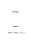
IP-Stepper
Dual Stepper Motor
Motion Controller
IndustryPack®
User Manual
©1999 SBS Technoogies Modular I/O
Subject to change without notice.
Manual Revision: 6 10/27/1999
Hardware Revision: B
IP-Stepper
Dual Stepper Motor
Motion Controller
IndustryPack®
SBS Technologies Modular I/O
181 Constitution Drive
Menlo Park, CA 94025
(650) 327-1200
(650) 327-3808 FAX
http://www.sbs-mio.com
©1999 SBS Technologies, Inc. Modular I/O.
IndustryPack is a registered trademark of SBS
Technologies, Inc. Modular I/O. QuickPack,
SDpacK and Unilin are trademarks SBS
Technologies, Inc. Modular I/O. PC•MIP is a
trademark of SBS Technologies, Inc. Modular
I/O and MEN Mikro GmbH.
SBS Technologies Modular I/O, Inc
acknowledges the trademarks of other
organizations for their respective products
mentioned in this document.
All rights are reserved: No one is permitted to
reproduce or duplicate, in any form, the whole
or part of this document without the express
consent of SBS Technologies, Inc. Modular
I/O. This document is meant solely for the
purpose in which it was delivered.
SBS Technologies, Inc. Modular I/O reserves
the right to make any changes in the devices
or device specifications contained herein at
any time and without notice. Customers are
advised to verify all information contained in
this document.
The electronic equipment described herein
generates, uses and may radiate radio
frequency energy, which can cause radio
interference. SBS Technologies, Inc. Modular
I/O assumes no liability for any damages
caused by such interference.
SBS Technologies, Inc. Modular I/O’s
products are not authorized for use as critical
components in medical applications such as
life support equipment, without the express
consent of the president of SBS Technologies,
Inc. Modular I/O.
This product has been designed to operate
with IndustryPack, PC•MIP or PMC modules
or carriers and compatible user-provided
equipment. Connection of incompatible
hardware is likely to cause serious damage.
SBS Technologies, Inc. Modular I/O assumes
no liability for any damages caused by such
Table of Contents
Product Description______________________________________________________________ 1
Applications Guide ______________________________________________________________ 3
VME Addressing_______________________________________________________________ 16
NuBus Addressing _____________________________________________________________ 17
ISA (IBM PC-AT) Addressing ____________________________________________________ 18
Getting Started ________________________________________________________________ 19
I/O Pin Wiring ________________________________________________________________ 23
IndustryPack Logic Interface Pin Assignment ________________________________________ 25
ID PROM ____________________________________________________________________ 26
Construction and Reliability ______________________________________________________ 27
Warranty and Repair____________________________________________________________ 28
Specifications _________________________________________________________________ 29
QuickStart Software Support _____________________________________________________ 30
List of Figures
FIGURE 1
FIGURE 2
FIGURE 3
FIGURE 4
FIGURE 5
FIGURE 6
FIGURE 7
FIGURE 8
FIGURE 9
FIGURE 10
FIGURE 11
FIGURE 12
FIGURE 13
FIGURE 14
BLOCK DIAGRAM _______________________________________________________________ 2
PCL-240MK REGISTER SUMMARY _________________________________________________ 4
EXAMPLE OF STOP START COMMANDS _______________________________________________ 5
EXAMPLE OF REGISTER SELECT COMMANDS___________________________________________ 7
VME WORD ACCESS ___________________________________________________________ 16
NUBUS WORD ACCESS __________________________________________________________ 17
ISA WORD ACCESS ____________________________________________________________ 18
PROGRAMMING EXAMPLE________________________________________________________ 20
EMERGENCY STOP INTERRUPT EXAMPLE ____________________________________________ 20
VELOCITY TRAJECTORY EXAMPLE ________________________________________________ 21
I/O PIN ASSIGNMENT CHANNEL 1 ________________________________________________ 23
I/O PIN ASSIGNMENT CHANNEL 2 ________________________________________________ 24
LOGIC INTERFACE PIN ASSIGNMENT _______________________________________________ 25
ID PROM DATA (HEX) ________________________________________________________ 26
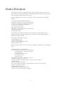
Product Description
The IP-Stepper provides two independent motion control channels for stepper systems. Each
channel consists of a Nippon Pulse Motor PCL-240MK programmable high speed pulse generator
and a U.S. Digital LS7166 Encoder Interface Chip.
The PCL-240MK Provides several advanced features which are supported on the IP-Stepper,
including:
•Fully programmable trapezoidal speed profile.
•Individually controllable acceleration and deceleration.
•Continuous constant speed and high speed operation.
•Constant speed and high speed origin return.
•On the fly speed ramp down.
•Halt diagnostic status register.
•Master/Slave operation for multi-axis synchronization.
•240K pps maximum speed.
•Programmable scaling.
The LS7166 provides additional quadrature decode capability for programmable way-point
triggering, indexing, travel limiting and closed loop motion control. Other additional features
provided by the LS7166 include:
•Pre-loadable 24 bit Up/Down counter.
•Programmable pre-scalar.
•24 Bit comparator Register.
•Overflow, Under flow and Match flags.
•Latched counter outputs.
With the marriage of these two ICs in each channel, IP-Stepper can implement powerful aggregate
features:
•Programmable "S" curve speed profiles.
•Externally triggerable capture channel configurable as:
¤ Gated qualifier for A & B channel inputs or
¤ Counter reset or
¤ Output latch transfer clock or
¤ Counter pre-load or
¤ interrupt source.
•Two channel master/slave synchronized movement.
•Immediate emergency stop execution.
•Interrupts generated for Emergency Stop, travel limits, counter overflow.
•Interrupt masking.
•Software selectable counter input.
•Opto isolated inputs configurable for either differential, current loop or TTL signals.
•Software selectable input polarity.
•Programmable interrupt vector.
•Simplified memory mapped register access.
•Fused +5 volt power outputs for driver biasing.
1
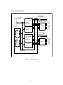
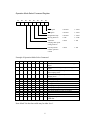
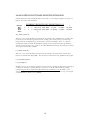
Simplified Block Diagram
Open Collector
Output Buffers
Pulse
IP Logic
Interface
OptoIsolation
Interupt
Vector
PCL 240MK
Stepper
Controller
71LS66
Counter
Xilinx FPGA
Figure 1
Block Diagram
2
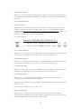
Open Collector
Output Buffers
Pulse
Direction
OptoIsolation
Encoder Feedback
and Switch Inputs
ID PROM
Masking and Polarity Control
71LS66
Counter
Encoder Feedback
and Switch Inputs
Direction
PCL 240MK
Stepper
Controller
Applications Guide
The IP-Stepper provides sophisticated and powerful stepper control capabilities. The following
information is provided for quick reference only. Complete factory data sheets are provided with the
engineering kit which is strongly recommended for first time buyers.
Motion control systems are potentially dangerous. Be sure carefully check signal phasing on the drive
signals and encoder feedback. Also, verify the interrupt masking, polarity and motor registers before
issuing start commands.
Programming
IP-Stepper integrates one PCL-240MK pulse generator and one LS7166 per channel. All of the
PCL-240MK registers are accessible and most of the functions are supported. The hardware waypoint inputs SD+ & SD- are not implemented but, both the PCL-240MK and the LS7166 counters
generate programmable way-point interrupts. The PCL-240MK control and data registers and the
LS7166 counter control and data registers are mapped into IP-I/O space memory locations. System
interrupts, interrupt masking, polarity, sync and ID PROM information are all incorporated on the
Xilinx FPGA.. The FPGA registers are assessable as IP-I/O space. See the addressing tables for
your particular system.
GENERAL
Signals with names having a * suffix are called ACTIVE LOW signals and are TRUE when they are
at a 0 logic level which is nominally less than 0.8 Volts. They are FALSE at a 1 logic level which is
nominally 1.4 volts or greater. Signals without the suffix are called ACTIVE HIGH signals and their
TRUE and FALSE definitions are the OPPOSITE of the ACTIVE LOW definition. For example
TERM1* would be set TRUE by writing a 1 to it's bit which would measure as over 1.4 volts on the
IP STEPPER board circuitry.
The phrase "Logic Interface" refers to the Electrical/Logical interface between an Industry Pack
board like the IP STEPPER and the carrier board on which it is installed.
The phrase "I/O Interface" refers to the OTHER connector on an Industry Pack that carries
signals, special power, etc. to the Industry Pack via the carrier board.
All software programmable IP STEPPER board registers should be reinitialized following power up
or a Logic Interface reset as the contents are reset to zeros.
Control register bits shown with the same names for both reading and writing have "read back"
capability. Other bits have either read or write capability only or a read signal that is functionally
related to the write signal of the same bit.
3
REGARDING PCL-240MK MOTOR CONTROLLER CHIP
Registers with more than 8 bits must be written as though they are 24 bits when using the
recommended "collective" access mode. The value of the extra bits beyond the registers specified
width is irrelevant. In addition, since the PCL-240MK transfers the value when the least significant
byte is written, it must be written LAST. Therefore, write the data in the order of most significant to
least significant byte.
It is recommended that "extension" mode be used rather than "standard mode.
The values written to the Start Stop command, Operation Mode Select command and Output Mode
Select command can be read back in the R17: Extension Status Buffer. The Register Select
command value written can NOT be read back. All other writeable registers can be read back.
See NIPPON PULSE MOTOR corp. PCL240MK data sheet for programming information. Note
that you must have the MK data sheet as the AK is a different part.
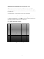
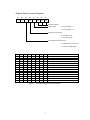
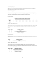
PCL-240MK Register set summary:
R No.
S
M
R
O
R0
R1
R2
R3
R4
R5
R6
R7
R10
R11
R12
R13
R16
R17
Description
Start Stop Commands
Operation Mode Select Command
Register Select Command
Output Mode Command
Down counter
FL register
RH1 register
RH2 register
Acceleration rate register
Deceleration rate register
Ramping-down point register
Multiplication register
Current position counter
Current speed monitor
Extension mode register
Extension mode register
Command buffer monitor
Extension status buffer
Figure 2
Bit Length
8
8
8
8
24
13
13
13
14
14
20
16
24
13
16
24
24
16
R/W
R/W
R/W
R/W
R/W
R/W
R/W
R/W
R/W
R/W
R/W
R/W
R/W
R/W
R
R/W
R/W
R
R
PCL-240MK register Summary
4
Start-Stop Command Register
D7
D6
0
0
D5
D4
D3
D2
D1
D0
Pulse Rate Selection
D7 D6 D5 D4 D3 D2 Dl
0
0
0
1
0
0
0
0
0
1
1
0
0
0
0
0
0
1
0
0
0
0
0
0
1
0
0
1
0
0
0
1
0
1
0
0
0
0
1
0
1
1
0
0
0
1
0
1
0
0
0
0
1
1
1
1
0
0
0
0
1
0
0
0
1
1
0
0
0
0
Figure 3
00: FL
10: FL
01: FH1
11: FH2
Speed Mode
0: Constant
1: High
Stop Control
0: OFF
1: ON
Start Control
0: OFF
1: ON
INT Output at Stop
0: None (reset)
1: Yes
D0 Description
0
FL-based constant-speed operation (with no INT signal
output) The PCL-240MK operates at a speed set in FL
register R1.
0
FL-based constant-speed operation (with the INT signal
output)
1
FH1-based constant-speed operation (with no INT signal
output) The PCL-240MK operates at a speed set in FH1
register R2.
1
FH2-based constant-speed operation (with no INT signal
output) The PCL-240MK operates at a speed set in FH2
register R3.
1
FH1-based high-speed operation (with no INT signal output)
The PCL-240MK starts at a speed set in the FL register, then
ramps up to a speed set in the FHI register.
1
FH2-based high-speed operation (with no INT signal output)
The PCL-240MK starts at a speed set in the FL register, then
ramps up to a speed set in the FH2 register.
0
Ramping down on the way. The PCL-240MK ramps down
from a speed set in the FHI or FH2 register to a speed set in
the FL register.
1
Deceleration stop. The PCL-240MK ramps down from a
speed set in the FHI or FH2 register and stops when the speed
reaches what is set in the FL register is reached. (A reset
command is required after stop.)
0
Immediate stop (with the INT signal output)
0
Immediate stop (reset command) (INT output reset)
Example of Stop Start Commands
5
Operation Mode Select Command Register
D7
D6
0
0
D5
D4
D3
D2
D1
D0
ORG signal
0: Invalid
1: Valid
SD signals
0: Invalid
1: Valid
Programmed stop
0: Invalid
1: Valid
Moving direction
0: CW
1: CCW
Automatic
ramping-down point
setting function
0: OFF
1: ON
Current position
counter operation
control
0: OFF
1: ON
Example of Operation Mode Select Command
D7
0
D6
1
D5
X
D4
X
D3
X
D2
X
Dl
X
D0
0
0
1
X
X
X
X
X
1
0
1
X
X
X
X
0
X
0
1
X
X
X
X
1
X
0
0
0
0
0
0
0
0
0
0
0
1
1
1
1
1
1
1
1
1
1
1
X
X
X
X
X
X
0
1
X
X
X
X
X
X
X
0
1
X
X
X
X
X
X
X
0
1
X
X
X
X
X
X
X
0
1
X
X
X
X
X
X
0
0
1
X
X
X
X
X
X
X
X
0
X
1
X
X
X
X
X
X
X
X
0
1
1
Description
The ORG terminal at low level does not stop pulse
output
The low-level ORG signal to pin 40 stops pulse
output.
The low-level SD signal to pin 23 or 22 does not
effect ramping-down.
The low-level SD signal to pin 23 or 22 effects
ramping down.
Pulse output does not stop with RO=0.
Pulse output stops with RO=0.
Moving in CW direction.
Moving in CCW direction.
A ramping-down point is to be written in R6.
A rarnping-down point is to be set automatically.
The current position counter is not operated.
The current position counter is operated.
Manual mode ORG and SD are invalid
Origin return mode.
Programmed operation mode ORG and SD are
valid also.
Note: Mark X in the above table may be either 0 or 1.
6
Register Select Command Register
D7
D6
1
0
D5
D4
D3
S4
D2
D1
D0
S2
S1
S0
Register numbers
OTS Control
0: OTS terminal = L
1: OTS terminal = H
Register group Slection
0: Standard group
1: Extension group
Input/Output Mode Selection
0: Input/output of every 8 bits
1: Collective input/output
D7
1
1
1
1
1
1
1
1
1
1
1
1
1
I
D6
0
0
0
0
0
0
0
0
0
0
0
0
0
0
D5
X
X
X
X
X
X
X
X
X
X
X
X
X
X
D4
0
0
0
0
0
0
0
0
1
1
1
1
1
1
D3
X
X
X
X
X
X
X
X
X
X
X
X
X
X
Figure 4
D2
0
0
0
0
1
1
1
1
0
0
0
0
1
1
Dl
0
0
1
I
0
0
1
1
0
0
1
1
1
1
D0
0
1
0
1
0
1
0
1
0
1
0
1
0
1
Description
Selects register R0.
Selects register R1.
Selects register R2.
Selects register R3.
Selects register R4.
Selects register R5.
Selects register R6.
Selects register R7.
Selects register R10.
Selects register R11.
Selects register R12.
Selects register R13.
Selects register R16.
Selects register R17.
Example of Register Select Commands
7
R17: 16-bit Status Buffer Bits D0..D7
The R17 allows the operator to monitor signal status as follows.
D7
D6
D5
D4
D3
D2
D1
D0
Interrupt Signal to Stop Operation
0: Output in Progress
1: Output in Cessation
Interrupt Signal to Start Ramping-down
0: Output in Progress
1: Output in Cessation
SD- Signal
Not supported
+SD Signal
Not supported
FU Signal
0:OFF
1: ON
FDOWN Signal
0:OFF
1: ON
LT Signal
0:OFF
1: ON
Pulse Output
0:OFF
8
1: ON
R17: 16-bit Status Buffer Bits D8..D15
During the extension status, you can and bits 8 ~ 14 to get information of causes why pulse input is
stopped.
D15 D14 D13 D12
D11 D10
D9
D8
1: by EL- is ON
1: by EL+ is ON
1: by ORG is ON
1: by Programmed mode
1: by Ramping down and stop command
1: by ALM input
1: by Stop command (reset command)
SUBCLK/ALM terminal monitor
9
XILINX INTERFACE SOFTWARE REGISTER DEFINITIONS
NOTE: All bits are read/write [R/W] unless shown with a - in the map and a [R] for read only or a
[W] for write only in their definitions.
INTERRUPT REGISTER BIT DEFINITIONS V0.2
Data Bit #
Write
Action
Read
Action
7
X
6
X
5
X
X
X
X
4
ESTP_ICLR
3
ESTP_IMSK*
2
CT_ICLR
ESTP_Ipendin ESTP_IMSK* CT_Ipending
g
1
CT_IMSK*
0
MT_IMSK*
CT_IMSK*
MT_IMSK*
MT_IMSK* [R/W] D0
When set to "0", masks (disables) interrupts from the channel's PCL-240MK motor controller. Has
no effect upon the interrupt's generation, rather, it simply prevents the presence of an interrupt
being noticed by the interrupt logic on the Industry Pack. Thus enabling ( with a "1" ) when an
interrupt has already occurred will immediately precipitate an interrupt to the IP Logic Interface.
This bit resets and powers on to a value of "0" which MASKS the interrupt. The interrupt is cleared
via a register bit in the PCL-240MK.
CT_IMSK* [R/W] D1
When set to "0", masks (disables) interrupts from the channel's LS7166 Counter with the same
behavior as described for MT_IMSK*. The interrupt is cleared via the CT_ICLR bit in this register.
CT_IPENDING [R] D2
CT_ICLR [W] D2
Reading a value of "1" from this bit indicates the presence of a pending LS7166 Counter interrupt. A
"0" means no interrupt is pending. Writing a value of "1" to this bit will CLEAR any pending
interrupt and prevent any further interrupts until the bit is returned to a "0." Normally a "0" is
written to this bit except when clearing an interrupt. The power up default is to a "0", so interrupts
are ENABLED, but masked via CT_IMSK*.
10
ESTP_IMSK* [R/W] D3
When set to "0", masks (disables) interrupts from the channel's Emergency Stop switch input with
the same behavior as described for MT_IMSK*. The interrupt is cleared via the ESTP_ICLR bit in
this register.
ESTP_IPENDING [R] D4
ESTP_ICLR [W] D4
Reading a value of "1" from this bit indicates the presence of a pending Emergency Stop switch
interrupt. A "0" means no interrupt is pending. Writing a value of "1" to this bit will CLEAR any
pending interrupt and prevent any further interrupts until the bit is returned to a "0." Normally a "0"
is written to this bit except when clearing an interrupt. The power up default is to a "0", so
interrupts are ENABLED, but masked via ESTP_IMSK*.
D7 - D5 Not Assigned.
POLARITY REGISTER BIT DEFINITIONS V0.2
Data Bit #
Write
Action
Read
Action
7
X
6
STP_Invert
5
Z_Invert
X
STP_Invert
Z_Invert
4
WP_INVER
T
WP_INVER
T
3
2
CT_Enable CP_Invert
CT_Enable CP_Invert
1
CH B
Invert
CH B
Invert
0
CH A
Invert
CH A
Invert
CH A INVERT [R/W] D0
When set to a "1", the logic levels of the signal to channel A of the channel's LS7166 counter will be
inverted prior to reaching the counter. Power up and reset state is NOT inverted.
CH B INVERT [R/W] D1
When set to a "1", the logic levels of the signal to channel B of the channel's LS7166 counter will be
inverted prior to reaching the counter. Power up and reset state is NOT inverted.
CP INVERT [R/W] D2
When set to a "1", the logic levels of the CAPTURE signal to the channel's LS7166 counter will be
inverted prior to reaching the counter. Power up and reset state is NOT inverted.
CT ENABLE [R/W] D3
When set to a "1", the CAPTURE signal is enabled to affect the channel's LS7166 counter as
configured. Power up and reset state is NOT enabled.
NOTE that the counter must also be programmed compatibly with the function selected for proper
operation to take
place. This bit resets and powers on to a value of "0".
WP INVERT [R/W] D4
When set to a "1", the logic levels of the channel's way-point signals will be inverted prior to
reaching the PCL-240MK. Way-point signals should be configured to be active low ("0" when true)
at the PCL-240MK. Power up and reset state is NOT inverted.
11
Z INVERT [R/W] D5
When set to a "1", the logic level of the channel's Z signal will be inverted prior to reaching the
PCL-240MK. Power up and reset state is NOT inverted.
STP INVERT [R/W] D6
When set to a "1", the logic level of the channel's Emergency stop signal will be inverted prior to
reaching the Interrupt Logic. The Emergency Stop signal should be configured to be active low ("0"
when true) to the interrupt logic. Power up and reset state is NOT inverted.
D7 Not Assigned.
SOURCE REGISTER BIT DEFINITIONS
Data Bit #
Write
Action
Read
Action
7
X
6
LDSL1
5
LDSL0
4
ABSL1
3
ABSL0
2
CBSL0
1
CASL1
0
CASL0
X
LDSL1
LDSL0
ABSL1
ABSL0
CBSL0
CASL1
CASL0
CASL0 - CASl1 [R/W] D0 - D1
These bits select the source for the Channel A input of the channel's LS7166 counter. Power up and
reset values are "0." When using PCL240 step output as input, invert Channel A in the polarity
register.
CASL1
0
0
1
1
CASL0
0
1
0
1
CHANNEL A SOURCE
X input
PCL240 Step pulse output *(invert Channel A)
Z signal after optional inversion
LOGICAL 1, No signal
CBSL0 [R/W] D2
This bit selects the source for the Channel B input of the channel's LS7166 counter. Power up and
reset value is "0."
CBSL0
0
1
CHANNEL B SOURCE
Y input
PCL240 motor Direction output *(invert Channel B)
ABSL0 - ABSl1 [R/W] D3 - D4
These bits select the source for the ABEN*/RESET* input of the channel's LS7166 counter.
Power up and reset values are "0." When using PCL240 motor direction output, set the bit to invert
Channel B in the polarity register.
ABSL1
0
0
1
1
ABSL0
0
1
0
1
ABEN*/RESET* SOURCE
Capture signal after optional inversion
Stop signal after optional inversion
Logical OR of above two signals
LOGICAL 1, No signal
12
LDSL0 - LDSl1 [R/W] D5 - D6
These bits select the source for the LDCNT*/LDLATCH* input of the channel's LS7166 counter.
Power up and reset values are "0."
LDSL1
0
0
1
1
LDSL0
0
1
0
1
LDCNT*/LDLATCH* SOURCE
Capture signal after optional inversion
Stop signal after optional inversion
Logical OR of above two signals
LOGICAL 1, No signal
D7 Not Assigned.
SYNC CONTROL REGISTER
Data Bit #
Write
Action
Read
Action
7
X
6
X
5
X
4
X
3
X
2
X
1
SUBCLK_EN
0
SYNC_EN
X
X
X
X
X
X
SUBCLK_EN
SYNC_EN
SYNC_EN [R/W] D0
When set to "1" connects the SYNO signal of the channel 1 PCL-240MK to the SYNI input of the
channel 2 PCL-240MK. This enables SYNCHRONOUS operation of the two motor controller
chips. Power up and reset state is NOT SYNC enabled.
SUBCLK_EN [R/W] D1
When set to "1" connects the SYNO signal of the channel 1 PCL-240MK to the SUBCLK/ALM
input of the channel 2 PCL-240MK. This enables SUBCLK operation of the channel 2 motor
controller chip. Power up and reset state is NOT SUBCLK enabled.
NOTE: Only one of the above two options should be enabled at on time.
13
D7 - D2 Not Assigned .
INTERRUPT VECTOR
Data Bit #
Write
Read
7
V7
V7
6
V6
V6
5
V5
V5
4
V4
V4
3
V3
V3
2
X
C2
1
X
C1
0
X
C0
The IP STEPPER stores any desired value five bit interrupt vector in this register. On a Write cycle,
only D7 - D3 are stored. On a read cycle, the previously stored value of D7 - D3 is read back upon
the same bits as they were written. In addition, C2 through C0 encode the value of the most
significant interrupt source with a pending interrupt. ( Channel 2 is the most significant, Channel 1
the least.) This full eight bit vector will be returned as the data of an interrupt vector request cycle
(IP Logic Interface INTSEL* true).
VECTOR PRIORITY ENCODING
C2, C1, C0
Interrupt Source
_______________________________________________
000
E-Stop channel 1 (lowest priority)
001
E-Stop channel 2
010
LS7166 Counter channel 1
011
LS7166 Counter channel 2
100
PCL-240MK channel 1
101
PCL-240MK channel 2 (highest priority)
LS7166 24 BIT COUNTER CHIP REGISTERS
The Data and Control registers in the IP address map provide direct access to the Data and Control
registers of the LS7166 counters. The Xilinx FPGA decodes and generates CS* RD* WR* and
C/D* signals for the LS7166. Please review the LS7166 register specifications for details of the
register functions.
For proper operation the counter's output pin 16 ( BW or COMP )should be programmed as active
low in the counter's Output Control Register bits 4 & 5. Use 00 for BW* or 11 for COMP*.
None of this device's writeable registers have read back capability. See LSI corp. LS7166 data sheet
for programming information.
Be sure to reset the PR/OL address pointer when accessing the Preset and Output latch registers by
writing a 1 to bit D0 of the Master control register. Failure to do so might result in garbled data if
errant reads or writes are made to these registers.
The two control signals to the LS7166 can provide the following actions depending upon internal
register programming of the LS7166.
14
LS7166 CONTROL FUNCTIONS
LS7166 Input
control register
bit 4
0
1
ABEN*/RESET* TRUE INPUT ACTION
LS7166 Input
control register
bit 5
0
0
1
LDCNT*/LDLATCH* TRUE INPUT ACTION
Reset the counter
Gate the counter's inputs
Load counter from preset compare register
Cause interrupt if 0 in preset register.
Transfer counter's count to output latch
Interfacing
The output stepper pulse and direction signals from IP-Stepper are driven by LSTTL open collector
buffers. This provides both ruggedness and adaptability. In the standard configuration the output
drivers are pulled up to the on board 5 volt supply. This Gives the user TTL compatibility right out
of the box. For different power requirements like, 12 or 24 VDC, external pull ups can be used.
Additionally, the encoder feedback signals and switch inputs are optio-isolated for system protection
and noise immunity. The encoder signals are buffered by special high speed optocouplers for high
speed and high resolution quadrature inputs. All optocoupler inputs can be user configured for
TTL, Differential or current loop signal levels.
Wiring Options
Normally isolated resistor type resistor packs are installed for current limiting of the optically
coupled current loop inputs. Changing these to bussed type resistor packs with +5V applied to the
I/O connector's pin corresponding to the resistor pack's pin 1, provides local current sourcing to
input signal + inputs. Thus, channel testing can be done by providing only current sinking on the pins. This provides much easier testing than full current loop interfaces on all pins. Connect as
follows.
SPECIAL TESTING WIRING OPTIONS
MOTOR CHANNEL
1
1
2
2
SIGNALS
X,Y,Z,CAPTURE
WAY-POINTS, STOP,
X,Y,Z,CAPTURE
WAY-POINTS, STOP,
15
I/O PIN to connect to +5 volts
2
4
27
29
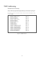
VME Addressing
Standard Word I/O Accessing
There are TWO motor control channels each of which has its own PCL240 motor controller and
LS7166 counter chips. BOTH channels SHARE the Interrupt Vector and Sync Control registers.
Byte Addresses are shown ( A0 is LSB ), but board is accessed on 16 bit word boundaries. Values
are shown in HEX.
MOTOR 1 CONTROL / STATUS
MOTOR 1 DATA BITS 0-7
MOTOR 1 DATA BITS 8-15
MOTOR 1 DATA BITS 16-23
MOTOR 2 CONTROL / STATUS
MOTOR 2 DATA BITS 0-7
MOTOR 2 DATA BITS 8-15
MOTOR 2 DATA BITS 16-23
COUNTER 1 DATA
COUNTER 1 CONTROL
COUNTER 2 DATA
COUNTER 2 CONTROL
CHANNEL 1 INTERRUPT REGISTER
CHANNEL 1 POLARITY REGISTER
CHANNEL 1 SOURCE REGISTER
CHANNEL 2 INTERRUPT REGISTER
CHANNEL 2 POLARITY REGISTER
CHANNEL 2 SOURCE REGISTER
SYNC CONTROL REGISTER
INTERRUPT VECTOR REGISTER
Figure 5
Base + 01
Base + 03
Base + 05
Base + 07
Base + 09
Base + 0B
Base + 0D
Base + 0F
Base + 11
Base + 13
Base + 19
Base + 1B
Base + 21
Base + 25
Base + 29
Base + 2D
Base + 31
Base + 35
Base + 39
Base + 3D
VME Word Access
16
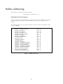
NuBus Addressing
The formula for conversion from VME to NuBus is:
NuBus address = (VME address x 2) - 1
Standard Word I/O Accessing
There are TWO motor control channels each of which has its own PCL-240MK motor controller
and LS7166 counter chips. BOTH channels SHARE the Interrupt Vector and Sync Control
registers.
Byte Addresses are shown ( A0 is LSB ), but board is accessed on 16 bit word boundaries. Values
are shown in HEX.
MOTOR 1 CONTROL / STATUS
MOTOR 1 DATA BITS 0-7
MOTOR 1 DATA BITS 8-15
MOTOR 1 DATA BITS 16-23
MOTOR 2 CONTROL / STATUS
MOTOR 2 DATA BITS 0-7
MOTOR 2 DATA BITS 8-15
MOTOR 2 DATA BITS 16-23
COUNTER 1 DATA
COUNTER 1 CONTROL
COUNTER 2 DATA
COUNTER 2 CONTROL
CHANNEL 1 INTERRUPT REGISTER
CHANNEL 1 POLARITY REGISTER
CHANNEL 1 SOURCE REGISTER
CHANNEL 2 INTERRUPT REGISTER
CHANNEL 2 POLARITY REGISTER
CHANNEL 2 SOURCE REGISTER
SYNC CONTROL REGISTER
INTERRUPT VECTOR REGISTER
Figure 6
Base + 01
Base + 05
Base + 09
Base + 0D
Base + 11
Base + 15
Base + 19
Base + 1D
Base + 21
Base + 25
Base + 31
Base + 35
Base + 41
Base + 41
Base + 49
Base + 51
Base + 59
Base + 61
Base + 71
Base + 79
NuBus Word Access
17
ISA (IBM PC-AT) Addressing
Standard Word I/O Accessing
There are TWO motor control channels each of which has its own PCL-240MK motor controller
and LS7166 counter chips. BOTH channels SHARE the Interrupt Vector and Sync Control
registers.
Byte Addresses are shown ( A0 is LSB ), but board is accessed on 16 bit word boundaries. Values
are shown in HEX.
MOTOR 1 CONTROL / STATUS
MOTOR 1 DATA BITS 0-7
MOTOR 1 DATA BITS 8-15
MOTOR 1 DATA BITS 16-23
MOTOR 2 CONTROL / STATUS
MOTOR 2 DATA BITS 0-7
MOTOR 2 DATA BITS 8-15
MOTOR 2 DATA BITS 16-23
COUNTER 1 DATA
COUNTER 1 CONTROL
COUNTER 2 DATA
COUNTER 2 CONTROL
CHANNEL 1 INTERRUPT REGISTER
CHANNEL 1 POLARITY REGISTER
CHANNEL 1 SOURCE REGISTER
CHANNEL 2 INTERRUPT REGISTER
CHANNEL 2 POLARITY REGISTER
CHANNEL 2 SOURCE REGISTER
SYNC CONTROL REGISTER
INTERRUPT VECTOR REGISTER
Figure 7
Base + 00
Base + 02
Base + 04
Base + 06
Base + 08
Base + 0A
Base + 0C
Base + 0E
Base + 10
Base + 12
Base + 18
Base + 1A
Base + 20
Base + 24
Base + 28
Base + 2C
Base + 30
Base + 34
Base + 38
Base + 3C
ISA Word Access
18
Getting Started
This section is intended to get first time user s started with IP-Stepper, quickly. The following steps
will verify IP-Stepper operation and installation in a fewminutes. The procedure uses a low level
debugger to program the IP. The debugger will depend on your particular host system. In the
example, channel 1 is programmed to execute a constant speed move. And, the Emergency Stop
function is verified and its inturrupt is verified and reset. An LED is used to indicate pulse output.
This simple load reduces the posibility of power module wiring errors and dangerous mechanical
system malfunctions during user orientation. For convience, the LED and resistor are supplied in the
IP-Stepper Engineering Kit. A piece of wire (or paper clip) can as the Emergency Stop switch.. This
procedure has been verified on several platforms including: GreenSpring VIPC 310 using OS-9
ROMBUG, Motorola MVME 162 running Motorloa's onboard debugger, 162-Bug, and IBM ATs
running MS-DOS DEBUG. Please take the time to try this experiment if you are unsure of a new
system.
1)
In the IP-Stepper Engineering Kit you will find:
i) an LED,
ii) a 330 ? resistor,
iii) a terminal block,
iv) and a 50 pin ribbon cable.
2)
Power down your system and install IP-Stepper in a vacant IP carrier slot. Connect the 50 pin
ribbon cable from your carrier to the terminal block. Be sure to observe the connector keying.
3)
Install the LED and 330 ? resistor on the STEP_OUT1 output. Connect the LED anode (long
lead) to STEP_OUT1, pin 20 on the terminal block. Connect the cathode (short lead) to GND,
pin 23. The resistor should be connected between FVCC pin 24 and STEP_OUT1, pin 20.
4) Use a wire to simulate an Emergency Stop switch. Connect one end of the wire to the
EM_STOP1* input, pin 25 of the terminal block. Leave the other end free.
5)
Power up the system.
6)
Determine the correct IP base address for your carrier slot. See your carrier manual for details.
For a quick check, read the ID PROM information at IP base address + $80 (hex).
19
7) Enter the following bytes using your debugger. Be sure to enter register data bytes in the order
shown below. All 24 bits of the PCL240MK registers MUST be loaded each time. And they
MUST be loaded least significant byte last.
VME
AT/ISA
OFFSET OFFSET
01
00
01
00
01
00
01
00
07
06
05
04
03
02
01
00
07
06
05
04
03
02
01
00
07
06
05
04
03
02
01
00
07
06
05
04
03
02
01
00
07
06
05
04
03
02
01
01
DATA
(HEX)
08
74
C8
A0
00
FF
FF
A1
00
00
01
A7
00
01
E8
B2
00
00
40
BB
13
20
00
10
READ/
WRITE
W
W
W
W
W
W
W
W
W
W
W
W
W
W
W
W
W
W
W
W
W
W
W
W
Figure 8
COMMENTS
Clear Stop/Start register
Set Op Mode register
Set Output Mode register
Select R0, Down Counter
R0 Data [D23..D16]
R0 Data [D15..D8]
R0 Data [D7..D0]
Select R1, FL Speed
R1 Data [D23..D16]
R1 Data [D15..D8]
R1 Data [D7..D0]
Select R7, Speed Multiplier
R7 Data [D23..D16]
R7 Data [D15..D8]
R7 Data [D7..D0]
Select R12, Ext. Mode 1
R12 Data [D23..D16]
R12 Data [D15..D8]
R12 Data [D7..D0]
Select R13, Ext. Mode 2
R13 Data [D23..D16]
R13 Data [D15..D8]
R13 Data [D7..D0]
Start command
Programming Example
8) The LED should start blinking at about one pulse per second.
9) Next test the Emergency Stop function by shorting the wire to ground. Touch the free end of the
wire to pin 23 of the terminal block. The LED should stop blinking.
10) To verify and clear the Emergency Stop interrupt register bits, peek and poke the following
bytes using your debugger. Note that the ESTP_ICLR bit MUST be Re-Enabled after clearing
the ESTP_Ipending bit. This is independent of the interrupt masking.
VME
AT/ISA DATA READ/
OFFSET OFFSET (Binary) WRITE
21
20 ???1 0000
R
21
20
???1 0000
W
21
20
???0 0000
W
Figure 9
COMMENTS
Interrupt Register
Verify ESTP_Ipending bit [D4]
Clear Emergency Stop. The LED
should start blinking again.
Re-Enable Emergency Stop.
Emergency Stop Interrupt Example
20
PCL-240MK Programming Applications Example:
In the following example the PCL-240MK pulse generator is programmed to execute a trapezoidal
velocity trajectory. Using displacement as the independent variable is an obvious practical approach
to motion control programming. As if by design, transformation of variables from time domain to
displacement domain simplifies register value calculations considerably.
Velocity
vf
vo
Displacement
xu
xf
xe
xd
xt
Given parameters:
Figure 10
Velocity Trajectory Example
Motor type = 200 step / revolution (1.8°/step)
xt = total displacement = 10 revs = 2000 pulses
xe = end displacement (optional) = 1 rev = 200 pulses
vo = initial velocity = 20 pps
v f = high speed flight velocity = 400 pps
tu = ramp up time = 1 sec
t d = ramp down time = 0.1 sec
FCLK = 4 Mhz, Standard for IP- Stepper.
n = 1 for ease of calculation
21
Intermediate variable calculations:
au = ramp up acceleration =
∆v v f − vo 400 − 20
=
=
= 380 pps2
∆t
tu
1
xu = ramp up displacement = votu +
ad = ramp down acceleration =
1
2
autu 2 = (20)(1) +
1
2
(380)(1)2 = 210 pulses
∆v vo − v f 20 − 400
=
=
= − 3800 pps 2
td
0.1
∆t
xd = ramp down displacement = v f td +
1
2
ad t d2 = (400)(0.1) −
1
2
(3800)(0.1) 2 = 21 pulses
x f = high speed flight dispalcement = x t − (x u + xd + xe ) = 2000 − (210 + 21 + 200) = 1569 pulses
Register value calculations:
R0 = 2000 = $7D0
R1 = 20 = $14
R2 = 400 = $190
F
4Mhz
R4 = CLK =
≈10526 = $291E
au
380
R5 =
FCLK 4Mhz
=
≈1053 = $41D
3800
ad
R6 = x d + x e = 21+ 200 = 221 = $DD
FCLK
4 Mhz
=
= 488 = $1E8
n ×8192 1×8192
S = $15
R7 =
22
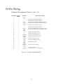
I/O Pin Wiring
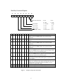
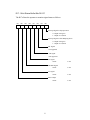
IP-Stepper Pin Assignment. Channel 1, Pins 1..25
PIN NUMBER
1
MOTOR
CHANNEL
1
2
1
3
1
4
1
5
1
6
1
7
1
8
1
9
1
10
1
11
1
12
1
13
1
14
1
15
1
16
1
17
1
18
1
19
1
20
1
21
1
22
1
23
1
24
1
25
1
PIN NAME
DESCRIPTION / FUNCTION
GND
X+
XWPP+
WPP-
Quadrature input, opto isolated, current in
Quadrature input, opto isolated, current out
Way-point input, PLUS direction, opto isolated, current in
Way-point input, PLUS direction, opto isolated, current out
GND
Y+
YWPM+
WPM-
Quadrature input, opto isolated, current in
Quadrature input, opto isolated, current out
Way-point input, MINUS direction, opto isolated, current in
Way-point input, MINUS direction, opto isolated, current out
GND
Z+
Index input, opto isolated, current in
Z-
Index input, opto isolated, current out
CAPTURE+
Capture input, opto isolated, current in
CAPTURE-
Capture input, opto isolated, current out
GND
STOP+
Stop input, opto isolated, current in
STOP-
Stop input, opto isolated, current out
GND
STEP
Step output, open collector
GND
DIRECTION
Direction output, open collector
GND
+5 volts
ESTOP*
Figure 11
+5 volts output, fused
Emergency Stop input, switch closure to gnd
I/O Pin Assignment Channel 1
23
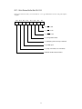
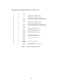
IP-Stepper Pin Assignment. Channel 2, Pins 26..50
26
2
27
2
28
2
29
2
30
2
31
2
32
2
33
2
34
2
35
2
36
2
37
2
38
2
39
2
40
2
41
2
42
2
43
2
44
2
45
2
46
2
47
2
48
2
49
2
50
2
GND
X+
Quadrature input, opto isolated, current in
X-
Quadrature input, opto isolated, current out
WPP+
WPP-
Way-point input, PLUS direction, opto isolated, current in
Way-point input, PLUS direction, opto isolated, current out
GND
Y+
YWPM+
WPM-
Quadrature input, opto isolated, current in
Quadrature input, opto isolated, current out
Way-point input, MINUS direction, opto isolated, current in
Way-point input, MINUS direction, opto isolated, current out
GND
Z+
Index input, opto isolated, current in
Z-
Index input, opto isolated, current out
CAPTURE+
Capture input, opto isolated, current in
CAPTURE-
Capture input, opto isolated, current out
GND
STOP+
Stop input, opto isolated, current in
STOP-
Stop input, opto isolated, current out
GND
STEP
Step output, open collector
GND
DIRECTION
Direction output, open collector
GND
+5 volts
ESTOP*
Figure 12
+5 volts output, fused
Emergency Stop input, switch closure to gnd
I/O Pin Assignment Channel 2
24
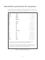
IndustryPack Logic Interface Pin Assignment
Figure 13 below gives the pin assignments for the IndustryPack Logic Interface connector on the
IP-Stepper. Pins marked n/c below are defined by the specification, but not used on IP-Stepper. See
also your User Manual for your IP Carrier board for more information.
GND
CLK
Reset*
D0
D1
D2
D3
D4
D5
D6
D7
n/c
n/c
n/c
n/c
n/c
n/c
n/c
n/c
n/c
n/c
n/c
n/c
+5V
GND
GND
+5V
R/W*
IDSel*
n/c
MEMSel*
n/c
INTSel*
n/c
IOSel*
n/c
A1
n/c
A2
n/c
A3
INTReq0*
A4
n/c
A5
n/c
n/c
Ack*
n/c
GND
1
26
2
3
27
28
4
5
29
30
6
7
31
32
8
9
33
34
10
11
35
36
12
13
37
38
14
15
39
40
16
17
41
42
18
19
43
44
20
21
45
46
22
23
47
48
24
25
49
50
Note 1: The no-connect (n/c) signals above are defined by the IndustryPack Logic Interface
Specification, but not used by this IP. See the Specification for more information.
Note 2: The layout of the pin numbers in this table corresponds to the physical placement of pins
on the IP connector. Thus this table may be used to easily locate the physical pin corresponding
to a desired signal. Pin 1 is marked with a square pad on the IndustryPack.
Figure 13
Logic Interface Pin Assignment
25
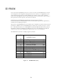
ID PROM
Every IP contains an ID PROM, whose size is at least 32 x 8 bits. The ID PROM aids in software
auto configuration and configuration management. The user's software, or a supplied driver, may
verify that the device it expects is actually installed at the location it expects, and is nominally
functional. The ID PROM contains the manufacturing revision level of the IP. If a driver requires
that a particular revision be present, it may check for it directly.
Standard data in the ID PROM on the IP-Stepper is shown in Figure 20 below.
For more information on IP ID PROMs refer to the IndustryPack Logic Interface Specification,
available from GreenSpring Computers.
The location of the ID PROM in the host's address space is dependent on which carrier board used.
Normally for VMEbus carriers the ID PROM space is directly above the IP's I/O space, or at IPbase + $80. Macintosh drivers use the ID PROM automatically. RM1260 address may be derived
from Figure 14 below by multiplying the addresses given by two, then subtracting one. RM1270
addresses may be derived by multiplying the addresses given by two, then adding one.
The ID PROM is equivalent to a Philips (Signetics) 82LS123.
3F
(available for user)
19
17
15
13
11
0F
0D
0B
09
07
05
03
01
CRC
No of bytes used
Driver ID, high byte
Driver ID, low byte
reserved
Revision
Model No: IP-Stepper
Manufacturer ID GreenSpring
ASCII “C”
ASCII “A”
ASCII “P”
ASCII “I”
Figure 14
ID PROM Data (hex)
26
(81)
(0C)
(00)
(01)
(00)
(A1)
(40)
(F0)
(43)
(41)
(50)
(49)
Construction and Reliability
IndustryPacks were conceived and engineered for rugged industrial environments. The IP-stepper is
constructed out of 0.062 inch thick FR4 V0 material.
The IndustryPack connectors are keyed, shrouded and gold plated on both contacts and receptacles.
They are rated at 1 Amp per pin and a minimum of 200 insertion cycles. These connectors make
consistent, correct insertion easy and reliable.
The IP is secured to the carrier with four M2 metric stainless steel screws. The heads of the screws
are countersunk into the IP. The four screws provide significant protection against shock, vibration,
and incomplete insertion. For most applications they are not required.
The IndustryPack provides a low temperature coefficient of 0.89 W/°C for uniform heat. This is
based on the temperature coefficient of the base FR4 material of 0.31 W/m-°C, and taking into
account the thickness and area of the IP. This coefficient means that if 0.89 Watts is applied
uniformly on the component side, that the temperature difference between the component and the
solder side is one degree Celsius.
27
Warranty and Repair
SBS Technologies, Inc. Modular I/O warrants this product to be free from defects in workmanship
and materials under normal use and service and in its original, unmodified condition, for a period of
one year from the time of purchase. If the product is found to be defective within the terms of this
warranty, SBS Technologies, Inc. Modular I/O’s sole responsibility shall be to repair, or at SBS
Technologies, Inc. Modular I/O's sole option to replace, the defective product. The product must
be returned by the original customer, insured, and shipped prepaid to SBS Technologies, Inc.
Modular I/O. All replaced products become the sole property of SBS Technologies, Inc. Modular
I/O.
SBS Technologies, Inc. Modular I/O’s warranty of and liability for defective products is limited to
that set forth herein. SBS Technologies, Inc. Modular I/O disclaims and excludes all other product
warranties and product liability, expressed or implied, including but not limited to any implied
warranties of merchantability or fitness for a particular purpose or use, liability for negligence in
manufacture or shipment of product, liability for injury to persons or property, or for any incidental
or consequential damages.
SBS Technologies, Inc. Modular I/O’s products are not authorized for use as critical components in
life support devices or systems without the express written approval of the General Manager of SBS
Technologies, Inc. Modular I/O.
Service Policy
Before returning a product for repair, verify as well as possible that the suspected unit is at fault.
Then call the Customer Service Department for a RETURN MATERIAL AUTHORIZATION
(RMA) number. Carefully package the unit, in the original shipping carton if this is available, and
ship prepaid and insured with the RMA number clearly written on the outside of the package.
Include a return address and the telephone number of a technical contact. For out-of-warranty
repairs, a purchase order for repair charges must accompany the return. SBS Technologies, Inc.
Modular I/O will not be responsible for damages due to improper packaging of returned items. For
service SBS Technologies, Inc. Modular I/O products not purchased directly from SBS
Technologies, Inc. Modular I/O, contact your reseller. Products returned to SBS Technologies, Inc.
Modular I/O for repair by other than the original customer will be treated as out-of-warranty.
Out of Warranty Repairs
Out of warranty repairs will be billed on a material and labor basis. The current minimum repair
charge is $100. Customer approval will be obtained before repairing any item if the repair charges
will exceed one half of the quantity one list price for that unit. Return transportation and insurance
will be billed as part of the repair and is in addition to the minimum charge.
For Service Contact:
Customer Service Department
SBS Technologies, Inc.
Modular I/O
181 Constitution Drive
Menlo Park, CA 94025
(650) 327-1200
FAX: (650) 327-3808
email: [email protected]
28
Specifications
Logic Interface
Number of Channels
Input Isolation
Input Ranges
Encoder/Counter
Limit Switches
Emergency Stop
Output Isolation
Output Ranges
Motion Controller IC
Internal Clock Frequency
Pulse Rate
Pulse Rate Multiplication
Number of Pulses
Counter IC
Counter size
Counter resolution
Counter frequency
Input polarity
Input masking
Interrupts
Temperature Coefficient
IndustryPack logic Interface, 0.7 compatible
Single-high size
Two
Each line optically isolated
EIA 485 differential or 20 mA current loop.
User configurable for TTL.
EIA 485 differential or 20 mA current loop.
User configurable for TTL.
TTL Compatible. GND = Stop.
Open collector type outputs.
TTL Compatible.
Nippon Pulse Motor PCL-240MK
4 MHz
240,000 pps
0.01x to 30x
1 to 16,777,215 (24-Bit)
U.S. Digital LS 7166
24-Bit Preloadable Up/Down
1x, 2x or 4x
10 MHz, max.
all inputs have programmable polarity
all inputs are maskable
Programmable interrupt vector. Maskable interrupts
generated by all hardware inputs and all software
programmed testable parameters
0.89 W/°C for uniform heat,
component side to solder side
Dimensions
1.800 by 3.900 by 0.340 inches maximum
Power
650 mW per IP typical (+5 V supply)
Environmental
Operating temperature: 0 to 70°C
Humidity: 5 to 95% non-condensing
Storage: –10 to +85°C
29
QuickStart Software Support
QuickStart software provides a simple software functional test of the IP hardware. It is not a driver
or an application programming library. Please consult with your GreenSpring sales representative on
the availability of QuickPack or DriverPack software for this IP.
QuickStart software is provided in ANSI C source code format. This software has been tested on a
Motorola MVME162 running OS-9 v3.0 and compiled with Ultra C v1.1.1 from Microware in ANSI
C mode. Some modifications will be necessary to use a different compiler or operating system. The
areas specific to OS-9 or Microware software tools have been marked as thoroughly as possible.
QuickStart software is supplied as is with no warranty or guarantee. The recipient may reuse and/or
modify this software for use with GreenSpring IndustryPacks only.
Function summaries are provided here for customer reference only. This information was current at
the time the manual was last revised. This information is not necessarily current or complete
manufacturing data, nor is it part of the product specification. All information following is copyright
GreenSpring Computers, Inc.
Current code listings, including print outs and floppy disk (DOS 3.5" 1.44 MB format), are available
from GreenSpring Computers as part of the Engineering Kit option or from your international
distributor.
30
------------------------------------------------------NAME
initLS7166 - initialize the LS7166 as a quadrature decoder
SYNOPSIS
initLS7166( LS7166 *pCtr )
DESCRIPTION
initLS7166() initializes the LS7166 chip as a 4X quadrature decoder.
RETURNS
SUCCESS
------------------------------------------------------NAME
readLS7166 - read the LS7166 quadrature counter
SYNOPSIS
INT32 readLS7166( LS7166 *pCtr )
DESCRIPTION
readLS7166() reads the 24 bit counter of the LS7166 and
returns a 32 bit sign extended integer value.
RETURNS
24 bit counter value sign extended to 32 bits.
------------------------------------------------------NAME
readDataPCL240MK - read a register (R0 - R17) from the PCL240MK
SYNOPSIS
UINT32 readDataPCL240MK( PCL240MK *pChip, UINT8 regNum )
DESCRIPTION
readDataPCL240MK() reads the 24 bit value of the given register
and returns it as a 32 bit value. The most significant 8 bits
are always returned as zero.
RETURNS
register value
------------------------------------------------------NAME
writeDataPCL240MK - write data to a PCL240MK register (R0 - R17)
SYNOPSIS
INT writeDataPCL240MK( PCL240MK *pChip, UINT8 regNum, UINT32 data )
DESCRIPTION
writeDataPCL240MK() writes the lower 24 bits of the value data
to the given register.
RETURNS
SUCCESS
------------------------------------------------------NAME
goPCL240MK - move the stepper motor the given number of steps
31
SYNOPSIS
INT goPCL240MK( PCL240MK *pChip, INT32 counts )
DESCRIPTION
goPCL240MK() causes the motor to move the given number of
counts. The motion is programmed for a trapezoidal velocity
profile.
A positive count moves the motor in the clockwise direction.
A negative count moves the motor in the counterclockwise
direction.
RETURNS
SUCCESS
------------------------------------------------------NAME
initPCL240MK - initialize the PCL240MK chip
SYNOPSIS
INT initPCL240MK( PCL240MK *pChip, INT Accel, INT CruiseVel )
DESCRIPTION
initPCL240MK() initializes the PCL240MK stepper motor
controller to perform symmetric trapezoidal velocity profile
moves with the given acceleration and cruise velocity.
RETURNS
SUCCESS
------------------------------------------------------NAME
resetEStop - clear the emergency stop condition for the given axis
SYNOPSIS
INT resetEStop( IP_STEPPER_CTRL *pAxisCtrl )
DESCRIPTION
resetEStop() resets the E-Stop status bit in the IP-Stepper
control register.
RETURNS
SUCCESS
------------------------------------------------------NAME
readEStop - read the current status of E-stop
SYNOPSIS
INT readEStop( IP_STEPPER_CTRL *pAxisCtrl )
DESCRIPTION
readEStop() returns the value of the E-Stop status bit.
RETURNS
TRUE if the E-Stop status bit is set (E-Stop pending).
FALSE if the E-Stop status bit is clear.
-------------------------------------------------------
32
NAME
testPCL240MK - test the stepper axis
DESCRIPTION
The stepper motor spins clockwise, then counterclockwise.
The encoder count is printed at each endpoint of motion.
33