1
i960® CA/CF Microprocessor
User’s Manual
March 1994
Order Number: 270710-003
Intel Corporation makes no warranty for the use of its products and assumes no responsibility for any errors which may appear
in this document nor does it make a commitment to update the information contained herein.
Intel retains the right to make changes to these specifications at any time, without notice.
Contact your local Intel sales office or your distributor to obtain the latest specifications before placing your product order.
MDS is an ordering code only and is not used as a product name or trademark of Intel Corporation.
Intel Corporation and Intel's FASTPATH are not affiliated with Kinetics, a division of Excelan, Inc. or its FASTPATH trademark or
products.
*Other brands and names are the property of their respective owners.
Additional copies of this document or other Intel literature may be obtained from:
Intel Corporation
Literature Sales
P.O. Box 7641
Mt. Prospect, IL 60056-7641
or call 1-800-879-4683
© INTEL CORPORATION 1994
CONTENTS
CHAPTER 1
INTRODUCTION
1.1
i960® MICROPROCESSOR ARCHITECTURE ............................................................
1.1.1
Parallel Instruction Execution ..................................................................................
1.1.2
Full Procedure Call Model .......................................................................................
1.1.3
Versatile Instruction Set and Addressing ................................................................
1.1.4
Integrated Priority Interrupt Model ...........................................................................
1.1.5
Complete Fault Handling and Debug Capabilities ...................................................
1.2
SYSTEM INTEGRATION ..............................................................................................
1.2.1
Pipelined Burst Bus Control Unit .............................................................................
1.2.2
Flexible DMA Controller ..........................................................................................
1.2.3
Priority Interrupt Controller ......................................................................................
1.3
ABOUT THIS MANUAL.................................................................................................
1.4
NOTATION AND TERMINOLOGY................................................................................
1.4.1
Reserved and Preserved .........................................................................................
1.4.2
Specifying Bit and Signal Values .............................................................................
1.4.3
Representing Numbers ...........................................................................................
1.4.4
Register Names .......................................................................................................
1-1
1-1
1-3
1-3
1-3
1-4
1-4
1-4
1-4
1-5
1-5
1-6
1-6
1-7
1-7
1-7
CHAPTER 2
PROGRAMMING ENVIRONMENT
2.1
OVERVIEW ................................................................................................................... 2-1
2.2
REGISTERS AND LITERALS AS INSTRUCTION OPERANDS .................................. 2-1
2.2.1
Global Registers ...................................................................................................... 2-2
2.2.2
Local Registers ........................................................................................................ 2-3
2.2.3
Special Function Registers (SFRs) ......................................................................... 2-4
2.2.4
Register Scoreboarding ........................................................................................... 2-4
2.2.5
Literals ..................................................................................................................... 2-5
2.2.6
Register and Literal Addressing and Alignment ...................................................... 2-5
2.3
CONTROL REGISTERS ............................................................................................... 2-6
2.4
ARCHITECTURE-DEFINED DATA STRUCTURES ..................................................... 2-8
2.5
MEMORY ADDRESS SPACE....................................................................................... 2-9
2.5.1
Memory Requirements .......................................................................................... 2-10
2.5.2
Data and Instruction Alignment in the Address Space .......................................... 2-11
2.5.3
Byte, Word and Bit Addressing ............................................................................. 2-11
2.5.4
Internal Data RAM ................................................................................................. 2-12
2.5.5
Instruction Cache .................................................................................................. 2-13
2.5.6
Data Cache (80960CF Only) ................................................................................. 2-14
2.6
PROCESSOR-STATE REGISTERS........................................................................... 2-14
2.6.1
Instruction Pointer (IP) Register ............................................................................ 2-15
2.6.2
Arithmetic Controls (AC) Register ......................................................................... 2-15
2.6.2.1
Initializing and Modifying the AC Register ...................................................... 2-16
2.6.2.2
Condition Code .............................................................................................. 2-16
iii
CONTENTS
2.6.3
Process Controls (PC) Register .............................................................................
2.6.3.1
Initializing and Modifying the PC Register ......................................................
2.6.4
Trace Controls (TC) Register .................................................................................
2.7
USER SUPERVISOR PROTECTION MODEL............................................................
2.7.1
Supervisor Mode Resources .................................................................................
2.7.2
Using the User-Supervisor Protection Model .........................................................
2-17
2-19
2-20
2-20
2-20
2-21
CHAPTER 3
DATA TYPES AND MEMORY ADDRESSING MODES
3.1
DATA TYPES ................................................................................................................
3.1.1
Integers ....................................................................................................................
3.1.2
Ordinals ...................................................................................................................
3.1.3
Bits and Bit Fields ....................................................................................................
3.1.4
Triple and Quad Words ...........................................................................................
3.1.5
Data Alignment ........................................................................................................
3.2
BYTE ORDERING.........................................................................................................
3.3
MEMORY ADDRESSING MODES ...............................................................................
3.3.1
Absolute ...................................................................................................................
3.3.2
Register Indirect ......................................................................................................
3.3.3
Index with Displacement ..........................................................................................
3.3.4
IP with Displacement ...............................................................................................
3.3.5
Addressing Mode Examples ....................................................................................
3-1
3-2
3-3
3-3
3-4
3-4
3-4
3-5
3-6
3-6
3-7
3-7
3-7
CHAPTER 4
INSTRUCTION SET SUMMARY
4.1
INSTRUCTION FORMATS ........................................................................................... 4-1
4.1.1
Assembly Language Format .................................................................................... 4-1
4.1.2
Branch Prediction .................................................................................................... 4-2
4.1.3
Instruction Encoding Formats .................................................................................. 4-2
4.1.4
Instruction Operands ............................................................................................... 4-3
4.2
INSTRUCTION GROUPS ............................................................................................. 4-4
4.2.1
Data Movement ....................................................................................................... 4-5
4.2.1.1
Load and Store Instructions ............................................................................. 4-5
4.2.1.2
Move ................................................................................................................. 4-6
4.2.1.3
Load Address ................................................................................................... 4-6
4.2.2
Arithmetic ................................................................................................................. 4-6
4.2.2.1
Add, Subtract, Multiply and Divide ................................................................... 4-7
4.2.2.2
Extended Arithmetic ......................................................................................... 4-8
4.2.2.3
Remainder and Modulo .................................................................................... 4-8
4.2.2.4
Shift and Rotate ................................................................................................ 4-9
4.2.3
Logical ................................................................................................................... 4-10
4.2.4
Bit and Bit Field ..................................................................................................... 4-10
4.2.4.1
Bit Operations ................................................................................................. 4-10
4.2.4.2
Bit Field Operations ........................................................................................ 4-11
iv
CONTENTS
4.2.5
Byte Operations .....................................................................................................
4.2.6
Comparison ...........................................................................................................
4.2.6.1
Compare and Conditional Compare ...............................................................
4.2.6.2
Compare and Increment or Decrement ..........................................................
4.2.6.3
Test Condition Codes .....................................................................................
4.2.7
Branch ...................................................................................................................
4.2.7.1
Unconditional Branch .....................................................................................
4.2.7.2
Conditional Branch .........................................................................................
4.2.7.3
Compare and Branch .....................................................................................
4.2.8
Call and Return .....................................................................................................
4.2.9
Conditional Faults ..................................................................................................
4.2.10
Debug ....................................................................................................................
4.2.11
Atomic Instructions ................................................................................................
4.2.12
Processor Management ........................................................................................
4.3
SYSTEM CONTROL FUNCTIONS .............................................................................
4.3.1
sysctl Instruction Syntax .......................................................................................
4.3.2
System Control Messages ....................................................................................
4.3.2.1
Request Interrupt ...........................................................................................
4.3.2.2
Invalidate Instruction Cache ...........................................................................
4.3.2.3
Configure Instruction Cache ...........................................................................
4.3.2.4
Reinitialize Processor .....................................................................................
4.3.2.5
Load Control Registers ..................................................................................
4-12
4-12
4-12
4-13
4-13
4-13
4-14
4-15
4-15
4-16
4-17
4-17
4-18
4-18
4-19
4-19
4-20
4-21
4-21
4-21
4-22
4-23
CHAPTER 5
PROCEDURE CALLS
5.1
OVERVIEW ................................................................................................................... 5-1
5.2
CALL AND RETURN MECHANISM ............................................................................. 5-2
5.2.1
Local Registers and the Procedure Stack ............................................................... 5-2
5.2.2
Local Register and Stack Management .................................................................. 5-4
5.2.2.1
Frame Pointer .................................................................................................. 5-4
5.2.2.2
Stack Pointer .................................................................................................... 5-4
5.2.2.3
Previous Frame Pointer ................................................................................... 5-4
5.2.2.4
Return Type Field ............................................................................................. 5-4
5.2.2.5
Return Instruction Pointer ................................................................................ 5-5
5.2.3
Call and Return Action ............................................................................................ 5-5
5.2.3.1
Call Operation .................................................................................................. 5-5
5.2.3.2
Return Operation .............................................................................................. 5-6
5.2.4
Caching of Local Register Sets ............................................................................... 5-6
5.2.5
Mapping Local Registers to the Procedure Stack ................................................... 5-9
5.3
PARAMETER PASSING ............................................................................................. 5-10
5.4
LOCAL CALLS ............................................................................................................ 5-12
5.5
SYSTEM CALLS ......................................................................................................... 5-12
5.5.1
System Procedure Table ....................................................................................... 5-13
5.5.1.1
Procedure Entries .......................................................................................... 5-14
5.5.1.2
Supervisor Stack Pointer ................................................................................ 5-14
v
CONTENTS
5.5.1.3
Trace Control Bit ............................................................................................
5.5.2
System Call to a Local Procedure .........................................................................
5.5.3
System Call to a Supervisor Procedure .................................................................
5.6
USER AND SUPERVISOR STACKS ..........................................................................
5.7
INTERRUPT AND FAULT CALLS...............................................................................
5.8
RETURNS ...................................................................................................................
5.9
BRANCH-AND-LINK ...................................................................................................
5-14
5-15
5-15
5-15
5-16
5-16
5-18
CHAPTER 6
INTERRUPTS
6.1
OVERVIEW ................................................................................................................... 6-1
6.2
SOFTWARE REQUIREMENTS FOR INTERRUPT HANDLING .................................. 6-2
6.3
INTERRUPT PRIORITY ................................................................................................ 6-3
6.4
INTERRUPT TABLE...................................................................................................... 6-3
6.4.1
Vector Entries .......................................................................................................... 6-4
6.4.2
Pending Interrupts ................................................................................................... 6-5
6.4.3
Caching Portions of the Interrupt Table ................................................................... 6-5
6.5
REQUESTING INTERRUPTS....................................................................................... 6-6
6.5.1
Posting Interrupts .................................................................................................... 6-6
6.5.2
Posting Interrupts Directly to the Interrupt Table ..................................................... 6-7
6.6
SYSTEM CONTROL INSTRUCTION (sysctl) ............................................................... 6-8
6.7
INTERRUPT STACK AND INTERRUPT RECORD ...................................................... 6-9
6.8
INTERRUPT SERVICE ROUTINES............................................................................ 6-10
6.9
INTERRUPT CONTEXT SWITCH............................................................................... 6-11
6.9.1
Executing-State Interrupt ....................................................................................... 6-12
6.9.2
Interrupted-State Interrupt ..................................................................................... 6-13
CHAPTER 7
FAULTS
7.1
FAULT HANDLING FACILITIES OVERVIEW ...............................................................
7.2
FAULT TYPES ..............................................................................................................
7.3
FAULT TABLE...............................................................................................................
7.4
STACK USED IN FAULT HANDLING ...........................................................................
7.5
FAULT RECORD...........................................................................................................
7.5.1
Fault Record Data ...................................................................................................
7.5.2
Return Instruction Pointer (RIP) ..............................................................................
7.5.3
Fault Record Location .............................................................................................
7.6
MULTIPLE AND PARALLEL FAULTS ..........................................................................
7.6.1
Multiple Faults .........................................................................................................
7.6.2
Multiple Trace Fault Conditions Only .......................................................................
7.6.3
Multiple Trace Fault Conditions with Other Fault Conditions ...................................
7.6.4
Parallel Faults ..........................................................................................................
vi
7-1
7-2
7-4
7-6
7-6
7-6
7-7
7-8
7-9
7-9
7-9
7-9
7-9
CONTENTS
7.6.5
7.6.6
7.6.7
7.7
7.7.1
7.7.2
7.7.3
7.7.4
7.7.5
7.8
7.8.1
7.8.2
7.8.3
7.8.4
7.9
7.9.1
7.9.2
7.9.3
7.9.4
7.9.5
7.10
7.10.1
7.10.2
7.10.3
7.10.4
7.10.5
7.10.6
7.10.7
Faults in One Parallel Instruction ..........................................................................
Faults in Multiple Parallel Instructions ...................................................................
Fault Record for Parallel Faults .............................................................................
FAULT HANDLING PROCEDURES ...........................................................................
Possible Fault Handling Procedure Actions ..........................................................
Program Resumption Following a Fault ................................................................
Returning to the Point in the Program Where the Fault Occurred .........................
Returning to a Point in the Program Other Than Where the Fault Occurred .........
Fault Controls ........................................................................................................
FAULT HANDLING ACTION.......................................................................................
Local Fault Call ......................................................................................................
System-Local Fault Call ........................................................................................
System-Supervisor Fault Call ................................................................................
Faults and Interrupts .............................................................................................
PRECISE AND IMPRECISE FAULTS ........................................................................
Precise Faults ........................................................................................................
Imprecise Faults ....................................................................................................
Asynchronous Faults .............................................................................................
No Imprecise Faults (NIF) Bit ................................................................................
Controlling Fault Precision ....................................................................................
FAULT REFERENCE..................................................................................................
Arithmetic Faults ....................................................................................................
Constraint Faults ...................................................................................................
Operation Faults ....................................................................................................
Parallel Faults ........................................................................................................
Protection Faults ...................................................................................................
Trace Faults ..........................................................................................................
Type Faults ............................................................................................................
7-10
7-10
7-10
7-12
7-12
7-12
7-13
7-13
7-14
7-14
7-15
7-16
7-16
7-17
7-17
7-18
7-18
7-18
7-18
7-19
7-20
7-21
7-22
7-23
7-24
7-25
7-26
7-28
CHAPTER 8
TRACING AND DEBUGGING
8.1
TRACE CONTROLS .....................................................................................................
8.1.1
Trace Controls (TC) Register ..................................................................................
8.1.2
Trace Enable Bit and Trace-Fault-Pending Flag .....................................................
8.1.3
Trace Control on Supervisor Calls ...........................................................................
8.2
TRACE MODES ............................................................................................................
8.2.1
Instruction Trace ......................................................................................................
8.2.2
Branch Trace ...........................................................................................................
8.2.3
Call Trace ................................................................................................................
8.2.4
Return Trace ...........................................................................................................
8.2.5
Prereturn Trace .......................................................................................................
8.2.6
Supervisor Trace .....................................................................................................
8.2.7
Breakpoint Trace .....................................................................................................
8-1
8-2
8-3
8-3
8-4
8-4
8-4
8-4
8-4
8-5
8-5
8-5
vii
CONTENTS
8.2.7.1
Software Breakpoints .......................................................................................
8.2.7.2
Hardware Breakpoints ......................................................................................
8.3
SIGNALING A TRACE EVENT .....................................................................................
8.4
HANDLING MULTIPLE TRACE EVENTS.....................................................................
8.5
TRACE FAULT HANDLING PROCEDURE ..................................................................
8.6
TRACE HANDLING ACTION ........................................................................................
8.6.1
Normal Handling of Trace Events ............................................................................
8.6.2
Prereturn Trace Handling ........................................................................................
8.6.3
Tracing and Interrupt Procedures ............................................................................
8-5
8-5
8-7
8-8
8-8
8-9
8-9
8-9
8-9
CHAPTER 9
INSTRUCTION SET REFERENCE
9.1
INTRODUCTION ........................................................................................................... 9-1
9.2
NOTATION .................................................................................................................... 9-1
9.2.1
Alphabetic Reference .............................................................................................. 9-2
9.2.2
Mnemonic ................................................................................................................ 9-2
9.2.3
Format ..................................................................................................................... 9-3
9.2.4
Description ............................................................................................................... 9-3
9.2.5
Action ....................................................................................................................... 9-4
9.2.6
Faults ....................................................................................................................... 9-6
9.2.7
Example ................................................................................................................... 9-7
9.2.8
Opcode and Instruction Format ............................................................................... 9-7
9.2.9
See Also .................................................................................................................. 9-7
9.3
INSTRUCTIONS............................................................................................................ 9-7
9.3.1
addc ........................................................................................................................ 9-8
9.3.2
addi, addo ............................................................................................................... 9-9
9.3.3
alterbit ................................................................................................................... 9-10
9.3.4
and, andnot .......................................................................................................... 9-11
9.3.5
atadd ..................................................................................................................... 9-12
9.3.6
atmod .................................................................................................................... 9-13
9.3.7
b, bx ...................................................................................................................... 9-14
9.3.8
bal, balx ................................................................................................................ 9-15
9.3.9
bbc, bbs ................................................................................................................ 9-17
9.3.10
BRANCH IF ........................................................................................................... 9-19
9.3.11
call ......................................................................................................................... 9-21
9.3.12
calls ....................................................................................................................... 9-22
9.3.13
callx ....................................................................................................................... 9-24
9.3.14
chkbit .................................................................................................................... 9-26
9.3.15
clrbit ...................................................................................................................... 9-27
9.3.16
cmpdeci, cmpdeco .............................................................................................. 9-28
9.3.17
cmpi, cmpo ........................................................................................................... 9-29
9.3.18
cmpinci, cmpinco ................................................................................................ 9-30
9.3.19
COMPARE AND BRANCH ................................................................................... 9-31
viii
CONTENTS
9.3.20
9.3.21
9.3.22
9.3.23
9.3.24
9.3.25
9.3.26
9.3.27
9.3.28
9.3.29
9.3.30
9.3.31
9.3.32
9.3.33
9.3.34
9.3.35
9.3.36
9.3.37
9.3.38
9.3.39
9.3.40
9.3.41
9.3.42
9.3.43
9.3.44
9.3.45
9.3.46
9.3.47
9.3.48
9.3.49
9.3.50
9.3.51
9.3.52
9.3.53
9.3.54
9.3.55
9.3.56
9.3.57
9.3.58
9.3.59
9.3.60
9.3.61
concmpi, concmpo ..............................................................................................
divi, divo ...............................................................................................................
ediv .......................................................................................................................
emul ......................................................................................................................
eshro (80960Cx Processor Only) .......................................................................
extract ...................................................................................................................
FAULT IF ..............................................................................................................
flushreg ................................................................................................................
fmark .....................................................................................................................
LOAD ....................................................................................................................
lda .........................................................................................................................
mark ......................................................................................................................
modac ...................................................................................................................
modi ......................................................................................................................
modify ...................................................................................................................
modpc ...................................................................................................................
modtc ....................................................................................................................
MOVE ....................................................................................................................
muli, mulo ............................................................................................................
nand ......................................................................................................................
nor .........................................................................................................................
not, notand ...........................................................................................................
notbit ....................................................................................................................
notor .....................................................................................................................
or, ornot ................................................................................................................
remi, remo ............................................................................................................
ret ..........................................................................................................................
rotate ....................................................................................................................
scanbit ..................................................................................................................
scanbyte ...............................................................................................................
sdma (80960Cx Processor Only) .......................................................................
setbit .....................................................................................................................
SHIFT ....................................................................................................................
spanbit ..................................................................................................................
STORE ..................................................................................................................
subc ......................................................................................................................
subi, subo ............................................................................................................
syncf .....................................................................................................................
sysctl (80960Cx Processor Only) ......................................................................
TEST .....................................................................................................................
udma (80960Cx Processor Only) ......................................................................
xnor, xor ...............................................................................................................
9-34
9-35
9-36
9-37
9-38
9-39
9-40
9-42
9-43
9-44
9-46
9-47
9-48
9-49
9-50
9-51
9-52
9-53
9-54
9-55
9-56
9-57
9-58
9-59
9-60
9-61
9-62
9-64
9-65
9-66
9-67
9-68
9-69
9-72
9-73
9-75
9-76
9-77
9-78
9-81
9-83
9-84
ix
CONTENTS
CHAPTER 10
THE BUS CONTROLLER
10.1
OVERVIEW ................................................................................................................. 10-1
10.2
MEMORY REGION CONFIGURATION ...................................................................... 10-2
10.2.1
Data Bus Width ...................................................................................................... 10-3
10.2.2
Burst and Pipelined Read Accesses ..................................................................... 10-3
10.2.3
Wait States ............................................................................................................ 10-3
10.2.4
Byte Ordering ........................................................................................................ 10-5
10.3
PROGRAMMING THE BUS CONTROLLER .............................................................. 10-5
10.3.1
Memory Region Configuration Registers (MCON 0-15) ........................................ 10-6
10.3.2
Bus Configuration Register (BCON) ...................................................................... 10-8
10.3.3
Configuring the Bus Controller .............................................................................. 10-9
10.4
DATA ALIGNMENT ..................................................................................................... 10-9
10.5
INTERNAL DATA RAM ............................................................................................. 10-13
10.6
BUS CONTROLLER IMPLEMENTATION................................................................. 10-13
10.6.1
Bus Queue ........................................................................................................... 10-14
10.6.2
Data Packing Unit ................................................................................................ 10-15
10.6.3
Bus Translation Unit and Sequencer ................................................................... 10-15
CHAPTER 11
EXTERNAL BUS DESCRIPTION
11.1
OVERVIEW ................................................................................................................. 11-1
11.1.1
Terminology: Requests and Accesses .................................................................. 11-1
11.1.1.1
Request .......................................................................................................... 11-1
11.1.1.2
Access ............................................................................................................ 11-2
11.1.2
Configuration ......................................................................................................... 11-2
11.2
BUS OPERATION ....................................................................................................... 11-2
11.2.1
Wait States ............................................................................................................ 11-4
11.2.2
Bus Width ............................................................................................................ 11-10
11.2.3
Non-Burst Requests ............................................................................................ 11-12
11.2.4
Burst Accesses .................................................................................................... 11-13
11.2.5
Pipelined Read Accesses .................................................................................... 11-21
11.3
LITTLE OR BIG ENDIAN MEMORY CONFIGURATION .......................................... 11-24
11.4
ATOMIC MEMORY OPERATIONS (The LOCK Signal) ........................................... 11-26
11.5
EXTERNAL BUS ARBITRATION .............................................................................. 11-28
11.5.1
Bus Backoff Function (BOFF pin) ........................................................................ 11-29
CHAPTER 12
INTERRUPT CONTROLLER
12.1
OVERVIEW .................................................................................................................
12.2
MANAGING INTERRUPT REQUESTS.......................................................................
12.2.1
Interrupt Controller Modes .....................................................................................
12.2.1.1
Dedicated Mode .............................................................................................
x
12-1
12-2
12-3
12-4
CONTENTS
12.2.1.2
Expanded Mode ............................................................................................. 12-5
12.2.1.3
Mixed Mode .................................................................................................... 12-7
12.2.2
Non-Maskable Interrupt (NMI) ............................................................................... 12-7
12.2.3
Saving the Interrupt Mask ..................................................................................... 12-7
12.3
EXTERNAL INTERFACE DESCRIPTION .................................................................. 12-8
12.3.1
Pin Descriptions .................................................................................................... 12-9
12.3.2
Interrupt Detection Options ................................................................................... 12-9
12.3.3
Programmer’s Interface ....................................................................................... 12-11
12.3.4
Interrupt Control Register (ICON) ........................................................................ 12-11
12.3.5
Interrupt Mapping Registers (IMAP0-IMAP2) ...................................................... 12-12
12.3.6
Interrupt Mask and Pending Registers (IMSK, IPND) ......................................... 12-14
12.3.7
Default and Reset Register Values ..................................................................... 12-15
12.3.8
Setting Up the Interrupt Controller ....................................................................... 12-16
12.3.9
Implementation .................................................................................................... 12-16
12.3.10
Interrupt Service Latency .................................................................................... 12-17
12.3.11
Optimizing Interrupt Performance ....................................................................... 12-19
12.3.12
Vector Caching Option ........................................................................................ 12-20
12.3.13
DMA Suspension on Interrupts ........................................................................... 12-21
12.3.14
Caching Interrupt-Handling Procedures .............................................................. 12-21
CHAPTER 13
DMA CONTROLLER
13.1
OVERVIEW ................................................................................................................. 13-1
13.2
DEMAND AND BLOCK MODE DMA .......................................................................... 13-2
13.3
SOURCE AND DESTINATION ADDRESSING .......................................................... 13-3
13.4
DMA TRANSFERS ..................................................................................................... 13-3
13.4.1
Multi-Cycle Transfers ............................................................................................ 13-3
13.4.2
Fly-By Single-Cycle Transfers ............................................................................... 13-5
13.4.3
Source/Destination Request Length ...................................................................... 13-6
13.4.4
Assembly and Disassembly .................................................................................. 13-9
13.4.5
Data Alignment .................................................................................................... 13-10
13.5
DATA CHAINING ...................................................................................................... 13-13
13.6
DMA-SOURCED INTERRUPTS ............................................................................... 13-16
13.7
SYNCHRONIZING A PROGRAM TO CHAINED BUFFER TRANSFERS ................ 13-17
13.8
TERMINATING A DMA ............................................................................................. 13-18
13.9
CHANNEL PRIORITY ............................................................................................... 13-20
13.10
CHANNEL SETUP, STATUS AND CONTROL......................................................... 13-20
13.10.1
DMA Command Register (DMAC) ....................................................................... 13-21
13.10.2
Set Up DMA Instruction (sdma) .......................................................................... 13-24
13.10.3
DMA Control Word .............................................................................................. 13-25
13.10.4
DMA Data RAM ................................................................................................... 13-27
13.10.5
Channel Setup Examples .................................................................................... 13-29
13.11
DMA EXTERNAL INTERFACE ................................................................................. 13-30
xi
CONTENTS
13.11.1
13.11.2
13.11.3
13.11.4
13.11.5
13.11.6
13.11.7
13.11.8
13.11.9
13.11.10
13.11.11
13.11.12
Pin Description ....................................................................................................
Demand Mode Request/Acknowledge Timing .....................................................
End Of Process/Terminal Count Timing ..............................................................
Block Mode Transfers ..........................................................................................
DMA Bus Request Pin .........................................................................................
DMA Controller Implementation ...........................................................................
DMA and User Program Processes .....................................................................
Bus Controller Unit ..............................................................................................
DMA Controller Logic ..........................................................................................
DMA Performance ...............................................................................................
DMA Throughput .................................................................................................
DMA Latency .......................................................................................................
13-30
13-31
13-32
13-33
13-33
13-34
13-34
13-35
13-35
13-36
13-38
13-40
CHAPTER 14
INITIALIZATION AND SYSTEM REQUIREMENTS
14.1
OVERVIEW ................................................................................................................. 14-1
14.2
INITIALIZATION .......................................................................................................... 14-2
14.2.1
Reset Operation .................................................................................................... 14-2
14.2.2
Self Test Function (STEST, FAIL) ......................................................................... 14-4
14.2.3
On-Circuit Emulation ............................................................................................. 14-5
14.2.4
Initial Memory Image (IMI) ..................................................................................... 14-5
14.2.5
Initialization Boot Record (IBR) ............................................................................. 14-5
14.2.6
Process Control Block (PRCB) .............................................................................. 14-8
14.3
REQUIRED DATA STRUCTURES ........................................................................... 14-11
14.3.1
Reinitializing and Relocating Data Structures ...................................................... 14-11
14.3.2
Initialization Flow ................................................................................................. 14-12
14.3.3
Startup Code Example ........................................................................................ 14-14
14.4
SYSTEM REQUIREMENTS...................................................................................... 14-26
14.4.1
Input Clock (CLKIN) ............................................................................................. 14-26
14.4.2
Power and Ground Requirements (VCC, VSS) ..................................................... 14-27
14.4.3
Power and Ground Planes .................................................................................. 14-27
14.4.4
Decoupling Capacitors ........................................................................................ 14-28
14.4.5
I/O Pin Characteristics ......................................................................................... 14-28
14.4.5.1
Output Pins ................................................................................................... 14-28
14.4.5.2
Input Pins ..................................................................................................... 14-29
14.4.6
High Frequency Design Considerations .............................................................. 14-29
14.4.7
Line Termination .................................................................................................. 14-30
14.4.8
Latchup ................................................................................................................ 14-31
14.4.9
Interference ......................................................................................................... 14-31
xii
CONTENTS
APPENDIX A
INSTRUCTION EXECUTION AND PERFORMANCE OPTIMIZATION
A.1
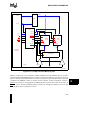
INTERNAL PROCESSOR STRUCTURE......................................................................... A-2
A.1.1
Instruction Scheduler (IS) .......................................................................................... A-3
A.1.2
Instruction Flow ......................................................................................................... A-4
A.1.3
Register File (RF) ...................................................................................................... A-6
A.1.4
Execution Unit (EU) ................................................................................................... A-7
A.1.5
Multiply/Divide Unit (MDU) ........................................................................................ A-7
A.1.6
Address Generation Unit (AGU) ................................................................................ A-7
A.1.7
Data RAM and Local Register Cache ....................................................................... A-7
A.1.8
Data Cache (80960CF Only) ..................................................................................... A-8
A.1.8.1
Data Cache Organization .................................................................................. A-8
A.1.8.2
Bus Configuration ............................................................................................. A-9
A.1.8.3
Global Control of the Cache .............................................................................. A-9
A.1.8.4
Data Fetch Policy ............................................................................................ A-10
A.1.8.5
Write Policy ..................................................................................................... A-10
A.1.8.6
Data Cache Coherency ................................................................................... A-10
A.1.8.7
BCU Pipeline and Data Cache Interaction ...................................................... A-11
A.1.8.8
BCU Queues and Cache Coherency .............................................................. A-12
A.1.8.9
DMA Operation and Data Coherency ............................................................. A-13
A.1.8.10
External I/O and Bus Masters and Cache Coherency .................................... A-13
A.2
PARALLEL INSTRUCTION PROCESSING................................................................... A-14
A.2.1
Parallel Issue ........................................................................................................... A-14
A.2.2
Parallel Execution .................................................................................................... A-15
A.2.3
Scoreboarding ......................................................................................................... A-17
A.2.3.1
Register Scoreboarding .................................................................................. A-18
A.2.3.2
Resource Scoreboarding ................................................................................ A-18
A.2.3.3
Prevention of Pipeline Stalls ........................................................................... A-18
A.2.3.4
Additional Scoreboarded Resources Due to the Data Cache ......................... A-19
A.2.4
Processing Units ..................................................................................................... A-20
A.2.4.1
Execution Unit (EU) ........................................................................................ A-20
A.2.4.2
Multiply/Divide Unit (MDU) .............................................................................. A-22
A.2.4.3
Data RAM (DR) ............................................................................................... A-24
A.2.4.4
Address Generation Unit (AGU) ..................................................................... A-25
A.2.4.5
Effective Address (efa) Calculations ............................................................... A-26
A.2.4.6
Bus Control Unit (BCU) ................................................................................... A-26
A.2.4.7
Control Pipeline ............................................................................................... A-28
A.2.4.8
Unconditional Branches .................................................................................. A-28
A.2.4.9
Conditional Branches ...................................................................................... A-32
A.2.5
Instruction Cache And Fetch Execution .................................................................. A-33
A.2.5.1
Instruction Cache Organization ....................................................................... A-33
A.2.5.2
Fetch Strategy ................................................................................................. A-34
A.2.5.3
Fetch Latency ................................................................................................. A-34
A.2.5.4
Cache Replacement ....................................................................................... A-36
A.2.6
Micro-flow Execution ............................................................................................... A-36
A.2.6.1
Invocation and Execution ................................................................................ A-37
xiii
CONTENTS
A.2.6.2
Data Movement ...............................................................................................
A.2.6.3
Bit and Bit Field ...............................................................................................
A.2.6.4
Comparison .....................................................................................................
A.2.6.5
Branch .............................................................................................................
A.2.6.6
Call and Return ...............................................................................................
A.2.6.7
Conditional Faults ...........................................................................................
A.2.6.8
Debug ..............................................................................................................
A.2.6.9
Atomic .............................................................................................................
A.2.6.10
Processor Management ..................................................................................
A.2.7
Coding Optimizations ..............................................................................................
A.2.7.1
Loads and Stores ............................................................................................
A.2.7.2
Multiplication and Division ...............................................................................
A.2.7.3
Advancing Comparisons .................................................................................
A.2.7.4
Unrolling Loops ...............................................................................................
A.2.7.5
Enabling Constant Parallel Issue ....................................................................
A.2.7.6
Alternating from Side to Side ..........................................................................
A.2.7.7
Branch Prediction ............................................................................................
A.2.7.8
Branch Target Alignment ................................................................................
A.2.7.9
Replacing Straight-Line Code and Calls .........................................................
A.2.8
Utilizing On-chip Storage .........................................................................................
A.2.8.1
Instruction Cache ............................................................................................
A.2.8.2
Data Cache (i960 CF Processor Only) ............................................................
A.2.8.3
Register Cache ...............................................................................................
A.2.8.4
Data RAM ........................................................................................................
A.2.9
Summary .................................................................................................................
A-38
A-39
A-40
A-40
A-41
A-42
A-42
A-42
A-42
A-43
A-44
A-45
A-46
A-46
A-48
A-49
A-53
A-53
A-54
A-55
A-55
A-55
A-56
A-56
A-57
APPENDIX B
BUS INTERFACE EXAMPLES
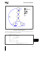
B.1
NON-PIPELINED BURST SRAM INTERFACE................................................................ B-1
B.1.1
Background ............................................................................................................... B-1
B.1.2
Implementation .......................................................................................................... B-1
B.1.3
Block Diagram ........................................................................................................... B-2
B.1.3.1
Chip Select Logic .............................................................................................. B-3
B.1.3.2
State Machine PLD ........................................................................................... B-3
B.1.3.3
Write Enable Generation Logic ......................................................................... B-3
B.1.3.4
Chip Select Generation ..................................................................................... B-3
B.1.4
Waveforms ................................................................................................................ B-4
B.1.4.1
Wait State Selection .......................................................................................... B-5
B.1.4.2
Output Enable and Write Enable Logic ............................................................. B-6
B.1.4.3
State Machine Descriptions .............................................................................. B-6
B.1.5
Trade-offs and Alternatives ..................................................................................... B-10
B.2
PIPELINED SRAM READ INTERFACE ......................................................................... B-10
B.2.1
Block Diagram ......................................................................................................... B-11
B.2.1.1
Address Latch ................................................................................................. B-12
B.2.1.2
State Machine PLD ......................................................................................... B-12
B.2.1.3
Write Enable Logic .......................................................................................... B-12
xiv
CONTENTS
B.2.2
Waveforms ..............................................................................................................
B.2.2.1
State Machines ...............................................................................................
B.2.3
Trade-offs and Alternatives .....................................................................................
B.3
INTERFACING TO DYNAMIC RAM...............................................................................
B.3.1
DRAM Access Modes .............................................................................................
B.3.1.1
Nibble Mode DRAM ........................................................................................
B.3.1.2
Fast Page Mode DRAM ..................................................................................
B.3.1.3
Static Column Mode DRAM ............................................................................
B.3.2
DRAM Refresh Modes ............................................................................................
B.3.3
Address Multiplexer Input Connections ...................................................................
B.3.4
Series Damping Resistors .......................................................................................
B.3.5
System Loading .......................................................................................................
B.3.6
Design Example: Burst DRAM with Distributed RAS Only Refresh Using DMA .....
B.3.7
DRAM Address Generation .....................................................................................
B.3.8
DRAM Controller State Machine .............................................................................
B.3.9
DRAM Refresh Request and Timer Logic ...............................................................
B.3.10 DMA Programming for Refresh ...............................................................................
B.3.11 Memory Ready ........................................................................................................
B.3.12 Region Table Programming ....................................................................................
B.3.13 Design Example: Burst DRAM with Distributed CAS-Before-RAS Refresh
Using READY Control .............................................................................................
B.3.14 DRAM Controller State Machine .............................................................................
B.4
INTERLEAVED MEMORY SYSTEMS ...........................................................................
B.5
INTERFACING TO SLOW PERIPHERALS USING THE INTERNAL
WAIT STATE GENERATOR ..........................................................................................
B.5.1
Implementation ........................................................................................................
B.5.2
Schematic ................................................................................................................
B.5.3
Waveforms ..............................................................................................................
B-13
B-13
B-15
B-15
B-15
B-16
B-17
B-18
B-18
B-20
B-20
B-21
B-21
B-23
B-25
B-28
B-29
B-29
B-29
B-32
B-33
B-37
B-41
B-41
B-41
B-43
APPENDIX C
CONSIDERATIONS FOR WRITING PORTABLE CODE
C.1
CORE ARCHITECTURE ..................................................................................................
C.2
ADDRESS SPACE RESTRICTIONS ...............................................................................
C.2.1
Reserved Memory .....................................................................................................
C.2.2
Internal Data RAM .....................................................................................................
C.2.3
Instruction Cache ......................................................................................................
C.2.4
Data Cache (80960CF Processor Only) ....................................................................
C.2.5
Data and Data Structure Alignment ...........................................................................
C.3
RESERVED LOCATIONS IN REGISTERS AND DATA STRUCTURES .........................
C.4
INSTRUCTION SET .........................................................................................................
C.4.1
Instruction Timing ......................................................................................................
C.4.2
Implementation-Specific Instructions .........................................................................
C.5
EXTENDED REGISTER SET...........................................................................................
C.6
INITIALIZATION ...............................................................................................................
C-1
C-2
C-2
C-2
C-2
C-3
C-3
C-4
C-4
C-4
C-4
C-5
C-5
xv
CONTENTS
C.7
INTERRUPTS .................................................................................................................
C.8
OTHER i960 CA/CF PROCESSOR IMPLEMENTATION-SPECIFIC FEATURES..........
C.8.1
Data Control Peripheral Units ...................................................................................
C.8.2
Fault Implementation ................................................................................................
C.9
BREAKPOINTS ...............................................................................................................
C.10 LOCK PIN ........................................................................................................................
C.10.1 External System Requirements ................................................................................
C-5
C-6
C-6
C-6
C-6
C-6
C-6
APPENDIX D
MACHINE-LEVEL INSTRUCTION FORMATS
D.1
GENERAL INSTRUCTION FORMAT..............................................................................
D.2
REG FORMAT.................................................................................................................
D.3
COBR FORMAT ..............................................................................................................
D.4
CTRL FORMAT ...............................................................................................................
D.5
MEM FORMAT ................................................................................................................
D.5.1
MEMA Format Addressing ........................................................................................
D.5.2
MEMB Format Addressing ........................................................................................
D-1
D-1
D-3
D-3
D-3
D-4
D-5
APPENDIX E
MACHINE LANGUAGE INSTRUCTION REFERENCE
E.1
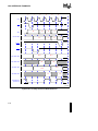
INSTRUCTION REFERENCE BY OPCODE.................................................................... E-1
APPENDIX F
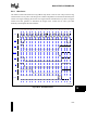
REGISTER AND DATA STRUCTURES
F.1
Data Structures ................................................................................................................ F-2
F.2
Registers ........................................................................................................................ F-10
GLOSSARY
INDEX
xvi
CONTENTS
FIGURES
Figure 1-1
Figure 2-1
Figure 2-2
Figure 2-3
Figure 2-4
Figure 2-5
Figure 2-6
Figure 3-1
Figure 3-2
Figure 4-1
Figure 4-2
Figure 5-1
Figure 5-2
Figure 5-3
Figure 5-4
Figure 5-5
Figure 6-1
Figure 6-2
Figure 6-3
Figure 6-4
Figure 7-1
Figure 7-2
Figure 7-3
Figure 7-4
Figure 7-5
Figure 8-1
Figure 8-2
Figure 8-3
Figure 8-4
Figure 10-1
Figure 10-2
Figure 10-3
Figure 10-4
Figure 10-5
Figure 10-6
Figure 11-1
Figure 11-2
Figure 11-3
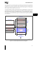
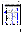
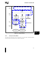
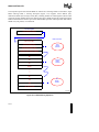
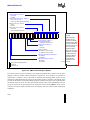
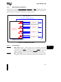
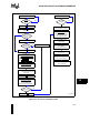
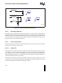
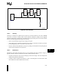
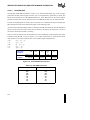
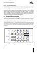
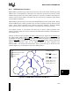
i960® CA/CF Superscalar Microprocessor Architecture ....................................... 1-2
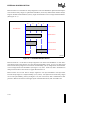
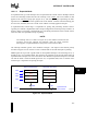
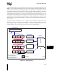
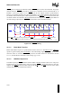
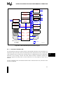
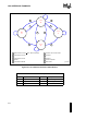
i960® Cx Microprocessor Programming Environment .......................................... 2-2
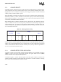
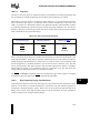
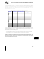
Control Table ........................................................................................................ 2-7
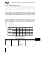
Address Space ..................................................................................................... 2-9
Arithmetic Controls (AC) Register....................................................................... 2-15
Process Controls (PC) Register ......................................................................... 2-18
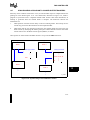
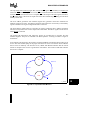
Example Application of the User-Supervisor Protection Model .......................... 2-22
Data Types and Ranges....................................................................................... 3-1
Data Placement in Registers ................................................................................ 3-5
Machine-Level Instruction Formats ...................................................................... 4-3
Source Operands for sysctl ............................................................................... 4-20
Procedure Stack Structure and Local Registers................................................... 5-3
Frame Spill ........................................................................................................... 5-7
Frame Fill.............................................................................................................. 5-8
System Procedure Table .................................................................................... 5-13
Previous Frame Pointer Register (PFP) (r0)....................................................... 5-16
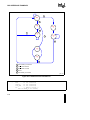
Interrupt Handling Data Structures ....................................................................... 6-2
Interrupt Table ...................................................................................................... 6-4
Storage of an Interrupt Record on the Interrupt Stack........................................ 6-10
Flowchart for Worst Case Interrupt Latency ....................................................... 6-14
Fault-Handling Data Structures ............................................................................ 7-1
Fault Table and Fault Table Entries ..................................................................... 7-5
Fault Record ......................................................................................................... 7-7
Storage of the Fault Record on the Stack ............................................................ 7-8
Fault Record for Parallel Faults .......................................................................... 7-11
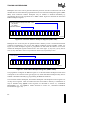
Trace Controls (TC) Register ............................................................................... 8-2
Instruction Address Breakpoint Registers (IPB0 - IPB1) ...................................... 8-6
Data Address Breakpoint Registers (DAB0 - DAB1) ............................................ 8-6
Hardware Breakpoint Control Register (BPCON)................................................. 8-7
MCON 0-15 Registers Configure External Memory............................................ 10-6
Memory Region Configuration Register (MCON 0-15) ....................................... 10-7
Bus Configuration Register (BCON) ................................................................... 10-8
Summary of Aligned-Unaligned Transfers for Little Endian Regions................ 10-11
Summary of Aligned-Unaligned Transfers for Little Endian Regions (cont) ..... 10-12
Bus Controller Block Diagram .......................................................................... 10-14
Internal Programmable Wait States.................................................................... 11-6
Quad-word Read from 32-bit Non-burst Memory ............................................... 11-8
Bus Request with READY and BTERM Control ................................................. 11-9
xvii
CONTENTS
Figure 11-4
Figure 11-5
Figure 11-6
Figure 11-7
Figure 11-8
Figure 11-9
Figure 11-10
Figure 11-11
Figure 11-12
Figure 11-13
Figure 11-14
Figure 11-15
Figure 11-16
Figure 11-17
Figure 11-18
Figure 11-19
Figure 12-1
Figure 12-2
Figure 12-3
Figure 12-4
Figure 12-5
Figure 12-6
Figure 12-7
Figure 12-8
Figure 12-9
Figure 13-1
Figure 13-2
Figure 13-3
Figure 13-4
Figure 13-5
Figure 13-6
Figure 13-7
Figure 13-8
Figure 13-9
Figure 13-10
Figure 13-11
Figure 13-12
Figure 13-13
Figure 13-14
xviii
Data Width and Byte Enable Encodings 11-10
Basic Read Request, Non-Pipelined, Non-Burst, Wait-States 11-12
Read / Write Requests, Non-Pipelined, Non-Burst, No Wait States 11-14
32-Bit-Wide Data Bus Bursts 11-16
16-Bit Wide Data Bus Bursts 11-17
8-Bit Wide Data Bus Bursts 11-17
32-Bit Bus, Burst, Non-Pipelined, Read Request with Wait States 11-19
32-Bit Bus, Burst, Non-Pipelined, Write Request without Wait States 11-20
Pipelined Read Memory System 11-21
Non-Burst Pipelined Read Waveform 11-22
Burst Pipelined Read Waveform 11-23
Pipelined to Non-Pipelined Transitions 11-24
The LOCK Signal 11-27
HOLD/HOLDA Bus Arbitration 11-29
Operation of the Bus Backoff Function 11-31
Example Application of the Bus Backoff Function 11-32
Interrupt Controller 12-3
Dedicated Mode 12-4
Expanded Mode 12-5
Implementation of Expanded Mode Sources 12-6
Interrupt Sampling 12-10
Interrupt Control (ICON) Register 12-11
Interrupt Mapping (IMAP0-IMAP2) Registers 12-13
Interrupt Mask (IMSK) and Interrupt Pending (IPND) Registers 12-15
Calculation of Worst Case Interrupt Latency - NL_int 12-19
Source Data Buffering for Destination Synchronized DMAs 13-5
Example of Source Synchronized Fly-by DMA 13-6
Source Synchronized DMA Loads from an 8-bit, Non-burst,
Non-pipelined Memory Region 13-7
Byte to Word Assembly 13-9
Optimization of an Unaligned DMA 13-13
DMA Chaining Operation 13-14
Source Chaining 13-15
Synchronizing to Chained Buffer Transfers 13-17
DMA Command Register (DMAC) 13-22
Setup DMA (sdma) Instruction Operands 13-25
DMA Control Word 13-26
DMA Data RAM 13-28
DMA External Interface 13-30
DMA Request and Acknowledge Timing 13-32
CONTENTS
Figure 13-15
Figure 13-16
Figure 13-17
Figure 14-1
Figure 14-2
Figure 14-3
Figure 14-4
Figure 14-5
Figure 14-6
Figure 14-7
Figure 14-8
Figure 14-9
Figure A-1
Figure A-2
Figure A-3
Figure A-4
Figure A-5
Figure A-6
Figure A-7
Figure A-8
Figure A-9
Figure A-10
Figure A-11
Figure A-12
Figure A-13
Figure A-14
Figure A-15
Figure A-16
Figure A-17
Figure A-18
Figure A-19
Figure B-1
Figure B-2
Figure B-3
Figure B-4
Figure B-5
Figure B-6
Figure B-7
Figure B-8
Figure B-9
EOP3:0 Timing ................................................................................................. 13-33
DMA and User Requests in the Bus Queue ..................................................... 13-36
DMA Throughput and Latency.......................................................................... 13-38
FAIL Timing ........................................................................................................ 14-4
Initial Memory Image (IMI) and Process Control Block (PRCB) ......................... 14-6
Process Control Block Configuration Words....................................................... 14-9
Processor Initialization Flow ............................................................................. 14-13
VCCPLL Lowpass Filter...................................................................................... 14-27
Reducing Characteristic Impedance................................................................. 14-28
Series Termination ........................................................................................... 14-30
AC Termination................................................................................................. 14-31
Avoid Closed-Loop Signal Paths ...................................................................... 14-32
C-Series Core and Peripherals............................................................................. A-1
i960 CA/CF Microprocessor Block Diagram ......................................................... A-3
Instruction Pipeline ............................................................................................... A-4
Six-Port Register File............................................................................................ A-6
Data Cache Organization ..................................................................................... A-8
BCU and Data Cache Interaction ....................................................................... A-11
Issue Paths ......................................................................................................... A-16
EU Execution Pipeline ........................................................................................ A-21
MDU Execution Pipeline ..................................................................................... A-22
MDU Pipelined Back-To-Back Operations.......................................................... A-23
Data RAM Execution Pipeline ............................................................................ A-24
The lda Pipeline ................................................................................................. A-25
Back-to-Back BCU Accesses ............................................................................. A-28
CTRL Pipeline for Branches to Branches ........................................................... A-29
Branch in First Executable Group....................................................................... A-30
Branch in Second Executable Group ................................................................. A-31
Branch in Third Executable Group ..................................................................... A-32
Fetch Execution .................................................................................................. A-36
Micro-flow Invocation .......................................................................................... A-38
Non-Pipelined Burst SRAM Interface ................................................................... B-2
Non-Pipelined SRAM Read Waveform................................................................. B-4
Non-Pipelined SRAM Write Waveform ................................................................. B-5
Chip Enable State Machine .................................................................................. B-7
A3:2 Address Generation State Machine ............................................................. B-8
Pipelined Read Address and Data ..................................................................... B-10
Pipelined SRAM Interface Block Diagram .......................................................... B-11
Pipelined Read Waveform .................................................................................. B-13
Pipelined Read Chip Enable State Machine....................................................... B-13
xix
CONTENTS
Figure B-10
Figure B-11
Figure B-12
Figure B-13
Figure B-14
Figure B-15
Figure B-16
Figure B-17
Figure B-18
Figure B-19
Figure B-20
Figure B-21
Figure B-22
Figure B-23
Figure B-24
Figure B-25
Figure B-26
Figure B-27
Figure B-28
Figure B-29
Figure B-30
Figure B-31
Figure B-32
Figure D-1
Figure F-1
Figure F-2
Figure F-3
Figure F-4
Figure F-5
Figure F-6
Figure F-7
Figure F-8
Figure F-9
Figure F-10
Figure F-11
Figure F-12
Figure F-13
Figure F-14
Figure F-15
Figure F-16
xx
Pipelined Read PA3:2 State Machine Diagram B-14
Nibble Mode Read B-16
Fast Page Mode DRAM Read B-17
Static Column Mode DRAM Read B-18
RAS-only DRAM Refresh B-19
CAS-before-RAS DRAM Refresh B-19
Address Multiplexer Inputs B-20
DRAM System with DMA Refresh B-22
DRAM Address Generation State Machine B-23
DRAM Controller State Machine B-26
DMA Request and Acknowledge Signals B-28
DMA Chaining Description B-29
DRAM System Read Waveform B-30
DRAM System Write Waveform B-31
Memory System Block Diagram B-32
DRAM State Machine B-34
Two-Way Interleaved Read Access Overlap B-37
Two-Way Interleaved Memory System B-39
Two-Way Interleaved Read Waveforms B-40
8-bit Interface Schematic B-42
Read Waveforms B-43
Write Waveforms B-44
State Machine Diagram B-45
Instruction Formats D-2
Control Table F-2
Fault Record F-3
Fault Table and Fault Table Entries F-4
Initial Memory Image (IMI) and Process Control Block (PRCB) F-5
Storage of an Interrupt Record on the Interrupt Stack F-6
Interrupt Table F-7
Procedure Stack Structure and Local Registers F-8
System Procedure Table F-9
Arithmetic Controls Register (AC) F-10
Bus Configuration Register (BCON) F-10
Data Address Breakpoint Registers F-11
DMA Command Register (DMAC) F-11
DMA Control Word F-12
Hardware Breakpoint Control Register (BPCON) F-13
Instruction Address Breakpoint Registers (IPB0 - IPB1) F-13
Interrupt Control (ICON) Register F-14
CONTENTS
Figure F-17
Figure F-18
Figure F-19
Figure F-20
Figure F-21
Figure F-22
Figure F-23
Interrupt Map (IMAP0 - IMAP2) Registers ..........................................................
Interrupt Mask (IMSK) and Interrupt Pending (IPND) Registers.........................
Memory Region Configuration Register (MCON 0-15) .......................................
Previous Frame Pointer Register (PFP) (r0).......................................................
Process Controls (PC) Register .........................................................................
Trace Controls (TC) Register .............................................................................
Process Control Block Configuration Words.......................................................
F-15
F-16
F-17
F-18
F-18
F-19
F-20
xxi
CONTENTS
TABLES
Table 1-1
Table 2-1
Table 2-2
Table 2-3
Table 2-4
Table 2-5
Table 2-6
Table 2-7
Table 2-8
Table 3-1
Table 3-2
Table 3-3
Table 3-4
Table 3-5
Table 4-1
Table 4-2
Table 4-3
Table 4-4
Table 4-5
Table 5-1
Table 5-2
Table 5-3
Table 7-1
Table 7-2
Table 9-1
Table 9-2
Table 9-3
Table 9-4
Table 9-5
Table 10-1
Table 10-2
Table 11-1
Table 11-2
Table 11-3
Table 11-4
Table 12-1
Table 12-2
Table 13-1
Table 13-2
xxii
Register Terminology Conventions ...................................................................... 1-8
Registers and Literals Used as Instruction Operands .......................................... 2-3
Allowable Register Operands ............................................................................... 2-6
Data Structure Descriptions.................................................................................. 2-8
Alignment of Data Structures in the Address Space .......................................... 2-11
Condition Codes for True or False Conditions ................................................... 2-16
Condition Codes for Equality and Inequality Conditions..................................... 2-16
Condition Codes for Carry Out and Overflow ..................................................... 2-17
Supervisor-Only Operations and Faults Generated in User Mode ..................... 2-21
Supported Integer Sizes ....................................................................................... 3-2
Supported Ordinal Sizes....................................................................................... 3-3
Memory Contents For Little and Big Endian Example .......................................... 3-5
Byte Ordering for Little and Big Endian Accesses ................................................ 3-5
Memory Addressing Modes .................................................................................. 3-6
i960® Cx Microprocessor Instruction Set Summary ............................................. 4-4
Arithmetic Operations ........................................................................................... 4-7
System Control Message Types and Operand Fields ........................................ 4-20
Cache Configuration Modes ............................................................................... 4-22
Control Register Table and Register Group Numbers........................................ 4-24
PRCB Cache Configuration Word and Internal Data RAM................................... 5-9
Encodings of Entry Type Field in System Procedure Table ............................... 5-14
Encoding of Return Status Field ......................................................................... 5-17
i960® Cx Processor Fault Types and Subtypes ................................................... 7-3
Fault Flags or Masks .......................................................................................... 7-15
Abbreviations in Pseudo-code .............................................................................. 9-5
Pseudo-code Symbol Definitions.......................................................................... 9-6
Fault Types and Subtypes .................................................................................... 9-6
Common Possible Faulting Conditions................................................................. 9-7
Cache Configuration Modes ............................................................................... 9-79
MCON0-15 Programmable Bits .......................................................................... 10-8
BCON Register Bit Definitions ............................................................................ 10-9
Bus Controller Pins ............................................................................................. 11-3
Byte Enable Encoding ...................................................................................... 11-11
Burst Transfers and Bus Widths ....................................................................... 11-15
Byte Ordering on Bus Transfers ....................................................................... 11-26
Location of Cached Vectors in Internal RAM.................................................... 12-20
Cache Configuration Modes ............................................................................. 12-22
Transfer Type Options ........................................................................................ 13-4
DMA Configuration and Byte Count Alignment ................................................ 13-10
CONTENTS
Table 13-3
Table 13-4
Table 13-5
Table 13-6
Table 13-7
Table 13-8
Table 14-1
Table 14-2
Table 14-3
Table A-1
Table A-2
Table 1-3
Table A-4
Table A-5
Table A-6
Table A-7
Table A-8
Table A-9
Table A-10
Table A-11
Table A-12
Table A-13
Table A-15
Table A-14
Table A-16
Table A-17
Table A-18
Table A-19
Table A-20
Table A-21
Table D-1
Table D-2
Table D-3
Table E-1
Table E-2
Table E-3
Table E-4
Table E-5
DMA Transfer Alignment Requirements 13-11
Rotating Channel Priority 13-20
DMA Transfer Clocks - NXFER 13-39
Base Values of Worst-case DMA Throughput used for
DMA Latency Calculation 13-42
DMA Latency Components 13-43
Values of DMA Latency Components 13-43
Pin Reset State 14-3
Register Values After Reset 14-3
i960® Cx Processor Input Pins 14-29
BCU Instructions for the i960 CF Processor A-12
Machine Type Sequences Which Can Be Issued In Parallel A-16
Scoreboarded Register Conditions A-18
Scoreboarded Resource Conditions A-19
Scoreboarded Resource Conditions Due to the Data Cache A-20
EU Instructions A-21
MDU Instructions A-23
Data RAM Instructions A-24
AGU Instructions A-25
BCU Instructions for the i960 CA Processor A-27
CTRL Instructions A-29
Cache Configuration Modes A-34
Fetch Strategy A-34
Store Micro-flow Instruction Issue Clocks A-39
Load Micro-flow Instruction Issue Clocks A-39
Bit and Bit Field Micro-flow Instructions A-40
bx and balx Performance A-40
callx Performance A-41
sysctl Performance A-43
Creative Uses for the lda Instruction A-49
Code Optimization Summary A-57
Encoding of SRC/DST Field in REG Format D-2
Addressing Modes for MEM Format Instructions D-4
Encoding of Scale Field D-5
Miscellaneous Instruction Encoding Bits E-1
REG Format Instruction Encodings E-2
COBR Format Instruction Encodings E-4
CTRL Format Instruction Encodings E-5
MEM Format Instruction Encodings E-6
xxiii
1
INTRODUCTION
CHAPTER 1
INTRODUCTION
The i960® CA and CF superscalar microprocessors represent Intel's commitment to provide a
spectrum of reliable, cost-effective, high-performance processors that satisfy the requirements of
today's innovative microprocessor-based products. The i960 Cx1 processors are designed for applications which require greater performance on a single chip than is usually found in an entire
embedded system. The sheer speed of the i960 Cx processors enriches traditional embedded applications and makes many new functions possible at a reduced cost. These embedded processors are
versatile; they are found in diverse products such as laser printers, X-terminals, bridges, routers,
PC add-in cards and server motherboards.
Figure 1-1 identifies the processors’ most notable features, including the multiple-instruction per
clock C-series core, two-way set associative instruction cache, programmable register cache, onchip data RAM, multi-mode programmable bus controller for its demultiplexed bus, four-channel
59 Mbyte per second DMA controller and high-speed interrupt controller.
1.1
i960® MICROPROCESSOR ARCHITECTURE
The i960 architecture provides a high-performance computing model. The architecture profits
from reduced instruction set computer (RISC) concepts and — through superscalar implementations — includes refinements for execution of more than one instruction per clock. The architecture provides a high-speed procedure call/return model, a powerful instruction set suited to
parallelism and integrated interrupt- and fault-handling models appropriate in a parallel execution
environment.
1.1.1
Parallel Instruction Execution
To sustain execution of multiple instructions in each clock cycle, a processor must decode multiple
instructions in parallel and simultaneously issue these instructions to parallel processing units. The
various processing units must then be able to independently access instruction operands in parallel
from a common register set.
The on-chip instruction cache enables parallel decode by constantly providing the next four
unexecuted instructions to the processor's instruction scheduler. In a single clock cycle, the
scheduler inspects all four instructions and issues one, two or three of these instructions in the
same clock cycle.
1. Throughout this manual, “Cx” refers to both the i960 CA and CF microprocessors. Information that is specific to each is
clearly indicated.
1-1
1
INTRODUCTION
Four-Channel
DMA Port
DMA Controller
Instruction
Prefetch Queue
Instruction Cache*
(Two-Way
Set Associative)
128-Bit Cache Bus
Interrupt
Programmable
Port Interrupt Controller
Parallel
Instruction
Scheduler
Multiply/Divide
Unit
Execution
Unit
Register-Side
Machine Bus
Memory-Side
Machine Bus
Memory Region
Configuration
Bus
Controller
Bus Request
Queues
Control
Address
Data
1 Kbyte
Direct Mapped
Data Cache
1 Kbyte
Data RAM
5 to 15 Sets
Register Cache
Six-Port
Register File
64-Bit
SRC1 Bus
32-Bit
Base Bus
64-Bit
SRC2 Bus
128-Bit
Load Bus
64-Bit
DST Bus
128-Bit
Store Bus
Note: Instruction Cache Size
CA = 1 Kbyte
CF = 4 Kbyte
Address
Generation Unit
F_CF001A
= CF Only
Figure 1-1. i960® CA/CF Superscalar Microprocessor Architecture
Parallel decode also speeds conditional operations such as branches. These instructions are
decoded and executed ahead of the current instruction pointer while maintaining the logical
control flow of the sequential program.
Once the scheduler issues an instruction or group of instructions, one of six parallel processing
units begins to execute each instruction. Each parallel unit handles a different subset of the
instruction set, enabling multiple instructions to be issued and executed every clock cycle. Each
unit executes its instructions in parallel with other processor operations.
The i960 Cx processors’ 32 general-purpose 32-bit registers are each six-ported to allow
unimpeded parallel access to independent processing units. To maintain the logical integrity of
sequential instructions which are being executed in parallel, the processor implements register
scoreboarding and resource scoreboarding interlocks.
1-2
INTRODUCTION
The superscalar i960 Cx processors can decode multiple instructions at once and issue them to
independent processing units where they are executed in parallel. As a result, the processors
deliver sustained execution of multiple instructions per clock from a sequential instruction stream.
1.1.2
Full Procedure Call Model
These processors support two types of procedure calls: an integrated call-and-return mechanism
and a RISC-style branch-and-link instruction. The integrated call-and-return mechanism automatically saves local registers when a call instruction executes and restores them when a ret (return)
instruction executes. The RISC-style branch-and-link is a fast call that does not save any of the
registers. These mechanisms result in high performance and reduced code size, while maintaining
assembly-level compatibility.
To attain the highest performance for procedure calls and returns, the processors integrate a
programmable depth register cache. The register cache internally saves the local registers for
procedure calls, rather than actually writing the data to the external procedure stack. This caching
greatly reduces the external bus traffic associated with procedure context saving and restoring.
1.1.3
Versatile Instruction Set and Addressing
The i960 Cx microprocessors offer a full set of load, store, move, arithmetic, shift, comparison and
branch instructions and support operations on both integer and ordinal data types. They also
provide a complete set of Boolean and bit-field instructions to simplify manipulation of bits and bit
strings.
Most instructions are typical RISC operations. However, several commonly used complex instructions are also part of the instruction set. Performance is optimized by implementing these
commonly used functions with parallel hardware. For instance, the 32x32 multiply operation — a
single instruction — takes less than five clocks to execute: 150 ns or less at 33 MHz. Furthermore,
the multiplier is a parallel unit; this allows instructions that follow a multiply to execute before the
multiplication is complete. In fact, if several unrelated instructions follow a multiply, the multiplication consumes only one clock of execution.
1.1.4
Integrated Priority Interrupt Model
The i960 Cx microprocessors provide a priority-based mechanism for servicing interrupts. The
mechanism transparently manages up to 248 distinct sources with 31 levels of priority. Interrupt
requests may be generated from external hardware, internal hardware or software.
The interrupt mechanism is managed by hardware which operates in parallel with program
execution. This reduces interrupt latency and overhead and provides flexible interrupt handling
control.
1-3
1
INTRODUCTION
1.1.5
Complete Fault Handling and Debug Capabilities
To aid in program development, the i960 Cx processors detect faults (exceptions). When a fault is
detected, the processors make an implicit call to a fault handling routine. Information collected for
each fault allows a program developer to quickly correct faulting code. The processors also allow
automatic recovery from most faults.
To support system debug, the i960 architecture provides a mechanism for monitoring processor
activities through a software tracing facility. The i960 Cx processors can be configured to detect as
many as seven different trace events, including breakpoints, branches, calls, supervisor calls,
returns, prereturns and the execution of each instruction (for single-stepping through a program).
The processors also provide four breakpoint registers that allow break decisions to be made based
upon instruction or data addresses.
1.2
SYSTEM INTEGRATION
The i960 Cx microprocessors are based on the C-series core, which is object code compatible with
the 32-bit i960 microprocessor core architecture. Additionally, the i960 Cx devices integrate three
peripherals around the core: bus control unit, DMA controller and interrupt controller.
1.2.1
Pipelined Burst Bus Control Unit
The i960 Cx processors integrate a 32-bit high-performance bus controller for interfacing to
external memory and peripherals. The bus control unit incorporates full wait state logic and bus
width control to provide high system performance with minimal system design complexity. The
bus control unit features a maximum transfer rate of 132 Mbytes per second (at 33 MHz).
Internally programmable wait states and 16 separately configurable memory regions allow the
processor to interface with a variety of memory subsystems with minimum complexity and
maximum performance.
1.2.2
Flexible DMA Controller
A four-channel DMA controller provides high-speed DMA data transfers. Source and destination
can be any combination of internal RAM, external memory or peripherals. DMA channels
perform single-cycle or multi-cycle transfers and can perform data packing and unpacking
between peripherals and memory with varying bus widths. Also provided are block transfers, in
addition to source- or destination-synchronized transfers.
The DMA supports various transfer types such as high speed fly-by, quad-word transfers and data
chaining with the use of linked descriptor lists. The high performance fly-by mode is capable of
transfer speeds of up to 59 Mbytes per second at 33 MHz.
1-4
INTRODUCTION
1.2.3
Priority Interrupt Controller
1
The interrupt controller provides full programmability of 248 interrupt sources into 31 priority
levels. The interrupt controller handles prioritization of software interrupts, hardware interrupts
and process priority. In addition, it also manages four internal sources from the DMA controller
and a single non-maskable interrupt input.
1.3
ABOUT THIS MANUAL
This i960® CA/CF Microprocessor User’s Manual provides detailed programming and hardware
design information for the i960 Cx microprocessors. It is written for programmers and hardware
designers who understand the basic operating principles of microprocessors and their systems.
This manual does not provide electrical specifications such as DC and AC parametrics, operating
conditions and packaging specifications. Such information is found in the 80960CA/CF microprocessor data sheets (80960CA order number is 270727; 80960CF is 272187). To obtain updates and
errata, call Intel’s FaxBack data-on-demand system (1-800-628-2283 or 916-356-3105).
For information on other i960 processor family products or the architecture in general, refer to
Intel's Solutions960® catalog (order number is 270791). It lists all current i960 microprocessor
family-related documents, support components, boards, software development tools, debug tools
and more. Other information can be obtained from Intel’s technical BBS (916-356-3600).
This manual is organized in three parts; each part comprises multiple chapters and/or appendices.
The following briefly describes each part:
•
Part I - Programming the i960 Cx Microprocessor (Chapters 2-9) details the programming
environment for the i960 Cx devices. Described here are the processor's registers, instruction
set, data types, addressing modes, interrupt mechanism, external interrupt interface and fault
mechanism.
•
Part II - System Implementation (Chapters 10-14) identifies requirements for designing a
system around the i960 Cx components, such as external bus interface, interrupt controller and
integrated DMA controller. Also described are programming requirements for the DMA
controller, bus controller and processor initialization.
•
Part III - Appendices includes quick references for hardware design and programming.
Appendices are also provided which describe the internal architecture, how to write assemblylevel code to exploit the parallelism of the processor and considerations for writing software
which is portable among all members of the i960 microprocessor family.
1-5
INTRODUCTION
1.4
NOTATION AND TERMINOLOGY
This section defines terminology and textual conventions that are used throughout the manual.
1.4.1
Reserved and Preserved
Certain fields in registers and data structures are described as being either reserved or preserved:
•
A reserved field is one that may be used by other i960 architecture implementations. Correct
treatment of reserved fields ensures software compatibility with other i960 processors. The
processor uses these fields for temporary storage; as a result, the fields sometimes contain
unusual values.
•
A preserved field is one that the processor does not use. Software may use preserved fields for
any function.
Reserved fields in certain data structures should be set to 0 (zero) when the data structure is
created. Set reserved fields to 0 when creating the Control Table, Initialization Boot Record,
Interrupt Table, Fault Table, System Procedure Table and Process Control Block. Software should
not modify or rely on these reserved field values after a data structure is created. When the
processor creates the Interrupt or Fault Record data structure on the stack, software should not
depend on the value of the reserved fields within these data structures.
Some bits or fields in data structures and registers are shown as requiring specific encoding. These
fields should be treated as if they were reserved fields. They should be set to the specified value
when the data structure is created or when the register is initialized and software should not
modify or rely on the value after that.
Reserved bits in the Special Function Registers and Arithmetic Controls (AC) register can be set
to 0 after initialization to ensure compatibility with future implementations. Reserved bits in the
Process Controls (PC) register and Trace Controls (TC) register should not be initialized.
When the AC, PC and TC registers are modified using modac, modpc or modtc instructions, the
reserved locations in these registers must be masked.
Certain areas of memory may be referred to as reserved memory in this reference manual.
Reserved — when referring to memory locations — implies that an implementation of the i960
architecture may use this memory for some special purpose. For example, memory-mapped
peripherals would be located in reserved memory areas on future implementations. Programs may
use reserved memory just like any other memory unless it is specifically documented otherwise.
The i960 Cx processors’ Initialization Boot Record must be located in reserved memory at address
FFFF FF00H. System designers typically map the entire boot ROM into the reserved memory to
reduce the complexity of the select decoding.
1-6
INTRODUCTION
1.4.2
Specifying Bit and Signal Values
1
The terms set and clear in this manual refer to bit values in register and data structures. If a bit is
set, its value is 1; if the bit is clear, its value is 0. Likewise, setting a bit means giving it a value of
1 and clearing a bit means giving it a value of 0.
The terms assert and deassert refer to the logically active or inactive value of a signal or bit,
respectively. A signal is specified as an active 0 signal by an overbar. For example, the input is
active low and is asserted by driving the signal to a logic 0 value.
1.4.3
Representing Numbers
All numbers in this manual can be assumed to be base 10 unless designated otherwise. In text,
binary numbers are sometimes designated with a subscript 2 (for example, 0012). If it is obvious
from the context that a number is a binary number, the “2” subscript may be omitted.
Hexadecimal numbers are designated in text with the suffix H (for example, FFFF FF5AH). In
pseudo-code action statements in the instruction reference section and occasionally in text,
hexadecimal numbers are represented by adding the C-language convention “0x” as a prefix. For
example “FF7AH” appears as “0xFF7A” in the pseudo-code.
1.4.4
Register Names
Special function registers and several of the global and local registers are referred to by their
generic register names, as well as descriptive names which describe their function. The global
register numbers are g0 through g15; local register numbers are r0 through r15; special function
registers are sf0, sf1 and sf2. However, when programming the registers in user-generated code,
make sure to use the instruction operand. i960 microprocessor compilers recognize only the
instruction operands listed in Table 1-1. Throughout this manual, the registers’ descriptive names,
numbers, operands and acronyms are used interchangeably, as dictated by context.
Groups of bits and single bits in registers and control words are called either bits, flags or fields.
These terms have a distinct meaning in this manual:
bit
Controls a processor function; programmed by the user.
flag
Indicates status. Generally set by the processor; certain flags are user programmable.
field
A grouping of bits (bit field) or flags (flag field).
1-7
INTRODUCTION
Table 1-1. Register Terminology Conventions
Register Descriptive Name
Global Registers
Frame Pointer
Register Number
Instruction
Operand
g0 - g15
g0 - g14
Acronym
g15
fp
r0 - r15
r3 - r15
Previous Frame Pointer
r0
pfp
PFP
Stack Pointer
r1
sp
SP
Local Registers
Return Instruction Pointer
FP
r2
rip
RIP
Interrupt Pending Register
sf0
sf0
IPND
Interrupt Mask Register
sf1
sf1
IMSK
DMA Command Register
sf2
sf2
DMAC
Specific bits, flags and fields in registers and control words are usually referred to by a register
abbreviation (in upper case) followed by a bit, flag or field name (in lower case). These items are
separated with a period. A position number designates individual bits in a field. For example, the
return type (rt) field in the previous frame pointer (PFP) register is designated as “PFP.rt”. The
least significant bit of the return type field is then designated as “PFP.rt0”.
1-8
2
PROGRAMMING
ENVIRONMENT
CHAPTER 2
PROGRAMMING ENVIRONMENT
2
This chapter describes the i960® Cx microprocessors’ programming environment including global
and local registers, special function registers, control registers, literals, processor-state registers
and address space.
2.1
OVERVIEW
The i960 architecture defines a programming environment for program execution, data storage and
data manipulation. Figure 2-1 shows the programming environment elements which include a
4 Gbyte (232 byte) flat address space, an instruction cache, global and local general-purpose
registers, a set of literals, special function registers, control registers and a set of processor state
registers. A register cache saves the 16 procedure-specific local registers.
The processor defines several data structures located in memory as part of the programming
environment. These data structures handle procedure calls, interrupts and faults and provide
configuration information at initialization. These data structures are:
2.2
•
interrupt stack
•
control table
•
system procedure table
•
local stack
•
fault table
•
process control block
•
supervisor stack
•
interrupt table
•
initialization boot record
REGISTERS AND LITERALS AS INSTRUCTION OPERANDS
The i960 Cx processors use only simple load and store instructions to access memory; all
operations take place at the register level. The processors use 16 global registers, 16 local registers,
three special function registers and 32 literals (constants 0-31) as instruction operands.
The global register numbers are g0 through g15; local register numbers are r0 through r15; special
function registers are sf0, sf1 and sf2. Several of these registers are used for a dedicated function.
For example, register r0 is the previous frame pointer, sometimes referred to as pfp. Some
assemblers and compilers only recognize one form of a register operand. i960 processor compilers
recognize only the instruction operands listed in Table 2-1. Throughout this manual, the registers’
descriptive names, numbers, operands and acronyms are used interchangeably, as dictated by
context.
2-1
PROGRAMMING ENVIRONMENT
FFFF FFFFH
0000 0000H
Address Space
Architecturally
Defined
Data Structures
Fetch
Load
Store
Instruction
Cache
Instruction
Stream
Instruction
Execution
Processor State
Registers
Instruction
Pointer
Arithmetic
Controls
g0
g15
Sixteen 32-Bit
Global Registers
Register Cache
Sixteen 32-Bit
Local Registers
r0
r15
Three Special
Function Registers
sf0
sf2
Process
Controls
Trace
Controls
Control Registers
F_CA001A
Figure 2-1. i960 Cx Microprocessor Programming Environment
2.2.1
Global Registers
Global registers are general-purpose 32-bit data registers that provide temporary storage for a
program’s computational operands. These registers retain their contents across procedure
boundaries. As such, they provide a fast and efficient means of passing parameters between
procedures.
2-2
PROGRAMMING ENVIRONMENT
Table 2-1. Registers and Literals Used as Instruction Operands
Instruction Operand
Register Name (number)
Function
g0 - g14
global (g0-g14)
general purpose
fp
global (g15)
frame pointer
Acronym
2
FP
pfp
local (r0)
previous frame pointer
PFP
sp
local (r1)
stack pointer
SP
RIP
rip
local (r2)
return instruction pointer
r3 - r15
local (r3-r15)
general purpose
sf0
special function 0
interrupt pending
IPND
sf1
special function 1
interrupt mask
IMSK
sf2
special function 2
DMA command
DMAC
0-31
literals
The i960 architecture supplies 16 global registers, designated g0 through g15. Register g15 is
reserved for the current Frame Pointer (FP) which contains the address of the first byte in the
current (topmost) stack frame. See section 5.2, “CALL AND RETURN MECHANISM” (pg. 5-2)
for a description of the FP and procedure stack.
After the processor is reset, register g0 contains die stepping information. Software must read the
value of g0 before any action is taken to modify this register. The Stepping Register Information
section in the 80960CA and CF data sheets describes the die stepping information contained in g0.
2.2.2
Local Registers
The i960 architecture provides a separate set of 32-bit local data registers (r0 through r15) for each
active procedure. These registers provide storage for variables that are local to a procedure. Each
time a procedure is called, the processor allocates a new set of local registers for that procedure and
saves the calling procedure’s local registers on the procedure stack. The processor performs local
register management; a program need not explicitly save and restore these registers.
r3 through r15 are general purpose registers; r0 through r2 are reserved for special functions: r0
contains the Previous Frame Pointer (PFP); r1 contains the Stack Pointer (SP); r2 contains the
Return Instruction Pointer (RIP). These are discussed in CHAPTER 5, PROCEDURE CALLS.
NOTE:
The processor does not always clear or initialize the set of local registers
assigned to a new procedure. Therefore, initial register contents are unpredictable. Also, because the processor does not initialize the local register save
area in the newly created stack frame for the procedure, its contents are equally
unpredictable.
2-3
PROGRAMMING ENVIRONMENT
2.2.3
Special Function Registers (SFRs)
The i960 architecture provides a mechanism to expand its architecture-defined register set with up
to 32 additional 32-bit registers. On the i960 Cx microprocessor, three special function registers
(SFRs) are provided as an extension to the architectural register model. These registers are
designated sf0, sf1, sf2 (see Table 2-1). Registers sf3 – sf31 are not implemented on the i960 Cx
processors. Reading or modifying unimplemented registers causes the operation-invalid-opcode
fault to occur. SFRs provide a means to configure and monitor the interrupt controller and DMA
controller status; for the i960 CF processor, SFRs are used to control the data cache.
The processor provides a mechanism which allows only privileged access to SFRs. These registers
can only be accessed while the processor is in supervisor execution mode. See section 2.7, “USER
SUPERVISOR PROTECTION MODEL” (pg. 2-20). A type-mismatch fault occurs if an
instruction with a SFR operand is executed in user mode.
SFRs are not used as operands for instructions whose machine-level instruction format is of type
MEM or CTRL. Such instructions include loads, stores and those which cause program redirection
(call, return and branches). APPENDIX D, MACHINE-LEVEL INSTRUCTION FORMATS
describes machine-level encoding for operands. Table 2-2 summarizes the use of SFRs as
instruction operands.
2.2.4
Register Scoreboarding
Register scoreboarding allows concurrent execution of sequential instructions. When an
instruction executes, the processor sets a register-scoreboard bit to indicate that a particular
register or group of registers is being used in an operation. If the instructions that follow do not
target registers already in use, the processor can execute those instructions before the prior
instruction execution completes.
A common application of this feature is to execute one or more single-cycle instructions concurrently with a multi-cycle instruction (e.g., multiply or divide). Example 2-1 shows a case where
register scoreboarding prevents a subsequent instruction from executing. It also illustrates
overlapping instructions which do not have register dependencies.
Register scoreboarding is implemented for global and local registers but not for SFRs. When a
SFR is the destination of a multi-cycle instruction, the programmer must prevent access to the SFR
until the multi-clock instruction returns a result to the SFR.
2-4
PROGRAMMING ENVIRONMENT
Example 2-1. Register Scoreboarding
muli
addi
muli
and
2.2.5
r4,r5,r6
r6,r7,r8
.
.
.
r4,r5,r10
r6,r7,r8
# r6 is scoreboarded
# add must wait for the previous multiply
# to complete
2
# r10 is scoreboarded; and instruction
# is executed concurrently with multiply
Literals
The architecture defines a set of 32 literals which can be used as operands in many instructions.
These literals are ordinal (unsigned) values that range from 0 to 31 (5 bits). When a literal is used
as an operand, the processor expands it to 32 bits by adding leading zeros. If the instruction
requires an operand larger than 32 bits, the processor zero-extends the value to the operand size. If
a literal is used in an instruction that requires integer operands, the processor treats the literal as a
positive integer value.
2.2.6
Register and Literal Addressing and Alignment
Several instructions operate on multiple-word operands. For example, the load long instruction
(ldl) loads two words from memory into two consecutive registers. The register for the lesssignificant word is specified in the instruction; the more-significant word is automatically loaded
into the next higher-numbered register.
In cases where an instruction specifies a register number and multiple, consecutive registers are
implied, the register number must be even if two registers are accessed (e.g., g0, g2) and an
integral multiple of 4 if three or four registers are accessed (e.g., g0, g4). If a register reference for
a source value is not properly aligned, the source value is undefined and an operation-invalidoperand fault is generated. If a register reference for a destination value is not properly aligned, the
registers to which the processor writes and the values written are undefined. The processor then
generates an operation-invalid-operand fault. The assembly language code in Example 2-2 shows
an example of correct and incorrect register alignment.
Example 2-2. Register Alignment
movl
movl
g3,g8
.
.
.
g4,g8
# INCORRECT ALIGNMENT - resulting value
# in registers g8 and g9 is
# unpredictable (non-aligned source)
# CORRECT ALIGNMENT
2-5
PROGRAMMING ENVIRONMENT
Global registers, local registers, special function registers and literals are used directly as
instruction operands. Table 2-2 lists instruction operands for each machine level instruction format
and positions which can be filled by each register or literal.
Table 2-2. Allowable Register Operands
Operand (1)
Instruction
Encoding
Local
Register
Global
Register
Extended
Register (SFR)
src1
src2
src/DST (as src)
src/DST (as DST)
src/DST (as both)
X
X
X
X
X
X
X
X
X
X
X
X
MEM
src/DST
abase
index
X
X
X
X
X
X
COBR
src1
src2
DST
X
X
X (3)
X
X
X (3)
REG
Operand Field
Literal
X
X
X
X
(2)
X
X (3)
NOTES:
1.
“X” denotes the register can be used as an operand in a particular instruction field.
2.
Extended registers cannot be addressed in the src/DST field of REG format instructions in which this
field is used as both source and destination (e.g., extract and modify).
3.
The COBR destination operands apply only to TEST instructions.
2.3
CONTROL REGISTERS
Control registers are used to configure on-chip peripherals: DMA controller, interrupt controller
and bus controller. A program cannot access control registers directly as instruction operands.
Instead, control registers are loaded from a data structure called the control table (see Figure 2-2).
The system control (sysctl) instruction moves control table values to on-chip control registers.
The control table comprises seven quad-word groups; each group is assigned a group number from
zero to six. When sysctl executes, the load control register message type and group number are
specified. sysctl moves the quad-word group of register values from the control table in memory
and writes the values to on-chip registers. See section 4.3, “SYSTEM CONTROL FUNCTIONS”
(pg. 4-19).
At initialization, the control table is automatically loaded into the on-chip control registers. This
action simplifies the user’s startup code by providing a transparent setup of the processor’s
peripherals at initialization. See CHAPTER 14, INITIALIZATION AND SYSTEM REQUIREMENTS.
2-6
PROGRAMMING ENVIRONMENT
0
31
IP Breakpoint 0 (IPB0)
00H
IP Breakpoint 1 (IPB1)
04H
Data Address Breakpoint 0 (DAB0)
08H
Data Address Breakpoint 1 (DAB1)
0CH
Interrupt Map 0 (IMAP0)
10H
Interrupt Map 1 (IMAP1)
14H
Interrupt Map 2 (IMAP2)
18H
Interrupt Control (ICON)
1CH
Memory Region 0 Configuration (MCON0)
20H
Memory Region 1 Configuration (MCON1)
24H
Memory Region 2 Configuration (MCON2)
28H
Memory Region 3 Configuration (MCON3)
2CH
Memory Region 4 Configuration (MCON4)
30H
Memory Region 5 Configuration (MCON5)
34H
Memory Region 6 Configuration (MCON6)
38H
Memory Region 7 Configuration (MCON7)
3CH
Memory Region 8 Configuration (MCON8)
40H
Memory Region 9 Configuration (MCON9)
44H
Memory Region 10 Configuration (MCON10)
48H
Memory Region 11 Configuration (MCON11)
4CH
Memory Region 12 Configuration (MCON12)
50H
Memory Region 13 Configuration (MCON13)
54H
Memory Region 14 Configuration (MCON14)
58H
Memory Region 15 Configuration (MCON15)
5CH
Reserved (Initialize to 0)
60H
Breakpoint Control (BPCON)
64H
Trace Controls (TC)
68H
Bus Configuration Control (BCON)
2
6CH
F_CA002A
Figure 2-2. Control Table
2-7
PROGRAMMING ENVIRONMENT
2.4
ARCHITECTURE-DEFINED DATA STRUCTURES
The architecture defines a set of data structures including stacks, interfaces to system procedures,
interrupt handling procedures and fault handling procedures. Table 2-3 defines the data structures
and references other sections of this manual where detailed information can be found.
Table 2-3. Data Structure Descriptions
Structure (see also)
user stack
Description
The processor uses this stack when executing application code.
section 5.6, “USER AND SUPERVISOR
STACKS” (pg. 5-15)
system procedure table
section 2.7, “USER SUPERVISOR
PROTECTION MODEL” (pg. 2-20)
section 5.5, “SYSTEM CALLS” (pg. 5-12)
interrupt table
section 6.4, “INTERRUPT TABLE” (pg.
6-3)
fault table
section 7.3, “FAULT TABLE” (pg. 7-4)
control table
section 2.3, “CONTROL REGISTERS”
(pg. 2-6)
section 4.3, “SYSTEM CONTROL
FUNCTIONS” (pg. 4-19)
Contains pointers to system procedures. Application code uses
the system call instruction (calls) to access system procedures
through this table. A specific type of system call — a system
supervisor call — switches execution mode from user mode to
supervisor mode. When the processor switches to supervisor
mode, it also switches to a new stack: the supervisor stack.
Contains vectors (pointers) to interrupt handling procedures.
When an interrupt is serviced, a particular interrupt table entry is
specified. A separate interrupt stack is provided to ensure that
interrupt handling does not interfere with application programs.
Contains pointers to fault handling procedures. When the
processor detects a fault, the processor selects a particular entry
in the fault table. The architecture does not require a separate fault
handling stack. Instead, a fault handling procedure uses the
supervisor stack, user stack or interrupt stack, depending on
processor execution mode when the fault occurred and type of call
made to the fault handling procedure.
Contains on-chip control register values. Control table values are
moved to on-chip registers at initialization or with sysctl.
The i960 Cx processors define two initialization data structures: initialization boot record (IBR)
and processor control block (PRCB). These structures provide initialization data and pointers to
other data structures in memory. When the processor is initialized, these pointers are read from the
initialization data structures and cached for internal use.
Pointers to the system procedure table, interrupt table, interrupt stack, fault table and control table
are specified in the processor control block. Supervisor stack location is specified in the system
procedure table. User stack location is specified in the user’s startup code. Of these structures, the
system procedure table, fault table, control table and initialization data structures may be in ROM;
the interrupt table and stacks must be in RAM. The interrupt table must be in RAM because the
processor sometimes writes to it.
2-8
PROGRAMMING ENVIRONMENT
2.5
MEMORY ADDRESS SPACE
Address space is byte-addressable with addresses running contiguously from 0 to 232-1. Some of
this address space is reserved or assigned special functions as shown in Figure 2-3.
Address
31
0
0
0000 0000H
NMI Vector
4
0000 0004H
Internal Data RAM (optional interrupt vectors)
0000 003FH
0000 0040H
64
Internal Data RAM (optional DMA registers)
0000 00BFH
0000 00C0H
0000 00FFH
0000 0100H
192
Internal Data RAM (user mode write protected)
256
Internal Data RAM (optional user mode write protection)
0000 03FFH
0000 0400H
1024
Code/Data
Architecturally Defined Data Structures
(external memory)
FEFF FFFFH
FF00 0000H
Reserved Memory
FFFF FFEFH
FFFF FF00H
Initialization Boot Record (IBR)
FFFF FF2CH
FFFF FF2DH
F_CA021A
Reserved Memory
232-1
(4 Gbytes)
FFFF FFFFH
Figure 2-3. Address Space
Address space can be mapped to read-write memory, read-only memory and memory-mapped I/O.
The architecture does not define a dedicated, addressable I/O space. There are no subdivisions of
the address space such as segments. For memory management, an external memory management
unit (MMU) may subdivide memory into pages or restrict access to certain areas of memory to
protect a kernel’s code, data and stack. However, the processor views this address space as linear.
An address in memory is a 32-bit value in the range 0H to FFFF FFFFH. Depending on the
instruction, an address can reference in memory a single byte, half-word (2 bytes), word (4 bytes),
double-word (8 bytes), triple-word (12 bytes) or quad-word (16 bytes). Refer to load and store
instruction descriptions in CHAPTER 9, INSTRUCTION SET REFERENCE for multiple-byte
addressing information.
2-9
2
PROGRAMMING ENVIRONMENT
2.5.1
Memory Requirements
The architecture requires that external memory has the following properties:
•
Memory must be byte-addressable.
•
Memory must support burst transfers (i.e., transfer blocks of up to 16 contiguous bytes).
•
No memory is mapped at reserved addresses which are specifically used by an implementation.
•
Memory must guarantee indivisible access (read or write) for addresses that fall within 16byte boundaries.
•
Memory must guarantee atomic access for addresses that fall within 16-byte boundaries.
The latter two capabilities — indivisible and atomic access — are required only when multiple
processors or other external agents, such as DMA or graphics controllers, share a common
memory.
indivisible access
Guarantees that a processor, reading or writing a set of memory locations,
completes the operation before another processor or external agent can read
or write the same location. The processor requires indivisible access within
an aligned 16-byte block of memory.
atomic access
A read-modify-write operation. Here the external memory system must
guarantee that — once a processor begins a read-modify-write operation on
an aligned, 16-byte block of memory — it is allowed to complete the
operation before another processor or external agent is allowed access to
the same location. An atomic memory system can be implemented by using
the LOCK signal to qualify hold requests from external bus agents. LOCK
is asserted for the duration of an atomic memory operation.
The upper 16 Mbytes of the address space — addresses FF00 0000H through FFFF FFFFH — are
reserved for implementation-specific functions. In general, programs can access this address space
section unless an implementation specifically uses the memory or forbids access.
This address range is termed “reserved” so future i960 architecture implementations may use these
addresses for special functions such as mapped registers or data structures. Therefore, to ensure
complete object-level compatibility, portable code must not access or depend on values in this
region. As shown in Figure 2-3, the initialization boot record is located in the i960 Cx processors’
reserved memory.
The i960 Cx processors require some special consideration when using the lower 1 Kbyte of
address space (addresses 0000H-03FFH). Loads and stores directed to these addresses access
internal memory; instruction fetches from these addresses are not allowed for the i960 Cx
processors. See section 2.5.4, “Internal Data RAM” (pg. 2-12).
2-10
PROGRAMMING ENVIRONMENT
2.5.2
Data and Instruction Alignment in the Address Space
Instructions, program data and architecturally defined data structures can be placed anywhere in
non-reserved address space while adhering to these alignment requirements:
•
Align instructions on word boundaries.
•
Align all architecturally defined data structures on the boundaries specified in Table 2-4.
•
Align instruction operands for the atomic instructions (atadd, atmod) to word boundaries in
memory.
The i960 Cx processors do not require that load and store data be aligned in memory. It can handle
a non-aligned load or store request by either of two methods:
•
It can automatically service a non-aligned memory access with microcode assistance as
described in section 10.4, “DATA ALIGNMENT” (pg. 10-9).
•
It can generate an operation unaligned fault when a non-aligned access is detected.
The method for handling non-aligned accesses is selected at initialization based on the value of the
Fault Configuration Word in the Process Control Block. See section 14.2.6, “Process Control
Block (PRCB)” (pg. 14-8).
Table 2-4. Alignment of Data Structures in the Address Space
Data Structure
System Procedure Table
4 byte
Interrupt Table
4 byte
Fault Table
4 byte
Control Table
16 byte
User Stack
16 byte
Supervisor Stack
16 byte
Interrupt Stack
16 byte
Process Control Block
16 byte
Initialization Boot Record
2.5.3
Alignment
Fixed at FFFF FF00H
Byte, Word and Bit Addressing
The processor provides instructions for moving data blocks of various lengths from memory to
registers (LOAD) and from registers to memory (STORE). Allowable sizes for blocks are bytes,
half-words (2 bytes), words (4 bytes), double words, triple words and quad words. For example, stl
(store long) stores an 8 byte (double word) data block in memory.
2-11
2
PROGRAMMING ENVIRONMENT
The most efficient way to move data blocks longer than 16 bytes is to move them in quad-word
increments, using quad-word instructions ldq and stq.
When a data block is stored in memory, normally the block’s least significant byte is stored at a
base memory address and the more significant bytes are stored at successively higher byte
addresses. This method of ordering bytes in memory is referred to as “little endian” ordering.
The i960 Cx processors also provide the option for ordering bytes in an opposite manner in
memory. The block’s most significant byte is stored at the base address and the less significant
bytes are stored at successively higher addresses. This byte ordering scheme — referred to as “big
endian” — applies to data blocks which are short words or words. For more about byte ordering,
see section 10.4, “DATA ALIGNMENT” (pg. 10-9).
When loading a byte, half word or word from memory to a register, the block’s least significant bit
is always loaded in register bit 0. When loading double words, triple words and quad words, the
least significant word is stored in the base register. The more significant words are then stored at
successively higher numbered registers. Bits can only be addressed in data that resides in a
register; bit 0 in a register is the least significant bit, bit 31 is the most significant bit.
2.5.4
Internal Data RAM
Internal data RAM is mapped to the lower 1 Kbyte (0000H to 03FFH) of the address space. Loads
and stores, with target addresses in internal data RAM, operate directly on the internal data RAM;
no external bus activity is generated. Data RAM allows time-critical data storage and retrieval
without dependence on external bus performance. The lower 1 Kbyte of memory is data memory
only. Instructions cannot be fetched from the internal data RAM. Instruction fetches directed to the
data RAM cause a type mismatch fault to occur.
Some internal data RAM locations are reserved for functions other than general data storage
(Figure 2-4). When the DMA controller is active, 32 bytes of data RAM are reserved for each
channel in use. Additionally, 64 bytes of data RAM may be used to cache specific interrupt
vectors. The word at location 0000H is always reserved for the cached NMI vector. With the
exception of the cached NMI vector, other reserved portions of the data RAM can be used for data
storage when the alternate function is not used.
As described in section 14.2.6, “Process Control Block (PRCB)” (pg. 14-8), local register cache
size is specified by the value of the Process Control Block’s Register Cache Configuration Word.
The first five local register sets are cached internally; if more than five sets are to be cached, the
local register cache can be extended into the internal data RAM. Up to ten more sets — occupying
up to 640 bytes of data RAM — can be used. When the local register cache is extended, each new
register set consumes 16 words of internal data RAM beginning at the highest data RAM address.
The user program is responsible for preventing corruption to the internal RAM areas set aside for
the register cache. See CHAPTER 5, PROCEDURE CALLS.
2-12
PROGRAMMING ENVIRONMENT
Internal RAM’s first 256 bytes (0000H to 00FFH) are user mode write protected. This data RAM
can be read while executing in user or supervisor mode; however, RAM can only be modified in
supervisor mode. Writes to these locations while in user mode cause a type mismatch fault to be
generated. This feature provides supervisor protection for DMA and Interrupt functions which use
internal RAM. See section 2.7, “USER SUPERVISOR PROTECTION MODEL” (pg. 2-20). User
mode write protection is optionally selected for the rest of the data RAM (0100H to 03FFH) by
setting the Bus Configuration Register (BCON) RAM protection bit.
2.5.5
Instruction Cache
The instruction cache enhances performance by reducing the number of instruction fetches from
external memory. The cache provides fast execution of cached code and loops of code in the cache
and also provides more bus bandwidth for data operations in external memory. The i960 Cx
processors’ instruction cache is a two-way set associative cache, organized in two sets of eightword lines. Each line is composed of four two-word blocks which can be replaced independently.
•
The i960 CA processor cache is 1 Kbyte, organized as two sets of 16 eight-word lines.
•
The i960 CF processor cache is 4 Kbytes, organized as two sets of 64 eight-word lines.
To optimize cache updates when branches or interrupts execute, each word in the line has a
separate valid bit. Cache misses cause the processor to issue either double- or quad-word fetches to
update the cache. Refer to APPENDIX A, INSTRUCTION EXECUTION AND
PERFORMANCE OPTIMIZATION for a thorough discussion of the instruction cache operation.
Bus snooping is not implemented with the i960 Cx processors’ cache. The cache does not detect
modification to program memory by loads, stores or actions of other bus masters. Several
situations may require program memory modification, such as uploading code at initialization or
uploading code from a backplane bus or a disk.
To achieve cache coherence, instruction cache contents can be invalidated after code modification
is complete. The sysctl instruction is used to invalidate the instruction cache for the i960 Cx
component. sysctl is issued with an invalidate-instruction-cache message type. See section 4.3,
“SYSTEM CONTROL FUNCTIONS” (pg. 4-19).
The user program is responsible for synchronizing a program with code modification and cache
invalidation. In general, a program must ensure that modified code space is not accessed until
modification and cache-invalidate is completed.
Instruction cache can be turned off, causing all instruction fetches to be directed to external
memory. Disabling the instruction cache is useful for debugging or monitoring a system at the
instruction prefetch level. To disable the instruction cache, sysctl is executed with the configureinstruction-cache message.
2-13
2
PROGRAMMING ENVIRONMENT
When the cache is disabled, the processor depends on a 16-word instruction buffer to provide
decoding instructions. The instruction buffer is organized as two sets of two-way set associative
cache with a four word line size. When the main cache is disabled, small loops of code may still
execute entirely within the instruction buffer.
The processor can be directed to load a block of instructions into the cache and then disable all
normal updates to this load cache portion. This cache load-and-lock mechanism is provided to
optimize interrupt latency and throughput. The first instructions of time-critical interrupt routines
are loaded into the locked cache. The interrupt, when serviced, is directed to the locked cache
portion. No external accesses are required for these instructions when the interrupt is serviced.
Only interrupts can be directed to fetch instructions from the instruction cache’s locked portion.
Other causes of program redirection always fetch from the normal memory hierarchy, even if the
target address of the redirection is represented in the locked cache. When bit 1 of an interrupt
vector is set to 1, the interrupt is fetched from the instruction cache’s locked portion. Execution
continues from the locked cache until a miss occurs, such as a branch, call or return to code
outside of the locked space. If an interrupt directed to the locked cache results in a miss, the
targeted instruction is fetched from the normal memory hierarchy.
Either the full cache or half the cache can be configured to load and lock. When only half of the
cache is loaded and locked, the other half acts as a normal two-way set associative cache.
Normally, an application locks only half the cache. Locking the full cache means that all
instruction fetches — except interrupts directed to the locked cache — come from external
memory. See section 12.3.14, “Caching Interrupt-Handling Procedures” (pg. 12-21) for more
details on the cache load and lock feature.
sysctl is issued with a configure-instruction-cache message type to select the load and lock
mechanism. When the lock option is selected, an address is specified which points to a memory
block to be loaded into the locked cache.
2.5.6
Data Cache (80960CF Only)
The i960 CF processor has a 1 Kbyte direct-mapped data cache which enhances performance by
reducing the number of load and store accesses to external memory. The data cache can return up
to a quad word (128 bits) to the register file in a single clock cycle on a cache hit. section A.1.8,
“Data Cache (80960CF Only)” (pg. A-8) fully describes the data cache.
2.6
PROCESSOR-STATE REGISTERS
The architecture defines four 32-bit registers that contain status and control information:
•
Instruction Pointer (IP) register
•
Arithmetic Controls (AC) register
•
Process Controls (PC) register
•
Trace Controls (TC) register
2-14
PROGRAMMING ENVIRONMENT
2.6.1
Instruction Pointer (IP) Register
The IP register contains the address of the instruction currently being executed. This address is
32 bits long; however, since instructions are required to be aligned on word boundaries in memory,
the IP’s two least-significant bits are always 0 (zero).
All i960 processor instructions are either one or two words long. The IP gives the address of the
lowest-order byte of the first word of the instruction.
The IP register cannot be read directly. However, the IP-with-displacement addressing mode
allows the IP to be used as an offset into the address space. This addressing mode can also be used
with the lda (load address) instruction to read the current IP value.
When a break occurs in the instruction stream — due to an interrupt, procedure call or fault — the
IP of the next instruction to be executed is stored in local register r2 which is usually referred to as
the return IP or RIP register. Refer to CHAPTER 5, PROCEDURE CALLS for further discussion
of this operation.
2.6.2
Arithmetic Controls (AC) Register
The AC register (Figure 2-4) contains condition code flags, integer overflow flag, mask bit and a
bit that controls faulting on imprecise faults. Unused AC register bits are reserved.
31
28
24
20
16
12
n
i
f
o
m
8
o
f
4
0
c
c
2
c
c
1
c
c
0
No-Imprecise-Faults Bit- AC.nif
(0) Some Faults are Imprecise
(1) All Faults are Precise
Integer Overflow Mask Bit - AC.om
(0) No Mask
(1) Mask
Integer-Overflow Flag - AC.of
(0) No Overflow
(1) Overflow
Condition Code Bits - AC.cc
Reserved
(Initialize to 0)
F_CA004A
Figure 2-4. Arithmetic Controls (AC) Register
2-15
2
PROGRAMMING ENVIRONMENT
2.6.2.1
Initializing and Modifying the AC Register
At initialization, the AC register is loaded from the Initial AC image field in the Process Control
Block. Reserved bits are set to 0 in the AC Register Initial Image. Refer to CHAPTER 14,
INITIALIZATION AND SYSTEM REQUIREMENTS.
After initialization, software must not modify or depend on the AC register’s reserved location.
The modify arithmetic controls (modac) instruction can be used to examine and/or modify any of
the register bits. This instruction provides a mask operand that can be used to limit access to the
register’s specific bits or groups of bits, such as the reserved bits.
The processor automatically saves and restores the AC register when it services an interrupt or
handles a fault. The processor saves the current AC register state in an interrupt record or fault
record, then restores the register upon returning from the interrupt or fault handler.
2.6.2.2
Condition Code
The processor sets the AC register’s condition code flags (bits 0-2) to indicate the results of certain
instructions — usually compare instructions. Other instructions, such as conditional branch
instructions, examine these flags and perform functions as dictated by the state of the condition
code. Once the processor sets the condition code flags, the flags remain unchanged until another
instruction executes that modifies the field.
Condition code flags show true\false conditions, inequalities (greater than, equal or less than
conditions) or carry and overflow conditions for the extended arithmetic instructions. To show true
or false conditions, the processor sets the flags as shown in Table 2-5. To show equality and
inequalities, the processor sets the condition code flags as shown in Table 2-6.
Table 2-5. Condition Codes for True or False Conditions
Condition Code
Condition
0102
true
0002
false
Table 2-6. Condition Codes for Equality and Inequality Conditions
2-16
Condition Code
Condition
0002
unordered (false)
0012
greater than (true)
0102
equal
1002
less than
PROGRAMMING ENVIRONMENT
Some i960 architecture implementations provide integrated floating point processing. The terms
ordered and unordered are used when comparing floating point numbers. If, when comparing two
floating point values, one of the values is a NaN (not a number), the relationship is said to be
“unordered.” The i960 Cx processors do not implement on-chip floating point processing.
To show carry out and overflow, the processor sets the condition code flags as shown in Table 2-7.
Table 2-7. Condition Codes for Carry Out and Overflow
Condition Code
Condition
01X2
carry out
0X12
overflow
Certain instructions, such as the branch-if instructions, use a 3 bit mask to evaluate the condition
code flags. For example, the branch-if-greater-or-equal instruction (bge) uses a mask of 0112 to
determine if the condition code is set to either greater-than or equal. These masks cover the
additional conditions of greater-or-equal (0112), less-or-equal (1102) and not-equal (1012). The
mask is part of the instruction opcode; the instruction performs a bitwise AND of the mask and
condition code.
The AC register integer overflow flag (bit 8) and integer overflow mask bit (bit 12) are used in
conjunction with the arithmetic-integer-overflow fault. The mask bit disables fault generation.
When the fault is masked and integer overflow is encountered, the processor — instead of
generating a fault — sets the integer overflow flag. If the fault is not masked, the fault is allowed to
occur and the flag is not set.
Once the processor sets this flag, it never implicitly clears it; the flag remains set until the program
clears it. Refer to the discussion of the arithmetic-integer-overflow fault in CHAPTER 7, FAULTS
for more information about the integer overflow mask bit and flag.
The no imprecise faults bit (bit 15) determines whether or not faults are allowed to be imprecise. If
set, all faults are required to be precise; if clear, certain faults can be imprecise. See section 7.9,
“PRECISE AND IMPRECISE FAULTS” (pg. 7-17) for more information.
2.6.3
Process Controls (PC) Register
The PC register (Figure 2-5) is used to control processor activity and show the processor’s current
state.PC register execution mode flag (bit 1) indicates that the processor is operating in either user
mode (0) or supervisor mode (1). The processor automatically sets this flag on a system call when
a switch from user mode to supervisor mode occurs and it clears the flag on a return from
supervisor mode. (User and supervisor modes are described in section 2.7, “USER SUPERVISOR
PROTECTION MODEL” (pg. 2-20)).
2-17
2
PROGRAMMING ENVIRONMENT
Trace-Enable Bit - PC.te
(0) no trace faults
(1) generated trace faults
Execution-Mode Flag - PC.em
(0) user mode
(1) supervisor mode
Trace-Fault-Pending PC.tfp
(0) no fault pending
(1) fault pending
State Flag - PC.s
(0) executing
(1) interrupted
Priority Field - PC.p
(0-31) process priority
p
4
31
28
24
20
p
3
p
2
p p
1 0
16
t
f
p
s
12
e t
m e
8
Reserved
(Do not modify)
4
0
F_CR005A
Figure 2-5. Process Controls (PC) Register
PC register state flag (bit 13) indicates processor state: executing (0) or interrupted (1). If the
processor is servicing an interrupt, its state is interrupted. Otherwise, the processor’s state is
executing.
While in the interrupted state, the processor can receive and handle additional interrupts. When
nested interrupts occur, the processor remains in the interrupted state until all interrupts are
handled, then switches back to executing state on the return from the initial interrupt procedure.
PC register priority field (bits 16 through 20) indicates the processor’s current executing or
interrupted priority. The architecture defines a mechanism for prioritizing execution of code,
servicing interrupts and servicing other implementation-dependent tasks or events. This
mechanism defines 32 priority levels, ranging from 0 (the lowest priority level) to 31 (the highest).
The priority field always reflects the current priority of the processor. Software can change this
priority by use of the modpc instruction.
The processor uses the priority field to determine whether to service an interrupt immediately or to
post the interrupt. The processor compares the priority of a requested interrupt with the current
process priority. When the interrupt priority is greater than the current process priority or equal to
31, the interrupt is serviced; otherwise it is posted. When an interrupt is serviced, the process
priority field is automatically changed to reflect interrupt priority. See CHAPTER 6,
INTERRUPTS.
2-18
PROGRAMMING ENVIRONMENT
PC register trace enable bit (bit 0) and trace fault pending flag (bit 10) control the tracing function.
The trace enable bit determines whether trace faults are to be generated (1) or not generated (0).
The trace fault pending flag indicates that a trace event has been detected (1) or not detected (0).
2
2.6.3.1
Initializing and Modifying the PC Register
Any of the following three methods can be used to change bits in the PC register:
•
Modify process controls instruction (modpc)
•
Alter the saved process controls prior to a return from an interrupt handler
•
Alter the saved process controls prior to a return from a fault handler
modpc directly reads and modifies the PC register. The processor must be in supervisor mode to
execute this instruction; a type-mismatch fault is generated if modpc is executed in user mode. As
with modac, modpc provides a mask operand that can be used to limit access to specific bits or
groups of bits in the register.
In the latter two methods, the interrupt or fault handler changes process controls in the interrupt or
fault record that is saved on the stack. Upon return from the interrupt or fault handler, the modified
process controls are copied into the PC register. The processor must be in supervisor mode prior to
return for modified process controls to be copied into the PC register.
When process controls are changed as described above, the processor recognizes the changes
immediately except for one situation: if modpc is used to change the trace enable bit, the processor
may not recognize the change before the next four instructions are executed.
After initialization (hardware reset), the process controls reflect the following conditions:
•
priority = 31
•
execution mode = supervisor
•
trace enable = off
•
state = interrupted
When the processor is reinitialized via the system control instruction and reinitialize message, the
PC register reflects the same conditions, except that the processor retains the same priority as
before reinitialization.
The reserved bits indicated in Figure 2-5 should never be set to zero; user software should not
depend on the value of the reserved bits. Normally, modpc is not used to directly modify execution
mode, trace fault pending and state flags except under special circumstances, such as in initialization code.
2-19
PROGRAMMING ENVIRONMENT
2.6.4
Trace Controls (TC) Register
The TC register, in conjunction with the PC register, controls processor tracing facilities. It
contains trace mode enable bits and trace event flags which are used to enable specific tracing
modes and record trace events, respectively. Trace controls are described in CHAPTER 8,
TRACING AND DEBUGGING.
2.7
USER SUPERVISOR PROTECTION MODEL
The capability of a separate user and supervisor execution mode creates a code and data protection
mechanism referred to as the user supervisor protection model. This mechanism allows code, data
and stack for a kernel (or system executive) to reside in the same address space as code, data and
stack for the application. The mechanism restricts access to all or parts of the kernel by the
application code. This protection mechanism prevents application software from inadvertently
altering the kernel.
2.7.1
Supervisor Mode Resources
The processor can be in either of two execution modes: user or supervisor. Supervisor mode is a
privileged mode which provides several additional capabilities over user mode.
•
When the processor switches to supervisor mode, it also switches to the supervisor stack.
Switching to the supervisor stack helps maintain a kernel’s integrity. For example, it allows
system debugging software or a system monitor to be accessed, even if an application’s
program destroys its own stack.
•
When an instruction executed in supervisor mode causes a bus access to occur, an external
supervisor pin SUP is asserted for loads, stores and instruction fetches. Hardware protection
of system code or data can be implemented by using the supervisor pin to qualify write
accesses to the protected memory.
•
In supervisor mode, the processor is allowed access to a set of supervisor-only functions and
instructions. For example, the processor uses supervisor mode to handle interrupts and trace
faults. Operations which can modify DMA or interrupt controller behavior or reconfigure bus
controller characteristics can only be performed in supervisor mode. These functions include
modification of SFRs, control registers or internal data RAM which is dedicated to the DMA
and interrupt controllers. A fault is generated if supervisor-only operations are attempted
while the processor is in user mode. Table 2-8 lists supervisor-only operations and the fault
which is generated if the operation is attempted in user mode.
The PC register execution mode flag specifies processor execution mode. The processor automatically sets and clears this flag when it switches between the two execution modes.
2-20
PROGRAMMING ENVIRONMENT
Table 2-8. Supervisor-Only Operations and Faults Generated in User Mode
Supervisor-Only Operation
2.7.2
User-Mode Fault
modpc (modify process controls)
type-mismatch
sysctl (system control)
constraint-privileged
sdma (setup DMA)
constraint-privileged
SFR as instruction operand
type-mismatch
Protected internal data RAM write
type-mismatch
2
Using the User-Supervisor Protection Model
A program switches from user mode to supervisor mode by making a system-supervisor call (also
referred to as a supervisor call). A system-supervisor call is a call executed with the call-system
instruction (calls). With the calls instruction, the IP for the called procedure comes from the
system procedure table. An entry in the system procedure table can specify an execution mode
switch to supervisor mode when the called procedure is executed. The calls instruction and the
system procedure table thus provide a tightly controlled interface to procedures which can execute
in supervisor mode. Once the processor switches to supervisor mode, it remains in that mode until
a return is performed to the procedure that caused the original mode switch.
Interrupts and some faults also cause the processor to switch from user to supervisor mode. When
the processor handles an interrupt, it automatically switches to supervisor mode. However, it does
not switch to the supervisor stack. Instead, it switches to the interrupt stack.
Figure 2-6 shows a system which implements the user-supervisor protection model to protect
kernel code and data. The code and data structures in the shaded areas can only be accessed in
supervisor mode.
In this example, kernel procedures are accessed through the system procedure table with systemsupervisor calls. These procedures execute in supervisor mode. Some application procedures are
also called through the system procedure table using a system-local call. Fault procedures are
executed in supervisor mode by directing the faults through the system procedure table. Interrupt
procedures, which are likely to modify SFRs, process controls or use other supervisor operations,
are executed in supervisor mode. The interrupt stack and supervisor stack are insulated from the
user stack in this system.
If an application does not require a user-supervisor protection mechanism, the processor can
always execute in supervisor mode. At initialization, the processor is placed in supervisor mode
prior to executing the first instruction of the application code. The processor then remains in
supervisor mode indefinitely, as long as no action is taken to change execution mode to user mode.
The processor does not need a user stack in this case.
2-21
PROGRAMMING ENVIRONMENT
Application
Program
System
Calls
Procedure
Table
Kernel/
System Exec.
Fault Handlers
User
Stack
Supervisor
Stack
Fault
Fault
Table
Interrupt
Interrupt
Table
Interrupt
Handlers
Indicates data structure in protected memory
Interrupt
Stack
F_CA006A
Figure 2-6. Example Application of the User-Supervisor Protection Model
2-22
3
DATA TYPES AND MEMORY
ADDRESSING MODES
CHAPTER 3
DATA TYPES AND MEMORY ADDRESSING MODES
3.1
3
DATA TYPES
The instruction set references or produces several data lengths and formats. The i960® architecture
defines the following data types:
•
Integer (8, 16, 32 and 64 bits)
•
Ordinal (unsigned integer 8, 16, 32 and 64 bits)
•
Triple Word (96 bits)
•
Quad Word (128 bits)
•
Bit
•
Bit Field
Figure 3-1 shows i960 architecture data types and the length and numeric range of each.
8
Bits
Bit Field
31
Length
0
16
Bits
LSB of
Bit Field
15
32
Bits
Byte
0
7
Short
0
Word
31
0
64
Bits
Long
0
63
96
Bits
Triple Word
0
95
128
Bits
Quad Word
0
127
Class
Numeric
(Integer)
Numeric
(Ordinal)
Non-Numeric
Data Type
Length
Range
Byte Integer
Short Integer
Integer
Long Integer
8 Bits
16 Bits
32 Bits
64 Bits
-27 to 27 -1
-2 15 to 215 -1
-2 31 to 231 -1
-2 63 to 263 -1
Byte Ordinal
8 Bits
16 Bits
0 to 28 -1
Short Ordinal
Ordinal
32 Bits
0 to 232 -1
Long Ordinal
64 Bits
0 to 264 -1
Bit
Bit Field
Triple Word
Quad Word
1 Bit
1-32 Bits
96 Bits
128 Bits
0 to 216 -1
N/A
F_CA008A
Figure 3-1. Data Types and Ranges
3-1
DATA TYPES AND MEMORY ADDRESSING MODES
3.1.1
Integers
Integers are signed whole numbers which are stored and operated on in two’s complement format
by the integer instructions. Most integer instructions operate on 32-bit integers. Byte and short
integers are only referenced by the byte and short classes of the load and store instructions. None
of the i960 Cx processor instructions reference or produce the long-integer data type. Table 3-1
shows the supported integer sizes.
Table 3-1. Supported Integer Sizes
Integer size
Descriptive name
8 bit
byte integers
16 bit
short integer
32 bit
integers
64 bit
long integers
NOTE:
HLL compilers may define long integer types differently than the i960 architecture.
Integer load or store size (byte, short or word) determines how sign extension or data truncation is
performed when data is moved between registers and memory.
For instructions ldib (load integer byte) and ldis (load integer short), a byte or short word in
memory is considered a two’s complement value. The value is sign-extended and placed in the 32bit register which is the destination for the load.
For instructions stib (store integer byte) and stis (store integer short), a 32-bit two’s complement
number in a register is stored to memory as a byte or short-word. If register data is too large to be
stored as a byte or short word, the value is truncated and the integer overflow condition is
signalled. When an overflow occurs, either an AC register flag is set or the integer overflow fault
is generated. CHAPTER 7, FAULTS describes the integer overflow fault.
For instructions ld (load word) and st (store word), data is moved directly between memory and a
register with no sign extension or data truncation.
3-2
DATA TYPES AND MEMORY ADDRESSING MODES
3.1.2
Ordinals
Ordinals — unsigned integer data types — are stored and operated on as positive binary values.
Table 3-2 shows the supported ordinal sizes.
Table 3-2. Supported Ordinal Sizes
Ordinal size
Descriptive name
8 bit
byte ordinals
16 bit
short ordinals
32 bit
ordinals
64 bit
long ordinals
3
The large number of instructions that perform logical, bit manipulation and unsigned arithmetic
operations reference 32-bit ordinal operands. When ordinals are used to represent Boolean values,
1 = TRUE and 0 = FALSE. Several extended arithmetic instructions reference the long ordinal data
type. Only load and store instructions reference the byte and short ordinal data types.
Sign and sign extension is not a consideration when ordinal loads and stores are performed; the
values may, however, be zero extended or truncated. A short word or byte load to a register causes
the value loaded to be zero extended to 32 bits. A short word or byte store to memory may cause an
ordinal value in a register to be truncated to fit its destination in memory. No overflow condition is
signalled in this case.
3.1.3
Bits and Bit Fields
The processor provides several instructions that perform operations on individual bits or bit fields
within register operands. An individual bit is specified for a bit operation by giving its bit number
and register. The least significant bit of a 32-bit register is bit 0; the most significant bit is bit 31.
A bit field is a contiguous sequence of bits within a register operand. Bit fields do not span register
boundaries. A bit field is defined by giving its length in bits (0-31) and the bit number of its lowest
numbered bit (0-31). In other words, the bit field is any contiguous group of bits (up to 31 bits
long) in a 32-bit register.
Loading and storing of bit and bit field data is normally performed using the ordinal load and store
instructions. Integer load and store instructions operate on two’s complement numbers. Depending
on the value, a byte or short integer load can result in sign extension of data in a register. A byte or
short store can signal an integer overflow condition.
3-3
DATA TYPES AND MEMORY ADDRESSING MODES
3.1.4
Triple and Quad Words
Triple- and quad-words refer to consecutive words in memory or in registers. Triple- and quadword loads, stores and move instructions use these data types. These instructions facilitate data
block movement. No data manipulation (sign extension, zero extension or truncation) is
performed in these instructions.
Triple- and quad-word data types can be considered a superset of — or as encompassing — the
other data types described. The data in each word subset of a quad word is likely to be the operand
or result of an ordinal, integer, bit or bit field instruction.
3.1.5
Data Alignment
Data in registers and memory must adhere to specific alignment requirements:
•
Align long-word operands in registers to double-register boundaries.
•
Align triple- and quad-word operands in registers to quad-register boundaries.
For the i960 Cx processors, data alignment in memory is not required. Unaligned memory
accesses — by programmable option — can either cause a fault or be handled automatically. Refer
to section 2.5.2, “Data and Instruction Alignment in the Address Space” (pg. 2-11) for a complete
description of alignment requirements for data and instructions.
3.2
BYTE ORDERING
The i960 Cx processors can be programmed to use little- or big endian-byte ordering for memory
accesses. Byte ordering refers to how data items larger than one byte are assembled:
•
For little-endian byte order, the byte with the lowest address in a multi-byte data item has the
least significance.
•
For big-endian byte order, the byte with the lowest address in a multi-byte data item has the
most significance.
For example, Table 3-3 shows 4 bytes of data in memory. Table 3-4 shows the differences between
little- and big-endian accesses for byte, short and word data. Figure 3-2 shows the resultant data
placement in registers.
Once data is read into registers, byte order is no longer relevant. The lowest significant bit is
always bit 0. The most significant bit is always bit 31 for words, bit 5 for short words, and bit 7 for
bytes.
3-4
DATA TYPES AND MEMORY ADDRESSING MODES
Table 3-3. Memory Contents For Little and Big Endian Example
ADDRESS
DATA
100H
12H
101H
34H
102H
56H
103H
78H
3
Table 3-4. Byte Ordering for Little and Big Endian Accesses
Access
Example
Little Endian
Big Endian
Byte at 100H
ldob 0x100, r3
12H
12H
Short at 102H
ldos 0x102, r3
7856H
5678H
Word at 100H
ld 0x100, r3
78563412H
12345678H
31
BYTE
24 23
XX
31
XX
24 23
XX
SHORT
31
87
XX
16 15
XX
24 23
DD
WORD
16 15
DD
87
DD
16 15
DD
0
0
DD
87
DD
0
DD
NOTES:
D’s are data transferred to/from memory
X’s are O’s for ordinal data
X’s are sign bit extensions for integer data
Figure 3-2. Data Placement in Registers
3.3
MEMORY ADDRESSING MODES
The processor provides nine modes for addressing operands in memory. Each addressing mode is
used to reference a byte in the processor’s address space. Table 3-5 shows the memory addressing
modes, a brief description of each mode’s address elements and assembly code syntax.
3-5
DATA TYPES AND MEMORY ADDRESSING MODES
Table 3-5. Memory Addressing Modes
Mode
Description
Absolute
offset
Assembler Syntax
offset
exp
displacement
exp
abase
(reg)
abase + offset
exp (reg)
with displacement
abase + displacement
exp (reg)
with index
abase + (index*scale)
(reg) [reg*scale]
displacement
Register Indirect
with offset
abase + (index*scale) + displacement
exp (reg) [reg*scale]
Index with displacement
with index and displacement
(index*scale) + displacement
exp [reg*scale]
IP with displacement
IP + displacement + 8
exp (IP)
NOTE: reg is register and exp is an expression or symbolic label.
3.3.1
Absolute
Absolute addressing modes allow a memory location to be referenced directly as an offset from
address 0H. At the instruction encoding level, two absolute addressing modes are provided:
absolute offset and absolute displacement, depending on offset size.
•
For the absolute offset addressing mode, the offset is an ordinal number ranging from 0 to
4095. The absolute offset addressing mode is encoded in the MEMA machine instruction
format.
•
For the absolute displacement addressing mode the offset is an integer (a displacement)
ranging from -231 to 231-1. The absolute displacement addressing mode is encoded in the
MEMB format.
Encoding level addressing modes and instruction formats are described in CHAPTER 9,
INSTRUCTION SET REFERENCE.
At the assembly language level, the two absolute addressing modes are combined into one. Both
modes use the same syntax. Typically, development tools allow absolute addresses to be specified
through arithmetic expressions (e.g., x + 44) or symbolic labels. After evaluating an address
specified with the absolute addressing mode, the assembler converts the address into an offset or
displacement and selects the appropriate instruction encoding format and addressing mode.
3.3.2
Register Indirect
Register indirect addressing modes use a register’s 32-bit value as a base for address calculation.
The register value is referred to as the address base (designated abase in Table 3-5). Depending on
the addressing mode, an optional scaled-index and offset can be added to this address base.
3-6
DATA TYPES AND MEMORY ADDRESSING MODES
Register indirect addressing modes are useful for addressing elements of an array or record
structure. When addressing array elements, the abase value provides the address of the first array
element; an offset (or displacement) selects a particular array element.
In register-indirect-with-index addressing mode, the index is specified using a value contained in a
register. This index value is multiplied by a scale factor; allowable factors are 1, 2, 4, 8 and 16.
The two versions of register-indirect-with-offset addressing mode at the instruction encoding level
are register-indirect-with-offset and register-indirect-with-displacement. As with absolute
addressing modes, the mode selected depends on the size of the offset from the base address.
At the assembly language level, the assembler allows the offset to be specified with an expression
or symbolic label, then evaluates the address to determine whether to use register-indirect-withoffset (MEMA format) or register-indirect-with-displacement (MEMB format) addressing mode.
Register-indirect-with-index-and-displacement addressing mode adds both a scaled index and a
displacement to the address base. There is only one version of this addressing mode at the
instruction encoding level; it is encoded in the MEMB instruction format.
3.3.3
Index with Displacement
A scaled index can also be used with a displacement alone. Again, the index is contained in a
register and multiplied by a scaling constant before displacement is added.
3.3.4
IP with Displacement
This addressing mode is used with load and store instructions to make them IP relative. IP-withdisplacement addressing mode references the next instruction’s address plus the displacement plus
a constant of 8. The constant is added because — in a typical processor implementation — the
address has incremented beyond the next instruction address at the time of address calculation. The
constant simplifies IP-with-displacement addressing mode implementation.
3.3.5
Addressing Mode Examples
The following examples show how i960 addressing modes are encoded in assembly language.
Example 3-1 shows addressing mode mnemonics. Example 3-2 illustrates the usefulness of scaled
index and scaled index plus displacement addressing modes. In this example, a procedure named
array_op uses these addressing modes to fill two contiguous memory blocks separated by a
constant offset. A pointer to the top of the block is passed to the procedure in g0, the block size is
passed in g1 and the fill data in g2.
3-7
3
DATA TYPES AND MEMORY ADDRESSING MODES
Example 3-1. Addressing Mode Mnemonics
st
ldob
stl
ldq
st
ldis
st
g4,xyz
#
#
(r3),r4
#
#
#
g6,xyz(g5)
#
#
#
(r8)[r9*4],r4
#
#
#
g3,xyz(g4)[g5*2] #
#
#
xyz[r12*1],r13
#
#
#
r4,xyz(IP)
#
#
absolute; word from g4 stored at memory
location designated with label xyz.
register indirect; ordinal byte from
memory location given in r3 loaded
into register r4 and zero extended.
register indirect with displacement;
double word from g6,g7 stored at memory
location xyz + g5.
register indirect with index; quad-word
beginning at memory location r8 + (r9
scaled by 4) loaded into r4 through r7.
register indirect with index and
displacement; word in g3 loaded to mem
location g4 + xyz + (g5 scaled by 2).
index with displacement; load short
integer at memory location xyz + r12
into r13 and sign extended.
IP with displacement; store word in r4
at memory location IP + xyz + 8.
Example 3-2. Use of Index Plus Scaled Index Mode
array_op:
mov
subi
b
.I34:
st
st
subi
.I33:
cmpible
ret
3-8
g0,r4
1,g1,r3
.I33
# pointer to array is moved to r4
# calculate index for the last array
# element to be filled.
g2,(r4)[r3*4]
# fill array at index
g2,0x30(r4)[r3*4] #fill array at index+constant offset
1,r3,r3
# decrement index
0,r3,.I34
# store next array elements if
# index is not 0
4
INSTRUCTION SET SUMMARY
CHAPTER 4
INSTRUCTION SET SUMMARY
This chapter overviews the i960® microprocessor family’s instruction set and i960 Cx processorspecific instruction set extensions. Also discussed are the assembly-language and instructionencoding formats, various instruction groups and each group’s instructions.
CHAPTER 9, INSTRUCTION SET REFERENCE describes each instruction — including
assembly language syntax — and the action taken when the instruction executes and examples of
how to use the instruction.
4.1
INSTRUCTION FORMATS
Instructions described in this manual are in two formats: assembly language and instruction
encoding. The following subsections briefly describe these formats.
4.1.1
Assembly Language Format
Throughout this manual, instructions are referred to by their assembly language mnemonics. For
example, the add ordinal instruction is referred to as addo. Examples use Intel 80960 assembler
assembly language syntax which consists of the instruction mnemonic followed by zero to three
operands, separated by commas. In the following assembly language statement example for addo,
ordinal operands in global registers g5 and g9 are added together; the result is stored in g7:
addo g5, g9, g7
# g7 ← g9 + g5
In the assembly language listings in this chapter, registers are denoted as:
g
sf
global register
special function register
r
#
local register
pound sign precedes a comment
All numbers used as literals or in address expressions are assumed to be decimal. Hexadecimal
numbers are denoted with a “0x” prefix (e.g., 0xffff0012). Several assembly language instruction
statement examples follow. Additional assembly language examples are given in section 3.3.5,
“Addressing Mode Examples” (pg. 3-7). Further information about assembly language syntax can
be found in Intel’s i960® Processor Assembler User’s Guide (order #485276).
subi r3, r5, r6
setbit 13, g4, g5
lda 0xfab3, r12
ld (r4), g3
st g10, (r6)[r7*2]
#r6 ←
#g5 ←
#r12←
#g3 ←
#g10←
r5 - 3
g4 with bit 13 set
0xfab3
memory location that g4 points to
memory location that r6+2*r7 points to
4-1
4
INSTRUCTION SET SUMMARY
4.1.2
Branch Prediction
Branch prediction is an implementation-specific feature of the i960 Cx processors. Not every
implementation of the i960 architecture uses the branch prediction bit.
Since branch instruction actions depend on the result of a previous comparison, the architecture
allows a programmer to predict the likely result of the branch operation for increased performance.
The programmer’s prediction is encoded in one bit of the machine language instruction. 80960
assemblers encode the prediction with a mnemonic suffix: .t = true, .f = false. Use the .t suffix to
speed up execution when an instruction usually takes a branch; use the .f suffix when an
instruction usually does not take a branch.
Because test and conditional-fault instructions also use condition codes, prediction suffixes are
also implemented on these instructions. Refer to section A.2.7.7, “Branch Prediction” (pg. A-53).
4.1.3
Instruction Encoding Formats
All instructions are encoded in one 32-bit machine language instruction — also known as an
opword — which must be word aligned in memory. An opword’s most significant eight bits
contain the opcode field. The opcode field determines the instruction to be performed and how the
remainder of the machine language instruction is interpreted. Instructions are encoded in opwords
in one of four formats (see Figure 4-1).
Instruction Type
register
Format
REG
compare and branch
COBR
control
CTRL
memory
MEM
4-2
Description
Most instructions are encoded in this format. Used primarily
for instructions which perform register-to-register operations.
An encoding optimization which combines compare and
branch operations into one opword. Other compare and
branch operations are also provided as REG and CTRL
format instructions.
Used for branches and calls that do not depend on registers for
address calculation.
Used for referencing an operand which is a memory address.
Load and store instructions — and some branch and call
instructions — use this format. MEM format has two
encodings: MEMA or MEMB. Usage depends upon the
addressing mode selected. MEMB-formatted addressing
modes use the word in memory immediately following the
instruction opword as a 32-bit constant.
INSTRUCTION SET SUMMARY
31
0
OPCODE
SRC/DST
SRC2
OPCODE
SRC1
REG
0
31
OPCODE
SRC1
SRC2
COBR
Displacement
0
31
OPCODE
Displacement
CTRL
4
0
31
OPCODE
SRC/DST
Address
Base
Offset
MEMA
0
31
OPCODE
SRC/DST
Address
Base
Scale
Index
32-Bit Displacement
MEMB
F_CA009A
Figure 4-1. Machine-Level Instruction Formats
4.1.4
Instruction Operands
This section identifies and describes operands that can be used with the instruction formats.
Format
REG
Operand(s)
src1, src2, src/dst
CTRL
displacement
COBR
src1, src2, displacement
MEM
src/dst, efa
Description
src1 and src2 can be global registers, local registers, special
function registers or literals. src/dst is either a global, local
or special function register.
CTRL format is used for branch and call instructions.
displacement value indicates the target instruction of the
branch or call.
src1, src2 indicate values to be compared; displacement
indicates branch target. src1 can specify a global register,
local register or a literal. src2 can specify a global, local or
special function register. See section 2.2.3, “Special
Function Registers (SFRs)” (pg. 2-4).
Specifies source or destination register and an effective
address (efa) formed by using the processor’s addressing
modes as described in section 3.3, “MEMORY
ADDRESSING MODES” (pg. 3-5). Registers specified in a
MEM format instruction must be either a global or local
register.
4-3
INSTRUCTION SET SUMMARY
4.2
INSTRUCTION GROUPS
The i960 processor instruction set can be categorized into the following functional groups:
•
•
•
•
Data Movement
Bit, Bit Field and Byte
Call/Return
Atomic
•
•
•
•
Arithmetic (Ordinal and Integer)
Comparison
Fault
Processor Management
•
•
•
Logical
Branch
Debug
Table 4-1 shows the instructions in these groups. The actual number of instructions is greater than
those shown in this list because — for some operations — several unique instructions are provided
to handle various operand sizes, data types or branch conditions. The following sections briefly
overview the instructions in each group.
Table 4-1. i960® Cx Microprocessor Instruction Set Summary
Data Movement
Load
Store
Move
Load Address
Comparison
Compare
Conditional Compare
Check Bit
Compare and Increment
Compare and Decrement
Test Condition Code
Debug
Modify Trace Controls
Mark
Force Mark
Arithmetic
Logical
Add
Subtract
Multiply
Divide
Add with carry
Subtract with carry
Extended Multiply
Extended Divide
Remainder
Modulo
Shift
*Extended Shift
Rotate
AND
NOT AND
AND NOT
OR
Exclusive OR
NOT OR
OR NOT
NOT
Exclusive NOR
NOR
NAND
Branch
Unconditional Branch
Conditional Branch
Compare and Branch
Atomic
Atomic Add
Atomic Modify
Bit, Bit Field, Byte
Set Bit
Clear Bit
Not Bit
Alter Bit
Scan For Bit
Span Over Bit
Extract
Modify
Scan Byte For Equal
Call/Return
Call
Call Extended
Call System
Return
Branch and Link
Fault
Conditional Fault
Synchronize Faults
Processor
Flush Local Registers
Modify Arithmetic Controls
Modify Process Controls
*System Control
*DMA Control
NOTE: Asterisk (*) denotes instructions that are i960 Cx processor-specific extensions to the i960
processor family’s instruction set.
4-4
INSTRUCTION SET SUMMARY
4.2.1
Data Movement
These instructions are used to move data from memory to global and local registers; from global
and local registers to memory; and data among local, global and special function registers.
Rules for register alignment must be followed when using load, store and move instructions that
move 8, 12 or 16 bytes at a time. See section 2.5, “MEMORY ADDRESS SPACE” (pg. 2-9) for
alignment requirements for code portability across implementations.
4
4.2.1.1
Load and Store Instructions
Load instructions listed below copy bytes or words from memory to local or global registers or to a
group of registers. Each load instruction requires a corresponding store instruction to copy to
memory bytes or words from a selected local or global register or group of registers. All load and
store instructions use the MEM format.
ld
ldob
ldos
ldib
ldis
ldl
ldt
ldq
load word
load ordinal byte
load ordinal short
load integer byte
load integer short
load long
load triple
load quad
st
stob
stos
stib
stis
stl
stt
stq
store word
store ordinal byte
store ordinal short
store integer byte
store integer short
store long
store triple
store quad
ld copies 4 bytes from memory into successive registers; ldl copies 8 bytes; ldt copies 12 bytes;
ldq copies 16 bytes.
st copies 4 bytes from successive registers into memory; stl copies 8 bytes; stt copies 12 bytes;
stq copies 16 bytes.
For ld, ldob, ldos, ldib and ldis, the instruction specifies a memory address and register; the
memory address value is copied into the register. The processor automatically extends byte and
short (half-word) operands to 32 bits according to data type. Ordinals are zero-extended; integers
are sign-extended.
For st, stob, stos, stib and stis, the instruction specifies a memory address and register; the
register value is copied into memory. For byte and short instructions, the processor automatically
reformats the source register’s 32-bit value for the shorter memory location. For stib and stis, this
reformatting can cause integer overflow if the register value is too large for the shorter memory
location. When integer overflow occurs, either an integer-overflow fault is generated or the
integer-overflow flag in the AC register is set, depending on the integer-overflow mask bit setting
in the AC register.
4-5
INSTRUCTION SET SUMMARY
For stob and stos, the processor truncates the operand and does not create a fault if truncation
resulted in the loss of significant bits.
4.2.1.2
Move
Move instructions copy data from a local, global, special function register or group of registers to
another register or group of registers. These instructions use the REG format.
mov
movl
movt
movq
4.2.1.3
move word
move long word
move triple word
move quad word
Load Address
The Load Address instruction (lda) computes an effective address in the address space from an
operand presented in one of the addressing modes. lda is commonly used to load a constant into a
register. This instruction uses the MEM format and can operate upon local or global registers.
On the i960 Cx processors, lda is useful for performing simple arithmetic operations. The
processor’s parallelism allows lda to execute in the same clock as another arithmetic or logical
operation.
4.2.2
Arithmetic
Table 4-2 lists arithmetic operations and data types for which the i960 Cx processors provide
instructions. “X” in this table indicates that the microprocessor provides an instruction for the
specified operation and data type. Extended shift right operation is an i960 Cx processor-specific
extension to the i960 processor family’s instruction set. All arithmetic operations are carried out
on operands in registers. Refer to section 4.2.11, “Atomic Instructions” (pg. 4-18) for instructions
which handle specific requirements for in-place memory operations.
All arithmetic instructions use the REG format and can operate on local, global or special function
registers. The following subsections describe arithmetic instructions for ordinal and integer data
types.
4-6
INSTRUCTION SET SUMMARY
Table 4-2. Arithmetic Operations
Data Types
Arithmetic Operations
Integer
Ordinal
Add
X
X
Add with Carry
X
X
Subtract
X
X
Subtract with Carry
X
X
Multiply
X
X
Extended Multiply
Divide
X
X
Extended Divide
X
X
Remainder
X
Modulo
X
Shift Left
X
X
Shift Right
X
X
*Extended Shift Right
Shift Right Dividing Integer
4
X
X
X
NOTE: *i960 Cx processor-specific extension to the 80960
instruction set.
4.2.2.1
Add, Subtract, Multiply and Divide
These instructions perform add, subtract, multiply or divide operations on integers and ordinals:
addi
addo
subi
subo
muli
mulo
divi
divo
add integer
add ordinal
subtract integer
subtract ordinal
multiply integer
multiply ordinal
divide integer
divide ordinal
addi, subi, muli and divi generate an integer-overflow fault if the result is too large to fit in the 32bit destination. divi and divo generate a zero-divide fault if the divisor is zero.
4-7
INSTRUCTION SET SUMMARY
4.2.2.2
Extended Arithmetic
These instructions support extended-precision arithmetic; i.e., arithmetic operations on operands
greater than one word in length:
addc
subc
emul
ediv
add ordinal with carry
subtract ordinal with carry
extended multiply
extended divide
addc adds two word operands (literals or contained in registers) plus the AC Register condition
code bit 1 (used here as a carry bit). If the result has a carry, bit 1 of the condition code is set;
otherwise, it is cleared. This instruction’s description in CHAPTER 9, INSTRUCTION SET
REFERENCE gives an example of how this instruction can be used to add two long-word (64-bit)
operands together.
subc is similar to addc, except it is used to subtract extended-precision values. Although addc
and subc treat their operands as ordinals, the instructions also set bit 0 of the condition codes if the
operation would have resulted in an integer overflow condition. This facilitates a software implementation of extended integer arithmetic.
emul multiplies two ordinals (each contained in a register), producing a long ordinal result (stored
in two registers). ediv divides a long ordinal by an ordinal, producing an ordinal quotient and an
ordinal remainder (stored in two adjacent registers).
4.2.2.3
Remainder and Modulo
These instructions divide one operand by another and retain the remainder of the operation:
remi
remo
modi
remainder integer
remainder ordinal
modulo integer
The difference between the remainder and modulo instructions lies in the sign of the result. For
remi and remo, the result has the same sign as the dividend; for modi, the result has the same sign
as the divisor.
4-8
INSTRUCTION SET SUMMARY
4.2.2.4
Shift and Rotate
These shift instructions shift an operand a specified number of bits left or right:
shlo
shro
shli
shri
shrdi
rotate
eshro
shift left ordinal
shift right ordinal
shift left integer
shift right integer
shift right dividing integer
rotate left
extended shift right ordinal
4
Except for rotate, these instructions discard bits shifted beyond the register boundary.
shlo shifts zeros in from the least significant bit; shro shifts zeros in from the most significant bit.
These instructions are equivalent to mulo and divo by the power of 2, respectively.
shli shifts zeros in from the least significant bit. If a shift of the specified places would result in an
overflow, an integer-overflow fault is generated (if enabled). The destination register is written
with the source shifted as much as possible without overflow and an integer-overflow fault is
signaled.
shri performs a conventional arithmetic shift right operation by shifting the sign bit in from the
most significant bit. However, when this instruction is used to divide a negative integer operand by
the power of 2, it may produce an incorrect quotient. (Discarding the bits shifted out has the effect
of rounding the result toward negative.)
shrdi is provided for dividing integers by the power of 2. With this instruction, 1 is added to the
result if the bits shifted out are non-zero and the operand is negative, which produces the correct
result for negative operands. shli and shrdi are equivalent to muli and divi by the power of 2,
respectively.
rotate rotates operand bits to the left (toward higher significance) by a specified number of bits.
Bits shifted beyond register’s left boundary (bit 31) appear at the right boundary (bit 0).
eshro is an i960 Cx processor-specific extension to the i960 processor family’s instruction set.
This instruction performs an ordinal right shift of a source register pair (64 bits) by as much as 32
bits and stores the result in a single (32-bit) register. This instruction is equivalent to an extended
divide by a power of 2, which produces no remainder. The instruction is also the equivalent of a
64-bit extract of 32 bits.
4-9
INSTRUCTION SET SUMMARY
4.2.3
Logical
These instructions perform bitwise Boolean operations on the specified operands:
and
notand
andnot
xor
or
nor
xnor
not
notor
ornot
nand
src2 AND src1
(NOT src2) AND src1
src2 AND (NOT src1)
src2 XOR src1
src2 OR src1
NOT (src2 OR src1)
src2 XNOR src1
NOT src1
(NOT src2) or src1
src2 or (NOT src1)
NOT (src2 AND src1)
These all use the REG format and can specify literals or local, global or special function registers.
The processor provides logical operations in addition to and, or and xor as a performance optimization. This optimization reduces the number of instructions required to perform a logical
operation and reduces the number of registers and instructions associated with bitwise mask
storage and creation.
4.2.4
Bit and Bit Field
These instructions perform operations on a specified bit or bit field in an ordinal operand. All use
the REG format and can specify literals or local, global or special function registers.
4.2.4.1
Bit Operations
These instructions operate on a specified bit:
setbit
clrbit
notbit
alterbit
scanbit
spanbit
set bit
clear bit
not bit
alter bit
scan for bit
span over bit
setbit, clrbit and notbit set, clear or complement (toggle) a specified bit in an ordinal.
4-10
INSTRUCTION SET SUMMARY
alterbit alters the state of a specified bit in an ordinal according to the condition code. If the
condition code is 010, the bit is set; if the condition code is 000, the bit is cleared.
chkbit, described in section 4.2.6, “Comparison” (pg. 4-12), can be used to check the value of an
individual bit in an ordinal.
scanbit and spanbit find the most significant set bit or clear bit, respectively, in an ordinal.
4.2.4.2
4
Bit Field Operations
The two bit field instructions are extract and modify.
extract converts a specified bit field, taken from an ordinal value, into an ordinal value. In essence,
this instruction shifts right a bit field in a register and fills in the bits to the left of the bit field with
zeros. (eshro also provides the equivalent of a 64-bit extract of 32 bits).
modify copies bits from one register, under control of a mask, into another register. Only
unmasked bits in the destination register are modified. modify is equivalent to a bit field move.
An application that uses little-endian memory regions may need to access 32-bit big-endian data.
The i960 Cx processors do not have a byte swap instruction; however, a byte swap can be
performed in five clocks by use of the modify and rotate instructions. Example 4-1 shows
assembly language instructions that can be used in assembly language programs or in programs
written in high level languages that support in-line assembly code, such as the GNU960 and Intel
C-tools C compilers.
Example 4-1. Byte Swap
/* Assume
rotate
ldconst
modify
rotate
g0 contains value to swap; result written to r3.
16,g0,r3
0xff00ff00,r4
r4,g0,r3
8,r3,r3
*/
For example, if register g0 contains 0x12345678, the final result in r3 should be 0x78563412 after
the byte swap. The following shows how each instruction works in this example.
Instruction
rotate
ldconst
modify
rotate
16,g0,r3
0xff00ff00,r4
r4,g0,r3
8,r3,r3
g0
0x12345678
0x12345678
0x12345678
0x12345678
r3
0x56781234
0x56781234
0x12785634
0x78563412
4-11
INSTRUCTION SET SUMMARY
4.2.5
Byte Operations
scanbyte performs a byte-by-byte comparison of two ordinals to determine if any two corresponding bytes are equal. The condition code is set based on the results of the comparison.
scanbyte uses the REG format and can specify literals or local, global or special function
registers.
4.2.6
Comparison
The processor provides several types of instructions for comparing two operands, as described in
the following subsections.
4.2.6.1
Compare and Conditional Compare
These instructions compare two operands then set the condition code bits in the AC register
according to the results of the comparison:
cmpi
cmpo
concmpi
concmpo
chkbit
compare integer
compare ordinal
conditional compare integer
conditional compare ordinal
check bit
These all use the REG format and can specify literals or local, global or special function registers.
The condition code bits are set to indicate whether one operand is less than, equal to or greater
than the other operand. See section 2.6.2, “Arithmetic Controls (AC) Register” (pg. 2-15) for a
description of the condition codes for conditional operations.
cmpi and cmpo simply compare the two operands and set the condition code bits accordingly.
concmpi and concmpo first check the status of condition code bit 2:
•
If not set, the operands are compared as with cmpi and cmpo.
•
If set, no comparison is performed and the condition code flags are not changed.
The conditional-compare instructions are provided specifically to optimize two-sided range
comparisons to check if A is between B and C (i.e., B ≤ A ≤ C). Here, a compare instruction (cmpi
or cmpo) checks one side of the range (e.g., A ≥ B) and a conditional compare instruction
(concmpi or concmpo) checks the other side (e.g., A ≤ C) according to the result of the first
comparison. The condition codes following the conditional comparison directly reflect the results
of both comparison operations. Therefore, only one conditional branch instruction is required to
act upon the range check; otherwise, two branches would be needed.
chkbit checks a specified bit in a register and sets the condition code flags according to the bit
state. The condition code is set to 0102 if the bit is set and 0002 otherwise.
4-12
INSTRUCTION SET SUMMARY
4.2.6.2
Compare and Increment or Decrement
These instructions compare two operands, set the condition code bits according to the results, then
increment or decrement one of the operands:
cmpinci
cmpinco
cmpdeci
cmpdeco
compare and increment integer
compare and increment ordinal
compare and decrement integer
compare and decrement ordinal
4
These all use the REG format and can specify literals or local, global or special function registers.
They are an architectural performance optimization which allows two register operations (e.g.,
compare and add) to execute in a single cycle. These are intended for use at the end of iterative
loops.
4.2.6.3
Test Condition Codes
These test instructions allow the state of the condition code flags to be tested:
teste
testne
testl
testle
testg
testge
testo
testno
test for equal
test for not equal
test for less
test for less or equal
test for greater
test for greater or equal
test for ordered
test for unordered
If the condition code matches the instruction-specified condition, these cause a TRUE (01H) to be
stored in a destination register; otherwise, a FALSE (00H) is stored. All use the COBR format and
can operate on local, global and special function registers.
Since test instruction actions depend on a comparison, the architecture allows a programmer to
predict the likely result of the operation for higher performance. The programmer’s prediction is
encoded in one bit of the opword. Intel 80960 assemblers encode the prediction with a mnemonic
suffix of .t for true and .f for false. Refer to section A.2.7.7, “Branch Prediction” (pg. A-53).
4.2.7
Branch
Branch instructions allow program flow direction to be changed by explicitly modifying the IP.
The processor provides three branch instruction types:
•
unconditional branch
•
conditional branch
•
compare and branch
4-13
INSTRUCTION SET SUMMARY
Most branch instructions specify the target IP by specifying a signed displacement to be added to
the current IP. Other branch instructions specify the target IP’s memory address, using one of the
processor’s addressing modes. This latter group of instructions is called extended addressing
instructions (e.g., branch extended, branch-and-link extended).
Since branch instruction actions depend on the result of a previous comparison, the architecture
allows a programmer to predict the likely result of the branch operation for higher performance.
The programmer’s prediction is encoded in one bit of the opword. The Intel 80960 assembler
encodes the prediction with a mnemonic suffix of .t for true and .f for false.
4.2.7.1
Unconditional Branch
These instructions are used for unconditional branching:
b
bx
bal
balx
Branch
Branch Extended
Branch and Link
Branch and Link Extended
b and bal use the CTRL format. bx and balx use the MEM format and can specify local or global
registers as operands. b and bx cause program execution to jump to the specified target IP. These
two instructions perform the same function; however, their determination of the target IP differs.
The target IP of a b instruction is specified at link time as a relative displacement from the current
IP. The target IP of the bx instruction is the absolute address resulting from the instruction’s use of
a memory addressing mode during execution.
bal and balx store the next instruction’s address in a specified register, then jump to the specified
target IP. (For bal, the RIP is automatically stored in register g14; for balx, the RIP location is
specified with an instruction operand.) As described in section 5.9, “BRANCH-AND-LINK” (pg.
5-18), branch and link instructions provide a method of performing procedure calls that do not use
the processor’s integrated call/return mechanism. Here, the saved instruction address is used as a
return IP. Branch and link is generally used to call leaf procedures (that is, procedures that do not
call other procedures).
bx and balx can make use of any memory addressing mode.
4-14
INSTRUCTION SET SUMMARY
4.2.7.2
Conditional Branch
With conditional branch (BRANCH IF) instructions, the processor checks the AC register condition
code flags. If these flags match the value specified with the instruction, the processor jumps to the
target IP. These instructions use the displacement-plus-IP method of specifying the target IP:
be{.t|.f}
branch if equal/true
branch if not equal
branch if less
branch if less or equal
branch if greater
branch if greater or equal
branch if ordered
branch if unordered/false
bne{.t|.f}
bl{.t|.f}
ble{.t|.f}
bg{.t|.f}
bge{.t|.f}
bo{.t|.f}
bno{.t|.f}
4
All use the CTRL format. bo and bno are used with real numbers. Refer to section 2.6.2.2,
“Condition Code” (pg. 2-16) for a discussion of the condition code for conditional operations.
4.2.7.3
Compare and Branch
These instructions compare two operands then branch according to the comparison result. Three
instruction subtypes are compare integer, compare ordinal and branch on bit:
cmpibe{.t | .f}
cmpibne{.t | .f}
cmpibl{.t | .f}
cmpible{.t | .f}
cmpibg{.t | .f}
cmpibge{.t | .f}
cmpibo{.t | .f}
cmpibno{.t | .f}
cmpobe{.t | .f}
cmpobne{.t|.f}
cmpobl{.t | .f}
cmpoble{.t | .f}
cmpobg{.t | .f}
cmpobge{.t | .f}
bbs{.t | .f}
bbc{.t | .f}
compare integer and branch if equal
compare integer and branch if not equal
compare integer and branch if less
compare integer and branch if less or equal
compare integer and branch if greater
compare integer and branch if greater or equal
compare integer and branch if ordered
compare integer and branch if unordered
compare ordinal and branch if equal
compare ordinal and branch if not equal
compare ordinal and branch if less
compare ordinal and branch if less or equal
compare ordinal and branch if greater
compare ordinal and branch if greater or equal
check bit and branch if set
check bit and branch if clear
4-15
INSTRUCTION SET SUMMARY
All use the COBR machine instruction format and can specify literals, local, global and special
function registers as operands. With compare ordinal and branch and compare integer and branch
instructions, two operands are compared and the condition code bits are set as described in section
4.2.6, “Comparison” (pg. 4-12). A conditional branch is then executed as with the conditional
branch (BRANCH IF) instructions.
With check bit and branch instructions, one operand specifies a bit to be checked in the other
operand. The condition code flags are set according to the state of the specified bit: 010 (true) if
the bit is set and 000 (false) if the bit is clear. A conditional branch is then executed according to
condition code bit settings.
These instructions optimize execution performance time. When it is not possible to separate
adjacent compare and branch instructions with other unrelated instructions, replacing two instructions with a single compare and branch instruction increases performance.
4.2.8
Call and Return
The processor offers an on-chip call/return mechanism for making procedure calls. Refer to
section 5.2, “CALL AND RETURN MECHANISM” (pg. 5-2). These instructions support this
mechanism:
call
callx
calls
ret
call
call extended
call system
return
call and ret use the CTRL machine-instruction format. callx uses the MEM format and can specify
local or global registers. calls uses the REG format and can specify local, global or special
function registers.
call and callx make local calls to procedures. A local call is a call that does not require a switch to
another stack. call and callx differ only in the method of specifying the target procedure’s address.
The target procedure of a call is determined at link time and is encoded in the opword as a signed
displacement relative to the call IP. callx specifies the target procedure as an absolute 32-bit
address calculated at run time using any one of the addressing modes. For both instructions, a new
set of local registers and a new stack frame are allocated for the called procedure.
calls is used to make calls to system procedures — procedures that provide a kernel or systemexecutive services. This instruction operates similarly to call and callx, except that it gets its
target-procedure address from the system procedure table. An index number included as an
operand in the instruction provides an entry point into the procedure table.
4-16
INSTRUCTION SET SUMMARY
Depending on the type of entry being pointed to in the system procedure table, calls can cause
either a system-supervisor call or a system-local call to be executed. A system-supervisor call is a
call to a system procedure that also switches the processor to supervisor mode and the supervisor
stack. A system-local call is a call to a system procedure that does not cause an execution mode or
stack change. Supervisor mode is described throughout CHAPTER 5, PROCEDURE CALLS.
ret performs a return from a called procedure to the calling procedure (the procedure that made the
call). ret obtains its target IP (return IP) from linkage information that was saved for the calling
procedure. ret is used to return from all calls — including local and supervisor calls — and from
implicit calls to interrupt and fault handlers.
4.2.9
Conditional Faults
Generally, the processor generates faults automatically as the result of certain operations. Fault
handling procedures are then invoked to handle various fault types without explicit intervention by
the currently running program. These conditional fault instructions permit a program to explicitly
generate a fault according to the state of the condition code flags.
faulte{.t|.f}
faultne{.t|.f}
faultl{.t|.f}
faultle{.t|.f}
faultg{.t|.f}
faultge{.t|.f}
faulto{.t|.f}
faultno{.t|.f}
fault if equal
fault if not equal
fault if less
fault if less or equal
fault if greater
fault if greater or equal
fault if ordered
fault if unordered
All use the CTRL format. Since the actions of these instructions are dependent upon the result of a
previous comparison, the architecture allows a programmer to predict the likely result of the
conditional fault instructions for higher performance. The programmer’s prediction is encoded in
one bit of the opword. The Intel 80960 assembler encodes the prediction with a mnemonic suffix
of .t for true and .f for false.
4.2.10
Debug
The processor supports debugging and monitoring of program activity through the use of trace
events. These instructions support these debugging and monitoring tools:
modpc
modtc
mark
fmark
modify process controls
modify trace controls
mark
force mark
4-17
4
INSTRUCTION SET SUMMARY
These all use the REG format. Trace functions are controlled with bits in the Trace Control (TC)
register which enable or disable various types of tracing. Other TC register flags indicate when an
enabled trace event is detected. Refer to CHAPTER 8, TRACING AND DEBUGGING.
modpc can enable/disable trace fault generation; modtc permits trace controls to be modified.
mark causes a breakpoint trace event to be generated if breakpoint trace mode is enabled. fmark
generates a breakpoint trace independent of the state of the breakpoint trace mode bits.
The i960 Cx processor-specific sysctl instruction, described in section 4.3, “SYSTEM
CONTROL FUNCTIONS” (pg. 4-19), also provides control over breakpoint trace event
generation. This instruction is used, in part, to load and control the i960 Cx microprocessors’
breakpoint registers.
4.2.11
Atomic Instructions
Atomic instructions perform read-modify-write operations on operands in memory. They allow a
system to ensure that, when an atomic operation is performed on a specified memory location, the
operation completes before another agent is allowed to perform an operation on the same memory.
These instructions are required to enable synchronization between interrupt handlers and
background tasks in any system. They are also particularly useful in systems where several agents
— processors, coprocessors or external logic — have access to the same system memory for
communication.
The atomic instructions are atomic add (atadd) and atomic modify (atmod). atadd causes an
operand to be added to the value in the specified memory location. atmod causes bits in the
specified memory location to be modified under control of a mask. Both instructions use the REG
format and can specify literals or local, global or special function registers.
4.2.12
Processor Management
These instructions control processor-related functions:
modpc
flushreg
modac
sysctl
sdma
udma
modify the process controls register
flush cached local register sets to memory
modify the AC register
perform system control function
set up a DMA controller channel
copy current DMA pointers to internal data RAM
All use the REG format and can specify literals or local, global or special function registers.
modpc provides a method of reading and modifying PC register contents. Only programs
operating in supervisor mode may modify the PC register; however, any program may read it.
4-18
INSTRUCTION SET SUMMARY
The processor provides a flush local registers instruction (flushreg) to save the contents of the
cached local registers to the stack. The flush local registers instruction automatically stores the
contents of all the local register sets — except the current set — in the register save area of their
associated stack frames.
The modify arithmetic controls instruction (modac) allows the AC register contents to be copied
to a register and/or modified under the control of a mask. The AC register cannot be explicitly
addressed with any other instruction; however, it is implicitly accessed by instructions that use the
condition codes or set the integer overflow flag.
sysctl is an i960 Cx processor-specific extension to the i960 family’s instruction set which is used
to configure the on-chip bus controller, interrupt controller, breakpoint registers and instruction
cache. It also permits software to signal an interrupt or cause a processor reset and reinitialization.
sysctl may only be executed by programs operating in supervisor mode.
sdma and udma are i960 Cx processor-specific extensions to the i960 family’s instruction set
which configure and monitor the on-chip DMA controller. These instructions may only be
executed by programs operating in supervisor mode. Refer to CHAPTER 9, INSTRUCTION SET
REFERENCE and CHAPTER 13, DMA CONTROLLER for a description of these instructions.
4.3
SYSTEM CONTROL FUNCTIONS
System control functions are a group of operations specific to the i960 Cx processor. These
operations are performed by issuing the system control (sysctl) instruction. sysctl is a generalpurpose instruction which performs a variety of functions. A message type field — an operand of
the instruction — determines which function is performed. The system control functions include
posting interrupts, configuring the instruction cache, invalidating the instruction cache, software
reinitialization and loading control registers.
4.3.1
sysctl Instruction Syntax
sysctl instruction syntax is generalized because the function of the operands differ, depending on
message type selection. As shown in Figure 4-2, the instruction takes three source operands. The
message type field is always the second byte of the source 1 operand. The instruction’s generalized
operand fields — designated as fields 1 through 4 — are interpreted differently or may not be used
depending on the function selected in the message type field (see Table 4-3).
sysctl is a supervisor-only instruction. Executing this instruction while in user mode generates the
type-mismatch fault.
4-19
4
INSTRUCTION SET SUMMARY
31
16 15
SRC1
Message Type
Field 2
0
8 7
Field 1
31
0
Field 3
SRC2
31
0
SRC/DST
(Used as SRC)
Field 4
F_CA007A
Figure 4-2. Source Operands for sysctl
Table 4-3. System Control Message Types and Operand Fields
SRC1
SRC2
SRC3
Field 3
Field 4
Message
Type
Field 1
Request Interrupt
00H
vector #
unused
unused
unused
Invalidate Cache
01H
unused
unused
unused
unused
02H
Mode
(see Table 4-4)
unused
Cache load
address
unused
03H
unused
unused
first instruction
address
PRCB address
04H
register group #
unused
unused
unused
Configure Cache
Reinitialize
Load Control Register
Field 2
NOTE: The processor ignores unused sources and fields.
4.3.2
System Control Messages
The five system control messages, defined in the following subsections, are:
•
request interrupt: causes an interrupt to be serviced or posted.
•
configure instruction cache: disables or locks instructions in a portion of the instruction cache.
•
invalidate instruction cache: causes the contents of the instruction to be purged.
•
reinitialize: restarts the processor.
•
load control register: loads the on-chip control registers.
4-20
INSTRUCTION SET SUMMARY
4.3.2.1
Request Interrupt
Executing sysctl with a message type of 00H causes an interrupt to be requested. Field 1 of the
instruction specifies the vector number of the interrupt requested. The remaining fields are not
defined. Requesting an interrupt with sysctl causes the following actions to occur:
•
The core performs an atomic write to the interrupt table and sets the bits in the pending
interrupts and pending priorities fields that correspond to the requested interrupt. This action
posts the software-requested interrupt.
•
The core updates the software priority register with the value of the highest pending priority
from the interrupt table. This may be the priority of the interrupt which was just posted. This
action causes the interrupt to be serviced if its priority is greater than the current process
priority or equal to 31.
Requesting an interrupt with a priority = 0 causes the interrupt table to be checked for posted
interrupts. See section 6.5, “REQUESTING INTERRUPTS” (pg. 6-6) for information about
software-requested interrupts.
4.3.2.2
Invalidate Instruction Cache
Executing sysctl with a message type of 01H invalidates all cache entries. This mode clears all
valid cache bits. After the operation, the cache is updated normally as misses occur. The mode is
provided to allow a program to load or modify program space; it ensures that instructions are
fetched from the modified space and not the cache.
4.3.2.3
Configure Instruction Cache
The i960 CA processor contains an instruction cache which supports pre-load and lock of either
none, half, or all of the instruction cache. However, only interrupt procedures can be locked into
the cache. The i960 CF processor cache locking scheme has fewer restrictions: any section of code
can be locked into half of the instruction cache — not just the interrupt procedures.
Executing sysctl with a message type of 02H selects cache mode. One of four cache modes are
selected with the configure instruction cache message:
•
•
normal cache
load and lock entire cache
•
•
load and lock half the cache
cache disabled
The sysctl field 1 value determines which configure cache operation is performed (see Table 4-4).
Field 3 is a word-aligned 32-bit address when a load and lock mode is selected; otherwise, this
field is ignored. Text following the table further defines the modes.
4-21
4
INSTRUCTION SET SUMMARY
Table 4-4. Cache Configuration Modes
Mode Field
Mode Description
80960CA
80960CF
0002
normal cache enabled
1 Kbyte
4 Kbytes
XX12
full cache disabled
1 Kbyte
4 Kbytes
1
4 Kbytes2
1002
Load and lock full cache (execute off-chip)
1 Kbyte
1102
Load and lock half the cache;
remainder is normal cache enabled
512 bytes
2 Kbytes
0102
Reserved
1 Kbyte
4 Kbytes
NOTES:
1. On the CA, only interrupt procedures can execute in the locked portion of the cache.
2. On the CF, interrupt procedures and other code can operate in the locked portion of the cache.
Mode 0002 configures the cache as two way set associative. Mode XX12 completely disables the
cache. Either of these cache configurations can be specified when the processor initializes by
programming the Cache Configuration Word in the PRCB. See section 14.2.6, “Process Control
Block (PRCB)” (pg. 14-8). The modes allow the cache to be turned off temporarily to aid in
debugging.
When the cache is disabled, the processor depends on a 16 word instruction buffer to provide
decoding instructions. The instruction buffer operates as a small cache, organized as two sets of
two way set associative cache, with a four word line size. When the main cache is disabled, small
code loops may still execute entirely within the instruction buffer.
Modes 1002 and 1102 select cache load-and-lock options. These modes determine whether half or
all of the cache is loaded with instructions and locked against further updates. The sysctl instruction’s field 3 must contain an address; this address points to a quad-word aligned block of memory
in the external address space. Instructions starting at this address are loaded into the cache. These
instructions can only be accessed by selected interrupts which vector to these instructions’
addresses. The load-and-lock mechanism selectively optimizes latency and throughput for
interrupts.
4.3.2.4
Reinitialize Processor
Executing sysctl with message type 03H reinitializes the processor. sysctl fields 3 and 4 must
contain, respectively, the First Instruction Pointer and the PRCB Pointer. Reinitialization bypasses
the i960 Cx processors’ built-in self-test. The PRCB is processed and the processor branches to the
first instruction. See section 14.2, “INITIALIZATION” (pg. 14-2) for a complete description of
the processor reinitialization steps.
4-22
INSTRUCTION SET SUMMARY
The reinitialize message is useful for changing the Initial Memory Image. For example, at initialization, the interrupt table is moved to RAM so the interrupts may be posted in the table’s pending
interrupts and priorities fields. In this case, the reinitialize message specifies a new PRCB which
contains a pointer to the new interrupt table in RAM. See section 14.3.1, “Reinitializing and
Relocating Data Structures” (pg. 14-11).
4.3.2.5
Load Control Registers
Executing sysctl with message type 04H causes the on-chip control registers to be loaded with
data from external memory. Each sysctl invocation causes four words from the Control Register
Table in external memory to be read and then placed in their respective internal control registers.
Field 1 must contain the number of the register group to be loaded. Table 4-5 shows the register
group number and the registers represented in the Control Register Table.
At initialization, or when the processor is reinitialized, all groups in the control table are automatically loaded into the on-chip control registers.
4-23
4
INSTRUCTION SET SUMMARY
Table 4-5. Control Register Table and Register Group Numbers
Group
00H
01H
02H
03H
04H
05H
06H
4-24
Byte Offset in Table
Control Register Loaded
00H
Data Address Breakpoint 0 (DAB0)
04H
IP Breakpoint Register 0 (IPB0)
08H
IP Breakpoint Register 1 (IPB1)
0CH
Data Address Breakpoint 1 (DAB1)
10H
Interrupt Map Register 0 (IMAP0)
14H
Interrupt Map Register 1 (IMAP1)
18H
Interrupt Map Register 2 (IMAP2)
1CH
Interrupt Control Register (ICON)
20H
Memory Region 0 Configuration (MCON0)
24H
Memory Region 1 Configuration (MCON1)
28H
Memory Region 2 Configuration (MCON2)
2CH
Memory Region 3 Configuration (MCON3)
30H
Memory Region 4 Configuration (MCON4)
34H
Memory Region 5 Configuration (MCON5)
38H
Memory Region 6 Configuration (MCON6)
3CH
Memory Region 7 Configuration (MCON7)
40H
Memory Region 8 Configuration (MCON8)
44H
Memory Region 9 Configuration (MCON9)
48H
Memory Region 10 Configuration (MCON10)
4CH
Memory Region 11 Configuration (MCON11)
50H
Memory Region 12 Configuration (MCON12)
54H
Memory Region 13 Configuration (MCON13)
58H
Memory Region 14 Configuration (MCON14)
5CH
Memory Region 15 Configuration (MCON15)
60H
Reserved
64H
Breakpoint Control Register (BPCON)
68H
Trace Controls Register (TC)
6CH
Bus Configuration Control (BCON)
5
PROCEDURE CALLS
CHAPTER 5
PROCEDURE CALLS
This chapter describes mechanisms for making procedure calls, which include branch-and-link
instructions, built-in call and return mechanism, call instructions (call, callx, calls), return
instruction (ret) and call actions caused by interrupts and faults.
5.1
5
OVERVIEW
The i960® architecture supports two methods for making procedure calls:
•
A RISC-style branch-and-link: a fast call best suited for calling procedures that do not call
other procedures.
•
An integrated call and return mechanism: a more versatile method for making procedure calls,
providing a highly efficient means for managing a large number of registers and the program
stack.
On a branch-and-link (bal, balx), the processor branches and saves a return IP in a register. The
called procedure uses the same set of registers and the same stack as the calling procedure. On a
call (call, callx, calls) or when an interrupt or fault occurs, the processor also branches to a target
instruction and saves a return IP. Additionally, the processor saves the local registers and allocates
a new set of local registers and a new stack for the called procedure. The saved context is restored
when the return instruction (ret) executes.
In many RISC architectures, a branch-and-link instruction is used as the base instruction for coding
a procedure call. The user program then handles register and stack management for the call. Since
the i960 architecture provides a fully integrated call and return mechanism, coding calls with
branch-and-link is not necessary. Additionally, the integrated call is much faster than typical RISCcoded calls.
The branch-and-link instruction in the i960 processor family, therefore, is used primarily for
calling leaf procedures. Leaf procedures call no other procedures. They are called “leaf
procedures” because they reside at the “leaves” of the call tree.
In the i960 architecture the integrated call and return mechanism is used in two ways:
•
explicit calls to procedures in a user’s program
•
implicit calls to interrupt and fault handlers
The remainder of this chapter explains the generalized call mechanism used for explicit and
implicit calls and call and return instructions.
5-1
PROCEDURE CALLS
The processor performs two call actions:
local
When a local call is made, execution mode remains unchanged and the stack
frame for the called procedure is placed on the local stack. The local stack refers
to the stack of the calling procedure.
supervisor
When a supervisor call is made, execution mode is switched to supervisor and
the stack frame for the called procedure is placed on the supervisor stack.
Explicit procedure calls can be made using several instructions. Local call instructions call and
callx perform a local call action. With call and callx, the called procedure’s IP is included as an
operand in the instruction.
A system call is made with calls. This instruction is similar to call and callx, except that the
processor obtains the called procedure’s IP from the system procedure table. A system call, when
executed, is directed to perform either the local or supervisor call action. These calls are referred
to as system-local and system-supervisor calls, respectively. A system-supervisor call is also
referred to as a supervisor call.
5.2
CALL AND RETURN MECHANISM
At any point in a program, the i960 processor has access to the global registers, a local register set
and the procedure stack. A subset of the stack allocated to the procedure is called the stack frame.
•
When a call executes, a new stack frame is allocated for the called procedure. The processor
also saves the current local register set, freeing these registers for use by the newly called
procedure. In this way, every procedure has a unique stack and a unique set of local registers.
•
When a return executes, the current local register set and current stack frame are deallocated.
The previous local register set and previous stack frame are restored.
5.2.1
Local Registers and the Procedure Stack
The processor automatically allocates a set of 16 local registers for each procedure. Since local
registers are on-chip, they provide fast access storage for local variables. Of the 16 local registers,
13 are available for general use; r0, r1 and r2 are reserved for linkage information to tie procedures
together.
NOTE:
The processor does not always clear or initialize the set of local registers
assigned to a new procedure. Therefore, initial register contents are unpredictable. Also, because the processor does not initialize the local register save
area in the newly created stack frame for the procedure, its contents are equally
unpredictable.
5-2
PROCEDURE CALLS
The procedure stack can be located anywhere in the address space and grows from low addresses
to high addresses. It consists of contiguous frames, one frame for each active procedure. Local
registers for a procedure are assigned a save area in each stack frame (Figure 5-1). The procedure
stack, available to the user, begins after this save area.
To increase procedure call speed, the architecture allows an implementation to cache the saved
local register sets on-chip. Thus, when a procedure call is made, the contents of the current set of
local registers often does not have to be written out to the save area in the stack frame in memory.
Refer to section 5.2.4, “Caching of Local Register Sets” (pg. 5-6) and section 5.2.5, “Mapping
Local Registers to the Procedure Stack” (pg. 5-9) for more about local registers and procedure
stack interrelations.
Procedure Stack
.
.
.
Previous Frame Pointer (PFP) r0
Current Register Set
g0
.
.
.
Stack Pointer (SP)
r1
Return Instruction Pointer (RIP) r2
Frame Pointer (FP)
g15
.
.
.
Previous
Stack
Frame
r15
user allocated stack
padding area
Previous Frame Pointer (PFP)
r0
Stack Pointer (SP)
r1
reserved for RIP
r2
.
.
.
r15
register
save area
Current
Stack
Frame
user allocated stack
unused stack
stack growth
(toward higher addresses)
F_CA010A
Figure 5-1. Procedure Stack Structure and Local Registers
5-3
5
PROCEDURE CALLS
5.2.2
Local Register and Stack Management
Global register g15 (FP) and local registers r0 (PFP), r1 (SP) and r2 (RIP) contain information to
link procedures together and link local registers to the procedure stack (Figure 5-1). The following
subsections describe this linkage information.
5.2.2.1
Frame Pointer
The frame pointer is the current stack frame’s first byte address. It is stored in global register g15,
the frame pointer (FP) register. The FP register is always reserved for the frame pointer; do not use
g15 for general storage. In the i960 Cx processors, frames are aligned on 16-byte boundaries
(Figure 5-1). When the processor creates a new frame on a procedure call — if necessary — it
adds a padding area to the stack so that the new frame starts on a 16-byte alignment boundary.
Stack frame alignment is defined for each implementation of the i960 processor family. This
alignment boundary is calculated from the relationship SALIGN*16. For the i960 Cx processors,
SALIGN=1 and stacks are aligned on 16-byte boundaries.
5.2.2.2
Stack Pointer
The stack pointer is the byte-aligned address of the stack frame’s next unused byte. The stack
pointer value is stored in local register r1, the stack pointer (SP) register. The procedure stack
grows upward (i.e., toward higher addresses). When a stack frame is created, the processor
automatically adds 64 to the frame pointer value and stores the result in the SP register. This action
creates the register save area in the stack frame for the local registers.
The user must modify the SP register value when data is stored or removed from the stack. The
i960 architecture does not provide an explicit push or pop instruction to perform this action. This
is typically done by adding the size of all pushes to the stack in one operation.
5.2.2.3
Previous Frame Pointer
The previous frame pointer is the previous stack frame’s first byte address. This address’ upper 28
bits are stored in local register r0, the previous frame pointer (PFP) register. The four leastsignificant bits of the PFP are used to store the return-type field.
5.2.2.4
Return Type Field
PFP register bits 0 through 3 contain return type information for the calling procedure. When a
procedure call is made — either explicit or implicit — the processor records the call type in the
return type field. The processor then uses this information to select the proper return mechanism
when returning to the calling procedure. The use of this information is described section 5.8,
“RETURNS” (pg. 5-16).
5-4
PROCEDURE CALLS
5.2.2.5
Return Instruction Pointer
When a call is made, the processor saves the address of the instruction after the call, providing a reentry point when the return instruction is executed. This address is automatically stored in local
register r2 of the calling frame. Register r2 is referred to as the return instruction pointer (RIP)
register. The RIP register is a special register; do not use r2 to hold operand values. Since interrupts
and faults trigger an implicit call action, the RIP register may be written at any time with the return
pointer associated with the interrupt or fault event.
5.2.3
Call and Return Action
To clarify how procedures are linked and how the local register and stack are managed, the
following sections describe a general call and return operation and the operations performed with
the FP, SP, PFP and RIP registers described in the preceding sections.
The events for call and return operations are given in a logical order of operation. The i960 Cx
processors can execute independent operations in parallel; therefore, many of these events execute
simultaneously. For example, to improve performance, the processors often begin prefetch of the
target instruction for the call or return before the operation is complete.
5.2.3.1
Call Operation
When a call instruction is executed or an implicit call is triggered:
1.
The processor stores the instruction pointer for the instruction following the call in the
current stack’s RIP register (r2).
2.
The current local registers — including the PFP, SP and RIP registers — are saved, freeing
these for use by the called procedure. Because saved local registers are cached on the i960
Cx processors, the registers are always saved in the on-chip local register cache at this time.
3.
The frame pointer (g15) for the calling procedure is stored in the current stack’s PFP register
(r0). The return type field in the PFP register is set according to the call type which is
performed. See section 5.8, “RETURNS” (pg. 5-16).
4.
A new stack frame is allocated by using the stack pointer value saved in step 3. This value is
first rounded to the next 16-byte boundary to create a new frame pointer, then stored in the
FP register. Next, 64 bytes are added to create the new frame’s register save area. This value
is stored in the SP register.
5.
The instruction pointer is loaded with the address of the first instruction in the called
procedure. The processor gets the new instruction pointer from the call, the system
procedure table, the interrupt table or the fault table, depending on the type of call executed.
Upon completion of these steps, the processor begins executing the called procedure.
5-5
5
PROCEDURE CALLS
5.2.3.2
Return Operation
A return from any call type — explicit or implicit — is always initiated with a return (ret)
instruction. On a return, the processor performs these operations:
1.
The current stack frame and local registers are deallocated by loading the FP register with
the value of the PFP register.
2.
The local registers for the return target procedure are retrieved. The registers are usually
read from the local register cache; however, in some cases, these registers have been
flushed from register cache to memory and must be read directly from the save area in the
stack frame.
3.
The processor sets the instruction pointer to the value of the RIP register.
Upon completion of these steps, the processor executes the procedure to which it returns.
5.2.4
Caching of Local Register Sets
The i960 architecture provides a local register cache to improve call and return performance.
Local registers are typically saved and restored from the local register cache when calls and
returns are executed. For the i960 Cx microprocessors, movement of a local register set between
local registers and cache takes only four clock cycles. Other overhead associated with a call or
return is performed in parallel with this data movement.
When the number of nested procedures exceeds local register cache size, local register sets must at
times be saved or restored to their associated save areas in the procedure stack. Because these
operations require access to external memory, this local cache miss impacts call and return
performance.
When a call is made and the register cache is full, a register set in the cache must be saved to
external memory to make room for the current set of local registers in the cache. This action is
referred to as a frame spill. The oldest set of local registers stored in the cache is spilled to the
associated local register save area in the procedure stack. Figure 5-2 illustrates a call operation
with and without a frame spill.
Similarly, when a return is made and the local register set for the target procedure is not available
in the cache, these local registers must be retrieved from the procedure stack in memory. This
operation is referred to as a frame fill. Figure 5-3 illustrates a return operation with and without a
frame fill.
Register cache size is specified at initialization by the register cache configuration word value in
the PRCB. The i960 Cx register cache size is adjustable to hold from 1 to 14 sets of local registers.
See section 14.2.6, “Process Control Block (PRCB)” (pg. 14-8) for more information about initialization and the PRCB.
5-6
PROCEDURE CALLS
call with no frame spill
call with frame spill
0
0
0
1
1
1
2
2
2
3
3
3
4
4
4
5
5
6
6
6
7
7
Procedure stack
(0 = Main, successive
numbers indicate nested
procedure level)
FRAME
SPILL
5
5
8
local register cache
(default depth = 5 sets)
current local
register set
n
local register
set n stored
on procedure stack
2
3
2
3
4
3
4
5
4
5
6
5
6
7
6
7
8
user
stack
space
n
reserved
for local
register set n
F_CA011A
Figure 5-2. Frame Spill
5-7
PROCEDURE CALLS
return with no frame fill
Procedure stack
return with frame fill
0
0
0
1
1
1
2
2
2
3
3
(0 = Main, successive
numbers indicate nested
procedure level)
4
FRAME
FILL
local register cache
(default depth = 5 sets)
current local
register set
3
4
n
local register
set n stored
on procedure stack
2
3
user
stack
space
n
reserved
for local
register set n
F_CA012A
Figure 5-3. Frame Fill
Up to five local register sets are cached by default with no impact to the processor’s available
resources. When the cache is configured for 6 to 14 sets, part of the internal data RAM is used to
expand the cache. Data RAM usage begins at the highest address of internal RAM (03FFH) and
grows downward.
As indicated in Table 5-1, the programmed value of the cache configuration word (CCW) in the
PRCB determines the number of register sets cached and the amount of internal data RAM used.
5-8
PROCEDURE CALLS
Table 5-1. PRCB Cache Configuration Word and Internal Data RAM
CCW Value
# of Cached Sets
Internal Data RAM Used
(in bytes)
0
1
0
1
6
≤ CCW ≤ 5
≤ CCW ≤ 15
CCW
0
CCW - 1
(CCW - 5) * 16
Register cache cannot be disabled. Register cache size equals 1 when the cache configuration word
is programmed to a value of 0. Also, a value of 5 or 6 produces the same cache number of cache
sets; however, when programmed to 6, 16 bytes of internal data RAM is used; when programmed
to 5, no internal data RAM is used.
The user program is responsible for preventing any corruption to the areas of internal RAM which
are used for the register cache. In a typical program, most procedure calls and returns cause
procedure depth to oscillate a few levels around a median call depth. The cache tends to be
partially filled at the median call depth. Cache flushes occur when oscillations around the median
depth are larger than the cache size can accommodate. Configuring local register cache to hold five
sets of local registers avoids numerous cache fills and spills for most applications and does not use
any of the data RAM which is available for general data storage. It is recommended to configure
the cache for a minimum of five register sets.
5.2.5
Mapping Local Registers to the Procedure Stack
Each local register set is mapped to a register save area of its respective frame in the procedure
stack (Figure 5-1). Saved local register sets are frequently cached on-chip rather than saved to
memory. This caching is performed non-transparently. Local register set contents are not saved
automatically to the save area in memory when the register set is cached. This would cause a
significant performance loss for call operations.
Also, no automatic update policy is implemented for register cache. If the register save area in
memory for a cached register set is modified, there is no guarantee that the modification will be
reflected when the register set is restored. The set must be written (or flushed) to memory because
of a frame spill prior to the modification for the modification to be valid.
flushreg causes the contents of all cached local register sets to be written (flushed) to their
associated stack frames in memory. The register cache is then invalidated, meaning that all flushed
register sets are restored from their save areas in memory. The current set of local registers is not
written to memory. flushreg is commonly used in debuggers or fault handlers to gain access to all
saved local registers. In this way, call history may be traced back through nested procedures.
flushreg is also used when implementing task switches in multitasking kernels. The procedure
stack is changed as part of the task switch. To change the procedure stack, flushreg is executed to
update the current procedure stack and invalidate all entries in the local register cache. Next, the
5-9
5
PROCEDURE CALLS
procedure stack is changed by directly modifying the FP and SP registers and executing a call
operation. After flushreg executes, the procedure stack may also be changed by modifying the
previous frame in memory and executing a return operation.
NOTE:
When a set of local registers is assigned to a new procedure, the processor may
or may not clear or initialize these registers. Therefore, initial register contents
are unpredictable. Also, the processor does not initialize the local register save
area in the newly created stack frame for the procedure; its contents are equally
unpredictable.
5.3
PARAMETER PASSING
Parameters are passed between procedures in two ways:
value
Parameters are passed directly to the calling procedure as part of the call and
return mechanism. This is the fastest method of passing parameters.
reference
Parameters are stored in an argument list in memory and a pointer to the
argument list is passed in a global register.
When passing parameters by value, the calling procedure stores the parameters to be passed in
global registers. Since the calling procedure and the called procedure share the global registers, the
called procedure has direct access to the parameters after the call.
When a procedure needs to pass more parameters than will fit in the global registers, they can be
passed by reference. Here, parameters are placed in an argument list and a pointer to the argument
list is placed in a global register.
The argument list can be stored anywhere in memory; however, a convenient place to store an
argument list is in the stack for a calling procedure. Space for the argument list is created by incrementing the SP register value. If the argument list is stored in the current stack, the argument list is
automatically deallocated when no longer needed.
A procedure receives parameters from — and returns values to — other calling procedures. To do
this successfully and consistently, all procedures must agree on the use of the global registers.
Parameter registers pass values into a function. Up to 12 parameters can be passed by value using
the global registers. If the number of parameters exceeds 12, additional parameters are passed
using the calling procedure’s stack; a pointer to the argument list is passed in a pre-designated
register. Similarly, several registers are set aside for return arguments and a return argument block
pointer is defined to point to additional parameters. If the number of return arguments exceeds the
5-10
PROCEDURE CALLS
available number of return argument registers, the calling procedure passes a pointer to an
argument list on its stack where the remaining return values will be placed. Example 5-1 illustrates
parameter passing by value and reference.
Local registers are automatically saved when a call is made. Because of the local register cache,
they are saved quickly and with no external bus traffic. The efficiency of the local register
mechanism plays an important role in two cases when calls are made:
1.
2.
When a procedure is called which contains other calls, global parameter registers are moved
to working local registers at the beginning of the procedure. In this way, parameter registers
are freed and nested calls are easily managed. The register move instruction necessary to
perform this action is very fast; the working parameters — now in local registers — are
saved efficiently when nested calls are made.
When other procedures are nested within an interrupt or fault procedure, the procedure must
preserve all normally non-preserved parameter registers. This is necessary because the
interrupt or fault occurs at any point in the user’s program and a return from an interrupt or
fault must restore the exact processor state. The interrupt or fault procedure can move nonpreserved global registers to local registers before the nested call.
Example 5-1. Parameter Passing Code Example
# Example of parameter passing . . .
# C-source:
int a,b[10];
#
a = proc1(a,1,’x’,&b[0]);
#
assembles to ...
mov
r3,g0
# value of a
ldconst
1,g1
# value of 1
ldconst
120,g2
# value of “x”
lda
0x40(fp),g3
# reference to b[10]
call
_proc1
mov
g0,r3
#save return value in “a”
.
.
_proc1:
movq
g0,r4
# save parameters
.
.
# other instructions in
procedure
.
# and nested calls
mov
r3,g0
# load return parameter
ret
5-11
5
PROCEDURE CALLS
5.4
LOCAL CALLS
A local call does not cause a stack switch. A local call can be made two ways:
•
with the call and callx instructions; or
•
with a system-local call as described in section 5.5, “SYSTEM CALLS” (pg. 5-12).
call specifies the address of the called procedures as the IP plus a signed, 24-bit displacement (i.e.,
-223 to 223 - 4). callx allows any of the addressing modes to be used to specify the procedure
address. The IP-with-displacement addressing mode allows full 32-bit IP-relative addressing.
When a local call is made with a call or callx, the processor performs the same operation as
described in section 5.2.3.1, “Call Operation” (pg. 5-5). The target IP for the call is derived from
the instruction’s operands and the new stack frame is allocated on the current stack.
5.5
SYSTEM CALLS
A system call is a call made via the system procedure table. It can be used to make a system-local
call — similar to a local call made with call and callx — or a system supervisor call.
A system call is initiated with calls, which requires a procedure number operand. The procedure
number provides an index into the system procedure table, where the processor finds IPs for
specific procedures.
Using an i960 processor language assembler, a system procedure is directly declared using the
.sysproc directive. At link time, the optimized call directive, callj, is replaced with a calls when a
system procedure target is specified. (Refer to current i960 processor assembler documents for a
description of the .sysproc and callj directives.)
The system call mechanism offers two benefits. First, it supports application software portability.
System calls are commonly used to call kernel services. By calling these services with a procedure
number rather than a specific IP, applications software does not need to be changed each time the
implementation of the kernel services is modified. Only the entries in the system procedure table
must be changed.
Second, the ability to switch to a different execution mode and stack with a system supervisor call
allows kernel procedures and data to be insulated from applications code. This benefit is further
described in section 2.7, “USER SUPERVISOR PROTECTION MODEL” (pg. 2-20).
5-12
PROCEDURE CALLS
5.5.1
System Procedure Table
The system procedure table is a data structure for storing IPs to system procedures. These can be
procedures which software can access through (1) a system call or (2) fault handling procedures,
which the processor can access through its fault handling mechanism. Using the system procedure
table to store IPs for fault handling is described in section 7.1, “FAULT HANDLING FACILITIES
OVERVIEW” (pg. 7-1).
Figure 5-4 shows the system procedure table structure. It is 1088 bytes in length and can have up to
260 procedure entries. At initialization, the processor caches a pointer to the system procedure
table. This pointer is located in the PRCB. The following subsections describe this table’s fields.
31
0
000H
008H
supervisor stack pointer base
T 00CH
010H
Trace
Control
Bit
02CH
procedure entry 0
030H
procedure entry 1
034H
procedure entry 2
038H
03CH
.
.
.
438H
43CH
procedure entry 259
Procedure Entry
31
2 1 0
address
Reserved
(Initialize to 0)
Entry Type:
00 - Local
10-Supervisor
Preserved
F_CA013A
Figure 5-4. System Procedure Table
5-13
5
PROCEDURE CALLS
5.5.1.1
Procedure Entries
A procedure entry in the system procedure table specifies a procedure’s location and type. Each
entry is one word in length and consists of an address (or IP) field and a type field. The address
field gives the address of the first instruction of the target procedure. Since all instructions are
word aligned, only the entry’s 30 most significant bits are used for the address. The entry’s two
least-significant bits specify entry type. The procedure entry type field indicates call type: systemlocal call or system-supervisor call (Table 5-2). On a system call, the processor performs different
actions depending on the type of call selected.
Table 5-2. Encodings of Entry Type Field in System Procedure Table
Encoding
5.5.1.2
Call Type
000
System-Local Call
001
Reserved
010
System-Supervisor Call
011
Reserved
Supervisor Stack Pointer
When a system-supervisor call is made, the processor switches to a new stack called the
supervisor stack, if not already in supervisor mode. The processor gets a pointer to this stack from
the supervisor stack pointer field in the system procedure table (Figure 5-4) during the reset initialization sequence and caches the pointer internally. Only the 30 most significant bits of the
supervisor stack pointer are given. The processor aligns this value to the next 16 byte boundary to
determine the first byte of the new stack frame.
5.5.1.3
Trace Control Bit
The trace control bit (byte 12, bit 0) specifies the new value of the trace enable bit in the PC
register (PC.te) when a system-supervisor call causes a switch from user mode to supervisor
mode. Setting this bit to 1 enables tracing in the supervisor mode; setting it to 0 disables tracing.
The use of this bit is described in section 8.1.2, “Trace Enable Bit and Trace-Fault-Pending Flag”
(pg. 8-3).
5-14
PROCEDURE CALLS
5.5.2
System Call to a Local Procedure
When a calls instruction references an entry in the system procedure table with an entry type of 00,
the processor executes a system-local call to the selected procedure. The action that the processor
performs is the same as described in section 5.2.3.1, “Call Operation” (pg. 5-5). The call’s target IP
is taken from the system procedure table and the new stack frame is allocated on the current stack.
The calls algorithm is described in section 9.3.12, “calls” (pg. 9-22).
5.5.3
System Call to a Supervisor Procedure
When a calls instruction references an entry in the system procedure table with an entry type of
010, the processor executes a system-supervisor call to the selected procedure. The call’s target IP
is taken from the system procedure table.
The processor performs the same action as described in section 5.2.3.1, “Call Operation” (pg. 5-5),
with the following exceptions:
•
If the processor is in user mode, it switches to supervisor mode.
•
The new frame for the called procedure is placed on the supervisor stack.
•
If a mode switch occurs, the state of the trace enable bit in the PC register is saved in the return
type field in the PFP register. The trace enable bit is then loaded from the trace control bit in
the system procedure table.
When the processor switches to supervisor mode, it remains in that mode and creates new frames
on the supervisor stack until a return is performed from the procedure that caused the original
switch to supervisor mode. While in supervisor mode, either the local call instructions (call and
callx) or calls can be used to call procedures.
The user-supervisor protection model and its relationship to the supervisor call are described in
section 2.7, “USER SUPERVISOR PROTECTION MODEL” (pg. 2-20).
5.6
USER AND SUPERVISOR STACKS
When using the user-supervisor protection mechanism, the processor maintains separate stacks in
the address space. One of these stacks—the user stack—is for procedures executed in user mode;
the other stack—the supervisor stack—is for procedures executed in supervisor mode.
The user and supervisor stacks are identical in structure (Figure 5-1). The base stack pointer for the
supervisor stack is automatically read from the system procedure table and cached internally at
initialization or when the processor is reinitialized with sysctl. Each time a user-to-supervisor
mode switch occurs, the cached supervisor stack pointer base is used for the starting point of the
new supervisor stack. The base stack pointer for the user stack is usually created in the initial-
5-15
5
PROCEDURE CALLS
ization code. See section 14.2, “INITIALIZATION” (pg. 14-2). The base stack pointers must be
aligned to a 16-byte boundary; otherwise, the first frame pointer in the stack is rounded up to the
next 16-byte boundary.
5.7
INTERRUPT AND FAULT CALLS
The architecture defines two types of implicit calls that make use of the call and return
mechanism: interrupt handling procedure calls and fault handling procedure calls. A call to an
interrupt procedure is similar to a system-supervisor call. Here, the processor obtains pointers to
the interrupt procedures through the interrupt table. The processor always switches to supervisor
mode on an interrupt procedure call.
A call to a fault procedure is similar to a system call. Fault procedure calls can be local calls or
supervisor calls. The processor obtains pointers to fault procedures through the fault table and
(optionally) through the system procedure table.
When a fault call or interrupt call is made, a fault record or interrupt record is placed in the newly
generated stack frame for the call. These records hold the machine state and information to
identify the fault or interrupt. When a return from an interrupt or fault is executed, machine state is
restored from these records. See CHAPTER 7, FAULTS and CHAPTER 6, INTERRUPTS for
more information on the structure of the fault and interrupt records.
5.8
RETURNS
The return (ret) instruction provides a generalized return mechanism that can be used to return
from any procedure that was entered by call, calls, callx, an interrupt call or a fault call. When ret
executes, the processor uses the information from the return-type field in the PFP register (Figure
5-5) to determine the type of return action to take.
Return Status
Return-Type Field - PFP.rt
Pre-Return-Trace Flag - PFP.p
Previous Frame Pointer
Address-PFP.a
a
3
1
31
a
4
28
24
20
16
12
8
p
4
r
t
2
r
t
1
r
t
0
0
F_CA014A
Figure 5-5. Previous Frame Pointer Register (PFP) (r0)
5-16
PROCEDURE CALLS
return-type field indicates the type of call which was made. Table 5-3 shows the return-type field
encoding for the various calls: local, supervisor, interrupt and fault.
trace-on-return flag (PFP.rt0 or bit 0 of the return-type field) stores the trace enable bit value when
a system-supervisor call is made from user mode. When the call is made, the PC register trace
enable bit is saved as the trace-on-return flag and then replaced by the trace controls bit in the
system procedure table. On a return, the trace enable bit's original value is restored. This
mechanism allows instruction tracing to be turned on or off when a supervisor mode switch occurs.
prereturn-trace flag (PFP.p) is used in conjunction with call-trace and prereturn-trace modes. If
call-trace mode is enabled when a call is made, the processor sets the prereturn-trace flag;
otherwise it clears the flag. Then, if this flag is set and prereturn-trace mode is enabled, a prereturn
trace event is generated on a return, before any actions associated with the return operation are
performed. See section 8.2, “TRACE MODES” (pg. 8-4) for a discussion of interaction between
call-trace and prereturn-trace modes with the prereturn-trace flag.
Table 5-3. Encoding of Return Status Field
Return
Status
Field
Call Type
Return Action
p000
Local call
(system-local call or system-supervisor call
made from supervisor mode)
Local return
(return to local stack; no mode switch)
p001
Fault call
Fault return
p01t
System-supervisor from user mode
Supervisor return
(return to user stack, mode switch to user
mode, trace enable bit is replaced with the t bit
stored in the PFP register on the call)
p100
reserved
p101
reserved
p110
reserved
p111
Interrupt call
NOTE:
Interrupt return
“p” is PFP.p (prereturn trace flag).
“t” denotes the trace-on-return flag; used only for system supervisor calls which cause a user-tosupervisor mode switch.
5-17
5
PROCEDURE CALLS
5.9
BRANCH-AND-LINK
A branch-and-link is executed using either the branch-and-link instruction (bal) or branch-andlink-extended instruction (balx). When either instruction executes, the processor branches to the
first instruction of the called procedure (the target instruction), while saving a return IP for the
calling procedure in a register. The called procedure uses the same set of local registers and stack
frame as the calling procedure. For bal, the return IP is automatically saved in global register g14;
for balx, the return IP instruction is saved in a register specified by one of the instruction’s
operands.
A return from a branch-and-link is generally carried out with a bx (branch extended) instruction,
where the branch target is the address saved with the branch-and-link instruction. The branch-andlink method of making procedure calls is recommended for calls to leaf procedures. Leaf
procedures typically call no other procedures. Branch-and-link is the fastest way to make a call,
providing the calling procedure does not require its own registers or stack frame.
5-18
6
INTERRUPTS
CHAPTER 6
INTERRUPTS
This chapter describes how a programmer uses the processor’s interrupt mechanism, defines data
structures used for interrupt handling and describes actions that the processor takes when handling
an interrupt.
CHAPTER 12, INTERRUPT CONTROLLER describes the mechanism for signaling and posting
interrupts; it is best suited for a system implementor.
6.1
6
OVERVIEW
An interrupt is an event that causes a temporary break in program execution so the processor can
handle another chore. Interrupts commonly request I/O services or synchronize the processor with
some external hardware activity. For interrupt handler portability across the i960® processor
family implementations, the architecture defines a consistent interrupt state and interrupt-priorityhandling mechanism. To manage and prioritize interrupt requests in parallel with processor
execution, the i960 Cx processors provide an on-chip programmable interrupt controller.
Requests for interrupt service come from many sources. These requests are prioritized so that
instruction execution is redirected only if an interrupt request is of higher priority than that of the
executing task.
When the processor is redirected to service an interrupt, it uses a vector number that accompanies
the interrupt request to locate the vector entry in the interrupt table. From that entry, it gets an
address to the first instruction of the selected interrupt procedure. The processor then makes an
implicit call to that procedure.
When the interrupt call is made, the processor uses a dedicated interrupt stack. A new frame is
created for the interrupt on this stack and a new set of local registers is allocated to the interrupt
procedure. The interrupted program’s current state is also saved.
Upon return from the interrupt procedure, the processor restores the interrupted program’s state,
switches back to the stack that the processor was using prior to the interrupt and resumes program
execution.
Since interrupts are handled based on priority, requested interrupts are often saved for later service
rather than being handled immediately. The mechanism for saving the interrupt is referred to as
interrupt posting. The mechanism the i960 Cx processors use for posting interrupts is described in
section 12.2, “MANAGING INTERRUPT REQUESTS” (pg. 12-2).
6-1
INTERRUPTS
On the i960 Cx processors, interrupt requests may originate from external hardware sources,
internal DMA sources or from software. External interrupts are detected with the chip’s 8-bit
interrupt port and with a dedicated NMI input. Interrupt requests originate from software by the
sysctl instruction which signals interrupts. To manage and prioritize all possible interrupts, the
microprocessor integrates an on-chip programmable interrupt controller. Integrated interrupt
controller configuration and operation is described in CHAPTER 12, INTERRUPT
CONTROLLER.
The i960 architecture defines two data structures to support interrupt processing (see Figure 6-1):
the interrupt table and interrupt stack. The interrupt table contains 248 vectors for interrupt
handling procedures and an area for posting software requested interrupts. The interrupt stack
prevents interrupt handling procedures from overwriting the stack in use by the application
program. It also allows the interrupt stack to be located in a different area of memory than the user
and supervisor stack (e.g., fast SRAM).
Memory
Interrupt
Request
i960® Cx
Processor
Interrupt
Table
Interrupt Pointer
Interrupt
Handling
Procedure
F_CA015A
Figure 6-1. Interrupt Handling Data Structures
6.2
SOFTWARE REQUIREMENTS FOR INTERRUPT HANDLING
To use the processor’s interrupt handling facilities, software must provide the following items in
memory:
•
Interrupt Table
•
Interrupt Handler Routines
•
Interrupt Stack
These items are generally established in memory as part of the initialization procedure. Once these
items are present in memory and pointers to them have been entered in the appropriate system data
structures, the processor handles interrupts automatically and independently from software.
6-2
INTERRUPTS
6.3
INTERRUPT PRIORITY
Each interrupt procedure pointer is eight bits in length, which allows up to 256 unique procedure
pointers to be defined. Each procedure pointer’s priority is defined by dividing the procedure
pointer number by eight. Thus, at each priority level, there are eight possible procedure pointers
(e.g., procedure pointers 8 through 15 have a priority of 1 and procedure pointers 246 through 255
have a priority of 31). Procedure pointers 0 through 7 cannot be used. Since 0 priority is the lowest
priority, a priority-0 interrupt will never successfully stop execution of a program of any priority.
The processor compares its current priority with the interrupt request priority to determine whether
to service the interrupt immediately or to delay service. The interrupt is serviced immediately if the
interrupt request priority is higher than the processor’s current priority (the priority of the program
or interrupt the processor is executing). If the interrupt priority is less than or equal to the
processor’s current priority, the processor does not service the request. When multiple interrupt
requests are pending at the same priority level, the request with the highest vector number is
serviced first.
Priority-31 interrupts are handled as a special case. Even when the processor is executing at
priority level 31, a priority-31 interrupt will interrupt the processor. On the i960 Cx processor
implementations, the non-maskable interrupt (NMI) interrupts priority-31 execution; no interrupt
can interrupt an NMI handler.
The processor may post requests for later servicing. Interrupts waiting to be serviced — called
pending interrupts — are discussed in section 6.4.2, “Pending Interrupts” (pg. 6-5).
6.4
INTERRUPT TABLE
The interrupt table (Figure 6-2), 1028 bytes in length, can be located anywhere in the non-reserved
address space. It must be aligned on a word boundary. The processor reads a pointer to interrupt
table byte 0 during initialization. The interrupt table must be located in RAM since the processor
must be able to read and write the table’s pending interrupt section.
The interrupt table is divided into two sections: vector entries and pending interrupts. Each are
described in the subsections that follow.
6-3
6
INTERRUPTS
31
8 7
0
000H
004H
Pending Priorities
Pending Interrupts
020H
Entry 8
024H (Vector 8)
Entry 9
028H (Vector 9)
Entry 10
02CH (Vector 10)
..
.
..
.
Entry 243
3D0H (Vector 243)
3D4H (Vector 244)
3E0H (Vector 247)
3E4H (Vector 248)
3E8H (Vector 249)
Reserved For NMI
..
.
Entry 252
3F0H (Vector 251)
3F4H (Vector 252)
Entry 255
400H (Vector 255)
..
.
Vector Entry
Instruction Pointer
2 1 0
X X
Entry Type:
00 Normal
01 Reserved
10 Target in Cache
11 Reserved
F_CA016A
Reserved (Initialize to 0)
Preserved
Figure 6-2. Interrupt Table
6.4.1
Vector Entries
A vector entry contains a specific interrupt handler’s address. When an interrupt is serviced, the
processor branches to the address specified by the vector entry.
Each interrupt is associated with an 8-bit vector number which points to a vector entry in the
interrupt table. The vector entry section contains 248 one-word entries. Vector numbers 8 through
243 and 252 through 255 and their associated vector entries are used for conventional interrupts.
Vector number 244 through 247 and 249 through 251 are reserved. Vector number 248 and its
associated vector entry is used for the non-maskable interrupt (NMI).
6-4
INTERRUPTS
Vector entry 248 contains the NMI handler address. When the processor is initialized, the NMI
vector located in the interrupt table is automatically read and stored in location 0H of internal data
RAM. The NMI vector is subsequently fetched from internal data RAM to improve this interrupt’s
performance.
Vector entry structure is given at the bottom of Figure 6-2. Each interrupt procedure must begin on
a word boundary, so the processor assumes that the vector’s two least significant bits are 0. Bits 0
and 1 of an entry indicate entry type: type 000 indicates that the interrupt procedure should be
fetched normally; type 010 indicates that the interrupt procedure should be fetched from the locked
partition of the instruction cache. Refer to section 12.3.14, “Caching Interrupt-Handling
Procedures” (pg. 12-21). The other possible entry types are reserved and must not be used.
6.4.2
Pending Interrupts
6
The pending interrupts section comprises the interrupt table’s first 36 bytes, divided into two
fields: pending priorities (byte offset 0 through 3) and pending interrupts (4 through 35).
Each of the 32 bits in the pending priorities field indicate an interrupt priority. When the processor
posts a pending interrupt in the interrupt table, the bit corresponding to the interrupt’s priority is
set. For example, if an interrupt with a priority of 10 is posted in the interrupt table, bit 10 is set.
Each of the pending interrupts field’s 256 bits represent an interrupt procedure pointer. Byte offset
5 is for vectors 8 through 15, byte offset 6 is for vectors 16 through 23, and so on. Byte offset 4, the
first byte of the pending interrupts field, is reserved. When an interrupt is posted, its corresponding
bit in the pending interrupt field is set.
This encoding of the pending priority and pending interrupt fields permits the processor to first
check if there are any pending interrupts with a priority greater than the current program and then
determine the vector number of the interrupt with the highest priority.
6.4.3
Caching Portions of the Interrupt Table
The architecture allows all or part of the interrupt table to be cached internally to the processor.
The purpose of caching these fields is to reduce interrupt latency by allowing the processor access
to certain interrupt procedure pointers and to the pending interrupt information without having to
make memory accesses. The microprocessor caches the following:
•
The value of the highest priority posted in the pending priorities field.
•
A predefined subset of interrupt procedure pointers (entries from the interrupt table).
•
Pending interrupts received from external interrupt pins and on-chip DMA controller
(hardware requested interrupts).
6-5
INTERRUPTS
This caching mechanism is non-transparent; in other words, the processor may modify fields in a
cached interrupt table without modifying the same fields in the interrupt table itself. Vector
caching is described in section 12.3.12, “Vector Caching Option” (pg. 12-20).
6.5
REQUESTING INTERRUPTS
On the i960 Cx microprocessors, interrupt requests may originate from external hardware sources,
internal DMA sources or from software. External interrupts are detected with the chip’s 8-bit
interrupt port and with a dedicated NMI input. Interrupt requests originate from software by the
sysctl instruction which signals interrupts. To manage and prioritize all possible interrupts, the
microprocessor integrates an on-chip programmable interrupt controller. The configuration and
operation of the integrated interrupt controller is described in section 12.2, “MANAGING
INTERRUPT REQUESTS” (pg. 12-2).
Interrupts may be requested directly by a user’s program. This mechanism is often useful for
requesting and prioritizing low-level tasks in a real time application.
Software can request interrupts in the following two ways: with the sysctl instruction or by
posting an interrupt in the interrupt table’s pending-interrupts and pending-priorities fields.
6.5.1
Posting Interrupts
For the i960 Cx processors, only software-requested interrupts are posted in the interrupt table;
hardware-requested interrupts are posted in the interrupt pending (IPND) register. This register
and the mechanism for requesting and posting hardware interrupts is described in section 12.3.6,
“Interrupt Mask and Pending Registers (IMSK, IPND)” (pg. 12-14). Software posting of interrupts
in the interrupt table can assist an application in prioritizing processing demands as follows:
•
By posting interrupt requests in the interrupt table, the application can delay the servicing of
low priority tasks which were signaled by a higher priority interrupt.
•
In systems with more than one processor, both processors can post and service interrupts from
a shared interrupt table. This interrupt table sharing allows processors to share the interrupt
handling load or provide a communication mechanism between the processors.
To post a pending interrupt in the memory-resident interrupt table, the processor performs the
atomic read/write operation that locks the interrupt table until the posting operation has completed
(see Example 6-1).
6-6
INTERRUPTS
Example 6-1. Atomic Read/Write Operation
# x and z are temporary registers
x ← atomic_read(pending_priorities);
# assert LOCK pin
z ← read(pending_interrupts(vector_number/8));
x(vector_number/8) ← 1;
z(vector_number mod 8) ← 1;
write(pending_interrupts(vector_number/8)) ← z;
# deassert LOCK
atomic_write(pending_priorities) ← x;
The LOCK pin can be used to prevent other agents on the bus from accessing the interrupt table
during the posting operation. On the i960 Cx microprocessor, posting software interrupts is
performed by sysctl.
6.5.2
Posting Interrupts Directly to the Interrupt Table
The i960 Cx processors — or external agent that is sharing memory with the microprocessor (such
as an I/O processor or another i960 Cx processor) — can post pending interrupts directly in the
interrupt table by setting the appropriate bits in the pending priorities and pending interrupts fields.
This action, however, does not ensure that the core will handle the interrupt immediately, nor does
it cause the core to update the value in the software priority register. To do this, the sysctl
instruction should be used as described in the preceding sections.
sysctl can be used at any time to explicitly force the core to check the interrupt table for pending
interrupts. This is done by specifying an invalid vector number in the range of 0 to 7. For example,
when an external agent is posting interrupts to a shared interrupt table, sysctl could be executed
periodically to guarantee recognition of pending interrupts which were posted in the table by the
external agent.
An external I/O agent or a coprocessor posts interrupts to a processor’s interrupt table in memory
in the same manner described above, providing it has the capability to perform atomic operations
on memory. When interrupts are posted in this manner, pending interrupts and pending priorities
must be modified in specific order and not allow access by the processor or other external agents
during the atomic modify operations.
The processor automatically checks the memory-based interrupt table when the processor posts an
interrupt using sysctl with a post interrupt message type.
When the processor finds a pending interrupt, it handles it as if it had just received the interrupt. If
the processor finds two pending interrupts at the same priority, it services the interrupt with the
highest vector number first.
6-7
6
INTERRUPTS
Example 6-2. Modifying Pending Interrupts
#set pending interrupt bit
atomic_modify(pending_interrupts(vector_number/8));
#set pending priority bit
atomic_modify(pending_priorities);
6.6
SYSTEM CONTROL INSTRUCTION (sysctl)
sysctl is typically used to request an interrupt in a program (see Example 6-3). The request
interrupt message type (00H) is selected and the interrupt procedure pointer number is specified in
the least significant byte of the instruction operand. See section 4.3, “SYSTEM CONTROL
FUNCTIONS” (pg. 4-19) for a complete discussion of sysctl.
Example 6-3. Using sysctl to Request an Interrupt
ldconst
0x53,g5
sysctl
g5, g5, g5
#
#
#
#
#
Vector number 53H is loaded
into byte 0 of register g5 and
the value is zero extended into
byte 1 of the register
Vector number 53H is posted
A literal can be used to post an interrupt with a vector number from 8 to 31. Here, the required
value of 00H in the second byte of a register operand is implied.
The action of the core when it executes the sysctl instruction is as follows:
1.
The core performs an atomic write to the interrupt table and sets bits in the pendinginterrupts and pending-priorities fields that correspond to the requested interrupt.
2.
The core updates the internal software priority register with the value of the highest pending
priority from the interrupt table. This may be the priority of the interrupt that was just
posted.
The interrupt controller continuously compares the following three values: software priority
register, current process priority, priority of the highest pending hardware-generated interrupt.
When the software priority register value is the highest of the three, the following actions occur:
1.
6-8
The interrupt controller signals the core that a software-generated interrupt is to be
serviced.
INTERRUPTS
2.
The core checks the interrupt table in memory, determines the vector number of the highest
priority pending interrupt and clears the pending-interrupts and pending-priorities bits in the
table that correspond to that interrupt.
3.
The core detects the interrupt with the next highest priority which is posted in the interrupt
table (if any) and writes that value into the software priority register.
4.
The core services the highest priority interrupt.
If more than one pending interrupt is posted in the interrupt table at the same interrupt priority, the
core handles the interrupt with the highest vector number first. The software priority register is an
internal register and, as such, is not visible to the user. The core only updates this register’s value
when sysctl requests an interrupt or when a software-generated interrupt is serviced.
6
6.7
INTERRUPT STACK AND INTERRUPT RECORD
The interrupt stack can be located anywhere in the non-reserved address space. The processor
obtains a pointer to the base of the stack during initialization. The interrupt stack has the same
structure as the local procedure stack described in section 5.2.1, “Local Registers and the
Procedure Stack” (pg. 5-2). As with the local stack, the interrupt stack grows from lower addresses
to higher addresses.
The processor saves the state of an interrupted program — or an interrupted interrupt procedure —
in a record on the interrupt stack. Figure 6-3 shows the structure of this interrupt record.
The interrupt record is always stored on the interrupt stack adjacent to the new frame that is created
for the interrupt handling procedure. It includes the state of the AC and PC registers at the time the
interrupt was received and the interrupt procedure pointer number used. Referenced to the new
frame pointer address (designated NFP), the saved AC register is located at address NFP-12; the
saved PC register is located at address NFP-16.
6-9
INTERRUPTS
31
Current Stack
(local, supervisor, or interrupt stack)
0
FP
current frame
31
Interrupt Stack
0
padding area
optional data
stack
growth
(not implemented for i960® Cx processor)
saved Process Controls Register
NFP-16
saved Arithmetic Controls Register
NFP-12
Interrupt
vector number
Record
NFP-8
NFP
new frame
Reserved
F_CA017A
Figure 6-3. Storage of an Interrupt Record on the Interrupt Stack
6.8
INTERRUPT SERVICE ROUTINES
An interrupt handling procedure performs a specific action that is associated with a particular
interrupt procedure pointer. For example, one interrupt handler task might be to initiate a DMA
transfer. The interrupt handler procedures can be located anywhere in the non-reserved address
space. Since instructions in the i960 processor family architecture must be word aligned, each
procedure must begin on a word boundary.
When an interrupt handling procedure is called, the processor allocates a new frame on the
interrupt stack and a set of local registers for the procedure. If not already in supervisor mode, the
processor always switches to supervisor mode while an interrupt is being handled. It also saves the
states of the AC and PC registers for the interrupted program. The interrupt procedure shares the
6-10
INTERRUPTS
remainder of the execution environment resources (namely the global registers, special function
registers and the address space) with the interrupted program. Thus, interrupt procedures must
preserve and restore the state of any resources shared with a non-cooperating program.
CAUTION!
Interrupt procedures must preserve and restore the state of any resources shared with a
non-cooperating program. For example, an interrupt procedure which uses a global register
which is not permanently allocated to it should save the register’s contents before it uses
the register and restore the contents before returning from the interrupt handler.
To reduce interrupt latency to critical interrupt routines, interrupt handlers may be locked into the
instruction cache. See section 12.3.14, “Caching Interrupt-Handling Procedures” (pg. 12-21) for a
complete description.
6.9
INTERRUPT CONTEXT SWITCH
When the processor services an interrupt, it automatically saves the interrupted program state or
interrupt procedure and calls the interrupt handling procedure associated with the new interrupt
request. When the interrupt handler completes, the processor automatically restores the interrupted
program state.
The method that the processor uses to service an interrupt depends on the processor state when the
interrupt is received. If the processor is executing a background task when an interrupt request is to
be serviced, the interrupt context switch must change stacks to the interrupt stack. This is called an
executing-state interrupt. If the processor is already executing an interrupt handler, no stack switch
is required since the interrupt stack will already be in use. This is called an interrupted-state
interrupt.
The following subsections describe interrupt handling actions for executing-state and interruptedstate interrupts. In both cases, it is assumed that the interrupt priority is higher than that of the
processor and thus is serviced immediately when the processor receives it.
6-11
6
INTERRUPTS
6.9.1
Executing-State Interrupt
When the processor receives an interrupt while in the executing state (i.e., executing a program), it
performs the following actions to service the interrupt. This procedure is the same regardless of
whether the processor is in user or supervisor mode when the interrupt occurs. The processor:
1.
switches to the interrupt stack (as shown in Figure 6-3). The interrupt stack pointer
becomes the new stack pointer for the processor.
2.
saves the current state of process controls and arithmetic controls in an interrupt record on
the interrupt stack. The processor also saves the interrupt procedure pointer number.
3.
allocates a new frame on the interrupt stack and loads the new frame pointer (NFP) in
global register g15.
4.
switches to the interrupted state.
5.
sets the state flag in its internal process controls to interrupted, its execution mode to
supervisor and its priority to the priority of the interrupt. Setting the processor's priority to
that of the interrupt ensures that lower priority interrupts cannot interrupt the servicing of
the current interrupt.
6.
clears the trace-fault-pending and trace-enable flags in its internal process controls.
Clearing these flags allows the interrupt to be handled without trace faults being raised.
7.
sets the frame return status field (associated with the PFP in register r0) to 1112.
8.
performs a call operation as described in CHAPTER 5, PROCEDURE CALLS. The
address for the called procedure is specified in the interrupt table for the specified interrupt
procedure pointer.
Once the processor completes the interrupt procedure, it performs the following return actions:
1.
copies the arithmetic controls field and the process controls field from the interrupt record
into the arithmetic controls register and process controls, respectively. It also returns the
trace-fault-pending flags and trace-enable bit to their values before the interrupt occurred.
2.
deallocates the current stack frame and interrupt record from the interrupt stack and
switches to the local stack or the supervisor stack (the one it was using when it was
interrupted).
3.
performs a return operation as described in CHAPTER 5, PROCEDURE CALLS. This
causes the processor to switch back to the local or supervisor stack (whichever it was using
before the interrupt).
4.
switches to the executing state and resumes work on the program, if there are no pending
interrupts to be serviced or trace faults to be handled.
6-12
INTERRUPTS
6.9.2
Interrupted-State Interrupt
If the processor receives an interrupt while it is servicing another interrupt, and the new interrupt
has a higher priority than the interrupt currently being serviced, the current interrupt-handler
routine is interrupted. Here, the processor performs the same interrupt-servicing action as is
described in section 6.9.1, “Executing-State Interrupt” (pg. 6-12) to save the state of the interrupted
interrupt-handler routine. The interrupt record is saved on the top of the interrupt stack prior to the
new frame that is created for use in servicing the new interrupt.
On the return from the current interrupt handler to the previous interrupt handler, the processor
deallocates the current stack frame and interrupt record, and stays on the interrupt stack.
6
6-13
INTERRUPTS
Dedicated Interrupt
set bit in IPND
Expanded Interrupt
Software Interrupt
get vector encoded
get vector in field 1
Non-Maskable Interrupt (NMI)
vector = 248
on XINT pins
set corresponding
pending bits in
interrupt table
is
IMSK
ANDed with
YES
IPND
= 0?
SIPR =
interrupt priority
get vector from
IMAP register
NOTE 1
is
NO
ICON.gie
continue normal
operation
=1?
YES
NOTE 2
is
int.prio
NO
> PC.p
or = 31?
continue normal
operation
FP = SP aligned to
next 16 byte boundary
+16
YES
signal core to
process interrupt
software
interrupt
?
YES
in interrupt table,
read pending interrupt bits;
clear pending interrupt bits
update SIPR with
next highest priority
NO
NOTE 3
PC.s = 1
?
YES
NO
SP = interrupt
stack pointer
store interrupt
record at FP - 16
New PC =
clear trace fault pending bit (TC.tfp)
clear trace enable bit (TC.te)
state = interrupted (PC.s = 1)
mode = supervisor (PC.em = 1)
get interrupt procedure pointer
SP = FP + 64
IP = interrupt procedure pointer
PFP =
FP | 7
NOTES:
1. “Is ICON Register global interrupts enable bit set to 1” (If yes, external interrupt pins are enabled)
2. “Is interrupt priority greater than process priority or equal to 31?”
3. “Is PC Register state bit set to 1?” (if yes, processor is interrupted; if no, processor is executing)
Figure 6-4. Flowchart for Worst Case Interrupt Latency
6-14
7
FAULTS
CHAPTER 7
FAULTS
This chapter describes the i960® Cx processors’ fault handling facilities. Subjects covered include
the fault handling data structures and fault handling mechanism. See section 7.10, “FAULT
REFERENCE” (pg. 7-20) for detailed information on each fault type.
7.1
FAULT HANDLING FACILITIES OVERVIEW
The i960 processor architecture defines various conditions in code and/or the processor’s internal
state that could cause the processor to deliver incorrect or inappropriate results or that could cause
it to head down an undesirable control path. These are called fault conditions. For example: for
inappropriate operand values and for invalid opcodes and addressing modes, the architecture
defines faults for divide-by-zero and overflow conditions on integer calculations.
As shown in Figure 7-1, the architecture defines a fault table, a system procedure table, a set of
fault handling procedures and a stack (user stack, supervisor stack or both) to handle processorgenerated faults.
Fault
Processor
Fault
Handling
Procedures
Fault
Table
System
Procedure
Table
Supervisor
Stack
User Stack
F_CA018A
Figure 7-1. Fault-Handling Data Structures
7-1
7
FAULTS
The fault table contains pointers to fault handling procedures. The system procedure table
optionally provides an interface to any fault handling procedure and allows faults to be handled in
supervisor mode. Stack frames for fault handling procedures are created on either the user or
supervisor stack, depending on the mode in which the fault is handled.
Once these data structures and the code for the fault procedures are established in memory, the
processor handles faults automatically and independently from application software.
The processor can detect a fault at any time while executing instructions: whether from a program,
interrupt handling procedure or fault handling procedure. If a fault occurs during program
execution, the processor determines the fault type and selects a corresponding fault handling
procedure from the fault table. It then invokes the fault handling procedure by means of an implicit
call. As described later in this chapter, the fault handler call can be:
•
a local call (call-extended operation)
•
a system-local call (local call through the system procedure table)
•
a system-supervisor call (also through the system procedure table)
As part of the implicit call to the fault handling procedure, the processor creates a fault record on
the stack that the fault handling procedure is using. This record includes information on the fault
and the processor’s state when the fault was generated.
After the fault record is created, the processor executes the selected fault handling procedure. If
the fault handling procedure recovers from the fault, the processor then restores itself to its state
prior to the fault and resumes program execution with no break in program control flow. If the
fault handling procedure cannot recover from the fault, the fault handler can call a debug monitor
or perform an action such as resetting the processor.
This procedure call mechanism handles faults that occur:
•
while the processor is servicing an interrupt
•
while the processor is working on another fault handling procedure
7.2
FAULT TYPES
The i960 architecture defines a basic set of faults which are categorized by type and subtype. Each
fault has a unique type and subtype number. When the processor detects a fault, it records the fault
type and subtype numbers in a fault record. It then uses the type number to select a fault handling
procedure.
7-2
FAULTS
The fault handling procedure can optionally use the subtype number to select a specific fault
handling action. The i960 Cx processor recognizes i960 architecture-defined faults and a new fault
subtype for detecting unaligned memory accesses. Table 7-1 lists all faults that the i960 Cx
processor detects, arranged by type and subtype. Text that follows the table gives column
definitions.
Table 7-1. i960® Cx Processor Fault Types and Subtypes
Fault Type
Number
1H
2H
3H
Name
Trace
Operation
Arithmetic
4H
Reserved (Floating Point)
5H
Constraint
6H
Reserved
7H
Protection
8H
Reserved
9H
Reserved
AH
Type
BH - FH
Reserved
Fault Subtype
Number or
Bit Position
Fault Record
Name
Bit 1
Instruction Trace
XX01 XX02H
Bit 2
Branch Trace
XX01 XX04H
Bit 3
Call Trace
XX01 XX08H
Bit 4
Return Trace
XX01 XX10H
Bit 5
Prereturn Trace
XX01 XX20H
Bit 6
Supervisor Trace
XX01 XX40H
Bit 7
Breakpoint Trace
XX01 XX80H
1H
Invalid Opcode
XX02 XX01H
2H
Unimplemented
XX02 XX02H
3H
Unaligned1
XX02 XX03H
4H
Invalid Operand
XX02 XX04H
1H
Integer Overflow
XX03 XX01H
2H
Arithmetic Zero-Divide
XX03 XX02H
1H
Constraint Range
XX05 XX01H
2H
Privileged
XX05 XX02H
Bit 1
Length
XX07 XX01H
1H
Type Mismatch
XX0A XX01H
7
NOTE:
1. The operation-unaligned fault is an i960 Cx processor-specific extension.
7-3
FAULTS
In Table 7-1:
•
The first (left-most) column contains the fault type numbers in hexadecimal.
•
The second column shows the fault type name.
•
The third column gives the fault subtype number as either: (1) a hexadecimal number or (2) as
a bit position in the fault record’s 8-bit fault subtype field. The bit position method of
indicating a fault subtype is used for certain faults — such as trace faults — in which two or
more fault subtypes may occur simultaneously.
•
The fourth column gives the fault subtype name. For convenience, individual faults are
referred to in this manual by their fault-subtype name. Thus an operation-invalid-operand
fault is referred to as simply an invalid-operand fault; an arithmetic-integer-overflow fault is
referred to as an integer-overflow fault.
•
The fifth column shows the encoding of the word in the fault record that contains the fault
type and fault subtype numbers.
Other i960 processor family members may provide extensions that recognize additional fault
conditions. Fault type and subtype encoding allows all faults to be included in the fault table: those
which are common to all i960 processors and those which are specific to one or more family
members. The fault types are used consistently for all family members. For example, Fault Type 4
is reserved for floating point faults. Any i960 processor with floating point operations uses Entry 4
to store the pointer to the floating point fault handling procedure.
7.3
FAULT TABLE
The fault table (Figure 7-2) is the processor’s pathway to the fault handling procedures. It can be
located anywhere in the address space. The processor obtains a pointer to the fault table during
initialization.
The fault table contains one entry for each fault type. When a fault occurs, the processor uses the
fault type to select an entry in the fault table. From this entry, the processor obtains a pointer to the
fault handling procedure for the type of fault that occurred. Once called, a fault handling
procedure has the option of reading the fault subtype or subtypes from the fault record when
determining the appropriate fault recovery action.
7-4
FAULTS
31
0
Fault Table
Parallel Fault Entry
00H
Trace Fault Entry
08H
Operation Fault Entry
10H
Arithmetic Fault Entry
18H
20H
28H
Constraint Fault Entry
30H
38H
Protection Fault Entry
40H
48H
Type Fault Entry
50H
7
FCH
Local-Call Entry
31
Fault-Handler Procedure Address
2 1 0
0
0
n
n+4
31
System-Call Entry
2 1 0
Fault-Handler Procedure Number
1
0000 027FH
Reserved (Initialize to 0)
0
n
n+4
F_CA019A
Figure 7-2. Fault Table and Fault Table Entries
7-5
FAULTS
As indicated in Figure 7-2, two fault table entry types are allowed: local-call entry and system-call
entry. Each is two words in length. The entry type field (bits 0 and 1 of the entry’s first word) and
the value in the entry’s second word determine the entry type.
local-call entry
(type 000)
Provides an instruction pointer for the fault handling procedure. The
processor uses this entry to invoke the specified procedure by means of an
implicit local-call operation. The second word of a local procedure entry is
reserved; it must be set to zero when the fault table is created and not
accessed after that.
system-call entry
(type 010)
Provides a procedure number in the system procedure table. This entry must
have an entry type of 010 and a value in the second word of 0000 027FH.
Using this entry, the processor invokes the specified fault handling procedure
by means of an implicit call-system operation similar to that performed for
the calls instruction. A fault handling procedure in the system procedure
table can be called with a system-local call or a system-supervisor call,
depending on the entry type in the system-procedure table.
To summarize, a fault handling procedure can be invoked through the fault table in any of three
ways: a local call, a system-local call or a system-supervisor call.
7.4
STACK USED IN FAULT HANDLING
The architecture does not define a dedicated fault handling stack. Instead, to handle a fault, the
processor uses either the user, interrupt or supervisor stack — whichever is active when the fault is
generated — with one exception: if the user stack is active when a fault is generated and the fault
handling procedure is called with an implicit supervisor call, the processor switches to the
supervisor stack to handle the fault.
7.5
FAULT RECORD
When a fault occurs, the processor records information about the fault in a fault record in memory.
The fault handling procedure uses the information in the fault record to correct or recover from the
fault condition and, if possible, resume program execution. The fault record is stored on the stack
that the fault handling procedure will use to handle the fault.
7.5.1
Fault Record Data
Figure 7-3 shows the fault record’s structure. In this record, the fault’s type number is stored in the
fault type field and the fault’s subtype number (or bit positions for multiple subtypes) is stored in
the fault subtype field. The address-of-faulting-instruction field contains the IP of the instruction
which caused the processor to fault.
7-6
FAULTS
When a fault is generated, the existing PC and AC register contents are stored in their respective
fault record fields. The processor uses this information to resume program execution after the fault
is handled. In the case of parallel instruction execution, these fields contain register states that were
pending when the processor completed execution of all parallel and out-of-order instructions.
31
0
Optional Data
Parallel Type No.
No. Parallel Faults
NFP-20
Process Controls
NFP-16
Arithmetic Controls
NFP-12
Fault Type
Address of Faulting Instruction
Reserved
Fault Subtype
NFP-8
NFP-4
F_CA020A
Figure 7-3. Fault Record
Optional data fields are defined for certain faults. These fields contain additional information about
the faulting conditions, usually to assist resumption. The i960 Cx processor uses these optional
data fields for two fault types only: parallel faults and operation-unaligned faults. The processor
can generate parallel faults when instructions are executed in parallel. section 7.6.1, “Multiple
Faults” (pg. 7-9), describes optional data field usage for parallel faults; section 7.10.3, “Operation
Faults” (pg. 7-23), describes optional data field usage for operation-unaligned faults. All unused
bytes in the fault record are reserved.
7.5.2
Return Instruction Pointer (RIP)
When a fault handling procedure is called, a return instruction pointer (RIP) is saved in the RIP
register (r2). The RIP points to an instruction where program execution can be resumed with no
break in the program’s control flow. It generally points to the faulting instruction or to the next
instruction to be executed. In some instances, however, the RIP is undefined. section 7.10,
“FAULT REFERENCE” (pg. 7-20), defines the RIP content for each fault.
7-7
7
FAULTS
7.5.3
Fault Record Location
The fault record is stored in the stack that the processor uses to execute the fault handling
procedure. As shown in Figure 7-4, this stack can be the user stack, supervisor stack or interrupt
stack. The fault record begins at byte address NFP-1. NFP refers to the new frame pointer which is
computed by adding the memory size allocated for padding and the fault record to the new stack
pointer (NSP).
The processor automatically determines the number of bytes required for the fault record and
increments the FP by that amount, rounding it off to the next highest 16-byte boundary. Fault
record size is variable, based on the size of the optional fault-data portion of the fault record.
Stack frame alignment is defined for each implementation of the i960 architecture. This alignment
boundary is calculated from the relationship SALIGN*16. For example, if SALIGN is selected to
be 4, stack frames are aligned on 64-byte boundaries. In the i960 Cx processors, SALIGN=1.
31
Current Stack
(User, Supervisor, or Interrupt Stack)
0
FP
Current Frame
SP
31
Local Stack or Supervisor Stack2
0
NSP1
Padding Area
Stack
Growth
Fault
Record
Fault Record
NFP-4
NFP
New Frame
NOTES:
1. If the call to the fault handler procedure does not require a stack switch, the new stack pointer
(NSP) is the same as SP.
2. If the processor is in user mode and the fault handler procedure is called with a system
supervisor call, the processor switches to the supervisor stack.
Figure 7-4. Storage of the Fault Record on the Stack
7-8
F_CA021A
FAULTS
7.6
MULTIPLE AND PARALLEL FAULTS
Multiple fault conditions can occur during a single instruction execution and during multiple
instruction execution when the instructions are executed by parallel execution units within the
processor. The following sections describe how faults are handled under these conditions.
7.6.1
Multiple Faults
Multiple fault conditions can occur during a single instruction execution. For example, an
instruction can have an invalid operand and unaligned address. When this situation occurs, the
processor is required to recognize and generate at least one of the fault conditions. The processor
may not detect all fault conditions and may not report all detected faults.
In a multiple fault situation, the reported fault condition is left to the implementation. The architecture, however, does define the criteria for determining which fault to report when trace fault
conditions are one or more of the fault conditions.
7.6.2
7
Multiple Trace Fault Conditions Only
Multiple trace fault conditions that single instruction executions generate are reported in a single
trace fault. To support this multiple fault reporting, the trace fault uses bit positions in the faultsubtype field to indicate occurrences of multiple faults of the same type (Table 7-1).
For example, when instruction tracing is enabled, an instruction trace fault condition is detected on
each instruction that is executed, along with other trace fault conditions that are enabled (e.g., a
call trace fault or a branch trace fault.) The processor generates a trace fault after each instruction
and sets the appropriate bit or bits in the fault-subtype field to indicate the instruction trace fault
and any other trace fault subtypes that occurred.
7.6.3
Multiple Trace Fault Conditions with Other Fault Conditions
The execution of a single instruction can create one or more trace fault conditions in addition to
multiple non-trace fault conditions. When this occurs, the processor generates at least two faults: a
non-trace fault and a trace fault.
The non-trace fault is handled first and the trace fault is triggered immediately after executing the
return instruction (ret) at the end of the non-trace fault handler.
7.6.4
Parallel Faults
The i960 Cx processors exploit the architecture’s tolerance of parallel and out-of-order instruction
execution by issuing instructions to multiple, independent execution units on the chip. The
following sub-sections describe how the processor handles faults in this environment.
7-9
FAULTS
7.6.5
Faults in One Parallel Instruction
When a fault occurs during the execution of a particular instruction, it is not possible to suspend
other instructions that are already executing in other execution units. To handle the fault, the
processor continues executing instructions until each execution unit instruction and all out-oforder instructions are executed. For example, if an integer overflow occurs during the addition in
the following code example, the fault is detected before the multiply has completed execution.
Before invoking the integer-overflow fault handling procedure, the processor waits for the
multiply to complete.
muli
addi
7.6.6
g2, g4, g6;
g8, g9, g10;
# results in integer overflow
Faults in Multiple Parallel Instructions
When executing instructions in parallel, it is possible for faults to occur in more than one currently
executing instruction. In the code sequence above, for example, an integer overflow fault could
occur for both the muli and addi instructions, with the fault from the addi instruction being
recognized by the processor first. To report multiple parallel faults, the architecture provides the
parallel fault type.
In these parallel fault situations, the processor saves the fault type and subtype of the second and
subsequent faults detected in the optional data field of the fault record. The fault handling
procedure for parallel faults can then analyze the fault record and handle the faults. The fault
record for parallel faults is described in the next section.
The existence of multiple parallel faults is often catastrophic. Multiple parallel faults are generated
as imprecise faults, which means that recovery from the faults is normally not possible. Imprecise
faults are described in section 7.9, “PRECISE AND IMPRECISE FAULTS” (pg. 7-17). Unless
imprecise faults are disallowed, a parallel-fault-handling procedure generally does not attempt to
recover from the faults, but instead calls a debug monitor to analyze the faults. If recovery from
every parallel fault is possible, the RIP allows the processor to resume executing the program
when the fault handling has completed.
Even though multiple faults can be generated by multiple instructions executing in parallel, only
one fault is ordinarily generated per instruction, as described in section 7.6.1, “Multiple Faults”
(pg. 7-9).
7.6.7
Fault Record for Parallel Faults
Figure 7-5 shows the structure of the fault record for parallel faults.
7-10
FAULTS
31
0
Fault Type n
Fault Subtype n
NFP-4-((n+1)* 32)
Address of Faulting Instruction (n)
Fault Type 2
Fault Subtype 2
Address of Faulting Instruction 2
Parallel Type No.
NFP-8-((n+1)* 32)
NFP-104
NFP-100
No. Parallel Faults
NFP-20
Process Controls
NFP-16
Arithmetic Controls
NFP-12
Fault Type 1
Fault Subtype 1
Address of Faulting Instruction
7
NFP-8
NFP-4
F_CA022A
Reserved
Figure 7-5. Fault Record for Parallel Faults
To calculate byte offsets, “n” indicates fault number. Thus, for the second fault recorded (n=2), the
relationship (NFP - 4 - ((n+1) * 32)) reduces to NFP-100. For the i960 Cx processors, number of
parallel faults allowed is 2 or 3.
When multiple parallel faults occur, the processor selects one of the faults and records it in the first
16 bytes of the fault record as described in section 7.5.1, “Fault Record Data” (pg. 7-6) for the
remaining parallel faults is then written to the fault record’s optional data field and the fault
handling procedure for parallel faults is invoked.
The first word in the fault record’s optional data field (NFP-20) contains information about the
parallel faults. The byte at offset NFP-18 contains 00H (encoding for the parallel fault type); the
byte at NFP-20 contains the number of parallel faults. The optional data field also contains a 32byte parallel fault record for each additional fault. These parallel fault records are stored incrementally in the fault record starting at byte offset NFP-97. The fault record for each additional fault
contains only the fault type, fault subtype and address-of-faulting-instruction field. (AC and PC
register values are not given for these faults; these are given in the fault record for the first fault.)
7-11
FAULTS
7.7
FAULT HANDLING PROCEDURES
The fault handling procedures can be located anywhere in the address space. Each procedure must
begin on a word boundary. The processor can execute the procedure in user mode or supervisor
mode, depending on the type of fault table entry.
To resume work on a program at the point where a fault occurred (following the recovery action of
the fault handling procedure), the fault handling procedure must be executed in supervisor mode.
The reason for this requirement is described in section 7.7.3, “Returning to the Point in the
Program Where the Fault Occurred” (pg. 7-13).
7.7.1
Possible Fault Handling Procedure Actions
The processor allows easy recovery from many faults that occur. When fault recovery is possible,
the processor’s fault handling mechanism allows the processor to automatically resume work on
the program or interrupt pending when the fault occurred. Resumption is initiated with a ret
instruction in the fault handling procedure.
If recovery from the fault is not possible or not desirable, the fault handling procedure can take one
of the following actions, depending on the nature and severity of the fault condition (or conditions,
in the case of multiple faults):
•
Return to a point in the program or interrupt code other than the point of the fault.
•
Call a debug monitor.
•
Explicitly write the processor state and fault record into memory and perform processor or
system shutdown.
•
Perform processor or system shutdown without explicitly saving the processor state or fault
information.
When working with the processor at the development level, a common fault handling procedure
action is to save the fault and processor state information and make a call to a debugging device
such as a debugging monitor. This device can then be used to analyze the fault information.
7.7.2
Program Resumption Following a Fault
Because of the i960 Cx processors’ multi-stage execution pipeline, faults can occur:
•
before execution of the faulting instruction (i.e., the instruction that causes the fault)
•
during instruction execution
•
immediately following execution
When the fault occurs before the faulting instruction is executed, the faulting instruction may be
re-executed upon return from the fault handling procedure.
7-12
FAULTS
When a fault occurs during or after execution of the faulting instruction, the fault may be
accompanied by a program state change such that program execution cannot be resumed after the
fault is handled. For example, when an integer overflow fault occurs, the overflow value is stored
in the destination. If the destination register is the same as one of the source registers, the source
value is lost, making it impossible to re-execute the faulting instruction.
In general, resumption of program execution with no changes in the program’s control flow is
possible with the following fault types or subtypes:
•
All Operation Subtypes
•
Arithmetic Zero Divide
•
All Constraint Subtypes
•
All Trace Subtypes
•
Length
Resumption of the program may or may not be possible with the following fault subtype:
•
Integer Overflow
The effect of specific fault types on a program is defined in section 7.10, “FAULT REFERENCE”
(pg. 7-20) under the heading Program State Changes.
7.7.3
Returning to the Point in the Program Where the Fault Occurred
As described in section 7.7.2, “Program Resumption Following a Fault” (pg. 7-12), most faults can
be handled such that program control flow is not affected. In this case, the processor allows work
on a program to be resumed at the point where the fault occurred, following a return from a fault
handling procedure (initiated with a ret instruction). The resumption mechanism used here is
similar to that provided for returning from an interrupt handler.
To use this mechanism, the fault handling procedure must be invoked using a supervisor call. This
method is required because — to resume work on the program at the point where the fault occurred
— the saved process controls in the fault record must be copied back into the PC register upon
return from the fault handling procedure. The processor only performs this action if the processor
is in supervisor mode when the return is executed.
7.7.4
Returning to a Point in the Program Other Than Where the Fault
Occurred
A fault handling procedure can also return to a point in the program other than where the fault
occurred. To do this, the fault procedure must alter the RIP.
7-13
7
FAULTS
To predictably perform a return from a fault handling procedure to an alternate point in the
program, the fault handling procedure should perform the following four steps:
1.
Flush the local register sets to the stack with a flushreg instruction,
2.
Modify the RIP in the previous frame,
3.
Clear the trace-fault-pending flag in the fault record’s process controls field before the return,
4.
Execute a return with the ret instruction.
Use this technique carefully and only in situations where the fault handling procedure is closely
coupled with the application program. Also, a return of this type can only be performed if the
processor is in supervisor mode prior to the return.
7.7.5
Fault Controls
Certain fault types and subtypes employ mask bits or flags that determine whether or not a fault is
generated when a fault condition occurs. Table 7-2 summarizes these flags and masks, data
structures in which they are located, fault subtypes they affect and where more information about
each can be found.
The integer overflow mask bit inhibits the generation of integer overflow faults. The use of this
mask is discussed in section 7.10, “FAULT REFERENCE” (pg. 7-20).
The no-imprecise-faults (NIF) bit controls the synchronizing of faults for a category of faults
called imprecise faults. The function of this bit is described in section 7.9, “PRECISE AND
IMPRECISE FAULTS” (pg. 7-17).
TC register trace mode bits and PC register trace enable bit support trace faults. Trace mode bits
enable trace modes; the trace enable bit enables trace fault generation. The use of these bits is
described in the trace faults description in section 7.10, “FAULT REFERENCE” (pg. 7-20).
Further discussion of these flags is provided in CHAPTER 8, TRACING AND DEBUGGING.
The unaligned fault mask bit is located in the process control block (PRCB), which is read during
initialization. It controls whether unaligned memory accesses are handled by the processor or
generate a fault. See section 10.4, “DATA ALIGNMENT” (pg. 10-9).
7.8
FAULT HANDLING ACTION
Once a fault occurs the processor saves the program state, calls the fault handling procedure and
— when the fault recovery action completes — restores the program state (if possible). No
software other than the fault handling procedures is required to support this activity.
7-14
FAULTS
Table 7-2. Fault Flags or Masks
Flag or Mask Name
Location
Faults Affected
Integer Overflow Mask Bit
Arithmetic Controls (AC) Register
Integer Overflow
No Imprecise Faults Bit
Arithmetic Controls (AC) Register
All Imprecise Faults
Trace Enable Bit
Process Controls (PC) Register
All Trace Faults
Trace Mode Flags
Trace Controls (TC) Register
All Trace Faults
Unaligned Fault Mask
Process Control Block (PRCB)
Unaligned Fault
NOTE:
The unaligned fault, unaligned fault mask and the processor control block are i960 Cx processor
extensions to the i960 architecture.
Three different types of implicit procedure calls can be used to invoke the fault handling procedure
according to the information in the selected fault table entry: a local call, a system-local call and a
system-supervisor call.
The following sections describe actions the processor takes while handling faults. It is not
necessary to read these sections to use the fault handling mechanism or to write a fault handling
procedure. This discussion is provided for those readers who wish to know the details of the fault
handling mechanism.
7.8.1
Local Fault Call
When the selected fault handler entry in the fault table is an entry type 000 (local procedure), the
processor operates as described in section 5.2.3.1, “Call Operation” (pg. 5-5), with the following
exceptions:
•
A new frame is created on the stack that the processor is currently using. The stack can be the
user stack, supervisor stack or interrupt stack.
•
The fault record is copied into the area allocated for it in the stack, beginning at NFP-1. (See
Figure 7-4.)
•
The processor gets the IP for the first instruction in the called fault handling procedure from
the fault table.
•
The processor stores the fault return code (0012) in the PFP return type field.
If the fault handling procedure is not able to perform a recovery action, it performs one of the
actions described in section 7.7.2, “Program Resumption Following a Fault” (pg. 7-12).
7-15
7
FAULTS
If the handler action results in recovery from the fault, a ret instruction in the fault handling
procedure allows processor control to return to the program that was pending when the fault
occurred. Upon return, the processor performs the action described in section 5.2.3.2, “Return
Operation” (pg. 5-6), except that the arithmetic controls field from the fault record is copied into
the AC register. Since the call made is local, the process controls field from the fault record is not
copied back to the PC register.
7.8.2
System-Local Fault Call
When the fault handler selects an entry for a local procedure in the system procedure table (entry
type 102), the processor performs the same action as is described in the previous section for a local
fault call or return. The only difference is that the processor gets the fault handling procedure's
address from the system procedure table rather than from the fault table.
7.8.3
System-Supervisor Fault Call
When the fault handler selects an entry for a supervisor procedure in the system procedure table,
the processor performs the same action described in section 5.2.3.1, “Call Operation” (pg. 5-5),
with the following exceptions:
•
If in user mode when the fault occurs: the processor switches to supervisor mode, reads the
supervisor stack pointer from the system procedure table and switches to the supervisor stack.
A new frame is then created on the supervisor stack.
•
If in supervisor mode when the fault occurs: the processor creates a new frame on the current
stack. If the processor is executing a supervisor procedure when the fault occurred, the current
stack is the supervisor stack; if it is executing an interrupt handler procedure, the current stack
is the interrupt stack. (The processor switches to supervisor mode when handling interrupts.)
•
The fault record is copied into the area allocated for it in the new stack frame, beginning at
NFP-1. (See Figure 7-4.)
•
The processor gets the IP for the first instruction of the fault handling procedure from the
system procedure table (using the index provided in the fault table entry).
•
The processor stores the fault return code (0012) in the PFP register return type field. If the
fault is not a trace fault, it copies the state of the system procedure table trace control flag
(byte 12, bit 0) into the PC register trace enable bit. If the fault is a trace fault, the trace enable
bit is cleared.
On a return from the fault handling procedure, the processor performs the action described in
section 5.2.3.2, “Return Operation” (pg. 5-6) with the following exceptions:
7-16
FAULTS
•
The fault record arithmetic controls field is copied into the AC register.
-
If the processor is in supervisor mode prior to the return from the fault handling procedure
(which it should be), the fault record process controls field is copied into the PC register.
-
If the PC register resume flag is set, the processor reads the resumption record from the
stack. (Restoring the PC register restores the trace-fault-pending flag and trace enable bit
values to their pre-fault values.)
-
If the processor was in user mode when the fault occurred, the mode is set back to user
mode; otherwise, the processor remains in supervisor mode.
•
The processor switches back to the stack it was using when the fault occurred. (If the
processor was in user mode when the fault occurred, this operation causes a switch from the
supervisor stack to the user stack.)
•
If the trace-fault-pending flag and trace enable bit are set, the trace fault is also handled at this
time.
PC register restoration causes any changes to the process controls caused by the fault handling
procedure to be lost. In particular, if the ret instruction from the fault handling procedure caused
the PC register trace-fault-pending flag to be set, this setting would be lost upon return.
7.8.4
Faults and Interrupts
If an interrupt occurs during:
•
an instruction that will fault; or
•
an instruction that has already faulted; or
•
fault handling procedure selection
the processor handles the interrupt in the following way: It completes the selection of the fault
handling procedure, then services the interrupt just prior to executing the first instruction of the
fault handling procedure. The fault is handled upon return from the interrupt. Handling the
interrupt before the fault reduces interrupt latency.
7.9
PRECISE AND IMPRECISE FAULTS
As described in section 7.6.4, “Parallel Faults” (pg. 7-9), the i960 architecture — to support
parallel and out-of-order instruction execution — allows some faults to be generated together and
not in sequence. When this situation occurs, it may be impossible to recover from some faults,
because the state of the instructions surrounding the faulting instruction has changed or the RIP is
unpredictable.
7-17
7
FAULTS
The processor provides two mechanisms for controlling the circumstances under which faults are
generated: the AC register no-imprecise-faults bit (NIF bit) and the synchronize-faults instruction
(syncf). Faults are categorized as precise, imprecise and asynchronous. The following subsections
describe each.
7.9.1
Precise Faults
Precise faults are those intended to be software recoverable. For any instruction that can generate a
precise fault, the processor:
•
does not execute the instruction if an unfinished prior instruction will fault, and
•
does not execute subsequent out-of-order instructions that will fault.
Also, the RIP points to an instruction where the processor can resume program execution without
breaking program control flow. Two faults are always precise: trace faults and protection faults.
7.9.2
Imprecise Faults
Imprecise faults are those where the architecture does not guarantee that sufficient information is
saved in the fault record to allow recovery from the fault. For imprecise faults, the faulting
instruction address is correct, but the state of execution of instructions surrounding the faulting
instruction may be unpredictable. Also, the architecture allows imprecise faults to be generated
out of order, which means that the RIP may not be of any value for recovery. Faults that the architecture allows to be imprecise include:
•
operation
•
arithmetic
•
constraint
•
type
Refer to section 7.10, “FAULT REFERENCE” (pg. 7-20) to determine which faults are precise.
7.9.3
Asynchronous Faults
Asynchronous faults are those whose occurrence has no direct relationship to the instruction
pointer. The i960 architecture does not define any faults in this category.
7.9.4
No Imprecise Faults (NIF) Bit
The NIF bit controls imprecise fault generation. When this bit is set, all faults generated are
precise. This means the following conditions hold true:
•
All faults are generated in order.
•
A precise fault record is provided for each fault: the faulting instruction address is correct and
the RIP provides a valid re-entry point into the program.
7-18
FAULTS
When the NIF bit is clear, imprecise faults are allowed to be generated: in parallel, out of order and
with an imprecise RIP. Here, the following conditions hold true:
•
When an imprecise fault occurs, the faulting instruction address in the fault record is valid, but
the saved IP is unpredictable.
•
If instructions are executed out of order and parallel faults occur, recovery from some faults
may not be possible because the faulting instruction’s source operands may be modified when
subsequent instructions are executed out of order.
7.9.5
Controlling Fault Precision
The syncf instruction forces the processor to complete execution of all instructions that occur prior
to syncf and to generate all faults before it begins work on instructions that occur after syncf. This
instruction has two uses:
•
forces faults to be precise when the NIF bit is clear.
•
ensures that all instructions are complete and all faults are generated in one block of code
before executing another block of code.
Compiled code should execute with the NIF bit clear, using syncf where necessary to ensure that
faults occur in order. In this mode, imprecise faults are considered as catastrophic errors from
which recovery is not needed.
The NIF bit should be set if recovery from one or more imprecise faults is required. For example,
the NIF bit should be set if a program needs to handle — and recover from — unmasked integeroverflow faults and the fault handling procedure cannot be closely coupled with the application to
perform imprecise fault recovery.
7-19
7
FAULTS
7.10
FAULT REFERENCE
This section describes each fault type and subtype and gives detailed information about what is
stored in the various fields of the fault record. The section is organized alphabetically by fault
type. The following paragraphs describe the information that is provided for each fault type.
Fault Type and Subtype:
Gives the number which appears in the fault record fault-type field
when the fault is generated. The fault-subtype section lists fault
subtypes and number associated with each fault subtype.
Function:
Describes the purpose of fault type and fault subtype. It also
describes how the processor handles each fault subtype.
RIP:
Describes the value saved in the RIP register of the stack frame that
the processor was using when the fault occurred. In the RIP
definitions, “next instruction” refers to: (1) the instruction directly
after the faulting instruction or (2) an instruction to which the
processor can logically return when resuming program execution.
Program State Changes:
Describes the effect(s) that a fault subtype causes in a program’s
control flow.
7-20
FAULTS
7.10.1
Arithmetic Faults
Fault Type:
3H
Fault Subtype:
Number
0H
1H
2H
3H-FH
Function:
Indicates a problem with an operand or the result of an arithmetic
instruction. An integer overflow fault is generated when the result
of an integer instruction overflows its destination and the AC
register integer overflow mask is cleared. Here, the result’s n least
significant bits are stored in the destination, where n is destination
size. Instructions that generate this fault are:
Name
Reserved
Integer Overflow
Arithmetic Zero Divide
Reserved
addi
subi
stib
shli
muli
divi
7
An arithmetic zero-divide fault is generated when the divisor
operand of an ordinal- or integer-divide instruction is zero. Instructions that generate this fault are:
divo
divi
ediv
remi
remo
RIP:
IP for next-executed instruction if a fault had not occurred.
Program State Changes:
Faults may be imprecise when executing with the NIF bit cleared.
An integer overflow fault may not be recoverable because the result
is stored in the destination before the fault is generated; e.g., the
faulting instruction cannot be re-executed if the destination register
was also a source register for the instruction. An arithmetic zerodivide fault is generated before execution of the faulting instruction.
7-21
FAULTS
7.10.2
Constraint Faults
Fault Type:
5H
Fault Subtype:
Number
0H
1H
2H
3H-FH
Function:
Indicates the program or procedure violated an architectural
constraint.
Name
Reserved
Constraint Range
Privileged
Reserved
A constraint-range fault is generated when a fault-if instruction is
executed and the AC register condition code field matches the
condition required by the instruction.
A privileged fault is also generated when the program or procedure
attempts to use a privileged (supervisor-mode only) instruction
while the processor is in user mode. Privileged instructions for the
i960 Cx processor are:
sdma
sysctl
RIP:
No defined value.
Program State Changes:
These faults may be imprecise when executing with the NIF bit
cleared. No changes in the program’s control flow accompany these
faults. A constraint-range fault is generated after the fault-if
instruction executes; the program state is not affected. A privileged
fault is generated before the faulting instruction executes.
7-22
FAULTS
7.10.3
Operation Faults
Fault Type:
2H
Fault Subtype:
Number
0H
1H
2H
3H
4H
5H - FH
Function:
Name
Reserved
Invalid Opcode
Unimplemented-Reserved
Invalid Operand
Reserved
Indicates the processor cannot execute the current instruction
because of invalid instruction syntax or operand semantics.
An invalid-opcode fault is generated when the processor attempts to
execute an instruction containing an undefined opcode or addressing
mode. An unimplemented fault is generated when processor
attempts to execute an instruction fetched from on-chip data RAM.
An unaligned fault is generated when the following conditions are
present: (1) the processor attempts to access an unaligned word or
group of words in memory; and (2) a fault is enabled by the
unaligned-fault mask bit in the PRCB fault configuration word.
The i960 Cx processors handle unaligned accesses to little endian
regions of memory in microcode and carry out the access regardless
of the unaligned-fault mask bit setting. The processors do not
support unaligned accesses to big endian regions; such attempts
result in incoherent data in memory. Enabling the unaligned fault
when using big endian byte ordering provides a means of detecting
unsupported unaligned accesses.
When an unaligned fault is signaled, the effective address of the
unaligned access is placed in the fault record’s optional data section,
beginning at address NFP-24. This address is useful to debug a
program that is making unintentional unaligned accesses.
An invalid-operand fault is generated when the processor attempts
to execute an instruction that has one or more operands having
special requirements which are not satisfied. A fault is caused by
specifying a non-existent SFR or non-defined sysctl and/or
references to an unaligned long-, triple- or quad-register group.
RIP:
No defined value.
Program State Changes:
Faults may be imprecise when executing with the NIF bit cleared. A
change in the program’s control flow does not accompany operation
faults; faults occur before instruction execution.
7-23
7
FAULTS
7.10.4
Parallel Faults
Fault Type:
See section 7.6.4, “Parallel Faults” (pg. 7-9).
Fault Subtype:
None; see Figure 7-5., Fault Record for Parallel Faults (pg. 7-11).
Function:
Indicates that one or more faults occurred when the processor was
executing instructions in parallel in different execution units. This
fault type can occur only when the AC register NIF bit is cleared.
If parallel faults occur, the number-of-parallel-faults field in the
fault record is a non-zero value which indicates the number of
parallel faults recorded. This field is located in the fault record at
location NFP-20.
A fault record is saved for each parallel fault detected. Information
contained in these records is the same as described in this section
for specific fault types.
RIP:
IP of instruction that would execute next if faults were not
generated.
Program State Changes:
Precision of faults recorded in a parallel fault record depends on the
fault types detected. A change in the program’s control flow may or
may not accompany parallel faults, depending on fault types
detected.
7-24
FAULTS
7.10.5
Protection Faults
Fault Type:
7H
Fault Subtype:
Number
0H-1H
2H
3H
4H
5-FH
Function:
Indicates a program or procedure is attempting to perform an illegal
operation that the architecture protects against.
Name
Reserved
Length
Reserved
SRAM Protection
Reserved
A length fault is generated when the index operand used in a calls
instruction points to an entry beyond the extent of the system
procedure table.
SRAM protection is generated when a write to the on-chip SRAM is
attempted while in user mode.
7
RIP:
Same as the address-of-faulting-instruction field.
Program State Changes:
This fault type is always precise, regardless of the NIF bit value. A
change in the program’s control flow does not accompany a length
fault; a fault is generated before the faulting instruction.
7-25
FAULTS
7.10.6
Trace Faults
Fault Type:
1H
Fault Subtype:
Number
Bit 0
Bit 1
Bit 2
Bit 3
Bit 4
Bit 5
Bit 6
Bit 7
Function:
Indicates the processor detected one or more trace events. The event
tracing mechanism is described in CHAPTER 8, TRACING AND
DEBUGGING.
Name
Reserved
Instruction Trace
Branch Trace
Call Trace
Return Trace
Prereturn Trace
Supervisor Trace
Breakpoint Trace
A trace event is the occurrence of a particular instruction or
instruction type in the instruction stream. The processor recognizes
seven different trace events: instruction, branch, call, return,
prereturn, supervisor, breakpoint. It detects these events only if the
TC register mode bit is set for the event. If the PC register trace
enable bit is also set, the processor generates a fault when a trace
event is detected.
A trace fault is generated following the instruction that causes a
trace event (or prior to the instruction for the prereturn trace event).
The following trace modes are available:
7-26
Instruction
Generates a trace event following every
instruction.
Branch
Generates a trace event following any branch
instruction when the branch is taken (a branch
trace event does not occur on branch-and-link
or call instructions).
Call
Generates a trace event following any call or
branch-and-link instruction or any implicit
procedure call (i.e., fault- or interrupt-call).
Return
Generates a trace event following a ret.
Prereturn
Generates a trace event prior to any ret
instruction, providing the PFP register prereturn
trace flag is set (the processor sets the flag
automatically when prereturn tracing is
enabled).
FAULTS
Supervisor
Generates a trace event following any calls
instruction that references a supervisor
procedure entry in the system procedure table
and on a return from a supervisor procedure
where the return status type in the PFP register
is 0102 or 0112.
Breakpoint
Generates a trace event following any processor
action that causes a breakpoint condition (such
as a mark or fmark instruction or a match of the
instruction-address breakpoint register or the
data-address breakpoint register).
Trace fault subtype and fault subtype field bits are associated with
each mode. Multiple fault subtypes can occur simultaneously; the
fault subtype bit is set for each subtype that occurs.
When a fault type other than a trace fault is generated during
execution of an instruction that causes a trace event, a non-trace
fault is handled before a trace fault. An exception is the prereturntrace fault, which occurs before the processor detects a non-trace
fault and is handled first.
Similarly, if an interrupt occurs during an instruction that causes a
trace event, the interrupt is serviced before the trace fault is handled.
Again, the prereturn trace fault is an exception. Since it is generated
before the instruction, it is handled before any interrupt that occurs
during instruction execution.
The address of the faulting instruction field in the fault record
contains the IP for the instruction that causes the trace event. For the
prereturn trace fault, this field has no defined value.
RIP:
IP for the instruction that would have executed next if the fault had
not occurred.
Program State Changes:
This fault type is always precise, regardless the NIF bit value. A
change in the program’s control flow accompanies all trace faults
(except the prereturn trace fault), because events that can cause a
trace fault to occur after the faulting instruction is completed. As a
result, the faulting instruction cannot be re-executed upon returning
from the fault handling procedure.
Since the prereturn trace fault is generated before ret executes, a
change in the program’s control flow does not accompany this fault;
the faulting instruction can be executed upon returning from the
fault handling procedure.
7-27
7
FAULTS
7.10.7
Type Faults
Fault Type:
AH
Fault Subtype:
Number
0H
1H
2H-FH
Function:
Indicates a program or procedure attempted to perform an illegal
operation on an architecture-defined data type or a typed data
structure. A type-mismatch fault is generated when attempts are
made to:
Name
Reserved
Type Mismatch
Reserved
• Modify the PC register with modpc while the processor is
in user mode.
•
Write to on-chip data RAM while the processor is in user
mode.
• Access a special function register while the processor is in
user mode.
RIP:
No defined value.
Program State Changes:
These faults may be imprecise when executing with the NIF bit
cleared. A change in the program’s control flow does not
accompany the type-mismatch fault because the fault occurs before
execution of the faulting instruction.
7-28
8
TRACING AND DEBUGGING
CHAPTER 8
TRACING AND DEBUGGING
This chapter describes the i960® Cx processors’ facilities for runtime activity monitoring.
The i960 architecture provides facilities for monitoring processor activity through trace event
generation. A trace event indicates a condition where the processor has just completed executing a
particular instruction or type of instruction or where the processor is about to execute a particular
instruction. When the processor detects a trace event, it generates a trace fault and makes an
implicit call to the fault handling procedure for trace faults. This procedure can, in turn, call
debugging software to display or analyze the processor state when the trace event occurred. This
analysis can be used to locate software or hardware bugs or for general system monitoring during
program development.
Tracing is enabled by the process controls (PC) register trace enable bit and a set of trace mode bits
in the trace controls (TC) register. Alternatively, the mark and fmark instructions can be used to
generate trace events explicitly in the instruction stream.
The i960 Cx processors also provide four hardware breakpoint registers that generate trace events
and trace faults. Two registers are dedicated to trapping on instruction execution addresses, while
the remaining two registers can trap on the addresses of various types of data accesses.
8.1
TRACE CONTROLS
To use the architecture’s tracing facilities, software must provide trace fault handling procedures,
perhaps interfaced with a debugging monitor. Software must also manipulate the following
registers and control bits to enable the various tracing modes and enable or disable tracing in
general. These controls are described in the following sub-sections.
•
TC register mode bits
•
PC register trace enable bit
•
PC register trace fault pending flag
•
PFP register return status field prereturn
trace flag (bit 0)
•
System procedure table supervisorstack-pointer field trace control bit
•
BPCON register breakpoint mode bits and
enable bits (in the control table)
•
IPB0-IPB1 registers’ address field
(in the control table)
•
DAB0-DAB1 registers’ address field and
enable bit (in the control table)
8-1
8
TRACING AND DEBUGGING
8.1.1
Trace Controls (TC) Register
The TC register (Figure 8-1) allows software to define conditions which generate trace events.
Trace Mode Bits
Instruction Trace Mode - TC.i
Branch Trace Mode - TC.b
Call Trace Mode -TC.c
Return Trace Mode - TC.r
Pre-Return Trace Mode - TC.p
Supervisor Trace Mode - TC.s
Breakpoint Trace Mode - TC.br
31
28
24
d
1
f
20
d i i b s p r
0 1 0 r f
f f
f f f f
16
c b
f f
i
f
b s
r
12
8
p r
4
c
b i
0
Trace Event Flags
Instruction - TC.if
Branch - TC.bf
Call - TC.cf
Return - TC.rf
Pre-Return - TC.pf
Supervisor - TC.sf
Breakpoint - TC.brf
Reserved
Hardware Breakpoint Event Flags
Instruction-Breakpoint 0 - TC.i0f
Instruction-Address Breakpoint 1 - TC.i1f
Data-Address Breakpoint 0 - TC.d0f
Data-Address Breakpoint 1 - TC.d1f
F_CA 023A
Figure 8-1. Trace Controls (TC) Register
The TC register contains mode bits and event flags. Mode bits define a set of tracing conditions
that the processor can detect. For example, when the call-trace mode bit is set, the processor
generates a trace event when a call or branch-and-link operation executes. See section 8.2 (pg.
8-4). The processor uses event flags to monitor which trace events are generated.
A special instruction, the modify-trace-controls (modtc) instruction, allows software to modify
the TC register. On initialization, all TC register bits and flags are cleared. modtc can then be used
to set or clear trace mode bits as required. Software can also access event flags using modtc;
however, this is generally not necessary. The processor automatically sets and clears these flags as
part of its trace handling mechanism. TC register bits 0, 8 through 16 and 28 through 31 are
reserved. Software must initialize these bits to zero and not modify them afterwards.
8-2
TRACING AND DEBUGGING
8.1.2
Trace Enable Bit and Trace-Fault-Pending Flag
The PC register trace enable bit and the trace-fault-pending flag — located in the process controls
register — control tracing. The trace enable bit enables the processor’s tracing facilities; when set,
the processor generates trace faults on all trace events.
Typically, software selects the trace modes to be used through the TC register. It then sets the trace
enable bit to begin tracing. This bit is also altered as part of some call and return operations that the
processor performs as described in section 8.6.3, “Tracing and Interrupt Procedures” (pg. 8-9).
The trace-fault-pending flag allows the processor to track when a trace event is detected for an
enabled trace condition. The processor uses this flag as follows:
1.
When the processor detects a trace event and tracing is enabled, it sets the flag.
2.
Before executing an instruction, the processor checks the flag.
3.
If the flag is set and tracing is enabled, it signals a trace fault.
By providing a means to record trace event occurrences, the trace-fault-pending flag allows the
processor to service an interrupt or handle a fault other than a trace fault before handling the trace
fault. Software should not modify this flag.
8.1.3
Trace Control on Supervisor Calls
The trace control bit allows tracing to be enabled or disabled when a call-system instruction (calls)
executes, which results in a switch to supervisor mode. This action occurs independent of whether
or not tracing is enabled prior to the call. A supervisor call is a calls instruction that references an
entry in the system procedure table with an entry type 0102. When a supervisor call executes, the
processor:
1.
Saves current PC register trace enable bit status in the PFP register return-type field bit 0.
2.
Sets the PC register trace enable bit to the value of the trace control bit. The processor gets
the trace control bit from bit 0 of the supervisor stack pointer, which is cached during the
reset initialization sequence.
When the trace control bit is set, tracing is enabled on supervisor calls; when cleared, tracing is
disabled on supervisor calls. Upon return from the supervisor procedure, the PC register trace
enable bit is restored to the value saved in the PFP register return-type field.
8-3
8
TRACING AND DEBUGGING
8.2
TRACE MODES
This section defines trace modes enabled through the TC register. These modes can be enabled
individually or several modes can be enabled at once. Some modes overlap, such as call-trace
mode and supervisor-trace mode. section 8.4, “HANDLING MULTIPLE TRACE EVENTS” (pg.
8-8) describes processor function when multiple trace events occur.
•
Instruction trace
•
Branch trace
•
Breakpoint trace
•
Call trace
•
Return trace
•
Supervisor trace
8.2.1
•
Prereturn trace
Instruction Trace
When the instruction-trace mode is enabled, the processor generates an instruction-trace event
each time an instruction executes. A debug monitor can use this mode to single-step the processor.
8.2.2
Branch Trace
When the branch-trace mode is enabled, the processor generates a branch-trace event when a
branch instruction executes and the branch is taken. A branch-trace event is not generated for
conditional-branch instructions that do not branch for branch-and-link, call or return instructions.
8.2.3
Call Trace
When the call-trace mode is enabled, the processor generates a call-trace event when a call
instruction (call, callx or calls) or a branch-and-link instruction (bal or balx) executes. An
implicit call — such as the action used to invoke a fault handling or an interrupt handling
procedure — also causes a call-trace event to be generated.
When the processor detects a call-trace event, it sets the prereturn-trace flag (PFP register bit 3) in
the new frame created by the call operation or — if a branch-and-link operation was performed —
it sets this flag in the current frame. The processor uses this flag to determine when to signal a
prereturn-trace event on a ret instruction.
8.2.4
Return Trace
When the return-trace mode is enabled, the processor generates a return-trace event any time a ret
instruction executes.
8-4
TRACING AND DEBUGGING
8.2.5
Prereturn Trace
The prereturn-trace mode causes the processor to generate a prereturn-trace event prior to ret
execution, providing the PFP register prereturn-trace flag is set. (Prereturn tracing cannot be used
without enabling call tracing.) The processor sets the prereturn-trace flag whenever it detects a
call-trace event as described above for call-trace mode. This flag performs a prereturn-tracepending function.
If another trace event occurs at the same time as the prereturn-trace event, the processor generates
a fault on the non-prereturn-trace event first. Then, on a return from that fault handler, it generates
a fault on the prereturn-trace event. The prereturn trace is the only trace event that can cause two
successive trace faults to be generated between instruction boundaries.
8.2.6
Supervisor Trace
When supervisor-trace mode is enabled, the processor generates a supervisor-trace event when:
•
a call-system instruction (calls) executes, where the procedure table entry is for a systemsupervisor call; or
•
a ret instruction executes and the return-type field is set to 0102 or 0112 (i.e., return from
supervisor mode).
When these procedures are called with supervisor calls, this trace mode allows a debugging
program to determine kernel-procedure call boundaries within the instruction stream.
8.2.7
Breakpoint Trace
Breakpoint trace mode allows trace events to be generated at places other than those specified with
the other trace modes. This mode is used in conjunction with mark and fmark.
8.2.7.1
Software Breakpoints
mark and fmark allow breakpoint trace events to be generated at specific points in the instruction
stream. When breakpoint trace mode is enabled, the processor generates a breakpoint trace event
any time it encounters a mark. fmark causes the processor to generate a breakpoint trace event
regardless of whether or not breakpoint trace mode is enabled.
8.2.7.2
Hardware Breakpoints
The hardware breakpoint registers are provided to enable generation of trace events and trace faults
on instruction addresses and data access addresses.
8-5
8
TRACING AND DEBUGGING
Breakpoint trace events can be generated when the processor executes an instruction with an IP
that matches one of the addresses programmed into the two instruction breakpoint registers (IPB0IPB1). Each instruction address breakpoint may be enabled or disabled individually by
programming the two least significant bits in IPB0 or IPB1. Figure 8-2 describes the instruction
address breakpoint registers.
Instruction-Address Breakpoint Enable - IPB.e
(00) disable
(11) enable
Instruction Address
e
1
31
28
24
20
16
12
8
4
e
0
0
F_CA024A
Figure 8-2. Instruction Address Breakpoint Registers (IPB0 - IPB1)
Breakpoint trace events may also be generated when a memory access is issued which matches
conditions programmed in one of two data address breakpoint registers (DAB0 - DAB1, see
Figure 8-3). Each breakpoint register is programmed to fault when the address of an access
matches the breakpoint register and the access is one of four types: (1) any store, (2) any load or
store, (3) any data load or store or any instruction fetch or (4) any memory access.
Data Address
31
28
24
20
16
12
8
4
0
F_CA025A
Figure 8-3. Data Address Breakpoint Registers (DAB0 - DAB1)
The programmer configures the BPCON register to set the data address breakpoint mode which
corresponds to one of these access types (Figure 8-4). Each data address breakpoint may also be
enabled or disabled individually by programming the BPCON enable bits.
The instruction-address breakpoint, data-address breakpoint and breakpoint control registers are
on-chip control registers. These are loaded from the control table in memory at initialization or
may be modified using sysctl. Control registers are described in section 2.3, “CONTROL
REGISTERS” (pg. 2-6); sysctl is further described in section 4.3, “SYSTEM CONTROL
FUNCTIONS” (pg. 4-19).
8-6
TRACING AND DEBUGGING
A breakpoint trace event is signalled when the processor attempts an access which is set for
detection (instruction or data breakpoint). Breakpoint trace is enabled by setting the appropriate
field in the IPB0, IPB1 and BPCON registers. If breakpoint trace is enabled, the appropriate TC
register hardware breakpoint trace event flags are set. If tracing is enabled, a trace fault is
generated after the faulting instruction completes execution.
31
28
24
20
e e
1 1
1 0
16
12
8
4
0
e e
0 0
1 0
Reserved
(Initialize to 0)
NOTE:
Data-Address Breakpoint (DAB0-DAB1) Modes
Break on:
00 store only
01 data only (load or store)
10 data or instruction fetch
11 any access
Data-Address 0 Breakpoint Enable - BPCON.e0
(00) disable
(11) enable
DAB0 Mode (See Note)
Data-Address 1 Breakpoint Enable - BPCON.e1
(00) disable
(11) enable
DAB1 Mode (See Note)
F_CA026A
8
Figure 8-4. Hardware Breakpoint Control Register (BPCON)
8.3
SIGNALING A TRACE EVENT
To summarize the information presented in the previous sections, the processor signals a trace
event when it detects any of the following conditions:
•
An instruction included in a trace mode group executes or is about to execute (in the case of a
prereturn trace event) and the trace mode for that instruction is enabled.
•
An implicit call operation executed and the call-trace mode is enabled.
•
A mark instruction executed and the breakpoint-trace mode is enabled.
•
An fmark instruction executed.
•
The processor is executing an instruction at an IP matching an enabled instruction address
breakpoint register.
•
The processor has issued a memory access matching the conditions of an enabled data address
breakpoint register.
8-7
TRACING AND DEBUGGING
When the processor detects a trace event and the PC register trace enable bit is set, the processor
performs the following action:
1.
The processor sets the appropriate TC register trace event flag. If a trace event meets the
conditions of more than one of the enabled trace modes, a trace event flag is set for each
trace mode condition that is met.
2.
The processor sets the PC register trace-fault-pending flag. The processor may set a trace
event flag and trace-fault-pending flag before completing execution of the instruction that
caused the event. However, the processor only handles trace events between instruction
executions.
If — when the processor detects a trace event — the PC register trace enable bit is clear, the
processor sets the appropriate event flags but does not set the PC register trace-fault-pending flag.
8.4
HANDLING MULTIPLE TRACE EVENTS
If the processor detects multiple trace events, it records one or more of them based on the
following precedence, where 1 is the highest precedence:
1.
Supervisor-trace event
2.
Breakpoint- (from mark or fmark instruction or from a breakpoint register), branch-, callor return-trace event
3.
Instruction-trace event
When multiple trace events are detected, the processor may not signal each event; however, it
always signals the one with the highest precedence.
8.5
TRACE FAULT HANDLING PROCEDURE
The processor calls the trace fault handling procedure when it detects a trace event. See section
7.7, “FAULT HANDLING PROCEDURES” (pg. 7-12) for general requirements for fault
handling procedures.
The trace fault handling procedure is involved in a specific way and is handled differently than
other faults. A trace fault handler must be involved with an implicit system-supervisor call. When
the call is made, the PC register trace enable bit in is cleared. This disables trace faults when the
trace fault handler is executing. Recall that, for all other implicit or explicit system-supervisor
calls, the trace enable bit is replaced with the system procedure table trace control bit. The
8-8
TRACING AND DEBUGGING
exceptional handling of trace enable for trace faults ensures that tracing is turned off when a trace
fault handling procedure is being executed. This is necessary to prevent an endless loop of trace
fault handling calls.
8.6
TRACE HANDLING ACTION
Once a trace event is signaled, the processor determines how to handle the trace event, according
to the PC register trace enable bit and trace fault pending flag settings and to other events that
might occur simultaneously with the trace event, such as an interrupt or non-trace fault. Subsections that follow describe how the processor handles trace events for various situations.
8.6.1
Normal Handling of Trace Events
Before the processor executes an instruction:
1.
The processor checks the state of the trace fault pending flag:
• If clear, the processor begins execution of the next instruction.
• If set, the processor performs the following actions.
2.
8
The processor checks the PC register trace enable bit state:
• If clear, the processor clears any trace event flags that are set prior executing the next
instruction.
• If set, the processor signals a trace fault and begins fault handling action as described in
section 7.7, “FAULT HANDLING PROCEDURES” (pg. 7-12).
8.6.2
Prereturn Trace Handling
The processor handles a prereturn trace event the same as described above except when it occurs at
the same time as a non-trace fault. In this case, the non-trace fault is handled first. On returning
from the fault handler for the non-trace fault, the processor checks the PFP register prereturn trace
flag. If set, the processor generates a prereturn trace event, then handles it as described in section
8.6.1, “Normal Handling of Trace Events” (pg. 8-9).
8.6.3
Tracing and Interrupt Procedures
When the processor invokes an interrupt handling procedure to service an interrupt, it disables
tracing. It does this by saving the PC register’s current state, then clearing the PC register trace
enable bit and trace fault pending flag.
8-9
TRACING AND DEBUGGING
On returning from the interrupt handling procedure, the processor restores the PC register to the
state it was in prior to handling the interrupt, which restores the trace enable bit and trace fault
pending flag states. If these two flags were set prior to calling the interrupt procedure, a trace fault
is signaled on return from the interrupt procedure.
NOTE:
On a return from an interrupt handling procedure, the trace fault pending flag is
restored. If this flag was set as a result of the interrupt procedure’s ret instruction
(i.e., indicating a return trace event), the detected trace event is lost. This is also
true on a return from a fault handler, when the fault handler is called with an
implicit supervisor call.
8-10
9
INSTRUCTION SET REFERENCE
CHAPTER 9
INSTRUCTION SET REFERENCE
This chapter provides detailed information about each instruction available to the i960® Cx
processors. Instructions are listed alphabetically by assembly language mnemonic. Format and
notation used in this chapter are defined in section 9.2, “NOTATION” (pg. 9-1).
9.1
INTRODUCTION
Information in this chapter is oriented toward programmers who write assembly language code for
the i960 Cx processors. The information provided for each instruction includes:
•
Alphabetic listing of all instructions
•
Assembly language mnemonic, name and
format
•
Description of the instruction’s operation
•
Action (or algorithm) and other side effects
of executing an instruction
•
Faults that can occur during execution
•
Assembly language example
•
Opcode and instruction encoding format
•
Related instructions
9
Additional information about the instruction set can be found in the following chapters and
appendices in this manual:
•
CHAPTER 4, INSTRUCTION SET SUMMARY - Summarizes the instruction set by group
and describes the assembly language instruction format.
•
APPENDIX D, MACHINE-LEVEL INSTRUCTION FORMATS - Describes instruction set
opword encodings.
•
APPENDIX E, MACHINE LANGUAGE INSTRUCTION REFERENCE - A quick-reference
listing of instruction encodings assists debug with a logic analyzer.
•
INSTRUCTION SET QUICK REFERENCE - (order #272220; included as an addendum to
this manual) A tabular quick reference of each instruction’s operation.
9.2
NOTATION
In general, notation in this chapter is consistent with usage throughout the manual; however, there
are a few exceptions. Read the following subsections to understand notations that are specific to
this chapter.
9-1
INSTRUCTION SET REFERENCE
9.2.1
Alphabetic Reference
Instructions are listed alphabetically by assembly language mnemonic. If several instructions are
related and fall together alphabetically, they are described as a group on a single page.
The instruction’s assembly language mnemonic is shown in bold at the top of the page (e.g.,
subc). Occasionally, it is not practical to list all mnemonics at the page top. In these cases, the
name of the instruction group is shown in capital letters (e.g., BRANCH IF or FAULT IF).
The i960 Cx processor-specific extensions to the i960 microprocessor instruction set are indicated
with a box around the instruction’s alphabetic reference. The following i960 Cx processor’s
instructions are such extensions:
eshro
sdma
sysctl
udma
Instruction set extensions are generally not portable to other i960 processor family implementations.
9.2.2
Mnemonic
The Mnemonic section gives the mnemonic (in boldface type) and instruction name for each
instruction covered on the page, for example:
subi
Subtract Integer
CTRL and COBR format instructions also allow the programmer to specify optional .t or .f
mnemonic suffixes for branch prediction:
•
.t indicates to the processor that the condition the instruction is testing for is likely to be true.
•
.f indicates that the condition is likely to be false.
The processor uses the programmer’s prediction to prefetch and decode instructions along the
most likely execution path when the actual path is not yet known. If the prediction was wrong, all
actions along the incorrect path are undone and the correct path is taken. For further discussion,
see section A.2.7.7, “Branch Prediction” (pg. A-53).
When the programmer provides no suffix with an instruction which supports a suffix, the
assembler makes its own prediction.
When an instruction supports prediction, the mnemonic listing includes the notation {.t|.f} to
indicate the option, for example:
be{.t|.f}
9-2
Branch If Equal
INSTRUCTION SET REFERENCE
9.2.3
Format
The Format section gives the instruction’s assembly language format and allowable operand types.
Format is given in two or three lines. The following is a two line format example:
sub*
src1
reg/lit/sfr
src2
reg/lit/sfr
dst
reg/sfr
The first line gives the assembly language mnemonic (boldface type) and operands (italics). When
the format is used for two or more instructions, an abbreviated form of the mnemonic is used. An *
(asterisk) at the end of the mnemonic indicates a variable: in the above example, sub* is either
subi or subo.
Operand names are designed to describe operand function (e.g., src, len, mask).
The second line shows allowable entries for each operand. Notation is as follows:
reg
Global (g0 ... g15) or local (r0 ... r15) register
lit
Literal of the range 0 ... 31
sfr
Special Function Register (sf0 ... sf2)
disp
Signed displacement of range (-222 ... 222 - 1)
mem
Address defined with the full range of addressing modes
9
NOTE:
For future implementations, the i960 architecture will allow up to 32 Special
Function Registers (SFRs). However, sf0, sf1 and sf2 are the only SFRs
implemented on the i960 Cx processors.
In some cases, a third line is added to show register or memory location contents. For example, it
may be useful to know that a register is to contain an address. The notation used in this line is as
follows:
addr
Address
efa
Effective Address
9.2.4
Description
The Description section is a narrative description of the instruction’s function and operands. It also
gives programming hints when appropriate.
9-3
INSTRUCTION SET REFERENCE
9.2.5
Action
The Action section gives an algorithm written in a pseudo-code that describes direct effects and
possible side effects of executing an instruction. Algorithms document the instruction’s net effect
on the programming environment; they do not necessarily describe how the processor actually
implements the instruction. For example, shli requires seven lines of pseudo-code to completely
describe its function. Although it might appear from the algorithm that the instruction should take
multiple clocks to execute, the i960 Cx processors execute the instruction in a single clock.
The following is an example of the action algorithm for the alterbit instruction:
if ((AC.cc1 = 0) = 0)
dst ← src andnot (2^(bitpos mod 32));
else dst ← src or (2^(bitpos mod 32));
2^(bitpos mod 32) is equivalent to 2(bitpos mod 32).
Table 9-1 defines each abbreviation used in the instruction reference pseudo-code. Table 9-2
explains the symbols used in the pseudo-code.
Since special function registers (sfr) may change independent of instruction execution, the
following distinctions are important when interpreting the algorithm of any instruction which
references a sfr.
1.
When a source operand is a sfr and referenced more than once in an algorithm, the operand’s
value at every reference is the same as the first reference. In other words, the instruction
operates as if the sfr was actually read only once, at the beginning of the instruction.
2.
When the same sfr is specified as the source for multiple operands of the same instruction, the
instruction operates as if the source sfr was actually read only once, at the beginning of the
instruction. When either source operand appears in the action algorithm, the single operand
value is used.
3.
When a sfr is specified as a destination and the algorithm indicates more than one modification of the destination, the instruction operates as if the sfr were written only once, at the
end of the instruction.
9-4
INSTRUCTION SET REFERENCE
Table 9-1. Abbreviations in Pseudo-code
AC.xxx
Arithmetic Controls Register fields
AC.cc
Condition Code flags (AC.cc2:0)
AC.cc0
Condition Code Bit 0
AC.cc1
Condition Code Bit 1
AC.cc2
Condition Code Bit 2
AC.nif
No Imprecise Faults flag
AC.of
Integer Overflow flag
AC.om
Integer Overflow Mask Bit
PC.xxx
Process Controls Register fields
PC.em
Execution Mode flag
PC.s
State Flag
PC.tfp
Trace Fault Pending flag
PC.p
Priority Field (PC.p5:0)
PC.te
Trace Enable Bit
TC.xxx
Trace Controls Register fields
TC.i
Instruction Trace Mode Bit
TC.c
Call Trace Mode Bit
TC.p
Pre-return Trace Mode Bit
TC.br
Breakpoint Trace Mode Bit
TC.b
Branch Trace Mode Bit
TC.r
Return Trace Mode Bit
TC.s
Supervisor Trace Mode Bit
TC.if
Instruction Trace Event flag
TC.cf
Call Trace Event flag
TC.pf
Pre-return Trace Event flag
TC.brf
Breakpoint Trace Event flag
TC.bf
Branch Trace Event flag
TC.rf
Return Trace Event flag
TC.sf
Supervisor Trace Event flag
PFP.xxx
Previous Frame Pointer (r0)
PFP.add
Address (PFP.add31:4)
PFP.rt
Return Type Field (PFP.rt2:0)
PFP.p
Pre-return Trace flag
sp
Stack Pointer (r1)
fp
Frame Pointer (g15)
rip
Return Instruction Pointer (r2)
SPT
System Procedure Table
SPT.base
SPT(targ)
9
Supervisor Stack Base Address
Address of SPT Entry targ
9-5
INSTRUCTION SET REFERENCE
Table 9-2. Pseudo-code Symbol Definitions
←
Assignment
=, ≠
Comparison: equal, not equal
<, >
less than, greater than
≤, ≥
less than or equal to, greater than or equal to
<<, >>
Logical Shift
^
Exponentiation
and, or, not, xor
Bitwise Logical Operations
mod
Modulo
+, -
Addition, Subtraction
*
Multiplication (Integer or Ordinal)
/
Division (Integer or Ordinal)
#..
Comment delimiter
memory()
Memory access of specified width
memory_{byte|short|word|long|triple|quad}()
memory() Width implied by context
9.2.6
Faults
The Faults section lists faults that can be signaled as a direct result of instruction execution. Table
9-3 shows two possible faulting conditions that are common to the entire instruction set and could
directly result from any instruction. These fault types are not included in the instruction reference.
Table 9-4 shows three possible faulting conditions that are common to large subsets of the
instruction set. Other instructions can generate faults in addition to those shown in the following
tables. If an instruction can generate a fault, it is noted in that instruction’s Faults section.
Table 9-3. Fault Types and Subtypes
Fault Type
Subtype
Instruction
An Instruction Trace Event is signaled after instruction completion. A
Trace fault is generated if both PC.te and TC.i=1.
Breakpoint
A Breakpoint Trace Event is signaled after completion of an
instruction for which there is a hardware breakpoint condition match
and TC.br is set. A Trace fault is generated if PC.te and TC.br are
both=1.
Unimplemented
An attempt to execute any instruction fetched from internal data
RAM causes an operation unimplemented fault.
Trace
Operation
9-6
Description
INSTRUCTION SET REFERENCE
Table 9-4. Common Possible Faulting Conditions
Fault Type
Subtype
Mismatch
Mismatch
Any instruction that attempts to write to internal data RAM while not in
supervisor mode causes a type mismatch fault.
Unimplemented
Any instruction that causes an unaligned memory access causes an
operation unimplemented fault if unaligned faults are not masked in the
Processor Control Block (PRCB).
Type
Operation
9.2.7
Description
Any instruction that references a special function register while not in
supervisor mode causes a type mismatch fault.
Example
The Example section gives an assembly language example of an application of the instruction.
9.2.8
Opcode and Instruction Format
The Opcode and Instruction Format section gives the opcode and instruction encoding format for
each instruction, for example:
subi
593H
REG
The opcode is given in hexadecimal format.The instruction encoding format is one of four possible
formats: REG, COBR, CTRL and MEM. Refer to APPENDIX D, MACHINE-LEVEL
INSTRUCTION FORMATS for more information on the formats.
9.2.9
See Also
The See Also section gives the mnemonics of related instructions which are also alphabetically
listed in this chapter.
9.3
INSTRUCTIONS
This section contains reference information on the processor’s instructions. It is arranged alphabetically by instruction or instruction group.
9-7
9
INSTRUCTION SET REFERENCE
9.3.1
addc
Mnemonic:
addc
Add Ordinal With Carry
Format:
addc
src1,
reg/lit/sfr
Description:
Adds src2 and src1 values and condition code bit 1 (used here as a carry in)
and stores the result in dst. If ordinal addition results in a carry, condition
code bit 1 is set; otherwise, bit 1 is cleared. If integer addition results in an
overflow, condition code bit 0 is set; otherwise, bit 0 is cleared. Regardless of
addition results, condition code bit 2 is always set to 0.
src2,
reg/lit/sfr
dst
reg/sfr
addc can be used for ordinal or integer arithmetic. addc does not distinguish
between ordinal and integer source operands. Instead, the processor evaluates
the result for both data types and sets condition code bits 0 and 1 accordingly.
An integer overflow fault is never signaled with this instruction.
Action:
dst ← src2 + src1 + AC.cc1;
AC.cc ← 0CV2;
# C is carry from ordinal addition
# V = 1 if integer addition would have generated an overflow.
Faults:
Type
Example:
# Example of double-precision arithmetic
# Assume 64-bit source operands
# in g0,g1 and g2,g3
cmpo 1, 0
# clears Bit 1 (carry bit) of
# the AC.cc
addc g0, g2, g0
# add low-order 32 bits;
# g0 ← g2 + g0 + Carry Bit
addc g1, g3, g1
# add high-order 32 bits;
# g1 ← g3 + g1 + Carry Bit
# 64-bit result is in g0, g1
Opcode:
addc
See Also:
addi, addo, subc, subi, subo
9-8
Mismatch. Non-supervisor reference of a sfr.
5B0H
REG
INSTRUCTION SET REFERENCE
9.3.2
addi, addo
Mnemonic:
addi
addo
Add Integer
Add Ordinal
Format:
add*
src1,
reg/lit/sfr
Description:
Adds src2 and src1 values and stores the result in dst. The binary results from
these two instructions are identical. The only difference is that addi can signal
an integer overflow.
Action:
dst ← src2 + src1;
Faults:
Type
Mismatch. Non-supervisor reference of a sfr.
Arithmetic
Integer Overflow. Result too large for destination register (addi
only). If overflow occurs and AC.om =1, fault is suppressed and
AC.of is set to 1. Least significant 32-bits of the result are
stored in dst.
Example:
addi r4, g5, r9
Opcode:
addi
addo
See Also:
addc, subi, subo, subc
591H
590H
src2,
reg/lit/sfr
dst
reg/sfr
# r9 ← g5 + r4
REG
REG
9
9-9
INSTRUCTION SET REFERENCE
9.3.3
alterbit
Mnemonic:
alterbit
Alter Bit
Format:
alterbit
bitpos,
reg/lit/sfr
Description:
Copies src value to dst with one bit altered. bitpos operand specifies bit to be
changed; condition code determines value to which the bit is set. If condition
code is X1X2 bit 1 = 1, selected bit is set; otherwise, it is cleared.
Action:
if (AC.cc1= 0)
dst ← src andnot 2^(bitpos mod 32);
else
2^(bitpos mod 32);
dst ← src or
Faults:
Type
Example:
# assume AC.cc = 0102
alterbit 24, g4,g9
dst
reg/sfr
Mismatch. Non-supervisor reference of a sfr.
58FH
Opcode:
alterbit
See Also:
chkbit, clrbit, notbit, setbit
9-10
src,
reg/lit/sfr
# g9 ← g4, with bit 24 set
REG
INSTRUCTION SET REFERENCE
9.3.4
and, andnot
Mnemonic:
and
andnot
And
And Not
Format:
and
src1,
reg/lit/sfr
src1,
reg/lit/sfr
andnot
Description:
src2,
reg/lit/sfr
src2,
reg/lit/sfr
dst
reg/sfr
dst
reg/sfr
Performs a bitwise AND (and) or AND NOT (andnot) operation on src2 and
src1 values and stores result in dst. Note in the action expressions below, src2
operand comes first, so that with andnot the expression is evaluated as:
{src2 andnot (src1)}
rather than
{src1 andnot (src2)}.
dst ← src2 and src1;
dst ← src2 andnot (src1);
Action:
and:
andnot:
Faults:
Type
Example:
and 0x17, g8, g2
andnot r3, r12, r9
Opcode:
and
andnot
See Also:
nand, nor, not, notand, notor, or, ornot, xnor, xor
Mismatch. Non-supervisor reference of a sfr.
581H
582H
# g2 ← g8 AND 0x17
# r9 ← r12 AND NOT r3
REG
REG
9
9-11
INSTRUCTION SET REFERENCE
9.3.5
atadd
Mnemonic:
atadd
Atomic Add
Format:
atadd
src/dst,
reg/sfr
addr
Description:
Adds src value (full word) to value in the memory location specified with
src/dst operand. Initial value from memory is stored in dst.
src,
reg/lit/sfr
dst
reg/sfr
Memory read and write are done atomically (i.e., other processors must be
prevented from accessing the word of memory containing the word specified
by src/dst operand until operation completes).
Memory location in src/dst is the word’s first byte (LSB) address. Address is
automatically aligned to a word boundary. (Note that src/dst operand maps to
src1 operand of the REG format.)
Action:
tempa ← src/dst andnot (0x3);
# force alignment to word boundary
temp ← memory_word (tempa); # LOCK asserted at begin of read
memory_word (tempa) ← temp + src; # ordinal addition
# LOCK deasserted after memory write
dst ← temp;
Faults:
Type
Example:
atadd r8, r2, r11
Opcode:
atadd
See Also:
atmod
9-12
Mismatch. Non-supervisor reference of a sfr. And/or nonsupervisor attempt to write to internal data RAM.
612H
#
#
#
#
#
r8 ← r2 + address r8, where
r8 specifies the address of a
word in memory;
r11 ← initial value, stored
at address r8 in memory
REG
INSTRUCTION SET REFERENCE
9.3.6
atmod
Mnemonic:
atmod
Atomic Modify
Format:
atmod
src
reg/sfr
addr
Description:
Copies the selected bits of src/dst value into memory location specified in src.
Bits set in mask operand select bits to be modified in memory. Initial value
from memory is stored in src/dst.
mask,
reg/lit/sfr
src/dst
reg/sfr
Memory read and write are done atomically (i.e., other processors must be
prevented from accessing the quad-word of memory containing the word
specified with the src/dst operand until operation completes).
Memory location in src is the modified word’s first byte (LSB) address.
Address is automatically aligned to a word boundary.
Action:
tempa ← src andnot (0x3);
# force alignment to word boundary
temp ← memory_word(tempa);
# LOCK asserted at
# beginning of memory read
memory_word(tempa) ← (src/dst and mask) or (temp and not(mask));
#LOCK deasserted during memory write after the memory write completes
src/dst ← temp;
Faults:
Type
Mismatch. Non-supervisor reference of a sfr and/or nonsupervisor attempt to write to internal data RAM.
Example:
atmod g5, g7, g10 #
#
#
#
#
Opcode:
atmod
See Also:
atadd
610H
g5 ← g5 masked by g7, where g5
specifies the address of a
word in memory;
g10 ← initial value, stored
at address g5 in memory
REG
9-13
9
INSTRUCTION SET REFERENCE
9.3.7
b, bx
Mnemonic:
b
bx
Branch
Branch Extended
Format:
b
targ
disp
bx
targ
mem
Description:
Branches to the specified target.
With the b instruction, IP specified with targ operand can be no farther than
-223 to (223- 4) bytes from current IP. When using the Intel i960 processor
assembler, targ operand must be a label which specifies target instruction’s
IP.
bx performs the same operation as b except the target instruction can be
farther than -223 to (223- 4) bytes from current IP. Here, the target operand is
an effective address, which allows the full range of addressing modes to be
used to specify target instruction’s IP. The “IP + displacement” addressing
mode allows the instruction to be IP-relative. Indirect branching can be
performed by placing target address in a register then using a register-indirect
addressing mode.
Refer to section 3.3, “MEMORY ADDRESSING MODES” (pg. 3-5) for a
complete discussion of the addressing modes.
Action:
b:
bx:
IP ← IP + displacement;
IP ← targ;
Faults:
Trace
Instruction. Branch.
Instruction and Branch Trace Events are signaled after
instruction completion. Trace fault is generated if PC.te=1 and
TC.i or TC.b=1.
Operation
Unimplemented. Execution from on-chip data RAM.
Operand. Invalid operand value encountered. (bx only)
Opcode. Invalid operand encoding encountered (bx only)
# resume execution at new IP
# resume execution at new IP
Example:
b xyz
# IP ← xyz;
bx 1332 (ip)
# IP ← IP + 8 + 1332;
# this example uses IP-relative addressing
Opcode:
b
bx
See Also:
bal, balx, BRANCH IF, COMPARE AND BRANCH, bbc, bbs
9-14
08H
84H
CTRL
MEM
INSTRUCTION SET REFERENCE
9.3.8
bal, balx
Mnemonic:
bal
balx
Branch and Link
Branch and Link Extended
Format:
bal
targ
disp
targ,
mem
balx
Description:
dst
reg
Stores address of instruction following bal or balx in a register then branches
to the instruction specified with the targ operand.
The bal and balx instructions are used to call leaf procedures (procedures that
do not call other procedures). The IP saved in the register provides a return IP
that the leaf procedure can branch to (using a b or bx instruction) to perform a
return from the procedure. Note that these instructions do not use the
processor’s call-and-return mechanism, so the calling procedure shares its
local-register set with the called (leaf) procedure.
With bal, address of next instruction is stored in register g14. targ operand
value can be no farther than -223 to (223- 4) bytes from current IP. When using
the Intel i960 processor assembler, targ must be a label which specifies the
target instruction’s IP.
balx performs same operation as bal except next instruction address is stored
in dst (allowing the return IP to be stored in any available register). With balx,
target instruction can be farther than -223 to (223- 4) bytes from current IP.
Here, the target operand is a memory type, which allows full range of
addressing modes to be used to specify target IP. “IP + displacement”
addressing mode allows instruction to be IP-relative. Indirect branching can
be performed by placing target address in a register and then using a registerindirect addressing mode.
Refer to section 3.3, “MEMORY ADDRESSING MODES” (pg. 3-5) for a
complete discussion of addressing modes available with memory-type
operands.
Action:
Faults:
bal:
g14 ← IP + 4;
IP ← IP + displacement;
# next IP destination is always g14
# resume execution at new IP
balx:
dst ← IP + inst length;
IP ← targ;
# instruction length is 4 or 8 bytes
# resume execution at the new IP
Trace
Instruction. Branch.
Instruction and Branch Trace Events are signaled after
instruction completion. Trace fault is generated if PC.te=1 and
TC.i or TC.br=1.
9-15
9
INSTRUCTION SET REFERENCE
Operation
Unimplemented. Execution from on-chip data RAM.
Operand. Invalid operand value encountered.
Opcode. Invalid operand encoding encountered.
IP ← xyz;
IP ← (g2);
address of return instruction
is stored in g4;
example of indirect addressing
Example:
bal xyz
balx (g2), g4
Opcode:
bal
balx
See Also:
b, bx, BRANCH IF, COMPARE AND BRANCH, bbc, bbs
9-16
0BH
85H
#
#
#
#
#
CTRL
MEM
INSTRUCTION SET REFERENCE
9.3.9
bbc, bbs
Mnemonic:
bbc{.t|.f}
bbs{.t|.f}
Check Bit and Branch If Clear
Check Bit and Branch If Set
Format:
bb*{.t|.f}
bitpos,
reg/lit
Description:
Checks bit in src (designated by bitpos) and sets AC register condition code
according to src value. The processor then performs conditional branch to
instruction specified with targ, based on condition code state.
src,
reg/sfr
targ
disp
Optional .t or .f suffix may be appended to mnemonic. Use .t to speed-up
execution when these instructions usually take the branch; use .f to speed-up
execution when these instructions usually do not take the branch. If suffix is
not provided, assembler is free to provide one.
For bbc, if selected bit in src is clear, the processor sets condition code to
0002 and branches to instruction specified with targ; otherwise, it sets
condition code to 0102 and goes to next instruction.
For bbs, if selected bit is set, the processor sets condition code to 0102 and
branches to targ; otherwise, it sets condition code to 0002 and goes to next
instruction.
targ can be no farther than -212 to (212 - 4) bytes from current IP. When using
the Intel i960 processor assembler, targ must be a label which specifies target
instruction’s IP.
Action:
bbc:
if ((src and 2^(bitpos mod 32)) = 0)
AC.cc← 0002;
IP ← IP + displacement;
# resume execution at new IP
else
AC.cc ← 0102;
# resume execution at next IP
bbs:
if ((src and 2^(bitpos mod 32)) = 1)
AC.cc ← 0102;
IP ← IP + displacement;
# resume execution at new IP
else
AC.cc ← 0002;
# resume execution at next IP
9-17
9
INSTRUCTION SET REFERENCE
Faults:
Trace
Instruction. Branch (if taken).
Instruction and Branch Trace Events are signaled after
instruction completion. Trace fault is generated if PC.te=1 and
TC.i or TC.b=1.
Operation
Unimplemented. Execution from on-chip data RAM.
Type
Mismatch. Non-supervisor reference of a sfr.
Example:
# assume bit 10 of r6 is clear
bbc 10, r6, xyz
# bit 10 of r6 is checked
# and found clear;
# AC.cc ← 000
# IP ← xyz;
Opcode:
bbc
bbs
See Also:
chkbit, COMPARE AND BRANCH, BRANCH IF
9-18
30H
37H
COBR
COBR
INSTRUCTION SET REFERENCE
9.3.10
BRANCH IF
Mnemonic:
be{.t|.f}
bne{.t|.f}
bl{.t|.f}
ble{.t|.f}
bg{.t|.f}
bge{.t|.f}
bo{.t|.f}
bno{.t|.f}
Branch If Equal/True
Branch If Not Equal
Branch If Less
Branch If Less Or Equal
Branch If Greater
Branch If Greater Or Equal
Branch If Ordered
Branch If Unordered/False
Format:
b*{.t|.f}
targ
disp
Description:
Branches to instruction specified with targ operand according to AC register
condition code state.
Optional .t or .f suffix may be appended to mnemonic. Use .t to speed-up
execution when these instructions usually take the branch; use .f to speed-up
execution when these instructions usually do not take the branch. If a suffix is
not provided, assembler is free to provide one.
For all branch-if instructions except bno, the processor branches to
instruction specified with targ, if the logical AND of condition code and
mask-part of opcode is not zero. Otherwise, it goes to next instruction.
For bno, the processor branches to instruction specified with targ if the
condition code is zero. Otherwise, it goes to next instruction.
For instance, bno (unordered) can be used as a branch-if false instruction
when coupled with chkbit. For bno, branch is taken if condition code equals
0002. be can be used as branch-if true instruction.
NOTE:
bo and bno are used by implementations that include floating point
coprocessor for branch operations involving real numbers. bno can be
used as branch-if-false instruction when used after chkbit. be can be
used as branch-if-true instruction when following chkbit.
The targ operand value can be no farther than -223 to (223- 4) bytes from
current IP.
9-19
9
INSTRUCTION SET REFERENCE
The following table shows condition code mask for each instruction. The
mask is in opcode bits 0-2.
Instruction
Action:
Mask
Condition
bno
0002
Unordered
bg
0012
Greater
be
0102
Equal
bge
0112
Greater or equal
bl
1002
Less
bne
1012
Not equal
ble
1102
Less or equal
bo
1112
Ordered
For all instructions except bno:
if ((mask and AC.cc) ≠ 0002) IP ← IP + displacement;
# resume execution at new IP
bno:
if (AC.cc = 0002) IP ← IP + displacement;
# resume execution at new IP
else
# resume execution at next IP
Faults:
Trace
Instruction. Branch (if taken). Breakpoint
Instruction and Branch Trace Events are signaled after
instruction completion. Trace fault is generated if PC.te=1 and
TC.i or TC.b=1.
Operation
Unimplemented. Execution from on-chip data RAM.
Example:
# assume (AC.cc AND 1002) ≠ 0
bl xyz
# IP ← xyz;
Opcode:
be
bne
bl
ble
bg
bge
bo
bno
See Also:
b, bx, bbc, bbs, COMPARE AND BRANCH, bal, balx, BRANCH IF
9-20
12H
15H
14H
16H
11H
13H
17H
10H
CTRL
CTRL
CTRL
CTRL
CTRL
CTRL
CTRL
CTRL
INSTRUCTION SET REFERENCE
9.3.11
call
Mnemonic:
call
Call
Format:
call
targ
disp
Description:
Calls a new procedure. targ operand specifies the IP of called procedure’s first
instruction. When using the Intel i960 processor assembler, targ must be a
label.
In executing this instruction, the processor performs a local call operation as
described in section 5.4, “LOCAL CALLS” (pg. 5-12). As part of this
operation, the processor saves the set of local registers associated with the
calling procedure and allocates a new set of local registers and a new stack
frame for the called procedure. Processor then goes to the instruction
specified with targ and begins execution.
targ can be no farther than -223 to (223 - 4) bytes from current IP.
Action:
Faults:
wait for any uncompleted instructions to finish;
temp ← (SP + 0xf andnot (0xf); # round to next boundary,
# these accesses are cached in
memory (FP) ← r0:15;
# local register cache
RIP ← next IP
PFP ← FP;
PFP.rt ← 0002;
FP ← temp;
SP ← temp + 64;
IP ← IP + displacement;
9
Trace
Instruction. Call. Breakpoint.
Instruction and Call Trace Events are signaled after instruction
completion. Trace fault is generated if PC.te=1 and TC.i or
TC.c=1.
Operation
Unimplemented. Execution from on-chip data RAM.
# IP ← xyz
Example:
call xyz
Opcode:
call
See Also:
bal, calls, callx
09H
CTRL
9-21
INSTRUCTION SET REFERENCE
9.3.12
calls
Mnemonic:
calls
Call System
Format:
calls
targ
reg/lit
Description:
Calls a system procedure. targ specifies called procedure’s number. For calls,
the processor performs system call operation described in section 5.5,
“SYSTEM CALLS” (pg. 5-12). targ provides an index to a system procedure
table entry from which the processor gets the called procedure’s IP.
The called procedure can be a local or supervisor procedure, depending on
system procedure table entry type. If it is a supervisor procedure, the
processor switches to supervisor mode (if not already in this mode).
Processor also allocates a new set of local registers and new stack frame for
called procedure. If the processor switches to supervisor mode, the new stack
frame is created on the supervisor stack.
Action:
9-22
if (targ> 259) Protection-length fault;
wait for any uncompleted instructions to finish;
temp_entry ← memory_word(SPT(targ));
# SPT(targ) is the address of the system procedure table entry targ.
RIP ← next IP;
if ((temp_entry.type = local) or (PC.em = supervisor))
{
# no stack switch required
# round to next boundary,
temp_FP ← (SP + 0x10) andnot(0xf);
# return type is local
temp_rt ← 0002;
}
else
{
# stack switch to supervisor stack
# required; read supervisor
temp_FP ← memory_word(cached(SPT);
# stack pointer
# set return type to supervisor
if (PC.te = 0) temp_rt ← 0102; # with trace disabled
# with trace enabled
else temp_rt ← 0112;
# Trace enable bit of the supervisor
PC.em ← supervisor;
# stack pointer is written to PC.te
PC.te ← temp_FP.T;
}
INSTRUCTION SET REFERENCE
Action:
# These accesses are cached in the local register cache.
memory(FP) ← r0:15
PFP ← FP;
PFP.ft ← temp_rt;
FP ← temp_FP;
SP ← temp_FP + 64;
IP ← temp_entry andnot (0x3);
Faults:
Trace
Instruction. Call. Supervisor. Breakpoint
Instruction, Call and Supervisor Trace Events are signaled after
instruction completion. Trace fault is generated if PC.te=1 and
TC.i, TC.c or TC.s=1.
Operation
Unimplemented. Execution from on-chip data RAM.
Type
Mismatch. Non-supervisor reference of a sfr.
Protection
Length. Specifies a system procedure number greater than 259.
# IP ← value obtained from
# procedure table for procedure
# number given in r12
Example:
calls r12
Opcode:
calls
See Also:
bal, call, callx
660H
REG
9
9-23
INSTRUCTION SET REFERENCE
9.3.13
callx
Mnemonic:
callx
Call Extended
Format:
callx
targ
mem
Description:
Calls new procedure. targ specifies IP of called procedure’s first instruction.
In executing callx, the processor performs a local call as described in section
5.4, “LOCAL CALLS” (pg. 5-12). As part of this operation, the processor
allocates a new set of local registers and a new stack frame for the called
procedure. Processor then goes to the instruction specified with targ and
begins execution of new procedure.
callx performs the same operation as call except the target instruction can be
farther than -223 to (223 - 4) bytes from current IP.
The targ operand is a memory type, which allows the full range of addressing
modes to be used to specify the IP of the target instruction. The “IP +
displacement” addressing mode allows the instruction to be IP-relative.
Indirect calls can be performed by placing the target address in a register and
then using one of the register-indirect addressing modes.
Refer to CHAPTER 3, DATA TYPES AND MEMORY ADDRESSING
MODES for a complete discussion of addressing modes.
Action:
wait for any uncompleted instructions to finish;
temp ← (SP + 0x10) andnot (0xf); # round to next boundary
RIP ← next IP;
# these accesses are cached in
memory(FP) ← r0:15
# local register cache
PFP ← FP;
PFP.rt ← 0002
FP ← temp;
SP ← temp + 64;
IP ← targ;
Faults:
Trace
Instruction. Call.
Instruction and Call Trace Events are signaled after instruction
completion. Trace fault is generated if PC.te=1 and TC.i, or
TC.c=1.
Operation
Unimplemented. Execution from on-chip data RAM.
Operand. Invalid operand value encountered.
Opcode. Invalid operand encoding encountered.
9-24
INSTRUCTION SET REFERENCE
Example:
callx (g5)
Opcode:
callx
See Also:
call, calls, bal
86H
# IP ← (g5), where the address
# in g5 is the address of the new
# procedure
MEM
9
9-25
INSTRUCTION SET REFERENCE
9.3.14
chkbit
Mnemonic:
chkbit
Check Bit
Format:
chkbit
bitpos,
reg/lit/sfr
Description:
Checks bit in src designated by bitpos and sets condition code according to
value found. If bit is set, condition code is set to 0102; if bit is clear, condition
code is set to 0002.
Action:
if ((src and 2^(bitpos mod 32)) = 0)
AC.cc ← 0002;
else
AC.cc ← 0102;
Faults:
Type
Example:
chkbit 13, g8
Opcode:
chkbit
See Also:
alterbit, clrbit, notbit, setbit, cmpi, cmpo
9-26
src
reg/lit/sfr
Mismatch. Non-supervisor reference of a sfr.
5AEH
# checks bit 13 in g8 and
# sets AC.cc according to the result
REG
INSTRUCTION SET REFERENCE
9.3.15
clrbit
Mnemonic:
clrbit
Clear Bit
Format:
clrbit
bitpos,
reg/lit/sfr
Description:
Copies src value to dst with one bit cleared. bitpos operand specifies bit to be
cleared.
Action:
dst ← src andnot(2^(bitpos mod 32));
Faults:
Type
Example:
clrbit 23, g3, g6 # g6 ← g3 with bit 23 cleared
Opcode:
clrbit
See Also:
alterbit, chkbit, notbit, setbit
src,
reg/lit/sfr
dst
reg/sfr
Mismatch. Non-supervisor reference of a sfr.
58CH
REG
9
9-27
INSTRUCTION SET REFERENCE
9.3.16
cmpdeci, cmpdeco
Mnemonic:
cmpdeci
cmpdeco
Compare and Decrement Integer
Compare and Decrement Ordinal
Format:
cmpdec*
src1,
reg/lit/sfr
Description:
Compares src2 and src1 values and sets condition code according to
comparison results. src2 is then decremented by one and result is stored in
dst. The following table shows condition code setting for the three possible
results of the comparison.
src2,
reg/lit/sfr
Condition Code
Comparison
1002
src1 < src2
0102
src1 = src2
0012
src1 > src2
dst
reg/sfr
These instructions are intended for use in ending iterative loops. For
cmpdeci, integer overflow is ignored to allow looping down through the
minimum integer values.
Action:
if (src1 < src2) AC.cc ← 1002;
else if (src1 = src2) AC.cc ← 0102;
else
AC.cc ← 0012;
#overflow suppressed for cmpdeci instruction
dst ← src2 - 1;
Faults:
Type
Example:
cmpdeci 12, g7, g1 # compares g7 with 12 and sets
# AC.cc to indicate the result;
# g1 ← g7 - 1
Opcode:
cmpdeci
cmpdeco
See Also:
cmpinco, cmpo, cmpi, cmpinci, COMPARE AND BRANCH
9-28
Mismatch. Non-supervisor reference of a sfr.
5A7H
5A6H
REG
REG
INSTRUCTION SET REFERENCE
9.3.17
cmpi, cmpo
Mnemonic:
cmpi
cmpo
Compare Integer
Compare Ordinal
Format:
cmp*
src1,
reg/lit/sfr
Description:
Compares src2 and src1 values and sets condition code according to
comparison results. The following table shows condition code settings for the
three possible comparison results.
src2
reg/lit/sfr
Condition Code
Comparison
1002
src1 < src2
0102
src1 = src2
0012
src1 > src2
cmpi followed by a branch-if instruction is equivalent to a compare-integerand-branch instruction. The latter method of comparing and branching
produces more compact code; however, the former method can result in faster
running code if used to take advantage of pipelining in the architecture. Same
is true for cmpo and the compare-ordinal-and-branch instructions.
Action:
if (src1 < src2) AC.cc ← 1002;
else if (src1 = src2) AC.cc ← 0102;
else AC.cc ← 0012;
Faults:
Type
Example:
cmpo r9, 0x10
9
Mismatch. Non-supervisor reference of a sfr.
bg xyz
5A1H
5A0H
#
#
#
#
#
compares the value in r9 with 0x10
and sets AC.cc to indicate the
result
branches to xyz if the value of r9
was greater than 0x10
REG
REG
Opcode:
cmpi
cmpo
See Also:
COMPARE AND BRANCH, cmpdeci, cmpdeco, cmpinci, cmpinco,
concmpi, concmpo
9-29
INSTRUCTION SET REFERENCE
9.3.18
cmpinci, cmpinco
Mnemonic:
cmpinci
cmpinco
Compare and Increment Integer
Compare and Increment Ordinal
Format:
cmpinc*
src1,
reg/lit/sfr
Description:
Compares src2 and src1 values and sets condition code according to
comparison results. src2 is then incremented by one and result is stored in
dst. The following table shows condition code settings for the three possible
comparison results.
src2,
reg/lit/sfr
Condition Code
dst
reg/sfr
Comparison
1002
src1 < src2
0102
src1 = src2
0012
src1 > src2
These instructions are intended for use in ending iterative loops. For
cmpinci, integer overflow is ignored to allow looping up through the
maximum integer values.
Action:
if (src1 < src2) AC.cc ← 1002;
else if (src1 = src2) AC.cc ← 0102;
else AC.cc ← 0012;
# overflow suppressed for cmpinci instruction
dst ← src2 + 1;
Faults:
Type
Example:
cmpinco r8, g2, g9 #
#
#
#
Opcode:
cmpinci
cmpinco
See Also:
cmpdeco, cmpo, cmpi, cmpdeci, COMPARE AND BRANCH
9-30
Mismatch. Non-supervisor reference of a sfr.
5A5H
5A4H
compares the values in g2
and r8 and sets AC.cc to
indicate the result;
g9 ← g2 + 1
REG
REG
INSTRUCTION SET REFERENCE
9.3.19
Mnemonic:
Format:
Description:
COMPARE AND BRANCH
cmpibe{.t|.f}
cmpibne{.t|.f}
cmpibl{.t|.f}
cmpible{.t|.f}
cmpibg{.t|.f}
cmpibge{.t|.f}
cmpibo{.t|.f}
cmpibno{.t|.f}
Compare Integer and Branch If Equal
Compare Integer and Branch If Not Equal
Compare Integer and Branch If Less
Compare Integer and Branch If Less Or Equal
Compare Integer and Branch If Greater
Compare Integer and Branch If Greater Or Equal
Compare Integer and Branch If Ordered
Compare Integer and Branch If Not Ordered
cmpobe{.t|.f}
cmpobne{.t|.f}
cmpobl{.t|.f}
cmpoble{.t|.f}
cmpobg{.t|.f}
cmpobge{.t|.f}
Compare Ordinal and Branch If Equal
Compare Ordinal and Branch If Not Equal
Compare Ordinal and Branch If Less
Compare Ordinal and Branch If Less Or Equal
Compare Ordinal and Branch If Greater
Compare Ordinal and Branch If Greater Or Equal
cmpib*{.t|.f}
src1,
reg/lit
src2,
reg/sfr
targ
disp
cmpob*{.t|.f}
src1,
reg/lit
src2,
reg/sfr
targ
disp
Compares src2 and src1 values and sets AC register condition code according
to comparison results. If logical AND of condition code and mask part of
opcode is not zero, the processor branches to instruction specified with targ;
otherwise, the processor goes to next instruction.
Optional .t or .f suffix may be appended to mnemonic. Use .t to speed-up
execution when these instructions usually take the branch. Use .f to speed-up
execution when these instructions usually do not take the branch. If suffix is
not provided, assembler is free to provide one.
targ can be no farther than -212 to (212 - 4) bytes from current IP. When using
the Intel i960 processor assembler, targ must be a label which specifies target
instruction’s IP.
The following table shows the condition-code mask for each instruction. The
mask is in bits 0-2 of the opcode.
Functions these instructions perform can be duplicated with a cmpi or cmpo
followed by a branch-if instruction, as described in section 9.3.17, “cmpi,
cmpo” (pg. 9-29).
9-31
9
INSTRUCTION SET REFERENCE
Instruction
Mask
Branch Condition
cmpibno
0002
No Condition
cmpibg
0012
src1 > src2
cmpibe
0102
src1 = src2
cmpibge
0112
src1
cmpibl
1002
src1 < src2
cmpibne
1012
src1 ≠ src2
cmpible
1102
src1 ≤ src2
cmpibo
1112
Any Condition
cmpobg
0012
src1 > src2
cmpobe
0102
src1 = src2
cmpobge
0112
src1 ≥ src2
cmpobl
1002
src1 < src2
cmpobne
1012
src1 ≠ src2
cmpoble
1102
src1 ≤ src2
≥ src2
NOTE: cmpibo always branches; cmpibno never branches.
Action:
if (src1 < src2) AC.cc ← 1002;
else if (src1 = src2) AC.cc ← 0102;
else AC.cc ← 0012;
if ((mask and AC.cc) ≠ 0002) IP ← IP + displacement;
# resume execution at the new IP
# resume execution at the next IP
else IP ← IP + 4;
Faults:
Trace
Instruction. Branch (if taken).
Instruction and Branch Trace Events are signaled after
instruction completion. Trace fault is generated if PC.te=1 and
TC.i or TC.br=1.
Operation
Unimplemented. Execution from on-chip data RAM.
Type
Mismatch. Non-supervisor reference of a sfr.
Example:
# assume g3 < g9
cmpibl g3, g9, xyz
# assume 19 ≥ r7
cmpobge 19, r7, xyz
9-32
# g9 is compared with g3;
# IP ← xyz.
# 19 is compared with r7
# IP ← xyz.
INSTRUCTION SET REFERENCE
3AH
3DH
3CH
3EH
39H
3BH
3FH
38H
32H
35H
34H
36H
31H
33H
COBR
COBR
COBR
COBR
COBR
COBR
COBR
COBR
COBR
COBR
COBR
COBR
COBR
COBR
Opcode:
cmpibe
cmpibne
cmpibl
cmpible
cmpibg
cmpibge
cmpibo
cmpibno
cmpobe
cmpobne
cmpobl
cmpoble
cmpobg
cmpobge
See Also:
BRANCH IF, cmpi, cmpo, bal, balx
9
9-33
INSTRUCTION SET REFERENCE
9.3.20
concmpi, concmpo
Mnemonic:
concmpi
concmpo
Conditional Compare Integer
Conditional Compare Ordinal
Format:
concmp*
src1,
reg/lit/sfr
Description:
Compares src2 and src1 values if condition code bit 2 is not set. If
comparison is performed, condition code is set according to comparison
results. Otherwise, condition codes are not altered.
src2
reg/lit/sfr
These instructions are provided to facilitate bounds checking by means of
two-sided range comparisons (e.g., is A between B and C?). They are
generally used after a compare instruction to test whether a value is
inclusively between two other values.
The example below illustrates this application by testing whether g3 value is
between g5 and g6 values, where g5 is assumed to be less than g6. First a
comparison (cmpo) of g3 and g6 is performed. If g3 is less than or equal to
g6 (i.e., condition code is either 0102 or 0012), a conditional comparison
(concmpo) of g3 and g5 is then performed. If g3 is greater than or equal to
g5 (indicating that g3 is within the bounds of g5 and g6), condition code is
set to 0102; otherwise, it is set to 0012.
Action:
if (AC.cc2 = 0)
if (src1 < src2) AC.cc ← 0102;
else AC.cc ← 0012;
Faults:
Type
Example:
cmpo g6, g3
Mismatch. Non-supervisor reference of a sfr.
concmpo g5, g3
5A3H
5A2H
#
#
#
#
compares g6 and g3 and
sets AC.cc
if AC.cc2 ¹ 1,
g5 is compared with g3
REG
REG
Opcode:
concmpi
concmpo
See Also:
cmpo, cmpi, cmpdeci, cmpdeco, cmpinci, cmpinco, COMPARE AND
BRANCH
9-34
INSTRUCTION SET REFERENCE
9.3.21
divi, divo
Mnemonic:
divi
divo
Divide Integer
Divide Ordinal
Format:
div*
src1,
reg/lit/sfr
Description:
Divides src2 value by src1 value and stores the result in dst. Remainder is
discarded.
src2,
reg/lit/sfr
dst
reg/sfr
For divi, an integer-overflow fault can be signaled.
Action:
dst ← quotient(src2 / src1);
# src2, src1 and dst are 32-bits
Faults:
Type
Mismatch. Non-supervisor reference of a sfr.
Arithmetic
Zero Divide. The src1 operand is 0.
Integer Overflow. Result too large for destination register (divi
only). If overflow occurs and AC.om=1, fault is suppressed and
AC.of is set to 1. Result’s least significant 32-bits are stored in
dst.
Example:
divo r3, r8, r13
Opcode:
divi
divo
See Also:
ediv, mulo, muli, emul
74BH
70BH
# r13 ← r8/r3
REG
REG
9
9-35
INSTRUCTION SET REFERENCE
9.3.22
ediv
Mnemonic:
ediv
Extended Divide
Format:
ediv
src1,
reg/lit/sfr
Description:
Divides src2 by src1 and stores result in dst. The src2 value is a long ordinal
(64 bits) contained in two adjacent registers. src2 specifies the lower
numbered register which contains operand’s least significant bits. src2 must
be an even numbered register (i.e., r0, r2, r4, ... or g0, g2, ... or sf0, sf2, ...).
src1 value is a normal ordinal (i.e., 32 bits).
src2,
reg/lit/sfr
dst
reg/sfr
The result consists of a one-word remainder and a one-word quotient.
Remainder is stored in the register designated by dst; quotient is stored in the
next highest numbered register. dst must be an even numbered register (i.e.,
r0, r2, r4, ... or g0, g2, ... or sf0, sf2, ...).
This instruction performs ordinal arithmetic.
If this operation overflows (quotient or remainder do not fit in 32 bits), no
fault is raised and the result is undefined.
Action:
dst ← (src2 - (src2 / src1) * src1);
# remainder
# quotient
dst + 1 ← (src2 / src1);
# src2 is 64-bits; src1, dst and dst+1 are 32-bits
Faults:
Type
Mismatch. Non-supervisor reference of a sfr.
Arithmetic
Zero Divide. The src1 operand is 0.
Example:
ediv g3, g4, g10
Opcode:
ediv
See Also:
emul, divi, divo
9-36
671H
# g10 ← remainder of g4,g5/g3
# g11 ← quotient of g4,g5/g3
REG
INSTRUCTION SET REFERENCE
9.3.23
emul
Mnemonic:
emul
Extended Multiply
Format:
emul
src1,
reg/lit/sfr
Description:
Multiplies src2 by src1 and stores the result in dst. Result is a long ordinal (64
bits) stored in two adjacent registers. dst specifies lower numbered register,
which receives the result’s least significant bits. dst must be an even
numbered register (i.e., r0, r2, r4, ... or g0, g2, ... or sf0, sf2, ...).
src2,
reg/lit/sfr
dst
reg/sfr
This instruction performs ordinal arithmetic.
Action:
dst ← src2 * src1;
Faults:
Type
Example:
emul r4, r5, g2
Opcode:
emul
See Also:
ediv, muli, mulo
# src1 and src2 are 32-bits; dst is 64-bits.
Mismatch. Non-supervisor reference of a sfr.
670H
# g2,g3 ← r4 * r5
REG
9
9-37
INSTRUCTION SET REFERENCE
9.3.24
eshro
(80960Cx Processor Only)
Mnemonic:
eshro
Extended Shift Right Ordinal
Format:
eshro
src1,
reg/lit/sfr
Description:
Shifts src2 right by (src1 mod 32) places and stores the result in dst. Bits
shifted beyond the least-significant bit are discarded.
src2,
reg/lit/sfr
dst
reg/sfr
src2 value is a long ordinal (i.e., 64 bits) contained in two adjacent registers.
src2 operand specifies the lower numbered register, which contains operand’s
least significant bits. src2 operand must be an even numbered register (i.e.,
r0, r2, r4, ... or g0, g2, ... or sf0, sf2, ...).
src1 operand is a single 32-bit register, literal, or sfr, where the lower 5-bits
specify the number of places that the src2 operand is to be shifted.
The shift operation result's least significant 32 bits are stored in dst.
Action:
dst ← src2 >> (src1 mod 32);
# src2 is 64 bits, src1 and dst are 32 bits
Faults:
Type
Example:
eshro g3, g4, g11
Opcode:
eshro
See Also:
SHIFT, extract
9-38
Mismatch. Non-supervisor reference of a sfr.
5D8H
# g11 ← g4,5 shifted right by
# (g3 MOD 32)
REG
INSTRUCTION SET REFERENCE
9.3.25
extract
Mnemonic:
extract
Extract
Format:
extract
bitpos,
reg/lit/sfr
Description:
Shifts a specified bit field in src/dst right and zero fills bits to left of shifted bit
field. bitpos value specifies the least significant bit of the bit field to be
shifted; len value specifies bit field length.
Action:
src/dst ← (src/dst >> (bitpos mod 32)) and (2^len - 1);
Faults:
Type
Example:
extract 5, 12, g4
Opcode:
extract
See Also:
modify
len,
reg/lit/sfr
src/dst
reg
Mismatch. Non-supervisor reference of a sfr.
651H
# g4 ← g4 with bits 5 through
# 16 shifted right
REG
9
9-39
INSTRUCTION SET REFERENCE
9.3.26
FAULT IF
Fault If Equal
Fault If Not Equal
Fault If Less
Fault If Less Or Equal
Fault If Greater
Fault If Greater Or Equal
Fault If Ordered
Fault If Not Ordered
Mnemonic:
faulte{.t|.f}
faultne{.t|.f}
faultl{.t|.f}
faultle{.t|.f}
faultg{.t|.f}
faultge{.t|.f}
faulto{.t|.f}
faultno{.t|.f}
Format:
fault*{.t|.f}
Description:
Raises a constraint-range fault if the logical AND of the condition code and
opcode’s mask-part is not zero. For faultno (unordered), fault is raised if
condition code is equal to 0002.
Optional .t or .f suffix may be appended to the mnemonic. Use .t to speed-up
execution when these instructions usually fault; use .f to speed-up execution
when these instructions usually do not fault. If a suffix is not provided, the
assembler is free to provide one.
faulto and faultno are provided for use by implementations with a floating
point coprocessor. They are used for compare and branch (or fault)
operations involving real numbers.
The following table shows the condition-code mask for each instruction. The
mask is opcode bits 0-2.
Instruction
Mask
Condition
faultno
0002
Unordered
faultg
0012
Greater
faulte
0102
Equal
faultge
0112
Greater or equal
faultl
1002
Less
faultne
1012
Not equal
faultle
1102
Less or equal
faulto
1112
Ordered
Action:
For all instructions except faultno:
if ((mask and AC.cc) ≠ 0002) Constraint-range fault;
faultno:
if (AC.cc=0002) Constraint-range fault;
Faults:
Constraint
9-40
Range. If condition being tested is true.
INSTRUCTION SET REFERENCE
Example:
# assume (AC.cc AND 1102) 0002
faultle
# Constraint Range Fault is generated
Opcode:
faulte
faultne
faultl
faultle
faultg
faultge
faulto
faultno
See Also:
BRANCH IF, TEST
1AH
1DH
1CH
1EH
19H
1BH
1FH
18H
CTRL
CTRL
CTRL
CTRL
CTRL
CTRL
CTRL
CTRL
9
9-41
INSTRUCTION SET REFERENCE
9.3.27
flushreg
Flush Local Registers
Mnemonic:
flushreg
Format:
flushreg
Description:
Copies the contents of every cached register set—except the current set—to
its associated stack frame in memory. The entire register cache is then
marked as purged (or invalid). On a return to a stack frame for which the
local registers are not cached, the processor reloads the locals from memory.
flushreg is provided to allow a debugger or application program to
circumvent the processor’s normal call/return mechanism. For example, a
debugger may need to go back several frames in the stack on the next return,
rather than using the normal return mechanism that returns one frame at a
time. Since the local registers of an unknown number of previous stack
frames may be cached, a flushreg must be executed prior to modifying the
PFP to return to a frame other than the one directly below the current frame.
Action:
Write all cached local register sets — except the current set — to memory;
Invalidate the local register cache.
Faults:
Type
Example:
flushreg
Opcode:
flushreg
9-42
Mismatch. Non-supervisor attempt to write to internal data
RAM.
66D
REG
INSTRUCTION SET REFERENCE
9.3.28
fmark
Force Mark
Mnemonic:
fmark
Format:
fmark
Description:
Generates a breakpoint trace event. Causes a breakpoint trace event to be
generated, regardless of breakpoint trace mode flag setting, providing the PC
register trace enable bit (bit 0) is set.
When a breakpoint trace event is detected, the PC register trace-fault-pending
flag (bit 10) and the TC register breakpoint-trace-event flag (bit 23) are set.
Then, a breakpoint-trace fault is generated before the next instruction
executes.
For more information on trace fault generation, refer to CHAPTER 7,
FAULTS.
Action:
Faults:
if (PC.te=1)
PC.tfp ← 1;
TC.bte ← 1;
Trace Breakpoint trace fault
Trace
Instruction. Breakpoint.
Instruction and Breakpoint Trace Events are signaled after
instruction completion. Trace fault is generated if PC.te=1.
Operation
Unimplemented. Execution from on-chip data RAM.
Example:
ld xyz, r4
addi r4, r5, r6
fmark
# Breakpoint trace event is generated at
# this point in the instruction stream.
Opcode:
fmark
See Also:
mark
66CH
REG
9-43
9
INSTRUCTION SET REFERENCE
9.3.29
LOAD
Mnemonic:
ld
ldob
ldos
ldib
ldis
ldl
ldt
ldq
Load
Load Ordinal Byte
Load Ordinal Short
Load Integer Byte
Load Integer Short
Load Long
Load Triple
Load Quad
Format:
ld*
src,
mem
Description:
Copies byte or byte string from memory into a register or group of successive
registers.
dst
reg
The src operand specifies the address of first byte to be loaded. The full range
of addressing modes may be used in specifying src. Refer to section 3.3,
“MEMORY ADDRESSING MODES” (pg. 3-5).
dst specifies a register or the first (lowest numbered) register of successive
registers.
ldob and ldib load a byte and ldos and ldis load a half word and convert it to
a full 32-bit word. Data being loaded is sign-extended during integer loads
and zero-extended during ordinal loads.
ld, ldl, ldt and ldq instructions copy 4, 8, 12 and 16 bytes, respectively, from
memory into successive registers.
For ldl, dst must specify an even numbered register (e.g., g0, g2, ... or r0,
r2,...). For ldt and ldq, dst must specify a register number that is a multiple of
four (e.g., g0, g4, g8, ... or r0, r4, r8, ...). Results are unpredictable if registers
are not aligned on the required boundary or if data extends beyond register
g15 or r15 for ldl, ldt or ldq.
Action:
9-44
ld:
ldob:
ldos:
ldib:
ldis:
ldl:
ldt:
ldq:
dst ← memory_word (src);
dst ← memory_byte (src) zero-extended to 32 bits;
dst ← memory_short (src) zero-extended to 32 bits;
dst ← memory_byte (src) sign-extended to 32 bits;
dst ← memory_short (src) sign-extended to 32 bits;
dst ← memory_long (src);
dst ← memory_triple (src);
dst ← memory_quad (src);
INSTRUCTION SET REFERENCE
Faults:
Operation
Unaligned. An unaligned src was referenced and bit 30 of the
Fault Configuration Word is 0.
Invalid Operand. Invalid operand value encountered.
Opcode. Invalid opcode encoding encountered.
Example:
ldl 2450 (r3), r10
Opcode:
ld
ldob
ldos
ldib
ldis
ldl
ldt
ldq
See Also:
MOVE, STORE
90H
80H
88H
C0H
C8H
98H
A0H
B0H
# r10, r11 ← r3 + 2450 in
# memory
MEM
MEM
MEM
MEM
MEM
MEM
MEM
MEM
9
9-45
INSTRUCTION SET REFERENCE
9.3.30
lda
Mnemonic:
lda
Load Address
Format:
lda
src,
mem
efa
Description:
Computes the effective address specified with src and stores it in dst. The src
address is not checked for validity. Any addressing mode may be used to
calculate efa.
dst
reg
An important application of this instruction is to load a constant longer than 5
bits into a register. (To load a register with a constant of 5 bits or less, mov
can be used with a literal as the src operand.)
Action:
dst ← efa (src);
Faults:
Operation
Operand. Invalid operand value encountered.
Opcode. Invalid opcode encoding encountered.
Example:
lda 58 (g9), g1
lda 0x749, r8
Opcode:
lda
9-46
8CH
# g1 ← g9+58
# r8 ← 0x749
MEM
INSTRUCTION SET REFERENCE
9.3.31
mark
Mark
Mnemonic:
mark
Format:
mark
Description:
Generates breakpoint trace event if breakpoint trace mode is enabled.
Breakpoint trace mode is enabled if the PC register trace enable bit (bit 0) and
the TC register breakpoint trace mode bit (bit 7) are set.
When a breakpoint trace event is detected, the PC register trace-fault-pending
flag (bit 10) and the TC register breakpoint-trace-event flag (bit 23) are set.
Then, before the next instruction is executed, a breakpoint trace fault is
generated.
If breakpoint trace mode is not enabled, mark behaves like a no-op.
For more information on trace fault generation, refer to CHAPTER 8,
TRACING AND DEBUGGING.
Action:
if ((PC.te=1) and (TC.br=1))
PC.tfp ← 1;
TC.bte ← 1;
Trace Breakpoint trace fault;
Faults:
Trace
Operation
Instruction. Breakpoint (if enabled).
Instruction and Breakpoint Trace Events are signaled after
instruction completion. Trace fault is generated if PC.te=1 and
TC.i or TC.br=1.
Unimplemented. Execution from on-chip data RAM.
Example:
# Assume that the breakpoint trace mode is enabled.
ld xyz, r4
addi r4, r5, r6
mark
# Breakpoint trace event is generated at this point
# in the instruction stream.
Opcode:
mark
See Also:
fmark, modpc, modtc
66BH
REG
9-47
9
INSTRUCTION SET REFERENCE
9.3.32
modac
Mnemonic:
modac
Modify AC
Format:
modac
mask,
reg/lit/sfr
Description:
Reads and modifies the AC register. src contains the value to be placed in the
AC register; mask specifies bits that may be changed. Only bits set in mask
are modified. Once the AC register is changed, its initial state is copied into
dst.
Action:
temp ← AC
AC ← (src and mask) or (AC andnot mask);
dst ← temp;
Faults:
Type
Example:
modac g1, g9, g12
Opcode:
modac
See Also:
modpc, modtc
9-48
src,
reg/lit/sfr
dst
reg/sfr
Mismatch. Non-supervisor reference of a sfr.
645H
# AC ← g9, masked by g1
# g12 ← initial value of AC
REG
INSTRUCTION SET REFERENCE
9.3.33
modi
Mnemonic:
modi
Modulo Integer
Format:
modi
src1,
reg/lit/sfr
Description:
Divides src2 by src1, where both are integers and stores the modulo
remainder of the result in dst. If the result is nonzero, dst has the same sign as
src1.
Action:
if (src1= 0) Arithmetic Zero Divide fault;
dst ← src2 - ((src2/src1) * src1);
if ((src2 * src1 < 0) and (dst ≠ 0)) dst ← dst + src1;
# src1, src2 and dst are 32 bits
Faults:
Type
Mismatch. Non-supervisor reference of a sfr.
Arithmetic
Zero Divide. The src1 operand is 0.
Example:
modi r9, r2, r5
Opcode:
modi
See Also:
divi, divo, remi, remo
749H
src2,
reg/lit/sfr
dst
reg/sfr
# r5 ← modulo (r2/r9)
REG
9
9-49
INSTRUCTION SET REFERENCE
9.3.34
modify
Mnemonic:
modify
Modify
Format:
modify
mask,
reg/lit/sfr
Description:
Modifies selected bits in src/dst with bits from src. The mask operand selects
the bits to be modified: only bits set in the mask operand are modified in
src/dst.
Action:
src/dst ← (src and mask) or (src/dst andnot mask);
Faults:
Type
Example:
modify g8, g10, r4
Opcode:
modify
See Also:
alterbit, extract
9-50
src,
reg/lit/sfr
src/dst
reg
Mismatch. Non-supervisor reference of a sfr.
650H
# r4 ← g10 masked by g8
REG
INSTRUCTION SET REFERENCE
9.3.35
modpc
Mnemonic:
modpc
Modify Process Controls
Format:
modpc
src,
reg/lit/sfr
Description:
Reads and modifies the PC register as specified with mask and src/dst. src/dst
operand contains the value to be placed in the PC register; mask operand
specifies bits that may be changed. Only bits set in the mask are modified.
Once the PC register is changed, its initial value is copied into src/dst. The src
operand is a dummy operand that should specify a literal or the same register
as the mask operand.
mask,
reg/lit/sfr
src/dst
reg
The processor must be in supervisor mode to use this instruction with a nonzero mask value. If mask=0, this instruction can be used to read the process
controls, without the processor being in supervisor mode.
If the action of this instruction results in processor priority being lowered, the
interrupt table is checked for pending interrupts.
Changing the PC register reserved fields can lead to unpredictable behavior as
described in section 2.6.3, “Process Controls (PC) Register” (pg. 2-17).
Action:
if (mask ≠ 0)
if (PC.em ≠ supervisor)) Type-mismatch fault;
temp ← PC;
PC ← (mask and src/dst) or (PC andnot mask);
src/dst ← temp;
if (temp.p > PC.p) check_pending_interrupts;
else src/dst ← PC;
Faults:
Type
9
Mismatch. Non-supervisor reference of a sfr.
Mismatch. Attempted to execute instruction with non-zero
mask value while not in supervisor mode.
Example:
modpc g9, g9, g8
Opcode:
modpc
See Also:
modac, modtc
655H
# process controls ← g8
# masked by g9
REG
When a modify-process-controls (modpc) instruction causes a program’s priority to be lowered,
other i960 processor family members check for pending interrupts in the memory-based interrupt
table; the i960 Cx devices internally store the priority of the highest pending interrupt found in the
interrupt table’s pending interrupts field. To improve performance, the stored priority is checked —
rather than the memory-based interrupt table — when modpc changes a process priority. The
internal priority value is updated each time an interrupt is posted using sysctl.
9-51
INSTRUCTION SET REFERENCE
9.3.36
modtc
Mnemonic:
modtc
Modify Trace Controls
Format:
modtc
mask,
reg/lit/sfr
Description:
Reads and modifies TC register as specified with mask and src. The src
operand contains the value to be placed in the TC register; mask operand
specifies bits that may be changed. Only bits set in mask are modified. mask
must not enable modification of reserved bits. Once the TC register is
changed, its initial state is copied into dst.
src,
reg/lit/sfr
dst
reg/sfr
The changed trace controls may take effect immediately or may be delayed.
If delayed, the changed trace controls may not take effect until after the first
non-branching instruction is fetched from memory or after four nonbranching instructions are executed.
For more information on the trace controls, refer to CHAPTER 7, FAULTS
and CHAPTER 8, TRACING AND DEBUGGING.
Action:
temp ← TC;
mask ← TC;
TC ← (mask and src) or (temp andnot mask);
dst ← temp;
Faults:
Type
Example:
modtc g12, g10, g2
Opcode:
modtc
See Also:
modac, modpc
9-52
Mismatch. Non-supervisor reference of a sfr.
654H
# trace controls ← g10 masked
# by g12; previous trace
# controls stored in g2
REG
INSTRUCTION SET REFERENCE
9.3.37
MOVE
Mnemonic:
mov
movl
movt
movq
Move
Move Long
Move Triple
Move Quad
Format:
mov*
src,
reg/lit/sfr
Description:
Copies the contents of one or more source registers (specified with src) to one
or more destination registers (specified with dst).
dst
reg/sfr
For movl, movt and movq, src and dst specify the first (lowest numbered)
register of several successive registers. src and dst registers must be even
numbered (e.g., g0, g2, ... or r0, r2, ... or sf0, sf2, ...) for movl and an integral
multiple of four (e.g., g0, g4, ... or r0, r4, ... or sf0, sf4, ...) for movt and
movq.
The moved register values are unpredictable when: 1) the src and dst
operands overlap; 2) registers are not properly aligned.
Action:
dst ← src;
Faults:
Type
Example:
movt g8, r4
Opcode:
mov
movl
movt
movq
See Also:
LOAD, STORE, lda
Mismatch. Non-supervisor reference of a sfr.
5CCH
5DCH
5ECH
5FCH
# r4, r5, r6 ← g8, g9, g10
9
REG
REG
REG
REG
9-53
INSTRUCTION SET REFERENCE
9.3.38
muli, mulo
Mnemonic:
muli
mulo
Multiply Integer
Multiply Ordinal
Format:
mul*
src1,
reg/lit/sfr
Description:
Multiplies the src2 value by the src1 value and stores the result in dst. The
binary results from these two instructions are identical. The only difference is
that muli can signal an integer overflow.
Action:
dst ← src2 * src1;
# src1, src2 and dst are 32 bits
Faults:
Type
Mismatch. Non-supervisor reference of a sfr.
Arithmetic
Integer Overflow. Result is too large for destination register
(muli only). If overflow occurs and AC.om=1, the fault is
suppressed and AC.of is set to 1. Result’s least significant 32
bits are stored in dst.
Example:
muli r3, r4, r9
Opcode:
muli
mulo
See Also:
emul, ediv, divi, divo
9-54
741H
701H
src2,
reg/lit/sfr
dst
reg/sfr
# r9 ← r4 TIMES r3
REG
REG
INSTRUCTION SET REFERENCE
9.3.39
nand
Mnemonic:
nand
Nand
Format:
nand
src1,
reg/lit/sfr
Description:
Performs a bitwise NAND operation on src2 and src1 values and stores the
result in dst.
Action:
dst ← not (src2 and src1);
Faults:
Type
Example:
nand g5, r3, r7
Opcode:
nand
See Also:
and, andnot, nor, not, notand, notor, or, ornot, xnor, xor
src2,
reg/lit/sfr
dst
reg/sfr
Mismatch. Non-supervisor reference of a sfr.
58EH
# r7 ← r3 NAND g5
REG
9
9-55
INSTRUCTION SET REFERENCE
9.3.40
nor
Mnemonic:
nor
Nor
Format:
nor
src1,
reg/lit/sfr
Description:
Performs a bitwise NOR operation on the src2 and src1 values and stores the
result in dst.
Action:
dst ← not (src2 or src1);
Faults:
Type
Example:
nor g8, 28, r5
Opcode:
nor
See Also:
and, andnot, nand, not, notand, notor, or, ornot, xnor, xor
9-56
src2,
reg/lit/sfr
dst
reg/sfr
Mismatch. Non-supervisor reference of a sfr.
588H
# r5 ← 28 NOR g8
REG
INSTRUCTION SET REFERENCE
9.3.41
not, notand
Mnemonic:
not
notand
Not
Not And
Format:
not
src,
reg/lit/sfr
src1,
reg/lit/sfr
notand
dst
reg/sfr
src2,
reg/lit/sfr
dst
reg/sfr
Description:
Performs a bitwise NOT (not instruction) or NOT AND (notand instruction)
operation on the src2 and src1 values and stores the result in dst.
Action:
not:
notand:
Faults:
Type
Action:
not g2, g4
notand r5, r6, r7
Opcode:
not
notand
See Also:
and, andnot, nand, nor, notor, or, ornot, xnor, xor
dst ← not (src);
dst ← (not (src2)) and src1;
Mismatch. Non-supervisor reference of a sfr.
58AH
584H
# g4 ← NOT g2
# r7 ← NOT r6 AND r5
REG
REG
9
9-57
INSTRUCTION SET REFERENCE
9.3.42
notbit
Mnemonic:
notbit
Not Bit
Format:
notbit
bitpos,
reg/lit/sfr
Description:
Copies the src value to dst with one bit toggled. The bitpos operand specifies
the bit to be toggled.
Action:
dst ← src xor 2^(bitpos mod 32);
Faults:
Type
Example:
notbit r3, r12, r7
Opcode:
notbit
See Also:
alterbit, chkbit, clrbit, setbit
9-58
src,
reg/lit/sfr
dst
reg/sfr
Mismatch. Non-supervisor reference of a sfr.
580H
# r7 ← r12 with the bit
# specified in r3 toggled
REG
INSTRUCTION SET REFERENCE
9.3.43
notor
Mnemonic:
notor
Not Or
Format:
notor
src1,
reg/lit/sfr
Description:
Performs a bitwise NOTOR operation on src2 and src1 values and stores
result in dst.
Action:
dst ← (not (src2)) or src1;
Faults:
Type
Example:
notor g12, g3, g6
Opcode:
notor
See Also:
and, andnot, nand, nor, not, notand, or, ornot, xnor, xor
src2,
reg/lit/sfr
dst
reg/sfr
Mismatch. Non-supervisor reference of a sfr.
58DH
# g6 ← NOT g3 OR g12
REG
9
9-59
INSTRUCTION SET REFERENCE
9.3.44
or, ornot
Mnemonic:
or
ornot
Or
Or Not
Format:
or
src1,
reg/lit/sfr
src2,
reg/lit/sfr
dst
reg/sfr
ornot
src1,
reg/lit/sfr
src2,
reg/lit/sfr
dst
reg/sfr
Description:
Performs a bitwise OR (or instruction) or ORNOT (ornot instruction)
operation on the src2 and src1 values and stores the result in dst.
Action:
or:
ornot:
Faults:
Type
Example:
or 14, g9, g3
ornot r3, r8, r11
Opcode:
or
ornot
See Also:
and, andnot, nand, nor, not, notand, notor, xnor, xor
9-60
dst ← src2 or src1;
dst ← src2 or (not (src1));
Mismatch. Non-supervisor reference of a sfr.
587H
58BH
# g3 ← g9 OR 14
# r11 ← r8 OR NOT r3
REG
REG
INSTRUCTION SET REFERENCE
9.3.45
remi, remo
Mnemonic:
remi
remo
Remainder Integer
Remainder Ordinal
Format:
rem*
src1,
reg/lit/sfr
Description:
Divides src2 by src1 and stores the remainder in dst. The sign of the result (if
nonzero) is the same as the sign of src2.
Action:
if (src1=0) Arithmetic Zero Divide fault;
dst ← src2 - ((src2 / src1) * src1);
# src1, src2 and dst are 32 bits
Faults:
Type
Mismatch. Non-supervisor reference of a sfr.
Arithmetic
Zero Divide. The src1 operand is 0
src2,
reg/lit/sfr
dst
reg/sfr
Integer Overflow. Result is too large for destination register
(remi only). If overflow occurs and AC.om=1, the fault is
suppressed and AC.of is set to 1. The least significant 32 bits of
the result are stored in dst.
Example:
remo r4, r5, r6
Opcode:
remi
remo
See Also:
modi
748H
708H
# r6 ← r5 rem r4
REG
REG
9
9-61
INSTRUCTION SET REFERENCE
9.3.46
ret
Return
Mnemonic:
ret
Format:
ret
Description:
Returns program control to the calling procedure. The current stack frame
(i.e., that of the called procedure) is deallocated and the FP is changed to
point to the calling procedure’s stack frame. Instruction execution is
continued at the instruction pointed to by the RIP in the calling procedure’s
stack frame, which is the instruction immediately following the call
instruction.
As shown in the action statement below, the return-status field and prereturntrace flag determine the action that the processor takes on the return. These
fields are contained in bits 0 through 3 of register r0 of the called procedure’s
local registers.
Refer to section 5.2.3, “Call and Return Action” (pg. 5-5) for discussion of
ret.
Faults:
wait for any uncompleted instructions to finish;
case return_type is
if ((PFP.rt=0012) or (PFP.rt=1112))
{
# return from fault or interrupt handler
AC ← memory(FP - 12);
if (PC.em=supervisor) PC ← memory(FP - 16);
}
else if ((PFP.rt=0102) or (PFP.rt=0112))
{
# return to non-supervisor procedure
PC.te ← PFP.rt0;
PC.em ← user;
}
else if (PFP.rt=0002)
{
# return from local
}
else Operation Unimplemented fault;
FP ← PFP;
# these accesses are cached in the local register cache
r0:15 ← memory(FP);
IP ← RIP;
TraceInstruction. Return. Pre-Return.
Instruction, Return and Pre-Return Trace Events are signaled
after instruction completion. Trace fault is generated if PC.te=1
and TC.i or TC.r or TC.p=1.
9-62
INSTRUCTION SET REFERENCE
Operation
Unimplemented. Execution from on-chip data RAM.
Unimplemented. Reserved return type encountered.
Example:
ret
Opcode:
ret
See Also:
call, calls, callx
# program control returns to context of
# calling procedure
0AH
CTRL
9
9-63
INSTRUCTION SET REFERENCE
9.3.47
rotate
Mnemonic:
rotate
Rotate
Format:
rotate
len,
reg/lit/sfr
Description:
Copies src to dst and rotates the bits in the resulting dst operand to the left
(toward higher significance). (Bits shifted off left end of word are inserted at
right end of word.) The len operand specifies number of bits that the dst
operand is rotated.
src,
reg/lit/sfr
dst
reg/sfr
This instruction can also be used to rotate bits to the right. Here, the number
of bits the word is to be rotated right is subtracted from 32 to get the len
operand.
Faults:
Type
Example:
rotate 13, r8, r12
Opcode:
rotate
See Also:
SHIFT, eshro
9-64
Mismatch. Non-supervisor reference of a sfr.
59DH
# r12 ← r8 with bits rotated
# 13 bits to left
REG
INSTRUCTION SET REFERENCE
9.3.48
scanbit
Mnemonic:
scanbit
Scan For Bit
Format:
scanbit
src,
reg/lit/sfr
Description:
Searches src value for most-significant set bit (1 bit). If a most significant 1
bit is found, its bit number is stored in dst and condition code is set to 0102. If
src value is zero, all 1’s are stored in dst and condition code is set to 0002.
Action:
tempsrc ← src;
if (tempsrc=0)
dst ← 0xFFFFFFFF;
AC.cc ← 0002;
else
i ← 31;
while ((tempsrc and 2^i)=0)
i ← i - 1;
dst ← i;
AC.cc ← 0102;
Faults:
Type
Example:
# assume g8 is nonzero
scanbit g8, g10
# g10 ← bit number of most# significant set bit in g8;
# AC.cc ← 0102
dst
reg/sfr
Mismatch. Non-supervisor reference of a sfr.
641H
Opcode:
scanbit
See Also:
spanbit, setbit
9
REG
9-65
INSTRUCTION SET REFERENCE
9.3.49
scanbyte
Mnemonic:
scanbyte
Scan Byte Equal
Format:
scanbyte
src1,
reg/lit/sfr
Description:
Performs byte-by-byte comparison of src1 and src2 and sets condition code
to 0102 if any two corresponding bytes are equal. If no corresponding bytes
are equal, condition code is set to 0002.
Action:
tmpsrc1 ← src1;
tmpsrc2 ← src2;
if
((tmpsrc1 and 000000FFH) = (tmpsrc2 and 000000FFH)
src2
reg/lit/sfr
or
(tmpsrc1 and 0000FF00H) = (tmpsrc2 and 0000FF00H)
or
(tmpsrc1 and 00FF0000H) = (tmpsrc2 and 00FF0000H)
or
(tmpsrc1 and FF000000H) = (tmpsrc2 and FF000000H))
AC.cc ← 0102;
else
AC.cc ← 0002;
Faults:
Type
Example:
# assume r9 = 0x11AB1100
scanbyte 0x00AB0011, r9
Opcode:
9-66
scanbyte
Mismatch. Non-supervisor reference of a sfr.
5ACH
REG
# AC.cc ← 0102
INSTRUCTION SET REFERENCE
9.3.50
sdma
(80960Cx Processor Only)
Mnemonic:
sdma
Setup DMA Channel
Format:
sdma
src1,
reg/lit/sfr
Description:
The DMA channel specified by src1 is set up using the control word in src2.
Dedicated data RAM for the specified DMA channel is written with src3
value. First two bits of src1 specify channel; src2 specifies DMA control
word as a literal or single 32-bit register; src3 specifies a single 32-bit register
if channel is data-chaining. This register contains the address of the first
chaining descriptor in memory. src3 must specify a register with a register
number divisible by four.
src2,
reg/lit/sfr
src3
reg/lit
If channel is not data chaining, src3 specifies a triple word contained in
registers src3, src3+1 and src3+2. src3 contains byte count for DMA; src3+1
contains source address; src3+2 contains destination address.
Action:
dma_control_for_channel[src1 mod 4] ← src2;
if (not chaining mode)
dma_ram[src1 mod 4] ← src3;
else
dma_ram[src1 mod 4] ← src3;
start_dma_channel[src1 mod 4];
# triple-word store
# word store
Faults:
Constraint
Privileged. Attempt to execute while not in supervisor mode.
Example:
ldconst
3,r6;
#
ldconst
Channel_3_Modes,r7;
#
ldq
Channel_3_transfer, r8; #
sdma r6, r7, r8
#
#
#
#
Opcode:
sdma
See Also:
udma
630H
set channel
load controls
load pointers
and byte count
from memory
configure dma
channel 3
REG
9-67
9
INSTRUCTION SET REFERENCE
9.3.51
setbit
Mnemonic:
setbit
Set Bit
Format:
setbit
bitpos,
reg/lit/sfr
Description:
Copies src value to dst with one bit set. bitpos specifies bit to be set.
Action:
dst ← src or 2^(bitpos mod 32);
Faults:
Type
Example:
setbit 15, r9, r1 # r1 ← r9 with bit 15 set
Opcode:
setbit
See Also:
alterbit, chkbit, clrbit, notbit
9-68
src,
reg/lit/sfr
dst
reg/sfr
Mismatch. Non-supervisor reference of a sfr.
583H
REG
INSTRUCTION SET REFERENCE
9.3.52
SHIFT
Mnemonic:
shlo
shro
shli
shri
shrdi
Shift Left Ordinal
Shift Right Ordinal
Shift Left Integer
Shift Right Integer
Shift Right Dividing Integer
Format:
sh*
len,
reg/lit/sfr
Description:
Shifts src left or right by the number of bits indicated with the len operand
and stores the result in dst. Bits shifted beyond register boundary are
discarded. For values of len greater than 32, the processor interprets the value
as 32.
src,
reg/lit/sfr
dst
reg/sfr
shlo shifts zeros in from the least significant bit; shro shifts zeros in from the
most significant bit. These instructions are equivalent to mulo and divo by the
power of 2, respectively.
shli shifts zeros in from the least significant bit. An overflow fault is
generated if the bits shifted out are not the same as the most significant bit (bit
31). If overflow occurs, dst will equal src shifted left as much as possible
without overflowing.
shri performs a conventional arithmetic shift-right operation by shifting in the
most significant bit (bit 31). When this instruction is used to divide a negative
integer operand by the power of 2, it produces an incorrect quotient
(discarding the bits shifted out has the effect of rounding the result toward
negative).
shrdi is provided for dividing integers by the power of 2. With this
instruction, 1 is added to the result if the bits shifted out are non-zero and the
src operand was negative, which produces the correct result for negative
operands.
shli and shrdi are equivalent to muli and divi by the power of 2.
eshro is provided for extracting a 32-bit value from a long ordinal (i.e., 64
bits), which is contained in two adjacent registers.
Action:
shlo:
if (len < 32) dst ← src << len;
else dst ← 0;
shro:
if (len < 32) dst ← src >> len;
else dst ← 0;
9-69
9
INSTRUCTION SET REFERENCE
shli:
if (len > 32) i ← 32;
else i ← len;
temp ← src;
s_sign ← temp.bit31
while ((temp.bit31 = s_sign) and (i ≠ 0))
{
temp ← temp << 1;
i ← i - 1;
}
dst ← temp;
shri:
if (len >32) i ← 32;
else i ← len;
temp ← src;
while (i ≠ 0)
{
temp ← temp >> 1;
temp.bit31 ← temp.bit30;
i ← i - 1;
}
dst ← temp;
shrdi:
Faults:
Example:
9-70
# shift temp right one bit
# extend temp’s sign bit
i ← len;
if (i > 32) i ← 32;
temp ← src;
s_sign ← temp.bit31
lost_bit ← 0;
while (i ≠ 0)
{
lost_bit ← lost_bit or temp.bit0;
# shift temp right one bit
temp ← temp >> 1;
# extend temp’s sign bit
temp.bit31 ← temp.bit30;
i ← i - 1;
}
if ((s_sign = 1) and (lost_bit = 1)) temp ← temp + 1;
dst ← temp;
Type
Mismatch. Non-supervisor reference of a sfr.
Arithmetic
Integer Overflow. Result is too large for the destination register
(shli only). If overflow occurs and AC.om is a 1, the fault is
suppressed and AC.of is set to a 1. After an overflow, dst will
equal src shifted left as much as possible without overflowing.
shli 13, g4, r6
# g6 ← g4 shifted left 13 bits
INSTRUCTION SET REFERENCE
59CH
598H
59EH
59BH
59AH
Opcode:
shlo
shro
shli
shri
shrdi
See Also:
divi, muli, rotate, eshro
REG
REG
REG
REG
REG
9
9-71
INSTRUCTION SET REFERENCE
9.3.53
spanbit
Mnemonic:
spanbit
Span Over Bit
Format:
spanbit
src,
reg/lit/sfr
Description:
Searches src value for the most significant clear bit (0 bit). If a most
significant 0 bit is found, its bit number is stored in dst and condition code is
set to 0102. If src value is all 1’s, all 1’s are stored in dst and condition code is
set to 0002.
Action:
if (src = FFFFFFFFH)
dst ← FFFFFFFFH;
AC.cc ← 0002;
else
i ← 31;
while ((src and 2^i) ¹ 0)
i ← i - 1;
dst ← i;
AC.cc ← 0102;
Faults:
Type
Example:
# assume r2 is not 0xffffffff
spanbit r2, r9
# r9 ← bit number of most# significant clear bit in r2;
# AC.cc ← 0102
Opcode:
spanbit
See Also:
scanbit
9-72
dst
reg/sfr
Mismatch. Non-supervisor reference of a sfr.
640H
REG
INSTRUCTION SET REFERENCE
9.3.54
STORE
Mnemonic:
st
stob
stos
stib
stis
stl
stt
stq
Store
Store Ordinal Byte
Store Ordinal Short
Store Integer Byte
Store Integer Short
Store Long
Store Triple
Store Quad
Format:
st*
src,
reg
Description:
Copies a byte or group of bytes from a register or group of registers to
memory. src specifies a register or the first (lowest numbered) register of
successive registers.
dst
mem
dst specifies the address of the memory location where the byte or first byte or
a group of bytes is to be stored. The full range of addressing modes may be
used in specifying dst. Refer to section 3.3, “MEMORY ADDRESSING
MODES” (pg. 3-5) for a complete discussion.
stob and stib store a byte and stos and stis store a half word from the src
register’s low order bytes. Data for ordinal stores is truncated to fit the
destination width. If the data for integer stores cannot be represented correctly
in the destination width, an Arithmetic Integer Overflow fault is signaled.
st, stl, stt and stq copy 4, 8, 12 and 16 bytes, respectively, from successive
registers to memory.
For stl, src must specify an even numbered register (e.g., g0, g2, ... or r0, r2,
...). For stt and stq, src must specify a register number that is a multiple of
four (e.g., g0, g4, g8, ... or r0, r4, r8, ...).
Action:
st:
stob:
stib:
stos:
stis:
stl:
stt:
stq:
Faults:
Operation
memory_word (dst) ← src;
memory_byte (dst) ← src truncated to 8 bits;
memory_byte (dst) ← src truncated to 8 bits;
memory_short (dst) ← src truncated to 16 bits;
memory_short (dst) ← src truncated to 16 bits;
memory_long (dst) ← src;
memory_triple (dst) ← src;
memory_quad (dst) ← src;
Unaligned. An unaligned dst was referenced and bit 30 of the
Fault Configuration Word is 0.
Invalid Operand. Invalid operand value encountered.
9-73
9
INSTRUCTION SET REFERENCE
Opcode. Invalid opcode encoding encountered.
Arithmetic
Integer Overflow. Result is too large for destination (stib and
stis only). If overflow occurs and AC.om=1, the fault is
suppressed and AC.of is set to 1. After an overflow,
destination contains the least significant n bits of the store,
where n is the transfer width (8 or 16 bits).
Type
Mismatch. Non-supervisor attempt to write to internal data
RAM.
Example:
st g2, 1254 (g6)
Opcode:
st
stob
stos
stib
stis
stl
stt
stq
See Also:
LOAD, MOVE
9-74
92H
82H
8AH
C2H
CAH
9AH
A2H
B2H
# word beginning at offset
#1254 + (g6) ← g2
MEM
MEM
MEM
MEM
MEM
MEM
MEM
MEM
INSTRUCTION SET REFERENCE
9.3.55
subc
Mnemonic:
subc
Subtract Ordinal With Carry
Format:
subc
src1,
reg/lit/sfr
Description:
Subtracts src1 from src2, then subtracts not (AC.cc1) and stores the result in
dst. If the ordinal subtraction results in a carry, AC.cc1 is set to 1, otherwise
AC.cc1 is set to 0.
src2,
reg/lit/sfr
dst
reg/sfr
This instruction can also be used for integer subtraction. Here, if integer
subtraction results in an overflow, condition code bit 0 is set.
subc does not distinguish between ordinals and integers: it sets condition
code bits 0 and 1 regardless of data type.
Action:
dst ← src2 - src1 + AC.cc1;
AC.cc ← 0CV2;
# V is
1 if integer subtraction would have generated an overflow,
#
0 otherwise
# C is
Carry out of the ordinal addition of src2 to not (src1) and
#
carry in.
Faults:
Type
Example:
subc g5, g6, g7
Opcode:
subc
See Also:
addc, addi, addo, subi, subo
Mismatch. Non-supervisor reference of a sfr.
# g7 ← g6 - g5 - not(Carry Bit)
5B2H
REG
9-75
9
INSTRUCTION SET REFERENCE
9.3.56
subi, subo
Mnemonic:
subi
subo
Subtract Integer
Subtract Ordinal
Format:
sub*
src1,
reg/lit/sfr
Description:
Subtracts src1 from src2 and stores the result in dst. The binary results from
these two instructions are identical. The only difference is that subi can
signal an integer overflow.
Action:
dst ← src2 - src1;
Faults:
Type
Mismatch. Non-supervisor reference of a sfr.
Arithmetic
Integer Overflow. Result too large for destination register (subi
only). Result’s least significant 32 bits are stored in dst. If
overflow occurs and AC.om=1, the fault is suppressed and
AC.of is set to a 1. The least significant 32 bits of the result are
stored in dst.
Example:
subi g6, g9, g12
Opcode:
subi
subo
See Also:
addi, addo, subc, addc
9-76
593H
592H
src2,
reg/lit/sfr
# g12 ← g9 - g6
REG
REG
dst
reg/sfr
INSTRUCTION SET REFERENCE
9.3.57
syncf
Synchronize Faults
Mnemonic:
syncf
Format:
syncf
Description:
Waits for all faults to be generated that are associated with any prior
uncompleted instructions.
Action:
if (AC.nif ≠ 1)
wait until no imprecise faults can occur associated with
instructions which have begun, but are not completed.;
Faults:
Example:
ld xyz, g6
addi r6, r8, r8
syncf
and g6, 0xFFFF, g8
# the syncf instruction ensures that any faults
# that may occur during the execution of the
# ld and addi instructions occur before the
# and instruction is executed
Opcode:
syncf
See Also:
mark, fmark
66FH
REG
9
9-77
INSTRUCTION SET REFERENCE
sysctl
9.3.58
(80960Cx Processor Only)
Mnemonic:
sysctl
System Control
Format:
sysctl
src1,
reg/lit/sfr
message, type
Description:
Processor control function specified by the message field of src1 is executed.
The type field of src1 is interpreted depending upon the command.
Remaining src1 bits are reserved. The src2 and src3 operands are also
interpreted depending upon the command.
src2,
reg/lit/sfr
src3;
reg/lit
The src1 operand is interpreted as follows:
31
16
src1
FIELD 2
15
8
70
MESSAGE TYPE
FIELD 1
The following table lists i960 Cx processor commands.
Message
Src1
Type
Field 1
Src2
Field 2
Field 3
Src3
Field 4
Request
Interrupt
00H
Vector Number
N/U
N/U
N/U
Invalidate
Cache
01H
N/U
N/U
N/U
N/U
Configure
Cache
02H
Cache Mode Configuration (see
table)
N/U
N/U
Cache load
address
N/U
Reinitialize
03H
N/U
N/U
1st Inst.
address
PRCB
address
Load Control
Register
04H
Register Group Number
N/U
N/U
N/U
NOTE: Sources and fields which are not used (designated N/U) are ignored.
When executing a sysctl instruction to load and lock either half or all of the cache, it is necessary
to provide a cache load address. The last two bits of the cache load address must be 102 for the
cache locking mechanism to work properly.
9-78
INSTRUCTION SET REFERENCE
Table 9-5. Cache Configuration Modes
Mode Field
Action:
Mode Description
CA
CF
0002
normal cache enabled
1 Kbyte
4 Kbytes
XX12
full cache disabled
1 Kbyte
4 Kbytes
1002
Load and lock full cache (execute off-chip)
1 Kbyte
4 Kbytes
1102
Load and lock half the cache;
remainder is normal cache enabled
512 bytes
2 Kbytes
0102
Reserved
1 Kbyte
4 Kbytes
temp ← src1;
tmpmessage ← (temp and 0xf0) >> 8;
switch (tmpmessage)
case 0:
# Signal an Interrupt
post_interrupt(temp and 0xf);
break;
case 1:
# Invalidate the Instruction Cache
invalidate_instruction_cache;
break;
case 2:
# Configure Instruction Cache
tmptype ← (src1 and 0xff);
if (tmptype.bit0 = 1) disable_instruction_cache;
else if (tmptype = 0x0) enable_1k_instruction_cache;
else if (tmptype = 0x4)
{
# Load and freeze 1k cache
instr_cache ← memory_1k(src2); # load 1k bytes
freeze_1k_instruction_cache;
}
else if (tmptype = 0 x 6)
{
# Load and freeze 512 bytes of cache
instr_cache ← memory_512(src2) # load 512 bytes
freeze_512_instruction_cache;
}
else
Reserved;
break;
9
9-79
INSTRUCTION SET REFERENCE
case 3:
case 4:
default:
# Software Reset
temp ← src2;
load PRCB pointed to by src3;
IP ← temp;
break;
# Load One Group of Control Registers
# from the Control Table
temp [0-3] ← memory_quad (Control Table Base + group
offset);
for (i ← 0; i<3; i ← i+1) control_reg[i] ← temp[i];
break
Operation invalid-operand fault;
Unimplemented.
command.
Faults:
Example:
Attempted
ldconst Clear_cache, g6
sysctl r6,r7,r8
be uploaded_code
Opcode:
sysctl
659H
#
#
#
#
#
#
to
execute
unimplemented
set clear cache message
execute cache invali
dation
r7, r8 are dummies here
branch to code which was
uploaded
REG
NOTE:
When a modify-process-controls (modpc) instruction causes a program’s
priority to be lowered, other i960 processor family members check for pending
interrupts in the memory-based interrupt table; the i960 Cx device internally
stores the priority of the highest pending interrupt found in the interrupt table’s
pending interrupts field. To improve performance, the stored priority is checked
— rather than the memory-based interrupt table — when modpc changes a
process priority. The internal priority value is updated each time an interrupt is
posted using sysctl.
9-80
INSTRUCTION SET REFERENCE
9.3.59
TEST
Mnemonic:
teste{.t|.f}
testne{.t|.f}
testl{.t|.f}
testle{.t|.f}
testg{.t|.f}
testge{.t|.f}
testo{.t|.f}
testno{.t|.f}
Test For Equal
Test For Not Equal
Test For Less
Test For Less Or Equal
Test For Greater
Test For Greater Or Equal
Test For Ordered
Test For Not Ordered
Format:
test*{.t|.f}
dst
reg/sfr
Description:
Stores a true (01H) in dst if the logical AND of the condition code and opcode
mask-part is not zero. Otherwise, the instruction stores a false (00H) in dst.
For testno (Unordered), a true is stored if the condition code is 0002,
otherwise a false is stored.
The following table shows the condition-code mask for each instruction. The
mask is in bits 0-2 of the opcode.
Instruction
Mask
Condition
testno
0002
Unordered
testg
0012
Greater
teste
0102
Equal
testge
0112
Greater or equal
testl
1002
Less
testne
1012
Not equal
testle
1102
Less or equal
testo
1112
Ordered
9
The optional .t or .f suffix may be appended to the mnemonic. Use .t to speedup execution when these instructions usually store a true (1) condition in dst.
Use .f to speed-up execution when these instructions usually store a false (0)
condition in dst. If a suffix is not provided, the assembler is free to provide
one.
Action:
For all instructions except testno:
if ((mask and AC.cc) = 0002) dst ← 0x1;
else dst ← 0x0;
testno:
if (AC.cc = 0002) dst ← 0x1;
else dst ← 0x0;
Faults:
Type
Mismatch. Non-supervisor reference of a sfr.
9-81
INSTRUCTION SET REFERENCE
Example:
# assume AC.cc = 1002
testl g9
# g9 ← 0x00000001
Opcode:
teste
testne
testl
testle
testg
testge
testo
testno
See Also:
cmpi, cmpdeci, cmpinci
9-82
22H
25H
24H
26H
21H
23H
27H
20H
COBR
COBR
COBR
COBR
COBR
COBR
COBR
COBR
INSTRUCTION SET REFERENCE
9.3.60
udma
(80960Cx Processor Only)
Update DMA-Channel RAM
Mnemonic:
udma
Format:
udma
Description:
The current status of the DMA channels is written to the dedicated DMA
RAM.
Action:
for (i = 0 to 3) dma_ram[i] ← dma_status_channel[i];
Example:
udma
ldq Channel_3_ram,r4
Opcode:
udma
See Also:
sdma
631H
#
#
#
#
update status to dma ram
read current pointers
and byte count for dma
channel 3
REG
9
9-83
INSTRUCTION SET REFERENCE
9.3.61
xnor, xor
Mnemonic:
xnor
xor
Exclusive Nor
Exclusive Or
Format:
xnor
src1,
reg/lit/sfr
src1,
reg/lit/sfr
xor
src2,
reg/lit/sfr
src2,
reg/lit/sfr
dst
reg/sfr
dst
reg/sfr
Description:
Performs a bitwise XNOR (xnor instruction) or XOR (xor instruction)
operation on the src2 and src1 values and stores the result in dst.
Action:
xnor:
xor:
Faults:
Type
Example:
xnor r3, r9, r12
xor g1, g7, g4
Opcode:
xnor
xor
See Also:
and, andnot, nand, nor, not, notand, notor, or, ornot
9-84
dst ← not (src2 xor src1);
dst ← src2 xor src1;
Mismatch. Non-supervisor reference of a sfr.
589H
586H
# r12 ← r9 XNOR r3
# g4 ← g7 XOR g1
REG
REG
10
THE BUS CONTROLLER
CHAPTER 10
THE BUS CONTROLLER
This chapter serves as a guide for a software developer when configuring the bus controller. It
overviews bus controller capabilities and implementation and describes how to program the bus
controller. System designers should reference CHAPTER 11, EXTERNAL BUS DESCRIPTION
for a functional description of the bus controller.
10.1
OVERVIEW
The bus controller supports a synchronous, 32-bit wide, demultiplexed external bus which consists
of 30 address lines, four byte enables, 32 data lines, two clock outputs and control and status
signals. The bus controller manages instruction fetches, data loads/stores and DMA transfer
requests. Bus management is accomplished by queuing bus requests; this effectively decouples
instruction execution speed from external memory access time.
Load and store instructions — the program’s interface to the bus controller — work on ordinal
(unsigned) or integer (signed) data. A single load or store instruction can move from 1 to 16 bytes
of data. The bus controller also handles instruction fetches, which read either 8 bytes (two words)
or 16 bytes (four words).
The bus controller divides the flat 4 Gbyte memory space into 16 regions; each region has
independent software programmable parameters that define data bus width, ready control, number
of wait states, pipeline read mode, byte ordering and burst mode. These parameters are stored in
the memory region configuration registers MCON 0-15. Each memory region is 228 bytes
(256 Mbytes).
The purpose of configurable memory regions is to provide system hardware interface support.
Regions are transparent to the software. The address’ upper four bits (A31:28) indicate which
region is enabled.
A data bus width parameter in each MCON register configures the external data bus as an 8-, 16or 32-bit bus for a region. This parameter determines byte enable signal encoding and the physical
location of data on data bus pins.
When a burst bus mode is enabled, a single address cycle can be followed with up to four data
cycles. This mode enables very high speed data bus transfers. When disabled, accesses appear as
one data cycle per address cycle. The burst bus mode can be enabled or disabled on a region-byregion basis.
10-1
10
THE BUS CONTROLLER
A programmable wait state generator inserts a programmed number of wait states into any
memory access. These wait states, independently programmable by region, can be specified
between:
•
address and data cycles
•
consecutive data cycles of burst accesses
•
the last data cycle and the address cycle of the next request
An external, memory-ready input permits the user’s hardware to insert wait states into any
memory cycle. This pin works with the wait state generator and is enabled or disabled on a regionby-region basis.
Pipelined read mode provides the highest data bandwidth for reads and instruction fetches. When a
region is programmed for pipelined reads, the next read’s address cycle overlaps the current read’s
data cycle.
The bus controller supports big and little endian byte ordering for memory operations. Byte
ordering determines how data is read from or written to the bus and ultimately how data is stored
in memory.
10.2
MEMORY REGION CONFIGURATION
Programmable memory region configurations simplify external memory system designs and
reduce system parts count. Certain bus access characteristics may be programmed. This
programmed bus scheme allows accesses made to different areas (or regions) in memory to have
different characteristics. For example, one area in memory can be configured for slow 8-bit
accesses; this is optimal for peripherals. Another area in memory can be configured for 32-bit
wide burst accesses; this is optimal for fast DRAM interfaces. Bus function in each region is
determined by the memory region configuration. The following bus characteristics are selected for
each region:
•
Selectable 8-, 16- or 32-bit-wide data bus
•
Programmable high performance burst access
•
Five wait state parameters
•
Memory-ready and burst cycle terminate for dynamic access control
•
Programmable pipelined reads
•
Big or little endian byte order
10-2
THE BUS CONTROLLER
These characteristics can be programmed independently for accesses made to each of 16 different
regions in memory. The value of the memory address upper four bits (A31:28) determine the
selected region. Memory region configuration affects all accesses to the addressed memory region.
Loads, stores, DMA transfers and instruction fetches all use the parameters defined for the region.
Programming region characteristics is accomplished by setting values in the memory region
configuration (MCON) registers. A separate register allows the user to program the characteristics
for each of the 16 memory regions. Memory region configuration registers are described in section
10.3, “PROGRAMMING THE BUS CONTROLLER” (pg. 10-5). The following subsections
describe the i960 Cx processors’ programmable bus characteristics.
10.2.1
Data Bus Width
Each region’s data bus width is programmed in the memory region configuration table. The i960
CX processors allow an 8-, 16- or 32-bit-wide data bus for each region. Byte enable signals
encoded in each region provide the proper address for 8-, 16- or 32-bit memory systems. The i960
CX processors use the lower order data lines when reading and writing to 8- or 16-bit memory.
10.2.2
Burst and Pipelined Read Accesses
To improve bus bandwidth, the i960 CX devices provide a burst access and pipelined read access.
These burst and pipelining modes are separately enabled or disabled for each memory region by
programming the memory region configuration table.
When burst access is enabled, the bus controller generates an address — the burst address —
followed by one to four data transfers. The lower two address bits (A3:2) are incremented for each
consecutive data transfer. Burst accesses facilitate the interface to fast page mode DRAM; wait
states following the address cycle and wait states between data cycles can be controlled independently. Data cycle time is typically a fraction of address cycle time. This provides an optimal wait
state profile for fast page mode DRAM.
When address pipelining is enabled, the next read address is asserted in the last data cycle of the
current read access. Pipelining makes the address cycle invisible for back-to-back read accesses.
10.2.3
Wait States
A wait state generator within the bus controller generates wait states for a memory access. For
many memory interfaces, the internal wait state generator eliminates the necessity to externally
generate a memory ready signal to indicate a valid data transfer.
Typically, extra clock cycles — wait states — are associated with each data cycle. Wait states
provide the required access times for external memory or peripherals. Five parameters,
programmed for each region define wait state generator operation. These parameters are:
10-3
10
THE BUS CONTROLLER
NRAD
Number of wait cycles for Read Address-to-Data. The number of wait states
between address cycle and first read data cycle. Programmable for 0-31 wait
states.
NRDD
Number of wait cycles for Read Data-to-Data. The number of wait states
between consecutive data cycles of a burst read. Programmable for 0-3 wait
states.
NWAD
Number of wait cycles for Write Address-to-Data. The number of wait states
that data is held after the address cycle and before the first write data cycle.
Programmable for 0-31 wait states.
NWDD
Number of wait cycles for Write Data-to-Data. The number of wait states that
data is held between consecutive data cycles of a burst write. Programmable for
0-3 wait states.
NXDA
Number of wait cycles for X (read or write) Data-to-Address. The minimum
number of wait states between the last data cycle of a bus request to the address
cycle of the next bus request. NXDA applies to read and write requests. Programmable for 0-3 clocks.
NRAD and NWAD describe address-to-data wait states. NRDD and NWDD specify the number of
wait states between consecutive data when burst mode is enabled. NRDD and NWDD are not used
in non-burst memory regions.
NXDA describes the number of wait states between consecutive bus requests. NXDA is the bus
turnaround time. An external device’s ability to relinquish the bus on a read access (read
deasserted to data float) determines the number of NXDA cycles.
NOTE:
For pipelined read accesses, the bus controller uses a value of zero (0) for NXDA,
regardless of the parameter’s programmed value. A non-zero NXDA value
defeats the purpose of pipelining. The programmed value of NXDA is used for
write requests to pipelined memory regions, as the i960 CX processor does not
support pipelined write accesses.
The ready (READY) and burst terminate (BTERM) inputs dynamically control bus accesses.
These inputs are enabled or disabled for each memory region. READY extends accesses by
forcing wait states. BTERM allows a burst access to be broken into multiple accesses, with no lost
data. The memory region registers are programmed to enable or disable these inputs for each
region.
10-4
THE BUS CONTROLLER
READY and BTERM work with the programmed internal wait state counter. If READY and
BTERM are enabled in a region, these pins are sampled only after the programmed number of wait
states expire. If the inputs are disabled in a region, the inputs are ignored and the internal wait state
counter alone determines access wait states. Refer to section 11.2.1, “Wait States” (pg. 11-4) for
details on the operation of the READY and BTERM inputs.
NOTE:
READY and BTERM must be disabled in regions where pipelined reads are
enabled.
10.2.4
Byte Ordering
Byte ordering determines how data is read from or written to the bus and ultimately how data is
stored in memory. Byte ordering can be individually selected for each memory region by setting a
bit in the corresponding MCON register. The bus controller supports big endian and little endian
byte ordering for memory operations:
little endian
The controller reads or writes a data word’s least-significant byte to the bus’
eight least-significant data lines (D7:0). Little endian systems store a word’s
least-significant byte at the lowest byte address in memory. For example, if a
little endian ordered word is stored at address 600, the least-significant byte is
stored at address 600 and the most-significant byte at address 603.
big endian
The controller reads or writes a data word’s least-significant byte to the bus’
eight most-significant data lines (D31:24). Big endian systems store the leastsignificant byte at the highest byte address in memory. So, if a big endian
ordered word is stored at address 600, the least-significant byte is stored at
address 603 and the most-significant byte at address 600.
10.3
PROGRAMMING THE BUS CONTROLLER
The bus controller is programmed using 17 control registers, 16 of which are MCON0-15; the
remaining one is the Bus Configuration (BCON) register. Control registers are automatically
loaded at initialization from the control table in external memory. Control registers are modified by
using the load control registers message of the system control (sysctl) instruction. See section 2.3,
“CONTROL REGISTERS” (pg. 2-6) for control register definition.
10-5
10
THE BUS CONTROLLER
10.3.1
Memory Region Configuration Registers (MCON 0-15)
The control table contains 16 memory region control registers MCON 0-15. Each specifies:
•
number of wait states
•
burst mode
•
data bus width
•
pipeline mode
•
byte ordering
•
external ready mode for the region that it controls
An address’ four most-significant bits indicate which region is being accessed. Each MCON
register is 32 bits wide (see Figure 10-1 and Figure 10-2); however, not all bits are currently used.
Table 10-1 defines MCON 0-15 register’s programmable bits.
Address
0000 0000H
1000 0000H
Address Space
Region 0
(256 MBytes)
Regions 1-12
Memory Region
Configuration
Table
Entries 1-12
D000 0000H
Region 13
(256 MBytes)
Entry 13
E000 0000H
Region 14
(256 MBytes)
F000 0000H
Region 15
(256 MBytes)
..
.
Entry 14
Entry 15
Figure 10-1. MCON 0-15 Registers Configure External Memory
10-6
0
Entry 0
...
FFFF FFFFH
Table Entry
31
F_CA027A
THE BUS CONTROLLER
Burst Enable
(0) disabled
(1) enabled
READY/BTERM Enable
(0) disabled
(1) enabled
Read Pipelining Enable
(0) disabled
(1) enabled
NRAD Wait States
0-31 wait states
NRDD Wait States
0-3 wait states
NXDA Wait States
0-3 wait states
NWAD Wait States
0-31 wait states
NWDD Wait States
0-3 wait states
31
28
24
20
16
Reserved
(Initialize To 0)
12
8
4
0
Bus Width
(00) 8-bit bus
(01) 16-bit bus
(10) 32-bit bus
(11) reserved
10
Byte Order
(0) little endian
(1) big endian
Memory Region Configuration
Register (MCON 0-15)
Data Cache Enable (i960 CF processor only)
(0) disabled
(1) enabled
F_CA028A
Figure 10-2. Memory Region Configuration Register (MCON 0-15)
10-7
THE BUS CONTROLLER
Table 10-1. MCON0-15 Programmable Bits
Entry Name
Bit #
Burst Enable
Definition
0
Enables or disables burst accesses for the region.
READY/BTERM
Enable
1
Enables or disables region’s READY and BTERM inputs. If disabled, READY and
BTERM are ignored.
Read Pipelining
Enable
2
Enables or disables address pipelining of region’s read accesses. READY and
BTERM are ignored during pipelined reads.
NRAD Wait States
3-7
Number of Read Address-to-Data wait states in the region. (Programmed for 0-31
Wait States)
NRDD Wait States
8-9
Number of Read Data-to-Data wait states in the region. (Programmed for 0-3 Wait
States)
NXDA Wait States
Number of X (read or write) Data-to-Address wait states in the region.
10-11 (Programmed for 0-3 Wait States). NXDA wait states are only inserted at the end
of a bus request.
NWAD Wait States
12-16
Number of Write Address-to-Data wait states in the region. (Programmed for 0-31
Wait States)
NWDD Wait States
17-18
Number of Write Data-to-Data wait states in the region. (Programmed for 0-3 Wait
States)
Bus Width
19-20
Determines region’s data bus width. Effects encoding of byte-enable signals
BE3:0
Byte Ordering
10.3.2
22
Selects region’s byte ordering: little endian or big endian.
Bus Configuration Register (BCON)
The Bus Configuration (BCON) register (Figure 10-3) is a 32-bit register that controls MCON 015 and internal data RAM protection. Table 10-2 defines the BCON register’s programmable bits.
Configuration Table Valid (BCON.ctv)
(0) table not valid
(1) table valid
Internal RAM Protection Enabled (BCON.irp)
(0) protection OFF
(1) protection ON
i
r
p
31
28
24
20
16
12
8
4
c
t
v
0
Bus Configuration Register (BCON)
Reserved
(Initialize to 0)
F_CA029A
Figure 10-3. Bus Configuration Register (BCON)
10-8
THE BUS CONTROLLER
Table 10-2. BCON Register Bit Definitions
Entry Name
Bit #
Definition
Configuration Table Valid
0
When BCON.ctv bit is clear, all memory is accessed as defined by
MCON 0. When BCON.ctv bit is set, MCON 0-15 are used.
Internal RAM Protection
1
Enables supervisor write protection for internal data RAM at
address 100H to 3FFH.
10.3.3
Configuring the Bus Controller
The bus controller is configured automatically when the processor initializes. All MCON 0-15
values are loaded from the control table and the BCON.ctv bit is set (table valid) before the first
instruction of application code executes. The user only has to supply the correct value in the
control table in external memory. See CHAPTER 14, INITIALIZATION AND SYSTEM
REQUIREMENTS for more details on the processor’s actions at initialization.
MCON 0-15 values may be altered after initialization by use of the sysctl instruction. It is
important to avoid altering an enabled MCON register while a bus access to that region is in
progress. It is acceptable, however, to write the same data to an enabled MCON register while a
bus access to that region is in progress. This consideration is especially important for MCON 0,
when it is the master entry (BCON.ctv = 0).
10.4
10
DATA ALIGNMENT
Aligned bus requests generate an address that occurs on a data type’s natural boundary. Quad
words and triple words are aligned on 16-byte boundaries; double words on 8-byte boundaries;
words on 4-byte boundaries; short words (half words) on 2-byte boundaries; bytes on 1-byte
boundaries.
Unaligned bus requests do not occur on these natural boundaries. Any unaligned bus request to a
little endian memory region is executed; however, unaligned requests to big endian regions are
supported only if software adheres to particular address alignment restrictions.
The processor handles all unaligned bus requests to little endian memory regions. It executes
unaligned little endian requests as several aligned requests. This method of handling an unaligned
bus request results in some performance loss compared to aligned requests: microcode uses CPU
cycles to generate aligned requests and more bus cycles are used to transfer unaligned data.
The processor may generate an operation-unaligned fault when any unaligned request is
encountered. This fault can be masked with the PRCB fault configuration word.
10-9
THE BUS CONTROLLER
When the processor encounters an unaligned request, microcode breaks the unaligned request into
a series of aligned requests. For example, if a read request is issued to read a little endian word
from address XXXX XXX1H (unaligned), a byte request followed by a short request followed by
a byte request is executed. Figure 10-4 and Figure 10-5 show how aligned and unaligned bus
transfers are carried out for memory regions that use little endian byte ordering.
If the unaligned fault is not masked, the bus controller executes the unaligned access — the same
as it does when the fault is masked — and signals an operation-unaligned fault. The unaligned
access fault can be used as a debug feature. Removing unaligned memory accesses from an
application increases performance.
NOTE:
When an unsupported unaligned bus request to a big endian region is attempted,
the bus controller handles the transfer exactly the same as it does for little endian
regions; that is, it treats the data as little endian data. Thus, the data is not stored
coherently in memory.
10-10
THE BUS CONTROLLER
0
4
8
12
16
20
24
Word Offset 0
1
2
3
4
5
6
Byte Offset
Short Request (Aligned)
Byte, Byte Requests
Short-Word
Load/Store
Short Request (Aligned)
Byte, Byte Requests
Word Request (Aligned)
Byte, Short, Byte, Requests
Word
Load/Store
Short, Short Requests
Byte, Short, Byte Requests
One Double-Word Burst (Aligned)
10
Byte, Short, Word, Byte Requests
Short, Word, Short Requests
Double-Word
Load/Store
Byte, Word, Short, Byte Requests
Word, Word Requests
One Double-Word
Request (Aligned)
F_CX048A
Figure 10-4. Summary of Aligned-Unaligned Transfers for Little Endian Regions
10-11
THE BUS CONTROLLER
Byte Offset
0
Word Offset 0
4
8
12
16
20
24
1
2
3
4
5
6
One Three-Word
Request (Aligned)
Byte, Short, Word,
Word, Byte Requests
Triple-Word
Load/Store
Short, Word, Word,
Short Requests
Byte, Word, Word,
Short, Byte Requests
Word, Word,
Word Requests
Word, Word,
Word Requests
Word,
Word,
Word
Requests
One Four-Word
Request (Aligned)
Byte, Short, Word, Word,
Word, Byte Requests
Quad-Word
Load/Store
Short, Word, Word, Word,
Short Requests
Byte, Word, Word, Word,
Short, Byte Requests
Word, Word, Word,
Word Requests
Double-Word,
Double-Word
Requests
F_CX049A
Figure 10-5. Summary of Aligned-Unaligned Transfers for Little Endian Regions (continued)
10-12
THE BUS CONTROLLER
10.5
INTERNAL DATA RAM
The i960 Cx processor contains 1 Kbyte of user-visible internal data RAM which is mapped into
the first 1 Kbyte of the address space (addresses 00H – 3FFH). Internal data RAM is accessed only
by loads, stores or DMA transfers. Instruction fetches directed to these addresses cause an
operation-unimplemented fault to occur.
A portion of this internal data RAM is optionally used to store DMA status, cached interrupt
vectors and, in some applications, cached local registers. The remaining data RAM can be used by
application software. Refer to section 2.5.4, “Internal Data RAM” (pg. 2-12).
Internal data RAM interfaces directly to an internal 128-bit bus. This bus is the pathway between
registers and data RAM. Because of the wide internal path, a quad word read or write is usually
performed in a single clock.
10.6
BUS CONTROLLER IMPLEMENTATION
The bus controller consists of four units (see Figure 10-6):
•
bus queue
•
data packing unit
•
translation unit
•
sequencer
The i960 Cx processors’ instruction fetch unit, execution unit and DMA unit all pass memory
requests to the bus controller unit which arbitrates, queues and executes these requests.
10-13
10
THE BUS CONTROLLER
Queue Unit
128
Store Data
Load Data
32
128
Packing
Unit
32 Data
32 Address
Address Bus
32
Translation
Unit
Address
Sequencer
Unit
Pin
Control
Data Bus
Control
A31:28
Control
Configuration
Data
16 Entries
Memory Region
Configuration Table
(MCON 0-15)
F_CA032A
Figure 10-6. Bus Controller Block Diagram
10.6.1
Bus Queue
The bus controller has a queue which contains entries for up to three bus requests. Each queue
entry consists of a 32-bit address, up to 128 bits of data (four words) and control information. The
bus queue decouples high bandwidth (128-bit-wide data) internal data buses from the lower
bandwidth (32-bit-wide data) external bus.
Two of these queue entries are reserved for bus requests generated from user code. The third queue
entry is used by the DMA controller. If no DMA channels are set up, the third slot is also used by
user code. User requests are serviced in a first-in, first-out (FIFO) manner. The DMA does not
issue back-to-back requests; therefore, the CPU is guaranteed access to the external bus between
DMA accesses, thus allowing the user and DMA processes to execute concurrently while sharing
the external bus.
Queue depth affects bus request and interrupt latency. Queued requests must be serviced before
the pending request can be serviced. If an interrupt occurs when all three bus queue entries are full,
the three outstanding requests must be serviced before the first interrupt instruction may be
fetched from memory.
10-14
THE BUS CONTROLLER
10.6.2
Data Packing Unit
The data packing unit handles data movement between queues and external bus. It controls data
alignment and data packing:
•
Data is unpacked when data store request width exceeds physical bus width
•
Data is packed when data load request width exceeds physical bus width
If a word load is issued to an 8-bit bus, the bus controller issues four 1-byte reads and the data
packing unit assembles incoming data into a single word. If a quad word-store is issued to an 8-bit
bus, the bus controller issues four 4-byte writes and the data packing unit unpacks the outgoing
data.
10.6.3
Bus Translation Unit and Sequencer
The bus translation unit is responsible for looking up the memory configuration in the region table.
The look-up is based on the bus request’s address. The bus request and region table data are passed
to the bus sequencer when the external bus is available. The sequencer then breaks the request into
a set of bus accesses; this generates the signals on the external bus pins.
10
10-15
11
EXTERNAL BUS DESCRIPTION
CHAPTER 11
EXTERNAL BUS DESCRIPTION
This chapter discusses the bus pins, bus transactions and bus arbitration. It shows waveforms to
illustrate some common bus configurations. This chapter serves as a guide for the hardware
designer when interfacing memory and peripherals to the i960® Cx processors. For further details
on external bus operation, refer to APPENDIX B, BUS INTERFACE EXAMPLES. For
information on bus controller configuration, refer to CHAPTER 10, THE BUS CONTROLLER.
For pin descriptions, refer to the 80960CA and CF data sheets.
11.1
OVERVIEW
The i960 Cx processors’ integrated bus controller and external bus provide a flexible, easy-to-use
interface to memory and peripherals. All bus transactions are synchronized with the processor
clock outputs (PCLK2:1); therefore, most memory system control logic can be implemented as
state machines. The internal programmable wait state generator, external ready control signals, bus
arbitration signals, data transceiver control signals and programmable bus width parameters all
combine to reduce system component count and ease the design task.
11.1.1
Terminology: Requests and Accesses
The terms request and access are used frequently when referring to bus controller operation. The
description of the bus modes and burst bus operation is simplified by defining these terms.
11
11.1.1.1
Request
The terms request, bus request or memory request describe interaction between the core and bus
controller. The bus controller is designed to decouple, as much as possible, bus activity from
instruction execution in the core. When a load or store instruction or instruction prefetch is issued,
the core delivers a bus request to the bus controller unit.
The bus controller unit independently processes the request and retrieves data from memory for
load instructions and instruction prefetches. The bus controller delivers data to memory for store
instructions. The i960 architecture defines byte, short word, word, double word, triple word and
quad word data lengths for load and store instructions.
When a load or store instruction is encountered, the core issues to the bus controller a bus request
of the appropriate data length: for example, ldq requests that four words of data be retrieved from
memory; stob requests that a single byte is delivered to memory.
11-1
EXTERNAL BUS DESCRIPTION
The processor fetches instructions using double or quad word bus requests. Its microcode issues
load and store requests to perform DMA transfers.
11.1.1.2
Access
The terms access, bus access or memory access describe the mechanism for moving data or
instructions between the bus controller and memory. An access is bounded by the assertion of
ADS (address strobe) and BLAST (burst last) signals, which are outputs from the processor. ADS
indicates that a valid memory address is present and an access has started. BLAST indicates that
the next data which is transferred is the end of access. The bus controller can be configured to
initiate burst, non-burst or pipelined accesses. A burst access begins with ADS followed by two to
four data transfers. The last data transfer is indicated by assertion of BLAST. Non-burst accesses
begin with assertion of ADS followed by a single data transfer. Pipelined accesses begin on the
same clock cycle in which the previous cycle completes. This is accomplished by asserting ADS
and a valid address during the last data transfer of the previous cycle. Pipelined accesses may also
be burst or non-burst.
The bus controller can be configured for various modes to optimize interfaces to external memory.
Access type — burst, non-burst or pipelined — is selected when the bus controller is configured.
11.1.2
Configuration
The bus controller can be configured in various ways. Bus width and access type can be set based
on external memory system requirements. For example, peripheral devices commonly have slow,
non-burst, 8-bit buses. The bus controller can be configured to make memory accesses to these 8bit non-burst devices. Each memory access to the peripheral begins with assertion of ADS and a
valid address. BLAST is asserted and, after the desired number of wait states, eight bits of data are
transferred.
A peripheral device is accessed as described above regardless of which bus request type is issued.
For example, if a program includes a ld (word load instruction) from the peripheral, the load is
executed as four 8-bit accesses to the peripheral.
11.2
BUS OPERATION
As described in Table 11-1, the i960 Cx processor bus consists of 30 address signals, four byte
enables, 32 data lines and various control and status signals. Some signals are referred to as status
signals. A status signal is valid for the duration of a bus request. Other signals are referred to as
control signals. Control signals are used to define and manage a bus request. This chapter defines
the bus pins and pin function.
11-2
EXTERNAL BUS DESCRIPTION
Table 11-1. Bus Controller Pins
Pin Name
Description
Input/Output
PCLK2:1
Processor Output Clocks
O
D31:0
Data Bus
I/O
A31:2
Address Bus
O
Control Signals:
BE3:0
Byte Enables
O
ADS
Address Strobe
O
WAIT
Wait States
O
BLAST
Burst Last
O
READY
Memory Ready
I
BTERM
Burst Terminate
I
DEN
Data Enable
O
Status Signals:
W/R
Write/Read
O
DT/R
Data Transmit/Receive
O
D/C
Data/Code Request
O
DMA
DMA Request
O
SUP
Supervisor Mode Request
O
Bus Arbitration:
HOLD
Hold Request
I
HOLDA
Hold Acknowledge
O
LOCK
Locked Request
O
BREQ
Bus Request Pending
O
BOFF
Bus Backoff
I
11
A bus access starts with an address cycle; address cycle is defined by the assertion of address
strobe (ADS). Address and byte enables (A31:2 and BE3:0 are also presented in the address cycle.
After the address cycle, extra clock cycles called wait states may be inserted to accommodate the
access time for external memory or peripherals. For write accesses, the data lines are driven during
wait states. For read accesses, data lines float. Wait states are discussed in section 11.2.1, “Wait
States” (pg. 11-4).
A data cycle follows wait states. For write accesses, the data cycle is the last clock cycle in which
valid data is driven onto the data bus. For read accesses, external memory must present valid data
on the rising edge of PCLK2:1 during the data cycle. Setup and hold time for input data is specified
in the 80960CA and CF data sheets.
11-3
EXTERNAL BUS DESCRIPTION
A bus access may be either non-burst or burst. A non-burst access ends after one data cycle to a
single memory location. A burst access involves two to four data cycles to consecutive memory
locations. BLAST — the burst last signal — is asserted to indicate the last data cycle of an access.
section 10.2.2, “Burst and Pipelined Read Accesses” (pg. 10-3) explains how to configure the bus
controller for burst or non-burst accesses.
Read accesses may be pipelined. (Write accesses are not pipelined in the i960 CX architecture.) In
a pipelined access, the data cycle and address cycle of two accesses overlap. This is possible
because address and data lines are not multiplexed. A valid address can be presented on the
address bus while a previous access ends with a data transfer on the data bus. section 10.2.2,
“Burst and Pipelined Read Accesses” (pg. 10-3) explains how to configure the bus for pipelined
accesses.
W/R is a status signal which discerns between a write request (store) or a read request (load or
prefetch).
DT/R and DEN pins are used to control data transceivers. Data transceivers may be used in a
system to isolate a memory subsystem or control loading on data lines. DT/R is used to control
transceiver direction; the signal is low for read requests and high for write requests. DT/R is valid
on the falling PCLK2:1 edge during the address cycle. DEN is used to enable the transceivers; it is
asserted on the rising PCLK2:1 edge following the address cycle. DT/R and DEN timings ensure
that DT/R does not change when DEN is asserted.
D/C, DMA and SUP provide information about the source of bus request. D/C indicates that the
current request is data or a code fetch. DMA indicates that the current request is a DMA access.
SUP indicates that the current request was originated by a supervisor mode process. When used
with a logic analyzer, these signals aid in software debugging.
D/C may also be used to implement separate external data and instruction memories. SUP can be
used to protect hardware from accesses while the processor is not in user mode.
The bus is in the idle state between bus requests. Idle bus state begins after NXDA cycles and ends
when ADS is asserted.
The bus controller aligns all bus accesses; non-aligned accesses are translated into a series of
smaller aligned accesses. Alignment is described in section 10.4, “DATA ALIGNMENT” (pg.
10-9).
11.2.1
Wait States
In non-burst mode, it is possible to insert wait states between the address and data cycle. In a burst
mode access, it is possible to insert wait states between the address cycle and data cycle and
between subsequent data cycles for a burst access. It is also possible to insert wait states between
bus accesses which occur back-to-back.
11-4
EXTERNAL BUS DESCRIPTION
The i960 Cx processors’ bus controller provides an internal counter for automatically inserting
wait states. The bus controller provides control of five different wait state parameters. Figure 11-1
and the following text describe each parameter.
NRAD
Number of wait cycles for Read Address-to-Data. The number of wait states
between the address cycle and first read data cycle. NRAD can be programmed
for 0-31 wait states.
NRDD
Number of wait cycles for Read Data-to-Data. The number of wait states
between consecutive data cycles of a burst read. NRDD can be programmed for 03 wait states.
NWAD
Number of wait cycles for Write Address-to-Data. The number of wait states that
data is held after the address cycle and before the first write data cycle. N WAD
can be programmed for 0-31 wait states.
NWDD
Number of wait cycles for Write Data-to-Data. The number of wait states that
data is held between consecutive data cycles of a burst write. NWDD can be
programmed for 0-3 wait states.
NXDA
Number of wait cycles for X (read or write) Data to Address. The minimum
number of wait states between the last data cycle of a bus request to the address
cycle of the next bus request. NXDA applies to read and write requests. NXDA can
be programmed for 0-3 clocks.
NRAD and NWAD describe address-to-data wait states; NRDD and NWDD specify the number of wait
states between consecutive data when burst mode is enabled. N RDD and NWDD are not used in nonburst memory regions.
NXDA describes the number of wait states between consecutive bus requests. NXDA is the bus
turnaround time. An external device’s ability to relinquish the bus on a read request (read
deasserted to data-float) determines the number of NXDA cycles.
NOTE:
NXDA states are only inserted after the last data transfer of a bus request.
Therefore, for requests composed of multiple accesses, N XDA states do not
appear between each access. For example, on an 8-bit burst bus, NXDA states are
inserted only after the fourth byte of a word request rather than after every byte.
(See Figure 11-2.)
11-5
11
EXTERNAL BUS DESCRIPTION
NRAD=3
A
3
2
1
NRDD=2
D00
2
1
NXDA=3
D01
3
2
1
A
PCLK
A3:2=00
A31:2
A3:2=01
Valid
D31:0
Invalid
Valid
ADS
BLAST
WAIT
NWAD=3
A
3
2
1
NWDD=2
D00
2
1
NXDA=3
D01
3
2
1
A
PCLK
A31:2
D31:0
A3:2=00
Valid (00)
A3:2=01
Invalid
Valid (01)
ADS
BLAST
WAIT
F_CA033A
Figure 11-1. Internal Programmable Wait States
For pipelined read accesses, the bus controller uses a value of zero for the NXDA parameter,
regardless of the programmed value for the parameter. A non-zero NXDA value defeats the purpose
of pipelining. The programmed value of NXDA is used for write requests to pipelined memory
regions.
11-6
EXTERNAL BUS DESCRIPTION
The processor asserts the WAIT signal when NRAD, NWAD, NRDD or NWDD are inserted. WAIT
can be used as a read or write strobe for the external memory system.
Wait states can also be controlled with READY and BTERM. These inputs are enabled or disabled
in a region by programming the memory region configuration table. Refer to section 10.2.3, “Wait
States” (pg. 10-3) for details on setting up bus controller for wait states.
When enabled, READY indicates to the processor that read data on the bus is valid or a write data
transfer has completed. The READY pin value is ignored until the NRAD, NRDD, NWAD or N WDD
wait states expire. At this time, if READY is deasserted (high), wait states continue to be inserted
until READY is asserted (low).
NXDA wait states cannot be extended by READY. The READY input is ignored during the idle
cycles, the address cycle and NXDA cycles. READY is also ignored in memory regions where
pipelining is enabled, regardless of memory region programming. For proper operation, the
READY inputs should be disabled in regions that have pipelining enabled.
The burst terminate signal (BTERM) breaks up a burst access. Asserting BTERM (low) for one
clock cycle completes the current data transfer and invokes another address cycle. This allows a
burst access to be dynamically broken into smaller accesses. The resulting accesses may also be
burst accesses. For example, if BTERM is asserted after the first word of a quad word burst, the bus
controller initiates another access by asserting ADS. The accompanying address is the address of
the second word of the burst access (A3:2 = 012). The bus controller then bursts the remaining
three words. The BLAST (burst last) signal indicates the last data transfer of the access.
Read data is accepted on the clock edge that asserts BTERM; write data is assumed written.
BTERM effectively overrides the memory ready (READY) signal when it is asserted. In this way,
no data is lost when the current access is terminated. When BTERM is asserted, READY is
ignored until after the address cycle which resumes the burst. As with READY, BTERM is ignored
when pipelining is enabled in a region, regardless of how the region is programmed. For proper
operation, the BTERM inputs should be disabled in regions that have pipelining enabled.
11-7
11
Bit
Value
Byte
Order
31-23
22
0
0..0
X
x
Ti
reserved
Function
reserved
EXTERNAL BUS DESCRIPTION
Bus
Width
NWDD
NWAD
NXDA
NRDD
NRAD
21
20-19
18-17
16-12
11-10
9-8
7-3
2
0
0
32-bit
10
X
xx
X
xxxxx
1
01
X
xx
0
00000
OFF
0
D
A
Ti
A
D
A
D
A
PipeLining
D
External
Ready
Control
Burst
1
0
Disabled Disabled
0
0
1
A
PCLK
ADS
A31:4, SUP
DMA, D/C,
BE3:0, LOCK
Valid
W/R
BLAST
DT/R
DEN
WAIT
A3:2
D31:0
Errata 10/31/94 SRB.
00
01
IN0
10
IN1
Wait signal incorrectly shown
as transitioning; it now correctly
shows that the signal is
asserted high throughout.
11
IN2
IN3
F_CA039A
Figure 11-2. Quad-word Read from 32-bit Non-burst Memory
11-8
Bits
Value
31-23
0
0..0
Byte
Order
22
X
x
reserved
Function
reserved
EXTERNAL BUS DESCRIPTION
Bus
Width
NWDD
N WAD
NXDA
NRDD
NRAD
21
20-19
18-17
16-12
11-10
9-8
7-3
2
0
0
32-bit
10
X
xx
X
xxxxx
1
01
1
01
2
00010
OFF
0
Not Ready
Ready
NRAD=2
A
2
1
Burst
Terminate
D
1
D
NRDD=1
NRAD=2
A
External
Ready
Control
Burst
1
0
Enabled Enabled
1
1
Ready
N RDD=1
W
PipeLining
2
1
D
1
W
Ready
D
PCLK
ADS
A31:4, SUP
DMA, D/C,
BE3:0, LOCK
D31:0
WAIT
READY
11
BTERM
BLAST
Note: BLAST is asserted in the last data transfer when WAIT is deasserted;
F_CA033A
BLAST stays asserted until the end of the data cycle.
Figure 11-3. Bus Request with READY and BTERM Control
11-9
EXTERNAL BUS DESCRIPTION
11.2.2
Bus Width
Each region’s data bus width is programmed in the memory region configuration table. The i960
Cx processors allow an 8-, 16- or 32-bit-wide data bus for each region. The i960 Cx processors
place 8- and 16-bit data on low order data pins. This simplifies interface to external devices. As
shown in Figure 11-4, 8-bit data is placed on lines D7:0; 16-bit data is placed on lines D15:0; 32bit data is placed on lines D31:0.
D31:24
D23:16
D15:8
D7:0
i960® CA/CF
Microprocessor
A31:2
16-BIT
8-BIT
A0
A1
BE0
BE1
32-BIT
A1
BHE
BE1
BE3
BLE
BE0
BE3
BE2
BE1
BE0
BE3:0
F_CA034A
Figure 11-4. Data Width and Byte Enable Encodings
The four byte enable signals are encoded in each region to generate proper address signals for 8-,
16- or 32-bit memory systems:
•
8-bit region: BE0 is address line A0; BE1 is address line A1.
•
16-bit region: BE1 is address line A1; BE3 is the byte high enable signal (BHE); BE0 is
the byte low enable signal (BLE).
•
32-bit region: byte enables are not encoded. Byte enables BE3:0 select byte 3 to byte 0,
respectively. Address lines A31:2 provide the most significant portion of the address.
(See Table 11-2.)
11-10
EXTERNAL BUS DESCRIPTION
For regions configured for 8- and 16-bit bus widths, data is repeated on the upper data lines for
aligned store operations. When storing a value to an 8-bit bus region, the processor drives the same
byte-wide data onto lines D7:0, D15:8, D23:16 and D31:24 simultaneously. When storing a value
to memory in a 16-bit bus region, the processor drives the same short-word data onto lines D15:0
and D31:16 simultaneously.
Table 11-2. Byte Enable Encoding
8-Bit Bus Width:
BYTE
BE3 (X)
BE2 (X)
BE1 (A1)
BE0 (A0)
0
X
X
0
0
1
X
X
0
1
2
X
X
1
0
3
X
X
1
1
16-Bit Bus Width:
BYTE
BE3 (BHE)
BE2 (X)
BE1 (A1)
BE0 (BLE)
0,1
0
X
0
0
2,3
0
X
1
0
0
1
X
0
0
1
0
X
0
1
2
1
X
1
0
3
0
X
1
1
32-Bit Bus Width:
BYTE
BE3
BE2
BE1
BE0
0,1,2,3
0
0
0
0
2,3
0
0
1
1
0,1
1
1
0
0
0
1
1
1
0
1
1
1
0
1
2
1
0
1
1
3
0
1
1
1
11
11-11
EXTERNAL BUS DESCRIPTION
11.2.3
Non-Burst Requests
Bit
Value
Byte
Order
31-23
22
0
0..0
X
x
reserved
Function
reserved
A basic request (non-burst, non-pipelined; see Figure 11-5) is an address cycle followed by a
single data cycle, including any optional wait states associated with the request. Wait states may be
generated internally by the wait state generator or externally using the i960 Cx processors’
READY input.
Bus
Width
NWDD
NWAD
NXDA
NRDD
NRAD
21
20-19
18-17
16-12
11-10
9-8
7-3
2
0
0
X
xx
X
xx
X
xxxxx
1
01
X
xx
3
00011
OFF
0
A
3
2
1
D
PipeLining
1
External
Ready
Control
Burst
1
0
Disabled Disabled
0
0
A
PCLK
ADS
A31:2, BE3:0
Valid
W/R
BLAST
DT/R
DEN
DMA, D/C,
SUP, LOCK
Valid
WAIT
D31:0
In
Figure 11-5. Basic Read Request, Non-Pipelined, Non-Burst, Wait-States
11-12
F_CX027A
EXTERNAL BUS DESCRIPTION
Non-burst accesses and non-pipelined reads are the most basic form of memory access. Non-burst
regions may be used to memory map peripherals and memory that cannot support burst accesses.
Ready control may be enabled or disabled for the region.
NRAD, NWAD and NXDA wait state fields of a region table entry control basic accesses:
•
NRAD specifies the number of wait states between address and data cycles for read
accesses.
•
NWAD specifies the number of wait states between address and data cycle for write
accesses.
•
NXDA specifies the number of wait states between data cycle and next address cycle.
Data-to-data wait states (N RDD, NWDD) are not used if burst accesses are not enabled.
A read access begins by asserting the proper address and status signals (ADS, A31:2, BE3:0, SUP,
D/C, DMA, W/R) on the rising clock edge that begins the address cycle (marked as “A” on the
figures). Assertion of ADS indicates the beginning of an access.
DT/R is driven on the clock’s next falling edge. This signal is asserted early to ensure that DT/R
does not change while DEN is asserted. DEN is asserted on the clock’s next rising edge (the rising
edge in which ADS is deasserted and the address cycle ends). DEN can be used to control external
data transceivers.
The cycles that follow are NRAD wait states. WAIT is asserted while the internal wait state
generator is counting. If READY/BTERM control is enabled in this region and READY is not
asserted after the wait state generator has finished counting, wait states continue to be inserted until
READY is asserted.
BLAST assertion indicates end of data transfer cycles for this access. DEN is deasserted. NXDA
wait states (turnaround wait states) follow BLAST; a new address cycle may start after NXDA
cycles expire. NXDA states allow time for slow devices to get off the bus. For this figure, this access
is the last access of a bus request because NXDA wait states are inserted and DEN is deasserted.
11.2.4
Burst Accesses
A burst access is an address cycle followed by two to four data cycles. The two least-significant
address signals automatically increment during a burst access.
Maximum burst size is four data cycles. This maximum is independent of bus width. A byte-wide
bus has a maximum burst size of four bytes; a word-wide bus has a maximum of four words. If a
quad word load request (e.g., ldq) is made to an 8 bit data region, it results in four 4-byte burst
accesses. (See Table 11-3.)
11-13
11
Bit
Value
Byte
Order
31-23
22
0
0..0
X
x
reserved
Function
reserved
EXTERNAL BUS DESCRIPTION
Bus
Width
NWDD
NWAD
NXDA
NRDD
NRAD
21
20-19
18-17
16-12
11-10
9-8
7-3
2
0
0
X
xx
X
xx
0
00000
0
00
X
xx
0
00000
OFF
0
A
D
A
D
A
PipeLining
External
Ready
Control
Burst
1
0
Disabled Disabled
0
0
D
PCLK
ADS
A31:4, SUP,
DMA, D/C,
BE3:0, LOCK
Valid
Valid
Valid
Valid
Valid
W/R
BLAST
DT/R
DEN
A3:2
Valid
WAIT
D31:0
In
Out
In
F_CX026A
Figure 11-6. Read / Write Requests, Non-Pipelined, Non-Burst, No Wait States
11-14
EXTERNAL BUS DESCRIPTION
Table 11-3. Burst Transfers and Bus Widths
Request
Bus Width
Number of Burst
Accesses
Number of
Transfers / Burst
Number of
Transfers
Quad Word
8 bit
16 bit
32 bit
4
2
1
4-4-4-4
4-4
4
16
8
4
Triple Word
8 bit
16 bit
32 bit
3
2
1
4-4-4
4-2
3
12
6
3
Double Word
8 bit
16 bit
32 bit
2
1
1
4
4
2
8
4
2
Word
8 bit
16 bit
32 bit
1
1
1
4
2
1
4
2
1
Short
8 bit
16 bit
32 bit
1
1
1
2
1
1
2
1
1
Byte
8 bit
16 bit
32 bit
1
1
1
1
1
1
1
1
1
Burst accesses increase bus bandwidth over non-burst accesses. The i960 Cx processors’ burst
access allows up to four consecutive data cycles to follow a single address cycle. Compared to nonburst memory systems, burst mode memory systems achieve greater performance out of slower
memory. SRAM, interleaved SRAM, Static Column Mode DRAM and Fast Page Mode DRAM
may be easily designed into burst-mode memory systems.
A burst read or write access consists of: a single address cycle, 0 to 31 address-to-data wait states
(NRAD or NWAD) and one to four data cycles, separated by zero to three data-to-data wait states
(NRDD or NWDD). If READY/BTERM control is enabled in the region, NRAD, NWAD, NRDD and
NWDD wait states may all be extended by not asserting READY. BTERM may be used to break a
burst access into smaller accesses.
The address’ two least-significant bits automatically increment after each burst data cycle. This is
true for 8-, 16- and 32-bit-wide data buses. When a memory region is configured for a 32-bit data
bus width, address pins A3:2 increment. For a 16-bit memory region, BE1 is encoded as A1 and
address pins A2:1 increment. When a memory region is configured for an 8-bit data bus width,
BE0 and BE1 — acting as the lower two bits of the address — increment.
Maximum burst size is four data transfers per access. For an 8- or 16-bit bus, this means that some
bus requests may result in multiple burst accesses. For example, a quad-word (16 byte) request to
an 8 bit memory results in four 4-byte burst accesses. Each burst access is limited to four byte-wide
data transfers.
11-15
11
EXTERNAL BUS DESCRIPTION
Burst accesses on a 32-bit bus are always aligned to even-word boundaries. Quad-word and tripleword accesses always begin on quad-word boundaries (A3:2=00); double-word transfers always
begin on double-word boundaries (A2=0); single-word transfers occur on single word boundaries.
(See Figure 11-7.)
A3:2
00
01
10
11
Quad-Word Burst
32-Bit Burst Bus
Triple-Word Burst
Double-Word Burst
Double-Word Burst
32-Bit
F_CA036A
Figure 11-7. 32-Bit-Wide Data Bus Bursts
Burst accesses for a 16-bit bus are always aligned to even short-word boundaries. A four shortword burst access always begins on a four short-word boundary (A2=0, A1=0). Two short-word
burst accesses always begin on an even short-word boundary (A1=0). Single short-word transfers
occur on single short-word boundaries (see Figure 11-8). For a 16-bit bus, data is transferred on
data pins D15:0. Data is also driven on upper data lines D31:16.
Burst accesses for an 8-bit bus are always aligned to even byte boundaries. Four-byte burst
accesses always begin on a 4-byte boundary (A1=0, A0=0). Two-byte burst accesses always begin
on an even byte boundary (A0=0) (see Figure 11-9). For an 8-bit bus, data is transferred on data
pins D7:0. Data is also driven on the upper bytes of the data bus D15:8, D23:16 and D31:24.
11-16
EXTERNAL BUS DESCRIPTION
A2:1 = (A2, BE1)
00
01
10
11
4 Short-Word Burst
16-Bit Burst Bus
2 Short-Word Burst
2 Short-Word Burst
16-Bit
F_CA037A
Figure 11-8. 16-Bit Wide Data Bus Bursts
A1:0 = (BE1:0)
00
01
10
11
4 Byte Burst
11
8-Bit Burst Bus
2 Byte Burst
2 Byte Burst
8-Bit
F_CA038A
Figure 11-9. 8-Bit Wide Data Bus Bursts
11-17
EXTERNAL BUS DESCRIPTION
Figure 11-10 shows a quad-word read on a 32-bit bus; Figure 11-11 shows a write. Burst access
begins by asserting the proper address and status signals (ADS, A31:2, BE3:0, SUP, D/C, DMA,
W/R). This is done on the rising edge that begins the address cycle (“A” on the figures). Word read
asserts all byte enable signals BE3:0. ADS assertion indicates beginning of access.
DT/R is driven on the clock’s next falling edge to ensure that DT/R does not change while DEN is
asserted. DEN is asserted on the clock’s next rising edge — the rising edge that ends the address
cycle. ADS is deasserted on this clock edge. DEN is used to control external data transceivers.
DEN and DT/R remain asserted throughout the burst access.
Wait-state cycles that follow an address are NRAD wait states. WAIT is asserted while the internal
wait-state generator is counting. If READY/BTERM control is enabled in this region and READY
and BTERM are not asserted after the wait-state generator has finished counting, wait states
continue to be inserted until READY is asserted. If BTERM is asserted, READY is ignored. Data
is then read and a new address cycle is generated.
The data cycle is followed by NRDD wait states. These wait states separate burst data cycles and
can be used to extend data access time of reads and data setup and hold times for writes.
BLAST assertion indicates the end of data transfer cycles for this access. At this time, DEN is
deasserted.
NXDA wait states (turnaround wait states) are inserted after the last access of a bus request. NXDA
wait states follow BLAST only when BLAST is asserted for the last access of a bus request. A new
address cycle may start after NXDA cycles have expired. NXDA states allow slow devices to get off
the bus.
11-18
Byte
Order
31-23
22
0
0..0
X
x
Function
Bit
Value
A
reserved
reserved
EXTERNAL BUS DESCRIPTION
Bus
Width
NWDD
NWAD
NXDA
NRDD
NRAD
21
20-19
18-17
16-12
11-10
9-8
7-3
2
0
0
32-bit
10
X
xx
X
xxxxx
1
01
1
01
2
00010
OFF
0
D
1
2
1
D
1
D
1
PipeLining
D
1
External
Ready
Control
Burst
1
0
Disabled Enabled
1
0
A
PCLK
ADS
A31:4, SUP,
DMA, D/C,
BE3:0, LOCK
Valid
W/R
BLAST
DT/R
DEN
A3:2
11
00
01
10
11
WAIT
D31:0
In0
In1
In2
In3
F_CX030A
Figure 11-10. 32-Bit Bus, Burst, Non-Pipelined, Read Request with Wait States
11-19
Bit
Value
Byte
Order
31-23
22
0
0..0
X
x
reserved
Function
reserved
EXTERNAL BUS DESCRIPTION
Bus
Width
NWDD
NWAD
NXDA
NRDD
NRAD
21
20-19
18-17
16-12
11-10
9-8
7-3
2
0
0
32-bit
10
0
00
0
00000
0
00
X
xx
X
xxxxx
OFF
0
A
D
D
D
PipeLining
D
External
Ready
Control
Burst
1
0
Disabled Enabled
1
0
A
PCLK
ADS
A31:4, SUP,
DMA, D/C,
BE3:0, LOCK
Valid
W/R
BLAST
DT/R
DEN
A3:2
00
01
10
11
Out1
Out2
Out3
WAIT
D31:0
Out0
F_CX031A
Figure 11-11. 32-Bit Bus, Burst, Non-Pipelined, Write Request without Wait States
11-20
EXTERNAL BUS DESCRIPTION
11.2.5
Pipelined Read Accesses
Pipelined read accesses provide the maximum data bandwidth. For pipelined reads, the next
address is output during the current data cycle. This effectively removes the address cycle from
consecutive pipelined accesses.
A pipelined read memory system is implemented by adding an address latch to the design (see
Figure 11-12). The address latch holds the address for the current read access while the processor
outputs the address for the next access. This allows the next address to be available during the data
cycle of the current access. Overlapping address and data cycles improves data bandwidth.
Write accesses to a pipelined region act the same as writes to a non-pipelined region. This means
that the address for a write access is not pipelined. Similarly, the address for a read access
following a write is not pipelined.
NOTE:
When pipelining is enabled in a region, READY and BTERM are ignored for
read and write cycles. These must be disabled in regions that use pipelining.
For pipelined reads, the bus controller uses a value of zero for the NXDA parameter, regardless of
the parameter’s programmed value. A non-zero NXDA value defeats the purpose of pipelining. The
programmed value of NXDA is used for write accesses to pipelined memory regions.
Address
PCLK
Address Latch
11
Memory Array
Pipeline Interface
Data
Address
0
1
2
3
Latched
Address
0
1
2
3
Data
0
1
2
3
F_CA041A
Figure 11-12. Pipelined Read Memory System
11-21
Bit
Value
Byte
Order
31-23
22
0
0..0
X
x
reserved
Function
reserved
EXTERNAL BUS DESCRIPTION
Bus
Width
NWDD
NWAD
NXDA
NRDD
21
20-19
18-17
16-12
11-10
9-8
7-3
2
1
0
0
0
X
xx
X
xx
X
xxxxx
X
xx
X
xx
0
00000
ON
1
X
x
Disabled
0
A
A'
D
A''
D'
A'''
D''
NRAD
A''''
D'''
PipeLining
External
Ready
Control
Burst
D''''
PCLK
ADS
A31:4, SUP,
DMA, D/C,
LOCK
Valid
Valid
Valid
Valid
Valid
Invalid
W/R
A3:2
BE3:0
D31:0
Invalid
Valid
Valid
IN
D
Valid
IN
D'
Valid
IN
D''
Valid
Invalid
IN
D'''
IN
D''''
WAIT
BLAST
DT/R
DEN
non-pipelined request concludes
pipelined reads begin.
pipelined reads conclude,
non-pipelined requests begin.
F_CX035A
Figure 11-13. Non-Burst Pipelined Read Waveform
11-22
Bit
Value
Byte
Order
31-23
22
0
0..0
X
x
reserved
Function
reserved
EXTERNAL BUS DESCRIPTION
Bus
Width
NWDD
NWAD
NXDA
N RDD
21
20-19
18-17
16-12
11-10
9-8
7-3
2
0
0
32-bit
10
X
xx
X
xxxxx
X
xx
0
00
0
00000
ON
1
A
D
D
D
A'
D
PipeLining
NRAD
D'
External
Ready
Control
Burst
1
0
Disabled Enabled
1
0
D'
PCLK
ADS
A31:4, SUP,
DMA, D/C,
BE3:0, LOCK
Valid
InValid
Valid
InValid
W/R
A3:2
00
01
IN
D
D31:0
10
IN
D
11
IN
D
Valid
IN
D
Valid
IN
D
InValid
IN
D
WAIT
11
BLAST
DT/R
DEN
non-pipelined request concludes
pipelined reads begin.
pipelined reads conclude,
non-pipelined requests begin.
F_CX037A
Figure 11-14. Burst Pipelined Read Waveform
11-23
EXTERNAL BUS DESCRIPTION
NonPipelined
Burst
Pipelined Burst
A0
D00
A1
D01
Pipelined Non-Burst
A30
D10
D11
D12
D13
A20
D20
A31
D30
A32
A33
D31
D32
A34
D33
A35
D34
D35
ADS
W/R
BLAST
A31:4
Valid
Valid
Valid
Valid
Valid
Valid
Valid
Valid
Valid
F_CA044A
Figure 11-15. Pipelined to Non-Pipelined Transitions
11.3
LITTLE OR BIG ENDIAN MEMORY CONFIGURATION
The bus controller supports big endian and little endian byte ordering for memory operations. Byte
ordering determines how data is read from or written to the bus and ultimately how data is stored
in memory. Little endian systems store a word’s least significant byte at the lowest byte address in
memory. For example, if a little endian ordered word is stored at address 600, the least significant
byte is stored at address 600 and the most significant byte at address 603. Big endian systems store
the least significant byte at the highest byte address in memory. So, if a big endian ordered word is
stored at address 600, the least significant byte is stored at address 603 and the most significant
byte at address 600.
The i960 Cx processors use little endian byte ordering internally for data-in registers and data-in
internal data RAM. Data-in memory (except for internal data RAM) can be stored in either little or
big endian order. A bit in the region table entry for a memory region determines the type of byte
ordering used in that region. Data and instructions can be located in either big or little endian
regions.
Both byte ordering methods are supported for short-word and word data types. Table 11-4 shows
how a word, half-word and byte data types are transferred on the bus according to the type of byte
ordering used for the selected memory region and bus width (32, 16 or 8 bits). All transfers shown
in the table are aligned memory accesses.
11-24
EXTERNAL BUS DESCRIPTION
For the word data type, assume that a hexadecimal value of aabbccddH is stored in an internal i960
Cx processor register, where aa is the word’s most significant byte and dd is the least significant
byte. Table 11-4 shows how this word is transferred on the bus to either a little endian or big endian
region of memory.
For the half-word data type, assume that a hexadecimal value of ccddH is stored in one of the i960
Cx processors’ internal registers. Note that the half-word goes out on different data lines on a 32bit bus depending on whether address line A1 is odd or even.
Table 11-4 also shows that the i960 Cx processors handle byte data types the same regardless of
byte ordering type. Multiple word bus requests (bursts) to a big endian region are handled as
individual words. Bytes in each word are stored in big endian order. Big endian data types that
exceed 32 bits are not supported and must be handled by software.
11
11-25
EXTERNAL BUS DESCRIPTION
Table 11-4. Byte Ordering on Bus Transfers
Word Data Type
Bus Pins (Data Lines 31:0)
Bus
Width
Addr Bits
A1:0
Xfer
32 bit
00
16 bit
00
00
8 bit
00
00
00
00
Little Endian
Big Endian
31:24
23:16
15:8
7:0
31:24
23:16
1st
aa
bb
cc
dd
dd
cc
bb
aa
1st
2nd
---
---
cc
aa
dd
bb
---
---
bb
dd
aa
cc
1st
2nd
3rd
4th
-----
-----
-----
dd
cc
bb
aa
-----
-----
-----
aa
bb
cc
dd
Half-Word Data Type
15:8
7:0
Bus Pins (Data Lines 31:0)
Little Endian
Big Endian
Bus
Width
Addr Bits
A1:0
Xfer
31:24
23:16
15:8
7:0
31:24
23:16
15:8
7:0
32 bit
00
10
1st
1st
-cc
-dd
cc
--
dd
--
-dd
-cc
dd
--
cc
--
16 bit
X0
1st
--
--
cc
dd
--
--
dd
cc
8 bit
X0
1st
2nd
---
---
---
dd
cc
---
---
---
cc
dd
Byte Data Type
Bus Pins (Data Lines 31:0)
Bus
Width
Addr Bits
A1:0
Xfer
32 bit
00
01
10
11
16 bit
8 bit
11.4
Little and Big Endian
31:24
23:16
15:8
7:0
1st
1st
1st
1st
---dd
--dd
--
-dd
---
dd
----
X0
X1
1st
1st
---
---
-dd
dd
--
XX
1st
--
--
--
dd
ATOMIC MEMORY OPERATIONS (The LOCK Signal)
LOCK output assertion indicates that the processor is executing an atomic read-modify-write
operation. Atomic instructions (atadd, atmod) require indivisible memory access. That is, another
bus agent must not access the target of the atomic instruction between read and write cycles.
LOCK can be used to implement indivisible accesses to memory.
11-26
EXTERNAL BUS DESCRIPTION
Atomic instructions consist of a load and store request to the same memory location. LOCK is
asserted in the first address cycle of the load request and deasserted in the cycle after the last data
transfer of the store request. The LOCK pin is not active during the NXDA states for the store
request.
When implementing a locked memory subsystem, consider the interaction that the following
mechanisms may have with the system. A system must account for these conditions during locked
accesses:
•
HOLD requests are acknowledged while LOCK is asserted.
•
An atomic load or store may be suspended using the BOFF input.
•
A DMA request may occur between the atomic load and store requests.
LOCK indicates that other agents should not write data to any address falling within the quad word
boundary of the address on the bus when LOCK was asserted. LOCK is deasserted after the write
portion of an atomic access. It is the responsibility of external arbitration logic to monitor the
LOCK pin and enforce its meaning for atomic memory operations. (See Figure 11-16.)
Read
A
Write
D
A
D
~
~
~ ~
PCLK
ADS
11
~
~
Valid
Valid
~
~ ~
~
A31:4, SUP
DMA, D/C,
BE3:0
~
~
W/R
BLAST
~
~
LOCK
F_CA045A
Figure 11-16. The LOCK Signal
11-27
EXTERNAL BUS DESCRIPTION
11.5
EXTERNAL BUS ARBITRATION
The i960 Cx processors provide a shared bus protocol to allow another bus master to access the
processors’ bus. The processor enters the hold state when an external bus master is granted bus
control. In the hold state, the processors’ data, address and control lines are floated (high Z) to
allow the external bus master to control the bus and memory interface.
The HOLD input signal is asserted to indicate that another processor or peripheral is attempting to
control the bus. The HOLDA (Hold Acknowledge) output signal acknowledges that the i960 Cx
processors have relinquished the bus. Bus pins float on the same clock cycle in which the hold
request is granted (HOLDA asserted). When the i960 Cx processors need to access the bus, they
use the bus request signal (BREQ) to signal the other processor or peripheral.
When the HOLD signal is asserted, the i960 Cx processors grant the hold request (asserts
HOLDA) and relinquishes control as follows:
•
If the bus is in the idle state, the hold request is granted immediately.
•
If a bus request is being serviced, the hold request is granted at the end of the current bus
request.
•
If the processor is in the backoff state BOFF pin asserted), the hold request is granted
after BOFF is deasserted and the resumed request has completed.
The hold request may be acknowledged between internal DMA load and store operations and
atomic requests (read-modify-write accesses that assert LOCK).
When the HOLD signal is removed, HOLDA is deasserted on the following PCLK2:1 cycle and
the bus and control signals are driven. The HOLD signal is a synchronous input. Setup and hold
times for this input are given in the 80960CA and CF data sheets.
BREQ indicates that the bus controller queue contains one or more pending bus requests. The bus
controller can queue up to three bus requests (refer to section 10.6.1, “Bus Queue” (pg. 10-14) for
a complete description of the bus queue). When the bus queue is empty, the BREQ pin is
deasserted. BREQ determines bus queue state during a hold state or before the hold state is
requested. It may be useful to use BREQ to qualify hold requests and optimize the processor’s use
of the bus when shared by external masters. Because the hold request is granted between bus
requests, the bus controller queue may contain one or more entries when the request is granted.
BREQ can be used to delay a hold request until all pending bus requests are complete. The
processor may continue executing from on-chip cache; therefore, it is possible that bus requests
may be posted in the queue after the hold request is granted. In this case, BREQ can be used to
relinquish the hold request when the processor needs the bus.
11-28
EXTERNAL BUS DESCRIPTION
HOLD and HOLDA arbitration can also function during the reset state. The bus controller
acknowledges HOLD while RESET is asserted. If RESET is asserted while HOLDA is asserted
(the processor has acknowledged the HOLD), the processor remains in the HOLDA state. The
processor does not go into the reset state until HOLD is removed and the processor removes
HOLDA.
Word Read Request
NRAD=1, NXDA=1
Hold State
Word Read
Request
NRAD=0,
NXDA=0
Hold State
PCLK2:1
ADS
A31:2, SUP,
DMA, D/C,
BE3:0, WAIT,
DEN, DT/R
Valid
Valid
BLAST
HOLD
HOLDA
11
F_CX044A
Figure 11-17. HOLD/HOLDA Bus Arbitration
11.5.1
Bus Backoff Function (BOFF pin)
The bus backoff input (BOFF) suspends a bus request already in progress and allows another bus
master to temporarily take control of the bus. The BOFF pin causes the current bus request to be
suspended. When BOFF is asserted, the processor’s address, data and status pins are floated on the
following clock cycle. At this time, an alternate bus master may take control of the local system
bus. When the alternate bus master has completed its accesses, BOFF is deasserted and the
suspended request is resumed upon assertion of ADS on the following clock cycle. (Figure 11-18).
11-29
EXTERNAL BUS DESCRIPTION
The backoff function differs from the bus hold mechanism. The backoff function suspends a bus
request which has already started. The request is later resumed when the pin is deasserted. The bus
hold mechanism allows another bus master to control the bus only after all executing bus requests
have completed.
Backoff can only be used for requests to regions which have the READY/BTERM inputs enabled,
with the NRAD, NRDD, NWAD and NWDD parameters programmed to 0.
BOFF may only be asserted during a bus access. Recall that a bus access includes and is bounded
by clock cycles in which ADS is valid and the clock cycle in which BLAST is valid and READY
input is asserted. External logic responsible for asserting BOFF must ensure that the signal is not
asserted during idle bus cycles or during bus turnaround (N XDA) cycles. Unpredictable behavior
may occur if BOFF is subsequently deasserted during an idle bus or turnaround cycle.
It is possible for HOLD and BOFF to be asserted in the same clock cycle. In this case, BOFF takes
precedence. The bus is relinquished to a hold request only after the current request is complete.
Bus backoff is intended for use with special multiprocessor designs or bus architectures that do not
implement “collision free” bus arbitration schemes (such as VME and MULTIBUS I). A collision
occurs when multiple processors begin a bus access simultaneously and a conflict for control of
one of the processor’s local memory occurs.
Figure 11-19 illustrates a bus collision. In this system, several processors share a common bus.
Each processor has local memory which is connected directly to that processor’s address, data and
control lines. Each processor can access another processor’s local memory over the bus.
Processor A has highest priority and Processor B has lowest priority for use of the bus. Processor
A and B simultaneously request an access over the bus. Processor A attempts to access Processor
B’s local memory and Processor B attempts to access another memory on the bus. Use of the bus is
granted to Processor A because it is the highest priority. For Processor A to complete its access,
the local bus for Processor B must be relinquished (floated). This is accomplished by asserting the
BOFF pin for Processor B.
When BOFF is asserted, external memory is responsible for gracefully cancelling the current
access. This means that the memory control state machine should cancel write cycles and return to
an idle state after BOFF is asserted. The processor ignores read data after BOFF is asserted.
11-30
EXTERNAL BUS DESCRIPTION
BLAST
NON-BURST
MAY CHANGE
∼
∼
∼
∼
RESUME REQUEST
DMA, D/C,
BE3:0, WAIT,
DEN, DT/R
D31:0,
(WRITES)
∼
∼
A31:2, SUP,
∼
∼
∼
∼
∼ ∼
∼ ∼
∼ ∼
SUSPEND REQUEST
∼
∼
∼ ∼
∼ ∼
∼ ∼
READY
BOFF
∼
∼
∼
∼
BURST
∼
∼ ∼
∼ ∼
∼
∼
∼
∼ ∼
∼ ∼
BURST
∼
∼
ADS
∼
∼
∼ ∼
~
~
Regenerate ADS
End Request
Begin Request
BOFF may be asserted to suspend request
BOFF may not
be asserted
Note: READY/BTERM must be enabled; NRAD, NRDD, NWAD, NWDD= 0
BOFF may not
be asserted
F_CX043A
Figure 11-18. Operation of the Bus Backoff Function
11-31
11
EXTERNAL BUS DESCRIPTION
Multi-Master Bus
Requested
Access to
Other Device
On Bus
Requested
Access to
Processor B
Local Memory
Bus Interface
CPU
Bus Interface
CPU
Local
Memory
Bus Interface
Local
Memory
Slave
Memory
or
Peripheral
Processor
System B
Processor
System A
Bus Grant Priority
High
Low
Figure 11-19. Example Application of the Bus Backoff Function
11-32
F_CA048A
12
INTERRUPT CONTROLLER
CHAPTER 12
INTERRUPT CONTROLLER
This chapter contains interrupt controller information that is of particular importance to the system
implementor. The method for handling interrupt requests from user code is described in
CHAPTER 6, INTERRUPTS. Specifically, this chapter describes the i960® Cx processors’
facilities for requesting and posting interrupts, the programmer’s interface to the on-chip interrupt
controller, implementation, latency and how to optimize interrupt performance.
12.1
OVERVIEW
The interrupt controller’s primary functions are to provide a flexible, low-latency means for
requesting and posting interrupts and to minimize the core’s interrupt handling burden. The
interrupt controller handles the posting of interrupts requested by hardware and software sources.
The interrupt controller, acting independently from the core, compares the priorities of posted
interrupts with the current process priority, off-loading this task from the core.
The interrupt controller provides the following features for managing hardware-requested
interrupts:
•
Low latency, high throughput handling.
•
Support of up to 248 external sources.
•
Eight external interrupt pins, one non-maskable interrupt pin, four internal DMA sources for
detection of hardware-requested interrupts.
•
Edge or level detection on external interrupt pins.
•
Debounce option on external interrupt pins.
12
The user program interfaces to the interrupt controller with four control registers and two special
function registers. The interrupt control register (ICON) and interrupt map control registers
(IMAP0-IMAP2) provide configuration information. The interrupt pending (IPND) special
function register posts hardware-requested interrupts. The interrupt mask (IMSK) special function
register selectively masks hardware-requested interrupts.
12-1
INTERRUPT CONTROLLER
12.2
MANAGING INTERRUPT REQUESTS
The i960 processor architecture provides a consistent interrupt model, as required for interrupt
handler compatibility between various implementations of the i960 processor family. The architecture, however, leaves the interrupt request management strategy to the specific i960 processor
family implementations. In the i960 Cx processors, the programmable on-chip interrupt controller
transparently manages all interrupt requests (Figure 12-1). These requests originate from:
•
8-bit external interrupt pins XINT7:0
•
four DMA controller channels
•
non-maskable interrupt pin NMI
•
sysctl instruction execution
External interrupt pins can be programmed to operate in three modes:
1.
dedicated mode: the pins may be individually mapped to interrupt vectors.
2.
expanded mode: the pins may be interpreted as a bit field which can request any of the 248
possible interrupts that the i960 processor family supports.
3.
mixed mode: five pins operate in expanded mode and can request thirty-two different
interrupts, and three pins operate in dedicated mode.
Dedicated-mode requests are posted in the Interrupt Pending Register (IPND). The processor does
not post expanded-mode requests.
The NMI pin allows a highest-priority, non-maskable and non-interruptible interrupt to be
requested. NMI is always a dedicated-mode input.
Each of the four DMA channels has an associated interrupt request to allow the application to
synchronize with the DMA operations of each channel. DMA interrupt requests are always
handled as dedicated-mode interrupt requests.
The application program may use the sysctl instruction to request interrupt service. The vector
that sysctl requests is serviced immediately or posted in the interrupt table’s pending interrupts
section, depending upon the current processor priority and the request’s priority. The interrupt
controller caches the priority of the highest priority interrupt posted in the interrupt table.
The interrupt controller continuously compares the priorities of the highest-posted software
interrupt and the highest-pending hardware interrupt to the processor’s priority. The core is
interrupted when a pending interrupt request is higher than the processor priority or a priority 31.
In the event that both hardware- and software-requested interrupts are posted at the same level, the
hardware interrupt is serviced before the software interrupt, when the priority is 1 to 30. At
priority 31, the software interrupt is serviced first.
12-2
INTERRUPT CONTROLLER
Service
Interrupts
core
comparator
Check
Pending
Interrupts
Software-Priority
Register
(internal)
Post
Interrupts
Request
Interrupt
Pending Priorities and
Pending Interrupts Fields
Interrupt Table
(external memory)
SYSCTL
Instruction
resolver
Interrupt Mask
Register (IMSK)
Interrupt Pending
Register (IPND)
implemented in the
Interrupt Controller
interrupt
detection
external
sources
software-generated
interrupts
current
process
priority
priority
DMA
sources
hardware-generated
interrupts
F_CA049A
12
Figure 12-1. Interrupt Controller
12.2.1
Interrupt Controller Modes
The eight external interrupt pins can be configured for one of three modes: expanded, dedicated
and mixed. Each mode is described in the subsections that follow.
12-3
INTERRUPT CONTROLLER
12.2.1.1
Dedicated Mode
In dedicated mode, each external interrupt pin is assigned a vector number. Vector numbers that
may be assigned to a pin are those with the encoding PPPP 00102 (Figure 12-2), where bits
marked P are programmed with bits in the interrupt map (IMAP) registers. This encoding of
programmable bits and preset bits can designate 15 unique vector numbers, each with a unique,
even-numbered priority. (Vector 0000 00102 is undefined; it has a priority of 0.)
Dedicated-mode interrupts are posted in the interrupt pending (IPND) register. Single bits in the
IPND register correspond to each of the eight dedicated external interrupt inputs, plus the four
DMA inputs to the interrupt controller. The interrupt mask (IMSK) register selectively masks each
of the dedicated-mode interrupts. The IMSK register can optionally be saved and cleared when a
dedicated interrupt is serviced. This allows other hardware-generated interrupts to be locked out
until the mask is restored. See section 12.3.3, “Programmer’s Interface” (pg. 12-11) for a further
description of the IMSK, IPND and IMAP registers.
Interrupt vectors are assigned to DMA inputs in the same way external pins are assigned
dedicated-mode vectors. The DMA interrupts are always dedicated-mode interrupts.
IMAP Control Registers
hard-wired vector offset
XINT0
PPPP
0010
XINT1
PPPP
0010
XINT2
PPPP
..
.
0010
XINT7
PPPP
0010
DMA0
PPPP
0010
DMA1
PPPP
0010
DMA2
PPPP
0010
DMA3
PPPP
0010
..
.
..
.
4 MSB
4 LSB
8
highest selected
vector number
F_CA050A
Figure 12-2. Dedicated Mode
12-4
INTERRUPT CONTROLLER
12.2.1.2
Expanded Mode
In expanded mode, up to 248 interrupts can be requested from external sources. Multiple external
sources are externally encoded into the 8-bit interrupt vector number. This vector number is then
applied to the external interrupt pins (Figure 12-3), with the XINT0 pin representing the leastsignificant bit and XINT7 the most significant bit of the number. Note that external interrupt pins
are active low; therefore, the inverse of the vector number is actually applied to the pins.
In expanded mode, external logic is responsible for posting and prioritizing external sources.
Typically, this scheme is implemented with a simple configuration of external priority encoders. As
shown in Figure 12-4 simple, combinational logic can handle prioritization of the external sources
when more than one expanded interrupt is pending.
NOTE:
The interrupt source, as shown in Figure 12-4, must remain asserted until the
processor services the interrupt and explicitly clears the source. Externalinterrupt pins in expanded mode are always active low and level-detect.
The interrupt controller ignores vector numbers 0 though 7. The output of the external priority
encoders in Figure 12-4 can use the 0 vector to indicate that no external interrupts are pending.
IMSK register bit 0 provides a global mask for all expanded interrupts. The remaining bits (1-7)
should be set to 0 in expanded mode. The mask bit can optionally be saved and cleared when an
expanded mode interrupt is serviced. This allows other hardware-requested interrupts to be locked
out until the mask is restored. IPND register bits 0-7, in expanded mode, have no function since
external logic is responsible for posting interrupts.
IMAP Control Registers
hard-wired vector offset
DMA0
PPPP
0010
DMA1
PPPP
0010
DMA2
PPPP
0010
DMA3
PPPP
0010
4 MSB
XINT7:0
12
4 LSB
8
highest selected
vector number
F_CA051A
Figure 12-3. Expanded Mode
12-5
INTERRUPT CONTROLLER
Enable Input
MSB
7
E1
GS
6
3
7
E1
GS
6
5
4
NC
A2
A1
2
5
A2
4
Priority
3 Encoder
Priority
Encoder
2
A1
1
1
0
E0
A0
7
E1
GS
0
E0
A0
Interrupt Sources
up to 63 lines
6
5
A2
4
Priority
3 Encoder
A1
2
1
0
E0
A0
7
E1
GS
6
5
A2
4
Priority
3 Encoder
A1
2
1
0
E0
A0
LSB
Figure 12-4. Implementation of Expanded Mode Sources
12-6
To i960 Cx
processor’s
INT pins
INTERRUPT CONTROLLER
12.2.1.3
Mixed Mode
In mixed mode, pins XINT0 through XINT4 are configured for expanded mode. These pins are
encoded for the five most-significant bits of an expanded-mode vector number; the three leastsignificant bits of the vector number are set internally to be 0102. Pins XINT5 through XINT7 are
configured for dedicated mode.
IMSK register bit 0 is a global mask for the expanded-mode interrupts; bits 5 through 7 mask the
dedicated interrupts from pins XINT5 through XINT7, respectively. IMSK register bits 1-4 must
be set to 0 in mixed mode. The IPND register posts interrupts from the dedicated-mode pins
XINT7:5. IPND register bits that correspond to expanded-mode inputs are not used.
CAUTION
When setting IMSK register bits in mixed mode, make sure IMSK register bits 1-4 are set to 0.
12.2.2
Non-Maskable Interrupt (NMI)
The NMI pin generates an interrupt for implementation of critical interrupt routines. NMI provides
an interrupt that cannot be masked and that has a higher priority than priority-31 interrupts and
priority-31 process priority. The interrupt vector for NMI resides in the interrupt table as vector
number 248. During initialization, the core caches the vector for NMI on-chip, to reduce NMI
latency. The NMI vector is cached in location 0H of internal data RAM.
The core immediately services NMI requests. While servicing NMI, the core does not respond to
any other interrupt requests — even another NMI request — until it returns from the NMI handling
procedure. An interrupt request on the NMI pin is always falling-edge detected.
12.2.3
Saving the Interrupt Mask
The IMSK register is automatically saved in register r3 when a hardware-requested interrupt is
serviced. After the mask is saved, the IMSK register is optionally cleared. This allows all interrupts
except NMIs to be masked while an interrupt is being serviced. Since the IMSK register value is
saved, the interrupt procedure can restore the value before returning. The option of clearing the
mask is selected by programming the ICON register as described in section 12.3.4, “Interrupt
Control Register (ICON)” (pg. 12-11). Several options are provided for interrupt mask handling:
1.
Mask is unchanged.
2.
Clear for dedicated-mode sources only.
3.
Clear for expanded-mode sources only.
4.
Clear for all hardware-requested interrupts (dedicated and expanded mode).
12-7
12
INTERRUPT CONTROLLER
Options 2 and 3 are used in mixed mode, where both dedicated-mode and expanded-mode inputs
are allowed. DMA interrupts are always dedicated-mode interrupts.
NOTE:
If the same interrupt is requested simultaneously by a dedicated- and an
expanded-mode source, the interrupt is considered an expanded-mode interrupt
and the IMSK register is handled accordingly.
The IMSK register must be saved and cleared when expanded mode inputs request a priority-31
interrupt. Priority-31 interrupts are interrupted by other priority-31 interrupts. In expanded mode,
the interrupt pins are level-activated. For level-activated interrupt inputs, instructions within the
interrupt handler are typically responsible for causing the source to deactivate. If these priority-31
interrupts are not masked, another priority-31 interrupt will be signaled and serviced before the
handler is able to deactivate the source. The first instruction of the interrupt handling procedure is
never reached, unless the option is selected to clear the IMSK register on entry to the interrupt.
Another use of the mask is to lock out other interrupts when executing time-critical portions of an
interrupt handling procedure. All hardware-generated interrupts are masked until software
explicitly replaces the mask.
The processor does not restore r3 to the IMSK register when the interrupt return is executed. If the
IMSK register is cleared, the interrupt handler must restore the IMSK register to enable interrupts
after return from the handler.
12.3
EXTERNAL INTERFACE DESCRIPTION
This section describes the physical characteristics of the interrupt inputs. The i960 Cx processors
provide eight external interrupt pins and one non-maskable interrupt pin for detecting external
interrupt requests. The eight external pins can be configured as dedicated inputs, where each pin is
capable of requesting a single interrupt. The external pins can also be configured in an expanded
mode, where the value asserted on the external pins represents an interrupt vector number. In this
mode, up to 248 values can be directly requested with the interrupt pins. The external interrupt
pins can be configured in mixed mode. In this mode, some pins are dedicated inputs and the
remaining pins are used in expanded mode.
12-8
INTERRUPT CONTROLLER
12.3.1
Pin Descriptions
The interrupt controller provides nine interrupt pins:
XINT7:0
External Interrupt (input) - These eight pins cause interrupts to be requested.
Pins are software configurable for three modes: dedicated, expanded, mixed.
Each pin can be programmed as an edge- or level-detect input. Also, a debounce
sampling mode for these pins can be selected under program control.
NMI
Non-Maskable Interrupt (input) - This edge-activated pin causes a non-maskable
interrupt event to occur. NMI is the highest priority interrupt recognized. A
debounce sampling mode for NMI can be selected under program control. These
pins are internally synchronized.
12.3.2
Interrupt Detection Options
The XINT7:0 pins can be programmed for level-low or falling-edge detection when used as
dedicated inputs. All dedicated inputs plus the NMI pin are programmed (globally) for fast
sampling or debounce sampling. Expanded-mode inputs are always sampled in debounce mode.
Pin detection and sampling options are selected by programming the ICON register.
•
When a pin is programmed for falling-edge detection, the corresponding pending bit in the
IPND register is set when a high-to-low transition is detected.
•
When a pin is programmed for low-level detection, the corresponding pending bit in the IPND
register is set when a low-level is detected.
Even for the level detect mode, the pending bits are “sticky” and remain set after the interrupt
source removes the active level from the interrupt pin.
The processor attempts to clear the pending bit on entry into the interrupt handler. Edge- and leveldetect modes are distinguished by the way software must deal with the external interrupt source on
entry into the handler.
•
For the edge-detect mode, the pending bit is cleared when the handler is entered. In this mode,
software is not required to clear the interrupt source.
•
In the level-detect mode, the pending bit remains set if the external source is still active. This
means that software must explicitly clear the interrupt source before returning from the
interrupt handler. Otherwise, the handler is re-entered after the return is executed.
Example 12-1 demonstrates how a level detect interrupt is typically handled. The example assumes
that the ld from address “timer_0,” deactivates the interrupt input.
12-9
12
INTERRUPT CONTROLLER
Example 12-1. Return from a Level-detect Interrupt
# Clear level-detect interrupts
ld
timer_0, g0
#
wait:
clrbit 0,sf0,sf0
#
bbs
0,sf0,wait
#
ret
#
before return from handler
Get timer value and clear XINT0
Attempt to clear bit
Retry if not clear
Return from handler
The debounce sampling mode provides a built-in filter for noisy or slow-falling inputs. The
debounce sampling mode requires that a low level is stable for approximately 6 PCLK2:1 periods
before the interrupt input is detected. Expanded mode interrupts are always sampled using the
debounce sampling mode. This mode provides time for interrupts to trickle through external
priority encoders.
Figure 12-5 shows how a signal is detected in each mode debounce and fast sample mode. The
debounce-sampling option adds several clocks to an interrupt’s latency due to the multiple clocks
of sampling. Interrupt pins are asynchronous inputs and are synchronized internally by the
processor. If the input width is sufficient, the input is detected correctly regardless of setup and
hold time relative to PCLK2:1.
The interrupt inputs are internally sampled once every two PCLK2:1 falling edges. Setup and hold
specifications are provided in the data sheet which guarantee detection of the interrupt on
particular edges of PCLK2:1. These specification are useful in designs which use synchronous
logic to generate interrupt signals to the processor. These specification must also be used to
calculate the minimum signal width, as shown in Figure 12-5.
*
*
*
*
*
PCLK
XINT 7:0
(fast sampled)
XINT 7:0
(debounce)
3 cycle min
detect
interrupt
7 cycle min
detect
interrupt
* Denotes sampling clock edge. interrupt pins are sampled one time for every 2 PCLK cycles
F_CA052A
Figure 12-5. Interrupt Sampling
12-10
INTERRUPT CONTROLLER
12.3.3
Programmer’s Interface
The programmer’s interface to the interrupt controller is through four control registers and two
special function registers (all described in this section): ICON control register, IMAP0-IMAP2
control registers, IMSK special-function register (sf1) and IPND special function register(sf0).
12.3.4
Interrupt Control Register (ICON)
The ICON register (Figure 12-6) is a 32-bit control register that sets up the interrupt controller.
Software can load this register using the sysctl instruction. The ICON register is also automatically loaded at initialization from the control table in external memory.
Interrupt Mode - ICON.im
(00) dedicated
(01) expanded
(10) mixed
(11) reserved
Signal Detection Mode - ICON.sdm
(0) level-low activated
(1) falling-edge activated
Global Interrupts Enable - ICON.gie
(0) enabled
(1) disabled
Mask Operation - ICON.mo
(00) move to R3, mask unchanged
(01) move to R3 and clear for dedicated mode interrupts
(10) move to R3 and clear for expanded mode interrupts
(11) move to R3 and clear for dedicated and expanded
mode interrupts
Vector Cache Enable - ICON.vce
(0) fetch from external memory
(1) fetch from internal RAM
Sampling Mode -ICON.sm
(0) debounce
(1) fast
Errata (12-06-94 SRB)
Vector Cache Enable
bits (ICON.vce)
incorrectly defined.
Bit 0 was “debounce”;
it now is correctly
defined as “Fetch From
External Memory”.
Bit 1 was “Fast”; is now
correctly defined as
“Fetch From Internal
RAM”.
12
DMA Suspension - ICON.dmas
(0) run on interrupt
(1) suspend on interrupt
d
m s vc
a m e
s
31
28
24
20
16
m m g
o o i
1 0 e
12
s s s s s s
d d d s d d
m m m m m m
7 6 5 4 3 2
8
4
s s
i
d d i m
m m m
1 0 1 0
0
Interrupt Control Register (ICON)
F_CA053A
Reserved
(Initialize to 0)
Figure 12-6. Interrupt Control (ICON) Register
12-11
INTERRUPT CONTROLLER
The interrupt mode field (bits 0 and 1) determines the operation mode for the external interrupt
pins (XINT7:0) — dedicated, expanded or mixed.
The signal-detection-mode bits (bits 2 - 9) determine whether the signals on the individual external
interrupt pins (XINT7:0) are level-low activated or falling-edge activated. Expanded-mode inputs
are always level-detected; the NMI input is always edge-detected — regardless of the bit’s value.
The global-interrupts enable bit (bit 10) globally enables or disables the external interrupt pins
and DMA inputs. It does not affect the NMI pin. This bit performs the same function as clearing
the mask register.
The mask-operation field (bits 11, 12) determines the operation the core performs on the mask
register when a hardware-generated interrupt is serviced. On an interrupt, the IMSK register is
either unchanged; cleared for dedicated-mode interrupts; cleared for expanded-mode interrupts; or
cleared for both dedicated- and expanded-mode interrupts.
The vector cache enable bit (bit 13) determines whether interrupt table vector entries are fetched
from the interrupt table or from internal data RAM. Only vectors with four least-significant bits
equal to 00102 may be cached in internal data RAM.
The sampling-mode bit (bit 14) determines whether dedicated inputs and NMI pin are sampled
using debounce sampling or fast sampling. Expanded-mode inputs are always detected using
debounce mode.
The DMA-suspension bit (bit 15) determines whether DMA continues running or is suspended
while an interrupt procedure is being called.
Bits 16 through 31 are reserved and must be set to 0 at initialization.
12.3.5
Interrupt Mapping Registers (IMAP0-IMAP2)
The IMAP registers (Figure 12-7) are three 32-bit registers (IMAP0 through IMAP2). These
register’s bits are used to program the vector number associated with the interrupt source when the
source is connected to a dedicated-mode input. IMAP0 and IMAP1 contain mapping information
for the external interrupt pins (four bits per pin); IMAP2 contains mapping information for the
DMA-interrupt inputs (four bits per input).
Each set of four bits contains a vector number’s four most-significant bits; the four leastsignificant bits are always 00102. In other words, each source can be programmed for a vector
number of PPPP 00102, where “P” indicates a programmable bit. For example, IMAP0 bits 4
through 7 contain mapping information for the XINT1 pin. If these bits are set to 01102, the pin is
mapped to vector number 0110 00102 (or vector number 98).
12-12
INTERRUPT CONTROLLER
Software can load the mapping registers using the sysctl instruction. The mapping registers are
also automatically loaded at initialization from the control table in external memory. Note that bits
16 through 31 of each register are reserved and should be set to 0 at initialization.
External Interrupt 0 Field - IMAP0.x0
External Interrupt 1 Field - IMAP0.x1
External Interrupt 2 Field - IMAP0.x2
External Interrupt 3 Field - IMAP0.x3
X
3
7
31
28
24
20
X
3
6
X
3
5
16
X
3
4
X
2
7
X
2
6
X
2
5
12
X
2
4
X
1
7
X
1
6
X
1
5
8
X
1
4
X
0
7
X
0
6
X
0
5
4
X
0
4
0
Interrupt Map Register 0 (IMAP0)
External Interrupt 4 Field - IMAP1.x4
External Interrupt 5 Field - IMAP1.x5
External Interrupt 6 Field - IMAP1.x6
External Interrupt 7 Field - IMAP1.x7
X
7
7
31
28
24
20
X
7
6
X
7
5
16
X
7
4
X
6
7
X
6
6
X
6
5
12
X
6
4
X
5
7
X
5
6
X
5
5
8
X
5
4
X
4
7
X
4
6
X
4
5
4
X
4
4
0
Interrupt Map Register 1 (IMAP1)
DMA Interrupt 0 Field - IMAP2.d0
DMA Interrupt 1 Field - IMAP2.d1
DMA Interrupt 2 Field - IMAP2.d2
DMA Interrupt 3 Field - IMAP2.d3
12
d
3
7
31
28
24
20
16
d
3
6
d
3
5
d
3
4
12
d
2
7
d
2
6
d
2
5
d
2
4
8
d
1
7
d
1
6
d
1
5
d
1
4
d
0
7
4
d
0
6
d
0
5
d
0
4
0
Interrupt Map Register 2 (IMAP2)
Reserved
(Initialize to 0)
F_CA054A
Figure 12-7. Interrupt Mapping (IMAP0-IMAP2) Registers
12-13
INTERRUPT CONTROLLER
12.3.6
Interrupt Mask and Pending Registers (IMSK, IPND)
The IMSK and IPND registers (Figure 12-8) are special-function registers (sf1 and sf0, respectively). Bits 0 through 7 of these registers are associated with the external interrupt pins (XINT7:0)
and bits 8 through 11 are associated with the DMA-interrupt inputs (DMA3:0). Bits 12 through 31
are reserved and should be set to 0 at initialization.
The IPND register posts dedicated-mode interrupts originating from the eight external dedicated
sources (when configured in dedicated mode) and the four DMA sources. Asserting one of these
inputs causes a 1 to be latched into its associated bit in the IPND register. In expanded mode, bits 0
through 7 of this register are not used and should not be modified; in mixed mode, bits 0 through 4
are not used and should not be modified.
The IMSK register provides a mechanism for masking individual bits in the IPND register. An
interrupt source is disabled if its associated mask bit is set to 0.
IMSK register bit 0 has two functions: it masks interrupt pin XINT0 in the dedicated mode and it
globally masks all expanded-mode interrupts in the expanded and mixed modes. In expanded
mode, bits 1 through 7 are not used and should only contain zeros; in mixed mode, bits 1 through
4 are not used and should only contain zeros.
Software can read and write the IPND and IMSK registers, using any instruction that can use
special-function registers as operands.
When the core handles a pending interrupt, it attempts to clear the bit that is latched for that
interrupt in the IPND register before it begins servicing the interrupt. If that bit is associated with
an interrupt source that is programmed for level detection and the true level is still present, the bit
remains set. Because of this, the interrupt routine for a level-detected interrupt should clear the
external interrupt source and explicitly clear the IPND bit before return from handler is executed.
An alternative method of posting interrupts in the IPND register (other than through the external
interrupt pins and DMA-interrupt inputs) is to set bits in the register directly using an instruction
— such as a move instruction. This operation has the same effect as requesting an interrupt
through the external interrupt pins or DMA-interrupt inputs. The bit set in the IPND register must
be associated with an interrupt source that is programmed for dedicated-mode operation.
12-14
INTERRUPT CONTROLLER
External Interrupt Pending Bits - IPND.xip
(0) no interrupt
(1) pending interrupt
DMA Interrupt Pending Bits - IPND.dip
(0) no interrupt
(1) pending interrupt
d
i
p
3
28
24
20
31
Interrupt Pending Registers (IPND) - SF0
16
d
i
p
2
d
i
p
1
d
i
p
0
12
x
i
p
7
x
i
p
6
x
i
p
5
x
i
p
4
8
x
i
p
3
x
i
p
2
x
i
p
1
x
i
p
0
4
0
Internal Interrupt Mask Bits - IMSK.xim
(0) masked
(1) not masked
DMA Interrupt Mask Bits - IMSK.dim
(0) masked
(1) not masked
d d d d x x x x x x x x
i
i i i i i i i i i i i
m m m m m m m m m m m m
3 2 1 0 7 6 5 4 3 2 1 0
31
28
24
20
16
12
8
4
0
Interrupt Mask Register (IMSK) - SF1
Reserved
(Initialize to 0)
F_CA055A
Figure 12-8. Interrupt Mask (IMSK) and Interrupt Pending (IPND) Registers
12.3.7
12
Default and Reset Register Values
The ICON and IMAP2:0 control registers are loaded from the control table in external memory
when the processor is initialized or reinitialized. The control table is described in section 2.3,
“CONTROL REGISTERS” (pg. 2-6). The IMSK register is set to 0 when the processor is
initialized (RESET is deasserted). The IPND register value is undefined after a power-up initialization (cold reset). The user is responsible for clearing this register before any mask register bits
are set; otherwise, unwanted interrupts may be triggered. For a reset while power is ON (warm
reset), the pending register value is retained.
12-15
INTERRUPT CONTROLLER
12.3.8
Setting Up the Interrupt Controller
This section provides several examples of setting up the interrupt controller. Recall that the IMAP
and ICON registers are control registers. When the entire control table is automatically read at
initialization, the ICON and IMAP registers are loaded with the values pre-programmed in the
table. In many applications, setting these register values in the initial control table is the only setup
required. The following examples describe how the interrupt controller can be dynamically
configured after initialization.
Example 12-2 sets up the interrupt controller for expanded-mode operation. Here, a value which
selects expanded-mode operation is loaded into the ICON register. The sysctl instruction is issued
with the load-control register message type (04H) and selecting group number 01H from the
control table. Group 01H contains the ICON and IMAP registers. Note that the IMAP registers, as
well as the ICON register, are reloaded with this operation.
Modifying the control table implies that the table (or part of it) must reside in RAM. If the control
registers are modified after initialization, the control register must be relocated to RAM by reinitializing. See section 14.3.1, “Reinitializing and Relocating Data Structures” (pg. 14-11).
Example 12-2. Programming the Interrupt Controller for Expanded Mode
# Example expanded mode setup .
mov
0,sf1
ldconst
0x01, g0
#
#
st
g0,ctrl_table_ICON #
#
ldconst
0x401,r4
#
#
#
#
sysctl
r4, r4, r4
#
mov
1,sf1
#
12.3.9
. .
clear IMSK register
(mask all interrupts)
store mode information to
control table
create operand for sysctl,
selects load control
register message type,
selects register group 1
load control register
unmask expanded interrupts
Implementation
The interrupt controller, microcode and core resources handle all stages of interrupt service.
Interrupt service is handled in the following stages:
Requesting Interrupts — In the i960 Cx processors, the programmable on-chip interrupt
controller transparently manages all interrupt requests. Interrupts are generated by hardware
(external events) or software (the user program). Hardware requests are signaled on the 8-bit
external interrupt port XINT7:0, the non-maskable interrupt pin NMI or the four DMA controller
channels. Software interrupts are signaled with the sysctl instruction with post-interrupt message
type.
12-16
INTERRUPT CONTROLLER
Posting Interrupts — When an interrupt is requested, the interrupt is either serviced immediately
or saved for later service, depending on the interrupt’s priority. Saving the interrupt for later service
is referred to as posting. An interrupt, once posted, becomes a pending interrupt. Hardware and
software interrupts are posted differently:
•
hardware interrupts are posted by setting the interrupt’s assigned bit in the interrupt pending
(IPND) special function register
•
software interrupts are posted by setting the interrupt’s assigned bit in the interrupt table’s
pending priorities and pending interrupts fields
Checking Pending Interrupts – Interrupts posted for later service must be compared to the
current process priority. If process priority changes, posted interrupts of higher priority are then
serviced. Comparing the process priority to posted interrupt priority is handled differently for
hardware and software interrupts. Each hardware interrupt is assigned a specific priority when the
processor is configured. The priority of all posted hardware interrupts is continually compared to
the current process priority. Software interrupts are posted in the interrupt table in external
memory. The highest priority posted in this table is also saved in an on-chip software priority
register; this register is continually compared to the current process priority.
Servicing Interrupts — If the process priority falls below that of any posted interrupt, the
interrupt is serviced. The comparator signals the core to begin a microcode sequence to perform
the interrupt context switch and branch to the first instruction of the interrupt routine.
Figure 12-9 illustrates interrupt controller function. For best performance, the interrupt flow for
hardware interrupt sources is implemented entirely in hardware.
The comparator only signals the core when a posted interrupt is a higher priority than the process
priority. Because the comparator function is implemented in hardware, microcode cycles are never
consumed unless an interrupt is serviced.
12.3.10
12
Interrupt Service Latency
The time required to perform an interrupt task switch is referred to as interrupt service latency.
Latency is the time measured between activation of an interrupt source and execution of the first
instruction for the accompanying interrupt-handling procedure. In the following discussion,
interrupt service latency is derived in number of PCLK2:1 cycles. The established measure of
interrupt service latency (in units of seconds) is derived with the following equation:
N Lint
Interrupt Service Latency (in seconds) = ------------fc
where:
Equation 12-1
fc = PCLK2:1 frequency (Hz)
NLint = number of PCLK2:1 cycles
12-17
INTERRUPT CONTROLLER
For real-time applications, worst-case interrupt latency must be considered for critical handling of
external events. For example, an interrupt from a FIFO buffer may need service to prevent the
FIFO from an overrun condition. For many applications, typical interrupt latency must be
considered in determining overall system performance. For example, a timer interrupt may
frequently trigger a task switch in a multi-tasking kernel.
The flowchart in Figure 12-9 can be used to determine worst-case interrupt latency. Flowchart
values are based on the assumption that the interrupt controller is configured in the following way:
•
Hardware interrupt is requested XINT7:0 pins or NMI
•
Fast sample mode - Fast sample mode is selected (ICON.sm=1)
•
Cached interrupt vector - Interrupt vector is fetched from internal data RAM. This is
automatic for the NMI vector or is selected in the ICON register (ICON.vce=1)
•
Cached interrupt handler - Cache hit for interrupt call target
•
DMA suspended on interrupt - DMA suspend on interrupt is enabled (ICON.dmas=1)
•
Minimum Bus Latency - All memory is configured as zero wait state and burst access mode.
NOTE:
The worst-case interrupt latency value does not account for interaction of faults
and interrupts. It is assumed that faults are not signaled in a stable system.
Because of the processor’s instruction mix and the nature of on-chip register cache, typical
interrupt latency is derived assuming that the interrupt occurs under the following constraints, in
addition to those listed above:
•
Interrupts a single cycle RISC instruction
•
Frame flush does not occur
•
Bus queue is empty
The value for typical interrupt latency (NL_int) is:
NL_int (typical) = 30 PCLK2:1 cycles
12-18
Equation 12-2
INTERRUPT CONTROLLER
Start Here
NO
YES
NL int=129
DIVO
Instruction
With Destination to
Local Register
?
Software
Interrupts Used
?
Software
Interrupts Used
?
NO
YES
NL int=111
YES
YES
NL int=160
NO
CALLS
Instruction Used
?
CALLS
Instruction Used
?
NO
YES
NL int=134
NO
NL int=93
F_CA056A
Figure 12-9. Calculation of Worst Case Interrupt Latency - NL_int
12.3.11
Optimizing Interrupt Performance
The i960 Cx processor has several features aimed at reducing the time required to respond to and
service interrupts. The following section describes three methods for reducing interrupt latency:
•
caching interrupt vectors on-chip
•
DMA suspension while servicing interrupts
•
caching of interrupt handling procedure code
Figure 12-9 shows that controlling the use of long instructions may also be used to optimize
interrupt performance.
12-19
12
INTERRUPT CONTROLLER
12.3.12
Vector Caching Option
To reduce interrupt latency, the i960 Cx processors allow some interrupt table vector entries to be
cached in internal data RAM. When the vector cache option is enabled and an interrupt request is
serviced which has a cached vector, the controller fetches the associated vector from internal RAM
rather than from the interrupt table in memory.
Interrupts with a vector number with four least-significant bits equal to 00102 can be cached. The
vectors that can be cached coincide with the vector numbers that are selected with the mapping
registers and assigned to dedicated-mode inputs. The vector caching option is selected when
programming the ICON register; software must explicitly store the vector entries in internal RAM.
Since the internal RAM is mapped directly to the address space, this operation can be performed
using the core’s store instructions. Table 12-1 shows the required vector mapping to specific
locations in internal RAM. For example, the vector entry for vector number 18 must be stored at
RAM location 04H, and so on.
The NMI vector is also shown in Table 12-1. This vector is always cached in internal data RAM at
location 0000H. The processor automatically loads this location at initialization with the value of
vector number 248 in the interrupt table.
Table 12-1. Location of Cached Vectors in Internal RAM
Vector Number (Binary)
Vector Number (Decimal)
12-20
Internal RAM Address
(NMI)
248
0000H
0001 00102
18
0004H
0010 00102
34
0008H
0011 00102
50
000CH
0100 00102
66
0010H
0101 00102
82
0014H
0110 00102
98
0018H
0111 00102
114
001CH
1000 00102
130
0020H
1001 00102
146
0024H
1010 00102
162
0028H
1011 00102
178
002CH
1100 00102
194
0030H
1101 00102
210
0034H
1110 00102
226
0038H
1111 00102
242
003CH
INTERRUPT CONTROLLER
12.3.13
DMA Suspension on Interrupts
Core resources required to execute a DMA operation may impact interrupt latency. A DMA
operation may be temporarily suspended to reduce the effects of the DMA when interrupt-response
time is critical. The DMA suspension option is programmed in the ICON register. When the option
is selected, the core suspends DMA processing while executing a call to an interrupt-handling
procedure for a hardware-requested interrupt. Once the core begins executing the interrupt
procedure, it restores DMA processing.
To improve interrupt throughput, DMA processing can be suspended until the execution of an
interrupt-handling procedure is complete. To accomplish this, the interrupt procedure must
explicitly suspend DMA operation by clearing the DMA command register’s channel enable field.
See section 13.10.1, “DMA Command Register (DMAC)” (pg. 13-21) for more information.
12.3.14
Caching Interrupt-Handling Procedures
Fetching the first instructions of an interrupt-handling procedure from external memory impacts
interrupt latency and throughput. The controller eliminates the fetch time by providing a
mechanism to lock procedures — or portions of procedures — in the processor’s instruction cache.
Using this cache locking feature, particular interrupt handlers can always be fetched from on-chip
instruction cache, eliminating the latency incurred from fetching the handlers from external
memory. Paragraphs that follow describe cache locking of interrupt procedures.
All, half, or none of the instruction cache can be pre-loaded and locked. Typically, one half is used
as normal instruction cache and the other half for locking instructions. The i960 CA processor
allows only interrupt procedures to be locked in the cache. An improved mechanism on the i960
CF processor has fewer restrictions: any section of code can be locked into the cache — not just
interrupt procedures.
sysctl provides the mechanism for locking sections of procedures into the cache. Instructions to be
locked must first be linked to a contiguous block in external memory. The block must be aligned to
a quad-word address. Next, sysctl is issued with the configure instruction cache message type. The
starting address of the block in memory is specified as an operand of the instruction.
12-21
12
INTERRUPT CONTROLLER
The i960 CA processor supports 512 bytes or 1 Kbytes of locked cache. The i960 CF processor,
with larger instruction cache, supports 2 Kbytes or 4 Kbytes of locked cache. As indicated in Table
12-2, the mode field of the sysctl instruction specifies the size of locked cache.
Table 12-2. Cache Configuration Modes
Mode Field
Mode Description
80960CA
80960CF
0002
normal cache enabled
1 Kbyte
4 Kbytes
XX12
full cache disabled
1 Kbyte
4 Kbytes
1
2 Kbytes2
1002
Load and lock half cache (execute off-chip)
1 Kbyte
1102
Load and lock half the cache;
remainder is normal cache enabled
512 bytes
2 Kbytes
0102
Reserved
1 Kbyte
4 Kbytes
NOTES:
1. On the CA, only interrupt procedures can execute in the locked portion of the cache.
2. On the CF, interrupt procedures and other code can operate in the locked portion of the cache.
When sysctl executes (mode 1102) with a command to lock half of the instruction cache, one way
of the i960 CF processor’s two-way set associative cache is preloaded and locked from the
specified address. The other half of the instruction cache functions as a 2 Kbyte direct-mapped
instruction cache. On the i960 CA processor, the instruction cache’s unlocked portion functions as
a 512 byte two-way set associative cache.
The i960 CF processor’s instruction scheduler checks both ways of the cache for every instruction
fetched. If an instruction is not found in either way, it is fetched from external memory and cached
in the unlocked way.
The i960 CA processor only allows interrupt handlers to be locked in the cache. The interrupt
vector’s two least-significant bits must be set to 0102 to cause the processor to fetch the interrupt
procedure from locked cache rather than the normal memory/cache hierarchy. The interrupt
procedure executes from the locked cache until a miss occurs in the locked section.
The cache remains locked until the cache mode is changed by the next sysctl instruction. The
invalidate instruction cache sysctl message invalidates both the locked and unlocked halves of the
cache. Refer to section 4.3, “SYSTEM CONTROL FUNCTIONS” (pg. 4-19) for details on using
the sysctl instruction to configure the instruction cache.
12-22
ERRATA:
06/14/94:
Page 12-22, Table 12-2
For the CF, Mode 1002
was incorrectly shown as
locking 4 Kbytes; it now
correctly shows 2 Kbytes.
This errata also occurs
on page 4-22.
13
DMA CONTROLLER
CHAPTER 13
DMA CONTROLLER
This chapter describes the i960® Cx processor’s integrated Direct Memory Access (DMA)
Controller: its operation modes, setup, external interface and DMA controller implementation.
13.1
OVERVIEW
The DMA controller concurrently manages up to four independent DMA channels. Each channel
supports memory-to-memory transfers where the source and destination can be any combination of
internal data RAM or external memory. The DMA mechanism provides two unique methods for
performing DMA transfers:
•
Demand-mode transfers (synchronized to external hardware). Typically used for transfers
between an external device and memory. In demand mode, external hardware signals for each
channel are provided to synchronize DMA transfers with external requesting devices.
•
Block-mode transfers (non-synchronized). Typically used to move blocks of data within
memory.
To perform a DMA operation, the DMA controller uses microcode, the core’s multi-process
resources, the bus controller and internal hardware dedicated to the DMA controller. Loads and
stores execute in DMA microcode to perform each transfer. The bus controller, directed by DMA
microcode, handles data transactions in external memory. DMA controller hardware synchronizes
transfers with external devices or memory, provides the programmer’s interface to the DMA
controller and manages the priority for servicing the four DMA channels.
The DMA controller uses multi-process resources, designed into the core, to enable DMA
operations to execute in microcode concurrently with the user’s program. This sharing of core
resources is accomplished with hardware-implemented processes for each of the four DMA
channels (the DMA processes) and a separate process for the user’s program (the user process).
Alternating between DMA processes and the user process enables a user’s program and up to four
DMAs (one per channel) to run at the same time.
To execute a DMA operation, a DMA process issues memory load or store requests. The bus
controller executes these memory processes as it would a load, store or prefetch request from the
user process. External bus access is shared equally between the user and DMA process. The bus
controller executes bus requests by each process in alternating fashion.
13-1
13
DMA CONTROLLER
The DMA controller is configurable to best exploit the core’s processing capabilities and external
bus performance. Source and destination request lengths are programmed for each DMA channel.
Based on request length, the DMA controller optimizes transfer performance between source and
destination with different external data bus widths. A DMA can be programmed for quad-word
transfers, taking best advantage of external bus burst capabilities. The DMA controller can also
efficiently execute transfers of unaligned data.
A single cycle “fly-by” transfer mode gives the highest performance transfers for a DMA. In this
mode, a single bus request executes a transfer of data from source to destination.
A data-chaining mode simplifies several commonly-performed DMA operations such as scatter or
gather. Data-chained DMAs are configured with a series of descriptors in memory. Each descriptor
describes the transfer of a single buffer or portion of the entire DMA. These descriptors can be
dynamically changed as the chained DMA progresses.
DMA setup and control is simple and efficient. The setup DMA (sdma) instruction sets up a DMA
operation. sdma specifies addressing, transfer type and DMA modes. A special-function register
— the DMA command register (DMAC) — is an interface for commonly-used command and
status functions for each channel.
Flexibility and a high degree of programmability for a DMA operation create a number of options
for balancing DMA and processor performance and DMA latency. This flexibility enables the
programmer to select the best DMA configuration for a particular application.
13.2
DEMAND AND BLOCK MODE DMA
A channel can be configured as a demand mode or block mode DMA channel. Demand mode
DMAs move data between memory and an external I/O device; block mode DMAs typically move
blocks of data from memory to memory.
When a channel is configured for demand mode, an external device requests a DMA transfer with
a DMA request input DREQ3:0. The DMA controller acknowledges the requesting device with a
DMA acknowledge signal DACK3:0. The DACK3:0 signal is asserted during the bus request
which the DMA controller makes to the requesting device. Specific DREQ3:0 and DACK3:0
signal relationships are described in section 13.11, “DMA EXTERNAL INTERFACE” (pg.
13-30). After a DMA channel is configured, the channel must be enabled by software through the
DMA command register (DMAC). The DMA operation continues until it:
•
is terminated (by an external source with EOP)
•
is suspended (by software)
•
ends because of a zero byte count
An interrupt may be generated to detect any of these three cases.
13-2
DMA CONTROLLER
13.3
SOURCE AND DESTINATION ADDRESSING
When a DMA operation is set up, it is described with a source address, destination address and
byte count. For each channel, an address is either held fixed or incremented after each transfer. A
fixed address is used for addressing external I/O devices; an address which increments is used for
the memory side of a DMA transfer. When a channel is set up, address increment or hold is
selected separately for the source and destination address.
Source and destination address and byte count are 32-bit values. Source and destination are byte
addressable over the entire address space. DMA operation length can be up to 4 Gbytes
(232 Bytes). Source and destination address and byte count are specified when sdma executes.
13.4
DMA TRANSFERS
The following sections explain DMA transfer characteristics, especially those transfer characteristics affected by channel setup. Intelligent selection of transfer characteristics works to balance
DMA performance and functionality with the performance of the user’s program.
Source/destination request length selects the bus request types which the DMA microcode issues
when executing a DMA transfer. To perform a transfer, combinations of byte, short-word, word
and quad-word load and store requests are issued. Refer to section 11.2, “BUS OPERATION” (pg.
11-2) for a detailed description of bus request.
As indicated in Table 13-1, transfer type is specified when a channel is set up using sdma. Transfer
type specifies source/ destination request length for a DMA operation and whether DMA transfer
is performed as a multiple-cycle transfer or as a fly-by (1 bus cycle) transfer. Multi-cycle transfer is
performed with two or more bus requests; fly-by transfer with a single bus request. Fly-by and
multi-cycle transfers are described in the following sections.
13.4.1
Multi-Cycle Transfers
Multi-cycle DMA transfer comprises two or more bus requests. For these multi-cycle transfers,
loads from a source address are followed by stores to a destination address. To execute the transfer,
DMA microcode issues the proper combination of bus requests. For example, a typical multi-cycle
DMA transfer could appear as a single byte load request followed by a single byte store request.
13-3
13
DMA CONTROLLER
Table 13-1. Transfer Type Options
Source Request Length
Destination Request Length
Transfer Type
Byte (8 bits)
Byte (8 bits)
Multi-Cycle
Byte (8 bits)
Byte (8 bits)
Fly-by
Byte (8 bits)
Short (16 bits)
Multi-Cycle
Byte (8 bits)
Word (32 bits)
Multi-Cycle
Short (16 bits)
Byte (8 bits)
Multi-Cycle
Short (16 bits)
Short (16 bits)
Multi-Cycle
Short (16 bits)
Short (16 bits)
Fly-by
Short (16 bits)
Word (32 bits)
Multi-Cycle
Word (32 bits)
Byte (8 bits)
Multi-Cycle
Word (32 bits)
Short (16 bits)
Multi-Cycle
Word (32 bits)
Word (32 bits)
Multi-Cycle
Word (32 bits)
Word (32 bits)
Fly-by
Quad-Word (128 bits)
Quad-Word (128 bits)
Multi-Cycle
Quad-Word (128 bits)
Quad-Word (128 bits)
Fly-by
For a multi-cycle transfer, source data is first loaded into on-chip DMA registers before it is stored
to the destination. The processor effectively buffers the data for each transfer. When a DMA
transfer is configured for destination synchronization, the DMA controller buffers source data,
waiting for the request (active DREQ3:0 signal) from the destination requestor. This operation
reduces latency. The initial DMA request, however, still requires the source data to be loaded
before the request is acknowledged. Source data buffering is shown in Figure 13-1. The DMA
controller does not perform multi-cycle transfers atomically. A DMA transfer does not cause the
processor’s LOCK output to be asserted. A bus hold request may also be acknowledged between
the bus requests which make up a multi-cycle transfer.
13-4
DMA CONTROLLER
32-bit device
®
32-bit memory
i960 CA / CF Microprocessor
source
buffer
(for load data)
DREQx
destination
DACKx
word
32
32
External Bus
next load
prefetched & buffered
External
Bus
word
load
word
store
word
load
word
store
first request
DREQx
DACKx
F_CA058A
Figure 13-1. Source Data Buffering for Destination Synchronized DMAs
13.4.2
Fly-By Single-Cycle Transfers
Fly-by transfers are executed with only a single load or store request. Source data is not buffered
internally; instead, the data passes directly between source and destination via the external data
bus. This makes fly-by the fastest DMA transfer type.
Fly-by transfers are commonly used for high-performance peripheral to memory transfers. The flyby mechanism is best described by giving an example of a source-synchronized demand mode
DMA (Figure 13-2). In the example, a peripheral at a fixed address is the source of a DMA and
memory is the destination. Each transfer is synchronized with the source.
The source requests a transfer by asserting the request pin DREQ3:0. When the request is serviced,
a store is issued to the destination memory while the requesting device is selected by the DMA
acknowledge pin DACK3:0. The source device, when selected, must drive the data bus for the store
instead of the processor. (The processor floats the data bus for a fly-by transfer.)
13-5
13
DMA CONTROLLER
32-bit device
source
DREQx
32-bit memory
i960® CA/CF Microprocessor
destination
DACKx
32
source drives data
processor floats
bus during store
32
1 word store
External Bus
External
Bus
word store
word store
DREQx
DACKx
F_CA059A
Figure 13-2. Example of Source Synchronized Fly-by DMA
If the destination of a fly-by is the requestor (destination synchronization), a load is issued to the
source while the destination is selected with the acknowledge pin. The destination, when selected,
reads the load data; the processor ignores the data from the load.
NOTE:
Fly-by mode may not access internal data RAM.
A fly-by DMA in block mode is started by software, as is any block-mode operation. Request pins
DREQ3:0 are ignored in block mode. Fly-by block-mode DMAs can be used to implement highperformance memory-to-memory transfers where source and destination addresses are fixed at
block boundaries. In this case, the acknowledge pin must be used in conjunction with external
hardware to uniquely address the source and destination for the transfer.
13.4.3
Source/Destination Request Length
Source and destination request length is selected when a DMA channel is configured. Request
length determines bus request types that the DMA microcode issues. Byte, short-word or quadword bus requests are issued by the DMA controller microcode. Figure 13-3 illustrates sourcesynchronized DMA loads.
13-6
DMA CONTROLLER
Source
Length = Word (8 Bits)
Request
ADS
D7:0
Byte 0
DREQx
DACKx
Byte
Access
Byte-Long
Request
Source
Length = Word (32 Bits)
Request
ADS
D7:0
Byte 0
Byte 1
Byte 2
Byte 3
DREQx
DACKx
Byte 0
Access
Byte 1
Access
Byte 2
Access
Byte 3
Access
13
Word-Long Bus Request
F_CA060A
Figure 13-3. Source Synchronized DMA Loads from an 8-bit, Non-burst, Non-pipelined
Memory Region
13-7
DMA CONTROLLER
The request length selected for a DMA operation — byte, short-word, word or quad-word —
should not be confused with external data bus width or other characteristics programmed in the
memory region configuration table. Request length dictates the type of bus request issued by DMA
controller microcode, while the region configuration of a DMA’s source and destination memory
control how that bus request is executed on the external bus.
As an example, consider a system in which a DMA source memory region is configured for 8-bit,
non-burst accesses and a word source request length is selected. DMA microcode issues word
loads (identical to the ld instruction) to DMA addresses in the source region. Since the source
memory region is configured as 8 bits, the bus controller handles the word loads as four 8-bit
accesses in that region. To contrast this example, if the DMA is configured for a byte source
request length, DMA microcode issues byte loads (identical to the ldob instruction) to DMA
addresses in the source region. The byte load to this region is executed as a single 8-bit access.
CHAPTER 11, EXTERNAL BUS DESCRIPTION fully describes bus configuration and how the
bus controller executes bus requests.
In demand mode transfers, DREQ3:0 is asserted to request a DMA transfer. DACK3:0 is asserted
during the bus request issued in response to the DMA request. Continuing the example started
above: if the DMA controller is set up for source synchronized demand mode, DREQ3:0 causes a
word (ld) request to be issued when source request length equals word and causes a byte (ldob)
request to be issued when the source request length equals byte. DACK3:0 is asserted for the
duration of the bus request for each case.
For demand mode transfers, the request length is typically selected to match the external bus width
of the external DMA device. If request length is greater than bus width, the DMA device must be
designed to support multiple data cycles for each DMA transfer requested. This may be accomplished by using a small FIFO and an external circuit to load and unload the FIFO. This method
reduces bus loading by the DMA process.
For block mode transfers, source and destination request lengths are typically selected to match
external data bus width. This configuration uses the external bus most efficiently and also reduces
latency for bus requests issued by the user process.
In instances where source and destination bus widths are different, DMA performance may be
increased by setting up the DMA with matching source and destination request lengths. This
configuration reduces DMA microcode overhead required to pack or unpack data between unequal
request lengths. Packing/unpacking is handled more efficiently by the bus controller unit.
Matching the request lengths may increase latency for bus requests issued by the user process.
Quad-word source and destination request lengths are used for highest DMA performance. Quad
transfers use the external bus most efficiently when the source or destination memory regions
support burst accesses. Since the request length for quad word transfers is always greater than the
bus width, DMA devices must support multiple data cycles for each requested DMA transfer.
Using quad-word request lengths may increase bus latency for loads, stores and instruction fetches
that the user’s program generates.
13-8
DMA CONTROLLER
In cases where source address, destination address or byte count are unaligned, requests shorter
than the selected request length are issued to align the transfers. Refer to section 13.4.5, “Data
Alignment” (pg. 13-10).
13.4.4
Assembly and Disassembly
The DMA controller internally assembles or disassembles data between different source and
destination request lengths. Assembly refers to the packing of narrow data into wider data.
Disassembly refers to the unpacking of wide data into narrow data. Assembly and disassembly is
performed automatically when a channel is set up with different source and destination request
lengths. Assembly and disassembly are performed for all aligned transfers configured with combinations of byte, short-word and word request lengths. Quad-word DMA transfers require that
source and destination request lengths equal quad word; therefore, data assembly and disassembly
are not applicable to this DMA mode.
Figure 13-4 shows a typical demand mode configuration in which an 8-bit device is the source
requestor for a DMA and 32-bit memory is the destination. If byte source and word destination
request length is selected for this DMA, data from four source requests is buffered before a load to
the 32-bit memory is executed. This configuration represents an optimal use of bus resources for a
DMA between an 8-bit device and 32-bit memory.
8-bit device
i960 ® CA/CF Microprocessor
buffer
DREQx
source
32-bit memory
byte 0
byte 1
byte 2
byte 3
DACKx
8
destination
32
1 store to
destination
4 loads from source
External Bus
External
Bus
byte
load
byte
load
byte
load
byte
load
13
word
store
DREQx
DACKx
F_CA061A
Figure 13-4. Byte to Word Assembly
13-9
DMA CONTROLLER
Microcode algorithms which perform assembly and disassembly are less efficient than algorithms
which perform transfers between source and destination with equal request lengths. DMA
controller assembly and disassembly is provided for convenience and for most efficient external
bus usage. For example, the system shown in Figure 13-4 functions the same when source and
destination request lengths are both byte-long. In this case, each transfer is performed with a byte
load followed by a byte store. DMA throughput is increased; however, the DMA makes more bus
requests to transfer the same amount of data.
13.4.5
Data Alignment
The DMA controller can handle fully unaligned DMA transfers under most circumstances. When
both the source and destination address increment, there are no alignment requirements for byte,
short or word transfers. The byte count may also be unaligned, or any value. Addresses for all
quad-word request transfer modes must always be quad-word aligned and the byte count must
always be evenly divisible by 16.
To interface to external DMA devices, the source or destination address may be set up as fixed.
Fixed addresses must always be aligned to the request-length boundary. The byte count for the
fixed addressing mode must be evenly divisible by the width of the fixed transfer. For example, a
32-16 transfer with a fixed destination address must have the byte count evenly divisible by two.
Table 13-3 summarizes the alignment requirements for all DMA transfers.
The byte count alignment depends on DMA controller configuration (see Table 13-2). For proper
operation, the byte count must be evenly divisible by the byte count alignment value. For example,
the byte count for a 32-bit fly-by transfer must be evenly divisible by four.
Table 13-2. DMA Configuration and Byte Count Alignment
Configuration
Byte Count Alignment
Multi-cycle block mode with byte, short-word or word long source
or destination request length
1
All quad word transfers
Multi-cycle mode at least one address fixed
Multi-cycle mode both addresses incrementing
All fly-by mode transfers
16
smallest fixed transfer length (bytes)
1
transfer length (bytes)
Multi-cycle DMAs to aligned memory blocks perform better than DMAs to unaligned memory
blocks. Additional microcode cycles are required to access the unaligned memory.
13-10
DMA CONTROLLER
Most unaligned DMA transfers, however, use the external bus almost as efficiently as aligned
DMAs. Multi-cycle DMA configurations which use the bus efficiently when memory blocks are
unaligned are:
•
Word-to-Word
•
Byte-to-Short
•
Byte-to-Word
•
Short-to-Byte
•
Word-to-Byte
Table 13-3. DMA Transfer Alignment Requirements
Boundary Alignment Requirements
Transfer Types
(Source-to-Destination)
Source Address
or Fly-by Address
Destination
Address
Fixed
Incr.
Fixed
Incr.
Multi-cycle
Byte
Byte
Byte
Byte
Fly-by
Byte
Byte
N/A
N/A
Multi-cycle
Byte
Byte
Short
Byte
Multi-cycle
Byte
Byte
Word
Byte
Multi-cycle
Short
Byte
Byte
Byte
Multi-cycle
Short
Byte
Short
Byte
Fly-by
Short
Short
N/A
N/A
Multi-cycle
Short
Byte
Word
Byte
Multi-cycle
Word
Byte
Byte
Byte
Multi-cycle
Word
Byte
Short
Byte
Multi-cycle
Word
Byte
Word
Byte
Fly-by
Word
Word
N/A
N/A
Multi-cycle
Quad
Quad
Quad
Quad
Fly-by
Quad
Quad
N/A
N/A
Byte-to-Byte (8/8 bit)
Byte-to-Short (8/16 bit)
Byte-to-Word (8/32 bit)
Short-to-Byte (16/8 bit)
Short-to-Short (16/16 bit)
Short-to-Word (16/32 bit)
Word-to-Byte (32/8 bit)
13
Word-to-Short (32/16 bit)
Word-to-Word (32/32 bit)
Quad-to-Quad (128/128 bit)
13-11
DMA CONTROLLER
Unaligned transfers are best utilized for block mode memory-to-memory transfers. However, the
synchronizing modes can also be fully unaligned given the restrictions in Table 13-3. These
optimized unaligned transfers are executed by performing byte requests until alignment is
enforced. At this time, aligned source and destination requests are executed. At end of transfer,
the DMA may revert to byte transfers to complete the DMA. While aligning the addresses, the
same location may be read more than once. Also, the synchronizing device may be required to
supply fewer or more bytes per transfer. For example, in 32-32 destination synchronized demand
mode the destination could be written with 1 to 7 bytes per DREQ.
When unaligned, the number of DREQs required to complete a transfer is very difficult to
calculate, given the large number of permutations. It may be greater than the byte count divided by
the transfer width. Each DREQ will generate a single DACK. This makes it much easier for
external hardware to assert DREQ, based on the DACK output.
This alignment mechanism is shown in Figure 13-5. This is an example of a 32-32 source synchronized transfer with source at 0x201, destination at 0x303 and a byte count of 12. It takes five
DREQs to complete this transfer, with DACK asserted for every access to the source.
Alignment overhead occurs at the beginning and end of the DMA operation and, depending on
DMA byte count, may be negligible. For short-short, short-to-word and word-to-short multi-cycle
transfers, the DMA performs byte requests when a memory block is unaligned.
13-12
DMA CONTROLLER
memory
LSB
MSB
ADDRESS
source
memory
region
0000 0200H
3
2
1
7
6
5
4
11
10
9
8
12
0000 0208H
0000 020CH
0000 0300H
1
destination
memory
region
0000 0204H
5
4
3
2
9
8
7
6
12
11
10
0000 0304H
0000 0308H
0000 030CH
10
byte number
bus operation
DREQ
1.
2.
3.
4.
5.
SOURCE
byte load @ 0201
word load @ 0200
word load @ 0204
word load @ 0208
word load @ 020C
DESTINATION
byte store @ 0303
word store 304
word store 308
byte store 30C
byte store 30D
byte store 30E
F_CA062A
Figure 13-5. Optimization of an Unaligned DMA
13.5
DATA CHAINING
Data chaining can generate complex DMAs by linking together multiple transfer operations and is
accomplished by using memory-based chaining descriptors to describe component parts of a more
complex DMA operation.
13-13
13
DMA CONTROLLER
The component parts of the chained DMA are referred to as chaining buffers. To describe a single
DMA chaining buffer, a chaining descriptor (Figure 13-6) supplies source address (SA),
destination address (DA) and byte count (BC). Chaining buffers are linked together with the value
of the next pointer (NPTR) field in the chaining descriptor. NPTR contains the chaining descriptor
address which describes the next part of the chained DMA operation. DMA operation ends when a
NPTR of 0 (null pointer) is encountered.
Internal Register
First Descriptor Pointer
Linked Descriptors In Memory
Buffer Transfers
Byte Count (BC)
Source Address (SA)
Destination Address (DA)
First
Buffer
Transfer
Next Descriptor Pointer (NPTR)
BC
SA
DA
Second
Buffer
Transfer
NPTR
..
.
BC
SA
DA
Nth
Buffer
Transfer
0H - Null Pointer
F_CA063A
Figure 13-6. DMA Chaining Operation
13-14
DMA CONTROLLER
A chained DMA operation is started by specifying a pointer to the first chaining descriptor when
sdma is used to configure the DMA channel. Initial source address, destination address and byte
count are taken from the first chaining descriptor. Chained DMAs are configured such that
subsequent buffer transfers use either source, destination or both of these addresses to continue the
chained DMA. These modes are referred to as source chaining, destination chaining or source/destination chaining. For example, if a channel is configured for source chaining (Figure 13-7), the
source address for the DMA operation is updated to the value specified in each new descriptor. The
destination address is continually incremented from the address specified in the DA field of the
first descriptor or is held fixed at that address. (Addresses may be incremented or held fixed for any
DMA operation.)
Each buffer transfer is handled as if it were a single non-chained DMA. Data alignment requirements for each buffer are identical to the requirements for any other DMA. See section 13.4.5,
“Data Alignment” (pg. 13-10). Since each buffer is considered a single DMA, data is never
internally buffered when moving from one buffer to another for unaligned DMAs.
Internal Register
First Descriptor Pointer
user loads
descriptors
source buffers
BC
SA
DA
NPTR
BC
SA
DA
NPTR
BC
SA
DA
NPTR
...
...
destination
buffer
13
...
BC
SA
DA
Terminate
BC = Byte Count
SA = Source Address
DA = Destination Address
NPTR = Next Pointer
0000
= not used
F_CA064A
Figure 13-7. Source Chaining
13-15
DMA CONTROLLER
Depending on DMA channel configuration and the chaining mode selected, certain fields in the
chaining descriptor are ignored, but must be set to zero for future compatibility:
1.
When a channel is source chained, the DA field of the first descriptor specifies the
destination address; the DA field in subsequent descriptors is ignored.
2.
When a channel is destination chained, the SA field of the first descriptor specifies the
source address; the SA field in subsequent descriptors is ignored.
3.
When a channel is configured for chained fly-by mode, the SA field always contains the
fly-by address; the DA field is ignored.
When descriptors are read from external memory, bus latency and memory speed affect chaining
latency. Chaining latency is defined as the time required for the DMA controller to access the next
descriptor plus the time required to set up for the next buffer transfer. Chaining latency is reduced
by placing descriptors in internal data RAM or fast memory.
13.6
DMA-SOURCED INTERRUPTS
Each DMA channel is the source for one interrupt. When a DMA channel signals an interrupt, the
DMA interrupt-pending bit corresponding to that channel is set in the interrupt-pending (IPND)
register. Each channel’s interrupt can be selectively masked in the interrupt mask (IMSK) register
or handled as a dedicated hardware-requested interrupt. Refer to CHAPTER 6, INTERRUPTS for
a complete description of hardware-requested interrupts.
The interrupt-pending bit for a DMA channel is set for the following conditions:
1.
A non-chained DMA terminates because byte count reaches zero (0) or a chained DMA
terminates because the null chaining pointer is reached.
2.
EOP3:0 pin is programmed as an input and asserted after a sdma is performed.
3.
For a chained DMA, the interrupt-on-buffer-complete function is enabled and the end of a
chaining buffer is reached.
13-16
DMA CONTROLLER
13.7
SYNCHRONIZING A PROGRAM TO CHAINED BUFFER TRANSFERS
When any of the conditions listed above occur, the current DMA request is completed before the
pending bit in the IPND register is set. Two mechanisms, illustrated in Figure 13-8, enable a
program to synchronize with a completed chained buffer transfer. With either mechanism, an
interrupt is generated when the chained buffer is complete. The distinction between the
mechanisms are:
1.
DMA operation continues with no delay on the next chaining buffer. The interrupt service
routine may process the data transferred for the completed buffer.
2.
DMA waits until the user program processes the first chaining buffer and sets up the next
buffer transfer by modifying the chaining descriptors. DMA continues with the next buffer
transfer when a bit in the DMA control register (DMAC) is cleared.
These options are selected when the DMA channel is set up with the sdma instruction.
chaining buffers
chaining buffers
Buffer 1
Buffer 1
interrupt procedure
interrupt procedure
..
.
..
.
..
.
CLRBIT 16,sf2, sf2
RET
RET
Buffer 2
..
.
Buffer 2
...
13
F_CA065A
Figure 13-8. Synchronizing to Chained Buffer Transfers
13-17
DMA CONTROLLER
13.8
TERMINATING A DMA
A DMA operation normally ends when one of the following events is encountered:
•
DMA byte count reaches zero (0) for a non-chained DMA mode.
•
EOP3:0 pin programmed as an input becomes active for a channel that is non-chained, sourceonly chained or destination-only chained.
•
EOP3:0 pin programmed as an input becomes active during the last buffer transfer for a
channel which is source/destination chained.
•
The null chaining pointer is encountered in any chaining mode.
The DMA takes the following actions when any one of these events occur:
•
DMAC register channel done flag is set.
•
DMAC register channel terminal count flag is set, only if the byte count has reached zero (0)
(non-chained) or the null chaining pointer is reached (chaining).
•
DMAC register channel active bit is reset after all channel activity has completed.
•
IPND register channel interrupt pending bit is set. If the corresponding bit in the IMSK is
cleared, an interrupt is signaled.
When a chained DMA channel is set up for source/destination chaining, the EOP3:0 inputs are
designed to terminate only the current chaining buffer. The DMA controller continues normally
with the next buffer transfer. The DMA ends as described above if the EOP3:0 pin is asserted
during the last buffer transfer.
When EOP3:0 is asserted, the entire DMA bus request completes before the DMA terminates. For
example, assume the DMA is programmed for quad-word transfers. If EOP3:0 is asserted, the
entire quad-word is transferred before the DMA terminates.
The DMA controller may be configured to generate an interrupt when a DMA terminates. A
program may determine how a DMA has ended by reading the DMAC register channel terminal
count and channel done flag values:
•
If a channel’s terminal count flag and done flag are set, the DMA has ended due to a byte
count of 0 (non-chaining) or a null chaining pointer reaching 0 (chaining).
•
If only the done flag is set for the channel, the DMA has ended because of an active EOP3:0
input.
For source/destination chained DMAs, an interrupt is generated by asserting EOP3:0 to terminate
the current chaining buffer.
13-18
DMA CONTROLLER
NOTE:
An interrupt is generated when:
•
EOP3:0 is asserted; or
•
when a buffer transfer is complete and the interrupt-on-buffer complete mode is
enabled.
There is no way in software to distinguish between these two interrupt sources. If this
distinction is necessary, the EOP3:0 pin may be connected to a dedicated external
interrupt source.
A DMA operation can be suspended at any time by clearing the DMAC register channel-enable bit.
It may be necessary to synchronize software to the completion of a channel’s bus activity after the
enable bit is cleared. This is accomplished by polling the DMA channel active bit as shown in the
following assembly code segment:
.
clrbit
0,sf2,sf2
# disable channel 0
self: bbs
4,sf2,self # wait for channel
# activity to complete
DMA operation is restarted by setting the channel enable bit. A channel may be suspended to allow
a section of time-critical user code to execute with the maximum core and bus resources available.
To reduce interrupt latency, all DMAs can be suspended when an interrupt is serviced. This option
is set in the Interrupt Control (ICON) register. When the option is selected, all DMA operations are
suspended during the time that the core processes the interrupt context switch. DMAs are restarted
before the interrupt procedure’s first instruction is encountered. This option reduces interrupt
latency by providing full processor resources to the interrupt context switch.
DMA operations can be suspended by user code in an interrupt procedure to increase procedure
throughput. This is accomplished by clearing the DMAC register channel enable field. See section
13.10.1, “DMA Command Register (DMAC)” (pg. 13-21). The interrupt procedure should reenable all suspended channels before returning.
Issuing sdma for an active channel causes the current DMA transfer to abort. Current DMA
operation is terminated and the channel is set up with the newly-issued sdma instruction. Do not
terminate a DMA operation with sdma; this instruction causes a “non-graceful” termination of a
DMA transfer. In other words, the transfer may be aborted between a source and destination
access, potentially losing part of the source data. Additionally, status information for the
terminated DMA is lost when the new sdma instruction reconfigures the channel. The channel
done bit is not set when sdma terminates a DMA.
13-19
13
DMA CONTROLLER
13.9
CHANNEL PRIORITY
Each DMA channel is assigned a priority. When more than one DMA channel is enabled, channel
priority determines the order in which transfers execute for each channel. Channel priority can be
programmed in one of two modes: fixed priority or rotating priority mode. The mode is selected
with the priority mode bit in DMAC register.
When fixed mode is selected, each channel has a set priority. Channel 0 has the highest priority,
followed by Channel 1, 2 and 3; Channel 3 has the lowest priority. In this mode, low-priority
DMAs assigned to Channels 1-3 can be locked out while a time-critical DMA assigned to Channel
0 receives all of the DMA controller’s attention.
When rotating priority is selected, a channel’s priority depends on the last channel serviced (see
Table 13-4). After a channel is serviced, the priority of that channel is automatically changed to the
lowest channel priority. The priority of the remaining enabled channels is increased with a new
channel becoming the highest priority. Rotating mode ensures that no single channel is locked out
for an extended period of time.
Table 13-4. Rotating Channel Priority
Last Channel
Serviced
Priority
Lowest
Highest
0
0
3
2
1
1
1
0
3
2
2
2
1
0
3
3
3
2
1
0
Rotating priority is useful for producing a uniform latency for every DMA channel. When rotating
mode is selected, the maximum latency for a single channel is the total of all latencies associated
with all enabled channels. When fixed mode is enabled, latency for any channel is dependent on
the activity of all channels of higher priority.
13.10
CHANNEL SETUP, STATUS AND CONTROL
The DMA controller uses the DMA command register (DMAC) and setup DMA instruction
(sdma) to configure and control the four DMA channels. The update DMA instruction (udma)
monitors the status of an in-progress DMA operation.
The DMAC register is a special function register (sf2). This register enables or disables each
channel and holds frequently-accessed status and control bits for the DMA controller, including
idle or active status and termination status for a channel.
13-20
DMA CONTROLLER
sdma configures each channel. sdma specifies source address, destination address, byte count,
transfer type, chained or non-chained operation.
When a channel is set up using sdma, an eight-word (32-byte) block of internal data RAM is
allocated for the channel. Channel state is stored in this section of data RAM when operation is
preempted by another DMA channel. The user can access the current status for any active or idle
DMA operation by examining data RAM assigned to a channel. This status includes the current
source and destination addresses and the remaining byte count. udma copies the state of an active
DMA channel to internal RAM.
These actions are usually taken to set up and start a DMA operation on the i960 Cx processors:
1.
A channel is set up using the sdma instruction.
2.
DMAC register is modified to enable the DMA.
3.
DMAC register is then read to monitor the activity of the DMA operation.
4.
udma can be issued and DMA data RAM examined for the current DMA status.
13.10.1
DMA Command Register (DMAC)
The DMA command register (Figure 13-9) is a 32-bit special function register (SFR) specified as
sf2 in assembly language. Bits 21-0 are used for DMA status and configuration; the remaining bits
(bits 31-22) are reserved. These reserved bits should be programmed to zero (0) at initialization
and not modified thereafter. These reserved bits are not implemented on the i960 Cx processors;
clearing these bits at initialization is only required for portability to other i960 processor family
products.
13
13-21
DMA CONTROLLER
Channel Enable Bits - DMAC.ce
(0) suspend
(1) enable
Channel Terminal Count Flags - DMAC.ctc
(0) non-zero byte count
(1) zero byte count (software must reset)
Channel Active Flags - DMAC.ca
(0) idle
(1) active
Channel Done Flags - DMAC.cd
(0) not done
(1) done (software must reset)
31
d
c
i
28
d
c
g
d
24
20
t
c c
p
w w
m
3 2
16
c c
w w
1 0
c
d
3
c
d
2
c
d
1
c
d
0
12
c
a
3
c
a
2
c
a
1
c
a
0
8
c
t
c
3
c
t
c
2
c
t
c
1
c
t
c
0
c
e
3
c
e
2
c
e
1
4
c
e
0
ERRATA:
0
DMA Command
Register bits 30
(Data Cache Global
Disable) and 31 (Data
Cache Invalidate) not
defined in Figure 13-9
or in the text that
follows the figure.
7/11/94
Channel Wait Bits - DMAC.cw
(0) read next descriptor
(1) descriptor has been read
Priority Mode Bit - DMAC.pm
(0) fixed
(1) rotating
Throttle Bit - DMAC.t
(0) 4 DMA to 1 user clock max
(1) 1 DMA to 1 user clock max
Data Cache Global Disable - DMAC.dcgd
(0) Enabled
(1) Disabled
DMA Command Register (DMAC)
Reserved
(Initialize to 0)
Data Cache Invalidate - DMAC.dci
(0) Enabled
(1) Invalidate
F_CA066A
Figure 13-9. DMA Command Register (DMAC)
The channel enable bits (bits 3-0) enable (1) or suspend (0) a DMA after a channel is set up. Bits 0
through 3 enable or disable channels 0 through 3, respectively. If an enable bit for a channel is
cleared when a channel is active, the DMA is suspended after pending DMA requests for the
channel are completed and all bus activity for the pending request is complete. The channel active
bits indicate the channel is suspended. DMA operation resumes at the point it was suspended when
the channel enable bit is set. To ensure that a DMA channel does not start immediately after it is
set up, the enable bit for the channel must be cleared by software before sdma is issued. This is
necessary because the DMA controller does not explicitly clear the enable bit after a DMA has
completed.
13-22
These were correctly
defined in the i960®
CF Microprocessor
Reference Manual
Supplement and
unintentionally
omitted from this
manual.
DMA CONTROLLER
The channel terminal count flags (bits 7-4) are set when a DMA has stopped because:
•
byte count has reached zero for a non-chained DMA; or
•
a null pointer in a chaining descriptor is encountered in data chaining mode.
Flags 4 through 7 indicate terminal count for channels 0 through 3, respectively. A terminal count
flag is set only after the last request for the channel is serviced and all bus activity for that request
is complete. A channel’s terminal count flag must be cleared by software before the DMA channel
is enabled. This is because the DMA controller does not explicitly clear the terminal count flags
after a DMA has completed — this action must be performed by software. The terminal count flags
indicate status only. Modifying these bits by software has no effect on a DMA operation.
The channel active flags (bits 11-8) indicate that a channel is either idle (0) or active (1). Bits 8
through 11 indicate active channels 0 though 3, respectively. For demand mode, the active bit is set
when the DMA request is recognized by internal hardware and remains set until all bus activity for
that request is complete. In block mode, the channel active bit remains set for the duration of the
block mode DMA. Channel active flags indicate status only. These flags cannot be modified by
software; attempts to modify these bits by software has no effect on a DMA operation.
The channel done flags (bits 15-12) indicate that a channel’s DMA has finished. Bits 12 through 15
indicate a completed DMA on channels 0 through 3, respectively. The DMA controller sets a
channel done flag when a DMA operation has finished in one of three ways:
•
byte count reached zero in a non-chaining mode
•
null pointer reached in a chaining mode
•
EOP3:0 signal is asserted which ends the DMA operation
DMA controller channel done flags are not cleared when a channel is set up or enabled. This action
must be performed by software. Channel done flags indicate status only; modifying these flags
does not affect DMA controller operation.
The channel wait bits (bits 19-16) signal that a chaining descriptor was read and, optionally,
enables a read of the next chaining descriptor in memory. Channel wait bits only enable the
descriptor read when the channel is set up with the channel wait function enabled. See section
13.10.2, “Set Up DMA Instruction (sdma)” (pg. 13-24).
This function provides synchronization for programs which dynamically change chaining
descriptors when a DMA is in progress. The DMA controller sets a channel wait bit when a
chaining descriptor is read from memory. If the channel wait function is enabled, the DMA
controller waits for the channel wait bit to be cleared by software before the next descriptor is read.
See section 13.5, “DATA CHAINING” (pg. 13-13).
The priority mode bit (bit 20) selects fixed (0) or rotating (1) priority mode. The priority mode
determines the order in which DMA channels are serviced if more than one request is pending. See
section 13.9, “CHANNEL PRIORITY” (pg. 13-20).
13-23
13
DMA CONTROLLER
throttle bit (bit 21) selects the maximum ratio of DMA process time to user process time. If the
throttle bit is set, the DMA process can take up to one clock for every one clock of the user
process. If the bit is clear, the DMA process can take up to four clocks for every one user process
clock. The effect of the throttle bit on DMA performance is fully described in section 13.11.10,
“DMA Performance” (pg. 13-36).
Data cache global disable bit (bit 30) controls the global enabling and disabling of the data cache.
After each region is configured as either cacheable or non-cacheable through the Region Table
entries, the data cache must still be globally enabled. Set this bit to 0 to enable the data cache; set
to 1 to globally disable the data cache. Setting this bit only disables the data cache; it does not
invalidate any of the entries. When the data cache is disabled, all loads and stores are treated as
non-cacheable. Data is not written into the cache for either a load or store. After reset, the data
cache is initially disabled and invalidated with this bit set to 1.
Due to implementation reasons, the data cache is not actually disabled until the second clock
following execution of the instruction which sets this bit. Any load/store issued in parallel or in the
clock after this instruction is still directed to the data cache. The following code can be used to
dynamically disable the data cache:
setbit 30,sf2, sf2
mov
g0, g0
mov
g0, g0
# set the bit to dynamically disable data cache
# wait two clocks before executing any code
# which accesses the data cache
Data cache invalidate bit (bit 31) is set to invalidate the entire data cache. Setting this bit clears all
valid bits in the data cache array. This provides a quick method of invalidating all the data cache.
The same restrictions apply to setting the data cache invalidate bit that apply to the data cache
global disable bit: the data cache is not actually disabled until the second clock following
execution of the instruction which sets this bit.
The cache invalidate logic transparently manages the case where multiple pending cacheable loads
are in the Bus Controller Unit (BCU) queues when the data cache is invalidated. The logic
continually invalidates the data cache until all loads have returned from the BCU. This ensures that
loads issued before the cache is invalidated are not written to the data cache.
The data cache invalidate bit remains set until all pending loads have returned and the cache is
invalidated. At that time, the bit is cleared.
13.10.2
Set Up DMA Instruction (sdma)
sdma configures a DMA channel. The sdma instruction has the following format:
sdma
13-24
op1,
reg/lit/sfr
op2,
reg/lit/sfr
op3
reg
ERRATA:
7/11/94
DMA Command Register bits 30
(Data Cache Global Disable)
and 31 (Data Cache Invalidate)
not defined in Figure 13-9 or in
the text that follows the figure.
These were correctly defined in
the i960® CF Microprocessor
Reference Manual Supplement
and unintentionally omitted
from this manual.
DMA CONTROLLER
The three operands are described in Figure 13-10 and in the following text:
op1:
This operand is the channel number (0-3) which is set up with sdma. Values
other than the valid channel numbers are reserved and can cause unpredictable
results if used.
op2:
This operand is the DMA control word for the channel. The control word selects
the modes and options for a DMA. The value of this operand is described in
section 13.10.3, “DMA Control Word” (pg. 13-25).
op3:
This operand is used differently depending on the DMA configuration and must
be a quad-aligned register (r4, r8, r12, g0, g4, g8 or g12):
•
Non-chaining multi-cycle DMAs: op3 is the first of three consecutive 32-bit
registers. The first register must be programmed with byte count; the
second, the source address; the third, the destination address.
•
Non-chained fly-by DMAs: op3 is the first of two consecutive 32-bit
registers. The first register must be programmed with byte count; the
second, the fly-by address.
•
All chained DMAs: op3 is a single 32-bit register. op3 must be programmed
with a pointer to the first chaining descriptor. See section 13.5, “DATA
CHAINING” (pg. 13-13) for more information on chaining descriptors.
The channel setup mechanism, started with the sdma instruction, is two-part. sdma is a multicycle instruction. When sdma is issued:
1.
the instruction executes — reading the register operands for the DMA operation — then
completes, freeing these registers for use by other instructions.
2.
a DMA setup process is triggered to complete the channel setup. The setup process runs
concurrently with the execution of the user’s program.
After the setup process is started, it is possible to enable a channel through the DMAC register
before the setup completes. In this case, the DMA controller waits for the setup to complete before
the DMA operation begins. The result is the potential for additional latency on the first DMA
request. To decrease this additional latency, issue the sdma instruction well in advance of enabling
the DMA channel.
A second sdma can be issued before a previously-issued DMA setup event completes. The second
sdma must wait for the first event to complete, preventing other instructions from executing. If the
segment of code which issues the sdma is time-critical, it may be beneficial to overlap other
operations — other than sdma — with the setup event and space the sdma instructions in the code
instead of issuing them back-to-back. A waiting sdma instruction is interruptible; therefore, backto-back sdma instructions do not adversely increase interrupt latency.
13-25
13
DMA CONTROLLER
Internal Register
non-chained
multI-cycle DMA
non-chained
fly-by DMA
any chained DMA
Channel No. (0-3)
op 1
Channel No. (0-3)
op 1
DMA Control Word
op 2
DMA Control Word
op 2
Byte Count
op 3
Byte Count
op 3
Source Address
Channel No. (0-3)
DMA Control Word
Pointer To 1st Descriptor
op 1
op 2
op 3
Fly-By Address
Destination Address
Note:
op3 must be a quad-aligned register (r4, r8, r12, g0, g4, g8, or g12).
F_CA067A
Figure 13-10. Setup DMA (sdma) Instruction Operands
13.10.3
DMA Control Word
DMA control word (Figure 13-11) specifies DMA modes and options. The control word is an
operand (op2) of the sdma instruction. Paragraphs that follow the figure define the register’s bit
and field settings.
13-26
DMA CONTROLLER
Transfer Type Field
00H 8-to-8 bits
01H 8-to-16 bits
02H reserved
03H 8-to-32 bits
04H 16-to-8 bits
05H 16-to-16 bits
06H reserved
07H 16-to-32 bits
08H 8 bits fly-by
09H 16 bits fly-by
0AH 128 bits fly-by quad
0BH 32 bits fly-by
0CH 32-to-8 bits
0DH 32-to-16 bits
0EH 128-to-128 bits quad
0FH 32-to-32 bits
Destination Addressing
(0) increment
(1) hold
Source Addressing
(0) increment
(1) hold
Synchronization Mode Bit
(0) source synchronized
(1) destination synchronized
Synchronization Select Bit
(0) block (non-synchronized)
(1) demand (synchronized)
EOP/TC Select Bit
(0) End Of Process
(1) Terminal Count
Destination Chaining Select Bit
(0) no chaining
(1) chained destination
Source Chaining Select Bit
(0) no chaining
(1) chained source
Interrupt-on-chaining-buffer Select Bit
(0) no interrupt
(1) interrupt
Chaining Wait Select Bit
(0) Wait function disabled
(1) Wait function enabled
31
28
Reserved
(Initialize To 0)
24
13
20
16
12
8
4
0
DMA Control Word (Instruction Operand for SDMA Instruction)
F_CA068A
Figure 13-11. DMA Control Word
13-27
DMA CONTROLLER
The transfer type field (bits 3-0) specifies the request length of bus requests issued by the DMA
controller and selects between multi-cycle and fly-by transfers.
The source/destination addressing bits (bits 4-5) determine if the source or destination address for
a channel is held fixed (1) or incremented (0) during a DMA. Bit 5 controls the source address and
bit 4 controls the destination address. The source addressing bit (bit 5) controls address increment
and hold for fly-by transfers.
The synchronization mode bit (bit 6) specifies that a multi-cycle demand mode transfer is synchronized with the source (0) or the destination (1). In fly-by mode, the bit specifies whether fly-by
stores (0) or fly-by loads (1) are performed. Fly-by stores are source synchronized; fly-by loads
are destination synchronized. For non-fly-by block mode transfers, this bit is ignored.
The synchronization select bit (bit 7) determines whether a transfer is demand (1) or block mode
(0).
The EOP/TC select bit (bit 8) selects EOP/TC3:0 pin function. If the EOP/TC3:0 select bit is
cleared (0), the pins are configured as end-of-process inputs EOP3:0. If set (1), the pin is
configured as a terminal count output TC3:0.
The following bits in the DMA control word control data chaining. If chaining mode is not used,
the source/destination chaining select bits (bits 9 and 10) must be set to 0.
The source/destination chaining select bits (bits 9-10) are set to enable data chaining mode.
Setting bit 9 enables destination chaining; setting bit 10 enables source chaining. Setting bits 9 and
10 enables source/destination chaining. Non-chaining mode is selected if both bits are clear.
The interrupt-on-chaining-buffer select bit (bit 11) is set to cause an interrupt to be generated
when byte count for a chained buffer reaches 0. Bit is ignored in a non-chaining mode.
The chaining-wait select bit (bit 12) is set to enable the channel-wait function. When the wait
enable function is selected, DMAC register channel-wait bits must be cleared before a chaining
descriptor is read. This channel-wait function —together with the interrupt-on, buffer-complete
function— allows chaining descriptors to be dynamically changed during the course of a chained
DMA operation. This bit is ignored when a non-chaining mode is selected. See section 13.5,
“DATA CHAINING” (pg. 13-13).
13.10.4
DMA Data RAM
The DMA controller uses up to 32 words of internal data RAM to swap service between active
channels. When a channel is set up, the DMA controller dedicates 8 words of data RAM to that
channel (see Figure 13-12). When channel service swaps from one channel to another, the active
channel’s state is saved in data RAM. The state is retrieved when the channel is again serviced.
DMA data RAM for a channel is only updated when service swaps to another channel or udma
executes.
13-28
DMA CONTROLLER
NOTE:
Channel swapping occurs when channel priority for a pending DMA request is
higher than that of the currently active or last-serviced channel.
Address
Internal SRAM
0000 0000H
0000 0040H
0000 0060H
0000 0080H
0000 00A0H
DMA Working Registers
Byte Count
0H
Source Address
4H
Destination Address
8H
Next Pointer (Chaining Mode)
CH
Reserved
10H
Reserved
14H
Reserved
18H
Reserved
1CH
Channel 0 Setup
(32 Bytes)
Channel 1 Setup
(32 Bytes)
Channel 2 Setup
(32 Bytes)
Channel 3 Setup
(32 Bytes)
0000 00C0H
F_CA069A
Figure 13-12. DMA Data RAM
udma flushes the state of a currently executing channel to data RAM. Additional DMA transfers
can occur between the time that udma executes and a program reads the locations in data RAM.
The channel may be suspended before udma executes to ensure coherence between the values read
from data RAM and actual DMA progress.
DMA data RAM is 128 bytes of internal RAM located at 0000 0040H to 0000 00BFH (See Figure
13-12). This memory is read/write in supervisor mode and read only in user mode. This supervisor
protection prevents errant modification of the DMA data RAM by a program.
DMA data RAM for any channel can be used for general purpose storage when the channel is not
in use. A program, however, must not modify data RAM dedicated for a channel which is already
set up and awaiting activity. In general, any modification of DMA data RAM for an active or idle
channel may cause unpredictable DMA controller operation. Conversely, executing sdma may
cause previously stored data to be overwritten in the data RAM.
13-29
13
DMA CONTROLLER
13.10.5
Channel Setup Examples
Example 13-1. Simple Block Mode Setup
## Block mode setup . . .
mov
0xc,g4
ldconst
c0_src_addr,g5
ldconst
c0_dest_addr,g6
ldconst
0xf,g3
sdma
.
.
.
setbit
0,g3,g4
#
#
#
#
#
#
Byte count = 12
Source address for channel 0
Destination addr for channel 0
DMA ctl word (32/32 std-source
inc. - dest. inc. - block)
Setup channel 0
# Other instructions (optional)
0,sf2,sf2
# enable channel 0
Example 13-2. Chaining Mode Setup
## Chaining mode setup . . .
ldconst ptr1,g4
# Initial descriptor pointer
ldconst 0x1a6f,g3
# DMA ctl word (32/32 std-source)
# hold-dest inc. -demand source
# sync.-dest. chain,channel wait,
# interrupt on buffer complete)
sdma
1,g3,g4
# Setup channel 1
.
.
# Other instructions (optional)
.
setbit
1,sf2,sf2
# enable channel 1
# Descriptor list in memory for
# chaining . . .
ptr1:
.word 0x100, b0_src_addr, b1_dest_addr, ptr3
ptr2:
.word 0x200, 0x0, b0_dest_addr, 0x0
ptr3:
.word 0x100, 0x0, b2_dest_addr, ptr2
13-30
DMA CONTROLLER
13.11
DMA EXTERNAL INTERFACE
DMA signal characteristics DACK3:0, DREQ3:0, EOP/TC3:0 and DMA and DMA transfer timing
requirements are described in the following sections. Figure 13-13 illustrates the external interface.
Refer to the i960 Cx microprocessor data sheets for AC specifications.
External Interface
System Bus (Address/Data/Control)
DREQ0
DACK0
EOP0 / TC0
i960® CA/CF
Microprocessor
.
.
Peripheral 0
DREQ1
DACK1
EOP1 / TC1
Peripheral 1
DREQ2
DACK2
EOP2 / TC2
Peripheral 2
DREQ3
DACK3
EOP3 / TC3
Peripheral 3
dedicated control for each channel
data passes over system bus
F_CA070A
Figure 13-13. DMA External Interface
13.11.1
Pin Description
DREQ3:0
DMA Request (input) - DMA request pins are individual, asynchronous
channel-request inputs used by peripheral circuits to obtain DMA service. In
fixed priority mode, DREQ0 has the highest priority; DREQ3 has the lowest
priority. A request is generated by asserting the DREQ3:0 pin for a channel.
DACK3:0
DMA Acknowledge (output) - notifies an external DMA device that a transfer is
taking place. The pin is active during the bus request issued to the DMA device.
13-31
13
DMA CONTROLLER
EOP/TC3:0
End of Process (input EOP3:0) or Terminal Count (output TC3:0) - As an
output, the pin is driven active (low) during the last transfer for a DMA and has
the same timing as the DACK3:0 signals. TC3:0 pins are asserted when byte
count reaches zero for a chained or non-chained DMA. As an input, an
asynchronous active (low) signal on the pin for a minimum of two clock cycles
causes DMA to terminate as described in section 13.8, “TERMINATING A
DMA” (pg. 13-18).
DMA
DMA Bus Request (output) - This pin indicates that a bus request is issued by
the DMA controller. The pin is active during a bus request originating from the
DMA controller and inactive during all other bus requests. DMA pin value is
indeterminate during idle bus cycles. The DMA pin is not active when chaining
descriptors are loaded from memory.
13.11.2
Demand Mode Request/Acknowledge Timing
Demand-mode transfers require that the DMA request DREQ3:0 signal is asserted before the
transfer is started. Demand mode transfers should satisfy two requirements:
1.
After the transfer is requested, the DMA controller must be fast in responding to the
requesting device. This characteristic is referred to as latency.
2.
The requesting device must be given enough time to deassert the request signal to prevent
an unwanted DMA transfer.
The timing for demand mode transfers is described in the following sections. Latency characteristics of a DMA transfer are described in section 13.11.10, “DMA Performance” (pg. 13-36).
An external device initiates a demand mode transfer by asserting (active low) one of the DMA
request pins. The acknowledge pin is driven active by the DMA controller during the bus request
issued to access the DMA requestor. Figure 13-14 shows DACK3:0 output timings.
To start a demand mode DMA, DREQ3:0 must be held asserted until the acknowledge bus request
is started. EOP3:0 pins do not require external synchronization; however, to guarantee detection
on a particular PCLK2:1 cycle, setup and hold requirements must be satisfied.
At the end of the acknowledge bus request, DREQ3:0 may be held active to initiate further DMA
transfers or DREQ3:0 may be driven inactive to prevent further transfers. Depending on DMA
mode, arbitration for the next DMA transfer begins:
Case 1:
On the PCLK2:1 cycle in which DACK3:0 is deasserted - This timing applies to
demand mode fly-by transfers — and multi-cycle packing or unpacking modes
— with adjacent request loads or adjacent request stores.
Case 2:
Two PCLK2:1 cycles after DACK3:0 is deasserted - This timing applies to
demand mode multi-cycle transfers with alternating request loads and stores.
13-32
DMA CONTROLLER
NOTE:
∼
∼
When a DMA operation is destination-synchronized, the next load access is
performed even if the request input is deasserted. This “prefetch” is implemented
to increase performance. If the following DMA cycle is prevented, prefetch data
is saved internally and stored when the next transfer is requested. The entire
DMA cycle is not repeated.
System
Clock
∼
∼
Start DMA
Bus Request
∼
∼
PCLK2:1
End DMA
Bus Request
(see Note)
DMA
Acknowledge
! (BLAST
& READY
& !WAIT)
DACKx
(All Modes)
DREQx
(Case 1)
DREQx
(Case 2)
∼
∼∼
∼∼
∼∼
∼∼
∼
ADS
high to prevent next bus cycle
tIS5
t IH5
high to prevent next bus cycle
tIS5
DMA
Request
tIH5
Note:
1. Case 1: DREQ must deassert before DACK deasserts. This applies to all Fly-By modes: source synchronized
packing modes and destination synchronized unpacking modes.
2. Case 2: DREQ must be deasserted by the second clock (rising edge) after DACK is driven high.
This applies to all other DMA transfers.
F_CX018A
3. DACKx is asserted for the duration of a DMA bus request. The request may consist of multiple bus
accesses (defined by ADS and BLAST).
13
Figure 13-14. DMA Request and Acknowledge Timing
13.11.3
End Of Process/Terminal Count Timing
EOP/TC3:0 can be programmed as an input EOP3:0 or output TC3:0 for each channel. EOP/TC3:0
pins are configured when a channel is setup using sdma.
TC3:0 is asserted when byte count reaches zero (0) for a chained or non-chained DMA. A TC3:0
pin for a channel is driven active during the last acknowledge bus request for a non-chained DMA
or during the last acknowledge bus request of each buffer for a chained DMA. TC3:0 pins have the
same timing as DACK3:0.
13-33
DMA CONTROLLER
EOP3:0 pins are asserted to terminate a DMA. EOP3:0 pins are active-level detected. For proper
internal detection, EOP3:0 pins must be asserted for a minimum of two and maximum of 17
PCLK2:1 cycles (See Figure 13-15). EOP3:0 pins do not require external synchronization;
however, to guarantee detection on a particular PCLK2:1 cycle, setup and hold requirements must
be satisfied. The maximum pulse width requirement for the EOP3:0 pin is to prevent more than
one buffer transfer to terminate in the source/destination chaining mode. EOP3:0 inputs adhere to
the same timing requirements as DREQ3:0 for arbitration of the next DMA transfer.
∼
∼
∼ ∼
∼ ∼
PCLK2:1
EOP
2 CLKs min
15 CLKs max
Note: EOP has the same AC timing requirements as DREQ to prevent unwanted DMA requests. EOP is NOT edge
triggered. EOP must be held for a minimum of 2 clock cycles, then deasserted within 15 clock cycles.
F_CX045A
Figure 13-15. EOP3:0 Timing
13.11.4
Block Mode Transfers
Block mode DMAs require no synchronization with a source or a destination device. DREQ3:0
inputs are ignored during block mode DMAs. The acknowledge signal DACK3:0 is driven active
when the source is accessed. EOP/TC3:0 pins have the same function as described in section
13.11.3, “End Of Process/Terminal Count Timing” (pg. 13-32).
13.11.5
DMA Bus Request Pin
The DMA request pin DMA indicates that the DMA controller initiated a bus access. The pin is
asserted (low) for any DMA load or store bus request. DMA is deasserted (high) for other bus
requests. The DMA pin has the same timing as the W/R pin. The DMA pin is not active when
chaining descriptors are fetched from memory.
13-34
DMA CONTROLLER
13.11.6
DMA Controller Implementation
The i960 Cx processors’ DMA functions are implemented primarily in microcode. Processor clock
cycles are required to setup and execute a DMA operation. DMA features — including data
chaining, data alignment, byte assembly and disassembly — are implemented in microcode. DMA
hardware arbitrates channel requests, handles the DMA external hardware interface and interfaces
to microcode for most efficient use of core resources.
When considering whether to use the DMA controller, two questions generally arise:
1.
When a DMA transfer is executing, how many internal processor clock cycles does the
DMA operation consume?
2.
When a DMA transfer is executing, how much of the total bus bandwidth is consumed by
the DMA bus operations?
These questions are addressed in the following sections.
13.11.7
DMA and User Program Processes
The i960 Cx processors allow DMA operations to be executed in microcode while providing core
bandwidth for the user’s program. This sharing of core resources is accomplished by implementing
separate hardware processes for each DMA channel and for the user’s program. Alternating
between the DMA and the user process enables the user code and up to four DMA processes (one
per channel) to run concurrently.
The environments for the DMA and user processes are implemented entirely in internal hardware,
as well as the mechanism for switching between processes. This hardware implementation enables
the i960 Cx processors to switch processes on clock boundaries; no instruction overhead is
necessary to switch the process. With this switching mechanism, DMA microcode and the user
program can frequently alternate execution with absolutely no performance loss caused by the
process switching.
A process switch from user process to DMA process occurs as a result of a DMA event. A DMA
event is signaled when a DMA channel requires service or is in the process of setting up a channel.
Signaling the DMA event is controlled by DMA logic.
After a DMA event is signaled, the DMA process takes a certain number of clock cycles and then
the user process is restored. The maximum ratio of DMA-to-user cycles is 4:1. This means that, at
most, the DMA process takes four clock cycles to every single-user process clock. The ratio of
DMA to user cycles can also be selected as 1:1 to increase execution speed of the user process
while a DMA is in progress. The user-to-DMA cycle ratio is controlled by the throttle bit in the
DMA command register (DMAC.t).
13-35
13
DMA CONTROLLER
A DMA rarely uses the maximum available cycles for the DMA process. Actual cycle allocation
between user process and DMA process depends on the type of DMA operation performed, DMA
channel activity and external bus loading and performance. Maximum allocation of internal
processor clocks to DMA processes are specified in section 13.11.10, “DMA Performance” (pg.
13-36).
13.11.8
Bus Controller Unit
The bus controller unit (BCU) accesses memory and devices which are source and destination of a
transfer. When the DMA process is active, DMA microcode issues load or store requests to the bus
controller to perform DMA data transfers. The DMA and user processes equally share access to
the bus on a request-by-request basis. If both processes attempt to flood the bus controller with
memory requests, the bus is shared equally; this prevents lockout of either process. If either
process does require the bus, the bus controller resource may be used entirely by either process.
The BCU contains a queue which accepts up to three pending requests for bus transactions (Figure
13-16). When a DMA channel is set up, the queue is divided such that one slot is dedicated for
DMA process requests and two slots are dedicated for user process requests. DMA and core
entries are arranged in such a way that when both a user and DMA slot are filled, bus request
servicing alternates between requests issued by the user and DMA processes.
13.11.9
DMA Controller Logic
DMA controller logic manages the execution of DMA operations independently from the core. It:
•
Synchronizes DMA transfers with external request/acknowledge signals.
•
Provides the program interface to set up each of the four DMA channels.
•
Provides the program interface to monitor the status of the four channels.
•
Arbitrates requests between multiple DMA channels by managing channel priority.
•
Produces the DMA event which causes DMA microcode to execute.
13-36
DMA CONTROLLER
User
Program
DMA
user program
and
DMA issue requests
Request Queue
user program requests
DMA requests
user program
DMA
Service
Requests
user program
DMA
..
.
13
F_CA073A
Figure 13-16. DMA and User Requests in the Bus Queue
13.11.10
DMA Performance
DMA performance is characterized by two values: throughput and latency (Figure 13-17).
Throughput measurement is needed as a measure of the DMA transfer bandwidth. Worst-case
latency is required to determine if the DMA is fast enough in responding to transfer requests from
DMA devices.
13-37
DMA CONTROLLER
Throughput describes how fast data is moved by DMA operations. In this discussion, throughput is
the measure of how often DMA requests are serviced. DMA throughput, denoted as NTREQ, is
measured in PCLK2:1 clocks per DMA request. As Figure 13-17 shows, NTREQ is the time
measured between adjacent assertions of DACK3:0. The established measure of throughput, in
units of bytes/second, is derived with the following equation:
B REQ × f C
Throughput (bytes/second) = -------------------------
N TREQ
Equation 13-1
where:
NTREQ
= throughput clocks per DMA request (PCLK2:1 cycles)
BREQ
= bytes per DMA request
fC
= PCLK2:1 frequency
Latency is defined as the maximum time delay measured between the assertion of DREQ3:0 and
the assertion of the corresponding DACK3:0 pin. In this section, latency is derived in number of
PCLK2:1 cycles. This value is denoted by the symbol NLATENCY. The established measure of
DMA latency, in units of seconds, is derived with this equation:
N LATENCY
DMA Latency (seconds) = ---------------------------fC
where:
NLATENCY
= Latency (PCLK2:1 cycles)
fC
= PCLK2:1 frequency
13-38
Equation 13-2
DMA CONTROLLER
DREQ 3:0
DACK 3:0
NLATENCY
NLATENCY
NTREQ
Latency =
NLATENCY
(Sec)
Throughput =
fc
BREQfC
NTREQ
(Bytes/Sec)
NLATENCY = Number of Latency Clocks
NTREQ = Number of Clocks Per DMA Request
B REQ = Number of Bytes Per DMA Request
fc
F_CA074A
= PCLK2:1 Frequency
Figure 13-17. DMA Throughput and Latency
13.11.11
DMA Throughput
DMA throughput (NTREQ) for a particular system is governed by the following factors:
•
DMA transfer type
•
Memory system configuration
•
Bus activity generated by the user process
•
DMA throttle bit value
NTREQ is derived from the transfer clocks (NXFER) provided in Table 13-5. Values in this table are
derived assuming:
•
No bus activity is generated by the user process.
•
DMA transfer source and destination memory are zero wait states or internal data RAM.
Table 13-5 provides the number of PCLK2:1 cycles required for each unit DMA transfer. Transfer
clock values, denoted by the symbol NXFER, are provided in the two boldface columns. These
columns show transfer clocks for the DMA throttle bit set to 1:1 and 4:1 configuration. Transfer
clocks are given in pairs separated by a “/”: the number on the left is the value for source synchronized demand mode transfers; the number on the right is the value for destination synchronized
demand mode transfers.
13-39
13
DMA CONTROLLER
Table 13-5 also shows the number of bytes per transfer. This is the number of bytes which are
transferred in NXFER clock cycles. Bytes per transfer is denoted by the symbol BXFER. DMA
throughput (N TREQ) is calculated as shown in Equation 13-3.
B R EQ
NTREQ = NXFER * ( ----------------- )
B XFER
Equation 13-3
where:
NXFER
= number of PCLK2:1 cycles per transfer
BREQ
= number of bytes transferred per DMA request
BXFER
= number of bytes per DMA transfer
Table 13-5. DMA Transfer Clocks - NXFER
Transfer Clocks
NXFER in PCLK2:1 cycles
(Source Sync./Destination Sync.)
Transfer Type
(source-to-destination
data length)
Bytes per
Transfer
(BXFER )
Throttle = 4:1
DMA
Process
User
Process
NXFER
Throttle = 1:1
User
Process
NXFER
8-to-8 Multi-Cycle
1
4/4
6/6
10/10
7/7
11/11
8-to-16 Multi-Cycle
2
11/11
10/11
21/22
18/19
29/30
8-to-32 Multi-Cycle
4
23/25
16/15
39/40
30/29
53/54
16-to-8 Multi-Cycle
2
10/10
8/8
18/18
14/13
24/23
16-to-16 Multi-Cycle
2
4/4
6/6
10/10
7/7
11/11
16-to-32 Multi-Cycle
4
9/12
11/8
20/20
17/14
26/26
32-to-8 Multi-Cycle
4
22/22
13/13
35/35
26/23
48/45
32-to-16 Multi-Cycle
2
10/11
8/8
18/19
14/13
24/24
32-to-32 Multi-Cycle (aligned)
4
4/4
6/6
10/10
7/7
11/11
32-to-32 Multi-Cycle
(unaligned)
4
6/6
6/6
12/12
9/9
15/15
128-to-128 Multi-Cycle
16
6/7
9/9
15/16
10/10
16/17
8-bit Fly-by
1
3/3
3/3
6/6
4/4
7/7
16-bit Fly-by
2
3/3
3/3
6/6
4/4
7/7
32-bit Fly-by
4
3/3
3/3
6/6
4/4
7/7
128-bit Fly-by
16
3/3
6/6
9/9
6/6
9/9
The columns in Table 13-5 labeled DMA Process and User Process show the number of clock
cycles allocated to either these processes during a single DMA transfer. Equation 13-4 provides
the minimum fraction of processor bandwidth remaining for the user process during a DMA
transfer.
13-40
DMA CONTROLLER
UserProcessClocks
Minimum User Process Bandwidth = ---------------------------------------------* 100%
N
Equation 13-4
XFER
Transfer types that do not perform assembly or disassembly always have NTREQ equal to N XFER.
For example, BXFER for a 32 to 32 bit multi-cycle transfer has a value of 4, which means that each
transfer moves 4 bytes. BREQ is 4 which indicates that 4 bytes of data is transferred every DMA
request. This means that every DMA request will cause a transfer. Throughput per DMA request
(NTREQ), found by using Equation 13-3, is equal to NXFER; 10 clocks.
In some cases a transfer does not occur every DMA request. For example, a source synchronized 8to-32 bit transfer requires 4 DMA requests before the transfer is complete. In this case BXFER=4,
NXFER=39 clocks, but BREQ=1. BREQ =1 because the source of this source-synchronized transfer
is only 8 bits (1 byte) wide. This leads to a NTREQ of 39/4 clocks. By changing this example from
source-synchronized to destination-synchronized, NTREQ becomes 39 clocks. This is due to the
fact that the destination is 32 bits (4 bytes) wide, and a complete transfer occurs every DMA
request.
13.11.12
DMA Latency
DMA latency in a system depends on the following factors:
•
DMA transfer type and subsequently the worst-case throughput value calculated for that
transfer
•
Number of channels enabled and the priority of the requesting channel
•
Status of the suspend DMA on interrupt bit in the Interrupt Control register (ICON.dmas)
DMA latency is the sum of the worst-case throughput for the channel plus added components
which are dependent on the configuration of the DMA controller. DMA latency is denoted as
NLATENCY in the following discussion and is measured in number of PCLK2:1 cycles.
Table 13-6 shows the values for worst-case throughput. NTREQ, NT_first and NT_chain describe
DMA throughput. NTREQ, derived in Equation 13-3, describes the average DMA throughput,
measured for a transfer which is in progress. NT_first and NT_chain represent boundary conditions of
throughput for the following conditions:
First DMA transfer in non-chained modes — NT_first is the throughput of the first transfer of a nonchained DMA operation. After the setup microcode completes, additional microcode is required to
start the first DMA transfer.
13-41
13
DMA CONTROLLER
First DMA transfer of a chained DMA buffer — NT_chain is the throughput between chained
buffers (chaining mode only). The time required to arbitrate another buffer transfer in chaining
mode, read the next chaining descriptor from memory and acknowledge the first transfer of the
new buffer. Two values are given in Table 13-6 for NT_chain to account for differences in
throughput for EOP chaining mode. EOP chaining occurs when the DMA controller is configured
for both source and destination chaining, the EOP/TC3:0 pins are configured as inputs and
EOP3:0 is asserted by the external system to cause chaining to the next buffer transfer.
NT_first and NT_chain are calculated as shown in Equations 13-5 and 13-6.
NT_first = [N T0_first + NT0_first *(0.6*throttle)]
Equation 13-5
NT_chain = [NT0_chain + NT0_first *(0.6*throttle)]
Equation 13-6
where:
throttle
= 0 for 4:1 throttle mode; 1 for 1:1 throttle mode
The factor of 0.6 is used to characterize the effect on the worst-case base throughput value of
disabling the throttle mode. For determination of NTREQ, Table 13-5 provides separate measurements with the throttle bit both enabled and disabled.
13-42
DMA CONTROLLER
Table 13-6. Base Values of Worst-case DMA Throughput used for DMA Latency Calculation
Base worst-case throughput per request (PCLK2:1 cycles)
(Source Synchronized/Destination Synchronized)
NT0_first
NT0_chain
(no EOP)
NT0_chain
(with EOP)
15/22
61/63
85/84
17/32
20/32
63/71
62/69
95/92
98/92
18/53
18/53
63/90
60/90
96/113
96/113
20/23
20/23
69/62
62/60
108/81
108/81
20/24
35/50
90/89
112/117
114/112
129/138
35/42
55/73
104/103
123/136
150/127
170/158
21/25
21/28
92/64
63/65
87/83
87/86
20/26
52/66
93/89
120/129
110/110
142/150
aligned
unaligned
24/33
30/52
92/74
118/93
94/95
114/114
128-to-128 Multi-Cycle
19/29
63/68
67/75
Transfer Type
(source-to-dest. data length)
8-to-8 Multi-Cycle
8-to-16 Multi-Cycle
aligned
unaligned
8-to-32 Multi-Cycle
aligned
unaligned
16-to-8 Multi-Cycle
aligned
unaligned
16-to-16 Multi-Cycle
aligned
unaligned
16-to-32 Multi-Cycle
aligned
unaligned
32-to-8 Multi-Cycle
aligned
unaligned
32-to-16 Multi-Cycle
aligned
unaligned
32-to-32 Multi-Cycle
8-bit Fly-by
27/27
59/59
88/80
16-bit Fly-by
27/27
59/59
88/80
32-bit Fly-by
27/27
59/59
88/80
128-bit Fly-by
27/27
59/59
88/80
13
Additional components of worst-case DMA latency depend on DMA controller configuration.
These components are defined in Table 13-7 and their values are given in Table 13-8.
13-43
DMA CONTROLLER
Table 13-7. DMA Latency Components
Nsetup
Set up
DMA
channel
Describes the time required for microcode to complete channel setup after
sdma executes. This latency component may be ignored if the channel is
enabled Nsetup clock cycles after sdma is executed.
Nswap
Swap
DMA
channel
Time required for a higher priority channel to preempt a lower priority channel
and the time required to copy the associated DMA working registers to internal
data RAM. If only one channel is enabled in a system, then Nswap equals 0.
Nlower
Lower
Priority
Channels
Latency of lower priority channels which are preempted when a DMA for the
highest priority channel is requested. A transfer on the lower priority channel
must complete before the higher priority channel is serviced.
Nint
Interrupt
Latency
Latency caused by servicing an interrupt with the suspend DMA mode enabled.
Nint is the same as the worst case interrupt latency for the system.
Table 13-8. Values of DMA Latency Components
Latency
Component
Nsetup
Nswap
Nlower
Nint
Condition
Value
(PCLK2:1 Cycles)
Non-chained DMA modes
36
Chained DMA modes
44
Channel enable delayed from sdma execution
by > 36 clock cycles in non-chaining mode or
> 44 clock cycles in a chained DMA mode.
0
Single DMA channel enabled - No channel
preemption
0
Multiple DMA channels enabled - Preempt
lower priority channels
5*(# of channels preempted)
Single DMA channel enabled - No channel
preemption
0
Multiple DMA channels enabled - Preempt
lower priority channel
NL’
DMA suspend on interrupt disabled
DMA suspend on interrupt enabled
Notes
(1)
0
Worst-case
Interrupt Latency
NOTES:
1. NL’ is the sum of maximum latencies of all channels which may be preempted by the requesting channel.
For example, with four DMA channels enabled and rotating priority mode, a channel request may be
required to preempt three other channels with pending requests. In this case, the NL’ component is the
sum of all of these latencies.
13-44
DMA CONTROLLER
As shown in Equations 13-7 and 13-8, worst-case DMA latency is finally calculated as the sum of
the individual latency components plus the worst-case throughput condition:
Non-chaining modes:
NLATENCY (worst case) = max(NT, NT_first) + Nsetup + Nswap + Nlower + Nint
Equation 13-7
Chaining modes:
NLATENCY (worst case) = NT_chain + Nsetup + Nswap + Nlower + N int
Equation 13-8
13
13-45
DMA CONTROLLER
13-46
14
INITIALIZATION AND SYSTEM
REQUIREMENTS
CHAPTER 14
INITIALIZATION AND SYSTEM REQUIREMENTS
This chapter describes the steps that the i960® Cx processors take during initialization. Discussed
are the RESET pin, the reset state, built-in self test (BIST) features and on-circuit emulation
function (ONCE). The chapter also describes the processor’s basic system requirements —
including power, ground and clock — and concludes with some general guidelines for high-speed
circuit board design.
14.1
OVERVIEW
During the time that the RESET pin is asserted, the processor is in a quiescent reset state. All
external pins are inactive and the internal processor state is forced to a known condition. The
processor begins initialization when the RESET pin is deasserted.
When initialization begins, the processor uses an Initial Memory Image (IMI) to establish its state.
The IMI includes:
•
Initialization Boot Record (IBR) – contains the addresses of the first instruction of the user’s
code and the PRCB.
•
Process Control Block (PRCB) – contains pointers to system data structures; also contains
information used to configure the processor at initialization.
•
System data structures – several data structure pointers are cached internally at initialization.
The i960 Cx processors may be reinitialized by software. When a reinitialization takes place, a
new PRCB and reinitialization instruction pointer are specified. Reinitialization is useful for
relocating data structures from ROM to RAM after initialization.
The processor supports several facilities to assist in system testing and startup diagnostics. The
ONCE mode electrically removes the processor from a system. This feature is useful for systemlevel testing where a remote tester exercises the processor system. During initialization, the
processor performs an internal functional self test and external bus self test. These features are
useful for system diagnostics to ensure basic CPU and system bus functionality.
The processor is designed to minimize the requirements of its external system. The processor
requires an input clock (CLKIN) and clean power and ground connections (VSS and VCC). Since
the processor can operate at a high frequency, the external system must be designed with considerations to reduce induced noise on signals, power and ground.
14-1
14
INITIALIZATION AND SYSTEM REQUIREMENTS
14.2
INITIALIZATION
Initialization describes the mechanism that the processor uses to establish its initial state and begin
instruction execution. Initialization begins when RESET is deasserted. At this time, the processor
automatically configures itself with information specified in the IMI and performs its built-in self
test. The processor then branches to the first instruction of user code.
The objective of the initialization sequence is to provide a complete, working initial state when the
first user instruction executes. The user’s startup code has only to perform several base functions
to place the processor in a configuration for executing application code.
14.2.1
Reset Operation
The RESET pin, when asserted (active low), causes the processor to enter the reset state. All
external signals go to a defined state (Table 14-1); internal logic is initialized; and certain registers
are set to defined values (Table 14-2). When the RESET pin is deasserted, the processor begins
initialization as described later in this chapter. RESET is a level-sensitive, asynchronous input.
The RESET pin must be asserted when power is applied to the processor. The processor then
stabilizes in the reset state. This power-up reset is referred to as cold reset. To ensure that all
internal logic has stabilized in the reset state, a valid input clock (CLKIN) and VCC must be
present and stable for a specified time before RESET can be deasserted.
The processor may also be cycled through the reset state after execution has started. This is
referred to as warm reset. For a warm reset, the RESET pin must be asserted for a minimum
number of clock cycles. Specifications for a cold and warm reset can be found in the i960 CA/CF
microprocessor data sheets.
The reset state cannot be entered under direct control from a program. No reset instruction — or
other condition which forces a reset — exists on the i960 Cx processors. The RESET pin must be
asserted to enter the reset state. The processor does, however, provide a means to reenter the
initialization process. See section 14.3.1, “Reinitializing and Relocating Data Structures” (pg.
14-11).
14-2
INITIALIZATION AND SYSTEM REQUIREMENTS
Table 14-1. Pin Reset State
Pins(1)
Reset State
Pins(1)
Reset State
A31:2
Floating
DMA
Floating
D31:0
Floating
SUP
Floating
BE3:0
High (inactive)
FAIL
Low (active)
W/R
Low (read)
DACK3
High (inactive)
ADS
High (inactive)
DACK2
High (inactive)
WAIT
High (inactive)
DACK1
High (inactive)
BLAST
High (inactive)
DACK0
High (inactive)
DT/R
Low (receive)
EOP/TC3
Floating (input)
DEN
High (inactive)
EOP/TC2
Floating (input)
LOCK
High (inactive)
EOP/TC1
Floating (input)
BREQ
Low (inactive)
EOP/TC0
Floating (input)
Floating
D/C
NOTE:
(1) Pin states shown assume HOLD and ONCE pins are not asserted. If HOLD is asserted during reset,
the hold is acknowledged by asserting HOLDA and the processor pins are configured in the Hold
Acknowledge state (See CHAPTER 10, THE BUS CONTROLLER.) If the ONCE pin is asserted, the
processor pins are all floated.
Table 14-2. Register Values After Reset
Register(1)
Value after cold reset
Value after warm reset
AC
AC initial image in PRCB
AC initial image in PRCB
PC
C01F2002H
C01F2002H
TC
TC initial image in PRCB
TC initial image in PRCB
FP (g15)
interrupt stack base
interrupt stack base
PFP (r0)
undefined
undefined
SP (r1)
interrupt stack base+64
interrupt stack base+64
RIP (r2)
undefined
undefined
IPND (sf0)
undefined
value before warm reset
IMSK (sf1)
00H
00H
DMAC (sf2)
00H
00H
14
NOTE:
(1) All control registers (not listed) are configured with their respective values from the control table after
reset.
14-3
INITIALIZATION AND SYSTEM REQUIREMENTS
14.2.2
Self Test Function (STEST, FAIL)
As part of initialization, the i960 Cx processors execute a bus confidence self test and, optionally,
an internal self test program. The self test (STEST) pin enables or disables internal self test. The
FAIL pin indicates that either of the self tests passed or failed.
Internal self test checks basic functionality of internal data paths, registers and memory arrays onchip. Internal self test is not intended for a full validation of the processor’s functionality. Internal
self test detects catastrophic internal failures and complements a user’s system diagnostics by
ensuring a confidence level in the processor before any system diagnostics are executed.
Internal self test is disabled with the STEST pin. Internal self test can be disabled if the initialization time needs to be minimized or if diagnostics are simply not necessary. The STEST pin is
sampled on the rising edge of the RESET input. If asserted (high), the processor executes the
internal self test; if deasserted, the processor bypasses internal self test. The external bus
confidence test is always performed regardless of STEST pin value.
The external bus confidence self test checks external bus functionality; it reads eight words from
the Initialization Boot Record (IBR) and performs a checksum on the words and the constant
FFFF FFFFH. If the processor calculates a sum of zero (0), the test passes. The external bus
confidence test can detect catastrophic bus failures such as shorted address, data or control lines in
the external system. See section 14.2.4, “Initial Memory Image (IMI)” (pg. 14-5).
~
~
~
~
The FAIL pin signals errors in either the internal self test or bus confidence self test. FAIL is
asserted (low) for each self test (Figure 14-1). If the test fails, the pin remains asserted and the
processor attempts to stop at the point of failure. If the test passes, FAIL is deasserted. When the
internal self test is disabled (with the STEST pin), FAIL still toggles at the point where the internal
self test would occur even though the internal self test is not executed. FAIL is deasserted after the
bus confidence test passes. In Figure 14-1, all transitions on the FAIL pin are relative to PCLK2:1
as shown in the 80960CA or CF data sheets.
RESET
(Bus Test)
Pass
~
~
FAIL
Cycles1
Fail
5 Cycles
NOTE:
On the 80960CA, cycles = ~60,000
On the 80960CF, cycles = ~280,000
Figure 14-1. FAIL Timing
14-4
~
~
(Internal Self-Test)
Pass
Fail
102 Cycles
F_CA075A
INITIALIZATION AND SYSTEM REQUIREMENTS
14.2.3
On-Circuit Emulation
On-circuit emulation aids board level testing. This feature allows a mounted i960 Cx processor to
electrically remove itself from a circuit board. In ONCE mode, the processor presents a high
impedance on every pin, nearly eliminating the processor’s power demands on the circuit board.
Once the processor is electrically removed, a functional tester can take the place of (emulate) the
mounted processor and execute a test of the i960 Cx processor system.
The on-circuit emulation mode is entered by asserting (low) the ONCE pin while the i960 Cx
processor is in the reset state. ONCE pin value is latched on RESET signal’s rising edge. The
ONCE pin should be left unconnected in an i960 Cx processor system. The pin is connected to
VCC through an internal pull-up resistor, causing the unconnected pin to remain in the inactive
state. To enter on-circuit emulation mode, an external tester simply drives the ONCE pin low
(overcoming the pull-up resistor) and initiates a reset cycle. To exit on-circuit emulation mode, the
reset cycle must be repeated with the ONCE pin deasserted prior to the rising edge of RESET. (See
the i960 CA/CF microprocessor data sheets for specific timing of the ONCE pin and the characteristics of the on-circuit emulation mode.)
14.2.4
Initial Memory Image (IMI)
The IMI comprises the minimum set of data structures that the processor needs to initialize its
system. The IMI performs three functions for the processor:
•
it provides initial configuration information for the core and integrated peripherals
•
it provides pointers to the system data structures and the first instruction to be executed after
the processor’s initialization
•
it provides checksum words that the processor uses in its self test routine at startup
The IMI is made up of three components: the initialization boot record (IBR), process control
block (PRCB) and system data structures. Figure 14-2 shows the IMI components. The IBR is
fixed in memory; the other components are referenced directly or indirectly by pointers in the IBR
and the PRCB.
14.2.5
Initialization Boot Record (IBR)
14
The IBR is the primary data structure required to initialize the i960 Cx processor. The IBR is a 12word structure which must be located at address FFFF FF00H (see Figure 14-2). The IBR is made
up of four components: the initial bus configuration data, the first instruction pointer, the PRCB
pointer and the self test checksum data.
14-5
INITIALIZATION AND SYSTEM REQUIREMENTS
Fixed Data Structures
Address
FFFFFF00H
Relocatable Data Structures
Initialization Boot Record:
User Code:
Initial Bus Configuration
(least significant byte of each word)
FFFFFF10H
First Instruction Pointer
Process Control Block (PRCB):
FFFFFF14H
FFFFFF18H
PRCB Pointer
Fault Table base address
00H
Control Table base address
04H
AC Register initial image
08H
Fault Configuration Word
0CH
Interrupt Table base address
10H
System Procedure Table base address
14H
Reserved
18H
Interrupt Stack Pointer
1CH
Instruction Cache Configuration Word
20H
Register Cache Configuration Word
24H
6 check words
(for bus confidence self-test)
FFFFFF2CH
Control Table
Interrupt Table
System Procedure Table
other architecturally-defined
data structures
(not required as part of IMI)
F_CA135A
Figure 14-2. Initial Memory Image (IMI) and Process Control Block (PRCB)
14-6
INITIALIZATION AND SYSTEM REQUIREMENTS
When the processor reads the IMI during initialization, it must know the bus characteristics of
external memory where the IMI is located. This bus configuration is read from the IBR’s first three
words. At initialization, the processor performs loads from the lower order byte of the IBR’s first
three words. These three bytes are combined and loaded into the memory region 0 configuration
register (MCON0) to program the initial bus characteristics for the system.
The byte in IBR word 0 is loaded into the lowest byte position of the MCON0 register; the next
two bytes from word 1 and word 2 are loaded into successively higher byte positions. The byte in
IBR word 4 is reserved and must be set to 00H. This byte is not loaded at initialization. See section
10.2, “MEMORY REGION CONFIGURATION” (pg. 10-2).
When initialization begins, the region configuration table valid bit (BCON.ctv) is cleared. This
means that every bus request issued takes configuration information from the MCON0 register,
regardless of the memory region associated with the request. The MCON0 register is initially set
by microcode to a value which allows the bus configuration data in the IBR to be loaded regardless
of actual memory configuration. This is done by configuring the external bus with its most relaxed
options:
•
Non-burst
•
NRAD = 31
•
Non-pipelined
•
NRDD = 3
•
Ready disabled
•
NWAD = 31
•
Bus width = 8 bits
•
NWDD = 3
•
Little endian byte order
•
NXDA = 3
With this region configuration, the first byte of bus configuration data is loaded from the IBR. This
byte is immediately placed into the lower byte of the MCON0 register. This action provides the
user-specified NRAD, pipeline control, ready control and burst control values for bus configuration.
The remaining configuration data bytes are then read with requests which use the new NRAD value.
Once all three bytes are read, MCON0 is rewritten and initialization continues. This reduces the
number of clocks required to load the bus configuration data.
The configuration data in MCON0 controls all memory regions. The bus configuration data is
typically programmed for a system’s region 15 bus characteristics. This is done because the
remainder of the IBR and the data structures must be loaded using the new bus characteristics and
the IBR is fixed in region 15.
The processor loads the remainder of the IBR which consists of the first instruction pointer, the
PRCB pointer and six checksum words. The PRCB pointer and the first instruction pointer are
internally cached. The six checksum words — along with the PRCB pointer and the first
instruction pointer — are used in a checksum calculation which implements a confidence test of
the external bus. The sum of these eight words plus FFFF FFFFH must equal 0.
14-7
14
INITIALIZATION AND SYSTEM REQUIREMENTS
After the checksum is computed, initialization continues. This includes caching various fields
from the PRCB, caching the NMI vector entry, caching the supervisor stack pointer and
computing the frame pointer and stack pointer.
As part of initialization, the processor loads the remainder of the memory region configuration
table from the external control table. The Bus Configuration (BCON) register is also loaded at this
time. The control table valid (BCON.ctv) bit can be set in the control table to validate the region
table after it is loaded. In this way, the bus controller is completely configured during initialization. See section 10.2, “MEMORY REGION CONFIGURATION” (pg. 10-2) for a discussion
of memory regions and section 10.3, “PROGRAMMING THE BUS CONTROLLER” (pg. 10-5)
for information about configuring the bus controller.
Example 14-1. Algorithm for Computing the Checksum
x← memory (FFFF FF10H);
chksum
chksum
chksum
chksum
chksum
chksum
chksum
chksum
14.2.6
←
←
←
←
←
←
←
←
read 8 words from physical
address FFFF FF10H
FFFFFFFFH add_with_carry x(0);
chksum add_with_carry x(1);
chksum add_with_carry x(2);
chksum add_with_carry x(3);
chksum add_with_carry x(4);
chksum add_with_carry x(5);
chksum add_with_carry x(6);
chksum add_with_carry x(7);
Process Control Block (PRCB)
The PRCB contains base addresses for system data structures and initial configuration information
for the core and integrated peripherals (see Figure 14-2). The base address pointers are cached in
internal registers at initialization. The base addresses are accessed from these internal registers
until the processor is reset or reinitialized.
The initial configuration information is programmed in the arithmetic controls (AC) initial image,
the register cache configuration word, the fault configuration word and the instruction cache
configuration word. Figure 14-3 shows these configuration words.
14-8
INITIALIZATION AND SYSTEM REQUIREMENTS
AC Register Initial Image
Condition Code Bits - AC.cc
Integer-Overflow Flag - AC.of
(0) no overflow
(1) overflow
Integer Overflow Mask Bit - AC.om
(0) enable overflow faults
(1) mask overflow faults
No-Imprecise-Faults Bit - AC.nif
(0) allow imprecise fault conditions
(1) prevent imprecise fault conditions
31
28
24
20
16
n
i
f
Fault Configuration Word
Must be set to 1
31
28
24
20
o
m
o
f
12
8
c
c
2
4
c
c
1
c
c
0
0
16
1
12
8
4
0
Mask Non-Aligned Bus Request Fault
(0) enable the fault
(1) mask the fault
Instruction Cache Configuration Word
Disable Instruction Cache
(0) enable cache
(1) disable cache
31
28
24
20
16
12
8
4
0
Register Cache Configuration Word
Number of cached register sets (0-15)
14
31
28
24
20
16
12
8
4
Reserved
(Initialize to 0)
0
F_CR076A
Figure 14-3. Process Control Block Configuration Words
14-9
INITIALIZATION AND SYSTEM REQUIREMENTS
The AC initial image is loaded into the on-chip AC register during initialization. The AC initial
image allows the initial value of the overflow mask, no imprecise faults bit and condition code bits
to be selected at initialization.
The AC initial image condition code bits can be used to specify the source of an initialization or
reinitialization when a single instruction entry point to the user startup code is desirable. This is
accomplished by programming the condition code in the AC initial image to a different value for
each different entry point. The user startup code can detect the condition code values — and thus
the source of the reinitialization — by using the compare or compare-and-branch instructions.
The fault configuration word allows the operation-unaligned fault to be masked when a nonaligned memory request is issued. (See section 10.4, “DATA ALIGNMENT” (pg. 10-9) for a
description of non-aligned memory requests.) If bit 30 in the fault configuration word is set, a fault
is not generated when a non-aligned bus request is issued. The i960 Cx processor, in this case,
automatically performs the required sequence of aligned bus requests. An application may elect to
generate a fault to detect unwanted non-aligned accesses by initializing bit 30 to 0, thus enabling
the fault.
The instruction cache configuration word allows the instruction cache to be enabled or disabled at
initialization. If bit 16 in the instruction cache configuration word is set, the instruction cache is
disabled and all instruction fetches are directed to external memory. Disabling the instruction
cache is useful for tracing execution in a software debug environment. Instruction cache remains
disabled until one of two operations is performed:
•
The processor is reinitialized with a new value in the instruction cache configuration word
•
sysctl is issued with the configure instruction cache message type and a cache configuration
mode other than disable cache
The register cache configuration word specifies the number of register sets cached on-chip. The
integrated procedure call mechanism saves the local register set when a call executes. Local
registers are saved to the local register cache. When this cache is full, the oldest set of local
registers is flushed to the stack in external memory.
The register cache configuration word’s least four bits specify the number of local register sets
internally cached. The number programmed in this word specifies from 0 to 15 register sets. When
more than five register sets are selected, space is taken from internal data RAM for the register
cache. See section 5.2, “CALL AND RETURN MECHANISM” (pg. 5-2) for a complete
description of the register caching mechanism.
14-10
INITIALIZATION AND SYSTEM REQUIREMENTS
14.3
REQUIRED DATA STRUCTURES
Several data structures are typically included as part of the IMI because values in these data
structures are accessed by the processor during initialization. These data structures are usually
programmed in the system’s boot ROM, located in memory region 15 of the address space. The
required data structures are:
•
PRCB
•
system procedure table
•
IBR
•
control table
•
interrupt table
At initialization, the processor loads the supervisor stack pointer from the system procedure table
and caches the pointer in an internal register. The supervisor stack pointer is located in the
preamble of the system procedure table at byte offset 12 from the base address. System procedure
table base address is programmed in the PRCB. See section 5.5.1, “System Procedure Table” (pg.
5-13).
The control table is the data structure that contains the on-chip control register values. It is
automatically loaded during initialization and must be completely constructed in the IMI. See
section 2.3, “CONTROL REGISTERS” (pg. 2-6) for a description of the control table.
At initialization, the NMI vector is loaded from the interrupt table and saved at location 0000H of
the internal data RAM. The interrupt table is typically programmed in the boot ROM and then
relocated to RAM by reinitializing the processor. See CHAPTER 6, INTERRUPTS for a
description of NMI and the interrupt table.
The remaining data structures which an application may need are the fault table, user stack,
supervisor stack and interrupt stack. The necessary stacks must be located in a system’s RAM. The
fault table is typically located in boot ROM. If it is necessary to locate the fault table in RAM, the
processor must be reinitialized.
14.3.1
Reinitializing and Relocating Data Structures
Reinitialization can reconfigure the processor and change pointers to data structures. The processor
is reinitialized by issuing the sysctl instruction with the reinitialize processor message type. (See
section 4.3, “SYSTEM CONTROL FUNCTIONS” (pg. 4-19) for a description of sysctl.) The
reinitialization instruction pointer and a new PRCB pointer are specified as operands to the sysctl
instruction. When the processor is reinitialized, the fields in the newly specified PRCB are loaded
as described in section 14.2.6, “Process Control Block (PRCB)” (pg. 14-8).
14-11
14
INITIALIZATION AND SYSTEM REQUIREMENTS
Reinitialization is useful for relocating data structures to RAM after initialization. The interrupt
table must be located in RAM: to post software-generated interrupts, the processor writes to the
pending priorities and pending interrupts fields in this table. It may also be necessary to relocate
the control table to RAM: it must be in RAM if the control register values are to be changed by the
user program. In some systems, it is necessary to relocate other data structures (fault table and
system procedure table) to RAM because of poor load performance from ROM.
After initialization, the user program is responsible for copying data structures from ROM into
RAM. The processor is then reinitialized with a new PRCB which contains the base addresses of
the new data structures in RAM.
Reinitialization is required to relocate any of several data structures since the processor caches the
pointers to the structures. The processor caches the following pointers during its initialization:
•
Interrupt Table Address
•
System Procedure Table Address
•
Supervisor Stack Pointer
•
Interrupt Stack Pointer
•
Fault Table Address
•
Control Table Address
•
PRCB Address
14.3.2
Initialization Flow
This section summarizes initialization by presenting a flow of the steps that the processor takes
during initialization (Figure 14-4). The entry point for reinitialization is also shown.
14-12
INITIALIZATION AND SYSTEM REQUIREMENTS
Hardware Reset
Software Reset
Reset state
Executing program
YES
RESET
Asserted
?
SYSCTL
reinitialize
?
NO
YES
Assert FAIL pin
Get PRCB pointer and start
IP from SYSCTL operands
0
TC
enable faults
Process PRCB
cache data structure pointers;
read configuration words
and configure processor
STEST
asserted on
rising edge of
reset
?
YES
NO
Cache NMI vector from
vector location 248 in
interrupt table
Perform internal self-test
Internal
self-test pass
?
YES
NO
Deassert FAIL pin
AC
PC
PC.em
PC.s
PC.p
NO
STOP
Cache supervisor stack pointer
from offset 12
in system-procedure table
FP = interrupt stack pointer
SP = FP + 64
Configure status
& control registers
0
0
Supervisor
Interrupted
31
Load control registers with
data in the control table
Execute user code;
branch to start IP
Set up bus controller
Load byte at FFFF FF00H
into byte 0 of MCON0
Load byte at FFFF FF04H into byte 1
and FFFF FF08H into byte 2
of MCON0
Assert FAIL pin
Compute checksum for
bus confidence self-test
Load words FFFF FF10H
through FFFF FF2CH
start IP is word at FFFF FF10H
14
NO
checksum = 0
?
YES
Deassert FAIL pin
F_CA0077A
Figure 14-4. Processor Initialization Flow
14-13
INITIALIZATION AND SYSTEM REQUIREMENTS
14.3.3
Startup Code Example
After initialization is complete, user startup code typically copies initialized data structures from
ROM to RAM, reinitializes the processor, sets up the first stack frame, changes the execution state
to non-interrupted and calls the _main routine. This section presents an example startup routine
and associated header file. This simplified startup file can be used as a basis for more complete
initialization routines. The MON960 debug monitor’s source code serves as an example of a more
complete initialization.
The examples in this section are useful for creating and evaluating startup code. The following
lists the example’s number, name and page.
•
Example 14-2., Startup Routine (init.s) (pg. 14-14)
•
Example 14-3., High-Level Startup Code (initmain.c) (pg. 14-20)
•
Example 14-5., Initialization Boot Record File (rom_ibr.c) (pg. 14-21)
•
Example 14-6., Linker Directive File (init.ld) (pg. 14-23)
•
Example 14-7., Makefile (pg. 14-24)
•
Example 14-8., Initialization Header File (init.h) (pg. 14-25)
Example 14-2. Startup Routine (init.s) (Sheet 1 of 6)
/*----------------------------------------------------------*/
/* init.s
*/
/*----------------------------------------------------------*/
/* initial PRCB
*/
.globl _rom_prcb
.align 4
_rom_prcb:
.word
boot_flt_table
.word
_boot_control_table
.word
0x00001000
.word
0x40000001
.word
boot_intr_table
.word
rom_sys_proc_table
.word
0
.word
_intr_stack
.word
0x00000000
.word
5
14-14
#
#
#
#
#
#
#
#
#
#
0
4
8
12
16
20
24
28
32
36
-
Fault Table
Control Table
AC reg mask overflow fault
Flt CFG- Allow Unaligned
Interrupt Table
System Procedure Table
Reserved
Interrupt Stack Pointer
Inst. Cache - enable cache
Reg. Cache - 5 sets cached
INITIALIZATION AND SYSTEM REQUIREMENTS
Example 14-2. Startup Routine (init.s) (Sheet 2 of 6)
/* ROM system procedure table */
.equ
supervisor_proc, 2
.text
.align 6
rom_sys_proc_table:
.space 12
# Reserved
.word
_supervisor_stack
# Supervisor stack pointer
.space 32
# Preserved
.word
_default_sysproc
# sysproc 0
.word
_default_sysproc
# sysproc 1
.word
_default_sysproc
# sysproc 2
.word
_default_sysproc
# sysproc 3
.word
_default_sysproc
# sysproc 4
.word
_default_sysproc
# sysproc 5
.word
_default_sysproc
# sysproc 6
.word
_fault_handler + supervisor_proc # sysproc 7
.word
_default_sysproc
# sysproc 8
.space 251*4
# sysproc 9-259
/* Fault Table */
.equ
.equ
.text
.align
syscall, 2
fault_proc, 7
4
14
14-15
INITIALIZATION AND SYSTEM REQUIREMENTS
Example 14-2. Startup Routine (init.s) (Sheet 3 of 6)
boot_flt_table:
.word
(fault_proc<<2)
.word
0x27f
.word
(fault_proc<<2)
.word
0x27f
.word
(fault_proc<<2)
.word
0x27f
.word
(fault_proc<<2)
.word
0x27f
.word
(fault_proc<<2)
.word
0x27f
.word
(fault_proc<<2)
.word
0x27f
.word
(fault_proc<<2)
.word
0x27f
.word
(fault_proc<<2)
.word
0x27f
.word
(fault_proc<<2)
.word
0x27f
.word
(fault_proc<<2)
.word
0x27f
.word
(fault_proc<<2)
.word
0x27f
.space 21*8
/* Boot Interrupt Table */
+ syscall
# 0-Parallel Fault
+ syscall
# 1-Trace Fault
+ syscall
# 2-Operation Fault
+ syscall
# 3-Arithmetic Fault
+ syscall
# 4-Reserved
+ syscall
# 5-Constraint Fault
+ syscall
# 6-Reserved
+ syscall
# 7-Protection Fault
+ syscall
# 8-Reserved
+ syscall
# 9-Reserved
+ syscall
# 0xa-Type Fault
.text
boot_intr_table:
.word
0
.word
0, 0, 0, 0, 0, 0, 0,
.word
_intx, _intx, _intx,
.word
_intx, _intx, _intx,
.word
_intx, _intx, _intx,
.word
_intx, _intx, _intx,
.word
_intx, _intx, _intx,
.word
_intx, _intx, _intx,
.word
_intx, _intx, _intx,
.word
_intx, _intx, _intx,
.word
_intx, _intx, _intx,
.word
_intx, _intx, _intx,
14-16
# reserved
0
_intx,
_intx,
_intx,
_intx,
_intx,
_intx,
_intx,
_intx,
_intx,
_intx,
_intx,
_intx,
_intx,
_intx,
_intx,
_intx,
_intx,
_intx,
_intx,
_intx,
_intx,
_intx,
_intx,
_intx,
_intx,
_intx,
_intx,
_intx,
_intx,
_intx,
_intx,
_intx,
_intx,
_intx,
_intx,
_intx,
_intx,
_intx,
_intx,
_intx,
_intx
_intx
_intx
_intx
_intx
_intx
_intx
_intx
_intx
_intx
INITIALIZATION AND SYSTEM REQUIREMENTS
Example 14-2. Startup Routine (init.s) (Sheet 4 of 6)
.word
.word
.word
.word
.word
.word
.word
.word
.word
.word
.word
.word
.word
.word
.word
.word
.word
.word
.word
.word
.word
_intx,
_intx,
_intx,
_intx,
_intx,
_intx,
_intx,
_intx,
_intx,
_intx,
_intx,
_intx,
_intx,
_intx,
_intx,
_intx,
_intx,
_intx,
_intx,
_intx,
_intx,
_intx,
_intx,
_intx,
_intx,
_intx,
_intx,
_intx,
_intx,
_intx,
_intx,
_intx,
_intx,
_intx,
_intx,
_intx,
_intx,
_intx,
_intx,
_intx,
_intx,
_intx,
_intx,
_intx,
_intx,
_intx,
_intx,
_intx,
_intx,
_intx,
_intx,
_intx,
_intx,
_intx,
_intx,
_intx,
_intx,
_intx,
_intx,
_intx,
_intx,
_intx,
_intx,
_intx,
_intx,
_intx,
_intx,
_intx,
_intx,
_intx,
_intx,
_intx,
_intx,
_intx,
_intx,
_intx,
_intx,
_intx,
_intx,
_intx,
_intx,
_intx,
_intx,
_intx,
_intx,
_intx,
_intx,
_intx,
_intx,
_intx,
_intx,
_intx,
_intx,
_intx,
_intx,
_intx,
_intx,
_intx,
_intx,
_intx,
_intx,
_intx,
_intx,
_intx,
_intx,
_intx,
_intx,
_intx,
_intx,
_intx,
_intx,
_intx,
_intx,
_intx,
_intx,
_intx,
_intx,
_intx,
_intx,
_intx,
_intx,
_intx,
_intx,
_intx,
_intx,
_intx,
_intx,
_intx,
_intx,
_intx,
_intx,
_intx,
_intx,
_intx,
_intx,
_intx,
_intx,
_intx,
_intx,
_intx,
_intx,
_intx,
_intx,
_intx,
_intx,
_intx,
_intx,
_intx
_intx
_intx
_intx
_intx
_intx
_intx
_intx
_intx
_intx
_intx
_intx
_intx
_intx
_intx
_intx
_intx
_intx
_intx
_intx
_intx
/* START */
/* Processor starts execution here after reset. */
.text
.globl _start_ip
.globl _reinit
_start_ip:
mov
0, g14
/* g14 must be 0 for ic960 C compiler */
/* Copy the .data area into RAM. It has been packed in the ROM
* after the code area. If the copy is not needed (RAM-based monitor),
* the symbol rom_data can be defined as 0 in the linker directives file.
*/
lda
rom_data, g1
# load source of copy
cmpobe 0, g1, 1f
lda
__Bdata, g2
# load destination
lda
__Edata, g3
init_data:
ldq
(g1), r4
addo
16, g1, g1
stq
r4, (g2)
addo
16, g2, g2
cmpobl g2, g3, init_data
1:
14-17
14
INITIALIZATION AND SYSTEM REQUIREMENTS
Example 14-2. Startup Routine (init.s) (Sheet 5 of 6)
/* Initialize the BSS area of RAM. */
lda
__Bbss, g2
# start of bss
lda
__Ebss, g3
# end of bss
movq
0,r4
bss_fill:
stq
r4, (g2)
addo
16, g2, g2
cmpobl g2, g3, bss_fill
/* Save initial value of g0; it contains the stepping number. */
st
g0, _componentid
_reinit:
ldconst 0x300, r4
# reinitialize sys control
lda
1f, r5
lda
_rom_prcb, r6
sysctl r4, r5, r6
1:
mov
0, g14
lda
lda
call
_user_stack, g0
_user_stack, g1
move_frame
/* new fp */
/* new pfp */
ldconst 0x001f2403, r3
ldconst 0x000f0003, r4
modpc
r3, r3, r4
/* PC mask */
/* PC value */
/* out of interrupted state */
call
# to main routine
_main
terminated:
fmark
# cause breakpoint trace fault
b
terminated
/* move_frame g0 - new frame pointer (FP)
g1 - new previous frame pointer (PFP)
This routine switches stacks. It should be called using a "local"
call. The new stack pointer (SP) is calculated by finding the
relative offset between the old FP and old SP, then adding this
offset to the new FP.
*/
14-18
INITIALIZATION AND SYSTEM REQUIREMENTS
Example 14-2. Startup Routine (init.s) (Sheet 6 of 6)
move_frame:
andnot 0xf, pfp, r3
mov
g0, r6
flushreg
ld
4(r3), r4
subo
r3, r4, r5
1:
ldq
(r3), r8
addo
16, r3, r3
stq
r8, (r6)
addo
16, r6, r6
cmpobl r3, r4, 1b
r5, r4
(g0)
4(g0)
pfp
/* old FP */
/* new FP */
/* old SP */
/* old SP offset from FP */
/* from old frame */
/* to new frame */
addo
st
st
mov
ret
g0,
g1,
r4,
g0,
/*
/*
/*
/*
new SP */
store new PFP in new frame */
store new SP in new frame */
new FP */
.globl
.globl
.globl
.bss
.bss
.bss
_intr_stack
_user_stack
_supervisor_stack
_user_stack, 0x0200, 6
_intr_stack, 0x0200, 6
_supervisor_stack, 0x0600, 6
# default application stack
# interrupt stack
# fault (supervisor) stack
.text
_fault_handler:
ldconst 'F', g0
call
_co
ret
_default_sysproc:
ret
14
_intx:
ldconst 'I', g0
call
_co
ret
14-19
INITIALIZATION AND SYSTEM REQUIREMENTS
Example 14-3. High-Level Startup Code (initmain.c)
unsigned componentid = 0;
main()
{
}
co()
{
}
/* system- or board-specific code goes here */
/* this code is called by init.s
*/
/* system or board-specific output routine goes here */
Example 14-4. Control Table (ctltbl.c) (Sheet 1 of 2)
/*----------------------------------------------------------*/
/* ctltbl.c
*/
/*----------------------------------------------------------*/
#include "init.h"
typedef struct
{
unsigned control_reg[28];
}CONTROL_TABLE;
const CONTROL_TABLE boot_control_table = {
/* -- Group 0 -- Breakpoint Registers */
0, 0, 0, 0,
/* -- Group 1 -- Interrupt Map Registers */
0, 0, 0,/* Interrupt Map Regs (set by code as needed) */
0xc3bc,
/* ICON
*
- dedicated mode,
*
- enabled
* sdm 0 - falling edge actived,
* sdm 1 - falling edge actived,
* sdm 2 - falling edge actived,
* sdm 3 - falling edge actived,
* sdm 4 - level-low activated,
* sdm 5 - falling edge actived,
* sdm 6 - falling edge actived,
* sdm 7 - falling edge actived,
*
- mask unchanged,
*
- not cached,
*
- fast,
*
- DMA suspended
*/
14-20
INITIALIZATION AND SYSTEM REQUIREMENTS
Example 14-4. Control Table (ctltbl.c) (Sheet 2 of 2)
/* -- Groups 2-5 -- Bus Configuration Registers */
DEFAULT,
/* Region 0 */
DEFAULT,
/* Region 1 */
DEFAULT,
/* Region 2 */
DEFAULT,
/* Region 3 */
DEFAULT,
/* Region 4 */
DEFAULT,
/* Region 5 */
DEFAULT,
/* Region 6 */
DEFAULT,
/* Region 7 */
DEFAULT,
/* Region 8 */
DEFAULT,
/* Region 9 */
DEFAULT,
/* Region 10 */
DEFAULT,
/* Region 11 */
DEFAULT,
/* Region 12 */
I_O,
/* Region 13 */
DRAM,
/* Region 14 */
FLASH,
/* Region 15 */
/* -- Group 6 -- Breakpoint, Trace and Bus Control Registers */
0,
/* Reserved */
0,
/* BPCON Register (reserved by monitor) */
0,
/* Trace Controls */
1
/* BCON Register (Region config. valid) */
};
Example 14-5. Initialization Boot Record File (rom_ibr.c) (Sheet 1 of 2)
#include "init.h"
/*
* NOTE: The ibr must be located at 0xFFFFFF00. Use the linker to
* locate this structure.
* The boot configuration is almost always region F, since the IBR
* must be located there
*/
#define BOOT_CONFIGFLASH
14
extern void start_ip();
extern unsigned rom_prcb;
extern unsigned checksum;
#define CS_6 (int) &checksum
/* value calculated in linker */
14-21
INITIALIZATION AND SYSTEM REQUIREMENTS
Example 14-5. Initialization Boot Record File (rom_ibr.c) (Sheet 2 of 2)
const IBR init_boot_record =
{
BYTE_N(0,BOOT_CONFIG),
0,0,0,
BYTE_N(1,BOOT_CONFIG),
0,0,0,
BYTE_N(2,BOOT_CONFIG),
0,0,0,
BYTE_N(3,BOOT_CONFIG),
0,0,0,
start_ip,
&rom_prcb,
-2,
0,
0,
0,
0,
CS_6
};
Example 14-6. Linker Directive File (init.ld) (Sheet 1 of 2)
/*----------------------------------------------------------*/
/* init.ld
*/
/*----------------------------------------------------------*/
MEMORY
{
/*
Enough space must be reserved in ROM after the text
section to hold the initial values of the data section.
*/
rom:
o=0xffff0000,l=0xfc00
rom_dat: o=0xfffffc00,l=0x0300
ibr:
data:
}
14-22
o=0xffffff00,l=0x00ff
o=0xe0000000,l=0x1000
/* placeholder for .data image */
INITIALIZATION AND SYSTEM REQUIREMENTS
Example 14-6. Linker Directive File (init.ld) (Sheet 2 of 2)
SECTIONS
{
.ibr :
{
rom_ibr.o
} > ibr
.text :
{
*(.text)
.=ALIGN(0x10);
} > rom
.data :
{
} > data
.bss :
{
} > data
}
rom_data = __Etext;
/* used in init.s as source of .data
section initial values. ROM960
"move" command places the .data
section right after the .text section */
_checksum = -(_rom_prcb + _start_ip);
/*
#*move $0 .text 0
#*move $0
#*move $0 .ibr 0xFF00
#*map $0
#*mkimage $0 $0.ima
#*quit
*/
14
Example 14-7. Makefile (Sheet 1 of 2)
/*----------------------------------------------------------*/
/* makefile
*/
/*----------------------------------------------------------*/
14-23
INITIALIZATION AND SYSTEM REQUIREMENTS
Example 14-7. Makefile (Sheet 2 of 2)
LDFILE = init
FINALOBJ = init
OBJS = init.o ctltbl.o initmain.o
IBR = rom_ibr.o
LDFLAGS = -ACA -Fcoff -T$(LDFILE) -m
ASFLAGS = -ACA -V
CCFLAGS = -ACA -Fcoff -V -c
init.ima: $(FINALOBJ)
rom960 $(LDFILE) $(FINALOBJ)
init: $(OBJS) $(IBR)
gld960 $(LDFLAGS) -o $< $(OBJS)
.s.o:
gas960c $(ASFLAGS) $<
.c.o:
gcc960 $(CCFLAGS) $<
14-24
INITIALIZATION AND SYSTEM REQUIREMENTS
Example 14-8. Initialization Header File (init.h) (Sheet 1 of 2)
/*----------------------------------------------------------*/
/* init.h
*/
/*----------------------------------------------------------*/
#define BYTE_N(n,data) (((unsigned)(data) >> (n*8)) & 0xFF)
typedef struct
{
unsigned charbus_byte_0;
unsigned charreserved_0[3];
unsigned charbus_byte_1;
unsigned charreserved_1[3];
unsigned charbus_byte_2;
unsigned charreserved_2[3];
unsigned charbus_byte_3;
unsigned charreserved_3[3];
void
(*first_inst)();
unsigned
*prcb_ptr;
int
check_sum[6];
}IBR;
#define
#define
#define
#define
BURST(on)
READY(on)
PIPELINE(on)
BIG_ENDIAN(on)
((on)?0x1:0)
((on)?0x2:0)
((on)?0x4:0)
((on)?(0x1<<22):0)
/* Bus Width can be 8,16 or 32, default to 8 */
#define BUS_WIDTH(bw) ((bw==16)?(1<<19):(0)) | ((bw==32)?(2<<19):(0))
/* Wait States */
#define NRAD(ws)
((ws>-1 && ws<32)?(ws<<3 ):0)
#define NRDD(ws)
((ws>-1 && ws<4 )?(ws<<8 ):0)
#define NXDA(ws)
((ws>-1 && ws<4 )?(ws<<10):0)
#define NWAD(ws)
((ws>-1 && ws<32)?(ws<<12):0)
#define NWDD(ws)
((ws>-1 && ws<4 )?(ws<<17):0)
/*
/*
/*
/*
/*
ws
ws
ws
ws
ws
can
can
can
can
can
be
be
be
be
be
0-31
0-3
0-3
0-31
0-3
*/
*/
*/
*/
*/
/* Bus configuration */
#define DEFAULT (BUS_WIDTH(8) | READY(0) | BURST(0) | BIG_ENDIAN(0) | \
PIPELINE(0) | NRAD(8) | NRDD(0) | NXDA(1)
| \
NWAD(8)
| NWDD(0))
#define I_O
(BUS_WIDTH(8) | READY(0) | BURST(0) | BIG_ENDIAN(0) | \
PIPELINE(0) | NRAD(13) | NRDD(0) | NXDA(3)
| \
NWAD(13)
| NWDD(0))
14-25
14
INITIALIZATION AND SYSTEM REQUIREMENTS
Example 14-8. Initialization Header File (init.h) (Sheet 2 of 2)
#define DRAM
(BUS_WIDTH(32)| READY(1) | BURST(1) | BIG_ENDIAN(0) | \
PIPELINE(0) | NRAD(2) | NRDD(1) | NXDA(1)
| \
NWAD(2)
| NWDD(1))
#define FLASH
(BUS_WIDTH(8) | READY(0) | BURST(0) | BIG_ENDIAN(0) | \
PIPELINE(0) | NRAD(4) | NRDD(0) | NXDA(1)
| \
NWAD(4)
| NWDD(0))
14.4
SYSTEM REQUIREMENTS
The following sections discuss generic hardware requirements for a system built around the i960
Cx processor. This section describes electrical characteristics of the i960 Cx processor’s interface
to the external circuit. The CLKIN, RESET, STEST, FAIL, ONCE, VSS and V CC pins are
described in detail. Specific signal functions for the external bus signals, DMA signals and
interrupt inputs are discussed in their respective sections in this manual.
14.4.1
Input Clock (CLKIN)
The clock input (CLKIN) determines processor execution rate and timing. The clock input is
internally divided by two — or used directly — to produce the external processor clock outputs,
PCLK1 and PCLK2. The CLKMODE pin state determines whether the input clock is in two-X or
one-X mode. When CLKMODE is tied to ground or left floating, the CLKIN input is internally
divided by two to produce PCLK2:1 (2X mode). When CLKMODE is pulled to a logic 1 (high),
the CLKIN input is used to create PCLK2:1 at the same frequency, using an internal phase-locked
loop circuit (1X mode). Refer to the i960 CA/CF microprocessor data sheets for CLKIN specifications.
The clock input is designed to be driven by most common TTL crystal clock oscillators. The clock
input must be free of noise and conform with the specifications listed in the data sheet. CLKIN
input capacitance is minimal; for this reason, it may be necessary to terminate the CLKIN circuit
board trace at the processor to prevent overshoot and undershoot. Additionally, a series-damping
resistor may be required to damp ringing on the input.
14-26
INITIALIZATION AND SYSTEM REQUIREMENTS
14.4.2
Power and Ground Requirements (VCC, VSS)
The large number of VSS and V CC pins effectively reduces the impedance of power and ground
connections to the chip and reduces transient noise induced by current surges. The i960 Cx
processor is implemented in CHMOS IV technology. Unlike NMOS processes, power dissipation
in the CHMOS process is due to capacitive charging and discharging on-chip and in the
processor’s output buffers; there is almost no DC power component. The nature of this power
consumption results in current surges when capacitors charge and discharge. The processor’s
power consumption depends mostly on frequency. It also depends on voltage and capacitive bus
load (see the i960 CA/CF microprocessor data sheets).
To reduce clock skew on later versions of the i960 Cx processor, the V CC pin for the Phase Lock
Loop (PLL) circuit is isolated on the pinout. The lowpass filter, as shown in Figure 14-5, reduces
CLKIN to PCLK2:1 skew in system designs. This circuit is compatible with those i960 Cx
processor versions which do not implement isolated PLL power.
100 Ω
VCC
22 µf
(Board Plane)
VCCPLL
(On i960 Cx processors)
F_CA078A
Figure 14-5. VCCPLL Lowpass Filter
14.4.3
Power and Ground Planes
Power and ground planes must be used in i960 Cx processor systems to minimize noise. Justification for these power and ground planes is the same as for multiple VSS and V CC pins. Power and
ground lines have inherent inductance and capacitance; therefore, an impedance Z=(L/C)1/2. Total
characteristic impedance for the power supply can be reduced by adding more lines. This effect is
illustrated in Figure 14-6, which shows that two lines in parallel have half the impedance of one.
To reduce impedance even further, add more lines. Ideally, a plane — an infinite number of parallel
lines — results in the lowest impedance. Fabricate ground planes with a minimum of 2 oz. copper.
All power and ground pins must be connected to a plane. Ideally, the i960 Cx processor should be
located at the center of the board to take full advantage of these planes, simplify layout and reduce
noise.
14-27
14
INITIALIZATION AND SYSTEM REQUIREMENTS
L0
C0
Z0 =
L0
C0
Z0 =
L0
2
2C0
L0
C0
L0
= 1/2
L0
C0
C0
F_CA079A
Figure 14-6. Reducing Characteristic Impedance
14.4.4
Decoupling Capacitors
Decoupling capacitors placed across the device between VCC and VSS reduce voltage spikes by
supplying the extra current needed during switching. Place these capacitors close to their devices
because connection line inductance negates their effect. Also, for this reason, the capacitors should
be low inductance. Chip capacitors (surface mount) exhibit lower inductance and require less
board space than conventional leaded capacitors.
14.4.5
I/O Pin Characteristics
The i960 Cx processor interfaces to its system through its pins. This section describes the general
characteristics of the input and output pins.
14.4.5.1
Output Pins
All output pins on the i960 Cx processor are three-state outputs. Each output can drive a logic 1
(low impedance to VCC); a logic 0 (low impedance to VSS); or float (present a high impedance to
VCC and VSS). Each pin can drive an appreciable external load. The i960 CA/CF microprocessor
data sheets describe each pin’s drive capability and provide timing and derating information to
calculate output delays based on pin loading.
Output drivers on the i960 Cx processor are specially designed to provide a uniform drive current
over the entire range of operating temperatures and voltages. This feature eliminates excess noise
produced by output drivers under adverse operating conditions.
14-28
INITIALIZATION AND SYSTEM REQUIREMENTS
14.4.5.2
Input Pins
All i960 Cx processor inputs are designed to detect TTL thresholds, providing compatibility with
the vast amount of available random logic and peripheral devices that use TTL outputs.
Most i960 Cx processor inputs are synchronous inputs (Table 14-3). A synchronous input pin must
have a valid level (TTL logic 0 or 1) when the value is used by internal logic. If the value is not
valid, it is possible for a metastable condition to be produced internally. The metastable condition
is avoided by qualifying the synchronous inputs with the rising edge of PCLK2:1 or a derivative of
PCLK2:1. The i960 CA/CF microprocessor data sheets specify input valid setup and hold times
relative to PCLK for the synchronized inputs.
Table 14-3. i960 Cx Processor Input Pins
Synchronous Inputs
D31:0
READY
BTERM
HOLD
Asynchronous Inputs
(sampled by PCLK2:1)
Asynchronous Inputs
(sampled by RESET)
RESET
XINT7:0
STEST
NMI
ONCE
DREQ3:0
CLKMODE
EOP3:0
i960 Cx processor inputs which are considered asynchronous are internally synchronized to the
rising edge of PCLK2:1. Since they are internally synchronized, the pins only need to be held long
enough for proper internal detection. In some cases, it is useful to know if an asynchronous input
will be recognized on a particular PCLK2:1 cycle or held off until a following cycle. The i960
CA/CF microprocessor data sheets provide setup and hold requirements relative to PCLK2:1
which ensure recognition of an asynchronous input on a particular clock. The data sheets also
supply hold times required for detection of asynchronous inputs.
The ONCE, CLKMODE and STEST inputs are asynchronous inputs. These signals are sampled
and latched on the rising edge of the RESET input instead of PCLK2:1.
14.4.6
14
High Frequency Design Considerations
At high signal frequencies and/or with fast edge rates, the transmission line properties of signal
paths in a circuit must be considered. Reflections, interference and noise become significant in
comparison to the high-frequency signals. These errors can be transient and therefore difficult to
debug. In this section, some high-frequency design issues are discussed; for more information,
consult a reference book on high-frequency design.
14-29
INITIALIZATION AND SYSTEM REQUIREMENTS
14.4.7
Line Termination
Input voltage level violations are usually due to voltage spikes that raise input voltage levels above
the maximum limit (overshoot) and below the minimum limit (undershoot). These voltage levels
can cause excess current on input gates, resulting in permanent damage to the device. Even if no
damage occurs, many devices are not guaranteed to function as specified if input voltage levels are
exceeded.
Signal lines are terminated to minimize signal reflections and prevent overshoot and undershoot.
Terminate the line if the round-trip signal path delay is greater than signal rise or fall time. If the
line is not terminated, the signal reaches its high or low level before reflections have time to
dissipate and overshoot or undershoot occurs.
For the i960 Cx processor, two termination methods are attractive: AC and series. An AC
termination damps the signal at the end of the series line; termination compensates for excess
current before the signal travels down the line.
Series termination decreases current flow in the signal path by adding a series resistor as shown in
Figure 14-7. The resistor increases signal rise and fall times so that the change in current occurs
over a longer period of time. Because the amount of voltage overshoot and undershoot depends on
the change in current over time (V = L di/dt), the increased time reduces overshoot and
undershoot. Place the series resistor as close as possible to the signal source. Series termination,
however, reduces signal rise and fall times, so it should not be used when these times are critical.
AC termination is effective in reducing signal reflection (ringing). This termination is accomplished by adding an RC combination at the signal’s destination (Figure 14-8). While the
termination provides no DC load, the RC combination damps signal transients.
Selection of termination methods and values is dependent upon many variables, such as output
buffer impedance, board trace impedance and length and timings that must be met.
A
B
C
RS
Source
F_CA080A
Figure 14-7. Series Termination
14-30
INITIALIZATION AND SYSTEM REQUIREMENTS
A
B
C
C
Source
R
F_CA081A
Figure 14-8. AC Termination
14.4.8
Latchup
Latchup is a condition in a CMOS circuit in which VCC becomes shorted to VSS. Intel’s CHMOS
IV process is immune to latchup under normal operation conditions. Latchup can be triggered
when the voltage limits on I/O pins are exceeded, causing internal PN junctions to become forward
biased. The following guidelines help prevent latchup:
•
Observe the maximum rating for input voltage on I/O pins.
•
Never apply power to an i960 Cx processor pin or a device connected to an i960 Cx processor
pin before applying power to the i960 Cx processor itself.
•
Prevent overshoot and undershoot on I/O pins by adding line termination and by designing to
reduce noise and reflection on signal lines.
14.4.9
14
Interference
Interference is the result of electrical activity in one conductor that causes transient voltages to
appear in another conductor. Interference increases with the following factors:
•
Frequency Interference is the result of changing currents and voltages. The more frequent the
changes, the greater the interference.
•
Closeness-of-two-conductors Interference is due to electromagnetic and electrostatic fields
whose effects are weaker further from the source.
14-31
INITIALIZATION AND SYSTEM REQUIREMENTS
Two types of interference must be considered in high frequency circuits: electromagnetic interference (EMI) and electrostatic interference (ESI).
EMI (also called crosstalk) is caused by the magnetic field that exists around any current-carrying
conductor. The magnetic flux from one conductor can induce current in another conductor,
resulting in transient voltage. Several precautions can minimize EMI:
•
Run ground lines between two adjacent lines wherever they traverse a long section of the
circuit board. The ground line should be grounded at both ends.
•
Run ground lines between the lines of an address bus or a data bus if either of the following
conditions exist:
— The bus is on an external layer of the board.
— The bus is on an internal layer but not sandwiched between power and ground planes that
are at most 10 mils away.
•
Avoid closed loops in signal paths (Figure 14-9). Closed loops cause excessive current and
create inductive noise, especially in the circuitry enclosed by a loop.
A
B
C
F_CA082A
Figure 14-9. Avoid Closed-Loop Signal Paths
ESI is caused by the capacitive coupling of two adjacent conductors. The conductors act as the
plates of a capacitor; a charge built up on one induces the opposite charge on the other.
The following steps reduce ESI:
•
Separate signal lines so that capacitive coupling becomes negligible.
•
Run a ground line between two lines to cancel the electrostatic fields.
14-32
A
INSTRUCTION EXECUTION
AND PERFORMANCE
OPTIMIZATION
APPENDIX A
INSTRUCTION EXECUTION
AND PERFORMANCE OPTIMIZATION
This appendix describes the i960® Cx processors’ core architecture and core features which
enhance the processors’ performance and parallelism. This appendix also describes assembly
language techniques for achieving the highest instruction-stream performance.
The i960 core architecture defines the programming environment, basic interrupt mechanism and
fault mechanism for all members of the i960 microprocessor family. The C-series core is a highperformance, highly parallel implementation. The i960 Cx processors integrate a bus controller,
DMA controller and interrupt controller around the core architecture (Figure A-1).
DMA
Controller
C-Series
Core
Bus
Control
Unit
Interrupt
Unit
F_CA083A
Figure A-1. C-Series Core and Peripherals
State-of-the-art silicon technology and innovative microarchitectural constructs achieve high
performance due to these features:
•
Parallel instruction decoding allows sustained, simultaneous execution of two instructions in
every clock cycle.
•
Most instructions execute in a single clock cycle.
•
Multiple, independent execution units enable multi-clock instructions to execute in parallel.
•
Resource and register scoreboarding provide efficient and transparent management for parallel
execution.
•
Branch look-ahead and branch prediction features enable branches to execute in parallel with
other instructions.
A-1
A
INSTRUCTION EXECUTION AND PERFORMANCE OPTIMIZATION
•
A local register cache permits fast calls, returns, interrupts and faults to be implemented.
•
A 1 Kbyte (80960CA) or 4 Kbyte (80960CF) two-way set associative instruction cache is
integrated on-chip.
•
A 1 Kbyte direct-mapped data cache is integrated on-chip (80960CF only).
•
1 Kbyte of static data RAM is integrated on-chip.
A.1
INTERNAL PROCESSOR STRUCTURE
The i960 Cx processor core contains the following main functional units:
•
Instruction Scheduler (IS)
•
Multiply/Divide Unit (MDU)
•
Register File (RF)
•
Address Generation Unit (AGU)
•
Execution Unit (EU)
•
Data RAM/Local Register Cache
Figure A-2 shows the i960 Cx processor block diagram. The IS and RF are the “heart” of the
processor. Other core functional units — referred to as coprocessors — interface to the IS and RF,
connecting to either the register (REG) side or the memory (MEM) side of the processors.
The IS issues directives via the REG and MEM interfaces which target a specific coprocessor.
That coprocessor then executes an express function virtually decoupled from the IS and the other
coprocessors. The REG and MEM data buses transfer data between the common RF and the
coprocessors.
The i960 Cx processors are designed to allow application specific coprocessors to interface to the
IS in the same way as core-defined coprocessors. The integrated peripherals — bus controller,
interrupt controller and DMA controller — interface to the i960 Cx processors’ REG and MEM
sides.
A-2
INSTRUCTION EXECUTION AND PERFORMANCE OPTIMIZATION
Four-Channel
DMA Port
DMA Controller
Instruction
Prefetch Queue
Instruction Cache*
(Two-Way
Set Associative)
128-Bit Cache Bus
Interrupt
Programmable
Port Interrupt Controller
Parallel
Instruction
Scheduler
Multiply/Divide
Unit
Execution
Unit
Register-Side
Machine Bus
Memory-Side
Machine Bus
Memory Region
Configuration
Bus
Controller
Bus Request
Queues
Control
Address
Data
1 Kbyte
Direct Mapped
Data Cache
1 Kbyte
Data RAM
5 to 15 Sets
Register Cache
Six-Port
Register File
64-Bit
SRC1 Bus
32-Bit
Base Bus
64-Bit
SRC2 Bus
128-Bit
Load Bus
64-Bit
DST Bus
128-Bit
Store Bus
Note: Instruction Cache Size
CA = 1 Kbyte
CF = 4 Kbyte
Address
Generation Unit
= CF Only
F_CF001A
Figure A-2. i960® CA/CF Microprocessor Block Diagram
A.1.1
Instruction Scheduler (IS)
The IS decodes the instruction stream and drives the decoded instructions onto the machine bus,
which is the major control bus. The IS can decode up to three instructions at a time, one from each
of three different classes of instructions: one REG format, one MEM format and one CTRL format
instruction. The IS directly executes the CTRL format instruction (branches), manages the
instruction pipeline and keeps track of which instructions are in the pipeline so faults can be
detected.
The IS is assisted by three associated functional blocks: instruction fetch unit, instruction cache
and microcode ROM.
A-3
A
INSTRUCTION EXECUTION AND PERFORMANCE OPTIMIZATION
The instruction fetch unit provides the IS with up to four words of instructions each cycle. It
extracts instructions from the instruction cache, microcode ROM and its instruction fetch queue
for presentation to the scheduler. The instruction fetch unit requests external fetch operations from
the bus controller whenever a cache miss occurs.
The instruction cache is 1 Kbyte (80960CA) or 4 Kbyte (80960CF), two-way set associative. This
cache delivers to the IS up to four instructions per clock. The cache allows many inner loops of
code to execute with no external instruction fetches; this maximizes the core’s performance.
The i960 Cx processors use a microcode engine to implement complex instructions and functions.
This includes implicit and explicit calls, returns, DMA assists and initialization sequences.
Microcode provides a method for implementing complex instructions in the processors’ RISC
environment. Unlike conventional microcode, i960 Cx processor microcode uses a RISC subset of
the instruction set in addition to specific micro-instructions. Microcode, therefore, can be thought
of as a RISC program containing operational routines for complex instructions. When the
instruction pointer references a microcoded instruction, the instruction fetch unit automatically
branches to the appropriate microcode routine. The i960 Cx processors perform this microcode
branch in 0 clocks.
A.1.2
Instruction Flow
Most instructions flow through a three-stage pipeline (Figure A-3):
•
The decode stage calculates the address used to fetch the next instruction from the instruction
cache. Additionally, this stage starts decoding the instruction.
•
The issue stage completes instruction decode and sends it to the appropriate execution unit.
•
During the execute stage, the operation is performed and the result is returned to the RF.
State
1
2
3
4
Decode
A
B
C
D
Issue
XXXXX
A
B
C
Execute
XXXXX
XXXXX
A
B
F_CA085A
Figure A-3. Instruction Pipeline
A-4
INSTRUCTION EXECUTION AND PERFORMANCE OPTIMIZATION
In the decode stage, the IS decodes the instruction and calculates the next instruction address. This
could be a macro- or micro-instruction address. It is either the next sequential address or the target
of a branch. For conditional branches, the IS uses condition codes or internal hardware flags to
determine which way to branch. If branch conditions are not valid when the IS sees a branch, the
processor guesses the branch direction, using the branch prediction specified in the instruction. If
the guess was wrong, the IS cancels the instructions on the wrong path and begins fetching along
the correct path.
In the issue stage, instructions are emitted or issued to the rest of the machine via the machine bus.
The machine bus consists of three parts: REG format instruction portion, MEM format instruction
portion and CTRL format portion. Each part of the machine bus goes to the coprocessor that
executes the appropriate instruction. The RF supplies operands and stores results for REG and
MEM format instructions. For this reason, the RF is connected to both the REG and MEM portions
of the machine bus. The CTRL portion stays within the instruction sequencer since it directly
executes the branch operations. Several events occur when an instruction is issued:
1.
The information is driven onto the machine bus.
2.
The IS reads the source operands and checks that all resources needed to execute the
instruction are available.
3.
The instruction is cancelled if any resource that the instruction requires is busy. The resource
is busy if a previous, incomplete instruction reserved it or the resource is already working on
an instruction.
4.
The IS then attempts to re-issue the instruction on the next clock; the same sequence of events
is repeated.
This processor resource management mechanism is called resource scoreboarding. A specific form
of resource scoreboarding is register scoreboarding. When an instruction’s computation stage takes
more than one clock, the result registers are scoreboarded. A subsequent operation needing that
particular register is delayed until the multi-clock operation completes. Instructions which do not
use the scoreboarded registers can execute in parallel.
The execute stage performs the instruction. This stage is handled by the coprocessors which
connect to the REG- and MEM-side buses. In this stage, the coprocessor has received operands
from the RF and recognized opcode which tells the coprocessor which instruction to execute.
Execution begins and a result is returned in this stage for single clock instructions.
The execute stage is a single- or multi-clock pipeline stage, depending on the operation performed
and the coprocessor targeted. For single-clock coprocessors—such as the integer execution unit—
the result of an operation is always returned immediately. Because of the three-stage pipeline
construction and the register bypassing mechanism, no conflicts between source access and result
return can occur. For multi-clock coprocessors—such as the multiply/divide unit—the coprocessor
must arbitrate access to the return path.
A-5
A
INSTRUCTION EXECUTION AND PERFORMANCE OPTIMIZATION
A.1.3
Register File (RF)
The RF contains the 16 local and 16 global registers and has six ports (Figure A-4). This allows
several of the core’s coprocessors to access the register set in parallel. This parallel access results
in an ability to execute one simple logic or arithmetic instruction, one memory operation
(LOAD/STORE) and one address calculation per clock.
MEM Data Buses
REG Data Buses
SRC1
SRC2
DST
128
64
Six-Ported Register File
64
16 Local Registers
64
16 Global Registers
128
Load
Store
32 Address
Base
F_CA086A
Figure A-4. Six-Port Register File
MEM coprocessors interface to the RF with a 128-bit wide load bus and a 128-bit wide store bus.
An additional 32-bit port allows the Address Generation Unit to simultaneously fetch an address
or address reduction operand. These wide load and store data paths:
•
enable up to four words of source data and four words of destination data to simultaneously
pass between the RF and a MEM coprocessor in a single clock.
•
provide a high-bandwidth path between data RAM, data cache (80960CF only) and local
register cache to implement high-speed data operations.
•
provide a highly efficient means for moving load, store and fetch data between the bus
controller and the RF.
REG coprocessors interface to the RF with two 64-bit source buses and a single 64-bit destination
bus. The source and result from different REG coprocessors can access the RF simultaneously
using this bus structure. The 64-bit source and destination buses allow the eshro, mov and movl
instructions to execute in a single cycle.
A-6
INSTRUCTION EXECUTION AND PERFORMANCE OPTIMIZATION
To manage register dependencies during parallel register accesses, register bypassing (result
forwarding) is implemented. The register bypassing mechanism is activated whenever an instruction’s source register is the same as the previous instruction’s destination register. The instruction
pipeline allows no time for the contents of a destination register to be written before it is read again
by another instruction. Because of this, the RF forwards the result data from the return bus directly
to the source bus without reading the source register.
A.1.4
Execution Unit (EU)
The EU is the i960 Cx processor core’s 32-bit arithmetic and logic unit. The EU can be viewed as a
self-contained REG coprocessor with its own instruction set. As such, the EU is responsible for
executing or supporting the execution of all integer and ordinal arithmetic instructions, logic and
shift instructions, move instructions, bit and bit-field instructions and compare operations. The EU
performs any arithmetic or logical instructions in a single clock.
A.1.5
Multiply/Divide Unit (MDU)
The MDU is a REG coprocessor which performs integer and ordinal multiply, divide, remainder
and modulo operations. The MDU detects integer overflow and divide by zero errors. The MDU is
optimized for multiplication, performing extended multiplies (32 by 32) in four to five clocks. The
MDU performs multiplies and divides in parallel with the main execution unit.
A.1.6
Address Generation Unit (AGU)
The AGU is a MEM coprocessor which computes the effective addresses for memory operations.
It directly executes the load address instruction (lda) and calculates addresses for loads and stores
based on the addressing mode specified in these instructions. Address calculations are performed
in parallel with the main execution unit (EU).
A.1.7
Data RAM and Local Register Cache
The data RAM and local register cache are part of a 1.5 Kbyte block of on-chip Static RAM
(SRAM). One Kbyte of this SRAM is mapped into the i960 Cx processors’ address space from
location 00000000H to 000003FFH. A portion of the remaining 512 bytes is dedicated to the local
register cache. This part of internal SRAM is not directly visible to the user. Loads and stores—
including quad-word accesses—to the internal data RAM are typically performed in only one
clock. The complete local register set, therefore, can be moved to the local register cache in only
four clocks.
A-7
A
INSTRUCTION EXECUTION AND PERFORMANCE OPTIMIZATION
A.1.8
Data Cache (80960CF Only)
The i960 CF processor has a 1 Kbyte direct-mapped data cache which enhances performance by
reducing the number of load and store accesses to external memory. The data cache can return up
to a quad word (128 bits) to the register file in a single clock cycle on a cache hit.
External memory is configured as cacheable or non-cacheable on a region-by-region basis, using
special bits in the memory region configuration registers MCON0-15. This makes it easy to
partition a system into cacheable regions (local memory) and non-cacheable regions.
The i960 CF processor implements a simple coherency mechanism. The data cache can also be
enabled, disabled or invalidated on a global basis through programming.
A.1.8.1
Data Cache Organization
The data cache has a four-word line size (see Figure A-5). Each of the 64 cache lines has an
associated cache tag containing the 22 most significant bits of the address and a valid bit. Each
line is further subdivided into single-word blocks, each with its own valid bit. This subblock
placement technique reduces latency on cache misses.
Data accesses result in cache hits and misses. Accesses that match valid address tags and word(s)
marked as valid are cache hits; other data accesses are misses.
Valid
Bit 31
Line 0
10
Cache Tag
Valid
Bit
Valid
Bit
Word @ Offset 0
Valid
Bit
Valid
Bit
Word @ Offset 1
Word @ Offset 2
Line 1
Line 2
Line 62
Line 63
Figure A-5. Data Cache Organization
A-8
Word @ Offset 3
INSTRUCTION EXECUTION AND PERFORMANCE OPTIMIZATION
A.1.8.2
Bus Configuration
Certain data accesses are implicitly non-cacheable. All DMA and atomic (atmod, atadd) accesses
are non-cacheable. User settings in the memory region configuration registers MCON0-15
determine which data accesses are cacheable or non-cacheable. Registers MCON0-15 divide
memory into 16 blocks whose characteristics are programmed through sysctl instructions. Refer to
section 4.3, “SYSTEM CONTROL FUNCTIONS” (pg. 4-19).
Micro-flow execution breaks unaligned accesses into aligned accesses; cacheability is determined
as described in the preceding paragraph. Data objects that cross programming boundaries may be
only partially in the data cache, resulting in a combination of cache hits and misses.
Upon reset or initialization, the processor clears all valid bits to zero to ensure that accesses are not
made to a cache line that may contain invalid data.
A.1.8.3
Global Control of the Cache
The data cache is globally enabled or disabled by a bit in the DMA Command Register. The
following example code shows how to disable the cache. Setting the data cache disable bit does not
take effect until the second clock after the setbit instruction is executed. Any load/store issued in
parallel with setbit or on the following clock will be directed to the data cache. Disabling the cache
does not invalidate any of its entries.
setbit
30,sf2,sf2
mov
mov
g0,g0
g0,g0
#
#
#
#
set the bit to dynamically disable
data cache
wait two clocks before executing
any code which accesses the data cache
The DMA Control Register’s data cache invalidate bit can be set to quickly invalidate the entire
cache. This invalidation clears all the individual valid bits in the data cache array. The effect of
changing this bit is also delayed by two clocks. If multiple cacheable loads are pending in the BCU
queues when the cache is invalidated, the processor continuously invalidates the cache until the
loads are finished. Once all cacheable loads are complete and all valid bits have been cleared, the
data cache invalidate bit reverts to 0.
Upon reset or initialization, the data cache is globally disabled and invalidated to ensure that
accesses are not made to a cache line that may contain invalid data.
A-9
A
INSTRUCTION EXECUTION AND PERFORMANCE OPTIMIZATION
A.1.8.4
Data Fetch Policy
Data fetch policy determines what happens for a load that misses the cache. The i960 CF processor
employs a natural fetch policy. Word, double-word, triple-word and quad-word loads are issued to
the bus control logic in their original widths. Byte and short-word loads are promoted to word bus
requests. Because most applications have 32-bit data buses, there is seldom a bandwidth penalty
for promoting a byte or short word load to a full word bus operation.
A.1.8.5
Write Policy
Write policy determines what happens on cacheable store operations. The write policy for the i960
CF processor is write-through and write-allocate. For cacheable stores, data is written into both
the cache and external memory simultaneously, regardless of whether the write is a hit or miss.
This maintains coherency between the data cache and external memory.
For cacheable stores that are equal to or greater than a word in length, cache tags and appropriate
valid bits are updated whenever data is written into the cache. Consider a word store as an
example. The tag is always updated and its valid bit is set. The appropriate valid bit for that word
is always set and the other three valid bits are always cleared.
Cacheable stores that are less than a word in length are handled differently. Byte and short-word
stores that hit the cache (i.e., are contained in valid words within valid cache lines) do not change
the tag and valid bits. The processor writes the data into the cache and external memory as usual.
A byte or short-word store to an invalid word within a valid cache line leaves the word valid bit
cleared because the rest of the word is still invalid. In all cases the processor simultaneously writes
the data into the cache and the external memory.
A.1.8.6
Data Cache Coherency
DMA cycles and atomic accesses from the atmod and atadd instructions are implicitly noncacheable. Otherwise, entire memory regions would have to be programmed as non-cacheable to
support routine DMA and semaphore operations.
Whenever the cacheability of a region is changed, cache coherency becomes an immediate issue.
The coherency mechanism solves this issue directly. The processor compares a non-cacheable
store to the relevant tag in the data cache. If the store address matches the tag, the processor
invalidates the entire cache line. In a single processor system, this guarantees that the data cache
never contains stale data. When the data cache is globally disabled, all stores are non-cacheable
and the processor invalidates relevant tags whenever addresses match.
A-10
INSTRUCTION EXECUTION AND PERFORMANCE OPTIMIZATION
A.1.8.7
BCU Pipeline and Data Cache Interaction
The BCU’s interaction with the data cache affects overall bus throughput. Figure A-6 shows how
the BCU and data cache process a series of hits and misses for cacheable loads and stores.
ld
(g0),g1
:data cache hit
ld
(g2),g4
:data cache miss
ld
(g3),g8
:data cache hit
st
g1,(g0)
:store is scoreboarded
Instruction
Scheduler
ld
ld
Address
Out Bus
BCU
Pipeline
——
ldq
——
st
g0
g2
g1
St Bus
External
Address Bus
g2
External
Data Bus
g0
Address Out Bus
g1
(g2)
g4←(g2)
LD Bus
Data
Cache
Pipeline
——
g2
Miss
g0
Hit
g3
Hit
g0
Cache←g1
St Bus
LD Bus g1←(g0)
quad
g8←(g3)
Cache
←(g2)
Figure A-6. BCU and Data Cache Interaction
During the first issue clock, the data cache receives the first load address and recognizes a cache
hit. The following clock is an execute clock; the cache returns data to the register file over the LD
bus. In the next issue clock the cache receives the second load address and recognizes a miss. It is
passed on to the BCU in the following clock. The BCU then processes the load as if there were no
data cache. Note that the following load quad instruction is scoreboarded for a single clock while
the previous cache miss is issued to the BCU. The load quad instruction is determined to be a hit in
the third issue clock and its full 128 bits of data is returned to the register file in the following
execute clock.
The i960 CF microprocessor scoreboards the store instruction until the pending load returns data to
the cache. The processor writes the data to the register file and the cache in the same clock,
updating the cache tag and valid bits. In the next clock, the store instruction is issued. For the store,
the processor writes unconditionally into the cache during the issue clock.
When using the i960 CF processor, refer to Table A-13 and Table A-10 for a listing of the single
clock load and store instructions. The table is valid when offset, displacement or indirect
addressing modes are used over an external bus with the following characteristics:
NXAD =NXDD=NXDA=0, Burst On, Pipelining On, Ready Disabled
A-11
A
INSTRUCTION EXECUTION AND PERFORMANCE OPTIMIZATION
For other addressing modes, information in section A.2.6, “Micro-flow Execution” (pg. A-36) still
applies.
For each instruction that requires multiple reads on the external bus, such as ldq, the BCU buffers
the return data until all data is returned from the bus. This optimization reduces the internal load
bus overhead to a minimum and allows the processor to access the MEM-side while external loads
are in progress. If instructions are issued back-to-back with no register dependencies and hit the
cache, execution can proceed at the rate of one instruction per clock. For cache misses, the
processor issues instructions until the cache is full. Subsequent back-to-back execution proceeds at
bus bandwidth.
Table A-1. BCU Instructions for the i960 CF Processor
Mnemonic
Issue
Clocks
Result
Latency
Clocks
Back-to-Back
Throughput
Result
Latency
Clocks
Back-to-Back
Throughput
Hits
Hits
Misses
Misses
ld
ldob
ldib
ldos
ldis
1
1
1
4
2
ldl
1
1
1
5
3
ldt
1
1
1
6
4
ldq
1
1
1
7
5
st
stob
stib
stos
stis
1
N/A
2
N/A
2
stl
1
N/A
3
N/A
3
stt
N/A
4
N/A
4
stq
N/A
5
N/A
5
A.1.8.8
BCU Queues and Cache Coherency
The bus control unit is implemented as a coprocessor. Many clock cycles can pass after a
cacheable load instruction is issued before data is returned to the data cache and registers. Because
of this delay, the BCU was modified to support data cache operation. The processor scoreboards
all stores when cacheable loads are present in the BCU queue. Consider the following case:
ld
st
A-12
xyz, R0
r4,xyz
# load from address xyz misses the data cache
# store is issued to the same address
INSTRUCTION EXECUTION AND PERFORMANCE OPTIMIZATION
The load instruction misses the data cache and is then issued to the bus control unit. It can take
several clocks before data is actually written to r0 and the data cache. If the store were issued
before the load returns data, an inconsistency would result. External memory would receive correct
data from the store, but the data cache would contain incorrect data from the load. The processor
prevents this inconsistency by stalling the store until the load returns data.
Since typical programs are not rich in store instructions, the policy of scoreboarding stores on
outstanding cacheable loads decreases overall processor performance less than one percent.
A.1.8.9
DMA Operation and Data Coherency
The policy of scoreboarding stores on cacheable loads does not apply to stores that the DMA
controller generates. A DMA store is issued to the BCU regardless of any cacheable loads in the
bus request queues.
DMA processes and user processes share core resources. The core alternates CPU cycles between
the DMA processes and the user processes. If a DMA store waited for all cacheable loads to
complete, large numbers of sequential cacheable loads from a user process could lock out the
DMA store indefinitely. This condition would be compounded by the fact that two of the three
BCU queues are assigned to the user process when DMA is active.
Allowing DMA stores to be unconditionally issued makes the DMA process more deterministic,
but it poses one potential data cache coherency issue. When the user process has a cacheable load
pending in the BCU and the DMA issues a store to the same address, stale data can end up in the
cache. It is up to the user to synchronize such operations in software. There are three possible
solutions:
•
Wait for the entire DMA transfer to complete before reading the data.
•
Check the DMA destination address to ensure that the DMA has progressed beyond the
address in question before reading it.
•
Disable the data cache for the memory region while the DMA operation is underway.
A.1.8.10
External I/O and Bus Masters and Cache Coherency
The i960 CF processor implements a single processor coherency mechanism. There is no hardware
mechanism—such as bus snooping—to support multiprocessing. If another bus master can change
shared memory, there is no guarantee that the data cache contains the most recent data. The user
must manage such data coherency issues in software.
Users typically program the MCON0-15 registers such that I/O regions are non-cacheable. Partitioning the system this way eliminates I/O as a source of coherency problems.
A-13
A
INSTRUCTION EXECUTION AND PERFORMANCE OPTIMIZATION
A.2
PARALLEL INSTRUCTION PROCESSING
At the center of the i960 Cx processor core is a set of parallel processing units capable of
executing multiple single-clock instructions in every clock. To support this rate, the IS can issue
up to three new instructions in every clock. Each processing unit has access to the multiple ports
of the chip’s six-ported register file; therefore, each processing unit can execute instructions
independently and in parallel.
In general, the register file, instruction scheduler, cache and fetch unit keep the parallel processing
units busy, given the typical diversity of instructions found in a rolling quad-word group of
instructions. To achieve highly optimized performance for critical code sequences, the user must
understand how instructions execute on the processor.
The following section describes instruction execution on the i960 Cx processors with the goal of
instruction stream optimization in mind. See section A.2.7, “Coding Optimizations” (pg. A-43) for
specific optimization techniques applicable to the i960 Cx processors.
A.2.1
Parallel Issue
The IS looks at a rolling quad-word group of unexecuted instructions every clock and issues all
instructions which can be executed in that clock. The scheduler can issue up to three instructions
every clock to the processing units and can sustain an issue rate of two instructions per clock. To
achieve parallelism, the IS detects to which machine “side” — REG, MEM or CTRL — each
instruction in the current quad-word group belongs.
When the IS issues a group of instructions, the appropriate parallel processing units acknowledge
receipt and begin execution. However, register and resource dependencies can delay instruction
execution. The processor transparently manages these interactions through register scoreboarding
and register bypassing.
To maximize the IS’s ability to issue instructions in parallel, the instruction cache is organized to
provide three or four instructions per clock to the scheduler. To minimize the cost of a cache miss,
the instruction fetch unit constantly checks whether a cache miss will occur on the next clock. If a
miss is imminent, an instruction fetch is issued.
The following discussions assume that instructions are always available from the instruction
cache. For a discussion of cache organization and the impact of cache misses, see section A.2.5,
“Instruction Cache And Fetch Execution” (pg. A-33).
A-14
INSTRUCTION EXECUTION AND PERFORMANCE OPTIMIZATION
A.2.2
Parallel Execution
Six parallel processing units are attached to the six-ported register file:
MEM-side:
REG-side:
CTRL-side:
Three units are attached to the machine’s memory side. MEM-side instructions
are dispatched over the MEM machine-bus.
BCU
Bus Control Unit executes memory reads and writes for instructions
which reference an operand in external memory.
DR
Data RAM handles memory reads and writes for instructions which
reference on-chip data RAM.
AGU
Address Generation Unit executes the lda, callx, bx and balx instructions and assists address calculation for all loads and stores.
Two units are attached to the register side. REG-side instructions are dispatched
over the REG machine bus.
MDU
Multiply/Divide Unit executes the multiply, divide, remainder, modulo
and extended multiply and divide instructions.
EU
Execution Unit executes all other arithmetic, logical, shift, comparison,
bit, bit field, move instructions and the scanbyte instruction.
One unit is on the control side.
IS
Instruction Scheduler directly executes control instructions by
modifying the next instruction pointer given to the instruction cache.
The processor uses on-chip ROM to execute instructions not directly executed by one of the
parallel processing units. This ROM contains a sequence of RISC instructions for each complex
instruction not directly executable in one of the parallel processing units. When the scheduler
encounters a complex instruction, the appropriate sequence of RISC instructions is issued for
execution. This sequence of instructions is called a micro-flow.
The IS can issue multiple instructions in every clock when the instructions decoded in that clock
can be executed by different machine sides. For example, an add can begin in the same clock as a
load since the addition is performed by the EU on the REG side, while the load is executed by the
BCU on the MEM side. Furthermore, a branch can be issued in the same clock as the add and load
since the IS executes it directly (three instructions per clock). The IS does not exploit every
possible combination of three instruction types in four consecutive words. Table A-2 summarizes
the sequences of instruction machine types that can be issued in parallel. A group of one or more
instructions which can be issued in the same clock is referred to in this appendix as an executable
group of instructions. Figure A-7 shows the paths that the IS has available for dispatching each
word of the rolling quad-word to the three machine sides.
A-15
A
INSTRUCTION EXECUTION AND PERFORMANCE OPTIMIZATION
Table A-2. Machine Type Sequences Which Can Be Issued In Parallel
Sequence
Description
RMxx
REG-side followed immediately by a MEM-side instruction
RMCx
REG-side followed immediately by a MEM-side followed immediately by a CTRL
instruction
RMxC
REG-side followed immediately by a MEM-side followed by a CTRL instruction in the
same rolling quad-word
RCxx
REG-side followed immediately by a CTRL instruction
RxCx
REG-side followed by a CTRL instruction in the same rolling quad-word
RxxC
MCxx
MEM-side followed immediately by a CTRL instruction
MxCx
MEM-side followed by a CTRL instruction in the same rolling quad-word
MxxC
Control
Instruction Cache**
2-Way Set Associative
Presents 4 words per clock to the Instruction Scheduler
next
IP
IP
rolling
quad-word
instruction
window
Word (IP)
Word (IP + 4)
Word (IP + 8)
Word (IP + 12)
Instruction
Fetch Unit
Instruction
Scheduler
parallel issue paths
Execution
Pipelines
REG
Pipelines
MEM
Pipelines
NOTE: Instruction Cache Size:
CA = 1 KByte
CF = 4 KByte
Figure A-7. Issue Paths
A-16
CTRL
Pipelines
F_CA087A
INSTRUCTION EXECUTION AND PERFORMANCE OPTIMIZATION
A.2.3
Scoreboarding
When the scheduler issues a group of instructions, the targeted parallel processing units
immediately acknowledge receipt of instructions and the scheduler begins considering the next
four unexecuted words of the instruction stream. The scheduler checks for register dependencies
between instructions before issuing them. The scheduler does not issue a group of instructions if:
1.
a register is specified as a destination more than once, or
2.
a register is specified as a destination in one instruction and a source in a subsequent
instruction
A single register may, however, be specified as a source in multiple instructions or as a source in
one instruction and a destination in a subsequent instruction. The six-port register set supports
these cases. For example, the following instructions cannot be issued in parallel due to register
dependencies:
addo
st
g0, g1, g2
g2, (g3)
# g2 is a destination
# g2 is a source;
# store must wait for addo to complete
g0, g1, g2
(g3), g2
# g2 is a destination
# g2 is also a destination;
# load must wait for addo to complete
or:
addo
ld
However, the following instructions can be issued in parallel:
addo
st
g0, g1, g2
g0, (g3)
# g0 is a source for both instructions
or:
addo
ld
g0, g1, g2
(g3), g0
# g0 is a source for addo and
# a destination for load
In all cases of parallel instruction issue, the IS ensures that the program operates as if the instructions were actually issued sequentially.
Two conditions can delay the execution of one or more of the instructions that the scheduler
attempted to issue: a scoreboarded register or a scoreboarded resource.
A-17
A
INSTRUCTION EXECUTION AND PERFORMANCE OPTIMIZATION
A.2.3.1
Register Scoreboarding
If an instruction’s source (or destination) register is the destination of a prior incomplete multiclock instruction (such as a load), the instruction is delayed. The scheduler attempts to reissue the
instruction every clock until the scoreboarded register is updated and the delayed instruction can
be executed. Table 1-3 summarizes conditions which cause a delay due to a scoreboarded register.
Table 1-3. Scoreboarded Register Conditions
Condition
Description
src busy
One or both of the registers specified as a source for the instruction was referenced as
a destination of a prior instruction which has not completed.
dst busy
The destination referenced by the instruction was referenced as a destination of a prior
instruction which has not completed.
cc busy
AC register condition codes are not valid. Correct branch prediction eliminates dead
clocks due to condition code dependencies.
A.2.3.2
Resource Scoreboarding
A scoreboarded resource also defeats the scheduler’s attempt to issue an instruction. A resource is
scoreboarded when it is needed to execute the instruction but is not available. The parallel
processing units are the resources. Table A-4 lists cases which cause an instruction to be delayed
due to a scoreboarded resource. Text that follows the table describes what happens to an
instruction once it is issued to a processing unit.
A.2.3.3
Prevention of Pipeline Stalls
To maintain the logical intent of the sequential instruction stream, the i960 Cx processors
implement register scoreboarding and register bypassing. Examples of each are demonstrated in
the descriptions and examples in this appendix. These mechanisms eliminate possible pipeline
stalls due to parallel register access dependencies. It is not necessary to perform any code optimizations to take advantage of this parallel support hardware.
Register scoreboarding maintains register coherency by preventing parallel execution units from
accessing registers for which there is an outstanding operation. When the IS issues an instruction
which requires multiple clocks to return a result, the instruction’s destination register is locked to
further accesses until it is updated. To manage this destination register locking, the processors use
a 33rd bit in each register to indicate whether the register is available or locked. This bit is called
the scoreboard bit. There is a scoreboard bit for each of the 32 registers.
A-18
INSTRUCTION EXECUTION AND PERFORMANCE OPTIMIZATION
Table A-4. Scoreboarded Resource Conditions
Condition
Description
BCU Queue Full
Bus Controller queues are full and the scheduler is attempting to issue a memory
request.
MDU Busy
The Multiply/Divide Unit is busy executing a previously issued instruction and the
scheduler is attempting to issue another instruction for which the MDU is responsible.
DR Busy
On-chip data RAM can support one 128-bit load or store every clock. However, the data
RAM has no queues for storing requests. The unit stalls execution if a new request is
issued to it when it has not been allowed to return data from a prior instruction.
For example, if the DR and BCU attempt to return results over the load bus in the same
clock, the BCU wins the arbitration. This delays the DR result by one clock. If, simultaneously, the IS is attempting to issue another instruction to the data RAM, the DR stalls
the processor for one clock.
Register bypassing eliminates a pipeline stall that would otherwise occur when one parallel
processing unit is returning a result to a register over one port while, in the same clock, another
unit is assessing the same register over a different port. Register bypassing logic constantly
monitors all register addresses being written and read. If a register is being read and written in the
same clock, bypass logic routes incoming data from the write port directly to the read port.
A.2.3.4
Additional Scoreboarded Resources Due to the Data Cache
In general, when the scheduler issues a group of instructions, the targeted parallel processing units
immediately acknowledge receipt of instructions and the scheduler begins considering the next
four unexecuted words of the instruction stream. There are, however, two conditions in which the
execution of one or more of the instructions that the scheduler attempted to issue would be
delayed. These conditions are: a scoreboarded register or a scoreboarded resource.
Because of the addition of the data cache to the MEM-side, there are a few additional scoreboarded
resources on the i960 CF processor. A scoreboarded resource thwarts the scheduler’s attempt to
issue an instruction. A resource is scoreboarded when it is needed to execute the instruction but is
not available. The parallel processing units are the resources.
To maintain cache coherency, the IS does not issue any user-process stores to the BCU until all
pending cacheable loads have returned to the data cache. The BCU is scoreboarded for user
process stores when its queues contain one or more cacheable loads. DMA stores are allowed to be
issued to the BCU. See section A.1.8.8, “BCU Queues and Cache Coherency” (pg. A-12).
A-19
A
INSTRUCTION EXECUTION AND PERFORMANCE OPTIMIZATION
A cacheable load is checked to see if it hits the data cache in the issue stage of the instruction
pipeline and returns data to the register file in the execute state. If the load missed the data cache,
it must be issued to the BCU to fetch the data from external memory. The missed load is not issued
to the BCU until the execute state, which is also the issue stage for the next instruction in the
pipeline. Because only one instruction can be issued to the BCU at a time, the BCU is scoreboarded for one clock cycle. Any instruction directed at the BCU in the clock cycle immediately
following a data cache miss is scoreboarded for one cycle.
For cache misses, the data cache is a multi-clock processor which must interact with the BCU to
return the load to the data cache. Because the data cache is a multi-clock processor, it must
arbitrate for access to the return path to the data cache. There is a conflict between any new load or
store being issued to the data cache and a load returning to the data cache from the BCU. In this
case, the IS stalls for one clock while the returning load is written into the data cache. Table A-5
summarizes the additional scoreboarded resources due to the i960 CF processor’s data cache unit.
Table A-5. Scoreboarded Resource Conditions Due to the Data Cache
Condition
Description
BCU queues contain
cacheable load
One or more of the BCU queues contains a cacheable load. The machine does
not issue any user process stores until all cacheable loads have returned to the
data cache.
BCU busy
The BCU can only support one access on every clock. If the BCU is processing
a load from a cache miss on the previous cycle, it cannot process an instruction
on the current cycle. The IS stalls issuance of the instruction to the BCU for one
clock in this case.
Data cache busy
The data cache is a resource which is shared between returning loads from the
BCU and the IS issuing loads/stores. The IS stalls issuance of a load or store for
one clock so the returning load form the BCU can be written into the data cache.
A.2.4
Processing Units
Once the IS issues a group of instructions, the appropriate processing units begin instruction
execution in parallel with all other processor operations. The following sections describe each
unit’s pipelines and execution times of the instructions they process.
A.2.4.1
Execution Unit (EU)
The EU performs arithmetic, logical, move, comparison, bit and bit-field operations. The EU
receives its instructions over the REG-machine bus and receives source operands over the src1 and
src2 buses and returns its result over the dst bus.
A-20
INSTRUCTION EXECUTION AND PERFORMANCE OPTIMIZATION
The EU pipeline is shown in Figure A-8. In the clock in which an EU instruction is issued, the EU
latches the source operands and begins performing the operation. In the following clock, the
instruction completes and the result is written to the destination register. When an instruction
immediately follows an EU operation that references the EU’s destination register, the new
instruction is issued in the clock following the EU operation.
The EU directly executes the instructions listed in Table A-6. The EU is pipelined such that backto-back EU operations execute at a one-clock sustained rate. The EU returns its result to the
destination register in the clock following the clock in which the instruction was issued. If a fixup
is needed during shrdi execution, the processor executes a four-clock micro-flow. See section
A.2.6, “Micro-flow Execution” (pg. A-36).
addo
shlo
subo
shro
g0,
g3,
g5,
g8,
Instruction
Scheduler
EU
Pipeline
g1,
g4,
g6,
g9,
g2
g5
g7
g10
Issue
Read src 1, src2
addo
shlo
subo
shro
g0, g1
g3, g4
g5, g6
g8, g9
g2←g0+g1
g5←g4<<g3
g7←g6-g5
Execute and
Write dst
g10←g9>>g8
Figure A-8. EU Execution Pipeline
Table A-6. EU Instructions
addo
addi
addc
subo
subi
subc
shlo
shro
shri
shli
shrdi
eshro
mov
movl
cmpo
cmpi
cmpdeco
cmpdeci
setbit
clrbit
notbit
alterbit
chkbit
scanbyte
and
andnot
notand
nand
or
nor
ornot
notor
xnor
xor
not
rotate
A
A-21
INSTRUCTION EXECUTION AND PERFORMANCE OPTIMIZATION
A.2.4.2
Multiply/Divide Unit (MDU)
The MDU performs multiplication, division, remainder and modulo operations. The MDU
receives its instructions over the REG-machine bus and source operands over the src1 and src2
buses and returns its result over the dst bus. Once the IS issues an MDU instruction, the MDU
performs its operations in parallel with all other execution.
The MDU pipeline for the 32x32 mulo instruction is shown in Figure A-9. In the clock in which
the multiply is issued, the MDU latches the source operands and begins the operation. The
multiply completes and the result is written to the destination register in the fifth clock following
the clock in which the instruction was issued. When an instruction immediately follows a multiply
which references the multiply’s destination, the instruction is not issued until the clock in which
the multiply result is returned. For example, an addo which follows a multiply and references the
destination of the multiply is delayed until the fourth clock after the processor issues the multiply.
This five-clock multiply latency is easily hidden; four to eight instructions could be placed
between the multiply and add without increasing the total number of processor clocks used.
addo
g0, g1, g2
mulo
g3, g4, g5
addo
g5, g6, g7
Instruction
Scheduler
EU
Pipeline
Issue
addo
Read src1, src2
g0, g1
Execute and
Write dst
Read src1, src2
MDU
Pipeline
mulo
——
——
——
——
addo
g5, g6
g2 ← g0+g1
g7← g5+g6
g3, g4
Execute
g5 ← g3 ∗g4
Write dst
Figure A-9. MDU Execution Pipeline
The MDU incorporates a one-clock pipeline unless integer overflow faults are enabled. The IS can
issue a new MDU instruction one clock before the previous result is written. For example, backto-back 32x32 multiply throughput is four clocks per multiply versus a five-clock multiply
latency. Figure A-10 shows the execution pipeline for back-to-back multiplies in which adjacent
instructions do not have a register dependency between them.
A-22
INSTRUCTION EXECUTION AND PERFORMANCE OPTIMIZATION
addo
mulo
mulo
addo
g0,
g2,
g5,
g8,
g1,
g3,
g6,
g9,
Instruction
Scheduler
EU
Pipeline
g2
g4
g7
g10
Issue
addo
Read src1, src2
g0, g1
Execute and
Write dst
——
——
——
mulo
addo
g8, g9
g2←g0+g1
Read src1, src2
MDU
Pipeline
mulo
g10←g8+g9
g2, g3
g5, g6
Execute
g4←g2∗g3
Write dst
Figure A-10. MDU Pipelined Back-To-Back Operations
The MDU directly executes instructions listed in Table A-7. The scheduler issues an MDU
instruction in one clock. The table also shows the length of the execution stage (latency) for each
instruction. Subsequent instructions not dependent upon MDU results are issued and executed in
parallel with the MDU. If instructions in the table are issued back-to-back and they have no
register dependency between them, the MDU pipeline improves throughput by one clock per
instruction.
Table A-7. MDU Instructions
Mnemonic
Issue
Clocks
Result
Latency
Back-to-Back
Throughput
(AC.om = 1)
Back-to-Back
Throughput
(AC.om = 0)
muli
32x32
16x32
1
1
5
3
4
2
5
3
mulo
32x32
16x32
1
1
5
3
4
2
4
3
emul
32x32
16x32
1
1
6
3
5
2
6
3
divi
13
37
36
36
divo
3
36
35
35
ediv
remi
remo
modi
3
36
35
35
A
A-23
INSTRUCTION EXECUTION AND PERFORMANCE OPTIMIZATION
A.2.4.3
Data RAM (DR)
On-chip data RAM (DR), described in section 2.5.4, “Internal Data RAM” (pg. 2-12), is singleported and 128-bits wide to support accesses of up to one quad-load or quad-store per clock. The
DR receives instructions over the MEM-machine bus, stores addresses over the 32-bit Address
Out bus and stores data over the 128-bit store bus. The DR returns data over the 128-bit load bus.
The one-clock DR pipeline for reads is shown in Figure A-11. When the IS issues a load from the
DR, load data is written to the destination register in the following clock.
An instruction which immediately follows a load from the DR and references the load destination
cannot execute in the same clock as the load. As shown in the figure, the instruction is issued in
the clock in which the load data is returning.
Table A-8 lists the instructions executed directly in most addressing modes (without micro-flow
execution) using the DR. As seen in Figure A-11, if these instructions are issued back-to-back,
they execute at a one-clock sustained rate, with or without register dependencies.
addo
g16, g0, g0
ldq
(g0), g4
addo
g4, g5, g6
ldt
(g7), g8
ldq
(g8), g0
Instruction
Scheduler
EU
Pipeline
Issue
addo
Read src1, src2
16, g0
Execute and
Write dst
ldq
addo
ldt
ldq
g4, g5
g0 ←g0+16
g6←g4+g5
Figure A-11. Data RAM Execution Pipeline
Table A-8. Data RAM Instructions
A-24
Load Latency = 1 clock
Store Latency = 1 clock
ld
ldob
ldib
ldos
ldis
ldl
ldt
ldq
st
stob
stib
stos
stis
stl
stt
stq
INSTRUCTION EXECUTION AND PERFORMANCE OPTIMIZATION
A.2.4.4
Address Generation Unit (AGU)
The AGU contains a 32-bit parallel shifter-adder to speed memory address calculations. It also
directly executes the lda instruction. The AGU receives instructions over the MEM-machine bus
and offset and displacement values over the address out bus from the IS. The AGU reads the global
and local registers over the 32-bit base bus register port and writes the registers over the 128-bit
load bus.
The AGU calculates an effective address (efa) which is either written to a destination register in
(the case of an lda instruction) or used as a memory address (in the case of loads, stores, extended
branches or extended calls). When an lda instruction is issued, the AGU returns the efa to the
destination register in the following clock for most addressing modes. An instruction which
immediately follows the lda and references the lda destination is not issued in the same clock as
the lda. As shown in Figure A-12, it is issued in the clock in which lda is writing the destination
register.
Table A-9 lists the lda addressing mode combinations that the AGU executes directly. As seen in
the figure, if lda instructions are issued back-to-back using one of the addressing modes in the
table, the instructions execute at a one-clock sustained rate with or without register dependencies.
addo
16, g0, g0
lda
16 (g0), g4
addo
g4, g5, g6
lda
16 [g7 * 4], g8
lda
16 (g8), g0
Instruction
Scheduler
EU
Pipeline
AGU
Pipeline
Issue
addo
Read src1, src2
16, g0
Execute and
Write dst
Read over
Base Bus
Execute and
Write over Ldbus
addo
lda
lda
lda
g4, g5
g0←g0+16
g6←g4+g5
g0
g7
g8
g4←g0+16 g8←(g7*4)+16
g0←g8+16
Figure A-12. The lda Pipeline
Table A-9. AGU Instructions
Mnemonic
lda
Issue Clocks
1
Addressing Mode
offset
disp
(reg)
offset(reg)
disp(reg)
disp[reg * scale]
A
Result Latency Clocks
1
A-25
INSTRUCTION EXECUTION AND PERFORMANCE OPTIMIZATION
A.2.4.5
Effective Address (efa) Calculations
The AGU calculates the efa for instructions which require one. When the addressing mode
specified by an instruction is the offset, disp or (reg) mode, the AGU generates the efa in parallel
with the instruction’s issuance. As shown in the previous pipeline figure for the DR (Figure A-11),
load and store instructions begin immediately for these addressing modes with no delay for
address generation. See section A.2.6, “Micro-flow Execution” (pg. A-36) for a description of
how other addressing modes are handled.
A.2.4.6
Bus Control Unit (BCU)
The BCU executes memory operations for load and store instructions, instruction fetches, microflows and DMA operations. It executes memory load requests in two clocks (zero wait states) and
returns a result on the third clock. Using address pipelining and on-chip request queuing, the BCU
can accept a load or store from the IS every clock and return load data every clock. The BCU
receives instructions over the MEM-machine bus, stores addresses over the 32-bit address out bus
and stores data over the 128-bit store bus. The BCU returns data over the 128-bit load bus.
The BCU receives a load address during the “issue” clock. The address is placed on the system bus
during the next clock (the first BCU execute stage). The system returns data at the end of the
following clock (the second BCU execute stage). On the next clock the BCU writes the data to the
destination register. This write is bypassed to the REG-side and MEM-side source buses and the
scoreboarded instruction is issued in the same clock.
The zero wait state load causes a two clock execution delay of the next instruction because the
load data is referenced immediately after the load is issued. If the memory system has wait states,
the load data delay would be longer. If the load is advanced in the code such that it is separated
from the instruction which uses the data, the load delay could be completely overlapped with the
execution of other instructions.
Store instruction execution would proceed as does the load, except that there would be no return
clock and no instructions could be stalled due to a scoreboarded register.
Table A-10 lists instructions that the i960 CA processor’s BCU executes directly. For each
instruction that requires multiple reads (such as ldq) the BCU buffers the return data until all data
is returned. This optimization reduces the internal load bus overhead to the minimum, giving more
clocks to the processor to access the DR and perform lda operations while external loads are in
progress. The table is valid when offset, displacement or indirect memory addressing modes are
used over an external bus with the following characteristics:
NXAD = NXDD = N XDA = 0, Burst On, Pipelining On, Ready Disabled
For other addressing modes, see section A.2.6, “Micro-flow Execution” (pg. A-36).
A-26
INSTRUCTION EXECUTION AND PERFORMANCE OPTIMIZATION
If instructions listed in the table are issued back-to-back with no register dependencies, they will
execute at a rate of one instruction per clock until the BCU queues are full. Once the queues are
full, further back-to-back BCU instructions execute at the bus bandwidth. Figure A-13 shows
back-to-back loads being executed.
Table A-10. BCU Instructions for the i960 CA Processor
Issue Clocks
Result Latency Clocks
Back-to-Back
Throughput
ld
ldob
ldib
ldos
ldis
1
3
1
ldl
1
4
2
ldt
1
5
3
ldq
1
6
4
st
stob
stib
stos
stis
1
N/A
2
stl
1
N/A
3
stt
1
N/A
4
stq
1
N/A
5
Mnemonic
To allow programs to issue load requests before the data is needed — and thus decouple memory
speeds from instruction execution — the BCU contains three queue entries. Each entry stores all
the information needed for a memory request:
•
For loads, the BCU contains the source address, destination register number and load type
•
For stores, BCU contains the destination address, store type and the store data
If a stq is executed, all four registers are written to the BCU queue in one clock. The BCU
performs the actual bus request without taking any further clocks from instruction execution. BCU
queues maintain memory requests in order. The requests are executed on the bus in the order that
they are issued from the instruction stream.
A
A-27
INSTRUCTION EXECUTION AND PERFORMANCE OPTIMIZATION
ld
ld
ld
addo
(g0), g1
(g2), g3
(g4), g5
g1, g6, g7
Instruction
Scheduler
BCU
Pipeline
Issue
ld
ld
ld
Address Out bus
St bus
g0
g2
g4
g0
g2
External
Address Bus
External Data Bus
LD Bus
Read src1, src2
EU
Pipeline
Execute and
Write dst
(go)
addo
g4
(g2)
(g4)
g1←(g0)
g3 ←(g2)
g5←(g4)
g1, g6
g7←g1+g6
Figure A-13. Back-to-Back BCU Accesses
When the DMA controller is enabled, one of the three queue entries is dedicated for DMA
operations. This improves DMA performance and latency at the expense of loads and stores. See
CHAPTER 13, DMA CONTROLLER.
A.2.4.7
Control Pipeline
The IS directly executes program flow control instructions. Branches take two clocks to execute in
the CTRL pipeline; however, the IS is able to see branches as many as four instructions ahead of
the current instruction pointer. This allows the scheduler to issue the branch early and, in most
cases, execute the branch without inserting a dead clock in the REG and MEM instruction streams.
Table A-11 lists the instructions that the IS executes directly, without the aid of micro-flows. For
information on other control flow instructions, see section A.2.6, “Micro-flow Execution” (pg.
A-36).
A.2.4.8
Unconditional Branches
Figure A-15 shows the IS issue stage and the CTRL pipeline for the case where the branch target
is another branch, disabling the IS’s ability to look ahead. The IS issues the branch in one clock;
the branch is executed in the next clock. The branch target is another branch, which the scheduler
issues immediately. Hence, branch instructions have a two-clock sustained rate when issued backto-back.
A-28
INSTRUCTION EXECUTION AND PERFORMANCE OPTIMIZATION
Table A-11. CTRL Instructions
Mnemonic
Issue Clocks
Latency Clocks
Back-to-Back Throughput
Clocks
1
2
2
bbe
bne
bl
ble
bg
bge
bo
bno
w: b
...
x: b
...
y: b
...
z: b
x
y
z
w
Instruction
Scheduler
CTRL
Pipeline
Issue
w: b
x: b
y: b
z: b
w: b
Execute
Figure A-14. CTRL Pipeline for Branches to Branches
Figures A-15, A-16 and A-17 show the IS issue stage and the CTRL pipeline for each case of
possible IS branch lookahead detection. Assuming that the IS can see four instructions every clock
from the instruction cache, the branch can be in the first, second or third group of instructions seen.
An executable group of instructions is a group of sequential instructions in the currently visible
quad-word which can be issued in the same clock. See section A.2, “PARALLEL INSTRUCTION
PROCESSING” (pg. A-14).
Figure A-15 shows the cases where a branch, when first seen by the IS, is in the first executable
group of instructions. The IS issues the branch immediately, along with the first one (or two)
instruction(s) ahead of it. Since the branch takes two clocks in the CTRL pipeline to execute, a
one-clock break in the IS’s ability to issue instructions occurs. On the next clock, the IS issues a
new group of instructions from the branch target.
A-29
A
INSTRUCTION EXECUTION AND PERFORMANCE OPTIMIZATION
In the figure, two other instructions were issued simultaneously with the branch. Hence, the
branch could be said to have taken one clock to execute. When the branch is the first instruction in
the group (the branch is a branch target) no other instructions are issued in parallel with the branch
and it takes a full two clocks to execute (as seen in Figure A-15).
b
x
...
x:
addo
g0, g1, g2
lda
2(g3), g4
b
y
...
y:
addo
g5, g6, g7
lda
2(g8), g9
Instruction
Scheduler
CTRL
Pipeline
EU
Pipeline
AGU
Pipeline
Issue
addo
lda
b
——
addo
lda
Execute
Read src1, src2
g0, g1
Execute and
Write dst
Read over
Base Bus
Execute and
Write over Ldbus
g5, g6
g2←g0+g1
g3
g7←g5+g6
g8
g4←2+g3
g9 ←g8+2
Figure A-15. Branch in First Executable Group
Figure A-16 shows the case where a branch, when first seen by the IS, is in the second executable
group (B) of instructions in the rolling quad-word, not the first executable group (A) which is
about to be issued. The IS issues the branch immediately, along with the first group of instructions
ahead of it (A). Since the branch takes two clocks in the CTRL pipeline to execute, there is no
break in the IS’s ability to issue instructions. On the next clock, the IS issues a new group of
instructions from the branch target.
In the figure, two other instructions were issued simultaneously with the branch and one
instruction was issued during the clock in which the branch was executing. Hence, it can be said
that this branch takes zero clocks to execute.
Figure A-17 shows the case where a branch, when first seen by the IS, is in the third executable
group (C) of instructions of the rolling quad-word, not the first executable group (A) which is
about to be issued. The IS issues group A, then issues the branch and group B simultaneously.
Since the branch takes two clocks in the CTRL pipeline to execute, there is no break in the IS’s
ability to issue instructions. On the clock following the issuance of group B, the IS issues a new
group of instructions from the branch target.
A-30
INSTRUCTION EXECUTION AND PERFORMANCE OPTIMIZATION
x:
y:
b
...
addo
lda
lda
b
...
addo
lda
x
g0, g1, g2
2(g3), g4
2(g5), g6
y
g7, g8, g9
2(g10), g11
Group:
Instruction
Scheduler
CTRL
Pipeline
EU
Pipeline
AGU
Pipeline
}A
}
}B
Issue
A
B
addo
lda
b
lda
addo
lda
Execute
Read src1, src2
g0, g1
Execute and
Write dst
Read over
Base Bus
Execute and
Write over Ldbus
g7, g8
g2←g0+g1
g3
g9←g7+g8
g5
g10
g4←g3+2
g6←g5+2
g11←g10+2
Figure A-16. Branch in Second Executable Group
A
A-31
INSTRUCTION EXECUTION AND PERFORMANCE OPTIMIZATION
b
...
lda
addo
addo
b
...
addo
lda
x:
y:
x
g8, g9, g10
2(g11), g12
Group:
Instruction
Scheduler
CTRL
Pipeline
EU
Pipeline
AGU
Pipeline
← A
← B
← C
2(g3), g4
g0, g1, g2
g5, g6, g7
y
Issue
A
B
C
lda
addo
b
addo
addo
lda
g0, g1
g5, g6
g8, g9
Execute
Read src1, src2
Execute and
Write dst
Read over
Base Bus
Execute and
Write over Ldbus
g2←g0+g1 g7←g5+g6 g10 ←g8+g9
g3
g11
g4←g3+2
g12←g11+2
Figure A-17. Branch in Third Executable Group
A.2.4.9
Conditional Branches
When the IS sees a conditional branch instruction, the condition codes are sometimes not yet
determined. For example, a conditional branch which immediately follows a compare instruction
cannot be allowed to complete execution until the result of the comparison is known. However, the
processor begins to execute the branch based upon the branch prediction bit set by the programmer
for that branch.
When one or more executable instruction groups separate the conditional instruction from the
instruction that changed the condition code, the condition code will have already settled in the
pipeline by the time the prefetch mechanism sees the conditional instruction. This situation allows
the branch to execute in zero clock cycles, as described in Figure A-17.
If the conditional instruction and the instruction that sets the condition codes are in the same
executable group or in consecutive groups, the condition code is not valid when the IS sees the
branch; a guess is required. If the prediction turns out to be correct, the branch executes in its
normal amount of time, as described in the previous section. If the prediction is wrong, the
pipeline is flushed. Any erroneously started single- or multiple-cycle instructions are killed and
the branch executes as if there had been no lookahead or prediction. In other words:
A-32
INSTRUCTION EXECUTION AND PERFORMANCE OPTIMIZATION
•
the branch takes two clocks out of the IS’s issue stage if it is in the same executable group as
the instruction which modified the condition codes; or
•
the branch takes one clock if it is in the executable group adjacent to the group that modifies
the condition codes.
A.2.5
Instruction Cache And Fetch Execution
The instruction cache provides three or four consecutive opcode words to the IS on every clock.
This capability allows the processor to dispatch instructions from the processor’s sequential
instruction stream to multiple independent parallel processing units. When a cache miss occurs or
is about to occur, the Instruction Fetch Unit issues instruction fetch requests to the BCU.
A.2.5.1
Instruction Cache Organization
The i960 Cx processors’ instruction cache is a two-way set associative cache, organized in two sets
of eight-word lines.
•
The i960 CA processor cache is 1 KByte, organized as two sets of 16 eight-word lines.
•
The i960 CF processor cache is 4 KBytes, organized as two sets of 64 eight-word lines.
Each line is composed of four two-word blocks which can be replaced independently.
On every clock, the cache accesses one or two lines and multiplexes the correct three or four words
to the IS. Three words are valid if the requested address is for an odd word in memory (A2=1).
Four words are valid if the requested address is for an even word of memory (A2=0).
The i960 CA processor’s instruction cache supports pre-loading and locking of none, half or all of
the instruction cache. However, only interrupt procedures can be locked into the cache. The cache
locking scheme is improved on the i960 CF processor and has fewer restrictions. Any section of
code can be locked into half of the instruction cache, not just the interrupt procedures.
When the i960 CF processor executes sysctl (modes 100, 110) with a command to lock the
instruction cache, one way of the two-way set associative cache is pre-loaded and locked from the
specified address. The other half of the instruction cache now functions as a 2 Kbyte directmapped instruction cache except for those instructions that sysctl locks. (The unlocked portion of
the i960 CA processor’s instruction cache functions as two-way set associative.) This mode of
operation continues until the cache mode is changed by the next sysctl instruction. As on the i960
CA processor, the invalidate instruction cache sysctl message invalidates both the locked and
unlocked halves of the cache.
The instruction scheduler checks all ways of the cache for every instruction fetched. If an
instruction is not found, it is fetched from external memory and loaded into the unlocked portion of
the instruction cache.
A-33
A
INSTRUCTION EXECUTION AND PERFORMANCE OPTIMIZATION
Table A-12. Cache Configuration Modes
Mode Field
Mode Description
CA
CF
0002
normal cache enabled
1 Kbyte
4 Kbytes
XX12
full cache disabled
1 Kbyte
4 Kbytes
1
4 Kbytes2
1002
Load and lock full cache (execute off-chip)
1 Kbyte
1102
Load and lock half the cache;
remainder is normal cache enabled
512 bytes
2 Kbytes
0102
Reserved
1 Kbyte
4 Kbytes
NOTES:
1. On the CA, only interrupt procedures can execute in the locked portion of the cache.
2. On the CF, interrupt procedures and other code can operate in the locked portion of the cache.
A.2.5.2
Fetch Strategy
When any of the three or four words presented to the scheduler are invalid, a cache miss is
signaled and an instruction fetch is issued. The Instruction Fetch Unit makes the fetch and prefetch
decisions.
Since the cache supports two-word and quad-word replacement within a line, instruction fetches
can be issued in either size. The conditions of the cache miss determine which fetch is issued.
Table A-13 describes the fetch decision.
Table A-13. Fetch Strategy
Words Provided To Scheduler
IP
IP+4
IP+8
IP+12
Fetch Initiated
A3:2 of requested IP = 0X2
A3:2 of requested IP = 1X2
Hit
Hit
Hit
Hit
no fetch
no fetch
Hit
Miss
Miss
Miss
Hit
Miss
Hit
Hit
Hit
Hit
Hit
Hit
fetch two words at IP
fetch two words at IP
Hit
Hit
Hit
Hit
Hit
Hit
Hit
Miss
Miss
Miss
Hit
Miss
fetch two words at IP+8
fetch two words at IP+8
fetch four words at IP
fetch two words at IP
and four words at IP+8
All other cases
A.2.5.3
Fetch Latency
The Instruction Fetch Unit initiates an instruction fetch by requesting quad-word or long-word
loads from the BCU. These fetches differ from actual instruction stream loads in two ways: load
destination and load data buffering.
A-34
INSTRUCTION EXECUTION AND PERFORMANCE OPTIMIZATION
First, the load destination of an instruction fetch is the instruction fetch buffer, not the register file.
Since fetch data goes directly from the BCU to the instruction fetch buffer and IS, the scheduler
can issue fetched instructions during the clock after they are read from external memory.
Second, to reduce fetch latency, the BCU buffers fetch data differently than a regular load
instruction. Instead of buffering four words of instructions before sending data to the fetch unit, the
BCU sends each word as it is received over the bus. If the fetches are from 8- or 16-bit memory, the
BCU collects 32 bits before sending the word to each fetch unit.
Figure A-18 shows the execution of a two-word fetch that resulted from a cache miss. The fetch
unit detects the cache miss at the end of the clock in which instructions would be issued had a hit
occurred. The fetch unit issues the instruction fetch in the following clock. Assuming that the BCU
is not busy with another operation, the request begins on the external bus in the next clock. The
first word of the fetch is returned to the fetch unit in the clock in which it is received from the
memory system; the IS attempts to issue the instruction to an execution unit in that same clock.
The remaining words of a fetch are returned as they are received from the system (i.e., one each
clock).
If the fetch request is the result of a prefetch decision, the IS is not stalled unless it needs an
instruction from the prefetch request.
If the processor is executing straight-line code which always misses the cache, the IS is only able
to issue instructions at a one-instruction-per-clock rate. It is never able to see multiple instructions
in one clock. The bus bandwidth of the memory subsystem containing the code limits the application’s performance.
A
A-35
INSTRUCTION EXECUTION AND PERFORMANCE OPTIMIZATION
y:
b
...
addo
subo
Instruction
Scheduler
CTRL
Pipeline
y
← Cache Miss
g0, g1, g2
g3, g4, g5
y: —
—
Issue
EU
Pipeline
——
——
addo
D
addo
D
subo
subo
Cache
Miss
Execute
Address Out bus
St bus
BCU
Pipeline
——
Fetch
Miss
External
Address Bus
A
External Data
Bus
Ld Bus
D
addo
D
subo
Read src1, src2
g0, g1
g3, g4
Execute and
Write dst
g2←g0+g1
g5 ←g4-g3
Figure A-18. Fetch Execution
A.2.5.4
Cache Replacement
Data fetched as a result of a cache miss is written to the cache when and if the fetched data is
requested by the IS. This optimization keeps unexecuted prefetched data from taking up valuable
cache space.
As the fetches come in from the BCU, the fetch unit stores incomplete fetch blocks in a queue. If
the IS requests one or more instructions which are in the queue, the fetch unit satisfies the queue
request. If the queue entry that the scheduler requests contains a full group (two words) of instructions, the valid groups in the queue are also written to the cache in the same clock that they are
given to the scheduler. The least-recently used set is updated.
A.2.6
Micro-flow Execution
The i960 Cx processors’ parallel processing units directly execute about half of the processor’s
instructions. The processor services the remaining complex instructions by executing a sequence
of simple instructions from an on-chip ROM. Complex instructions are detected in the clock in
which they are fetched. This information becomes part of the instruction encoding stored in the
instruction fetch unit queue and/or instruction cache.
A-36
INSTRUCTION EXECUTION AND PERFORMANCE OPTIMIZATION
Micro-flow instruction sequences are written to enable the parallel processing units to perform the
required function as fast as possible. Micro-flows use instructions described in prior sections of
this appendix (machine types REG, MEM and CTRL) and some special parallel circuitry to carry
out the complex instructions. An instruction which cannot be directly issued to a parallel
processing unit is said to have the machine type µ.
A.2.6.1
Invocation and Execution
Invocating a micro-flow can be considered analogous to the processor’s execution of an unconditional branch into the on-chip ROM. However, pre-decoding and optimized lookahead logic makes
the micro-flow invocation more efficient than a branch instruction.
While the IS is issuing one group of instructions, parallel decode circuitry checks to see if the next
executable instruction is a µ instruction (Figure A-19). If so, the opcode words presented to the IS
in the next clock come from the on-chip ROM location that contains the micro-flow for the
detected complex instruction. The IS actually never attempts to issue a complex encoding. The
processor detects the encoding when the instruction is fetched, then traps during the clock in which
the instruction is presented to the IS.
Generally, no clocks are lost when switching to a micro-flow. However, two conditions can defeat
the lookahead logic:
•
branches to REG-, CTRL- or COBR-format instructions which are implemented as microflows (µ); or
•
cache misses from straight-line code execution.
Under these conditions, the switch to on-chip ROM causes a one-clock break in the IS’s ability to
issue instructions.
Complex instructions encoded with the MEM-format do not require lookahead detection to trap to
the ROM without overhead. Therefore, MEM-format instructions of machine type µ do not see a
one-clock performance loss even when lookahead logic is defeated. Furthermore, micro-flows
return to general execution with no overhead; back-to-back micro-flows do not incur the one-clock
defeated lookahead penalty.
A
A-37
INSTRUCTION EXECUTION AND PERFORMANCE OPTIMIZATION
Control
µROM
Present 4 words per clock to Instruction
Instruction
Cache
rolling
quad-word
instruction
window
Present 4 words per clock to Instruction Scheduler
Word (IP)
Word (IP + 4)
Word (IP + 8)
next
IP
Word (IP + 12)
IP
Instruction
Fetch Unit
Instruction
Scheduler
parallel issue paths
Execution
Pipelines
REG
Pipelines
MEM
Pipelines
CTRL
Pipelines
F_CA099A
Figure A-19. Micro-flow Invocation
When micro-flows execute, they consume the instruction scheduler’s activity. From the first clock
through the last clock of a micro-flow, the IS is typically issuing two instructions per clock. MEMside micro-flows — such as loads and stores — can be issued in parallel with REG-side instructions. Performance of micro-flowed instructions is measured by the number of clocks taken to
issue instructions.
A.2.6.2
Data Movement
Data movement instructions supported as micro-flows include the triple and quad-word register
move instructions and the lda, load and store instructions which use complex addressing modes.
movt and movq each take two clocks to execute.
lda takes two clocks to execute for the (reg)[reg * scale] and disp(reg)[reg * scale] addressing
modes and can be issued in parallel with an instruction of machine type REG. lda using the
disp(IP) addressing mode takes four clocks to execute and can be issued in parallel with a machine
type REG instruction. The AGU executes lda directly for all other addressing modes.
A-38
INSTRUCTION EXECUTION AND PERFORMANCE OPTIMIZATION
Load and store instructions are summarized in Table A-14 and Table A-15. The number of clocks
shown is the additional number of issue clocks consumed for address calculation prior to the load
or store being issued to the BCU or DR. These instructions can be issued in parallel with a machine
type REG instruction. To find the result latency of the BCU or DR, see the appropriate section
earlier in this appendix.
Table A-14. Load Micro-flow Instruction Issue Clocks
The following load instructions consume n additional issue clocks for address
calculation before initiating a load request to the BCU or DR, where n for each
addressing mode is as follows:
Mnemonic
disp(reg)
offset(reg)
disp[reg * scale]
ld, ldob, ldib,
ldos, ldis, ldl, ldt,
ldq
(reg)[reg * scale]
disp(reg)[reg * scale]
1
disp(IP)
2
4
NOTE: offset, disp and (reg) memory addressing modes incur no address calculation overhead.
A.2.6.3
Bit and Bit Field
scanbit, spanbit, extract and modify are executed as micro-flows. Table A-16 lists their
execution times. For these instructions, the IS issues n clocks of instructions in place of the singleword i960 Cx processor instruction encoding, where n is shown in the table.
Table A-15. Store Micro-flow Instruction Issue Clocks
The following store instructions consume n additional issue clocks for address
calculation prior to initiating a store request to the BCU or DR, where n for each
addressing mode is as follows:
Mnemonic
st, stob, stib, stos,
stis, stl, stt, stq
disp(reg)
offset(reg)
disp[reg * scale]
1
(reg)[reg * scale]
disp(reg)[reg * scale]
2
disp(IP)
4
NOTE: offset, disp and (reg) memory addressing modes incur no address calculation overhead.
A
A-39
INSTRUCTION EXECUTION AND PERFORMANCE OPTIMIZATION
Table A-16. Bit and Bit Field Micro-flow Instructions
Mnemonic
A.2.6.4
Execution Clocks (n)
scanbit
1
spanbit
2
extract
4
modify
3
Comparison
test* instructions are executed as micro-flows. Execution time depends upon condition code
validity and prediction bit settings. When condition codes are valid or the prediction bit is set
correctly, a test* instruction takes one issue clock if its correct result is a 1 and two issue clocks if
its correct result is a 0. Otherwise, the test* instruction takes three issue clocks to execute.
A.2.6.5
Branch
Compare and branch, extended branch, branch and link and extended branch and link instructions
are implemented with micro-flows.
cmpib* and cmpob* instructions take one issue clock if the prediction was correct and two issue
clocks if the prediction was incorrect, assuming a cached branch target.
bal takes two issue clocks to execute, assuming a cache hit.
bx and balx are summarized in Table A-17. The number of clocks shown is the total number of
issue clocks consumed by the instruction prior to the code at the branch target being issued. Times
shown assume instruction cache hits and a DR-based link target. These instructions may be issued
in parallel with a machine-type R instruction.
Table A-17. bx and balx Performance
The following instructions consume n issue clocks before target code is issued, where
n for each addressing mode is as follows:
Mnemonic
bx, balx
A-40
disp
offset
(reg)
disp(reg)
offset(reg)
disp[reg * scale]
4
(reg)[reg * scale]
disp(reg)[reg * scale]
4
disp(IP)
6
INSTRUCTION EXECUTION AND PERFORMANCE OPTIMIZATION
A.2.6.6
Call and Return
Procedure call, return and system procedure call instructions are implemented as micro-flows. call
consumes four issue clocks when the target is cached and a register cache location is available.
When a frame spill is required, an additional 22 issue clocks are consumed in a zero-wait-state
system before the target code begins execution. The worst-case memory activity for a call with a
frame spill and a cache miss is one quad-word instruction fetch followed by four quad-word stores.
Wait states in the instruction fetch directly impact call speed, while wait states in the frame stores
are decoupled from internal execution by the BCU queues.
ret consumes four issue clocks when the target and the previous register set are both cached. When
a frame fill is required, an additional 38 issue clocks are consumed in a zero-wait-state system
before the target code begins execution. The worst-case memory activity for a return with a frame
fill and a cache miss is four quad-word reads followed by one quad-word fetch. Wait states in the
instruction fetch or the frame fill directly impact return speed.
calls consumes up to 56 issue clocks if the call is to a supervisor procedure. If the call is to a nonsupervisor procedure, calls takes 38 issue clocks. These times assume an available register cache
location and a cached target. During calls execution, the processor accesses the system procedure
table with a single-word read and a long-word read. The presence of several wait states in these
reads directly affects the instruction’s performance. The impact of non-cached target code or a
frame spill on the calls instruction is identical to the impact on the call instruction.
callx timing is similar to call instruction timing with the exception of issue clocks. Table A-18
shows total issue clocks for callx.
Table A-18. callx Performance
The following instruction consumes n issue clocks before target code is
issued, where n for each addressing mode is as follows:
Mnemonic
callx
disp
offset
(reg)
disp(reg)
offset(reg)
disp[reg * scale]
7
(reg)[reg * scale]
disp(reg)[reg * scale]
9
disp(IP)
9
A
Times shown assume instruction cache hits.
A-41
INSTRUCTION EXECUTION AND PERFORMANCE OPTIMIZATION
A.2.6.7
Conditional Faults
fault* instructions are implemented with micro-flows and require one issue clock if the prediction
bit is correct and no fault occurs. If the prediction bit is incorrect and no fault occurs, the instructions require two issue clocks. The time it takes to enter a fault handler varies greatly depending
upon the state of the processor’s parallel processing units.
A.2.6.8
Debug
mark and fmark are implemented with micro-flows. mark takes one issue clock if no trace fault is
signaled. If a trace fault is signaled or fmark is executed, the processor performs an implicit call to
the trace fault handler. As with conditional faults, the time required to enter a fault handler varies
greatly.
A.2.6.9
Atomic
Atomic instructions are implemented with micro-flows. atadd takes seven issue clocks and atmod
takes eight issue clocks to execute with an idle bus in a zero-wait state system. Memory wait states
directly affect execution speed.
A.2.6.10
Processor Management
Processor management instructions implemented as micro-flows include: modpc, modac, modtc,
syncf, flushreg, sdma, udma and sysctl.
modpc
requires 17 clocks to execute if process priority is changed and 12 clocks if
process priority is not changed.
modac
requires 9 clocks.
modtc
requires 15 clocks.
syncf
takes 4 issue clocks if there are no possible outstanding faults. Otherwise, the
instruction locks the IS until it is certain that no prior instruction will fault.
flushreg
requires 24 clocks for each frame that is flushed. This translates to 120 cycles to
flush five frames. Wait states in the memory being written affect this instruction’s performance.
sdma
executes in 22 clocks. In the case of back-to-back sdma instructions, 40 clocks
are required.
udma
requires 4 clocks.
sysctl
Timings shown in Table A-19 assume a zero wait-state memory system.
A-42
INSTRUCTION EXECUTION AND PERFORMANCE OPTIMIZATION
Table A-19. sysctl Performance
Message
Message Type
Issue Clocks
Request Interrupt
00H
37 + bus wait states
Invalidate Cache
01H
38
Configure Cache
02H
52 with 1 Kbyte cache enabled;
48 with 1Kbyte cache disabled.
2078 + bus wait states with load and lock 1Kbyte;
1103 + bus wait states with load and lock 512
bytes.
Reinitialize
03H
243 + bus wait states
Load Control Register Group
04H
42 + bus wait states
A.2.7
Coding Optimizations
Embedded applications often benefit from hand-optimized interrupt handlers and critical
primitives. This section reviews coding optimizations which arise due to the microarchitecture of
the i960 Cx instruction set processor. The examples in this section are constructed to illustrate
particular optimization tricks. In general, every example could be further optimized by applying
several techniques instead of one.
A
A-43
INSTRUCTION EXECUTION AND PERFORMANCE OPTIMIZATION
A.2.7.1
Loads and Stores
Separate load instructions from instructions that use load data. Remember that store instructions
can also be reordered. Although it returns no results to a register, a poorly placed store in front of a
critical load slows down the load. Reorder to issue the load first. Example A-1 shows a simple
change that saved one clock from a five-clock loop.
Example A-1. Overlapping Loads (Checksum)
loop:
opt_loop:
ldob
(g0), g1
ldob
(g0), g1
addo
g1, g2, g2
cmpinco
g0, g3, g0
cmpinco
g0, g3, g0
addo
g1, g2, g2
bl.t
loop
bl.t
opt_loop
Execution:
Clock
MEMop
CTRLop
Clock
1
ldob
1
2
:
2
3
:
3
4
addo
bl.t
4
5
cmpinco
:
5
6
A-44
REGop
Execution:
ldob
REGop
MEMop
CTRLop
ldob
cmpinco
:
:
addo
bl.t
:
ldob
INSTRUCTION EXECUTION AND PERFORMANCE OPTIMIZATION
A.2.7.2
Multiplication and Division
Begin multiply and divide instructions several cycles before instructions that use their results.
MDU instructions consume less than one clock if they are sufficiently separated from the instructions that use their results. Also remember to use shift instructions to replace multiplication and
division by powers of two. Example A-2 shows overlapping pointer math and a comparison with
the 32x32 multiply time in a simple multiply-accumulate loop.
Example A-2. Overlapping MDU Operations (Multiply-Accumulate)
loop:
ld
ld
muli
addi
addo
addo
cmpobl.t
(g0), g2
(g1), g3
g2, g3, g4
g4, g5, g5
4, g0, g0
4, g1, g1
g0, g6, loop
Execution (from DR):
Clock
REGop
MEMop
CTRLop
opt_loop:
ld
ld
muli
addo
cmpo
addo
addi
bl.t
Execution (from
Clock
REGop
(g0), g2
(g1), g3
g2, g3, g4
4, g0, g0
g0, g6
4, g1, g1
g4, g5, g5
opt_loop
DR):
MEMop
1
ld
1
ld
2
ld
2
ld
3
muli
3
muli
4
:
4
: addo
5
:
5
: cmpo
6
:
6
: addo
7
:
7
:
8
addi
8
addi
9
addo
9
10
addo
11
cmpo
12
CTRLop
bl.t
:
ld
bl.t
:
ld
A
A-45
INSTRUCTION EXECUTION AND PERFORMANCE OPTIMIZATION
A.2.7.3
Advancing Comparisons
Where possible, instructions which change condition codes should be separated from instructions
that use condition codes. Although correct branch prediction gives the same performance as
separating the compare from the branch, prediction is statistical while separation is deterministic.
In the previous example, optimized code advanced the comparison enough that branch prediction
is not being relied upon to keep the branch-true path executing at nine clocks. Furthermore, the
branch-false path does not take extra clocks since the condition codes are known when the branch
is encountered.
In a situation where the comparison and a branch cannot be separated to achieve a performance
advantage, use the combined compare and branch instructions. This is likely to lead to faster
execution since the two instructions are encoded in a single word. This code economy frees
another location in the cache and the IS may be able to see the branch earlier because the branch is
encoded in the same opcode word.
A.2.7.4
Unrolling Loops
Expand small loops into larger loops which fill the cache, use more registers and pipeline their
memory operations. The strategy is to begin accessing the memory system as soon as the routine is
entered and to make the best use of the bus. Less bus bandwidth is used for the same operations if
the algorithm is implemented with quad loads and/or stores.
The large register set allows an unrolled loop to have multiple sets of working temporary registers
for operations in various stages. For example, the previous checksum example is repeated in
Example A-3. The loop is unrolled to perform checksums nearly twice as fast as the simple loop.
A-46
INSTRUCTION EXECUTION AND PERFORMANCE OPTIMIZATION
Example A-3. Unrolling Loops (Checksum)
-- initialize -loop:
ldob
addo
cmpinco
bl.t
ret
-- initialize -opt_loop:
ldob
(g0), g1
cmpinco
g0, g3, g0
addo
g4, g2, g2
bge.f
exit1
ldob
(g0), g4
cmpinco
g0, g3, g0
addo
g1, g2, g2
bl.t
opt_loop
exit2:
addo
g4, g2, g2
ret
exit1:
addo
g1,g2,g2
ret
Execution:
(g0), g1
g1, g2, g2
g0, g3, g0
loop
Execution:
Clock
REGop
MEMop
CTRLop
Clock
REGop
1
ldob
1
2
:
2
cmpinco
3
addo g4
3
:
4
addo
5
cmpinco
6
ldob
MEMop
CTRLop
ldob g1
:
bge.f
:
:
bl.t
4
:
5
cmpinco
:
bl.t
6
addo g1
:
:
7
ldob g4
ldob g1
A
A-47
INSTRUCTION EXECUTION AND PERFORMANCE OPTIMIZATION
A.2.7.5
Enabling Constant Parallel Issue
As described in section A.2.1, “Parallel Issue” (pg. A-14), certain sequences of machine-type
instructions can be executed in parallel, such as REG-MEM, REG-MEM-CTRL, MEM-CTRL. In
Example A-4 the checksum loop is repeated. Another clock is eliminated by reordering code for
parallel issue.
Example A-4. Order for Parallelism (Checksum)
-- initialize -loop:
ldob
addo
cmpinco
bl.t
ret
-- initialize -opt_loop:
addo
g4, g2, g2
ldob
(g0), g1
cmpinco
g0, g3, g0
bge.f
exit1
ldob
(g0), g4
cmpinco
g0, g3, g0
addo
g1, g2, g2
bl.t
opt_loop
exit2:
addo
g4, g2, g2
ret
exit1:
addo
g1,g2,g2
ret
Execution:
(g0), g1
g1, g2, g2
g0, g3, g0
loop
Execution:
Clock
REGop
CTRLop
Clock
REGop
MEMop
CTRLop
1
ldob
1
addo g4
ldob g1
bge.f
2
:
2
cmpinco
:
:
3
:
3
ldob g4
4
addo
bl.t
4
cmpinco
:
bl.t
5
cmpinco
:
5
addo g1
:
:
6
addo g4
ldob g1
6
A-48
MEMop
ldob
INSTRUCTION EXECUTION AND PERFORMANCE OPTIMIZATION
A.2.7.6
Alternating from Side to Side
The i960 Cx processor can sustain execution of two instructions per clock. To maximize this
capability, try to start instructions in two of the three pipelines each clock. To increase parallelism,
move an instruction from a unit which has become a critical path to a unit with available clocks.
The AGU performs shifts, additions and moves that can replace EU operations. Literal addressing
mode, in combination with EU or AGU operations, provides some freedom in deciding which side
loads constants into registers. Remember to use addressing modes that the AGU executes directly
(machine type M, not µ).
Table A-20 lists several conversions that can move an instruction to the AGU from either the EU or
MDU. Example A-5 exploits the lda instruction to increase a 3x3 lowpass filter’s performance by
approximately 30 percent.
Table A-20. Creative Uses for the lda Instruction
Operation
Equivalent lda instruction
addo 5, g0, g1
# constant addition
lda 5(g0), g1
shlo 2, g1, g2
# shifts by a constant
lda [ g1 * 4], g2
mov 31, g0
# constant load
lda 31, g0
shlo 2, g1, g2
addo 5, g2, g2
# shift/add combination
lda 5[ g1 * 4], g2
mov g0, g1
# register move
lda (g0), g1
A
A-49
INSTRUCTION EXECUTION AND PERFORMANCE OPTIMIZATION
Example A-5. Change the Type of Instruction Used (3x3 Lowpass Mask)
Y[ ] = X[ ] * M[ ]
M[ ] =
#
#
#
#
#
#
#
#
#
initial values
g0 points to X(0,0)
g1 points to Y(1,1)
g2 contains imax
r4 load temp
r5 accumulator
r6 = imax (i count temp)
r7 = jmax (j count temp)
r8 = imax-1
# (new mask row offset)
# r9 = 2*imax - 2
# (new i offset)
# r10 is 2*imax + 1
# (new j offset)
b next_j
next_i:
subo
r9, g0, g0
next_j:
# first mask row
ldob
(g0), r5
addo
1, g0, g0
ldob
(g0), r4
addo
1, g0, g0
shlo
1, r4, r4
addo
r4, r5, r5
ldob
(g0), r4
addo
r4, r5, r5
addo
r8, g0, g0
# second mask row
ldob
(g0), r4
A-50
1
-----16
2
-----16
1
-----16
2
-----16
4
-----16
2
-----16
1
-----16
2
-----16
1
-----16
#
#
#
#
#
#
#
#
#
initial values
g0 points to X(0,0)
g1 points to Y(1,0)
g2 contains imax
r4 load temp
r5 accumulator
r6 = imax (i count temp)
r7 = jmax (j count temp)
r8 = imax-1
# (new mask row offset)
# r9 = 2*imax - 2
# (new i offset)
# r10 is 2*imax + 1
# (new j offset)
new_next_i:
new_next_j:
# first mask row
addo
1, g1, g1
ldob
(g0), r5
addo
1, g0, g0
ldob
(g0), r4
addo
1, g0, g0
lda
[r4 * 2], r4
addo
r4, r5, r5
ldob
(g0), r4
addo
r4, r5, r5
addo
r8, g0, g0
# second mask row
ldob
(g0), r4
INSTRUCTION EXECUTION AND PERFORMANCE OPTIMIZATION
addo
1, g0, g0
shlo
1, r4, r4
addo
r4, r5, r5
ldob
(g0), r4
addo
1, g0, g0
shlo
2, r4, r4
addo
r4, r5, r5
ldob
(g0), r4
shlo
1, r4, r4
addo
r4, r5, r5
addo
r8, g0, g0
# third mask row
ldob
(g0), r4
addo
1, g0, g0
addo
r4, r5, r5
ldob
(g0), r4
addo
1, g0, g0
shlo
1, r4, r4
addo
r4, r5, r5
ldob
(g0), r4
addo
r4, r5, r5
shro
4, r5, r5
stob
r5, (g1)
addo
1, g1, g1
# update pointers
cmpdeco 2, r6, r6
bg
next_i
mov
g2, r6
cmpdeco 2, r7, r7
subo
r10, g0, g0
addo
2, g1, g1
bg
next_j
ret
Execution from DR (new loop):
Clock
REGop
1
subo
2
3
ldob
addo
4
5
MEMop
Clock
REGop
MEMop
1
addo
ldob
2
addo
3
ldob
addo
CTRLop
addo
1, g0, g0
addo
r4, r5, r5
lda
[r4 * 2], r4
ldob
(g0), r4
addo
1, g0, g0
lda
[r4 * 4], r4
addo
r4, r5, r5
ldob
(g0), r4
addo
r8, g0, g0
lda
[r4 * 2], r4
addo
r4, r5, r5
# third mask row
ldob
(g0), r4
addo
1, g0, g0
addo
r4, r5, r5
ldob
(g0), r4
addo
1, g0, g0
lda
[r4 * 2], r4
addo
r4, r5, r5
ldob
(g0), r4
addo
r4, r5, r5
shro
4, r5, r5
cmpdeco 2, r6, r6
stob
r5, (g1)
subo
r9, g0, g0
# update pointers
bg.t
new_next_i
addo
r9, g0, g0
lda
(g2), r6
cmpdeco 2, r7, r7
lda
2(g1), g1
subo
r10, g0, g0
bg.t
new_next_j
ret
Execution from DR (loop):
CTRLop
ldob
4
addo
lda
5
addo
ldob
A-51
A
INSTRUCTION EXECUTION AND PERFORMANCE OPTIMIZATION
Clock
REGop
6
shlo
7
addo
8
CTRLop
ldob
Clock
REGop
6
addo
MEMop
7
addo
8
addo
lda
addo
9
addo
ldob
10
addo
10
addo
lda
ldob
ldob
11
addo
12
addo
12
addo
lda
13
shlo
13
addo
ldob
14
addo
14
addo
15
ldob
15
addo
16
addo
16
addo
lda
17
shlo
17
addo
ldob
18
addo
18
addo
19
19
shro
20
shlo
ldob
20
cmpdeco
21
addo
21
subo
22
addo
22
addo
23
ldob
24
addo
25
addo
26
27
ldob
addo
28
shlo
29
addo
30
ldob
31
addo
32
shro
33
stob
34
addo
bg.t
35
cmpdeco
:
36
subo
CTRLop
ldob
9
11
A-52
MEMop
ldob
stob
bg.t
:
ldob
INSTRUCTION EXECUTION AND PERFORMANCE OPTIMIZATION
A.2.7.7
Branch Prediction
Conditional branches execute faster if the branch direction is correctly predicted using the branch
prediction bits on conditional instructions. This is particularly true when a comparison cannot be
separated from the test in a conditional instruction. When the prediction is correct, branches
generally execute in parallel with other execution. If prediction is not correct, the worst case
branch time for cached execution is still two clocks.
Although prediction bits are most likely set to gain maximum throughput, different strategies can
be used for setting the prediction bits. A code sequence dominated by comparisons and conditional
branches might see large differences between execution time of the fastest path and slowest path.
Prediction bits can be set to provide the best average throughput to ensure the fastest worst case
execution or to minimize deviation between slowest and fastest times.
A.2.7.8
Branch Target Alignment
Branch target code executes with more parallelism in the first clock if the branch target is longword or quad-word aligned. Quad-word alignment is preferable for prefetch efficiency.
The IS sees four words in a clock when the requested IP is long-word aligned and three words
when the requested IP is not on a long-word boundary. Aligned branch targets give the scheduler
another word to examine on the first clock following a branch. However, there are only a few cases
where this optimization pays off.
The IS takes advantage of seeing four words on the first clock after a branch when the fourth word
is a branch or micro-flow and all three previous opcodes are executable in one clock. Example A-6
shows a three-word executable group (add followed by lda with 32-bit constant) followed by a
micro-flow. The sequence executes one clock faster when the branch target is long-word aligned.
The reason for the extra clock is described in section A.2.6, “Micro-flow Execution” (pg. A-36).
Since optimization can save one clock under such circumstances, it could be worthwhile in small,
frequently executed loops.
A
A-53
INSTRUCTION EXECUTION AND PERFORMANCE OPTIMIZATION
Example A-6. Align Branch Targets
-- initialize -.align 2
mov g0, g0
#nop
target:
add
g0, g1
lda
0xffffffff, g2
scanbit
g3, g4
addo
g5, g6
- more Execution:
Clock
REGop
MEMop
-- initialize -.align 2
target:
add
g0, g1
lda
0xffffffff, g2
scanbit
g3, g4
addo
g5, g6
- more Execution:
CTRLop
Clock
1
b target
1
b target
2
:
2
:
3
addo
3
addo
µ4
scanbit
µ4
scanbit
µ5
:
5
addo
6
addo
6
more
7
more
A.2.7.9
lda
REGop
MEMop
CTRLop
lda
Replacing Straight-Line Code and Calls
bal takes three or four clocks to execute and does not cause a frame spill to memory. Replacing
calls with branch and link instructions is an obvious optimization. However, a not-so-obvious but
equally beneficial optimization is to use branches and bal to reduce a critical procedure’s code
size.
When porting optimized algorithms originally written for other processors, the software engineer
often expands the code in a straight-line fashion due to branch speed penalties of the original
target and the lack of on-chip caching. On the i960 Cx processors, branches are virtually free in
cached programs and cached program execution is dramatically faster than non-cached execution.
Therefore, branches and the branch-and-link instruction should be used to compress algorithms
into the cache. For example, the previous low-pass filter routine could be modified to use coefficients from registers instead of literals. A short code piece could then sequence different filter
coefficients through the registers and branch (using bal) to the filter loop. The entire routine would
fit in the instruction cache and could perform a chain of linear filters without a procedure call.
A-54
INSTRUCTION EXECUTION AND PERFORMANCE OPTIMIZATION
A.2.8
Utilizing On-chip Storage
The processor has the ability to consume instructions and execute quad-word memory operations
in parallel with arithmetic operations every clock. The instruction cache, data cache (i960 CF
processor only), register cache and on-chip data RAM are valuable resources for sustaining such
optimized execution.
Compiler experimentation is an important aid to maximize utilization of on-chip storage resources.
Compiler optimization is not limited to instruction caching. In particular, execution profiling will
automate assignment of frequently used data to the data RAM. Availability of data RAM provides
more options for partitioning data between context-based storage (register cache), general storage
(data cache where available) and static caching (data RAM).
A.2.8.1
Instruction Cache
If an algorithm fits into the instruction cache, it generally executes faster than if it did not fit. This
is true even if the compressed code contains more comparisons and branches than uncompressed
code contains.
If a loop fits in the cache but is not capable of executing two instructions per clock due to memory
or resource dependencies, keep unrolling the loop and pipelining operations until the cache is full.
To increase performance of loops with multiple iterations and memory operations, unroll the loops
until all registers are used or the cache is full.
If the system is interrupt-intensive, consider locking interrupt service routines into the cache. On
the i960 CF microprocessor, cache locking is extended to any frequently executed code segments.
Some experimentation may be necessary to determine if cache locking impacts performance of
remaining non-locked code.
Finally, as mentioned in a previous section on branches, aligning branch targets can improve
performance. While long-word aligned branch targets improve the scheduler’s lookahead ability in
the first clock of the branch, quad-word aligned branch targets reduce the number of long-word
instruction fetches issued. Although the long-word fetch is implemented to reduce cache miss
latency for many cases, the quad-word instruction fetch is more efficient for system throughput.
A.2.8.2
Data Cache (i960 CF Processor Only)
The i960 CF microprocessor has a 1 Kbyte, direct-mapped data cache. The effect of data caching
on performance is usually not as great as the effect of instruction caching because the processor
often accesses data in a random, occasional pattern compared to the repetitive, looping pattern
commonly seen with instruction execution.
A-55
A
INSTRUCTION EXECUTION AND PERFORMANCE OPTIMIZATION
The data cache behaves like SRAM for cache hits, delivering data in a single clock. Data cache
misses require BCU interaction, as do all stores to external memory addresses. Data caching can
be enabled for particular memory regions. In most cases, programmers will use this function only
to distinguish non-cacheable memory-mapped I/O space from ordinary data memory. Once the
data cache is enabled, its operation is transparent as there are no further programming options.
A.2.8.3
Register Cache
Register cache can be thought of as a data cache which selectively caches only that data related to
procedure context. section 5.2, “CALL AND RETURN MECHANISM” (pg. 5-2) describes the
i960 Cx processors’ register cache.
The register cache/data RAM partition is programmable. Therefore, the user can determine the
trade-off between procedural context caching and static caching of procedure variables in the onchip data RAM. Experiments can be run to measure the sensitivity of system performance to
register cache depth of a fixed program. Minimizing register cache depth maximizes on-chip data
RAM for variable caching.
Some situations exist where flushreg can optimize register cache usage. When an application
crosses the boundary between non-real-time processing and real-time processing, it might be
desirable to flush the register set. Flushing the register set at the beginning of a routine saves time
that would otherwise be spent on frame spills later in the routine. However, this approach may
actually result in a greater number of spills occurring than would otherwise have occurred without
the premature flush.
This technique may be used to control interrupt latency within sections of background code. For
example, it may be advantageous to execute a flush at the beginning of a routine which executes
many loads from very slow memory. This reduces interrupt latency within that code section since
there is no possibility of the interrupt’s frame spill being impeded by slow memory operations.
A.2.8.4
Data RAM
On every clock, 128 bits of data can be loaded from or stored to the data RAM. This rate is
sustained simultaneously with single-clock arithmetic operations executing from the independent
REG-side register ports.
Allocated correctly, this resource dramatically increases performance of critical application
algorithms. If data RAM space is scarce, locations can be dynamically allocated. If data RAM
space is plentiful, locations can be globally allocated to achieve minimum latency to critical
variables.
A-56
INSTRUCTION EXECUTION AND PERFORMANCE OPTIMIZATION
Variables which are used heavily over short periods of time or are used heavily by one procedure
should be dynamically allocated. Such variables could be DMA descriptors for the currently active
packets or coefficients for filters which process large images on command. Dynamically allocated
data RAM space would be loaded from main memory at the onset of intense processing and
restored to main memory as the activity subsides.
Global allocation of DR space should be saved for storing variables which are heavily used by a
variety of procedures over a long period of time or for storing variables needed by latency-critical
activities. For example, the programmer may wish to allocate space for coefficients of a continuously operating filter or standard DMA descriptor templates from which run-time descriptors are
built in data RAM.
A.2.9
Summary
Table A-21 summarizes code optimization tactics presented in the previous sections. Optimizing
compilers for the i960 processor family are designed to exploit most of these techniques.
Advanced compilers also incorporate profiling features to automate much of the experimentation
process.
Table A-21. Code Optimization Summary
Tactic
Description
Advance “long” operations
Separate comparisons, loads, stores and MDU operations from the
instructions that use their results.
Unroll loops
Unroll time-consuming loops until:
1) processor executes loop with two instructions per clock;
2) bus is saturated with quad operations;
3) no registers are left;
4) loop does not fit in the cache.
Order for parallelism
Alternate REG-side instructions with MEM-side instructions so they may
be issued in parallel.
Migrate the operation
To enable parallelism, move EU and MDU operations to the AGU or vice
versa.
Use branch prediction
Set prediction bits correctly in conditional instructions.
Align branch targets
Align branch targets of critical loops on an even-word or quad-word
boundary.
Compress code to fit
If loop does not fit in cache, use branches, branch-and-links or calls to
compress code size so it fits. Use code size optimization instructions
(e.g., cmpobe) where possible.
Use data RAM
Use high-bandwidth data RAM space for performance-critical and/or
latency-critical variables
A-57
A
B
BUS INTERFACE EXAMPLES
APPENDIX B
BUS INTERFACE EXAMPLES
This appendix describes how to interface the processor to external memory systems. Also
discussed are non-pipelined and pipelined burst SRAM, non-pipelined burst DRAM, slow 8-bit
memory systems and high performance pipelined burst EPROM. All issues discussed in each
example are independent of operating frequency.
Design examples, state machines and pseudo-code are for example only; refer to the EP80960Cx
Evaluation Platform User’s Guide (order number 272456) for actual programmable logic
equations.
B.1
NON-PIPELINED BURST SRAM INTERFACE
This appendix uses a simple SRAM design to demonstrate how the bus and control signals are
used. The design also demonstrates the internal wait state generator. The basic SRAM interface
provides the basic information needed to design most I/O and memory interfaces. The design
supports burst and non-burst bus accesses. The SRAM interface is important for shared memory
systems; variations can be used to communicate with external memory mapped peripherals.
B.1.1
Background
SRAM devices are available in a wide variety of packages and densities. SRAM address pins are
always dedicated as inputs. Data pins may be configured in two ways:
•
each pin can be dedicated as an input or an output
•
a set of data pins may be used for both data in and data out
Control signals usually found on SRAM include: Chip Enable (CE), Output Enable (OE) and
Write Enable (WE). The following example deals with a SRAM that has CE, OE and WE control
signals, address inputs and data input/output pins.
Memory is read when CE and OE are asserted and WE is not asserted. Memory is written when CE
and WE are asserted. The OE input becomes don’t care when WE is asserted. However, it is
recommended that OE is not asserted at the beginning or end of a write cycle; this can lead to bus
contention.
B.1.2
B
Implementation
Figure B-1 illustrates a 32-bit burst access SRAM interface. The design may be simplified if burst
access modes are not required; it is easily modified for 8- or 16-bit buses.
B-1
BUS INTERFACE EXAMPLES
WAIT generated by the internal wait state generator, is used to generate write strobes at the proper
place in the write cycle. WAIT is used in the address generation circuit to generate mid-burst
addresses. External address generation improves performance in burst accesses.
B.1.3
Block Diagram
The 32-bit burst SRAM interface consists of chip select logic, a state machine Programmable
Logic Device (PLD) and write enable logic.
A31:4
Chip
Select
Logic
CS
A3:2
ADS
BLAST
BA3:2
State
Machine
PAL
WAIT
CE
OE
ADR
ADR
ADR
ADR
SRAM
SRAM
SRAM
SRAM
CE
OE
CE
OE
CE
OE
CE
OE
WE
WE
WE
WE
W/R
D7:0
D7:0
D7:0
D7:0
PCLK
WE
WE0
BE0
WE1
BE1
WE2
BE2
WE3
BE3
D7:0
D15:8
D23:16
D31:24
D31:0
F_CA101A
Figure B-1. Non-Pipelined Burst SRAM Interface
B-2
BUS INTERFACE EXAMPLES
B.1.3.1
Chip Select Logic
Chip select logic is a simple asynchronous data selector; it can be implemented with an external
state machine or PLD. Chip select (CS) is based only on the address and is not qualified with any
other signals. The state machine PLD qualifies CS with ADS. See section B.2.2, “Waveforms” (pg.
B-13) for a more in-depth discussion of chip select generation.
B.1.3.2
State Machine PLD
The SRAM state machine PLD generates the CE and OE signals to the SRAM. This PLD also
contains the next-address generation logic; this logic improves burst access performance. The
improvement occurs because the i960 Cx processors’ worst-case address valid delay is longer than
the PLD’s worst-case delay.
B.1.3.3
Write Enable Generation Logic
The write enable generation logic generates the WE signal to the SRAM. WE signals are
conditioned on the i960 Cx processor byte enables (BE3:0), the write/read signal (W/R) and the
wait signal (WAIT).
There is a write enable signal (WE3:0) for each byte position corresponding to the byte enable
signals (BE3:0); this allows byte, short-word and word-wide writes. Read accesses to this memory
system always result in word reads. The i960 Cx devices — in the case of byte- or short-word reads
— read the data from the correct place on the data bus.
B.1.3.4
Chip Select Generation
ADS assertion during the PCLK rising edge indicates the address is valid. Address setup time to
this clock edge is PCLK period (TPP), minus address output delay (TOV). CS signal generation
time (CS_gen) must satisfy the input setup time of the State Machine PLD(TPLD_setup). Therefore:
CS_gen = TPP - TOV - TPLD_setup
Equation B-1
B
B-3
BUS INTERFACE EXAMPLES
B.1.4
Waveforms
Figure B-2 shows a Non-Pipelined SRAM Read Waveform; Figure B-3 shows a Non-Pipelined
SRAM Write Waveform.
A
D
D
D
D
A
D
D
D
D
A
D
CLK
ADS
NRAD = 0
NRDD = 0
NXDA = 0
CS
A3:2
0
1
A31:4
DATA
2
3
0
1
Valid
0
1
2
3
Valid
2
3
0
1
0 - Wait State
Non-Pipelined
Burst Read
0
Valid
2
3
0
W/R
BLAST
CE
OE
F_CA102A
Figure B-2. Non-Pipelined SRAM Read Waveform
B-4
ERRATA (10-31-94) SRB
On pg B-5, Fig B-3, the
ADS# signal incorrectly
showed a deassertion in
the 6th cycle and the 3rd
deassertion in the 11th
cycle.
It now correctly shows
NO deassertion in the 6th
cycle and the last
deassertion in the 10th
cycle. (2nd deassertion
removed; 3rd deassertion
shifted left 1 cycle).
BUS INTERFACE EXAMPLES
A
1
D
1
D
1
D
1
D
A
1
D
Errata (12-06-94 SRB)
CLK
ADS# clock
incorrectly goes low in
the sixth and eleventh
cycles.
ADS
NWAD= 1
NWDD = 1
NXDA = 0
CS
A3:2
0
1
A31:4
DATA
2
3
Valid
0
1
0
It now correctly goes
low in the first and
tenth cycles.
1 - Wait State
Burst Write
Valid
2
3
0
W/R
BLAST
CE
WAIT
WE
Figure B-3. Non-Pipelined SRAM Write Waveform
B.1.4.1
Wait State Selection
The i960 Cx processors incorporate an internal wait state generator; wait state selection is dictated
by the memory system. The number of NRAD wait states required is a function of output enable
access time, chip enable access time or address access time. N RAD must be selected so the wait
states and data cycle accommodate the longest of these times. It is important to consider PLD
output delay.
B-5
B
BUS INTERFACE EXAMPLES
The number of NRDD wait states required is a function of address access time. NRDD must be
selected so that the wait states and data cycle accommodate the memory system’s address to data
time. If the memory system is using the burst addresses provided by the i960 Cx processors, it is
important to consider address output delay from the i960 Cx devices. If external address
generation is used, PLD delay is important.
The number of NWAD and NWDD wait states required is a function of memory write cycle time.
The number of NXDA wait states required is a function of the memory system’s output-to-float
time. NXDA determines how soon read data from the memory must be off the data bus before any
other device asserts data on the data bus. This could be a read from another memory system or a
write from the i960 Cx processors.
B.1.4.2
Output Enable and Write Enable Logic
The output enable signal is simply (see Figure B-1):
OE = W/R
Equation B-2
The PLD is used to buffer the W/R signal; this may be necessary to reduce the load on the W/R
signal.
The write enable signals are:
WE = !(WAIT & W/R);
or
WE0 = !(WE & BE0);
WE1 = !(WE & BE1);
WE2 = !(WE & BE2);
WE3 = !(WE & BE3);
The WAIT signal is used to create the write strobe. When W/R indicates a write and BEx and
WAIT are asserted, the logic asserts WE. The i960 CA/CF Microprocessor Data Sheets guarantee
a relationship from WAIT high to write data invalid.
B.1.4.3
State Machine Descriptions
The state machine PLD incorporates two state machines: one controls SRAM chip enable (CE);
the other generates the A3:2 address signals for multiple word burst accesses.
B-6
BUS INTERFACE EXAMPLES
The chip enable state machine (Figure B-4) controls the CE signal. CE is normally not enabled, but
when both ADS and BSRAM_CS are asserted, CE is asserted and remains asserted until BLAST is
asserted. BLAST indicates the access is complete. CE is the output of the state register; therefore,
the CE output delay is the clock-to-output time of the PLD. Minimizing CE delay provides more
memory access time.
The A3:2 address generation state machine (Figure B-5) generates consecutive addresses for
multiple word burst accesses. The address generation state machine is not necessary if the memory
region is defined in the region configuration table as non-burst.
The burst address outputs (BA3:2) correspond to registers within the PLD. Address generation
time then corresponds to the clock-to-output time of the PLD. The BA3:2 signals are forced to 0
when BLAST is asserted.
The pseudo-code descriptions that follow the figures are provided only to describe the state
machine diagrams. They are not intended to be PLD equations. A trailing # indicates a signal is
asserted low.
In the pseudo-code description, the assertion of ADS and SRAM_CS indicates the beginning of an
access. The state machine jumps to the proper state based on A3:2. The assertion of CE indicates
that an access is underway. The assertion of CE, !WAIT and !BLAST indicates that the current
transfer is complete and it is time to generate the next address. The assertion of BLAST indicates
the access is complete.
Idle
ADS & CS
BLAST
Active
Assert CE
B
F_CA104A
Figure B-4. Chip Enable State Machine
B-7
BUS INTERFACE EXAMPLES
A
C
A3:2
00
D
D
A3:2
01
A3:2
11
D
B
A 3:2
10
E
A (ADS & CS & !A3 & A2) (CE & ! WAIT & ! BLAST)
E
A Access 01 first or next access
B ADS & CS & A3 & !A2
B Access 01
C ADS & CS & A2 & A3
C Access 11
D BLAST
D Access completed
E CE& !WAIT & !BLAST
E Next access
Figure B-5. A3:2 Address Generation State Machine
Pseudo-code Key
#
B-8
signal is asserted low
==
equality test
!
logical NOT
:=
clocked assignment
&
logical AND
=
value assignment
|
logical OR
X
Don’t Care
F_CA105A
BUS INTERFACE EXAMPLES
STATE_0:
IF
/* BA3:2 = 00 */
/* access 01 OR Next access */
(ADS && SRAM_CS && (A3:2 == 01))||(CE & !WAIT & !BLAST);
THEN
next state is STATE_1;
ELSE IF
/* access 10 */
ADS && SRAM_CS && (A3:2 == 10);
THEN
next state is STATE_2;
ELSE IF
/* access 11 */
ADS && SRAM_CS && (A3:2 == 11);
THEN
next state is STATE_3;
ELSE
/* Idle or access 00 */
next state is STATE_0;
STATE_1:
/* BA3:2 = 01 */
/* Next access */
CE & !WAIT & !BLAST;
THEN
next state is STATE_2;
ELSE IF
/* Done */
BLAST;
THEN
next state is STATE_0;
ELSE
/* Just Wait */
next state is STATE_1;
IF
STATE_2:
/* BA3:2 = 10 */
/* Next access */
IF
CE & !WAIT & !BLAST;
THEN
next state is STATE_3;
ELSE IF
BLAST;
THEN
next state is STATE_0;
ELSE
next state is STATE_2;
STATE_3:
IF
/* Done */
/* Just Wait */
/* BA3:2 = 11 */
/* Done */
BLAST;
THEN
next state is STATE_0;
ELSE
next state is STATE_3;
B
B-9
BUS INTERFACE EXAMPLES
B.1.5
Trade-offs and Alternatives
The SRAM example just described demonstrates a burst SRAM memory interface. If a non-burst
interface is desired, the address generation section of the state machine PLD may be removed. The
design is also easily expanded to accommodate multiple banks of SRAM.
The i960 Cx processors’ integrated bus controller simplifies external memory system design. The
internal wait state generator decouples the memory speed from the memory controller. The
memory control PLD does not use any of the memory access parameters. So, operation of the
memory control PLD is independent of memory access times. Memory access parameters are
entered into the memory region configuration table via software.
B.2
PIPELINED SRAM READ INTERFACE
The following example illustrates the implementation of a pipelined read SRAM system. A zero
wait state pipelined read memory system will have a 20 percent improvement in read data
bandwidth over a non-pipelined memory system using the same memory devices. The pipelined
read memory system is similar in design to the burst memory system.
A pipelined read memory system is the highest performance memory system that can be interfaced
to the i960 Cx processors. The address cycle of consecutive accesses is overlapped with the data
cycle of the previous access. This results in the maximum bandwidth utilization of the bus. (See
Figure B-6.)
PCLK
ADR
Memory ADR
DATA
0
1
2
3
0
1
2
3
0
1
2
3
F_CA106A
Figure B-6. Pipelined Read Address and Data
B-10
BUS INTERFACE EXAMPLES
B.2.1
Block Diagram
The same SRAM used in a non-pipelined read memory system can be used in a pipelined read
memory system. Figure B-7 shows a 32-bit-wide burst read pipelined memory system. Burst mode
is used to speed write accesses.
The design of a pipelined read SRAM interface is very similar to the design of a non-pipelined
SRAM interface. The difference is that an address latch and a W/R latch have been added.
Chip select logic is a simple asynchronous data selector. Chip select (CS) is based only on the
address and is not qualified with any other signals. See section B.1, “NON-PIPELINED BURST
SRAM INTERFACE” (pg. B-1) for more information on chip select generation.
PA
A31:4
Chip
Select
Logic
80960Cx
Latch
OE
W/R
PCLK
CS
A3:2
ADS
BLAST
PA3:2
State
Machine
PLD
ADR
SRAM
CE
OE
WAIT
W/R
CE
OE
WE
ADR
SRAM
ADR
SRAM
CE
OE
WE
D7:0
CE
OE
WE
D7:0
D7:0
ADR
SRAM
CE
OE
WE
D7:0
PCLK
WE
WE0
BE0
WE1
BE1
WE2
BE2
WE3
BE3
D7:0
D15:8
D23:16
D31:24
B
D31:0
F_CA107A
Figure B-7. Pipelined SRAM Interface Block Diagram
B-11
BUS INTERFACE EXAMPLES
B.2.1.1
Address Latch
During pipelined reads, the i960 Cx processors output the next address during the last data cycle of
the current access. This requires either an address latch or memory devices that are designed to
work with the pipelined bus.
B.2.1.2
State Machine PLD
The state machine PLD contains logic to control CE and address signals A3:2. CE is controlled by
a simple state machine; A3:2 automatically increment during burst accesses. The A3:2 signals are
pipelined; they must be latched for read accesses. Write accesses are not pipelined; therefore it is
necessary for burst writes to latch A3:2 on reads and pass A3:2 through. The A3:2 generation is
implemented as a state machine to achieve minimum address delay out of the PLD. PA3:2
(pipelined address 3:2) outputs are also the state bit of the PLD. This ensures that the address
delay is only the clock-to-output time for the PLD.
B.2.1.3
Write Enable Logic
Write enable logic uses the byte enable signals (BE3:0), the WAIT signal and a latched version of
the W/R signal (OE). Therefore:
WE = !(OE & WAIT & BE);
or:
WE0 = !OE | WAIT | BE0;
WE1 = !OE | WAIT | BE1;
WE2 = !OE | WAIT | BE2;
WE3 = !OE | WAIT | BE3;
DEN remains asserted as long as consecutive pipelined read accesses continue. DEN and DT/R
are related to the data, not the address; therefore, DEN and DT/R are not pipelined and retain the
same timing for pipelined and non-pipelined reads.
In the pipelined read mode, a series of non-burst accesses results in ADS remaining asserted for
several clock cycles. Similarly, BLAST remains asserted for several clock cycles.
W/R behaves slightly differently for pipelined reads than for non-pipelined reads. W/R is not valid
for the last cycle of a pipelined read. This requires that W/R be latched for pipelined reads similar
to A31:2. The following signals are pipelined during pipelined read accesses: A31:2, BE3:0, SUP,
DMA and D/C. All of these pipelined signals are invalid during the last cycle of a pipelined read.
Address delay time for the pipelined read is the output valid time of the address latch (or the PA3:2
generation PLD). Minimizing address delay maximizes access time.
B-12
BUS INTERFACE EXAMPLES
B.2.2
Waveforms
A0
D00
D01
D02
A1
D03
D10
D11
A2
D13
D12
A3
D20
D30
D31
D33
PCLK
ADS
A31:2
DATA
00
01
00
02
01
03
02
10
11
12
13
03
10
11
12
20
13
30
31
32
20
30
31
32
BLAST
F_CA108A
Figure B-8. Pipelined Read Waveform
B.2.2.1
State Machines
Chip enable (CE) is controlled by a simple state machine. The state machine is normally in the idle
state and CE is not asserted. When ADS and PSRAM_CS are asserted, the CE state machine goes
to the active state. CE remains active until BLAST is asserted.
Idle
ADS & PSRAM_CS
BLAST & ! (ADS & PSRAM_CS)
B
Active
Assert CE
F_CA109A
Figure B-9. Pipelined Read Chip Enable State Machine
B-13
BUS INTERFACE EXAMPLES
The PA3:2 state machine latches the A3:2 address bits on read and generates the low address bit
for writes. During read, PA3:2 is a latched version of A3:2. If a write access occurs, the state
machine generates the proper PA3:2 addresses.
A3:2
xx
X
A
D
A3:2
11
X
X
X
C
B
A3:2
00
Y
Y
A 3:2
01
A 3:2
10
Y
X BLAST
Y !WAIT & !BLAST
State Bits
XXX
X A3 A2
A ADS WR CS !A3 !A2
B ADS WR CS !A3 A2
C ADS WR CS A3 !A2
D ADS WR CS A3 A2
F_CA0110A
Figure B-10. Pipelined Read PA3:2 State Machine Diagram
In the READ_STATE, the state machine simply latches A3:2 and outputs them as PA3:2. On a
write, the state machine jumps to the appropriate state based on the value of A3:2. When in a write
state, the state machine will advance to the next write state if WAIT and BLAST are not asserted.
The state machine can advance from any write state to the READ_STATE.
B-14
BUS INTERFACE EXAMPLES
B.2.3
Trade-offs and Alternatives
The example described above demonstrates a burst pipelined read SRAM memory interface. Burst
mode is used to improve write performance. If write performance is not critical (i.e., if the region is
used only for code), the next address generation PLD can be removed. The design is easily
expanded to accommodate multiple SRAM banks.
B.3
INTERFACING TO DYNAMIC RAM
This section provides an overview of DRAM and DRAM access modes and describes an i960 Cx
processor-specific DRAM interface. Two specific design examples are also included: one design
uses the integrated DMA unit to refresh the DRAM, the other example uses the CAS-before-RAS
method of refresh. Both designs illustrate the advantage of the i960 Cx processors’ burst bus and
the fast column address access times available on many modern DRAMs.
The burst bus and memory region configuration tables simplify DRAM interface to the i960 Cx
processors. DRAM systems can be designed in many ways — there are memory access options,
memory system configuration options and refresh mode options.
DRAM offers high data density, fast access times and low cost per bit. DRAM is available in a
wide variety of packages, making it easy to pack a lot of memory into a small space. DRAM
features described here are provided as general information. (See specific data sheets for detailed
information.)
The i960 Cx processors’ burst mode bus is well suited to the high speed multiple column access
modes found in DRAM. Nibble, fast page and static column modes of DRAM can easily be
exploited to improve i960 Cx processor memory system performance.
All DRAMs have a multiplexed address bus, a write enable input (WE) and two address strobes:
row address strobe (RAS) and column address strobe (CAS). Some DRAMs also have an output
enable input (OE). DRAMs are accessed by placing a valid row address on the address input pins
and asserting RAS; then the column address is driven onto the DRAM address pins and CAS is
asserted. Write enable (WE) input on the DRAM determines whether the access is a read or write.
Output enable input (OE) — found on some DRAMs — controls the DRAM output buffers and
can be useful for multibanked and interleaved designs.
B.3.1
DRAM Access Modes
The modes discussed in the following subsections are:
•
section B.3.1.1, “Nibble Mode DRAM” (pg. B-16)
•
section B.3.1.2, “Fast Page Mode DRAM” (pg. B-17)
•
section B.3.1.3, “Static Column Mode DRAM” (pg. B-18)
B
B-15
BUS INTERFACE EXAMPLES
B.3.1.1
Nibble Mode DRAM
Nibble mode DRAM (Figure B-11) allows up to four consecutive columns within a selected row to
be read or written at a high data rate. A read or write cycle starts by asserting RAS. Strobing CAS
accesses the consecutive column data. The input address is ignored after the first column access.
CLK
ADR
Row
Col0
RAS
CAS
WE
DATA
HI-Z
C0
C1
Figure B-11. Nibble Mode Read
B-16
C2
C3
F_CA111A
BUS INTERFACE EXAMPLES
B.3.1.2
Fast Page Mode DRAM
Fast page mode DRAM (Figure B-12) is similar to nibble mode DRAM, except fast page mode
allows any column within a selected row to be read or written at a high data rate. A read or write
cycle starts by asserting RAS. Strobing CAS accesses the selected column data. During reads, the
CAS falling edge latches the address (internal to the DRAM) and enables the output. The
processor’s four word burst bus can easily take advantage of the faster column access times
provided by fast page mode DRAM.
CLK
ADR
Row
Col0
Col1
Col2
Col3
RAS
CAS
WE
DATA
HI-Z
C0
C1
C2
C3
F_CA112A
Figure B-12. Fast Page Mode DRAM Read
B
B-17
BUS INTERFACE EXAMPLES
B.3.1.3
Static Column Mode DRAM
Static column mode DRAM write accesses (Figure B-13) are similar to fast page mode writes.
Static column read cycles start by asserting RAS. Accesses to any column within the selected row
may be treated as static RAM, using CAS as an output enable. The fastest DRAM read accesses
are achieved with static column DRAM. The i960 Cx processors’ four word burst bus can easily
take advantage of the fast column access times provided by nibble mode, fast page mode or static
column mode DRAM.
CLK
ADR
Row
Col0
Col1
Col2
Col3
RAS
CAS
WE
DATA
HI-Z
C0
C1
C2
C3
F_CA113A
Figure B-13. Static Column Mode DRAM Read
B.3.2
DRAM Refresh Modes
All DRAMs require periodic refresh to retain data. DRAMs may be refreshed in one of two ways:
RAS-only refresh or CAS-before-RAS refresh. RAS-only refresh (Figure B-14) is realized by
asserting a row address on the address pins and asserting RAS. CAS is not asserted. A single,
RAS-only refresh cycle refreshes all columns within the selected row. CAS-before-RAS refreshes
(Figure B-15) do not require an address to be generated; DRAM generates the row address with an
internal counter.
B-18
BUS INTERFACE EXAMPLES
CLK
ADR
ROW
RAS
CAS
F_CA114A
Figure B-14. RAS-only DRAM Refresh
CLK
ADR
RAS
CAS
F_CA115A
Figure B-15. CAS-before-RAS DRAM Refresh
B
DRAM may be refreshed in either a distributed or a burst manner. Burst refresh does not refer to
the burst access bus. The term simply means that all memory rows are sequentially accessed when
the refresh interval time expires. Distributed refresh implies that refresh cycles are distributed
within the refresh interval required by the memory.
B-19
BUS INTERFACE EXAMPLES
Distributed refresh cycles are spread out over the refresh interval, reducing possible access latency.
Burst refreshing may lock the processor out of the DRAM for a longer period of time; it may be
inappropriate for some applications. Burst refreshing, however, guarantees that no refresh activity
occurs between refresh intervals. Some applications may take advantage of this to burst refresh the
DRAM during a time it will not be accessed, making refresh invisible to the application.
B.3.3
Address Multiplexer Input Connections
Address multiplexer inputs can be ordered such that 256 Kbyte through 4 Mbyte DRAM can be
supported. Interleaving the upper address signals provides compatibility with all these memory
densities. Figure B-16 illustrates this arrangement. Availability of DRAM modules with standard
pinouts makes this an attractive way to ensure future memory expansion.
DRAM ADR
PROCESSOR
COL
ADDRESS
ROW
0
A2
A11
1
A3
A12
2
A4
A13
3
256K
1M
4M
A5
A14
4
A6
A15
5
A7
A16
6
A8
A17
7
A9
A18
8
A10
A19
9
A20
A21
10
A22
A23
F_CA116A
Figure B-16. Address Multiplexer Inputs
B.3.4
Series Damping Resistors
Series-damping resistors are recommended on all DRAM control and address inputs. Seriesdamping resistors prevent overshoot and undershoot on input lines. Damping is required because
of the large capacitive load present when many DRAMs are connected together, combined with
circuit board trace inductance. Damping resistor values are typically between 15 and 100 Ohms,
depending on the load; the lower the load, the higher the required damping resistor value. If the
damping resistor value is too high, the signal will be overdamped, extending memory cycle time.
If the damping resistor value is too low, overshoot or undershoot is not sufficiently damped.
B-20
BUS INTERFACE EXAMPLES
B.3.5
System Loading
The i960 Cx processors can drive a large capacitive load. However, systems with many DRAM
banks may require data buffers and — for interleaved designs — multiplexers to isolate the DRAM
load from the i960 Cx processors or other system components with less drive capability (e.g., high
speed SRAM).
RAS and CAS inputs to the DRAM should also be designed with consideration for capacitive load.
When many DRAMs are connected to common RAS and CAS signals, the capacitive load can
become considerable.
B.3.6
Design Example: Burst DRAM with Distributed RAS Only Refresh Using
DMA
The goal of this design is to illustrate a DRAM interface controller that provides good memory
performance while maintaining controller independence with respect to memory speed and
processor clock frequency. One of the four on-chip integrated DMA channels is used for DRAM
refresh. The region table, DMA and the i960 Cx processor bus signals are used to develop a
transparent DRAM controller that does not require any information about the memory subsystem.
Figure B-17 shows the DRAM system design. The DRAM is configured as a single, byte
accessible, 32-bit-wide bank. RAS is common to the entire bank; CAS3:0 serve as byte selects
within the bank. WE is common to all the DRAM. The byte accessible bank can be built from four
8-bit-wide DRAM modules; eight 4-bit-wide DRAM modules; eight 4-bit-wide DRAM chips; or
32 1-bit-wide DRAM devices.
B
B-21
BUS INTERFACE EXAMPLES
A10:4,
A21:13
ADR
COL-ADR
CS
Logic
2:1
MUX
A3:2,
A12:11
CS
PCLK
PCLK
BLAST
BLAST
WAIT
WAIT
COL-ADR
ADR
Logic
COL-ADR
DRAM X8
DRAM
Control
Logic
RAS
A
A
A
A
RAS
RAS
RAS
RAS
WE
WE
WE
WE
CAS0
D
CAS1
D
CAS2
D
CAS3
WE
ADS
W/R
CAS3:0
BE3:0
DACK0
DREQ0
D
REF_REQ
Refresh
Request
Timer/
Logic
D7:0
D15:8
D23:16
D31:24
D31:0
F_CA117A
Figure B-17. DRAM System with DMA Refresh
Control logic is divided into three logical blocks: DRAM control logic, DRAM address generation
logic and refresh request timer logic. DRAM control logic is the main controller. It controls the
address multiplexer and all DRAM control lines during normal and refresh accesses. Address
generation logic serves as a multiplexer and an address generator. The refresh request timer logic
generates the periodic refresh request to the DMA unit.
B-22
BUS INTERFACE EXAMPLES
B.3.7
DRAM Address Generation
DRAM address generation logic speeds burst accesses for static column mode and fast page mode
DRAM. This is accomplished by reducing the time required to present the consecutive column
addresses during a burst access. If the address generator is not present, the address valid delay time
consists of the worst-case address valid delay time plus the worst-case propagation delay through
the input address multiplexer.
DRAM address generation logic must control the DRAM address two least significant bits. During
the initial DRAM access, address generation logic acts like a multiplexer. During column accesses
within a burst, address generation logic generates consecutive addresses. Therefore, DRAM
address generation logic is designed to function as a multiplexer and an address generator.
If an address generator is used, address valid delay time is equal to address generation time.
Address generation delay time consists of the clock-to-feedback and feedback-to-output delays for
the selected device.
Figure B-18 illustrates the requirements for address generation logic. Signals into the DRAM logic
are: ADR2, ADR3, ADR12, ADR13, WAIT and BLAST from the processor and COL_ADR from
the DRAM controller logic. COL_ADR indicates if the DRAM controller is requesting the row
address (COL_ADR not asserted) or column address (COL_ADR asserted). Signals output from
DRAM address generation logic are the DRAM address two least significant bits,
DRAM_ADR2:3. The pseudo-code following the figure is provided only to describe the state
machine diagram. It is not intended for direct use as PLD equations.
State:
0: Address Multiplexer
A !BLAST & !WAIT & !A3 & !A2
B !BLAST & !WAIT & A3 & !A2
IF(!COL_ADR)
DRAM_ADR 3:2 = ADR 3:2
0
C !BLAST & !WAIT
D BLAST
D
IF(COL_ADR)
DRAM_ADR 3:2 = ADR 12:11
D
1: DRAM_ADR 3:2 = 0:1
2: DRAM_ADR 3:2 = 1:0
3: DRAM_ADR 3:2 = 1:1
B
A
D
1
3
2
B
C
C
F_CA118A
Figure B-18. DRAM Address Generation State Machine
B-23
BUS INTERFACE EXAMPLES
STATE_0:
STATE_1:
STATE_2:
STATE_3:
B-24
/* Multiplexer Emulation */
DRAM_ADR2 = (!COL_ADR && A2) || (COL_ADR && A11);
DRAM_ADR3 = (!COL_ADR && A3) || (COL_ADR && A12);
IF
/* address generation */
WAIT && !BLAST && COL_ADR
&& (ADR3 == 0) && (ADR2 == 0);
THEN
next state is STATE_1;
ELSE IF
WAIT && BLAST && COL_ADR
&& (ADR3 == 1) && (ADR2 == 0);
THEN
next state is STATE_3;
ELSE
next state is STATE_0;
/* Generate address 01 */
DRAM_ADR2 = 1;
DRAM_ADR3 = 0;
IF
BLAST;
THEN
next state is STATE_0;
ELSE IF
BLAST && WAIT;
THEN
next state is STATE_2;
ELSE
next state is STATE_1
/* Generate address 10 */
DRAM_ADR2 = 0;
DRAM_ADR3 = 1;
IF
BLAST;
THEN
next state is STATE_0;
ELSE IF
BLAST && WAIT;
THEN
next state is STATE_3;
ELSE
next state is STATE_2
/* Generate address 11 */
DRAM_ADR0 = 1;
DRAM_ADR1 = 1;
IF
BLAST;
THEN
the next state is STATE_0;
ELSE
next state is STATE_3
BUS INTERFACE EXAMPLES
B.3.8
DRAM Controller State Machine
Figure B-19 is a state machine that describes DRAM control logic. The state machine shown, or
subsets thereof, may be implemented in a variety of ways depending on the application’s requirements. PLD implementations are the easiest and the design may fit into a variety of high speed
PLDs.
Signals going into the DRAM control logic are: ADS, PCLK, W/R, BLAST, WAIT, BE3:0 from
the bus controller; DACK0, the DMA acknowledge signal; and DRAM_CS, a system generated
chip select that indicates a DRAM access. DRAM control logic generates RAS, CAS3:0, WE and
COL_ADR. Control signal for the address multiplexer is COL_ADR.
Controller logic relies on the wait state region table and DMA controller. Programming these onchip peripherals is described later. DMA acknowledge, DACK0, indicates a DRAM refresh cycle.
The DRAM WE signal is generated with combinatorial logic (WE =!(W/R)).
B
B-25
BUS INTERFACE EXAMPLES
E
IDLE
0
A
RAS
1
REF
5
B
D
CAS
2
C
REF
6
D
CAS
3
CAS
4
D
A ADS & DRAM_CS & !DACK0
B !W/R - READ ACCESS
C W/R - WRITE ACCESS
D BLAST
E ADS &DRAM_CS & DACK0
F_CA119A
Figure B-19. DRAM Controller State Machine
STATE_0:
/* Idle */
RAS
CAS3:0
COL_ADR
IF
ADS &&
B-26
is not asserted;
is not asserted;
is not asserted;
/* memory access */
DRAM_CS && !DACK0;
BUS INTERFACE EXAMPLES
THEN
the next state is
ELSE IF
/* refresh
ADS && DRAM_CS &&
THEN
the next state is
ELSE
the next state is
STATE_1:
STATE_2:
STATE_3:
STATE_4:
STATE_5:
STATE_1;
access */
DACK0;
STATE_5;
STATE_0;
/* Assert RAS */
RAS
is asserted;
CAS3:0
is not asserted;
COL_ADR
is not asserted;
IF
WRITE;
/* write */
THEN
the next state is STATE_3;
ELSE
/* read */
the next state is STATE_2;
/*Static Column Mode Read, Assert CAS */
RAS
is asserted;
CAS3:0
is asserted;
COL_ADR
is asserted;
IF
BLAST;
THEN
the next state is STATE_0;
ELSE
the next state is STATE_2;
/* Select Column Address */
RAS
is asserted;
CAS3:0
is not asserted;
COL_ADR
is asserted;
the next state is STATE_4;
/* Assert CAS */
RAS
is asserted;
COL_ADR
is asserted;
CAS0 = BE0;
CAS1 = BE1;
CAS2 = BE2;
CAS3 = BE3;
IF
WAIT && BLAST;
THEN
the next state is STATE_3;
ELSE IF
BLAST
THEN
the next state is STATE_0;
ELSE
the next state is STATE_4;
the next state is STATE_6;
/* REFRESH CYCLE, RAS ONLY REFRESH */
B
B-27
BUS INTERFACE EXAMPLES
RAS
CAS3:0
COL_ADR
STATE_6:
is not asserted;
is not asserted;
is asserted;
/* REFRESH CYCLE, Assert RAS */
is asserted;
is not asserted;
is asserted;
RAS
CAS3:0
COL_ADR
IF
BLAST;
THEN
the next state is STATE_0;
ELSE
the next state is STATE_6;
B.3.9
DRAM Refresh Request and Timer Logic
DRAM refresh request and timer logic is responsible for generating DMA requests at an
appropriate interval and for removing the DMA request after receiving DMA acknowledge.
Typical DRAM must be refreshed every 4 ms; refresh cycles must be performed on all 256 rows
during this 4 ms interval. If a distributed refresh method is chosen, a refresh cycle must be
performed every 15 µs. The time base can be generated from a counter connected to PCLK, a timer
counter chip or any other time base. DMA request and acknowledge signals are shown in Figure
B-20.
~
~
CLK
~
~~
~
DREQ
~
~
DACK0
~
~
ADS
ADR
~
~
DMA
BLAST
F_CA120A
Figure B-20. DMA Request and Acknowledge Signals
B-28
BUS INTERFACE EXAMPLES
B.3.10 DMA Programming for Refresh
DMA should be programmed to perform 32-bit, fly-by, source synchronized demand mode
transfers with source chaining. The chaining must be set up to perform an infinite loop of transfers.
When all transfers are complete and all rows are refreshed, the cycle begins again. See Figure B-21
for chaining description.
0xC
ADR
0XXXXXXXX0
DRAM_REF_CHAIN
NEXT_PTR
0x8
DESTINATION ADR
& DRAM_REF_CHAIN
X
0x4
0x0
SOURCE ADR
BYTE COUNT
DRAM ADR
NUMBERS OF ROWS
F_CA121A
Figure B-21. DMA Chaining Description
B.3.11 Memory Ready
The memory ready input to the i960 Cx processors’ (READY) indicates the completion of a
DRAM read or write cycle. READY must be generated by the DRAM controller and must satisfy
setup and hold times specified in the data sheet. If multiple memory systems are using READY,
ready signals from these memory systems must be logically ORed together.
B.3.12 Region Table Programming
Region table programming is critical to DRAM operation. NRAD and N WAD wait states must
satisfy RAS, CAS and address valid times for the DRAM. NRDD and NWDD times must satisfy the
column address to data access times. The NXDA time must satisfy RAS precharge time. Figures
B-22 and B-23 show typical system waveforms for this design. Note that RAS is not asserted until
the end of the address cycle; this delay contributes to RAS precharge time. In some DRAM
designs, it may be possible to remove RAS before access is complete. This is especially true for
static column reads and multiple world access. If RAS can be removed early in the access, RAS
precharge can occur during the access.
B
B-29
BUS INTERFACE EXAMPLES
A
3
2
1
D
1
D
1
D
1
D
T
CLK
ADS
RAS
DRAM
ADR
ROW
COL 00
COL 01
COL10
COL11
CAS
DATA
(CA)
00
01
10
11
BLAST
WAIT
F_CA122A
Figure B-22. DRAM System Read Waveform
B-30
BUS INTERFACE EXAMPLES
A
2
1
D
1
D
1
D
1
D
T
CLK
ADS
RAS
DRAM
ADR
00
MUX 00
01
10
01
10
11
CAS
DATA
00
11
WE
BLAST
WAIT
F_CA123A
Figure B-23. DRAM System Write Waveform
B
B-31
BUS INTERFACE EXAMPLES
B.3.13 Design Example: Burst DRAM with Distributed CAS-Before-RAS Refresh
Using READY Control
This example illustrates a DRAM system design that uses CAS-before-RAS refresh and READY
control. CAS-before-RAS refresh uses the internal refresh address generation capabilities of
modern DRAMs. The design does not use a DMA channel for refresh. READY must be generated
by the DRAM controller to indicate that a data transfer is complete. The controller must arbitrate
between access requests and refresh requests, control the address multiplexer and RAS precharge
time. The internal wait state generator is not used. The DRAM controller must be designed with
information about processor and DRAM speed.
The memory system block diagram (Figure B-24) is similar to the schematic for the previous
example, except for the absence of the DMA controller connection. The refresh timer indicates it
is time to refresh the DRAM.
A10:4, A21:13
ADR
COL-ADR
CS
Logic
2:1
MUX
A3:2,
A12:11
CS
PCLK
PCLK
BLAST
BLAST
ADR
Logic
WAIT
WAIT
COL-ADR
DRAM
Control
Logic
CS
DRAM X8
COL-ADR
RAS
A
RAS
A
RAS
A
RAS
A
RAS
WE
WE
WE
WE
CAS0
CAS1
CAS2
CAS3
WE
CAS3:0
ADS
W/R
D
BE3:0
D
D
D
READY
REF_REQ
Refresh
Request
Timer
D7:0
D15:8
D23:16
D31:24
D31:0
F_CA124A
Figure B-24. Memory System Block Diagram
B-32
BUS INTERFACE EXAMPLES
B.3.14 DRAM Controller State Machine
The state machine in Figure B-25 is more complicated than the state machine in the previous
example. This is because the controller works without the help of the internal wait-state generator.
There are two advantages of this design over the previous example: a DMA channel is not used and
the refresh cycle does not require the processor bus. Not using a DMA channel for DRAM refresh
makes the DMA channel available for other applications within the system.
CAS-before-RAS refresh mode does not require the bus or any processor intervention; therefore,
DRAM refresh occurs autonomously. The DRAM controller state machine described here assumes
80 ns static column mode DRAM with a 33 MHz clock (PCLK). This DRAM controller does not
require the internal wait state generator; as a result, all wait state parameters can be programmed to
zero (0).
B
B-33
BUS INTERFACE EXAMPLES
IDLE
0
NOT RAS
NOT CAS
NOT RDY
NOT COL_ADR
WE = WRITE
REF
6
REF
5
NOT RAS
NOT CAS
NOT RDY
((ADS & CS) ACC_REQ) & ! REF_REQ)
RAS
1
NOT RAS
NOT CAS
NOT RDY
REF_REQ
MUX
2
WRITE & !BLAST
WRITE & BLAST
RAS
NOT CAS
NOT READY
NOT COL_ADR
WE = WRITE
RAS
NOT CAS
NOT READY
COL_ADR
WE = WRITE
RAS
CAS:=BE
READY=!WRITE
COL_ADR
WE=WRITE
!WRITE
CAS
3
!BLAST
BLAST
CAS
4
Idle
RAS
CAS:=BE
READY
COL_ADR
WE=WRITE
NOT RAS
CAS
NOT RDY
NOT WE
REF
7
RAS
CAS
NOT RDY
NOT WE
REF
8
RAS
CAS
NOT RDY
REF
9
RAS
CAS
NOT RDY
REF
10
ADS & CS
RDY & BLAST
ACC_REQ
Active
F_CA125A
Figure B-25. DRAM State Machine
B-34
BUS INTERFACE EXAMPLES
The refresh request timer generates the refresh request signal (REF_REQ), indicating that it is time
to refresh the DRAM. The controller gives preference to refresh requests over access requests. This
ensures that the entire memory remains refreshed. The access request signal (ACC_REQ) shown
on the state diagram is a latched signal. ACC_REQ is asserted when ADS and DRAM_CS are both
asserted. ACC_REQ is deasserted when BLAST is asserted. It is necessary to latch the access
request because the controller could be in a refresh or RAS precharge state when the processor
accesses the DRAM.
The pseudo-code description below is provided only to describe the state machine diagram. It is
not intended to be used directly as PLD equations.
STATE_0:
STATE_1:
STATE_2:
STATE_3:
/* Idle */
RAS
is not asserted;
CAS3:0
is not asserted;
COL_ADR
is not asserted;
READY
is not asserted;
WE = W/R;
IF
REF_REQ;
THEN
the next state is STATE_7;/* Refresh */
ELSE IF
(ADS && DRAM_CS) || ACC_REQ;
THEN
the next state is STATE_1;/* Access*/
ELSE
the next state is STATE_0;/* Idle */
/* Assert RAS */
RAS
is asserted;
CAS3:0
is not asserted;
COL_ADR
is not asserted;
READY
is not asserted;
WE = W/R;
the next state is STATE_2;
/* MUX the address */
RAS
is asserted;
CAS3:0
is not asserted;
COL_ADR
is asserted;
READY
is not asserted;
WE = W/R;
/* Assert CAS, write is
ready, read is not */
RAS
is asserted;
CAS3:0 = BE3:0;
COL_ADR
is asserted;
READY =!W/R;
WE = W/R;
IF
W/R && BLAST;
/* Write access not done */
THEN
B
B-35
BUS INTERFACE EXAMPLES
STATE_0:
STATE_4:
STATE_5:
STATE_6:
STATE_7:
STATE_8:
B-36
/* Idle */
the next state is STATE_2;/* remove CAS */
ELSE IF
W/R && BLAST;
/* Write Finished*/
THEN
the next state is STATE_5;
/*RAS Precharge*/
ELSE
/* !W/R, Read*/
the next state is STATE_4;
/* Read */
/* Read data ready */
RAS
is asserted;
CAS3:0 = BE3:0;
COL_ADR
is asserted;
READY
is asserted;
WE = W/R;
IF
BLAST
/* read not Done */
THEN
the next state is STATE_3;
/* Remove READY */
ELSE
/* BLAST, Read Done */
the next state is STATE_5;
/*RAS Precharge*/
the next state is STATE_3;
/* RAS Precharge */
RAS
is not asserted;
CAS3:0
is not asserted;
COL_ADR = X;
READY
is not asserted;
WE = X;
the next state is STATE_6;
/* More RAS Precharge */
RAS
is not asserted;
CAS3:0
is not asserted;
COL_ADR = X;
READY
is not asserted;
WE = X;
the next state is STATE_0;
/*Return to idle*/
/* Refresh, assert CAS */
RAS
is not asserted;
CAS3:0
is asserted;
COL_ADR = X;
READY
is not asserted;
WE
is not asserted;
the next state is STATE_8;
/* Refresh, assert RAS */
RAS
is asserted;
CAS3:0
is asserted;
COL_ADR = X;
READY
is not asserted;
WE
is not asserted;
the next state is STATE_8;STATE_9:
/* Refresh Hold
RAS */
RAS
is asserted;
CAS3:0
is asserted;
BUS INTERFACE EXAMPLES
STATE_0:
/* Idle */
COL_ADR = X;
READY
is not asserted;
WE = X;
the next state is STATE_10;
STATE_10:
/* Refresh Hold RAS */
RAS
is asserted;
CAS3:0
is asserted;
COL_ADR = X;
READY
is not asserted;
WE
is not asserted;
the next state is STATE_5;
/*RAS Precharge*/
B.4
INTERLEAVED MEMORY SYSTEMS
Interleaving memory can provide a significant improvement in memory system performance.
Interleaved memory systems overlap accesses to consecutive addresses; this results in higher
performance with slower memory. Two-way memory interleaving is accomplished by dividing the
memory into banks: one bank for even word addresses, one for odd word addresses. The least
significant address bit (A2) is used to select a bank. The two banks are read in parallel and the data
is put onto the data bus by a multiplexer. This can allow the wait states of the second access to be
overlapped with the data transfer of the first access. Figure B-26 shows the access overlap for a
burst access.
ONE WAIT STATE BURST PIPELINED MEMORY SYSTEM
A
A
1
D
1
D
1
D
1
D
1
D
1
D
1
D
1
D
SAME MEMORY - INTERLEAVED
A
1
A
D
EVEN BANK
ODD BANK
A
1
D
_
D
D
_
D
D
D
D
1
D
1
D
_
D
D
_
D
D
D
D
B
F_CA126A
Figure B-26. Two-Way Interleaved Read Access Overlap
B-37
BUS INTERFACE EXAMPLES
Figure B-27 is a simple schematic of a two-way, interleaved, pipelined memory system. The
design is similar to the design of a non-interleaved pipelined memory design with the following
exceptions:
•
an output data multiplexer is used to prevent data contention
•
the write data buffers isolate the memory data buses for writes
•
the low address bit to the memory devices is A3
The A2 address determines which bank (even or odd word) is selected. Figure B-28 shows the read
waveform.
Figure B-28 illustrates a memory system that interleaves read accesses. Write interleaving requires
latching the written data and controlling memory access with the READY signal. Write interleaving provides less performance improvement than read interleaving. Write data must come
from the processor; this means a write interleaved system must queue data. The i960 Cx processor
bus controller queues all access; therefore, write interleaving does not significantly benefit most
applications.
B-38
BUS INTERFACE EXAMPLES
PA31:4
A31:4
Latch
PCLK
Control
Logic
A3OD
A3:2
A3EV
W/R
CE_OD
ADS
CE_EV
CE
BLAST
OE
OE
WE
WE3:0
WAIT
RD_SEL
Address
EVEN
A2=0
Data
Address
CE
OE
ODD
A2=1
WE3:0
Data
WRITE
32
32
80960Cx
Processor
S
OE
2:1
Multiplexer
D31:0
F_CA127A
Figure B-27. Two-Way Interleaved Memory System
Memory interleaving can be applied to SRAM, DRAM and even EPROM memory systems.
Interleaved SRAM and EPROM memory systems overlap access times for consecutive accesses to
improve memory system performance. The i960 Cx processors’ pipelined read mode can be used
on SRAM and EPROM systems to further increase memory system performance. However,
pipelined read mode is not appropriate for DRAM memory systems that require NXDA states or
READY control. Interleaved DRAM memory systems can overlap the memory access time and
RAS precharge time of consecutive accesses.
B-39
B
BUS INTERFACE EXAMPLES
A
1
D
D
D
D
CLK
ADS
ADR
Latched ADR
01
00
00
10
11
01
10
11
BLAST
WAIT
Even Bank ADR
Even Bank Data
Odd Bank ADR
Odd Bank Data
A3=1
A3=0
D2
D0
A3=1
A3=0
D1
D3
Data SELECT
(Latched A2)
F_CA128A
Figure B-28. Two-Way Interleaved Read Waveforms
B-40
BUS INTERFACE EXAMPLES
B.5
INTERFACING TO SLOW PERIPHERALS USING THE INTERNAL WAIT STATE
GENERATOR
This section illustrates how easy it is to interface slow peripherals to the i960 Cx processor. This
example shows the interface to an Intel 82C54-2 Timer/Counter and an Intel 82510 UART. The
integrated internal wait state generator, programmable data bus width and data transceiver control
signals simplify the logic required to implement the interface.
A system may require several slower-speed peripherals; other peripherals may use the interface
described here.
B.5.1
Implementation
Both the 82C54-2 Timer/Counter and 82510 UART have address, read, write and chip enable
inputs and an 8-bit bidirectional data bus. The slow peripherals example considers only the
memory mapped interface to chip control registers. The 82C54-2 and 82510 are memory mapped
into a memory region programmed for non-burst, non-pipelined reads and an 8-bit data bus.
The RD high to data float time dictates the number of NXDA wait states required. Recovery time
between reads or writes requires special treatment. The following example assumes a 33 MHz bus.
The issues are the same at other operating frequencies.
B.5.2
Schematic
The interface consists of chip select logic, a registered PLD with at least two combinatorial outputs
and a data transceiver.
Chip select logic is the same as in previous examples. A simple demultiplexer is based only on the
address. The PLD that controls access qualifies this signal with the address strobe (ADS).
The state machine PLD generates chip enable, read and write signals for the UART and Timer/Counter. It also generates the data enable control for the data transceiver. The A3 address signal
determines which peripheral is enabled.
The data transceiver is enabled by the PLD. The transceiver is activated when both the CS and
DEN signals are asserted. The equation is:
DATA_8_EN = CS | DEN
Equation B-3
B
B-41
BUS INTERFACE EXAMPLES
Transceiver direction control is connected directly to the DT/R signal of the i960 Cx devices. Data
transceiver usage is optional; it is used here to reduce capacitive loading on the data bus. The i960
Cx processors can drive substantial capacitive loads; however, high-speed SRAM may have
limited drive capabilities. If high-speed SRAM is on the data bus, it may be necessary to buffer the
slower peripherals.
ADR
i960® Cx
Microprocessor
CS
Logic
Interface
Logic
CS
A3
A2
CS_UART
CE_TC
CS_TC
RD
CS
UART
82510
WR
A1:0
ADS
BLAST
WAIT
DEN
W/R
PCLK
ADS
RD
BLAST
WR
WAIT
WR
DEN
RD
W/R
CS_TC
TIMER
COUNTER
82C54-2
PCLK
A1:0
DATA_8_EN
BE1:0
EN
D7:0
D7:0
DT/R
DT/R
F_CA129A
Figure B-29. 8-bit Interface Schematic
B-42
BUS INTERFACE EXAMPLES
B.5.3
Waveforms
The Timer/Counter and UART have long address setup times to read or write. They also have long
read and write recovery times. This design uses a PLD to implement a state machine that delays the
read or write signal. Delaying the read or write signal satisfies command recovery times. Using the
internal wait state generator to determine the length of the overall read or write cycle adds
flexibility and simplifies the state machine.
A
12
11
10
9
8
7
6
5
4
3
2
1
D
2
1
A
CLK
ADS
WAIT
BLAST
DEN
CE
RD
D
DATA
F_CA130A
B
Figure B-30. Read Waveforms
B-43
BUS INTERFACE EXAMPLES
Data lines are not driven during NXDA wait states. This requires gating the W/R signal with the
WAIT signal, so that W/R goes high while the data is still asserted. There is a relative timing for
output data hold after WAIT goes high. The data hold requirement of the peripheral and the delay
time to gate the write signal with WAIT determines if this is an appropriate solution.
The state machine simply delays the read or write signal so that back-to-back commands to the
peripheral satisfy the peripheral’s command recovery time. When the write state is entered, the
W/R output of the PLD is a gated version of the WAIT signal. This guarantees that the peripheral’s
write data hold time is satisfied.
A
11
10
9
8
7
6
5
4
3
2
1
D
2
1
A
CLK
ADS
W/R
WAIT
BLAST
DEN
CS
WR
DATA
Data Valid
F_CA131A
Figure B-31. Write Waveforms
B-44
BUS INTERFACE EXAMPLES
0: IDLE
1: CE asserted
2: CE asserted, delay control
3: CE asserted, delay control
4: Assert READ
5: Assert WRITE
WR = WAIT
0
A
1
A ADS & CS
B BLAST
NRAD = 12
NWAD =11
NXDA = 2
2
B
3
WRITE
READ
5
4
WR=WAIT
RD ASSERTED
F_CA132A
Figure B-32. State Machine Diagram
This pseudo-code example is provided only to describe the state machine diagram shown in Figure
B-32. It is not intended for direct use as PLD equations.
STATE_1:
STATE_0: /*idle */
CE_UART
is not asserted;
CE_TC
is not asserted;
RD
is not asserted;
W/R
is not asserted;
IF
/* selected */
ADS & CS;
THEN
next state is STATE_1;
ELSE
next state is STATE_0;
/* Enable Selected Chip, Hold Off
Write or Read */
B
B-45
BUS INTERFACE EXAMPLES
STATE_2:
STATE_3:
STATE_0: /*idle */
CE_UART = A3;
CE_TC = !A3;
RD
is not asserted;
W/R
is not asserted;
the next state is state_2
/* Enable Selected Chip, Hold Off
Write or Read */
CE_UART = A3;
CE_TC = !A3;
RD
is not asserted;
W/R
is not asserted;
the next state is state_3
/* Enable Selected Chip, Hold Off
Write or Read */
CE_UART = A3;
CE_TC = !A3;
RD
is not asserted;
W/R
is not asserted;
IF
!READ
THEN
next state is STATE_4;
ELSE
next state is STATE_5;
STATE_4:
STATE_5:
/* read */
/* write */
/* Read asserted to
selected peripheral */
CE_UART = A3;
CE_TC = !A3;
RD
is asserted;
W/R
is not asserted;
IF
BLAST
/* Done */
THEN
next state is STATE_0;
ELSE
/* write */
next state is STATE_4;
/* Write asserted to selected peripheral */
CE_UART = A3;
CE_TC = !A3;
RD
is not asserted;
W/R = WAIT
IF
BLAST
/* Done */
THEN
next state is STATE_0;
ELSE
next state is STATE_5;
B-46
/* write */
C
CONSIDERATIONS FOR
WRITING PORTABLE CODE
APPENDIX C
CONSIDERATIONS FOR
WRITING PORTABLE CODE
This appendix describes the aspects of the microprocessor that are implementation dependent. The
following information is intended as a guide for writing application code that is directly portable to
other i960® architecture implementations.
C.1
CORE ARCHITECTURE
All i960 microprocessor family products are based on the core architecture definition. An i960
processor can be thought of as consisting of two parts: the core architecture implementation and
implementation-specific features. The core architecture defines the following mechanisms and
structure:
•
Programming environment: global and local registers, literals, processor state registers, data
types, memory addressing modes, etc.
•
Implementation-independent instruction set
•
Procedure call mechanism
•
Mechanism for servicing interrupts and the interrupt and process priority structure
•
Mechanism for handling faults and the implementation-independent fault types and subtypes
Implementation-specific features are one or all of:
•
Additions to the instruction set beyond the instructions defined by the core architecture.
•
Extensions to the register set beyond the global, local and processor-state registers which are
defined by the core architecture.
•
On-chip program or data memory.
•
Integrated peripherals which implement features not defined explicitly by the core architecture.
Code is directly portable (object code compatible) when it does not depend on implementationspecific instructions, mechanisms or registers. The aspects of this microprocessor which are implementation dependent are described below. Those aspects not described below are part of the core
architecture.
C-1
C
CONSIDERATIONS FOR WRITING PORTABLE CODE
C.2
ADDRESS SPACE RESTRICTIONS
Address space properties that are implementation-specific to this microprocessor are described in
the subsections that follow.
C.2.1
Reserved Memory
Addresses in the range FF00 0000H to FFFF FFFFH are reserved by the i960 architecture. Any
uses of reserved memory are implementation specific. The i960 Cx processor uses a section of the
reserved address space for the initialization boot record; see section 14.2.5, “Initialization Boot
Record (IBR)” (pg. 14-5). The initialization boot record may not exist or may be structured
differently for other implementations of the i960 architecture. Code which relies on structures in
reserved memory is not portable to all i960 processor implementations.
C.2.2
Internal Data RAM
Internal data RAM — an i960 Cx processor implementation-specific feature — is mapped to the
first 1 Kbyte of the processors’ address space (0000H – 03FFH). High performance, supervisorprotected data space and the locations assigned for DMA and interrupt functions are special
features which are implemented in internal data RAM. Code which relies on these special features
is not directly portable to all i960 processor implementations.
C.2.3
Instruction Cache
The i960 architecture allows instructions to be cached on-chip in a non-transparent fashion. This
means that cache may not detect modification of the program memory by loads, stores or
alteration by external agents. Each implementation of the i960 architecture which uses an
integrated instruction cache provides a mechanism to purge the cache or some other method that
forces consistency between external memory and internal cache.
This mechanism is implementation-dependent. Application code which supports modification of
the code space must use this implementation-specific feature and, therefore, is not object code
portable to all i960 processor implementations.
The CA has a 1-Kbyte instruction cache; the CF has a 4-Kbyte instruction cache. This instruction
cache is purged using the system control (sysctl) instruction, which may not be available on other
i960 processors.
The CA instruction cache supports locking interrupt procedures into none, half, or all of the cache.
The unlocked portion functions as a two-way set associative cache. The CF instruction cache
supports locking any code section into half of the cache. The unlocked portion functions as a
direct-mapped cache. Refer to section 2.5.5, “Instruction Cache” (pg. 2-13) for a description of
cache configuration.
C-2
CONSIDERATIONS FOR WRITING PORTABLE CODE
C.2.4
Data Cache (80960CF Processor Only)
The i960 CF processor’s 1 Kbyte direct-mapped data cache can return up to a quad word (128 bits)
to the register file in a single clock cycle on a cache hit. In this sense, the data cache has the same
bandwidth as the data RAM for cache hits. The data cache has a four-word line size with a separate
valid bit for each word in a line. The write policy is write-through and write-allocate.
With respect to data accesses on a region-by-region basis, external memory is configured as either
cacheable or non-cacheable. A bit in the memory region table entry defines whether or not data
accesses are cacheable. This makes it very easy to partition a system into non-cacheable regions
(for I/O or shared data in a multiprocessor system) and cacheable regions (local system memory)
with no external hardware logic. To maintain data cache coherency, the i960 CF processor
implements a simple single processor coherency mechanism. Also, by software control, the data
cache can be globally enabled, globally disabled or globally invalidated. A data access is either:
•
explicitly defined as cacheable or non-cacheable—through the memory region table
•
implicitly defined as non-cacheable—by the nature of the access; all DMA accesses and
atomic accesses (atmod, atadd) are implicitly defined as non-cacheable data accesses
The data cache indirectly supports unaligned accesses. Micro-flows break unaligned accesses into
aligned accesses which are cacheable or non-cacheable according to the same rules as aligned
accesses. An unaligned access could be only partially in the data cache and be a combination of
hits and misses. The data cache supports both big-endian and little-endian data types.
C.2.5
Data and Data Structure Alignment
The i960 architecture does not define how to handle loads and stores to non-aligned addresses.
Therefore, code which generates non-aligned addresses may not be compatible with all i960
processor implementations. The i960 CA/CF processors automatically handle non-aligned load
and store requests in microcode. See section 10.4, “DATA ALIGNMENT” (pg. 10-9).
The address boundaries on which an operand begins can impact processor performance. Operands
that span more word boundaries than necessary suffer a cost in speed due to extra bus cycles. In
particular, an operand that spans a 16-byte (quad-word) boundary suffers a large cost in speed.
Alignment of architecturally defined data structures in memory is implementation dependent. See
section 2.4, “ARCHITECTURE-DEFINED DATA STRUCTURES” (pg. 2-8). Code which relies
on specific alignment of data structures in memory is not portable to every i960 processor type.
For each i960 processor type, stack frame alignment is defined according to an SALIGN
parameter. This alignment boundary is calculated from the relationship SALIGN*16. In the i960
Cx processors, SALIGN = 1 so stack frames are aligned on 16-byte boundaries. The low-order N
bits of the Frame Pointer are ignored and are always interpreted to be zero. The N parameter is
defined by the following expression: SALIGN*16 = 2N. Thus for the i960 Cx processors, N is 4.
C-3
C
CONSIDERATIONS FOR WRITING PORTABLE CODE
C.3
RESERVED LOCATIONS IN REGISTERS AND DATA STRUCTURES
Some register and data structure fields are defined as reserved locations. A reserved field may be
used by future implementations of the i960 architecture. For portability and compatibility, code
should initialize reserved locations. When an implementation uses a reserved location, the implementation-specific feature is activated by a value of 1 in the reserved field. Setting the reserved
locations to 0 guarantees that the features are disabled.
C.4
INSTRUCTION SET
The i960 architecture defines a comprehensive instruction set. Code which uses only the architecturally-defined instruction set is object-level portable to other implementations of the i960 architecture. Some implementations may favor a particular code ordering to optimize performance.
This special ordering, however, is never required by an implementation. The following
subsections describe the implementation-dependent instruction set properties.
C.4.1
Instruction Timing
An objective of the i960 architecture is to allow microarchitectural advances to translate directly
into increased performance. The architecture does not restrict parallel or out-of-order instruction
execution, nor does it define the time required to execute any instruction or function. Code which
depends on instruction execution times, therefore, is not portable to all i960 processor architecture
implementations.
C.4.2
Implementation-Specific Instructions
Most of the processor’s instruction set is defined by the core architecture. Several instructions are
specific to the i960 Cx processors. These instructions are either functional extensions to the
instruction set or instructions which control implementation-specific functions. CHAPTER 9,
INSTRUCTION SET REFERENCE denotes each implementation-specific instruction. These
instructions are:
•
eshro
extended shift right ordinal
•
sdma
set up DMA controller
•
udma
update DMA data RAM
•
sysctl
system control
Application code using implementation-specific instructions is not directly portable to the entire
i960 processor family.
C-4
CONSIDERATIONS FOR WRITING PORTABLE CODE
C.5
EXTENDED REGISTER SET
The i960 architecture defines a way to address an extended set of 32 registers in addition to the
16 global and 16 local registers. Some or all of these registers may be implemented on a specific
i960 processor. Since the use of the extended register set is not defined, code which addresses these
registers is not functionally compatible with all implementations of the i960 architecture.
On the i960 Cx processors, three extended registers are implemented as special-function registers,
which are designated by bits 5 and 6 of REG format instructions.
C.6
INITIALIZATION
The i960 architecture does not define an initialization mechanism. The way that an i960-based
product is initialized is implementation dependent. Code which accesses locations in initialization
data structures is not portable to other i960 processor implementations.
The i960 Cx processors use an initialization boot record (IBR) and a process control block to hold
initial configuration and a first instruction pointer.
C.7
INTERRUPTS
The i960 architecture defines the interrupt servicing mechanism. This includes priority definition,
interrupt table structure and interrupt context switching which occurs when an interrupt is serviced.
The core architecture does not define the means for requesting interrupts (external pins, software,
etc.) or for posting interrupts (i.e., saving pending interrupts).
The method for requesting interrupts depends on the implementation. The i960 Cx processors have
an interrupt controller that manages nine external interrupt pins and four internal DMA sources.
The organization of these pins and the registers of the interrupt controller are implementation
specific. Code which configures the interrupt controller is not directly portable to other i960 implementations.
On the i960 Cx processors, interrupts may also be requested in software with the sysctl
instruction. This instruction and the software request mechanism are implementation specific.
Posting interrupts is also implementation specific. Different implementations may optimize
interrupt posting according to interrupt type and interrupt controller configuration. A pending
priorities and pending interrupts field is provided in the interrupt table for interrupt posting.
However, the i960 Cx processors post hardware requested interrupts internally in the IPND register
instead. Code which requests interrupts by setting bits in the pending priorities and pending
interrupts field of the interrupt table is not portable. Also, application code which expects
interrupts to be posted in the interrupt table is not object-code portable to all i960-based products.
C-5
C
CONSIDERATIONS FOR WRITING PORTABLE CODE
The i960 Cx processors do not store a 16-byte resumption record for suspended instructions in the
interrupt or fault record. Portable programs must tolerate interrupt stack frames with and without
these resumption records.
C.8
OTHER i960 CA/CF PROCESSOR IMPLEMENTATION-SPECIFIC FEATURES
Subsections that follow describe additional implementation-specific features of the i960 Cx
processors. These features do not relate directly to application code portability.
C.8.1
Data Control Peripheral Units
The DMA controller, bus controller and interrupt controller are implementation-specific
extensions to the core architecture. Operation, setup and control of these units is not a part of the
core architecture. Other implementations of the i960 architecture are free to augment or modify
such system integration features.
C.8.2
Fault Implementation
The architecture defines a subset of fault types and subtypes which apply to all implementations of
the architecture. Other fault types and subtypes may be defined by implementations to detect
errant conditions which relate to implementation-specific features. For example, the i960 Cx
microprocessors provide an operation-unaligned fault for detecting non-aligned memory accesses.
Future i960 processor implementations which generate this fault are expected to assign the same
fault type and subtype number to the fault.
C.9
BREAKPOINTS
Breakpoint registers are not defined in the i960 architecture.
C.10 LOCK PIN
The LOCK pin is not defined in the i960 architecture. Bus control logic and protocol associated
with this pin may vary among i960 processor implementations.
C.10.1 External System Requirements
External system requirements are not defined by the architecture. The external bus, RESET pin,
clock input (and output), power and ground requirements, testability features and I/O characteristics are all specific to the i960 microprocessor implementation.
C-6
D
MACHINE-LEVEL
INSTRUCTION FORMATS
APPENDIX D
MACHINE-LEVEL INSTRUCTION FORMATS
This appendix describes the encoding format for instructions used by the i960® processors.
Included is a description of the four instruction formats and how the addressing modes relate to the
these formats. Refer also to APPENDIX E, MACHINE LANGUAGE INSTRUCTION
REFERENCE.
D.1
GENERAL INSTRUCTION FORMAT
The i960 architecture defines four basic instruction encoding formats (as shown in Figure D-1):
REG, COBR, CTRL and MEM. Each instruction uses one of these formats, which is defined by
the instruction’s opcode field. All instructions are one word long and begin on word boundaries.
MEM format instructions are encoded in one of two sub-formats: MEMA or MEMB. MEMB
permits an optional second word to hold a displacement value. The following sections describe
each format’s instruction word fields.
D.2
REG FORMAT
REG format is used for operations performed on data contained in global, special function or local
registers. Most of the i960 processor family’s instructions use this format.
The opcode for the REG instructions is 12 bits long (three hexadecimal digits) and is split between
bits 7 through 10 and bits 24 through 31. For example, the addi opcode is 591H. Here, 59H is
contained in bits 24 through 31; 1H is contained in bits 7 through 10.
src1 and src2 fields specify the instruction’s source operands. Operands can be global or local
registers, special-function registers or literals. Mode bits (M1 for src1 and M2 for src2), specialpurpose bits (s1 for src1 and s2 for src2) and the instruction type determine what an operand
specifies:
• If a mode bit and its associated special-purpose bit are set to 0, the respective src1 or src2 field
specifies a global or local register.
• If the mode bit is set to 1 and the special-purpose bit is set to 0, the field specifies a literal in
the range of 0 to 31.
• If the mode bit is set to 0 and the special-purpose bit is set to 1, the field specifies a specialfunction register.
D
D-1
MACHINE-LEVEL INSTRUCTION FORMATS
31
28
24
OPCODE
31
SRC/DST
28
24
OPCODE
31
28
20
20
SRC/DST
24
20
16
SRC2
16
SRC2
16
OPCODE
31
28
12
M M
3 2
8
M
1
12
M
1
OPCODE
4
S
2
S
1
8
4
8
OPCODE
20
SRC/DST
16
12
ABASE
0
0
S
T 2
4
8
COBR
0
T 0
DISPLACEMENT
24
REG
SRC1
DISPLACEMENT
12
0
4
CTRL
0
MEMA
OFFSET
MODE
31
28
OPCODE
24
20
SRC/DST
16
12
8
ABASE
1
SCALE
4
0
0
0
INDEX
MEMB
OPTIONAL DISPLACEMENT
Figure D-1. Instruction Formats
The src/dst field can specify a source operand, a destination operand or both, depending on the
instruction. Here again, mode bit M3 determines how this field is used. Table D-1 shows this
relationship.
Table D-1. Encoding of SRC/DST Field in REG Format
M3
SRC/DST
SRC Only
DST Only
0
g0 .. g15
r0 .. r15
g0 .. g15
r0 .. r15
g0 .. g15
r0 .. r15
1
Not Allowed
Literal
sf0 .. sf31
If M3 is clear, the src/dst operand is a global or local register that is encoded as shown in Table
D-1. If M3 is set, the src/dst operand can be used as a source-only operand that is: (1) a literal or
(2) a destination-only operand that is a special function register.
D-2
MACHINE-LEVEL INSTRUCTION FORMATS
D.3
COBR FORMAT
The COBR format is used primarily for compare-and-branch instructions. The test-if instructions
also use the COBR format. The COBR opcode field is eight bits (two hexadecimal digits).
The src1 and src2 fields specify source operands for the instruction. The src1 field can specify
either a global or local register or a literal as determined by mode bit m1. The src2 field can specify
a global, local or special function register as determined by special purpose bit s2. Complete
encodings of these fields is shown in Table E-1., Miscellaneous Instruction Encoding Bits.
The T bit supports 80960Cx processors’ branch prediction for conditional instructions. If T is set to
0, the condition being tested is likely to be true; if set to 1, the condition is likely to be false.
The displacement field contains a signed two’s complement number that specifies a word
displacement. The processor uses this value to compute the address of a target instruction to which
the processor goes as a result of a comparison. The displacement field’s value can range from -210
to 210 -1. To determine the target instruction’s IP, the processor converts the displacement value to
a byte displacement (i.e., multiplies the value by 4). It then adds the resulting byte displacement to
the IP of the current instruction.
For the test-if instructions, only the src1 field is used. Here, this field specifies a destination global
or local register; M1 is ignored.
D.4
CTRL FORMAT
The CTRL format is used for instructions that branch to a new IP, including the branch, branch-if,
bal and call instructions; ret also uses this format. The CTRL opcode field is eight bits (two
hexadecimal digits).
A branch target address is specified with the displacement field in the same manner as COBR
format instructions. The displacement field specifies a word displacement as a signed, two’s
complement number in the range -221 to 221-1. The processor ignores the ret instruction’s
displacement field.
The T bit performs the same prediction function for CTRL instructions as it does for COBR
instructions.
D.5
MEM FORMAT
The MEM format is used for instructions that require a memory address to be computed. These
instructions include the load, store and lda instructions. Also, the extended versions of the branch,
branch-and-link and call instructions (bx, balx and callx) use this format.
D-3
D
MACHINE-LEVEL INSTRUCTION FORMATS
The two MEM-format encodings are MEMA and MEMB. MEMB can optionally add a 32-bit
displacement (contained in a second word) to the instruction. Bit 12 of the instruction’s first word
determines whether MEMA (clear) or MEMB (set) is used.
The opcode field is eight bits long for either encoding. The src/dst field specifies a global or local
register. For load instructions, src/dst specifies the destination register for a word loaded into the
processor from memory or, for operands larger than one word, the first of successive destination
registers. For store instructions, this field specifies the register or group of registers that contain
the source operand to be stored in memory.
The mode field determines the address mode used for the instruction. Table D-2 summarizes the
addressing modes for the two MEM-format encodings. Fields used in these addressing modes are
described in the following sections.
Table D-2. Addressing Modes for MEM Format Instructions
Format
Mode
MEMA
00
10
MEMB
0100
0101
0110
0111
1100
1101
1110
1111
Address Computation
offset
(abase) + offset
(abase)
(IP) + displacement + 8
reserved
(abase) + (index) * 2scale
displacement
(abase) + displacement
(index) * 2scale + displacement
(abase) + (index) * 2scale + displacement
NOTE:
In these address computations, a field in parentheses, e.g., (abase), indicates that the value in the
specified register is used in the computation.
Usage of a reserved encoding causes generation of an invalid-opcode fault.
D.5.1
MEMA Format Addressing
The MEMA format provides two addressing modes:
• absolute offset
• register indirect with offset
The offset field specifies an unsigned byte offset from 0 to 4096. The abase field specifies a global
or local register that contains an address in memory.
D-4
MACHINE-LEVEL INSTRUCTION FORMATS
For the absolute-offset addressing mode (mode = 00), the processor interprets the offset field as an
offset from byte 0 of the current process address space; the abase field is ignored. Using this
addressing mode along with the lda instruction allows a constant in the range 0 to 4096 to be
loaded into a register.
For the register-indirect-with-offset addressing mode (mode = 10), offset field value is added to the
address in the abase register. Setting the offset value to zero creates a register indirect addressing
mode; however, this operation can generally be carried out faster by using the MEMB version of
this addressing mode.
D.5.2
MEMB Format Addressing
The MEMB format provides the following seven addressing modes:
• absolute displacement
• register indirect
• register indirect with displacement
• register indirect with displacement
• register indirect with index and displacement
• index with displacement
• IP with displacement
The abase and index fields specify local or global registers, the contents of which are used in
address computation. When the index field is used in an addressing mode, the processor automatically scales the index register value by the amount specified in the scale field. Table D-3 gives the
encoding of the scale field. The optional displacement field is contained in the word following the
instruction word. The displacement is a 32-bit signed two’s complement value.
Table D-3. Encoding of Scale Field
Scale
Scale Factor (Multiplier)
000
1
001
2
010
4
011
8
100
16
101 to 111
Reserved
NOTE:
Usage of a reserved encoding causes generation of an invalid-opcode fault.
For the IP with displacement mode, the value of the displacement field plus eight is added to the
address of the current instruction.
D-5
D
E
MACHINE LANGUAGE
INSTRUCTION REFERENCE
APPENDIX E
MACHINE LANGUAGE INSTRUCTION REFERENCE
E.1
INSTRUCTION REFERENCE BY OPCODE
This section lists the instruction encoding for each i960® microprocessor instruction. Instructions
are grouped by instruction format and listed by opcode within each format.
Table E-1. Miscellaneous Instruction Encoding Bits
M3
M2
M1
S2
S1
T
Description
x
x
0
x
0
—
src1 is a global or local register
x
x
1
x
0
—
src1 is a literal
x
x
0
x
1
—
src1 is a special function register
x
x
1
x
1
—
reserved
x
0
x
0
x
—
src2 is a global or local register
x
1
x
0
x
—
src2 is a literal
x
0
x
1
x
—
src2 is a special function register
x
1
x
1
x
—
reserved
0
x
x
x
x
—
src/dst is a global or local register
1
x
x
x
x
—
src/dst is a literal when used as a source or a special function
register when used as a destination. M3 may not be 1 when src/dst
is used both as a source and destination in an instruction (atmod,
modify, extract, modpc).
REG Format
COBR Format
—
—
0
0
—
x
—
—
1
0
—
x
src1 src2 and dst are global or local registers
src1 is a literal, src2 and dst are global or local registers
—
—
0
1
—
x
src1 is a global or local register, src2 and dst are special function
registers
—
—
1
1
—
0
src1 is a literal, src2 and dst are special function registers
—
—
x
—
x
0
Outcome of conditional test is predicted to be true.
—
—
x
—
x
1
Outcome of conditional test is predicted to be false.
COBR Format and CTRL Format
E
E-1
MACHINE LANGUAGE INSTRUCTION REFERENCE
58:1
58:2
58:3
58:4
58:6
58:7
58:8
58:9
58:A
58:B
58:C
58:D
58:E
58:F
59:0
59:1
59:2
59:3
59:8
59:A
59:B
59:C
59:D
59:E
5A:0
5A:1
5A:2
5A:3
5A:4
5A:5
5A:6
E-2
notbit
and
andnot
setbit
notand
xor
or
nor
xnor
not
ornot
clrbit
notor
nand
alterbit
addo
addi
subo
subi
shro
shrdi
shri
shlo
rotate
shli
cmpo
cmpi
concmpo
concmpi
cmpinco
cmpinci
cmpdeco
src1
Special
Flags
Opcode
(3-0)
13
12
11
10...... 7
6
5
4........ 0
0101 1000
dst
src
M3
M2
M1
0000
S2
S1
bitpos
0101 1000
dst
src2
M3
M2
M1
0001
S2
S1
src1
0101 1000
dst
src2
M3
M2
M1
0010
S2
S1
src1
0101 1000
dst
src
M3
M2
M1
0011
S2
S1
bitpos
0101 1000
dst
src2
M3
M2
M1
0100
S2
S1
src1
0101 1000
dst
src2
M3
M2
M1
0110
S2
S1
src1
0101 1000
dst
src2
M3
M2
M1
0111
S2
S1
src1
0101 1000
dst
src2
M3
M2
M1
1000
S2
S1
src1
0101 1000
dst
src2
M3
M2
M1
1001
S2
S1
src1
0101 1000
dst
M3
M2
M1
1010
S2
S1
src
0101 1000
dst
M3
M2
M1
1011
S2
S1
src1
0101 1000
dst
src
M3
M2
M1
1100
S2
S1
bitpos
0101 1000
dst
src2
M3
M2
M1
1101
S2
S1
src1
0101 1000
dst
src2
M3
M2
M1
1110
S2
S1
src1
0101 1000
dst
src
M3
M2
M1
1111
S2
S1
bitpos
0101 1001
dst
src2
M3
M2
M1
0000
S2
S1
src1
0101 1001
dst
src2
M3
M2
M1
0001
S2
S1
src1
0101 1001
dst
src2
M3
M2
M1
0010
S2
S1
src1
0101 1001
dst
src2
M3
M2
M1
0011
S2
S1
src1
0101 1001
dst
src
M3
M2
M1
1000
S2
S1
len
0101 1001
dst
src
M3
M2
M1
1010
S2
S1
len
0101 1001
dst
src
M3
M2
M1
1011
S2
S1
len
0101 1001
dst
src
M3
M2
M1
1100
S2
S1
len
0101 1001
dst
src
M3
M2
M1
1101
S2
S1
len
0101 1001
dst
src
M3
M2
M1
1110
S2
S1
len
0101 1010
src2
M3
M2
M1
0000
S2
S1
src1
0101 1010
src2
M3
M2
M1
0001
S2
S1
src1
0101 1010
src2
M3
M2
M1
0010
S2
S1
src1
0101 1010
src2
M3
M2
M1
0011
S2
S1
src1
31............24 23.....19 18 .. 14
58:0
Mode
src2
src/dst
Opcode
(11 - 4)
Mnemonic
Opcode
Table E-2. REG Format Instruction Encodings (Sheet 1 of 2)
src2
0101 1010
dst
src2
M3
M2
M1
0100
S2
S1
src1
0101 1010
dst
src2
M3
M2
M1
0101
S2
S1
src1
0101 1010
dst
src2
M3
M2
M1
0110
S2
S1
src1
MACHINE LANGUAGE INSTRUCTION REFERENCE
5A:C
5A:E
5B:0
5B:2
5C:C
5D:8
5D:C
5E:C
5F:C
63:0
63:1
64:0
64:1
64:5
65:0
65:1
65:4
65:5
65:9
66:0
66:B
66:C
66:D
66:F
67:0
67:1
70:1
70:8
70:B
74:1
74:8
74:9
74:B
cmpdeci
scanbyte
chkbit
addc
subc
mov
eshro
movl
movt
movq
sdma
udma
spanbit
scanbit
modac
modify
extract
modtc
modpc
sysctl
calls
mark
fmark
flushreg
syncf
emul
ediv
mulo
remo
divo
muli
remi
modi
divi
src1
Special
Flags
Opcode
(3-0)
13
12
11
10 ..... 7
6
5
4 ....... 0
src2
M3
M2
M1
0111
S2
S1
src1
0101 1010
src2
M3
M2
M1
1100
S2
S1
src1
0101 1010
src
M3
M2
M1
1110
S2
S1
bitpos
31............24 23.....19 18 .. 14
5A:7
Mode
src2
src/dst
Opcode
(11 - 4)
Mnemonic
Opcode
Table E-2. REG Format Instruction Encodings (Sheet 2 of 2)
0101 1010
dst
0101 1011
dst
src2
M3
M2
M1
0000
S2
S1
src1
0101 1011
dst
src2
M3
M2
M1
0010
S2
S1
src1
0101 1100
dst
M3
M2
M1
1100
S2
S1
src
0101 1101
dst
M3
M2
M1
1000
S2
S1
src1
0101 1101
dst
M3
M2
M1
1100
S2
S1
src
0101 1110
dst
M3
M2
M1
1100
S2
S1
src
0101 1111
dst
M3
M2
M1
1100
S2
S1
src
0110 0011
src3
M3
M2
M1
0000
S2
S1
src1
src2
src2
0110 0011
0001
0110 0100
dst
M3
M2
M1
0000
S2
S1
src
0110 0100
dst
M3
M2
M1
0001
S2
S1
src
0110 0100
mask
src
M3
M2
M1
0101
S2
S1
dst
0110 0101
src/dst
src
M3
M2
M1
0000
S2
S1
mask
0110 0101
src/dst
len
M3
M2
M1
0001
S2
S1
bitpos
0110 0101
mask
src
M3
M2
M1
0100
S2
S1
dst
0110 0101
src/dst
mask
M3
M2
M1
0101
S2
S1
src
0110 0101
src3
src2
M3
M2
M1
1001
S2
S1
src1
0110 0110
M3
M2
M1
0000
S2
S1
src
0110 0110
M3
M2
M1
1011
S2
S1
0110 0110
M3
M2
M1
1100
S2
S1
0110 0110
M3
M2
M1
1101
S2
S1
0110 0110
M3
M2
M1
1111
S2
S1
0110 0111
dst
src2
M3
M2
M1
0000
S2
S1
src1
0110 0111
dst
src2
M3
M2
M1
0001
S2
S1
src1
0111 0000
dst
src2
M3
M2
M1
0001
S2
S1
src1
0111 0000
dst
src2
M3
M2
M1
1000
S2
S1
src1
0111 0000
dst
src2
M3
M2
M1
1011
S2
S1
src1
0111 0100
dst
src2
M3
M2
M1
0001
S2
S1
src1
0111 0100
dst
src2
M3
M2
M1
1000
S2
S1
src1
0111 0100
dst
src2
M3
M2
M1
1001
S2
S1
src1
0111 0100
dst
src2
M3
M2
M1
1011
S2
S1
src1
E
E-3
MACHINE LANGUAGE INSTRUCTION REFERENCE
E-4
12 ...........................2
S2
13
T
Displacement
18... 14
M
31 ........... 24 2319
src2
src1
Opcode
Opcode
Mnemonic
Table E-3. COBR Format Instruction Encodings
1
0
20
testno
0010 0000
dst
M1
T
S2
21
testg
0010 0001
dst
M1
T
S2
22
teste
0010 0010
dst
M1
T
S2
23
testge
0010 0011
dst
M1
T
S2
24
testl
0010 0100
dst
M1
T
S2
25
testne
0010 0101
dst
M1
T
S2
26
testle
0010 0110
dst
M1
T
S2
27
testo
0010 0111
dst
M1
T
S2
30
bbc
0011 0000
bitpos
src
M1
targ
T
S2
31
cmpobg
0011 0001
src1
src2
M1
targ
T
S2
32
cmpobe
0011 0010
src1
src2
M1
targ
T
S2
33
cmpobge
0011 0011
src1
src2
M1
targ
T
S2
34
cmpobl
0011 0100
src1
src2
M1
targ
T
S2
35
cmpobne
0011 0101
src1
src2
M1
targ
T
S2
36
cmpoble
0011 0110
src1
src2
M1
targ
T
S2
37
bbs
0011 0111
bitpos
src
M1
targ
T
S2
38
cmpibno
0011 1000
src1
src2
M1
targ
T
S2
39
cmpibg
0011 1001
src1
src2
M1
targ
T
S2
3A
cmpibe
0011 1010
src1
src2
M1
targ
T
S2
3B
cmpibge
0011 1011
src1
src2
M1
targ
T
S2
3C
cmpibl
0011 1100
src1
src2
M1
targ
T
S2
3D
cmpibne
0011 1101
src1
src2
M1
targ
T
S2
3E
cmpible
0011 1110
src1
src2
M1
targ
T
S2
3F
cmpibo
0011 1111
src1
src2
M1
targ
T
S2
MACHINE LANGUAGE INSTRUCTION REFERENCE
b
23...........2
1
0
0000 1000
targ
T
0
targ
T
0
09
call
0000 1001
0A
ret
0000 1010
0B
bal
0000 1011
targ
0
31............24
T
Displacement
08
Opcode
Opcode
Mnemonic
Table E-4. CTRL Format Instruction Encodings
T
0
T
0
10
bno
0001 0000
targ
T
0
11
bg
0001 0001
targ
T
0
12
be
0001 0010
targ
T
0
13
bge
0001 0011
targ
T
0
14
bl
0001 0100
targ
T
0
15
bne
0001 0101
targ
T
0
16
ble
0001 0110
targ
T
0
17
bo
0001 0111
targ
T
0
18
faultno
0001 1000
T
0
19
faultg
0001 1001
T
0
1A
faulte
0001 1010
T
0
1B
faultge
0001 1011
T
0
1C
faultl
0001 1100
T
0
1D
faultne
0001 1101
T
0
1E
faultle
0001 1110
T
0
1F
faulto
0001 1111
T
0
E
E-5
MACHINE LANGUAGE INSTRUCTION REFERENCE
Table E-5. MEM Format Instruction Encodings
31........ 24 23 .. .19 18....... 14 1312
Opcode
3124
src/dst
ABASE
110
Mode
Offset
23 .. .19 18....... 14 13 .......12 . 11........10 97
Opcode
src/dst
ABASE
Mode
65
Scale
00
40
Index
Displacement
Effective Address
efa =
offset
Opcode
dst
offset(reg)
Opcode
dst
(reg)
Opcode
dst
disp + 8 (IP)
Opcode
dst
(reg1)[reg2 * scale]
Opcode
dst
disp
Opcode
dst
disp(reg)
Opcode
dst
disp[reg * scale]
Opcode
dst
disp(reg1)[reg2*scale]
Opcode
dst
Opcode
E-6
Mnemonic
0
0
offset
reg
1
0
offset
reg
0
1
reg1
reg
reg1
0
0
00
0
1
0
displacement
1
00
0
1
1
1
1
1
0
displacement
0
00
1
1
0
displacement
1
00
1
1
1
displacement
0
scale
00
reg
1
1
1
displacement
1
scale
00
reg2
Opcode
scale
00
Mnemonic
80
ldob
98
ldl
82
stob
9A
stl
84
bx
A0
ldt
85
balx
A2
stt
86
callx
B0
ldq
88
ldos
B2
stq
8A
stos
C0
ldib
8C
lda
C2
stib
90
ld
C8
ldis
92
st
CA
stis
reg2
F
REGISTER AND DATA
STRUCTURES
APPENDIX F
REGISTER AND DATA STRUCTURES
This appendix is a compilation of all register and data structure figures described throughout the
manual. Section F.1, “Data Structures” (pg. F-2) contains diagrams of the memory-resident data
structures, listed in order of importance. Section F.2, “Registers” (pg. F-10) lists all registers alphabetically. Following each figure is a reference that indicates the section that discusses the figure.
Fig.
Register / Data Structure
F-1 Control Table
F-2 Fault Record
F-3 Fault Table and Fault Table Entries
Initial Memory Image (IMI) and Process
F-4
Control Block (PRCB)
Storage of an Interrupt Record on the
F-5
Interrupt Stack
F-6 Interrupt Table
Procedure Stack Structure and Local
F-7
Registers
F-8 System Procedure Table
F-9 Arithmetic Controls Register (AC)
F-10 Bus Configuration Register (BCON)
F-11 Data Address Breakpoint Registers
F-12 DMA Command Register (DMAC)
F-13 DMA Control Word
Hardware Breakpoint Control Register
F-14
(BPCON)
Instruction Address Breakpoint Registers
F-15
(IPB0 - IPB1)
F-16 Interrupt Control (ICON) Register
F-17
F-18
F-19
F-20
F-21
F-22
F-23
Where defined in the manual
Page
Section 2.3, “CONTROL REGISTERS” (pg. 2-6)
Section 7.5.1, “Fault Record Data” (pg. 7-6)
Section 7.3, “FAULT TABLE” (pg. 7-4)
F-2
F-3
F-4
Section 14.2.5, “Initialization Boot Record (IBR)” (pg. 14-5)
F-5
Section 6.7, “INTERRUPT STACK AND INTERRUPT RECORD” (pg.
6-9)
Section 6.4, “INTERRUPT TABLE” (pg. 6-3)
F-6
F-7
Section 5.2.1, “Local Registers and the Procedure Stack” (pg. 5-2)
F-8
Section 5.5.1.1, “Procedure Entries” (pg. 5-14)
Section 2.6.2, “Arithmetic Controls (AC) Register” (pg. 2-15)
Section 10.3.2, “Bus Configuration Register (BCON)” (pg. 10-8)
Section 8.2.7, “Breakpoint Trace” (pg. 8-5)
Section 13.10.1, “DMA Command Register (DMAC)” (pg. 13-21)
Section 13.10.3, “DMA Control Word” (pg. 13-25)
F-9
F-10
F-10
F-11
F-11
F-12
Section 8.2.7, “Breakpoint Trace” (pg. 8-5)
F-13
Section 8.2.7, “Breakpoint Trace” (pg. 8-5)
F-13
Section 12.3.4, “Interrupt Control Register (ICON)” (pg. 12-11)
Section 12.3.5, “Interrupt Mapping Registers (IMAP0-IMAP2)” (pg.
Interrupt Map (IMAP0 - IMAP2) Registers
12-12)
Interrupt Mask (IMSK) and Interrupt Pending Section 12.3.6, “Interrupt Mask and Pending Registers (IMSK, IPND)”
(IPND) Registers
(pg. 12-14)
Memory Region Configuration Register
Section 10.3.1, “Memory Region Configuration Registers (MCON 0(MCON 0-15)
15)” (pg. 10-6)
Previous Frame Pointer Register (PFP) (r0) Section 5.8, “RETURNS” (pg. 5-16)
Process Controls (PC) Register
Section 2.6.3.1, “Initializing and Modifying the PC Register” (pg. 2-19)
Trace Controls (TC) Register
Section 8.1.1, “Trace Controls (TC) Register” (pg. 8-2)
Process Control Block Configuration Words Section 14.3, “REQUIRED DATA STRUCTURES” (pg. 14-11)
F-14
F-15
F-16
F-17
F-18
F-18
F-19
F-20
F-1
F
REGISTER AND DATA STRUCTURES
F.1
Data Structures
0
31
IP Breakpoint 0 (IPB0)
0H
IP Breakpoint 1 (IPB1)
4H
Data Address Breakpoint 0 (DAB0)
8H
Data Address Breakpoint 1 (DAB1)
CH
Interrupt Map 0 (IMAP0)
10H
Interrupt Map 1 (IMAP1)
14H
Interrupt Map 2 (IMAP2)
18H
Interrupt Control (ICON)
1CH
Memory Region 0 Configuration (MCON0)
20H
Memory Region 1 Configuration (MCON1)
24H
Memory Region 2 Configuration (MCON2)
28H
Memory Region 3 Configuration (MCON3)
2CH
Memory Region 4 Configuration (MCON4)
30H
Memory Region 5 Configuration (MCON5)
34H
Memory Region 6 Configuration (MCON6)
38H
Memory Region 7 Configuration (MCON7)
3CH
Memory Region 8 Configuration (MCON8)
40H
Memory Region 9 Configuration (MCON9)
44H
Memory Region 10 Configuration (MCON10)
48H
Memory Region 11 Configuration (MCON11)
4CH
Memory Region 12 Configuration (MCON12)
50H
Memory Region 13 Configuration (MCON13)
54H
Memory Region 14 Configuration (MCON14)
58H
Memory Region 15 Configuration (MCON15)
5CH
Reserved (Initialize to 0)
60H
Breakpoint Control (BPCON)
64H
Trace Controls (TC)
68H
Bus Configuration Control (BCON)
6CH
F_CA002A
Figure F-1. Control Table
Section 2.3, “CONTROL REGISTERS” (pg. 2-6)
F-2
REGISTER AND DATA STRUCTURES
31
F
0
Optional Data
Parallel Type No.
No. Parallel Faults
NFP-20
Process Controls
NFP-16
Arithmetic Controls
NFP-12
Fault Type
Address of Faulting Instruction
Reserved
Fault Subtype
NFP-8
NFP-4
F_CA020A
Figure F-2. Fault Record
Section 7.5.1, “Fault Record Data” (pg. 7-6)
F-3
REGISTER AND DATA STRUCTURES
31
0
Fault Table
Parallel Fault Entry
00H
Trace Fault Entry
08H
Operation Fault Entry
10H
Arithmetic Fault Entry
18H
20H
28H
Constraint Fault Entry
30H
38H
Protection Fault Entry
40H
48H
Type Fault Entry
50H
FCH
Local-Call Entry
31
Fault-Handler Procedure Address
2 1 0
0
0
n
n+4
31
System-Call Entry
2 1 0
Fault-Handler Procedure Number
1
0000 027FH
Reserved (Initialize to 0)
Figure F-3. Fault Table and Fault Table Entries
Section 7.3, “FAULT TABLE” (pg. 7-4)
F-4
0
n
n+4
F_CA019A
REGISTER AND DATA STRUCTURES
Fixed Data Structures
Address
F
Relocatable Data Structures
Initialization Boot Record:
FFFFFF00H
User Code:
Initial Bus Configuration
(least significant byte of each word)
FFFFFF10H
First Instruction Pointer
Process Control Block (PRCB):
FFFFFF14H
FFFFFF18H
PRCB Pointer
Fault Table base address
00H
Control Table base address
04H
AC Register initial image
08H
Fault Configuration Word
0CH
Interrupt Table base address
10H
System Procedure Table base address
14H
Reserved
18H
Interrupt Stack Pointer
1CH
Instruction Cache Configuration Word
20H
Register Cache Configuration Word
24H
6 check words
(for bus confidence self-test)
FFFFFF2CH
Control Table
Interrupt Table
System Procedure Table
other architecturally-defined
data structures
(not required as part of IMI)
F_CA135A
Figure F-4. Initial Memory Image (IMI) and Process Control Block (PRCB)
Section 14.2.5, “Initialization Boot Record (IBR)” (pg. 14-5)
F-5
REGISTER AND DATA STRUCTURES
31
Current Stack
(local, supervisor, or interrupt stack)
0
FP
current frame
31
Interrupt Stack
0
padding area
optional data
stack
growth
(not implemented for i960® Cx processor)
saved Process Controls Register
NFP-16
saved Arithmetic Controls Register
NFP-12
Interrupt
vector number
Record
NFP-8
NFP
new frame
Reserved
F_CA017A
Figure F-5. Storage of an Interrupt Record on the Interrupt Stack
Section 6.7, “INTERRUPT STACK AND INTERRUPT RECORD” (pg. 6-9)
F-6
REGISTER AND DATA STRUCTURES
31
8 7
F
0
000H
004H
Pending Priorities
Pending Interrupts
020H
Entry 8
024H (Vector 8)
Entry 9
028H (Vector 9)
Entry 10
02CH (Vector 10)
..
.
..
.
Entry 243
3D0H (Vector 243)
3D4H (Vector 244)
3E0H (Vector 247)
3E4H (Vector 248)
3E8H (Vector 249)
Reserved For NMI
..
.
Entry 252
3F0H (Vector 251)
3F4H (Vector 252)
Entry 255
400H (Vector 255)
..
.
Vector Entry
Instruction Pointer
2 1 0
X X
Entry Type:
00 Normal
01 Reserved
10 Target in Cache
11 Reserved
F_CA016A
Reserved (Initialize to 0)
Preserved
Figure F-6. Interrupt Table
Section 6.4, “INTERRUPT TABLE” (pg. 6-3)
F-7
REGISTER AND DATA STRUCTURES
Procedure Stack
.
.
.
Previous Frame Pointer (PFP) r0
Current Register Set
g0
.
.
.
Stack Pointer (SP)
r1
Return Instruction Pointer (RIP) r2
Frame Pointer (FP)
g15
.
.
.
Previous
Stack
Frame
r15
user allocated stack
padding area
Previous Frame Pointer (PFP)
r0
Stack Pointer (SP)
r1
reserved for RIP
r2
.
.
.
r15
register
save area
Current
Stack
Frame
user allocated stack
unused stack
stack growth
(toward higher addresses)
F_CA010A
Figure F-7. Procedure Stack Structure and Local Registers
Section 5.2.1, “Local Registers and the Procedure Stack” (pg. 5-2)
F-8
REGISTER AND DATA STRUCTURES
31
F
0
000H
008H
supervisor stack pointer base
T 00CH
010H
Trace
Control
Bit
02CH
procedure entry 0
030H
procedure entry 1
034H
procedure entry 2
038H
03CH
.
.
.
438H
43CH
procedure entry 259
Procedure Entry
31
2 1 0
address
Reserved
(Initialize to 0)
Entry Type:
00 - Local
10-Supervisor
Preserved
F_CA013A
Figure F-8. System Procedure Table
Section 5.5.1.1, “Procedure Entries” (pg. 5-14)
F-9
REGISTER AND DATA STRUCTURES
F.2
Registers
28
31
24
20
16
12
n
i
f
8
4
o
f
o
m
0
c
c
2
c
c
1
c
c
0
No-Imprecise-Faults Bit - AC.nif
(0) some faults are imprecise
(1) all faults are precise
Integer Overflow Mask Bit - AC.om
(0) no mask
(1) mask
Integer-Overflow Flag - AC.of
(0) no overflow
(1) overflow
Condition Code Bits - AC.cc
Reserved
(Initialize to 0)
F_CA004A
Figure F-9. Arithmetic Controls Register (AC)
Section 2.6.2, “Arithmetic Controls (AC) Register” (pg. 2-15)
Configuration Table Valid (BCON.ctv)
(0) table not valid
(1) table valid
Internal RAM Protection Enabled (BCON.irp)
(0) protection OFF
(1) protection ON
i
r
p
31
28
24
20
16
12
8
4
c
t
v
0
Bus Configuration Register (BCON)
Reserved
(Initialize to 0)
F_CA029A
Figure F-10. Bus Configuration Register (BCON)
Section 10.3.2, “Bus Configuration Register (BCON)” (pg. 10-8)
F-10
REGISTER AND DATA STRUCTURES
F
Data Address
31
28
24
20
16
12
8
4
0
F_CA025A
Figure F-11. Data Address Breakpoint Registers
Section 8.2.7, “Breakpoint Trace” (pg. 8-5)
F-11
REGISTER AND DATA STRUCTURES
Channel Enable Bits - DMAC.ce
(0) suspend
(1) enable
Channel Terminal Count Flags - DMAC.ctc
(0) non-zero byte count
(1) zero byte count (software must reset)
Channel Active Flags - DMAC.ca
(0) idle
(1) active
Channel Done Flags - DMAC.cd
(0) not done
(1) done (software must reset)
31
d
c
i
28
d
c
g
d
24
20
t
c c
p
w w
m
3 2
16
c c
w w
1 0
ERRATA: 7/11/94
c
d
3
c
d
2
c
d
1
c
d
0
c
a
3
12
c
a
2
c
a
1
c
a
0
8
c
t
c
3
c
t
c
2
c
t
c
1
c
t
c
0
c
e
3
c
e
2
c
e
1
4
c
e
0
DMA Command
Register bits 30 (Data
Cache Global Disable)
and 31 (Data Cache
Invalidate) not defined
in Figure 13-9 or in the
text that follows the
figure.
0
Channel Wait Bits - DMAC.cw
(0) read next descriptor
(1) descriptor has been read
Priority Mode Bit - DMAC.pm
(0) fixed
(1) rotating
These were correctly
defined in the i960®
CF Microprocessor
Reference Manual
Supplement and
unintentionally omitted
from this manual.
Throttle Bit - DMAC.t
(0) 4 DMA to 1 user clock max
(1) 1 DMA to 1 user clock max
Data Cache Global Disable - DMAC.dcgd
(0) Enabled
(1) Disabled
DMA Command Register (DMAC)
Reserved
(Initialize to 0)
Data Cache Invalidate - DMAC.dci
(0) Enabled
(1) Invalidate
Figure F-12. DMA Command Register (DMAC)
Section 13.10.1, “DMA Command Register (DMAC)” (pg. 13-21)
F-12
F_CA066A
REGISTER AND DATA STRUCTURES
F
Transfer Type Field
00H 8-to-8 bits
01H 8-to-16 bits
02H reserved
03H 8-to-32 bits
04H 16-to-8 bits
05H 16-to-16 bits
06H reserved
07H 16-to-32 bits
08H 8 bits fly-by
09H 16 bits fly-by
0AH 128 bits fly-by quad
0BH 32 bits fly-by
0CH 32-to-8 bits
0DH 32-to-16 bits
0EH 128-to-128 bits quad
0FH 32-to-32 bits
Destination Addressing
(0) increment
(1) hold
Source Addressing
(0) increment
(1) hold
Synchronization Mode Bit
(0) source synchronized
(1) destination synchronized
Synchronization Select Bit
(0) block (non-synchronized)
(1) demand (synchronized)
EOP/TC Select Bit
(0) End Of Process
(1) Terminal Count
Destination Chaining Select Bit
(0) no chaining
(1) chained destination
Source Chaining Select Bit
(0) no chaining
(1) chained source
Interrupt-on-chaining-buffer Select Bit
(0) no interrupt
(1) interrupt
Chaining Wait Select Bit
(0) Wait function disabled
(1) Wait function enabled
31
28
24
20
16
12
8
4
0
DMA Control Word (instruction operand for SDMA instruction)
Reserved
(Initialize to 0)
F_CA068A
Figure F-13. DMA Control Word
Section 13.10.3, “DMA Control Word” (pg. 13-25)
F-13
REGISTER AND DATA STRUCTURES
31
28
24
20
16
e e
1 1
1 0
12
8
4
0
e e
0 0
1 0
Reserved
(Initialize to 0)
Note:
Data-Address Breakpoint (DAB0-DAB1) Modes
Break on:
00 store only
01 data only (load or store)
10 data or instruction fetch
11 any access
Data-Address 0 Breakpoint Enable - BPCON.e0
(00) disable
(11) enable
DAB0 Mode (See Note)
Data-Address 1 Breakpoint Enable - BPCON.e1
(00) disable
(11) enable
DAB1 Mode (See Note)
F_CA026A
Figure F-14. Hardware Breakpoint Control Register (BPCON)
Section 8.2.7, “Breakpoint Trace” (pg. 8-5)
Instruction-Address Breakpoint Enable - IPB.e
(00) disable
(11) enable
Instruction Address
e
1
31
28
24
20
16
12
8
e
0
4
0
F_CA024A
Figure F-15. Instruction Address Breakpoint Registers (IPB0 - IPB1)
Section 8.2.7, “Breakpoint Trace” (pg. 8-5)
F-14
REGISTER AND DATA STRUCTURES
F
Interrupt Mode - ICON.im
(00) dedicated
(01) expanded
(10) mixed
(11) reserved
Signal Detection Mode - ICON.sdm
(0) level-low activated
(1) falling-edge activated
Global Interrupts Enable - ICON.gie
(0) enabled
(1) disabled
Mask Operation - ICON.mo
(00) move to R3, mask unchanged
(01) move to R3 and clear for dedicated mode interrupts
(10) move to R3 and clear for expanded mode interrupts
(11) move to R3 and clear for dedicated and expanded
mode interrupts
Vector Cache Enable - ICON.vce
(0) Fetch From External Memory
(1) Fetch From Internal RAM
Sampling Mode -ICON.sm
(0) debounce
(1) fast
Errata (12-06-94 SRB)
Vector Cache Enable
bits (ICON.vce)
incorrectly defined.
Bit 0 was “debounce”;
it now is correctly
defined as “Fetch From
External Memory”.
Bit 1 was “Fast”; is now
correctly defined as
“Fetch From Internal
RAM”.
DMA Suspension - ICON.dmas
(0) run on interrupt
(1) suspend on interrupt
d
m s vc
a m e
s
31
28
24
20
16
m m g
o o i
1 0 e
12
s s s s s s
d d d s d d
m m m m m m
7 6 5 4 3 2
8
4
s s
i
d d i m
m m m
1 0 1 0
0
Interrupt Control Register (ICON)
F_CA053A
Reserved
(Initialize to 0)
Figure F-16. Interrupt Control (ICON) Register
Section 12.3.4, “Interrupt Control Register (ICON)” (pg. 12-11)
F-15
REGISTER AND DATA STRUCTURES
External Interrupt 0 Field - IMAP0.x0
External Interrupt 1 Field - IMAP0.x1
External Interrupt 2 Field - IMAP0.x2
External Interrupt 3 Field - IMAP0.x3
X
3
7
31
28
24
20
X
3
6
X
3
5
16
X
3
4
X
2
7
X
2
6
X
2
5
12
X
2
4
X
1
7
X
1
6
X
1
5
8
X
1
4
X
0
7
X
0
6
X
0
5
4
X
0
4
0
Interrupt Map Register 0 (IMAP0)
External Interrupt 4 Field - IMAP1.x4
External Interrupt 5 Field - IMAP1.x5
External Interrupt 6 Field - IMAP1.x6
External Interrupt 7 Field - IMAP1.x7
X
7
7
31
28
24
20
X
7
6
X
7
5
16
X
7
4
X
6
7
X
6
6
X
6
5
12
X
6
4
X
5
7
X
5
6
X
5
5
8
X
5
4
X
4
7
X
4
6
X
4
5
4
X
4
4
0
Interrupt Map Register 1 (IMAP1)
DMA Interrupt 0 Field - IMAP2.d0
DMA Interrupt 1 Field - IMAP2.d1
DMA Interrupt 2 Field - IMAP2.d2
DMA Interrupt 3 Field - IMAP2.d3
d
3
7
31
28
24
20
16
d
3
6
d
3
5
d
3
4
d
2
7
d
2
6
d
2
5
12
d
2
4
8
d
1
7
d
1
6
d
1
5
d
1
4
4
d
0
7
d
0
6
d
0
5
d
0
4
0
Interrupt Map Register 2 (IMAP2)
Reserved
(Initialize to 0)
F_CA054A
Figure F-17. Interrupt Map (IMAP0 - IMAP2) Registers
Section 12.3.5, “Interrupt Mapping Registers (IMAP0-IMAP2)” (pg. 12-12)
F-16
REGISTER AND DATA STRUCTURES
F
External Interrupt Pending Bits - IPND.xip
(0) no interrupt
(1) pending interrupt
DMA Interrupt Pending Bits - IPND.dip
(0) no interrupt
(1) pending interrupt
d
i
p
3
28
24
20
31
Interrupt Pending Registers (IPND) - SF0
16
d
i
p
2
d
i
p
1
d
i
p
0
12
x
i
p
7
x
i
p
6
x
i
p
5
x
i
p
4
8
x
i
p
3
x
i
p
2
x
i
p
1
x
i
p
0
4
0
Internal Interrupt Mask Bits - IMSK.xim
(0) masked
(1) not masked
DMA Interrupt Mask Bits - IMSK.dim
(0) masked
(1) not masked
d d d d x x x x x x x x
i
i i i i i i i i i i i
m m m m m m m m m m m m
3 2 1 0 7 6 5 4 3 2 1 0
31
28
24
20
16
12
8
4
0
Interrupt Mask Register (IMSK) - SF1
Reserved
(Initialize to 0)
F_CA055A
Figure F-18. Interrupt Mask (IMSK) and Interrupt Pending (IPND) Registers
Section 12.3.6, “Interrupt Mask and Pending Registers (IMSK, IPND)” (pg. 12-14)
F-17
REGISTER AND DATA STRUCTURES
Burst Enable
(0) disabled
(1) enabled
READY/BTERM Enable
(0) disabled
(1) enabled
Read Pipelining Enable
(0) disabled
(1) enabled
NRAD Wait States
0-31 wait states
NRDD Wait States
0-3 wait states
NXDA Wait States
0-3 wait states
NWAD Wait States
0-31 wait states
NWDD Wait States
0-3 wait states
31
28
24
20
16
Reserved
(Initialize to 0)
12
8
4
0
Bus Width
(00) 8-bit bus
(01) 16-bit bus
(10) 32-bit bus
(11) reserved
Byte Order
(0) little endian
(1) big endian
Memory Region Configuration
Register (MCON 0-15)
Data Cache Enable (i960 CF processor only)
(0) disabled
(1) enabled
Figure F-19. Memory Region Configuration Register (MCON 0-15)
Section 10.3.1, “Memory Region Configuration Registers (MCON 0-15)” (pg. 10-6)
F-18
F_CA028A
REGISTER AND DATA STRUCTURES
F
Return Status
Return-Type Field - PFP.rt
Pre-Return-Trace Flag - PFP.p
Previous Frame Pointer
Address-PFP.a
a
3
1
a
4
31
28
24
20
16
12
8
p
4
r
t
2
r
t
1
r
t
0
0
F_CA014A
Figure F-20. Previous Frame Pointer Register (PFP) (r0)
Section 5.8, “RETURNS” (pg. 5-16)
Trace-Enable Bit - PC.te
(0) no trace faults
(1) generated trace faults
Execution-Mode Flag - PC.em
(0) user mode
(1) supervisor mode
Trace-Fault-Pending PC.tfp
(0) no fault pending
(1) fault pending
State Flag - PC.s
(0) executing
(1) interrupted
Priority Field - PC.p
(0-31) process priority
p
4
31
28
24
20
p
3
p
2
p p
1 0
16
t
f
p
s
12
e t
m e
8
Reserved
(Do Not Modify)
4
0
F_CR005A
Figure F-21. Process Controls (PC) Register
Section 2.6.3.1, “Initializing and Modifying the PC Register” (pg. 2-19)
F-19
REGISTER AND DATA STRUCTURES
Trace Mode Bits
Instruction Trace Mode - TC.i
Branch Trace Mode - TC.b
Call Trace Mode -TC.c
Return Trace Mode - TC.r
Pre-Return Trace Mode - TC.p
Supervisor Trace Mode - TC.s
Breakpoint Trace Mode - TC.br
31
28
24
d
1
f
20
d i i b s
0 1 0 r f
f f f f
p r
f f
16
c b
f f
i
f
b s
r
12
8
p r
4
c
b i
0
Trace Event Flags
Instruction - TC.if
Branch - TC.bf
Call - TC.cf
Return - TC.rf
Pre-Return - TC.pf
Supervisor - TC.sf
Breakpoint - TC.brf
Reserved
Hardware Breakpoint Event Flags
Instruction-Breakpoint 0 - TC.i0f
Instruction-Address Breakpoint 1 - TC.i1f
Data-Address Breakpoint 0 - TC.d0f
Data-Address Breakpoint 1 - TC.d1f
Figure F-22. Trace Controls (TC) Register
Section 8.1.1, “Trace Controls (TC) Register” (pg. 8-2)
F-20
F_CA 023A
REGISTER AND DATA STRUCTURES
F
AC Register Initial Image
Condition Code Bits - AC.cc
Integer-Overflow Flag - AC.of
(0) no overflow
(1) overflow
Integer Overflow Mask Bit - AC.om
(0) enable overflow faults
(1) mask overflow faults
No-Imprecise-Faults Bit - AC.nif
(0) allow imprecise fault conditions
(1) prevent imprecise fault conditions
31
28
24
20
16
n
i
f
Fault Configuration Word
Must be set to 1
31
28
24
20
o
m
o
f
12
8
c
c
2
4
c
c
1
c
c
0
0
16
1
12
8
4
0
Mask Non-Aligned Bus Request Fault
(0) enable the fault
(1) mask the fault
Instruction Cache Configuration Word
Disable Instruction Cache
(0) enable cache
(1) disable cache
31
28
24
20
16
12
8
4
0
20
16
12
8
4
0
Register Cache Configuration Word
Number of cached register sets (0-15)
31
28
24
Reserved
(Initialize to 0)
F_CR076A
Figure F-23. Process Control Block Configuration Words
Section 14.3, “REQUIRED DATA STRUCTURES” (pg. 14-11)
F-21
INDEX
INDEX
9-13
A
atmod
Absolute
atomic access 2-10
absolute displacement 3-6
Atomic instructions (LOCK signal) 4-18, 11-26
absolute offset 3-6
B
b*
initial image 14-10
see also Arithmetic Controls (AC) register
add*
9-9
addc
9-8
addi, addo
b, bx
9-14
bal, balx
bb*
Address Space Restrictions
data cache C-3
data structure alignment C-3
instruction cache C-2
internal data RAM C-2
reserved memory C-2
stack frame alignment C-3
addressing registers and literals 2-5
AGU (address generation unit) A-7
alignment of registers and literals 2-5
and, andnot
9-11
argument list 5-10
Arithmetic Controls (AC) register 2-15
condition code flags 2-16
initialization 2-16
integer overflow flag 2-17
no imprecise faults bit 2-17
arithmetic instructions 4-6
add, subtract, multiply or divide 4-7
extended-precision instructions 4-8
9-17
BCU, see Bus Control Unit
be, bg, bge
9-19
big endian 2-12, 11-24
bit definition 1-7
bit, bit field and byte instructions 4-10
bit field instructions 4-11
bit instructions 4-10
byte instructions 4-12
bits and bit fields 3-3
bl, ble, bne
9-19
Block-mode transfers (DMA) 13-1
bo, bno
9-10
9-15
9-17
bbc, bbs
9-9
Address Generation Unit (AGU) A-7, A-25
alterbit
9-19
9-19
branch instructions 4-13, 9-19
compare and branch instructions 4-15
conditional branch instructions 4-15
unconditional branch instructions 4-14
branch prediction 4-2
branch-and-link 5-1
coding calls 5-1
returning from 5-18
Breakpoint Trace Event 9-6
breakpoints C-6
remainder and modulo instructions 4-8
built-in self test 14-2
shift and rotate instructions 4-9
burst access 10-3
arithmetic operations and data types 4-7
atadd
9-12
INDEX
AC register
bus access 11-2
bus backoff input (BOFF) 11-29
Index-1
INDEX
Bus Configuration (BCON) register 10-5, 10-8
call and return instructions 4-16
Bus Control Unit A-26
call and return mechanism 5-1, 5-2
loads A-26
explicit calls 5-1
queue entries A-27
implicit calls 5-1
stores A-26
local register cache 5-3
local registers 5-2
bus controller
configuration 10-9, 11-2
procedure stack 5-3
instruction fetches 10-1
register and stack management 5-4
load and store instructions 10-1
frame pointer 5-4
memory regions 10-1
previous frame pointer 5-4
overview 1-4, 10-1
return instruction pointer 5-5
programming 10-2, 10-5
return type field 5-4
stack pointer 5-4
queue 10-14
stack frame 5-2
wait state generator 10-3
bus requests 11-1
call and return operations 5-5
aligned 10-9
call operation 5-5
little endian memory regions 10-9
return operation 5-6
5-2, 9-22
operation-unaligned fault 10-9
calls
unaligned 10-9
call-trace mode 8-4
unsupported unaligned 10-10
callx
5-2, 9-24
bus translation unit 10-15
chkbit
bus width 11-10
clock input (CLKIN) 14-26
byte ordering
clrbit
9-27
cmp*
9-29
big and little endian 11-24
9-26
C
cmpdec*
CA/CF functional units A-2
cmpdeci, cmpdeco
cache
cmpi, cmpo
9-28
9-28
9-29
load-and-lock 2-14, 12-21
cmpib*, cmpob*
locking 4-21
cmpibe, cmpibne, cmpibl, cmpible
9-31
9-31
cache replacement A-36
cmpibg, cmpibge, cmpibo, cmpibno
caching of local register sets 5-6
cmpinc*
call
9-30
frame fills 5-6
cmpinci, cmpinco
frame spills 5-6
cmpobe, cmpobne
9-31
mapping to the procedure stack 5-9
cmpobg, cmpobge
9-31
updating the register cache 5-9
cmpobl, cmpoble
5-2, 9-21
Index-2
9-30
9-31
9-31
INDEX
branch prediction A-53
branch target alignment A-53
comparison and branching A-46
compressing algorithms using branching A-54
data cache A-55
data RAM A-55
instruction cache A-55
loads and stores A-44
loop expansion A-46
maximizing instruction execution A-49
multiplication and division A-45
on-chip storage A-55
register cache A-56
reordering code for parallel issue A-48
cold reset 12-15, 14-2
comparison instructions 4-12, 9-31
compare and conditional compare instructions
4-12
compare and increment or decrement instructions 4-13
test condition instructions 4-13
concmp*
data alignment 3-4
data alignment in external memory 2-11
data cache 2-14, A-8
BCU interaction A-11
bus configuration A-9
coherency A-10
BCU queues A-12
DMA operation A-13
I/0 and bus masters A-13
data fetch policy A-10
global control A-9
hits and misses A-8
organization A-8
subblock placement A-8
write policy A-10
data control peripheral units C-6
data fetch policy A-10
data movement instructions 4-5
load address instruction 4-6
load instructions 4-5
move instructions 4-6
9-34
concmpi, concmpo
D
INDEX
Coding Optimizations
9-34
data packing unit 10-15
conditional fault instructions 4-17
Data RAM A-24
configurable memory regions
(see also MCON) 10-1
Data RAM (DR) A-7
data structure locations 2-10
Control Pipeline
conditional branches A-32
unconditional branches A-28
control registers 2-1, 2-7
control table 2-1, 2-6, 2-8
initialization 14-11
core architecture A-1
core architecture mechanisms C-1
Index-3
INDEX
data structures
DMA
control table 2-1, 2-6, 2-8
block mode 13-2
fault table 2-1, 2-8
block-mode transfers 13-1
initialization boot record 2-1, 2-8
byte count alignment 13-10
interrupt stack 2-1, 2-8
data assembly 13-9
interrupt table 2-1, 2-8
data chaining 13-13
local stack 2-1
data disassembly 13-9
processor control block 2-1, 2-8
data RAM 13-27
supervisor stack 2-1, 2-8
demand mode 13-2
system procedure table 2-1, 2-8
demand mode transfers 13-1, 13-8
user stack 2-8
demand mode, starting 13-31
end-of-process 13-32
data types
bits and bit fields 3-3
execution 13-1
data alignment 3-4
fixed addresses 13-10
integers 3-2
Fly-by transfers 13-5
ordinals 3-3
latency 13-40
triple and quad words 3-4
multi-cycle transfers 13-3
overview 13-1
debug
overview 8-1
pin definitions 13-30
debug instructions 4-17
setup and control 13-2
decoupling capacitors 14-28
terminal count 13-32
termination 13-2
Demand-mode transfers (DMA) 13-1
transfer 13-3
design considerations
transfer type 13-3
high frequency 14-29
unaligned DMA transfers 13-10
interference 14-31
latchup 14-31
line termination 14-30
DMA command register (DMAC) 13-21
DMA controller
Block mode DMAs 13-33
performance A-1
overview 1-4
die stepping information
location 2-3
Direct Memory Access (DMA) Controller 13-1
div*
9-35
divi, divo
DMAC register 13-20
E
ediv
9-35
9-36
effective address (efa) A-25
effective address calculations A-26
electromagnetic interference (EMI) 14-32
electrostatic interference (ESI) 14-32
Index-4
INDEX
9-37
eshro
fault record 7-6
address-of-faulting-instruction field 7-6
9-38
EU (execution unit) A-7
fault subtype field 7-6
executable group A-15, A-29
fault type field 7-6
Execution Unit (EU) A-7, A-20
location 7-6, 7-8
explicit calls 5-1
extended addressing instructions 4-14
extended register set C-5
external interrupt pins (XINT7:0) 12-9
external memory requirements 2-10
external system requirements C-6
extract
9-39
optional data fields 7-7
size 7-8
structure 7-6
INDEX
emul
fault table 2-1, 2-8, 7-4
local-call entry 7-6
location 7-4
system-call entry 7-6
fault type and subtype numbers 7-2
F
fault types 7-4
fault conditions 7-1
fault*
fault handling
faulte, faultne, faultl, faultle
9-40
data structures 7-1
faultg, faultge
9-40
during program execution 7-2
faulto, faultno
9-40
fault record 7-2, 7-6
faults C-6
fault table 7-2, 7-4
NIF bit 7-19
fault type and subtype numbers 7-2
overview 1-4
fault types 7-4
precision (syncf) 7-19
local calls 7-2
multiple fault conditions 7-9
return instruction pointer (RIP) 7-7
returning to an alternate point in the program
7-14
9-40
fetch latency A-34
fetch strategy A-34
field definition 1-7
flag definition 1-7
5-9, 9-42
stack frame alignment 7-8
flushreg
stack usage 7-6
fly-by transfer mode 13-2, 13-5
supervisor stack 7-2
fmark
system procedure table 7-2
FP (Frame Pointer - g15) 5-4
system-local calls 7-2
frame fills 5-6
system-supervisor calls 7-2
Frame Pointer (FP) 5-4
user stack 7-2
fault handling procedure
9-43
location 2-3
frame spills 5-6
invocation 7-6
fault instructions 9-40
Index-5
INDEX
instruction cache 2-1, 2-13, 4-21
G
global registers 2-1, 2-2
overview 1-7
bus snooping 2-13
configuration 2-13, A-33
disabling 2-13
I
enabling and disabling 14-10
IBR, see initialization boot record
instruction buffer 2-14
ICON register 12-11
invalidation 2-13
IMAP registers 12-12
load-and-lock mechanism 2-14
IMI 14-5
2-14
overview 1-1
size 2-13, A-33
implementation-specific features C-1
implicit calls 5-1, 7-2
sysctl
IMSK register 12-7, 12-14
Instruction Fetch Unit A-34
Index with Displacement 3-7
Instruction flow A-4
indivisible access 2-10
decode stage A-5
initial memory image (IMI) 14-5
execute stage A-5
initialization 14-1, 14-2
CLKIN 14-26
issue stage A-5
instruction formats 4-3
data structure locations 14-11
assembly language format 4-1
hardware requirements 14-26
branch prediction 4-2
power and ground 14-27
instruction encoding format 4-2
Initialization Boot Record (IBR) 2-1, 2-8, 14-5
Instruction Pointer (IP) register 2-15
initialization mechanism C-5
Instruction Scheduler (IS) 12-22, A-3
instruction buffer 2-14
Instruction Cache
cache replacement A-36
fetch latency A-34
fetch strategy A-34
locking A-33
Index-6
instruction cache A-4
instruction fetch unit A-4
microcode A-4
Instruction Set
implementation-specific instructions C-4
instruction timing C-4
INDEX
add*
addc
9-9
9-8
instruction set (continued)
ediv
9-36
emul 9-37
9-9
alterbit 9-10
and, andnot 9-11
atadd 9-12
atmod 9-13
b* 9-19
b, bx 9-14
bal, balx 9-15
bb* 9-17
bbc, bbs 9-17
be, bg, bge 9-19
bl, ble, bne 9-19
bo, bno 9-19
call 9-21
calls 9-22
callx 9-24
chkbit 9-26
clrbit 9-27
cmp* 9-29
cmpdec* 9-28
eshro
cmpdeci, cmpdeco
9-28
9-29
cmpib*, cmpob* 9-31
mov, movl, movt, movq
cmpi, cmpo
mul*
9-31
cmpibg, cmpibge, cmpibo, cmpibno 9-31
cmpinc* 9-30
cmpinci, cmpinco 9-30
cmpobe, cmpobne 9-31
cmpobg, cmpobge 9-31
cmpobl, cmpoble 9-31
concmp* 9-34
concmpi, concmpo 9-34
div* 9-35
divi, divo 9-35
nand
addi, addo
cmpibe, cmpibne, cmpibl, cmpible
9-38
extract 9-39
fault* 9-40
faulte, faultne, faultl, faultle
faultg, faultge
faulto, faultno
9-40
9-40
9-40
INDEX
instruction set
9-42
fmark 9-43
ld* 9-44
flushreg
ld, ldl, ldt , ldq
lda
9-44
9-46
9-44
ldob, ldos 9-44
mark 9-47
modac 9-48
modi 9-49
modify 9-50
modpc 9-51
modtc 9-52
mov* 9-53
ldib, ldis
9-53
9-54
muli, mulo
9-54
9-55
nor 9-56
9-57
9-58
notor 9-59
or, ornot 9-60
remi, remo 9-61
ret 9-62
rotate 9-64
scanbit 9-65
scanbyte 9-66
not, notand
notbit
Index-7
INDEX
internal data RAM 2-12, 10-13
instruction set (continued)
sdma
9-67
9-68
sh* 9-69
local register cache 2-12
setbit
location 2-12
shli, shri, shrdi
9-69
9-69
spanbit 9-72
st* 9-73
st , stl, stt , stq 9-73
stib, stis 9-73
stob, stos 9-73
sub* 9-76
subc 9-75
subi, subo 9-76
sysctl 9-78
syncf 9-77
test* 9-81
reserved areas 2-12
shlo, shro
write protection 2-13
teste, testne, testl, testle
modification 2-13
interrupt controller 12-1
configuration 12-16
interrupt pins 12-9
overview 1-5, 12-1
program interface 12-1
programmer interface 12-11
setup 12-16
interrupt handling procedures 6-10
AC and PC registers 6-10
address space 6-11
global registers 6-11
9-81
9-81
testo, testno 9-81
udma 9-83
xnor, xor 9-84
testg, testge
instruction set functional groups 4-4
instruction cache 6-11
interrupt stack 6-10
local registers 6-10
location 6-10
special function registers 6-11
supervisor mode 6-10
Instruction Trace Event 9-6
interrupt latency 12-18
instructions
interrupt mask
parallel execution 1-1
parallel issue A-14
saving 12-7
interrupt pins
parallel processing A-14
dedicated mode 12-2
scoreboarding A-17
expanded mode 12-2
instruction-trace mode 8-4
integers 3-2
mixed mode 12-2
interrupt posting 6-1
data truncation 3-2
interrupt procedure pointer 6-5
sign extension 3-2
interrupt record 6-9
location 6-9
interrupt request management 12-2
Index-8
INDEX
interrupts (continued)
interrupt controller 6-6
optimizing performance 12-19
origination 6-6
physical characteristics 12-8
sysctl
posting 6-1, 6-6, 12-17
6-8
interrupt service latency 12-17
priority handling 12-2
interrupt servicing mechanism C-5
priority-31 interrupts 6-3, 12-8
interrupt stack 2-1, 2-8, 6-9
programmable options 12-9
requesting 12-16
structure 6-9
INDEX
interrupt requests
restoring r3 12-8
interrupt table 2-1, 2-8, 6-3
servicing 6-3, 12-17
alignment 6-3
sysctl
caching mechanism 6-6
12-2
vector caching 12-20
initialization 14-11
location 6-3
IP register, see Instruction Pointer (IP) register
LOCK pin 6-7
IP with Displacement 3-7
locking 6-6
IPND register 12-14
pending interrupts 6-5
IS (instruction scheduler) A-3
vector entries 6-4
L
interrupts
checking pending 12-17
clearing the source 12-5
dedicated mode 12-4
dedicated mode posting 12-4
latency (interrupt servicing) 12-17
ld*
9-44
ld, ldl, ldt , ldq
lda
9-44
9-46
9-44
definition 6-1
ldib, ldis
DMA operations 12-2
ldob, ldos
DMA suspension 12-21
leaf procedures 5-1
expanded mode 12-5
literal addressing and alignment 2-5
function 6-1
literals 2-1, 2-5
internal RAM 12-20
little endian 2-12, 11-24
interrupt context switch 6-11
Load and store instructions 10-1
interrupt handling procedures 6-10
load instructions 4-5, 9-44
interrupt record 6-9
load-and-lock mechanism 2-14, 4-22
interrupt stack 6-9
local calls 5-2, 5-12, 7-2
interrupt table 6-3
masking hardware interrupts 12-8
mixed mode 12-7
non-maskable 12-7
call
9-44
5-2
5-2
callx
Local Register Cache 5-3, A-7
non-maskable interrupt (NMI) 6-3
Index-9
INDEX
local registers 2-1, 5-2
memory addressing modes
allocation 2-3, 5-2
Absolute 3-6
management 2-3
examples 3-7
overview 1-7
Index with Displacement 3-7
usage 5-2
IP with Displacement 3-7
Register Indirect 3-6
local stack 2-1
LOCK pin C-6
memory region configuration (MCON) table 10-1
logical instructions 4-10
memory region control registers (MCON 0-15) 10-6
M
memory regions (A31:28) 10-3
mark
memory request 11-1
9-47
Micro-flows
MCON
atomic instructions A-42
external bus width 10-1
bit and bit field instructions A-39
MCON0-15 registers 10-1, 10-6
branch instructions A-40
I/O configuration A-13
call and return instructions A-41
memory region configuration 10-3
comparison instructions A-40
MDU (multiply/divide unit) A-7
data movement instructions A-38
memory access 11-2
debug instructions A-42
non-burst and non-pipelined 11-13
definition A-15
memory address space 2-1
execution A-38
external memory requirements 2-10
fault instructions A-42
atomic access 2-10
byte ordering
big endian 2-12
little endian 2-12
data alignment 2-11
data block sizes 2-11
data block storage 2-12
invocation A-37
processor management instructions A-42
modac
modi
9-48
9-49
modify
9-50
modify-trace-controls (modtc) instruction 8-2
indivisible access 2-10
modpc
9-51
instruction alignment in external memory
modtc
9-52
2-11
reserved memory 2-10
mov*
9-53
mov, movl, movt, movq
location 2-9
move instructions 9-53
management 2-9
mul*
9-53
9-54
muli, mulo
9-54
multiple fault conditions 7-9
Multiply/Divide Unit (MDU) A-7, A-22
Index-10
INDEX
pending interrupts 6-5
N
encoding 6-5
9-55
NIF bit 7-14, 7-19
NMI 12-7
no-imprecise-faults (NIF) bit 7-14
non-maskable interrupt (NMI) 6-3, 12-7, 12-9
nor
9-56
not, notand
notbit
9-58
notor
9-59
9-57
NRAD 10-4, 11-5
NRDD 10-4, 11-5
NWAD 10-4, 11-5
NWDD 10-4, 11-5
interrupt procedure pointer 6-5
pending priorities field 6-5
PFP (Previous Frame Pointer - r0) 5-4, 5-16
Pipeline Stalls
register bypassing A-19
register scoreboarding A-18
pipelined read accesses 10-3, 11-21
posting interrupts 6-6
atomic modify operations 6-7
external agents 6-7
hardware-requested interrupts 6-6
software-requested interrupts 6-6
sysctl
6-7
NXDA 10-4, 11-5
power and ground planes 14-27
O
PRCB 14-8
ONCE 14-1, 14-5
prereturn-trace mode 8-5
on-circuit emulation (ONCE) 14-1, 14-5
Previous Frame Pointer (PFP) 5-4, 5-16
one-X mode 14-26
or, ornot
9-60
ordinals 3-3
location 2-3
priority-31 interrupts 6-3, 12-8
procedure calls
sign and sign extension 3-3
branch-and-link 5-1
sizes 3-3
call and return mechanism 5-1
output pins 14-28
INDEX
nand
leaf procedures 5-1
overview 1-3
P
procedure stack 5-3
parallel instruction execution
overview 1-1
growth 5-3
Process Controls (PC) register 2-17
Parallel Issue A-14
execution mode flag 2-17
parallel processing A-14
initialization 2-19
parallel execution A-15
parameter passing 5-10
modification 2-19
modpc
2-19
argument list 5-10
priority field 2-18
by reference 5-10
processor state flag 2-18
by value 5-10
trace enable bit 2-19
PC register, see Process Controls (PC) register 2-17
trace fault pending flag 2-19
Index-11
INDEX
Processing Units A-20
registers
Address Generation Unit A-25
naming conventions 1-7
Bus Control Unit A-26
remi, remo
Data RAM A-24
reserved locations C-4
Execution Unit A-20
reserved memory 1-6
Multiply/Divide Unit A-22
resource scoreboarding A-5, A-18
processor control block 2-1, 2-8
processor initialization 14-1
ret
Arithmetic Controls (AC) register 2-15
Instruction Pointer (IP) register 2-15
Process Controls (PC) register 2-17
Trace Controls (TC) register 2-20
R
r0 (Previous Frame Pointer) 5-16
register addressing and alignment 2-5
register bypassing A-7
register cache 2-1, 5-9
size 5-9
location 2-3
return operation 5-6
return type field 5-4
RF (register file) A-6
RIP (Return Instruction Pointer - r2) 5-4
rotate
MEM A-6
MEM units A-15
REG A-6
REG units A-15
Register Indirect 3-6
9-64
S
SALIGN C-3
scanbit
9-65
scanbyte
9-66
Scoreboarding A-17
register scoreboarding A-18
Register File (RF) A-6
CTRL units A-15
9-62
Return Instruction Pointer (RIP) 5-5
processor management instructions 4-18
processor state registers 2-1, 2-14
9-61
resource scoreboarding A-18
sdma
9-67, 13-24
setbit
9-68
SFRs, see special function registers 2-1
sh*
9-69
shift instructions 9-69
9-69
register-indirect-with-displacement 3-7
shli, shri, shrdi
register-indirect-with-index 3-7
shlo, shro
register-indirect-with-index-and-displacement
six-port register file A-6
3-7
register-indirect-with-offset 3-7
register scoreboarding 2-4, A-5, A-18
common application 2-4
example 2-5
implementation 2-4
Index-12
9-69
SP (Stack Pointer - r1) 5-4
spanbit
9-72
INDEX
special function registers (SFRs) 2-1, 2-4, 9-4
system control functions 4-19
access to 2-4
sysctl instruction syntax
data cache (CF only) 2-4
system control messages 4-20
4-19
configure instruction cache 4-21
reading or modifying 2-4
invalidate cache 4-21
usage 2-4
load control registers 4-23
SRAM interface B-1
reinitialize processor 4-22
SRAM A-7
request interrupt 4-21
st*
system procedure table 2-1, 2-8
9-73
st, stl, stt, stq
initialization 14-11
9-73
system-local call 7-2
stack frame
allocation 5-2
Stack Pointer (SP) 5-4
location 2-3
Static RAM A-7
stib, stis
INDEX
overview 1-7
9-73
system-supervisor call 7-2
T
test instructions 9-81
test*
9-81
teste, testne, testl, testle
9-73
testg, testge
9-81
store instructions 4-5, 9-73
testo, testno
9-81
stob, stos
sub*
9-76
subc
9-75
subi, subo
9-81
three-state output pins 14-28
Trace Controls (TC) register 2-20, 8-2
9-76
trace events 8-1
supervisor calls 5-2
hardware breakpoint registers 8-1
supervisor mode resources 2-20
mark and fmark 8-1
supervisor pin 2-20
PC and TC registers 8-1
supervisor stack 2-1, 2-8
trace-fault-pending flag 8-3
supervisor-trace mode 8-4
TTL input pins 14-29
syncf
7-19, 9-77
sysctl
4-21, 9-78
system calls 5-2, 5-12
calls 5-2
system-local calls 5-2
system-supervisor calls 5-2
two-X mode 14-26
U
udma
9-83
unaligned DMA transfers 13-10
user stack 2-8
user supervisor protection model 2-20
supervisor mode resources 2-20
usage 2-21
Index-13
INDEX
V
vector entries 6-4
NMI 6-5
structure 6-5
W
wait states
programmable wait state generator 10-2
warm reset 12-15, 14-2
write policy A-10
X
xnor, xor
Index-14
9-84
G
INSTRUCTION SET QUICK
REFERENCE KEY
--1
APPENDIX A
INSTRUCTION SET QUICK REFERENCE KEY
For each instruction, this quick reference lists mnemonic, name, assembler syntax, action, opcode,
instruction format, machine type and execution time.
Mnemonic
The acronym recommended for use by i960® processor assemblers.
Name
A descriptive name for the instruction.
Assembler Syntax
The recommended operand ordering and syntax for i960 processor
assemblers.
Action
An abbreviated algorithmic description of the action that the instruction
performs, including modification to the AC, PC or TC registers. Any
possible faults generated are also listed. Table A-1 describes the meaning of
the shorthand used in the register and fault sections of the reference.
Table A-1. Action Shorthand
Symbol
Definition
Symbol
Definition
—
Not changed or generated by
the instruction.
C
Call
0
Set to 0 by the instruction
under any condition.
S
Supervisor
1
Set to 1 by the instruction
under any condition.
BR
Breakpoint
÷
May be set or cleared by the
instruction.
R
Return
Ø
May be cleared – but is
never set – by the instruction.
P
Prereturn
¦
May be set – but is never
cleared – by the instruction.
U
Unimplemented
T
Trace Fault Type
OP
Invalid Operand
O
Operation Fault Type
OC
Invalid Opcode
A
Arithmetic Fault Type
IO
Integer Overflow
C
Constraint Fault Type
ZD
Zero Divide
P
Privilege Fault Type
M
Machine
Y
Type Fault Type
R
Range
I
Instruction
?
Undefined
B
Branch
A-1
INSTRUCTION SET QUICK REFERENCE KEY
Opcode
The instruction’s opcode.
Instruction Format
The encoding format of the instruction. Appendix D details the complete
encoding for each instruction.
Machine Type
Indicates which group of parallel processing units are used to execute the
instruction. Table A-2 lists the possible machine types.
Table A-2. Machine Type Shorthand
Execution Time
Symbol
Definition
R
Register — The instruction is executed in parallel by a processing unit
on the Register side of the processor.
M
Memory — The instruction is executed in parallel by a processing unit
on the Memory side of the processor.
C
Control — The instruction is executed by the Instruction Scheduler, in
parallel with other R- or M-type instructions.
µ
Micro-flow — The processor performs this instruction by issuing a
sequence of R-, M- and/or C-type instructions stored in its internal
ROM.
The instruction's execution time is listed in two ways: Instruction Issue and
Result Latency. These times are not additive; they represent a range — from
minimum to maximum — within which actual execution time will fall.
Instruction Issue time is the number of clocks the instruction uses when
there are no register or resource dependencies to slow it down. Back-toback instructions with no dependencies execute at the instruction issue rate.
Result Latency is the length of time that an instruction uses to complete
once it begins. Back-to-back instructions which are dependent upon each
other execute at the Result Latency rate.
In the Instruction Execution column, a range of numbers (e.g., 0.5-1)
indicates either the degree of parallel instruction issue achieved or
conditions specific to the instruction’s run-time execution (such as branch
taken or not taken). Table A-3 describes the shorthand for additive factors
that appear in the execution time columns.
A-2
INSTRUCTION SET QUICK REFERENCE KEY
Table A-3. Execution Times Shorthand for Additive Factors
efa
The time for effective address calculation.
For the lda instruction, efa =
For all other references, efa =
#clocks
Addressing Mode
0
offset
0
disp
0
(reg)
0
offset(reg)
0
disp(reg)
0
disp[reg * scale]
1
(reg)[reg * scale]
1
disp(reg)[reg * scale]
3
disp+8(IP)
#clocks
Addressing Mode
0
offset
0
disp
0
(reg)
1
offset(reg)
1
disp(reg)
1
disp[reg * scale]
2
(reg)[reg * scale]
2
disp(reg)[reg * scale]
4
disp+8(IP)
bus
The time necessary to perform the external memory operations associated with the instruction.
The additive factor bus equals 0 when memory operations associated with the instruction are in
the on-chip data RAM. Bus is also equal to zero for branches and calls where the target is in the
instruction cache.
spill
The time required to write one cached register set to its reserved frame on the stack. Although
spill is a function of bus, spill equals 36 when the stack is in external zero wait state memory.
fill
The time required to read one register set from the previous stack frame. Although fill is a
function of bus, fill equals 36 when the stack is in external zero wait state memory.
frames
The number of register sets flushed to memory.
fixup
When the shrdi instruction concludes, a four clock micro-flow executes if any bits shifted out
were set and the source operand was negative. Fixup is four clocks for this case. Fixup is zero
clocks for positive operands and for negative operands in which only zeros are shifted out.
A-3
i960® Cx Microprocessor
Instruction Set Quick Reference
March 1994
Order Number 272220-002
i960® Cx Microprocessor User’s Guide — Instruction Set Quick Reference
For each instruction, this quick reference lists mnemonic, name, assembler syntax, action, opcode, instruction format, machine type and
execution time.
Mnemonic
The acronym recommended for use by i960® processor assemblers.
Name
A descriptive name for the instruction.
Assembler Syntax
The recommended operand ordering and syntax for i960 processor assemblers.
Action
An abbreviated algorithmic description of the action that the instruction performs, including modification to the AC, PC
or TC registers. Any possible faults generated are also listed. Table 1 describes the meaning of the shorthand used in the
register and fault sections of the reference.
Table 1. Action Shorthand
Symbol
—
0
1
÷
Ø
¦
T
O
A
C
P
Y
I
B
March 1994
Definition
Symbol
Not changed or generated by the instruction.
Set to 0 by the instruction under any condition.
Set to 1 by the instruction under any condition.
May be set or cleared by the instruction.
May be cleared – but is never set – by the instruction.
May be set – but is never cleared – by the instruction.
Trace Fault Type
Operation Fault Type
Arithmetic Fault Type
Constraint Fault Type
Privilege Fault Type
Type Fault Type
Instruction
Branch
C
S
BR
R
P
U
OP
OC
IO
ZD
M
R
?
Page 1 of 18
Definition
Call
Supervisor
Breakpoint
Return
Prereturn
Unimplemented
Invalid Operand
Invalid Opcode
Integer Overflow
Zero Divide
Machine
Range
Undefined
Order Number 272220-002
i960® Cx Microprocessor User’s Guide — Instruction Set Quick Reference
Opcode
The instruction’s opcode.
Instruction Format
The encoding format of the instruction. Appendix D details the complete encoding for each instruction.
Machine Type
Indicates which group of parallel processing units are used to execute the instruction. Table 2 lists the possible machine
types.
Table 2. Machine Type Shorthand
Symbol
R
Definition
Register — The instruction is executed in parallel by a processing unit on the Register side of the processor.
M
Memory — The instruction is executed in parallel by a processing unit on the Memory side of the processor.
C
Control — The instruction is executed by the Instruction Scheduler, in parallel with other R- or M-type instructions.
µ
Micro-flow — The processor performs this instruction by issuing a sequence of R-, M- and/or C-type instructions stored in its internal ROM.
Execution Time
The instruction's execution time is listed in two ways: Instruction Issue and Result Latency. These times are not additive;
they represent a range — from minimum to maximum — within which actual execution time will fall.
Instruction Issue time is the number of clocks the instruction uses when there are no register or resource dependencies to
slow it down. Back-to-back instructions with no dependencies execute at the instruction issue rate.
Result Latency is the length of time that an instruction uses to complete once it begins. Back-to-back instructions which
are dependent upon each other execute at the Result Latency rate.
In the Instruction Execution column, a range of numbers (e.g., 0.5-1) indicates either the degree of parallel instruction
issue achieved or conditions specific to the instruction’s run-time execution (such as branch taken or not taken). Table 3
describes the shorthand for additive factors that appear in the execution time columns.
March 1994
Page 2 of 18
Order Number 272220-002
i960® Cx Microprocessor User’s Guide — Instruction Set Quick Reference
Table 3. Execution Times Shorthand for Additive Factors
efa
The time for effective address calculation.
For the lda instruction, efa =
#clocks
Addressing Mode
0
offset
0
disp
0
(reg)
0
offset(reg)
0
disp(reg)
0
disp[reg * scale]
1
(reg)[reg * scale]
1
disp(reg)[reg * scale]
3
disp+8(IP)
For all other references, efa =
#clocks
Addressing Mode
0
offset
0
disp
0
(reg)
1
offset(reg)
1
disp(reg)
1
disp[reg * scale]
2
(reg)[reg * scale]
2
disp(reg)[reg * scale]
4
disp+8(IP)
bus
The time necessary to perform the external memory operations associated with the instruction. The additive factor bus equals 0 when memory
operations associated with the instruction are in the on-chip data RAM. Bus is also equal to zero for branches and calls where the target is in the
instruction cache.
spill
The time required to write one cached register set to its reserved frame on the stack. Although spill is a function of bus, spill equals 36 when the
stack is in external zero wait state memory.
fill
The time required to read one register set from the previous stack frame. Although fill is a function of bus, fill equals 36 when the stack is in
external zero wait state memory.
frames
The number of register sets flushed to memory.
fixup
When the shrdi instruction concludes, a four clock micro-flow executes if any bits shifted out were set and the source operand was negative.
Fixup is four clocks for this case. Fixup is zero clocks for positive operands and for negative operands in which only zeros are shifted out.
March 1994
Page 3 of 18
Order Number 272220-002
i960® Cx Microprocessor User’s Guide — Instruction Set Quick Reference
Arithmetic Controls
Mnemonic
addc
addi
addo
alterbit
and
andnot
atadd
atmod
b
Description
Process Controls
Trace Controls
Faults
nif
om
of
cc
2
cc
1
cc
0
p
tfp
em
te
Events
Modes
T
O
A
—
—
—
0
÷
÷
—
÷
—
—
I
—
I
U
—
Instruction Execution
Opcode
Opcode
Format
Mach.
Type
Instruction
Issue
Result
Latency
— — M
5B:0
REG
R
0.5 - 1
1
C
P
Y
Add Ordinal with Carry
src1,
src2,
reg/lit/sfr
reg/lit/sfr
dst
reg/sfr
dst ← src2 + src1 + AC.cc1
AC.cc0 ← integer overflow
AC.cc1 ← carry out
Add Integer
src1,
src2,
reg/lit/sfr
reg/lit/sfr
dst
reg/sfr
—
—
÷
— — —
—
÷
—
—
I
—
I
U
IO
— — M
59:1
REG
R
0.5 - 1
1
dst ← src2 + src1
Add Ordinal
src1,
reg/lit/sfr
src2,
reg/lit/sfr
dst
reg/sfr
—
—
— — — —
—
÷
—
—
I
—
I
U
—
— — M
59:0
REG
R
0.5 - 1
1
dst ← src2 + src1
Alter Bit
bitpos,
reg/lit/sfr
src,
reg/lit/sfr
dst
reg/sfr
—
—
— — — —
—
—
—
I
—
I
U
—
— — M
58:F
REG
R
0.5 - 1
1
—
—
— — — —
—
÷
—
—
I
—
I
U
—
— — M
58:1
REG
R
0.5 - 1
1
—
—
— — — —
—
÷
—
—
I
—
I
U
—
— — M
58:2
REG
R
0.5 - 1
1
—
—
— — — —
—
÷
—
—
I
—
I
U
—
— — M
61:2
REG
µ
7 + wait
—
—
— — — —
—
÷
—
—
I
—
I
U
—
— — M
61:0
REG
m
8 + wait
—
—
— — — —
—
÷
—
—
IB
—
IB
U
—
— — —
08
CTRL
C
0-2
if (AC.cc1 = 1)
dst ← src or 2^(bitpos mod 32)
else dst ← src and not (2^(bitpos mod 32)
And
src1,
src2,
dst
reg/lit/sfr
reg/lit/sfr
reg/sfr
dst ← src2 and src1
And Not
src1,
reg/lit/sfr
src2,
reg/lit/sfr
dst
reg/sfr
dst ← src2 and not(src1)
Atomic Add Ordinal
src/dst,
src,
reg
reg/lit/sfr
dst
reg/sfr
dst ← memory(src/dst and not(0x3))
memory(src/dst and not(0x3)) ← dst + src
LOCK is asserted during the read and deasserted after
the write is completed.
Atomic Modify
src,
mask,
src/dst
reg/lit/sfr
reg/lit/sfr
reg
temp ← memory(src and not(0x3))
memory(src and not(0x3)) ← (src/dst and mask) or
(temp and not(mask))
src/dst ← temp
LOCK is asserted during the read and deasserted after
the write is completed.
Branch
targ
2
IP ← targ
March 1994
Page 4 of 18
Order Number 272220-002
i960® Cx Microprocessor User’s Guide — Instruction Set Quick Reference
Arithmetic Controls
Mnemonic
bal
balx
bbc
bbs
Description
Branch and Link
targ
g14 ← next IP
IP ← targ
Branch And Link Extended
targ,
dst
mem
reg
dst ← next IP
IP ← targ
Check Bit and Branch If Clear
bitpos,
src,
reg/lit/sfr
reg
AC.cc1 ← (src and 2^(bitpos mod 32))
if (AC.cc1 = 0) IP ← targ
Check Bit and Branch If Set
bitpos,
src,
reg/lit/sfr
reg
be
AC.cc1 ← (src and 2^(bitpos mod 32))
if (AC.cc1 = 1) IP ← targ
Branch If Equal
targ
bg
if ((AC.cc and 010) ≠ 0) IP ← targ
Branch If Greater
targ
bge
if (( AC.cc and 001) ≠ 0) IP ← targ
Branch If Greater Or Equal
targ
bl
if (( AC.cc and 011) ≠ 0) IP ← targ
Branch If Less
targ
ble
if (( AC.cc and 100) ≠ 0) IP ← targ
Branch If Less Or Equal
targ
bne
if (( AC.cc and 110) ≠ 0) IP ← targ
Branch If Not Equal
targ
bno
if (( AC.cc and 101) ≠ 0) IP ← targ
Branch If Not Ordered
targ
bo
bx
if ( AC.cc = 000) IP ← targ
Branch If Ordered
targ
if ( AC.cc ≠ 0) IP ← targ
Branch Extended
targ
mem
Process Controls
Trace Controls
Instruction Execution
Opcode
Format
Mach.
Type
Instruction
Issue
Result
Latency
— — —
0B
CTRL
C
1-2
2
—
— — —
85
MEM
µ
4-6
4-6
U
—
— — M
30
COBR
C
1-3
3
IB
U
—
— — M
37
COBR
C
1-3
3
—
IB
U
—
— — —
12
CTRL
C
0-2
2
IB
—
IB
U
—
— — —
11
CTRL
C
0-2
2
—
IB
—
IB
U
—
— — —
13
CTRL
C
0-2
2
—
—
IB
—
IB
U
—
— — —
14
CTRL
C
0-2
2
÷
—
—
IB
—
IB
U
—
— — —
16
CTRL
C
0-2
2
—
÷
—
—
IB
—
IB
U
—
— — —
15
CTRL
C
0-2
2
— — — —
—
÷
—
—
IB
—
IB
U
—
— — —
10
CTRL
C
0-2
2
—
— — — —
—
÷
—
—
IB
—
IB
U
—
— — —
17
CTRL
C
0-2
2
—
— — — —
—
÷
—
—
IB
—
IB
OP
U
OC
—
— — —
84
MEM
µ
4-6
4-6
om
of
—
—
—
cc
2
cc
1
cc
0
p
tfp
em
te
Events
Modes
T
O
A
— — — —
—
÷
—
—
IB
—
IB
U
—
—
— — — —
—
÷
—
—
IB
—
I
OP
U
OC
—
—
—
0
÷
0
—
÷
—
—
IB
—
IB
—
—
—
0
÷
0
—
÷
—
—
IB
—
—
—
— — — —
—
÷
—
—
IB
—
—
— — — —
—
÷
—
—
—
—
— — — —
—
÷
—
—
—
— — — —
—
÷
—
—
— — — —
—
—
—
— — — —
—
—
—
—
C
P
Y
targ
targ
IP ← targ
March 1994
Faults
Opcode
nif
Page 5 of 18
Order Number 272220-002
i960® Cx Microprocessor User’s Guide — Instruction Set Quick Reference
Arithmetic Controls
Mnemonic
Description
nif
om
of
—
—
—
cc
2
cc
1
Process Controls
cc
0
Trace Controls
Faults
Instruction Execution
Opcode
Opcode
Format
Mach.
Type
Instruction
Issue
Result
Latency
09
CTRL
µ
4 + spill
4 + spill
66:0
REG
µ
38 - 56 +
spill
38 - 56 +
spill
— — —
86
MEM
µ
7-9+
spill
7-9+
spill
—
— — M
5A:E
REG
R
0.5 - 1
1
U
—
— — M
58:C
REG
R
0.5 - 1
1
I
U
—
— — M
5A:7
REG
R
0.5 - 1
1
I
U
—
— — M
5A:6
REG
R
0.5 - 1
1
p
tfp
em
te
Events
Modes
T
O
A
C
P
Y
— — — —
—
÷
—
—
IC
—
IC
—
—
— — —
—
— — — —
—
÷
÷
÷
ICS
—
ICS
U
—
—
—
—
— — — —
—
÷
—
—
IC
—
IC
OP
U
OC
—
—
—
—
0
—
÷
—
—
I
—
I
U
—
—
— — — —
—
÷
—
—
I
—
I
if (src1 < src2) AC.cc ← 100;
else if (src1 = src2) AC.cc ← 010;
else AC.cc ← 001;
/* overflow is ignored */
dst ← src2 -1;
Compare and Decrement Ordinal
src1,
src2,
dst
reg/lit/sfr
reg/lit/sfr
reg/sfr
—
—
—
÷
÷
÷
—
÷
—
—
I
—
if (src1 < src2) AC.cc ← 100;
else if (src1 = src2) AC.cc ← 010;
else AC.cc ← 001;
dst ← src2 - 1;
—
—
—
÷
÷
÷
—
÷
—
—
I
—
Call
targ
disp
call
calls
callx
chkbit
clrbit
cmpdeci
cmpdeco
RIP ← next IP
temp ← (sp + 0x10) and not (0xf)
/* accesses are cached
memory (fp) ← r0:15
in local register cache */
PFP ← FP
PFP.rt ← 000
FP ← temp
SP ← FP + 64
IP ← targ
Call System
src
reg/lit/sfr
if (src > 259) Protection-length fault
if (local call or PC.em = 1)
{ Perform Local Call using SPT }
else { Perform Supervisor Call using SPT }
Call Extended
targ
mem
rip ← next IP
temp ← (sp + 0x10) and not (0xf)
/* accesses are cached
memory (fp) ← r0:15
in local register cache */
PFP ← FP
PFP.rt ← 000
FP ← temp
SP ← fp + 64
IP ← targ
Check Bit
bitpos,
src
reg/lit/sfr
reg/lit/sfr
if (src and 2^(bitpos mod 32) = 0)
AC.cc1 ← 0;
else AC.cc1 ← 1;
Clear Bit
bitpos,
src,
reg/lit/sfr
reg/lit/sfr
dst
reg/sfr
dst ← src and not(2^(bitpos mod 32))
Compare and Decrement Integer
src1,
src2,
reg/lit/sfr
reg/lit/sfr
dst
reg/sfr
March 1994
0
÷
Page 6 of 18
L
M
Order Number 272220-002
i960® Cx Microprocessor User’s Guide — Instruction Set Quick Reference
Arithmetic Controls
Mnemonic
cmpi
cmpibe
cmpibg
cmpibl
cmpible
cmpibne
cmpibno
cmpibo
Description
Compare Integer
src1,
reg/lit/sfr
src2,
reg/lit/sfr
if (src1 < src2) AC.cc ← 100;
else if (src2 = src2) AC.cc ← 010;
else AC.cc ← 001;
Compare Integer and Branch If Equal
src1,
src2,
reg/lit/sfr
reg
if (src1 < src2) AC.cc ← 100, IP ← targ;
else if (src1 = src2) AC.cc ← 010, IP ← targ;
else AC.cc ← 001;
Compare Integer and Branch If Not Equal
src1,
src2,
targ
reg/lit/sfr
reg
if (src1 < src2) AC.cc ← 100, IP ← targ;
else if (src1 = src2) AC.cc ← 010;
else AC.cc ← 001, IP ← targ;
Compare Integer and Branch If Not Ordered
src1,
src2,
targ
reg/lit/sfr
reg
if (src1 < src2) AC.cc ← 100;
else if (src1 = src2) AC.cc ← 010;
else AC.cc ← 001;
IP ← targ
March 1994
Faults
Instruction Execution
Opcode
Opcode
Format
Mach.
Type
Instruction
Issue
Result
Latency
— — M
5A:1
REG
R
0.5 - 1
1
—
— — M
3A
COBR
C
1-3
1-3
U
—
— — M
39
COBR
C
1-3
1-3
IB
U
—
— — M
3C
COBR
C
1-3
1-3
—
IB
U
—
— — M
3E
COBR
C
1-3
1-3
IB
—
IB
U
—
— — M
3D
COBR
C
1-3
1-3
—
IB
—
IB
U
—
— — M
38
COBR
C
1-3
1-3
—
IB
—
IB
U
—
— — M
3F
COBR
C
1-3
1-3
of
cc
2
cc
1
cc
0
p
tfp
em
te
Events
Modes
T
O
A
—
—
—
÷
÷
÷
—
÷
—
—
I
—
I
U
—
—
—
—
÷
÷
÷
—
÷
—
—
IB
—
IB
U
—
—
—
÷
÷
÷
—
÷
—
—
IB
—
IB
—
—
—
÷
÷
÷
—
÷
—
—
IB
—
—
—
—
÷
÷
÷
—
÷
—
—
IB
—
—
—
÷
÷
÷
—
÷
—
—
—
—
—
÷
÷
÷
—
÷
—
—
—
—
÷
÷
÷
—
÷
—
C
P
Y
targ
if (src1 < src2) AC.cc ← 100, IP ← targ;
else if (src1 = src2) AC.cc ← 010;
else AC.cc ← 001;
Compare Integer and Branch If Less Or Equal
src1,
src2,
targ
reg/lit/sfr
reg
if (src1 < src2) AC.cc ← 100;
else if (src1 = src2) AC.cc ← 010;
else AC.cc ← 001;
Compare Integer and Branch If Ordered
src1,
src2,
reg/lit/sfr
reg
Trace Controls
om
targ
if (src1 < src2) AC.cc ← 100;
else if (src1 = src2) AC.cc ← 010, IP ← targ;
else AC.cc ← 001;
Compare Integer and Branch If Greater
src1,
src2,
targ
reg/lit/sfr
reg
if (src1 < src2) AC.cc ← 100;
else if (src1 = src2) AC.cc ← 010;
else AC.cc ← 001, IP ← targ;
Compare Integer and Branch If Less
src1,
src2,
reg/lit/sfr
reg
Process Controls
nif
targ
Page 7 of 18
Order Number 272220-002
i960® Cx Microprocessor User’s Guide — Instruction Set Quick Reference
Arithmetic Controls
Mnemonic
cmpinci
cmpinco
cmpo
cmpobe
cmpobg
cmpobl
cmpoble
cmpobne
Description
Process Controls
Trace Controls
Faults
Opcode
Format
Mach.
Type
Instruction
Issue
Result
Latency
— — M
5A:5
REG
R
0.5 - 1
1
—
— — M
5A:4
REG
R
0.5 - 1
1
U
—
— — M
5A:0
REG
R
0.5 - 1
1
IB
U
—
— — M
32
COBR
C
1-3
1-3
—
IB
U
—
— — M
31
COBR
C
1-3
1-3
IB
—
IB
U
—
— — M
34
COBR
C
1-3
1-3
—
IB
—
IB
U
—
— — M
36
COBR
C
1-3
1-3
—
IB
—
IB
U
—
— — M
35
COBR
C
1-3
1-3
om
of
cc
2
cc
1
cc
0
p
tfp
em
te
Events
Modes
T
O
A
if (src1 < src2) AC.cc ← 100;
else if (src1 = src2) AC.cc ← 010;
else AC.cc ← 001;
/* overflow is ignored */
dst ← src2+1;
Compare and Increment Ordinal
src1,
src2,
dst
reg/lit/sfr
reg/lit/sfr
reg/sfr
—
—
—
÷
÷
÷
—
÷
—
—
I
—
I
U
—
if (src1 < src2) AC.cc ← 100;
else if (src1 = src2) AC.cc ← 010;
else AC.cc ← 001;
dst ← src2 +1;
Compare Ordinal
src1,
src2,
reg/lit/sfr
reg/lit/sfr
—
—
—
÷
÷
÷
—
÷
—
—
I
—
I
U
—
—
—
÷
÷
÷
—
÷
—
—
I
—
I
—
—
—
÷
÷
÷
—
÷
—
—
IB
—
—
—
—
÷
÷
÷
—
÷
—
—
IB
—
—
—
÷
÷
÷
—
÷
—
—
—
—
—
÷
÷
÷
—
÷
—
—
—
—
÷
÷
÷
—
÷
—
Compare and Increment Integer
src1,
src2,
reg/lit/sfr
reg/lit/sfr
if (src1 < src2) AC.cc ← 100;
else if (src1 = src2) AC.cc ← 010;
else AC.cc ← 001;
Compare Ordinal and Branch If Equal
src1,
src2,
reg/lit/sfr
reg
Y
targ
if (src1 < src2) AC.cc ← 100, IP ← targ;
else if (src1 = src2) AC.cc ← 010, IP ← targ;
else AC.cc ← 001;
Compare Ordinal and Branch If Not Equal
src1,
src2,
targ
reg/lit/sfr
reg
March 1994
P
targ
if (src1 < src2) AC.cc ← 100, IP ← targ;
else if (src1 = src2) AC.cc ← 010;
else AC.cc ← 001;
Compare Ordinal and Branch If Less Or Equal
src1,
src2,
targ
reg/lit/sfr
reg
if (src1 < src2) AC.cc ← 100, IP ← targ;
else if (src1 = src2) AC.cc ← 010;
else AC.cc ← 001, IP ← targ;
C
dst
reg/sfr
if (src1 < src2) AC.cc ← 100;
else if (src1 = src2) AC.cc ← 010, IP ← targ;
else AC.cc ← 001;
Compare Ordinal and Branch If Greater
src1,
src2,
targ
reg/lit/sfr
reg
if (src1 < src2) AC.cc ← 100;
else if (src1 = src2) AC.cc ← 010;
else AC.cc ← 001, IP ← targ;
Compare Ordinal and Branch If Less
src1,
src2
reg/lit/sfr
reg
Instruction Execution
Opcode
nif
Page 8 of 18
Order Number 272220-002
i960® Cx Microprocessor User’s Guide — Instruction Set Quick Reference
Arithmetic Controls
Mnemonic
concmpi
concmpo
divi
divo
ediv
emul
eshro
extract
Description
Process Controls
Trace Controls
Faults
Instruction Execution
Opcode
Opcode
Format
Mach.
Type
Instruction
Issue
Result
Latency
— — M
5A:3
REG
R
0.5 - 1
1
—
— — M
5A:2
REG
R
0.5 - 1
1
U
IO
ZD
— — M
74:B
REG
m
3
37
I
U
ZD
— — M
70:B
REG
m
3
35,36
—
I
U
ZD
— — M
67:1
REG
R
3
35,36
I
—
I
U
—
— — M
67:0
REG
R
0.5 - 1
4
—
I
—
I
U
—
— — M
5D:8
REG
R
0.5 - 1
1
—
—
I
—
I
U
—
— — M
65:1
REG
µ
4
4
—
—
I
—
I
U
—
R — —
1A
CTRL
µ
1-2
99 if fault
taken
nif
om
of
cc
2
cc
1
cc
0
p
tfp
em
te
Events
Modes
T
O
A
if (AC.cc2 = 0)
{
if (src1 ≤ src2) AC.cc ← 010;
else AC.cc ← 001;
}
Conditional Compare Ordinal
src1,
src2,
reg/lit/sfr
reg/lit/sfr
—
—
—
÷
÷
÷
—
÷
—
—
I
—
I
U
—
if (AC.cc2 = 0)
{
if (src1 ≤ src2) AC.cc ← 010;
else AC.cc← 001;
}
Divide Integer
src1,
src2,
reg/lit/sfr
reg/lit/sfr
—
—
—
÷
÷
÷
—
÷
—
—
I
—
I
U
—
—
¦
— — —
—
÷
—
—
I
—
I
—
—
— — — —
—
÷
—
—
I
—
—
—
— — — —
—
÷
—
—
I
—
—
— — — —
—
÷
—
—
—
—
— — — —
—
÷
—
—
—
— — — —
—
÷
—
—
— — — —
—
÷
C
P
Y
Conditional Compare Integer
src1,
src2,
reg/lit/sfr
reg/lit/sfr
dst
reg/sfr
if (src1 =0) Arithmetic Zero Divide fault
dst ← quotient (src2/src1)
/* src2, src1 and dst are 32 bits*/
Divide Ordinal
src1,
src2,
dst
reg/lit/sfr
reg/lit/sfr
reg/sfr
if (src1 = 0) Arithmetic Zero Divide fault
dst ← quotient (src2/src1)
/* src2, src1 and dst are 32 bits */
Extended Divide
src1,
src2,
dst
reg/lit/sfr
reg/lit/sfr
reg/sfr
if (src1 = 0) Arithmetic Zero Divide fault
dst ← remainder (src2/src1)
dst + 1 ← quotient (src2/src1)
/* src2 is 64 bits; src1, dst and dst + 1 are 32 bits */
Extended Multiply
src1,
src2,
dst
reg/lit/sfr
reg/lit/sfr
reg/sfr
dst ← src2 * src1
/* src2 and src1 are 32 bits; dst is 64 bits */
Extended Shift Right Ordinal
src1,
src2,
dst
reg/lit/sfr
reg/lit/sfr
reg/sfr
dst ← src2 >> (src1 mod 32)
/*src2 is 64 bits */
Extract
bitpos,
len,
src/dst
reg/lit/sfr
reg/lit/sfr
reg
src/dst ← (src/dst >> (bitpos mod 32))
and (2^(len mod 32) -1)
Fault If Equal
faulte
if ((AC.cc and 010) ≠ 0)
Constraint Range fault
March 1994
Page 9 of 18
Order Number 272220-002
i960® Cx Microprocessor User’s Guide — Instruction Set Quick Reference
Arithmetic Controls
Mnemonic
Description
nif
om
of
cc
2
cc
1
Process Controls
cc
0
Trace Controls
Faults
p
tfp
em
te
Events
Modes
T
O
A
C
P
Y
Instruction Execution
Opcode
Opcode
Format
Mach.
Type
Instruction
Issue
Result
Latency
Fault If Greater
faultg
if (( AC.cc and 001) ≠ 0)
Constraint Range fault
Fault If Greater Or Equal
—
—
— — — —
—
÷
—
—
I
—
I
U
—
R — —
19
CTRL
µ
1-2
99 if fault
taken
faultge
if (( AC.cc and 011) ≠ 0)
Constraint Range fault
Fault If Less
—
—
— — — —
—
÷
—
—
I
—
I
U
—
R — —
1B
CTRL
µ
1-2
99 if fault
taken
faultl
if (( AC.cc and 100) ≠ 0)
Constraint Range fault
Fault If Less Or Equal
—
—
— — — —
—
÷
—
—
I
—
I
U
—
R — —
1C
CTRL
µ
1-2
99 if fault
taken
faultle
if (( AC.cc and 110) ≠ 0)
Constraint Range fault
Fault If Not Equal
—
—
— — — —
—
÷
—
—
I
—
I
U
—
R — —
1E
CTRL
µ
1-2
99 if fault
taken
faultne
if (( AC.cc and 101) ≠ 0)
Constraint Range fault
Fault If Not Ordered
—
—
— — — —
—
÷
—
—
I
—
I
U
—
R — —
1D
CTRL
µ
1-2
99 if fault
taken
—
—
— — — —
—
÷
—
—
I
—
I
U
—
R — —
18
CTRL
µ
1-2
99 if fault
taken
—
—
— — — —
—
÷
—
—
I
—
I
U
—
R — —
1F
CTRL
µ
1-2
99 if fault
taken
—
—
— — — —
—
÷
—
—
I
—
I
U
—
— — M
66:D
REG
µ
24 * #
frames
24 * #
frames
—
—
— — — —
—
÷
—
—
IBR
—
IBR
—
—
— — —
66:C
REG
µ
—
—
— — — —
—
÷
—
—
I
—
I
—
— — —
90
MEM M or µ
1 + efa
dst ← memory_word(src)
Load Address
src,
dst
mem
reg
efa
OP
U
OC
1 + efa +
bus
—
—
— — — —
—
÷
—
—
I
—
I
OP
OC
—
— — —
8C
MEM M or µ
0.5 - 1 +
efa
1 + efa
dst ← efa(src)
Load Integer Byte
src,
mem
—
—
— — — —
—
÷
—
—
I
—
I
—
— — —
C0
MEM M or µ
1 + efa
1 + efa +
bus
—
—
— — — —
—
÷
—
—
I
—
I
—
— — —
C8
MEM M or µ
1 + efa
1 + efa +
bus
faultno
faulto
flushreg
fmark
ld
lda
ldib
ldis
if ( AC.cc = 000)
Constraint Range fault
Fault If Ordered
if (( AC.cc and 111) ≠ 0)
Constraint Range fault
Flush Local Registers
Write all cached local register sets to memory
Invalidate all local register cache locations
Force Mark
if (PC.te = 1)
{ PC.tfp ← 1; TC.bte ← 1;
Trace Breakpoint fault }
Load
src,
dst
mem
reg
dst
reg
dst ← memory_byte(src) sign-extended
Load Integer Short
src,
dst
mem
reg
dst ← memory_short(src) sign-extended
March 1994
Page 10 of 18
OP
U
OC
OP
U
OC
Order Number 272220-002
i960® Cx Microprocessor User’s Guide — Instruction Set Quick Reference
Arithmetic Controls
Mnemonic
ldl
ldob
ldos
ldq
ldt
Description
nif
om
of
—
—
dst, dst+1 ← memory_long(src)
Load Ordinal Byte
src,
dst
mem
reg
—
dst ← memory_byte(src) zero-extended
Load Ordinal Short
src,
dst
mem
reg
cc
2
cc
1
Process Controls
cc
0
Trace Controls
Faults
p
tfp
em
te
Events
Modes
T
— — — —
—
÷
—
—
I
—
I
—
— — — —
—
÷
—
—
I
—
I
—
—
— — — —
—
÷
—
—
I
—
I
dst ← memory_short(src) zero-extended
Load Quad
src,
dst
mem
reg
—
—
— — — —
—
÷
—
—
I
—
I
dst, dst+1, dst+2, dst+3 ← memory_quad(src)
Load Triple
src,
dst
mem
reg
—
—
— — — —
—
÷
—
—
I
—
I
—
—
— — — —
—
÷
—
—
IBR
—
IBR
÷
÷
÷
÷
÷
—
÷
—
—
I
—
—
—
¦
— — —
—
÷
—
—
I
—
—
— — — —
—
÷
—
—
—
—
— — — —
÷
÷
÷
÷
Load Long
src,
mem
dst
reg
modac
modi
modify
modpc
if ((PC.te = 1) and (TC.btm = 1))
{ PC.tfp ← 1;
TC.bte ← 1;
Trace Breakpoint fault }
Modify AC
mask,
src,
reg/lit/sfr
reg/lit/sfr
dst
reg/sfr
temp ← AC
AC ← (src and mask) or (AC and not (mask))
dst ← temp
Modulo Integer
src1,
src2,
dst
reg/lit/sfr
reg/lit/sfr
reg/sfr
if (src2 = 0) Arithmetic Zero Divide fault
dst ← src2 mod src /* src2, src1 and dst are 32 bits*/
Modify
mask,
src,
src/dst
reg/lit/sfr
reg/lit/sfr
reg
src/dst ← (src and mask)
or (src/dst and not(mask))
Modify PC
src,
mask,
reg/lit/sfr
reg/lit/sfr
if ((mask ≠ 0) and (PC.em ≠ Supervisor))
Type Mismatch fault
temp ← PC
PC ← (mask and src/dst)
or (PC and not(mask))
src/dst ← temp
March 1994
÷
OP
U
OC
OP
U
OC
OP
U
OC
OP
U
OC
OP
U
OC
A
C
P
Y
Opcode
Opcode
Format
Instruction Execution
Mach.
Type
Instruction
Issue
Result
Latency
—
— — —
98
MEM M or µ
1 + efa
1 + efa +
bus
—
— — —
80
MEM M or µ
1 + efa
1 + efa +
bus
—
— — —
88
MEM M or µ
1 + efa
1 + efa +
bus
—
— — —
B0
MEM M or µ
1 + efa
1 + efa +
bus
—
— — —
A0
MEM M or µ
1 + efa
1 + efa +
bus
U
—
— — —
66:B
REG
µ
17
17
I
U
—
— — M
64:5
REG
µ
9
9
—
I
U
IO
ZD
— — M
74:9
REG
R
3
36
I
—
I
U
—
— — M
65:0
REG
µ
3
3
I
—
I
U
—
— — M
65:5
REG
µ
12, 17
12, 17
dst, dst+1, dst+2 ← memory_triple(src)
Mark
mark
O
src/dst
reg
Page 11 of 18
Order Number 272220-002
i960® Cx Microprocessor User’s Guide — Instruction Set Quick Reference
Arithmetic Controls
Mnemonic
modtc
mov
movl
movq
movt
muli
mulo
nand
nor
not
notand
Description
Modify TC
mask,
reg/lit/sfr
src,
reg/lit/sfr
dst
reg/sfr
temp ← TC
TC ← (mask and src) or (TC and not(mask))
dst ← temp
Move
src,
dst
reg/lit/sfr
reg/sfr
dst ← src /* 32 bits */
Move Long
src,
reg/lit/sfr
dst ← src /* 64 bits */
Move Quad
src,
reg/lit/sfr
dst
reg/sfr
dst
reg/sfr
dst ← src /* 128 bits */
Move Triple
src,
dst
reg/lit/sfr
reg/sfr
dst ← src /* 96 bits */
Multiply Integer
src1,
reg/lit/sfr
src2,
reg/lit/sfr
dst ← src2 * src
Multiply Ordinal
src1,
reg/lit/sfr
src2,
reg/lit/sfr
dst ← src2 * src1
Nand
src1,
reg/lit/sfr
dst
reg/sfr
nif
om
of
—
—
—
cc
2
cc
1
Process Controls
cc
0
Trace Controls
Faults
Opcode
Format
Mach.
Type
Instruction
Issue
Result
Latency
— — M
65:4
REG
µ
15
15
—
— — M
5C:C
REG
R
0.5 - 1
1
U
—
— — M
5D:C
REG
R
0.5 - 1
1
I
U
—
— — M
5F:C
REG
µ
2
2
—
I
U
—
— — M
5E:C
REG
µ
2
2
I
—
I
U
IO
— — M
74:1
REG
R
0.5 - 1
2, 3, 4, 5
—
I
—
I
U
—
— — M
70:1
REG
R
0.5 - 1
2, 3, 4, 5
tfp
em
te
Events
Modes
T
O
A
— — — —
—
÷
—
—
I, √
÷
I
U
—
—
— — — —
—
÷
—
—
I
—
I
U
—
—
— — — —
—
÷
—
—
I
—
I
—
—
— — — —
—
÷
—
—
I
—
—
—
— — — —
—
÷
—
—
I
—
—
— — —
—
÷
—
—
—
—
— — — —
—
÷
—
¦
Instruction Execution
Opcode
p
C
P
Y
/* dst, src2, src1 are 32 bits*/
dst
reg/sfr
/* dst, src2, src1 are 32 bits*/
src2,
reg/lit/sfr
dst
reg/sfr
—
—
— — — —
—
÷
—
—
I
—
I
U
—
— — M
58:E
REG
R
0.5 - 1
1
dst ← not(src2 and src1)
Nor
src1,
src2,
reg/lit/sfr
reg/lit/sfr
dst
reg/sfr
—
—
— — — —
—
÷
—
—
I
—
I
U
—
— — M
58:8
REG
R
0.5 - 1
1
—
—
— — — —
—
÷
—
—
I
—
I
U
—
— — M
58:A
REG
R
0.5 - 1
1
—
—
— — — —
—
÷
—
—
I
—
I
U
—
— — M
58:4
REG
R
0.5 - 1
1
dst ← not( src2 or src1)
Not
src,
dst
reg/lit/sfr
reg/sfr
dst ← not(src)
Not And
src1,
reg/lit/sfr
src2,
reg/lit/sfr
dst
reg/sfr
dst ← (not (src2)) and src1
March 1994
Page 12 of 18
Order Number 272220-002
i960® Cx Microprocessor User’s Guide — Instruction Set Quick Reference
Arithmetic Controls
Mnemonic
notbit
notor
or
ornot
remi
remo
Description
Not Bit
bitpos,
reg/lit/sfr
rotate
om
of
cc
2
cc
1
Process Controls
cc
0
Trace Controls
Faults
p
tfp
em
te
Events
Modes
T
O
A
C
P
Y
Instruction Execution
Opcode
Opcode
Format
Mach.
Type
Instruction
Issue
Result
Latency
src,
reg/lit/sfr
dst
reg/sfr
—
—
— — — —
—
÷
—
—
I
—
I
U
—
— — M
58:0
REG
R
0.5 - 1
1
dst ← src xor 2^(bitpos mod 32)
Not Or
src1,
src2,
reg/lit/sfr
reg/lit/sfr
dst
reg/sfr
—
—
— — — —
—
÷
—
—
I
—
I
U
—
— — M
58:D
REG
R
0.5 - 1
1
dst ← (not (src2)) or src1
Or
src1,
src2,
reg/lit/sfr
reg/lit/sfr
dst
reg/sfr
—
—
— — — —
—
÷
—
—
I
—
I
U
—
— — M
58:7
REG
R
0.5 - 1
1
dst ← src2 or src1
Or Not
src1,
reg/lit/sfr
—
—
— — — —
—
÷
—
—
I
—
I
U
—
— — M
58:B
REG
R
0.5 - 1
1
—
—
— — —
—
÷
—
—
I
—
I
U
IO
ZD
— — M
74:8
REG
m
3
36
—
—
— — — —
—
÷
—
—
I
—
I
U
ZD
— — M
70:8
REG
m
3
36
÷
÷
÷
÷
÷
÷
Ø
÷
IRPS
—
IR
PS
U
—
— — —
0A
CTRL
µ
4 + fill
4 + fill
—
—
— — — —
—
÷
—
—
I
—
I
U
—
— — M
59:D
REG
R
0.5 - 1
1
src2,
reg/lit/sfr
dst
reg/sfr
dst ← src2 or (not(src1))
Remainder Integer
src1,
src2,
reg/lit/sfr
reg/lit/sfr
dst
reg/sfr
if (src1 = 0) Arithmetic Zero Divide fault
dst ← remainder (src2/src1)
/* src2, src1 and dst are 32 bits*/
Remainder Ordinal
src1,
src2,
reg/lit/sfr
reg/lit/sfr
dst
reg/sfr
if (src1 = 0) Arithmetic Zero Divide fault
dst ← remainder (src2 ÷ src1)
/* src2, src1 and dst are 32 bits*/
Return
ret
nif
if ((PFP.rt = 001) or (PFP.rt = 111))
{
/* ret from fault or interrupt handler */
AC ← memory (FP -12)
if (PC.em = Supervisor)
PC ← memory(FP-16)
}
else if ((PFP.rt = 010) or ( PFP.rt = 011)
{
/* ret to user procedure*/
PC.te ← PFP.rt0
PC.em ← User
}
FP ← PFP
/* accesses are cached in*/
r0-15 ← memory (FP)
/*local register cache */
IP ← RIP
Rotate
len,
src,
dst
reg/lit/sfr
reg/lit/sfr
reg/sfr
¦
÷
÷
dst ← src rotate_left (len mod 32)
March 1994
Page 13 of 18
Order Number 272220-002
i960® Cx Microprocessor User’s Guide — Instruction Set Quick Reference
Arithmetic Controls
Mnemonic
scanbit
scanbyte
sdma
setbit
shli
Description
Scan for Bit
src,
reg/lit/sfr
Trace Controls
Faults
Instruction Execution
Opcode
Opcode
Format
Mach.
Type
Instruction
Issue
Result
Latency
— — M
64:1
REG
µ
1
1
—
— — M
5A:C
REG
R
0.5 - 1
1
U
—
P
— M
63:0
REG
µ
22, 40 for
back-toback
SDMA’s
22, 40 for
back-toback
SDMA’s
I
U
—
— — M
58:3
REG
R
0.5 - 1
1
I
U
IO
— — M
59:E
REG
R
0.5 - 1
1
om
of
cc
2
cc
1
cc
0
p
tfp
em
te
Events
Modes
T
O
A
—
—
—
0
÷
0
—
÷
—
—
I
—
I
U
—
—
—
—
0
÷
0
—
÷
—
—
I
—
I
U
—
—
— — ,— —
—
÷
—
—
I
—
I
—
—
— — — —
—
÷
—
—
I
—
—
—
—
÷
—
—
I
—
C
P
Y
dst
reg/sfr
if(src = 0)
{
dst ← 0xffff ffff
AC.cc ← 000
}
else
{
for (i =31; (src and 2^i) = 0; i ← i-1)
dst ← i ;
AC.cc ← 010
}
Scan Byte Equal
src1,
src2,
reg/lit/sfr
reg/lit/sfr
if (
((src1 and 0x0000 00ff) =
(src2 and 0x0000 00ff)) or
((src1 and 0x0000 ff00) =
(src2 and 0x0000 ff00)) or
((src1 and 0x00ff 0000) =
(src2 and 0x00ff 0000)) or
((src1 and 0xff00 0000) =
(src2 and 0xff00 0000))
)
AC.cc ← 010
else
AC.cc ← 000
Setup DMA Channel
src1,
src2,
reg/lit/sfr
reg/lit/sfr
dma_channel_control (src1) ← src2
if (not chaining mode)
DMA_RAM (src1) ← src3
else
DMA_RAM (src1) ← src3
Set Bit
bitpos,
src,
reg/lit/sfr
reg/lit/sfr
dst ← src or 2^(bitpos mod 32)
Shift Left Integer
len,
src,
reg/lit/sfr
reg/lit/sfr
if (len > 32) i ← 32
else i ← len
temp ← src
s_sign ← temp.bit31
while ((temp.bit31 = s_sign) and (i ≠ 0))
{
temp ← temp << 1
i-}
dst ← temp
March 1994
Process Controls
nif
src3
reg/lit
/* quad store */
/*word store */
dst
reg/sfr
dst
reg/sfr
¦
— — —
Page 14 of 18
Order Number 272220-002
i960® Cx Microprocessor User’s Guide — Instruction Set Quick Reference
Arithmetic Controls
Mnemonic
shlo
shrdi
shri
shro
spanbit
Description
Shift Left Ordinal
len,
reg/lit/sfr
src,
reg/lit/sfr
dst
reg/sfr
if (len < 32) dst ← src << len
else dst ← 0
Shift Right Dividing Integer
len,
src,
reg/lit/sfr
reg/lit/sfr
dst
reg/sfr
if (len > 32) i ← 32;
else i ← len;
temp ← src;
s_sign ← temp.bit31
lost_bit ← 0
while (i ≠ 0)
{
lost_bit ← lost_bit or temp.bit0;
temp ← temp >> 1;
temp.bit31 ← temp.bit30;
i ← i - 1;
}
if ((s_sign = 1) and (lost_bit = 1))
temp ← temp + 1;
dst ← temp;
Shift Right Integer
len,
src,
reg/lit/sfr
reg/lit/sfr
if (len > 32) i ← 32;
else i ← len;
temp ← src;
while ((temp.31 = temp.30) and (i ≠ 0))
{
temp ← temp >> 1;
temp.bit31 ← temp.bit30;
i ← i - 1;
}
dst ← temp;
Shift Right Ordinal
len,
src,
reg/lit/sfr
reg/lit/sfr
nif
om
of
—
—
—
cc
2
cc
1
Process Controls
cc
0
Trace Controls
Faults
Instruction Execution
Opcode
Opcode
Format
Mach.
Type
Instruction
Issue
Result
Latency
— — M
59:C
REG
R
0.5 - 1
1
—
— — M
59:A
REG
m
3
3
U
—
— — M
59:B
REG
R
0.5 - 1
1
I
U
—
— — M
59:8
REG
R
0.5 - 1
1
I
U
—
— — M
64:0
REG
µ
2
2
p
tfp
em
te
Events
Modes
T
O
A
— — — —
—
÷
—
—
I
—
I
U
—
—
— — — —
—
÷
—
—
I
—
I
U
—
—
— — — —
—
÷
—
—
I
—
I
—
—
— — — —
—
÷
—
—
I
—
—
—
—
—
÷
—
—
I
—
C
P
Y
dst
reg/sfr
dst
reg/sfr
if (len < 32) dst ← src >> len
else dst ← 0
Span Over Bit
src,
dst
reg/lit/sfr
reg/sfr
if(src = 0xffff ffff)
{
dst ← 0xffff ffff
AC.cc ← 000
}
else
{
for (i =31; (src and 2^i) ≠ 0; i ← i − 1);
dst ← i
AC.cc ← 010
}
March 1994
0
÷
0
Page 15 of 18
Order Number 272220-002
i960® Cx Microprocessor User’s Guide — Instruction Set Quick Reference
Arithmetic Controls
Mnemonic
Description
cc
2
cc
1
Process Controls
cc
0
nif
om
of
dst
mem
—
—
— — — —
memory_word(dst) ← src
Store Integer Byte
src,
dst
reg/lit
mem
—
—
¦
memory_byte(dst) ← src
/* truncated to 8 bits */
Store Integer Short
src,
dst
reg/lit
mem
—
—
¦
memory_short(dst) ← src
/* truncated to 16 bits */
Store Long
src,
dst
reg/lit
mem
—
memory_long(dst) ← src, src+1
Store Ordinal Byte
src,
dst
reg/lit
mem
Trace Controls
Faults
p
tfp
em
te
Events
Modes
T
—
÷
—
—
I
—
I
— — —
—
÷
—
—
I
—
I
— — —
—
÷
—
—
I
—
I
—
— — — —
—
÷
—
—
I
—
I
—
—
— — — —
—
÷
—
—
I
—
I
memory_byte(dst) ← src
/*truncated to 8 bits */
Store Ordinal Short
src,
dst
reg/lit
mem
—
—
— — — —
—
÷
—
—
I
—
I
memory_short(dst) ← src
/* truncated to 16 bits */
Store Quad
src,
dst
reg/lit
mem
—
—
— — — —
—
÷
—
—
I
—
I
memory_quad(dst) ← src, src+1, src+2, src+3
Store Triple
src,
dst
reg/lit
mem
—
—
— — — —
—
÷
—
—
I
—
I
—
—
—
÷
—
÷
—
—
I
—
I
¦
— — —
—
÷
—
—
I
—
— — — —
—
÷
—
—
I
—
Store
src,
reg/lit
st
stib
stis
stl
stob
stos
stq
stt
subc
subi
subo
memory_triple(dst) ← src, src+1, src+2
Subtract Ordinal With Carry
src1,
src2,
reg/lit/sfr
reg/lit/sfr
dst
reg/sfr
dst ← src2 - src1 - not(AC.cc1)
AC.cc0 ← integer overflow
AC.cc1 ← carry out
Subtract Integer
src1,
src2,
reg/lit/sfr
reg/lit/sfr
dst
reg/sfr
—
—
dst ← src2 - src1
Subtract Ordinal
src1,
reg/lit/sfr
dst
reg/sfr
—
—
src2,
reg/lit/sfr
0
÷
O
OP
U
OC
OP
U
OC
OP
U
OC
OP
U
OC
OP
U
OC
OP
U
OC
OP
U
OC
OP
U
OC
A
C
P
Y
Opcode
Opcode
Format
Instruction Execution
Mach.
Type
Instruction
Issue
Result
Latency
—
— — M
92
MEM M or µ
0.5 - 1 +
efa
IO
— — M
C2
MEM M or µ
0.5 - 1 +
efa
IO
— — M
CA
MEM M or µ
0.5 - 1 +
efa
—
— — M
9A
MEM M or µ
0.5 - 1 +
efa
—
— — M
82
MEM M or µ
0.5 - 1 +
efa
—
— — M
8A
MEM M or µ
0.5 - 1 +
efa
—
— — M
B2
MEM M or µ
0.5 - 1 +
efa
—
— — M
A2
MEM M or µ
0.5 - 1 +
efa
U
—
— — M
5B:2
REG
R
0.5 - 1
1
I
U
IO
— — M
59:3
REG
R
0.5 - 1
1
I
U
—
— — M
59:2
REG
R
0.5 - 1
1
dst ← src2 - src1
March 1994
Page 16 of 18
Order Number 272220-002
i960® Cx Microprocessor User’s Guide — Instruction Set Quick Reference
Arithmetic Controls
Mnemonic
Description
cc
2
cc
1
Process Controls
cc
0
nif
om
of
—
—
— — — —
Trace Controls
Faults
p
tfp
em
te
Events
Modes
T
O
A
—
÷
—
—
I
—
I
U
—
C
P
Y
Instruction Execution
Opcode
Opcode
Format
Mach.
Type
Instruction
Issue
Result
Latency
66:F
REG
µ
4
4
65:9
REG
µ
Synchronize Faults
syncf
sysctl
80960CA
if (AC.nif ≠ 1)
{
Wait until no imprecise fault could occur associated with
instructions which have begun, but are not completed.
}
System Control
src1,
src2,
src3
reg/lit/sfr
reg/lit/sfr
reg/lit
i ← (src1 and 0xff) >> 8
switch (i)
case 0:
Post an Interrupt
break;
case 1:
Purge the Instruction Cache
break;
case 2:
Configure the Instruction Cache
1 Kbyte cache enabled
— — —
—
—
— — — —
—
÷
—
—
I
—
I
U
—
— — M
37 + bus
37 + bus
—
—
— — — —
—
÷
—
—
I
—
I
U
—
— — M
38
38
—
—
— — — —
—
÷
—
—
I
—
I
U
—
— — M
52
52
48
48
2078 + bus 2078 + bus
1103 + bus 1103 + bus
1 Kbyte cache disabled
load and lock 1 Kbyte
load and lock 512 bytes
break;
case 3:
Software Reset
break;
case 4:
sysctl
80960CF
Load Control Register Group
break;
default: Operation Invalid Operand fault
return
System Control
src1,
src2,
src3
reg/lit/sfr
reg/lit/sfr
reg/lit
i ← (src1 and 0xff) >> 8
switch (i)
case 0:
Post an Interrupt
break;
case 1:
Purge the Instruction Cache
break;
case 2:
Configure the Instruction Cache
4 Kbyte cache enabled
0
0
0
0
31
÷
1
0
I
0
I
U
—
— — M
243 + bus
243 + bus
—
—
— — — —
0
—
÷
—
—
I
—
I
U
—
— — M
42 + bus
42 + bus
?
?
?
?
?
?
?
?
?
?
?
?
?
?
?
?
0
?
?
?
?
65:9
REG
µ
—
—
— — — —
—
÷
—
—
I
—
I
U
—
— — M
37 + bus
37 + bus
—
—
— — — —
—
÷
—
—
I
—
I
U
—
— — M
38
38
—
—
— — — —
—
÷
—
—
I
—
I
U
—
— — M
52
48
52
48
0
0
0
0
31
÷
1
0
I
0
I
U
—
— — M
—
—
— — — —
—
÷
—
—
I
—
I
U
—
— — M
?
?
?
?
?
?
?
?
?
?
?
?
?
4 Kbyte cache disabled
load and lock 2 Kbytes
break;
case 3:
Software Reset
break;
case 4:
Load Control Register Group
break;
default: Operation Invalid Operand fault
return
March 1994
0
?
0
?
?
Page 17 of 18
?
?
3653 + bus 3653 + bus
265 + bus 265 + bus
42 + bus
42 + bus
?
?
Order Number 272220-002
i960® Cx Microprocessor User’s Guide — Instruction Set Quick Reference
Arithmetic Controls
Mnemonic
teste
testg
testge
testl
testle
testne
testno
testo
Description
Test For Equal
dst
reg/sfr
if (( AC.cc and 010) ≠ 0) dst ← 1
else dst ← 0
Test For Greater
dst
reg/sfr
if (( AC.cc and 001) ≠ 0) dst ← 1
else dst ← 0
Test For Greater Or Equal
dst
reg/sfr
if (( AC.cc and 011) ≠ 0) dst ← 1
else dst ← 0
Test For Less
dst
reg/sfr
if (( AC.cc and 100) ≠ 0) dst ← 1
else dst ← 0
Test For Less Or Equal
dst
reg/sfr
if (( AC.cc and 110) ≠ 0) dst ← 1
else dst ← 0
Test For Not Equal
dst
reg/sfr
if (( AC.cc and 101) ≠ 0) dst ← 1
else dst ← 0
Test For Not Ordered
dst
reg/sfr
if (AC.cc = 000) dst ← 1
else dst ← 0
Test For Ordered
dst
reg/sfr
if (( AC.cc and 111) ≠ 0) dst ← 1
else dst ← 0
Update DMA Channel
udma
xnor
xor
Copy DMA working registers to on-chip DMA RAM
Exclusive Nor
src1,
src2,
dst
reg/lit/sfr
reg/lit/sfr
reg/sfr
dst ← not(src2 or src1) or (src2 and src1)
Exclusive Or
src1,
src2,
reg/lit/sfr
reg/lit/sfr
dst
reg/sfr
nif
om
of
—
—
—
cc
2
cc
1
Process Controls
cc
0
Trace Controls
Faults
Instruction Execution
Opcode
Opcode
Format
Mach.
Type
Instruction
Issue
Result
Latency
— — M
22
COBR
µ
1-2
1-2
—
— — M
21
COBR
µ
1-2
1-2
U
—
— — M
23
COBR
µ
1-2
1-2
I
U
—
— — M
24
COBR
µ
1-2
1-2
—
I
U
—
— — M
26
COBR
µ
1-2
1-2
I
—
I
U
—
— — M
25
COBR
µ
1-2
1-2
—
I
—
I
U
—
— — M
20
COBR
µ
1-2
1-2
—
—
I
—
I
U
—
— — M
27
COBR
µ
1-2
1-2
÷
—
—
I
—
I
U
—
P
— —
63:1
REG
µ
4
4
—
÷
—
—
I
—
I
U
—
— — M
58:9
REG
R
0.5 - 1
1
—
÷
—
—
I
—
I
U
—
— — M
58:6
REG
R
0.5 - 1
1
p
tfp
em
te
Events
Modes
T
O
A
— — — —
—
÷
—
—
I
—
I
U
—
—
— — — —
—
÷
—
—
I
—
I
U
—
—
— — — —
—
÷
—
—
I
—
I
—
—
— — — —
—
÷
—
—
I
—
—
—
— — — —
—
÷
—
—
I
—
—
— — — —
—
÷
—
—
—
—
— — — —
—
÷
—
—
—
— — — —
—
÷
—
—
— — — —
—
—
—
— — — —
—
—
— — — —
C
P
Y
dst ← (src2 or src1) and not (src2 and src1)
March 1994
Page 18 of 18
Order Number 272220-002