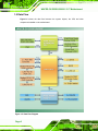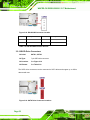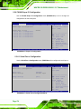
1
WAFER-CV-D25501/N26001 3.5" Motherboard 1 IEI Technology Corp. MODEL: WAFER-CV-D25501/N26001 3.5" SBC with Intel® Atom™ D2550/N2600 Processor, DDR3, VGA/Dual LVDS, Dual PCIe GbE, USB 2.0, PCIe Mini, SATA 3Gb/s, Audio and RoHS User Manual Page i Rev. 1.03 – 11 December, 2012 WAFER-CV-D25501/N26001 3.5" Motherboard Revision Date Version Changes 11 December, 2012 1.03 Added CN6 connector information 23 November, 2012 1.02 Updated the note for the Intel® GMA driver limitation 13 August, 2012 1.01 Added a note for the Intel® GMA driver limitation 26 June, 20 1.00 Initial release Page ii WAFER-CV-D25501/N26001 3.5" Motherboard Copyright COPYRIGHT NOTICE The information in this document is subject to change without prior notice in order to improve reliability, design and function and does not represent a commitment on the part of the manufacturer. In no event will the manufacturer be liable for direct, indirect, special, incidental, or consequential damages arising out of the use or inability to use the product or documentation, even if advised of the possibility of such damages. This document contains proprietary information protected by copyright. All rights are reserved. No part of this manual may be reproduced by any mechanical, electronic, or other means in any form without prior written permission of the manufacturer. TRADEMARKS All registered trademarks and product names mentioned herein are used for identification purposes only and may be trademarks and/or registered trademarks of their respective owners. Page iii WAFER-CV-D25501/N26001 3.5" Motherboard Table of Contents 1 INTRODUCTION.......................................................................................................... 1 1.1 INTRODUCTION........................................................................................................... 2 1.2 MODEL VARIATIONS ................................................................................................... 2 1.3 CONNECTORS ............................................................................................................. 3 1.4 DIMENSIONS ............................................................................................................... 4 1.5 DATA FLOW ................................................................................................................ 6 1.6 TECHNICAL SPECIFICATIONS ...................................................................................... 7 2 PACKING LIST ............................................................................................................. 9 2.1 ANTI-STATIC PRECAUTIONS ...................................................................................... 10 2.2 UNPACKING PRECAUTIONS ....................................................................................... 10 2.3 PACKING LIST............................................................................................................11 2.4 OPTIONAL ITEMS ...................................................................................................... 12 3 CONNECTORS ........................................................................................................... 13 3.1 PERIPHERAL INTERFACE CONNECTORS..................................................................... 14 3.1.1 WAFER-CV-D25501/N26001 Layout .............................................................. 14 3.1.2 Peripheral Interface Connectors ..................................................................... 15 3.1.3 External Interface Panel Connectors............................................................... 16 3.2 INTERNAL PERIPHERAL CONNECTORS ...................................................................... 16 3.2.1 5 V SATA Power Connectors............................................................................ 16 3.2.2 12 V Power Connector ..................................................................................... 17 3.2.3 Audio Connector .............................................................................................. 17 3.2.4 Backlight Inverter Connectors......................................................................... 18 3.2.5 Battery Connector............................................................................................ 19 3.2.6 Digital Input/Output (DIO) Connector............................................................ 20 3.2.7 Fan Connectors................................................................................................ 21 3.2.8 Keyboard/Mouse Connector ............................................................................ 22 3.2.9 LVDS1 Connector ............................................................................................ 23 3.2.10 LVDS2 Connector .......................................................................................... 24 3.2.11 LVDS2 Backlight Control Connector ............................................................. 26 Page iv WAFER-CV-D25501/N26001 3.5" Motherboard 3.2.12 PCIe Mini Card Slots..................................................................................... 26 3.2.13 Power & HDD LED Connector..................................................................... 28 3.2.14 Power Button Connector................................................................................ 29 3.2.15 Reset Button Connector ................................................................................. 30 3.2.16 RS-232 Serial Port Connectors...................................................................... 30 3.2.17 RS-422/485 Serial Port Connector ................................................................ 31 3.2.18 SATA Drive Connectors ................................................................................. 32 3.2.19 USB Connectors............................................................................................. 33 3.3 EXTERNAL PERIPHERAL INTERFACE CONNECTOR PANEL ......................................... 34 3.3.1 Ethernet Connectors ........................................................................................ 34 3.3.2 Serial Port Connector (COM1) ....................................................................... 35 3.3.3 USB Connectors............................................................................................... 36 3.3.4 VGA Connector ................................................................................................ 36 4 INSTALLATION ......................................................................................................... 38 4.1 ANTI-STATIC PRECAUTIONS ...................................................................................... 39 4.2 INSTALLATION CONSIDERATIONS .............................................................................. 39 4.3 SO-DIMM INSTALLATION ....................................................................................... 41 4.4 JUMPER SETTINGS .................................................................................................... 42 4.4.1 AT/ATX Power Selection Jumper ..................................................................... 42 4.4.2 Clear CMOS Jumper........................................................................................ 43 4.4.3 LVDS1 Voltage Selection.................................................................................. 44 4.4.4 LVDS2 Voltage Selection.................................................................................. 45 4.4.5 LVDS2 Panel Type Selection Jumper............................................................... 46 4.5 CHASSIS INSTALLATION ............................................................................................ 47 4.5.1 Airflow.............................................................................................................. 47 4.5.2 Motherboard Installation................................................................................. 48 4.6 INTERNAL PERIPHERAL DEVICE CONNECTIONS ........................................................ 48 4.6.1 Audio Kit Installation....................................................................................... 48 4.6.2 LVDS LCD Installation.................................................................................... 49 4.6.3 Full-size PCIe Mini Card Installation ............................................................. 51 4.6.4 Half-size PCIe Mini Card Installation............................................................. 53 4.6.5 SATA Drive Connection ................................................................................... 54 4.6.6 Single RS-232 Cable ........................................................................................ 55 4.6.7 Keyboard/Mouse Y-cable Connector ............................................................... 56 Page v WAFER-CV-D25501/N26001 3.5" Motherboard 4.7 EXTERNAL PERIPHERAL INTERFACE CONNECTION ................................................... 58 4.7.1 LAN Connection............................................................................................... 58 4.7.2 Serial Device Connection ................................................................................ 59 4.7.3 USB Connection (Dual Connector) ................................................................. 60 4.7.4 VGA Monitor Connection ................................................................................ 60 4.8 HEAT SINK ENCLOSURE............................................................................................ 62 5 BIOS .............................................................................................................................. 64 5.1 INTRODUCTION......................................................................................................... 65 5.1.1 Starting Setup................................................................................................... 65 5.1.2 Using Setup ...................................................................................................... 65 5.1.3 Getting Help..................................................................................................... 66 5.1.4 Unable to Reboot after Configuration Changes .............................................. 66 5.1.5 BIOS Menu Bar................................................................................................ 66 5.2 MAIN........................................................................................................................ 67 5.3 ADVANCED ............................................................................................................... 68 5.3.1 ACPI Settings ................................................................................................... 68 5.3.2 RTC Wake Settings ........................................................................................... 69 5.3.3 CPU Configuration.......................................................................................... 71 5.3.4 IDE Configuration ........................................................................................... 72 5.3.5 USB Configuration........................................................................................... 73 5.3.6 F81866 Super IO Configuration...................................................................... 74 5.3.6.1 Serial Port n Configuration ....................................................................... 74 5.3.7 F81866 H/W Monitor....................................................................................... 78 5.3.7.1 Smart Fan Mode Configuration ................................................................ 79 5.3.8 Serial Port Console Redirection ...................................................................... 80 5.3.9 iEi Feature ....................................................................................................... 83 5.4 CHIPSET ................................................................................................................... 84 5.4.1 Host Bridge Configuration .............................................................................. 84 5.4.1.1 Intel IGD Configuration............................................................................ 85 5.4.2 South Bridge Configuration............................................................................. 87 5.5 BOOT........................................................................................................................ 88 5.6 SECURITY ................................................................................................................. 90 5.7 EXIT ......................................................................................................................... 90 6 SOFTWARE DRIVERS .............................................................................................. 92 Page vi WAFER-CV-D25501/N26001 3.5" Motherboard 6.1 AVAILABLE SOFTWARE DRIVERS .............................................................................. 93 6.2 STARTING THE DRIVER PROGRAM ............................................................................ 93 6.3 CHIPSET DRIVER INSTALLATION ............................................................................... 95 6.4 GRAPHICS DRIVER INSTALLATION ............................................................................ 99 6.5 LAN DRIVER INSTALLATION .................................................................................. 103 6.6 AUDIO DRIVER INSTALLATION ............................................................................... 105 A BIOS OPTIONS ........................................................................................................ 108 B ONE KEY RECOVERY ............................................................................................111 B.1 ONE KEY RECOVERY INTRODUCTION .....................................................................112 B.1.1 System Requirement........................................................................................113 B.1.2 Supported Operating System ..........................................................................114 B.2 SETUP PROCEDURE FOR WINDOWS .........................................................................115 B.2.1 Hardware and BIOS Setup .............................................................................116 B.2.2 Create Partitions ............................................................................................116 B.2.3 Install Operating System, Drivers and Applications ..................................... 120 B.2.4 Build-up Recovery Partition.......................................................................... 121 B.2.5 Create Factory Default Image....................................................................... 123 B.3 AUTO RECOVERY SETUP PROCEDURE .................................................................... 128 B.4 SETUP PROCEDURE FOR LINUX .............................................................................. 133 B.5 RECOVERY TOOL FUNCTIONS ................................................................................ 136 B.5.1 Factory Restore ............................................................................................. 138 B.5.2 Backup System ............................................................................................... 139 B.5.3 Restore Your Last Backup.............................................................................. 140 B.5.4 Manual........................................................................................................... 141 B.6 RESTORE SYSTEMS FROM A LINUX SERVER THROUGH LAN .................................. 142 B.6.1 Configure DHCP Server Settings .................................................................. 143 B.6.2 Configure TFTP Settings ............................................................................... 144 B.6.3 Configure One Key Recovery Server Settings ............................................... 145 B.6.4 Start the DHCP, TFTP and HTTP ................................................................. 146 B.6.5 Create Shared Directory................................................................................ 146 B.6.6 Setup a Client System for Auto Recovery ...................................................... 147 B.7 OTHER INFORMATION ............................................................................................ 150 B.7.1 Using AHCI Mode or ALi M5283 / VIA VT6421A Controller....................... 150 B.7.2 System Memory Requirement ........................................................................ 152 Page vii WAFER-CV-D25501/N26001 3.5" Motherboard C TERMINOLOGY ..................................................................................................... 153 D DIGITAL I/O INTERFACE..................................................................................... 157 D.1 INTRODUCTION ...................................................................................................... 158 D.2 DIO CONNECTOR PINOUTS ................................................................................... 158 D.3 ASSEMBLY LANGUAGE SAMPLES........................................................................... 159 D.3.1 Enable the DIO Input Function .................................................................... 159 D.3.2 Enable the DIO Output Function.................................................................. 159 E WATCHDOG TIMER............................................................................................... 160 F HAZARDOUS MATERIALS DISCLOSURE........................................................ 163 F.1 HAZARDOUS MATERIALS DISCLOSURE TABLE FOR IPB PRODUCTS CERTIFIED AS ROHS COMPLIANT UNDER 2002/95/EC WITHOUT MERCURY ..................................... 164 Page viii WAFER-CV-D25501/N26001 3.5" Motherboard List of Figures Figure 1-1: WAFER-CV-D25501/N26001 .......................................................................................2 Figure 1-2: Connectors ..................................................................................................................3 Figure 1-3: WAFER-CV-D25501/N26001 Dimensions (mm) ........................................................4 Figure 1-4: External Interface Panel Dimensions (mm) ..............................................................5 Figure 1-5: Data Flow Diagram......................................................................................................6 Figure 3-1: Connectors and Jumpers.........................................................................................14 Figure 3-2: 5 V SATA Power Connector Locations ...................................................................16 Figure 3-3: 12 V Power Connector Location..............................................................................17 Figure 3-4: Audio Connector Location .......................................................................................18 Figure 3-5: Backlight Inverter Connector Locations.................................................................19 Figure 3-6: Battery Connector Location.....................................................................................20 Figure 3-7: Digital I/O Connector Location ................................................................................21 Figure 3-8: Fan Connector Locations.........................................................................................22 Figure 3-9: Keyboard/Mouse Connector Location ....................................................................23 Figure 3-10: LVDS1 Connector Location ...................................................................................24 Figure 3-11: LVDS2 Connector Location ...................................................................................25 Figure 3-12: LVDS2 Backlight Control Connector Location ....................................................26 Figure 3-13: PCIe Mini Card Slot Locations...............................................................................27 Figure 3-14: Power & HDD LED Connector Location................................................................28 Figure 3-15: Power Button Connector Location........................................................................29 Figure 3-16: Reset Button Connector Location.........................................................................30 Figure 3-17: RS-232 Serial Port Connector Locations..............................................................31 Figure 3-18: RS-422/485 Connector Location............................................................................32 Figure 3-19: SATA Drive Connector Locations .........................................................................32 Figure 3-20: USB Connector Locations......................................................................................33 Figure 3-21: External Peripheral Interface Connector ..............................................................34 Figure 3-22: RJ-45 Ethernet Connector......................................................................................35 Figure 3-23: COM1 Pinout Locations..........................................................................................36 Figure 3-24: VGA Connector .......................................................................................................37 Figure 4-1: SO-DIMM Installation ................................................................................................41 Page ix WAFER-CV-D25501/N26001 3.5" Motherboard Figure 4-2: AT/ATX Power Selection Jumper Location ............................................................43 Figure 4-3: Clear CMOS Jumper Location .................................................................................44 Figure 4-4: LVDS1 Voltage Selection Jumper Location ...........................................................45 Figure 4-5: LVDS2 Voltage Selection Jumper Location ...........................................................46 Figure 4-6: LVDS2 Panel Type Selection Switch Location.......................................................47 Figure 4-7: Audio Kit Cable Connection.....................................................................................49 Figure 4-8: LVDS Connector........................................................................................................50 Figure 4-9: Backlight Inverter Connection.................................................................................51 Figure 4-10: Remove the Retention Screw for the Full-size PCIe Mini Card ..........................52 Figure 4-11: Insert the Full-size PCIe Mini Card into the Socket at an Angle.........................52 Figure 4-12: Secure the Full-size PCIe Mini Card......................................................................53 Figure 4-13: Remove the Retention Screws for the Half-size PCIe Mini Card........................53 Figure 4-14: Insert the Half-size PCIe Mini Card into the Socket at an Angle ........................54 Figure 4-15: Secure the Half-size PCIe Mini Card .....................................................................54 Figure 4-16: SATA Drive Cable Connection...............................................................................55 Figure 4-17: Single RS-232 Cable Installation ...........................................................................56 Figure 4-18: Keyboard/mouse Y-cable Connection ..................................................................57 Figure 4-19: LAN Connection ......................................................................................................58 Figure 4-20: Serial Device Connector.........................................................................................59 Figure 4-21: USB Connector........................................................................................................60 Figure 4-22: VGA Connector .......................................................................................................61 Figure 4-23: Heat Sink Retention Screws ..................................................................................63 Figure 6-1: Start Up Screen .........................................................................................................94 Figure 6-2: Drivers ........................................................................................................................94 Figure 6-3: Chipset Driver Screen...............................................................................................95 Figure 6-4: Chipset Driver Welcome Screen..............................................................................96 Figure 6-5: Chipset Driver License Agreement .........................................................................97 Figure 6-6: Chipset Driver Read Me File ....................................................................................97 Figure 6-7: Chipset Driver Setup Operations ............................................................................98 Figure 6-8: Chipset Driver Installation Finish Screen...............................................................99 Figure 6-9: Graphics Driver Welcome Screen ........................................................................ 100 Figure 6-10: Graphics Driver License Agreement.................................................................. 101 Figure 6-11: Graphics Driver Read Me File ............................................................................. 101 Figure 6-12: Graphics Driver Setup Operations ..................................................................... 102 Figure 6-13: Graphics Driver Installation Finish Screen ....................................................... 102 Page x WAFER-CV-D25501/N26001 3.5" Motherboard Figure 6-14: LAN Driver Welcome Screen .............................................................................. 103 Figure 6-15: LAN Driver Installation ........................................................................................ 104 Figure 6-16: LAN Driver Installation Complete....................................................................... 104 Figure 6-17: Audio Driver Installation File Extraction............................................................ 105 Figure 6-18: Audio Driver Welcome Screen............................................................................ 106 Figure 6-19: Audio Driver Installation...................................................................................... 106 Figure 6-20: Audio Driver Installation Complete .................................................................... 107 Figure B-1: IEI One Key Recovery Tool Menu ........................................................................ 112 Figure B-2: Launching the Recovery Tool .............................................................................. 117 Figure B-3: Recovery Tool Setup Menu .................................................................................. 117 Figure B-4: Command Prompt ................................................................................................. 118 Figure B-5: Partition Creation Commands.............................................................................. 119 Figure B-6: Launching the Recovery Tool .............................................................................. 121 Figure B-7: Manual Recovery Environment for Windows ..................................................... 121 Figure B-8: Building the Recovery Partition........................................................................... 122 Figure B-9: Press Any Key to Continue .................................................................................. 122 Figure B-10: Press F3 to Boot into Recovery Mode............................................................... 123 Figure B-11: Recovery Tool Menu ........................................................................................... 123 Figure B-12: About Symantec Ghost Window ........................................................................ 124 Figure B-13: Symantec Ghost Path ......................................................................................... 124 Figure B-14: Select a Local Source Drive ............................................................................... 125 Figure B-15: Select a Source Partition from Basic Drive ...................................................... 125 Figure B-16: File Name to Copy Image to ............................................................................... 126 Figure B-17: Compress Image.................................................................................................. 126 Figure B-18: Image Creation Confirmation ............................................................................. 127 Figure B-19: Image Creation Complete ................................................................................... 127 Figure B-20: Image Creation Complete ................................................................................... 127 Figure B-21: Press Any Key to Continue ................................................................................ 128 Figure B-22: Auto Recovery Utility .......................................................................................... 129 Figure B-23: Disable Automatically Restart............................................................................ 129 Figure B-24: Launching the Recovery Tool ............................................................................ 130 Figure B-25: Auto Recovery Environment for Windows ....................................................... 130 Figure B-26: Building the Auto Recovery Partition................................................................ 131 Figure B-27: Factory Default Image Confirmation ................................................................. 131 Figure B-28: Image Creation Complete ................................................................................... 132 Page xi WAFER-CV-D25501/N26001 3.5" Motherboard Figure B-29: Press any key to continue .................................................................................. 132 Figure B-30: IEI Feature ............................................................................................................ 133 Figure B-31: Partitions for Linux.............................................................................................. 134 Figure B-32: System Configuration for Linux......................................................................... 135 Figure B-33: Access menu.lst in Linux (Text Mode) .............................................................. 135 Figure B-34: Recovery Tool Menu ........................................................................................... 136 Figure B-35: Recovery Tool Main Menu .................................................................................. 137 Figure B-36: Restore Factory Default ...................................................................................... 138 Figure B-37: Recovery Complete Window .............................................................................. 138 Figure B-38: Backup System.................................................................................................... 139 Figure B-39: System Backup Complete Window ................................................................... 139 Figure B-40: Restore Backup ................................................................................................... 140 Figure B-41: Restore System Backup Complete Window ..................................................... 140 Figure B-42: Symantec Ghost Window ................................................................................... 141 Figure B-43: Disable Automatically Restart............................................................................ 148 Page xii WAFER-CV-D25501/N26001 3.5" Motherboard List of Tables Table 1-1: WAFER-CV-D25501/N26001 Model Variations ...........................................................2 Table 1-2: WAFER-CV-D25501/N26001 Specifications ...............................................................8 Table 2-1: Packing List.................................................................................................................12 Table 2-2: Optional Items.............................................................................................................12 Table 3-1: Peripheral Interface Connectors ...............................................................................15 Table 3-2: Rear Panel Connectors ..............................................................................................16 Table 3-3: 5 V SATA Power Connector Pinouts ........................................................................17 Table 3-4: 12 V Power Connector Pinouts .................................................................................17 Table 3-5: Audio Connector Pinouts ..........................................................................................18 Table 3-6: Backlight Inverter Connector Pinouts ......................................................................19 Table 3-7: Battery Connector Pinouts ........................................................................................20 Table 3-8: Digital I/O Connector Pinouts....................................................................................21 Table 3-9: Fan Connector Pinouts ..............................................................................................22 Table 3-10: Keyboard/Mouse Connector Pinouts .....................................................................23 Table 3-11: LVDS1 Connector Pinouts .......................................................................................24 Table 3-12: LVDS2 Connector Pinouts .......................................................................................25 Table 3-13: LVDS2 Backlight Control Connector Pinouts........................................................26 Table 3-14: PCIe Mini Card Slot Pinouts ....................................................................................28 Table 3-15: Power & HDD LED Connector Pinouts ...................................................................29 Table 3-16: Power Button Connector Pinouts ...........................................................................29 Table 3-17: Reset Button Connector Pinouts ............................................................................30 Table 3-18: RS-232 Serial Port Connector Pinouts ...................................................................31 Table 3-19: RS-422/485Connector Pinouts ................................................................................32 Table 3-20: SATA Drive Connector Pinouts...............................................................................33 Table 3-21: USB Connector Pinouts ...........................................................................................34 Table 3-22: LAN Pinouts ..............................................................................................................34 Table 3-23: RJ-45 Ethernet Connector LEDs .............................................................................35 Table 3-24: RS-232 Serial Port (COM 1) Pinouts .......................................................................35 Table 3-25: USB Port Pinouts......................................................................................................36 Table 3-26: VGA Connector Pinouts...........................................................................................37 Page xiii WAFER-CV-D25501/N26001 3.5" Motherboard Table 4-1: Jumpers .......................................................................................................................42 Table 4-2: AT/ATX Power Selection Jumper Settings...............................................................43 Table 4-3: Clear CMOS Jumper Settings....................................................................................43 Table 4-4: LVDS1 Voltage Selection Jumper Settings..............................................................44 Table 4-5: LVDS2 Voltage Selection Jumper Settings..............................................................45 Table 4-6: LVDS2 Panel Resolution ............................................................................................47 Table 5-1: BIOS Navigation Keys ................................................................................................66 Page xiv WAFER-CV-D25501/N26001 3.5" Motherboard BIOS Menus BIOS Menu 1: Main .......................................................................................................................67 BIOS Menu 2: Advanced ..............................................................................................................68 BIOS Menu 3: ACPI Settings .......................................................................................................69 BIOS Menu 4: RTC Wake Settings ..............................................................................................70 BIOS Menu 5: CPU Configuration ...............................................................................................71 BIOS Menu 6: IDE Configuration.................................................................................................72 BIOS Menu 7: USB Configuration ...............................................................................................73 BIOS Menu 8: Super IO Configuration........................................................................................74 BIOS Menu 9: Serial Port n Configuration Menu.......................................................................74 BIOS Menu 10: F81866 H/W Monitor...........................................................................................78 BIOS Menu 11: Smart Fan Mode Configuration ........................................................................80 BIOS Menu 12: Serial Port Console Redirection .......................................................................81 BIOS Menu 13: IEI Feature...........................................................................................................83 BIOS Menu 14: Chipset ................................................................................................................84 BIOS Menu 15: Host Bridge Configuration ................................................................................85 BIOS Menu 16: Intel IGD Configuration......................................................................................85 BIOS Menu 17: Southbridge Chipset Configuration .................................................................87 BIOS Menu 18: Boot .....................................................................................................................88 BIOS Menu 19: Security ...............................................................................................................90 BIOS Menu 20:Exit........................................................................................................................91 WAFER-CV-D25501/N26001 Page xv WAFER-CV-D25501/N26001 3.5" Motherboard Chapter 1 1 Introduction Page 1 WAFER-CV-D25501/N26001 3.5" Motherboard 1.1 Introduction Figure 1-1: WAFER-CV-D25501/N26001 The WAFER-CV-D25501/N26001 3.5” motherboard is an Intel® Atom™ D2550/N2600 processor platform that supports one 1066 MHz or 800 MHz DDR3 SO-DIMM memory. The WAFER-CV-D25501/N26001 supports VGA display output and comes with two LVDS connectors supporting 24-bit or 18-bit LVDS screens. Maximum six USB ports, two SATA 3Gb/s connectors, two PCIe Mini card slots, four COM ports, and one audio connector provide flexible expansion options. 1.2 Model Variations The model variations of the WAFER-CV-D25501/N26001 are listed below. Model No. CPU WAFER-CV-D25501-R10 Intel® Atom D2550 1.86 GHz WAFER-CV-N26001-R10 Intel® Atom N2600 1.6 GHz Table 1-1: WAFER-CV-D25501/N26001 Model Variations Page 2 WAFER-CV-D25501/N26001 3.5" Motherboard 1.3 Connectors The connectors on the WAFER-CV-D25501/N26001 are shown in the figure below. Figure 1-2: Connectors Page 3 WAFER-CV-D25501/N26001 3.5" Motherboard 1.4 Dimensions The main dimensions of the WAFER-CV-D25501/N26001 are shown in the diagram below. Figure 1-3: WAFER-CV-D25501/N26001 Dimensions (mm) Page 4 WAFER-CV-D25501/N26001 3.5" Motherboard . Figure 1-4: External Interface Panel Dimensions (mm) Page 5 WAFER-CV-D25501/N26001 3.5" Motherboard 1.5 Data Flow Figure 1-5 shows the data flow between the system chipset, the CPU and other 6 components installed on the motherboard. Figure 1-5: Data Flow Diagram Page 6 WAFER-CV-D25501/N26001 3.5" Motherboard 1.6 Technical Specifications The WAFER-CV-D25501/N26001 technical specifications are listed below. Specification/Model WAFER-CV-D25501 Form Factor 3.5” System CPU Intel® Atom™ D2550 1.86 GHz System Chipset Intel® NM10 Memory Graphics Engine WAFER-CV-N26001 Intel® Atom™ N2600 1.6 GHz One 1066 MHz DDR3/DDR3L (1.35V) One 800 MHz DDR3/DDR3L (1.35V) SO-DIMM support (up to 4 GB) SO-DIMM support (up to 2 GB) Intel® GMA 3650 with a 640 MHz Intel® GMA 3600 with a 400 MHz graphics core graphics core Dual display supported One VGA One LVDS1 is integrated in the Intel® Atom™ D2550/N2600 processor One LVDS2 is driven by the Chrontel CH7511 DP to LVDS converter Display Ethernet 24-bit single-channel LVDS1 with 18-bit single-channel LVDS1 with up to 1440x900 resolution up to 1366x768 resolution 24-bit dual-channel LVDS2 with up 24-bit dual-channel LVDS2 with up to 1920x1200 resolution to 1600x1200 resolution Dual Realtek RTL8111E PCIe GbE controller (LAN1 with ASF 2.0 support) BIOS UEFI BIOS Super I/O Controller Fintek F81866 Watchdog Timer Software programmable supports 1~255 sec. system reset Expansion Audio COM Digital I/O One full-size PCIe Mini card slot with mSATA support One half-size PCIe Mini card slot Realtek ALC662 HD Audio codec Three RS-232 (one by external connector; two by on-board pin headers) One RS-422/485 by internal 4-pin wafer connector One 8-bit digital input/output connector (4-bit input/4-bit output) Page 7 WAFER-CV-D25501/N26001 3.5" Motherboard Specification/Model Fan WAFER-CV-D25501 WAFER-CV-N26001 One 3-pin CPU fan connector One 3-pin system fan connector Keyboard/mouse One internal pin-header connector SATA Two SATA 3Gb/s ports with 5V power Six USB 2.0/1.1 devices supported: USB Two by external connectors Four by on-board pin headers 12 V only Power Supply AT and ATX support One internal 4-pin (2x2) power connector 12V @ 1.53 A (1.86 GHz Intel® 12V @ 1.15 A (1.6 GHz Intel® Power Consumption Atom™ D2550 with 1 GB 1066 MHz Atom™ N2600 with 1 GB 1066 MHz DDR3 SO-DIMM memory) DDR3 SO-DIMM memory) Operating -20ºC ~ 60ºC with free air -20ºC ~ 70ºC with free air Temperature -20ºC ~ 70ºC with force air -20ºC ~ 75ºC with force air -30ºC ~ 80ºC -30ºC ~ 85ºC Storage Temperature Humidity (Operating) 5% ~ 95% (non-condensing) Dimensions (LxW) 146 mm x 102 mm Weight (GW/NW) 600 g/250 g Table 1-2: WAFER-CV-D25501/N26001 Specifications Page 8 WAFER-CV-D25501/N26001 3.5" Motherboard Chapter 2 2 Packing List Page 9 WAFER-CV-D25501/N26001 3.5" Motherboard 2.1 Anti-static Precautions WARNING! Static electricity can destroy certain electronics. Make sure to follow the ESD precautions to prevent damage to the product, and injury to the user. Make sure to adhere to the following guidelines: Wear an anti-static wristband: Wearing an anti-static wristband can prevent electrostatic discharge. Self-grounding: Touch a grounded conductor every few minutes to discharge any excess static buildup. Use an anti-static pad: When configuring any circuit board, place it on an anti-static mat. Only handle the edges of the PCB: Don't touch the surface of the motherboard. Hold the motherboard by the edges when handling. 2.2 Unpacking Precautions When the WAFER-CV-D25501/N26001 is unpacked, please do the following: Follow the antistatic guidelines above. Make sure the packing box is facing upwards when opening. Make sure all the packing list items are present. Page 10 WAFER-CV-D25501/N26001 3.5" Motherboard 2.3 Packing List NOTE: If any of the components listed in the checklist below are missing, do not proceed with the installation. Contact the IEI reseller or vendor the WAFER-CV-D25501/N26001 was purchased from or contact an IEI sales representative directly by sending an email to [email protected]. 3 The WAFER-CV-D25501/N26001 is shipped with the following components: Quantity Item and Part Number 1 WAFER-CV-D25501/N26001 motherboard 1 SATA and power cable Image (P/N: 32801-000201-100-RS) 1 Audio cable (P/N: 32000-072100-RS) 1 RS-232 cable (P/N: 32205-002700-100-RS) 1 KB/MS cable (P/N: 32000-023800-RS) 1 Power cable (P/N: 32100-087100-RS) Page 11 WAFER-CV-D25501/N26001 3.5" Motherboard Quantity Item and Part Number 1 Mini jumper pack 1 One Key Recovery CD 1 Utility CD 1 Quick Installation Guide Image Table 2-1: Packing List 2.4 Optional Items The following are optional components which may be separately purchased: Item and Part Number Dual USB cable (wo bracket) (P/N: 32001-008600-100-RS) RS-422/485 cable (200 mm) (P/N: 32205-003800-100-RS) Table 2-2: Optional Items Page 12 Image WAFER-CV-D25501/N26001 3.5" Motherboard Chapter 3 3 Connectors Page 13 WAFER-CV-D25501/N26001 3.5" Motherboard 3.1 Peripheral Interface Connectors This chapter details all the jumpers and connectors. 3.1.1 WAFER-CV-D25501/N26001 Layout The figure below shows all the connectors and jumpers. Figure 3-1: Connectors and Jumpers Page 14 WAFER-CV-D25501/N26001 3.5" Motherboard 3.1.2 Peripheral Interface Connectors The table below lists all the connectors on the board. Connector Type Label 5 V SATA power connectors 2-pin wafer SATA_PWR1, SATA_PWR2 12 V power connector 4-pin Molex power CN3 connector Audio connector 10-pin box header AUDIO1 Backlight inverter connectors 5-pin wafer INV1, INV2 Battery connector 2-pin wafer CN1 Digital Input/Output (DIO) connector 10-pin header DIO1 Fan connectors 3-pin wafer CPU_FAN1, SYS_FAN2 Keyboard and mouse connector 6-pin wafer KB_MS1 LVDS connectors 20-pin/30-pin crimp LVDS1, LVDS2 LVDS2 backlight control connector 6-pin wafer CN6 PCIe Mini card slots 52-pin PCIe Mini M_PCIE1, M_PCIE2 Power & HDD LED connector 6-pin header CN2 Power button connector 2-pin wafer PWR_BTN1 Reset button connector 2-pin wafer RST_BTN1 RS-232 serial port connectors 10-pin header COM2, COM3 RS-422/485 serial port connector 4-pin wafer COM4 Serial ATA (SATA) drive connectors 7-pin SATA SATA1, SATA2 USB 2.0 connectors 8-pin header USB2, USB3 Table 3-1: Peripheral Interface Connectors Page 15 WAFER-CV-D25501/N26001 3.5" Motherboard 3.1.3 External Interface Panel Connectors The table below lists the connectors on the external I/O panel. Connector Type Label Dual USB port Dual USB port USB1 Ethernet connectors RJ-45 LAN1, LAN2 RS-232 serial port connector Male DB-9 COM1 VGA connector 15-pin female VGA1 Table 3-2: Rear Panel Connectors 3.2 Internal Peripheral Connectors The section describes all of the connectors on the WAFER-CV-D25501/N26001. 3.2.1 5 V SATA Power Connectors CN Label: SATA_PWR1, SATA_PWR2 CN Type: 2-pin wafer CN Location: See Figure 3-2 CN Pinouts: See Table 3-3 Use the 5 V SATA power connectors to connect to SATA device power connection. Figure 3-2: 5 V SATA Power Connector Locations Page 16 WAFER-CV-D25501/N26001 3.5" Motherboard Pin No. Description 1 +5V 2 Ground Table 3-3: 5 V SATA Power Connector Pinouts 3.2.2 12 V Power Connector CN Label: CN3 CN Type: 4-pin Molex power connector CN Location: See Figure 3-3 CN Pinouts: See Table 3-4 The ATX power connector connects to an ATX power supply. Figure 3-3: 12 V Power Connector Location Pin Description 1 GND 2 GND 3 +12V 4 +12V Table 3-4: 12 V Power Connector Pinouts 3.2.3 Audio Connector CN Label: AUDIO1 CN Type: 10-pin box header CN Location: See Figure 3-4 CN Pinouts: See Table 3-5 Page 17 WAFER-CV-D25501/N26001 3.5" Motherboard The 10-pin audio connector is connected to external audio devices including speakers and microphones for the input and output of audio signals to and from the system. Figure 3-4: Audio Connector Location Pin Description Pin Description 1 Line-out_R 2 Line-in_R 3 AUD_GND 4 AUD_GND 5 Line-out _L 6 Line-in _L 7 AUD_GND 8 AUD_GND 9 MIC1_R 10 MIC1_L Table 3-5: Audio Connector Pinouts 3.2.4 Backlight Inverter Connectors CN Label: INV1, INV2 CN Type: 5-pin wafer CN Location: See Figure 3-5 CN Pinouts: See Table 3-6 The backlight inverter connectors provide the backlights on the LCD display connected to the WAFER-CV-D25501/N26001 with +12V of power. Page 18 WAFER-CV-D25501/N26001 3.5" Motherboard Figure 3-5: Backlight Inverter Connector Locations Pin Description 1 LCD_BKLTCTL 2 GROUND 3 +12V 4 GROUND 5 LCD_BKLEN Table 3-6: Backlight Inverter Connector Pinouts 3.2.5 Battery Connector CAUTION: Risk of explosion if battery is replaced by an incorrect type. Only certified engineers should replace the on-board battery. Dispose of used batteries according to instructions and local regulations. CN Label: CN1 CN Type: 2-pin wafer Page 19 WAFER-CV-D25501/N26001 3.5" Motherboard CN Location: See Figure 3-6 CN Pinouts: See Table 3-7 This is connected to the system battery. The battery provides power to the system clock to retain the time when power is turned off. Figure 3-6: Battery Connector Location Pin Description 1 Battery+ 2 GND Table 3-7: Battery Connector Pinouts 3.2.6 Digital Input/Output (DIO) Connector CN Label: DIO1 CN Type: 10-pin header CN Location: See Figure 3-7 CN Pinouts: See Table 3-8 The digital input/output connector is managed through a Super I/O chip. The DIO connector pins are user programmable. Page 20 WAFER-CV-D25501/N26001 3.5" Motherboard Figure 3-7: Digital I/O Connector Location Pin Description Pin Description 1 GND 2 VCC 3 Output 3 4 Output 2 5 Output 1 6 Output 0 7 Input 3 8 Input 2 9 Input 1 10 Input 0 Table 3-8: Digital I/O Connector Pinouts 3.2.7 Fan Connectors CN Label: CPU_FAN1, SYS_FAN1 CN Type: 3-pin wafer CN Location: See Figure 3-8 CN Pinouts: See Table 3-9 The fan connectors attach to the CPU/system cooling fans. Page 21 WAFER-CV-D25501/N26001 3.5" Motherboard Figure 3-8: Fan Connector Locations PIN NO. DESCRIPTION 1 GND 2 +12 V 3 Fan Speed Detect Table 3-9: Fan Connector Pinouts 3.2.8 Keyboard/Mouse Connector CN Label: KB_MS1 CN Type: 6-pin wafer CN Location: See Figure 3-9 CN Pinouts: See Table 3-10 The keyboard and mouse connector can be connected to a standard PS/2 cable or PS/2 Y-cable to add keyboard and mouse functionality to the system. Page 22 WAFER-CV-D25501/N26001 3.5" Motherboard Figure 3-9: Keyboard/Mouse Connector Location Pin Description 1 +5 V KB DATA 2 MS DATA 3 MS CLK 4 KB DATA 5 KB CLK 6 GROUND Table 3-10: Keyboard/Mouse Connector Pinouts 3.2.9 LVDS1 Connector CN Label: LVDS1 CN Type: 20-pin crimp CN Location: See Figure 3-10 CN Pinouts: See Table 3-11 The 20-pin LVDS LCD connector can be connected to an 18-bit/24-bit single-channel LVDS panel. Page 23 WAFER-CV-D25501/N26001 3.5" Motherboard Figure 3-10: LVDS1 Connector Location Pin Description Pin Description 1 GND 2 GND 3 LVDS_DATA0 4 LVDS_DATA0# 5 LVDS_DATA1 6 LVDS_DATA1# 7 LVDS_DATA2 8 LVDS_DATA2# 9 LVDS_CLK 10 LVDS_CLK# 11 LVDS_DATA3 12 LVDS_DATA3# 13 GND 14 GND 15 LDDC_DATA 16 LDDC_CLK 17 VCC_LCD 18 VCC_LCD 19 VCC_LCD 20 VCC_LCD Table 3-11: LVDS1 Connector Pinouts 3.2.10 LVDS2 Connector CN Label: LVDS2 CN Type: 30-pin crimp CN Location: See Figure 3-11 CN Pinouts: See Table 3-12 The 30-pin LVDS LCD connector can be connected to a 24-bit dual-channel LVDS panel. Page 24 WAFER-CV-D25501/N26001 3.5" Motherboard Figure 3-11: LVDS2 Connector Location Pin Description Pin Description 1 GND 2 GND 3 LVDS_DATA0 4 LVDS_DATA0# 5 LVDS_DATA1 6 LVDS_DATA1# 7 LVDS_DATA2 8 LVDS_DATA2# 9 LVDS_CLK1 10 LVDS_CLK1# 11 LVDS_DATA3 12 LVDS_DATA3# 13 GND 14 GND 15 LVDS_DATA4 16 LVDS_DATA4# 17 LVDS_DATA5 18 LVDS_DATA5# 19 LVDS_DATA6 20 LVDS_DATA6# 21 LVDS_CLK2 22 LVDS_CLK2# 23 LVDS_DATA7 24 LVDS_DATA7# 25 GND 26 GND 27 VCC_LCD 28 VCC_LCD 29 VCC_LCD 30 VCC_LCD Table 3-12: LVDS2 Connector Pinouts Page 25 WAFER-CV-D25501/N26001 3.5" Motherboard 3.2.11 LVDS2 Backlight Control Connector CN Label: CN6 CN Type: 6-pin wafer CN Location: See Figure 3-12 CN Pinouts: See Table 3-13 This connector allows control of the LVDS2 panel backlight. Figure 3-12: LVDS2 Backlight Control Connector Location Function Panel power button Panel brightness + Panel brightness - Pin Description 1 PWRDN 2 GND 3 BLUP 4 GND 5 BLDN 6 GND Table 3-13: LVDS2 Backlight Control Connector Pinouts 3.2.12 PCIe Mini Card Slots CN Label: M_PCIE1, M_PCIE2 CN Type: 52-pin PCIe Mini card slot CN Location: See Figure 3-13 CN Pinouts: See Table 3-14 The M_PCIE2 slot can be connected to a full-size PCIe Mini card while the M_PCIE1 slot can be connected to a half-size PCIe Mini card. Page 26 WAFER-CV-D25501/N26001 3.5" Motherboard NOTE: The M_PCIE2 slot supports mSATA devices. Figure 3-13: PCIe Mini Card Slot Locations Pin Description Pin Description 1 PCIE_WAKE# 2 VCC3 3 N/C 4 GND 5 N/C 6 1.5V 7 N/C 8 N/C 9 GND 10 N/C 11 PCIE_CLK# 12 N/C 13 PCIE_CLK 14 N/C 15 GND 16 N/C 17 N/C 18 GND 19 N/C 20 N/C 21 GND 22 PCIRST# 23 PCIE_RXN 24 VCC3 25 PCIE_RXP 26 GND 27 GND 28 1.5V 29 GND 30 SMBCLK 31 PCIE_TXN 32 SMBDATA 33 PCIE_TXP 34 GND 35 GND 36 USBD- Page 27 WAFER-CV-D25501/N26001 3.5" Motherboard Pin Description Pin Description 37 GND 38 USBD+ 39 VCC3 40 GND 41 VCC3 42 N/C 43 GND 44 N/C 45 N/C 46 N/C 47 N/C 48 1.5V 49 N/C 50 GND 51 N/C 52 VCC3 Table 3-14: PCIe Mini Card Slot Pinouts 3.2.13 Power & HDD LED Connector CN Label: CN2 CN Type: 6-pin wafer CN Location: See Figure 3-14 CN Pinouts: See Table 3-15 The LED connector connects to an HDD indicator LED and a power LED on the system chassis to inform the user about HDD activity and the power on/off status of the system. Figure 3-14: Power & HDD LED Connector Location Page 28 WAFER-CV-D25501/N26001 3.5" Motherboard Pin Description 1 +5V 2 GND 3 Power LED+ 4 Power LED- 5 HDD LED+ 6 HDD LED- Table 3-15: Power & HDD LED Connector Pinouts 3.2.14 Power Button Connector CN Label: PWR_BTN1 CN Type: 2-pin wafer CN Location: See Figure 3-15 CN Pinouts: See Table 3-16 The power button connector is connected to a power switch on the system chassis to enable users to turn the system on and off. Figure 3-15: Power Button Connector Location Pin Description 1 PWR_BTN+ 2 PWR_BTN- Table 3-16: Power Button Connector Pinouts Page 29 WAFER-CV-D25501/N26001 3.5" Motherboard 3.2.15 Reset Button Connector CN Label: RST_BTN1 CN Type: 2-pin wafer CN Location: See Figure 3-16 CN Pinouts: See Table 3-17 The reset button connector is connected to a reset switch on the system chassis to enable users to reboot the system when the system is turned on. Figure 3-16: Reset Button Connector Location Pin Description 1 RESET+ 2 RESET- Table 3-17: Reset Button Connector Pinouts 3.2.16 RS-232 Serial Port Connectors CN Label: COM2, COM3 CN Type: 10-pin header CN Location: See Figure 3-17 CN Pinouts: See Table 3-18 Each of these connectors provides RS-232 connections. Page 30 WAFER-CV-D25501/N26001 3.5" Motherboard Figure 3-17: RS-232 Serial Port Connector Locations Pin Description Pin Description 1 DCD 2 DSR 3 RXD 4 RTS 5 TXD 6 CTS 7 DTR 8 RI 9 GND 10 GND Table 3-18: RS-232 Serial Port Connector Pinouts 3.2.17 RS-422/485 Serial Port Connector CN Label: COM4 CN Type: 4-pin wafer CN Location: See Figure 3-18 CN Pinouts: See Table 3-19 NOTE: These pins are shared with those on the main serial port. Use either the pins on the main connector, or on this connector, but not both. This connector provides RS-422 or RS-485 communications. Page 31 WAFER-CV-D25501/N26001 3.5" Motherboard Figure 3-18: RS-422/485 Connector Location Pin Description Pin Description 1 RXD422- 3 TXD422+/TXD485+ 2 RXD422+ 4 TXD422-/TXD485- Table 3-19: RS-422/485Connector Pinouts 3.2.18 SATA Drive Connectors CN Label: SATA1, SATA2 CN Type: 7-pin SATA drive connector CN Location: See Figure 3-19 CN Pinouts: See Table 3-20 The SATA drive connectors can be connected to SATA drives and support up to 3Gb/s data transfer rate. Figure 3-19: SATA Drive Connector Locations Page 32 WAFER-CV-D25501/N26001 3.5" Motherboard Pin Description 1 GND 2 TX+ 3 TX- 4 GND 5 RX- 6 RX+ 7 GND Table 3-20: SATA Drive Connector Pinouts 3.2.19 USB Connectors CN Label: USB2, USB3 CN Type: 8-pin header CN Location: See Figure 3-20 CN Pinouts: See Table 3-21 Each USB connector provides connectivity to two USB 1.1/2.0 ports. Figure 3-20: USB Connector Locations Pin Description Pin Description 1 USB_VCC 2 GND 3 DATA- 4 DATA+ 5 DATA+ 6 DATA- Page 33 WAFER-CV-D25501/N26001 3.5" Motherboard Pin Description Pin Description 7 GND 8 USB_VCC Table 3-21: USB Connector Pinouts 3.3 External Peripheral Interface Connector Panel The figure below shows the external peripheral interface connector (EPIC) panel. The EPIC panel consists of the following: Figure 3-21: External Peripheral Interface Connector 3.3.1 Ethernet Connectors CN Label: LAN1, LAN2 CN Type: RJ-45 connector CN Location: See Figure 3-21 CN Pinouts: See Table 3-22 The WAFER-CV-D25501/N26001 is equipped with two built-in RJ-45 Ethernet controllers. Each controller can connect to the LAN through one RJ-45 LAN connector. Pin Description Pin Description 1 LAN1_MDI0+ 5 LAN1_MDI2+ 2 LAN1_MDI0- 6 LAN1_MDI2- 3 LAN1_MDI1+ 7 LAN1_MDI3+ 4 LAN1_MDI1- 8 LAN1_MDI3- Table 3-22: LAN Pinouts Page 34 WAFER-CV-D25501/N26001 3.5" Motherboard Figure 3-22: RJ-45 Ethernet Connector LED Description LED Description A on: linked B off: 10 Mb/s blinking: data is being sent/received green: 100 Mb/s orange: 1000 Mb/s Table 3-23: RJ-45 Ethernet Connector LEDs 3.3.2 Serial Port Connector (COM1) CN Label: COM1 CN Type: Male DB-9 connector CN Location: See Figure 3-21 CN Pinouts: See Table 3-24 and Figure 3-23 The serial port connects to a RS-232 serial communications device. Pin Description Pin Description 1 DATA CARRIER DETECT (DCD) 6 DATA SET READY (DSR) 2 RECEIVE DATA (RXD) 7 REQUEST TO SEND (RTS) 3 TRANSMIT DATA (TXD) 8 CLEAR TO SEND (CTS) 4 DATA TERMINAL READY (DTR) 9 RING INDICATOR (RI) 5 GND Table 3-24: RS-232 Serial Port (COM 1) Pinouts Page 35 WAFER-CV-D25501/N26001 3.5" Motherboard Figure 3-23: COM1 Pinout Locations 3.3.3 USB Connectors CN Label: USB1 CN Type: Dual USB port CN Location: See Figure 3-21 CN Pinouts: See Table 3-25 The ports connect to both USB 2.0 and USB 1.1 devices. Pin Description Pin Description 1 USB_VCC 2 USB_VCC 3 DATA- 4 DATA- 5 DATA+ 6 DATA+ 7 GND 8 GND Table 3-25: USB Port Pinouts 3.3.4 VGA Connector CN Label: VGA1 CN Type: 15-pin Female CN Location: See Figure 3-21 CN Pinouts: See Figure 3-24 and Table 3-26 The VGA connector connects to a monitor that accepts a standard VGA input. Page 36 WAFER-CV-D25501/N26001 3.5" Motherboard Pin Description Pin Description 1 RED 2 GREEN 3 BLUE 4 NC 5 GND 6 GND 7 GND 8 GND 9 VGAVCC 10 GND 11 NC 12 DDCDAT 13 HSYNC 14 VSYNC 15 DDCCLK Table 3-26: VGA Connector Pinouts Figure 3-24: VGA Connector NOTE: Due to Intel® GMA driver limitation, the monitor connected to the VGA connector may become extended desktop or not have signal to it after restarting from the graphics driver installation. To work out this limitation, press the Ctrl+Alt+F1 hotkey to switch the primary display to CRT mode. Page 37 WAFER-CV-D25501/N26001 3.5" Motherboard Chapter 4 4 Installation Page 38 WAFER-CV-D25501/N26001 3.5" Motherboard 4.1 Anti-static Precautions WARNING: Failure to take ESD precautions during the installation of the WAFER-CV-D25501/N26001 may result in permanent damage to the WAFER-CV-D25501/N26001 and severe injury to the user. Electrostatic discharge (ESD) can cause serious damage to electronic components, including the WAFER-CV-D25501/N26001. Dry climates are especially susceptible to ESD. It is therefore critical that whenever the WAFER-CV-D25501/N26001 or any other electrical component is handled, the following anti-static precautions are strictly adhered to. Wear an anti-static wristband: - Wearing a simple anti-static wristband can help to prevent ESD from damaging the board. Self-grounding:- Before handling the board touch any grounded conducting material. During the time the board is handled, frequently touch any conducting materials that are connected to the ground. Use an anti-static pad: When configuring the WAFER-CV-D25501/N26001, place it on an antic-static pad. This reduces the possibility of ESD damaging the WAFER-CV-D25501/N26001. Only handle the edges of the PCB:-: When handling the PCB, hold the PCB by the edges. 4.2 Installation Considerations NOTE: The following installation notices and installation considerations should be read and understood before installation. All installation notices must be strictly adhered to. Failing to adhere to these precautions may lead to severe damage and injury to the person performing the installation. Page 39 WAFER-CV-D25501/N26001 3.5" Motherboard WARNING: The installation instructions described in this manual should be carefully followed in order to prevent damage to the components and injury to the user. Before and during the installation please DO the following: Read the user manual: o The user manual provides a complete description of the WAFER-CV-D25501/N26001 installation instructions and configuration options. Wear an electrostatic discharge cuff (ESD): o Electronic components are easily damaged by ESD. Wearing an ESD cuff removes ESD from the body and helps prevent ESD damage. Place the WAFER-CV-D25501/N26001 on an antistatic pad: o When installing or configuring the motherboard, place it on an antistatic pad. This helps to prevent potential ESD damage. Turn all power to the WAFER-CV-D25501/N26001 off: o When working with the WAFER-CV-D25501/N26001, make sure that it is disconnected from all power supplies and that no electricity is being fed into the system. Before and during the installation of the WAFER-CV-D25501/N26001 DO NOT: Remove any of the stickers on the PCB board. These stickers are required for warranty validation. Use the product before verifying all the cables and power connectors are properly connected. Allow screws to come in contact with the PCB circuit, connector pins, or its components. Page 40 WAFER-CV-D25501/N26001 3.5" Motherboard 4.3 SO-DIMM Installation WARNING: Using incorrectly specified SO-DIMM may cause permanent damage to the WAFER-CV-D25501/N26001. Please make sure the purchased SO-DIMM complies with the memory specifications of the WAFER-CV-D25501/N26001. SO-DIMM specifications compliant with the WAFER-CV-D25501/N26001 are listed in Chapter 1. To install a SO-DIMM into a SO-DIMM socket, please follow the steps below and refer to Figure 4-1. Figure 4-1: SO-DIMM Installation Step 1: Locate the SO-DIMM socket. Place the WAFER-CV-D25501/N26001 on an anti-static pad with the solder side facing up. Step 2: Align the SO-DIMM with the socket. The SO-DIMM must be oriented in such a way that the notch in the middle of the SO-DIMM must be aligned with the plastic bridge in the socket. Step 3: Insert the SO-DIMM. Push the SO-DIMM chip into the socket at an angle. (See Figure 4-1) Step 4: Open the SO-DIMM socket arms. Gently pull the arms of the SO-DIMM socket out and push the rear of the SO-DIMM down. (See Figure 4-1) Page 41 WAFER-CV-D25501/N26001 3.5" Motherboard Step 5: Secure the SO-DIMM. Release the arms on the SO-DIMM socket. They clip into place and secure the SO-DIMM in the socket.Step 0: 4.4 Jumper Settings NOTE: A jumper is a metal bridge used to close an electrical circuit. It consists of two or three metal pins and a small metal clip (often protected by a plastic cover) that slides over the pins to connect them. To CLOSE/SHORT a jumper means connecting the pins of the jumper with the plastic clip and to OPEN a jumper means removing the plastic clip from a jumper. The hardware jumpers must be set before installation. Jumpers are shown in Table 4-1. Description Label Type AT/ATX power selection JP2 2-pin header Clear CMOS JP3 3-pin header LVDS1 voltage selection JP4 3-pin header LVDS2 voltage selection JP1 3-pin header LVDS2 panel type selection SW1 4-pin switch Table 4-1: Jumpers 4.4.1 AT/ATX Power Selection Jumper Jumper Label: JP2 Jumper Type: 2-pin header Jumper Settings: See Table 4-2 Jumper Location: See Figure 4-2 Page 42 WAFER-CV-D25501/N26001 3.5" Motherboard The AT/ATX power selection jumper specifies the system power mode as AT or ATX. Setting Description Short 1-2 Use ATX power (Default) Off Use AT power Table 4-2: AT/ATX Power Selection Jumper Settings Figure 4-2: AT/ATX Power Selection Jumper Location 4.4.2 Clear CMOS Jumper Jumper Label: JP3 Jumper Type: 3-pin header Jumper Settings: See Table 4-3 Jumper Location: See Figure 4-3 To reset the BIOS, move the jumper to the "Clear BIOS" position for 3 seconds or more, and then move back to the default position. Setting Description Short 1-2 Normal Short 2-3 Clear BIOS Table 4-3: Clear CMOS Jumper Settings Page 43 WAFER-CV-D25501/N26001 3.5" Motherboard Figure 4-3: Clear CMOS Jumper Location 4.4.3 LVDS1 Voltage Selection WARNING: Permanent damage to the screen and WAFER-CV-D25501/N26001 may occur if the wrong voltage is selected with this jumper. Please refer to the user guide that came with the monitor to select the correct voltage. Jumper Label: JP4 Jumper Type: 3-pin header Jumper Settings: See Table 4-4 Jumper Location: See Figure 4-4 Sets the voltage provided to the monitor by LVDS1. Setting Description Short 1-2 +3.3V LVDS (Default) Short 2-3 +5V LVDS Table 4-4: LVDS1 Voltage Selection Jumper Settings Page 44 WAFER-CV-D25501/N26001 3.5" Motherboard Figure 4-4: LVDS1 Voltage Selection Jumper Location 4.4.4 LVDS2 Voltage Selection WARNING: Permanent damage to the screen and WAFER-CV-D25501/N26001 may occur if the wrong voltage is selected with this jumper. Please refer to the user guide that came with the monitor to select the correct voltage. Jumper Label: JP1 Jumper Type: 3-pin header Jumper Settings: See Table 4-5 Jumper Location: See Figure 4-5 Sets the voltage provided to the monitor connected to LVDS2. Setting Description Short 1-2 +3.3V LVDS (Default) Short 2-3 +5V LVDS Table 4-5: LVDS2 Voltage Selection Jumper Settings Page 45 WAFER-CV-D25501/N26001 3.5" Motherboard Figure 4-5: LVDS2 Voltage Selection Jumper Location 4.4.5 LVDS2 Panel Type Selection Jumper Jumper Label: SW1 Jumper Type: 4-pin switch Jumper Settings: See Table 4-6 Jumper Location: See Figure 4-6 Sets the panel type of the LVDS2 video channel. Pin No. 4321 EDID Resolution Color Depth Channel 0000 800 x 600 @ 60 Hz 18-bit Single 0001 1024 x 768 @ 60Hz 18-bit Single 0010 1024 x 768 @ 60Hz 24-bit Single 0011 1280 x 768 @ 60Hz 18-bit Single 0100 1280 x 800 @ 60Hz 18-bit Single 0101 1280 x 960 @ 60Hz 18-bit Single 0110 1280 x 1024 @ 60Hz 24-bit Dual 0111 1366 x 768 @ 60Hz 18-bit Single 1000 1366 x 768 @ 60Hz 24-bit Single 1001 1440 x 900 @ 60Hz 24-bit Dual 1010 1440 x 1050 @ 60Hz 24-bit Dual 1011 1600 x 900 @ 60Hz 24-bit Dual Page 46 WAFER-CV-D25501/N26001 3.5" Motherboard Pin No. 4321 EDID Resolution Color Depth Channel 1100 1680 x 1050 @ 60Hz 24-bit Dual 1101 1600 x 1200 @ 60Hz 24-bit Dual 1110 1920 x 1080 @ 60Hz 24-bit Dual 1111 1920 x 1200 @ 60Hz 24-bit Dual Table 4-6: LVDS2 Panel Resolution Figure 4-6: LVDS2 Panel Type Selection Switch Location 4.5 Chassis Installation 4.5.1 Airflow WARNING: Airflow is critical to the cooling of the CPU and other on-board components. The chassis in which the WAFER-CV-D25501/N26001 must have air vents to allow cool air to move into the system and hot air to move out. The WAFER-CV-D25501/N26001 must be installed in a chassis with ventilation holes on the sides allowing airflow to travel through the heat sink surface. In a system with an Page 47 WAFER-CV-D25501/N26001 3.5" Motherboard individual power supply unit, the cooling fan of a power supply can also help generate airflow through the board surface. NOTE: IEI has a wide range of chassis available. Please contact your WAFER-CV-D25501/N26001 representative at vendor, [email protected] 3 reseller or visit or the an IEI IEI sales website (http://www.ieiworld.com.tw) to find out more about the available 3 chassis. 4.5.2 Motherboard Installation To install the WAFER-CV-D25501/N26001 motherboard into the chassis please refer to the reference material that came with the chassis. 4.6 Internal Peripheral Device Connections This section outlines the installation of peripheral devices to the on-board connectors. 4.6.1 Audio Kit Installation The Audio Kit that came with the WAFER-CV-D25501/N26001 connects to the 10-pin audio connector on the WAFER-CV-D25501/N26001. The audio kit consists of three audio jacks. One audio jack, Mic In, connects to a microphone. The remaining two audio jacks, Line-In and Line-Out, connect to two speakers. To install the audio kit, please refer to the steps below: Step 1: Locate the audio connector. The location of the 10-pin audio connector is shown in Chapter 3. Step 2: Align pin 1. Align pin 1 on the on-board connector with pin 1 on the audio kit connector. Pin 1 on the audio kit connector is indicated with a white dot. See Figure 4-7. Page 48 WAFER-CV-D25501/N26001 3.5" Motherboard Figure 4-7: Audio Kit Cable Connection Step 3: Connect the audio devices. Connect one speaker to the line-in audio jack, one speaker to the line-out audio jack and a microphone to the mic-in audio jack. 4.6.2 LVDS LCD Installation The WAFER-CV-D25501/N26001 can be connected to a TFT LCD screen through the LVDS crimp connectors on the board. To connect a TFT LCD to the WAFER-CV-D25501/N26001, please follow the steps below. Step 1: Locate the connector. The locations of the LVDS connectors are shown in Chapter 3. Step 2: Insert the cable connector. Insert the connector from the LVDS PCB driving board to the LVDS connector as shown in Figure 4-8. When connecting the connectors, make sure the pins are properly aligned. Page 49 WAFER-CV-D25501/N26001 3.5" Motherboard WARNING: The diagram below is merely for illustration. The configuration and connection of the cables from the TFT LCD screen being installed may be different. Please refer to the installation manual that came with the TFT LCD screen. Figure 4-8: LVDS Connector Step 3: Locate the backlight inverter connector. The locations of the backlight inverter connectors are shown in Chapter 3. Step 4: Connect backlight connector. Connect the backlight connector to the driver TFT LCD PCB as shown in Figure 4-9. When inserting the cable connector, make sure the pins are properly aligned. Page 50 WAFER-CV-D25501/N26001 3.5" Motherboard Figure 4-9: Backlight Inverter Connection 4.6.3 Full-size PCIe Mini Card Installation To install a full-size PCIe Mini card, please follow the steps below. Step 1: Locate the full-size PCIe Mini card slot. The location of the full-size PCIe Mini card slot is shown in Chapter 3. Step 2: Remove the retention screw. Remove the retention screw secured on the motherboard as shown in Figure 4-10. Page 51 WAFER-CV-D25501/N26001 3.5" Motherboard Figure 4-10: Remove the Retention Screw for the Full-size PCIe Mini Card Step 3: Insert into the socket at an angle. Line up the notch on the card with the notch on the connector. Slide the PCIe Mini card into the socket at an angle of about 20º (Figure 4-11). Figure 4-11: Insert the Full-size PCIe Mini Card into the Socket at an Angle Step 4: Secure the full-size PCIe Mini card. Secure the full-size PCIe Mini card with the retention screw previously removed (Figure 4-12). Page 52 WAFER-CV-D25501/N26001 3.5" Motherboard Figure 4-12: Secure the Full-size PCIe Mini Card 4.6.4 Half-size PCIe Mini Card Installation To install a half-size PCIe Mini card, please follow the steps below. Step 1: Locate the half-size PCIe Mini card slot. The location of the half-size PCIe Mini card slot is shown in Chapter 3. Step 2: Remove the retention screws. Remove the two retention screws secured on the motherboard as shown in Figure 4-13. Figure 4-13: Remove the Retention Screws for the Half-size PCIe Mini Card Page 53 WAFER-CV-D25501/N26001 3.5" Motherboard Step 3: Insert into the socket at an angle. Line up the notch on the card with the notch on the connector. Slide the PCIe Mini card into the socket at an angle of about 20º (Figure 4-14). Figure 4-14: Insert the Half-size PCIe Mini Card into the Socket at an Angle Step 4: Secure the half-size PCIe Mini card. Secure the half-size PCIe Mini card with the two retention screws previously removed (Figure 4-15). Figure 4-15: Secure the Half-size PCIe Mini Card 4.6.5 SATA Drive Connection The WAFER-CV-D25501/N26001 is shipped with a SATA drive cable. To connect the SATA drive to the connector, please follow the steps below. Page 54 WAFER-CV-D25501/N26001 3.5" Motherboard Step 1: Locate the SATA connector and the SATA power connector. The locations of the connectors are shown in Chapter 3. Step 2: Insert the cable connector. Insert the cable connector into the on-board SATA drive connector and the SATA power connector. See Figure 4-16. Figure 4-16: SATA Drive Cable Connection Step 3: Connect the cable to the SATA disk. Connect the connector on the other end of the cable to the connector at the back of the SATA drive. See Figure 4-16. Step 4: To remove the SATA cable from the SATA connector, press the clip on the connector at the end of the cable. 4.6.6 Single RS-232 Cable The single RS-232 cable consists of one serial port connector attached to a serial communications cable that is then attached to a D-sub 9 male connector. To install the single RS-232 cable, please follow the steps below. Page 55 WAFER-CV-D25501/N26001 3.5" Motherboard Step 1: Locate the connector. The locations of the RS-232 connectors are shown in Chapter 3. Step 2: Insert the cable connector. Insert the connector into the serial port header. See Figure 4-17. A key on the front of the cable connector ensures the connector can only be installed in one direction. Figure 4-17: Single RS-232 Cable Installation Step 3: Secure the bracket. The single RS-232 connector has two retention screws that must be secured to a chassis or bracket. Step 4: Connect the serial device. Once the single RS-232 connector is connected to a chassis or bracket, a serial communications device can be connected to the system. 4.6.7 Keyboard/Mouse Y-cable Connector The WAFER-CV-D25501/N26001 is shipped with a keyboard/mouse Y-cable connector. The keyboard/mouse Y-cable connector connects to a keyboard/mouse connector on the WAFER-CV-D25501/N26001 and branches into two cables that are each connected to a PS/2 connector, one for a mouse and one for a keyboard. To connect the keyboard/mouse Y-cable connector, please follow the steps below. Page 56 WAFER-CV-D25501/N26001 3.5" Motherboard Step 1: Locate the connector. The location of the keyboard/mouse Y-cable connector is shown in Chapter 3. Step 2: Align the connectors. Correctly align pin 1 on the cable connector with pin 1 on the WAFER-CV-D25501/N26001 keyboard/mouse connector. See Figure 4-18. Step 3: Insert the cable connectors. Once the cable connector is properly aligned with the keyboard/mouse connector on the WAFER-CV-D25501/N26001, connect the cable connector to the on-board connector. See Figure 4-18. Figure 4-18: Keyboard/mouse Y-cable Connection Step 4: Attach PS/2 connectors to the chassis. The keyboard/mouse Y-cable connector is connected to two PS/2 connectors. To secure the PS/2 connectors to the chassis please refer to the installation instructions that came with the chassis. Step 5: Connect the keyboard and mouse. Once the PS/2 connectors are connected to the chassis, a keyboard and mouse can each be connected to one of the Page 57 WAFER-CV-D25501/N26001 3.5" Motherboard PS/2 connectors. The keyboard PS/2 connector and mouse PS/2 connector are both marked. Please make sure the keyboard and mouse are connected to the correct PS/2 connector. 4.7 External Peripheral Interface Connection This section describes connecting devices to the external connectors on the WAFER-CV-D25501/N26001. 4.7.1 LAN Connection The RJ-45 connector enables connection to an external network. To connect a LAN cable with an RJ-45 connector, please follow the instructions below. Step 1: Locate the RJ-45 connector. The locations of the RJ-45 connectors are shown in Chapter 3. Step 2: Align the connectors. Align the RJ-45 connector on the LAN cable with the RJ-45 connector on the WAFER-CV-D25501/N26001. See Figure 4-19. Figure 4-19: LAN Connection Page 58 WAFER-CV-D25501/N26001 3.5" Motherboard Step 3: Insert the LAN cable RJ-45 connector. Once aligned, gently insert the LAN cable RJ-45 connector into the on-board RJ-45 connector. 4.7.2 Serial Device Connection The WAFER-CV-D25501/N26001 has a single male DB-9 connector on the external peripheral interface panel for a serial device. Follow the steps below to connect a serial device to the WAFER-CV-D25501/N26001. Step 1: Locate the DB-9 connector. The location of the DB-9 connector is shown in Chapter 3. Step 2: Insert the serial connector. Insert the DB-9 connector of a serial device into the DB-9 connector on the external peripheral interface. See Figure 4-20. Figure 4-20: Serial Device Connector Step 3: Secure the connector. Secure the serial device connector to the external interface by tightening the two retention screws on either side of the connector. Page 59 WAFER-CV-D25501/N26001 3.5" Motherboard 4.7.3 USB Connection (Dual Connector) The external USB Series "A" receptacle connectors provide easier and quicker access to external USB devices. Follow the steps below to connect USB devices to the WAFER-CV-D25501/N26001. Step 1: Locate the USB Series "A" receptacle connectors. The locations of the USB Series "A" receptacle connectors are shown in Chapter 3. Step 2: Insert a USB Series "A" plug. Insert the USB Series "A" plug of a device into the USB Series "A" receptacle on the external peripheral interface. See Figure 4-21. Figure 4-21: USB Connector 4.7.4 VGA Monitor Connection The WAFER-CV-D25501/N26001 has a single female DB-15 connector on the external peripheral interface panel. The DB-15 connector is connected to a CRT or VGA monitor. To connect a monitor to the WAFER-CV-D25501/N26001, please follow the instructions below. Page 60 WAFER-CV-D25501/N26001 3.5" Motherboard Step 1: Locate the female DB-15 connector. The location of the female DB-15 connector is shown in Chapter 3. Step 2: Align the VGA connector. Align the male DB-15 connector on the VGA screen cable with the female DB-15 connector on the external peripheral interface. Step 3: Insert the VGA connector. Once the connectors are properly aligned with the insert the male connector from the VGA screen into the female connector on the WAFER-CV-D25501/N26001. See Figure 4-22. Figure 4-22: VGA Connector Step 4: Secure the connector. Secure the DB-15 VGA connector from the VGA monitor to the external interface by tightening the two retention screws on either side of the connector. Page 61 WAFER-CV-D25501/N26001 3.5" Motherboard 4.8 Heat Sink Enclosure WARNING: Never run the WAFER-CV-D25501/N26001 without the heat sink secured to the board. The heat sink ensures the system remains cool and does not need addition heat sinks to cool the system. WARNING: When running the WAFER-CV-D25501/N26001, do not put the WAFER-CV-D25501/N26001 directly on a surface that can not dissipate system heat, especially the wooden or plastic desk. It is highly recommended to run the WAFER-CV-D25501/N26001 on a heat dissipation surface or using copper pillars to hold the board up from the desk below When the WAFER-CV-D25501/N26001 is shipped it is secured to a heat sink with five retention screws. If the WAFER-CV-D25501/N26001 must be removed from the heat sink, the five retention screws must be removed. Page 62 WAFER-CV-D25501/N26001 3.5" Motherboard Figure 4-23: Heat Sink Retention Screws Page 63 WAFER-CV-D25501/N26001 3.5" Motherboard Chapter 5 5 BIOS Page 64 WAFER-CV-D25501/N26001 3.5" Motherboard 5.1 Introduction The BIOS is programmed onto the BIOS chip. The BIOS setup program allows changes to certain system settings. This chapter outlines the options that can be changed. 5.1.1 Starting Setup The UEFI BIOS is activated when the computer is turned on. The setup program can be activated in one of two ways. 1. Press the DEL or F2 key as soon as the system is turned on or 2. Press the DEL or F2 key when the “Press DEL or F2 to enter SETUP” message appears on the screen. If the message disappears before the DEL or F2 key is pressed, restart the computer and try again. 5.1.2 Using Setup Use the arrow keys to highlight items, press ENTER to select, use the PageUp and PageDown keys to change entries, press F1 for help and press ESC to quit. Navigation keys are shown in the following table. Key Function Up arrow Move to previous item Down arrow Move to next item Left arrow Move to the item on the left hand side Right arrow Move to the item on the right hand side + Increase the numeric value or make changes - Decrease the numeric value or make changes Page Up key Move to the next page Page Dn key Move to the previous page Page 65 WAFER-CV-D25501/N26001 3.5" Motherboard Key Function Esc key Main Menu – Quit and not save changes into CMOS Status Page Setup Menu and Option Page Setup Menu -Exit current page and return to Main Menu F1 General help, only for Status Page Setup Menu and Option Page Setup Menu F2 Load previous values F3 Load optimized defaults F4 Save changes and Exit BIOS Table 5-1: BIOS Navigation Keys 5.1.3 Getting Help When F1 is pressed a small help window describing the appropriate keys to use and the possible selections for the highlighted item appears. To exit the Help Window press ESC or the F1 key again. 5.1.4 Unable to Reboot after Configuration Changes If the computer cannot boot after changes to the system configuration are made, CMOS defaults. Use the jumper described in Chapter 4. 5.1.5 BIOS Menu Bar The menu bar on top of the BIOS screen has the following main items: Main – Changes the basic system configuration. Advanced – Changes the advanced system settings. Chipset – Changes the chipset settings. Boot – Changes the system boot configuration. Security – Sets User and Supervisor Passwords. Save & Exit – Selects exit options and loads default settings The following sections completely describe the configuration options found in the menu items at the top of the BIOS screen and listed above. Page 66 WAFER-CV-D25501/N26001 3.5" Motherboard 5.2 Main The Main BIOS menu (BIOS Menu 1) appears when the BIOS Setup program is entered. The Main menu gives an overview of the basic system information. Aptio Setup Utility – Copyright (C) 2011 American Megatrends, Inc. Main Advanced Chipset Boot Security Save & Exit BIOS Information BIOS Vendor Core Version Compliancy Project Version Build Date and Time American Megatrends 4.6.5.3 0.16 UEFI 2.3; PI 1.2 B217AR10.ROM 03/14/2012 11:53:40 Set the Date. Use Tab to switch between Data elements. ---------------------- : Select Screen ↑ ↓: Select Item Enter: Select +/-: Change Opt. Access Level Administrator F1: General Help F2: Previous Values F3: Optimized Defaults F4: Save & Exit ESC: Exit Version 2.14.1219. Copyright (C) 2011 American Megatrends, Inc. System Date System Time [Fri 04/13/2012] [15:10:27] BIOS Menu 1: Main System Overview The BIOS Information lists a brief summary of the BIOS. The fields in BIOS Information cannot be changed. The items shown in the system overview include: BIOS Vendor: Installed BIOS vendor Core Version: Current BIOS version Project Version: the board version Build Date and Time: Date and time the current BIOS version was made The System Overview field also has two user configurable fields: System Date [xx/xx/xx] Use the System Date option to set the system date. Manually enter the day, month and year. Page 67 WAFER-CV-D25501/N26001 3.5" Motherboard System Time [xx:xx:xx] Use the System Time option to set the system time. Manually enter the hours, minutes and seconds. 5.3 Advanced Use the Advanced menu (BIOS Menu 2) to configure the CPU and peripheral devices through the following sub-menus: WARNING: Setting the wrong values in the sections below may cause the system to malfunction. Make sure that the settings made are compatible with the hardware. Aptio Setup Utility – Copyright (C) 2011 American Megatrends, Inc. Main Advanced Chipset Boot Security Save & Exit > > > > > > > > > ACPI Settings RTC Wake Settings CPU Configuration IDE Configuration USB Configuration F81866 Super IO Configuration F81866 H/W Monitor Serial Port Console Redirection iEi Feature System ACPI Parameters ---------------------- : Select Screen ↑ ↓: Select Item Enter: Select +/-: Change Opt. F1: General Help F2: Previous Values F3: Optimized Defaults F4: Save & Exit ESC: Exit Version 2.14.1219. Copyright (C) 2011 American Megatrends, Inc. BIOS Menu 2: Advanced 5.3.1 ACPI Settings The ACPI Settings menu (BIOS Menu 3) configures the Advanced Configuration and Power Interface (ACPI) options. Page 68 WAFER-CV-D25501/N26001 3.5" Motherboard Aptio Setup Utility – Copyright (C) 2011 American Megatrends, Inc. Advanced ACPI Settings ACPI Sleep State [S1 (CPU Stop Clock)] Select the highest ACPI sleep state the system will enter when the SUSPEND button is pressed. ---------------------: Select Screen ↑ ↓: Select Item Enter: Select +/-: Change Opt. F1: General Help F2: Previous Values F3: Optimized Defaults F4: Save & Exit ESC: Exit Version 2.14.1219. Copyright (C) 2011 American Megatrends, Inc. BIOS Menu 3: ACPI Settings ACPI Sleep State [S1 (CPU Stop Clock)] Use the ACPI Sleep State option to specify the sleep state the system enters when it is not being used. S1 (CPU Stop DEFAULT The system enters S1 (POS) sleep state. The system appears off. The CPU is stopped; RAM is Clock) refreshed; the system is running in a low power mode. S3 (Suspend to RAM) The caches are flushed and the CPU is powered off. Power to the RAM is maintained. The computer returns slower to a working state, but more power is saved. 5.3.2 RTC Wake Settings The RTC Wake Settings menu (BIOS Menu 4) enables the system to wake at the specified time. Page 69 WAFER-CV-D25501/N26001 3.5" Motherboard Aptio Setup Utility – Copyright (C) 2011 American Megatrends, Inc. Advanced Wake system with Fixed Time [Disabled] Enable or disable System wake on alarm event. When enabled, System will wake on the date::hr::min::sec specified ---------------------- : Select Screen ↑ ↓: Select Item Enter: Select +/-: Change Opt. F1: General Help F2: Previous Values F3: Optimized Defaults F4: Save & Exit ESC: Exit Version 2.14.1219. Copyright (C) 2011 American Megatrends, Inc. BIOS Menu 4: RTC Wake Settings Wake system with Fixed Time [Disabled] Use the Wake system with Fixed Time option to enable or disable the system wake on alarm event. Disabled DEFAULT The real time clock (RTC) cannot generate a wake event Enabled If selected, the Wake up every day option appears allowing you to enable to disable the system to wake every day at the specified time. Besides, the following options appear with values that can be selected: Wake up date Wake up hour Wake up minute Wake up second After setting the alarm, the computer turns itself on from a suspend state when the alarm goes off. Page 70 WAFER-CV-D25501/N26001 3.5" Motherboard 5.3.3 CPU Configuration Use the CPU Configuration menu (BIOS Menu 5) to view detailed CPU specifications and configure the CPU. Aptio Setup Utility – Copyright (C) 2011 American Megatrends, Inc. Advanced CPU Configuration Processor Type EMT64 Processor Speed System Bus Speed Ratio Status Actual Ratio System Bus Speed Processor Stepping Microcode Revision L1 Cache RAM L2 Cache RAM Processor Core Hyper-Threading Intel(R) Atom(TM) CPU D2700 @ 2.13GHz Not Supported 2132 MHz 533 MHz 16 16 533 MHz 30661 268 2x56 k 2x512 k Dual Supported Enabled for Windows XP and Linux (OS optimized for Hyper-Threading Technology) and Disabled for other OS (OS not optimized for Hyper-Threading Technology). ---------------------- : Select Screen ↑ ↓: Select Item Enter: Select +/-: Change Opt. F1: General Help F2: Previous Values Hyper-Threading [Enabled] F3: Optimized Defaults F4: Save & Exit ESC: Exit Version 2.14.1219. Copyright (C) 2011 American Megatrends, Inc. BIOS Menu 5: CPU Configuration The CPU Configuration menu (BIOS Menu 5) lists the following CPU details: Processor Type: Lists the brand name of the CPU being used. EMT64: Indicates if EMT64 is supported by the CPU. Processor Speed: Lists the CPU processing speed. System Bus Speed: Lists the system bus speed. Ratio Status: Lists the ratio status. Actual Ratio: Lists the ratio of the frequency to the clock speed. Processor Stepping: Lists the CPU ID. Microcode Revision: Lists the microcode revision. L1 Cache RAM: Lists the CPU L1 cache size. L2 Cache RAM: Lists the CPU L2 cache size. Processor Core: Lists the number of the processor core. Hyper-Threading: Indicates if Intel HT Technology is supported by the CPU. Page 71 WAFER-CV-D25501/N26001 3.5" Motherboard Hyper-Threading [Enabled] Use the Hyper-Threading BIOS option to enable or disable the Intel Hyper-Threading Technology. Disables the Intel Hyper-Threading Technology. Disabled Enabled DEFAULT Enables the Intel Hyper-Threading Technology. 5.3.4 IDE Configuration Use the IDE Configuration menu (BIOS Menu 6) to change and/or set the configuration of the SATA devices installed in the system. Aptio Setup Utility – Copyright (C) 2011 American Megatrends, Inc. Advanced SATA1 SATA2 Configure SATA as Not Present Not Present Select a configuration for SATA Controller. [IDE] --------------------- : Select Screen ↑ ↓: Select Item Enter: Select +/-: Change Opt. F1: General Help F2: Previous Values F3: Optimized Defaults F4: Save & Exit ESC: Exit Version 2.14.1219. Copyright (C) 2011 American Megatrends, Inc. BIOS Menu 6: IDE Configuration Configure SATA as [IDE] Use the Configure SATA as option to configure SATA devices as normal IDE or AHCI devices. IDE AHCI Page 72 DEFAULT Configures SATA devices as normal IDE device. Configures SATA devices as AHCI device. WAFER-CV-D25501/N26001 3.5" Motherboard 5.3.5 USB Configuration Use the USB Configuration menu (BIOS Menu 7) to read USB configuration information and configure the USB settings. Aptio Setup Utility – Copyright (C) 2011 American Megatrends, Inc. Advanced USB Configuration USB Devices: None Legacy USB Support [Enabled] Enables Legacy USB support. AUTO option disables legacy support if no USB devices are connected. DISABLE option will keep USB devices available only for EFI applications. --------------------: Select Screen ↑ ↓: Select Item Enter: Select +/-: Change Opt. F1: General Help F2: Previous Values F3: Optimized Defaults F4: Save & Exit ESC: Exit Version 2.14.1219. Copyright (C) 2011 American Megatrends, Inc. BIOS Menu 7: USB Configuration Legacy USB Support [Enabled] Use the Legacy USB Support BIOS option to enable USB mouse and USB keyboard support. Normally if this option is not enabled, any attached USB mouse or USB keyboard does not become available until a USB compatible operating system is fully booted with all USB drivers loaded. When this option is enabled, any attached USB mouse or USB keyboard can control the system even when there is no USB driver loaded onto the system. Legacy USB support disabled Disabled Enabled Auto DEFAULT Legacy USB support enabled Legacy USB support disabled if no USB devices are connected Page 73 WAFER-CV-D25501/N26001 3.5" Motherboard 5.3.6 F81866 Super IO Configuration Use the F81866 Super IO Configuration menu (BIOS Menu 8) to set or change the configurations for the serial ports. Aptio Setup Utility – Copyright (C) 2011 American Megatrends, Inc. Advanced F81866 Super IO Configuration F81866 Super IO > Serial Port 1 > Serial Port 2 > Serial Port 3 > Serial Port 4 Chip Configuration Configuration Configuration Configuration Set Parameters of Serial Port 1 (COMA) F81866 --------------------: Select Screen ↑ ↓: Select Item Enter: Select +/-: Change Opt. F1: General Help F2: Previous Values F3: Optimized Defaults F4: Save & Exit ESC: Exit Version 2.14.1219. Copyright (C) 2011 American Megatrends, Inc. BIOS Menu 8: Super IO Configuration 5.3.6.1 Serial Port n Configuration Use the Serial Port n Configuration menu (BIOS Menu 9) to configure the serial port n. Aptio Setup Utility – Copyright (C) 2011 American Megatrends, Inc. Advanced Serial Port n Configuration Serial Port Device Settings Enable or Disable Serial Port (COM) [Enabled] IO=3F8h; IRQ=4 --------------------: Select Screen ↑ ↓: Select Item Enter: Select +/-: Change Opt. F1: General Help F2: Previous Values F3: Optimized Defaults F4: Save & Exit ESC: Exit Version 2.14.1219. Copyright (C) 2011 American Megatrends, Inc. Change Settings [Auto] BIOS Menu 9: Serial Port n Configuration Menu Page 74 WAFER-CV-D25501/N26001 3.5" Motherboard 5.3.6.1.1 Serial Port 1 Configuration Serial Port [Enabled] Use the Serial Port option to enable or disable the serial port. Disable the serial port Disabled Enabled DEFAULT Enable the serial port Change Settings [Auto] Use the Change Settings option to change the serial port IO port address and interrupt address. Auto DEFAULT The serial port IO port address and interrupt address are automatically detected. IO=3F8h; Serial Port I/O port address is 3F8h and the interrupt IRQ=4 address is IRQ4 IO=3F8h; Serial Port I/O port address is 3F8h and the interrupt IRQ=3, 4 address is IRQ3, 4 IO=2F8h; Serial Port I/O port address is 2F8h and the interrupt IRQ=3, 4 address is IRQ3, 4 IO=3E8h; Serial Port I/O port address is 3E8h and the interrupt IRQ=3, 4 address is IRQ3, 4 IO=2E8h; Serial Port I/O port address is 2E8h and the interrupt IRQ=3, 4 address is IRQ3, 4 5.3.6.1.2 Serial Port 2 Configuration Serial Port [Enabled] Use the Serial Port option to enable or disable the serial port. Disable the serial port Disabled Enabled DEFAULT Enable the serial port Page 75 WAFER-CV-D25501/N26001 3.5" Motherboard Change Settings [Auto] Use the Change Settings option to change the serial port IO port address and interrupt address. Auto DEFAULT The serial port IO port address and interrupt address are automatically detected. IO=2F8h; Serial Port I/O port address is 2F8h and the interrupt IRQ=3 address is IRQ3 IO=3F8h; Serial Port I/O port address is 3F8h and the interrupt IRQ=3, 4 address is IRQ3, 4 IO=2F8h; Serial Port I/O port address is 2F8h and the interrupt IRQ=3, 4 address is IRQ3, 4 IO=3E8h; Serial Port I/O port address is 3E8h and the interrupt IRQ=3, 4 address is IRQ3, 4 IO=2E8h; Serial Port I/O port address is 2E8h and the interrupt IRQ=3, 4 address is IRQ3, 4 5.3.6.1.3 Serial Port 3 Configuration Serial Port [Enabled] Use the Serial Port option to enable or disable the serial port. Disable the serial port Disabled Enabled DEFAULT Enable the serial port Change Settings [Auto] Use the Change Settings option to change the serial port IO port address and interrupt address. Auto DEFAULT The serial port IO port address and interrupt address are automatically detected. Page 76 WAFER-CV-D25501/N26001 3.5" Motherboard IO=3E8h; Serial Port I/O port address is 3E8h and the interrupt IRQ=10 address is IRQ10 IO=3F8h; Serial Port I/O port address is 3F8h and the interrupt IRQ=10, 11 address is IRQ10, 11 IO=2F8h; Serial Port I/O port address is 2F8h and the interrupt IRQ=10, 11 address is IRQ10, 11 IO=3E8h; Serial Port I/O port address is 3E8h and the interrupt IRQ=10, 11 address is IRQ10, 11 IO=2E8h; Serial Port I/O port address is 2E8h and the interrupt IRQ=10, 11 address is IRQ10, 11 IO=250h; Serial Port I/O port address is 250h and the interrupt IRQ=10, 11 address is IRQ10, 11 IO=2E0h; Serial Port I/O port address is 2E0h and the interrupt IRQ=10, 11 address is IRQ10, 11 5.3.6.1.4 Serial Port 4 Configuration Serial Port [Enabled] Use the Serial Port option to enable or disable the serial port. Disable the serial port Disabled Enabled DEFAULT Enable the serial port Change Settings [Auto] Use the Change Settings option to change the serial port IO port address and interrupt address. Auto DEFAULT The serial port IO port address and interrupt address are automatically detected. IO=2E8h; Serial Port I/O port address is 2E8h and the interrupt IRQ=10 address is IRQ10 Page 77 WAFER-CV-D25501/N26001 3.5" Motherboard IO=3F8h; Serial Port I/O port address is 3F8h and the interrupt IRQ=10, 11 address is IRQ10, 11 IO=2F8h; Serial Port I/O port address is 2F8h and the interrupt IRQ=10, 11 address is IRQ10, 11 IO=3E8h; Serial Port I/O port address is 3E8h and the interrupt IRQ=10, 11 address is IRQ10, 11 IO=2E8h; Serial Port I/O port address is 2E8h and the interrupt IRQ=10, 11 address is IRQ10, 11 IO=250h; Serial Port I/O port address is 250h and the interrupt IRQ=10, 11 address is IRQ10, 11 IO=2E0h; Serial Port I/O port address is 2E0h and the interrupt IRQ=10, 11 address is IRQ10, 11 5.3.7 F81866 H/W Monitor The F81866 H/W Monitor menu (BIOS Menu 10) contains the fan configuration submenus and displays operating temperature, fan speeds and system voltages. Aptio Setup Utility – Copyright (C) 2011 American Megatrends, Inc. Advanced PC Health Status > Smart Fan Mode Configuration CPU Temperature System Temperature CPU_FAN1 Speed SYS_FAN1 Speed +VCC_CPU +VCC_GFX +V1.05S +V1.5_DDR3 VSB5V +V3.3S VSB3V VBAT Smart Fan Mode Select : : : : : : : : : : : : +52 C +51 C N/A N/A +1.488 +0.968 +1.056 +1.504 +5.040 +3.344 +3.344 +3.264 --------------------: Select Screen ↑ ↓: Select Item Enter: Select +/-: Change Opt. F1: General Help F2: Previous Values F3: Optimized Defaults F4: Save & Exit ESC: Exit Version 2.14.1219. Copyright (C) 2011 American Megatrends, Inc. BIOS Menu 10: F81866 H/W Monitor Page 78 V V V V V V V V WAFER-CV-D25501/N26001 3.5" Motherboard PC Health Status The following system parameters and values are shown. The system parameters that are monitored are: System Temperatures: o o CPU Temperature System Temperature Fan Speeds: o o CPU Fan Speed System Fan Speed Voltages: o o o o o o o o +VCC_CPU +VCC_GFX +V1.05S +1.5_DDR3 VSB5V +V3.3S VSB3V VBAT 5.3.7.1 Smart Fan Mode Configuration Use the Smart Fan Mode Configuration submenu (BIOS Menu 11) to configure fan temperature and speed settings. Page 79 WAFER-CV-D25501/N26001 3.5" Motherboard Aptio Setup Utility – Copyright (C) 2011 American Megatrends, Inc. Advanced Smart Fan Mode Configuration CPU_FAN1 Smart Fan CPU Temperature 1 CPU Temperature 2 CPU Temperature 3 CPU Temperature 4 SYS_FAN1 Smart Fan System Temperature System Temperature System Temperature System Temperature Control Smart Fan Mode Select [Auto Duty-Cycle Mode] 60 50 40 30 [Auto Duty-Cycle Mode] 60 50 40 30 Control 1 2 3 4 --------------------: Select Screen ↑ ↓: Select Item Enter: Select +/-: Change Opt. F1: General Help F2: Previous Values F3: Optimized Defaults F4: Save & Exit ESC: Exit Version 2.14.1219. Copyright (C) 2011 American Megatrends, Inc. BIOS Menu 11: Smart Fan Mode Configuration CPU_FAN1/SYS_FAN Smart Fan Control [Auto Duty-Cycle Mode] Use the CPU_FAN1 or SYS_FAN1 Smart Fan Control option to configure the CPU or System Smart Fan. DEFAULT Auto Duty-Cycle The fan adjusts its speed using Auto Duty-Cycle settings Mode Manual Duty Mode The fan spins at the speed set in Manual Duty Mode settings CPU/System Temperature n Use the + or – key to change the fan CPU or System Temperature n value. Enter a decimal number between 1 and 100. 5.3.8 Serial Port Console Redirection The Serial Port Console Redirection menu (BIOS Menu 12) allows the console redirection options to be configured. Console redirection allows users to maintain a system remotely by re-directing keyboard input and text output through the serial port. Page 80 WAFER-CV-D25501/N26001 3.5" Motherboard Aptio Setup Utility – Copyright (C) 2011 American Megatrends, Inc. Advanced COM1 Console Redirection > Console Redirection Settings [Disabled] COM2 Console Redirection > Console Redirection Settings [Disabled] Console Redirection Enable or Disable --------------------: Select Screen ↑ ↓: Select Item COM3 Enter: Select Console Redirection [Disabled] +/-: Change Opt. > Console Redirection Settings F1: General Help F2: Previous Values F3: Optimized Defaults F4: Save & Exit ESC: Exit Version 2.14.1219. Copyright (C) 2011 American Megatrends, Inc. BIOS Menu 12: Serial Port Console Redirection Console Redirection [Disabled] Use Console Redirection option to enable or disable the console redirection function. Disabled DEFAULT Disabled the console redirection function Enabled the console redirection function Enabled Terminal Type [ANSI] Use the Terminal Type option to specify the remote terminal type. VT100 The target terminal type is VT100 VT100+ The target terminal type is VT100+ VT-UTF8 The target terminal type is VT-UTF8 ANSI DEFAULT The target terminal type is ANSI Bits per second [115200] Use the Bits per second option to specify the serial port transmission speed. The speed must match the other side. Long or noisy lines may require lower speeds. Page 81 WAFER-CV-D25501/N26001 3.5" Motherboard 9600 Sets the serial port transmission speed at 9600. 19200 Sets the serial port transmission speed at 19200. 38400 Sets the serial port transmission speed at 38400. 57600 Sets the serial port transmission speed at 57600. 115200 DEFAULT Sets the serial port transmission speed at 115200. Data Bits [8] Use the Data Bits option to specify the number of data bits. Sets the data bits at 7. 7 8 DEFAULT Sets the data bits at 8. Parity [None] Use the Parity option to specify the parity bit that can be sent with the data bits for detecting the transmission errors. None Even DEFAULT No parity bit is sent with the data bits. The parity bit is 0 if the number of ones in the data bits is even. Odd The parity bit is 0 if the number of ones in the data bits is odd. Mark The parity bit is always 1. This option does not provide error detection. Space The parity bit is always 0. This option does not provide error detection. Stop Bits [1] Use the Stop Bits option to specify the number of stop bits used to indicate the end of a serial data packet. Communication with slow devices may require more than 1 stop bit. Page 82 WAFER-CV-D25501/N26001 3.5" Motherboard 1 DEFAULT Sets the number of stop bits at 1. Sets the number of stop bits at 2. 2 5.3.9 iEi Feature Use the iEi Feature menu (BIOS Menu 13) to configure One Key Recovery function. Aptio Setup Utility – Copyright (C) 2011 American Megatrends, Inc. Advanced iEi Feature Auto Recovery Function [Disabled] Auto Recovery Function Reboot and recover system automatically within 10 min, when OS crashes. Please install Auto Recovery API service before enabling this function. --------------------: Select Screen ↑ ↓: Select Item Enter: Select +/-: Change Opt. F1: General Help F2: Previous Values F3: Optimized Defaults F4: Save & Exit ESC: Exit Version 2.14.1219. Copyright (C) 2011 American Megatrends, Inc. BIOS Menu 13: IEI Feature Auto Recovery Function [Disabled] Use the Auto Recovery Function BIOS option to enable or disable the auto recovery function of the IEI One Key Recovery. Disabled Enabled DEFAULT Auto recovery function disabled Auto recovery function enabled Page 83 WAFER-CV-D25501/N26001 3.5" Motherboard 5.4 Chipset Use the Chipset menu (BIOS Menu 14) to access the Host Bridge and Southbridge configuration menus. WARNING! Setting the wrong values for the Chipset BIOS selections in the Chipset BIOS menu may cause the system to malfunction. Aptio Setup Utility – Copyright (C) 2011 American Megatrends, Inc. Main Advanced Chipset Boot Security Save & Exit > Host Bridge > South Bridge Host Bridge Parameters --------------------: Select Screen ↑ ↓: Select Item Enter: Select +/-: Change Opt. F1: General Help F2: Previous Values F3: Optimized Defaults F4: Save & Exit ESC: Exit Version 2.14.1219. Copyright (C) 2011 American Megatrends, Inc. BIOS Menu 14: Chipset 5.4.1 Host Bridge Configuration Use the Host Bridge Configuration menu (BIOS Menu 15) to configure the Intel IGD Configuration and display the memory information. Page 84 WAFER-CV-D25501/N26001 3.5" Motherboard Aptio Setup Utility – Copyright (C) 2011 American Megatrends, Inc. Chipset > Intel IGD Configuration Config Intel IGD Settings ******* Memory Information ******* Memory Frequency Total Memory DIMM#1 1067 MHz(DDR3) 1024 MB 1024 MB --------------------: Select Screen ↑ ↓: Select Item Enter: Select +/-: Change Opt. F1: General Help F2: Previous Values F3: Optimized Defaults F4: Save & Exit ESC: Exit Version 2.14.1219. Copyright (C) 2011 American Megatrends, Inc. BIOS Menu 15: Host Bridge Configuration 5.4.1.1 Intel IGD Configuration Use the Intel IGD Configuration submenu (BIOS Menu 16) to configure the video device connected to the system. Aptio Setup Utility – Copyright (C) 2011 American Megatrends, Inc. Advanced Intel IGD Configuration IGFX – Boot Type LVDS1 Panel Type Backlight Control Fixed Graphics Memory Size [VBIOS Default] [800x600 LVDS] [Inverted] [128MB] Select the Video Device which will be activated during POST. This has no effect if external graphics present. : Select Screen ↑ ↓: Select Item Enter: Select +/-: Change Opt. F1: General Help F2: Previous Values F3: Optimized Defaults F4: Save & Exit ESC: Exit Version 2.14.1219. Copyright (C) 2011 American Megatrends, Inc. BIOS Menu 16: Intel IGD Configuration Page 85 WAFER-CV-D25501/N26001 3.5" Motherboard IGFX - Boot Type [VBIOS Default] Use the IGFX - Boot Type option to select the display device used by the system when it boots. Configuration options are listed below. VBIOS Default DEFAULT CRT LVDS1 LVDS2 LVDS1 Panel Type [800x600 LVDS] Use the LVDS1 Panel Type option to select the type of flat panel connected to the system. Configuration options are listed below. 640x480 LVDS 800x600 LVDS DEFAULT 1024x768 LVDS 1280x1024 LVDS 1366x768 LVDS 1224x600 LVDS 1280x800 LVDS Backlight Control [Inverted] Use the Backlight Control option to select the backlight control mode. Brightest at high voltage level Normal Inverted DEFAULT Brightest at low voltage level Fixed Graphics Memory Size [128MB] Use the Fixed Graphics Memory Size option to specify the maximum amount of memory that can be allocated as graphics memory. Configuration options are listed below. 128MB 256MB Page 86 DEFAULT WAFER-CV-D25501/N26001 3.5" Motherboard 5.4.2 South Bridge Configuration Use the South Bridge Configuration menu (BIOS Menu 17) to configure the Southbridge chipset. Aptio Setup Utility – Copyright (C) 2011 American Megatrends, Inc. Chipset Auto Power Button Status [Disabled] Power Saving Function(ERP) Restore AC Power Loss [Disabled] [Last State] Enable to reduce power consumption in system off state. --------------------: Select Screen ↑ ↓: Select Item Enter: Select +/-: Change Opt. F1: General Help F2: Previous Values F3: Optimized Defaults F4: Save & Exit ESC: Exit Version 2.14.1219. Copyright (C) 2011 American Megatrends, Inc. BIOS Menu 17: Southbridge Chipset Configuration Power Saving Function(ERP) [Disabled] Use the Power Saving Function(ERP) option to enable or disable the power saving function. Disabled DEFAULT Disables the power saving function. Enables the power saving function. Enabled Restore AC Power Loss [Last State] Use the Restore AC Power Loss BIOS option to specify what state the system returns to if there is a sudden loss of power to the system. Power Off The system remains turned off Power On The system turns on Last State DEFAULT The system returns to its previous state. If it was on, it turns itself on. If it was off, it remains off. Page 87 WAFER-CV-D25501/N26001 3.5" Motherboard 5.5 Boot Use the Boot menu (BIOS Menu 18) to configure system boot options. Aptio Setup Utility – Copyright (C) 2011 American Megatrends, Inc. Main Advanced Chipset Boot Security Save & Exit Boot Configuration Bootup NumLock State Quiet Boot Launch PXE OpROM Option ROM Messages UEFI Boot [On] [Enabled] [Disabled] [Force BIOS] [Disabled] Select the keyboard NumLock state --------------------: Select Screen ↑ ↓: Select Item Boot Option Priorities Enter: Select +/-: Change Opt. F1: General Help F2: Previous Values F3: Optimized Defaults F4: Save & Exit ESC: Exit Version 2.14.1219. Copyright (C) 2011 American Megatrends, Inc. BIOS Menu 18: Boot Bootup NumLock State [On] Use the Bootup NumLock State BIOS option to specify if the number lock setting must be modified during boot up. On DEFAULT Allows the Number Lock on the keyboard to be enabled automatically when the computer system boots up. This allows the immediate use of the 10-key numeric keypad located on the right side of the keyboard. To confirm this, the Number Lock LED light on the keyboard is lit. Off Does not enable the keyboard Number Lock automatically. To use the 10-keys on the keyboard, press the Number Lock key located on the upper left-hand corner of the 10-key pad. The Number Lock LED on the keyboard lights up when the Number Lock is engaged. Page 88 WAFER-CV-D25501/N26001 3.5" Motherboard Quiet Boot [Enabled] Use the Quiet Boot BIOS option to select the screen display when the system boots. Normal POST messages displayed Disabled Enabled DEFAULT OEM Logo displayed instead of POST messages Launch PXE OpROM [Disabled] Use the Launch PXE OpROM option to enable or disable boot option for legacy network devices. Disabled DEFAULT Ignore all PXE Option ROMs Load PXE Option ROMs. Enabled Option ROM Messages [Force BIOS] Use the Option ROM Messages option to set the Option ROM display mode. Force DEFAULT Sets display mode to force BIOS. BIOS Sets display mode to current. Keep Current UEFI Boot [Disabled] Use the UEFI Boot BIOS option to allow the system to boot from the UEFI devices. Disabled Enabled DEFAULT Disables to boot from the UEFI devices. Enables to boot from the UEFI devices. Page 89 WAFER-CV-D25501/N26001 3.5" Motherboard 5.6 Security Use the Security menu (BIOS Menu 19) to set system and user passwords. Aptio Setup Utility – Copyright (C) 2011 American Megatrends, Inc. Main Advanced Chipset Boot Security Save & Exit Password Description Set Setup Administrator Password If ONLY the Administrator’s password is set, then this only limits access to Setup and is only asked for when entering Setup. If ONLY the User’s password is set, then this is a power on password and must be entered to boot or enter Setup. In Setup the User will have Administrator rights. The password must be 3 to 20 characters long. --------------------: Select Screen ↑ ↓: Select Item Enter: Select +/-: Change Opt. F1: General Help F2: Previous Values Administrator Password F3: Optimized Defaults User Password F4: Save & Exit ESC: Exit Version 2.14.1219. Copyright (C) 2011 American Megatrends, Inc. BIOS Menu 19: Security Administrator Password Use the Administrator Password to set or change a administrator password. User Password Use the User Password to set or change a user password. 5.7 Exit Use the Exit menu (BIOS Menu 20) to load default BIOS values, optimal failsafe values and to save configuration changes. Page 90 WAFER-CV-D25501/N26001 3.5" Motherboard Aptio Setup Utility – Copyright (C) 2011 American Megatrends, Inc. Main Advanced Chipset Boot Security Save & Exit Save Changes and Reset Discard Changes and Reset Reset the system after saving the changes. Restore Defaults Save as User Defaults Restore User Defaults --------------------: Select Screen ↑ ↓: Select Item Enter: Select +/-: Change Opt. F1: General Help F2: Previous Values F3: Optimized Defaults F4: Save & Exit ESC: Exit Version 2.14.1219. Copyright (C) 2011 American Megatrends, Inc. BIOS Menu 20:Exit Save Changes and Reset Use the Save Changes and Reset option to save the changes made to the BIOS options and reset the system. Discard Changes and Reset Use the Discard Changes and Reset option to exit the system without saving the changes made to the BIOS configuration setup program. Restore Defaults Use the Restore Defaults option to load the optimal default values for each of the parameters on the Setup menus. F3 key can be used for this operation. Save as User Defaults Use the Save as User Defaults option to save the changes done so far as user defaults. Restore User Defaults Use the Restore User Defaults option to restore the user defaults to all the setup options. Page 91 WAFER-CV-D25501/N26001 3.5" Motherboard Chapter 6 6 Software Drivers Page 92 WAFER-CV-D25501/N26001 3.5" Motherboard 6.1 Available Software Drivers NOTE: The content of the CD may vary throughout the life cycle of the product and is subject to change without prior notice. Visit the IEI website or contact technical support for the latest updates. The following drivers can be installed on the system: Chipset Graphics LAN Audio Installation instructions are given below. 6.2 Starting the Driver Program To access the driver installation programs, please do the following. Step 1: Insert the CD that came with the system into a CD drive connected to the system. NOTE: If the installation program doesn't start automatically: Click "Start->Computer->CD Drive->autorun.exe" Step 2: The driver main menu appears (Figure 6-1). Page 93 WAFER-CV-D25501/N26001 3.5" Motherboard Figure 6-1: Start Up Screen Step 3: Click WAFER-CV-D25501/N26001. Step 4: The list of drivers in Figure 6-2 appears. Figure 6-2: Drivers Page 94 WAFER-CV-D25501/N26001 3.5" Motherboard 6.3 Chipset Driver Installation To install the chipset driver, please do the following. Step 1: Access the driver list. (See Section 6.2) Step 2: Click “1-Chipset”. Step 3: Go to the 32-bit or 64-bit folder that corresponds to your OS version. Step 4: Open the Intel Chipset Software Installation Utility folder. Step 5: Double click the infinst_autol icon. Step 6: The setup files are extracted as shown in Figure 6-3. Figure 6-3: Chipset Driver Screen Step 7: When the setup files are completely extracted, the Welcome Screen in Figure 6-4 appears. Page 95 WAFER-CV-D25501/N26001 3.5" Motherboard Figure 6-4: Chipset Driver Welcome Screen Step 8: Click Next to continue. Step 9: The license agreement in Figure 6-5 appears. Step 10: Read the License Agreement. Step 11: Click Yes to continue. Page 96 WAFER-CV-D25501/N26001 3.5" Motherboard Figure 6-5: Chipset Driver License Agreement Step 12: The Read Me file in Figure 6-6 appears. Step 13: Click Next to continue. Figure 6-6: Chipset Driver Read Me File Page 97 WAFER-CV-D25501/N26001 3.5" Motherboard Step 14: Setup Operations are performed as shown in Figure 6-7. Figure 6-7: Chipset Driver Setup Operations Step 15: Once the Setup Operations are complete, click Next to continue. Step 16: The Finish screen appears. Step 17: Select “Yes, I want to restart the computer now” and click the Finish icon. See Figure 6-8. Page 98 WAFER-CV-D25501/N26001 3.5" Motherboard Figure 6-8: Chipset Driver Installation Finish Screen 6.4 Graphics Driver Installation NOTE: Due to Intel® GMA driver limitation, the monitor connected to the VGA connector may become extended desktop or not have signal to it after restarting from the graphics driver installation. To work out this limitation, press the Ctrl+Alt+F1 hotkey to switch the primary display to CRT mode. To install the graphics driver, please do the following. Step 1: Access the driver list. (See Section 6.2) Step 2: Click “2-Graphics”. Step 3: Open the 32-bit or 64-bit folder that corresponds to your OS version. Step 4: Double click the Setup icon. Page 99 WAFER-CV-D25501/N26001 3.5" Motherboard Step 5: The Welcome Screen in Figure 6-9 appears. Figure 6-9: Graphics Driver Welcome Screen Step 6: Click Next to continue. Step 7: The license agreement in Figure 6-10 appears. Step 8: Read the License Agreement. Step 9: Click Yes to continue. Page 100 WAFER-CV-D25501/N26001 3.5" Motherboard Figure 6-10: Graphics Driver License Agreement Step 10: The Read Me file in Figure 6-11 appears. Step 11: Click Next to continue. Figure 6-11: Graphics Driver Read Me File Step 12: Setup Operations are performed as shown in Figure 6-12. Page 101 WAFER-CV-D25501/N26001 3.5" Motherboard Figure 6-12: Graphics Driver Setup Operations Step 13: Once the Setup Operations are complete, click the Next icon to continue. Step 14: The Finish screen appears. Step 15: Select “Yes, I want to restart the computer now” and click the Finish icon. See Figure 6-13. Figure 6-13: Graphics Driver Installation Finish Screen Page 102 WAFER-CV-D25501/N26001 3.5" Motherboard 6.5 LAN Driver Installation To install the LAN driver, please do the following. Step 1: Access the driver list shown in Figure 6-2. (See Section 6.2) Step 2: Click “3-LAN”. Step 3: Go to the Win7 > Install_Win7_7048_09162011 folder. Step 4: Double click the setup icon. Step 5: The Welcome screen in Figure 6-14 appears. Figure 6-14: LAN Driver Welcome Screen Step 6: Click Next to continue. Step 7: The Ready to Install screen in Figure 6-15 appears. Step 8: Click Install to proceed with the installation. Page 103 WAFER-CV-D25501/N26001 3.5" Motherboard Figure 6-15: LAN Driver Installation Step 9: The program begins to install. Step 10: When the driver installation is complete, the screen in Figure 6-16 appears. Step 11: Click Finish to exit. Figure 6-16: LAN Driver Installation Complete Page 104 WAFER-CV-D25501/N26001 3.5" Motherboard 6.6 Audio Driver Installation To install the Audio driver, please do the following. Step 1: Access the driver list. (See Section 6.2) Step 2: Click “4-Audio”. Step 3: Open the Win7 folder. Step 4: Double click the Vista_Win7_R263 icon. Step 5: The installation files are extracted as shown in Figure 6-17. Figure 6-17: Audio Driver Installation File Extraction Step 6: The Welcome screen in Figure 6-18 appears. Page 105 WAFER-CV-D25501/N26001 3.5" Motherboard Figure 6-18: Audio Driver Welcome Screen Step 7: Click Next to continue. Step 8: The program begins to install. Step 9: The installation progress can be monitored in the progress bar shown in Figure 6-19. Figure 6-19: Audio Driver Installation Step 10: When the driver installation is complete, the screen in Figure 6-20 appears. Page 106 WAFER-CV-D25501/N26001 3.5" Motherboard Figure 6-20: Audio Driver Installation Complete Step 11: Select “Yes, I want to restart my computer now” and click Finish. Step 12: The system reboots. Page 107 WAFER-CV-D25501/N26001 3.5" Motherboard Appendix A A BIOS Options Page 108 WAFER-CV-D25501/N26001 3.5" Motherboard Below is a list of BIOS configuration options in the BIOS chapter. System Overview .................................................................................................................67 System Date [xx/xx/xx] ........................................................................................................67 System Time [xx:xx:xx] .......................................................................................................68 ACPI Sleep State [S1 (CPU Stop Clock)] ...........................................................................69 Wake system with Fixed Time [Disabled]..........................................................................70 Hyper-Threading [Enabled].................................................................................................72 Configure SATA as [IDE].....................................................................................................72 Legacy USB Support [Enabled]..........................................................................................73 Serial Port [Enabled]............................................................................................................75 Change Settings [Auto] .......................................................................................................75 Serial Port [Enabled]............................................................................................................75 Change Settings [Auto] .......................................................................................................76 Serial Port [Enabled]............................................................................................................76 Change Settings [Auto] .......................................................................................................76 Serial Port [Enabled]............................................................................................................77 Change Settings [Auto] .......................................................................................................77 PC Health Status ..................................................................................................................79 CPU_FAN1/SYS_FAN Smart Fan Control [Auto Duty-Cycle Mode]................................80 CPU/System Temperature n................................................................................................80 Console Redirection [Disabled] .........................................................................................81 Terminal Type [ANSI]...........................................................................................................81 Bits per second [115200].....................................................................................................81 Data Bits [8] ..........................................................................................................................82 Parity [None].........................................................................................................................82 Stop Bits [1] ..........................................................................................................................82 Auto Recovery Function [Disabled]...................................................................................83 IGFX - Boot Type [VBIOS Default]......................................................................................86 LVDS1 Panel Type [800x600 LVDS] ...................................................................................86 Backlight Control [Inverted]................................................................................................86 Fixed Graphics Memory Size [128MB]...............................................................................86 Power Saving Function(ERP) [Disabled]...........................................................................87 Restore AC Power Loss [Last State] .................................................................................87 Bootup NumLock State [On]...............................................................................................88 Page 109 WAFER-CV-D25501/N26001 3.5" Motherboard Quiet Boot [Enabled] ...........................................................................................................89 Launch PXE OpROM [Disabled] .........................................................................................89 Option ROM Messages [Force BIOS].................................................................................89 UEFI Boot [Disabled] ...........................................................................................................89 Administrator Password .....................................................................................................90 User Password .....................................................................................................................90 Save Changes and Reset ....................................................................................................91 Discard Changes and Reset ...............................................................................................91 Restore Defaults ..................................................................................................................91 Save as User Defaults .........................................................................................................91 Restore User Defaults .........................................................................................................91 Page 110 WAFER-CV-D25501/N26001 3.5" Motherboard Appendix B B One Key Recovery Page 111 WAFER-CV-D25501/N26001 3.5" Motherboard B.1 One Key Recovery Introduction The IEI one key recovery is an easy-to-use front end for the Norton Ghost system backup and recovery tool. This tool provides quick and easy shortcuts for creating a backup and reverting to that backup or reverting to the factory default settings. NOTE: The latest One Key Recovery software provides an auto recovery function that allows a system running Microsoft Windows OS to automatically restore from the factory default image after encountering a Blue Screen of Death (BSoD) or a hang for around 10 minutes. Please refer to Section B.3 for the detailed setup procedure. The IEI One Key Recovery tool menu is shown below. Figure B-1: IEI One Key Recovery Tool Menu Prior to using the IEI One Key Recovery tool (as shown in Figure B-1) to backup or 78 restore Windows system, five setup procedures are required. 1. Hardware and BIOS setup (see Section B.2.1) 78 2. Create partitions (see Section B.2.2) 78 3. Install operating system, drivers and system applications (see Section B.2.3) 78 4. Build-up recovery partition (see Section B.2.4) 78 5. Create factory default image (see Section B.2.5) 78 Page 112 WAFER-CV-D25501/N26001 3.5" Motherboard After completing the five initial setup procedures as described above, users can access the recovery tool by pressing <F3> while booting up the system. The detailed information of each function is described in Section B.5. NOTE: The initial setup procedures for Linux system are described in Section B.3. 78 B.1.1 System Requirement NOTE: The recovery CD can only be used with IEI products. The software will fail to run and a warning message will appear when used on non-IEI hardware. To create the system backup, the main storage device must be split into two partitions (three partitions for Linux). The first partition will be for the operating system, while the second partition will be invisible to the operating system and contain the backup made by the one key recovery software. The partition created for recovery images must be big enough to contain both the factory default image and the user backup image. The size must be calculated before creating the Page 113 WAFER-CV-D25501/N26001 3.5" Motherboard partitions. Please take the following table as a reference when calculating the size of the partition. OS OS Image after Ghost Compression Ratio Windows® 7 7 GB 5 GB 70% Windows® XPE 776 MB 560 MB 70% Windows® CE 6.0 36 MB 28 MB 77% NOTE: Specialized tools are required to change the partition size if the operating system is already installed. B.1.2 Supported Operating System The recovery CD is compatible with both Microsoft Windows and Linux operating system (OS). The supported OS versions are listed below. Microsoft Windows o o o o o o o o Windows 2000 Windows XP (Service Pack 2 or 3 required) Windows Vista Windows 7 Windows CE 5.0 Windows CE 6.0 Windows XP Embedded Windows Embedded Standard 7 NOTE: The auto recovery function (described in Section B.3) and the restore through LAN function (described in Section B.6) are not supported in the Windows CE 5.0/6.0 operating system environment. Page 114 WAFER-CV-D25501/N26001 3.5" Motherboard Linux o o o o o o o o o o o o o o Fedora Core 12 (Constantine) Fedora Core 11 (Leonidas) Fedora Core 10 (Cambridge) Fedora Core 8 (Werewolf) Fedora Core 7 (Moonshine) RedHat RHEL-5.4 RedHat 9 (Ghirke) Ubuntu 8.10 (Intrepid) Ubuntu 7.10 (Gutsy) Ubuntu 6.10 (Edgy) Debian 5.0 (Lenny) Debian 4.0 (Etch) SuSe 11.2 SuSe 10.3 NOTE: Installing unsupported OS versions may cause the recovery tool to fail. B.2 Setup Procedure for Windows Prior to using the recovery tool to backup or restore, a few setup procedures are required. Step 1: Hardware and BIOS setup (see Section B.2.1) Step 2: Create partitions (see Section B.2.2) 78 Step 3: Install operating system, drivers and system applications (see Section B.2.3) 78 Step 4: Build the recovery partition (see Section B.2.4) or build the auto recovery 78 partition (see Section B.3) Step 5: Create factory default image (see Section B.2.5) Step0: 78 Page 115 WAFER-CV-D25501/N26001 3.5" Motherboard The detailed descriptions are described in the following sections. NOTE: The setup procedures described below are for Microsoft Windows operating system users. For Linux, most of the setup procedures are the same except for several steps described in Section B.3. 78 B.2.1 Hardware and BIOS Setup Step 1: Make sure the system is powered off and unplugged. Step 2: Install a hard drive or SSD in the system. An unformatted and unpartitioned disk is recommended. Step 3: Connect an optical disk drive to the system and insert the recovery CD. Step 4: Turn on the system. Step 5: Press the <DELETE> key as soon as the system is turned on to enter the BIOS. Step 6: Select the connected optical disk drive as the 1st boot device. (Boot Device Priority Boot 1st Boot Device). Step 7: Save changes and restart the computer. Continue to the next section for instructions on partitioning the internal storage.Step0: B.2.2 Create Partitions To create the system backup, the main storage device must be split into two partitions (three partitions for Linux). The first partition will be for the operating system, while the second partition will be invisible to the operating system and contain the backup made by the one key recovery software. Step 1: Put the recovery CD in the optical drive of the system. Page 116 WAFER-CV-D25501/N26001 3.5" Motherboard Step 2: Boot the system from recovery CD. When prompted, press any key to boot from the recovery CD. It will take a while to launch the recovery tool. Please be patient! Figure B-2: Launching the Recovery Tool Step 3: The recovery tool setup menu is shown as below. Figure B-3: Recovery Tool Setup Menu Step 4: Press <6> then <Enter>. Page 117 WAFER-CV-D25501/N26001 3.5" Motherboard Figure B-4: Command Prompt Step 5: The command prompt window appears. Type the following commands (marked in red) to create two partitions. One is for the OS installation; the other is for saving recovery files and images which will be an invisible partition. (Press <Enter> after entering each line below) system32>diskpart DISKPART>list vol DISKPART>sel disk 0 DISKPART>create part pri size= ___ DISKPART>assign letter=N DISKPART>create part pri size= ___ DISKPART>assign letter=F DISKPART>exit system32>format N: /fs:ntfs /q /y system32>format F: /fs:ntfs /q /v:Recovery /y system32>exit Page 118 WAFER-CV-D25501/N26001 3.5" Motherboard Figure B-5: Partition Creation Commands Page 119 WAFER-CV-D25501/N26001 3.5" Motherboard NOTE: Use the following commands to check if the partitions were created successfully. Step 6: Press any key to exit the recovery tool and automatically reboot the system. Please continue to the following procedure: Build the Recovery Partition.Step0: B.2.3 Install Operating System, Drivers and Applications Install the operating system onto the unlabelled partition. The partition labeled "Recovery" is for use by the system recovery tool and should not be used for installing the operating system or any applications. NOTE: The operating system installation program may offer to reformat the chosen partition. DO NOT format the partition again. The partition has already been formatted and is ready for installing the new operating system. To install the operating system, insert the operating system installation CD into the optical drive. Restart the computer and follow the installation instructions. Page 120 WAFER-CV-D25501/N26001 3.5" Motherboard B.2.4 Build-up Recovery Partition Step 1: Put the recover CD in the optical drive. Step 2: Start the system. Step 3: Boot the system from the recovery CD. When prompted, press any key to boot from the recovery CD. It will take a while to launch the recovery tool. Please be patient! Figure B-6: Launching the Recovery Tool Step 4: When the recovery tool setup menu appears, press <2> then <Enter>. Figure B-7: Manual Recovery Environment for Windows Page 121 WAFER-CV-D25501/N26001 3.5" Motherboard Step 5: The Symantec Ghost window appears and starts configuring the system to build a recovery partition. In this process the partition created for recovery files in Section B.2.2 is hidden and the recovery tool is saved in this partition. 78 Figure B-8: Building the Recovery Partition Step 6: After completing the system configuration, press any key in the following window to reboot the system. Figure B-9: Press Any Key to Continue Step 7: Eject the recovery CD.Step0: Page 122 WAFER-CV-D25501/N26001 3.5" Motherboard B.2.5 Create Factory Default Image NOTE: Before creating the factory default image, please configure the system to a factory default environment, including driver and application installations. To create a factory default image, please follow the steps below. Step 1: Turn on the system. When the following screen displays (Figure B-10), press 78 the <F3> key to access the recovery tool. The message will display for 10 seconds, please press F3 before the system boots into the operating system. Figure B-10: Press F3 to Boot into Recovery Mode Step 2: The recovery tool menu appears. Type <4> and press <Enter>. (Figure B-11) 78 Figure B-11: Recovery Tool Menu Step 3: The About Symantec Ghost window appears. Click OK button to continue. Page 123 WAFER-CV-D25501/N26001 3.5" Motherboard Figure B-12: About Symantec Ghost Window Step 4: Use mouse to navigate to the option shown below (Figure B-13). 78 Figure B-13: Symantec Ghost Path Step 5: Select the local source drive (Drive 1) as shown in Figure B-14. Then click OK. 78 Page 124 WAFER-CV-D25501/N26001 3.5" Motherboard Figure B-14: Select a Local Source Drive Step 6: Select a source partition (Part 1) from basic drive as shown in Figure B-15. 78 Then click OK. Figure B-15: Select a Source Partition from Basic Drive Step 7: Select 1.2: [Recovery] NTFS drive and enter a file name called iei (Figure B-16). Click Save. The factory default image will then be saved in the 78 selected recovery drive and named IEI.GHO. WARNING: The file name of the factory default image must be iei.GHO. Page 125 WAFER-CV-D25501/N26001 3.5" Motherboard Figure B-16: File Name to Copy Image to Step 8: When the Compress Image screen in Figure B-17 prompts, click High to make 78 the image file smaller. Figure B-17: Compress Image Page 126 WAFER-CV-D25501/N26001 3.5" Motherboard Step 9: The Proceed with partition image creation window appears, click Yes to continue. Figure B-18: Image Creation Confirmation Step 10: The Symantec Ghost starts to create the factory default image (Figure B-19). 78 Figure B-19: Image Creation Complete Step 11: When the image creation completes, a screen prompts as shown in Figure B-20. 78 Click Continue and close the Ghost window to exit the program. Figure B-20: Image Creation Complete Page 127 WAFER-CV-D25501/N26001 3.5" Motherboard Step 12: The recovery tool main menu window is shown as below. Press any key to reboot the system. Step0: Figure B-21: Press Any Key to Continue B.3 Auto Recovery Setup Procedure The auto recovery function allows a system to automatically restore from the factory default image after encountering a Blue Screen of Death (BSoD) or a hang for around 10 minutes. To use the auto recovery function, follow the steps described in the following sections. CAUTION: The auto recovery function can only run on a Microsoft Windows system with the following OS versions: Windows 2000 Windows 7 Windows XP Windows XP Embedded Windows Vista Windows Embedded Standard 7 CAUTION: The setup procedure may include a step to create a factory default image. It is suggested to configure the system to a factory default environment before the configuration, including driver and application installations. Page 128 WAFER-CV-D25501/N26001 3.5" Motherboard Step 1: Follow the steps described in Section B.2.1 ~ Section B.2.3 to setup BIOS, create partitions and install operating system. Step 2: Install the auto recovery utility into the system by double clicking the Utility/AUTORECOVERY-SETUP.exe in the One Key Recovery CD. This utility MUST be installed in the system, otherwise, the system will automatically restore from the factory default image every ten (10) minutes. Figure B-22: Auto Recovery Utility Step 3: Disable the automatically restart function before creating the factory default image. Go to: My Computer Properties Advanced. Click the Settings button of Startup and Recovery. Deselect “Automatically restart”. Click OK to save the settings and exit. (See Figure B-23) Figure B-23: Disable Automatically Restart Page 129 WAFER-CV-D25501/N26001 3.5" Motherboard Step 4: Reboot the system from the recovery CD. When prompted, press any key to boot from the recovery CD. It will take a while to launch the recovery tool. Please be patient! Figure B-24: Launching the Recovery Tool Step 5: When the recovery tool setup menu appears, press <4> then <Enter>. Figure B-25: Auto Recovery Environment for Windows Step 6: The Symantec Ghost window appears and starts configuring the system to build an auto recovery partition. In this process the partition created for recovery files in Section B.2.2 is hidden and the auto recovery tool is saved in this partition. Page 130 WAFER-CV-D25501/N26001 3.5" Motherboard Figure B-26: Building the Auto Recovery Partition Step 7: After completing the system configuration, the following message prompts to confirm whether to create a factory default image. Type Y to have the system create a factory default image automatically. Type N within 6 seconds to skip this process (The default option is YES). It is suggested to choose YES for this option. Figure B-27: Factory Default Image Confirmation Page 131 WAFER-CV-D25501/N26001 3.5" Motherboard Step 8: The Symantec Ghost starts to create the factory default image (Figure B-28). Figure B-28: Image Creation Complete Step 9: After completing the system configuration, press any key in the following window to restart the system. Figure B-29: Press any key to continue Step 10: Eject the One Key Recovery CD and restart the system. Step 11: Press the <DELETE> key as soon as the system is turned on to enter the BIOS. Step 12: Enable the Auto Recovery Function option (Advanced Recovery Function). Page 132 iEi Feature Auto WAFER-CV-D25501/N26001 3.5" Motherboard Main Advanced PCIPNP BIOS SETUP UTILITY Boot Security Chipset Exit iEi Feature ⎯⎯⎯⎯⎯⎯⎯⎯⎯⎯⎯⎯⎯⎯⎯⎯⎯⎯⎯⎯⎯⎯⎯⎯⎯⎯⎯ Auto Recovery Function [Enabled] Recover from PXE [Disabled] ↑ ↓ Enter F1 F10 ESC Select Screen Select Item Go to SubScreen General Help Save and Exit Exit v02.61 ©Copyright 1985-2006, American Megatrends, Inc. Figure B-30: IEI Feature Step 13: Save changes and restart the system. If the system encounters a Blue Screen of Death (BSoD) or a hang for around 10 minutes, it will automatically restore from the factory default image. B.4 Setup Procedure for Linux The initial setup procedures for a Linux system are mostly the same with the procedure for Microsoft Windows. Please follow the steps below to setup the recovery tool for Linux OS. Step 1: Hardware and BIOS setup. Refer to Section B.2.1. 78 Step 2: Install Linux operating system. Make sure to install GRUB (v0.97 or earlier) MBR type and Ext3 partition type. Leave enough space on the hard drive to create the recover partition later. NOTE: If the Linux OS is not installed with GRUB (v0.97 or earlier) and Ext3, the Symantec Ghost may not function properly. While installing Linux OS, please create two partitions: Page 133 WAFER-CV-D25501/N26001 3.5" Motherboard Partition 1: / Partition 2: SWAP NOTE: Please reserve enough space for partition 3 for saving recovery images. Figure B-31: Partitions for Linux Step 3: Create a recovery partition. Insert the recovery CD into the optical disk drive. Follow Step 1 ~ Step 3 described in Section B.2.2. Then type the following 78 commands (marked in red) to create a partition for recovery images. system32>diskpart DISKPART>list vol DISKPART>sel disk 0 DISKPART>create part pri size= ___ DISKPART>assign letter=N DISKPART>exit system32>format N: /fs:ntfs /q /v:Recovery /y system32>exit Step 4: Build-up recovery partition. Press any key to boot from the recovery CD. It will take a while to launch the recovery tool. Please be patient. When the recovery tool setup menu appears, type <3> and press <Enter> (Figure B-32). The 78 Symantec Ghost window appears and starts configuring the system to build-up a Page 134 WAFER-CV-D25501/N26001 3.5" Motherboard recovery partition. After completing the system configuration, press any key to reboot the system. Eject the recovery CD. Figure B-32: System Configuration for Linux Step 5: Access the recovery tool main menu by modifying the “menu.lst”. To first access the recovery tool main menu, the menu.lst must be modified. In Linux, enter Administrator (root). When prompt appears, type: cd /boot/grub vi menu.lst Figure B-33: Access menu.lst in Linux (Text Mode) Step 6: Modify the menu.lst as shown below. Page 135 WAFER-CV-D25501/N26001 3.5" Motherboard Step 7: The recovery tool menu appears. (Figure B-34) 78 Figure B-34: Recovery Tool Menu Step 8: Create a factory default image. Follow Step 2 ~ Step 12 described in Section B.2.5 to create a factory default image. 78 B.5 Recovery Tool Functions After completing the initial setup procedures as described above, users can access the recovery tool by pressing <F3> while booting up the system. However, if the setup procedure in Section B.3 has been completed and the auto recovery function is enabled, the system will automatically restore from the factory default image without pressing the F3 key. The recovery tool main menu is shown below. Page 136 WAFER-CV-D25501/N26001 3.5" Motherboard Figure B-35: Recovery Tool Main Menu The recovery tool has several functions including: 1. Factory Restore: Restore the factory default image (iei.GHO) created in Section B.2.5. 78 2. Backup system: Create a system backup image (iei_user.GHO) which will be saved in the hidden partition. 3. Restore your last backup: Restore the last system backup image 4. Manual: Enter the Symantec Ghost window to configure manually. 5. Quit: Exit the recovery tool and restart the system. WARNING: Please do not turn off the system power during the process of system recovery or backup. WARNING: All data in the system will be deleted during the system recovery. Please backup the system files before restoring the system (either Factory Restore or Restore Backup). Page 137 WAFER-CV-D25501/N26001 3.5" Motherboard B.5.1 Factory Restore To restore the factory default image, please follow the steps below. Step 1: Type <1> and press <Enter> in the main menu. Step 2: The Symantec Ghost window appears and starts to restore the factory default. A factory default image called iei.GHO is created in the hidden Recovery partition. Figure B-36: Restore Factory Default Step 3: The screen is shown in Figure B-37 appears when completed. Press any key to 78 reboot the system. Figure B-37: Recovery Complete Window Page 138 WAFER-CV-D25501/N26001 3.5" Motherboard B.5.2 Backup System To backup the system, please follow the steps below. Step 1: Type <2> and press <Enter> in the main menu. Step 2: The Symantec Ghost window appears and starts to backup the system. A backup image called iei_user.GHO is created in the hidden Recovery partition. Figure B-38: Backup System Step 3: The screen is shown in Figure B-39 appears when system backup is complete. 78 Press any key to reboot the system. Figure B-39: System Backup Complete Window Page 139 WAFER-CV-D25501/N26001 3.5" Motherboard B.5.3 Restore Your Last Backup To restore the last system backup, please follow the steps below. Step 1: Type <3> and press <Enter> in the main menu. Step 2: The Symantec Ghost window appears and starts to restore the last backup image (iei_user.GHO). Figure B-40: Restore Backup Step 3: The screen shown in Figure B-41 appears when backup recovery is complete. 78 Press any key to reboot the system. Figure B-41: Restore System Backup Complete Window Page 140 WAFER-CV-D25501/N26001 3.5" Motherboard B.5.4 Manual To restore the last system backup, please follow the steps below. Step 1: Type <4> and press <Enter> in the main menu. Step 2: The Symantec Ghost window appears. Use the Ghost program to backup or recover the system manually. Figure B-42: Symantec Ghost Window Step 3: When backup or recovery is completed, press any key to reboot the system. Step0: Page 141 WAFER-CV-D25501/N26001 3.5" Motherboard B.6 Restore Systems from a Linux Server through LAN The One Key Recovery allows a client system to automatically restore to a factory default image saved in a Linux system (the server) through LAN connectivity after encountering a Blue Screen of Death (BSoD) or a hang for around 10 minutes. To be able to use this function, the client system and the Linux system MUST reside in the same domain. CAUTION: The supported client OS includes: Windows 2000 Windows 7 Windows XP Windows XP Embedded Windows Vista Windows Embedded Standard 7 Prior to restoring client systems from a Linux server, a few setup procedures are required. Step 1: Configure DHCP server settings Step 2: Configure TFTP settings Step 3: Configure One Key Recovery server settings Step 4: Start DHCP, TFTP and HTTP Step 5: Create a shared directory Step 6: Setup a client system for auto recovery The detailed descriptions are described in the following sections. In this document, two types of Linux OS are used as examples to explain the configuration process – CentOS 5.5 (Kernel 2.6.18) and Debian 5.0.7 (Kernel 2.6.26). Page 142 WAFER-CV-D25501/N26001 3.5" Motherboard B.6.1 Configure DHCP Server Settings Step 1: Install the DHCP #yum install dhcp (CentOS, commands marked in red) #apt-get install dhcp3-server (Debian, commands marked in blue) Step 2: Confirm the operating system default settings: dhcpd.conf. CentOS Use the following command to show the DHCP server sample location: #vi /etc/dhcpd.conf The DHCP server sample location is shown as below: Use the following command to copy the DHCP server sample to etc/dhcpd.conf: #cp /usr/share/doc/dhcp-3.0.5/dhcpd.conf.sample /etc/dhcpd.conf #vi /etc/dhcpd.conf Debian #vi /etc/dhcpd.conf Edit “/etc/dhcpd.conf” for your environment. For example, add next-server PXE server IP address; Page 143 WAFER-CV-D25501/N26001 3.5" Motherboard filename “pxelinux.0”; B.6.2 Configure TFTP Settings Step 1: Install the tftp, httpd and syslinux. #yum install tftp-server httpd syslinux (CentOS) #apt-get install tftpd-hpa xinetd syslinux (Debian) Step 2: Enable the TFTP server by editing the “/etc/xinetd.d/tftp” file and make it use the remap file. The “-vvv” is optional but it could definitely help on getting more information while running the remap file. For example: CentOS #vi /etc/xinetd.d/tftp Modify: disable = no server_args = -s /tftpboot –m /tftpboot/tftpd.remap -vvv Page 144 WAFER-CV-D25501/N26001 3.5" Motherboard Debian Replace the TFTP settings from “inetd” to “xinetd” and annotate the “inetd” by adding “#”. #vi /etc/inetd.conf Modify: #tftp dgram udp wait root /usr/sbin....... (as shown below) #vi /etc/xinetd.d/tftp B.6.3 Configure One Key Recovery Server Settings Step 1: Copy the Utility/RECOVERYR10.TAR.BZ2 package from the One Key Recovery CD to the system (server side). Step 2: Extract the recovery package to /. #cp RecoveryR10.tar.bz2 / #cd / #tar –xvjf RecoveryR10.tar.bz2 Step 3: Copy “pxelinux.0” from “syslinux” and install to “/tftboot”. #cp /usr/lib/syslinux/pxelinux.0 /tftpboot/ Page 145 WAFER-CV-D25501/N26001 3.5" Motherboard B.6.4 Start the DHCP, TFTP and HTTP Start the DHCP, TFTP and HTTP. For example: CentOS #service xinetd restart #service httpd restart #service dhcpd restart Debian #/etc/init.d/xinetd reload #/etc/init.d/xinetd restart #/etc/init.d/dhcp3-server restart B.6.5 Create Shared Directory Step 1: Install the samba. #yum install samba Step 2: Create a shared directory for the factory default image. #mkdir /share #cd /share #mkdir /image #cp iei.gho /image WARNING: The file name of the factory default image must be iei.gho. Step 3: Confirm the operating system default settings: smb.conf. #vi /etc/samba/smb.conf Page 146 WAFER-CV-D25501/N26001 3.5" Motherboard Modify: [image] comment = One Key Recovery path = /share/image browseable = yes writable = yes public = yes create mask = 0644 directory mask = 0755 Step 4: Edit “/etc/samba/smb.conf” for your environment. For example: Step 5: Modify the hostname #vi /etc/hostname Modify: RecoveryServer B.6.6 Setup a Client System for Auto Recovery Step 1: Disable the automatically restart function before creating the factory default image. Go to: My Computer Properties Advanced. Click the Settings button of Startup and Recovery. Deselect “Automatically restart”. Click OK to save the settings and exit. (See Figure B-43) Page 147 WAFER-CV-D25501/N26001 3.5" Motherboard Figure B-43: Disable Automatically Restart Step 2: Configure the following BIOS options of the client system. Advanced → iEi Feature → Auto Recovery Function → Enabled Advanced → iEi Feature → Recover from PXE → Enabled Boot → Launch PXE OpROM → Enabled Step 3: Continue to configure the Boot Option Priorities BIOS option of the client system: Boot Option #1 remain the default setting to boot from the original OS. Boot Option #2 select the boot from LAN option. Step 4: Save changes and exit BIOS menu. Exit Save Changes and Exit Step 5: Install the auto recovery utility into the system by double clicking the Utility/AUTORECOVERY-SETUP.exe in the One Key Recovery CD. This utility Page 148 WAFER-CV-D25501/N26001 3.5" Motherboard MUST be installed in the system, otherwise, the system will automatically restore from the factory default image every ten (10) minutes. Step 6: Restart the client system from LAN. If the system encounters a Blue Screen of Death (BSoD) or a hang for around 10 minutes, it will automatically restore from the factory default image. The following screens will show when the system starts auto recovering. Page 149 WAFER-CV-D25501/N26001 3.5" Motherboard NOTE: A firewall or a SELinux is not in use in the whole setup process described above. If there is a firewall or a SELinux protecting the system, modify the configuration information to accommodate them. B.7 Other Information B.7.1 Using AHCI Mode or ALi M5283 / VIA VT6421A Controller When the system uses AHCI mode or some specific SATA controllers such as ALi M5283 or VIA VT6421A, the SATA RAID/AHCI driver must be installed before using one key recovery. Please follow the steps below to install the SATA RAID/AHCI driver. Step 1: Copy the SATA RAID/AHCI driver to a floppy disk and insert the floppy disk into a USB floppy disk drive. The SATA RAID/AHCI driver must be especially designed for the on-board SATA controller. Step 2: Connect the USB floppy disk drive to the system. Step 3: Insert the One Key Recovery CD into the system and boot the system from the CD. Step 4: When launching the recovery tool, press <F6>. Page 150 WAFER-CV-D25501/N26001 3.5" Motherboard Step 5: When the following window appears, press <S> to select “Specify Additional Device”. Page 151 WAFER-CV-D25501/N26001 3.5" Motherboard Step 6: In the following window, select a SATA controller mode used in the system. Then press <Enter>. The user can now start using the SATA HDD. Step 7: After pressing <Enter>, the system will get into the recovery tool setup menu. Continue to follow the setup procedure from Step 4 in Section B.2.2 Create 78 Partitions to finish the whole setup process. B.7.2 System Memory Requirement To be able to access the recovery tool by pressing <F3> while booting up the system, please make sure to have enough system memory. The minimum memory requirement is listed below. Using Award BIOS: 128 MB system memory Using AMI BIOS: 512 MB system memory. Page 152 WAFER-CV-D25501/N26001 3.5" Motherboard Appendix C C Terminology Page 153 WAFER-CV-D25501/N26001 3.5" Motherboard AC ’97 Audio Codec 97 (AC’97) refers to a codec standard developed by Intel® in 1997. ACPI Advanced Configuration and Power Interface (ACPI) is an OS-directed configuration, power management, and thermal management interface. AHCI Advanced Host Controller Interface (AHCI) is a SATA Host controller register-level interface. ATA The Advanced Technology Attachment (ATA) interface connects storage devices including hard disks and CD-ROM drives to a computer. ARMD An ATAPI Removable Media Device (ARMD) is any ATAPI device that supports removable media, besides CD and DVD drives. ASKIR Amplitude Shift Keyed Infrared (ASKIR) is a form of modulation that represents a digital signal by varying the amplitude (“volume”) of the signal. A low amplitude signal represents a binary 0, while a high amplitude signal represents a binary 1. BIOS The Basic Input/Output System (BIOS) is firmware that is first run when the computer is turned on and can be configured by the end user CODEC The Compressor-Decompressor (CODEC) encodes and decodes digital audio data on the system. CMOS Complimentary metal-oxide-conductor is an integrated circuit used in chips like static RAM and microprocessors. COM COM refers to serial ports. Serial ports offer serial communication to expansion devices. The serial port on a personal computer is usually a male DB-9 connector. DAC The Digital-to-Analog Converter (DAC) converts digital signals to analog signals. DDR Double Data Rate refers to a data bus transferring data on both the rising and falling edges of the clock signal. DMA Direct Memory Access (DMA) enables some peripheral devices to bypass the system processor and communicate directly with the system memory. Page 154 WAFER-CV-D25501/N26001 3.5" Motherboard DIMM Dual Inline Memory Modules are a type of RAM that offer a 64-bit data bus and have separate electrical contacts on each side of the module. DIO The digital inputs and digital outputs are general control signals that control the on/off circuit of external devices or TTL devices. Data can be read or written to the selected address to enable the DIO functions. EHCI The Enhanced Host Controller Interface (EHCI) specification is a register-level interface description for USB 2.0 Host Controllers. EIDE Enhanced IDE (EIDE) is a newer IDE interface standard that has data transfer rates between 4.0 MBps and 16.6 MBps. EIST Enhanced Intel® SpeedStep Technology (EIST) allows users to modify the power consumption levels and processor performance through application software. The application software changes the bus-to-core frequency ratio and the processor core voltage. FSB The Front Side Bus (FSB) is the bi-directional communication channel between the processor and the Northbridge chipset. GbE Gigabit Ethernet (GbE) is an Ethernet version that transfers data at 1.0 Gbps and complies with the IEEE 802.3-2005 standard. GPIO General purpose input HDD Hard disk drive (HDD) is a type of magnetic, non-volatile computer storage device that stores digitally encoded data. ICH The Input/Output Control Hub (ICH) is an Intel® Southbridge chipset. IrDA Infrared Data Association (IrDA) specify infrared data transmission protocols used to enable electronic devices to wirelessly communicate with each other. L1 Cache The Level 1 Cache (L1 Cache) is a small memory cache built into the system processor. L2 Cache The Level 2 Cache (L2 Cache) is an external processor memory cache. LCD Liquid crystal display (LCD) is a flat, low-power display device that consists of two polarizing plates with a liquid crystal panel in between. Page 155 WAFER-CV-D25501/N26001 3.5" Motherboard LVDS Low-voltage differential signaling (LVDS) is a dual-wire, high-speed differential electrical signaling system commonly used to connect LCD displays to a computer. POST The Power-on Self Test (POST) is the pre-boot actions the system performs when the system is turned-on. RAM Random Access Memory (RAM) is volatile memory that loses data when power is lost. RAM has very fast data transfer rates compared to other storage like hard drives. SATA Serial ATA (SATA) is a serial communications bus designed for data transfers between storage devices and the computer chipsets. The SATA bus has transfer speeds up to 1.5 Gbps and the SATA II bus has data transfer speeds of up to 3.0 Gbps. S.M.A.R.T Self Monitoring Analysis and Reporting Technology (S.M.A.R.T) refers to automatic status checking technology implemented on hard disk drives. UART Universal Asynchronous Receiver-transmitter (UART) is responsible for asynchronous communications on the system and manages the system’s serial communication (COM) ports. UHCI The Universal Host Controller Interface (UHCI) specification is a register-level interface description for USB 1.1 Host Controllers. USB The Universal Serial Bus (USB) is an external bus standard for interfacing devices. USB 1.1 supports 12Mbps data transfer rates and USB 2.0 supports 480Mbps data transfer rates. VGA The Video Graphics Array (VGA) is a graphics display system developed by IBM. Page 156 WAFER-CV-D25501/N26001 3.5" Motherboard Appendix D D Digital I/O Interface Page 157 WAFER-CV-D25501/N26001 3.5" Motherboard D.1 Introduction The DIO connector on the WAFER-CV-D25501/N26001 is interfaced to GPIO ports on the Super I/O chipset. The DIO has both 4-bit digital inputs and 4-bit digital outputs. The digital inputs and digital outputs are generally control signals that control the on/off circuit of external devices or TTL devices. Data can be read or written to the selected address to enable the DIO functions. NOTE: For further information, please refer to the datasheet for the Super I/O chipset. D.2 DIO Connector Pinouts The following table describes how the DIO connector pins are connected to the Super I/O GPIO port 1. Pin Description Super I/O Pin Super I/O Pin Description 1 Ground N/A N/A 2 VCC N/A N/A 3 Output 3 GP27 General purpose I/O port 2 bit 7. 4 Output 2 GP26 General purpose I/O port 2 bit 6. 5 Output 1 GP25 General purpose I/O port 2 bit 5. 6 Output 0 GP24 General purpose I/O port 2 bit 4. 7 Input 3 GP23 General purpose I/O port 2 bit 3. 8 Input 2 GP22 General purpose I/O port 2 bit 2 9 Input 1 GP21 General purpose I/O port 2 bit 1 10 Input 0 GP20 General purpose I/O port 2 bit 0 Table D-1: Digital I/O Connector Pinouts Page 158 WAFER-CV-D25501/N26001 3.5" Motherboard D.3 Assembly Language Samples D.3.1 Enable the DIO Input Function The BIOS interrupt call INT 15H controls the digital I/O. An assembly program to enable digital I/O input functions is listed below. MOV AX, 6F08H Sets the digital port as input INT 15H Initiates the INT 15H BIOS call D.3.2 Enable the DIO Output Function The BIOS interrupt call INT 15H controls the digital I/O. An assembly program to enable digital I/O output functions is listed below. MOV AX, 6F09H MOV BL, 09H INT 15H Sets the digital port as output Initiates the INT 15H BIOS call Page 159 WAFER-CV-D25501/N26001 3.5" Motherboard Appendix E E Watchdog Timer Page 160 WAFER-CV-D25501/N26001 3.5" Motherboard NOTE: The following discussion applies to DOS environment. Contact IEI support or visit the IEI website for specific drivers for other operating systems. The Watchdog Timer is provided to ensure that standalone systems can always recover from catastrophic conditions that cause the CPU to crash. This condition may have occurred by external EMIs or a software bug. When the CPU stops working correctly, Watchdog Timer either performs a hardware reset (cold boot) or a Non-Maskable Interrupt (NMI) to bring the system back to a known state. A BIOS function call (INT 15H) is used to control the Watchdog Timer. INT 15H: AH – 6FH Sub-function: AL – 2: Sets the Watchdog Timer’s period. BL: Time-out value (Its unit-second is dependent on the item “Watchdog Timer unit select” in CMOS setup). Table E-1: AH-6FH Sub-function Call sub-function 2 to set the time-out period of Watchdog Timer first. If the time-out value is not zero, the Watchdog Timer starts counting down. When the timer value reaches zero, the system resets. To ensure that this reset condition does not occur, calling sub-function 2 must periodically refresh the Watchdog Timer. However, the watchdog timer is disabled if the time-out value is set to zero. A tolerance of at least 10% must be maintained to avoid unknown routines within the operating system (DOS), such as disk I/O that can be very time-consuming. Page 161 WAFER-CV-D25501/N26001 3.5" Motherboard NOTE: When exiting a program it is necessary to disable the Watchdog Timer, otherwise the system resets. EXAMPLE PROGRAM: ; INITIAL TIMER PERIOD COUNTER ; W_LOOP: ; MOV AX, 6F02H ;setting the time-out value MOV BL, 30 ;time-out value is 48 seconds INT 15H ; ; ADD THE APPLICATION PROGRAM HERE ; CMP JNE ; EXIT ; Page 162 W_LOOP MOV AX, 6F02H MOV BL, 0 INT ; EXIT_AP, 1 15H ;is the application over? ;No, restart the application ;disable Watchdog Timer ; WAFER-CV-D25501/N26001 3.5" Motherboard Appendix F F Hazardous Materials Disclosure Page 163 WAFER-CV-D25501/N26001 3.5" Motherboard F.1 Hazardous Materials Disclosure Table for IPB Products Certified as RoHS Compliant Under 2002/95/EC Without Mercury The details provided in this appendix are to ensure that the product is compliant with the Peoples Republic of China (China) RoHS standards. The table below acknowledges the presences of small quantities of certain materials in the product, and is applicable to China RoHS only. A label will be placed on each product to indicate the estimated “Environmentally Friendly Use Period” (EFUP). This is an estimate of the number of years that these substances would “not leak out or undergo abrupt change.” This product may contain replaceable sub-assemblies/components which have a shorter EFUP such as batteries and lamps. These components will be separately marked. Please refer to the table on the next page. Page 164 WAFER-CV-D25501/N26001 3.5" Motherboard Part Name Toxic or Hazardous Substances and Elements Lead Mercury Cadmium Hexavalent Polybrominated Polybrominated (Pb) (Hg) (Cd) Chromium Biphenyls Diphenyl (CR(VI)) (PBB) Ethers (PBDE) Housing X O O O O X Display X O O O O X Printed Circuit X O O O O X X O O O O O X O O O O X Fan Assembly X O O O O X Power Supply X O O O O X O O O O O O Board Metal Fasteners Cable Assembly Assemblies Battery O: This toxic or hazardous substance is contained in all of the homogeneous materials for the part is below the limit requirement in SJ/T11363-2006 X: This toxic or hazardous substance is contained in at least one of the homogeneous materials for this part is above the limit requirement in SJ/T11363-2006 Page 165 WAFER-CV-D25501/N26001 3.5" Motherboard 此附件旨在确保本产品符合中国 RoHS 标准。以下表格标示此产品中某有毒物质的含量符 合中国 RoHS 标准规定的限量要求。 本产品上会附有”环境友好使用期限”的标签,此期限是估算这些物质”不会有泄漏或突变”的 年限。本产品可能包含有较短的环境友好使用期限的可替换元件,像是电池或灯管,这些元 件将会单独标示出来。 部件名称 有毒有害物质或元素 铅 汞 镉 六价铬 多溴联苯 多溴二苯 (Pb) (Hg) (Cd) (CR(VI)) (PBB) 醚 (PBDE) 壳体 X O O O O X 显示 X O O O O X 印刷电路板 X O O O O X 金属螺帽 X O O O O O 电缆组装 X O O O O X 风扇组装 X O O O O X 电力供应组装 X O O O O X 电池 O O O O O O O: 表示该有毒有害物质在该部件所有物质材料中的含量均在 SJ/T11363-2006 标准规定的限量要求以下。 X: 表示该有毒有害物质至少在该部件的某一均质材料中的含量超出 SJ/T11363-2006 标准规定的限量要求。 Page 166