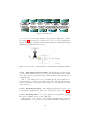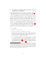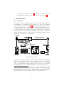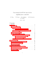
1
User manual for FPGA laser lock-in amplifier/servo controller G. Yang J. F. Barry E. S. Shuman D. DeMille M. H. Steinecker July 3, 2012 Contents 1 Overview 1.1 Introduction . . . . . . . . . . . . . . . . . . . . . . . . . . 1.2 Principles of operation . . . . . . . . . . . . . . . . . . . . 1.2.1 Lock-in amplifier . . . . . . . . . . . . . . . . . . . 1.2.1.1 Modulation waveform generator . . . . . 1.2.1.2 Gain and low-pass filter module . . . . . 1.2.2 Two-channel proportional-integral servo control . . 1.2.3 Ramp mode . . . . . . . . . . . . . . . . . . . . . . 1.3 Signal inputs and outputs . . . . . . . . . . . . . . . . . . 1.4 Basics of operation . . . . . . . . . . . . . . . . . . . . . . 1.4.1 Selecting a mode of operation . . . . . . . . . . . . 1.4.2 Displaying and modifying control parameters . . . 1.4.2.1 Fine tuning and coarse tuning . . . . . . 1.4.2.2 Resetting the display . . . . . . . . . . . 1.4.2.3 Resetting filters . . . . . . . . . . . . . . 1.4.3 Parameters that are disabled under certain modes . . . . . . . . . . . . . . . . . . . . . . . . . . . . . . . . . . . . . . . . . . . . . . . . . . . . . . . . . . . . 4 4 5 5 5 7 8 8 10 13 13 16 18 18 18 19 2 Mechanical layout 2.1 Assembly and connectorization instructions 2.2 On/off switch and reset button . . . . . . . 2.3 FX2 extension interface board . . . . . . . . 2.4 Inputs and outputs . . . . . . . . . . . . . . 3 Electrical characteristics 3.1 The Linear Technology LTC2624 DAC 3.2 The Digilent PmodR2R resistor-ladder 3.3 The analog capture circuit . . . . . . . 3.4 Power supply . . . . . . . . . . . . . . 3.5 Related resources . . . . . . . . . . . . 1 . . . . . . . . . . . . . . . . . . . . . . . . . . . . . . . . . . . . . . . . . . . . . . . . 19 19 21 22 22 . . . . DACs . . . . . . . . . . . . . . . . . . . . . . . . . . . . . . . . . . . . . . . . . . . . . . . . . . . . . . . . . . . . . . . . . . . 23 23 24 25 25 27 4 Initial setup and testing 28 4.1 How to download the software . . . . . . . . . . . . . . . . . . . . 28 4.2 Known bugs and how to recover from them . . . . . . . . . . . . 36 4.2.1 Frozen display . . . . . . . . . . . . . . . . . . . . . . . . 36 5 Procedures for operation 36 5.1 Operation modes . . . . . . . . . . . . . . . . . . . . . . . . . . . 36 5.2 Setting the appropriate lock-in amplifier low-pass-filter cutoff frequency . . . . . . . . . . . . . . . . . . . . . . . . . . . . . . . . . 36 5.3 Procedure for ramping, setting the lock-in gain, and preparing for laser locking . . . . . . . . . . . . . . . . . . . . . . . . . . . . 37 5.3.1 Procedure . . . . . . . . . . . . . . . . . . . . . . . . . . . 37 5.4 Procedure for locking with the slow servo (piezo voltage) channel 39 5.4.1 Procedure . . . . . . . . . . . . . . . . . . . . . . . . . . . 40 5.5 Procedure for locking with the slow servo and the fast servo . . . 41 5.5.1 Procedure . . . . . . . . . . . . . . . . . . . . . . . . . . . 41 6 Performance 6.1 Overview . . . . . . . . 6.2 Procedure for estimating 6.2.1 Procedure . . . . 6.3 Performance data . . . . . . . laser . . . . . . . . . . . . linewidth . . . . . . . . . . . . . . . . . . . . . . . . . . . . . . . . . . . . . . . . . . . . . . . . . . . . . . . . . . . . . . . . . . . . 42 42 43 43 44 7 Materials 44 7.1 Making the box . . . . . . . . . . . . . . . . . . . . . . . . . . . . 45 8 Appendix 8.1 Quick reference . . . . . . . . . . . . . . . . . . . . . . . 8.1.1 Switch configurations . . . . . . . . . . . . . . . 8.1.2 Input and output ranges . . . . . . . . . . . . . . 8.1.3 Parameters, ranges, and bit depths . . . . . . . . 8.2 Miscellaneous characteristics of the system . . . . . . . . 8.2.1 Overflow and underflow prevention . . . . . . . . 8.2.2 Pipelined architecture . . . . . . . . . . . . . . . 8.2.3 Modulation waveform generator implementation 8.3 Troubleshooting the lock . . . . . . . . . . . . . . . . . . 8.3.1 Testing procedure . . . . . . . . . . . . . . . . . 8.4 Related resources . . . . . . . . . . . . . . . . . . . . . . . . . . . . . . . . . . . . . . . . . . . . . . . . . . . . . . . . . . . . . . . . . . . . . . . . . . . . . 45 45 45 47 48 48 48 49 49 49 50 52 . . . . . . . . . . . . . . . . . . . . . . . . . 6 6 7 7 7 List of Figures 1 2 3 4 5 System block diagram. . . . . . . . . . . . . . Lock-in amplifier. . . . . . . . . . . . . . . . . Display shots of the waveform generator. . . . RC filter circuit diagram. . . . . . . . . . . . Screen shots of RC filter control parameters. . 2 . . . . . . . . . . . . . . . . . . . . . . . . . . . . . . 6 7 8 9 10 11 12 13 14 15 16 17 18 19 20 21 22 23 24 25 26 27 28 29 30 31 32 33 34 35 36 37 38 39 40 41 42 43 44 45 Piezo and diode current servo channels. . . . . . . . . . . . . . . Bode plot of servo loops. . . . . . . . . . . . . . . . . . . . . . . . Ramp control of servo drive. . . . . . . . . . . . . . . . . . . . . . Ramp display. . . . . . . . . . . . . . . . . . . . . . . . . . . . . . Inputs and outputs. . . . . . . . . . . . . . . . . . . . . . . . . . Demo board layout. . . . . . . . . . . . . . . . . . . . . . . . . . User interface. . . . . . . . . . . . . . . . . . . . . . . . . . . . . Rotary knob and push-button switches. . . . . . . . . . . . . . . Menu items. . . . . . . . . . . . . . . . . . . . . . . . . . . . . . . Rotary knob central push-button switch. . . . . . . . . . . . . . . Assembly layout. . . . . . . . . . . . . . . . . . . . . . . . . . . . Assembly schematic. . . . . . . . . . . . . . . . . . . . . . . . . . On/off switch and reset button. . . . . . . . . . . . . . . . . . . . FX2 module interface board and block diagram . . . . . . . . . . ADC and DAC layout. . . . . . . . . . . . . . . . . . . . . . . . . Digital square wave modulation (dither) and 6-pin I/O extension connector. . . . . . . . . . . . . . . . . . . . . . . . . . . . . . . . Output glitch noise of the LTC2624. . . . . . . . . . . . . . . . . The PmodR2R resistor-ladder DAC. . . . . . . . . . . . . . . . . Detailed view of analog capture circuit. . . . . . . . . . . . . . . Power supply and details of voltage suppliers. . . . . . . . . . . . Icon for Xilinx iMPACT application. . . . . . . . . . . . . . . . . Jumper locations. . . . . . . . . . . . . . . . . . . . . . . . . . . . USB status LED. . . . . . . . . . . . . . . . . . . . . . . . . . . . Automatic project creation dialog box. . . . . . . . . . . . . . . . Automatic device detection dialog box. . . . . . . . . . . . . . . . Device detection. . . . . . . . . . . . . . . . . . . . . . . . . . . . Selecting “Intialize Chain” in the drop-down menu. . . . . . . . . Automatic device configuration. . . . . . . . . . . . . . . . . . . . Manual device configuration. . . . . . . . . . . . . . . . . . . . . Assigning configuration file. . . . . . . . . . . . . . . . . . . . . . Memory configuration dialog box. . . . . . . . . . . . . . . . . . . Uploading configuration to the FPGA. . . . . . . . . . . . . . . . Dispersion curve shape. . . . . . . . . . . . . . . . . . . . . . . . Oscilloscope display. . . . . . . . . . . . . . . . . . . . . . . . . . Testing setup. . . . . . . . . . . . . . . . . . . . . . . . . . . . . . Power spectral density of locked laser error signal. . . . . . . . . Control switches. . . . . . . . . . . . . . . . . . . . . . . . . . . . Example of an underflow error signal. . . . . . . . . . . . . . . . Signals in the lock-in amplifier unit. . . . . . . . . . . . . . . . . Default LCD display. . . . . . . . . . . . . . . . . . . . . . . . . . 3 8 8 9 9 10 13 17 17 18 18 20 21 22 22 23 23 24 25 26 27 28 29 29 30 31 32 33 33 33 34 35 35 38 40 42 44 45 49 50 51 List of Tables 1 2 3 4 5 6 1 1.1 Inputs and outputs . . . . . . . . . . . . . . . . . . . Mode switches and their functions . . . . . . . . . . Inactive parameters. . . . . . . . . . . . . . . . . . . Reprint of table 2: Mode switches and functionalities Input and output specifications. . . . . . . . . . . . Control parameters. . . . . . . . . . . . . . . . . . . . . . . . . . . . . . . . . . . . . . . . . . . . . . . . . . . . . . . . . . . . 12 14 19 46 48 48 Overview Introduction This system, the AS-1, is a laser servo control system built from an off-theshelf field programmable gate array (FPGA) demo board made by Digilent, the Spartan 3AN700 FPGA. (The FPGA demo board and kit accessories can be purchased from Digi-Key, an online electronics component vendor.) The board has two channels of analog input, four channels of analog output, and a number of extension connectors for plug-ins. For the laser servo control system, we implement a lock-in amplifier and two proportional-integral (PI) servo control channels, one fast and one slow (called “diode current” and “piezo voltage,” respectively, based on their anticipated use). In this configuration, the system can stabilize the output frequency of the laser and “ramp” its piezo voltage to scan for spectral features. By bypassing the lock-in function, the system can operate as a dedicated two-channel feedback servo. All the control parameters can be changed on-the-fly through onboard rotary knobs and push-buttons, and their values are displayed on a two-line LCD display in real time. A dynamic bandwidth allocation algorithm allows the user to change the amount of bandwidth assigned to certain analog output channels by simply flipping a switch. Some details of the signal processing inside the AS-1 can be monitored during normal operation. Four channels of high-speed monitor signal output are offered to provide critical checkpoints along the data processing pathway. The system is subject to a few limitations of which the user should be aware. First, the input and output signals are unipolar, with limited ranges of allowed voltage. It may be necessary to add offset voltages and/or auxiliary hardware in order to provide compatibility between the AS-1 and the remainder of a users setup. Second, the analog-to-digital (ADC) and digital-to-analog conversion (DAC) hardware have finite bandwidth (though the servo loop speeds we have achieved are suitable for many standard laser-locking protocols). Details of these limitations are given later in this manual. 4 1.2 Principles of operation The system consists of a waveform-processing unit and a user interface. The waveform-processing components of the system consist of a lock-in amplifier unit (which generates and outputs its own modulation waveform) and two channels of PI servo control. The waveform-processing unit generates servo feedback outputs based on an error signal input (that is, some signal corresponding to the difference between the measured process variable and its setpoint). In a typical application, the system provides a modulation signal that is used to produce a modulated error signal; this signal is then provided to the system as the input and is demodulated by the lock-in amplifier. Alternatively, the lock-in unit can be bypassed, and an error signal can be provided directly as the system input. In either case, further processing transforms the error signal into feedback to be delivered by the servo control output channels. In addition, the user can choose to output a symmetric triangle wave (or “ramp” signal) to the slow servo control (piezo voltage) output channel. In a typical application, this scans the frequency of a laser back and forth to allow one or more resonant transmission peaks of a Fabry-Perot cavity to be observed using a photodiode. The user interface presents the values of the internal control parameters and allows the user to change these parameters during operation. Figure 1 shows the relationship between the waveform-processing unit and the user interface. 1.2.1 Lock-in amplifier The role of the lock-in amplifier is two-fold: first, to generate and output a modulation signal at some specified frequency, and second, to demodulate the input signal to the system using the same generated modulation signal (with a phase offset). The architecture of the lock-in amplifier unit can be seen in figure 2. Its key components include a modulation waveform generator, a multiplier with gain, and a low-pass filter. The lock-in amplifier can also be bypassed to use the system as a dedicated feedback servo; details of this mode of operation are given in section 5.1. 1.2.1.1 Modulation waveform generator The user can choose to output a sinusoidal signal through a DAC or a digital square wave signal with fixed amplitude. To output the sinusoidal signal, the user can opt to use the integrated Linear Technology LTC2624 quad DAC or one of the monitor output channels provided by several 25 MHz resistor-ladder DACs (Digilent PmodR2R), which are connected to extension ports on the FPGA board. When using the LTC2624, due to the modest slew rate (1 V/µs), we recommend a modulation frequency less than 150 kHz. If the faster resistor-ladder DAC is used, the maximum usable 5 Figure 1: System block diagram. Transmission Input In Modulation Drive Digital Mod. Drive Out Lock-‐in Amplifier Out Lock-‐in Gain Modulation Waveform Generator Mixer Output x Multiplier Out Phase Shifter Phase-‐shifted Digital Mod. Drive Error Signal Lock-‐in Amplifier Low-‐pass Filter Figure 2: Lock-in amplifier. 6 modulation frequency is limited by the Nyquist frequency of the analog input ADC, at 750 kHz. A digital modulation signal output is also provided that can generate a 3.3 V peak-to-peak square wave at 50 MS/s. The modulation waveform (either analog or digital) is phase-shifted internally to generate a phase-offset modulation waveform with 12-bit phase precision. The display gives the phase shift in units of π. (When a digital square wave modulation is used, both the phase-shifted and non-phase-shifted modulation signals are provided as outputs for testing and comparison.) Figure 3: Display shots of the waveform generator. The 14-bit input signal from the ADC is multiplied with the phase-shifted modulation waveform to produce what we refer to as the mixer output signal. 1.2.1.2 Gain and low-pass filter module The mixer output signal is multiplied by a pre-filter gain (between the mixer and the filter, so called post-mixer gain in the menu) and low-pass filtered through an infinite impulse response filter (IIR filter). The IIR implementation of the low-pass filter has exactly the same characteristics as an ideal simple RC filter and is completely specified by its cut-off frequency f (see figure 4). A proof of the equivalence of an IIR filter and an RC filter is provided in the companion paper. Figure 5: Screen shots of RC filter control parameters. Figure 4: RC filter circuit diagram. 7 1.2.2 Two-channel proportional-integral servo control The system generates two channels of proportional-integral (PI) servo control with variable low-pass cut-off frequencies and gains. A high-pass filter is implemented in the fast servo control (diode current) channel to allow any lowfrequency feedback to be provided solely by the slow servo control (piezo voltage) channel (which is expected to have a much larger tuning range than the fast servo control channel). PI Servo Slow x Error Signal Piezo Gain Piezo Low-‐pass Filter PI Slow Piezo Drive PI Servo Fast x Diode Current Diode Current Low-‐pass Gain High-‐pass Filter PI Fast Current Drive Figure 6: Piezo and diode current servo channels. The Bode plot of the complete system is shown in figure 7. Figure 7: Bode plot of servo loops. 1.2.3 Ramp mode The ramp feature is intended to allow the user to scan a laser for a spectral feature, such as a resonant transmission peak of a Fabry-Perot cavity. When 8 the ramp is on, the slow servo control (piezo voltage) signal is disconnected from its output channel, and instead a symmetric triangle wave is output to this output. Both the slow and fast servos are effectively disabled in ramp mode; their low-pass filters are set to a cutoff frequency of 14 mHz whenever the ramp is on. Figure 8: Ramp control of servo drive. The ramp frequency is displayed as a single number (which we call the ramp frequency exponent) from 0 to 15. (The digits above 9 are displayed as 10 → “:”, 11 → “;”, 12 → “<”, 13 → “=”, 14 → “>”, 15 →“?”.) The ramp frequency in Hz is ≈ 1500/2x , where x is the ramp frequency exponent. The default ramp frequency exponent of 6 corresponds to a frequency of ≈ 24 Hz. Figure 9: Ramp display. The peak-to-peak amplitude of the ramp is controlled with 12-bit precision from 0 to 3.3 V; the triangle wave has a fixed mean voltage of 1.65 V. Rotating 9 the knob while the ramp menu item is displayed changes the amplitude. With the same menu displayed, the frequency can be changed by depressing and turning the knob simultaneously. 1.3 Signal inputs and outputs There are two channels of analog input, four channels of analog output, and two channels of digital output native to the Spartan 3AN demo board. Through the attached expansion board, another four channels of high-speed analog monitor output are provided. Pmod Resistor Ladder ADC Monitor 4 Monitor 3 Monitor 2 2 Channel Input ADC LTC1407A Monitor 1 Input (adc_a) Monitor 1 GND J19 header Not Used (adc_b) 6-pin I/O Connector 4-Channel Output DAC LTC2624 Not Used Not Used Digital Mod Drive Phase Shifted Digital Mod GND VCC Modulation Drive Not Used Piezo Drive Current Drive Figure 10: Inputs and outputs. The dual-ADC (LTC1407) used for the analog inputs reads in two channels at 14-bit precision. The input range is from 400 mV to 2.9 V; therefore any signal outside this range, including signals extending to ground, must be shifted with an offset amplifier before being sent to the ADC. The sampling rate is 1.5 MS/s for each channel. A programmable pre-amplifier (LTC6912-1) is used before each analog input ADC to provide input impedance of 10 kΩ at unity gain. This gain can be adjusted using the AS-1 system software, and higher gain settings will produce lower input impedances. For the native analog outputs, a single four-channel Linear Technology DAC (LTC2624) on the FPGA board generates signals with 12-bit resolution from 0 to 3.3 V, with the total 1.5 MS/s bandwidth shared among all the four output channels. This DAC has a typical allowed output current of up to ∼ 20 mA, which gives an effective output impedance of ∼ 160 Ω. The LTC2624 has a slew rate of 1 V/µs and a settling time of 10 µs. The high-speed analog monitor signals are output via Digilent Pmod resistorladder DACs attached to the FX2 Module Interface Board (MIB) expansion card. These Pmod DACs have an output range from 0 to 3.3 V with a rated bandwidth of 25 MHz and 8-bit resolution. In our system, these DAC data lines are updated at 50 MHz. The resistor-ladder DACs used in this system have an 10 output impedance of > 10 kΩ. Therefore, short cable length is advised while using these monitor outputs (to avoid attenuation of high-frequency signals due to large cable capacitances), and (buffer) amplification is required to use these outputs with low impedance loads. In practice, we have frequently monitored these channels with oscilloscope probes. The names and functions of these inputs and outputs are described in table 1. All the output signals are treated as bipolar signals centered at 1.65 V. On the other hand, the input may be treated as a unipolar signal with reference zero at 0.4 V or a bipolar signal with reference zero at 1.65 V. In both cases, the input signal must remain within the range from 0.4 V to 2.9 V. (An offset amplifier is used to lift the input signal by 0.4 V in our test setup.) 11 Table 1: Inputs and outputs Port Input ADC-A ADC-B Analog output LTC2624-1 Name System input N/A Modulation output LTC2624-2 N/A LTC2624-3 Slow servo (piezo voltage) channel LTC2624-4 Fast servo (diode current) channel High-speed analog output Resistor-ladder Monitor 1 DAC 1 Resistor-ladder DAC 2 Monitor 2 Resistor-ladder DAC 3 Monitor 3 Resistor-ladder DAC 4 Digital output J19 < 3 > Monitor 4 J19 < 2 > Digital square modulation Phase-shifted square modulation Function Signal properties 0.4–2.9 V, 14 bits, 10 kΩ Input signal (e.g., from 1.5 MS/s a photodiode following a Fabry-Perot cavity) Not used 1.5 MS/s 0–3.3 V, 12 bits, ∼ 160 Ω Modulation signal 1.02 MS/s or 0 S/s* Not used Ramp or slow PI servo control Fast PI servo control TTL trigger synchronized with ramp waveform High-passed error signal or error signal with 8x gain Modulation signal or phase-shifted modulation signal Mixer signal or system input signal Fast square modulation signal Fast square modulation signal with applied phase offset 0 S/s 30 kS/s 450 kS/s or 1.47 MS/s* 0–3.3 V, 8 bits, > 10 kΩ 50 MS/s 50 MS/s 50 MS/s 50 MS/s 0 V/3.3 V, 1 bit, > 10 kΩ 50 MS/s 50 MS/s *In configuration 1, the analog modulation waveform is output on LTC2624-1 (that is, channel 1 of the slow DAC). In this configuration, it is allocated a bandwidth of 1.02 MS/s, and the fast servo (diode current) channel is allocated a bandwidth of 450 kS/s. In configuration 2, the modulation waveform is output instead on resistor-ladder DAC 3, allowing a bandwidth of 1.47 MS/s to be allocated to the fast servo (diode current) channel. The location of the analog input and outputs are shown in figure 11. 12 Figure 11: Demo board layout. 1.4 1.4.1 Basics of operation Selecting a mode of operation Figure 12 shows the layout of the mode switches. On the left side of the knob, the slide switches are, from left to right, SW3, SW2, SW1, and SW0. On the right side, four additional switches are plugged into the extension connector J18. They are, from left to right, J18 < 0 >, J18 < 1 >, J18 < 2 >, and J18 < 3 >. 13 Please note that these four switches must be plugged in in order for the system to function. Table 2 lists the function of the eight mode switches. Table 2: Mode switches and their functions Switch Setting SW3 Down Up SW2 Down Up SW1 Down Function or Mode Selects the monitor output signal function. Monitor 1 always provides a TTL trigger synchronized with the ramp. Monitor 2: Error signal (or demodulated system input signal) Monitor 3: Modulation signal Monitor 4: System input signal Monitor 2: High-pass-filtered signal from the fast servo channel Monitor 3: Phase-shifted modulation signal Monitor 4: Mixer signal (from after the lock-in multiplier but before the lock-in low-pass filter) Controls the fast servo (diode current) channel Fast servo channel enabled In this mode the low-pass-filter cutoff frequency on the fast servo channel is determined by the setting in the menu. Fast servo channel disabled In this mode the low-pass-filter cutoff frequency on the fast servo channel is set to 14 mHz ≈ 1/(1.5 minutes), effectively disabling this channel. Controls the ramp Ramp enabled The display switches to “RAMP is ON.” The ramp mode disconnects the slow servo (piezo voltage) channel from its output, and instead a symmetric triangle wave (with frequency and amplitude specified on the LCD) is sent to the slow servo output. In ramp mode, the low-pass filter frequencies for both servo channels are set to 14 mHz ≈ 1/(1.5 minutes), effectively disabling the two servos. 14 Mode switches and their functions Switch Setting Function or Mode Up Ramp disabled The slow servo (piezo voltage) channel is connected to its output normally, and its low-pass filter frequency determined normally (by the setting in the menu). Selects the modulation waveform (analog sine or digital square wave) Modulation waveform in sinusoidal mode A sinusoidal modulation waveform is sent to the modulation drive output, and a phase-shifted version is sent to the lock-in for demodulation of the input signal. Modulation output in square wave mode A square wave modulation waveform is sent to a digital output line, and a phase-shifted version is sent to the lockin for demodulation of the input signal. The digital square wave modulation signal and the phase-shifted digital modulation signal can be monitored in this mode at J19 < 3 > and J19 < 2 >. Switches between lock-in modes (active or bypass) Lock-in active This is the normal mode of operation, where the input signal is demodulated in the lock-in amplifier. Lock-in bypassed In bypass mode, the lock-in amplifier is disabled so that signal from the input can be used directly by the servo channels as an error signal. (Note that the lock-in low-pass filter is still effective, however.) In this mode, the following parameters are automatically set: Input reference voltage: 1.65 V Modulation frequency: 0 SW0 Down Up J18 < 0 > Down Up 15 Mode switches and their functions Switch Setting J18 < 1 > Down Up J18 < 2 > Down Up J18 < 3 > Down Up 1.4.2 Function or Mode Switches the input reference zero (0.4 V or 1.65 V). The input reference zero is automatically set at 1.65V in lock-in bypass mode. In both modes, the input signal must remain between 0.4 V and 2.9 V. Reference zero set to 0.4 V In this mode, input signals are treated as unipolar and positive. Reference zero set to 1.65 V In this mode, input signals are treated as bipolar, with values below 1.65 V treated as negative and values above treated as positive. Controls the slow DAC (LTC 2624) bandwidth allocation Configuration 1. Bandwidth allocation ratios are as follows: Modulation waveform output: 68% (1.02 MS/s) Slow servo (piezo voltage) channel: 2% (30 kS/s) Fast servo (diode current) channel: 30% (450 kS/s) Configuration 2. Bandwidth allocation ratios are as follows: Modulation waveform output: 0% Slow servo (piezo voltage) channel: 2% (30 kS/s) Fast servo (diode current) channel: 98% (1.47 MS/s) Slow servo (piezo voltage) channel polarity switch Original Inverted Displaying and modifying control parameters Parameters such as the modulation amplitude, modulation frequency, various gains, and various filter cutoff frequencies are accessible through the user interface (UI). The UI consists of a 2-line character LCD display, mode switches, momentary push-buttons, and a rotary knob with an integrated push-button. 16 Figure 12: User interface. All the available parameters are presented in the menu in a cyclical sequence, as shown in figure 14. The user can cycle through the control parameters by pushing the “west” and “east” push-buttons. The “south” button is used to reset the LCD display. The “north” button can be used to zero all the lowpass filters in the control system, equivalent to discharging the capacitors in an analog low-pass filter. Figure 13: Rotary knob and push-button switches (adapted from the Digilent manual). To modify a parameter, the user turns the rotary knob (shown in figure 13). Due to hardware differences between production batches of the demo board, the direction of increment may vary (i.e. a clockwise turn may increase the value in some boards, while a counterclockwise turn might do so in others). The rotary knob on the demo board has a built-in push-button that is used to 17 Figure 14: Menu items. choose between coarse and fine changes of the parameter during knob rotation (see figure 15). In ramp mode, this is used to choose between adjusting the ramp frequency (by depressing the knob while turning) and adjusting the ramp amplitude (by turning the knob freely). Figure 15: Rotary knob central push-button switch (from the Digilent manual). 1.4.2.1 Fine tuning and coarse tuning When changing any given parameter, the change that takes place at each step is a fixed fraction of the original value. The only exception is the phase, which is changed linearly instead of logarithmically. Fine or coarse tuning can be selected. Turning the knob freely (without depressing the knob), each rotary step changes the value of the selected parameter by 12.5%. If the knob is depressed, a finer change of 1.56% will take place with each rotary step. 1.4.2.2 Resetting the display If the display appears frozen, it can be reset by pressing the “Display Reset” button, the “south” button. (See section 4.2.1.) 1.4.2.3 Resetting filters To reset the high and low-pass filters, a global filter reset is available as the “north” pushbutton. When trying to lock a laser to a spectral line, it is important to have the low-pass filters zeroed to provide the best lock with maximized locking range on 18 each side. Low-pass filters with relatively high cutoff frequency such as the lockin amplifier low-pass are generally less sensitive to this condition. To confirm that the slow servo low-pass filter is zeroed, one can compare this channel’s output with the standard 1.65 V reference voltage. 1.4.3 Parameters that are disabled under certain modes In some modes of operation, certain parameters are not applicable or have predefined values. These inactive parameters are given in table 3. Mode Fast servo (diode current) off Ramp mode Lock-in bypass mode 2 2.1 Table 3: Inactive parameters. Inactive parameters Notes Fast servo (diode current) This parameter is set to low-pass-filter cutoff fre- 14 mHz to effectively disable the fast servo channel. quency Slow servo (piezo voltage) and fast servo (diode current) low-pass-filter cutoff frequencies Input reference zero These parameters are set to 14 mHz to effectively disable both servo channels. The input reference zero is locked at 1.65 V. Switch J18 < 1 > has no effect. Mechanical layout Assembly and connectorization instructions The system includes the Digilent Spartan-3AN demo board and an FX2 Module Interface Board (MIB). As shown in figure 16, four Pmod resistor-ladder DACs are attached to the J1–J4 12-pin headers on the FX2 interface board to provide outputs for the monitor 1–4 signals. An additional Pmod slide-switch board is connected via J18. A sample layout of the BNC cable connectors in an enclosure is shown in figure 17. The user must connect cables between the output pins on the boards and the BNC connectors on the enclosure. We have soldered small coaxial cables directly to pins on the board. The outer conductors of the cables (and BNC connectors) are connected to the ground terminals on the board. 19 Figure 16: Assembly layout. 20 Figure 17: Assembly schematic. 2.2 On/off switch and reset button The on/off switch of the board and the FPGA reset button can be found as indicated in figure 18. The on/off switch is used to turn the power on and off. The reset button can be used to quickly reset or reprogram the FPGA. This should not disrupt any connection between the FPGA and a computer being used to program it. 21 Figure 18: On/off switch and reset button. 2.3 FX2 extension interface board The FX2 high-speed extension port on the demo board is used to connect to the Digilent FX2 Module Interface Board (MIB), shown in figure 19. In our setup, four resistor-ladder DACs are connected through the 12-pin Pmod connectors on the FX2 MIB. Figure 19: FX2 module interface board and block diagram (from Digilent FX2 MIB reference manual). 2.4 Inputs and outputs The Linear Technology ADC and DAC are laid out as shown in figure 20. 22 Figure 20: ADC and DAC layout. The monitor 1 and 2 signals are drawn from the Pmod resistor-ladder DACs (which are plugged in on the FX2 interface board via the J3 and J4 12-pin headers) and output through the black two-pin headers extending from the end of each Pmod DAC. The digital square wave modulation signal can be taken from pins 2 and 3 of the J19 header if needed. We did not connect this to an output jack on the front panel of the enclosure, but the user can do so easily if desired. Figure 21: Digital square wave modulation (dither) and 6-pin I/O extension connector. 3 3.1 Electrical characteristics The Linear Technology LTC2624 DAC The LTC2624 DAC used on the Digilent board is a rail-to-rail-voltage DAC, with an effective output impedance of ∼ 160 Ω. (More correctly, it can drive loads larger than ∼ 160 Ω reliably.) 23 A few design properties of this DAC limit the performance of the system. The sampling rate of the DAC is 1.5 MS/s. This gives a Nyquist frequency of 750 kHz; however, the usable output bandwidth is further limited by the modest slew rate of 1 V/µs, which effectively cuts off the high-frequency components in the reconstruction of an output waveform of reasonable magnitude. In addition, the LTC2624 DAC also has a moderate glitch noise, a noise that appears when the DAC switches between output values. The amplitude of this transient is on the scale of 20 mV at midrange (1.65 V). Figure 22: Output glitch noise of the LTC2624 (from data sheet). The four analog outputs on this DAC share a total bandwidth of 1.5 MS/s, which is allocated taking into account how fast the signal of each channel is expected to change, as described in table 5. The dynamic bandwidth allocation algorithm allows on-the-fly changes to the allocation ratio. There are two configurations. In configuration 1, the analog modulation output is allocated a sampling bandwidth of 1.02 MS/s, compared with 450 kS/s for the fast servo control (diode current) channel and 30 kS/s for the slow servo control (piezo voltage) channel. In configuration 2, the modulation output is completely bypassed, providing 1.47 MS/s of bandwidth to the fast servo control (diode current) channel (and 30 kS/s for the slow servo control (piezo voltage) channel). Slide switch J18 < 2 > allows the user to choose between these modes (see table 2). More information on the LTC2624 DAC can be found on the Linear Technology website: http://www.linear.com/product/LTC2624. 3.2 The Digilent PmodR2R resistor-ladder DACs The PmodR2R DACs provide 8-bit digital-to-analog conversion at up to 25 MHz. Note, from the design schematics shown in figure 23, it is easy to estimate that these DACs do not output any current (less that 0.1 mA), and therefore they should only be used to drive a high-impedance device such as an oscilloscope 24 or (buffer) amplifier. The high output impedance of the Pmod R2R DACs also means that fast signals will be severely attenuated if the outputs are sent through coaxial cables of any significant capacitance. http://www.digilentinc.com/ Data/Products/PMOD-‐R2R/ PmodR2R-‐block-‐207.gif Figure 23: The PmodR2R resistor-ladder DAC. More information on the PmodR2R DAC can be found on the Digilent website: http://www.digilentinc.com/Products/Detail.cfm?NavPath=2,401, 615&Prod=PMOD-R2R 3.3 The analog capture circuit The analog capture circuit on the FPGA board consists of a LTC6912 dualchannel, programmable-gain pre-amplifier connected to a LTC1407 14-bit, dualchannel, 1.5-MS/s-per-channel, simultaneous-sampling ADC. The pre-amplifier is programmed to have unity gain in our setup. The LTC1407 ADC has two differential inputs with a range of 2.5 V (±1.25 V); however, on the FPGA board, the range of the inputs is centered around the 1.65 V internal reference zero. Hence, the analog capture circuit can only accept incoming signals from 0.4 V to 2.9 V in this design. The input impedance of the analog capture circuit is 10 kΩ when the programmable preamplifier is set to unity gain. The input impedance is lower at higher gains. The inputs have idle potentials of 1.65 V when not connected. 3.4 Power supply The board uses an AC wall adapter to supply 5 V (DC) through a connector socket on the upper-left corner of the board. A detailed description of the volt- 25 Figure 24: Detailed view of analog capture circuit (from Xilinx user guide). 26 age supply on the board can be found at http://www.xilinx.com/support/ documentation/boards_and_kits/ug334.pdf. Figure 25: Power supply and details of voltage suppliers (from Xilinx user guide). 3.5 Related resources Refer to the following links for additional information and datasheets: • Xilinx Spartan-3A/3AN FPGA Starter Kit Board User Guide: http:// www.xilinx.com/support/documentation/boards_and_kits/ug334.pdf • LTC2624 Quad DAC Datasheet http://www.linear.com/pc/downloadDocument. do?navId=H0,C1,C1155,C1005,C1156,P2048,D2170 • Resistor Ladder DAC http://www.digilentinc.com/Data/Products/PMOD-R2R/ PmodR2R_rm_RevB.pdf • LTC6912 Dual Programmable Gain Amplifiers with Serial Digital Interface http://www.linear.com/pc/downloadDocument.do?navId=H0,C1, C1154,C1009,C1121,P7596,D5359 • LTC1407A-1 Serial, 14-bit, Simultaneous-Sampling ADCs with Shutdown http://www.linear.com/pc/downloadDocument.do?navId=H0,C1,C1155, C1001,C1158,P2420,D1295 27 4 Initial setup and testing 4.1 How to download the software 1. First, the WebPACK software from Xilinx must be installed. To download this software from the Xilinx website, the user needs to register. See http://www.xilinx.com/tools/webpack.htm. Complete the registration, download the software, and install the software. 2. After installation, locate the Xilinx iMPACT application on your computer. Figure 26: Icon for Xilinx iMPACT application. 3. Now check all the jumpers on the FPGA demo board. Details can be found in the FPGA user guide. Briefly, one should check the status of the following jumpers, shown in figure 27: boot mode select jumper (bottom left of the figure), reset select J18 (upper right), SPI programming jumper (upper right), and power supply and memory jumper (bottom right). 28 Figure 27: Jumper locations. 4. Now connect the 5 V (DC) power supply to the power jack on the demo board (J4) 5. Connect the FPGA to your PC using the USB cable (J7). The green LED on the side of the USB socket (J7) should flash a couple of times. When it stops blinking and is constantly on, it means the PC is ready to communicate with the board using the USB interface. Figure 28: USB status LED. 6. Now open up iMPACT if you havent done so. If this is your first time running iMPACT, it will prompt you to create a new project. Click “Yes.” 29 Figure 29: Automatic project creation dialog box. 7. In the next dialog box, choose the option shown in figure 30 and click “OK.” The system should automatically detect the FPGA device. If so, skip to step 10. If not, continue with the next step. 30 Figure 30: Automatic device detection dialog box. 31 Figure 31: Device detection. 8. If the detection failed, disconnect and reconnect the FPGA device. Wait for the green LED on the side of the USB jacket to blink a couple of times. 9. Right-click in the area indicated in figure 32 to bring up a drop-down menu; click “Initialize Chain.” 32 Figure 32: Selecting “Intialize Chain” in the drop-down menu. 10. After communication with the device is established, iMPACT will need to assign configuration files. This will either begin automatically (as shown in figure 33) or by right-clicking the device and choosing “Assign New Configuration File” from the drop-down menu (as shown in figure 34). Figure 33: Automatic device configuration. 33 Figure 34: Manual device configuration. 11. For the FPGA, choose the design file you downloaded from us, “controller.bit.” Click “Open.” Figure 35: Assigning configuration file “controller.bit.” 12. A new window should pop up. This is for the memory. Choose “Bypass.” 34 Figure 36: Memory configuration dialog box; choose “Bypass.” 13. Now you can upload the configuration to the FPGA. Right click on the device and choose “Program Flash and Load FPGA” in the drop-down menu. Figure 37: Uploading configuration to the FPGA. 35 4.2 4.2.1 Known bugs and how to recover from them Frozen display In some cases, the binary to decimal conversion can take a very long time after switching between menu items in the middle of a conversion. If the display appears to be frozen, it can be reset by pressing the “Display Reset” button (the “south” button). 5 Procedures for operation This section outlines procedures for operating the system in a typical laserlocking application. The procedures that follow assume that the user has set up the system in a configuration similar to that shown in figure 40. 5.1 Operation modes This system has two primary operation modes: the ramp mode and the laserlocking mode (see section 1.4.1). In the ramp mode, the servo signals are effectively disabled for both the slow servo control (piezo voltage) and the fast servo control (diode current) outputs, and instead a triangle-wave signal is sent to the slow servo control (piezo voltage) output. Hence, the laser frequency is tuned back and forth with a linear dependence in time. The user can turn the ramp mode on or off by flipping switch SW1 on the FPGA demo board (see table 2). In the laser-locking mode, the system servo controls the laser wavelength based on the error signal that is generated by the on-board lock-in amplifier. In this mode, the laser can be locked using both the fast and slow servos or the slow servo alone. A lock-in-bypass mode is also available (enabled using switch J18 < 0 >; see table 2). This mode is intended to allow the user to provide a bipolar error signal (centered around the 1.65 V reference zero) as the system input; this error signal is then used directly by the slow servo control (piezo voltage) and fast servo control (diode current) channels. The internal lock-in amplifier is bypassed, and the modulation output is disabled. Note, however, that the lock-in amplifier’s low-pass filter is still in effect in this mode. 5.2 Setting the appropriate lock-in amplifier low-pass-filter cutoff frequency The low-pass-filter cutoff frequency of the lock-in amplifier should be less than ∼ 1/6 times the modulation frequency to adequately suppress the response of the system at the modulation frequency. 36 5.3 Procedure for ramping, setting the lock-in gain, and preparing for laser locking The procedure in this section is used to determine a useful range of gain for the lock-in amplifier, to find the proper phase offset for the modulation signal1 , and to center the laser frequency on the desired spectral feature for locking. Using a four-channel oscilloscope, make the following connections to prepare for the procedure that follows. Using a tee, connect the Fabry-Perot transmission signal (which provides the input to the system; maintain this connection as well) to scope channel 1. Connect the modulation signal output to scope channel 2 and trigger on its rising edge. Connect the monitor 2 output to scope channel 3 and the slow servo control (piezo voltage) channel output to scope channel 4. If only a two-channel scope is available, instead connect the monitor 2 output to scope channel 1 and the Fabry-Perot transmission signal to scope channel 2; connect the modulation signal output to the external trigger channel of the scope and trigger on its rising edge. An example is shown in figure 39. Note: If the transmission signal extends below 400 mV, you must use an offset amplifier to ensure that the minimum voltage sent to the system input remains above 400 mV. The system input has a range from 400 mV to 2.9 V. 5.3.1 Procedure 1. Turn on the power to the board. 2. Reset the low-pass filters by pressing the “north” button. 3. If using the analog modulation output, pick a modulation waveform frequency that is less than 150 kHz. The default modulation waveform frequency is 61 kHz. If using the digital modulation output at J19 < 3 >, the frequency can be set as high as 700+ kHz. 4. Leave the modulation amplitude as 1 V (default setting) for now. (This does not affect the digital modulation output, which is fixed at 3.3 V peakto-peak.) Increasing the modulation amplitude will change the shape of the dispersion-like (see figure 38) error signal as well as the capture range. Proper amplitude can be found after one is able to display the dispersionlike signal on a scope (that is, after step 13). 1 In a typical application, the (non-phase-shifted) modulation signal is used to drive an acousto-optic modulator (AOM), which dithers the laser frequency before it enters a FabryPerot cavity; the transmission signal is then read on a photodiode and provided to the system as the input signal. This produces some unknown phase delay relative to the (non-phaseshifted) modulation signal. Finding the proper phase offset refers to finding the offset corresponding to this unknown phase delay so that the lock-in amplifier may correctly demodulate the input signal (using the phase-shifted modulation signal). 37 Figure 38: Dispersion curve shape (adapted from http://users-phys.au.dk/ philip/pictures/physicsfigures/). 5. Turn on the ramp (by sliding the switch SW1 to the up position). 6. Observe the Fabry-Perot transmission signal on the scope, and change the central laser frequency (using, e.g., the piezo offset on the laser’s controller) until the desired spectral peak is found. 7. Change the ramping amplitude to get a proper scanning range, where features of a single peak can be seen. 8. Center the peak: adjust the laser frequency (using, e.g., the piezo offset on the laser’s controller) such that the peak is located at the midpoint (that is, 1.65 V) of the triangle ramping signal. 9. To make sure the lock-in amplifier gain is set properly, select the mixer output signal for output on monitor 4 by flipping SW3 up. Temporarily disconnect monitor 2 from the scope and connect monitor 4 to this scope channel. 10. Turn the lock-in amplifier gain up and down, until the mixer output signal is around half of the total dynamic range (around 1.65–2 V peak-to-peak if no other attenuation or amplification is in place). Then the lock-in amplifier gain is set properly. 11. Flip SW3 down to select the error signal for output on monitor 2. Disconnect monitor 4 from the scope and reconnect monitor 2 to this scope channel. You should see a dispersion-shaped curve with a (reference-) zero-crossing at the position of the spectral peak on the raw input signal. Now start to change the phase (using the “east” or “west” button to select the phase offset parameter on the LCD and adjusting its value using the 38 rotary knob). The amplitude of the dispersion-shaped error signal should start to decrease. 12. Find the phase at which the error signal is a zeroed line even when scanning through a transmission line. Now the phase corresponds to ±π/2 phase relative to the modulated signal. The sign will need to be experimentally determined. 13. Add or subtract π/2 from this phase value, and set the phase offset on the LCD to the resulting value. This is where you should see the maximum amplitude in the error signal. 14. To find the best modulation amplitude, start with a modulation amplitude of 0. Increasing the amplitude will result in a wider dispersion signal with less and less center slope. Since this is before you have set the low-pass filter in the lock-in, you may see modulation residuals in the waveform. 15. Further increase will result in the zero-crossing dispersion signals separating into two inverted peaks. Decrease the modulation amplitude to prevent this separation.This will provide the best performance of the lock. 16. To set the lock-in amplifier low-pass-filter cutoff frequency, begin with the cutoff frequency the same as the modulation frequency. You should still see strong oscillations in the error signal at the modulation frequency as you ramp through a spectral line. Now, turn down the cutoff frequency until you see no obvious residual wiggles in the error signal at the modulation frequency. 17. To more carefully set the modulation amplitude, again start from a modulation amplitude of 0. Initially, increase of the modulation amplitude increases the amplitude of the dispersion-like signal. Stop increasing the modulation amplitude when further increase decreases the slope of the dispersion-like signal (i.e. broadens the line without increasing its amplitude). 18. Adjust the central frequency of the laser (using, e.g., the piezo offset on the laser’s controller) and turn down the amplitude of the ramp to zoom in on a peak of interest for locking. 5.4 Procedure for locking with the slow servo (piezo voltage) channel With the phase and the lock-in gain set up correctly, locking the laser using the slow servo control (piezo voltage) channel is simply a matter of increasing this servos gain up to a level just below where the system begins to undergo auto-oscillation. This procedure assumes the same connections are in place as described in section 5.3. 39 5.4.1 Procedure 1. Disable the fast servo (diode current) channel by turning its gain down to zero. 2. Reset the filters by pressing the “north” button. 3. To tune to a transmission line, first turn off the ramp by flipping SW1 down. Observe the Fabry-Perot transmission signal on a time-scale such that the modulation frequency is easily visible. Adjust the laser’s frequency (using, e.g., the piezo offset on the laser’s controller). You are tuned to a transmission line when the transmission signal shows periodic oscillations at a frequency twice that of the modulation frequency. Typical signals under these conditions are shown in figure 39. Figure 39: Oscilloscope display. The blue trace is the modulation signal. The yellow trace is the signal from the Fabry-Perot photodiode; this is provided to the system as the input signal. The purple and green traces are the error signal and the piezo drive signal, respectively. 4. Increase the slow servo (piezo voltage) gain, starting from 0. At first, the lock should become more stable, as seen by smaller fluctuations of the error signal. As the gain is increased further, the error signal will suddenly begin to oscillate, and the system will become unstable. 5. Starting from around 1 kHz, turn down the low-pass-filter cutoff frequency for the slow servo (piezo voltage) channel just enough to make the oscillations in the error signal too small to see. 6. Repeat 4 and 5 until further increase of gain destabilizes the laser. 40 As a reference, the value of the low-pass-filter cutoff frequency found to be optimal in our setup was around 200–500 mHz. 5.5 Procedure for locking with the slow servo and the fast servo Assuming the laser is stably locked using the slow servo control (piezo voltage) channel as described above, the fast servo control (diode current) channel can be added to the lock with the following procedure. 5.5.1 Procedure 1. Make sure the fast servo (diode current) gain is set to 0. 2. Set the high-pass-filter cutoff frequency to around 1 Hz. 3. One can reset the filters by pressing the “north” button. This will unlock the laser, since the slow servo channel will have already accumulated some level of offset, and resetting all the filters will (reference-) zero the slow servo channel output. Relock the laser by tuning to a close-by Fabry-Perot transmission line. To do this, slightly change the central frequency of the laser (using, e.g., the piezo offset on the laser’s controller). 4. Set the fast servo (diode current) low-pass-filter cutoff frequency to above that of the lock-in-amplifier low-pass filter. 5. Check that you are still locked with the slow servo (piezo voltage) channel. This can be verified by seeing oscillations of the error signal if the slow servo (piezo voltage) gain is slightly increased. If not, repeat the slow servo (piezo voltage) locking procedure and then return to step 1 of this procedure. 6. In general, increasing the gain should result in a tighter lock. However, at some point further increase will result in excessive feedback and cause auto-oscillation. Therefore, the gain limit is reached when such autooscillation occurs. Begin turning up the fast servo (diode current) gain until the system becomes unstable and starts to oscillate. One can try to decrease the slow servo (piezo voltage) gain or increase the fast servo (diode current) high-pass-filter cutoff frequency to prevent the fast servo and the slow servo channels from fighting against each other. However, if further increase of the high-pass-filter cutoff frequency does not make a substantial difference, do not continue increasing the cutoff frequency. 7. The effect of the fast servo (diode current) channel is more obvious if one uses a spectrum analyzer to monitor the spectrum of fluctuations in the laser frequency. To do this, send the error signal output to a spectrum analyzer, and adjust the fast servo (diode current) and slow servo (piezo 41 voltage) gains as described in step 6 to minimize the Vrms seen on the spectrum analyzer. This should produce the narrowest laser line.2 6 6.1 Performance Overview To test the performance of this system, we locked a Toptica external-cavity diode laser (DL100) to a transmission line of a Fabry-Perot cavity. The schematic of the test setup is shown in figure 40. The optical frequency modulation is accomplished with an acousto-optic modulator (AOM); the AOM is driven by a voltage-controlled oscillator (VCO) whose frequency in turn is dithered by the modulation signal from our system. The Fabry-Perot has a finesse of 200 and a free spectral range of 1 GHz, giving it transmission peaks with spectral widths of 5 MHz. An amplified photodiode transforms the laser light transmitted through the Fabry-Perot cavity into a voltage signal. Figure 40: Testing setup. The photodiode signal is offset by 400 mV using a Stanford Research Systems (SRS) voltage amplifier (SR560) in order to match the reference zero of the input channel of our system. The offset is set by turning a small screw on the front panel of the SRS amplifier. With this 400 mV offset, the photodiode signal with no light is lifted from 0 V to 400 mV and will be read by the ADC as zero. 2 Looking at the spectrum of the error signal, one can tune the parameters to achieve the least root-mean-squared of the power spectrum. However, note that decreasing the modulation amplitude will change the slope of the zero-crossing dispersion-like signal and therefore affect the amplitude of the error signal. Change of the lock-in-amplifier gain will also change the apparent amplitude of the error signal. These changes do not reflect a tighter lock. 42 On the output end, a 20 dB Mini-Circuits attenuator is used between the slow servo (piezo voltage) output and the laser controller’s piezo input to limit the effect of the glitch noise of the DAC (see section 3.1). Similarly, another 20 dB attenuator is used in series with the fast servo (diode current) output. In our setup, with a laser locked using both the fast and slow servos, we estimate a short-term laser linewidth of 190 kHz based on the error signal. The power spectral density plot is given at the end of this section. 6.2 Procedure for estimating laser linewidth We assume the servo parameters are tuned and the laser locked following the procedures in section 5. The linewidth of the laser is estimated by following the procedure below. The goal is to determine the constant of proportionality between the amplitude of the error signal and the frequency shift of the laser. Then, by reading out the noise spectrum of the error signal from a spectrum analyzer, we can determine the root-mean-squared (RMS) frequency noise of the laser within a particular frequency band. 6.2.1 Procedure 1. Throughout this procedure, the following parameters have to be fixed in order to preserve the measured proportionality constant: • • • • Modulation amplitude Lock-in-amplifier gain Lock-in-amplifier low-pass-filter cutoff frequency Intensity of the Fabry-Perot resonant transmission peak (which entails, e.g., fixing the laser intensity and the gain setting of the FabryPerot photodiode). In order to keep these parameters fixed, we recommend first locking the laser, then maintaining these parameters during the rest of the procedure (when the laser will again be unlocked for several steps). 2. Turn on the ramp (this disables the lock servo loops). Look at the error signal on an oscilloscope. Measure the peak-to-peak amplitude of the (reference-) zero-crossing error signal as well as the time difference between the positive peak and the negative peak of a single dispersion-shaped line (see figure 38). With the same ramp amplitude and frequency, also measure the time difference between successive positive or successive negative peaks (that is, across a full free spectral range (FSR) of the cavity). With a known FSR of the cavity, we can work out the conversion factor between the amplitude of the error signal near the zero-crossing and the laser . Make sure the same spectral line with change in laser frequency, dfdV the same amplitude is measured here as is used for locking the laser, since the amplitude of the peak will affect this conversion factor. 43 3. Now return the laser to lock as described in section 5. Once re-locked, look at the error signal on a spectrum analyzer. Integrate power spectral density (in units Vrms /Hz) over the whole bandwidth determined by the number of samples, and take the square root of the integral to get the Vrms of the error signal. 4. Convert the RMS error signal voltage deviation to a linewidth ∆frms , laser . using ∆frms = Vrms · dfdV 6.3 Performance data In our test setup, we obtained the power spectral density data shown in figure 41. Figure 41: Power spectral density of locked laser error signal (in V2 /Hz). 7 Materials This section lists the parts and assembly needed to make the system operational. • FPGA Demo Board: Spartan-3AN Starter Kit. http://search.digikey. com/scripts/DkSearch/dksus.dll?Cat=2621773&k=fpga%20spartan%203AN • FX2 Module Interface Board (MIB). http://www.digilentinc.com/Products/ Detail.cfm?NavPath=2,648,613&Prod=FX2MIB • PmodR2R Resistor Ladder DAC. http://www.digilentinc.com/Products/ Detail.cfm?NavPath=2,401,615&Prod=PMOD-R2R • Offset Amplifier: Stanford Research Systems SR560 amplifier. A homebuilt amplifier could also be constructed to provide a 400 mV offset to the input signals. http://thinksrs.com/products/SR560.htm 44 • BNC connectors with isolated ground (5-8 needed). http://www.newark. com/jsp/displayProduct.jsp?sku=93F7577&CMP=KNC-G10000692&HBX_ OU=50&HBX_PK=AMPHENOL+31-10-RFX • Box: Hammond 1444-22 or a suitable alternative. http://www.newark. com/hammond/1444-22/1444-series-chassis/dp/95F2614 7.1 Making the box Punch or drill 3/8” diameter holes on the front surface of the box to mount the BNC connectors. Connect the BNC connectors with the leads of the FPGA laser control system as shown in figure 17. The LCD display and rotary knobs can only be accessed with the lid open or if additional holes are punched or milled in the top cover of the box. 8 8.1 Appendix Quick reference This section provides a selection of reference information reprinted from elsewhere in the manual or in the companion paper. 8.1.1 Switch configurations As shown in figure 42, there are four slide switches on the right side of the LCD display, four push-button switches, and a rotary-knob push-button switch. Table 4 provides a reference for the function of selected mode switches; the complete set of mode switch functions is given in table 2. Figure 42: Control switches. 45 Table 4: Reprint of table 2: Mode switches and functionalities Switch Setting SW3 Down Up SW2 Down Up SW1 Down Function or Mode Selects the monitor output signal function. Monitor 1 always provides a TTL trigger synchronized with the ramp. Monitor 2: Error signal (or demodulated system input signal) Monitor 3: Modulation signal Monitor 4: System input signal Monitor 2: High-pass-filtered signal from the fast servo channel Monitor 3: Phase-shifted modulation signal Monitor 4: Mixer signal (from after the lock-in multiplier but before the lock-in low-pass filter) Controls the fast servo (diode current) channel Fast servo channel enabled In this mode the low-pass-filter cutoff frequency on the fast servo channel is determined by the setting in the menu. Fast servo channel disabled In this mode the low-pass-filter cutoff frequency on the fast servo channel is set to 14 mHz ≈ 1/(1.5 minutes), effectively disabling this channel. Controls the ramp Ramp enabled The display switches to “RAMP is ON.” The ramp mode disconnects the slow servo (piezo voltage) channel from its output, and instead a symmetric triangle wave (with frequency and amplitude specified on the LCD) is sent to the slow servo output. In ramp mode, the low-pass filter frequencies for both servo channels are set to 14 mHz ≈ 1/(1.5 minutes), effectively disabling the two servos. 46 Reprint of table 2: Mode switches and functionalities Switch Setting Function or Mode Up Ramp disabled The slow servo (piezo voltage) channel is connected to its output normally, and its low-pass filter frequency determined normally (by the setting in the menu). Selects the modulation waveform (analog sine or digital square wave) Modulation waveform in sinusoidal mode A sinusoidal modulation waveform is sent to the modulation drive output, and a phase-shifted version is sent to the lock-in for demodulation of the input signal. Modulation output in square wave mode A square wave modulation waveform is sent to a digital output line, and a phase-shifted version is sent to the lockin for demodulation of the input signal. The digital square wave modulation signal and the phase-shifted digital modulation signal can be monitored in this mode at J19 < 3 > and J19 < 2 >. SW0 Down Up 8.1.2 Input and output ranges Input and output ranges are given in table 5. (For additional information, see section 1.3.) 47 Table 5: Input and output specifications. Name of signal System input signal Analog modulation output (in configuration 1) Analog modulation output (in configuration 2) Digital modulation output Slow servo (piezo voltage) output Fast servo (diode current) output (in config. 1) Fast servo (diode current) output (in config. 2) Monitor 1 output Monitor 2 output 8.1.3 Range 0.4–2.9 V 0–3.3 V Reference zero 0.4 V or 1.65 V 1.65 V Bit depth 14 bits 12 bits Sampling rate 1.5 MS/s 1.02 MS/s Impedance 10 kΩ ∼ 160 Ω 0–3.3 V 1.65 V 8 bits 50 MS/s > 10 kΩ 0 or 3.3 V 0–3.3 V 1.65 V 1.65 V 1 bit 12 bits 50 MS/s 30 kS/s 100 Ω ∼ 160 Ω 0–3.3 V 1.65 V 12 bits 100 kS/s ∼ 160 Ω 0–3.3 V 1.65 V 12 bits 1.47 MS/s ∼ 160 Ω 0–3.3 V 0–3.3 V 1.65 V 1.65 V 8 bits 8 bits 50 MS/s 50 MS/s > 10 kΩ > 10 kΩ Parameters, ranges, and bit depths Parameters, ranges, and bit depths/precisions are given in 6. Table 6: Control parameters. Parameter Modulation amplitude Modulation frequency Phase Lock-in filter Piezo low-pass filter Current high-pass filter Current low-pass filter Post-mixer gain Piezo gain Current gain Ramp amplitude Ramp frequency Range 0–3.3 V 3 kHz – 12.5 MHz 0–2π 0.22 mHz – 238 kHz 0.22 mHz – 238 kHz 0.22 mHz – 238 kHz 0.22 mHz – 238 kHz 0.015–1024 1–65536 0.015–1024 0–3.3 V 0.046 Hz – 1.5 kHz Bit depth 12-bit 12-bit 14-bit 12-bit* 12-bit* 12-bit* 12-bit* 16-bit 16-bit 16-bit 11-bit 4-bit Tuning scale Linear Linear Linear Exponential Exponential Exponential Exponential Exponential Exponential Exponential Linear Exponential Notes Fixed point Fixed point Fixed point Floating point Floating point Floating point Floating point Fixed point Fixed point Fixed point Fixed point Increments by 2× *Parameter has 12-bit resolution but is tunable over a 30-bit dynamic range. 8.2 8.2.1 Miscellaneous characteristics of the system Overflow and underflow prevention Overflow and underflow occurs in a digital system when the register that corresponds to a signal goes above its allowed maximum value or goes below its allowed minimum value. This results in the register value cycling back from the other end of range. An example is shown in figure 43, where a sine wave is output digitally. The lower half of the signal extends to too low a voltage and demonstrates underflow. During the setup of the lock, the lock-in-amplifier gain has to be small enough to prevent overflow to the multiplier. This can be done by examining the mixer output and looking for signs of distortion like that described above. Overflow 48 Figure 43: Example of an underflow error signal. or underflow can be prevented by reducing the lock-in-amplifier gain when they are observed. In the rest of the system, overflow and underflow protection are implemented within each low-pass filter. 8.2.2 Pipelined architecture Due to limited resources on the low-cost Spartan-3AN700 FPGA, a pipelined architecture is used for all three low-pass-filter units (with gain) and the highpass-filter unit. This allows the calculations for all four filter units to be completed in 10 clock cycles rather than 16. 8.2.3 Modulation waveform generator implementation The modulation waveform generator is very similar to a standard Direct Digital Synthesizer (DDS) in design. A 32-bit internal phase counter accumulates phase at each clock cycle, with a variable step. A 12-by-14-bit lookup table then translates the first 16 bits of the counter to a sinusoidal waveform. To limit memory usage, only one quarter of the whole period is stored. 8.3 Troubleshooting the lock Currently, there is no functionality in the program to display the software version number. Therefore, it is important to make sure before starting that the board has loaded the right program and is functioning properly. This can be done simply by downloading the newest firmware to the board when the original version is uncertain. 49 In addition, a sequence of Power-On Tests (POT) can help the user become more familiar with the internal processing algorithms. These steps can be skipped once the user is confident with the system. The following sequence may help in understanding and testing the functionality of the system. In order to show the correct result in the following testing sequence, all of the waveform processing units in the FPGA as well as analog interfaces including the DAC and ADCs have to work properly. By drawing monitor signals from critical checkpoints of the system, we can test the systems integrity from upstream to downstream and convince ourselves that the system is indeed doing what it is supposed to. 8.3.1 Testing procedure Figure 44: Signals in the lock-in amplifier unit. 1. Connect the (analog) modulation output to the system input. In this configuration, the system multiplies a known signal with its phase-shifted counterpart. 2. Connect the (analog) modulation output, the monitor 2 output, the slow servo (piezo voltage) output, and the fast servo (diode current) output to inputs 14 of a four-channel oscilloscope. 3. Turn on the power supply, and press the display reset (“south”) button once. The LCD should appear as in the figure below (though the voltage number may be slightly different). 50 Figure 45: Default LCD display. 4. Set the mode switches to the following values. Switch SW3 SW2 SW1 SW0 Value Up (High-pass-filtered signal on monitor 2) Down (Fast servo on) Down (Ramp off) Down (Sinusoidal modulation) 5. Set the parameters to the following values. Parameter Modulation amplitude Modulation frequency Modulation phase offset Multiplier gain Value 1.65 V 61 kHz 0 0.001k 6. Press the filter reset (“north”) button once. You should see the slow servo (piezo voltage) output and the fast servo (diode current) output are both reset to 1.65 V. If not, please check that you have the latest version of the program. 7. On the oscilloscope, monitor 2 should appear as a smooth sinusoidal signal. If not, try decreasing the low-pass filter gain. A zig-zag appearance in the signal indicates that the overall gain is too high, and the 14-bit process is saturated. If decreasing the filter gain doesnt solve the problem and the signal still looks distorted, the program may be corrupted. Try updating the firmware or, if a new version is not available, uploading the same version to the board again. Successful completion of this test shows that the multiplier and the gain are working properly, as are all the connections to the resistor-ladder DAC. 8. Now flip SW3 down, which should output the error signal on monitor 2. 9. Changes made to the lock-in-amplifier low-pass-filter cutoff frequency will have an effect on the overall amplitude of the error signal, which decreases 51 when the filter cutoff frequency is decreased below the modulation frequency. If you see a signal with discontinuities or with discontinuities in its slope, try decreasing the lock-in-amplifier gain. If decreasing the gain does not solve the problem, try updating the firmware or, if a new version is not available, uploading the same version to the board again. Also check the integrity of each physical connection to the board. If successful, this test shows that the lock-in-amplifier low-pass filter is working properly. 10. Now increase the lock-in-amplifier gain until the error signal on monitor 2 shows a clear sine wave. 11. Now look at the slow servo (piezo voltage) output and the fast servo (diode current) output. Repeat steps 9 and 10 for each of these servo channels. If changing the gain does not render a smooth sinusoidal signal for any output, one of the filter units in this channel is not functioning correctly. Try updating the firmware or, if a new version is not available, downloading the same version to the board again. If successful, this test shows that the whole feedback control system is working properly. 12. In order to test the ramp, flip SW1 up, which turns the ramp on. Observe the ramp signal from the slow servo (piezo voltage) output. Now confirm the functionality of the ramp by changing the ramp amplitude parameter. The mean value of the signal should not change. If this signal does not respond as expected, try updating the firmware or, if a new version is not available, uploading the same version to the board again. Also check each physical connection to the board. 13. To change the ramp frequency, turn the knob while keeping the knob depressed. If the frequency does not change as expected, try updating the firmware or, if a new version is not available, downloading the same version to the board again Now the whole system has been tested, and it is ready to be used to lock a laser. 8.4 Related resources Refer to the following links for additional information and data sheets for the commercial hardware devices used in this work: • Xilinx Spartan-3A/3AN FPGA Starter Kit Board User Guide: http:// www.xilinx.com/support/documentation/boards_and_kits/ug334.pdf • LTC2624 Quad DAC Data Sheet http://www.linear.com/pc/downloadDocument. do?navId=H0,C1,C1155,C1005,C1156,P2048,D2170 • Resistor Ladder DAC http://www.digilentinc.com/Data/Products/PMOD-R2R/ PmodR2R_rm_RevB.pdf 52 • LTC6912 Dual Programmable Gain Amplifiers with Serial Digital Interface http://www.linear.com/pc/downloadDocument.do?navId=H0,C1, C1154,C1009,C1121,P7596,D5359 • LTC1407A-1 Serial 14-bit Simultaneous Sampling ADCs with Shutdown http://www.linear.com/pc/downloadDocument.do?navId=H0,C1,C1155, C1001,C1158,P2420,D1295 53