1
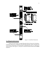
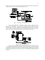
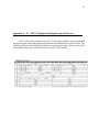
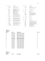
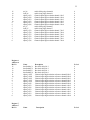
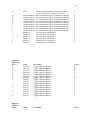
F1TDC A High-Resolution, Multi-Hit, VME64x Time-to-Digital Converter User’s Manual V1.2 17 March 2005 2 Table of Contents 1 Introduction ……………………………………… 3 2 Specifications ……………………………………… 4 3 The F1TDC Architecture ……..………………………….. 3.1 The F1 ASIC Chip ……..………………………….. 3.2 Module Architecture ……..………………………….. 3.3 Configuring the F1TDC ………………………….. 5 5 7 8 4 Connections 4.1 Front Panel .………………………………………. 4.1.1 Input Connectors ………………………….. 4.1.2 Timing & Control Connector ……………. 4.2 Backplane ……………………………………….. 10 10 11 13 5 Using the Module 5.1 Controlling the Module …………………………. 5.2 Module Operation ………………………………… 5.3 Module Registers .………………………………... 5.4 Data Format ……………………………………….. 15 16 17 23 Appendices A – F1 ASIC Configuration Registers and Addresses ……… 27 B – Sample F1 ASIC Configuration Register Values ……… 37 ……..……… xx C – F1 TDC Configuration Control Manual 3 1 Introduction F1TDC - A VME64x High Resolution, Multi-Hit, Time-to-Digital Converter Multi-Hit, Differential ECL Inputs High Resolution up to 60 pS LSB Wide Dynamic Range up to 7.8 uS High Stability by PLL Feedback Loop Data Validation by Trigger Matching with Zero Suppression Programmable Trigger Window and Latency Data Storage up to 1 Million Hits Flexible Control Inputs Via Front Panel or Backplane VME64x Compliant with 2eVME Data Transfer Cycles The F1TDC is a high resolution Time-to-Digital Converter (TDC). This module is particularly suited for applications requiring high-resolution time measurements with multi-hit capability at high event rates and where high channel densities are desirable. Wide dynamic range combined with trigger matching, zero suppression and deep storage alleviates the need for further data manipulation and reduces intermediate data storage requirements. A standard VME64x data acquisition bus guarantees the user will have high data throughput combined with long term industry support. 4 2 Specifications Packaging 6U VME64x Inputs Differential ECL (110 Ohm) 64 Channels @ 120 pS LSB 32 Channels @ 60 pS LSB Control START, SYNCRES, TRIGGER Front Panel – Differential ECL (110 Ohm) Backplane – Differential LVPECL (110 Ohm) Clock Differential LVPECL (110 Ohm) – 40 MHz Internal, Front Panel, Backplane Dynamic Range 7.8 uS (for 120 pS LSB) 3.9 uS (for 60 pS LSB) Standard Deviation Less than 0.9 LSB INL 0 LSB DNL 10-50% LSB Acquisition Trigger Matching w/ Zero suppression Programmable Trigger Window and Latency FIFO 1 M TDC Data Words Interface 32-bit VME Block Transfers (>20 Mbyte/s) 64-bit VME Block Transfers (>40 Mbyte/s) Power +12V @ 0.5A -12V @ 0.4A +3.3V @ 7.3A +5V @ 1.8A 5 3 The F1TDC Architecture The block diagram for the F1TDC module is shown in figure 1. The front-end section of the F1TDC encompasses the signal inputs with ECL-toLVPECL translators, the timing control inputs, reference clock, router/translator, resolution adjust control and eight (8) F1 ASIC chips. The back-end section encompasses the FIFOs, data bus control logic, initialization controls and VME64x interface functions. Figure 1 – F1TDC Module Block Diagram 3.1 The F1 ASIC Chip The core of our TDC module is the F1 TDC chip. A functional block diagram of the F1 ASIC chip is shown in figure 2. This chip uses purely digital delay techniques to measure time by means of a 19-tap asymmetric ring oscillator with phase-locked loop (PLL) control. Each of the pipelined F1 chips provides eight channels at 120 pS LSB or four channels at 60 pS LSB when a reference clock of 40 MHz is used. Internal FIFOs allow for storage of 16 hits per channel in leading and/or trailing edge modes. The following outline pertains to the use of the F1 chip in our TDC module. A key feature of the F1 chip is a Trigger Matching processing unit, which allows for selection of hits within a programmable time window and latency from the occurrence of a valid trigger input. Hits that fall outside of the window and latency settings are suppressed from the output buffer and cleared from the hit FIFO. Figure 3 depicts the operation of the trigger matching function. 6 Figure 2 - The F1 ASIC Chip The trigger matching feature is used in common start/stop and synchronous measurement modes. In common start/stop mode, a Start signal resets the internal measurement counter and a Trigger signal sets the measurement window. Hits falling within these two signals will always be accepted by the trigger matching unit. In synchronous mode, a Synch-Reset signal is used to reset the internal measurement counter and thus synchronize all TDCs in an experiment. Internal start signals are automatically generated at a programmable rate. The trigger matching unit validates hits within the programmed window and latency. Headers and trailers identifying the channel, chip, trigger time and event number can be output to delineate events. The dynamic range is 7.8 uS at 120 pS LSB and 3.9 uS at 60 pS, with a 40 MHz Reference Clock. To ensure stability and measurement reliability, each F1 chip is PLL-regulated against temperature drifts and manufacturing tolerances. The feedback loop employs a phase-frequency detector, a loop filter and a voltage regulator, which drives the substrate or core of the F1 chip. In this manner, delays within the internal Delay Locked Loop (DLL) are kept constant which translates into a stable LSB resolution or bin size. 7 The F1 chip is configured via a serial interface port, which accesses 16 registers. Readout of data is via a 24-bit parallel port. Further information on the F1 ASIC Chip can be obtained by contacting acammesselectronic gmbh at www.acam.de . Figure 3 - Trigger Matching 3.2 Module Architecture The eight F1 TDC chips on our module provide 64 channels in normal mode, or 32 channels in high resolution mode. Front panel input signal levels are differential ECL to be compatible with existing systems. Timing control signals are provided on the front panel and are also available through backplane connections for ease of system integration. A 128K word deep FIFO capable of simultaneous reads and writes is attached to each F1 TDC chip to buffer its output data. The VME interface and all control logic and registers are implemented in a single Field Programmable Gate Array (FPGA). All VME bus tranceivers are compatible with the high-speed protocols of the VME64x standard. The RAM shown in Figure 1 is an option not present on this version of the TDC. Output data from the F1 TDC chip is ordered according to channel number (channel 0 first, channel 7 last). Within each channel, hit data is ordered from earliest to latest. Each F1 TDC chip may be configured to supply a header word for channel 0 and a trailer word for channel 7 in its output data stream whenever a trigger occurs. This takes place even if there is no valid hit data for the trigger. During readout, control logic uses these markers to switch between the FIFOs that supply the data. In this way, data from multiple chips that are associated with the same trigger may be assembled into an event fragment for the module. Individual channels may be disabled during configuration of the F1 TDC chips. The FIFO for an individual F1 TDC chip may also be bypassed from the readout sequence. The module can be configured to set a flag in a register when the data from a programmed number of triggers is available in its buffers. This flag may be optionally used to interrupt the crate controller. Readout is accomplished most efficiently using a 8 block transfer protocol. Because the number of data words currently stored in the module is not available to the crate controller, a slave terminated block transfer is used instead. The crate controller is programmed to read out, via block mode, a number of words that is beyond the storage capacity of the module. During readout the module will provide the block of data associated with the programmed number of triggers. When this data is depleted the module terminates the block transfer by issuing a bus error (BERR). A register bit in the module is set when this occurs. The crate controller can query this bit to verify that the bus error was generated deliberately by the module and does not signify a system failure. To enhance system performance a set of TDC modules may be read out as a single logical read using a multiblock protocol. This involves passing a token between modules along a private line. It is implemented in the following way. All TDC modules in the set are programmed to respond to a Common Address Range used exclusively for multiblock transfers. Only the TDC having the token will actually respond to such an address cycle. The TDC module of the set that is furthest left in the crate is configured to be the first module and initially claims the token. The module furthest to the right is set as the last module. All modules except the last one are configured to pass the token when they have transferred the programmed number of events. The last module is instead configured to respond with BERR. In addition, the first module may be configured to initiate readout by interrupting the crate controller when the data from a programmed number of triggers is available in its buffers. A slave terminated block transfer using the Common Address Range will accomplish the readout of the data from the programmed number of triggers for all boards of the set. When BERR occurs signaling the completion of this transfer, the first module seizes the token again. 3.3 Configuring the F1TDC The TDC module contains eight F1 TDC devices that must be configured prior to operation. Each device contains sixteen 16-bit write-only configuration registers that are accessed through a synchronous serial bus. The TDC configuration control logic is implemented in the FPGA. It contains a serializer for the TDCs, a register file RAM, a configuration sequence RAM, an EEPROM controller, and host interface logic. An overview of the configuration control logic architecture is shown in Figure 4. A 24-bit frame is transmitted to 8 TDCs on a synchronous serial bus. This frame consists of a 3-bit device address, one broadcast bit, a 4-bit register address, and 16-bit data. A TDC will accept a frame if its unique hardware address matches the device address transmitted in the frame. The TDC configuration registers are write-only. Read-back is accomplished using a local copy of the registers stored in FPGA RAM. A 128x16 register file RAM stores all 16 registers from each of 8 TDCs. Any write to the register file will store the data in RAM and serialize the data to the TDCs. The serializer constructs the TDC data frame based on the register file address and write data. 9 Data TDC #1 Serializer Register File RAM (128 x 16) TDC #8 Interface Logic Sequence RAM (128 x 24) Master Controller Clock EEPROM Controller SPI Interface FPGA Serial EEPROM (512 x 8) Figure 4: F1 TDC Configuration Control Logic For the TDCs to function properly, the TDC registers must be configured in a specific order. A configuration sequence RAM is provided to remove this burden from the host software. The 128x24 sequence RAM permits configuration of any register on any TDC in any order. This is accomplished by storing entire 24-bit serial data frames sequentially in RAM. A programmable end address is used to mark the end of sequence. When the configuration sequence is triggered, the RAM is read sequentially from address 0 to the end address. The 24-bit data is decoded and passed to the register file where it is stored and serialized. A 512x8 serial EEPROM stores the sequence RAM and other user data. The EEPROM is accessed through an EEPROM controller and an SPI compatible interface. The controller provides a random access read/write interface to the EEPROM. It manages device opcodes, status, and data. The SPI interface contains a clock manager and a serializer/deserializer. Since the Sequence RAM and end address occupy only 385 bytes of the 512-byte EEPROM, the remaining space is available for user data. The Master Controller module provides a host interface to the control logic and interconnects the register file, sequencer, and EEPROM modules. It permits read and write access to the Register File RAM, Sequence RAM, and EEPROM. The host can trigger TDC configuration from Sequence RAM and transfer of Sequence RAM to or from the EEPROM. At power-up, the Sequence RAM and end address are automatically loaded from EEPROM then passed to the register file and serializer to configure the TDCs. This automatic power-up configuration removes considerable software overhead for a large number of TDC boards. A description of all the configuration registers can be found in 10 Appendix A. Sample values of the registers under various operating conditions are found in Appendix B. 4.1 Connections – Front Panel 4.1.1 Input Connectors Time measurements are performed on differential ECL signals connected to the top and bottom stacked headers. Each header has 17 pairs of pins with the + (true) on the side of the orientation key (left side) and the – (complement) on the right side, as illustrated in figure 5, and differentially terminated into 110 Ohm impedance. The 17th pair is not used or connected in any manner. Only the rightmost headers on each of the top and bottom stacks are used during high-resolution measurements. Please, notice the orientation of the socket and cable when making connections to the module. 11 Figure 5 – Front Panel Connections 4.1.2 Timing & Control Connector Timing and control signals are supplied through either the front panel or backplane. Front panel connections are appropriate for small data acquisition systems and require the user to provide connections to a 14-pin header by individual pair sockets or 14-pin socket with twisted-pair cable (figure 6). All inputs are differential and terminated into 110 Ohm impedance. 12 Figure 6 – Timing & Control Signals CLK0 Reference Clock Output, Differential LVPECL, 40 MHz. CLKI Reference Clock Input, Differential LVPECL, Capacitively Coupled. STRT Start, Differential ECL Input - Resets the Internal Measurement Counter on all F1 ASIC Chips in Common Start/Stop Mode. The Signal Inputs Function as Stops. SYNC Synch-Reset, Differential ECL Input – Resets the Internal Measurement Counter on all F1 ASIC Chips in Synchronous Mode. TRIG Trigger, Differential ECL Input – Sets the Measurement Validation Window. The Trigger Window and Latency are Programmable During Configuration. BUSY Busy, Differential ECL Output – Data FIFO Memory Almost Full Condition. Triggers should be stopped to avoid loss of data. The user has the option of selecting the reference clock source through the VME interface. The internal reference clock source has a frequency stability of 100 ppm . As the timing resolution of the F1 ASIC Chips depends on the stability of the reference clock, the user should exercise caution when selecting and implementing external reference sources. Figure 7 shows a simplified diagram of the reference clock distribution. Note that all reference clock paths are differential and all the external LVPECL inputs are capacitively coupled for safety reasons. Systems employing PECL signals with receivers and sources powered from separate power supplies should have all inputs capacitively coupled as 13 damage to receivers may occur when input signals forward bias the input ESD structures and the input base-collector junction of un-powered receivers. Figure 7 – Reference Clock Distribution Once the internal REF-CLK is enabled, its output is always available at the front panel and the backplane. In systems with multiple modules and where clock synchronization is required, a single module can be configured as the REF_CLK master clock. The use of an external LVPECL clock distribution module will then be required. Figure 8 illustrates possible implementations for small and large scale systems. Figure 8 – REF_CLK Distribution Larger systems employing multiple sub-racks may benefit from integration of the various timing and control signals into a single board located within each sub-rack, further providing ECL-to-LVPECL or Optical-to-LVPECL translation. Additional care should be taken to minimize signal skews. Figure 9 depicts various high-speed, differential signal standards. 14 Figure 9 – Typical High-Speed Differential Signal Standards 4.2 Connections – Backplane The VME64x standard specifies that 160-pin DIN connectors be used for connectors P1 and P2. Tables 1 and 2 show the pin allocations for P1 and P2, respectively. Table 1 – P1 Pin allocation* 1 2 3 4 5 6 7 8 9 10 11 12 13 14 15 16 17 18 19 20 21 22 23 24 25 26 27 28 29 30 31 32 Z MPR AGND MCLK AGND MSD AGND MMD AGND MCTL AGND RESP* AGND RsvBus AGND RsvBus AGND RsvBus AGND RsvBus AGND RsvBus AGND RsvBus AGND RsvBus AGND RsvBus AGND RsvBus AGND RsvBus AGND A DV0 DV1 DV2 DV3 DV4 DV5 DV6 DV7 AGND SYSCLK AGND DSV1* DSV0* WV* AGND DTACKV* AGND ASV* AGND IACKV* IACKINV* IACKOUTV* AMV4 AV7 AV6 AV5 AV4 AV3 AV2 AV1 -12IN +5IN Table 2 – P2 Pin allocation* B BBSY* BCLR* ACFAIL* BG0IO* BG0IO* BG1IO* BG1IO* BG2IO* BG2IO* BG3IO* BG3IO* BR0* BR1* BR2* BR3* AMV0 AMV1 AMV2 AMV3 AGND SERA SERB AGND IRQV7* IRQV6* IRQV5* IRQV4* IRQV3* IRQV2* IRQV1* +5VSTDBY +5IN C DV8 DV9 DV10 DV11 DV12 DV13 DV14 DV15 AGND SYSFAIL* BERRV* SYSRESETV* LWV* AMV5 AV23 AV22 AV21 AV20 AV19 AV18 AV17 AV16 AV15 AV14 AV13 AV12 AV11 AV10 AV09 AV08 +12IN +5IN D VPC AGND +V1 +V2 RsvU -V1 -V2 RsvU GAP* GA0* GA1* +3.3IN GA2* +3.3IN GA3* +3.3IN GA4* +3.3IN RsvBus +3.3IN RsvBus +3.3IN RsvBus +3.3IN RsvBus +3.3IN LI/I* +3.3IN LI/O* +3.3IN AGND VPC 15 1 2 3 4 5 6 7 8 9 10 11 12 13 14 15 16 17 18 19 20 21 22 23 24 25 26 27 28 29 30 31 32 Z UD AGND UD AGND UD AGND UD AGND UD AGND UD AGND UD AGND UD AGND UD AGND UD AGND UD AGND UD AGND UD AGND UD AGND UD AGND AGND AGND A UD UD UD UD UD UD UD UD UD UD UD UD UD UD UD UD UD UD UD UD UD UD UD UD UD UD UD UD UD AGND REFCLK_B_OUTREFCLK_B_OUT+ *Pins with shaded entries are not used. B +5IN AGND RETRY* AV24 AV25 AV26 AV27 AV28 AV29 AV30 AV31 AGND +5IN DV16 DV17 DV18 DV19 DV20 DV21 DV22 DV23 AGND DV24 DV25 DV26 DV27 DV28 DV29 DV30 DV31 AGND +5IN C UD LOOP LOOP AGND UD +3.3IN +3.3IN +3.3IN +3.3IN AGND +3.3IN AGND UD UD UD UD AGND SPARE_OUT_R TOKEN_OUT_R SPARE_IN_R TOKEN_IN_R BUSY_B_OUTBUSY_B_OUT+ AGND TRIGGER_B_IN+ TRIGGER_B_INSTART_B_IN+ START_B_INREFCLK_B_IN+ REFCLK_B_INSYNCRES_B_INSYNCRES_B_IN+ D UD UD UD UD UD UD UD UD UD UD UD UD UD UD UD UD UD AGND AGND AGND AGND UD UD UD UD UD UD UD UD UD AGND VPC 16 5 Using the Module 5.1 Controlling the Module Communication with the module is by standard VME bus protocols. All registers and memory locations are defined to be 4-byte entities. The VME slave module has three distinct address ranges. A24 – The base address of this range is set by a 12-element DIP switch on the board. It occupies 4 Kbytes of VME address space, organized in 1 K 32-bit words. Relative to the base address, this space is divided as follows: 000-7FF – Register space to control and monitor the module 800-FFF – F1 chip configuration space Detailed information about the F1 chip configuration space is found in Appendix C. To summarize, the F1 chip configuration space is divided as follows: 800-9FF – Configuration register file. The 4-byte registers are ordered as: Chip 0 register 0, 1, 2, …, 15, Chip 1 register 0, 1, 2, …, 15, … Chip 7 register 0, 1, 2, …, 15. Direct writes to an F1 chip register may be made to the address: Address = 800 + (40 * chip #) + (4 * register #). The order in which the registers are written should be the following: register 15, 10, 0, 1, 6, 8, 9, 11, 12, 13, 14, 7, 2, 3, 4, 5. Sample values of the F1 chip registers under several operating conditions are found in Appendix B. A00-BFF – Setup RAM (see Appendix C). C00-DFF – Configuration control registers (see Appendix C). E00-FFF – Spare A32 - The base address of this range is programmed into register ADR32. It occupies 4 Mbytes of VME address space, organized in 1 M 32-bit words. A read of any address in this range will yield the next TDC data word from the module. Even though the module is 17 a FIFO, the expanded address range allows the VME master to increment the address during block transfers. This address range can participate in single cycle, 32-bit block, and 64-bit block reads. The only valid write to this address range is the data value 0x80000000 which re-enables the module to generate interrupts (after one has occurred). The address range must be enabled by setting ADR32[0] = 1. A32 - The lower and upper limits of this address range are programmed into register ADR_MB. This common address range for a set of TDC modules in the crate is used to implement the Multiblock protocol. By means of token passing TDC data may be read out from multiple TDC modules using a single logical block read. The board possessing the token will respond to a read cycle in this address range with the next TDC data word from that module. The token is passed along a private daisy chain line to the next module when it has transferred all data from a programmed number of events (register EVENT LEVEL). The address range must be enabled by setting ADR_MB[0] = 1. 5.2 Module Operation The following describes the setup and operation of the TDC in single and multiple module applications. Single Module – After a reset of the module (CSR[31] = 1), the F1 chip configuration registers may be written directly through the A24 address space (800-9FF). The source for the control signals is set to Front (CTRL[0] = 0) and the internal clock is selected and turned on (CTRL[2] = 0, CTRL[1] = 1). The EVENT LEVEL register is loaded with the number of events (i.e. triggers) that constitute a block. The INTERRUPT register may be loaded with the interrupt ID and level if the module is to initiate an interrupt when the defined block of data is available for readout. The address for data access is loaded (ADR32), and the F1 chips that are to participate in the readout are selected (CTRL[23…16]). The event level interrupt (CTRL[3] = 1) is enabled if interrupt generation is desired. The BERR response is enabled (CTRL[6] = 1) to allow the module to indicate when the complete block of data has been read out. When the programmed number of triggers has been received, the event level flag (CSR[3]) will be set and an interrupt will be generated if enabled. The user should initiate a DMA block read (32 or 64-bit) from the address in stored in ADR32. The length of the block read should be programmed to be larger than the expected size of the data block (e.g. 4 Mbytes). The module will terminate the DMA transfer by issuing BERR when all data from the block has been transferred. Interrupt generation must be re-enabled by writing 0x80000000 to the address in ADR32. Multiple Modules – All modules should be reset and loaded with the configuration register values as described above for a single module. The source of the control signals for the modules is set to Front or Back depending on the distribution system used. The internal clocks need not be turned on, as a clock source is provided as part of the distribution system. The EVENT LEVEL register and the chips selected for readout are loaded into each module. A unique address for data access is loaded into ADR32 for each 18 module. The common address range for the Multiblock protocol is loaded into ADR_MB for each module. All modules are programmed to participate in the Multiblock protocol (CTRL[7] = 1). The left-most TDC module in the system is programmed as the first module (CTRL[8] = 1), and the right-most TDC module is designated the last module (CTRL[9] = 1). For the first module, the INTERRUPT register may be loaded and the event level interrupt bit enabled, if desired. The BERR response is enabled for the last module only. For backplane mounted signal distribution systems, the token passing lines are included in the system. Front signal distribution systems need additional connections to the backplane for token passing lines (see Table 2). When the programmed number of triggers has been received, the event level flag will be set in each module and an interrupt will be generated by the first module (if enabled). The user should initiate a DMA block read (32 or 64-bit) from the address stored in ADR_MB. The length of the block read should be programmed to be larger than the total size of data from all modules (e.g. 4 Mbytes x # modules). Since the first module initially has the token, it will respond with data to the VME bus cycles. When data from the first module’s block has been depleted, it passes the token to the next module in the chain. This module will respond with data until its data block is exhausted and the token is passed to the next module. The last module will terminate the DMA transfer by issuing BERR when all data from its block has been transferred. Upon detecting BERR, the first module takes possession of the token. Interrupt generation must be re-enabled by writing 0x80000000 to the address in ADR32 of the first module. 5.3 Module Registers CSR – Control/Status (0x0) 0 – (R/W) – spare control bit 1 – (R/W) – TDC chip configuration error (writing 1 clears status) 2 – (R) – TDC chip configuration active 3 – (R) – event level flag asserted 4 – (R) – zero events in buffer 5 – (R) – BERR status 6 – (R) – Token status 7 – (R) – ERROR condition exists for an enabled TDC chip 8 – (R) – TDC chip 0 error 9 – (R) – TDC chip 1 error 19 10 – (R) – TDC chip 2 error 11 – (R) – TDC chip 3 error 12 – (R) – TDC chip 4 error 13 – (R) – TDC chip 5 error 14 – (R) – TDC chip 6 error 15 – (R) – TDC chip 7 error 16 – (R) – Internal Buffer # for next data word (0 = Buffer #0, 1 = Buffer #1) 17 – (R) – Internal Buffer #0 empty flag 18 – (R) – Internal Buffer #1 empty flag 19 – (R) – End-of-Block flag for next data word 20 – (R) – Filler Word flag for next data word (valid only for Buffer #1) 21 – (R) – External FIFO empty flag 22 – 23 – Spare (read as zero) 24 – 27 – (not used) 28 – (W) – Pulse Spare Out ( if CTRL[12] = 1 ) 29 – (W) – Pulse Soft Trigger ( if CTRL[5] = 1 ) 30 – (W) – Pulse Soft Reset 31 – (W) – Pulse Hard Reset CTRL – Control (0x4) 0 – (R/W) – Front/Back Control Signals select (0 = Front, 1 = Back) 1 – (R/W) – Internal Clock Control ( 0 = Clock OFF, 1 = Clock ON ) 2 – (R/W) – Clock Select ( 0 = Internal (if CTRL[0] = 0), 1 = External ) 20 3 – (R/W) – Enable Event Level Interrupt 4 – (R/W) – Enable Error Interrupt 5 – (R/W) – Enable Soft Trigger 6 – (R/W) – Enable BERR response 7 – (R/W) – Enable Multiblock protocol 8 – (R/W) – FIRST board in Multiblock system 9 – (R/W) – LAST board in Multiblock system 10 – (R/W) – Enable readout of all F1 chip headers/trailers 11 – (R/W) – Enable BUSY output to front panel 12 – (R/W) – Enable Spare output 13 – 15 – (not used – read as 0) 16 - 23 (R/W) – Enable Readout from TDC 0 - 7 24 – 31 – (not used – read as 1) EVENT COUNT (0x8) [15…0] - (R) – Event Count[15…0]. Event Count = 0 _ CSR[4] = 1. [31…16] – (not used) EVENT LEVEL (0xC) [15…0] - (R/W) – Event Level[15…0]. Event Count ≥ Event Level _ CSR[3] = 1. [31…16] – (not used) INTERRUPT (0x10) [7…0] – (R/W) – Interrupt ID (vector) [10…8] – (R/W) – Interrupt Level [2..0]. Valid values = 1,..,7. 21 11 - 15 – (not used) [20…16] – (R) – Geographic Address (slot number) in VME64x chassis. 21 – 22 – (not used) 23 – (R) – Parity Error in Geographic Address. 24 – 31 – (not used) ADR32 – Address for data access (0x14) 0 – (R/W) – Enable 32-bit address decoding 1 – 5 – (not used – read as 0) [15…6] – (R/W) – Base Address for 32-bit addressing mode (4 Mbyte total) ADR_MB – Multiblock Address for data access (0x18) 0 – (R/W) – Enable Multiblock address decoding 1 – 5 – (not used – read as 0) [15…6] – (R/W) – Lower Limit address (ADR_MIN) for Multiblock access 16 – 21 – (not used – read as 0) [31…22] – (R/W) – Upper Limit address (ADR_MAX) for Multiblock access The board that has the TOKEN will respond with data when the VME address satisfies the following condition: ADR_MIN ≤ Address < ADR_MAX. TDC STATUS (4 registers) (0xXX – TDC chips ‘A’ & ‘B’): (0x1C – TDC chips 0 & 1) (0x20 – TDC chips 2 & 3) (0x24 – TDC chips 4 & 5) (0x28 – TDC chips 6 & 7) 22 (bits 0 – 15 for chip ‘B’, bits 16 – 31 for chip ‘A’) 0 – Resolution LOCKED (B) 1 – TDC Hit FIFO Overflow (B) 2 – TDC Trigger FIFO Overflow (B) 3 – TDC Output FIFO Overflow (B) 4 – External FIFO Full (B) 5 – External FIFO Almost Full – BUSY asserted if chip enabled (B) 6 – External FIFO Empty (B) 7 – TDC Initialized (B) 8 – Loss of Resolution Lock Occurred (B) 9 – TDC Hit FIFO Overflow Occurred (B) 10 – TDC Trigger FIFO Overflow Occurred (B) 11 – TDC Output FIFO Overflow Occurred (B) 12 – External FIFO Full Occurred (B) 13 – 15 – (not used – read as 0) 16 – Resolution LOCKED (A) 17 – TDC Hit FIFO Overflow (A) 18 – TDC Trigger FIFO Overflow (A) 19 – TDC Output FIFO Overflow (A) 20 – External FIFO Full (A) 21 – External FIFO Almost Full – BUSY asserted if chip enabled (A) 22 – External FIFO Empty (A) 23 – TDC Initialized (A) 23 24 – Loss of Resolution Lock Occurred (A) 25 – TDC Hit FIFO Overflow Occurred (A) 26 – TDC Trigger FIFO Overflow Occurred (A) 27 – TDC Output FIFO Overflow Occurred (A) 28 – External FIFO Full Occurred (A) 29 – 31 – (not used – read as 0) FIRM – Firmware revision (0x2C) [7…0] – (R) – firmware revision [15…8] – (R) – board type (“F1”) SCALER 1 – Event Count (0x30) [31…0] – (R) – total event count as determined by the 1st enabled TDC chip SCALER 2 – Event Counters (0x34) [3…0] – (R) – low 4 bits of event counter for TDC chip #1 [7…4] – (R) – low 4 bits of event counter for TDC chip #2 [11…8] – (R) – low 4 bits of event counter for TDC chip #3 [15…12] – (R) – low 4 bits of event counter for TDC chip #4 [19…16] – (R) – low 4 bits of event counter for TDC chip #5 [23…20] – (R) – low 4 bits of event counter for TDC chip #6 [27…24] – (R) – low 4 bits of event counter for TDC chip #7 [31…28] – (R) – low 4 bits of event counter for TDC chip #8 24 5.4 Data Format The F1TDC chip outputs 24-bit words. The words are of 2 types: header/trailer and data. The header/trailer words are used as event or channel separators, and provide information such as the event number and trigger time. A data word contains the time measurement for a hit. The bit assignments are shown below. The header/trailer words can be enabled for each channel of the chip. In this case the chip data stream for a trigger appears as follows: header – channel 0 data – channel 0, earliest hit … data – channel 0, latest hit trailer – channel 0 header – channel 1 data – channel 1, earliest hit … data – channel 1, latest hit trailer – channel 1 … … header – channel 7 data – channel 7, earliest hit … data – channel 7, latest hit trailer – channel 7 In this case, the headers/trailers take up space in the F1TDC chip’s output buffer while providing redundant information. A better solution is to enable only the header for channel 0, and the trailer for channel 7. The chip data stream then appears as follows: 25 header – channel 0 data – channel 0, earliest hit … data – channel 0, latest hit data – channel 1, earliest hit … data – channel 1, latest hit … … data – channel 7, earliest hit … data – channel 7, latest hit trailer – channel 7 In our application of the F1TDC chip, we require that at least the header for channel 0 and the trailer for channel 7 be enabled for each chip that is to be read out. (The chips to be read out are specified by CTRL[23…16]). This minimal header/trailer information is used to assemble event fragments from different chips into a single event fragment that is associated with a given trigger for the board. During module readout, the default mode is to suppress all headers/trailers except the header for channel 0 of the first chip enabled for readout (Event Header) and the trailer for channel 7 of the last chip enabled for readout (Event Trailer). If all chips 0-7 are enabled, the module data stream associated with a trigger will appear as follows: header – chip 0, channel 0 (Event Header) data – chip 0, channel 0, earliest hit … data – chip 0, channel 0, latest hit … … data – chip 0, channel 7, earliest hit … data – chip 0, channel 7, latest hit … … … data – chip 7, channel 0, earliest hit … data – chip 7, channel 0, latest hit … … data – chip 7, channel 7, earliest hit … data – chip 7, channel 7, latest hit trailer – chip 7, channel 7 (Event Trailer) 26 Whenever an intermediate chip header indicates an error condition (Trigger FIFO Overflow) it will be forced into the data stream so that this condition will not be missed. The normally suppressed intermediate chip headers do contain independent measurements of the Event Number and Trigger Time. To assure that all chips of the module stay correctly synchronized, the Event Number and Trigger Time are monitored for changes between chips. Intermediate chip headers are forced into the data stream only if their Event Number or Trigger Time differs from the values of the preceding chip. Since the Event Header is always inserted into the data stream, the Event Number and Trigger Time information for each chip can be completely reconstructed. As an example, suppose chip 4 of the module records a different Trigger Time for an event than the other 7 chips. The module data stream for this event will appear as follows: header – chip 0, channel 0 (Event Header) data – chip 0, channel 0, earliest hit … data – chip 3, channel 7, latest hit header – chip 4, channel 0 (intermediate header) data – chip 4, channel 0, earliest hit … data – chip 4, channel 7, latest hit header – chip 5, channel 0 (intermediate header) data – chip 5, channel 0, earliest hit … data – chip 7, channel 7, latest hit trailer – chip 7, channel 7 (Event Trailer) This indicates that chips 0-3 have the same Event Number and Trigger Time, while chip 4 has recorded different values. The intermediate header from chip 5 re-establishes values that are the same for chips 5-7. Any difference in the Event Number among the chips indicates a serious error that requires a reset of the board. Trigger Time differences of up to 1 count among the chips is acceptable. (Note that for a 9-bit Trigger Time, 0 and 511 differ by 1.) For the Trigger Time, this assumes that an external SYNC_RESET signal has been successfully applied at the start of the run. The user is strongly encouraged to monitor the Event Number and Trigger Time provided in these headers to assure synchronization across the entire system. For diagnostic purposes, all intermediate chip headers/trailers can be forced to be read out by setting register bit CTRL[10] = 1. In this mode, each trigger will produce 16 header/trailer words from a module in addition to the time measurement data words. The data word transferred across the VME bus includes the 24-bit TDC word AND additional board location and F1TDC chip error information, as follows: 27 DATA - module data word (4 Mbyte address range, base programmed in register ADR32) [23…0] – F1 chip word, as described above 24 – F1 chip Hit FIFO Overflow 25 – F1 chip Output FIFO Overflow 26 – F1 chip Resolution Locked [31…27] – Slot ID Slot ID = 1-21 indicates valid data. The module will return Slot ID = 30 when the data is not valid (e.g. an empty module is read, or data is not yet ready to be extracted). Slot ID = 0 is the tag for a ‘filler’ word. This is a non-valid data word that is inserted to make the block of data output from the module consist of an even number of words. (An even number of words simplifies 64-bit readout mode.) Note that a block of data may consist of many events (register EVENT LEVEL). Data should be ignored if Slot ID = 0 or 30. For 64-bit readout, if EITHER of the words of the pair have Slot ID = 30, BOTH words should be ignored. (If one of the words is valid, it will appear again in the next successful read). 28 Appendix A – F1 ASIC Configuration Registers and Addresses The F1 ASIC Chip contains sixteen (16), 16-bit registers which can be programmed for specific applications and requirements and must be downloaded in a specific order. The following tables provide detailed information on register functionality. However, note that some registers may not be available to the user of the F1TDC module. 29 Register 0 Address: 0 Bit No. 15 14 13 12 11 10 9 8 7 6 5 4 3 2 1 0 Name head-en(8) head-en(7) head-en(6) head-en(5) head-en(4) head-en(3) head-en(2) head-en(1) trail-en(8) trail-en(7) trail-en(6) trail-en(5) trail-en(4) trail-en(3) trail-en(2) trail-en(1) Description Header-Enable Kanal8 Header-Enable Kanal7 Header-Enable Kanal6 Header-Enable Kanal5 Header-Enable Kanal4 Header-Enable Kanal3 Header-Enable Kanal2 Header-Enable Kanal1 Trailer-Enable Kanal8 Trailer-Enable Kanal7 Trailer-Enable Kanal6 Trailer-Enable Kanal5 Trailer-Enable Kanal4 Trailer-Enable Kanal3 Trailer-Enable Kanal2 Trailer-Enable Kanal1 Default 0 0 0 0 0 0 0 0 0 0 0 0 0 0 0 0 Register 1 Address: 1 Bit No. Name Description Default 30 15 14 13 12 11 10 9 8 7 6 5 4 3 2 1 0 highres hitmode letramode sq(1) sq(0) fakehalf ovlaphigh ibspeed(1) ibspeed(0) obspeed m_inh slow(3) slow(2) slow(1) slow(0) DACstart 0=noral resolution , 1=high resolution 32 channel hit mode Leading-trailing edge mode Measurement core adjust bit 1 Measurement core adjust bit 0 Not relevant for common mode Not relevant for common mode Processing speed Trigger Bit1 Processing speed Trigger Bit0 Transfer rate output FIFO to interface FIFO Software disable for all stop inputs (0 = on , 1 = off) Measurement result processing speed Bit3 Measurement result processing speed Bit2 Measurement result processing speed Bit1 Measurement result processing speed Bit0 Start flag for data transfer to 8-fold DAC 0 0 0 0 0 0 0 0 0 0 0 0 0 0 0 0 Register 2 Address: 2 Bit No. 15 14 13 12 11 10 9 8 7 6 5 4 3 2 1 0 Name tra_k2 lead_k2 adjust_k2(5) adjust_k2(4) adjust_k2(3) adjust_k2(2) adjust_k2(1) adjust_k2(0) tra_k1 lead_k1 adjust_k1(5) adjust_k1(4) adjust_k1(3) adjust_k1(2) adjust_k1(1) adjust_k1(0) Description enable falling edge channel 2 enable rising edge channel 2 Channel adjust high resolution channel 2 bit 5 Channel adjust high resolution channel 2 bit 4 Channel adjust high resolution channel 2 bit 3 Channel adjust high resolution channel 2 bit 2 Channel adjust high resolution channel 2 bit 1 Channel adjust high resolution channel 2 bit 0 enable falling edge channel 1 enable rising edge channel 1 Channel adjust high resolution channel 1 bit 5 Channel adjust high resolution channel 1 bit 4 Channel adjust high resolution channel 1 bit 3 Channel adjust high resolution channel 1 bit 2 Channel adjust high resolution channel 1 bit 1 Channel adjust high resolution channel 1 bit 0 Default 0 0 0 0 0 0 0 0 0 0 0 0 0 0 0 0 Register 3 Address: 3 Bit No. Name Description Default 31 15 14 13 12 11 10 9 8 7 6 5 4 3 2 1 0 tra_k4 lead_k4 adjust_k4(5) adjust_k4(4) adjust_k4(3) adjust_k4(2) adjust_k4(1) adjust_k4(0) tra_k3 lead_k3 adjust_k3(5) adjust_k3(4) adjust_k3(3) adjust_k3(2) adjust_k3(1) adjust_k3(0) enable falling edge channel 4 enable rising edge channel 4 Channel adjust high resolution channel 4 bit 5 Channel adjust high resolution channel 4 bit 4 Channel adjust high resolution channel 4 bit 3 Channel adjust high resolution channel 4 bit 2 Channel adjust high resolution channel 4 bit 1 Channel adjust high resolution channel 4 bit 0 enable falling edge channel 3 enable rising edge channel 3 Channel adjust high resolution channel 3 bit 5 Channel adjust high resolution channel 3 bit 4 Channel adjust high resolution channel 3 bit 3 Channel adjust high resolution channel 3 bit 2 Channel adjust high resolution channel 3 bit 1 Channel adjust high resolution channel 3 bit 0 0 0 0 0 0 0 0 0 0 0 0 0 0 0 0 0 Register 4 Address: 4 Bit No. 15 14 13 12 11 10 9 8 7 6 5 4 3 2 1 0 Name tra_k6 lead_k6 adjust_k6(5) adjust_k6(4) adjust_k6(3) adjust_k6(2) adjust_k6(1) adjust_k6(0) tra_k5 lead_k5 adjust_k5(5) adjust_k5(4) adjust_k5(3) adjust_k5(2) adjust_k5(1) adjust_k5(0) Description enable falling edge channel 6 enable rising edge channel 6 Channel adjust high resolution channel 6 bit 5 Channel adjust high resolution channel 6 bit 4 Channel adjust high resolution channel 6 bit 3 Channel adjust high resolution channel 6 bit 2 Channel adjust high resolution channel 6 bit 1 Channel adjust high resolution channel 6 bit 0 enable falling edge channel 5 enable rising edge channel 5 Channel adjust high resolution channel 5 bit 5 Channel adjust high resolution channel 5 bit 4 Channel adjust high resolution channel 5 bit 3 Channel adjust high resolution channel 5 bit 2 Channel adjust high resolution channel 5 bit 1 Channel adjust high resolution channel 5 bit 0 Default 0 0 0 0 0 0 0 0 0 0 0 0 0 0 0 0 Register 5 Address: 5 Bit No. Name Description Default 32 15 14 13 12 11 10 9 8 7 6 5 4 3 2 1 0 tra_k8 lead_k8 adjust_k8(5) adjust_k8(4) adjust_k8(3) adjust_k8(2) adjust_k8(1) adjust_k8(0) tra_k7 lead_k7 adjust_k7(5) adjust_k7(4) adjust_k7(3) adjust_k7(2) adjust_k7(1) adjust_k7(0) Register 6 Address: 6 Bit No. 15 14 13 12 11 10 9 8 7 6 5 4 3 2 1 0 Name busclkdelay(3) busclkdelay(2) busclkdelay(1) busclkdelay(0) adjust_k10(5) adjust_k10(4) adjust_k10(3) adjust_k10(2) adjust_k10(1) adjust_k9(0) adjust_k9(5) adjust_k9(4) adjust_k9(3) adjust_k9(2) adjust_k9(1) adjust_k9(0) Register 7 Address: 7 Bit No. Name enable falling edge channel 8 enable rising edge channel 8 Channel adjust high resolution channel 8 bit 5 Channel adjust high resolution channel 8 bit 4 Channel adjust high resolution channel 8 bit 3 Channel adjust high resolution channel 8 bit 2 Channel adjust high resolution channel 8 bit 1 Channel adjust high resolution channel 8 bit 0 enable falling edge channel 7 enable rising edge channel 7 Channel adjust high resolution channel 7 bit 5 Channel adjust high resolution channel 7 bit 4 Channel adjust high resolution channel 7 bit 3 Channel adjust high resolution channel 7 bit 2 Channel adjust high resolution channel 7 bit 1 Channel adjust high resolution channel 7 bit 0 Description Bus clock delay bit 3 Bus clock delay bit 2 Bus clock delay bit 1 Bus clock delay bit 0 Channel adjust high resolution reference channel B bit 5 Channel adjust high resolution reference channel B bit 4 Channel adjust high resolution reference channel B bit 3 Channel adjust high resolution reference channel B bit 2 Channel adjust high resolution reference channel B bit 1 Channel adjust high resolution reference channel B bit 0 Channel adjust high resolution reference channel A bit 5 Channel adjust high resolution reference channel A bit 4 Channel adjust high resolution reference channel A bit 3 Channel adjust high resolution reference channel A bit 2 Channel adjust high resolution reference channel A bit 1 Channel adjust high resolution reference channel A bit 0 Description 0 0 0 0 0 0 0 0 0 0 0 0 0 0 0 0 Default 0 0 0 0 0 0 0 0 0 0 0 0 0 0 0 0 Default 33 15 beinit Flag to F1, indicates that initialisation is finished 0 = not initialised, 1 = completely initialised Sets measurement range in synchronous mode bit 8 Sets measurement range in synchronous mode bit 7 Sets measurement range in synchronous mode bit 6 Sets measurement range in synchronous mode bit 5 Sets measurement range in synchronous mode bit 4 Sets measurement range in synchronous mode bit 3 Sets measurement range in synchronous mode bit 2 Sets measurement range in synchronous mode bit 1 Sets measurement range in synchronous mode bit 0 Sets time for hit sampling bit 5 Sets time for hit sampling bit 4 Sets time for hit sampling bit 3 Sets time for hit sampling bit 2 Sets time for hit sampling bit 1 Sets time for hit sampling bit 0 0 14 13 12 11 10 9 8 7 6 5 4 3 2 1 0 refstart-counter(8) refstart-counter(7) refstart-counter(6) refstart-counter(5) refstart-counter(4) refstart-counter(3) refstart-counter(2) refstart-counter(1) refstart-counter(0) hit-time(5) hit-time(4) hit-time(3) hit-time(2) hit-time(1) hit-time(0) Register 8 Address: 8 Bit No. 15 14 13 12 11 10 9 8 7 6 5 4 3 2 1 0 Name breite(15) breite(14) breite(13) breite(12) breite(11) breite(10) breite(9) breite(8) breite(7) breite(6) breite(5) breite(4) breite(3) breite(2) breite(1) breite(0) Description Trigger window width bit 15 Trigger window width bit 14 Trigger window width bit 13 Trigger window width bit 12 Trigger window width bit 11 Trigger window width bit 10 Trigger window width bit 9 Trigger window width bit 8 Trigger window width bit 7 Trigger window width bit 6 Trigger window width bit 5 Trigger window width bit 4 Trigger window width bit 3 Trigger window width bit 2 Trigger window width bit 1 Trigger window width bit 0 Default 0 0 0 0 0 0 0 0 0 0 0 0 0 0 0 0 Register 9 Address: 9 Bit No. Name Description Default 0 0 0 0 0 0 0 0 0 0 0 0 0 0 0 34 15 14 13 12 11 10 9 8 7 6 5 4 3 2 1 0 offset(15) offset(14) offset(13) offset(12) offset(11) offset(10) offset(9) offset(8) offset(7) offset(6) offset(5) offset(4) offset(3) offset(2) offset(1) offset(0) Trigger window offset bit 15 Trigger window offset bit 14 Trigger window offset bit 13 Trigger window offset bit 12 Trigger window offset bit 11 Trigger window offset bit 10 Trigger window offset bit 9 Trigger window offset bit 8 Trigger window offset bit 7 Trigger window offset bit 6 Trigger window offset bit 5 Trigger window offset bit 4 Trigger window offset bit 3 Trigger window offset bit 2 Trigger window offset bit 1 Trigger window offset bit 0 Register 10 Address: 10 Bit No. 15 14 13 12 11 10 9 8 7 6 5 4 3 2 1 0 Name diagon1 testpll track negphase Res.Adj. Ref-Clk-Div(2) Ref-Clk-Div(1) Ref-Clk-Div(0) Highspeed.Div(7) Highspeed.Div(6) Highspeed.Div(5) Highspeed.Div(4) Highspeed.Div(3) Highspeed.Div(2) Highspeed.Div(1) Highspeed.Div(0) Register 11 Address: 11 Bit No. Name Description Select diagnosis mode bit 1 Diagnosis PLL Cut the regulation loop of the PLL Negotiation of the phase output PLL Switch on resolution adjust mode Reference clock divider bit 2 Reference clock divider bit 1 Reference clock divider bit 0 PLL divider bit 7 PLL divider bit 6 PLL divider bit 5 PLL divider bit 4 PLL divider bit 3 PLL divider bit 2 PLL divider bit 1 PLL divider bit 0 Description 0 0 0 0 0 0 0 0 0 0 0 0 0 0 0 0 Default 0 0 0 0 0 0 0 0 0 0 0 0 0 0 0 0 Default 35 15 14 13 12 11 10 9 8 7 6 5 4 3 2 1 0 dac2(7) dac2(6) dac2(5) dac2(4) dac2(3) dac2(2) dac2(1) dac2(0) dac1(7) dac1(6) dac1(5) dac1(4) dac1(3) dac1(2) dac1(1) dac1(0) Transfer data to DAC2 bit 7 Transfer data to DAC2 bit 6 Transfer data to DAC2 bit 5 Transfer data to DAC2 bit 4 Transfer data to DAC2 bit 3 Transfer data to DAC2 bit 2 Transfer data to DAC2 bit 1 Transfer data to DAC2 bit 0 Transfer data to DAC1 bit 7 Transfer data to DAC1 bit 6 Transfer data to DAC1 bit 5 Transfer data to DAC1 bit 4 Transfer data to DAC1 bit 3 Transfer data to DAC1 bit 2 Transfer data to DAC1 bit 1 Transfer data to DAC1 bit 0 0 0 0 0 0 0 0 0 0 0 0 0 0 0 0 0 Register 12 Address: 12 Bit No. 15 14 13 12 11 10 9 8 7 6 5 4 3 2 1 0 Name dac4(7) dac4(6) dac4(5) dac4(4) dac4(3) dac4(2) dac4(1) dac4(0) dac4(7) dac3(6) dac3(5) dac3(4) dac3(3) dac3(2) dac3(1) dac3(0) Description Transfer data to DAC4 bit 7 Transfer data to DAC4 bit 6 Transfer data to DAC4 bit 5 Transfer data to DAC4 bit 4 Transfer data to DAC4 bit 3 Transfer data to DAC4 bit 2 Transfer data to DAC4 bit 1 Transfer data to DAC4 bit 0 Transfer data to DAC3 bit 7 Transfer data to DAC3 bit 6 Transfer data to DAC3 bit 5 Transfer data to DAC3 bit 4 Transfer data to DAC3 bit 3 Transfer data to DAC3 bit 2 Transfer data to DAC3 bit 1 Transfer data to DAC3 bit 0 Default 0 0 0 0 0 0 0 0 0 0 0 0 0 0 0 0 Register 13 Address: 13 Bit No. Name Description Default 36 15 14 13 12 11 10 9 8 7 6 5 4 3 2 1 0 dac6(7) dac6(6) dac6(5) dac6(4) dac6(3) dac6(2) dac6(1) dac6(0) dac6(7) dac5(6) dac5(5) dac5(4) dac5(3) dac5(2) dac5(1) dac5(0) Transfer data to DAC6 bit 7 Transfer data to DAC6 bit 6 Transfer data to DAC6 bit 5 Transfer data to DAC6 bit 4 Transfer data to DAC6 bit 3 Transfer data to DAC6 bit 2 Transfer data to DAC6 bit 1 Transfer data to DAC6 bit 0 Transfer data to DAC5 bit 7 Transfer data to DAC5 bit 6 Transfer data to DAC5 bit 5 Transfer data to DAC5 bit 4 Transfer data to DAC5 bit 3 Transfer data to DAC5 bit 2 Transfer data to DAC5 bit 1 Transfer data to DAC5 bit 0 0 0 0 0 0 0 0 0 0 0 0 0 0 0 0 0 Register 14 Address: 14 Bit No. 15 14 13 12 11 10 9 8 7 6 5 4 3 2 1 0 Name dac8(7) dac8(6) dac8(5) dac8(4) dac8(3) dac8(2) dac8(1) dac8(0) dac8(7) dac7(6) dac7(5) dac7(4) dac7(3) dac7(2) dac7(1) dac7(0) Description Transfer data to DAC8 bit 7 Transfer data to DAC8 bit 6 Transfer data to DAC8 bit 5 Transfer data to DAC8 bit 4 Transfer data to DAC8 bit 3 Transfer data to DAC8 bit 2 Transfer data to DAC8 bit 1 Transfer data to DAC8 bit 0 Transfer data to DAC7 bit 7 Transfer data to DAC7 bit 6 Transfer data to DAC7 bit 5 Transfer data to DAC7 bit 4 Transfer data to DAC7 bit 3 Transfer data to DAC7 bit 2 Transfer data to DAC7 bit 1 Transfer data to DAC7 bit 0 Default 0 0 0 0 0 0 0 0 0 0 0 0 0 0 0 0 Register 15 Address: 15 Bit No. Name Description Default 37 15 14 13 12 11 10 9 8 7 6 5 4 3 2 1 0 diagon2 nu nu nu nu nu nu nu diasel(3) diasel(2) diasel(1) diasel(0) rosta syncstart com_mode bus824 Select diagnosis mode bit 2 not used not used not used not used not used not used not used Diagnosis selector bit 3 Diagnosis selector bit 2 Diagnosis selector bit 1 Diagnosis selector bit 0 Start ring oscillator (0 = off , 1 = on) Select synchronous mode (0 = off, 1 = on) Select common mode Select bus width (0 = 24 Bit, 1 = 8 Bit) 0 0 0 0 0 0 0 0 0 0 0 0 0 0 0 0 38 Appendix B – Sample F1 ASIC Configuration Registers Values Normal Resolution, Non-synchronous Mode: Register 0-7: Register 8-15: 0180 0000 4040 4040 4040 4040 003F C880 63A4 CDEC 1FBC 0000 0000 0000 0000 0008 rising edge refcnt = 290 tframe = 7300 ns refclkdiv = 128 hsdiv = 188 bin size = 0.112 ns full range = 7338.9 ns trigwin = 25508 window = 2856.4 ns triglat = 52716 latency = 5903.2 ns (40 MHz clock) Normal Resolution, Synchronous Mode: Register 0-7: Register 8-15: 0180 0000 4040 4040 4040 4040 003F C880 63A4 CDEC 1FBC 0000 0000 0000 0000 000C rising edge refcnt = 290 tframe = 7300 ns refclkdiv = 128 hsdiv = 188 bin size = 0.112 ns full range = 7338.9 ns trigwin = 25508 window = 2856.4 ns triglat = 52716 latency = 5903.2 ns (40 MHz clock) synchronous range = 65189 bins High Resolution, Non-synchronous Mode: Register 0-7: Register 8-15: 0180 8000 407F 407F 407F 407F 003F A400 31D2 66F6 1FBC 0000 0000 0000 0000 0008 rising edge refcnt = 144 tframe = 3650 ns refclkdiv = 128 hsdiv = 188 bin size = 0.056 ns full range = 3669.4 ns trigwin = 12754 window = 1428.2 ns triglat = 26358 latency = 2951.6 ns (40 MHz clock) High Resolution, Synchronous Mode: Register 0-7: Register 8-15: 0180 8000 407F 407F 407F 407F 003F A400 31D2 66F6 1FBC 0000 0000 0000 0000 000C rising edge refcnt = 144 tframe = 3650 ns (40 MHz clock) refclkdiv = 128 hsdiv = 188 bin size = 0.056 ns full range = 3669.4 ns trigwin = 12754 window = 1428.2 ns triglat = 26358 latency = 2951.6 ns synchronous range = 65189 bins 39