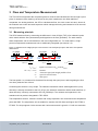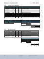
1
Ultrasonic-Flow-Converter Data Sheet TDC-GP30 System-Integrated Solution for Ultrasonic Flow Meters Volume 1: General Data and Frontend Description July 31th, 2015 Document-No: DB_GP30Y_Vol1_en V0.1 UFC TDC-GP30 acam-messelectronic gmbh is now a member of ams group Copyrights & Disclaimer Copyright acam-messelectronic gmbh, Friedrich-List-Str. 4, 76297 Stutensee, Germany-Europe. Trademarks Registered. All rights reserved. The material herein may not be reproduced, adapted, merged, translated, stored, or used without the prior written consent of the copyright owner. Devices sold by acam-messelectronic gmbh are covered by the warranty and patent indemnification provisions appearing in its General Terms of Trade. acam-messelectronic gmbh makes no warranty, express, statutory, implied, or by description regarding the information set forth herein. acammesselectronic gmbh reserves the right to change specifications and prices at any time and without notice. Therefore, prior to designing this product into a system, it is necessary to check with acammesselectronic gmbh for current information. This product is intended for use in commercial applications. Applications requiring extended temperature range, unusual environmental requirements, or high reliability applications, such as military, medical life-support or life-sustaining equipment are specifically not recommended without additional processing by acam-messelectronic gmbh for each application. This product is provided by acam-messelectronic gmbh “AS IS” and any express or implied warranties, including, but not limited to the implied warranties of merchantability and fitness for a particular purpose are disclaimed. acam-messelectronic gmbh shall not be liable to recipient or any third party for any damages, including but not limited to personal injury, property damage, loss of profits, loss of use, interruption of business or indirect, special, incidental or consequential damages, of any kind, in connection with or arising out of the furnishing, performance or use of the technical data herein. No obligation or liability to recipient or any third party shall arise or flow out of acam-messelectronic gmbh rendering of technical or other services. “Preliminary” product information describes a product which is not in full production so that full information about the product is not yet available. Therefore, acam -messelectronic gmbh (“acam”) reserves the right to modify this product without notice. Support / Contact For direct sales, distributor and sales representative contacts, visit the acam web site at: www.acam.de www.ams.com For technical support you can contact the acam support team: [email protected] or by phone +49-7244-74190. Ultrasonic Flow Converter Vol. 1 TDC-GP30 Notational Conventions Throughout the GP30 documentation, the following stile formats are used to support efficient reading and understanding of the documents: Hexadecimal numbers are denoted by a leading 0x, e.g. 0xAF = 175 as decimal number. Decimal numbers are given as usual. Binary numbers are denoted by a leading 0b, e.g. 0b1101 = 13. The length of a binary number can be given in bit (b) or Byte (B), and the four bytes of a 32b word are denoted B0, B1, B2 and B3 where B0 is the lowest and B3 the highest byte. Abbreviations and expressions which have a special or uncommon meaning within the context of GP30 application are listed and shortly explained in the list of abbreviations, see following page. They are written in plain text. Whenever the meaning of an abbreviation or expression is unclear, please refer to the glossary at the end of this document. Variable names for hard coded registers and flags are in bold. Meaning and location of these variables is explained in the datasheet (see registers CR, SRR and SHR). Variable names which represent memory or code addresses are in bold italics. Many of these addresses have a fixed value inside the ROM code, others may be freely defined by software. Their meaning is explained in the firmware and ROM code description, and their physical addresses can be found in the header files. These variable names are defined by the header files and thus known to the assembler as soon as the header files are included in the assembler source code. Note that different variable names may have the same address, especially temporary variables. 1 Physical variables are in italics (real times, lengths, flows or temperatures). Ultrasonic Flow Converter Vol. 1 TDC-GP30 Abbrevations AM CD CPU CR CRC DIFTOF, DIFTOF_ALL DR FEP FDB FHL FW FWC FWD FWD-RAM GPIO Hit HSO INIT IO I2C LSO MRG NVRAM, NVM PI PP PWR R RAA RAM RI ROM ROM code SHR SPI SRAM SRR SUMTOF Task TDC TOF, TOF_ALL TS TM UART USM V ref X,Y,Z ZCD Amplitude measurement Configuration Data Central Processing Unit Configuration Register Cyclic Redundancy Check Difference of up and down ->TOF Debug Register Frontend Processing Frontend data buffer First hit level (physical value V FHL ) Firmware, software stored on the chip Firmware Code Firmware Data Firmware Data memory General purpose input/output Stands for a detected wave period High speed oscillator Initialization process of ->CPU or -> FEP Input/output Inter-Integrated Circuit bus Low speed oscillator Measurement Rate Generator Programmable Non-Volatile Memory Pulse interface Post Processing Pulse width ratio RAM address pointer of the CPU, can also stand for the addressed register Random Access Area Random Access Memory Remote Interface Read Only Memory Hard coded routines in ROM System Handling Register Serial Peripheral Interface Static RAM Status & Result Register Sum of up and down TOF Process, job Time-to-digital-converter Time of Flight Task Sequencer Temperature measurement Universal Asynchronous Receiver & Transmitter Ultrasonic measurement Reference voltage Internal registers of the CPU Zero cross detection, physical level V ZCD For details see the glossary in section 9. 2 www.acam.de DB_GP30Y_Vol1_en.docx V0.0 TDC-GP30 Vol. 1 Content 1 2 3 4 5 6 7 8 Overview ................................................................................................................................ 1-3 1.1 Key Features .................................................................................................................. 1-3 1.2 Block diagram................................................................................................................. 1-4 1.3 Ordering Numbers .......................................................................................................... 1-4 Characteristics & Specifications.............................................................................................. 2-1 2.1 Electrical Characteristics ................................................................................................ 2-1 2.2 Timings .......................................................................................................................... 2-4 2.3 Pin Description ............................................................................................................... 2-7 2.4 Package Drawings .......................................................................................................... 2-9 Flow and Temperature Measurement ................................................................................... 3-11 3.1 Measuring principle ...................................................................................................... 3-11 3.2 Ultrasonic Measurement ............................................................................................... 3-15 3.3 Temperature Measurement ........................................................................................... 3-19 3.4 Chip level calibrations ................................................................................................... 3-24 Special Service Functions ...................................................................................................... 4-1 4.1 Watchdog ....................................................................................................................... 4-1 4.2 Time Stamp (RTC) ......................................................................................................... 4-1 4.3 Backup ........................................................................................................................... 4-1 4.4 Clock Management ......................................................................................................... 4-1 4.5 Power Supply ................................................................................................................. 4-4 4.6 Voltage Measurement ..................................................................................................... 4-6 Remote Port Interfaces ........................................................................................................... 5-1 5.1 SPI Interface .................................................................................................................. 5-1 5.2 UART Interface ............................................................................................................... 5-1 5.3 Remote Communication (Opcodes) ................................................................................ 5-3 5.4 Opcodes ......................................................................................................................... 5-3 General Purpose IO Unit ........................................................................................................ 6-1 6.1 Pulse Interface ............................................................................................................... 6-2 6.2 EEPROM Interface ......................................................................................................... 6-5 Memory Organization & CPU .................................................................................................. 7-1 7.1 Program Area ................................................................................................................. 7-3 7.2 Random Access Area (RAA) ........................................................................................... 7-4 7.3 Configuration Registers ................................................................................................ 7-10 7.4 System Handling Register ............................................................................................ 7-21 7.5 Status Registers ........................................................................................................... 7-28 Applications ............................................................................................................................ 8-1 8.1 GP30-DEMO Board ........................................................................................................ 8-1 8.2 GP30 Typical Configuration ............................................................................................ 8-2 DB_GP30Y_Vol1_en.docx V0.1 www.acam.de 1-1 Ultrasonic Flow Converter Vol. 1 TDC-GP30 9 Glossary ................................................................................................................................. 9-1 10 Miscellaneous ...................................................................................................................... 10-1 10.1 Bug Report ................................................................................................................... 10-1 10.2 Last Changes ............................................................................................................... 10-1 1-2 www.acam.de DB_GP30Y_Vol1_en.docx V0.1 TDC-GP30 Vol. 1 1 Overview TDC-GP30 is the next generation in acam’s development for ultrasonic flow converters. The objectives of the TDC-GP30 development are as follows: Easy-to-adapt two-chip solution for ultrasonic heat and water meters (GP30 + simple µP) Single-chip solution for many industrial applications or pure flow meter parts All flow and temperature calculations are done by GP30 External µP needed only for interfaces (e.g. LCD, wireless, etc.) and other general-purpose tasks Integrated standard pulse interface enables one-to-one replacement of mechanical meters by GP30 based single-chip heat and water meters – customer µP and software remains unchanged. All in all, the TDC-GP30 is the next step in ultrasonic flow metering. It drastically simplifies the design of ultrasonic heat and water meters and is the necessary step for compact energy -saving ultrasonic water meters. The ultra-low-current capabilities allow the use of standard 2/3 AA or AA lithium thionyl chloride batteries at 6-8 Hz measuring frequency even in the water meter version. The TDC-GP30 is a system-on-chip approach that allows you to perform all measurement tasks in one IC. 1.1 Key Features High performance + ultra-low power 32-Bit CPU with 128 * 32 bit NVRAM (non-volatile RAM) for user firmware parameter & data 4k * 8 bit NVRAM (non-volatile RAM) for user firmware program code 4k * 8 bit ROM for system task code and special flow library code Capability of MID-compliant flow & temperature calculation, GP30-supported Flexible interfaces, SPI, UART, pulse (flow only) Advanced high-precision analog part Transducers can be connected directly to GP30, no external components required Amplitude measurements of receiving signal for secure bubble, aging and empty spool piece detection Up to 31 multi-hits for flow measurement yield the highest accuracy High update rates with very low power consumption of for example 6 µA at 8 Hz, including flow and temperature calculations, measure rate adopted to the flow Very low space and component requirements DB_GP30Y_Vol1_en.docx V0.1 www.acam.de 1-3 Ultrasonic Flow Converter Vol. 1 TDC-GP30 1.2 Block diagram Figure 1-1: Block diagram Vcc: 2.5...3.6 V 4/8 MHz 32.768 kHz quartz ceramic 10u Clock Management A) Supervisor 100u 10R D) User Interfaces Voltage Measurement Voltage Regulator Measure Rate Generator & Task Sequencer Ultrasonic Frontend PT1000 PT1000 680n Temperature Frontend 1k System Tasks & Flow Library User-FW Program & ACAM-FW Program ROM (4k * 8) NVRAM (4k * 8) SPI / UART SPI / UART RAM & Register Time-to-Digital-Converter (TDC) Transducer 1...4 MHz Remote Interface User-FW Data NVRAM (128*32) CPU 32 Bit Pulse Interface Pulse DIR EEPROM Interface SCL SDA General Purpo se IO Unit GPIOs 100n C0G B) Frontend C) Post processing Main functional blocks of TDC-GP30: A) Supervisor: Timing and voltage control B) Frontend: TOF and sensor temperature measurements C) Post processing: CPU operations, including initialization and firmware operations D) User interfaces: Chip communication over SPI or UART, Pulse interface and GPIOs 1.3 Ordering Numbers Part# Package Carrier, Quantity Order number TDC-GP30YA QFN40 T&R, 3000 502030004 TDC-GP30YD QFN32 T&R, 3000 502030003 GP30-DEV-KIT System Box, 1 220260003 This product is RoHS-compliant and does not contain any Pb. 1-4 www.acam.de DB_GP30Y_Vol1_en.docx V0.1 TDC-GP30 Vol. 1 2 Characteristics & Specifications 2.1 Electrical Characteristics Absolute Maximum Ratings Stresses beyond those listed under “Absolute Maximum Ratings“ may cause permanent damage to the device. These are stress ratings only. Functional operation of the device at these or any other conditions beyond those indicated under “Electrical Characteristics” is not implied. Exposure to absolute maximum rating conditions for extended periods may affect device reliability. Table 2-1 Absolute maximum ratings Symbol Parameter Min Max Units VCC Supply voltage VCC vs. GND -0.3 4.0 V All other pins -0.3 VCC + 0.6 V Tamb Ambient temperature -40 +125 °C Tstrg Storage temperature -55 +150 °C Tbody Body temperature JEDEC J-STD-020 260 °C ESD ESD rating (HBM), each pin ±2 kV Table 2-2 Recommended operating conditions Parameter Conditions Min. Typ. Max. Unit VCC Supply voltage main supply voltage 2.5 3.0 3.6 V VDD18 Core supply Internally derived from VCC and regulated 1.65 1.80 1.92 V fLSO Low speed oscillator (LSO) frequency fHSO High-speed oscillator (HSO) frequency 32.768 kHz For Standard transducers, max. 2 MHz, 3.6 4 4.4 MHz For 4 MHz transducers, not in combination with UART 7.2 8 8.8 MHz Other frequencies in the range from 2 MHz to 8 MHz may be possible with limitations fSPI SPI Interface Clock Frequency fTOF TOF measurement frequency tcycle Measurement cycle time DB_GP30Y_Vol1_en.docx V0.1 SPI communication 𝑓𝑇𝑂𝐹 = 1 (𝑇𝑂𝐹_𝑅𝐴𝑇𝐸 ∗ 𝑡𝑐𝑦𝑐𝑙𝑒 ) LSB = 976.5625 µs www.acam.de 0.004 1…8 10 MHz 80 Hz 4000 ms 2-1 Ultrasonic Flow Converter Vol. 1 TDC-GP30 Table 2-3 DC Characteristics (VCC = 3.0 V, Tj = -40 to +85 °C) Symbol Parameter IStandby Supply current only 32 kHz, Standby mode Conditions Min. Typ. Max. Unit only 32 kHz oscillator running @ 25 °C, VCC = 3.6 V = 3.0 V 3.6 2.2 µA µA VCC = 3.6 V = 3.0 V off 80 65 <1 µA µA nA Only during active TOF time measurement 1.3 mA all clocks off, @25 °C 1.8V LDO running 1.9 µA all clocks off 0.08 µA Ihs Operation current 4 MHz oscillator Itmu Current into time measuring unit including analog frontend ICCq Quiescent current GP30 IDDqc Quiescent current 1.8V digital core IAFE Average operating current analog front end only TOF_UP+DOWN, 1/s 0.42 µA Io Average operating current incl. CPU processing current TOF_UP+DOWN, 1/s 0.9 µA Voh High level output voltage Ioh= 4 mA VCC - 0.4 Vol Low level output voltage Iol = 4 mA Vih Logic High level input voltage for proper logic function 0.7* VCC for low leakage current VCC - 0.2 Vil Logic Low level input voltage for proper logic function for low leakage current V 0.4 V V 0.3* VCC 0.2 V Note: See also section 4.5.2 for more information about the current consumption Table 2-4 Terminal Capacitance Symbol Terminal Condition Rated Value Min. Ci Digital input Co Digital output Cio Bidirectional Unit Typ. measured @ VCC = 3.0 V f = 1 MHz, Ta = 25 °C Max. 7 pF 7 7 Table 2-5 Analog Frontend Symbol Terminal Condition Rated Value Min. Comparator input offset voltage (chopper stabilized) 2-2 Typ. Unit Max. < 1.6 www.acam.de mV DB_GP30Y_Vol1_en.docx V0.1 TDC-GP30 Vol. 1 Table 2-6 NVRAM Symbol Terminal Condition Minimum Value Unit Data retention @ 125 °C VCC = 3.0 to 3.6 V 20 Years Endurance * @ 25 C VCC= 3.0 to 3.6 V 105 Cycles @ 125 C VCC= 3.0 to 3.6 V 104 Cycles * See 6.2 EEPROM interface for backup applications. Converter Specification Table 2-7 Time Measuring Unit (VCC = 3.0 V, Tj = 25 °C) Symbol Terminal Condition Rated Value Min. Unit Typ. Max. LSB TDC Resolution (BINSize) 11 ps LSB TDC rms Noise 1.2 LSB tm Measurement range TOF measurement 10 4096 µs tm Measurement range Temperature interface measurement 10 1024 µs Table 2-8 Temperature Measuring Unit1 Symbol Terminal PT500 Typical. Typical Resolution RMS 17.0 17.0 Absolute Gain 2 1.0004 1.0002 Gain-Drift vs. V CC 0.01 0.01 %/V <2 <3 ppm/K Gain-Drift vs. Temp 1 Unit PT1000 Bit Initial Zero Offset T cold <-> T hot <2 <4 mK Initial Zero Offset T ref <-> (T cold , T hot ) < 20 < 40 mK Offset Drift vs. Temp < 0.05 < 0.05 mK/K 2-Wire measurement with compensation of Rds(on) and gain (Schmitt trigger). All values measured at VCC = 3.0 V, Cload = 100 nF for PT1000 and 200 nF for PT500 (C0G-type) 2 Compared to an ideal gain of 1.0 DB_GP30Y_Vol1_en.docx V0.1 www.acam.de 2-3 Ultrasonic Flow Converter TDC-GP30 Vol. 1 2.2 Timings At VCC = 3.0 V ± 0.3 V, ambient temperature -40 °C to +85 °C unless otherwise specified 2.2.1 Oscillators Table 2-9 Oscillator specifications Symbol Parameter Min. Typ. LSO_CLK 32 kHz reference oscillator at frequency fLSO 32.768 kHz STLSO 32 kHz oscillator start-up time after power-up <1 Sec. HSO_CLK High-speed reference oscillator at frequency fHSO STHSO_CER Oscillator start-up time with ceramic resonator <100 µs STHSO_CRY Oscillator start-up time with crystal oscillator (not recommended) 3 ms 2 Max. 4 8 Unit MHz Remark: It is strongly recommended that a ceramic oscillator be used for HSO_CLK because a quartz oscillator needs much longer time to settle than a ceramic oscillator. This consumes a lot of current, but using a quartz oscillator has no advantage when high speed clock calibration is done as supported by GP30. 2.2.2 Power-On Table 2-10 Power-on timings Symbol Parameter tVDD18_STB Time when VDD18 is stable after power on of VCC (CL=100µF on VDD18_OUT) tRC_RLS Time when remote communication is released after power on of VCC 2.2.3 Min. Typ. 27 Max. Unit 20 ms 40 ms UART Interface Table 2-11UART timings Symbol Parameter Min. Baud rate Baud rate 4800 tBIT tIBG Typ. Max. Unit 115200 bps Bit time (baud rate = 4800 Baud) 208.33 µs Bit time (Baudrate = 115200 Baud) 8.68 µs Inter-Byte Gap 1 tBIT 50 Figure 2-1 UART timing tBIT tIBG ST 2-4 B0 B1 B2 B3 B4 www.acam.de B5 B6 B7 SP ST DB_GP30Y_Vol1_en.docx V0.1 TDC-GP30 2.2.4 Vol. 1 SPI Interface Table 2-12 SPI timings Symbol Parameter min max Unit fSCK Serial clock frequency 10 MHz tSCK Serial clock time period 100 ns tpwh Serial clock, pulse width high 0.4 * tSCK ns tpwl Serial clock, pulse width low 0.4 * tSCK ns tsussn SSN enable to valid latch clock 0.5 * tSCK ns thssn SSN hold time after SCK falling 0.5 * tSCK ns tpwssn SSN pulse width between two cycles tSCK ns tsud Data set-up time prior to SCK falling 5 ns thd Data hold time before SCK falling 5 ns tvd Data valid after SCK rising 20 ns Serial interface (SPI compatible, clock phase bit =1, clock polarity bit =0): Figure 2-2 SPI Write tsussn tpwssn tpwl PIN: tpwh SSN SSN_GPIO2 tSCK thssn SCK SI MSB SCK_RXD MOSI_GPIO3 LSB tsud thd Figure 2-3 SPI Read tsussn tpwl PIN: tpwssn tpwh SSN SSN_GPIO2 tSCK SCK SCK_RXD SI MSB tsud SO 6 LSB 1 thd MOSI_GPIO3 MSB 1 MSB-1 MISO_TXD LSB tvd OPCODE DB_GP30Y_Vol1_en.docx V0.1 DATA www.acam.de 2-5 Ultrasonic Flow Converter 2.2.5 Vol. 1 TDC-GP30 EEPROM Interface (fHSO = 4MHz) Table 2-13 EEPROM timings Symbol Parameter Min. Typ. Max. Unit f SCL SCL clock frequency 400 t LOW Low period of SCL clock 1300 1500 ns t HIGH High period of SCL clock 600 1000 ns t HD_STA Hold time for (repeated) START condition (S & Sr) 600 1000 ns t SU_STA Setup time for repeated START condition (Sr) 600 750 ns t SU_DAT Setup time data 100 750 ns t HD_DAT Hold time data 0 750 ns t VD_DAT Valid time data t SU_STO Setup time for STOP condition (P) 600 t BUF Bus free time between STOP and START condition 1300 kHz 750 900 1750 ns ns ns Figure 2-4 EEPROM timing S tSU_DAT tVD_DAT PIN e.g.: E2P_SDA GPIO5 tHIGH E2P_SCL GPIO6 1/fSCL tHD_STA tLOW tHD_DAT Sr P S E2P_SDA GPIO5 tSU_STA tSU_STO E2P_SCL GPIO6 tHD_STA 2-6 PIN e.g.: 9th clock tBUF www.acam.de DB_GP30Y_Vol1_en.docx V0.1 TDC-GP30 Vol. 1 2.3 Pin Description 2.3.1 Device Marking Example: GP30 Y A 15 03 Device family Silicon revision (Y) Chip package (A = QFN40; D = QFN32) Year (15 = YEAR 2015) Calendar week (03 = CW 03) QFN Packages Chips OPEXT_OUT 11 VCC GPIO0 GPIO1 for test only for test only GPIO4 UART_SEL XIN_32KHZ XOUT_32KHZ 20 10 30 XOUT_4MHZ PTWCOMB 1 VDD18_IN VDD18_IN SSN_GPIO2 VDD18_OUT MOSI_GPIO3 VCC GPIO6 LP_MODE for test only US_UP SCK_RXD GND MISO_TXD US_DOWN 8 INTN_DIR 21 GPIO5 7 GP30YD 1503 1 7 GP30YA 1503 PTWCOMB VDD18_IN VDD18_OUT VCC LP_MODE US_UP GND US_DOWN US_VREF OPEXT_IN 32 PTWCOMA PTHOTA PTHOTB CLOAD PTCOLDA PTCOLDB PTREF 25 VCC QFN32 40 PTWCOMA n.c. PTHOTA PTHOTB CLOAD PTCOLDA PTCOLDB PTREF VCC 31 XIN_4MHZ QFN40 24 XIN_4MHZ XOUT_4MHZ VDD18_IN SSN_GPIO2 MOSI_GPIO3 For test only SCK_RXD 17 MISO_TXD US_VREF 9 VCC GPIO0 GPIO1 UART_SEL XIN_32KHZ XOUT_32KHZ INTN_DIR 16 2.3.2 Figure 2-5 GP30 Pinout QFN 40 QFN32 Name Description Buffer type 1 1 PTWCOMB Temperature Sensor Port Common B Analog 2 2 VDD18_IN VDD18 TDC Supply Input (1.8 V) Supply 3 3 VDD18_OUT VDD18 voltage regulator output (1.8 V) Supply 4 4 VCC VCC IO & Analog Supply (2.5..3.6 V) Supply 5 5 LP_MODE Low Power Mode (analog/digital) Digital IN(Pull-up) 6 6 US_UP Ultrasonic Transducer (Fire Up / Receive Down) Analog 7 7 GND Ground plane 8 8 US_DOWN Ultrasonic Transducer (Fire Down / Receive Up) Analog 9 9 US_VREF Ultrasonic Reference Voltage Vref (typ. 0.7 V) DB_GP30Y_Vol1_en.docx V0.1 www.acam.de Power 2-7 Ultrasonic Flow Converter Vol. 1 TDC-GP30 QFN 40 QFN32 Name Description Buffer type 10 - OPEXT_IN External OP In (connect the input of the optional external OpAmp for amplifying ultrasonic echo here) Analog 11 - OPEXT_OUT External OP Out (connect the output of the optional external OpAmp for amplifying ultrasonic echo here) Analog 12 10 VCC VCC IO & Analog Supply (2.5..3.6 V) Supply 13 11 GPIO0 General Purpose IO 0 Digital IO 14 12 GPIO1 General Purpose IO 1 Digital IO 15 - TST_I for test only 16 - TST_O for test only 17 - GPIO4 General Purpose IO 4 Digital IO 18 13 UART_SEL UART Select (0:SPI / 1:UART) Digital IN 19 14 XIN_32KHZ Low-Speed Oscillator (32.768 kHz) Clock 20 15 XOUT_32KHZ Low-Speed Oscillator (32.768 kHz) Clock 21 - GPIO5 General Purpose IO 5 Digital IO 22 16 INTN_DIR SPI: Interrupt (low active) UART: Direction (0:Receive / 1:Send) Digital OUT 23 17 MISO_TXD SPI: Master In / Slave Out UART: Transmit Data Digital OUT 24 18 SCK_RXD SPI: Serial Clock UART: Receive Data Digital IN 25 19 TEST_MODE_N for test only Digital IN(Pull-up) 26 - GPIO6 General Purpose IO 6 Digital IO 27 20 MOSI_GPIO3 SPI: Master Out / Slave In UART: GPIO Digital IN 28 21 SSN_GPIO2 SPI: Slave Select (low active) UART: GPIO Digital IN 29 22 VDD18_IN VDD18 Digital Core Supply Input (1.8 V) Supply 30 23 XOUT_4MHZ High-Speed Oscillator (4 or 8 MHz) Clock 31 24 XIN_4MHZ High-Speed Oscillator (4 or 8 MHz) Clock 32 25 VCC VCC IO & Analog Supply (2.5..3.6 V) Supply 33 26 PTREF Temperature Sensor Port Reference Resistor Analog 34 27 PTCOLDB Temperature Sensor Port Cold B Analog 35 28 PTCOLDA Temperature Sensor Port Cold A Analog 36 29 CLOAD Temperature Measurement Load Capacitor Analog 37 30 PTHOTB Temperature Sensor Port Hot B Analog 38 31 PTHOTA Temperature Sensor Port Hot A Analog 39 - n.c. not connected 40 32 PTWCOMA Temperature Sensor Port Common A 2-8 www.acam.de Digital IN DB_GP30Y_Vol1_en.docx V0.1 TDC-GP30 Vol. 1 2.4 Package Drawings Figure 2-7 QFN-32 package outline, 5 x 5 x 0.9 mm³, 0.5 mm lead pitch, bottom view 3.65 ± 0.15 0.43 ± 0.07 0.43 ± 0.07 0. 25 ± 0. 05 3.65 ± 0.15 5.00 ± 0.10 4. 65 ± 0.15 5.00 ± 0.10 6. 00 ± 0.10 4.65 ± 0.15 6.00 ± 0.10 Figure 2-6 QFN-40 package outline, 6 x 6 x 0.9 mm³, 0.5 mm lead pitch, bottom view 0.25 ± 0.05 0.5 ± 0.025 0. 5 ± 0.025 Side view 0.90 ± 0.10 0.025 ± 0.025 Landing pattern QFN32: (4.30) (3.30) 0.75 0.75 (3.30) 4.10 4.10 5.10 (4.30) 5.10 Landing pattern QFN40: 0.25 0.5 0.25 0.5 Caution: The center pad is internally connected to GND. No wires other than GND are allowed underneath. It is not necessary to connect the center pad to GND. DB_GP30Y_Vol1_en.docx V0.1 www.acam.de 2-9 Ultrasonic Flow Converter Vol. 1 TDC-GP30 Marking: GP30 YYWW : Date Code: YYWW: YY = Year, WW = week Thermal resistance: Roughly 28 K/W (value just for reference). Environmental: The package is RoHS-compliant and does not contain any lead. Moisture Sensitive Level (MSL) Based on JEDEC 020 moisture sensitivity level definition the TDC-GP30 is classified as MSL 3. Soldering Temperature Profile The temperature profile for infrared reflow furnace (in which the temperature is the resin’s surface temperature) should be maintained within the range described below. Figure 2-8 Soldering profile Package body surface temperature Max. peak temperature: 260 °C 250 °C for up to 10 seconds Pre-heating: 140°C to 200°C 60 to 120 seconds Heating: 220°C up to 35 seconds Time Maximum temperature The maximum temperature requirement for the resin surface, where 260ºC is the peak temperature of the package body’s surface, is that the resin surface temperature must not exceed 250ºC for more than 10 seconds. This temperature should be kept as low as possible to reduce the load caused by thermal stress on the package, which is why soldering is recommended only for short periods. In addition to using a suitable temperature profile, we also recommend that you check carefully to confirm good soldering results. 2-10 www.acam.de DB_GP30Y_Vol1_en.docx V0.1 TDC-GP30 Vol. 1 3 Flow and Temperature Measurement The TDC-GP30 incorporates the complete system to measure and calculate the flow through a spool piece for ultrasonic flow metering: the driver for the piezo transducers, the offset stabilized comparator, the analog switches, the CPU to calculate the flow, the clock control unit and , above all, the measure rate control and task sequencer which manage the timing and interaction of all the units during measurement. 3.1 Measuring principle The GP30 measures flow by measuring the difference in time-of-flight (TOF) of an ultrasonic pulse which travels with the flow (downstream) and opposite to the flow (upstream). For water meters, water temperature can be calculated from the time-of-flight data, too.. For heat meters, a highprecision temperature measurement unit is additionally integrated (see section 3.3). Figure 3-1 Ultrasonic time-of-flight principle: Cross sections of an example spool piece with down- and upstream measurement US_DOWN US_UP 𝑡𝑑𝑜𝑤𝑛 = 𝐿 𝑐0 + 𝑣 𝑡𝑢𝑝 , 𝑡𝑑𝑜𝑤𝑛 : ∆𝑡 = 𝑡𝑢𝑝 − 𝑡𝑑𝑜𝑤𝑛 : 𝐿: 𝑐0 : 𝑣: US_UP US_DOWN 𝑡𝑢𝑝 = 𝐿 𝑐0 − 𝑣 𝑣≈ ∆𝑡 ∗ 𝑐0 ² 2∗𝐿 Signal travel times 𝑇𝑂𝐹𝑈𝑃 and 𝑇𝑂𝐹𝐷𝑂𝑊𝑁 𝐷𝐼𝐹𝑇𝑂𝐹 ultrasonic signal path length parallel to flow speed of sound in water flow speed The flow speed v is a measure for the actual flow through the spool piece, and integrating the flow over time yields the flow volume. Connecting the sensors is very simple. The ultrasonic transducer which sends against flow (in up direction) is directly connected to the US_UP pin, the ultrasonic transducer which sends with flow (in down direction) is directly connected to the US_DOWN pin. The resistors and capacitors in the transducer driver path are integrated in TDC-GP30 . The temperature sensors, reference resistor and charge capacitors are connected to the temperature ports and GND. The temperature unit is suitable for sensors with 500 Ohm and higher like PT500 or PT1000. The chip supports 2-wire sensors and 4-wire sensors and is good for 1.5 mK rms resolution. DB_GP30Y_Vol1_en.docx V0.1 www.acam.de 3-11 Ultrasonic Flow Converter Vol. 1 TDC-GP30 Figure 3-2 External connection of sensors: ultrasonic transducers (left) and temperature sensors (right for 2-Wire; for 4-wire sensors, see section 3.3) PTHOT PTCOLD PT1000 TDC PT1000 Fire US_UP US_DOWN 1k PTREF CLOAD TDC 100n C0G GP30 3.1.1 GP30 Measurement Sequence The GP30 is designed for autonomous operation. In self-controlled flow meter mode it triggers all measurements and does data processing to deliver final results, independent of external control. It can also be configured to wake up an external microcontroller for communication of results.. Alternatively, the GP30 can act as a pure converter that controls the measurement but without any data processing (time conversion mode, self-controlled). For debugging, individual tasks can also be triggered remotely by an external microcontroller (time conversion mode, remote controlled). Table 3-1 Operating modes Operating Mode Measure Rate Generation Flow meter mode (self-controlled) Time conversion mode (selfcontrolled) Time conversion mode (remote controlled, only for test or debug purpose) Application Setup Post Processing by GP30 by GP30 per Remote per Remote by GP30 per Remote The various functional blocks of the TDC-GP30 are controlled by hard-wired configuration registers (CR) and system handling registers (SHR) in the random access memory area (RAA). For selfcontrolled applications the configurations are stored in the firmware data section FWD2 of the RAA. From there the configuration data is automatically copied into the direct mapped registers during a boot sequence. The various configuration registers and system handling registers are described in detail in section 7. The variable names are formatted in bold in this document for better reading. In low power mode, the GP30 generally needs a 32.768 kHz oscillator to act as a continuously running clock (LSO). For time measurement the GP30 typically uses a high speed oscillator (HSO), typically featuring a 4 MHz ceramic resonator. The HSO is activated only for the short period of the measurement. In the same manner, the comparator and other analog elements are powered only for the short period of the measurement. 3-12 www.acam.de DB_GP30Y_Vol1_en.docx V0.1 TDC-GP30 Vol. 1 The low-frequency clock LSO is used as Base for the task sequencer cycle Base for the pulse interface Base for the time stamp Base for an initial UART baud rate of 4.800 baud In self-controlled modes, the supervisor function block of TDC-GP30 fully controls the entire operation sequence. It determines cycle timing through the measurement rate generator (MRG), which triggers the task sequencer (TS). The task sequencer calls and coordinates the different tasks according to configuration. The tasks themselves can be grouped as shown in the following table. Table 3-2 GP30 Tasks System tasks Initialization VCC voltage measurement Ultrasonic measurement (time-of-flight and/or amplitude measurement) Temperature measurement (external or internal) Calibration of high-speed clock Calibration of amplitude measurement Calibration of comparator offset TDC Calibration (automatically) Activation of CPU for any calculation through firmware Sending out communication requests to initialize remote communication Frontend measurement tasks Frontend calibration tasks Post processing Remote communication initialization The rate of measurement and calibration tasks can be configured, while initialization, post processing and communication are typically controlled by various flags which indic ate the preceding measurement processes or resets. For example, post processing by the firmware typically depends on the flag register SRR_FEP_STF, it decides for flow or sensor temperature calculations according to the most recent measurements done. See section 7.5 for details on status and result registers. The following figure illustrates rate settings for various tasks. DB_GP30Y_Vol1_en.docx V0.1 www.acam.de 3-13 Ultrasonic Flow Converter Vol. 1 TDC-GP30 Figure 3-3 Rate settings of various tasks 32kHz Measure rate cycle timer A MR_CT Measure rate cycle timer B MR_CT Flow measurement Amplitude meas. Amplitude meas. Calibr. TOF_RATE A AM_RATE AMC_RATE CPU post proccessing Temperature measurement Zero cross calibration HS clock calibration Voltage measurement TM_RATE ZCC_RATE B HSC_RATE VM_RATE The most important parameters are set in configuration registers (CR, see section 7.3): Register CR_MRG_TS, address 0xC6 MR_CT: Task sequencer cycle time. The actual physical cycle time is tcycle = MR_CT* 976.5625 µs [0, 1…8191]. The measurement rate generator triggers measurements in two alternating channels, one MR_CT (A) triggering the flow and amplitude measurement, the other one (B) triggering temperature and voltage measurement as well as the high speed clock (HSO) and the comparator offset calibration. Channel B triggers a half cycle time after channel A, to avoid mutual influences among the measurements. Register: CR_TM, address 0xC7 TM_RATE: Defines the number of sequence cycle triggers between sensor temperature measurements [0=off, 1, 2…1023]. The sensor temperature measurement frequency is 1 / (tcycle * TM_RATE) Register: CR_USM_AM, address 0xCB AM_RATE: Defines the number of sequence cycle triggers between amplitude measurements [0=off, 1, 2, 5, 10, 20, 50, 100]. AMC_RATE sets the number of amplitude measurements between amplitude calibration measurements [0=off, 1, 2, 5, 10, 20, 50, 100]. Register: SHR_TOF_RATE, address 0xD0 TOF_RATE: Defines the number of sequence cycle triggers between TOF measurements [0=off, 1…63]. The TOF measurement frequency is 1 / (tcycle * TOF_RATE) Register CR_CPM, address 0xC5 HSC_RATE: Defines the number of sequence cycle triggers between high-speed clock calibration measurements (4 MHz ceramic against 32.768 kHz quartz) [0=off, 1, 2, 5, 10, 20, 50, 100]. VM_RATE: Defines the number of sequence cycle triggers between low battery detection measurements [0=off, 1, 2, 5, 10, 20, 50, 100]. The following sections describe the front end measurement tasks in more detail . 3-14 www.acam.de DB_GP30Y_Vol1_en.docx V0.1 TDC-GP30 Vol. 1 3.2 Ultrasonic Measurement The measurement rate generator in channel A typically triggers the task sequencer (TS) for a complete sequence of flow measurement, starting with an ultrasonic time-of-flight (TOF) measurement, and – if desired – ending in front end processing which does all necessary calculations. .The TOF measurement is made up of the two time-of-flight measurements in up and down direction (in other words, against flow and with flow). The pause time between the two measurements can be configured in multiples of ¼ period of the base frequency (50 Hz or 60 Hz) in several steps, to optimize rejection of mains frequency distortions. The time-of-flight measurement triggers the amplitude measurement. The GP30 can automatically toggle the measurement direction sequence between up /down- and down/up-measurement from cycle to cycle. This helps suppress errors caused by temperature drift. Figure 3-4 Timing of the ultrasonic measurement with 20 ms pause interval (example) 20 ms US_UP send US_DOWN receive receive send HS Clock ~ 400 µs Frontend processing Post processing (CPU) Remote communication TOF_UP TOF_DOWN Important configuration parameters are: Register CR_CPM, address 0xC5 HS_CLK_ST: Settling time for the high-speed clock HSO, from 76 µs to 5 ms BF_SEL: Selection of base frequency (50 Hz/ 60 Hz) with period tbase Register CR_MRG, address 0xC6 PP_EN: Enables post-processing Register CR_USM_PRC, address 0xC8 USM_TO: sets the timeout for the TOF measurement [128 µs … 4096 µs] USM_DIR_MODE: defines start direction or the toggling of start direction USM_PAUSE: pause time between measurements [0=only one measurement, 2: 0.25* tbase, 3..7: 0.5..2.5*tbase] Register CR_USM_FRC, address 0xC9 FPG_FP_NO: number of fire pulses [1…128] FPG_CLK_DIV: HSO frequency divided by this factor +1 gives the actual frequency of the measurement signal (fire frequency) Further important parameters configure the first wave detection and amplitude measurement as described in the following sections. DB_GP30Y_Vol1_en.docx V0.1 www.acam.de 3-15 Ultrasonic Flow Converter 3.2.1 Vol. 1 TDC-GP30 First Wave Detection To do a time-of-flight measurement, the received signal needs to be identified and its arrival time needs to be measured thoroughly. This can be done by defining a first wave, and then counting subsequent waves and storing the relevant arrival times. This is elaborated in the following: The receive signal, typically a burst-like signal, is converted into a digital signal using an internal comparator. While receiving, the reference voltage of the comparator most of the time equals the zero line of the receive signal to identify zero crossings (Actually, the zero line is the overlaid reference voltage Vref, and the comparator’s reference is set to the zero cross detection level VZCD, which is calibrated to Vref ). This way, received wave periods are converted into digital hits. To determine an absolute numbering of the hits, a so-called first wave is defined by adding a welldefined voltage level, the first hit level (VFHL), to the comparator’s reference. This first wave detection, at a comparator level which differs from the zero cross level, is implemented to make the time-of-flight measurement independent from temperature and flow. The offset level VFHL practically represents the level of receive signal at which the first wave is detected, which generates the first hit. After the first hit was detected, the comparator’s reference is brought back to zero cross detection level (VZCD) at the 2 nd hit, and the subsequent hit measurements are done at zero crossing. The following parameters define the first wave detection and the TOF hits: The trigger level ZCD_FHL, which defines the comparator offset level VFHL The count number of the first subsequent TOF hit (TOF Start hit) which is actually measured The number of measured TOF hits The interval between measured TOF hits The TOF start hit delay: This delay disables hit detections for some defined lead time. This parameter is used as alternative to the first wave detection. The diagram 3-5 below shows the measurement flow in TDC-GP30 first wave mode. Starting the measurement with the comparator offset VFHL different from zero, e.g. 100 mV, helps suppressing noise and allows the detection of a dedicated wave of t he receive burst that can be used as reference. Once this first wave is detected, the offset is set back to the zero cross detection level VZCD. It is recommended to start actual TOF hit measurements after at least two more wave periods. The count number of the TOF start hit, the total number of TOF hits and the number of ignored hits between TOF hits are set by configuration. Ignored hits are in particular helpful when signal frequencies approaching half of the HSO frequency are used (e. q. 2 MHz signals when using a 4 MHz HSO). In such cases, the internal arithmetic unit is not fast enough to do all necessary calculations for each single hit, so at least every second hit must be ignored. 3-16 www.acam.de DB_GP30Y_Vol1_en.docx V0.1 TDC-GP30 Vol. 1 Figure 3-5 First wave detection 1. Programmable trigger level, set to First Hit Level (FHL) for save detection of the chosen first hit 2. Afterwards, the trigger level is automatically set to the zero cross level (ZCL)“ Wave period Receive Burst ZCD Comparator output First Hit x Ignored Hit PW_FH 1. TOF Hits x Ignored Hit x Ignored Hit Start Hit PW_SH 1. 2. 3. N-th PW_FH = pulse width first hit, PW_SH = pulse width start hit The important parameters are: ZCD_LVL: The zero cross detection level VZCD is automatically calibrated to the reference voltage level Vref. This calibration should be configured to be repeated regularly ( see section 7.4.8) Register CR_USM_PRC, address 0xC8 USM_NOISE_MASK: Opens the receive channel after a programmable delay, e.g. for noise suppression Register CR_USM_FRC, address 0xC9 ZCD_FHL: First hit level, offset to VZCD, to be set from -224 mV to +200 mV (typ.). The actual physical value is VFHL = ± 0.88mV * ZCD_FHL (typ.; sign given by ZCD_FHL_DIR). ZCD_FHL_DIR: Offset sign positive or negative ZCC_TS_RATE: Configuring the offset calibration of the comparator Register CR_USM_TOF, address 0xCA TOF_HIT_NO: Number of hits for the time-of-flight measurement [1…31] TOF_HIT_IGN: Number of waves ignored between the TOF measurements [0…3] TOF_START_HIT_MODE: Selects mode for TOF start hit TOF_START_HIT_NO: Number of waves counted after first detected hit which is defined as TOF start hit [2…31] Register SHR_TOF_START_HIT_DLY TOF_START_HIT_DLY: Delay window after which the next detected hit is defined to TOF start hit. Starting time of the delay window refers to rising edge of 1st fire pulse (like stop masking in predecessor TDC-GP22, defined by DELVAL) DB_GP30Y_Vol1_en.docx V0.1 www.acam.de 3-17 Ultrasonic Flow Converter Vol. 1 TDC-GP30 Like in TDC-GP22, the first wave detection is supported by a pulse width measurement option. Therefore the pulse width of the first hit, measured at the signal amplitude VFHL (unequal to zero), is compared to the pulse width of the TOF start hit measured without offset at VZCD. The result is read as PWR = PW_FH/PW_SH and is typically < 1. The ratio PWR can be used to track VFHL. Register CR_USM_AM, address 0xCB PWD_EN: Enable the pulse width detection 3.2.2 Amplitude Measurement A new feature in TDC-GP30 is a true amplitude measurement. The result is time data that reflect the amplitude of the receive burst. During operation the relative time information is fully sufficient for amplitude comparisons. The formula to calculate the amplitude in mV is given in the user manual DB_GP30_Vol3.pdf. The features are: True peak amplitude measurement with every TOF (configurable) Highly reliable bubble and aging detection Very good consistency check in comparison to first wave detection Easy quality check in production and development Configurable number of hits to stop the amplitude measurement – this allows to measure the peak amplitude of each single wave at the start of the burst signal ( but only one single value in each TOF measurement) Figure 3-6 Amplitude measurement 1,1 peak measurement 1 0,9 single slope AD-Conversion 0,8 . 0,7 0,6 0,5 0,4 0,3 0 2 4 6 8 10 12 14 16 18 20 22 24 Time/µs The most important parameters are: Register CR_USM_AM, address 0xCB AM_RATE: Rate for amplitude measurement in sequence cycles [0=off, 1, 2, 5, 10, 20, 50, 100] AM_PD_END: Number of the wave when peak detection stops [0=off, 1…31] AMC_RATE: Calibration rate for amplitude measurement [0=off, 1, 2, 5, 10, 20, 50, 100] 3-18 www.acam.de DB_GP30Y_Vol1_en.docx V0.1 TDC-GP30 3.2.3 Vol. 1 Reading Ultrasonic Measurement Results The GP30 measurement results are stored in a RAM section called front end data buffer (FDB). This section is used for flow measurement data and temperature measurement data alternately. Therefore, it is necessary to read the time-of-flight data directly after the end of a flow measurement and before the temperature measurement starts. The ultrasonic flow measurement stores the following results in the RAM section: Table 3-3 Reading results from front end data buffer in the RAM Name FDB_US_TOF_ADD_ALL_U FDB_US_PW_U FDB_US_AM_U FDB_US_AMC_VH FDB_US_TOF_ADD_ALL_D RAA address 0x080 0x081 0x082 0x083 0x084 Description Ultrasonic Ultrasonic Ultrasonic Ultrasonic Ultrasonic direction Ultrasonic Ultrasonic Ultrasonic TOF UP, sum of all TOF hits, up direction pulse width ratio, up direction amplitude value, up direction amplitude calibration value, high TOF DOWN, sum of all TOF hits, down 0x085 pulse width ratio, down direction 0x086 amplitude value, down direction 0x087 amplitude calibration value, low 0x088 FDB_US_TOF_0_U to … _7_U to Ultrasonic TOF UP values 0 to 7, up direction 0x08F 0x090 FDB_US_TOF_0_D to …_7_D to Ultrasonic TOF DOWN values 0 to 7, down direction 0x097 For debugging purposes, it is possible to read the individual TOF_up and TOF_down data for the first FDB_US_PW_D FDB_US_AM_D FDB_US_AMC_VL eight hits. Furthermore, the user can read the pulse width ratio PWR and the peak amplitude value AM for both directions. Single TOF values (addresses 0x88 … 0x97) are only posted if TOF_HITS_TO_FDB is set in configuration register CR_USM_TOF. TOF and amplitude measurement data are all times, given as 32-bit fixed point numbers with 16 integer bits and 16 fractional bits in multiples of the HSO period (typically 250 ns with 4 MHz HSO). So the meaning of the least significant bit is 1 LSB = 250 ns /2 16 = 3.8146972 ps. Note that these values may need a further calibration step, depending on usage (see section 3.4.1) The pulse width ratio PWR is an 8-bit fixed point number with 1 integer bit and 7 fractional bits. For example, PWR=0b01001101 means 0.6015625 in decimal. 3.3 Temperature Measurement Precision temperature measurement is mandatory in heat meters. Therefore, for example external platinum sensors of 500 Ohm or 1000 Ohm are placed in the input stream (hot) and the outp ut DB_GP30Y_Vol1_en.docx V0.1 www.acam.de 3-19 Ultrasonic Flow Converter Vol. 1 TDC-GP30 stream (cold). In addition to the ultrasonic measurement interface, TDC-GP30 has a dedicated temperature sensor interface which permits measurements of such resistive sensors. The resistance measurement of the temperature sensor interface is based on discharge time measurement, as known from acam’s PICOSTRAIN chip family. A load capacitor Cload,of typically100 nF capacitance (COG recommended), is discharged via the sensors and via a common reference resistor. GP30 supports 2-wire sensors and 4-wire sensors. The 2-wire sensors wiring is simpler, having one side at GND, but can’t correct for additional line resistances and possibly changing contact resistances and thus demands a soldered connection. The 4-wire connection corrects for the contact resistance and therefor can be used with plugs instead of solder connections. For details on the interface function and calibration, please refer to the user manual DB_GP30_Vol3.pdf. Figure 3-7 2-wire temperature sensor setup Figure 3-8: 4-wire temperature sensor setup Plug connection Solder conncetion PTWCOMB PTWCOMB PTWCOMA PTWCOMA PTHOTA PTHOTA PTHOTB PTHOTB CLOAD CLOAD GP30 PTCOLDA PTCOLDA PTCOLDB PTCOLDB PTREF PTREF GP30 New in GP30 is the implementation of the PICOSTRAIN method for resistive sensors. This method adds internal compensation measurements to improve the temperature stability of the results. In two wire mode this results in 4 or 5 discharge cycles for actual resistance measurements. In 4 wire mode, the maximal number of discharge cycles for the measurement itself is 14. In both cases, 2 or 8 fake measurements need to be added for increased measurement accuracy. The measurement sequence is typically repeated with configurable pause time and order, such that each measurement is done twice in a cycle. The pause time can be configured in multiples of ¼ period of the base frequency (50 Hz or 60 Hz) in several steps, to optimize rejection of mains frequency distortions. Reversing the order of the measurements helps suppressing linear changes during a measurement sequence, by adding up the associated results pairwise. In addition to the external measurement ports, a simple temperature sensor is also integrated in the chip. The interface can be configured to toggle between internal and external measurements, such that both options can be used alternatingly. For details on internal temperature measurement, please refer to the user manual DB_GP30_Vol3.pdf. 3-20 www.acam.de DB_GP30Y_Vol1_en.docx V0.1 TDC-GP30 Vol. 1 The following parameters are important for the configuration of the temperature measurement: Register CR_CPM, address 0xC5 BF_SEL: Selection of base frequency (50 Hz/ 60 Hz) Register CR_TM, address 0xC7 TM_RATE: Rate for temperature measurements in sequence cycles [0=off, 1…1023] TM_PAUSE: pause time between the two temperature measurement sequences [0=only one measurement, 2: 0.25*tbase, 3..7: 0.5..2.5*tbase] TM_PORT_NO: sets number of ports, 2 or 3 TM_WIRE_MODE: selects between 2–wire and 4-wire modes TM_FAKE_NO: sets number of fake measurements, 2 or 8 TM_PORT_MODE: 0 = pull-down for inactive ports, 1 = no pull own TM_MODE: 0 = internal, 1 = external, 2, 3 = toggling TM_DCH_SEL: selects the cycle time and therefore the discharge time limit, 512 µs or 1024 µs TM_PORT_ORDER: defines the order of the port switching (00: always default order, 01: always reversed, 10: 1st measurement: default order / 2nd measurement: reversed order, 11: vice versa DB_GP30Y_Vol1_en.docx V0.1 www.acam.de 3-21 Ultrasonic Flow Converter Vol. 1 TDC-GP30 Figure 3-9 Cload discharge cycles, 2-wire mode (schematic) Discharge time ~ 0.7 x R x C, e.g. 100µs Vcload Vcc Vtrig Cycle time = 512 µs or 1024 µs (@4 MHz) Vcload PP PTR_RAB PTH_HAB PTC_CAB PTR_RA 2 or 8 fakes + 5 port measurements 3.3.1 Reading Temperature Measurement Results After a temperature measurement, the discharge times can be read from the following RAM addresses. Note: Those RAM cells are used also by the TOF measurements. Therefore data must be read before the next TOF measurement. For details on measurement description, switch setting and calibration calculation, please refer to the user manual DB_GP30_Vol3.pdf. Table 3-4 Reading temperature measurement data from front end data buffer in the RAM RAA Address Name Description 0x080 FDB_TM_PP_M1 Schmitt trigger delay Compensation Value 0x081 FDB_TM_PTR_RAB_M1 PT Ref: Impedance Value 0x082 FDB_TM_PTC_CAB_M1 PT Cold: Impedance Value 0x083 FDB_TM_PTH_HAB_M1 PT Hot: Impedance Value 0x084 FDB_TM_PTR_RA_M1 PT Ref: 1st Rds(on) correction Value 0x085 FDB_TM_PP_M2 Schmitt trigger delay Compensation Value 0x086 FDB_TM_PTR_RAB_M2 PT Ref: Impedance Value 0x087 FDB_TM_PTC_CAB_M2 PT Cold: Impedance Value 0x088 FDB_TM_PTH_HAB_M2 PT Hot: Impedance Value 0x089 FDB_TM_PTR_RA_M2 PT Ref: 1st Rds(on) correction Value 0x08A FDB_TM_PTR_4W_RB_M1 PT Ref: 2nd Rds(on) correction Value 0x08B FDB_TM_PTC_4W_CA_M1 PT Cold: 1 st Rds(on) correction Value 0x08C FDB_TM_PTC_4W_CB_M1 PT Cold: 2nd Rds(on) correction Value 0x08D FDB_TM_PTC_4W_AC_M1 PT Cold: 3rd Rds(on) correction Value 3-22 www.acam.de DB_GP30Y_Vol1_en.docx V0.1 TDC-GP30 Vol. 1 0x08E FDB_TM_PTC_4W_BC_M1 PT Cold: 4 th Rds(on) correction Value 0x08F FDB_TM_PTH_4W_HA_M1 PT Hot: 1st Rds(on) correction Value 0x090 FDB_TM_PTH_4W_HB_M1 PT Hot: 2nd Rds(on) correction Value 0x091 FDB_TM_PTH_4W_AH_M1 PT Hot: 3rd Rds(on) correction Value 0x092 FDB_TM_PTH_4W_BH_M1 PT Hot: 4th Rds(on) correction Value 0x093 FDB_TM_PTR_4W_RB_M2 PT Ref: 2nd Rds(on) correction Value 0x094 FDB_TM_PTC_4W_CA_M2 PT Cold: 1 st Rds(on) correction Value 0x095 FDB_TM_PTC_4W_CB_M2 PT Cold: 2nd Rds(on) correction Value 0x096 FDB_TM_PTC_4W_AC_M2 PT Cold: 3rd Rds(on) correction Value 0x097 FDB_TM_PTC_4W_BC_M2 PT Cold: 4 th Rds(on) correction Value 0x098 FDB_TM_PTH_4W_HA_M2 PT Hot: 1st Rds(on) correction Value 0x099 FDB_TM_PTH_4W_HB_M2 PT Hot: 2nd Rds(on) correction Value 0x09A FDB_TM_PTH_4W_AH_M2 PT Hot: 3rd Rds(on) correction Value 0x09B FDB_TM_PTH_4W_BH_M2 PT Hot: 4th Rds(on) correction Value Values with names ending in M2 come from the repeated measurements. They remain unchanged when no second measurement is done (TM_PAUSE = 0). Letters before the measurement number indicate active port (Ref., Cold and Hot, A or B; preceeding A or B means ground port switched). The values at the shaded addresses (0x08A – 0x09B) are only posted if TM_WIRE_MODE is set to 4wire in CR_TM. Temperature measurement data is all times given as 32-bit fixed-point numbers with 16 integer bits and 16 fractional bits in multiples of the HSO period (250 ns with 4 MHz HSO). So the meaning of the least significant bit is 1 LSB = 250 ns /2 16 = 3.8146972 ps. For 2-Wire measurements, simple calibration calculations yield corrected resistance values: Reference resistor Cold sensor Hot sensor (3-port case) 𝑡𝑅 = 𝑡𝑅𝐴𝐵 − 𝑡𝑅𝑂 − 𝛥𝑡 𝑡 𝑡𝐶 = 𝑡𝐶𝐴𝐵 − 𝑅𝑂⁄2 − 𝛥𝑡 𝑡 𝑡𝐻 = 𝑡𝐻𝐴𝐵 − 𝑅𝑂⁄2 — 𝛥𝑡 A good approximation gives for the Schmitt trigger delay compensation 𝛥𝑡 = 2𝑡𝑃𝑃 − 2 𝑡𝐶𝐴𝐵 𝑡𝑅𝐴𝐵 𝑡𝐶𝐴𝐵 +𝑡𝑅𝐴𝐵 and for the R ds (on) correction (the correction of switch resistances) 𝑡𝑅𝑂 = 𝑡𝑅𝐴 -𝑡𝑅𝐴𝐵 . Note that the Schmitt trigger delay compensation requires a measurement of the cold sensor. In case one sensor may be optional, always use the hot sensor for the optional one. With the known reference resistor value 𝑅𝑅𝐸𝐹 we then get the Cold sensor resistance: 𝑅𝐶 = 𝑅𝑅𝐸𝐹 Hot sensor resistance (3-port case): 𝑅𝐻 = 𝑅𝑅𝐸𝐹 DB_GP30Y_Vol1_en.docx V0.1 www.acam.de 𝑡𝐶 𝑡𝑅 𝑡𝐻 𝑡𝑅 3-23 Ultrasonic Flow Converter Vol. 1 TDC-GP30 When a PT sensor of resistance 𝑅0 is used, the actual temperature may be derived from the corrected resistance using the following simplified approximation 𝑅 2 𝑅 𝑇/°𝐶 = 𝐶2 ∗ (𝑅 ) + 𝐶1 ∗ (𝑅 ) + 𝐶0 0 0 Note that 𝑅/𝑅0 = (𝑅/𝑅𝑅𝐸𝐹 )/(𝑅0 /𝑅𝑅𝐸𝐹 ), so the argument can as well be the relative resistance, depending on knowledge of 𝑅0 or 𝑅0 /𝑅𝑅𝐸𝐹 from calibration. Using the coefficients 𝐶2 = 10.115, 𝐶1 = 235.57 and 𝐶0 = −245.683, the approximation is valid in the range 0°C to 100 °C with less than 3 mK deviation from the normed polynomial for PT’s (see IEC 60751:2008) A simpler linear approach would be: 𝑇𝐶 = 𝑇0 + (𝑅𝐶 − 𝑅𝑃𝑇𝐶 )/𝑅𝑅𝐸𝐹 /𝑆𝑃𝑇𝐶 𝑇𝐻 = 𝑇0 + (𝑅𝐻 − 𝑅𝑃𝑇𝐻 )/𝑅𝑅𝐸𝐹 /𝑆𝑃𝑇𝐻 𝑇0 is temperature at a calibration point, e.g. 20 °C, and 𝑅𝑃𝑇𝐶 and 𝑅𝑃𝑇𝐻 , respectively, are the sensor resistances at calibration temperatures. The gain 𝑆𝑃𝑇𝐶 or 𝑆𝑃𝑇𝐻 is the sensitivity of the sensor, e.g. 3850 ppm for platinum. This simple equation is valid in the range 0 °C to 100 °C with about 250 mK deviation from the normed polynomial for PT’s. Both, polynomial and linear calculation are supported by ROM routines. See vol ume 2, ROM_TEMP_POLYNOM and ROM_TEMP_LINEAR_FN. 3.4 Chip level calibrations TDC-GP30 features calibration functions on chip level which make the chip widely independent of tolerances and aging effects. Most chip level calibrations are enabled through measurem ents that are done performed as configurable frontend tasks. Of course, any other desired calibration like flow or temperature calibration of the whole measurement system can be implemented in a suitable firmware. In contrast, the following chip level calibrations are already supported by dedicated hardware functions: Calibration of high-speed clock Calibration of amplitude measurement Calibration of comparator offset TDC Calibration (automatically) 3.4.1 Calibration of high-speed clock In the majority of applications, it makes sense to use for the high speed clock HSO a ceramic resonator, with (in comparison to a crystal) low quality factor. Then the overall current consumption is reduced by switching on the HSO only when needed (during any TDC or TOF measurement ). The low quality factor permits low settling times for the HSO. Of course, in consequence the accuracy and long term stability of the HSO is worse than with a crystal. The appropriate solution is to calibrate the HSO regularly against the stable high-quality, but low power LSO. To enable this calibration, TDC-GP30 measures four periods of the LSO with the TDC, which is always referred to the instantaneous HSO period (see section 3.4.4). The measurement result can be used to re calculate TDC time data to refer to the higher accuracy of the LSO. While the calibration 3-24 www.acam.de DB_GP30Y_Vol1_en.docx V0.1 TDC-GP30 Vol. 1 measurement is supported by GP30, the re-calculation and correction of TDC results has to be done by the user according to his needs. This happens typically in a firmware. HSO calibration is done at a rate defined in: Register CR_CPM, address 0xC5 HSC_RATE: Defines the number of sequence cycle triggers between high-speed clock calibration measurements (4 MHz ceramic against 32.768 kHz quartz) [0=off, 1, 2, 5, 10, 20, 50, 100]. The resulting measurements are then stored as raw TDC values in: 0x0E4 SRR_HCC_VAL High-Speed Clock Calibration Value The measured value corresponds to four LSO periods in terms of raw TDC values (HSO-periods in fd16). For example, the nominal value for fHSO = 4 MHz and fLSO = 32.768 kHz would be 0x01E8 4800 (488.28125 in decimal numbers). From the actual value in SRR_HCC_VAL and the ideal value, a calibration factor can be derived such that corrected TDC result values are calculated as (𝑐𝑜𝑟𝑟𝑒𝑐𝑡𝑒𝑑 𝑇𝐷𝐶 𝑟𝑒𝑠𝑢𝑙𝑡) = (𝑟𝑎𝑤 𝑇𝐷𝐶 𝑟𝑒𝑠𝑢𝑙𝑡) ∗ 4𝑓𝐻𝑆𝑂,𝑛𝑜𝑚. 𝐒𝐑𝐑_𝐇𝐂𝐂_𝐕𝐀𝐋∗𝑓𝐿𝑆𝑂,𝑛𝑜𝑚. This calculation is not implemented in hardware and has to be done whenever needed. It is not necessary when only ratios of results are of interest, for example in sensor temperature measurements. It is of interest when precise actual time values are needed, for example when calculating flow from TOF measurements. 3.4.2 Calibration of amplitude measurement The amplitude measurement is done by a single slope AD-conversion of a stored peak amplitude value. In practice, this means a sample & hold detector stores the amplitude peak value during the measurement interval (between the first wave and the configured end of the measurement) in a capacitor. Then this capacitor is discharged at constant current down to Vref, which yields a discharge time measured by the internal TDC. The amplitude measurement is calibrated against two reference level measurements at nominal offset levels of Vref and Vref /2, respectively. From these two reference time measurements, slope and offset of the calibration curve can be calculated, which permits to calculate actual amplitudes from the measured peak amplitudes. The rate and interval length of amplitude measurements, and the rate of calibrations is defined in: Register CR_USM_AM, address 0xCB AM_RATE: Rate for amplitude measurement in sequence cycles [0=off, 1, 2, 5, 10, 20, 50, 100] AM_PD_END: Number of the wave when peak detection stops [0=off, 1…31] AMC_RATE: Calibration rate for amplitude measurement per amplitude measurement [0=off, 1, 2, 5, 10, 20, 50, 100] DB_GP30Y_Vol1_en.docx V0.1 www.acam.de 3-25 Ultrasonic Flow Converter Vol. 1 TDC-GP30 The resulting measurements are then stored as raw TDC values in: Name RAA address Description FDB_US_AM_U FDB_US_AMC_VH FDB_US_AM_D FDB_US_AMC_VL 0x082 0x083 0x086 0x087 Ultrasonic Ultrasonic Ultrasonic Ultrasonic amplitude amplitude amplitude amplitude value, up direction calibration value, high value, down direction calibration value, low It is, however, not necessary to calculate actual amplitudes since the measur ed time values themselves can be used for relative amplitude comparison. In this case, the calibration values are used in reverse way to derive time values, for example from given limits, for amplitude comparison. For details please refer to the user manual DB_GP30_Vol3.pdf. While the amplitude measurement is repeatable and stabilized through calibration, it is still not a high-precision measurement. It has a minimal measurement level above Vref which is given by an offset of some mV. In the final measurement result another offset of a few mV typically remains. And, since amplitude measurement always starts at the first wave, it should be clear that the result can never be smaller than the first hit detection level VFHL. 3.4.3 Calibration of comparator offset The zero line of the receive signal is structurally given by the hard -coded Vref level (typically 0.7 V). The zero cross detection level VZCD is the corresponding reference level of the comparator and is defined in register SHR_ZCD_LVL. To ensure that the comparator correctly detects zero crossings of the signal, VZCD has to be calibrated to Vref regularly – basically this compensates the offset of the comparator. The calibration is automatically done once after power-on, and then at a rate defined in: Register CR_USM_FRC, address 0xC9 ZCC_TS_RATE: Configuring the rate of offset calibration of the comparator The calibration automatically updates the value in SHR_ZCD_LVL, such that the user does not need to take any action. Note that the value in SHR_ZCD_LVL may be changed by the user, but such changes are overwritten by the next comparator offset calibration. 3.4.4 TDC calibration (automatically) The TDC measures time using a fast ring oscillator with fine time resolution. This ring oscillator is automatically calibrated against the HSO at the beginning of every TDC measurement. This results in time data from the TDC which is automatically referred to HSO periods – raw TDC values are always given as 32 bit numbers, where the first 16 bit are full HSO periods (typicall y 250 ns), the lower 16 bit are the corresponding fractions (LSB is typically 3.8 ps). The user does not need to care about this calibration. However, the HSO uses typically a ceramic resonator and needs in this case calibration against the crystal LSO. This changes the absolute time data of the TDC, see section 3.4.1. 3-26 www.acam.de DB_GP30Y_Vol1_en.docx V0.1 TDC-GP30 Vol. 1 4 Special Service Functions 4.1 Watchdog After a system reset the watchdog of GP30 is enabled. After a watchdog time of roughly 13 s, the watchdog resets the chip if its timer is not being cleared before. This is typically done by the firmware using the command clrwtd, such that a system reset happens whenever the firmware skips clearing the watchdog (for any reason). Watchdog time is based on a not stabilized internal oscillator clock source of 10 kHz. For operation in time conversion mode, it can be useful to disable the watchdog of GP30. For that a special code should be written to register CR_WD_DIS. Disable Watchdog SHR_WD_DIS = 0x 48DB_A399 WR SHR_WD_DIS ≠ 0x 48DB_A399 Disables GP30 watchdog Enables GP30 watchdog 4.2 Time Stamp (RTC) The time stamp function is an elapsed time counter with an additional register for latching counter value. The latched time stamp can be read via two registers, representing hours, minutes & seconds. In configuration register CR_CPM the user defines the mode of how the timestamp is updated: TSV_UPD_MODE: = 0: = 1: Timestamp updated by setting bit TSV_UPD in register SHR_EXC Timestamp automatically update with every second TSV_UPD: = 0: = 1: No action Update Time Stamp Value The actual timestamp can be read from the following status registers: SRR_TS_HOUR Bits 17:0 TS_HOUR, 1 LSB = 1 hour SRR_TS_MIN_SEC Bits 15:8 TS_MIN, 1 LSB = 1 minute Bits 7:0 TS_SEC, 1 LSB = 1 second 4.3 Backup Backup handling in GP30 can optionally be performed via firmware in the integrated CPU and an external EEPROM. Please refer to the user manual volume 3 for details about this special function. 4.4 Clock Management GP30 is equipped with pins for two external clock sources. A low speed clock (LSO, typically 32.768 kHz) is made up by connecting a resonator at pins XIN_32KHZ & XOUT_32KHZ, and a high speed clock (HSO, typically 4 or 8 MHz) via pins XIN_4MHZ & XOUT_4MHZ. Alternatively, active external clocks may be fed into the XOUT pins (XIN must be grounded then). Following clock operating modes can be distinguished: DB_GP30Y_Vol1_en.docx V0.1 www.acam.de 4-1 Ultrasonic Flow Converter Vol. 1 TDC-GP30 Low Power Mode Single Source Clocking Mode 4.4.1 Low Power Mode Typically the GP30 operates in low power mode. In this mode the internal low speed clock LSO is made up by a quartz crystal resonator connected to pins XIN_32KHZ & XOUT_32KHZ. The high speed clock HSO, made up by a ceramic resonator on pins XIN_4MHZ & XOUT_4MHZ, is activated by internal control only when needed for measurement. To support ultrasonic transducers with a frequency of up to 4MHz, the GP30 can also be sourced with a high speed clock of 8 MHz (Note: not suitable with UART). Compared to a quartz, a ceramic resonator with lower quality factor has the benefit of a short settling time, which saves power consumption of GP30. On the other hand the HSO needs to be calibrated against the more stable LSO regularly in this case. This calibration can be triggered by the task sequencer or by an external command. Important register CR_CPM 0x0C5 HS_CLK_ST: Defines settling time for high speed clock HS_CLK_SEL: Defines the frequency of high speed clock HSC_RATE: Defines repetition rate for high speed clock calibration task HSC_RATE sets the high-speed clock calibration rate. 0 turns it off, higher values set the clock calibration every 2nd / 5th / 10th / 20th / 50th / 100th cycle trigger. HS_CLK_SEL selects between a 4 MHz clock and an 8 MHz clock. HCC_UPD: High-Speed Clock Calibration Update (see section 3.4.1) 0: No update in SRR_HCC_VAL 1: Updated value in SRR_HCC_VAL Status register: 0x0E4 SRR_HCC_VAL High-Speed Clock Calibration Value The low speed clock can be sourced by a quartz or directly by an oscillator clock. Table 4-1 Oscillator pins in low power mode Pin name Clock source is passive quartz LP_MODE Not connected or connected to VCC XIN_32KHZ Connected to a quartz crystal resonator (32.768 kHz) XOUT_32KHZ XIN_4MHZ XOUT_4MHZ 4-2 Clock source is external oscillator Connect to GND Connected to an oscillator clock (32.768 kHz) Connected to a ceramic resonator (4 or 8 MHz) www.acam.de DB_GP30Y_Vol1_en.docx V0.1 TDC-GP30 Vol. 1 Connecting XIN_32KHZ & XOUT_32KHZ with a quartz: XIN_32KHZ XOUT_32KHZ R1 = 10 MΩ C1, C2 = 10 pF R1 f(Quartz)= 32.768 kHz R1 f(Resonator)= 4 or 8 MHz C2 C1 4.4.2 Connecting XIN_4MHZ & XOUT_4MHZ with a resonator: R1 = 560 kΩ XIN_4MHZ XOUT_4MHZ Single Source Clocking Mode This mode is not recommended for applications where low power is needed. In single source clocking mode, no external low speed source is needed. The internal low speed clock is derived from high speed clock and is provided with a frequency of 32 kHz. For this reason the high speed clock is enabled all the time. The high speed clock can be sourced by an external quartz. Table 4-2 Oscillator pins in single source clocking mode Pin name Clock source is passive quartz LP_MODE Connected to GND XIN_32KHZ Connected to GND XOUT_32KHZ Left unconnected XIN_4MHZ Connected to a quartz (4 or 8 MHz) XOUT_4MHZ Connecting XIN_4MHZ & XOUT_4MHZ with a quartz: R1 = 150 kΩ XIN_4MHZ XOUT_4MHZ C1, C2 = 10 pF R1 f(Quartz) = 4 or 8 MHz C1 C2 DB_GP30Y_Vol1_en.docx V0.1 www.acam.de 4-3 Ultrasonic Flow Converter Vol. 1 TDC-GP30 4.5 Power Supply 4.5.1 Supply voltage GP30 is a high-end mixed analog/digital device. Good power supply is mandatory for the chip to reach full performance. It should be highly capacitive and of low inductance. Figure 4-1 AS1360 47R Vin 4u7 Vout 4R7 100u Low series resistance from the same source should be applied to all VCC pins , even though all VCC pins are internally connected. All ground pins should be connected to a ground plane on the printed circuit board. The supply voltage should be provided by a battery or fixed linear voltage regulator. Do not use switched regulators, to avoid disturbances caused by the add-on noise of this type of regulator. The chip can also be driven directly with battery voltage – due to the wide operation voltage range, there is no need to regulate operation voltage for the GP30 to some fixed value.. The measurement quality of a time-to-digital converter depends on good power supply. Due to its cyclic short-time operations, the chip draws strongly pulsed instantaneous operation currents, and therefore sufficient bypassing is mandatory: Recommendations: VCC VDD18_IN 4.5.2 68 to 100 µF 22 µF Current consumption The current consumption of the total system is a very important parameter for heat and water meters. The demands are higher especially for water meters because the measurement rate needs to be higher. A typical measurement rate for a water meter should be in the range of 6 to 8 Hz. The architecture of the GP30 is especially designed to reach an extremely low operating current to allow the use of small battery sizes like 2/3 AA or AA cells. In the following tables, data for average operating current is given at VCC = 3.0 V and an environment temperature of 25 °C. At VCC = 3.6 V the current will increase by a constant offset of roughly 2 µA. In the extreme case of VCC = 3.6 V and an environment temperature of 85 °C, the additional current offset caused by voltage and temperature will be typically 11uA. Furthermore, any communication over serial interface or pulse interface will increase current consumption according to the current drawn on the interface lines. The current consumption is the sum of the various parts and can be estimated in the following manner: 4-4 www.acam.de DB_GP30Y_Vol1_en.docx V0.1 TDC-GP30 Vol. 1 Table 4-3 Current calculation (VCC = 3.0 V, environment temperature 25 °C, no communication) Stand-by current I Standby Average Operating current Io 1.8 V LVDO (~ 1 µA), 32 kHz oscillator and timer and control functions driven by the 32 kHz oscillator 2.2 µA I tmu Analog frontend: This is the current for a complete TOF_UP/TOF_DOWN measurement into the time measuring unit, the front end and the 4 MHz oscillator. The value depends on the configuration, TOF_RATE=1. 0.42 µA @ 1 Hz I cpu CPU current: Complete calculation of the flow measurement of a TOF_UP/TOF_DOWN time pair, including all necessary tasks (plausibility checks, flow calculation, temperature calculation, non-linear correction, etc.). The value depends on the configuration and firmware complexity. 0.39 µA @ 1 Hz IT The current (charge) for a complete temperature measurement is typ.2.5 µAs with two PT1000 in two-wire connection. In heat meters the temperature is measured typically once every 30 seconds. 0.158 µA @ 1/30 Hz While Heat meters typically run with 2 Hz, in water meters a higher measurement rate of 6 to 8 Hz is desirable. Intelligent software will also take care of zero flow situations when the measurement rate can be reduced. The table below uses as example a time share of 90% of zero flow. . The following table shows the estimated current consumption in different applications: Table 4-4 Current consumption examples (measured values @ VCC = 3.0V, environment temperature 25 °C) Heat meter 2 Hz measure rate + 2 external temperature sensors With flow and temperature measurement every 30 s. 3.9 µA Water meter 2 Hz measure rate Zeroflow 3.8 µA 8 Hz measure rate With flow 8.5 µA 8 Hz with flow (10% of operating time), 2 Hz with no flow (90% of operating time) 0.1 x 8.5 µA + 0.9 x 3.8 µA 4.3 µA DB_GP30Y_Vol1_en.docx V0.1 www.acam.de 4-5 Ultrasonic Flow Converter Vol. 1 TDC-GP30 4.6 Voltage Measurement The voltage measurement is the only measurement task which is performed directly by the supervisor and not by frontend processing. It’s automatically executed if VM_RATE > 0. The value of VCC is measured and can be compared to a low battery threshold. Important registers CR_CPM 0x0C5 SRR_VCC_VAL 0x0E5 4-6 VM_RATE: Defines repetition rate for voltage measurement task LBD_TH: Defines the low battery threshold Value of V CC can be read out from here www.acam.de DB_GP30Y_Vol1_en.docx V0.1 TDC-GP30 Vol. 1 5 Remote Port Interfaces The GP30 is able to operate in flow meter mode or in time conversion mode. In flow meter mode a remote port interface is needed to program the GP30. In time conversion mode a remote port interface is needed to configure and for measurement related communication with the GP30. The remote port interface can be selected as an SPI or as a UART interface by the pin UART_SEL. The function of the five remote port pins depends on the port selection: Pin Name SPI UART UART_SEL 0 1 SSN_GPIO2 SSN [I] GPIO2 [IO] (not used by UART) MOSI_GPIO3 MOSI [I] GPIO3 [IO] (not used by UART) SCK_RXD SCK [I] RXD [I] MISO_TXD* MISO [O] TXD [O] INTN_DIR INTN [O] DIR [O] *Pin MISO_TXD must be grounded over 3.3 MΩ to avoid undefined logic levels in high Z state 5.1 SPI Interface The SPI interface of the GP30 is able to operate as a slave in a multi-slave SPI bus working in SPI mode 1. Pin MISO_TXD is in high Z state when the chip is not communicating. SPI mode 1 (CPOL = 0, CPHA = 1) is defined as follows: Idle State of SCK is LOW Data is sent in both directions with rising edge of SCK Data is latched on both sides with falling edge of SCK Slave select (SSN) and slave interrupt (INTN) are low active. 5.2 UART Interface The GP30 can also use a universal asynchronous receive/transmit interface. This is mainly used for data transfer via long cables. This UART always works in half duplex. Remote requests from external controller are always acknowledged by the GP30. Also, the GP30 is able to send messages by itself. UART - Framing Little endian: LSB (least significant bit) und LSByte (least significant byte) first Inter byte gap needed Incremental write & read to memories UART CRC Generation Default Polynomial: X 16 + X 12 + X 5 + 1 (CRC16-CCITT) Data byte & CRC in reverse order (little endian) Initial Value: 0xFFFF User definable CRC polynomial DB_GP30Y_Vol1_en.docx V0.1 www.acam.de 5-1 Ultrasonic Flow Converter Vol. 1 TDC-GP30 UART –Error handling (see section 5.4.9) Wrong CRC (cyclic redundancy check) Collision handling Unknown commands Inter-byte gap too large Wrong start or stop bit UART Messaging Mode The UART can be configured to operate in a messaging mode, transferring measurement results, triggered by measure cycle or by firmware decision. Optionally a wakeup byte can be send before a message is transferred. UART Baud Rates The GP30 is able to operate with a low baud rate (4,800 baud) or one of 4 different high baud rates of up to 115,200. The baud rate can be changed with the baud rate command by the remote control. Before changing to a new baud rate, the remote control first has to receive an acknowledge message from the GP30 with the current baud rate. A low baud rate is typically used for Initial communication A high baud rate is typically used for Programming firmware code & data to GP30 Messaging measurement results in flow meter mode The baud rate generation in GP30 can be derived from low speed clock frequency fLSO (32.768 kHz) or high speed clock frequency fHSO (4 MHz). For baud rates which are derived from HSO, this clock has to be activated by writing 0b10 to HSO_MODE in SHR_RC register before starting remote communication with new baud rate. For messaging mode the baud rate can be separately configured to operate in a high baud rate. Baud Rate Command 32.768 kHz 4 MHz Baud Rate Low Baud Rate RC_BRC_LOW supported supported 4800 High Baud Rate RC_BRC_H00 not supported RC_BRC_H01 5-2 19200 38400 RC_BRC_H10 57600 RC_BRC_H11 115200 www.acam.de DB_GP30Y_Vol1_en.docx V0.1 TDC-GP30 Vol. 1 5.3 Remote Communication (Opcodes) A remote control always starts communication with the GP30 by sending a remote command RC_xx_xx (see the list of possible commands in section 5.4) as the first byte of a remote request, independently from the selected interface. In case of the UART a 2-byte CRC follows. This is always followed by an acknowledge of the GP30 with a 2-byte CRC included. Acronyms: RC_.... Remote Command (1 Byte) RAA_ADR Random Access Area Address (1 Byte) RAA_BL Random Access Area Block Length (1 Byte) RAA_WDx_Bx Random Access Area Write Data (4 Bytes) RAA_RDx_Bx Random Access Area Read Data (4 Bytes) FWC_ADR FW Code Memory Address (2 Bytes) FWC_BL FW Code Memory Block Length (1 Byte) FWC_WDx_Bx FW Code Memory Write Data (1 Byte) MD_LEN Message Data Length (1 Byte) MD_Bx Message Data (4 Bytes) MC_ Message Command (1 Byte) CRC Cyclic Redundancy Check (2 Bytes) 5.4 Opcodes 5.4.1 Resets & Inits Remote Command RC_SYS_RST RC_SYS_INIT RC_CPU_INIT RC_SV_INIT RC_FEP_INIT Code SPI UART Description 0x99 0x9A 0x9B 0x9C 0x9D X X X X X X X X X X Resets Resets Resets Resets Resets SPI UART Remote request Command 5.4.2 GP30 completely whole GP30 without configuration registers CPU Supervisor Frontend Processing Answer Remote request RC_xxx Command RC_xxx CRC CRC_B0 CRC_B1 GP30 Acknowledge Command RC_xxx CRC CRC_B0 CRC_B1 Memory Access Remote Command RC_RAA_WR RC_RAA_RD RC_FWC_WR Code 0x5A 0x5B 0x7A 0x7B 0x5C SPI X UART X X X X X Description Write to RAM or register area Write to FW data area (NVRAM) Read from RAM or register area Read from FW data area (NVRAM) Write to FW code area (NVRAM) The least significant bits of remote commands RC_RAA_WR, RC_RAA_RD correlate to the most significant bit of the RAA address RAA_ADR[8]. RAA_ADR[7:0] are defined in a separate address byte. DB_GP30Y_Vol1_en.docx V0.1 www.acam.de 5-3 Ultrasonic Flow Converter 5.4.3 Vol. 1 RAA Write (in blocks, x = 0 to 127) SPI UART Remote request Answer Remote request GP30 Acknowledge Command RC_RAA_WR Command RC_RAA_WR Address RAA_ADR Address RAA_ADR Length RAA_BL Write data RAA_WD0_B0 RAA_WD0_B1 RAA_WD0_B2 RAA_WD0_B3 RAA_WD1_B0 … RAA_WDx_B3 CRC_B0 CRC_B1 Write data RAA_WD0_B3 RAA_WD0_B2 RAA_WD0_B1 RAA_WD0_B0 RAA_WD1_B3 … RAA_WDx_B0 CRC 5.4.4 Command RC_RAA_WR CRC CRC_B0 CRC_B1 RAA Read (in blocks, x = 0 to 127) SPI UART Remote request Answer Remote request GP30 Acknowledge Command RC_RAA_RD Command RC_RAA_RD Address Address RAA_ADR Length RAA_BL CRC CRC_B0 CRC_B1 RAA_ADR Read data RAA_RD0_B3 RAA_RD0_B2 RAA_RD0_B1 RAA_RD0_B0 RAA_RD1_B3 … RAA_RDx_B0 Command RC_RAA_RD Length RAA_BL Read data RAA_RD0_B0 RAA_RD0_B1 RAA_RD0_B2 RAA_RD0_B3 RAA_RD1_B0 … RAA_RDx_B3 CRC_B0 CRC_B1 CRC 5-4 TDC-GP30 www.acam.de DB_GP30Y_Vol1_en.docx V0.1 TDC-GP30 5.4.5 Vol. 1 FWC Write (in blocks, x = 0 to 127) SPI UART Remote request Answer Remote request GP30 Acknowledge Command RC_FWC_WR Command RC_FWC_WR Address FWC_ADR_B1 FWC_ADR_B0 Address FWC_ADR_B0 FWC_ADR_B1 FWC_BL Length Write data FWC_WD0 FWC_WD1 FWC_WD2 … FWC_WDx Write data CRC 5.4.6 FWC_WD0 FWC_WD1 FWC_WD2 … FWC_WDx CRC_B0 CRC_B1 Command RC_FWC_WR CRC CRC_B0 CRC_B1 Measurement Task Request Remote Command Code RC_MT_REQ 0xDA SPI X UART X Description Measure Task Request The Measure Task Request is followed by an extended command EC_MT_REQ which defines the requested measure task(s): Extended Command EC_MT_REQ Description Measure Task Request EC_MT_REQ [Bit 0]: VCC Voltage Measurement EC_MT_REQ [Bit 1]: not used EC_MT_REQ [Bit 2]: Time Of Flight Measurement EC_MT_REQ [Bit 3]: Amplitude Measurement EC_MT_REQ [Bit 4]: Amplitude Measurement Calibration EC_MT_REQ [Bit 5]: Temperature Measurement EC_MT_REQ [Bit 6]: High Speed Clock Calibration EC_MT_REQ [Bit 7]: Zero Cross Calibration SPI UART Remote request Answer Remote request Command RC_MT_REQ Command RC_MT_REQ Extended EC_MT_REQ Extended EC_MT_REQ CRC CRC_B0 CRC_B1 DB_GP30Y_Vol1_en.docx V0.1 www.acam.de GP30 Acknowledge Command RC_xxx CRC CRC_B0 CRC_B1 5-5 Ultrasonic Flow Converter 5.4.7 Vol. 1 TDC-GP30 Debug & System Commands Remote Command Code SPI UART Description RC_BM_RLS 0x87 X X Bus Master Release RC_BM_REQ 0x88 X X Bus Master Request RC_MCT_OFF 0x8A X X Measure Cycle Timer Off RC_MCT_ON 0x8B X X Measure Cycle Timer On RC_GPR_REQ 0x8C X X General Purpose Request RC_IF_CLR 0x8D X X Interrupt Flags Clear RC_COM_REQ 0x8E X X Communication Request RC_DBG_STEP 0xB1 X X Single step of program code in debug mode RC_FW_CHKSUM 0xB8 X X Builds checksum of all FW memories SPI UART Remote request Command 5.4.8 Answer Remote request RC_xxx GP30 Acknowledge Command RC_xxx CRC CRC_B0 CRC_B1 Command RC_xxx CRC CRC_B0 CRC_B1 Baud Rate Change Remote Command Code RC_BRC_LOW 0xA0 SPI X UART Change to Low Baud Rate Description RC_BRC_H00 0xA4 X Change to High Baud Rate 0 RC_BRC_H01 0xA5 X Change to High Baud Rate 1 RC_BRC_H10 0xA6 X Change to High Baud Rate 2 RC_BRC_H11 0xA7 X Change to High Baud Rate 3 UART Remote request 5-6 Command RC_xxx CRC CRC_B0 CRC_B1 www.acam.de GP30 Acknowledge Command RC_xxx CRC CRC_B0 CRC_B1 DB_GP30Y_Vol1_en.docx V0.1 TDC-GP30 5.4.9 Vol. 1 UART Messages Message Code SPI UART MC_MSQ_IRQ 0xA8 X Message Interrupt Request MC_MSG_DATA 0xAA X Message Data MC_COM_ERR 0xAB X Communication Error Message Interrupt Request Description Message Data GP30 Message GP30 Message Message code CRC Message code Payload MC_MSG_IRQ CRC_B0 CRC_B1 Communication Error GP30 Message Message code Payload MC_COM_ERR CRC CRC_B0 CRC_B1 EM_COM_ERR CRC MC_MSG_DATA MD_LEN MD0_B0 MD0_B1 MD0_B2 MD0_B3 MD1_B0 … MDx_B3 CRC_B0 CRC_B1 Communication Error EM_COM_ERR: EM_COM_ERR [Bit 0] = Collision EM_COM_ERR [Bit 1] = Unknown command EM_COM_ERR [Bit 2] = CRC error EM_COM_ERR [Bit 3] = Inter-byte gap too long EM_COM_ERR [Bit 4] = Start / stop bit not detected DB_GP30Y_Vol1_en.docx V0.1 www.acam.de 5-7 Ultrasonic Flow Converter 5-8 Vol. 1 www.acam.de TDC-GP30 DB_GP30Y_Vol1_en.docx V0.1 TDC-GP30 Vol. 1 6 General Purpose IO Unit The General Purpose IO Unit supports up to 7 GPIOs which can be used for different internal signals and/or interfaces. Dependent on package size and remote interface , following GPIOs are available (signed by X): GPIOx 32pin / SPI 32pin / UART 40pin / SPI 40pin / UART GPIO0 X X X X GPIO1 X X X X GPIO2 X X GPIO3 X X GPIO4 X X GPIO5 X X GPIO6 X X Following GPIO assignments are possible if pins are available (as defined above): E2P_MODE 00 GPx_DIR 01/10/11 00 (OUT) GPx_SEL - 00 01 10 11 GPIO0 GPI[0] GPO[0] PI_PULSE LS_CLK US_FIRE GPIO1 GPI[1] GPO[1] PI_DIR ERROR_N US_DIR GPIO2 GPI[2] GPO[2] PI_PULSE TSQ_BSY LS_CLK GPIO3 GPI[3] GPO[3] PI_DIR TSQ_BSY ERROR_N GPIO4 GPI[4] GPO[4] US_IFC_EN TSQ_BSY US_FIRE_BUSY GPIO5 GPI[5] GPO[5] PI_PULSE LS_CLK US_IFC_EN GPIO6 GPI[6] GPO[6] PI_DIR ERROR_N US_RCV_EN Pin The assignment of the GPIOs has to be configured by GPx_DIR & GPx_SEL (x = 0..6) E2P_MODE in in CR_GP_CTRL CR_PI_E2P Registered general purpose signals: GPI[6:0]: GPO[6:0]: General Purpose Inputs readable via SRR_GPI General Purpose Outputs writable via SHR_GPO Pulse interface signals (for more details, see section below): PI_PULSE: PI_DIR: DB_GP30Y_Vol1_en.docx V0.1 Pulse Interface Out (for more details, see section below) Pulse Interface Direction (for more details, see section below) www.acam.de 6-1 Ultrasonic Flow Converter Vol. 1 TDC-GP30 Ultrasonic measurement signals, suitable for extended circuits outside GP30, e.g. gas meter applications: US_IFC_EN: US_DIR: US_FIRE_BUSY: US_FIRE: US_RCV_EN: Signalizes time when ultrasonic interface is enabled Direction of ultrasonic measurement (up / down) Signalizes time while fire burst is sent Ultrasonic fire burst Signalizes time while detection of receive burst is enabled Other signals: LS_CLK: TSQ_BUSY: ERROR_N: Low speed clock of GP30 (32,768 kHz) Signalizes time while task sequencer & GP30 is busy Signalizes error state (low active) 6.1 Pulse Interface The pulse interface for flow indication is a separate, independent unit integrated in the GPIO unit. It is designed to provide pulse signals that signal flow volume, fully compatible to typical pulse interfaces of mechanical flow meters. It is thus possible to design an ultrasonic flow meter subsystem using TDC-GP30, which can be used as one-to-one replacement for mechanical flow meters. The pulse interface generates pulses, where each pulse corresponds to a configurable flow volume (pulse valence, for example one pulse per 100 ml). The parameters of the pulse interface are configured as described below, in register CR_PI_E2P. The interface then operates at its configured update rate, independent of measurement interface and CPU, by generating pulses according to the actual flow volume. The flow volume must be signaled and updated, typically by a firmware running on the CPU, by updating the register SHR_PI_NPULSE or, more simple, by using the ROM routine ROM_PI_UPD. The ROM routine calculates the necessary input variables for the pulse interface from a given flow volume. For more details please refer to DB_GP30Y_Vol2 and DB_GP30Y_Vol3. It is of course also possible to configure and update the pulse interface via remote interface by an external µController. The following figure gives on overview of the relevant units and variables. 6-2 www.acam.de DB_GP30Y_Vol1_en.docx V0.1 TDC-GP30 Vol. 1 Figure 6-1 Relevant function blocks and variables in pulse interface Remote Interface ( SPI / UART) CR_PI_E2P SHR_PI_NPULSE SHR_PI_TPA SHR_PI_IU_TIME SHR_PI_IU_NO SPI / UART RAM PI_UPD CPU 32 Bit 6.1.1 Pulse Interface Pulse GPIO0 / GPIO2 / GPIO5 Direction GPIO1 / GPIO3 / GPIO6 Configuration of the pulse output The pulse interface outputs can be provided via GPIO0/GPIO1 (optionally via GPIO2/GPIO3 or GPIO5/GPIO6) see section 7.3.3 (register CR_GP_CRTL) Basic configuration of the pulse interface is done in register CR_PI_E2P, see section 7.3.2. The most important configuration variables have the following meaning: PI_OUT_MODE: Selects the two possible output formats. PI_OUT_MODE=0 GPIO0 = Pulse output, provides the pulses, indicating flow GPIO1 = Direction output, provides the direction of the measured flow rate, indicating positive/negative flow Figure 6-2 PI_TPW GPIO0 GPIO1 PI_OUT_MODE=1 GPIO0 = Pulse output, positive direction, issued for flow direction forward GPIO1 = Pulse output, negative direction, issued for flow direction reverse Figure 6-3 GPIO0 GPIO1 DB_GP30Y_Vol1_en.docx V0.1 www.acam.de 6-3 Ultrasonic Flow Converter Vol. 1 TDC-GP30 PI_TPW: Pulse width in multiples of 0.97656 ms (= period of 1024 Hz generated by 32.768 kHz clock), configurable from 1 to 255 (0.97656 ms to 249 ms). PI_OUT_MODE and PI_TPW are initial parameters, which are typically configured once. The general FW library of GP30 provide subroutines for pulse interface initialization dependent on following application parameter: TOF measure cycle time Pulse valence (ratio pulses/liter) Maximum flow For more details please refer to DB_GP30Y_Vol2 and DB_GP30Y_Vol3. 6-4 www.acam.de DB_GP30Y_Vol1_en.docx V0.1 TDC-GP30 Vol. 1 6.2 EEPROM Interface The EEPROM interface for an external memory extension (e.g. for backup purpose) is a separate, independent unit, integrated in the GPIO unit, which can be controlled by firmware of the integrated CPU. The EEPROM interface is a master interface suited for a single two-wire connection to an I2C compatible EEPROM in fast mode (400 k). It does not support I2C spike suppression or output slope control. E2P_SCL: Serial clock line E2P_SDA: Serial data line (bidirectional) The assignment of E2P signal lines to GPIOs can be configured by E2P_MODE in CR_PI_E2P as follows: E2P_MODE 01 10 11 GPIO0 E2P_SCL *) *) GPIO1 E2P_SDA *) *) GPIO2 *) E2P_SCL *) *) E2P_SDA *) GPIO3 00 *) GPIO4 *) GPIO5 *) *) E2P_SCL GPIO6 *) *) E2P_SDA *) as configured by GPx_DIR & GPx_SEL (table at beginning of this chapter) A 7-bit slave address of external EEPROM can be configured by E2P_ADR in CR_PI_E2P. With E2P_PU_EN in CR_PI_E2P, internal pullup resistors can connected to both EEPROM signal lines. The general FW library of GP30 provide subroutines for EEPROM communication. For more details, please refer to DB_GP30Y_Firmware. DB_GP30Y_Vol1_en.docx V0.1 www.acam.de 6-5 Ultrasonic Flow Converter 6-6 Vol. 1 www.acam.de TDC-GP30 DB_GP30Y_Vol1_en.docx V0.1 TDC-GP30 Vol. 1 7 Memory Organization & CPU TDC-GP30 is a system-on-chip approach designed to perform all measurement and calculation tasks in one chip. This kind of operation as a complete measurement system is called flow meter mode (see also section 3.1.1). Operation in flow meter mode requires usage of the internal 32 -bit CPU and an appropriate firmware. Details on this are given in DB_GP30Y_Vol2 and DB_GP30Y_Firmware. In the following, the main focus is on description of memory organization, including register addresses and functions. The knowledge of the various memory and register structures is important for operation in flow meter mode, but of course equally important for operation in time conversion mode. In time conversion mode, the GP30 does no further result evaluation and acts mainly as time -of-flight measurement system. This operation mode is comparable to the well -known acam chips GP21 and GP22. The following diagram shows the memory organization and how the frontend, the CPU and the remote interface interact. Figure 7-1 Memory organization UART / SPI Frontend Remote Interface RAM 176 * 32 Bit not used 16 * 32 Bit Register Area 64 * 32 Bit Firmware Data NVRAM 128 * 32 Bit Random Access Area CPU Core Firmware Code Memory ROM Code ROM 4 kByte NVRAM 4 kByte Firmware USER & Firmware ACAM Program Area In time conversion mode, the chip is configured by writing to the register area in the RAM via the remote interface. After completion of a measurement, the frontend writes the various results for time - DB_GP30Y_Vol1_en.docx V0.1 www.acam.de 7-1 Ultrasonic Flow Converter Vol. 1 TDC-GP30 of-flight, temperature, amplitude, pulse width and voltage into the front end data buffer (FDB, see section 7.2.1) in the RAM. From there the user can read the raw data via the remote interface. Figure 7-2 Time Conversion Mode IDLE Frontend Remote Interface Frontend Processing Remote Communication Frontend Processing IDLE Remote Communication IDLE Task Sequencer Cycle In the case of flow meter mode, the frontend processing would be followed by a post processing in CPU. Controlled by post processing a subsequent remote communication could be initiated, if desired. Figure 7-3 Flow Meter Mode IDLE Frontend CPU Remote Interface Frontend Processing Post Processing Remote Communication IDLE Frontend Processing Post Processing IDLE Task Sequencer Cycle Any programmable firmware has to be stored in the firmware code memory, a non-volatile 4kByte NVRAM block. Additionally, many functions are already implemented as ROM routines in the ROM code memory block. The CPU uses the 176 * 32 bit RAM to read measurement results, to do its calculations and to write the final results. Configuration and calibration data is stored in the 128 * 32 bit firmware data memory. RAM and firmware data, as well as configuration and other system registers are all located in the random access address area (RAA). ROM and firmware code memory share a different address bus system and are not readable from outside the chip. The firmware code memory and the firmware data memory are zero static power NVRAMs. Since they don’t draw current when not in use, they are not switched down and remain permanently usable. However, the address and data bus of the RAA can only be allocated to one system at a time, so outside access to RAA memory cells is usually not possible when the frontend or the CPU operate on it. 7-2 www.acam.de DB_GP30Y_Vol1_en.docx V0.1 TDC-GP30 Vol. 1 7.1 Program Area Program area consists of two memory parts: A 4-kbyte NVRAM for re-programmable program code, and a 4-kbyte ROM with read-only program code. Firmware Code Memory 0x0000 System Code Memory ROM Check of CPU Request 0xF000 0xF033 0xF03C Firmware Code USER Common ROM Subroutines (FWU) 0xFDE7 FWU Revision FWU_RNG 0xFDE8 Firmware Code ACAM Bootloader (FWA) Checksum Generation 0xFF14 0xFF77 0xFFFF 0x0FFF The firmware code in re-programmable NVRAM memory consists of: A USER part which can be programmed by customer (green colored) An acam part, pre-programmed by acam including general subroutines addressable by customer. The available size of USER Firmware (FWU) is defined in register SRR_FWU_RNG which can be read by customer. The USER firmware has also a 4-byte reserved area at the end of the code memory, which can be used to implement a revision number. The revision can be read via register SRR_FWU_REV. Additionally the revision of ACAM firmware can be read via SRR_FWA_REV. Note that these two registers get updated by the bootloader and may contain invalid data before the bootloader had been operated. The firmware code in read-only ROM memory includes system subroutines (bootloader, checksum generation) and general subroutines which are also addressable by customer. It also handles initial DB_GP30Y_Vol1_en.docx V0.1 www.acam.de 7-3 Ultrasonic Flow Converter Vol. 1 TDC-GP30 check of CPU requests set in SHR_CPU_REQ register. For more details on FW program development, please refer to DB_GP30Y_Firmware. 7.2 Random Access Area (RAA) The random access area can be separated into 3 sections: Random access memory (RAM) storing volatile firmware data and including frontend data buffer Register area Non-volatile RAM (NVRAM) storing non-volatile firmware data The RAA has the following structure: IP RAM 176*32 Direct Mapped Register NVRAM 128*32 Address DWORD Section Description 0x000–0x07F 128 FWV Firmware variables RW 0x080–0x087 8 FDB Frontend Data Buffer RW 0x088–0x09B 20 FDB / (FWV) Frontend Data Buffer / Firmware variables RW 0x09C–0x09F 4 FWV Firmware variables RW 0x0A0–0x0AF 16 FWV or (TEMP) Firmware variables or Temporary variables RW 0x0B0–0x0BF 16 NU not used - 0x0C0–0x0CF 16 CR Configuration Registers RW 0x0D0–0x0DF 16 SHR System Handling Registers RW 0x0E0–0x0EF 16 SRR Status & Result Registers RO 0x0F0–0x0F7 8 NU not used - 0x0F8–0x0FB 4 DR Debug Registers RO 0x0FC–0x0FF 4 NU Not used - 0x100–0x11F 32 FWD1 Firmware data RW 0x120–0x16B 76 FWD2 Firmware data RW 0x16C–0x17A 15 CD Configuration Data RW 0x17B 1 BLD_RLS Bootloader Release RW 0x17C 1 FWD1 Checksum RW 0x17D 1 FWD2 Checksum RW 0x17E 1 FWU Checksum RW 0x17F 1 FWA Checksum RW FW_CS RI* 0x180–0x1FF 128 NU Not used *Access through the Remote Interface (RI) may be read/write (RW) or read only (RO) 7-4 www.acam.de - DB_GP30Y_Vol1_en.docx V0.1 TDC-GP30 Vol. 1 A detailed CPU and NVRAM memory description is given in DB_GP30Y_Vol2. The configuration data is described in section 7.3, the system handling registers in section 7.4. Firmware variables may be any intermediate or final results as well as custom control variables of the firmware, and firmware data typically contains any configuration and calibration data. For details, please refer to DB_GP30Y_Firmware. 7.2.1 Frontend data buffer (FDB) The front end data buffer is used by the time-of-flight measurement and the temperature measurement alternately. For explanations on the data format, see sections 3.2.3 and 3.3.1. Depending on which measurement has been executed recently, and depending on configuration, the RAM of the FDB can have the following content: Time-of-flight measurement: Table 7-1 RAM addresses TOF data RAA Address Name 0x080 FDB_US_TOF_SUM_OF_ALL_U Ultrasonic TOF Sum of All Value Up 0x081 FDB_US_PW_U Ultrasonic Pulse Width Ratio Up 0x082 FDB_US_AM_U Ultrasonic Amplitude Value Up 0x083 FDB_US_AMC_VH Ultrasonic Amplitude Calibrate Value High 0x084 FDB_US_TOF_SUM_OF_ALL_D Ultrasonic TOF Sum of All Value Down 0x085 FDB_US_PW_D Ultrasonic Pulse Width Ratio Down 0x086 FDB_US_AM_D Ultrasonic Amplitude Value Down 0x087 FDB_US_AMC_VL Ultrasonic Amplitude Calibrate Value Low 0x088 FDB_US_TOF_0_U Ultrasonic TOF Up Value 0 0x089 FDB_US_TOF_1_U Ultrasonic TOF Up Value 1 0x08A FDB_US_TOF_2_U Ultrasonic TOF Up Value 2 0x08B FDB_US_TOF_3_U Ultrasonic TOF Up Value 3 0x08C FDB_US_TOF_4_U Ultrasonic TOF Up Value 4 0x08D FDB_US_TOF_5_U Ultrasonic TOF Up Value 5 0x08E FDB_US_TOF_6_U Ultrasonic TOF Up Value 6 0x08F FDB_US_TOF_7_U Ultrasonic TOF Up Value 7 0x090 FDB_US_TOF_0_D Ultrasonic TOF Down Value 0 0x091 FDB_US_TOF_1_D Ultrasonic TOF Down Value 1 0x092 FDB_US_TOF_2_D Ultrasonic TOF Down Value 2 0x093 FDB_US_TOF_3_D Ultrasonic TOF Down Value 3 0x094 FDB_US_TOF_4_D Ultrasonic TOF Down Value 4 DB_GP30Y_Vol1_en.docx V0.1 Description www.acam.de 7-5 Ultrasonic Flow Converter Vol. 1 TDC-GP30 0x095 FDB_US_TOF_5_D Ultrasonic TOF Down Value 5 0x096 FDB_US_TOF_6_D Ultrasonic TOF Down Value 6 0x097 FDB_US_TOF_7_D Ultrasonic TOF Down Value 7 Temperature measurement: Table 7-2 RAM address temperature measurement data RAA Address Name Description 0x080 FDB_TM_PP_M1 Schmitt trigger delay Compensation Value 0x081 FDB_TM_PTR_RAB_M1 PT Ref: Impedance Value 0x082 FDB_TM_PTC_CAB_M1 PT Cold: Impedance Value 0x083 FDB_TM_PTH_HAB_M1 PT Hot: Impedance Value 0x084 FDB_TM_PTR_RA_M1 PT Ref: 1st Rds(on) correction Value 0x085 FDB_TM_PP_M2 Schmitt trigger delay Compensation Value 0x086 FDB_TM_PTR_RAB_M2 PT Ref: Impedance Value 0x087 FDB_TM_PTC_CAB_M2 PT Cold: Impedance Value 0x088 FDB_TM_PTH_HAB_M2 PT Hot: Impedance Value 0x089 FDB_TM_PTR_RA_M2 PT Ref: 1st Rds(on) correction Value 0x08A FDB_TM_PTR_4W_RB_M1 PT Ref: 2nd Rds(on) correction Value 0x08B FDB_TM_PTC_4W_CA_M1 PT Cold: 1 st Rds(on) correction Value 0x08C FDB_TM_PTC_4W_CB_M1 PT Cold: 2nd Rds(on) correction Value 0x08D FDB_TM_PTC_4W_AC_M1 PT Cold: 3rd Rds(on) correction Value 0x08E FDB_TM_PTC_4W_BC_M1 PT Cold: 4 th Rds(on) correction Value 0x08F FDB_TM_PTH_4W_HA_M1 PT Hot: 1st Rds(on) correction Value 0x090 FDB_TM_PTH_4W_HB_M1 PT Hot: 2nd Rds(on) correction Value 0x091 FDB_TM_PTH_4W_AH_M1 PT Hot: 3rd Rds(on) correction Value 0x092 FDB_TM_PTH_4W_BH_M1 PT Hot: 4th Rds(on) correction Value 0x093 FDB_TM_PTR_4W_RB_M2 PT Ref: 2nd Rds(on) correction Value 0x094 FDB_TM_PTC_4W_CA_M2 PT Cold: 1 st Rds(on) correction Value 0x095 FDB_TM_PTC_4W_CB_M2 PT Cold: 2nd Rds(on) correction Value 0x096 FDB_TM_PTC_4W_AC_M2 PT Cold: 3rd Rds(on) correction Value 0x097 FDB_TM_PTC_4W_BC_M2 PT Cold: 4 th Rds(on) correction Value 0x098 FDB_TM_PTH_4W_HA_M2 PT Hot: 1st Rds(on) correction Value 0x099 FDB_TM_PTH_4W_HB_M2 PT Hot: 2nd Rds(on) correction Value 0x09A FDB_TM_PTH_4W_AH_M2 PT Hot: 3rd Rds(on) correction Value 0x09B FDB_TM_PTH_4W_BH_M2 PT Hot: 4th Rds(on) correction Value 7-6 www.acam.de DB_GP30Y_Vol1_en.docx V0.1 TDC-GP30 Vol. 1 The values at the shaded addresses (0x08A – 0x09B) are only posted if TM_WIRE_MODE is set to 4-wire in CR_TM. 7.2.2 Configuration Registers The TDC-GP30 has 15 configuration registers of up to 32 bit word length. Configuration registers mainly contain fixed parameters which define the operation of all units of the GP30. They can be automatically updated by the bootloader from firmware data. For details see section 7.3. Address Register Description 0x0C0 CR_WD_DIS Watchdog Disable 0x0C1 CR_PI_E2C Pulse Interface 0x0C2 CR_GP_CTRL General Purpose Control 0x0C3 CR_UART UART Interface 0x0C4 CR_IEH Interrupt & Error Handling 0x0C5 CR_CPM Clock & Power Management 0x0C6 CR_MRG_TS Measure Rate Generator & Task Sequencer 0x0C7 CR_TM Temperature Measurement 0x0C8 CR_USM_PRC USM: Processing 0x0C9 CR_USM_FRC USM: Fire & Receive Control 0x0CA CR_USM_TOF USM: Time of Flight 0x0CB CR_USM_AM USM: Amplitude Measurement 0x0CC CR_TRIM1 Trim Parameter 0x0CD CR_TRIM2 Trim Parameter 0x0CE CR_TRIM3 Trim Parameter 0x0CF not used not used 7.2.3 System Handling Registers (SHR) The TDC-GP30 has 14 system handling registers of up to 32 bit word length. System handling registers also define the operation of the various units of GP30, like the configuration registers. Unlike the configuration registers, they contain data which is supposed to change during operation. These registers are not automatically updated. For details see section 7.4. DB_GP30Y_Vol1_en.docx V0.1 www.acam.de 7-7 Ultrasonic Flow Converter Vol. 1 TDC-GP30 Address Register Description 0x0D0 SHR_TOF_RATE Time-of-Flight rate 0x0D1 not used not used 0x0D2 not used not used 0x0D3 SHR_GPO General Purpose Out 0x0D4 SHR_PI_NPULSE Pulse Interface Number of Pulses 0x0D5 SHR_PI_TPA Pulse Interface Time Pulse Distance 0x0D6 SHR_PI_IU_TIME Pulse Interface Internal Update Time Distance 0x0D7 SHR_PI_IU_NO Pulse Interface Number of internal Update 0x0D8 SHR_TOF_START_HIT_D LY Start Hit Release Delay 0x0D9 SHR_ZCD_LVL Zero cross detection, level 0x0DA SHR_ZCD_FHL_U Zero Cross DetectionFirst Hit Level Up 0x0DB SHR_ZCD_FHL_D Zero Cross DetectionFirst Hit Level Down 0x0DC SHR_CPU_REQ CPU Requests 0x0DD SHR_EXC Executables 0x0DE SHR_RC Remote Control 0x0DF SHR_FW_TRANS_EN Firmware Transaction Enable 7-8 www.acam.de DB_GP30Y_Vol1_en.docx V0.1 TDC-GP30 7.2.4 Vol. 1 Status & Result Registers The TDC-GP30 has 16 status & result registers of up to 32 bit word length. The status & result registers contain information generated by the chip hardware, e.g. st atus information like error flags or timing information, or measurement values from various hard-coded calibrations. They can’t be directly written. For details see section 7.5. Address Register Description 0x0E0 SRR_IRQ_FLAG Interrupt Flags 0x0E1 SRR_ERR_FLAG Error Flags 0x0E2 SRR_FEP_STF Frontend Processing Status Flags 0x0E3 SRR_GPI General Purpose In 0x0E4 SRR_HCC_VAL High-Speed Clock Calibration Value 0x0E5 SRR_VCC_VAL Measurement Value for VCC Voltage 0x0E6 SRR_TSV_HOUR Time Stamp Value: Hours 0x0E7 SRR_TSV_MIN_SEC Time Stamp Value: Minutes & Seconds 0x0E8 SRR_TOF_CT Time Of Flight Cycle Time 0x0E9 SRR_TS_TIME Task Sequencer Time 0x0EA SRR_MSC_STF Miscellaneous Status Flags 0x0EB SRR_E2P_RD EEPROM Read Data 0x0EC SRR_FWU_RNG Range Firmware Code User 0x0ED SRR_FWU_REV Revision Firmware Code User 0x0EE SRR_FWA_REV Revision Firmware Code ACAM 0x0EF SRR_LSC_CV Low Speed Clock Value 7.2.5 Debug Registers The four debug registers are for test purpose only. In debug mo de (not available yet), they will contain internal CPU variables. Address Register Description 0x0F8 DR_ALU_X ALU Register X 0x0F9 DR_ALU_Y ALU Register Y 0x0FA DR_ALU_Z ALU Register Z 0x0FB DR_CPU_A ALU Flags & Program Counter DB_GP30Y_Vol1_en.docx V0.1 www.acam.de 7-9 Ultrasonic Flow Converter Vol. 1 TDC-GP30 7.3 Configuration Registers 7.3.1 CR_WD_DIS (Watchdog Disable) Bit 31:0 7.3.2 Description WD_DIS: Watchdog Disable Code to disable Watchdog: 0x48DB_A399, Write only register. Status of watchdog can be checked in WD_DIS in register SRR_MSC_STF CR_PI_E2P (Pulse & EEPROM Interface) Bit Format Reset BIT32 0xAF0 A7435 0x0C1 Format Reset E2P_PU_EN: EEPROM Interface Pull-up Enable BIT B0 20:14 E2P_ADR: EEPROM Interface Slave Address BIT7 0 13:12 E2P_MODE: EEPROM Interface Mode 00: EEPROM interface disabled 01: EEPROM interface enabled on GPIO 0/1 10: EEPROM interface enabled on GPIO 2/3 (only if UART remote interface) 11: EEPROM interface enabled on GPIO 5/6 BIT2 b00 31:22 21 Description Not used 11 not used 10 PI_UPD_MODE 0: Automatic Update disabled, only by PI_UPD in SHR_EXC 1: Automatic Update wit next TOF Trigger BIT2 b00 9 PI_OUT_MODE 0: Output of pulses on 1 line with additional direction signal 1: Output of pulses on different lines for each direction BIT b0 8 PI_EN, Pulse Interface Enable, if operating in flow meter mode 0: Pulse Interface disabled 1: Pulse Interface enabled BIT b0 UINT [7:0] 1 7:0 7-10 0x0C0 PI_TPW: Pulse Interface, Pulse Width = PI_TPW * 976.5625 μs (LP_MODE = 1), = PI_TPW * 1 ms (LP_MODE = 0) www.acam.de DB_GP30Y_Vol1_en.docx V0.1 TDC-GP30 7.3.3 Vol. 1 CR_GP_CTRL (General Purpose Control) Bit Description 0x0C2 Format Reset BIT2 b01 31:30 SCK_RXD_CFG: Configuration of SCK (SPI) or RXD (UART) Port 00: Input High Z 01: Input Pull Up 10: Input Pull Down 11: Input High Z 29:28 not used 27:26 GP6_SEL: Output Select of General Purpose Port 6 00: General Purpose Out[6] 01: Pulse Interface -> Direction 10: Error Flag (low active) 11: Ultrasonic Receive Busy BIT2 b00 25:24 GP6_DIR: Direction of General Purpose Port 6 see definition for GP0_DIR BIT2 b01 23:22 GP5_SEL: Output Select of General Purpose Port 5 00: General Purpose Out[5] 01: Pulse Interface -> Pulse 10: Low Speed Clock 11: Ultrasonic Measurement Busy BIT2 b00 21:20 GP5_DIR: Direction of General Purpose Port 5 see definition for GP0_DIR BIT2 b01 19:18 GP4_SEL: Output Select of General Purpose Port 4 00: General Purpose Out[4] 01: Ultrasonic Measurement Busy 10: GP30 Busy 11: Ultrasonic Fire Busy BIT2 b00 17:16 GP4_DIR: Direction of General Purpose Port 4 see definition for GP0_DIR BIT2 b01 15:14 GP3_SEL: Output Select of General Purpose Port 3 00: General Purpose Out[3] 01: Pulse Interface -> Direction 10: GP30 Busy 11: Error Flag (low active) BIT2 b00 13:12 GP3_DIR: Direction of General Purpose Port 3, if remote interface is operating in UART mode. When operating in SPI mode this port is used for MOSI 00: Output (UART:GP3) / Input High Z (SPI: MOSI) 01: Input Pull Up 10: Input Pull Down 11: Input High Z BIT2 b01 11:10 GP2_SEL: Output Select of General Purpose Port 2 00: General Purpose Out[2] 01: Pulse Interface -> Pulse 10: GP30 Busy 11: Low Speed Clock BIT2 b00 DB_GP30Y_Vol1_en.docx V0.1 www.acam.de 7-11 Ultrasonic Flow Converter Bit Description TDC-GP30 Format Reset 9:8 GP2_DIR: Direction of General Purpose Port 2, if remote interface is operating in UART mode. When operating in SPI mode this port is used for SSN 00: Output (UART: GP2) / Input High Z (SPI: SSN) 01: Input Pull Up 10: Input Pull Down 11: Input High Z BIT2 b01 7:6 GP1_SEL: Output Select of General Purpose Port 1 00: General Purpose Out[1] 01: Pulse Interface -> Direction 10: Error Flag (low active) 11: Ultrasonic Direction BIT2 b00 5:4 GP1_DIR: Direction of General Purpose Port 1 see definition for GP0_DIR BIT2 b01 3:2 GP0_SEL: Output Select of General Purpose Port 0 00: General Purpose Out[0] 01: Pulse Interface -> Pulse 10: Low Speed Clock 11: Ultrasonic Fire Burst BIT2 b00 1:0 GP0_DIR: Direction of General Purpose Port 0 00: Output 01: Input Pull Up 10: Input Pull Down 11: Input High Z BIT2 b01 7.3.4 CR_UART (UART Interface) Bit 31:16 7-12 Vol. 1 0x0C3 Description UART_CRC_POLY: CRC Polynom Format Reset UINT [15:0] h1021 15 UART_CRC_ORDER 0: UART CRC in unreversed order 1: UART CRC in reversed order BIT b0 14 UART_CRC_INIT_VAL 0: UART CRC Initial Value = 0x0000 1: UART CRC Initial Value = 0x1111 BIT b1 13 UART_CRC_MODE, if operating in flow meter mode 0: UART CRC with default settings 1: UART CRC with configured settings For initial communication or operating in time conversion mode UART_CRC_MODE in SHR_RC has to be used. BIT b1 12 UART_WUP_EN 0: Wake Up Command disabled 1: Wake Up Command enabled BIT b0 www.acam.de DB_GP30Y_Vol1_en.docx V0.1 TDC-GP30 Bit Vol. 1 Format Reset UART_HBR: UART High Baud Rate If any High Baud Mode enabled: 00: 19200 Baud 01: 38400 Baud 10: 57600 Baud 11: 115200 Baud BIT2 b01 9 UART_HB_MODE: UART High Baud Mode 0: High Baud Rate only controlled by remote controller 1: High Baud Rate enabled for UART Data Message BIT b1 8 UART_IRQ_CLR_MODE: UART Interrupt Clear Mode 0: UART Remote Interrupt has to be cleared by remote controller 1: UART Remote Interrupt automatically cleared by GP30 BIT b0 11:10 Description 7:4 UART_DATA_MSG_ADR Address of automatic data message UINT [3:0] 0 3:0 UART_DATA_MSG_LEN 0: Automatic Data Message disabled 1-7: Length of automatic data message UINT [3:0] 0 Format Reset 7.3.5 CR_IEH (Interrupt & Errorhandling) 0x0C4 Bit Description 31 CPU_BLD_CS: Checksum Execution after bootloader 0: Checksum execution after bootloader disabled 1: Checksum execution after bootloader enabled BIT b0 CPU_GPT: General Purpose Timer, triggers General Purpose Handling for CPU via Task Sequencer 000: 1h 001: 2h 010: 4h 011: 6h 100: 8h 101: 12h 110: 24h 111: 48h BIT 0 27 Has to be set 0 BIT b0 26 CPU_REQ_EN_GPH: CPU Request Enable, General Purpose Handling triggered by General Purpose Timer 0: disabled 1: enabled BIT2 b00 25 not used BIT b0 24 CPU_REQ_EN_PP: CPU Request Enable, Post Processing If enabled, PP_EN in CR_MRG_TS has also be set. BIT b0 23 IRQ_EN_ERR_FLAG: Interrupt Request Enable, Error Flag BIT b1 22 IRQ_EN_DBG_STEP_FNS: Interrupt Request Enable, Debug Step Finished BIT b1 21 IRQ_EN_FW: Interrupt Request Enable, Firmware BIT b1 20 IRQ_EN_FW_S: Interrupt Request Enable , Firmware, synchronized with task sequencer BIT b1 30:28 DB_GP30Y_Vol1_en.docx V0.1 www.acam.de 7-13 Ultrasonic Flow Converter Bit Description 19 TDC-GP30 Format Reset IRQ_EN_CHKSUM_FNS: Interrupt Request Enable, Checksum generation finished BIT b1 18 IRQ_EN_BLD_FNS: Interrupt Request Enable, Bootload finished BIT b1 17 IRQ_EN_TRANS_FNS: Interrupt Request Enable, FW Transaction finished BIT b1 16 IRQ_EN_TSQ_FNS: Interrupt Request Enable, Task Sequencer finished BIT b1 15 EF_EN_CS_FWA_ERR: Error Flag Enable, FWA Checksum Error BIT b0 14 EF_EN_CS_FWU_ERR: Error Flag Enable, FWU Checksum Error BIT b0 13 EF_EN_CS_FWD2_ERR: Error Flag Enable, FWD2 Checksum Error BIT b0 12 EF_EN_CS_FWD1_ERR: Error Flag Enable, FWD1 Checksum Error BIT b0 11 Not used 10 EF_EN_E2P_ACK_ERR: Error Flag Enable, EEPROM Acknowledge Error BIT b0 9 EF_EN_TSQ_TMO: Error Flag Enable, Task Sequencer Timeout BIT b0 8 EF_EN_TM_SQC_TMO: Error Flag Enable, Temperature Sequence Timeout BIT b0 7 EF_EN_USM_SQC_TMO: Error Flag Enable, Ultrasonic Sequence Timeout BIT b0 6 EF_EN_LBD_ERR: Error Flag Enable, Low Battery Detect Error BIT b0 5 EF_EN_ZCC_ERR: Error Flag Enable, Zero Cross Calibration Error BIT b0 4 EF_EN_TM_SC: Error Flag Enable, Temperature Measurement Short Circuit BIT b0 3 EF_EN_TM_OC: Error Flag Enable, Temperature Measurement Open Circuit BIT b0 2 EF_EN_AM_TMO: Error Flag Enable, Amplitude Measurement Timeout BIT b0 1 EF_EN_TOF_TMO: Error Flag Enable, TOF Timeout BIT b0 0 EF_EN_TDC_TMO: Error Flag Enable, TDC Timeout BIT b0 7.3.6 CR_CPM (Clock- & Power-Management) Bit 31:24 0x0C5 Description Format Reset Not used 23 BF_SEL: Base Frequency Select 0: 50 Hz T(BF_SEL) = 20 ms 1: 60 Hz T(BF_SEL) = 16.66 ms BIT b0 22 TSV_UPD_MODE: Time stamp update mode 0: Timestamp updated by TSV_UPD in SHR_EXC 1: Timestamp automatically update with every second BIT b0 UINT [5:0] 0 21:16 7-14 Vol. 1 LBD_TH: Low battery detection threshold, can be used for VCC measurement 1 LSB: 25 mV LBD_TH = 0: 2.13 V LBD_TH = 63: 3.70 V www.acam.de DB_GP30Y_Vol1_en.docx V0.1 TDC-GP30 Bit Vol. 1 Format Reset VM_RATE: VCC Voltage measurement rate 000: VCC Voltage measurement disabled 001: VCC Voltage measurement every measure cycle trigger 010: VCC Voltage measurement every 2. sequence cycle trigger 011: VCC Voltage measurement every 5. sequence cycle trigger 100: VCC Voltage measurement every 10. sequence cycle trigger 101: VCC Voltage measurement every 20. sequence cycle trigger 110: VCC Voltage measurement every 50. sequence cycle trigger 111: VCC Voltage measurement every 100. sequence cycle trigger BIT3 b000 GPH_MODE: General Purpose Handling Mode 0: General Purpose Handling invoked without High Speed Clock 1: General Purpose Handling invoked with High Speed Clock BIT b0 HSC_RATE: High-Speed Clock Calibration Rate 000: Clock Calibration disabled 001: Clock Calibration every measure cycle trigger 010: Clock Calibration every 2. measurement cycle trigger 011: Clock Calibration every 5. measurement cycle trigger 100: Clock Calibration every 10. measurement cycle trigger 101: Clock Calibration every 20. measurement cycle trigger 110: Clock Calibration every 50. measurement cycle trigger 111: Clock Calibration every 100. measurement cycle trigger BIT3 b000 HS_CLK_SEL: High-Speed Clock Select, if operating in flow meter mode 0: if 4 MHz clock source is used 1: if 8 MHz clock source is used For initial communication or operating in time conversion mode HS_CLK_SEL in SHR_RC has to be used. BIT b1 7:5 HBR_TO: High-Speed Clock Timeout if High Baud rate enabled 000: 10 ms 001: 20 ms 010: 30 ms 011: 40 ms 100: 60 ms 101: 80 ms 110: 100 ms 111: 120 ms BIT3 b001 4:2 HS_CLK_ST: High-Speed Clock Settling Time 000: On Request, Settling Time 74 µs 001: On Request, Settling Time 104 µs 010: On Request, Settling Time 135 µs 011: On Request, Settling Time 196 µs 100: On Request, Settling Time 257 µs 101: On Request, Settling Time 379 µs 110: On Request, Settling Time 502 µs 111: On Request, Settling Time ~5000 µs BIT3 b110 1:0 Has to be set 00 BIT2 b00 15:13 12 11:9 8 7.3.7 Description CR_MRG_TS (Measure Rate Generator & Task Sequencer) Bit 31:24 Description 0x0C6 Format Not used DB_GP30Y_Vol1_en.docx V0.1 www.acam.de 7-15 Reset Ultrasonic Flow Converter Bit Description 23 TDC-GP30 Format Reset TS_START_MODE: Task Sequencing Start Mode 0: Task Sequencing first starts when remote interface isn’t busy 1: Task Sequencing starts independent of remote busy state BIT b0 22:20 TS_CST: Checksum Timer 000: Checksum timer disabled 001: 1h 010: 2h 011: 6h 100: 24h 101: 48h 110: 96h 111: 168h BIT3 b000 19:17 Has to be set 000 BIT3 0 16 BG_PLS_MODE: Bandgap pulse mode 0: Bandgap in self-pulsed mode 1: Bandgap synchronized pulsed by Task sequencer BIT b1 15 PP_MODE: Post processing mode (only if post processing is enabled) 0: Post processing requested with every task sequencer trigger 1: Post processing only requested if a measurement task is requested BIT b0 14 PP_EN: Post processing enable, used by CPU, if operating in flow meter mode 0: Post processing disabled 1: Post processing enabled If enabled, CPU_REQ_EN_PP in CR_IEH has also be set. BIT b0 13 TS_RESTART_EN: Task Sequencer Restart Enable 0: No automatic restart of task sequencer if not in IDLE 1: Task Sequencer automatically restarts with next measure cycle trigger if not in IDLE BIT b1 UINT [12:0] 0 Format Reset 12:0 7.3.8 MR_CT: Measure rate cycle time 0: Measure rate generator disabled 1 – 8191: Cycle time = MR_CT * 976.5625 µs = MR_CT * 1 ms (LP_MODE = 1), (LP_MODE = 0) CR_TM (Temperature Measurement) Bit 31:24 7-16 Vol. 1 Description 0x0C7 Not used 23 TM_FAKE_NO: Number of Fake measurements 0: 2 fake measurements 1: 8 fake measurements BIT b0 22 TM_DCH_SEL: TM Discharge Select 0: 512 µs 1: 1024 µs BIT b0 www.acam.de DB_GP30Y_Vol1_en.docx V0.1 TDC-GP30 Bit Vol. 1 Format Reset 21:20 TM_LD_DLY: Temperature Measurement Load Delay 00: 01: 10: 11: BIT2 b00 19:18 TM_PORT_ORDER: TM Measurement Port Order 00: Measurement always in default port order 01: Measurement always in reversed order 10: 1. measurement: default order / 2. measurement: reversed order 11: 1. measurement: reversed order / 2. measurement: default order BIT2 b00 17 TM_PORT_MODE: Port Mode 0: Inactive ports pulled to GND while measurement 1: Inactive ports set to HighZ while measurement (only for extern measurement) BIT b0 16 TM_PORT_NO: Number of Ports 0: 2 ports 1: 3 ports (only for extern 2-wire measurement) BIT b0 15 TM_WIRE_MODE: Temperature Measurement Wire Mode 0: 2 Wire 1: 4 Wire (only for extern measurement) BIT b0 TM_MODE: Temperature Measurement Mode 00: Extern 01: Intern 1x: Toggling between Extern/Intern BIT2 b00 BIT3 b000 UINT [9:0] 0 Format Reset 14:13 12:10 Description TM_PAUSE: Pause time between 2 temperature measurements 000: no pause, only one measurement performed * 001: not allowed 010: Pause time = 0.25 * T(BF_SEL) ms 011: Pause time = 0.5 * T(BF_SEL) ms 100: Pause time = 1.0 * T(BF_SEL) ms 101: Pause time = 1.5 * T(BF_SEL) ms 110: Pause time = 2.0 * T(BF_SEL) ms 111: Pause time = 2.5 * T(BF_SEL) ms * In case no pause is selected it is recommended to disable the error flags EF_EN_TM_SQC_TMO 9:0 7.3.9 TM_RATE: Temperature Measurement Rate 0: Temperature Measurement disabled 1-1023: Rate of Temperature Measurement related to sequencer cycle trigger CR_USM_PRC (Ultrasonic Measurement Processing) Bit 31:18 Description 0x0C8 Not used DB_GP30Y_Vol1_en.docx V0.1 www.acam.de 7-17 Ultrasonic Flow Converter Bit Vol. 1 TDC-GP30 Format Reset 17:16 USM_TO: Timeout 00: 128 µs 01: 256 µs 10: 1024 µs 11: 4096 µs BIT2 b00 15:8 USM_NOISE_MASK_WIN: Defines the window as long any signal (e.g. noise) is masked on receive path. Starting time refers to rising edge of 1st fire pulse. End time defines switching point between firing and receiving state of transducer interface. Offset: -0.4 µs 1 LSB: 1 µs UINT [7:0] 0 7:6 Has to be set 00 BIT2 b00 5:4 USM_DIR_MODE: Ultrasonic Measurement Direction Mode 00: Always starting firing via Fire Buffer Up 01: Always starting firing via Fire Buffer Down 1x: Toggling direction with every ultrasonic measurement BIT2 b00 BIT3 b000 3 2:0 Description Not used USM_PAUSE: Pause time between 2 ultrasonic measurements 000: no pause, only 1 measurement performed * 001: not allowed 010: Pause time = 0.25 * T(BF_SEL) ms 011: Pause time = 0.5 * T(BF_SEL) ms 100: Pause time = 1.0 * T(BF_SEL) ms 101: Pause time = 1.5 * T(BF_SEL) ms 110: Pause time = 2.0 * T(BF_SEL) ms 111: Pause time = 2.5 * T(BF_SEL) ms * In case no pause is selected it is recommended to disable the error flags EF_EN_USM_SQC_TMO 7.3.10 CR_USM_FRC (Ultrasonic Measurement Fire & Receive Control) Bit 31:27 26 25:21 20 7-18 Description 0x0C9 Format Reset TI_GM_MODE: Gas Meter Mode 0: Gas Meter Mode disabled 1: Gas Meter Mode enabled BIT b1 TI_PATH_EN: Transducer Interface Path Enable, if Gas Meter Mode is enabled [4]: Enable analog switches in both US buffer [3]: Enable precharge transistors in both US buffer [2]: Enable pulldown transistors in both US buffer [1]: Enable receive path transistors as defined in TI_PATH_SEL [0]: Enable fire buffer as defined in TI_PATH_SEL BIT5 b0000 0 TI_ERA_EN: External receive amplifier 0: External receive amplifier disabled 1: External receive amplifier enabled BIT b0 Not used www.acam.de DB_GP30Y_Vol1_en.docx V0.1 TDC-GP30 Bit Vol. 1 Format Reset 19:18 TI_PATH_SEL: Transducer interface path select 00: No fire buffer & no receive path selected 01: Fire buffer 1 & receive path 1 selected 10: Fire buffer 2 & receive path 2 selected 11: Both Fire Buffer & both Receive Paths selected BIT2 b00 17:15 ZCC_RATE: Zero Cross Calibration Rate 000: Zero cross calibration via task sequencer disabled 001: Zero cross calibration every measure cycle trigger 010: Zero cross calibration every 2. measurement cycle trigger 011: Zero cross calibration every 5. measurement cycle trigger 100: Zero cross calibration every 10. measurement cycle trigger 101: Zero cross calibration every 20. measurement cycle trigger 110: Zero cross calibration every 50. measurement cycle trigger 111: Zero cross calibration every 100. measurement cycle trigger BIT3 b000 ZCD_FHL_POL: First Hit Level polarity 0: Positive, first hit level above zero cross level 1: Negative, first hit level below zero cross level BIT 0 14 Description 13:7 FPG_FP_NO: Number of fire pulses UINT [6:0] 0 6:0 FPG_CLK_DIV: Fire pulse generator clock divider (1 .. 127) Frequency = High Speed Clock divided by (FPG_CLK_DIV + 1) 0: divided by 2 1: divided by 2 2: divided by 3 …. 127: divided by 128 BIT7 0 Format Reset 7.3.11 CR_USM_TOF (Ultrasonic Measurement Time of Flight) Bit Description 0x0CA 31:16 Not used 15:14 TOF_EDGE_MODE: Time of Flight, Edge Mode 00: Time measurement on positive edge of TOF Hit 01: Time measurement on negative edge of TOF Hit 10: Edge for TOF hit toggling after every measurement cycle 11: Edge for TOF hit toggling after every 2. measurement cycle BIT2 b00 13 TOF_HITS_TO_FDB: TOF Hits stored to frontend data buffer 0: Only TOF sum of all values is stored to Frontend Data Buffer 1: TOF sum of all values and the first 8 TOF values are stored to Frontend Data Buffer BIT 0 UINT [4:0] 0 12:8 TOF_HIT_NO: Number of TOF hits taken for TDC measurement 0: not allowed 1: 1 Hit 2: 2 Hits …. 31: 31 Hits DB_GP30Y_Vol1_en.docx V0.1 www.acam.de 7-19 Ultrasonic Flow Converter Bit Description Vol. 1 TDC-GP30 Format Reset 7:6 TOF_HIT_IGN: Number of hits ignored between two TOF hits taken for TDC measurement 00: 0 Hits 01: 1 Hit 10: 2 Hits 11: 3 Hits BIT2 b00 5:1 TOF_START_HIT_NO: Defines number of detected hits after first hit which is defined as the starting TOF hit for TDC measurement 0: 0 Hits not allowed because start hit cannot be first hit 1: 1 Hits not recommended due to instability after first hit 2: 2 Hits …. 31: 31 Hits UINT [4:0] 0 BIT 0 Format Reset PWD_EN: Enables pulse width detection 0: Pulse width detection disabled 1: Pulse width detection enabled BIT 0 14:12 AMC_RATE: Amplitude measurement calibration rate 000: AM Calibration disabled 001: AM Calibration with every amplitude measurement 010: AM Calibration with every 2. amplitude measurement 011: AM Calibration with every 5. amplitude measurement 100: AM Calibration with every 10. amplitude measurement 101: AM Calibration with every 20. amplitude measurement 110: AM Calibration with every 50. amplitude measurement 111: AM Calibration with every 100. amplitude measurement BIT3 b000 11:9 Has to be set 000 BIT3 0 UINT [4:0] 0 BIT 0 0 7.3.12 TOF_START_HIT_MODE: Selects mode for TOF start hit 0: Start hit for TOF measurement defined by TOF_START_HIT_NO 1: Start hit for TOF measurement defined by TOF_START_HIT_DLY CR_USM_AM (Ultrasonic Measurement Amplitude Measurement) Bit 31:16 15 8:4 Description 0x0CB Not used AM_PD_END: Amplitude Measurement, Peak Detection End, defined by number of detected hits 0: not allowed 1: after 1. detected Hit 2: after 2. detected Hit …. 30: after 30. detected Hit 31: not allowed Recommended condition: AM_PD_END <= TOF_START_HIT_NO 3 7-20 Has to be set 0 www.acam.de DB_GP30Y_Vol1_en.docx V0.1 TDC-GP30 Vol. 1 Bit Description 2:0 AM_RATE: Amplitude measurement Rate 000: Amplitude measure disabled 001: Amplitude measure every TOF trigger ..010: Amplitude measure every 2. TOF trigger 011: Amplitude measure every 5. TOF trigger 100: Amplitude measure every 10. TOF trigger 101: Amplitude measure every 20. TOF trigger 110: Amplitude measure every 50. TOF trigger ..111: Amplitude measure every 100. TOF trigger 7.3.13 CR_TRIM1 (Trim Parameter 1) Bit 31:0 7.3.14 Description 31:0 7.3.15 31:0 BIT3 b000 Format Reset BIT32 h0000 _0000 0x0CC 0x0CD Description Format Reset BIT32 h4037 _65C5 Trim Parameter 2 Recommended Code: 0x401725CF CR_TRIM3 (Trim Parameters) Bit Reset Trim Parameter 1 Recommended Code: 0x84A0C47C CR_TRIM2 (Trim Parameters) Bit Format 0x0CE Description Format Reset BIT32 h0000 _0818 Format Reset UINT [5:0] 1 Trim Parameter 3 Recommended Code: 0x00270808 7.4 System Handling Register 7.4.1 SHR_TOF_RATE (Time Of Flight Rate) Bit Description 31:6 Not used 5:0 TOF_RATE: TOF Rate 0: TOF Measurement disabled 1-63: Rate of TOF Measurement relative to measure rate cycle trigger 7.4.2 SHR_GPO (General Purpose Out) Bit 31:16 15 Description 0x0D0 0x0D3 Format Reset BIT 0 Not used FWA_CSE: FWA Checksum Error Typically set by Checksum Generation in ROM Code DB_GP30Y_Vol1_en.docx V0.1 www.acam.de 7-21 Ultrasonic Flow Converter Bit Description 14 Vol. 1 TDC-GP30 Format Reset FWU_CSE: FWU Checksum Error Typically set by Checksum Generation in ROM Code BIT 0 13 FWD2_CSE: FWD2 Checksum Error Typically set by Checksum Generation in ROM Code BIT 0 12 FWD1_CSE: FWD1 Checksum Error Typically set by Checksum Generation in ROM Code BIT 0 11 PI_DIR_FRC1: Forces High on Pulse Direction Typically set by Firmware BIT 0 10 PI_DIR_FRC0: Forces Low on Pulse Direction Typically set by Firmware BIT 0 9 PI_OUT_FRC1: Forces High on Pulse Output Typically set by Firmware for Error Indication BIT 0 8 PI_OUT_FRC0: Forces Low on Pulse Output Typically set by Firmware for Zero Flow BIT 0 7 Not used UINT [6:0] 0 Format Reset UINT [31:0] 0 Format Reset UINT [15:0] 0 Format Reset UINT [15:0] 0 6:0 7.4.3 GPO: General Purpose Out SHR_PI_NPULSE (Pulse Interface Number of Pulses) Bit 31:0 7.4.4 0x0D4 Description PI_NPULSE: Number of Pulses 1 LSB: 1/ 224 SHR_PI_TPA (Pulse Interface Time Pulse Distance) Bit 0x0D5 Description 31:16 Not used 15:0 PI_TPA: Minimal distance between two pulses 1 LSB: 0.97656 ms (LP_MODE = 1) 1 LSB: 1 ms (LP_MODE = 0) Mandatory condition: PI_TPA > PI_TPW 7.4.5 SHR_PI_IU_TIME (Pulse Interface Internal Update Time Distance) Bit Description 31:16 Not used 15:0 PI_IU_TIME: Time between 2 Internal Updates 1 LSB: 0.97656 ms (LP_MODE = 1) 1 LSB: 1 ms (LP_MODE = 0) 0x0D6 Mandatory condition: PI_IU_TIME > 2 and PI_IU_TIME > PI_TPW 7-22 www.acam.de DB_GP30Y_Vol1_en.docx V0.1 TDC-GP30 7.4.6 Vol. 1 SHR_PI_IU_NO (Pulse Interface Number of Auto Updates) Bit 31:8 0x0D7 Description Format Reset UINT [7:0] 0 Format Reset UINT [18:0] 0 Format Reset UINT [9:0] 0 Not used PI_IU_NO: Number of Internal Updates between 2 General Updates 7:0 7.4.7 Recommended condition for uniformed pulse generation: (PI_IU_NO + 1) * PI_IU_TIME = TOF_RATE * MR_CT SHR_TOF_START_HIT_DLY (TOF Start Hit Delay) 0x0D8 Bit Description 31:19 Not used 18:0 TOF_START_HIT_DLY: Delay window after which next detected hit is defined to TOF start hit. Starting time of delay window refers to rising edge of 1st fire pulse 1 LSB: 7.8125 ns (HS_CLK: 4 MHz) 3.90625 ns (HS_CLK: 8 MHz) 7.4.8 SHR_ZCD_LVL (Zero Cross Detection Level) Bit 31:10 9:0 7.4.9 Description 0x0D9 Not used ZCD_LVL: Zero Cross Detection Level 1 LSB: ~ 0.88 mV SHR_FHL_U (First Hit Level Up) Bit Description 31:8 Not used 7:0 ZCD_FHL_U: First Hit Level Up 1 LSB ~ 0.88 mV 7.4.10 Bit SHR_FHL_D (First Hit Level Down) Description 31:8 Not used 7:0 ZCD_FHL_D: First Hit Level Down 1 LSB ~ 0.88 mV 7.4.11 SHR_CPU_REQ (CPU Requests) 0x0DA Format Reset SINT [7:0] 0 Format Reset SINT [7:0] 0 0x0DB 0x0DC All bits are typically triggered by the task sequencer, the error handling, a general purpose pin or the remote control. For test or debugging purposes it is also possible to write directly to these registers. DB_GP30Y_Vol1_en.docx V0.1 www.acam.de 7-23 Ultrasonic Flow Converter Vol. 1 TDC-GP30 Bits have to be cleared by the system program code or the user program code. Bit Format Reset 5 CPU_REQ_FW_INIT: CPU Request Firmware Initialization 0: Firmware Initialization not requested 1: Firmware Initialization requested Initially triggered by Bootloader BIT-T b0 4 CPU_REQ_GPH: CPU Request General Purpose Handling 0: General Purpose Handling in CPU not requested 1: General Purpose Handling in CPU requested - Synchronously triggered via Task Sequencer by any General Purpose Request BIT-T b0 3 not used BIT-T b0 2 CPU_REQ_PP: CPU Request Post Processing User 0: Post Processing in CPU not requested 1: Post Processing in CPU requested - Synchronously triggered by Task Sequencer if enabled BIT-T b0 1 CPU_REQ_CHKSUM: CPU Request Build Checksum 0: Build Checksum in CPU not requested 1: Configuration Compare in CPU requested - Synchronously triggered via Task Sequencer by Checksum Timer - Asynchronously triggered by Remote Controller - Initially triggered by Bootloader BIT-T b0 0 CPU_REQ_BLD_EXC: CPU Request Bootloader Execute 0: Bootloader Subroutine in CPU not requested 1: Bootloader Subroutine in CPU requested Initially triggered by Task Sequencer after system reset BIT-T b0 31:6 7.4.12 Description Not used SHR_EXC (Executables) 0x0DD Executables implemented as self-clearing bits. Bit 7-24 Description Format Reset 31:16 Not used 15 Not used SCB 0 14 GPH_TRIG: General Purpose Handling Trigger 0: No action 1: Triggers General Purpose Handling for CPU via Task Sequencer SCB 0 13 GPR_REQ_CLR: General Purpose Request Clear 0: No action 1: Clears general purpose request via remote interface SCB 0 12 COM_REQ_CLR: Communication Request Clear 0: No action 1: Clears communication request via remote interface SCB 0 11 FW_IRQ: FW Interrupt Request 0: No action 1: Interrupt Request triggered by FW SCB 0 www.acam.de DB_GP30Y_Vol1_en.docx V0.1 TDC-GP30 Vol. 1 Bit Description Format Reset 10 FW_IRQ_S: FW Interrupt Request, synchronized with task sequencer 0: No action 1: Interrupt Request triggered by FW and synchronized with task sequencer SCB 0 9 ZCC_RNG_CLR: Zero Cross Calibration Range Clear 0: No action 1: Clears Zero Cross Calibration Range SCB 0 8 TOF_RATE_CLR: TOF Rate Clear 0: No action 1: Clears TOF Rate in SHR_TOF_RATE SCB 0 7 E2P_CLR: E2P Clear 0: No action 1: Clears E2P interface SCB 0 6 BG_REFRESH: Bandgap Refresh 0: No action 1: Bandgap Refresh SCB 0 5 PI_UPD: Pulse Interface Update 0: No action 1: Updates Pulse Interface SCB 0 4 TSV_UPD: Time Stamp Value Update 0: No action 1: Update Time Stamp Value SCB 0 3 TSC_CLR: Time Stamp Clear 0: No action 1: Clears Time Stamp Counter SCB 0 2 FES_CLR: Frontend Status Clear 0: No action 1: Clears Frontend Status Register SRR_FEP_STF SCB 0 1 EF_CLR: Error Flag Clear 0: No action 1: Clears Error Flag Register SRR_ERR_FLAG SCB 0 0 IF_CLR: Interrupt Flag Clear 0: No action 1: Clears Interrupt Flag Register SRR_IRQ_FLAG SCB 0 7.4.13 SHR_RC (Remote Control) 0x0DE The remote control register is implemented with radio buttons and self-clearing bits. It is used when operating in time conversion mode accessed by remote control. Radio buttons have the advantage in that single states of the register settings can be changed without knowing the complete state of the register. This saves a pre-reading of the register when operating in remote mode. To change a dedicated bit write a 1 to this one and a 0 to all others. Bit 31:21 Description Format not used DB_GP30Y_Vol1_en.docx V0.1 www.acam.de 7-25 Reset Ultrasonic Flow Converter 7-26 Bit Description Vol. 1 TDC-GP30 Format Reset 20 FWD_RECALL: Recalls Firmware Data 0: No action 1: Starts recalling of Firmware Data from Flash to SRAM Execution needs to be enabled by SHR_FW_TRANS_EN SCB 0 19 FWC_RECALL: Recalls Firmware Program Code 0: No action 1: Starts recalling of Firmware Program Code from Flash to SRAM Execution needs to be enabled by SHR_FW_TRANS_EN SCB 0 18 FW_ERASE: Erases User Firmware Program Code & Firmware Data 0: No action 1: Starts erasing User Firmware Program Code & Data Execution needs to be enabled by SHR_FW_TRANS_EN SCB 0 17 FW_STORE_LOCK: Stores & Lock User Firmware Program Code & Firmware Data 0: No action 1: Starts storing & locking of User Firmware Program Code & Data Execution needs to be enabled by SHR_FW_TRANS_EN SCB 0 16 FW_STORE: Stores User Firmware Program Code & Firmware Data 0: No action 1: Starts storing of Firmware User Program Code & Data Execution needs to be enabled by SHR_FW_TRANS_EN SCB 0 RB b01 RB b01 RB b01 RB b01 15:14 not used 13:12 FWD1_MODE: Firmware Data 1 Mode 00: No Change of FWD1_MODE state (WO) 01: FWD1 Read disabled when GP30 will be protected 10: FWD1 Read enabled when GP30 will be protected 11: No Change of FWD1_MODE state (WO) 11:10 BG_MODE: Bandgap Mode 00: No Change of BG_MODE state 01: Bandgap controlled as configured 10: Bandgap always on 11: No Change of BG_MODE state 9:8 HSO_MODE: High Speed Oscillator Mode 00: No Change of HSO_MODE state (WO) 01: HSO controlled as configured 10: HSO always on 11: No Change of HSO_MODE state (WO) 7:6 DBG_EN: Debug Enable 00: No Change of DBG_EN state 01: Debug Mode disabled 10: Debug Mode enabled 11: No Change of DBG_EN state www.acam.de (WO) (WO) (WO) (WO) DB_GP30Y_Vol1_en.docx V0.1 TDC-GP30 Vol. 1 Bit Description Format Reset 5:4 UART_CRC_MODE: UART CRC Mode 00: No Change of UART_CRC_MODE state (WO) 01: UART_CRC_MODE default 10: UART_CRC_MODE as configured 11: No Change of DBG_EN state RB b01 3:2 HS_CLK_SEL: High Speed Clock Select 00: No Change of HS_CLK_SEL state (WO) 01: If 4 MHz clock source, has to be initially configured after reset 10: If 8 MHz clock source 11: No Change of HS_CLK_SEL state (WO) RB b10 1:0 CFG_OK: GP30 Configuration OK 00: No Change of CFG_OK state 01: GP30 not properly configured 10: GP30 properly configured 11: No Change of CFG_OK state RB b01 Format Reset BIT32 hAF0A _7435 7.4.14 Bit 31:0 (WO) (WO) (WO) SHR_FW_TRANS_EN (Firmware Transaction Enable) Description FW_TRANS_EN: Firmware Transaction Enable Code to enable transactions of firmware into NVRAMs: h50F5_B8CA Write only register Status of this register can be checked in FW_TRANS_EN in register SRR_MSC_STF DB_GP30Y_Vol1_en.docx V0.1 www.acam.de 0x0DF 7-27 Ultrasonic Flow Converter Vol. 1 TDC-GP30 7.5 Status Registers 7.5.1 SRR_IRQ_FLAG (Interrupt Flags) Bit 31:8 Description Format Reset Not used 7 ERR_FLAG: At least 1 error flag is set BIT b0 6 DBG_STEP_END: Debug Step Ended BIT b0 5 FW_IRQ: Firmware Interrupt Request BIT b0 4 FW_IRQ_S: Firmware Interrupt Request, synchronized with task sequencer BIT b0 3 CHKSUM_FNS: Checksum Subroutine Finished BIT b0 2 BLD_FNS: Bootloader Finished BIT b0 1 FW_TRANS_FNS: Firmware Transaction Finished BIT b0 0 TSQ_FNS: Task Sequencer Finished BIT b0 Format Reset 7.5.2 SRR_ERR_FLAG (Error Flags) Bit 31:10 7-28 0x0E0 0x0E1 Description Not used 15 EF_CS_FWA_ERR: Error Flag FWA Checksum BIT b0 14 EF_CS_FWU_ERR: Error Flag FWU Checksum BIT b0 13 EF_CS_FWD2_ERR: Error Flag FWD2Checksum BIT b0 12 EF_CS_FWD1_ERR: Error Flag FWD1Checksum BIT b0 11 Not used BIT b0 10 EF_E2P_ACK_ERR: Error Flag EEPROM Acknowledge BIT b0 9 EF_TSQ_TMO: Error Flag Task Sequencer Timeout BIT b0 8 EF_TM_SQC_TMO: Error Flag Temperature Sequence Timeout BIT b0 7 EF_USM_SQC_TMO: Error Flag Ultrasonic Sequence Timeout BIT b0 6 EF_LBD_ERR: Error Flag Low Battery Detect BIT b0 5 EF_ZCC_ERR: Error Flag Zero Cross Calibration BIT b0 4 EF_TM_SC_ERR: Error Flag Temperature Measurement Short Circuit BIT b0 3 EF_TM_OC_ERR: Error Flag Temperature Measurement Open Circuit BIT b0 2 EF_AM_TMO: Error Flag Amplitude Measurement Timeout BIT b0 1 EF_TOF_TMO: Error Flag TOF Timeout BIT b0 0 EF_TDC_TMO: Error Flag TDC Timeout BIT b0 www.acam.de DB_GP30Y_Vol1_en.docx V0.1 TDC-GP30 7.5.3 Vol. 1 SRR_FEP_STF (Frontend Processing Status Flags) Bit 31:10 Description 0x0E2 Format Reset Not used 9 US_AMC_UPD: Ultrasonic Update for AMC measurement 0: No update in frontend buffer 1: Updated value in AMC area of frontend buffer BIT b0 8 US_AM_UPD: Ultrasonic Update for AM measurement 0: No update in frontend buffer 1: Updated value in AM area of frontend buffer BIT b0 7 US_TOF_EDGE: TOF Measurement Edge 0: Positive Edge 1: Negative Edge BIT b0 6 US_TOF_UPD: Ultrasonic Update for TOF measurement 0: No update in frontend buffer 1: Updated value in TOF area of frontend buffer BIT b0 5 US_D_UPD: Ultrasonic Update in Down direction 0: No update in frontend buffer 1: Updated value in ultrasonic down area of frontend buffer BIT b0 4 US_U_UPD: Ultrasonic Update in Up direction 0: No update in Frontend Buffer 1: Updated value in ultrasonic up area of frontend buffer BIT b0 3 TM_ST: Temperature Measurement Subtask 0: Temperature Measurement with 1 subtask 1: Temperature Measurement with 2 subtasks BIT b0 2 TM_MODE: Temperature Measurement Mode 0: External Measurement 1: Internal Measurement BIT b0 1 TM_UPD: Temperature Measurement Update 0: No update in Frontend Buffer 1: Updated value in Temp Measure related Frontend Buffer BIT b0 0 HCC_UPD: High-Speed Clock Calibration Update 0: No update in SRR_HCC_VAL 1: Updated value in SRR_HCC_VAL BIT b0 Format Reset 7.5.4 SRR_GPI (General Purpose In) Bit 31:12 Description 0x0E3 Not used 11 LS_CLK_S: Low Speed Clock, synchronized to CPU Clock BIT 10 NVM_RDY: NVRAM Ready BIT 9 UART_SEL: UART Select BIT 8 LP_MODE: Low Power Mode BIT 7 not used 6:0 GPI: General Purpose In DB_GP30Y_Vol1_en.docx V0.1 BIT7 www.acam.de 7-29 0 Ultrasonic Flow Converter 7.5.5 TDC-GP30 SRR_HCC_VAL (High-Speed Clock Calibration Value) Bit 0x0E4 Description 31:26 Not used 25:0 HCC_VAL: High-Speed Clock Calibration Value Measures the time of 4 LS_CLK periods: 122.07 µs 1 LSB: 250 ns / 216 (if fHS_CLK = 4 MHz) 1 LSB: 125 ns / 216 (if fHS_CLK = 8 MHz) 7.5.6 Format Reset UINT [25:0] 0 SRR_VCC_VAL (VCC Value) Bit 31: 6 5:0 7.5.7 0x0E5 Description UINT [5:0] 0 Format Reset UINT [17:0] 0 Format Reset 0x0E6 Description Not used 17:0 TS_HOUR: Timestamp Hours 1 LSB: 1h SRR_TS_MIN_SEC (Time Stamp Minutes & Seconds) Bit Reset VCC_VAL: Measured value of VCC voltage 1 LSB: 25 mV VCC_VAL = 0: 2.13 V VCC_VAL = 63: 3.70 V 31:18 7.5.8 Format Not used SRR_TS_HOUR (Time Stamp Hours) Bit 0x0E7 Description 31:16 Not used 15:8 TS_MIN: Timestamp Minutes 1 LSB: 1min Range (0-59) UINT [7:0] 0 7:0 TS_SEC: Timestamp Seconds 1 LSB: 1sec Range (0-59) UINT [7:0] 0 7.5.9 SRR_TOF_CT (Time of Flight, Cycle Time) Bit 7-30 Vol. 1 0x0E8 Description 31:13 Not used 12:0 TOF_CT: TOF Cycle Time Cycle Time = TOF_CT * 976.5625 µs = TOF_CT * 1 ms www.acam.de (LP_MODE = 1), (LP_MODE = 0) Format Reset UINT [12:0] 0 DB_GP30Y_Vol1_en.docx V0.1 TDC-GP30 7.5.10 Vol. 1 SRR_TS_TIME (Task Sequencer time) Bit Description 31:12 Not used 11:0 TS_TIME: Task Sequencer Time Current Time = TS_TIME * 976,5625 µs = TS_TIME* 1 ms 7.5.11 0x0E9 31:16 Reset UINT [11:0] 0 Format Reset (LP_MODE = 1), (LP_MODE = 0) SRR_MSC_STF (Miscellaneous Status Flags) Bit Format Description 0x0EA Not used 15 WD_DIS: Watchdog Disabled BIT b0 14 E2P_BSY: E2P Busy BIT b0 13 E2P_ACK: EEPROM Acknowledge BIT b0 12 HSO_STABLE: High Speed Oscillator Stable BIT b0 11 Not used BIT b0 10 CST_REQ: Request by Checksum Timer BIT b0 9 Not used BIT b0 8 Not used BIT b0 7 GPH_REQ: General Purpose Request by GPH_TRIG in SHR_EXC BIT b0 6 GPT_REQ: General Purpose Request by GP Timer BIT b0 5 GPR_REQ: General Purpose Request by remote interface BIT b0 4 COM_REQ: Communication Request by remote interface BIT b0 3 FWD1_RD_EN: FWD1 Read Enabled BIT b0 2 FW_UNLOCKED: FW Unlocked BIT b0 1 FW_STORE_ALL: FW Store All BIT b0 0 FW_TRANS_EN: FW Transaction Enabled BIT b0 Format Reset BIT8 0 7.5.12 Bit SRR_E2P_RD (EEPROM Read Data) Description 31:8 not used 7:0 E2P_DATA: EEPROM Read Data Read Data from external EEPROM connected via EEPROM interface DB_GP30Y_Vol1_en.docx V0.1 www.acam.de 0x0EB 7-31 Ultrasonic Flow Converter 7.5.13 Bit 0x0EC Description Not used 11:0 FWU_RNG: FW User Range Number of FW Code addresses which are reserved for FW User Code starting at address 0. Bit 31:0 7.5.15 Bit 31:0 7.5.16 Bit 6:0 TDC-GP30 SRR_FWU_RNG (FW User Range) 31:12 7.5.14 7-32 Vol. 1 SRR_FWU_REV (FW User Revision) Description Format Reset UINT [11:0] 0 Format Reset BIT32 0 Format Reset BIT32 0 0x0ED FWU_REV: FW User Revision Last 4 Bytes in FW User Code Range, reserved for revision. SRR_FWA_REV (FW ACAM Revision) Description FWA_REV: FW ACAM Revision 4 Bytes in FW ACAM Code Range, reserved for revision. SRR_LSC_CV (Low Speed Clock Count Value) Description LSC_CV: Low Speed Clock Count Value www.acam.de 0x0EE 0x0EF Format Reset BIT7 0 DB_GP30Y_Vol1_en.docx V0.1 TDC-GP30 Vol. 1 8 Applications 8.1 GP30-DEMO Board For Ultrasonic Heat/Water Meter with 2-Wire Temperature Measurement The following diagram shows the complete schematics of a heat meter front end. For details refer to the GP30-DEMO-KIT datasheet. Figure 8-1 Complete schematics of the GP30 DEMO board: Temperature Hot VCC 100n VCC LP_MODE US_UP GND US_DOWN 25 560k XIN_4MHZ XOUT_4MHZ VDD18_IN SSN_GPIO2 SSN MOSI MOSI_GPIO3 For test only SCK_RXD 17 SCK / RX MISO / TX MISO_TXD INT 32.768kHz 10p 10M XOUT_32KHZ XIN_32KHZ 680p UART_SEL GPIO1 GPIO0 VCC US_VREF FIRE_DOWN VCC PTREF PTCOLDB 8 9 FIRE_UP 24 10p GPIO DB_GP30Y_Vol1_en.docx V0.1 www.acam.de SPI / UART VDD18_OUT 4R7 100u PTCOLDA 1 7 GP30YD 1503 VDD18_IN 16 PTWCOMB INTN_DIR VDD18 CLOAD 100u PTHOTB 1k PTHOTA 4u7 Vout PTWCOMA Vin 32 Vin 3.6V 4 MHz 100n 4R7 Pulse interface AS1360 47R Cold 8-1 Ultrasonic Flow Converter Vol. 1 TDC-GP30 8.2 GP30 Typical Configuration The following table shows a typical configuration as it is used in our example that simply calculates the DIFTOF and converts this to an output via the pulse interface (DIF_over_PI.cfg). Table 8-1 Typical configuration Register Address Content Main settings CR_WD_DIS 0xC0 0xAF0A7435 Watchdog enabled CR_PI_E2P 0xC1 0x0034310A Pulse interface enabled, with update over PI_UPD… CR_GP_CTRL 0xC2 0x81111144 GPIO0 and GPIO1 set for pulse interface; pulls ups activated on inputs to avoid floating gates CR_UART 0xC3 0x00001000 Not used CR_IEH 0xC4 0x011F03FF Various triggers for interrupt and error are set CR_CPM 0xC5 0x00280AE8 Voltage measurement disabled. 4 MHz high speed clock, calibrated every 20 th sequence, settling time 135µs CR_MRG_TS 0xC6 0x00016080 Back timer and checksum timer disabled, bandgap synchronized, MR_CT = 253 (~247ms) CR_TM 0xC7 0x00F99400 Temperature measurement off CR_USM_PRC 0xC8 0x00002824 Ultrasonic measurement, 20ms between TOF_UP and TOF_DOWN, toggling direction, noise window 40.6 µs, 128 µs timeout CR_USM_FRC 0xC9 0x03E48C83 25 pulses at 1 MHz CR_USM_TOF 0xCA 0x00000C10 First hit mode, starting with 9 th hit, 12 hits, no ignored ones, positive edges CR_USM_AM 0xCB 0x0000B481 Amplitude measurement with every TOF for 8 hits CR_TRIM1 0xCC 0x84A0C47C Trim bits as recommended CR_TRIM2 0xCD 0x401725CF Trim bits as recommended CR_TRIM3 0xCE 0x00270808 Trim bits as recommended SHR_TOF_RATE 0xD0 0x00000001 TOF rate = 1 SHR_TOF_START_HIT_DLY 0xD8 0x00000000 Start hit delay window = 0 (not active) SHR_ZCD_FHL_U 0xDA 0x00000055 First hit level up = 85 (~ 74.8 mV) SHR_ZCD_FHL_D 0xDB 0x00000055 First hit level down = 85 (~ 74.8 mV) 8-2 www.acam.de DB_GP30Y_Vol1_en.docx V0.1 TDC-GP30 Vol. 1 9 Glossary Terms AM Backup Bootloader Burst Calibration CD Comparator Meaning GP30 interpretation Amplitude measurement This is a peak measurement of the received signal amplitude. It can be configured to be executed in different time frames, which allows to pick the overall signal maximum (to control the signal level), or to measure only the peak of a selected number of ->wave periods. The latter allows for a more detailed receive signal analysis. Permanent storage of a GP30 is prepared for an external data backup, foreseen o ver the data copy built-in I2C-bus, which permits write and read with an external EEPROM. In principle, a user may also utilize the ->GPIOs for his own interface implementation for external backup. System routine that Typically after a system reset, first time when the ->TS calls the initializes CPU >CPU, the bootloader routine is called. If the -> Firmware is operation released, the bootloader loads the chip configuration from FWD into CR and does other hardware initialisations like reading firmware revision numbers and calculation of checksums. Analog signal containing For a flow measurement, a ->fire burst, that means a fixed number of a number of ->wave ->wave periods of the measurement frequency, is send over a periods ->transducer into the flow medium. After some travel time (see >TOF), a receive burst appears at the opposed transducer, which is detected as a number of ->hits. Note that the peak amplitude of the receive burst must not exceed -> V ref to avoid negative voltages. Parameter adjustment to In GP30, different calibration processes are implemented and compensate variations needed for high quality measurements: ->Firmware calibrations: Flow and temperature calibration, but also the ->FHL adjustment are under full control of the firmware. Half-automated calibrations: ->AM calibration and ->HSO calibration are based on dedicated measurements, initiated by the ->TS on demand. The actual calibrations need further evaluation by the firmware. Fully hard-coded calibrations: these calibrations need no interaction from firmware. One example is ->ZCD level calibration, which only needs to be initiated by the ->TS frequently. Another example is >TDC calibration which happens automatically before each measurement. Configuration Data 16 x (up to) 32b words of ->flash memory for configuration of the chip, address range 0x16C - 0x17A (->NVRAM). Is copied to ->CR for actual usage. CPU Device that compares two input signals Central Processing Unit CR Configuration Register CRC Cyclic Redundancy Check C0G DIFTOF, DIFTOF_ALL Difference of up and down ->TOF DB_GP30Y_Vol1_en.docx V0.1 See ->ZCD-comparator 32b processor (Harvard architecture type) for general data processing. The CPU has a fixed instruction set and acts directly on its three input- and result-registers ->X,Y and Z as well as on addressed RAM. The fourth register of the CPU is the ->RAM address pointer R. Instructions for the CPU are read as -> FWC or >ROM code at an address given by the ->program counter. The chip actually uses for its hardware configuration a copy of the >CD into the CR address range 0x0C0 - 0x0CF (see ->direct mapped registers). Method for checksum calculation to control data integrity, employed in GP30 for ->UART communication. Material of a ceramic capacitor with a very low temperature drift of capacity The difference between up and down ->TOF is the actual measure for flow speed. (see also ->SUMTOF). DIFTOF_ALL is the DIFTOF using ->TOF_ALL results, averaged over all TOF ->hits. www.acam.de 9-1 Ultrasonic Flow Converter Terms Direct mapped registers Meaning Registers with direct hardware access DR Debug Register FEP FDB Frontend Processing Frontend data buffer FHL, V FHL First hit level Fire, fire burst, fire buffer Firmware Send signal ->burst Flow meter mode Operation mode of GP30 as full flow meter system Frontend Main measurement circuit block FWC Firmware Code FWD Firmware Data FWD-RAM Firmware Data memory GPIO General purpose input/output 9-2 Program code (in a file) for chip operation Vol. 1 TDC-GP30 GP30 interpretation These register cells are not part of some fixed memory block, they rather have individual data access. This makes them suitable for hardware control. See ->SHR, ->SRR, ->CR and ->DR. Labels have the according prefix. Internal registers of the ->CPU, mapped to the RAA address range 0x0F8 – 0x0FB in debug mode. Task of the ->TS where frontend measurements are performed Part of the -> RAM where the -> frontend temporarily stores its latest measurement results (-> RAA address range from 0x80 up to maximally 0x9B) Voltage level similar to the ->ZCD level, but shifted away from Zero level, for save detection of a first ->hit. The FHL determines, which of the ->wave periods of the receive -> burst is detected as first hit. It thus has a strong influence on ->TOF and must be well controlled, in order to achieve comparable TOF measurements. The measurement signal on sending side is called fire burst, its output amplifier correspondingly fire buffer. The program code can be provided by acam or by the customer, or a combination of both. The complete program code becomes the >FWC (firmware code) when stored in the ->NVRAM. The term firmware is in general used for all firmware programs, no matter if they make up the complete FWC or not. In flow meter mode, the TDC-GP30 also performs further evaluation of ->TOF results, to calculate physical results like flow and temperature. To do this, it uses a ->firmware running on its internal CPU. See for comparison -> time conversion mode This part of the GP30 chip is the main measurement device, containing the analog measurement interface (including the -> TDC). The frontend provides measurement results which are stored in the >FDB. Firmware code denotes the complete content of the ->NVRAM’s 4kB section (address range 0x0000 to 0x 0FFF). The difference to the term ->firmware is on the one hand that firmware means the program in the file. On the other hand, a particular firmware may provide just a part of the complete FWC. FWC is addressed by the CPU’s program counter, it is not available for direct read processes like RAM. The firmware configuration and calibration data, to be stored in the >FWD-RAM 128 x 32b words of ->NVRAM (built as volatile ->SRAM and non-volatile flash memory). The FWD-RAM is organized in two address ranges, FWD1 (-> RAM addresses 0x100 0x11F) and FWD2 (RAM addresses 0x120 – 0x17F). Main purpose is calibration and configuration Due to its structure, FWD-RAM can be used like usual ->RAM by the firmware. But note that with every data recall from flash memory the contents of the SRAM cells get overwritten. GP30 has up to 7 GPIO pins which can be configured by the user. Some of them can be configured as ->PI or ->I2C-interface. www.acam.de DB_GP30Y_Vol1_en.docx V0.1 TDC-GP30 Vol. 1 Terms Hit Meaning Stands for a detected wave period HSO High speed oscillator INIT Initialization process of ->CPU or -> FEP IO I2C Input/output Inter-Integrated Circuit bus Low speed oscillator LSO MRG Measurement Rate Generator NVRAM, NVM Programmable NonVolatile Memory PI Pulse interface PP Post Processing DB_GP30Y_Vol1_en.docx V0.1 GP30 interpretation The receive ->burst is typically a signal which starts with ->wave periods of the measurement frequency at increasing signal levels. While the first of these wave periods are too close to noise for a reliable detection, later signal wave periods with high level can be detected safely by the ->ZCD-comparator. The comparator converts the analog input signal into a digital signal, which is a sequence of hits. To detect the first hit at an increased signal level, away from noise, the input signal is compared to the ->FHL. After the first hit, the level for comparison is immediately reduced to the ->ZCD level, such that all later hits are detected at zero crossing (note that the ZCD level is defined to zero with respect to the receive signal, it is actually close to -> V ref or another userdefined level). Different hits are denoted according to their usage: Hit (in general) stands for any detected ->wave period. First hit is actually the first hit in a ->TOF measurement (not the first wave period!) TOF hits means all hits which are evaluated for ->TOF measurements. Note that typically the first hit is not a TOF hit. Start hit is the first TOF hit. This is typically not the first hit, but (according to configuration) some well-defined later hit. Minimum the 3 rd hit has to set as Start hit. Stop hit is the last TOF hit. It is also defined by configuration and should not be too close to the end of the receive ->burst. Ignored hits are all hits which are not evaluated for the TOF measurement: All hits between first hit and start hit, as well any hit between TOF hits or after the stop hit. The 4 or 8 MHz oscillator of the GP30. In usual operation only switched on when needed, to reduce energy consumption. This is the time base for ->TDC measurements. The HSO is typically less accurate that the ->LSO. It should be frequently ->calibrated against the LSO to obtain the desired absolute accuracy of the ->TDC. In GP30 terminology, INIT processes don’t reset registers or digital IOs, while -> reset does at least one of it. Several different INIT processes are implemented, see chapter “Reset hierarchy” for details. Connections to the outside world for input or output Standard serial bus for communication with external chips. Implemented in GP30 only in part for EEPROM data exchange. The 32768 Hz crystal oscillator of the GP30. This oscillator controls the main timing functions (->MRG and ->TS, real time clock). The measurement rate generator controls the cyclic ->tasks of GP30 by setting task requests in a rate defined by configuration (->CR). When the MRG is activated, it periodically triggers the ->TS for initiating the actual ->tasks. GP30 contains two sections of programmable non-volatile memory: One section of 4kB ->FWC memory, and another of ->FWD-RAM (FWD1:-> RAM addresses 0x100 - 0x11F and FWD2: RAM addresses 0x120 – 0x17F), in total 128 x 32b words. It is organized as a volatile SRAM part which is directly accessed from outside, and a non-volatile flash memory part. Standard 2-wire interface for flow output of a water meter. Typically outputs one pulse per some fixed water volume (e.g. one pulse per 0.1 l ), while the other wire signals the flow direction. Permits standalone operation and is fully compatible to mechanical water meters. Processing activities of the -> CPU, typically after frontend processing (e.g. a measurement) , initiated by –>TS www.acam.de 9-3 Ultrasonic Flow Converter Terms Program counter Meaning Pointer to the current code address of the ->CPU PWR Pulse width ratio R RAM address pointer of the CPU RAA Random Access Area RAM Random Access Memory Address of a cell in the RAA range RAM address Register Memory cell for dedicated data storage Reset Reset of the chip RI Remote Interface ROM Read Only Memory ROM code Hard coded routines in ROM Serial Clock Serial Data System Handling Register SCL SDA SHR SPI SRAM SRR 9-4 Vol. 1 TDC-GP30 GP30 interpretation The program counter addresses the currently evaluated ->FWC or >ROM-code cell during ->CPU operation The program counter always starts at 0xF000, when any CPU action is requested. If any kind of firmware code execution is requested, the program counter is continued at 0x0000 (for FW initialization, post processing or general purpose handling). Width of the pulse following the first ->hit, related to the pulse width at the start hit. This width indicates the position of the ->FHL relative to the level of the detected ->wave period and thus gives some information on detection safety (small value means FHL is close to the peak amplitude and the desired wave period may be missed due to noise; large value indicates the danger that an earlier wave period may reach FHL level and trigger the first hit before the desired wave period). The ->CPU acts on the data of the ->X-,Y- and Z-register and on one single RAM cell. The pointer R defines the address of the current RAM cell. Address range from 0x000 to 0x1FF covering the ->RAM addresses. Memory cells within this address range can all be read, most of them can also be written (except ->SRR and ->DR). The RAA covers memory cells of different technology: ->RAM (including ->FDB), ->FWD-RAM ( including ->CD), ->direct mapped registers (->SHR, ->SRR, ->CR and ->DR). 176 x 32b words of volatile memory, used by ->FDB and -> Firmware. Address range 0x000 to 0x0AF A RAM address is used by the firmware or over ->RI to point to a memory cell for data storage or retrieval. Note that RAM addresses cover not only actual RAM, but all cells in the RAA range. Address range from 0x000 to 0x1FF Memory cells are typically called register when they contain flags or configuration bits, or when they have a single dedicated purpose (see ->CPU, ->CR, ->SHR and ->SRR). GP30 has different processes and commands that can call resets and initializations at different levels. Some of them refresh ->CR or GPIO state, others just (re-) initialize CPU or frontend. The latter a re rather denoted ->INIT. See chapter “Reset hierarchy” for details. Interface for communication with a remote controller (see ->SPI and ->UART) 4kB of fixed memory, contains hard coded routines for general purpose and parts of acam’s ->firmware (ROM code). Address range 0xF000 – 0xFFFF. The ROM code is addressed by the CPU’s program counter, it is not available for direct read processes like RAM. See -> ROM. Serial clock of EEPROM interface Serial data of EEPROM interface Registers that directly control chip operation. The data & flags of system handling registers have a dynamic character. They are typically updated by post processing, but have to be initially configured before measurement starts. Serial Peripheral Standard interface for communication of the GP30 with an external Interface master controller (alternative to ->UART). Static RAM GP30 does not use any dynamic RAM, in fact all RAM in GP30 is static RAM. However, the term “SRAM” is in particular used for the RAM-part of the ->NVRAM. Status & Result Register The SRR-registers describe the current state of the chip. They are set by the chip hardware and contain error and other condition flags, timing information and so on. www.acam.de DB_GP30Y_Vol1_en.docx V0.1 TDC-GP30 Terms SUMTOF, SUMTOF_ALL Vol. 1 Meaning Sum of up and down TOF GP30 interpretation The sum of up and down ->TOF is a measure for the speed of sound in the medium, which can be used for temperature calculation. SUMTOF_ALL is the SUMTOF using ->TOF_ALL results, averaged over all TOF ->hits. Supervisor Functional block of The supervisor of TDC-GP30 controls chip operation and timing GP30 that controls through the measurement rate generator (->MRG) and the task voltage and timing sequencer (–>TS). It also covers voltage control and adjustment functions as well as the main oscillators -> LSO and ->HSO Task Process, job The term task is used for a process which aims at fulfilling some fixed purpose, separate from other tasks with different goals. Typical tasks in GP30 are ->TOF measurement, temperature measurement (-> TM), post processing (-> PP), remote communication and voltage measurement. Time Remotely controlled In time conversion mode, the TDC-GP30 mainly acts as a ->TOF conversion operation of GP30 measurement system. It may operate self-controlled or remotely mode controlled, but it does no further result evaluation. This operation mode is similar to the typical usage of the acam chips GP21 and GP22. For comparison see ->Flow meter mode TDC Time-to-digital-converter The core measurement device of GP30. Measures times between a start- and a stop-signal at high accuracy and high resolution. The internal fast time base of the TDC is automatically ->calibrated against the ->HSO before each measurement. TOF, TOF_ALL Time of Flight Basic measurement result for an ultrasonic flow meter: The time between send and receive ->burst (with some offset, depending on >hit detection). Measurements of TOF are done in flow direction (down TOF) and in the opposite direction (up TOF). GP30 also provides the sum of all TOF ->hits in the values TOF_ALL. TS Task Sequencer The task sequencer arranges and initiates the ->tasks which are requested by the ->MRG in one measurement cycle or which are initiated remotely. TM Temperature This task means a temperature measurement using sensors, in measurement contrast to temperatures which are calculated results from a TOF measurement (see -> SUMTOF) Transducer Electromechanical Transducers for flow measurements are piezoelectric devices that conversion device convert an electrical signal into ultrasound and reverse. They are usually matched to the flow medium (e.g. water). GP30 can connect directly to the send and receive transducer. UART Universal Asynchronous Standard interface for communication of the GP30 with an external Receiver & Transmitter master controller (alternative to ->SPI). USM Ultrasonic measurement The principle of an ultrasonic flow meter is to measure ->TOFs of ultrasound in flow direction and against it, and to calculate the flow from the result. See also ->transducer. Reference voltage V ref The analog interface of GP30 refers to V ref , a nominal voltage for -> V ZCD of typically 0.7V. This makes it possible to receive a DC-free AC-signal with a single supply voltage. Up to the level of V ref , negative swings of the receive signal are avoided. Zero cross detection This voltage level represents the virtual zero line for the receive V ZCD level >burst. It is normally close to -> V ref , just differing by the offset of the ->ZCD-comparator. Needs frequent ->calibration to compensate the slowly changing offset. Optionally, this voltage can be configured differently in SHR_ZCD… through the firmware. Watchdog, Reset timer for chip re- The watchdog of GP30 ->resets the chip (including ->CR refresh) if watchdog clear initialization no watchdog clear (->firmware command clrwdt) within 13.2s (typically) is executed. This is a safety function to interrupt hang-up situations. It can be disabled for remote control, when no firmware clears the watchdog automatically. DB_GP30Y_Vol1_en.docx V0.1 www.acam.de 9-5 Ultrasonic Flow Converter Terms Wave period Meaning One period of the signal wave X-, Y- and Zregister ZCD Input- and result registers of the CPU Zero cross detection ZCDComparator ->comparator for ->hit detection 9-6 Vol. 1 TDC-GP30 GP30 interpretation A period of typically 1us length for a 1 MHz measurement frequency. This may be a digital pulse, for example when sending, or a more sinusoidal wave when receiving. Fire or receive ->bursts are sequences of wave periods. The ->CPU acts on these ->registers for data input and result output. All ->hits following the first hit are detected when the received signal crosses a voltage level V ZCD , defined as zero with respect to the receive ->burst. In contrast, the first hit is detected when the received signal crosses the different voltage level V FHL (->FHL). The ZCD-comparator in GP30 detects ->hits in the received -> burst signal by comparing the received signal level to a given reference voltage (see also -> FHL, ->ZCD and ->hit). www.acam.de DB_GP30Y_Vol1_en.docx V0.1 TDC-GP30 Vol. 1 10 Miscellaneous 10.1 Bug Report - 10.2 Last Changes 27.02.2015 Version 0.0 First release 31.07.2015 Version 0.1, Figures 3-4, 3-7, 3-9, TRIM1 to TRIM3 values, 4.4.1 & 4.4.2 external clock, 1.3 Ordering Numbers Table 2-2, Figure 2-5, 3-5, 5.4 Opcodes-RAA Read Section 2 adjusting the parameters names, additions in chapter 3 & 4 & 6.1 & 9 DB_GP30Y_Vol1_en.docx V0.1 www.acam.de 10-1 acam-messelectronic gmbh Friedrich-List-Straße 4 76297 Stutensee Germany Phone +49 7244 7419 – 0 Fax +49 7244 7419 – 29 E-Mail [email protected] www.acam.de www.ams.com