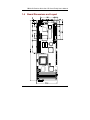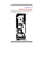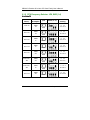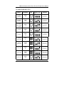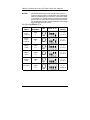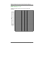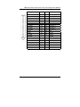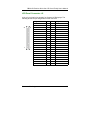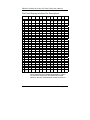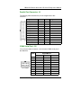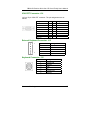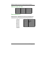
1
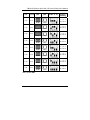
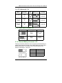
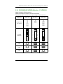
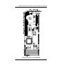
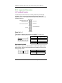
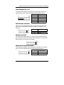
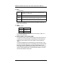
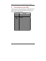
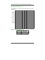
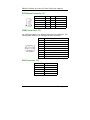
SBC8153 Pentium All-in-One PCI/ISA CPU Card Family User’s Manual Disclaimers ! " ! # !! ! Copyright 1999 by AXIOM Technology Co., Ltd. All rights reserved. April 1999, Version C1 Printed in Taiwan Trademarks Acknowledgments AXIOM is a trademark of AXIOM Technology Co., Ltd. AMD is a trademark of Advanced Micro Devices, Inc. Award is a registered trademark of Award Software International, Inc. Cyrix is a trademark of Cyrix Corporation. C&T is a trademark of Chips and Technologies, Inc. IBM, PC/AT, PS/2, VGA are trademarks of International Business Machines Corporation. Intel and Pentium are registered trademarks of Intel Corporation. MS-DOS, and Windows ’95 are trademarks of Microsoft Corporation. SMC is a trademark of Standard Microsystems Corporation. Other brand names and trademarks are the properties and registered brands of their respective owners. ii ESD Precautions Integrated circuits on computer boards are sensitive to static electricity. To avoid damaging chips from electrostatic discharge, observe the following precautions: ! Do not remove boards or integrated circuits from their anti-static packaging until you are ready to install them. ! Before handling a board or integrated circuit, touch an unpainted portion of the system unit chassis for a few seconds. This helps to discharge any static electricity on your body. ! Wear a wrist-grounding strap, available from most electronic component stores, when handling boards and components. SBC8153 Series Comparison Table Model SBC8153V SBC8153 Processor Processor Socket Chipset Multi I/O Chip BIOS L2 cache Max. RAM Memory Sockets VGA CRT/LCD Display Memory Watchdog Timer PC/104 Connector Enhanced IDE 2S/1P USB IrDA CPU Digital Temp. Sensor (LM75) Board Size SBC8153V-2M Intel Pentium (P54C, P55C/MMX) Cyrix 6x86, 6x86L, 6x86MX, MII AMD K5, K6, K6-2, IDT C6, W2-3D C&T 65550 1MB ZIF Socket 7 Intel 430TX SMC 37C669 Award 512KB P.B. SRAM 256MB FPM/EDO 4 x 72-pin SIMMs None C&T 65550 None 2MB 16-level yes yes yes yes yes yes 388mm x 124mm iii Unpacking After unpacking the CPU card, check and see if the following items are included and in good condition. If any of the items is missing or damaged, notify your dealer immediately. ! SBC8153V, SBC8153V-2M, or SBC8153 Pentium All-in-One CPU Card x 1 ! User’s Manual x 1 ! Warranty Card x 1 ! 3.5” FDD Cable x 1 ! 3.5” HDD Cable x 1 ! COM, printer extension cables with bracket x 1 ! PS/2 mouse cable with bracket x 1 ! Mini-DIN to DIN keyboard adapter cable x 1 ! Intel PCI IDE Driver and Flash Memory Utility Diskette x 1 ! C&T 65550 VGA Driver Diskette x 1 (SBC8153 does not include this driver disk.) Make sure that all of the items listed above are present. What To Do If There Is A Problem If there are damaged or missing parts, contact your supplier and/or dealer immediately. Do not attempt to apply power to the board if there is damage to any of its components. iv Table of Contents Chapter 1 1.1 1.2 1.3 1.4 Features ................................................................ ................................................................ 2 Specifications ........................................................ ........................................................ 2 Intelligence .......................................................... .......................................................... 4 Board Dimensions and Layout ................................. ................................. 5 Chapter 2 2.1 CPU Voltage Selector: JP2, JP4, SW1 (1-4)......................................... 8 CPU Frequency Selector: JP6, SW3 (1-4)..........................................10 Clear CMOS Content: JP5.....................................................................13 External Battery Connector: J18 ..........................................................13 Panel Signal Level Setting: JPW1 ..........................................................14 RS232/422/485 (COM2) Selection: J7, JPW2/3/4 ...........................15 Connectors .......................................................... .......................................................... 16 2.2.1 Improvised Connectors........................................................................18 Chapter 3 3.1 3.2 Hardware Installation CPU Installation ................................................. ................................................. 21 Memory Installation ............................................ ............................................ 21 Chapter 4 4.1 4.2 4.3 4.4 4.5 4.6 4.7 4.8 4.9 4.10 4.11 4.12 4.13 4.14 Jumpers and Connectors Jumper Jumper Settings................................ Settings..................................................... ..................................................... 8 2.1.1 2.1.2 2.1.3 2.1.4 2.1.5 2.1.6 2.2 Introduction Introduction Award BIOS Setup Setup BIOS Setup ........................................................... ........................................................... 23 Standard CMOS Setup .......................................... .......................................... 25 BIOS Features Setup................................ Setup ............................................ ............................................ 29 Chipset Features Setup ....................................... ....................................... 31 Power Management Setup .................................... .................................... 33 PNP/PCI Configuration................................ Configuration ......................................... ......................................... 35 Load BIOS Defaults ............................................. ............................................. 36 Load Setup Defaults ........................................... ........................................... 37 Integrated Peripherals ....................................... ....................................... 38 Supervisor / User Password ................................ 40 IDE HDD Auto Detection ....................................... ....................................... 41 HDD Low Level Format................................ Format......................................... ......................................... 41 Save & Exit Setup ................................................. ................................................. 42 Exit Without Saving ............................................. ............................................. 43 Table of Contents v Chapter 5 5.1 5.1.1 5.1.2 5.1.3 5.2 Driver Installation ....................................................................................46 Installing Drivers for Windows NT 3.5x .............. 47 5.3.1 5.4 Driver Installation ....................................................................................45 Changing Display Drivers.......................................................................46 Changing Color Schemes .....................................................................46 Installing Drivers for Windows 95 ..................... 46 5.2.1 5.3 Driver Installation ....................................................................................47 Installing Drivers for Windows NT 4.0 ............... 48 5.4.1 Driver Installation ....................................................................................48 Chapter 6 6.1 6.2 VGA Driver Installation Installing Drivers for Windows 3.1 .................... 45 Intel PIIX Bus Master Master IDE Driver Installation System Requirements ........................................... ........................................... 51 Installing the Software ...................................... ...................................... 52 Appendix A Watchdog Timer Configuration Appendix B I/O Port Address Map and Interrupt Request Lines (IRQ) Connector Pin Assignments Appendix C vi Table of Contents SBC8153 Pentium All-in-One CPU Card Family User’s Manual Chapter 1 Introduction The SBC8153 CPU Card Family consists of PCI Pentium Industrial CPU cards based on the Intel 430TX chipset and is fully designed for harsh industrial environment. It features ZIF Socket 7 compatible with various processors from Intel, AMD and Cyrix. This card accommodates up to 256MB of DRAMs in FPM or EDO configurations and a secondary level 512KB cache. The SBC8153 CPU Card Family comes with onboard CPU temperature sensor to protect your processor from overheating. The power management feature provides power savings by slowing down the CPU clock, turning OFF the monitor screen and stopping the HDD spindle motor. Introduction 1 SBC8153 Pentium All-in-One CPU Card Family User’s Manual 1.1 Features " CPU Speed 90~366MHz, Intel P54C, P55C/MMX, Cyrix 6x86, 6x86L, 6x86MX, MII, AMD K5, K6, K6-2, IDT C6, W2-3D " Intel 430TX PCIset " Up to 256MB system memory " Onboard VGA CRT/LCD " 16 level programmable watchdog timer " High speed bi-directional SPP/ECP/EPP parallel port " PC/104 connector " CPU Temperature monitoring and alert (LM75) " Auto fan OFF 1.2 " Specifications CPU: ! ! ! ! ! ! ! ! ! Intel Pentium/P55C* 90/100/120/133/150/166/200/233 Cyrix 6x86/6x86L P150+/P166+ Cyrix 6x86MX-166/180/200 Cyrix MII 300 AMD K5 PR90/PR100/PR133/PR166 AMD K6-166/200/233/266/300 AMD K6-2/266/300/333/366/400 IDT C6/180/200/240 IDT Winchip2-3D/200/240 NOTE: Only hardware ver. C1 with BIOS ver. D11.11.x and later support the AMD K6-2-400MHz CPU. " Processor Socket: ZIF Socket 7 " Chipset: Intel 430TX PCIset with built-in PCI EIDE " BIOS: ! Award BIOS, PnP support ! FLASH EEPROM (128KB/256KB) for BIOS update ! ISA Plug and Play (PnP) extension ! Power management 2 Introduction SBC8153 Pentium All-in-One CPU Card Family User’s Manual NOTE: " Hardware ver. C1 and later features Flash EEPROM upgrade from 128KB to 256KB. System Memory: ! Up to 256MB FPM/EDO DRAM ! Four 72-pin SIMM sockets for DRAMs in 4MB, 8MB, 6MB, 32MB and 64MB configurations " L2 Cache: 512KB Pipeline Burst SRAM " Multi I/O: SMC 37C669 chipset " Parallel Port: One high-speed parallel port, SPP/EPP/ECP mode " Serial Port: Two 16550 UART compatible RS232/422/485 ports " Enhanced IDE: ! Two Bus Mastering EIDE mode, up to 4 devices ! Two EIDE interfaces for up to four devices, support PIO Mode 3/4 or Ultra DMA/33 IDE Hard Disk and ATAPI CD-ROM " FDD Interface: Two floppy drives (360/720KB, 1.2/1.44/2.88MB, LS-120) " USB Interface: Two USB pin-header connectors, compliant with USB Specification Rev. 1.0 " Watchdog Timer: ! ! ! ! 16-level, programmable I/O port 0443H to enable watchdog I/O port 0441H to disable watchdog Time-out timing select 0/2/4/6/8/10/12/14/16/18/20/22/ 24/26/28/30 seconds (+/-20%) " Green Function: " Keyboard Connector: PC/AT type mini-DIN that supports PC/AT; supports a 5-pin external keyboard connector Introduction Power management via BIOS, activated through mouse/keyboard movement 3 SBC8153 Pentium All-in-One CPU Card Family User’s Manual " IrDA Interface: " VGA Display: (for SBC8153V and SBC8153V-2M only) ! ! ! ! ! ! ! ! ! " Pin-header connector for the optional IrDA external connector C&T 65550 VGA chip onboard SVGA for CRT & Panel 32-bit PCI local bus VGA BIOS with 128KB flash ROM and system BIOS 15-pin connector 1024 X 768 (256 colors) resolution on SVGA(1MB memory) 41-pin connector for LCD panel, 640 x 480 resolution LCD panel supports monochrome, color STN, TFT, EL Simultaneous VGA and panel display Environmental and Mechanical: ! ! ! ! 1.3 Power Supply: 3.5A @+5V Temperature: 0°C to 60°C Humidity: 5% to 95% Dimensions: 338mm x 124mm Intelligence " CPU Slow Down: When system overheating is detected, CPU slows down to prevent CPU damage. The CPU speed is restored when temperature falls to a safe level. System overheat is usually caused by malfunctioning of the CPU or system fan. " Auto Fan OFF: To reduce energy consumption and system noise, the system fan automatically powers OFF during sleep mode. " Temperature Monitoring and Alert: A sensor for the CPU temperature on the SBC8153 monitors the CPU temperature and alerts the user through the speaker when temperature exceeds the safe heat level. 4 Introduction SBC8153 Pentium All-in-One CPU Card Family User’s Manual 1.4 Board Dimensions and Layout Introduction 5 SBC8153 Pentium All-in-One CPU Card Family User’s Manual 6 SBC8153 Pentium All-in-One CPU Card Family User’s Manual Chapter 2 Jumpers and Connectors The onboard jumpers configure your CPU card according to the needs of your applications. If you doubt on the best jumper configuration, contact your dealer or sales reps. KB CTRL BIOS J7 JPW2 JPW3 JPW4 28 27 I/O 37C669 J18 JP5 BAT1 1 1 256Kx16 C&T 65550 256Kx16 2 1 JPW1 JP6 82371AB PIIX4 JP2 DIP 64Kx64 1 2 3 4 ON SW1 1 2 3 4 JP4 ON DIP SW3 82439TX TX BZ1 Jumper Locations on the SBC8153 Jumpers and Connectors 7 SBC8153 Pentium All-in-One CPU Card Family User’s Manual 2.1 Jumper Settings Making the proper jumper settings configures the SBC8153 to match the your application needs. The following tables show the correct jumper settings for the onboard devices. 2.1.1 CPU Voltage Selector: JP2, JP4, SW1 (1-4) For Single Voltage CPU**: Intel P54C, Cyrix 6x86, AMD K5, and IDT C6/W2-3D Vio Vcore 3.5V 3.5V JP2 JP4 OPEN SW1 (1-4) Switch Setting 1 2 3 4 on on on on SHORT **Default For Dual Voltage CPU: Intel P55C*, Cyrix 6x86L/MX/MII, AMD K6/K6-2 Vio Vcore 3.3V 3.5V 3.3V 3.2V 3.3V 3.0V 3.3V 2.9V 3.3V 2.8V JP2 JP4 SHORT OPEN SHORT OPEN SHORT SHORT SHORT SW1 (1-4) OPEN OPEN OPEN Switch Setting 1 2 3 4 on on on on 1 2 3 4 off off on on 1 2 3 4 off on off on 1 2 3 4 on off off on 1 2 3 4 off off off on Continued . . . . . 8 Jumpers and Connectors SBC8153 Pentium All-in-One CPU Card Family User’s Manual Vio Vcore 3.3V 2.7V JP2 SHORT 3.3V 2.6V 3.3V 2.5V 3.3V 2.4V SHORT SHORT SHORT 3.3V 2.3V 3.3V 2.2V 3.3V 2.1V 3.3V 2.0V SHORT SHORT SHORT SHORT JP4 OPEN OPEN OPEN OPEN OPEN OPEN OPEN OPEN SW1 (1-4) Switch Setting 1 2 3 4 on on on off 1 2 3 4 off on on off 1 2 3 4 on off on off 1 2 3 4 off off on off 1 2 3 4 on on off off 1 2 3 4 off on off off 1 2 3 4 on off off off 1 2 3 4 off off off off * P55C = Pentium MMX Jumpers and Connectors 9 SBC8153 Pentium All-in-One CPU Card Family User’s Manual 2.1.2 CPU Frequency Selector: JP6, SW3 (1-4) For Intel Pentium CPU CPU FREQ. Bus Clock Multiplier P54C-90 60MHz 1.5x P54C-100 66MHz 1.5x P54C-120 60MHz 2x P54C-133 66MHz 2x P54C-150 60MHz 2.5x P54C/P55C166 66MHz 2.5x P54C/P55C200 66MHz 3x P55C-233 66MHz 3.5x 10 JP6 OPEN OPEN OPEN OPEN OPEN OPEN OPEN OPEN SW3 (1-4) Switch Setting 1 2 3 4 on on off off 1 2 3 4 off off off off 1 2 3 4 on on on off 1 2 3 4 off off on off 1 2 3 4 on on on on 1 2 3 4 off off on on 1 2 3 4 off off off on 1 2 3 4 off off off off Jumpers and Connectors SBC8153 Pentium All-in-One CPU Card Family User’s Manual For AMD K5/K6/K6-2 CPU CPU FREQ. Bus Clock Multiplier K5-PR100 (100MHz) 66MHz 1.5x K5-PR133 (133MHz) 66MHz 1.5x K5-PR166 (116.7MHz) K6-166 66MHz 1.75x K6-200 66MHz 3x K6-233 66MHz 3.5x K6-266 K6-2-266 66MHz 4x K6-300 K6-2-300 66MHz 4.5x K6-2-333 66MHz 5x K6-2-366 66MHz 5.5x K6-2-400 66MHz 6.0x Jumpers and Connectors JP6 OPEN OPEN OPEN OPEN OPEN SHORT SHORT SHORT SHORT OPEN SW3 (1-4) Switch Setting 1 2 3 4 off off off off 1 2 3 4 off off on off 1 2 3 4 off off on on 1 2 3 4 off off off on 1 2 3 4 off off off off 1 2 3 4 off off on off 1 2 3 4 off off on on 1 2 3 4 off off off on 1 2 3 4 off off off off 1 2 3 4 off off on off 11 SBC8153 Pentium All-in-One CPU Card Family User’s Manual NOTE: The thermal specification of the AMD K6-2-400 CPU has a maximum thermal power of 22.7W. When using the AMD K62-400 on the SBC8153 CPU Card Family, make sure to install a compatible CPU cooling fan that can sustain such thermal power capacity. Ensure that the airflow specifications of the fan are sufficient enough to provide ventilation to the voltage regulators beside the CPU socket. For Cyrix 6x86/MII CPU CPU FREQ. Bus Clock Multiplier 6x86(L)P150+ (120MHz) 60MHz 2x 6x86(L)P166+ (133MHz) 66MHz 2x 6x86MXPR166 60MHz 2.5x 6x86MXPR200 66MHz 2.5x 6x86MXPR233 66MHz 3x MII-300GP 66MHz 3.5x 12 JP6 OPEN OPEN OPEN OPEN OPEN OPEN SW3 (1-4) Switch Setting 1 2 3 4 on on on off 1 2 3 4 off off on off 1 2 3 4 on on on on 1 2 3 4 off off on on 1 2 3 4 off off off on 1 2 3 4 off off off off Jumpers and Connectors SBC8153 Pentium All-in-One CPU Card Family User’s Manual For IDT C6/Winchip2 CPU CPU FREQ. Bus Clock Multiplier C6-180MHz 60MHz 3x C6/W2-3D 200MHz 66MHz 3x C6/W2-3D 240MHz 60MHz 4x JP6 SW3 (1-4) Switch Setting 1 2 3 4 on on off on OPEN 1 2 3 4 off off off on OPEN 1 2 3 4 on on on off SHORT 2.1.3 Clear CMOS Content: JP5 JP5 1 1 2 2 3 3 Setting Function Pin 2-3 SHORT Clear CMOS Content Pin 1-2 SHORT Normal Operation 2.1.4 External Battery Connector: J18 This 4-pin connector allows the user to connect an external battery to maintain the information stored in the CMOS RAM in case the built-in battery malfunctions. The default is set to Internal Battery with a jumper connecting pin 1 and pin 2. J18 Pin # 1 1 Internal Battery 2 3 4 1 Signal Name Ground Battery GND N.C. Vcc External Battery Jumpers and Connectors 13 SBC8153 Pentium All-in-One CPU Card Family User’s Manual 2.1.5 Panel Signal Level Setting: JPW1 JP5 Setting Function 1 Pin 2-3 Short 5V (default) Pin 1-2 Short 3.3V 3 1 3 NOTE: 14 This function setting is only available with the hardware ver. C1 and later. Jumpers and Connectors SBC8153 Pentium All-in-One CPU Card Family User’s Manual 2.1.6 RS232/422/485 (COM2) Selection: J7, JPW2/3/4 COM1 is fixed for RS-232 use only COM2 is selectable for RS232, RS-422 and RS-485. The following table describes the jumper settings of this connector. COM2 Function RS-232 RS-422 RS-485 J7 Jumper Setting (pin closed) 1-3 2-4 7-8 9-10 11-12 13-14 15-16 17-18 3-5 4-6 23-25 27-28 3-5 4-6 19-20 21-22 23-25 24-26 27-28 J7 Jumper Illustration 1 3 5 7 9 11 13 15 17 19 21 23 25 27 • • • • • • • • • • • • • • • • • • • • • • • • • • • • J7 JPW2 JPW3 JPW4 2 4 6 8 10 12 14 16 18 20 22 24 26 28 1 3 5 7 9 11 13 15 17 19 21 23 25 27 • • • • • • • • • • • • • • • • • • • • • • • • • • • • J7 2 4 6 8 10 12 14 16 18 20 22 24 26 28 1 3 5 7 9 11 13 15 17 19 21 23 25 27 • • • • • • • • • • • • • • • • • • • • • • • • • • • • J7 OPEN SHORT SHORT OPEN SHORT SHORT OPEN SHORT OPEN Jumpers and Connectors 2 4 6 8 10 12 14 16 18 20 22 24 26 28 15 SBC8153 Pentium All-in-One CPU Card Family User’s Manual 2.2 Connectors The connectors on the SBC8153 allow you to connect external devices such as keyboard, floppy disk drives, hard disk drives, printers, etc. The following table and diagram list the function and location of each connector on the SBC8153. Their corresponding pin assignments are described in Appendix C. Connectors Front Bezel Connector EIDE Connectors Floppy Drive Connector CPU Fan Power Connector LCD Panel Connector Parallel Port Connector COM1 Serial Port PS/2 Mouse Connector COM2 Serial Port IrDA Connector VGA CRT Connector External Keyboard Connector Keyboard Connector USB Connectors Power Connector PC/104 Connectors 16 Label J1 J3, J4 J5 J6 J8 J9 J10 J11 J12 J13 J14 J15 J16 J19, J20 P1 CON1, CON2 Jumpers and Connectors SBC8153 Pentium All-in-One CPU Card Family User’s Manual Connector Locations on the SBC8153 Jumpers and Connectors 17 SBC8153 Pentium All-in-One CPU Card Family User’s Manual 2.2.1 Improvised Connectors J1: Front Bezel Connector The front bezel of the case has a control panel that provides light indication of the computer activities and switches to change the computer status. J1 is a 20-pin header that provides interfaces for the following functions. Hard Disk Drive LED Reset Switch Turbo LED Connector Not Defined Dual Function Power Button Power LED & Keylock Speaker Speaker: Pins 1 - 4 This connector provides an interface to a speaker for audio tone generation. An 8-ohm speaker is recommended. J1Pin # Signal Name Speaker out Reserved Ground +5V 1 2 3 4 Green Function: Pins 6 and 16 This connector is for the Green Switch on the control panel, which, when pressed, will force the motherboard immediately into the power saving (sleep) mode. 18 J1 Pin # Signal Name 6 16 Sleep Ground Jumpers and Connectors SBC8153 Pentium All-in-One CPU Card Family User’s Manual Power LED and Keylock: Pins 11 - 15 The power LED indicates the status of the main power switch. The keylock switch, when closed, will disable the keyboard function. J1 Pin # 11 12 13 14 15 Signal Name Power LED Reserved Ground Keylock Ground Turbo LED Connector: Pins 8 and 18 There is the no turbo/deturbo function on the CPU card. The Turbo LED on the control panel will always be ON when attached to this connector. J1 Pin # 8 18 Signal Name 5V Ground Reset Switch: Pins 9 and 19 The reset switch allows the user to reset the system without turning the main power switch OFF and then ON. Orientation is not required when making a connection to this header. Hard Disk Drive LED Connector: Pins 10 and 20 This connector connects to the hard drive activity LED on the control panel. This LED will flash when the HDD is being accessed. J1 Pin # 10 20 Jumpers and Connectors Signal Name HDD Active# +5V 19 SBC8153 Pentium All-in-One CPU Card Family User’s Manual J6: CPU Fan Power Connector J6 is a 2-pin header for a CPU fan. The fan must be a 12V fan. +12V GND 1 2 J6: CPU Fan Power Connector J13: IrDA Connector This connector is used for an IrDA connector for wireless communication. +5V IRRX IRTX 1 N.C. GND J19, J20: USB Connectors J19 and J20 are optional USB connectors. The following table shows the pin outs of these connectors. J20 Vcc USBUSB+ GND J19 1 2 3 4 1 2 USB3 USB+ 4 GND USB 20 Jumpers and Connectors SBC8153 Pentium All-in-One CPU Card Family User’s Manual Chapter 3 Hardware Installation This chapter provides information on how to use the jumpers and connectors on the SBC8153 in order to set up a workable system. 3.1 CPU Installation The SBC8153 Industrial CPU Card supports a ZIF processor socket for Pentium-level processors. Unlike PGA sockets, ZIF (Zero Insertion Force) sockets come with a lever to secure the processor. Make sure the notch on the corner of the CPU corresponds with the notch on the inside of the socket. After you have installed the processor into the ZIF socket, check if the jumpers for the CPU type and speed are correct. NOTE: 3.2 Ensure that the CPU heat sink and the CPU top surface are in total contact to avoid CPU overheating problem that would cause your system to hang or be unstable. Memory Installation The SBC8153 Industrial CPU Card supports four 72-pin SIMM sockets for a maximum total memory of 256MB. The DRAMs (5Volts) for the SIMM sockets can be 4MB, 8MB, 16MB, 32MB, and 64MB in EDO and FPM types. The following should be noted when populating the SIMM sockets: 1. SIMM1/SIMM2 and SIMM3/SIMM4 should consist of the same size SIMMs. SIMM1/SIMM2 and SIMM3/SIMM4 should consist of the same type SIMMs. For example, SIMM1 and SIMM2 are both be EDO or Page Mode. Hardware Installation 21 SBC8153 Pentium All-in-One CPU Card Family User’s Manual 2. Either SIMM1/SIMM2 or SIMM3/SIMM4 can be populated first. (SIMM1, SIMM2) (SIMM3, SIMM4) 8MB 4MB×2 22 Total Memory 8MB×2 16MB 16MB×2 32MB 32MB×2 64MB 64MB×2 128MB 16MB 4MB×2 4MB×2 8MB×2 4MB×2 24MB 16MB×2 4MB×2 40MB 32MB×2 4MB×2 72MB 8MB×2 8MB×2 32MB 16MB×2 8MB×2 48MB 32MB×2 8MB×2 80MB 16MB×2 16MB×2 64MB 32MB×2 16MB×2 96MB 32MB×2 32MB×2 128MB 64MB×2 64MB×2 256MB Hardware Installation SBC8153 Pentium All-in-One CPU Card Family User’s Manual Chapter 4 Award BIOS Setup The Award BIOS installed in your computer systems ROM supports Intel/Cyrix/AMD processors in a standard IBM-AT compatible I/O system. The BIOS provides critical low-level support for standard devices such as disk drives, serial and parallel ports. It also adds virus and password protection as well as special support for detailed finetuning of the chipset controlling the entire system. 4.1 BIOS Setup Award BIOS provides a Setup utility program for specifying the system configurations and settings. The system BIOS ROM stores the Setup utility. When you turn ON the computer, Award BIOS is immediately activated. Pressing the <Del> key immediately allows you to enter the Setup utility. If you are a bit late in pressing the <Del> key, POST will continue with its test routines, thus preventing you from invoking the Setup. If you still wish to enter Setup, restart the system by pressing the Reset button or simultaneously press the <Ctrl>, <Alt> and <Delete> keys. You can also restart by turning the system OFF and back ON again. The following message will appear on the screen: Press <DEL> to Enter Setup In general, you press the arrow keys to highlight items, <Enter> to select, the <PgUp> and <PgDn> keys to change entries, <F1> for help and <Esc> to quit. When you enter Setup utility, the Main Menu screen will appear on the screen. The Main Menu allows you to select from various setup functions and exit choices. Award BIOS Setup 23 SBC8153 Pentium All-in-One CPU Card Family User’s Manual ROM PCI/ISA BIOS CMOS SETUP UTILITY AWARD SOFTWARE, INC. STANDARD CMOS SETUP INTEGRATED PERIPHERALS BIOS FEATURES SETUP SUPERVISOR PASSWORD CHIPSET FEATURES SETUP USER PASSWORD POWER MANAGEMENT SETUP IDE HDD AUTO DETECTION PNP/PCI CONFIGURATION HDD LOW LEVEL FORMAT LOAD BIOS DEFAULTS SAVE & EXIT SETUP LOAD SETUP DEFAULTS EXIT WITHOUT SAVING ESC : Quit # $ % & : Select Item F10 : Save & Exit Setup (Shift) F2 : Change Color Time, Date, Hard Disk Type The section below the setup items of the Main Menu displays the control keys for this menu. Another section at the bottom of the Main Menu, just below the control keys section, displays information on the currently highlighted item in the list. NOTE: After making and saving system changes with Setup, you find that your computer cannot boot, the Award BIOS supports an override to the CMOS settings that resets your system to its default. We strongly recommend that you avoid making any changes to the chipset defaults. These defaults have been carefully chosen by both Award and your system manufacturer to provide the absolute maximum performance and reliability. 24 Award BIOS Setup SBC8153 Pentium All-in-One CPU Card Family User’s Manual 4.2 Standard CMOS Setup Standard CMOS Setup choice allows you to record some basic hardware configurations in your computer system and set the system clock and error handling. If the Industrial CPU Card is already installed in a working system, you will not need to select this option. You will need to run the Standard CMOS option, however, if you change your system hardware configurations, the onboard battery fails, or the configuration stored in the CMOS memory was lost or damaged. ROM PCI/ISA BIOS STANDARD CMOS SETUP AWARD SOFTWARE, INC. Date (mm:dd:yy) : Mon, Aug 19 1996 Time (hh:mm:ss) : 00 : 00 : 00 HARD DISKS TYPE SIZE CYLS HEAD PRECOMP LANDZ SECTOR MODE Primary Master Auto 0 0 0 0 0 0 Auto Primary Slave None 0 0 0 0 0 0 ----- Secondary Master None 0 0 0 0 0 0 ----- Secondary Slave None 0 0 0 0 0 0 ----- Drive A : 1.44M, 3.5in Drive B : None Floppy 3 Mode Support : Disabled Video : EGA / VGA Halt On : All Errors ESC : Quit # $ % & : Select Item F1 : Help (Shift) F2 : Change Color Base Memory : 640K Extended Memory : 15360K Other Memory : 384K Total Memory : 16384K PU / PD / + / - : Modify At the bottom of the menu are the control keys for use on this menu. If you need any help in each item field, you can press the <F1> key. It will display the relevant information to help you. The memory display at the lower right-hand side of the menu is read-only. It will adjust automatically according to the memory changed. The following describes each item of this menu. Award BIOS Setup 25 SBC8153 Pentium All-in-One CPU Card Family User’s Manual " Date The date format is: The day of week, from Sun to Sat, determined by the BIOS, is read only day month The month, 1 to 12 date The date, from 1 to 31 (or the maximum allowed in the month), can key in the numerical / function key year The year, 1994 to 2097 To set the date, highlight the “Date” field and use the PageUp/ PageDown or +/keys to set the current time. " Time The time format is: hour 00 to 23 minute 00 to 59 second 00 to 59 To set the time, highlight the “Time” field and use the <PgUp>/ <PgDn> or +/keys to set the current time. " Primary HDDs / Secondary HDDs The onboard PCI IDE connectors provide Primary and Secondary channels for connecting up to four IDE hard disks or other IDE devices. Each channel can support up to two hard disks; the first is the “Master” and the second is the “Slave”. To enter the specifications for a hard disk drive, you must select first a “Type”. There are 45 predefined types and 4 user definable types are for Enhanced IDE BIOS. Type 1 to 45 are predefined. Type “User” is user-definable. For the Primary Master/Slave as well as Secondary Master/Slave, you can select “Auto” under the TYPE and MODE fields. This will enable auto detection of your IDE drives and CD-ROM drive during POST. 26 Award BIOS Setup SBC8153 Pentium All-in-One CPU Card Family User’s Manual Press <PgUp>/<PgDn> to select a numbered hard disk type or type the number and press the <Enter> key. The hard disk will not work properly if you enter incorrect information for this field. If your hard disk drive type is not matched or listed, you can use Type User to define your own drive type manually. If you select Type User, related information is asked to be entered to the following items. CYLS. number of cylinders HEADS number of read/write heads PRECOMP write precompensation LANDZ landing zone SECTORS number of sectors SIZE Automatically adjusts according to the configuration MODE (for IDE HDD only) Auto Normal (HD < 528MB) Large (for MS-DOS only) LBA (HD > 528MB and supports Logical Block Addressing) NOTE: The specifications of your drive must match with the drive table. If your hard disk drive type is not matched or listed, you can use Type User to define your own drive type manually. " Drive A / Drive B These fields identify the types of floppy disk drive A or drive B that has been installed in the computer. The available specifications are: None No floppy drive installed 360K, 5.25 in 5.25 inch PC-type standard drive; 360Kb capacity 1.2M, 5.25 in 5.25 inch AT-type high-density drive; 1.2MB capacity 720K, 3.5 in 3.5 inch double-sided drive; 720Kb capacity 1.44M, 3.5 in 3.5 inch double-sided drive; 1.44MB capacity 2.88M, 3.5 in 3.5 inch double-sided drive; 2.88MB capacity Award BIOS Setup 27 SBC8153 Pentium All-in-One CPU Card Family User’s Manual " Floppy 3 Mode Support This is the Japanese standard floppy drive. The standard stores 1.2MB in a 3.5inch diskette. You have four options to choose: Disabled Drive A Drive B Both No 3 mode floppy drive installed. (default) Installed 3 mode drive at drive A Installed 3 mode drive at drive B Installed 3 mode drive at drive A and B " Video This field selects the type of video display card installed in your system. You can choose the following video display cards: EGA/VGA CGA 40 For EGA, VGA, SEGA, SVGA or PGA monitor adapters.(default) Power up in 40 column mode CGA 80 Power up in 80 column mode MONO For Hercules or MDA, includes high resolution monochrome adapters " Halt On This field determines whether the system will halt if an error is detected during power up. 28 No errors The system boot will not be halted for any error that may be detected. (default) All errors Whenever the BIOS detects a non-fatal error, the system will be halted and you will be prompted. All, But Keyboard The system boot will not be halted for a keyboard error; it will stop for all other errors All, But Diskette The system boot will not be halted for a disk error; it will stop for all other errors. All, But Disk/Key The system boot will not be halted for a keyboard or disk error; it will stop for all other errors. Award BIOS Setup SBC8153 Pentium All-in-One CPU Card Family User’s Manual 4.3 BIOS Features Setup This section allows you to configure and improve your system and allows you to set up some system features according to your preference. ROM / PCI ISA BIOS BIOS FEATURES SETUP AWARD SOFTWARE, INC. Virus Warning : Disabled Video BIOS Shadow : Enabled CPU Internal Cache : Enabled C8000-CBFFF Shadow : Disabled External Cache : Enabled CC000-CFFFF Shadow : Disabled Quick Power On Self Test : Disabled D0000-D3FFF Shadow : Disabled Boot Sequence : A, C, SCSI D4000-D7FFF Shadow : Disabled Swap Floppy Drive : Disabled D8000-DBFFF Shadow : Disabled Boot Up Floppy Seek : Enabled DC000-DFFF Shadow : Disabled Boot Up Numlock Status : On Boot Up System Speed : High Gate A20 Option : Fast Security Option : Setup PCI /VGA Palette Snoop : Disabled OS Select For DRAM>64MB : Non-OS2 ESC : Quit # $ % & : Select Item F1 : Help PU/PD/+/- : Modify F5 : Old Values (Shift) F2 : Color F6 : Load BIOS Defaults F7 : Load Setup Defaults " Virus Warning This item protects the boot sector and partition table of your hard disk against accidental modifications. If an attempt is made, the BIOS will halt the system and display a warning message. If this occurs, you can either allow the operation to continue or run an anti-virus program to locate and remove the problem. Many disk diagnostic programs that attempt to access NOTE: the boot sector table can cause the virus warning. If you will run such a program, disable the Virus Warning feature. " CPU Internal Cache / External Cache These allow you to enable (speed up memory access) or disable the cache. By default, these items are Enabled. " Quick Power On Self Test This choice speeds up the Power On Self Test (POST) after you power up the system. If it is set to Enabled, BIOS will skip some items. By default, this choice is Enabled. Award BIOS Setup 29 SBC8153 Pentium All-in-One CPU Card Family User’s Manual " Boot Sequence This field determines the drive that the system searches first for an operating system. The options are : ! A, C, SCSI ! D, A, SCSI ! SCSI, C, A ! C, A, SCSI ! E, A, SCSI ! C only The default value is A, C, SCSI. ! ! ! ! ! C, CDROM, A F, A, SCSI LS120, C CDROM, C, A SCSI, A, C " Swap Floppy Drive This item allows you to determine whether to enable the swap Floppy Drive or not. When enabled, the BIOS swaps floppy drive assignments so that Drive A becomes Drive B, and Drive B becomes Drive A. By default, this field is set to Disabled. " Boot Up Floppy Seek When enabled, the BIOS will seek whether or not the floppy drive installed has 40 or 80 tracks. 360K type has 40 tracks while 760K, 1.2M and 1.44M all have 80 tracks. By default, this field is set to Enabled. " Boot Up NumLock Status This allows you to activate the NumLock function after you power up the system. By default, the system boots up with NumLock ON. " Boot Up System Speed This has no function and selects the default system speed (High). " Gate A20 Option This field allows you to select how Gate A20 is worked. The Gate A20 is a device used to address memory above 1 MB. By default, this field is set to Fast. " Security Option This field allows you to limit access to the System and Setup. The default value is Setup. When you select System, the system prompts for the User Password every time you boot up. When you select Setup, the system always boots up and prompts for the Supervisor Password only when the Setup utility is called up. " PCI/VGA Palette Snoop Some display cards that are non-standard VGA may not show colors properly. This field allows you to set whether MPEG ISA/VESA VGA Cards can work with PCI/VGA or not. When this field is enabled, a PCI/VGA can work with a MPEG ISA/VESA VGA card. When this field is disabled, a PCI/VGA cannot work with a MPEG ISA/VESA Card. 30 Award BIOS Setup SBC8153 Pentium All-in-One CPU Card Family User’s Manual " OS Select for DRAM > 64MB This option allows the system to access greater than 64MB of DRAM memory when used with OS/2 that depends on certain BIOS calls to access memory. The default setting is NON-OS/2. " Video BIOS Shadow This item allows you to change the Video BIOS location from ROM to RAM. Video Shadow will increase the video speed. " C8000 - CBFFF Shadow/DC000 - DFFFF Shadow Shadowing a ROM reduces the memory available between 640KB to 1024KB. These fields determine whether optional ROM will be copied to RAM or not. 4.4 Chipset Features Setup This Setup menu controls the configuration of the Industrial CPU Card chipset. ROM PCI/ISA BIOS CHIPSET FEATURES SETUP AWARD SOFTWARE INC. DRAM Timing : 70ns System BIOS Cacheable : Disabled Current CPU Temperature: 37°C/98°F CPU Warning Temperature: 80°C/176°F Video BIOS Cacheable : Disabled 8 Bit I/O Recovery Time : 1 16 Bit I/O Recovery Time : 1 Memory Hole At 15M-16M : Disabled PCI 2.1 Compliance ** System Hardware Monitor * Disabled ESC : Quit # $ % & : Select Item F1 : Help PU/PD/+/- : Modify F5 : Old Values (Shift) F2 : Color F6 : Load BIOS Defaults F7 : Load Setup Defaults " DRAM Timing The DRAM Timing Registers control the DRAM timing. The timing type is dependent on the system design. Slower rates may be required in some system designs to support loose layouts or slower memory. " System BIOS Cacheable When enabled, access to the system BIOS ROM addressed at F0000H-FFFFFH are cached, provided that the cache controller is enabled. Award BIOS Setup 31 SBC8153 Pentium All-in-One CPU Card Family User’s Manual " Video BIOS Cacheable When enabled, access to video BIOS addressed at C0000H to C7FFFH are cached, provided that the cache controller is enabled. " 8 Bit I/O Recovery Time This field allows you to select the recovery time allowed for 8 bit I/O. By default, this field is set to 1 Clock. " 16 Bit I/O Recovery Time This field allows you to select the recovery time allowed for 16 bit I/O. By default, this field is set to 1 Clock. " Memory Hole at 15M-16M In order to improve performance, certain space in memory can be reserved for ISA cards. This field allows you to reserve 15MB to 16MB memory address space to ISA expansion cards. This makes memory from 15MB and up unavailable to the system. Expansion cards can only access memory up to 16MB. By default, this field is set to Disabled. " PCI 2.1 Compliance Concurrent PCI allows multiple PCI transfers from the PCI master buses to memory to CPU. By default, this field is set to Disabled. " System Hardware Monitor The onboard hardware thermal sensor monitors CPU temperature changes and prevents the CPU from overheating. Alert is sounded through the speaker and CPU speed slows down when the temperature exceeds the temperature set in the BIOS until the temperature falls below a safe level. By default, this field is set to 80°°C/176°°F. 32 Award BIOS Setup SBC8153 Pentium All-in-One CPU Card Family User’s Manual 4.5 Power Management Setup The Power Management Setup allows you to save energy of your system effectively. It will shut down the hard disk and turn OFF video display after a period of inactivity. ROM PCI/ISA BIOS (2A59IM29) POWER MANAGEMENT SETUP AWARD SOFTWARE, INC. Power Management : Disabled PM Control by APM : Yes IRQ3 [ 3-7, 9-15],NMI ** Reload Global Timer Events ** : Enabled Video Off Method : DPMS Primary IDE 0 : Disabled Video Off After : Suspend Primary IDE 1 : Disabled Doze Mode : Disabled Secondary IDE 0 : Disabled Standby Mode : Disabled Secondary IDE 1 : Disabled Suspend Mode : Disabled Floppy Disk : Disabled HDD Power Down : Disabled Serial Port : Enabled VGA Active Monitor : Disabled Parallel Port CPUFAN Off In Suspend : Enabled ESC : Quit # $ % & : Select Item : Disabled F1 : Help PU/PD/+/- : Modify F5 : Old Values (Shift) F2 : Color F6 : Load BIOS Defaults F7 : Load Setup Defaults " Power Management This field allows you to select the type of power saving management modes. There are four selections. Disable No power management. (Default) Min. Power Saving Minimum power management Max. Power Saving Maximum power management. Only available for SL CPU User Define Each of the ranges are from 1 min. to 1hr. Except for HDD Power Down which ranges from 1 min. to 15 min. " PM Control by APM This field allows you to use the Advanced Power Management device to enhance the Max. Power Saving mode and stop the CPU internal clock. If the Max. Power Saving is not enabled, this will be preset to NO. Award BIOS Setup 33 SBC8153 Pentium All-in-One CPU Card Family User’s Manual " Video Off Method This field defines the Video Off features. V/H SYNC + Blank DPMS Blank Screen Default setting, blank the screen and turn off vertical and horizontal scanning Allows the BIOS to control the video display card if it supports the DPMS feature This option only writes blanks to the video buffer " Video Off After This specifies the mode after which the Video Off feature is enabled. The options are Doze, Standby, Suspend, and N/A. " Doze Mode When enabled, and after the set time of system inactivity, the CPU clock will run at a slower speed while all other devices still operate at full speed. " Standby Mode When enabled, and after the set time of system inactivity, the fixed disk drive and the video would be shut OFF while all other devices still operate at full speed. " Suspend Mode When enabled, and after the set time of system inactivity, all devices except the CPU will be shut OFF. " HDD Power Down When enabled, and after the set time of system inactivity, the hard disk drive will be powered down while all other devices remain active. " VGA Active Monitor This option specifies if the BIOS is to monitor activity on the display monitor for power conservation purposes. " CPU Fan Off in Suspend System fans will power OFF automatically even in suspend mode. This function reduces both energy consumption and system noise. 34 Award BIOS Setup SBC8153 Pentium All-in-One CPU Card Family User’s Manual 4.6 PNP/PCI Configuration This option configures the PCI bus system. All PCI bus systems on the system use INT#, thus all installed PCI cards must be set to this value. ROM PCI/ISA BIOS PNP/PCI CONFIGURATION AWARD SOFTWARE INC. PNP OS Installed : Yes Resources Controlled by : Manual Reset Configuration Data : Disabled IRQ-3 assigned to : Legacy ISA IRQ-4 assigned to : Legacy ISA IRQ-5 assigned to : Legacy ISA IRQ-7 assigned to : Legacy ISA IRQ-9 assigned to : PCI/ISA PnP IRQ-10 assigned to : PCI/ISA PnP IRQ-11 assigned to : PCI/ISA PnP IRQ-12 assigned to : PCI/ISA PnP IRQ-14 assigned to : PCI/ISA PnP IRQ-15 assigned to : PCI/ISA PnP DMA-0 assigned to : PCI/ISA PnP Used MEM base addr : N/A DMA-1 assigned to : PCI/ISA PnP ESC : Quit # $ & : Select Item DMA-3 assigned to : PCI/ISA PnP F1 : Help PU/PD/+/- : Modify DMA-5 assigned to : PCI/ISA PnP F5 : Old Values (Shift) F2 : Color DMA-6 assigned to : PCI/ISA PnP F6 : Load BIOS Defaults DMA-7 assigned to : PCI/ISA PnP F7 : Load Setup Defaults " PNP OS Installed This field allows you to specify if the operating system installed in your system is plug and play aware. NOTE: Operating systems such as DOS, OS/2, and Windows 3.x do not use PnP. " Resources Controlled by This PnP BIOS can configure all of the boot and compatible devices automatically. However, this capability needs you to use a PnP operating system such as Windows 95. The default value is Manual. " Reset Configuration Data This field allows you to determine whether to reset the configuration data or not. The default value is Disabled. Award BIOS Setup 35 SBC8153 Pentium All-in-One CPU Card Family User’s Manual " IRQ3/4/5/7/9/10/11/12/14/15, DMA0/1/3/5/6/7 assigned to These fields allow you to determine the IRQ/DMA assigned to the ISA bus and is not available to any PCI slot. " Used MEM base addr This field allows the user to set the base address and block size of a legacy (non-PnP) ISA card that uses any memory segment within the C800H and DFFFH address range. If the you have such a card and are not using an ICU (ISA Configuration Utility) to specify its address range, select a base address from the six available options. During selection, the “Used MEM Length” field will appear with the block size options. If you have more than one legacy ISA card in your system that require the use of this address range, you can increase the block size to either 8K, 16K, 32K or 64K. If you are using ICU to accomplish this task, leave “Used MEM base addr” to its default setting of N/A. 4.7 Load BIOS Defaults This option allows you to load the troubleshooting default values permanently stored in the BIOS ROM. The default settings are nonoptimal and disable all high-performance features. ROM PCI/ISA BIOS CMOS SETUP UTILITY AWARD SOFTWARE, INC. STANDARD CMOS SETUP INTEGRATED PERIPHERALS BIOS FEATURES SETUP SUPERVISOR PASSWORD CHIPSET FEATURES SETUP USER PASSWORD POWER MANAGEMENT SETUP IDE HDD AUTO DETECTION Load BIOS Defaults (Y/N)? N PNP/PCI CONFIGURATION SAVE & EXIT SETUP LOAD BIOS DEFAULTS EXIT WITHOUT SAVING LOAD SETUP DEFAULTS ESC : Quit # $ % & : Select Item F10 : Save & Exit Setup (Shift) F2 : Change Color Load BIOS Defaults except Standard CMOS Setup To load BIOS defaults value to CMOS SRAM, enter Y. 36 Award BIOS Setup SBC8153 Pentium All-in-One CPU Card Family User’s Manual 4.8 Load Setup Defaults This option allows you to load the default values to your system configuration. These default settings are optimal and enable all high performance features. ROM PCI/ISA BIOS CMOS SETUP UTILITY AWARD SOFTWARE, INC. STANDARD CMOS SETUP INTEGRATED PERIPHERALS BIOS FEATURES SETUP SUPERVISOR PASSWORD CHIPSET FEATURES SETUP USER PASSWORD POWER MANAGEMENT SETUP IDE HDD AUTO DETECTION PNP/PCI CONFIGURATION & EXIT Load Setup DefaultsSAVE (Y/N)? N SETUP LOAD BIOS DEFAULTS EXIT WITHOUT SAVING LOAD SETUP DEFAULTS ESC : Quit # $ % & : Select Item F10 : Save & Exit Setup (Shift) F2 : Change Color Load BIOS Defaults except Standard CMOS Setup To load SETUP defaults value to CMOS SRAM, enter Y. Award BIOS Setup 37 SBC8153 Pentium All-in-One CPU Card Family User’s Manual 4.9 Integrated Peripherals This option allows you to determine your hard disk configuration, mode and port. ROM PCI/ISA BIOS INTEGRATED PERIPHERALS AWARD SOFTWARE INC. IDE HDD Block Mode : Enabled IDE Primary Master PIO : Auto IDE Primary Slave PIO : Auto IDE Secondary Master PIO : Auto IDE Secondary Slave PIO : Auto IDE Primary Master UDMA : Auto IDE Primary Slave UDMA : Auto IDE Secondary Master UDMA : Auto IDE Secondary Slave UDMA : Auto On-Chip Primary PCI IDE : Enabled On-Chip Secondary PCI IDE : Enabled USB Keyboard Support : Disabled Onboard FDD Controller : Enabled Onboard UAART 1 : Auto ESC : Quit # $ & : Select Item Onboard UART 2 : Auto F1 : Help PU/PD/+/- : Modify Onboard UART 2 Mode : Standard F5 : Old Values (Shift) F2 : Color Onboard Parallel Port : 378H/IRQ7 F6 : Load BIOS Defaults Parallel Port Mode : Normal F7 : Load Setup Defaults " IDE HDD Block Mode This field allows your hard disk controller to use the fast block mode to transfer data to and from your hard disk drive. " IDE Primary Master/Slave PIO And Secondary Master/Slave PIO These fields allow your system hard disk controller to work faster. Rather than have the BIOS issue a series of commands that transfer to or from the disk drive, PIO (Programmed Input/Output) allows the BIOS to communicate with controller and CPU directly. The system supports five modes, numbered from 0 (default) to 4, which primarily differ in timing. When Auto is selected, the BIOS will select the best available mode. " IDE Primary Master/Slave UDMA And Secondary Master/Slave UDMA This field allows your system to improve disk I/O throughput to 33Mb/sec with the Ultra DMA/33 feature. The options are Auto and Disabled. 38 Award BIOS Setup SBC8153 Pentium All-in-One CPU Card Family User’s Manual " On-Chip Primary/Secondary PCI IDE These fields allow you either to enable or disable the Primary/Secondary controller. You might choose to disable the controller if you were to add a higher performance or specialized controller. " USB Keyboard Support This field allows your system to support a USB keyboard. " Onboard FDD Controller This option allows you to select the onboard FDD port. " Onboard Serial/Parallel Port These fields allow you to select the onboard serial/parallel port and its address. The default value for these ports are: Serial Port 1 3F8/IRQ4 Serial Port 2 2F8/IRQ3 Parallel Port 378H/IRQ7 " UART 2 Mode This field determines the UART 2 mode in your computer. The options are Standard, HPSIR, and ASKIR. " Onboard Parallel Mode This field allows you to determine parallel port mode function. Normal Normal Printer Port EPP Enhanced Parallel Port ECP Extended Capabilities Port ECP+EPP Award BIOS Setup Extended Capabilities Port or Enhanced Parallel Port 39 SBC8153 Pentium All-in-One CPU Card Family User’s Manual 4.10 Supervisor / User Password These two options set the system password. Supervisor Password sets a password that will be used to protect the system and Setup utility. User Password sets a password that will be used exclusively on the system. To specify a password, highlight the type you want and press <Enter>. The Enter Password: message prompts on the screen. Type the password, up to eight characters in length, and press <Enter>. The system confirms your password by asking you to type it again. After setting a password, the screen automatically returns to the main screen. To disable a password, just press the <Enter> key when you are prompted to enter the password. A message will confirm the password to be disabled. Once the password is disabled, the system will boot and you can enter Setup freely. ROM PCI/ISA BIOS CMOS SETUP UTILITY AWARD SOFTWARE, INC. STANDARD CMOS SETUP INTEGRATED PERIPHERALS BIOS FEATURES SETUP SUPERVISOR PASSWORD CHIPSET FEATURES SETUP USER PASSWORD POWER MANAGEMENT SETUP IDE HDD AUTO DETECTION PNP/PCI CONFIGURATION Enter Password: SAVE & EXIT SETUP LOAD BIOS DEFAULTS EXIT WITHOUT SAVING LOAD SETUP DEFAULTS ESC : Quit # $ % & : Select Item F10 : Save & Exit Setup (Shift) F2 : Change Color Change / Set / Disable Password 40 Award BIOS Setup SBC8153 Pentium All-in-One CPU Card Family User’s Manual 4.11 IDE HDD Auto Detection This option detects the parameters of an IDE hard disk drive, and automatically enters them into Standard CMOS Setup screen. ROM PCI/ISA BIOS STANDARD CMOS SETUP AWARD SOFTWARE, INC. HARD DISKS TYPE SIZE CYLS HEAD PRECOMP LANDZ SECTOR MODE Primary Master: Select Primary Master Option (N=SKIP) : N OPTIONS TYPE SIZE 1 (Y) 0 0 CYLS HEAD PRECOMP 0 0 0 LANDZ SECTOR MODE 0 0 NORMAL NOTE: Some OSes (like SCO-UNIX) must use ”NORMAL” for installation ESC: SKIP Up to four IDE drives can be detected, with parameters for each appearing in sequence inside a box. To accept the displayed entries, press the Y key; to skip to the next drive, press the N key. If you accept the values, the parameters will appear listed beside the drive letter on the screen. 4.12 HDD Low Level Format This option should only be used by a professional. Low-level formatting can cause irreparable damage to your hard disk. The procedures include selecting the drive you want to low-level format, determining the bad tracks, and proceeding with pre-formatting. Award BIOS Setup 41 SBC8153 Pentium All-in-One CPU Card Family User’s Manual 4.13 Save & Exit Setup This option allows you to determine whether to accept the modifications or not. If you type Y, you will quit the setup utility and save all changes into the CMOS memory. If you type N, you will return to Setup utility. ROM PCI/ISA BIOS CMOS SETUP UTILITY AWARD SOFTWARE, INC. STANDARD CMOS SETUP INTEGRATED PERIPHERALS BIOS FEATURES SETUP SUPERVISOR PASSWORD CHIPSET FEATURES SETUP USER PASSWORD POWER MANAGEMENT SETUP IDE HDD AUTO DETECTION Save to CMOS and Exit(y/N)? N SAVE & EXIT SETUP PNP/PCI CONFIGURATION LOAD BIOS DEFAULTS EXIT WITHOUT SAVING LOAD SETUP DEFAULTS ESC : Quit F10 : Save & Exit Setup # $ % & : Select Item (Shift) F2 : Change Color Save Data to CMOS & Exit Setup 42 Award BIOS Setup SBC8153 Pentium All-in-One CPU Card Family User’s Manual 4.14 Exit Without Saving Select this option to exit the Setup utility without saving the changes you have made in this session. Typing Y will quit the Setup utility without saving the modifications. Typing N will return you to Setup utility. ROM PCI/ISA BIOS CMOS SETUP UTILITY AWARD SOFTWARE, INC. STANDARD CMOS SETUP INTEGRATED PERIPHERALS BIOS FEATURES SETUP SUPERVISOR PASSWORD CHIPSET FEATURES SETUP USER PASSWORD POWER MANAGEMENT SETUP IDE HDD AUTO DETECTION Quit Without Saving (Y/N)? N PNP/PCI CONFIGURATION SAVE & EXIT SETUP LOAD BIOS DEFAULTS EXIT WITHOUT SAVING LOAD SETUP DEFAULTS ESC : Quit F10 : Save & Exit Setup # $ % & : Select Item (Shift) F2 : Change Color Abandon all Data & Exit Setup Award BIOS Setup 43 SBC8153 Pentium All-in-One CPU Card Family User’s Manual This page does not contain any information. 44 SBC8153 Pentium All-in-One CPU Card Family User’s Manual Chapter 5 VGA Driver Installation This chapter provides information on how to install the VGA drivers that come in the floppy diskette with your SBC8153 card. Please follow the instructions set forth in this chapter carefully. Please note that there must be relevant software installed in your system before you could proceed to install the VGA drivers. It is recommended that you make a copy of the VGA driver diskette and put the backup copy in a safe place. 5.1 Installing Drivers for Windows 3.1 5.1.1 Driver Installation Included in your VGA Drivers diskette are drivers designed for Windows 3.1. To install the drivers, please follow the procedure below. 1. Run Windows as you would normally do to check if the operating system is working properly. 2. Insert the VGA Drivers diskette into your floppy disk drive that we will assume to be Drive A. In the Program Manager in Windows, choose File from the menu on top of the screen. From the pull-down menu , Choose Run. When prompted to enter the file to run, type a:\windows\setup and press <ENTER> or click OK to start the installation. The setup program then installs the drivers in the directory where the Windows program is. When the drivers are loaded, press <ENTER> to finish the installation. The Display Driver Control Panel appears when the installation is complete. It allows you to choose and load the installed display drivers. VGA Driver Installation 45 SBC8153 Pentium All-in-One CPU Card Family User’s Manual 5.1.2 Changing Display Drivers Windows allows you to change your display drivers. To do so, select Windows Setup in the Main window. Then select Change System Settings in the Option menu. Click on the arrow at the end of the Display line to see the list of display drivers available. Click on the driver you want and click on the OK button. Follow the instructions to complete the change. 5.1.3 Changing Color Schemes Windows also allows you to change the color scheme of your system. From the Main window, select the Control Panel and then the Color icon. The screen shows you the current color scheme. To change the current color configuration, select the color scheme you want and click the OK button. 5.2 Installing Drivers for Windows 95 5.2.1 Driver Installation The following section describes the normal display driver installation procedures for Windows 95. Use the following procedures when installing the display drivers for Windows 95. 1. Click Start, then Settings, then Control Panel. 2. Double click on "Display". 3. Select the "Settings" page, click the "Change Display Type" button. 4. Click the "Change" button in the "Adapter Type" area. 5. Click the "Have Disk" button and press "OK". 6. Specify the path to the new driver and press <ENTER>: Example 1: Insert the drivers’ disk in the A: floppy drive, and enter A:\win95. Example 2: Type in the name of the directory where you copied the drivers, either on your local hard drive or on a network share. 46 VGA Driver Installation SBC8153 Pentium All-in-One CPU Card Family User’s Manual Example 3: If you're not sure exactly where the drivers are, choose the "Browse..." button to find them. 7. The "Select Device" dialog box will appear. Select the adapter that corresponds to the one you installed in your machine and click OK. 8. Windows 95 will copy the display drivers to the proper directories on your system. 9. Continue choosing Close until asked to restart your machine from the "Systems Settings Change" dialog box. 10. After the system has restarted, you can go back into the Display applet and select alternate screen resolutions and color depths. 5.3 Installing Drivers for Windows NT 3.5x 5.3.1 Driver Installation The following section describes the VGA driver installation procedures for Windows NT 3.5x. 1. Run Windows NT Setup from Main Group 2. Choose Option from the menu (Alt-O) 3. Select Change System Setting (Alt-C) 4. Choose "Other" under the Display section 5. Insert display driver disk in appropriate floppy drive 6. Type the destination as “A:\NT35x VGA Driver Installation 47 SBC8153 Pentium All-in-One CPU Card Family User’s Manual 5.4 Installing Drivers for Windows NT 4.0 5.4.1 Driver Installation Once you are in the Windows NT 4.0 environment, follow the procedures below to install the VGA drivers in the diskette that comes with your CPU card. 1. Click the Start button, then go to Settings and click on Control Panel. 2. Click on the Display icon to start the Display Properties window. 3. Click on the Settings tab, and then click on Display Type. 4. In the Change Display Type window, click on Change in Adapter Type. This will bring up the Select Device Window. 5. In the Change Display window, click on Have Disk. Follow the directions on the screen to supply the directory where the Windows NT driver files are located. Then select OK, or press ENTER. 6. Select Chips Video Accelerator from Display list provided, then click OK or press ENTER. 7. You will then see a warning panel about Third Party Drivers. Click on Yes to finish the installation. 8. Once the installation is complete, the system must be shut down and restarted for the new drivers to take effect. 9. When the system has restarted, the default graphics mode ( usually 640x480x256color ) has been automatically selected. Click the Start button, then go to Settings and click on Control Panel. Click on the Display icon to start the Display Properties window. Click on the Settings tab. A new screen setting can be selected using either of the following methods: A. 48 Use the slide-bar in the Desktop Area to select new setting. VGA Driver Installation SBC8153 Pentium All-in-One CPU Card Family User’s Manual B. Click on List All Modes. From the list provided, select a new setting, then click OK or press ENTER. C. Click on Test to test the newly selected graphics mode. Follow the instructions given on the screen. A test screen should appear, followed by the Testing Mode window. Click on Yes to continue. Click on Apply to switch to the new graphics mode. Graphics modes are changed dynamically on NT 4.0, so you do not need to shut down and restart for the new screen settings to work. VGA Driver Installation 49 SBC8153 Pentium All-in-One CPU Card Family User’s Manual 50 SBC8153 Pentium All-in-One CPU Card Family User’s Manual Chapter 6 Intel PIIX Bus Master IDE Driver Installation This chapter describes the installation procedure for Intel PIIX Bus Master IDE Drivers for Windows 95. 6.1 System Requirements This section describes system requirements for the PIIX Bus Master IDE Device Driver for Windows 95*. This driver has been designed for and tested with Windows 95 only. This driver will only install on systems with Windows 95. 1. The system must contain a supported Intel processor and chipset configuration. 2. Ensure that a mouse is connected to the system. 3. One of the following versions of Windows 95* must be installed on the system prior to running utility program. Windows 95* 4.00.950 (Retail) Windows 95* 4.00.950a (OSR1) Windows 95* 4.00.950b (OSR2 without USB Supplement) Windows 95* 4.00.950b (OSR2.1 with USB Supplement) 4. This utility should only be used on desktop systems. The utility must not be executed on notebook or portable systems with or without dock. 5. It is assumed that the BIOS properly initialized the 82371xB IDE interface for Bus Master IDE operation. 6. There are no other non-82371xB IDE controllers (add-in IDE controller or sound card with IDE) enabled on the system. Intel PIIX Bus Master IDE Driver Installation 51 SBC8153 Pentium All-in-One CPU Card Family User’s Manual 6.2 Installing the Software This subsection describes how to install the software on a system where Windows 95 is installed. NOTE: Record the location of the Windows 95* directory before installing the driver. 1. Check the System Requirements. Windows 95* must be fully installed and running on the system prior to running this software. 2. Close any running applications. 3. Remove references to installed real-mode IDE device drivers in the AUTOEXEC.BAT and CONFIG.SYS files (especially any drivers that control ATAPI CD-ROM and special IDE features). Use the Notepad utility to do this. The driver files are stored in an integrated application setup program. This program is a Windows 95* program that allows the driver files to be INSTALLED or DE-INSTALLED. Execute the driver setup program. Run SETUP.EXE. 4. Click 'Next' on Welcome Screen to read and agree to the license agreement. View the text file and choose File\Exit to close Notepad and continue. NOTE: 5. Click 'Yes' if you agree to continue. NOTE: 6. 52 If you click 'No', the program will terminate. Select 'INSTALL', to install the PIIX Bus Master IDE Device Driver when prompted to do so. NOTE: 7. If you click 'No', the program will terminate. If the driver is currently installed on the system, SETUP will ask you whether or not you want to continue. Follow the prompts on the screen to Install the driver if desired. Click 'OK' to restart the system when prompted to do so. Intel PIIX Bus Master IDE Driver Installation SBC8153 Pentium All-in-One CPU Card Family User’s Manual 8. Follow the screen instructions and use default settings to complete the setup when Windows 95* is re-started. Upon re-start, Windows 95* will display that it has found an Intel PCI Bus Master IDE controller hardware and is installing hardware for it. If a "New Hardware Found" dialog box is displayed requesting the location of the drivers, use the mouse to click on the scrollbar and click on the <Windows 95* directory>\System\IOSubSys path: For example: Click on 'C:\WINDOWS\SYSTEM\IOSUBSYS\' Click 'OK'. 9. Select 'Yes', when prompted to re-start Windows 95. NOTE: After installation, the following driver and related files are stored as listed. <Windows 95* directory>\System\IOSubSys\IDEATAPI.MPD <Windows 95* directory>\System\IOSubSys\PIIXVSD.VXD <Windows 95* directory>\INF\IDEATAPI.INF Intel PIIX Bus Master IDE Driver Installation 53 SBC8153 Pentium All-in-One CPU Card Family User’s Manual 54 SBC8153 Pentium All-in-One CPU Card Family User’s Manual Appendix A Watchdog Timer Configuration The function of the watchdog timer is to reset the system automatically and is defined at I/O port 0443H. To enable the watchdog timer and allow the system to reset, write I/O port 0443H. To disable the timer, write I/O port 0441H for the system to stop the watchdog function. The timer has a tolerance of 20% for its intervals. The following describes how the timer should be programmed. Enabling Watchdog: MOV AX, 000FH (Choose the values from 0) MOV OUT DX, 0443H DX, AX Disabling Watchdog MOV AX, 00FH (Any value is fine.) MOV DX, 0441H OUT DX, AX WATCHDOG TIMER CONTROL TABLE Level Value Time/sec Level Value Time/sec 1 2 3 4 5 6 7 8 F E D C B A 9 8 0 2 4 6 8 10 12 14 9 10 11 12 13 14 15 16 7 6 5 4 3 2 1 0 16 18 20 22 24 26 28 30 Watchdog Timer Configuration 55 SBC8153 Pentium All-in-One CPU Card Family User’s Manual 56 SBC8153 Pentium All-in-One CPU Card Family User’s Manual Appendix B I/O Port Address Map and Interrupt Request Lines (IRQ) A. I/O Port Address Map Each peripheral device in the system is assigned a set of I/O port addresses which also becomes the identity of the device. There are a total of 1K port address space available. The following table lists the I/O port addresses used on the Industrial CPU Card. Address 000h - 01Fh 020h - 03Fh 040h - 05Fh 060h - 06Fh 070h - 07Fh 080h - 09Fh 0A0h - 0BFh 0C0h - 0DFh 0F0h 0F1h 1F0h - 1F7h 278 - 27F 2F8h - 2FFh 2B0 - 2DF 378h - 3FFh 360 - 36F 3B0 - 3BF 3C0 - 3CF 3D0 - 3DF 3F0h - 3F7h 3F8h - 3FFh Device Description DMA Controller #1 Interrupt Controller #1 Timer Keyboard Controller Real Time Clock, NMI DMA Page Register Interrupt Controller #2 DMA Controller #2 Clear Math Coprocessor Busy Signal Reset Math Coprocessor IDE Interface Parallel Port #2(LPT2) Serial Port #2(COM2) Graphics adapter Controller Parallel Port #1(LPT1) Network Ports Monochrome & Printer adapter EGA adapter CGA adapter Floppy Disk Controller Serial Port #1(COM1) I/O Port Address Map and Interrupt Request Lines (IRQ) 57 SBC8153 Pentium All-in-One CPU Card Family User’s Manual B. Interrupt Request Lines (IRQ) There are a total of 15 IRQ lines available on the Industrial CPU Card. Peripheral devices use interrupt request lines to notify CPU for the service required. The following table shows the IRQ used by the devices on the Industrial CPU Card. Level IRQ0 IRQ1 IRQ2 IRQ3 IRQ4 IRQ5 IRQ6 IRQ7 IRQ8 IRQ9 IRQ10 IRQ11 IRQ12 IRQ13 IRQ14 IRQ15 58 Function System Timer Output Keyboard Interrupt Cascade Serial Port #2 Serial Port #1 Parallel Port #2 Floppy Disk Controller Parallel Port #1 Real Time Clock Software Redirected to Int 0Ah Reserved Reserved Reserved 80287 Primary IDE Secondary IDE I/O Port Address Map and Interrupt Request Lines (IRQ) SBC8153 Pentium All-in-One CPU Card Family User’s Manual Appendix C Connector Pin Assignments Front Bezel Connector: J1 J1: Pins 1 – 4 Pins 6 and 16: Pins 11 – 15: Pins 8 and 18: Pins 9 and 19: Pins Pins 10 and 20: Pin # 1 2 3 4 5 6 7 8 9 10 Speaker Green Function Power LED and Keylock Turbo LED Connector Reset Switch Hard Disk Drive LED Connector: Signal Name Speaker Out Reserved Ground +5V Reserved Sleep Reserved Turbo LED External Reset HDD Active# Connector Pin Assignments Pin # 11 12 13 14 15 16 17 18 19 20 Signal Name Power LED Reserved Ground Keylock Ground Ground Reserved Ground Ground +5V 59 SBC8153 Pentium All-in-One CPU Card Family User’s Manual EIDE Connectors: J3, J4 J3 is the primary IDE connector and J4 is the secondary IDE connector. Signal Name J3 60 Reset IDE Host data 7 Host data 6 Host data 5 Host data 4 Host data 3 Host data 2 Host data 1 Host data 0 Ground DRQ0 Host IOW Host IOR IOCHRDY DACK0 IRQ14 Address 1 Address 0 Chip select 0 Activity Pin Pin 1 2 3 4 5 6 7 8 9 10 11 12 13 14 15 16 17 18 19 20 21 22 23 24 25 26 27 28 29 30 31 32 33 34 35 36 37 38 39 40 Signal Name Ground Host data 8 Host data 9 Host data 10 Host data 11 Host data 12 Host data 13 Host data 14 Host data 15 Key Ground Ground Ground Host ALE Ground Reserved Reserved Address 2 Chip select 1 Ground Connector Pin Assignments SBC8153 Pentium All-in-One CPU Card Family User’s Manual Signal Name J4 Reset IDE Host data 7 Host data 6 Host data 5 Host data 4 Host data 3 Host data 2 Host data 1 Host data 0 Ground DRQ0 Host IOW Host IOR IOCHRDY DACK1 MIRQ0 Address 1 Address 0 Chip select 0 Activity Connector Pin Assignments Pin Pin 1 2 3 4 5 6 7 8 9 10 11 12 13 14 15 16 17 18 19 20 21 22 23 24 25 26 27 28 29 30 31 32 33 34 35 36 37 38 39 40 Signal Name Ground Host data 8 Host data 9 Host data 10 Host data 11 Host data 12 Host data 13 Host data 14 Host data 15 Key Ground Ground Ground Host ALE Ground Reserved Reserved Address 2 Chip select 1 Ground 61 SBC8153 Pentium All-in-One CPU Card Family User’s Manual Floppy Drive Connector: J5 J5 of the SBC8153 is a 34-pin header and will support up to 2.88MB floppy drives. Signal Name Ground Ground Ground Ground Ground Ground Ground Ground Ground Ground Ground Ground Ground Ground Ground Ground Ground Pin Pin 1 2 3 4 5 6 7 8 9 10 11 12 13 14 15 16 17 18 19 20 21 22 23 24 25 26 27 28 29 30 31 32 33 34 Signal Name RM/LC Reserved Reserved Index Motor enable 0 Drive select 1 Drive select 0 Motor enable 1 Direction Step Write data Write gate Track 00 Write protect Read data Side 1 select Diskette change CPU Fan Power Connector: J6 J6 Pin # 1 2 62 Signal Name +12V Ground Connector Pin Assignments SBC8153 Pentium All-in-One CPU Card Family User’s Manual LCD Panel Connector: J8 J8 is a 41-pin (dual in line header) for flat panel LCD displays. The following shows the pin assignments of this connector. Signal Name 40 2 41 1 P20 P16 P21 P17 P22 P18 P23 P19 VCC FLM MDE LP SHFCLK 3.3V 3.3V ENABKL LCDVDD ENVEE GND GND Reserved Connector Pin Assignments Pin Pin 1 2 3 4 5 6 7 8 9 10 11 12 13 14 15 16 17 18 19 20 21 22 23 24 25 26 27 28 29 30 31 32 33 34 35 36 37 38 39 40 Signal Name GND VCC P0 P8 P1 P9 P2 P10 P3 P11 P4 P12 P5 P13 P6 P14 P7 P15 +12V +12V 41 63 SBC8153 Pentium All-in-One CPU Card Family User’s Manual Flat Panel Display Interface Pin Descriptions Mono Mono Mono Color Color Color Color Color Color Color Color STN 65550 SS DD DD TFT TFT TFT HR STN SS STN SS STN DD STN DD STN DD Pin# Pin Name 8-bit 8-bit 16-bit 9/12/16 bit 18/24 bit 18/24 bit 8-bit (X4bP) 16-bit (4bP) 8-bit (4bP) 16-bit (4bP) 24-bit 71 P0 -- UD3 UD7 B0 B0 B00 R1 R1 UR1 UR0 UR0 72 P1 -- UD2 UD6 B1 B1 B01 B1 G1 UG1 UG0 UG0 73 P2 -- UD1 UD5 B2 B2 B02 G2 B1 UB1 UB0 UB0 74 P3 -- UD0 UD4 B3 B3 B03 R3 R2 UR2 UR1 LR0 75 P4 -- LD3 UD3 B4 B4 B10 B3 G2 LR1 LR0 LG0 76 P5 -- LD2 UD2 G0 B5 B11 G4 B2 LG1 LG0 LB0 78 P6 -- LD1 UD1 G1 B6 B12 R5 R3 LB1 LB0 UR1 79 P7 -- LD0 UD0 G2 B7 B13 B5 G3 LR2 LR1 UG1 81 P8 P0 -- LD7 G3 G0 G00 Shfclku B3 -- UG1 UB1 82 P9 P1 -- LD6 G4 G1 G01 -- R4 -- UB1 LR1 83 P10 P2 -- LD5 G5 G2 G02 -- G4 -- UR2 LG1 84 P11 P3 -- LD4 R0 G3 G03 -- B4 -- UG2 LB1 85 P12 P4 -- LD3 R1 G4 G10 -- R5 -- LG1 UR2 86 P13 P5 -- LD2 R2 G5 G11 -- G5 -- LB1 UG2 87 P14 P6 -- LD1 R3 G6 G12 -- B5 -- LR2 UB2 88 P15 P7 -- LD0 R4 G7 G13 -- R6 -- LG2 LR2 90 P16 -- -- -- -- R0 R00 -- -- -- -- LG2 91 P17 -- -- -- -- R1 R01 -- -- -- -- LB2 92 P18 -- -- -- -- R2 R02 -- -- -- -- UR3 93 P19 -- -- -- -- R3 R03 -- -- -- -- UG3 94 P20 -- -- -- -- R4 R10 -- -- -- -- UB3 95 P21 -- -- -- -- R5 R11 -- -- -- -- LR3 96 P22 -- -- -- -- R6 R12 -- -- -- -- LG3 97 P23 -- -- -- -- R7 R13 -- -- -- -- LB3 67 FLM FLM FLM FLM FLM FLM FLM FLM FLM FLM FLM FLM 68 LP LP LP LP LP LP LP LP LP LP LP LP 69 MDE M M M M M M M M M M M 70 ShfClk ShfClk ShfClk ShfClk ShfClk ShfClk ShfClk ShfClk ShfClk ShfClk ShfClk ShfClk Pixels/ Clock 8 8 16 1 1 2 2-2/3 5-1/3 2-2/3 5-1/3 8 NOTE: 64 The higher order output lines should be used when only 9 or 12 bits are needed from the 9/12/16-bit TFT interface, or when only 18 bits are needed from the 18/24-bit TFT or TFT HR interfaces. The lower order bits should be left unconnected. Connector Pin Assignments SBC8153 Pentium All-in-One CPU Card Family User’s Manual Parallel Port Connector: J9 The following table describes the pin out assignments of this connector. Signal Name Pin # Pin # 1 14 2 15 3 16 4 17 5 18 6 19 7 20 8 21 Line printer strobe PD0, parallel data 0 PD1, parallel data 1 PD2, parallel data 2 PD3, parallel data 3 PD4, parallel data 4 PD5, parallel data 5 PD6, parallel data 6 PD7, parallel data 7 ACK, acknowledge Busy Paper empty Select 9 22 10 23 11 24 12 25 13 N/A Signal Name AutoFeed Error Initialize Select Ground Ground Ground Ground Ground Ground Ground Ground N/A COM2 Serial Port: J10 J10, a 10-pin header connector, is the onboard COM2 serial port of the SBC8153. Signal Name Pin # 1 2 3 4 5 6 J10: COM2 7 8 9 10 RS-232 R2-422 RS-485 DCD RX TX DTR GND DSR RTS CTS RI Reserved TXTX+ RX+ RX GND RTSRTS+ CTS+ CTSReserved DATADATA+ Reserved Reserved GND Reserved Reserved Reserved Reserved Reserved Connector Pin Assignments 65 SBC8153 Pentium All-in-One CPU Card Family User’s Manual PS/2 Mouse Connector: J11 Signal Name Pin # Pin # Signal Name 1 Mouse clock 5V Reserved Reserved 4 3 6 5 8 7 10 9 Reserved Reserved Reserved Mouse data GND COM1 Serial Port: J12 J12, a DB-9 connector, is an onboard serial port of the SBC8153. The following table shows the pin assignments of this connector. Pin # 1 2 3 4 5 6 J12: COM1 7 8 9 Signal Name DCD, Data carrier detect RXD, Receive data TXD, Transmit data DTR, Data terminal ready GND, ground DSR, Data set ready RTS, Request to send CTS, Clear to send RI, Ring indicator IrDA Connector: J13 J13 Pin # 1 2 3 4 5 66 Signal Name +5V Reserved Ir RX Ground Ir TX Connector Pin Assignments SBC8153 Pentium All-in-One CPU Card Family User’s Manual VGA CRT Connector: J14 J14 is a 15-pin VGA CRT connector. The pin assignments are as follows: Signal Name Pin Pin Signal Name Red 1 2 Green Blue 3 4 Reserved GND 5 6 GND GND 7 8 GND Reserved 9 10 GND Reserved 11 12 Reserved HSYNC 13 14 VSYNC Reserved 15 External Keyboard Connector: J15 J15 Pin # 1 Signal Name 5 Keyboard clock Keyboard data PG GND Vcc J16 Pin # Signal Name 1 2 3 4 5 Keyboard Connector: J16 1 2 3 4 5 6 Connector Pin Assignments Keyboard data Reserved GND 5V Keyboard clock Reserved 67 SBC8153 Pentium All-in-One CPU Card Family User’s Manual USB Connectors: J19, J20 J20 Pin # J19 Pin # 1 1 2 2 3 3 4 4 Signal Name Vcc USBUSB+ Ground Power Connector: P1 When using an AT compatible power supply, plug the power supply connectors into P1. Make sure the power supply connectors are connected in the right orientation. See the pin assignments below. 1 P1 Pin# 1 2 3 4 5 6 Signal Name Reserved +5V +12V -12V GND GND 6 68 Connector Pin Assignments SBC8153 Pentium All-in-One CPU Card Family User’s Manual PC/104 Connector: CON1, CON2 CON1 and CON2 are dual-in-line pin headers that support PC-104 modules. CON1 consists of 64 pins and CON2 has 40 pins. The following table shows the their pin assignments. CON1 Pin Signal Name IOCHK A1 D7 A2 D6 A3 D5 A4 D4 A5 D3 A6 D2 A7 D1 A8 D0 A9 IOCHRDY A10 AEN A11 A19 A12 A18 A13 A17 A14 A16 ZA15 A15 A16 A14 A17 A13 A18 A12 A19 A11 A20 A10 A21 A9 A22 A8 A23 A7 A24 A6 A25 A5 A26 A4 A27 A3 A28 A2 A29 A1 A30 A0 A31 GND A32 Pin B1 B2 B3 B4 B5 B6 B7 B8 B9 B10 B11 B12 B13 B14 B15 B16 B17 B18 B19 B20 B21 B22 B23 B24 B25 B26 B27 B28 B29 B30 B31 B32 CON2 Signal Name GND REST VCC IRQ9 -5V DRQ2 -12V OWS +12V GND SMEMW SMEMR IOW IOR DACK3 DRQ3 DACK1 DRQ1 REFRESH CLK IRQ7 IRQ6 IRQ5 IRQ4 IRQ3 DACK2 TC BALE VCC OSC GND GND Connector Pin Assignments Pin C1 C2 C3 C4 C5 C6 C7 C8 C9 C10 C11 C12 C13 C14 C15 C16 C17 C18 C19 C20 Signal Name GND SBHE LA23 LA22 LA21 LA20 LA19 LA18 LA17 MEMR MEMW D8 D9 D10 D11 D12 D13 D14 D15 KEY PIN Pin D1 D2 D3 D4 D5 D6 D7 D8 D9 D10 D11 D12 D13 D14 D15 D16 D17 D18 D19 D20 Signal Name GND MEMCS16 IOCS16 IRQ10 IRQ11 IRQ12 IRQ15 IRQ14 DACK0 DRQ0 DACK5 DRQ5 DACK6 DRQ6 DACK7 DRQ7 VCC MASTER GND GND 69 SBC8153 Pentium All-in-One CPU Card Family User’s Manual B32 A32 B1 A1 CON1 C1 C20 D1 D20 CON2 70 Connector Pin Assignments