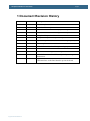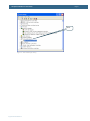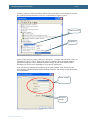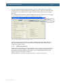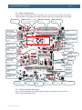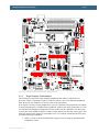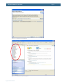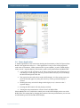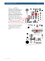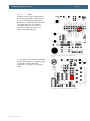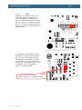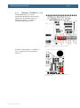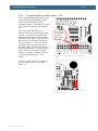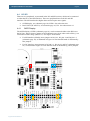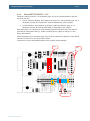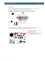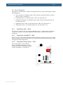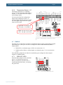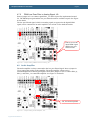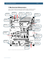
1
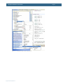
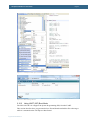
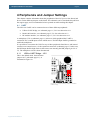
LPCXpresso Base Board - User’s Guide Copyright 2010 © Embedded Artists AB LPCXpresso Base Board User’s Guide Get Up-and-Running Quickly and Start Developing Your Applications On Day 1! EA2-USG-1001 Rev PA14 LPCXpresso Base Board - User’s Guide Page 2 Embedded Artists AB Södra Promenaden 51 SE-211 38 Malmö Sweden [email protected] http://www.EmbeddedArtists.com Copyright 2005-2010 © Embedded Artists AB. All rights reserved. No part of this publication may be reproduced, transmitted, transcribed, stored in a retrieval system, or translated into any language or computer language, in any form or by any means, electronic, mechanical, magnetic, optical, chemical, manual or otherwise, without the prior written permission of Embedded Artists AB. Disclaimer Embedded Artists AB makes no representation or warranties with respect to the contents hereof and specifically disclaim any implied warranties or merchantability or fitness for any particular purpose. Information in this publication is subject to change without notice and does not represent a commitment on the part of Embedded Artists AB. Feedback We appreciate any feedback you may have for improvements on this document. Please send your comments to [email protected]. Trademarks All brand and product names mentioned herein are trademarks, services marks, registered trademarks, or registered service marks of their respective owners and should be treated as such. Copyright 2010 © Embedded Artists AB LPCXpresso Base Board - User’s Guide Page 3 Table of Contents 1 Document Revision History 5 2 Introduction 6 2.1 Features 6 2.2 ESD and Handling Precaution 7 2.3 Other Products from Embedded Artists 7 2.3.1 Design and Production Services 7 2.3.2 OEM / Education / QuickStart Boards and Kits 7 3 Getting Started 8 3.1 LPCXpresso 8 3.2 Initial Preparation 8 3.3 Board Powering 9 3.4 Console Interface via USB-to-UART Bridge 9 3.4.1 FTDI USB Driver 10 3.4.2 USB Driver Behavior 13 3.5 Main Components 14 3.6 Default Jumper Positions 14 3.6.1 3.7 Illegal Jumper Combinations Things to Note about the LPCXpresso Base Board 3.7.1 Rev A 16 16 3.8 Import Sample Applications 16 3.9 Demo Application 19 3.10 Program Download 20 3.10.1 Using LPCXpresso IDE/Debugger 20 3.10.2 Using USB Boot Mode (LPC1343) 20 3.10.3 Using UART (ISP) Boot Mode 23 4 Peripherals and Jumper Settings 4.1 UART 26 26 4.1.1 USB-to-UART Bridge – U22 26 4.1.2 RS422/485 – U6 28 4.1.3 RF-module – U23 31 4.2 I2C 32 4.2.1 E2PROM, 24LC08 – U11 32 4.2.2 Port Expander, PCA9532 – U12 32 4.2.3 Light Sensor, ISL29003 – U13 33 4.2.4 Accelerometer, MMA7455 – U14 33 4.3 SPI 34 4.3.1 Dataflash, AT45DB016 – U15 35 4.3.2 7-segment display via shift register – U16 36 4.3.3 SD/MMC memory card interface 37 4.4 Copyright 2010 © Embedded Artists AB 15 I2C/SPI 38 LPCXpresso Base Board - User’s Guide Page 4 4.4.1 OLED Display 38 4.4.2 Dual UART SC16IS752 – U19 39 4.5 USB 40 4.6 Direct Digital IO 41 4.6.1 Push Button (BL) – SW3 41 4.6.2 Push Button (WAKEUP) – SW4 41 4.6.3 Quadrature Rotary Switch – SW5 41 4.6.4 Temperature Sensor – U7 42 4.7 PWM IO 4.7.1 RGB-LED, LED3 42 4.7.2 PWM Low Pass Filter to Analog Signal, U9 43 4.8 Audio Amplifier 43 4.9 Direct Analog IO 44 4.9.1 Trimming Potentiometer – R105 44 4.9.2 BNC Analog Input, X2 and U8 44 4.10 Mbed: CAN and Ethernet 46 4.10.1 CAN – U4 46 4.10.2 Ethernet – J19 46 5 Usage of CPU Pins 47 5.1 Expansion Connectors 6 mbed and LPC1114/LCP1343 Differences 48 50 6.1 mbed 50 6.2 LPC1114/LPC1343 50 7 Mechanical Dimensions 52 8 Troubleshooting 53 8.1 The Board is Always in Reset 53 8.2 Analog Input PIO0_11 Does Not Reach Zero 53 9 Further Information Copyright 2010 © Embedded Artists AB 42 54 LPCXpresso Base Board - User’s Guide Page 5 1 Document Revision History Revision Date Description PA1-PA2 2010-01-20 First incomplete version. PA3 2010-01-24 Second, still incomplete version. PA4 2010-01-25 Added more information about jumper settings. PA5 2010-01-26 Added information to the Getting Started Chapter. PA6 2010-01-26 Completed chapter 5 and 6. PA7 2010-01-28 Completed chapter 4 and updated chapter 6. PA8 2010-01-29 Updated chapter 3 and added Troubleshooting chapter (8). PA9 2010-01-30 First complete version. PA10 2010-02-10 Added information about PIO0_11 analog input. PA11 2010-02-11 Added information about J54 in section 8.1. PA12 2010-02-17 Corrected errors in Figure 23 and Figure 35. PA13 2010-02-20 Added information about SW4 and updated powering instructions. PA14 2010-02-22 Updated section 3.3: Added a recommendation to use the USB interfaces on the Base Board to power the board. Copyright 2010 © Embedded Artists AB LPCXpresso Base Board - User’s Guide Page 6 2 Introduction Thank you for buying Embedded Artists’ LPCXpresso Base Board, designed for the LPCXpresso Board (target LPC1343 and LPC1114) and the mbed module from NXP’s. This document is a User’s Guide that describes the LPCXpresso Base Board hardware design. The general focus will be for the LPCXpresso boards but differences for the mbed module will be noted. 2.1 Features The LPCXpresso Base Board makes it possible for you to get started with experiments and prototyping immediately with the LPCXpresso Board. The LPCXpresso Base Board can also be used together with the mbed module. The board has been design in cooperation with several Universities in order to be suitable for training and education situations. The many on-board peripherals easy your learning curve and speed up your program development. The features of the LPCXpresso Base Board are: Common features Socket for LPCXpresso and mbed module 50 pin expansion dual row pin list connector (male, 100mil pitch) for simple connection external designs and to a logic analyzer 50 pin expansion dual row header connector (female, 100mil pitch) for simple connection to breadboard Battery powering (small coin battery) USB interface Reset pushbutton Digital IO RGB-LED (can be PWM controlled) 5-key joystick switch 2 pushbuttons, one for activating bootloader Rotary switch with quadrature encoding (timer capture) Temperature sensor with PWM output (timer capture) Analog IO Trimming potentiometer input (analog input) PWM to analog LP-filtering (PWM output and analog input) Speaker output (PWM output) Oscilloscope probe inout stage Serial bus - SPI Shift register driving 7-segment LED SD/MMC memory card interface Dataflash SPI-NOR flash Serial bus - I2C Serial bus I2C/SPI shared SC16IS752 - I2C/SPI to 2xUART bridge; connected to RS232 fullmodem interface and one expansion UART 96x64 pixel white OLED (alternative I2C/SPI interface) Serial bus - UART USB-to-serial bridge, with automatic ISP activation RS422/485 interface Interface socket for XBee RF-module Copyright 2010 © Embedded Artists AB PCA9532 port expander connected to 16 LEDs 8kbit E2PROM MMA7455L accelerometer with I2C interface Light sensor LPCXpresso Base Board - User’s Guide Specific mbed module support CAN bus interface (can be simulated with LPCXpresso) Ethernet RJ45 connector with integrated magnetic Dimensions 150 x 180 mm Power Powered via USB (+5V) Page 7 2.2 ESD and Handling Precaution Please note that the LPCXpresso Base Board come without any case/box and all components are exposed for finger touches – and therefore extra attention must be paid to ESD (ElectroStatic Discharge) precaution. Make it a habit to always first touch the metal surface of one of the USB or SC/MMC connectors for a few seconds with both hands before touching any other parts of the boards. That way, you will have the same electrical potential as the board and therefore minimize the risk for ESD. Note that Embedded Artists does not replace boards that have been damaged by ESD. Do not exercise pressure on the OLED display glass area. That will surely damage the display. Also, do not apply pressure on the flex cable connecting the OLED to the pcb. This cable is relatively sensitive and can be damaged if too much pressure is applied to it. Note that Embedded Artists do not replace OLED displays where it has been improperly handled. 2.3 Other Products from Embedded Artists Embedded Artists have a broad range of low cost LPC1xxx/LPC2xxx/LPC3xxx based boards developed for prototyping / development as well as for OEM applications. Modifications for OEM applications can be done easily, even for modest production volumes. Contact Embedded Artists for further information about design and production services. 2.3.1 Design and Production Services Embedded Artists provide design services for custom designs, either completely new or modification to existing boards. Specific peripherals and I/O can be added easily to different designs, for example, communication interfaces, specific analog or digital I/O, and power supplies. Embedded Artists has a broad, and long, experience in designing industrial electronics in general and with NXP’s LPC2xxx microcontroller family in specific. Our competence also includes wireless and wired communication for embedded systems. For example IEEE802.11b/g (WLAN), Bluetooth™, ZigBee™, ISM RF, Ethernet, CAN, RS485, and Fieldbuses. 2.3.2 OEM / Education / QuickStart Boards and Kits Visit Embedded Artists’ home page, www.EmbeddedArtists.com, for information about other OEM / Education / QuickStart boards / kits or contact your local distributor. Copyright 2010 © Embedded Artists AB LPCXpresso Base Board - User’s Guide Page 8 3 Getting Started This chapter contains information about how to get acquainted with the LPCXpresso Base Board. Please read this section first before you start using the board - it will be worthwhile! 3.1 LPCXpresso The main source of information about the LPCXpresso LPC1343/LPC1114 boards as well as the LPCXpresso Debugger/IDE is http://www.nxp.com/lpcxpresso. On this site you will find introduction videos, getting started manual, a forum, link to where you can download the IDE and more information that is related to LPCXpresso. 3.2 Initial Preparation The LPCXpresso Base Board is delivered with two pin lists. These pin lists must be soldered onto your LPCXpresso LPC1343/LPC1114 board before it can be used with the LPCXpresso Base Board. Figure 1 and Figure 2 shows how the pin lists are soldered onto an LPCXpresso LPC1343 board. Figure 1 – LPCXpresso LPC1343 with pin list Figure 2 – LPCXpresso LPC1343 with pin list Copyright 2010 © Embedded Artists AB LPCXpresso Base Board - User’s Guide Page 9 3.3 Board Powering The board can be powered from a PC via the included USB cable (mini-B to A cable). When the LPCXpresso LPC1343/LPC1114 board is mounted on the base board there are a total of three USB interfaces and all can be used to power the base board. Although all USB interfaces can be used to power the board it is recommended to use any of the USB interfaces on the base board. The main power source is, for example, the USB-to-UART bridge. See Figure 3 for the three USB interfaces. Section 3.4 describes how to install necessary drivers for the USB-to-UART bridge. If there is a problem when powering the board only via the LPCXpresso Board (for example the LPCXpresso Base Board is always in reset), check section 8.1 for more information. J54 jumpers (see Figure 21) might need to be removed or powering through the USB-to-UART connector might be needed. 2. Used when debugging (LPCXpresso IDE) 3. USB device (not LPC1114) 1. USB-to-UART (main power source) Figure 3 – Base Board with a mounted LPCXpresso LPC1343 board 3.4 Console Interface via USB-to-UART Bridge The LPCXpresso Base Board contains a USB-to-Serial bridge chip (FT232R from FTDI) that connects the UART channel on the LPCXpresso target cpu (LPC1343 or LPC1114) to a virtual COM port on the PC (via USB). It is this serial channel that is the console interface to the system. Special USB drivers must be installed on the PC in order for the virtual COM port to be created. See subsection below for a description of how to install the FTDI USB driver. Copyright 2010 © Embedded Artists AB LPCXpresso Base Board - User’s Guide 3.4.1 Page 10 FTDI USB Driver A USB driver must be installed on your PC computer in order to get the USB-to-UART chip (FT232R) to function. Make sure to download the latest version of the driver, which can be found at the following URL: http://www.ftdichip.com/Drivers/VCP.htm (search for a FT232R driver for your operating system). When the LPCXpresso Base Board is connected to the PC (via an USB cable) the PC will ask for a driver. Unpack/unzip the downloaded driver file and browse to the position of the driver files. After successful driver installation, a COM port will be created. Before any communication with the Board can take place the UART settings must be correctly set. The following description is valid for Windows™ XP, but other operating systems have similar dialog windows. See the USB driver documentation for details, if needed. To change the UART settings, first open the System Properties dialog, as illustrated in the figure below. Device Manager Figure 4 – System Settings Dialog Then select the Device Manager and open the Ports list, as illustrated in Figure 5 below. Copyright 2010 © Embedded Artists AB LPCXpresso Base Board - User’s Guide Page 11 Ports Figure 5 – Device Manager Dialog Copyright 2010 © Embedded Artists AB LPCXpresso Base Board - User’s Guide Page 12 The new COM port (USB Serial Port) will be listed under the Ports list. Right-click on the new USB Serial Port and select Properties, as illustrated in Figure 6 below. USB Serial Port Properties Figure 6 – Device Manager Port Dialog Select 115200 bits per second, 8 data bits, none parity, 1 stop bit, and none flow control, as illustrated in Figure 7 below. Then select Advanced settings. Please note that different application programs can use different baudrate settings for the serial channel. Other baudrates can also be used, depending on your specific application. Also note that it is normally not needed to set the used baudrate at all. The driver and FT232R chip will automatically handle different baudrates. The setting is only shown here for completeness. UART settings Advanced settings Figure 7 – USB Serial Port Properties Dialog Copyright 2010 © Embedded Artists AB LPCXpresso Base Board - User’s Guide Page 13 Select the desired COM port number under the Advanced settings dialog. Some terminal programs needs low COM port number, for example between 1 and 5. Very often the COM port number for the USB Serial Port is higher than this, therefore this need to be changed manually. It is common that all COM ports with low numbers are listed as occupied, but test to change to a low number anyway. Very often it is no problem at all to do so. COM Port Number Setting Figure 8 – Advanced USB Serial Port Properties Dialog Finally it is time to test if you have successfully installed and configured the USB Serial Port. Start a terminal program. Connect to the correct COM port, with 115200 bits per second, 8N1, no flow control. 3.4.2 USB Driver Behavior Sometimes the USB COM port does not enumerate properly when the board in connected to the PC. This is a known “feature” of the USB driver. If you experience this problem, just unplug the board shortly and then plug in again. A new COM port that can be accessed properly should be created the second time. This problem may occur after every time you start (i.e., power cycle) your PC. Copyright 2010 © Embedded Artists AB LPCXpresso Base Board - User’s Guide Page 14 3.5 Main Components Figure 9 below illustrates the main component of the LPCXpresso Base Board. The number inside parenthesis (pX) indicate on which schematic page (X) the components can be found. USB interface X1 (p5) Ethernet interface J19 (p5) (mbed functionality) Expansion connectors J5/J6 (p3) Reset push button SW1 (p2) JTAG interface (not mounted, for future functionality) J8, J10 (p4) LPCXpresso connector J4 (p2) UART-USB interface U22, X3 (p11) On board LPC1xxx (not mounted, for future functionality) U3 (p4) RS485 / CAN interface J15 (p5) Battery connector J1 (p2) 7-seg display U16, DIS1 (p9) Voltage measuring pads PAD8/9/10 (p11) Data flash U15 (p9) SD/MMC interface J40 (p9) OLED display OLED1, U17 (p10) Light sensor U13 (p8) RS232 UART + TTL UART J52, J53, U18, U19 (p10) 16-LEDs U12 (p8) RF module U23 (p11) E2PROM U11 (p8) RGB-LED LED3 (p6) Quadrature rotary switch SW5 (p6) BNC input X2 (p7) 5-switch joystick SW2 (p6) Push buttons SW3, SW4 (p6) Accelerometer U14 (p8) Temperature sensor U7 (p6) Trimpot. R105 (p7) Speaker U10, SP1 (p7) PWM Low pass filter U9 (p7) Figure 9 – LPCXpresso Base Board Main Components 3.6 Default Jumper Positions Figure 10 below illustrates the default jumper positions as mounted when the board is delivered from Embedded Artists. Copyright 2010 © Embedded Artists AB LPCXpresso Base Board - User’s Guide Page 15 Figure 10 – LPCXpresso Base Board default Jumper Settings 3.6.1 Illegal Jumper Combinations The LPCXpresso Base Board has multiple peripherals that connect to the LPC1xxx processor. There is a shortage of pins to connect to and in a few cases different peripherals must share pins. See chapter 5 for an overview of all connections. If an output is used by several peripherals it is less of a problem. The peripherals just cannot be used simultaneously. If outputs from peripherals can drive the same signal, there is a risk of contention and damages of output drivers due to short circuit conditions. 270 ohm series resistors have been added in all places where several outputs can drive the same signal. This limits any short circuit currents to reasonable levels. To avoid the situation in the first place, avoid the following contentions: Copyright 2010 © Embedded Artists AB PIO0_2 can drive the OLED SPI-SSEL signal as well as being an output from the temperature sensor. LPCXpresso Base Board - User’s Guide Page 16 PIO1_4 can be driven by SW4 (wakeup) as well as the analog signal from the BNC analog input (U8). PIO1_8 can drive the TX-EN signal as well as being an interrupt output from the accelerometer (U14). PIO2_5 can be driven by three interrupt sources: accelerometer (U14), light sensor (U13) and dual uart (U19). See the jumper settings for each specific peripheral in chapter 4 . 3.7 Things to Note about the LPCXpresso Base Board This section lists things to note about different version of the LPCXpresso Base Board. 3.7.1 Rev A The 7-segment display is mounted 180 degrees from the normally expected way. The dot is in the upper left corner instead of the lower right. The silkscreen text around J41 can be a little confusing. The text “U16-SOUT” should rather be “U16-SIN”. Similarly, the text “U16-SIN” should rather be “U16SOUT”. 3.8 Import Sample Applications This section describes how you import the sample applications available on Embedded Artists support site into the LPCXpresso IDE. 1. Download the zip file from the support site and store it on your computer (e.g. to C:\temp\xpresso\lpc1343_base_board_100125.zip) 2. Start the LPCXpresso IDE and preferably select an empty workspace (an empty directory) 3. Press the “Import Example Projects” button from the Quickstart panel, see Figure 11. 4. A dialog window will be opened, see Figure 12. Browse to the previously downloaded zip file. Select the file and press the Next button followed by the Finish button. 5. When the zip file has been imported you will see all projects in the Project Explorer window, see Figure 13. 6. Select the project you would like to build and click the Build button in the Quickstart panel, see Figure 14. 7. Continue to section 3.9 for alternatives of how to download the program to the LPCXpresso board. Note: All the projects with prefix Lib_ are library projects and not sample applications. These library projects contain common code used by several of the sample applications. Lib_CMSISv1p30_LPC31xx – Cortex Microcontroller Software Interface Standard as defined by ARM Lib_MCU – Drivers for peripherals on the LPC1343/LPC1114 microcontroller Lib_EaBaseBoard – Drivers for peripherals on the Embedded Artists LPCXpresso Base Board Lib_FatFs_SD – ChaN’s FAT Fs module ported to the LPCXpresso base Board (used with the MMC/SD card interface). Copyright 2010 © Embedded Artists AB LPCXpresso Base Board - User’s Guide Figure 11 – Import project Copyright 2010 © Embedded Artists AB Page 17 LPCXpresso Base Board - User’s Guide Figure 12 – LPCXpresso Import Dialog Figure 13 – LPCXpresso imported projects Copyright 2010 © Embedded Artists AB Page 18 LPCXpresso Base Board - User’s Guide Page 19 Figure 14 – LPCXpresso Build button 3.9 Demo Application A suitable application to start with when checking the functionality of the LPCXpresso Base Board is the application called demo. This application is using several of the peripherals, such as the accelerometer, LEDs (connected to I/O port expander), joystick, OLED display, rotary switch, 7-segment display, SW3 button, speaker, trim potentiometer and RGB LED. 3 out of the 16 LEDs will always be lit and by tilting the board the LEDs that are lit will change (as a moving) bar. The way you move the board (in y-axis) will change the direction and speed of this bar. The joystick can be used to draw on the OLED display. It is like moving a pen you never lift from the paper. By using the center key on the joystick the display is cleared. Rotating the rotary switch will change which digit (0 to 9) is shown on the 7segment display. Pressing the SW3 button will start playing a melody. Turning the trim potentiometer will turn on/off the RGB LEDs Please note that P1.10 is used both to control power to the OLED display and to one of the RGB LEDs. This means that by changing the position of the trim potentiometer you can turn on/off both the green LED and the OLED display. Copyright 2010 © Embedded Artists AB LPCXpresso Base Board - User’s Guide Page 20 3.10 Program Download 3.10.1 Using LPCXpresso IDE/Debugger If you are using the LPCXpresso IDE to develop and build your applications you can directly download the program to the LPCXpresso Board from within the IDE. 1. Make sure you have connected a USB cable (mini-B to A) between your computer and the LPCXpresso LPC1343/LPC1114 board, see Figure 3 (USB interface 2). 2. Build your application as mentioned in section 3.7. 3. Click the Debug button in the Quickstart panel, see Figure 15. When the program has been downloaded, execution will stop at the first breakpoint which is the main function. 4. Press the F8 key on your keyboard to continue execution. Figure 15 – LPCXpresso Debugging View 3.10.2 Using USB Boot Mode (LPC1343) The LPC1343 supports In-System Programming (ISP) from the USB port through enumeration as a Mass Storage Class Device, i.e., you can drag and drop a binary file to the drive associated with the LPC1343. This section describes how you generate the binary file, adds the necessary checksum to the binary file and downloads the file to the target while it is mounted on the LPCXpresso Base Board. Copyright 2010 © Embedded Artists AB LPCXpresso Base Board - User’s Guide Page 21 For this to work you need to have some jumpers correctly set. If you have all jumpers in default position as described in section 3.6 USB boot mode will work; otherwise please check the following. USB interface – jumpers described in section 4.5. SW3 button – jumper described in section 4.6.1. You also need to make sure that the BL_EN signal is connected to PIO0_1 signal, see section 4.1.1.1 and Figure 22. After you have checked the jumper settings continue with the steps described below. 1. Build your application in the LPCXpresso IDE as mentioned in section 3.7. 2. Right-click on the generated axf file, go to the Binary Utilities menu and select Create binary. See Figure 16. 3. Open a command prompt in the directory containing the axf file. This can be done from the Utilities menu, see Figure 17. 4. Update the binary file with a correct checksum. In the example below it is assumed that you are using LPCXpresso IDE 3.2 installed in C:\nxp\lpcxpresso_3.2. It is also assumed that you are using a LPC1343 and the binary file is named oled_periph.bin. C:\nxp\lpcxpresso_3.2\bin\checksum.exe –p lpc1343 –v oled_periph.bin 5. You need to have a USB cable (mini-B to A) connected between your computer and the USB interface (interface 3 as shown in Figure 3). 6. Hold down the SW3 button and then press and release the reset button on the LPCXpresso base board. A storage device named CRP DISABLD will now appear on your computer, see Figure 18. 7. Open the Mass storage device and you will find a file named firmware.bin. Delete this file and then copy the file created in step 4 above to the CRP DISABLD drive. 8. Reset the board and your application will start. Copyright 2010 © Embedded Artists AB LPCXpresso Base Board - User’s Guide Figure 16 – LPCXpresso IDE Create a Binary File Copyright 2010 © Embedded Artists AB Page 22 LPCXpresso Base Board - User’s Guide Page 23 Figure 17 – LPCXpresso IDE Open Command Prompt Figure 18 – Mass Storage Device 3.10.3 Using UART (ISP) Boot Mode The LPC1343/LPC1114 supports In-System Programming (ISP) from the UART. This section describes how you generate the hex file and then download the file to the target while it is mounted on the LPCXpresso Base Board. Copyright 2010 © Embedded Artists AB LPCXpresso Base Board - User’s Guide Page 24 For this to work you need to have some jumpers correctly set. If you have all jumpers in default position, as described in section 3.6, all you need to do is remove the USB_VBUS jumper. This jumper is shown in Figure 41. If USB_VBUS is connected the LPC1343 (note that this doesn’t apply for the LPC1114) won’t enter UART boot mode, only USB boot mode. If you don’t have the jumpers in default position please make sure you at least have the UART related jumpers set as described in sections 4.1.1 and 4.1.1.1. After you have checked the jumper settings continue with the steps described below. 1. Download and install Flash Magic (http://www.flashmagictool.com/). You need version 5.43 or later. 2. Build your application in the LPCXpresso IDE as mentioned in section 3.7. 3. Open a command prompt in the directory containing the axf file. This can be done from the Utilities menu, see Figure 17. 4. Convert the axf file to a hex file. In this example it is assumed that your sample application is named oled_periph. arm-none-eabi-objcopy –O ihex oled_periph.axf oled_periph.hex 5. Start Flash Magic, select Device (LPC1343 or LPC1114/301), COM Port (the COM port associated with the target, section 3.4.1 describes the USB-to-UART bridge). Set baud rate to 115200, Interface to None and Oscillator to 12 MHz. Browse to the hex file you would like to download, see Figure 19 for an example. 6. Click the Start button and your application will be downloaded to the target. Copyright 2010 © Embedded Artists AB LPCXpresso Base Board - User’s Guide Figure 19 Flash Magic Copyright 2010 © Embedded Artists AB Page 25 LPCXpresso Base Board - User’s Guide Page 26 4 Peripherals and Jumper Settings This chapter contains information about the peripherals of the LPCXpresso Base Board and how to set the different jumpers on the board. The schematic can be downloaded in pdf from the support page, and is recommended to have printed out while reading this chapter. 4.1 UART The LPC1xxx UART can be connected to one of three different peripherals: USB-to-UART bridge, see schematic page 11, U22. See subsection 4.1.1 RS422/485 interface, see schematic page 5, U6. See subsection 4.1.2 RF-module interface, see schematic page 11, U23. See subsection 4.1.3 A multiplexer (U25 on schematic page 11) selects to which peripheral the UART is connected. The A and B inputs selects which source. The INH input shall be grounded to enable the multiplexer. It is possible to not connect the UART to any of three peripherals listed above, and instead connect to an external source, via the expansion connectors (schematic page 3). In this case, the INH input shall be high which is that same as not inserting the INH jumper (pin 5-6 of J7). The multiplexer circuit is then disconnected. 4.1.1 USB-to-UART Bridge – U22 This is the default mode. Insert all three jumpers in J7 (schematic page 11), as illustrated in Figure 20. Figure 20 – Jumper Setting: UART to USB-toUART bridge Copyright 2010 © Embedded Artists AB LPCXpresso Base Board - User’s Guide Page 27 4.1.1.1 ISP-option The USB-to-UART bridge can automatically activate the bootload mode of the LPC1xxx. A program image can then be downloaded via the UART channel. The RTS signal can pull pin PIO0_1 low, which enabled bootload mode after reset. The DTR signal can pull pin PIO0_0 low, which is the reset input. By inserting both jumpers in J54 (schematic page 11) the USB-to-UART bridge (U22) can control the PIO0_0 and PIO0_1 signals via RTS and DTR, see Figure 21. Upper: DTR to PIO0_0 (reset) Lower: RTS to PIO0_1 (bootload enable) Figure 21 – Jumper Setting: Enable ISP via USBto-UART bridge, J54 The BL_EN signal must be connected to PIO0_1 signal. This is accomplished by inserting a jumper in J13, pin 1-2 (schematic page 5). See Figure 22 for details. Figure 22 – Jumper Setting: Enable ISP via USBto-UART mode, J13 Copyright 2010 © Embedded Artists AB LPCXpresso Base Board - User’s Guide 4.1.2 Page 28 RS422/485 – U6 To connect the UART to the RS422/485 transceiver, insert two jumpers in J7 (schematic page 11), as illustrated in Figure 23. A RS422/485 transceiver must control the Rx- and Tx-patchs. This is accomplished via J17 and J18. The subsections below described the differences in jumper settings for RS422 and RS485, respectively. Figure 23 – Jumper Setting: UART to RS422/485, U6 Copyright 2010 © Embedded Artists AB LPCXpresso Base Board - User’s Guide Page 29 4.1.2.1 RS422 In RS422, the Rx- and Tx-paths must be controlled independently since both can be active simultaneously (full duplex). Rx-enable is controlled by PIO1_9 (insert J17) and is active low. Tx-enable is controlled by PIO1_8 (insert J18 in position 2-3) and is active high. See Figure 24 for jumper details. Figure 24 – Jumper Setting: Enable RS422 control It is possible to have 120 ohm termination resistors (R76 and R77 on schematic page 5) on the Rx- and Tx-data paths, respectively. See Figure 25 for jumper details. Figure 25 – Jumper Setting: Rs422 termination Copyright 2010 © Embedded Artists AB LPCXpresso Base Board - User’s Guide Page 30 4.1.2.2 RS485 In RS485, the Rx- and Tx-paths can be controlled together since they are not active simultaneously (half duplex). PIO1_9 controls both Rx and Tx. When PIO1_9 is high, Tx is enabled, and when PIO1_9 is low, Rx is enabled. Insert J17 and J18 in position 1-2. See Figure 26 for jumper details. Figure 26 – Jumper Setting: Enable RS485 control It is possible to connect the Rx- and Txdata paths via jumper J16 (on schematic page 5). Only one twisted pair used to communicate between nodes. It is also possible to add a 120 ohm termination resistor (R77 on schematic page 5) on the common Rx- and Tx-data path. See Figure 27 for jumper details. Upper: J16, data path jumpers Lower: J20, pin 1-2, termination jumper Figure 27 – Jumper Setting: Enable RS485 data and termination Copyright 2010 © Embedded Artists AB LPCXpresso Base Board - User’s Guide 4.1.3 Page 31 RF-module – U23 To connect the UART to the RF-module, U23 (interface socket for XBee™ modules from Digi™), insert two jumpers in J7 (schematic page 11), as illustrated in Figure 28. Figure 28 – Jumper Setting: UART to RF-module When communicating with the RFmodule, sometimes extra control signals are needed. J59 on schematic page 11 allows these to be connected. Figure 29 illustrates where the J59 can be found on the board. J59 Figure 29 – Jumper Setting: RF-module extra signals Copyright 2010 © Embedded Artists AB LPCXpresso Base Board - User’s Guide Page 32 4.2 I2C The LPC1xxx I2C-bus is connected to the following peripherals: E2PROM (24LC08), see schematic page 8, U11. See subsection 4.2.1 Port expander (PCA9532), see schematic page 8, U12. See subsection 4.2.2 Light sensor (ISL29003), see schematic page 8, U13. See subsection 4.2.3 Accelerometer (MMA7455), see schematic page 8, U14. See subsection 4.2.4 OLED display, see schematic page 10, OLED1. See subsection 4.4.1 Dual UART (SC16IS752), see schematic page 10, U19. See subsection 4.4.2 Note that these peripherals are always connected to the I2C-bus with the exception of the OLED display and UART-bridge (SC16IS752). These two peripherals have both I2C and SPI interfaces and they are described in a different section. The schematic specifies the I2C-addresses used (schematic page 8 and 10). 4.2.1 E2PROM, 24LC08 – U11 U12 is always connected to the I2C-bus. Write protect status on the memory area in U11 can be controlled by jumper J35 (schematic page 8). See Figure 30 for details. Inserted: Write operations enabled on U11 Open: Write protect enabled on U11 Figure 30 – Jumper Setting: E2PROM, 24LCD08 write protect 4.2.2 Port Expander, PCA9532 – U12 There are no jumpers of the 16-bit I2C-port expander. U12 is always connected to the I2Cbus. Copyright 2010 © Embedded Artists AB LPCXpresso Base Board - User’s Guide 4.2.3 Page 33 Light Sensor, ISL29003 – U13 U13 is always connected to the I2Cbus.There is an interrupt output that can be connected to PIO2_5 via J36 (schematic page 8). See Figure 31 for details. Make sure there is no other driver on the PIO2_5 signal when using it as interrupt signal. There is a 270 ohm series resistor to prevent damages in case there is more than one driver of the signal. Figure 31 – Jumper Setting: Light sensor, ISL29003 interrupt output 4.2.4 Accelerometer, MMA7455 – U14 U14 is always connected to the I2Cbus.There are two interrupt outputs that can be connected to PIO1_8 and PIO2_5 via J37 (schematic page 8). See Figure 32 for details. Make sure there are no other drivers on the PIO1_8 and PIO2_5 signals when using them as interrupt signals. There are 270 ohm series resistors to prevent damages in case there is more than one driver of the signals. Figure 32 – Jumper Setting: Accelerometer, MMC7455 interrupt outputs Copyright 2010 © Embedded Artists AB LPCXpresso Base Board - User’s Guide Copyright 2010 © Embedded Artists AB 4.3 SPI The LPC1xxx SPI-bus is connected to the following peripherals: Dataflash (AT45DB016), see schematic page 9, U15. See subsection 4.3.1 7-segment display via shift register, see schematic page 9, U16. See subsection 4.3.2 SD/MMC memory card interface, see schematic page 9, J40. See subsection 4.3.3 Dual UART (SC16IS752), see schematic page 10, U19. See subsection 4.4.2 OLED display, see schematic page 10, OLED1. See subsection 4.4.1 These peripherals can all be connected to the SPI-bus. The OLED display and the UARTbridge (SC16IS752) can alternatively also be connected to the I2C-bus. These two peripherals have both I2C and SPI interfaces and they are described in a different section. The Dataflash, 7-segment display and SD/MMC memory card interface are all controlled (chip select – SSEL) by PIO1_11. That means that only one of these three peripherals can be used at a time. A multiplexer (U26 on schematic page 9) selects to which of these three peripheral that PIO1_11 connects to, and controls the respective SSEL input signal. The A and B inputs select which one. The INH input shall be grounded to enable the multiplexer. EA2-USG-1001 Rev PA14 LPCXpresso Base Board - User’s Guide 4.3.1 Page 35 Dataflash, AT45DB016 – U15 The Dataflash chip, U15, can be connected to the SPI-bus. Insert all four jumpers in J38 (schematic page 9), as illustrated in Figure 33, in order to connect all SPI signals to U15. Figure 33 – Jumper Setting: J38 for Dataflash, U15 In order to connect PIO1_11 to SSEL of U15, set jumpers for J55 according to Figure 34. Figure 34 – Jumper Setting: PIO1_11, SSEL to Dataflash, U15 Copyright 2010 © Embedded Artists AB LPCXpresso Base Board - User’s Guide 4.3.2 Page 36 7-segment display via shift register – U16 The 7-segment display shift register, U16, can be connected to the SPI-bus. Insert three (of the four) jumpers in J41 (schematic page 9), as illustrated in Figure 35, in order to connect the SPI signals to U16. J41, pin 1-2 shall normally not be inserted. This is the output from the shift register. It can only be connected to the SPI-MISO signal if this is the only chip connected on the SPI-bus. The reason for this is that the shift register always drive the output signal, i.e., it is never in highimpedance state (regardless the state of the SSEL input). Note that the silkscreen text around J41 (for rev A of the board) is wrong. The text “U16-SOUT” should rather be “U16-SIN”. Similarly, the text “U16-SIN” should rather be “U16SOUT”. J41, pin 1-2. Do normally not insert this jumper. Figure 35 – Jumper Setting: J41 for shift register, U16 In order to connect PIO1_11 to SSEL of U16, set jumpers for J55 according to Figure 36. Figure 36 – Jumper Setting: PIO1_11, SSEL to shift register, U16 Copyright 2010 © Embedded Artists AB LPCXpresso Base Board - User’s Guide 4.3.3 Page 37 SD/MMC memory card interface The SD/MMC memory card interface connector, J40, can be connected to the SPI-bus. Insert all five jumpers in J39 (schematic page 9), as illustrated in Figure 37, in order to connect all SPI signals to J40 (and ultimately the SD/MMC memory card). Note that the memory card can only be interfaced in the simpler and lower data rate SPI-mode. J39, pin 9-10. Not always needed. Also note that J39, pin 9-10, is optional. It is a card detect signal (active low) that is connected to PIO2_10. It is not always needed. If not, simply do not insert this jumper and PIO2_10 can be used for other purposes. Figure 37 – Jumper Setting: J39 for SD/MMC memory card interface, J40 In order to connect PIO1_11 to CS signal of J40 (the SPI-SSEL signal), set jumpers for J55 according to Figure 38. Figure 38 – Jumper Setting: PIO1_11, SSEL to SD/MMC interface, J40 Copyright 2010 © Embedded Artists AB LPCXpresso Base Board - User’s Guide Page 38 4.4 I2C/SPI There are two peripherals, as presented in the I2C and SPI sections, which can be connected to either the I2C or the SPI interfaces. These two peripherals have both I2C and SPI interfaces. The SPI interface has higher data rate but require more signals. OLED display, see schematic page 10, OLED1. See subsection 4.4.1 Dual UART (SC16IS752), see schematic page 10, U19. See subsection 4.4.2 4.4.1 OLED Display The OLED display, OLED1 (schematic page 10), can be connected either to the SPI-bus or the I2C-bus. Always insert a jumper in J44 (schematic page 10) in order to allow PIO1_10 to control the OLED-voltage (about 11V). See Figure 39 for details. For SPI interface (default), insert jumpers in J42, J43, J45 pin1-2 and J46 pin 1-2 (schematic page 10), as illustrated in Figure 39. Note that SPI mode is illustrated by blue jumpers. For I2C interface, insert jumpers in J45 pin 2-3, J46 pin 2-3 and J47 (schematic page 10), as illustrated in Figure 39. Note that I2C mode is illustrated by yellow jumpers. Figure 39 – Jumper Setting: OLED in SPI/I2C Mode Copyright 2010 © Embedded Artists AB LPCXpresso Base Board - User’s Guide 4.4.2 Page 39 Dual UART SC16IS752 – U19 The dual UART SC16IS752, U19 (schematic page 10), can be connected either to the SPIbus or the I2C-bus. For I2C interface (default), insert jumpers in J48 pin 2-3, J49 (schematic page 10), as illustrated in Figure 40. Note that I2C mode is illustrated by yellow jumpers. For SPI interface, insert jumpers in J48 pin1-2 and J50 (schematic page 10), as illustrated in Figure 40. Note that SPI mode is illustrated by blue jumpers. Note that J50 pin 7-8 is optional. It is the interrupt signal from the dual uart (U19) that can optionally be connected to PIO2_5. If that is wanted, insert a jumper in J50 pin 7-8. See Figure 40 for details. Insert all jumpers in J51 (schematic page 10) in order to connect uart channel A to the RS232 interface (U18 and J52). See Figure 40 for details. Connector J53 carries uart channel B that can be used for custom interface. J51 J53 Figure 40 – Jumper Setting: SC16IS752, U19, in I2C/SPI Mode J50 pin7-8 Copyright 2010 © Embedded Artists AB LPCXpresso Base Board - User’s Guide Page 40 4.5 USB The LPC1343 USB interface can be connected to mini-B USB connector (X1, on schematic page 5). Note that the LPC1114 does not contain any USB interface. The USB power signal must be connected to the VBUS sense input, PIO0_3. This is accomplished by inserting a jumper in J12, pin 1-2. See Figure 41 for details. Figure 41 – Jumper Setting: USB VBUS, J12 The USB connect function is controlled by J14. If a jumper is inserted in J14, pin 1-2, the connect functionality is controlled by PIO0_6. This is the default jumper position. J14 right: USB connect controlled by PIO0_6. J14 left: USB connect always on. Figure 42 – Jumper Setting: USB Connect, J14 Copyright 2010 © Embedded Artists AB LPCXpresso Base Board - User’s Guide Page 41 4.6 Direct Digital IO The LPC1xxx is connected to a number of peripherals directly via the general purpose digital input/output pins: 5-key joystick), see schematic page 6, SW2. Directly connected to PIO2_0, PIO2_1, PIO2_2, PIO2_3 and PIO2_4 Push button (BL), see schematic page 6, SW3. See subsection 4.6.1 Push button (Wakeup), see schematic page 6, SW4. Directly connected to PIO1_4. See subsection 4.6.2 Quadrature rotary switch, see schematic page 6, SW5. See subsection 4.6.3 Temperature sensor, see schematic page 6, U7. See subsection 4.6.4 4.6.1 Push Button (BL) – SW3 See Figure 22 on page 27 for J13 settings (schematic page 5). A jumper must be inserted in J13, pin 1-2 in order to connect the signal from SW3 to PIO0_1 (which is the bootload enable pin). 4.6.2 Push Button (WAKEUP) – SW4 PIO1_4 are can be driven from both SW4 and from the BNC Analog Input (U8) via J28.Note that J28 must not be inserted when SW4 is to be used. See Figure 49 for details where to find J28 (upper left side of the picture). 4.6.3 Quadrature Rotary Switch – SW5 Insert both jumpers in J56 (schematic page 6), as illustrated in Figure 43. This will connect the two signals (QA and QB) to PIO1_0 and PIO1_1, respectively. Figure 43 – Jumper Setting: Quadrature Rotary Switch, J56 Copyright 2010 © Embedded Artists AB LPCXpresso Base Board - User’s Guide 4.6.4 Page 42 Temperature Sensor – U7 The output signal from U7 (schematic page 6) can be connected to either PIO0_2 or PIO1_5. J25 selects which. See Figure 44 for jumper details. J26 can set the TS0/TS1 configuration inputs of the temperature sensor. An inserted jumper pulls the respective signal low. The signal is high when leaving the jumper position open. Upper pos.: U7 to PIO0_2 Lower pos.: U7 to PIO1_5 Right: J26, pin 1-2 (U7-TS0) Left: J26, pin 3-4 (U7-TS1) Figure 44 – Jumper Setting: Temperature sensor, U7 4.7 PWM IO The LPC1xxx is connected to a number of peripherals directly via the general purpose digital input/output pins. These pins can also be configured as Pulse Width Modulated (PWM) output signals: RGB-LED, see schematic page 6, LED3. See subsection 4.7.1 PWM Low Pass Filter to Analog Signal, see schematic page 7, U9. See subsection 4.7.2 Note that these peripherals can either be controlled by pins configured as direct digital outputs or as PWM outputs. 4.7.1 RGB-LED, LED3 Insert the three jumpers in J23 (schematic page 6), as illustrated in Figure 45. PIO1_9 controls the red LED. PIO1_2 controls the blue LED. PIO1_10 controls the green LED. Figure 45 – Jumper Setting: RGB-LED, LED3 Copyright 2010 © Embedded Artists AB LPCXpresso Base Board - User’s Guide 4.7.2 Page 43 PWM Low Pass Filter to Analog Signal, U9 Insert a jumper in J31 to connect signal PIO1_2 to the low pass filer implemented around U9. The PWM input signal and the low pass filtered result are available on pads. See Figure 46 for details. The low pass filtered signal, which is an analog signal (as opposed to the digital PWM signal) can be connected to an audio amplifier. See section 4.8 for details about this. Pads to access the input PWM signal and the low pass filtered result. Figure 46 – Jumper Setting: PWM Low Pass Filtering, U9 4.8 Audio Amplifier The audio amplifier is always connected to the low pass filtered signal. Insert a jumper in J32 to connect the speaker to the amplifier. The audio amplifier volume can be controlled/adjusted via three digital signals. Insert three jumpers in J33 to connect PIO3_0, PIO3_1 and PIO3_2 to control the amplifier. See Figure 47 for details. J34, for external speaker Figure 47 – Jumper Setting: Audio Amplifier, U10 Copyright 2010 © Embedded Artists AB LPCXpresso Base Board - User’s Guide Page 44 4.9 Direct Analog IO The LPC1xxx is connected to a number of peripherals directly via analog input pins: Trimming potentiometer (R105), see schematic page 7. See subsection 4.9.1 BNC input (X2 and U8), see schematic page 7. See subsection 4.9.2 4.9.1 Trimming Potentiometer – R105 Insert jumper in J27 to connect the analog signal from the trimming potentiometer to PIO0_11, which is an analog input of the LPC1xxx. See Figure 48 for details. Figure 48 – Jumper Setting: trimming Potentiometer R105 4.9.2 BNC Analog Input, X2 and U8 X2 is a BNC connector and U8 implements a simple input stage that can be DC or AC coupled. There is also an option to have x10 amplification. It is possible to connect an oscilloscope probe to X2. Insert a jumper in J28 to connect the analog signal to PIO1_4. Select DC or AC coupling with J29 and J57. Note that J29/J57 shall always be set in the same position (left or right). Insert a jumper in J30 to get x10 amplification. No jumper in J30 results in x1 amplification. See Figure 49 for details. Copyright 2010 © Embedded Artists AB LPCXpresso Base Board - User’s Guide Page 45 Left: DC coupling Right: AC coupling J30 insert: x10 J30 open: x1 Figure 49 – Jumper Setting: BNC analog input, U8 Copyright 2010 © Embedded Artists AB LPCXpresso Base Board - User’s Guide Page 46 4.10 Mbed: CAN and Ethernet There are two peripherals that are only valid for the mbed module: CAN (U4), see schematic page 5. See subsection 4.10.1 Ethernet connector (J19), see schematic page 5. See subsection 4.10.2 4.10.1 CAN – U4 The mbed module has a microcontroller that has a built-in CAN controlled peripheral. U4 (TJA1040) is an external CAN transceiver, see schematic page 5. Insert jumpers in J12, pin 2-3 and J13, pin 2-3 to connect the CAN transceiver to the mbed module. See Figure 50 for details. Note that even though the LPC1xxx processor does not have a built-in CAN controlled it is possible to create a CAN controlled in software (at least for low bit rates). Figure 50 – Jumper Setting: CAN, U4 4.10.2 Ethernet – J19 The Ethernet connector (J19, schematic page 5) is always connected to the mbed module. The Ethernet PHY is on the mbed module. There are two LEDs inside the J19. Note that the LEDs are not controlled by the Ethernet PHY. They have to be controlled by software. See Figure 51 for details about J21. Figure 51 – Jumper Setting: Ethernet Connector, J19 Copyright 2010 © Embedded Artists AB gpio gpio gpio pwm pwm pwm not mbed not mbed not mbed not mbed not mbed spi not mbed not mbed not mbed not mbed PIO2_0 / DTR PIO2_1 / DSR PIO2_2 / DCD PIO2_3 / RI PIO2.4 PIO2.5 PIO2.6 PIO2.7 PIO2.8 PIO2.9 PIO2.10 PIO2_11 / SCK PIO3.0 PIO3.1 PIO3.2 PIO3.3 mbed module "problem" ain tms ain tdo ain/aout trst ain swdio ain not mbed uart uart not mbed pwm pwm pwm TMS / PIO1_0 / AD1 / CT32B1_CAP0 TDO / PIO1_1 / AD2 / CT32B1_MAT0 TRST / PIO1_2 / AD3 / CT32B1_MAT1 SWDIO / PIO1_3 / AD4 / CT32B1_MAT2 PIO1_4 / AD5 / CT32B1_MAT3 / WAKEUP PIO1_5 / RTS / CT32B0_CAP0 PIO1_6 / RXD / CT32B0_MAT0 PIO1_7 / TXD / CT32B0_MAT1 PIO1_8 / CT16B1_CAP0 PIO1_9 / CT16B1_MAT0 PIO1_10 / AD6 / CT16B1_MAT1 PIO1_11 / AD7 led2 led1 RXD TXD dtr rts RXD TXD RXD TXD TX-EN RX-EN# center left right up down wakeup Qa Qb red green blue Alt.1 ain sp-clk sp-u/d sp-sh pwm-out irq1-out irq2-out USB-to- RFRS422/ Rotary RGB- Temp- AINPWM-to24LC0 mbed SWD JTAG USB ETH CAN UART module RS485 Joystick PB-SW3 PB-SW4 Switch LED sensor trimpot BNC Aout PCA9532 MMA7455 8 Reset / PIO0_0 nRES reset reset reset reset reset PIO0_1 / CLKOUT / CT32B0_MAT2 / USB_FTOGGLE can use bl_en bl_en PIO0_2 / SSEL / CT16B0_CAP0 gpio Alt.2 PIO0_3 / USB_VBUS can use use PIO0_4 / SCL i2c scl scl scl PIO0_5 / SDA i2c sda sda sda PIO0_6 / USB_CONNECT / SCK not mbed use PIO0_7 / CTS gpio cts PIO0_8 / MISO/CT16B_MAT0 spi PIO0_9 / MOSI / CT16B0_MAT1 / SWO spi (swo) SWCLK / PIO0_10 / SCK / CT16B0_MAT2 swclk tck TDI / PIO0_11 / AD0 / CT32B0_MAT3 ain tdi ain irq-out scl sda scl sda Dual UART reset cd spi-sck spi-ssel spi-sck spi-sck spi-ssel spi-ssel spi-sck d/c Voled-en spi-sck spi-ssel irq spi-miso spi-miso spi-miso spi-miso spi-miso spi-mosi spi-mosi spi-mosi spi-mosi spi-mosi scl sda ssel Light Sensor - SD/MMC 7ISL2900 I/F segment Dataflash OLED reset reset LPCXpresso Base Board - User’s Guide Copyright 2010 © Embedded Artists AB 5 Usage of CPU Pins The table below shoes which pins are used for the different peripherals. EA2-USG-1001 Rev PA14 LPCXpresso Base Board - User’s Guide Page 48 The yellow colored fields signal where there are problems for the mbed module. See chapter 6 for details about the differences between mbed modules and LPCXpresso Boards. 5.1 Expansion Connectors All LPC1xxx pins, except the USB signals, are available together with power on two expansion connectors (see schematic page 3). There is a male (J5) and a female (J6) 50position connector. See Figure 52 for details. Left side Figure 52 – LPCXpresso Base Board Expansion Connectors (J5, J6) Copyright 2010 © Embedded Artists AB Right side LPCXpresso Base Board - User’s Guide Page 49 The text on the pcb indicates where the different signals can be accessed. The left side of J6 is also valid as a left side of J5, and similar is the right side of J5 also valid as right side of J6. All PIO-pins have 270 ohm series resistors to provide some protection for short circuits and to some extent also ESD. Note that the current to external circuits are not limited. Keep power consumption below 50mA if powered only via the LPCXpresso Board (via the USB connector for LPC-LINK) or below 250mA if powered via the USB-to-UART bridge on the LPCXpresso Base Board (connector X3, schematic page 11). The male expansion connector (J5) can use a standard 50 position flat cable to interface to an external design. The female expansion connector (J6) can be used to interface breadboard designs via simple wire jumpers. Copyright 2010 © Embedded Artists AB LPCXpresso Base Board - User’s Guide Page 50 6 mbed and LPC1114/LCP1343 Differences There are small but important differences between the mbed module and the LPCXpresso boards, and there are also small differences between the LPCXpresso boards. This chapter explains the differences. 6.1 mbed This document describes the LPCXpresso Base Board from the perspective of connecting it to LPCXpresso boards with LPC1xxx processors (currently LPC1114 and LPC1343 versions exist). The board is however also designed for the mbed module. The LPCXpresso boards are in many ways compatible with the mbed module. Mechanically they have the same format, except that the LPCXpresso boards have more pins at one end of the board. Most pins can have the same functionality, like UART, I2C, SPI, analog input, etc. The mbed module has a powerful processor that has built-in peripherals for CAN and Ethernet. The LPCXpresso Base Board has special support for this in the form of: - CAN transceiver (U4, see schematic page 5) - Ethernet connector (J19, see schematic page 5) The following limitations apply to the mbed module: - Cannot control the audio amplifier (U10). Lack signals PIO3_0, PIO3_1, PIO3_2. - No card detect signal from SD/MMC memory card interface. Lack signal PIO2_10. - OLED must be interfaced via I2C (not SPI). Lack PIO2_7, which is used as D/C input signal for the display. - Dual UART (SC16IS752) must be interfaced via I2C (not SPI). Lack PIO2_8, which is used as SPI-SSEL for the chip. - Lack PIO1_5: used as RTS for RF-module (U23), also used for temperature alternative 1 output (U7). - Lack PIO1_8: used as TX_EN for RS422 (U6) (can however use PIO1_9 to drive both TX_EN and RX_EN#), also used for irq2 output from accelerometer (U14). Note that if the design have unused pins these can be connected to the missing ones (listed above). Such connections must be manually soldered. 6.2 LPC1114/LPC1343 The LPC1114 and LPC1343 are basically pin compatible, but with two exceptions: Copyright 2010 © Embedded Artists AB On LPC1114, PIO3_4/PIO3_5 have taken the place of PIO2_4/PIO2_5, and PIO2_4/PIO2_5 have taken the place of the USB data signals. There are a number of places where this has an effect (see also table in Chapter 5 ): o PIO2_4 connects to one of the Joystick switches (SW2 on schematic page 6). Connects instead to PIO3_4 on the LPC1114. o PIO2_5 can connect to INT1 output on MMA7455 (Accelerometer on schematic page 8). Connects instead to PIO3_5 on the LPC1114. o PIO2_5 can connect to INT output on ISL29003 (Light sensor on schematic page 8). Connects instead to PIO3_5 on the LPC1114. LPCXpresso Base Board - User’s Guide o PIO2_5 can connect to INT output on SC16IS752 (Dual UART on schematic page 10). Connects instead to PIO3_5 on the LPC1114. The LPC1114 does not have an USB interface. It is PIO2_4 and PIO2_5 on the LPC1114 that are on the same place as the USB interface data signals. The USB data signals are routed directly to the mini-B USB connector on the base board and there is no possibility to access these signals when using the LPC1114. Also study the schematic of the LPCXpresso Board, target LPC1114. Copyright 2010 © Embedded Artists AB Page 51 LPCXpresso Base Board - User’s Guide Page 52 7 Mechanical Dimensions Figure 53 below contains a drawing of the board that includes mechanical measures. Important holes or center lines are marked with x,y coordinates in mil and mm. X1 center line (1805, -) mil [25.15, -] mm J19 center line (1695, -) mil [43.05, -] mm Pin 1 of J5 (2327, 6548) mil [59.10, 166.32] mm Pin 1 of J6 (2327, 6168) mil [59.10, 156.67] mm Mounting hole (248, 6747) mil [6.30, 171.37] mm Mounting hole (5365, 6747) mil [136.27, 171.37] mm X3 center line (-, 5348) mil [-, 135.84] mm Pin 1 of J4 (1130, 4663) mil [28.70, 118.44] mm Pin 1 of J15 (5356, 4890) mil [136.05, 124.20] mm Mounting hole (4020, 3660) mil [102.11, 92.96] mm Center line of J52 (-, 2488) mil [-, 63.20] mm Center line of memory card (J40) (-, 3073) mil [-, 78.06] mm Pin 1 of U23 (5282, 2288) mil [134.18, 58.12] mm Mounting hole (248, 248) mil [6.30, 6.30] mm Mounting hole (5365, 248) mil [136.27, 6.30] mm X2 center line (4808, -) mil [122.12, -] mm Figure 53 – LPCXpresso Base Board Mechanical Dimensions Copyright 2010 © Embedded Artists AB LPCXpresso Base Board - User’s Guide Page 53 8 Troubleshooting 8.1 The Board is Always in Reset Reason 1: If a terminal application, such as Tera Term, is connected to the COM port associated with the board and at the same time have the J54 jumpers (see Figure 21) inserted, the terminal application might be the cause of this problem. If the terminal application is pulling DTR low the board will be reset and if it pulls RTS low it will control the bootload enable functionality. Solution 1: Remove the jumpers and try again (please note that the jumpers must be inserted if the board is programmed using the UART boot mode). Reason 2: If the board is powered only through the USB interface on the LPCXpresso LPC1343/LPC1114 Board (interface 2 as shown in Figure 3) the FTDI USB-to-UART bridge won’t be powered. The output pins such as RTS and CTS might then have a low output. If the J54 jumpers, see Figure 21, are inserted the board will always be in reset. Solution 2: Power the board also through USB interface 1, as shown in Figure 3, or remove the J54 jumpers. 8.2 Analog Input PIO0_11 Does Not Reach Zero The trimming potentiometer (R105) can be used to create an analog voltage to PIO0_11 (analog input 1). The lowest possible reading can be between 20-40 (on a scale from 0 to 1023) even if the trimming potentiometer is turned to the lowest output voltage. Reason: There are pull-up resistors on PIO0_11 that will generate a current through R106. One pull-up resistor is internal in the LPC1xxx and can be disabled via program control. The other pull-up resistor is R46 (via R57), found on schematic page 4. These resistors are actually mounted even though the schematic indicate that this is an optional mounting. The voltage across R106 can be up to about 0.1 volt due to the pull-up resistors on PIO0_11. Solution: Make sure that PIO0_11 does not have the (LPC1xxx) internal pull-up resistor enabled. This is a pin configuration. Also remove R57 or R46. Either of these resistors can easily be de-soldered from the pcb. Copyright 2010 © Embedded Artists AB LPCXpresso Base Board - User’s Guide Page 54 9 Further Information The LPC1343/LPC1114 microcontrollers are complex circuits and there are a number of other documents with more information. The following documents are recommended as a complement to this document. [1] NXP LPC1114 Datasheet http://ics.nxp.com/products/lpc1000/datasheet/lpc1111.lpc1112.lpc1113.lpc1114.pdf [2] NXP LPC1343 Datasheet http://ics.nxp.com/products/lpc1000/datasheet/lpc1311.lpc1313.lpc1342.lpc1343.pdf [3] NXP LPC1114 User’s Manual http://ics.nxp.com/support/documents/microcontrollers/pdf/ user.manual.lpc1111.lpc1112.lpc1113.lpc1114.pdf [4] NXP LPC1343 User’s Manual http://ics.nxp.com/support/documents/microcontrollers/pdf/user.manual.lpc13xx.pdf [5] LPC1000 Yahoo Group. A discussion forum dedicated entirely to the NXP LPC1xxx series of microcontrollers. http://groups.yahoo.com/group/lpc1000/ [6] LPC2000 Yahoo Group. A discussion forum dedicated entirely to the NXP LPC2xxx series of microcontrollers. http://groups.yahoo.com/group/lpc2000/ Note that there can be newer versions of the documents than the ones linked to here. Always check for the latest information / version. Copyright 2010 © Embedded Artists AB