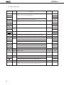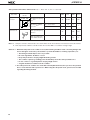
1
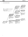
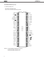
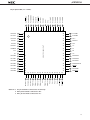
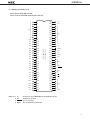
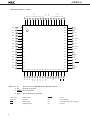
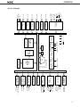
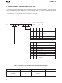
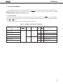
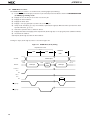
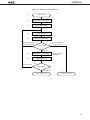
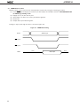
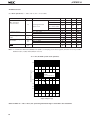
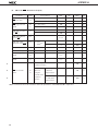
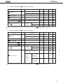
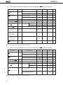
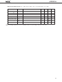
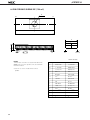
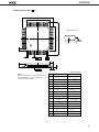
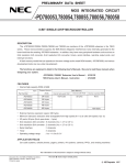
DATA SHEET
MOS INTEGRATED CIRCUIT
μPD78P014
8-BIT SINGLE-CHIP MICROCOMPUTER
DESCRIPTION
The μPD78P014 is a member of the μPD78014 subseries of 78K/0 series products. It uses a one-time-programmable
(OTP) ROM or EPROM instead of the mask ROM of the μPD78014.
Because the μPD78P014 can be programmed by users, it is ideally suited for applications involving the evaluation
of systems in development stages, small-scale production of many different products, and rapid development and timeto-market of a new product.
Detailed information about product features and specifications can be found in the following document. Please
make sure to read this document before starting design.
μPD78014, 78014Y Series User’s Manual : IEU-1343
FEATURES
• Pin compatible with mask ROM versions (except VPP pin)
• Internal PROM: 32K bytesNote
• μPD78P014DW
: Reprogrammable (ideal for system evaluation)
• μPD78P014CW, 78P014GC-AB8 : Programmable once only (ideal for small-scale production)
• Internal high-speed RAM: 1024 bytesNote
• Buffer RAM: 32 bytes
• Operable over same supply voltage range as mask ROM version (2.7 to 6.0 V)
• Available for the QTOPTM microcomputer
Note The internal PROM and internal high-speed RAM size can be set by means of the memory size switching
register.
Remark The QTOP microcomputer is the general term for a single-chip microcomputer with on-chip one-time
PROM. NEC supports its program writing, marking, screening, and verification.
Differences from mask ROM versions are as follows:
• The same memory mapping as on a mask ROM version is possible by setting the memory size
switching register.
• There is no function for incorporating pull-up resistors by means of a mask option in P60 to P63
pins.
ORDERING INFORMATION
Part No.
μPD78P014CW
μPD78P014DW
μPD78P014GC-AB8
Package
Internal ROM
64-pin plastic shrink DIP (750 mil)
64-pin ceramic shrink DIP (with window) (750 mil)
One-time PROM
EPROM
64-pin plastic QFP (14 × 14 mm)
One-time PROM
In this document, the common parts of the one-time PROM version and EPROM version are represented by PROM.
The information in this document is subject to change without notice.
Document No. IC-3098C
(O. D. No. IC-8111C)
Date Published January 1995 P
Printed in Japan
The mark ★ shows revised points.
©
1992
μPD78P014
★
78K/0 SERIES DEVELOPMENT
μ PD78078Y Subseries
μ PD78064Y Subseries
μ PD78064 Subseries
Products in Volume Production
100-pin package
LCD controller/driver,
UART added
16-bit timer/event counter
function enhanced
Products under Development
2
Y subseries are products compatible with I C bus.
μ PD78014 Subseries
64-pin package
A/D converter,
16-bit timer/event counter,
SIO with automatic transmission/
reception function added
Multiply/divide instructions
added
100-pin package
8-bit timer/event counter
added
External expansion function
enhanced
μ PD78098 Subseries
μ PD78054Y Subseries
μ PD78054 Subseries
μ PD78014Y Subseries
μ PD78078 Subseries
80-pin package
UART, D/A converter,
real-time output port added
16-bit timer/event counter
function enhanced
80-pin package
IEBus™ controller added
μ PD78083 Subseries
42/44-pin package
UART, A/D converter,
8-bit timer/event counter
function
μ PD78018FY Subseries
μ PD78018F Subseries
64-pin package
Capable of low voltage and
high-speed operation
μ PD780208 Subseries
μ PD78044A Subseries
μ PD78024 Subseries
μ PD78002Y Subseries
μ PD78002 Subseries
64-pin package
2
64-pin package
A/D converter,
16-bit timer/event counter,
FIPTM controller/driver,
multiply/divide instructions
added
μ PD78044 Subseries
80-pin package
Automatic transmission/reception
function added
6-bit up/down counter added
FIP controller/driver function
enhanced
100-pin package
FIP controller/driver function
enhanced
μPD78P014
OUTLINE OF FUNCTION
Item
Internal memory
Function
• PROM
: 32K bytes
Note
• RAM
Internal high-speed RAM : 1024 bytesNote
Buffer RAM
: 32 bytes
Memory space
64K bytes
General registers
8 bits × 32 registers (8 bits × 8 registers × 4 banks)
Instruction cycle
On-chip instruction execution time cycle modification function
Main system clock
selected
0.4 μs/0.8 μs/1.6 μs/3.2 μs/6.4 μs (at 10.0 MHz operation)
Subsystem clock
selected
122 μs (at 32.768 kHz operation)
Instruction set
• 16-bit operation
• Multiply/divide (8 bits × 8 bits,16 bits ÷ 8 bits)
• Bit manipulate (set, reset, test, Boolean operation)
• BCD correction, etc.
I/O ports
A/D converter
Total
:
• CMOS input
:
53
2
• CMOS I/O
:
47
• N-channel open-drain I/O (15 V withstand voltage) :
4
• 8-bit resolution × 8 channels
• Operable over a wide power supply voltage range: VDD = 2.7 to 6.0 V
Serial interface
• 3-wire/SBI/2-wire mode selectable
: 1 channel
• 3-wire mode (on-chip max. 32 bytes automatic data transmit/receive function) : 1 channel
Timer
• 16-bit timer/event counter : 1 channel
• 8-bit timer/event counter : 2 channels
• Clock timer
: 1 channel
• Watchdog timer
: 1 channel
Timer output
3 (14-bit PWM output : 1)
Clock output
39.1 kHz, 78.1 kHz, 156 kHz, 313 kHz, 625 kHz, 1.25 MHz (at main system clock 10.0 MHz operation)
32.768 kHz (at subsystem clock 32.768 kHz operation)
Buzzer output
2.4 kHz, 4.9 kHz, 9.8 kHz (at main system clock 10.0 MHz operation)
Vectored
interrupts
Maskable
interrupts
Internal : 8, External : 4
Non-maskable
interrupt
Internal : 1
Software
interrupt
Internal : 1
Test input
Internal : 1
External : 1
Operating voltage range
VDD = 2.7 to 6.0 V
Operating temperature
range
–40 to +85 °C
Package
• 64-pin plastic shrink DIP (750 mil)
• 64-pin plastic QFP (14 × 14 mm)
• 64-pin ceramic shrink DIP (with window) (750 mil)
Note The capacity of the internal PROM and internal high-speed RAM can be set by means of the memory size
switching register.
3
μPD78P014
PIN CONFIGURATION (Top View)
(1) Normal operating mode
64-pin plastic shrink DIP (750 mil)
64-pin ceramic shrink DIP (with window) (750 mil)
P20/SI1
1
64
AV REF
P21/SO1
2
63
AV DD
P22/SCK1
3
62
P17/ANI7
P23/STB
4
61
P16/ANI6
P24/BUSY
5
60
P15/ANI5
P25/SI0/SB0
6
59
P14/ANI4
P26/SO0/SB1
7
58
P13/ANI3
P27/SCK0
8
57
P12/ANI2
P30/TO0
9
56
P11/ANI1
P31/TO1
10
55
P10/ANI0
P32/TO2
11
54
AV SS
P33/TI1
12
53
P04/XT1
52
XT2
51
V PP
50
X1
49
X2
48
V DD
13
14
P36/BUZ
15
P37
16
V SS
17
P40/AD0
18
47
P03/INTP3
P41/AD1
19
46
P02/INTP2
P42/AD2
20
45
P01/INTP1
P43/AD3
21
44
P00/INTP0/TI0
P44/AD4
22
43
RESET
P45/AD5
23
42
P67/ASTB
P46/AD6
24
41
P66/WAIT
P47/AD7
25
40
P65/WR
P50/A8
26
39
P64/RD
P51/A9
27
38
P63
P52/A10
28
37
P62
P53/A11
29
36
P61
P54/A12
30
35
P60
P55/A13
31
34
P57/A15
V SS
32
33
P56/A14
μPD78P014CW
μPD78P014DW
P34/TI2
P35/PCL
Cautions 1. VPP pin should be connected to VSS directly.
2. AVDD pin should be connected to VDD.
3. AVSS pin should be connected to VSS.
4
μPD78P014
P12/ANI2
P13/ANI3
P14/ANI4
P15/ANI5
P16/ANI6
P17/ANI7
AV DD
AV REF
P20/SI1
P21/SO1
P22/SCK1
P23/STB
P24/BUSY
P25/SI0/SB0
P26/SO0/SB1
P27/SCK0
64-pin plastic QFP (14 × 14 mm)
1
64 63 62 61 60 59 58 57 56 55 54 53 52 51 50 49
48
P11/ANI1
P31/TO1
2
47
P10/ANI0
P32/TO2
3
46
AV SS
P33/TI1
4
45
P04/XT1
P34/TI2
5
44
XT2
P35/PCL
6
43
V PP
P36/BUZ
7
42
X1
P37
8
41
X2
V SS
9
40
V DD
39
P03/INTP3
μPD78P014GC-AB8
P30/TO0
35
RESET
P45/AD5
15
34
P67/ASTB
P46/AD6
33
16
17 18 19 20 21 22 23 24 25 26 27 28 29 30 31 32
P66/WAIT
P65/WR
14
P64/RD
P44/AD4
P63
P00/INTP0/TI0
P62
36
P61
13
P60
P43/AD3
P57/A15
P01/INTP1
P56/A14
37
V SS
12
P55/A13
P42/AD2
P54/A12
P02/INTP2
P53/A11
38
P52/A10
11
P51/A9
P41/AD1
P50/A8
10
P47/AD7
P40/AD0
Cautions 1. VPP pin should be connected to VSS directly.
2. AVDD pin should be connected to VDD.
3. AVSS pin should be connected to VSS.
5
μPD78P014
6
P00 to P04
P10 to P17
: Port 0
: Port 1
AD0 to AD7
A8 to A15
: Address/Data Bus
: Address Bus
P20 to P27
P30 to P37
: Port 2
: Port 3
RD
WR
: Read Strobe
: Write Strobe
P40 to P47
P50 to P57
: Port 4
: Port 5
WAIT
ASTB
: Wait
: Address Strobe
P60 to P67
: Port 6
INTP0 to INTP3 : Interrupt From Peripherals
X1, X2
XT1, XT2
: Crystal (Main System Clock)
: Crystal (Subsystem Clock)
TI0 to TI2
TO0 to TO2
: Timer Input
: Timer Output
RESET
ANI0 to ANI7
: Reset
: Analog Input
SB0, SB1
SI0, SI1
: Serial Bus
: Serial Input
AVDD
AVSS
: Analog Power Supply
: Analog Ground
SO0, SO1
SCK0, SCK1
: Serial Output
: Serial Clock
AVREF
VDD
: Analog Reference Voltage
: Power Supply
PCL
BUZ
: Programmable Clock
: Buzzer Clock
VPP
VSS
: Programming Power Supply
: Ground
STB
BUSY
: Strobe
: Busy
μPD78P014
(2) PROM programming mode
64-pin plastic shrink DIP (750 mil)
64-pin ceramic shrink DIP (with window) (750 mil)
64
V SS
2
63
V DD
3
62
4
61
5
60
6
59
7
58
8
57
D0
9
56
D1
10
55
D2
11
54
V SS
D3
12
53
(L)
D4
13
52
Open
D5
14
51
V PP
D6
15
50
(L)
D7
16
49
Open
V SS
17
48
V DD
A0
18
A1
19
46
A2
20
45
A3
21
44
A9
A4
22
43
RESET
A5
23
42
A6
24
41
A7
25
40
CE
A8
26
39
OE
(L)
27
38
A10
28
37
A11
29
36
A12
30
35
A13
31
34
V SS
32
33
(L)
Cautions 1. (L)
2. VSS
μPD78P014CW
μPD78P014DW
1
(L)
47
(L)
(L)
(L)
A14
: Connect to VSS individually via a pull-down resistor.
: Connect to ground.
3. RESET : Set to low level.
4. Open : Do not make any connection.
7
μPD78P014
47
D2
3
46
V SS
D3
4
45
(L)
D4
5
44
Open
D5
6
43
V PP
D6
7
42
(L)
D7
8
41
Open
V SS
9
40
V DD
A0
10
A1
11
A2
12
37
A3
13
36
A9
A4
14
35
RESET
A5
15
34
A6
16
17
18
19
20
21
22
23
24
25
A12
A13
V SS
A14
60
59
58
57
(L)
2
A11
61
V DD
D1
A10
62
V SS
49
48
(L)
63
55
1
A8
64
56
D0
A7
(L)
64-pin plastic QFP (14 × 14 mm)
54
53
52
51
50
(L)
μPD78P014GC-AB8
39
38
(L)
Cautions 1. (L)
2. VSS
28
29
30
31
CE
27
(L)
26
OE
(L)
33
32
: Connect to VSS individually with a pull-down resistor.
: Connect to ground.
3. RESET : Set to low level.
4. Open : Do not make any connection.
8
A0 to A14
D0 to D7
: Address Bus
: Data Bus
RESET
VDD
: Reset
: Power Supply
CE
OE
: Chip Enable
: Output Enable
VPP
VSS
: Programming Power Supply
: Ground
INTP0/P00
-INTP3/P03
ANI0/P10
-ANI7/P17
AVDD
AVSS
AVREF
STB/P23
BUSY/P24
SO1/P21
SCK1/P22
SI1/P20
SCK0/P27
SO0/SB1/P26
SI0/SB0/P25
TI2/P34
TO2/P32
TI1/P33
TO1/P31
TI0/INTP0/P00
TO0/P30
INTERRUPT
CONTROL
A/D CONVERTER
SERIAL
INTERFACE 1
SERIAL
INTERFACE 0
WATCH TIMER
WATCHDOG TIMER
8-bit TIMER/
EVENT COUNTER 2
8-bit TIMER/
EVENT COUNTER 1
16-bit TIMER/
EVENT COUNTER
BUZ/P36
BUZZER
OUTPUT
ALU
PCL/P35
CLOCK
OUTPUT
CONTROL
PROM
PROGRAM
MEMORY
32768×8
PROGRAM COUNTER
CLOCK
DIVIDER
SUB
RESET VDD
X1 X2
MAIN
VSS
STAND BY
CONTROL
RAM
DATA MEMORY
1056×8
GENERAL REG.
CLOCK GENERATOR
SP
P04/XT1 XT2
PSW
DECODE
AND
CONTROL
VPP
EXTERNAL
ACCESS
PORT6
PORT5
PORT4
PORT3
PORT2
PORT1
PORT0
ASTB/P67
WAIT/P66
WR/P65
RD/P64
A8/P50A15/P57
AD0/P40AD7/P47
P60-P67
P50-P57
P40-P47
P30-P37
P20-P27
P10-P17
P00
P01-P03
P04
μPD78P014
BLOCK DIAGRAM
9
μPD78P014
CONTENTS
1.
DIFFERENCES BETWEEN μPD78P014 AND MASK ROM VERSION ................................................... 11
2.
PIN FUNCTIONS ....................................................................................................................................... 12
2.1
Normal Operating Mode Pins ......................................................................................................................... 12
2.2
2.3
PROM Programming Mode Pins ..................................................................................................................... 15
Pin Input/Output Circuits and Connection of Unused Pins ........................................................................ 16
3.
INTERNAL MEMORY SIZE SWITCHING REGISTER (IMS) ................................................................... 18
4.
PROM PROGRAMMING ........................................................................................................................... 19
4.1
4.2
Operating Modes .............................................................................................................................................. 19
PROM Write Procedure .................................................................................................................................... 20
4.3
PROM Read Procedure ..................................................................................................................................... 22
5.
ERASURE PROCEDURE (μPD78P014DW ONLY) ................................................................................... 23
6.
OPAQUE FILM FOR ERASURE WINDOW (μPD78P014DW ONLY) ...................................................... 23
7.
ONE-TIME PROM VERSION SCREENING .............................................................................................. 23
8.
ELECTRICAL SPECIFICATIONS ............................................................................................................... 24
9.
CHARACTERISTIC CURVES (FOR REFERENCE ONLY) ........................................................................ 49
10. PACKAGE DRAWINGS ............................................................................................................................. 53
11. RECOMMENDED SOLDERING CONDITIONS ........................................................................................ 56
APPENDIX A. DEVELOPMENT TOOLS ......................................................................................................... 57
APPENDIX B. RELATED DOCUMENTS ........................................................................................................59
10
μPD78P014
1. DIFFERENCES BETWEEN μPD78P014 AND MASK ROM VERSION
The μPD78P014 incorporates one-time PROM which can be written to once only, or EPROM to which programs
can be written, erased and rewritten.
By setting the internal memory size switching register, it is possible to make the functions of this device, except
for the PROM specification and mask option for pins P60 to P63, identical to those of a mask ROM version.
The differences between μPD78P014 and mask ROM versions are shown in Table 1-1.
Table 1-1. Differences Between μPD78P014 and Mask ROM Version
Item
μPD78P014
Mask ROM Version
IC pin
No
Yes
VPP pin
Yes
No
No mask option for incorporation of pullup resistor
Pull-up resistor incorporation possible by
means of mask option
Mask option for pins P60 to P63
Caution In the μPD78P014, the capacity of the internal PROM and internal high-speed RAM can be changed by using
the internal memory size switching register.
RESET input sets internal PROM to 32K bytes and internal high-speed RAM to 1K bytes.
11
μPD78P014
2. PIN FUNCTIONS
2.1
Normal Operating Mode Pins
(1) Port pins (1/2)
Alternate
Pin Name
I/O
Input
P00
P01
Input/
output
P02
Function
Port 0
5-bit I/O port
After Reset
Input only
Input
INTP0/TI0
Input/output can be specified in 1-bit unit.
Input
INTP1
When used as an input port, pull-up resistor can
be used by software.
INTP2
INTP3
P03
P04
Function
Note 1
Input only
Input
P10 to P17
Input/
output
Port 1
Input
XT1
Input
ANI0 to
8-bit input/output port.
ANI7
Input/output can be specified in 1-bit unit.
When used as an input port, pull-up resistor can be used by
software.Note 2
P20
Input/
output
P21
Port 2
8-bit input/output port.
Input
SO1
Input/output can be specified in 1-bit unit.
P22
SI1
SCK1
When used as an input port, pull-up resistor can be used by software.
P23
STB
P24
BUSY
P25
SI0/SB0
P26
SO0/SB1
P27
SCK0
P30
Input/
output
P31
Port 3
Input
8-bit input/output port.
TO0
TO1
Input/output can be specified in 1-bit unit.
P32
TO2
When used as an input port, pull-up resistor can be used by software.
P33
TI1
P34
TI2
P35
PCL
P36
BUZ
P37
–
P40 to P47
Input/
output
Port 4
Input
AD0 to AD7
8-bit input/output port.
Input/output can be specified in 8-bit unit.
When used as an input port, pull-up resistor can be used by software.
(Test input flag (KRIF) is set to 1 by falling edge detection.)
Notes 1. When P04/XT1 pins are used as the input ports, set processor clock control register bit 6 (FRC) to 1. (Do
not use the on-chip feedback resistor of the subsystem clock oscillation circuit.)
2. When P10/ANI0 to P17/ANI7 pins are used as the analog inputs for A/D converter, the pull-up resistor is
automatically disabled.
12
μPD78P014
(1) Port pins (2/2)
Pin Name
P50 to P57
I/O
Input/
output
After Reset
Function
Port 5
Alternate
Function
Input
A8 to A15
Input
—
8-bit input/output port.
LED can be driven directly.
Input/output can be specified in 1-bit unit.
When used as an input port, pull-up resistor can be used by software.
P60
P61
P62
Input/
output
Port 6
8-bit input/output port. Input/output can
be specified in 1-bit unit.
N-ch open-drain input/
output port.
LED can be driven
directly.
P63
P64
P65
When used as an input
port, pull-up resistor can
be used by software.
RD
WR
P66
WAIT
P67
ASTB
13
μPD78P014
(2) Non port pins (1/2)
Altrnate
Pin Name
INTP0
Function
After Reset
External interrupt input with specifiable valid edge (rising edge, falling
edge, or both rising and falling edges).
Input
I/O
Input
INTP1
P02
INTP3
P03
Falling edge detection external interrupt input.
Input
Serial interface serial data input.
Input
Output
Serial interface serial data output.
Input
P26/SB1
P21
SO1
SB0
P25/SB0
P20
SI1
SO0
P00/TI0
P01
INTP2
SI0
Function
P25/SI0
Input/
output
Serial interface serial data input/output.
Input/
output
Serial interface serial clock input/output.
Output
Serial interface automatic transmission/reception strobe output.
Input
P23
BUSY
Input
Serial interface automatic transmission/reception busy input.
Input
P24
TI0
Input
Input of external count clock to 16-bit timer (TM0).
Input
P00/INTP0
SB1
SCK0
SCK1
STB
Input
P26/SO0
Input
P27
P22
TI1
Input of external count clock to 8-bit timer (TM1).
P33
TI2
Input of external count clock to 8-bit timer (TM2).
P34
TO0
Output
16-bit timer (TM0) output (alternate function with 14-bit PWM output).
Input
P30
TO1
8-bit timer (TM1) output.
P31
TO2
8-bit timer (TM2) output.
P32
PCL
Output
Clock output (for trimming main system clock or subsystem clock).
Input
P35
BUZ
Output
Buzzer output.
Input
P36
AD0 to AD7
Input/
output
Low address/data bus when memory is expanded externally.
Input
P40 to P47
A8 to A15
Output
High address bus when memory is expanded externally.
Input
P50 to P57
RD
Output
External memory read operation strobe signal output.
Input
P64
14
P65
External memory write operation strobe signal output.
WR
WAIT
Input
Wait insertion at external memory access.
Input
P66
ASTB
Output
Output of strobe which externally latches address information to be
output to ports 4 and 5 when accessing external memory.
Input
P67
μPD78P014
(2) Non port pins (2/2)
Pin Name
I/O
ANI0 to ANI7
Input
A/D converter analog input.
AVREF
Input
AVDD
2.2
After Reset
Function
Alternate
Function
Input
P10 to P17
A/D converter reference voltage input.
—
—
—
A/D converter analog power supply. Connect to VDD.
—
—
AVSS
—
A/D converter ground potential. Connect to VSS.
—
—
RESET
Input
System reset input.
—
—
X1
Input
Main system clock oscillation crystal connection.
—
—
X2
—
—
—
XT1
Input
Input
P04
XT2
—
—
—
VDD
—
Positive power supply.
—
—
VPP
—
(High voltage application for program write/verify. Directly connected
to VSS in normal operating mode.)
—
—
VSS
—
Ground potential
—
—
Subsystem clock oscillation crystal connection.
PROM Programming Mode Pins
Pin Name
I/O
RESET
Input
Function
PROM programming mode setting.
When +5 V or +12.5 V is applied to the VPP pin and a low-level signal to the RESET pin, the PROM
programming mode is set.
VPP
Input
PROM programming mode setting and high voltage application for program write/verify.
A0 to A14
Input
Address bus.
D0 to D7
Input/
Data bus.
output
CE
Input
PROM enable input/program pulse input.
OE
Input
PROM read strobe input.
VDD
—
Positive power supply.
VSS
—
Ground potential.
15
μPD78P014
2.3
Pin Input/Output Circuits and Connection of Unused Pins
The input/output circuit type of each pin and the recommended connection of unused pins are shown in Table
2-1.
The configuration of each type of input/output circuit is shown in Figure 2-1.
Table 2-1. Type of Pin Input/Output Circuits
Pin Name
P00/INTP0/TI0
P01/INTP1
Input/Output
Circuit Type
2
8-A
I/O
Recommended Connection for Used Pins
Input
Connect to VSS .
Input/output
Input
: Connect to VSS .
Output
: Leave open.
P02/INTP2
P03/INTP3
P04/XT1
16
Input
Connected to VSS .
P10/ANI0 to P17/ANI7
11
Input/output
Input
Output
: Connect to VDD or VSS .
: Leave open.
P20/SI1
8-A
Input/output
P21/SO1
5-A
Input
Output
: Connect to VDD or VSS .
: Leave open.
P22/SCK1
8-A
P23/STB
5-A
P24/BUSY
8-A
P25/SI0/SB0
10-A
Input/output
Input
Output
: Connect to VDD or VSS .
: Leave open.
Input/output
Input
: Connect to VDD or VSS .
Output
: Leave open.
Input
Output
: Connect to VDD or VSS .
: Leave open.
P26/SO0/SB1
P27/SCK0
P30/TO0
5-A
P31/TO1
P32/TO2
P33/TI1
8-A
P34/TI2
P35/PCL
5-A
P36/BUZ
P37
P40/AD0 to P47/AD7
5-E
P50/A8 to P57/A15
5-A
P60 to P63
13
P64/RD
5-A
Input/output
P65/WR
P66/WAIT
P67/ASTB
16
RESET
2
XT2
16
AVREF
—
Input
—
—
Leave open.
Connect to VSS .
AVDD
Connect to VDD.
AVSS
Connect to VSS .
VPP
Directly connect to VSS.
μPD78P014
Figure 2-1. Pin Input/Output Circuits
Type 2
V DD
Type 10-A
pullup
enable
P-ch
IN
V DD
data
P-ch
IN/OUT
Schmitt-Triggered Input with Hysteresis Characteristic
V DD
Type 5-A
pullup
enable
open-drain
output disable
N-ch
VDD
Type 11
pullup
enable
P-ch
P-ch
V DD
data
V DD
P-ch
IN/OUT
data
P-ch
IN/OUT
output
disable
Comparator
N-ch
N-ch
output
disable
P-ch
+
–
N-ch
VREF (Threshold Voltage)
input
enable
input
enable
VDD
Type 5-E
pullup
enable
Type 13
P-ch
IN/OUT
data
output disable
V DD
data
N-ch
P-ch
IN/OUT
output
disable
N-ch
Middle-High Voltage Input Buffer
Type 8-A
Type 16
V DD
pullup
enable
feedback
cut-off
P-ch
V DD
data
P-ch
P-ch
IN/OUT
output
disable
N-ch
XT1
XT2
17
μPD78P014
3. INTERNAL MEMORY SIZE SWITCHING REGISTER (IMS)
This register is used to prevent part of the internal memory from being used by software. Setting the internal
memory size switching register (IMS) enables memory mapping identical to that of a mask ROM version with
different internal memory (ROM and RAM) to be used.
The IMS register is set by an 8-bit memory manipulation instruction.
RESET input sets this register to C8H.
Figure 3-1. Internal Memory Size Switching Register Format
7
IMS
6
5
RAM2 RAM1 RAM0
4
0
3
2
1
0
Address
ROM3 ROM2 ROM1 ROM0
At Reset
R/W
C8H
W
FFF0H
ROM3 ROM2 ROM1 ROM0 Internal ROM Capacity Selection
0
0
0
1
4 K bytes
0
0
1
0
8 K bytes
0
1
0
0
16 K bytes
0
1
1
0
24 K bytes
1
0
0
0
32K bytes
Setting prohibited
Other than above
RAM2 RAM1 RAM0
Internal High-Speed RAM Capacity Selection
0
0
0
768 bytes
0
0
1
640 bytes
0
1
0
512 bytes
0
1
1
384 bytes
1
0
0
256 bytes
1
0
1
Setting prohibited
1
1
0
1024 bytes
1
1
1
896 bytes
The IMS set values to make the memory map identical to various mask ROM versions are shown in Table 3-1.
Table 3-1. Examples of Internal Memory Size Switching Register Settings
18
Target Mask ROM Version
IMS Set Value
Target Mask ROM Version
IMS Set Value
μPD78001B
82H
μPD78012B
44H
μPD78002B
64H
μPD78013
C6H
μPD78011B
42H
μPD78014
C8H
μPD78P014
4. PROM PROGRAMMING
The μPD78P014 incorporates a 32K-byte PROM as program memory. When programming the μPD78P014, the
PROM programming mode is set by means of the VPP and RESET pins. For the connection of unused pins, see “PIN
CONFIGURATION (2) PROM programming mode”.
4.1 Operating Modes
When +5 V or +12.5 V is applied to the VPP pin and a low-level signal is applied to the RESET pin, the μPD78P014
enters the programming mode. This is one of the operating modes shown in Table 4-1 below according to the setting
of the CE and OE pins.
Also, the PROM contents can be read by setting the read mode.
Table 4-1. PROM Programming Operating Modes
Pins
Operating Mode
RESET
VPP
VDD
Program write
+12.5 V
Program verify
+6 V
Program inhibit
CE
OE
D0 to D7
L
H
Data input
H
L
Data output
H
H
High-impedance
L
L
Data output
L
H
High-impedance
H
L/H
High-impedance
L
Read
Output disable
Standby
+5 V
+5 V
19
μPD78P014
4.2
PROM Write Procedure
The PROM write procedure is as shown below, allowing high-speed writing.
(1) Fix the RESET pin low. Supply +5 V to the VPP pin. Unused pins are handled as shown in “PIN CONFIGURATION
(2) PROM programming mode”.
(2) Supply +6 V to the VDD pin and +12.5 V to the VPP pin.
(3) Supply the initial address.
(4) Supply the write data.
(5) Supply a 1 ms program pulse (active low) to the CE pin.
(6) Verify mode. If written, go to (8); if not written, repeat (4) through (6). When the write operation has been
repeated 25 times, go to (7).
(7) Halt write operation due to defective device.
(8) Supply write data and supply (times repeated in (4) through (6)) × 3 ms program pulse (additional write).
(9) Increment the address.
(10) Repeat (4) through (9) until the final address.
Timing for steps (2) through (8) above is shown in Figure 4-1.
Figure 4-1. PROM Write/Verify Timing
Repe a t e d X T i m e s
Write
Additional
Verify
Write
A0-A1 4
Address Input
Hi-Z
Hi- Z
D0 -D7
Data Input
Data
Output
Hi-Z
Hi-Z
Data Input
+12 .5 V
V PP
V DD
+6 V
V DD
V DD
CE(Inp ut)
OE(In pu t)
20
3Xms
μPD78P014
Figure 4-2. Write Procedure Flowchart
(1)
Start write
(2)
Supply power supply voltage
(3)
Supply initial address
(4)
Supply write data
(5)
Supply program pulse
(6)
Write Not Possible
(Less than 25 Times)
Write Not Possible
(25th Times)
Verify mode
Write OK
(8)
Additional write (3X ms pulse)
(9)
Address increment
X: Number of Write
Repetitions
(10)
≤ Final Address
Final address
>Final Address
Write completed
(7)
Defective device
21
μPD78P014
4.3 PROM Read Procedure
PROM contents can be read onto the external data bus (D0 to D7) using the following procedure.
(1) Fix the RESET pin low. Supply +5 V to the VPP pin. Unused pins are handled as shown in “PIN CONFIGURATION
(2) PROM programming mode”.
(2) Supply +5 V to the VDD and VPP pins.
(3) Input address of data to be read to pins A0 through A14.
(4) Read mode .
(5) Output data to pins D0 through D7.
Timing for steps (2) through (5) above is shown in Figure 4-3.
Figure 4-3. PROM Read Timing
A0-A14
Address Input
CE (Input)
OE (Input)
D0-D7
22
Hi-Z
Data Output
Hi-Z
μPD78P014
5. ERASURE PROCEDURE (μPD78P014DW ONLY)
With the μPD78P014DW, it is possible to erase (set to FFH) data written to the program memory, and rewrite the
memory.
The data can be erased by exposing the window to light with a wavelength of approximately 400 nm or less.
Usually, exposure is performed with ultraviolet light with a wavelength of 254 nm. The amount of exposing required
for complete erasure is shown below.
•
UV intensity x erasure time: 15 W•s/cm2 or more
•
Erasure time: 15 to 20 minutes (using a 12,000 μW/cm2 ultraviolet lamp. A longer erasure time may be
required in case of deterioration of the ultraviolet lamp or dirt on the erasure window).
Erasure should be carried out with the ultraviolet lamp placed at a distance of 2.5 cm or less from the window.
If the ultraviolet lamp is fitted with a filter, this should be removed before performing exposure.
6. OPAQUE FILM FOR ERASURE WINDOW (μPD78P014DW ONLY)
An opaque film should be applied to the erasure window except when erasing the EPROM contents, in order to
prevent the EPROM contents from being unintentionally erased by light other than from the erasure lamp, and the
internal circuits other than EPROM from misoperation due to light.
7. ONE-TIME PROM VERSION SCREENING
One-time PROM versions (μPD78P014CW and μPD78P014GC-AB8) cannot be fully tested and shipped by NEC for
reasons related to their structure. It is recommended that after writing the necessary data and storing at high
temperature under the following conditions, screening should be conducted to verify the PROM.
Storage Temperature
Storage Time
125 °C
24 hours
NEC provides charged services for one-time PROM writing, marking, screening, and verification, under the name
“QTOP Microcomputer”. Contact NEC for details.
23
★
μPD78P014
8. ELECTRICAL SPECIFICATIONS
Absolute Maximum Ratings (Ta = 25 °C)
Parameter
Supply voltage
Input voltage
Symbol
VDD
VPP
AVDD
AVREF
AVSS
VI1
Output voltage
Analog input voltage
Output current high
VI2
VI3
VO
VAN
Test Conditions
P00
P30
P64
P60
A9
to
to
to
to
P04, P10 to P17, P20 to P27,
P37, P40 to P47, P50 to P57,
P67, X1, X2, XT2
P63
Open-drain
PROM programming mode
P10 to P17
1 pin
Analog input pins
Total for P10 to P17, P20 to P27, P30 to P37
IOH
Output current low
IOLNote
Operating temperature
Storage temperature
Topt
Tstg
Total for P01 to P03, P40 to P47, P50 to P57,
P60 to P67
Peak value
1 pin
R.m.s. value
Total for P40 to P47,
Peak value
P50 to P55
R.m.s. value
Total for P01 to P03,
Peak value
P56, P57, P60 to P67
R.m.s. value
Total for P01 to P03,
Peak value
P64 to P67
R.m.s. value
Total for P10 to P17,
Peak value
P20 to P27, P30 to P37
R.m.s. value
Ratings
–0.3 to +7.0
–0.3 to +13.5
–0.3 to VDD + 0.3
–0.3 to VDD + 0.3
–0.3 to + 0.3
Unit
V
V
V
V
V
–0.3 to VDD + 0.3
V
–0.3 to +16
–0.3 to +13.5
–0.3 to VDD + 0.3
AVSS – 0.3 to AVREF + 0.3
–10
V
V
V
V
mA
–15
mA
–15
mA
30
15
100
70
100
70
50
20
50
20
–40 to +85
–65 to +150
mA
mA
mA
mA
mA
mA
mA
mA
mA
mA
°C
°C
Note The r.m.s. value should be calculated as follows: [R.m.s. value] = [Peak value] x √Duty
Caution Product quality may suffer if the absolute maximum rating is exceeded for even a single parameter, even
momentarily. In other words, the absolute maximum ratings are rated values at which the product is on
the verge of suffering physical damage, and therefore the product must be used under conditions which
ensure that the absolute maximum ratings are not exceeded.
Remark Unless otherwise specified, alternate function pin characteristics are the same as port pin characteristics.
24
μPD78P014
Main System Clock Oscillator Characteristics (Ta = –40 to +85 °C, VDD = 2.7 to 6.0 V)
Recommended
Circuit
Resonator
Ceramic
resonator
Vss X1
X2
Parameter
Test Conditions
MIN.
Oscillation frequency
(fX)Note 1
VDD = Oscillation voltage
range
1
Oscillation stabilization timeNote 2
After VDD has reached
MIN. of oscillation
voltage range
TYP.
MAX.
Unit
10
MHz
4
ms
10
MHz
10
ms
R1
C2
C1
Crystal
resonator
Vss X1
C1
X2
Oscillation frequency
(fX)Note 1
8.38
C2
Oscillation stabilization timeNote 2
External clock
X1
1
X2
μ PD74HCU04
VDD = 4.5 to 6.0 V
30
X1 input frequency
(fX)Note 1
1.0
10.0
MHz
X1 input high-/lowlevel width (tXH/tXL)
42.5
500
ns
Notes 1. Only the oscillator characteristics are shown. Refer to AC characteristics for instruction execution times.
2. This is the time required for oscillation to stabilize after a reset or STOP mode release.
Cautions 1. When the main system clock oscillator is used, the following should be noted concerning wiring in
the area in the figure enclosed by a dotted line to prevent the influence of wiring capacitance, etc.
• The wiring should be kept as short as possible.
• No other signal lines should be crossed.
• Keep away from lines carrying a high fluctuating current.
• The oscillator capacitor grounding point should always be at the same potential as VSS.
• Do not connect to a ground pattern carrying a high current.
• A signal should not be taken from the oscillator.
2. When the main system clock is stopped and the device is operating on the subsystem clock, wait until
the oscillation stabilization time has been secured by the program before switching back to the main
system clock.
25
μPD78P014
Subsystem Clock Oscillator Characteristics (Ta = –40 to +85 °C, VDD = 2.7 to 6.0 V)
Resonator
Crystal
resonator
Recommended
Circuit
Parameter
Vss XT1 XT2
Oscillation frequency
(fXT)Note 1
R2
C3
External clock
XT1 XT2
C4
Oscillation stabilization timeNote 2
Test Conditions
MIN.
TYP.
MAX.
Unit
32
32.768
35
kHz
1.2
2
VDD = 4.5 to 6.0 V
s
10
XT1 input frequency
(fXT)Note 1
32
100
kHz
XT1 input high-/lowlevel width (tXTH/tXTL)
5
15
μs
Notes 1. Only the oscillator characteristics are shown. Refer to AC characteristics for instruction execution times.
2. Time required to stabilize oscillation after VDD reaches MIN. of oscillation voltage range.
Cautions 1. When the subsystem clock oscillator is used, the following should be noted concerning wiring in the
area in the figure enclosed by a dotted line to prevent the influence of wiring capacitance, etc.
• The wiring should be kept as short as possible.
• No other signal lines should be crossed.
• Keep away from lines carrying a high fluctuating current.
• The oscillator capacitor grounding point should always be at the same potential as VSS.
• Do not connect to a ground pattern carrying a high current.
• A signal should not be taken from the oscillator.
2. The subsystem clock oscillator is a circuit with a low amplification level, more prone to misoperation
due to noise than the main system clock. When using the subsystem clock, special care is needed
regarding the wiring method.
26
μPD78P014
Recommended Oscillation Constants
Main System Clock: Ceramic Resonator (Ta = –40 to +85 °C)
Manufacturer
Murata Mfg.
Frequency
(MHz)
Product Name
Recommended Oscillator
Constant
Range
Oscillation Voltage
C1 (pF)
C2 (pF)
R1 (kΩ)
MIN. (V)
MAX. (V)
CSB1000J
1.00
100
100
6.8
2.8
6.0
CSB××××J
1.01 to 1.25
100
100
4.7
2.8
6.0
CSA×. ×××MK
1.26 to 1.79
100
100
0
2.8
6.0
100
100
0
2.7
6.0
0
2.7
6.0
0
2.7
6.0
0
2.7
6.0
0
2.7
6.0
0
2.7
6.0
0
3.0
6.0
0
3.0
6.0
CSA×. ××MG093
1.80 to 2.44
CST×. ××MG093
Incorporated Incorporated
CSA×. ××MG
30
2.45 to 4.18
CST×. ××MGW
CSA×. ××MGU
Incorporated Incorporated
30
4.19 to 6.00
CST×. ××MGWU
CSA×. ××MT
6.01 to 10.0
CST×. ××MTW
30
30
Incorporated Incorporated
30
30
Incorporated Incorporated
Remark ×. ××, ×. ××× and ×××× indicate frequency.
Subsystem Clock: Crystal Resonator (Ta = –40 to +60 °C)
Manufacturer
Daishinku Corp.
Frequency
(kHz)
Product Name
DT-38 (1TA632E00,
load capacitance 6.3 pF)
32.768
Recommended Oscillator
Constant
Range
Oscillation Voltage
C3 (pF)
C4 (pF)
R2 (kΩ)
MIN. (V)
MAX. (V)
10
10
100
2.7
6.0
Capacitance (Ta = 25 °C, VDD = VSS = 0 V)
Parameter
Input capacitance
Input/output capacitance
Symbol
CIN
CIO
Test Conditions
f = 1 MHz Unmeasured pins returned to 0 V
P01 to P03, P10 to P17,
f = 1 MHz Unmeasured P20 to P27, P30 to P37,
P40 to P47, P50 to P57,
pins returned to 0 V
P64 to P67
P60 to P63
MIN.
TYP.
MAX.
Unit
15
pF
15
pF
20
pF
Remark Unless otherwise specified, alternate function pin characteristics are the same as port pin characteristics.
27
μPD78P014
DC Characteristics (Ta = –40 to +85 °C, VDD = 2.7 to 6.0 V)
Parameter
Input voltage high
Test Conditions
Symbol
MIN.
TYP.
MAX.
Unit
VIH1
P10 to P17, P21, P23, P30 to P32, P35 to P37,
P40 to P47, P50 to P57, P64 to P67
0.7 VDD
VDD
V
VIH2
P00 to P03, P20, P22, P24 to P27, P33, P34, RESET 0.8 VDD
VDD
V
VIH3
P60 to P63
VIH4
X1, X2
VIH5
XT1/P04, XT2
Open-drain
VDD = 4.5 to 6.0 V
0.7 VDD
15
V
VDD – 0.5
VDD
V
VDD – 0.5
VDD
V
VDD – 0.3
VDD
V
VIL1
P10 to P17, P21, P23, P30 to P32, P35 to P37,
P40 to P47, P50 to P57, P64 to P67
0
0.3 VDD
V
VIL2
P00 to P03, P20, P22, P24 to P27, P33, P34, RESET
0
0.2 VDD
V
VIL3
P60 to P63
0
0.3 VDD
V
VIL4
X1, X2
0
0
0.2 VDD
0.4
V
V
VIL5
XT1/P04, XT2
0
0.4
V
0
0.3
V
Input voltage low
Output voltage high
VOH1
Output voltage low
VDD = 4.5 to 6.0 V
VDD = 4.5 to 6.0 V
VDD = 4.5 to 6.0 V, IOH = –1 mA
VDD – 1.0
V
IOH = –100 μA
VDD – 0.5
V
P50 to P57, P60 to P63
VOL1
VDD = 4.5 to 6.0 V,
IOL = 15 mA
P01 to P03, P10 to P17,
VDD = 4.5 to 6.0 V,
P20 to P27, P30 to P37,
I = 1.6 mA
P40 to P47, P64 to P67 OL
0.4
2.0
V
0.4
V
0.2 VDD
V
0.5
V
VDD = 4.5 to 6.0 V,
Input leakage current
high
VOL2
SB0, SB1, SCK0
VOL3
IOL = 400 μA
3
VIN = VDD
P00 to P03, P10 to P17,
P20 to P27, P30 to P37,
P40 to P47, P50 to P57,
P60 to P67, RESET
X1, X2, XT1/P04, XT2
μA
20
μA
VIN = 15 V
P60 to P63
80
μA
–3
μA
–20
μA
ILIH1
ILIH2
ILIH3
Input leakage current low
ILIL1
ILIL2
open-drain, pulled
high (R = 1 kΩ)
VIN = 0 V
P00
P20
P40
P60
to
to
to
to
P03,
P27,
P47,
P67,
P10 to P17,
P30 to P37,
P50 to P57,
RESET
X1, X2, XT1/P04, XT2
Remark Unless otherwise specified, alternate function pin characteristics are the same as port pin characteristics.
28
μPD78P014
DC Characteristics (Ta = –40 to +85 °C, VDD = 2.7 to 6.0 V)
Parameter
Test Conditions
Symbol
MIN.
TYP.
MAX.
Unit
Output leakage current
high
ILOH1
VOUT = VDD
3
μA
Output leakage current
low
ILOL
VOUT = 0 V
–3
μA
90
kΩ
500
kΩ
9
1
1.4
550
27
3
4.2
1650
mA
mA
mA
90
50
25
5
180
100
50
10
μA
μA
μA
μA
μA
Software pull-up resistor
R2
Supply currentNote 3
IDD1
IDD2
IDD3
IDD4
IDD5
IDD6
VIN = 0 V, P01 to P03,
P10 to P17, P20 to P27,
4.5 V ≤ VDD ≤ 6.0 V
15
P30 to P37, P40 to P47,
P50 to P57, P64 to P67
2.7 V ≤ VDD < 4.5 V
20
8.38 MHz crystal oscillation operating mode
8.38 MHz crystal oscillation HALT mode
32.768 kHz crystal oscillation operating mode
32.768 kHz crystal oscillation HALT mode
VDD = 5.0 V ± 10%Note 1
VDD = 3.0 V ± 10%Note 2
VDD = 5.0 V ± 10%
VDD = 3.0 V ± 10%
VDD = 5.0 V ± 10%
VDD = 3.0 V ± 10%
VDD = 5.0 V ± 10%
VDD = 3.0 V ± 10%
XT1 = 0 V
VDD = 5.0 V ± 10%
1
30
μA
STOP mode
Feedback resistor used
VDD = 3.0 V ± 10%
0.5
10
μA
VDD = 5.0 V ± 10%
0.1
30
μA
VDD = 3.0 V ± 10%
0.05
10
μA
XT1 = 0 V
STOP mode
Feedback resistor
not used
40
Notes 1. High-speed mode operation (when processor clock control register is set to 00H).
2. Low-speed mode operation (when processor clock control register is set to 04H).
3. Not including AVREF currents or port currents
Remark Unless otherwise specified, alternate function pin characteristics are the same as port pin characteristics.
29
μPD78P014
AC Characteristics
(1) Basic operation (Ta = –40 to +85 °C, VDD = 2.7 to 6.0 V)
Parameter
Cycle time
(Min. instruction
execution time)
TI input frequency
TI input high-/low-level
width
Interrupt input high-/lowlevel width
RESET low-level width
MIN.
Test Conditions
Symbol
VDD = 4.5 to 6.0 V
Ta = –40 to +40 °C
VDD = 4.75 to 6.0 V
Ta = –40 to +40 °C
Operating with subsystem clock
VDD = 4.5 to 6.0 V
Operating with main
system clock
TCY
fTI
VDD = 4.5 to 6.0 V
tTIH
tTIL
INTP0
INTP1 to INTP3
KR0 to KR7
tINTH
tINTL
MAX.
Unit
0.48
64
μs
1.91
64
μs
0.4
64
μs
64
125
4
275
μs
μs
MHz
kHz
ns
μs
μs
μs
μs
0.96
40
0
0
100
1.8
8/fsamNote
10
10
TYP.
122
10
tRSL
μs
Note In combination with bits 0 (SCS0) and 1 (SCS1) of sampling clock select register, selection of fsam is possible
between fX/2N+1, fX/64, and fX/128 (N = 0 to 4).
TCY
VS
VDD (At main system clock operation)
Cycle Time TCY [μ s]
60
10
Operation Guaranteed
Range
(Ta = –40 to +85 °C)
2.0
1.0
0.5
0.4
0
1
2
3
4
5
6
Supply Voltage VDD [V]
Caution When Ta = –40 to +40 °C, the operation guaranteed range is extended to the dotted line.
30
μPD78P014
(2) Read/write operation (Ta = –40 to +85 °C, VDD = 2.7 to 6.0 V)
Parameter
Symbol
Test Conditions
MIN.
MAX.
Unit
ASTB high-level width
tASTH
0.5tCY
ns
Address setup time
tADS
0.5tCY – 30
ns
Address hold time
tADH
10
ns
Load resistance ≥ 5 kΩ
tADD1
(2 + 2n)tCY – 50
ns
(3 + 2n)tCY – 100
ns
tRDD1
(1 + 2n)tCY – 25
ns
tRDD2
(2.5 + 2n)tCY – 100
ns
Data input time from address
tADD2
5
Data input time from RD↓
Read data hold time
tRDH
0
ns
tRDL1
(1.5 + 2n)tCY – 20
ns
tRDL2
(2.5 + 2n)tCY – 20
ns
RD low-level width
tRDWT1
0.5tCY
ns
tRDWT2
1.5tCY
ns
tWRWT
0.5tCY
ns
(2 + 2n)tCY
ns
WAIT↓ input time from RD↓
WAIT↓ input time from WR↓
WAIT low-level width
tWTL
(0.5 + 2n)tCY + 10
Write data setup time
tWDS
100
ns
Write data hold time
tWDH
5
ns
WR low-level width
tWRL1
(2.5 + 2n)tCY – 20
ns
RD↓ delay time from ASTB↓
tASTRD
0.5tCY – 30
ns
WR↓ delay time from ASTB↓
tASTWR
1.5tCY – 30
ns
ASTB↑ delay time from
RD↑ in external fetch
tRDAST
tCY – 10
tCY + 40
ns
Address hold time from
RD↑ in external fetch
tRDADH
tCY
tCY + 50
ns
Write data output time from RD↑
tRDWD
10
WR↓ delay time from write data
tWDWR
VDD = 4.5 to 6.0 V
VDD =4.5 to 6.0 V
Address hold time from WR↑
ns
0.5tCY – 120
0.5tCY
ns
0.5tCY – 170
0.5tCY
ns
tCY
tCY + 60
ns
tCY
tCY + 100
ns
tWRADH
RD↑ delay time from WAIT↑
tWTRD
0.5tCY
2.5tCY + 80
ns
WR↑ delay time from WAIT↑
tWTWR
0.5tCY
2.5tCY + 80
ns
Remarks
1.
tCY = TCY/4
2.
3.
n indicates number of waits.
CL = 100 pF (CL indicates the load capacitance of pins P40/AD0 to P47/AD7, P50/A8 to P57/A15, P64/
RD, P65/WR, P66/WAIT, P67/ASTB.)
31
μPD78P014
(3) Serial interface (Ta = –40 to +85 °C, VDD = 2.7 to 6.0 V)
(a)
3-wire serial I/O mode (SCK... Internal clock output)
Parameter
Symbol
Test Conditions
VDD = 4.5 to 6.0 V
SCK cycle time
MIN.
TYP.
MAX.
Unit
800
ns
3200
ns
tKCY1/2 – 50
ns
tKCY1
tKH1
VDD = 4.5 to 6.0 V
SCK high-/low-level
width
tKL1
tKCY1/2 – 150
ns
SI setup time (to SCK↑)
tSIK1
100
ns
SI hold time (from SCK↑)
tKSI1
400
ns
SO output delay time
from SCK↓
tKSO1
VDD = 4.5 to 6.0 V
300
ns
1000
ns
MAX.
Unit
C = 100 pFNote
Note C is the load capacitance of SO output line.
(b)
3-wire serial I/O mode (SCK...External clock input)
Parameter
Symbol
Test Conditions
VDD = 4.5 to 6.0 V
SCK cycle time
tKH2
3200
ns
VDD = 4.5 to 6.0 V
400
ns
1600
ns
SI setup time (to SCK↑)
tSIK2
100
ns
SI hold time (from SCK↑)
tKSI2
400
ns
SO output delay time
from SCK↓
tKSO2
300
ns
1000
ns
160
ns
When using the
16-bit timer
output function
700
ns
When not using
the 16-bit timer
output function
1000
ns
When using the external device
expansion function
160
ns
When not using the external
device expansion function
1000
ns
VDD = 4.5 to 6.0 V
tR2
tF2
★
SCK rise and fall times
(For serial interface
channel 1)
C = 100 pFNote
tR2
tF2
When not
using the
external device
expansion
function
Note C is the load capacitance of SO output line.
32
ns
tKL2
SCK rise and fall times
(For serial interface
channel 0)
★
800
SCK high-/low-level
width
When using the external device
expansion function
★
TYP.
tKCY2
★
★
MIN.
μPD78P014
(c)
SBI mode (SCK...Internal clock output)
Parameter
Symbol
Test Conditions
VDD = 4.5 to 6.0 V
SCK cycle time
SCK high-/low-level
width
MIN.
TYP.
MAX.
Unit
800
ns
3200
ns
tKCY3/2 - 50
ns
tKCY3/2 - 150
ns
100
ns
300
ns
tKCY3/2
ns
tKCY3
tKH3
VDD = 4.5 to 6.0 V
tKL3
VDD = 4.5 to 6.0 V
SB0, SB1 setup time
(to SCK↑)
tSIK3
SB0, SB1 hold time
(from SCK↑)
tKSI3
SB0, SB1 output
delay time from SCK↓
tKSO3
SB0, SB1↓ from SCK↑
tKSB
tKCY3
ns
SCK↓ from SB0, SB1↓
tSBK
tKCY3
ns
SB0, SB1 high-level
width
tSBH
tKCY3
ns
SB0, SB1 low-level
width
tSBL
tKCY3
ns
R = 1 kΩ,
C = 100 pFNote
VDD = 4.5 to 6.0 V
0
250
ns
0
1000
ns
Note R and C are the load resistance and load capacitance of the SB0 and SB1 output line.
33
μPD78P014
(d)
SBI mode (SCK...External clock input)
Parameter
Symbol
Test Conditions
VDD = 4.5 to 6.0 V
SCK cycle time
SCK high-/low-level
width
MIN.
TYP.
800
ns
3200
ns
tKH4
VDD = 4.5 to 6.0 V
400
ns
tKL4
1600
ns
VDD = 4.5 to 6.0 V
100
ns
300
ns
tKCY4/2
ns
SB0, SB1 setup time
(to SCK↑)
tSIK4
SB0, SB1 hold time
(from SCK↑)
tKSI4
SB0, SB1 output
delay time from SCK↓
tKSO4
SB0, SB1↓ from SCK↑
tKSB
tKCY4
ns
SCK↓ from SB0, SB1↓
tSBK
tKCY4
ns
SB0, SB1 high-level
width
tSBH
tKCY4
ns
SB0, SB1 low-level
width
tSBL
tKCY4
ns
R = 1 kΩ,
C = 100 pFNote
VDD = 4.5 to 6.0 V
0
300
ns
0
1000
ns
When using the external device
expansion function
SCK rise and fall
times
★
tR4
tF4
When not
using the
external device
expansion
function
160
ns
When using the
16-bit timer
output function
700
ns
When not using
the 16-bit timer
output function
1000
ns
Note R and C are the load resistance and load capacitance of the SB0 and SB1 output line.
34
Unit
tKCY4
★
★
MAX.
μPD78P014
(e)
2-wire serial I/O mode (SCK... Internal clock output)
Parameter
Symbol
Test Conditions
VDD = 4.5 to 6.0 V
SCK cycle time
MIN.
TYP.
MAX.
Unit
1600
ns
3800
ns
tKCY5/2 – 50
ns
tKCY5
R = 1 kΩ, C = 100 pFNote
SCK high-level width
tKH5
SCK low-level width
tKL5
tKCY5/2 – 50
ns
SB0, SB1 setup time (to SCK↑)
tSIK5
300
ns
SB0, SB1 hold time (from SCK↑)
tKSI5
600
ns
SB0, SB1 output delay time
from SCK↓
tKSO5
R = 1 kΩ,
C = 100 pFNote
VDD = 4.5 to 6.0 V
0
250
ns
0
1000
ns
Note R and C are the load resistance and load capacitance of the SCK0, SB0 and SB1 output line.
(f)
2-wire serial I/O mode (SCK... External clock input)
Parameter
Symbol
Test Conditions
VDD = 4.5 to 6.0 V
SCK cycle time
MIN.
TYP.
MAX.
Unit
1600
ns
3800
ns
tKCY6
SCK high-level width
tKH6
650
ns
SCK low-level width
tKL6
800
ns
SB0, SB1 setup time (to SCK↑)
tSIK6
100
ns
SB0, SB1 hold time (from SCK↑)
tKSI6
tKCY6/2
ns
SB0, SB1 output delay time
from SCK↓
tKSO6
R = 1 kΩ,
C = 100 pFNote
0
300
ns
0
1000
ns
160
ns
★
When using the
16-bit timer
output function
700
ns
★
When not using
the 16-bit timer
output function
1000
ns
★
VDD = 4.5 to 6.0 V
When using the external device
expansion function
SCK rise and fall times
tR6
tF6
When not
using the
external device
expansion
function
Note R and C are the load resistance and load capacitance of the SCK0, SB0 and SB1 output line.
35
μPD78P014
(g)
3-wire serial I/O mode with automatic transmit/receive function (SCK...Internal clock output)
Parameter
Symbol
Test Conditions
VDD = 4.5 to 6.0 V
SCK cycle time
MIN.
TYP.
MAX.
Unit
800
ns
3200
ns
tKCY7/2 – 50
ns
tKCY7
VDD = 4.5 to 6.0 V
SCK high/low-level
width
tKH7
tKL7
tKCY7/2 – 150
ns
SI setup time (to SCK↑)
tSIK7
100
ns
SI hold time (from SCK↑)
tKSI7
400
ns
SO output delay time
from SCK↓
tKSO7
C = 100 pFNote
300
VDD = 4.5 to 6.0 V
ns
1000
ns
tKCY7
ns
tKCY7 + 30
ns
STB↑ from SCK↑
tSBD
400
Strobe signal highlevel width
tSBW
tKCY7 – 30
Busy signal setup time
(to busy signal
detection timing)
tBYS
100
ns
Busy signal hold time
(from busy signal
detection timing)
tBYH
100
ns
SCK↓ from busy
inactive
tSPS
2tKCY7
ns
Note C is the load capacitance of the SO output line.
(h)
3-wire serial I/O mode with automatic transmit/receive function (SCK...External clock input)
Parameter
Symbol
Test Conditions
VDD = 4.5 to 6.0 V
SCK cycle time
MAX.
Unit
800
ns
3200
ns
tKH8
VDD = 4.5 to 6.0 V
400
ns
SCK high/low-level
width
tKL8
1600
ns
SI setup time (to SCK↑)
tSIK8
100
ns
SI hold time (from SCK↑)
tKSI8
400
ns
SO output delay time
from SCK↓
tKSO8
SCK rise and fall times
300
ns
1000
ns
When using the external device
expansion function
160
ns
When not using the external
device expansion function
1000
ns
VDD = 4.5 to 6.0 V
tR8
tF8
Note
C = 100 pF
Note C is the load capacitance of the SO output line.
36
TYP.
tKCY8
★
★
MIN.
μPD78P014
A/D Converter Characteristics (Ta = –40 to +85 °C, AVDD = VDD = 2.7 to 6.0 V, AVSS = VSS = 0 V)
Parameter
Symbol
Resolution
Overall error
Test Conditions
MIN.
TYP.
MAX.
Unit
8
8
8
bit
0.6
%
200
μs
Note
Conversion time
tCONV
19.1
Sampling time
tSAMP
24/fx
Analog input voltage
VIAN
AVSS
AVREF
V
Reference voltage
AVREF
2.7
AVDD
V
AVREF current
IREF
1.5
mA
μs
0.5
Note Excluding quantization error (±1/2LSB). Shown as a percentage of the full scale value.
37
μPD78P014
AC Timing Test Point (Excluding X1 and XT1 Input)
0.8 VDD
0.2 VDD
0.8 VDD
0.2 VDD
Point of
measurement
Clock Timing
1/fX
tXL
tXH
VDD - 0.5 V
0.4V
X1 Input
1/fXT
tXTL
tXTH
VDD - 0.5 V
0.4V
XT1 Input
TI Timing
1/fTI
tTIL
TI0-TI2
38
tTIH
μPD78P014
Read/Write Operation
External fetch (no wait):
A8-A15
Upper 8-Bit Address
Lower 8-Bit
Address
tADD1
Hi-z
AD0-AD7
tADS
tASTH
Operation
Code
tRDADH
tRDD1
tADH
tRDAST
ASTB
RD
tRDL1
tASTRD
tRDH
External fetch (wait insertion):
A8-A15
Upper 8-Bit Address
Lower 8-Bit
Address
tADD1
Hi-z
AD0-AD7
Operation
Code
tRDADH
tRDD1
tADS
tASTH
tADH
tRDAST
ASTB
RD
tASTRD
tRDL1
tRDH
WAIT
tRDWT1
tWTL
tWTRD
39
μPD78P014
External data access (no wait):
A8-A15
Upper 8-Bit Address
Lower
8-Bit
Address
tADD2
Hi-z
AD0-AD7
Read Data
tADS
Hi-z
Write Data
tRDD2
tADH
tRDH
tASTH
ASTB
RD
tRDWD
tWDS
tRDL2
tASTRD
tWDH
tWDWR
tWRADH
WR
tASTWR
tWRL1
External data access (wait insertion):
A8-A15
Upper 8-Bit Address
Lower
8-Bit
Address
tADD2
Hi-z
AD0-AD7
Read Data
Hi-z
Write Data
tRDD2
tADS
tADH
tRDH
tASTH
ASTB
tASTRD
RD
tRDL2
tWDH
tWDS
tRDWD
tWDWR
WR
tASTWR
tWRL1
tWRADH
WAIT
tRDWT2
tWTRD
tWTL
40
tWRWT
tWTL
tWTWR
μPD78P014
Serial Transfer Timing
3-wire serial I/O mode:
tKCY 1.2
tKL1.2
tKH1.2
tR2
tF2
★
SCK
tSIK1.2
SI
tKSI1.2
Input Data
tKSO1.2
SO
Output Data
SBI mode (bus release signal transfer):
tKCY3.4
tKL3.4
tKH3.4
tR4
★
tF4
SCK
tKSB
tSBL
tSBH
tSBK
tSIK3.4
tKSI3.4
SB0, SB1
tKSO3.4
SBI mode (command signal transfer):
tKCY3.4
tKL3.4
tKH3.4
tR4
★
tF4
SCK
tKSB
tSIK3.4
tSBK
tKSI3.4
SB0, SB1
tKSO3.4
41
μPD78P014
2-wire serial I/O mode:
tKCY5.6
tKL5.6
★
tKH5.6
tR6
tF6
SCK
tSIK5.6
tKSI5.6
tKSO5.6
SB0, SB1
3-wire serial I/O mode with automatic transmit/receive function:
SO
SI
D2
D1
D2
D1
D7
D0
D7
tKSI7.8
tSIK7.8
tKH7.8
tKSO7.8
★
D0
tF8
SCK
tKL7.8
STB
tSBD
tSBW
tR8
tKCY7.8
3-wire serial I/O mode with automatic transmit/receive function (Busy processing):
SCK
7
8
9Note
10Note
tBYS
10+nNote
tBYH
1
tSPS
BUSY
(Active high)
Note The signal is not actually low here, but is represented in this way to show the timing.
42
μPD78P014
Data Memory STOP Mode Low Supply Voltage Data Retention Characteristics (Ta = –40 to +85 °C)
Parameter
Symbol
Data retention power
supply voltage
VDDDR
Data retention power
supply current
IDDDR
Release signal set time
tSREL
Oscillation
stabilization wait time
tWAIT
MIN.
Test Conditions
TYP.
2.0
VDDDR = 2.0 V
Subsystem clock stop and
feedback resistor disconnected
0.1
MAX.
Unit
6.0
V
10
μA
μs
0
Release by RESET
218/fx
ms
Release by interrupt
Note
ms
Note In combination with bits 0 to 2 (OSTS0 to OSTS2) of oscillation stabilization time select register, selection
of 213/fx and 215/fx to 218/fx is possible.
Data Retention Timing (STOP Mode Release by RESET)
Internal Reset Operation
HALT Mode
Operating Mode
STOP Mode
Data Retention Mode
VDD
VDDDR
tSREL
Stop Instruction Execution
RESET
tWAIT
Data Retention Timing (Standby Release Signal: STOP Mode Release by Interrupt Signal)
HALT Mode
Operating Mode
STOP Mode
Data Retention Mode
VDD
VDDDR
tSREL
Stop Instruction Execution
Standby Release Signal
(Interrupt Request)
tWAIT
43
μPD78P014
Interrupt Input Timing
tINTL
INTP0-INTP2
tINTL
INTP3
RESET Input Timing
tRSL
RESET
44
tINTH
μPD78P014
DC Programming Characteristics (Ta = 25 ± 5 °C, VSS = 0 V)
Test Conditions
MIN.
TYP.
MAX.
Unit
0.7 VDDP
VDDP
V
0
0.3 VDDP
V
10
μA
Symbol
SymbolNote
Input voltage
high
VIH
VIH
Input voltage
low
VIL
VIL
Input leakage
current
ILIP
ILI
0 ≤ VI ≤ VDDP
VOH1
VOH1
IOH = –400 μA
2.4
V
VOH2
VOH2
IOH = –100 μA
VDD – 0.7
V
VOL
VOL
IOL = 2.1 mA
ILO
—
0 ≤ VO ≤ VDDP, OE = VIH
VDDP
VCC
Parameter
Output
voltage high
Output
voltage low
Output
leakage
current
VDDP supply
voltage
VPP supply
voltage
VDDP supply
current
VPP supply
current
Program memory write mode
VPP
IDD
IPP
VPP
ICC
IPP
5.75
6.0
0.45
V
10
μA
6.25
V
Program memory read mode
4.5
5.0
5.5
V
Program memory write mode
12.5
12.5
12.8
V
Program memory read mode
VPP = VDDP
Program memory write mode
5
30
mA
Program memory read mode
CE = VIL, VI = VIH
5
30
mA
Program memory write mode
CE = VIL, OE = VIH
5
30
mA
Program memory read mode
1
100
μA
Note Corresponding μPD27C256A symbol.
45
μPD78P014
Program Operation
AC Characteristics (Ta = 25 ± 5 °C, VDD = 6.0 ± 0.25 V, VPP = 12.5 ± 0.3 V, VSS = 0 V)
Parameter
Test Conditions
Symbol
SymbolNote
tSAC
tAS
2
μs
OE↓ delay time from data
tDDOO
tOES
2
μs
Input data setup time (to CE↓)
tSIDC
tDS
2
μs
Address hold time (from CE↑)
tHCA
tAH
2
μs
tHCID
tDH
2
μs
Output data hold time
(from OE↑)
tHOOD
tDF
0
VPP setup time (to CE↓)
tSVPC
tVPS
1
ms
VDDP setup time (to CE↓)
tSVDC
tVDS
1
ms
Initial program pulse width
tWL1
tPW
0.95
Additional program pulse width
tWL2
tOPW
2.85
Data output time from OE↓
tDOOD
tOE
Address setup time (to CE↓)
Input data hold time
MIN.
TYP.
MAX.
(from CE↑)
130
1.0
Unit
ns
1.05
ms
78.75
ms
1
μs
MAX.
Unit
Note Corresponding μPD27C256A symbol.
Read Operation
AC Characteristics (Ta = 25 ± 5 °C, VDD = 5.0 ± 0.5 V, VPP = VDD, VSS = 0 V)
Test Conditions
MIN.
TYP.
Parameter
Symbol
SymbolNote
Data output time from address
tDAOD
tACC
200
ns
Data output time from CE↓
tDCOD
tCE
200
ns
Data output time from OE↓
tDOOD
tOE
75
ns
Data hold time (from OE↑)
tHCOD
tDF
0
60
ns
Data hold time (from address)
tHAOD
tOH
0
ns
Note Corresponding μPD27C256A symbol.
PROM Mode Setting
AC Characteristics (Ta = 25 ± 5 °C, VSS = 0 V)
Parameter
PROM mode setup time
46
Symbol
tSMA
Test Conditions
MIN.
10
TYP.
MAX.
Unit
μs
μPD78P014
PROM Write Mode Timing
Valid Address
A0-A14
tHCA
tSAC
D0-D7
Data Input
tSIDC
Data Output
tHCID
Data Input
tHOOD
tSIDC
tHCID
V PP
V PP
V DDP
tSVPC
V DDP +1
V DDP
V DDP
tSVDC
V IH
CE
V IL
tWL1
tDOOD
tWL2
tDDOO
V IH
OE
VIL
Cautions 1. VDDP should be applied before VPP, and cut after VPP.
2. VPP should not reach +13V or above including overshoot.
47
μPD78P014
PROM Read Mode Timing
Valid Address
A0-A14
CE
tDCOD
OE
tDOOD
tHAOD
tDAOO
tHCOD
Hi-z
D0-D7
Data Output
PROM Mode Setting Timing
V DDP
V DD
0
RESET
V DDP
V PP
0
tSMA
A0- A14
48
Valid Address
Hi-z
μPD78P014
9. CHARACTERISTIC CURVES (FOR REFERENCE ONLY)
IDD vs VDD (Main System Clock : 8.38 MHz)
(Ta = 25°C)
10.0
PCC=00H
PCC=01H
5.0
PCC=02H
PCC=03H
PCC=04H
PCC=30H
and HALT (X1 Oscillation,
XT1 Oscillation)
1.0
Supply Current I DD [mA]
0.5
PCC=B0H
0.1
0.05
HALT (X1 Stop,
XT1 Oscillation)
STOP (X1 Stop, XT1
Oscillation) and Reset
0.01
f X = 8.38 MHz
f XT = 32.768 kHz
0.005
0.001
0
2
3
4
5
6
7
8
Supply Voltage VDD [V]
49
μPD78P014
IDD vs VDD (Main System Clock : 4.19 MHz)
(Ta = 25°C)
10.0
PCC=00H
5.0
PCC=01H
PCC=02H
PCC=03H
PCC=04H
PCC=30H
HALT (X1 Oscillation,
XT1 Oscillation)
1.0
Supply Current I DD [mA]
0.5
PCC=B0H
0.1
0.05
HALT (X1 Stop,
XT1 Oscillation)
STOP (X1 Stop, XT1
Oscillation)
0.01
f X = 4.19 MHz
f XT = 32.768 kHz
0.005
0.001
0
2
3
4
5
Supply Voltage VDD [V]
50
6
7
8
μPD78P014
VOL vs IOL (Ports 0 , 2 to 5, P64 to P67)
(Ta = 25 °C)
VDD = 6 V
Output Current Low IOL [mA]
30
VDD = 5 V
VDD = 4 V
20
VDD = 3 V
10
0
0
0.5
1.0
Output Voltage Low VOL [V]
VOL vs IOL (Port 1)
(Ta = 25 °C)
VDD = 6 V
30
VDD = 5 V
Output Current Low IOL [mA]
VDD = 4 V
20
VDD = 3 V
10
0
0
0.5
1.0
Output Voltage Low VOL [V]
51
μPD78P014
VOL vs IOL (P60 to P63)
(Ta = 25 °C)
VDD = 6 V VDD = 5 V
Output Current Low IOL [mA]
30
20
VDD = 4 V
VDD = 3 V
10
0
0
0.5
1.0
Output Voltage Low VOL [V]
VOH vs IOH (Ports 0 to 5, P64 to P67)
(Ta = 25 °C)
VDD = 6 V VDD = 5 V
Output Current High IOH [mA]
–10
VDD = 4 V
–5
0
0
0.5
1.0
Output Voltage High VDD – VOH [V]
52
VDD = 3 V
μPD78P014
10. PACKAGE DRAWINGS
64 PIN PLASTIC SHRINK DIP (750 mil)
64
33
1
32
A
K
H
G
J
I
L
F
D
N
M
NOTE
B
C
M
R
ITEM
MILLIMETERS
INCHES
1) Each lead centerline is located within 0.17 mm (0.007 inch) of
its true position (T.P.) at maximum material condition.
A
58.68 MAX.
2.311 MAX.
B
1.78 MAX.
0.070 MAX.
2) Item "K" to center of leads when formed parallel.
C
1.778 (T.P.)
0.070 (T.P.)
D
0.50±0.10
0.020+0.004
–0.005
F
0.9 MIN.
0.035 MIN.
G
3.2±0.3
0.126±0.012
H
0.51 MIN.
0.020 MIN.
I
4.31 MAX.
0.170 MAX.
J
5.08 MAX.
0.200 MAX.
K
19.05 (T.P.)
0.750 (T.P.)
L
17.0
0.669
M
0.25+0.10
–0.05
0.010+0.004
–0.003
N
0.17
0.007
R
0~15°
0~15°
P64C-70-750A,C-1
53
μPD78P014
64 PIN CERAMIC SHRINK DIP (750 mil)
S
64
33
1
32
A
K
H
G
J
I
L
F
D
N
M
CB
0 to 15°
M
P64DW-70-750A
NOTES
1) Each lead centerline is located within 0.25 mm
(0.010 inch) of its true position (T.P.) at maxi-mum
material condition.
2) Item "K" to center of leads when formed
parallel.
ITEM
MILLIMETERS
INCHES
A
58.68 MAX.
2.310 MAX.
B
1.78 MAX.
0.070 MAX.
C
1.778 (T.P.)
0.070 (T.P.)
D
+0.05
0.46 –
0.018
F
0.8 MIN.
0.031 MIN.
G
–
3.5 +0.3
0.138 –
H
1.0 MIN.
0.039 MIN.
I
3.0
0.118
J
5.08 MAX.
0.200 MAX.
K
19.05 (T.P.)
0.750 (T.P.)
L
18.8
0.740
M
0.25
N
0.25
S
54
–+0.002
+0.05
–
8.89
+0.012
+0.002
0.010 –0.003
0.01
0.350
μPD78P014
64 PIN PLASTIC QFP (
14)
A
B
33
32
48
49
F
Q
5°±5°
S
C
D
detail of lead end
64
1
G
17
16
H
I M
J
M
P
K
N
L
P64GC-80-AB8-3
NOTE
Each lead centerline is located within 0.15
mm (0.006 inch) of its true position (T.P.) at
maximum material condition.
ITEM
MILLIMETERS
INCHES
A
17.6 ± 0.4
0.693 ± 0.016
B
14.0 ± 0.2
0.551 +0.009
–0.008
C
14.0 ± 0.2
0.551+0.009
–0.008
D
17.6 ± 0.4
0.693 ± 0.016
F
1.0
0.039
G
1.0
0.039
H
0.35 ± 0.10
0.014 +0.004
–0.005
I
0.15
0.006
J
0.8 (T.P.)
0.031 (T.P.)
K
1.8 ± 0.2
0.071 ± 0.008
L
0.8 ± 0.2
0.031+0.009
–0.008
M
0.15+0.10
–0.05
0.006+0.004
–0.003
N
0.10
0.004
P
2.55
0.100
Q
0.1 ± 0.1
0.004 ± 0.004
S
2.85 MAX.
0.112 MAX.
55
μPD78P014
11. RECOMMENDED SOLDERING CONDITIONS
The μPD78P014 should be soldered and mounted under the conditions recommended in the table below.
For detail of recommended soldering conditions, refer to the information document “Semiconductor Device
Mounting Technology Manual” (IEI-1207).
For soldering methods and conditions other than those recommended below, contact our salesman.
Table 11-1. Surface Mounted Type Soldering Conditions
μPD78P014GC-AB8: 64-pin plastic QFP (14 × 14 mm)
Soldering Method
Soldering Conditions
Symbol
Infrared ray reflow
Package peak temperature: 230 °C
Duration: 30 sec. max. (at 210 °C or above) Number of times: Once
Time limit: 2 daysNote (thereafter 20 hours prebaking required at 125 °C)
IR30-202-1
VPS
Package peak temperature: 215 °C
Duration: 40 sec. max. (at 200 °C or above) Number of times: Once
Time limit: 2 daysNote (thereafter 20 hours prebaking required at 125 °C)
VP15-202-1
Pin partial heating
Pin temperature: 300 °C max. Duration: 3 sec. max.
(Per side of the device)
Note For the storage period after dry-pack decapsulation, storage conditions are max. 25°C, 65% RH.
Caution Use of more than one soldering method should be avoided (except in the case of pin partial heating).
Table 11-2. Insert Type Soldering Conditions
μPD78P014CW: 64-pin plastic shrink DIP (750 mil)
μPD78P014DW: 64-pin ceramic shrink DIP (with window) (750 mil)
Soldering Method
★
Soldering Conditions
Wave soldering
(Pin only)
Solder bath temperature : 260 °C max. Duration: 10 sec. max.
Pin partial heating
Pin temperature: 300 °C max. Duration: 3 sec. max (per 1 pin).
Caution The wave soldering applies to the pin only. Ensure that no solder touches the body directly.
56
μPD78P014
APPENDIX A. DEVELOPMENT TOOLS
The following development tools are available for system development using the μPD78P014.
Language Processing Software
RA78K/0
Note 1, 2, 3
78K/0 series common assembler package
CC78K/0
Note 1, 2, 3
78K/0 series common C compiler package
DF78014
Note 1, 2, 3
μPD78014 subseries device file
CC78K/0-L
Note 1, 2, 3
★
78K/0 series common C compiler library source file
PROM Writing Tools
PG-1500
PROM programmer
PA-78P014CW
PA-78P014GC
PG-1500 controller Note 1, 2
Programmer adapter connected to PG-1500
PG-1500 control program
Debugging Tools
IE-78000-R
78K/0 series common in-circuit emulators
IE-78000-R-BK
78K/0 series common break board
IE-78014-R-EM
μPD78002/78014 subseries evaluation emulation boards
EP-78240CW-R
μPD78244 subseries common emulation probes
EP-78240GC-R
EV-9200GC-64
SD78K/0
Note 1, 2
Socket to be mounted on a user system board made for 64-pin plastic QFP
IE-78000-R screen debugger
SM78K/0
Note 3, 4, 5, 6
78K/0 series common system simulator
DF78014
Note 1, 2, 3, 4, 5
μPD78014 subseries device file
★
Real-Time OS
RX78K/0 Note 1, 2, 3
78K/0 series common real-time OS
MX78K/0 Note 1, 2, 3, 6
78K/0 series common OS
★
57
μPD78P014
Fuzzy Inference Development Support System
FE9000 Note 1/FE9200 Note 5
Fuzzy knowledge data creation tool
FT9080 Note 1/FT9085 Note 2
Translator
FI78K0 Note 1, 2
Fuzzy inference module
FD78K0 Note 1, 2
Fuzzy inference debugger
Notes 1. PC-9800 series (MS-DOSTM) based
2. IBM PC/ATTM (PC DOSTM) based
★
3. HP9000 series 300TM, HP9000 series 700TM (HP-UXTM) based, SPARCstationTM (SunOSTM) based, EWS-4800
series (EWS-UX/V) based
4. PC-9800 series (MS-DOS+WindowsTM) based
5. IBM PC/AT (PC DOS + Windows) based
6. Under development
★
Remarks 1. For third party development tools, see the 78K/0 Series Selection Guide (IF-1185).
2. RA78K/0, CC78K/0, SD78K/0, and SM78K/0 are used together with the DF78014.
58
μPD78P014
APPENDIX B. RELATED DOCUMENTS
Device Related Documents
Document Name
Document No. (Japanese) Document No. (English)
μPD78014/78014Y Series User’s Manual
78K/0 Series User's Manual Instructions
78K/0 Series Application Notes
IEU-780
IEU-1343
IEU-849
IEU-1372
Basic I
IEA-715
IEA-1288
Basic II
IEA-740
IEA-1299
Electronic Notebook
IEA-744
IEA-1301
Development Tool Related Documents (User’s Manual)
Document Name
Document No. (Japanese) Document No. (English)
Operation
EEU-809
EEU-1399
Language
EEU-815
EEU-1404
EEU-817
EEU-1402
Operation
EEU-656
EEU-1280
Language
EEU-655
EEU-1284
EEU-651
EEU-1335
PG-1500 Controller
EEU-704
EEU-1291
IE-78000-R
EEU-810
EEU-1398
RA78K Series Assembler Package
RA78K Series Structured Assembler Preprocessor
CC78K Series C Compiler
PG-1500 PROM Programmer
IE-78000-R-BK
SD78K/0 Screen Debugger
Basic
Reference
EEU-867
EEU-1427
EEU-852
EEU-816
EEU-1414
EEU-1413
Other Related Documents
Document Name
Document No. (Japanese) Document No. (English)
Package Manual
IEI-635
IEI-1213
Semiconductor Device Mounting Technology Manual
IEI-616
IEI-1207
Quality Grades on Semiconductor Devices
Semiconductor Devices Quality Guarantee Guide
IEI-620
IEI-1209
MEI-603
MEI-1202
Caution The above related documents are subject to change without notice. For design purposes, etc., be
sure to use the latest documents.
59
μPD78P014
[MEMO]
60
μPD78P014
NOTES FOR CMOS DEVICES
1 PRECAUTION AGAINST ESD FOR SEMICONDUCTORS
Note: Strong electric field, when exposed to a MOS device, can cause destruction
of the gate oxide and ultimately degrade the device operation. Steps must
be taken to stop generation of static electricity as much as possible, and
quickly dissipate it once, when it has occurred. Environmental control must
be adequate. When it is dry, humidifier should be used. It is recommended
to avoid using insulators that easily build static electricity. Semiconductor
devices must be stored and transported in an anti-static container, static
shielding bag or conductive material.
All test and measurement tools
including work bench and floor should be grounded. The operator should
be grounded using wrist strap. Semiconductor devices must not be touched
with bare hands. Similar precautions need to be taken for PW boards with
semiconductor devices on it.
2 HANDLING OF UNUSED INPUT PINS FOR CMOS
Note: No connection for CMOS device inputs can be cause of malfunction. If no
connection is provided to the input pins, it is possible that an internal input
level may be generated due to noise, etc., hence causing malfunction. CMOS
devices behave differently than Bipolar or NMOS devices. Input levels of
CMOS devices must be fixed high or low by using a pull-up or pull-down
circuitry.
Each unused pin should be connected to VDD or GND with a
resistor, if it is considered to have a possibility of being an output pin. All
handling related to the unused pins must be judged device by device and
related specifications governing the devices.
3 STATUS BEFORE INITIALIZATION OF MOS DEVICES
Note: Power-on does not necessarily define initial status of MOS device. Production
process of MOS does not define the initial operation status of the device.
Immediately after the power source is turned ON, the devices with reset
function have not yet been initialized. Hence, power-on does not guarantee
out-pin levels, I/O settings or contents of registers. Device is not initialized
until the reset signal is received. Reset operation must be executed immediately after power-on for devices having reset function.
61
μPD78P014
No part of this document may be copied or reproduced in any form or by any means without the prior written
consent of NEC Corporation. NEC Corporation assumes no responsibility for any errors which may appear in this
document.
NEC Corporation does not assume any liability for infringement of patents, copyrights or other intellectual
property rights of third parties by or arising from use of a device described herein or any other liability arising
from use of such device. No license, either express, implied or otherwise, is granted under any patents,
copyrights or other intellectual property rights of NEC Corporation or others.
The devices listed in this document are not suitable for use in aerospace equipment, submarine cables, nuclear
reactor control systems and life support systems. If customers intend to use NEC devices for above applications
or they intend to use "Standard" quality grade NEC devices for applications not intended by NEC, please contact
our sales people in advance.
Application examples recommended by NEC Corporation
Standard: Computer, Office equipment, Communication equipment, Test and Measurement equipment,
Machine tools, Industrial robots, Audio and Visual equipment, Other consumer products, etc.
Special: Automotive and Transportation equipment, Traffic control systems, Antidisaster systems, Anticrime
systems, etc.
M4 92.6
FIP is a trademark of NEC Corporation.
IEBus and QTOP are trademarks of NEC Corporation.
MS-DOS and Windows are trademarks of Microsoft Corporation.
PC/AT and PC DOS are trademarks of IBM Corporation.
HP9000 series 300, HP9000 series 700 and HP-UX are trademarks of Hewlett-Packard Company.
SPARCstation is a trademark of SPARC International, Inc.
SunOS is a trademark of Sun Microsystems, Inc.