1
User’s Manual
µPD780948 Subseries
8-bit Single-Chip Microcontroller
µPD780948
µPD78F0948
Document No. U12670EE3V0UD00
Date Published April 2003
NEC Corporation 2003
Printed in Germany
NOTES FOR CMOS DEVICES
1
PRECAUTION AGAINST ESD FOR SEMICONDUCTORS
Note:
Strong electric field, when exposed to a MOS device, can cause destruction of the gate oxide and
ultimately degrade the device operation. Steps must be taken to stop generation of static electricity
as much as possible, and quickly dissipate it once, when it has occurred. Environmental control
must be adequate. When it is dry, humidifier should be used. It is recommended to avoid using
insulators that easily build static electricity. Semiconductor devices must be stored and transported
in an anti-static container, static shielding bag or conductive material. All test and measurement
tools including work bench and floor should be grounded. The operator should be grounded using
wrist strap. Semiconductor devices must not be touched with bare hands. Similar precautions need
to be taken for PW boards with semiconductor devices on it.
2
HANDLING OF UNUSED INPUT PINS FOR CMOS
Note:
No connection for CMOS device inputs can be cause of malfunction. If no connection is provided
to the input pins, it is possible that an internal input level may be generated due to noise, etc., hence
causing malfunction. CMOS devices behave differently than Bipolar or NMOS devices. Input levels
of CMOS devices must be fixed high or low by using a pull-up or pull-down circuitry. Each unused
pin should be connected to V DD or GND with a resistor, if it is considered to have a possibility of
being an output pin. All handling related to the unused pins must be judged device by device and
related specifications governing the devices.
3
STATUS BEFORE INITIALIZATION OF MOS DEVICES
Note:
Power-on does not necessarily define initial status of MOS device. Production process of MOS
does not define the initial operation status of the device. Immediately after the power source is
turned ON, the devices with reset function have not yet been initialized. Hence, power-on does
not guarantee out-pin levels, I/O settings or contents of registers. Device is not initialized until the
reset signal is received. Reset operation must be executed immediately after power-on for devices
having reset function.
2
User’s Manual U12670EE3V0UD00
•
The information in this document is current as of 24.04, 2003. The information is subject to change
without notice. For actual design-in, refer to the latest publications of NEC Electronics data sheets or
data books, etc., for the most up-to-date specifications of NEC Electronics products. Not all products
and/or types are available in every country. Please check with an NEC sales representative for
availability and additional information.
•
No part of this document may be copied or reproduced in any form or by any means without prior
written consent of NEC Electronics. NEC Electronics assumes no responsibility for any errors that
may appear in this document.
•
NEC Electronics does not assume any liability for infringement of patents, copyrights or other
intellectual property rights of third parties by or arising from the use of NEC Electronics products
listed in this document or any other liability arising from the use of such NEC Electronics products.
No license, express, implied or otherwise, is granted under any patents, copyrights or other intellectual
property rights of NEC Electronics or others.
•
Descriptions of circuits, software and other related information in this document are provided for
illustrative purposes in semiconductor product operation and application examples. The incorporation
of these circuits, software and information in the design of customer's equipment shall be done
under the full responsibility of customer. NEC Electronics no responsibility for any losses incurred by
customers or third parties arising from the use of these circuits, software and information.
•
While NEC Electronics endeavors to enhance the quality, reliability and safety of NEC Electronics
products, customers agree and acknowledge that the possibility of defects thereof cannot be eliminated
entirely. To minimize risks of damage to property or injury (including death) to persons arising from
defects in NEC Electronics products, customers must incorporate sufficient safety measures in their
design, such as redundancy, fire-containment and anti-failure features.
•
NEC Electronics products are classified into the following three quality grades: “Standard”, “Special”
and “Specific”.
The "Specific" quality grade applies only to NEC Electronics products developed based on a customerdesignated “quality assurance program” for a specific application. The recommended applications of
NEC Electronics product depend on its quality grade, as indicated below. Customers must check the
quality grade of each NEC Electronics product before using it in a particular application.
"Standard":
Computers, office equipment, communications equipment, test and measurement
equipment, audio and visual equipment, home electronic appliances, machine tools,
personal electronic equipment and industrial robots.
"Special":
Transportation equipment (automobiles, trains, ships, etc.), traffic control systems,
anti-disaster systems, anti-crime systems, safety equipment and medical equipment
(not specifically designed for life support).
"Specific":
Aircraft, aerospace equipment, submersible repeaters, nuclear reactor control systems,
life support systems and medical equipment for life support, etc.
The quality grade of NEC Electronics products is “Standard” unless otherwise expressly specified in
NEC Electronics data sheets or data books, etc. If customers wish to use NEC Electronics products in
applications not intended by NEC Electronics, they must contact NEC Electronics sales representative
in advance to determine NEC Electronics 's willingness to support a given application.
Notes:
1.
" NEC Electronics" as used in this statement means NEC Electronics Corporation and
also includes its majority-owned subsidiaries.
2.
" NEC Electronics products" means any product developed or manufactured by or for
NEC Electronics (as defined above).
M8E 02.10
User’s Manual U12670EE3V0UD00
3
Regional Information
Some information contained in this document may vary from country to country. Before using any NEC
product in your application, please contact the NEC office in your country to obtain a list of authorized
representatives and distributors. They will verify:
•
Device availability
•
Ordering information
•
Product release schedule
•
Availability of related technical literature
•
Development environment specifications (for example, specifications for third-party tools and
components, host computers, power plugs, AC supply voltages, and so forth)
•
Network requirements
In addition, trademarks, registered trademarks, export restrictions, and other legal issues may also vary
from country to country.
NEC Electronics Inc. (U.S.)
Santa Clara, California
Tel: 408-588-6000
800-366-9782
Fax: 408-588-6130
800-729-9288
NEC Electronics (Europe) GmbH
Duesseldorf, Germany
Tel: 0211-65 03 01
Fax: 0211-65 03 327
Sucursal en España
Madrid, Spain
Tel: 091- 504 27 87
Fax: 091- 504 28 60
Succursale Française
Vélizy-Villacoublay, France
Tel: 01-30-67 58 00
Fax: 01-30-67 58 99
Filiale Italiana
Milano, Italy
Tel: 02-66 75 41
Fax: 02-66 75 42 99
NEC Electronics Hong Kong Ltd.
Hong Kong
Tel: 2886-9318
Fax: 2886-9022/9044
Branch The Netherlands
Eindhoven, The Netherlands
Tel: 040-244 58 45
Fax: 040-244 45 80
NEC Electronics Hong Kong Ltd.
Seoul Branch
Seoul, Korea
Tel: 02-528-0303
Fax: 02-528-4411
Branch Sweden
Taeby, Sweden
Tel: 08-63 80 820
Fax: 08-63 80 388
United Kingdom Branch
Milton Keynes, UK
Tel: 01908-691-133
Fax: 01908-670-290
NEC Electronics Singapore Pte. Ltd.
Singapore
Tel: 65-6253-8311
Fax: 65-6250-3583
NEC Electronics Taiwan Ltd.
Taipei, Taiwan
Tel: 02-2719-2377
Fax: 02-2719-5951
NEC do Brasil S.A.
Electron Devices Division
Guarulhos, Brasil
Tel: 55-11-6465-6810
Fax: 55-11-6465-6829
4
User’s Manual U12670EE3V0UD00
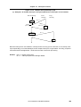
Preface
Readers
This manual has been prepared for engineers who want to understand the
functions of the µPD780948 Subseries and design and develop its
application systems and programs.
µPD780948 Subseries:
µPD780948(A), µPD780948(A1), µPD78F0948
Purpose
This manual is intended for users to understand the functions of the
µPD780948 Subseries.
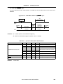
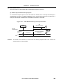
Organization
The µPD780948 subseries manual is separated into two parts: this manual
and the instruction edition (common to the 78K/0 series).
µPD780948
Subseries
This Manual
•
•
•
•
Pin functions
Internal block functions
Interrupt
Other on-chip peripheral functions
78K/0 series
User’s Manual
Instruction
• CPU functions
• Instruction set
• Explanation of each instruction
How to Read This Manual
Before reading this manual, you should have general knowledge of electric
and logic circuits and microcontrollers.
• When you want to use this manual as the manual for (A) products and (A1) products:
→ Only the quality grade differs between (A) and (A1) products.
Read the part number as follows:
µPD780948 → µPD780948(A), µPD780948(A1)
• When you want to understand the function in general:
→ Read this manual in the order of the contents.
• How to interpret the register format:
→ For the bit number enclosed in square, the bit name is defined as a reserved word in RA78K/0,
and in CC78K/0 and defined in the header file of hte IAR compiler.
• To make sure the details of the registers when you know the register name.
→ Refer to Appendix C.
Related Documents
The related documents indicated in this publication may include preliminary
versions. However, preliminary versions are not marked as such.
User’s Manual U12670EE3V0UD00
5
Preface
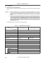
• Related documents for µPD780948 Subseries
Document No.
Document name
Japanese
English
µPD780948 Subseries User’s Manual
Planned
This manual
78K/0 Series User’s Manual-Instruction
IEU-849
U12326E
78K/0 Series Instruction Table
U10903J
-
78K/0 Series Instruction Set
U10904J
-
• Related documents for development tools (User's Manuals)
Document No.
Document name
Japanese
Operation
EEU-809
EEU-1399
Language
EEU-815
EEU-1404
EEU-817
EEU-1402
Operation
EEU-656
EEU-1280
Language
EEU-655
EEU-1284
Operation
U11517J
-
Language
U11518J
-
Programming Note
EEA-618
EEA-1208
CC78K Series Library Source File
EEU-777
-
IE-78K0-NS-A
U14889J
U14889E
IE-78K0-NS-P04
Planned
IE-780948-NS-EM4
U14514J
NP-100GF-TQ
-
-
RA78K Series Assembler Package
RA78K Series Structured Assembler Preprocessor
CC78K Series C Compiler
CC78K/0 C Compiler
CC78K/0 C Compiler Application Note
6
English
U14515E
SM78K0 System Simulator Windows™ Base
Reference
U15373J
U15373E
SM78K0 Series System Simulator
External part user
open Interface
U15802J
U15802E
ID78K0-NS Integrated Debugger Windows
Base
Guide
U15185J
U15185E
User’s Manual U12670EE3V0UD00
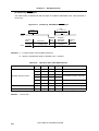
Preface
• Related documents for embedded software (User’s Manual)
Document name
78K/0 Series Real-Time OS
78K/0 Series OS MX78K0
Document No.
Japanese
English
Basics
U11537J
-
Installation
U11536J
-
Technical
U11538J
-
Basics
EEU-5010
-
EEU-829
EEU1438
Fuzzy Knowledge Data Creation Tool
78K/0, 78K/II, 87AD Series Fuzzy Inference Development Support SysEEU-862
tem-Translator
EEU-1444
78K/0 Series Fuzzy Inference Development Support System- Fuzzy
Inference Module
EEU-858
EEU-1441
78K/0 Series Fuzzy Inference Development Support System- Fuzzy
Inference Debugger
EEU-921
EEU-1458
• Other Documents
Document name
Document No.
Japanese
English
IC Package Manual
C10943X
-
Semiconductor Device Mounting Technology Manual
C10535J
C10535E
Quality Grade on NEC Semiconductor Devices
C11531J
C11531E
Reliability Quality Control on NEC Semiconductor Devices
C10983J
C10983E
Electric Static Discharge (ESD) Test
MEM-539
-
Semiconductor Devices Quality Assurance Guide
MEI-603
MEI-1202
Microcontroller Related Product Guide - Third Party Manufacturers
U11416J
-
Caution:
The above documents are subject to change without prior notice. Be sure to use the
latest version document when starting design.
User’s Manual U12670EE3V0UD00
7
Preface
Legend
Symbols and notation are used as follows:
Weight in data notation : Left is high-order column, right is low order column
Active low notation
: xxx (pin or signal name is over-scored) or
/xxx (slash before signal name)
Memory map address: : High order at high stage and low order at low stage
Note
: Explanation of (Note) in the text
Caution
: Item deserving extra attention
Remark
: Supplementary explanation to the text
Numeric notation
: Binary . . . XXXX or XXXB
Decimal . . . XXXX
Hexadecimal . . . XXXXH or 0x XXXX
Prefixes representing powers of 2 (address space, memory capacity)
K (kilo) : 210 = 1024
M (mega) : 220 = 10242 = 1,048,576
G (giga) : 230 = 10243 = 1,073,741,824
8
User’s Manual U12670EE3V0UD00
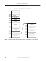
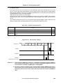
Table of Contents
Preface . . . . . . . . . . . . . . . . . . . . . . . . . . . . . . . . . . . . . . . . . . . . . . . . . . . . . . . 5
Chapter 1
Outline (µPD780948 Subseries) . . . . . . . . . . . . . . . . . . . . . . . . . . . . . . . . . . 27
1.1
1.2
1.3
1.4
1.5
1.6
1.7
1.8
1.9
1.10
Features . . . . . . . . . . . . . . . . . . . . . . . . . . . . . . . . . . . . . . . . . . . . . . . . . . . . . . . . . . . . . 27
Application . . . . . . . . . . . . . . . . . . . . . . . . . . . . . . . . . . . . . . . . . . . . . . . . . . . . . . . . . . . 27
Ordering Information . . . . . . . . . . . . . . . . . . . . . . . . . . . . . . . . . . . . . . . . . . . . . . . . . . . 28
Quality Grade . . . . . . . . . . . . . . . . . . . . . . . . . . . . . . . . . . . . . . . . . . . . . . . . . . . . . . . . . 28
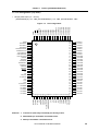
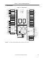
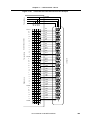
Pin Configuration (Top View) . . . . . . . . . . . . . . . . . . . . . . . . . . . . . . . . . . . . . . . . . . . . 29
78K/0 Series Expansion . . . . . . . . . . . . . . . . . . . . . . . . . . . . . . . . . . . . . . . . . . . . . . . . 31
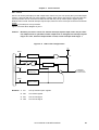
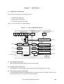
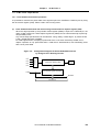
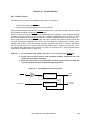
Block Diagram . . . . . . . . . . . . . . . . . . . . . . . . . . . . . . . . . . . . . . . . . . . . . . . . . . . . . . . . 33
Overview of Functions . . . . . . . . . . . . . . . . . . . . . . . . . . . . . . . . . . . . . . . . . . . . . . . . . 34
Mask Option . . . . . . . . . . . . . . . . . . . . . . . . . . . . . . . . . . . . . . . . . . . . . . . . . . . . . . . . . . 35
Differences between Flash and Mask ROM version . . . . . . . . . . . . . . . . . . . . . . . . . . 35
Chapter 2
Pin Function (µPD780948 Subseries) . . . . . . . . . . . . . . . . . . . . . . . . . . . . . . 37
2.1
2.2
2.3
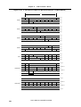
Pin Function List . . . . . . . . . . . . . . . . . . . . . . . . . . . . . . . . . . . . . . . . . . . . . . . . . . . . . . 37
Non-Port Pins . . . . . . . . . . . . . . . . . . . . . . . . . . . . . . . . . . . . . . . . . . . . . . . . . . . . . . . . . 39
Description of Pin Functions . . . . . . . . . . . . . . . . . . . . . . . . . . . . . . . . . . . . . . . . . . . . 41
2.3.1
P00 to P07 (Port 0) . . . . . . . . . . . . . . . . . . . . . . . . . . . . . . . . . . . . . . . . . . . . . . . 41
2.3.2
P10 to P17 (Port 1) . . . . . . . . . . . . . . . . . . . . . . . . . . . . . . . . . . . . . . . . . . . . . . . 42
2.3.3
P20 to P26 (Port 2) . . . . . . . . . . . . . . . . . . . . . . . . . . . . . . . . . . . . . . . . . . . . . . . 42
2.3.4
P30 to P34 (Port 3) . . . . . . . . . . . . . . . . . . . . . . . . . . . . . . . . . . . . . . . . . . . . . . . 43
2.3.5
P40 to P47 (Port 4) . . . . . . . . . . . . . . . . . . . . . . . . . . . . . . . . . . . . . . . . . . . . . . . 43
2.3.6
P50 to P57 (Port 5) . . . . . . . . . . . . . . . . . . . . . . . . . . . . . . . . . . . . . . . . . . . . . . . 44
2.3.7
P64, P65 and P67 (Port 6) . . . . . . . . . . . . . . . . . . . . . . . . . . . . . . . . . . . . . . . . . 44
2.3.8
P70 to P77 (Port 7) . . . . . . . . . . . . . . . . . . . . . . . . . . . . . . . . . . . . . . . . . . . . . . . 44
2.3.9
P120 to P127 (Port 12) . . . . . . . . . . . . . . . . . . . . . . . . . . . . . . . . . . . . . . . . . . . . 45
2.3.10
P130 to P137 (Port 13) . . . . . . . . . . . . . . . . . . . . . . . . . . . . . . . . . . . . . . . . . . . . 45
2.3.11
P140 to P147 (Port 14) . . . . . . . . . . . . . . . . . . . . . . . . . . . . . . . . . . . . . . . . . . . . 45
2.3.12
CTXD . . . . . . . . . . . . . . . . . . . . . . . . . . . . . . . . . . . . . . . . . . . . . . . . . . . . . . . . . 46
2.3.13
CRXD . . . . . . . . . . . . . . . . . . . . . . . . . . . . . . . . . . . . . . . . . . . . . . . . . . . . . . . . . 46
2.3.14
COM0 to COM3 . . . . . . . . . . . . . . . . . . . . . . . . . . . . . . . . . . . . . . . . . . . . . . . . . 46
2.3.15
VLC0 to VLC2 . . . . . . . . . . . . . . . . . . . . . . . . . . . . . . . . . . . . . . . . . . . . . . . . . . . . 46
2.3.16
AVDD/AVREF . . . . . . . . . . . . . . . . . . . . . . . . . . . . . . . . . . . . . . . . . . . . . . . . . . . . 46
2.3.17
AVSS . . . . . . . . . . . . . . . . . . . . . . . . . . . . . . . . . . . . . . . . . . . . . . . . . . . . . . . . . . 46
2.3.18
RESET . . . . . . . . . . . . . . . . . . . . . . . . . . . . . . . . . . . . . . . . . . . . . . . . . . . . . . . . 46
2.3.19
X1 and X2 . . . . . . . . . . . . . . . . . . . . . . . . . . . . . . . . . . . . . . . . . . . . . . . . . . . . . . 46
2.3.20
CL1 and CL2. . . . . . . . . . . . . . . . . . . . . . . . . . . . . . . . . . . . . . . . . . . . . . . . . . . . 46
2.3.21
VDD . . . . . . . . . . . . . . . . . . . . . . . . . . . . . . . . . . . . . . . . . . . . . . . . . . . . . . . . . . . 46
2.3.22
VSS . . . . . . . . . . . . . . . . . . . . . . . . . . . . . . . . . . . . . . . . . . . . . . . . . . . . . . . . . . . 47
2.3.23
VPP (µPD78F0948 only) . . . . . . . . . . . . . . . . . . . . . . . . . . . . . . . . . . . . . . . . . . . 47
2.3.24
IC (Mask ROM version only). . . . . . . . . . . . . . . . . . . . . . . . . . . . . . . . . . . . . . . . 47
2.4
Pin I/O Circuits and Recommended Connection of Unused Pins . . . . . . . . . . . . . . . 48
Chapter 3
CPU Architecture . . . . . . . . . . . . . . . . . . . . . . . . . . . . . . . . . . . . . . . . . . . . . . 55
3.1
Memory Space . . . . . . . . . . . . . . . . . . . . . . . . . . . . . . . . . . . . . . . . . . . . . . . . . . . . . . . . 55
3.1.1
Internal program memory space. . . . . . . . . . . . . . . . . . . . . . . . . . . . . . . . . . . . . 57
3.1.2
Internal data memory space . . . . . . . . . . . . . . . . . . . . . . . . . . . . . . . . . . . . . . . . 59
3.1.3
Special function register (SFR) area. . . . . . . . . . . . . . . . . . . . . . . . . . . . . . . . . . 59
3.1.4
External memory space . . . . . . . . . . . . . . . . . . . . . . . . . . . . . . . . . . . . . . . . . . . 59
3.1.5
Data memory addressing . . . . . . . . . . . . . . . . . . . . . . . . . . . . . . . . . . . . . . . . . . 60
3.2
Processor Registers . . . . . . . . . . . . . . . . . . . . . . . . . . . . . . . . . . . . . . . . . . . . . . . . . . . 62
3.2.1
Control registers . . . . . . . . . . . . . . . . . . . . . . . . . . . . . . . . . . . . . . . . . . . . . . . . . 62
3.2.2
General registers . . . . . . . . . . . . . . . . . . . . . . . . . . . . . . . . . . . . . . . . . . . . . . . . 65
3.2.3
Special function register (SFR). . . . . . . . . . . . . . . . . . . . . . . . . . . . . . . . . . . . . . 66
User’s Manual U12670EE3V0UD00
9
3.3
Instruction Address Addressing . . . . . . . . . . . . . . . . . . . . . . . . . . . . . . . . . . . . . . . . . 70
3.3.1
Relative addressing . . . . . . . . . . . . . . . . . . . . . . . . . . . . . . . . . . . . . . . . . . . . . . 70
3.3.2
Immediate addressing . . . . . . . . . . . . . . . . . . . . . . . . . . . . . . . . . . . . . . . . . . . . 71
3.3.3
Table indirect addressing . . . . . . . . . . . . . . . . . . . . . . . . . . . . . . . . . . . . . . . . . . 72
3.3.4
Register addressing . . . . . . . . . . . . . . . . . . . . . . . . . . . . . . . . . . . . . . . . . . . . . . 73
3.4
Operand Address Addressing . . . . . . . . . . . . . . . . . . . . . . . . . . . . . . . . . . . . . . . . . . . 74
3.4.1
Implied addressing . . . . . . . . . . . . . . . . . . . . . . . . . . . . . . . . . . . . . . . . . . . . . . . 74
3.4.2
Register addressing . . . . . . . . . . . . . . . . . . . . . . . . . . . . . . . . . . . . . . . . . . . . . . 75
3.4.3
Direct addressing . . . . . . . . . . . . . . . . . . . . . . . . . . . . . . . . . . . . . . . . . . . . . . . . 76
3.4.4
Short direct addressing. . . . . . . . . . . . . . . . . . . . . . . . . . . . . . . . . . . . . . . . . . . . 77
3.4.5
Special function register (SFR) addressing . . . . . . . . . . . . . . . . . . . . . . . . . . . . 78
3.4.6
Register indirect addressing . . . . . . . . . . . . . . . . . . . . . . . . . . . . . . . . . . . . . . . . 79
3.4.7
Based addressing . . . . . . . . . . . . . . . . . . . . . . . . . . . . . . . . . . . . . . . . . . . . . . . . 80
3.4.8
Based indexed addressing . . . . . . . . . . . . . . . . . . . . . . . . . . . . . . . . . . . . . . . . . 81
3.4.9
Stack addressing . . . . . . . . . . . . . . . . . . . . . . . . . . . . . . . . . . . . . . . . . . . . . . . . 82
Chapter 4
Port Functions . . . . . . . . . . . . . . . . . . . . . . . . . . . . . . . . . . . . . . . . . . . . . . . . 83
4.1
4.2
Port Functions . . . . . . . . . . . . . . . . . . . . . . . . . . . . . . . . . . . . . . . . . . . . . . . . . . . . . . . . 83
Port Configuration . . . . . . . . . . . . . . . . . . . . . . . . . . . . . . . . . . . . . . . . . . . . . . . . . . . . . 86
4.2.1
Port 0 . . . . . . . . . . . . . . . . . . . . . . . . . . . . . . . . . . . . . . . . . . . . . . . . . . . . . . . . . 87
4.2.2
Port 1 . . . . . . . . . . . . . . . . . . . . . . . . . . . . . . . . . . . . . . . . . . . . . . . . . . . . . . . . . 88
4.2.3
Port 2 . . . . . . . . . . . . . . . . . . . . . . . . . . . . . . . . . . . . . . . . . . . . . . . . . . . . . . . . . 89
4.2.4
Port 3 . . . . . . . . . . . . . . . . . . . . . . . . . . . . . . . . . . . . . . . . . . . . . . . . . . . . . . . . . 90
4.2.5
Port 4 . . . . . . . . . . . . . . . . . . . . . . . . . . . . . . . . . . . . . . . . . . . . . . . . . . . . . . . . . 91
4.2.6
Port 5 . . . . . . . . . . . . . . . . . . . . . . . . . . . . . . . . . . . . . . . . . . . . . . . . . . . . . . . . . 92
4.2.7
Port 6 . . . . . . . . . . . . . . . . . . . . . . . . . . . . . . . . . . . . . . . . . . . . . . . . . . . . . . . . . 93
4.2.8
Port 7 . . . . . . . . . . . . . . . . . . . . . . . . . . . . . . . . . . . . . . . . . . . . . . . . . . . . . . . . . 94
4.2.9
Port 12 . . . . . . . . . . . . . . . . . . . . . . . . . . . . . . . . . . . . . . . . . . . . . . . . . . . . . . . . 95
4.2.10
Port 13 . . . . . . . . . . . . . . . . . . . . . . . . . . . . . . . . . . . . . . . . . . . . . . . . . . . . . . . . 96
4.2.11
Port 14 . . . . . . . . . . . . . . . . . . . . . . . . . . . . . . . . . . . . . . . . . . . . . . . . . . . . . . . . 97
4.3
Port Function Control Registers. . . . . . . . . . . . . . . . . . . . . . . . . . . . . . . . . . . . . . . . . . 98
4.4
Port Function Operations . . . . . . . . . . . . . . . . . . . . . . . . . . . . . . . . . . . . . . . . . . . . . . 103
4.4.1
Writing to input/output port . . . . . . . . . . . . . . . . . . . . . . . . . . . . . . . . . . . . . . . . 103
4.4.2
Reading from input/output port . . . . . . . . . . . . . . . . . . . . . . . . . . . . . . . . . . . . . 103
4.4.3
Operations on input/output port . . . . . . . . . . . . . . . . . . . . . . . . . . . . . . . . . . . . 104
Chapter 5
Clock Generator . . . . . . . . . . . . . . . . . . . . . . . . . . . . . . . . . . . . . . . . . . . . . . 105
5.1
5.2
5.3
5.4
Clock Generator Functions . . . . . . . . . . . . . . . . . . . . . . . . . . . . . . . . . . . . . . . . . . . . . 105
Clock Generator Configuration. . . . . . . . . . . . . . . . . . . . . . . . . . . . . . . . . . . . . . . . . . 106
Clock Generator Control Register . . . . . . . . . . . . . . . . . . . . . . . . . . . . . . . . . . . . . . . 107
System Clock Oscillator . . . . . . . . . . . . . . . . . . . . . . . . . . . . . . . . . . . . . . . . . . . . . . . 109
5.4.1
Main system clock oscillator . . . . . . . . . . . . . . . . . . . . . . . . . . . . . . . . . . . . . . . 109
5.4.2
Subsystem clock oscillator . . . . . . . . . . . . . . . . . . . . . . . . . . . . . . . . . . . . . . . . 110
5.4.3
When no subsystem clock is used . . . . . . . . . . . . . . . . . . . . . . . . . . . . . . . . . . 114
5.5
Clock Generator Operations . . . . . . . . . . . . . . . . . . . . . . . . . . . . . . . . . . . . . . . . . . . . 115
5.5.1
Main system clock operations. . . . . . . . . . . . . . . . . . . . . . . . . . . . . . . . . . . . . . 116
5.5.2
Subsystem clock operations . . . . . . . . . . . . . . . . . . . . . . . . . . . . . . . . . . . . . . . 116
5.6
Changing System Clock and CPU Clock Settings . . . . . . . . . . . . . . . . . . . . . . . . . . 117
5.6.1
Time required for switchover between system clock and CPU clock . . . . . . . . 117
5.6.2
System clock and CPU clock switching procedure . . . . . . . . . . . . . . . . . . . . . . 118
Chapter 6
6.1
6.2
6.3
6.4
10
16-Bit Timer / Event Counter 0 . . . . . . . . . . . . . . . . . . . . . . . . . . . . . . . . . . 119
16-bit Timer/Event Counter 0 Function . . . . . . . . . . . . . . . . . . . . . . . . . . . . . . . . . . . 119
16-bit Timer/Event Counter 0 Configuration . . . . . . . . . . . . . . . . . . . . . . . . . . . . . . . 120
16-Bit Timer/Event Counter 0 Control Register. . . . . . . . . . . . . . . . . . . . . . . . . . . . . 124
16-Bit Timer/Event Counter 0 Operations . . . . . . . . . . . . . . . . . . . . . . . . . . . . . . . . . 130
6.4.1
Operation as interval timer (16 bits) . . . . . . . . . . . . . . . . . . . . . . . . . . . . . . . . . 130
6.4.2
PPG output operation . . . . . . . . . . . . . . . . . . . . . . . . . . . . . . . . . . . . . . . . . . . . 132
User’s Manual U12670EE3V0UD00
6.4.3
Pulse width measurement . . . . . . . . . . . . . . . . . . . . . . . . . . . . . . . . . . . . . . . . 133
6.4.4
Operation as external event counter. . . . . . . . . . . . . . . . . . . . . . . . . . . . . . . . . 141
6.4.5
Operation to output square wave . . . . . . . . . . . . . . . . . . . . . . . . . . . . . . . . . . . 143
6.5
16-Bit Timer/Event Counter 0 Operating Precautions . . . . . . . . . . . . . . . . . . . . . . . 145
Chapter 7
16-Bit Timer 2 . . . . . . . . . . . . . . . . . . . . . . . . . . . . . . . . . . . . . . . . . . . . . . . . 149
7.1
7.2
7.3
7.4
16-Bit Timer 2 Functions . . . . . . . . . . . . . . . . . . . . . . . . . . . . . . . . . . . . . . . . . . . . . . . 149
16-Bit Timer 2 Configuration. . . . . . . . . . . . . . . . . . . . . . . . . . . . . . . . . . . . . . . . . . . . 150
16-Bit Timer 2 Control Registers . . . . . . . . . . . . . . . . . . . . . . . . . . . . . . . . . . . . . . . . 152
16-Bit Timer 2 Operations . . . . . . . . . . . . . . . . . . . . . . . . . . . . . . . . . . . . . . . . . . . . . . 155
7.4.1
Pulse width measurement operations. . . . . . . . . . . . . . . . . . . . . . . . . . . . . . . . 155
7.5
16-Bit Timer 2 Precautions . . . . . . . . . . . . . . . . . . . . . . . . . . . . . . . . . . . . . . . . . . . . . 159
Chapter 8
8-Bit Timer/Event Counters 50 and 51 . . . . . . . . . . . . . . . . . . . . . . . . . . . . 161
8.1
8.2
8.3
8.4
8-Bit Timer/Event Counters 50 and 51 Functions . . . . . . . . . . . . . . . . . . . . . . . . . . . 161
8-Bit Timer/Event Counters 50 and 51 Configurations. . . . . . . . . . . . . . . . . . . . . . . 163
8-Bit Timer/Event Counters 50 and 51 Control Registers . . . . . . . . . . . . . . . . . . . . 166
8-Bit Timer/Event Counters 50 and 51 Operations . . . . . . . . . . . . . . . . . . . . . . . . . . 171
8.4.1
Interval timer operations (8-bit timer/event counter mode) . . . . . . . . . . . . . . . . 171
8.4.2
External event counter operation . . . . . . . . . . . . . . . . . . . . . . . . . . . . . . . . . . . 176
8.4.3
Square-wave output . . . . . . . . . . . . . . . . . . . . . . . . . . . . . . . . . . . . . . . . . . . . . 177
8.4.4
PWM output operations . . . . . . . . . . . . . . . . . . . . . . . . . . . . . . . . . . . . . . . . . . 179
8.5
Cautions on 8-Bit Timer/Event Counters 50 and 51 . . . . . . . . . . . . . . . . . . . . . . . . . 182
Chapter 9
9.1
9.2
9.3
9.4
Watch Timer . . . . . . . . . . . . . . . . . . . . . . . . . . . . . . . . . . . . . . . . . . . . . . . . . 185
Watch Timer Functions . . . . . . . . . . . . . . . . . . . . . . . . . . . . . . . . . . . . . . . . . . . . . . . . 185
Watch Timer Configuration . . . . . . . . . . . . . . . . . . . . . . . . . . . . . . . . . . . . . . . . . . . . . 186
Watch Timer Mode Register (WTM) . . . . . . . . . . . . . . . . . . . . . . . . . . . . . . . . . . . . . . 187
Watch Timer Operations . . . . . . . . . . . . . . . . . . . . . . . . . . . . . . . . . . . . . . . . . . . . . . . 189
9.4.1
Watch timer operation. . . . . . . . . . . . . . . . . . . . . . . . . . . . . . . . . . . . . . . . . . . . 189
9.4.2
Interval timer operation . . . . . . . . . . . . . . . . . . . . . . . . . . . . . . . . . . . . . . . . . . . 189
Chapter 10 Watchdog Timer . . . . . . . . . . . . . . . . . . . . . . . . . . . . . . . . . . . . . . . . . . . . . . 191
10.1
10.2
10.3
10.4
Watchdog Timer Functions. . . . . . . . . . . . . . . . . . . . . . . . . . . . . . . . . . . . . . . . . . . . . 191
Watchdog Timer Configuration . . . . . . . . . . . . . . . . . . . . . . . . . . . . . . . . . . . . . . . . . 193
Watchdog Timer Control Registers . . . . . . . . . . . . . . . . . . . . . . . . . . . . . . . . . . . . . . 194
Watchdog Timer Operations . . . . . . . . . . . . . . . . . . . . . . . . . . . . . . . . . . . . . . . . . . . . 196
10.4.1
Watchdog timer operation. . . . . . . . . . . . . . . . . . . . . . . . . . . . . . . . . . . . . . . . . 196
10.4.2
Interval timer operation . . . . . . . . . . . . . . . . . . . . . . . . . . . . . . . . . . . . . . . . . . . 197
Chapter 11 Clock Output Control Circuit. . . . . . . . . . . . . . . . . . . . . . . . . . . . . . . . . . . . 199
11.1
11.2
11.3
Clock Output Control Circuit Functions . . . . . . . . . . . . . . . . . . . . . . . . . . . . . . . . . . 199
Clock Output Control Circuit Configuration . . . . . . . . . . . . . . . . . . . . . . . . . . . . . . . 200
Clock Output Function Control Registers . . . . . . . . . . . . . . . . . . . . . . . . . . . . . . . . . 201
Chapter 12 A/D Converter . . . . . . . . . . . . . . . . . . . . . . . . . . . . . . . . . . . . . . . . . . . . . . . . 203
12.1
12.2
12.3
12.4
A/D Converter Functions. . . . . . . . . . . . . . . . . . . . . . . . . . . . . . . . . . . . . . . . . . . . . . . 203
A/D Converter Configuration . . . . . . . . . . . . . . . . . . . . . . . . . . . . . . . . . . . . . . . . . . . 204
A/D Converter Control Registers . . . . . . . . . . . . . . . . . . . . . . . . . . . . . . . . . . . . . . . . 206
A/D Converter Operations . . . . . . . . . . . . . . . . . . . . . . . . . . . . . . . . . . . . . . . . . . . . . . 209
12.4.1
Basic Operations of A/D Converter. . . . . . . . . . . . . . . . . . . . . . . . . . . . . . . . . . 209
12.4.2
Input voltage and conversion results . . . . . . . . . . . . . . . . . . . . . . . . . . . . . . . . 211
12.4.3
A/D converter operation mode . . . . . . . . . . . . . . . . . . . . . . . . . . . . . . . . . . . . . 213
12.5 A/D Converter Precautions . . . . . . . . . . . . . . . . . . . . . . . . . . . . . . . . . . . . . . . . . . . . . 215
12.6 Cautions on Emulation . . . . . . . . . . . . . . . . . . . . . . . . . . . . . . . . . . . . . . . . . . . . . . . . 218
12.6.1
D/A converter mode register (DAM0) . . . . . . . . . . . . . . . . . . . . . . . . . . . . . . . . 218
User’s Manual U12670EE3V0UD00
11
Chapter 13 Serial Interface Channel 30 . . . . . . . . . . . . . . . . . . . . . . . . . . . . . . . . . . . . . 219
13.1
13.2
13.3
13.4
13.5
Serial Interface Channel 30 Functions . . . . . . . . . . . . . . . . . . . . . . . . . . . . . . . . . . . . 219
Serial Interface Channel 30 Configuration. . . . . . . . . . . . . . . . . . . . . . . . . . . . . . . . . 220
List of SFRs (Special Function Registers). . . . . . . . . . . . . . . . . . . . . . . . . . . . . . . . . 220
Serial Interface Control Register . . . . . . . . . . . . . . . . . . . . . . . . . . . . . . . . . . . . . . . . 221
Serial Interface Operations . . . . . . . . . . . . . . . . . . . . . . . . . . . . . . . . . . . . . . . . . . . . . 222
13.5.1
Operation stop mode . . . . . . . . . . . . . . . . . . . . . . . . . . . . . . . . . . . . . . . . . . . . 222
13.5.2
Three-wire serial I/O mode . . . . . . . . . . . . . . . . . . . . . . . . . . . . . . . . . . . . . . . . 223
Chapter 14 Serial Interface Channel 31 . . . . . . . . . . . . . . . . . . . . . . . . . . . . . . . . . . . . . 225
14.1
14.2
14.3
14.4
14.5
Serial Interface Channel 31 Functions . . . . . . . . . . . . . . . . . . . . . . . . . . . . . . . . . . . . 225
Serial Interface Channel 31 Configuration. . . . . . . . . . . . . . . . . . . . . . . . . . . . . . . . . 226
List of SFRs (Special Function Registers). . . . . . . . . . . . . . . . . . . . . . . . . . . . . . . . . 226
Serial Interface Control Registers . . . . . . . . . . . . . . . . . . . . . . . . . . . . . . . . . . . . . . . 227
Serial Interface Channel 31 Operations . . . . . . . . . . . . . . . . . . . . . . . . . . . . . . . . . . . 228
14.5.1
Operation stop mode . . . . . . . . . . . . . . . . . . . . . . . . . . . . . . . . . . . . . . . . . . . . 228
14.5.2
Two-wire serial I/O mode . . . . . . . . . . . . . . . . . . . . . . . . . . . . . . . . . . . . . . . . . 229
Chapter 15 Serial Interface UART. . . . . . . . . . . . . . . . . . . . . . . . . . . . . . . . . . . . . . . . . . 233
15.1
15.2
15.3
15.4
15.5
Serial Interface UART Functions . . . . . . . . . . . . . . . . . . . . . . . . . . . . . . . . . . . . . . . . 233
Serial Interface UART Configuration . . . . . . . . . . . . . . . . . . . . . . . . . . . . . . . . . . . . . 234
List of SFRS (Special Function Registers) . . . . . . . . . . . . . . . . . . . . . . . . . . . . . . . . 235
Serial Interface Control Registers . . . . . . . . . . . . . . . . . . . . . . . . . . . . . . . . . . . . . . . 236
Serial Interface Operations . . . . . . . . . . . . . . . . . . . . . . . . . . . . . . . . . . . . . . . . . . . . . 241
15.5.1
Operation stop mode . . . . . . . . . . . . . . . . . . . . . . . . . . . . . . . . . . . . . . . . . . . . 241
15.5.2
Asynchronous serial interface (UART) mode . . . . . . . . . . . . . . . . . . . . . . . . . . 242
15.6 Standby Function. . . . . . . . . . . . . . . . . . . . . . . . . . . . . . . . . . . . . . . . . . . . . . . . . . . . . 254
Chapter 16 CAN Controller . . . . . . . . . . . . . . . . . . . . . . . . . . . . . . . . . . . . . . . . . . . . . . . 255
16.1
CAN Protocol . . . . . . . . . . . . . . . . . . . . . . . . . . . . . . . . . . . . . . . . . . . . . . . . . . . . . . . . 256
16.1.1
Protocol Mode Function . . . . . . . . . . . . . . . . . . . . . . . . . . . . . . . . . . . . . . . . . . 256
16.1.2
Message Format. . . . . . . . . . . . . . . . . . . . . . . . . . . . . . . . . . . . . . . . . . . . . . . . 256
16.1.3
Data Frame / Remote Frame . . . . . . . . . . . . . . . . . . . . . . . . . . . . . . . . . . . . . . 257
16.1.4
Description of each field . . . . . . . . . . . . . . . . . . . . . . . . . . . . . . . . . . . . . . . . . . 258
16.1.5
Error Frame . . . . . . . . . . . . . . . . . . . . . . . . . . . . . . . . . . . . . . . . . . . . . . . . . . . 264
16.1.6
Overload Frame . . . . . . . . . . . . . . . . . . . . . . . . . . . . . . . . . . . . . . . . . . . . . . . . 265
16.2 Function . . . . . . . . . . . . . . . . . . . . . . . . . . . . . . . . . . . . . . . . . . . . . . . . . . . . . . . . . . . . 266
16.2.1
Arbitration . . . . . . . . . . . . . . . . . . . . . . . . . . . . . . . . . . . . . . . . . . . . . . . . . . . . . 266
16.2.2
Bit Stuffing . . . . . . . . . . . . . . . . . . . . . . . . . . . . . . . . . . . . . . . . . . . . . . . . . . . . 266
16.2.3
Multi Master . . . . . . . . . . . . . . . . . . . . . . . . . . . . . . . . . . . . . . . . . . . . . . . . . . . 267
16.2.4
Multi Cast . . . . . . . . . . . . . . . . . . . . . . . . . . . . . . . . . . . . . . . . . . . . . . . . . . . . . 267
16.2.5
Sleep Mode/Stop Function . . . . . . . . . . . . . . . . . . . . . . . . . . . . . . . . . . . . . . . . 267
16.2.6
Error Control Function . . . . . . . . . . . . . . . . . . . . . . . . . . . . . . . . . . . . . . . . . . . 268
16.2.7
Baud Rate Control Function . . . . . . . . . . . . . . . . . . . . . . . . . . . . . . . . . . . . . . . 271
16.2.8
State Shift Chart . . . . . . . . . . . . . . . . . . . . . . . . . . . . . . . . . . . . . . . . . . . . . . . . 274
16.3 Outline Description . . . . . . . . . . . . . . . . . . . . . . . . . . . . . . . . . . . . . . . . . . . . . . . . . . . 277
16.4 Connection with Target System . . . . . . . . . . . . . . . . . . . . . . . . . . . . . . . . . . . . . . . . . 278
16.5 CAN Controller Configuration. . . . . . . . . . . . . . . . . . . . . . . . . . . . . . . . . . . . . . . . . . . 278
16.6 Special Function Register for CAN-module . . . . . . . . . . . . . . . . . . . . . . . . . . . . . . . 279
16.7 Message and Buffer Configuration . . . . . . . . . . . . . . . . . . . . . . . . . . . . . . . . . . . . . . 280
16.8 Transmit Buffer Structure . . . . . . . . . . . . . . . . . . . . . . . . . . . . . . . . . . . . . . . . . . . . . 281
16.9 Transmit Message Format. . . . . . . . . . . . . . . . . . . . . . . . . . . . . . . . . . . . . . . . . . . . . . 281
16.10 Receive Buffer Structure . . . . . . . . . . . . . . . . . . . . . . . . . . . . . . . . . . . . . . . . . . . . . . . 285
16.11 Receive Message Format . . . . . . . . . . . . . . . . . . . . . . . . . . . . . . . . . . . . . . . . . . . . . . 286
16.12 Mask Function . . . . . . . . . . . . . . . . . . . . . . . . . . . . . . . . . . . . . . . . . . . . . . . . . . . . . . . 292
16.13 Operation of the CAN Controller . . . . . . . . . . . . . . . . . . . . . . . . . . . . . . . . . . . . . . . . 296
16.13.1 CAN control register (CANC) . . . . . . . . . . . . . . . . . . . . . . . . . . . . . . . . . . . . . . 296
16.13.2 DCAN Error Status Register . . . . . . . . . . . . . . . . . . . . . . . . . . . . . . . . . . . . . . . 300
12
User’s Manual U12670EE3V0UD00
16.13.3 CAN Transmit Error Counter . . . . . . . . . . . . . . . . . . . . . . . . . . . . . . . . . . . . . . 303
16.13.4 CAN Receive Error Counter . . . . . . . . . . . . . . . . . . . . . . . . . . . . . . . . . . . . . . . 303
16.13.5 Message Count Register . . . . . . . . . . . . . . . . . . . . . . . . . . . . . . . . . . . . . . . . . 304
16.14 Baudrate Generation . . . . . . . . . . . . . . . . . . . . . . . . . . . . . . . . . . . . . . . . . . . . . . . . . . 306
16.15 Function Control . . . . . . . . . . . . . . . . . . . . . . . . . . . . . . . . . . . . . . . . . . . . . . . . . . . . . 312
16.15.1 Transmit Control . . . . . . . . . . . . . . . . . . . . . . . . . . . . . . . . . . . . . . . . . . . . . . . . 312
16.15.2 Receive Control . . . . . . . . . . . . . . . . . . . . . . . . . . . . . . . . . . . . . . . . . . . . . . . . 314
16.15.3 Mask Control. . . . . . . . . . . . . . . . . . . . . . . . . . . . . . . . . . . . . . . . . . . . . . . . . . . 315
16.15.4 Special Functions . . . . . . . . . . . . . . . . . . . . . . . . . . . . . . . . . . . . . . . . . . . . . . . 317
16.16 Interrupt Information . . . . . . . . . . . . . . . . . . . . . . . . . . . . . . . . . . . . . . . . . . . . . . . . . . 319
16.16.1 Interrupt Vectors . . . . . . . . . . . . . . . . . . . . . . . . . . . . . . . . . . . . . . . . . . . . . . . . 319
16.16.2 Transmit Interrupt . . . . . . . . . . . . . . . . . . . . . . . . . . . . . . . . . . . . . . . . . . . . . . . 319
16.16.3 Receive Interrupt . . . . . . . . . . . . . . . . . . . . . . . . . . . . . . . . . . . . . . . . . . . . . . . 319
16.16.4 Error Interrupt . . . . . . . . . . . . . . . . . . . . . . . . . . . . . . . . . . . . . . . . . . . . . . . . . . 320
16.17 Influence of the standby Function of the CAN Controller . . . . . . . . . . . . . . . . . . . . 321
16.17.1 CPU Halt Mode. . . . . . . . . . . . . . . . . . . . . . . . . . . . . . . . . . . . . . . . . . . . . . . . . 321
16.17.2 CPU Stop Mode . . . . . . . . . . . . . . . . . . . . . . . . . . . . . . . . . . . . . . . . . . . . . . . . 321
16.17.3 DCAN Sleep Mode . . . . . . . . . . . . . . . . . . . . . . . . . . . . . . . . . . . . . . . . . . . . . . 321
16.17.4 DCAN Stop Mode . . . . . . . . . . . . . . . . . . . . . . . . . . . . . . . . . . . . . . . . . . . . . . . 323
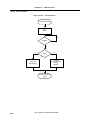
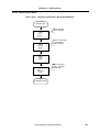
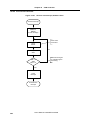
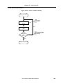
16.18 Functional Description by Flowcharts . . . . . . . . . . . . . . . . . . . . . . . . . . . . . . . . . . . . 324
16.18.1 Initialization . . . . . . . . . . . . . . . . . . . . . . . . . . . . . . . . . . . . . . . . . . . . . . . . . . . . 324
16.18.2 Transmit Preparation . . . . . . . . . . . . . . . . . . . . . . . . . . . . . . . . . . . . . . . . . . . . 325
16.18.3 Abort Transmit . . . . . . . . . . . . . . . . . . . . . . . . . . . . . . . . . . . . . . . . . . . . . . . . . 326
16.18.4 Handling by the DCAN . . . . . . . . . . . . . . . . . . . . . . . . . . . . . . . . . . . . . . . . . . . 327
16.18.5 Receive Event Oriented . . . . . . . . . . . . . . . . . . . . . . . . . . . . . . . . . . . . . . . . . . 328
16.18.6 Receive Task Oriented . . . . . . . . . . . . . . . . . . . . . . . . . . . . . . . . . . . . . . . . . . . 329
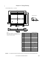
Chapter 17 LCD Controller / Driver. . . . . . . . . . . . . . . . . . . . . . . . . . . . . . . . . . . . . . . . . 331
17.1
17.2
17.3
17.4
17.5
17.6
17.7
17.8
LCD Controller/Driver Functions . . . . . . . . . . . . . . . . . . . . . . . . . . . . . . . . . . . . . . . . 331
LCD Controller/Driver Configuration . . . . . . . . . . . . . . . . . . . . . . . . . . . . . . . . . . . . . 332
LCD Controller/Driver Control Registers . . . . . . . . . . . . . . . . . . . . . . . . . . . . . . . . . . 334
LCD Controller/Driver Settings . . . . . . . . . . . . . . . . . . . . . . . . . . . . . . . . . . . . . . . . . . 335
LCD Display Data Memory . . . . . . . . . . . . . . . . . . . . . . . . . . . . . . . . . . . . . . . . . . . . . 336
Common Signals and Segment Signals . . . . . . . . . . . . . . . . . . . . . . . . . . . . . . . . . . 337
Supplying of LCD Drive Voltages VLC0, VLC1, VLC2 . . . . . . . . . . . . . . . . . . . . . . . . . . . . . . . . .340
Display Modes . . . . . . . . . . . . . . . . . . . . . . . . . . . . . . . . . . . . . . . . . . . . . . . . . . . . . . . 344
17.8.1
Static display example . . . . . . . . . . . . . . . . . . . . . . . . . . . . . . . . . . . . . . . . . . . 344
17.8.2
2-time-division display example . . . . . . . . . . . . . . . . . . . . . . . . . . . . . . . . . . . . 347
17.8.3
3-time-division display example . . . . . . . . . . . . . . . . . . . . . . . . . . . . . . . . . . . . 350
17.8.4
4-time-division display example . . . . . . . . . . . . . . . . . . . . . . . . . . . . . . . . . . . . 354
17.9 Cautions on Emulation . . . . . . . . . . . . . . . . . . . . . . . . . . . . . . . . . . . . . . . . . . . . . . . . 357
17.9.1
LCD timer control register (LCDTM) . . . . . . . . . . . . . . . . . . . . . . . . . . . . . . . . . 357
Chapter 18 Sound Generator . . . . . . . . . . . . . . . . . . . . . . . . . . . . . . . . . . . . . . . . . . . . . 359
18.1
18.2
18.3
18.4
Sound Generator Function . . . . . . . . . . . . . . . . . . . . . . . . . . . . . . . . . . . . . . . . . . . . . 359
Sound Generator Configuration . . . . . . . . . . . . . . . . . . . . . . . . . . . . . . . . . . . . . . . . . 360
Sound Generator Control Registers . . . . . . . . . . . . . . . . . . . . . . . . . . . . . . . . . . . . . 360
Sound Generator Operations . . . . . . . . . . . . . . . . . . . . . . . . . . . . . . . . . . . . . . . . . . . 365
18.4.1
To output basic cycle signal SGOF (without amplitude) . . . . . . . . . . . . . . . . . . 365
18.4.2
To output basic cycle signal SGO (with amplitude) . . . . . . . . . . . . . . . . . . . . . 366
Chapter 19 Interrupt Functions. . . . . . . . . . . . . . . . . . . . . . . . . . . . . . . . . . . . . . . . . . . . 367
19.1
19.2
19.3
19.4
Interrupt Function Types. . . . . . . . . . . . . . . . . . . . . . . . . . . . . . . . . . . . . . . . . . . . . . . 367
Interrupt Sources and Configuration . . . . . . . . . . . . . . . . . . . . . . . . . . . . . . . . . . . . . 368
Interrupt Function Control Registers . . . . . . . . . . . . . . . . . . . . . . . . . . . . . . . . . . . . . 371
Interrupt Servicing Operations . . . . . . . . . . . . . . . . . . . . . . . . . . . . . . . . . . . . . . . . . . 377
19.4.1
Non-maskable interrupt request acknowledge operation . . . . . . . . . . . . . . . . . 377
19.4.2
Maskable interrupt request acknowledge operation . . . . . . . . . . . . . . . . . . . . . 379
User’s Manual U12670EE3V0UD00
13
19.4.3
19.4.4
19.4.5
Software interrupt request acknowledge operation . . . . . . . . . . . . . . . . . . . . . 382
Multiple interrupt servicing . . . . . . . . . . . . . . . . . . . . . . . . . . . . . . . . . . . . . . . . 382
Interrupt request reserve . . . . . . . . . . . . . . . . . . . . . . . . . . . . . . . . . . . . . . . . . 386
Chapter 20 External Device Expansion . . . . . . . . . . . . . . . . . . . . . . . . . . . . . . . . . . . . . 389
20.1
20.2
20.3
20.4
External Device Expansion Functions . . . . . . . . . . . . . . . . . . . . . . . . . . . . . . . . . . . . 389
External Device Expansion Function Control Register . . . . . . . . . . . . . . . . . . . . . . 393
External Device Expansion Function Timing . . . . . . . . . . . . . . . . . . . . . . . . . . . . . . 396
Example of Connection with Memory . . . . . . . . . . . . . . . . . . . . . . . . . . . . . . . . . . . . 401
Chapter 21 Standby Function . . . . . . . . . . . . . . . . . . . . . . . . . . . . . . . . . . . . . . . . . . . . . 403
21.1
Standby Function and Configuration. . . . . . . . . . . . . . . . . . . . . . . . . . . . . . . . . . . . . 403
21.1.1
Standby function . . . . . . . . . . . . . . . . . . . . . . . . . . . . . . . . . . . . . . . . . . . . . . . . 403
21.1.2
Standby function control register . . . . . . . . . . . . . . . . . . . . . . . . . . . . . . . . . . . 404
21.2 Standby Function Operations. . . . . . . . . . . . . . . . . . . . . . . . . . . . . . . . . . . . . . . . . . . 405
21.2.1
HALT mode. . . . . . . . . . . . . . . . . . . . . . . . . . . . . . . . . . . . . . . . . . . . . . . . . . . . 405
21.2.2
STOP mode . . . . . . . . . . . . . . . . . . . . . . . . . . . . . . . . . . . . . . . . . . . . . . . . . . . 408
Chapter 22 Reset Function . . . . . . . . . . . . . . . . . . . . . . . . . . . . . . . . . . . . . . . . . . . . . . . 411
22.1
Reset Function . . . . . . . . . . . . . . . . . . . . . . . . . . . . . . . . . . . . . . . . . . . . . . . . . . . . . . . 411
Chapter 23 µPD78F0948 . . . . . . . . . . . . . . . . . . . . . . . . . . . . . . . . . . . . . . . . . . . . . . . . . 415
23.1
23.2
23.3
Memory Size Switching Register (IMS) . . . . . . . . . . . . . . . . . . . . . . . . . . . . . . . . . . . 416
Internal Expansion RAM Size Switching Register . . . . . . . . . . . . . . . . . . . . . . . . . . 417
Flash memory programming. . . . . . . . . . . . . . . . . . . . . . . . . . . . . . . . . . . . . . . . . . . . 418
23.3.1
Selection of transmission method . . . . . . . . . . . . . . . . . . . . . . . . . . . . . . . . . . . 418
23.3.2
Initialization of the programming mode. . . . . . . . . . . . . . . . . . . . . . . . . . . . . . . 419
23.3.3
Flash memory programming function . . . . . . . . . . . . . . . . . . . . . . . . . . . . . . . . 419
23.3.4
Flash programmer connection . . . . . . . . . . . . . . . . . . . . . . . . . . . . . . . . . . . . . 420
23.3.5
Flash programming precautions . . . . . . . . . . . . . . . . . . . . . . . . . . . . . . . . . . . . 422
Chapter 24 Instruction Set . . . . . . . . . . . . . . . . . . . . . . . . . . . . . . . . . . . . . . . . . . . . . . . 423
24.1
Legends Used in Operation List . . . . . . . . . . . . . . . . . . . . . . . . . . . . . . . . . . . . . . . . . 423
24.1.1
Operand identifiers and description methods . . . . . . . . . . . . . . . . . . . . . . . . . . 423
24.1.2
Description of “operation” column . . . . . . . . . . . . . . . . . . . . . . . . . . . . . . . . . . . 424
24.2 Operation List . . . . . . . . . . . . . . . . . . . . . . . . . . . . . . . . . . . . . . . . . . . . . . . . . . . . . . . 425
24.3 Instructions Listed by Addressing Type . . . . . . . . . . . . . . . . . . . . . . . . . . . . . . . . . . 433
Chapter 25 Electrical Specifications . . . . . . . . . . . . . . . . . . . . . . . . . . . . . . . . . . . . . . . 437
25.1
25.2
25.3
25.4
25.5
25.6
Absolute Maximum Ratings . . . . . . . . . . . . . . . . . . . . . . . . . . . . . . . . . . . . . . . . . . . . 437
Capacitance . . . . . . . . . . . . . . . . . . . . . . . . . . . . . . . . . . . . . . . . . . . . . . . . . . . . . . . . . 440
Main System Clock Oscillation Circuit Characteristics . . . . . . . . . . . . . . . . . . . . . . 442
Subsystem Clock Oscillation Circuit Characteristics . . . . . . . . . . . . . . . . . . . . . . . 448
DC Characteristics . . . . . . . . . . . . . . . . . . . . . . . . . . . . . . . . . . . . . . . . . . . . . . . . . . . . 451
AC Characteristics . . . . . . . . . . . . . . . . . . . . . . . . . . . . . . . . . . . . . . . . . . . . . . . . . . . . 460
25.6.1
Basic Operation . . . . . . . . . . . . . . . . . . . . . . . . . . . . . . . . . . . . . . . . . . . . . . . . 460
25.6.2
Read/Write Operation . . . . . . . . . . . . . . . . . . . . . . . . . . . . . . . . . . . . . . . . . . . . 466
25.6.3
Serial Interface . . . . . . . . . . . . . . . . . . . . . . . . . . . . . . . . . . . . . . . . . . . . . . . . . 472
25.6.4
A/D Converter Characteristics . . . . . . . . . . . . . . . . . . . . . . . . . . . . . . . . . . . . . 479
25.6.5
Data Memory Stop Mode Low Supply Voltage Data Retention Characteristics 481
25.6.6
Flash Memory Programming Characteristics . . . . . . . . . . . . . . . . . . . . . . . . . . 484
Chapter 26 Package Drawing . . . . . . . . . . . . . . . . . . . . . . . . . . . . . . . . . . . . . . . . . . . . . 487
Chapter 27 Recommended Soldering Conditions . . . . . . . . . . . . . . . . . . . . . . . . . . . . 489
Appendix A Development Tools . . . . . . . . . . . . . . . . . . . . . . . . . . . . . . . . . . . . . . . . . . . 491
14
User’s Manual U12670EE3V0UD00
Appendix B Embedded Software . . . . . . . . . . . . . . . . . . . . . . . . . . . . . . . . . . . . . . . . . . . 497
Appendix C Index . . . . . . . . . . . . . . . . . . . . . . . . . . . . . . . . . . . . . . . . . . . . . . . . . . . . . . . 499
Appendix D Revision History . . . . . . . . . . . . . . . . . . . . . . . . . . . . . . . . . . . . . . . . . . . . . . 503
User’s Manual U12670EE3V0UD00
15
16
User’s Manual U12670EE3V0UD00
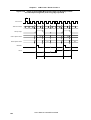
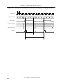
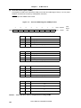
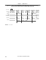
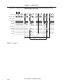
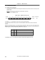
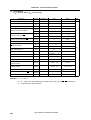
List of Figures
Figure 1-1:
Figure 1-2:
Figure 1-3:
Figure 2-1:
Figure 2-2:
Figure 3-1:
Figure 3-2:
Figure 3-3:
Figure 3-4:
Figure 3-5:
Figure 3-6:
Figure 3-7:
Figure 3-8:
Figure 3-9:
Figure 3-10:
Figure 3-11:
Figure 3-12:
Figure 3-13:
Figure 3-14:
Figure 3-15:
Figure 3-16:
Figure 3-17:
Figure 3-18:
Figure 3-19:
Figure 3-20:
Figure 3-21:
Figure 3-22:
Figure 4-1:
Figure 4-2:
Figure 4-3:
Figure 4-4:
Figure 4-5:
Figure 4-6:
Figure 4-7:
Figure 4-8:
Figure 4-9:
Figure 4-10:
Figure 4-11:
Figure 4-12:
Figure 4-13:
Figure 4-14:
Figure 4-15:
Figure 4-16:
Figure 5-1:
Figure 5-2:
Figure 5-3:
Figure 5-4:
Figure 5-5:
Figure 5-6:
Figure 5-7:
Figure 6-1:
Figure 6-2:
Figure 6-3:
Figure 6-4:
Figure 6-5:
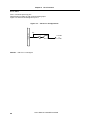
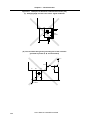
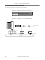
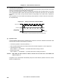
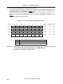
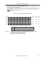
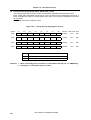
Pin Configuration ......................................................................................................... 29
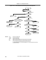
78K/0 Series Expansion .............................................................................................. 31
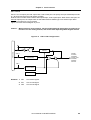
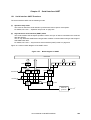
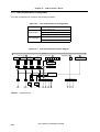
Block Diagram ............................................................................................................. 33
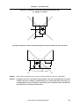
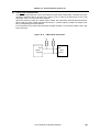
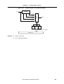
Connection of IC Pins.................................................................................................. 47
Pin Input/Output Circuits (1/3) ..................................................................................... 51
Memory Map of the µPD780948 ................................................................................. 55
Memory Map of the µPD78F0948 ............................................................................... 56
Data Memory Addressing of µPD780948 .................................................................... 60
Data Memory Addressing of µPD78F0948.................................................................. 61
Program Counter Configuration .................................................................................. 62
Program Status Word Configuration ........................................................................... 62
Stack Pointer Configuration......................................................................................... 64
Data to be Saved to Stack Memory............................................................................. 64
Data to be Reset to Stack Memory ............................................................................. 64
General Register Configuration ................................................................................... 65
Relative Addressing .................................................................................................... 70
Immediate Addressing................................................................................................. 71
Table Indirect Addressing............................................................................................ 72
Register Addressing .................................................................................................... 73
Register Addressing .................................................................................................... 75
Direct addressing ........................................................................................................ 76
Short direct addressing ............................................................................................... 77
Special-Function Register (SFR) Addressing.............................................................. 78
Register indirect addressing ........................................................................................ 79
Based addressing description example....................................................................... 80
Based indexed addressing description example ......................................................... 81
Stack addressing description example ........................................................................ 82
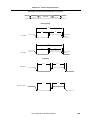
Port Types ................................................................................................................... 83
P00 to P07 Configurations .......................................................................................... 87
P10 to P17 Configurations .......................................................................................... 88
P20 to P26 Configurations .......................................................................................... 89
P30 to P34 Configurations .......................................................................................... 90
P40 to P47 Configurations .......................................................................................... 91
P50 to P57 Configurations .......................................................................................... 92
P64, P65 and P67 Configurations ............................................................................... 93
P70 to P77 Configurations .......................................................................................... 94
P120 to P127 Configurations ...................................................................................... 95
P130 to P137 Configurations ...................................................................................... 96
P140 to P147 Configurations ...................................................................................... 97
Port Mode Register Format ......................................................................................... 99
Pull-Up Resistor Option Register (PU0, PU4, PU7 and PU13) Format..................... 100
Port Function Register (PF2, PF5, PF7, PF12 to PF14) Format ............................... 101
Memory Expansion Mode Register Format ............................................................... 102
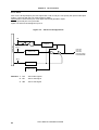
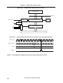
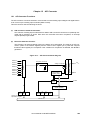
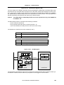
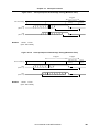
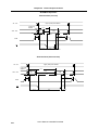
Block Diagram of Clock Generator ............................................................................ 106
Processor Clock Control Register Format (1/2)......................................................... 107
External Circuit of Main System Clock Oscillator ...................................................... 109
External Circuit of Subsystem Clock Oscillator ......................................................... 110
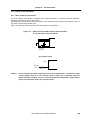
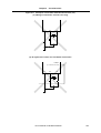
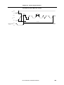
Examples of Oscillator with Bad Connection (1/3) .................................................... 111
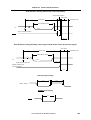
Main System Clock Stop Function ............................................................................ 116
System Clock and CPU Clock Switching................................................................... 118
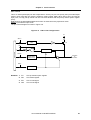
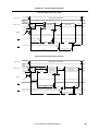
Block Diagram of 16-Bit Timer/Event Counter 0 (TM0) ............................................. 120
Format of 16-Bit Timer Mode Control Register (TMC0) ............................................ 125
Format of Capture/Compare Control Register 0 (CRC0) .......................................... 126
Format of 16-Bit Timer Output Control Register (TOC0)........................................... 127
Format of Prescaler Mode Register 0 (PRM0) .......................................................... 128
User’s Manual U12670EE3V0UD00
17
Figure 6-6:
Figure 6-7:
Figure 6-8:
Figure 6-9:
Figure 6-10:
Figure 6-11:
Figure 6-12:
Figure 6-13:
Figure 6-14:
Figure 6-15:
Figure 6-16:
Figure 6-17:
Figure 6-18:
Figure 6-19:
Figure 6-20:
Figure 6-21:
Figure 6-22:
Figure 6-23:
Figure 6-24:
Figure 6-25:
Figure 6-26:
Figure 6-27:
Figure 6-28:
Figure 6-29:
Figure 7-1:
Figure 7-2:
Figure 7-3:
Figure 7-4:
Figure 7-5:
Figure 7-6:
Figure 7-7:
Figure 7-8:
Figure 7-9:
Figure 7-10:
Figure 8-1:
Figure 8-2:
Figure 8-3:
Figure 8-4:
Figure 8-5:
Figure 8-6:
Figure 8-7:
Figure 8-8:
Figure 8-9:
Figure 8-10:
Figure 8-11:
Figure 8-12:
Figure 8-13:
Figure 8-14:
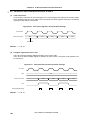
Figure 8-15:
18
Port Mode Register 7 (PM7) Format ......................................................................... 129
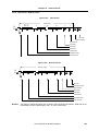
Control Register Settings When Timer 0 Operates as Interval Timer ....................... 130
Configuration of Interval Timer .................................................................................. 131
Timing of Interval Timer Operation ............................................................................ 131
Control Register Settings in PPG Output Operation.................................................. 132
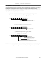
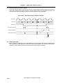
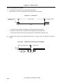
Control Register Settings for Pulse Width Measurement
with Free Running Counter and One Capture Register............................................. 133
Configuration for Pulse Width Measurement with Free Running Counter................. 134
Timing of Pulse Width Measurement with Free Running Counter
and One Capture Register (with both edges specified)............................................. 134
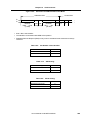
Control Register Settings for Measurement of Two Pulse Widths
with Free Running Counter........................................................................................ 135
CR01 Capture Operation with Rising Edge Specified ............................................... 136
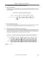
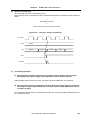
Timing of Pulse Width Measurement Operation with Free Running Counter
(with both edges specified)........................................................................................ 136
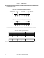
Control Register Settings for Pulse Width Measurement
with Free Running Counter and Two Capture Registers........................................... 137
Timing of Pulse Width Measurement with Free Running Counter
and Two Capture Registers (with rising edge specified) ........................................... 138
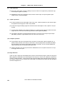
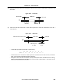
Control Register Settings for Pulse Width Measurement by Restarting .................... 139
Timing of Pulse Width Measurement by Restarting (with rising edge specified)....... 140
Control Register Settings in External Event Counter Mode....................................... 141
Configuration of External Event Counter ................................................................... 142
Timing of External Event Counter Operation (with rising edge specified) ................. 142
Set Contents of Control Registers in Square Wave Output Mode............................. 143
Timing of Square Wave Output Operation ................................................................ 144
Start Timing of 16-Bit Timer Register ........................................................................ 145
Timing after Changing Compare Register during Timer Count Operation ................ 145
Data Hold Timing of Capture Register....................................................................... 146
Operation Timing of OVF0 Flag................................................................................. 147
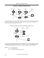
Timer 2 (TM2) Block Diagram ................................................................................... 149
16-Bit Timer Mode Control Register (TMC2) Format ................................................ 152
Capture Pulse Control Register (CRC2) Format ....................................................... 153
Prescaler Mode Register (PRM2) Format ................................................................. 154
Configuration Diagram for Pulse Width Measurement
by Using the Free Running Counter .......................................................................... 155
Timing of Pulse Width Measurement Operation by Using the Free Running
Counter and One Capture Register (with Both Edges Specified).............................. 156
CR2m Capture Operation with Rising Edge Specified .............................................. 157
Timing of Pulse Width Measurement Operation by Free Running Counter
(with Both Edges Specified) ...................................................................................... 158
16-Bit Timer Register Start Timing ............................................................................ 159
Capture Register Data Retention Timing................................................................... 159
8-Bit Timer/Event Counter 50 Block Diagram............................................................ 163
8-Bit Timer/Event Counter 51 Block Diagram............................................................ 164
Block Diagram of 8-Bit Timer/Event Counters 50 and 51 Output Control Circuit ...... 165
Timer Clock Select Register 50 Format..................................................................... 166
Timer Clock Select Register 51 Format..................................................................... 167
8-Bit Timer Mode Control Register 50 Format........................................................... 168
8-Bit Timer Mode Control Register 51 Format (1/2) .................................................. 169
Port Mode Register 0 Format .................................................................................... 170
8-Bit Timer Mode Control Register Settings for Interval Timer Operation ................. 171
Interval Timer Operation Timings (1/3)...................................................................... 172
8-Bit Timer Mode Control Register Setting for External Event Counter Operation.... 176
External Event Counter Operation Timings (with Rising Edge Specified) ................. 176
8-Bit Timer Mode Control Register Settings for Square-Wave Output Operation ..... 177
Square-wave Output Operation Timing ..................................................................... 178
8-Bit Timer Control Register Settings for PWM Output Operation ............................ 179
User’s Manual U12670EE3V0UD00
Figure 8-16:
Figure 8-17:
Figure 8-18:
Figure 8-19:
Figure 8-20:
Figure 8-21:
Figure 8-22:
Figure 9-1:
Figure 9-2:
Figure 9-3:
Figure 10-1:
Figure 10-2:
Figure 10-3:
Figure 11-1:
Figure 11-2:
Figure 11-3:
Figure 11-4:
Figure 12-1:
Figure 12-2:
Figure 12-3:
Figure 12-4:
Figure 12-5:
Figure 12-6:
Figure 12-7:
Figure 12-8:
Figure 12-9:
Figure 12-10:
Figure 12-11:
Figure 12-12:
Figure 12-13:
Figure 13-1:
Figure 13-2:
Figure 13-3:
Figure 13-4:
Figure 13-5:
Figure 14-1:
Figure 14-2:
Figure 14-3:
Figure 14-4:
Figure 14-5:
Figure 14-6:
Figure 15-1:
Figure 15-2:
Figure 15-3:
Figure 15-4:
Figure 15-5:
Figure 15-6:
Figure 15-7:
Figure 15-8:
Figure 15-9:
Figure 15-10:
Figure 15-11:
Figure 15-12:
Figure 15-13:
Figure 16-1:
Figure 16-2:
Figure 16-3:
Figure 16-4:
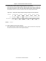
PWM Output Operation Timing (Active high setting)................................................. 180
PWM Output Operation Timings (CRn0 = 00H, active high setting) ......................... 180
PWM Output Operation Timings (CRn = FFH, active high setting) ........................... 181
PWM Output Operation Timings (CRn changing, active high setting)....................... 181
8-bit Timer Registers 50 and 51 Start Timings .......................................................... 182
External Event Counter Operation Timings ............................................................... 182
Timings after Compare Register Change during Timer Count Operation ................. 183
Block Diagram of Watch Timer.................................................................................. 185
Watch Timer Mode Control Register (WTM) Format (1/2) ........................................ 187
Operation Timing of Watch Timer/Interval Timer....................................................... 190
Watchdog Timer Block Diagram................................................................................ 193
Timer Clock Select Register 2 Format....................................................................... 194
Watchdog Timer Mode Register Format ................................................................... 195
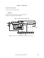
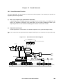
Remote Controlled Output Application Example ....................................................... 199
Clock Output Control Circuit Block Diagram.............................................................. 200
Timer Clock Select Register 0 Format....................................................................... 201
Port Mode Register 6 Format .................................................................................... 202
A/D Converter Block Diagram ................................................................................... 203
Power-Fail Detection Function Block Diagram .......................................................... 204
A/D Converter Mode Register (ADM1) Format.......................................................... 206
Analog Input Channel Specification Register (ADS1) Format ................................... 207
Power-Fail Compare Mode Register (PFM) Format.................................................. 208
Power-fail compare threshold value register (PFT) ................................................... 208
Basic Operation of 8-Bit A/D Converter..................................................................... 210
Relation between Analog Input Voltage and A/D Conversion Result ........................ 212
A/D Conversion ......................................................................................................... 214
Example Method of Reducing Current Consumption in Standby Mode .................... 215
Analog Input Pin Handling ......................................................................................... 216
A/D Conversion End Interrupt Request Generation Timing....................................... 217
D/A Converter Mode Register (DAM0) Format.......................................................... 218
Block Diagram of SIO30 ............................................................................................ 219
Format of Serial Operation Mode Register 30 (CSIM30) .......................................... 221
Format of Serial Operation Mode Register 30 (CSIM30) .......................................... 222
Format of Serial Operation Mode Register (CSIM30) ............................................... 223
Timing of Three-wire Serial I/O Mode........................................................................ 224
Block Diagram of SIO31 Macro ................................................................................. 225
Format of Serial Operation Mode Register (CSIM31) ............................................... 227
Format of Serial Operation Mode Register 31 (CSIM31) .......................................... 228
Format of Serial Operation Mode Register 31 (CSIM31) .......................................... 229
Timing of Three-wire Serial I/O Mode........................................................................ 230
2-Wire Mode Connection........................................................................................... 231
Block Diagram of UART ............................................................................................ 233
Format of Asynchronous Serial Interface Mode Register (ASIM0) (1/2) ................... 236
Format of Asynchronous Serial Interface Status Register (ASIS0) ........................... 238
Format of Baud Rate Generator Control Register (BRGC0) (1/2)............................. 239
Register Settings ....................................................................................................... 241
Format of Asynchronous Serial Interface Mode Register (ASIM0) (1/2) ................... 242
Format of Asynchronous Serial Interface Status Register (ASIS0) ........................... 244
Format of Baud Rate Generator Control Register (BRGC0) (1/2)............................. 245
Error Tolerance (when k = 0), including Sampling Errors.......................................... 248
Format of Transmit/Receive Data in Asynchronous Serial Interface......................... 249
Timing of Asynchronous Serial Interface Transmit Completion Interrupt .................. 251
Timing of Asynchronous Serial Interface Receive Completion Interrupt ................... 252
Receive Error Timing................................................................................................. 253
Data Frame ............................................................................................................... 257
Remote Frame .......................................................................................................... 257
Data Frame ............................................................................................................... 258
Arbitration Field/Standard Format Mode ................................................................... 258
User’s Manual U12670EE3V0UD00
19
Figure 16-5:
Figure 16-6:
Figure 16-7:
Figure 16-8:
Figure 16-9:
Figure 16-10:
Figure 16-11:
Figure 16-12:
Figure 16-13:
Figure 16-14:
Figure 16-15:
Figure 16-16:
Figure 16-17:
Figure 16-18:
Figure 16-19:
Figure 16-20:
Figure 16-21:
Figure 16-22:
Figure 16-23:
Figure 16-24:
Figure 16-25:
Figure 16-26:
Figure 16-27:
Figure 16-28:
Figure 16-29:
Figure 16-30:
Figure 16-31:
Figure 16-32:
Figure 16-33:
Figure 16-34:
Figure 16-35:
Figure 16-36:
Figure 16-37:
Figure 16-38:
Figure 16-39:
Figure 16-40:
Figure 16-41:
Figure 16-42:
Figure 16-43:
Figure 16-44:
Figure 16-45:
Figure 16-46:
Figure 16-47:
Figure 16-48:
Figure 16-49:
Figure 16-50:
Figure 16-51:
Figure 16-52:
Figure 16-53:
Figure 16-54:
Figure 17-1:
Figure 17-2:
Figure 17-3:
Figure 17-4:
Figure 17-5:
Figure 17-6:
Figure 17-7:
20
Arbitration Field/Extended Format Mode................................................................... 259
Control Field (Standard Format Mode)...................................................................... 260
Control Field (Extended Format Mode) ..................................................................... 260
Data Field .................................................................................................................. 261
CRC Field .................................................................................................................. 261
ACK Field .................................................................................................................. 262
End of Frame............................................................................................................. 262
Interframe Space/Error Active ................................................................................... 263
Interframe Space/Error Passive ................................................................................ 263
Error Frame ............................................................................................................... 264
Overload Frame......................................................................................................... 265
Nominal Bit Time (8 to 25 Time Quanta) ................................................................... 271
Adjusting Synchronization of the Data Bit ................................................................. 272
Bit Synchronization.................................................................................................... 273
Transmission State Shift Chart.................................................................................. 274
Reception State Shift Chart ....................................................................................... 275
Error State Shift Chart ............................................................................................... 276
Structural Block Diagram........................................................................................... 277
Connection to the CAN Bus....................................................................................... 278
Transmit Message Definition Bits ............................................................................. 282
Transmit Identifier ..................................................................................................... 283
Transmit Data ........................................................................................................... 284
Control bits for Receive Identifier ............................................................................. 287
Receive Status Bits (1/2) .......................................................................................... 288
Receive Identifier ...................................................................................................... 290
Receive Data ............................................................................................................ 291
Identifier Compare with Mask .................................................................................... 293
Control Bits for Mask Identifier ................................................................................. 294
Mask Identifier .......................................................................................................... 295
CAN Control Register (1/2) ....................................................................................... 296
DCAN Support........................................................................................................... 297
Time Stamp Function ................................................................................................ 299
SOFOUT Toggle Function......................................................................................... 299
Global Time System Function ................................................................................... 299
CAN Error Status Register (1/3) ............................................................................... 300
Transmit Error Counter ............................................................................................. 303
Receive Error Counter .............................................................................................. 303
Message Count Register (MCNT) (1/2) .................................................................... 304
Bit Rate Prescaler (1/2) ............................................................................................ 306
Synchronization Control Registers 0 and 1 (1/2) ..................................................... 308
Transmit Control Register (1/2) ................................................................................ 312
Receive Message Register ....................................................................................... 314
Mask Control Register .............................................................................................. 315
Redefinition Control Register (1/2) ........................................................................... 317
Initialization Flow Chart ............................................................................................. 324
Transmit Preparation ................................................................................................. 325
Transmit Abort ........................................................................................................... 326
Handling of Semaphore Bits by DCAN-Module......................................................... 327
Receive with Interrupt, Software Flow ....................................................................... 328
Receive, Software Polling.......................................................................................... 329
LCD Controller/Driver Block Diagram........................................................................ 332
LCD Clock Select Circuit Block Diagram................................................................... 333
LCD Display Mode Register (LCDM) Format ............................................................ 334
LCD Display Control Register (LCDC) Format .......................................................... 335
Relationship between LCD Display Data Memory Contents
and Segment/Common Outputs ................................................................................ 336
Common Signal and Static Signal Voltages and Phases .......................................... 339
LCD Drive Power Supply Connection Examples (with External Split Resistor) (1/2) 340
User’s Manual U12670EE3V0UD00
Figure 17-8:
Figure 17-9:
Figure 17-10:
Figure 17-11:
Figure 17-12:
Figure 17-13:
Figure 17-14:
Figure 17-15:
Figure 17-16:
Figure 17-17:
Figure 17-18:
Figure 17-19:
Figure 17-20:
Figure 17-21:
Figure 17-22:
Figure 17-23:
Figure 18-1:
Figure 18-2:
Figure 18-3:
Figure 18-4:
Figure 18-5:
Figure 18-6:
Figure 18-7:
Figure 19-1:
Figure 19-2:
Figure 19-3:
Figure 19-4:
Figure 19-5:
Figure 19-6:
Figure 19-7:
Figure 19-8:
Figure 19-9:
Figure 19-10:
Figure 19-11:
Figure 19-12:
Figure 19-13:
Figure 19-14:
Figure 20-1:
Figure 20-2:
Figure 20-3:
Figure 20-4:
Figure 20-5:
Figure 20-6:
Figure 20-7:
Figure 20-8:
Figure 20-9:
Figure 21-1:
Figure 21-2:
Figure 21-3:
Figure 21-4:
Figure 21-5:
Figure 21-6:
Figure 22-1:
Figure 22-2:
Figure 22-3:
Figure 22-4:
Figure 23-1:
Example of LCD Drive Voltage Supply from Off-Chip ............................................... 342
Example of LCD Drive Power Supply (external resistors) ......................................... 343
Static LCD Display Pattern and Electrode Connections............................................ 344
Static LCD Panel Connection Example ..................................................................... 345
Static LCD Drive Waveform Examples...................................................................... 346
2-Time-Division LCD Display Pattern and Electrode Connections............................ 347
2-Time-Division LCD Panel Connection Example ..................................................... 348
2-Time-Division LCD Drive Waveform Examples (1/2 Bias Method) ........................ 349
3-Time-Division LCD Display Pattern and Electrode Connections............................ 350
3-Time-Division LCD Panel Connection Example ..................................................... 351
3-Time-Division LCD Drive Waveform Examples (1/2 Bias Method) ........................ 352
3-Time-Division LCD Drive Waveform Examples (1/3 Bias Method) ........................ 353
4-Time-Division LCD Display Pattern and Electrode Connections............................ 354
4-Time-Division LCD Panel Connection Example ..................................................... 355
4-Time-Division LCD Drive Waveform Examples (1/3 Bias Method) ........................ 356
LCD Timer Control Register (LCDTM) Format .......................................................... 357
Sound Generator Block Diagram .............................................................................. 359
Concept of Each Signal ............................................................................................. 360
Sound Generator Control Register (SGCR) Format (1/2) ......................................... 361
Sound Generator Buzzer Control Register (SGBR) Format...................................... 363
Sound Generator Amplitude Register (SGAM) Format ............................................. 364
Sound Generator Output Operation Timing .............................................................. 365
Sound Generator Output Operation Timing .............................................................. 366
Basic Configuration of Interrupt Function (1/2).......................................................... 369
Interrupt Request Flag Register Format .................................................................... 372
Interrupt Mask Flag Register Format......................................................................... 373
Priority Specify Flag Register Format........................................................................ 374
Formats of External Interrupt Rising Edge Enable Register
and External Interrupt Falling Edge Enable Register ................................................ 375
Program Status Word Format ................................................................................... 376
Flowchart from Non-Maskable Interrupt Generation to Acknowledge ...................... 377
Non-Maskable Interrupt Request Acknowledge Timing ............................................ 378
Non-Maskable Interrupt Request Acknowledge Operation ....................................... 378
Interrupt Request Acknowledge Processing Algorithm ............................................. 380
Interrupt Request Acknowledge Timing (Minimum Time).......................................... 381
Interrupt Request Acknowledge Timing (Maximum Time)......................................... 381
Multiple Interrupt Example (1/2) ................................................................................ 384
Interrupt Request Hold .............................................................................................. 387
Memory Map when Using External Device Expansion Function (1/3)....................... 390
Memory Expansion Mode Register Format ............................................................... 393
Memory Expansion Wait Register Format................................................................. 394
Memory Size Switching Register Format .................................................................. 395
Instruction Fetch from External Memory.................................................................... 397
External Memory Read Timing .................................................................................. 398
External Memory Write Timing .................................................................................. 399
External Memory Read Modify Write Timing ............................................................. 400
Connection Example of µPD780948 and Memory .................................................... 401
Oscillation Stabilization Time Select Register Format............................................... 404
Standby Timing ......................................................................................................... 404
HALT Mode Clear upon Interrupt Generation ........................................................... 406
HALT Mode Release by RESET Input ...................................................................... 407
STOP Mode Release by Interrupt Generation .......................................................... 409
Release by STOP Mode RESET Input...................................................................... 410
Block Diagram of Reset Function .............................................................................. 411
Timing of Reset Input by RESET Input ..................................................................... 412
Timing of Reset due to Watchdog Timer Overflow.................................................... 412
Timing of Reset Input in STOP Mode by RESET Input ............................................. 412
Memory Size Switching Register Format .................................................................. 416
User’s Manual U12670EE3V0UD00
21
Figure 23-2:
Figure 23-3:
Figure 23-4:
Figure 23-5:
Figure 23-6:
Figure A-1:
22
Internal Expansion RAM Size Switching Register Format......................................... 417
Transmission Method Selection Format .................................................................... 418
Connection of the Flash Programmer using 3-Wire Serial I/O Method ..................... 420
Connection of the Flash Programmer using UART Method ...................................... 420
Connection of the Flash Programmer using Pseudo 3-wire Serial I/O Method ......... 421
Development Tool Configuration ............................................................................... 492
User’s Manual U12670EE3V0UD00
List of Tables
Table 1-1:
Table 1-2:
Table 1-3:
Table 1-4:
Table 2-1:
Table 2-2:
Table 2-3:
Table 3-1:
Table 3-2:
Table 3-3:
Table 3-4:
Table 3-5:
Table 3-6:
Table 3-7:
Table 3-8:
Table 3-9:
Table 3-10:
Table 3-11:
Table 4-1:
Table 4-2:
Table 5-1:
Table 5-2:
Table 6-1:
Table 6-2:
Table 6-3:
Table 7-1:
Table 8-1:
Table 8-2:
Table 8-3:
Table 8-4:
Table 8-5:
Table 8-6:
Table 8-7:
Table 8-8:
Table 8-9:
Table 9-1:
Table 9-2:
Table 9-3:
Table 10-1:
Table 10-2:
Table 10-3:
Table 10-4:
Table 10-5:
Table 11-1:
Table 12-1:
Table 13-1:
Table 13-2:
Table 14-1:
Table 14-2:
Table 15-1:
Table 15-2:
Table 15-3:
Table 15-4:
The major functional differences between the subseries ............................................... 32
Overview of Functions .................................................................................................... 34
Differences between Flash and Mask ROM version ...................................................... 35
Differences between Flash and Mask ROM version ...................................................... 35
Pin Input/Output Types................................................................................................... 37
Non-Port Pins ................................................................................................................. 39
Types of Pin Input/Output Circuits.................................................................................. 48
Internal ROM Capacities ................................................................................................ 57
Vectored Interrupts ......................................................................................................... 58
Special Function Register List ........................................................................................ 67
Implied Addressing ......................................................................................................... 74
Register Addressing ....................................................................................................... 75
Direct addressing............................................................................................................ 76
Short direct addressing................................................................................................... 77
Special-Function Register (SFR) Addressing................................................................. 78
Register indirect addressing ........................................................................................... 79
Based addressing........................................................................................................... 80
Based indexed addressing ............................................................................................. 81
Pin Input/Output Types................................................................................................... 84
Port Configuration........................................................................................................... 86
Clock Generator Configuration ..................................................................................... 106
Maximum Time Required for CPU Clock Switchover ................................................... 117
Configuration of 16-bit Timer/Event Counter (TM0) ..................................................... 120
Valid edge of TI00 Pin and valid edge of capture trigger of capture/compare register. 122
Valid edge of TI01 Pin and valid edge of capture trigger of capture/compare register. 122
Timer 2 Configuration ................................................................................................... 150
8-Bit Timer/Event Counter 50 Interval Times ............................................................... 161
8-Bit Timer/Event Counter 51 Interval Times ............................................................... 161
8-Bit Timer/Event Counter 50 Square-Wave Output Ranges....................................... 162
8-Bit Timer/Event Counter 51 Square-Wave Output Ranges....................................... 162
8-Bit Timer/Event Counters 50 and 51 Configurations ................................................. 163
8-Bit Timer/Event Counters 50 Interval Times.............................................................. 175
8-Bit Timer/Event Counters 51 Interval Times.............................................................. 175
8-Bit Timer/Event Counters 50 Square-Wave Output Ranges
(8-Bit Timer/Event Counter Mode)................................................................................ 178
8-Bit Timer/Event Counters 51 Square-Wave Output Ranges
(8-Bit Timer/Event Counter Mode)................................................................................ 178
Interval Timer Interval Time.......................................................................................... 186
Watch Timer Configuration........................................................................................... 186
Interval Timer Operation............................................................................................... 189
Watchdog Timer Inadvertent Program Overrun Detection Times ................................ 191
Interval Times ............................................................................................................... 192
Watchdog Timer Configuration..................................................................................... 193
Watchdog Timer Overrun Detection Time .................................................................... 196
Interval Timer Interval Time.......................................................................................... 197
Clock Output Control Circuit Configuration................................................................... 200
A/D Converter Configuration ........................................................................................ 204
Composition of SIO30 .................................................................................................. 220
List of SFRs (Special Function Registers).................................................................... 220
Composition of SIO31 .................................................................................................. 226
List of SFRs (Special Function Registers).................................................................... 226
Configuration of UART ................................................................................................. 234
List of SFRs (Special Function Registers).................................................................... 235
Relation between 5-bit Counter’s Source Clock and “n” Value .................................... 247
Relation between Main System Clock and Baud Rate ................................................. 248
User’s Manual U12670EE3V0UD00
23
Table 15-5:
Table 16-1:
Table 16-2:
Table 16-3:
Table 16-4:
Table 16-5:
Table 16-6:
Table 16-7:
Table 16-8:
Table 16-9:
Table 16-10:
Table 16-11:
Table 16-12:
Table 16-13:
Table 16-14:
Table 16-15:
Table 16-16:
Table 16-17:
Table 16-18:
Table 16-19:
Table 16-20:
Table 16-21:
Table 16-22:
Table 16-23:
Table 16-24:
Table 16-25:
Table 16-26:
Table 16-27:
Table 17-1:
Table 17-2:
Table 17-3:
Table 17-4:
Table 17-5:
Table 17-6:
Table 17-7:
Table 17-8:
Table 17-9:
Table 18-1:
Table 18-2:
Table 19-1:
Table 19-2:
Table 19-3:
Table 19-4:
Table 20-1:
Table 20-2:
Table 20-3:
Table 21-1:
Table 21-2:
Table 21-3:
Table 21-4:
Table 22-1:
Table 23-1:
Table 23-2:
Table 23-3:
Table 23-4:
Table 23-5:
Table 24-1:
Table 24-2:
24
Causes of Receive Errors............................................................................................. 253
Outline of the Function ................................................................................................. 255
Bit Number of the Identifier .......................................................................................... 259
RTR Setting ................................................................................................................. 259
Mode Setting ............................................................................................................... 259
Data Length Code Setting ........................................................................................... 260
Operation in the Error State ......................................................................................... 263
Definition of each Field ................................................................................................ 264
Definition of each Frame ............................................................................................. 265
Arbitration .................................................................................................................... 266
Bit Stuffing ................................................................................................................... 266
Error Types .................................................................................................................. 268
Output Timing of the Error Frame ................................................................................ 268
Types of Error .............................................................................................................. 269
Error Counter ............................................................................................................... 270
Segment Name and Segment Length ......................................................................... 271
CAN Configuration........................................................................................................ 278
SFR Definitions............................................................................................................. 279
SFR Bit Definitions ....................................................................................................... 279
Message and Buffer Configuration ............................................................................... 280
Transmit Message Format............................................................................................ 281
Receive Message Format............................................................................................. 286
Mask Function .............................................................................................................. 292
Possible Setup of the SOFOUT Function..................................................................... 298
Transmission / Reception Flag ..................................................................................... 298
Possible Reactions of the DCAN.................................................................................. 303
Mask Operation Buffers................................................................................................ 316
Interrupt Sources .......................................................................................................... 319
Maximum Number of Display Pixels............................................................................. 331
LCD Controller/Driver Configuration............................................................................. 332
COM Signals ................................................................................................................ 337
LCD Drive Voltage........................................................................................................ 338
LCD Drive Voltages (with On-Chip Split Resistor) connected externally...................... 340
Selection and Non-Selection Voltages (COM0) .......................................................... 344
Selection and Non-Selection Voltages (COM0, COM1) .............................................. 347
Selection and Non-Selection Voltages (COM0 to COM2) ........................................... 350
Selection and Non-Selection Voltages (COM0 to COM3) ........................................... 354
Sound Generator Configuration.................................................................................... 360
Maximum and Minimum Values of the Buzzer Output Frequency ............................... 362
Interrupt Source List ..................................................................................................... 368
Various Flags Corresponding to Interrupt Request Sources ........................................ 371
Times from Maskable Interrupt Request Generation to Interrupt Service .................... 379
Interrupt Request Enabled for Multiple Interrupt during Interrupt Servicing ................. 383
Pin Functions in External Memory Expansion Mode .................................................... 389
State of Port 4 to Port 6 Pins in External Memory Expansion Mode ............................ 389
Values when the Memory Size Switching Register is Reset ........................................ 395
HALT Mode Operating Status ...................................................................................... 405
Operation after HALT Mode Release ........................................................................... 407
STOP Mode Operating Status...................................................................................... 408
Operation after STOP Mode Release........................................................................... 410
Hardware Status after Reset ........................................................................................ 413
Differences among µPD78F0948 and Mask ROM Versions ........................................ 415
Values when the Memory Size Switching Register is Reset ........................................ 416
Examples of internal Expansion RAM Size Switching Register Settings ..................... 417
Transmission Method List............................................................................................. 418
Main Functions of Flash Memory Programming........................................................... 419
Operand Identifiers and Description Methods .............................................................. 423
Operation List ............................................................................................................... 425
User’s Manual U12670EE3V0UD00
Table 24-3:
Table 24-4:
Table 24-5:
Table 24-6:
Table 27-1:
8-bit instructions ........................................................................................................... 433
16-bit instructions ......................................................................................................... 434
Bit manipulation instructions......................................................................................... 434
Call/instructions/branch instructions ............................................................................. 435
Surface Mounting Type Soldering Conditions .............................................................. 489
User’s Manual U12670EE3V0UD00
25
26
User’s Manual U12670EE3V0UD00
Chapter 1 Outline (µPD780948 Subseries)
1.1 Features
• Internal memory
Item
Part Number
•
•
•
•
•
•
•
Program
Memory
(ROM)
Data Memory
Internal
high-speed
RAM
LCD
Display
RAM
Internal
Expansion
RAM
Package
µPD780948
60 Kbytes
1024 bytes
40 bytes
992 bytes
100-pin plastic QFP (fine pitch)
µPD78F0948
60 Kbytes
1024 bytes
40 bytes
992 bytes
100-pin plastic QFP (fine pitch)
External memory expansion
Minimum instruction execution time can be
changed from high speed (0.25 µs) to ultra
low speed
I/O ports: 79 (N-ch open drain: 5
8-bit resolution A/D converter: 8 channels
Sound generator
LCD-controller / driver
CAN-Interface
•
•
•
•
•
•
Serial interface
2-wire mode
3-wire mode
UART mode
Timer
Supply voltage
: 3 channels
: 1 channel
: 1 channel
: 1 channel
: 6 channels
: VDD = 4.0 to 5.5 V
The CAN macro is qualified according the requirements of ISO 11898 using the test procedures
defined by ISO 16845 and passed successfully the test procedures as recommended by C & S / FH
Wolfenbuettel.
1.2 Application
Dashboard, climate controller, security unit etc.
User’s Manual U12670EE3V0UD00
27
Chapter 1 Outline (µPD780948 Subseries)
1.3 Ordering Information
Part Number
Package
Internal ROM
µPD780948GF(A)-xxx-3BA
100-pin plastic QFP (14 × 20 mm, resin thickness 2.7 mm)
Mask ROM
µPD780948GF(A1)-xxx-3BA
100-pin plastic QFP (14 × 20 mm, resin thickness 2.7 mm)
Mask ROM
µPD78F0948GF-3BA
100-pin plastic QFP (14 × 20 mm, resin thickness 2.7 mm)
Flash Memory
Remark:
xxx indicates ROM code suffix.
1.4 Quality Grade
Part Number
Package
Quality Grade
µPD780948GF(A)-xxx-3BA
100-pin plastic QFP (14 × 20 mm, resin thickness 2.7 mm)
Special
µPD780948GF(A1)-xxx-3BA
100-pin plastic QFP (14 × 20 mm, resin thickness 2.7 mm)
Special
µPD78F0948GF-3BA
100-pin plastic QFP (14 × 20 mm, resin thickness 2.7 mm)
Standard
Remark:
xxx indicates ROM code suffix.
Please refer to "Quality Grades on NEC Semiconductor Device" (Document No. C11531E) published
by NEC Corporation to know the specification of quality grade on the devices and its recommended
applications.
28
User’s Manual U12670EE3V0UD00
Chapter 1 Outline (µPD780948 Subseries)
1.5 Pin Configuration (Top View)
•
100-pin plastic QFP (14 × 20 mm)
µPD780948GF(A)- xxx - 3BA, µPD780948GF(A1)- xxx - 3BA, µPD78F0948GF - 3BA
Pin Configuration
CRxD
P64/RD
P65/WR
P67/ASTB
P40/AD0
P41/AD1
P42/AD2
P43/AD3
P44/AD4
P45/AD5
P46/AD6
P47/AD7
P50/A8/S39
P51/A9/S38
P52/A10/S37
P53/A11/S36
P54/A12/S35
P55/A13/S34
P56/A14/S33
P57/A15/S32
Figure 1-1:
CTxD
P00/INTP0
P01/INTP1
P02/INTP2
P03/INTP3/T2PO
P04/INTP4/TI01
P05/TI00/TO0
P06/TI50/TO50
P07/TI51/TO51
P20/SI0
P21/SO0
P22/SCK0
P23/SI1/SO1
P24/SCK1
P25/RxD
P26/TxD
RESET
X1
X2
VPP(/IC)
CL1/CCLK
CL2
VSS2
VDD2
AVDD/AVREF
21
60
22
59
23
58
24
57
25
56
26
55
27
54
28
53
29
52
30
51
31 32 33 34 35 36 37 38 39 40 41 42 43 44 45 46 47 48 49 50
P70/S31
P71/S30
P72/S29
P73/S28
P74/S27
P75/S26
P76/S25
P77/S24
P120/S23
P121/S22
P122/S21
P123/S20
P124/S19
P125/S18
P126/S17
P127/S16
P130/S15
P131/S14
P132/S13
P133/S12
P134/S11
P135/S10
P136/S9
P137/S8
P140/S7
P141/S6
P142/S5
P143/S4
P144/S3
P145/S2
P15/ANI5
P16/ANI6
P17/ANI7
AVSS
P30/TI20
P31/TI21
P32/TI22
P33/PCL/SGOA
P34/SGO/SGOF
VSS1
VDD1
VLC0
VLC1
VLC2
COM0
COM1
COM2
COM3
P147/S0
P146/S1
P10/ANI0
P11/ANI1
P12/ANI2
P13/ANI3
P14/ANI4
100 99 98 97 96 95 94 93 92 91 90 89 88 87 86 85 84 83 82 81
1
80
2
79
3
78
4
77
5
76
6
75
7
74
8
73
9
72
10
71
11
70
12
69
13
68
14
67
15
66
16
65
17
64
18
63
19
62
20
61
Cautions: 1. Connect IC (internally connected) pin directly to VSS.
2. AVDD/AVREF pin should be connected to VDD.
3. AVSS pin should be connected to VSS.
User’s Manual U12670EE3V0UD00
29
Chapter 1 Outline (µPD780948 Subseries)
Remark:
When these devices are used in applications, that require reduction of the noise, generated
from inside the microcontroller, the implementation of noise reduction measures, such as
connecting the VSS1 and VSS2 to different ground lines, is recommended.
Pin Identifications
P00 to P07
:
Port 0
RXD
:
Receive Data
P10 to P17
:
Port 1
TXD
:
Transmit Data
P20 to P26
:
Port 2
SGO
:
Sound Generator Output
P30 to P34
:
Port 3
SGOA
:
Sound Generator Amplitude
P40 to P47
:
Port 4
SGOF
:
Sound Generator Frequency
P50 to P57
:
Port 5
PCL
:
Programmable Clock Output
P64, P65, P67
:
Port 6
AD0 to AD7
:
Address / Data Bus
P70 to P77
:
Port 7
A8 to A15
:
Address Bus
P120 to P127
:
Port 12
RD
:
Read Strobe
P130 to P137
:
Port 13
WR
:
Write Strobe
P140 to P147
:
Port 14
ASTB
:
Address Strobe
INTP0 to INTP4
:
Interrupt from Peripherals
S0 to S39
:
Segment Output
TI00, TI01
:
Timer Input
COM0 to COM3
:
Common Output
TI50, TI51
:
Timer Input
X1, X2
:
Crystal (Main System Clock)
TI20 to TI22
:
Timer Input
CL1, CL2
:
RC (Subsystem clock)
TO0, TO51, TO52
:
Timer Output
RESET
:
Reset
T2PO
:
Timer Output
ANI0 to ANI7
:
Analog Input
CRXD
:
CAN Receive Data
AVSS
:
Analog Ground
CTXD
:
CAN Transmit Data
AVDD/AVREF
:
Analog Reference Voltage and
CCLK
:
CAN Clock
:
ADC Power Supply
SI0
:
Serial Input
VDD
:
Power Supply
SO0
:
Serial Output
VPP
:
Programming Power Supply
SCK0, SCK1
:
Serial Clock
VSS
:
Ground
SI1/SO1
:
Serial Input/Output
IC
:
Internally Connected
30
User’s Manual U12670EE3V0UD00
Chapter 1 Outline (µPD780948 Subseries)
1.6 78K/0 Series Expansion
The following shows the products organized according to usage.
The names in the parallelograms are subseries.
Figure 1-2:
78K/0 Series Expansion
Products in mass production
Products under development
Y subseries products are compatible with I2C bus.
Control
100-pin
100-pin
100-pin
µ PD78075B
µ PD78078
µ PD78070A
100-pin
80-pin
80-pin
µ PD780058
µPD780065
64-pin
µ PD780078
64-pin
64-pin
µ PD780034A
µ PD780024A
42/44-pin
µ PD78083
64-pin
µPD780988
EMI-noise reduced version of the µPD78078
µPD78078Y
µ PD78054 with timer and enhanced external interface
µ PD78070AY
ROMless version of the µ PD78078
µ PD78078Y with enhanced serial I/O and limited function
µ PD780018AY
µ PD780058Y
µ PD780078Y
µ PD780034AY
µ PD780024AY
µ PD78054 with enhanced serial I/O
µ PD780024A with expanded RAM
µ PD780034A with timer and enhanced serial I/O
µ PD780024A with enhanced A/D converter
µ PD78018F with enhanced serial I/O
On-chip UART, capable of operating at low voltage (1.8 V)
Inverter control
On-chip inverter control circuit and UART. EMI-noise reduced.
VFD drive
78K/0
Series
100-pin
µ PD780208
µ PD78044F with enhanced I/O and VFD C/D. Display output total: 53
80-pin
For panel control. On-chip VFD C/D. Display output total: 53
80-pin
µ PD780232
µPD78044H
80-pin
µPD78044F
Basic subseries for driving VFD. Display output total: 34
µ PD78044F with N-ch open-drain I/O. Display output total: 34
LCD drive
120-pin
µ PD780338
120-pin
µ PD780328
µPD780318
µ PD780308
µPD78064B
µPD78064
120-pin
100-pin
100-pin
100-pin
µ PD780308 with enhanced display function and timer. Segment signal output: 40 pins max.
µ PD780308 with enhanced display function and timer. Segment signal output: 32 pins max.
µ PD780308 with enhanced display function and timer. Segment signal output: 24 pins max.
µPD780308Y
µ PD78064 with enhanced SIO, and expanded ROM and RAM
EMI-noise reduced version of the µ PD78064
µ PD78064Y
Basic subseries for driving LCDs, on-chip UART
Bus interface supported
100-pin
80-pin
µ PD780948
µ PD78098B
µ PD78054 with IEBusTM controller
µ PD780702Y
µPD780703Y
µ PD780833Y
80-pin
80-pin
80-pin
On-chip IEBus controller
On-chip CAN controller
On-chip controller compliant with J1850 (Class 2)
µPD780816
Meter control
Specialized for CAN controller function
100-pin
µPD780958
80-pin
µPD780852
µPD780828B
For industrial meter control
On-chip automobile meter controller/driver
64-pin
80-pin
Remark:
On-chip CAN controller
For automobile meter driver. On-chip CAN controller
VFD (Vacuum Fluorescent Display) is referred to as FIPTM (Fluorescent Indicator Panel) in
some documents, but the functions of the two are the same.
User’s Manual U12670EE3V0UD00
31
Chapter 1 Outline (µPD780948 Subseries)
The major functional differences between the subseries are shown below.
Table 1-1:
Function
The major functional differences between the subseries
ROM
Capacity
(Bytes)
Subseries Name
Timer
8-bit 16-bit
WT
WDT
8-bit 10-bit 8-bit
A/D
A/D
D/A
I/O
VDD External
MIN Expansion
value
88
1.8 V
61
2.7 V
68
1.8 V
4 ch (UART: 1 ch) 60
2.7 V
Serial Interface
µPD78075B 32K to 40K
µPD78078
48K to 60K 4 ch
3 ch (UART: 1 ch)
2 ch
µPD78070A -
8 ch
1 ch
3 ch (time-division UART: 1 ch)
µPD780058 24K to 60K
1 ch
Control
1 ch
µPD780065 40K to 48K
µPD780078 48K to 60K 2 ch
2 ch
O
3 ch (UART: 2 ch) 52
-
8 ch
µPD780034A
8K to 32K
1 ch
3 ch (UART: 1 ch) 51
8K to 16K
-
-
µPD780988 16K to 60K 3 ch
Note
-
µPD780208 32K to 60K 2 ch
1 ch
1 ch
1.8 V
µPD780024A
8 ch
µPD78083
Inverter
control
1 ch (UART: 1 ch) 33
1 ch
-
8 ch
-
-
2 ch (UART: 2 ch) 47
4.0 V
74
2.7 V
40
4.5 V
8 ch
O
2 ch
µPD780232 16K to 24K 3 ch
-
-
VFD drive
4 ch
1 ch
-
-
µPD78044H 32K to 48K
1 ch
2 ch
1 ch
1 ch
8 ch
68
µPD78044F 16K to 40K
2.7 V
2 ch
µPD780338
54
µPD780328 48K to 60K 3 ch
2 ch
-
10 ch
1 ch 2 ch (UART: 1 ch) 62
µPD780318
1.8 V
70
LCD drive
1 ch
1 ch
µPD78064B 32K
2 ch
1 ch
-
3 ch (time-division UART: 1 ch)
µPD780308 48K to 60K
8 ch
-
-
57
2.0 V
79
4.0 V
69
2.7 V
2 ch (UART: 1 ch)
µPD78064
16K to 32K
µPD780948 60 K
Bus
µPD78098B 40K to 60K 2 ch
interface
supported
µPD780816 32K to 60K
Meter
control
2 ch
8 ch
1 ch
1 ch
1 ch
-
2 ch
2 ch
12 ch
-
2 ch (UART: 1 ch) 46
4.0
2.2 V
-
4.0 V
-
µPD780958 48K to 60K 4 ch
2 ch
-
1 ch
-
-
-
2 ch (UART: 1 ch) 69
Dashboard µPD780852 32K to 40K
3 ch
control
µPD780828B 32K to 60K
1 ch
1 ch
1 ch
5 ch
-
-
3 ch (UART: 1 ch)
56
59
Note: 16-bit timer: 2 channels
10-bit timer: 1 channel
32
O
3 ch (UART: 1 ch)
User’s Manual U12670EE3V0UD00
Chapter 1 Outline (µPD780948 Subseries)
1.7 Block Diagram
TI50/TO50
8 bit Timer 50
TI51/TO51
8 bit Timer 51
VSS2
16 bit Timer 2
IC/VPP
TI20
TI21
TI22
T2PO
Block Diagram
VSS1
16 bit Timer 0
VDD2
TI00/TO0
TI01
VDD1
Figure 1-3:
Port 0
8
Port 1
8
Port 2
7
Port 3
5
Port 4
8
Port 5
8
Port 6
3
Port 7
8
Watch Timer
Watchdog Timer
78K/0
CPU
Core
SI0
SO0
SCK0
Serial Interface
Channel 0
SI1/SO1
SCK1
Serial Interface
Channel 1
Port 12
8
UART
Port 13
8
RxD
TxD
ANI0ANI7
AVSS
AVDD/AVREF
RAM
Port 14
A/D Converter
8
Interface
S0-S7
60 K ROM
AD0AD7
A8A15
/RD
/WR
ASTB
External
Access
INTP0INTP4
Interrupt
Control
S8-S15
S16-S23
DCAN
Interface
CCLK
CRxD
CTxD
RAM
LCD
Controller
driver
S24-S31
S32-S39
COM0-COM3
System
Control
8MHz / SV
RC Oscillator
RESET
X1
X2
CL1
VLC0-VLC2
SGO/SGOF
Sound Generator
SGOA
CL2
Clock Output
Control
PCL
Standby
Control
Remark:
The internal ROM and RAM capacity depends on the product.
User’s Manual U12670EE3V0UD00
33
Chapter 1 Outline (µPD780948 Subseries)
1.8 Overview of Functions
Table 1-2:
Overview of Functions
Part Number
µPD780948
Item
Internal
memory
µPD78F0948
ROM
60 Kbytes
Internal high-speed RAM
1024 bytes
LCD Display RAM
40 bytes
Internal Expansion RAM
992 bytes
Memory space
64 Kbytes
General registers
8 bits × 32 registers (8 bits × 8 registers × 4 banks)
Instruction cycle
On-chip instruction execution time selective function
When main system clock
selected
0.25 µs/0.5 µs/1 µs/2 µs/4 µs (at 8 MHz)
When subsystem clock
selected
122 µs (at 32.768 KHz)
Instruction set
16-bit operation
Multiplication/division (8 bits × 8 bits, 16 bits ÷ 8 bits)
Bit manipulation (set, reset, test, boolean operation)
BCD adjustment, etc.
Total: 79
I/O ports
CMOS input: 8
CMOS I/O: 71
A/D converter
8-bit resolution × 8 channels
Serial Interface
3-wire mode: 1 channel
2-wire mode: 1 channel
UART mode: 1 channel
Timer
16 bit timer / event counter: 2 channels
8 bit timer / event counter: 2 channels
Watch timer: 1 channel
Watchdog timer: 1 channel
Timer output
3 (16-bit PWM output × 1, 8-bit PWM output × 2)
Clock output
62.5 KHz, 125 KHz, 250 KHz, 500 KHz, 1 MHz, 2 MHz,
4 MHz, 8 MHz (at main system clock of 8.0 MHz)
Sound Generator
1 channel
LCD-controller/Driver
max. 40 seg. × 4
CAN
1 channel
Vectored
interrupts
Maskable interrupts
Internal: 22
External: 5
Non-maskable interrupts
Internal: 1
Software interrupts
Internal: 1
Supply voltage
VDD = 4.0 V to 5.5 V
Package
100-pin plastic QFP (14 mm × 20 mm)
34
User’s Manual U12670EE3V0UD00
Chapter 1 Outline (µPD780948 Subseries)
1.9 Mask Option
The mask ROM version provides LCD split resistor which allows user to specify whether to connect
LCD split resistor externally.
The mask options provided in the µPD780948 Subseries are shown in Table 1-3.
Table 1-3:
Differences between Flash and Mask ROM version
Pin Names
Mask Options
VLC0, VLC1, VLC2
LCD-split resistor can be specified internally
1.10 Differences between Flash and Mask ROM version
The differences between the two versions are shown in Table 1-4 below.
Differences of the electrical specification are given in Chapter 24 “Electrical specifications” on page
411.
Table 1-4:
Differences between Flash and Mask ROM version
Flash Version
Mask ROM Version
ROM
Flash EEPROM
Mask ROM
LCD Split Resistor
None
Mask Option
VPP pin
Yes
None (IC pin)
User’s Manual U12670EE3V0UD00
35
[MEMO]
36
User’s Manual U12670EE3V0UD00
Chapter 2
Pin Function (µPD780948 Subseries)
2.1 Pin Function List
Normal Operating Mode Pins / Pin Input/Output Types
Table 2-1: Pin Input/Output Types (1/2)
Input/Output
Pin Name
After
Reset
INTP0
Input
P01
INTP1
Input
INTP2
Input
INTP3/T2P0
Input
INTP4/TI01
Input
TI00/TO0
Input
P06
TI50/TO50
Input
P07
TI51/TO51
Input
ANI0 - ANI7
Input
SI0
Input
SO0
Input
SCK0
Input
SI1/SO1
Input
SCK1
Input
P25
RXD
Input
P26
TXD
Input
P30
TI20
Input
TI21
Input
TI22
Input
PCL/SGOA
Input
SGO/SGOF
Input
AD0 - AD7
Input
P03
P04
P05
Input
Alternate Function
P00
P02
Input/Output
Function
P10 - P17
Port 0
8-bit input / output port
input / output mode can be specified bit-wise
If used as an input port, a pull-up resistor can be
connected by software bit-wise
Port 1
8-bit input port
Input mode can be specified bit-wise.
P20
P21
P22
Input/Output P23
P24
P31
Input/Output P32
P33
Port 2
7-bit output port
input / output mode can be specified bit-wise.
If used as an output port, the port buffer can be set
a CMOS or N-ch open drain buffer.
Port 3
5-bit input / output port
input / output mode can be specified bit-wise
P34
Input/Output P40 - P47
Port 4
8-bit input / output port
input / output mode can be specified bit-wise
If used as an input port, a pull-up resistor can be
connected by software.
Input/Output P50 - P57
Port 5
8-bit input / output port
input / output mode can be specified bit-wise.
This port can be used in External Memory ExpanA8/S39 - A15/S32
sion mode Register. Not for external memory expansion used ports can be used either for LCD or port
function.
User’s Manual U12670EE3V0UD00
Input
37
Chapter 2 Pin Function (µPD780948 Subseries)
Table 2-1: Pin Input/Output Types (2/2)
Input/Output
Pin Name
Function
Alternate Function
After
Reset
RD
Input
WR
Input
ASTB
Input
Port 7
8-bit input / output port
input / output mode can be specified bit-wise
If used as an input port, a pull-up resistor can be
connected by software.
This port can be used as a segment signal output
port or an I/O port in 1-bit units by setting the port
function register.
S31 - S24
Input
Port 12
8-bit input / output port
input / output mode can be specified bit-wise
Input/Output P120 - P127
This port can be used as a segment signal output
port or an I/O port in 8-bit units by setting the port
function register.
S23 - S16
Input
Port 13
8-bit input / output port
input / output mode can be specified bit-wise
If used as an input port, a pull-up resistor can be
Input/Output P130 - P137
connected by software.
This port can be used as a segment signal output
port or an I/O port in 8-bit units by setting the port
function register.
S15 - S8
Input
Port 14
8-bit input / output port
input / output mode can be specified bit-wise
Input/Output P140 - P147
This port can be used as a segment signal output
port or an I/O port in 8-bit units by setting the port
function register.
S7 - S0
Input
P64
Input/Output P65
P67
Input/Output P70 - P77
38
Port 6
3-bit output port
input / output mode can be specified bit-wise
User’s Manual U12670EE3V0UD00
Chapter 2 Pin Function (µPD780948 Subseries)
2.2 Non-Port Pins
Table 2-2:
Pin Name
Input/Output
Non-Port Pins (1/2)
After
Reset
Function
INTP0
P00
INTP1
INTP2
Alternate
Function Pin
P01
Input
External interrupts with specifiable valid edges (risInput
ing edge, falling edge, both rising and falling edges)
P02
INTP3
P03/T2P0
INTP4
P04/TI01
SI0
SI1
SO0
SO1
SCK0
Input
Serial interface serial data input
Input
Output
Serial interface serial data output
Input
P20
P23/SO1
P21
P23/SI1
P22
Input/Output Serial interface serial clock input / output
Input
RXD
Input
Asynchronous serial interface data input
Input
P25
TXD
Output
Asynchronous serial interface data output
Input
P26
CRXD
Input
CAN serial data input
Input
-
CTXD
Output
CAN serial data output
Output
-
CCLK
Input
CAN serial clock input
-
CL1
SCK1
TI00
P05/TO0
External count clock input to 16-bit timer (TM0)
TI01
P04/INTP4
TI20
TI21
P24
P30
Input
Capture trigger input
Input
TI22
P31
P32
TI50
External count clock input to 8-bit timer (TM50)
P06/TO50
TI51
External count clock input to 8-bit timer (TM51)
P07/TO51
TO0
16-bit timer output
P05/TI00
T2P0
TO50
Output
TO51
16-bit timer output
8-bit timer output (also used for PWM output)
Input
8-bit timer output (also used for PWM output)
P03/INTP3
P06/TI50
P07/TI51
PCL
Output
Clock output
Input
P33/SGOA
AD0 - AD7
Input/Output
Low-order address/data bus at external memory
expansion
Input
P40 - P47
A8 - A15
Output
High-order address/data bus at external memory
expansion
Input
P50 - P57,
S39 - S32
RD
Output
WR
ASTB
Output
Strobe signal output for read operation from external
memory
Strobe signal output for write operation from external
memory
Strobe output to access external memory
User’s Manual U12670EE3V0UD00
P64
Input
P65
Input
P67
39
Chapter 2 Pin Function (µPD780948 Subseries)
Table 2-2:
Pin Name
Input/Output
Non-Port Pins (2/2)
After
Reset
Function
Alternate
Function Pin
S0 - S7
P147 - P140
S8 - S15
P137 - P130
S16 - S23
Output
Segment signal output of LCD controller / driver
Input
P127 - P120
S24 - S31
P77 - P70
S32 - S39
P57 - P50, A15 - A8
COM0-COM3 Output
Common signal output of LCD controller /driver
Output
-
VLC0 - VLC2
-
LCD drive voltage
-
-
SGO
Output
Sound generator output
Input
P34/SGOF
SGOA
Output
Sound generator amplitude output
Input
P33/PCL
SGOF
Output
Sound generator frequency output
Input
P34/SGO
ANI0 to ANI7 Input
A/D converter analog input
Input
P10 - P17
AVDD /AVREF -
AD converter reference voltage input and analog
power supply
-
-
AVSS
-
AD converter ground potential. Connect to VSS
-
-
RESET
Input
System reset input
-
-
X1
-
-
-
X2
-
-
-
CL1
Input
-
CCLK
CL2
-
-
-
VDD1,VDD2
-
Positive power supply
-
-
VSS1,VSS2
-
Ground potential
-
-
VPP
-
High voltage supply for flash programming
(only flash version)
-
IC
IC
-
Internal connection. Connect directly to VSS
(only Mask ROM version)
-
VPP
40
Crystal connection for main system clock
RC connection for subsystem clock
User’s Manual U12670EE3V0UD00
Chapter 2 Pin Function (µPD780948 Subseries)
2.3 Description of Pin Functions
2.3.1 P00 to P07 (Port 0)
This is an 8-bit input/output port. Besides serving as input/output port the external interrupt input, an
external count clock input to the timer, a capture trigger signal input and a timer signal output are implemented.
(1)
Port mode
P00 to P07 function as input/output ports. P00 to P07 can be specified for input or output bit-wise
with a port mode register. When they are used as input ports, pull-up resistors can be connected
to them by defining the pull-up resistors bit-wise in the pull-up resistor option register.
(2)
Control mode
In this mode, these ports function as an external interrupt input, an external count clock input to
the timer, and a timer signal output.
(a) INTP0 to INTP4
INTP0 to INTP4 are external interrupt input pins which can specify valid edges (rising edge, falling
edge, and both rising and falling edges). INTP4 becomes a 16-bit timer/event counter capture trigger signal input pin with a valid edge input.
(b) TI00
Pin for external count clock input to 16-bit timer/event counter and pin for capture trigger signal
input to the 16-bit timer/event counter capture register (CR01).
(c) TI01
Pin for capture trigger signal input to capture register of 16-bit timer/event counter (CR00).
(d) TI50
Pin for external count clock input to 8-bit timer/event counter.
(e) TI51
Pin for external count clock input to 8-bit timer/event counter.
(f) TO0
Pin for output of the 16-bit timer/event counter.
(g) TO50
Pin for output of the 8-bit timer/event counter.
(h) TO51
Pin for output of the 8-bit timer/event counter.
(i) T2PO
Pin for output of the 16-bit timer (TM2).
User’s Manual U12670EE3V0UD00
41
Chapter 2 Pin Function (µPD780948 Subseries)
2.3.2 P10 to P17 (Port 1)
This is an 8-bit input/output port. Besides serving as input/output port, they function as an A/D converter analog input.
The following operating modes can be specified bit-wise.
(1)
Port mode
These ports function as 8-bit input ports.
(2)
Control mode
These ports function as A/D converter analog input pins (ANI0 to ANI7).
2.3.3 P20 to P26 (Port 2)
This is a 7-bit input/output port. Besides serving as input/output port, they function as data input/output
to/from the serial interface, clock input/output.
The following operating modes can be specified bit-wise.
(1)
Port mode
These ports function as 7-bit input/output ports. They can be specified bit-wise as input or output
ports with port mode register 2. P20 to P24 are selectable as N-ch open drain or as CMOS output.
(2)
Control mode
These ports function as serial interface data input/output, clock input/output.
(a) SI0, SI1, SO0, SO1
Serial interface serial data input/output pins
(b) SCK0 and SCK1
Serial interface serial clock input/output pins
(c) RXD, TXD
Asynchronous serial interface data input/output pins
Caution:
42
When this port is used as a serial interface, the I/O and output latches must be set
according to the function the user requires.
User’s Manual U12670EE3V0UD00
Chapter 2 Pin Function (µPD780948 Subseries)
2.3.4 P30 to P34 (Port 3)
This is a 5-bit input/output port. Beside serving as input/output ports, they function as timer input, clock
output and sound generator output.
The following operating modes can be specified bit-wise.
(1)
Port mode
These ports function as 5-bit input/output ports. They can be specified bit-wise as input or output
ports with port mode register 3.
(2)
Control mode
These ports function as timer input, clock output, and sound generator output.
(a) TI20, TI21 and TI22
Pin for external capture trigger input to the 16-bit timer/capture registers of TM2.
(b) PCL
Clock output pin.
(c) SGO, SGOA and SGOF
Pins for separate or composed signal output of the sound generator.
2.3.5 P40 to P47 (Port 4)
This is an 8-bit input/output port. Besides serving as input/output port, they function as an address/data
bus.
The following operating mode can be specified in 8-bit units.
(1)
Port mode
These ports function as 8-bit input/output ports. They can be specified in 8-bit units for input or
output ports by using the memory expansion mode register. When they are used as input ports,
pull-up resistors can be connected bit-wise by defining the pull-up resistor option register 4.
(2)
Control mode
These ports function as low-order address/data bus pins (AD0 to AD7) in external memory expansion mode.
User’s Manual U12670EE3V0UD00
43
Chapter 2 Pin Function (µPD780948 Subseries)
2.3.6 P50 to P57 (Port 5)
This is an 8-bit input/output port. Besides serving as input/output port, they function as an address bus
and LCD controller/driver.
The following operating modes can be specified bit-wise.
(1)
Port mode
These ports function as 8-bit input/output ports. They can be specified bit-wise as input/output
ports with port mode register 5.
(2)
Control mode
These ports function as high-order address bus pins (A8 to A15) in external memory expansion
mode or as segment signal output pins (S32 to S39) of LCD controller/driver output.
2.3.7 P64, P65 and P67 (Port 6)
This is a 3-bit input/output port. Besides serving as input/output port, they are used for control in external memory expansion mode.
The following operating modes can be specified bit-wise.
(1)
Port mode
These ports function as 3-bit input/output ports. They can be specified bit-wise as input or output
ports with port mode register 6.
(2)
Control mode
These ports function as control signal output pins (RD, WR, ASTB) in external memory expansion
mode, therefore a pin has to be used as a control signal output.
2.3.8 P70 to P77 (Port 7)
This is an 8-bit input/output port. In addition to its use as an input/output port, it is also used as segment
signal output of the LCD controller/driver.
The following operating modes can be specified bit-wise.
(1)
Port mode
Port 7 functions as a 8-bit input/output port. Bit-wise specification as an input port or output port is
possible by means of port mode register 7. When used as input ports, pull-up resistors can be
connected by defining the pull-up resistor option register 7.
(2)
Control mode
Port 7 functions as segment signal output pins (S24 to S31) of LCD controller/driver.
44
User’s Manual U12670EE3V0UD00
Chapter 2 Pin Function (µPD780948 Subseries)
2.3.9 P120 to P127 (Port 12)
This is an 8-bit input/output port. Besides serving as input/output port, they function as segment signal
output pins of LCD controller/driver.
The following operating modes can be specified bit-wise or byte-wise.
(1)
Port mode
These ports function as 8-bit input/output ports. They can be specified bit-wise as input or output
ports with port mode register 12.
(2)
Control mode
These ports function as segment output signal pins (S16 to S23) of LCD controller/driver.
2.3.10 P130 to P137 (Port 13)
This is an 8-bit input/output port. Besides serving as input/output port, they function as segment signal
output pins of LCD controller/driver.
The following operating modes can be specified bit-wise or byte-wise.
(1)
Port mode
These ports function as 8-bit input/output ports. They can be specified bit-wise as input or output
ports with port mode register 13. When used as input ports, pull-up resistors can be connected by
defining the pull-up resistor option register 13.
(2)
Control mode
These ports function as segment output signal pins (S8 to S15) of LCD controller/driver.
2.3.11 P140 to P147 (Port 14)
This is an 8-bit input/output port. Besides serving as input/output port, they function as segment signal
output pins of LCD controller/driver.
The following operating modes can be specified bit-wise or byte-wise.
(1)
Port mode
These ports function as 8-bit input/output ports. They can be specified bit-wise as input or output
ports with port mode register 14.
(2)
Control mode
These ports function as segment output signal pins (S0 to S7) of LCD controller/driver.
User’s Manual U12670EE3V0UD00
45
Chapter 2 Pin Function (µPD780948 Subseries)
2.3.12 CTXD
This pin functions as CAN-controller transmit output.
2.3.13 CRXD
This pin functions as CAN-controller receive input.
2.3.14 COM0 to COM3
These are LCD controller/driver common signal output pins.
2.3.15 VLC0 to VLC2
These are LCD drive voltage pins. In the Mask ROM product, a split resistor for LCD drive voltage generation can be incorporated by a mask option, without connecting external split resistors.
2.3.16 AVDD/AVREF
A/D converter reference voltage input pin and the power supply for the A/D-converter.
When A/D converter is not used, connect this pin to VDD.
2.3.17 AVSS
This is a ground voltage pin of A/D converter. Always use the same voltage as that of the VSS pin even
when A/D converter is not used.
2.3.18 RESET
This is a low-level active system reset input pin.
2.3.19 X1 and X2
Crystal resonator connect pins for main system clock oscillation. For external clock supply, input it to
X1.
2.3.20 CL1 and CL2
RC connection pins for subsystem clock oscillation.
For external clock supply, input it to CL1 and leave CL2 open. For CAN-clock, input it to CL1 and leave
CL2 open.
2.3.21 VDD
Positive power supply pin. The power supply pin VDD1 corporates the power supply of the port, while
VDD2 corporates the power supply of the oscillator, the CPU and the peripherals.
46
User’s Manual U12670EE3V0UD00
Chapter 2 Pin Function (µPD780948 Subseries)
2.3.22 VSS
Ground potential pin. The ground pin VSS1 corporates the ground of the port, while VSS2 corporates the
ground of the oscillator, the CPU and the peripherals.
2.3.23 VPP (µPD78F0948 only)
High-voltage apply pin for FLASH programming mode setting. Connect directly to VSS in normal operating mode.
2.3.24 IC (Mask ROM version only)
The IC (Internally Connected) pin is provided to set the test mode to check the µPD78F0948 at delivery.
Connect it directly to the VSS with the shortest possible wire in the normal operating mode.
When a voltage difference is produced between the IC pin and VSS pin because the wiring between
those two pins is too long or an external noise is input to the IC pin, the user’s program may not run
normally.
Figure 2-1:
Vss
Connection of IC Pins
IC
As short as possible
Caution:
Connect IC pins to VSS pins directly.
User’s Manual U12670EE3V0UD00
47
Chapter 2 Pin Function (µPD780948 Subseries)
2.4 Pin I/O Circuits and Recommended Connection of Unused Pins
The input/output circuit type of each pin and recommended connection of unused pins are shown in the
following table.
For the input/output circuit configuration of each type, see Table 2-3, “Types of Pin Input/Output Circuits,” on page 48.
Table 2-3:
∗
Pin Name
Types of Pin Input/Output Circuits (1/3)
Input/Output
Circuit Type
I/O
8-A
I/O
11-B
I
Recommended Connection for Unused Pins
P00/INTP0
P01/INTP1
P02/INTP2
P03/INTP3/T2P0
P04/INTP4/TI01
Input: Connect to VDD or VSS via a resistor individually.
Output: Leave open.
P05/TI00/TO0
P06/TI50/TO50
P07/TI51/TO51
P10/ANI0
P11/ANI1
P12/ANI2
P13/ANI3
P14/ANI4
Connect to VDD or VSS directly
P15/ANI5
P16/ANI6
P17/ANI7
P20/SI0
P21/SO0
P22/SCK0
10
P23/SI1/SOA
I/O
Input: Connect to VDD or VSS via a resistor individually.
Output: Leave open.
I/O
Input: Connect to VDD or VSS via a resistor individually.
Output: Leave open.
P24/SCK1
P25/RXD
8-A
P26/TXD
5-A
P30/TI20
P31/TI21
8-A
P32/TI22
P33/PCL/SGOA
P34/SGO/SGOF
48
5
User’s Manual U12670EE3V0UD00
Chapter 2 Pin Function (µPD780948 Subseries)
∗
Table 2-3:
Pin Name
Types of Pin Input/Output Circuits (2/3)
Input/Output
Circuit Type
I/O
5-A
I/O
Input: Connect to VDD or VSS via a resistor individually.
Output: Leave open.
17
O
Input: Connect to VDD or VSS via a resistor individually.
Output: Leave open.
5
I/O
Input: Connect to VDD or VSS via a resistor individually.
Output: Leave open.
17-B
I/O
Input: Connect to VDD or VSS via a resistor individually.
Output: Leave open.
17-B
I/O
Input: Connect to VDD or VSS via a resistor individually.
Output: Leave open.
Recommended Connection for Unused Pins
P40/AD0
P41/AD1
P42/AD2
P43/AD3
P44/AD4
P45/AD5
P46/AD6
P47/AD7
P50/A8/S39
P51/A9/S38
P52/A10/S37
P53/A11/S36
P54/A12/S35
P55/A13/S34
P56/A14/S33
P57/A15/S32
P64/RD
P65/WR
P67/ASTB
P70/S31
P71/S30
P72/S29
P73/S28
P74/S27
P75/S26
P76/S25
P77/S24
P120/S23
P121/S22
P122/S21
P123/S20
P124/S19
P125/S18
P126/S17
P127/S16
User’s Manual U12670EE3V0UD00
49
Chapter 2 Pin Function (µPD780948 Subseries)
∗
Table 2-3:
Types of Pin Input/Output Circuits (3/3)
Input/Output
Circuit Type
I/O
17-A
I/O
Input: Connect to VDD or VSS via a resistor individually.
Output: Leave open.
17
I/O
Input: Connect to VDD or VSS via a resistor individually.
Output: Leave open.
18
O
VLC0 - VLC2
-
-
CRXD
1
I
Connect to VDD via a resistor individually.
CTXD
2
O
Leave open.
CL1/CCLK
-
I
Connect to VDD or VSS via a resistor individually
CL2
-
-
Leave open
RESET
1
I
-
AVDD / AVREF
-
-
Connect to VDD
AVSS
-
-
Connect to VSS
-
-
Connect directly to VSS
Pin Name
Recommended Connection for Unused Pins
P130/S15
P131/S14
P132/S13
P133/S12
P134/S11
P135/S10
P136/S9
P137/S8
P140/S7
P141/S6
P142/S5
P143/S4
P144/S3
P145/S2
P146/S1
P147/S0
COM0 - COM3
IC
VPP
50
Leave open
User’s Manual U12670EE3V0UD00
Chapter 2 Pin Function (µPD780948 Subseries)
Figure 2-2:
Pin Input/Output Circuits (1/3)
Type 1
Type 2
VDD
P-ch
IN
Data
OUT
N-ch
Type 5
Pullup
enable
V DD
Data
P-ch
V DD
P-ch
IN/OUT
Output
disable
V DD
Type 5-A
Data
P-ch
N-ch
IN/OUT
Output
disable
N-ch
Input
disable
Input
enable
Type 8
Type 8-A
V DD
V DD
Data
Pullup
enable
P-ch
P-ch
V DD
IN/OUT
Output
disable
N-ch
Data
P-ch
IN/OUT
Output
disable
User’s Manual U12670EE3V0UD00
N-ch
51
Chapter 2 Pin Function (µPD780948 Subseries)
Figure 2-2:
Pin Input/Output Circuits (2/3)
Type 11-B
Type 10
VDD
P-ch
Data
P-ch
IN/OUT
Open drain
output disable
Comparator
+
-
N-ch
IN
N-ch
V REF (Threshold Voltage)
Input
enable
Type 17
Type 17-A
Pullup
enable
VDD
Data
VDD
P-ch
VDD
P-ch
IN/OUT
Output
disable
Data
P-ch
N-ch
IN/OUT
Output
disable
Input
enable
N-ch
Input
enable
VLC0
P-ch
VLC0
VLC1
N-ch
P-ch
P-ch
VLC1
N-ch
SEG
Data
P-ch
N-ch
SEG
Data
VLC2
P-ch
N-ch
VLC2
N-ch
52
P-ch
User’s Manual U12670EE3V0UD00
N-ch
Chapter 2 Pin Function (µPD780948 Subseries)
Figure 2-2:
Type 17-B
Pin Input/Output Circuits (3/3)
Type 17-C
V DD
Pullup
enable
P-ch
V DD
V DD
Data
Data
P-ch
IN/OUT
P-ch
IN/OUT
Output
disable
Output
disable
N-ch
N-ch
V LC0
P-ch
V LC0
V LC1
P-ch
N-ch
V LC1
N-ch
P-ch
SEG
Data
SEG
Data
P-ch
P-ch
P-ch
N-ch
V LC2
N-ch
N-ch
V LC2
N-ch
Type 18
P-ch
VLC0
VLC1
OUT
COM
VLC2
N-ch
User’s Manual U12670EE3V0UD00
53
[MEMO]
54
User’s Manual U12670EE3V0UD00
Chapter 3
CPU Architecture
3.1 Memory Space
The memory map of the µPD780948 is shown in Figure 3-1.
Figure 3-1:
FFFFH
FF20H
FF1FH
FF00H
FEFFH
FEE0H
FEDFH
FE20H
FB00H
FAFFH
FA80H
FA7FH
FA58H
FA57H
Memory Map of the µPD780948
Special Function Registers
(SFRs) 256 x 8 bits
General Registers
32 x 8 bits
Internal High-speed RAM
1024 x 8 bits
Not usable
LCD Display RAM
40 x 4 bits
EFFFH
Not usable
Program Area
1000H
0FFFH
F7E0H
F7DFH
CALLF Entry Area
Internal Expansion RAM
992 x 8 bits
0800H
07FFH
Program Area
F400H
F3FFH
External Memory
0080H
007FH
F000H
EFFFH
CALLT Table Area
Internal ROM
61440 x 8 bits
0000H
∗
0040H
003FH
Vector Table Area
0000H
Note: In the expansion RAM between F400H and F7DFH it is not possible to do code execution.
User’s Manual U12670EE3V0UD00
55
Chapter 3 CPU Architecture
The memory map of the µPD78F0948 is shown in Figure 3-2.
Figure 3-2:
FFFFH
FF20H
FF1FH
FF00H
FEFFH
FEE0H
FEDFH
FE20H
FB00H
FAFFH
FA80H
FA7FH
FA58H
FA57H
Memory Map of the µPD78F0948
Special Function Registers
(SFRs) 256 x 8 bits
General Registers
32 x 8 bits
Internal High-speed RAM
1024 x 8 bits
Not usable
LCD Display RAM
40 x 4 bits
EFFFH
Not usable
Program Area
1000H
0FFFH
F7E0H
F7DFH
CALLF Entry Area
Internal Expansion RAM
992 x 8 bits
0800H
07FFH
Program Area
F400H
F3FFH
External Memory
0080H
007FH
F000H
EFFFH
CALLT Table Area
Internal Flash EEPROM
61440 x 8 bits
0000H
∗
0040H
003FH
Vector Table Area
0000H
Note: In the expansion RAM between F400H and F7DFH it is not possible to do code execution.
56
User’s Manual U12670EE3V0UD00
Chapter 3 CPU Architecture
3.1.1 Internal program memory space
The internal program memory space stores programs and table data. This is generally accessed by the
program counter (PC).
The µPD780948 Subseries have various size of internal ROMs or Flash EPROM as shown below.
Table 3-1:
Part Number
Internal ROM Capacities
Internal ROM
Type
Capacity
µPD780948
Mask ROM
61440 x 8-bits
µPD78F0948
Flash EEPROM
61440 x 8-bits
The internal program memory is divided into three areas: vector table area, CALLT instruction table
area, and CALLF instruction table area. These areas are described on the next page.
User’s Manual U12670EE3V0UD00
57
Chapter 3 CPU Architecture
(1)
Vector table area
The 64-byte area 0000H to 003FH is reserved as a vector table area. The RESET input and program start addresses for branch upon generation of each interrupt request are stored in the vector
table area.
Of the 16-bit address, low-order 8 bits are stored at even addresses and high-order 8 bits are
stored at odd addresses.
Table 3-2:
58
Vectored Interrupts
Vector Table Address
Interrupt Request
0004H
INWDT
0006H
INTAD
0008H
INTOVF
000AH
INTTM20
000CH
INTTM21
000EH
INTTM22
0010H
INTP0
0012H
INTP1
0014H
INTP2
0016H
INTP3
0018H
INTP4
001AH
INTCE
001CH
INTCR
001EH
INTCT0
0020H
INTCT1
0022H
INTCSI0
0024H
INTCSI1
0026H
INTSER
0028H
INTSR
002AH
INTST
002CH
INTTM00
002EH
INTTM01
0030H
INTTM50
0032H
INTTM51
0036H
INTWTI
0038H
INTWT
003EH
BRK
User’s Manual U12670EE3V0UD00
Chapter 3 CPU Architecture
(2)
CALLT instruction table area
The 64-byte area 0040H to 007FH can store the subroutine entry address of a 1-byte call instruction (CALLT).
(3)
CALLF instruction entry area
The area 0800H to 0FFFH can perform a direct subroutine call with a 2-byte call instruction
(CALLF).
3.1.2 Internal data memory space
The µPD780948 Subseries units incorporate the following RAMs.
(1)
Internal high-speed RAM
This is a 1024 x 8-bit configuration in the area FB00H to FEFFH 4 banks of general registers, each
bank consisting of eight 8-bit registers, are allocated in the 32-byte area FEE0H to FEFFH.
The internal high-speed RAM has to be used as a stack memory.
(2)
LCD-Display RAM
The LCD-Display RAM is allocated to the 40 x 4 bits area from FA58H to FA7FH. LCD-Display
RAM can also be used as normal RAM.
(3)
Internal expansion RAM
Internal expansion RAM is allocated to the 992-byte area from F400H to F7DFH.
3.1.3 Special function register (SFR) area
An on-chip peripheral hardware special function register (SFR) is allocated in the area FF00H to
FFFFH. (Refer to Table 3-3, “Special Function Register List,” on page 67).
Caution:
Do not access addresses where the SFR is not assigned.
3.1.4 External memory space
The external memory space is accessible by setting the memory expansion mode register. External
memory space can store program, table data, etc. and allocate peripheral devices.
User’s Manual U12670EE3V0UD00
59
Chapter 3 CPU Architecture
3.1.5 Data memory addressing
The µPD780948 Subseries is provided with a verity of addressing modes which take account of memory manipulability, etc. Special addressing methods are possible to meet the functions of the special
function registers (SFRs) and general registers. The data memory space is the entire 64K-byte space
(0000H to FFFFH).
Figures 3-3 and 3-4 show the data memory addressing modes.
For details of addressing, refer to 3.4 ”Operand Address Addressing” on page 74.
Figure 3-3:
FFFFH
FF20H
FF1FH
FF00H
FEFFH
FEE0H
FEDFH
FE20H
FB00H
FAFFH
FA80H
FA7FH
FA58H
FA57H
Data Memory Addressing of µPD780948
Special Function Registers
(SFRs) 256 x 8 bits
General Registers
32 x 8 bits
SFR Addressing
Register Addressing
Short Direct
Addressing
Internal High-speed RAM
1024 x 8 bits
Not usable
LCD Display RAM
40 x 4 bits
Direct
Addressing
Register
Indirect
Addressing
Not usable
Based
Addressing
Based
Indexed
Addressing
F7E0H
F7DFH
Internal Expansion RAM
992 x 8 bits
F400H
F3FFH
External Memory
F000H
EFFFH
Internal ROM
61440 x 8 bits
0000H
∗
Note: In the expansion RAM between F400H and F7DFH it is not possible to do code execution.
60
User’s Manual U12670EE3V0UD00
Chapter 3 CPU Architecture
Figure 3-4:
FFFFH
FF20H
FF1FH
FF00H
FEFFH
FEE0H
FEDFH
FE20H
FB00H
FAFFH
FA80H
FA7FH
FA58H
FA57H
Data Memory Addressing of µPD78F0948
Special Function Registers
(SFRs) 256 x 8 bits
General Registers
32 x 8 bits
SFR Addressing
Register Addressing
Short Direct
Addressing
Internal High-speed RAM
1024 x 8 bits
Not usable
LCD Display RAM
40 x 4 bits
Direct
Addressing
Register
Indirect
Addressing
Not usable
Based
Addressing
Based
Indexed
Addressing
F7E0H
F7DFH
Internal Expansion RAM
992 x 8 bits
F400H
F3FFH
External Memory
F000H
EFFFH
Internal Flash EEPROM
61440 x 8 bits
0000H
∗
Note: In the expansion RAM between F400H and F7DFH it is not possible to do code execution.
User’s Manual U12670EE3V0UD00
61
Chapter 3 CPU Architecture
3.2 Processor Registers
The µPD780948 Subseries units incorporate the following processor registers.
3.2.1 Control registers
The control registers control the program sequence, statuses, and stack memory. The control registers
consist of a program counter, a program status word and a stack pointer.
(1)
Program counter (PC)
The program counter is a 16-bit register which holds the address information of the next program
to be executed.
In normal operation, the PC is automatically incremented according to the number of bytes of the
instruction to be fetched. When a branch instruction is executed, immediate data and register contents are set.
RESET input sets the reset vector table values at addresses 0000H and 0001H to the program
counter.
Figure 3-5:
Program Counter Configuration
15
0
PC
(2)
Program status word (PSW)
The program status word is an 8-bit register consisting of various flags to be set/reset by instruction execution.
Program status word contents are automatically stacked upon interrupt request generation or
PUSH PSW instruction execution and are automatically reset upon execution of the RETB, RETI
and POP PSW instructions.
RESET input sets the PSW to 02H.
Figure 3-6:
Program Status Word Configuration
7
0
IE
62
Z
RBS1
AC
RBS0
0
ISP
User’s Manual U12670EE3V0UD00
CY
Chapter 3 CPU Architecture
(a) Interrupt enable flag (IE)
This flag controls the interrupt request acknowledge operations of the CPU.
When 0, the IE is set to interrupt disabled (DI) status. All interrupts except non-maskable interrupt
are disabled.
When 1, the IE is set to interrupt enabled (EI) status and interrupt request acknowledge is controlled with an in-service priority flag (ISP), an interrupt mask flag for various interrupt sources, and a
priority specification flag.
The IE is reset to (0) upon DI instruction execution or interrupt request acknowledgement and is
set to (1) upon EI instruction execution.
(b) Zero flag (Z)
When the operation result is zero, this flag is set (1). It is reset (0) in all other cases.
(c) Register bank select flags (RBS0 and RBS1)
These are 2-bit flags to select one of the four register banks.
In these flags, the 2-bit information which indicates the register bank selected by SEL RBn instruction execution is stored.
(d) Auxiliary carry flag (AC)
If the operation result has a carry from bit 3 or a borrow at bit 3, this flag is set (1). It is reset (0) in
all other cases.
(e) In-service priority flag (ISP)
This flag manages the priority of acknowledge able maskable vectored interrupts. When 0,
acknowledgment of the vectored interrupt request specified to low-order priority with the priority
specify flag registers (PR0L, PR0H, and PR1L) is disabled. Whether an actual interrupt request is
acknowledged or not is controlled with the interrupt enable flag (IE).
(f) Carry flag (CY)
This flag stores overflow and underflow upon add/subtract instruction execution. It stores the shiftout value upon rotate instruction execution and functions as a bit accumulator during bit manipulation instruction execution.
User’s Manual U12670EE3V0UD00
63
Chapter 3 CPU Architecture
(3)
Stack pointer (SP)
This is a 16-bit register to hold the start address of the memory stack area. Only the internal highspeed RAM area can be set as the stack area.
Figure 3-7:
Stack Pointer Configuration
15
0
SP
The SP is decremented ahead of write (save) to the stack memory and is incremented after read
(reset) from the stack memory.
Each stack operation saves/resets data as shown in Figures 3-8 and 3-9.
Caution:
Since RESET input makes SP contents indeterminate, be sure to initialize the SP
before instruction execution.
Figure 3-8:
Data to be Saved to Stack Memory
PUSH rp Instruction
Interrupt and
BRK Instruction
CALL, CALLF, and
CALLT Instruction
SP
SP
SP _ 2
SP
SP _ 2
PC7 to PC0
Register Pair Lower
SP _ 2
PC7 to PC0
SP _ 2
PC15 to PC8
SP _ 1
Register Pair Upper
SP _ 1
PC15 to PC8
SP _ 1
PSW
SP
SP
Figure 3-9:
Data to be Reset to Stack Memory
POP rp Instruction
RETI and RETB
Instruction
RET Instruction
SP
Register Pair Lower
SP
PC7 to PC0
SP
PC7 to PC0
SP + 1
Register Pair Upper
SP + 1
PC15 to PC8
SP + 1
PC15 to PC8
SP + 2
PSW
SP + 2
SP
SP + 2
SP
64
SP _ 3
SP _ 2
SP
SP
SP _ 3
User’s Manual U12670EE3V0UD00
SP + 3
Chapter 3 CPU Architecture
3.2.2 General registers
A general register is mapped at particular addresses (FEE0H to FEFFH) of the data memory. It consists
of 4 banks, each bank consisting of eight 8-bit registers (X, A, C, B, E, D, L, and H).
Each register can also be used as an 8-bit register. Two 8-bit registers can be used in pairs as a 16-bit
register (AX, BC, DE, and HL).
They can be described in terms of function names (X, A, C, B, E, D, L, H, AX, BC, DE, and HL) and
absolute names (R0 to R7 and RP0 to RP3).
Register banks to be used for instruction execution are set with the CPU control instruction (SEL RBn).
Because of the 4-register bank configuration, an efficient program can be created by switching between
a register for normal processing and a register for interruption for each bank.
Figure 3-10:
General Register Configuration
(a) Absolute Name
16-Bit Processing
8-Bit Processing
FEFFH
R7
BANK0
RP3
R6
FEF8H
R5
BANK1
RP2
R4
FEE0H
R3
RP1
BANK2
R2
FEE8H
R1
RP0
BANK3
R0
FEE0H
15
0
7
0
(b) Function Name
16-Bit Processing
8-Bit Processing
FEFFH
H
BANK0
HL
L
FEF8H
D
BANK1
DE
E
FEF0H
B
BC
BANK2
C
FEE8H
A
AX
BANK3
X
FEE0H
15
0
User’s Manual U12670EE3V0UD00
7
0
65
Chapter 3 CPU Architecture
3.2.3 Special function register (SFR)
Unlike a general register, each special function register has special functions.
It is allocated in the FF00H to FFFFH area.
The special function registers can be manipulated in a similar way as the general registers, by using
operation, transfer, or bit-manipulate instructions. The special function registers are read from and written to in specified manipulation bit units (1, 8, and/or 16) depending on the register type.
Each manipulation bit unit can be specified as follows.
• 1-bit manipulation
Describe the symbol reserved with assembler for the 1-bit manipulation instruction operand
(sfr.bit).
This manipulation can also be specified with an address.
• 8-bit manipulation
Describe the symbol reserved with assembler for the 8-bit manipulation instruction operand
(sfr).
This manipulation can also be specified with an address.
• 16-bit manipulation
Describe the symbol reserved with assembler for the 16-bit manipulation instruction operand
(sfrp).
When addressing an address, describe an even address.
Table 3-3, “Special Function Register List,” on page 67 gives a list of special function registers.
The meaning of items in the table is as follows.
• Symbol
The assembler software RA78K0 translates these symbols into corresponding addresses
where the special function registers are allocated. These symbols should be used as instruction
operands in the case of programming.
• R/W
This column shows whether the corresponding special function register can be read or written.
R/W : Both reading and writing are enabled.
R
: The value in the register can read out. A write to this register is ignored.
W : A value can be written to the register. Reading values from the register is impossible.
• Manipulation
The register can be manipulated in bit units.
• After reset
The register is set to the value immediately after the RESET signal is input.
66
User’s Manual U12670EE3V0UD00
Chapter 3 CPU Architecture
Table 3-3:
Address
Special Function Register List (1/3)
SFR Name
Symbol
R/W
Manipulation Bit
Unit
1-bit
8-bit 16-bit
After
Reset
FF00H
Port 0
P0
R/W
×
×
-
00H
FF01H
Port 1
P1
R
×
×
-
00H
FF02H
Port 2
P2
R/W
×
×
-
00H
FF03H
Port 3
P3
R/W
×
×
-
00H
FF04H
Port 4
P4
R/W
×
×
-
00H
FF05H
Port 5
P5
R/W
×
×
-
00H
FF06H
Port 6
P6
R/W
×
×
-
00H
FF07H
Port 7
P7
R/W
×
×
-
00H
FF0CH
Port 12
P12
R/W
×
×
-
00H
FF0DH
Port 13
P13
R/W
×
×
-
00H
FF0EH
Port 14
P14
R/W
×
×
-
00H
16-bit timer/counter register 0
TM0
TM0L
R
-
-
×
00H
TM0H
R
-
-
×
00H
FF12H
8-bit timer register 50
TM50
R
-
×
-
00H
FF13H
8-bit timer register 51
TM51
R
-
×
-
00H
16-bit capture/compare register 00
CR00
16-bit capture/compare register 01
CR01
FF18H
Compare register 50
FF19H
Compare register 51
FF1BH
A/D conversion result register
FF1FH
FF10H
FF11H
CR00L
R
-
-
×
00H
CR00H
R
-
-
×
00H
CR01L
R
-
-
×
00H
CR01H
R
-
-
×
00H
CR50
R/W
-
×
-
00H
CR51
R/W
-
×
-
00H
ADCR1
R
-
×
-
00H
Serial I/O shift register 30
SIO30
R/W
-
×
-
00H
FF20H
Port mode register 0
PM0
R/W
×
×
-
FFH
FF22H
Port mode register 2
PM2
R/W
×
×
-
FFH
FF23H
Port mode register 3
PM3
R/W
×
×
-
FFH
FF24H
Port mode register 4
PM4
R/W
×
×
-
FFH
FF25H
Port mode register 5
PM5
R/W
×
×
-
FFH
FF26H
Port mode register 6
PM6
R/W
×
×
-
FFH
FF27H
Port mode register 7
PM7
R/W
×
×
-
FFH
FF2CH
Port mode register 12
PM12
R/W
×
×
-
FFH
FF2DH
Port mode register 13
PM13
R/W
×
×
-
FFH
FF2EH
Port mode register 14
PM14
R/W
×
×
-
FFH
FF30H
Pull-up resistor option register 0
PU0
R/W
×
×
-
00H
FF34H
Pull-up resistor option register 4
PU4
R/W
×
×
-
00H
FF37H
Pull-up resistor option register 7
PU7
R/W
×
×
-
00H
FF3DH
Pull-up resistor option register 13
PU13
R/W
×
×
-
00H
FF40H
Clock output select register
CKS
R/W
×
×
-
00H
FF41H
Watch timer mode register
WTM
R/W
×
×
-
00H
FF42H
Watchdog timer clock selection register
WDCS
R/W
×
×
-
00H
FF47H
Memory expansion mode register
MEM
R/W
×
×
-
00H
FF14H
FF15H
FF16H
FF17H
User’s Manual U12670EE3V0UD00
67
Chapter 3 CPU Architecture
Table 3-3:
Address
Special Function Register List (2/3)
SFR Name
Symbol
R/W
Manipulation Bit
Unit
1-bit
8-bit 16-bit
After
Reset
FF48H
Ext. INT rising edge enable register
EGP
R/W
×
×
-
00H
FF49H
Ext. INT falling edge enable register
EGN
R/W
×
×
-
00H
W
-
×
-
00H
Note 1
LCDTM
FF4AH
LCD timer mode control register
FF52H
Port function register 2
PF2
R/W
×
×
-
00H
FF55H
Port function register 5
PF5
R/W
×
×
-
00H
FF57H
Port function register 7
PF7
R/W
×
×
-
00H
FF5CH
Port function register 12
PF12
R/W
×
×
-
00H
FF5DH
Port function register 13
PF13
R/W
×
×
-
00H
FF5EH
Port function register 14
PF14
R/W
×
×
-
00H
FF60H
16-bit timer mode control register 0
TMC0
R/W
×
×
-
00H
FF61H
Prescaler mode register 0
PRM0
R/W
-
×
-
00H
FF62H
Capture/Compare control register 0
CRC0
R/W
-
×
-
00H
FF63H
16-bit timer output control register 0
TOC0
R/W
×
×
-
00H
FF65H
16-bit timer mode control register 2
TMC2
R/W
×
×
-
00H
FF66H
Prescaler mode register 2
PRM2
R/W
-
×
-
00H
FF67H
Capture/Compare control register 2
CRC2
FF68H
FF69H
FF6AH
FF6BH
FF6CH
16-bit timer/counter register 2
TM2
16-bit capture register 20
CR20
R/W
-
×
-
00H
TM2L
R
-
-
×
00H
TM2H
R
-
-
×
00H
CR20L
R
-
-
×
00H
CR20H
R
-
-
×
00H
CR21L
R
-
-
×
00H
CR21H
R
-
-
×
00H
CR22L
R
-
-
×
00H
16-bit capture register 21
CR21
16-bit capture register 22
CR22
R
-
-
×
00H
FF70H
8-bit timer mode control register 50
TMC50
R/W
×
×
-
00H
FF71H
Timer clock selection register 50
TCL50
R/W
-
×
-
00H
FF74H
8-bit timer mode control register 51
TMC51
R/W
×
×
-
00H
FF6DH
FF6EH
FF6FH
CR22H
FF75H
Timer clock selection register 51
TCL51
R/W
-
×
-
00H
FF90H
LCD display mode register
LCDM
R/W
×
×
-
00H
FF92H
LCD display control register
LCDC
R/W
×
×
-
00H
FF98H
A/D converter mode register 1
ADM1
R/W
×
×
-
00H
FF99H
Analog channel select register 1
ADS1
R/W
-
×
-
00H
FF9AH
Power fail comparator mode register
PFM
R/W
×
×
-
00H
FF9BH
Power fail comparator threshold register
PFT
R/W
-
×
-
00H
FF9CH
D/A converter channel 0 mode registerNote 2
DAM0
R/W
×
×
-
00H
FFA0H
UART operation mode register
ASIM0
R/W
×
×
-
00H
FFA1H
UART receive status register
ASIS0
R
-
×
-
00H
FFA2H
Baud rate generator control register
BRGC0
R/W
-
×
-
00H
FFA3H
Transmit shift register
TXS0
W
-
×
-
FFH
Receive buffer register
RXB0
R
-
×
-
FFH
Notes: 1. Only emulator has this register (D78P0308)
2. This register is needed for the emulation of power fail detect (PFD) Function
68
User’s Manual U12670EE3V0UD00
Chapter 3 CPU Architecture
Table 3-3:
Address
Special Function Register List (3/3)
SFR Name
Symbol
R/W
Manipulation Bit
Unit
1-bit
R/W
×
CSIM31
R/W
SIO31
R/W
CANC
Transmit control register
TCR
FFB2H
Received message register
RMES
FFB3H
Redefinition control register
REDEF
FFB4H
CAN error status register
CANES
FFB5H
Transmit error counter
TEC
FFB6H
Receive error counter
REC
FFB7H
Message count register
MCNT
FFB8H
Bit rate prescaler
BRPRS
FFB9H
Synchronous control register 0
SYNC0
FFA8H
Serial mode register 0
CSIM30
FFAAH
Serial mode register 1
FFABH
Serial I/O shift register 31
FFB0H
CAN control register
FFB1H
8-bit 16-bit
After
Reset
×
-
00H
×
×
-
00H
-
×
-
00H
R/W
×
×
-
01H
R/W
-
×
-
00H
R
-
×
-
00H
R/W
×
×
-
00H
R/W
-
×
-
00H
R
-
×
-
00H
R
-
×
-
00H
R/W
-
×
-
00H
R/W
-
×
-
3FH
R/W
-
×
-
18H
FFBAH
Synchronous control register 1
SYNC1
R/W
-
×
-
0EH
FFBBH
Mask control register
MASKC
R/W
-
×
-
00H
FFC0H
Sound generator control register
SGCR
R/W
×
×
-
00H
FFC1H
Sound generator amplitude control register
SGAM
R/W
-
×
-
00H
FFC2H
Sound generator buzzer control register
SGBR
-
00H
FFE0H
Interrupt request flag register 0L
FFE1H
Interrupt request flag register 0H
FFE2H
Interrupt request flag register 1L
FFE3H
Interrupt request flag register 1H
FFE4H
Interrupt mask flag register 0L
FFE5H
Interrupt mask flag register 0H
FFE6H
Interrupt mask flag register 1L
FFE7H
Interrupt mask flag register 1H
FFE8H
Priority order specified flag 0L
FFE9H
Priority order specified flag 0H
FFEAH
Priority order specified flag 1L
IF0
IF1
MK0
MK1
PR0
PR1
R/W
-
×
IF0L
R/W
×
×
IF0H
R/W
×
×
IF1L
R/W
×
×
IF1H
R/W
×
×
MK0L
R/W
×
×
MK0H
R/W
×
×
MK1L
R/W
×
×
MK1H
R/W
×
×
PR0L
R/W
×
×
PR0H
R/W
×
×
PR1L
R/W
×
×
PR1H
×
×
×
×
×
×
00H
00H
00H
00H
FFH
FFH
FFH
FFH
FFH
FFH
FFH
FFEBH
Priority order specified flag 1H
R/W
×
×
FFF0H
Memory size switching register
IMS
R/W
-
×
-
CFH
FFF4H
Internal expansion RAM size switching register
IXS
R/W
-
×
-
0CH
FFF8H
Memory expansion wait register
MM
R/W
×
×
-
10H
FFF9H
Watchdog timer mode register
WDTM
R/W
×
×
-
00H
FFFAH
Oscillation stabilisation time register
OSTS
R/W
-
×
-
04H
FFFBH
Processor clock control register
PCC
R/W
×
×
-
04H
User’s Manual U12670EE3V0UD00
FFH
69
Chapter 3 CPU Architecture
3.3 Instruction Address Addressing
An instruction address is determined by program counter (PC) contents. The PC contents are normally
incremented (+1 for each byte) automatically according to the number of bytes of an instruction to be
fetched each time another instruction is executed. However, when a branch instruction is executed, the
branch destination information is set to the PC and branched by the following addressing.
(For details of instructions, refer to 78K/0 User's Manual - Instructions (U12326E).
3.3.1 Relative addressing
The value obtained by adding 8-bit immediate data (displacement value: jdisp8) of an instruction code
to the start address of the following instruction is transferred to the program counter (PC) and branched.
The displacement value is treated as signed two’s complement data (-128 to +127) and bit 7 becomes
a sign bit.
In other words, the range of branch in relative addressing is between -128 and +127 of the start
address of the following instruction. This function is carried out when the BR $addr16 instruction or a
conditional branch instruction is executed.
Figure 3-11:
Relative Addressing
15
0
... PC indicates the start address
of the instruction
after the BR instruction.
PC
+
15
8
a
7
0
6
S
jdisp8
15
0
PC
When S = 0, all bits of a are 0.
When S = 1, all bits of a are 1.
70
User’s Manual U12670EE3V0UD00
Chapter 3 CPU Architecture
3.3.2 Immediate addressing
Immediate data in the instruction word is transferred to the program counter (PC) and branched.
This function is carried out when the CALL!addr16 or BR!addr16 or CALLF!addr11 instruction is executed.
CALL!addr16 and BR!addr16 instructions can branch to all the memory space.
CALLF!addr11 instruction branches to the area from 0800H to 0FFFH.
Figure 3-12:
Immediate Addressing
(a) In the case of CALL!addr16 and BR!addr16 instructions
7
0
CALL or BR
Low Addr.
High Addr.
15
8 7
0
PC
(b) In the case of CALLF!addr11 instruction
7 6
4
3
0
CALLF
fa10–8
fa7–0
15
PC
0
11 10
0
0
0
8 7
0
1
User’s Manual U12670EE3V0UD00
71
Chapter 3 CPU Architecture
3.3.3 Table indirect addressing
Table contents (branch destination address) of the particular location to be addressed by bits 1 to 5 of
the immediate data of an operation code are transferred to the program counter (PC) and branched.
Table indirect addressing is carried out when the CALLT [addr5] instruction is executed. This instruction
can refer to the address stored in the memory table 40H to 7FH and branch to all the memory space.
Figure 3-13:
7
Operation Code
6
1
Table Indirect Addressing
5
1
1
ta4–0
1
15
Effective Address
0
7
0
0
0
0
0
0 10
8
7
0
0
8
7
6
5
1 0
0
Memory (Table) 0
Low Addr.
High Addr.
Effective Address+1
15
PC
72
User’s Manual U12670EE3V0UD00
0
Chapter 3 CPU Architecture
3.3.4 Register addressing
Register pair (AX) contents to be specified with an instruction word are transferred to the program counter (PC) and branched.
This function is carried out when the BR AX instruction is executed.
Figure 3-14:
Register Addressing
0 7
7
X
A
rp
15
0
8
7
0
PC
User’s Manual U12670EE3V0UD00
73
Chapter 3 CPU Architecture
3.4 Operand Address Addressing
The following methods are available to specify the register and memory (addressing) which undergo
manipulation during instruction execution.
3.4.1 Implied addressing
The register which functions as an accumulator (A and AX) in the general register is automatically
(implicitly) addressed.
Of the µPD780948 Subseries instruction words, the following instructions employ implied addressing.
Table 3-4:
Instruction
Implied Addressing
Register to be Specified by Implied Addressing
MULU
A register for multiplicant and AX register for product storage
DIVUW
AX register for dividend and quotient storage
ADJBA/ADJBS
A register for storage of numeric values which become decimal correction targets
ROR4/ROL4
A register for storage of digit data which undergoes digit rotation
Operand format
Because implied addressing can be automatically employed with an instruction, no particular operand
format is necessary.
Description example
In the case of MULU X
With an 8-bit x 8-bit multiply instruction, the product of A register and X register is stored in AX. In this
example, the A and AX registers are specified by implied addressing.
74
User’s Manual U12670EE3V0UD00
Chapter 3 CPU Architecture
3.4.2 Register addressing
The general register is accessed as an operand. The general register to be accessed is specified with
register bank select flags (RBS0 and RBS1) and register specify code (Rn, RPn) in the instruction
code.
Register addressing is carried out when an instruction with the following operand format is executed.
When an 8-bit register is specified, one of the eight registers is specified with 3 bits in the operation
code.
Operand format
Table 3-5:
Identifier
Register Addressing
Description
r
X, A, C, B, E, D, L, H
rp
AX, BC, DE, HL
‘r’ and ‘rp’ can be described with function names (X, A, C, B, E, D, L, H, AX, BC, DE and HL) as well as
absolute names (R0 to R7 and RP0 to RP3).
Description example
Figure 3-15:
Register Addressing
(a) MOV A, C; when selecting C register as r
Operation code
0 1 1 0 0 0 1 0
Register specify code
(b) INCW DE; when selecting DE register pair as rp
Operation code
1 0 0 0 0 1 0 0
Register specify code
User’s Manual U12670EE3V0UD00
75
Chapter 3 CPU Architecture
3.4.3 Direct addressing
The memory indicated by immediate data in an instruction word is directly addressed.
Operand format
Table 3-6:
Direct addressing
Identifier
addr16
Description
Label or 16-bit immediate data
Description example
MOV A, !0FE00H; when setting !addr16 to FE00H
Figure 3-16:
Operation code
76
Direct addressing
1 0 0 0 1 1 1 0
OP code
0 0 0 0 0 0 0 0
00H
1 1 1 1 1 1 1 0
FEH
User’s Manual U12670EE3V0UD00
Chapter 3 CPU Architecture
3.4.4 Short direct addressing
The memory to be manipulated in the fixed space is directly addressed with 8-bit data in an instruction
word.
The fixed space to which this addressing is applied to is the 256-byte space, from FE20H to FF1FH. An
internal high-speed RAM and a special function register (SFR) are mapped at FE20H to FEFFH and
FF00H to FF1FH, respectively.
The SFR area where short direct addressing is applied (FF00H to FF1FH) is a part of the SFR area. In
this area, ports which are frequently accessed in a program, a compare register of the timer/event
counter, and a capture register of the timer/event counter are mapped and these SFRs can be manipulated with a small number of bytes and clocks.
When 8-bit immediate data is at 20H to FFH, bit 8 of an effective address is set to 0. When it is at 00H
to 1FH, bit 8 is set to 1. Refer to Figure 3-17 below.
Operand format
Table 3-7:
Short direct addressing
Identifier
Description
saddr
Label of FE20H to FF1FH immediate data
saddrp
Label of FE20H to FF1FH immediate data (even address only)
Figure 3-17:
Short direct addressing
(a) Description example
MOV 0FE30H, #50H; when setting saddr to FE30H and immediate data to 50H.
Operation code
0 0 0 1 0 0 0 1
OP code
0 0 1 1 0 0 0 0
30H (saddr-offset)
0 1 0 1 0 0 0 0
50H (immediate data)
(b) Illustration
7
0
OP code
saddr-offset
Short Direct Memory
8 7
15
Effective Address
1
1
1
1
1
1
0
1
When 8-bit immediate data is 20H to FFH, α = 0
When 8-bit immediate data is 00H to 1FH, α = 1
User’s Manual U12670EE3V0UD00
77
Chapter 3 CPU Architecture
3.4.5 Special function register (SFR) addressing
The memory-mapped special function register (SFR) is addressed with 8-bit immediate data in an
instruction word.
This addressing is applied to the 240-byte spaces FF00H to FFCFH and FFE0H to FFFFH. However,
the SFR mapped at FF00H to FF1FH can be accessed with short direct addressing.
Operand format
Table 3-8:
Special-Function Register (SFR) Addressing
Identifier
Description
sfr
Special-function register name
sfrp
16-bit manipulatable special-function register name (even address only)
Figure 3-18:
Special-Function Register (SFR) Addressing
(a) Description example
MOV PM0, A; when selecting PM0 (FE20H) as sfr
Operation code
1 1 1 1 0 1 1 0
OP code
0 0 1 0 0 0 0 0
20H (sfr-offset)
(b) Illustration
7
0
OP code
sfr-offset
SFR
8 7
15
Effective Address
78
1
1
1
1
1
1
1
0
1
User’s Manual U12670EE3V0UD00
Chapter 3 CPU Architecture
3.4.6 Register indirect addressing
The memory is addressed with the contents of the register pair specified as an operand. The register
pair to be accessed is specified with the register bank select flag (RBS0 and RBS1) and the register
pair specify code in the instruction code. This addressing can be carried out for all the memory spaces.
Operand format
Table 3-9:
Register indirect addressing
Identifier
Description
-
[DE], [HL]
Figure 3-19:
Register indirect addressing
(a) Description example
MOV A, [DE]; when selecting [DE] as register pair
Operation code
1 0 0 0 0 1 0 1
(b) Illustration
16
8 7
E
D
DE
7
The contents of addressed
memory are transferred
7
0
Memory
0
Memory address specified
by register pair DE
0
A
User’s Manual U12670EE3V0UD00
79
Chapter 3 CPU Architecture
3.4.7 Based addressing
8-bit immediate data is added to the contents of the base register, that is, the HL register pair, and the
sum is used to address the memory. The HL register pair to be accessed is in the register bank specified with the register bank select flags (RBS0 and RBS1). Addition is performed by expanding the offset
data as a positive number to 16 bits. A carry from the 16th bit is ignored. This addressing can be carried
out for all the memory spaces.
Operand format
Table 3-10:
Based addressing
Identifier
Description
-
[HL + byte]
Figure 3-20:
Based addressing description example
MOV A, [HL + 10H]; when setting byte to 10H
Operation code
1 0 1 0 1 1 1 0
0 0 0 1 0 0 0 0
80
User’s Manual U12670EE3V0UD00
Chapter 3 CPU Architecture
3.4.8 Based indexed addressing
The B or C register contents specified in an instruction are added to the contents of the base register,
that is, the HL register pair, and the sum is used to address the memory. The HL, B, and C registers to
be accessed are registers in the register bank specified with the register bank select flag (RBS0 and
RBS1).
Addition is performed by expanding the contents of the B or C register as a positive number to 16 bits.
A carry from the 16th bit is ignored. This addressing can be carried out for all the memory spaces.
Operand format
Table 3-11:
Figure 3-21:
Based indexed addressing
Identifier
Description
-
[HL + B], [HL + C]
Based indexed addressing description example
In the case of MOV A, [HL + B]
Operation code
1 0 1 0 1 0 1 1
User’s Manual U12670EE3V0UD00
81
Chapter 3 CPU Architecture
3.4.9 Stack addressing
The stack area is indirectly addressed with the stack pointer (SP) contents.
This addressing method is automatically employed when the PUSH, POP, subroutine call and RETURN
instructions are executed or the register is saved/reset upon generation of an interrupt request.
Stack addressing enables to address the internal high-speed RAM area only.
Figure 3-22:
Stack addressing description example
In the case of PUSH DE
Operation code
82
1 0 1 1 0 1 0 1
User’s Manual U12670EE3V0UD00
Chapter 4
Port Functions
4.1 Port Functions
The µPD780948 Subseries units incorporate five input ports and eighty-six input/output ports.
Figure 4-1 shows the port configuration. Every port is capable of 1-bit and 8-bit manipulations and can
carry out considerably varied control operations. Besides port functions, the ports can also serve as
on-chip hardware input/output pins.
Figure 4-1:
Port6
Port Types
P64
P65
P67
P00
Port0
P70
P07
Port7
P10
P77
Port1
P120
P17
Port12
P20
P127
Port2
P130
P26
P30
Port13
Port3
P137
P34
P140
P40
Port4
Port14
P147
P47
P50
Port5
P57
User’s Manual U12670EE3V0UD00
83
Chapter 4
Table 4-1:
Input/
Output
Pin Name
Function
P01
INTP1
Input
INTP2
Input
INTP3/T2P0
Input
INTP4/TI01
Input
TI00/TO0
Input
P06
TI50/TO50
Input
P07
TI51/TO51
Input
ANI0-ANI7
Input
SI0
Input
P03
P04
P10-P17
P21
P22
P23
P24
P25
Port 0
8-bit input/output port
Input/output mode can be specified bit-wise
If used an input port, a pull-up resistor can be connected by
software bit-wise
Port 1
8-bit input/output port
Input/output mode can be specified bit-wise
SO0
Port 2
SCK0
7-bit output only port
Input/output mode can be specified bit-wise
SI1/SO1
If used as an output port, the port buffer can be set a CMOS
SCK1
or N-ch open drain buffer
RXD
Input
TI20
Input
TI21
Input
TI22
Input
PCL/SGOA
Input
SGO/SGOF
Input
P32
P50-P57
P65
P67
84
Input
P30
P64
Input/
Output
Input
Input
Port 3
5-bit input/output port
Input/output mode can be specified bit-wise
P34
Input/
Output
Input
TXD
P33
Input/
Output
Input
P26
P31
Input/
Output
After
Reset
Input
P20
Input/
Output
Alternate Function
INTP0
P05
Input
Pin Input/Output Types (1/2)
P00
P02
Input/
Output
Port Functions
P70-P77
Port 5
8-bit input/output port
Input/output mode can be specified bit-wise
This port can be used in External Memory Expansion mode A8/S39 - A15/S32
with the 4, 6 or 8-bit address by setting the Memory Expansion mode register. not for external memory used ports can
be used either for LCD or port function.
Port 6
3-bit input/output port
Input/output mode can be specified bit-wise
RD
Input
WR
Input
ASTB
Input
Port 7
8-bit input/output port
Input/output mode can be specified bit-wise
If used an input port, a pull-up resistor can be connected by S31 - S24
software. This port can be used as a segment signal output
port or an I/O port in 1-bit units by setting the port function
register
User’s Manual U12670EE3V0UD00
Input
Input
Chapter 4
Table 4-1:
Input/
Output
Pin Name
Port Functions
Pin Input/Output Types (2/2)
Function
Alternate Function
After
Reset
Input/
Output
Port 12
8-bit input/output port
Input/output mode can be specified bit-wise
P120-P127 If used an input port, a pull-up resistor can be connected by S23 - S16
software. This port can be used as a segment signal output
port or an I/O port in 8-bit units by setting the port function
register
Input
Input/
Output
Port 13
8-bit input/output port
Input/output mode can be specified bit-wise
P130-P137 If used an input port, a pull-up resistor can be connected by S15 - S8
software. This port can be used as a segment signal output
port or an I/O port in 8-bit units by setting the port function
register
Input
Input/
Output
Port 14
8-bit input/output port
Input/output mode can be specified bit-wise
P140-P147 If used an input port, a pull-up resistor can be connected by S7 - S0
software. This port can be used as a segment signal output
port or an I/O port in 8-bit units by setting the port function
register
Input
User’s Manual U12670EE3V0UD00
85
Chapter 4
Port Functions
4.2 Port Configuration
A port consists of the following hardware:
Table 4-2:
Item
86
Port Configuration
Configuration
Control register
Port mode register (PMm: m = 0, 2 to 7, 12, 13, 14)
Pull-up resistor option register (PUm: m = 0, 4, 7, 13)
Port function register (PFm: m = 2, 5, 7, 12, 13, 14)
Memory expansion mode register (MEM)
Port
Total: 79 ports
Pull-up resistor
Software-specifically for 32 pins
User’s Manual U12670EE3V0UD00
Chapter 4
Port Functions
4.2.1 Port 0
Port 0 is an 8-bit input/output port with output latch. P00 to P07 pins can specify the input mode/output
mode in 1-bit units with the port mode register 0 (PM0). When P00 to P07 pins are used as input pins,
a pull-up resistor can be connected to them bit-wise with the pull-up resistor option register (PU0).
Dual-function include external interrupt request input, external count clock input to the timer and timer
output.
RESET input sets port 0 to input mode.
Figure 4-2 shows block diagram of port 0.
Caution:
Because port 0 also serves for external interrupt request input, when the port function output mode is specified and the output level is changed, the interrupt request
flag is set. Thus, when the output mode is used, set the interrupt mask flag to 1.
Figure 4-2:
P00 to P07 Configurations
VDD
WRPUO
PU0
P-ch
RD
Internal bus
Selector
WRPORT
Output Latch
(P00 to P07)
P00/INTP0,
P01/INTP1 to
P07/TI51/TO51
WRPM
PM00 to PM07
Remarks: 1. PU
: Pull-up resistor option register
2. PM
: Port mode register
3. RD
: Port 0 read signal
4. WR
: Port 0 write signal
User’s Manual U12670EE3V0UD00
87
Chapter 4
Port Functions
4.2.2 Port 1
Port 1 is an 8-bit input only port.
Dual-functions include an A/D converter analog input.
Figure 4-3 shows a block diagram of port 1.
Figure 4-3:
P10 to P17 Configurations
Internal bus
RD
Remark:
88
P10/ANI0
to
P17/ANI7
RD: Port 1 read signal
User’s Manual U12670EE3V0UD00
Chapter 4
Port Functions
4.2.3 Port 2
Port 2 is a 7-bit output port with output latch. P20 to P26 pins can specify the input mode/output mode
in 1-bit units with the port mode register 2 (PM2).
Dual-functions include serial interface data input/output, clock input/output. When P20 to P24 pins are
used as output ports, the output buffer is selectable between CMOS-type or N-channel open drain.
RESET input sets port 2 to input mode.
Figure 4-4 shows a block diagram of port 2.
Caution:
When used as a serial interface, set the input/output and output latch according to its
functions. For the setting method, refer to the Serial Operating Mode Register format.
Figure 4-4:
P20 to P26 Configurations
RD
Internal bus
Selector
WRPORT
Output Latch
(P20 to P26)
P20/SI0,
P21/SO0,
P22/SCK0,
P23/SI1, SO1,
P24/SCK1,
P25/RxD,
P26/TxD
WRPM
PM20 to PM26
Dual Function
Remarks: 1. PM
: Port mode register
2. RD
: Port 2 read signal
3. WR
: Port 2 write signal
User’s Manual U12670EE3V0UD00
89
Chapter 4
Port Functions
4.2.4 Port 3
Port 3 is a 5-bit input/output port with output latch. P30 to P34 pins can specify the input mode/output
mode in 1-bit units with the port mode register 3 (PM3).
Dual-function include timer input, clock output and sound generator output.
RESET input sets port 3 to input mode.
Figure 4-5 shows a block diagram of port 3.
Figure 4-5:
P30 to P34 Configurations
RD
Internal bus
Selector
WRPORT
P30/TI20,
P31/TI21,
P32/TI22,
P33/PCL/SGOA,
P34/SGO/SGOF
Output Latch
(P30 to P34)
WRPM
PM30 to PM34
Dual Function
Remarks: 1. PM
90
: Port mode register
2. RD
: Port 3 read signal
3. WR
: Port 3 write signal
User’s Manual U12670EE3V0UD00
Chapter 4
Port Functions
4.2.5 Port 4
This is an 8-bit input/output port with output latches. P40 to p47 pins can specify the input mode/output
mode in 8-bit units with the memory expansion mode register (MM). When P40 to P47 are used as
input ports, on-chip pull-up resistor can be connected bit-wise with the pull-up resistor option register
(PU4).
Dual functions include address/data bus function in external memory expansion mode.
RESET input sets the input mode.
The port 4 block diagram is shown in Figure 4-6.
Figure 4-6:
P40 to P47 Configurations
VDD
WRPUO
PU4
P-ch
RD
Internal bus
Selector
WRPORT
Output Latch
(P40 to P47)
P40/AD0
to
P47/AD7
WRPM
PM40 to PM47
Remarks: 1. PU
: Pull-up resistor option register
2. PM
: Port mode register
3. RD
: Port 4 read signal
4. WR
: Port 4 write signal
User’s Manual U12670EE3V0UD00
91
Chapter 4
Port Functions
4.2.6 Port 5
Port 5 is an 8-bit output port with output latch. P50 to P57 pins can specify the input mode/output mode
in 1-bit units with the port mode register 5 (PM5).
Dual-functions include address bus function in external memory expansion mode and segment signal
outputs of LCD controller/driver.
RESET input sets port 5 to input mode.
Figure 4-7 shows a block diagram of port 5.
Caution:
When used as segment lines, set the port function (PF5) according to its functions.
Figure 4-7:
P50 to P57 Configurations
RD
Selector
WRPORT
P50/A8/S39
to
P57/A15/S32
Internal bus
Output Latch
(P50 to P57)
WRPM
PM50 to PM57
Alternate
Function
Remarks: 1. PM
92
: Port mode register
2. RD
: Port 5 read signal
3. WR
: Port 5 write signal
User’s Manual U12670EE3V0UD00
Chapter 4
Port Functions
4.2.7 Port 6
Port 6 is a 3-bit input/output port with output latch. P64, P65 and P67 pins can specify the input mode/
output mode in 1-bit units with the port mode register 6 (PM6).
Dual-function include the control signal output function in external memory expansion mode.
RESET input sets port 6 to input mode.
Figure 4-8 shows block diagrams of port 6.
Figure 4-8:
P64, P65 and P67 Configurations
RD
Internal bus
Selector
WRPORT
Output Latch
P64, P65, P67
P64/RD,
P65/WR
P67/ASTB
WRPM
PM64, PM65, PM67
Remarks: 1. PM
: Port mode register
2. RD
: Port 6 read signal
3. WR
: Port 6 write signal
User’s Manual U12670EE3V0UD00
93
Chapter 4
Port Functions
4.2.8 Port 7
This is an 8-bit input/output port with output latches. Input mode/output mode can be specified in 1-bit
units with a port mode register 7. When P70 to P77 are used as input pins, an on-chip pull-up resistor
can be connected bit-wise with the pull-up resistor option register (PU7).
Dual-functions include segment signal output of LCD controller/driver.
RESET input sets the input mode.
Port 7 block diagram is shown in Figure 4-9.
Caution:
When used as segment lines, set the port function (PF7) according to its functions.
Figure 4-9:
P70 to P77 Configurations
VDD
WRPUO
P-ch
PU7
RD
Internalbus
Selector
WRPORT
Output Latch
(P70 to P77)
WRPM
PM70 to PM77
Dual Function
Remarks: 1. PU
94
: Pull-up resistor option register
2. PM
: Port mode register
3. RD
: Port 7 read signal
4. WR
: Port 7 write signal
User’s Manual U12670EE3V0UD00
P70/S21
to
P77/S28
Chapter 4
Port Functions
4.2.9 Port 12
This is an 8-bit input/output port with output latches. Input mode/output mode can be specified in 1-bit
units with the port mode register 12.
These pins are dual function pins and serve as segment signal output of LCD controller/driver.
RESET input sets the input mode.
The port 12 block diagram is shown in Figure 4-10.
Caution:
When used as segment lines, set the port function (PF12) according to its functions.
Figure 4-10:
P120 to P127 Configurations
RD
Selector
WRPORT
Internal bus
Output Latch
(P120 to P127)
P120/S23
to
P127/S16
WRPM
PM120 to PM127
Dual Function
Remarks: 1. PM
: Port mode register
2. RD
: Port 12 read signal
3. WR
: Port 12 write signal
User’s Manual U12670EE3V0UD00
95
Chapter 4
Port Functions
4.2.10 Port 13
This is an 8-bit input/output port with output latches. Input mode/output mode can be specified in 1-bit
units with a port mode register 13. When P130 to P137 are used as input pins, an on-chip pull-up resistor can be connected bit-wise with the pull-up resistor option register (PU13).
Dual-functions include segment signal output of LCD controller/driver.
RESET input sets the input mode.
Port 13 block diagram is shown in Figure 4-11.
Caution:
When used as segment lines, set the port function (PF13) according to its functions.
Figure 4-11:
P130 to P137 Configurations
VDD
WRPUO
P-ch
PU13
RD
Selector
Internal bus
WRPORT
Output Latch
(P130 to P137)
WRPM
PM130 to PM137
Dual Function
Remarks: 1. PU
96
: Pull-up resistor option register
2. PM
: Port mode register
3. RD
: Port 13 read signal
4. WR
: Port 13 write signal
User’s Manual U12670EE3V0UD00
P130/S15
to
P137/S8
Chapter 4
Port Functions
4.2.11 Port 14
This is an 8-bit input/output port with output latches. Input mode/output mode can be specified in 1-bit
units with the port mode register 14.
These pins are dual function pins and serve as segment signal output of LCD controller/driver.
RESET input sets the input mode.
The port 14 block diagram is shown in Figure 4-12.
Caution:
When used as segment lines, set the port function (PF14) according to its functions.
Figure 4-12:
P140 to P147 Configurations
RD
Selector
Internal bus
WRPORT
Output Latch
(P140 to P147)
P140/S7
to
P147/S0
WRPM
PM140 to PM147
Dual Function
Remarks: 1. PM
: Port mode register
2. RD
: Port 14 read signal
3. WR
: Port 14 write signal
User’s Manual U12670EE3V0UD00
97
Chapter 4
Port Functions
4.3 Port Function Control Registers
The following four types of registers control the ports.
• Port mode registers (PM0, PM2 to PM7, PM12, PM13, PM14)
• Pull-up resistor option register (PU0, PU4, PU7, PU13)
• Port function registers (PF2, PF5, PF7, PF12, PF13, PF14)
• Memory expansion mode register (MEM).
(1)
Port mode registers (PM0, PM2 to PM7, PM12, PM13, PM14)
These registers are used to set port input/output in 1-bit units.
PM0, PM2 to PM7, PM12, PM13 and PM14 are independently set with a 1-bit or 8-bit memory
manipulation instruction.
RESET input sets registers to FFH.
When port pins are used as alternate-function pins, set the port mode register and output latch
according to the function.
Cautions: 1. Pins P10 to P17 are input-only pins.
2. As port 0 has an alternate function as external interrupt request input, when the
port function output mode is specified and the output level is changed, the interrupt request flag is set. When the output mode is used, therefore, the interrupt
mask flag should be set to 1 beforehand.
98
User’s Manual U12670EE3V0UD00
Chapter 4
Figure 4-13:
PM0
PM2
PM3
PM4
PM5
PM6
PM7
Port Functions
Port Mode Register Format
7
6
5
4
3
2
1
0
PM07
PM06
PM05
PM04
PM03
PM02
PM01
PM00
7
6
5
4
3
2
1
0
1
PM26
PM25
PM24
PM23
PM22
PM21
PM20
7
6
5
4
3
2
1
0
1
1
1
PM34
PM33
PM32
PM31
PM30
7
6
5
4
3
2
1
0
PM47
PM46
PM45
PM44
PM43
PM42
PM41
PM40
7
6
5
4
3
2
1
0
PM57
PM56
PM55
PM54
PM53
PM52
PM51
PM50
7
6
5
4
3
2
1
0
R/W Address
PM67
1
PM65
PM64
1
1
1
1
R/W
7
6
5
4
3
2
1
0
R/W Address
PM77
PM76
PM75
PM74
PM73
PM72
PM71
PM70
7
6
5
4
3
2
1
0
PM126
PM125
PM124
PM123
PM122
PM121
PM120
6
5
4
3
2
1
0
PM136
PM135
PM134
PM133
PM132
PM131
PM130
6
5
4
3
2
1
0
PM146
PM145
PM144
PM143
PM142
PM141
PM140
PM12 PM127
7
PM13 PM137
7
PM14 PM147
PMmn
R/W Address
R/W
FF20H
R/W Address
R/W
FF22H
R/W Address
R/W
FF23H
R/W Address
R/W
FF24H
R/W Address
R/W
R/W
FF25H
FF26H
FF27H
R/W Address
R/W
FF2CH
R/W Address
R/W
FF2DH
R/W Address
R/W
FF2EH
After
Reset
FFH
After
Reset
FFH
After
Reset
FFH
After
Reset
FFH
After
Reset
FFH
After
Reset
FFH
After
Reset
FFH
After
Reset
FFH
After
Reset
FFH
After
Reset
FFH
PMmn Pin Input/Output Mode Selection
(m = 0, 2 - 7, 12, 13, 14; n = 0 - 7)
0
Output mode (output buffer ON)
1
Input mode (output buffer OFF)
User’s Manual U12670EE3V0UD00
99
Chapter 4
(2)
Port Functions
Pull-up resistor option register (PU0, PU4, PU7 and PU13)
This register is used to set whether to use an internal pull-up resistor at each port or not. No onchip pull-up resistors can be used to the bits set to the output mode, irrespective of PU0, PU4,
PU7 and PU13 setting.
PU0, PU4, PU7 and PU13 are set with an 1-bit or an 8-bit memory manipulation instruction.
RESET input sets this register to 00H.
Caution:
When PUm is set to 1, the on-chip pull-up resistors are connected irrespective of the
input/output mode. When using in output mode, set the bits of PUm to 0.
Figure 4-14:
PU0
PU4
PU7
PU13
Pull-Up Resistor Option Register (PU0, PU4, PU7 and PU13) Format
7
6
5
4
3
2
1
0
PU07
PU06
PU05
PU04
PU03
PU02
PU01
PU00
7
6
5
4
3
2
1
0
PU47
PU46
PU45
PU44
PU43
PU42
PU41
PU40
7
6
5
4
3
2
1
0
PU77
PU76
PU75
PU74
PU73
PU72
PU71
PU70
7
6
5
4
3
2
1
0
PU137
PU136
PU135
PU134
PU133
PU132
PU131
PU130
PUmn
100
R/W Address
R/W
R/W Address
R/W
On-chip pull-up resistor not used
1
On-chip pull-up resistor used
User’s Manual U12670EE3V0UD00
FF34H
R/W Address
R/W
FF37H
R/W Address
R/W
PUmn Pin Internal Pull-up Resistor Selection
(m = 0, 4, 7, 13; n = 0 - 7)
0
FF30H
FF3DH
After
Reset
00H
After
Reset
00H
After
Reset
00H
After
Reset
00H
Chapter 4
(3)
Port Functions
Port function register (PF2, PF5, PF7, PF12 to PF14)
This register is used to set the output buffer of port 2 (P20 to P24) and the LCD segment function
of ports 5, 7, 12, 13 and 14.
PF2, PF5 and PF7 are set with an 1-bit or 8-bit manipulation instruction. PF12 to PF14 are set with
an 8-bit manipulation instruction.
RESET input sets this register to 00H.
Figure 4-15:
7
6
5
4
3
2
1
0
0
0
0
PF24
PF23
PF22
PF21
PF20
7
6
5
4
3
2
1
0
PF57
PF56
PF55
PF54
PF53
PF52
PF51
PF50
7
6
5
4
3
2
1
0
PF77
PF76
PF75
PF74
PF73
PF72
PF71
PF70
7
6
5
4
3
2
1
0
PF127
PF126
PF125
PF124
PF123
PF122
PF121
PF120
7
6
5
4
3
2
1
0
PF137
PF136
PF135
PF134
PF133
PF132
PF131
PF130
7
6
5
4
3
2
1
0
PF147
PF146
PF145
PF144
PF143
PF142
PF141
PF140
PF2
PF5
PF7
PF12
PF13
PF14
Port Function Register (PF2, PF5, PF7, PF12 to PF14) Format
PF2n
Caution:
R/W
FF52H
R/W Address
R/W
FF55H
R/W Address
R/W
FF57H
R/W Address
R/W
FF5CH
R/W Address
R/W
FF5DH
R/W Address
R/W
FF5EH
After
Reset
00H
After
Reset
00H
After
Reset
00H
After
Reset
00H
After
Reset
00H
After
Reset
00H
P2n Port Function Selection
(n = 0 - 4)
0
Push pull output buffer
1
N-channel open drain output buffer
PFmn
R/W Address
PFmn Port Function Selection
(m = 5, 7, 12, 13, 14; n = 0 - 7)
0
Port function
1
LCD segment function
For PF12 to PF14 it is only allowed to set 00H or FFH.
User’s Manual U12670EE3V0UD00
101
Chapter 4
(4)
Port Functions
Memory expansion mode register (MEM)
This register is used to set input/output of port 4, 5 and 6.
MM is set with an 1-bit or an 8-bit memory manipulation instruction.
RESET input sets this register to 00H.
Figure 4-16:
MEM
Memory Expansion Mode Register Format
7
6
5
4
3
2
1
0
0
0
0
0
0
MM2
MM1
MM0
MM2 MM1 MM0
P40-P47
Single-chip mode
Port mode
0
0
0
1
1
256-byte mode
0
Memory
4 Kbyte mode
expansion
16 Kbyte mode
mode
1
0
1
0
1
1
1
1
Other than above
R/W
FF47H
After
Reset
00H
P40-P47, P50-P57, P64, P65, P67 Pin State
Single-chip/Memory Expansion
Mode Selection
0
R/W Address
P50-P53
P54, P55 P56, P57
P64-P67
Port mode
Port mode
P64=RD
P65=WR
Port mode P67=ASTB
A12, A13
A14, A15
Port mode
AD0-AD7
A8-A11
Full address modeNote
Setting prohibited
Note: The full address mode allows external expansion for all areas of the 64-Kbyte address space,
except the internal ROM, RAM, SFR, and use-prohibited areas.
102
User’s Manual U12670EE3V0UD00
Chapter 4
Port Functions
4.4 Port Function Operations
Port operations differ depending on whether the input or output mode is set, as shown below.
4.4.1 Writing to input/output port
(1)
Output mode
A value is written to the output latch by a transfer instruction, and the output latch contents are
output from the pin.
Once data is written to the output latch, it is retained until data is written to the output latch again.
(2)
Input mode
A value is written to the output latch by a transfer instruction, but since the output buffer is OFF, the
pin status does not change.
Once data is written to the output latch, it is retained until data is written to the output latch again.
Caution:
In the case of 1-bit memory manipulation instruction, although a single bit is manipulated the port is accessed as an 8-bit unit. Therefore, on a port with a mixture of input
and output pins, the output latch contents for pins specified as input are undefined
except for the manipulated bit.
4.4.2 Reading from input/output port
(1)
Output mode
The output latch contents are read by a transfer instruction. The output latch contents do not
change.
(2)
Input mode
The pin status is read by a transfer instruction. The output latch contents do not change.
User’s Manual U12670EE3V0UD00
103
Chapter 4
Port Functions
4.4.3 Operations on input/output port
(1)
Output mode
An operation is performed on the output latch contents, and the result is written to the output latch.
The output latch contents are output from the pins.
Once data is written to the output latch, it is retained until data is written to the output latch again.
(2)
Input mode
The output latch contents are undefined, but since the output buffer is OFF, the pin status does not
change.
Caution:
104
In the case of 1-bit memory manipulation instruction, although a single bit is manipulated the port is accessed as an 8-bit unit. Therefore, on a port with a mixture of input
and output pins, the output latch contents for pins specified as input are undefined,
even for bits other than the manipulated bit.
User’s Manual U12670EE3V0UD00
Chapter 5 Clock Generator
5.1 Clock Generator Functions
The clock generator generates the clock to be supplied to the CPU and peripheral hardware.
The following type of system clock oscillators is available.
(1)
Main system clock oscillator
This circuit oscillates at frequencies of 4 to 8.38 MHz. Oscillation can be stopped by executing the
STOP instruction or setting the processor clock control register.
(2)
Subsystem clock oscillator
The circuit oscillates at typical frequency of 40 KHz. Oscillation cannot be stopped.
User’s Manual U12670EE3V0UD00
105
Chapter 5 Clock Generator
5.2 Clock Generator Configuration
The clock generator consists of the following hardware.
Table 5-1:
Clock Generator Configuration
Item
Configuration
Control register
Processor clock control register (PCC)
Main system clock oscillator
Oscillator
Subsystem clock oscillator
Figure 5-1:
CL2
X1
X2
fXT
Subsystem
Clock
Oscillator
Main
System
Clock
Oscillator
Watch Timer
Prescaler
Clock to
Peripheral
Hardware
1/2
fX
Prescaler
fX
fX fX fX fX
2 22 23 24
fXT
2
Selector
CL1
Block Diagram of Clock Generator
Standby
Control
Circuit
3
STOP
MCC CLS CSS PCC2 PCC1 PCC0
ProcessorClock
ControlRegister
Internal Bus
106
User’s Manual U12670EE3V0UD00
CPU Clock
(fCPU)
Chapter 5
Clock Generator
5.3 Clock Generator Control Register
The clock generator is controlled by the processor clock control register (PCC).
(1)
Processor clock control register (PCC)
The PCC selects a CPU clock and the division ratio, determines whether to make the main system
clock oscillator operate or stop.
The PCC is set with an 1-bit or an 8-bit memory manipulation instruction.
RESET input sets the PCC to 04H.
Figure 5-2:
PCC
Processor Clock Control Register Format (1/2)
<7>
6
<5>
<4>
3
2
1
0
MCC
0
CLS
CSS
0
PCC2
PCC1
PCC0
R/W
CSS
0
1
R/W
PCC2
PCC1
PCC0
CPU Clock Selection (fCPU)
0
0
0
fX (0.25 µs)
0
0
1
fX/2 (0.5 µs)
0
1
0
fX/22 (1 µs)
0
1
1
fX/23 (2 µs)
1
0
0
fX/24 (4 µs)
0
0
0
0
0
1
0
1
0
0
1
1
1
0
0
Other than above
R
R/W Address
CLS
FFFBH
After
Reset
04H
fXT/2 (122 µs)
Setting prohibited
CPU Clock Status
0
Main system clock
1
Subsystem clock
User’s Manual U12670EE3V0UD00
107
Chapter 5 Clock Generator
Figure 5-2:
R/W
Processor Clock Control Register Format (2/2)
MCC
Main System Clock Oscillation Control
0
Oscillation possible
1
Oscillation stopped
Cautions: 1. Bit 5 is a read-only bit.
2. Bit 3 and bit 5 must be set to 0.
3. When the CPU is operating on the subsystem clock, MCC should be used to stop
the main system clock oscillation. A STOP instruction should not be used.
4. When external clock input is used, MCC should not be set, because the X2 pin is
connected to VDD via a resistor.
Remarks: 1. fX: Main system clock oscillation frequency
2. fXT: Subsystem clock oscillation frequency
3. Figures in parentheses indicate minimum instruction execution time: 2fCPU when operating at fX = 8.0 MHz or fXT = 32.768 KHz.
108
User’s Manual U12670EE3V0UD00
Chapter 5
Clock Generator
5.4 System Clock Oscillator
5.4.1 Main system clock oscillator
The main system clock oscillator oscillates with a crystal resonator or a ceramic resonator (standard:
8.0 MHz) connected to the X1 and X2 pins.
External clocks can be input to the main system clock oscillator. In this case, the clock signal to the X1
pin and the X2 pin has to be left open.
Figure 5-3 shows an external circuit of the main system clock oscillator.
Figure 5-3:
External Circuit of Main System Clock Oscillator
(a) Crystal and ceramic oscillation
IC
X2
X1
Crystal or
Ceramic
Resonator
(b) External clock
Open
External
Clock
X2
X1
µPD74HCU04
Caution:
Do not execute the STOP instruction and do not set MCC (bit 7 of processor clock
control register PCC) to 1 if an external clock is input. This is because when the
STOP instruction or MCC is set to 1, the main system clock operation stops and the
X2 pin is connected to VDD1 via a pull-up resistor.
User’s Manual U12670EE3V0UD00
109
Chapter 5 Clock Generator
5.4.2 Subsystem clock oscillator
The subsystem clock oscillator oscillates with a RC-resonator (standard: 40 KHz) connected to the CL1
and CL2 pins.
External clocks can be input to the subsystem clock oscillator. In this case, input a clock signal to the
CL1 pin and open the CL2 pin.
Figure 5-4 shows an external circuit of the subsystem clock oscillator.
Figure 5-4:
External Circuit of Subsystem Clock Oscillator
(a) RC oscillation
CL2
R
CL1
C
(b) External clock
CL2
External
Clock
CL1
Cautions: 1. When an external clock is used for CAN, the CPU operation and the watch timer
operation with subsystem clock are prohibited.
The setting of the CSS-bit (PCC-register) and the WTM 7-bit (WTM-register) to 1 is
prohibited.
2. When using a main system clock oscillator and a subsystem clock oscillator,
carry out wiring in the broken-line area in Figures 5-3 and 5-4 as follows to prevent any effects from wiring capacities.
•
Minimize the wiring length.
•
Do not allow wiring to intersect with other signal conductors. Do not allow
wiring to come near abruptly changing high current.
•
Set the potential of the grounding position of the oscillator capacitor to that of
VSS. Do not ground to any ground pattern where high current is present.
•
Do not fetch signals from the oscillator.
3. Take special note of the fact that the subsystem clock oscillator is a circuit with
low-level amplification so that current consumption is maintained at low levels.
Figure 5-5 shows examples of oscillator having bad connection.
110
User’s Manual U12670EE3V0UD00
Chapter 5
Figure 5-5:
Clock Generator
Examples of Oscillator with Bad Connection (1/3)
(a) Wiring of connection circuits is too long
IC
X2
X1
(b) A signal line crosses over oscillation circuit lines
PORTn
(n = 0 to 10, 12, 13)
IC
X2
X1
User’s Manual U12670EE3V0UD00
111
Chapter 5 Clock Generator
Figure 5-5:
Examples of Oscillator with Bad Connection (2/3)
(c) Changing high current is too near a signal conductor
IC
X2
X1
High
Current
(d) Current flows through the grounding line of the oscillator
(potential at points A, B, and C fluctuate)
VDD
Pnm
IC
X2
A
B
X1
C
High
Current
112
User’s Manual U12670EE3V0UD00
Chapter 5
Figure 5-5:
Clock Generator
Examples of Oscillator with Bad Connection (3/3)
(e) Signals are fetched
IC
X2
X1
(f) Signal conductors of the main and subsystem clock are parallel and near each other
IC
X2
X1
CL2
CL1
CL1 and CL2 are wiring in parallel
Remark:
When using a subsystem clock, replace X1 and X2 with CL1 and CL2, respectively.
Caution:
In Figure 5-5 (f), CL1 and X1 are wired in parallel. Thus, the cross-talk noise of X1 may
increase with CL1, resulting in malfunctioning. To prevent that from occurring, it is
recommended to wire CL1 and X1 so that they are not in parallel, and to connect the
IC pin between CL1 and X1 directly to VSS.
User’s Manual U12670EE3V0UD00
113
Chapter 5 Clock Generator
5.4.3 When no subsystem clock is used
If it is not necessary to use subsystem clocks for low power consumption operations and clock operations, connect the CL1 and CL2 pins as follows.
CL1: Connect to VDD or GND
CL2: Open
114
User’s Manual U12670EE3V0UD00
Chapter 5
Clock Generator
5.5 Clock Generator Operations
The clock generator generates the following various types of clocks and controls the CPU operating
mode including the standby mode.
• Main system clock fX
• Subsystem clock fXT
• CPU clock fCPU
• Clock to peripheral hardware.
The following clock generator functions and operations are determined with the processor clock control
register (PCC).
(a) Upon generation of RESET signal, the lowest speed mode of the main system clock (4 µs
when operated at 8.0 MHz) is selected (PCC = 04H). Main system clock oscillation stops while
low level is applied to RESET pin.
(b) With the main system clock selected, one of the five CPU clock stages (fX, fX/2, fX/22, fX/23 or
fX/24) can be selected by setting the PCC.
(c) With the main system clock selected, two standby modes, the STOP and HALT modes, are
available.
(d) The PCC can be used to select the subsystem clock and to operate the system with low current consumption (122 µs when operated at 32.768 KHz).
(e) With the subsystem clock selected, main system clock oscillation can be stopped with the
PCC. The HALT mode can be used. However, the STOP mode cannot be used. (Subsystem
clock oscillation cannot be stopped.)
User’s Manual U12670EE3V0UD00
115
Chapter 5 Clock Generator
5.5.1 Main system clock operations
When operated with the main system clock (with bit 5 (CLS) of the processor clock control register
(PCC) set to 0), the following operations are carried out by PCC setting.
(a) Because the operation guarantee instruction execution speed depends on the power supply
voltage, the instruction execution time can be changed by bits 0 to 2 (PCC0 to PCC2) of the
PCC.
(b) If bit 7 (MCC) of the PCC is set to 1 when operated with the main system clock, the main system clock oscillation does not stop. When bit 4 (CSS) of the PCC is set to 1 and the operation
is switched to subsystem clock operation (CLS = 1) after that, the main system clock oscillation stops (see Figure 5-6).
Figure 5-6:
Main System Clock Stop Function
(a) Operation when MCC is set after setting CSS with main system clock operation
MCC
CSS
CLS
Main System Clock Oscillation
Subsystem Clock Oscillation
CPU Clock
5.5.2 Subsystem clock operations
When operated with the subsystem clock (with bit 5 (CLS) of the processor clock control register (PCC)
set to 1), the following operations are carried out.
(a) The instruction execution time remains constant (122 µs when operated at 32.768 KHz) irrespective of bits 0 to 2 (PCC0 to PCC2) of the PCC.
(b) Watchdog timer counting stops.
Caution:
116
Do not execute the STOP instruction while the subsystem clock is in operation.
User’s Manual U12670EE3V0UD00
Chapter 5
Clock Generator
5.6 Changing System Clock and CPU Clock Settings
5.6.1 Time required for switchover between system clock and CPU clock
The system clock and CPU clock can be switched over by means of bit 0 to bit 2 (PCC0 to PCC2) and
bit 4 (CSS) of the processor clock control register (PCC).
The actual switchover operation is not performed directly after writing to the PCC, but operation continues on the pre-switchover clock for several instructions (see Table 5-2).
Determination as to whether the system is operating on the main system clock or the subsystem clock
is performed by bit 5 (CLS) of the PCC register.
Table 5-2:
Maximum Time Required for CPU Clock Switchover
Set Values after
Switchover
Set Values before Switchover
CSS PCC2 PCC1 PCC0 CSS PCC2 PCC1 PCC0 CSS PCC2 PCC1 PCC0 CSS PCC2 PCC1 PCC0 CSS PCC2 PCC1 PCC0 CSS PCC2 PCC1 PCC0
MCS CSS PCC2 PCC1 PCC0
0
X
0
0
0
0
0
0
0
1
8 instructions
0
0
1
0
0
0
0
0
0
1
16 instructions
0
1
0
16 instructions
8 instructions
0
1
1
16 instructions
8 instructions
4 instructions
1
0
0
16 instructions
8 instructions
4 instructions
0
0
1
1
0
1
0
0
1
X
X
4 instructions
2 instructions
1 instruction
1 instruction
4 instructions
2 instructions
1 instruction
1 instruction
2 instructions
1 instruction
1 instruction
1 instruction
1 instruction
2 instructions
X
1 instruction
f X /2f XT instruction f X /4f XT instruction f X /8f XT instruction f X /16f XT instruction f X /32f XT instruction
(77 instructions) (39 instructions) (20 instructions) (10 instructions) (5 instructions)
1
1
X
X
X
f X /4f XT instruction f X /8f XT instruction f X /16f XT instruction f X /32f XT instruction f X /64f XT instruction
(39 instructions) (20 instructions) (10 instructions) (5 instructions)
(3 instructions)
0
Caution:
Selection of the CPU clock cycle scaling factor (PCC0 to PCC2) and switchover from
the main system clock to the subsystem clock (changing CSS from 0 to 1) should not
be performed simultaneously. Simultaneous setting is possible, however, for selection of the CPU clock cycle scaling factor (PCC0 to PCC2) and switchover from the
subsystem clock to the main system clock (changing CSS from 1 to 0).
User’s Manual U12670EE3V0UD00
117
Chapter 5 Clock Generator
5.6.2 System clock and CPU clock switching procedure
This section describes switching procedure between system clock and CPU clock.
Figure 5-7:
System Clock and CPU Clock Switching
VDD
RESET
Interrupt
Request
Signal
SystemClock
CPUClock
fX
fX
Minimum Maximum Speed
Speed
Operation
Operation
Wait (16.3 ms: 8.0 MHz)
fXT
Subsystem Clock
Operation
fX
High-Speed
Operation
Internal Reset Operation
(1)
The CPU is reset by setting the RESET signal to low level after power-on. After that, when reset is
released by setting the RESET signal to high level, main system clock starts oscillation. At this
time, oscillation stabilization time (217/fX) is secured automatically.
After that, the CPU starts executing the instruction at the minimum speed of the main system clock
(4 µs when operated at 8.0 MHz).
(2) After the lapse of a sufficient time for the VDD voltage to increase to enable operation at maximum
speeds, the processor clock control register (PCC) is rewritten and the maximum-speed operation
is carried out.
(3) Upon detection of a decrease of the VDD voltage due to an interrupt request signal, the main system clock is switched to the subsystem clock (which must be in an oscillation stable state).
(4) Upon detection of VDD voltage reset due to an interrupt request signal, 0 is set to bit 7 (MCC) of
PCC and oscillation of the main system clock is started. After the lapse of time required for stabilization of oscillation, the PCC is rewritten and the maximum-speed operation is resumed.
Caution:
118
When subsystem clock is being operated while main system clock was stopped, if
switching to the main system clock is made again, be sure to switch after securing
oscillation stable time by software.
User’s Manual U12670EE3V0UD00
Chapter 6
16-Bit Timer / Event Counter 0
6.1 16-bit Timer/Event Counter 0 Function
16-bit timer/event counter 0 (TM0) has the following functions:
• Interval timer
• PPG output
• Pulse width measurement
• External event counter
• Square wave output
(1)
Interval timer
When 16-bit timer/event counter is used as an interval timer, it generates an interrupt request at
predetermined time intervals.
(2)
PPG output
16-bit timer/event counter can output a square wave whose frequency and output pulse width can
be freely set.
(3)
Pulse width measurement
16-bit timer/event counter can be used to measure the pulse width of a signal input from an external source.
(4)
External event counter
16-bit timer/event counter can be used to measure the number of pulses of a signal input from an
external source.
(5)
Square wave output
16-bit timer/event counter can output a square wave any frequency.
User’s Manual U15251EE3V0UD00
119
Chapter 6
16-Bit Timer / Event Counter 0
6.2 16-bit Timer/Event Counter 0 Configuration
16-bit timer/event counter 0 (TM0) consists of the following hardware:
Table 6-1:
Configuration of 16-bit Timer/Event Counter (TM0)
Item
Configuration
Timer register
16 bits x 1 (TM0)
Register
Capture/compare register: 16 bits × 2 (CR00, CR01)
Timer output
1 (TO0)
16-bit timer mode control register (TMC0)
Capture/compare register 0 (CRC0)
Control register
16-bit timer output control register (TOC0)
Prescaler mode register 0 (PRM0)
Port mode register 7 (PM7)
Figure 6-1:
Block Diagram of 16-Bit Timer/Event Counter 0 (TM0)
Internal bus
Capture/compare
control register 0
(CRC0)
Noise
rejection
circuit
TI01/
INTP4/
P04
Selector
Selector
CRC02 CRC01 CRC00
16-bit capture/compare
register 00 (CR00)
INTTM00
Coincidence
1
fx/2 4
fx/2
fx/2
16-bit timer register (TM0)
Selector
fx/2
7
Noise
rejection
circuit
2
Output
control
circuit
Coincidence
Noise
rejection
circuit
TO0/P05/TI00
16-bit capture/compare
register 01 (CR01)
Selector
TI00/
TO0/
P05
Clear
INTTM01
CRC02
TMC03 TMC02 TMC01 OVF0
PRM01PRM00
Prescaler mode
register 0 (PRM0)
TOC04 LVS0
Timermode
control register (TMC0)
Timer output control
register (TOC0)
Internal bus
120
LVR0 TOC01 TOE0
User’s Manual U15251EE3V0UD00
Chapter 6 16-Bit Timer / Event Counter 0
(1)
16-bit timer register (TM0)
TM0 is a 16-bit read-only register that counts pulses.
The counter is incremented in synchronization with the rising edge of an input clock. If the count
value is read during operation, input of the count clock is temporarily stopped, and the count value
at that point is read. The count value is reset to 0000H in the following cases:
<1>
<2>
<3>
<4>
RESET is input.
TMC03 and TMC02 are cleared.
Valid edge of TI00 is input in the clear & start mode by inputting valid edge of TI00.
TM0 and CR00 coincide with each other in the clear & start mode on coincidence between
TM0 and CR00.
User’s Manual U15251EE3V0UD00
121
Chapter 6
(2)
16-Bit Timer / Event Counter 0
Capture/compare register 00 (CR00)
CR00 is a 16-bit register that functions as a capture register and as a compare register. Whether
this register functions as a capture or compare register is specified by using bit 0 (CRC00) of the
capture/compare control register 0.
(a) When using CR00 as compare register
The value set to CR00 is always compared with the count value of the 16-bit timer register (TM0).
When the values of the two coincide, an interrupt request (INTTM00) is generated. When TM00 is
used as an interval timer, CR00 can also be used as a register that includes the interval time.
(b) When using CR00 as capture register
The valid edge of the TI00 or TI01 pin can be selected as a capture trigger. The valid edge of TI00
and TI01 is performed via the prescaler mode register 0 (PRM0).
Tables 6-2 and 6-3 show the conditions that apply when the capture trigger is specified as the valid
edge of the TI00 pin and the valid edge of the TI01 pin respectively.
Table 6-2:
Valid edge of TI00 Pin and valid edge of capture trigger of capture/compare register
ES01
ES00
0
0
Falling edge
Rising edge
Falling edge
0
1
Rising edge
Falling edge
Rising edge
1
0
Setting prohibited
Setting prohibited
Setting prohibited
1
1
Both rising and falling
edges
No capture operation
Both rising and falling
edges
Table 6-3:
Valid Edge of TI00 Pin
Capture Trigger of CR00
Capture Trigger of CR01
Valid edge of TI01 Pin and valid edge of capture trigger of capture/compare register
ES01
ES00
Valid Edge of TI01 Pin
Capture Trigger of CR00
0
0
Falling edge
Rising edge
0
1
Rising edge
Falling edge
1
0
Setting prohibited
Setting prohibited
1
1
Both rising and falling edges
Both rising and falling edges
CR00 is set by a 16-bit memory manipulation instruction.
After RESET input, the value of CR00 is undefined.
Cautions: 1. Set another value than 0000H to CR00. This means, that an 1-pulse count operation cannot be performed when CR00 is used as an event counter. However, in the
three-running mode and in the clear mode using the valid edge of TI00, if 0000H is
set to CR00, an interrupt request (INTTM00) is generated following overflow
(FFFFH).
2. If the new value of CR00 is less than the value of 16-bit counter 0 (TM0), TM0 continues counting, overflows, and than starts counting from 0 again. If the new
value of CR00 is less than the old value, therefore, the timer must be restarted
after the value of CR00 is changed.
122
User’s Manual U15251EE3V0UD00
Chapter 6 16-Bit Timer / Event Counter 0
(3)
Capture/compare register 01 (CR01)
This is a 16-bit register that can be used as a capture register and a compare register. Whether it
is used as a capture register or compare register is specified by bit 2 (CRC02) of the capture/compare control register 0.
(a) When using CR01 as compare register
The value set to CR01 is always compared with the count value of the 16-bit timer register (TM0).
When the values of the two coincide, an interrupt request (INTTM01) is generated.
(b) When using CR01 as capture register
The valid edge of the TI00 pin can be selected as a capture trigger. The valid edge of TI00 is specified by using the prescaler mode register 0 (PRM0).
R01 is set by a 16-bit memory manipulation instruction.
After RESET input, the value of CR00 is undefined.
Caution:
Set another value than 0000H to CR01. This means, that an 1-pulse count operation
cannot be performed when CR01 is used as an event counter. However, in the threerunning mode and in the clear mode using the valid edge of TI00, if 0000H is set to
CR00, an interrupt request (INTTM00) is generated following overflow (FFFFH).
User’s Manual U15251EE3V0UD00
123
Chapter 6
16-Bit Timer / Event Counter 0
6.3 16-Bit Timer/Event Counter 0 Control Register
The following four types of registers control 16-bit timer/event counter 0.
• 16-bit timer mode control register (TMC0)
• Capture/compare control register (CRC0)
• 16-bit timer output control register (TOC0)
• Prescaler mode register 0 (PRM0)
• Port mode register 0 (PM0)
(1)
16-bit timer mode control register (TMC0)
This register specifies the operation mode of the 16-bit timer and the clear mode, output timing,
and overflow detection of the 16-bit timer register.
TMC0 is set by an 1-bit or an 8-bit memory manipulation instruction.
RESET input sets TMC0 to 00H.
Caution:
124
The 16-bit timer register starts operating when a value other than 0, 0 (operation stop
mode) is set to TMC02 and TMC03. To stop the operation, set 0, 0 to TMC02 and
TMC03.
User’s Manual U15251EE3V0UD00
Chapter 6 16-Bit Timer / Event Counter 0
Figure 6-2:
TMC0
Format of 16-Bit Timer Mode Control Register (TMC0)
7
6
5
4
3
2
1
<0>
0
0
0
0
TMC03
TMC02
TMC01
OVF0
TMC03 TMC02 TMC01
0
0
0
0
0
1
0
1
0
Operating mode,
clear mode
Operation stop (TM0 is
cleared to 0)
1
1
1
0
0
1
0
1
1
1
0
1
1
1
R/W
Selection of TO0
output timing
Not affected
FF60H
After
Reset
00H
Generation of interrupt
Does not generate
Coincidence between TM0
and CR00 or coincidence
between TM0 and CR01
Free-running mode
0
R/W Address
Coincidence between TM0
and CR00, coincidence
between TM0 and CR01, or
valid edge of TI00
Clears and starts at valid
edge of TI00
-
Coincidence between TM0
and CR00 or coincidence
Clears and starts on coinci- between TM0 and CR01
dence between TM0 and
Coincidence between TM0
CR00
and CR00, coincidence
between TM0 and CR01, or
valid edge of TI00
OVF0
Generates on coincidence
between TM0 and CR00 or
coincidence between TM0
and CR01
Detection of overflow of 16-bit timer register
0
Overflows
1
Does not overflow
Cautions: 1. Before changing the clear mode and TO0 output timing, be sure to stop the timer
operation (reset TMC02 and TMC03 to 0, 0).
2. The valid edge of the TI00 pin is selected by using the prescaler mode register 0
(PRM0).
3. When a mode in which the timer is cleared and started on coincidence between
TM0 and CR00, the OVF0 flag is set to 1 when the count value of TM0 changes
from FFFFH to 0000H with CR00 set to FFFFH.
Remark:
T00 : output pin of 16-bit timer/counter (TM0)
TI00 : input pin of 16-bit timer/counter (TM0)
TM0 : 16-bit timer register
CR00 : compare register 00
CR01 : compare register 01
User’s Manual U15251EE3V0UD00
125
Chapter 6
(2)
16-Bit Timer / Event Counter 0
Capture/compare control register 0 (CRC0)
This register controls the operation of the capture/compare registers (CR00 and CR01).
CRC0 is set by an 1-bit or an 8-bit memory manipulation instruction.
RESET input sets CRC0 to 00H.
Figure 6-3:
CRC0
Format of Capture/Compare Control Register 0 (CRC0)
7
6
5
4
3
2
1
0
0
0
0
0
0
CRC02
CRC01
CRC00
CRC02
R/W Address
R/W
FF62H
After
Reset
00H
Selection of operation mode of CR01
0
Operates as compare register
1
Operates as capture register
CRC01
Selection of capture trigger of CR00
0
Captured at valid edge of TI01
1
Captured in reverse phase of valid edge of TI00
CRC00
Selection of operation mode of CR00
0
Operates as compare register
1
Operates as capture register
Cautions: 1. Before setting CRC0, be sure to stop the timer operation.
2. When the mode in which the timer is cleared and started on coincidence between
TM0 and CR00 is selected by the 16-bit timer mode control register (TMC0), do
not specify CRC00 as a capture register.
3. If valid edge of TI00 is both falling and rising, the capture operation is not available when CRC01 = 1.
4. To surely perform the capture operation, the capture trigger requires a pulse two
times longer than the count clock selected by prescaler mode register 0 (PRM0).
126
User’s Manual U15251EE3V0UD00
Chapter 6 16-Bit Timer / Event Counter 0
(3)
16-bit timer output control register (TOC0)
This register controls the operation of the 16-bit timer/event counter 0 output control circuit by setting or resetting the R-S flip-flop, enabling or disabling reverse output, enabling or disabling output
of 16-bit timer/counter (TM0), enabling or disabling one-shot pulse output operation, and selecting
an output trigger for a one-shot pulse by software.
TOC0 is set by an 1-bit or an 8-bit memory manipulation instruction.
RESET input sets TOC0 to 00H.
Figure 6-4 shows the format of TOC0.
Figure 6-4:
TOC0
Format of 16-Bit Timer Output Control Register (TOC0)
7
6
5
4
<3>
<2>
1
<0>
0
0
0
TOC04
LVS0
LVR0
TOC01
TOE0
TOC04
R/W Address
R/W
FF63H
After
Reset
00H
Timer output F/F control on coincidence between CR01 and TM0
0
Disables inversion timer output
1
Enables inversion timer output
LVS0
LVR0
Set status of timer output F/F of 16-bit timer/counter (TM0)
0
0
Not affected
0
1
Resets timer output F/F (0)
1
0
Sets timer output F/F (1)
1
1
Setting prohibited
TOC01
Timer output F/F control on coincidence between CR00 and TM0
0
Disables inversion timer output F/F
1
Enables inversion timer output F/F
TOE0
Output control of 16-bit timer/counter (TM0)
0
Disables output (port mode)
1
Enables output
Cautions: 1. Before setting TOC0, be sure to stop the timer operation.
2. LVS0 and LVR0 are 0 when read after data have been set to them.
3. Be sure to set bit 5 to bit 7 to 0.
User’s Manual U15251EE3V0UD00
127
Chapter 6
(4)
16-Bit Timer / Event Counter 0
Prescaler mode register 0 (PRM0)
This register selects a count clock of the 16-bit timer/event counter 0 and the valid edge of TI00,
TI01 input. PRM0 is set by an 1-bit or an 8-bit memory manipulation instruction.
RESET input sets PRM0 to 00H.
Figure 6-5:
PRM0
Format of Prescaler Mode Register 0 (PRM0)
7
6
5
4
3
2
1
ES11
ES10
ES01
ES00
0
0
PRM01
ES11
ES10
0
0
Falling edge
0
1
Rising edge
1
0
Setting prohibited
1
1
Both falling and rising edges
ES01
ES00
0
0
Falling edge
0
1
Rising edge
1
0
Setting prohibited
1
1
Both falling and rising edges
PRM01
PRM00
0
0
fX/21 (4 MHz)
0
1
fX/24 (500 KHz)
1
0
fX/27 (62.5 KHz)
1
1
Valid edge of TI00
0
R/W Address
PRM00 R/W
FF61H
After
Reset
00H
Selection of valid edge of TI01
Selection of valid edge of TI00
Selection of count clock
Caution:
When selecting the valid edge of TI00 as the count clock, do not specify the valid
edge of TI00 to clear and start the timer and as a capture trigger.
Remark:
Figures in parentheses apply to operation with fX = 8.00 MHz.
128
User’s Manual U15251EE3V0UD00
Chapter 6 16-Bit Timer / Event Counter 0
(5)
Port mode register 0 (PM0)
This register sets port 0 input/output in 1-bit units.
When using the P05/TO0/TI00 pin for timer output, set PM05 and the output latch of P05 to 0.
PM0 is set with an 1-bit or an 8-bit memory manipulation instruction.
RESET input sets PM0 value to FFH.
Figure 6-6:
PM0
Port Mode Register 7 (PM7) Format
7
6
5
4
3
2
1
0
PM07
PM06
PM05
PM04
PM03
PM02
PM01
PM00
PM0n
R/W Address
R/W
FF20H
After
Reset
FFH
P0n pin input/output mode selection (n = 0 to 7
0
Output mode (output buffer ON)
1
Input mode (output buffer OFF)
User’s Manual U15251EE3V0UD00
129
Chapter 6
16-Bit Timer / Event Counter 0
6.4 16-Bit Timer/Event Counter 0 Operations
6.4.1 Operation as interval timer (16 bits)
The 16-bit timer/event counter operates as an interval timer when the 16-bit timer mode control register
(TMC0) and capture/compare control register 0 (CRC0) are set as shown in Figure 6-7.
In this case, 16-bit timer/event counter repeatedly generates an interrupt at the time interval specified
by the count value set in advance to the 16-bit capture/compare register 00 (CR00).
When the count value of the 16-bit timer register 0 (TM0) coincides with the set value of CR00, the
value of TM0 is cleared to 0, and the timer continues counting. At the same time, an interrupt request
signal (INTTM00) is generated.
The count clock of the 16-bit timer/event counter 0 can be selected by bits 0 and 1 (PRM00 and
PRM01) of the prescaler mode register 0 (PRM0).
Figure 6-7:
Control Register Settings When Timer 0 Operates as Interval Timer
(a) 16-bit timer mode control register (TMC0)
TMC03 TMC02 TMC01 OVF0
TMC0
0
0
0
0
1
1
0/1
0
Clears and starts on
coincidence between
TM0 and CR00.
(b) Capture/compare control register 0 (CRC0)
CRC02 CRC01 CRC00
CRC0
0
0
0
0
0
0/1
0/1
0
CR00 as compare
register
Remark:
130
0/1:
When these bits are reset to 0 or set to 1, the other functions can be used along with
the interval timer function. For details, refer to Figures 6-2 and 6-3.
User’s Manual U15251EE3V0UD00
Chapter 6 16-Bit Timer / Event Counter 0
Figure 6-8:
Configuration of Interval Timer
16-bit capture/compare
register 00 (CR00)
fx/2
INTTM00
4
fx/2
Selector
fx/2
1
7
OVF0
16-bit timer register (TM0)
TI01/P04
Clear circuit
Figure 6-9:
Timing of Interval Timer Operation
t
Count clock
TM0 count value
0000H
0001H
Count starts
CR00
N
N
0000H 0001H
N
0000H 0001H
Clear
Clear
N
N
N
N
INTTM00
Interrupt accepted
Interrupt accepted
TO0
Interval time
Remark:
Interval time
Interval time
Interval time = (N+1) x t: N = 0000H to FFFFH
User’s Manual U15251EE3V0UD00
131
Chapter 6
16-Bit Timer / Event Counter 0
6.4.2 PPG output operation
The 16-bit timer/counter can be used for PPG (Programmable Pulse Generator) output by setting the
16-bit timer mode control register (TMC0) and capture/compare control register 0 (CRC0) as shown in
Figure 6-10.
The PPG output function outputs a rectangular wave with a cycle specified by the count value set in
advance to the 16-bit capture/compare register 00 (CR00) and a pulse width specified by the count
value set in advance to the 16-bit capture/compare register 01 (CR01).
Figure 6-10:
Control Register Settings in PPG Output Operation
(a) 16-bit timer mode control register (TMC0)
TMC03 TMC02 TMC01 OVF0
TMC0
0
0
0
0
1
1
0
0
Clears and starts on
coincidence between
TM0 and CR00.
(b) Capture/compare control register 0 (CRC0)
CRC02 CRC01 CRC00
CRC0
0
0
0
0
0
0
0/1
0
CR00 as compare register
CR01 as compare register
(c) 16-bit timer output control register (TOC0)
TOC04 LVS0
TOC0
0
0
0
1
0/1
LVR0 TOC01 TOE0
0/1
1
1
Enables TO0 output
Reverses output on coincidence
between TM0 and CR00
Specifies initial value of
TO0 output F/F
Reverses output on coincidence
between TM0 and CR01
Remark:
x: don’t care
Cautions: 1. Make sure that 0000H ≤ CR01 < CR00 ≤ FFFFH is set to CR00 and CR01.
2. The cycle of the pulse generator through PPG output (CR00 setting value +1) has
a duty of (CR01 setting value + 1) / (CR00 setting value + 1)
132
User’s Manual U15251EE3V0UD00
Chapter 6 16-Bit Timer / Event Counter 0
6.4.3 Pulse width measurement
The 16-bit timer register (TM0) can be used to measure the pulse widths of the signals input to the TI00
and TI01 pins.
Measurement can be carried out with TM0 used as a free running counter or by restarting the timer in
synchronization with the edge of the signal input to the TI00 pin.
(1)
Pulse width measurement with free running counter and one capture register
If the edge specified by the prescaler mode register 0 (PRM0) is input to the TI00 pin when the 16bit timer register (TM0) is used as a free running counter (refer to Figure 6-11), the value of TM0 is
loaded to the 16-bit capture/compare register 01 (CR01), and an external interrupt request signal
(INTTM01) is set.
The edge is specified by using bits 6 and 7 (ES10 and ES11) of the prescaler mode register 0
(PRM0). The rising edge, falling edge, or both the rising and falling edges can be selected.
The valid edge is detected through sampling at a count clock cycle selected by the prescaler mode
register 0n (PRM0), and the capture operation is not performed until the valid level is detected two
times. Therefore, noise with a short pulse width can be rejected.
Figure 6-11: Control Register Settings for Pulse Width Measurement
with Free Running Counter and One Capture Register
(a) 16-bit timer mode control register (TMC0)
TMC03 TMC02 TMC01 OVF0
TMC0
0
0
0
0
0
1
0/1
0
Free running mode
(b) Capture/compare control register 0 (CRC0)
CRC02 CRC01 CRC00
CRC0
0
0
0
0
0
1
0/1
0
CR00 as compare register
CR01 as capture register
Remark:
0/1:
When these bits are reset to 0 or set to 1, the other functions can be used along with
the pulse width measurement function. For details, refer to Figures 6-2 and 6-3.
User’s Manual U15251EE3V0UD00
133
Chapter 6
Configuration for Pulse Width Measurement with Free Running Counter
fx/2
fx/2
fx/2
1
Selector
Figure 6-12:
16-Bit Timer / Event Counter 0
4
16-bit timer register (TM0)
OVF0
7
16-bit capture/compare register 01
(CR01)
TI00/P05
INTTM00
Internal bus
Figure 6-13:
Timing of Pulse Width Measurement with Free Running Counter
and One Capture Register (with both edges specified)
t
Count clock
TM0 count value
0000H 0001H
D0
D1
FFFFH 0000H
D2
D3
TI00 pin input
Value loaded
to CR01
D0
D1
D2
INTTM00
OVF0
(D1 - D0) x t
134
(10000H - D1 + D2) x t
User’s Manual U15251EE3V0UD00
(D3 - D2) x t
D3
Chapter 6 16-Bit Timer / Event Counter 0
(2)
Measurement of two pulse widths with free running counter
The pulse widths of the two signals respectively input to the TI00 and TI01 pins can be measured
when the 16-bit timer register (TM0) is used as a free running counter (refer to Figure 6-14).
When the edge specified by bits 4 and 5 (ES00 and ES01) of the prescaler mode register 0
(PRM0) is input to the TI00 pin, the value of the TM0 is loaded to the 16-bit capture/compare register 01 (CR01) and an external interrupt request signal (INTTM01) is set.
When the edge specified by bits 6 and 7 (ES10 and ES11) of the prescaler mode register 0
(PRM0) is input to the TI01 pin, the value of TM0 is loaded to the 16-bit capture/compare register
00 (CR00), and an external interrupt request signal (INTTM00) is set.
The edges of the TI00 and TI01 pins are specified by bits 4 and 5 (ES00 and ES01) and bits 6 and
7 (ES10 and ES11) of PRM0, respectively. The rising, falling, or both rising and falling edges can
be specified.
The valid edge of TI00 pin and TI01 pin is detected through sampling at a count clock cycle
selected by the prescaler mode register 0 (PRM0), and the capture operation is not performed
until the valid level is detected two times. Therefore, noise with a short pulse width can be rejected.
Figure 6-14:
Control Register Settings for Measurement of Two Pulse Widths
with Free Running Counter
(a) 16-bit timer mode control register (TMC0)
TMC03 TMC02 TMC01 OVF0
TMC0
0
0
0
0
0
1
0/1
0
Free running mode
(b) Capture/compare control register 0 (CRC0)
CRC02 CRC01 CRC00
CRC0
0
0
0
0
0
1
0
1
CR00 as capture register
Captures valid edge of TI01/P71 pin to CR00.
CR01 as capture register
Remark:
0/1:
When these bits are reset to 0 or set to 1, the other functions can be used along with
the pulse width measurement function. For details, refer to Figures 6-2 and 6-3.
User’s Manual U15251EE3V0UD00
135
Chapter 6
16-Bit Timer / Event Counter 0
(a) Capture operation (free running mode)
The following figure illustrates the operation of the capture register when the capture trigger is
input.
Figure 6-15:
CR01 Capture Operation with Rising Edge Specified
Count clock
TM0
n–3
n–2
n–1
n
n+1
TI00
Rising edge detection
n
CR01
INTTM01
Figure 6-16:
Timing of Pulse Width Measurement Operation with Free Running Counter
(with both edges specified)
t
Count clock
TM0 count value
0000H 0001H
D0
D0 + 1
D1
D1 + 1
FFFFH 0000H
D2
D2 + 1 D2 + 2
TI00 pin input
CR01 capture value
D0
D2
D1
INTTM01
TI01 pin input
CR00 capture value
D1
D2 + 1
INTTM00
OVF0
(D1 – D0) × t
(10000H – D1 + D2) × t
(10000H – D1 + (D2 + 1)) × t
136
User’s Manual U15251EE3V0UD00
(D3 – D2) × t
D3
Chapter 6 16-Bit Timer / Event Counter 0
(3)
Pulse width measurement with free running counter and two capture registers
When the 16-bit timer register (TM0) is used as a free running counter (refer to Figure 6-17), the
pulse width of the signal input to the TI00 pin can be measured.
When the edge specified by bits 4 and 5 (ES00 and ES01) of the prescaler mode register 0
(PRM0) is input to the TI00 pin, the value of TM0 is loaded to the 16-bit capture/compare register
01 (CR01), and an external interrupt request signal (INTTM01) is set.
The value of TM0 is also loaded to the 16-bit capture/compare register 00 (CR00) when an edge
reverse to the one that triggers capturing to CR01 is input.
The edge of the TI00 pin is specified by bits 4 and 5 (ES00 and ES01) of the prescaler mode register 0 (PRM0). The rising or falling edge can be specified.
The valid edge of TI00 pin and TI01 pin is detected through sampling at a count clock cycle
selected by the prescaler mode register 0 (PRM0), and the capture operation is not performed
until the valid level is detected two times. Therefore, noise with a short pulse width can be rejected.
Caution:
If the valid edge of the TI00 pin is specified to be both the rising and falling edges, the
capture/compare register 00 (CR00) cannot perform its capture operation.
Figure 6-17: Control Register Settings for Pulse Width Measurement
with Free Running Counter and Two Capture Registers
(a) 16-bit timer mode control register (TMC0)
TMC03 TMC02 TMC01 OVF0
TMC0
0
0
0
0
0
1
0/1
0
Free running mode
(b) Capture/compare control register 0 (CRC0)
CRC02 CRC01 CRC00
CRC0
0
0
0
0
0
1
1
1
CR00 as capture register
Captures to CR00 at edge reverse to valid
edge o f TI00 pin.
CR01 as capture register
Remark:
0/1:
When these bits are reset to 0 or set to 1, the other functions can be used along with
the pulse width measurement function. For details, refer to Figures 6-2 and 6-3.
User’s Manual U15251EE3V0UD00
137
Chapter 6
16-Bit Timer / Event Counter 0
Figure 6-18: Timing of Pulse Width Measurement with Free Running Counter
and Two Capture Registers (with rising edge specified)
t
Count clock
TM0 count value
0000H 0001H
D0
D1
FFFFH 0000H
D2
D3
TI00 pin input
CR01 capture value
D0
D2
D1
CR00 capture value
D3
INTTM01
OVF0
(D1 - D0) x t
138
(10000H - D1 + D2) x t
User’s Manual U15251EE3V0UD00
(D3 - D2) x t
Chapter 6 16-Bit Timer / Event Counter 0
(4)
Pulse width measurement by restarting
When the valid edge of the TI00 pin is detected, the pulse width of the signal input to the TI00 pin
can be measured by clearing the 16-bit timer register (TM0) once and then resuming counting
after loading the count value of TM0 to the 16-bit capture/compare register 01 (CR01).
The edge of the TI00 pin is specified by bits 4 and 5 (ES00 and ES01) of PRM0. The rising or falling edge can be specified.
The valid edge is detected through sampling at a count clock cycle selected by the prescaler mode
register 0 (PRM0), and the capture operation is not performed until the valid level is detected two
times. Therefore, noise with a short pulse width can be rejected.
Caution:
If the valid edge of the TI00 pin is specified to be both the rising and falling edges, the
capture/compare register 00 (CR00) cannot perform its capture operation.
Figure 6-19:
Control Register Settings for Pulse Width Measurement by Restarting
(a) 16-bit timer mode control register (TMC0)
TMC03 TMC02 TMC01 OVF0
TMC0
0
0
0
0
1
0
0/1
0
Clears and starts at valid edge of TI00/P70 pin.
(b) Capture/compare control register 0 (CRC0)
CRC02 CRC01 CRC00
CRC0
0
0
0
0
0
1
1
1
NCR00 as capture register
Captures to CR00 at edge reverse to
valid edge of TI00/P70.
CR01 as capture register
Remark:
0/1:
When these bits are reset to 0 or set to 1, the other functions can be used along with
the pulse width measurement function. For details, refer to Figures 6-2 and 6-3.
User’s Manual U15251EE3V0UD00
139
Chapter 6
Figure 6-20:
16-Bit Timer / Event Counter 0
Timing of Pulse Width Measurement by Restarting (with rising edge specified)
t
Count clock
TM0 count value
0000H 0001H
D0
0000H 0001H D1
D2
0000H 0001H
TI00 pin input
CR01 capture value
D0
CR00 capture value
D2
D1
INTTM01
D1 x 1
D2 x 1
140
User’s Manual U15251EE3V0UD00
Chapter 6 16-Bit Timer / Event Counter 0
6.4.4 Operation as external event counter
16-bit timer/event counter can be used as an external event counter which counts the number of clock
pulses input to the TI00 pin from an external source by using the 16-bit timer register (TM0).
Each time the valid edge specified by the prescaler mode register 0 (PRM0) has been input to the TI00
pin, TM0 is incremented.
When the count value of TM0 coincides with the value of the 16-bit capture/compare register 00
(CR00), TM0 is cleared to 0, and an interrupt request signal (INTTM00) is generated.
The edge of the TI00 pin is specified by bits 4 and 5 (ES00 and ES01) of the prescaler mode register 0
(PRM0). The rising, falling, or both the rising and falling edges can be specified.
The valid edge is detected through sampling at a count clock cycle, selected by the prescaler mode register 0 (PRM0) and performed until the valid level is detected two times. Therefore, noise with a short
pulse width can be rejected.
Figure 6-21:
Control Register Settings in External Event Counter Mode
(a) 16-bit timer mode control register (TMC0)
TMC03 TMC02 TMC01 OVF0
TMC0
0
0
0
0
1
1
0/1
0
Clears and starts on coincidence
between TM0 and CR00
(b) Capture/compare control register 0 (CRC0)
CRC02 CRC01 CRC00
CRC0
0
0
0
0
0
0/1
0/1
0
CR00 as compare register
Remark:
0/1:
When these bits are reset to 0 or set to 1, the other functions can be used along with
the external event counter function. For details, refer to Figures 6-2 and 6-3.
User’s Manual U15251EE3V0UD00
141
Chapter 6
Figure 6-22:
16-Bit Timer / Event Counter 0
Configuration of External Event Counter
16-bit capture/compare
register (CR00)
INTTM00
Clear
fx/2
1
fx/2
4
fx/2
7
fx/2
Noise elimination
circuit
16-bit timer register (TM0)
OVF0
Noise elimination
circuit
16-bit capture/compare
register 01 (CR01)
Selector
Valid edge of TI00
Internal bus
Figure 6-23:
Timing of External Event Counter Operation (with rising edge specified)
TI00 pin input
TM0 count value
CR00
0000H 0001H 0002H 0003H 0004H 0005H
N-1
N
0000H 0001H 0002H 0003H
N
INTTM00
Caution:
142
Read TM0 when reading the count value of the external event counter.
User’s Manual U15251EE3V0UD00
Chapter 6 16-Bit Timer / Event Counter 0
6.4.5 Operation to output square wave
The 16-bit timer/event counter 0 can be used to output a square wave with any frequency at an interval
specified by the count value set in advance to the 16-bit capture/compare register 00 (CR00).
By setting bits 0 (TOE0) and 1 (TOC01) of the 16-bit timer output control register to 1, the output status
of the TO0 pin is reversed at an interval specified by the count value set in advance to CR00. In this
way, a square wave of any frequency can be output.
Figure 6-24:
Set Contents of Control Registers in Square Wave Output Mode
(a) 16-bit timer mode control register (TMC0)
TMC03 TMC02 TMC01 OVF0
TMC0
0
0
0
0
1
1
0/1
0
Clears and starts on coincidence
between TM0 and CR00.
(b) Capture/compare control register 0 (CRC0)
CRC02 CRC01 CRC00
CRC0
0
0
0
0
0
0/1
0/1
0
CR00 as compare register
(c) 16-bit timer output control register (TOC0)
TOC04 LVS0
TOC0
0
0
0
0
0/1
LVR0
0/1
TOC01 TOE0
1
1
Enables TO0 output
Reverses output on coincidence
between TM0 and CR00
Specifies initial value of TO0
output F/F
Does not reverse output on coincidence
between TM0 and CR01
Remark:
0/1:
When these bits are reset to 0 or set to 1, the other functions can be used along with
the square wave output function. For details, refer to Figures 6-2, 6-3, and 6-4.
User’s Manual U15251EE3V0UD00
143
Chapter 6
Figure 6-25:
16-Bit Timer / Event Counter 0
Timing of Square Wave Output Operation
Count clock
TM0 count value
CR00
0000H 0001H 0002H
N-1
N
0000H 0001H 0002H
N
INTTM00
TO0 pin output
144
User’s Manual U15251EE3V0UD00
N-1
N
0000H
Chapter 6 16-Bit Timer / Event Counter 0
6.5 16-Bit Timer/Event Counter 0 Operating Precautions
(1)
Error on starting timer
An error of up to 1 clock occurs before the coincidence signal is generated after the timer has
been started. This is because the 16-bit timer register (TM0) is started asynchronously in respect
to the count pulse.
Figure 6-26:
Start Timing of 16-Bit Timer Register
Count pulses
TM0 count value
0000H
0001H
0002H
0003H
0004H
Timer starts
(2)
16-bit compare register setting
Set another value than 0000H to the 16-bit captured compare register CR00, CR01. This means,
that a 1-pulse count operation cannot be performed, when it is used as event counter.
(3)
Setting compare register during timer count operation
If the value to which the current value of the 16-bit capture/compare register 00 (CR00) has been
changed is less than the value of the 16-bit timer register (TM0), TM0 continues counting, overflows, and starts counting again from 0. If the new value of CR00 (M) is less than the old value (N),
the timer must be restarted after the value of CR00 has been changed.
Figure 6-27:
Timing after Changing Compare Register during Timer Count Operation
Count pulse
N
CR00
TM0 count
Remark:
X-1
M
X
FFFFH
0000H
0001H
0002H
N>X>M
User’s Manual U15251EE3V0UD00
145
Chapter 6
(4)
16-Bit Timer / Event Counter 0
Data hold timing of capture register
If the valid edge is input to the TI00 pin while the 16-bit capture/compare register 01 (CR01) is
read, CR01 performs the capture operation, but this capture value is not guaranteed. However, the
interrupt request flag (INTTM01) is set as a result of detection of the valid edge.
Figure 6-28:
Data Hold Timing of Capture Register
Count pulse
TM0 count
N
N+1
N+2
M
M+1
M+2
Edge input
Interrupt request flag
Capture read signal
CR01 interrupt value
X
N+1
Capture
(5)
Setting valid edge
Before setting the valid edge of the TI00/TO0/P70 pin, stop the timer operation by resetting bits 2
and 3 (TMC02 and TMC03) of the 16-bit timer mode control register to 0, 0. Set the valid edge by
using bits 4 and 5 (ES00 and ES01) of the prescaler mode register 0 (PRM0).
146
User’s Manual U15251EE3V0UD00
Chapter 6 16-Bit Timer / Event Counter 0
(6)
Operation of OVF0 flag
The OVF0 flag is set to 1 in the following case:
Select mode in which 16-bit timer/counter is cleared and started on coincidence between TM0 and
CR00.
↓
Set CR00 to FFFFH
↓
When TM0 counts up from FFFFH to 0000H
Figure 6-29:
Operation Timing of OVF0 Flag
Count pulse
CR00
FFFFH
TM0
FFFEH
FFFFH
0000H
0001H
OVF0
INTTM00
(7)
Contending operations
(a) The contending operation between the read time of 16-bit capture/compare register
(CR00/CR01) and capture trigger input (CR00/CR01 used as capture register)
Capture/trigger input is prior to the other. The data read from CR00/CR01 is not defined.
(b) The coincidence timing of contending operation between the write period of 16-bit capture/compare register (CR00/CR01) and 16-bit timer register (TM0) (CR00/CR01 used as
a compare register)
The coincidence discriminant is not performed normally. Do not write any data to CR00/CR01 near
the coincidence timing.
User’s Manual U15251EE3V0UD00
147
Chapter 6
(8)
16-Bit Timer / Event Counter 0
Timer operation
(a) Even if the 16-bit timer counter 0 (TM0) is read, the value is not captured by 16-bit timer capture/compare register 01 (CR01).
(b) Regardless of the CPU's operation mode, when the timer stops, the input signals to pins
TI00/TI01 are not acknowledged.
(9)
Capture operation
(a) If TI00 is specified as the valid edge of the count clock, capture operation by the capture register specified as the trigger for TI00 is not possible.
(b) If both the rising and falling edges are selected as the valid edges of TI00, capture is not performed.
(c) To ensure the reliability of the capture operation, the capture trigger requires a pulse two times
longer than the count clock selected by prescaler mode register 0 (PRM0).
(d) The capture operation is performed at the fall of the count clock. An interrupt request input
(INTTM0n), however, is generated at the rise of the next count clock.
(10) Compare operation
(a) The INTTM0n may not be generated if the set value of 16-bit timer capture registers 00, 01
(CR00, CR01) and the count value of 16-bit timer counter (TM0) match and CR00 and CR01
are overwritten at the timing of INTTM0n generation. Therefore, do not overwrite CR00 and
CR01 frequently even if overwriting the same value.
(b) Capture operation may not be performed for CR00/CR01 set in compare mode even if a capture trigger has been input.
(11) Edge detection
If the TI01 pin is high level immediately after system reset and rising edge or both the rising and
falling edges are specified as the valid edge for the TI00 pin or TI01 pin to enable the 16-bit timer
counter 0 (TM0) operation, a rising edge is detected immediately after. Be careful when pulling up
the TI00 pin of the TI01 pin. However, the rising edge is not detected at restart after the operation
has been stopped once.
148
User’s Manual U15251EE3V0UD00
Chapter 7
16-Bit Timer 2
7.1 16-Bit Timer 2 Functions
The 16-bit timer 2 (TM2) has the following functions.
• Pulse width measurement
• Divided output of input pulse
• Time stamp function for the DCAN
Figure 7-1 shows 16-Bit Timer 2 Block Diagram.
Figure 7-1:
Timer 2 (TM2) Block Diagram
Prescaler mode
register (PRM2)
ES21 ES20 ES11 ES10 ES01 ES00 PRM21PRM20
CRC21CRC20
16-bit timer mode control
register (TMC2)
TMC22 TPOE
Selector
fx/4
fx/8
fx/32
fx/128
Internal bus
Capture pulse control
register (CRC2)
16-bit timer register (TM2)
INTOVF
ES21, ES20
TI22/P32
Prescaler
1, ½, ¼, 1/8
Noise rejection
circuit
Edge detection
circuit
16-bit capture register (CR22)
INTTM22
ES11, ES10
TI21/P31
Noise rejection
circuit
Edge detection
circuit
16-bit capture register (CR21)
INTTM21
ES01, ES00
TI20/P30
Edge detection
circuit
Noise rejection
circuit
16-bit capture register (CR20)
INTTM20
TPO/P03/INTP3
TPOE
DCAN
Internal bus
(1)
Pulse width measurement
TM2 can measure the pulse width of an external input signal.
(2)
Divided output of input pulse
The frequency of an input signal can be divided and the divided signal can be output.
(3)
Timer stamp function for the DCAN
An internal signal output of the DCAN-module can be used to build a time stamp function of the
system (please refer to the chapter of the DCAN-module).
User’s Manual U12670EE3V0UD00
149
Chapter 7 16-Bit Timer 2
7.2 16-Bit Timer 2 Configuration
Timer 2 consists of the following hardware.
Table 7-1:
Item
Timer 2 Configuration
Configuration
Timer register
16 bits x 1 (TM2)
Register
Capture register: 16 bits × 3 (CR20 to CR22)
16 bit timer mode control register (TMC2)
Control register
Capture pulse control register (CRC2)
Prescaler mode register (PRM2)
(1)
16-bit timer register (TM2)
TM2 is a 16-bit read-only register that counts count pulses.
The counter is incremented in synchronization with the rising edge of an input clock. The count
value is reset to 0000H in the following case:
At RESET input
The count value is undefined in the following case:
- TMC22 is disabled.
Caution:
(2)
When the timer TM2 is disabled, the value of the timer register TM2 will be undefined.
Capture register 20 (CR20)
The valid edge of the TI20 pin can be selected as the capture trigger. Setting of the TI20 valid
edge is performed by setting of the prescaler mode register (PRM2). When the valid edge of the
TI20 is detected, an interrupt request (INTTM20) is generated.
CR20 is read by a 16-bit memory manipulation instruction.
After RESET input, the value of CR20 is undefined.
150
User’s Manual U12670EE3V0UD00
Chapter 7 16-Bit Timer 2
(3)
Capture register 21 (CR21)
The valid edge of the TI21 pin can be selected as the capture trigger. Setting of the TI21 valid
edge is performed by setting of the prescaler mode register (PRM2). When the valid edge of the
TI21 is detected, an interrupt request (INTTM21) is generated.
CR21 is read by a 16-bit memory manipulation instruction.
After RESET input, the value of CR21 is undefined.
(4)
Capture register 22 (CR22)
The valid edge of the TI22 pin can be selected as the capture trigger. Setting of the TI22 valid
edge is performed by setting of the prescaler mode register (PRM2). When the valid edge of the
TI22 is detected, an interrupt request (INTTM22) is generated.
CR22 is read by a 16-bit memory manipulation instruction.
After RESET input, the value of CR22 is undefined.
User’s Manual U12670EE3V0UD00
151
Chapter 7 16-Bit Timer 2
7.3 16-Bit Timer 2 Control Registers
The following three types of registers are used to control timer 0.
• 16-bit timer mode control register (TMC2)
• Capture pulse control register (CRC2)
• Prescaler mode register (PRM2)
(1)
16-bit timer mode control register (TMC2)
This register sets the 16-bit timer operating mode and controls the prescaler output signals.
TMC0 is set with an 1-bit or an 8-bit memory manipulation instruction.
RESET input clears TMC2 value to 00H.
Figure 7-2:
TMC2
16-Bit Timer Mode Control Register (TMC2) Format
7
6
5
4
3
<2>
1
<0>
0
0
0
0
0
TMC22
0
TPOE
TMC22
R/W
FF65H
After
Reset
00H
Timer 2 Operating Mode Selection
0
Operation stop
1
Operation enabled
TPOE
R/W Address
Timer 2 Prescaler Output Control
0
Prescaler signal output disabled
1
Prescaler signal output enabled
Cautions: 1. Before changing the operation mode, stop the timer operation (by setting 0 to
TMC22).
2. Bit 1 and bits 3 to 7 must be set to 0.
152
User’s Manual U12670EE3V0UD00
Chapter 7 16-Bit Timer 2
(2)
Capture pulse control register (CRC2)
This register specifies the division ratio of the capture pulse input to the 16-bit capture register
(CR22) from an external source.
CRC2 is set with an 8-bit memory manipulation instruction.
RESET input sets CRC2 value to 00H.
Figure 7-3:
∗
CRC2
Capture Pulse Control Register (CRC2) Format
7
6
5
4
3
2
<1>
<0>
0
0
0
0
0
0
CRC21
CRC20
CRC21
CRC20
0
0
Does not divide capture pulse (TI22)
0
1
Divides capture pulse by 2 (TI22/2)
1
0
Divides capture pulse by 4 (TI22/4)
1
1
Divides capture pulse by 8 (TI22/8)
R/W Address
R/W
FF67H
After
Reset
00H
TI22 - Capture Pulse Selection
Cautions: 1. Timer operation must be stopped before setting CRC2.
2. Bits 2 to 7 must be set to 0.
User’s Manual U12670EE3V0UD00
153
Chapter 7 16-Bit Timer 2
(3)
Prescaler mode register (PRM2)
This register is used to set 16-bit timer (TM2) count clock and valid edge of TI2n (n = 0 to 2) input.
PRM2 is set with an 8-bit memory manipulation instruction.
RESET input sets PRM2 value to 00H.
Figure 7-4:
PRM2
7
6
5
4
3
2
1
ES21
ES20
ES11
ES10
ES01
ES00
PRM21
Caution:
154
Prescaler Mode Register (PRM2) Format
0
R/W Address
PRM20 R/W
ES21
ES20
TI22 Valid Edge Selection
0
0
Falling edge
0
1
Rising edge
1
0
Setting prohibited
1
1
Both falling and rising edges
ES11
ES10
0
0
Falling edge
0
1
Rising edge
1
0
Setting prohibited
1
1
Both falling and rising edges
ES01
ES00
0
0
Falling edge
0
1
Rising edge
1
0
Setting prohibited
1
1
Both falling and rising edges
PRM21
PRM20
Count Clock Selection
0
0
fX/22
0
1
fX/23
1
0
fX/25
1
1
fX/27
TI21 Valid Edge Selection
TI20 Valid Edge Selection
Timer operation must be stopped before setting PRM2.
User’s Manual U12670EE3V0UD00
FF66H
After
Reset
00H
Chapter 7 16-Bit Timer 2
7.4 16-Bit Timer 2 Operations
7.4.1 Pulse width measurement operations
It is possible to measure the pulse width of the signals input to the TI20/P30 to TI22/P32 pins by using
the 16-bit timer register (TM2). TM2 is used in free-running mode.
Pulse width measurement with free-running counter and one capture register (TI20)
When the edge specified by the prescaler mode register (PRM2) is input to the TI20/P30 pin, the
value of TM2 is taken into 16-bit capture register 20 (CR20) and an external interrupt request signal (INTTM20) is set.
Any of three edge specifications can be selected - rising, falling, or both edges - by means of bits
2 and 3 (ES00 and ES01) of PRM2.
For valid edge detection, sampling is performed at the count clock selected by PRM2, and a
capture operation is only performed when a valid level is detected twice, thus eliminating noise
with a short pulse width.
Figure 7-5:
Configuration Diagram for Pulse Width Measurement
by Using the Free Running Counter
fx/22
fx/23
fx/25
Selector
(1)
16-bit timer register (TM2)
INTOVF
fx/27
TI20
16-bit capture register 20 (CR20)
INTTM20
Internal bus
User’s Manual U12670EE3V0UD00
155
Chapter 7 16-Bit Timer 2
Figure 7-6:
Timing of Pulse Width Measurement Operation by Using the Free Running
Counter and One Capture Register (with Both Edges Specified)
t
Count clock
TM2 count
value
0000H 0001H
D0
D1
FFFFH 0000H
D2
D3
TI2m pin
input
Value loaded
to CR2m
D0
D1
D2
INTTM2m
INTOVF
(D1 – D0) x t
Remark:
156
(10000H – D1 + D2) x t
m = 0 to 2
User’s Manual U12670EE3V0UD00
(D3 – D2) x t
D3
Chapter 7 16-Bit Timer 2
(2)
Measurement of three pulse widths with the free running counter
The 16-bit timer register (TM2) allows simultaneous measurement of the pulse widths of the three
signals input to the TI20/P30 to TI22/P32 pins.
When the edge specified by bits 2 and 3 (ES00 and ES01) of prescaler mode register (PRM2) is
input to the TI20/P30 pin, the value of TM2 is taken into 16-bit capture register 20 (CR20) and an
external interrupt request signal (INTTM20) is set.
Also, when the edge specified by bits 4 and 5 (ES10 and ES11) of PRM0 is input to the TI21/P31
pin, the value of TM2 is taken into 16-bit capture register 21 (CR21) and an external interrupt
request signal (INTTM21) is set.
When the edge specified by bits 6 and 7 (ES20 and ES21) of PRM2 is input to the TI22/P32 pin,
the value of TM2 is taken into 16-bit capture register 22 (CR22) and external interrupt request signal (INTTM22) is set.
Any of three edge specifications can be selected - rising, falling, or both edges - as the valid edges
for the TI20/P30 to TI22/P32 pins by means of bits 2 and 3 (ES00 and ES01), bits 4 and 5 (ES10
and ES11), and bits 6 and 7 (ES06 and ES07) of PRM2, respectively.
For TI20/P30 pin valid edge detection, sampling is performed at the interval selected by the prescaler mode register (PRM2), and a capture operation is only performed when a valid level is
detected twice, thus eliminates the noise of a short pulse width.
• Capture operation
Capture register operation in capture trigger input is shown.
Figure 7-7:
CR2m Capture Operation with Rising Edge Specified
Count clock
TM2
n–3
n–2
n–1
n
n+1
TI2m
Rising edge
detection
n
CR2m
INTTM2m
Remark:
m = 0 to 2
User’s Manual U12670EE3V0UD00
157
Chapter 7 16-Bit Timer 2
Figure 7-8:
Timing of Pulse Width Measurement Operation by Free Running Counter
(with Both Edges Specified)
t
Count clock
TM2 count value
0000H 0001H
D0
D1
D0
D1
FFFFH 0000H
D2
D3
TI2m pin input
Value loaded
to CR2m
D2
INTTM2m
TI2n pin input
Value loaded
to CR2n
D1
INTTM2n
INTOVF
(D1 – D0) x t
(10000H – D0 + D2) x t
(10000H – D1 + (D2 + 1) x t
Remark:
158
m = 0 to 2,
n = 1, 2
User’s Manual U12670EE3V0UD00
(D3 – D2) x t
D3
Chapter 7 16-Bit Timer 2
∗
7.5 16-Bit Timer 2 Precautions
(1)
Timer start errors
An error with a maximum of one clock may occur until counting is started after timer start, because
the 16-bit timer register (TM2) can be started asynchronously with the count pulse.
Figure 7-9:
16-Bit Timer Register Start Timing
Count pulse
0000H
TM2 count value
0001H
0003H
0002H
0004H
Timer start
(2)
Capture register data retention timings
If the valid edge of the TI2n pin is input during the 16-bit capture register 0m (CR2n) is read,
CR2m performs capture operation, but the capture value is not guaranteed. However, the interrupt
request flag (INTTM2n) is set upon detection of the valid edge.
Figure 7-10:
Capture Register Data Retention Timing
Count pulse
TM2 count value
N-3
N-2
N-1
N
N+1
M-3
M-2
M-1
M
M+1 M+2
M+3
Edge input
Interrupt request flag
Capture read signal
CR0n interrupt value
X
N
N
Capture operation
Remark:
n = 0 to 2
User’s Manual U12670EE3V0UD00
159
Chapter 7 16-Bit Timer 2
(3)
Valid edge setting
Set the valid edge of the TI2m/P3m pin after setting bit 2 (TMC22) of the 16-bit timer mode control
register to 0, and then stopping timer operation. Valid edge setting is carried out with bits 2 to 7
(ESm0 and ESm1) of the prescaler mode register (PRM2).
Remark:
(4)
m = 0 to 2
Occurrence of INTTM2n
INTTM2n occurs even if no capture pulse exists, immediately after the timer operation has been
started (TMC02 of TMC2 has been set to 1) with a high level applied to the input pins TI20 to TI22
of 16-bit timer 2. This occurs if the rising edge (with ESn1 and ESn0 of PRM0 set to 0, 1), or both
the rising and falling edges (with ESn1 and ESn0 of PRM2 set to 1, 1) are selected. INTTM2n
does not occur if a low level is applied to TI20 to TI22.
(5)
Timer stop
When the timer TM2 is disabled, the value of the timer register will be undefined.
160
User’s Manual U12670EE3V0UD00
Chapter 8 8-Bit Timer/Event Counters 50 and 51
8.1 8-Bit Timer/Event Counters 50 and 51 Functions
The timer 50 and 51 have the following functions:
• Interval timer
• External event counter
• Square-wave output
• PWM output.
(1)
8-bit interval timer
Interrupts are generated at the present time intervals.
Table 8-1:
8-Bit Timer/Event Counter 50 Interval Times
Minimum Interval Width
Maximum Interval Width
28
1/fX (125 ns)
Resolution
× 1/fX (32 µs)
1/fX (125 ns)
21 × 1/fX (250 ns)
29 × 1/fX (64 µs)
21 × 1/fX (250 ns)
23 × 1/fX (1 µs)
211 × 1/fX (256 µs)
23 × 1/fX (1 µs)
25 × 1/fX (4 µs)
213 × 1/fX (1 ms)
25 × 1/fX (4 µs)
27 × 1/fX (16 µs)
215 × 1/fX (4 ms)
27 × 1/fX (16 µs)
29 × 1/fX (64 µs)
217 × 1/fX (16 ms)
29 × 1/fX (64 µs)
Table 8-2:
8-Bit Timer/Event Counter 51 Interval Times
Minimum Interval Width
1/fX (125 ns)
Maximum Interval Width
28
Resolution
× 1/fX (32 µs)
1/fX (125 ns)
21 × 1/fX (250 ns)
29 × 1/fX (64 µs)
21 × 1/fX (250 ns)
23 × 1/fX (1 µs)
211 × 1/fX (256 µs)
23 × 1/fX (1 µs)
25 × 1/fX (4 µs)
213 × 1/fX (1 ms)
25 × 1/fX (4 µs)
27 × 1/fX (16 µs)
215 × 1/fX (4 ms)
27 × 1/fX (16 µs)
212 × 1/fX (512 µs)
220 × 1/fX (131 ms)
212 × 1/fX (512 µs)
Remarks: 1. fX: Main system clock oscillation frequency
2. Values in parentheses when operated at fX = 8.0 MHz.
User’s Manual U12670EE3V0UD00
161
Chapter 8 8-Bit Timer/Event Counters 50 and 51
(2)
External event counter
The number of pulses of an externally input signal can be measured.
(3)
Square-wave output
A square wave with any selected frequency can be output.
Table 8-3:
8-Bit Timer/Event Counter 50 Square-Wave Output Ranges
Minimum Interval Width
Maximum Interval Width
Resolution
1/fX (125 ns)
28 × 1/fX (32 µs)
1/fX (125 ns)
21 × 1/fX (250 ns)
29 × 1/fX (64 µs)
21 × 1/fX (250 ns)
23 × 1/fX (1 µs)
211 × 1/fX (256 µs)
23 × 1/fX (1 µs)
25 × 1/fX (4 µs)
213 × 1/fX (1 ms)
25 × 1/fX (4 µs)
27 × 1/fX (16 µs)
215 × 1/fX (4 ms)
27 × 1/fX (16 µs)
29 × 1/fX (64 µs)
217 × 1/fX (16 ms)
29 × 1/fX (64 µs)
Table 8-4:
8-Bit Timer/Event Counter 51 Square-Wave Output Ranges
Minimum Interval Width
Maximum Interval Width
Resolution
1/fX (125 ns)
28 × 1/fX (32 µs)
1/fX (125 ns)
21 × 1/fX (250 ns)
29 × 1/fX (64 µs)
21 × 1/fX (250 ns)
23 × 1/fX (1 µs)
211 × 1/fX (256 µs)
23 × 1/fX (1 µs)
25 × 1/fX (4 µs)
213 × 1/fX (1 ms)
25 × 1/fX (4 µs)
27 × 1/fX (16 µs)
215 × 1/fX (4 ms)
27 × 1/fX (16 µs)
212 × 1/fX (512 µs)
220 × 1/fX (131 ms)
212 × 1/fX (512 µs)
Remarks: 1. fX: Main system clock oscillation frequency
2. Values in parentheses when operated at fX = 8.0 MHz.
(4)
PWM output
TM50 and TM51 can generate an 8-bit resolution PWM output.
162
User’s Manual U12670EE3V0UD00
Chapter 8 8-Bit Timer/Event Counters 50 and 51
8.2 8-Bit Timer/Event Counters 50 and 51 Configurations
The 8-bit timer/event counters 50 and 51 consist of the following hardware.
Table 8-5:
8-Bit Timer/Event Counters 50 and 51 Configurations
Item
Configuration
Timer register
8 bits x 2 (TM50, TM51)
Register
Compare register 8 bits x 2 (CR50, CR51)
Timer output
2 (TO50, TO51)
Timer clock select register 50 and 51 (TCL50, TCL51)
Control register
8-bit timer mode control registers 50 and 51 (TMC50, TMC51)
Port mode register 0 (PM0)
Figure 8-1:
8-Bit Timer/Event Counter 50 Block Diagram
Internal Bus
8-Bit Compare
Register (CR50)
Match
fx
fx/21
fx/23
fx/25
fx/27
fx/29
INTTM50
Selector
Note
8-Bit Timer
Register n (TM50)
TI50/P06/TO50
Output
Control
OVF
TO50/P06/TI50
Clear
Selector
6
4
2
TCL TCL TCL
502 501 500
TCE TMC
50
506
Timer Clock Select
Register 50
LVS LVR TMC TOE
50
50 501
50
8-Bit Timer Mode
Control Register 50
Internal Bus
Note: Refer to Figure 8-3 for details of configurations of 8-bit timer/event counters 50 and 51 output
control circuits.
User’s Manual U12670EE3V0UD00
163
Chapter 8 8-Bit Timer/Event Counters 50 and 51
Figure 8-2:
8-Bit Timer/Event Counter 51 Block Diagram
Internal Bus
8-Bit Compare
Register (CR51)
Match
fx
fx/21
fx/23
fx/25
fx/27
fx/212
INTTM51
Selector
Note
8-Bit Timer
Register n (TM51)
TI51/P07/TO51
Output
Control
OVF
TO51/P07/TI51
Clear
Selector
6
4
2
TCL TCL TCL
512 511 510
TCE
51
Timer Clock Select
Register 51
TMC LVS LVR TMC TOE
516
51
51
511 51
8-Bit Timer Mode
Control Register 51
Internal Bus
Note: Refer to Figure 8-3 for details of configurations of 8-bit timer/event counters 50 and 51 output
control circuits.
164
User’s Manual U12670EE3V0UD00
Chapter 8 8-Bit Timer/Event Counters 50 and 51
Figure 8-3:
Block Diagram of 8-Bit Timer/Event Counters 50 and 51 Output Control Circuit
TMCn1
TMCn6
LVRn
R
LVSn
S
Selector
RESET
Q
TMCn1
TO50/P06/TI50,
TO51/P07/TI51
INV
P06, P07
Output Latch
TMCn6
INTTMn
TCEn
PM06,
PM07
PWM Output Circuit
Timer Output F/F2
INTTMn
R
OVFn
S
Q
Level
F/F
TOEn
Remarks: 1. The section in the broken line is an output control circuit.
2. n = 50, 51
(1)
Compare register 50 and 51 (CR50, CR51)
These 8-bit registers compare the value set to CR50 to 8-bit timer register 5 (TM50) count value,
and the value set to CR51 to the 8-bit timer register 51 (TM51) count value, and, if they match,
generate interrupts request (INTTM50 and INTTM51, respectively).
CR50 and CR51 are set with an 8-bit memory manipulation instruction. They cannot be set with a
16-bit memory manipulation instruction. The 00H to FFH values can be set.
RESET input sets CR50 and CR51 values to 00H.
Caution:
(2)
To use PWM mode, set CRn value before setting TMCn (n = 50, 51) to PWM mode.
8-bit timer registers 50 and 51 (TM50, TM51)
These 8-bit registers count pulses.
TM50 and TM51 are read with an 8-bit memory manipulation instruction.
RESET input sets TM50 and TM51 to 00H.
User’s Manual U12670EE3V0UD00
165
Chapter 8 8-Bit Timer/Event Counters 50 and 51
8.3 8-Bit Timer/Event Counters 50 and 51 Control Registers
The following three types of registers are used to control the 8-bit timer/event counters 50 and 51.
• Timer clock select register 50 and 51 (TCL50, TCL51)
• 8-bit timer mode control registers 50 and 51 (TMC50, TMC51)
• Port mode register 0 (PM0)
(1)
Timer clock select register 50 (TCL50)
This register sets count clocks of 8-bit timer register 50.
TCL50 is set with an 8-bit memory manipulation instruction.
RESET input sets TCL50 to 00H.
Figure 8-4:
TCL50
Timer Clock Select Register 50 Format
7
6
5
4
3
0
0
0
0
0
2
1
0
R/W Address
TCL502 TCL501 TCL500 R/W
FF71H
TCL502
TCL501
TCL500
8-bit Timer Register 50 Count Clock Selection
0
0
0
TI50 falling edge Note
0
0
1
TI50 rising edge Note
0
1
0
fX (8.0 MHz)
0
1
1
fX/21 (4.0 MHz)
1
0
0
fX/23 (1.0 MHz)
1
0
1
fX/25 (250 KHz)
1
1
0
fX/27 (62.5 KHz)
1
1
1
fX/29 (15.6 KHz)
Other than above
Setting prohibited
Note: When clock is input from the external, timer output (PWM output) cannot be used.
Cautions: 1. When rewriting TCL50 to other data, stop the timer operation beforehand.
2. Set always bits 3 to 7 to "0".
Remarks: 1. fX: Main system clock oscillation frequency
2. TI50: 8-bit timer register 50 input pin
3. Values in parentheses apply to operation with fX = 8.0 MHz
166
User’s Manual U12670EE3V0UD00
After
Reset
00H
Chapter 8 8-Bit Timer/Event Counters 50 and 51
(2)
Timer clock select register 51 (TCL51)
This register sets count clocks of 8-bit timer register 51.
TCL51 is set with an 8-bit memory manipulation instruction.
RESET input sets TCL51 to 00H.
Figure 8-5:
TCL51
Timer Clock Select Register 51 Format
7
6
5
4
3
0
0
0
0
0
2
1
0
R/W Address
TCL512 TCL511 TCL510 R/W
FF75H
TCL512
TCL511
TCL510
8-bit Timer Register 51 Count Clock Selection
0
0
0
TI51 falling edge Note
0
0
1
TI51 rising edge Note
0
1
0
fX (8.0 MHz)
0
1
1
fX/21 (4.0 MHz)
1
0
0
fX/23 (1.0 MHz)
1
0
1
fX/25 (250 KHz)
1
1
0
fX/27 (62.5 KHz)
1
1
1
fX/212 (1.9 KHz)
Other than above
After
Reset
00H
Setting prohibited
Note: When clock is input from the external, timer output (PWM output) cannot be used.
Cautions: 1. When rewriting TCL51 to other data, stop the timer operation beforehand.
2. Set always bits 3 to 7 to "0".
Remarks: 1. fX: Main system clock oscillation frequency
2. TI51: 8-bit timer register 51 input pin
3. Values in parentheses apply to operation with fX = 8.0 MHz
User’s Manual U12670EE3V0UD00
167
Chapter 8 8-Bit Timer/Event Counters 50 and 51
(3)
8-bit timer mode control register 50 (TMC50)
This register enables/stops operation of 8-bit timer register 50, sets the operating mode of 8-bit
timer register 50 and controls operation of 8-bit timer/event counter 50 output control circuit.
It selects the R-S flip-flop (timer output F/F 1, 2) setting/resetting, the active level in PWM mode,
inversion enabling/disabling in modes other than PWM mode and 8-bit timer/event counter 5 timer
output enabling/disabling.
TMC50 is set with an 1-bit or an 8-bit memory manipulation instruction.
RESET input sets TMC50 to 00H.
Figure 8-6:
<7>
6
TMC50 TCE50 TMC506
8-Bit Timer Mode Control Register 50 Format
5
4
<3>
<2>
0
0
LVS50
LVR50
TOE50
<0>
TMC501 TOE50
R/W Address
R/W
8-Bit Timer/Event Counter 50 Output Control
0
Output disabled (Port mode)
1
Output enabled
TMC501
1
In PWM Mode
In Other Mode
Active level selection
Timer output F/F1 control
0
Active high
Inversion operation disabled
1
Active low
Inversion operation enabled
8-Bit Timer/Event Counter 50 Timer
Output F/F1 Status Setting
LVS50
LVR50
0
0
No change
0
1
Timer output F/F1 reset (0)
1
0
Timer output F/F1 set (1)
1
1
Setting prohibited
TMC506
8-Bit Timer/Event Counter 50 Operating Mode Selection
0
Clear & start mode on match of TM50 and CR50
1
PWM mode (free-running)
TCE50
8-Bit Timer Register 50 Operation Control
0
Operation Stop (TM50 clear to 0)
1
Operation Enable
Cautions: 1. Timer operation must be stopped before setting TMC50.
2. If LVS50 and LVR50 are read after data are set, they will be 0.
3. Be sure to set bit 4 and bit 5 to 0.
168
User’s Manual U12670EE3V0UD00
FF70H
After
Reset
00H
Chapter 8 8-Bit Timer/Event Counters 50 and 51
(4)
8-bit timer mode control register 51 (TMC51)
This register enables/stops operation of 8-bit timer register 51, sets the operating mode of 8-bit
timer register 51 and controls operation of 8-bit timer/event counter 51 output control circuit.
It selects the R-S flip-flop (timer output F/F 1, 2) setting/resetting, active level in PWM mode, inversion enabling/disabling in modes other than PWM mode and 8-bit timer/event counter 51 timer
output enabling/disabling.
TMC51 is set with an 1-bit or an 8-bit memory manipulation instruction.
RESET input sets TMC51 to 00H.
Figure 8-7:
<7>
6
TMC51 TCE51 TMC516
8-Bit Timer Mode Control Register 51 Format (1/2)
5
4
<3>
<2>
0
TMC514
LVS51
LVR51
TOE51
<0>
TMC511 TOE51
R/W Address
R/W
Output disabled (Port mode)
1
Output enabled
In PWM Mode
In Other Mode
Active level selection
Timer output F/F1 control
0
Active high
Inversion operation disabled
1
Active low
Inversion operation enabled
00H
8-Bit Timer/Event Counter 51 Timer
Output F/F1 Status Setting
LVS51
LVR50
0
0
No change
0
1
Timer output F/F1 reset (0)
1
0
Timer output F/F1 set (1)
1
1
Setting prohibited
TMC514
FF74H
After
Reset
8-Bit Timer/Event Counter 51 Output Control
0
TMC511
1
Individual of cascade mode connection
0
Individual mode (8-bit timer/counter mode)
1
Cascade connection mode (16-bit timer/counter mode)
User’s Manual U12670EE3V0UD00
169
Chapter 8 8-Bit Timer/Event Counters 50 and 51
Figure 8-7:
8-Bit Timer Mode Control Register 51 Format (2/2)
TMC516
8-Bit Timer/Event Counter 51 Operating Mode Selection
0
Clear & start mode on match of TM51 and CR51
1
PWM mode (free-running)
TCE51
8-Bit Timer Register 51 Operation Control
0
Operation Stop (TM51 clear to 0)
1
Operation Enable
Cautions: 1. Timer operation must be stopped before setting TMC51.
2. If LVS51 and LVR51 are read after data are set, they will be 0.
3. Be sure to set bit 5 to 0.
(5)
Port mode register 0 (PM0)
This register sets port 0 input/output in 1-bit units.
When using the P06/TI50/TO50 and P07/TI51/TO51 pins for timer output, set PM06, PM07 and
the output latches of P06 and P07 to 0.
PM0 is set with an 1-bit or an 8-bit memory manipulation instruction.
RESET input sets PM0 to FFH.
Figure 8-8:
PM0
7
6
5
4
3
2
1
0
PM07
PM06
PM05
PM04
PM03
PM02
PM01
PM00
PM0n
170
Port Mode Register 0 Format
PM0n Input/Output mode Selection (n = 0 to 7)
0
Output mode (output buffer ON)
1
Input mode (output buffer OFF)
User’s Manual U12670EE3V0UD00
R/W Address
R/W
FF20H
After
Reset
FFH
Chapter 8 8-Bit Timer/Event Counters 50 and 51
8.4 8-Bit Timer/Event Counters 50 and 51 Operations
8.4.1 Interval timer operations (8-bit timer/event counter mode)
Setting the 8-bit timer mode control registers (TMC50 and TMC51) as shown in Figure 8-9 allows operation as an interval timer. Interrupts are generated repeatedly using the count value preset in 8-bit compare registers (CR50 and CR51) as the interval.
When the count value of the 8-bit timer register 50 or 51 (TM50, TM51) matches the value set to CR50
or CR51, counting continues with the TM50 or TM51 value cleared to 0 and the interrupt request signal
(INTTM50, INTTM51) is generated.
Count clock of the 8-bit timer register 50 (TM50) can be selected with the timer clock select register 50
(TCL50) and count clock of the 8 bit timer register 51 (TM51) can be selected with the timer clock select
register 51 (TCL51).
Figure 8-9:
8-Bit Timer Mode Control Register Settings for Interval Timer Operation
TMCn4 LVSn LVRn TMCn1 TOEn
TCEn TMCn6
TMCn
1
0
0
0
0/1
0/1
0/1
0/1
8-bit timer/event counter mode
Clear and start on match of TMn and CRn
TMn operation enable
Setting Method
(1)
Set each register
TCL5n : Selects the count clock
CR5n
: Compare value
TMC5n : Selects the clear and start mode when TM5n and CR5n match.
(TMC5n = 0000xxxx0B, x is not done care).
(2)
When TCE5n = 1 is set, counting starts.
(3)
When the values of TM5n and CR5n match, INTTM5n is generated (TM5n is cleared to 00H).
(4)
Then, INTTM5n is repeatedly generated during the same interval. When counting stops,
set TCE5n = 0.
Remarks: 1. 0/1: Setting 0 or 1 allows another function to be used simultaneously with the interval
timer. See 8.3 (3)”8-bit timer mode control register 50 (TMC50)” on page 168 and (4)”8bit timer mode control register 51 (TMC51)” on page 169 for details.
2. n = 50, 51
User’s Manual U12670EE3V0UD00
171
Chapter 8 8-Bit Timer/Event Counters 50 and 51
Figure 8-10:
Interval Timer Operation Timings (1/3)
(a) When N = 00H to FFH
t
Count Clock
TMn Count Value
00
01
N
00
01
Clear
N
CRn
N
00
01
Clear
N
N
N
Interrupt Acknowledge
Interrupt Acknowledge
TCEn
Count Start
INTTMn
TOn
Interval Time
Interval Time
Remarks: 1. Interval time = (N + 1) x t: N = 00H to FFH
2. n = 50, 51
(b) When CRn = 00H
t
Count clock
TMn 00H
00H
00H
CRn
00H
00H
TCEn
INTTMn
TIOn
Interval time
Remark:
172
N
n = 50, 51
User’s Manual U12670EE3V0UD00
Interval Time
Chapter 8 8-Bit Timer/Event Counters 50 and 51
Figure 8-10:
Interval Timer Operation Timings (2/3)
(c) When CRn = FFH
t
Count clock
TMn
CRn
01
FE
FF
FF
00
FE
FF
FF
00
FF
TCEn
INTTMn
Interrupt received
Interrupt
received
TIOn
Interval time
Remark:
n = 50, 51
(d) Operated by CR5n transition (M < N)
Count clock
TMn N 00H
CRn
M
N
FFH
00H
N
M
00H
M
TCEn
INTTMn
TIOn
CRn transition
Remark:
TMn overflows since M < N
n = 50, 51
User’s Manual U12670EE3V0UD00
173
Chapter 8 8-Bit Timer/Event Counters 50 and 51
Figure 8-10:
Interval Timer Operation Timings (3/3)
(e) Operated by CR5n transition (M > N)
Count clock
TMn
N
CRn
N
00H
01H
1
N
M
TCEn
INTTMn
TIOn
CRn transition
Remark:
174
n = 50, 51
User’s Manual U12670EE3V0UD00
M
00H
01H
Chapter 8 8-Bit Timer/Event Counters 50 and 51
Table 8-6:
8-Bit Timer/Event Counters 50 Interval Times
TCLn2
TCLn1
TCLn0
Minimum Interval Time
Maximum Interval Time
Resolution
0
0
0
T/n input cycle
28 × T/n input cycle
T/n input edge input cycle
0
0
1
T/n input cycle
28 × T/n input cycle
T/n input edge input cycle
0
1
0
1/fX (125 nS)
28 × 1/fX (32 µs)
1/fX (125 nS)
0
1
1
21 × 1/fX ((250 nS)
29 × 1/fX (64 ms)
21 × 1/fX ((250 nS)
1
0
0
23 × 1/fX (1 µs)
211 × 1/fX (256 ms)
23 × 1/fX (1 µs)
1
0
1
25 × 1/fX (4 µs)
213 × 1/fX (1 ms)
25 × 1/fX (4 µs)
1
1
0
27 × 1/fX (16 µs)
215 × 1/fX (4 ms)
27 × 1/fX (16 µs)
1
1
1
29 × 1/fX (64 µs)
217 × 1/fX (16 ms)
29 × 1/fX (64 µs)
Other than above
Setting prohibited
Table 8-7:
8-Bit Timer/Event Counters 51 Interval Times
TCLn2
TCLn1
TCLn0
Minimum Interval Time
Maximum Interval Time
Resolution
0
0
0
T/n input cycle
28 × T/n input cycle
T/n input edge input cycle
0
0
1
T/n input cycle
28 × T/n input cycle
T/n input edge input cycle
0
1
0
1/fX (125 nS)
28 × 1/fX (32 µs)
1/fX (125 nS)
0
1
1
21 × 1/fX ((250 nS)
29 × 1/fX (64 ms)
21 × 1/fX ((250 nS)
1
0
0
23 × 1/fX (1 µs)
211 × 1/fX (256 ms)
23 × 1/fX (1 µs)
1
0
1
25 × 1/fX (4 µs)
213 × 1/fX (1 ms)
25 × 1/fX (4 µs)
1
1
0
27 × 1/fX (16 µs)
215 × 1/fX (4 ms)
27 × 1/fX (16 µs)
1
1
1
212 × 1/fX (512 µs)
220 × 1/fX (131 ms)
212 × 1/fX (512 µs)
Other than above
Setting prohibited
Remarks: 1. fX: Main system clock oscillation frequency
2. Values in parentheses apply to operation with fX = 8.0 MHz.
3. n = 50, 51
User’s Manual U12670EE3V0UD00
175
Chapter 8 8-Bit Timer/Event Counters 50 and 51
8.4.2 External event counter operation
The external event counter counts the number of external clock pulses to be input to the
TI50/P06/TO50 and TI51/P07/TO51 pins with 8-bit timer registers 50 and 51 (TM50 and TM51).
TM50 and TM51 are incremented each time the valid edge specified with timer clock select registers 50
and 51 (TCL50 and TCL51) is input. Either rising or falling edge can be selected.
When the TM50 and TM51 counted values match the values of 8-bit compare registers (CR50 and
CR51), TM50 and TM51 are cleared to 0 and the interrupt request signals (INTTM50 and INTTM51) are
generated.
Figure 8-11:
8-Bit Timer Mode Control Register Setting for External Event Counter Operation
TMCn4 LVSn LVRn TMCn1 TOEn
TCEn TMCn6
TMCn
1
0
0
0
x
x
x
0
TOn output disable
8-bit timer/event counter mode
Clear and start mode on match of TMn and CRn
TMn operation enable
Remarks: 1. n = 50, 51
2. x: don’t care
Figure 8-12:
External Event Counter Operation Timings (with Rising Edge Specified)
Count Clock
TMn Count Value
00
01
CRn
02
13
04
05
N-1
N
N
TCEn
INTTMn
Remarks: 1. N = 00H to FFH
2. n = 50, 51
176
User’s Manual U12670EE3V0UD00
00
01
02
03
Chapter 8 8-Bit Timer/Event Counters 50 and 51
8.4.3 Square-wave output
A square wave with any selected frequency is output at intervals of the value preset to 8-bit compare
registers (CR50 and CR51).
The TO50/P06/TI50 or TO51/P07/TI51 pin output status is reversed at intervals of the count value preset to CR50 or CR51 by setting bit 1 (TMC501) and bit 0 (TOE50) of the 8-bit timer output control register 5 (TMC50), or bit 1 (TMC511) and bit 0 (TOE51) of the 8-bit timer mode control register 6 (TMC51)
to 1.
This enables a square wave of a selected frequency to be output.
Figure 8-13:
8-Bit Timer Mode Control Register Settings for Square-Wave Output Operation
TCEn TMCn6
TMCn
1
0
TMCn4 LVSn LVRn TMCn1 TOEn
0
0
0/1
0/1
1
1
TOn output enable
Inversion of output on match of TMn and CRn
Specifies TO1 output F/F1 initial value
TMn operation enable
Clear and start mode on match of TMn and CRn
TMn operation enable
Setting Method
(1)
Set the registers
Set the port latch and port mode register to 0.
TCL5n : Selects the count clock
CR5n
: Compare value
TMC5n : Selects the clear and start mode when TM5n and CR5n match.
LVS5n
LVR5n
Setting State of Timer Output flip-flop
1
0
High level output
0
1
Low level output
Inversion of timer output flip-flop enabled
Timer output enabled
→
TOE5n = 1
(2)
(3)
(4)
When TCE5n = 1 is set, the counter starts operating.
When the values of TM5n and CR5n match, the timer output flip-flop inverts. Also, INTTM5n is
generated and TM5n is cleared to 00H.
Then, the timer output flip-flop is inverted for the same interval to output a square wave from
TO5n.
Caution:
When TI50/P06/TO50 or TI51/P07/TO51 pin is used as the timer output, set port mode
register (PM00 or PM07), and output latch to 0.
Remark:
n = 50, 51
User’s Manual U12670EE3V0UD00
177
Chapter 8 8-Bit Timer/Event Counters 50 and 51
Figure 8-14:
Square-wave Output Operation Timing
Count clock
TMn count value
00H
01H
02H
N-1
N
00H
01H
02H
N-1
N
00H
Count start
CRn
N
Note
T0n
Note: TOn output initial value can be set by bits 2 and 3 (LVRn, LVSn) of the 8-bit timer mode control
register TCMn.
Remark:
n = 50, 51
Table 8-8:
8-Bit Timer/Event Counters 50 Square-Wave Output Ranges
(8-Bit Timer/Event Counter Mode)
TCL502
TCL501
TCL500
Minimum Pulse Time
Maximum Pulse Time
Resolution
0
1
0
1/fX (125 nS)
28 × 1/fX (32 µs)
1/fX (125 nS)
0
1
1
21 × 1/fX ((250 nS)
29 × 1/fX (64 ms)
21 × 1/fX ((250 nS)
1
0
0
23 × 1/fX (1 µs)
211 × 1/fX (256 ms)
23 × 1/fX (1 µs)
1
0
1
25 × 1/fX (4 µs)
213 × 1/fX (1 ms)
25 × 1/fX (4 µs)
1
1
0
27 × 1/fX (16 µs)
215 × 1/fX (4 ms)
27 × 1/fX (16 µs)
1
1
1
29 × 1/fX (64 µs)
217 × 1/fX (16 ms)
29 × 1/fX (64 µs)
Table 8-9:
8-Bit Timer/Event Counters 51 Square-Wave Output Ranges
(8-Bit Timer/Event Counter Mode)
TCL502
TCL501
TCL500
Minimum Pulse Time
Maximum Pulse Time
Resolution
0
1
0
1/fX (125 nS)
28 × 1/fX (32 µs)
1/fX (125 nS)
0
1
1
21 × 1/fX ((250 nS)
29 × 1/fX (64 ms)
21 × 1/fX ((250 nS)
1
0
0
23 × 1/fX (1 µs)
211 × 1/fX (256 ms)
23 × 1/fX (1 µs)
1
0
1
25 × 1/fX (4 µs)
213 × 1/fX (1 ms)
25 × 1/fX (4 µs)
1
1
0
27 × 1/fX (16 µs)
215 × 1/fX (4 ms)
27 × 1/fX (16 µs)
1
1
1
212 × 1/fX (512 µs)
220 × 1/fX (131 ms)
212 × 1/fX (512 µs)
Remarks: 1. fX: Main system clock oscillation frequency
2. Values in parentheses when operated at fX = 8.0 MHz.
3. n = 50, 51.
178
User’s Manual U12670EE3V0UD00
Chapter 8 8-Bit Timer/Event Counters 50 and 51
8.4.4 PWM output operations
Setting the 8-bit timer mode control registers (TMC50 and TMC51) as shown in Figure 8-15 allows
operation as PWM output. Pulses with the duty rate determined by the values preset in 8-bit compare
registers (CR50 and CR51) output from the TO50/P06/TI50 or TO51/P07/TI51 pin.
Select the active level of PWM pulse with bit 1 of the 8-bit timer mode control register 50 (TMC50) or bit
1 of the 8-bit timer mode control register 51 (TMC51).
This PWM pulse has an 8-bit resolution. The pulse can be converted into an analog voltage by integrating it with an external low-pass filter (LPF). Count clock of the 8-bit timer register 50 (TM50) can be
selected with the timer clock select register 50 (TCL50) and count clock of the 8-bit timer register 51
(TM51) can be selected with the timer clock select register 51 (TCL51).
PWM output enable/disable can be selected with bit 0 (TOE50) of TMC50 or bit 0 (TOE51) of TMC51.
Figure 8-15:
8-Bit Timer Control Register Settings for PWM Output Operation
TCEn TMCn6
TMCn
1
1
TMCn4 LVSn LVRn TMCn1 TOEn
0
0
x
x
0/1
1
TOn output enable
Sets active level
8-bit timer/event counter mode
PWM mode
TMn operation enable
Setting Method
(1)
(2)
(3)
(4)
(5)
Set the port latch and port mode register to "0".
Set the active level width in the 8-bit compare register n (CR5n).
Select the count clock in the timer clock selection register n (TCL5n).
Set the active level in bit 1 (TMCn1) of TMCn.
Count operation starts when bit 7 (TCEn) of TMCn is set to "1".
Set TCEn to "0" to stop count operation.
PWM Output Operation
(1)
(2)
(3)
(4)
(5)
When counting starts, the PWM output (output from TO5n) outputs the inactive level until an
overflow occurs.
When the overflow occurs, the active level specified in step (1) in the setting method is output. The
active level is output until CRn and the count of the 8-bit counter n (TMn) match.
The PWM output after CR5n and the count match is the inactive level until an overflow occurs
again.
Steps (2) and (3) repeat until counting stops.
If counting is stopped by TCEn = 0, the PWM output goes to the inactive level.
Remark:
n = 50, 51
User’s Manual U12670EE3V0UD00
179
Chapter 8 8-Bit Timer/Event Counters 50 and 51
Figure 8-16:
PWM Output Operation Timing (Active high setting)
CRn Changing
(M N)
Count Clock
00
TMn Count Value
CRn
02
01
FF
00
M
01
02
N
N+1
N
N+2
N+3 00
N
TCEn
INTTMn
OVFn
TOn
Inactive Level
Inactive Level
Remark:
Active Level
Inactive Level
n = 50, 51
Figure 8-17:
PWM Output Operation Timings (CRn0 = 00H, active high setting)
CRn Changing
(M 00)
Count Clock
00
TMn Count Value
CRn
01
M
02
FF
00
01
02
00
FF
00
01
02
00
00
TCEn
INTTMn
OVFn
TOn
Inactive Level
Remark:
180
Inactive Level
n = 50, 51
User’s Manual U12670EE3V0UD00
Chapter 8 8-Bit Timer/Event Counters 50 and 51
Figure 8-18:
PWM Output Operation Timings (CRn = FFH, active high setting)
Count Clock
00
TMn Count Value
02
01
CRn
FF
FF
00
01
02
FF
00
FF
01
02
00
FF
TCEn
INTTMn
OVFn
TOn
Inactive Level
Active Level
Inactive Level
Inactive Level
Active Level
Remark:
n = 50, 51
Figure 8-19:
PWM Output Operation Timings (CRn changing, active high setting)
CRn Changing
(N M)
Count
Clock
TMn
Count
Value
CRn0
FF
00
01
02
N
N
N+1
N+2
FF
00
01
N
02
M
M+2 M+3 00
M+1
M
M
Active Level
Inactive Level
TCEn
INTTMn
OVFn
TOn
Active Level
Inactive Level
Remark:
n = 50, 51
Caution:
If CRn is changed during TMn operation, the value changed is not reflected until TMn
overflows.
User’s Manual U12670EE3V0UD00
181
Chapter 8 8-Bit Timer/Event Counters 50 and 51
∗
8.5 Cautions on 8-Bit Timer/Event Counters 50 and 51
(1)
Timer start errors
An error with a maximum of one clock might occur concerning the time required for a match signal
to be generated after the timer starts. This is because 8-bit timer registers 50 and 51 are started
asynchronously with the count pulse.
Figure 8-20:
8-bit Timer Registers 50 and 51 Start Timings
Count Pulse
TMn Count Value
01H
00H
02H
03H
04H
Timer Start
Remark:
(2)
n = 50, 51
Compare registers 50 and 51 sets
The 8-bit compare registers (CR50 and CR51) can be set to 00H.
Thus, when an 8-bit compare register is used as an event counter, one-pulse count operation can
be carried out.
Figure 8-21:
External Event Counter Operation Timings
TIn Input
CRn
TMn Count Value
00H
00H
00H
TOn
Interrupt Request Flag
Remark:
182
n = 50, 51
User’s Manual U12670EE3V0UD00
00H
00H
Chapter 8 8-Bit Timer/Event Counters 50 and 51
(3)
Operation after compare register change during timer count operation
If the values after the 8-bit compare registers (CR50 and CR51) are changed are smaller than
those of 8-bit timer registers (TM50 and TM51), TM50 and TM51 continue counting, overflow and
then restarts counting from 0. Thus, if the value (M) after CR50 and CR51 change is smaller than
that (N) before change it is necessary to restart the timer after changing CR50 and CR51.
Figure 8-22:
Timings after Compare Register Change during Timer Count Operation
Count Pulse
CRn
TMn Count Value
Remark:
(4)
N
X-1
M
X
FFFFH
0000H
0001H
0002H
n = 50, 51
TM50 and TM51 read during timer operation
When TM50 and TM51 are read during operation, choose a select clock which has a longer high/
low level wave because the select clock is stopped temporarily.
User’s Manual U12670EE3V0UD00
183
[MEMO]
184
User’s Manual U12670EE3V0UD00
Chapter 9
Watch Timer
9.1 Watch Timer Functions
The watch timer has the following functions:
• Watch timer
• Interval timer
The watch timer and the interval timer can be used simultaneously.
The Figure 9-1 shows Watch Timer Block Diagram.
Block Diagram of Watch Timer
Selector
Figure 9-1:
fXT
9-bit prescaler
fW
fW
24
fW
25
fW
26
fW
27
fW
28
5-bit counter
fW
29
INTWT
Clear
Selector
fX/2
Selector
Clear
8
WTM7 WTM6 WTM5 WTM4 WTM3
INTWTI
0
WTM1 WTM0
Watch timer mode
control register (WTM)
Internal bus
User’s Manual U12670EE3V0UD00
185
Chapter 9
(1)
Watch Timer
Watch timer
When the main system clock or subsystem clock is used, interrupt requests (INTWT) are
generated at 0.5 second intervals.
(2)
Interval timer
Interrupt requests (INTWTI) are generated at the preset time interval.
Table 9-1:
Interval Timer Interval Time
Interval Time
When operated at
fX = 8.00 MHz
When operated at
fXT = 32.768 KHz
24/fW
512 µs
488 µs
25/fW
1 ms
977 µs
26/fW
2 ms
1.95 ms
27/fW
4 ms
3.91 ms
28/fW
8.19 ms
7.81 ms
29/fW
16.38 ms
15.6 ms
Remarks: 1. fX: Main system clock oscillation frequency
2. fW: Watch timer clock frequency
9.2 Watch Timer Configuration
The watch timer consists of the following hardware.
Table 9-2:
Watch Timer Configuration
Item
186
Configuration
Counter
5 bits × 1
Prescaler
9 bits × 1
Control register
Watch timer mode control register (WTM)
User’s Manual U12670EE3V0UD00
Chapter 9 Watch Timer
9.3 Watch Timer Mode Register (WTM)
This register sets the watch timer count clock, the watch timer operating mode, and prescaler interval
time and enables/disables prescaler and 5-bit counter operations. WTM is set with an 1-bit or an 8-bit
memory manipulation instruction.
RESET input sets WTM to 00H.
Figure 9-2:
WTM
Watch Timer Mode Control Register (WTM) Format (1/2)
7
6
5
4
3
2
1
0
WTM7
WTM6
WTM5
WTM4
WTM3
0
WTM1
WTM0
WTM7
R/W Address
R/W
FF41H
After
Reset
00H
Watch Timer Count Clock Selection
0
Input clock set to fX / 28
1
Input clock set to fXT
Prescaler Interval Time Selection
WTM6
WTM5
WTM4
0
0
0
fX = 8.00 MHz Operation
fXT = 32.768 KHz Operation
0
24/fW (512 µs)
24/fW (488 µs)
0
1
25/fW (1 ms)
25/fW (977 µs)
0
1
0
26/fW (2 ms)
26/fW (1.95 ms)
0
1
1
27/fW (4 ms)
27/fW (3.91 ms)
1
0
0
28/fW (8.19 ms)
28/fW (7.81 ms)
1
0
1
29/fW (16.38 ms)
29/fW (15.6 ms)
Other than above
WTM3
Setting prohibited
Watch Operating Mode Selections
0
Normal operating mode (interrupt generation at 214/fW)
1
Fast feed operating mode (interrupt generation at 25/fW)
User’s Manual U12670EE3V0UD00
187
Chapter 9
Figure 9-2:
Watch Timer Mode Control Register (WTM) Format (2/2)
WTM1
5-Bit Counter Operation Control
0
Clear after operation stop
1
Operation enable
WTM0
Caution:
Prescaler Operation Control
0
Clear after operation stop
1
Operation enable
When the watch timer is used, the prescaler should not be cleared frequently. When
rewriting WTM4 to WTM6 to other data, stop the timer operation beforehand.
Remarks: 1. fW :
188
Watch Timer
Watch timer clock frequency (fX/28 or fXT)
2. fX :
Main system clock oscillation frequency
3. fXT :
Subsystem clock oscillation frequency
User’s Manual U12670EE3V0UD00
Chapter 9 Watch Timer
9.4 Watch Timer Operations
9.4.1 Watch timer operation
When the subsystem clock is used, the timer operates as a watch timer with a 0.5-second interval. The
watch timer is generated interrupt request at the constant time interval.
When bit 0 (WTM0) and bit 1 (WTM1) of the watch timer mode control register (WTM) are set to 1, the
count operation starts. When set to 0, the 5-bit counter is cleared and the count operation stops.
For simultaneous operation of the interval timer, zero-second start can be only the watch timer by
setting WTM1 to 0. However, since the 9-bit prescaler is not cleared the first overflow of the watch timer
(INTWT) after zero-second start may include an error of up to 29 × 1/fW.
9.4.2 Interval timer operation
The watch timer operates as interval timer which generates interrupt request repeatedly at an interval of
the preset count value.
The interval time can be selected with bits 4 to 6 (WTM4 to WTM6) of the watch timer mode control
register (WTM).
Table 9-3:
Interval Timer Operation
WTM6
WTM5
WTM4
Interval Time
fX = 8.00 MHz Operation
fXT = 32.768 KHz Operation
0
0
0
24 × 1/fW
512 µs
488 µs
0
0
1
25 × 1/fW
1 ms
977 µs
0
1
0
26 × 1/fW
2 ms
1.95 ms
0
1
1
27 × 1/fW
4 ms
3.91 ms
1
0
0
28 × 1/fW
8.19 ms
7.81 ms
1
0
1
29 × 1/fW
16.38 ms
15.6 ms
Other than above
Remarks: 1. fX :
Setting prohibited
Main system clock oscillation frequency
2. fXT :
Subsystem clock oscillation frequency
3. fW :
Watch timer clock frequency
User’s Manual U12670EE3V0UD00
189
Chapter 9
Figure 9-3:
Watch Timer
Operation Timing of Watch Timer/Interval Timer
5-bit counter
0H
Overflow
Start
Overflow
Count clock fw
Watch timer
interrupt INTWT
Interrupt time of watch timer
Interrupt time of watch timer
Interval timer
interrupt INTWTI
Interval timer
(T)
T
Remark:
fW : Watch timer clock frequency
Caution:
If the watch timer and 5-bit counter are enabled by the watch timer operation mode
control register 0 (WDTM0), the time from this setting to the occurrence of the first
interrupt request (INTWDT) is not exactly the value set by bits 2 and 3 of WTM. This is
because the 5-bit counter is late by one output cycle of the 11-bit prescaler in starting
to count. The second INTWT signal and those that follow are generated exactly at the
set time.
190
User’s Manual U12670EE3V0UD00
Chapter 10 Watchdog Timer
10.1 Watchdog Timer Functions
The watchdog timer has the following functions:
• Watchdog timer
• Interval timer
Caution:
(1)
Select the watchdog timer mode or the interval timer mode with the watchdog timer
mode register (WDTM).
Watchdog timer mode
Upon detection of an inadvertent program loop, a non-maskable interrupt request or RESET can
be generated.
Table 10-1:
Watchdog Timer Inadvertent Program Overrun Detection Times
Runaway Detection Time
212
Remark:
× 1/fX
212 × 1/fX (512 µs)
213 × 1/fX
213 × 1/fX (1 ms)
214 × 1/fX
214 × 1/fX (2 ms)
215 × 1/fX
215 × 1/fX (4 ms)
216 × 1/fX
216 × 1/fX (8.19 ms)
217 × 1/fX
217 × 1/fX (16.38 ms)
218 × 1/fX
218 × 1/fX (32.76 ms)
220 × 1/fX
220 × 1/fX (131 ms)
Figures in parentheses apply to operation with fX = 8.0 MHz.
User’s Manual U12670EE3V0UD00
191
Chapter 10
(2)
Watchdog Timer
Interval timer mode
Interrupts are generated at the preset time intervals.
Table 10-2:
Interval Times
Interval Time
Remark:
192
212 × 1/fX
212 × 1/fX (512 µs)
213 × 1/fX
213 × 1/fX (1 ms)
214 × 1/fX
214 × 1/fX (2 ms)
215 × 1/fX
215 × 1/fX (4 ms)
216 × 1/fX
216 × 1/fX (8.19 ms)
217 × 1/fX
217 × 1/fX (16.38 ms)
218 × 1/fX
218 × 1/fX (32.76 ms)
220 × 1/fX
220 × 1/fX (131 ms)
Figures in parentheses apply to operation with fX = 8.0 MHz.
User’s Manual U12670EE3V0UD00
Chapter 10
Watchdog Timer
10.2 Watchdog Timer Configuration
The watchdog timer consists of the following hardware.
Table 10-3:
Watchdog Timer Configuration
Item
Configuration
Timer clock select register (WDCS)
Control register
∗
Watchdog timer mode register (WDTM)
Figure 10-1:
Watchdog Timer Block Diagram
Internal Bus
fX
28
Prescaler
TMMK4
fX fX
25 26
fX
27
fX
28
fX
29
fX fX
210 212
RUN
TMIF4
Selector
fX
24
Control
Circuit
8-Bit
Counter
INTWDT
Maskable Interrupt
Request
RESET
INTWDT
Non-Maskable
Interrupt Request
3
WDCS2 WDCS1 WDCS0
WDTM4 WDTM3
Watchdog Timer Clock
Selection Register
Watchdog Timer
Mode Register
Internal Bus
User’s Manual U12670EE3V0UD00
193
Chapter 10
Watchdog Timer
10.3 Watchdog Timer Control Registers
The following two types of registers are used to control the watchdog timer.
• Watchdog timer clock select register (WDCS)
• Watchdog timer mode register (WDTM)
(1)
Watchdog timer clock select register (WDCS)
This register sets the watchdog timer count clock.
WDCS is set with 8-bit memory manipulation instruction.
RESET input sets WDCS to 00H.
Figure 10-2:
WDCS
Caution:
Timer Clock Select Register 2 Format
7
6
5
4
3
2
1
0
0
0
0
0
0
WDCS2
WDCS1
WDCS0
Overflow Time of Watchdog Timer
0
0
0
fX/212 (512 µs)
0
0
1
fX/213 (1 ms)
0
1
0
fX/214 (2 ms)
0
1
1
fX/215 (4 ms)
1
0
0
fX/216 (8.19 ms)
1
0
1
fX/217 (16.38 ms)
1
1
0
fX/218 (32.76 ms)
1
1
1
fX/220 (131 ms)
WDCS2 WDCS1 WDCS0 R/W
FF42H
When rewriting WDCS to other data, stop the timer operation beforehand.
Remarks: 1. fX: Main system clock oscillation frequency
2. Figures in parentheses apply to operation with fX = 8.0 MHz.
194
R/W Address
User’s Manual U12670EE3V0UD00
After
Reset
00H
Chapter 10
(2)
Watchdog Timer
Watchdog timer mode register (WDTM)
This register sets the watchdog timer operating mode and enables/disables counting.
WDTM is set with an 1-bit or an 8-bit memory manipulation instruction.
RESET input sets WDTM to 00H.
Figure 10-3:
WDTM
<7>
6
5
RUN
0
0
Watchdog Timer Mode Register Format
4
3
WDTM4 WDTM3
2
1
0
R/W Address
0
0
0
R/W
FFF9H
After
Reset
00H
Watchdog Timer Operation Mode Selection Note 1
WDTM4
WDTM3
0
X
Interval timer mode
(Maskable interrupt occurs upon generation of an overflow)
1
0
Watchdog timer mode 1
(Non-maskable interrupt occurs upon generation of an overflow)
1
1
Watchdog timer mode 2
(Reset operation is activated upon generation of an overflow)
Watchdog Timer Operation Mode Selection Note 2
RUN
0
Count stop
1
Counter is cleared and counting starts
Notes: 1. Once set to 1, WDTM3 and WDTM4 cannot be cleared to 0 by software.
2. Once set to 1, RUN cannot be cleared to 0 by software.
Thus, once counting starts, it can only be stopped by RESET input.
Caution:
When 1 is set in RUN so that the watchdog timer is cleared, the actual overflow time
is up to 0.5% shorter than the time set by watchdog timer clock select register.
Remark:
x = don't care.
User’s Manual U12670EE3V0UD00
195
Chapter 10
Watchdog Timer
10.4 Watchdog Timer Operations
10.4.1 Watchdog timer operation
When bit 4 (WDTM4) of the watchdog timer mode register (WDTM) is set to 1, the watchdog timer is
operated to detect any inadvertent program loop.
The watchdog timer count clock (inadvertent program loop detection time interval) can be selected with
bits 0 to 2 (WDCS0 to WDCS2) of the timer clock select register (WDCS).
Watchdog timer starts by setting bit 7 (RUN) of WDTM to 1. After the watchdog timer is started, set
RUN to 1 within the set overrun detection time interval. The watchdog timer can be cleared and counting is started by setting RUN to 1. If RUN is not set to 1 and the inadvertent program loop detection time
is past, system reset or a non-maskable interrupt request is generated according to the WDTM bit 3
(WDTM3) value.
The watchdog timer can be cleared when RUN is set to 1.
The watchdog timer continues operating in the HALT mode but it stops in the STOP mode. Thus, set
RUN to 1 before the STOP mode is set, clear the watchdog timer and then execute the STOP instruction.
Cautions: 1. The actual overrun detection time may be shorter than the set time by a maximum
of 0.5%.
2. When the subsystem clock is selected for CPU clock, watchdog timer count operation is stopped.
Table 10-4:
Watchdog Timer Overrun Detection Time
WDCS2
WDCS1
WDCS0
Runaway Detection Time
0
0
0
fX/212 (512 µs)
0
0
1
fX/213 (1 ms)
0
1
0
fX/214 (2 ms)
0
1
1
fX/215 (4 ms)
1
0
0
fX/216 (8.19 ms)
1
0
1
fX/217 (16.38 ms)
1
1
0
fX/218 (32.76 ms)
1
1
1
fX/220 (131 ms)
Remarks: 1. fX: Main system clock oscillation frequency
2. Figures in parentheses apply to operation with fX = 8.0 MHz.
196
User’s Manual U12670EE3V0UD00
Chapter 10
Watchdog Timer
10.4.2 Interval timer operation
The watchdog timer operates as an interval timer which generates interrupts repeatedly at an interval of
the preset count value when bit 3 (WDTM3) of the watchdog timer mode register (WDTM) is set to 0,
respectively.
When the watchdog timer operates as interval timer, the interrupt mask flag (TMMK4) and priority
specify flag (TMPR4) are validated and the maskable interrupt request (INTWDT) can be generated.
Among maskable interrupts, the INTWDT default has the highest priority.
The interval timer continues operating in the HALT mode but it stops in STOP mode. Thus, set bit 7
(RUN) of WDTM to 1 before the STOP mode is set, clear the interval timer and then execute the STOP
instruction.
Cautions: 1. Once bit 4 (WDTM4) of WDTM is set to 1 (with the watchdog timer mode selected),
the interval timer mode is not set unless RESET input is applied.
2. The interval time just after setting with WDTM may be shorter than the set time by
a maximum of 0.5%.
3. When the subsystem clock is selected for CPU clock, watchdog timer count
operation is stopped.
Table 10-5:
Interval Timer Interval Time
WDCS2
WDCS1
WDCS0
Interval Time
0
0
0
fX/212 (512 µs)
0
0
1
fX/213 (1 ms)
0
1
0
fX/214 (2 ms)
0
1
1
fX/215 (4 ms)
1
0
0
fX/216 (8.19 ms)
1
0
1
fX/217 (16.38 ms)
1
1
0
fX/218 (32.76 ms)
1
1
1
fX/220 (131 ms)
Remarks: 1. fX: Main system clock oscillation frequency
2. Figures in parentheses apply to operation with fX = 8.0 MHz.
User’s Manual U12670EE3V0UD00
197
[MEMO]
198
User’s Manual U12670EE3V0UD00
Chapter 11
Clock Output Control Circuit
11.1 Clock Output Control Circuit Functions
The clock output control circuit is intended for carrier output during remote controlled transmission and
clock output for supply to peripheral LSI. Clocks selected with the clock output selection register (CKS)
are output from the PCL/P33/SGOA pin.
Follow the procedure below to route clock pulses to the SGOA pin:
(1) Select the clock pulse output frequency (with clock pulse output disabled) with bits 0 to 3
(CCS0 to CCS2) of CKS.
(2) Set the P61 output latch to 0.
(3) Set bit 1 (PM33) of port mode register 6 to 0 (set to output mode).
(4) Set bit 4 (CLOE) of clock output selection register to 1.
Caution:
Clock output cannot be used when setting P33 output latch to 1.
Remark:
When clock output enable/disable is switched, the clock output control circuit does not
generate pulses with smaller widths than the original signal carries. (See the portions
marked with * in Figure 11-1).
Figure 11-1:
Remote Controlled Output Application Example
CLOE
*
*
PCL/P33/SGOA Pin Output
User’s Manual U12670EE3V0UD00
199
Chapter 11
Clock Output Control Circuit
11.2 Clock Output Control Circuit Configuration
The clock output control circuit consists of the following hardware.
Table 11-1:
Clock Output Control Circuit Configuration
Item
Configuration
Control register
Figure 11-2:
Clock output selection register (CKS)
Port mode register 3 (PM3)
Clock Output Control Circuit Block Diagram
fX
f X /22
f X /23
f X /24
f X /2
5
f X /2
6
Selector
f X /2
Synchronizing
Circuit
PCL /P33/SGOA
f X /27
4
P33
Output Latch
CLOE CCS2 CCS1 CCS0
Clock Output Selection Register
Internal Bus
200
User’s Manual U12670EE3V0UD00
PM33
Port Mode Register 3
Chapter 11 Clock Output Control Circuit
11.3 Clock Output Function Control Registers
The following two types of registers are used to control the clock output function.
• Clock output selection register (CKS)
• Port mode register 3 (PM3)
(1)
Clock output selection register (CKS)
This register sets PCL output clock.
CKS is set with an 1-bit or an 8-bit memory manipulation instruction.
RESET input sets CKS to 00H.
Caution:
When enabling PCL output, set CCS0 to CCS2, then set 1 in CLOE with an 1-bit
memory manipulation instruction.
Figure 11-3:
CKS
Timer Clock Select Register 0 Format
7
6
5
<4>
3
2
1
0
0
0
0
CLOE
0
CCS2
CCS1
CCS0
CCS2
CCS1
CCS0
PCL Output Clock Selection
0
0
0
fX (8 MHz)
0
0
1
fX/21 (4 MHz)
0
1
0
fX/22 (2 MHz)
0
1
1
fX/23 (1 MHz)
1
0
0
fX/24 (500 KHz)
1
0
1
fX/25 (250 KHz)
1
1
0
fX/26 (125 KHz)
1
1
1
fX/27 (62.5 KHz)
Other than above
CLOE
R/W Address
R/W
FF40H
After
Reset
00H
Setting prohibited
PCL Output Control
0
Output disable
1
Output enable
Remarks: 1. fX: Main system clock oscillation frequency
2. Figures in parentheses apply to operation with fX = 8.0 MHz.
User’s Manual U12670EE3V0UD00
201
Chapter 11
(2)
Clock Output Control Circuit
Port mode register 3 (PM3)
With this register the port mode PM3 can be set bit-wise.
When using the P33/PCL/SGOA pin for clock output function, set PM33 and output latch of P33
to 0.
PM3 is set with an 1-bit or an 8-bit memory manipulation instruction.
RESET input sets PM3 to FFH.
Figure 11-4:
PM3
7
6
0
0
5
PM3n
202
Port Mode Register 6 Format
4
3
2
1
0
PM34
PM33
PM32
PM31
PM30
PM3n Pin Input/Output Mode Selection
(n = 0 to 4)
0
Output mode (output buffer ON)
1
Input mode (output buffer OFF)
User’s Manual U12670EE3V0UD00
R/W Address
R/W
FF23H
After
Reset
FFH
Chapter 12 A/D Converter
12.1 A/D Converter Functions
The A/D converter is an 8-bit resolution converter that converts analog input voltages into digital values.
It can control up to 8 analog input channels (ANI0 to ANI7).
This A/D converter has the following functions:
(1)
A/D conversion with 8-bit resolution
One channel of analog input is selected from ANI0 to ANI7, and A/D conversion is repeatedly executed with a resolution of 8 bits. Each time the conversion has been completed, an interrupt
request (INTAD) is generated.
(2)
Power-fail detection function
This function is to detect a voltage group in the battery of an automobile. The result of an A/D conversion (value of the ADCR1 register) and the value of PFT register (PFT: power-fail compare
threshold value register) are compared. If the condition for comparison is satisfied, the INTAD is
generated.
Figure 12-1:
ANI0/P10
A/D Converter Block Diagram
Sample & hold circuit
Voltage comparator
Selector
ANI2/P12
ANI3/P13
ANI4/P14
ANI5/P15
Successive
approximation
register (SAR)
ANI6/P16
Tap selector
ANI1/P11
AVDD /AVREF
AVss
ANI7/P17
Control
circuit
3
ADS12 ADS11ADS10
INTAD
A/D conversion result
register (ADCR1)
ADCS1 FR12 FR11 FR10
Analog input channel
specification register
A/D converter mode register
Internal bus
User’s Manual U12670EE3V0UD00
203
Chapter 12
Figure 12-2:
A/D Converter
Power-Fail Detection Function Block Diagram
PFCM
PFEN
ANI2/P12
ANI3/P13
ANI4/P14
ANI5/P15
ANI6/P16
ANI7/P17
Multiplexer
ANI1/P11
Comparator
A/D converter
Selector
ANI0/P10
INTAD
Power-fail compare
threshold value
register (PFT)
PFEN PFCM
Power-fail compare
mode register (PFM)
Internal bus
12.2 A/D Converter Configuration
A/D converter consists of the following hardware.
Table 12-1:
A/D Converter Configuration
Item
Analog input
Registers
Configuration
8 channels (ANI0 to ANI7)
Successive approximation register (SAR)
A/D conversion result register (ADCR1)
A/D converter mode register (ADM1)
Control registers
Analog input channel specification register (ADS1)
Power-fail compare mode register (PFM)
Power-fail compare threshold value register (PFT)
(1)
Successive approximation register (SAR)
This register compares the analog input voltage value to the voltage tap (compare voltage) value
applied from the series resistor string, and holds the result from the most significant bit (MSB).
When up to the least significant bit (LSB) is set (end of A/D conversion), the SAR contents are
transferred to the A/D conversion result register.
204
User’s Manual U12670EE3V0UD00
Chapter 12
(2)
A/D Converter
A/D conversion result register (ADCR1)
This register holds the A/D conversion result. Each time when the A/D conversion ends, the conversion result is loaded from the successive approximation register.
ADCR1 is read with an 8-bit memory manipulation instruction.
RESET input clears ADCR1 to 00H.
Caution:
(3)
If a write operation is executed to the A/D converter mode register (ADM1) and the
analog input channel specification register (ADS1), the contents of ADCR1 are undefined. Read the conversion result before a write operation is executed to ADM1 and
ADS1. If a timing other than the above is used, the correct conversion result may not
be read.
Sample & hold circuit
The sample & hold circuit samples each analog input sequential applied from the input circuit, and
sends it to the voltage comparator. This circuit holds the sampled analog input voltage value during A/D conversion.
(4)
Voltage comparator
The voltage comparator compares the analog input to the series resistor string output voltage.
(5)
Series resistor string
The series resistor string is in AVDD/AVREF to AVSS, and generates a voltage to be compared to
the analog input.
(6)
ANI0 to ANI7 pins
These are eight analog input pins to feed analog signals to the A/D converter. ANI0 to ANI7 are
alternate-function pins that can also be used for digital input.
Caution:
(7)
Use ANI0 to ANI7 input voltages within the specified range. If a voltage higher than
AVDD or lower than AVSS is applied (even if within the absolute maximum rating
range), the conversion value of that channel will be undefined and the conversion
values of other channels may also be affected.
AVDD/AVREF pin (shared with AVREF pin)
This pin inputs the A/D converter reference voltage and is used as the A/D-converter power supply
pin. The supply power has to be connected when the A/D converter is used.
It converts signals from ANI0 to ANI7 into digital signals according to the voltage applied between
AVDD/AVREF and AVSS.
Even when the A/D-converter is not used, the pin AVDD/AVREF has to be connected to VDD.
(8)
AVSS pin
This is the GND potential pin of the A/D converter. Always keep it at the same potential as the VSS
pin even when not using the A/D converter.
User’s Manual U12670EE3V0UD00
205
Chapter 12
A/D Converter
12.3 A/D Converter Control Registers
The following 4 types of registers are used to control A/D converter.
• A/D converter mode register (ADM1)
• Analog input channel specification register (ADS1)
• Power-fail compare mode register (PFM)
• Power-fail compare threshold value register (PFT)
(1)
A/D converter mode register (ADM1)
This register sets the conversion time for analog input to be A/D converted, conversion start/stop,
and external trigger. ADM1 is set with an 8-bit memory manipulation instruction.
RESET input clears ADM1 to 00H.
Figure 12-3:
<7>
ADM1 ADCS1
A/D Converter Mode Register (ADM1) Format
6
5
4
3
2
1
0
R/W Address
0
FR12
FR11
FR10
0
0
0
R/W
ADCS1
A/D Conversion Operation Control
0
Stop conversion operation
1
Enable conversion operation
FR12
FR11
FR10
Conversion Time Selection Note
0
0
0
144/fX
0
0
1
120/fX
0
1
0
96/fX
1
0
0
72/fX
1
0
1
60/fX
1
1
0
48/fX
Other than above
Setting prohibited
Note: Set so that the A/D conversion time is 15 µs or more.
Caution:
Bits 0 to 2 and bit 6 must be set to 0.
Remark:
fX: Main system clock oscillation frequency.
206
User’s Manual U12670EE3V0UD00
FF98H
After
Reset
00H
Chapter 12
(2)
A/D Converter
Analog input channel specification register (ADS1)
This register specifies the analog voltage input port for A/D conversion.
ADS1 is set with an 8-bit memory manipulation instruction.
RESET input clears ADS1 to 00H.
Figure 12-4:
ADS1
Analog Input Channel Specification Register (ADS1) Format
7
6
5
4
3
2
1
0
0
0
0
0
0
ADS12
ADS11
ADS10
R/W
ADS12
ADS11
ADS10
Analog Input Channel Specification
0
0
0
ANI0
0
0
1
ANI1
0
1
0
ANI2
0
1
1
ANI3
1
0
0
ANI4
1
0
1
ANI5
1
1
0
ANI6
1
1
1
ANI7
Other than above
Caution:
R/W Address
FF99H
After
Reset
00H
Setting prohibited
Bits 3 to 7 must be set to 0.
User’s Manual U12670EE3V0UD00
207
Chapter 12
(3)
A/D Converter
Power-fail compare mode register (PFM)
The power-fail compare mode register (PFM) controls a comparison operation.
PFM is set with an 1-bit or an 8-bit memory manipulation instruction.
RESET input clears PFM to 00H.
Figure 12-5:
PFM
Power-Fail Compare Mode Register (PFM) Format
7
6
5
4
3
2
1
0
R/W Address
PFEN
PFCM
0
0
0
0
0
0
R/W
PFEN
Disables power-fail comparison (used as normal A/D converter)
1
Enables power-fail comparison (used to detect power failure)
PFCM
1
Caution:
(4)
00H
Enables Power-Fail Comparison
0
0
FF9AH
After
Reset
Power-Fail Compare Mode Selection
ADCR1 ≥ PFT
Generates interrupt request signal INTAD
ADCR1 < PFT
Does not generate interrupt request signal INTAD
ADCR1 ≥ PFT
Does not generate interrupt request signal INTAD
ADCR1 < PFT
Generates interrupt request signal INTAD
Bits 0 to 5 must be set to 0.
Power-fail compare threshold value register (PFT)
The power-fail compare threshold value register (PFT) sets a threshold value against which the
result of A/D conversion is to be compared.
PFT is set with an 8-bit memory manipulation instruction.
RESET input clears PFT to 00H.
Figure 12-6:
PFT
208
Power-fail compare threshold value register (PFT)
7
6
5
4
3
2
1
0
PFT7
PFT6
PFT5
PFT4
PFT3
PFT2
PFT1
PFT0
User’s Manual U12670EE3V0UD00
R/W Address
R/W
FF9BH
After
Reset
00H
Chapter 12
A/D Converter
12.4 A/D Converter Operations
12.4.1 Basic Operations of A/D Converter
<1> Select one channel for A/D conversion with the analog input channel specification register (ADS1).
<2> The voltage input to the selected analog input channel is sampled by the sample & hold circuit.
<3> When sampling has been done for a certain time, the sample & hold circuit is placed in the hold
state and the input analog voltage is held until the A/D conversion operation is ended.
<4> Set bit 7 of the successive approximation register (SAR) is set automatically so that the tap selector sets the series resistor string voltage tap to (1/2) AVDD.
<5> The voltage difference between the series resistor string voltage tap and analog input is compared
with the voltage comparator. If the analog input is greater than (1/2) AVDD, the MSB of SAR
remains set. If the analog input is smaller than (1/2) AVDD, the MSB is reset.
<6> Next, bit 6 of SAR is automatically set, and the operation proceeds to the next comparison. The
series resistor string voltage tap is selected according to the preset value of bit 7, as described
below.
• Bit 7 = 1: (3/4) AVDD
• Bit 7 = 0: (1/4) AVDD
The voltage tap and analog input voltage are compared and bit 6 of SAR is manipulated as follows.
• Analog input voltage ≥ Voltage tap: Bit 6 = 1
• Analog input voltage < Voltage tap: Bit 6 = 0
<7> Comparison is continued in this way up to bit 0 of SAR.
<8> Upon completion of the comparison of 8 bits, an effective digital result value remains in SAR, and
the result value is transferred to and latched in the A/D conversion result register (ADCR1).
At the same time, the A/D conversion end interrupt request (INTAD) can also be generated.
Caution:
The first A/D conversion value just after A/D conversion start is undefined.
User’s Manual U12670EE3V0UD00
209
Chapter 12
Figure 12-7:
A/D Converter
Basic Operation of 8-Bit A/D Converter
Conversion time
Sampling time
A/D converter
operation
SAR
Sampling
Undefined
A/D conversion
80H
C0H
or
40H
Conversion
result
Conversion
result
ADCR1
INTAD
A/D conversion operations are performed continuously until bit 7 (ADCS1) of the A/D converter mode
register (ADM1) is reset (to 0) by software.
If a write operation to the ADM1 and analog input channel specification register (ADS1) is performed
during an A/D conversion operation, the conversion operation is initialized, and if the ADCS1 bit is set
(to 1), conversion starts again from the beginning.
RESET input sets the A/D conversion result register (ADCR1) to 00H.
210
User’s Manual U12670EE3V0UD00
Chapter 12
A/D Converter
12.4.2 Input voltage and conversion results
The relation between the analog input voltage input to the analog input pins (ANI0 to ANI7) and the A/D
conversion result (stored in the A/D conversion result register (ADCR1)) is given by the following
expression.
ADCR1 = INT (
VIN
AVDD
× 256 + 0.5)
or
(ADCR1 – 0.5) ×
where, INT( )
VIN
AVDD
256
- VIN < (ADCR1 + 0.5) ×
AVDD
256
: Function which returns integer part of value in parentheses
: Analog input voltage
AVDD/AVREF : AVDD pin voltage
ADCR1
: A/D conversion result register (ADCR1) value
Figure 12-8, “Relation between Analog Input Voltage and A/D Conversion Result,” on page 212 shows
the relation between the analog input voltage and the A/D conversion result.
User’s Manual U12670EE3V0UD00
211
Chapter 12
Figure 12-8:
A/D Converter
Relation between Analog Input Voltage and A/D Conversion Result
255
254
253
A/D conversion result
(ADCR1)
3
2
1
0
1
1
3
2
5
3
512 256 512 256 512 256
507 254 509 255 511
512 256 512 256 512
Input voltage/AVDD
212
User’s Manual U12670EE3V0UD00
1
Chapter 12
A/D Converter
12.4.3 A/D converter operation mode
The operation mode of the A/D converter is the select mode. One analog input channel is selected from
among ANI0 to ANI7 with the analog input channel specification register (ADS1) and A/D conversion is
performed when bit ADCS1 in ADM1 is set to 1.
The following two types of functions can be selected by setting the PFEN flag of the PFM register.
• Normal 8-bit A/D converter (PFEN = 0)
• Power-fail detection function (PFEN = 1)
(1)
A/D conversion (when PFEN = 0)
When bit 7 (ADCS1) of the A/D converter mode register (ADM1) is set to 1 and bit 7 of the powerfail compare mode register (PFM) is set to 0, A/D conversion of the voltage applied to the analog
input pin specified with the analog input channel specification register (ADS1) starts.
Upon the end of the A/D conversion, the conversion result is stored in the A/D conversion result
register (ADCR1), and the interrupt request signal (INTAD) is generated. After one A/D conversion
operation has ended, the next conversion operation is immediately started. A/D conversion operations are repeated until new data is written to ADS1.
If ADS1 is rewritten during A/D conversion operation, the A/D conversion operation under execution is stopped, and A/D conversion of a newly selected analog input channel is started.
If data with ADCS1 set to 0 is written to ADM1 during A/D conversion operation, the A/D conversion operation stops immediately.
(2)
Power-fail detection function (when PFEN = 1)
When bit 7 (ADCS1) of the A/D converter mode register (ADM1) and bit 7 (PFEN) of the power-fail
compare mode register (PFM) are set to 1, A/D conversion of the voltage applied to the analog
input pin specified with the analog input channel specification register (ADS1) starts.
Upon the end of the A/D conversion, the conversion result is stored in the A/D conversion result
register (ADCR1), compared with the value of the power-fail compare threshold value register
(PFT), and INTAD is generated under the condition specified by the PFCM flag of the PFM register.
Caution:
When executing power-fail comparison, the interrupt request signal (INTAD) is not
generated on completion of the first conversion after ADCS1 has been set to 1. INTAD
is valid from completion of the second conversion.
User’s Manual U12670EE3V0UD00
213
Chapter 12
Figure 12-9:
ADM1 rewrite
ADCS1 = 1
A/D conversion
A/D Converter
A/D Conversion
ADS1 rewrite
ANIn
ANIn
ADCS1 = 0
ANIn
ANIm
ANIm
Conversion suspended;
Conversion results are not stored
ADCR1
ANIn
ANIn
INTAD
(PFEN = 0)
INTAD
(PFEN = 1)
First conversion Condition satisfied
Remarks: 1. n = 0, 1, ..., 4
2. m = 0, 1, ..., 4
214
User’s Manual U12670EE3V0UD00
Stop
ANIm
Chapter 12
A/D Converter
12.5 A/D Converter Precautions
(1)
Current consumption in standby mode
A/D converter stops operating in the standby mode. At this time, current consumption can be
reduced by setting bit 7 (ADCS1) of the A/D converter mode register (ADM1) to 0 in order to stop
conversion.
Figure 12-10 shows how to reduce the current consumption in the standby mode.
Figure 12-10:
Example Method of Reducing Current Consumption in Standby Mode
AVDD
AV DD /AVREF
AD-converter power supply
AVREF
P-ch
ADCS1
Series resistor string (~ 21 KΩ)
AVSS
(2)
Input range of ANI0 to ANI7
The input voltages of ANI0 to ANI7 should be within the specification range. In particular, if a
voltage higher than AVDD or lower than AVSS is input (even if within the absolute maximum rating
range), the conversion value of that channel will be undefined and the conversion values of other
channels may also be affected.
(3)
Contending operations
(a) Contention between A/D conversion result register (ADCR1) write and ADCR1 read by
instruction upon the end of conversion
ADCR1 read is given priority. After the read operation, the new conversion result is written to
ADCR1.
(b) Contention between ADCR1 write and A/D converter mode register (ADM1) write or
analog input channel specification register (ADS1) write upon the end of conversion
ADM1 or ADS1 write is given priority. ADCR1 write is not performed, nor is the conversion end
interrupt request signal (INTAD) generated.
User’s Manual U12670EE3V0UD00
215
Chapter 12
(4)
A/D Converter
Noise counter measures
To maintain 8-bit resolution, attention must be paid to noise input to pin AVDD and pins ANI0 to
ANI7. Because the effect increases in proportion to the output impedance of the analog input
source, it is recommended that a capacitor be connected externally as shown in Figure 12-11 to
reduce noise.
Figure 12-11:
Analog Input Pin Handling
If there is a possibility that noise equal to or higher than AVDD/AVREF
or equal to or lower than AVSS may enter, clamp with a diode with a
small V F value (0.3 V or lower).
Reference
voltage
input
AVDD/AVREF
ANI0 to ANI7
C = 100 to 1000 pF
AVSS
VSS
(5)
ANI0 to ANI7
The analog input pins (ANI0 to ANI7) also function as input port pins (P10 to P17).
When A/D conversion is performed with any of pins ANI0 to ANI7 selected, do not execute a port
input instruction while conversion is in progress, as this may reduce the conversion resolution.
Also, if digital pulses are applied to a pin adjacent to the pin in the process of A/D conversion, the
expected A/D conversion value may not be obtainable due to coupling noise. Therefore, avoid
applying pulses to pins adjacent to the pin undergoing A/D conversion.
(6)
AVREF pin input impedance
A series resistor string of approximately 21 kΩ is connected between the AVDD/AVREF pin and the
AVSS pin.
Therefore, if the output impedance of the reference voltage is high, this will result in parallel connection to the series resistor string between the AVDD/AVREF pin and the AVSS pin, and there will
be a large reference voltage error.
216
User’s Manual U12670EE3V0UD00
Chapter 12
(7)
A/D Converter
Interrupt request flag (ADIF)
The interrupt request flag (ADIF) is not cleared even if the analog input channel specification register (ADS1) is changed.
Caution is therefore required if a change of analog input pin is performed during A/D conversion.
The A/D conversion result and conversion end interrupt request flag for the pre-change analog
input may be set just before the ADS1 rewrite. If the ADIF is read immediately after the ADS1
rewrite, the ADIF may be set despite the fact that the A/D conversion for the post-change analog
input has not ended.
When the A/D conversion is stopped and then resumed, clear ADIF before the A/D conversion
operation is resumed.
Figure 12-12:
A/D Conversion End Interrupt Request Generation Timing
ADS1 rewrite
(start of ANIn conversion)
A/D conversion
ANIn
ADCR1
ADS1 rewrite
(start of ANIm conversion)
ANIn
ANIn
ADIF is set but ANIm conversion
has not ended.
ANIm
ANIn
ANIm
ANIm
ANIm
INTAD
Remarks: 1. n = 0, 1, ..., 4
2. m = 0, 1, ..., 4
(8)
Read of A/D conversion result register (ADCR1)
When a write operation is executed to A/D converter mode register (ADM1) and analog input
channel specification register (ADS1), the contents of ADCR1 are undefined. Read the conversion
result before write operation is executed to ADM1, ADS1. If a timing other than the above is used,
the correct conversion result may not be read.
User’s Manual U12670EE3V0UD00
217
Chapter 12
A/D Converter
12.6 Cautions on Emulation
To perform debugging with an in-circuit emulator, the D/A converter mode register (DAM0) must be set.
DAM0 is a register used to set the emulation board.
12.6.1 D/A converter mode register (DAM0)
DAM0 is necessary if the power-fail detection function is used. Unless DAM0 is set, the power-fail
detection function cannot be used. DAM0 is a write-only register.
Because the IE-78K0-NS-P04 uses an external analog comparator and a D/A converter to implement
part of the power-fail detection function, the reference voltage must be controlled.
Therefore, set bit 0 (DACE) of DAM0 to 1 when using the power-fail detection function.
Figure 12-13:
DAM0
D/A Converter Mode Register (DAM0) Format
7
6
5
4
3
2
1
0
0
0
0
0
0
0
0
DACE
DACE
R/W Address
R/W
FF9CH
After
Reset
00H
Reference Voltage Control
0
Disabled
1
Enabled (when power-fail detection function is used)
Cautions: 1. DAM0 is a special register that must be set when debugging is performed with an
In-Circuit Emulator. Even if this register is used, the operation of the µPD780948
Subseries is not affected. However, delete the instruction that manipulates this
register from the program at the final stage of debugging.
2. Bits 7 to 1 must be set to 0.
218
User’s Manual U12670EE3V0UD00
Chapter 13 Serial Interface Channel 30
13.1 Serial Interface Channel 30 Functions
The SIO30 has the following two modes.
• Operation stop mode
• 3-wire serial I/O mode
(1)
Operation stop mode
This mode is used if serial transfer is not performed. For details, see 13.5.1 ”Operation stop
mode” on page 222.
(2)
3-wire serial I/O mode (fixed as MSB first)
This is an 8-bit data transfer mode using three lines: a serial clock line (SCK0), serial output line
(SO0), and serial input line (SI0).
Since simultaneous transmit and receive operations are enabled in 3-wire serial I/O mode, the
processing time for data transfers is reduced.
The first bit in the 8-bit data in serial transfers is fixed as the MSB.
3-wire serial I/O mode is useful for connection to a peripheral I/O device that includes a clock-synchronous serial interface, like a display controller, etc. For details see 13.5.2 ”Three-wire serial
I/O mode” on page 223.
Figure 13-1 shows a block diagram of the SIO30.
Figure 13-1:
Block Diagram of SIO30
Internal bus
8
Direction control circuit
8
Serial I/O shift register
30 (SIO30)
SI0/P20
SO0/P21
Serial clock
counter
Interruption request
signal generator
Serial clock
control circuit
Selector
SCK0/P22
CSIE30
MODE0
SCL301
User’s Manual U12670EE3V0UD00
INTCSI0
fX/23
fX/27
TM50
SCL300
219
Chapter 13 Serial Interface Channel 30
13.2 Serial Interface Channel 30 Configuration
The SIO30 includes the following hardware.
Table 13-1:
Composition of SIO30
Item
(1)
Configuration
Registers
Serial I/O shift register 30 (SIO30)
Control registers
Serial operation mode register 30 (CSIM30)
Serial I/O shift register 30 (SIO30)
This is an 8-bit register that performs parallel-serial conversion and serial transmit/receive (shift
operations) synchronized with the serial clock.
SIO30 is set by an 8-bit memory manipulation instruction.
When “1” is set to bit 7 (CSIE30) of the serial operation mode register (CSIM30), a serial operation
can be started by writing data to or reading data from SIO30.
When transmitting, data written to SIO30 is output via the serial output (SO0).
When receiving, data is read from the serial input (SI0) and written to SIO30.
The RESET signal resets the register value to 00H.
Caution:
Do not access SIO30 during a transmit operation unless the access is triggered by a
transfer start. (Read is disabled when MODE = 0 and write is disabled when
MODE = 1.)
13.3 List of SFRs (Special Function Registers)
Table 13-2:
SFR name
220
List of SFRs (Special Function Registers)
1-bit
8-bit
16-bit
R/W
×
×
-
00H
R/W
-
×
-
00H
R/W
Serial operation mode register 30 CSIM30
Serial I/O shift register 30
SIO30
Units available for bit manipulation
Value after
reset
Symbol
User’s Manual U12670EE3V0UD00
Chapter 13
Serial Interface Channel 30
13.4 Serial Interface Control Register
The SIO30 uses the following type of register for control functions.
• Serial operation mode register 30 (CSIM30)
Serial operation mode register 30 (CSIM30)
This register is used to enable or disable the serial clock, selects operation modes, and defines specific
operations.
CSIM30 can be set via an 1-bit or an 8-bit memory manipulation instruction.
The RESET input sets the value to 00H.
Figure 13-2:
<7>
CSIM30 CSIE30
Format of Serial Operation Mode Register 30 (CSIM30)
6
5
4
3
0
0
0
0
2
1
0
R/W Address
MODE0 SCL301 SCL300 R/W
FFA8H
After
Reset
00H
Enable/disable specification for SIO30
CSIE30
Shift register operation
Serial counter
Port Note 1
0
Operation stop
Clear
Port function
1
Operation enable
Count operation enable
Serial operation + port function
MODE0
Transfer operation modes and flags
Operation mode
Transfer start trigger
SO0/P21
0
Transmit/receive mode
Write to SIO30
SO0 output
1
Receive-only mode Note 2
Read from SIO30
Port function
SCL301
SCL300
Clock selection (fX = 8.00 MHz)
0
0
External clock input
0
1
8-bit timer 50 (TM50) output
1
0
fX/23
1
1
fX/27
Notes: 1. When CSIE30 = 0 (SIO30 operation stop status), the pins connected to SI0 and SO0 can be
used for port functions.
2. When MODE0 = 1 (Receive mode), pin P21 can be used for port function.
User’s Manual U12670EE3V0UD00
221
Chapter 13 Serial Interface Channel 30
13.5 Serial Interface Operations
This section explains two modes of SIO30.
13.5.1 Operation stop mode
This mode is used if the serial transfers are not performed to reduce power consumption.
During the operation stop mode, the pins can be used as normal I/O ports as well.
Register settings
The operation stop mode can be set via the serial operation mode register 30 (CSIM30).
CSIM30 can be set via an 1-bit or an 8-bit memory manipulation instructions.
The RESET input sets the value to 00H.
Figure 13-3:
<7>
CSIM30 CSIE30
CSIE30
Format of Serial Operation Mode Register 30 (CSIM30)
6
5
4
3
0
0
0
0
2
1
0
R/W Address
MODE0 SCL301 SCL300 R/W
FFA8H
After
Reset
00H
SIO30 Operation Enable/Disable Specification
Shift register operation
Serial counter
Port
0
Operation stop
Clear
Port functionNote 1
1
Operation enable
Count operation enable
Serial operation + port function
Note: When CSIE30 = 0 (SIO30 operation stop status), the pins connected to SI0 and SO0 can be
used for port functions.
222
User’s Manual U12670EE3V0UD00
Chapter 13
Serial Interface Channel 30
13.5.2 Three-wire serial I/O mode
The three-wire serial I/O mode is useful when connecting a peripheral I/O device that includes a
clock-synchronous serial interface, a display controller, etc.
This mode executes the data transfer via three lines: a serial clock line (SCK0), serial output line (SO0),
and serial input line (SI0).
(1)
Register settings
The 3-wire serial I/O mode is set via serial operation mode register 30 (CSIM30).
CSIM30 can be set via an 1-bit or an 8-bit memory manipulation instructions.
The RESET input set the value to 00H.
Figure 13-4:
<7>
CSIM30 CSIE30
CSIE30
Format of Serial Operation Mode Register (CSIM30)
6
5
4
3
0
0
0
0
2
1
0
R/W Address
MODE0 SCL301 SCL300 R/W
FFA8H
After
Reset
00H
Enable/disable specification for SIO30
Shift register operation
Serial counter
Port
0
Operation stop
Clear
Port functionNote 1
1
Operation enable
Count operation enable Serial operation + port functionNote 2
Transfer operation modes and flags
MODE0
Operation mode
Transfer start trigger
SO0/P21
0
Transmit/receive mode
Write to SIO30
SO0 output
1
Receive-only mode Note 2
Read from SIO30
Port function
SCL301
SCL300
Clock selection (fX = 8.00 MHz)
0
0
External clock input
0
1
8-bit timer 50 (TM50) output
1
0
fX/23
1
1
fX/27
Notes: 1. When CSIE30 = 0 (SIO30 operation stop status), the pins SI0 and SO0 can be used for port
functions.
2. When MODE0 = 1 (Receive mode), pin P21 can be used for port function.
User’s Manual U12670EE3V0UD00
223
Chapter 13 Serial Interface Channel 30
(2)
Communication Operations
In the three-wire serial I/O mode, data is transmitted and received in 8-bit units. Each bit of data is
sent or received synchronized with the serial clock.
The serial I/O shift register 30 (SIO30) is shifted synchronized with the falling edge of the serial
clock. The transmission data is held in the SO0 latch and is transmitted from the SO0 pin. The
data is received via the SI0 pin synchronized with the rising edge of the serial clock is latched to
SIO30.
The completion of an 8-bit transfer automatically stops operation of SIO30 and sets a serial transfer completion flag.
Figure 13-5:
Serial clock
1
Timing of Three-wire Serial I/O Mode
2
3
4
5
6
7
8
SI3
DI7
DI6
DI5
DI4
DI3
DI2
DI1
DI0
SO3
DO7
DO6
DO5
DO4
DO3
DO2
DO1
DO0
Serial transfer
completion flag
Transfer completion
Transfer starts in synchronized with the serial clock’s falling edge
(3)
Transfer start
A serial transfer starts when the following conditions have been satisfied and transfer data has
been set to serial I/O shift register 30 (SIO30).
• The SIO30 operation control bit must be set (CSIE30 = 1)
• In Transmit/receive mode
When CSIE30 = 1 and MODE0 = 0, transfer starts when writing to SIO30.
• In Receive-only mode
When CSIE30 = 1 and MODE0 = 1, transfer starts when reading from SIO30.
Caution:
After the data has been written to SIO30, the transfer will not start even if the CSIE30
bit value is set to “1”.
The completion of an 8-bit transfer automatically stops the serial transfer operation and sets a serial
transfer completion flag.
224
User’s Manual U12670EE3V0UD00
Chapter 14 Serial Interface Channel 31
14.1 Serial Interface Channel 31 Functions
The SIO31 has the following two modes.
• Operation stop mode
• 2-wire serial I/O mode
(1)
Operation stop mode
This mode is used if serial transfer is not performed. For details, see 14.5.1 ”Operation stop
mode” on page 228.
(2)
2-wire serial I/O mode (fixed as MSB first)
This is an 8-bit data transfer mode using two lines: a serial clock line (SCK1) and a serial input/
output line (SIO1).
Since simultaneous transmit and receive operations are enabled in 2-wire serial I/O mode, the
processing time for data transfers is reduced.
The first bit in the 8-bit data in serial transfers is fixed as the MSB.
2-wire serial I/O mode is useful for connection to a peripheral I/O device that includes a clock-synchronous serial interface, like a display controller, etc.
Figure 14-1 shows a block diagram of the SIO31 macro.
Figure 14-1:
Block Diagram of SIO31 Macro
Internal bus
8
Direction control circuit
8
Serial I/O shift register
31 (SIO31)
SI1/SO1/P23
SCK1/P24
Serial clock
counter
Interruption request
signal generator
Serial clock
control circuit
Selector
CSIE31
MODE1
User’s Manual U12670EE3V0UD00
SCL311
INTCSI1
fX/26
fX/27
TM50
SCL310
225
Chapter 14 Serial Interface Channel 31
14.2 Serial Interface Channel 31 Configuration
The SIO31 includes the following hardware.
Table 14-1:
Composition of SIO31
Item
(1)
Configuration
Registers
Serial I/O shift register 31 (SIO31)
Control registers
Serial operation mode register 31 (CSIM31)
Serial I/O shift register (SIO31)
This is an 8-bit register that performs parallel-serial conversion and serial transmit/receive (shift
operations) synchronized with the serial clock.
SIO31 is set by an 8-bit memory manipulation instruction.
When “1” is set to bit 7 (CSIE31) of the serial operation mode register (CSIM31), a serial operation
can be started by writing data to or reading data from SIO31.
When transmitting, data written to SIO31 is output via the serial output (SO1).
When receiving, data is read from the serial input (SI1) and written to SIO31.
The RESET signal resets the register value to 00H.
Caution:
Do not access SIO31 during a transmit operation unless the access is triggered by a
transfer start.
14.3 List of SFRs (Special Function Registers)
Table 14-2:
SFR name
226
List of SFRs (Special Function Registers)
1-bit
8-bit
16-bit
R/W
×
×
-
00H
R/W
-
×
-
00H
R/W
Serial operation mode register 31 CSIM31
Serial I/O shift register
SIO31
Units available for bit manipulation
Value after
reset
Symbol
User’s Manual U12670EE3V0UD00
Chapter 14
Serial Interface Channel 31
14.4 Serial Interface Control Registers
The SIO31 uses the following type of register for control functions.
• Serial operation mode register (CSIM31)
(1)
Serial operation mode register (CSIM31)
This register is used to enable or disable the serial clock, selects operation modes, and defines
specific operations.
CSIM31 can be set via an 1-bit or an 8-bit memory manipulation instruction.
The RESET input sets the value to 00H.
Figure 14-2:
<7>
CSIM31 CSIE31
Format of Serial Operation Mode Register (CSIM31)
6
5
4
3
0
0
0
0
2
1
0
R/W Address
MODE1 SCL311 SCL310 R/W
FFAAH
After
Reset
00H
Enable/disable specification for SIO31
CSIE31
Shift register operation
Serial counter
Port Note
0
Operation stop
Clear
Port function
1
Operation enable
Count operation enable
Serial operation + port function
MODE1
Transfer operation modes and flags
Operation mode
Transfer start trigger
SO1/SI1/P23
0
Transmit/receive mode
Write to SIO31
SO1/SI1
1
Receive-only mode
Read from SIO31
Port function
SCL311
SCL310
Clock selection (fX = 8.00 MHz)
0
0
External clock input
0
1
8-bit timer 50 (TM50) output
1
0
fX/26
1
1
fX/27
Note: When CSIE31 = 0 (SIO31 operation stop status), the pins connected to SI1/SO1 and SCK1 can
be used for port functions.
User’s Manual U12670EE3V0UD00
227
Chapter 14 Serial Interface Channel 31
14.5 Serial Interface Channel 31 Operations
This section explains two modes of SIO31.
14.5.1 Operation stop mode
This mode is used if the serial transfers are not performed to reduce power consumption.
During the operation stop mode, the pins can be used as normal I/O ports as well.
Register settings
The operation stop mode can be set via the serial operation mode register 31 (CSIM31).
CSIM31 can be set via an 1-bit or an 8-bit memory manipulation instructions.
The RESET input sets the value to 00H.
Figure 14-3:
<7>
CSIM31 CSIE31
CSIE31
Format of Serial Operation Mode Register 31 (CSIM31)
6
5
4
3
0
0
0
0
2
1
0
R/W Address
MODE1 SCL311 SCL310 R/W
FFAAH
After
Reset
00H
SIO31 Operation Enable/Disable Specification
Shift register operation
Serial counter
Port
0
Operation stop
Clear
Port functionNote
1
Operation enable
Count operation enable
Serial operation + port function
Note: When CSIE31 = 0 (SIO31 operation stop status), the pins SI1/SO1 can be used for port functions.
228
User’s Manual U12670EE3V0UD00
Chapter 14
Serial Interface Channel 31
14.5.2 Two-wire serial I/O mode
The 2-wire serial I/O mode is useful when connecting a peripheral I/O device that includes a clock-synchronous serial interface, a display controller, etc.
This mode executes the data transfer via two lines: a serial clock line (SCK1) and serial input/output line
(SI1/SO1).
(1)
Register settings
The 2-wire serial I/O mode is set via serial operation mode register 31 (CSIM31).
CSIM31 can be set by an 1-bit or 8-bit memory manipulation instructions.
The RESET input sets CSIM31 to 00H.
Figure 14-4:
<7
CSIM31 CSIE31
CSIE31
Format of Serial Operation Mode Register 31 (CSIM31)
6
5
4
3
0
0
0
0
2
1
0
R/W Address
MODE1 SCL311 SCL310 R/W
FFAAH
After
Reset
00H
Enable/disable specification for SIO31
Shift register operation
Serial counter
Port
0
Operation stop
Clear
Port functionNote
1
Operation enable
Count operation enable
Serial operation + port function
Transfer operation modes and flags
MODE1
Operation mode
Transfer start trigger
P23/SO1/SI1
0
Transmit/transmit and receive mode
Write to SIO31
SO1/SI1
1
Receive-only mode
Read from SIO31
SI1
SCL311
SCL310
Clock selection
0
0
External clock input
0
1
8-bit timer 50 (TM50) output
1
0
fX/26
1
1
fX/27
Note: When CSIE31 = 0 (SIO31 operation stop status), the pin connected to SI1/SO1 can be used for
port functions.
User’s Manual U12670EE3V0UD00
229
Chapter 14 Serial Interface Channel 31
(2)
Communication Operations
In the two-wire serial I/O mode, the data is transmitted and received in 8-bit units. Each bit of data
is sent or received synchronized with the serial clock.
The serial I/O shift register 31 (SIO31) is shifted synchronized with the falling edge of the serial
clock. Transmission data is held in the SO31 latch and is output from the SO31 pin. The data that
is received via the SI31 pin synchronized with the rising edge of the serial clock is latched to
SIO31.
The completion of an 8-bit transfer automatically stops operation of SIO31 and sets a serial transfer completion flag.
Figure 14-5:
Serial clock
SI1/SO1
1
Timing of Three-wire Serial I/O Mode
2
D7
3
D6
4
D5
5
D4
6
D3
7
D2
8
D1
Serial transfer
completion flag
D0
Transfer completion
Transfer starts in synchronized with the serial clock’s falling edge
(3)
Operation start
A serial operation starts when the following two conditions have been satisfied and transfer data
has been set to serial I/O shift register 31 (SIO31).
• The SIO31 operation control bit (CSIE31) = 1
• After an 8-bit serial transfer, the internal serial clock is either stopped or is set to high level.
• Transmit/receive mode
When CSIE31 = 1 and MODE1 = 0, transfer starts when writing to SIO31.
• Receive-only mode
When CSIE31 = 1 and MODE1 = 0, transfer starts when reading from SIO31.
Caution:
After data has been written to SIO31, transfer will not start even if the CSIE31 bit
value is set to “1”.
Completion of an 8-bit transfer automatically stops the serial transfer operation and sets a serial
transfer completion flag.
230
User’s Manual U12670EE3V0UD00
Chapter 14
(4)
Serial Interface Channel 31
2-wire serial communication
The SCK1 and SI1/SO0 pins can be used with N-ch open drain output buffer. Therefore, the external pull-up resistors have to be used as in Figure 14-6. In order to set these pins to N-ch open
drain type, write 1 to PF24 and PF23 registers.
When this product is used as a master, PM23, PM24, the output latch P23 and P24 should be 0.
When used as a slave, PM23 and PM24 should be 1. A static output by software is always possible by manipulating the output latches.
If it is necessary to turn off the N-ch transistor for data reception, FFH must be written to SIO1 register in advance.
Figure 14-6:
2-Wire Mode Connection
R
SCK1
Master
SI1/SO1
R
SCK1
Slave
SI1/SO1
User’s Manual U12670EE3V0UD00
231
[MEMO]
232
User’s Manual U12670EE3V0UD00
Chapter 15
Serial Interface UART
15.1 Serial Interface UART Functions
The serial interface UART has the following modes.
(1)
Operation stop mode
This mode is used if the serial transfer is performed to reduce power consumption.
For details, see 15.5.1 ”Operation stop mode” on page 241.
(2)
Asynchronous serial interface (UART) mode
This mode enables the full-duplex operation where one byte of data is transmitted and received
after the start bit.
The on-chip dedicated UART baud rate generator enables communications using a wide range of
selectable baud rates.
For details, see 15.5.2 ”Asynchronous serial interface (UART) mode” on page 242.
Figure 15-1 shows a block diagram of the UART macro.
Figure 15-1:
Block Diagram of UART
Internal bus
ASIM0
Receive
RXB0 buffer
TXE0 RXE0 PS01 PS00 CL0
RxS0
RxD/P25
Receive
shift
register
ASIS0
PE0 FE0 OVE0
SL0 ISRM0
TXS0 Transmit
shift
register
TxD/P26
Receive
control
parity
check
INTSER
INTSR
Transmit
control
parity
addition
INTST
Baud rate
generator
User’s Manual U12670EE3V0UD00
fX/2 - fX/28
233
Chapter 15
Serial Interface UART
15.2 Serial Interface UART Configuration
The UART includes the following hardware.
Table 15-1:
Item
Configuration of UART
Configuration
Transmit shift register 1 (TXS0)
Registers
Receive shift register 1 (RXS0)
Receive buffer register (RXB0)
Asynchronous serial interface mode register (ASIM0)
Control registers
Asynchronous serial interface status register (ASIS0)
Baud rate generator control register (BRGC0)
(1)
Transmit shift register 1 (TXS0)
This register is for setting the transmit data. The data is written to TXS0 for transmission as serial
data.
When the data length is set as 7 bits, bits 0 to 6 of the data written to TXS0 are transmitted as
serial data. Writing data to TXS0 starts the transmit operation.
TXS0 can be written via an 8-bit memory manipulation instructions. It cannot be read.
When RESET is input, its value is FFH.
Cautions: 1. Do not write to TXS0 during a transmit operation.
2. The same address is assigned to TXS0 and the receive buffer register (RXB0).
A read operation reads values from RXB0.
(2)
Receive shift register 1 (RXS0)
This register converts serial data input via the RXD pin to parallel data. When one byte of the data
is received at this register, the receive data is transferred to the receive buffer register (RXB0).
RXS0 cannot be manipulated directly by a program.
(3)
Receive buffer register (RXB0)
This register is used to hold receive data. When one byte of data is received, one byte of new
receive data is transferred from the receive shift register (RXS0).
When the data length is set as 7 bits, receive data is sent to bits 0 to 6 of RXB0. The MSB must be
set to “0” in RXB0.
RXB0 can be read to via 8-bit memory manipulation instructions. It cannot be written to.
When RESET is input, its value is FFH.
Caution:
234
The same address is assigned to RXB0 and the transmit shift register (TXS0).
During a write operation, values are written to TXS0.
User’s Manual U12670EE3V0UD00
Chapter 15
(4)
Serial Interface UART
Transmission control circuit
The transmission control circuit controls transmit operations, such as adding a start bit, parity bit,
and stop bit to data that is written to the transmit shift register (TXS0), based on the values set to
the asynchronous serial interface mode register (ASIM0).
(5)
Reception control circuit
The reception control circuit controls the receive operations based on the values set to the asynchronous serial interface mode register (ASIM0). During a receive operation, it performs error
checking, such as parity errors, and sets various values to the asynchronous serial interface status register (ASIS0) according to the type of error that is detected.
15.3 List of SFRS (Special Function Registers)
Table 15-2:
List of SFRs (Special Function Registers)
Units available for bit manipulation
SFR name
Symbol
1-bit
8-bit
16-bit
Value
when
reset
-
×
-
FFH
R/W
Transmit shift register
TXS0
W
Receive buffer register
RXB0
R
Asynchronous serial interface mode register
ASIM0
R/W
×
×
-
R
-
×
-
R/W
-
×
-
Asynchronous serial interface status register ASIS0
Baud rate generator control register
BRGC0
User’s Manual U12670EE3V0UD00
00H
235
Chapter 15
Serial Interface UART
15.4 Serial Interface Control Registers
The UART uses the following three types of registers for control functions.
• Asynchronous serial interface mode register (ASIM0)
• Asynchronous serial interface status register (ASIS0)
• Baud rate generator control register (BRGC0)
(1)
Asynchronous serial interface mode register (ASIM0)
This is an 8-bit register that controls the UART serial transfer operation.
ASIM0 can be set by an 1-bit or an 8-bit memory manipulation instructions.
RESET input sets the value to 00H.
Figure 15-2 shows the format of ASIM0.
Figure 15-2:
ASIM0
Format of Asynchronous Serial Interface Mode Register (ASIM0) (1/2)
<7>
<6>
5
4
3
2
1
0
R/W Address
TXE0
RXE0
PS01
PS00
CL0
SL0
ISRM0
0
R/W
236
RXD/P25 pin function
FFA0H
TXE0
RXE0
0
0
Operation stop
Port function
Port function
0
1
UART0 mode
(receive only)
Serial operation
Port function
1
0
UART0 mode
(transmit only)
Port function
Serial operation
1
1
UART0 mode
(transmit and receive)
Serial operation
Serial operation
PS01
PS00
0
0
No parity
0
1
Zero parity always added during transmission
No parity detection during reception (parity errors do not occur)
1
0
Odd parity
1
1
Even parity
CL0
Operation mode
0
7 bits
1
8 bits
TXD/P26 pin function
Parity bit specification
Character length specification
User’s Manual U12670EE3V0UD00
After
Reset
00H
Chapter 15
Figure 15-2:
Format of Asynchronous Serial Interface Mode Register (ASIM0) (2/2)
SL0
Caution:
Stop bit length specification for transmit data
0
1 bit
1
2 bits
ISRM0
Serial Interface UART
Receive completion interrupt control when error occurs
0
Receive completion interrupt is issued when an error occurs
1
Receive completion interrupt is not issued when an error occurs
Do not switch the operation mode until the current serial transmit/receive operation
has stopped.
User’s Manual U12670EE3V0UD00
237
Chapter 15
(2)
Serial Interface UART
Asynchronous serial interface status register (ASIS0)
When a receive error occurs during UART mode, this register indicates the type of error.
ASIS0 can be read using an 8-bit memory manipulation instruction.
When RESET is input, its value is 00H.
Figure 15-3:
ASIS0
Format of Asynchronous Serial Interface Status Register (ASIS0)
7
6
5
4
3
2
1
0
0
0
0
0
0
PE0
FE0
OVE0
PE0
R/W Address
R
FFA1H
After
Reset
00H
Parity error flag
0
No parity error
1
Parity error
(Incorrect parity bit detected)
FE0
Framing error flag
0
No framing error
1
Framing errorNote 1
(Stop bit not detected)
FE0
Overrun error flag
0
No overrun error
1
Overrun errorNote 2
(Next receive operation was completed before data was read from receive buffer register)
Notes: 1. Even if a stop bit length of two bits has been set to bit 2 (SL0) in the asynchronous serial
interface mode register (ASIM0), the stop bit detection during a receive operation only
applies to a stop bit length of 1 bit.
2. Be sure to read the contents of the receive buffer register (RXB0) when an overrun error
has occurred.
Until the contents of RXB0 are read, further overrun errors will occur when receiving data.
238
User’s Manual U12670EE3V0UD00
Chapter 15
(3)
Serial Interface UART
Baud rate generator control register (BRGC0)
This register sets the serial clock for UART.
BRGC0 can be set via an 8-bit memory manipulation instruction.
When RESET is input, its value is 00H.
Figure 15-4 shows the format of BRGC0.
Figure 15-4:
BRGC0
Format of Baud Rate Generator Control Register (BRGC0) (1/2)
7
6
5
4
3
2
1
0
0
TPS02
TPS01
TPS00
MDL03
MDL02
MDL01
MDL00
R/W Address
R/W
FFA2H
After
Reset
00H
(fX = 8.00 MHz)
TPS02
TPS01
TPS00
Source clock selection for 5-bit counter
n
1
1
0
0
0
fX/2
0
0
1
fX/22
2
0
1
0
fX/23
3
0
1
1
fX/24
4
5
1
0
0
fX/25
1
0
1
fX/26
6
1
1
0
fX/27
7
1
fX/28
8
1
1
User’s Manual U12670EE3V0UD00
239
Chapter 15
Figure 15-4:
Serial Interface UART
Format of Baud Rate Generator Control Register (BRGC0) (2/2)
MDL03
MDL02
MDL01
MDL00
Input clock selection for baud rate generator
k
0
0
0
0
fSCK/16
0
0
0
0
1
fSCK/17
1
0
0
1
0
fSCK/18
2
0
0
1
1
fSCK/19
3
0
1
0
0
fSCK/20
4
0
1
0
1
fSCK/21
5
0
1
1
0
fSCK/22
6
0
1
1
1
fSCK/23
7
1
0
0
0
fSCK/24
8
1
0
0
1
fSCK/25
9
1
0
1
0
fSCK/26
10
1
0
1
1
fSCK/27
11
1
1
0
0
fSCK/28
12
1
1
0
1
fSCK/29
13
1
1
1
0
fSCK/30
14
1
1
1
1
Setting prohibited
-
Caution:
Writing to BRGC0 during a communication operation may cause abnormal output
from the baud rate generator and disable further communication operations. Therefore, do not write to BRGC0 during a communication operation.
Remarks: 1. fSCK: Source clock for 5-bit counter
2. n: Value set via TPS00 to TPS02 (1 ≤ n ≤ 8)
3. k: Value set via MDL00 to MDL03 (0 ≤ k ≤ 14)
240
User’s Manual U12670EE3V0UD00
Chapter 15
Serial Interface UART
15.5 Serial Interface Operations
This section explains the different modes of the UART.
15.5.1 Operation stop mode
This mode is used when serial transfer is performed to reduce power consumption.
In the operation stop mode, pins can be used as ordinary ports.
Register settings
Operation stop mode settings are made via the asynchronous serial interface mode register (ASIM0).
TXE0 and RXE0 must be set to 0.
Figure 15-5:
ASIM0
Register Settings
<7>
<6>
5
4
3
2
1
0
R/W Address
TXE0
RXE0
PS01
PS00
CL0
SL0
ISRM0
0
R/W
TXE0
RXE0
0
0
Operation stop
Port function
Port function
0
1
UART0 mode
(receive only)
Serial operation
Port function
1
0
UART0 mode
(transmit only)
Port function
Serial operation
1
1
UART0 mode
(transmit and receive)
Serial operation
Serial operation
Caution:
Operation mode
RXD pin function
FFA0H
After
Reset
00H
TXD pin function
Do not switch the operation mode until the current serial transmit/receive operation
has stopped.
User’s Manual U12670EE3V0UD00
241
Chapter 15
Serial Interface UART
15.5.2 Asynchronous serial interface (UART) mode
This mode enables full-duplex operation where one byte of the data is transmitted or received after the
start bit.
The on-chip dedicated UART baud rate generator enables communications by using a wide range of
selectable baud rates.
(1)
Register settings
The UART mode settings are made via the asynchronous serial interface mode register (ASIM0),
asynchronous serial interface status register (ASIS0), and the baud rate generator control register
(BRGC0).
(a) Asynchronous serial interface mode register (ASIM0)
ASIM0 can be set by an 1-bit or an 8-bit memory manipulation instructions.
When RESET is input, its value is 00H.
Figure 15-6:
ASIM0
Format of Asynchronous Serial Interface Mode Register (ASIM0) (1/2)
<7>
<6>
5
4
3
2
1
0
R/W Address
TXE0
RXE0
PS01
PS00
CL0
SL0
ISRM0
0
R/W
TXE0
RXE0
0
0
Operation stop
Port function
Port function
0
1
UART0 mode
(receive only)
Serial operation
Port function
1
0
UART0 mode
(transmit only)
Port function
Serial operation
1
1
UART0 mode
(transmit and receive)
Serial operation
Serial operation
PS01
PS00
0
0
No parity
0
1
Zero parity always added during transmission
No parity detection during reception (parity errors do not occur)
1
0
Odd parity
1
1
Even parity
CL0
242
Operation mode
RXD pin function
FFA0H
Parity bit specification
Character length specification
0
7 bits
1
8 bits
TXD pin function
User’s Manual U12670EE3V0UD00
After
Reset
00H
Chapter 15
Figure 15-6:
Format of Asynchronous Serial Interface Mode Register (ASIM0) (2/2)
SL0
Caution:
Stop bit length specification for transmit data
0
1 bit
1
2 bits
ISRM0
Serial Interface UART
Receive completion interrupt control when error occurs
0
Receive completion interrupt is issued when an error occurs
1
Receive completion interrupt is not issued when an error occurs
Do not switch the operation mode until the current serial transmit/receive operation
has stopped.
User’s Manual U12670EE3V0UD00
243
Chapter 15
Serial Interface UART
(b) Asynchronous serial interface status register (ASIS0)
ASIS0 can be read using an 8-bit memory manipulation instruction.
When RESET is input, its value is 00H.
Figure 15-7:
ASIS0
Format of Asynchronous Serial Interface Status Register (ASIS0)
7
6
5
4
3
2
1
0
0
0
0
0
0
PE0
FE0
OVE0
PE0
R/W Address
R
FFA1H
After
Reset
00H
Parity error flag
0
No parity error
1
Parity error
(Incorrect parity bit detected)
FE0
Framing error flag
0
No framing error
1
Framing errorNote 1
(Stop bit not detected)
OVE0
Overrun error flag
0
No overrun error
1
Overrun errorNote 2
(Next receive operation was completed before data was read from receive buffer register)
Notes: 1. Even if a stop bit length of two bits has been set to bit 2 (SL0) in the asynchronous serial
interface mode register (ASIM0), the stop bit detection during a receive operation only
applies to a stop bit length of 1 bit.
2. Be sure to read the contents of the receive buffer register (RXB0) when an overrun error
has occurred.
Until the contents of RXB0 are read, further overrun errors will occur when receiving data.
244
User’s Manual U12670EE3V0UD00
Chapter 15
Serial Interface UART
(c) Baud rate generator control register (BRGC0)
BRGC0 can be set via an 8-bit memory manipulation instruction.
When RESET is input, its value is 00H.
Figure 15-8:
BRGC0
Format of Baud Rate Generator Control Register (BRGC0) (1/2)
7
6
5
4
3
2
1
0
0
TPS02
TPS01
TPS00
MDL03
MDL02
MDL01
MDL00
R/W Address
R/W
FFA2H
After
Reset
00H
(fX = 8.00 MHz)
TPS02
TPS01
TPS00
Source clock selection for 5-bit counter
n
1
0
0
0
fX/21
0
0
1
fX/22
2
3
0
1
0
fX/23
0
1
1
fX/24
4
1
0
0
fX/25
5
6
1
0
1
fX/26
1
1
0
fX/27
7
1
1
1
fX/28
8
User’s Manual U12670EE3V0UD00
245
Chapter 15
Figure 15-8:
Serial Interface UART
Format of Baud Rate Generator Control Register (BRGC0) (2/2)
MDL03
MDL02
MDL01
MDL00
Input clock selection for baud rate generator
k
0
0
0
0
fSCK/16
0
0
0
0
1
fSCK/17
1
0
0
1
0
fSCK/18
2
0
0
1
1
fSCK/19
3
0
1
0
0
fSCK/20
4
0
1
0
1
fSCK/21
5
0
1
1
0
fSCK/22
6
0
1
1
1
fSCK/23
7
1
0
0
0
fSCK/24
8
1
0
0
1
fSCK/25
9
1
0
1
0
fSCK/26
10
1
0
1
1
fSCK/27
11
1
1
0
0
fSCK/28
12
1
1
0
1
fSCK/29
13
1
1
1
0
fSCK/30
14
1
1
1
1
Setting prohibited
-
Caution:
Writing to BRGC0 during a communication operation may cause abnormal output
from the baud rate generator and disable further communication operations. Therefore, do not write to BRGC0 during a communication operation.
Remarks: 1. fSCK: Source clock for 5-bit counter
2. n: Value set via TPS00 to TPS02 (1 ≤ n ≤ 8)
3. k: Value set via MDL00 to MDL03 (0 ≤ k ≤ 14)
246
User’s Manual U12670EE3V0UD00
Chapter 15
Serial Interface UART
The transmit/receive clock that is used to generate the baud rate is obtained by dividing the main
system clock.
• Baud rate setting
The main system clock is divided to generate the transmit/receive clock. The baud rate generated
by the main system clock is determined according to the following formula.
fX
[Baud rate] =
2n+1(k + 16)
[kbps]
fX : Oscillation frequency of main system clock in MHz
n : Value set via TPS00 to TPS02 (1 ≤ n ≤ 8)
For details, see Table 15-3.
k : Value set via MDL00 to MDL02 (0 ≤ k ≤ 14) in register BRGC0
The relation between the 5-bit counter’s source clock assigned to bits 4 to 6 (TPS00 to TPS02) of
BRGC0 and the “n” value in the above formula is shown in Figure 15-4, “Format of Baud Rate
Generator Control Register (BRGC0) (1/2),” on page 239.
Table 15-3:
TPS02
Remark:
TPS01
Relation between 5-bit Counter’s Source Clock and “n” Value
TPS00
Source clock selection for 5-bit counter
n
1
0
0
0
fX/21
0
0
1
fX/22
2
0
1
0
fX/23
3
0
1
1
fX/24
4
1
0
0
fX/25
5
1
0
1
fX/26
6
1
1
0
fX/27
7
1
1
1
fX/28
8
fX: Oscillation frequency of main system clock.
User’s Manual U12670EE3V0UD00
247
Chapter 15
Serial Interface UART
• Error tolerance range for baud rates
The tolerance range for baud rates depends on the number of bits per frame and the counter’s
division rate [1/(16 + k)].
Table 15-4 describes the relation between the main system clock and the baud rate and
Figure 15-9 shows an example of a baud rate error tolerance range.
Table 15-4:
Baud rate
(bps)
Relation between Main System Clock and Baud Rate
fX = 8.386 MHz
fX = 8.000 MHz
fX = 5.000 MHz
fX = 4.1943 MHz
BRGCO
ERR (%)
BRGCO
ERR (%)
BRGCO
ERR (%)
BRGCO
ERR (%)
600
7BH
1.10
7AH
0.16
70H
1.73
6BH
1.14
1200
6BH
1.10
6AH
0.16
60H
1.73
5BH
1.14
2400
5BH
1.10
5AH
0.16
50H
1.73
4BH
1.14
4800
4BH
1.10
4AH
0.16
40H
1.73
3BH
1.14
9600
3BH
1.10
3AH
0.16
30H
1.73
2BH
1.14
19200
2BH
-1.3
2AH
0.16
20H
1.73
1BH
1.14
31250
21H
1.10
20H
0
14H
0
11H
-1.31
38400
1BH
1.10
1AH
0.16
10H
1.73
0BH
1.14
76800
0BH
1.10
0AH
0.16
00H
1.73
-
-
115200
02H
1.03
01H
0.16
-
-
-
-
Remarks: 1. fX: Oscillation frequency of main system clock
2. n: Value set via TPS00 to TPS02 (1 ≤ n ≤ 8)
3. k: Value set via MDL00 to MDL03 (0 ≤ k ≤ 14)
Figure 15-9:
Error Tolerance (when k = 0), including Sampling Errors
Ideal
sampling
point
32T
64T
256T
288T
320T
304T
Basic timing
(clock cycle T)
High-speed clock
(clock cycle T’)
enabling normal
reception
Low-speed clock
(clock cycle T”)
enabling normal
reception
Remark:
START
D0
D7
336T
P
STOP
15.5T
START
D0
30.45T
D7
P
60.9T
STOP
Sampling error
0.5T
304.5T
15.5T
START
D0
33.55T
D7
67.1T
P
301.95T
STOP
335.5T
T: 5-bit counter’s source clock cycle
Baud rate error tolerance (when k = 0) =
±15.5 × 100
= 4.8438 (%)
320
248
352T
User’s Manual U12670EE3V0UD00
Chapter 15
(2)
Serial Interface UART
Communication operations
(a) Data format
As shown in Figure 15-10, the format of the transmit/receive data consists of a start bit, character
bits, a parity bit, and one or more stop bits.
The asynchronous serial interface mode register (ASIM0) is used to set the character bit length,
parity selection, and stop bit length within each data frame.
Figure 15-10:
Format of Transmit/Receive Data in Asynchronous Serial Interface
1 data frame
Start
bit
D0
D1
D2
D3
D4
D5
D6
D7
Parity
bit
Stop bit
•
Start bit.............
1 bit
•
Character bits...
7 bits or 8 bits
•
Parity bit...........
Even parity, odd parity, zero parity, or no parity
•
Stop bit(s)........
1 bit or 2 bits
When “7 bits” is selected as the number of character bits, only the low-order 7 bits (bits 0 to 6) are
valid. In this case during a transmission the highest bit (bit 7) is ignored and during reception the
highest bit (bit 7) must be set to “0”.
The asynchronous serial interface mode register (ASIM0) and the baud rate generator control
register (BRGC0) are used to set the serial transfer rate.
If a receive error occurs, information about the receive error can be recognized by reading the
asynchronous serial interface status register (ASIS0).
User’s Manual U12670EE3V0UD00
249
Chapter 15
Serial Interface UART
(b) Parity types and operations
The parity bit is used to detect bit errors in transfer data. Usually, the same type of parity bit is
used by the transmitting and receiving sides. When odd parity or even parity is set, errors in the
parity bit (the odd-number bit) can be detected. When zero parity or no parity is set, errors are not
detected.
• Even parity
• During transmission
The number of bits in transmit data that includes a parity bit is controlled so that there are an
even number of “1” bits. The value of the parity bit is as follows.
If the transmit data contains an odd number of “1” bits: the parity bit value is “1”.
If the transmit data contains an even number of “1” bits: the parity bit value is “0”
• During reception
The number of “1” bits is counted among the transfer data that include a parity bit, and a parity
error occurs when the result is an odd number.
• Odd parity
• During transmission
The number of bits in transmit data that includes a parity bit is controlled so that there is an odd
number of “1” bits. The value of the parity bit is as follows.
If the transmit data contains an odd number of “1” bits: the parity bit value is “0”
If the transmit data contains an even number of “1” bits: the parity bit value is “1”
• During reception
The number of “1” bits is counted among the transfer data that include a parity bit, and a parity
error occurs when the result is an even number.
• Zero parity
During transmission, the parity bit is set to “0” regardless of the transmit data.
During reception, the parity bit is not checked. Therefore, no parity errors will occur regardless of
whether the parity bit is a “0” or a “1”.
• No parity
No parity bit is added to the transmit data.
During reception, receive data is regarded as having no parity bit. Since there is no parity bit, no
parity errors will occur.
250
User’s Manual U12670EE3V0UD00
Chapter 15
Serial Interface UART
(c) Transmission
The transmit operation is started when transmit data is written to the transmit shift register (TXS0).
A start bit, parity bit, and stop bit(s) are automatically added to the data.
Starting the transmit operation shifts out the data in TXS0, thereby emptying TXS0, after which a
transmit completion interrupt (INTST0) is issued.
The timing of the transmit completion interrupt is shown in Figure 15-11.
Figure 15-11:
Timing of Asynchronous Serial Interface Transmit Completion Interrupt
(i) Stop bit length: 1 bit
TxD (output)
START
D0
D1
D2
D6
D7
Parity
D7
Parity
STOP
INTST
(ii) Stop bit length: 2 bits
TxD (output)
START
D0
D1
D2
D6
STOP
INTST
Caution:
Do not write to the asynchronous serial interface mode register (ASIM0) during a
transmit operation. Writing to ASIM0 during a transmit operation may disable further
transmit operations (in such cases, enter a RESET to restore normal operation).
Whether or not a transmit operation is in progress can be determined via software
using the transmit completion interrupt (INTST) or the interrupt request flag (STIF)
that is set by INTST.
User’s Manual U12670EE3V0UD00
251
Chapter 15
Serial Interface UART
(d) Reception
The receive operation is enabled when bit 6 (RXE0) of the asynchronous serial interface mode
register (ASIM0) is set to "1", and input data via RXD pin is sampled.
The serial clock specified by ASIM0 is used when sampling the RXD pin.
When the RXD pin goes low, the 5-bit counter begins counting, the start timing signal for data
sampling is output if half of the specified baud rate time has elapsed. If the sampling of the RXD0
pin input of this start timing signal yields a low-level result, a start bit is recognized, after which the
5-bit counter is initialized and starts counting and data sampling begins. After the start bit is recognized, the character data, parity bit, and one-bit stop bit are detected, at which point reception of
one data frame is completed.
Once the reception of one data frame is completed, the receive data in the shift register is transferred to the receive buffer register (RXB0) and a receive completion interrupt (INTSR0) occurs.
Even if an error has occurred, the receive data in which the error occurred is still transferred to
RXB0 and INTSR0 occurs (see Figure Figure 15-9, “Error Tolerance (when k = 0), including Sampling Errors,” on page 248).
If the RXE0 bit is reset (to “0”) during a receive operation, the receive operation is stopped immediately. At this time, neither the contents of RXB0 and ASIS0 will change, nor does INTSR or
INTSER occur.
Figure 15-12 shows the timing of the asynchronous serial interface receive completion interrupt.
Figure 15-12:
RxD (input)
Timing of Asynchronous Serial Interface Receive Completion Interrupt
START
D0
D1
D2
D6
D7
Parity
STOP
INTSR
Caution:
252
Be sure to read the contents of the receive buffer register (RXB0) even when a
receive error has occurred. Overrun errors will occur during the next data receive
operations and the receive error status will remain until the contents of RXB0 are
read.
User’s Manual U12670EE3V0UD00
Chapter 15
Serial Interface UART
(e) Receive errors
Three types of errors can occur during a receive operation: parity error, framing error, or overrun
error. If, as the result of the data reception, an error flag is set to the asynchronous serial interface
status register (ASIS0), a receive error interrupt (INTSER0) will occur. Receive error interrupts are
generated before receive interrupts (INTSR0).
Table 15-5 lists the causes of receive errors.
As part of the receive error interrupt (INTSER0) servicing, the contents of ASIS0 can be read to
determine which type of error occurred during the receive operation (see Table 15-5 and Figure
15-13).
The content of ASIS0 is reset (to “0”) if the receive buffer register (RXB0) is read or when the next
data is received (if the next data contains an error, another error flag will be set).
Table 15-5:
Causes of Receive Errors
Receive error
Parity error
ASIS0
value
Cause
Parity specified during transmission does not match parity of receive data
04H
Framing error Stop bit was not detected
Overrun error
02H
Reception of the next data was completed before data was read from the receive buffer
register
Figure 15-13:
RxD0 (input)
START
D0
01H
Receive Error Timing
D1
D2
D6
D7
Parity
STOP
INTSR0
INTSER0
INTSER0
(When parity error occurs)
Cautions: 1. The contents of ASIS0 are reset (to “0”) when the receive buffer register (RXB0) is
read or when the next data is received. To obtain information about the error, be
sure to read the contents of ASIS0 before reading RXB0.
2. Be sure to read the contents of the receive buffer register (RXB0) even when a
receive error has occurred. Overrun errors will occur during the next data receive
operations and the receive error status will remain until the contents of RXB0 are
read.
User’s Manual U12670EE3V0UD00
253
Chapter 15
Serial Interface UART
15.6 Standby Function
Serial transfer operations can be performed during HALT mode.
During STOP mode, serial transfer operations are stopped and the values in the asynchronous serial
interface mode register (ASIM0), the transmit shift register (TXS0), the receive shift register (RXS0),
and the receive buffer register (RXB0) remain as they were just before the clock was stopped.
Output from the TXD pin retains the immediately previous data if the clock is stopped (if the system
enters STOP mode) during a transmit operation. If the clock is stopped during a receive operation, the
data received before the clock was stopped is retained and all subsequent operations are stopped. The
receive operation can be restarted once the clock is restarted.
254
User’s Manual U12670EE3V0UD00
Chapter 16 CAN Controller
∗
Table 16-1:
Outline of the Function
Feature
Details
Protocol
CAN2.0 with active extended frame capability
(Bosch specification 2.0 part B)
Baudrate
Max. 500 Kbps at 8 MHz clock supply
Bus line control
CMOS in / out for external transceiver
Clock
Selected by register
Data storage
CPU RAM area with shared access
DCAN uses up to 288 byte of RAM
Unused bytes can be used by CPU for other tasks
Message organisation
Received messages will be stored in RAM area
depending on message identifier
Transmit messages have two dedicated buffers in RAM area
Message number
One input receive shadow buffer (not readable by user)
Up to 16 receive message objects including 2 masks
Two transmit channels
Message sorting
Unique identifier on all 16 receive message objects
Up to 2 message objects with mask
Global mask for all messages
DCAN protocol
SFR access for general control
Interrupt
Transmit interrupt for each channel
One receive interrupt with enable control for each message
One error interrupt
Time functions
Support of time stamp and global time system
Programmable single shot mode
Diagnostic
Readable error counters
“Valid protocol activity flag” for verification of bus connection
“Receive only” mode for automatic baudrate detection
Power down modes
Sleep mode: Wake up from CAN bus
Stop mode: No wake-up from CAN bus
User’s Manual U12670EE3V0UD00
255
Chapter 16
CAN Controller
16.1 CAN Protocol
CAN is an abbreviation of "Controller Area Network", and is a class C high speed multiplexed communication protocol. CAN is specified by Bosch in the CAN specification 2.0 from September 1991 and is
standardized in ISO-11898 (International Organization for Standardization) and SAE (Society of Automotive Engineers).
16.1.1 Protocol Mode Function
(1)
Standard format mode
• This mode supports an 11-bit message identifier thus making it possible to differentiate
between 2048 types of messages.
(2)
Extended format mode
• In the extended format mode, the identifier has 29 bits. It is built by the standard identifier
(11 bits) and an extended identifier (18 bits).
• When the IDE bits of the arbitration field is "recessive", the frame is sent in the extended format
mode.
• When a message in extended format mode and a remote frame in standard format mode are
simultaneously transmitted, the node transmitting the message with the standard mode wins
the arbitration.
(3)
Bus values
• The bus can have one of two complementary logical values: "dominant" or "recessive". During
simultaneous transmission of "dominant" and "recessive" bits, the resulting bus value will be
"dominant" (non destructive arbitration).
• For example, in case of a wired-AND implementation of the bus, the "dominant" level would be
represented by a logical "0" and the "recessive" level by a logical “1”.
This specific representation is used in this manual.
• Physical states (e.g. electrical voltage, light) that represent the logical levels are not given in this
document.
16.1.2 Message Format
The CAN protocol message supports different types of frames. The types of frames are listed below:
256
• Data frame:
Carries the data from a transmitter to the receiver.
• Remote frame:
Transmission demand frame from the requesting node.
• Error frame:
Frame sent on error detection.
• Overload frame:
Frame sent when a data or remote frame would be overwritten by the next
one before the receiving node could process it. The reception side did not
finish its operations on the reception of the previously received frame yet.
User’s Manual U12670EE3V0UD00
Chapter 16 CAN Controller
16.1.3 Data Frame / Remote Frame
Figure 16-1:
R
D
1
(
)
(11 + 1)
(29 + 3)
Data Frame
Data frame
0 ... 64
6
16
2
7
3
) (
(
)
Bus idle
Interframe space
End of frame
ACK field
CRC field
Data field
Control field
Arbitration field
Start of frame
Figure 16-2:
Remote Frame
Remote frame
R
D
(
)
(
) (
)
Bus idle
Interframe space
End of frame
ACK field
CRC field
Control field
Arbitration field
Start of frame
Remark:
This frame is transmitted when the reception node requests transmission. Data field is not
transmitted even if the data length code ≠ '0' in the control field.
User’s Manual U12670EE3V0UD00
257
Chapter 16
CAN Controller
16.1.4 Description of each field
(1)
"R" indicates recessive level. "D" indicates dominant level.
Start of frame: The start of data frame and remote frame are indicated.
Figure 16-3:
Interframe space
on bus idle
Data Frame
Start of frame
Arbitration field
R
D
1 bit
• The start of frame (SOF) is denoted by the falling edge of the bus signal.
• Reception continues when 'Dominant level' is detected at the sample point.
• The bus becomes idle state when 'Recessive level' is detected at a sample point.
(2)
Arbitration field: Sets priority, specifies data frame or remote frame, and defines the protocol
mode.
Figure 16-4:
Arbitration Field/Standard Format Mode
Arbitration field
Control field
R
D
Identifier
ID28 . . . ID18
(11 bits)
258
RTR IDE r0
(1 bit) (1 bit)
User’s Manual U12670EE3V0UD00
Chapter 16 CAN Controller
Figure 16-5:
Arbitration Field/Extended Format Mode
Arbitration field
Control field
R
D
Identifier
ID28 . . . ID18
(11 bits)
SRR IDE
(1 bit) (1 bit)
Identifier
ID17 . . . ID0
(18 bits)
RTR r1
(1 bit)
r0
• ID28 - ID0 is the identifier.
• The identifier is transmitted with MSB at first position.
• Substitute Remote Request (SRR) is only used in extended format mode and is always
recessive.
Table 16-2:
Bit Number of the Identifier
Protocol Mode Identifier
Number
Standard format mode
11 bits
Extended format mode
29 bits
Table 16-3:
Frame Type
RTR Setting
RTR Bit
Data frame
0
Remote frame
1
Table 16-4:
Protocol Mode
Mode Setting
IDE Bit
Standard format mode
0
Extended format mode
1
User’s Manual U12670EE3V0UD00
259
Chapter 16
(3)
CAN Controller
Control field: The data byte number DLC in the data field specifies the number of data bytes in the
current frame (DLC=0 to 8).
Figure 16-6:
Control Field (Standard Format Mode)
Arbitration field
Data field
Control field
R
D
r0
RTR IDE
Figure 16-7:
DLC3 DLC2DLC1DLC0
Control Field (Extended Format Mode)
Arbitration field
Data field
Control field
R
D
RTR
r0
r1
DLC3 DLC2DLC1DLC0
• The bits r0 and r1 are reserved bits for future use and are recommended to be recessive.
Table 16-5:
Data Length Code Setting
Data Length Code
Remark:
260
DLC3
DLC2
DLC1
DLC0
Number of Data Bytes
0
0
0
0
0
0
0
0
1
1
.
.
.
.
.
.
.
.
0
1
1
1
7
1
X
X
X
8
In case of a remote frame, the data field is not generated even if data length code ≠ '0'.
User’s Manual U12670EE3V0UD00
Chapter 16 CAN Controller
(4)
Data field: This field carries the data bytes to be sent. The number of data bytes is defined by the
DLC value.
Figure 16-8:
Control field
Data Field
Data field
CRC field
R
D
Data
(8 bits)
Data
(8 bits)
(5)
CRC field: This field consists of a 15-bit CRC sequence to check the transmission error and a
CRC delimiter.
Figure 16-9:
Data field and control field
CRC Field
CRC field
ACK field
R
D
CRC sequence CRC delimiter
(1 bit)
(15 bits)
• 15 bits CRC generation polynomial is expressed by
P(X) = X 15 + X 14 + X 10 + X 8 + X 7 + X 4 + X 3 + 1.
• Transmission node: Transmits the CRC sequence calculated from the start of frame, arbitration
field, control field and data field eliminating stuff bits.
• Reception node: The CRC received will be compared with the CRC calculated in the receiving
node. For this calculation the stuff bits of the received CRC are eliminated. In case these do not
match, the node issues an error frame.
User’s Manual U12670EE3V0UD00
261
Chapter 16
(6)
CAN Controller
ACK field: For check of normal reception.
Figure 16-10:
ACK Field
ACK field
CRC field
End of frame
R
D
ACK slot ACK delimiter
(1 bit)
(1 bit)
• Receive node sets the ACK slot to dominant level if no error was detected.
(7)
End of frame: Indicates the end of the transmission/reception.
Figure 16-11:
ACK field
R
D
262
End of frame
End of Frame
Interframe space of overload frame
(7 bits)
User’s Manual U12670EE3V0UD00
Chapter 16 CAN Controller
(8)
Interframe space: This sequence is inserted after data frames, remote frames, error frames, and
overload frames in the serial bitstream on the bus to indicate start or end of a frame. The length of
the interframe space depends on the error state (active or passive) of the node.
(a) Error active: Consists of 3 bits intermission and bus idle.
Figure 16-12:
Any frame
Interframe Space/Error Active
Any frame
Interframe space
R
D
Intermission
(3 bits)
Bus idle
(0 to ¥ bits)
(b) Error passive: Consists of 3 bits intermission, suspend transmission and bus idle.
Figure 16-13:
Each frame
Interframe Space/Error Passive
Each frame
Interframe space
R
D
Intermission
(3 bits)
Remark:
Suspend
transmission
(8 bits)
Bus idle
(0 to ¥ bits)
The nominal value of the intermission field is 3 bits. However, transmission nodes may start
immediately a transmission already in the 3rd bit of this field when a dominant level is
detected.
Table 16-6:
Error State
Operation in the Error State
Operation
Error active
Any node in this state is able to start a transmission whenever the bus is idle.
Error passive
Any node in this state has to wait for 11 consecutive recessive bits before initiating a
transmission.
User’s Manual U12670EE3V0UD00
263
Chapter 16
CAN Controller
16.1.5 Error Frame
The type of an Error Frame is defined by its error flag:
• This frame is sent from a node if an error is detected.
• ACTIVE ERROR FLAG or PASSIVE ERROR FLAG. Which kind of flag a node transmits after
detecting an error condition depends on the internal count of the error counters of each node.
Figure 16-14:
Error Frame
Error frame
R
D
(
)
(
)
Interframe space or overload frame
Error delimiter
Error flag
Error flag
Error bit
Table 16-7:
No.
Name
1
Error flag
2
Error flag
superpositioning
3
Bit Number
6
Definition of each Field
Definition
Error active node: sends 6 bits dominant level continuously.
Error passive node: sends 6 bits recessive level continuously.
0 to 6
Nodes receiving an “error flag” detect bit stuff errors and issue error
flags’ themselves.
Error delimiter
8
Sends 8 bits recessive level continuously.
In case of monitoring dominant level at 8th bit, an overload frame is
transmitted after the next bit.
4
Erroneous bit
-
An error frame is transmitted continuously after the bit where the error
has occurred (in case of a CRC error, transmission continues after
the ACK delimiter).
5
Interframe space/
overload frame
264
3/14
20 MAX
Interframe space or overload frame continues.
User’s Manual U12670EE3V0UD00
Chapter 16 CAN Controller
16.1.6 Overload Frame
• This frame is started at the first bit of the intermission when the reception node is busy with
exploiting the receive operation and is not ready for further reception.
• When a bit error is detected in the intermission, also an overload frame is sent following the next
bit after the bit error detection.
• Detecting a dominant bit during the 3rd bit of intermission will be interpreted as START OF
FRAME.
• At most two OVERLOAD FRAMEs may be generated to delay the next DATA FRAME or
REMOTE FRAME.
Figure 16-15:
Overload Frame
Overload frame
R
D
(
)
(
)
Interframe space or overload frame
Overload delimiter
Overload flag superpositioning (Node n)
Overload flag (Node m)
Each frame
Table 16-8:
No.
Name
Bit Number
Definition of each Frame
Definition
1
Overload flag
6
2
Overload flag
from any node
0 to 6
3
Overload
delimiter
8
Sends 8 bits recessive level continuously.
In case of monitoring dominant level at 8th bit, an overload frame is
transmitted after the next bit.
4
Any frame
-
Output following the end of frame, error delimiter and overload
delimiter.
5
Interframe space/
overload frame
3/14
20 MAX
Sent 6 bits dominant level continuously.
A node that receives an overload flag in the interframe space.
Issues an overload flag.
Interframe space or overload frame continues.
User’s Manual U12670EE3V0UD00
265
Chapter 16
CAN Controller
16.2 Function
16.2.1 Arbitration
If two or more nodes happen to start transmission in coincidence, the access conflict is solved by a bitwise arbitration mechanism during transmission of the ARBITRATION FIELD.
(1)
When a node starts transmission:
• During bus idle, the node having the output data can transmit.
(2)
When more than one node starts transmission:
• The node with the lower identifier wins the arbitration.
• Any transmitting node compares its output arbitration field and the data level on the bus.
• It looses arbitration, when it sends recessive level and reads dominant from bus.
Table 16-9:
Level Detection
(3)
Arbitration
Status of Arbitrating Node
Conformity of Level
Continuous Transmission
Non-conformity of
Level
The data output is stopped from the next bit and reception operation starts.
Priority of data frame and remote frame:
• When a data frame and remote frame with the same message identifier are on the bus, the data
frame has priority because its RTR bit carries 'Dominant level'. The data frame wins the
arbitration.
16.2.2 Bit Stuffing
When the same level continues for more than 5 bits, bit stuffing (insert 1 bit with inverse level) takes
place.
• Due to this a resynchronization of the bit timing can be done at least every 10 bits.
• Nodes detecting an error condition send an error frame, violating the bit stuff rule and indicating
this message to be erroneous for all nodes.
Table 16-10:
Bit Stuffing
Transmission
During the transmission of a data frame and a remote frame, when the same level continues
for 5 bits in the data between the start of frame and the ACK field, 1 bit level with reverse level
of data is inserted before the following bit.
Reception
During the reception of a data frame and a remote frame, when the same level continues for
5 bits in the data between the start of frame and the ACK field, the reception is continued by
deleting the next bit.
266
User’s Manual U12670EE3V0UD00
Chapter 16 CAN Controller
16.2.3 Multi Master
As the bus priority is determined by the identifier, any node can be the bus master.
16.2.4 Multi Cast
Any message can be received by any node (broadcast).
16.2.5 Sleep Mode/Stop Function
This is a function to put the CAN controller in waiting mode to achieve low power consumption. The
SLEEP mode of the DCAN complies to the method described in ISO 11898.
Additional to this SLEEP mode, which can be woken up by bus activities, the STOP mode is fully controlled by the CPU device.
User’s Manual U12670EE3V0UD00
267
Chapter 16
CAN Controller
16.2.6 Error Control Function
(1)
Error types
Table 16-11:
Error Types
Description of Error
Type
Detection State
Detection Method
Detection
Condition
Transmission/
Reception
Field/Frame
Bit error
Comparison of output
level and level on the bus
(except stuff bit)
Disagreement
of both levels
Transmission/
reception node
Bit that output data on the bus at the
start of frame to the end of frame,
error frame and overload frame.
Stuff error
Check of the reception
data at the stuff bit
6 consecutive
bits of the
same output
level
Transmission/
reception node
Start of frame to CRC sequence
CRC error
Comparison of the CRC
generated from the
reception data and the
received CRC sequence
Disagreement
of CRC
Reception node Start of frame to data field
Form
error
Field/frame check of the
fixed format
Detection of
the fixed format error
CRC delimiter
ACK field
Reception node End of frame
Error frame
Overload frame
ACK error
Check of the ACK slot by
the transmission node
Detection of
recessive
level in ACK
slot
Transmission
node
(2)
Output timing of the error frame
Table 16-12:
Type
(3)
ACK slot
Output Timing of the Error Frame
Output timing
Bit error, stuff error,
form error, ACK error
Error frame is started at the next bit timing following the detected error
Error passive
CRC error frame is started at the next bit timing following the ACK delimiter
Measures when error occurs
• Transmission node re-transmits the data frame or the remote frame after the error frame.
• The new CAN standard (ISO-11898) allows a programmable suppression of this retransmission. It is called single shot mode.
268
User’s Manual U12670EE3V0UD00
Chapter 16 CAN Controller
(4)
Error state
(a) Types of error state
• Three types of error state: These are error active, error passive and bus off.
• The transmission error counter (TEC) and the reception error counter (REC) control the error
state.
• The error counters are incremented on each error occurrence (refer to Table 16-13).
• If the value of error counter exceeds 96, warning level for error passive state is reached.
• When only one node is active at start-up, it may not receive an acknowledgment on a
transmitted message. This will increment TEC until error passive state is reached. The bus off
state will not be reached because for this specific condition TEC will not increment any more if
values greater than 127 are reached.
• A node in bus off state will not issue any dominant level on the CAN transmit pin. The reception
of messages is not affected by the bus off state.
Table 16-13:
Type
Error active
Error passive
Bus off
Operation
Value of Error Counter
Transmission/
reception
0 to 127
Transmission
128 to 255
Reception
Transmission
Reception
Types of Error
128 or more
more than 255
-
Output Error Flag Type
Active error flag (6 bits of dominant level continue)
Passive error flag (6 bits of recessive level continue)
Communication cannot be made
Does not exist
User’s Manual U12670EE3V0UD00
269
Chapter 16
CAN Controller
(b) Error counter
• Error counter counts up when an error has occurred, and counts down upon successful
transmission and reception. The error counters are updated during the first bit of an error flag.
Table 16-14:
Error Counter
Transmission Error
Counter (TEC)
Reception Error
Counter (REC)
Reception node detects an error (except bit error in the active
error flag or overload flag).
No change
+1
Reception node detects dominant level following the error flag
of the own error frame.
No change
+8
Transmission node transmits an error flag.
Exception:
1. ACK error is detected in the error passive state and dominant level is not detected in the passive error flag sent.
2. Stuff error generation in arbitration field.
+8
No change
Bit error detection during active error flag and overload flag
when transmitting node is in error active state.
+8
No change
Bit error detection during active error flag and overload flag
when receiving node is in error active state.
No change
+8
+8
+8
When the transmitting node has completed to sent without
error.
-1
(-0 when
error counter = 0)
No change
When the reception node has completed to receive without
error.
No change
-1 (1 ≤REC ≤127)
–0 (REC = 0)
119-127 (REC > 127)
State
When the node detects fourteen continuous dominant bits
counted from the beginning of the active error flag or the overload flag, and every time, eight subsequent dominant bits after
that are detected.
Every time when the node detects eight continuous dominant
bits after the passive error flag.
(c) Overload frame
• In case the recessive level of first intermission bit is driven to dominant level, an overload frame
occurs on the bus. Upon detection of an overload frame any transmit request will be postponed
until the bus becomes idle.
270
User’s Manual U12670EE3V0UD00
Chapter 16 CAN Controller
16.2.7 Baud Rate Control Function
(1)
Nominal bit time (8 to 25 time quanta)
• Definition of 1 data bit time is as follows.
Figure 16-16:
Nominal Bit Time (8 to 25 Time Quanta)
Nominal bit time
Sync
segment
Prop
segment
Phase
segment 1
Phase
segment 2
SJW
SJW
Sample point
[1 Minimum time for one time/quantum (TQ) = 1/fx]
• Sync segment: In this segment the bit synchronization is performed.
• Prop segment: This segment absorbs delays of the output buffer, the CAN bus and the input
buffer. Prop segment time =(output buffer delay) + (CAN bus delay) + (input buffer delay).
• Phase segment 1/2: These segments compensate the data bit time error. The larger the size
measured in TQ is, the larger is the tolerable error.
• The synchronization jump width (SJW) specifies the synchronization range. The SJW is
programmable. SJW can have less or equal number of TQ as phase segment 2.
Table 16-15:
Segment Name and Segment Length
Segment Name
Segment Length
(allowed Number of TQs)
Sync segment
(Synchronization segment)
1
Prop segment
(Propagation segment)
Programmable 1 to 8
Phase segment 1
(Phase buffer segment 1)
Programmable 1 to 8
Phase segment 2
(Phase buffer segment 2)
Maximum of phase segment 1
and the IPT Note
SJW
Programmable 1 to 4
Note: IPT = Information Processing Time. It needs to be less than or equal to 2 TQ.
User’s Manual U12670EE3V0UD00
271
Chapter 16
(2)
CAN Controller
Adjusting synchronization of the data bit
• The transmission node transmits data synchronized to the transmission node bit timing.
• The reception node adjusts synchronization at recessive to dominant edges on the bus.
Depending on the protocol this synchronization can be a hard or soft synchronization.
(a) Hard synchronization
This type of synchronization is performed when the reception node detects a start of frame in
the bus idle state.
• When the node detects a falling edge of a SOF, the current time quanta becomes the
synchronization segment. The length of the following segments are defined by the values
programmed into the SYNC0 and SYNC1 registers.
Figure 16-17:
Adjusting Synchronization of the Data Bit
Bus idle
Start of frame
CAN bus
Bit timing
272
Sync
segment
Prop
segment
Phase
segment 1
Phase
segment 2
User’s Manual U12670EE3V0UD00
Chapter 16 CAN Controller
(b) Soft synchronization
When a recessive to dominant level change on the bus is detected, a soft synchronization is
performed.
• If the phase error is larger than the programmed SJW value, the node will adjust the timing by
applying this SJW-value. Full synchronization is achieved by subsequent adjustments on the
next recessive to dominant edge(s).
• These errors that are equal or less of the programmed SJW are corrected instantly and full
synchronization is achieved already for the next bit.
• The TQ at which the edge occurs becomes sync segment forcibly, if the phase error is less than
or equal to SJW.
Figure 16-18:
Phase
segment
Bit Synchronization
Sync
segment
Prop
segment
-SJW
Phase
segment 2
Sync
segment
Prop
segment
+SJW
User’s Manual U12670EE3V0UD00
273
Chapter 16
CAN Controller
16.2.8 State Shift Chart
Figure 16-19:
Transmission State Shift Chart
Reception
C
Start of frame
End
Bit error
Arbitration field
A
Reception
RTR = 1
Control field
Bit error
RTR = 0
Data field
Bit error
End
CRC field
Bit error
End
ACK field
ACK error
End
End of frame
End
Intermission 1
Error passive
Bit error
Error frame
End
Bit error
Bit error
Form error
Overload frame
End
Error active
Initialization setting
Intermission 2
8 bits of '1'
Start of frame reception
B
Bus idle
Start of frame transmission
Reception
274
User’s Manual U12670EE3V0UD00
Chapter 16 CAN Controller
Figure 16-20:
Reception State Shift Chart
Transmission
B
Start of frame
Transmission
End
A
Stuff error
Arbitration field
RTR = 1
Stuff error
Control field
RTR = 0
Data field
Stuff error
End
CRC field
CRC error, stuff error
End
ACK field
ACK error, bit error
End
End of frame
Bit error, form error
Error frame
End
End
Intermission 1
Not ready
Not ready
Bit error
Form error
Overload frame
End
Initialization setting
Start of frame transmission
C
Bus idle
Start of frame reception
Transmission
User’s Manual U12670EE3V0UD00
275
Chapter 16
Figure 16-21:
CAN Controller
Error State Shift Chart
(a) Transmission
Error active
TEC >
TEC < 127
128
Error passive
TEC
>
256
Bus off
TEC = 0
TEC = Transmission error counter
(b) Reception
Error active
REC > 128
Error passive
REC < 127
REC = Reception error counter
276
User’s Manual U12670EE3V0UD00
Chapter 16 CAN Controller
16.3 Outline Description
Figure 16-22:
Structural Block Diagram
CANL
CANH
CPU Access
Bus Arbitration Logic
Receive
Messages
Receive
Messages
Receive
Messages
Receive
Messages
CPU
SFR
Memory
Access
Engine
Transmit
Buffers
Transmit
Buffers
Interface
Management
High Speed
RAM
Memory
Buffer
RAM
(includes global registers)
CAN
Protocol
Time Stamp Signal
Timer
DCAN-Interface
External
Transceiver
This interface part handles all protocol activities by hardware in the CAN protocol part. The memory
access engine fetches information for the CAN protocol transmission from the dedicated RAM area to
the CAN protocol part or compares and sorts incoming information and stores it into predefined RAM
areas.
The DCAN interfaces directly to the RAM area that is accessible by the DCAN and by the CPU.
The DCAN part works with an external bus transceiver which converts the transmit data and receive
data lines to the electrical characteristics of the CAN bus itself.
User’s Manual U12670EE3V0UD00
277
Chapter 16
CAN Controller
16.4 Connection with Target System
The DCAN Macro has to be connected to the CAN bus with an external transceiver.
Figure 16-23:
Connection to the CAN Bus
CTXD
DCAN Macro
CRXD
CANL
Transceiver
CANH
16.5 CAN Controller Configuration
The CAN-module consists of the following hardware
.
Table 16-16: CAN Configuration
Item
278
Configuration
Message definition
In RAM area
CAN input/output
1 (CTXD)
1 (CRXD)
Control registers
CAN control register (CANC)
Transmit control register (TCR)
Receive message register (RMES)
Redefinition control register (REDEF)
CAN error status register (CANES)
Transmit error counter (TEC)
Receive error counter (REC)
Message count register (MCNT)
Bit rate prescaler (BRPRS)
Synchronous control register 0 (SNYC0)
Synchronous control register 1 (SYNC1)
Mask control register (MASKC)
User’s Manual U12670EE3V0UD00
Chapter 16 CAN Controller
16.6 Special Function Register for CAN-module
Table 16-17:
Register Name
SFR Definitions
Symbol
R/W
Bit Manipulation Units
1-bit
8-bit
16-bit
After Reset
CAN control register
CANC
R/W
×
×
-
01H
Transmit control register
TCR
R/W
-
×
-
00H
Receive message register
RMES
R
-
×
-
00H
Redefinition control register
REDEF
R/W
×
×
-
00H
CAN error status register
CANES
R/W
-
×
-
00H
Transmit error counter
TEC
R
-
×
-
00H
Receive error counter
REC
R
-
×
-
00H
Message count register
MCNT
R
-
×
-
C0H
Bit rate prescaler
BRPRS
R/W
-
×
-
00H
Synchronous control register 0
SYNC0
R/W
-
×
-
18H
Synchronous control register 1
SYNC1
R/W
-
×
-
0EH
Mask control register
MASKC
R/W
-
×
-
00H
The following SFR bits can be accessed with 1-bit instructions. The other SFR registers have to be
accessed with 8-bit instructions.
Table 16-18: SFR Bit Definitions
Name
Description
Bit
SOFE
Start of frame enable
CANC.4
SLEEP
Sleep mode
CANC.2
INIT
Initialize
CANC.0
DEF
Redefinition enable
REDEF.7
User’s Manual U12670EE3V0UD00
279
Chapter 16
CAN Controller
16.7 Message and Buffer Configuration
Table 16-19:
Address Note 2
Message and Buffer Configuration
Register Name
00xH
Transmit buffer 0
01xH
Transmit buffer 1
02xH
Receive message 0 / Mask 0
03xH
Receive message 1
04xH
Receive message 2 / Mask 1
05xH
Receive message 3
06xH
Receive message 4
07xH
Receive message 5
08xH
Receive message 6
09xH
Receive message 7
0AxH
Receive message 8
0BxH
Receive message 9
0CxH
Receive message 10
0DxH
Receive message 11
0ExH
Receive message 12
0FxH
Receive message 13
10xH
Receive message 14
11xH
Receive message 15
R/W
After Reset
R/W
Note 1
Notes: 1. Contents is undefined, because data resides in normal RAM area.
2. This address is an offset to the RAM area starting address defined with CADD0/1 in the
message count register (MCNT).
280
User’s Manual U12670EE3V0UD00
Chapter 16 CAN Controller
16.8
Transmit Buffer Structure
The DCAN has two independent transmit buffers. The two buffers have a 16 byte data structure for
standard and extended frames with the ability to send up to 8 data bytes per message. The structure of
the transmit buffer is similar to the structure of the receive buffers. The CPU can use addresses that are
specified as “unused” in the transmit buffer layout. As well the CPU may use unused ID addresses,
unused data addressesNote, and an unused transmit buffer of the DCAN for its own purposes. The control bits, the identification and the message data have to be stored in the message RAM area.
The transmission control is done by the TCR register. A transmission priority selection allows the customer to realize an application specific priority selection. After the priority selection the transmission
can be started by setting the TXRQn bit (n = 0, 1).
In the case that both transmit buffers are used, the transmit priorities can be set. For this purpose the
DCAN has the TXP bit in the TCR register. The application software has to set this priority before the
transmission is started.
The two transmit buffers supply two independent interrupt lines for an interrupt controller.
Note: Message objects that need less than 8 data byte (DLC < 8) may use the remaining bytes
(8 - DLC) for application purposes.
16.9 Transmit Message Format
Table 16-20:
Transmit Message Format
Name
AddressNote
Bit 7
Bit 6
Bit 5
Bit 4
Bit 3
Bit 2
Bit 1
Bit 0
TCON
n0H
IDE
RTR
0
0
DLC3
DLC2
DLC1
DLC0
0
0
0
0
0
0
n1H
Unused
IDTX0
n2H
ID standard part
IDTX1
n3H
IDTX2
n4H
ID extended part
IDTX3
n5H
ID extended part
IDTX4
n6H
ID standard part
ID extended part
0
0
0
0
0
n7H
Unused
DATA0
n8H
Message data byte 0
DATA1
n9H
Message data byte 1
DATA2
nAH
Message data byte 2
DATA3
nBH
Message data byte 3
DATA4
nCH
Message data byte 4
DATA5
nDH
Message data byte 5
DATA6
nEH
Message data byte 6
DATA7
nFH
Message data byte 7
Note: This address is a relative offset to the starting address of the transmit buffer.
User’s Manual U12670EE3V0UD00
281
Chapter 16
(1)
CAN Controller
Transmit Message Definition
The memory location labelled TCON includes the information of the RTR bit and the bits of the
control field of a data or remote frame.
TCON is set with a 1-bit or an 8-bit memory manipulation instruction.
RESET input sets TCON to an undefined value.
Figure 16-24:
Transmit Message Definition Bits
Symbol
7
6
5
4
3
2
1
0
TCON
IDE
RTR
0
0
DLC3
DLC2
DLC1
DLC0
IDE
xxx0H
undefined R/W
Identifier Extension Select
0
Transmit standard frame message; 11 bit identifier
1
Transmit extended frame message; 29 bit identifier
RTR
Remote Transmission Select
0
Transmit data frames
1
Transmit remote frames
DLC3
DLC2
DLC1
DLC0
Data Length Code Selection of
Transmit Message
0
0
0
0
0 data bytes
0
0
0
1
1 data bytes
0
0
1
0
2 data bytes
0
0
1
1
3 data bytes
0
1
0
0
4 data bytes
0
1
0
1
5 data bytes
0
1
1
0
6 data bytes
0
1
1
1
7 data bytes
1
0
0
0
8 data bytes
Others than above
Remark:
Address After Reset R/W
Note
The control field describes the format of frame that is generated and its length. The
reserved bits of the CAN protocol are always sent in dominant state (0).
Note: The data length code selects the number of bytes which have to be transmitted. Valid entries for
the data length code (DLC) are 0 to 8. If a value greater than 8 is selected, 8 bytes are
transmitted in the data frame. The Data Length Code is specified in DLC3 through DLC0.
282
User’s Manual U12670EE3V0UD00
Chapter 16 CAN Controller
(2)
Transmit Identifier Definition
These memory locations set the message identifier in the arbitration field of the CAN protocol.
IDTX0 to IDTX4 register can be set with a 1-bit or an 8-bit memory manipulation instruction.
RESET input sets IDTX0 to IDTX4 to an undefined value.
Figure 16-25:
Transmit Identifier
Symbol
7
6
5
4
3
2
1
0
IDTX0
ID28
ID27
ID26
ID25
ID24
ID23
ID22
ID21
xxx2H
undefined R/W
IDTX1
ID20
ID19
ID18
0
0
0
0
0
xxx3H
undefined R/W
IDTX2
ID17
ID16
ID15
ID14
ID13
ID12
ID11
ID10
xxx4H
undefined R/W
IDTX3
ID9
ID8
ID7
ID6
ID5
ID4
ID3
ID2
xxx5H
undefined R/W
IDTX4
ID1
ID0
0
0
0
0
0
0
xxx6H
undefined R/W
Remark:
Address After Reset R/W
If a standard frame is defined by the IDE bit in the TCON byte then IDTX0 and IDTX1 are
used only. IDTX2 to IDTX4 are free for use by the CPU for application needs.
User’s Manual U12670EE3V0UD00
283
Chapter 16
(3)
CAN Controller
Transmit Data Definition
These memory locations set the transmit message data of the data field in the CAN frame.
DATA0 to DATA7 can be set with a 1-bit or an 8-bit memory manipulation instruction.
RESET input sets DATA0 to DATA7 to an undefined value.
Figure 16-26:
Symbol
7
6
5
4
3
Transmit Data
2
1
0
Address After Reset R/W
DATA0
xxx8H
undefined R/W
DATA1
xxx9H
undefined R/W
DATA2
xxxAH
undefined R/W
DATA3
xxxBH
undefined R/W
DATA4
xxxCH
undefined R/W
DATA5
xxxDH
undefined R/W
DATA6
xxxEH
undefined R/W
DATA7
xxxFH
undefined R/W
Remark:
284
Unused data bytes that are not used by the definition in the DLC bits in the TCON byte are
free for use by the CPU for application needs.
User’s Manual U12670EE3V0UD00
Chapter 16 CAN Controller
16.10 Receive Buffer Structure
The DCAN has up to 16 receive buffers. The number of used buffers is defined by the MCNT register.
Unused receive buffers can be used as application RAM for the CPU. The received data is stored
directly in this RAM area.
The 16 buffers have a 16 byte data structure for standard and extended frames with a capacity of up to
8 data bytes per message. The structure of the receive buffer is similar to the structure of the transmit
buffers. The semaphore bits DN and MUC enable a secure reception detection and data handling. For
the first 8 receive message buffers the successful reception is mirrored by the DN-flags in the RMES
register.
The receive interrupt request can be enabled or disabled for each used buffer separately.
User’s Manual U12670EE3V0UD00
285
Chapter 16
CAN Controller
16.11 Receive Message Format
Table 16-21:
Receive Message Format
AddressNote 1
Bit 7
Bit 6
Bit 5
Bit 4
Bit 3
Bit 2
Bit 1
Bit 0
IDCON
n0H
0
0
0
0
0
ENI
RTR
IDE
DSTAT
n1H
DN
MUC
R1
R0
IDREC0
n2H
IDREC1
n3H
IDREC2
n4H
ID extended part
IDREC3
n5H
ID extended part
IDREC4
n6H
Name
DLC
ID standard part
ID standard part
ID extended part
0
0
0
0
0
0
0
n7H
unused
DATA0
n8H
Message data byte 0
DATA1
n9H
Message data byte 1
DATA2
nAH
Message data byte 2
DATA3
nBH
Message data byte 3
DATA4
nCH
Message data byte 4
DATA5
nDH
Message data byte 5
DATA6
nEH
Message data byte 6
DATA7
nFH
Message data byte 7
0
RTRRECNote 2
0
0
Notes: 1. This address is a relative offset to the start address of the receive buffer.
2. RTRREC is the received value of the RTR message bit when this buffer is used together with
a mask function.
By using the mask function a successfully received identifier overwrites the bytes IDREC0
and IDREC1 for standard frame format and IDREC0 to IDREC4 for extended frame format.
For the RTRREC bit exist two modes:
•
RTR bit in the MCON byte of the dedicated mask is set to 0. In this case RTRREC will
always be written to 0 together with the update of the IDn bits in IDREC1. The received
frame type (data or remote) is defined by the RTR bit in IDCON of the buffer.
•
RTR bit in the MCON byte of the dedicated mask is set to 1 (data and remote frames
are accepted). In this case the RTR bit in IDCON has no meaning. The received message type passed the mask is shown in RTRREC.
If a buffer is not assigned to a mask function (mask 1, mask 2 or global mask) the bytes
IDREC0 to IDREC4 are only read for comparing. During initialization the RTRREC should be
defined to 0.
286
User’s Manual U12670EE3V0UD00
Chapter 16 CAN Controller
(1)
Receive control bits definition
The memory location labelled IDCON defines the kind of frame (data or remote frame with standard or extended format) that is monitored for the associated buffer. Notification by the receive interrupt upon successful reception can be selected for each receive buffer separately.
IDCON can be set with a 1-bit or an 8-bit memory manipulation instruction.
RESET input sets IDCON to an undefined value.
Figure 16-27:
Control bits for Receive Identifier
Symbol
7
6
5
4
3
2
1
0
IDCON
0
0
0
0
0
ENI
RTR
IDE
IDE
Receive standard frame message; 11-bit identifier
1
Receive extended frame message; 29-bit identifier
undefined R/W
Remote Transmission Select
0
Receive data frames
1
Receive remote frames
ENI
xxx0H
Identifier Extension Select
0
RTR
Address After Reset R/W
Enable Interrupt on ReceiveNote
0
No interrupt generated
1
Generate receive interrupt after reception of valid message
The control bits define the type of message that is transferred in the associated buffer if this type of
message appears on the bus.
This byte will never be written by the DCAN. Only the host CPU can change this byte.
Note: The user has to define with the ENI bit if he wants to set a receive interrupt request when new
data is received in this buffer.
User’s Manual U12670EE3V0UD00
287
Chapter 16
(2)
CAN Controller
Receive status bits definition
The memory location labelled DSTAT sets the receive status bits of the arbitration field of the CAN
protocol.
DSTAT can be set with a 1-bit or an 8-bit memory manipulation instruction.
RESET input sets DSTAT to an undefined value.
Figure 16-28:
Receive Status Bits (1/2)
Symbol
7
6
5
4
3
2
1
0
DSTAT
DN
MUC
R1
R0
DLC3
DLC2
DLC1
DLC0
Address After Reset R/W
xxx1H
undefined R/W
The receive status reflects the current status of a message. It signals whether new data is stored or if
the DCAN currently transfers data into this buffer.
In addition the data length of the last transferred data and the reserved bits of the protocol are shown.
DN
Data New
0
No change in data
1
Data changed
The DCAN-module sets DN twice. At first when it starts storing a message from the shadow buffer into
the receive buffer and secondly when it finished the operation.
The CPU needs to clear this bit, to signal by itself that it has read the data. During initialization of the
receive buffers the DN-bit should also be cleared. Otherwise the CPU gets no information on an update
of the buffer after a successful reception.
MUC
Memory Update
0
CAN does not access data part
1
CAN is transferring new data to message buffer
The DCAN-module sets MUC when it starts transferring a message into the buffer and clears the MUC
bit when the transfer is finished.
R1
0
Reserved bit 1 of received message was “0”
1
Reserved bit 1 of received message was “1”
R0
288
Reserved Bit 1
Reserved Bit 0
0
Reserved bit 0 of received message was “0”
1
Reserved bit 0 of received message was “1”
User’s Manual U12670EE3V0UD00
Chapter 16 CAN Controller
Figure 16-28:
Receive Status Bits (2/2)
Data Length Code Selection
of Receive Message
DLC3
DLC2
DLC1
DLC0
0
0
0
0
0 data bytes
0
0
0
1
1 data bytes
0
0
1
0
2 data bytes
0
0
1
1
3 data bytes
0
1
0
0
4 data bytes
0
1
0
1
5 data bytes
0
1
1
0
6 data bytes
0
1
1
1
7 data bytes
1
0
0
0
8 data bytes
Others than above
Note
DSTAT is written by the DCAN two times during message storage:
At the first access to this buffer DN = 1, MUC = 1, reserved bits and DLC are written.
At the last access to this buffer DN = 1, MUC = 0, reserved bits and DLC are written.
Note: Valid entries for the data length code are 0 to 8. If a value higher than 8 is received, 8 bytes are
stored in the message buffer frame together with the data length code received in the DLC of
the message.
User’s Manual U12670EE3V0UD00
289
Chapter 16
(3)
CAN Controller
Receive Identifier Definition
These memory locations define the receive identifier of the arbitration field of the CAN protocol.
IDREC0 to IDREC4 can be set with a 1-bit or an 8-bit memory manipulation instruction.
RESET input sets IDREC0 to IDREC4 to an undefined value.
Figure 16-29:
Receive Identifier
Symbol
7
6
5
4
3
2
1
0
IDREC0
ID28
ID27
ID26
ID25
ID24
ID23
ID22
ID21
Address After Reset R/W
xxx2H
undefined R/W
IDREC1
ID20
ID19
ID18
0
0
0
0
RTRREC
xxx3H
undefined R/W
IDREC2
ID17
ID16
ID15
ID14
ID13
ID12
ID11
ID10
xxx4H
undefined R/W
IDREC3
ID9
ID8
ID7
ID6
ID5
ID4
ID3
ID2
xxx5H
undefined R/W
IDREC4
ID1
ID0
0
0
0
0
0
0
xxx6H
undefined R/W
The identifier of the receive message has to be defined during the initialization of the DCAN.
The DCAN uses this data for the comparison with the identifiers received on the CAN bus. For normal
message buffers without mask function this data is only read by the DCAN for comparison. In combination with a mask function this data is overwritten by the received ID that has passed the mask.
The identifier of the receive messages should not be changed without being in the initialization phase or
setting the receive buffer to redefinition in the RDEF register, because the change of the contents can
happen at the same time when the DCAN uses the data for comparison. This can cause inconsistent
data stored in this buffer and also the ID-part can be falsified in case of using mask function.
Remarks: 1. The unused parts of the identifier (IDREC1 bit 4 - 0 always and IDREC4 bit 5 - 0 in case
of extended frame reception) may be written by the DCAN to “0”. They are not released
for other use by the CPU.
2. RTRREC is the received value of the RTR message bit when this buffer is used together
with a mask function.
By using the mask function a successfully received identifier overwrites the IDREC0
and IDREC1 registers for standard frame format and the IDREC0 to IDREC4 registers
for extended frame format.
For the RTRREC bit exists two modes:
•
RTR bit in the MCON register of the dedicated mask is set to “0”. In this case
RTRREC bit will always be written to “0” together with the update of the IDn bits
(n = 18 to 20) in IDREC1. The received frame type (data or remote) is defined by
the RTR bit in IDCON of the buffer.
•
RTR bit in the MCON register of the dedicated mask is set to “1” (data and remote
frames are accepted). In this case the RTR bit in IDCON register has no meaning.
The received message type passed the mask is shown in RTRREC bit.
If a buffer is not dedicated to a mask function (mask 1, mask 2 or global mask) the
IDREC0 to IDREC4 registers are only read for comparing. All receive identifiers should
be defined to “0” before the application sets up its specific values.
290
User’s Manual U12670EE3V0UD00
Chapter 16 CAN Controller
(4)
Receive Message Data Part
These memory locations set the receive message data part of the CAN protocol.
DATA0 to DATA7 can be set with a 1-bit or an 8-bit memory manipulation instruction.
RESET input sets DATA0 to DATA7 to an undefined value.
Figure 16-30:
Symbol
7
6
5
4
3
Receive Data
2
1
0
Address After Reset R/W
DATA0
xxx8H
undefined R/W
DATA1
xxx9H
undefined R/W
DATA2
xxxAH
undefined R/W
DATA3
xxxBH
undefined R/W
DATA4
xxxCH
undefined R/W
DATA5
xxxDH
undefined R/W
DATA6
xxxEH
undefined R/W
DATA7
xxxFH
undefined R/W
The DCAN stores received data bytes in this memory area. Only those data bytes which are actually
received and match with the identifier are stored in the receive buffer memory area.
If the DLC is less than eight, the DCAN will not write additional bytes exceeding the DLC value up to
eight. The DCAN stores a maximum of 8 bytes (according to the CAN protocol rules) even when the
received DLC is greater than eight.
User’s Manual U12670EE3V0UD00
291
Chapter 16
CAN Controller
16.12 Mask Function
Table 16-22: Mask Function
Name
Address
MCON
n0H
Bit 7
Bit 6
Bit 5
Bit 4
Bit 3
Bit 2
Bit 1
Bit 0
RTR
n1H
Unused
MREC0
n2H
ID standard part
MREC1
n3H
MREC2
n4H
ID extended part
MREC3
n5H
ID extended part
MREC4
n6H
ID standard part
ID extended part
0
0
0
n7H
Unused
n8H
Unused
n9H
Unused
nAH
Unused
nBH
Unused
nCH
Unused
nDH
Unused
nEH
Unused
nFH
Unused
0
0
0
0
0
0
0
0
Receive message buffer 0 and buffer 2 can be switched for masked operation with the mask control
register (MASKC). In this case the message does not hold message identifier and data of the frame.
Instead, it holds identifier and RTR mask information for masked compare operations for the next higher
message buffer number. In case the global mask is selected, it keeps mask information for all higher
message buffer numbers.
A mask does not store any information about identifier length. Therefore the same mask can be used
for both types of frames (standard and extended) during global mask operation.
All unused bytes can be used by the CPU for application needs.
(1)
Identifier Compare with Mask
The identifier compare with mask provides the possibility to exclude some bits from the comparison process. That means each bit is ignored when the corresponding bit in the mask definition is
set to one.
The setup of the mask control register (MASKC) defines which receive buffer is used as a mask
and which receive buffer uses which mask for comparison.
The mask does not include any information about the identifier type to be masked. This has to be
defined within the dedicated receive buffer. Therefore a global mask can serve for standard
receive buffers at the same time as for extended receive buffer.
292
User’s Manual U12670EE3V0UD00
Chapter 16 CAN Controller
Figure 16-31:
Identifier Compare with Mask
Received Identifier
Compare
Bit by Bit
Store on equal
Mask stored in Receive Buffer 0 or 2
Disable
Compare
for masked
Bits
Identifier stored in Receive Buffer
This function implements the so called basic-CAN behaviour.
In this case the type of identifier is fixed to standard or extended by the setup of the IDE bit in the
receive buffer. The comparison of the RTR bit can also be masked. It is possible to receive data and
remote frames on the same masked receive buffer.
The following information is stored in the receive buffer:
• Identifier (11 or 29 bit as defined by IDE bit)
• Remote bit (RTRREC) if both frames types (data or remote) can be received by this buffer
• Reserved bits
• Data length code (DLC)
• Data bytes as defined by DLC
Caution:
All writes into the DCAN memory are byte accesses. Unused bits in the same byte
will be written zero. Unused bytes will not be written and are free for application use
by the CPU.
User’s Manual U12670EE3V0UD00
293
Chapter 16
(2)
CAN Controller
Mask Identifier Control Register (MCON)
The memory location labelled MCON sets the mask identifier control bit of the CAN protocol.
MCON can be set with a 1-bit or an 8-bit memory manipulation instruction.
RESET input sets MCON to an undefined value.
Figure 16-32:
Control Bits for Mask Identifier
Symbol
7
6
5
4
3
2
1
0
MCON
0
0
0
0
0
0
RTR
0
RTR
Address After Reset R/W
xxx0H
undefined R/W
Remote Transmission Select
0
Check RTR bit of received message Note 1
1
Receive message independent from RTR bit Note 2
Notes: 1. For RTR = 0 the received frame type (data or remote) is defined by the RTR bit in IDCON of
the dedicated buffer. In this case RTRREC will always be written to “0” together with the
update of the IDn bits (n = 18 to 20) in IDREC1.
2. In case RTR in MCON is set to “1”, RTR bit in IDCON of the dedicated receive buffer has no
meaning. The received message type passed the mask is shown in the RTRREC bit.
294
User’s Manual U12670EE3V0UD00
Chapter 16 CAN Controller
(3)
Mask Identifier Definition
These memory locations set the mask identifier definition of the DCAN.
MREC0 to MREC4 can be set with a 1-bit or an 8-bit memory manipulation instruction.
RESET input sets MREC0 to MREC4 to an undefined value.
Figure 16-33:
Mask Identifier
Symbol
7
6
5
4
3
2
1
0
MREC0
MID28
MID27
MID26
MID25
MID24
MID23
MID22
MID21
xxx2H
undefined R/W
MREC1
MID20
MID19
MID18
0
0
0
0
0
xxx3H
undefined R/W
MREC2
MID17
MID16
MID15
MID14
MID13
MID12
MID11
MID10
xxx4H
undefined R/W
MREC3
MID9
MID8
MID7
MID6
MID5
MID4
MID3
MID2
xxx5H
undefined R/W
MREC4
MID1
MID0
0
0
0
0
0
0
xxx6H
undefined R/W
MIDn
Address After Reset R/W
Mask Identifier Bit (n = 0...28)
0
Check IDn bit in IDREC0 through IDREC4 of received message
1
Receive message independent from IDn bit
User’s Manual U12670EE3V0UD00
295
Chapter 16
CAN Controller
16.13 Operation of the CAN Controller
16.13.1 CAN control register (CANC)
The operational modes are controlled via the CAN control register CANC.
CANC can be set with a 1-bit or an 8-bit memory manipulation instruction.
RESET input sets CANC to 01H.
Figure 16-34:
Symbol
7
6
5
CANC
RXF
TXF
0
R
R
R
<4>
CAN Control Register (1/2)
3
SOFE SOFSEL SLEEP
R/W
R/W
1
<0>
Address
After
Reset
STOP
INIT
FFB0H
01H
R/W
R/W
<2>
R/W
CANC.5 has always to be written as 0.
INIT
Request status for operational modes
0
Normal operation
1
Initialization mode
The INIT is the request bit to control the DCAN. INIT starts and stops the CAN protocol activities. Due
to bus activities disabling the DCAN is not allowed any time. Therefore changing the INIT bit must not
have an immediate effect to the CAN protocol activities. Setting the INIT bit is a request only.
The INITSTAT bit in the CANES register reflects if the request has been granted. The registers MCNT,
SYNC0, SYNC1, and MASKC are write protected while INIT is cleared independently of INITSTAT.
Any write to these registers when INIT is set and the initialisation mode is not confirmed by the
INITSTAT bit can have unexpected behaviour to the CAN bus.
STOP
Stop Mode Selection
0
Normal sleep operation / Sleep mode is released when a transition on
the CAN bus is detected
1
Stop operation / Sleep mode is cancelled only by CPU access. No
wake up from CAN bus
SLEEP
296
Sleep/Stop Request for CAN protocol
0
Normal operation
1
CAN protocol goes to sleep or stop mode depending on STOP bit
User’s Manual U12670EE3V0UD00
Chapter 16 CAN Controller
Figure 16-34:
CAN Control Register (2/2)
The clock supply to the DCAN is switched off during initialization, DCAN Sleep, and DCAN Stop mode.
All modes are only accepted while CAN protocol is in idle state, whereby the CRXD pin must be recessive (= high level). A sleep or stop request out of idle state is rejected and the WAKE bit in CANES is
set. DCAN Sleep and DCAN Stop mode can be requested in the same manner. The only difference is
that the DCAN Stop mode prevents the wake up by CAN bus activity.
Caution:
The DCAN Sleep or DCAN Stop mode can not be requested as long as the WAKE bit
in CANES is set.
The DCAN Sleep mode is cancelled under following conditions:
a) CPU clears the SLEEP bit.
b) Any transition while idle state on CAN bus (STOP = 0).
c) CPU sets SLEEP, but CAN protocol is active due to bus activity.
The WAKE bit in CANES is set under condition b) and c).
SOFSEL
Start of Frame Output Function Select
0
Last bit of EOF is used to generate the time stamp
1
SOF is used to generate the time stamp
SOFE
Start of Frame Enable
0
SOFOUT does not change
1
SOFOUT toggles depending on the selected mode
Figure 16-35:
DCAN Support
Last bit
of EOF
SOF
Data CRC EOF
FRC
MUX
Receive
Buffer 4
T
T-FF
SOFSEL
Q
SOFOUT
Capture Register
SOFE
Clear
SOFC
DCAN
16 Bit Timer
The generation of an SOFOUT signal can be used for time measurements and for global time base synchronization of different CAN nodes as a prerequisite for time triggered communication.
User’s Manual U12670EE3V0UD00
297
Chapter 16
Table 16-23:
CAN Controller
Possible Setup of the SOFOUT Function
SOFSEL
SOFC
SOFE
x
x
0
Time stamp function disabled
0
x
1
Toggles with each EOF
1
0
1
Toggles with each start of frame on the
CAN Bus
1
Toggles with each start of frame on the
CAN bus.
Clears SOFE bit when DCAN starts to
store a message in receive buffer 4
1
1
SOFOUT Function
SOFC is located in the synchronization register SYNC1.
RESET and setting of the INIT bit of CANC register clears the SOFOUT to 0.
Table 16-24:
TXF
Transmission / Reception Flag
Transmission Flag
0
No transmission
1
Transmission active on CAN bus Note
RXF
Reception Flag
0
No data on the CAN bus
1
Reception active on the CAN bus
The TXF and RXF bits of CANC register show the present status of the DCAN to the bus.
If both bits are cleared, the bus is in idle state.
RXF and TXF bits are read-only bits. During initialization mode both bits do not reflect the bus status.
Note: Transmission is active until intermission is completed.
298
User’s Manual U12670EE3V0UD00
Chapter 16 CAN Controller
Figure 16-36:
Time Stamp Function
INT
Object n
INT
Object n
Other valid or
invalid message
Valid message
SOF
Enable SOF
Valid message
SOF
SOF
Edge for capture
Edge for capture
Figure 16-37:
SOFOUT Toggle Function
Any valid or
invalid message
SOF
Any valid or
invalid message
Any valid or
invalid message
SOF
SOF
Edge for
capture
Edge for
capture
Edge for
capture
Enable
SOF
Figure 16-38:
Global Time System Function
INT
Object n
Other valid or
invalid message
SOF
Edge for
capture
Enable
SOF
Valid sync.
message buffer 4
SOF
Other valid or
invalid message
SOF
Edge for
capture
Disable
SOF
User’s Manual U12670EE3V0UD00
299
Chapter 16
CAN Controller
16.13.2 DCAN Error Status Register
This register shows the status of the DCAN.
CANES has to be set with an 8-bit memory manipulation instruction.
RESET input sets CANES to 00H.
The RESET sets the INIT-bit in CANC register, therefore CANES will be read as 08H after RESET
release.
Figure 16-39:
CAN Error Status Register (1/3)
Symbol
7
6
5
4
3
2
1
0
Address
After
Reset
CANES
BOFF
RECS
TECS
0
INITSTATE
VALID
WAKE
OVER
FFB4H
00H
R
R
R
R
R
R/W
R/W
R/W
Remark:
BOFF, RECS, TECS and INITSTATE are read only bits.
Caution:
Don’t use bit operations on this SFR.
The VALID, WAKE and OVER bits have a special behavior during CPU write
operations:
•
Writing a “0” to them do not change them.
•
Writing an “1” clears the associated bit.
This avoids any timing conflicts between CPU access and internal activities. An
internal set condition of a bit overrides a CPU clear request at the same time.
BOFF
Bus Off Flag
0
Transmission error counter ≤ 255
1
Transmission error counter > 255
BOFF is cleared after receiving 128 x 11 bits recessive state (Bus idle) or by issuing a hard DCAN reset
with the TLRES bit in the MCNTn register Note.
An interrupt is generated when the BOFF bit changes its value.
RECS
Reception error counter status
0
Reception error counter < 96
1
Reception error counter ≥ 96 / Warning level for error passive reached
RECS is updated after each reception.
An interrupt is generated when RECS changes its value.
Note:
300
Issuing TLRES bit may violate the minimum recovery time as defined in ISO-11898.
User’s Manual U12670EE3V0UD00
Chapter 16 CAN Controller
Figure 16-39:
TECS
CAN Error Status Register (2/3)
Transmission error counter status
0
Transmission error counter < 96
1
Transmission error counter ≥ 96 / Warning level for error passive reached
TECS is updated after each reception.
An interrupt is generated when TECS changes its value.
INITSTATE
Operational status of the DCAN
0
CAN is in normal operation
1
CAN is stopped and ready to accept new configuration data
INITSTATE changes with a delay to the INIT bit in CANC register. The delay depends on the current bus
activity and the time to set all internal activities to inactive state. This time can be several bit times long.
While BOFF bit is set, a request to go into the initialization mode by setting the INIT bit is ignored. In this
case the INITSTATE bit will not be set until the Bus-off state is left.
VALID
Valid protocol activity detected
0
No valid message detected by the CAN protocol
1
Error free message reception from CAN bus
This bit shows valid protocol activities independent from the message definitions and the RXONLY bit
setting in SYNC1n register. VALID is updated after each reception. The VALID bit will be set at the end
of the frame when a complete protocol without errors has been detected.
Cautions: 1. The VALID bit is cleared if CPU writes an “1” to it, or when the INIT bit in CANC
register is set.
2. Writing a “0” to the valid bit has no influence.
User’s Manual U12670EE3V0UD00
301
Chapter 16
Figure 16-39:
CAN Controller
CAN Error Status Register (3/3)
WAKE
Wake up Condition
0
Normal operation
1
Sleep mode has been cancelled
or sleep/stop mode request was not granted
This bit is set and an error interrupt is generated under the following circumstances:
a) A CAN bus activity occurs during DCAN Sleep mode.
b) Any attempt to set the SLEEP bit in the CAN control register during receive or transmit operation will immediately set the WAKE bit.
The CPU must clear this bit after recognition in order to receive further error interrupts, because the
error interrupt line is kept active as long as this bit is set.
Cautions: 1. The WAKE bit is cleared to “0” if CPU writes an “1” to it, or when the INIT bit in
CANC register is set.
2. Writing a “0” to the WAKE bit has no influence.
OVER
Overrun Condition
0
Normal operation
1
Overrun occurred during access to RAM
The overrun condition is set whenever the CAN can not perform all RAM accesses that are necessary
for comparing and storing received data or fetching transmitted data. Typically, the overrun condition is
encountered when the frequency for the macro is too low compared to the programmed baud rate. An
error interrupt is generated at the same time.
The DCAN interface will work properly (i. e. no overrun condition will occur) with the following settings:
The DCAN clock as defined with the PRM bits in the BRPRS register is set to a minimum of 16 times of
the CAN baudrate and the selected CPU clock (defined in the PCC register) is set to a minimum of 16
times of the baudrate.
Possible reasons for an overrun condition are:
• Too many messages are defined.
• DMA access to RAM area is too slow compared to the CAN Baudrate.
The possible reactions of the DCAN differ depending on the situation, when the overrun occurs.
302
User’s Manual U12670EE3V0UD00
Chapter 16 CAN Controller
Table 16-25:
Possible Reactions of the DCAN
Overrun Situation
When detected
DCAN Behavior
Cannot get transmit data.
The frame itself conforms to the CAN
specification, but its content is faulty.
Next data byte request from protocol. Corrupted data or ID in the frame.
Immediate during the frame.
TXRQx bit (x = 0, 1) is not cleared.
DCAN will retransmit the correct frame
after synchronization to the bus.
Cannot store receive data.
Data storage is ongoing during the
six bit of the next frame.
Cannot get data for ID comparison
ID compare is ongoing during six bits Message is not received and its data
of next frame.
is lost.
Data in RAM is inconsistent. No
receive flags. DN and MUC bit may be
set in message.
16.13.3 CAN Transmit Error Counter
This register shows the transmit error counter.
TEC register can be read with an 8-bit memory manipulation instruction.
RESET input sets TEC to 00H.
Figure 16-40:
Transmit Error Counter
Symbol
7
6
5
4
3
2
1
0
Address
After
Reset
TEC
TEC7
TEC6
TEC5
TEC4
TEC3
TEC2
TEC1
TEC0
FFB5H
00H
R
R
R
R
R
R
R
R
The transmit error counter reflects the status of the error counter for transmission errors as it is defined
in the CAN protocol according ISO 11898.
16.13.4 CAN Receive Error Counter
This register shows the receive error counter.
REC can be read with an 8-bit memory manipulation instruction.
RESET input sets REC to 00H.
Figure 16-41:
Receive Error Counter
Symbol
7
6
5
4
3
2
1
0
Address
After
Reset
REC
REC7
REC6
REC5
REC4
REC3
REC2
REC1
REC0
FFB6H
00H
R
R
R
R
R
R
R
R
The receive error counter reflects the status of the error counter for reception errors as it is defined in
the CAN protocol according ISO 11898.
User’s Manual U12670EE3V0UD00
303
Chapter 16
CAN Controller
16.13.5 Message Count Register
This register sets the number of receive message buffers and allocates the RAM area of the receive
message buffers, which are handled by the DCAN-module.
MCNT can be read with an 8-bit memory manipulation instruction.
RESET input sets MCNT to C0H.
Figure 16-42:
Symbol
7
6
5
Message Count Register (MCNT) (1/2)
4
3
2
1
0
MCNT CADD1 CADD0 TLRES MCNT4 MCNT3 MCNT2 MCNT1 MCNT0
R/W
R/W
R/W
R/W
R/W
R/W
R/W
Address
After Reset
FFB7H
C0H
R/W
This register is readable at any time.
Write is only permitted when the CAN is in initialization mode.
304
MCNT4
MCNT3
MCNT2
MCNT1
MCNT0
Receive Message Count
0
0
0
0
0
Setting prohibited
0
0
0
0
1
1 receive buffer
0
0
0
1
0
2 receive buffer
0
0
0
1
1
3 receive buffer
0
0
1
0
0
4 receive buffer
0
0
1
0
1
5 receive buffer
0
0
1
1
0
6 receive buffer
0
0
1
1
1
7 receive buffer
0
1
0
0
0
8 receive buffer
0
1
0
0
1
9 receive buffer
0
1
0
1
0
10 receive buffer
0
1
0
1
1
11 receive buffer
0
1
1
0
0
12 receive buffer
0
1
1
0
1
13 receive buffer
0
1
1
1
0
14 receive buffer
0
1
1
1
1
15 receive buffer
1
0
0
0
0
16 receive buffer
1
x
x
x
x
Setting prohibited, will be
automatically changed to 16
User’s Manual U12670EE3V0UD00
Chapter 16 CAN Controller
Figure 16-42:
TLRES
Cautions: 1.
Message Count Register (MCNT) (2/2)
Reset function for CAN Protocol Machine
0
No Reset is issued
1
Reset of CAN protocol machine is issued if DCAN is in bus off
state, DCAN will enter INIT state (CANC.0 = 1 && CANES.3 = 1)
Issuing TLRES bit may violate the minimum recovery time as defined in ISO11898.
2. If no receive buffer is desired, define one receive buffer and disable this buffer
with the REDEF function.
CADD1 CADD0
0
0
0
1
1
0
1
1
DCAN Address definition
Setting prohibited
F600H to F7DFH (reset value)
User’s Manual U12670EE3V0UD00
305
Chapter 16
CAN Controller
16.14 Baudrate Generation
(1)
Bit Rate Prescaler Register
This register sets the clock for the DCAN (internal DCAN clock) and the number of clocks per time
quantum (TQ).
BRPRS can be set with an 8-bit memory manipulation instruction.
RESET input sets BRPRS to 3FH.
Symbol
7
BRPRS
PRM1
R/W
6
Figure 16-43:
Bit Rate Prescaler (1/2)
5
3
4
2
1
0
PRM0 BRPRS5 BRPRS4 BRPRS3 BRPRS2 BRPRS1 BRPRS0
R/W
R/W
R/W
R/W
R/W
R/W
Address
After Reset
FFB8H
3FH
R/W
The PRMn (n = 0, 1) bits define the clock source for the DCAN operation.
The PRM selector defines the input clock to the DCAN Macro and influences therefore all DCAN
activities.
Writing to the BRPRS register is only allowed during initialization mode. Any write to this register when
INIT bit is set in CANC register and the initialization mode is not confirmed by the INITSTATE bit of
CANES register can cause unexpected behaviour to the CAN bus.
PRM1
PRM0
Input Clock Selector for DCAN Clock
0
0
fX is input for DCAN
0
1
fX/2 is input for DCAN
1
0
fX/4 is input for DCAN
1
1
CCLK is input for DCAN
The BRPRSn bits (n = 0 to 5) define the number of DCAN clocks applied for one TQ.
306
User’s Manual U12670EE3V0UD00
Chapter 16 CAN Controller
Figure 16-43:
Bit Rate Prescaler (2/2)
Setting of BRPRSn (n = 5 to 0):
BRPRS5
BRPRS4
BRPRS3
BRPRS2
BRPRS1
BRPRS0
Bit Rate PrescalerNote
0
0
0
0
0
0
2
0
0
0
0
0
1
4
0
0
0
0
1
0
6
0
0
0
0
1
1
8
.
.
.
.
.
.
.
.
.
.
.
.
.
2 x BRPRSn[5-0] + 2
.
.
.
.
.
.
.
1
1
1
0
1
0
118
1
1
1
0
1
1
120
1
1
1
1
0
0
122
1
1
1
1
0
1
124
1
1
1
1
1
0
126
1
1
1
1
1
1
128
Note: The bit rate prescaler value represents the DCAN clocks per TQ.
User’s Manual U12670EE3V0UD00
307
Chapter 16
(2)
CAN Controller
Synchronization Control Registers 0 and 1
These registers define the CAN bit timing. They define the length of one data bit on the CAN bus,
the position of the sample point during the bit timing, and the synchronization jump width. The
range of resynchronization can be adapted to different CAN bus speeds or network characteristics. Additionally, some modes related to the baud rate can be selected in SYNC1 register.
SYNC0 and SYNC1 can be read or written with an 8-bit memory manipulation instruction.
RESET input sets SYNC0 to 18H.
RESET input sets SYNC1 to 0EH.
Figure 16-44:
Synchronization Control Registers 0 and 1 (1/2)
Symbol
7
6
5
4
3
2
1
0
SYNC0
SPT2
SPT1
SPT0
DBT4
DBT3
DBT2
DBT1
DBT0
Symbol
7
6
5
4
3
2
1
0
SYNC1
0
SOFC
SJW1
SJW0
SPT4
SPT3
SAMP RXONLY
Address After Reset R/W
FFB9H
DBT3
DBT2
DBT1
DBT0
Other than under
0
0
1
1
1
8 x TQ
0
1
0
0
0
9 x TQ
0
1
0
0
1
10 x TQ
0
1
0
1
0
11 x TQ
0
1
0
1
1
12 x TQ
0
1
1
0
0
13 x TQ
0
1
1
0
1
14 x TQ
0
1
1
1
0
15 x TQ
0
1
1
1
1
16 x TQ
1
0
0
0
0
17 x TQ
1
0
0
0
1
18 x TQ
1
0
0
1
0
19 x TQ
1
0
0
1
1
20 x TQ
1
0
1
0
0
21 x TQ
1
0
1
0
1
22 x TQ
1
0
1
1
0
23 x TQ
1
0
1
1
1
24 x TQ
1
1
0
0
0
Other than above
308
Data Bit Time
Setting prohibited
25 x TQ
Setting prohibited
User’s Manual U12670EE3V0UD00
R/W
Address After Reset R/W
The length of a data bit time is programmable via DBT[4-0].
DBT4
18H
FFBAH
0EH
R/W
Chapter 16 CAN Controller
Figure 16-44:
Synchronization Control Registers 0 and 1 (2/2)
The position of the sample point within the bit timing is defined by SPT0n through SPT4n.
SPT4
SPT3
SPT2
SPT1
SPT0
Other than under
Sample Point Position
Setting prohibited
0
0
0
0
1
2 x TQ
0
0
0
1
0
3 x TQ
0
0
0
1
1
4 x TQ
0
0
1
0
0
5 x TQ
0
0
1
0
1
6 x TQ
0
0
1
1
0
7 x TQ
0
0
1
1
1
8 x TQ
0
1
0
0
0
9 x TQ
0
1
0
0
1
10 x TQ
0
1
0
1
0
11 x TQ
0
1
0
1
1
12 x TQ
0
1
1
0
0
13 x TQ
0
1
1
0
1
14 x TQ
0
1
1
1
0
15 x TQ
0
1
1
1
1
16 x TQ
1
0
0
0
0
17 x TQ
Other than above
Setting prohibited
SJW0 and SJW1 define the synchronization jump width as specified in ISO 11898.
SJW1
SJW0
Synchronisation Jump Width
0
0
1 x TQ
0
1
2 x TQ
1
0
3 x TQ
1
1
4 x TQ
User’s Manual U12670EE3V0UD00
309
Chapter 16
CAN Controller
Limits on defining the bit timing
The sample point position needs to be programmed between 3TQNote and 17TQ, which equals a
register value of 2 ≤ SPTxn ≤ 16 (n = 0, 1; x = 4 to 0).
The number of TQ per bit is restricted to the range from 8TQ to 25TQ, which equals a register
value of 7 ≤ DBTxn ≤ 24 (n = 0, 1; x = 4 to 0).
The length of phase segment 2 (TSEG2) in TQ is given by the difference of TQ per bit (DBTxn)
and the sample point position (SPTxn). Converted to register values the following condition
applies:
2 ≤ DBTxn - SPTxn ≤ 8 (n = 0, 1; x = 4 to 0).
The number of TQ allocated for soft synchronization must not exceed the number of TQ for phase
segment 2, but SJWyn may have as many TQ as phase segment 2:
SJWyn ≤ DBTxn - SPTxn - 1 (n = 0, 1; x = 4 to 0; y = 0, 1).
Note: Sample point positions of 3 TQ or 4 TQ are for test purposes only. For the minimum number of
TQ per bit time, 8TQ, the minimum sample point position is 5 TQ.
Example:
System clock:
fx
8 MHz
CAN parameter:
Baud rate
500 kBaud
Sample Point
75%
SJW
25%
At first, calculate the overall prescaler value:
fX
8 MHz
------------------------ = ----------------------------- = 16
500 KBaud
Baudrate
16 can be split as 1 x 16 or 2 x 8. Other factors can not be mapped to the registers. Only 8 and 16
are valid values for TQ per bit. Therefore the overall prescaler value realized by BRPRSn is 2 or 1
respectively.
The following register settings apply:
Register value
Description
Bit fields
BRPRSn = 00h
Clock selector = fx
PRMn = 00b
BRPRSx = 000000b
SYNC0n = A7h
CAN Bit in TQ = 8
DBTx = 00111b
7 < (fx/Baudrate/bit rate prescaler) < 25]
SYNC1n = 0zzz0100b sample point 75% = 6 TQ
SJW 25% = 2 TQ
1 TQ equals 2 clocks
z depends on the setting of:
- Number of sampling points
- Receive only function
- Use of time stamp or global time system
310
User’s Manual U12670EE3V0UD00
SPTx = 00101b
SJWy = 01b
Chapter 16 CAN Controller
The receive-only mode can be used for baudrate detection. Different baudrate configurations can be
tested without disturbing other CAN nodes on the bus.
RXONLY
Receive Only Operation
0
Normal operation
1
Only receive operation, CAN does not activate transmit line
Differences to CAN protocol in the receive-only mode:
• The mode never sends an acknowledge, error frames or transmit messages.
• The error counters do not count.
The VALID bit in CANES reports if the DCAN interface receives any valid message.
SAMP defines the number of sample points per bit as specified in the ISO-11898.
SAMP
Bit Sampling
0
Sample receive data one time at receive point
1
Sample receive data three times and take majority decision at
sample point
SOFC works in conjunction with the SOFE and SOFSEL bits in the CAN Control Register CANC. For
detailed information please refer to the bit description of that SFR register and the time function mode.
SOFC
Caution:
Start of Frame Control
0
SOFE bit is independent from CAN bus activities
1
SOFE bit will be cleared when a message for receive message
4 is received and SOF mode is selected
CPU can read SYNC0/SYNC1 register at any time. Writing to the SYNC0/SYNC1
registers is only allowed during initialization mode. Any write to this register when
INIT is set and the initialization mode is not confirmed by the INITSTATE bit can have
unexpected behavior to the CAN bus.
User’s Manual U12670EE3V0UD00
311
Chapter 16
CAN Controller
16.15 Function Control
16.15.1 Transmit Control
(1)
Transmit control register
This register controls the transmission of the DCAN-module. The transmit control register (TCR)
provides complete control over the two transmit buffers and their status. It is possible to request
and abort transmission of both buffers independently.
TCR can be set with a an 8-bit memory manipulation instruction.
RESET input sets TCR to 00H.
Figure 16-45:
Transmit Control Register (1/2)
Symbol
7
6
5
4
3
2
1
0
Address
After Reset
TCR
TXP
0
TXC1
TXC0
TXA1
TXA0
TXRQ1
TXRQ0
FFB1H
00H
R/W
R
R
R
R/W
R/W
R/W
R/W
Caution:
Don't use bit operations on this register. Also logical operations (read-modify-write)
via software may lead to unexpected transmissions. Initiating a transmit request for
buffer 1 while TXRQ0 is already set, is simply achieved by writing 02H or 82H. The
status of the bits for buffer 0 is not affected by this write operation.
TXP
Transmission Priority
0
Buffer 0 has priority over buffer 1
1
Buffer 1 has priority over buffer 0
The user defines which buffer has to be send first in the case of both request bits are set. If only one
buffer is requested by the TXRQn bits (n = 0, 1) bits, TXP bit has no influence.
TXCn (n = 0, 1) shows the status of the first transmission. It is updated when TXRQn (n = 0, 1) is
cleared.
TXAn
0
1
TXCn
Transmission Abort Flag
Write: normal operation
Read: no abort pending
Write: aborts current transmission request for this buffer n
Read: abort is pending
Transmission Complete Flag
0
Transmit was aborted / no data sent
1
Transmit was complete / abort had no effect
The TXAn bits (n = 0, 1) allow to free a transmit buffer with a pending transmit request. Setting the
TXAn bit (n = 0, 1) by the CPU requests the DCAN to empty its buffer by clearing the respective TXRQn
bit (n = 0, 1).
312
User’s Manual U12670EE3V0UD00
Chapter 16 CAN Controller
Figure 16-45:
Transmit Control Register (2/2)
The TXAn bits (n = 0, 1) have a dual function:
1. The CPU can request an abort by writing a “1” into the bit.
2. The DCAN signals whether such an request is still pending. The bit is cleared at the same time
when the TXRQn bit (n = 0, 1) is cleared.
The abort process does not affect any rules of the CAN protocol. A frame already started will continue
to its end.
An abort operation can cause different results dependent on the time it is issued.
d) When an abort request is recognized by the DCAN before the start of the arbitration for transmit,
the TXCn bit (n = 0, 1) is reset showing that the buffer was not send to other nodes.
e) When the abort request is recognized during the arbitration and the arbitration is lost afterwards,
the TXCn bit (n = 0, 1) is reset showing that the buffer was not send to other nodes.
f) When the abort request is recognized during frame transmission and the transmission ends with
an error afterwards, the TXCn bit (n = 0, 1) is reset showing that the buffer was not send to other
nodes.
g) When the abort request is recognized during the frame transmission and transmission ends without error. The TXCn bit (n = 0, 1) is set showing a successful transfer of the data. I.e the abort
request was not issued.
In all cases the TXRQn bit and the TXAn bit (n = 0, 1) bit will be cleared at the end of the abort operation, when the transmit buffer is available again.
Cautions: 1. The bits are cleared when the INIT bit in CANC register is set.
2. Writing a 0 to TXAn (n = 0, 1) bit has no influence
3. Do not perform read-modify-write operations on TCR.
The TXCn bit (n = 0, 1) are updated at the end of every frame transmission or abort.
TXRQn
0
1
Transmission Request Flag
Write: no influence
Read: transmit buffer is free
Write: request transmission for buffer n
Read: transmit buffer is occupied by former transmit request
The transmit request bits are checked by the DCAN immediately before the frame is started. The order
in which the TXRQn bit (n = 0, 1) will be set does not matter as long as the first requested frame is not
started on the bus.
The TXRQn bit (n = 0, 1) have dual function:
• 1. Request the transmission of a transmit buffer.
• 2. Inform the CPU whether a buffer is available or if it is still occupied by a former transmit
request.
Setting the transmission request bit requests the DCAN to sent the buffer contents onto the bus. The
DCAN clears the bit after completion of the transmission. Completion is either a normal transfer without
error or an abort request.
User’s Manual U12670EE3V0UD00
313
Chapter 16
CAN Controller
An error during the transmission does not influence the transmit request status. The DCAN will automatically retry the transfer.
Cautions: 1. The bits are cleared when the INIT bit in CANC is set. A transmission already
started will be finished but not retransmitted in case of an error.
2. Writing a 0 to TXRQ0 bit has no influence.
3. Do not use bit operations on this register.
4. Do not change data in transmit buffer when the corresponding TXRQ bit is set.
16.15.2 Receive Control
The receive message register mirrors the current status of the first 8 receive buffers. Each buffer has
one status bit in this register. This bit is always set when a new message is completely stored out of the
shadow buffer into the associated buffer. The CPU can easily find the last received message during
receive interrupt handling. The bits in this register always correspond to the DN bit in the data buffers.
They are cleared when the CPU clears the DN bit in the data buffer. The register itself is read only.
(1)
Receive message register
This register shows receptions of messages of the DCAN-module. More than one bit set is possible.
RMES can be read with a 1-bit or an 8-bit memory manipulation instruction.
RESET input sets RMES to 00H.
Figure 16-46:
Receive Message Register
Symbol
7
6
5
4
3
2
1
0
Address
After Reset
RMES
DN7
DN6
DN5
DN4
DN3
DN2
DN1
DN0
FFB2H
00H
R
R
R
R
R
R
R
R
This register is read only and it is cleared when the INIT bit in CANC register is set.
DN
Data New Bit for Message n (n = 0...7)
0
No message received on message n or CPU has cleared DN
bit in message n
1
Data received in message n that was not acknowledged by the
CPU
DN0 bit has no meaning when receive buffer 0 is configured for mask operation in the mask control
register.
DN2 bit has no meaning when receive buffer 2 is configured for mask operation in the mask control
register.
314
User’s Manual U12670EE3V0UD00
Chapter 16 CAN Controller
16.15.3 Mask Control
The mask control register defines whether the DCAN compares all identifier bits or if some bits are not
used for comparison. This functionality is provided by the use of the mask information. The mask information defines for each bit of the identifier whether it is used for comparison or not. The DCAN uses a
receive buffer for this information, when it is enabled by the mask control register. In this case this buffer
is not used for normal message storage. Unused bytes can be used for application needs.
Mask control register
This register controls the mask function applied to any received message.
MASKC can be written with an 8-bit memory manipulation instruction.
RESET input sets MASKC to 00H.
Figure 16-47:
Mask Control Register
Symbol
7
6
5
4
3
2
1
0
Address
After Reset
MASKC
0
0
0
0
0
GLOBAL
MSK1
MSK0
FFBBH
00H
R/W
R/W
R/W
R/W
R
R/W
R/W
R/W
MSK0
Mask 0 Enable
0
Receive buffer 0 and 1 in normal operation
1
Receive buffer 0 is mask for buffer 1
MSK1
Mask 1 Enable
0
Receive buffer 2 and 3 in normal operation
1
Receive buffer 2 is mask for buffer 3
GLOBAL
Caution:
Enable Global Mask
0
Normal operation
1
Highest defined mask is active for all following buffers
This register is readable at any time. Writing to the MASKC register is only allowed
during initialization mode. Any write to this register when INIT bit is set and the
initialization mode is not confirmed by the INITSTATE bit can have unexpected
behavior to the CAN bus.
User’s Manual U12670EE3V0UD00
315
Chapter 16
CAN Controller
The following table shows which compare takes place for the different receive buffers. The ID in this
table always represents the ID stored in the mentioned receive buffer. The table also shows which
buffers are used to provide the mask information and therefore do not receive messages. A global mask
can be used for standard and extended frames at the same time. The frame type is only controlled by
the IDE bit of the receiving buffer.
Table 16-26:
GLOBAL MSK1 MSK0
Mask Operation Buffers
Receive Buffer
0
1
2
3
4-15
Operation
X
0
0
Compare
ID
Compare
ID
Compare
ID
Compare
ID
Compare
ID
Normal
0
0
1
Mask0
Compare
ID & mask0
Compare
ID
Compare
ID
Compare
ID
One mask
0
1
0
Compare
ID
Compare
ID
Mask1
Compare
ID & mask1
Compare
ID
One mask
0
1
1
Mask0
Compare
ID & mask0
Mask1
Compare
ID & mask1
Compare
ID
Two masks
1
0
1
Mask0
Compare
Compare
ID & mask0 ID & mask0
Compare
ID
& mask0
Global mask
1
1
0
Compare
ID
Compare
ID
Mask1
Compare
ID
& mask1
Two normal,
rest global mask
1
1
1
Mask0
Compare
ID & mask0
Mask1
Compare
ID
& mask1
One mask,
rest global mask
Priority of receive buffers during compare
It is possible that more than one receive buffer is configured to receive a particular message. For this
case an arbitrary rule for the storage of the message into one of several matching receive buffers
becomes effective. The priority of a receive buffers depends on its type defined by the setup of the
mask register in first place and its number in second place.
The rules for priority are:
• All non-masked receive buffers have a higher priority than the masked receive buffer.
• Lower numbered receive buffers have higher priority.
Examples:
1.
2.
3.
316
All RX buffers are enabled to receive the same standard identifier 0x7FFH. Result: the message
with identifier 0x7FFH is stored in RX0.
In difference to the previous set up, the mask option is set for RX2. Again the message 0x7FFH is
stored in buffer in RX0.
If additionally RX0 is configured as a mask, the message will be stored in RX4.
User’s Manual U12670EE3V0UD00
Chapter 16 CAN Controller
16.15.4 Special Functions
(1)
Redefinition control register
This register controls the redefinition of an identifier of a received buffer.
REDEF can be written with an 1-bit or an 8-bit memory manipulation instruction.
RESET input sets REDEF to 00H.
Figure 16-48:
Redefinition Control Register (1/2)
Symbol
<7>
6
5
4
3
2
1
0
Address
After Reset
REDEF
DEF
0
0
0
SEL3
SEL2
SEL1
SEL0
FFB3H
00H
R/W
R
R
R
R/W
R/W
R/W
R/W
The redefinition register provides a way to change identifiers and other control information for one
receive buffer, without disturbing the operation of the other buffers.
DEF
Redefine Permission Bit
0
Normal operation
1
Receive operation for selected message is disabled.
CPU can change definition data for this message.
This bit is cleared when INIT bit in CANC is set.
User’s Manual U12670EE3V0UD00
317
Chapter 16
Figure 16-48:
CAN Controller
Redefinition Control Register (2/2)
SEL3
SEL2
SEL1
SEL0
0
0
0
0
Buffer 0 is selected for redefinition
0
0
0
1
Buffer 1 is selected for redefinition
0
0
1
0
Buffer 2 is selected for redefinition
0
0
1
1
Buffer 3 is selected for redefinition
0
1
0
0
Buffer 4 is selected for redefinition
0
1
0
1
Buffer 5 is selected for redefinition
0
1
1
0
Buffer 6 is selected for redefinition
0
1
1
1
Buffer 7 is selected for redefinition
1
0
0
0
Buffer 8 is selected for redefinition
1
0
0
1
Buffer 9 is selected for redefinition
1
0
1
0
Buffer 10 is selected for redefinition
1
0
1
1
Buffer 11 is selected for redefinition
1
1
0
0
Buffer 12 is selected for redefinition
1
1
0
1
Buffer 13 is selected for redefinition
1
1
1
0
Buffer 14 is selected for redefinition
1
1
1
1
Buffer 15 is selected for redefinition
Other than above
Buffer selection (n =0...15)
Setting prohibited
Cautions: 1. Keep special programming sequence. Failing to do so can cause inconsistent
data or loss of receive data.
2. Do not change DEF bit and SEL bit at the same time. Change SEL bit only when
DEF bit is cleared.
3. Write first SEL with DEF cleared. Write than SEL with DEF, or use bit manipulation
instruction. Only clear DEF bit by keeping SEL or use bit manipulation instruction.
Setting the redefinition bit removes the selected receive buffer from the list of possible ID hits during
identifier comparisons.
Setting the DEF bit will not have immediate effect, if DCAN is preparing to store or is already in
progress of storing a received message into the particular buffer. In this case the redefinition request is
ignored for the currently processed message.
The application should monitor the DN flag before requesting the redefinition state for a particular
buffer. A DN flag set indicates a new message that arrived or a new message that is in progress of
being stored to that buffer. The application should be prepared to receive a message immediately after
redefinition state was set. The user can identify this situation because the data new bit (DN) in the
receive buffer will be set. This is of special importance if it is used together with a mask function
because in this case the DCAN also writes the identifier part of the message to the receive buffer. Then
the application needs to re-write the configuration of the message buffer.
318
User’s Manual U12670EE3V0UD00
Chapter 16 CAN Controller
16.16 Interrupt Information
16.16.1 Interrupt Vectors
The DCAN peripheral supports four interrupt sources as shown in the following table.
Table 16-27:
Function
Interrupt Sources
Source
Interrupt Flag
Error
Error counter
Overrun error
Wake up
CEIF
Receive
Received frame is valid
CRIF
Transmit buffer 0
TXRQ0 is cleared
CTIF0
Transmit buffer 1
TXRQ1 is cleared
CTIF1
16.16.2 Transmit Interrupt
The transmit interrupt is generated when all following conditions are fulfilled:
• The transmit interrupt 0 is generated when TXRQ0 bit is cleared.
• The transmit interrupt 1 is generated when TXRQ1 bit is cleared.
Clearing of these bits releases the buffer for writing a new message into it. This event can occur due to
a successful transmission or due to an abort of a transmission. Only the DCAN can clear this bit. The
CPU can only request to clear the TXRQn bit by setting the ABORTn bit (n = 0, 1).
16.16.3 Receive Interrupt
The receive interrupt is generated when all of the following conditions are fulfilled:
• CAN protocol part marks received frame valid.
• The received frame passes the acceptance filter. In other words, a message buffer with an
identifier/mask combination fits to the received frame.
• The memory access engine successfully stored data in the message buffer.
• The message buffer is marked for interrupt generation with ENI bit set.
The memory access engine can delay the interrupt up to the 7th bit of the next frame because of its
compare and store operations.
User’s Manual U12670EE3V0UD00
319
Chapter 16
CAN Controller
16.16.4 Error Interrupt
The error interrupt is generated when any of the following conditions are fulfilled:
• Transmission error counter (BOFF) changes its state.
• Transmission error counter status (TECS) changes its state.
• Reception error counter status (RECS) changes its state.
• Overrun during RAM access (OVER) becomes active.
• The wake-up condition (WAKE) becomes active.
The wake-up condition activates an internal signal to the interrupt controller. In order to receive further
error interrupts generated by other conditions, the CPU needs to clear the WAKE bit in CANES register
every time a wake-up condition was recognized.
No further interrupt can be detected by the CPU as long as the WAKE bit is set.
320
User’s Manual U12670EE3V0UD00
Chapter 16 CAN Controller
16.17 Influence of the standby Function of the CAN Controller
16.17.1 CPU Halt Mode
The CPU halt mode is possible in conjunction with DCAN Sleep mode.
16.17.2 CPU Stop Mode
The DCAN stops any activity when its clock supply stops due to a CPU Stop mode issued. This may
cause an erroneous behaviour on the CAN bus. Entering the CPU Stop Mode is not allowed when the
DCAN is in normal mode, i.e. online to the CAN bus.
The DCAN will reach an overrun condition, when it receives clock supply again.
CPU Stop mode is possible when the DCAN was set to initialization state, sleep mode or stop mode
beforehand. Note that the CPU will not be started again if the DCAN Stop mode was entered previously.
16.17.3 DCAN Sleep Mode
The DCAN Sleep mode is intended to lower the power consumption during phases where no communication is required.
The CPU requests the DCAN Sleep mode. The DCAN will signal with the WAKE bit, if the request was
granted or if it is not possible to enter the sleep mode due to ongoing bus activities.
After a successful switch to the DCAN Sleep mode, the CPU can safely go into halt, watch or stop
mode. However, the application needs to be prepared that the DCAN cancels the sleep mode any time
due to bus activities. If the wake-up interrupt is serviced, the CPU Stop mode has not to be issued.
Otherwise the CPU will not be released from CPU Stop mode even when there is ongoing bus activity.
The wake-up is independent from the clock. The release time for the CPU Stop mode of the device is of
no concern because the DCAN synchronizes again to the CAN bus after clock supply has started.
User’s Manual U12670EE3V0UD00
321
Chapter 16
CAN Controller
The following example sketches the general approach on how to enter the DCAN Sleep mode. Note
that the function may not return for infinite time when the CAN bus is busy. The user may apply time out
controls to avoid excessive run-times.
Code example:
DCAN_Sleep_Mode(void){
CANES = 0x02;
CANC = 0x04
while (CANES & 0x02)
{
CANES = 0x02;
CANC = 0x04;
}
}
// clear Wake bit
// request DCAN Sleep mode
// check if DCAN Sleep mode was accepted
// try again to get DCAN asleep
The following code example assures a safe transition into CPU Stop mode for all timing scenarios of a
suddenly occurring bus activity. The code prevents that the CPU gets stuck with its oscillator stopped
despite CAN bus activity.
Code example:
........
//any application code
DCAN_Sleep_Mode;
//request and enter DCAN sleep mode
........
//any application code
DI();
//disable interrupts
Note
NOP;
NOP;
if (wakeup_interrupt_occurred == FALSE)
// the variable wakeup_interrupt occurred
// needs to be initialized at system reset
// and it needs to be set TRUE when servicing
// the wake-up interrupt.
{
CPU_STOP;
//enter CPU Stop mode
}
NOP:Note
NOP:
NOP;
EI();
// enable interrupts
.........
// resume with application code
Note: The interrupt acknowledge needs some clock cycles (depends on host core). In order to prevent
that the variable wakeup_interrupt_occurred is already read before DI(); becomes effective
some NOP-instruction have to be inserted. As well the number of NOP-instructions after the
CPU Stop instruction is dependent on the host core. The given example is tailored for 78K0.
322
User’s Manual U12670EE3V0UD00
Chapter 16 CAN Controller
16.17.4 DCAN Stop Mode
The CPU requests this mode from DCAN. The procedure equals the request for DCAN Sleep mode.
The DCAN will signal with the WAKE bit, if the request was granted or if it is not possible to enter the
DCAN Stop mode due to ongoing bus activities.
After a successful switch to the DCAN Stop mode, the CPU can safely go into halt, watch or stop mode
without any precautions. The DCAN can only be woken up by the CPU. Therefore the CPU needs to
clear the SLEEP bit in the CANC register.
This mode reduces the power consumption of the DCAN to a minimum.
Code example:
DCAN_Stop_Mode(void){
CANES = 0x02;
CANC = 0x06
while (CANES & 0x02)
{
CANES = 0x02;
CANC = 0x06;
}
}
// clear Wake bit
// request DCAN Stop mode
// check if DCAN Stop mode was accepted
// try again to get DCAN into stop mode
User’s Manual U12670EE3V0UD00
323
Chapter 16
CAN Controller
16.18 Functional Description by Flowcharts
16.18.1 Initialization
Figure 16-49:
RESET
Initialization Flow Chart
Software Init
set INIT=1 in CANC
set
BRPRS
SYNC0/1
Initilialize
message and mask
data
set
MCNT
MASKC
Clear INIT=0 in CANC
End Initialization
324
User’s Manual U12670EE3V0UD00
Write for
BRPRS
SYNC0/1
MCNT
MASKC
is now disabled
Chapter 16 CAN Controller
16.18.2 Transmit Preparation
Figure 16-50:
Transmit Preparation
Transmit
=1
TXRQn
Wait or
Abort or
Try other Buffer
=0
Write data
Select Priority
TXP
Set
TXRQn = 1
End Transmit
User’s Manual U12670EE3V0UD00
325
Chapter 16
CAN Controller
16.18.3 Abort Transmit
Figure 16-51:
Transmit Abort
Transmission Abort
Set
TXAn
=1
TXRQn
=0
=0
TXCn
=1
Transmit
was successful
before
ABORT
Transmit
was aborted
End Transmission
Abort
326
User’s Manual U12670EE3V0UD00
Chapter 16 CAN Controller
16.18.4 Handling by the DCAN
Figure 16-52:
Handling of Semaphore Bits by DCAN-Module
Data Storage
Warns that data
will be changed
Write
DN = 1
MUC = 1
Write
Identifier
bytes
Only for buffers that
are declared for
mask operation
Write
Data
bytes
Write
DN = 1
MUC = 0
DLC
Data is changed.
MUC = 0 signals
stable data
End Data Storage
User’s Manual U12670EE3V0UD00
327
Chapter 16
CAN Controller
16.18.5 Receive Event Oriented
Figure 16-53:
Receive with Interrupt, Software Flow
Receive Interrupt
scans
RMES or
DN bits
to find message
Uses CLR1
Command
Clear
DN bit
No
read or process
data
DN = 0
AND
MUC = 0
Data was changed
by CAN during the
processing
Yes
Clear
Interrupt
End Receive
interrupt
328
User’s Manual U12670EE3V0UD00
Chapter 16 CAN Controller
16.18.6 Receive Task Oriented
Figure 16-54:
Receive, Software Polling
Receive Polled
Uses CLR1
command
Clear
DN bit
Read or process
data
DN = 0
AND
MUC = 0
No
Data was changed
by CAN during the
processing
Yes
End Receive Polled
User’s Manual U12670EE3V0UD00
329
[MEMO]
330
User’s Manual U12670EE3V0UD00
Chapter 17
LCD Controller / Driver
17.1 LCD Controller/Driver Functions
The functions of the LCD controller/driver incorporated in the µPD780948 Subseries are listed below.
(1)
(2)
Automatic output of segment signals and common signals is possible by automatic reading of the
display data memory.
Display mode
• Static
• 1/2 duty (1/2 bias)
• 1/3 duty (1/2 bias)
• 1/3 duty (1/3 bias)
• 1/4 duty (1/3 bias)
(3)
(4)
Any of four frame frequencies can be selected in each display mode.
Maximum of 40 segment signal outputs (S0 to S39); 4 common signal outputs (COM0 to COM3).
All segment outputs can be switched to input/output ports.
P147/S0 to P140/S7, P137/S8 to P130/S15 and P127/S16 to P120/S23 are byte-wise switchable.
P77/S24 to P70/S31and P57/S32 to P50/S39 are bitwise switchable.
The maximum number of displayable pixels is shown in Table 17-1.
Table 17-1:
Maximum Number of Display Pixels
Bias Method
Time Division
Common Signals Used
Maximum Number of Display Pixels
-
Static
COM0 (COM1, 2, 3)
40 (40 segments x 1 common)
2
COM0, COM1
80 (40 segments x 2 commons)
COM0 - COM2
120 (40 segments x 3 commons)
COM0 to COM3
160 (40 segments x 4 commons)
1/2
3
3
1/3
4
User’s Manual U12670EE3V0UD00
331
Chapter 17 LCD Controller / Driver
17.2 LCD Controller/Driver Configuration
The LCD controller/driver consists of the following hardware.
Table 17-2:
LCD Controller/Driver Configuration
Item
Configuration
Segment signals: 40
Display outputs
Segment signals with alternate function: 40
Common signals: 4 (COM0 to COM3)
LCD display mode register (LCDM)
Control registers
Figure 17-1:
LCD display control register (LCDC)
LCD Controller/Driver Block Diagram
Internal bus
Display data memory
FA7FH
76543210
FA68H
76543210
LCD display mode register (LCDM)
FA67H
76543210
FA58H
76543210
LCD display control
register (LCDC)
LIPS
LCDON LCDM6 LCDM5 LCDM4 LCDM2 LCDM1 LCDM0
Port function register (PFn)
(n = 5, 7, 12, 13, 14)
3
LCD clock selector
f LCD
3210
selector
... ... ...
3210
selector
3210
selector
... ... ...
... ... ...
3210
selector
Timing controller
... ... ...
Segment selector
Note ... ... ... ... ... Note
Note
P77 output
buffer
S0/P147... ... ... ... ...S23/P120
Remark:
332
S24/P77
... ... ...
Note
Common driver
LCD driver voltage controller
P50 output
buffer
... ... ...
S39/P50
COM0 COM1 COM2 COM3
Segment driver
User’s Manual U12670EE3V0UD00
V LC0
V LC1 V LC2
Chapter 17
Figure 17-2:
14
LCD Controller / Driver
LCD Clock Select Circuit Block Diagram
f LCD /2
3
f LCD /2
2
f LCD /2
Selector
Prescaler
fx/2
LCDCL
f LCD
3
LCDM6 LCDM5 LCDM4
LCD display mode register
Internal bus
Remarks: 1. LCDCL: LCD clock
2. fLCD: LCD clock frequency
User’s Manual U12670EE3V0UD00
333
Chapter 17 LCD Controller / Driver
17.3 LCD Controller/Driver Control Registers
The LCD controller/driver is controlled by the following two registers.
• LCD display mode register (LCDM)
•
(1)
LCD display control register (LCDC)
LCD display mode register (LCDM)
This register sets display operation enabling/disabling, the LCD clock, frame frequency.
LCDM is set with an 1-bit or 8-bit memory manipulation instruction.
RESET input clears LCDM to 00H.
Figure 17-3:
∗
Symbol
7
6
5
LCD Display Mode Register (LCDM) Format
4
LCDM LCDON LCDM6 LCDM5 LCDM4
LCDON
3
0Note
2
0
LCDM2 LCDM1 LCDM0
0
Display off (all segment outputs are non-select signal outputs)
1
Display on
FF90H
LCDM6
LCDM5
LCDM4
LCD Clock Selection (fX = 8.00 MHz)
0
0
0
fX/217 (61 Hz)
0
0
1
fX/216 (122 Hz)
0
1
0
fX/215 (244 Hz)
0
1
1
fX/214 (488 Hz)
Setting prohibited
LCDM2
LCDM1
LCDM0
0
0
0
Selects Display mode of LCD Controller/Driver
Time Division
Bias Mode
0
4
1/3
0
1
3
1/3
0
1
0
3
1/2
0
1
1
2
1/2
1
0
0
Other than above
Static
Setting prohibited
fX = Main system clock oscillation frequency (at 8.00 MHz)
Note: Bit 3 has to be set to 0.
334
Address After Reset R/W
LCD Display Enable/Disable
Other than above
Remark:
1
User’s Manual U12670EE3V0UD00
00H
R/W
Chapter 17
(2)
LCD Controller / Driver
LCD display control register (LCDC)
This register sets cutoff of the current flowing to split resistors for LCD drive voltage generation
and switchover between segment output and input/output port functions.
LCDC is set with an 1-bit or 8-bit memory manipulation instruction.
RESET input clears LCDC to 00H.
Figure 17-4:
LCD Display Control Register (LCDC) Format
Symbol
7
6
5
4
3
2
1
0
LCDC
1
0
0
0
0
0
0
LIPS
LIPS
Caution:
Address After Reset R/W
FF92H
00H
R/W
LCD Driving Power Supply Selection
0
Does not supply power to LCD
1
Supplies power to LCD from VDD pin
Set bit 7 to 1 and bit 1 to bit 6 to 0.
17.4 LCD Controller/Driver Settings
LCD controller/driver settings should be performed as shown below.
<1> Set the initial value in the display data memory (FA58H to FA7FH).
<2> Set the pins to be used as segment outputs in port function registers (PF5, PF7, PF12, PF13 and
PF14).
<3> Set the LCD power supply in the LCD display control register (LCDC).
<4> Set the LCD clock in the LCD display mode register (LCDM).
Next, set data in the display data memory according to the display contents.
User’s Manual U12670EE3V0UD00
335
Chapter 17 LCD Controller / Driver
17.5 LCD Display Data Memory
The LCD display data memory is mapped onto addresses FA58H to FA7FH. The data stored in the
LCD display data memory can be displayed on an LCD panel by the LCD controller/driver.
Figure 17-5 shows the relationship between the LCD display data memory contents and the segment
outputs/common outputs.
Any area not used for display can be used as normal RAM.
Figure 17-5:
Address
b7
Relationship between LCD Display Data Memory Contents
and Segment/Common Outputs
b6
b5
b4
b3
b2
b1
b0
FA7FH
S0/P147
FA7CH
S1/P146
FA7DH
S2/P145
FA7CH
S3/P144
FA5AH
S37/P52
FA59H
S38/P51
FA58H
S39/P50
COM3
COM2
COM1
COM0
Caution:
The higher 4 bits of the LCD display data memory do not incorporate memory. Be
sure to set them to 0.
Remark:
The data of S0 is stored at the highest address in the LCD display data memory.
336
User’s Manual U12670EE3V0UD00
Chapter 17
LCD Controller / Driver
17.6 Common Signals and Segment Signals
An individual pixel on an LCD panel lights when the potential difference of the corresponding common
signal and segment signal reaches or exceeds a given voltage (the LCD drive voltage VLCD).
As an LCD panel deteriorates if a DC voltage is applied in the common signals and segment signals, it
is driven by AC voltage.
(1)
Common signals
For common signals, the selection timing order is as shown in Table 17-3 according to the number
of time divisions set, and operations are repeated with these as the cycle. In the static display
mode, the same signal is output to COM0 through COM3.
With 2-time-division operation, pins COM2 and COM3 are left open, and with 3-time-division operation, the COM3 pin is left open.
Table 17-3:
COM Signals
COM signal
COM0
COM1
COM2
COM3
Open
Open
Time division
Static
2-time division
3-time division
Open
4-time division
(2)
Segment signals
Segment signals correspond to a 40-byte LCD display data memory. Each display data memory
bit 0, bit 1, bit 2, and bit 3 is read in synchronization with the COM0, COM1, COM2 and COM3 timings respectively, and if the value of the bit is 1, it is converted to the selection voltage. If the value
of the bit is 0, it is converted to the non-selection voltage and send to a segment pin (S0 to S39).
Consequently, it is necessary to check what combination of front surface electrodes (corresponding to the segment signals) and rear surface electrodes (corresponding to the common signals) of
the LCD panel to be used to form the display pattern, and then write a bit data corresponding on a
one-to-one basis with the pattern to be displayed.
In addition, because LCD display data memory bits 1 and 2 are not used with the static display
mode, bits 2 and 3 are not used with the 2-time-division method, and bit 3 is not used with the 3time-division method, these can be used for other than display purposes.
Bits 4 to 7 are fixed at 0.
User’s Manual U12670EE3V0UD00
337
Chapter 17 LCD Controller / Driver
(3)
Common signal and segment signal output waveforms
The voltages shown in Table 17-4 are output in the common signals and segment signals.
The ±VLCD ON voltage is only produced when the common signal and segment signal are both at
the selection voltage; other combinations produce the OFF voltage.
Table 17-4:
LCD Drive Voltage
(a) Static display mode
Segment
Common
VLC0, VSS1
Select
Non-select
VSS1, VLC0
VLC0, VSS1
-VLCD, +VLCD
0 V, 0 V
(b) 1/2 bias method
Segment
Common
Select
Non-select
VSS1, VLC0
VLC0, VSS1
Select level
VLC0, VSS1
-VLCD, +VLCD
0 V, 0 V
Non-select level
VLC1 = VLC2
-1/2 VLCD, +1/2 VLCD
+1/2 VLCD, -1/2 VLCD
(c) 1/3 bias method
Segment
Common
338
Select
Non-select
VSS1, VLC0
VLC1, VLC2
Select level
VLC0, VSS1
-VLCD, +VLCD
-1/3 VLCD, +1/3 VLCD
Non-select level
VLC2, VLC1
-1/3 VLCD, +1/3 VLCD
-1/3 VLCD, +1/3 VLCD
User’s Manual U12670EE3V0UD00
Chapter 17
Figure 17-6:
LCD Controller / Driver
Common Signal and Static Signal Voltages and Phases
(a) Static display mode
Selected
Not selected
VLC0
VLCD
Common signal
VSS1
VLC0
VLCD
Segment signal
VSS1
T
Remark:
T
T
: One LCDCL cycle
(b) 1/2 bias method
Selected
Not selected
VLC0
VLC2
Common signal
VLCD
VSS1
VLC0
Segment signal
VLC2
VLCD
VSS1
T
Remark:
T
T
: One LCDCL cycle
(c) 1/3 bias method
Selected
Not selected
VLC0
VLC1
VLC2
Common signal
VLCD
VSS1
VLC0
VLC1
VLC2
Segment signal
VLCD
VSS1
T
Remark:
T
T
: One LCDCL cycle
User’s Manual U12670EE3V0UD00
339
Chapter 17 LCD Controller / Driver
17.7 Supplying of LCD Drive Voltages VLC0, VLC1, VLC2
The split resistors makes it possible to produce LCD drive voltages appropriate to the various bias
methods shown in Table 17-5 without using external split resistors.
Table 17-5:
LCD Drive Voltages (with On-Chip Split Resistor) connected externally
Bias Method
No bias
(static mode)
1/2 Bias Method
1/3 Bias Method
VLC0
VLCD
VLCD
VLCD
VLC1
2/3 VLCD
VLC2
1/3 VLCD
LCD Drive Voltage
1/2 VLCD
2/3 VLCD
1/3 VLCD
An example of supply of the LCD drive voltage from off-chip is shown in Figure 17-9. Stepless LCD
drive voltages can be supplied by means of variable resistor r.
Cautions: 1. The Flash version µPD78F0948 has no internal split resistor.
2. The Mask version µPD780948 has the possibility to implement interval split resistors via mask option.
Figure 17-7:
LCD Drive Power Supply Connection Examples (with External Split Resistor) (1/2)
(a) Static display modeNote
VDD1
P-ch
LIPS
VLC0
VLC1
VLCD
VLC2
VSS1
VSS1
Note: LIPS should always be set to 1 (including in standby mode).
340
User’s Manual U12670EE3V0UD00
Chapter 17
Figure 17-7:
LCD Controller / Driver
LCD Drive Power Supply Connection Examples (with External Split Resistor) (2/2)
(b) 1/2 bias method
(Example with VDD1 = 5 V, VLCD = 5 V)
VDD1
P-ch
LIPS
VLC0
R
VLC1
VLCD
VLC2
R
VSS1
VSS1
(c) 1/3 bias method
(Example with VDD1 = 5 V, VLCD = 5 V)
VDD1
P-ch
LIPS
VLC0
R
VLC1
VLCD
R
VLC2
R
VSS1
VSS1
Cautions: 1. The Flash version µPD78F0948 has no internal split resistor.
2. The Mask version µPD780948 has the possibility to implement interval split resistors via mask option.
User’s Manual U12670EE3V0UD00
341
Chapter 17 LCD Controller / Driver
Figure 17-8:
Example of LCD Drive Voltage Supply from Off-Chip
VDD1
P-ch
LIPS
VLC0
R
VLC1
VLCD
R
VLC2
R
VSS1
VSS1
VLCD =
3R
V DD1
3R + r
Cautions: 1. The Flash version µPD78F0948 has no internal split resistor.
2. The Mask version µPD780948 has the possibility to implement interval split resistors via mask option.
342
User’s Manual U12670EE3V0UD00
Chapter 17
Figure 17-9:
LCD Controller / Driver
Example of LCD Drive Power Supply (external resistors)
(a) To supply LCD drive voltage from VDD
VDD2
LIPS (= 1)
P-ch
Note
V LC0
R
V LC1
R
V LC2
R
V SS
VSS
(b) To supply LCD drive voltage from external source
VDD2
VDD
LIPS (= 0)
P-ch
r1
Note
V LC0
R
r2
VSS
V LC1
R
V LC2
R
V SS
VSS
Cautions: 1. The Flash version µPD78F0948 has no internal split resistor.
2. The Mask version µPD780948 has the possibility to implement interval split resistors via mask option.
User’s Manual U12670EE3V0UD00
343
Chapter 17 LCD Controller / Driver
17.8 Display Modes
17.8.1 Static display example
Figure 17-11 shows the connection of a static type 5-digit LCD panel with the display pattern shown in
Figure 17-10 with segment (S0 to S39) and common (COM0) signals. The display example is “123.45,”
and the display data memory contents (addresses FA68H to FA27H) correspond to this.
An explanation is given here taking the example of the third digit “3.” (
). In accordance with the display pattern in Figure 17-10, selection and non-selection voltages must be output to pins S16 through
S23 as shown in Table 17-6 at the COM0 common signal timing.
Table 17-6:
Segment
Common
S16
S17
S18
S19
S20
S21
S22
S23
S
S
S
S
NS
S
NS
S
COM0
Remark:
Selection and Non-Selection Voltages (COM0)
S: Selection,
NS: Non-selection
From this, it can be seen that 10101111 must be prepared in the BIT0 bits of the display data memory
corresponding to S16 to S23.
The LCD drive waveforms for S19, S20, and COM0 are shown in Figure 17-12. When S19 is at the
selection voltage at the timing for selection with COM0, it can be seen that the +VLCD/–VLCD AC square
wave, which is the LCD illumination (ON) level, is generated.
Shorting the COM0 through COM3 lines increases the current drive capability because the same waveform as COM0 is output to COM1 through COM3.
Figure 17-10:
Static LCD Display Pattern and Electrode Connections
S8n+3
S8n+4
S8n+2
S8n+5
S8n+6
COM0
S8n+1
S8n
S8n+7
Remark:
344
n = 0 to 4
User’s Manual U12670EE3V0UD00
Chapter 17
Figure 17-11:
LCD Controller / Driver
Static LCD Panel Connection Example
Timing strobes
COM3
COM2
BIT3
x
x
x
x
x
x
x
x
x
x
x
x
x
x
x
x
x
x
x
x x
x
x
4
3
S28
x
x
x
x
x
D
C
x
x
x
x
x x
x x x
x
x
x
x
1
x
x
0 0
x x
x
FA98H
0
9
x
A
S33
S34
0 0
B
x
x
x
E
FA60H
F
x
x
S31
S32
1
1
S30
0
x
S29
1
x
S25
S26
S27
1
2
S22
S23
S24
x
x
x
x
1
x
x
0
1
x
0
5
0 0 1
1
x
6
x x x
x x x
x x x
8
0
9
x x
x x
x x
x
x
S20
S21
x
x
x
x
x
x
x
x
x
x
S19
x
S16
S17
S18
x
1 1 0
S15
x
x
1
S13
A
7
S11
S12
S14
0
B
1
E
D
C
S9
S10
LCD panel
BIT2
x
x
x
BIT1
x
x
x
x
x
x
x
x
x
x
0
x
1
x
0
x
1
1
x
1
x
0
x
1
0
1
1
1
FA70H
F
x
3
2
0
4
x
5
x
6
x
8
7
S6
S7
S8
x
9
S5
0
A
S4
x
B
S2
S3
x
D
C
S1
1 1
E
S0
x
BIT0
COM0
FA7FH
Data memory address
Can be shorted
COM1
S35
S36
S37
S38
S39
User’s Manual U12670EE3V0UD00
345
Chapter 17 LCD Controller / Driver
Figure 17-12:
Static LCD Drive Waveform Examples
TF
VLC0
COM0
VSS1
VLC0
S19
VSS1
VLC0
S20
VSS1
+VLCD
COM0-S19
0
–VLCD
+VLCD
COM0-S20
0
–VLCD
346
User’s Manual U12670EE3V0UD00
Chapter 17
LCD Controller / Driver
17.8.2 2-time-division display example
Figure 17-14 shows the connection of a 2-time-division type 10-digit LCD panel with the display pattern
shown in Figure 17-13 with segment signals (S0 to S39) and common signals (COM0, COM1). The display example is “123456.7890,” and the display data memory contents correspond to this.
An explanation is given here taking the example of the eighth digit “3” (
). In accordance with the display pattern in Figure 17-13, selection and non-selection voltages must be output to pins S28 through
S31 as shown in Table 17-7 at the COM0 and COM1 common signal timings.
Table 17-7:
Selection and Non-Selection Voltages (COM0, COM1)
Segment
S28
S29
S30
S31
COM0
S
S
NS
NS
COM1
NS
S
S
S
Common
Remark:
S: Selection,
NS: Non-selection
From this, it can be seen that, for example, xx10 must be prepared in the display data memory corresponding to S31.
Examples of the LCD drive waveforms between S31 and the common signals are shown in
Figure 17-15. When S31 is at the selection voltage at the COM1 selection timing, it can be seen that
the +VLCD/–VLCD AC square wave, which is the LCD illumination (ON) level, is generated.
Figure 17-13:
S4n + 2
S4n + 3
2-Time-Division LCD Display Pattern and Electrode Connections
S4n + 1
COM0
S4n
COM1
Remark:
n = 0 to 9
User’s Manual U12670EE3V0UD00
347
Chapter 17 LCD Controller / Driver
Timing strobes
Figure 17-14:
Open
Open
BIT3
x
x
x
x
x
1
x
x
9
1
1
x
x
0
x
x
7
0
x
x
x
8
0
0
S6
1
1
x
1
S5
S7
S8
x
x
x
x
x
x
x
x
x
x
x
x
x
x
x
S16
S17
S18
S19
0
x
x
0
9
1 1
x x
x
x
x
x x
0
x
x
2
1
1 1 0 0
x x x x
x x x x
x
1
S29
S30
x
x
x
x
S32
x
x
S33
S34
x
S36
A
1
0
x
x
S37
9
0 0
x x
x
S35
0 0
x
x x x
x
1
1
1
D
C
1 1
0 1
E
0
FA60H
F
S25
S26
S27
S28
S31
0
0
3
S22
S23
S24
x
1
1 0
1
4
1 1 0
0
1
5
0
6
0
8
7
1
B
x
1
A
S20
S21
1
x
x
x
x
x
1 1
1
0
0
1 1 0
1 1
x x
1
1 1
1
1
1
S15
0 1 0
E
D
C
S13
S14
1
1
FA70H
F
1
4
1
3
2
5
S9
S10
S11
S12
FA98H
S38
S39
x
B
In bits marked X, any data can be stored because this is a 2-time-division display.
User’s Manual U12670EE3V0UD00
LCD panel
BIT2
x
x
1
A
1
S4
1
S2
S3
6
Remark:
BIT1
0
D
C
x
1
S1
0
E
1
S0
1
BIT0
COM0
B
Data memory address
COM3
COM2
COM1
FA7FH
348
2-Time-Division LCD Panel Connection Example
Chapter 17
Figure 17-15:
LCD Controller / Driver
2-Time-Division LCD Drive Waveform Examples (1/2 Bias Method)
TF
VLC0
COM0
VLC1(VLC2)
VSS1
VLC0
COM1
VLC1(VLC2)
VSS1
VLC0
S31
VLC1(VLC2)
VSS1
+VLCD
+1/2VLCD
COM0-S31
0
–1/2VLCD
–VLCD
+VLCD
+1/2VLCD
COM1-S31
0
–1/2VLCD
–VLCD
User’s Manual U12670EE3V0UD00
349
Chapter 17 LCD Controller / Driver
17.8.3 3-time-division display example
Figure 17-17 shows the connection of a 3-time-division type 13-digit LCD panel with the display pattern
shown in Figure 17-16 with segment signals (S0 to S38) and common signals (COM0 to COM2). The
display example is “123456.7890123,” and the display data memory contents correspond to this.
An explanation is given here taking the example of the eighth digit “6.” (
). In accordance with the display pattern in Figure 17-16, selection and non-selection voltages must be output to pins S21 through
S23 as shown in Table 17-8 at the COM0 to COM2 common signal timings.
Table 17-8:
Selection and Non-Selection Voltages (COM0 to COM2)
Segment
S21
S22
S23
COM0
NS
S
S
COM1
S
S
S
COM2
S
S
-
Common
Remark:
S: Selection,
NS: Non-selection
From this, it can be seen that x110 must be prepared in the display data memory (address FA12H) corresponding to S21.
Examples of the LCD drive waveforms between S21 and the common signals are shown in
Figure 17-18 (1/2 bias method) and Figure 17-19 (1/3 bias method). When S21 is at the selection voltage at the COM1 selection timing, and S21 is at the selection voltage at the COM2 selection timing, it
can be seen that the +VLCD/–VLCD AC square wave, which is the LCD illumination (ON) level, is generated.
Figure 17-16:
3-Time-Division LCD Display Pattern and Electrode Connections
COM0
S3n + 1
S3n + 2
S3n
COM1
COM2
Remark:
350
n = 0 to 12
User’s Manual U12670EE3V0UD00
Chapter 17
Figure 17-17:
3-Time-Division LCD Panel Connection Example
Timing strobes
COM3
COM1
x
x
x
x
x
x
x
x
x
S11
0
x
0
x
0
0
x
1 0
0
0
1
1
0
0 1
0
0
1 1
0
x
0
x
x
1 0
x
x
x
x
0
x
0
x
x
x
x
1
x
x
S23
7
0
x
x
x
1
0
x
S27
3
2
x 0
x x
S29
x
S30
x x
S31
x
x
x
x
x
x
x 1 0
0
1
0
1
0 0
1
S36
1 0 0
0 x 0
x x x
S35
A
FA98H
S32
S34
B
9
S28
S33
0
0
1
D
C
0 1 1
1
1
E
0 1 1
FA60H
F
1 0
1 0
1
1
5
1
1
1
0
4
0 1
1
1
S26
6
1
S24
S25
1 0
9
1
8
1
x
1
1 1 1
S22
A
1
S20
S21
1
B
0
C
0
S18
S19
1
S17
0
S15
S16
1
E
D
1 1 1
1
FA70H
F
1
2
S12
S13
S14
1
1
3
1
6
LCD panel
0
0
S10
7
5
4
BIT3
BIT2
x
x
x
x
BIT1
1
x
1
1
1
1
0
1
S8
S9
0
8
0
S7
0
S6
0
S5
1
9
:
S4
1
A
Remarks: 1. x’ :
S3
1
D
C
S1
S2
1
E
S0
0
BIT0
COM0
B
Data memory address
Open
COM2
FA7FH
2. x
LCD Controller / Driver
S37
S38
Irrelevant bits because they have no corresponding segment in the LCD panel
Irrelevant bits because this is a 3-time-division display
User’s Manual U12670EE3V0UD00
351
Chapter 17 LCD Controller / Driver
Figure 17-18:
3-Time-Division LCD Drive Waveform Examples (1/2 Bias Method)
TF
VLC0
VLC1(VLC2)
COM0
VSS1
VLC0
VLC1(VLC2)
COM1
VSS1
VLC0
VLC1(VLC2)
COM2
VSS1
VLC0
VLC1(VLC2)
S21
VSS1
+VLCD
+1/2VLCD
COM0-S21
0
–1/2VLCD
–VLCD
+VLCD
+1/2VLCD
COM1-S21
0
–1/2VLCD
–VLCD
+VLCD
+1/2VLCD
COM2-S21
0
–1/2VLCD
–VLCD
352
User’s Manual U12670EE3V0UD00
Chapter 17
Figure 17-19:
LCD Controller / Driver
3-Time-Division LCD Drive Waveform Examples (1/3 Bias Method)
TF
VLC0
VLC1
COM0
VLC2
VSS1
VLC0
VLC1
COM1
VLC2
VSS1
VLC0
VLC1
COM2
VLC2
VSS1
VLC0
VLC1
S21
VLC2
VSS1
+VLCD
+1/3VLCD
COM0-S21
0
–1/3VLCD
–VLCD
+VLCD
+1/3VLCD
COM1-S21
0
–1/3VLCD
–VLCD
+VLCD
+1/3VLCD
COM2-S21
0
–1/3VLCD
–VLCD
User’s Manual U12670EE3V0UD00
353
Chapter 17 LCD Controller / Driver
17.8.4 4-time-division display example
Figure 17-21 shows the connection of a 4-time-division type 20-digit LCD panel with the display pattern
shown in Figure 17-20 with segment signals (S0 to S39) and common signals (COM0 to COM3). The
display example is “123456.78901234567890,” and the display data memory contents correspond to
this.
An explanation is given here taking the example of the 15th digit “6.” (
). In accordance with the display pattern in Figure 17-20, selection and non-selection voltages must be output to pins S28 and S29
as shown in Table 17-9 at the COM0 to COM3 common signal timings.
Table 17-9:
Selection and Non-Selection Voltages (COM0 to COM3)
Segment
S28
S29
COM0
S
S
COM1
NS
S
COM2
S
S
COM3
S
S
Common
Remark:
S: Selection,
NS: Non-selection
From this, it can be seen that 1101 must be prepared in the display data memory (address FA0BH) corresponding to S28.
Examples of the LCD drive waveforms between S28 and the COM0 and COM1 signals are shown in
Figure 17-22 (for the sake of simplicity, waveforms for COM2 and COM3 have been omitted). When
S28 is at the selection voltage at the COM0 selection timing, it can be seen that the +VLCD/–VLCD AC
square wave, which is the LCD illumination (ON) level, is generated.
Figure 17-20:
4-Time-Division LCD Display Pattern and Electrode Connections
S2n
COM0
COM1
COM2
COM3
S2n + 1
Remark:
354
n = 0 to 18
User’s Manual U12670EE3V0UD00
Chapter 17
Figure 17-21:
LCD Controller / Driver
4-Time-Division LCD Panel Connection Example
COM3
Timing strobes
COM2
COM1
BIT3
1
0
1
1
1
S5
0
S6
S7
S8
1
1
0
0
0
0
1
0
0 1
1
0
0
0
1 1
0
1 0 1
0
0 1
1
1 0
1 1
1 1 1 1
1 1 1 0
0 1 0 0
S24
S25
S26
S27
S28
S29
1
S30
0
0 1 0 0
1 1 1 0
0 1 1 0
S33
S34
S35
1
S36
S37
0
1
0
1
S22
S23
S32
0 0 1 0
0 1 0 0
1
1
1
S21
S31
S38
1 0
FA98H
0
1 0 0
0 1
1
9
1
A
1 0
B
S20
1
1
D
C
0
E
1 0 1
1 1 1
F
0
1
FA60H
S16
S17
S18
S19
0 0
1
1 1 1
1
1
2
1
4
3
S15
0
0
1 1 1
5
1
6
1
0 1 0
0
1
8
7
1
9
1
A
1
B
1
E
D
C
0
FA70H
F
1
0
0 1
1
1 1
1
1
1
S13
S14
1
2
0
S11
S12
1
S10
1
4
S9
1
5
1
6
1
1
8
7
1
9
LCD panel
BIT2
0
1
0
BIT1
0
1
1
1
1
A
1
0
1
1
1
1
S4
0
Timing strobes
0
B
3
Data memory
S2
S3
0 0
Data memory address
C
1
D
S1
1
E
S0
1
FA7FH
1
BIT0
COM0
S39
User’s Manual U12670EE3V0UD00
355
Chapter 17 LCD Controller / Driver
Figure 17-22:
4-Time-Division LCD Drive Waveform Examples (1/3 Bias Method)
TF
VLC0
VLC1
COM0
VLC2
VSS1
VLC0
VLC1
COM1
VLC2
VSS1
VLC0
VLC1
COM2
VLC2
VSS1
VLC0
VLC1
COM3
VLC2
VSS1
VLC0
VLC1
S28
VLC2
VSS1
+VLCD
+1/3VLCD
0
COM0-S28
–1/3VLCD
–VLCD
+VLCD
+1/3VLCD
0
COM1-S28
–1/3VLCD
–VLCD
356
User’s Manual U12670EE3V0UD00
Chapter 17
LCD Controller / Driver
17.9 Cautions on Emulation
To perform debugging with an in-circuit emulator, the LCD timer control register (LCDTM) must be set.
LCDTM is a register used to set on the emulation board.
17.9.1 LCD timer control register (LCDTM)
LCDTM is a write-only register that controls supply of the LCD-clock. Unless LCDTM is set, the LCD
controller/ driver does not operate. Therefore, set bit 1 (TMC21) of LCDTM to 1 when using the LCD
controller/driver.
Figure 17-23:
LCD Timer Control Register (LCDTM) Format
Symbol
7
6
5
4
3
2
1
0
Address After Reset R/W
LCDTM
1
0
0
0
0
0
TMC21
0
FF4AH
TMC21
00H
W
LCD Clock Supply Control
0
LCD controller/driver stop mode (supply of LCD clock is stopped)
1
LCD controller/driver operating mode (supply of LCD clock is enabled)
Cautions: 1. LCDTM is a special register that must be set when debugging is performed with
an in-circuit emulator. Even if this register is used, the operation of the
µPD780948 Subseries is not affected. However, delete the instruction that manipulates this register from the program at the final stage of debugging.
2. Bits 7 to 2, and bit 0 must be set to 0.
User’s Manual U12670EE3V0UD00
357
[MEMO]
358
User’s Manual U12670EE3V0UD00
Chapter 18
Sound Generator
18.1 Sound Generator Function
The sound generator has the function to operate an external speaker. The following two signals are
supplied by the sound generator.
(1)
Basic cycle output signal (with/without amplitude)
A buzzer signal with a variable frequency in a range of 0.5 to 3.8 KHz (at fX = 8.38 MHz) can be
output. The amplitude of the basic cycle output signal can be varied by ANDing the basic cycle
output signal with the 7-bit-resolution PWM signal, to achieve control of the volume.
(2)
Amplitude output signal
A PWM signal with a 7-bit resolution for variable amplitude can be generated independently.
Figure 18-1 shows the sound generator block diagram and Figure 18-2 shows the concept of each signal.
Figure 18-1:
Sound Generator Block Diagram
Internal bus
Sound generator control register (SGCR)
TCE SGOB SGCL2SGCL1SGCL0
fSG1
Selector
1/2
2
Prescaler
fSG2
5-bit counter
Clear
Comparator
PWM amplitude
1/2
Selector
fX
Selector
SGCL0
SGO/
SGOF/
P34
S
Q
Comparator
R
7
4
SGBR3SGBR2SGBR1SGBR0
SGOB
SGAM6 SGAM5 SGAM4 SGAM3SGAM2SGAM1SGAM0
Sound generator buzzer
control register (SGBR)
PCL/
SGOA/
P33
P33 output
latch
Sound generator amplitude
register (SGAM)
Internal bus
User’s Manual U12670EE3V0UD00
Clock output
control circuit (PCL)
PM33
Port mode
register 3 (PM3)
359
Chapter 18
Figure 18-2:
Sound Generator
Concept of Each Signal
Basic cycle output SGOF
(without amplitude)
Amplitude output SGOA
Basic cycle output SGO
(with amplitude)
18.2 Sound Generator Configuration
The sound generator consists of the following hardware.
Table 18-1:
Sound Generator Configuration
Item
Configuration
Counter
8 bits x 1, 5 bits x 1
SG output
SGO/SGOF (with/without append bit of basic cycle output)
SGOA (amplitude output)
Control register
Sound generator control register (SGCR)
Sound generator buzzer control register (SGBR)
Sound generator amplitude register (SGAM)
18.3 Sound Generator Control Registers
The following three types of registers are used to control the sound generator.
• Sound generator control register (SGCR)
• Sound generator buzzer control register (SGBR)
• Sound generator amplitude control register (SGAM)
360
User’s Manual U12670EE3V0UD00
Chapter 18
(1)
Sound Generator
Sound generator control register (SGCR)
SGCR is a register which sets up the following four types.
• Controls sound generator output
• Selects output of sound generator
• Selects sound generator input frequency fSG1
• Selects 5-bit counter input frequency fSG2
SGCR is set with an 1-bit or an 8-bit memory manipulation instruction.
RESET input clears SGCR to 04H.
Figure 18-3 shows the SGCR format.
Figure 18-3:
Sound Generator Control Register (SGCR) Format (1/2)
Symbol
7
6
5
4
3
SGCR
TCE
0
0
0
SGOB
TCE
2
1
0
SGCL2 SGCL1 SGCL0
Address After Reset R/W
FFC0H
00H
R/W
Sound Generator Output Selection
0
Timer operation stopped
SGOF/SGO and SGOA for low-level output
1
Sound generator operation
SGOF/SGO and SGOA for output
Caution:
Before setting the TCE bit, set all the other bits.
Remark:
SGOF :
SGO :
SGOA :
Basic cycle signal (without amplitude)
Basic cycle signal (with amplitude)
Amplitude signal
SGOB
Sound Generator Output Selection
0
Selects SGOF and SGOA outputs
1
Selects SGO and PCL outputs
SGCL2
SGCL1
5-Bit Counter Input Frequency fSG2 Selection
0
0
fSG2 = fSG1/25
0
1
fSG2 = fSG1/26
1
0
fSG2 = fSG1/27
1
1
fSG2 = fSG1/28
User’s Manual U12670EE3V0UD00
361
Chapter 18
Figure 18-3:
Sound Generator
Sound Generator Control Register (SGCR) Format (2/2)
SGCL0
Sound Generator Input Frequency Selection
0
fSG1 = fX/2
1
fSG1 = fX
Cautions: 1. When rewriting SGCR to other data, stop the timer operation (TCE = 0)
beforehand.
2. Bits 4 to 6 must be set to 0.
Table 18-2:
Maximum and Minimum Values of the Buzzer Output Frequency
Maximum and Minimum Values of Buzzer Output
SGCL2
SGCL1
SGCL0
fSG2
fX = 8 MHz
fX = 8.38 MHz
Max. (KHz)
Min. (KHz)
Max. (KHz)
Min. (KHz)
3.677
1.953
3.851
2.046
0
0
0
fSG1/26
0
0
1
fSG1/25
7.354
3.906
7.702
4.092
0
1
0
fSG1/27
1.838
0.976
1.926
1.024
0
1
1
fSG1/26
3.677
1.953
0.481
2.046
1
0
0
fSG1/28
0.919
0.488
0.963
0.512
1
0
1
fSG1/27
1.838
0.976
1.926
1.024
1
1
0
fSG1/29
0.460
0.244
0.481
0.256
1
1
1
fSG1/28
0.919
0.488
0.963
0.512
The sound generator output frequency fSG can be calculated by the following expression.
fSG = 2 (SGCL0 – SGCL1 – 2 × SGCL2 – 7) × {fX / (SGBR + 17)}
Substitute 0 or 1 for SGCL0 to SGCL2 in the above expression. Substitute a decimal value to SGBR.
For fX = 8 MHz, SGCL0 to SGCL2 is (1, 0, 0), and SGBR0 to SGBR3 is (1, 1, 1, 1), SGBR = 15, then
fSG is retrieved as
fSG
362
= 2 (1 – 0 – 2 × 0 – 7) × {fX / (15 + 17)}
= 3.906 KHz
User’s Manual U12670EE3V0UD00
Chapter 18
(2)
Sound Generator
Sound generator buzzer control register (SGBR)
SGBR is a register that sets the basic frequency of the sound generator output signal.
SGBR is set with an 8-bit memory manipulation instruction.
RESET input clears SGBR to 00H.
Figure 18-4 shows the SGBR format.
Figure 18-4:
Sound Generator Buzzer Control Register (SGBR) Format
Symbol
7
6
5
4
SGBR
0
0
0
0
SGBR3
SGBR2
SGBR1
3
2
1
0
Address After Reset R/W
SGBR3 SGBR2 SGBR1 SGBR0
SGBR0
FFC2H
00H
R/W
Buzzer Output Frequency (KHz) Note
fX = 8 MHz)
fX = 8.38 MHz)
0
0
0
0
3.677
3.851
0
0
0
1
3.472
3.637
0
0
1
0
3.290
3.446
0
0
1
1
3.125
3.273
0
1
0
0
2.976
3.117
0
1
0
1
2.841
2.976
0
1
1
0
2.717
2.847
0
1
1
1
2.604
2.728
1
0
0
0
2.500
2.619
1
0
0
1
2.404
2.518
1
0
1
0
2.315
2.425
1
0
1
1
2.232
2.339
1
1
0
0
2.155
2.258
1
1
0
1
2.083
2.182
1
1
1
0
2.016
2.112
1
1
1
1
1.953
2.046
Note: Output frequency where SGCL0, SGCL1, and SGCL2 are 0, 0, and 0.
Cautions: 1. When rewriting SGBR to other data, stop the timer operation (TCE = 0)
beforehand.
2. Bits 4 to 7 must be set to 0.
(3)
Sound generator amplitude register (SGAM)
SGAM is a register that sets the amplitude of the sound generator output signal.
SGAM is set with an 1-bit or an 8-bit memory manipulation instruction.
RESET input clears SGAM to 00H.
Figure 18-5 shows the SGAM format.
User’s Manual U12670EE3V0UD00
363
Chapter 18
Figure 18-5:
Symbol
7
SGAM
0
6
Sound Generator
Sound Generator Amplitude Register (SGAM) Format
5
4
3
2
1
0
SGAM6 SGAM5 SGAM4 SGAM3 SGAM2 SGAM1 SGAM0
Address After Reset R/W
FFC1H
00H
SGAM6
SGAM5
SGAM4
SGAM3
SGAM2
SGAM1
SGAM0
Amplitude
0
0
0
0
0
0
0
0/128
0
0
0
0
0
0
1
2/128
0
0
0
0
0
1
0
3/128
0
0
0
0
0
1
1
4/128
0
0
0
0
1
0
0
5/128
0
0
0
0
1
0
1
6/128
0
0
0
0
1
1
0
7/128
0
0
0
0
1
1
1
8/128
0
0
0
1
0
0
0
9/128
0
0
0
1
0
0
1
10/128
0
0
0
1
0
1
0
11/128
0
0
0
1
0
1
1
12/128
0
0
0
1
1
0
0
13/128
0
0
0
1
1
0
1
14/128
0
0
0
1
1
1
0
15/128
0
0
0
1
1
1
1
16/128
0
0
1
0
0
0
0
17/128
0
0
1
0
0
0
1
18/128
0
0
1
0
0
1
0
19/128
0
0
1
0
0
1
1
20/128
0
0
1
0
1
0
0
21/128
0
0
1
0
1
0
1
22/128
0
0
1
0
1
1
0
23/128
0
0
1
0
1
1
1
24/128
0
0
1
1
0
0
0
25/128
0
0
1
1
0
0
1
26/128
0
0
1
1
0
1
0
27/128
0
0
1
1
0
1
1
28/128
0
0
1
1
1
0
0
29/128
0
0
1
1
1
0
1
30/128
0
0
1
1
1
1
0
31/128
1
1
1
1
1
1
1
128/128
¦
R/W
¦
Cautions: 1. When rewriting the contents of SGAM, the timer operation does not need to be
stopped. However, note that a high level may be output for one period due to
rewrite timing.
2. Bit 7 must be set to 0.
364
User’s Manual U12670EE3V0UD00
Chapter 18
Sound Generator
18.4 Sound Generator Operations
18.4.1 To output basic cycle signal SGOF (without amplitude)
Select SGOF output by setting bit 3 (SGOB) of the sound generator control register (SGCR) to “0”.
The basic cycle signal with a frequency specified by the SGCL0 to SGCL2 and SGBR0 to SGBR3 is
output.
At the same time, the amplitude signal with an amplitude specified by the SGAM0 to SGAM6 is output
from the SGOA pin.
Figure 18-6:
Sound Generator Output Operation Timing
n
n
n
n
n
n
Timer
Comparator 1
coincidence
SGOF
SGOA
User’s Manual U12670EE3V0UD00
365
Chapter 18
Sound Generator
18.4.2 To output basic cycle signal SGO (with amplitude)
Select SGO output by setting bit 3 (SGOB) of the sound generator control register (SGCR) to “1”.
The basic cycle signal with a frequency specified by the SGCL0 to SGCL2 and SGBR0 to SGBR3 is
output.
When SGO output is selected, the SGOA pin can be used as a PCL output (clock output) or I/O port
pin.
Figure 18-7:
Sound Generator Output Operation Timing
n
n
n
n
Timer
Comparator 1
coincidence
SGOF
SGOA
SGO
366
User’s Manual U12670EE3V0UD00
n
n
Chapter 19
Interrupt Functions
19.1 Interrupt Function Types
The following three types of interrupt functions are used.
(1)
Non-maskable interrupt
This interrupt is acknowledged unconditionally even in a disabled state. It does not undergo interrupt priority control and is given top priority over all other interrupt requests.
It generates a standby release signal.
The non-maskable interrupt has one source of interrupt request from the watchdog timer.
(2)
Maskable interrupts
These interrupts undergo mask control. Maskable interrupts can be divided into a high interrupt
priority group and a low interrupt priority group by setting the priority specify flag register
(PR0L, PR0H, PR1L and PR1H).
Multiple high priority interrupts can be applied to low priority interrupts. If two or more interrupts
with the same priority are simultaneously generated, each interrupts has a predetermined priority
(see Table 19-1, “Interrupt Source List,” on page 368).
A standby release signal is generated.
The maskable interrupt has seven sources of external interrupt requests and fifteen sources of
internal interrupt requests.
(3)
Software interrupt
This is a vectored interrupt to be generated by executing the BRK instruction. It is acknowledged
even in a disabled state. The software interrupt does not undergo interrupt priority control.
User’s Manual U12670EE3V0UD00
367
Chapter 19 Interrupt Functions
19.2 Interrupt Sources and Configuration
There are total of 26 interrupt sources: non-maskable, maskable and software interrupts.
Table 19-1:
Interrupt
Priority
Maskability
Note 1
Nonmaskable
Maskable
Software
_
Interrupt Source List
Interrupt Source
Name
INTWDT
Trigger
Basic
Internal/ Vector Structure
External Address
TypeNote 2
Overflow of watchdog timer (When the Watchdog
timer NMI is selected)
(A)
0004H
0
INTWDT
Overflow of watchdog timer (When the interval
timer mode is selected)
1
INTAD
End of A/D converter conversion
2
INTOVF
Overflow of 16-bit timer 2
3
Generation of 16-bit timer capture register (CR20)
INTTM20
match signal
000AH
4
INTTM21
Generation of 16-bit timer capture register (CR21)
match signal
000CH
5
INTTM22
Generation of 16-bit timer capture register (CR22)
match signal
000EH
6
INTP0
0010H
7
INTP1
0012H
8
INTP2
9
INTP3
10
INTP4
11
INTCE
CAN Error
001AH
12
INTCR
CAN Receive
001CH
13
INTCT0
CAN Transmit buffer 0
001EH
14
INTCT1
CAN Transmit buffer 1
0020H
15
INTCSI0 End of serial interface channel 0 transfer
16
INTCSI1 End of serial interface channel 1 transfer
0024H
17
INTSER
Channel 1 UART reception error generation
0026H
18
INTSR
End of channel 1 UART reception
0028H
19
INTST
End of channel 1 UART transfer
002AH
20
INTTM00
Generation of 16-bit timer/event counter 50 match
signal
21
INTTM01
Generation of 16-bit timer 0 capture/compare register (CR00) match signal
002EH
22
INTTM50
Generation of 8-bit timer 1 capture/compare register (CR01) match signal
0030H
23
INTTM51
Generation of 8-bit timer/event counter 51 match
signal
0032H
24
INTWTI
Reference time interval signal from watch timer
0036H
25
INTWT
Reference time interval signal from watch timer
0038H
_
BRK_I
BRK instruction execution
Pin input edge detection
0006H
Internal
0008H
External 0014H
(B)
(C)
0016H
0018H
0022H
Internal
(B)
002CH
Internal 003EH
(D)
Notes: 1. Default priorities are intended for two or more simultaneously generated maskable
interrupt requests. 0 is the highest priority and 22 is the lowest priority.
2. Basic configuration types (A) to (D) correspond to (A) to (D) of Figure 19-1on page 369.
368
User’s Manual U12670EE3V0UD00
Chapter 19
Figure 19-1:
Interrupt Functions
Basic Configuration of Interrupt Function (1/2)
(a) Internal non-maskable interrupt
Internal Bus
Vector Table
Address
Generator
Priority Control
Circuit
Interrupt
Request
Standby
Release Signal
(b) Internal maskable interrupt
Internal Bus
MK
Interrupt
Request
IF
IE
PR
ISP
Priority Control
Circuit
Vector Table
Address
Generator
Standby
Release Signal
Remark:
IF
IE
ISP
MK
PR
:
:
:
:
:
Interrupt request flag
Interrupt enable flag
In-service priority flag
Interrupt mask flag
Priority specify flag
User’s Manual U12670EE3V0UD00
369
Chapter 19 Interrupt Functions
Figure 19-1:
Basic Configuration of Interrupt Function (2/2)
(c) External maskable interrupt (except INTP0)
Internal Bus
External Interrupt
Mode Register
(EGN, EGP)
Interrupt
Request
Edge
Detector
MK
IE
PR
Priority Control
Circuit
IF
ISP
Vector Table
Address
Generator
Standby
Release Signal
(d) Software interrupt
Internal Bus
Priority Control
Circuit
Interrupt
Request
Remark:
370
IF
IE
ISP
MK
PR
:
:
:
:
:
Vector Table
Address
Generator
Interrupt request flag
Interrupt enable flag
In-service priority flag
Interrupt mask flag
Priority specify flag
User’s Manual U12670EE3V0UD00
Chapter 19
Interrupt Functions
19.3 Interrupt Function Control Registers
The following six types of registers are used to control the interrupt functions.
• Interrupt request flag register (IF0L, IF0H, IF1L, IF1H)
• Interrupt mask flag register (MK0L, MK0H, MK1L, MK1H)
• Priority specify flag register (PR0L, PR0H, PR1L, PR1H)
• External interrupt mode register (EGP, EGN)
• Program status word (PSW)
Table 19-2 gives a listing of interrupt request flags, interrupt mask flags, and priority specify flags corresponding to interrupt request sources.
Table 19-2:
Various Flags Corresponding to Interrupt Request Sources
Interrupt Request
Signal Name
Interrupt Request
Flag
Interrupt Mask
Flag
Priority Specify
Flag
INTP0
PIF0
PMK0
PPR0
INTP1
PIF1
PMK1
PPR1
INTP2
PIF2
PMK2
PPR2
INTP3
PIF3
PMK3
PPR3
INTP4
PIF4
PMK4
PPR3
INTTM00
TMIF00
TMMK00
TMPR00
INTTM01
TMIF01
TMMK01
TMPR01
INTOVF
OVFIF
OVFMK
OVFPR
INTTM20
TMIF20
TMMK20
TMPR20
INTTM21
TMIF21
TMMK21
TMPR21
INTTM22
TMIF22
TMMK22
TMPR22
INTM50
TMIF50
TMMK50
TMPR50
INTM51
TMIF51
TMMK51
TMPR51
INTWTI
WTIIF
WTIMK
WTIPR
INTWT
WTIF
WTMK
WTPR
INTWDT
WDTIF
WDTMK
WDTPR
INTAD
ADIF
ADMK
ADPR
INTCSI0
CSIIF0
CSIMK0
CSIPR0
INTCSI1
CSIIF1
CSIMK1
CSIPR1
INTSER
SERIF
SERMK
SERPR
INTSR
SRIF
SRMK
SRPR
INTST
STIF
STMK
STPR
INTCE
CEIF
CEMK
CEPR
INTCR
RRF
CRMK
CRPR
INTCT0
CTIF0
CTMK0
CTPR0
INTCT1
CTIF1
CTMK1
CTPR1
User’s Manual U12670EE3V0UD00
371
Chapter 19 Interrupt Functions
(1)
Interrupt request flag registers (IF0L, IF0H, IF1L, IF1H)
The interrupt request flag is set to 1 when the corresponding interrupt request is generated or an
instruction is executed. It is cleared to 0 when an instruction is executed upon acknowledgment of
an interrupt request or upon application of RESET input.
IF0L, IF0H, IF1L and IF1H are set with an 1-bit or 8-bit memory manipulation instruction. If IF0L
and IF0H are used as a 16-bit register IF0, use a 16-bit memory manipulation instruction for the
setting.
RESET input sets these registers to 00H.
Figure 19-2:
Symbol
<7>
<6>
IF0L
PIF1
PIF0
IF0H
CSIIF0
CTIF1
IF1L
TMIF51 TMIF50 TMIF01 TMIF00
IF1H
0
0
xxIFx
<5>
Interrupt Request Flag Register Format
<4>
<3>
<2>
TMIF22 TMIF21 TMIF20 OVFIF
CTIF0
0
CRIF
0
<1>
<0>
ADIF
TMIF4
Address After Reset R/W
FFE0H
00H
R/W
CEIF
PIF4
PIF3
PIF2
FFE1H
00H
R/W
STIF
SRIF
SERIF
CSIIF1
FFE2H
00H
R/W
0
WTIF
WTIIF
0
FFE3H
00H
R/W
Interrupt request flag
0
No interrupt request signal
1
Interrupt request signal is generated; interrupt request state
Cautions: 1. TMIF4 flag is R/W enabled only when the watchdog timer is used as an interval
timer. If used in the watchdog timer mode 1, set TMIF4 flag to 0.
2. Set always 0 in IF1H bit 0 and bit 3 to bit 7.
372
User’s Manual U12670EE3V0UD00
Chapter 19
(2)
Interrupt Functions
Interrupt mask flag registers (MK0L, MK0H, MK1L, MK1H)
The interrupt mask flag is used to enable/disable the corresponding maskable interrupt service
and to set standby clear enable/disable.
MK0L, MK0H, MK1L and MK1H are set with an 1-bit or an 8-bit memory manipulation instruction.
If MK0L and MK0H are used as a 16-bit register MK0, use a 16-bit memory manipulation instruction for the setting.
RESET input sets these registers to FFH.
Figure 19-3:
Symbol
<7>
<6>
MK0L
PMK1
PMK0
<5>
Interrupt Mask Flag Register Format
<4>
<3>
<2>
<1>
<0>
TMMK22 TMMK21 TMMK20 OVFMK ADMK TMMK4
MK0H CSIMK0 CTMK1
CTMK0
CRMK
CEMK
PMK4
PMK3
PMK2
Address After Reset R/W
FFE4H
FFH
R/W
FFE5H
FFH
R/W
MK1L TMMK51 TMMK50 TMMK01 TMMK00 STMK
SRMK SERMK CSIMK1
FFE6H
FFH
R/W
MK1H
WMKF WTIMK
FFE7H
FFH
R/W
1
1
1
xxMKx
1
1
1
Interrupt Servicing Control
0
Interrupt servicing enabled
1
Interrupt servicing disabled
Cautions: 1. If TMMK4 flag is read when the watchdog timer is used as a non-maskable
interrupt, MK0 value becomes undefined.
2. Set always 1 in MK1H bit 0 and bit 3 to bit 7.
User’s Manual U12670EE3V0UD00
373
Chapter 19 Interrupt Functions
(3)
Priority specify flag registers (PR0L, PR0H, PR1L, PR1H)
The priority specify flag is used to set the corresponding maskable interrupt priority orders.
PR0L, PR0H, PR1L and PR1H are set with an 1-bit or an 8-bit memory manipulation instruction. If
PR0L and PR0H are used as a 16-bit register PR0, use a 16-bit memory manipulation instruction
for the setting.
RESET input sets these registers to FFH.
Figure 19-4:
Symbol
<7>
PR0L
PPR1
PR0H
<6>
<5>
Priority Specify Flag Register Format
<4>
<3>
<2>
PPR0 TMPR22 TMPR21 TMPR20 OVFPR
CSIPR0 CTPR1 CTPR0
CRPR
CEPR
PPR4
<1>
<0>
ADPR
TMPR4
Address After Reset R/W
FFE8H
FFH
R/W
PPR3
PPR2
FFE9H
FFH
R/W
PR1L TMPR51 TMPR50 TMPR01 TMPR00 TMPR52 STPR
SRPR CSIPR1
FFEAH
FFH
R/W
PR1H
WTIPR
FFEBH
FFH
R/W
1
1
1
1
xxPRx
1
WPRF
1
Priority Level Selection
0
High priority level
1
Low priority level
Cautions: 1. When a watchdog timer is used as a non-maskable interrupt, set 1 in TMPR4 flag.
2. Set always 1 in PR1H bit 0 and bit 3 to bit 7.
374
User’s Manual U12670EE3V0UD00
Chapter 19
(4)
Interrupt Functions
External interrupt rising edge enable register (EGP), external interrupt falling edge enable
register (EGN)
EGP and EGN specify the valid edge to be detected on pins P00 to P02.
EGP and EGN can be read or written to with an 1-bit or an 8-bit memory manipulation instruction.
These registers are set to 00H when the RESET signal is output.
Figure 19-5: Formats of External Interrupt Rising Edge Enable Register
and External Interrupt Falling Edge Enable Register
Symbol
7
6
5
4
3
2
1
0
EGP
0
0
0
EGP4
EGP3
EGP2
EGP1
EGP0
Symbol
7
6
5
4
3
2
1
0
EGN
0
0
0
EGN4
EGN3
EGN2
EGN1
EGN0
EGPn
EGNn
0
0
Interrupt disable
0
1
Falling edge
1
0
Rising edge
1
1
Both rising and falling edges
Address After Reset R/W
FF48H
00H
R/W
Address After Reset R/W
FF49H
00H
R/W
Valid edge of INTPn pin (n = 0 - 4)
User’s Manual U12670EE3V0UD00
375
Chapter 19 Interrupt Functions
(5)
Program status word (PSW)
The program status word is a register to hold the instruction execution result and the current status
for interrupt request. The IE flag to set maskable interrupts (enable/disable) and the ISP flag to
control multiple interrupt servicing are mapped.
Besides 8-bit unit read/write, this register can carry out operations with a bit manipulation instruction and dedicated instructions (EI and DI). When a vectored interrupt request is acknowledged,
and when the BRK instruction is executed, the contents of PSW automatically is saved onto the
stack and the IE flag is reset to 0. If a maskable interrupt request is acknowledged contents of the
priority specify flag of the acknowledged interrupt are transferred to the ISP flag. The acknowledged contents of PSW is also saved onto the stack with the PUSH PSW instruction. It is retrieved
from the stack with the RETI, RETB, and POP PSW instructions.
RESET input sets PSW to 02H.
Figure 19-6:
Symbol
7
6
5
4
3
2
1
0
PSW
IE
Z
RBS1
AC
RBS0
0
ISP
CY
ISP
After Reset R/W
Priority of Interrupt Currently Being Received
0
High-priority interrupt servicing (low-priority interrupt disable)
1
Interrupt request not acknowledged or low-priority interrupt
servicing (all-maskable interrupts enable)
IE
376
Program Status Word Format
Interrupt Request Acknowledge Enable/Disable
0
Disable
1
Enable
User’s Manual U12670EE3V0UD00
02H
R/W
Chapter 19
Interrupt Functions
19.4 Interrupt Servicing Operations
19.4.1 Non-maskable interrupt request acknowledge operation
A non-maskable interrupt request is unconditionally acknowledged even if in an interrupt request
acknowledge disable state. It does not undergo interrupt priority control and has highest priority over all
other interrupts.
If a non-maskable interrupt request is acknowledged, PSW and PC are pushed on the stack. The IE
and ISP flags are reset to 0, and the vector table contents are loaded into PC.
A new non-maskable interrupt request generated during execution of a non-maskable interrupt servicing program is acknowledged after the current execution of the non-maskable interrupt servicing program is terminated (following RETI instruction execution) and one main routine instruction is executed.
If a new non-maskable interrupt request is generated twice or more during a non-maskable interrupt
service program execution, only one non-maskable interrupt request is acknowledged after termination
of the non-maskable interrupt service program execution.
Figure 19-7:
Flowchart from Non-Maskable Interrupt Generation to Acknowledge
Start
WDTM4 = 1
(with watchdog timer
mode selected)?
No
Interval timer
Yes
Overflow in WDT?
No
Yes
WDTM3 = 0
(with non-maskable
interrupt selected)?
No
Reset processing
Yes
Interrupt request generation
WDT interrupt servicing?
No
Interrupt request
held pending
Yes
Interrupt control
register unaccessed?
No
Yes
Interrupt
service start
Remark:
WDTM :
WDT :
Watchdog timer mode register
Watchdog timer
User’s Manual U12670EE3V0UD00
377
Chapter 19 Interrupt Functions
Figure 19-8:
CPU Instruction
Non-Maskable Interrupt Request Acknowledge Timing
Instruction
PSW and PC Save, Jump Interrupt Sevicing
to Interrupt Servicing
Program
Instruction
TMIF4
Remark:
WDTIF :
Watchdog timer interrupt request flag
Figure 19-9:
Non-Maskable Interrupt Request Acknowledge Operation
(a) If a new non-maskable interrupt request is generated
during non-maskable interrupt servicing program execution
Main Routine
NMI Request
1 Instruction
Execution
NMI Request
NMI Request Reserve
Reserved NMI Request Processing
(b) If two non-maskable interrupt requests are generated
during non-maskable interrupt servicing program execution
Main Routine
NMI Request
1 Instruction
Execution
NMI
Request
Reserved
NMI
Request
Reserved
Although two or more NMI requests
have been generated, only one
request has been acknowledged.
378
User’s Manual U12670EE3V0UD00
Chapter 19
Interrupt Functions
19.4.2 Maskable interrupt request acknowledge operation
A maskable interrupt request becomes acknowledgeable when an interrupt request flag is set to 1 and
the interrupt mask (MK) flag is cleared to 0. A vectored interrupt request is acknowledged in an interrupt
enable state (with IE flag set to 1). However, a low-priority interrupt request is not acknowledged during
high-priority interrupt service (with ISP flag reset to 0).
Wait times from maskable interrupt request generation to interrupt servicing are as follows.
Table 19-3:
Times from Maskable Interrupt Request Generation to Interrupt Service
Minimum Time
Maximum TimeNote
When xxPRx = 0
7 clocks
32 clocks
When xxPRx = 1
8 clocks
33 clocks
Note: If an interrupt request is generated just before a divide instruction, the wait time is maximized.
Remark:
1 clock: 1/ fCPU
(fCPU: CPU clock)
If two or more maskable interrupt requests are generated simultaneously, the request specified for
higher priority with the priority specify flag is acknowledged first. If two or more requests are specified
for the same priority with the priority specify flag, the interrupt request with the higher default priority is
acknowledged first.
Any reserved interrupt requests are acknowledged when they become acknowledgeable.
Figure 19-10 on page 380 shows interrupt request acknowledge algorithms.
When a maskable interrupt request is acknowledged, the contents of program status word (PSW) and
program counter (PC) are saved in this order onto the stack. Then, the IE flag is reset (to 0), and the
value of the acknowledged interrupt priority specify flag is transferred to the ISP flag. Further, the vector
table data determined for each interrupt request is loaded into PC and the program will branch
accordingly.
Return from the interrupt is possible with the RETI instruction.
User’s Manual U12670EE3V0UD00
379
Chapter 19 Interrupt Functions
Figure 19-10:
Interrupt Request Acknowledge Processing Algorithm
Start
No
xxIF = 1?
Yes (Interrupt Request
Generation)
No
xxMK = 0?
Yes
Interrupt request
reserve
Yes (High priority)
xxPR = 0?
No (Low Priority)
Yes
Any highpriority interrupt among
simultaneously generated
xxPR = 0 interrupts?
Interrupt request
reserve
No
No
IE = 1?
Yes
Interrupt request
reserve
Vectored interrupt
servicing
Any
simultaneously
generated xxPR = 0
interrupts?
Yes
Interrupt request
reserve
No
Any
simultaneously
generated high-priority
interrupts?
Yes
Interrupt request
reserve
No
IE = 1?
No
Interrupt request
reserve
Yes
ISP = 1?
Yes
No
Interrupt request
reserve
Vectored interrupt
servicing
Remark:
380
xxIF
xxMK
xxPR
IE
ISP
:
:
:
:
:
Interrupt request flag
Interrupt mask flag
Priority specify flag
Flag to control maskable interrupt request acknowledge
Flag to indicate the priority of interrupt being serviced
(0 = an interrupt with higher priority is being serviced,
1 = interrupt request is not acknowledged or an interrupt with lower priority
is being serviced)
User’s Manual U12670EE3V0UD00
Chapter 19
Figure 19-11:
Interrupt Functions
Interrupt Request Acknowledge Timing (Minimum Time)
6 Clocks
CPU Processing
Instruction
Instruction
PSW and PC Save,
Jump to Interrupt
Servicing
Interrupt
Servicing
Program
xxIF
(xxPR = 1)
8 Clocks
xxIF
(xxPR = 0)
7 Clocks
Remark:
1 clock: 1/ fCPU
(fCPU: CPU clock)
Figure 19-12:
Interrupt Request Acknowledge Timing (Maximum Time)
25 Clocks
CPU Processing
Instruction
Divide Instruction
6 Clocks
PSW and PC Save,
Jump to Interrupt
Servicing
Interrupt
Servicing
Program
xxIF
(xxPR = 1)
33 Clocks
xxIF
(xxPR = 0)
32 Clocks
Remark:
1 clock: 1/ fCPU
(fCPU: CPU clock)
User’s Manual U12670EE3V0UD00
381
Chapter 19 Interrupt Functions
19.4.3 Software interrupt request acknowledge operation
A software interrupt request is acknowledged by BRK instruction execution. Software interrupt cannot
be disabled.
If a software interrupt is acknowledged, the contents of program status word (PSW) and program counter (PC) are saved to stacks, in this order. Then the IE flag is reset (to 0), and the contents of the vector
tables (003EH and 003FH) are loaded into PC and the program branches accordingly.
Return from the software interrupt is possible with the RETB instruction.
Caution:
Do not use the RETI instruction for returning from the software interrupt.
19.4.4 Multiple interrupt servicing
A multiple interrupt service consists in acknowledging another interrupt during the execution of another
interrupt routine.
A multiple interrupt service is generated only in the interrupt request acknowledge enable state (IE = 1)
(except non-maskable interrupt). As soon as an interrupt request is acknowledged, it enters the
acknowledge disable state (IE = 0). Therefore, in order to enable multiple interrupts, it is necessary to
set the interrupt enable state by setting the IE flag (1) with the EI instruction during interrupt servicing.
Even in an interrupt enabled state, a multiple interrupt may not be enabled. However, it is controlled
according to the interrupt priority. There are two priorities, the default priority and the programmable priority. The multiple interrupt is controlled by the programmable priority control.
If an interrupt request with the same or higher priority than that of the interrupt being serviced is generated, it is acknowledged as a multiple interrupt. In the case of an interrupt with a priority lower than that
of the interrupt being processed, it is not acknowledged as a multiple interrupt.
An interrupt request not acknowledged as a multiple interrupt due to interrupt disable or a low priority is
reserved and acknowledged following one instruction execution of the main processing after the completion of the interrupt being serviced.
During non-maskable interrupt servicing, multiple interrupts are not enabled.
Table 19-4 on page 383 shows an interrupt request enabled for multiple interrupt during interrupt servicing, and Figure 19-13 on page 384 shows multiple interrupt examples.
382
User’s Manual U12670EE3V0UD00
Chapter 19
Table 19-4:
Interrupt Functions
Interrupt Request Enabled for Multiple Interrupt during Interrupt Servicing
Maskable Interrupt Non-maskable
Request
Interrupt
Request
Interrupt being serviced
Maskable Interrupt Request
xxPR = 0
xxPR = 1
IE = 1
IE = 0
IE = 1
IE = 0
D
D
D
D
D
ISP = 0
E
E
D
D
D
ISP = 1
E
E
D
E
D
E
E
D
E
D
Non-maskable interrupt
Maskable Interrupt
Software interrupt
Remarks: 1. E : Multiple interrupt enable
2. D : Multiple interrupt disable
3. ISP and IE are the flags contained in PSW
ISP = 0 : An interrupt with higher priority is being serviced
ISP = 1 : An interrupt request is not accepted or an interrupt with lower priority is being
serviced
IE = 0 : Interrupt request acknowledge is disabled
IE = 1 : Interrupt request acknowledge is enabled
4. xxPR is a flag contained in PR0L, PR0H, and PRIL
xxPR = 0 : Higher priority level
xxPR = 1 : Lower priority level
User’s Manual U12670EE3V0UD00
383
Chapter 19 Interrupt Functions
Figure 19-13:
Multiple Interrupt Example (1/2)
(a) Example 1. Two multiple interrupts generated
Main Processing
INTyy
Servicing
INTxx
Servicing
IE = 0
IE = 0
IE = 0
EI
EI
EI
INTyy
(PR = 0)
INTxx
(PR = 1)
INTzz
Servicing
INTzz
(PR = 0)
RETI
RETI
RETI
During interrupt INTxx servicing, two interrupt requests, INTyy and INTzz are acknowledged, and a multiple interrupt is generated. An EI instruction is issued before each interrupt request acknowledge, and
the interrupt request acknowledge enable state is set.
(b) Example 2. Multiple interrupt is not generated by priority control
Main Processing
EI
INTxx
Servicing
INTyy
Servicing
IE = 0
EI
INTyy
(PR = 1)
INTxx
(PR = 0)
RETI
1 Instruction
Execution
IE = 0
RETI
The interrupt request INTyy generated during interrupt INTxx servicing is not acknowledged because
the interrupt priority is lower than that of INTxx, and a multiple interrupt is not generated. INTyy request
is retained and acknowledged after execution of 1 instruction execution of the main processing.
Remark:
384
PR = 0 : Higher priority level
PR = 1 : Lower priority level
IE = 0 : Interrupt request acknowledge disable
User’s Manual U12670EE3V0UD00
Chapter 19
Figure 19-13:
Interrupt Functions
Multiple Interrupt Example (2/2)
(c) Example 3. A multiple interrupt is not generated because interrupts are not enabled
Main Processing
EI
INTxx
(PR = 0)
1 Instruction
Execution
INTxx
Servicing
INTyy
Servicing
IE = 0
INTyy
(PR = 0)
RETI
IE = 0
RETI
Because interrupts are not enabled in interrupt INTxx servicing (an EI instruction is not issued), interrupt request INTyy is not acknowledged, and a multiple interrupt is not generated. The INTyy request is
reserved and acknowledged after 1 instruction execution of the main processing.
Remark:
PR = 0 : Higher priority level
IE = 0 : Interrupt request acknowledge disable
User’s Manual U12670EE3V0UD00
385
Chapter 19 Interrupt Functions
19.4.5 Interrupt request reserve
Some instructions may reserve the acknowledge of an instruction request until the completion of the
execution of the next instruction even if the interrupt request is generated during the execution.
The following list shows such instructions (interrupt request reserve instruction).
• MOV
PSW, #byte
• MOV
A, PSW
• MOV
PSW, A
• MOV1
PSW.bit, CY
• MOV1
CY, PSW.bit
• AND1
CY, PSW.bit
• OR1
CY, PSW.bit
• XOR
CY, PSW.bit
• SET1/CLR1 PSW.bit
• RETB
• RETI
• PUSH
PSW
• POP
PSW
• BT
PSW.bit, $addr16
• BF
PSW.bit, $addr16
• BTCLR
PSW.bit, $addr16
• EI
• DI
• Manipulate instructions:
for IF0L, IF0H, IF1L, IF1H, MK0L, MK0H, MK1L, MK1H,
PR0L, PR0H, PR1L, PR1H, EGP, EGN registers.
Caution:
386
BRK instruction is not an interrupt request reserve instruction described above.
However, in a software interrupt started by the execution of BRK instruction, the IE
flag is cleared to 0. Therefore, interrupt requests are not acknowledged even when a
maskable interrupt request is issued during the execution of the BRK instruction.
However, non-maskable interrupt requests are acknowledged.
User’s Manual U12670EE3V0UD00
Chapter 19
Interrupt Functions
Figure 19-14 shows the interrupt request hold timing.
Figure 19-14:
CPU processing
Instruction N
Interrupt Request Hold
Instruction M
Save PSW and PC,
Jump to interrupt service
Interrupt service
program
xxIF
Remarks: 1. Instruction N: Instruction that holds interrupts requests
2. Instruction M: Instructions other than interrupt request pending instruction
3. The xxPR (priority level) values do not affect the operation of xxIF (interrupt request).
User’s Manual U12670EE3V0UD00
387
[MEMO]
388
User’s Manual U12670EE3V0UD00
Chapter 20
External Device Expansion
20.1 External Device Expansion Functions
The external device expansion functions connect external devices to areas other than the internal
ROM, RAM, and SFR. Connection of external devices uses ports 4 to 6. Ports 4 to 6 control address/
data, read/write strobe, wait, address strobe etc.
Table 20-1:
Pin Functions in External Memory Expansion Mode
Pin function at external device connection
Alternate function
Name
Table 20-2:
Function
AD0 to AD7
Multiplexed address/data bus
P40 to P47
A8 to A15
Address bus
P50 to P57
RD
Read strobe signal
P64
WR
Write strobe signal
P65
ASTB
Address strobe signal
P67
State of Port 4 to Port 6 Pins in External Memory Expansion Mode
Ports and bits
Port 4
Port 5
Port 6
Modes
0-7
0 1 2 3 4 5 6 7
45
Single-chip mode
Port
Port
Port
256-byte expansion mode
Address/data
Port
RD, WR, ASTB
4 Kbyte expansion mode
Address/data
16 Kbyte expansion mode
Address/data
Full address mode
Address/data
Address
Port
Address
Address
User’s Manual U12670EE3V0UD00
Port
RD, WR, ASTB
RD, WR, ASTB
RD, WR, ASTB
389
Chapter 20 External Device Expansion
Figure 20-1:
Memory Map when Using External Device Expansion Function (1/3)
(a) µPD780948/µPD78F0948 Memory map when internal ROM size is 32 Kbytes
FFFFH
Special Function Registers
FF00H
FEFFH
Internal High-Speed RAM
FB00H
FAFFH
Not usable
FB80H
FA7FH
LCD Display RAM
FA58H
FA57H
Not usable
F7E0H
F7DFH
Internal Expansion RAM
F400H
FA7FH
Full-Address Mode
(when MM2-MM0=111)
C000H
BFFFH
16-Kbyte Expansion Mode
(when MM2-MM0=101)
9000H
8FFFH
4-Kbyte Expansion Mode
(when MM2-MM0=100)
8100H
80FFH
8000H
7FFFH
256-byte Expansion Mode
(when MM2-MM0=011)
Single-chip Mode
0000H
390
User’s Manual U12670EE3V0UD00
Chapter 20 External Device Expansion
Figure 20-1:
Memory Map when Using External Device Expansion Function (2/3)
(b) µPD780948/µPD78F0948 Memory map when internal ROM size is 56 Kbytes
FFFFH
Special Function Registers
FF00H
FEFFH
Internal High-Speed RAM
FB00H
FAFFH
Not usable
FB80H
FA7FH
LCD Display RAM
FA58H
FA57H
Not usable
F7E0H
F7DFH
Internal Expansion RAM
F400H
F3FFH
Full-Address Mode
(when MM2-MM0=111)
or
16-Kbyte Expansion Mode
(when MM2-MM0=101)
F000H
EFFFH
4-Kbyte Expansion Mode
(when MM2-MM0=100)
E100H
F0FFH
256-byte Expansion Mode
(when MM2-MM0=011)
E000H
DFFFH
Single-chip Mode
0000H
User’s Manual U12670EE3V0UD00
391
Chapter 20 External Device Expansion
Figure 20-1:
Memory Map when Using External Device Expansion Function (3/3)
(c) µPD780948/µPD78F0948 Memory map when internal ROM size is 60 Kbytes
FFFFH
Special Function Registers
FF00H
FEFFH
Internal High-Speed RAM
FB00H
FAFFH
Not usable
FB80H
FA7FH
LCD Display RAM
FA58H
FA57H
Not usable
F7E0H
F7DFH
Internal Expansion RAM
F400H
F3FFH
Not usable
F000H
EFFFH
Single-chip Mode
0000H
Caution:
392
When the internal ROM size is 60 Kbytes, the area from F000H to F3FFH cannot be
used. F000H to F3FFH can be used as external memory by setting the internal ROM
size to less than 56 Kbytes by the memory size switching register (IMS).
User’s Manual U12670EE3V0UD00
Chapter 20 External Device Expansion
20.2 External Device Expansion Function Control Register
The external device expansion function is controlled by the memory expansion mode register (MEM),
the memory expansion wait register (MM), and memory size switching register (IMS).
(1)
Memory expansion mode register (MEM)
MM sets the wait count and external expansion area, and also sets the input/output of port 4.
MM is set with an 8-bit memory manipulation instruction.
RESET input sets this register to 10H.
Figure 20-2:
Memory Expansion Mode Register Format
Symbol
7
6
5
4
3
2
1
0
MEM
0
0
0
0
0
MM2
MM1
MM0
MM2 MM1 MM0
0
0
0
0
0
1
0
1
1
1
0
0
1
0
1
1
1
1
Other than above
Single-chip/Memory
Expansion Mode Selection
P40-P47
P50-P53
16 KB mode
00H
R/W
P54, P55 P56, P57 P64, P65,P67
Port mode
Port mode
256-byte mode
4-KB mode
FF47H
P40-P47, P50-P57, P64, P65, P67 Pin state
Single-chip mode
Memory
expansion
mode
Address After Reset R/W
Port mode
AD0-AD7
Port mode
A8-A11
Full address
mode Note
A12, A13
P64=RD
P65=WR
P67=ASTB
A14, A15
Setting prohibited
Note: The full address mode allows external expansion to the entire 64-Kbyte address space except
for the internal ROM, RAM, and SFR areas and the reserved areas.
User’s Manual U12670EE3V0UD00
393
Chapter 20 External Device Expansion
(2)
Memory expansion wait register (MM)
MM sets the wait count.
MM is set with an 1-bit memory or an 8-bit memory manipulation instruction.
RESET input sets this register to 10H.
Figure 20-3:
Memory Expansion Wait Register Format
Symbol
7
6
5
4
3
2
1
0
Address After Reset R/W
MM
0
0
0
PW0
0
0
0
0
FFF8H
PW0
394
Wait Control
0
No wait
1
Wait (one wait state insertion)
User’s Manual U12670EE3V0UD00
10H
R/W
Chapter 20 External Device Expansion
(3)
Memory size switching register (IMS)
This register specifies the internal memory size. In principle, use IMS in a default status. However,
when using the external device expansion function with the µPD780948, set IMS so that the internal ROM capacity is 56 Kbytes or lower.
IMS is set with an 8-bit memory manipulation instruction.
RESET input sets this register to the value indicated in Table 20-3.
Figure 20-4:
Memory Size Switching Register Format
Symbol
<7>
<6>
<5>
4
<3>
<2>
<1>
<0>
IMS
RAM2
RAM1
RAM0
0
ROM3
ROM2
ROM1
ROM0
Address After Reset R/W
FFF0H
ROM3
ROM2
ROM1
ROM0
Internal ROM size selection
1
0
0
0
32 Kbytes
1
1
1
0
56 Kbytes
1
1
1
1
60 Kbytes
Other than above
Note
R/W
Setting prohibited
RAM2
RAM1
RAM0
Internal high-speed RAM size selection
1
1
0
1024 bytes
Other than above
Setting prohibited
Note: The values after reset depend on the product (See Table 20-3).
Table 20-3:
Values when the Memory Size Switching Register is Reset
Part Number
Reset Value
µPD780948
CFH
µPD78F0948
CFH
User’s Manual U12670EE3V0UD00
395
Chapter 20 External Device Expansion
20.3 External Device Expansion Function Timing
Timing control signal output pins in the external memory expansion mode are as follows.
(1)
RD pin (Alternate function: P64)
Read strobe signal output pin. The read strobe signal is output in data accesses and instruction
fetches from external memory.
During internal memory access, the read strobe signal is not output (maintains high level).
(2)
WR pin (Alternate function: P65)
Write strobe signal output pin. The write strobe signal is output in data access to external memory.
During internal memory access, the write strobe signal is not output (maintains high level).
(3)
ASTB pin (Alternate function: P67)
Address strobe signal output pin. Timing signal is output without regard to the data accesses and
instruction fetches from external memory. The ASTB signal is also output when the internal memory is accessed.
(4)
AD0 to AD7, A8 to A15 pins (Alternate function: P40 to P47, P50 to P57)
Address/data signal output pin. Valid signal is output or input during data accesses and instruction
fetches from external memory.
These signals change when the internal memory is accessed (output values are undefined).
Timing charts are shown in Figures 20-5 to 20-8.
396
User’s Manual U12670EE3V0UD00
Chapter 20 External Device Expansion
Figure 20-5:
Instruction Fetch from External Memory
(a) No wait (PW0 = 0) setting
ASTB
RD
AD0-AD7
Lower Address
A8-A15
Operation Code
Higher Address
(b) Wait (PW0 = 1) setting
ASTB
RD
AD0-AD7
A8-A15
Lower Address
Operation Code
Higher Address
Internal Wait Signal
(1-clock wait)
User’s Manual U12670EE3V0UD00
397
Chapter 20 External Device Expansion
Figure 20-6:
External Memory Read Timing
(a) No wait (PW0 = 0) setting
ASTB
RD
AD0-AD7
Lower Address
A8-A15
Read Data
Higher Address
(b) Wait (PW0 = 1) setting
ASTB
RD
AD0-AD7
A8-A15
Lower Address
Read Data
Higher Address
Internal Wait Signal
(1-clock wait)
398
User’s Manual U12670EE3V0UD00
Chapter 20 External Device Expansion
Figure 20-7:
External Memory Write Timing
(a) No wait (PW0 = 0) setting
ASTB
WR
AD0-AD7
Hi-Z
Lower Address
Write Data
Higher Address
A8-A15
(b) Wait (PW0 = 1) setting
ASTB
WR
AD0-AD7
A8-A15
Lower Address
Hi-Z
Write Data
Higher Address
Internal Wait Signal
(1-clock wait)
User’s Manual U12670EE3V0UD00
399
Chapter 20 External Device Expansion
Figure 20-8:
External Memory Read Modify Write Timing
(a) No wait (PW0 = 0) setting
ASTB
RD
WR
AD0-AD7
Lower Address
A8-A15
Hi-Z
Read Data
Write Data
Higher Address
(b) Wait (PW0 = 1) setting
ASTB
RD
WR
AD0-AD7
A8-A15
Lower Address
Read Data
Hi-Z
Higher Address
Internal Wait Signal
(1-clock wait)
400
User’s Manual U12670EE3V0UD00
Write Data
Chapter 20 External Device Expansion
20.4 Example of Connection with Memory
This section provides µPD780948 and external memory connection examples in Figure 20-9. SRAMs
are used as the external memory in these diagrams. In addition, the external device expansion function
is used in the full-address mode, and the address from 0000H to 7FFFH (32 Kbytes) are allocated for
internal ROM, and the addresses after 8000H for SRAM.
Figure 20-9:
µPD780948
Connection Example of µPD780948 and Memory
VDD VDD
µPD43256B
CS
RD
OE
WR
WE
Data
Bus
I/O1-I/O8
A8-A14
A0-A14
µPD74HC573
ASTB
Address
Bus
LE
Q0-Q7
AD0-AD7
D0-D7
OE
User’s Manual U12670EE3V0UD00
401
[MEMO]
402
User’s Manual U12670EE3V0UD00
Chapter 21
Standby Function
21.1 Standby Function and Configuration
21.1.1 Standby function
The standby function is designed to decrease the power consumption of the system. The following two
modes are available.
(1)
HALT mode
HALT instruction execution sets the HALT mode. The HALT mode is intended to stop the CPU
operation clock. System clock oscillator continues oscillation. In this mode, current consumption
cannot be decreased as much as in the STOP mode. The HALT mode is capable of restart immediately upon interrupt request and to carry out intermittent operations such as watch applications.
(2)
STOP mode
STOP instruction execution sets the STOP mode. In the STOP mode, the main system clock oscillator stops and the whole system stops. CPU current consumption can be considerably
decreased.
Data memory low-voltage hold (down to VDD = 2.0 V Note)is possible. Thus, the STOP mode is
effective to hold data memory contents with ultra-low current consumption. Because this mode
can be cleared upon interrupt request, it enables intermittent operations to be carried out.
However, because a wait time is necessary to secure an oscillation stabilization time after the
STOP mode is cleared, select the HALT mode if it is necessary to start processing immediately
upon interrupt request.
In any mode, all the contents of the register, flag, and data memory just before entering the standby
mode are held. The input/output port output latch and output buffer status are also held.
Cautions: 1. The STOP mode can be used only when the system operates with the main system clock (subsystem clock oscillation cannot be stopped). The HALT mode can
be used with either the main system clock or the subsystem clock.
2. When proceeding to the STOP mode, be sure to stop the peripheral hardware
operation and execute the STOP instruction.
3. The following sequence is recommended for power consumption reduction of the
A/D converter when the standby function is used: first clear bit 7 (CS) to 0 to stop
the A/D conversion operation, and then execute the HALT or STOP Instruction.
Note: The data memory low-voltage depends on the operating temperature of the device.
User’s Manual U12670EE3V0UD00
403
Chapter 21
Standby Function
21.1.2 Standby function control register
A wait time after the STOP mode is cleared upon interrupt request till the oscillation stabilizes is controlled with the oscillation stabilization time select register (OSTS).
OSTS is set with an 8-bit memory manipulation instruction.
RESET input sets OSTS to 04H.
However, it takes 217/fX until the STOP mode is cleared by RESET input.
Figure 21-1:
Oscillation Stabilization Time Select Register Format
Symbol
7
6
5
4
3
OSTS
0
0
0
0
0
2
0
OSTS2 OSTS1 OSTS0
FFFAH
OSTS1
OSTS0
Selection of Oscillation Stabilization Time
when STOP Mode is Released
0
0
0
212/fX (512 µs)
0
0
1
214/fX (2 ms)
0
1
0
215/fX (4.1 ms)
1
1
1
216/fX (8.9 ms)
1
0
0
217/fX (16.38 ms)
04H
R/W
Setting prohibited
The wait time after STOP mode clear does not include the time (see “a” in the Figure
21-2 below) from STOP mode clear to clock oscillation start, regardless of clearance
by RESET input or by interrupt generation.
Figure 21-2:
Standby Timing
STOP Mode Clear
X1 Pin
Voltage
Waveform
a
VSS
Remarks: 1. fX: Main system clock oscillation frequency
2. Values in parentheses apply to operating at fX = 8.00 MHz
404
Address After Reset R/W
OSTS2
Other than above
Caution:
1
User’s Manual U12670EE3V0UD00
Chapter 21
Standby Function
21.2 Standby Function Operations
21.2.1 HALT mode
(1)
HALT mode set and operating status
The HALT mode is set by executing the HALT instruction. It can be set with the main system clock
or the subsystem clock.
The operating status in the HALT mode is described below.
Table 21-1:
HALT Mode Operating Status
HALT mode setting
HALT execution during main
system clock operation
Item
HALT execution during subsystem
clock operation
(Main system clock stops)
Clock generator
Both main and subsystem clocks can be oscillating / Clock supply to the
CPU stops
CPU
Operation stops
Port (output latch)
Status before HALT mode setting is held
16-bit timer/event counter (TM0)
Operable
Operation stops
16-bit timer (TM2)
Operable
Operation stops
8-bit timer event counter (TM50/TM51) Operable
Operable when TI is selected as
count clock
Watch timer
Operable
Operable when fXT is selected as
count clock
Watchdog timer
Operable
Operation stops
A/D converter
Operation stops
Serial I/F
Operable
CAN
Operation stops
Sound generator
Operable
External interrupt (INTP0 to INTP4)
Operable
LCD - C/D
Operable
Operable at external SCK
Operation stops
Operation stops
Bus lines in external expansion
AD0 to AD7
High impedance
A8 to A15
Status before HALT mode is held
PSTB
Low level
WR, RD
High level
User’s Manual U12670EE3V0UD00
405
Chapter 21
(2)
Standby Function
HALT mode clear
The HALT mode can be cleared with the following four types of sources.
(a) Clear upon unmasked interrupt request
An unmasked interrupt request is used to clear the HALT mode. If interrupt acknowledge is enabled, vectored interrupt service is carried out. If disabled, the next address instruction is executed.
Figure 21-3:
HALT Mode Clear upon Interrupt Generation
HALT
Instruction
Wait
Standby
Release Signal
Operating
Mode
HALT Mode
Wait
Operating Mode
Oscillation
Clock
Remarks: 1. The broken line indicates the case when the interrupt request which has cleared the
standby status is acknowledged.
2. Wait time will be as follows:
•
When vectored interrupt service is carried out
: 8 to 9 clocks
•
When vectored interrupt service is not carried out : 2to 3 clocks
(b) Clear upon non-maskable interrupt request
The HALT mode is cleared and vectored interrupt service is carried out whether interrupt acknowledge is enabled or disabled.
406
User’s Manual U12670EE3V0UD00
Chapter 21
Standby Function
(c) Clear upon RESET input
As is the case with normal reset operation, a program is executed after branch to the reset vector
address.
Figure 21-4:
HALT Mode Release by RESET Input
Wait
17
(2 /f x : 16.3 ms)
HALT
Instruction
RESET
Signal
Operating
Mode
HALT Mode
Oscillation
Clock
Reset
Period
Oscillation
stop
Oscillation
Stabilization
Wait Status
Operating
Mode
Oscillation
Remarks: 1. fX: Main system clock oscillation frequency
2. Values in parentheses apply to operation at fX = 8.0 MHz
Table 21-2:
Release Source
Operation after HALT Mode Release
MKxx
PRxx
IE
ISP
Operation
0
0
0
x
Next address instruction execution
0
0
1
x
Interrupt service execution
0
1
0
1
0
1
x
0
0
1
1
1
Interrupt service execution
1
x
x
x
HALT mode hold
Non-maskable interrupt request
-
-
x
x
Interrupt service execution
RESET input
-
-
x
x
Reset processing
Maskable interrupt request
Remark:
Next address instruction execution
x: Don’t care
User’s Manual U12670EE3V0UD00
407
Chapter 21
Standby Function
21.2.2 STOP mode
(1)
STOP mode set and operating status
The STOP mode is set by executing the STOP instruction. It can be set only with the main system
clock.
Cautions: 1. When the STOP mode is set, the X2 pin is internally connected to VDD via a pullup resistor to minimize leakage current at the crystal oscillator. Thus, do not use
the STOP mode in a system where an external clock is used for the main system
clock.
2. Because the interrupt request signal is used to clear the standby mode, if there is
an interrupt source with the interrupt request flag set and the interrupt mask flag
reset, the standby mode is immediately cleared if set. Thus, the STOP mode is
reset to the HALT mode immediately after execution of the STOP instruction. After
the wait time set using the oscillation stabilization time select register (OSTS), the
operating mode is set.
The operating status in the STOP mode is described below.
Table 21-3:
STOP Mode Operating Status
STOP mode setting
With subsystem clock
Without subsystem clock
Item
Clock generator
Only main system clock stops oscillation
CPU
Operation stops
Port (output latch)
Operation stops
16-bit timer/event counter (TM0)
Operable when TI is selected as count clock
16-bit timer (TM2)
Operation stops
8-bit timer event counter (TM50/TM51) Operable when TI50 or TI51 are selected as count clock
Watch timer
Operable when fXT is selected as
count clock
Watchdog timer
Operation stops
A/D converter
Operation stops
Serial I/F
Operable at external SCK
CAN
Operation stops
Sound generator
Operation stops
External interrupt (INTP0 to INTP4)
Operable
LCD - C/D
Operation stops
Operation stops
Bus lines in external expansion
408
AD0 to AD7
High impedance
A8 to A15
Status before STOP mode is held
PSTB
Low level
WR, RD
High level
User’s Manual U12670EE3V0UD00
Chapter 21
(2)
Standby Function
STOP mode release
The STOP mode can be cleared with the following three types of sources.
(a) Release by unmasked interrupt request
An unmasked interrupt request is used to release the STOP mode. If interrupt acknowledge is
enabled after the lapse of oscillation stabilization time, vectored interrupt service is carried out. If
interrupt acknowledge is disabled, the next address instruction is executed.
Figure 21-5:
STOP Mode Release by Interrupt Generation
Wait
(Time set by OSTS)
STOP
Instruction
Standby
Release Signal
Clock
Remark:
Operationg
Mode
STOP Mode
Oscillation Stabilization
Wait Status
Oscillation
Oscillation Stop
Oscillation
Operating
Mode
The broken line indicates the case when the interrupt request which has cleared the
standby status is acknowledged.
User’s Manual U12670EE3V0UD00
409
Chapter 21
Standby Function
(b) Release by RESET input
The STOP mode is cleared and after the lapse of oscillation stabilization time, reset operation is
carried out.
Figure 21-6:
Release by STOP Mode RESET Input
Wait
(217/f x : 16.3 ms)
STOP
Instruction
RESET
Signal
Operating
Mode
STOP Mode
Reset
Period
Oscillation Stop
Oscillation
Oscillation
Stabilization
Wait Status
Operating
Mode
Oscillation
Clock
Remarks: 1. fX: Main system clock oscillation frequency
2. Values in parentheses apply to operation at fX = 8.0 MHz
Table 21-4:
Release Source
Operation after STOP Mode Release
MKxx
PRxx
IE
ISP
Operation
0
0
0
x
Next address instruction execution
0
0
1
x
Interrupt service execution
0
1
0
1
0
1
x
0
0
1
1
1
Interrupt service execution
1
x
x
x
STOP mode hold
Non-maskable interrupt request
-
-
x
x
Interrupt service execution
RESET input
-
-
x
x
Reset processing
Maskable interrupt request
Remark:
410
Next address instruction execution
x: Don’t care
User’s Manual U12670EE3V0UD00
Chapter 22 Reset Function
22.1 Reset Function
The following two operations are available to generate the reset signal.
• External reset input with RESET pin
• Internal reset by watchdog timer overrun time detection
External reset and internal reset have no functional differences. In both cases, program execution starts
at the address at 0000H and 0001H by RESET input.
When a low level is input to the RESET pin or the watchdog timer overflows, a reset is applied and each
hardware is set to the status as shown in Table 22-1, “Hardware Status after Reset,” on page 413. Each
pin has high impedance during reset input or during oscillation stabilization time just after reset clear.
When a high level is input to the RESET input, the reset is cleared and program execution starts after
the lapse of oscillation stabilization time (217/fX). The reset applied by watchdog timer overflow is automatically cleared after a reset and program execution starts after the lapse of oscillation stabilization
time (217/fX) (see Figure 22-2, “Timing of Reset Input by RESET Input,” on page 412, Figure 22-3, “Timing of Reset due to Watchdog Timer Overflow,” on page 412, and Figure 22-4, “Timing of Reset Input in
STOP Mode by RESET Input,” on page 412).
Cautions: 1. For an external reset, apply a low level for 10 µs or more to the RESET pin.
2. During reset the main system clock oscillation remains stopped but the subsystem clock oscillation continues.
3. When the STOP mode is cleared by reset, the STOP mode contents are held during reset. However, the port pin becomes high-impedance.
Figure 22-1:
RESET
Count Clock
Block Diagram of Reset Function
Reset
Signal
Reset Control Circuit
Watchdog Timer
Overflow
Interrupt
Function
Stop
User’s Manual U12670EE3V0UD00
411
Chapter 22 Reset Function
Figure 22-2:
Timing of Reset Input by RESET Input
X1
Oscillation
Stabilization
Time Wait
Reset Period
(Oscillation Stop)
Normal Operation
Normal Operation
(Reset Processing)
RESET
Internal
Reset Signal
Delay
Delay
High Impedance
Port Pin
Figure 22-3:
Timing of Reset due to Watchdog Timer Overflow
X1
Reset Period
(Oscillation Stop)
Normal Operation
Oscillation
Stabilization
Time Wait
Watchdog
Timer Overflow
Normal Operation
(Reset Processing)
Internal
Reset Signal
High Impedance
Port Pin
Figure 22-4:
Timing of Reset Input in STOP Mode by RESET Input
X1
STOP Instruction Execution
Normal Operation
Stop Status
(Oscillation Stop)
Reset Period
(Oscillation Stop)
Oscillation
Stabilization
Time Wait
RESET
Internal
Reset Signal
Delay
Port Pin
412
Delay
High Impedance
User’s Manual U12670EE3V0UD00
Normal Operation
(Reset Processing)
Chapter 22
Table 22-1:
Reset Function
Hardware Status after Reset (1/2)
Hardware
Status after Reset
Program counter (PC)Note 1
The contents of reset vector tables
(0000H and 0001H) are set
Stack pointer (SP)
Undefined
Program status word (PSW)
02H
Data memory
UndefinedNote 2
General register
UndefinedNote 2
Ports 0 to 7, Port 12, 13, 14
(P0 to P7, P12, P13, P14)
00H
RAM
Port (Output latch)
Port mode register (PM0 to PM7, PM12, PM13, PM14)
FFH
Pull-up resistor option register (PU0, PU4, PU7, PU13)
00H
Port function selection (PF2, PF5, PF7, PF12 - PF14)
00H
Processor clock control register (PCC)
04H
Memory size switching register (IMS)
CFH
Internal expansion RAM size switching register (IXS)
OCH
Oscillation stabilization time select register (OSTS)
04H
16-bit timer/event counter 0
16-bit timer/event counter 2
8-bit timer/event counters 50
and 51
Watch timer
Watchdog timer
PCL clock output
Sound generator
Timer register (TM0)
00H
Capture control register (CR00, CR01)
00H
Prescaler selection register (PRM0)
00H
Mode control register (TMC0)
00H
Capture/compare control register 0 (CRC0)
00H
Output control register (TOC0)
00H
Timer register (TM2)
00H
Capture control register (CR20, CR21, CR22) 00H
Prescaler mode register (PRM2)
00H
Mode control register (TMC2)
00H
Timer register (TM50, TM51)
00H
Compare register (CR50, CR51)
00H
Clock select register (TCL50, TCL51)
00H
Mode control register (TMC50, TMC51)
00H
Mode register (WTM)
00H
Clock selection register (WDCS)
00H
Mode register (WDTM)
00H
Clock output selection register (CKS)
00H
Control register (SGCR)
04H
Amplitude control (SGAM)
00H
Buzzer control (SGBC)
00H
Notes: 1. During reset input or oscillation stabilization time wait, only the PC contents among the hardware statuses become undefined. All other hardware statuses remains unchanged after reset.
2. The post-reset status is held in the standby mode.
User’s Manual U12670EE3V0UD00
413
Chapter 22 Reset Function
Table 22-1:
Hardware Status after Reset (2/2)
Hardware
Serial interface
Status after Reset
Operating mode register 0 (CSIM30)
00H
Shift register 0 (SIO30)
00H
Operating mode register 1 (CSIM31)
00H
Shift register 1 (SIO31)
00H
Asynchronous mode register (ASIM0)
00H
Asynchronous status register (ASIS0)
00H
Baudrate generator control register (BRGC0) 00H
Transmit shift register (TXS0)
Receive buffer register (RXB0)
A/D converter
FFH
Mode register (ADM1)
00H
Conversion result register (ADCR1)
00H
Input select register (ADS1)
00H
Power Fail Comparator Mode Register (PFM) 00H
LCD-controller/driver
Power Fail Threshold Register (PFT)
00H
Mode register (LCDM)
00H
Control register (LCDC)
00H
Request flag register (IF0L, IF0H, IF1L, IF1H) 00H
Interrupt
Mask flag register (MK0L, MK0H, MK1L,
MK1H)
FFH
Priority specify flag register (PR0L, PR0H,
PR1L, PR1H)
FFH
External interrupt rising edge register (EGP)
00H
External interrupt falling edge register (EGN) 00H
CAN
414
Control register (CANC)
01H
Transmit control register (TCR)
00H
Receive message register (RMES)
00H
Redefinition register (REDEF)
00H
Error status register (CANES)
00H
Transmit error counter register (TEC)
00H
Receive error counter register (REC)
00H
Message count register (MCNT)
00H
Bit rate prescaler register (BRPRS)
3FH
Synchronous control register (SYNC0)
18H
Synchronous control register (SYNC1)
0EH
Mark control register (MASKC)
00H
User’s Manual U12670EE3V0UD00
Chapter 23
µPD78F0948
The flash memory versions of the µPD780948 Subseries includes the µPD78F0948.
The µPD78F0948 replaces the internal mask ROM of the µPD780948 with flash memory to which a
program can be written, deleted and overwritten while mounted on the PCB.
Table 23-1 lists the differences among the µPD78F0948 and the mask ROM versions.
Table 23-1:
Differences among µPD78F0948 and Mask ROM Versions
Item
Caution:
µPD78F0948
Mask ROM Versions
IC pin
None
Available
VPP pin
Available
None
Electrical characteristics
Please refer to Chapter 25 ”Electrical Specifications” on page 437 of this document.
Flash memory versions and mask ROM versions differ in their noise tolerance and
noise emission. If replacing flash memory versions with mask ROM versions when
changing from test production to mass production, be sure to perform sufficient evaluation with CS versions (not ES versions) of mask ROM versions.
User’s Manual U12670EE3V0UD00
415
Chapter 23
µPD78F0948
23.1 Memory Size Switching Register (IMS)
This register specifies the internal memory size by using the memory size switching register (IMS), so
that the same memory map as on the mask ROM version can be achieved.
IMS is set with an 8-bit memory manipulation instruction.
RESET input sets this register to the value indicated in Table 23-2.
Figure 23-1:
Memory Size Switching Register Format
Symbol
7
6
5
4
3
2
1
0
IMS
RAM2
RAM1
RAM0
0
ROM3
ROM2
ROM1
ROM0
Address After Reset R/W
FFF0H
ROM3
ROM2
ROM1
ROM0
Internal ROM size selection
1
0
0
0
32 K bytes
1
1
1
0
56 K bytes
1
1
1
1
60 K bytes
Other than above
Setting prohibited
RAM2
RAM1
RAM0
Internal high-speed RAM size selection
1
1
0
1024 bytes
Other than above
Setting prohibited
Note: The values after reset depend on the product (See Table 23-2).
Table 23-2:
416
Values when the Memory Size Switching Register is Reset
Part Number
Reset Value
µPD780948
CFH
µPD78F0948
CFH
User’s Manual U12670EE3V0UD00
Note
R/W
Chapter 23 µPD78F0948
23.2 Internal Expansion RAM Size Switching Register
The µPD78F0948 allows users to define its internal extension RAM size by using the internal expansion
RAM size switching register (IXS), so that the same memory mapping as that of a mask ROM version
with a different internal expansion RAM is possible.
The IXS is set by an 8-bit memory manipulation instruction.
RESET signal input sets IXS to 0CH.
Caution:
When the µPD780948 and µPD78F0948 are used, be sure to set the value specified in
Table 23-3 to IXS. Other settings are prohibited.
Figure 23-2:
Internal Expansion RAM Size Switching Register Format
Symbol
7
6
5
4
IXS
0
0
0
0
3
2
1
0
IXRAM3 IXRAM2 IXRAM1 IXRAM0
Address After Reset R/W
FFF4H
0CH
IXRAM3
IXRAM2
IXRAM1
IXRAM0
Internal Expansion RAM capacity selection
1
0
1
0
1024 bytes
Other than above
R/W
Setting prohibited
The value which is set in the IXS that has the identical memory map to the mask ROM versions is given
in Table 23-3.
Table 23-3:
Examples of internal Expansion RAM Size Switching Register Settings
Relevant Mask ROM Version
IXS Setting
µPD780948
0AH
µPD78F0948
0AH
User’s Manual U12670EE3V0UD00
417
Chapter 23
µPD78F0948
23.3 Flash memory programming
On-board writing of flash memory (with device mounted on target system) is supported.
On-board writing is done after connecting a dedicated flash writer to the host machine and the target
system.
Moreover, writing to flash memory can also be performed using a flash memory writing adapter connected to flash programmer.
23.3.1 Selection of transmission method
Writing to flash memory is performed using a flash programmer and serial a communication. Select the
transmission method for writing from Table 23-4. For the selection of the transmission method, a format
like the one shown in Figure 23-3 is used. The transmission methods are selected with the VPP pulse
numbers shown in Table 23-4.
Table 23-4:
∗
Transmission Method
Transmission Method List
Number of
Channels
Pin Used
Number of
VPP Pulses
3-wire serial I/O
1
SI0/P20,
SO0/P21,
SCK0/P22
0
Pseudo 3-wire serial I/O
1
P30 (Serial data input),
P31 (Serial data output),
P32 (Serial clock input)
12
UART
1
RXD0/P25,
TXD0/P26
8
Cautions: 1. Be sure to select the number of VPP pulses shown in Table 23-4 for the transmission method.
2. If performing write operations to flash memory with the UART transmission
method, set the main system clock oscillation frequency to 4 MHz or higher.
Figure 23-3:
Transmission Method Selection Format
V PP pulses
10 V
V PP
VDD
V SS
VDD
RESET
VSS
418
Flash write mode
User’s Manual U12670EE3V0UD00
Chapter 23 µPD78F0948
23.3.2 Initialization of the programming mode
When VPP reaches up to 10 V with RESET terminal activated, on-board programming mode becomes
available.
After release of RESET, the programming mode is selected by the number of VPP pulses.
23.3.3 Flash memory programming function
Flash memory writing is performed through command and data transmit/receive operations using the
selected transmission method. The main functions are listed in Table 23-5.
Table 23-5:
Function
Main Functions of Flash Memory Programming
Description
Reset
Detects write stop and transmission synchronization
Batch verify
Compares the entire memory contents and input data
Batch delete
Deletes the entire memory contents
Batch blank check
Checks the deletion status of the entire flash memory
High-speed write
Performs writing to the flash memory according to the write start address
and the number of write data (bytes)
Continuous write
Performs successive write operations using the data input with highspeed write operation
Status
Checks the current operation mode and operation end
Oscillation frequency setting
Inputs the resonator oscillation frequency information
Delete time setting
Inputs the flash memory delete time
Baudrate setting
Sets the transmission rate when the UART method is used
Silicon signature read
Outputs the device name, memory capacity, and device block information
User’s Manual U12670EE3V0UD00
419
Chapter 23
µPD78F0948
23.3.4 Flash programmer connection
Connection of flash programmer and the µPD78F0948 differs depending on communication method
(3-wire serial I/O, UART). Each case of connection shows in Figures 23-4, 23-5 and 23-6.
Figure 23-4:
∗
Connection of the Flash Programmer using 3-Wire Serial I/O Method
Flash programmer
VPP
VPP
VDD
VDD
RESET
SCK
Figure 23-5:
∗
µPD78F0948
RESET
SCK0
SO
SI0
SI
SO0
GND
V SS
CLK
X1
Connection of the Flash Programmer using UART Method
Flash programmer
VPP
VPP
VDD
VDD
RESET
420
µPD78F0948
RESET
SO
RXD0
SI
TXD0
GND
V SS
CLK
X1
User’s Manual U12670EE3V0UD00
Chapter 23 µPD78F0948
Figure 23-6:
∗
Connection of the Flash Programmer using Pseudo 3-wire Serial I/O Method
Flash programmer
µPD78F0948
VPP
VPP
VDD
VDD
RESET
RESET
SCK
(Serial clock input)
SO
(Serial data input)
SI
(Serial data output)
GND
V SS
CLK
X1
VPP
:
Programming voltage applied from the on-board programming tool.
RESET
:
A RESET is generated and the device is set to the on-board programming mode.
System clock
CLK, X1
:
:
The CPU clock for the device may be supplied by the on-board program tool.
Alternatively the crystal or ceramic oscillator on the target H/W can be used in the
on-board programming mode. The external system clock has to be connected with
the X1 pin on the device.
VDD
:
The power supply for the device may be supplied by the on-board program tool.
Alternatively the power supply on the target H/W can be used in the on-board
programming mode.
GND
:
Ground level VSS.
SCK
:
Serial clock generated by the on-board programming tool.
SI
:
Serial data sent by the on-board programming tool.
SO
:
Serial data sent by the device.
RXD
:
Serial data sent by the on-board programming tool.
TXD
:
Serial data sent by the device.
User’s Manual U12670EE3V0UD00
421
Chapter 23
µPD78F0948
23.3.5 Flash programming precautions
• Please make sure that the signals used by the on-board programming tool do not conflict with
other devices on the target H/W.
• A read functionality is not supported because of software protection. Only a verify operation of
the whole Flash EPROM is supported. In verify mode data from start address to final address
(EFFFH) has to be supplied by the programming tool. The device compares each data with onchip flash content and replies with a signal for O.K. or not O.K.
422
User’s Manual U12670EE3V0UD00
Chapter 24 Instruction Set
This chapter describes each instruction set of the µPD780948 Subseries as list table.
For details of its operation and operation code, refer to the separate document “78K/0 series USER’S
MANUAL - Instruction (U12326E).”
24.1 Legends Used in Operation List
24.1.1 Operand identifiers and description methods
Operands are described in “Operand” column of each instruction in accordance with the description
method of the instruction operand identifier (refer to the assembler specifications for detail). When there
are two or more description methods, select one of them. Alphabetic letters in capitals and symbols,
#, !, $ and [ ] are key words and must be described as they are. Each symbol has the following meaning.
• # : Immediate data specification
• !
: Absolute address specification
• $ : Relative address specification
• [ ] : Indirect address specification
In the case of immediate data, describe an appropriate numeric value or a label. When using a label, be
sure to describe the #, !, $, and [ ] symbols.
For operand register identifiers, r and rp, either function names (X, A, C, etc.) or absolute names
(names in parentheses in the table below, R0, R1, R2, etc.) can be used for description.
Table 24-1:
Operand Identifiers and Description Methods
Identifier
Description Method
r
X (R0), A (R1), C (R2), B (R3), E (R4), D (R5), L (R6), H (R7)
rp
AX (RP0), BC (RP1), DE (RP2), HL (RP3)
sfr
Special-function register symbolNote
sfrp
Special-function register symbol (16-bit manipulatable register even addresses only)Note
saddr
FE20H-FF1FH Immediate data or labels
saddrp
FE20H-FF1FH Immediate data or labels (even address only)
addr16
0000H-FFFFH Immediate data or labels
(Only even addresses for 16-bit data transfer instructions)
addr11
0800H-0FFFH Immediate data or labels
addr5
0040H-007FH Immediate data or labels (even address only)
word
16-bit immediate data or label
byte
8-bit immediate data or label
bit
3-bit immediate data or label
RBn
RB0 to RB3
Note: Addresses from FFD0H to FFDFH cannot be accessed with these operands.
Remark:
For special-function register symbols, refer to Table 3-3, “Special Function Register List,” on
page 67.
User’s Manual U12670EE3V0UD00
423
Chapter 24
Instruction Set
24.1.2 Description of “operation” column
A
: A register; 8-bit accumulator
X
: X register
B
: B register
C
: C register
D
: D register
E
: E register
H
: H register
L
: L register
AX
: AX register pair; 16-bit accumulator
BC
: BC register pair
DE
: DE register pair
HL
: HL register pair
PC
: Program counter
SP
: Stack pointer
PSW
: Program status word
CY
: Carry flag
AC
: Auxiliary carry flag
Z
: Zero flag
RBS
: Register bank select flag
IE
: Interrupt request enable flag
NMIS : Non-maskable interrupt servicing flag
()
: Memory contents indicated by address or register contents in parentheses
XH, XL : Higher 8 bits and lower 8 bits of 16-bit register
: Logical product (AND)
: Logical sum (OR)
: Exclusive logical sum (exclusive OR)
——:
Inverted data
addr16 : 16-bit immediate data or label
jdisp8 : Signed 8-bit data (displacement value)
25.1.3 Description of “flag operation” column
(Blank) : Not affected
0
: Cleared to 0
1
: Set to 1
X
: Set/cleared according to the result
R
: Previously saved value is restored
424
User’s Manual U12670EE3V0UD00
Chapter 24 Instruction Set
24.2 Operation List
Table 24-2:
Instruction
Mnemonic
Group
MOV
8-bit data
transfer
XCH
Operands
Byte
Operation List (1/8)
Clock
Operation
Note 1
Note 2
r, #byte
2
4
-
r← byte
saddr, #byte
3
6
7
(saddr) ← byte
sfr, #byte
3
-
7
str ← byte
A, r Note 3
1
2
-
A←r
r, A Note 3
1
2
-
r←A
A, saddr
2
4
5
A ←(saddr)
saddr, A
2
4
5
(saddr) ← A
A, sfr
2
-
5
A ← sfr
sfr, A
2
-
5
sfr ← A
A, !addr16
3
8
9+n
!addr16, A
3
8
9 + m (addr16) ← A
PSW, #byte
3
-
7
Flag
Z AC CY
A ← (addr16)
PSW ← byte
A, PSW
2
-
5
A ← PSW
PSW, A
2
-
5
PSW ← A
A ← (DE)
A, [DE]
1
4
5+n
[DE], A
1
4
5 + m (DE) ← A
×
×
×
×
×
×
A ← (HL)
A, [HL]
1
4
5+n
[HL], A
1
4
5 + m (HL) ← A
A ← (HL + byte)
A, [HL + byte]
2
8
9+n
[HL + byte], A
2
8
9 + m (HL + byte) ← A
A ← (HL + B)
A, [HL + B]
1
6
7+n
[HL + B], A
1
6
7 + m (HL + B) ← A
A ← HL + C)
A, [HL + C]
1
6
7+n
[HL + C], A
1
6
7 + m (HL + C) ← A
A, r Note 3
1
2
-
A↔r
A, saddr
2
4
6
A ↔ (saddr)
A, sfr
2
-
6
A ↔ (sfr)
A, !addr16
3
8
10+n+m A ↔ (addr16)
A, [DE]
1
4
6+n+m A ↔ (DE)
A, [HL]
1
4
6+n+m A ↔ (HL)
A, [HL + byte]
2
8
10+n+m A ↔ (HL + byte)
A, [HL + B]
2
8
10+n+m A ↔ (HL + B)
A, [HL + C]
2
8
10+n+m A ↔ (HL + C)
Notes: 1. When the internal high-speed RAM area is accessed or instruction with no data access
2. When an area except the internal high-speed RAM area is accessed.
3. Except “r = A”
4. Only when rp = BC, DE or HL
Remarks: 1. One instruction clock cycle is one cycle of the CPU clock (fCPU) selected by the PCC register.
2. This clock cycle applies to internal ROM program.
3. n is the number of waits when external memory expansion area is read from.
4. m is the number of waits when external memory expansion area is written to.
User’s Manual U12670EE3V0UD00
425
Chapter 24
Table 24-2:
Instruction
Mnemonic
Group
16-bit data MOVW
transfer
Operands
8-bit
operation
Operation
Note 2
3
6
-
4
8
10
Flag
Z AC CY
rp ← word
(saddrp) ← word
sfrp, #word
4
-
10
sfrp ← word
AX, saddrp
2
6
8
AX ← (saddrp)
saddrp, AX
2
6
8
(saddrp) ← AX
AX, sfrp
2
-
8
AX ← sfrp
sfrp, AX
2
-
8
sfrp ← AX
Note 4
1
4
-
AX ← rp
rp, AX Note 4
1
4
-
rp ← AX
AX, !addr16
3
10
12 + 2n AX ← (addr16)
!addr16, AX
3
10
12 + 2m (addr16) ← AX
1
4
-
AX × rp
A, #byte
2
4
-
A, CY ← A + byte
×
×
×
saddr, #byte
3
6
8
(saddr), CY ← (saddr) + byte
×
×
×
2
4
-
A, CY ← A + r
×
×
×
AX,
rp Note 4
Note 3
r, A
2
4
-
r, CY ← r + A
×
×
×
A, saddr
2
4
5
A, CY ← A + (saddr)
×
×
×
A, !addr16
3
8
9+n
A, CY ← A + (addr16)
×
×
×
A, [HL]
1
4
5+n
A, CY ← A + (HL)
×
×
×
A, [HL + byte]
2
8
9+n
A, CY ← A + (HL + byte)
×
×
×
A, [HL + B]
2
8
9+n
A, CY ← A + (HL + B)
×
×
×
A, [HL + C]
2
8
9+n
A, CY ← A + (HL + C)
×
×
×
A, #byte
2
4
-
A, CY ← A + byte + CY
×
×
×
saddr, #byte
3
6
8
(saddr), CY ← (saddr) + byte + CY
×
×
×
2
4
-
A, CY ← A + r + CY
×
×
×
r, A
2
4
-
r, CY ← r + A + CY
×
×
×
A, saddr
2
4
5
A, CY ← A + (saddr) + CY
×
×
×
A, !addr16
3
8
9+n
A, CY ← A + (addr16) + CY
×
×
×
A, r
ADDC
Clock
Note 1
saddrp, #word
A, r
ADD
Operation List (2/8)
rp, #word
AX, rp
XCHW
Byte
Instruction Set
Note 3
A, [HL]
1
4
5+n
A, CY ← A + (HL) + CY
×
×
×
A, [HL + byte]
2
8
9+n
A, CY ← A + (HL + byte) + CY
×
×
×
A, [HL + B]
2
8
9+n
A, CY ← A + (HL + B) + CY
×
×
×
A, [HL + C]
2
8
9+n
A, CY ← A + (HL + C) + CY
×
×
×
Notes: 1. When the internal high-speed RAM area is accessed or instruction with no data access
2. When an area except the internal high-speed RAM area is accessed.
3. Except “r = A”
4. Only when rp = BC, DE or HL
Remarks: 1. One instruction clock cycle is one cycle of the CPU clock (fCPU) selected by the PCC register.
2. This clock cycle applies to internal ROM program.
3. n is the number of waits when external memory expansion area is read from.
4. m is the number of waits when external memory expansion area is written to.
426
User’s Manual U12670EE3V0UD00
Chapter 24 Instruction Set
Table 24-2:
Instruction
Mnemonic
Group
Operands
2
4
-
A, CY ← A - byte
×
×
×
6
8
(saddr), CY ← (saddr) - byte
×
×
×
2
4
-
A, CY ← A - r
×
×
×
Note 3
r, A
2
4
-
r, CY ← r - A
×
×
×
A, saddr
2
4
5
A, CY ← A - (saddr)
×
×
×
A, !addr16
3
8
9+n
A, CY ← A - (addr16)
×
×
×
A, [HL]
1
4
5+n
A, CY ← A - (HL)
×
×
×
A, [HL + byte]
2
8
9+n
A, CY ← A - (HL + byte)
×
×
×
A, [HL + B]
2
8
9+n
A, CY ← A - (HL + B)
×
×
×
A, [HL + C]
2
8
9+n
A, CY ← A - (HL + C)
×
×
×
A, #byte
2
4
-
A, CY ← A - byte - CY
×
×
×
saddr, #byte
3
6
8
(saddr), CY ← (saddr) - byte - CY
×
×
×
2
4
-
A, CY ← A - r - CY
×
×
×
2
4
-
r, CY ← r - A - CY
×
×
×
Note 3
A, saddr
2
4
5
A, CY ← A - (saddr) - CY
×
×
×
A, !addr16
3
8
9+n
A, CY ← A - (addr16) - CY
×
×
×
A, [HL]
1
4
5+n
A, CY ← A - (HL) - CY
×
×
×
A, [HL + byte]
2
8
9+n
A, CY ← A - (HL + byte) - CY
×
×
×
A, [HL + B]
2
8
9+n
A, CY ← A - (HL + B) - CY
×
×
×
A, [HL + C]
2
8
9+n
A, CY ← A - (HL + C) - CY
×
×
×
A, #byte
2
4
-
A ← A ∧ byte
×
saddr, #byte
3
6
8
(saddr) ← (saddr) ∧ byte
×
2
4
-
A←A∧r
×
A, r
AND
Flag
Z AC CY
3
r, A
SUBC
Operation
Note 2
A, #byte
A, r
8-bit
operation
Clock
Note 1
saddr, #byte
A, r
SUB
Byte
Operation List (3/8)
Note 3
r, A
2
4
-
r←r∧A
×
A, saddr
2
4
5
A ← A ∧ (saddr)
×
A, !addr16
3
8
9+n
A ← A ∧ (addr16)
×
A, [HL]
1
4
5+n
A ← A ∧ (HL)
×
A, [HL + byte]
2
8
9+n
A ← A ∧ (HL + byte)
×
A, [HL + B]
2
8
9+n
A ← A ∧ (HL + B)
×
A, [HL + C]
2
8
9+n
A ← A ∧ (HL + C)
×
Notes: 1. When the internal high-speed RAM area is accessed or instruction with no data access
2. When an area except the internal high-speed RAM area is accessed.
3. Except “r = A”
4. Only when rp = BC, DE or HL
Remarks: 1. One instruction clock cycle is one cycle of the CPU clock (fCPU) selected by the PCC register.
2. This clock cycle applies to internal ROM program.
3. n is the number of waits when external memory expansion area is read from.
4. m is the number of waits when external memory expansion area is written to.
User’s Manual U12670EE3V0UD00
427
Chapter 24
Table 24-2:
Instruction
Mnemonic
Group
Operands
XOR
ADDW
16-bit
operation
Multiply/
divide
Operation
Note 2
Flag
Z AC CY
2
4
-
A ← A ∨ byte
×
3
6
8
(saddr) ← (saddr) ∨ byte
×
2
4
-
A←A∨r
×
Note 3
r, A
2
4
-
r←r∨A
×
A, saddr
2
4
5
A ← A ∨ (saddr)
×
A, !addr16
3
8
9+n
A ← A ∨ (addr16)
×
A, [HL]
1
4
5+n
A ← A ∨ (HL)
×
A, [HL + byte]
2
8
9+n
A ← A ∨ (HL + byte)
×
A, [HL + B]
2
8
9+n
A ← A ∨ (HL + B)
×
A, [HL + C]
2
8
9+n
A ← A ∨ (HL + C)
×
A, #byte
2
4
-
A ← A ∨ byte
×
saddr, #byte
3
6
8
(saddr) ← (saddr) ∨ byte
×
2
4
-
A←A∨r
×
r, A
2
4
-
r←r∨A
×
A, saddr
2
4
5
A ← A ∨ (saddr)
×
A, !addr16
3
8
9+n
A ← A ∨ (addr16)
×
Note 3
A, [HL]
1
4
5+n
A ← A ∨ (HL)
×
A, [HL + byte]
2
8
9+n
A ← A ∨ (HL + byte)
×
A, [HL + B]
2
8
9+n
A ← A ∨ (HL + B)
×
A, [HL + C]
2
8
9+n
A ← A ∨ (HL + C)
×
A, #byte
2
4
-
A - byte
×
×
×
saddr, #byte
3
6
8
(saddr) - byte
×
×
×
2
4
-
AA - r
×
×
×
A, r
CMP
Clock
Note 1
saddr, #byte
A, r
8-bit
operation
Operation List (4/8)
A, #byte
A, r
OR
Byte
Instruction Set
Note 3
r, A
2
4
-
r-A
×
×
×
A, saddr
2
4
5
A - (saddr)
×
×
×
A, !addr16
3
8
9+n
A - (addr16)
×
×
×
A, [HL]
1
4
5+n
A - (HL)
×
×
×
A, [HL + byte]
2
8
9+n
A - (HL + byte)
×
×
×
A, [HL + B]
2
8
9+n
A - (HL + B)
×
×
×
A - (HL + C)
×
×
×
AX, CY ← AX + word
×
×
×
A, [HL + C]
2
8
9+n
AX, #word
3
6
-
SUBW
AX, #word
3
6
-
AX, CY ← AX - word
×
×
×
CMPW
AX, #word
3
6
-
AX – word
×
×
×
MULU
X
2
16
-
AX ← A x X
DIVUW
C
2
25
-
AX (Quotient), C (Remainder) ← AX ÷ C
Notes: 1. When the internal high-speed RAM area is accessed or instruction with no data access
2. When an area except the internal high-speed RAM area is accessed.
3. Except “r = A”
4. Only when rp = BC, DE or HL
Remarks: 1. One instruction clock cycle is one cycle of the CPU clock (fCPU) selected by the PCC register.
2. This clock cycle applies to internal ROM program.
3. n is the number of waits when external memory expansion area is read from.
4. m is the number of waits when external memory expansion area is written to.
428
User’s Manual U12670EE3V0UD00
Chapter 24 Instruction Set
Table 24-2:
Instruction
Mnemonic
Group
INC
Byte
Clock
Note 1
Operation
Note 2
Flag
Z AC CY
r
1
2
-
r←r+1
×
×
saddr
2
4
6
(saddr) ← (saddr) + 1
×
×
r
1
2
-
r←r–1
×
×
saddr
2
4
6
(saddr) ← (saddr) – 1
×
×
INCW
rp
1
4
-
rp ← rp + 1
DECW
rp
1
4
-
rp ← rp - 1
ROR
A, 1
1
2
-
(CY, A7 ← A0, Am – 1 ← Am) x 1 time
×
ROL
A, 1
1
2
-
(CY, A0 ← A7, Am + 1 ← Am) x 1 time
×
×
×
Increment/
DEC
decrement
Rotate
Operands
Operation List (5/8)
RORC
A, 1
1
2
-
(CY ← A0, A7 ← CY, Am – 1 ← Am) x 1
time
ROLC
A, 1
1
2
-
(CY ← A7, A0 ← CY, Am + 1 ← Am) x 1
time
ROR4
[HL]
2
10
12+n+m
A3 – 0 ← (HL)3 – 0, (HL)7 – 4 ← A3 – 0,
(HL)3 – 0 ← (HL)7 – 4
ROL4
[HL]
A3 – 0 ← (HL)7 – 4, (HL)3 – 0 ← A3 – 0,
(HL)7 – 4 ← (HL)3 – 0
ADJBA
2
4
-
Decimal Adjust Accumulator after
Addition
×
×
×
ADJBS
2
4
-
Decimal Adjust Accumulator after Sub×
tract
×
×
BCD adjust
MOV1
Bit
manipulate
AND1
CY, saddr.bit
3
6
7
CY ← saddr.bit)
×
CY, sfr.bit
3
-
7
CY ← sfr.bit
×
CY, A.bit
2
4
-
CY ← A.bit
×
CY, PSW.bit
3
-
7
CY ← PSW.bit
×
CY, [HL].bit
2
6
7+n
CY ← (HL).bit
×
saddr.bit, CY
3
6
8
(saddr.bit) ← CY
sfr.bit, CY
3
-
8
sfr.bit ← CY
A.bit, CY
2
4
-
A.bit ← CY
PSW.bit, CY
3
-
8
PSW.bit ← CY
×
×
8+n+m (HL).bit ← CY
[HL].bit, CY
2
6
CY, saddr.bit
3
6
7
CY ← CY ∧ saddr.bit)
×
CY, sfr.bit
3
-
7
CY ← CY ∧ sfr.bit
×
CY, A.bit
2
4
-
CY ← CY ∧ A.bit
×
CY, PSW.bit
3
-
7
CY ← CY ∧ PSW.bit
×
CY, [HL].bit
2
6
7+n
CY ← CY ∧ (HL).bit
×
Notes: 1. When the internal high-speed RAM area is accessed or instruction with no data access
2. When an area except the internal high-speed RAM area is accessed.
3. Except “r = A”
4. Only when rp = BC, DE or HL
Remarks: 1. One instruction clock cycle is one cycle of the CPU clock (fCPU) selected by the PCC register.
2. This clock cycle applies to internal ROM program.
3. n is the number of waits when external memory expansion area is read from.
4. m is the number of waits when external memory expansion area is written to.
User’s Manual U12670EE3V0UD00
429
Chapter 24
Table 24-2:
Instruction
Mnemonic
Group
OR1
XOR1
Bit
manipulate
SET1
CLR1
Operands
Byte
Instruction Set
Operation List (6/8)
Clock
Note 1
Operation
Note 2
Flag
Z AC CY
CY, saddr.bit
3
6
7
CY ← CY ∨ saddr.bit)
×
CY, sfr.bit
3
-
7
CY ← CY ∨ sfr.bit
×
CY, A.bit
2
4
-
CY ← CY ∨ A.bit
×
CY, PSW.bit
3
-
7
CY ← CY ∨ PSW.bit
×
CY ← CY ∨ (HL).bit
×
CY ← CY ∨ saddr.bit)
×
CY, [HL].bit
2
6
7+n
CY, saddr.bit
3
6
7
CY, sfr.bit
3
-
7
CY ← CY ∨ sfr.bit
×
CY, A.bit
2
4
-
CY ← CY ∨ A.bit
×
CY, PSW.bit
3
-
7
CY ← CY ∨ PSW.bit
×
CY, [HL].bit
2
6
7+n
CY ← CY ∨ (HL).bit
×
saddr.bit
2
4
6
(saddr.bit) ← 1
sfr.bit
3
-
8
sfr.bit ← 1
A.bit
2
4
-
A.bit ← 1
PSW.bit
2
-
6
PSW.bit ← 1
[HL].bit
2
6
saddr.bit
2
4
6
×
×
×
×
×
×
8+n+m (HL).bit ← 1
(saddr.bit) ← 0
sfr.bit
3
-
8
sfr.bit ← 0
A.bit
2
4
-
A.bit ← 0
6
PSW.bit ← 0
PSW.bit
2
-
[HL].bit
2
6
SET1
CY
1
2
-
CY ← 1
1
CLR1
CY
1
2
-
CY ← 0
0
NOT1
CY
1
2
-
CY ← CY
×
8+n+m (HL).bit ← 0
Notes: 1. When the internal high-speed RAM area is accessed or instruction with no data access
2. When an area except the internal high-speed RAM area is accessed.
3. Except “r = A”
4. Only when rp = BC, DE or HL
Remarks: 1. One instruction clock cycle is one cycle of the CPU clock (fCPU) selected by the PCC register.
2. This clock cycle applies to internal ROM program.
3. n is the number of waits when external memory expansion area is read from.
4. m is the number of waits when external memory expansion area is written to.
430
User’s Manual U12670EE3V0UD00
Chapter 24 Instruction Set
Table 24-2:
Instruction
Mnemonic
Group
Operands
Byte
Operation List (7/8)
Clock
Note 1
Note 2
CALL
!addr16
3
7
-
(SP – 1) ←(PC + 3)H, (SP – 2) ← (PC
+ 3)L, PC ←addr16, SP ←SP – 2
CALLF
!addr11
2
5
-
(SP – 1) ←(PC + 2)H, (SP – 2) ← (PC
+ 2)L, PC15 – 11 ← 00001, PC10 – 0 ←
addr11, SP ← SP – 2
-
(SP – 1) ← (PC + 1)H, (SP – 2) ← (PC
+ 1)L, PCH ← (00000000, addr5 + 1),
PCL ← (00000000, addr5), SP ← SP –
2
CALLT
[addr5]
1
6
Call/return
BRK
1
6
-
RET
1
6
-
PCH ← (SP + 1), PCL ← (SP),SP ←
SP + 2
RETI
1
6
-
PCH ← (SP + 1), PCL ← (SP), PSW
R
← (SP + 2), SP ← SP + 3, NMIS ← 0
R
R
RETB
1
6
-
PCH ← (SP + 1), PCL ← (SP), PSW
← (SP + 2), SP ← SP + 3
R
R
R
PSW
1
2
-
(SP – 1) ← PSW, SP ← SP – 1
rp
1
4
-
(SP – 1) ← rpH, (SP – 2) ← rpL, SP ←
PSW
1
2
-
SP – 2
PSW ← (SP), SP ← SP + 1
R
R
R
rp
1
4
-
rpH ← (SP + 1), rpL ← (SP), SP ← SP
SP, #word
4
-
10
+2
SP ← word
SP, AX
2
-
8
SP ← AX
AX, SP
2
-
8
AX ← SP
!addr16
3
6
-
PC ← addr16
$addr16
2
6
-
PC ← PC + 2 + jdisp8
AX
2
8
-
PCH ← A, PCL ← X
BC
$addr16
2
6
-
PC ← PC + 2 + jdisp8 if CY = 1
BNC
$addr16
2
6
-
PC ← PC + 2 + jdisp8 if CY = 0
BZ
$addr16
2
6
-
PC ← PC + 2 + jdisp8 if Z = 1
BNZ
$addr16
2
6
-
PC ← PC + 2 + jdisp8 if Z = 0
Stack
manipulate POP
MOVW
Conditional
branch
Flag
Z AC CY
(SP – 1) ← PSW, (SP – 2) ← (PC +
1)H, (SP – 3) ← (PC + 1)L, PCH ←
(003FH), PCL ← (003EH), SP ← SP –
3, IE ← 0
PUSH
Unconditional
branch
Operation
BR
Notes: 1. When the internal high-speed RAM area is accessed or instruction with no data access
2. When an area except the internal high-speed RAM area is accessed.
3. Except “r = A”
4. Only when rp = BC, DE or HL
Remarks: 1. One instruction clock cycle is one cycle of the CPU clock (fCPU) selected by the PCC register.
2. This clock cycle applies to internal ROM program.
3. n is the number of waits when external memory expansion area is read from.
4. m is the number of waits when external memory expansion area is written to.
User’s Manual U12670EE3V0UD00
431
Chapter 24
Table 24-2:
Instruction
Mnemonic
Group
BT
BF
Operands
Byte
Instruction Set
Operation List (8/8)
Clock
Note 1
Operation
Note 2
saddr.bit, $addr16
3
8
9
PC ← PC + 3 + jdisp8 if(saddr.bit) = 1
sfr.bit, $addr16
4
-
11
PC ← PC + 4 + jdisp8 if sfr.bit = 1
A.bit, $addr16
3
8
-
PC ← PC + 3 + jdisp8 if A.bit = 1
PSW.bit, $addr16
3
-
9
PC ← PC + 3 + jdisp8 if PSW.bit = 1
[HL].bit, $addr16
3
10
saddr.bit, $addr16
4
10
11
Flag
Z AC CY
11 + n PC ← PC + 3 + jdisp8 if (HL).bit = 1
PC ← PC + 4 + jdisp8 if(saddr.bit) = 0
sfr.bit, $addr16
4
-
11
PC ← PC + 4 + jdisp8 if sfr.bit = 0
A.bit, $addr16
3
8
-
PC ← PC + 3 + jdisp8 if A.bit = 0
PSW.bit, $addr16
4
-
[HL].bit, $addr16
3
10
saddr.bit, $addr16
4
10
11
PC ← PC + 4 + jdisp8 if PSW. bit = 0
11 + n PC ← PC + 3 + jdisp8 if (HL).bit = 0
PC ← PC + 4 + jdisp8
12
if(saddr.bit) = 1
then reset(saddr.bit)
Conditional
branch
sfr.bit, $addr16
4
-
12
PC ← PC + 4 + jdisp8 if sfr.bit = 1
then reset sfr.bit
BTCLR
A.bit, $addr16
3
8
-
PSW.bit, $addr16
4
-
12
PC ← PC + 3 + jdisp8 if A.bit = 1
then reset A.bit
PC ← PC + 4 + jdisp8 if PSW.bit = 1
×
then reset PSW.bit
3
10
B, $addr16
2
6
-
B ← B – 1, then
PC ← PC + 2 + jdisp8 if B ≠ 0
C, $addr16
2
6
-
C ← C –1, then
PC ← PC + 2 + jdisp8 if C ≠ 0
saddr. $addr16
3
8
10
RBn
2
4
-
PC ← PC + 3 + jdisp8 if(saddr) ≠ 0
RBS1, 0 ← n
NOP
1
2
-
No Operation
EI
2
-
6
IE ← 1(Enable Interrupt)
DI
2
-
6
IE ← 0(Disable Interrupt)
DBNZ
SEL
CPU
control
12+n+m PC ← PC + 3 + jdisp8 if (HL).bit = 1
then reset (HL).bit
[HL].bit, $addr16
(saddr) ← (saddr) – 1, then
HALT
2
6
-
Set HALT Mode
STOP
2
6
-
Set STOP Mode
Notes: 1. When the internal high-speed RAM area is accessed or instruction with no data access
2. When an area except the internal high-speed RAM area is accessed.
3. Except “r = A”
4. Only when rp = BC, DE or HL
Remarks: 1. One instruction clock cycle is one cycle of the CPU clock (fCPU) selected by the PCC register.
2. This clock cycle applies to internal ROM program.
3. n is the number of waits when external memory expansion area is read from.
4. m is the number of waits when external memory expansion area is written to.
432
User’s Manual U12670EE3V0UD00
×
×
Chapter 24 Instruction Set
24.3 Instructions Listed by Addressing Type
(1)
8-bit instructions
MOV, XCH, ADD, ADDC, SUB, SUBC, AND, OR, XOR, CMP, MULU, DIVUW, INC, DEC, ROR,
ROL, RORC, ROLC, ROR4, ROL4, PUSH, POP, DBNZ
Table 24-3:
8-bit instructions
2nd Operand
1st Operand
#byte
A
rNote
sfr
saddr !addr16 PSW
[DE]
MOV
MOV MOV
XCH
XCH XCH
ADD
ADD ADD
ADDC
ADDC ADDC
SUB MOV SUB SUB
MOV
MOV
SUBC XCH SUBC SUBC
XCH
AND
AND AND
OR
OR
OR
XOR
XOR XOR
CMP
CMP CMP
A
ADD
ADDC
SUB
SUBC
AND
OR
XOR
CMP
r
MOV
ADD
ADDC
SUB
MOV SUBC
AND
OR
XOR
CMP
[HL]
MOV
XCH
ADD
ADDC
SUB
SUBC
AND
OR
XOR
CMP
MOV
XCH
ADD
ADDC
SUB
SUBC
AND
OR
XOR
CMP
1
None
ROR
ROL
RORC
ROLC
INC
DEC
B, C
DBNZ
sfr
MOV MOV
saddr
MOV
ADD
ADDC
SUB
SUBC
AND
OR
XOR
CMP
!addr16
PSW
[HL + byte]
[HL + B] $addr16
[HL + C]
DBNZ
INC
DEC
MOV
PUSH
POP
MOV MOV
[DE]
MOV
[HL]
MOV
[HL + byte]
[HL + B]
[HL + C]
MOV
ROR4
ROL4
X
MULU
C
DIVU
W
Note: Except r = A
User’s Manual U12670EE3V0UD00
433
Chapter 24
(2)
Instruction Set
16-bit instructions
MOVW, XCHW, ADDW, SUBW, CMPW, PUSH, POP, INCW, DECW
Table 24-4:
2nd Operand
1st Operand
AX
#word
AX
ADDW
SUBW
CMPW
sfrp
MOVW
saddrp
MOVW
!addr16
MOVW
sp
MOVW
sfrp
MOVW
MOVW
saddrp
MOVW
MOVW
None
MOVW
INCW
DECW
PUSH
POP
Note
MOVW
sp
rpNote
MOVW
XCHW
rp
!addr16
16-bit instructions
MOVW
MOVW
MOVW
Note: Only when rp = BC, DE, HL
(3)
Bit manipulation instructions
MOV1, AND1, OR1, XOR1, SET1, CLR1, NOT1, BT, BF, BTCLR
Table 24-5:
2nd Operand
1st Operand
sfr.bit
saddr.bit
PSW.bit
[HL].bit
CY
$addr16
None
A.bit
MOV1
BT
BF
BTCLR
SET1
CLR1
sfr.bit
MOV1
BT
BF
BTCLR
SET1
CLR1
saddr.bit
MOV1
BT
BF
BTCLR
SET1
CLR1
PSW.bit
MOV1
BT
BF
BTCLR
SET1
CLR1
[HL].bit
MOV1
BT
BF
BTCLR
SET1
CLR1
CY
434
A.bit
Bit manipulation instructions
MOV1
AND1
OR1
XOR1
MOV1
AND1
OR1
XOR1
MOV1
AND1
OR1
XOR1
MOV1
AND1
OR1
XOR1
MOV1
AND1
OR1
XOR1
User’s Manual U12670EE3V0UD00
SET1
CLR1
NOT1
Chapter 24 Instruction Set
(4)
Call/instructions/branch instructions
CALL, CALLF, CALLT, BR, BC, BNC, BZ, BNZ, BT, BF, BTCLR, DBNZ
Table 24-6:
2nd Operand
1st Operand
Basic instruction
Call/instructions/branch instructions
AX
BR
!addr16
CALL
BR
!addr11
CALLF
Compound instruction
[addr5]
CALLT
$addr16
BR
BC
BNC
BZ
BNZ
BT
BF
BTCLR
DBNZ
Other instructions
ADJBA, ADJBS, BRK, RET, RETI, RETB, SEL, NOP, EI, DI, HALT, STOP
User’s Manual U12670EE3V0UD00
435
[MEMO]
436
User’s Manual U12670EE3V0UD00
Chapter 25 Electrical Specifications
∗
25.1 Absolute Maximum Ratings
(1)
µPD780948(A)
(TA = 25°C)
Parameter
Symbol
Conditions
Rating
VDD
Supply voltage
-0.3 to + 6.0
AVDD/
AVREF
AVDD/AVREF = VDD
-0.3 to VDD + 0.3
AVSS
Input voltage
VI
Output voltage
VO
Analog input voltage
VAN
High level output
current
IOH
-0.3 to + 0.3
P00 - P07, P10 - P17, P20 - P26, P30 - P34,
P40 - P47, P50 - P57, P64, P65, P67, P70 - P77,
P120 - P127, P130 - P137, P140 - P147, X1, X2,
CL1, RESET
IOL
V
-0.3 to VDD +0.3
-0.3 to VDD +0.3
P10 to P17
Analog input pin
AVSS -0.3 to AVDD+0.3
1 pin (except P34)
-10
P34
-30
P00 - P07, P20 - P26, P30 - P33, P40 - P47, P50 P57, P64, P65, P67, P70 - P77, P120 - P127,
P130 - P137, P140 - P147, CTXD total
-30
1 pin (except P34)
Low level output
current
Unit
Note P34
Peak
value
20
Effective
value
10
Peak
value
30
Effective
value
20
P00 - P07, P20 - P26, P30 - P33, P40 - Peak
P47, P64, P65, P67, CTXD total
Effective
P50 - P57, P70 - P77, P120 - P127,
P130 - P137, P140 - P147 total
mA
50
20
Peak
50
Effective
20
Operating
temperature
TOPT
-40 to +85
Storage
temperature
TSTG
-40 to +125
°C
Note: Effective value should be calculated as follows: [Effective value] = [Peak value] × √duty
Caution:
Product quality may suffer if the absolute maximum ratings are exceeded for even a
single parameter or even momentarily. That is, the absolute maximum ratings are
rated values at which the product is on the verge of suffering physical damage.
Therefore the product must be used under conditions which ensure that the absolute
maximum ratings are not exceeded.
Remark:
The characteristics of the dual-function pins are the same as those of the port pins unless
otherwise specified.
User’s Manual U12670EE3V0UD00
437
Chapter 25
(2)
Electrical Specifications
µPD780948(A1)
(TA = 25°C)
Parameter
Symbol
Conditions
Rating
VDD
Supply voltage
-0.3 to + 6.0
AVDD/
AVREF
AVDD/AVREF = VDD
-0.3 to VDD + 0.3
AVSS
Input voltage
VI
Output voltage
VO
Analog input voltage
VAN
High level output
current
IOH
-0.3 to + 0.3
P00 - P07, P10 - P17, P20 - P26, P30 - P34,
P40 - P47, P50 - P57, P64, P65, P67, P70 - P77,
P120 - P127, P130 - P137, P140 - P147, X1, X2,
CL1, RESET
V
-0.3 to VDD +0.3
-0.3 to VDD +0.3
P10 to P17
Analog input pin
AVSS -0.3 to AVDD+0.3
1 pin (except P34)
-10
P34
-20
P00 - P07, P20 - P26, P30 - P33, P40 - P47, P50 P57, P64, P65, P67, P70 - P77, P120 - P127,
P130 - P137, P140 - P147, CTXD total
-30
1 pin (except P34)
Low level output
current
Unit
Note P34
IOL
Peak
value
20
Effective
value
10
Peak
value
20
Effective
value
15
P00 - P07, P20 - P26, P30 - P33, P40 - Peak
P47, P64, P65, P67, CTXD total
Effective
P50 - P57, P70 - P77, P120 - P127,
P130 - P137, P140 - P147 total
mA
30
15
Peak
30
Effective
15
Operating
temperature
TOPT
-40 to +110
Storage
temperature
TSTG
-40 to +150
°C
Note: Effective value should be calculated as follows: [Effective value] = [Peak value] × √duty
Caution:
Product quality may suffer if the absolute maximum ratings are exceeded for even a
single parameter or even momentarily. That is, the absolute maximum ratings are
rated values at which the product is on the verge of suffering physical damage.
Therefore the product must be used under conditions which ensure that the absolute
maximum ratings are not exceeded.
Remark:
The characteristics of the dual-function pins are the same as those of the port pins unless
otherwise specified.
438
User’s Manual U12670EE3V0UD00
Chapter 25
(3)
Electrical Specifications
µPD78F0948
(TA = 25°C)
Parameter
Supply voltage
Symbol
Conditions
Rating
VDD
-0.3 to + 6.0
VPP
-0.3 to +11.0
AVDD/
AVREF
AVDD/AVREF = VDD
-0.3 to VDD + 0.3
AVSS
Input voltage
VI
Output voltage
VO
Analog input voltage
VAN
High level output
current
IOH
-0.3 to + 0.3
P00 - P07, P10 - P17, P20 - P26, P30 - P34,
P40 - P47, P50 - P57, P64, P65, P67, P70 - P77,
P120 - P127, P130 - P137, P140 - P147, X1, X2,
CL1, RESET
IOLNote
P10 to P17
Analog input pin
Storage
temperature
TSTG
AVSS -0.3 to AVDD+0.3
-10
P34
-30
P00 - P07, P20 - P26, P30 - P33, P40 - P47, P50 P57, P64, P65, P67, P70 - P77, P120 - P127,
P130 - P137, P140 - P147, CTXD total
-30
P34
P50 - P57, P70 - P77, P120 - P127,
P130 - P137, P140 - P147 total
TOPT
-0.3 to VDD +0.3
1 pin (except P34)
Peak
value
20
Effective
value
10
Peak
value
30
Effective
value
20
P00 - P07, P20 - P26, P30 - P33, P40 - Peak
P47, P64, P65, P67, CTXD total
Effective
Operating
temperature
V
-0.3 to VDD +0.3
1 pin (except P34)
Low level output
current
Unit
mA
50
20
Peak
50
Effective
20
-40 to +85
°C
-40 to +125
Note: Effective value should be calculated as follows: [Effective value] = [Peak value] × √duty
Caution:
Product quality may suffer if the absolute maximum ratings are exceeded for even a
single parameter or even momentarily. That is, the absolute maximum ratings are
rated values at which the product is on the verge of suffering physical damage.
Therefore the product must be used under conditions which ensure that the absolute
maximum ratings are not exceeded.
Remark:
The characteristics of the dual-function pins are the same as those of the port pins unless
otherwise specified.
User’s Manual U12670EE3V0UD00
439
Chapter 25
Electrical Specifications
25.2 Capacitance
(1)
µPD780948(A)
(TA = 25°C, VDD = VSS = 0 V)
Parameter
Symbol
Input
CIN
capacitance
Input/output
CIO
capacitance
Remark:
(2)
Min.
Typ.
Max.
Unit
15
pF
P00 - P07, P10- P17, P20 - P26,
P30 - P33, P40 - P47, P50 - P57,
P64, P65, P67, P70 - P77, P100 P103, P120 - P127, P130 - P137,
P140 - P147
15
pF
P34
30
pF
f = 1 MHz
Other than measured pins: 0 V
f = 1 MHz
Other than measured
pins: 0 V
The characteristics of the dual-function pins are the same as those of the port pins unless
otherwise specified.
µPD780948(A1)
(TA = 25°C, VDD = VSS = 0 V)
Parameter
Symbol
Input
CIN
capacitance
Input/output
CIO
capacitance
Remark:
440
Function
Function
Max.
Unit
15
pF
P00 - P07, P10- P17, P20 - P26,
P30 - P33, P40 - P47, P50 - P57,
P64, P65, P67, P70 - P77, P100 P103, P120 - P127, P130 - P137,
P140 - P147
15
pF
P34
30
pF
f = 1 MHz
Other than measured pins: 0 V
f = 1 MHz
Other than measured
pins: 0 V
Min.
Typ.
The characteristics of the dual-function pins are the same as those of the port pins unless
otherwise specified.
User’s Manual U12670EE3V0UD00
Chapter 25
(3)
Electrical Specifications
µPD78F0948
(TA = 25°C, VDD = VSS = 0 V)
Parameter
Symbol
Input
CIN
capacitance
Input/output
CIO
capacitance
Remark:
Function
Max.
Unit
15
pF
P00 - P07, P10- P17, P20 - P26,
P30 - P33, P40 - P47, P50 - P57,
P64, P65, P67, P70 - P77, P100 P103, P120 - P127, P130 - P137,
P140 - P147
15
pF
P34
30
pF
f = 1 MHz
Other than measured pins: 0 V
f = 1 MHz
Other than measured
pins: 0 V
Min.
Typ.
The characteristics of the dual-function pins are the same as those of the port pins unless
otherwise specified.
User’s Manual U12670EE3V0UD00
441
Chapter 25
Electrical Specifications
25.3 Main System Clock Oscillation Circuit Characteristics
(1)
µPD780948(A)
(TA = -40°C to +85°C, VDD = 4.0 to 5.5 V)
Resonator
Recommended Circuit
IC X2
X1
Ceramic
resonator
C2
IC X2
X1
External
clock
Oscillator frequency
(fX) Note 1
Oscillation stabilization time Note 2
C1
X2
Oscillator frequency
(fX) Note 1
Oscillation stabilization time Note 2
C1
Crystal
resonator
C2
Parameter
X1
X1 input frequency
(fX) Note 1
Conditions
MIN.
VDD = 4.0 to 5.5 V
4.0
TYP. MAX.
8.0
After VDD reaches
oscillator voltage
range MIN. 4.0 V
VDD = 4.0 to 5.5 V
4.0
8.0
After VDD reaches
oscillator voltage
range MIN. 4.0 V
VDD = 4.0 to 5.5 V
4.0
X1 input high/low-level
VDD = 4.0 to 5.5 V
width (tXH, tXL)
55
8.0
Unit
8.38
MHz
10
ms
8.38
MHz
10
ms
8.38
MHz
125
ns
open
µPD74HCU04
Notes: 1. Indicates only oscillation circuit characteristics. Refer to “AC Characteristics” for instruction
execution time.
2. Time required to stabilize oscillation after reset or STOP mode release.
Cautions: 1. When using the main system clock oscillation circuit, wiring in the area enclosed
with the broken line should be carried out as follows to avoid an adverse effect
from wiring capacitance.
•
Wiring should be as short as possible.
•
Wiring should not cross other signal lines.
•
Wiring should not be placed close to a varying high current.
•
The potential of the oscillation circuit capacitor ground should always be the
same as that of VSS.
•
Do not ground wiring to a ground pattern in which a high current flows.
•
Do not fetch a signal from the oscillation circuit.
2. When the main system clock is stopped and the system is operated by the subsystem clock, the subsystem clock should be switched again to the main system
clock after the oscillation stabilization time is secured by the program.
442
User’s Manual U12670EE3V0UD00
Chapter 25
Electrical Specifications
Recommended Oscillator Data
Main System clock: Ceramic Resonator
Manufacturer
Murata Mfg. Co., Ltd.
AVX Kyocera Grp.
Product Name
Frequency
(MHz)
Recommended Oscillator Constant
C1 (pF)
C2 (pF)
R1 (KΩ)
CSA4.00MGA
4.0
30
30
0
CST4.00MGWA
4.0
30
30
0
CSAC4.00MGCA
4.0
30
30
0
CSTCC4.00MGA
4.0
15
15
0
CSA8.00MGA
8.0
30
30
0
CST8.00MGWA
8.0
30
30
0
CSAC8.00MGCA
8.0
30
30
0
CSTCC8.00MGA
8.0
15
15
0
PBRC4.00BRVA
4.0
33
33
0
PBRC8.00BRVA
8.0
33
33
0
Remarks
built-in
capacitor
built-in
capacitor
built-in
capacitor
built-in
capacitor
Main System Clock: Crystal Resonator
Manufacturer
Product Name
Frequency
(MHz)
Recommended Oscillator Constant
C1 (pF)
C2 (pF)
R1 (KΩ)
CX-5FW 4 MHz
4.0
10
10
8.2
HC-49/U-S 8 MHz
8.0
8
8
0
CX-11F 8 MHz
8.0
3.3
3.3
2.4
NDK
AT-51
8.0
15
15
0
KDS - Daishinku
AT-49
8.0
27
18
0
HC49/U13
8.0
27
33
0
HC49/L
8.0
27
33
0
HC49/S
8.0
27
33
0
Kinseki
SaRonix
Caution:
Remarks
The oscillator constants and oscillator voltage range indicate conditions for stable
oscillation, but do not guarantee oscillation frequency accuracy. If oscillation frequency accuracy is required for actual circuits, it is necessary to adjust the oscillation frequency of the oscillator in the actual circuit. Please contact the manufacturer
of the resonator to be used.
User’s Manual U12670EE3V0UD00
443
Chapter 25
(2)
Electrical Specifications
µPD780948(A1)
(TA = -40°C to +110°C, VDD = 4.0 to 5.5 V)
Resonator
Recommended Circuit
IC X2
X1
Ceramic
resonator
C2
IC X2
X1
External
clock
Oscillator frequency
(fX) Note 1
Oscillation stabilization time Note 2
C1
X2
Oscillator frequency
(fX) Note 1
Oscillation stabilization time Note 2
C1
Crystal
resonator
C2
Parameter
X1
X1 input frequency
(fX) Note 1
Conditions
MIN.
VDD = 4.0 to 5.5 V
4.0
TYP. MAX.
8.0
After VDD reaches
oscillator voltage
range MIN. 4.0 V
VDD = 4.0 to 5.5 V
4.0
8.0
After VDD reaches
oscillator voltage
range MIN. 4.0 V
VDD = 4.0 to 5.5 V
4.0
X1 input high/low-level
VDD = 4.0 to 5.5 V
width (tXH, tXL)
55
8.0
Unit
8.38
MHz
10
ms
8.38
MHz
10
ms
8.38
MHz
125
ns
open
µPD74HCU04
Notes: 1. Indicates only oscillation circuit characteristics. Refer to “AC Characteristics” for instruction
execution time.
2. Time required to stabilize oscillation after reset or STOP mode release.
Cautions: 1. When using the main system clock oscillation circuit, wiring in the area enclosed
with the broken line should be carried out as follows to avoid an adverse effect
from wiring capacitance.
•
Wiring should be as short as possible.
•
Wiring should not cross other signal lines.
•
Wiring should not be placed close to a varying high current.
•
The potential of the oscillation circuit capacitor ground should always be the
same as that of VSS.
•
Do not ground wiring to a ground pattern in which a high current flows.
•
Do not fetch a signal from the oscillation circuit.
2. When the main system clock is stopped and the system is operated by the subsystem clock, the subsystem clock should be switched again to the main system
clock after the oscillation stabilization time is secured by the program.
444
User’s Manual U12670EE3V0UD00
Chapter 25
Electrical Specifications
Recommended Oscillator Data
Main System clock: Ceramic Resonator
Manufacturer
Murata Mfg. Co., Ltd.
AVX Kyocera Grp.
Product Name
Frequency
(MHz)
Recommended Oscillator Constant
C1 (pF)
C2 (pF)
R1 (KΩ)
CSA4.00MGA
4.0
30
30
0
CST4.00MGWA
4.0
30
30
0
CSAC4.00MGCA
4.0
30
30
0
CSTCC4.00MGA
4.0
15
15
0
CSA8.00MGA
8.0
30
30
0
CST8.00MGWA
8.0
30
30
0
CSAC8.00MGCA
8.0
30
30
0
CSTCC8.00MGA
8.0
15
15
0
PBRC4.00BRVA
4.0
33
33
0
PBRC8.00BRVA
8.0
33
33
0
Remarks
built-in
capacitor
built-in
capacitor
built-in
capacitor
built-in
capacitor
Main System Clock: Crystal Resonator
Manufacturer
Product Name
Frequency
(MHz)
Recommended Oscillator Constant
C1 (pF)
C2 (pF)
R1 (KΩ)
CX-5FW 4 MHz
4.0
10
10
8.2
HC-49/U-S 8 MHz
8.0
8
8
0
CX-11F 8 MHz
8.0
3.3
3.3
2.4
NDK
AT-51
8.0
15
15
0
KDS - Daishinku
AT-49
8.0
27
18
0
HC49/U13
8.0
27
33
0
HC49/L
8.0
27
33
0
HC49/S
8.0
27
33
0
Kinseki
SaRonix
Caution:
Remarks
The oscillator constants and oscillator voltage range indicate conditions for stable
oscillation, but do not guarantee oscillation frequency accuracy. If oscillation frequency accuracy is required for actual circuits, it is necessary to adjust the oscillation frequency of the oscillator in the actual circuit. Please contact the manufacturer
of the resonator to be used.
User’s Manual U12670EE3V0UD00
445
Chapter 25
(3)
Electrical Specifications
µPD78F0948
(TA = -40°C to +85°C, VDD = 4.0 to 5.5 V)
Resonator
Recommended Circuit
IC X2
X1
Ceramic
resonator
C2
IC X2
X1
External
clock
Oscillator frequency
(fX) Note 1
Oscillation stabilization time Note 2
C1
X2
Oscillator frequency
(fX) Note 1
Oscillation stabilization time Note 2
C1
Crystal
resonator
C2
Parameter
X1
X1 input frequency
(fX) Note 1
Conditions
MIN.
VDD = 4.0 to 5.5 V
4.0
TYP. MAX.
8.0
After VDD reaches
oscillator voltage
range MIN. 4.0 V
VDD = 4.0 to 5.5 V
4.0
8.0
After VDD reaches
oscillator voltage
range MIN. 4.0 V
VDD = 4.0 to 5.5 V
4.0
X1 input high/low-level
VDD = 4.0 to 5.5 V
width (tXH, tXL)
55
8.0
Unit
8.38
MHz
10
ms
8.38
MHz
10
ms
8.38
MHz
125
ns
open
µPD74HCU04
Notes: 1. Indicates only oscillation circuit characteristics. Refer to “AC Characteristics” for instruction
execution time.
2. Time required to stabilize oscillation after reset or STOP mode release.
Cautions: 1. When using the main system clock oscillation circuit, wiring in the area enclosed
with the broken line should be carried out as follows to avoid an adverse effect
from wiring capacitance.
•
Wiring should be as short as possible.
•
Wiring should not cross other signal lines.
•
Wiring should not be placed close to a varying high current.
•
The potential of the oscillation circuit capacitor ground should always be the
same as that of VSS.
•
Do not ground wiring to a ground pattern in which a high current flows.
•
Do not fetch a signal from the oscillation circuit.
2. When the main system clock is stopped and the system is operated by the subsystem clock, the subsystem clock should be switched again to the main system
clock after the oscillation stabilization time is secured by the program.
446
User’s Manual U12670EE3V0UD00
Chapter 25
Electrical Specifications
Recommended Oscillator Data
Main System clock: Ceramic Resonator
Manufacturer
Murata Mfg. Co., Ltd.
AVX Kyocera Grp.
Product Name
Frequency
(MHz)
Recommended Oscillator Constant
C1 (pF)
C2 (pF)
R1 (KΩ)
CSA4.00MGA
4.0
30
30
0
CST4.00MGWA
4.0
30
30
0
CSAC4.00MGCA
4.0
30
30
0
CSTCC4.00MGA
4.0
15
15
0
CSA8.00MGA
8.0
30
30
0
CST8.00MGWA
8.0
30
30
0
CSAC8.00MGCA
8.0
30
30
0
CSTCC8.00MGA
8.0
15
15
0
PBRC4.00BRVA
4.0
33
33
0
PBRC8.00BRVA
8.0
33
33
0
Remarks
built-in
capacitor
built-in
capacitor
built-in
capacitor
built-in
capacitor
Main System Clock: Crystal Resonator
Manufacturer
Product Name
Frequency
(MHz)
Recommended Oscillator Constant
C1 (pF)
C2 (pF)
R1 (KΩ)
CX-5FW 4 MHz
4.0
10
10
8.2
HC-49/U-S 8 MHz
8.0
8
8
0
CX-11F 8 MHz
8.0
3.3
3.3
2.4
NDK
AT-51
8.0
15
15
0
KDS - Daishinku
AT-49
8.0
27
18
0
HC49/U13
8.0
27
33
0
HC49/L
8.0
27
33
0
HC49/S
8.0
27
33
0
Kinseki
SaRonix
Caution:
Remarks
The oscillator constants and oscillator voltage range indicate conditions for stable
oscillation, but do not guarantee oscillation frequency accuracy. If oscillation frequency accuracy is required for actual circuits, it is necessary to adjust the oscillation frequency of the oscillator in the actual circuit. Please contact the manufacturer
of the resonator to be used.
User’s Manual U12670EE3V0UD00
447
Chapter 25
∗
Electrical Specifications
25.4 Subsystem Clock Oscillation Circuit Characteristics
(1)
µPD780948(A)
(TA = -40°C to +85°C, VDD = 4.0 to 5.5 V)
Resonator
Recommended circuit
CL1
CL2
RC osc.
R
Parameter
MIN.
TYP.
MAX.
Unit
32
40
80
KHz
CL1 Input Note 1 4.0 V ≤ V ≤ 5.5 V
DD
frequency (fXT)
0.032
8.0
8.38
MHz
CL1 Input
high/low level
4.0 V ≤ VDD ≤ 5.5 V
width (tXTH, tXTL)
0.055
15.6
µs
Oscillator Note 1
frequency (fXT)
C
External
clock Note 3
CL1
Test Conditions
4.0 V ≤ VDD ≤ 5.5 V
R = 510 KΩ Note 2
C = 33 pFNote 2
CL2
Notes: 1. Only oscillator circuit characteristics are shown. Regarding instruction execute time, please
refer to AC characteristics.
2. Reference data.
3. CAN operation with external clock.
Cautions: 1. When using the subsystem clock oscillation circuit, wiring in the area enclosed
with the broken line should be carried out as follows to avoid an adverse effect
from wiring capacitance.
•
Wiring should be as short as possible.
•
Wiring should not cross other signal lines.
•
Wiring should not be placed close to a varying high current.
•
The potential of the oscillation circuit capacitor ground should always be the
same as that of VSS.
•
Do not ground wiring to a ground pattern in which a high current flows.
•
Do not fetch a signal from the oscillation circuit.
2. The subsystem clock oscillation circuit is designed to be a circuit with a low
amplification level, for low power consumption more prone to mis-operation due
to noise than that of the main system clock. Therefore, when using the subsystem clock, take special cautions for wiring methods.
448
User’s Manual U12670EE3V0UD00
Chapter 25
(2)
Electrical Specifications
µPD780948(A1)
(TA = -40°C to +110°C, VDD = 4.0 to 5.5 V)
Resonator
Recommended circuit
CL1
CL2
RC osc.
R
Parameter
MIN.
TYP.
MAX.
Unit
32
40
80
KHz
CL1 Input Note 1 4.0 V ≤ V ≤ 5.5 V
DD
frequency (fXT)
0.032
8.0
8.38
MHz
CL1 Input
high/low level
4.0 V ≤ VDD ≤ 5.5 V
width (tXTH, tXTL)
0.055
15.6
µs
Oscillator Note 1
frequency (fXT)
C
External
clock Note 3
CL1
Test Conditions
4.0 V ≤ VDD ≤ 5.5 V
R = 510 KΩ Note 2
C = 33 pFNote 2
CL2
Notes: 1. Only oscillator circuit characteristics are shown. Regarding instruction execute time, please
refer to AC characteristics.
2. Reference data.
3. CAN operation with external clock.
Cautions: 1. When using the subsystem clock oscillation circuit, wiring in the area enclosed
with the broken line should be carried out as follows to avoid an adverse effect
from wiring capacitance.
•
Wiring should be as short as possible.
•
Wiring should not cross other signal lines.
•
Wiring should not be placed close to a varying high current.
•
The potential of the oscillation circuit capacitor ground should always be the
same as that of VSS.
•
Do not ground wiring to a ground pattern in which a high current flows.
•
Do not fetch a signal from the oscillation circuit.
2. The subsystem clock oscillation circuit is designed to be a circuit with a low
amplification level, for low power consumption more prone to mis-operation due
to noise than that of the main system clock. Therefore, when using the subsystem clock, take special cautions for wiring methods.
User’s Manual U12670EE3V0UD00
449
Chapter 25
(3)
Electrical Specifications
µPD78F0948
(TA = -40°C to +85°C, VDD = 4.0 to 5.5 V)
Resonator
Recommended circuit
CL1
CL2
RC osc.
R
Parameter
MIN.
TYP.
MAX.
Unit
32
40
80
KHz
CL1 Input Note 1 4.0 V ≤ V ≤ 5.5 V
DD
frequency (fXT)
0.032
8.0
8.38
MHz
CL1 Input
high/low level
4.0 V ≤ VDD ≤ 5.5 V
width (tXTH, tXTL)
0.055
15.6
µs
Oscillator Note 1
frequency (fXT)
C
External
clock Note 3
CL1
Test Conditions
4.0 V ≤ VDD ≤ 5.5 V
R = 510 KΩ Note 2
C = 33 pFNote 2
CL2
Notes: 1. Only oscillator circuit characteristics are shown. Regarding instruction execute time, please
refer to AC characteristics.
2. Reference data.
3. CAN operation with external clock.
Cautions: 1. When using the subsystem clock oscillation circuit, wiring in the area enclosed
with the broken line should be carried out as follows to avoid an adverse effect
from wiring capacitance.
•
Wiring should be as short as possible.
•
Wiring should not cross other signal lines.
•
Wiring should not be placed close to a varying high current.
•
The potential of the oscillation circuit capacitor ground should always be the
same as that of VSS.
•
Do not ground wiring to a ground pattern in which a high current flows.
•
Do not fetch a signal from the oscillation circuit.
2. The subsystem clock oscillation circuit is designed to be a circuit with a low
amplification level, for low power consumption more prone to mis-operation due
to noise than that of the main system clock. Therefore, when using the subsystem clock, take special cautions for wiring methods.
450
User’s Manual U12670EE3V0UD00
Chapter 25
∗
Electrical Specifications
25.5 DC Characteristics
(1)
µPD780948(A)
(TA = -40°C to +85°C, VDD = 4.0 to 5.5 V)
Parameter
High-level
input voltage
Low-level
input voltage
High-level
output voltage
Low-level
output voltage
High-level
input leakage
current
Low-level
input leakage
current
Symbol
Conditions
MIN.
VIH1
P00 - P07, P10 - P17, P20 - P26, P30 - P34, P40 - P47,
P50 - P57, P64, P65, P67, P70 - P77, P120 - P127,
P130 - P137, P140 - P147
TYP.
MAX.
0.7 VDD
VIH2
RESET, CRXD
0.8 VDD
VIH4
X1, X2, CL1
VIL1
P00 - P07, P10 - P17, P20 - P26, P30 - P34, P40 - P47,
P50 - P57, P64, P65, P67, P70 - P77, P120 - P127,
P130 - P137, P140 - P147
0
0.3 VDD
VIL2
RESET, CRXD
0
0.2 VDD
VIL4
X1, X2, CL1
0
0.4
VDD
VDD - 0.5
P00 - P07, P10 - P17, P20 - P26,
P30 - P34, P40 - P47, P50 - P57,
VOH1 P64, P65, P67, P70 - P77, P120 P127, P130 - P137, P140 - P147,
CTXD
VDD = 4.0 - 5.5 V
VDD - 1.0
IOH = -1 mA
VDD
VOH3 SGO
VDD = 4.5 - 5.5 V
VDD - 0.7
IOH = -20 mA
VDD
VOL1
P00 - P07, P10 - P17, P20 - P26,
P30 - P34, P40 - P47, P50 - P57,
P64, P65, P67, P70 - P77, P120 P127, P130 - P137, P140 - P147,
CTXD
VDD = 4.0 - 5.5 V
IOL = 1.6 mA
0
0.4
VOL3
SGO
VDD = 4.5 - 5.5 V
IOL = 20 mA
0
0.7
ILIH1
P00 - P07, P10 - P17, P20 - P26,
P30 - P34, P40 - P47, P50 - P57,
P64, P65, P67, P70 - P77, P120 P127, P130 - P137, P140 - P147,
CRXD, ANI0 -ANI7
VIN = VDD
0
3
ILIH2
X1, X2, CL1
0
20
ILIL1
P00 - P07, P10 - P17, P20 - P26,
P30 - P34, P40 - P47, P50 - P57,
P64, P65, P67, P70 - P77, P120 P127, P130 - P137, P140 - P147,
CRXD, ANI0 -ANI7
0
-3
IILIL2
X1, X2, CL1
0
-20
VIN = 0 V
V
High-level output leakage
current
ILOH
VOUT = VDD
0
3
Low-level output leakage
current
ILOL
VOUT = 0 V
0
-3
Software pullup resistor
R2
Remark:
VIN = 0 V
Unit
4.5 V ≤ VDD ≤ 5.5 V
10
30
100
µA
KΩ
The characteristics of the dual-function pins are the same as those of the port pins unless
otherwise specified.
User’s Manual U12670EE3V0UD00
451
Chapter 25
Electrical Specifications
µPD780948(A)
Parameter
Symbol
Power supply
current
MIN.
TYP. MAX. Unit
8.0 MHz crystal oscillation
operating mode (PCC = 00H)Note 2
5.5
11
8.0 MHz crystal oscillation
operating mode (PCC = 00H)Note 3
9.5
19
IDD2
8.0 MHz crystal oscillation
HALT mode (PCC = 04H)Note 4
1.4
2.8
IDD3
RC oscillation operating mode
(fXT = 40 KHz)
180
540
IDD4
RC oscillation HALT mode
(fXT = 40 KHz)
60
180
IDD5
CL1 = VDD
STOP mode
1
30
IDD1
Note 1
Conditions
mA
µA
Notes: 1. Current through VDD0, VDD1 respectively through VSS0, VSS1.
Excluded is the current through the inside pull-up resistors, through AVDD/AVREF, the port
current.
2. CPU is operable.
The other peripherals like: CAN controller, Timer 0, Timer 2, serial interfaces, A/D converter
etc. are stopped.
3. CPU and all peripherals (except for the A/D converter) are in operating mode and PCL output is fX.
4. CPU is in HALT mode and all other peripherals (except Watch timer) are stopped.
Remarks: 1. fX: Main system clock oscillation frequency.
2. fXT: Subsystem clock oscillation frequency.
3. The typical values are with respect to TA = 25°C.
µPD780948(A)
LCD C/D Static Method
Parameter
Symbol
Conditions
MIN.
LCD drive voltage
VLCD
3.0
LCD split resistor
RLCD
5
LCD output voltage
deviation Note (common)
VODC
LCD output voltage
deviation Note (segment)
VODS
IO = ± 5 µA
3.0 V ≤ VLCD ≤ VDD
VLCD0 = VLCD
IO = ± 1 µA
0
TYP.
15
MAX.
Unit
VDD
V
45
KΩ
± 0.2
V
0
± 0.2
Note: The voltage deviation is the difference from the output voltage corresponding to the ideal value
of the segment and common outputs (VLCDN; n = 0, 1, 2).
452
User’s Manual U12670EE3V0UD00
Chapter 25
Electrical Specifications
µPD780948(A)
LCD C/D 1/2 Bias Method
Parameter
Symbol
Conditions
MIN.
LCD drive voltage
VLCD
3.0
LCD split resistor
RLCD
5
LCD output voltage
deviation Note (common)
VODC
LCD output voltage
deviation Note (segment)
VODS
IO = ± 5 µA
3.0 V ≤ VLCD ≤ VDD
VLCD0 = VLCD
VLCD1 = VLCD × 1/2
VLCD2 = VLCD × 1/2
IO = ± 1 µA
TYP.
15
MAX.
Unit
VDD
V
45
KΩ
± 0.2
0
V
± 0.2
0
Note: The voltage deviation is the difference from the output voltage corresponding to the ideal value
of the segment and common outputs (VLCDN; n = 0, 1, 2).
µPD780948(A)
LCD C/D 1/3 Bias Method
Parameter
Symbol
Conditions
MIN.
LCD drive voltage
VLCD
3.0
LCD split resistor
RLCD
5
LCD output voltage
deviation Note (common)
VODC
LCD output voltage
deviation Note (segment)
VODS
IO = ± 5 µA
3.0 V ≤ VLCD ≤ VDD
VLCD0 = VLCD
VLCD1 = VLCD × 2/3
VLCD2 = VLCD × 1/3
IO = ± 1 µA
0
TYP.
15
MAX.
Unit
VDD
V
45
KΩ
± 0.2
V
0
± 0.2
Note: The voltage deviation is the difference from the output voltage corresponding to the ideal value
of the segment and common outputs (VLCDN; n = 0, 1, 2).
User’s Manual U12670EE3V0UD00
453
Chapter 25
(2)
Electrical Specifications
µPD780948(A1)
(TA = -40°C to +110°C, VDD = 4.0 to 5.5 V)
Parameter
High-level
input voltage
Low-level
input voltage
High-level
output voltage
Low-level
output voltage
High-level
input leakage
current
Low-level
input leakage
current
Symbol
Conditions
MIN.
TYP.
MAX.
VIH1
P00 - P07, P10 - P17, P20 - P26, P30 - P34, P40 - P47,
P50 - P57, P64, P65, P67, P70 - P77, P120 - P127,
P130 - P137, P140 - P147
0.7 VDD
VIH2
RESET, CRXD
0.8 VDD
VIH4
X1, X2, CL1
VIL1
P00 - P07, P10 - P17, P20 - P26, P30 - P34, P40 - P47,
P50 - P57, P64, P65, P67, P70 - P77, P120 - P127,
P130 - P137, P140 - P147
0
0.3 VDD
VIL2
RESET, CRXD
0
0.2 VDD
VIL4
X1, X2, CL1
0
0.4
VDD
VDD - 0.2
P00 - P07, P10 - P17, P20 - P26,
P30 - P34, P40 - P47, P50 - P57,
VOH1 P64, P65, P67, P70 - P77, P120 P127, P130 - P137, P140 - P147,
CTXD
VDD = 4.0 - 5.5 V
VDD - 1.0
IOH = -1 mA
VDD
VOH3 SGO
VDD = 4.5 - 5.5 V
VDD - 0.7
IOH = -15 mA
VDD
VOL1
P00 - P07, P10 - P17, P20 - P26,
P30 - P34, P40 - P47, P50 - P57,
P64, P65, P67, P70 - P77, P120 P127, P130 - P137, P140 - P147,
CTXD
VDD = 4.0 - 5.5 V
IOL = 1.6 mA
0
0.45
VOL3
SGO
VDD = 4.5 - 5.5 V
IOL = 15 mA
0
0.8
ILIH1
P00 - P07, P10 - P17, P20 - P26,
P30 - P34, P40 - P47, P50 - P57,
P64, P65, P67, P70 - P77, P120 P127, P130 - P137, P140 - P147,
CRXD, ANI0 -ANI7
0
10
ILIH2
X1, X2, CL1
0
20
ILIL1
P00 - P07, P10 - P17, P20 - P26,
P30 - P34, P40 - P47, P50 - P57,
P64, P65, P67, P70 - P77, P120 P127, P130 - P137, P140 - P147,
CRXD, ANI0 -ANI7
0
-10
IILIL2
X1, X2, CL1
0
-20
VIN = VDD
VIN = 0 V
V
High-level output leakage
current
ILOH
VOUT = VDD
0
10
Low-level output leakage
current
ILOL
VOUT = 0 V
0
-10
Software pullup resistor
R2
Remark:
454
Unit
VIN = 0 V
4.5 V ≤ VDD ≤ 5.5 V
10
30
120
µA
KΩ
The characteristics of the dual-function pins are the same as those of the port pins unless
otherwise specified.
User’s Manual U12670EE3V0UD00
Chapter 25
Electrical Specifications
µPD780948(A1)
Parameter
Symbol
Power supply
current
MIN.
TYP. MAX. Unit
8.0 MHz crystal oscillation
operating mode (PCC = 00H)Note 2
5.5
12
8.0 MHz crystal oscillation
operating mode (PCC = 00H)Note 3
9.5
20
IDD2
8.0 MHz crystal oscillation
HALT mode (PCC = 04H)Note 4
1.4
3.8
IDD3
RC oscillation operating mode
(fXT = 40 KHz)
180
1540
IDD4
RC oscillation HALT mode
(fXT = 40 KHz)
60
1180
IDD5
CL1 = VDD
STOP mode
1
1000
IDD1
Note 1
Conditions
mA
µA
Notes: 1. Current through VDD0, VDD1 respectively through VSS0, VSS1.
Excluded is the current through the inside pull-up resistors, through AVDD/AVREF, the port
current.
2. CPU is operable.
The other peripherals like: CAN controller, Timer 0, Timer 2, serial interfaces, A/D converter
etc. are stopped.
3. CPU and all peripherals (except for the A/D converter) are in operating mode and PCL output is fX.
4. CPU is in HALT mode and all other peripherals (except Watch timer) are stopped.
Remarks: 1. fX: Main system clock oscillation frequency.
2. fXT: Subsystem clock oscillation frequency.
3. The typical values are with respect to TA = 25°C.
µPD780948(A1)
LCD C/D Static Method
Parameter
Symbol
Conditions
MIN.
LCD drive voltage
VLCD
3.0
LCD split resistor
RLCD
5
LCD output voltage
deviation Note (common)
VODC
LCD output voltage
deviation Note (segment)
VODS
IO = ± 5 µA
3.0 V ≤ VLCD ≤ VDD
VLCD0 = VLCD
IO = ± 1 µA
0
TYP.
15
MAX.
Unit
VDD
V
45
KΩ
± 0.2
V
0
± 0.2
Note: The voltage deviation is the difference from the output voltage corresponding to the ideal value
of the segment and common outputs (VLCDN; n = 0, 1, 2).
Caution:
The LCD C/D cannot be used at high temperature (TA = 110°C).
The maximum temperature is TA = 85°C.
User’s Manual U12670EE3V0UD00
455
Chapter 25
Electrical Specifications
µPD780948(A1)
LCD C/D 1/2 Bias Method
Parameter
Symbol
Conditions
MIN.
LCD drive voltage
VLCD
3.0
LCD split resistor
RLCD
5
LCD output voltage
deviation Note (common)
VODC
LCD output voltage
deviation Note (segment)
VODS
IO = ± 5 µA
3.0 V ≤ VLCD ≤ VDD
VLCD0 = VLCD
VLCD1 = VLCD × 1/2
VLCD2 = VLCD × 1/2
TYP.
15
MAX.
Unit
VDD
V
45
KΩ
± 0.2
0
V
IO = ± 1 µA
± 0.2
0
Note: The voltage deviation is the difference from the output voltage corresponding to the ideal value
of the segment and common outputs (VLCDN; n = 0, 1, 2).
Caution:
The LCD C/D cannot be used at high temperature (TA = 110°C).
The maximum temperature is TA = 85°C.
µPD780948(A1)
LCD C/D 1/3 Bias Method
Parameter
Symbol
Conditions
MIN.
LCD drive voltage
VLCD
3.0
LCD split resistor
RLCD
5
LCD output voltage
deviation Note (common)
VODC
LCD output voltage
deviation Note (segment)
VODS
IO = ± 5 µA
3.0 V ≤ VLCD ≤ VDD
VLCD0 = VLCD
VLCD1 = VLCD × 2/3
VLCD2 = VLCD × 1/3
IO = ± 1 µA
TYP.
0
15
MAX.
Unit
VDD
V
45
KΩ
± 0.2
V
0
± 0.2
Note: The voltage deviation is the difference from the output voltage corresponding to the ideal value
of the segment and common outputs (VLCDN; n = 0, 1, 2).
Caution:
456
The LCD C/D cannot be used at high temperature (TA = +110°C).
The maximum temperature is TA = +85°C.
User’s Manual U12670EE3V0UD00
Chapter 25
(3)
Electrical Specifications
µPD78F0948
(TA = -40°C to +85°C, VDD = 4.0 to 5.5 V)
Parameter
High-level
input voltage
Low-level
input voltage
High-level
output voltage
Low-level
output voltage
High-level
input leakage
current
Low-level
input leakage
current
Symbol
Conditions
MIN.
TYP.
MAX.
VIH1
P00 - P07, P10 - P17, P20 - P26, P30 - P34, P40 - P47,
P50 - P57, P64, P65, P67, P70 - P77, P120 - P127,
P130 - P137, P140 - P147
0.7 VDD
VIH2
RESET, CRXD
0.8 VDD
VIH4
X1, X2, CL1
VIL1
P00 - P07, P10 - P17, P20 - P26, P30 - P34, P40 - P47,
P50 - P57, P64, P65, P67, P70 - P77, P120 - P127,
P130 - P137, P140 - P147
0
0.3 VDD
VIL2
RESET, CRXD
0
0.2 VDD
VIL4
X1, X2, CL1
0
0.4
VDD
VDD - 0.5
P00 - P07, P10 - P17, P20 - P26,
P30 - P34, P40 - P47, P50 - P57,
VOH1 P64, P65, P67, P70 - P77, P120 P127, P130 - P137, P140 - P147,
CTXD
VDD = 4.0 - 5.5 V
VDD - 1.0
IOH = -1 mA
VDD
VOH3 SGO
VDD = 4.5 - 5.5 V
VDD - 0.7
IOH = -20 mA
VDD
VOL1
P00 - P07, P10 - P17, P20 - P26,
P30 - P34, P40 - P47, P50 - P57,
P64, P65, P67, P70 - P77, P120 P127, P130 - P137, P140 - P147,
CTXD
VDD = 4.0 - 5.5 V
IOL = 1.6 mA
0
0.4
VOL3
SGO
VDD = 4.5 - 5.5 V
IOL = 20 mA
0
0.7
ILIH1
P00 - P07, P10 - P17, P20 - P26,
P30 - P34, P40 - P47, P50 - P57,
P64, P65, P67, P70 - P77, P120 P127, P130 - P137, P140 - P147,
CRXD, ANI0 -ANI7
VIN = VDD
0
3
ILIH2
X1, X2, CL1
0
20
ILIL1
P00 - P07, P10 - P17, P20 - P26,
P30 - P34, P40 - P47, P50 - P57,
P64, P65, P67, P70 - P77, P120 P127, P130 - P137, P140 - P147,
CRXD, ANI0 -ANI7
0
-3
IILIL2
X1, X2, CL1
0
-20
VIN = 0 V
V
High-level output leakage
current
ILOH
VOUT = VDD
0
3
Low-level output leakage
current
ILOL
VOUT = 0 V
0
-3
Software pullup resistor
R2
Remark:
VIN = 0 V
Unit
4.5 V ≤ VDD ≤ 5.5 V
10
30
100
µA
KΩ
The characteristics of the dual-function pins are the same as those of the port pins unless
otherwise specified.
User’s Manual U12670EE3V0UD00
457
Chapter 25
Electrical Specifications
µPD78F0948
Parameter
Symbol
Power supply
current
MIN.
TYP. MAX. Unit
8.0 MHz crystal oscillation
operating mode (PCC = 00H)Note 2
9.5
19
8.0 MHz crystal oscillation
operating mode (PCC = 00H)Note 3
15
28.5
IDD2
8.0 MHz crystal oscillation
HALT mode (PCC = 04H)Note 4
1.4
2.8
IDD3
RC oscillation operating mode
(fXT = 40 KHz)
180
540
IDD4
RC oscillation HALT mode
(fXT = 40 KHz)
60
180
IDD5
CL1 = VDD
STOP mode
1
30
IDD1
Note 1
Conditions
mA
µA
Notes: 1. Current through VDD0, VDD1 respectively through VSS0, VSS1.
Excluded is the current through the inside pull-up resistors, through AVDD/AVREF, the port
current.
2. CPU is operable.
The other peripherals like: CAN controller, Timer 0, Timer 2, serial interfaces, A/D converter
etc. are stopped.
3. CPU and all peripherals (except for the A/D converter) are in operating mode and PCL output is fX.
4. CPU is in HALT mode and all other peripherals (except Watch timer) are stopped.
Remarks: 1. fX: Main system clock oscillation frequency.
2. fXT: Subsystem clock oscillation frequency.
3. The typical values are with respect to TA = 25°C.
µPD78F0948
LCD C/D Static Method
Parameter
Symbol
Conditions
MIN.
LCD drive voltage
VLCD
3.0
LCD split resistor
RLCD
5
LCD output voltage
deviation Note (common)
VODC
LCD output voltage
deviation Note (segment)
VODS
IO = ± 5 µA
3.0 V ≤ VLCD ≤ VDD
VLCD0 = VLCD
IO = ± 1 µA
0
TYP.
15
MAX.
Unit
VDD
V
45
KΩ
± 0.2
V
0
± 0.2
Note: The voltage deviation is the difference from the output voltage corresponding to the ideal value
of the segment and common outputs (VLCDN; n = 0, 1, 2).
458
User’s Manual U12670EE3V0UD00
Chapter 25
Electrical Specifications
µPD78F0948
LCD C/D 1/2 Bias Method
Parameter
Symbol
Conditions
MIN.
LCD drive voltage
VLCD
3.0
LCD split resistor
RLCD
5
LCD output voltage
deviation Note (common)
VODC
LCD output voltage
deviation Note (segment)
VODS
IO = ± 5 µA
3.0 V ≤ VLCD ≤ VDD
VLCD0 = VLCD
VLCD1 = VLCD × 1/2
VLCD2 = VLCD × 1/2
IO = ± 1 µA
TYP.
15
MAX.
Unit
VDD
V
45
KΩ
± 0.2
0
V
± 0.2
0
Note: The voltage deviation is the difference from the output voltage corresponding to the ideal value
of the segment and common outputs (VLCDN; n = 0, 1, 2).
µPD78F0948
LCD C/D 1/3 Bias Method
Parameter
Symbol
Conditions
MIN.
LCD drive voltage
VLCD
3.0
LCD split resistor
RLCD
5
LCD output voltage
deviation Note (common)
VODC
LCD output voltage
deviation Note (segment)
VODS
IO = ± 5 µA
3.0 V ≤ VLCD ≤ VDD
VLCD0 = VLCD
VLCD1 = VLCD × 2/3
VLCD2 = VLCD × 1/3
IO = ± 1 µA
0
TYP.
15
MAX.
Unit
VDD
V
45
KΩ
± 0.2
V
0
± 0.2
Note: The voltage deviation is the difference from the output voltage corresponding to the ideal value
of the segment and common outputs (VLCDN; n = 0, 1, 2).
User’s Manual U12670EE3V0UD00
459
Chapter 25
Electrical Specifications
25.6 AC Characteristics
∗
25.6.1 Basic Operation
(1)
µPD780948(A)
(TA = -40°C to +85°C, VDD = 4.0 to 5.5 V)
Parameter
Symbol
Test Conditions
MIN.
Cycle time Note 1
TCY
4.0 V ≤ VDD ≤ 5.5 V
TI50, TI51 input frequency
MAX.
Unit
0.25
125
µs
fTI5
0
4
MHz
TI50, TI51 input high/low level
width
tTIH5
tTIL5
100
TI20, TI21, TI22 input high/low
level width
tTIH2
tTIL2
3/fSMP2
TI00, TI01 input high/low level
width
tCAPH
tCAPL
3/fSMP0
Interrupt input high/low level
width
TINTH
TINTL
RESET low level width
TYP.
ns
Note 2
Note 3
INTP0-INTP4
tRSL
µs
1
10
Notes: 1. The cycle time equals to the minimum instruction execution time.
For example:
1 NOP instruction corresponds to 2 CPU clock cycles (fCPU) selected by the processor clock
control register (PCC).
2. fSMP2 (sampling clock) = fX/4, fX/8, fX/32, fX/128
3. fSMP0 (sampling clock) = fX/2, fX/16, fX/128
Selection of fSMP0 = fX/2, fX/16, fX/128 is possible using bits 0 and 1 (PRM00, PRM01) of
prescaler mode register PRM0. However, if the TI00 valid edge is selected as the count
clock, the value becomes fSMP0 = fX/2.
460
User’s Manual U12670EE3V0UD00
Chapter 25
Electrical Specifications
TCY vs. VDD
60
Cycle time TCY [µ s]
10
Operation guaranteed
range
2.0
1.0
0.5
0.4
0
1
2
3
4
5
6
Supply voltage VDD [V]
User’s Manual U12670EE3V0UD00
461
Chapter 25
(2)
Electrical Specifications
µPD780948(A1)
(TA = -40°C to +110°C, VDD = 4.0 to 5.5 V)
Parameter
Cycle time
Note 1
Symbol
Test Conditions
MIN.
TCY
4.0 V ≤ VDD ≤ 5.5 V
MAX.
Unit
0.25
125
µs
4
MHz
TI50, TI51 input frequency
fTI5
0
TI50, TI51 input high/low level
width
tTIH5
tTIL5
100
TI20, TI21, TI22 input high/low
level width
tTIH2
tTIL2
3/fSMP2
TI00, TI01 input high/low level
width
tCAPH
tCAPL
3/fSMP0
Interrupt input high/low level
width
TINTH
TINTL
RESET low level width
TYP.
ns
Note 2
Note 3
INTP0-INTP4
tRSL
µs
1
10
Notes: 1. The cycle time equals to the minimum instruction execution time.
For example:
1 NOP instruction corresponds to 2 CPU clock cycles (fCPU) selected by the processor clock
control register (PCC).
2. fSMP2 (sampling clock) = fX/4, fX/8, fX/32, fX/128
3. fSMP0 (sampling clock) = fX/2, fX/16, fX/128
Selection of fSMP0 = fX/2, fX/16, fX/128 is possible using bits 0 and 1 (PRM00, PRM01) of
prescaler mode register PRM0. However, if the TI00 valid edge is selected as the count
clock, the value becomes fSMP0 = fX/2.
462
User’s Manual U12670EE3V0UD00
Chapter 25
Electrical Specifications
TCY vs. VDD
60
Cycle time TCY [µ s]
10
Operation guaranteed
range
2.0
1.0
0.5
0.4
0
1
2
3
4
5
6
Supply voltage VDD [V]
User’s Manual U12670EE3V0UD00
463
Chapter 25
(3)
Electrical Specifications
µPD78F0948
(TA = -40°C to +85°C, VDD = 4.0 to 5.5 V)
Parameter
Cycle time
Note 1
Symbol
Test Conditions
MIN.
TCY
4.0 V ≤ VDD ≤ 5.5 V
MAX.
Unit
0.25
125
µs
4
MHz
TI50, TI51 input frequency
fTI5
0
TI50, TI51 input high/low level
width
tTIH5
tTIL5
100
TI20, TI21, TI22 input high/low
level width
tTIH2
tTIL2
3/fSMP2
TI00, TI01 input high/low level
width
tCAPH
tCAPL
3/fSMP0
Interrupt input high/low level
width
TINTH
TINTL
RESET low level width
TYP.
ns
Note 2
Note 3
INTP0-INTP4
tRSL
µs
1
10
Notes: 1. The cycle time equals to the minimum instruction execution time.
For example:
1 NOP instruction corresponds to 2 CPU clock cycles (fCPU) selected by the processor clock
control register (PCC).
2. fSMP2 (sampling clock) = fX/4, fX/8, fX/32, fX/128
3. fSMP0 (sampling clock) = fX/2, fX/16, fX/128
Selection of fSMP0 = fX/2, fX/16, fX/128 is possible using bits 0 and 1 (PRM00, PRM01) of
prescaler mode register PRM0. However, if the TI00 valid edge is selected as the count
clock, the value becomes fSMP0 = fX/2.
464
User’s Manual U12670EE3V0UD00
Chapter 25
Electrical Specifications
TCY vs. VDD
60
Cycle time TCY [µ s]
10
Operation guaranteed
range
2.0
1.0
0.5
0.4
0
1
2
3
4
5
6
Supply voltage VDD [V]
User’s Manual U12670EE3V0UD00
465
Chapter 25
Electrical Specifications
25.6.2 Read/Write Operation
(1)
µPD780948(A)
(TA = -40°C to +85°C, VDD = 4.0 to 5.5 V)
Parameter
Symbol
Conditions
MIN.
ASTB high-level width
tASTH
0.3 tCY
Address setup time
tADS
20
Address hold time
tADH
6
Data input time from address
Data input time from RD ↓
MAX.
tADD1
(2+2n) tCY - 54
tADD2
(3+3n) tCY - 60
tRDD1
(2+2n) tCY - 87
tRDD2
(3+3n) tCY - 93
Address output time from RD ↓
tRDAD
0
Read data hold time
tRDH
0
tRDL1
(1.5+2n) tCY - 33
tRDL2
(2.5+2n) tCY - 33
Write data setup time
tWDS
60
Write data hold time
tWDH
6
WR low-level width
tWRL
(1.5+2n) tCY - 15
RD ↓ delay time from ASTB ↓
tASTRD
6
WR ↓ delay time from ASTB ↓
tASTWR
2 tCY - 15
ASTB ↑ delay time from RD ↑
at external fetch
tRDAST
0.8 tCY - 15
1.2 tCY
Address hold time from RD ↑
at external fetch
tRDADH
0.8 tCY - 15
1.2 tCY + 30
Write data output time from RD ↑
tRDWD
40
Write data output time from WR ↑
tWRDWD
10
60
Address hold time from WR ↑
tWRADH
0.8 tCY - 15
1.2 tCY + 30
RD low-level width
100
ns
Remarks: 1. tCY = tCY/4
2. CL = 100 pF (CL are capacitances of AD0 to AD7, A8 to A15, RD, WR, ASTB pin).
3. n indicates the number of waits.
466
User’s Manual U12670EE3V0UD00
Unit
Chapter 25
(2)
Electrical Specifications
µPD780948(A1)
(TA = -40°C to +110°C, VDD = 4.0 to 5.5 V)
Parameter
Symbol
Conditions
MIN.
ASTB high-level width
tASTH
0.3 tCY
Address setup time
tADS
20
Address hold time
tADH
6
Data input time from address
Data input time from RD ↓
MAX.
tADD1
(2+2n) tCY - 54
tADD2
(3+3n) tCY - 60
tRDD1
(2+2n) tCY - 87
tRDD2
(3+3n) tCY - 93
Address output time from RD ↓
tRDAD
0
Read data hold time
tRDH
0
tRDL1
(1.5+2n) tCY - 33
tRDL2
(2.5+2n) tCY - 33
Write data setup time
tWDS
60
Write data hold time
tWDH
6
WR low-level width
tWRL
(1.5+2n) tCY - 15
RD ↓ delay time from ASTB ↓
tASTRD
6
WR ↓ delay time from ASTB ↓
tASTWR
2 tCY - 15
ASTB ↑ delay time from RD ↑
at external fetch
tRDAST
0.8 tCY - 15
1.2 tCY
Address hold time from RD ↑
at external fetch
tRDADH
0.8 tCY - 15
1.2 tCY + 30
Write data output time from RD ↑
tRDWD
40
Write data output time from WR ↑
tWRDWD
10
60
Address hold time from WR ↑
tWRADH
0.8 tCY - 15
1.2 tCY + 30
RD low-level width
Unit
100
ns
Remarks: 1. tCY = tCY/4
2. CL = 100 pF (CL are capacitances of AD0 to AD7, A8 to A15, RD, WR, ASTB pin).
3. n indicates the number of waits.
Caution:
The external access interface cannot be used on the µPD780948GF(A1) at high
temperature (TA = +110°C).
The maximum temperature is TA = +85°C.
User’s Manual U12670EE3V0UD00
467
Chapter 25
(3)
Electrical Specifications
µPD78F0948
(TA = -40°C to +85°C, VDD = 4.0 to 5.5 V)
Parameter
Symbol
Conditions
MIN.
ASTB high-level width
tASTH
0.3 tCY
Address setup time
tADS
20
Address hold time
tADH
6
Data input time from address
Data input time from RD ↓
MAX.
tADD1
(2+2n) tCY - 54
tADD2
(3+3n) tCY - 60
tRDD1
(2+2n) tCY - 87
tRDD2
(3+3n) tCY - 93
Address output time from RD ↓
tRDAD
0
Read data hold time
tRDH
0
tRDL1
(1.5+2n) tCY - 33
tRDL2
(2.5+2n) tCY - 33
Write data setup time
tWDS
60
Write data hold time
tWDH
6
WR low-level width
tWRL
(1.5+2n) tCY - 15
RD ↓ delay time from ASTB ↓
tASTRD
6
WR ↓ delay time from ASTB ↓
tASTWR
2 tCY - 15
ASTB ↑ delay time from RD ↑
at external fetch
tRDAST
0.8 tCY - 15
1.2 tCY
Address hold time from RD ↑
at external fetch
tRDADH
0.8 tCY - 15
1.2 tCY + 30
Write data output time from RD ↑
tRDWD
40
Write data output time from WR ↑
tWRDWD
10
60
Address hold time from WR ↑
tWRADH
0.8 tCY - 15
1.2 tCY + 30
RD low-level width
100
ns
Remarks: 1. tCY = tCY/4
2. CL = 100 pF (CL are capacitances of AD0 to AD7, A8 to A15, RD, WR, ASTB pin).
3. n indicates the number of waits.
468
User’s Manual U12670EE3V0UD00
Unit
Chapter 25
Electrical Specifications
AC Timing Test Points (excluding X1, CL1 inputs)
0.8 VDD
0.2 VDD
Test points
0.8 VDD
0.2 VDD
Clock Timing
1/fX
tXL
tXH
VDD – 0.5 V
0.4 V
X1 Input
1/fXT
tXTL
tXTH
VDD – 0.5 V
0.4 V
CL1 Input
TI Timing
t CAPL
t CAPH
tTIL2
tTIH2
TI00, TI01
TI20, TI21, TI22
User’s Manual U12670EE3V0UD00
469
Chapter 25
Electrical Specifications
Read/Write Operation
External fetch (no wait)
A8 - A15
Upper (lower) 8-bit address
Lower 8-bit
address
tADD1
Hi-Z
AD0 - AD7
tADS
tASTH
Operation
code
tRDADH
tRDD1
tADH
tRDAST
ASTB
RD
tRDL1
tASTRD
tRDH
External fetch (wait insertion)
A8 - A15
Upper (lower) 8-bit address
Lower 8-bit
address
tADD1
Hi-Z
AD0 - AD7
Operation
code
tRDD1
tADS
tASTH
tRDADH
tADH
tRDAST
ASTB
RD
tASTRD
470
tRDL1
User’s Manual U12670EE3V0UD00
tRDH
Chapter 25
Electrical Specifications
External data access (no wait)
Upper (lower) 8-bit address
A8 - A15
Lower
8-bit
address
tADD2
Hi-Z
AD0 - AD7
tADS
Read data
Hi-Z
Hi-Z
Write data
tRDD2
tADH
tRDH
tASTH
ASTB
RD
tASTRD
tRDWD
tRDL2
tWDS
tWDH
tWRADH
tWRWDÊ
WR
tASTWR
tWRL
External data access (wait insertion)
Upper (lower) 8-bit address
A8 - A15
Lower
8-bit
address
tADD2
Hi-Z
AD0 - AD7
Read data
Hi-Z
Hi-Z
Write data
tRDD2
tADS
tADH
tRDH
tASTH
ASTB
tASTRD
RD
tRDL2
tRDWD
tWDS
tWDH
tWRWD
WR
tASTWR
User’s Manual U12670EE3V0UD00
tWRL
tWRADH
471
Chapter 25
Electrical Specifications
25.6.3 Serial Interface
(1)
µPD780948(A)
(TA = -40°C to +85°C, VDD = 4.0 to 5.5 V)
3-wire serial I/O mode (SCK0 Internal clock output)
Parameter
Symbol
Conditions
MIN.
tKCY1
1000
SCK0 high/low-level width
tKH1, tKL1
tKCY1/2 - 50
SI0 setup time (to SCK0) ↑
tSIK1
100
SI0 hold time (from SCK0) ↑
tKSI1
400
SO0 output delay time (from SCK0) ↓
tKSO1
SCK0 cycle time
C = 100 pF Note
MAX.
Unit
ns
300
Note: C is the load capacitance of SO0, SCK0 output line
3-wire serial I/O mode (SCK0 External clock output)
Parameter
Symbol
Conditions
MIN.
tKCY1
800
SCK0 high/low-level width
tKH1, tKL1
400
SI0 setup time (to SCK0) ↑
tSIK1
100
SI0 hold time (from SCK0) ↑
tKSI1
400
SO0 output delay time (from SCK0) ↓
tKSO1
SCK0 cycle time
C = 100 pF Note
Note: C is the load capacitance of SO0, SCK0 output line
472
User’s Manual U12670EE3V0UD00
MAX.
Unit
ns
300
Chapter 25
Electrical Specifications
2-wire serial I/O mode (SCK1 Internal clock output)
Parameter
Symbol
Conditions
MIN.
MAX.
SCK1 cycle time
tKCY5
2000
SCK1 high-level width
tKH5
tKCY5/2 - 160
SCK1 low-level width
tKL5
SI1 setup time (to SCK1) ↑
tSIK5
SI1 hold time (from SCK1) ↑
tKSI5
SO1 output delay time (from SCK1) ↓
tKSO5
R = 1 KΩ
C = 100 pF Note
Unit
tKCY5/2 - 160
ns
300
600
300
Note: R and C are the load resistance and the load capacitance of the SI1/SO1 and SCK1 output line.
3-wire serial I/O mode (SCK1 External clock output)
Parameter
Symbol
Conditions
MIN.
SCK1 cycle time
tKCY5
2000
SCK1 high-level width
tKH5
840
SCK1 low-level width
tKL5
SI1, SO1 setup time (to SCK1) ↑
tSIK5
SI1, SO1 hold time (from SCK1) ↑
tKSI5
SI1, SO1 output delay time (from SCK1) ↓
tKSO5
R = 1 KΩ
C = 100 pF Note
MAX.
Unit
840
ns
300
600
300
Note: R and C are the load resistance and the load capacitance of the SI1/SO1 and SCK1 output line.
UART mode (Dedicated baud rate generator output)
Parameter
Symbol
Conditions
MIN.
Transfer rate
User’s Manual U12670EE3V0UD00
TYP.
MAX.
Unit
125
bps
473
Chapter 25
(2)
Electrical Specifications
µPD780948(A1)
(TA = -40°C to +110°C, VDD = 4.0 to 5.5 V)
3-wire serial I/O mode (SCK0 Internal clock output)
Parameter
Symbol
Conditions
MIN.
tKCY1
1200
SCK0 high/low-level width
tKH1, tKL1
tKCY1/2 - 100
SI0 setup time (to SCK0) ↑
tSIK1
150
SI0 hold time (from SCK0) ↑
tKSI1
500
SO0 output delay time (from SCK0) ↓
tKSO1
SCK0 cycle time
C = 100 pF Note
MAX.
Unit
ns
400
Note: C is the load capacitance of SO0, SCK0 output line
3-wire serial I/O mode (SCK0 External clock output)
Parameter
Symbol
Conditions
MIN.
tKCY1
1000
SCK0 high/low-level width
tKH1, tKL1
500
SI0 setup time (to SCK0) ↑
tSIK1
150
SI0 hold time (from SCK0) ↑
tKSI1
500
SO0 output delay time (from SCK0) ↓
tKSO1
SCK0 cycle time
C = 100 pF Note
Note: C is the load capacitance of SO0, SCK0 output line
474
User’s Manual U12670EE3V0UD00
MAX.
Unit
ns
400
Chapter 25
Electrical Specifications
2-wire serial I/O mode (SCK1 Internal clock output)
Parameter
Symbol
Conditions
MIN.
MAX.
SCK1 cycle time
tKCY5
2000
SCK1 high-level width
tKH5
tKCY5/2 - 160
SCK1 low-level width
tKL5
SI1 setup time (to SCK1) ↑
tSIK5
SI1 hold time (from SCK1) ↑
tKSI5
SO1 output delay time (from SCK1) ↓
tKSO5
R = 1 KΩ
C = 100 pF Note
Unit
tKCY5/2 - 160
ns
300
600
400
Note: R and C are the load resistance and the load capacitance of the SI1/SO1 and SCK1 output line.
3-wire serial I/O mode (SCK1 External clock output)
Parameter
Symbol
Conditions
MIN.
SCK1 cycle time
tKCY5
2000
SCK1 high-level width
tKH5
840
SCK1 low-level width
tKL5
SI1, SO1 setup time (to SCK1) ↑
tSIK5
SI1, SO1 hold time (from SCK1) ↑
tKSI5
SI1, SO1 output delay time (from SCK1) ↓
tKSO5
R = 1 KΩ
C = 100 pF Note
MAX.
Unit
840
ns
300
600
400
Note: R and C are the load resistance and the load capacitance of the SI1/SO1 and SCK1 output line.
UART mode (Dedicated baud rate generator output)
Parameter
Symbol
Conditions
MIN.
Transfer rate
User’s Manual U12670EE3V0UD00
TYP.
MAX.
Unit
125
bps
475
Chapter 25
(3)
Electrical Specifications
µPD78F0948
(TA = -40°C to +85°C, VDD = 4.0 to 5.5 V)
3-wire serial I/O mode (SCK0 Internal clock output)
Parameter
Symbol
Conditions
MIN.
tKCY1
1000
SCK0 high/low-level width
tKH1, tKL1
tKCY1/2 - 50
SI0 setup time (to SCK0) ↑
tSIK1
100
SI0 hold time (from SCK0) ↑
tKSI1
400
SO0 output delay time (from SCK0) ↓
tKSO1
SCK0 cycle time
C = 100 pF Note
MAX.
Unit
ns
300
Note: C is the load capacitance of SO0, SCK0 output line
3-wire serial I/O mode (SCK0 External clock output)
Parameter
Symbol
Conditions
MIN.
tKCY1
800
SCK0 high/low-level width
tKH1, tKL1
400
SI0 setup time (to SCK0) ↑
tSIK1
100
SI0 hold time (from SCK0) ↑
tKSI1
400
SO0 output delay time (from SCK0) ↓
tKSO1
SCK0 cycle time
C = 100 pF Note
Note: C is the load capacitance of SO0, SCK0 output line
476
User’s Manual U12670EE3V0UD00
MAX.
Unit
ns
300
Chapter 25
Electrical Specifications
2-wire serial I/O mode (SCK1 Internal clock output)
Parameter
Symbol
Conditions
MIN.
MAX.
SCK1 cycle time
tKCY5
2000
SCK1 high-level width
tKH5
tKCY5/2 - 160
SCK1 low-level width
tKL5
SI1 setup time (to SCK1) ↑
tSIK5
SI1 hold time (from SCK1) ↑
tKSI5
SO1 output delay time (from SCK1) ↓
tKSO5
R = 1 KΩ
C = 100 pF Note
Unit
tKCY5/2 - 160
ns
300
600
300
Note: R and C are the load resistance and the load capacitance of the SI1/SO1 and SCK1 output line.
3-wire serial I/O mode (SCK1 External clock output)
Parameter
Symbol
Conditions
MIN.
SCK1 cycle time
tKCY5
2000
SCK1 high-level width
tKH5
840
SCK1 low-level width
tKL5
SI1, SO1 setup time (to SCK1) ↑
tSIK5
SI1, SO1 hold time (from SCK1) ↑
tKSI5
SI1, SO1 output delay time (from SCK1) ↓
tKSO5
R = 1 KΩ
C = 100 pF Note
MAX.
Unit
840
ns
300
600
300
Note: R and C are the load resistance and the load capacitance of the SI1/SO1 and SCK1 output line.
UART mode (Dedicated baud rate generator output)
Parameter
Symbol
Conditions
MIN.
Transfer rate
User’s Manual U12670EE3V0UD00
TYP.
MAX.
Unit
125
bps
477
Chapter 25
Electrical Specifications
Serial Transfer Timing
3-wire serial I/O mode
tKCYm
tKLm
tKHm
SCK0
tSIKm
SI0
tKSIm
Input data
tKSO m
SO0
Remark:
Output data
m=1
2-wire serial I/O mode
tKCY5
tKL5
tKH5
SCK1
tSIK5
tKSI5
tKSO5
SI1, SO1
478
User’s Manual U12670EE3V0UD00
Chapter 25
∗
Electrical Specifications
25.6.4 A/D Converter Characteristics
(1)
µPD780948(A)
(TA = -40°C to +85°C,
VDD = 4.0 to 5.5 V, AVSS = VSS = 0V, fX = 8 MHz)
Parameter
Symbol
Test Conditions
MIN.
TYP.
MAX.
Unit
8
8
8
bit
± 0.6
%
µs
Resolution
Overall error
Note
Conversion time
tCONV
15
40
Analog input voltage
VIAN
AVSS
AVDD
AVDD / AVREF
4.0
VDD
Reference voltage
AVDD / AVREF current
IREF
ADCS-bit = 1
750
1500
ADCS-bit = 0
0
3
V
µA
Note: Overall error excluding quantization (± 1/2 LSB). It is indicated as a ratio to the full-scale value.
Remark:
(2)
fX: Main system clock oscillation frequency.
µPD780948(A1)
(TA = -40°C to +110°C,
VDD = 4.0 to 5.5 V, AVSS = VSS = 0V, fX = 8 MHz)
Parameter
Symbol
Test Conditions
MIN.
TYP.
MAX.
Unit
8
8
8
bit
± 1.37
%
µs
Resolution
Overall error Note
Conversion time
tCONV
15
40
Analog input voltage
VIAN
AVSS
AVDD
AVDD / AVREF
4.0
VDD
Reference voltage
AVDD / AVREF current
IREF
ADCS-bit = 1
750
1500
ADCS-bit = 0
0
3
V
µA
Note: Overall error excluding quantization (± 1/2 LSB). It is indicated as a ratio to the full-scale value.
Remark:
fX: Main system clock oscillation frequency.
User’s Manual U12670EE3V0UD00
479
Chapter 25
(3)
Electrical Specifications
µPD78F0948
(TA = -40°C to +85°C,
VDD = 4.0 to 5.5 V, AVSS = VSS = 0V, fX = 8 MHz)
Parameter
Symbol
Test Conditions
Resolution
MIN.
TYP.
MAX.
Unit
8
8
8
bit
± 0.6
%
µs
Overall error Note
Conversion time
tCONV
15
40
Analog input voltage
VIAN
AVSS
AVDD
AVDD / AVREF
4.0
VDD
Reference voltage
AVDD / AVREF current
IREF
ADCS-bit = 1
750
1500
ADCS-bit = 0
0
3
V
µA
Note: Overall error excluding quantization (± 1/2 LSB). It is indicated as a ratio to the full-scale value.
Remark:
480
fX: Main system clock oscillation frequency.
User’s Manual U12670EE3V0UD00
Chapter 25
Electrical Specifications
25.6.5 Data Memory Stop Mode Low Supply Voltage Data Retention Characteristics
(1)
µPD780948(A)
(TA = -40°C to +85°C)
Parameter
Symbol
Data retention power supply voltage
VDDDR
Data retention power supply current
IDDDR
Release signal set time
tSREL
Oscillation stabilization wait time
tWAIT
Test Conditions
MIN.
TYP.
2.0
VDDDR = 4.0 V
1
MAX.
Unit
5.5
V
30
µA
0
µS
Release by RESET
217/fX
Release by interrupt
Note
ms
Note: In combination with bits 0 to 2 (OSTS0 to OSTS2) of oscillation stabilization time select register,
selection of 212/fX and 214/fX to 217/fX is possible.
Remark:
(2)
fX: Main system clock oscillation frequency.
µPD780948(A1)
(TA = -40°C to +110°C)
Parameter
Symbol
Data retention power supply voltage
VDDDR
Data retention power supply current
IDDDR
Release signal set time
tSREL
Oscillation stabilization wait time
tWAIT
Test Conditions
MIN.
TYP.
4.0
VDDDR = 4.0 V
1
0
MAX.
Unit
5.5
V
1000
µA
µS
Release by RESET
217/fX
Release by interrupt
Note
ms
Note: In combination with bits 0 to 2 (OSTS0 to OSTS2) of oscillation stabilization time select register,
selection of 212/fX and 214/fX to 217/fX is possible.
Remark:
fX: Main system clock oscillation frequency.
User’s Manual U12670EE3V0UD00
481
Chapter 25
(3)
Electrical Specifications
µPD78F0948
(TA = -40°C to +85°C)
Parameter
Symbol
Data retention power supply voltage
VDDDR
Data retention power supply current
IDDDR
Release signal set time
tSREL
Oscillation stabilization wait time
tWAIT
Test Conditions
MIN.
TYP.
2.0
VDDDR = 4.0 V
1
0
MAX.
Unit
5.5
V
30
µA
µS
17
Release by RESET
2 /fX
Release by interrupt
Note
ms
Note: In combination with bits 0 to 2 (OSTS0 to OSTS2) of oscillation stabilization time select register,
selection of 212/fX and 214/fX to 217/fX is possible.
Remark:
482
fX: Main system clock oscillation frequency.
User’s Manual U12670EE3V0UD00
Chapter 25
Electrical Specifications
Data Retention Timing (STOP mode release by RESET)
Internal reset operation
HALT mode
Operating mode
STOP mode
Data retension mode
VDD
VDDDR
tSREL
STOP instruction execution
RESET
tWAIT
Data Retention Timing (Standby release signal: STOP mode release by Interrupt signal)
HALT mode
Operating mode
STOP mode
Data retension mode
VDD
VDDDR
tSREL
STOP instruction execution
Standby release signal
(interrupt request)
tWAIT
Interrupt Input Timing
tINTL
tINTH
INTP0 - INTP4
RESET Input Timing
tRSL
RESET
User’s Manual U12670EE3V0UD00
483
Chapter 25
Electrical Specifications
25.6.6 Flash Memory Programming Characteristics
µPD78F0948
(TA = -40°C to +85°C,
VDD = 4.5 to 5.5 V, VSS = 0 V, VPP = 10.2 to 10.4 V)
(1)
Basic characteristics
Parameter
Symbol
Conditions
MIN.
fX
4.0 ≤ VDD ≤ 5.5 V
Operating frequency
TYP
MAX.
Unit
4.0
8.38
MHz
4.0
5.5
V
0.2 VDD
V
VDD
Operation voltage when writing
VPPL
Upon VPP low-level detection
0
VPP
Upon VPP high-level detection
0.8 VDD
VDD
1.2 VDD
V
VPPH
Upon VPP high-voltage detection
10.2
10.3
10.4
V
20
mA
100
mA
500
µs
20
times
Supply voltage
VDD supply current
IDD
VPP supply current
IPP
VPP = 10.0 V
75
Write time (per byte)
tWRT
Number of rewrites
CWRT
Erase time
tERASE
2
40
s
tPRG
+ 10
+ 40
°C
Programming temperature
50
Data Retention
(2)
10
Years
Serial write operation characteristics
Parameter
Symbol
Conditions
MIN.
VPP set time
tPSRON
VPP high voltage
1.0
VPP ↑ set time from VDD ↑
tDRPSR
VPP high voltage
1.0
RESET ↑ set time from VPP ↑
tPSRRF
VPP high voltage
1.0
VPP ↑ count start time from
RESET ↑
tRFCF
Count execution time
Unit
µs
tCOUNT
2.0
tCH
8.0
VPP counter low-level width
tCL
8.0
484
MAX.
1.0
VPP counter high-level width
VPP counter noise elimination
width
TYP
ms
µs
tNFW
40
User’s Manual U12670EE3V0UD00
ns
Chapter 25
Electrical Specifications
Flash Memory Write Mode Set Timing
VDD
VDD
tDRPSR
0V
tCH
tRFCF
VPPH
VPP
VPP
VPPL
tCL
tPSRON
tPSRRF
tCOUNT
VDD
RESET (input)
0V
User’s Manual U12670EE3V0UD00
485
[MEMO]
486
User’s Manual U12670EE3V0UD00
∗
Chapter 26 Package Drawing
100-Pin Plastic QFP (14 × 20 mm)
A
B
Q
F
G
H
I M
5¡±5¡
31
30
S
100
1
Detail of lead end
D
51
50
C
80
81
J
M
P
K
N
L
P100GF-65-3BA1-2
Note:
Each lead centerline is located within 0.15
mm (0.006 inch) of its true position (T.P.) at
maximum material condition.
Remark:
Item
Millimeters
Inches
A
23.6 ± 0.4
0.929 ± 0.016
B
20.0 ± 0.2
0.795 +0.009
–0.008
C
14.0 ± 0.2
0.551+0.009
–0.008
D
17.6 ± 0.4
0.693 ± 0.016
F
0.8
0.031
G
0.6
0.024
H
0.30 ± 0.10
0.012+0.004
–0.005
I
0.15
0.006
J
0.65 (T.P.)
0.026 (T.P.)
K
1.8 ± 0.2
0.071+0.008
–0.009
L
0.8 ± 0.2
0.031+0.009
–0.008
M
0.15+0.10
–0.05
0.006 +0.004
–0.003
N
0.10
0.004
P
2.7
0.106
Q
0.1 ± 0.1
0.004 ± 0.004
S
3.0 MAX.
0.119 MAX.
The shape and material of the ES product is the same as the mass produced product.
User’s Manual U12670EE3V0UD00
487
[MEMO]
488
User’s Manual U12670EE3V0UD00
Chapter 27
∗
Recommended Soldering Conditions
The µPD78F0948 should be soldered and mounted under the conditions in the table below.
For detail of recommended soldering conditions, refer to the information document Semiconductor
Device Mounting Technology Manual (IEI-1207).
For soldering methods and conditions other than those recommended below, consult our sales
personnel.
• µPD780948GF(A)-XXX-3BA
: 100-pin plastic QFP (14 × 20 mm)
• µPD780948GF(A1)-XXX-3BA
: 100-pin plastic QFP (14 × 20 mm)
• µPD78F0948GF-3BA
: 100-pin plastic QFP (14 × 20 mm)
Table 27-1:
Soldering Method
Surface Mounting Type Soldering Conditions
Soldering conditions
Recommended
Condition Symbol
Infrared reflow
Package peak temperature: 235°C.
Duration: 30 sec max. (at 210°C or above).
Number of times: twice max.
<Precautions>
(1) The second reflow should be started after the first reflow device
temperature has returned to the ordinary state.
(2) Flux washing must not be performed by the use of water after the
first reflow.
IR35-00-3
VPS
Package peak temperature: 215°C.
Duration: 40 sec max. (at 210°C or above).
Number of times: twice max.
<Precautions>
(1) The second reflow should be started after the first reflow device
temperature has returned to the ordinary state.
(2) Flux washing must not be performed by the use of water after the
first reflow.
VR15-00-3
Wave soldering
Soldering bath temperature: 260°C max.
Duration: 10 sec max.
Number of times: once.
Preheating temperature: 120°C max. (package surface temperature)
WS60-00-1
Pin part heating
Pin temperature: 300°C max.
Duration: 3 sec max. (per device side)
Caution:
-
Use of more than one soldering method should be avoided (except in the case of pin
part heating).
User’s Manual U12670EE3V0UD00
489
[MEMO]
490
User’s Manual U12670EE3V0UD00
Appendix A
Development Tools
The following development tools are available for the development of systems that employ the
µPD780948 Subseries.
Figure A-1 shows the development tool configuration.
• Support for PC98-NX series
Unless otherwise specified, products compatible with IBM PC/ATTM computers are compatible
with PC98-NX series computers. When using PC98-NX series computers, refer to the explanation
for IBM PC/AT computers.
• Windows (Unless otherwise specified, “Windows” means the following OS).
• Windows 95/98
• Windows NT Version 4.0
• Windows 2000
User’s Manual U12670EE3V0UD00
491
Appendix A
Figure A-1:
Development Tools
Development Tool Configuration
(a) When using the in-circuit emulator IE-78K0-NS-A
Language Processing Software
• Assembler package
• C compiler package
• C library source file
• Device file
Debugging Tool
• System simulator
• Integrated debugger
• Device file
Embedded Software
• Real-time OS
• OS
Host Machine (PC)
Interface adapter,
PC card interface, etc.
Flash Memory
Write Environment
In-circuit Emulator
Emulation board
Flash programmer
I/O board
Flash memory
write adapter
Power supply unit
Performance board
On-chip flash
memory version
Emulation probe
Conversion socket or
conversion adapter
Target system
Remark:
492
Items in broken line boxes differ according to the development environment. See A.3.1
Hardware.
User’s Manual U12670EE3V0UD00
Appendix A
Development Tools
A.1 Language Processing Software
NEC Software
RA78K/0
Assembler Package
This assembler converts programs written in mnemonics into an object codes executable with a microcontroller.
Further, this assembler is provided with functions capable of automatically creating
symbol tables and branch instruction optimization.
This assembler should be used in combination with an optional device file.
<Precaution when using RA78K/0 in PC environment>
This assembler package is a DOS-based application. It can also be used in Windows,
however, by using the Project Manager (included in assembler package) on Windows.
CC78K/0
C Compiler Package
This compiler converts programs written in C language into object codes executable
with a microcontroller.
This compiler should be used in combination with an optical assembler package and
device file.
<Precaution when using CC78K/0 in PC environment>
This C compiler package is a DOS-based application. It can also be used in Windows,
however, by using the Project Manager (included in assembler package) on Windows.
Device File
This file contains information peculiar to the device.
This device file should be used in combination with an optical tool (RA78K/0, CC78K/0,
SM78K0, ID78K0-NS, and ID78K0).
Corresponding OS and host machine differ depending on the tool to be used with.
CC78K/0-L
C Library Source File
This is a source file of functions configuring the object library included in the C compiler
package (CC78K/0).
This file is required to match the object library included in C compiler package to the
customer's specifications.
IAR Software
A78000
Assembler package used for the 78K0 series.
ICC78000
C compiler package used for the 78K0 series.
XLINK
Linker package used for the 78K0 series.
A.2 Flash Memory Writing Tools
FlashMASTER
Flashpro III
(part number: FL-PR3, PG-FP3)
Flash programmer dedicated to microcontrollers with on-chip flash memory.
Flashpro IV
(part number: PG-FP4)
Flash Programmer
FA-100GF
Flash Memory Writing Adapter
Flash memory writing adapter used connected to the Flashpro II and Flashpro
III.
• FA-100GF: 100-pin plastic QFP (GF-3BA type)
User’s Manual U12670EE3V0UD00
493
Appendix A
Development Tools
A.3 Debugging Tools
A.3.1 Hardware
(1)
When using the In-Circuit Emulator IE-78K0-NS-A
IE-78K0-NS-A
In-circuit Emulator
The in-circuit emulator serves to debug hardware and software when developing
application systems using a 78K/0 Series product. It corresponds to integrated
debugger (ID78K0-NS). This emulator should be used in combination with power
supply unit, emulation probe, and interface adapter which is required to connect this
emulator to the host machine.
IE-70000-MC-PS-B
Power Supply Unit
This adapter is used for supplying power from a receptacle of 100-V to 240-V AC.
EB-Power FW 7301/05
Power Supply Unit
This adapter is used for supplying power from a receptable of 100 V to 240 V AC
IE-70000-98-IF-C
Interface Adapter
This adapter is required when using the PC-9800 series computer (except notebook type) as the IE-78K0-NS-A host machine (C bus compatible).
IE-70000-CD-IF-A
PC Card Interface
This is PC card and interface cable required when using notebook-type computer
as the IE-78K0-NS-A host machine (PCMCIA socket compatible).
IE-70000-PC-IF-C
Interface Adapter
This adapter is required when using the IBM PC compatible computers as the IE78K0-NS-A host machine (ISA bus compatible).
IE-70000-PCI-IF-A
Interface Adapter
This adapter is required when using a computer with PCI bus as the IE-78K0-NS
host machine.
IE-78K0-NS-P04
Emulation Board
This board emulates the operations of the peripheral hardware peculiar to a device.
It should be used in combination with an in-circuit emulator.
IE-780948-NS-EM4
Probe Board
This board provides the connection and buffers between the emulation board and
the connector of the emulation probe.
NP-100GF-TQ
Emulation Probe
This probe is used to connect the in-circuit emulator to a target system and is
designed for use with 100-pin plastic QFP.
NQPACK100RB
YQPACK100RB
YQSOCKET100RBF
HQPACK100RB
Conversion Adapter
(2)
This conversion adapter connects the NP-100GF-TQ to a target system board
designed for a 100-pin plastic QFP.
Socket Details
NQPACK100RB
Socket for soldering on the target.
YQPACK100RB
Adapter socket for connecting the probe to the NQPACK100RB
HQPACK100RB
Lid socket for connecting the device to the NQPACK100RB
YQSOCKET100RBF
High adapter between the device to the YQPACK100RB and the probe
494
User’s Manual U12670EE3V0UD00
Appendix A
Development Tools
A.3.2 Software
SM78K0
System Simulator
This system simulator is used to perform debugging at C source level or assembler level while simulating the operation of the target system on a host machine.
This simulator runs on Windows.
Use of the SM78K0 allows the execution of application logical testing and performance testing on an independent basis from hardware development without
having to use an in-circuit emulator, thereby providing higher development efficiency and software quality.
The SM78K0 should be used in combination with the optional device file.
This debugger is a control program to debug 78K/0 Series microcontrollers. It
adopts a graphical user interface, which is equivalent visually and operationally
to Windows or OSF/Motif™. It also has an enhanced debugging function for C
ID78K0-NS
language programs, and thus trace results can be displayed on screen in C-lanIntegrated Debugger
guage level by using the windows integration function which links a trace result
(supporting In-Circuit Emulator with its source program, disassembled display, and memory display. In addition,
IE-78K0-NS-A)
by incorporating function modules such as task debugger and system performance analyzer, the efficiency of debugging programs, which run on real-time
OSs can be improved. It should be used in combination with the optional device
file.
User’s Manual U12670EE3V0UD00
495
[MEMO]
496
User’s Manual U12670EE3V0UD00
Appendix B
Embedded Software
For efficient development and maintenance of the µPD780948 Subseries, the following embedded software products are available.
B.1 Real-Time OS
RX78K/0
Real-time OS
RX78K/0 is a real-time OS conforming with the µITRON specifications. Tool (configurator) for generating nucleus of RX78K/0 and plural information tables is supplied. Used in
combination with an optional assembler package (RA78K/0) and device file
MX78K0
OS
µTRON specification subset OS. Nucleus of MX78K0 is supplied. This OS performs
task management, event management, and time management. It controls the task execution sequence for task management and selects the task to be executed next.
Caution:
When purchasing the RX78K/0, fill in the purchase application form in advance and
sign the User Agreement.
B.2 Fuzzy Inference Development Support System
FE9000/FE9200
Fuzzy knowledge data
creation tool
FT9080/FT9085
FI78K0
FD78K0
Fuzzy inference debugger
Program that supports input, edit, and evaluation (simulation) of fuzzy knowledge
data (fuzzy rule and membership function). FE9200 works on Windows.
Part number: µSxxxxFE9000 (PC-9800 Series)
µSxxxxFE9200 (IBM PC/AT and compatible machines)
Program that translates fuzzy knowledge data obtained by using fuzzy knowledge.
Translator data creation tool into assembler source program for RA78K0.
Part number: µSxxxxFT9080 (PC-9800 Series)
µSxxxxFT9085 (IBM PC/AT and compatible machines)
Program that executes fuzzy inference. Executes fuzzy inference when linked with
Fuzzy inference module, fuzzy knowledge data translated by translator.
Part number: µSxxxxFI78K0 (PC-9800 Series, IBM PC/AT and compatible
machines)
Support software for evaluation and adjustment of fuzzy knowledge data by using incircuit emulator and at hardware level.
Part number: µSxxxxFD78K0 (PC-9800 Series, PC/AT and compatible machines)
User’s Manual U12670EE3V0UD00
497
[MEMO]
498
User’s Manual U12670EE3V0UD00
Appendix C
Index
Numerics
16 . . . . . . . . . . . . . . . . . . . . . . . . . . . . . . . . . . . . . . . . . . . . . . . . . . . . . . . . . . . . . . . . . . . . . . . . . . . . 124
16-bit timer mode control register (TMC0) . . . . . . . . . . . . . . . . . . . . . . . . . . . . . . . . . . . . . . . . . . . . . 124
16-bit timer mode control register (TMC2) . . . . . . . . . . . . . . . . . . . . . . . . . . . . . . . . . . . . . . . . . . . . . 152
16-bit timer output control register (TOC0) . . . . . . . . . . . . . . . . . . . . . . . . . . . . . . . . . . . . . . . . . . . . 127
16-bit timer register (TM0) . . . . . . . . . . . . . . . . . . . . . . . . . . . . . . . . . . . . . . . . . . . . . . . . . . . . . . . . . 121
16-bit timer register (TM2) . . . . . . . . . . . . . . . . . . . . . . . . . . . . . . . . . . . . . . . . . . . . . . . . . . . . . . . . . 150
8-bit timer mode control register 50 (TMC50) . . . . . . . . . . . . . . . . . . . . . . . . . . . . . . . . . . . . . . . . . . 168
8-bit timer mode control register 51 (TMC51) . . . . . . . . . . . . . . . . . . . . . . . . . . . . . . . . . . . . . . . . . . 169
8-bit timer registers 50 and 51 (TM50, TM51) . . . . . . . . . . . . . . . . . . . . . . . . . . . . . . . . . . . . . . . . . . 165
A
A/D conversion result register (ADCR1) . . . . . . . . . . . . . . . . . . . . . . . . . . . . . . . . . . . . . . . . . . 205, 217
A/D converter mode register (ADM1) . . . . . . . . . . . . . . . . . . . . . . . . . . . . . . . . . . . . . . . . . . . . . . . . . 206
Analog input channel specification register (ADS1) . . . . . . . . . . . . . . . . . . . . . . . . . . . . . . . . . . . . . . 207
Asynchronous serial interface mode register (ASIM0) . . . . . . . . . . . . . . . . . . . . . . . . . . . . . . . . 236, 242
Asynchronous serial interface status register (ASIS0) . . . . . . . . . . . . . . . . . . . . . . . . . . . . . . . . 238, 244
Auxiliary carry flag (AC) . . . . . . . . . . . . . . . . . . . . . . . . . . . . . . . . . . . . . . . . . . . . . . . . . . . . . . . . . . . . 63
B
Baud rate generator control register (BRGC0) . . . . . . . . . . . . . . . . . . . . . . . . . . . . . . . . . . . . . 239, 245
Bit Rate Prescaler Register . . . . . . . . . . . . . . . . . . . . . . . . . . . . . . . . . . . . . . . . . . . . . . . . . . . . . . . . 306
C
CAN control register (CANC) . . . . . . . . . . . . . . . . . . . . . . . . . . . . . . . . . . . . . . . . . . . . . . . . . . . . . . . 296
CAN Receive Error Counter . . . . . . . . . . . . . . . . . . . . . . . . . . . . . . . . . . . . . . . . . . . . . . . . . . . . . . . . 303
CAN Transmit Error Counter . . . . . . . . . . . . . . . . . . . . . . . . . . . . . . . . . . . . . . . . . . . . . . . . . . . . . . . 303
Capture . . . . . . . . . . . . . . . . . . . . . . . . . . . . . . . . . . . . . . . . . . . . . . . . . . . . . . . . . . . . . . . . . . . . . . . 123
Capture pulse control register (CRC2) . . . . . . . . . . . . . . . . . . . . . . . . . . . . . . . . . . . . . . . . . . . . . . . . 153
Capture register 20 (CR20) . . . . . . . . . . . . . . . . . . . . . . . . . . . . . . . . . . . . . . . . . . . . . . . . . . . . . . . . 150
Capture register 21 (CR21) . . . . . . . . . . . . . . . . . . . . . . . . . . . . . . . . . . . . . . . . . . . . . . . . . . . . . . . . 151
Capture register 22 (CR22) . . . . . . . . . . . . . . . . . . . . . . . . . . . . . . . . . . . . . . . . . . . . . . . . . . . . . . . . 151
Capture/compare control register 0 (CRC0) . . . . . . . . . . . . . . . . . . . . . . . . . . . . . . . . . . . . . . . . . . . 126
Capture/compare register 00 (CR00) . . . . . . . . . . . . . . . . . . . . . . . . . . . . . . . . . . . . . . . . . . . . . . . . . 122
Capture/compare register 01 (CR01) . . . . . . . . . . . . . . . . . . . . . . . . . . . . . . . . . . . . . . . . . . . . . . . . . 123
Carry flag (CY) . . . . . . . . . . . . . . . . . . . . . . . . . . . . . . . . . . . . . . . . . . . . . . . . . . . . . . . . . . . . . . . . . . . 63
Clock output selection register (CKS) . . . . . . . . . . . . . . . . . . . . . . . . . . . . . . . . . . . . . . . . . . . . . . . . 201
Compare register 50 and 51 (CR50, CR51) . . . . . . . . . . . . . . . . . . . . . . . . . . . . . . . . . . . . . . . . . . . 165
D
D/A converter mode register (DAM0) . . . . . . . . . . . . . . . . . . . . . . . . . . . . . . . . . . . . . . . . . . . . . . . . . 218
DCAN Error Status Register . . . . . . . . . . . . . . . . . . . . . . . . . . . . . . . . . . . . . . . . . . . . . . . . . . . . . . . 300
E
External Interrupt Falling Edge Enable Register . . . . . . . . . . . . . . . . . . . . . . . . . . . . . . . . . . . . . . . . 375
External interrupt rising edge enable register (EGP) . . . . . . . . . . . . . . . . . . . . . . . . . . . . . . . . . . . . . 375
G
General registers . . . . . . . . . . . . . . . . . . . . . . . . . . . . . . . . . . . . . . . . . . . . . . . . . . . . . . . . . . . . . . . . . 65
I
IDREC0 to IDREC4 . . . . . . . . . . . . . . . . . . . . . . . . . . . . . . . . . . . . . . . . . . . . . . . . . . . . . . . . . . . . . . 290
IDTX0 to IDTX4 register . . . . . . . . . . . . . . . . . . . . . . . . . . . . . . . . . . . . . . . . . . . . . . . . . . . . . . . . . . . 283
In-service priority flag (ISP) . . . . . . . . . . . . . . . . . . . . . . . . . . . . . . . . . . . . . . . . . . . . . . . . . . . . . . . . . 63
Internal Expansion RAM Size Switching Register . . . . . . . . . . . . . . . . . . . . . . . . . . . . . . . . . . . . . . . 417
Interrupt enable flag (IE) . . . . . . . . . . . . . . . . . . . . . . . . . . . . . . . . . . . . . . . . . . . . . . . . . . . . . . . . . . . 63
User’s Manual U12670EE3V0UD00
499
Appendix C
Index
Interrupt mask flag registers (MK0L, MK0H, MK1L, MK1H) . . . . . . . . . . . . . . . . . . . . . . . . . . . . . . . 373
Interrupt request flag (ADIF) . . . . . . . . . . . . . . . . . . . . . . . . . . . . . . . . . . . . . . . . . . . . . . . . . . . . . . . 217
Interrupt request flag registers (IF0L, IF0H, IF1L, IF1H) . . . . . . . . . . . . . . . . . . . . . . . . . . . . . . . . . . 372
L
LCD display control register (LCDC) . . . . . . . . . . . . . . . . . . . . . . . . . . . . . . . . . . . . . . . . . . . . . . . . . 335
LCD display mode register (LCDM) . . . . . . . . . . . . . . . . . . . . . . . . . . . . . . . . . . . . . . . . . . . . . . . . . . 334
LCD timer control register (LCDTM) . . . . . . . . . . . . . . . . . . . . . . . . . . . . . . . . . . . . . . . . . . . . . . . . . 357
M
Mask control register . . . . . . . . . . . . . . . . . . . . . . . . . . . . . . . . . . . . . . . . . . . . . . . . . . . . . . . . . . . . . 315
Mask Identifier Control Register (MCON) . . . . . . . . . . . . . . . . . . . . . . . . . . . . . . . . . . . . . . . . . . . . . 294
Memory Size Switching Register (IMS) . . . . . . . . . . . . . . . . . . . . . . . . . . . . . . . . . . . . . . . . . . . . . . . 416
Message Count Register . . . . . . . . . . . . . . . . . . . . . . . . . . . . . . . . . . . . . . . . . . . . . . . . . . . . . . . . . . 304
O
Oscillation Stabilization Time Select Register . . . . . . . . . . . . . . . . . . . . . . . . . . . . . . . . . . . . . . . . . . 404
P
Port 0 . . . . . . . . . . . . . . . . . . . . . . . . . . . . . . . . . . . . . . . . . . . . . . . . . . . . . . . . . . . . . . . . . . . . . . . . . . 87
Port 1 . . . . . . . . . . . . . . . . . . . . . . . . . . . . . . . . . . . . . . . . . . . . . . . . . . . . . . . . . . . . . . . . . . . . . . . . . . 88
Port 2 . . . . . . . . . . . . . . . . . . . . . . . . . . . . . . . . . . . . . . . . . . . . . . . . . . . . . . . . . . . . . . . . . . . . . . . . . . 89
Port 3 . . . . . . . . . . . . . . . . . . . . . . . . . . . . . . . . . . . . . . . . . . . . . . . . . . . . . . . . . . . . . . . . . . . . . . . . . . 90
Port 4 . . . . . . . . . . . . . . . . . . . . . . . . . . . . . . . . . . . . . . . . . . . . . . . . . . . . . . . . . . . . . . . . . . . . . . . . . . 91
Port 5 . . . . . . . . . . . . . . . . . . . . . . . . . . . . . . . . . . . . . . . . . . . . . . . . . . . . . . . . . . . . . . . . . . . . . . . . . . 92
Port 6 . . . . . . . . . . . . . . . . . . . . . . . . . . . . . . . . . . . . . . . . . . . . . . . . . . . . . . . . . . . . . . . . . . . . . . . . . . 93
Port 8 . . . . . . . . . . . . . . . . . . . . . . . . . . . . . . . . . . . . . . . . . . . . . . . . . . . . . . . . . . . . . . . . . . . . . . . 94, 96
Port 9 . . . . . . . . . . . . . . . . . . . . . . . . . . . . . . . . . . . . . . . . . . . . . . . . . . . . . . . . . . . . . . . . . . . . . . . 95, 97
Port function register (PF3, PF4, PF8 and PF9) . . . . . . . . . . . . . . . . . . . . . . . . . . . . . . . . . . . . . . . . 101
Port mode register 2 (PM2) . . . . . . . . . . . . . . . . . . . . . . . . . . . . . . . . . . . . . . . . . . . . . . . . . . . . . . . . 170
Port mode register 6 (PM6) . . . . . . . . . . . . . . . . . . . . . . . . . . . . . . . . . . . . . . . . . . . . . . . . . . . . . . . . 202
Port mode register 7 (PM7) . . . . . . . . . . . . . . . . . . . . . . . . . . . . . . . . . . . . . . . . . . . . . . . . . . . . . . . . 129
Port mode registers (PM0, PM2 to PM6, PM8, PM9) . . . . . . . . . . . . . . . . . . . . . . . . . . . . . . . . . . . . . 98
Power-fail compare mode register (PFM) . . . . . . . . . . . . . . . . . . . . . . . . . . . . . . . . . . . . . . . . . . . . . 208
Power-fail compare threshold value register (PFT) . . . . . . . . . . . . . . . . . . . . . . . . . . . . . . . . . . . . . . 208
Prescaler mode register (PRM2) . . . . . . . . . . . . . . . . . . . . . . . . . . . . . . . . . . . . . . . . . . . . . . . . . . . . 154
Prescaler mode register 0 (PRM0) . . . . . . . . . . . . . . . . . . . . . . . . . . . . . . . . . . . . . . . . . . . . . . . . . . 128
Priority specify flag registers (PR0L, PR0H, PR1L, PR1H) . . . . . . . . . . . . . . . . . . . . . . . . . . . . . . . . 374
Processor clock control register (PCC) . . . . . . . . . . . . . . . . . . . . . . . . . . . . . . . . . . . . . . . . . . . . . . . 107
Program counter (PC) . . . . . . . . . . . . . . . . . . . . . . . . . . . . . . . . . . . . . . . . . . . . . . . . . . . . . . . . . . . . . 62
Program status word (PSW) . . . . . . . . . . . . . . . . . . . . . . . . . . . . . . . . . . . . . . . . . . . . . . . . . . . . 62, 376
Pull-up resistor option register (PU0, PU3, PU4, PU6, PU8, PU9) . . . . . . . . . . . . . . . . . . . . . . . . . . 100
Pulse width measurement with free-running counter and one capture register (TI20) . . . . . . . . . . . 155
R
Receive buffer register (RXB0) . . . . . . . . . . . . . . . . . . . . . . . . . . . . . . . . . . . . . . . . . . . . . . . . . . . . . 234
Receive message register . . . . . . . . . . . . . . . . . . . . . . . . . . . . . . . . . . . . . . . . . . . . . . . . . . . . . . . . . 314
Receive shift register 1 (RXS0) . . . . . . . . . . . . . . . . . . . . . . . . . . . . . . . . . . . . . . . . . . . . . . . . . . . . . 234
Redefinition control register . . . . . . . . . . . . . . . . . . . . . . . . . . . . . . . . . . . . . . . . . . . . . . . . . . . . . . . . 317
Register bank select flags (RBS0 and RBS1) . . . . . . . . . . . . . . . . . . . . . . . . . . . . . . . . . . . . . . . . . . . 63
S
Serial I/O shift register (SIO30) . . . . . . . . . . . . . . . . . . . . . . . . . . . . . . . . . . . . . . . . . . . . . . . . . . . . . 220
Serial I/O shift register (SIO31) . . . . . . . . . . . . . . . . . . . . . . . . . . . . . . . . . . . . . . . . . . . . . . . . . . . . . 226
Serial Operation Mode Register (CSIM30) . . . . . . . . . . . . . . . . . . . . . . . . . . . . . . . . . . . . . . . . 222, 223
Serial operation mode register (CSIM30) . . . . . . . . . . . . . . . . . . . . . . . . . . . . . . . . . . . . . . . . . . . . . 221
Serial Operation Mode Register (CSIM31) . . . . . . . . . . . . . . . . . . . . . . . . . . . . . . . . . . . . . . . . 228, 229
Serial operation mode register (CSIM31) . . . . . . . . . . . . . . . . . . . . . . . . . . . . . . . . . . . . . . . . . . . . . 227
Sound generator amplitude register (SGAM) . . . . . . . . . . . . . . . . . . . . . . . . . . . . . . . . . . . . . . . . . . . 363
500
User’s Manual U12670EE3V0UD00
Appendix C
Index
Sound generator buzzer control register (SGBR) . . . . . . . . . . . . . . . . . . . . . . . . . . . . . . . . . . . . . . . 363
Sound generator control register (SGCR) . . . . . . . . . . . . . . . . . . . . . . . . . . . . . . . . . . . . . . . . . . . . . 361
Special function register (SFR) . . . . . . . . . . . . . . . . . . . . . . . . . . . . . . . . . . . . . . . . . . . . . . . . . . . 66, 78
Special Function Register List . . . . . . . . . . . . . . . . . . . . . . . . . . . . . . . . . . . . . . . . . . . . . . . . . . . . . . . 67
Stack pointer (SP) . . . . . . . . . . . . . . . . . . . . . . . . . . . . . . . . . . . . . . . . . . . . . . . . . . . . . . . . . . . . . . . . 64
Successive approximation register (SAR) . . . . . . . . . . . . . . . . . . . . . . . . . . . . . . . . . . . . . . . . . . . . . 204
Synchronization Control Registers 0 and 1 . . . . . . . . . . . . . . . . . . . . . . . . . . . . . . . . . . . . . . . . . . . . 308
T
Timer clock select register 50 (TCL50) . . . . . . . . . . . . . . . . . . . . . . . . . . . . . . . . . . . . . . . . . . . . . . . 166
Timer clock select register 51 (TCL51) . . . . . . . . . . . . . . . . . . . . . . . . . . . . . . . . . . . . . . . . . . . . . . . 167
Transmit control register . . . . . . . . . . . . . . . . . . . . . . . . . . . . . . . . . . . . . . . . . . . . . . . . . . . . . . . . . . 312
Transmit shift register 1 (TXS0) . . . . . . . . . . . . . . . . . . . . . . . . . . . . . . . . . . . . . . . . . . . . . . . . . . . . . 234
W
Watch Timer Mode Register (WTM) . . . . . . . . . . . . . . . . . . . . . . . . . . . . . . . . . . . . . . . . . . . . . . . . . 187
Watchdog timer clock select register (WDCS) . . . . . . . . . . . . . . . . . . . . . . . . . . . . . . . . . . . . . . . . . . 194
Watchdog timer mode register (WDTM) . . . . . . . . . . . . . . . . . . . . . . . . . . . . . . . . . . . . . . . . . . . . . . 195
Z
Zero flag (Z) . . . . . . . . . . . . . . . . . . . . . . . . . . . . . . . . . . . . . . . . . . . . . . . . . . . . . . . . . . . . . . . . . . . . . 63
User’s Manual U12670EE3V0UD00
501
502
User’s Manual U12670EE3V0UD00
Appendix D
Revision History
The following shows the revision history up to present. Application portions signifies the chapter of each
edition.
Table 1-1:
Edition No.
Major items revised
Table 2-3: Types of Pin Input/Output Circuits revised.
(1/2)
Revised Sections
Chapter 2
Pin Function
(µPD780948 Subseries)
Note added in Figure 3-1: Memory Map of the µPD780948 and Figure 3-2:
Memory Map of the µPD78F0948
Chapter 3
CPU Architecture
Note added in Figure 3-3: Data Memory Addressing of the µPD780948
and Figure 3-4: Data Memory Addressing of the µPD78F0948
Modification of Figure 7-3: Capture Pulse Control Register (CRC2) Format Chapter 7
16-bit Timer 2
Modification of 7.5 16-bit Timer 2 Precautions
Modification of 8.5 Cautions on 8-bit Timer/Event Counters 50 and 51
Chapter 8
8-bit Timer/Event
Counters 50 and 51
Modification of Figure 10-1: Watchdog Timer Block Diagram
Chapter 10
Watchdog Timer
Deletion of Chapter 13 Serial Interface Outline
EE3
Revision of Chapter 16 CAN Controller
Chapter 16
CAN Controller
Figure 17-3: LCD Display Mode Register (LCDM) Format revised
Chapter 17
LCD Controller/Driver
Table 23-4: Transmission Method List revised
Modification of Figure 23-4: Connection of the Flash Programmer Using
3-Wire SIO30 Method
Modification of Figure 23-5: Connection of the Flash Programmer Using
UART Method
Chapter 23
µPD78F0948 and
Memory Definition
Modification of Figure 23-6: Connection of the Flash Programmer Using
Pseudo 3-Wire Serial I/O
Addition of Chapter 25 Electrical Specifications
Modification of 25.4 Subsystem Clock Oscillator Circuit Characteristics
Modification of 25.5 DC Characteristics
Chapter 25
Electrical Specifications
Modification of 25.6.1 Basic Operation
Modification of 25.6.4 A/D Converter Characteristics
Addition of Chapter 26 Package Drawing
Chapter 26
Package Drawing
Addition of Chapter 27 Recommended Soldering Conditions
Chapter 27
Recommended Soldering
Conditions
User’s Manual U12670EE3V0UD00
503
Appendix D
Revision History
Table 1-1:
Edition No.
Major items revised
504
User’s Manual U12670EE3V0UD00
(2/2)
Revised Sections
Facsimile Message
From:
Name
Company
Tel.
Although NEC has taken all possible steps
to ensure that the documentation supplied
to our customers is complete, bug free
and up-to-date, we readily accept that
errors may occur. Despite all the care and
precautions we've taken, you may
encounter problems in the documentation.
Please complete this form whenever
you'd like to report errors or suggest
improvements to us.
FAX
Address
Thank you for your kind support.
North America
Hong Kong, Philippines, Oceania
NEC Electronics Inc.
NEC Electronics Hong Kong Ltd.
Corporate Communications Dept. Fax: +852-2886-9022/9044
Fax: 1-800-729-9288
1-408-588-6130
Korea
Europe
NEC Electronics Hong Kong Ltd.
NEC Electronics (Europe) GmbH
Seoul Branch
Market Communication Dept.
Fax: 02-528-4411
Fax: +49-211-6503-274
South America
NEC do Brasil S.A.
Fax: +55-11-6465-6829
Asian Nations except Philippines
NEC Electronics Singapore Pte. Ltd.
Fax: +65-6250-3583
Japan
NEC Semiconductor Technical Hotline
Fax: +81- 44-435-9608
Taiwan
NEC Electronics Taiwan Ltd.
Fax: 02-2719-5951
I would like to report the following error/make the following suggestion:
Document title:
Document number:
Page number:
If possible, please fax the referenced page or drawing.
Document Rating
Excellent
Good
Acceptable
Poor
Clarity
Technical Accuracy
Organization
CS 99.1