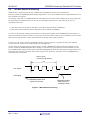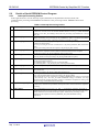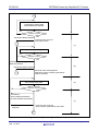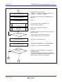
1
APPLICATION NOTE RL78/G10 EEPROM Control by Simplified I2C Function R01AN2217EJ0100 Rev. 1.00 Sep. 17, 2014 Introduction This application note describes how to control the external serial EEPROM by using Simplified I2C function of the serial array unit (SAU). Realizes reading/writing serial EEPROM through I2C bus connection using Simplified I2C function by interrupt processing. Target Device RL78/G10 When applying the sample program covered in this application note to another microcontroller, modify the program according to the specifications for the target microcontroller and conduct an extensive evaluation of the modified program. R01AN2217EJ0100 Rev. 1.00 Sep. 17, 2014 Page 1 of 81 RL78/G10 EEPROM Control by Simplified I2C Function Contents 1. Specification ..................................................................................................................... 4 1.1 Page Boundary Processing ....................................................................................................... 6 1.2 I2C Bus Release Processing ...................................................................................................... 7 1.3 Address Setup Processing of EEPROM ................................................................................... 8 1.3.1 Targeted EEPROM Specification............................................................................................ 8 1.3.2 Address Update ...................................................................................................................... 8 1.3.3 Writing Processing of EEPROM ............................................................................................. 8 2. Operation Confirmation Conditions ............................................................................... 9 3. Related Application Notes............................................................................................... 9 4. Description of Hardware ................................................................................................ 10 4.1 Hardware Configuration Example ........................................................................................... 10 4.2 List of Pins to be Used ............................................................................................................. 11 5. Software .......................................................................................................................... 12 5.1 Operation Outline ...................................................................................................................... 12 5.2 Details of Serial EEPROM Control Program ........................................................................... 14 5.2.1 Interrupt Processing Outline ................................................................................................. 14 5.2.2 EEPROM Control Program State Transitions ....................................................................... 15 5.3 Option Byte Settings................................................................................................................. 21 5.4 Constants ................................................................................................................................... 21 5.5 Variables .................................................................................................................................... 23 5.6 Function (Subroutine) List ....................................................................................................... 23 5.7 Function (Subroutine) Specifications ..................................................................................... 24 5.7.1 External Function .................................................................................................................. 24 5.7.2 Internal Processing Function ................................................................................................ 27 5.8 Flowcharts ................................................................................................................................. 29 5.8.1 CPU Initialization Function .................................................................................................... 29 5.8.2 I/O Port Setup ....................................................................................................................... 30 5.8.3 Clock Generation Circuit ....................................................................................................... 32 5.8.4 Interrupt Setup ...................................................................................................................... 33 5.8.5 Main Processing ................................................................................................................... 35 5.8.6 IIC00 Initialization .................................................................................................................. 39 5.8.7 INTIIC00 Interrupt Entry Processing ..................................................................................... 45 5.8.8 EEPROM Upper Address Transmitting ................................................................................ 46 5.8.9 EEPROM Lower Address Transmitting ................................................................................ 46 5.8.10 Restart Processing Setup ..................................................................................................... 47 5.8.11 I2C Write Processing ............................................................................................................ 47 5.8.12 I2C Data Reception Start Processing ................................................................................... 48 R01AN2217EJ0100 Rev. 1.00 Sep. 17, 2014 Page 2 of 81 RL78/G10 EEPROM Control by Simplified I2C Function 5.8.13 I2C Data Reception Processing ............................................................................................ 49 5.8.14 Final Data Reception Processing.......................................................................................... 50 5.8.15 Data Transmission Start Processing .................................................................................... 50 5.8.16 Data Transmission Processing ............................................................................................. 51 5.8.17 Completion of Data Writing ................................................................................................... 52 5.8.18 Check Processing for Data Write Completion ...................................................................... 53 5.8.19 Write Start Processing to Specified Block ............................................................................ 54 5.8.20 I2C Bus Access Start ............................................................................................................ 54 5.8.21 Specified Block Read-out Start Processing .......................................................................... 55 5.8.22 Read Situation Check Processing ........................................................................................ 55 5.8.23 Write/Read Completion Waiting Processing ......................................................................... 56 5.8.24 Stop Condition Execution...................................................................................................... 57 5.8.25 Timer Initialization ................................................................................................................. 58 5.8.26 Start Condition Generation ................................................................................................... 66 5.8.27 Stop Condition Generation.................................................................................................... 71 5.8.28 I2C Bus Release Processing ................................................................................................ 73 5.8.29 SCL Pulse Generation .......................................................................................................... 73 5.8.30 SCL Signal Raising ............................................................................................................... 74 5.8.31 SCL Signal Lowering ............................................................................................................ 74 5.8.32 SCL Signal Width Securing................................................................................................... 75 5.8.33 Calculation of Slave Address ................................................................................................ 76 5.9 Sample Code Setup .................................................................................................................. 77 5.9.1 The Way of Sample Code Setting ........................................................................................ 77 5.9.2 Processing in the Sample Code............................................................................................ 79 6. Sample Code .................................................................................................................. 81 7. Documents for Reference ............................................................................................. 81 R01AN2217EJ0100 Rev. 1.00 Sep. 17, 2014 Page 3 of 81 RL78/G10 1. EEPROM Control by Simplified I2C Function Specification In this application note, controls serial EEPROM which is connected to external with using Simplified I2C function of the serial array unit (SAU). Checks a state of SW1 after end of the rest. Reads all memory areas of the serial EEPROM if SW1 is pressed. Reads and writes data of all memory areas of the serial EEPROM if SW1 is not pressed. Access to the serial EEPROM is performed per block (data size chosen from 4/8/16 bytes). Blinks LED whenever 1 block of writing/reading processing of serial EEPROM is completed normally. If the writing/reading processing is failed, stops LED blinking. (The state of LED is lighting or extinction and subsequent processing is not performed.) When the writing/reading of serial EEPROM carry out a normal end, makes LED lighting state and moves to the waiting for SW1 keypress. If SW1 is pressed, makes LED lighting-out state and performs writing/reading all the memory areas of EEPROM. The detail specification of this application note is shown below. ・RL78/G10 microcontroller is used as the master, and serial EEPROM is used as the slave. ・Selects a target serial EEPROM from 512K-bit (64K-byte) to 2K-bit (256-byte). (Selectable serial EEPROMs are 2K-bit, 4K-bit, 8K-bit, 16K-bit, 32K-bit, 64K-bit, 128K-bit, 256K-bit and 512K-bit. 256K-bit serial EEPROM is selected as the default.) ・Selects a communication rate either first mode (Max.384k bps*) or normal mode (Max.100 kbps). * As for the transfer rate of simplified I2C function, the duty ration is 50% due to use SAU operation clock. For this reason, it is required to set a transfer rate that the low level width of a SCL signal meets the specification of I2C bus (1.3 μs). And the first mode is not 400kbps but around 384kbps. (Refer to RL78/G10 User's Manual: Hardware for more information.) ・Accesses serial EEPROM per a data block unit defined beforehand. In this application note, the data size of 1 block is chosen from 4/8/16 bytes in order to avoid processing of the page boundary at the time of EEPROM writing. (Refer to “1.1 Page Boundary Processing” for more information.) ・Bus release processing is performed in consideration of a possibility that I2C bus is occupied. (Refer to “1.2 I2C Bus Release Processing” for more information.) ・Using interrupt processing, writing/reading EEPROM are performed in the background. Table 1.1 shows the peripheral function to be used and its use. Figure 1.1 shows the operation outline. Table 1.1 Peripheral Function to be Used and its Use Peripheral Function Serial array unit (SAU) Use Using a simplified I2C function, I2C master transmission and reception are performed. (SCL00 pin and SDA00 pin are used.) Timer array unit 0 (TAU0) Uses the interval timer of 100us or 400us in order to check the completion of writing at data transmission processing. (A timer speed is switched to either first mode or normal mode.) Channel 1 R01AN2217EJ0100 Rev. 1.00 Sep. 17, 2014 Page 4 of 81 RL78/G10 EEPROM Control by Simplified I2C Function End of the reset Keypress of SW1 No operation of SW1 Reading from all memory areas of EEPROM LED is illuminated or extinguished whenever the processing of 1 block is ended normally. Writing to all memory areas of EEPROM LED is illuminated or extinguished whenever the processing of 1 block is ended normally. Normal end Abnormal end Normal end Abnormal end Reading from all memory areas of EEPROM LED is illuminated or extinguished whenever the processing of 1 block is ended normally. Abnormal end EEPROM Access failure processing The infinite loop in LED lighting or a putting-out-lights state is continued. Normal end Keypress of SW1 Waiting for SW1 keypress Illuminates LED, and waits SW1 keypress in HALT mode. When SW1 is pressed, extinguishes LED. Figure 1.1 Operation Outline R01AN2217EJ0100 Rev. 1.00 Sep. 17, 2014 Page 5 of 81 RL78/G10 1.1 EEPROM Control by Simplified I2C Function Page Boundary Processing EEPROM is divided into the page of the size which differs from 16 bytes to 128 bytes according to a kind. When reading data from EEPROM, paying attention to these page boundaries is not necessary, but following cautions are required to write data in EEPROM. As for the writing of EEPROM, accessing to plural pages at one processing (1 block) is prohibited. Since a page will not be automatically updated, if the address for writing arrives at the final address of a page before end of the writing, it overwrites from the head address of the same page. For this reason, if it writes in being unconscious of a page boundary, there is a possibility that data overwrite which is not expected has occurred. In this application note, in order to avoid the incorrect writing by page boundary access, a data block is chosen from 4/8/16 byte in advance. Since these block sizes are enough small to write in one page, the page boundary is not need to be conscious. EEPROM 1 block size 4/8/16 bytes 1 block size 4/8/16 bytes 1 block size 4/8/16 bytes Page size 64 bytes Choses a writing block size from 4/8/16 bytes so that 1 block of write-in processing may be settled in page size. Page size 64 bytes Figure 1.2 EEPROM Page Boundary Processing R01AN2217EJ0100 Rev. 1.00 Sep. 17, 2014 Page 6 of 81 RL78/G10 1.2 EEPROM Control by Simplified I2C Function I2C Bus Release Processing When I2C bus is used, generates the stop condition first and makes the I2C bus into a released state. However, if the slave (EEPROM) makes the SDA signal the low level, stop condition cannot be generated and I2 C bus may be unable to be opened. For example, when read-out of EEPROM has been interrupted by the reasons of the communications processing of I2C bus not having been finished normally on the way, this abnormal condition occurs. The following two can be considered as the cause. (1) The master was reset by factors other than a power down during read-out of EEPROM. (2) The master answered ACK to the last data at the time of read-out of EEPROM. (1) will be in an abnormal condition because there is no means which applies reset to EEPROM from the outside. (2) will be in an abnormal condition because it is necessary to certainly answer NACK to the received data (in the case that data reception ends normally as well) when the master of I2C bus ends reception operation. In such a case, the master of I2C bus manipulates the SCL signal by software to generate the fake clocks (dummy clocks) of I2C bus. And waits for a SDA signal to become high-level. If a SCL signal is generated for longer than or equal to 9 clocks, EEPROM will make a SDA signal high-level. The reason is as follows. EEPROM outputs data according to a transmission request from the master. If the data is 0 (low level), EEPROM has stopped. If SCL signal is detected, EEPROM shifts to the next data output and stops the drive of a SDA signal after 8 clocks at the latest for the ACK reception from the master. And after 9 clocks, EEPROM detects NACK and stops transmission. Dummy clock 8 clocks (rough sketch) SCL signal SDA signal EEPROM makes SDA signal into low level. EEPROM releases SDA signal. (for checking of ACK) Figure 1.3 Bus Release Processing R01AN2217EJ0100 Rev. 1.00 Sep. 17, 2014 Page 7 of 81 RL78/G10 1.3 1.3.1 EEPROM Control by Simplified I2C Function Address Setup Processing of EEPROM Targeted EEPROM Specification In this application note, uses Serial EEPROM of Renesas Electronics. The serial EEPROM varies in an addressing method of the memory cell in the EEPROM depending on capacity size. Table 1.2 shows the specification of serial EEPROM used with this application note made by Renesas Electronics. Table 1.2 Addressing Method of EEPROM Bit 7 Bit 6 Bit 5 Bit 4 Bit 3 Bit 2 Bit 1 Bit 0 1 0 1 0 A2 A1 A0 R/W Products R1EX24512B R1EX24256BNote R1EX128B R1EX24064A R1EX24032A R1EX24016A R1EX24008A R1EX24004A R1EX24002A Capacity (byte) 64K 32K 16K 8K 4K 2K 1K 512 256 Required address length 16 bits (a15 to a0) 15 bits (a14 to a0) 14 bits (a13 to a0) 13 bits (a12 to a0) 12 bits (a11 to a0) 11 bits (a10 to a0) 10 bits (a9 to a0) 9 bits (a8 to a0) 8 bits (a7 to a0) A2 to A0 1st byte 2nd byte - - - - - a10 to a8 a9,a8 A0=a8 - a15 to a8 a14 to a8 a13 to a8 a12 to a8 a11 to a8 a7 to a0 a7 to a0 a7 to a0 a7 to a0 a7 to a0 a7 to a0 a7 to a0 a7 to a0 a7 to a0 - - - - Note: It is EEPROM used for the operation confirmation of this application note. 1.3.2 Address Update Reading or writing is performed by specifying an address, the address is updated automatically and comes to show the next address in EEPROM. Therefore, it is not necessary to specify an address each time when performing continuation writing and reading data. However, the continuation writing over a page boundary requires the described cautions "1.1 Page Boundary Processing". 1.3.3 Writing Processing of EEPROM If a master (RL78/G10) generates stop condition, EEPROM will actually start writing data received to a memory cell. The execution time of this writing processing (for 1 page)is about 5 ms, and EEPROM does not responds ACK to a master (RL78/G10) in this 5 ms. In order to write data continuously, it is necessary to transmit the next data after the waiting of the writing end waiting (about 5 ms). As a method of checking a writing completion waiting state, start condition is generated from a master (RL78/G10), and it transmits in the writing mode (LSB=0) of EEPROM. Although it becomes a NACK response under writing processing, if writing is completed, it becomes an ACK response and can check the state of EEPROM. R01AN2217EJ0100 Rev. 1.00 Sep. 17, 2014 Page 8 of 81 RL78/G10 2. EEPROM Control by Simplified I2C Function Operation Confirmation Conditions The sample code accompanying this application note has been run and confirmed under the conditions below. Table 2.1 Operation Confirmation Conditions Item MCU used Operating frequency Contents RL78/G10 (R5F10Y16) ・ High-speed on-chip oscillator (HOCO) clock: 20 MHz ・ CPU/peripheral hardware clock: 20 MHz Operating voltage Integrated development environment (CubeSuite+) Assembler (CubeSuite+) Integrated development environment (e2studio) Assembler (e2studio) Integrated development environment (IAR) Assembler (IAR) Board used 3.3V(Operation is possible over a voltage range of 2.9 to 5.5 V.) SPOR Operating Voltage: Rising voltage: 2.90V Falling voltage: 2.84V Renesas Electronics CubeSuite+ V2.02.01 Renesas Electronics RA78K0R V1.70 Renesas Electronics e2studio V2.2.0.13 Renesas Electronics KPIT GNURL78-ELF Toolchain V14.0.1 IAR Systems IAR Embedded Workbench for Renesas RL78 V1.40.2 IAR Systems IAR Assembler for Renesas RL78 V1.40.2 RL78/G10 target board (QB-R5F10Y16-TB) Table 2.2 EEPROM Specifications Item EEPROM used Operating voltage range Contents R1EX24256B Maximum operation frequency Capacity Page size Rewriting time 400kHz 3. single power supply: 1.8V to 5.5V 256K bits 64 bytes 5ms Related Application Notes The application notes that are related to this application note are listed below for reference. RL78/G10 Initialization (R01AN1454E) Application Note RL78/G10 Timer Array Unit (Interval Timer) (R01AN1457E) Application Note R01AN2217EJ0100 Rev. 1.00 Sep. 17, 2014 Page 9 of 81 RL78/G10 4. EEPROM Control by Simplified I2C Function Description of Hardware 4.1 Hardware Configuration Example Figure 4.1 shows an example of hardware configuration that is used for this application note. RL78/G10 (master) VDD VDD VDD RESET VDD SW1 LED P00 P137/INTP0 Vcc External pull-up P02/SCL00 VSS Vcc SCL P01/SDA00 P40/TOOL0 EEPROM (slave) R1EX24256B A0 A1 SDA A2 VSS WP For on-chip debugger Figure 4.1 Hardware Configuration Cautions: 1. The purpose of this circuit is only to provide the connection outline and the circuit is simplified accordingly. When designing and implementing an actual circuit, provide proper pin treatment and make sure that the hardware's electrical specifications are met (connect the input-only ports separately to VDD orVSS via a resistor). 2. VDD must be held at not lower than the reset release voltage (VSPOR) that is specified as SPOR. 3. Since EEPROM device address pins (A0, A1, A2) are pulled-up inside EEPROM, they are recognized unconnecting. R01AN2217EJ0100 Rev. 1.00 Sep. 17, 2014 Page 10 of 81 RL78/G10 4.2 EEPROM Control by Simplified I2C Function List of Pins to be Used Figure 4.1 lists the pins to be used and their functions. Table 4.1 Pins to be Used and their Functions Pin Name P00 I/O Output P01/SDA00 Input Output P02/SCL00 P137/INTP0 Output Input R01AN2217EJ0100 Rev. 1.00 Sep. 17, 2014 Description LED drive port Under EEPROM read-out/writing processing: Blinking: Blinks LED whenever 1 block of writing/reading processing of serial EEPROM is completed normally. Lighting/extinction: An error is occurred at writing/reading of EEPROM. Waiting for SW1 keypress: Lighting: Waiting for SW1 keypress. Extinction: Accepts SW1 keypress and starts EEPROM writing/reading processing again. Simplified I2C data input/output Simplified I2C clock output Switch input (SW1) At power-on No operation: Starts EEPROM writing/reading processing. Keypress: Reads out EEPROM. Waiting for keypress No operation: Continues to wait keypress. Keypress: Starts EEPROM writing/reading processing. Page 11 of 81 RL78/G10 5. 5.1 EEPROM Control by Simplified I2C Function Software Operation Outline This application note checks the SW1 state after the release from the reset. When SW1 is pressed, reads all memory areas of serial EEPROM. When SWI is not pressed, reads and writes all memory areas of serial EEPROM Blinks LED whenever 1 block of writing/reading processing of serial EEPROM is completed normally. If the writing/reading processing is failed, stops LED blinking. (The state of LED is lighting or extinction and subsequent processing is not performed.) When the writing/reading of serial EEPROM carry out a normal end, makes LED lighting state and moves to the waiting for SW1 keypress. If SW1 is pressed, makes LED lighting-out state and performs writing/reading all the memory areas of EEPROM. (1) Initializes on-chip peripheral functions. <Setting conditions> a) Sets I/O port. Sets a digital I/O to PMC0 register. Sets the initial value to P0 register as initializes LED connection pin (P00) is high output, SDA00 pin (P01) is low output, and SCL00 pin (P02) is low output. Sets the initial value to PM0 register as initializes LED connection pin (PM00) is output, SDA00 pin (PM01) is input, and SCL00 (PM02) is input. b) Sets clock generator. Sets HOCODIV register to 20MHz. c) Initializes interruption related registers. Sets the mask of INTP0 interrupt. Enables to detect falling edge of INTP0 interrupt. Clears the interrupt request of INTP0 interrupt. (2) Clears the memory area used by a program. a) Clears the number of blocks writing/reading (variable: BLOCK_NUMBER). b) Clears data storage areas of reading and writing (variable: WRITE_BUFF, READ_BUFF, R_BUFF_END). c) Clears I2C interrupt control status (variable: STATUS). d) Clears the number of data I2C writing/reading processing (variable: DATACOUNT). e) Clears the slave address of I2C (variable: SLAVEADDR). (3) Initializes SAU as the simplified I2C function. a) Sets SAU0EN bit of PER0 register as a clock is provided to SAU. b) Sets SPS0 register as the frequency of operation clock CK00 and operation clock CK01 are 20MHz. c) Sets SIR00 register as the error flag is cleared. d) Sets SMR00H register as the operation clock CK00 is selected. e) Sets SMR00L register as the simplified I2C mode and the transfer end interrupt are set. f) Sets SCR00H register as the transfer mode, no parity, and type 1 are set. g) Sets SCR00L register as MSB first is set. h) Sets SDR00H register as the transfer clock is 384kbps at fast mode and 100kbps at normal mode. i) Sets SO00 bit of SO0 register as SDA pin is high. j) Sets CKO00 bit of CKO0 register as SCL pin is high. k) Sets POM0 register as SDA pin and SCL pin are output. R01AN2217EJ0100 Rev. 1.00 Sep. 17, 2014 Page 12 of 81 RL78/G10 (4) EEPROM Control by Simplified I2C Function Sets TAU0 for confirming the Transmit data completion. Initializes TAU0 to 100μs at the fast mode and to 400μs at the normal mode. a) Sets TAU0EN bit of PER0 register to provide the clock to TAU. b) Sets TTH01 bit of TTH0 register and TT01 bit of TT0 register to stop the timer. c) Sets the frequency of the operation clock CK00 and the operation clock CK01 to fCLK/16 (fast mode) or fCLK/64 (normal mode) through TPS0 register. d) Sets TMR01H register as the operation clock CK01 is selected and The 8-bit timer operation is set. e) Sets TMR01L register to set the interval timer. f) Sets TDR01H register as 100μs at the fast mode and 400μs at the normal mode. g) Sets TOE01 bit of TOE0 register to set TO01 output disabled. h) Sets TO0 register to set Timer output value 0. i) Sets TMMK01H bit of MK0L register to set the interrupt request mask. j) Sets TMIF01H bit of IF0L register to set interrupt request clear. (5) Generates stop condition and makes I2C bus the bus release status before using I2C bus. In order to make I2C bus the bus released status, waits for SDA signal becomes high by generating spurious I2C bus clock (dummy clock) through controlling SCL00 signal by a program. After becoming high of SDA signal, generates the stop condition and releases the bus. (6) Monitors the state of SW1, and if SW1 is pressed, performs EEPROM reading processing. If SW1 is not pressed, performs reading and writing processing of EEPROM. Refer to Chapter 5.2 for more information about EEPROM control part. (7) Creates data to be written to EEPROM. Creates data to be written based on selected block size (4/8/16-byte), the number of blocks of EEPROM that is destination to write, and the final 1 byte of write buffer. The example of data to be written at the time of choosing 4 bytes as block size is shown in Table 5.1. Table 5.1 Data to be written into EEPROM Block number to be written The example of write data. (In the case that the block size is 4 bytes.) After reset releasing 0x00, 0x00, 0x00, 0x00 Write block number 0 0x01, 0x02, 0x03, 0x04 (Creates data to be written from the previous wrote data: final value 0x00.) Write block number 1 0x05, 0x06, 0x07, 0x08 (Creates data to be written from the previous wrote data: final value 0x04.) ・・・ ・・・ Write block number 16 0x41, 0x42, 0x43, 0x44 ・・・ ・・・ Write block number 63 0xFD, 0xFE, 0xFF, 0x00 Write block number 64 0x01, 0x02, 0x03, 0x04 ・・・ ・・・ Note: This application note shows control examples of EEPROM (R1EX24256B) by I2C bus using the simplified I2C functions of RL78/G10 (IIC00). If channels or EEPRO to be used are changed, conducts an extensive evaluation of the modified program. R01AN2217EJ0100 Rev. 1.00 Sep. 17, 2014 Page 13 of 81 RL78/G10 5.2 5.2.1 EEPROM Control by Simplified I2C Function Details of Serial EEPROM Control Program Interrupt Processing Outline In this application note, uses the interrupt request (INTIIC00) of simplified I2C function (IIC00). The communications processing with EEPROM is divided into some processing routines. Table 5.2 shows those processing. Table 5.2 Interrupt Processing Outline No. Processing routine name 0 IINTIIC00 1 R_IIC00_Tx_addr1 2 R_IIC00_Tx_addr2 3 R_IIC00_Rx_RST 4 R_IIC00_RxDataST 5 R_IIC00_RxData 6 R_IIC00_Rx_Last 7 R_IIC00_TxDataST 8 R_IIC00_TxData 9 R_EEPROM_WT_END 10 IINTTM01H R01AN2217EJ0100 Rev. 1.00 Sep. 17, 2014 Processing If IIC00 receives ACK, makes to branch to processing of 1 to 9 of the following. If NACK is received, it will be checked whether STATUS is AFT_TX (under EEPROM writing). If it is AFT_TX, nothing is done, but error processing is performed if it is except AFT_TX. Upper bytes transmitting processing of the EEPROM address after the completion of slave address transmitting. It is processing of only EEPROM of 32K to a 512K bit, and common to transmission and reception. The next processing is R_IIC00_Tx_addr2. Lower address transmitting processing of EEPROM. This processing is common to transmission and reception. The next processing at the time of transmission is R_IIC00_TxDataST (data transmission start). The next processing at the time of reception is R_IIC00_Rx_RST (restart). Performs the restart condition generate and the slave address transmission in reception mode after the completion of slave address transmission at the time of reception. The next processing is R_IIC00_RxDataST (data reception start). The start of data reception processing after the completion of slave address transmission in receiving mode. The next processing is R_IIC00_RxData (data reception). The data reception processing. Stores received data to a buffer. The next processing as follows. The remaining data is 2 bytes or more: R_IIC00_RxData The remaining data is 1: R_IIC00_Rx_Last (receiving the final data) Stops IIC00 by the completion of final data reception, and generates stop condition. Data transmission-start processing after the completion of slave address transmission by data transmission. The next processing is R_IIC00_TxData (data transmission). The completion of data transmission of 1 byte. The following data will be transmitted if there is the remaining data. The next processing is R_IIC00_TxData. If the remaining day is lost, generates stop condition (EEPROM starts writing received data to the memory cell) , sets AFT_TX (under EEPROM writing) to STATUS, and stops operation of IIC00. Activates the timer in order to confirm the completion of writing. The next processing is IINTTM01H (timer interrupt). The completion of writing processing of EEPROM (the ACK response to slave address transmission). Generates stop condition, and stops the timer which confirms the completion of writing. Interval interruption in every 100 μs or 400 μs. Confirms the completion of writing at EEPROM (transmission of slave address in transmission mode). The response to this slave address transmission is INTIIC00 interrupt request. Transmission processing will be completed if the response becomes R_EEPROM_WT_END (EEPROM writing completion). Page 14 of 81 RL78/G10 5.2.2 EEPROM Control by Simplified I2C Function EEPROM Control Program State Transitions In this application note, if the access processing to EEPROM begins, a state will change by interrupt request (INTIIC00) generating of IIC00. The change state of read-out and write-in processing is shown below. (1) Reading processing state transition Figure 5.1 and Figure 5.2 show the serial EEPROM reading processing state transition. Starts reading A (a) Standby state No INTIIC0 occurs? Yes Parameter error Receiving request & normal parameter/ Start condition generation & Slave address transmission A Transmission waiting state of slave address No INTIIC0 occurs? Yes INTIIC00 & ACK response & 16K bits or less/ Address transmission INTIIC00 & NACK response/ Stop condition generation (b) B A INTIIC00 & ACK response & 32K bits or over/ Upper address transmission Transmission waiting state of EEPROM upper address No INTIIC0 occurs? Yes INTIIC00 & NACK response/ Stop condition generation INTIIC00 & ACK response/ Lower address transmission B A Figure 5.1 Reading Processing State Transition (1/2) R01AN2217EJ0100 Rev. 1.00 Sep. 17, 2014 Page 15 of 81 RL78/G10 EEPROM Control by Simplified I2C Function B Transmission waiting state of EEPROM lower address No INTIIC0 occurs? INTIIC00 & NACK response/ Stop condition generation Yes INTIIC00 & ACK response/ Restart & slave address response A (c) Transmission waiting state of slave address No INTIIC0 occurs? INTIIC00 & NACK response/ Stop condition generation Yes INTIIC00/Reception activation A (d) Data reception waiting state No INTIIC0 occurs? Yes INTIIC00 & remaining 1 byte/Reading reception data & NACK response & reception activation INTIIC00 & remaining 2 bytes or more /Reading received data & reception activation (e) Final data reception waiting state No INTIIC0 occurs? Yes INTIIC00/Reading received data & Stop condition generation (f) A Figure 5.2 Reading Processing State Transition (2/2) R01AN2217EJ0100 Rev. 1.00 Sep. 17, 2014 Page 16 of 81 RL78/G10 EEPROM Control by Simplified I2C Function (a) If EEPROM reading processing is called under the standby state, a parameter (the target block number) will be checked. When the block number is wrong, since it is a parameter error, processing is ended. If a parameter is right, start condition will be generated and a slave address will be transmitted as LSB=0. (b) Checks a response from a slave by a interrupt request from INTIIC00. When it is NACK response, generates a stop condition and ends the processing. When it is ACK response, transmits EEPROM address. At this time, 2 bytes of address information is transmitted to EEPROM which is 32K bits or above, and 1 byte of address information is transmitted to EEPROM which is 16K bits or less. (c) The response from a slave is checked by the interrupt request of INTIIC00. If it is a NACK response, generates a stop condition and ends the processing. When it is ACK response, generates a restart condition and transmits a slave address as LSB=1. (d) Checks a response from a slave by INTIIC00 interrupt request. If it is NACK response, generates stop condition and ends the processing. If it is ACK response, stops IIC00, and then changes into receiving mode and reboots. Activates the receiving operation by writing the dummy data to SIO00. (e) Stores received data into a buffer by INTIIC00 interrupt request. If the number of remaining receiving data is 2 or more, activate the receiving operation by writing the dummy data to SIO00. If the number of remaining receiving data is 1, disables ACK response (SOE00=0) and activates the receiving operation by writing dummy data to SIO00. (f) Stores receiving data to a buffer by INTIIC00 interrupt request. Since the receiving processing is completed, stops IIC00 operation, generates stop condition, and finishes the processing. R01AN2217EJ0100 Rev. 1.00 Sep. 17, 2014 Page 17 of 81 RL78/G10 EEPROM Control by Simplified I2C Function (2) Writing processing state transition Figure 5.3 and Figure 5.4 show the serial EEPROM writing processing state transition. Starts writing C (a) Standby state No INTIIC0 occurs? Yes Parameter error Receiving request & normal parameter/ Start condition generation & Slave address transmission C Transmission waiting state of slave address No INTIIC0 occurs? Yes INTIIC00 & ACK response & 16K bits and below/Address transmission INTIIC00 & NACK response/ Stop condition generation (b) D C INTIIC00 & ACK response & 32K bits and above/ Upper address transmission Transmission waiting state of EEPROM upper address No INTIIC0 occurs? Yes INTIIC00 & NACK response/ Stop condition generation INTIIC00 & ACK response/ Lower address transmission D C Figure 5.3 Writing Processing State Transition (1/2) R01AN2217EJ0100 Rev. 1.00 Sep. 17, 2014 Page 18 of 81 RL78/G10 EEPROM Control by Simplified I2C Function D Transmission waiting state of EEPROM lower address No INTIIC0 occurs? Yes INTIIC00 & NACK response INTIIC00 & ACK response/ Data transmission C (c) Data transmission waiting state No INTIIC0 occurs? Yes INTIIC00 & Remaining data exists/ Data transmission (d) INTIIC00 & NACK response INTIIC00 & No remaining data/ IIC00 stop & Stop condition generation & TM01H activation C Data writing waitig state (e) No INTIIC0 occurs? Yes INTTM01H/ Start condition generation & Slave address transmission (f) INTIIC00 & ACK response/ INTIIC00 & NACK response Stop condition generation & stop IIC00 C Figure 5.4 Writing Processing State Transition (2/2) R01AN2217EJ0100 Rev. 1.00 Sep. 17, 2014 Page 19 of 81 RL78/G10 EEPROM Control by Simplified I2C Function (a) If EEPROM reading processing is called under the standby state, a parameter (the target block number) will be checked. When the block number is wrong, since it is a parameter error, processing is ended. If a parameter is right, start condition will be generated and a slave address will be transmitted as LSB=0. (b) Checks a response from a slave by a interrupt request from INTIIC00. When it is NACK response, generates a stop condition and ends the processing. When it is ACK response, transmits EEPROM address. At this time, 2 bytes of address information is transmitted to EEPROM which is 32K bits or above, and 1 byte of address information is transmitted to EEPROM which is 16K bits or less. (c) The response from a slave is checked by the interrupt request of INTIIC00. If it is a NACK response, generates a stop condition and ends the processing. When it is ACK response, writes transmission data to SIO00 and starts transmission. (d) Checks a response from a slave by INTIIC00 interrupt request. If it is NACK response, generates stop condition and finishes the processing. If it is ACK response, writes the next transmission data to SIO00 and starts the transmission. If there is no next data, generates stop condition, completes the transmission, and starts writing to EEPROM. In order to confirm the completion of writing, activates TM01H as an interval timer of 100μs. At this time, changes Variable STATUS into AFT_TX and sets up under the writing processing after transmission. (e) In order to confirm the completion of writing to EEPROM by INTTM01H interrupt request, transmits start condition and slave address (LSB=0). (f) Checks a response from a slave by INTIIC00 interrupt request. If it is NACK response, waits for the next INTTM01H interrupt request. If it is ACK response, generates stop condition, and stops IIC00 and TM01H since writing to EEPROM is completed. Variable STATUS is set to the completion of transmission. R01AN2217EJ0100 Rev. 1.00 Sep. 17, 2014 Page 20 of 81 RL78/G10 5.3 EEPROM Control by Simplified I2C Function Option Byte Settings Table 5.3 shows the option byte setting. Table 5.3 Option Byte Setting Address 000C0H Value 11101110B 000C1H 11110111B 000C2H 000C3H 11111001B 10000101B 5.4 Description Watchdog timer operation stop (Stops counting after the release from the reset state.) P125/RESET pin: RESET input (The on-chip pull-up resistor is always valid.) SPOR voltage Rising-edge voltage: 2.90V Falling-edge voltage: 2.84V HOCO : 20MHz Enables the on-chip debugger Constants Table 5.4 and Table 5.5 list the constants that are used in this sample program. Table 5.4 Constants for the Sample Program (1/2) Constant Setting Description CLKFREQ 20000 FAST_MODE - It is the definition which expressed the operation clock fCLK of RL78/G10 per kHz. It is defined at the time of the fast mode use. When undefined, it operates as a normal mode. <Fast mode setting> DIVIDE 13 * CLKFREQ / 10000 <Normal mode setting> DIVIDE 50 * CLKFREQ / 10000 <Common> CSDRDATA (DIVIDE - 1) * 2 SCLLOWW (DIVIDE -13 + 4)/5 SCLHIGHW (DIVIDE2 -13 + 4)/5 R1EX24002A 00H R1EX24004A 01H R1EX24008A 02H R1EX24016A 03H R1EX24032A 04H R1EX24064A 05H R1EX24128B 06H R1EX24256B 07H R1EX24512B 08H EEPROM_MAX 09H R01AN2217EJ0100 Rev. 1.00 Sep. 17, 2014 384kbps 100 kbps SDR00H SCL low time SCL high time 2K-bit EEPROM 4K-bit EEPROM 8K-bit EEPROM 16K-bit EEPROM 32K-bit EEPROM 64K-bit EEPROM 128K-bit EEPROM 256K-bit EEPROM 512K-bit EEPROM device end Page 21 of 81 RL78/G10 EEPROM Control by Simplified I2C Function Table 5.5 Constants for the Sample Program (1/2) Constant Setting Description The size of a block is defined. By default, it is 4 bytes/block. Although the block size can be changed into 8 or 16 bytes, if makes it too large, a possibility that futility will occur will become high. BLKSIZE 4 SLAVE MASK0 MASK2 EEPROM 0A0H 00000000B 11111111B R1EX24256B BLKNO Slave address Mask pattern Mask pattern Name of EEPROM. Its value is from 0 (2K bits) to 8 (512K bits). 32768/BLKSIZE The number of blocks included in EEPROM. A value is decided by capacity setup of EEPROM. Here, the value at the time of choosing 256K-bit EEPROM is shown. I2C_OK 00000000B Normal end PARA_ERR 01000100B Parameter error NO_ACK1 01000000B No ACK response to Slave address NO_ACK2 01000001B Slave data error (write-protect ) BUS_ERR 01100000B I2C-Bus error TRANSMIT 10000000B Slave address transmission status AFT_TX TRANSMIT + 20H Data writing status RECEIVE TRANSMIT + 40H Receiving status TRNSEND 00H SVAMSK 11111110B RETRYCNT 9 CTXMODETxH 10000000B Initialization of IIC register CRXMODERxH 01000000B Refer to the item of the flowchart for details. CTRXMODEL 00010111B CSMRDATAH 00000000B CSMRDATAL 00100100B R01AN2217EJ0100 Rev. 1.00 Sep. 17, 2014 transmit completes Mask R/W bit Maximum number of dummy SCL pulses Page 22 of 81 RL78/G10 5.5 EEPROM Control by Simplified I2C Function Variables Table 5.6 lists the variables that are used in this sample program. Table 5.6 Variables for the Sample Program Variable NEXTADR EEPROMADDR BLOCK_NUMBER Outline Stores a transfer destination address. Specifies EEPROM address. Specifies the block number which EEPROM of a controlled object wants to access. WRITE_BUFF READ_BUFF R_BUFF_END STATUS DATACOUNT SLAVEADDR Sets data to write in EEPROM. A buffer which stores read data from EEPROM. Stores data which is received at the end of specified size. Stores the status of I2C interrupt control function by function. Stores the number of data of I2C writing or reading. Slave address of I2C. 5.6 Function (Subroutine) List Table 5.7 and Table 5.8 shows the function (subroutine). Table 5.7 Function (External Function) Function PUTDATA GETDATA PUT_ CHK GET_ CHK WAIT_END StopCond R_IIC00_Init SINITAU IINTIIC00 Outline Writing start processing to the specified block Reading start processing from the specified block Writing to EEPROM state check processing Reading from EEPROM state check processing Waiting processing for the completion of access to EEPROM Execution of stop condition to I2C bus Initialization of IIC00 Initialization of TAU01 IIC00 interrupt handler Table 5.8 Function (Internal Processing Function) Function StartCond R_IIC00_send_Stop R_IIC00_wait_bus R_IIC00_SCL_pulse R_IIC00_SCL_high R_IIC00_SCL_low R_IIC00_SCL_Time get_slave_Addr R01AN2217EJ0100 Rev. 1.00 Sep. 17, 2014 Outline Generates start condition to I2C bus Generates stop condition to I2C bus Releases I2C bus Outputs SCL signal of 1 pulse Raises SCL signal to high falls SCL signal to low Secures the time of the pulse width of a SCL signal Calculates the address in I2C bus of EEPROM Page 23 of 81 RL78/G10 5.7 EEPROM Control by Simplified I2C Function Function (Subroutine) Specifications This section describes the specifications for the functions (subroutines) that are used in this sample program. 5.7.1 External Function [Function Name] PUTDATA Writing start processing to the specified block Outline Checks the state of the bus and generates start condition. Explanation Then, calculates the address of a cell from a block number and transmits a slave address. BLOCK_NUMBER : Block number which data will be written in Argument : Data to write WRITE_BUFF Return value Variable STATUS: TRANSMIT : Processing is started normally. PARA_ERR : The error in specification (The block BUS_ERR number was too large. : I2 C bus is not in the state which can be used. Remarks Return value is stored into the global variable STATUS. [Function Name] GETDATA Reading start processing from the specified block Outline Checks the state of the bus and generates start condition. Explanation Then, calculates the address of a cell from a block number and transmits a slave address. BLOCK_NUMBER : Block number which data will be read from Argument READ_BUFF : Read-out data storing area Variable STATUS: Return value RECEIVE : Processing is started normally. PARA_ERR : The error in specification (The block BUS_ERR number was too large. : I2 C bus is not in the state which can be used. Remarks Return value is stored into the global variable STATUS. R01AN2217EJ0100 Rev. 1.00 Sep. 17, 2014 Page 24 of 81 RL78/G10 EEPROM Control by Simplified I2C Function [Function Name] PUT_CHK Writing to EEPROM state check processing Outline Checks the state after start writing to EEPROM. If the processing is completed, Z flag Explanation is set. None Argument : Processing is completed. Z flag = 1 Return value Variable STATUS: I2C_OK : Normal end BUS_ERR : The state which cannot use a bus. NO_ACK1 TRANSMIT : No ACK response from a slave. AFT_TX : Under slave address transmission. Z flag = 0 : Data transfer is completed and it is under writing. : Under continuation of processing. Remarks If MSB of STATUS is 1, it is under processing. If MSB of STATUS is 0, it is the completion of processing. [Function Name] GET_CHK Reading from EEPROM state check processing Outline Checks the state after start reading from EEPROM. If the processing is completed, Z Explanation flag is set. None Argument : Processing is completed. Z flag = 1 Return value Variable STATUS: I2C_OK : Normal end BUS_ERR : The state which cannot use a bus. NO_ACK1 : No ACK response from a slave. Z flag = 0 : Under continuation of processing. : Under slave address transmission. RECEIVE : Under receiving data. RxData : Under receiving the final data. RxLast Remarks If MSB of STATUS is 1, it is under processing. If MSB of STATUS is 0, it is the completion of processing. [Function Name] WAIT_END Outline Waiting processing for the completion of access to EEPROM Explanation Checks the value of variable STATUS, and waits for the completion of processing. Argument None = 0: Normal end Return value CY flag = 1: Abnormal end Remarks R01AN2217EJ0100 Rev. 1.00 Sep. 17, 2014 Page 25 of 81 RL78/G10 EEPROM Control by Simplified I2C Function [Function Name] StopCond Outline Execution of stop condition to I2C bus Explanation Performs stop condition to I2C bus. Then checks SDA signal, and if SDA signal is low, performs the bus release processing. After finishing bus release, generates stop condition again. Argument None Return value CY flag = 0: Normal end = 1: Abnormal end Remarks The pin is output state. IIC00 is stopped. [Function Name] R_IIC00_Init Outline Initialization of IIC00 Explanation Initializes the interval timer for confirming the completion of writing to EEPROM. The interval is set to 100us at the time of the fast mode, and to 400us at the time of the normal mode. Argument None Return value None Remarks None [Function Name] SINITAU Initialization of TAU01 Outline Explanation Initializes the interval timer of 100μs for confirming the completion of writing to EEPROM. Argument None Return value None Remarks None R01AN2217EJ0100 Rev. 1.00 Sep. 17, 2014 Page 26 of 81 RL78/G10 5.7.2 EEPROM Control by Simplified I2C Function Internal Processing Function [Function Name] StartCond Outline Generates start condition to I2C bus Explanation Generates start condition to I2C bus by manipulating CKO0 and SO0 bit, and makes IIC00 operation enabled state. Argument None Return value None Remarks IIC00 will be in the state of operation enabled by transmitting permission. [Function Name] R_IIC00_send_Stop Generates stop condition to I2C bus Outline Explanation Stopping operation of IIC00 and adjusting timing with using software, generates stop condition (raises SDA signal, raises SCL signal and then raises SDA signal) to I2C bus by manipulating CKO0 and SO0 bit. Argument None Return value None Remarks None [Function Name] R_IIC00_wait_bus Outline Releases I2C bus Explanation Confirms that SDA signal is high. If SDA signal is low, checks the state of the SDA signal outputting 10 false clocks to SCL signal. Even if outputs 9 clocks, when a SDA signal does not become high, it is considered as an error. Argument None Variable STATUS: Return value I2C_OK : Confirmation of bus release (SDA moves to high.) BUS_ERR : SDA still remains in low. Remarks This is a countermeasure against the process discontinuation after data output from EEPROM because of CPU reset and so on. Normally, generates stop condition after this. [Function Name] R_IIC00_SCL_pulse Outline Outputs SCL signal of 1 pulse Explanation Outputs low and high to SCL signal by manipulating CKO0 register. After switching SCL signal, the time for securing the low width or high width of a SCL signal is secured. Argument None Return value None Remarks None R01AN2217EJ0100 Rev. 1.00 Sep. 17, 2014 Page 27 of 81 RL78/G10 EEPROM Control by Simplified I2C Function [Function Name] R_IIC00_SCL_high Outline Raises SCL signal to high Explanation In order to generate stop condition, manipulates CKO0 register to make SCL signal into high, and secures the time for securing high width. Argument None Return value None Remarks None [Function Name] R_IIC00_ SCL_low Outline Falls SCL signal to low Explanation In order to move to the communication operation after generating start condition, manipulates CKO0 register to make SCL signal into low, and secures the time for securing low width. Argument None Return value None Remarks None [Function Name] R_IIC00_SCL_Time Outline Secures the time of the pulse width of a SCL signal Explanation Secures pulse width of SCL signal (1.3us). Argument None Return value None Remarks None [Function Name] get_slave _Addr Calculates the address in I2C bus of EEPROM Outline Explanation Calculates the information to incorporate a memory cell address of EEPROM into a slave address of I2C bus from the information which is set in variable area for internal EEPROM control. And calculates a slave address which is used at actual I2C bus. Argument None = 0: The block number is normal. Return value CY flag: = 1: The block number is error. Remarks None R01AN2217EJ0100 Rev. 1.00 Sep. 17, 2014 Page 28 of 81 RL78/G10 5.8 EEPROM Control by Simplified I2C Function Flowcharts Figure 5.5 shows the overall flowchart of the sample program described in this application note. Start The option bytes are referenced before the initialization function is called. CPU Initialization function RESET_START End Figure 5.5 Overall Flowchart 5.8.1 CPU Initialization Function Figure 5.6 shows the flowchart for the CPU initialization function. RESET_START Set up ES register ES register ← 00H (For table reference) Set stack pointer Set up redirection Set up I/O ports SINIPORT Set up clock generation circuit SINICLK Interrupt initialization SINIINTP0 PIOR register ← 00H PMC0 register← #11100001B P0 register ← #00000110B PM0 register ← #11100110B Sets an operation clock to HOCO (20 MHz). Initialization related to INTP0 register Call main routine main HALT Figure 5.6 CPU Initialization Function R01AN2217EJ0100 Rev. 1.00 Sep. 17, 2014 Page 29 of 81 RL78/G10 5.8.2 EEPROM Control by Simplified I2C Function I/O Port Setup Figure 5.7 shows the flowchart for I/O port setup. SINIPORT PMC0 register ← 11100001B P0 register ← 00000110B PM0 register ← 11100110B Set up port register RET Figure 5.7 I/O Port Setup Function Note: Refer to the section entitled "Flowcharts" in RL78/G10 Initialization Application Note (R01AN1454E) for the configuration of the unused ports. Port setting ・Port mode control register 0 (PMC0) Switching between analog input and digital I/O ・Port registers 0 (P0) Setup of an output latch of each port ・Port mode registers 0 (PM0) Selection of the I/O mode of each port Symbol:PMC0 7 6 5 4 3 2 1 0 1 1 1 PMC04 PMC03 PMC02 PMC01 1 1 1 1 0 0 0 0 1 Bits 4 to 1 0 P0n pin digital I/O/analog input selection Digital I/O (alternate function other than analog input) 1 Analog input PMC0n R01AN2217EJ0100 Rev. 1.00 Sep. 17, 2014 Page 30 of 81 RL78/G10 EEPROM Control by Simplified I2C Function Symbol:P0 7 6 5 4 3 2 1 0 0 0 0 P04 P03 P02 P01 P00 0 0 0 0 0 1 1 0 Bits 2 and 1 P0n P0n pin output data control (in output mode) 0 Output mode (output buffer on) 1 Input mode (output buffer off) Bit 0 P00 P00 pin output data control (in output mode) 0 Output mode (output buffer on) 1 Input mode (output buffer off) Symbol:PM0 7 6 5 4 3 2 1 0 1 1 1 PM04 PM03 PM02 PM01 PM00 1 1 1 0 0 1 1 0 Bits 2 and 1 PM0n P0n pin I/O mode selection 0 Output mode (output buffer on) 1 Input mode (output buffer off) Bit 0 PM0n P00 pin I/O mode selection 0 Output mode (output buffer on) 1 Input mode (output buffer off) Note: Refer to ‘RL78/G10 User's Manual: Hardware’ for more information about the register setting method. R01AN2217EJ0100 Rev. 1.00 Sep. 17, 2014 Page 31 of 81 RL78/G10 5.8.3 EEPROM Control by Simplified I2C Function Clock Generation Circuit Figure 5.8 shows the flowchart for clock generation circuit setup. SINICLK HOCODIV2 to 0 bits ← 1: Sets HOCO frequency to 24 MHz Select frequency of high-speed on-chip oscillator RET Figure 5.8 Clock Generation Circuit Setup Selection of high-speed on-chip oscillator frequency ・High-speed on-chip oscillator frequency selection register (HOCODIV) Selects the frequency of high-speed on-chip oscillator. Symbol:HOCODIV 7 6 5 4 3 2 0 0 0 0 0 0 0 0 0 0 1 0 HOCODIV2 HOCODIV1 HOCODIV0 0 0 1 Bits 2 to 0 HOCODIV 2 HOCODIV 1 HOCODIV 0 High-speed on-chip oscillator clock frequency selection 0 0 1 20MHz 0 1 0 10MHz 0 1 1 5MHz 1 0 0 2.5MHz 0 1 1 Other than above 1.25MHz Setting prohibited Note: Refer to ‘RL78/G10 User's Manual: Hardware’ for more information about the register setting method. R01AN2217EJ0100 Rev. 1.00 Sep. 17, 2014 Page 32 of 81 RL78/G10 5.8.4 EEPROM Control by Simplified I2C Function Interrupt Setup Figure 5.9 shows the flowchart for setting up the interrupt. SINIINTP0 PMK0 bit ← 1: Sets a mask for INTP0 interrupt. Disable INTP0 interrupt EGN0 register ← 01H: Enables falling edge detection of INTP0 interrupt. Falling edge detection enabled PIF0 bit ← 0: Clears INTP0 interrupt request. Clear interrupt request flag RET Figure 5.9 Interrupt Setup Setup INTP0 pin edge detection ・Interrupt mask flag registers (MK0L) Sets up the interrupt mask flag. ・External interrupt falling edge enable register 0 (EGN0) This register specifies the valid edge for INTP0 ・Interrupt request flag registers (IF0L) Clears interrupt request flag. Symbol:MK0L 7 6 5 4 TMMK00 TMMK01H SREMK0 3 SRMK0 2 STMK0 1 0 PMK1 PMK0 WDTIMK x 1 x CSIMK00 IICMK00 x x x x x Bit 1 PMK0 Interrupt servicing control 0 Interrupt servicing enabled 1 Interrupt servicing disabled R01AN2217EJ0100 Rev. 1.00 Sep. 17, 2014 Page 33 of 81 RL78/G10 EEPROM Control by Simplified I2C Function Symbol: EGN0 7 6 5 4 3 2 1 0 EGN7 EGN6 EGN5 EGN4 EGN3 EGN2 EGN1 EGN0 x x x x x x x 1 EGP0 EGN0 INTP0 pin valid edge selection 0 0 Edge detection disabled 0 1 Falling edge 1 0 Rising edge 1 1 Both rising and falling edges Symbol:IF0L 7 6 TMIF00 5 TMIF01H 4 SREIF0 3 SRIF0 2 STIF0 1 0 PIF1 PIF0 WDTIIF x 0 x CSIIF00 IICIF00 x x x x x Bit 1 PIF0 Interrupt request flag 0 No interrupt request signal is generated 1 Interrupt request is generated, interrupt request status Note: Refer to ‘RL78/G10 User's Manual: Hardware’ for more information about the register setting method. R01AN2217EJ0100 Rev. 1.00 Sep. 17, 2014 Page 34 of 81 RL78/G10 5.8.5 EEPROM Control by Simplified I2C Function Main Processing Figure 5.10, Figure 5.11, Figure 5.12, and Figure 5.13 show the flowchart for main processing. main DI bit ← 1 Disable interrupt Turns LED1 off. 0 bit of P0 register ← 1 Turn LED1 off Clears using memory areas. Variable: BLOCK_NUMBER←0 Variable: WRITE_BUFF←0 Variable: STATUS←0 Variable: READ_BUFF←0 Variable: DATACOUNT←0 Variable: R_BUFF_END←0 Variable: SLAVEADDR←0 Initialize variables Initialize I2C R_IIC00_Init Initializes the timer with the following setup values. Fast mode: 100us Normal mode: 400us Initialize the timer SINITAU I2C bus release processing StopCond E Performs the I2C bus release processing. When SW1 is off, performs writing processing to EEPROM. When SW1 is pressed, moves to No judgment. When SW1 is pressed, performs reading processing from EEPROM. No SW1 is off? Yes IE bit ← 0 Disable interrupt AX register ← Variable: BLOCKNUMBER Shifts AX register to the 2 to 4-bit left according to block size. Block INDEX acquisition EEPROM address translation B register ←Constant: BLKSIZE Obtain the number of blocks F G Figure 5.10 Main Processing (1/4) R01AN2217EJ0100 Rev. 1.00 Sep. 17, 2014 Page 35 of 81 RL78/G10 EEPROM Control by Simplified I2C Function F Obtain data to be written Set data to be written Sets data which to be written to EEPROM to the memory. IE bit ← 1 Enable interrupt Write to EEPROM Calls writing function to EEPROM, and starts interrupt processing. PUTDATA Wait for the completion of EEPROM WAIT END No Write processing to EEPROM. A register ← A register + variable: READ_BUFF-1 A register ← A register + B register Waits for the completion of writing to EEPROM. An infinite loop is carried out when the processing ends in an error. Normal end? When CY flag is set as the return value of WAIT_END, moves to the No judgment. Yes LED output inversion Block INDEX increment P0 register ← P0 register ^ 0x01 Variable: BLOCKNUMBER ← BLOCKNUMBER+1 AX register ← Variable: BLOCKNUMBER No Complete writing for all blocks? Yes Repeats the write processing for the number of EEPROM blocks. Compares AX register and the constant: BLKNO. If CY flag is set (constant: BLKNO is larger than AX register value) moves to the No judgment. E G Figure 5.11 Main Processing (2/4) R01AN2217EJ0100 Rev. 1.00 Sep. 17, 2014 Page 36 of 81 RL78/G10 EEPROM Control by Simplified I2C Function G Reads from EEPROM. Block INDEX clear 1 Interrupt enabled Read from EEPROM IE bit ← 1 Calls reading function to EEPROM, and starts interrupt processing. GETDATA Wait for the completion of reading from EEPROM WAIT END No Variable: BLOCKNUMBER←0 Waits for the completion of reading from EEPROM. An infinite loop is carried out when the processing ends in an error. Normal end? When CY flag is set as the return value of WAIT_END, moves to the No judgment. Yes LED output inversion Block INDEX increment P0 register ← P0 register ^ 0x01 Variable: BLOCKNUMBER←BLOCKNUMBER+1 AX register← Variable: BLOCKNUMBER No Repeats the read processing for the number of EEPROM blocks. Complete reading for all blocks? Yes Compares AX register and the constant: BLKNO. If CY flag is set (constant: BLKNO is larger than AX register value) moves to the No judgment. 1 H Figure 5.12 Main Processing (3/4) R01AN2217EJ0100 Rev. 1.00 Sep. 17, 2014 Page 37 of 81 RL78/G10 EEPROM Control by Simplified I2C Function H 0 bit of P0 register ← 0 LED on The interrupt disabled Clears INTP0 interrupt request flag Clears INTP0 interrupt mask flag IE bit ← 0 PIF0 bit ← 0 PMK0 bit ← 0 HALT No Waits while carrying out a loop until SW1 is pressed. INTP0 interrupt occurs? Keypress of SW1 starts EEPROM write processing again. Moves to No judgment until SW1 is pressed. Yes BLOCK_NUMBER clear INTP0 interrupt mask flag set LED off Variable: BLOCK_NUMBER ← 0 PMK0 bit ← 1 0 bit of P0 register ← 1 E Figure 5.13 Main Processing (4/4) R01AN2217EJ0100 Rev. 1.00 Sep. 17, 2014 Page 38 of 81 RL78/G10 5.8.6 EEPROM Control by Simplified I2C Function IIC00 Initialization Figure 5.14 shows the IIC00 initialization (R_IIC00_Init). Chanel 0 of SAU0 is set to IIC00 at IIC initialization. Fast mode is selected for IIC00 setup. In the simplified I2C function of SAU, since duty of a transfer clock cannot be set up freely, it is necessary to set up a transmission clock so that the low level width of a SCL signal may satisfy the specification value (1.3 ms) of I2 C bus. Therefore, fast mode becomes a transfer rate of about 384k bps instead of 400k bps. R_IIC00_Init Clock supply Sets SAU0EN bit and supplies clock. Prescaler setup Sets frequency of CK00 and CK499 by SPS0 register. SPS0 register ← 00H Error flag clear Clears SIR00 register SIR00 register ← 07H Mode register setup Communication operation setup Communication rate setup SMR00H register ← 00000000B: CK00 selection SMR00L register ← 00100100B: simplified I2C, transfer end interrupt SCR00H register ← 10000000B: transfer mode, no parity, and type1 SCR00L register ← 00010111B: 8 bit length, MSB fast, and 1STOP bit. SDR00H register ← Rate setting: Fast mode・384kbps Normal mode・100 kbps SDA pin output value initialization SO0 register ← 00000011B: SDA pin is high. SCL pin output value initialization CKO0vregister ← 00000011B: SCL pin is high. N-ch O.D. output of SDA pin Port mode setup POM0 register.1 bit ← 1: N-ch O.D. output Sets SCL pin and SDA pin to output. RET Figure 5.14 IIC00 Initialization R01AN2217EJ0100 Rev. 1.00 Sep. 17, 2014 Page 39 of 81 RL78/G10 EEPROM Control by Simplified I2C Function Start supplying clock to the serial array unit 0. ・Peripheral enable register 0 (PER0) Starts supplying clock to the serial array unit 0. Symbol:PER0 7 6 5 4 TMKAEN CMPEN Note Note ADCEN x x x 3 IICA0EN 2 1 0 Note 0 SAU0EN 0 TAU0EN x 0 1 0 X Note 16-pin products only. Bit 2 Control of serial array unit 0 input clock supply SAU0EN Stops supply of input clock. 0 • SFR used by serial array unit 0 cannot be written. • Serial array unit 0 is in the reset status. Enables input clock supply. 1 • SFR used by serial array unit 0 can be read/written. Setup of the serial clock frequency. ・Serial clock select register 0 (SPS0) Selects the operation clock of serial array unit 0. Symbol:SPS0 7 6 5 4 3 2 1 0 PRS013 PRS012 PRS011 PRS010 PRS003 PRS002 PRS001 PRS000 0 0 0 0 0 0 0 0 Bits 7 to 0 Section of operation clock (CKn) (n = 0、 1) PRS PRS PRS PRS 0n3 0n2 0n1 0n0 0 0 0 0 fCLK 1.25 MHz 2.5 MHz 5 MHz 10 MHz 20 MHz 0 0 0 1 fCLK/2 625 kHz 1.25 MHz 2.5 MHz 5 MHz 10 MHz 0 0 1 0 fCLK/2 2 313 kHz 625 kHz 1.25 MHz 2.5 MHz 5 MHz 156 kHz 313 kHz 625 kHz 1.25 MHz 2.5 MHz 78 kHz 156 kHz 313 kHz 625 kHz 1.25 MHz fCLK = fCLK = fCLK = fCLK = fCLK = 1.25MHz 2.5MHz 5MHz 10MHz 20MHz 0 0 1 1 fCLK/2 3 0 1 0 0 fCLK/2 4 0 1 0 1 fCLK/2 5 39 kHz 78 kHz 156 kHz 313 kHz 625 kHz 0 1 1 0 fCLK/2 6 19.5 kHz 39 kHz 78 kHz 156 kHz 313 kHz 0 1 1 1 fCLK/2 7 9.8 kHz 19.5 kHz 39 kHz 78 kHz 156 kHz 1 0 0 0 fCLK/2 8 4.9 kHz 9.8 kHz 19.5 kHz 39 kHz 78 kHz 1 0 0 1 fCLK/2 9 2.5 kHz 4.9 kHz 9.8 kHz 19.5 kHz 39 kHz 1 0 1 0 fCLK/2 10 1.22 kHz 2.5 kHz 4.9 kHz 9.8 kHz 19.5 kHz 1 0 1 1 fCLK/2 11 625 Hz 1.22 kHz 2.5 kHz 4.9 kHz 9.8 kHz 1 1 0 0 fCLK/2 12 313 Hz 625 Hz 1.22 kHz 2.5 kHz 4.9 kHz 1 1 0 1 fCLK/2 13 152 Hz 313 Hz 625 Hz 1.22 kHz 2.5 kHz 1 1 1 0 fCLK/2 14 78Hz 152 Hz 313 Hz 625 Hz 1.22 kHz 1 1 1 1 fCLK/2 15 39Hz 78Hz 152 Hz 313 Hz 625 Hz R01AN2217EJ0100 Rev. 1.00 Sep. 17, 2014 Page 40 of 81 RL78/G10 EEPROM Control by Simplified I2C Function Clears Serial flag clear trigger register 0 ・Serial flag clear trigger register 0n (SIR0n) Clears the error flag of SAU Symbol:SIR0n 7 6 5 4 3 2 0 0 0 0 0 0 0 0 0 0 1 FECT0n 0 Note PECT0n OVCT0n 1 1 1 Note Provided in the SIR01 register only. Bit 2 FECT0n Clear trigger of framing error of channel n 0 Not cleared 1 Clears the FEF0n bit of the SSR0n register to 0. Bit 1 PECT0n Clear trigger of parity error flag of channel n 0 Not cleared 1 Clears the PEF0n bit of the SSR0n register to 0. Bit 0 OVCT0n Clear trigger of overrun error flag of channel n 0 Not cleared 1 Clears the OVF0n bit of the SSR0n register to 0. R01AN2217EJ0100 Rev. 1.00 Sep. 17, 2014 Page 41 of 81 RL78/G10 EEPROM Control by Simplified I2C Function Setup of the transmission channel operation d mode register 00 (SMR00H, SMR00L) ・Serial Interrupt source Operation mode Selection of the transfer clock. Selection of fMCK. Symbol:SMR00H 7 6 5 SMR00L 4 3 2 1 0 7 6 5 4 3 2 CKS 00 CCS 00 0 0 0 0 0 0 0 0 1 0 0 0 0 0 0 0 0 0 0 0 0 1 0 0 1 0 MD MD MD 002 001 000 1 0 0 Bit 7(SMR00H) CKS00 Selection of operation clock (fMCK) of channel 0 0 Operation clock CK00 set by the SPS0 register 1 Operation clock CK01 set by the SPS0 register Bit 6(SMR00H) CCS00 Selection of transfer clock (fTCLK) of channel 0 0 Divided operation clock fMCK specified by the CKS00 bit 1 Clock input fSCK from the SCKp pin (slave transfer in CSI mode) Bits 2 and 1(SMR00L) MD002 0 MD001 0 Setting of operation mode of channel 0 CSI mode 0 1 UART mode 1 0 Simplified I2C mode 1 1 Setting prohibited Bit 0(SMR00L) MD000 0 1 Selection of interrupt source of channel 0 Transfer end interrupt Buffer empty interrupt (Occurs when data is transferred from the SDR00L register to the shift register.) Note: Refer to ‘RL78/G10 User's Manual: Hardware’ for more information about the register setting method. R01AN2217EJ0100 Rev. 1.00 Sep. 17, 2014 Page 42 of 81 RL78/G10 EEPROM Control by Simplified I2C Function Setup of communication operation setting of transmission channel ・Serial communication operation setting register 00 (SCR00H, SCR00L) Sets data length, data transfer sequence, and operation data. Symbol:SCR00H 7 6 5 4 3 2 1 0 TXE00 RXE00 DAP00 CKP00 0 EOC00 PTC001 PTC000 1 0 0 0 0 0 0 0 Bits 7 and 6 TXE00 RXE00 Setting of operation mode of channel 0 0 0 Disable communication 0 1 Reception only 1 0 Transmission only 1 1 Transmission/reception Bit 2 EOC00 Selection of masking of error interrupt signal (INTSRE0) 0 Disables generation of error interrupt INTSRE0 (INTSR0 is generated). 1 Enables generation of error interrupt INTSRE0 (INTSR0 is not generated if an error occurs). Setup of transmission channel transfer clock ・Serial data register 00 (SDR00H, SDR00L) Transfer clock frequency: Undefined Symbol:SDR00H (Division ratio setting register) 7 6 0/1 5 0/1 4 0/1 3 0/1 2 0/1 1 0/1 SDR00L (Transmit/receive buffer register) 0 0/1 7 0 6 0 5 0 4 0 3 0 2 0 1 0 0 0 0 Bits 7 to 1(SDR00H) SDR00H[7:1] Transfer clock setting by dividing the operating clock (fMCK) 0 0 0 0 0 0 0 fMCK/2 0 0 0 0 0 0 1 fMCK /4 0 0 0 0 0 1 0 fMCK /6 0 0 0 0 0 1 1 fMCK /8 ・ ・ ・ ・ ・ ・ ・ ・ ・ ・ ・ ・ ・ ・ ・ ・ 1 1 1 1 1 1 0 fMCK /254 1 1 1 1 1 1 1 fMCK /256 Note: Refer to ‘RL78/G10 User's Manual: Hardware’ for more information about the register setting method. R01AN2217EJ0100 Rev. 1.00 Sep. 17, 2014 Page 43 of 81 RL78/G10 EEPROM Control by Simplified I2C Function Setup of initial output level of transmission channel ・Serial output register 0 (SO0) Setup of initial output level Symbol:SO0 7 6 5 0 0 0 0 Note 16-pin products only. 4 3 2 1 0 0 0 0 0 0 0 0 0 SO01 Note SO00 1 1 Bits 1 and 0 SO01 SO00 Serial data output of channel 0 1 1 Serial data output value is “1”. 0 0 Serial data output value is “0”. Setup of serial clock output of transmission channel ・Serial clock output register (CKO0) Setup of serial clock output Symbol:CKO0 7 6 5 4 3 2 1 0 0 0 0 0 0 0 CKO01 CKO00 0 0 0 0 0 0 1 1 Bits 1 and 0 CKO01 CKO00 Serial clock output of channel 0 1 1 Serial clock output value is “1”. 0 0 Serial clock output value is “0”. Setup of port output mode register ・Port output mode register 0 (POM0) Sets a N-ch open-drain output (VDD tolerant) mode for transmitting data Symbol:POM0 7 6 5 POM07 POM06 Note Note x x 4 3 2 1 0 0 0 0 0 0 0 0 0 POM01 POM00 1 x Note 16-pin products only. Bit 1 POM01 P01 pin output mode selection 0 Normal output mode 1 N-ch open-drain output (VDD tolerant) mode R01AN2217EJ0100 Rev. 1.00 Sep. 17, 2014 Page 44 of 81 RL78/G10 5.8.7 EEPROM Control by Simplified I2C Function INTIIC00 Interrupt Entry Processing Figure 5.15 shows INTIIC00 interrupt entry processing (IINTIIC00). Confirms a response from EEPROM by INTIIC00 interrupt processing. If it is ACK response, branches to the address (address of the routine which actually processes) of the value of the variable NEXTADR stored in advance. If it is NACK response, checks the state of writing of EEPROM. When it is under writing (Variable STATUS is AFT_TX), processing is ended as it is, and in the case of others, error processing is performed. IINTIIC00 Save AX register Read SSR00 register No ACK response? Yes AX register ← Processing address Branch to each processing The contents of the AX register used by processing are saved to a stack area. In order to check the state of I2C communication, the contents of SSR00 If it is NACK response, move to communication state check. If 1 bit of SSR00 register is set, it is No judging. Variable: Reads the value of NEXTADR into AX register Branches to the address saved in AX register. Branch destinations are indicated to the following flow charts. ・R_IIC00_Tx_addr1 ・R_IIC00_Tx_addr2 ・R_IIC00_TxDataST ・R_IIC00_TxData ・R_EEPROM_WT_END ・R_IIC00_Rx_RST ・R_IIC00_RxDataST ・R_IIC00_RxData ・R_IIC00_Rx_Last Clear the status No Except under writing? Yes Set error status : Upper address transmitting : Lower address transmitting : Start of data reception processing : Data transmission : Completion of data writing : Restart : Start of I2C data reception : I2C data reception : Final data reception Clears the error status of SSR00 register. If it is under writing at EEPROM (variable: STATUS==constant: AFT_TX), the processing is ended as a No judging. Variable: Sets the error status to STATUS. Execute stop condition StopCond Executes stop condition to I2C bus. Restore AX register Restores the contents of AX register from a stack area. RETI Figure 5.15 INTIIC00 Interrupt Entry Processing R01AN2217EJ0100 Rev. 1.00 Sep. 17, 2014 Page 45 of 81 RL78/G10 5.8.8 EEPROM Control by Simplified I2C Function EEPROM Upper Address Transmitting Figure 5.16 shows EEPROM upper address transmitting (R_IIC00_Tx_addr1). It is a processing routine which is used at EEPROM not less than 32K bits. In control of EEPROM of 16K bit or less, by $IF sentence, it will be in the state where anything does not have processing, and EEPROM lower address transmitting processing (R_IIC00_Tx_addr2) will start directly. R_IIC00_Tx_addr1 Setup the next processing address A ← Upper address IICWrite Sets the next processing address (R_IIC00_Tx_addr2) to the variable: NEXTADR. Sets the upper address of EEPROM to A register. Branches to the function (subroutine) IICWrite. Figure 5.16 EEPROM Upper Address Transmitting (R_IIC00_Tx_addr1) 5.8.9 EEPROM Lower Address Transmitting Figure 5.17 shows EEPROM lower address transmitting (R_IIC00_Tx_addr2). The memory cell to EEPROM selected in the slave address is addressed. In 32K bits or more EEPROM, it becomes transmission (specified) of a lower address. R_IIC00_Tx_addr2 Setup the next processing address No Write processing? Yes Setup the next processing address A ← Lower address IICWrite Sets the next processing address (R_IIC00_Rx_RST) to the variable: NEXTADR. If it is not a write processing of EEPROM (variable: STATUS== constant: RECEIVE), branches as a No judging. Sets the next processing address (R_IIC00_Tx_DataST) to the variable: NEXTADR. Sets the lower address of EEPROM to A register. Branches to the function (subroutine) IICWrite. Figure 5.17 EEPROM Lower Address Transmitting (R_IIC00_Tx_addr2) R01AN2217EJ0100 Rev. 1.00 Sep. 17, 2014 Page 46 of 81 RL78/G10 5.8.10 EEPROM Control by Simplified I2C Function Restart Processing Setup Figure 5.18 shows the restart processing (R_IIC00_Rx_RST). After the completion of address transmission of EEPROM, in order to read data from EEPROM, the communication direction of I2C bus is changed to master reception. R_IIC00_Rx_RST Start condition generation StartCond Generates start condition for the change to read. Next processing address setup Sets the next processing address (R_IIC00_Rx_DataST) to variable NEXTADR. A register ← Slave address Sets a slave address of EEPROM to A register. Read direction setup IICWrite Sets LSB of A register and sets up as the read direction. Branches to the function (subroutine) IICWrite. Figure 5.18 Restart Processing 5.8.11 I2C Write Processing Figure 5.19 shows I2C write processing (IICWrite). This processing is a common routine for escaping from interrupt processing, after transmitting the data of A register to I2C bus. IICWrite SIO00 register ← A register Restore AX register RETI Forwards the data of A register to SIO00 register, and starts transmission. Restores the value of AX register from a stack area. Returns from interruption processing. Figure 5.19 I2C Write Processing R01AN2217EJ0100 Rev. 1.00 Sep. 17, 2014 Page 47 of 81 RL78/G10 5.8.12 EEPROM Control by Simplified I2C Function I2C Data Reception Start Processing Figure 5.20 shows the I2C data reception start processing (R_IIC00_RxDataST). This is a processing routine of the completion of slave address transmission in master reception after restarting. Stops IIC00, changes the mode of IIC00 from transmission to reception, and reboots IIC00. Writes dummy data to SIO00 and starts receiving processing. R_IIC00_RxDataST Stops operation of IIC00. 0 bit of ST0 register ← 1 IIC00 operation stop Clears TxE00 bit of SCR00H register, and sets RXE00 bit. SCR00H register ← Constant: #CRXMODERxH Reception mode setup Enables IIC00 operation. 0 bit of SS0 register ← 1 Enable IIC00 operation Sets the next processing address (R_IIC00_Rx_DataST) into the variable: NEXTADR. Next processing address setup Dummy data set Sets dummy data into A register for receiving. A register ← FFH IICWrite Branches to the function (subroutine) IICWrite. Figure 5.20 I2C Data Reception Start Processing R01AN2217EJ0100 Rev. 1.00 Sep. 17, 2014 Page 48 of 81 RL78/G10 5.8.13 EEPROM Control by Simplified I2C Function I2C Data Reception Processing Figure 5.21 shows I2C data reception processing (R_IIC00_RxData). Stores received data to a buffer. When the next received data are the final data, in order that a master responds a NACK, disables the data output of IIC00 and starts reception. R_IIC00_RxData No Save BC register Saves the contents of the BC register used by processing to a stack area. Calculate the data pointer Calculates the pointer for saving received data, and sets it to B register. Read received data Reads received data from SIO00 register. Save received data Saves received data into the buffer. Restore BC register Restores the contents of BC register from a stack area. Count the number of data Counts down of the number of received data (variable: DATACOUNT). 2 or more bytes are remaining? Yes Dummy data set IICWrite If the number of remaining receiving data is 2 or more bytes, branches to the processing to activate reception. If the number of remaining receiving data is 0, branches as No judging. Sets dummy data into A register for receiving. A register ← FFH Branches to the function (subroutine) IICWrite. Disable IIC00 data output Next processing address setup Clears SOE00 bit and disables ACK response of IIC00. Sets the next processing address (R_IIC00_Rx_Last) into the variable: NEXTADR. Dummy data set Sets dummy data into A register for receiving. A register ← FFH IICWrite Branches to the function (subroutine) IICWrite. Figure 5.21 I2C Data Reception Processing R01AN2217EJ0100 Rev. 1.00 Sep. 17, 2014 Page 49 of 81 RL78/G10 5.8.14 EEPROM Control by Simplified I2C Function Final Data Reception Processing Figure 5.22 shows the final data reception processing (R_IIC00_RxLast). Stores the final received data to a buffer, and stops receiving operation of IIC00. Generates stop condition and sets a status (variable STATUS) to the completion of receiving. R_IIC00_Rx_Last Read received data Reads received data from SIO00 register. A register ← SIO00 register Store received data Stores received data into a buffer. Variable: R_BUFF_END ← A Stop IIC00 operation Stops operation of IIC00. 0 bit of ST0 register ← 1 Generate stop condition Generates stop condition for the completion of communication. R_IIC00_send_Stop Set the status of the completion of receiving Restore AX register Sets the completion of communication (constant: TRNSEND) to variable: STATUS. Restores the value of AX register from a stack area. RETI Figure 5.22 Final Data Reception Processing 5.8.15 Data Transmission Start Processing Figure 5.23 shows the data transmission start processing (R_IIC00_TxDataST). This is the data transmission to EEPROM start processing. Sets the next processing address (R_IIC00_TxData) into the variable: NEXTADR. R_IIC00_TxDataST Next processing address setup TxDATASUB Sets the next processing address (R_IIC00_ TxData) into the variable: NEXTADR. Branches to the data transmission processing. Figure 5.23 Data Transmission Start Processing R01AN2217EJ0100 Rev. 1.00 Sep. 17, 2014 Page 50 of 81 RL78/G10 5.8.16 EEPROM Control by Simplified I2C Function Data Transmission Processing Figure 5.24 shows the data transmission processing (R_IIC00_TxData). This is the completion of data transmission processing of 1-byte. If there is remaining data, continues to transmit data read from buffer. When there is no data, generates stop condition (start to write data to memory cell). After that, in order to check the completion of writing to EEPROM, starts the interval timer for 100 ms (it is 400 ms at the time of a normal mode) in the fast mode. R_IIC00_TxData Count the number of data No There is remaining data? Counts down the number of transmission data of variable: DATACOUNT. If the variable: DATACOUNT is 0, branches as No judging. Yes Calculate data point Calculates a pointer for reading transmission data. Saves the contents of BC register to be used for processing into a stack area. BC register save Transmission data read Sets a data pointer to B register, and reads send data from a buffer. Restore BC register Restore the contents of BC register from a stack area. Branches to the function (subroutine) IICWrite. IICWrite Generate stop condition R_IIC00_send_Stop Generates stop condition for the completion of transmission. Set a variable: STATUS to under writing (constant: AFT_TX). Status change Next processing address setup Sets an address of the next processing to variable: NEXTADR (R_EEPROM_WT_END). Activates TAU01 to write completion check timing. 1 bit of TSH0 register ← 1 Activate TAU01 Interrupt flag clear Enable timer interrupt Restore AX register TMIF01H bit ← 0 TMMK01H bit ← 0 Restores the contents of AX register from a stack area. RETI Figure 5.24 Data Transmission Processing R01AN2217EJ0100 Rev. 1.00 Sep. 17, 2014 Page 51 of 81 RL78/G10 5.8.17 EEPROM Control by Simplified I2C Function Completion of Data Writing Figure 5.25 shows the completion of data writing (R_EEPROM_WT_END). This flowchart describes a processing that the data to be written is received by EEPROM successfully. The writing to EEPROM is completed by this processing. R_EEPROM_WT_END Generate stop condition R_IIC00_send_Stop Set the completion of receiving status Generates stop condition for the completion of communication. Sets the completion of communication (constant: TRNSEND) to variable: STATUS. Stop the timer interrupt Stops TAU01 which is used for check of the completion of writing. 1 bit of TTH0 register ← 1 TMMK01H bit ← 1 Clear the interrupt flag TMIF01H bit ←0 Stop TAU01 Restore AX register Restores the contents of AX register from a stack area. RETI Figure 5.25 Completion of Data Writing R01AN2217EJ0100 Rev. 1.00 Sep. 17, 2014 Page 52 of 81 RL78/G10 5.8.18 EEPROM Control by Simplified I2C Function Check Processing for Data Write Completion Figure 5.26 shows the check processing for data writing completion (IINTTM01H). Starts transmission of a slave address in transmission mode to EEPROM by the interval interrupt. The response from EEPROM to slave address is processed by IINTIIC00. IINTTM01H Save AX register Clear the error flag Generate start condition StartCond Transmit a slave address Restore AX register Saves the contents of AX register to be used for processing into a stack area. Clear the error flag of SSR00 register. SIR00 register ← 07H Generates start condition to transmit slave address. Writes a slave address to SIO00 in transmission mode, and starts transmission. SIO00 register ← constant: SLAVE Restores the value of AX register from a stack RETI Figure 5.26 Check Processing for Data Write Completion R01AN2217EJ0100 Rev. 1.00 Sep. 17, 2014 Page 53 of 81 RL78/G10 5.8.19 EEPROM Control by Simplified I2C Function Write Start Processing to Specified Block Figure 5.27 shows the write start processing to specified block (PUTDATA). PUTDATA get_slave_Addr Calculates a slave address from specified block number, and if the block number is out of EEPROM’s range, ends the processing as an error. The access range is correct? When CY flag is set as a return value of get_slave_Addr, moves to No judging. Calculate slave address No Yes Sets the status to transmission. Variable: STATUS ← Constant: #TRANSMIT Setup status STARTIIC00 RET Figure 5.27 Write Start Processing to Specified Block 5.8.20 I2C Bus Access Start Figure 5.28 shows the I2C bus access start (STARTIIC00). This processing is a common routine for starting I2C bus access. STARTIIC00 Number of data setup Sets the size of a block as the number of transmission data. Variable: DATACOUNT ← Constant: #BLKSIZE Next processing address setup Sets the next processing address (R_IIC00_Tx_addr1) into the variable: NEXTADR. Start condition generation Generates start condition to I2C bus. StartCond Slave address setup Writes slave address into SIO00 register. A ← Variable: SLAVEADDR SIO00 register ← A RET Figure 5.28 I2C Bus Access Start R01AN2217EJ0100 Rev. 1.00 Sep. 17, 2014 Page 54 of 81 RL78/G10 5.8.21 EEPROM Control by Simplified I2C Function Specified Block Read-out Start Processing Figure 5.29 shows the specified block read-out start processing (GETDATA). GETDATA Calculate slave address get_slave_Addr No Calculates a slave address from specified block number, and if the block number is out of EEPROM’s range, ends the processing as an error. Goes to No judging when CY flag is set as a return value of get_slave_Addr. The access range is correct? Yes Setup status Sets the status to reception. Variable: STATUS ← Constant: #RECEIVE STARTIIC00 Starts access of I2C bus. The end by error. RET Figure 5.29 Specified Block Read-out Start Processing (GETDATA) 5.8.22 Read Situation Check Processing Figure 5.3 shows the read situation check processing (GET_CHK). The write situation check processing (PUT_CHK) and the read situation check processing (GET_CHK) are the same processings. GET_CHK Reads a status. A register ← Variable: STATUS Read status Mask the operation mode Masks the operation mode of MSB, and if it is normal end, sets Z flag. Sets the error status to CY flag. CY flag ← Variable: STATUS.6 Set error to the flag RET Figure 5.30 Read Situation Check Processing R01AN2217EJ0100 Rev. 1.00 Sep. 17, 2014 Page 55 of 81 RL78/G10 5.8.23 EEPROM Control by Simplified I2C Function Write/Read Completion Waiting Processing Figure 5.31 shows the write/read completion waiting processing (WAIT_END). WAIT_END No The processing is completed? Waiting for interruption. While variable: STATUS.7 is 1, this loop is continued as a No judging. Yes Set error to the flag Sets the error status to CY flag. CY flag ← Variable: STATUS.6 RET Figure 5.31 Write/Read Completion Waiting Processing R01AN2217EJ0100 Rev. 1.00 Sep. 17, 2014 Page 56 of 81 RL78/G10 5.8.24 EEPROM Control by Simplified I2C Function Stop Condition Execution Figure 5.32 shows the stop condition execution (StopCond). StopCond Sets the status to normal end. Variable: STATUS ← Constant: # I2C_OK Setup status Stop condition generation R IIC00 send Stop Generates stop condition by IIC00. Set SDA pin to input Sets SDA pin of P0 which is used by SDA signal to input mode. 1 bit of PM0 register ← 1 SDA signal is low level? Checks for SDA pin level of P0 register. If SDA pin of P0 register is high level, branches as No judging. No Yes Outputs a dummy clock to I2C bus, and waits for the bus release. I2C bus release R IIC00 wait bus Sets SDA pin of P0 which is used by SDA signal to output mode. 1 bit of PM0 register ← 0 Set SDA pin to output No Bus release is successful? Yes Stop condition generation R IIC00 send Stop Set SDA pin to output Interrupt disabled If I2C bus release was successful, generates stop condition. When CY flag was set as a return value of R_IIC00_wait_bus, branches as No judging. If I2C bus release was failed, sets CY flag and returns. Sets SDA pin of P0 which is used by SDA signal to output mode. 1 bit of PM0 register ← 0 Sets the mask of IIC00 interrupt request. IICMK00 bit ← 1 RET Figure 5.32 Stop Condition Execution R01AN2217EJ0100 Rev. 1.00 Sep. 17, 2014 Page 57 of 81 RL78/G10 5.8.25 EEPROM Control by Simplified I2C Function Timer Initialization Figure 5.33 shows the timer initialization (SINITAU). SINITAU Clock supply Timer stop Prescaler setup Mode register setup Interval time setup Sets TAU0EN bit and supplies clock. Stops TAU01. 1 bit of TTH0 register ← 1 1 bit of TT0 register ← 1 Sets frequencies of CK00 and CK01 in TPS0 register. CK01: fCLK/16 (when the fast mode is set) CK01: fCLK/64 (when the normal mode is set) TMR01H register ← 10001000B: Select, 8-bit timer TMR01L register ← 00000000B: Interval timer TDR01H register ← 124(100μs/400μs) TO01 output disabled 1 bit of TOE0 register ← 0: TO01 output disabled TO01 output value initialization TO0 register ← 00000000B: Clears TO01 output Interrupt disabled TMMK01H bit ← 1: Masks interrupt request. TMIF01H bit ← 0: Clears interrupt request. RET Figure 5.33 Timer Initialization R01AN2217EJ0100 Rev. 1.00 Sep. 17, 2014 Page 58 of 81 RL78/G10 EEPROM Control by Simplified I2C Function Starting clock supply to the timer array unit ・Peripheral enable register 0 (PER0) Starts clock supply to the timer array unit 0. Symbol:PER0 7 6 5 4 TMKAEN CMPEN Note Note ADCEN x x x 3 2 IICA0EN 1 0 Note 0 SAU0EN 0 TAU0EN x 0 x 0 1 Note 16-pin products only. Bit 0 TAU0EN Control of timer array unit input clock Stops supply of input clock. 0 ・ SFR used by the timer array unit cannot be written. ・ The timer array unit is in the reset status. Supplies input clock. ・SFR used by the timer array unit can be read/written. 1 Timer operation stop ・Timer channel stop register 0 (TT0) Counting operation is stopped for TAU. ・Timer channel stop register 0 (TTH0) Counting operation is stopped for TAU. Symbol:TT0 7 6 5 4 3 0 0 0 0 0 0 0 0 2 1 0 TT03 TT02 Note Note TT01 TT00 x x x 1 Note 16-pin products only. Bits 3 to 0 TT0n Operation stop trigger of channel n (n = 0 to 3) 0 No trigger operation 1 TE0n is cleared to 0, and counting operation is stopped. TT01 and TT03 bits are the trigger to stop operation of the lower 8-bit timer when channels 1 and 3 are in the 8-bit timer mode. Symbol:TTH0 7 6 5 4 3 0 0 0 0 0 0 0 0 2 TTH03 1 0 Note 0 TTH01 0 x 0 1 0 Note 16-pin products only. Bits 3 and 1 TTH0n Operation stop trigger of channel n (n = 1, 3) 0 No trigger operation 1 TEH0n is cleared to 0, and counting operation is stopped (stop trigger is generated). * This bit is the trigger to stop operation of the higher 8-bit timer when channels 1 and 3 are used in the 8-bit timer mode. R01AN2217EJ0100 Rev. 1.00 Sep. 17, 2014 Page 59 of 81 RL78/G10 EEPROM Control by Simplified I2C Function Setup of the timer clock frequency ・Timer clock select register 0 (TPS0) Selects the operation clock of timer array unit 0. Symbol:TPS0 7 6 5 4 3 2 1 0 PRS013 PRS012 PRS011 PRS010 PRS003 PRS002 PRS001 PRS000 x x x x 0 0 0 0 Bits 7 to 0 PRS PRS 0k3 0k2 PRS PRS Selection of operation clock (CK0k) Note (k = 0, 1) 0k1 0k0 fCLK= fCLK= fCLK= fCLK= 1.25MHz 2.5MHz 5MHz 10MHz fCLK= 20MHz 0 0 0 0 fCLK 1.25 MHz 2.5 MHz 5 MHz 10 MHz 20 MHz 0 0 0 1 fCLK/2 625 kHz 1.25 MHz 2.5 MHz 5 MHz 10 MHz 313 kHz 625 kHz 1.25 MHz 2.5 MHz 5 MHz 156 kHz 313 kHz 625 kHz 1.25 MHz 2.5 MHz 78 kHz 156 kHz 313 kHz 625 kHz 1.25 MHz 39 kHz 78 kHz 156 kHz 313 kHz 625 kHz 19.5 kHz 39 kHz 78 kHz 156 kHz 313 kHz 0 0 1 0 fCLK/2 2 0 0 1 1 fCLK/2 3 0 1 0 0 fCLK/24 0 1 0 1 fCLK/2 0 1 1 0 fCLK/26 0 1 1 1 fCLK/2 7 9.8 kHz 19.5 kHz 39 kHz 78 kHz 156 kHz 1 0 0 0 fCLK/2 8 4.9 kHz 9.8 kHz 19.5 kHz 39 kHz 78 kHz 9 5 1 0 0 1 fCLK/2 2.5 kHz 4.9 kHz 9.8 kHz 19.5 kHz 39 kHz 1 0 1 0 fCLK/2 10 1.22 kHz 2.5 kHz 4.9 kHz 9.8 kHz 19.5 kHz 1 0 1 1 fCLK/2 11 625 Hz 1.22 kHz 2.5 kHz 4.9 kHz 9.8 kHz 1 1 0 0 fCLK/2 12 313 Hz 625 Hz 1.22 kHz 2.5 kHz 4.9 kHz 1 1 0 1 fCLK/2 13 152 Hz 313 Hz 625 Hz 1.22 kHz 2.5 kHz 1 1 1 0 fCLK/2 14 78Hz 152 Hz 313 Hz 625 Hz 1.22 kHz 1 1 1 1 fCLK/2 15 39Hz 78Hz 152 Hz 313 Hz 625 Hz Note When changing the clock selected for fCLK (by changing the system clock control register (CKC) value), stop timer array unit (TT0 = 0FH, TTH0 = 0AH). Note: Refer to ‘RL78/G10 User's Manual: Hardware’ for more information about the register setting method. R01AN2217EJ0100 Rev. 1.00 Sep. 17, 2014 Page 60 of 81 RL78/G10 EEPROM Control by Simplified I2C Function Setup of channel 0 operation mode ・Timer mode register 0n (TMR0nH、TMR0nL) Selection of the operation clock (fMCK). Selection of the count clock. Select the 16 or 8-bit timer. Specifying the start trigger and capture trigger. Selection of the valid edge of the timer input. Setting of the operation mode. Symbol:TMR0nH 7 6 5 4 3 2 1 0 CKS0n1 0 0 CCS0n SPLIT0n STS0n2 STS0n1 STS0n0 1 0 0 0 1 0 0 0 Bit 7 CKS0n1 Selection of operation clock (fMCK) of channel n 0 Operation clock CK00 set by timer clock select register 0 (TPS0) 1 Operation clock CK01 set by timer clock select register 0 (TPS0) Bit 4 CCS0n Selection of count clock (fTCLK) of channel n 0 Operation clock (fMCK) specified by the CKS0n1 bit 1 Valid edge of input signal input from the TI0n pin Bit 3 SPLIT0n Selection of 8 or 16-bit timer operation for channels 1 and 3 (n = 1, 3) 0 Operates as 16-bit timer. 1 Operates as 8-bit timer Bits 2 to 0 STS002 STS001 STS000 Setting of start trigger or capture trigger of channel n (n = 0, 1 (for 10-pin products); n = 0 to 3 (for 16-pin products)) 0 0 0 Only software trigger start is valid (other trigger sources are unselected). 0 0 1 Valid edge of the TI0n pin input is used as the start trigger and capture trigger. 0 1 0 Both the edges of the TI0n pin input are used as a start trigger and a capture trigger. 1 0 0 When the channel is used as a slave channel with the one-shot pulse output, PWM output function, or multiple PWM output function: The interrupt request signal of the master channel (INTTM0n) is used as the start trigger. When the channel is used as a slave channel in two-channel input with oneshot pulse output function: 1 1 0 The interrupt request signal of the master channel (INTTM0n) is used as the start trigger. A valid edge of the TI03 pin input of the slave channel is used as the end trigger Other than above R01AN2217EJ0100 Rev. 1.00 Sep. 17, 2014 Setting prohibited Page 61 of 81 RL78/G10 EEPROM Control by Simplified I2C Function Symbol:TMR0nL 7 6 5 4 3 2 1 0 CIS0n1 CIS0n0 0 0 MD0n3 MD0n2 MD0n1 MD0n0 0 0 0 0 0 0 0 0 Bits 7 and 6 CIS0n1 CIS0n0 0 0 0 1 1 0 1 1 Selection of TI0n pin input valid edge Falling edge Rising edge Both edges (when low-level width is measured) Start trigger: Falling edge, Capture trigger: Rising edge Both edges (when high-level width is measured) Start trigger: Rising edge, Capture trigger: Falling edge Bits 3 to 1 MD MD MD Setting of operation 0n3 0n2 0n1 mode of channel n 0 0 0 Interval timer mode Corresponding function Count operation of TCR Interval timer/Square wave output/Divider function/PWM output (master) Input pulse interval measurement/Twochannel 0 1 0 Capture mode 0 1 1 Event counter mode External event counter input with one-shot pulse output Down count Up count function (slave) 1 0 0 One-count mode Delay counter/One-shot pulse output/Twochannel input with one-shot pulse output Down count Down count function (master)/PWM output (slave) 1 1 0 Other than above Capture & one-count Measurement of high-/low-level width of mode input signal Up count Setting prohibited The operation of each mode changes depending on the operation of MD0n0 bit (refer to the table below). Note: Refer to ‘RL78/G10 User's Manual: Hardware’ for more information about the register setting method. R01AN2217EJ0100 Rev. 1.00 Sep. 17, 2014 Page 62 of 81 RL78/G10 EEPROM Control by Simplified I2C Function Bit 0 Operation mode (Value set by the MD0n3 to MD0n1 bits) MD 000 ・Interval timer mode 0 (0, 0, 0) ・Capture mode 1 (0, 1, 0) ・Event counter mode 0 (0, 1, 1) 0 ・One-count mode Note 1 (1, 0, 0) 1 Setting of starting counting and interrupt Timer interrupt is not generated when counting is started (timer output does not change, either). Timer interrupt is generated when counting is started (timer output also changes). Timer interrupt is not generated when counting is started (timer output does not change, either). Start trigger is invalid during counting operation. At that time, a timer interrupt is not generated. Start trigger is valid during counting operation . At that time, a timer interrupt is not generated. Timer interrupt is not generated when counting is started ・Capture & one-count mode 0 (1, 1, 0) (timer output does not change, either). Start trigger is invalid during counting operation. At that time, a timer interrupt is not generated. Other than above Setting prohibited Setup of Timer data register 0 ・Timer data register 0n (TDR0nH、TDR0nL) Symbol:TDR0nH 7 6 0/1 5 0/1 TDR0nL 4 0/1 3 0/1 2 0/1 1 0/1 0 0/1 7 0/1 6 0/1 5 0/1 4 0/1 3 0/1 2 0/1 1 0/1 0 0/1 0/1 Note: Refer to ‘RL78/G10 User's Manual: Hardware’ for more information about the register setting method. R01AN2217EJ0100 Rev. 1.00 Sep. 17, 2014 Page 63 of 81 RL78/G10 EEPROM Control by Simplified I2C Function Setup of disabling timer output ・Timer output enable register 0 (TOE0) Sets enabling/disabling timer output of each channel. Symbol:TOE0 7 6 5 4 3 0 0 0 0 0 0 0 0 2 1 0 TOE03 TOE02 Note Note TOE01 TOE00 x x 0 x Note 16-pin products only. Bit 1 TOE01 Timer output enable/disable of channel 0 Disable output of timer. Without reflecting on TO0n bit timer operation, to fixed the output. Writing to the TO0n bit is enabled and the level set in the TO0n bit is output from the TO0n pin. 0 Enable output of timer. 1 Reflected in the TO0n bit timer operation, to generate the output waveform. Writing to the TO0n bit is disabled (writing is ignored). Setup of output value of timer output pin ・Timer output register 0 (TO0) Sets the output value of timer output pin of each channel. Symbol:TO0 7 6 5 4 3 0 0 0 0 0 0 0 0 2 1 0 TO03 TO02 Note Note TO01 TO00 x x x 0 Note 16-pin products only. Bit 0 TO00 Timer output of channel 0 0 Timer output value is “0”. 1 Timer output value is “1”. R01AN2217EJ0100 Rev. 1.00 Sep. 17, 2014 Page 64 of 81 RL78/G10 EEPROM Control by Simplified I2C Function Setup of the timer capture completion interrupt ・Interrupt mask flag registers (MK0L) Clears the interrupt request flag. ・Interrupt request flag registers (IF0L) Sets the interrupt mask. Symbol:MK0L 7 6 5 4 3 2 1 0 STMK0 TMMK00 TMMK01H SREMK0 SRMK0 CSIMK00 PMK1 PMK0 WDTIMK x x x IICMK00 x x 1 x x Bit 6 TMMK01 Interrupt servicing control 0 Interrupt servicing enabled 1 Interrupt servicing disabled Symbol:IF0L 7 6 5 4 3 2 1 0 STIF0 TMIF00 TMIF01H SREIF0 SRIF0 CSIIF00 PIF1 PIF0 WDTIIF x x x IICIF00 x 0 x x x Bit 6 TMIF00 Interrupt request flag 0 No interrupt request signal is generated 1 Interrupt request is generated, interrupt request status Note: Refer to ‘RL78/G10 User's Manual: Hardware’ for more information about the register setting method. R01AN2217EJ0100 Rev. 1.00 Sep. 17, 2014 Page 65 of 81 RL78/G10 5.8.26 EEPROM Control by Simplified I2C Function Start Condition Generation Figure 5.34 shows the start condition generation (StartCond). StartCond IIC00 operation stop Stops operation of channel 0 (IIC00). 0 bit of ST0 register ← 1 IIC00 output disabled Disables output of channel 0 (IIC00). 0 bit of SOE0 register ← 0 Raise SDA signal Raises SDA signal. SO0 register ← #00000011B Wait for set-up time R_IIC00_SCL_Time Waits for set-up time of SDA signal. Raises SCL signal R_IIC00_SCL_high Falls SDA signal Wait for hold time R_IIC00_ SCL_Time Falls SCL signal Secure low-level width of SCL signal Raises SCL signal. Falls SDA signal (start condition generation). SO0 register ← #00000010B Waits for hold time of SDA signal. Falls SCL signal for preparation to communicate. CKO0 register ← #00000010B Secures the low-level width of SCL signal. R_IIC00_ SCL_Time Enable IIC00 transmission IIC00 output enabled IIC00 operation enabled Interrupt request clear Interrupt enabled Sets IIC00 transmission enabled for address transmission. SCR00H register ← Constant: CTXMODETxH Enables output of channel 0 (IIC00). 0 bit of SOE0 register ← 1 Enables operation of channel 0 (IIC00). 0 bit of SS0 register ← 0 Clears IIC00 interrupt request. IICIF00 bit ← 0 Releases a mask of IIC00 interrupt request. IICMK00 bit ← 0 RET Figure 5.34 Start Condition Generation (StartCond) R01AN2217EJ0100 Rev. 1.00 Sep. 17, 2014 Page 66 of 81 RL78/G10 EEPROM Control by Simplified I2C Function Stops the serial communication ・Serial channel stop register 0 (ST0) Stops the serial communication operation for IIC00 ・Serial output enable register 0 (SOE0) Disables output Symbol:ST0 7 6 5 4 3 2 1 0 0 0 0 0 0 0 ST01 ST00 0 0 0 0 0 0 x 1 Bit 0 ST00 Operation stop trigger of channel 0 0 No trigger operation 1 Clears the SE00 bit to 0 and stops the communication operation Symbol:SOE0 7 6 5 4 3 2 1 0 0 0 0 0 0 0 SOE01 SOE00 0 0 0 0 0 0 x 0 Bit 0 SOE00 Serial output enable/disable of channel 0 0 Disables output by serial communication operation 1 Enables output by serial communication operation Note: Refer to ‘RL78/G10 User's Manual: Hardware’ for more information about the register setting method. Setup of initial output level ・Serial output register 0 (SO0) Setting of initial output level Symbol:SO0 7 6 5 4 3 2 1 0 0 0 0 0 0 0 0 0 0 0 0 0 SO01 Note SO00 x 1/0 Note 16-pin products only. Bit 0 SO00 Serial data output of channel 0 1 0 Serial data output value is “1”. Serial data output value is “0”. R01AN2217EJ0100 Rev. 1.00 Sep. 17, 2014 Page 67 of 81 RL78/G10 EEPROM Control by Simplified I2C Function Setup of the serial click output for translation channel ・Serial clock output register (CKO0) Setting of the serial clock output level for starting the communication Symbol:CKO0 7 6 5 4 3 2 1 0 0 0 0 0 0 0 CKO01 CKO00 0 0 0 0 0 0 x 0/1 Bit 0 CKO00 Serial clock output of channel 0 1 0 Serial clock output value is “1”. Serial clock output value is “0”. Setup of the communication operation for translation channel ・Serial communication operation setting register 00 (SCR00H) Setting of operation mode Symbol:SCR00H 7 6 5 4 3 2 1 0 TXE00 RXE00 DAP00 CKP00 0 EOC00 PTC001 PTC000 1 0 0 0 0 0 0 0 Bits 7 and 6 TXE00 RXE00 Setting of operation mode of channel 0 0 0 Disable communication. 0 1 Reception only 1 0 Transmission only 1 1 Transmission/reception Bits 5 and 4 DAP00 CKP00 0 0 Selection of data and clock phase in CSI mode Be sure to set DAP0n, CKP0n = 0, 0 in the UART mode and simplified I2C mode. Bit 2 EOC00 Selection of masking of error interrupt signal (INTSRE0) 0 Disables generation of error interrupt INTSRE0 (INTSR0 is generated). 1 Enables generation of error interrupt INTSRE0 (INTSR0 is not generated if an error occurs). Bits 1 and 0 PTC001 PTC000 Setting of parity bit in UART mode Transmission Reception 0 0 Does not output the parity bit. Receives without parity Be sure to set PTC0n1, PTC0n0 = 0, 0 in the CSI mode and simplified I2C mode. Note: Refer to ‘RL78/G10 User's Manual: Hardware’ for more information about the register setting method. R01AN2217EJ0100 Rev. 1.00 Sep. 17, 2014 Page 68 of 81 RL78/G10 EEPROM Control by Simplified I2C Function Enables output of target channel for the serial communication operation ・Serial output enable register 0 (SOE0) Enables output Symbol:SOE0 7 6 5 4 3 2 1 0 0 0 0 0 0 0 SOE01 SOE00 0 0 0 0 0 0 x 1 Bit 0 SOE00 Serial output enable/disable of channel 0 0 Disables output by serial communication operation. 1 Enables output by serial communication operation. Entering the communication it t t ・Serial channel start register 0 (SS0) Starts the operation Symbol: SS0 7 6 5 4 3 2 1 0 0 0 0 0 0 0 SS01 SS00 0 0 0 0 0 0 0 1 Bit 0 SS00 Operation start trigger of channel 0 0 No trigger operation 1 Sets the SE00 bit to 1 and enters the communication wait status Note: Refer to ‘RL78/G10 User's Manual: Hardware’ for more information about the register setting method. R01AN2217EJ0100 Rev. 1.00 Sep. 17, 2014 Page 69 of 81 RL78/G10 EEPROM Control by Simplified I2C Function Setup of the timer capture completion interrupt ・Interrupt request flag registers (IF0L) Clears the interrupt request flag. ・Interrupt mask flag registers (MK0L) Sets the interrupt mask. Symbol:IF0L 7 6 5 4 3 2 1 0 STIF0 TMIF00 TMIF01H x SREIF0 x SRIF0 CSIIF00 PIF1 PIF0 WDTIIF x IICIF00 0 x x x x Bit 3 IICIF00 0 1 Interrupt request flag No interrupt request signal is generated Interrupt request is generated, interrupt request status Symbol:MK0L 7 6 5 4 3 2 1 0 STMK0 TMMK00 TMMK01H SREMK0 SRMK0 CSIMK00 PMK1 PMK0 WDTIMK x x x IICMK00 X x x x 0 Bit 3 IICMK00 0 1 Interrupt servicing control Interrupt servicing enabled Interrupt servicing disabled Note: Refer to ‘RL78/G10 User's Manual: Hardware’ for more information about the register setting method. R01AN2217EJ0100 Rev. 1.00 Sep. 17, 2014 Page 70 of 81 RL78/G10 5.8.27 EEPROM Control by Simplified I2C Function Stop Condition Generation Figure 5.35 shows the stop condition generation (R_IIC00_send_Stop). R_IIC00_send_Stop Secure high-level width of SCL Secures the high-level width of SDA signal. R_IIC00_SCL_Time Stop IIC00 operation Stops operation of channel 0 (IIC00). Bit 0 of ST0 register ← 1 IIC00 output disabled Disables output of channel 0 (IIC00). Bit 0 of SOE0 register ← 0 Falls SDA signal. SO0 register ←#00000010B Falls SDA signal Wait for set-up time R_IIC00_ SCL_Time Raises SCL signal R_IIC00_SCL_high Waits for set-up time of SDA signal. Raises SCL signal. Raises SDAsignal Raises SDA signal (stop condition generation). SO0 register ← #00000011B Clear CY flag Clears CY flag as the processing is completed. Wait for hold time R_IIC00_ SCL_Time Waits for hold time of SDA signal. RET Figure 5.35 Stop Condition Generation R01AN2217EJ0100 Rev. 1.00 Sep. 17, 2014 Page 71 of 81 RL78/G10 EEPROM Control by Simplified I2C Function Stops the serial communication ・Serial channel stop register 0 (ST0) Stops IIC00 operation ・Serial output enable register 0 (SOE0) Disables output Symbol:ST0 7 6 5 4 3 2 1 0 0 0 0 0 0 0 ST01 ST00 0 0 0 0 0 0 x 1 Bit 0 ST00 Operation stop trigger of channel 0 0 No trigger operation 1 Clears the SE00 bit to 0 and stops the communication operation Symbol:SOE0 7 6 5 4 3 2 1 0 0 0 0 0 0 0 SOE01 SOE00 0 0 0 0 0 0 x 0 Bit 0 SOE00 Serial output enable/disable of channel 0 0 Disables output by serial communication operation. 1 Enables output by serial communication operation. Setup of initial output level ・Serial output register 0 (SO0) Setting of the serial output level Symbol:SO0 7 6 5 4 3 2 1 0 0 0 0 0 0 0 0 0 0 0 0 0 SO01 Note SO00 x 1/0 Note 16-pin products only. Bit 0 SO00 Serial data output of channel 0 1 0 Serial data output value is “1”. Serial data output value is “0”. Note: Refer to ‘RL78/G10 User's Manual: Hardware’ for more information about the register setting method. R01AN2217EJ0100 Rev. 1.00 Sep. 17, 2014 Page 72 of 81 RL78/G10 5.8.28 EEPROM Control by Simplified I2C Function I2C Bus Release Processing Figure 5.36 shows I2C bus release processing (R_IIC00_wait_bus). R_IIC00_wait_bus The number of dummy clocks setup Sets the number of dummy clocks to be generated. A register ← Constant: RETRYCNT SCL pulse generation R_IIC00_ SCL_pulse Outputs dummy clocks from SCL signal. The number of dummy clocks count No Counts the number of generated dummy clocks. If the number of dummy clocks (A register) are not 0, branches as a No judging. Output of 9 clocks are completed? Yes SDA signal check Sets the state of SDA signal to CY flag. Invert CY flag Clears CY flag when SDA signal is high. RET Figure 5.36 I2C Bus Release Processing 5.8.29 SCL Pulse Generation Figure 5.37 shows the SCL pulse generation (R_IIC00_SCL_pulse). R_IIC00_SCL_pulse Lower SCL signal R_IIC00_ SCL_low Lowers SCL signal. Raise SCL signal R_IIC00_ SCL_high Raises SCL signal. RET Figure 5.37 SCL Pulse Generation R01AN2217EJ0100 Rev. 1.00 Sep. 17, 2014 Page 73 of 81 RL78/G10 5.8.30 EEPROM Control by Simplified I2C Function SCL Signal Raising Figure 5.38 shows the SCL signal raising (R_IIC00_SCL_high). R_IIC00_SCL_high Raise SCL signal Secure high-level width of SCL signal R_IIC00_ SCL_Time Raises SCL signal. CKO0 register ← #00000011B Secures the high-level width of SCL signal. RET Figure 5.38 SCL Signal Raising 5.8.31 SCL Signal Lowering Figure 5.39 shows the SCL signal lowering (R_IIC00_SCL_low). R_IIC00_SCL_low Raise SCL signal Raises SCL signal. CKO0 register ← #00000010B Secure low-level width of SCL signal R_IIC00_ SCL_Time Secures the low-level width of SCL signal. RET Figure 5.39 SCL Signal Lowering R01AN2217EJ0100 Rev. 1.00 Sep. 17, 2014 Page 74 of 81 RL78/G10 5.8.32 EEPROM Control by Simplified I2C Function SCL Signal Width Securing Figure 5.40 shows the SCL signal width securing (R_IIC00_SCL_Time). R_IIC00_SCL_Time Setup counter Count down Sets a count value to X register. X ← Constant: SCLLOWW Decrements a value of X register by 1. X register ← X register ─ 1 No Complete counting? If X register is not 0, branches as a No judging. Yes RET Figure 5.40 SCL Signal Width Securing R01AN2217EJ0100 Rev. 1.00 Sep. 17, 2014 Page 75 of 81 RL78/G10 5.8.33 EEPROM Control by Simplified I2C Function Calculation of Slave Address Figure 5.41 shows the calculation of slave address (get_slave_Addr). get_slave_Addr Read a block number Sets a value of variable: BLOCK_NUMBER to AX register. Check the block number Compares the value of AX register with constant BLKNO. Dummy status setup Sets constant: PARA_ERR (parameter error) to variable: STATUS. Invert CY flag No Block number is normal? Sets CY flag when the block number specification error is occurred. If CY flag is set, branches as No judging. Yes Status setup Sets constant: I2C_OK (normal end) to variable: STATUS. Calculate EEPROM address Converts block number into EEPROM address (×4/×8/×16) EEPROM address setup Sets EEPROM address to variable: EEPROMADDR. Mask the upper address Extracts the information to be reflected in a slave address from EEPROM upper address. Modify a slave address Reflects extracted information in a slave address. Set the slave address Sets the created slave address to variable: SLAVEADDR. RET Figure 5.41 Calculation of Slave Address R01AN2217EJ0100 Rev. 1.00 Sep. 17, 2014 Page 76 of 81 RL78/G10 5.9 EEPROM Control by Simplified I2C Function Sample Code Setup 5.9.1 The Way of Sample Code Setting The setup method for controlling serial EEPROM by sample code is shown below. In the sample code, the definition related to setup is described by the header file (DEV&EEPROM.inc). The device to be used defines the following. (1) Control targets Target EEPROM for controlling is only one that is from 512K bits (64K bytes) to 2K bits (256 bytes), and defined in the header file according to EEPROM to be used. 256K-bit EEPROM is chosen by the default. $RESET( 2KbitEEPROM : 4KbitEEPROM : 8KbitEEPROM : 16KbitEEPROM : 32KbitEEPROM ) $RESET( 64KbitEEPROM : 128KbitEEPROM : 256KbitEEPROM : 512KbitEEPROM ) ;$SET( 2KbitEEPROM ) ;$SET( 4KbitEEPROM ) ;$SET( 8KbitEEPROM ) ;$SET( 16KbitEEPROM ) ;$SET( 32KbitEEPROM ) ;$SET( 64KbitEEPROM ) ;$SET( 128KbitEEPROM ) $SET( 256KbitEEPROM ) ;$SET( 512KbitEEPROM ) Figure 5.42 Definition of the target EEPROM (2) Block information It is the definition which shows the size of a block. By default, it is 4 bytes/block. BLKSIZE SET 4 ; 4bytes/block ;BLKSIZE ;BLKSIZE SET SET 8 16 ; 8bytes/block ; 16bytes/block Figure 5.43 Block Information Although the block size can be changed into 8 or 16 bytes, if makes it too large, a possibility that futility will occur will become high. In order to change, delete ";" of the head of a line to change. (3) Control parameter A parameter required for control of each EEPROM is defined below. If the block information on EEPROM is specified, required information will be set to a control parameter. A parameter when 256K-bit EEPROM is specified is shown below. . $ELSEIF( PROM256K ) EEPROM SET R1EX24256B BLKNO SET 32768/BLKSIZE ;7 ; 8192 blocks/device Figure 5.44 Control Parameter R01AN2217EJ0100 Rev. 1.00 Sep. 17, 2014 Page 77 of 81 RL78/G10 EEPROM Control by Simplified I2C Function The meaning of each parameter is as follows. a) b) c) EEPROM: Name of EEPROM. It is a value of 0 (2K bits) to 8 (512K bits). BLKNO: The number of blocks included in EEPROM. MASK: The upper bits of the cell address of EEPROM are shown. It is used when specifying the slave address of I2 C bus. It is 0x00, 0x01, 0x03, or 0x07. (4) Transfer rate parameter The transfer rate of I2C bus is the fast mode or normal mode. By the default, it has set to the fast mode. Initial setup is performed according to this mode. Since it is necessary to set a transfer rate to also satisfy the specifications about the low level width of SCL signal, a definition is given as follows. If this value is set to SDR00H, the wished transmission speed can be set up. This value is determined by the specifications of low-level width (1.3μs). $IF( FAST_MODE ) DIVIDE EQU 13 * CLKFREQ / 10000 ; fast mode(384kbps) $ELSE DIVIDE EQU 50 * CLKFREQ / 10000 ; normal mode(100kbps) This is the low-level width determined by the transfer rate (100kbps). $ENDIF Figure 5.45 Management Information by I2C Bus to be Used (5) Dummy clock setup parameter The number of the dummy clocks for making a bus release is defined as follows. RETRYCNT EQU 10 ; max. dummy SCL pulse number Figure 5.46 To Specify the Number of Dummy Clocks (6) Control information In this program, uses global variables described in Figure 5.51 to access EEPROM. The size of the program is suppressed by using the control information fixed in this way. BLOCK_NUMBER: WRITE_BUFF: READ_BUFF: STATUS: DS DS DS DS 2 BLKSIZE BLKSIZE 1 ; index block number to access ; write data buffer ; read data buffer ; result of operation Figure 5.47 EEPROM Control Information BLOCK_NUMBER: The block number which control target EEPROM wants to access is specified. WRITE_BUFF: Data to write in EEPROM is set. READ_BUFF: A buffer where the data read from EEPROM is stored. R01AN2217EJ0100 Rev. 1.00 Sep. 17, 2014 Page 78 of 81 RL78/G10 5.9.2 EEPROM Control by Simplified I2C Function Processing in the Sample Code The processing in the sample code is described below. (1) EEPROM control information clear In Figure 5.48, clears EEPROM control information of internal memory. ; ; ; buffer area initilize MOV CLRB MAIN_LOOP1: MOV DEC BNZ B, A #BLKSIZE*2+5 ; set data number BLOCK_NUMBER-1[B], A ; clear memory B ; count down data number $MAIN_LOOP1 Figure 5.48 EEPROM Control Information Clear (2) Hardware initialization In Figure 5.49, initializes the hardware to be used. And then generates stop condition and makes I2C bus an initial state. ; ; ; IIC00 and timer initialize CALL CALL CALL !R_IIC00_Init SINITAU !StopCond ; initialize IIC00 function ; initialize 100us timer ; IIC bus initialize(bus free) Figure 5.49 Hardware Initialization (3) Write to EEPROM processing In Figure 5.50, as a preprocessing to write data in EEPROM, data to write in is set as memory area WRITE_BUFF, and the block number of EEPROM to write in variable BLOCK_NUMBER is set. Then, a control function is called. Activates the write to EEPROM processing by “CALL !PUTDATA” and starts the write to EEPROM processing. Since all processing is interrupt processing in the background, shortly after starting, processing will return. It is possible to perform other processing simultaneously. Here, waits for the completion of "CALL !WAIT_END" processing without performing any others. CY flag is set and returned if any errors occurred. In this example, if an error is detected, an infinite loop will be carried out at ERRORLOOP1. EI CALL NOP CALL ERRORLOOP1: BC !PUTDATA ; write data to EEPROM !WAIT_END ; wait for complete $ERRORLOOP1 ; loop if error Figure 5.50 Write to EEPROM Processing R01AN2217EJ0100 Rev. 1.00 Sep. 17, 2014 Page 79 of 81 RL78/G10 EEPROM Control by Simplified I2C Function (4) Read from EEPROM processing In Figure 5.51, as a read processing from EEPROM, a block number is set to variable BLOCK_NUMBER and a read-out routine is called. Here, processing returns only by the read processing from EEPROM starting as well. Waits for the completion of processing by "CALL !WAIT_END" like the write processing. CALL NOP !GETDATA CALL !WAIT_END ; wait for complete $ERRORLOOP2 ; loop if error ERRORLOOP2: BC Figure 5.51 Read from EEPROM Processing R01AN2217EJ0100 Rev. 1.00 Sep. 17, 2014 Page 80 of 81 RL78/G10 6. EEPROM Control by Simplified I2C Function Sample Code The sample code is available on the Renesas Electronics Website. 7. Documents for Reference RL78/G10 User's Manual: Hardware (R01UH0384E) RL78 Family User's Manual: Software (R01US0015E) (The latest versions of the documents are available on the Renesas Electronics Website.) Technical Updates/Technical Brochures (The latest versions of the documents are available on the Renesas Electronics Website.) Website and Support Renesas Electronics Website http://www.renesas.com/ Inquiries http://www.renesas.com/contact/ All trademarks and registered trademarks are the property of their respective owners. R01AN2217EJ0100 Rev. 1.00 Sep. 17, 2014 Page 81 of 81 Revision History < RL78/G10 EEPROM Control by Simplified I2C Function> Rev. Date Description Page Summary Rev. 1.00 Sep. 17, 2014 — First edition issued A-1 General Precautions in the Handling of MPU/MCU Products The following usage notes are applicable to all MPU/MCU products from Renesas. For detailed usage notes on the products covered by this document, refer to the relevant sections of the document as well as any technical updates that have been generated for the products. 1. Handling of Unused Pins Handle unused pins in accordance with the directions given under Handling of Unused Pins in the manual. The input pins of CMOS products are generally in the high-impedance state. In operation with an unused pin in the open-circuit state, extra electromagnetic noise is induced in the vicinity of LSI, an associated shoot-through current flows internally, and malfunctions occur due to the false recognition of the pin state as an input signal become possible. Unused pins should be handled as described under Handling of Unused Pins in the manual. 2. Processing at Power-on The state of the product is undefined at the moment when power is supplied. The states of internal circuits in the LSI are indeterminate and the states of register settings and pins are undefined at the moment when power is supplied. In a finished product where the reset signal is applied to the external reset pin, the states of pins are not guaranteed from the moment when power is supplied until the reset process is completed. In a similar way, the states of pins in a product that is reset by an on-chip power-on reset function are not guaranteed from the moment when power is supplied until the power reaches the level at which resetting has been specified. 3. Prohibition of Access to Reserved Addresses Access to reserved addresses is prohibited. The reserved addresses are provided for the possible future expansion of functions. Do not access these addresses; the correct operation of LSI is not guaranteed if they are accessed. 4. Clock Signals After applying a reset, only release the reset line after the operating clock signal has become stable. When switching the clock signal during program execution, wait until the target clock signal has stabilized. When the clock signal is generated with an external resonator (or from an external oscillator) during a reset, ensure that the reset line is only released after full stabilization of the clock signal. Moreover, when switching to a clock signal produced with an external resonator (or by an external oscillator) while program execution is in progress, wait until the target clock signal is stable. 5. Differences between Products Before changing from one product to another, i.e. to a product with a different part number, confirm that the change will not lead to problems. The characteristics of an MPU or MCU in the same group but having a different part number may differ in terms of the internal memory capacity, layout pattern, and other factors, which can affect the ranges of electrical characteristics, such as characteristic values, operating margins, immunity to noise, and amount of radiated noise. When changing to a product with a different part number, implement a system-evaluation test for the given product. Notice 1. Descriptions of circuits, software and other related information in this document are provided only to illustrate the operation of semiconductor products and application examples. You are fully responsible for the incorporation of these circuits, software, and information in the design of your equipment. Renesas Electronics assumes no responsibility for any losses incurred by you or third parties arising from the use of these circuits, software, or information. 2. Renesas Electronics has used reasonable care in preparing the information included in this document, but Renesas Electronics does not warrant that such information is error free. Renesas Electronics assumes no liability whatsoever for any damages incurred by you resulting from errors in or omissions from the information included herein. 3. Renesas Electronics does not assume any liability for infringement of patents, copyrights, or other intellectual property rights of third parties by or arising from the use of Renesas Electronics products or technical information described in this document. No license, express, implied or otherwise, is granted hereby under any patents, copyrights or other intellectual property rights of Renesas Electronics or others. 4. You should not alter, modify, copy, or otherwise misappropriate any Renesas Electronics product, whether in whole or in part. Renesas Electronics assumes no responsibility for any losses incurred by you or third parties arising from such alteration, modification, copy or otherwise misappropriation of Renesas Electronics product. 5. Renesas Electronics products are classified according to the following two quality grades: "Standard" and "High Quality". The recommended applications for each Renesas Electronics product depends on the product's quality grade, as indicated below. "Standard": Computers; office equipment; communications equipment; test and measurement equipment; audio and visual equipment; home electronic appliances; machine tools; personal electronic equipment; and industrial robots etc. "High Quality": Transportation equipment (automobiles, trains, ships, etc.); traffic control systems; anti-disaster systems; anti-crime systems; and safety equipment etc. Renesas Electronics products are neither intended nor authorized for use in products or systems that may pose a direct threat to human life or bodily injury (artificial life support devices or systems, surgical implantations etc.), or may cause serious property damages (nuclear reactor control systems, military equipment etc.). You must check the quality grade of each Renesas Electronics product before using it in a particular application. You may not use any Renesas Electronics product for any application for which it is not intended. Renesas Electronics shall not be in any way liable for any damages or losses incurred by you or third parties arising from the use of any Renesas Electronics product for which the product is not intended by Renesas Electronics. 6. You should use the Renesas Electronics products described in this document within the range specified by Renesas Electronics, especially with respect to the maximum rating, operating supply voltage range, movement power voltage range, heat radiation characteristics, installation and other product characteristics. Renesas Electronics shall have no liability for malfunctions or damages arising out of the use of Renesas Electronics products beyond such specified ranges. 7. Although Renesas Electronics endeavors to improve the quality and reliability of its products, semiconductor products have specific characteristics such as the occurrence of failure at a certain rate and malfunctions under certain use conditions. Further, Renesas Electronics products are not subject to radiation resistance design. Please be sure to implement safety measures to guard them against the possibility of physical injury, and injury or damage caused by fire in the event of the failure of a Renesas Electronics product, such as safety design for hardware and software including but not limited to redundancy, fire control and malfunction prevention, appropriate treatment for aging degradation or any other appropriate measures. Because the evaluation of microcomputer software alone is very difficult, please evaluate the safety of the final products or systems manufactured by you. 8. Please contact a Renesas Electronics sales office for details as to environmental matters such as the environmental compatibility of each Renesas Electronics product. Please use Renesas Electronics products in compliance with all applicable laws and regulations that regulate the inclusion or use of controlled substances, including without limitation, the EU RoHS Directive. Renesas Electronics assumes no liability for damages or losses occurring as a result of your noncompliance with applicable laws and regulations. 9. Renesas Electronics products and technology may not be used for or incorporated into any products or systems whose manufacture, use, or sale is prohibited under any applicable domestic or foreign laws or regulations. You should not use Renesas Electronics products or technology described in this document for any purpose relating to military applications or use by the military, including but not limited to the development of weapons of mass destruction. When exporting the Renesas Electronics products or technology described in this document, you should comply with the applicable export control laws and regulations and follow the procedures required by such laws and regulations. 10. It is the responsibility of the buyer or distributor of Renesas Electronics products, who distributes, disposes of, or otherwise places the product with a third party, to notify such third party in advance of the contents and conditions set forth in this document, Renesas Electronics assumes no responsibility for any losses incurred by you or third parties as a result of unauthorized use of Renesas Electronics products. 11. This document may not be reproduced or duplicated in any form, in whole or in part, without prior written consent of Renesas Electronics. 12. Please contact a Renesas Electronics sales office if you have any questions regarding the information contained in this document or Renesas Electronics products, or if you have any other inquiries. (Note 1) "Renesas Electronics" as used in this document means Renesas Electronics Corporation and also includes its majority-owned subsidiaries. (Note 2) "Renesas Electronics product(s)" means any product developed or manufactured by or for Renesas Electronics. SALES OFFICES http://www.renesas.com Refer to "http://www.renesas.com/" for the latest and detailed information. Renesas Electronics America Inc. 2801 Scott Boulevard Santa Clara, CA 95050-2549, U.S.A. Tel: +1-408-588-6000, Fax: +1-408-588-6130 Renesas Electronics Canada Limited 1101 Nicholson Road, Newmarket, Ontario L3Y 9C3, Canada Tel: +1-905-898-5441, Fax: +1-905-898-3220 Renesas Electronics Europe Limited Dukes Meadow, Millboard Road, Bourne End, Buckinghamshire, SL8 5FH, U.K Tel: +44-1628-585-100, Fax: +44-1628-585-900 Renesas Electronics Europe GmbH Arcadiastrasse 10, 40472 Düsseldorf, Germany Tel: +49-211-6503-0, Fax: +49-211-6503-1327 Renesas Electronics (China) Co., Ltd. Room 1709, Quantum Plaza, No.27 ZhiChunLu Haidian District, Beijing 100191, P.R.China Tel: +86-10-8235-1155, Fax: +86-10-8235-7679 Renesas Electronics (Shanghai) Co., Ltd. Unit 301, Tower A, Central Towers, 555 Langao Road, Putuo District, Shanghai, P. R. China 200333 Tel: +86-21-2226-0888, Fax: +86-21-2226-0999 Renesas Electronics Hong Kong Limited Unit 1601-1613, 16/F., Tower 2, Grand Century Place, 193 Prince Edward Road West, Mongkok, Kowloon, Hong Kong Tel: +852-2265-6688, Fax: +852 2886-9022/9044 Renesas Electronics Taiwan Co., Ltd. 13F, No. 363, Fu Shing North Road, Taipei 10543, Taiwan Tel: +886-2-8175-9600, Fax: +886 2-8175-9670 Renesas Electronics Singapore Pte. Ltd. 80 Bendemeer Road, Unit #06-02 Hyflux Innovation Centre, Singapore 339949 Tel: +65-6213-0200, Fax: +65-6213-0300 Renesas Electronics Malaysia Sdn.Bhd. Unit 906, Block B, Menara Amcorp, Amcorp Trade Centre, No. 18, Jln Persiaran Barat, 46050 Petaling Jaya, Selangor Darul Ehsan, Malaysia Tel: +60-3-7955-9390, Fax: +60-3-7955-9510 Renesas Electronics Korea Co., Ltd. 12F., 234 Teheran-ro, Gangnam-Ku, Seoul, 135-920, Korea Tel: +82-2-558-3737, Fax: +82-2-558-5141 © 2014 Renesas Electronics Corporation. All rights reserved. Colophon 4.0