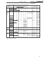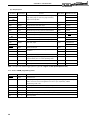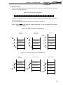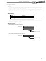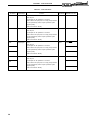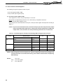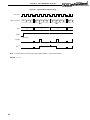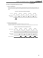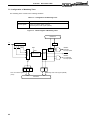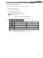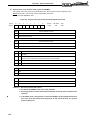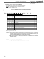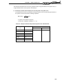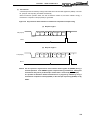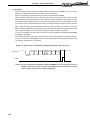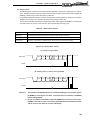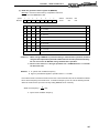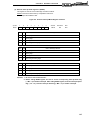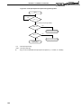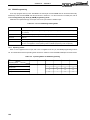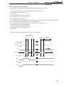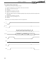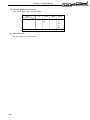
1
To our customers,
Old Company Name in Catalogs and Other Documents
On April 1st, 2010, NEC Electronics Corporation merged with Renesas Technology
Corporation, and Renesas Electronics Corporation took over all the business of both
companies. Therefore, although the old company name remains in this document, it is a valid
Renesas Electronics document. We appreciate your understanding.
Renesas Electronics website: http://www.renesas.com
April 1st, 2010
Renesas Electronics Corporation
Issued by: Renesas Electronics Corporation (http://www.renesas.com)
Send any inquiries to http://www.renesas.com/inquiry.
Notice
1.
2.
3.
4.
5.
6.
7.
All information included in this document is current as of the date this document is issued. Such information, however, is
subject to change without any prior notice. Before purchasing or using any Renesas Electronics products listed herein, please
confirm the latest product information with a Renesas Electronics sales office. Also, please pay regular and careful attention to
additional and different information to be disclosed by Renesas Electronics such as that disclosed through our website.
Renesas Electronics does not assume any liability for infringement of patents, copyrights, or other intellectual property rights
of third parties by or arising from the use of Renesas Electronics products or technical information described in this document.
No license, express, implied or otherwise, is granted hereby under any patents, copyrights or other intellectual property rights
of Renesas Electronics or others.
You should not alter, modify, copy, or otherwise misappropriate any Renesas Electronics product, whether in whole or in part.
Descriptions of circuits, software and other related information in this document are provided only to illustrate the operation of
semiconductor products and application examples. You are fully responsible for the incorporation of these circuits, software,
and information in the design of your equipment. Renesas Electronics assumes no responsibility for any losses incurred by
you or third parties arising from the use of these circuits, software, or information.
When exporting the products or technology described in this document, you should comply with the applicable export control
laws and regulations and follow the procedures required by such laws and regulations. You should not use Renesas
Electronics products or the technology described in this document for any purpose relating to military applications or use by
the military, including but not limited to the development of weapons of mass destruction. Renesas Electronics products and
technology may not be used for or incorporated into any products or systems whose manufacture, use, or sale is prohibited
under any applicable domestic or foreign laws or regulations.
Renesas Electronics has used reasonable care in preparing the information included in this document, but Renesas Electronics
does not warrant that such information is error free. Renesas Electronics assumes no liability whatsoever for any damages
incurred by you resulting from errors in or omissions from the information included herein.
Renesas Electronics products are classified according to the following three quality grades: “Standard”, “High Quality”, and
“Specific”. The recommended applications for each Renesas Electronics product depends on the product’s quality grade, as
indicated below. You must check the quality grade of each Renesas Electronics product before using it in a particular
application. You may not use any Renesas Electronics product for any application categorized as “Specific” without the prior
written consent of Renesas Electronics. Further, you may not use any Renesas Electronics product for any application for
which it is not intended without the prior written consent of Renesas Electronics. Renesas Electronics shall not be in any way
liable for any damages or losses incurred by you or third parties arising from the use of any Renesas Electronics product for an
application categorized as “Specific” or for which the product is not intended where you have failed to obtain the prior written
consent of Renesas Electronics. The quality grade of each Renesas Electronics product is “Standard” unless otherwise
expressly specified in a Renesas Electronics data sheets or data books, etc.
“Standard”:
8.
9.
10.
11.
12.
Computers; office equipment; communications equipment; test and measurement equipment; audio and visual
equipment; home electronic appliances; machine tools; personal electronic equipment; and industrial robots.
“High Quality”: Transportation equipment (automobiles, trains, ships, etc.); traffic control systems; anti-disaster systems; anticrime systems; safety equipment; and medical equipment not specifically designed for life support.
“Specific”:
Aircraft; aerospace equipment; submersible repeaters; nuclear reactor control systems; medical equipment or
systems for life support (e.g. artificial life support devices or systems), surgical implantations, or healthcare
intervention (e.g. excision, etc.), and any other applications or purposes that pose a direct threat to human life.
You should use the Renesas Electronics products described in this document within the range specified by Renesas Electronics,
especially with respect to the maximum rating, operating supply voltage range, movement power voltage range, heat radiation
characteristics, installation and other product characteristics. Renesas Electronics shall have no liability for malfunctions or
damages arising out of the use of Renesas Electronics products beyond such specified ranges.
Although Renesas Electronics endeavors to improve the quality and reliability of its products, semiconductor products have
specific characteristics such as the occurrence of failure at a certain rate and malfunctions under certain use conditions. Further,
Renesas Electronics products are not subject to radiation resistance design. Please be sure to implement safety measures to
guard them against the possibility of physical injury, and injury or damage caused by fire in the event of the failure of a
Renesas Electronics product, such as safety design for hardware and software including but not limited to redundancy, fire
control and malfunction prevention, appropriate treatment for aging degradation or any other appropriate measures. Because
the evaluation of microcomputer software alone is very difficult, please evaluate the safety of the final products or system
manufactured by you.
Please contact a Renesas Electronics sales office for details as to environmental matters such as the environmental
compatibility of each Renesas Electronics product. Please use Renesas Electronics products in compliance with all applicable
laws and regulations that regulate the inclusion or use of controlled substances, including without limitation, the EU RoHS
Directive. Renesas Electronics assumes no liability for damages or losses occurring as a result of your noncompliance with
applicable laws and regulations.
This document may not be reproduced or duplicated, in any form, in whole or in part, without prior written consent of Renesas
Electronics.
Please contact a Renesas Electronics sales office if you have any questions regarding the information contained in this
document or Renesas Electronics products, or if you have any other inquiries.
(Note 1) “Renesas Electronics” as used in this document means Renesas Electronics Corporation and also includes its majorityowned subsidiaries.
(Note 2) “Renesas Electronics product(s)” means any product developed or manufactured by or for Renesas Electronics.
User’s Manual
µPD789014 Subseries
8-bit Single-chip Microcontrollers
µPD789011
µPD789012
µPD78P9014
Document No. U11187EJ3V0UMJ1 (3rd edition)
Date Published September 2000 N CP(K)
©
Printed in Japan
1996
[MEMO]
2
NOTES FOR CMOS DEVICES
1
PRECAUTION AGAINST ESD FOR SEMICONDUCTORS
Note:
Strong electric field, when exposed to a MOS device, can cause destruction of the gate oxide and
ultimately degrade the device operation. Steps must be taken to stop generation of static electricity as
much as possible, and quickly dissipate it once, when it has occurred. Environmental control must be
adequate. When it is dry, humidifier should be used. It is recommended to avoid using insulators that
easily build static electricity. Semiconductor devices must be stored and transported in an anti-static
container, static shielding bag or conductive material. All test and measurement tools including work
bench and floor should be grounded. The operator should be grounded using wrist strap. Semiconductor
devices must not be touched with bare hands. Similar precautions need to be taken for PW boards with
semiconductor devices on it.
2
HANDLING OF UNUSED INPUT PINS FOR CMOS
Note:
No connection for CMOS device inputs can be cause of malfunction. If no connection is provided to the
input pins, it is possible that an internal input level may be generated due to noise, etc., hence causing
malfunction. CMOS devices behave differently than Bipolar or NMOS devices. Input levels of CMOS
devices must be fixed high or low by using a pull-up or pull-down circuitry. Each unused pin should be
connected to VDD or GND with a resistor, if it is considered to have a possibility of being an output pin.
All handling related to the unused pins must be judged device by device and related specifications
governing the devices.
3
STATUS BEFORE INITIALIZATION OF MOS DEVICES
Note:
Power-on does not necessarily define initial status of MOS device. Production process of MOS does
not define the initial operation status of the device. Immediately after the power source is turned ON,
the devices with reset function have not yet been initialized. Hence, power-on does not guarantee outpin levels, I/O settings or contents of registers. Device is not initialized until the reset signal is received.
Reset operation must be executed immediately after power-on for devices having reset function.
QTOP and EEPROM are trademarks of NEC Corporation.
MS-DOS, Windows, and Windows NT are either registered trademarks or trademarks of Microsoft
Corporation in the United States and/or other countries.
IBM DOS and PC/AT are trademarks of International Business Machines Corporation.
HP9000 Series 700 and HP-UX are trademarks of Hewlett-Packard Company.
SPARCstation is a trademark of SPARC International, Inc.
Solaris and SunOS are trademarks of Sun Microsystems, Inc.
OSF/Motif is a trademark of Open Software Foundation, Inc.
NEWS and NEWS-OS are trademarks of Sony Corporation.
TRON is an abbreviation of The Realtime Operating system Nucleus.
ITRON is an abbreviation of Industrial TRON.
3
The export of this product from Japan is regulated by the Japanese government. To export this product may be prohibited
without governmental license, the need for which must be judged by the customer. The export or re-export of this product
from a country other than Japan may also be prohibited without a license from that country. Please call an NEC sales
representative.
• The information in this document is current as of September, 2000. The information is subject to
change without notice. For actual design-in, refer to the latest publications of NEC's data sheets or
data books, etc., for the most up-to-date specifications of NEC semiconductor products. Not all
products and/or types are available in every country. Please check with an NEC sales representative
for availability and additional information.
• No part of this document may be copied or reproduced in any form or by any means without prior
written consent of NEC. NEC assumes no responsibility for any errors that may appear in this document.
• NEC does not assume any liability for infringement of patents, copyrights or other intellectual property rights of
third parties by or arising from the use of NEC semiconductor products listed in this document or any other
liability arising from the use of such products. No license, express, implied or otherwise, is granted under any
patents, copyrights or other intellectual property rights of NEC or others.
• Descriptions of circuits, software and other related information in this document are provided for illustrative
purposes in semiconductor product operation and application examples. The incorporation of these
circuits, software and information in the design of customer's equipment shall be done under the full
responsibility of customer. NEC assumes no responsibility for any losses incurred by customers or third
parties arising from the use of these circuits, software and information.
• While NEC endeavours to enhance the quality, reliability and safety of NEC semiconductor products, customers
agree and acknowledge that the possibility of defects thereof cannot be eliminated entirely. To minimize
risks of damage to property or injury (including death) to persons arising from defects in NEC
semiconductor products, customers must incorporate sufficient safety measures in their design, such as
redundancy, fire-containment, and anti-failure features.
• NEC semiconductor products are classified into the following three quality grades:
"Standard", "Special" and "Specific". The "Specific" quality grade applies only to semiconductor products
developed based on a customer-designated "quality assurance program" for a specific application. The
recommended applications of a semiconductor product depend on its quality grade, as indicated below.
Customers must check the quality grade of each semiconductor product before using it in a particular
application.
"Standard": Computers, office equipment, communications equipment, test and measurement equipment, audio
and visual equipment, home electronic appliances, machine tools, personal electronic equipment
and industrial robots
"Special": Transportation equipment (automobiles, trains, ships, etc.), traffic control systems, anti-disaster
systems, anti-crime systems, safety equipment and medical equipment (not specifically designed
for life support)
"Specific": Aircraft, aerospace equipment, submersible repeaters, nuclear reactor control systems, life
support systems and medical equipment for life support, etc.
The quality grade of NEC semiconductor products is "Standard" unless otherwise expressly specified in NEC's
data sheets or data books, etc. If customers wish to use NEC semiconductor products in applications not
intended by NEC, they must contact an NEC sales representative in advance to determine NEC's willingness
to support a given application.
(Note)
(1) "NEC" as used in this statement means NEC Corporation and also includes its majority-owned subsidiaries.
(2) "NEC semiconductor products" means any semiconductor product developed or manufactured by or for
NEC (as defined above).
M8E 00. 4
4
Regional Information
Some information contained in this document may vary from country to country. Before using any NEC
product in your application, pIease contact the NEC office in your country to obtain a list of authorized
representatives and distributors. They will verify:
•
Device availability
•
Ordering information
•
Product release schedule
•
Availability of related technical literature
•
Development environment specifications (for example, specifications for third-party tools and
components, host computers, power plugs, AC supply voltages, and so forth)
•
Network requirements
In addition, trademarks, registered trademarks, export restrictions, and other legal issues may also vary
from country to country.
NEC Electronics Inc. (U.S.)
NEC Electronics (Germany) GmbH
NEC Electronics Hong Kong Ltd.
Santa Clara, California
Tel: 408-588-6000
800-366-9782
Fax: 408-588-6130
800-729-9288
Benelux Office
Eindhoven, The Netherlands
Tel: 040-2445845
Fax: 040-2444580
Hong Kong
Tel: 2886-9318
Fax: 2886-9022/9044
NEC Electronics Hong Kong Ltd.
Velizy-Villacoublay, France
Tel: 01-30-67 58 00
Fax: 01-30-67 58 99
Seoul Branch
Seoul, Korea
Tel: 02-528-0303
Fax: 02-528-4411
NEC Electronics (France) S.A.
NEC Electronics Singapore Pte. Ltd.
Milton Keynes, UK
Tel: 01908-691-133
Fax: 01908-670-290
Madrid Office
Madrid, Spain
Tel: 91-504-2787
Fax: 91-504-2860
United Square, Singapore
Tel: 65-253-8311
Fax: 65-250-3583
NEC Electronics Italiana s.r.l.
NEC Electronics (Germany) GmbH
Milano, Italy
Tel: 02-66 75 41
Fax: 02-66 75 42 99
Scandinavia Office
Taeby, Sweden
Tel: 08-63 80 820
Fax: 08-63 80 388
NEC Electronics (France) S.A.
NEC Electronics (Germany) GmbH
Duesseldorf, Germany
Tel: 0211-65 03 02
Fax: 0211-65 03 490
NEC Electronics (UK) Ltd.
NEC Electronics Taiwan Ltd.
Taipei, Taiwan
Tel: 02-2719-2377
Fax: 02-2719-5951
NEC do Brasil S.A.
Electron Devices Division
Guarulhos-SP Brasil
Tel: 55-11-6462-6810
Fax: 55-11-6462-6829
J00.7
5
Major Revisions in This Edition
Page
p.32
Description
Modification of recommended connection of unused pins in Table 2-1. Types of Pin Input/
Output Circuits
p.46
Modification of part of name and symbol in Table 3-4. Special Function Register List
p.80
Addition of Caution in 6.2 (1) 8-bit compare register 0n (CR0n)
p.81
Modification of symbol and flag name in Figure 6-2. 8-Bit Timer Mode Control Register 00
Format
p.82
Modification of symbol and flag name in Figure 6-3. 8-Bit Timer Mode Control Register 01
Format
p.84
Modification of operation explanation in 6.4.1 Operation as interval timer
p.86
Modification of operation explanation in 6.4.2 Operation as external event counter
p.87
Modification of operation explanation in 6.4.3 Operation as square wave output
p.101
Modification of symbol and flag name in Figure 8-3. Serial Operating Mode Register 00 Format,
p.102
Modification of symbol and flag name in Figure 8-4. Asynchronous Serial Interface Mode
p.105
Modification of 1-bit memory manipulation instruction enabled in 8.3 (3) Asynchronous serial
p.105
Modification of symbol and flag name in Figure 8-5. Asynchronous Serial Interface Status
p.111
Addition of explanation regarding transmit operation and explanation regarding read operation
p.125
Addition of explanation regarding transmit/receive operation in 8.4.3 3-wire serial I/O mode
p.135
Modification of flag name in Figure 9-2. Interrupt Request Flag Register 0 Format
p.136
Modification of flag name in Figure 9-3. Interrupt Mask Flag Register 0 Format
p.159
Addition of Caution in Table 12-1.
and addition of Caution regarding transmit/receive operation
Register 00 Format, and addition of Caution regarding transmit operation
interface status register 00 (ASIS00)
Register 00 Format
of RXB00 register in 8.4.2 Asynchronous serial interface (UART) mode
Differences between µPD78P9014 and Mask ROM
Versions
p.177
Addition of SolarisTM to operating system in A.1 Language Processing Software
p.178
Addition of PA-17K-DZ to PROM programmer adapter in A.2.1 Hardware
p.179
Modification of PC card interface name to IE-70000-CD-IF-A, and addition of IE-70000-PCI-IF
to interface adapter in A.3.1 Hardware
The mark
6
shows major revised points.
INTRODUCTION
Readers
This manual is intended for user engineers who understand the functions of the
µPD789014 Subseries to design and develop its application systems and programs.
• The target subseries is the µPD789014 Subseries, which consists of the µPD789011,
789012, and 78P9014.
Purpose
This manual is designed to deepen your understanding of the following functions
using the following organization.
Organization
Two manuals are available for the µPD789014 Subseries: this manual and Instruction
Manual (common to the 78K/0S Series).
78K/0S Series
µPD789014 Subseries
User’s Manual
User’s Manual
— Instruction
• Pin functions
• CPU function
• Internal block functions
• Instruction set
• Interrupt
• Instruction description
• Other internal peripheral functions
How to Read This Manual
It is assumed that the readers of this manual have general knowledge on electrical
engineering, logic circuits, and microcontrollers.
To understand the overall functions of the µPD789014 Subseries
→ Read this manual in the order of the CONTENTS.
How to read register formats
→ The name of a bit whose number is in brackets is reserved for the assembler
and is defined for the C compiler by the header file sfrbit.h.
To learn the detailed functions of a register whose register name is known
→ Refer to APPENDIX C REGISTER INDEX.
To learn the details of the instruction functions of the 78K/0S Series
→ Refer to 78K/0S Series User’s Manual — Instruction (U11047E) separately
available.
Conventions
Data significance
: Higher digits on the left and lower digits on the right
Active low representation : ××× (overscore over pin or signal name)
Note
: Footnote for item marked with Note in the text
Caution
: Information requiring particular attention
Remark
: Supplementary information
Numerical representation : Binary ... ×××× or ××××B
Decimal ... ××××
Hexadecimal ... ××××H
7
Related Documents
The related documents indicated in this publication may include preliminary versions.
However, preliminary versions are not marked as such.
Device Related Documents
Document Name
Document No.
English
Japanese
µPD789011, 789012 Data Sheet
U11095E
U11095J
µPD78P9014 Data Sheet
U10912E
U10912J
µPD789014 Subseries User’s Manual
This manual
U11187J
78K/0S Series User’s Manual — Instruction
U11047E
U11047J
Documents for Development Tool (User’s Manual)
Document Name
Document No.
English
RA78K0S Assembler Package
CC78K0S C Compiler
Japanese
Operation
U11622E
U11622J
Assembly Language
U11599E
U11599J
Structured Assembly Language
U11623E
U11623J
Operation
U11816E
U11816J
Language
U11817E
U11817J
SM78K0S System Simulator WindowsTM Based
Reference
U11489E
U11489J
SM78K Series System Simulator
External Part User Open
Interface Specifications
U10092E
U10092J
ID78K0S Integrated Debugger Windows Based
Reference
U12901E
U12901J
Document for Embedded Software (User’s Manual)
Document Name
Document No.
English
78K/0S Series OS MX78K0S
U12938E
Japanese
U12938J
Caution The related documents listed above are subject to change without notice. Be sure to use the latest
version of each document for designing.
8
Other Related Documents
Document Name
Document No.
English
Japanese
NEC IC Package Manual (CD-ROM)
C13388E
—
Semiconductor Device Mounting Technology Manual
C10535E
C10535J
Quality Grades on NEC Semiconductor Devices
C11531E
C11531J
NEC Semiconductor Device Reliability/Quality Control System
C10983E
C10983J
Guide to Prevent Damage for Semiconductor Devices by Electrostatic Discharge (ESD)
C11892E
C11892J
Guide to Quality Assurance for Semiconductor Devices
MEI-1202
—
—
U11416J
Microcomputer Product Series Guide
Caution The related documents listed above are subject to change without notice. Be sure to use the latest
version of each document for designing.
9
[MEMO]
10
CONTENTS
CHAPTER 1 GENERAL ....................................................................................................................
1.1
1.2
1.3
1.4
1.5
1.6
1.7
19
Features ..............................................................................................................................
Applications .......................................................................................................................
Ordering Information ........................................................................................................
Pin Configuration (Top View) ..........................................................................................
78K/0S Series Lineup .......................................................................................................
Block Diagram ...................................................................................................................
Overview of Functions .....................................................................................................
19
19
19
20
22
24
25
CHAPTER 2 PIN FUNCTIONS .........................................................................................................
27
2.1 List of Pin Functions ........................................................................................................
27
2.1.1
Pins in normal operating mode ..............................................................................................
2.1.2
Pins in PROM programming mode ........................................................................................
27
28
2.2 Description of Pin Functions ..........................................................................................
29
2.2.1
P00 to P07 (Port 0) .................................................................................................................
29
2.2.2
P10 to P17 (Port 1) .................................................................................................................
29
2.2.3
P20 to P22 (Port 2) .................................................................................................................
29
2.2.4
P30 to P32 (Port 3) .................................................................................................................
30
2.2.5
RESET .....................................................................................................................................
31
2.2.6
X1, X2 ......................................................................................................................................
31
2.2.7
VDD ...........................................................................................................................................
31
2.2.8
VSS ...........................................................................................................................................
31
2.2.9
VPP (µPD78P9014 only) ..........................................................................................................
31
2.2.10 IC (mask ROM version only) ..................................................................................................
31
2.3 Pin Input/Output Circuits and Recommended Connection of Unused Pins ............
32
CHAPTER 3 CPU ARCHITECTURE ................................................................................................
33
3.1 Memory Space ...................................................................................................................
33
3.1.1
Internal program memory space ............................................................................................
36
3.1.2
Internal data memory (internal high-speed RAM) space ......................................................
37
3.1.3
Special function register (SFR) area ......................................................................................
37
3.1.4
Data memory addressing .......................................................................................................
38
3.2 Processor Registers .........................................................................................................
41
3.2.1
Control registers ......................................................................................................................
41
3.2.2
General registers ....................................................................................................................
44
3.2.3
Special function register (SFR) ..............................................................................................
45
3.3 Instruction Address Addressing .....................................................................................
47
3.3.1
Relative addressing ................................................................................................................
47
3.3.2
Immediate addressing ............................................................................................................
48
3.3.3
Table indirect addressing ........................................................................................................
49
3.3.4
Register addressing ................................................................................................................
49
11
3.4 Operand Address Addressing .........................................................................................
50
3.4.1
Direct addressing ....................................................................................................................
50
3.4.2
Short direct addressing ...........................................................................................................
51
3.4.3
Special function register (SFR) addressing ...........................................................................
52
3.4.4
Register addressing ................................................................................................................
53
3.4.5
Register indirect addressing ...................................................................................................
54
3.4.6
Based addressing ...................................................................................................................
55
3.4.7
Stack addressing ....................................................................................................................
55
CHAPTER 4 PORT FUNCTIONS .....................................................................................................
57
4.1 Functions of Ports ............................................................................................................
4.2 Port Configuration ............................................................................................................
57
59
4.2.1
Port 0 .......................................................................................................................................
59
4.2.2
Port 1 .......................................................................................................................................
60
4.2.3
Port 2 .......................................................................................................................................
61
4.2.4
Port 3 .......................................................................................................................................
64
4.3 Port Function Control Registers ....................................................................................
4.4 Operation of Port Functions ...........................................................................................
66
68
4.4.1
Writing to I/O port ....................................................................................................................
68
4.4.2
Reading from I/O port .............................................................................................................
68
4.4.3
Arithmetic operation of I/O port ..............................................................................................
68
CHAPTER 5 CLOCK GENERATOR ................................................................................................
69
5.1
5.2
5.3
5.4
Function of Clock Generator ...........................................................................................
Configuration of Clock Generator ..................................................................................
Clock Generator Control Register ..................................................................................
System Clock Oscillator ..................................................................................................
69
69
70
71
5.4.1
System clock oscillator ...........................................................................................................
71
5.4.2
Divider circuit ...........................................................................................................................
73
5.5 Operation of Clock Generator .........................................................................................
5.6 Changing Setting of CPU Clock .....................................................................................
74
75
5.6.1
Time required for switching CPU clock ..................................................................................
75
5.6.2
Switching CPU clock ...............................................................................................................
75
CHAPTER 6 8-BIT TIMER/EVENT COUNTER ...............................................................................
77
6.1
6.2
6.3
6.4
12
Functions of 8-Bit Timer/Event Counter ........................................................................
8-Bit Timer/Event Counter Configuration ......................................................................
8-Bit Timer/Event Counter Control Registers ...............................................................
Operation of 8-Bit Timer/Event Counter ........................................................................
78
79
81
84
6.4.1
Operation as interval timer .....................................................................................................
84
6.4.2
Operation as external event counter ......................................................................................
86
6.4.3
Operation as square wave output ..........................................................................................
87
6.5 Notes on Using 8-Bit Timer/Event Counters .................................................................
89
CHAPTER 7 WATCHDOG TIMER ....................................................................................................
7.1
7.2
7.3
7.4
91
Functions of Watchdog Timer .........................................................................................
Configuration of Watchdog Timer ..................................................................................
Watchdog Timer Control Registers ................................................................................
Operation of Watchdog Timer .........................................................................................
91
92
93
95
7.4.1
Operation as watchdog timer .................................................................................................
95
7.4.2
Operation as interval timer .....................................................................................................
96
CHAPTER 8 SERIAL INTERFACE 00 .............................................................................................
97
8.1
8.2
8.3
8.4
Serial
Serial
Serial
Serial
Interface
Interface
Interface
Interface
00
00
00
00
Functions .......................................................................................... 97
Configuration .................................................................................... 97
Control Registers ............................................................................. 101
Operation .......................................................................................... 109
8.4.1
Operation stop mode ..............................................................................................................
109
8.4.2
Asynchronous serial interface (UART) mode ........................................................................
111
8.4.3
3-wire serial I/O mode ............................................................................................................
125
CHAPTER 9 INTERRUPT FUNCTIONS .......................................................................................... 131
9.1
9.2
9.3
9.4
Interrupt
Interrupt
Interrupt
Interrupt
Function Types .................................................................................................
Sources and Configuration .............................................................................
Function Control Registers .............................................................................
Processing Operation ......................................................................................
131
131
134
139
9.4.1
Non-maskable interrupt request acceptance operation ........................................................
139
9.4.2
Maskable interrupt acceptance operation ..............................................................................
141
9.4.3
Multiplexed interrupt processing ............................................................................................
143
9.4.4
Interrupt request reserve ........................................................................................................
145
CHAPTER 10 STANDBY FUNCTION .............................................................................................. 147
10.1 Standby Function and Configuration ............................................................................. 147
10.1.1 Standby function .....................................................................................................................
147
10.1.2 Standby function control register ...........................................................................................
148
10.2 Operation of Standby Function ...................................................................................... 149
10.2.1 HALT mode ..............................................................................................................................
149
10.2.2 STOP mode .............................................................................................................................
152
CHAPTER 11 RESET FUNCTION .................................................................................................... 155
CHAPTER 12 µPD78P9014 .............................................................................................................. 159
12.1 PROM Programming ......................................................................................................... 160
12.1.1 Operating modes ....................................................................................................................
160
12.1.2 Program memory write procedure ..........................................................................................
161
12.1.3 Program memory read procedure ..........................................................................................
162
12.1.4 One-time PROM screening ....................................................................................................
163
13
CHAPTER 13 INSTRUCTION SET .................................................................................................. 165
13.1 Operation ........................................................................................................................... 165
13.1.1 Operand identifiers and description methods ........................................................................
165
13.1.2 Description of “operation” column ..........................................................................................
166
13.1.3 Description of “flag operation” column ...................................................................................
166
13.2 Operation List .................................................................................................................... 167
13.3 Instructions Listed by Addressing Type ....................................................................... 172
APPENDIX A DEVELOPMENT TOOLS ........................................................................................... 175
A.1 Language Processing Software ...................................................................................... 177
A.2 PROM Writing Tools ......................................................................................................... 178
A.2.1 Hardware .................................................................................................................................
178
A.2.2 Software ..................................................................................................................................
178
A.3 Debugging Tools ............................................................................................................... 179
A.3.1 Hardware .................................................................................................................................
179
A.3.2 Software ..................................................................................................................................
180
APPENDIX B EMBEDDED SOFTWARE ......................................................................................... 181
APPENDIX C REGISTER INDEX ..................................................................................................... 183
C.1 Register Name Index (Alphabetic Order) ...................................................................... 183
C.2 Register Symbol Index (Alphabetic Order) ................................................................... 185
APPENDIX D REVISION HISTORY ................................................................................................. 187
14
LIST OF FIGURES (1/2)
Figure No.
Title
Page
2-1
Pin Input/Output Circuits ....................................................................................................................
32
3-1
Memory Map (µPD789011) ................................................................................................................
33
3-2
Memory Map (µPD789012) ................................................................................................................
34
3-3
Memory Map (µPD78P9014) ..............................................................................................................
35
3-4
Data Memory Addressing (µPD789011) ............................................................................................
38
3-5
Data Memory Addressing (µPD789012) ............................................................................................
39
3-6
Data Memory Addressing (µPD78P9014) ..........................................................................................
40
3-7
Program Counter Configuration .........................................................................................................
41
3-8
Program Status Word Configuration ..................................................................................................
41
3-9
Stack Pointer Configuration ................................................................................................................
43
3-10
Data to be Saved to Stack Memory ...................................................................................................
43
3-11
Data to be Restored from Stack Memory ..........................................................................................
43
3-12
General Register Configuration ..........................................................................................................
44
4-1
Port Types ...........................................................................................................................................
57
4-2
Block Diagram of P00 to P07 .............................................................................................................
59
4-3
Block Diagram of P10 to P17 .............................................................................................................
60
4-4
Block Diagram of P20 .........................................................................................................................
61
4-5
Block Diagram of P21 .........................................................................................................................
62
4-6
Block Diagram of P22 .........................................................................................................................
63
4-7
Block Diagram of P30 and P31 ..........................................................................................................
64
4-8
Block Diagram of P32 .........................................................................................................................
65
4-9
Port Mode Register Format ................................................................................................................
67
4-10
Pull-Up Resistor Option Register Format ..........................................................................................
67
5-1
Block Diagram of Clock Generator ....................................................................................................
69
5-2
Processor Clock Control Register Format .........................................................................................
70
5-3
External Circuit of System Clock Oscillator .......................................................................................
71
5-4
Incorrect Examples of Resonator Connection ...................................................................................
72
5-5
Switching CPU Clock ..........................................................................................................................
75
6-1
Block Diagram of 8-Bit Timer/Event Counter .....................................................................................
80
6-2
8-Bit Timer Mode Control Register 00 Format ..................................................................................
81
6-3
8-Bit Timer Mode Control Register 01 Format ..................................................................................
82
6-4
Port Mode Register 3 Format .............................................................................................................
83
6-5
Interval Timer Operation Timing .........................................................................................................
85
6-6
External Event Counter Operation Timing (with rising edge specified) ............................................
86
6-7
Square Wave Output Timing ..............................................................................................................
88
6-8
Start Timing of 8-Bit Timer Register ...................................................................................................
89
6-9
External Event Counter Operation Timing .........................................................................................
89
7-1
Block Diagram of Watchdog Timer .....................................................................................................
92
15
LIST OF FIGURES (2/2)
Figure No.
16
Title
Page
7-2
Timer Clock Select Register 2 Format ...............................................................................................
93
7-3
Watchdog Timer Mode Register Format ............................................................................................
94
8-1
Block Diagram of Serial Interface 00 .................................................................................................
98
8-2
Block Diagram of Baud Rate Generator ............................................................................................
99
8-3
Serial Operating Mode Register 00 Format .......................................................................................
101
8-4
Asynchronous Serial Interface Mode Register 00 Format ................................................................
102
8-5
Asynchronous Serial Interface Status Register 00 Format ...............................................................
105
8-6
Baud Rate Generator Control Register 00 Format ...........................................................................
106
8-7
Asynchronous Serial Interface Transmit/Receive Data Format ........................................................
117
8-8
Asynchronous Serial Interface Transmission Completion Interrupt Timing .....................................
119
8-9
Asynchronous Serial Interface Reception Completion Interrupt Timing ...........................................
120
8-10
Receive Error Timing ..........................................................................................................................
121
8-11
3-Wire Serial I/O Mode Timing ...........................................................................................................
128
9-1
Basic Configuration of Interrupt Function ..........................................................................................
133
9-2
Interrupt Request Flag Register 0 Format .........................................................................................
135
9-3
Interrupt Mask Flag Register 0 Format ..............................................................................................
136
9-4
External Interrupt Mode Register 0 Format .......................................................................................
137
9-5
Program Status Word Configuration ..................................................................................................
138
9-6
Flowchart from Non-Maskable Interrupt Request Generation to Acceptance ..................................
140
9-7
Timing of Non-Maskable Interrupt Request Acceptance ...................................................................
140
9-8
Accepting Non-Maskable Interrupt Request ......................................................................................
140
9-9
Interrupt Request Acceptance Program Algorithm ............................................................................
142
9-10
Interrupt Request Acceptance Timing (example of MOV A, r) ..........................................................
143
9-11
Interrupt Request Acceptance Timing
(When interrupt request flag generates at the last clock during instruction execution) ..................
143
9-12
Example of Multiplexed Interrupt .......................................................................................................
144
10-1
Oscillation Stabilization Time Select Register Format ......................................................................
148
10-2
Releasing HALT Mode by Interrupt ....................................................................................................
150
10-3
Releasing HALT Mode by RESET Input ............................................................................................
151
10-4
Releasing STOP Mode by Interrupt ...................................................................................................
153
10-5
Releasing STOP Mode by RESET Input ...........................................................................................
154
11-1
Block Diagram of Reset Function ......................................................................................................
155
11-2
Reset Timing by RESET Input ...........................................................................................................
156
11-3
Reset Timing by Overflow in Watchdog Timer ..................................................................................
156
11-4
Reset Timing by RESET Input in STOP Mode ..................................................................................
156
A-1
Development Tools .............................................................................................................................
176
LIST OF TABLES (1/2)
Table No.
Title
Page
2-1
Types of Pin Input/Output Circuits .....................................................................................................
32
3-1
Internal ROM Capacity .......................................................................................................................
36
3-2
Vector Table .........................................................................................................................................
36
3-3
Internal High-Speed RAM Capacity ...................................................................................................
37
3-4
Special Function Register List ............................................................................................................
46
4-1
Port Functions .....................................................................................................................................
58
4-2
Port Configuration ...............................................................................................................................
59
4-3
Port Mode Register and Output Latch Settings When Using Alternate Functions ..........................
66
5-1
Configuration of Clock Generator ......................................................................................................
69
5-2
Maximum Time Required for Switching CPU Clock ..........................................................................
75
6-1
Interval Time of 8-Bit Timer/Event Counter .......................................................................................
78
6-2
Square Wave Output Range of 8-Bit Timer/Event Counter ..............................................................
78
6-3
8-Bit Timer/Event Counter Configuration ...........................................................................................
79
6-4
Interval Time of 8-Bit Timer/Event Counter .......................................................................................
84
6-5
Square Wave Output Range of 8-Bit Timer/Event Counter ..............................................................
87
7-1
Runaway Detection Time of Watchdog Timer ...................................................................................
91
7-2
Interval Time ........................................................................................................................................
91
7-3
Configuration of Watchdog Timer .......................................................................................................
92
7-4
Runaway Detection Time of Watchdog Timer ...................................................................................
95
7-5
Interval Time of Interval Timer ............................................................................................................
96
8-1
Serial Interface 00 Configuration .......................................................................................................
97
8-2
Serial Interface 00 Operating Mode Settings ....................................................................................
103
8-3
Example of Relationship between System Clock and Baud Rate ....................................................
107
8-4
Relationship between ASCK Pin Input Frequency and Baud Rate (When BRGC00 is set to 80H)
108
8-5
Example of Relationship between System Clock and Baud Rate ....................................................
115
8-6
Relationship between ASCK Pin Input Frequency and Baud Rate (When BRGC00 is set to 80H)
116
8-7
Receive Error Causes .........................................................................................................................
121
8-8
Number of Clocks Required to Read RXB00 Register .....................................................................
123
9-1
Interrupt Source List ...........................................................................................................................
132
9-2
Flags Corresponding to Interrupt Request Signal Name ..................................................................
134
9-3
Time from Generation of Maskable Interrupt Request to Processing ..............................................
141
10-1
HALT Mode Operating Status ............................................................................................................
149
10-2
Operation after Release of HALT Mode .............................................................................................
151
10-3
STOP Mode Operating Status ............................................................................................................
152
10-4
Operation after Release of STOP Mode ............................................................................................
154
17
LIST OF TABLES (2/2)
Table No.
18
Title
Page
11-1
Hardware Status after Reset ..............................................................................................................
157
12-1
Differences between µPD78P9014 and Mask ROM Versions ..........................................................
159
12-2
Pins in PROM Programming Mode ....................................................................................................
160
12-3
Operating Modes of PROM Programming .........................................................................................
160
13-1
Operand Identifiers and Description Methods ...................................................................................
165
CHAPTER 1
GENERAL
1.1 Features
ROM and RAM capacity
Item
Program Memory
Part Number
µPD789011
ROM
µPD789012
2 Kbytes
Data Memory
(Internal High-Speed RAM)
128 bytes
4 Kbytes
µPD78P9014
PROM
8 Kbytes
256 bytes
Minimum instruction execution time can be changed from high-speed (0.4 µs) to low-speed (1.6 µs) (system
clock at 5.0-MHz operation)
I/O port: 22 lines
Serial interface: 1 channel
3-wire serial I/O mode/UART mode selection
Timer: 3 channels
• 8-bit timer/event counter
: 2 channels
• Watchdog timer
: 1 channel
Vectored interrupt source: 9
Supply voltage: VDD = 1.8 to 5.5 V
Operating ambient temperature: TA = –40 to +85°C
1.2 Applications
Small home appliances, remote controls, video games, etc.
1.3 Ordering Information
Part number
Package
Internal ROM
µPD789011CT-×××
28-pin plastic shrink DIP (400 mil)
Mask ROM
µPD789011GT-×××
28-pin plastic SOP (375 mil)
Mask ROM
µPD789012CT-×××
28-pin plastic shrink DIP (400 mil)
Mask ROM
µPD789012GT-×××
28-pin plastic SOP (375 mil)
Mask ROM
µPD78P9014CT
28-pin plastic shrink DIP (400 mil)
One-time PROM
µPD78P9014GT
28-pin plastic SOP (375 mil)
One-time PROM
Remark
××× indicates ROM code suffix.
19
CHAPTER 1
GENERAL
1.4 Pin Configuration (Top View)
(1) Normal operating mode
• 28-pin plastic shrink DIP (400 mil)
µPD789011CT-×××, 789012CT-×××, and 78P9014CT
• 28-pin plastic SOP (375 mil)
µPD789011GT-×××, 789012GT-×××, and 78P9014GT
P31/INTP1/TI1/TO1
1
28
P30/INTP0/TI0/TO0
P32/INTP2
2
27
P22/RxD/SI0
IC (VPP)
3
26
P21/TxD/SO0
RESET
4
25
P20/ASCK/SCK0
X2
5
24
P17
X1
6
23
P16
VSS
7
22
P15
VDD
8
21
P14
P00
9
20
P13
P01
10
19
P12
P02
11
18
P11
P03
12
17
P10
P04
13
16
P07
P05
14
15
P06
Caution Connect IC directly to VSS.
Remark
( ): µPD78P9014
ASCK
IC
: Asynchronous Serial Clock
: Internally Connected
P00 to P07
P10 to P17
: Port0
: Port1
P20 to P22
P30 to P32
: Port2
: Port3
RESET
RxD
: Reset
: Receive Data
20
SCK0
: Serial Clock
SI0
SO0
: Serial Input
: Serial Output
TI0
TO0
: Timer Input
: Timer Output
TxD
VDD
: Transmit Data
: Power Supply
VPP
VSS
: Programming Power Supply
: Ground
CHAPTER 1
GENERAL
(2) PROM programming mode
• 28-pin plastic shrink DIP (400 mil)
µPD78P9014CT
• 28-pin plastic SOP (375 mil)
µPD78P9014GT
1
28
MD3
2
27
MD2
VPP
3
26
MD1
RESET
4
25
MD0
Open
5
24
X1
6
23
VSS
7
22
VDD
8
21
D0
9
20
D1
10
19
D2
11
18
D3
12
17
D4
13
16
D7
D5
14
15
D6
(L)
(L)
Cautions 1. (L)
2. VSS
: Independently connect to VSS via a pull-down resistor.
: Connect to the ground.
3. RESET : Set to low level.
4. Open
D0 to D7
: Leave open.
: Data Bus
VDD
: Power Supply
MD0 to MD3
: Programming Power Supply
VPP
: Programming Power Supply
RESET
: Reset
VSS
: Ground
X1
: Programming Clock Input
21
CHAPTER 1
GENERAL
1.5 78K/0S Series Lineup
The products in the 78K/0S Series are listed below. The names enclosed in boxes are subseries names.
Products in mass production
Products under development
For small-scale general-purpose applications
44-pin
µPD789046
Added a subsystem clock to the µPD789026.
42/44-pin
µPD789026
Enhanced timer of the µ PD789014.
28-pin
µPD789014
On-chip UART, capable of operating at low voltage (1.8 V).
For small-scale general-purpose applications + A/D
78K/0S
Series
44/48-pin
µPD789217AY
RC-oscillator version of the µ PD789197AY.
44/48-pin
µ PD789197AY
EEPROM
TM
and SMB incorporated to the µPD789177.
44-pin
µPD789177
Enhanced A/D of the µPD789167.
44-pin
µPD789167
µPD789156
Enhanced a timer of the µPD789104A.
30-pin
Enhanced A/D of the µPD789146.
30-pin
28/30-pin
µPD789146
µPD789134A
EEPROM incorporated to the µPD789104A.
Enhanced A/D of the µPD789124A.
28/30-pin
µPD789124A
µPD789114A
RC-oscillator version of the µPD789104A.
28/30-pin
28/30-pin
µPD789104A
Added an A/D and multiplier to the µPD789104.
Enhanced A/D of the µPD789104A.
For inverter control
44-pin
µPD789842
Inverter control circuit with on-chip UART.
For LCD drive
80-pin
µ PD789417A
Enhanced A/D of the µPD789407A.
80-pin
88-pin
µ PD789407A
µPD789830
Added A/D to the µPD789026 and enhanced a timer.
On-chip dot-LCD and UART.
For ASSP
22
44-pin
µPD789840
For a keypad, with on-chip POC.
42/44-pin
µPD789800
For a PC keyboard, with on-chip USB function.
5-pin
µPD789810
For an IC card, with on-chip security circuit.
CHAPTER 1
GENERAL
The major functional differences among the subseries are listed below.
Function
Subseries Name
ROM
Capacity
Small-scale µPD789046
16 K
general-
µPD789026
4 K to 16 K
purpose
µPD789014
2 K to 4 K
Timer
8-Bit 10-Bit
8-Bit 16-Bit Watch WDT A/D
1 ch
1 ch
1 ch
1 ch
–
Serial Interface
I/O
A/D
–
VDD
1 ch (UART: 1 ch)
34
1.8 V
–
1.8 V
RC-oscillatorversion,
On-chip
–
2 ch
Small-scale µPD789217AY 16 K to 24 K 3 ch
generalpurpose
–
1 ch
22
1 ch
1 ch
–
8 ch
2 ch
UART: 1 ch
31
SMB: 1 ch
+ A/D
EEPROM
µPD789197AY
On-chip
EEPROM
µPD789177
1 ch (UART: 1 ch)
µPD789167
–
–
4 ch
4 ch
–
EEPROM
–
4 ch
RC-oscillator-
µPD789124A
4 ch
–
µPD789114A
–
4 ch
µPD789104A
4 ch
–
1 ch
8 ch
–
1 ch (UART: 1 ch)
30
4.0 V
–
1 ch
–
7 ch
1 ch (UART: 1 ch)
43
1.8 V
–
7 ch
–
30
2.7 V
1 ch
29
2.8 V
2ch (USB: 1 ch)
31
4.0 V
–
1
1.8 V
8 K to 16 K 1 ch
–
µPD789146
µPD789134A 2 K to 8 K
Inverter
control
µPD789842
LCD drive
µPD789417A 12 K to 24 K 3 ch
8 K to 16 K 3 ch Note 1 ch
1 ch
1 ch
µPD789407A
µPD789830
24 K
1 ch
µPD789840
8K
2 ch
µPD789800
µPD789810
Note
–
8 ch
µPD789156
ASSP
Remark
MIN. Value
–
–
1 ch
4 ch
–
–
On-chip
version
–
–
–
6K
20
–
On-chip
EEPROM
10-bit timer: 1 channel
23
CHAPTER 1
GENERAL
1.6 Block Diagram
TI0/TO0/
P30/INTP0
8-bit TIMER/
EVENT COUNTER00
PORT0
P00 to P07
8-bit TIMER/
EVENT COUNTER01
PORT1
P10 to P17
WATCHDOG TIMER
PORT2
P20 to P22
PORT3
P30 to P32
78K/0S
CPU CORE
TI1/TO1/
P31/INTP1
SCK0/ASCK/P20
SO0/TxD/P21
SI0/RxD/P22
INTP0/P30 to
INTP2/P32
SERIAL
INTERFACE00
INTERRUPT
CONTROL
ROM
RAM
VDD
VSS
IC
(VPP)
SYSTEM
CONTROL
Remarks 1. The internal ROM and RAM capacities vary depending on the product.
2. An item in parentheses applies to the µPD78P9014 only.
24
RESET
X1
X2
CHAPTER 1
GENERAL
1.7 Overview of Functions
µPD789011
Part Number
µPD789012
µPD78P9014
Item
Internal memory
ROM
Mask ROM
2 Kbytes
High-speed RAM
One-time PROM
4 Kbytes
128 bytes
8 Kbytes
256 bytes
Minimum instruction execution time
0.4 µs/1.6 µs (@ 5.0-MHz operation with system clock)
Instruction set
• 16-bit operation
• Bit manipulation (set, reset, test), etc.
I/O ports
CMOS input/output
Serial interface
3-wire serial I/O mode/UART mode selectable: 1 channel
Timer
• 8-bit timer/event counter : 2 channels
• Watchdog timer
Timer outputs
Vectored interrupt
sources
: 22
: 1 channel
2
Maskable
Internal: 5, External: 3
Non-maskable
Internal: 1
Power supply voltage
VDD = 1.8 to 5.5 V
Operating ambient temperature
TA = –40 to +85°C
Packages
• 28-pin plastic shrink DIP (400 mil)
• 28-pin plastic SOP (375 mil)
25
[MEMO]
26
CHAPTER 2
PIN FUNCTIONS
2.1 List of Pin Functions
2.1.1 Pins in normal operating mode
(1) Port pins
Input/Output
Function
P00 to P07
Pin Name
Input/output
Port 0
8-bit I/O port
Input/output can be specified in 1-bit units.
When used as an input port, an on-chip pull-up resistor
can be specified by means of pull-up resistor option
register (PUO).
LEDs can be driven directly.
Input
—
P10 to P17
Input/output
Port 1
8-bit I/O port
Input/output can be specified in 1-bit units.
When used as an input port, an on-chip pull-up resistor
can be specified by means of pull-up resistor option
register (PUO).
LEDs can be driven directly.
Input
—
P20
Input/output
Port 2
3-bit I/O port
Input/output can be specified in 1-bit units.
When used as an input port, an on-chip pull-up resistor
can be specified by means of pull-up resistor option
register (PUO).
LEDs can be driven directly.
Input
Port 3
3-bit I/O port
Input/output can be specified in 1-bit units.
When used as an input port, an on-chip pull-up resistor
can be specified by means of pull-up resistor option
register (PUO).
LEDs can be driven directly.
Input
P21
P22
P30
P31
P32
Input/output
After Reset
Alternate Function
ASCK/SCK0
TxD/SO0
RxD/SI0
INTP0/TI0/TO0
INTP1/TI1/TO1
INTP2
27
CHAPTER 2
PIN FUNCTIONS
(2) Non-port pins
Pin Name
INTP0Note
Input/Output
Input
Function
After Reset
External interrupt input for which the valid edge (rising
Input
edge, falling edge, or both rising edge and falling
INTP1Note
P30/TI0/TO0
P31/TI1/TO1
edge) can be specified
INTP2Note
Alternate Function
P32
SI0Note
Input
Serial interface serial data input
Input
P22/RxD
SO0
Output
Serial interface serial data output
Input
P21/TxD
SCK0Note
Input/output
Serial interface serial clock input/output
Input
P20/ASCK
RxDNote
Input
Serial data input for asynchronous serial interface
Input
P22/SI0
TxD
Output
Serial data output for asynchronous serial interface
Input
P21/SO0
ASCKNote
Input
Serial clock input for asynchronous serial interface
Input
P20/SCK0
TI0Note
Input
External count clock input to 8-bit timer (TM0)
Input
P30/INTP0/TO0
TI1Note
TO0
External count clock input to 8-bit timer (TM1)
Output
8-bit timer output
P31/INTP1/TO1
Input
TO1
P30/INTP0/TI0
P31/INTP1/TI1
RESET
Input
System reset input
Input
X1
Input
Connecting crystal resonator for system clock
oscillation
—
—
—
—
—
X2
—
VDD
—
Positive power supply
—
—
VPP
—
High voltage applied during program write/verify.
Connect directly to VSS in normal operating mode.
—
—
VSS
—
Ground potential
—
—
IC
—
Internally connected. Connect directly to VSS.
—
—
Note
Pin input from Schmitt-trigger (refer to Type 5-D of Figure 2-1 Pin Input/Output Circuits).
2.1.2 Pins in PROM programming mode
Pin Name
Input/Output
Function
RESET
Input
Connect to VSS.
VPP
Input
PROM programming mode setting, and high voltage applied during program write/verify.
When +5.5 V and +12.5 V are applied to VDD and VPP pins, respectively, PROM
programming mode is set.
MD0 to MD3
Input/output
Operating mode selected in PROM programming mode
D0 to D7
Input/output
Data bus
X1
Input
Address update clock input in PROM programming mode
VDD
—
PROM programming mode setting and positive power supply
VSS
—
Ground potential
28
CHAPTER 2
PIN FUNCTIONS
2.2 Description of Pin Functions
2.2.1 P00 to P07 (Port 0)
These pins constitute an 8-bit I/O port and can be set in the input or output port mode in 1-bit units by using port
mode register 0 (PM0). When these pins are used as an input port, an on-chip pull-up resistor can be used in the
pull-up resistor option register (PUO).
LEDs can be driven directly.
2.2.2 P10 to P17 (Port 1)
These pins constitute an 8-bit I/O port and can be set in the input or output port mode in 1-bit units by using port
mode register 1 (PM1). When these pins are used as an input port, an on-chip pull-up resistor can be used in the
pull-up resistor option register (PUO).
LEDs can be driven directly.
2.2.3 P20 to P22 (Port 2)
These pins constitute a 3-bit I/O port. In addition, these pins provide the function to input/output the data and clock
of the serial interface.
LEDs can be driven directly.
Port 2 can be specified in the following operation modes in 1-bit units.
(1) Port mode
In this mode, port 2 functions as a 3-bit I/O port which can be set in the input or output port mode in 1-bit units
by using the port mode register 2 (PM2). When the port is used as an input port, an on-chip pull-up resistor
can be used in the pull-up resistor option register (PUO).
(2) Control mode
In this mode, the pins of port 2 function as the data input/output and the clock input/output of the serial interface.
(a) SI0, SO0
These are the serial data I/O pins of the serial interface.
(b) SCK0
This is the serial clock I/O pin of the serial interface.
(c) RxD, TxD
This is the serial data I/O pin of asynchronous serial interface.
(d) ASCK
This is the serial clock input pin of asynchronous serial interface.
Caution When using P20 through P22 as serial interface pins, the I/O or output latch must be set according
to the functions to be used. For the details of the setting, refer to Table 8-2 Serial Interface 00
Operating Mode Settings.
29
CHAPTER 2
PIN FUNCTIONS
2.2.4 P30 to P32 (Port 3)
These pins constitute a 3-bit I/O port. In addition, they also function as external interrupt input and timer I/O.
LEDs can be driven directly.
Port 3 can be specified in the following operation modes in 1-bit units.
(1) Port mode
In this mode, port 3 functions as a 3-bit I/O port which can be set in the input or output port mode in 1-bit units
by using the port mode register 3 (PM3). When the port is used as an input port, an on-chip pull-up resistor
can be used in the pull-up resistor option register (PUO).
(2) Control mode
In this mode, the pins of port 3 function as external interrupt input and timer I/O.
(a) INTP0 to INTP2
These pins input external interrupt signals whose valid edge can be specified to either rising, falling, or
both edges.
(b) TI0, TI1
These pins input an external clock to the 8-bit timer/event counter.
(c) TO0, TO1
These are 8-bit timer output pins.
30
CHAPTER 2
PIN FUNCTIONS
2.2.5 RESET
This pin inputs an active-low system reset signal.
2.2.6 X1, X2
These pins are used to connect a crystal resonator for system clock oscillation.
To supply an external clock, input the clock to X1 and input the inverted signal to X2.
2.2.7 VDD
Positive power supply pin
2.2.8 VSS
Ground pin
2.2.9 VPP (µPD78P9014 only)
A high voltage should be applied to this pin when the PROM programming mode is set and when the program is
written or verified.
Connect this pin directly to VSS in the normal operation mode.
2.2.10 IC (mask ROM version only)
The IC (Internally Connected) pin is used to set the µPD789011 and 789012 in the test mode before shipment.
In the normal operation mode, connect this pin directly to the VSS pin with as short a wiring length as possible.
If a potential difference is generated between the IC pin and VSS pin due to a long wiring length between the IC
pin and VSS pin or an external noise superimposed on the IC pin, a user program may not run correctly.
Connect the IC pin directly to the VSS pin.
VSS IC
Keep short
31
CHAPTER 2
PIN FUNCTIONS
2.3 Pin Input/Output Circuits and Recommended Connection of Unused Pins
The input/output circuit type of each pin and recommended connection of unused pins are shown in Table 2-1.
For the input/output circuit configuration of each type, refer to Figure 2-1.
Table 2-1. Types of Pin Input/Output Circuits
Pin Name
Input/Output Circuit Type
Input/Output
5-A
Input/output
P00 to P07
P10 to P17
P20/ASCK/SCK0
5-D
P21/TxD/SO0
5-A
P22/RxD/SI0
5-D
Recommended Connection of Unused Pins
Input: Independently connect to VDD or VSS via a
resistor.
Output:Leave open.
P30/INTP0/TI0/TO0
P31/INTP1/TI1/TO1
P32/INTP2
RESET
2
—
IC (mask ROM version)
—
—
—
Connect directly to VSS.
VPP (µPD78P9014)
Figure 2-1. Pin Input/Output Circuits
Type 2
Type 5-D
VDD
pullup
enable
IN
P-ch
VDD
data
P-ch
IN/OUT
Schmitt-triggered input with hysteresis characteristics
output
disable
Type 5-A
input
enable
VDD
pullup
enable
P-ch
VDD
data
P-ch
IN/OUT
output
disable
input
enable
32
N-ch
N-ch
CHAPTER 3
CPU ARCHITECTURE
3.1 Memory Space
The µPD789014 Subseries can access 64 Kbytes of memory space. Figures 3-1 through 3-3 show the memory
maps.
Figure 3-1. Memory Map (µPD789011)
FFFFH
Special Function Registers
256 × 8 bits
FF00H
FEFFH
Internal High-speed RAM
128 × 8 bits
FE80H
FE7FH
Reserved
Data
memory space
07FFH
0800H
07FFH
Program Area
Program
memory space
Internal ROM
2048 × 8 bits
0080H
007FH
0040H
003FH
CALLT Table Area
Program Area
0014H
0013H
Vector Table Area
0000H
0000H
33
CHAPTER 3
CPU ARCHITECTURE
Figure 3-2. Memory Map (µPD789012)
FFFFH
Special Function Registers
256 × 8 bits
FF00H
FEFFH
Internal High-speed RAM
128 × 8 bits
FE80H
FE7FH
Reserved
Data
memory space
0FFFH
1000H
0FFFH
Program Area
Program
memory space
Internal ROM
4096 × 8 bits
0080H
007FH
0040H
003FH
CALLT Table Area
Program Area
0014H
0013H
Vector Table Area
0000H
34
0000H
CHAPTER 3
CPU ARCHITECTURE
Figure 3-3. Memory Map (µPD78P9014)
FFFFH
Special Function Registers
256 × 8 bits
FF00H
FEFFH
Internal High-speed RAM
256 × 8 bits
FE00H
FDFFH
Reserved
Data
memory space
1FFFH
2000H
1FFFH
Program Area
Program
memory space
Internal PROM
8192 × 8 bits
0080H
007FH
0040H
003FH
CALLT Table Area
Program Area
0014H
0013H
Vector Table Area
0000H
0000H
35
CHAPTER 3
CPU ARCHITECTURE
3.1.1 Internal program memory space
The internal program memory space stores programs and table data. This space is usually addressed by the
program counter (PC).
The µPD789014 Subseries provide the internal ROMs (or PROM) containing the following capacities on each
product.
Table 3-1. Internal ROM Capacity
Part Number
Internal ROM
Structure
µPD789011
Mask ROM
µPD789012
Capacity
2048 × 8 bits
4096 × 8 bits
µPD78P9014
8192 × 8 bits
PROM
The following areas are allocated to the internal program memory space:
(1) Vector table area
A 20-byte area of addresses 0000H to 0013H is reserved as a vector table area. This area stores program
start addresses to be used when branching by the RESET input or an interrupt request generation. Of a 16bit program address, the lower 8 bits are stored in an even address, and the higher 8 bits are stored in an
odd address.
Table 3-2. Vector Table
Vector Table Address
Interrupt Request
Vector Table Address
Interrupt Request
0000H
RESET input
000CH
INTSR/INTCSI0
0004H
INTWDT
000EH
INTST
0006H
INTP0
0010H
INTTM0
0008H
INTP1
0012H
INTTM1
000AH
INTP2
(2) CALLT instruction table area
In a 64-byte area of addresses 0040H to 007FH, the subroutine entry address of a 1-byte call instruction
(CALLT) can be stored.
36
CHAPTER 3
CPU ARCHITECTURE
3.1.2 Internal data memory (internal high-speed RAM) space
The µPD789014 Subseries provide internal high-speed RAM containing the following capacities on each product.
The internal high-speed RAM can also be used as a stack memory.
Table 3-3. Internal High-Speed RAM Capacity
Part Number
µPD789011
Capacity
128 × 8 bits
µPD789012
µPD78P9014
256 × 8 bits
3.1.3 Special function register (SFR) area
Special function registers (SFRs) of on-chip peripheral hardware are allocated to an area of FF00H to FFFFH (refer
to Table 3-4).
37
CHAPTER 3
CPU ARCHITECTURE
3.1.4 Data memory addressing
The µPD789014 Subseries provide a variety of addressing modes which take account of memory manipulability,
etc. Especially at addresses corresponding to data memory area (FE80H to FFFFH), particular addressing modes
are possible to meet the functions of the special function registers (SFR) and general registers. Figures 3-4 through
3-6 show the data memory addressing modes.
Figure 3-4. Data Memory Addressing (µPD789011)
FFFFH
Special Function Registers (SFR)
256 × 8 bits
SFR Addressing
FF20H
FF1FH
FF00H
FEFFH
Internal High-speed RAM
128 × 8 bits
Short Direct
Addressing
FE80H
FE7FH
Direct Addressing
Register Indirect
Addressing
Reserved
0800H
07FFH
Internal ROM
2048 × 8 bits
0000H
38
Based Addressing
CHAPTER 3
CPU ARCHITECTURE
Figure 3-5. Data Memory Addressing (µPD789012)
FFFFH
Special Function Registers (SFR)
256 × 8 bits
SFR Addressing
FF20H
FF1FH
FF00H
FEFFH
Internal High-speed RAM
128 × 8 bits
Short Direct
Addressing
FE80H
FE7FH
Direct Addressing
Register Indirect
Addressing
Reserved
Based Addressing
1000H
0FFFH
Internal ROM
4096 × 8 bits
0000H
39
CHAPTER 3
CPU ARCHITECTURE
Figure 3-6. Data Memory Addressing (µPD78P9014)
FFFFH
Special Function Registers (SFR)
256 × 8 bits
SFR Addressing
FF20H
FF1FH
FF00H
FEFFH
Internal High-speed RAM
256 × 8 bits
Short Direct
Addressing
FE20H
FE1FH
FE00H
FDFFH
Direct Addressing
Register Indirect
Addressing
Based Addressing
Reserved
2000H
1FFFH
Internal PROM
8192 × 8 bits
0000H
40
CHAPTER 3
CPU ARCHITECTURE
3.2 Processor Registers
The µPD789014 Subseries provide the following on-chip processor registers:
3.2.1 Control registers
The control registers contain special functions to control the program sequence statuses and stack memory. A
program counter, a program status word, and a stack pointer are control registers.
(1) Program counter (PC)
The program counter is a 16-bit register which holds the address information of the next program to be
executed.
In normal operation, the PC is automatically incremented according to the number of bytes of the instruction
to be fetched. When a branch instruction is executed, immediate data or register contents is set.
RESET input sets the reset vector table values at addresses 0000H and 0001H to the program counter.
Figure 3-7. Program Counter Configuration
15
0
PC PC15 PC14 PC13 PC12 PC11 PC10 PC9
PC8
PC7
PC6 PC5
PC4 PC3
PC2
PC1
PC0
(2) Program status word (PSW)
The program status word is an 8-bit register consisting of various flags to be set/reset by instruction execution.
Program status word contents are automatically stacked upon interrupt request generation or PUSH PSW
instruction execution and are automatically restored upon execution of the RETI and POP PSW instructions.
RESET input sets the PSW to 02H.
Figure 3-8. Program Status Word Configuration
7
PSW
IE
0
Z
0
AC
0
0
1
CY
41
CHAPTER 3
CPU ARCHITECTURE
(a) Interrupt enable flag (IE)
This flag controls interrupt request acknowledge operations of CPU.
When IE = 0, the IE is set to interrupt disabled (DI) status. All interrupt requests except non-maskable
interrupt are disabled.
When IE = 1, the IE is set to interrupt enabled (EI) status and interrupt request acknowledgement is
controlled with an interrupt mask flag for various interrupt sources.
This flag is reset to (0) upon DI instruction execution or interrupt acknowledgment and is set to (1) upon
EI instruction execution.
(b) Zero flag (Z)
When the operation result is zero, this flag is set to (1). It is reset to (0) in all other cases.
(c) Auxiliary carry flag (AC)
If the operation result has a carry from bit 3 or a borrow at bit 3, this flag is set to (1). It is reset to (0)
in all other cases.
(d) Carry flag (CY)
This flag stores overflow and underflow upon add/subtract instruction execution. It stores the shift-out
value upon rotate instruction execution and functions as a bit accumulator during bit manipulation
instruction execution.
42
CHAPTER 3
CPU ARCHITECTURE
(3) Stack pointer (SP)
This is a 16-bit register to hold the start address of the memory stack area. Only the internal high-speed RAM
area can be set as the stack area.
Figure 3-9. Stack Pointer Configuration
15
SP
0
SP15 SP14 SP13 SP12 SP11 SP10 SP9
SP8
SP7
SP6
SP5
SP4
SP3
SP2
SP1
SP0
The SP is decremented ahead of write (save) to the stack memory and is incremented after read (restore)
from the stack memory.
Each stack operation saves/restores data as shown in Figures 3-10 and 3-11.
Caution Since RESET input makes SP contents undefined, be sure to initialize the SP before
instruction execution.
Figure 3-10. Data to be Saved to Stack Memory
PUSH rp
Instruction
Interrupt
CALL, CALLT
Instructions
SP
SP
SP _ 2
SP
SP _ 2
SP _ 3
SP _ 3
PC7 to PC0
SP _ 2
Lower Half
Register Pairs
SP _ 2
PC7 to PC0
SP _ 2
PC15 to PC8
SP _ 1
Upper Half
Register Pairs
SP _ 1
PC15 to PC8
SP _ 1
PSW
SP
SP
SP
Figure 3-11. Data to be Restored from Stack Memory
POP rp
Instruction
SP
RET Instruction
RETI Instruction
SP
Lower Half
Register Pairs
SP
PC7 to PC0
SP
PC7 to PC0
SP + 1
Upper Half
Register Pairs
SP + 1
PC15 to PC8
SP + 1
PC15 to PC8
SP + 2
PSW
SP + 2
SP
SP + 2
SP
SP + 3
43
CHAPTER 3
CPU ARCHITECTURE
3.2.2 General registers
A general register consists of eight 8-bit registers (X, A, C, B, E, D, L, and H).
In addition that each register can be used as an 8-bit register, two 8-bit registers in pairs can be used as a 16bit register (AX, BC, DE, and HL).
They can be described in terms of functional names (X, A, C, B, E, D, L, H, AX, BC, DE, and HL) and absolute
names (R0 to R7 and RP0 to RP3).
Figure 3-12. General Register Configuration
(a) Absolute Names
16-Bit Processing
8-Bit Processing
R7
RP3
R6
R5
RP2
R4
R3
RP1
R2
R1
RP0
R0
15
0
7
0
(b) Functional Names
16-Bit Processing
8-Bit Processing
H
HL
L
D
DE
E
B
BC
C
A
AX
X
15
44
0
7
0
CHAPTER 3
CPU ARCHITECTURE
3.2.3 Special function register (SFR)
Unlike a general register, each special function register has a special function.
It is allocated in the 256-byte area FF00H to FFFFH.
The special function register can be manipulated, like the general register, with the operation, transfer, and bit
manipulation instructions. Manipulatable bit units (1, 8, and 16) differ depending on the special function register type.
Each manipulation bit unit can be specified as follows.
• 1-bit manipulation
Describes a symbol reserved with assembler for the 1-bit manipulation instruction operand (sfr.bit). This
manipulation can also be specified with an address.
• 8-bit manipulation
Describes a symbol reserved with assembler for the 8-bit manipulation instruction operand (sfr). This
manipulation can also be specified with an address.
• 16-bit manipulation
Describes a symbol reserved with assembler for the 16-bit manipulation instruction operand. When addressing
an address, describe an even address.
Table 3-4 lists the special function register. The meanings of the symbols in this table are as follows:
• Symbol
Indicates the addresses of the implemented special function registers. The symbols shown in this column are
the reserved words of the assembler, and have already been defined in the header file called “sfrbit.h” of C
compiler. Therefore, these symbols can be used as instruction operands if assembler or integrated debugger
is used.
• R/W
Indicates whether the special function register in question can be read or written.
R/W
: Read/write
R
: Read only
W
: Write only
• Manipulatable bit unit
Indicates the bit units (1, 8, 16) in which the special function register in question can be manipulated.
• After reset
Indicates the status of the special function register when the RESET signal is input.
45
CHAPTER 3
CPU ARCHITECTURE
Table 3-4. Special Function Register List
Address
Special Function Register (SFR) Name
Symbol
R/W
Manipulatable Bit Unit
1 bit
16 bits
FF00H
Port 0
P0
FF01H
Port 1
P1
—
FF02H
Port 2
P2
—
FF03H
Port 3
P3
—
Transmit shift register 00
TXS00 SIO00
FF10H
–––––––––––––––––––––––––––––––––––––––––
R/W
8 bits
W
—
—
After Reset
—
–––––
00H
FFH
–––––––––––-
Receive buffer register 00
RXB00
R
FF20H
Port mode register 0
PM0
R/W
FF21H
Port mode register 1
PM1
—
FF22H
Port mode register 2
PM2
—
FF23H
Port mode register 3
PM3
—
FF42H
Timer clock select register 2
TCL2
FF50H
Compare register 00
CR00
FF51H
8-bit timer register 00
TM00
FF53H
8-bit timer mode control register 00
TMC00
FF54H
Compare register 01
CR01
W
—
—
Undefined
FF55H
8-bit timer register 01
TM01
R
—
—
00H
FF57H
8-bit timer mode control register 01
TMC01
FF70H
Asynchronous serial interface mode register 00
ASIM00
FF71H
Asynchronous serial interface status register 00
ASIS00
R
—
FF72H
Serial operating mode register 00
CSIM00
R/W
—
FF73H
Baud rate generator control register 00
BRGC00
FFE0H
Interrupt request flag register 0
IF0
—
FFE4H
Interrupt mask flag register 0
MK0
—
FFH
FFECH
External interrupt mode register 0
INTM0
—
00H
FFF7H
Pull-up resistor option register
PUO
—
FFF9H
Watchdog timer mode register
WDTM
—
FFFAH
Oscillation stabilization time select register
OSTS
FFFBH
Processor clock control register
PCC
46
Undefined
—
FFH
—
—
00H
W
—
—
Undefined
R
—
—
00H
R/W
—
R/W
—
—
—
—
—
—
—
04H
—
02H
CHAPTER 3
CPU ARCHITECTURE
3.3 Instruction Address Addressing
An instruction address is determined by program counter (PC) contents. PC contents are normally incremented
(+1 for each byte) automatically according to the number of bytes of an instruction to be fetched each time another
instruction is executed. When a branch instruction is executed, the branch destination information is set to the PC
and branched by the following addressing (For details of each instruction, refer to 78K/0S Series User’s Manual
— Instruction (U11047E)).
3.3.1 Relative addressing
[Function]
The value obtained by adding 8-bit immediate data (displacement value: jdisp8) of an instruction code to the
start address of the following instruction is transferred to the program counter (PC) and branched. The
displacement value is treated as signed two’s complement data (–128 to +127) and bit 7 becomes a sign bit.
In other words, the range of branch in relative addressing is between –128 and +127 of the start address of
the following instruction.
This function is carried out when the BR $addr16 instruction or a conditional branch instruction is executed.
[Illustration]
15
0
... PC is the start address of
PC
the next instruction of
a BR instruction.
+
8
15
α
7
6
0
S
jdisp8
15
0
PC
When S = 0, α indicates all bits “0”.
When S = 1, α indicates all bits “1”.
47
CHAPTER 3
CPU ARCHITECTURE
3.3.2 Immediate addressing
[Function]
Immediate data in the instruction word is transferred to the program counter (PC) and branched.
This function is carried out when the CALL !addr16 and BR !addr16 instructions are executed.
CALL !addr16 and BR !addr16 instructions can branch to all the memory spaces.
[Illustration]
In case of CALL !addr16, BR !addr16 instruction
7
0
CALL or BR
Low Addr.
High Addr.
15
PC
48
8 7
0
CHAPTER 3
CPU ARCHITECTURE
3.3.3 Table indirect addressing
[Function]
Table contents (branch destination address) of the particular location to be addressed by the low-order-5-bit
immediate data of an instruction code from bit 1 to bit 5 are transferred to the program counter (PC) and
branched.
Table indirect addressing is carried out when the CALLT [addr5] instruction is executed. This instruction can
refer to the address stored in the memory table 40H to 7FH and branch to all the memory spaces.
[Illustration]
7
Instruction Code
6
0
5
1
1
ta4–0
0
15
Effective Address
0
0
0
0
0
0
0
Memory (Table)
7
0
8
7
6
0
0
1
1 0
5
0
0
Low Addr.
High Addr.
Effective Address + 1
15
8
0
7
PC
3.3.4 Register addressing
[Function]
Register pair (AX) contents to be specified with an instruction word are transferred to the program counter (PC)
and branched.
This function is carried out when the BR AX instruction is executed.
[Illustration]
7
rp
0
7
A
15
0
X
8
7
0
PC
49
CHAPTER 3
CPU ARCHITECTURE
3.4 Operand Address Addressing
The following various methods are available to specify the register and memory (addressing) which undergo
manipulation during instruction execution.
3.4.1 Direct addressing
[Function]
The memory indicated by immediate data in an instruction word is directly addressed.
[Operand format]
Identifier
addr16
Description
Label or 16-bit immediate data
[Description example]
MOV A, !FE00H; When setting !addr16 to FE00H
Instruction code
0
0
1
0
1
0
0
1
OP code
0
0
0
0
0
0
0
0
00H
1
1
1
1
1
1
1
0
FEH
[Illustration]
7
0
OP code
addr16 (low)
addr16 (high)
Memory
50
CHAPTER 3
CPU ARCHITECTURE
3.4.2 Short direct addressing
[Function]
The memory to be manipulated in the fixed space is directly addressed with 8-bit data in an instruction word.
The fixed space where this addressing is applied to is the 160-byte space FE80H to FF1FH. An internal highspeed RAM and a special function register (SFR) are mapped at FE80H to FEFFH and FF00H to FF1FH,
respectively.
The SFR area (FF00H to FF1FH) where short direct addressing is applied is a part of all SFR areas. In this
area, ports which are frequently accessed in a program and a compare register of the timer/event counter are
mapped, and these SFRs can be manipulated with a small number of bytes and clocks.
When 8-bit immediate data is at 20H to FFH, bit 8 of an effective address is set to 0. When it is at 00H to
1FH, bit 8 is set to 1. Refer to [Illustration].
[Operand format]
Identifier
Description
saddr
Label or FE80H to FF1FH immediate data
saddrp
Label or FE80H to FF1FH immediate data (even address only)
[Description example]
MOV FE90H, #50H; When setting saddr to FE90H and the immediate data to 50H
Instruction code
1
1
1
1
0
1
0
1
OP code
1
0
0
1
0
0
0
0
90H (saddr-offset)
0
1
0
1
0
0
0
0
50H (immediate data)
[Illustration]
7
0
OP code
saddr-offset
Short Direct Memory
15
Effective
Address
1
8
1
1
1
1
1
1
0
α
When 8-bit immediate data is 20H to FFH, α = 0.
When 8-bit immediate data is 00H to 1FH, α = 1.
51
CHAPTER 3
CPU ARCHITECTURE
3.4.3 Special function register (SFR) addressing
[Function]
The memory-mapped special function register (SFR) is addressed with 8-bit immediate data in an instruction
word.
This addressing is applied to the 240-byte spaces FF00H to FFCFH and FFE0H to FFFFH. However, the SFR
mapped at FF00H to FF1FH can be accessed with short direct addressing.
[Operand format]
Identifier
Description
sfr
Special function register name
[Description example]
MOV PM0, A; When selecting PM0 for sfr
Instruction code
1
1
1
0
0
1
1
1
0
0
1
0
0
0
0
0
[Illustration]
7
0
OP code
sfr-offset
SFR
15
Effective
Address
52
1
8 7
1
1
1
1
1
1
1
0
CHAPTER 3
CPU ARCHITECTURE
3.4.4 Register addressing
[Function]
The general register is accessed as an operand. The general register to be accessed is specified with register
specify code and functional name in the instruction code.
Register addressing is carried out when an instruction with the following operand format is executed. When
an 8-bit register is specified, one of the eight registers is specified with 3 bits in the instruction code.
[Operand format]
Identifier
Description
r
X, A, C, B, E, D, L, H
rp
AX, BC, DE, HL
‘r’ and ‘rp’ can be described with absolute names (R0 to R7 and RP0 to RP3) as well as functional names (X,
A, C, B, E, D, L, H, AX, BC, DE, and HL).
[Description example]
MOV A, C; When selecting the C register for r
Instruction code
0
0
0
0
1
0
1
0
0
0
1
0
0
1
0
1
Register specify code
INCW DE; When selecting the DE register pair for rp
Instruction code
1
0
0
0
1
0
0
0
Register specify code
53
CHAPTER 3
CPU ARCHITECTURE
3.4.5 Register indirect addressing
[Function]
The memory is addressed with the contents of the register pair specified as an operand. The register pair
to be accessed is specified with the register pair specify code in the instruction code. This addressing can
be carried out for all the memory spaces.
[Operand format]
Identifier
—
Description
[DE], [HL]
[Description example]
MOV A, [DE]; When selecting register pair [DE]
Instruction code
0
0
1
0
1
0
1
1
[Illustration]
15
8 7
E
D
DE
7
The contents of addressed
memory are transferred
7
A
54
0
0
0
Memory address specified
by register pair DE
CHAPTER 3
CPU ARCHITECTURE
3.4.6 Based addressing
[Function]
8-bit immediate data is added to the contents of the base register, that is, the HL register pair, and the sum
is used to address the memory. Addition is performed by expanding the offset data as a positive number to
16 bits. A carry from the 16th bit is ignored. This addressing can be carried out for all the memory spaces.
[Operand format]
Identifier
—
Description
[HL+byte]
[Description example]
MOV A, [HL+10H]; When setting byte to 10H
Instruction code
0
0
1
0
1
1
0
1
0
0
0
1
0
0
0
0
3.4.7 Stack addressing
[Function]
The stack area is indirectly addressed with the stack pointer (SP) contents.
This addressing method is automatically employed when the PUSH, POP, subroutine call, and return
instructions are executed or the register is saved/restored upon generation of an interrupt request.
Stack addressing enables to address the internal high-speed RAM area only.
[Description example]
In the case of PUSH DE
Instruction code
1
0
1
0
1
0
1
0
55
[MEMO]
56
CHAPTER 4
PORT FUNCTIONS
4.1 Functions of Ports
The µPD789014 Subseries provides the ports shown in Figure 4-1, enabling various methods of control.
Numerous other functions are provided that can be used in addition to the digital I/O port function. For more
information on these additional functions, refer to CHAPTER 2 PIN FUNCTIONS.
Figure 4-1. Port Types
Port 2
P20
P00
P22
Port 0
Port 3
P30
P07
P32
P10
Port 1
P17
57
CHAPTER 4
PORT FUNCTIONS
Table 4-1. Port Functions
Pin Name
Input/Output
Function
P00 to P07
Input/output
Port 0
8-bit I/O port
Input/output can be specified in 1-bit units.
When used as an input port, an on-chip pull-up resistor
can be specified by means of pull-up resistor option
register (PUO).
LEDs can be driven directly.
Input
—
P10 to P17
Input/output
Port 1
8-bit I/O port
Input/output can be specified in 1-bit units.
When used as an input port, an on-chip pull-up resistor
can be specified by means of pull-up resistor option
register (PUO).
LEDs can be driven directly.
Input
—
P20
Input/output
Port 2
3-bit I/O port
Input/output can be specified in 1-bit units.
When used as an input port, an on-chip pull-up resistor
can be specified by means of pull-up resistor option
Input
P21
P31
P32
58
Input/output
Port 3
3-bit I/O port
Input/output can be specified in 1-bit units.
When used as an input port, an on-chip pull-up resistor
can be specified by means of pull-up resistor option
register (PUO).
LEDs can be driven directly.
Alternate Function
ASCK/SCK0
TxD/SO0
register (PUO).
LEDs can be driven directly.
P22
P30
After Reset
RxD/SI0
Input
INTP0/TI0/TO0
INTP1/TI1/TO1
INTP2
CHAPTER 4
PORT FUNCTIONS
4.2 Port Configuration
Ports have the following hardware configuration.
Table 4-2. Port Configuration
Item
Configuration
Control register
Port mode register (PMm: m = 0 to 3)
Pull-up resistor option register (PUO)
Port
Total: 22 (Input/output: 22)
Pull-up resistor
Total: 22 (internal pull-up resistor can be connected by software)
4.2.1 Port 0
This is an 8-bit I/O port with output latch. Port 0 can be specified in the input or output mode in 1-bit units by using
the port mode register 0 (PM0). When P00 to P07 pins are used as input port pins, on-chip pull-up resistors can be
connected in 8-bit units by using the pull-up resistor option register (PUO).
Port 0 is set in the input mode when the RESET signal is input.
Figure 4-2 shows the block diagram of port 0.
Figure 4-2. Block Diagram of P00 to P07
VDD
WRPUO
PUO0
P-ch
Internal bus
RD
WRPORT
Output latch
(P00 to P07)
P00 to P07
WRPM
PM00 to PM07
Remark
PUO : pull-up resistor option register
PM
: port mode register
RD
: port 0 read signal
WR
: port 0 write signal
59
CHAPTER 4
PORT FUNCTIONS
4.2.2 Port 1
This is an 8-bit I/O port with output latch. It can be specified in the input or output mode in 1-bit units by using
the port mode register 1 (PM1). When using P10 to P17 pins as input port pins, on-chip pull-up resistors can be
connected in 8-bit units by using the pull-up resistor option register (PUO).
This port is set in the input mode when the RESET signal is input.
Figure 4-3 shows the block diagram of port 1.
Figure 4-3. Block Diagram of P10 to P17
VDD
WRPUO
PUO1
P-ch
Internal bus
RD
WRPORT
Output latch
(P10 to P17)
WRPM
PM10 to PM17
Remark
60
PUO : pull-up resistor option register
PM
: port mode register
RD
: port 1 read signal
WR
: port 1 write signal
P10 to P17
CHAPTER 4
PORT FUNCTIONS
4.2.3 Port 2
This is a 3-bit I/O port with output latch. Port 2 can be specified in the input or output mode in 1-bit units by using
the port mode register 2 (PM2). When using P20 to P22 pins as input port pins, internal pull-up resistors can be
connected in 1-bit units by using the pull-up resistor option register (PUO).
The pins of this port are also used as the data I/O pin of the serial interface.
This port is set in the input mode when the RESET signal is input.
Figures 4-4 through 4-6 show the block diagrams of port 2.
Caution When using the pins of port 2 as the serial interface, the I/O or output latch must be set according
to the functions to be used. For the details of the setting, refer to Table 8-2 Serial Interface 00
Operating Mode Settings.
Figure 4-4. Block Diagram of P20
VDD
WRPUO
PUO2
Internal bus
RD
P-ch
Alternate
function
WRPORT
Output latch
(P20)
P20/ASCK/
SCK0
WRPM
PM20
Alternate
function
PUO : pull-up resistor option register
PM
: port mode register
RD
: port 2 read signal
WR : port 2 write signal
61
CHAPTER 4
PORT FUNCTIONS
Figure 4-5. Block Diagram of P21
VDD
WRPUO
PUO2
P-ch
Internal bus
RD
WRPORT
Output latch
(P21)
WRPM
PM21
Alternate
function
PUO : pull-up resistor option register
PM
: port mode register
RD
: port 2 read signal
WR : port 2 write signal
62
P21/TxD/
SO0
CHAPTER 4
PORT FUNCTIONS
Figure 4-6. Block Diagram of P22
VDD
WRPUO
PUO2
Alternate
function
RD
Internal bus
P-ch
WRPORT
Output latch
(P22)
P22/RxD/SI0
WRPM
PM22
PUO : pull-up resistor option register
PM
: port mode register
RD
: port 2 read signal
WR : port 2 write signal
63
CHAPTER 4
PORT FUNCTIONS
4.2.4 Port 3
This is a 3-bit I/O port with output latch. Port 3 can be specified in the input or output mode in 1-bit units by using
the port mode register 3 (PM3). When using P30 to P32 pins as input port pins, on-chip pull-up resistors can be
connected in 3-bit units by using the pull-up resistor option register (PUO).
The pins of this port are also used as the timer I/O and external interrupt pins.
This port is set in the input mode when the RESET signal is input.
Figures 4-7 and 4-8 show the block diagrams of port 3.
Figure 4-7. Block Diagram of P30 and P31
VDD
WRPUO
PUO3
Internal bus
RD
Alternate
function
WRPORT
Output latch
(P30, P31)
WRPM
PM30, PM31
Alternate
function
PUO : pull-up resistor option register
PM
: port mode register
RD
: port 3 read signal
WR : port 3 write signal
64
P-ch
P30/INTP0/TI0/TO0
P31/INTP1/TI1/TO1
CHAPTER 4
PORT FUNCTIONS
Figure 4-8. Block Diagram of P32
VDD
WRPUO
PUO3
Internal bus
RD
P-ch
Alternate
function
WRPORT
Output latch
(P32)
P32/INTP2
WRPM
PM32
PUO : pull-up resistor option register
PM
: port mode register
RD
: port 3 read signal
WR : port 3 write signal
65
CHAPTER 4
PORT FUNCTIONS
4.3 Port Function Control Registers
The following two types of registers control the ports.
• Port mode registers (PM0 to PM3)
• Pull-up resistor option register (PUO)
(1) Port mode registers (PM0 to PM3)
These registers are used to set port input/output in 1-bit units.
PM0 to PM3 are independently set with a 1-bit or 8-bit memory manipulation instruction.
RESET input sets these registers to FFH.
When port pins are used as alternate-function pins, set the port mode register and output latch according to
Table 4-3.
Caution As port 3 has an alternate function as external interrupt input, when the port function output
mode is specified and the output level is changed, the interrupt request flag is set. When the
output mode is used, therefore, the interrupt mask flag should be set to 1 beforehand.
Table 4-3. Port Mode Register and Output Latch Settings When Using Alternate Functions
Pin Name
Alternate Function
Name
P30
P31
P32
PM××
P××
Input/Output
INTP0
Input
1
×
TI0
Input
1
×
TO0
Output
0
0
INTP1
Input
1
×
TI1
Input
1
×
TO1
Output
0
0
INTP2
Input
1
×
Caution When using port 2 as serial interface pins, the I/O or output latch must be set according to the
functions to be used. For the details of the setting, refer to Table 8-2 Serial Interface 00 Operating
Mode Settings.
Remark
×
: don’t care
PM×× : port mode register
P××
66
: port output latch
CHAPTER 4
PORT FUNCTIONS
Figure 4-9. Port Mode Register Format
7
Symbol
6
5
4
3
2
1
0
Address
After Reset
R/W
PM0
PM07 PM06 PM05 PM04 PM03 PM02 PM01 PM00
FF20H
FFH
R/W
PM1
PM17 PM16 PM15 PM14 PM13 PM12 PM11 PM10
FF21H
FFH
R/W
PM2
1
1
1
1
1
PM22 PM21 PM20
FF22H
FFH
R/W
PM3
1
1
1
1
1
PM32 PM31 PM30
FF23H
FFH
R/W
Pmn Pin Input/Output Mode Selection
PMmn
(m = 0 to 3, n = 0 to 7)
0
Output mode (output buffer ON)
1
Input mode (output buffer OFF)
(2) Pull-up resistor option register (PUO)
The pull-up resistor option register (PUO) sets whether an on-chip pull-up resistor on each port is used or not.
On the port which is specified to use the on-chip pull-up resistor in the PUO, the pull-up resistor can be internally
used only for the bits set in the input mode. No on-chip pull-up resistors can be used in the bits set in the
output mode in spite of setting the PUO. On-chip pull-up resistors cannot be used even when the pins are
used as the alternate-function output pins.
PUO is set with a 1-bit or 8-bit memory manipulation instruction.
RESET input sets the PUO to 00H.
Figure 4-10. Pull-Up Resistor Option Register Format
Symbol
7
6
5
4
PUO
0
0
0
0
<3>
<2>
<1>
<0>
PUO3 PUO2 PUO1 PUO0
PUOm
Address
After Reset
R/W
FFF7H
00H
R/W
Pm On-chip Pull-up Resistor Selection
(m = 0 to 3)
0
On-chip pull-up resistor not used
1
On-chip pull-up resistor used
67
CHAPTER 4
PORT FUNCTIONS
4.4 Operation of Port Functions
The operation of a port differs depending on whether the port is set in the input or output mode, as described below.
4.4.1 Writing to I/O port
(1) In output mode
A value can be written to the output latch by using a transfer instruction. The contents of the output latch can
be output from the pins of the port.
The data once written to the output latch is retained until new data is written to the output latch.
Caution Executing a bit manipulation instruction or a logic operation instruction for the port with
alternate-output functions may fix the output pin level. Therefore, use an 8-bit data transfer
instruction or a 16-bit data transfer instruction.
(2) In input mode
A value can be written to the output latch by using a transfer instruction. However, the status of the pin is
not changed because the output buffer is OFF.
The data once written to the output latch is retained until new data is written to the output latch.
Caution A 1-bit memory manipulation instruction is executed to manipulate 1 bit of a port. However,
this instruction accesses the port in 8-bit units. When this instruction is executed to
manipulate a bit of an input/output port, therefore, the contents of the output latch of the pin
that is set in the input mode and not subject to manipulation become undefined.
4.4.2 Reading from I/O port
(1) In output mode
The status of a pin can be read by using a transfer instruction. The contents of the output latch are not changed.
(2) In input mode
The status of a pin can be read by using a transfer instruction. The contents of the output latch are not changed.
4.4.3 Arithmetic operation of I/O port
(1) In output mode
An arithmetic operation can be performed with the status of a pin. The result of the operation is written to
the output latch. The contents of the output latch are output from the port pins.
The data once written to the output latch is retained until new data is written to the output latch.
(2) In input mode
The contents of the output latch become undefined. However, the status of the pin is not changed because
the output buffer is OFF.
Caution A 1-bit memory manipulation instruction is executed to manipulate 1 bit of a port. However,
this instruction accesses the port in 8-bit units. When this instruction is executed to
manipulate a bit of an input/output port, therefore, the contents of the output latch of the pin
that is set in the input mode and not subject to manipulation become undefined.
68
CHAPTER 5
CLOCK GENERATOR
5.1 Function of Clock Generator
The clock generator generates the clock to be supplied to the CPU and peripheral hardware. The system clock
oscillator consists of the following type.
• System clock oscillator
This circuit oscillates at frequencies of 1.0 to 5.0 MHz. Oscillation can be stopped by executing the STOP
instruction.
5.2 Configuration of Clock Generator
The clock generator consists of the following hardware.
Table 5-1. Configuration of Clock Generator
Item
Configuration
Control register
Processor clock control register (PCC)
Oscillator
System clock oscillator
Figure 5-1. Block Diagram of Clock Generator
Prescaler
X2
System clock
oscillator
Clock to peripheral
hardware
fX
Prescaler
fX
22
STOP
Selector
X1
Standby
control
circuit
Wait control
circuit
CPU clock (fCPU)
PCC1
Processor clock control register (PCC)
Internal bus
69
CHAPTER 5
CLOCK GENERATOR
5.3 Clock Generator Control Register
The clock generator is controlled by the following register:
• Processor clock control register (PCC)
(1) Processor clock control register (PCC)
The PCC sets CPU clock selection and the ratio of division.
The PCC is set with a 1-bit or 8-bit memory manipulation instruction.
RESET input sets the PCC to 02H.
Figure 5-2. Processor Clock Control Register Format
Symbol
7
6
5
4
3
2
1
0
Address
After Reset
R/W
PCC
0
0
0
0
0
0
PCC1
0
FFFBH
02H
R/W
PCC1
CPU Clock (fCPU) Selection
(0.2 µ s)
0
fX
1
fX/22 (0.8 µ s)
Caution Bit 0 and bits 2 to 7 must be set to 0.
Remarks
1. fX: system clock oscillation frequency
2. Value in parentheses is when operating at fX = 5.0 MHz.
3. Minimum instruction execution time: 2fCPU
• When fCPU = 0.2 µs: 0.4 µs
• When fCPU = 0.8 µs: 1.6 µs
70
CHAPTER 5
CLOCK GENERATOR
5.4 System Clock Oscillator
5.4.1 System clock oscillator
The system clock oscillator is oscillated by the crystal or ceramic resonator (5.0 MHz TYP.) connected across the
X1 and X2 pins.
An external clock can also be input to the circuit. In this case, input the clock signal to the X1 pin, and input the
reversed signal to the X2 pin.
Figure 5-3 shows the external circuit of the system clock oscillator.
Figure 5-3. External Circuit of System Clock Oscillator
(a) Crystal or ceramic oscillation
VSS
X1
(b) External clock
External
clock
X2
X1
X2
Crystal
or
ceramic resonator
Cautions 1. While an external clock is input to the circuit, do not execute the STOP instruction. Doing
so stops the system clock operation and pulls up the X2 pin to VDD.
2. When using the system clock oscillator, wire the area enclosed by the broken line in Figure
5-3 as follows to avoid an adverse effect from wiring capacitance:
•
Keep the wiring length as short as possible.
•
Do not cross the wiring with the other signal lines. Do not route the wiring near a signal
•
Always keep the ground point of the oscillator capacitor to the same potential as VSS. Do
•
Do not fetch signals from the oscillator.
line through which a high fluctuating current flows.
not ground the capacitor to a ground pattern in which a high current flows.
Figure 5-4 shows incorrect examples of resonator connection.
71
CHAPTER 5
CLOCK GENERATOR
Figure 5-4. Incorrect Examples of Resonator Connection (1/2)
(a) Too long wiring
(b) Crossed signal line
PORTn
(n = 0 to 3)
VSS
72
X1
X2
VSS
X1
X2
CHAPTER 5
CLOCK GENERATOR
Figure 5-4. Incorrect Examples of Resonator Connection (2/2)
(c) Wiring near high fluctuating current
(d) Current flowing through ground line of
oscillator (potential at points A, B, and
C fluctuates)
VDD
Pmn
VSS
X1
X2
VSS
X1
X2
High current
A
B
C
High current
(e) Signal is fetched
VSS
X1
X2
5.4.2 Divider circuit
The divider circuit divides the output of the system clock oscillator (fX) to generate various clocks.
73
CHAPTER 5
CLOCK GENERATOR
5.5 Operation of Clock Generator
The clock generator generates the following clocks and controls the operation modes of the CPU, such as the
standby mode:
• System clock
• CPU clock
fX
fCPU
• Clock to peripheral hardware
The operation of the clock generator is determined by the processor clock control register (PCC), as follows:
(a) The low-speed mode 2fCPU (1.6 µs: at 5.0-MHz operation) of the system clock is selected when the RESET
signal is generated (PCC = 02H). While a low level is input to the RESET pin, oscillation of the system
clock is stopped.
(b) Two types of CPU clocks fCPU (0.2 µs and 0.8 µs: at 5.0-MHz operation) can be selected by the PCC setting.
(c) Two standby modes, STOP and HALT, can be used.
(d) The clock to the peripheral hardware is supplied by dividing the system clock. The other peripheral
hardware is stopped when the system clock is stopped (except, however, the external clock input
operation).
74
CHAPTER 5
CLOCK GENERATOR
5.6 Changing Setting of CPU Clock
5.6.1 Time required for switching CPU clock
The CPU clock can be selected by using bit 1 (PCC1) of the processor clock control register (PCC).
Actually, the specified clock is not selected immediately after the setting of PCC has been changed, and the old
clock is used for the duration of several instructions after that (refer to Table 5-2).
Table 5-2. Maximum Time Required for Switching CPU Clock
Set Value before Switching
PCC1
Set Value after Switching
PCC1
PCC1
0
1
0
1
4 clocks
2 clocks
Remark Two clocks are the minimum instruction execution
time of the CPU clock before switching.
5.6.2 Switching CPU clock
The following figure illustrates how the CPU clock switches.
Figure 5-5. Switching CPU Clock
VDD
RESET
CPU clock
Low-speed
operation
High-speed
operation
Wait (6.55 ms: at 5.0-MHz operation)
Internal reset operation
<1> The CPU is reset when the RESET pin is made low on power application. The effect of resetting is released
when the RESET pin is later made high, and the system clock starts oscillating. At this time, the time during
which oscillation stabilizes (215/fX) is automatically secured.
After that, the CPU starts instruction execution at the low speed of the system clock (1.6 µs: at 5.0-MHz
operation).
<2> After the time during which the VDD voltage rises to the level at which the CPU can operate at the highest
speed has elapsed, the processor clock control register (PCC) is rewritten so that the high speed can be
selected.
75
[MEMO]
76
CHAPTER 6
8-BIT TIMER/EVENT COUNTER
The µPD789014 Subseries provide the following on-chip timers:
(1) 8-bit timer/event counters (TM00 and TM01)
These counters can be used as interval timers, external event counters, and for output of square waves of
any frequency.
(2) Watchdog timer (WDTM)
The watchdog timer can also be used to generate a non-maskable interrupt, maskable interrupt, or RESET
signal at any intervals set in advance (refer to CHAPTER 7 WATCHDOG TIMER).
77
CHAPTER 6
8-BIT TIMER/EVENT COUNTER
6.1 Functions of 8-Bit Timer/Event Counter
The 8-bit timer/event counters have the following functions:
• Interval timer
• External event counter
• Square wave output
(1) 8-bit interval timer
When the 8-bit timer/event counter is used as an interval timer, it generates an interrupt at any time intervals
set in advance.
Table 6-1. Interval Time of 8-Bit Timer/Event Counter
Minimum Interval Time
Maximum Interval Time
1/fX (200 ns)
2 /fX (51.2 µs)
2 /fX (6.4 µs)
5
Remarks 1. fX
Resolution
8
1/fX (200 ns)
13
25/fX (6.4 µs)
2 /fX (1.64 ms)
: system clock oscillation frequency
2. ( ) : at fX = 5.0-MHz operation
(2) External event counter
The number of pulses of an externally input signal can be measured.
(3) Square wave output
A square wave of any frequency can be output.
Table 6-2. Square Wave Output Range of 8-Bit Timer/Event Counter
Minimum Pulse Width
Maximum Pulse Width
1/fX (200 ns)
2 /fX (51.2 µs)
2 /fX (6.4 µs)
5
Remarks
1/fX (200 ns)
13
25/fX (6.4 µs)
2 /fX (1.64 ms)
1. fX : system clock oscillation frequency
2. ( ) : at fX = 5.0-MHz operation
78
Resolution
8
CHAPTER 6
8-BIT TIMER/EVENT COUNTER
6.2 8-Bit Timer/Event Counter Configuration
The 8-bit timer/event counter consists of the following hardware configuration.
Table 6-3. 8-Bit Timer/Event Counter Configuration
Item
Configuration
Timer register
8 bits × 2 (TM00, TM01)
Register
Compare register: 8 bits × 2 (CR00, CR01)
Timer output
2 (TO0, TO1)
Control register
8-bit timer mode control registers 00, 01 (TMC00, TMC01)
Port mode register 3 (PM3)
79
CHAPTER 6
8-BIT TIMER/EVENT COUNTER
Figure 6-1. Block Diagram of 8-Bit Timer/Event Counter
Internal bus
8-bit compare register
(CR0n)
P3n
output latch
PM3n
Match
INTTMn
Selector
fx
fx/25
8-bit timer register
(TM0n)
F/F
TOn/P3n/
INTPn/TIn
Clear
TIn/P3n/
INTPn/TOn
Selector
2
TCE0n TCL0n1 TCL0n0 TOE0n
8-bit timer mode control register 0n (TMC0n)
Internal bus
n = 0, 1
(1) 8-bit compare register 0n (CR0n)
An 8-bit register to compare the value set to CR0n with the 8-bit timer register 0n (TM0n) count value, and
if they match, generate an interrupt request (INTTMn).
CR0n is set with an 8-bit memory manipulation instruction. The 00H to FFH values can be set.
RESET input sets CR0n to undefined.
Caution Be sure to rewrite the CR0n value after stopping timer operation.
Remark
n = 0, 1
(2) 8-bit timer register 0n (TM0n)
This is 8-bit register to count count pulses.
TM0n is read with an 8-bit memory manipulation instruction.
RESET input sets TM0n to 00H.
Remark
80
n = 0, 1
CHAPTER 6
8-BIT TIMER/EVENT COUNTER
6.3 8-Bit Timer/Event Counter Control Registers
The following two types of registers are used to control the 8-bit timer/event counter.
• 8-bit timer mode control registers 00, 01 (TMC00, TMC01)
• Port mode register 3 (PM3)
(1) 8-bit timer mode control register 00 (TMC00)
This register enables/stops operation of 8-bit timer register 00 (TM00), sets the count clock of 8-bit timer/event
counter 00, and controls the operation of the output control circuit.
TMC00 is set with a 1-bit or 8-bit memory manipulation instruction.
RESET input sets TMC00 to 00H.
Figure 6-2. 8-Bit Timer Mode Control Register 00 Format
Symbol
TMC00
<7>
6
5
4
3
TCE00
0
0
0
0
2
1
TCL001 TCL000 TOE00
TCE00
Address
After Reset
R/W
FF53H
00H
R/W
8-Bit Timer Register 00 Operation Control
0
Operation stop (TM00 cleared to 0)
1
Operation enable
8-Bit Timer Register 00 Count Clock Selection
TCL001 TCL000
0
0
fX
0
1
fX/25 (156 kHz)
1
0
Rising edge of TI0 Note
1
1
Falling edge of TI0 Note
(5.0 MHz)
TOE00
8-Bit Timer/Event Counter 00 Output Control
0
Output disable (port mode)
1
Output enable
Note
<0>
When clock is externally input, timer output cannot be used.
Caution Be sure to select the count clock after stopping timer operation (TCE00 = 0). For details,
refer to 6.4 Operation of 8-Bit Timer/Event Counter.
Remarks
1. fX : system clock oscillation frequency
2. ( ) : at fX = 5.0-MHz operation
81
CHAPTER 6
8-BIT TIMER/EVENT COUNTER
(2) 8-bit timer mode control register 01 (TMC01)
This register enables/stops operation of 8-bit timer register 01 (TM01), sets the count clock of 8-bit timer/event
counter 01, and controls the operation of the output control circuit.
TMC01 is set with a 1-bit or 8-bit memory manipulation instruction.
RESET input sets TMC01 to 00H.
Figure 6-3. 8-Bit Timer Mode Control Register 01 Format
Symbol
<7>
TMC01 TCE01
6
5
4
3
0
0
0
0
2
<0>
TCL011 TCL010 TOE01
Address
After Reset
R/W
FF57H
00H
R/W
8-Bit Timer Register 01 Operation Control
TCE01
0
Operation stop (TM01 cleared to 0)
1
Operation enable
TCL011 TCL010
8-Bit Timer Register 01 Count Clock Selection
0
0
fX
0
1
fX/25 (156 kHz)
1
0
Rising edge of TI1Note
1
1
Falling edge of TI1Note
(5.0 MHz)
TOE01
8-Bit Timer/Event Counter 01 Output Control
0
Output disable (port mode)
1
Output enable
Note
1
When clock is externally input, timer output cannot be used.
Caution Be sure to select the count clock after stopping timer operation (TCE01 = 0). For details,
refer to 6.4 Operation of 8-Bit Timer/Event Counter.
Remarks
1. fX : system clock oscillation frequency
2. ( ) : at fX = 5.0-MHz operation
82
CHAPTER 6
8-BIT TIMER/EVENT COUNTER
(3) Port mode register 3 (PM3)
This register sets port 3 input/output in 1-bit units.
When using the P30/INTP0/TI0/TO0 and P31/INTP1/TI1/TO1 pins for timer output, set PM30, PM31 and the
output latch of P30, P31 to 0.
PM3 is set with a 1-bit or 8-bit memory manipulation instruction.
RESET input sets PM3 to FFH.
Figure 6-4. Port Mode Register 3 Format
Symbol
7
6
5
4
3
PM3
1
1
1
1
1
PM3n
2
1
0
PM32 PM31 PM30
Address
After Reset
R/W
FF23H
FFH
R/W
P3n Pin Input/Output Mode Selection (n = 0 to 2)
0
Output mode (output buffer ON)
1
Input mode (output buffer OFF)
83
CHAPTER 6
8-BIT TIMER/EVENT COUNTER
6.4 Operation of 8-Bit Timer/Event Counter
6.4.1 Operation as interval timer
The interval timer repeatedly generates an interrupt at time intervals specified by the count value set to the 8-bit
compare register 00 and 01 (CR00 and CR01) in advance.
To operate the 8-bit timer/event counter as an interval timer, the settings are required in the following order.
<1> Set the 8-bit timer register 0n (TM0n) to operation disable (TCE0n (bit 7 of 8-bit timer mode control register
0n (TMC0n)) = 0).
<2> Set count clock of 8-bit timer/event counter (refer to Table 6-4).
<3> Set count value to CR0n.
<4> Set TM0n to operation enable (TCE0n = 1).
When the count value of the 8-bit timer register 0n (TM0n) matches the value set to CR0n, the value of TM0n is
cleared to 0 and TM0n continue counting. At the same time, an interrupt request signal (INTTMn) is generated.
Table 6-4 shows interval time, and Figure 6-5 shows the timing of interval timer operation.
Caution When the count clock and TM0n operation enable are set simultaneously with TMC0n using the
8-bit memory manipulation instruction, the error of a cycle from which a timer has been started
may become one clock or more. Therefore, settings must be done in the above order to operate
the 8-bit timer/event counter as an interval timer.
Remark
n = 0, 1
Table 6-4. Interval Time of 8-Bit Timer/Event Counter
TCL0n1 TCL0n0
Minimum Interval Time
Maximum Interval Time
0
1/fX (200 ns)
2 /fX (51.2 µs)
0
1
2 /fX (6.4 µs)
1
0
0
1
1
1/fX (200 ns)
13
2 /fX (1.64 ms)
25/fX (6.4 µs)
TIn input cycle
28 × TIn input cycle
TIn input edge cycle
TIn input cycle
2 × TIn input cycle
TIn input edge cycle
5
8
Remarks 1. fX : system clock oscillation frequency
2. ( ) : at fX = 5.0-MHz operation
3. n = 0, 1
84
Resolution
8
CHAPTER 6
8-BIT TIMER/EVENT COUNTER
Figure 6-5. Interval Timer Operation Timing
t
Count clock
TM0n count value
00
01
N
00
01
Clear
CR0n
N
N
00
01
N
Clear
N
N
N
Interrupt accepted
Interrupt accepted
TCE0n
Count starts
INTTMn
TOn
Interval time
Remarks
Interval time
Interval time
1. Interval time = (N + 1) × t : N = 00H to FFH
2. n = 0, 1
85
CHAPTER 6
8-BIT TIMER/EVENT COUNTER
6.4.2 Operation as external event counter
The external event counter counts the number of external clock pulses input to the TI0/P30/INTP0/TO0 and TI1/
P31/INTP1/TO1 pins by using the timer register 00 and 01 (TM00 and TM01).
To operate the 8-bit timer/event counter as an external event counter, the settings are required in the following
order.
<1> Set P30 and P31 to input mode (PM30 = 1, PM31 = 1).
<2> Set the 8-bit timer register 0n (TM0n) to operation disable (TCE0n (bit 7 of 8-bit timer mode control register
0n (TMC0n)) = 0).
<3> Specify the rising and falling edges of TIn (refer to Table 6-4), and set TOn to output disable (TOE0n (bit 0
of TMC0n) = 0).
<4> Set count value to CR0n.
<5> Set TM0n to operation enable (TCE0n = 1).
Each time the valid edge specified by bit 1 (TCL000 and TCL010) of TMC00 and TMC01 is input, the value of the
8-bit timer register 0n (TM00 and TM01) is incremented.
When the count values of TM00 and TM01 match the value set to CR00 and CR01, the values of TM00 and TM01
are cleared to 0 and TM00 and TM01 continue counting. At the same time, an interrupt request signal (INTTM0 and
INTTM1) is generated.
Figure 6-6 shows the timing of the external event counter operation (with rising edge specified).
Caution When the count clock and TM0n operation enable are set simultaneously with TMC0n using the
8-bit memory manipulation instruction, the error of a cycle from which a timer has been started
may become one clock or more. Therefore, settings must be done in the above order to operate
the 8-bit timer/event counter as an external event counter.
Remark
n = 0, 1
Figure 6-6. External Event Counter Operation Timing (with rising edge specified)
TIn pin input
TM0n count value
00
01
02
CR0n
INTTMn
1. N = 00H to FFH
2. n = 0, 1
86
04
05
N
TCE0n
Remarks
03
N–1
N
00
01
02
03
CHAPTER 6
8-BIT TIMER/EVENT COUNTER
6.4.3 Operation as square wave output
The 8-bit timer/event counter can generate output square waves of a given frequency at intervals specified by the
count value set to the 8-bit compare registers 00 and 01 (CR00 and CR01) in advance.
To operate the 8-bit timer/event counter for square wave output, the settings are required in the following order.
<1> Set P30 and P31 to output mode (PM30 = 0, PM31 = 0), and set output latches of P30 and P31 to 0.
<2> Set the 8-bit timer register 0n (TM0n) to operation disable (TCE0n (bit 7 of 8-bit timer mode control register
0n (TMC0n)) = 0).
<3> Set count clock of 8-bit timer/event counter (refer to Table 6-5), and set TOn to output enable (TOE0n (bit
0 of TMC0n) = 1).
<4> Set count value to CR0n.
<5> Set TM0n to operation enable (TCE0n = 1).
When the count value of an 8-bit timer register 0n (TM00 and TM01) matches the value set in CR00 and CR01,
the TO0/P30/INTP0/TI0 and TO1/P31/INTP1/TI1 pin output will be inverted, respectively. Through application of this
mechanism, square waves of any frequency can be output. As soon as a match occurs, the TM00 and TM01 value
will be cleared to 0 then resume to count, generating an interrupt request signal (INTTM0 and INTTM1).
Setting 0 to the bit 7 in TMC00 and TMC01, that is, TCE00 and TCE01 clears the square-wave output to 0.
Table 6-5 shows square wave output range, and Figure 6-7 shows timing of square wave output.
Caution When the count clock and TM0n operation enable are set simultaneously with TMC0n using the
8-bit memory manipulation instruction, the error of a cycle from which a timer has been started
may become one clock or more. Therefore, settings must be done in the above order to operate
the 8-bit timer/event counter for square wave output.
Remark
n = 0, 1
Table 6-5. Square Wave Output Range of 8-Bit Timer/Event Counter
TCL0n1 TCL0n0
0
0
Minimum Pulse Width
Maximum Pulse Width
0
1/fX (200 ns)
2 /fX (51.2 µs)
1
2 /fX (6.4 µs)
5
Resolution
8
1/fX (200 ns)
13
25/fX (6.4 µs)
2 /f X (1.64 ms)
Remarks 1. fX : system clock oscillation frequency
2. ( ) : at fX = 5.0-MHz operation
3. n = 0, 1
87
CHAPTER 6
8-BIT TIMER/EVENT COUNTER
Figure 6-7. Square Wave Output Timing
Count clock
TM0n count value
CR0n
00
01
N
N
00
01
N
00
Clear
Clear
N
N
01
TCE0n
Count start
INTTMn
Interrupt accepted
Interrupt accepted
TOnNote
Note
The initial value of TOn during output enable (TOE0n = 1) becomes low-level.
Remark
88
n = 0, 1
N
N
CHAPTER 6
8-BIT TIMER/EVENT COUNTER
6.5 Notes on Using 8-Bit Timer/Event Counters
(1) Error on starting timer
An error of up to 1 clock occurs after the timer has been started until a coincidence signal is generated. This
is because the 8-bit timer registers 00 and 01 (TM00 and TM01) are started in asynchronization with the count
pulse.
Figure 6-8. Start Timing of 8-Bit Timer Register
Count pulse
TM00 and TM01
count values
00H
01H
02H
03H
04H
Timer starts
(2) Setting of compare register
The compare registers 00 and 01 (CR00 and CR01) can be set to 00H.
Therefore, one pulse can be counted when an 8-bit timer/event counter operates as an event counter.
Figure 6-9. External Event Counter Operation Timing
Tl0 and Tl1 inputs
CR00, CR01
TM00 and TM01
count values
00H
00H
00H
00H
00H
Interrupt request flag
89
[MEMO]
90
CHAPTER 7
WATCHDOG TIMER
7.1 Functions of Watchdog Timer
The watchdog timer has the following functions:
• Watchdog timer
• Interval timer
Caution Select the watchdog timer mode or interval timer mode by using the watchdog timer mode
register (WDTM).
(1) Watchdog timer
The watchdog timer is used to detect program runaway. When a runaway is detected, a non-maskable interrupt
or the RESET signal can be generated.
Table 7-1. Runaway Detection Time of Watchdog Timer
Runaway
Detection Time
At fX = 5.0 MHz
410 µs
211 × 1/fX
2
13
× 1/fX
1.64 ms
2
15
× 1/fX
6.55 ms
2
17
× 1/fX
26.2 ms
fX: system clock oscillation frequency
(2) Interval timer
The interval timer generates an interrupt at a given interval set in advance.
Table 7-2. Interval Time
Interval Time
At fX = 5.0 MHz
211 × 1/fX
410 µs
213 × 1/fX
1.64 ms
215 × 1/fX
6.55 ms
217 × 1/fX
26.2 ms
fX: system clock oscillation frequency
91
CHAPTER 7
WATCHDOG TIMER
7.2 Configuration of Watchdog Timer
The watchdog timer consists of the following hardware:
Table 7-3. Configuration of Watchdog Timer
Item
Configuration
Control register
Timer clock select register 2 (TCL2)
Watchdog timer mode register (WDTM)
Figure 7-1. Block Diagram of Watchdog Timer
Internal bus
fX
24
TMMK4
Prescaler
fX
26
fX
28
fX
210
RUN
TMIF4
Selector
Clear
7-bit counter
Control
circuit
INTWDT
maskable
interrupt request
RESET
INTWDT
non-maskable
interrupt request
3
TCL22 TCL21 TCL20
WDTM4 WDTM3
Timer clock select register 2
(TCL2)
Watchdog timer mode register (WDTM)
Internal bus
92
CHAPTER 7
WATCHDOG TIMER
7.3 Watchdog Timer Control Registers
The following two types of registers are used to control the watchdog timer.
• Timer clock select register 2 (TCL2)
• Watchdog timer mode register (WDTM)
(1) Timer clock select register 2 (TCL2)
This register sets the watchdog timer count clock.
TCL2 is set with an 8-bit memory manipulation instruction.
RESET input sets TCL2 to 00H.
Figure 7-2. Timer Clock Select Register 2 Format
Symbol
7
6
5
4
3
TCL2
0
0
0
0
0
TCL22 TCL21 TCL20
0
0
0
1
2
0
TCL22 TCL21 TCL20
Address After Reset
0
0
fX/26
R/W
00H
FF42H
R/W
Interval Time
Watchdog Timer Count Clock Selection
fX/24
(312.5 kHz)
211/fX
(410 µ s)
(78.1 kHz)
213/fX
(1.64 ms)
(19.5 kHz)
215/fX
(6.55 ms)
1
0
0
fX/28
1
1
0
fX/210 (4.88 kHz)
Other than above
1
217/fX (26.2 ms)
Setting prohibited
Remarks 1. fX: system clock oscillation frequency
2. Figures in parentheses apply to operation when fX = 5.0 MHz.
93
CHAPTER 7
WATCHDOG TIMER
(2) Watchdog timer mode register (WDTM)
This register sets an operation mode of the watchdog timer, and enables/disables counting of the watchdog
timer.
WDTM is set with a 1-bit or 8-bit memory manipulation instruction.
RESET input sets WDTM to 00H.
Figure 7-3. Watchdog Timer Mode Register Format
Symbol
<7>
6
5
WDTM
RUN
0
0
4
3
WDTM4 WDTM3
2
1
0
Address
After Reset
R/W
0
0
0
FFF9H
00H
R/W
Selects Operation of Watchdog TimerNote 1
RUN
0
Stops counting.
1
Clears counter and starts counting.
Selects Operation Mode of Watchdog TimerNote 2
WDTM4 WDTM3
0
0
Operation stop
0
1
Interval timer mode (overflow occurs and maskable interrupt occurs)Note 3
1
0
Watchdog timer mode 1 (overflow occurs and non-maskable interrupt occurs)
1
1
Watchdog timer mode 2 (overflow occurs and reset operation started)
Notes
1. Once RUN has been set to (1), it cannot be cleared to (0) by software. Therefore, when counting
is started, it cannot be stopped by any means other than RESET input.
2. Once WDTM3 and WDTM4 have been set to (1), they cannot be cleared to (0) by software.
3. The watchdog timer starts operations as an interval timer when RUN is set to 1.
Cautions 1. When the watchdog timer is cleared by setting 1 to RUN, the actual overflow time is up
to 0.8% shorter than the time set by the timer clock select register 2 (TCL2).
2. In watchdog timer mode 1 or 2, set WDTM4 to 1 after confirming the TMIF4 (bit 0 of
interrupt request flag 0 (IF0)) being set to 0. When watchdog timer mode 1 or 2 is selected
under the condition where TMIF4 is 1, a non-maskable interrupt occurs at the completion
of rewriting.
94
CHAPTER 7
WATCHDOG TIMER
7.4 Operation of Watchdog Timer
7.4.1 Operation as watchdog timer
The watchdog timer detects a program runaway when bit 4 (WDTM4) of the watchdog timer mode register (WDTM)
is set to 1.
The count clock (runaway detection time interval) of the watchdog timer can be selected by bits 0 to 2 (TCL20
to TCL22) of the timer clock select register 2 (TCL2). By setting bit 7 (RUN) of WDTM to 1, the watchdog timer is
started. Set RUN to 1 within the set runaway detection time interval after the watchdog timer has been started. By
setting RUN to 1, the watchdog timer can be cleared and start counting. If RUN is not set to 1, and the runaway
detection time is exceeded, the system is reset or a non-maskable interrupt is generated by the value of bit 3 (WDTM3)
of WDTM.
The watchdog timer continues operation in the HALT mode, but stops in the STOP mode. Therefore, set RUN
to 1 before entering the STOP mode to clear the watchdog timer, and then execute the STOP instruction.
Caution
The actual runaway detection time may be up to 0.8% shorter than the set time.
Table 7-4. Runaway Detection Time of Watchdog Timer
TCL22
0
0
1
1
TCL21
0
1
0
1
TCL20
0
0
0
0
Runaway Detection Time
At fX = 5.0 MHz
2
11
× 1/fX
410 µs
2
13
× 1/fX
1.64 ms
2
15
× 1/fX
6.55 ms
2
17
× 1/fX
26.2 ms
fX: system clock oscillation frequency
95
CHAPTER 7
WATCHDOG TIMER
7.4.2 Operation as interval timer
When bits 4 and 3 (WDTM4 and WDTM3) of watchdog timer mode register (WDTM) are set to 0 and 1, the watchdog
timer also operates as an interval timer that repeatedly generates an interrupt at time intervals specified by a count
value set in advance.
Select a count clock (or interval time) by setting bits 0 through 2 (TCL20 to TCL22) of timer clock select register
2 (TCL2). The watchdog timer starts operation as an interval timer when the RUN bit (bit 7 of WDTM) is set to 1.
In the interval timer mode, the interrupt mask flag (TMMK4) is valid, and a maskable interrupt (INTWDT) can be
generated. The priority of INTWDT is set as the highest of all the maskable interrupts.
The interval timer continues operation in the HALT mode, but stops in the STOP mode. Therefore, set RUN to
1 before entering the STOP mode to clear the interval timer, and then execute the STOP instruction.
Cautions 1. Once bit 4 (WDTM4) of WDTM is set to 1 (when the watchdog timer mode is selected),
the interval timer mode is not set, unless the RESET signal is input.
2. The interval time immediately after the setting by WDTM may be up to 0.8% shorter than
the set time.
Table 7-5. Interval Time of Interval Timer
TCL22
0
0
1
1
TCL21
0
1
0
1
TCL20
0
0
0
0
Interval Time
2
× 1/fX
410 µs
2
13
× 1/fX
1.64 ms
2
15
× 1/fX
6.55 ms
2
17
× 1/fX
26.2 ms
fX: system clock oscillation frequency
96
At fX = 5.0 MHz
11
CHAPTER 8
SERIAL INTERFACE 00
8.1 Serial Interface 00 Functions
The serial interface 00 employs the following three modes.
• Operation stop mode
• Asynchronous serial interface (UART) mode
• 3-wire serial I/O mode
(1) Operation stop mode
This mode is used when serial transfer is not carried out. It enables power consumption reduction.
(2) Asynchronous serial interface (UART) mode
In this mode, one byte of data following the start bit is transmitted/received, and full-duplex operation is
possible.
A dedicated UART baud rate generator is incorporated, allowing communication over a wide range of baud
rates. In addition, the baud rate can be defined by scaling the input clock to the ASCK pin.
(3) 3-wire serial I/O mode (MSB/LSB start bit switchable)
In this mode, 8-bit data transfer is carried out with three lines, one for serial clock (SCK0) and two for serial
data (SI0, SO0).
The 3-wire serial I/O mode supports simultaneous transmit and receive operation, reducing data transfer
processing time.
It is possible to switch the start bit of 8-bit data to be transmitted between the MSB and the LSB, thus allowing
connection to devices with either start bit.
The 3-wire serial I/O mode is effective for connecting display controllers and peripheral I/Os such as the 75XL
Series, 78K Series, and 17K Series, which have internal conventional clock synchronous serial interface.
8.2 Serial Interface 00 Configuration
Serial interface 00 has the following hardware configuration.
Table 8-1. Serial Interface 00 Configuration
Item
Configuration
Register
Transmit shift register 00 (TXS00)
Receive shift register 00 (RXS00)
Receive buffer register 00 (RXB00)
Control register
Serial operating mode register 00 (CSIM00)
Asynchronous serial interface mode register 00 (ASIM00)
Asynchronous serial interface status register 00 (ASIS00)
Baud rate generator control register 00 (BRGC00)
97
98
Figure 8-1. Block Diagram of Serial Interface 00
Internal bus
Asynchronous serial
interface status register 00
(ASIS00)
Receive buffer
register (RXB00/SIO00)
PE00
Asynchronous serial interface
mode register 00 (ASIM00)
Direction
control circuit
FE00 OVE00
Direction
control circuit
TXE00 RXE00 PS001 PS000 CL00
SL00
Transmit shift register
(TXS00/SIO00)
CHAPTER 8
Receive shift
register (RXS00)
RxD/SI0/P22
TxD/SO0/P21
SERIAL INTERFACE 00
PM21
PM20
Receive control
circuit
Transmit
control circuit
INTSR/INTCSI0
SCK output
control circuit
INTST
ASCK/SCK0/P20
Note
Baud rate generator
fX/2 to fX/28
CSIE00
TXE00
RXE00
CSIE00 DIR00 CSCK00
Baud rate generator control register 00
(BRGC00)
Internal bus
For the baud rate generator configuration, see Figure 8-2.
CSCK00
TPS003 TPS002 TPS001 TPS000
Serial operating mode register 00
(CSIM00)
Note
4
Figure 8-2. Block Diagram of Baud Rate Generator
CSIE00
TXE00
RXE00
Stop
fX/25
Prescaler
BRGC00 write
fX
28
fX
27
fX
26
fX
25
fX
24
fX/2
fX
23
fX
22
fX
2
TXE00
Transmit clock
3-bit counter
Clear
Selector
1/2
SERIAL INTERFACE 00
Receive clock
Selector
ASCK/SCK0/P20
4
3-bit counter
CSCK00
Clear
CSIE00
CHAPTER 8
1/2
Selector
Clear
Clear
RXE00
CSIE00
Start bit detection
BRGC00 write
TPS003 TPS002 TPS001 TPS000
RXE00
Baud rate generator
control register
(BRGC00)
Internal bus
99
CHAPTER 8
SERIAL INTERFACE 00
(1) Transmit shift register 00 (TXS00)
This register is used to specify data to be transmitted. Data written to TXS00 is transmitted as serial data.
If the data length is specified as 7 bits, bits 0 to 6 of the data written to TXS00 are transferred as the transmit
data. The transmit operation is started by writing data to TXS00.
TXS00 is written to with an 8-bit memory manipulation instruction. It cannot be read.
RESET input sets TXS00 to FFH.
Caution Do not write to TXS00 during transmission.
TXS00 and the receive buffer register 00 (RXB00) are allocated to the same address, and when
reading is performed, RXB00 values are read.
(2) Receive shift register 00 (RXS00)
This register is used to convert serial data input to the RxD pin into parallel data. Each time one byte of data
is received, it is transferred to the receive buffer register 00 (RXB00).
The RXS00 cannot be manipulated directly by program.
(3) Receive buffer register 00 (RXB00)
This register is used to hold received data. Each time one byte of data is received, a new receive data is
transferred from the receive shift register 00 (RXS00).
If the data length is specified as 7 bits, receive data is transferred to bits 0 to 6 of RXB00, and the MSB of
RXB00 always becomes 0.
RXB00 can be read with an 8-bit memory manipulation instruction. It cannot be written to.
RESET input becomes undefined.
Caution RXB00 and the transmit shift register 00 (TXS00) are allocated to the same address, and when
an interrupt is executed, the values are written to TXS00.
(4) Transmit control circuit
This circuit controls transmit operations by adding a start bit, parity bit, and stop bit to data written to the transmit
shift register 00 (TXS00), according to the data set to the asynchronous serial interface mode register 00
(ASIM00).
(5) Receive control circuit
This circuit controls receive operations according to the data set to the asynchronous serial interface mode
register 00 (ASIM00). It performs also parity error check, etc., during receive operations, and when an error
is detected, it sets the value to the asynchronous serial interface status register 00 (ASIS00) depending on
the nature of the error.
100
CHAPTER 8
SERIAL INTERFACE 00
8.3 Serial Interface 00 Control Registers
The following four types of registers are used to control the serial interface 00.
• Serial operating mode register 00 (CSIM00)
• Asynchronous serial interface mode register 00 (ASIM00)
• Asynchronous serial interface status register 00 (ASIS00)
• Baud rate generator control register 00 (BRGC00)
(1) Serial operating mode register 00 (CSIM00)
This register is set when using the serial interface 00 in the 3-wire serial I/O mode.
CSIM00 is set with a 1-bit or 8-bit memory manipulation instruction.
RESET input sets CSIM00 to 00H.
Figure 8-3. Serial Operating Mode Register 00 Format
Symbol
<7>
CSIM00 CSIE00
6
5
4
3
0
0
0
0
CSIE00
2
DIR00 CSCK00
0
Address
After Reset
R/W
0
FF72H
00H
R/W
Operation Control in 3-Wire Serial I/O Mode
0
Operation stop
1
Operation enable
DIR00
Start Bit Specification
0
MSB
1
LSB
CSCK00
1
Clock Selection in 3-Wire Serial I/O Mode
0
Input clock to SCK0 pin from external
1
Dedicated baud rate generator output
Cautions 1. Be sure to set 0 to bit 0 and bits 3 to 6.
2. Set 00H to the CSIM00 at the UART mode.
3. In the 3-wire serial I/O mode, if the operation is interrupted (CSIE00 = 0) during data
transmission/reception, and if the operation control flag is cleared (CSIE00 = 0) when
not performing data transmit/receive, P21, which is the alternate-function I/O port pin
of SO0, cannot be used as a general-purpose output port.
101
CHAPTER 8
SERIAL INTERFACE 00
(2) Asynchronous serial interface mode register 00 (ASIM00)
This register is set when using the serial interface 00 in the asynchronous serial interface mode.
ASIM00 is set with a 1-bit or 8-bit memory manipulation instruction.
RESET input sets ASIM00 to 00H.
Figure 8-4. Asynchronous Serial Interface Mode Register 00 Format
Symbol
<7>
<6>
5
4
3
2
ASIM00 TXE00 RXE00 PS001PS000 CL00 SL00
TXE00
1
0
Address
After Reset
R/W
0
0
FF70H
00H
R/W
Transmit Operation Control
0
Transmit operation stop
1
Transmit operation enable
RXE00
Receive Operation Control
0
Receive operation stop
1
Receive operation enable
PS001 PS000
Parity Bit Specification
0
0
No parity
0
1
Always add 0 parity at transmission
Parity check is not performed at reception (No parity error is generated)
1
0
Odd parity
1
1
Even parity
CL00
Character Length Specification
0
7 bits
1
8 bits
SL00
Transmit Data Stop Bit Length Specification
0
1 bit
1
2 bits
Cautions 1. Be sure to set 0 to bits 0 and 1.
2. Set 00H to the ASIM00 at the 3-wire serial I/O mode.
3. Switching operation modes must be performed after the halt of serial transmit/receive
operation.
4. In the UART mode, if the operation is interrupted (TXE00 = 0) during data transmission,
P21, which is the alternate-function I/O port pin of TxD, cannot be used as a generalpurpose output port.
102
CHAPTER 8
SERIAL INTERFACE 00
Table 8-2. Serial Interface 00 Operating Mode Settings (1/2)
(1) Operation stop mode
ASIM00
CSIM00
0
0
×
P22/SI0/RxD
P21/SO0/TxD
P20/SCK0/ASCK
Clock
Pin Function
Pin Function
Pin Function
P22
P21
P20
Shift
P22/SI0/RxD
P21/SO0/TxD
P20/SCK0/ASCK
Bit
Clock
Pin Function
Pin Function
Pin Function
LSB
External
Bit
TXE00 RXE00 CSIE00 DIR00 CSCK00
0
Shift
PM22 P22 PM21 P21 PM20 P20 Start
×
×Note 1 ×Note 1 ×Note 1 ×Note 1 ×Note 1 ×Note 1
Other than above
—
—
Setting prohibited
(2) Asynchronous serial interface mode
ASIM00
PM22 P22 PM21 P21 PM20 P20 Start
CSIM00
TXE00 RXE00 CSIE00 DIR00 CSCK00
1
0
0
0
0
×Note 1
×Note 1
0
1
1
×
P22
clock
×Note 1 ×Note 1
TxD
ASCK input
(CMOS output)
Internal
P20
clock
0
1
0
0
0
1
×
×Note 1 ×Note 1
1
×
External
RxD
P21
ASCK input
clock
× Note 1 ×Note 1
Internal
P20
clock
1
1
0
0
0
1
×
0
1
1
×
×Note 1 ×Note 1
External
TxD
clock
(CMOS output)
Internal
ASCK input
P20
clock
Other than above
Setting prohibited
103
CHAPTER 8
SERIAL INTERFACE 00
Table 8-2. Serial Interface 00 Operating Mode Settings (2/2)
(3) 3-wire serial I/O mode
ASIM00
PM22 P22 PM21 P21 PM20 P20 Start
CSIM00
Bit
TXE00 RXE00 CSIE00 DIR00 CSCK00
0
0
1
0
0
1Note 2 ×Note 2
0
1
1
×
Shift
P22/SI0/RxD
P21/SO0/TxD
P20/SCK0/ASCK
Clock
Pin Function
Pin Function
Pin Function
SI0Note 2
SO0
SCK0 input
MSB External
clock
1
0
1
(CMOS output)
Internal
SCK0 output
clock
1
1
0
1
×
LSB
External
SCK0 input
clock
1
0
1
Internal
clock
Other than above
Notes
Setting prohibited
1. Can be used as port function.
2. If used only for transmission, can be used as P22 (CMOS input/output).
Remark
104
×: don’t care
SCK0 output
CHAPTER 8
SERIAL INTERFACE 00
(3) Asynchronous serial interface status register 00 (ASIS00)
This register indicates types of error when a reception error is generated in the asynchronous interface mode.
ASIS00 is read with a 1-bit or 8-bit memory manipulation instruction.
The contents of ASIS00 become undefined in the 3-wire serial I/O mode.
RESET input sets ASIS00 to 00H.
Figure 8-5. Asynchronous Serial Interface Status Register 00 Format
Symbol
7
6
5
4
3
ASIS00
0
0
0
0
0
PE00
2
1
0
PE00 FE00 OVE00
Address
After Reset
R/W
FF71H
00H
R
Parity Error Flag
0
Parity error not generated
1
Parity error generated (when the parity of transmit data does not coincide.)
FE00
Flaming Error Flag
0
Flaming error not generated
1
Flaming error generated (when stop bit is not detected.)Note 1
Overrun Error Flag
OVE00
0
Overrun error not generated
1
Overrun error generatedNote 2
(when the next receive operation is completed before the data is read from the receive buffer register.)
Notes
1. Even when the stop bit length is set to 2 bits by setting bit 2 (SL00) of the asynchronous serial
interface mode register 00 (ASIM00), the stop bit detection in the case of reception is performed
with 1 bit.
2. When an overrun error occurs, be sure to read out the receive buffer register 00 (RXB00). Unless
RXB00 is read out, overrun errors occur at each data reception.
105
CHAPTER 8
SERIAL INTERFACE 00
(4) Baud rate generator control register 00 (BRGC00)
This register is used to set the serial clock of serial interface 00.
BRGC00 is set with an 8-bit memory manipulation instruction.
RESET input sets BRGC00 to 00H.
Figure 8-6. Baud Rate Generator Control Register 00 Format
7
Symbol
6
5
4
BRGC00 TPS003 TPS002 TPS001 TPS000
3
2
1
0
Address
After Reset
R/W
0
0
0
0
FF73H
00H
R/W
3-Bit Counter Source Clock Selection
TPS003 TPS002 TPS001 TPS000
0
0
0
0
fX/2 (2.5 MHz)
1
0
0
0
1
fX/22 (1.25 MHz)
2
0
0
1
0
fX/23
(625 kHz)
3
0
0
1
1
fX/24 (313 kHz)
4
0
1
0
0
fX/25 (156 kHz)
5
0
1
0
1
fX/26 (78.1 kHz)
6
0
1
1
0
fX/27
(39.1 kHz)
7
0
1
1
1
fX/28 (19.5 kHz)
8
1
0
0
0
Input clock from external to ASCK pinNote
–
Other than above
Note
n
Setting prohibited
Only used in UART mode.
Cautions 1. When writing to BRGC00 is performed during a communication operation, the baud rate
generator output is disrupted and communications cannot be performed normally. Be
sure not to write to BRGC00 during communication operation.
2. Be sure not to select n = 1 during an operation at fX = 5.0 MHz because n = 1 exceeds
the baud rate limit.
Remarks
1. fX: system clock oscillation frequency
2. Figure in parentheses applies to operation when fX = 5.0 MHz.
106
CHAPTER 8
SERIAL INTERFACE 00
The baud rate transmit/receive clock to be generated is either a signal scaled from the system clock, or a signal
scaled from the clock input from the ASCK pin.
(a) Generation of baud rate transmit/receive clock by means of system clock
The transmit/receive clock is generated by scaling the system clock. The baud rate generated from the
system clock is found from the following expression.
[Baud rate] =
fX
2n+1 × 8
[Hz]
fX : system clock oscillation frequency
Table 8-3. Example of Relationship between System Clock and Baud Rate
Baud Rate
BRGC00 Set Value
(bps)
1200
70H
2400
60H
4800
50H
9600
40H
19200
30H
38400
20H
76800
10H
Error (%)
fX = 5.0 MHz
fX = 4.9152 MHz
1.73
0
107
CHAPTER 8
SERIAL INTERFACE 00
(b) Generation of baud rate transmit/receive clock by means of external clock from ASCK pin
The transmit/receive clock is generated by scaling the clock input from the ASCK pin. The baud rate
generated from the clock input from the ASCK pin is found from the following expression.
[Baud rate] =
fASCK
16
[Hz]
fASCK: frequency of clock input to ASCK pin
Table 8-4. Relationship between ASCK Pin Input Frequency
and Baud Rate (When BRGC00 is set to 80H)
108
Baud Rate (bps)
ASCK Pin Input Frequency (kHz)
75
1.2
150
2.4
300
4.8
600
9.6
1200
19.2
2400
38.4
4800
76.8
9600
153.6
19200
307.2
31250
500.0
38400
614.4
CHAPTER 8
SERIAL INTERFACE 00
8.4 Serial Interface 00 Operation
Serial interface 00 provides the following three types of modes.
• Operation stop mode
• Asynchronous serial interface (UART) mode
• 3-wire serial I/O mode
8.4.1 Operation stop mode
In the operation stop mode, serial transfer is not executed, therefore, the power consumption can be reduced. The
P20/SCK0/ASCK, P21/SO0/TxD, and P22/SI0/RxD pins can be used as normal I/O ports.
(1) Register setting
Operation stop mode is set by serial operating mode register 00 (CSIM00) and asynchronous serial interface
mode register 00 (ASIM00).
(a) Serial operating mode register 00 (CSIM00)
CSIM00 is set with a 1-bit or 8-bit memory manipulation instruction.
RESET input sets CSIM00 to 00H.
Symbol
<7>
CSIM00 CSIE00
6
5
4
3
0
0
0
0
CSIE00
2
1
DIR00 CSCK00
0
Address
After Reset
R/W
0
FF72H
00H
R/W
Operation Control in 3-Wire Serial I/O Mode
0
Operation stop
1
Operation enable
Caution Be sure to set 0 to bit 0 and bits 3 to 6.
109
CHAPTER 8
SERIAL INTERFACE 00
(b) Asynchronous serial interface mode register 00 (ASIM00)
ASIM00 is set with a 1-bit or 8-bit memory manipulation instruction.
RESET input sets ASIM00 to 00H.
Symbol
<7>
<6>
5
4
3
2
ASIM00 TXE00 RXE00 PS001PS000 CL00 SL00
TXE00
1
0
Address
After Reset
R/W
0
0
FF70H
00H
R/W
Transmit Operation Control
0
Transmit operation stop
1
Transmit operation enable
RXE00
Receive Operation Control
0
Receive operation stop
1
Receive operation enable
Caution Be sure to set 0 to bits 0 and 1.
110
CHAPTER 8
SERIAL INTERFACE 00
8.4.2 Asynchronous serial interface (UART) mode
In this mode, the one-byte data following the start bit is transmitted/received and thus full-duplex communication
is possible.
This device incorporates a UART-dedicated baud rate generator that enables communications at a desired transfer
rate from many options. In addition, the baud rate can also be defined by dividing the input clock to the ASCK pin.
The UART-dedicated baud rate generator also can output the 31.25-kbps baud rate that complies with the MIDI
standard.
(1) Register setting
The UART mode is set by serial operating mode register 00 (CSIM00), asynchronous serial interface mode
register 00 (ASIM00), asynchronous serial interface status register 00 (ASIS00), and baud rate generator
control register 00 (BRGC00).
(a) Serial operating mode register 00 (CSIM00)
CSIM00 is set with a 1-bit or 8-bit memory manipulation instruction.
RESET input sets CSIM00 to 00H.
Set 00H to CSIM00 when UART mode is selected.
Symbol
<7>
CSIM00 CSIE00
6
5
4
3
0
0
0
0
CSIE00
2
DIR00 CSCK00
0
Address
After Reset
R/W
0
FF72H
00H
R/W
Operation Control in 3-Wire Serial I/O Mode
0
Operation stop
1
Operation enable
DIR00
Start Bit Specification
0
MSB
1
LSB
CSCK00
1
Clock Selection in 3-Wire Serial I/O Mode
0
Input clock to SCK0 pin from external
1
Dedicated baud rate generator output
Caution Be sure to set 0 to bit 0 and bits 3 to 6.
111
CHAPTER 8
SERIAL INTERFACE 00
(b) Asynchronous serial interface mode register 00 (ASIM00)
ASIM00 is set with a 1-bit or 8-bit memory manipulation instruction.
RESET input sets ASIM00 to 00H.
Symbol
<7>
<6>
5
4
3
2
ASIM00 TXE00 RXE00 PS001 PS000 CL00 SL00
TXE00
1
0
Address
After Reset
R/W
0
0
FF70H
00H
R/W
Transmit Operation Control
0
Transmit operation stop
1
Transmit operation enable
RXE00
Receive Operation Control
0
Receive operation stop
1
Receive operation enable
PS001 PS000
Parity Bit Specification
0
0
No parity
0
1
Always add 0 parity at transmission
Parity check is not performed at reception (No parity error is generated)
1
0
Odd parity
1
1
Even parity
CL00
Character Length Specification
0
7 bits
1
8 bits
SL00
Transmit Data Stop Bit Length Specification
0
1 bit
1
2 bits
Cautions 1. Be sure to set 0 to bits 0 and 1.
2. Switching operation modes must be performed after the halt of serial transmit/
receive operation.
112
CHAPTER 8
SERIAL INTERFACE 00
(c) Asynchronous serial interface status register 00 (ASIS00)
ASIS00 is read with a 1-bit or 8-bit memory manipulation instruction.
RESET input sets ASIS00 to 00H.
Symbol
7
6
5
4
3
ASIS00
0
0
0
0
0
PE00
2
1
0
PE00 FE00 OVE00
Address
After Reset
R/W
FF71H
00H
R
Parity Error Flag
0
Parity error not generated
1
Parity error generated (when the parity of transmit data does not coincide.)
FE00
Flaming Error Flag
0
Framing error not generated
1
Framing error generated (when stop bit is not detected.)Note 1
Overrun Error Flag
OVE00
0
Overrun error not generated
1
Overrun error generatedNote 2
(when the next receive operation is completed before the data is read from the receive buffer register.)
Notes
1. Even when the stop bit length is set to 2 bits by setting bit 2 (SL00) of the asynchronous serial
interface mode register 00 (ASIM00), the stop bit detection in the case of reception is performed
with 1 bit.
2. When an overrun error occurs, be sure to read out the receive buffer register 00 (RXB00). Unless
RXB00 is read out, overrun errors occur at each data reception.
113
CHAPTER 8
SERIAL INTERFACE 00
(d) Baud rate generator control register 00 (BRGC00)
BRGC00 is set with an 8-bit memory manipulation instruction.
RESET input sets BRGC00 to 00H.
Symbol
7
6
5
4
BRGC00 TPS003 TPS002 TPS001 TPS000
3
2
1
0
Address
After Reset
R/W
0
0
0
0
FF73H
00H
R/W
TPS003 TPS002 TPS001 TPS000
0
0
0
3-Bit Counter Source Clock Selection
n
0
fX/2 (2.5 MHz)
1
2
0
0
0
1
fX/22
0
0
1
0
fX/23 (625 kHz)
3
0
0
1
1
fX/24 (313 kHz)
4
0
1
0
0
fX/25 (156 kHz)
5
(1.25 MHz)
0
1
0
1
fX/26
(78.1 kHz)
6
0
1
1
0
fX/27 (39.1 kHz)
7
0
1
1
1
fX/28 (19.5 kHz)
8
1
0
0
0
Input clock from external to ASCK pin
–
Other than above
Setting prohibited
Cautions 1. When writing to BRGC00 is performed during a communication operation, the output of
baud rate generator is disrupted and communications cannot be performed normally. Be
sure not to write to BRGC00 during communication operation.
2. Be sure not to select n = 1 during an operation at fX = 5.0 MHz because n = 1 exceeds
the baud rate limit.
Remarks
1. fX: system clock oscillation frequency
2. Figure in parentheses applies to operation when fX = 5.0 MHz.
114
CHAPTER 8
SERIAL INTERFACE 00
The baud rate transmit/receive clock to be generated is either a signal scaled from the system clock, or
a signal scaled from the clock input from the ASCK pin.
(i)
Generation of baud rate transmit/receive clock by means of system clock
The transmit/receive clock is generated by scaling the system clock. The baud rate generated from
the system clock is found from the following expression.
[Baud rate] =
fX
2n+1 × 8
[Hz]
fX: system clock oscillation frequency
n: value set in TPS000 to TPS003 (2 ≤ n ≤ 8)
Table 8-5. Example of Relationship between System Clock and Baud Rate
Baud Rate
BRGC00 Set Value
(bps)
Error (%)
fX = 5.0 MHz
1200
70H
2400
60H
4800
50H
9600
40H
19200
30H
38400
20H
76800
10H
1.73
fX = 4.9152 MHz
0
115
CHAPTER 8
SERIAL INTERFACE 00
(ii) Generation of baud rate transmit/receive clock by means of external clock from ASCK pin
The transmit/receive clock is generated by scaling the clock input from the ASCK pin. The baud rate
generated from the clock input from the ASCK pin is found from the following expression.
[Baud rate] =
fASCK
16
[Hz]
fASCK: frequency of clock input to ASCK pin
Table 8-6. Relationship between ASCK Pin Input Frequency
and Baud Rate (When BRGC00 is set to 80H)
Baud Rate (bps)
116
ASCK Pin Input Frequency (kHz)
75
1.2
150
2.4
300
4.8
600
9.6
1200
19.2
2400
38.4
4800
76.8
9600
153.6
19200
307.2
31250
500.0
38400
614.4
CHAPTER 8
SERIAL INTERFACE 00
(2) Communication operation
(a) Data format
The transmit/receive data format is as shown in Figure 8-7. One data frame consists of a start bit, character
bits, parity bit and stop bit(s).
The specification of character bit length, parity selection, and specification of stop bit length for each data
frame is carried out with asynchronous serial interface mode register 00 (ASIM00).
Figure 8-7. Asynchronous Serial Interface Transmit/Receive Data Format
One Data Frame
Start
Bit
D0
• Start bit ....................
D1
D2
D3
D4
D5
D6
D7
Parity
Bit
Stop Bit
1 bit
• Character bits ..........
7 bits/8 bits
• Parity bits .................
Even parity/odd parity/0 parity/no parity
• Stop bit(s) ................
1 bit/2 bits
When 7 bits are selected as the number of character bits, only the lower 7 bits (bits 0 to 6) are valid; in
transmission the most significant bit (bit 7) is ignored, and in reception the most significant bit (bit 7) is
always “0”.
The serial transfer rate is selected by means of ASIM00 and the baud rate generator control register 00
(BRGC00).
If a serial data receive error is generated, the receive error contents can be determined by reading the
status of the asynchronous serial interface status register 00 (ASIS00).
117
CHAPTER 8
SERIAL INTERFACE 00
(b) Parity types and operation
The parity bit is used to detect a bit error in the communication data. Normally, the same kind of parity
bit is used on the transmitting side and the receiving side. With even parity and odd parity, a one-bit (odd
number) error can be detected. With 0 parity and no parity, an error cannot be detected.
(i)
Even parity
• At transmission
The transmission operation is controlled so that the number of bits with a value of “1” in the transmit
data including parity bit may be even. The parity bit value should be as follows.
The number of bits with a value of “1” is an odd number in transmit data : 1
The number of bits with a value of “1” is an even number in transmit data : 0
• At reception
The number of bits with a value of “1” in the receive data including parity bit is counted, and if the
number is odd, a parity error is generated.
(ii) Odd parity
• At transmission
Conversely to the even parity, the transmission operation is controlled so that the number of bits
with a value of “1” in the transmit data including parity bit may be odd. The parity bit value should
be as follows.
The number of bits with a value of “1” is an odd number in transmit data : 0
The number of bits with a value of “1” is an even number in transmit data : 1
• At reception
The number of bits with a value of “1” in the receive data including parity bit is counted, and if the
number is even, a parity error is generated.
(iii) 0 Parity
When transmitting, the parity bit is set to “0” irrespective of the transmit data.
At reception, a parity bit check is not performed. Therefore, a parity error is not generated, irrespective
of whether the parity bit is set to “0” or “1”.
(iv) No parity
A parity bit is not added to the transmit data. At reception, data is received assuming that there is
no parity bit. Since there is no parity bit, a parity error is not generated.
118
CHAPTER 8
SERIAL INTERFACE 00
(c) Transmission
A transmit operation is started by writing transmit data to the transmit shift register 00 (TXS00). The start
bit, parity bit and stop bit(s) are added automatically.
When the transmit operation starts, the data in TXS00 is shifted out, and when TXS00 is empty, a
transmission completion interrupt (INTST) is generated.
Figure 8-8. Asynchronous Serial Interface Transmission Completion Interrupt Timing
(a) Stop bit length: 1
STOP
D0
TxD (Output)
D1
D2
D6
D7
Parity
D7
Parity
START
INTST
(b) Stop bit length: 2
D0
TxD (Output)
D1
D2
D6
STOP
START
INTST
Caution Do not replace the asynchronous serial interface mode register 00 (ASIM00) during a
transmit operation. If the ASIM00 register is replaced during transmission, subsequent
transmission may not be performed (the normal state is restored by RESET input).
It is possible to determine whether transmission is in progress by software by using a
transmission completion interrupt (INTST) or the interrupt request flag (STIF00) set by
INTST.
119
CHAPTER 8
SERIAL INTERFACE 00
(d) Reception
When bit 6 (RXE) of the asynchronous serial interface mode register 00 (ASIM00) is set (1), a receive
operation is enabled and sampling of the RxD pin input is performed.
RxD pin input sampling is performed using the serial clock specified by ASIM00.
When the RxD pin input becomes low, the 3-bit counter starts counting, and at the time when the half
time determined by the specified baud rate has passed, the data sampling start timing signal is output.
If the RxD pin input sampled again as a result of this start timing signal is low, it is identified as a start
bit, the 3-bit counter is initialized and starts counting, and data sampling is performed. When character
data, a parity bit and one stop bit are detected after the start bit, reception of one frame of data ends.
When one frame of data has been received, the receive data in the shift register is transferred to the receive
buffer register 00 (RXB00), and a reception completion interrupt (INTSR) is generated.
If an error is generated, the receive data in which the error was generated is still transferred to RXB00,
and INTSR is generated.
If the RXE00 bit is reset (0) during the receive operation, the receive operation is stopped immediately.
In this case, the contents of RXB00 and asynchronous serial interface status register 00 (ASIS00) are
not changed, and INTSR is not generated.
Figure 8-9. Asynchronous Serial Interface Reception Completion Interrupt Timing
STOP
D0
RxD (Input)
D1
D2
D6
D7
Parity
START
INTSR
Caution Be sure to read the receive buffer register 00 (RXB00) even if a receive error occurs. If
RXB00 is not read, an overrun error will be generated when the next data is received,
and the receive error state will continue indefinitely.
120
CHAPTER 8
SERIAL INTERFACE 00
(e) Receive errors
The following three errors may occur during a receive operation: a parity error, framing error, or overrun
error. The data reception result error flag is set in the asynchronous serial interface status register 00
(ASIS00). Receive error causes are shown in Table 8-7.
It is possible to determine what kind of error was generated during reception by reading the contents of
ASIS00 in the reception error interrupt servicing (see Figures 8-9 and 8-10).
The contents of ASIS00 are reset (0) by reading the receive buffer register 00 (RXB00) or receiving the
next data (if there is an error in the next data, the corresponding error flag is set).
Table 8-7. Receive Error Causes
Receive Errors
Cause
Parity error
Transmission-time parity specification and reception data parity do not match
Framing error
Stop bit not detected
Overrun error
Reception of next data is completed before data is read from receive buffer register
Figure 8-10. Receive Error Timing
(a) Parity error generated
STOP
D0
RxD (Input)
D1
D2
D6
D7
Parity
START
INTSR
(b) Framing error or overrun error generated
STOP
D0
RxD (Input)
D1
D2
D6
D7
Parity
START
INTSR
Cautions 1. The contents of the ASIS00 register are reset (0) by reading the receive buffer register
00 (RXB00) or receiving the next data. To ascertain the error contents, read ASIS00
before reading RXB00.
2. Be sure to read the receive buffer register 00 (RXB00) even if a receive error occurs.
If RXB00 is not read, an overrun error will be generated when the next data is received,
and the receive error state will continue indefinitely.
121
CHAPTER 8
SERIAL INTERFACE 00
(3) UART mode cautions
(a) When bit 7 (TXE00) of the asynchronous serial interface mode register 00 (ASIM00) is cleared during
transmission, be sure to set the transmit shift register 00 (TXS00) to FFH, then set TXE00 to 1 before
executing the next transmission.
(b) When bit 6 (RXE00) of the asynchronous serial interface mode register 00 (ASIM00) is cleared during
reception, receive buffer register 00 (RXB00) and receive completion interrupt (INTSR) are as follows.
RxD Pin
Parity
RXB00
INTSR
<1>
<3>
<2>
When RXE00 is set to 0 at a time indicated by <1>, RXB00 holds the previous data and does not generate
INTSR.
When RXE00 is set to 0 at a time indicated by <2>, RXB00 renews the data and does not generate INTSR.
When RXE00 is set to 0 at a time indicated by <3>, RXB00 renews the data and generates INTSR.
122
CHAPTER 8
SERIAL INTERFACE 00
(c) If the operation is interrupted (TXE00 = 0) during data transmission, P21, which is the alternate-function
I/O port pin of TxD, cannot be used as a general-purpose output port. Therefore, do not clear the transmit
operation enable flag (TXE00 = 0) during data transmission in the transmit operation enabled state (TXE00
= 1). When switching to the general-purpose output port, clear the transmit operation enable flag (TXE00
= 0) upon completion of data transmission.
An example of a program switching to the general-purpose output port following UART transmit completion
is shown below.
MOV
CSIM00, #00H
MOV
BRGC00, #40H
; Baud rate
: 9600 bps
MOV
ASIM00, #88H
; Character length
: 8 bits
Stop bit length
: 1bit, no parity
WAIT:
BF
STIF00, $WAIT
CLR1
TXE00
(d) Upon occurrence of INTSR, if the RXB00 register has been read before the clock shown in Table 8-8 from
the start of this interrupt routine, an overrun error is generated. To read the receive data, do so after letting
the number of clocks indicated in Table 8-8 elapse prior to reading RXB00.
Table 8-8. Number of Clocks Required to Read RXB00 Register
BRGC00 Set Value
System Clock High-Speed
System Clock Low-Speed
Operation (PCC1 = 0)
Operation (PCC1 = 1)
10H
76800
0
0
20H
38400
0
0
30H
19200
7
2
40H
9600
23
6
50H
4800
55
14
60H
2400
119
30
70H
1200
247
62
80H
Note
Transfer RateNote
In the case of external clock, satisfy the following equation.
EXCL1 (Hz) > fCPU (Hz)/(9 clocks + × clocks)
When fX = 4.9152-MHz operation
EXCL1
: External clock frequency (transfer rate × 24)
fCPU
: CPU operation frequency
9 clocks
: Because interrupt processing is started one clock after the occurrence of an interrupt (interrupt
processing uses 8 clocks), a total of 9 clocks are required.
× clocks
: Number of clocks until RXB00 read
123
CHAPTER 8
Example
SERIAL INTERFACE 00
Number of clocks required to read RXB00 register if clock signal is input from external when 300bps transfer is desired (when fCPU = 1-MHz operation)
EXCL1 = 300 × 24
= 4.8 kHz
4.8 kHz > 1 MHz/(9 + ×)
× > (1 MHz/4.8 kHz) – 9
× > 199.3
Therefore, in this case, wait 200 clocks before reading the RXB00 register within the interrupt
routine.
124
CHAPTER 8
SERIAL INTERFACE 00
8.4.3 3-wire serial I/O mode
The 3-wire serial I/O mode is useful for connection of peripheral I/Os and display controllers, etc., which incorporate
a conventional synchronous clocked serial interface, such as the 75XL Series, 78K Series, 17K Series, etc.
Communication is performed using three lines: the serial clock (SCK0), serial output (SO0), and serial input (SI0).
(1) Register setting
3-wire serial I/O mode settings are performed using serial operating mode register 00 (CSIM00), the
asynchronous serial interface mode register 00 (ASIM00), and the baud rate generator control register 00
(BRGC00).
(a) Serial operating mode register 00 (CSIM00)
CSIM00 is set with a 1-bit or 8-bit memory manipulation instruction.
RESET input sets CSIM00 to 00H.
Symbol
<7>
CSIM00 CSIE00
6
5
4
3
0
0
0
0
CSIE00
2
DIR00 CSCK00
0
Address
After Reset
R/W
0
FF72H
00H
R/W
Operation Control in 3-Wire Serial I/O Mode
0
Operation stop
1
Operation enable
DIR00
Start Bit Specification
0
MSB
1
LSB
CSCK00
1
Clock Selection in 3-Wire Serial I/O Mode
0
Input clock to SCK0 pin from external
1
Dedicated baud rate generator output
Caution Be sure to set 0 to bit 0 and bits 3 to 6.
125
CHAPTER 8
SERIAL INTERFACE 00
(b) Asynchronous serial interface mode register 00 (ASIM00)
ASIM00 is set with a 1-bit or 8-bit memory manipulation instruction.
RESET input sets ASIM00 to 00H.
When the 3-wire serial I/O mode is selected, 00H must be set to ASIM00.
Symbol
<7>
<6>
5
4
3
2
ASIM00 TXE00 RXE00 PS001PS000 CL00 SL00
TXE00
1
0
Address
After Reset
R/W
0
0
FF70H
00H
R/W
Transmit Operation Control
0
Transmit operation stop
1
Transmit operation enable
RXE00
Receive Operation Control
0
Receive operation stop
1
Receive operation enable
PS001 PS000
Parity Bit Specification
0
0
No parity
0
1
Always add 0 parity at transmission
Parity check is not performed at reception (No parity error is generated)
1
0
Odd parity
1
1
Even parity
CL00
Character Length Specification
0
7 bits
1
8 bits
SL00
Transmit Data Stop Bit Length Specification
0
1 bit
1
2 bits
Cautions 1. Be sure to set 0 to bits 0 and 1.
2. Switching operation modes must be performed after serial transmit/receive operation
is halted.
126
CHAPTER 8
SERIAL INTERFACE 00
(c) Baud rate generator control register 00 (BRGC00)
BRGC00 is set with an 8-bit memory manipulation instruction.
RESET input sets BRGC00 to 00H.
Symbol
7
6
5
4
BRGC00 TPS003 TPS002 TPS001 TPS000
3
2
1
0
Address
After Reset
R/W
0
0
0
0
FF73H
00H
R/W
TPS003 TPS002 TPS001 TPS000
3-Bit Counter Source Clock Selection
n
0
0
0
0
fX/2 (2.5 MHz)
1
0
0
0
1
fX/22 (1.25 MHz)
2
0
fX/23
(625 kHz)
3
0
0
1
0
0
1
1
fX/24
(313 kHz)
4
0
1
0
0
fX/25 (156 kHz)
5
0
1
0
1
fX/26 (78.1 kHz)
6
0
fX/27
(39.1 kHz)
7
1
fX/28
(19.5 kHz)
8
0
0
1
1
1
1
Other than above
Setting prohibited
Cautions 1. When writing to BRGC00 is performed during a communication operation, the baud
rate generator output is disrupted and communications cannot be performed normally.
Be sure not to write to BRGC00 during communication operation.
2. Be sure not to select n = 1 during an operation at fX = 5.0 MHz because n = 1 exceeds
the baud rate limit.
Remarks
1. fX: system clock oscillation frequency
2. Figure in parentheses applies to operation when fX = 5.0 MHz.
If the internal clock is used as the serial clock for the 3-wire serial I/O mode, set the TPS000 to TPS003
bits to set the frequency of the serial clock. To obtain the frequency to be set, use the following formula.
When the serial clock is input from off-chip, setting BRGC00 is not necessary.
Serial clock frequency =
fX
2n+1
[Hz]
fX : system clock oscillation frequency
127
CHAPTER 8
SERIAL INTERFACE 00
(2) Communication operation
In the 3-wire serial I/O mode, data transmission/reception is performed in 8-bit units. Data is transmitted/
received bit by bit in synchronization with the serial clock.
Transmit shift register 00 (TXS00/SIO00) and receive shift register 00 (RXS00) shift operations are performed
in synchronization with the fall of the serial clock (SCK0). Then transmit data is held in the SO0 latch and
output from the SO0 pin. Also, receive data input to the SI0 pin is latched in the receive buffer register 00
(RXB00/SIO00) on the rise of SCK0.
At the end of an 8-bit transfer, the operation of TXS00/SIO00 or RXS00 stops automatically, and the interrupt
request signal (INTCSI0) is generated.
Figure 8-11. 3-Wire Serial I/O Mode Timing
SCK0
1
2
3
4
5
6
7
8
SI0
DI7
DI6
DI5
DI4
DI3
DI2
DI1
SO0
DO7
DO6
DO5
DO4
DO3
DO2
DO1
DI0
DO0
INTCSI0
Transfer start at the falling edge of SCK0
End of transfer
Caution In the 3-wire serial I/O mode, if the operation is interrupted (CSIM00 = 0) during data
transmission/reception, and if the operation control flag is cleared (CSIE00 = 0) when not
performing data transmit/receive, P21, which is the alternate-function I/O port pin of SO0,
cannot be used as a general-purpose output port.
To use P21 as a general-purpose output port, do the following.
• Do not clear the operation control flag (CSIE00) until transmit/receive ends.
• To stop the 3-wire serial I/O mode, clear the operation control flag (CSIE00 = 0) after
transmitting FFH once. Moreover, clear the transmit operation enable flag (TXE00 = 0) after
transmitting FFH as a UART mode transmission.
An example of a program for stopping the 3-wire serial I/O mode is shown below.
Example 1. Transmission in 3-wire serial I/O mode
128
MOV
CSIM00, #02H
MOV
BRGC00, #00H
MOV
ASIM00, #80H
MOV
TXS00, #0FFH
CLR1
CSIE00
CHAPTER 8
SERIAL INTERFACE 00
When TXS00 is written to, the SO0 pin immediately becomes high level (after 4 clocks). However, a clock
rides the SCK0 clock signal.
Example 2. Transmission in UART mode
MOV
CSIM00, #00H
MOV
BRGC00, #00H
MOV
ASIM00, #80H
MOV
TXS00, #0FFH
CLR1
TXE00
After 16 to 32 clocks following writing to TXS00, the SO0 pin becomes high level. By using this method, the
SCK0 pin remains low level.
(3) Transfer start
Serial transfer is started by setting transfer data to the transmit shift register 00 (TXS00/SIO00) when the
following two conditions are satisfied.
• Serial operating mode register 00 (CSIM00) bit 7 (CSIE00) = 1
• Internal serial clock is stopped or SCK0 is a high level after 8-bit serial transfer.
Caution If CSIE00 is set to “1” after data write to TXS00/SIO00, transfer does not start.
A termination of 8-bit transfer stops the serial transfer automatically and generates the interrupt request signal
(INTCSI0).
129
[MEMO]
130
CHAPTER 9
INTERRUPT FUNCTIONS
9.1 Interrupt Function Types
The following two types of interrupt functions are used.
(1) Non-maskable interrupt
This interrupt is acknowledged unconditionally even in the interrupt disabled state. It does no undergo interrupt
priority control and is given top priority over all other interrupt requests.
A standby release signal is generated.
The non-maskable interrupt has one source of interrupt from the watchdog timer.
(2) Maskable interrupt
These interrupts undergo mask control. If two or more interrupts with the same priority are simultaneously
generated, each interrupt has a predetermined priority (priority) as shown in Table 9-1.
A standby release signal is generated.
The maskable interrupt has three sources of external interrupts and five sources of internal interrupts.
9.2 Interrupt Sources and Configuration
There are total of 9 non-maskable and maskable interrupts in the interrupt sources (see Table 9-1).
131
CHAPTER 9
INTERRUPT FUNCTIONS
Table 9-1. Interrupt Source List
Interrupt Type
PriorityNote 1
Interrupt Source
Name
Internal
/External
Trigger
Internal
Vector
Basic
Table Configuration
Address
TypeNote 2
Non-maskable
—
INTWDT
Watchdog timer overflow (with watchdog
timer mode 1 selected)
0004H
Maskable
0
INTWDT
Watchdog timer overflow (with interval
timer mode selected)
1
INTP0
Pin input edge detection
2
INTP1
0008H
3
INTP2
000AH
4
INTSR
End of serial interface 00 UART reception
INTCSI0
End of serial interface 00 3-wire transfer
5
INTST
End of serial interface 00 UART
transmission
000EH
6
INTTM0
Generation of matching signal of 8-bit
0010H
(A)
(B)
External
Internal
0006H
000CH
(C)
(B)
timer/event counter 00
7
INTTM1
Generation of matching signal of 8-bit
timer/event counter 01
0012H
Notes 1. Priority is the priority order when several maskable interrupts are generated at the same time. 0 is the
highest order and 7 is the lowest order.
2. Basic configuration types (A) to (C) correspond to (A) to (C) in Figure 9-1.
132
CHAPTER 9
INTERRUPT FUNCTIONS
Figure 9-1. Basic Configuration of Interrupt Function
(A) Internal non-maskable interrupt
Internal bus
Vector table
address generator
Interrupt request
Standby release signal
(B) Internal maskable interrupt
Internal bus
MK
Interrupt request
IE
Vector table
address generator
IF
Standby release signal
(C) External maskable interrupt
Internal bus
External interrupt mode
register 0 (INTM0)
Interrupt
request
Edge
detector
MK
IF
IE
Vector table
address generator
Standby
release signal
IF
: interrupt request flag
IE
: interrupt enable flag
MK : interrupt mask flag
133
CHAPTER 9
INTERRUPT FUNCTIONS
9.3 Interrupt Function Control Registers
The following four registers are used to control the interrupt functions.
• Interrupt request flag register 0 (IF0)
• Interrupt mask flag register 0 (MK0)
• External interrupt mode register 0 (INTM0)
• Program status word (PSW)
Table 9-2 gives a listing of interrupt request flag and interrupt mask flag names corresponding to interrupt requests.
Table 9-2. Flags Corresponding to Interrupt Request Signal Name
Interrupt Request Signal Name
Interrupt Request Flag
Interrupt Mask Flag
INTWDT
TMIF4
TMMK4
INTP0
PIF0
PMK0
INTP1
PIF1
PMK1
INTP2
PIF2
PMK2
INTSR/INTCSI0
SRIF00
SRMK00
INTST
STIF00
STMK00
INTTM0
TMIF00
TMMK00
INTTM1
TMIF01
TMMK01
134
CHAPTER 9
INTERRUPT FUNCTIONS
(1) Interrupt request flag register 0 (IF0)
The interrupt request flag is set to 1 when the corresponding interrupt request is generated or an instruction
is executed. It is cleared to 0 when an instruction is executed upon acknowledgement of an interrupt request
or upon RESET input.
IF0 is set with a 1-bit or 8-bit memory manipulation instruction.
RESET input sets IF0 to 00H.
Figure 9-2. Interrupt Request Flag Register 0 Format
Symbol <7>
IF0
<6>
<5>
<3>
<2>
<1>
TMIF01 TMIF00 STIF00 SRIF00 PIF2
PIF1
PIF0 TMIF4
××IF×
<4>
<0>
Address
After Reset
R/W
FFE0H
00H
R/W
Interrupt Request Flag
0
No interrupt request signal is generated
1
Interrupt request signal is generated; Interrupt request state
Cautions 1. TMIF4 flag is R/W enabled only when a watchdog timer is used as an interval timer. If the
watchdog timer mode 1 and 2 are used, set TMIF4 flag to 0.
2. Because port 3 has an alternate function as the external interrupt input, when the output
level is changed by specifying the output mode of the port function, an interrupt request
flag is set. Therefore, 1 should be set in the interrupt mask flag before using the output
mode.
135
CHAPTER 9
INTERRUPT FUNCTIONS
(2) Interrupt mask flag register 0 (MK0)
The interrupt mask flag is used to enable/disable the corresponding maskable interrupt service.
MK0 is set with a 1-bit or 8-bit memory manipulation instruction.
RESET input sets MK0 to FFH.
Figure 9-3. Interrupt Mask Flag Register 0 Format
Symbol
MK0
<7>
<6>
<5>
<4>
<3>
TMMK01 TMMK00 STMK00 SRMK00 PMK2
××MK×
<2>
PMK1
<1>
<0>
PMK0 TMMK4
Address
After Reset
R/W
FFE4H
FFH
R/W
Interrupt Servicing Control
0
Interrupt servicing enabled
1
Interrupt servicing disabled
Cautions 1. If the TMMK4 flag is read when a watchdog timer is used in watchdog timer mode 1 and
2, its value becomes undefined.
2. Because port 3 has an alternate function as the external interrupt input, when the output
level is changed by specifying the output mode of the port function, an interrupt request
flag is set. Therefore, 1 should be set in the interrupt mask flag before using the output
mode.
136
CHAPTER 9
INTERRUPT FUNCTIONS
(3) External interrupt mode register 0 (INTM0)
This register is used to set the valid edge of INTP0 to INTP2.
INTM0 is set with an 8-bit memory manipulation instruction.
RESET input sets INTM0 to 00H.
Figure 9-4. External Interrupt Mode Register 0 Format
Symbol
INTM0
7
6
5
4
3
2
ES21 ES20 ES11 ES10 ES01 ES00
ES21 ES20
1
0
Address
After Reset
R/W
0
0
FFECH
00H
R/W
INTP2 Valid Edge Selection
0
0
Falling edge
0
1
Rising edge
1
0
Setting prohibited
1
1
Both rising and falling edges
INTP1 Valid Edge Selection
ES11 ES10
0
0
Falling edge
0
1
Rising edge
1
0
Setting prohibited
1
1
Both rising and falling edges
INTP0 Valid Edge Selection
ES01 ES00
0
0
Falling edge
0
1
Rising edge
1
0
Setting prohibited
1
1
Both rising and falling edges
Cautions 1. Be sure to set 0 to bits 0 and 1.
2. Before setting INTM0 register, be sure to set the corresponding interrupt mask flag
(××MK× = 1) to disable interrupts. After setting INTM0 register, clear the interrupt request
flag (××IF× = 0), clear the interrupt mask flag (××MK× = 0) to enable interrupts.
137
CHAPTER 9
INTERRUPT FUNCTIONS
(4) Program status word (PSW)
The program status word is a register used to hold the instruction execution result and the current status for
interrupt requests. The IE flag to set maskable interrupt enable/disable is mapped.
Besides 8-bit unit read/write, this register can carry out operations with a bit manipulation instruction and
dedicated instructions (EI, DI). When a vectored interrupt request is acknowledged, PSW is automatically
saved into a stack, and the IE flag is reset to 0. It is reset from the stack with the RETI and POP PSW
instructions.
RESET input sets PSW to 02H.
Figure 9-5. Program Status Word Configuration
Symbol
7
6
5
4
3
2
1
0
After Reset
PSW
IE
Z
0
AC
0
0
1
CY
02H
Used when normal instruction is executed
IE
138
Interrupt Acknowledge Enable/Disable
0
Disable
1
Enable
CHAPTER 9
INTERRUPT FUNCTIONS
9.4 Interrupt Processing Operation
9.4.1 Non-maskable interrupt request acceptance operation
The non-maskable interrupt request is unconditionally accepted even when interrupts are disabled. It is not subject
to interrupt priority control and takes precedence over all other interrupts.
When the non-maskable interrupt request is acknowledged, PSW and PC are saved to the stack in that order, the
IE flag is reset to 0, the contents of the vector table are loaded to the PC, and then program execution branches.
Figure 9-6 shows the flowchart from non-maskable interrupt request generation to acceptance. Figure 9-7 shows
the timing of non-maskable interrupt request acceptance. Figure 9-8 shows the acceptance operation if multiple nonmaskable interrupts are generated.
Caution During a non-maskable interrupt service program execution, do not input another non-maskable
interrupt request; if it is input, the service program will be interrupted and the new non-maskable
interrupt request will be acknowledged.
139
CHAPTER 9
INTERRUPT FUNCTIONS
Figure 9-6. Flowchart from Non-Maskable Interrupt Request Generation to Acceptance
Start
WDTM4 = 1
(watchdog timer mode
is selected)
No
Interval timer
Yes
No
WDT
overflows
Yes
WDTM3 = 0
(non-maskable interrupt
is selected)
No
Reset processing
Yes
Interrupt request is generated
Interrupt processing is started
WDTM : watchdog timer mode register
WDT
: watchdog timer
Figure 9-7. Timing of Non-Maskable Interrupt Request Acceptance
CPU processing
Instruction
Instruction
Saving PSW and PC, and
jump to interrupt processing Interrupt processing program
TMIF4
Figure 9-8. Accepting Non-Maskable Interrupt Request
Main routine
First interrupt processing
NMI request
(first)
NMI request
(second)
Second interrupt processing
140
CHAPTER 9
INTERRUPT FUNCTIONS
9.4.2 Maskable interrupt acceptance operation
A maskable interrupt request can be accepted when the interrupt request flag is set to 1 and the corresponding
interrupt mask flag is cleared to 0. A vectored interrupt request is accepted in the interrupt enabled status (when
the IE flag is set to 1).
The time required to start the interrupt processing after a maskable interrupt request has been generated is shown
in Table 9-3.
Refer to Figures 9-10 and 9-11 for the interrupt request acceptance timing.
Table 9-3. Time from Generation of Maskable Interrupt Request to Processing
Minimum Time
9 clocks
Note
Maximum TimeNote
19 clocks
The wait time is maximum when an
interrupt request is generated immediately
before BT and BF instruction.
Remark
1 clock :
1
(fCPU : CPU clock)
fCPU
When two or more maskable interrupt requests are generated at the same time, they are accepted starting from
the interrupt request assigned the highest priority.
A pended interrupt is accepted when the status where it can be accepted is set.
Figure 9-9 shows the algorithm of accepting interrupt requests.
When a maskable interrupt request is accepted, the contents of PSW and PC are saved to the stack in that order,
the IE flag is reset to 0, and the data in the vector table determined for each interrupt request is loaded to the PC,
and execution branches.
To return from interrupt processing, use the RETI instruction.
141
CHAPTER 9
INTERRUPT FUNCTIONS
Figure 9-9. Interrupt Request Acceptance Program Algorithm
Start
No
××IF = 1 ?
Yes (Interrupt request generated)
××MK = 0 ?
No
Yes
Interrupt request pending
No
IE = 1 ?
Yes
Interrupt request pending
Vectored interrupt
processing
××IF : interrupt request flag
××MK : interrupt mask flag
IE
142
: flag to control maskable interrupt request acceptance (1 = enable, 0 = disable)
CHAPTER 9
INTERRUPT FUNCTIONS
Figure 9-10. Interrupt Request Acceptance Timing (example of MOV A, r)
8 clocks
Clock
CPU
MOV A, r
Saving PSW and PC, jump
to interrupt processing
Interrupt processing program
Interrupt
If an interrupt request flag (××IF) is set before an instruction clock n (n = 4 to 10) under execution becomes n–
1, the interrupt is accepted after the instruction under execution completes. Figure 9-10 shows an example of the
interrupt request acceptance timing for an 8-bit data transfer instruction MOV A, r. Since this instruction is executed
for 4 clocks, if an interrupt occurs for 3 clocks after the execution starts, the interrupt acceptance processing is
performed after the MOV A, r instruction is completed.
Figure 9-11. Interrupt Request Acceptance Timing
(When interrupt request flag generates at the
last clock during instruction execution)
8 clocks
Clock
CPU
NOP
MOV A, r
Saving PSW and PC, jump
to interrupt processing
Interrupt
processing
program
Interrupt
If an interrupt request flag (××IF) is set at the last clock of the instruction, the interrupt acceptance processing starts
after the next instruction is executed. Figure 9-11 shows an example of the interrupt acceptance timing for an interrupt
request flag that is set at the second clock of NOP (2-clock instruction). In this case, the MOV A, r instruction after
the NOP instruction is executed, and then the interrupt acceptance processing is performed.
Caution Interrupt requests are reserved while the interrupt request flag register 0 (IF0) or the interrupt
mask flag register 0 (MK0) is being accessed.
9.4.3 Multiplexed interrupt processing
Multiplexed interrupt processing in which another interrupt is accepted while an interrupt is processed can be
processed by priority. When the priority is controlled by the default priority and two or more interrupts are generated
at once, interrupt processing is performed according to the priority assigned to each interrupt request in advance (refer
to Table 9-1).
143
CHAPTER 9
INTERRUPT FUNCTIONS
Figure 9-12. Example of Multiplexed Interrupt
Example 1. Multiplexed interrupt is accepted
INTxx processing
Main processing
IE = 0
EI
EI
INTxx
INTyy processing
IE = 0
INTyy
RETI
RETI
During interrupt INTxx servicing, interrupt request INTyy is accepted, and a multiple interrupt is generated. An
EI instruction is issued before each interrupt request acceptance, and the interrupt request acceptance enable state
is set.
Example 2. A multiple interrupt is not generated because interrupts are not enabled
INTxx processing
Main processing
EI
IE = 0
INTyy processing
INTyy is kept pending
INTyy
RETI
INTxx
IE = 0
RETI
Because interrupts are not enabled in interrupt INTxx servicing (an EI instruction is not issued), interrupt request
INTyy is not accepted, and a multiple interrupt is not generated. The INTyy request is reserved and accepted after
the INTxx processing is performed.
IE = 0: Interrupt request acceptance disabled
144
CHAPTER 9
INTERRUPT FUNCTIONS
9.4.4 Interrupt request reserve
Some instructions may reserve the acceptance of an instruction request until the completion of the execution of
the next instruction even if the interrupt request (maskable interrupt, non-maskable interrupt, and external interrupt)
is generated during the execution. The following shows such instructions (interrupt request reserve instruction).
• Manipulation instruction for the interrupt request flag register 0 (IF0)
• Manipulation instruction for the interrupt mask flag register 0 (MK0)
145
[MEMO]
146
CHAPTER 10
STANDBY FUNCTION
10.1 Standby Function and Configuration
10.1.1 Standby function
The standby function is to reduce the power dissipation of the system and can be effected in the following two
modes:
(1) HALT mode
This mode is set when the HALT instruction is executed. The HALT mode stops the operation clock of the
CPU. The system clock oscillator continues oscillating. This mode does not reduce the power dissipation
as much as the STOP mode, but is useful for resuming processing immediately when an interrupt request
is generated, or for intermittent operations.
(2) STOP mode
This mode is set when the STOP instruction is executed. The STOP mode stops the system clock oscillator
and stops the entire system. The power dissipation of the CPU can be substantially reduced in this mode.
The low voltage (VDD = 1.8 V) of the data memory can be retained. Therefore, this mode is useful for retaining
the contents of the data memory at an extremely low current.
The STOP mode can be released by an interrupt request, so that this mode can be used for intermittent
operation. However, some time is required until the system clock oscillator stabilizes after the STOP mode
has been released. If processing must be resumed immediately by using an interrupt request, therefore, use
the HALT mode.
In both modes, the previous contents of the registers, flags, and data memory before setting the standby mode
are all retained. In addition, the statuses of the output latch of the I/O ports and output buffer are also retained.
Caution To set the STOP mode, be sure to stop the operations of the peripheral hardware, and then
execute the STOP instruction.
147
CHAPTER 10
STANDBY FUNCTION
10.1.2 Standby function control register
The wait time after the STOP mode is released upon interrupt request until the oscillation stabilizes is controlled
with the oscillation stabilization time select register (OSTS).
OSTS is set with an 8-bit memory manipulation instruction.
RESET input sets OSTS to 04H. However, the oscillation stabilization time after RESET input is 215/fX, instead
of 217/fX.
Figure 10-1. Oscillation Stabilization Time Select Register Format
Symbol
7
6
5
4
3
OSTS
0
0
0
0
0
2
0
OSTS2 OSTS1 OSTS0
OSTS2 OSTS1 OSTS0
Address
After Reset
R/W
FFFAH
04H
R/W
Oscillation Stabilization Time Selection
0
0
0
212/fX (819 µ s)
0
1
0
215/fX (6.55 ms)
1
0
0
217/fX (26.2 ms)
Other than above
1
Setting prohibited
Caution The wait time after the STOP mode is released does not include the time from STOP mode
release to clock oscillation start (“a” in the figure below), regardless of release by RESET
input or by interrupt generation.
STOP mode release
X1 Pin Voltage
Waveform
a
VSS
Remarks
1. fX : system clock oscillation frequency
2. Figures in parentheses applies to operation when fX = 5.0 MHz.
148
CHAPTER 10
STANDBY FUNCTION
10.2 Operation of Standby Function
10.2.1 HALT mode
(1) HALT mode
The HALT mode is set by executing the HALT instruction.
The operation status in the HALT mode is shown in the following table.
Table 10-1. HALT Mode Operating Status
Item
HALT Mode Operating Status
Clock generator
Enables system clock oscillation
Stops clock supply to CPU
CPU
Stops operation
Port (Output latch)
Retains the status before setting the HALT mode
8-bit timer/event counter
Enables operation
Watchdog timer
Enables operation
Serial interface
Enables operation
External interrupt
Enables operation
149
CHAPTER 10
STANDBY FUNCTION
(2) Releasing HALT mode
The HALT mode can be released by the following three types of sources:
(a) Releasing by unmasked interrupt request
The HALT mode is released by an unmasked interrupt request. In this case, if the interrupt request is
enabled to be accepted, vectored interrupt processing is performed. If the interrupt is disabled, the
instruction at the next address is executed.
Figure 10-2. Releasing HALT Mode by Interrupt
HALT
instruction
Wait
Standby
release signal
Operation
mode
HALT mode
Wait
Operation mode
Oscillation
Clock
Remarks 1. The broken line indicates the case where the interrupt request that has released the
standby mode is accepted.
2. The wait time is as follows:
• When vectored interrupt processing is performed
: 9 to 10 clocks
• When vectored interrupt processing is not performed : 1 to 2 clocks
(b) Releasing by non-maskable interrupt request
The HALT mode is released regardless of whether the interrupt is enabled or disabled, and vectored
interrupt processing is performed.
150
CHAPTER 10
STANDBY FUNCTION
(c) Releasing by RESET input
When the HALT mode is released by the RESET signal, execution branches to the reset vector address
in the same manner as the ordinary reset operation, and program execution is started.
Figure 10-3. Releasing HALT Mode by RESET Input
Wait
(215/f X : 6.55 ms)
HALT
instruction
RESET
signal
Operation
mode
Clock
HALT mode
Reset
period
Oscillation
stabilization
wait status
Oscillation
Oscillation
stops
Oscillation
Operation
mode
Remarks 1. fX : system clock oscillation frequency
2. ( ) : at fX = 5.0-MHz operation
Table 10-2. Operation after Release of HALT Mode
Releasing Source
MK××
IE
0
0
Executes next address instruction
0
1
Executes interrupt processing
1
×
Retains HALT mode
Non-maskable interrupt request
—
×
Executes interrupt processing
RESET input
—
—
Reset processing
Maskable interrupt request
Operation
×: don’t care
151
CHAPTER 10
STANDBY FUNCTION
10.2.2 STOP mode
(1) Setting and operation status of STOP mode
The STOP mode is set by executing the STOP instruction.
Cautions 1. When the STOP mode is set, the X2 pin is internally pulled up to VDD to suppress the
current leakage of the crystal oscillation circuit block. Therefore, do not use the STOP
mode in a system where the external clock is used as the system clock.
2. Because the standby mode can be released by an interrupt request signal, the standby
mode is released as soon as it is set if there is an interrupt source whose interrupt request
flag is set and interrupt mask flag is reset. When the STOP mode is set, therefore, the
HALT mode is set immediately after the STOP instruction has been executed, the wait
time set by the oscillation stabilization time select register (OSTS) elapses, and then an
operation mode is set.
The operation status in the STOP mode is shown in the following table.
Table 10-3. STOP Mode Operating Status
Item
STOP Mode Operating Status
Clock generator
Stops system clock oscillation
CPU
Stops operation
Port (Output latch)
Retains the status before setting the STOP mode
8-bit timer/event counter
Enables operation only when TI0 or TI1 is selected as count clock
Watchdog timer
Stops operation
Serial interface
Enables operation only when input clock from external is selected as serial clock
External interrupt
Enables operation
152
CHAPTER 10
STANDBY FUNCTION
(2) Releasing STOP mode
The STOP mode can be released by the following two types of sources:
(a) Releasing by unmasked interrupt request
The STOP mode can be released by an unmasked interrupt request. In this case, if the interrupt is enabled
to be accepted, vectored interrupt processing is performed, after the oscillation stabilization time has
elapsed. If the interrupt acceptance is disabled, the instruction at the next address is executed.
Figure 10-4. Releasing STOP Mode by Interrupt
Wait
( set time by OSTS)
STOP
instruction
Standby
release signal
Clock
Remark
Operation
mode
STOP mode
Oscillation stabilization
wait status
Oscillation
Oscillation
stops
Oscillation
Operation
mode
The broken line indicates the case where the interrupt request that has released the standby
mode is accepted.
153
CHAPTER 10
STANDBY FUNCTION
(b) Releasing by RESET input
When the STOP mode is released by the RESET signal, the reset operation is performed after the
oscillation stabilization time has elapsed.
Figure 10-5. Releasing STOP Mode by RESET Input
Wait
(215/f X : 6.55 ms)
STOP
instruction
RESET
signal
Operation
mode
Clock
Reset
period
STOP mode
Oscillation
stops
Oscillation
Oscillation
stabilization
wait status
Oscillation
Remarks 1. fX : system clock oscillation frequency
2. ( ) : at fX = 5.0-MHz operation
Table 10-4. Operation after Release of STOP Mode
Releasing Source
Maskable interrupt request
RESET input
×: don’t care
154
MK××
IE
Operation
0
0
Executes next address instruction
0
1
Executes interrupt processing
1
×
Retains STOP mode
—
—
Reset processing
Operation
mode
CHAPTER 11
RESET FUNCTION
The following two operations are available to generate reset signals.
(1)
External reset input with RESET pin
(2)
Internal reset by program runaway time detected with watchdog timer
External and internal reset have no functional differences. In both cases, program execution starts at the address
at 0000H and 0001H by reset signal input.
When a low level is input to the RESET pin or the watchdog timer overflows, a reset is applied and each hardware
is set to the status shown in Table 11-1. Each pin has a high impedance during reset input or during oscillation
stabilization time just after reset clear.
When a high level is input to the RESET pin, the reset is cleared and program execution is started after the oscillation
stabilization time (215/fx) has elapsed. The reset applied by the watchdog timer overflow is automatically cleared after
reset, and program execution is started after the oscillation stabilization time (215/fx) has elapsed (see Figures 11-2
through 11-4).
Cautions 1. For an external reset, input a low level for 10 µs or more to the RESET pin.
2. When the STOP mode is cleared by reset, the STOP mode contents are held during reset input.
However, the port pins become high impedance.
Figure 11-1. Block Diagram of Reset Function
RESET
Count clock
Reset signal
Reset control circuit
Watchdog timer
Overflow
Interrupt function
Stop
155
CHAPTER 11
RESET FUNCTION
Figure 11-2. Reset Timing by RESET Input
X1
Oscillation
stabilization
time wait
Reset period
(oscillation
stops)
During normal
operation
Normal operation
(reset processing)
RESET
Internal
reset signal
Delay
Delay
Hi-Z
Port pin
Figure 11-3. Reset Timing by Overflow in Watchdog Timer
X1
Oscillation
stabilization
time wait
Reset period
(oscillation
continues)
During normal operation
Normal operation
(reset processing)
Overflow in
watchdog timer
Internal
reset signal
Hi-Z
Port pin
Figure 11-4. Reset Timing by RESET Input in STOP Mode
X1
STOP instruction execution
Stop status
(oscillation
During normal operation
stops)
Reset period
(oscillation
stops)
Oscillation
stabilization
time wait
Normal operation
(reset processing)
RESET
Internal
reset signal
Delay
Port pin
156
Delay
Hi-Z
CHAPTER 11
RESET FUNCTION
Table 11-1. Hardware Status after Reset
Hardware
Program counter (PC)
Note 1
Status after Reset
The contents of reset
vector tables (0000H and
0001H) are set.
Stack pointer (SP)
Undefined
Program status word (PSW)
02H
RAM
Data memory
UndefinedNote 2
General register
UndefinedNote 2
Port (P0 to P3) (Output latch)
00H
Port mode register (PM0 to PM3)
FFH
Pull-up resistor option register (PUO)
00H
Processor clock control register (PCC)
02H
Oscillation stabilization time select register (OSTS)
04H
8-bit timer/event counter
Timer register (TM00, TM01)
00H
Compare register (CR00, CR01)
Undefined
Mode control register (TMC00, TMC01)
00H
Timer clock select register (TCL2)
00H
Mode register (WDTM)
00H
Mode register (CSIM00)
00H
Asynchronous serial interface mode register (ASIM00)
00H
Asynchronous serial interface status register (ASIS00)
00H
Baud rate generator control register (BRGC00)
00H
Transmit shift register (TXS00)
FFH
Watchdog timer
Serial interface
–––––––––––––––––––––––––––––––––––––––––––––––––––––––––––––––––––––
Interrupt
Notes
Receive buffer register (RXB00)
Undefined
Request flag register (IF0)
00H
Mask flag register (MK0)
FFH
External interrupt mode register (INTM0)
00H
1. During reset input and oscillation stabilization time wait, only the PC contents among the hardware
statuses become undefined.
All other hardware remains unchanged after reset.
2. The post-reset values are retained in the standby mode.
157
[MEMO]
158
CHAPTER 12
µPD78P9014
The µPD78P9014 is a version with an internal ROM of the µPD789011 and 789012 expanded and replaced with
a one-time PROM.
The differences between the µPD78P9014 and the mask ROM versions are shown in
Table 12-1.
Table 12-1. Differences between µPD78P9014 and Mask ROM Versions
Item
One-Time PROM Version
µPD78P9014
Internal memory
Mask ROM Version
µPD789011
ROM
8 Kbytes
2 Kbytes
High-speed RAM
256 bytes
128 bytes
IC pin
Not provided
Provided
VPP pin
Provided
Not provided
Electrical specifications
Refer to each data sheet.
µPD789012
4 Kbytes
Caution There are differences in noise immunity and noise radiation between the PROM and mask ROM
versions. When pre-producing an application set with the PROM version and then massproducing it with the mask ROM version, be sure to conduct sufficient evaluations for the
commercial samples (not engineering samples) of the mask ROM version.
159
CHAPTER 12
µPD78P9014
12.1 PROM Programming
An on-chip program memory in the µPD78P9014 is an 8-Kbyte one-time PROM that can be written electrically.
Write/verify of this one-time PROM uses the pins shown in Table 12-2. For the connection of unused pins, refer to
1.4 Pin Configuration (Top View) (2) PROM programming mode.
Addresses are updated through clock input from the X1 pin instead of address input.
Table 12-2. Pins in PROM Programming Mode
Pin
Function
VPP
PROM programming mode setting, and high voltage applied during program write/verify (normally
VDD potential).
MD0 to MD3
Pin used for selecting operating mode during program write/verify.
D0 to D7
Data bus
X1
Address update clock input during program write/verify.
VDD
PROM programming mode setting and power supply voltage application pin. Normally, 1.8 to 5.5 V
and +5.5 V are applied in normal operating mode and PROM programming mode, respectively.
12.1.1 Operating modes
When +5.5 V is applied to the VDD pin, and +12.5 V is applied to the VPP pin, the PROM programming mode is
set. This mode will become the operating mode as shown in Table 12-3 when the MD0 to MD3 pins are set as shown.
Table 12-3. Operating Modes of PROM Programming
Pin
VPP
VDD
MD0
MD1
MD2
MD3
+12.5
+5.5
H
L
H
L
Write mode
L
H
H
H
Verify mode
L
L
H
H
Program inhibit mode
H
×
H
H
Operating Mode
Program memory address 0 clear
×: L or H
160
CHAPTER 12
µPD78P9014
12.1.2 Program memory write procedure
Program memory is written by the following procedure. High-speed writing is possible.
(1)
Pull down unused pins to VSS via a resistor. Fix the X1 pin at low level.
(2)
Supply 5 V to the VDD and VPP pins.
(3)
10 µs wait.
(4)
Program memory address 0 clear mode.
(5)
Supply +5.5 V to VDD and +12.5 V to VPP.
(6)
Write data with 1-ms write mode.
(7)
Verify mode. Proceed to step (8) if write was performed, or repeat steps (6), (7) if write was not performed.
(8)
(X: Number of writes in steps (6), (7)) × 1-ms additional write.
(9)
Program memory address incremented (+1) through input of 4 pulses to X1 pin.
(10) Repeat steps (6) to (9) until last address.
(11) Program memory address 0 clear mode.
(12) Change VDD and VPP pins voltage to 5 V.
(13) Power off.
Steps (2) to (9) of the above procedure are shown in the figure below.
Repeat X times
Write
VPP
Address
Additional write increment
Verify
VPP
VDD
VDD + 0.5
VDD
VDD
X1
D0 to D7
Hi-Z
Data Input
Hi-Z
Data Output
Hi-Z
Data Input
Hi-Z
MD0
MD1
MD2
MD3
161
CHAPTER 12
µPD78P9014
12.1.3 Program memory read procedure
Program memory is read by the following procedure.
(1)
Pull down unused pins to VSS via a resistor. Fix the X1 pin at low level.
(2)
Supply +5 V to the VDD and VPP pins.
(3)
10 µs wait.
(4)
Program memory address 0 clear mode.
(5)
Supply +5.5 V to VDD and +12.5 V to VPP.
(6)
Verify mode. Data are output as one address sequentially every fourth pulse cycles when clock pulse is fed
to the X1 pin.
(7)
Program memory address 0 clear mode.
(8)
Change VDD and VPP pins voltage to +5 V.
(9)
Power off.
Steps (2) to (7) of the above procedure are shown in the figure below.
VPP
VPP
VDD
VDD + 0.5
VDD
VDD
X1
D0 to D7
Data Output
MD0
MD1
MD2
MD3
162
“L”
Data Output
CHAPTER 12
µPD78P9014
12.1.4 One-time PROM screening
The one-time PROM version, due to its structure, cannot be fully tested by NEC before shipping. It is recommended
to perform screening to verify PROM after writing necessary data and performing high-temperature storage under
the conditions indicated below.
Storage Temperature
125°C
Storage Time
24 hours
NEC offers the services with charged to write through mark, screen, and verify a one-time PROM version as we
call the “QTOPTM Microcontroller”. For details, contact an NEC sales representative.
163
[MEMO]
164
CHAPTER 13
INSTRUCTION SET
This chapter lists the instruction set of the µPD789014 Subseries. For the details of the operation and machine
language (instruction code) of each instruction, refer to 78K/0S Series User’s Manual — Instruction (U11047E).
13.1 Operation
13.1.1 Operand identifiers and description methods
Operands are described in “Operand” column of each instruction in accordance with the description method of the
instruction operand identifier (refer to the assembler specifications for detail). When there are two or more description
methods, select one of them. Alphabetic letters in capitals and symbols, #, !, $, and [ ] are key words and are described
as they are. Each symbol has the following meaning.
• #
: Immediate data specification
• !
: Absolute address specification
• $
: Relative address specification
• [ ] : Indirect address specification
In the case of immediate data, describe an appropriate numeric value or a label. When using a label, be sure to
describe the #, !, $ and [ ] symbols.
For operand register identifiers, r and rp, either function names (X, A, C, etc.) or absolute names (names in
parenthesis in the table below, R0, R1, R2, etc.) can be used for description.
Table 13-1. Operand Identifiers and Description Methods
Identifier
Description Method
r
rp
sfr
X (R0), A (R1), C (R2), B (R3), E (R4), D (R5), L (R6), H (R7)
AX (RP0), BC (RP1), DE (RP2), HL (RP3)
Special-function register symbol
saddr
saddrp
FE80H to FF1FH Immediate data or labels
FE80H to FF1FH Immediate data or labels (even addresses only)
addr16
addr5
0000H to FFFFH Immediate data or labels (only even addresses for 16-bit data transfer instructions)
0040H to 007FH Immediate data or labels (even addresses only)
word
byte
bit
16-bit immediate data or label
8-bit immediate data or label
3-bit immediate data or label
Remark Refer to Table 3-4 Special Function Register List for symbols of special function registers.
165
CHAPTER 13 INSTRUCTION SET
13.1.2 Description of “operation” column
A
: A register; 8-bit accumulator
X
: X register
B
: B register
C
: C register
D
: D register
E
: E register
H
: H register
L
: L register
AX
: AX register pair; 16-bit accumulator
BC
: BC register pair
DE
: DE register pair
HL
: HL register pair
PC
: Program counter
SP
: Stack pointer
PSW
: Program status word
CY
: Carry flag
AC
: Auxiliary carry flag
Z
: Zero flag
IE
: Interrupt request enable flag
NMIS
: Flag indicating non-maskable interrupt servicing in progress
()
: Memory contents indicated by address or register contents in parenthesis
×H, ×L
: Higher 8 bits and lower 8 bits of 16-bit register
∧
: Logical product (AND)
∨
: Logical sum (OR)
∨
: Exclusive logical sum (exclusive OR)
—
: Inverted data
addr16 : 16-bit immediate data or label
jdisp8
: Signed 8-bit data (displacement value)
13.1.3 Description of “flag operation” column
(Blank) : Unchanged
166
0
: Cleared to 0
1
: Set to 1
×
: Set/cleared according to the result
R
: Previously saved value is restored
CHAPTER 13 INSTRUCTION SET
13.2 Operation List
Flag
Mnemonic
Operands
Byte
Clock
Operation
Z AC CY
MOV
XCH
Notes
r, #byte
3
6
r ← byte
saddr, #byte
3
6
(saddr) ← byte
sfr, #byte
3
6
sfr ← byte
A, r
Note 1
2
4
A←r
r, A
Note 1
2
4
r←A
A, saddr
2
4
A ← (saddr)
saddr, A
2
4
(saddr) ← A
A, sfr
2
4
A ← sfr
sfr, A
2
4
sfr ← A
A, !addr16
3
8
A ← (addr16)
!addr16, A
3
8
(addr16) ← A
PSW, #byte
3
6
PSW ← byte
A, PSW
2
4
A ← PSW
PSW, A
2
4
PSW ← A
A, [DE]
1
6
A ← (DE)
[DE], A
1
6
(DE) ← A
A, [HL]
1
6
A ← (HL)
[HL], A
1
6
(HL) ← A
A, [HL+byte]
2
6
A ← (HL+byte)
[HL+byte], A
2
6
(HL+byte) ← A
A, X
1
4
A↔X
A, rNote 2
2
6
A↔r
A, saddr
2
6
A ↔ (saddr)
A, sfr
2
6
A ↔ sfr
A, [DE]
1
8
A ↔ (DE)
A, [HL]
1
8
A ↔ (HL)
A, [HL+byte]
2
8
A ↔ (HL+byte)
× × ×
× × ×
1. Except r = A.
2. Except r = A, X.
Remark
One instruction clock cycle is one CPU clock cycle (fCPU) selected by processor clock control register
(PCC).
167
CHAPTER 13 INSTRUCTION SET
Flag
Mnemonic
Operands
Byte
Clock
Operation
rp, #word
3
6
rp ← word
AX, saddrp
2
6
AX ← (saddrp)
saddrp, AX
2
8
(saddrp) ← AX
AX, rpNote
1
4
AX ← rp
rp, AXNote
1
4
rp ← AX
XCHW
AX, rpNote
1
8
AX ↔ rp
ADD
A, #byte
2
4
A, CY ← A + byte
× × ×
saddr, #byte
3
6
(saddr), CY ← (saddr) + byte
× × ×
A, r
2
4
A, CY ← A + r
× × ×
A, saddr
2
4
A, CY ← A + (saddr)
× × ×
A, !addr16
3
8
A, CY ← A + (addr16)
× × ×
A, [HL]
1
6
A, CY ← A + (HL)
× × ×
A, [HL+byte]
2
6
A, CY ← A + (HL+byte)
× × ×
A, #byte
2
4
A, CY ← A + byte + CY
× × ×
saddr, #byte
3
6
(saddr), CY ← (saddr) + byte + CY
× × ×
A, r
2
4
A, CY ← A + r + CY
× × ×
A, saddr
2
4
A, CY ← A + (saddr) + CY
× × ×
A, !addr16
3
8
A, CY ← A + (addr16) + CY
× × ×
A, [HL]
1
6
A, CY ← A + (HL) + CY
× × ×
A, [HL+byte]
2
6
A, CY ← A + (HL+byte) + CY
× × ×
A, #byte
2
4
A, CY ← A – byte
× × ×
saddr, #byte
3
6
(saddr), CY ← (saddr) – byte
× × ×
A, r
2
4
A, CY ← A – r
× × ×
A, saddr
2
4
A, CY ← A – (saddr)
× × ×
A, !addr16
3
8
A, CY ← A – (addr16)
× × ×
A, [HL]
1
6
A, CY ← A – (HL)
× × ×
A, [HL+byte]
2
6
A, CY ← A – (HL+byte)
× × ×
Z AC CY
MOVW
ADDC
SUB
Note
Only when rp = BC, DE, or HL.
Remark
One instruction clock cycle is one CPU clock cycle (fCPU) selected by processor clock control register
(PCC).
168
CHAPTER 13 INSTRUCTION SET
Flag
Mnemonic
Operands
Byte
Clock
Operation
A, #byte
2
4
A, CY ← A – byte – CY
× × ×
saddr, #byte
3
6
(saddr), CY ← (saddr) – byte – CY
× × ×
A, r
2
4
A, CY ← A – r – CY
× × ×
A, saddr
2
4
A, CY ← A – (saddr) – CY
× × ×
A, !addr16
3
8
A, CY ← A – (addr16) – CY
× × ×
A, [HL]
1
6
A, CY ← A – (HL) – CY
× × ×
A, [HL+byte]
2
6
A, CY ← A – (HL+byte) – CY
× × ×
A, #byte
2
4
A ← A ∧ byte
×
saddr, #byte
3
6
(saddr) ← (saddr) ∧ byte
×
A, r
2
4
A←A∧r
×
A, saddr
2
4
A ← A ∧ (saddr)
×
A, !addr16
3
8
A ← A ∧ (addr16)
×
A, [HL]
1
6
A ← A ∧ (HL)
×
A, [HL+byte]
2
6
A ← A ∧ (HL+byte)
×
A, #byte
2
4
A ← A ∨ byte
×
saddr, #byte
3
6
(saddr) ← (saddr) ∨ byte
×
A, r
2
4
A←A∨r
×
A, saddr
2
4
A ← A ∨ (saddr)
×
A, !addr16
3
8
A ← A ∨ (addr16)
×
A, [HL]
1
6
A ← A ∨ (HL)
×
A, [HL+byte]
2
6
A ← A ∨ (HL+byte)
×
A, #byte
2
4
A ← A ∨ byte
×
saddr, #byte
3
6
(saddr) ← (saddr) ∨ byte
×
A, r
2
4
A←A∨r
×
A, saddr
2
4
A ← A ∨ (saddr)
×
A, !addr16
3
8
A ← A ∨ (addr16)
×
A, [HL]
1
6
A ← A ∨ (HL)
×
A, [HL+byte]
2
6
A ← A ∨ (HL+byte)
×
Z AC CY
SUBC
AND
OR
XOR
Remark
One instruction clock cycle is one CPU clock cycle (fCPU) selected by processor clock control register
(PCC).
169
CHAPTER 13 INSTRUCTION SET
Flag
Mnemonic
Operands
Byte
Clock
Operation
A, #byte
2
4
A – byte
× × ×
saddr, #byte
3
6
(saddr) – byte
× × ×
A, r
2
4
A–r
× × ×
A, saddr
2
4
A – (saddr)
× × ×
A, !addr16
3
8
A – (addr16)
× × ×
A, [HL]
1
6
A – (HL)
× × ×
A, [HL+byte]
2
6
A – (HL+byte)
× × ×
ADDW
AX, #word
3
6
AX, CY ← AX + word
× × ×
SUBW
AX, #word
3
6
AX, CY ← AX – word
× × ×
CMPW
AX, #word
3
6
AX – word
× × ×
INC
r
2
4
r←r+1
× ×
saddr
2
4
(saddr) ← (saddr) + 1
× ×
r
2
4
r←r–1
× ×
saddr
2
4
(saddr) ← (saddr) – 1
× ×
INCW
rp
1
4
rp ← rp + 1
DECW
rp
1
4
rp ← rp – 1
ROR
A, 1
1
2
(CY, A7 ← A0, Am–1 ← Am) × 1
×
ROL
A, 1
1
2
(CY, A0 ← A7, Am+1 ← Am) × 1
×
RORC
A, 1
1
2
(CY ← A0, A7 ← CY, Am–1 ← Am) × 1
×
ROLC
A, 1
1
2
(CY ← A7, A0 ← CY, Am+1 ← Am) × 1
×
SET1
saddr.bit
3
6
(saddr.bit) ← 1
sfr.bit
3
6
sfr.bit ← 1
A.bit
2
4
A.bit ← 1
PSW.bit
3
6
PSW.bit ← 1
[HL].bit
2
10
(HL).bit ← 1
saddr.bit
3
6
(saddr.bit) ← 0
sfr.bit
3
6
sfr.bit ← 0
A.bit
2
4
A.bit ← 0
PSW.bit
3
6
PSW.bit ← 0
[HL].bit
2
10
(HL).bit ← 0
SET1
CY
1
2
CY ← 1
1
CLR1
CY
1
2
CY ← 0
0
NOT1
CY
1
2
CY ← CY
×
Z AC CY
CMP
DEC
CLR1
Remark
× × ×
One instruction clock cycle is one CPU clock cycle (fCPU) selected by processor clock control register
(PCC).
170
× × ×
CHAPTER 13 INSTRUCTION SET
Flag
Mnemonic
Operands
Byte
Clock
Operation
Z AC CY
CALL
!addr16
3
6
(SP – 1) ← (PC + 3)H, (SP – 2) ← (PC + 3)L,
PC ← addr16, SP ← SP – 2
CALLT
[addr5]
1
8
(SP – 1) ← (PC + 1)H, (SP – 2) ← (PC + 1)L,
PCH ← (00000000, addr5 + 1),
PCL ← (00000000, addr5), SP ← SP – 2
RET
1
6
PCH ← (SP + 1), PCL ← (SP), SP ← SP + 2
RETI
1
8
PCH ← (SP + 1), PCL ← (SP),
PSW ← (SP + 2), SP ← SP + 3, NMIS ← 0
PSW
1
2
(SP – 1) ← PSW, SP ← SP – 1
rp
1
4
(SP – 1) ← rpH, (SP – 2) ← rpL, SP ← SP – 2
PSW
1
4
PSW ← (SP), SP ← SP + 1
rp
1
6
rpH ← (SP + 1), rpL ← (SP), SP ← SP + 2
MOVW
SP, AX
2
8
SP ← AX
AX, SP
2
6
AX ← SP
BR
!addr16
3
6
PC ← addr16
$addr16
2
6
PC ← PC + 2 + jdisp8
AX
1
6
PCH ← A, PCL ← X
BC
$saddr16
2
6
PC ← PC + 2 + jdisp8 if CY = 1
BNC
$saddr16
2
6
PC ← PC + 2 + jdisp8 if CY = 0
BZ
$saddr16
2
6
PC ← PC + 2 + jdisp8 if Z = 1
BNZ
$saddr16
2
6
PC ← PC + 2 + jdisp8 if Z = 0
BT
saddr.bit, $addr16
4
10
PC ← PC + 4 + jdisp8 if (saddr.bit) = 1
sfr.bit, $addr16
4
10
PC ← PC + 4 + jdisp8 if sfr.bit = 1
A.bit, $addr16
3
8
PC ← PC + 3 + jdisp8 if A.bit = 1
PSW.bit, $addr16
4
10
PC ← PC + 4 + jdisp8 if PSW.bit = 1
saddr.bit, $addr16
4
10
PC ← PC + 4 + jdisp8 if (saddr.bit) = 0
sfr.bit, $addr16
4
10
PC ← PC + 4 + jdisp8 if sfr.bit = 0
PUSH
POP
BF
A.bit, $addr16
3
8
PC ← PC + 3 + jdisp8 if A.bit = 0
PSW.bit, $addr16
4
10
PC ← PC + 4 + jdisp8 if PSW.bit = 0
B, $addr16
2
6
B ← B – 1, then PC ← PC + 2 + jdisp8 if B ≠ 0
C, $addr16
2
6
C ← C – 1, then PC ← PC + 2 + jdisp8 if C ≠ 0
saddr, $addr16
3
8
(saddr) ← (saddr) – 1, then
PC ← PC + 3 + jdisp8 if (saddr) ≠ 0
NOP
1
2
No Operation
EI
3
6
IE ← 1 (Enable Interrupt)
DI
3
6
IE ← 0 (Disable Interrupt)
HALT
1
2
Set HALT Mode
STOP
1
2
Set STOP Mode
DBNZ
Remark
R R R
R R R
One instruction clock cycle is one CPU clock cycle (fCPU) selected by processor clock control register
(PCC).
171
CHAPTER 13 INSTRUCTION SET
13.3 Instructions Listed by Addressing Type
(1) 8-bit instructions
MOV, XCH, ADD, ADDC, SUB, SUBC, AND, OR, XOR, CMP, INC, DEC, ROR, ROL, RORC, ROLC, PUSH,
POP, DBNZ
2nd Operand
#byte
A
r
sfr
saddr
!addr16
MOV
PSW
[DE]
[HL]
[HL+byte] $addr16
1
None
1st Operand
A
r
ADD
MOVNote MOV
MOV
ADDC
SUB
XCHNote
ADD
XCH
ADD
SUBC
AND
ADDC
SUB
OR
XOR
CMP
MOV
MOV
MOV
MOV
ROR
XCH
ADD
XCH
ADD
XCH
ADD
ROL
RORC
ADDC
SUB
ADDC
SUB
ADDC
SUB
ADDC
SUB
ROLC
SUBC
AND
SUBC
AND
SUBC
AND
SUBC
AND
SUBC
AND
OR
XOR
OR
XOR
OR
XOR
OR
XOR
OR
XOR
CMP
CMP
CMP
CMP
CMP
XCH
MOV
MOV
INC
DEC
B, C
sfr
saddr
DBNZ
MOV
MOV
MOV
MOV
ADD
ADDC
DBNZ
INC
DEC
SUB
SUBC
AND
OR
XOR
CMP
!addr16
PSW
MOV
MOV
MOV
[DE]
MOV
[HL]
MOV
[HL+byte]
MOV
Note
172
Except r = A.
PUSH
POP
CHAPTER 13 INSTRUCTION SET
(2) 16-bit instructions
MOVW, XCHW, ADDW, SUBW, CMPW, PUSH, POP, INCW, DECW
2nd Operand
#word
AX
rpNote
saddrp
SP
None
1st Operand
Note
AX
ADDW
SUBW
CMPW
rp
MOVW
MOVW
XCHW
MOVW
MOVWNote
saddrp
MOVW
SP
MOVW
MOVW
INCW
DECW
PUSH
POP
Only when rp = BC, DE, or HL.
(3) Bit manipulation instructions
SET1, CLR1, NOT1, BT, BF
2nd Operand
$addr16
None
1st Operand
A.bit
BT
BF
SET1
CLR1
sfr.bit
BT
BF
SET1
CLR1
saddr.bit
PSW.bit
[HL].bit
BT
SET1
BF
CLR1
BT
BF
SET1
CLR1
SET1
CLR1
CY
SET1
CLR1
NOT1
173
CHAPTER 13 INSTRUCTION SET
(4) Call instructions/branch instructions
CALL, CALLT, BR, BC, BNC, BZ, BNZ, DBNZ
2nd Operand
AX
!addr16
[addr5]
$addr16
1st Operand
Basic Instructions
Compound Instructions
(5) Other instructions
RET, RETI, NOP, EI, DI, HALT, STOP
174
BR
CALL
BR
CALLT
BR
BC
BNC
BZ
BNZ
DBNZ
APPENDIX A
DEVELOPMENT TOOLS
The following development tools are available for development of systems using the µPD789014 Subseries. Figure
A-1 shows development tools.
• Support to PC98-NX Series
Unless specified otherwise, the products supported by IBM PC/ATTM compatibles can be used in PC98-NX
Series. When using the PC98-NX Series, refer to the explanation of IBM PC/AT compatibles.
• Windows
Unless specified otherwise, “Windows” indicates the following operating systems.
• Windows 3.1
• Windows 95
• Windows NTTM Ver.4.0
175
APPENDIX A
DEVELOPMENT TOOLS
Figure A-1. Development Tools
Embedded Software
PROM Programmer Control Software
· OS
· PG-1500 controller
Language Processing Software
· Assembler package
· C compiler package
· C library source file
· System simulator
· Integrated debugger
· Device file
Host machine
(PC or EWS)
Interface adapter
PROM Writing
Environment
In-circuit emulator
PROM programmer
CPU core board
Emulation board
Programmer adapter
Product with
on-chip PROM
Emulation probe
Target system
176
APPENDIX A
DEVELOPMENT TOOLS
A.1 Language Processing Software
RA78K0S
Assembler package
Program that converts program written in mnemonic into object code that can be
executed by microcontroller.
In addition, automatic functions to generate symbol table and optimize branch
instructions are also provided.
Used in combination with optional device file (DF789014).
<Caution when used under PC environment>
The assembler package is a DOS-based application but may be used under the
Windows environment by using Project Manager of Windows (included in the
assembler package).
Part number: µS××××RA78K0S
CC78K0S
C compiler package
Program that converts program written in C language into object codes that can be
executed by microcontroller.
Used in combination with optional assembler package and device file.
<Caution when used under PC environment>
The C compiler package is a DOS-based application but may be used under the
Windows environment by using Project Manager of Windows (included in the
assembler package).
Part number: µS××××CC78K0S
DF789014Note
File containing the information inherent to the device.
Used in combination with other optional tools (RA78K0S, CC78K0S, SM78K0S).
The corresponding operating system and host machine depend on the tools they
are combined with.
Device file
Part number: µS××××DF789014
Note
DF789014 is a common file that can be used with RA78K0S, CC78K0S, and SM78K0S.
Remark
×××× in the part number differs depending on the host machines and operating systems to be used.
µS××××RA78K0S
µS××××CC78K0S
µS××××DF789014
××××
AA13
AB13
Host Machine
PC-9800 Series
IBM PC/AT compatibles
BB13
HP9000 Series
3K13
SPARCstationTM
3K15
Note
NEWSTM
(RISC)
Supply Media
Japanese
WindowsNote
3.5" 2HD FD
Japanese
WindowsNote
3.5" 2HC FD
English
700TM
3P16
3R13
OS
WindowsNote
HP-UXTM (Rel.10.10)
DAT (DDS)
SunOSTM
3.5" 2HC FD
(Rel.4.1.4),
Solaris (Rel.2.5.1)
1/4" CGMT
NEWS-OSTM
3.5" 2HC FD
(Rel.6.1)
Also operates under the DOS environmment.
177
APPENDIX A
DEVELOPMENT TOOLS
A.2 PROM Writing Tools
A.2.1 Hardware
PG-1500
PROM programmer
PROM programmer that can program PROM-contained single-chip microcontrollers
in stand-alone mode or through manipulation from host machine when connected
to board supplied as accessory and optional PROM programmer adapter.
Can program representative PROMs from 256K-bit to 4M-bit models.
PA-78P9014GT
PA-17K-DZ
PROM programmer adapter
PROM programmer adapter for µPD78P9014 and connected to PG-1500.
A.2.2 Software
PG-1500 controller
Connects PG-1500 and host machine with serial and parallel interfaces and controls
PG-1500 on host machine.
The PG-1500 controller is a DOS-based application. Use this software in the DOS
pane when running it on Windows.
Part number: µS××××PG1500
Remark
×××× in the part number differs depending on the host machines and operating systems to be used.
µS××××PG1500
××××
5A13
Host Machine
PC-9800 Series
OS
MS-DOSTM
Supply Media
3.5" 2HD FD
(Ver. 3.30 to Ver. 6.2Note)
5B13
Note
IBM PC/AT compatibles
IBM DOSTM (J5.02/VNote)
3.5" 2HC FD
Although the MS-DOS or IBM DOS Ver. 5.0 or later provides a task swap function,
the above software does not provide the task swap function.
178
APPENDIX A
DEVELOPMENT TOOLS
A.3 Debugging Tools
A.3.1 Hardware
IE-78K0-NS
In-circuit emulator
In-circuit emulator for debugging hardware and software of application system using 78K/0S
Series. Supports integrated debugger (ID-78K0S-NS). Used in combination with AC adapter,
emulation probe, and interface adapter for connecting the host machine.
IE-70000-MC-PS-B
AC adapter
This is the adapter for supplying power from AC-100 V outlet.
IE-70000-98-IF-C
Interface adapter
This adapter is needed when PC-9800 Series (excluding notebook type) is used as a host
machine of IE-78K0S-NS (C bus supported).
IE-70000-CD-IF-ANote 1
PC card interface
This PC card and interface cable are needed when a PC-9800 Series notebook-type personal
computer is used as a host machine of IE-78K0S-NS (PCMCIA socket supported).
IE-70000-PC-IF-C
Interface adapter
This adapter is needed when IBM PC/AT compatibles are used as a host machine of IE78K0S-NS (ISA bus supported).
IE-70000-PCI-IFNote 1
Interface adapter
This adapter is needed when a personal computer incorporating PCI bus is used as a host
machine of IE-78K0S-NS.
IE-789014-NS-EM1
Emulation board
Emulation board for emulating the peripheral hardware inherent to the device.
Used in combination with in-circuit emulator.
NP-28CTNote 2
Emulation probe
Emulation probe for connecting the in-circuit emulator and target system.
This is for 28-pin plastic shrink DIP.
NP-28GTNote 2
Emulation probe
Emulation probe for connecting the in-circuit emulator and target system.
This is for 28-pin plastic SOP.
Notes
1. Under development
2. The NP-28CT and NP-28GT are the products of Naitou Densei Machidaseisakusho Co., Ltd. (+8144-822-3813). Contact an NEC distributor regarding the purchase of these products.
179
APPENDIX A
DEVELOPMENT TOOLS
A.3.2 Software
ID78K0S-NS
Integrated debugger
(Supports in-circuit emulator
IE78K0S-NS)
Control program for debugging 78K/0S Series.
This program provides a graphical user interface. It runs on Windows for personal computer
users and on OSF/MotifTM for engineering work station users, and has visual designs and
operationability that comply with these operating systems. In addition, it has a powerful debug
function that supports C language. Therefore, trace results can be displayed at a C language
level by the window integration function that links source program, disassembled display, and
memory display, to the trace result. This software also allows users to add other function
extension modules such as task debugger and system performance analyzer to improve the
debug efficiency for programs using a real-time operating system.
Used in combination with optional device file.
Part number: µS××××ID78K0S-NS
Remark
×××× in the part number differs depending on the host machines and operating system to be used.
µS××××ID78K0S-NS
××××
Host Machine
Supply Media
PC-9800 Series
Japanese Windows
3.5" 2HD FD
AB13
IBM PC/AT compatibles
Japanese Windows
3.5" 2HC FD
BB13
SM78K0S
System simulator
OS
AA13
English Windows
Debugs program at C source level or assembler level while simulating operation of target system
on host machine.
SM78K0S runs on Windows.
By using SM78K0S, the logic and performance of an application can be verified independently
of hardware development even when the in-circuit emulator is not used. This enhances
development efficiency and improves software quality.
Used in combination with optional device file (DF789014).
Part number: µS××××SM78K0S
Remark
×××× in the part number differs depending on the host machines and operating system to be used.
µS××××SM78K0S
××××
OS
Supply Media
PC-9800 Series
Japanese Windows
3.5" 2HD FD
AB13
IBM PC/AT compatibles
Japanese Windows
3.5" 2HC FD
BB13
180
Host Machine
AA13
English Windows
APPENDIX B
EMBEDDED SOFTWARE
The following embedded software is available for efficient program development and maintenance of the
µPD789014 Subseries.
MX78K0S
OS
MX78K0S is a subset OS that is based on the µITRON specification. Supplied with the MX78K0S
nucleus. The MX78K0S OS controls tasks, events, and time. In task control, the MX78K0S OS
controls task execution order, and then perform the switching process to a task to be executed.
<Caution when used under PC environment>
The MX78K0S is a DOS-based application. Use this software in the DOS pane when running it on
Windows.
181
[MEMO]
182
APPENDIX C
REGISTER INDEX
C.1 Register Name Index (Alphabetic Order)
[A]
Asynchronous serial interface mode register 00 (ASIM00) ... 102, 110, 112, 126
Asynchronous serial interface status register 00 (ASIS00) ... 105, 113
[B]
Baud rate generator control register 00 (BRGC00) ... 106, 114, 127
[E]
8-bit compare register 00 (CR00) ... 80
8-bit compare register 01 (CR01) ... 80
8-bit timer mode control register 00 (TMC00) ... 81
8-bit timer mode control register 01 (TMC01) ... 82
8-bit timer register 00 (TM00) ... 80
8-bit timer register 01 (TM01) ... 80
External interrupt mode register 0 (INTM0) ... 137
[I]
Interrupt mask flag register 0 (MK0) ... 136
Interrupt request flag register 0 (IF0) ... 135
[O]
Oscillation stabilization time select register (OSTS) ... 148
[P]
Port 0 (P0) ... 59
Port 1 (P1) ... 60
Port 2 (P2) ... 61
Port 3 (P3) ... 64
Port mode register 0 (PM0) ... 66
Port mode register 1 (PM1) ... 66
Port mode register 2 (PM2) ... 66
Port mode register 3 (PM3) ... 66, 83
Processor clock control register (PCC) ... 70
Pull-up resistor option register (PUO) ... 67
[R]
Receive buffer register 00 (RXB00) ... 100
[S]
Serial operating mode register 00 (CSIM00) ... 101, 109, 111, 125
183
APPENDIX C
[T]
Timer clock select register 2 (TCL2) ... 93
Transmit shift register 00 (TXS00) ... 100
[W]
Watchdog timer mode register (WDTM) ... 94
184
REGISTER INDEX
APPENDIX C
REGISTER INDEX
C.2 Register Symbol Index (Alphabetic Order)
[A]
ASIM00 : Asynchronous serial interface mode register 00 ... 102, 110, 112, 126
ASIS00
: Asynchronous serial interface status register 00 ... 105, 113
[B]
BRGC00 : Baud rate generator control register 00 ... 106, 114, 127
[C]
CR00
: 8-bit compare register 00 ... 80
CR01
: 8-bit compare register 01 ... 80
CSIM00 : Serial operating mode register 00 ... 101, 109, 111, 125
[I]
IF0
: Interrupt request flag register 0 ... 135
INTM0
: External interrupt mode register 0 ... 137
MK0
: Interrupt mask flag register 0 ... 136
OSTS
: Oscillation stabilization time select register ... 148
P0
: Port 0 ... 59
P1
: Port 1 ... 60
P2
: Port 2 ... 61
P3
: Port 3 ... 64
PCC
: Processor clock control register ... 70
PM0
: Port mode register 0 ... 66
PM1
: Port mode register 1 ... 66
PM2
: Port mode register 2 ... 66
PM3
: Port mode register 3 ... 66, 83
PUO
: Pull-up resistor option register ··· 67
RXB00
: Receive buffer register 00 ... 100
TCL2
: Timer clock select register 2 ... 93
TM00
: 8-bit timer register 00 ... 80
TM01
: 8-bit timer register 01 ... 80
TMC00
: 8-bit timer mode control register 00 ... 81
TMC01
: 8-bit timer mode control register 01 ... 82
TXS00
: Transmit shift register 00 ... 100
WDTM
: Watchdog timer mode register ... 94
[M]
[O]
[P]
[R]
[T]
[W]
185
[MEMO]
186
APPENDIX D
REVISION HISTORY
Major revisions by edition and revised chapters are shown below.
Edition
2nd
Major Revisions from Previous Edition
Revised Chapters
“Under development” changed to “Developed” for the µPD789011, 789012, and
78P9014
Whole manual
Addition of Caution for I/O port
CHAPTER 4 PORT
FUNCTIONS
Modification of maximum time required for switching CPU clock
CHAPTER 5 CLOCK
GENERATOR
Modification and addition of Caution to setting of watchdog timer mode register
CHAPTER 7 WATCHDOG
TIMER
Addition of Caution to setting of external interrupt mode register 0
CHAPTER 9 INTERRUPT
FUNCTIONS
Addition of description of interrupt request acceptance timing in maskable interrupt
Modification of timing chart of reset timing by RESET input
Modification of timing chart of reset timing by overflow in watchdog timer
CHAPTER 11 RESET
FUNCTION
Modification of timing chart of reset timing by RESET input in STOP mode
3rd
Modification of recommended connection of unused pins
CHAPTER 2 PIN
FUNCTIONS
Modification of part of register name and symbol of special function register
CHAPTER 3 CPU
ARCHITECTURE
Addition of Caution to 8-bit compare register 0n
CHAPTER 6 8-BIT
Modification of symbol and flag name of 8-bit timer mode control register 00
TIMER/EVENT COUNTER
Modification of symbol and flag name of 8-bit timer mode control register 01
Modification of description of interval timer operation
Modification of description of external event counter operation
Modification of description of square wave output operation
Modification of symbol and flag name of serial operating mode register 00,
CHAPTER 8 SERIAL
and addition of Caution regarding transmit/receive operation
INTERFACE 00
Modification of symbol and flag name of asynchronous serial interface mode
register 00, and addition of Caution regarding transmit operation
Modification of description of 1-bit memory manipulation instruction enabled in
asynchronous serial interface status register 00
Modification of symbol and flag name of asynchronous serial interface status
register 00
Addition of description regarding transmit operation and description regarding read
operation of RXB00 register in asynchronous serial interface (UART) mode
Addition of description regarding transmit/receive operation in 3-wire serial
I/O mode
Modification of flag name of interrupt request flag register 0
CHAPTER 9
Modification of flag name of interrupt mask flag register 0
INTERRUPT FUNCTIONS
Addition of Caution for replacing PROM version with mask ROM version
CHAPTER 12
µPD78P9014
Addition of Solaris to operating system of language processing software
APPENDIX A
Addition of PA-17K-DZ to PROM programmer adapter
DEVELOPMENT TOOLS
Modification of PC card interface name, and addition of IE-70000-PCI-IF
to interface adapter
187
APPENDIX D
[MEMO]
188
REGISTER INDEX
Facsimile Message
From:
Name
Company
Tel.
Although NEC has taken all possible steps
to ensure that the documentation supplied
to our customers is complete, bug free
and up-to-date, we readily accept that
errors may occur. Despite all the care and
precautions we've taken, you may
encounter problems in the documentation.
Please complete this form whenever
you'd like to report errors or suggest
improvements to us.
FAX
Address
Thank you for your kind support.
North America
Hong Kong, Philippines, Oceania
NEC Electronics Inc.
NEC Electronics Hong Kong Ltd.
Corporate Communications Dept. Fax: +852-2886-9022/9044
Fax: 1-800-729-9288
1-408-588-6130
Korea
Europe
NEC Electronics Hong Kong Ltd.
NEC Electronics (Europe) GmbH
Seoul Branch
Technical Documentation Dept.
Fax: 02-528-4411
Fax: +49-211-6503-274
South America
NEC do Brasil S.A.
Fax: +55-11-6462-6829
Asian Nations except Philippines
NEC Electronics Singapore Pte. Ltd.
Fax: +65-250-3583
Japan
NEC Semiconductor Technical Hotline
Fax: 044-435-9608
Taiwan
NEC Electronics Taiwan Ltd.
Fax: 02-2719-5951
I would like to report the following error/make the following suggestion:
Document title:
Document number:
Page number:
If possible, please fax the referenced page or drawing.
Document Rating
Excellent
Good
Acceptable
Poor
Clarity
Technical Accuracy
Organization
CS 00.6