1
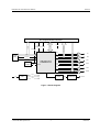
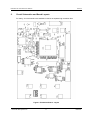
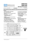
EV9100
CML Microcircuits
COMMUNICATION SEMICONDUCTORS
Evaluation Kit
User Manual
UM9100/1 August 2005
Advance Information
Features
• Target CMX910 installed
•
C-BUS interface
• Auxiliary ADC and DAC interface
•
19.2MHz device clock
• Digital/analogue PCB with low noise
floor
•
Interfaces to RF daughterboard with all
necessary signals
• Differential and single-ended baseband
interface
•
On-board power regulation and
distribution
• FX604 FSK modem IC fitted for extra Rx
channel
1
Brief Description
The EV9100 evkit is available for the evaluation, experimentation and design-in of the CMX910 AIS
Baseband Processor IC.
Comprising a digital/analogue pcb with an on-board CMX910 device, the evkit provides access to the
CMX910’s baseband signal, control and data interfaces as well as its auxilliary ADC and DAC functions.
The evkit also provides an FX604 FSK modem and associated circuitry to allow evaluation of the
CMX910's external FSK interface.
Jumpers, links and test points allow the user to dynamically monitor and/or isolate all aspects of the IC’s
signal and voltage levels.
This evkit has a simple power requirement with on-board voltage regulation and distribution.
© 2005 CML Microsystems Plc
Evaluation Kit User Manual for CMX910
EV9100
CONTENTS
Section
Page
1
Brief Description ..................................................................................... 1
2.
Preliminary Information.......................................................................... 4
2.1
Laboratory Equipment............................................................... 4
2.2
Handling Precautions ................................................................ 4
2.3
Approvals.................................................................................... 4
3.
Quick Start ............................................................................................... 4
4.
Signal Lists .............................................................................................. 5
5.
Circuit Schematics and Board Layouts.............................................. 11
6.
Detailed Description ............................................................................. 12
6.1
Hardware Description.............................................................. 12
6.2
Firmware Description .............................................................. 13
6.3
Software Description............................................................... 13
6.4
Evaluation Tests ...................................................................... 13
7.
Performance Specification................................................................... 14
7.1
Electrical Performance ............................................................ 14
It is always recommended that you check for the latest product datasheet version from the
Datasheets page of the CML website: [www.cmlmicro.com].
Note: This product is in development: Changes and additions will be made to this
specification. Items marked TBD or left blank will be included in later issues.
Information in this user manual should not be relied upon for final product design.
© 2005 CML Microsystems Plc
2
UM9100/1
Evaluation Kit User Manual for CMX910
EV9100
TxI+
TxI-
C-BUS
C-BUS
Header
+3.3V
TxQ+
TxQ-
SLOTCLK
UTC1PPS
Reference
Oscillator
CMX910
AFC
DAC4
TxI
Rx Differential
Reference
RF
Enables
Tx Differential
C-BUS
Expansion
Aux ADCs & DACs
C-BUS
RF Daughterboard Connector
RxI+
RxI-
TxQ
RxI1
RxQ+
RxQ-
RxQ1
RxI+
RxI-
RxI2
RxQ+
RxQ-
RxQ2
+3.3V
Vin
PSU
FX604
+2.5V
-3.3V
FSK
LimiterDiscriminator
FSK In
Figure 1 Block Diagram
© 2005 CML Microsystems Plc
3
UM9100/1
Evaluation Kit User Manual for CMX910
2.
Preliminary Information
2.1
Laboratory Equipment
EV9100
The following laboratory equipment is needed to use this evaluation kit:
2.1.1
Power Supply
+5V, -6V.
The -6V supply is optional, as the EV9100 incorporates a negative voltage generator. The board
is supplied with JP2 jumpered between pins 1 and 2, which connects the negative supply to the
on-board negative voltage generator, rather than the -6V external supply.
Note that the external negative supply connector is labelled -5V on the PCB. This is
incorrect, it should read -6V.
2.1.2
Signal Generators and Analysers
Suitable AIS Baseband I and Q signals must be generated by external equipment connected to
this Evaluation Kit. The signals produced by this kit must also be analysed by external
equipment. Provision is also made on this kit for connections to the Auxiliary ADC and DAC and
digital Device Enable Ports. A multi-way connector, J10, allows for the connection of a
(customer-supplied) daughter card containing RF circuitry.
2.1.3
C-BUS Control
This Evaluation Kit is controlled by a (customer-supplied) host µController, via the C-BUS
connector, J16. This is a 3.3V digital logic serial interface, which can be connected to a host
µController's SPI port. There is no firmware or software supplied with this Evaluation Kit.
2.2
Handling Precautions
Like most evaluation kits, this product is designed for use in office and laboratory environments.
The following practices will help ensure its proper operation.
2.2.1
Static Protection
This product uses low power CMOS circuits which can be damaged by electrostatic discharge.
Partially damaged circuits can function erroneously, leading to misleading results. Observe ESD
precautions at all times when handling this product.
2.2.2
Contents - Unpacking
Please ensure that you have received all of the items on the separate information sheet (EK9100)
and notify CML within 7 working days if the delivery is incomplete.
2.3
Approvals
There are no approvals for this product.
3.
Quick Start
Customers should assemble all of the equipment required to demonstrate the CMX910 and
connect it to the Evaluation Kit before applying power to the kit. Power should be applied to this
kit before the host µController is powered-up. Consult sections 6 and 7.1.3 of this User Manual
for details of the analogue and digital signal levels.
© 2005 CML Microsystems Plc
4
UM9100/1
Evaluation Kit User Manual for CMX910
4.
EV9100
Signal Lists
CONNECTOR PINOUT
Connector
Ref
Connector
Pin No.
Signal Name
Signal
Type
Description
J26
1
-Vin
Power
J26
2
DGND
Power
J26
3
+Vin
Power
+ve power supply.
J16
1
CSN
I/P
Active low chip select.
J16
2
CSXN
I/P
Active low chip select expansion input.
J16
3
CDATA
I/P
Command Data (Data from host to
CMX910).
J16
4
SLOTCLKN
O/P
Active low AIS Slot Clock.
J16
5
SCLK
I/P
Serial Clock.
J16
6
UTC1PPS
I/P
1Hz clock signal from GPS unit to CMX910.
J16
7
RDATA
O/P
Reply data (Data from CMX910 to host).
J16
8
RESETN
I/P
Active low reset.
J16
9
IRQN
O/P
Active low interrupt. This is an open drain
output from the CMX910.
J16
10
DGND
Power
© 2005 CML Microsystems Plc
5
Optional -ve power supply.
UM9100/1
Evaluation Kit User Manual for CMX910
EV9100
CONNECTOR PINOUT
Connector
Ref.
Note:
J18
Connector
Pin No.
Signal Name
Signal
Type
Description
On J18, odd-numbered pins are outputs from the single-to-differential op-amps.
Even-numbered pins are inputs to the CMX910. See also the table of jumper settings.
1, 2
Rx1IN
O/P - I/P
Channel 1 Rx I Negative
J18
3, 4
Rx1IP
O/P - I/P
Channel 1 Rx I Positive
J18
5, 6
Rx1QN
O/P - I/P
Channel 1 Rx Q Negative
J18
7, 8
Rx1QP
O/P - I/P
Channel 1 Rx Q Positive
J18
9, 10, 11,
12
AGND
Power
J18
13, 14
Rx2IN
O/P - I/P
Channel 2 Rx I Negative
J18
15, 16
Rx2IP
O/P - I/P
Channel 2 Rx I Positive
J18
17, 18
Rx2QN
O/P - I/P
Channel 2 Rx Q Negative
J18
19, 20
Rx2QP
O/P - I/P
Channel 2 Rx Q Positive
J19
Rx1I
I/P
Channel 1 Rx I
J20
Rx1Q
I/P
Channel 1 Rx Q
J23
Rx2I
I/P
Channel 2 Rx I
J25
Rx2Q
I/P
Channel 2 Rx Q
© 2005 CML Microsystems Plc
6
UM9100/1
Evaluation Kit User Manual for CMX910
EV9100
CONNECTOR PINOUT
Connector
Ref.
Note:
J1
Connector
Pin No.
Signal Name
Signal
Type
Description
On J1, Odd-numbered pins are buffered outputs from the CMX910.
Even-numbered pins are inputs to the differential-to-single op-amps.
See also the table of jumper settings.
1, 2
TxIN
O/P - I/P
Tx I Negative
J1
3, 4
TxIP
O/P - I/P
Tx I Positive
J1
5, 6
AGND
Power
J1
7, 8
TxQN
O/P - I/P
Tx Q Negative
J1
9, 10
TxQP
O/P - I/P
Tx Q Positive
J14
FSK IN
I/P
FSK input
J22
TxI
O/P
TxI Single ended
J24
TxQ
O/P
TxQ Single ended
J21
1
Aux ADC 0
I/P
Auxillary ADC 0 Input
J21
2
Aux ADC 1
I/P
Auxillary ADC 1 Input
J21
3
Aux ADC 2
I/P
Auxillary ADC 2 Input
J21
4
Aux ADC 3
I/P
Auxillary ADC 3 Input
J21
5
Aux ADC 4
I/P
Auxillary ADC 4 Input
J21
6, 7
AGND
Power
J21
8
Aux DAC 0
O/P
Auxillary DAC 0 Output
J21
9
Aux DAC 1
O/P
Auxillary DAC 1 Output
J21
10
Aux DAC 2
O/P
Auxillary DAC 2 Output
J21
11
Aux DAC 3
O/P
Auxillary DAC 3 Output
J21
12
Aux DAC 4
O/P
Auxillary DAC 4 Output
© 2005 CML Microsystems Plc
7
UM9100/1
Evaluation Kit User Manual for CMX910
EV9100
CONNECTOR PINOUT
Connector
Ref.
Connector
Pin No.
Signal Name
Signal
Type
Description
J10
1
CDATA
I/P
Command Data
J10
2
SCLK
I/P
Serial Clock
J10
3
EXP1N
I/P
CBUS expansion 1
J10
4
EXP3N
I/P
CBUS expansion 3
J10
5
DGND
Power
Digital Ground
J10
6
EXP4N
I/P
CBUS expansion 4
J10
7
ENAB0
O/P
RF Enable 0
J10
8
ENAB2
O/P
RF Enable 2
J10
9
ENAB4
O/P
RF Enable 4
J10
10
DGND
Power
Digital Ground
J10
11
UTC1PPS
I/P
1Hz GPS clock
J10
12
DGND
Power
Digital Ground
J10
13
FSK_RXD
I/P
Demodulated FSK data
J10
14
DGND
Power
Digital Ground
J10
15
DGND
Power
Digital Ground
J10
16
AGND
Power
Analogue Ground
J10
17
VREF_EXT
I/P
External Voltage Ref.
J10
18
AUXADC1
I/P
Aux ADC 1 Input
J10
19
AUXADC3
I/P
Aux ADC 3 Input
J10
20
AGND
Power
Analogue Ground
J10
21
AUXDAC1
O/P
Aux DAC 1 Output
J10
22
AUXDAC3
O/P
Aux DAC 3 Output
J10
23
AGND
Power
Analogue Ground
J10
24
RX1IP
I/P
Ch 1 Rx I Positive
J10
25
RX1QP
I/P
Ch 1 Rx Q Positive
J10
26
RX2IN
I/P
Ch 2 Rx I Negative
J10
27
RX2QN
I/P
Ch 2 Rx Q Negative
J10
28
AGND
Power
Analogue Ground
J10
29
TXIP
O/P
Tx I Positive
J10
30
TXQP
O/P
Tx Q Positive
continued overleaf ...
© 2005 CML Microsystems Plc
8
UM9100/1
Evaluation Kit User Manual for CMX910
EV9100
CONNECTOR PINOUT
Connector
Ref.
Connector
Pin No.
Signal Name
Signal
Type
Description
J10
31
AGND
Power
Analogue Ground
J10
32
TXQN
O/P
Tx Q Negative
J10
33
TXIN
O/P
Tx I Negative
J10
34
RX2QP
I/P
Ch 2 Rx Q Positive
J10
35
RX2IP
I/P
Ch 2 Rx I Positive
J10
36
AGND
Power
Analogue Ground
J10
37
RX1QN
I/P
Ch 1 Rx Q Negative
J10
38
RX1IN
I/P
Ch 1 Rx I Negative
J10
39
AUXDAC4
O/P
Aux DAC 4 Output
J10
40
AUXDAC2
O/P
Aux DAC 2 Output
J10
41
AUXDAC0
O/P
Aux DAC 0 Output
J10
42
AUXADC4
I/P
Aux ADC 4 Input
J10
43
AUXADC2
I/P
Aux ADC 2 Input
J10
44
AUXADC0
I/P
Aux ADC 0 Input
J10
45
FSK_IN
I/P
FSK Modulation
J10
46
+VIN
Power
Unregulated Supply
J10
47
+3V3_EXT
O/P
+3.3V supply, 100mA maximum
J10
48
FSK_MUTE
I/P
Logic Input
J10
49
FSK_DET
I/P
Logic Input
J10
50
REFCLK
O/P
CMX910 Clock
J10
51
nSLOTCLK
O/P
AIS Slot Clock
J10
52
ENAB5
O/P
RF Enable 5
J10
53
ENAB3
O/P
RF Enable 3
J10
54
ENAB1
O/P
RF Enable 1
J10
55
nEXP5
I/P
CBUS expansion 5
J10
56
DGND
Power
Digital Ground
J10
57
IRQN
O/P
Active low interrupt
J10
58
EXP2N
I/P
CBUS expansion 2
J10
59
EXP0N
I/P
CBUS expansion 0
J10
60
RDATA
O/P
Reply data
© 2005 CML Microsystems Plc
9
UM9100/1
Evaluation Kit User Manual for CMX910
EV9100
TEST POINTS
Test Point
Ref.
Default
Measurement
Description
TP1, 2
0V
Digital ground
TP3, 4
0V
Analogue ground
TP27
3.3V
3.3V digital supply
TP28
3.3V
3.3V external supply
TP29
2.5V
2.5V digital supply
JUMPERS
Link
Ref.
Positions
Default
Position
J15
1-2, 2-3
2-3
J18
1-2, 3-4, 5-6, 7-8
All fitted
Connect single-to-differential op-amp circuit outputs for Rx
Channel 1 to CMX910, if fitted.
J18
13-14, 15-16,
17-18, 19-20
All fitted
Connect single-to-differential op-amp circuit outputs for Rx
Channel 2 to CMX910, if fitted.
J1
1-2, 3-4, 7-8,
9-10
All fitted
Connect CMX910 Tx outputs to differential-to-single opamp circuit inputs, if fitted.
JP1
1-2
Not
Fitted
If fitted, the tri-state buffers between the FX604 and the
CMX910 will be disabled i.e. their outputs will be high
impedance.
JP2
1-2, 2-3
1-2
JP13
1-2
Fitted
Voltage reference select. If fitted, the CMX910's internal
reference will be used as a reference for the differential-tosingle Tx op-amp circuit. If not fitted, then an external
reference can be supplied from the RF transceiver
interface (J10).
JP14
1-2
Not
Fitted
External regulator control. If fitted, an external 2.5V
regulator will be enabled. This is not necessary for normal
operation.
JP15
1-2
Not
Fitted
If a jumper is fitted to JP15 then the negative voltage
converter will be shut down. Default state is not fitted.
Notes: I/P =
O/P =
BI
=
© 2005 CML Microsystems Plc
Description
FSK_MUTE select. 1-2 is high, disabling CMX910
interface, 2-3 is low, enabling CMX910 interface.
Negative voltage supply selection. 1-2 is on-board
switched-mode supply, 2-3 is external supply.
Input
Output
Bidirectional
10
UM9100/1
Evaluation Kit User Manual for CMX910
5.
EV9100
Circuit Schematics and Board Layouts
For clarity, circuit schematics are available in this kit as separate high resolution files.
Figure 2 Evaluation Board - Layout
© 2005 CML Microsystems Plc
11
UM9100/1
Evaluation Kit User Manual for CMX910
6.
Detailed Description
6.1
Hardware Description
EV9100
6.1.1 CMX910
The EV9100 comprises a CMX910 device mounted on a PCB with convenient interfaces so that users
can rapidly develop their own CMX910 prototype circuits and make connections to user-provided external
circuits. Refer to the CMX910 data sheet for a detailed description of the IC's operation.
The CMX910 is a highly integrated baseband signalling processor IC, which meets the requirements of
the class A and class B marine Automatic Identification System (AIS) transponder market. It is half duplex
in operation, comprising two parallel I+Q Rx paths and one Tx path. These are configurable for AIS or
FSK (DSC) operation. A 1200bps FSK demodulator interface provides the third parallel decode path
required by the AIS class A market. Integrated Rx/Tx data buffers and a slot/sample timer are also
provided, reducing the processing required by the host µC. A C-BUS expansion port, an RF device
enable port and a number of auxiliary ADCs and DACs are also provided. There is a push-to-make switch
on the pcb, connected to the CMX910's nRESET pin.
6.1.2 Oscillator
The clock for the CMX910 is provided by a 19.2MHz VCTCXO. By default its control input is held at midrail, but it can be tuned using the CMX910 AuxDAC4. If this is required, fit a 5k6Ω resistor in position R19.
6.1.3 Rx Signal Conditioning
The Rx inputs to the CMX910 are differential. The header J18 can be used to apply differential signals
(max 0.85Vpp per pin, centred at 1.25V) via anti-alias filters. Alternatively, jumpers can be fitted to J18
and single ended signals applied to the SMA connectors J19 and J20 (Ch1) and/or J23 and J25 (Ch2).
On-board op-amps (U18, U20) then perform single-ended to differential conversion and shift the signal to
the appropriate DC level. The signals applied to the SMA connectors should be DC coupled and centred
about 0V. Maximum signal level at the SMA connectors is 0.85Vpp.
6.1.4 Tx Signal Conditioning
The Tx outputs from the CMX910 are differential. These signals pass through an RC filter and a buffer
and are available on J1. Alternatively, jumpers can be fitted on J1 and on-board op-amps (U19) then
perform differential to single-ended conversion and level shifting. The single-ended outputs are available
on SMA connectors J22 and J24. These signals are centred about 0V and are capable of driving a 50Ω
load. These outputs are not designed to drive large capacitive loads.
6.1.5 FX604
The EV9100 has an FX604 FSK modem IC interfaced to the CMX910's 1200bps FSK demodulator
interface. The FX604 is enabled by the signal ENAB4. The CMX910's FSK_MUTE pin can be manually
pulled up or down via J15, or driven from the RF transceiver interface. This is likely to be driven by a
'squelch' output from a limiter-discriminator. The FX604 outputs can be isolated from the CMX910 by
fitting a jumper to JP1. The input to this circuit is an SMA connector, J14.
6.1.6 Digital Interface
Digital signals can be found on J16. These include the C-BUS interface, as well as some discrete logic
signals. All digital signals use 3.3V levels.
6.1.7 RF Transceiver Interface
J10 is intended to allow the connection of a daughter card containing RF circuitry. This connector is
manufactured by JAE and has the part number TX14-60R-6ST-MH1. The mating half is part number
TX15-60P-6ST-MH1. In the UK they can be purchased from Farnell Electronic Components (388-7790
and 388-7870). Note that this connector is numbered 1-30 along one edge, then 31-60 in the opposite
direction along the other edge.
6.1.8 Power Distribution System
The EV9100 is designed to be operated from a single +5V (nominal) supply. The EV9100 circuitry runs
from +3.3V and +2.5V supplies which are generated using on board linear regulators. There is also an on
board negative voltage converter to provide the -3.3V for the Tx and Rx op-amps. If required, this can be
© 2005 CML Microsystems Plc
12
UM9100/1
Evaluation Kit User Manual for CMX910
EV9100
disabled by fitting a jumper to JP15. In this case, the jumper on JP2 should be moved from pins 1 and 2
to pins 2 and 3, and -6V applied to pin 1 of J26. A separate +3.3V supply is used to power the circuitry on
the daughtercard. This is capable of supplying 100mA maximum.
6.1.9
Options
6.1.9.1 External Reference
An external voltage reference (VREF_EXT) can be applied from the RF Transceiver interface. In this case
the jumper should be removed from JP13. This will have the effect of centring the differential Tx I and Q
signals about VREF_EXT.
6.1.9.2 AuxADC Signal Conditioning
AuxADC0, AuxADC1 and AuxADC2 have uncommitted op-amps on their inputs. These op-amps are
configured as non-inverting followers by default, but the PCB is arranged so that other configurations are
possible by changing component values.
6.2
Firmware Description
There is no firmware required with this Evaluation Kit.
6.3
Software Description
There is no software supplied with this Evaluation Kit. Customers must supply their own software,
compatible with their chosen µController.
6.4
Evaluation Tests
This Evaluation Kit is capable of being used to demonstrate the following functions:
•
•
•
•
•
•
•
•
•
•
•
•
•
Receive AIS25 and AIS12.5 bursts in AIS burst mode.
Receive AIS25 and AIS12.5 bursts in AIS raw mode.
Receive DSC bursts using internal modem.
Receive DSC bursts using external FX604 modem.
Transmit AIS25 and AIS12.5 bursts in AIS burst mode.
Transmit AIS25 and AIS12.5 bursts in AIS burst mode.
Transmit DSC bursts.
CS-TDMA sensing and transmit abort.
Synchronisation to external UTC clock.
Sleep mode.
Control of external RF circuitry.
C-BUS expansion.
Auxilliary converters.
© 2005 CML Microsystems Plc
13
UM9100/1
Evaluation Kit User Manual for CMX910
7.
Performance Specification
7.1
Electrical Performance
EV9100
7.1.1 Absolute Maximum Ratings
Exceeding these maximum ratings can result in damage to the Evaluation Kit.
Min.
-0.3
+0.3
-0.3
0
-10
+10
Supply (+VIN - VSS)
Supply (-VIN - VSS)
Voltage on any connector pin to VSS
Current into or out of VIN and VSS pins
Storage Temperature
Operating Temperature
Max.
12.0
-12.0
VDD + 0.3
±250
+70
+35
Units
V
V
V
mA
°C
°C
Max.
5.5
-7.0
+35
Units
V
V
°C
7.1.2 Operating Limits
Correct operation of the Evaluation Kit outside these limits is not implied.
Notes
Supply (+VIN - VSS)
Supply (-VIN - VSS)
Operating Temperature
1
Min.
4.5
-6.0
+10
Notes:
1. Negative supply is optional, so this pin may be left unconnected.
© 2005 CML Microsystems Plc
14
UM9100/1
Evaluation Kit User Manual for CMX910
7.1.3
EV9100
Operating Characteristics
For the following conditions unless otherwise specified:
+VIN - VSS = 5.0V; External Negative Supply not connected; default jumper positions; Tamb = +25°C;
CMX910 Xtal Oscillator Frequency = 19.2MHz.
Notes
Min.
DC Parameters
IDD (immediately after power on)
IDD (Operating)
Typ.
Max.
100
160
6
3V3 External Daughtercard Supply
AC Parameters
Tx Single-ended Outputs
Tx O/P voltage swing
Tx O/P DC offset
Minimum Load impedance
3.15
2
3
Tx Differential Outputs
Tx O/P voltage swing
Tx O/P DC offset
Minimum Load impedance
4
5
Rx Single-ended Inputs
Rx I/P max voltage swing
Rx I/P DC Offset
Input impedance
2
Rx Differential Inputs
Rx I/P max voltage swing
Rx I/P DC Offset
Input impedance
3.30
mA
mA
3.45
2
V
2.0
0
50
Vp-p
V
Ω
2.1
1.25
2
Vp-p
V
kΩ
0.85
0
10
Vp-p
V
kΩ
0.85
1.25
Vp-p
V
kΩ
1.0
0
10
Vp-p
V
kΩ
100
FSK Input
FSK I/P max voltage swing
FSK I/P DC Offset
Input impedance
Units
Notes:
2. DC Coupled.
3. These outputs are not designed to drive highly capacitative loads.
4. Peak-to-peak differential i.e. 1.05Vp-p on each pin.
5. Or VREF_EXT. See section 6.1.9.1.
6. This voltage rail is generated by the EV9100 to supply the daughtercard. Iout < 100mA.
© 2005 CML Microsystems Plc
15
UM9100/1
Evaluation Kit User Manual for CMX910
EV9100
CML does not assume any responsibility for the use of any circuitry described. No IPR or circuit patent licences are implied.
CML reserves the right at any time without notice to change the said circuitry and any part of this product specification.
Evaluation kits and demonstration boards are supplied for the sole purpose of demonstrating the operation of CML products
and are supplied without warranty. They are intended for use in a laboratory environment only and are not for re-sale, enduse or incorporation into other equipments. Operation of these kits and boards outside a laboratory environment is not
permitted within the European Community. All software/firmware is supplied "as is" and is without warranty. It forms part of
the product supplied and is licensed for use only with this product, for the purpose of demonstrating the operation of CML
products. Whilst all reasonable efforts are made to ensure that software/firmware contained in this product is virus free, CML
accepts no resonsibility whatsoever for any contamination which results from using this product and the onus for checking
that the software/firmware is virus free is placed on the purchaser of this evaluation kit or development board.
www.cmlmicro.com
For FAQs see: www.cmlmicro.com/products/faqs/
For a full data sheet listing see: www.cmlmicro.com/products/datasheets/download.htm
For detailed application notes: www.cmlmicro.com/products/applications/
Oval Park, Langford,
Maldon, Essex,
CM9 6WG - England.
4800 Bethania Station Road,
Winston-Salem,
NC 27105 - USA.
No 2 Kallang Pudding Road,
#09 - 05/06 Mactech
Industrial Building,
Singapore 349307
No. 218, Tian Mu Road
West, Tower 1, Unit 1008,
Shanghai Kerry Everbright
City, Zhabei,
Shanghai 200070,
China.
Tel: +44 (0)1621 875500
Tel: +65 6745 0426
Fax: +44 (0)1621 875600
Tel: +1 336 744 5050,
800 638 5577
Fax: +1 336 744 5054
Fax: +65 6745 2917
Tel: +86 21 6317 4107
+86 21 6317 8916
Fax: +86 21 6317 0243
Sales:
[email protected]
Sales:
[email protected]
Sales:
[email protected]
Sales:
[email protected]
Technical Support:
[email protected]
Technical Support:
[email protected]
Technical Support:
[email protected]
Technical Support:
[email protected]