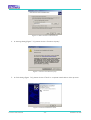
1
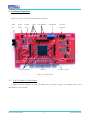
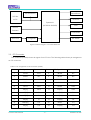
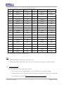
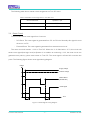
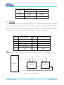
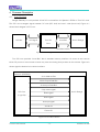
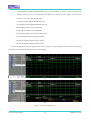
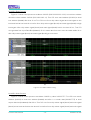
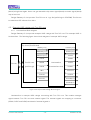
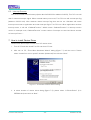
True PCI
User’s Manual
Design Gateway Co., Ltd.
Rev 1.1
(PD0402-6-00-2E)
*** Please read this manual carefully before using True PCI ***
Revision History
Revision
1.0
1.1
Date
11 February 2005
6 May 2005
True PCI User’s Manual
Detail of change
Initial Release
To update user interface code is able to read the DIP-Switch’s
value, and is able to display the output data on LED.
-I-
PD0402-6-00-02E
Table of Contents
1. Introduction.................................................................................................................................... 1
1.1. Summary Feature................................................................................................................... 1
1.2. Minimum System Requirement .............................................................................................. 2
1.3. Software Requirement............................................................................................................ 2
1.4. Warranty Policy ...................................................................................................................... 2
1.5. Customer Support.................................................................................................................. 2
2. TruePCI System ............................................................................................................................. 3
3. Hardware Description .................................................................................................................... 4
3.1. True PCI Startrt Kit Description .............................................................................................. 4
3.2. PCI Connector........................................................................................................................ 5
3.3. Clock Generator..................................................................................................................... 6
3.4. Reset Circuit .......................................................................................................................... 7
3.5. DIP switch (SW1) ................................................................................................................... 8
3.6. Push Button Switch (PB1 and PB2)........................................................................................ 8
3.7. LED ........................................................................................................................................ 9
3.8. 72 GPIOs ............................................................................................................................... 9
3.9. JTAG Port............................................................................................................................. 12
4. Firmware Description ................................................................................................................... 13
4.1. True PCI Core ...................................................................................................................... 13
4.2. Example VHDL design with True PCI core........................................................................... 16
4.3. Vender ID and Device ID Changing .................................................................................... 23
5. True PCI Demo Application.......................................................................................................... 23
6. Function in Dynamic Link Library (*.DLL)..................................................................................... 26
6.1. True PCI Function ................................................................................................................ 26
6.2. Interrupt Process.................................................................................................................. 28
7. How to install Device Driver ......................................................................................................... 28
8. Simulation model of PCI core....................................................................................................... 30
9. Synthesis PCI core....................................................................................................................... 30
True PCI User’s Manual
- II -
PD0402-6-00-02E
1. Introduction
Thank you very much for purchasing True PCI Starter Kit. Please check that all the following items
are in the box. If anything is missing or damaged, contact your distributor or Design Gateway Co.,Ltd.
1. True PCI Card
2. User’s Manual
3. CD ROM contains:
- True PCI core (pciif32.ngc and pciif32.vhd)
- Example VHDL source code (UserInterface.vhd, TruePCI.vhd and Memory.vhd)
- Pin Assignment for example VHDL source code (truepci.ucf)
- Configuration file (truepci.bit and truepci.mcs)
- Test Bench (PkTbPCIIF32.vhd, PkTestBench.vhd, PkTestPattern.vhd and TbTruePCI.vhd)
- Schematic (TruePCIRev1_2.pdf)
- Demo Application (TruePCI.exe)
- Dynamic Link Library for Demo Application (InStepPciDll.dll)
- Application Source Code
- Device Driver (InStepPciDrv.inf and InStepPciDrv.sys)
- User’s Manual
True PCI is a development PCI starter kit that provides a complete solution for design and
application based on Xilinx Spartan-3 family. The kit is suitable for users who is not familiar with PCI
protocol but would like to connect user’s board to PCI slot on computer.
True PCI utilizes 200,000 system gates Spartan-3 device (XC3S200), High gate density and large
number of GPIOs allow complete solutions to be implemented in advance design on FPGA. True PCI
card provides 72 I/Os for general purpose input / output (GPIO). This GPIO support both +2.5V and
+3.3V input. True PCI card has 4 LEDs, 2 push buttons and an 8-Bit DIP-Switch for general purpose.
1.1. Summary Feature
1.
2.
3.
4.
5.
Spartan-3 device 200,000 system gates (XC3S200)
+3.3V, 32 bits, 33MHz PCI Interface for PC slot-based development
JTAG configuration
72 General Purpose I/O
4 LEDs indicator, 2 Push Buttons switch and 1 8-bit DIP-Switch
True PCI User’s Manual
-1-
PD0402-6-00-02E
1.2. Minimum System Requirement
1.
2.
3.
4.
Pentium II or compatible processor (recommend Pentium III)
RAM 128 MB (recommend 256 MB)
Windows XP or Windows 2000
+3.3V, 32 bits, 33MHz PCI slot
1.3. Software Requirement
1. Xilinx ISE webpack for FPGA designer
2. Model Sim for FPGA designer
3. Microsoft Visual Studio.NET (Visual C++.NET) for application designer
1.4. Warranty Policy
1. Product warranty is valid for 6 months from purchasing date.
2. Warranty is void if any modification has been made to this product and any incorrect operation
from this manual or warranty sticker is torn or damaged.
3. In order to claim for product exchange or technical support within warranty period, official
receipt is required for unregistered customer as an evidence of purchasing whereas official
receipt is unnecessary for registered customer (please fill up registration card attached
herewith the product and send back to Design Gateway Co.,Ltd).
1.5. Customer Support
Customer can contact to [email protected] for support of any problem about True PCI
or visit our website at www.design-gateway.com.
True PCI User’s Manual
-2-
PD0402-6-00-02E
2. TruePCI System
Application (TruePCI.exe)
DLL (InstepPciDll.dll)
Software
Hardware
Device Driver
(InstepPciDrv.inf, InstepPciDrv.sys)
PCI slot
TruePCI.vhd
PCI Core (pciif32.ngc)
User design (UserInterface.vhd)
Spartan-3
Hardware (Use’s board)
Figure 2-1 True PCI System
From above flowchart, True PCI system consists of software and hardware. Software is application
(True PCI), DLL (InstepPciDll.dll) and Device Driver (InstepPciDrv.inf and InstepPciDrv.sys). Hardware
is PCI core (pciif32.ngc) and user’s design (UserInterface.vhd). Design Gateway Co.,Ltd recommends
users do not change DLL, Device Driver and PCI core. For application and FPGA user’s design, Users
can design new one by reference from TruePCI.exe and UserInterface.vhd
True PCI User’s Manual
-3-
PD0402-6-00-02E
3. Hardware Description
Figure 3-1 shows True PCI starter kit and its feature
JTAG
Port
Reset
Switch
DONE
LED
4-LED 2-Push Button
3-GPIO Connector
DIP Switch
PCI Slot
External
Oscillator
Spartan-3 FPGA
Figure 3-1 True PCI Card
3.1. True PCI Startrt Kit Description
A high-level block diagram of True PCI Starter kit is shown in Figure 3-2 followed by a brief
description of each section.
True PCI User’s Manual
-4-
PD0402-6-00-02E
Reset Button
PCI Connector
PCI Slot
on PC
72 GPIOs
Spartan-III
(XC3S200-4PQ208)
External
Oscillator
LED
Push Button
JTAG Port
Config ROM
DIP Switch
Figure 3-2 Block Diagram of True PCI Starter Kit
3.2. PCI Connector
This connector (CON2) shows all signals from PCI slot. The following table shows pin assignment
on PCI connector.
Table 3-1 Pin assignment on PCI connector (CON2)
Pin No.
1
3
5
7
9
11
13
15
17
19
21
PCI Signal Name
INTA#
INTD#
PRSNT1#
RST#
GNT#
AD[31]
AD[29]
AD[27]
AD[25]
C/BE#[3]
AD[23]
True PCI User’s Manual
Spartan-3 Pin
P197
NC
NC
P183
P200
P204
P2
P4
P7
P10
P12
Pin No.
2
4
6
8
10
12
14
16
18
20
22
-5-
PCI Signal Name
INTB#
INTC#
PRSNT2#
CLK
REQ#
AD[30]
AD[28]
AD[26]
AD[24]
IDSEL
AD[22]
Spartan-3 Pin
NC
NC
NC
P184
P203
P205
P3
P5
P9
P11
P13
PD0402-6-00-02E
Table 3-1 Pin assignment on PCI connector (CON2) (continued)
Pin No.
23
25
27
29
31
33
35
37
39
41
43
45
47
49
51
53
55
57
PCI Signal Name
AD[21]
AD[19]
AD[17]
C/BE#[2]
IRDY#
DEVSEL#
LOCK#
SDONE
SERR#
C/BE#[1]
AD[14]
AD[12]
AD[10]
AD[8]
AD[7]
AD[5]
AD[3]
AD[1]
Spartan-3 Pin
P15
P18
P20
P22
P26
P28
NC
P31
P34
P36
P39
P42
P44
P46
P50
P52
P58
P62
Pin No.
24
26
28
30
32
34
36
38
40
42
44
46
48
50
52
54
56
58
PCI Signal Name
AD[20]
AD[18]
AD[16]
FRAME#
TRDY#
STOP#
PERR#
SBO#
PAR
AD[15]
AD[13]
AD[11]
AD[9]
C/BE#[0]
AD[6]
AD[4]
AD[2]
AD[0]
Spartan-3 Pin
P16
P19
P21
P24
P27
P29
NC
P33
P35
P37
P40
P43
P45
P48
P51
P57
P61
P63
NC = this pin does not connect to Xilinx Spartan-3
Note:
1. ACK64 and REQ64 signal use for 64-bit PCI slot.
2. JTAG signal (TRST, TCK, TMS, TDO, TDI) from PCI slot do not connect to JTAG Connector.
3.3. Clock Generator
True PCI card can receive clock from 2 sources
- PCI Clock: This clock is generated from PC via PCI slot. It is running at 33 MHz
- External Clock: On True PCI card provide oscillator socket (OSC1). Users can use both half
size and full size oscillator. This socket support only +3.3V oscillator.
True PCI User’s Manual
-6-
PD0402-6-00-02E
The following table shows master clock assignment on True PCI card.
Table 3-2 Masters clock assignment on True PCI card
Clock Generator
PCI Clock
External Clock
Spartan-3 pin
P184
P79
3.4. Reset Circuit
True PCI can receive reset signal from 2 sources
- PCI Reset: This reset signal is generated from PC via PCI slot. Normally this signal is reset
when turn on PC.
- External Reset: This reset signal is generated from external reset circuit.
The reset circuit will monitor +3.3V on True PCI. When the +3.3V falls below +2.7V, this circuit will
assert reset signal (low logic level) to Spartan-3. In addition to monitoring +3.3V, the reset circuit can
generate reset pulse by press reset button on True PCI. The reset signal is a fixed 230 ms active low
pulse. The following figure shows reset signal timing diagram.
Voltage
Supply Voltage
Detector Voltage
Manual Reset
(Reset Button)
Reset Signal
Time
230 ms
230 ms
Figure 3-3 Reset Signal Timing Diagram
True PCI User’s Manual
-7-
PD0402-6-00-02E
Table 3-3 Reset signal on True PCI
Reset Signal
PCI Reset
Reset Circuit
Spartan-3 Pin
P183
P156
3.5. DIP switch (SW1)
True PCI provides 8-position DIP switch input. This switch can set to a low or high logic level. Table
3-4 shows logic level on 8-position DIP switch and table 3-5 shows pin assignment from 8-position DIP
switch to Spartan-3
Table 3-4 Logic level defines on 8-position DIP switch.
DIP switch setting
ON
OFF
Logic Level
Low
High
Table 3-5 8-position DIP switch assignment
Signal Name
DIP8
DIP7
DIP6
DIP5
DIP4
DIP3
DIP2
DIP1
Spartan-3 Pin
P115
P114
P113
P111
P109
P108
P107
P106
Description
DIP switch input 8
DIP switch input 7
DIP switch input 6
DIP switch input 5
DIP switch input 4
DIP switch input 3
DIP switch input 2
DIP switch input 1
3.6. Push Button Switch (PB1 and PB2)
True PCI provides two push button switches to Spartan-3. Each push button switch generates
active low signal. The following table shows pin assignment from push button to Spartan-3
True PCI User’s Manual
-8-
PD0402-6-00-02E
Table 3-6 Push button switch assignment
Push Button
PB1
PB2
Spartan-3 Pin
P149
P148
3.7. LED
True PCI provides 4 LEDs for users. Each LED is active low. The following table shows pin
assignment from LED to Spartan-3
Table 3-7 LED assignment
LED No.
LED1
LED2
LED3
LED4
Spartan-3 Pin
P155
P154
P152
P150
Note:
DONE’s LED monitors status in configuration process. While Spartan-3 is configured, DONE’s LED
should be bright. When configuration Spartan-3 complete, DONE’s LED should be off.
3.8. 72 GPIOs
True PCI provides 3 GPIO connectors (CON6, CON7 and CON8) and each connector have 24-bit
GPIO pins. Users can use all GPIOs both input and output. All GPIOs connect directly to Spartan-III
and each GPIO pin supports only +3.3V tolerant input. Users must carefully connecting GPIO pin to
user’s board. The following table shows pin assignment from each GPIO connector to Spartan-3
True PCI User’s Manual
-9-
PD0402-6-00-02E
Table 3-8 Pin assignment at GPIO connector (CON6)
Pin No.
1
3
5
7
9
11
13
15
17
19
21
23
25
27
29
Spartan-3 Pin
+5V
P161
P165
P167
P169
P172
P176
GND
P180
P182
P187
P190
P194
P198
GND
Pin No.
2
4
6
8
10
12
14
16
18
20
22
24
26
28
30
Spartan-3 Pin
+5V
P162
P166
P168
P171
P175
P178
GND
P181
P185
P189
P191
P196
P199
GND
Table 3-9 Pin assignment at GPIO connector (CON7)
Pin No.
1
3
5
7
9
11
13
15
17
19
True PCI User’s Manual
Spartan-3 Pin
+5V
P147
P144
P141
P139
P137
P133
GND
P131
P128
Pin No.
2
4
6
8
10
12
14
16
18
20
- 10 -
Spartan-3 Pin
+5V
P146
P143
P140
P138
P135
P132
GND
P130
P126
PD0402-6-00-02E
Table 3-9 Pin assignment at GPIO connector (CON7) (continued)
Pin No.
21
23
25
27
29
Spartan-3 Pin
P125
P123
P120
P117
GND
Pin No.
22
24
26
28
30
Spartan-3 Pin
P124
P122
P119
P116
GND
Table 3-10 Pin assignment at GPIO connector (CON8)
Pin No.
1
3
5
7
9
11
13
15
17
19
21
23
25
27
29
Spartan-3 Pin
+5V
P102
P100
P96
P94
P90
P86
GND
P80
P78
P76
P72
P68
P65
GND
Pin No.
2
4
6
8
10
12
14
16
18
20
22
24
26
28
30
Spartan-3 Pin
+5V
P101
P97
P95
P93
P87
P85
GND
P81
P77
P74
P71
P67
P64
GND
VCCO for connector CON6 and CON8 are fixed at +3.3V, so output voltage from GPIO pin at
connector CON6 and CON8 is +3.3V. VCCO for connector CON7, users can select from JP3 (between
+2.5V and +3.3V). The following table shows VCCO jumper setting.
True PCI User’s Manual
- 11 -
PD0402-6-00-02E
Table 3-11 VCCO jumper setting (JP3)
VCCO for
CON7
+2.5V
+3.3V
JP3
1-2
Open
Closed
2-3
Closed
Open
3.9. JTAG Port
True PCI provides JTAG connector that programs the on-board PROM (XCF01S) and configures
Spartan-3 (XC3S200). Users can use download cable from Xilinx to program PROM and configure
Spartan-3. In addition to download cable, users can use JtagLink or Universal Download Cable from
Design Gateway Co.,Ltd. The following table shows JTAG connector pin assignment.
Table 3-12 JTAG pin assignment
Pin No.
1
3
5
7
9
JTAG Signal
TCK
TDO
TMS
DONE (Optional)
TDI
Pin No.
2
4
6
8
10
JTAG Signal
GND
+3.3V
GND
Note:
DONE signal on pin 7 is optional signal that is for JtagLink only not for other download cable.
TCK
TMS
JTAG Port
TDI
PROM
(XCF01S)
TDI
TD0
Spartan-3
(XC3S200)
TDI
TD0
TDO
Figure 3-4 True PCI JTAG Chain
True PCI User’s Manual
- 12 -
PD0402-6-00-02E
4. Firmware Description
4.1. True PCI Core
Design Gateway Co.,Ltd provides 32 bit PCI core interface for Spartan-3 FPGA on True PCI card.
This PCI core manages signal between PC side (PCI slot) and user’s side (local bus). Figure 4-1
shows block diagram of PCI core.
PCI Slot
PCI Signal
True PCI
Core
Local Bus
User’s Design
XC3S200-PQ208
Figure 4-1 Block Diagram of PCI Core.
True PCI core provides “Local Bus” that is standard memory interface. So users do not need to
know PCI protocol. Users need to know only local bus timing that provides in this manual. Figure 4-2
shows signal’s direction in local bus interface.
Spartan-3 (XC3S200)
13-bit Address Bus
32-bit Output Data Bus
32-bit Input Data Bus
PCI Core
(*.ngc file)
Chip select signal
Read signal
User’s Design
Write signal
Interrupt signal
Vender ID
Device ID
Figure 4-2 Local Bus Interface
True PCI User’s Manual
- 13 -
PD0402-6-00-02E
- 13-bit Address signal (lbaddr[14:2]): This is PCI address. True PCI core provides PCI
address from bit 2 to bit 14 because PCI data bus is 32-bit access. When users access
one time, users can get 4-byte data.
- 32-bit Input Data signal (lbdatain[31:0])
- 32-bit Output Data signal (lbdataout[31:0])
- Read signal, active low level (lbrdb)
- Write signal, active low level (lbwrb)
- Chip Select signal, active low level (lbcsb)
- Interrupt signal, active high level (lbint)
- Vender ID signal, default value 0xF0F0
- Device ID signal, default value 0xF0F0
Local bus timing is shown in figure 4-3 and 4-4. In figure 4-3 (a) and (b) show local bus read timing
and figure 4-4 (a) and (b) show local bus write timing.
(a)
(b)
Figure 4-3 Local Bus Read Timing.
True PCI User’s Manual
- 14 -
PD0402-6-00-02E
Local Bus Read Process
Figure 4-3 shows read process at address 0x000C (0000-0000-0000-1100). In local bus address
should be show address 0x0003 (000-0000-0000-11). True PCI core send address (0x0003) to local
bus address (lbaddr) after that 30 ns True PCI core force chip select signal and read signal to low
level and hold at low level 60 ns before force chip select signal (lbcsb) and read signal (lbrdb) to high
level again. After chip select signal (lbscb) and read signal (lbrdb) hold in low level 30 ns, True PCI
core get data from Input Data Bus (lbdatain). So it is mean data from users must be stable within 30 ns
after chip select signal (lbscb) and read signal (lbrdb) go to low level.
(a)
(b)
Figure 4-4 Local Bus Writes Timing.
Local Bus Write Process
Figure 4-4 shown writes process at address 0x000C by value 0x00007777. True PCI core sends
address (0x0003) to local bus address (lbaddr) and after 1 ns sends data (0x00007777) to local
output data bus (lbdataout) after 29 ns True PCI core force chip select signal (lbcsb) and write signal
(lbwrb) to low level and hold at low level 60 ns before force chip select signal (lbcsb) and write signal
True PCI User’s Manual
- 15 -
PD0402-6-00-02E
(lbwrb) to high level again. Users can get data while chip select signal (lbcsb) and write signal (lbwrb)
stay at low level.
Design Gateway Co.,Ltd provides True PCI core in *.ngc file (pciif32.ngc in CD-ROM). This file can
be added into ISE software from Xilinx.
4.2. Example VHDL design with True PCI core
4.2.1 UserInterface Block diagram
Design Gateway Co.,Ltd provide example VHDL design with True PCI core. This example VHDL is
UserInterface. The following figure shown block diagram of example VHDL design.
Top Level (TruePCI.vhd)
PCI slot
TruePCI core
(pciif32.ngc)
LBAddr [14:2]
ExtAddr [14:2]
LBDataOut [31:0]
ExtData [31:0]
LBDataIn [31:0]
ExtCsB
LBCsB
ExtRdB
LBRdB
LBWrB
UserInterface
(UserInterface.vhd)
ExtWrB
ExtPBInt
LBInt
ExtUserInt
VenderID
ExtGPIO
DeviceID
WriteLED[3:0]
ReadDIP[7:0]
Figure 4-5 Example VHDL Design Block Diagram
UserInterface is example VHDL design connecting with True PCI core. This module manages
signal between True PCI core and external signal. The external signals are mapping to connector
(CON6, CON7 and CON8) and detail of external signals is
True PCI User’s Manual
- 16 -
PD0402-6-00-02E
- External Address (ExtAddr [14:2]): This external address bus is the same signal as local
bus address.
- External Data (ExtData [31:0]): This external data bus is bidirection. UserInterface control
external data bus direction. When read process, UserInterface reads data from external
data bus (ExtData) and sends data to local bus input data (LBDataIn). When write process,
UserInterface write data from local bus output data (LBDataOut) to external data bus
(ExtData).
- External Chip Select (ExtCsB): This external chip select is the same signal as local bus
chip select (LBCsB).
- External Read (ExtRdB): This external read signal is the same signal as local bus read
signal (LBRdB).
- External Write (ExtWrB): This external write signal is the same signal as local bus write
signal (LBWrB).
- External Push Button Interrupt (ExtPBInt), active low level: This is an interrupt signal from
push button (PB2).
- External User’s Interrupt, active low level: This interrupt signal receives from user’s board
by pin 23 on CON6.
- External GPIO (ExtGPIO [15:0]): This is GPIO signal. Users can read or write data to each
GPIO that is free from others. GPIO signal uses address 0x0004 to control GPIO direction
and address 0x0008 for read/write data.
- Write LED (WriteLED[3..0]): These are signals used to control LED1 to LED 4 of True PCI
Card. Users are able to control them, which, writing the 4 last LSB, the address 0x000C are
defined for control data.
- Read DIP-Switch(DIP-Switch[7:0]): These are reading signal used to read the input of DIPSwitch. Users are able to read the DIP Switch values through the address 0x000C.
Users can change VenderID and DeviceID in this code. While operate system, both of ID must be
fix value.
4.2.2 Internal Register in UserInterface
In UserInterface has 3 control register
True PCI User’s Manual
- 17 -
PD0402-6-00-02E
1. Interrupt register: This register maps to address 0x0000 in user’s space. In address 0x0000,
Bit 1 is interrupt enable, bit 0 is interrupt flag and another bit do not use. The following table
shown description of interrupt register
Table 4-1 Interrupt Register
Bit
Logic Level
0
1
1
0
0
1
Descriptions
disable external interrupt
enable external interrupt
no external interrupt occurred
external interrupt occurred
Users can enable interrupt register by writing data 0x00000002 to address 0x0000. On the other
hand, users can disable interrupt register by writing data 0x00000000 to address 0x0000. When
external interrupt occurred bit 0 at address 0x0000 is set to high level (logic ‘1’). Users can clear this
interrupt by writing data 0x00000002 to address 0x0000.
Note
- Users can clear external interrupt all time, although external interrupt is disable.
- Design Gateway Co.,Ltd recommends users to use address 0x0000 for interrupt register
because in device driver map address 0x0000 for external interrupt. When external
interrupt occurred, device driver will automatically get and clear external interrupt.
- UserInterface receives external interrupt from 2 sources: External Push Button Interrupt
(ExtPBInt) and External User’s Interrupt (ExtUserInt).
2. GPIO direction register: This register maps to address 0x0004 and use from bit 0 to bit 15. The
following table shows GPIO direction.
Table 4-2 GPIO Direction
Logic
Direction
0
Input
1
Output
3. GPIO data register: This register maps to address 0x0008 and use from bit 0 to bit 15. This
registers uses with GPIO direction. If GPIO direction set to input, users can read 16-bit data
True PCI User’s Manual
- 18 -
PD0402-6-00-02E
from GPIO pin at this register. And if GPIO direction set to output, users can write 16-bit data to
GPIO pin at this register.
Note
- Each GPIO pins do not depend on each other. Users can freely control each GPIO pin.
4. DIP- Switch registers: These registers are established on the address 0x000C. From LSB to
MSB registers, they are used to read the value of DIP-Switch on the True-PCI.
In example VHDL code, Design Gateway provides source code and configuration file. Users can
use them without any modification. FPGA folder in CD-ROM contains:
- UserInterface.vhd, TruePCI.vhd and Memory.vhd is example source code file.
- truepci.ucf is pin assignment file.
- truepci.bit is configuration file for Spartan-3 (XC3S200-PQ208)
- truepci.mcs is configuration file for PROMs (XCF01S)
- PkTbPCIIF32.vhd, PkTestBench.vhd, PkTestPattern.vhd and TbTruePCI.vhd is Test Bench
file for simulation
- pciif32.vhd is True PCI core for simulation
- pciif32.ngc is True PCI core for synthesis and implement
Both configuration files are map signal to connector (CON6, CON7 and CON8). The following table
shows pin assignment on connector (CON6, CON7 and CON8)
True PCI User’s Manual
- 19 -
PD0402-6-00-02E
Table 4-3 Pin assignment on connectors CON6
Pin no. Spartan-3 Pin UserInterface signal
1
2
3
P161
ExtData[31]
4
P162
ExtData[30]
5
P165
ExtData[29]
6
P166
ExtData[28]
7
P167
ExtData[27]
8
P168
ExtData[26]
9
P169
ExtData[25]
10
P171
ExtData[24]
11
P172
ExtRdB
12
P175
ExtWrB
13
P176
ExtAddr[14]
14
P178
ExtAddr[13]
15
16
17
P180
ExtAddr[12]
18
P181
ExtAddr[11]
19
P182
ExtAddr[10]
20
P185
ExtAddr[9]
21
P187
ExtAddr[8]
22
P189
ExtAddr[7]
23
P190
ExtUserInt
24
P191
ExtAddr[6]
25
P194
ExtAddr[5]
26
P196
ExtAddr[4]
27
P198
ExtAddr[3]
28
P199
ExtAddr[2]
29
30
-
True PCI User’s Manual
- 20 -
Description
+5V
+5V
External Data Bus bit 31
External Data Bus bit 30
External Data Bus bit 29
External Data Bus bit 28
External Data Bus bit 27
External Data Bus bit 26
External Data Bus bit 25
External Data Bus bit 24
External Read signal, active low level.
External Write signal, active low level.
External Address Bus bit 14
External Address Bus bit 13
Ground
Ground
External Address Bus bit 12
External Address Bus bit 11
External Address Bus bit 10
External Address Bus bit 9
External Address Bus bit 8
External Address Bus bit 7
External User Interrupt, active low level
External Address Bus bit 6
External Address Bus bit 5
External Address Bus bit 4
External Address Bus bit 3
External Address Bus bit 2
Ground
Ground
PD0402-6-00-02E
Table 4-4 Pin assignment on connectors CON7
Pin no. Spartan-3 Pin UserInterface signal
1
2
3
P147
ExtData[23]
4
P146
ExtData[22]
5
P144
ExtData[21]
6
P143
ExtData[20]
7
P141
ExtData[19]
8
P140
ExtData[18]
9
P139
ExtData[17]
10
P138
ExtData[16]
11
P137
ExtData[15]
12
P135
ExtData[14]
13
P133
ExtData[13]
14
P132
ExtData[12]
15
16
17
P131
ExtData[11]
18
P130
ExtData[10]
19
P128
ExtData[9]
20
P126
ExtData[8]
21
P125
ExtData[7]
22
P124
ExtData[6]
23
P123
ExtData[5]
24
P122
ExtData[4]
25
P120
ExtData[3]
26
P119
ExtData[2]
27
P117
ExtData[1]
28
P116
ExtData[0]
29
30
-
True PCI User’s Manual
- 21 -
Description
+5V
+5V
External Data Bus bit 23
External Data Bus bit 22
External Data Bus bit 21
External Data Bus bit 20
External Data Bus bit 19
External Data Bus bit 18
External Data Bus bit 17
External Data Bus bit 16
External Data Bus bit 15
External Data Bus bit 14
External Data Bus bit 13
External Data Bus bit 12
Ground
Ground
External Data Bus bit 11
External Data Bus bit 10
External Data Bus bit 9
External Data Bus bit 8
External Data Bus bit 7
External Data Bus bit 6
External Data Bus bit 5
External Data Bus bit 4
External Data Bus bit 3
External Data Bus bit 2
External Data Bus bit 1
External Data Bus bit 0
Ground
Ground
PD0402-6-00-02E
Table 4-5 Pin assignment on connectors CON8
Pin no. Spartan-3 Pin UserInterface signal
1
2
3
P102
ExtGPIO[0]
4
P101
ExtGPIO[1]
5
P100
ExtGPIO[2]
6
P97
ExtGPIO[3]
7
P96
ExtGPIO[4]
8
P95
ExtGPIO[5]
9
P94
ExtGPIO[6]
10
P93
ExtGPIO[7]
11
P90
ExtGPIO[8]
12
P87
ExtGPIO[9]
13
P86
ExtGPIO[10]
14
P85
ExtGPIO[11]
15
16
17
P80
ExtGPIO[12]
18
P81
ExtGPIO[13]
19
P78
ExtGPIO[14]
20
P77
ExtGPIO[15]
21
P76
ExtCsB
22
P74
23
P72
24
P71
25
P68
26
P67
27
P65
28
P64
29
30
-
Description
+5V
+5V
General Purpose Input/Output bit 0
General Purpose Input/Output bit 1
General Purpose Input/Output bit 2
General Purpose Input/Output bit 3
General Purpose Input/Output bit 4
General Purpose Input/Output bit 5
General Purpose Input/Output bit 6
General Purpose Input/Output bit 7
General Purpose Input/Output bit 8
General Purpose Input/Output bit 9
General Purpose Input/Output bit 10
General Purpose Input/Output bit 11
Ground
Ground
General Purpose Input/Output bit 12
General Purpose Input/Output bit 13
General Purpose Input/Output bit 14
General Purpose Input/Output bit 15
External Chip select signal, active low level
Ground
Ground
Note:
- When users use GPIO, JP3 should be set to +3.3V (recommended).
True PCI User’s Manual
- 22 -
PD0402-6-00-02E
4.3. Vender ID and Device ID Changing
Vender ID and Device ID of True PCI are fixed to 0xF0F0, however users can change both of them.
If users want to change Vender ID and Device ID, users must change in UserInterface.vhd near
Output Assignment and in InStepPciDrv.inf in this line.
%InStepPciDrv%=InStepPciDrv.Install, PCI\VEN_F0F0&DEV_F0F0
Vender ID, Device ID in InStepPciDrv.inf and Vender ID, Device ID in UserInterface.vhd must have
same value. If these values are not the same, application can not access to True PCI core.
4.4. The True PCI configuration
For the FPGA configuration on True PCI, it directly impacts to the Base address of the True PCI card
which its’ configuration is disappeared. From this event, True PCI software is unable to read or to write
the data from True PCI Card, therefore users necessitates to restart the machine after reconfiguration.
5. True PCI Demo Application
TruePCI.exe is demonstration application to access read/write data to True PCI card. Users can
use this application without modification of application. On the other hand, users can develop new
application with reference from True PCI demo application. This application is developed on Visual
C++ .NET. So Design Gateway Co.,Ltd recommends users to develop application on Microsoft
Visual Studio.NET. Figure 5-1 shows True PCI demo application.
True PCI User’s Manual
- 23 -
PD0402-6-00-02E
Figure 5-1 True PCI Demo Application
True PCI demo application has 3 main controls
1. Checking Device Count: Users can check how many True PCI card do install on user’s PC by
press “ChkDevCnt” button and True PCI demo application will display count number of True
PCI card on “Device Count : “. And “Interrupt Count : “ use for count external interrupt.
2. Initialize / Close Device: This main control use for open device and close device. Users should
open device (press “OpenDev” button) before access True PCI card and close device (press
“CloseDev” button) before closing demo application. If users do not open device, users can
not access True PCI card.
3. Read/ Write Register: This main control reads or writes register. Offset means offset address
from PCI base address (normally BIOS controls base address by itself) On True PCI card,
Users can use address 0x0000 to 0x7FFF. For address 0x8000 to 0xFFFF reserve for PCI
system register. Design Gateway Co.,Ltd do not guarantee any problem. If users access
address in this range. In read access, Users can fill offset address to “Offset (Hex) : “ and
press “Read” button. True PCI demo application read data from address and show data in
“Value (Hex) : “. In write access, Users can fill offset address to “Offset (Hex) : “ and fill data to
“Value (Hex) : “ after that press “Write” button. True PCI demo application will send data to
address
True PCI User’s Manual
- 24 -
PD0402-6-00-02E
Note
True PCI demo application supports access True PCI only 1 card. If users installs True PCI more
than 1 card, this application will not support additional cards.
True PCI User’s Manual
- 25 -
PD0402-6-00-02E
6. Function in Dynamic Link Library (*.DLL)
Design Gateway Co.,Ltd provides function library in DLL module (InStepPciDll.dll). Users can
include DLL module to user’s project and develop application based on example application.
6.1. True PCI Function
1. Initial Device
Format
Function
Parameter
Return Value
InitDevice (PCHAR pDevName,
UCHAR DevNo,
ULONG FlagOffset,
ULONG FlgInterrestBit,
ULONG MskOffset,
ULONG MskVal,
UCHAR ClearFlagMode,
UCHAR MaskMode,
ULONG (*CBFn)( PVOID, PVOID, PVOID));
Initial True PCI card
PCHAR pDevName
Device name
UCHAR DevNo
Device number
ULONG FlagOffset
Interrupt Flag Register's offset
ULONG FlgInterrestBit
Interest bit Flag
ULONG MskOffset
Interrupt Mask Register's offset
ULONG MskVal
Interrupt Mask value
UCHAR ClearFlagMode
Clear interrupt flag mode
UCHAR MaskMode
Interrupt mask register mode
ULONG (*CBFn)( PVOID, PVOID, PVOID) Call back function for interrupt
PVOID hHANDLE
Device’s handle (Can open device)
Note
- In initial device function, all parameter use with initial PCI system. Design Gateway Co.,Ltd
recommend users do not change this parameter.
- If application can not access to True PCI card, the return value equals NULL. On the other
hand, if application can access to True PCI card, the return value does not equal NULL.
True PCI User’s Manual
- 26 -
PD0402-6-00-02E
2. Check Device Count
Format
Function
Parameter
Return Value
UCHAR ChkDeviceCnt (PCHAR pDevName);
Number of True PCI card
PCHAR pDevName Device name want to check
UCHAR
Number of True PCI card
Note
- In check device count function, pDevName is “InStepPciDrv”. Users do not change this
name because this name is fixed.
3. Read Register
Format
Function
Parameter
Return Value
ULONG reg_read (PVOID hHANDLE,
ULONG offset);
Read data from True PCI card
PVOID hHANDLE, Device's handle that returned from InitDevice
ULONG offset
Offset address
ULONG
Data value
4. Write Register
Format
Function
Parameter
Return Value
VOID reg_write (PVOID hHANDLE,
ULONG offset,
ULONG val);
Write data to True PCI card
PVOID hHANDLE Device's handle that returned from InitDevice
ULONG offset
Offset address
ULONG val
Data value
-
5. Exit Device
Format
Function
Parameter
Return Value
VOID ExitDevice (PVOID hHANDLE);
Disconnect to True PCI card
-
True PCI User’s Manual
- 27 -
-
PD0402-6-00-02E
6.2. Interrupt Process
After users enable external interrupt (write data 0x00000002 to address 0x0000), True PCI core will
wait for external interrupt signal. When external interrupt occurred, True PCI core will set interrupt flag
(address 0x0000 bit0). After windows detect interrupt flag that was be set. Windows will create
interrupt event sent to application and clear interrupt flag in True PCI core. When application receives
interrupt event, it will call “CallbackFunction”. Which means “CallbackFunction” is interrupt service
routine. In example code, “CallbackFunction” counts number of interrupt occurred and shows number
at “Interrupt Count : “
7. How to install Device Driver
Please follow these steps to install True PCI device driver:
1. Turn off PC and then install True PCI card into PCI slot.
2. After turn on PC, “Found New Hardware Wizard” dialog (figure 7-1) will be occurs. Please
select “Install from a list or specific location (Advanced)” and click at “Next”.
Figure 7-1 “Found New Hardware Wizard” dialog
3. In select location of device driver dialog (figure 7-2), please select “X:\DeviceDriver” (X is
CDROM drive) and click at “Next”.
True PCI User’s Manual
- 28 -
PD0402-6-00-02E
Figure 7-2 Select location of device driver
4. In warning dialog (figure 7-3), please click at “Continue Anyway”.
Figure 7-3 Click at “Continue Anyway”
5. In finish dialog (figure 7-4), please click at “Finish” to complete install device driver process.
Figure 7-4 Finish install device driver
True PCI User’s Manual
- 29 -
PD0402-6-00-02E
8. Simulation model of PCI core
For simulating, the simulation model of PCI core, this requires “simprim” library. For Xilinx ISE
Webpack version 6.3, the source files of “simprim” library are located at "C:\Xilinx\vhdl\src\simprims".
The source files are composed of:
- simprim_Vpackage_mti.vhd
- simprim_Vcomponents_mti.vhd
- simprim_VITAL_mti.vhd
Please create library “simprim” and compile these source files before simulating the simulation
model of PCI core.
9. Synthesis PCI core
On True PCI’s CD, there are example source codes of how to use PCI core. The example codes
are composed of “TruePCI.vhd” and “UserInterface.vhd”. “TruePCI.vhd” is a top level module.
“UserInterface.vhd” is a module that interfaces with PCI core. These two source files show the
example of how to use PCI core. Users can modify both “TruePCI.vhd” and “UserInterface.vhd”.
Anyway, Design Gateway Co.,Ltd recommends modifying only “UserInterface.vhd” because it is more
convenient for users.
True PCI User’s Manual
- 30 -
PD0402-6-00-02E
Note
True PCI User’s Manual
- 31 -
PD0402-6-00-02E
54 BB Building, 13th Floor, Room No.1302, Sukhumvit 21 Rd. (Asoke)
Klongtoey-Nua, Wattana, Bangkok 10110 Thailand
Tel. (662)261-2277, Fax. (662)261-2290
www.design-gateway.com