1
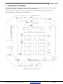
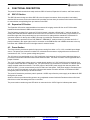
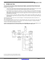
ATHENA III PANEL I/O BOARD
User Manual
Revision A
Revision
Date
Comment
A
1/10/13
Initial Release
FOR TECHNICAL SUPPORT
PLEASE CONTACT:
[email protected]
January 2013
Copyright 2013
Diamond Systems Corporation
555 Ellis Street
Mountain View, CA 94043 USA
Tel 1-650-810-2500
Fax 1-650-810-2525
www.diamondsystems.com
CONTENTS
Important Safe-Handling Information .....................................................................................................................3
1. Description ........................................................................................................................................................4
2. Block Diagram ...................................................................................................................................................4
3. Mechanical Drawing .........................................................................................................................................5
4. Functional Description .....................................................................................................................................6
4.1 SBC I/O Section.............................................................................................................................................6
4.2 Expansion I/O Section ...................................................................................................................................6
4.3 Power Section................................................................................................................................................6
5. SBC I/O Section – Bottom Side .......................................................................................................................7
5.1 Ethernet .........................................................................................................................................................7
5.2 Input Power....................................................................................................................................................7
5.3 VGA ...............................................................................................................................................................7
5.4 Serial Ports ....................................................................................................................................................8
5.5 USB 0/1 Ports ................................................................................................................................................9
5.6 USB 2/3 Ports ................................................................................................................................................9
5.7 Data Acquisition I/O .................................................................................................................................... 10
6. SBC I/O Section – Top Side .......................................................................................................................... 11
6.1 Input Power................................................................................................................................................. 11
6.2 Ethernet ...................................................................................................................................................... 11
6.3 VGA ............................................................................................................................................................ 11
6.4 USB ............................................................................................................................................................ 11
6.5 PS/2 Keyboard and Mouse ......................................................................................................................... 11
6.6 Data Acquisition .......................................................................................................................................... 11
6.7 Serial Ports ................................................................................................................................................. 12
7. Expansion I/O Section ................................................................................................................................... 13
7.1 Serial Port Expansion ................................................................................................................................. 13
7.2 VGA Expansion .......................................................................................................................................... 13
7.3 Digital I/O Expansion .................................................................................................................................. 13
7.4 AUX Power Connector ............................................................................................................................... 13
8. Power Section ................................................................................................................................................ 14
Athena III Panel I/O Board User Manual Rev A
www.diamondsystems.com
Page 2
IMPORTANT SAFE-HANDLING INFORMATION
WARNING: ESD-Sensitive Electronic Equipment!
Observe ESD-safe handling procedures when working with this product.
Always use this product in a properly grounded work area and wear
appropriate ESD-preventive clothing and/or accessories.
Always store this product in ESD-protective packaging when not in use.
Safe Handling Precautions
Aurora contains numerous I/O connectors that connect to sensitive electronic components. This creates many
opportunities for accidental damage during handling, installation and connection to other equipment. The list here
describes common causes of failure found on boards returned to Diamond Systems for repair. This information is
provided as a source of advice to help you prevent damaging your Diamond (or any vendor’s) embedded
computer boards.
ESD damage – This type of damage is almost impossible to detect, because there is no visual sign of failure or
damage. The symptom is that the board simply stops working, because some component becomes defective.
Usually the failure can be identified and the chip can be replaced.
To prevent ESD damage, always follow proper ESD-prevention practices when handling computer boards.
Damage during handling or storage – On some boards we have noticed physical damage from mishandling. A
common observation is that a screwdriver slipped while installing the board, causing a gouge in the PCB surface
and cutting signal traces or damaging components.
Another common observation is damaged board corners, indicating the board was dropped. This may or may not
cause damage to the circuitry, depending on what is near the corner. Most of our boards are designed with at
least 25 mils clearance between the board edge and any component pad, and ground / power planes are at least
20 mils from the edge to avoid possible shorting from this type of damage. However these design rules are not
sufficient to prevent damage in all situations.
A third cause of failure is when a metal screwdriver tip slips, or a screw drops onto the board while it is powered
on, causing a short between a power pin and a signal pin on a component. This can cause overvoltage / power
supply problems described below. To avoid this type of failure, only perform assembly operations when the
system is powered off.
Sometimes boards are stored in racks with slots that grip the edge of the board. This is a common practice for
board manufacturers. However our boards are generally very dense, and if the board has components very close
to the board edge, they can be damaged or even knocked off the board when the board tilts back in the rack.
Diamond recommends that all our boards be stored only in individual ESD-safe packaging. If multiple boards are
stored together, they should be contained in bins with dividers between boards. Do not pile boards on top of each
other or cram too many boards into a small location. This can cause damage to connector pins or fragile
components.
Power supply wired backwards – Our power supplies and boards are not designed to withstand a reverse
power supply connection. This will destroy each IC that is connected to the power supply. In this case the board
will most likely will be unrepairable and must be replaced. A chip destroyed by reverse power or by excessive
power will often have a visible hole on the top or show some deformation on the top surface due to vaporization
inside the package. Check twice before applying power!
Bent connector pins – This type of problem is often only a cosmetic issue and is easily fixed by bending the pins
back to their proper shape one at a time with needle-nose pliers. This situation can occur when pulling a ribbon
cable off of a pin header. Note: If the pins are bent too severely, bending them back can cause them to weaken
unacceptably or even break, and the connector must be replaced.
Athena III Panel I/O Board User Manual Rev A
www.diamondsystems.com
Page 3
1.
DESCRIPTION
The Athena III panel I/O board plugs directly onto the Athena III PC/104 single board computer and provides
industry-type I/O connectors for all I/O features on the board. The panel I/O board mounts in the Pandora
enclosure to provide a cable-free mounting system for Athena III.
Key feature highlights include:
Plugs onto the Athena III SBC and provides all I/O without cables
Provides additional front panel I/O for 2 additional PC/104 boards
Mounts in Pandora enclosure
Provides connection for power switch
Provides power paths for +5V and variable voltage input
2.
BLOCK DIAGRAM
Athena III Panel I/O Board User Manual Rev A
www.diamondsystems.com
Page 4
3.
MECHANICAL DRAWING
A mechanical drawing of the Athena III panel I/O board connector layout is provided below. The drawing shows
the top side of the panel I/O board with the relative connector locations.
All I/O connectors are located on the board so that there is sufficient room to install all connectors without
interference with any other connector or mounting hole.
Athena III Panel I/O Board Top Side
Athena III Panel I/O Board User Manual Rev A
www.diamondsystems.com
Page 5
4.
FUNCTIONAL DESCRIPTION
The panel I/O board contains three major sections: SBC I/O section, Expansion I/O section, and Power section.
4.1
SBC I/O Section
The SBC I/O section brings out all the SBC I/O to the front panel connectors. On the top side it has industry
standard I/O connectors, and on the bottom side it provides dual row 2mm pin sockets on the bottom of the board
to mate with the corresponding 2mm pin headers on the SBC.
4.2
Expansion I/O Section
The Expansion I/O section contains additional connectors for bringing out the I/O from one PC/104 module
installed below the Athena III SBC inside the enclosure.
The first feature provides I/O for a generic PC/104 I/O board. It includes a 50-pin 2x20 .1” pitch pin header for
mating with a standard ribbon cable that connects to the I/O connector of a PC/104 board. This pin header is on
the bottom right side of the panel board in a spot convenient for mating with the standard PC/104 board I/O
connector location. On the top side a DB37 connector is provided for external access to this I/O.
The second feature provides I/O for a DSC EMM-XT / EMM-4M-XT serial port board. It provides two 2x10 .1”
pitch pin headers in the upper right corner for connection to the EMM board, and 3 DB9M connectors in the top
left center and 1 DB9M connector in the right center for external access.
4.3
Power Section
The Power section provides two paths for input power coming from either a +5V, +12V or variable input voltage
source. The power input connector consists of a 1x4 header that connects to a plug with screw connectors for
connections to +5V, +12V or system voltage and ground.
The +5V source is routed through a 1x2 .156” pitch friction lock connector for a front panel switch and then to a
pin socket on the bottom side that mates with the Athena III SBC. The switch connector can be bypassed with a
jumper if desired.
The +12V or variable input voltage source is routed through another 1x2 .156” pitch friction lock connector for a
front panel switch and then to a separate 1x2 .156” pitch friction lock connector for connection to a DC/DC power
supply mounted inside the enclosure. The 5VDC output of this DC/DC power supply then has two paths to the
Athena III SBC: (1) It can connect directly to the PC/104 bus of the system, if the power supply is mounted on the
bus; or (2) it can be routed back to the panel I/O board with another connector and then to the Athena III SBC
through the panel I/O board’s pin socket connection.
The panel I/O board also provides a path for optional +12VDC output from the power supply to the Athena III SBC
through the pin socket.
Another connector provides auxiliary power to any peripherals mounted inside the Pandora enclosure like hard
disk drives or other data storage devices or recorders.
The power section contains a green LED which is connected to the +5VDC signal to indicate power status.
Athena III Panel I/O Board User Manual Rev A
www.diamondsystems.com
Page 6
5.
SBC I/O SECTION – BOTTOM SIDE
All these connectors are on the bottom side of the panel I/O board. Their locations and pinouts match exactly the
corresponding connectors on the Athena III SBC. The pin numbering of these connectors, when facing the
connector, is reversed from the pin numbering on the male pin headers.
5.1
5.2
Ethernet
NC
1
2
NC
MDI0+
3
4
MDI0-
MDI1+
5
6
MDI1-
MDI2+
7
8
MDI2-
MDI3+
9
10
MDI3-
Input Power
The power signals on these connectors come from either the front panel input power connector via jumpers, or an
external switch, and connect to the power signals on the PC/104 connector of the Athena III SBC.
A
5.3
B
GND
1
+5V
1
NC
2
NC
2
+5V
3
GND
3
NC
4
GND
4
NC
5
NC
6
NC
7
NC
8
+12V
9
VGA
This connector provides a connection for VGA monitors. Note that while the DDC serial detection pins are
present, there is no 5V supply provided, nor are the old “Monitor ID” pins used.
Athena III Panel I/O Board User Manual Rev A
GRN
1
2
RED
BLU
3
4
GND
HSYN
5
6
DDAT
VSYN
7
8
DCLK
www.diamondsystems.com
Page 7
5.4
Serial Ports
This connector provides 4 serial ports, printer port and PS/2 keyboard and mouse signals from the Athena III CPU
board. The four serial ports are jumper-configurable for RS-232, RS-422, or RS-485 protocols.
SERA DCD
A01
B01
PPRT_~STRB
SERA DSR
A02
B02
PPRT_LNFD
SERA RXD
A03
B03
PPRT_PD0
SERA RTS
A04
B04
PPRT_PERR
SERA TXD
A05
B05
PPRT_PD1
SERA CTS
A06
B06
PPRT_~INIT
SERA DTR
A07
B07
PPRT_PD2
SERA RNG
A08
B08
PPRT_~SELP
SERA GND
A09
B09
PPRT_PD3
SERB DCD
A10
B10
PPRT_GND
SERB DSR
A11
B11
PPRT_PD4
SERB RXD
A12
B12
PPRT_GND
SERB RTS
A13
B13
PPRT_PD5
SERB TXD
A14
B14
PPRT_GND
SERB CTS
A15
B15
PPRT_PD6
SERB DTR
A16
B16
PPRT_GND
SERB RNG
A17
B17
PPRT_PD7
SERB GND
A18
B18
PPRT_GND
SERC DCD
A19
B19
PPRT_~PACK
SERC DSR
A20
B20
PPRT_GND
SERC RXD
A21
B21
PPRT_PBSY
SERC RTS
A22
B22
PPRT_GND
SERC TXD
A23
B23
PPRT_PPOT
SERC CTS
A24
B24
PPRT_GND
SERC DTR
A25
B25
PPRT_SLCT
SERC RNG
A26
B26
KB CLK
SERC GND
A27
B27
KB GND
SERD DCD
A28
B28
KB DATA
SERD DSR
A29
B29
KB VCC
SERD RXD
A30
B30
MS CLK
SERD RTS
A31
B31
MS GND
SERD TXD
A32
B32
MS DATA
SERD CTS
A33
B33
MS VCC
SERD DTR
A34
B34
RST GND
SERD RNG
A35
B35
~RST IN
SERD GND
A36
B36
A37
B37
A38
B38
A39
B39
A40
B40
Athena III Panel I/O Board User Manual Rev A
www.diamondsystems.com
Page 8
5.5
USB 0/1 Ports
This connector provides access to the 2 USB 2.0 ports. The shield pin is tied to system ground. The Key positions
are missing to match the key position in the cable to prevent misconnection.
5.6
NC
1
2
Shield / Ground
USB1 Pwr-
3
4
USB0 Pwr-
USB1 Data+
5
6
USB0 Data+
USB1 Data-
7
8
USB0 Data-
USB1 Pwr+
9
10
USB0 Pwr+
USB 2/3 Ports
This connector provides access to the 2 USB 2.0 ports. The shield pin is tied to system ground. The Key positions
are missing to match the key position in the cable to prevent misconnection.
NC
1
2
Shield / Ground
USB3 Pwr-
3
4
USB2 Pwr-
USB3 Data+
5
6
USB2 Data+
USB3 Data-
7
8
USB2 Data-
USB3 Pwr+
9
10
USB2 Pwr+
Athena III Panel I/O Board User Manual Rev A
www.diamondsystems.com
Page 9
5.7
Data Acquisition I/O
This connector provides a connection for the DAQ functions on the Athena III SBC.
DIO A0
1
26
DIO A1
DIO A2
2
27
DIO A3
DIO A4
3
28
DIO A5
DIO A6
4
29
DIO A7
DIO B0
5
30
DIO B1
DIO B2
6
31
DIO B3
DIO B4
7
32
DIO B5
DIO B6
8
33
DIO B7
DIO C0
9
34
DIO C1
DIO C2
10
35
DIO C3
DIO C4 / Gate 0
11
36
DIO C5 / Gate 1
DIO C6 / Clk 1
12
37
DIO C7 / Out 0
Ext Trig
13
38
Tout 1
+5V Out
14
39
Dground
Vout 0
15
40
Vout 1
Vout 2
16
41
Vout 3
Aground (Vout)
17
42
Aground (Vin)
Vin 0
18
43
Vin 8
Vin 1
19
44
Vin 9
Vin 2
20
45
Vin 10
Vin 3
21
46
Vin 11
Vin 4
22
47
Vin 12
Vin 5
23
48
Vin 13
Vin 6
24
49
Vin 14
Vin 7
25
50
Vin 15
Athena III Panel I/O Board User Manual Rev A
www.diamondsystems.com
Page 10
6.
SBC I/O SECTION – TOP SIDE
These SBC I/O connectors are on the top side of the panel I/O board. They face out through the enclosure front
panel.
6.1
Input Power
The input power connector is dual-footprint of two connectors. Connector 1 is a 1x4 Phoenix-type header – screw
plug style connector. The input power may be supplied either by +5VDC and/or +12V / +Vin. The +5V is intended
to be connected via jumper or switched to the Athena III SBC power connector via an external power switch. If
there is +12V available with the +5V then there is an option to jumper the +12V to the +12V bus on the Athena III
SBC power connector. Connector 2 is a screw-type circular connector that is optional for customers that want a
more secure connection than what Connector 1 has.
The +12V / +Vin is also intended to be connected via jumper or switched via an external power switch to an
auxiliary connector on the back side of the board, which then is used to connect to a DC/DC power supply. The
output of the DC/DC power supply is then fed either to the PC/104 bus power pins (if the power supply is on the
PC/104 bus) or back to the panel I/O board and then to the Athena III SBC through the +5V pins on the SBC’s
mating power input connector.
6.2
1
+12V / Var
2
GND
3
+5V
Ethernet
The Ethernet connector is a vertical metal-shielded RJ-45 jack with industry standard pinout for 10/100/1000Mbps
Ethernet. The signals come from the SBC mating Ethernet connector.
Proper isolation must be maintained on all Ethernet signal routing to meet industry standard signal isolation
specifications. No ground or power plane should be above or underneath these signals.
6.3
VGA
The VGA connector is standard vertical DD15 female connector with industry standard VGA pinout. It has 4-40
thread inserts and hex screwlocks. The signals come from the Athena III SBC mating VGA connector.
6.4
USB
The USB connectors are four vertical metal shrouded type A connectors with industry standard pinout for USB.
The signals come from the two Athena III SBC mating USB connectors.
6.5
PS/2 Keyboard and Mouse
The PS/2 connectors are two vertical Mini-DIN-6 connectors with industry standard pinout for PS/2 keyboard and
mouse. The signals come from the Athena III SBC mating PS/2 connector.
6.6
Data Acquisition
The data acquisition connector is a vertical 50-pin connector with long ejector/latches for a mating ribbon cable
connector with strain relief. The signals come from the Athena III SBC mating data acquisition connector and
have a 1 to 1 correspondence with that connector pinout.
Athena III Panel I/O Board User Manual Rev A
www.diamondsystems.com
Page 11
6.7
Serial Ports
The serial port connectors are six vertical DB9 male connectors. They have 4-40 thread inserts and hex
screwlocks. Ports 1-4 signals come from the 80-pin SBC connector. Ports 5-6 signals come from a 2x10 pin
expansion connector. The signal pinouts of the connectors used in the RS-232, RS-422, RS-485 protocols are
shown below.
DB9
Pin
RS-232 Configuration
Signal
Name
Serial Port
Connector
Signal
Name
DB9
Pin
1
DCD 1
1
2
DSR 1
6
2
RXD 1
3
4
RTS 1
7
3
TXD 1
5
6
CTS 1
8
4
DTR 1
7
8
RI 1
9
5
GND 1
9
10
NC
RS-422 Configuration
RS-485 configuration
DCD
1
2
DSR
NC
1
2
NC
NC
1
2
NC
RXD
3
4
RTS
TXD+
3
4
TXD-
NC
3
4
TXD/RXD-
TXD
5
6
CTS
GND
5
6
RXD-
TXD/RXD+
5
6
NC
DTR
7
8
RI
RXD+
7
8
NC
NC
7
8
NC
GND
9
10
NC
GND
9
10
NC
GND
9
10
NC
Athena III Panel I/O Board User Manual Rev A
www.diamondsystems.com
Page 12
7.
EXPANSION I/O SECTION
These connectors are on the bottom side of the panel I/O board, outside the PC/104 outline. They do not connect
to the Athena III SBC. They are used for other internal connections and functions. These connectors are 0.1” pitch
male pin headers.
7.1
Serial Port Expansion
The serial port expansion connector is a 2x10 pin 0.1” pitch male pin header. Their signals are brought out to two
DB9 male connectors for serial ports 5 and 6 on the top side of the panel board.
7.2
VGA Expansion
The VGA expansion connector is a 2x10 pin 0.1” pitch male pin header that is used to connect VGA signals from
an alternate source to the VGA connector.
7.3
Digital I/O Expansion
The data I/O connector is a 50-Pin Centronics female connector that connects the digital I/O signals from an
expansion digital I/O board to the outside world.
7.4
AUX Power Connector
The AUX Power connector allows power connection to peripherals mounted inside the Pandora enclosure like
HDDs (hard disk drives), recording devices or other devices that cannot get power from the PC/104 stack.
+12V/VAR
1
GND
2
GND
3
+5V
4
Athena III Panel I/O Board User Manual Rev A
www.diamondsystems.com
Page 13
8.
POWER SECTION
The power section provides the means to bring power to the system. The schematic below indicates the power
routing between the input power connector and the Athena III SBC through the panel I/O board. Power may be
provided in several methods:
1. +5V in from the input power connector directly to the panel I/O board, using either the front panel switch
or a direct connection, and then the Athena III SBC through the SBC’s input connector.
2. Vin (8-30VDC) from the input power connector to a connector leading to an internal DC/DC power supply,
whose output is driven directly onto the PC/104 bus using the PC/104 bus connectors on the DC/DC
power supply. The Vin may be routed to the power supply connector either through the front panel switch
or through a direct connection.
3. Same as #2 above, except the +5VDC and optional +12VDC outputs of the DC/DC power supply are
routed back to the panel I/O board and then connected to the Athena III SBC through the SBC power
input connector.
The switch bypass jumpers are 0-ohm ¼ watt T/H resistors. To use the panel power switch, the resistor is cut
away, opening the circuit.
The +12V input option jumper is also a 0-ohm ¼ watt T/H resistor used to route +12V from the Vin pin to the +12V
pin on the Athena III power connector. If the Vin voltage is not +12V then the resistor is cut away to isolate the
+12V pin on the Athena III primary power connector.
If power is being provided by one of Diamond Systems’ Jupiter-MM (JMM) power supplies, cable 6981016 can be
used to connect jumper block J35 on the Athena III SBC to the Jupiter-MM power supply output.
PC/104™ is a trademark of the PC/104 Embedded Consortium.
All other trademarks are the property of their respective owners.
Athena III Panel I/O Board User Manual Rev A
www.diamondsystems.com
Page 14