1
SMT300Q
SMT300Q User Guide V1.6
User Manual (QCF42); Version 3.0, 8/11/00; © Sundance Multiprocessor Technology Ltd. 1999
Page 2 of 61
SMT300Q SMT300Q User Guide V1.65
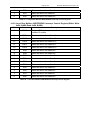
Date
Comments
Engineer
Version
30-09-02
Original Document
SP
1.1
23/04/04
PLL register
SP
1.2
21/05/04
Power connector part number correction
TJW
1.3
16/11/04
Added: TIM sites location
SM
1.4
26/11/05
Corrected: location Pin 1 of J21
SM
1.5
7/12/05
Removed SDB references
AJP
1.6
Page 3 of 61
SMT300Q SMT300Q User Guide V1.65
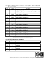
Table of Contents
1
2
Introduction ..................................................................................................................................... 8
Functional Description .................................................................................................................... 9
2.1
Block Diagram ...................................................................................................................... 10
2.2
ComPort Switching Matrix.................................................................................................... 11
2.3
TIM Sites location................................................................................................................. 12
3
Setting Up the SMT300Q.............................................................................................................. 13
4
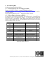
Host Memory Map......................................................................................................................... 14
4.1
CompactPCI Bridge Chip Internal Register (BAR0)............................................................. 14
4.2
I/O Space Register Assignments (BAR1) ............................................................................ 14
4.3
Memory Space Assignments(BAR2).................................................................................... 15
5
DSP Resource Memory Map ........................................................................................................ 16
6
Shared Memory Resource ............................................................................................................ 17
7
ComPorts ...................................................................................................................................... 18
7.1
ComPort Switching (Quick Switches)................................................................................... 18
7.2
Buffered ComPort................................................................................................................. 19
8
ComPort to CompactPCI Interface ............................................................................................... 23
8.1
ComPort Registers (Offset 0x10, BAR1).............................................................................. 23
8.2
Control Register (Offset 0x14, BAR1) .................................................................................. 23
8.3
Status Register (Offset 0x14, BAR1 , Read-Only) ............................................................... 24
8.4
Interrupt Control Register (Offset 0x18, BAR1) ................................................................... 25
9
PLL................................................................................................................................................ 26
9.1
PLLREG1 (BAR1 Offset 6016) .............................................................................................. 26
9.2
PLLREG2 (BAR1 Offset 6416) .............................................................................................. 26
9.3
Frequency Select (Bank 2, 3 and 4)..................................................................................... 26
9.4
Phase Shift Select (Bank 2) ................................................................................................. 27
9.5
Phase Shift Select (Bank 3 and 4) ....................................................................................... 27
10 JTAG Controller ............................................................................................................................ 28
11 Using the SMT300Q External/Internal JTAG with TI Tools. ......................................................... 30
12 Firmware Upgrades ...................................................................................................................... 31
13 Global/Local Bus Transfers, DSP <-> CompactPCI. ................................................................... 33
13.1
Mailbox Accesses................................................................................................................. 33
13.1.1
Doorbell Interrupts ....................................................................................................... 34
13.2
DSP Interrupt Control ........................................................................................................... 34
13.3
DSP To Local Aperture 0 control and Accessing................................................................. 35
13.3.1
Global bus access protocol ......................................................................................... 36
14 Interrupts ....................................................................................................................................... 40
14.1
SMT300Q-To-CompactPCI Interrupts.................................................................................. 40
14.2
CompactPCI-To-SMT300Q Interrupts.................................................................................. 41
14.3
Interrupt Registers................................................................................................................ 41
14.3.1
CompactPCI Interrupt Configuration Register(Offset 0x4C, BAR0)............................ 41
14.3.2
CompactPCI Interrupt Status Register(Offset 0x48, BAR0)........................................ 43
14.3.3
Local Bus Interrupt Mask Register(Offset 0x77, BAR0).............................................. 44
Page 4 of 61
SMT300Q SMT300Q User Guide V1.65
14.3.4
Local Bus Interrupt Status Register(Offset 0x76, BAR0) ............................................ 45
14.3.5
CompactPCI Mailbox WRITE/READ Interrupt Control Register(Offset: Write 0xD0,
BAR0 Read 0xD2, BAR0) ............................................................................................................. 45
14.3.6
Local Bus Mailbox WRITE/READ Interrupt Control Register(Offset Write 0xD4, BAR0
Read 0xD6, BAR0) ....................................................................................................................... 46
14.3.7
Mailbox Write/Read Interrupt Status Register(Offset: Write 0xD8, BAR0 Read 0xDA,
BAR0)
47
14.3.8
INTREG Register(Offset 0x40, BAR1) ........................................................................ 47
14.4
Example ............................................................................................................................... 48
14.4.1
An Interrupt service routine must be set up, in this the following register will need to be
cleared
48
15 Stand-Alone Mode ........................................................................................................................ 50
16 Performance Figures .................................................................................................................... 51
16.1
Relative JTAG speeds.......................................................................................................... 52
17 Mechanical Dimensions ................................................................................................................ 53
18 Power consumption ...................................................................................................................... 53
19 Cables and Connectors ................................................................................................................ 54
19.1
ComPorts ............................................................................................................................. 54
19.2
Buffered ComPort Cabling ................................................................................................... 54
19.3
JTAG back panel cabling ..................................................................................................... 56
20 Where’s that Jumper?................................................................................................................... 58
21 Expansion Header (J2) ................................................................................................................. 59
22 JTAG Interface circuits.................................................................................................................. 60
22.1
Signal Description ................................................................................................................ 60
Page 5 of 61
SMT300Q SMT300Q User Guide V1.65
Table of Figures
Figure 1 : Block Diagram for SMT300Q (Master site only) ........................................10
Figure 2: ComPort Switching Matrix ..........................................................................11
Figure 3: TIM sites location........................................................................................12
Figure 4 : Operation of quick switches.......................................................................18
Figure 5 : TBC Data Routing .....................................................................................28
Figure 6 : JTAG header pin numbers.........................................................................32
Figure 7 : Local Bus to DSP Connectivity ..................................................................33
Figure 8 : DSP Transfer via the Local Aperture 0 ......................................................36
Figure 9 : Timing diagram for DSP local bus access .................................................38
Figure 10 : SMT300Q to CompactPCI Interrupts.......................................................40
Figure 11 : CompactPCI to SMT300Q Interrupts .......................................................41
Figure 12 : Auxiliary Power Connector ......................................................................50
Figure 13 : JTAG speed Comparison chart ...............................................................52
Figure 14 : Jumper Finder Diagram ...........................................................................58
Figure 15 : Expansion Header Pin Out Diagram........................................................59
Figure 16 : JTAG Slave circuit ...................................................................................61
Page 6 of 61
SMT300Q SMT300Q User Guide V1.65
Table of Tables
Table 1 : Table of Abbreviations ..................................................................................7
Table 2 : I/O address space map...............................................................................14
Table 3 : Memory space map ....................................................................................15
Table 4 : Memory space map ....................................................................................16
Table 6 : COM-SWITCH Register..............................................................................19
Table 7: Buffered ComPort 1 connections .................................................................20
Table 8: Buffered ComPort 2 connections .................................................................20
Table 9: Buffered ComPort 3 connections .................................................................20
Table 10: Buffered ComPort 4 connections ...............................................................20
Table 11: Buffered ComPort 5 connections ...............................................................21
Table 12: Buffered ComPort 6 connections ...............................................................21
Table 13: Buffered ComPort 7 connections ...............................................................21
Table 14: Buffered ComPort 8 connections ...............................................................22
Table 15 : Buffered ComPort Additional Signals........................................................22
Table 16 : Control Register........................................................................................23
Table 17 : Status Register .........................................................................................24
Table 18 : Interrupt Control Register..........................................................................25
Table 19 : PLLREG1 Register ...................................................................................26
Table 20 : PLLREG2 Register ...................................................................................26
Table 21 : PLL Frequency Select ..............................................................................26
Table 22 : PLL Phase Shift Select (Bank 2)...............................................................27
Table 23 : PLL Phase Shift Select (Bank 3 and 4).....................................................27
Table 24 : JTAG Header pin function.........................................................................32
Table 25 : CompactPCI Interrupt Configuration Register...........................................43
Table 26 : CompactPCI Interrupt Status Register......................................................44
Table 27 : Local Bus Interrupt Mask Register...........................................................45
Table 28 : Local Bus Interrupt Status Register ..........................................................45
Table 29 : CompactPCI Mailbox WRITE/READ Interrupt Control Register................46
Table 30 : Local Bus Mailbox WRITE/READ Interrupt Control Register ....................46
Table 31 : Mailbox Write/Read Interrupt Status Register...........................................47
Table 32 : INTREG Register......................................................................................48
Table 33 : Performance Figures ................................................................................51
Table 35 : Buffered ComPort connector pin out.........................................................55
Table 36 : Buffered JTAG connector pin functionality as JTAG source .....................56
Table 37 : Buffered JTAG connector pin functionality as JTAG master .....................57
Page 7 of 61
Table Of Abbreviations
BAR
Base Address Region
DMA
Direct Memory Access
EPLD
Electrically Programmable Logic Device
CompactPCI
SRAM
Compact Peripheral Component Interconnect
Static Random Access Memory
TBC
Test Bus Controller
TIM
Texas Instruments Module
Table 1 : Table of Abbreviations
SMT300Q SMT300Q User Guide V1.65
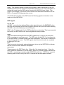
1 Introduction
The SMT300Q is a quad-site module carrier board that provides access to TIM
modules over the CompactPCI bus.
The carrier can hold up to four ‘C6x modules and these can exchange data using
ComPorts. A ComPort routing matrix, using electronic “quick switches”, is provided to
allow module connectivity without external cables.
The first TIM on the carrier is known as the “Master Module” and an enhanced
CompactPCI interface allows data packets to be exchanged between this module
and the CompactPCI bus at burst speeds in the range of 60–100MB/s. The DSP has
access to the CompactPCI Bridge internal registers to control DMAs, mailbox events,
and interrupts.
1MB of SRAM is mapped on to the Global Bus and can be accessed as a global
resource by the Host system across the CompactPCI Bridge or by the Master
Module.
An on-board JTAG controller allows systems to be debugged using Code Composer
Studio. This JTAG controller also has buffered outputs and inputs that can be
accessed using connectors on the carrier’s back panel. This allows off-board devices
to be connected into the JTAG chain.
Headers are provided for RESET_IN and RESET_OUT to allow multiple SMT300Q
carriers to be connected together and synchronised.
The board requires a 3.3-volt supply that is taken from the CompactPCI connector
and is made available at the fixing pillars for each module.
The SMT300Q may also be used with ‘C4x-based TIMs. When using these ‘C4x
modules you must ensure that a Master ‘C4x Module does not use its global memory
(if any is available) as this will prevent the SMT300Q from working.
If your SMT300Q does not have the Global Interface connector fitted (an ordering
option), the Master Module will still be able to use its global bus resources. The
module will not have access to the SMT300Q global resources, such as SRAM and
CompactPCI Bridge, but full ComPort and JTAG control will still be available.
User Manual (QCF42); Version 3.0, 8/11/00; © Sundance Multiprocessor Technology Ltd. 1999
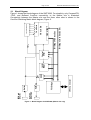
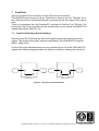
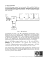
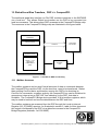
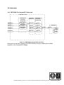
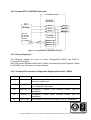
2 Functional Description
Figure 1 gives the block diagram of the SMT300Q. The Slave Module sites (2–4) are
not shown, as they do not have any direct interface to the CompactPCI Bus, SRAM,
ComPort or JTAG sections of the design. The connectivity of slave sites is shown in
Figure 2.
The CompactPCI interface connects to a Quick Logic EPC363 bridge device. It has a
32-bit 33MHz CompactPCI interface that supports I2C control, mailbox register
access, and direct memory reads and writes. The CompactPCI bus is translated to a
Local bus, which is connected to the following devices:
• Shared SRAM 1MB
• Control EPLD that manages ComPort access
• JTAG controller
• Module Global Bus
• CompactPCI Bridge device
An on-board arbitration unit controls which device, Master Module or CompactPCI
Bridge, has access to this local bus resource.
The local bus has a 33MHz clock to control transfers between the various resources.
This is available on the CLKIN pin on the Master site and should be selected in
preference to the on-board oscillator to allow the DSP to synchronise its accesses to
and from the CompactPCI Bridge registers. The CompactPCI Bridge has an input
and output FIFO capable of transferring 256 32-bit words of data to and from the
DSP at 33MHz, thus bursting a maximum local bus transfer rate of 132MB/s.
The Master Module can access the SRAM over the local bus at transfer rates up to
100MB/s. The number of wait states required by the Master Module will vary
depending on the speed of the module. Maximum access rates use a 20ns strobe
cycle.
The JTAG controller is based on the TI 8990 device, and drivers can be supplied for
Code Composer Studio (Part Number SMT6012). The presence of a TIM in a
module site causes its SENSE pin to switch the module into the JTAG chain.
ComPort communication from the Host to the Master Module site is switched through
a quick-switch, as illustrated in Figure 1. This allows the following connectivity:
• Connect the Host to the Master Module’s ComPort 3 (T1C3) and connect the
FMS (C_BUF) directly to the external buffered ComPort. This allows any of
the ComPorts on sites 1—4 to be connected to the external buffered ComPort
with an FMS cable; or
• Connect the Host to the external buffered ComPort and connect ComPort 3 of
the Master site to the FMS connector (C_BUF).
User Manual (QCF42); Version 3.0, 8/11/00; © Sundance Multiprocessor Technology Ltd. 1999
Page 10 of 61
SMT300Q SMT300Q User Guide V1.65
Figure 1 : Block Diagram for SMT300Q (Master site only)
CPCI Connector
PCI Bridge
Buffered
JTAG OUT
Buffered
JTAG IN
Buffer
Buffer
8990
1 MB
SRAM
Control
EPLD
PCI Bridge Data Bus (32 Bit)
PCI Bridge Address Bus
Global Bus
Module Site
ComPorts
HOST
ComPort
ComPort Routing Matrix
3 4 0 2 1 5
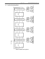
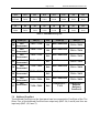
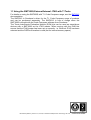
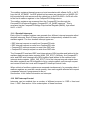
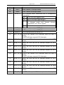
2.1 Block Diagram
Figure 1 shows the block diagram of the SMT300Q. For simplicity, only CompactPCI,
JTAG, and Buffered ComPort connectivity to the Master site is illustrated.
Connectivity between the Master site and the three other sites is shown in the
ComPort Switching Matrix block diagram, Figure 2.
Front Panel Sockets
Front Panel Sockets
Cross Bar switch
Comm 3 Comm 4
3
Cross Bar switch
Comm 1 Comm 2
0
2
Site 2
1
0
5
4
Site 3
Figure 2: ComPort Switching Matrix
Comm 5 Comm 6
Buffer
CPLD
Front Panel Sockets
3
2
1
Cross Bar switch
Buffer
CPLD
3
0
5
4
0
5
4
Site 4
Comm 7 Comm 8
Buffer
CPLD
Front Panel Sockets
3
2
1
Cross Bar switch
Buffer
CPLD
2
Site 1
1
5
4
2.2
To cPCI CPLD
Page 11 of 61
SMT300Q SMT300Q User Guide V1.65
ComPort Switching Matrix
Page 12 of 61
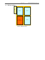
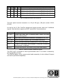
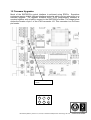
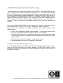
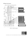
2.3
SMT300Q SMT300Q User Guide V1.65
TIM Sites location
cPCI
Connector
TIM Site 4
TIM Site 3
TIM Site 1
MASTER MODULE
TIM Site 2
Figure 3: TIM sites location
Page 13 of 61
SMT300Q SMT300Q User Guide V1.65
3 Setting Up the SMT300Q
The SMT300Q should be set up in the following way.
•
•
•
•
•
Turn the PC off and insert the card into a spare CompactPCI slot.
Switch on PC and wait for the O/S to boot up.
Windows 95/98/NT/2000 will detect new hardware.
Windows should automatically find the drivers from the CD, if not browse to the
CD or if you downloaded from the ftp site to the folder where you unzipped the
SMT6300 software.
You can run the SMTBoardInfo application to detect the number of SMT300Qs in
your system and report their slot positions and I/O addresses. This information is
required when setting up code composer for the board.
4 Host Memory Map
All address information is given in bytes :
4.1 CompactPCI Bridge Chip Internal Register (BAR0)
Please see V363EPC Local Bus CompactPCI Bridge User Manual
(http://www.quicklogic.com/home.asp?PageID=223&sMenuID=114#Docs) for details
of internal registers.
Where required, registers from the V3 datasheet have been included.
4.2 I/O Space Register Assignments (BAR1)
In target mode, a host device accesses the SMT300Q across the CompactPCI bus,
which gives access to the target mode registers. The operating system or BIOS will
normally allocate a base address for the target mode registers of each SMT300Q.
Access to each register within the SMT300Q is then made at offsets from this base
address as shown in the table below.
Offset (Hex)
Register(Write)
Register(Read)
Width
0x00
-
-
0x04
-
-
0x08
-
-
0x0C
-
-
0x10
COMPORT_OUT
COMPORT_IN
32
0x14
CONTROL
STATUS
32
0x18
INT_CONTROL
0x1C
-
-
0x20 to 0x3F
COMPORT Configuration
COMPORT Configuration
0x24
COM_SWITCH
COM_SWITCH
16
0x2C
COM_SWITCH_EX
COM_SWITCH_EX
32
0x40
INTREG
INTREG
16
0x80 to 0xAF
TBC Write
TBC Read
16
32
Table 2 : I/O address space map
User Manual (QCF42); Version 3.0, 8/11/00; © Sundance Multiprocessor Technology Ltd. 1999
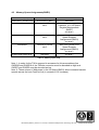
4.3
Memory Space Assignments(BAR2)
Address (Hex)
Description
Notes
0x0000 0000 – 0x000F FFFF
Shared Memory Bank
1MB SRAM
0x00200090
ComPort Data
Mirror
Mirror of COMPORT_OUT /
COMPORT_IN in I/O Space
Register Assignments
(BAR1)
See Note 2
0x00200094
ComPort Status
Mirror
Mirror of Control / Status in I/O
Space Register
Assignments (BAR1)
See Note 2
0x00200098
ComPort Int_Control
Mirror
Mirror of Int_Control in I/O
Space Register
Assignments (BAR1)
See Note 2
0x0020 0000-0x0020 007F
Global Bus
See Note 1
Table 3 : Memory space map
Note 1: In order for the TIM to respond to accesses for this area address line
GADD30 and GADD19 of the TIM site connector must be decoded as high and
GADD7 and GADD5 must be decoded as low.
Note 2: These mirrors of Addresses in the I/O Space (BAR1) allow increased transfer
speeds across the host ComPort link (in excess of 10X increase).
User Manual (QCF42); Version 3.0, 8/11/00; © Sundance Multiprocessor Technology Ltd. 1999
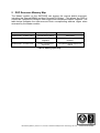
5 DSP Resource Memory Map
The Master module on the SMT300Q can access the various board resources,
including the Shared SRAM and the CompactPCI Bridge. This allows the DSP to
control the CompactPCI Bridge’s DMA engine and manipulate mailbox registers. The
table below illustrates the resources and their corresponding address region when
accessed by the Master module.
C60 Address Access
Description
Notes
0xD000 0000 – 0xD00F FFFF
Shared Memory Bank
1MB SRAM
0x1C00 0000 – 0x1C00 00FF
CompactPCI Bridge
Registers
CompactPCI Bridge Internal
resisters
0x1800 0000 – 0x183F FFFF
Local-to-CompactPCI
Aperture 0
CompactPCI Bridge Aperture 0
Space
Table 4 : Memory space map
User Manual (QCF42); Version 3.0, 8/11/00; © Sundance Multiprocessor Technology Ltd. 1999
6 Shared Memory Resource
The SMT300Q has 1 MB of shared SRAM that can be accessed by both the
CompactPCI host and the Master module. This allows applications to transfer data
between the host PC and the DSP at data rates approaching 100MB/s. The address
of the shared memory is shown in the memory map.
The CompactPCI Bridge DMA processor sees the shared memory at a different
address from that used for normal accesses. For normal memory access the memory
base address register offset is 0x0000 0000. For DMA access address line A28 (On
hardware interface) must be high, therefore DMA memory access starts at 0x4000
0000 (Not 0x1000 0000 as addressing is in bytes).
User Manual (QCF42); Version 3.0, 8/11/00; © Sundance Multiprocessor Technology Ltd. 1999
7 ComPorts
Figure 2 shows how the ComPorts of each TIM site are connected.
The SMT300Q gives access to all six ComPorts on each of the four TIM sites. All of
the ComPorts can be connected buffered connectors on the front panel of the carrier
card.
There is a connection from the CompactPCI interface to ComPort 3 on TIM site 1 for
booting the TIM. This connection can be severed with a quick switch (COM-SWITCH
register offset 0x24, BAR1 bit 15)
7.1
ComPort Switching (Quick Switches)
Several of the TIM ComPorts can be linked together without the need for external
cables. This is done using quick switches controlled by the COM-SWITCH register
(BAR1, offset 0x24)
For all of the quick switches expect the one controlled by bit 15 of the COM-SWITCH
register, the following diagrams show the effects of setting or clearing the control bit.
CPb
CPa
Quick Switch Off (0)
CPb
CPa
Quick Switch On (1)
Figure 4 : Operation of quick switches
User Manual (QCF42); Version 3.0, 8/11/00; © Sundance Multiprocessor Technology Ltd. 1999
Page 19 of 61
SMT300Q SMT300Q User Guide V1.65
D15
D14
D13
D12
D11
D10
D9
D8
CompactP
CI-T1C3
T3C3T4C0
T3C2T4C5
T3C1T4C4
T2C3T3C0
T2C2T3C5
T2C1T3C4
T1C3T2C0
D7
D6
D5
D4
D3
D2
D1
D0
T1C2T2C5
T1C1T2C4
T4C3T1C0
T4C2T1C5
T4C1T1C4
T4C3T1C0
T4C2T1C5
T4C1T1C4
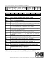
Table 5 : COM-SWITCH Register
Bit
Clear (0)
Set (1)
D0
Not
Connected
T4C1—T1C4
D1
Not
Connected
T4C2—T1C5
D2
Not
Connected
T4C3—T1C0
D3
Not
Connected
T1C4—T4C1
D4
Not
Connected
T1C5—T4C2
D5
Not
Connected
T1C0—T4C3
D6
Not
Connected
D7
Not
Connected
T1C1—T2C4
T1C2—T2C5
Bit
D8
D9
D10
D11
D12
D13
D14
D15
Clear (0)
Not Connected
Not Connected
Not Connected
Not Connected
Not Connected
Not Connected
Not Connected
CompactPCI—
T1C3
Set (1)
T1C3—T2C0
T2C1—T3C4
T2C2—T3C5
T2C3—T3C0
T3C1—T4C4
T3C2—T4C5
T3C3—T4C0
CompactPCI—
External
Buffered
ComPort 2
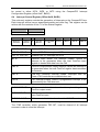
7.2 Buffered ComPort
The buffered ComPorts on the front panel can be connected to ComPorts of the Tim
Sites. Four of the buffered ComPorts are output only (BUF 2,4,6 and 8) and four are
input only (BUF 1,3,5 and 7).
Page 20 of 61
SMT300Q SMT300Q User Guide V1.65
Connection is controlled by COM_SWITCH_EX register (BAR1, Offset 0x2C,), shown
below,
D3
D2
D1
D0
Buffered ComPort 1 Connection (Input Only)
0
X
X
X
Buffered ComPort 1 Disabled
1
0
1
1
Buffered ComPort 1 Connected to TIM Site 1 ComPort 3
1
1
0
0
Buffered ComPort 1 Connected to TIM Site 2 ComPort 4
1
1
0
1
Buffered ComPort 1 Connected to TIM Site 2 ComPort 5
Table 6: Buffered ComPort 1 connections
D7
D6
D5
D4
Buffered ComPort 2 Connection (Output Only)
0
X
X
X
Buffered ComPort 2 Disabled
1
0
0
0
Buffered ComPort 2 Connected to TIM Site 2 ComPort 0
1
0
0
1
Buffered ComPort 2 Connected to TIM Site 1 ComPort 1
1
0
1
0
Buffered ComPort 2 Connected to TIM Site 1 ComPort 2
Table 7: Buffered ComPort 2 connections
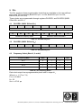
D11 D10 D9
D8
Buffered ComPort 3 Connection (Input Only)
0
X
X
X
Buffered ComPort 3 Disabled
1
0
1
1
Buffered ComPort 3 Connected to TIM Site 2 ComPort 3
1
1
0
0
Buffered ComPort 3 Connected to TIM Site 3 ComPort 4
1
1
0
1
Buffered ComPort 3 Connected to TIM Site 3 ComPort 5
Table 8: Buffered ComPort 3 connections
D15 D14 D13 D12
Buffered ComPort 4 Connection (Output Only)
0
X
X
X
Buffered ComPort 2 Disabled
1
0
0
0
Buffered ComPort 4 Connected to TIM Site 3 ComPort 0
1
0
0
1
Buffered ComPort 4 Connected to TIM Site 2 ComPort 1
1
0
1
0
Buffered ComPort 4 Connected to TIM Site 2 ComPort 2
Table 9: Buffered ComPort 4 connections
Page 21 of 61
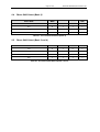
D19 D18 D17 D16
SMT300Q SMT300Q User Guide V1.65
Buffered ComPort 5 Connection (Input Only)
0
X
X
X
Buffered ComPort 5 Disabled
1
0
1
1
Buffered ComPort 5 Connected to TIM Site 3 ComPort 3
1
1
0
0
Buffered ComPort 5 Connected to TIM Site 4 ComPort 4
1
1
0
1
Buffered ComPort 5 Connected to TIM Site 4 ComPort 5
Table 10: Buffered ComPort 5 connections
D23 D22 D21 D20
Buffered ComPort 6 Connection (Output Only)
0
X
X
X
Buffered ComPort 6 Disabled
1
0
0
0
Buffered ComPort 6 Connected to TIM Site 4 ComPort 0
1
0
0
1
Buffered ComPort 6 Connected to TIM Site 3 ComPort 1
1
0
1
0
Buffered ComPort 6 Connected to TIM Site 3 ComPort 2
Table 11: Buffered ComPort 6 connections
D27 D26 D25 D24
Buffered ComPort 7 Connection (Input Only)
0
X
X
X
Buffered ComPort 7 Disabled
1
0
1
1
Buffered ComPort 7 Connected to TIM Site 4 ComPort 3
1
1
0
0
Buffered ComPort 7 Connected to TIM Site 1 ComPort 4
1
1
0
1
Buffered ComPort 7 Connected to TIM Site 1 ComPort 5
Table 12: Buffered ComPort 7 connections
D31 D30 D29 D28
Buffered ComPort 8 Connection (Output Only)
0
X
X
X
Buffered ComPort 8 Disabled
1
0
0
0
Buffered ComPort 8 Connected to TIM Site 1 ComPort 0
1
0
0
1
Buffered ComPort 8 Connected to TIM Site 4 ComPort 1
1
0
1
0
Buffered ComPort 8 Connected to TIM Site 4 ComPort 2
Table 13: Buffered ComPort 8 connections
The front panel mounted connector is a 26 pin 3M type, (3M part number 102265212JL).
As well as the 12 C4x ComPort signals and signal grounds, there are 6 additional
signals. Note that these signals are NOT essential for communications:
Name
Description
I/O_OUT
Output high when port is outputting data, output low when
port is receiving data.
I/O_IN
Input which prevents bus contention if connected to I/O_OUT
/RST_OUT
Active low open collector copy of the board reset drive.
/RST_IN
Active low board reset input, pulled up to 3.3V by 100 ohms.
VCC
1 AMP +5 Volt supply, with resetable 1 Amp fuse, to power a
remote buffer, if required.
SHIELD
Overall cable shield, connected to plug shells and chassis.
Table 14 : Buffered ComPort Additional Signals
The /RST_OUT is intended to allow synchronised reset of a number of boards by
driving the /RST_IN input.
The SMT502-Buffer is the recommended cable assembly for the buffered Comport
and can be purchased separately.
User Manual (QCF42); Version 3.0, 8/11/00; © Sundance Multiprocessor Technology Ltd. 1999
8 ComPort to CompactPCI Interface
The ComPort interface is memory mapped to the CompactPCI Bridge as illustrated in
table 1 : I/O address space map. The ComPort uses the Control and Data registers to
detect the state of the input and output FIFOs. The following section describes the bit
definitions for these registers.
8.1 ComPort Registers (Offset 0x10, BAR1)
The host is connected to the first TIM site using Comport 3 (T1C3). This port is bidirectional and will automatically switch direction to meet a request from either the
host or the DSP. Both input and output registers are 32 bits wide. Data can only be
written to COMPORT_OUT when STATUS[OBF] is 0. Data received from the DSP is
stored in COMPORT_IN and STATUS[IBF] is set to 1. Reading COMPORT_IN will
clear STATUS[IBF] and allow another word to be received from the DSP.
8.2 Control Register (Offset 0x14, BAR1)
The CONTROL register can only be written. It contains flags, which control the boot
modes of the first TIM site.
7-5
4
3
2
1
0
notNMI
IIOF2
IIOF1
IIOF0
RESET
RESET
Write a 1 to this bit to assert the reset signal to the TIM
module on the SMT300Q.
IIOF0
IIOF1
IIOF2
These bits connect to the corresponding pins on the TIM site
1. Writing 0 causes the corresponding IIOF line to go low.
NotNMI
A 0 written to this bit will assert the active low NMI to the
TIM.
Table 15 : Control Register
Note. On CompactPCI system reset, RESET is asserted to the TIM site.
User Manual (QCF42); Version 3.0, 8/11/00; © Sundance Multiprocessor Technology Ltd. 1999
8.3
Status Register (Offset 0x14, BAR1 , Read-Only)
31:22
21
20
19
18
17
16
CONFIG_L
TBC
RDY
0
MASTER
IBF
OBF
15:12
11
10
9
8
IM2
IM1
IM0
INTD
7
6
5
4
3
2
1
0
C40 INT
TBC INT
IBF INT
OBE INT
C40 IE
TBC IE
IBF IE
OBE IE
OBE IE
Set if ComPort output buffer empty interrupts enabled.
IBF IE
Set if ComPort input buffer full interrupts enabled
TBC IE
Set if JTAG interrupts enabled
C40 IE
Set if interrupt from TIM DSP enabled
OBE INT
Set if the ComPort output buffer becomes empty. Cleared by writing a
1 to the corresponding bit in the interrupt control register.
IBF INT
Set if the ComPort input buffer receives a word. Cleared by writing a
1to the corresponding bit in the interrupt control register
TBC INT
Set when the TBC asserts its interrupt. Cleared by removing the
source of the interrupt in the TBC.
C40 INT
Set when the TIM DSP sets its host interrupt bit. Cleared by writing a
1 to the corresponding bit in the interrupt control register.
INTD
The logical OR of bits 7—4 in this register gated with each one’s
enable bit.
OBF
Set when a word is written to the ComPort output register. Cleared
when the word has been transmitted to the DSP.
IM0
Interrupt mask 0. Returns Interrupt Control Register Bit 8.
IM1
Interrupt mask 1. Returns Interrupt Control Register Bit 9.
IM2
Interrupt mask 2. Returns Interrupt Control Register Bit 10.
IBF
Set when a word is in the ComPort input register.
MASTER
Set when the SMT300Q bridge owns the ComPort interface token.
TBC RDY
Reflects the current state of the TBC RDY pin. This bit is active high
and therefore and inversion of the TBC pin.
CONFIG_L
Reflects the state of the TIMs’ CONFIG signal. Active low.
Table 16 : Status Register
INTD is the input interrupt into the CompactPCI Bridge from the SMT300Q, this can
User Manual (QCF42); Version 3.0, 8/11/00; © Sundance Multiprocessor Technology Ltd. 1999
Page 25 of 61
SMT300Q SMT300Q User Guide V1.65
be routed to either INTA, INTB, or INTC using the CompactPCI Interrupt
Configuration Register (offset 0x4C, BAR0)
8.4 Interrupt Control Register (Offset 0x18, BAR1)
This write-only register controls the generation of interrupts on the CompactPCI bus.
Each interrupt source has an associated enable and clear flag. This register can be
written with the contents of bits 7:0 of the Status Register.
10
9
DSP-PC IIOF2 En
DSP-PC IIOF1 En
8
7
6
5
4
3
2
1
0
DSP-PC
IIOF0 En
CLEAR
C40 INT
0
CLEAR
IBF INT
CLEAR OBE
INT
C40 IE
TBC IE
IBF IE
OBE IE
DSP-PC IIOF2 En
Enables DSP-PC interrupts on IIOF2
DSP-PC IIOF1 En
Enables DSP-PC interrupts on IIOF1
DSP-PC IIOF0 En
Enables DSP-PC interrupts on IIOF0
IBF IE
ComPort Input Buffer Full Interrupt Enable. Allows an
interrupt to be generated when the host ComPort input
register is loaded with data from the C40.
OBE IE
ComPort Output Buffer Empty Interrupt. Allows an interrupt to
be generated when the host ComPort register has transmitted
its contents.
TBC IE
Test Bus Controller Interrupt Enable. Interrupts from the
Texas JTAG controller are enabled when set.
C40 IE
C40 Interrupt Enable. Allows a programmed interrupt to be
generated by the C40 when set.
CLEAR OBE INT
Write a one to this bit to clear the interrupt resulting from a
ComPort output event.
CLEAR IBF INT
Write a one to this bit to clear the interrupt event resulting
from ComPort input.
CLEAR C40 INT
Write a one to this bit to clear down the C40 INT event.
Table 17 : Interrupt Control Register
The JTAG controller, which generates TBC INT, must be cleared of all interrupt
sources in order to clear the interrupt.
9 PLL
The PLL produces three programmable clocks that are available on the user-defined
pins of the TIM connectors (Bank2CLK pin 1 on J24, Bank3CLK pin 3 on J24,
Bank4CLK pin 8 on J23).
These clocks are programmable through registers PLLREG1 and PLLREG2 (BAR1
Offset 6016 and 6416).
9.1
PLLREG1 (BAR1 Offset 6016)
D15
D14
D13
D12
D11
Bank3CLK Frequency Select
D7
D6
D5
D10
D9
D8
Bank3CLK Phase Shift Select
D4
D3
Bank2CLK Frequency Select
D2
D1
D0
Bank2CLK Phase Shift Select
Table 18 : PLLREG1 Register
9.2
PLLREG2 (BAR1 Offset 6416)
D7
D6
D5
D4
D3
Bank4CLK Frequency Select
D2
D1
D0
Bank4CLK Phase Shift Select
Table 19 : PLLREG2 Register
9.3
Frequency Select (Bank 2, 3 and 4)
Frequency (MHz)
MSB
LSB
66 / 1
0
1
0
1
66 / 3
0
1
1
1
66 / 8
1
1
0
1
66 / 12
1
1
1
1
Table 20 : PLL Frequency Select
Each clock output has a programmable phase shift in steps of tu.
Where tu = 1 / (FNOM * N)
FNOM = 66 MHz
N = 32
So tu = 473.5 ps
User Manual (QCF42); Version 3.0, 8/11/00; © Sundance Multiprocessor Technology Ltd. 1999
Page 27 of 61
9.4
SMT300Q SMT300Q User Guide V1.65
Phase Shift Select (Bank 2)
Phase Shift
MSB
LSB
-4 tu
0
1
0
1
-2 tu
0
1
1
1
+2 tu
1
1
0
1
+4 tu
1
1
1
1
Table 21 : PLL Phase Shift Select (Bank 2)
9.5
Phase Shift Select (Bank 3 and 4)
Phase Shift
MSB
LSB
-8 tu
0
1
0
1
-6 tu
0
1
1
1
+6 tu
1
1
0
1
+8 tu
1
1
1
1
Table 22 : PLL Phase Shift Select (Bank 3 and 4)
10 JTAG Controller
The SMT300Q has an on board Test Bus Controller (TBC), an SN74ACT8990 from
Texas Instruments. The TBC is controlled from the CompactPCI bus giving access to
the on-site TIMs and/or any number of external TIMs. Please refer to the Texas
Instruments data sheet for details of this controller. The TBC is accessed in I/O space
BAR1 offset 0x80.
Site 1
Buffered
JTAG
Connectors
Site 2
Site 3
Site 4
Test Bus
Switching
Matrix
Buffers
Test Bus
Controller
PCI bridge
Figure 5 : TBC Data Routing
The SMT300Q can operate in two TBC modes; Master mode and Slave mode. In
Master mode, the Test Bus Controller on the SMT300Q drives the JTAG scan chain
through the TIM sites on the SMT300Q. If any or all the sites are not populated with a
TIM then the modules SENSE signal is used to enable a tri-state buffer connecting
the TDI and TDO (JTAG Data In and Data Out) on the specific site, maintaining the
integrity of the JTAG data path. This switching is automatic. The SMT300Q auto
detects external JTAG connections and switches the JTAG circuitry accordingly.
When the SMT300Q is configured in Slave mode, the TBC on the SMT300Q is
disabled, as the TBC is assumed to be on another device connected to the
SMT300Q.
The SMT501-JTAG is designed to connect two SMTxxx carrier boards i.e., SMT300Q
controlling an SMT328 VME carrier. The length of SMT501-JTAG is 1 meter.
There are two external JTAG connectors (JTAG IN, JTAG OUT). JTAG OUT is used
when in master mode to connect to slave devices and JTAG IN is used in slave mode
to connect master devices to the SMT300Q. Both connectors can be used at the
same time to produce a chain of boards.
User Manual (QCF42); Version 3.0, 8/11/00; © Sundance Multiprocessor Technology Ltd. 1999
Page 29 of 61
SMT300Q SMT300Q User Guide V1.65
When using the JTAG chain with multiple carriers that have a large number of vacant
TIM sites it may be necessary to reduced the speed of the JTAG clock (mater board
only) to improve reliability. This can be done by inserting jumper J7 (Figure 14 :
Jumper Finder Diagram) which halves the JTAG clock frequency.
11 Using the SMT300Q External/Internal JTAG with TI Tools.
For details on using the SMT300Q with T.I. Code Composer range, see the SMT6012
documentation.
The SMT6012 is Sundance’s driver for the T.I. Code Composer range of products
and can be purchased separately. The SMT6012 is free of charge when the
SMT300Q is bought with the Code Composer software from Sundance.
The Texas Instruments Evaluation Module (EVM) kits can be used as stand-alone
devices with a SMT300Q as the JTAG master. When running with the EVM kits
ensure that the EVM jumper has been set up correctly. i.e. External JTAG has been
selected and the DSP boot location is valid (set for internal memory space).
User Manual (QCF42); Version 3.0, 8/11/00; © Sundance Multiprocessor Technology Ltd. 1999
12 Firmware Upgrades
Much of the SMT300Q’s control interface is achieved using EPLDs. Sometime
customers require slightly different interface protocols, which can be catered for by a
firmware upgrade. To upgrade firmware Xilinx JTAG programming software is
required together with a lead to connect to the SMT300Q’s header. The image below
shows the location of pin 1 of the JTAG connector J21. This connector is a 2x3 2mm
pin header.
Pin 1 JTAG Programmer
Header
2
4
6
1
3
5
User Manual (QCF42); Version 3.0, 8/11/00; © Sundance Multiprocessor Technology Ltd. 1999
Page 32 of 61
SMT300Q SMT300Q User Guide V1.65
Figure 6 : JTAG header pin numbers
Pin Number
Function
1
Vcc (5v)
2
Gnd
3
TCK
4
TDO
5
TDI
6
TMS
Table 23 : JTAG Header pin function
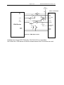
13 Global/Local Bus Transfers, DSP <-> CompactPCI.
The traditional global bus interface on C6x DSP modules interfaces to the SMT300Q
via a local bus. This allows Global bus transfers on the DSP to be converted into
local bus accesses. This allows direct DSP accesses to the CompactPCI Bridge chip.
The resources in the CompactPCI Bridge chip are illustrated in the figure below.
PCI Bridge Device
MailBox
Read/Write
Interrupt Control
Local Bus
DSP Global
Bus Access
Local To PCI Bus
Apperture Control
LOCAL <-> PCI
Apperture 0
16MB Address
Space
Arbitration
Unit
Figure 7 : Local Bus to DSP Connectivity
13.1 Mailbox Accesses
The mailbox registers can be used if small amounts of data or commands between
the CompactPCI bus and the DSP, via the local bus, need to be transferred. Rather
than sending ComPort data, and therefore require the DSP to be checking its
ComPort for commands, a mailbox write by the CompactPCI bus can be initialized to
generate an interrupt on an DSP IIOF line indicating, to the DSP, that data is
available. The CompactPCI Bridge device provides 16 8-bit mailbox registers, which
may be used to transmit and receive data between the DSP and Host.
The mailbox registers are accessed from the DSP through the Local-to-Internal
Register (LB_IO_BASE) aperture. As illustrated in section 5, table 4 of this document
this region is accessed by the DSP via a global bus access to the CompactPCI
Bridge Registers (Address : 0x1C00 0000).
User Manual (QCF42); Version 3.0, 8/11/00; © Sundance Multiprocessor Technology Ltd. 1999
Page 34 of 61
SMT300Q SMT300Q User Guide V1.65
The mailbox registers themselves are on byte boundaries with offsets 0xC0 -> 0xCF,
from the LB_IO_BASE. As DSP global bus accesses are carried out on WORD (32bit) boundaries a write access over the global bus to 0x1C00 0000 + 0xC0 will write
to the first 4 mailbox registers in the CompactPCI Bridge device.
The mailbox registers are accessed from the CompactPCI bus through the
CompactPCI-to-Internal Register (CompactPCI_IO_BASE) aperture. This is
accessed via the CompactPCI Bridge Chip Internal Register (BAR0), byte offset
0xC0 -> 0xCF.
13.1.1 Doorbell Interrupts
Each of the 16 mailbox registers can generate four different interrupt requests called
doorbell interrupts. Each of these requests can be independently masked for each
mailbox register. The four doorbell interrupt types are:
• DSP interrupt request on read from CompactPCI side
• DSP interrupt request on write from CompactPCI side
• CompactPCI interrupt request on read from DSP side
• CompactPCI interrupt request on write from DSP side
The CompactPCI read and DSP read interrupts are OR’d together and latched in the
mailbox read interrupt status register (MAIL_RD_STAT). Similarly, the CompactPCI
write and DSP write interrupts are OR’d together and latched in the mailbox write
interrupt status register (MAIL_WR_STAT). All of the interrupt request outputs from
the status registers are OR’d together to form a single mailbox unit interrupt request
and routed to both the Local and CompactPCI Interrupt Control Units.
When a block of mailbox registers are accessed simultaneously, for example when 4
mailbox registers are read as a word quantity, then each register affected will request
a separate interrupt if programmed to do so.
See section 14 for further information on Interrupts.
13.2 DSP Interrupt Control
Interrupts can be enabled from a number of different sources i.e. DSP-> Host and
Host -> DSP. See section 14 for a description of these functions.
13.3 DSP To Local Aperture 0 control and Accessing
The quickest way to transfer information from the DSP to CompactPCI Bus or vice
versa is to use the Local-to-CompactPCI Aperture 0 in the CompactPCI Bridge
device. A DSP unit may be required to transfer large amounts of acquired data to the
PC host for data storage or post-processing etc. Allowing the DSP to take control of
the CompactPCI bus means that the HOST only requires to transfer data, from an
internal allocated region of memory, after the transfer has been completed by the
DSP. Alerting the Host that data has been transferred can be accomplished in a
number of ways i.e. writing to the mailbox register, which can then generate an
interrupt.
The Local-to-CompactPCI Aperture 0 is mapped as a region of addressable space
from 0x1800 0000 – 0x183F FFFF (words), as shown in Table 4, section 5.
There are a number of registers in initialise before data can be read or written via this
address space.
• Unlock the CompactPCI Bridge System register. This requires a write to the
LB_CFG_SYSTEM (offset 0x78, BAR 0) with the value 0xA05F.
• Write the upper 8 bits of your destination address (in bytes) to the upper 8 bits
of the 32-bit Local Bus to CompactPCI Map 0 register (LB_MAP0_RES, offset
in bytes 0x5c ).
• Convert you lower 24-bit address to a word aligned value.
• Write/Read data from Local-to-CompactPCI Aperture 0 .
The diagram below illustrates this procedure.
In the example below the WritetoCompactPCIregisters(offset,data) function writes
data over the DSP’s Global bus, at a base address of 0x1800 0000 (words), the first
parameter passed to this function in the offset address in words, and the second is
the data to be written.
User Manual (QCF42); Version 3.0, 8/11/00; © Sundance Multiprocessor Technology Ltd. 1999
Page 36 of 61
SMT300Q SMT300Q User Guide V1.65
Receive Target address via Com-Port
Link
i.e. 0xFE12 3000
Unlock the system register in PCI bridge
#define LB_CFG_SYSTEM
(0x78>>2) (divide by 4 to word align offset address of PCI
bridge register)
WritePCIRegisters((unsigned int)LB_CFG_SYSTEM,0xA05F);
WritePCIRegisters((unsigned int)LB_CFG_SYSTEM,0x22008800);
// Unlock Code
// Restore Value
Write Lower 24 bits of byte TargetAddress to the LB_MAP0_RES register
#define LB_MAP0_RES
(0x5C>>2)
#define LB_MAP0_MEMORY_RW 0x00060000
#define LB_MAP0_ADDRESS_MASK 0xFF000000
WritePCIRegisters((unsigned int)LB_MAP0_RES,(unsigned int)(TargetAddress &
LB_MAP0_ADDRESS_MASK ) | LB_MAP0_MEMORY_RW);
// The LB_MAP0_MEMORY_RW must be Or’ed with the data to ensure the other register in
// the 32-bit word has its correct value.
Write WORD Aligned data to Local Aperture space 0.
WritePCIApperture0((ByteToWord32(((TargetAddress) & ~LB_MAP0_ADDRESS_MASK))),Length,buffer);
Where
void WritePCIApperture0(unsigned int address,unsigned long Length,unsigned int *buffer)
{
unsigned int Index;
globalbuswriteClockMB(0x18000000 + address , Length , buffer);
}
Figure 8 : DSP Transfer via the Local Aperture 0
13.3.1 Global bus access protocol
In Figure 8, the WriteCompactPCIApperture function calls a function
C6xGlobalWriteClockMB().
This function enables the DSP’s global bus to transfer Length words from the DSP’s
internal memory map pointed to by buffer. The function puts the Global bust into burst
Page 37 of 61
SMT300Q SMT300Q User Guide V1.65
mode. This interface allows a synchronous stream of data to be written to the 256
WORD input FIFO of the Local To CompactPCI aperture 0. For more information on
setting this mode from the DSP can be found in the SMT335 Users Guide. This
section concentrates on the burst mode interface and arbitration mechanism for the
DSP to CompactPCI Bridge aperture access.
The Global bus interface of the DSP uses the following signals to interface to the
local bus of the SMT300Q.
DSP Signals.
AE*, DE*, CE0*
AE*/DE* are active low address/Data enable signal driven by the SMT300Q, when
the DSP has ownership of the Bus this signal is driven low by the SMT300Q allowing
the DSP to drive the Address pins and Data pins.
CE0* is the Tri-state control for the DSP’s global bus control pins. This is permanently
tied low by the SMT300Q as the control signals are always enable.
STRB1*
This is the data strobe signal from the DSP’s global bus. It is driven low when the
DSP is carrying out an access cycle. The DSP waits for the RDY1* to be driven low
by the SMT300Q to indicate transfer has been completed. This transfer is carried out
in synchronous burst mode. The DSP signals when the burst transfer is completed
by pulling STAT0 low.
RDY1*
This is an active low transfer acknowledgement, driven by the SMT300Q to indicate
that the current transfer has been completed.
STAT0..STAT3
These comprise the DSP Status line. When all of the signals are logic ‘1’ then the
DSP Global bus interface is in an idle state. When any of these signals is driven low
the DSP is requesting ownership of the SMT300Q’s local bus. STAT0 has a special
meaning and is driven low by the DSP to indicate the last data packet transfer.
A0..A30
The DSP’s global Bus address lines
D0..D31
The DSP’s global Bus data lines
IIOF0, IIOF1 & IIOF2
The DSP’s Interrupt signals. These are open collector signals on the SMT300Q.
They can be driven by the DSP to generate an interrupt to the host, or they can be
driven by the host to interrupt the DSP.
In the timing diagram below all signals change relative to the rising LCLK signal. This
signal is the H1 clock signal of the DSP when using the DSP global bus in
synchronous mode (see SMT335 User Guide).
TIMReq
FIFO Full
LCLK
STAT[1.3]
STRB1
RDY1
STAT0
AE/DE
A[30..0]
D[31..0]
Figure 9 : Timing diagram for DSP local bus access
* LCLK Period =30nS, frequency is 33MHz.
The DSP initiates a global bus R/W by asserting the STRB1 low and STAT[1:3}
change (see TIM Spec for details of STAT[1..3]). Once the arbitration unit detects
this, it waits for the last cycle of the Local bus to be completed by the CompactPCI
Bridge, before allowing the DSP to become Bus Master. Once the DSP is Master the
arbitration unit drives AE and DE low to enable the DSP’s address and data lines.
RDY1 is driven low by the arbitor to indicate to the DSP, on the next rising LCLK, that
the data packet has been transferred. If the input FIFO (256 Words Deep) becomes
full, the arbitration logic de-asserts the RDY1 signal to indicate a hold-off state. Once
the data has been transferred from the FIFO to the CompactPCI bus RDY1 is reasserted to continue the transfer. The end of the burst access is indicated by
asserting STAT0 low. If RDY1 is not active then STAT0 should remain asserted until
ready is asserted and the final data transaction has been completed.
It is possible for a deadlock condition to arise, i.e. the CompactPCI bus is trying to
read from the SMT300Q resources while the DSP is reading from the CompactPCI
User Manual (QCF42); Version 3.0, 8/11/00; © Sundance Multiprocessor Technology Ltd. 1999
Page 39 of 61
SMT300Q SMT300Q User Guide V1.65
Bus. If this happens, the arbitration unit gives the CompactPCI Bridge device priority
and services the HOST CompactPCI access before giving bus ownership back to the
DSP.
When running code composer applications to debug the DSP a reduction in the
speed of the debugger may be noticed. The DSP has priority when accessing the
local bus and any other accesses will only occur under the following conditions.
• Burst access finishes
• A deadlock condition occurs which forces the DSP to release ownership of the
Bus.
For multi-threaded applications the length of the DSP burst can be lowered to allow
CompactPCI bus R/W cycles to snatch cycles from the DSP.
14 Interrupts
14.1 SMT300Q-To-CompactPCI Interrupts
CONTROL EPLD
INTERRUPT
CONTROL
REGISTER
TIMIIOF0
TIMIIOF1
TIMIIOF2
DSP IIOF0
ENABLE
DSP IIOF1
ENABLE
DSP IIOF2
ENABLE
STATUS
INTERRUPT
REGISTER CONTROL
REGISTER
DSP INT
C40 IE
IBF INT
IBF IE
OBE INT
OBE IE
TBC INT
TBC IE
PCI Bridge
INTD
INTD
INTA
INTB
JTAG INT
Figure 10 : SMT300Q to CompactPCI Interrupts
Interrupts can also be caused by the SMT300Q by writing or reading the mailbox
registers in the CompactPCI Bridge.
User Manual (QCF42); Version 3.0, 8/11/00; © Sundance Multiprocessor Technology Ltd. 1999
INTC
14.2 CompactPCI-To-SMT300Q Interrupts
CONTROL CPLD
CONTROL
REGISTER
PCI
Bridge
LINT can
be caused
by any PCI
interrupt
e.g. Mailbox
LINT
IIOF0
TIMIIOF0
IIOF1
TIMIIOF1
IIOF2
TIMIIOF2
INTREG
REGISTER
LINT
TIMIIOF0 IE
TIMIIOF1 IE
TIMIIOF2 IE
Figure 11 : CompactPCI to SMT300Q Interrupts
14.3 Interrupt Registers
The following register are used to control CompactPCI-To-DSP and DSP-ToCompactPCI interrupts:
Note that Control Register (Offset 0x14, BAR1) and Interrupt Control Register (Offset
0x18, BAR1) are also used to control interrupts.
14.3.1 CompactPCI Interrupt Configuration Register(Offset 0x4C, BAR0)
Bits
Name
Description
31
MAILBOX
Mailbox Interrupt Enable: Enables a CompactPCI interrupt
from the mailbox unit
30
LOCAL
Local Bus Direct Interrupt Enable: Enables direct local bus
to CompactPCI interrupts
29
MASTER_PI
CompactPCI Master Local Interrupt Enable: (see V3
datasheet)
28
SLAVE_PI
CompactPCI Slave Local Interrupt Enable: (see V3
datasheet)
27
OUT-POST
I2O Outbound Post List Not Empty: (see V3 datasheet)
User Manual (QCF42); Version 3.0, 8/11/00; © Sundance Multiprocessor Technology Ltd. 1999
Page 42 of 61
SMT300Q SMT300Q User Guide V1.65
26
-
Reserved
25
DMA1
DMA Channel 1 interrupt enable
24
DMA0
DMA Channel 0 interrupt enable
23-22
MODE_D
INTD interrupt mode: Determines use of corresponding
interrupt pin
00
Active low level triggered input
01
High-to-low edge triggered input
10
Software cleared output. INTD pin is asserted via
an interrupt event and cleared through
CompactPCI_INT_STAT register
11
Reserved
21-20
MODE_C
INTC interrupt mode (as MODE_D)
19-18
MODE_B
INTB interrupt mode (as MODE_D)
17-16
MODE_A
INTA interrupt mode (as MODE_D)
15
INTD_TO_LB 1=INTD will request LICU interrupts when the input is
active
0=INTD will never request LICU interrupts
14
INTC_TO_D
When set INTC will act as interrupt request for INTD
output
13
INTB_TO_D
When set INTB will act as interrupt request for INTD
output
12
INTA_TO_D
When set INTA will act as interrupt request for INTD
output
11
INTD_TO_C
When set INTD will act as interrupt request for INTC
output
10
INTC_TO_LB 1=INTC will request LICU interrupts when the input is
active
0=INTC will never request LICU interrupts
9
INTB_TO_C
When set INTB will act as interrupt request for INTC
output
8
INTA_TO_C
When set INTA will act as interrupt request for INTC
output
7
INTD_TO_B
When set INTD will act as interrupt request for INTB
output
6
INTC_TO_B
When set INTC will act as interrupt request for INTB
output
5
INTB_TO_LB 1=INTB will request LICU interrupts when the input is
Page 43 of 61
SMT300Q SMT300Q User Guide V1.65
active
0=INTB will never request LICU interrupts
4
INTA_TO_B
When set INTA will act as interrupt request for INTB
output
3
INTD_TO_A
When set INTD will act as interrupt request for INTA
output
2
INTC_TO_A
When set INTC will act as interrupt request for INTA
output
1
INTB_TO_A
When set INTB will act as interrupt request for INTA
output
0
INTA_TO_LB 1=INTA will request LICU interrupts when the input is
active
0=INTA will never request LICU interrupts
Table 24 : CompactPCI Interrupt Configuration Register
14.3.2 CompactPCI Interrupt Status Register(Offset 0x48, BAR0)
Bits
Name
Description
31
MAILBOX
30
LOCAL
29-28
-
27
OUT_POST
26
-
25
DMA1
DMA channel 1 interrupt
24
DMA0
DMA channel 0 interrupt
23-15
-
14
INTC_TO_D
INTD output from INTC input: when set (1) an interrupt has
occurred on INTC
13
INTB_TO_D
INTD output from INTB input: when set (1) an interrupt has
occurred on INTB
Mailbox Interrupt:
1=Mailbox interrupt request active
0=No mailbox interrupts pending
Cleared by clearing MAIL_RD_STAT and
MAIL_WR_STAT
Local bus direct interrupt:
1=Local bus master requests a CompactPCI interrupt
0=No operation
This bit is set by writing 1 and cleared by writing 0
Reserved
I2O outbound post list not empty: (see V3 datasheet)
Reserved
Reserved
Page 44 of 61
SMT300Q SMT300Q User Guide V1.65
12
INTA_TO_D
INTD output from INTA input: when set (1) an interrupt has
occurred on INTA
11
INTD_TO_C
INTC output from INTD input: when set (1) an interrupt has
occurred on INTD
10
-
9
INTB_TO_C
INTC output from INTB input: when set (1) an interrupt has
occurred on INTB
8
INTA_TO_C
INTC output from INTA input: when set (1) an interrupt has
occurred on INTA
7
INTD_TO_B
INTB output from INTD input: when set (1) an interrupt has
occurred on INTD
6
INTC_TO_B
INTB output from INTC input: when set (1) an interrupt has
occurred on INTC
5
-
4
INTA_TO_B
INTB output from INTA input: when set (1) an interrupt has
occurred on INTA
3
INTD_TO_A
INTA output from INTD input: when set (1) an interrupt has
occurred on INTD
2
INTC_TO_A
INTA output from INTC input: when set (1) an interrupt has
occurred on INTC
1
INTB_TO_A
INTA output from INTB input: when set (1) an interrupt has
occurred on INTB
0
-
Reserved
Reserved
Reserved
Table 25 : CompactPCI Interrupt Status Register
14.3.3 Local Bus Interrupt Mask Register(Offset 0x77, BAR0)
Bits
Name
7
MAILBOX
6
CompactPCI_RD
CompactPCI read error interrupt enable
5
CompactPCI_WR
CompactPCI write error interrupt enable
4
CompactPCI_INT
Global CompactPCI interrupt to local interrupt
enable
3
Description
Global mailbox interrupt enable
CompactPCI_PERR CompactPCI parity error interrupt enable
2
I2O_QWR
1
DMA1
I2O inbound post queue write interrupt enable
DMA channel 1 interrupt enable
Page 45 of 61
0
DMA0
SMT300Q SMT300Q User Guide V1.65
DMA channel 0 interrupt enable
Table 26 : Local Bus Interrupt Mask Register
14.3.4 Local Bus Interrupt Status Register(Offset 0x76, BAR0)
Bits
Name
Description
7
MAILBOX
1=interrupt has been requested by one or more of
the mailbox registers
0=no mailbox interrupts pending
6
CompactPCI_RD
See V3 datasheet
5
CompactPCI_WR
See V3 datasheet
4
CompactPCI_INT
See V3 datasheet
3
CompactPCI_PERR See V3 datasheet
2
I2O_QWR
See V3 datasheet
1
DMA1
See V3 datasheet
0
DMA0
See V3 datasheet
Table 27 : Local Bus Interrupt Status Register
14.3.5 CompactPCI Mailbox WRITE/READ Interrupt Control Register(Offset:
Write 0xD0, BAR0 Read 0xD2, BAR0)
Bits
Name
Description
15
EN15
Local interrupts on CompactPCI bus writes/reads to
mailbox15 enable
14
EN14
Same as above for mailbox 14
13
EN13
Same as above for mailbox 13
12
EN12
Same as above for mailbox 12
11
EN11
Same as above for mailbox 11
10
EN10
Same as above for mailbox 10
9
EN9
Same as above for mailbox 9
8
EN8
Same as above for mailbox 8
7
EN7
Same as above for mailbox 7
6
EN6
Same as above for mailbox 6
5
EN5
Same as above for mailbox 5
4
EN4
Same as above for mailbox 4
3
EN3
Same as above for mailbox 3
Page 46 of 61
SMT300Q SMT300Q User Guide V1.65
2
EN2
Same as above for mailbox 2
1
EN1
Same as above for mailbox 1
0
EN0
Same as above for mailbox 0
Table 28 : CompactPCI Mailbox WRITE/READ Interrupt Control Register
14.3.6 Local Bus Mailbox WRITE/READ Interrupt Control Register(Offset Write
0xD4, BAR0 Read 0xD6, BAR0)
Bits
Name
Description
15
EN15
CompactPCI interrupts on Local bus writes/reads to
mailbox15 enable
14
EN14
Same as above for mailbox 14
13
EN13
Same as above for mailbox 13
12
EN12
Same as above for mailbox 12
11
EN11
Same as above for mailbox 11
10
EN10
Same as above for mailbox 10
9
EN9
Same as above for mailbox 9
8
EN8
Same as above for mailbox 8
7
EN7
Same as above for mailbox 7
6
EN6
Same as above for mailbox 6
5
EN5
Same as above for mailbox 5
4
EN4
Same as above for mailbox 4
3
EN3
Same as above for mailbox 3
2
EN2
Same as above for mailbox 2
1
EN1
Same as above for mailbox 1
0
EN0
Same as above for mailbox 0
Table 29 : Local Bus Mailbox WRITE/READ Interrupt Control Register
14.3.7 Mailbox Write/Read Interrupt Status Register(Offset: Write 0xD8, BAR0
Read 0xDA, BAR0)
Bits
Name
Description
15
EN15
1=Mailbox 15 has requested a CompactPCI or Local
write/read interrupt
0=Mailbox 15 has not requested a CompactPCI or Local
write/read interrupt
14
EN14
Same as above for mailbox 14
13
EN13
Same as above for mailbox 13
12
EN12
Same as above for mailbox 12
11
EN11
Same as above for mailbox 11
10
EN10
Same as above for mailbox 10
9
EN9
Same as above for mailbox 9
8
EN8
Same as above for mailbox 8
7
EN7
Same as above for mailbox 7
6
EN6
Same as above for mailbox 6
5
EN5
Same as above for mailbox 5
4
EN4
Same as above for mailbox 4
3
EN3
Same as above for mailbox 3
2
EN2
Same as above for mailbox 2
1
EN1
Same as above for mailbox 1
0
EN0
Same as above for mailbox 0
Register cleared by writing 1, writing 0 has no effect
Table 30 : Mailbox Write/Read Interrupt Status Register
14.3.8 INTREG Register(Offset 0x40, BAR1)
Bits
Name
Description
15
-
Reserved
14
-
Reserved
13
-
Reserved
12
-
Reserved
11
-
Reserved
10
-
Reserved
User Manual (QCF42); Version 3.0, 8/11/00; © Sundance Multiprocessor Technology Ltd. 1999
Page 48 of 61
SMT300Q SMT300Q User Guide V1.65
9
-
Reserved
8
-
Reserved
7
-
Reserved
6
-
Reserved
5
-
Reserved
4
-
Reserved
3
-
Reserved
2
IIOF2EN
PC to DSP TIMIIOF2 interrupt enable
1
IIOF1EN
PC to DSP TIMIIOF1 interrupt enable
0
IIOF0EN
PC to DSP TIMIIOF0 interrupt enable
Table 31 : INTREG Register
14.4 Example
The example below shows how the DSP can cause an interrupt on the PC by writing
to mailbox register 0.
The PC must first enable the interrupts, to do this the following register bits must be
altered, and an interrupt thread handler needs to be created.
CompactPCI Interrupt Configuration Register(Offset 0x4C, BAR0) – bit 31 must be
set.
Local Bus Interrupt Mask Register(Offset 0x77, BAR0) – bit 7 must be set.
Local Bus Mailbox WRITE/READ Interrupt Control Register(Offset Write 0xD4, BAR0
Read 0xD6, BAR0) – bit 0 of the write register (0xD4) must be set.*
An Interrupt service routine must be set up, in this the following register will need to
be cleared
Mailbox Write/Read Interrupt Status Register(Offset: Write 0xD8, BAR0 Read 0xDA,
BAR0) – bit 0 of the write register (0xD8) must be cleared.**
Local Bus Interrupt Status Register(Offset 0x76, BAR0) – bit 7 must be cleared.
To cause the interrupt the DSP needs to write to the mailbox register in the V3 chip,
this is done by writing to address 0x1C0000C0 (this will write to the first four
mailboxes).
*These are two separate registers, one to enable interrupts on reads from the
mailbox registers the other to enable interrupts on writes to the mailbox registers.
**These are two separate registers, one shows interrupt status for reads from the
mailbox register the other to show interrupt status on writes to the mailbox registers.
User Manual (QCF42); Version 3.0, 8/11/00; © Sundance Multiprocessor Technology Ltd. 1999
15 Stand-Alone Mode
For the SMT300Q to operate in stand-alone mode Jumper J8 (Figure 14 : Jumper
Finder Diagram) must be installed and the Auxiliary power header (J1) connected.
The plug for the power connector is AMP part No 640440-8. The connector requires
wiring as shown in the pin diagram below. Wire of 0.3 mm2 core (22 AWG) should be
used.
1
1) +12V
2
2) -12V
3
3) +5V
4
4) +5V
5
5) +3.3V
6
6) +3.3V
7
7) GND
8
8) GND
Figure 12 : Auxiliary Power Connector
User Manual (QCF42); Version 3.0, 8/11/00; © Sundance Multiprocessor Technology Ltd. 1999
16 Performance Figures
The following performance figures are for the SMT300Q with the Rev. A1 V3
CompactPCI bridging device fitted and using a SMT335. Further performance figures
will be issued as faster V3 CompactPCI bridging devices become available and are
fitted to the SMT300Q.
The figures shown below may vary greatly depending on the application. Some of
the issues are:
PC Architecture and performance
Transfer parameters.
• The transfer size.
• Frequency of transfer.
• The layout of the target memory. (Scatter/Gather or contiguous)
Availability of the CompactPCI bus.
• Other devices on the CompactPCI bus.
• Debugging traffic on the bus.
• ComPort traffic.
Transfer type
MIN (Mb/s)
MAX (Mb/s)
AVERAGE
(Mb/s)
Comments
C60 Burst
Read To Host
Memory
45
82
70
Will Vary depending
on CompactPCI traffic
C60 Burst
Write To Host
Memory
11
88
68
Will Vary depending
on CompactPCI traffic
Table 32 : Performance Figures
User Manual (QCF42); Version 3.0, 8/11/00; © Sundance Multiprocessor Technology Ltd. 1999
16.1 Relative JTAG speeds
Relative Emulator Speeds
Speed relative to XDS510
3.00
2.70
2.50
2.00
1.67
1.50
1.62
1.25
1.00
1.20
0.85
1.00
0.60
0.50
0.50
0.00
XDS510
FleXDS
SPI525
XDS510PP
Plus
SPI515
XDS510PP
Tiger
SMT106
Emulator
Figure 13 : JTAG speed Comparison chart
User Manual (QCF42); Version 3.0, 8/11/00; © Sundance Multiprocessor Technology Ltd. 1999
SMT310Q
17 Mechanical Dimensions
The board size is 234 mm by 160 mm
18 Power consumption
The SMT300Q takes 3.3V and 5V power from the PC’s internal power supply. The
following current consumption figures were measured using a LEM current clamp
during a quiescent period.
Current drawn from 3.3v supply
Current drawn from 5v supply
:
:
440 mA
100 mA
User Manual (QCF42); Version 3.0, 8/11/00; © Sundance Multiprocessor Technology Ltd. 1999
19 Cables and Connectors
19.1 ComPorts
The cables used with FMS connectors are not supplied with the SMT300Q. You can
order them separately from Sundance with part number SMT500-FMSxx, where xx is
the cable length in centimetres.
19.2 Buffered ComPort Cabling
Connecting between buffered ComPorts requires a 1 to 1 cable; the SMT502-Buffer
is the recommended cable assembly and can be purchased separately.
Cable plugs
3M Scotchflex 10126-6000EL FES part 038740A
Plug shells
3M Scotchflex 10326-A200-00 FES part 038760D
Cable type
3M Scotchflex KUCKMPVVSB28-13PAIR FES part 038781E
This cable has 13 individual pairs, with an overall shield, and an outer diameter of
7mm. Cable length should be as short as possible. The maximum tested cable length
is 1 meter.
On reset, each ComPort initialises to being either an input or an output.
Do not connect ‘Reset to Input’ ComPorts together.
Do not connect ‘Reset to Output’ ComPorts together.
However if this should occur, no damage will result, because ComPort direction
signals disable relevant ComPorts.
The following table shows connector pin-out and cable pair connections. This is
important, as the critical signals must be paired with a ground as shown. The
allocation to twisted pairs is based on grouping the data signals because they change
at the same time, so that crosstalk is not an issue. Each control signal has its own
ground:
User Manual (QCF42); Version 3.0, 8/11/00; © Sundance Multiprocessor Technology Ltd. 1999
Page 55 of 61
SMT300Q SMT300Q User Guide V1.65
Pin
Twisted
Pair
RTI
Signal
RTO
Signal
Pin
Twisted
Pair
RTI Signal
RTO Signal
1
1
I/O_OUT
I/O_IN
15
8
D2
D2
2
1
GND
GND
16
8
D3
D3
3
2
I/O_IN
I/O_OUT
17
9
D4
D4
4
2
GND
GND
18
9
D5
D5
5
3
/CSTRB
/CSTRB
19
10
D6
D6
6
3
GND
GND
20
10
D7
D7
7
4
/CRDY
/CRDY
21
11
VCC
VCC
8
4
GND
GND
22
11
GND
GND
9
5
/CREQ
/CREQ
23
12
/RST_OUT
/RST_IN
10
5
GND
GND
24
12
GND
GND
11
6
/CACK
/CACK
25
13
/RST_IN
/RST_OUT
12
6
GND
GND
26
13
GND
GND
13
7
D0
D0
SHELL
-
SHIELD
SHIELD
14
7
D1
D1
Table 33 : Buffered ComPort connector pin out
The overall shield is attached to the body of the metal plug shell.
The signal VCC is fused on the board at 1 amp; it automatically resets when the load
is removed.
When the buffered ComPort is reset to input, pins 1 and 23 are always driven and
pins 3 and 25 are always receivers. When the buffered ComPort is reset to output,
pins 3 and 25 are always driven and pins 1 and 23 are always receivers.
Page 56 of 61
SMT300Q SMT300Q User Guide V1.65
19.3 JTAG back panel cabling
The 20-way JTAG connectors require the following cabling components:
Cable plugs
3M Scotchflex 10120-6000EL, FES part 038739R
Plug shells
3M Scotchflex 10320-A200-00, FES part 038759A
Cable type
3M Scotchflex KUCKMPVVSB28-10PAIR, FES part 038780G
When the SMT300Q is configured as a Slave using the Buffered JTAG connector as
a JTAG source, the buffered connector pins are used as follows:
Pin
Signal
Direction
Description
1
TDI
IN
JTAG data in
2
GND
3
TDO
OUT
JTAG data out
4
GND
5
TMS
IN
JTAG Test mode select
6
GND
7
TCK
IN
JTAG clock, up to 10MHz
8
GND
9
TCK_RET
OUT
JTAG clock return
10
GND
11
/TRST
IN
JTAG Reset
12
GND
13
/RESET
IN
Board Reset in
14
PD
OUT
Presence detect, +5V 1A fused
15
/DETECT
IN
Detect external JTAG controller when grounded
16
CONFIG
OPEN COLL
Global open collector C4x CONFIG
17
EMU0
OUT
Buffered EMU0 output
18
EMU1
OUT
Buffered EMU1 output
19
SPARE1
20
SPARE2
Table 34 : Buffered JTAG connector pin functionality as JTAG source
When the SMT300Q is configured as a Master, using the Buffered JTAG connector to
connect to a JTAG slave, the buffered connector pins are used as follows:
Page 57 of 61
SMT300Q SMT300Q User Guide V1.65
Pin
Signal
Direction
Description
1
TDI
OUT
JTAG data out
2
GND
3
TDO
IN
JTAG data in
4
GND
5
TMS
OUT
JTAG Test mode select
6
GND
7
TCK
OUT
JTAG clock 10MHz
8
GND
9
TCK_RET
IN
JTAG clock return
10
GND
11
/TRST
OUT
JTAG Reset
12
GND
13
/RESET
OUT
Board Reset out
14
PD
IN
Presence detect when pulled high
15
/DETECT
OUT
Detect external JTAG controller when
grounded
16
CONFIG
OPEN COLL
Global open collector C4x CONFIG
17
EMU0
IN
Buffered EMU0 output
18
EMU1
IN
Buffered EMU1 output
19
SPARE1
20
SPARE2
Table 35 : Buffered JTAG connector pin functionality as JTAG master
20 Where’s that Jumper?
Below is a diagram to help locate the jumpers:
J39 Clock Source
J40 PLL Freq Range
J1 Auxilliary Power
J2 Expansion Header
J17 Config In/Out
J12 Config In/Out
J10 Reset In/Out
J9 Reset In/Out
J8 Standalone Mode
J7 JTAG Clock half speed
J21 JTAG programming header
Figure 14 : Jumper Finder Diagram
User Manual (QCF42); Version 3.0, 8/11/00; © Sundance Multiprocessor Technology Ltd. 1999
21 Expansion Header (J2)
The expansion header is a 40 pin interleaved ground header which provides access
to the three interrupt lines (IIMOF0, IIMOF01, IIMOF2) and two clock lines (TCK0,
TCK1) of each of the four TIM sites. The pin out for the header is shown below:
TIM SITE 1
TIM SITE 2
TIM SITE 3
TIM SITE 4
IIMOF0
1
2
GND
IIMOF1
3
4
GND
IIMOF2
5
6
GND
TCK0
7
8
GND
TCK1
9
10
GND
IIMOF0
11
12
GND
IIMOF1
13
14
GND
IIMOF2
15
16
GND
TCK0
17
18
GND
TCK1
19
20
GND
IIMOF0
21
22
GND
IIMOF1
23
24
GND
IIMOF2
25
26
GND
TCK0
27
28
GND
TCK1
29
30
GND
IIMOF0
31
32
GND
IIMOF1
33
34
GND
FigureIIMOF2
15 : Expansion
Header
Pin Out Diagram
GND
35
36
TCK0
37
38
GND
TCK1
39
40
GND
User Manual (QCF42); Version 3.0, 8/11/00; © Sundance Multiprocessor Technology Ltd. 1999
Page 60 of 61
SMT300Q SMT300Q User Guide V1.65
22 JTAG Interface circuits
The buffered JTAG circuit on the SMT300Q allows connection between SMT300Q
cards and other compatible carrier modules. This section describes the JTAG
interfacing circuitry to customers custom-built slave devices.
22.1 Signal Description
TDI :
TDO :
TMS :
TCK :
TCK_RET
/TRST
/RESET
PD
/DETECT
CONFIG
EMU0,EMU1
JTAG Test Data In. This signal is driven by the master device.
JTAG Test Data Out. This signal is driven by the slave device
(i.e. SMT300Q)
Test Mode Select. Driven by the master device.
JTAG Clock. Driven by the master
JTAG Clock Return, driven by the slave.
JTAG Reset, driven by the master.
Board Reset. Driven my master. (unused on SMT300Q)
Pod Detect signal.
This signal should be connected 3.3V or 5V on the slave device to
indicate to the master that an external device is present.
This signal is pulled to GND by a master. If connecting two SMT300Q
together a jumper is used on one of the carriers (switching it to slave
mode) to prevent two masters being connected together.
This signal is unused and should be left unconnected.
These are open collector JTAG emulation pins and should be
connected to the DSP. Pull-up resistors are required.
The JTAG circuit for a slave target board is shown in Figure 16. Using the correct
buffers and connectivity is essential to achieving a working JTAG interface.
Page 61 of 61
SMT300Q SMT300Q User Guide V1.65
VCC
4k7
Slave Connector
TDI
TDI
TDO
TDO
TCLK
TCLK_RET
TCLK
TMS
TMS
/TRST
/TRST
/RESET
VCC
VCC
JTAG Device
PD /DETECT
CONFIG
EMU0
4k7
4k7
EMU0
EMU1
EMU1
Figure 16 : JTAG Slave circuit
All buffers are of type 74FCT244 (5V) / 74LV244 (3.3V) or equivalent.
N.B. When the JTAG device is NON 5v tolerant ensure that 3.3v buffers are used.