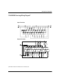
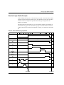
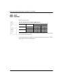
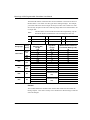
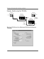
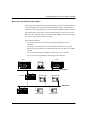
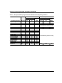
1
Allen-Bradley MicroLogix 1500 Programmable Controllers (Bulletin 1764 Controllers) User Manual Important User Information Because of the variety of uses for the products described in this publication, those responsible for the application and use of this control equipment must satisfy themselves that all necessary steps have been taken to assure that each application and use meets all performance and safety requirements, including any applicable laws, regulations, codes and standards. The illustrations, charts, sample programs and layout examples shown in this guide are intended solely for purposes of example. Since there are many variables and requirements associated with any particular installation, Allen-Bradley does not assume responsibility or liability (to include intellectual property liability) for actual use based upon the examples shown in or included with this publication. Allen-Bradley publication SGI-1.1, Safety Guidelines for the Application, Installation and Maintenance of Solid-State Control (available from your local Allen-Bradley office), describes some important differences between solid-state equipment and electromechanical devices that should be taken into consideration when applying products such as those described in this publication. Reproduction of the contents of this copyrighted publication, in whole or part, without written permission of Allen-Bradley Company, Inc., is prohibited. Throughout this manual we use notes to make you aware of safety considerations: ! ATTENTION: Identifies information about practices or circumstances that can lead to personal injury or death, property damage or economic loss. Attention statements help you to: • identify a hazard • avoid a hazard • recognize the consequences Note: Identifies information that is critical for successful application and understanding of the product. MicroLogix, Compact, SLC, DTAM Micro, PanelView are trademarks of Rockwell Automation. RSLogix 500 is a trademark of Rockwell Software, Inc. Windows is a trademark of MicroSoft Corporation. Belden is a trademark of Belden, Inc. Preface Preface Read this preface to familiarize yourself with the rest of the manual. It provides information concerning: • who should use this manual • the purpose of this manual • related documentation • conventions used in this manual • Allen-Bradley support Who Should Use this Manual Use this manual if you are responsible for designing, installing, programming, or troubleshooting control systems that use MicroLogix 1500 controllers. You should have a basic understanding of electrical circuitry and familiarity with relay logic. If you do not, obtain the proper training before using this product. Purpose of this Manual This manual is a reference guide for MicroLogix 1500 controllers. It describes the procedures you use to install, wire, program, and troubleshoot your controller. This manual: • explains how to install and wire your controllers • gives you an overview of the MicroLogix 1500 controller system • provides the instruction set for the MicroLogix 1500 controllers • contains application examples to show the instruction set in use Refer to your programming software user documentation for more information on programming your MicroLogix 1500 controller. P-1 MicroLogix 1500 Programmable Controllers User Manual Related Documentation The following documents contain additional information concerning Allen-Bradley products. To obtain a copy, contact your local Allen-Bradley office or distributor. For Read this Document Document Number Information on understanding and applying micro controllers. MicroMentor Information on mounting and wiring the MicroLogix 1500 Base Units, including a mounting template for easy installation MicroLogix 1500 Programmable Controllers Installation Instructions 1764-5.1 A description on how to install and connect an AIC+. This manual also contains information on network wiring. Advanced Interface Converter (AIC+) User Manual 1761-6.4 Information on how to install, configure, and commission a DNI DeviceNet™ Interface User Manual 1761-6.5 1761-MMB Information on DF1 open protocol. DF1 Protocol and Command Set Reference Manual 1770-6.5.16 In-depth information on grounding and wiring Allen-Bradley programmable controllers Allen-Bradley Programmable Controller Grounding and Wiring Guidelines 1770-4.1 A description of important differences between solid-state programmable controller products and hard-wired electromechanical devices Application Considerations for SolidState Controls SGI-1.1 An article on wire sizes and types for grounding electrical equipment National Electrical Code - Published by the National Fire Protection Association of Boston, MA. A complete listing of current documentation, including ordering instructions. Also indicates whether the documents are available on CD-ROM or in multi-languages. Allen-Bradley Publication Index SD499 Allen-Bradley Industrial Automation Glossary AG-7.1 A glossary of industrial automation terms and abbreviations P-2 Preface Common Techniques Used in this Manual The following conventions are used throughout this manual: • Bulleted lists such as this one provide information, not procedural steps. • Numbered lists provide sequential steps or hierarchical information. • Italic type is used for emphasis. Allen-Bradley Support Allen-Bradley offers support services worldwide, with over 75 Sales/Support Offices, 512 authorized Distributors and 260 authorized Systems Integrators located throughout the United States alone, plus Allen-Bradley representatives in every major country in the world. Local Product Support Contact your local Allen-Bradley representative for: • sales and order support • product technical training • warranty support • support service agreements Technical Product Assistance If you need to contact Allen-Bradley for technical assistance, please review the information in the Troubleshooting appendix first. Then call your local Allen-Bradley representative. P-3 MicroLogix 1500 Programmable Controllers User Manual Your Questions or Comments on this Manual If you find a problem with this manual, or you have any suggestions for how this manual could be made more useful to you, please contact us at the address below: Allen-Bradley Company, Inc. Control and Information Group Technical Communication, Dept. A602V P.O. Box 2086 Milwaukee, WI 53201-2086 or visit our internet page at: http://www.ab.com/micrologix P-4 Table of Contents Table of Contents 1 Hardware Overview Hardware Overview . . . . . . . . . . . . . . . . . . . . . . . . . . . . . . . . . . . . . . . . . . . . . . . . . . . . . 1-1 Component Descriptions . . . . . . . . . . . . . . . . . . . . . . . . . . . . . . . . . . . . . . . . . . . . . . . . . 1-2 Communication Options . . . . . . . . . . . . . . . . . . . . . . . . . . . . . . . . . . . . . . . . . . . . . . . . . 1-5 2 Installing Your Controller Agency Certifications . . . . . . . . . . . . . . . . . . . . . . . . . . . . . . . . . . . . . . . . . . . . . . . . . . . 2-1 Compliance to European Union Directives . . . . . . . . . . . . . . . . . . . . . . . . . . . . . . . . . . . 2-2 General Considerations . . . . . . . . . . . . . . . . . . . . . . . . . . . . . . . . . . . . . . . . . . . . . . . . . . 2-3 Safety Considerations . . . . . . . . . . . . . . . . . . . . . . . . . . . . . . . . . . . . . . . . . . . . . . . . . . . 2-4 Power Considerations . . . . . . . . . . . . . . . . . . . . . . . . . . . . . . . . . . . . . . . . . . . . . . . . . . . 2-6 Preventing Excessive Heat . . . . . . . . . . . . . . . . . . . . . . . . . . . . . . . . . . . . . . . . . . . . . . . 2-8 Master Control Relay. . . . . . . . . . . . . . . . . . . . . . . . . . . . . . . . . . . . . . . . . . . . . . . . . . . . 2-8 Base Unit Mounting Dimensions . . . . . . . . . . . . . . . . . . . . . . . . . . . . . . . . . . . . . . . . . 2-13 Controller Spacing . . . . . . . . . . . . . . . . . . . . . . . . . . . . . . . . . . . . . . . . . . . . . . . . . . . . . 2-13 Mounting the Controller . . . . . . . . . . . . . . . . . . . . . . . . . . . . . . . . . . . . . . . . . . . . . . . . 2-14 Installing Controller Components . . . . . . . . . . . . . . . . . . . . . . . . . . . . . . . . . . . . . . . . . 2-18 3 Wiring Your Controller Wire Requirements . . . . . . . . . . . . . . . . . . . . . . . . . . . . . . . . . . . . . . . . . . . . . . . . . . . . . 3-1 Using Surge Suppressors . . . . . . . . . . . . . . . . . . . . . . . . . . . . . . . . . . . . . . . . . . . . . . . . . 3-4 Grounding the Controller. . . . . . . . . . . . . . . . . . . . . . . . . . . . . . . . . . . . . . . . . . . . . . . . . 3-7 Wiring Diagrams . . . . . . . . . . . . . . . . . . . . . . . . . . . . . . . . . . . . . . . . . . . . . . . . . . . . . . . 3-8 Sinking and Sourcing Circuits . . . . . . . . . . . . . . . . . . . . . . . . . . . . . . . . . . . . . . . . . . . . . 3-8 Controller I/O Wiring . . . . . . . . . . . . . . . . . . . . . . . . . . . . . . . . . . . . . . . . . . . . . . . . . . 3-14 4 Connecting the System Default Communication Configuration . . . . . . . . . . . . . . . . . . . . . . . . . . . . . . . . . . . . . . 4-1 Using the Communications Toggle Push Button . . . . . . . . . . . . . . . . . . . . . . . . . . . . . . 4-2 Connecting to the RS-232 Port . . . . . . . . . . . . . . . . . . . . . . . . . . . . . . . . . . . . . . . . . . . . 4-3 Connecting to a DH485 Network . . . . . . . . . . . . . . . . . . . . . . . . . . . . . . . . . . . . . . . . . . 4-8 Connecting the AIC+ . . . . . . . . . . . . . . . . . . . . . . . . . . . . . . . . . . . . . . . . . . . . . . . . . . . 4-12 DeviceNet Communications . . . . . . . . . . . . . . . . . . . . . . . . . . . . . . . . . . . . . . . . . . . . . 4-20 toc-i MicroLogix 1500 Programmable Controllers User Manual 5 Using Inputs and Outputs Embedded I/O. . . . . . . . . . . . . . . . . . . . . . . . . . . . . . . . . . . . . . . . . . . . . . . . . . . . . . . . . .5-2 Expansion I/O . . . . . . . . . . . . . . . . . . . . . . . . . . . . . . . . . . . . . . . . . . . . . . . . . . . . . . . . . .5-2 I/O Configuration . . . . . . . . . . . . . . . . . . . . . . . . . . . . . . . . . . . . . . . . . . . . . . . . . . . . . . .5-3 I/O Forcing . . . . . . . . . . . . . . . . . . . . . . . . . . . . . . . . . . . . . . . . . . . . . . . . . . . . . . . . . . . .5-4 Input Filtering . . . . . . . . . . . . . . . . . . . . . . . . . . . . . . . . . . . . . . . . . . . . . . . . . . . . . . . . . .5-5 Latching Inputs . . . . . . . . . . . . . . . . . . . . . . . . . . . . . . . . . . . . . . . . . . . . . . . . . . . . . . . . .5-6 6 Controller Memory and File Types Controller Memory . . . . . . . . . . . . . . . . . . . . . . . . . . . . . . . . . . . . . . . . . . . . . . . . . . . . . .6-2 Data Files . . . . . . . . . . . . . . . . . . . . . . . . . . . . . . . . . . . . . . . . . . . . . . . . . . . . . . . . . . . . .6-5 Protecting Data Files During Download . . . . . . . . . . . . . . . . . . . . . . . . . . . . . . . . . . . . .6-6 Password Protection . . . . . . . . . . . . . . . . . . . . . . . . . . . . . . . . . . . . . . . . . . . . . . . . . . . . .6-9 Clearing the Controller Memory . . . . . . . . . . . . . . . . . . . . . . . . . . . . . . . . . . . . . . . . . .6-10 Allow Future Access Setting (OEM Lock) . . . . . . . . . . . . . . . . . . . . . . . . . . . . . . . . . .6-11 Function Files . . . . . . . . . . . . . . . . . . . . . . . . . . . . . . . . . . . . . . . . . . . . . . . . . . . . . . . . .6-12 7 Using Trim Pots and the Data Access Tool (DAT) Trim Pot Operation. . . . . . . . . . . . . . . . . . . . . . . . . . . . . . . . . . . . . . . . . . . . . . . . . . . . . .7-1 Data Access Tool (DAT) . . . . . . . . . . . . . . . . . . . . . . . . . . . . . . . . . . . . . . . . . . . . . . . . .7-3 DAT Keypad and Indicator Light Functions . . . . . . . . . . . . . . . . . . . . . . . . . . . . . . . . . .7-3 Power-Up Operation. . . . . . . . . . . . . . . . . . . . . . . . . . . . . . . . . . . . . . . . . . . . . . . . . . . . .7-5 DAT Function File . . . . . . . . . . . . . . . . . . . . . . . . . . . . . . . . . . . . . . . . . . . . . . . . . . . . . .7-6 F1 and F2 Functions . . . . . . . . . . . . . . . . . . . . . . . . . . . . . . . . . . . . . . . . . . . . . . . . . . . .7-13 Working Screen Operation . . . . . . . . . . . . . . . . . . . . . . . . . . . . . . . . . . . . . . . . . . . . . . .7-14 Non-Existent Elements . . . . . . . . . . . . . . . . . . . . . . . . . . . . . . . . . . . . . . . . . . . . . . . . . .7-14 Controller Faults . . . . . . . . . . . . . . . . . . . . . . . . . . . . . . . . . . . . . . . . . . . . . . . . . . . . . . .7-14 Error Conditions . . . . . . . . . . . . . . . . . . . . . . . . . . . . . . . . . . . . . . . . . . . . . . . . . . . . . . .7-15 8 Using Real Time Clock and Memory Modules Real Time Clock Operation . . . . . . . . . . . . . . . . . . . . . . . . . . . . . . . . . . . . . . . . . . . . . . .8-1 Memory Module Operation . . . . . . . . . . . . . . . . . . . . . . . . . . . . . . . . . . . . . . . . . . . . . . .8-4 9 Using the High Speed Counter High Speed Counter (HSC) Function File . . . . . . . . . . . . . . . . . . . . . . . . . . . . . . . . . . . .9-2 High Speed Counter Function File Sub-Elements Summary . . . . . . . . . . . . . . . . . . . . . .9-4 HSC Function File Sub-Elements . . . . . . . . . . . . . . . . . . . . . . . . . . . . . . . . . . . . . . . . . .9-5 HSL - High Speed Counter Load . . . . . . . . . . . . . . . . . . . . . . . . . . . . . . . . . . . . . . . . . .9-29 RAC - Reset Accumulated Value. . . . . . . . . . . . . . . . . . . . . . . . . . . . . . . . . . . . . . . . . .9-31 toc-ii 10 Using High Speed Outputs PTO - Pulse Train Output Instruction . . . . . . . . . . . . . . . . . . . . . . . . . . . . . . . . . . . . . . 10-1 Pulse Train Output Function . . . . . . . . . . . . . . . . . . . . . . . . . . . . . . . . . . . . . . . . . . . . . 10-1 Pulse Train Outputs (PTO) Function File . . . . . . . . . . . . . . . . . . . . . . . . . . . . . . . . . . . 10-6 Pulse Train Output Function File Sub-Elements Summary . . . . . . . . . . . . . . . . . . . . . 10-7 PWM - Pulse Width Modulation Instruction. . . . . . . . . . . . . . . . . . . . . . . . . . . . . . . . 10-20 PWM Function . . . . . . . . . . . . . . . . . . . . . . . . . . . . . . . . . . . . . . . . . . . . . . . . . . . . . . 10-20 Pulse Width Modulated (PWM) Function File . . . . . . . . . . . . . . . . . . . . . . . . . . . . . . 10-21 Pulse Width Modulated Function File Elements Summary . . . . . . . . . . . . . . . . . . . . 10-22 11 Programming Instructions Overview Instruction Set . . . . . . . . . . . . . . . . . . . . . . . . . . . . . . . . . . . . . . . . . . . . . . . . . . . . . . . . 11-1 Using the Instruction Descriptions . . . . . . . . . . . . . . . . . . . . . . . . . . . . . . . . . . . . . . . . 11-2 12 Relay-Type (Bit) Instructions XIC - Examine if Closed, XIO - Examine if Open . . . . . . . . . . . . . . . . . . . . . . . . . . . . 12-2 OTE - Output Energize . . . . . . . . . . . . . . . . . . . . . . . . . . . . . . . . . . . . . . . . . . . . . . . . . 12-4 OTL - Output Latch, OTU - Output Unlatch. . . . . . . . . . . . . . . . . . . . . . . . . . . . . . . . . 12-5 ONS - One Shot . . . . . . . . . . . . . . . . . . . . . . . . . . . . . . . . . . . . . . . . . . . . . . . . . . . . . . . 12-7 OSR - One Shot Rising, OSF - One Shot Falling . . . . . . . . . . . . . . . . . . . . . . . . . . . . . 12-8 13 Timer and Counter Instructions Timer Instructions Overview . . . . . . . . . . . . . . . . . . . . . . . . . . . . . . . . . . . . . . . . . . . . . 13-1 TON - Timer, On-Delay . . . . . . . . . . . . . . . . . . . . . . . . . . . . . . . . . . . . . . . . . . . . . . . . 13-4 TOF - Timer, Off-Delay . . . . . . . . . . . . . . . . . . . . . . . . . . . . . . . . . . . . . . . . . . . . . . . . 13-5 RTO - Retentive Timer On . . . . . . . . . . . . . . . . . . . . . . . . . . . . . . . . . . . . . . . . . . . . . . 13-6 CTU - Count Up, CTD - Count Down . . . . . . . . . . . . . . . . . . . . . . . . . . . . . . . . . . . . 13-10 RES - Reset . . . . . . . . . . . . . . . . . . . . . . . . . . . . . . . . . . . . . . . . . . . . . . . . . . . . . . . . . 13-11 14 Compare Instructions Using the Compare Instructions . . . . . . . . . . . . . . . . . . . . . . . . . . . . . . . . . . . . . . . . . . 14-2 EQU - Equal, NEQ - Not Equal. . . . . . . . . . . . . . . . . . . . . . . . . . . . . . . . . . . . . . . . . . . 14-3 GRT - Greater Than, LES - Less Than . . . . . . . . . . . . . . . . . . . . . . . . . . . . . . . . . . . . . 14-4 GEQ - Greater Than or Equal To, LEQ - Less Than or Equal To. . . . . . . . . . . . . . . . . 14-5 MEQ - Mask Compare for Equal. . . . . . . . . . . . . . . . . . . . . . . . . . . . . . . . . . . . . . . . . . 14-6 LIM - Limit Test . . . . . . . . . . . . . . . . . . . . . . . . . . . . . . . . . . . . . . . . . . . . . . . . . . . . . . 14-8 toc-iii MicroLogix 1500 Programmable Controllers User Manual 15 Math Instructions Using the Math Instructions . . . . . . . . . . . . . . . . . . . . . . . . . . . . . . . . . . . . . . . . . . . . . .15-2 Updates to Math Status Bits . . . . . . . . . . . . . . . . . . . . . . . . . . . . . . . . . . . . . . . . . . . . . .15-3 ADD - Add, SUB - Subtract. . . . . . . . . . . . . . . . . . . . . . . . . . . . . . . . . . . . . . . . . . . . . .15-4 MUL - Multiply, DIV - Divide. . . . . . . . . . . . . . . . . . . . . . . . . . . . . . . . . . . . . . . . . . . .15-5 NEG - Negate . . . . . . . . . . . . . . . . . . . . . . . . . . . . . . . . . . . . . . . . . . . . . . . . . . . . . . . . .15-6 CLR - Clear . . . . . . . . . . . . . . . . . . . . . . . . . . . . . . . . . . . . . . . . . . . . . . . . . . . . . . . . . .15-6 SCL - Scale. . . . . . . . . . . . . . . . . . . . . . . . . . . . . . . . . . . . . . . . . . . . . . . . . . . . . . . . . . .15-7 SCP - Scale with Parameters . . . . . . . . . . . . . . . . . . . . . . . . . . . . . . . . . . . . . . . . . . . . .15-8 SQR - Square Root . . . . . . . . . . . . . . . . . . . . . . . . . . . . . . . . . . . . . . . . . . . . . . . . . . . .15-10 16 Conversion Instructions Using Decode and Encode Instructions . . . . . . . . . . . . . . . . . . . . . . . . . . . . . . . . . . . . .16-2 DCD - Decode 4 to 1-of-16 . . . . . . . . . . . . . . . . . . . . . . . . . . . . . . . . . . . . . . . . . . . . . .16-3 ENC - Encode 1-of-16 to 4. . . . . . . . . . . . . . . . . . . . . . . . . . . . . . . . . . . . . . . . . . . . . . .16-4 FRD - Convert from Binary Coded Decimal (BCD) . . . . . . . . . . . . . . . . . . . . . . . . . . .16-6 TOD - Convert to Binary Coded Decimal (BCD) . . . . . . . . . . . . . . . . . . . . . . . . . . . .16-10 17 Logical Instructions Using Logical Instructions . . . . . . . . . . . . . . . . . . . . . . . . . . . . . . . . . . . . . . . . . . . . . . .17-1 Updates to Math Status Bits . . . . . . . . . . . . . . . . . . . . . . . . . . . . . . . . . . . . . . . . . . . . . .17-2 AND - Bit-Wise AND . . . . . . . . . . . . . . . . . . . . . . . . . . . . . . . . . . . . . . . . . . . . . . . . . .17-3 OR - Logical OR . . . . . . . . . . . . . . . . . . . . . . . . . . . . . . . . . . . . . . . . . . . . . . . . . . . . . .17-4 XOR - Exclusive OR . . . . . . . . . . . . . . . . . . . . . . . . . . . . . . . . . . . . . . . . . . . . . . . . . . .17-5 NOT - Logical NOT . . . . . . . . . . . . . . . . . . . . . . . . . . . . . . . . . . . . . . . . . . . . . . . . . . . .17-6 18 Move Instructions MOV - Move . . . . . . . . . . . . . . . . . . . . . . . . . . . . . . . . . . . . . . . . . . . . . . . . . . . . . . . . .18-2 MVM - Masked Move . . . . . . . . . . . . . . . . . . . . . . . . . . . . . . . . . . . . . . . . . . . . . . . . . .18-4 19 File Instructions COP - Copy File . . . . . . . . . . . . . . . . . . . . . . . . . . . . . . . . . . . . . . . . . . . . . . . . . . . . . . .19-2 FLL - Fill File . . . . . . . . . . . . . . . . . . . . . . . . . . . . . . . . . . . . . . . . . . . . . . . . . . . . . . . . .19-3 BSL - Bit Shift Left . . . . . . . . . . . . . . . . . . . . . . . . . . . . . . . . . . . . . . . . . . . . . . . . . . . .19-5 BSR - Bit Shift Right . . . . . . . . . . . . . . . . . . . . . . . . . . . . . . . . . . . . . . . . . . . . . . . . . . .19-7 FFL - First In, First Out (FIFO) Load . . . . . . . . . . . . . . . . . . . . . . . . . . . . . . . . . . . . . .19-9 FFU - First In, First Out (FIFO) Unload . . . . . . . . . . . . . . . . . . . . . . . . . . . . . . . . . . .19-12 LFL - Last In, First Out (LIFO) Load . . . . . . . . . . . . . . . . . . . . . . . . . . . . . . . . . . . . .19-15 LFU - Last In, First Out (LIFO) Unload . . . . . . . . . . . . . . . . . . . . . . . . . . . . . . . . . . .19-18 toc-iv 20 Sequencer Instructions SQC- Sequencer Compare . . . . . . . . . . . . . . . . . . . . . . . . . . . . . . . . . . . . . . . . . . . . . . . 20-2 SQO- Sequencer Output . . . . . . . . . . . . . . . . . . . . . . . . . . . . . . . . . . . . . . . . . . . . . . . . 20-6 SQL - Sequencer Load. . . . . . . . . . . . . . . . . . . . . . . . . . . . . . . . . . . . . . . . . . . . . . . . . 20-10 21 Program Control Instructions JMP - Jump to Label . . . . . . . . . . . . . . . . . . . . . . . . . . . . . . . . . . . . . . . . . . . . . . . . . . . 21-2 LBL - Label . . . . . . . . . . . . . . . . . . . . . . . . . . . . . . . . . . . . . . . . . . . . . . . . . . . . . . . . . . 21-2 JSR - Jump to Subroutine . . . . . . . . . . . . . . . . . . . . . . . . . . . . . . . . . . . . . . . . . . . . . . . 21-3 SBR - Subroutine Label. . . . . . . . . . . . . . . . . . . . . . . . . . . . . . . . . . . . . . . . . . . . . . . . . 21-3 RET - Return from Subroutine . . . . . . . . . . . . . . . . . . . . . . . . . . . . . . . . . . . . . . . . . . . 21-4 SUS - Suspend . . . . . . . . . . . . . . . . . . . . . . . . . . . . . . . . . . . . . . . . . . . . . . . . . . . . . . . . 21-4 TND - Temporary End. . . . . . . . . . . . . . . . . . . . . . . . . . . . . . . . . . . . . . . . . . . . . . . . . . 21-5 END - Program End. . . . . . . . . . . . . . . . . . . . . . . . . . . . . . . . . . . . . . . . . . . . . . . . . . . . 21-5 MCR - Master Control Reset. . . . . . . . . . . . . . . . . . . . . . . . . . . . . . . . . . . . . . . . . . . . . 21-6 22 Input and Output Instructions IIM - Immediate Input with Mask . . . . . . . . . . . . . . . . . . . . . . . . . . . . . . . . . . . . . . . . . 22-2 IOM - Immediate Output with Mask . . . . . . . . . . . . . . . . . . . . . . . . . . . . . . . . . . . . . . . 22-4 REF- I/O Refresh . . . . . . . . . . . . . . . . . . . . . . . . . . . . . . . . . . . . . . . . . . . . . . . . . . . . . . 22-6 23 Using Interrupts Information About Using Interrupts . . . . . . . . . . . . . . . . . . . . . . . . . . . . . . . . . . . . . . . 23-1 User Interrupt Instructions . . . . . . . . . . . . . . . . . . . . . . . . . . . . . . . . . . . . . . . . . . . . . . . 23-7 INT - Interrupt Subroutine. . . . . . . . . . . . . . . . . . . . . . . . . . . . . . . . . . . . . . . . . . . . . . . 23-7 STS - Selectable Timed Start. . . . . . . . . . . . . . . . . . . . . . . . . . . . . . . . . . . . . . . . . . . . . 23-8 UID - User Interrupt Disable . . . . . . . . . . . . . . . . . . . . . . . . . . . . . . . . . . . . . . . . . . . . . 23-9 UIE - User Interrupt Enable. . . . . . . . . . . . . . . . . . . . . . . . . . . . . . . . . . . . . . . . . . . . . 23-10 UIF - User Interrupt Flush . . . . . . . . . . . . . . . . . . . . . . . . . . . . . . . . . . . . . . . . . . . . . . 23-12 Using the Selectable Timed Interrupt (STI) Function File . . . . . . . . . . . . . . . . . . . . . 23-13 Using the Event Input Interrupt (EII) Function File . . . . . . . . . . . . . . . . . . . . . . . . . . 23-19 24 Process Control Instruction The PID Concept . . . . . . . . . . . . . . . . . . . . . . . . . . . . . . . . . . . . . . . . . . . . . . . . . . . . . . 24-1 The PID Equation . . . . . . . . . . . . . . . . . . . . . . . . . . . . . . . . . . . . . . . . . . . . . . . . . . . . . 24-2 PD Data File . . . . . . . . . . . . . . . . . . . . . . . . . . . . . . . . . . . . . . . . . . . . . . . . . . . . . . . . . 24-3 Input Parameters . . . . . . . . . . . . . . . . . . . . . . . . . . . . . . . . . . . . . . . . . . . . . . . . . . . . . . 24-5 Output Parameters . . . . . . . . . . . . . . . . . . . . . . . . . . . . . . . . . . . . . . . . . . . . . . . . . . . . . 24-7 Tuning Parameters . . . . . . . . . . . . . . . . . . . . . . . . . . . . . . . . . . . . . . . . . . . . . . . . . . . . 24-10 Runtime Errors. . . . . . . . . . . . . . . . . . . . . . . . . . . . . . . . . . . . . . . . . . . . . . . . . . . . . . . 24-19 Analog I/O Scaling . . . . . . . . . . . . . . . . . . . . . . . . . . . . . . . . . . . . . . . . . . . . . . . . . . . 24-21 Application Notes . . . . . . . . . . . . . . . . . . . . . . . . . . . . . . . . . . . . . . . . . . . . . . . . . . . . 24-22 toc-v MicroLogix 1500 Programmable Controllers User Manual 25 Communications Instructions MicroLogix 1500 Messaging Overview. . . . . . . . . . . . . . . . . . . . . . . . . . . . . . . . . . . . .25-2 Remote Messages . . . . . . . . . . . . . . . . . . . . . . . . . . . . . . . . . . . . . . . . . . . . . . . . . . . . .25-14 MSG Instruction Error Codes. . . . . . . . . . . . . . . . . . . . . . . . . . . . . . . . . . . . . . . . . . . .25-18 Timing Diagram for MicroLogix 1500 MSG Instruction . . . . . . . . . . . . . . . . . . . . . .25-21 Service Communications (SVC) . . . . . . . . . . . . . . . . . . . . . . . . . . . . . . . . . . . . . . . . .25-24 Examples: Ladder Logic. . . . . . . . . . . . . . . . . . . . . . . . . . . . . . . . . . . . . . . . . . . . . . . .25-27 Using Local Messaging . . . . . . . . . . . . . . . . . . . . . . . . . . . . . . . . . . . . . . . . . . . . . . . .25-28 Using Remote Messaging. . . . . . . . . . . . . . . . . . . . . . . . . . . . . . . . . . . . . . . . . . . . . . .25-34 Example 2 - Passthru via DH485 Channel 0 of the SLC 5/04 Processor. . . . . . . . . . .25-37 Example - Passthu using Two 1785-KA5s. . . . . . . . . . . . . . . . . . . . . . . . . . . . . . . . . .25-40 A Specifications Controller Dimensions . . . . . . . . . . . . . . . . . . . . . . . . . . . . . . . . . . . . . . . . . . . . . . . . . . A-9 Compact I/O Dimensions . . . . . . . . . . . . . . . . . . . . . . . . . . . . . . . . . . . . . . . . . . . . . . . A-10 Transistor Output Transient Pulses . . . . . . . . . . . . . . . . . . . . . . . . . . . . . . . . . . . . . . . A-10 B Replacement Parts MicroLogix 1500 Replacement Kits . . . . . . . . . . . . . . . . . . . . . . . . . . . . . . . . . . . . . . . Lithium Battery (1747-BA) . . . . . . . . . . . . . . . . . . . . . . . . . . . . . . . . . . . . . . . . . . . . . . Replacement Doors . . . . . . . . . . . . . . . . . . . . . . . . . . . . . . . . . . . . . . . . . . . . . . . . . . . . Replacement Terminal Blocks . . . . . . . . . . . . . . . . . . . . . . . . . . . . . . . . . . . . . . . . . . . . C B-1 B-2 B-6 B-8 Troubleshooting Your System Understanding the Controller LED Status . . . . . . . . . . . . . . . . . . . . . . . . . . . . . . . . . . . C-2 Controller Error Recovery Model . . . . . . . . . . . . . . . . . . . . . . . . . . . . . . . . . . . . . . . . . C-4 Identifying Controller Faults . . . . . . . . . . . . . . . . . . . . . . . . . . . . . . . . . . . . . . . . . . . . . C-5 Calling Allen-Bradley for Assistance. . . . . . . . . . . . . . . . . . . . . . . . . . . . . . . . . . . . . . C-14 D Understanding the Communication Protocols RS-232 Communication Interface . . . . . . . . . . . . . . . . . . . . . . . . . . . . . . . . . . . . . . . . . D-1 DF1 Full-Duplex Protocol . . . . . . . . . . . . . . . . . . . . . . . . . . . . . . . . . . . . . . . . . . . . . . . D-2 DF1 Half-Duplex Protocol . . . . . . . . . . . . . . . . . . . . . . . . . . . . . . . . . . . . . . . . . . . . . . . D-4 DH485 Communication Protocol . . . . . . . . . . . . . . . . . . . . . . . . . . . . . . . . . . . . . . . . . D-10 E System Loading and Heat Dissipation System Loading Limitations. . . . . . . . . . . . . . . . . . . . . . . . . . . . . . . . . . . . . . . . . . . . . . E-1 System Loading Worksheet . . . . . . . . . . . . . . . . . . . . . . . . . . . . . . . . . . . . . . . . . . . . . . E-4 Calculating Heat Dissipation . . . . . . . . . . . . . . . . . . . . . . . . . . . . . . . . . . . . . . . . . . . . . E-6 toc-vi F Memory Usage and Instruction Execution Time Programming Instructions Memory Usage and Execution Time . . . . . . . . . . . . . . . . . . F-1 Scan Time Worksheet . . . . . . . . . . . . . . . . . . . . . . . . . . . . . . . . . . . . . . . . . . . . . . . . . . . F-8 G System Status File Status File Overview . . . . . . . . . . . . . . . . . . . . . . . . . . . . . . . . . . . . . . . . . . . . . . . . . . . .G-1 Status File Details . . . . . . . . . . . . . . . . . . . . . . . . . . . . . . . . . . . . . . . . . . . . . . . . . . . . . .G-3 Glossary Index toc-vii MicroLogix 1500 Programmable Controllers User Manual toc-viii Hardware Overview 1 Hardware Overview Hardware Overview The MicroLogix 1500 programmable controller contains a power supply, input circuits, output circuits, and a processor. The controller is available in 24 I/O and 28 I/O configurations. The hardware features of the controller are: 1 10 2 RUN REM PROG 3 12 4 5 11 10 9 8 1 7 Feature Description Feature 6 Description 1 Removable Terminal Blocks 7 Memory Module/Real-Time Clock1 2 Interface to Expansion I/O, Removable ESD Barrier 8 Replacement Battery1 3 Input LEDs 9 Battery 4 Output LEDs 10 Terminal Doors and Label 5 Communication Port 11 Data Access Tool1 6 Status LEDs 12 Mode Switch, Trim Pots 1.Optional. 1-1 MicroLogix 1500 Programmable Controllers User Manual Component Descriptions A controller is composed of a standard processor (1764-LSP) and one of the base units listed below. The FET transistor and relay outputs are available on the 1764-28BXB base only. Base Units Catalog Number 1-2 Base Unit I/O and Power Supply 1764-24AWA Twelve 120V ac inputs, twelve relay outputs and 120/240V ac power supply 1764-24BWA Twelve 24V dc inputs, twelve relay outputs and 120/240V ac power supply 1764-28BXB Sixteen 24V dc inputs, six FET and six relay outputs and 24V dc power supply Hardware Overview Processor (Catalog Number 1764-LSP) Data Access Tool (Catalog Number 1764-DAT) (Shown mounted on a Processor Unit.) 1-3 MicroLogix 1500 Programmable Controllers User Manual Memory Modules/Real-Time Clock (Catalog Number 1764-MM1RTC, 1764-MM1, 1764-RTC) (Shown mounted in a Processor Unit.) Expansion I/O Compact™ expansion I/O can be connected to the MicroLogix 1500 Controller. A maximum of eight I/O modules may be connected to the base. See “System Loading and Heat Dissipation” on page E-1 for more information on system configurations. End Cap An end cap terminator (catalog number 1769-ECR) must be used at the end of the group of I/O modules attached to the MicroLogix 1500 Controller. The end cap terminator is not provided with the base and processor units. It is required when using expansion I/O. 1-4 Hardware Overview Accessories Cables Use only the following communication cables in Class I, Division 2 hazardous locations. Environment Classification Class I, Division 2 Hazardous Environment Communication Cables 1761-CBL-PM02 Series C or later 1761-CBL-HM02 Series C or later 1761-CBL-AM00 Series C or later 1761-CBL-AP00 Series C or later 2707-NC8 Series B or later 2707-NC9 Series B or later 2707-NC10 Series B or later 2707-NC11 Series B or later Programming Programming the MicroLogix 1500 programmable controller is done using RSLogix 500, Rev. 3.01.00 or later. Programming cables are not provided. Communication Options The MicroLogix 1500 can be connected to a personal computer using the DF1 protocol. It can also be connected to the DH485 network using an Advanced Interface Converter (catalog number 1761-NET-AIC) and to the DeviceNet network using a DeviceNet Interface (catalog number 1761-NET-DNI). See “Connecting the System” on page 4-1 for descriptions of these communication options. 1-5 MicroLogix 1500 Programmable Controllers User Manual 1-6 Installing Your Controller 2 Installing Your Controller This chapter shows you how to install your controller system. The only tools you require are a Flat or Phillips head screwdriver and drill. Topics include: • agency certifications • compliance to European Union Directives • using in hazardous locations • master control relay • power considerations • preventing excessive heat • controller spacing • mounting the controller Agency Certifications • UL 508 • C-UL under CSA C22.2 no. 142 • Class I, Division 2, Groups A, B, C, D (UL 1604, C-UL under CSA C22.2 no. 213) • CE compliant for all applicable directives 2-1 MicroLogix 1500 Programmable Controllers User Manual Compliance to European Union Directives This product has the CE mark and is approved for installation within the European Union and EEA regions. It has been designed and tested to meet the following directives. EMC Directive This product is tested to meet Council Directive 89/336/EEC Electromagnetic Compatibility (EMC) and the following standards, in whole or in part, documented in a technical construction file: • EN 50081-2 EMC - Generic Emission Standard, Part 2 - Industrial Environment • EN 50082-2 EMC - Generic Immunity Standard, Part 2 - Industrial Environment This product is intended for use in an industrial environment. Low Voltage Directive This product is tested to meet Council Directive 73/23/EEC Low Voltage, by applying the safety requirements of EN 61131-2 Programmable Controllers, Part 2 Equipment Requirements and Tests. For specific information required by EN 61131-2, see the appropriate sections in this publication, as well as the following Allen-Bradley publications: 2-2 • Industrial Automation Wiring and Grounding Guidelines for Noise Immunity, publication 1770-4.1 • Guidelines for Handling Lithium Batteries, publication AG-5.4 • Automation Systems Catalog, publication B111 Installing Your Controller General Considerations Most applications require installation in an industrial enclosure (Pollution Degree 21) to reduce the effects of electrical interference (Over Voltage Category II 2) and environmental exposure. Locate your controller as far as possible from power lines, load lines, and other sources of electrical noise such as hard-contact switches, relays, and AC motor drives. For more information on proper grounding guidelines, see the Industrial Automation Wiring and Grounding Guidelines publication 1770-4.1. ! ATTENTION: Vertical mounting is not recommended due to heat build-up considerations. ! ATTENTION: Be careful of metal chips when drilling mounting holes for your controller or other equipment within the enclosure or panel. Drilled fragments that fall into the base or processor unit could cause damage. Do not drill holes above a mounted controller if the protective debris strips have been removed or the processor has been installed. 1 Pollution Degree 2 is an environment where normally only non-conductive pollution occurs except that occasionally temporary conductivity caused by condensation shall be expected. 2 Overvoltage Category II is the load level section of the electrical distribution system. At this level transient voltages are controlled and do not exceed the impulse voltage capability of the products insulation. 2-3 MicroLogix 1500 Programmable Controllers User Manual Safety Considerations Safety considerations are an important element of proper system installation. Actively thinking about the safety of yourself and others, as well as the condition of your equipment, is of primary importance. We recommend reviewing the following safety considerations. Hazardous Location Considerations This equipment is suitable for use in Class I, Division 2, Groups A, B, C, D or nonhazardous locations only. The following ATTENTION statement applies to use in hazardous locations. ATTENTION: EXPLOSION HAZARD ! • Substitution of components may impair suitability for Class I, Division 2. • Do not replace components or disconnect equipment unless power has been switched off or the area is known to be non-hazardous. • Do not connect or disconnect components unless power has been switched off or the area is known to be non-hazardous. • This product must be installed in an enclosure. All cables connected to the product must remain in the enclosure or be protected by conduit or other means. Use only the following communication cables in Class I, Division 2 hazardous locations. Environment Classification Class I, Division 2 Hazardous Environment Communication Cables 1761-CBL-PM02 Series C or later 1761-CBL-HM02 Series C or later 1761-CBL-AM00 Series C or later 1761-CBL-AP00 Series C or later 2707-NC8 Series B or later 2707-NC9 Series B or later 2707-NC10 Series B or later 2707-NC11 Series B or later 2-4 Installing Your Controller Disconnecting Main Power ! ATTENTION: Explosion Hazard - Do not replace components or disconnect equipment unless power has been switched off and the area is known to be non-hazardous. The main power disconnect switch should be located where operators and maintenance personnel have quick and easy access to it. In addition to disconnecting electrical power, all other sources of power (pneumatic and hydraulic) should be de-energized before working on a machine or process controlled by a controller. Safety Circuits ! ATTENTION: Explosion Hazard - Do not connect or disconnect connectors while circuit is live unless area is known to be nonhazardous. Circuits installed on the machine for safety reasons, like overtravel limit switches, stop push buttons, and interlocks, should always be hard-wired directly to the master control relay. These devices must be wired in series so that when any one device opens, the master control relay is de-energized thereby removing power to the machine. Never alter these circuits to defeat their function. Serious injury or machine damage could result. Power Distribution There are some points about power distribution that you should know: • The master control relay must be able to inhibit all machine motion by removing power to the machine I/O devices when the relay is de-energized. It is recommended that the controller remain powered even when the master control relay is de-energized. • If you are using a dc power supply, interrupt the load side rather than the ac line power. This avoids the additional delay of power supply turn-off. The dc power supply should be powered directly from the fused secondary of the transformer. Power to the dc input and output circuits should be connected through a set of master control relay contacts. 2-5 MicroLogix 1500 Programmable Controllers User Manual Periodic Tests of Master Control Relay Circuit Any part can fail, including the switches in a master control relay circuit. The failure of one of these switches would most likely cause an open circuit, which would be a safe power-off failure. However, if one of these switches shorts out, it no longer provides any safety protection. These switches should be tested periodically to assure they will stop machine motion when needed. Power Considerations The following explains power considerations for the micro controllers. Isolation Transformers You may want to use an isolation transformer in the ac line to the controller. This type of transformer provides isolation from your power distribution system to reduce the electrical noise that enters the controller and is often used as a step down transformer to reduce line voltage. Any transformer used with the controller must have a sufficient power rating for its load. The power rating is expressed in volt-amperes (VA). Power Supply Inrush During power-up, the MicroLogix 1500 power supply allows a brief inrush current to charge internal capacitors. Many power lines and control transformers can supply inrush current for a brief time. If the power source cannot supply this inrush current, the source voltage may sag momentarily. The only effect of limited inrush current and voltage sag on the MicroLogix 1500 is that the power supply capacitors charge more slowly. However, the effect of a voltage sag on other equipment should be considered. For example, a deep voltage sag may reset a computer connected to the same power source. The following considerations determine whether the power source must be required to supply high inrush current: • The power-up sequence of devices in a system. • The amount of the power source voltage sag if the inrush current cannot be supplied. • The effect of voltage sag on other equipment in the system. If the entire system is powered-up at the same time, a brief sag in the power source voltage typically will not affect any equipment. 2-6 Installing Your Controller Loss of Power Source The power supply is designed to withstand brief power losses without affecting the operation of the system. The time the system is operational during power loss is called “program scan hold-up time after loss of power.” The duration of the power supply hold-up time depends on the type and state of the I/O, but is typically between 10 milliseconds and 3 seconds. When the duration of power loss reaches this limit, the power supply signals the processor that it can no longer provide adequate dc power to the system. This is referred to as a power supply shutdown. The processor then performs an orderly shutdown of the controller. Input States on Power Down The power supply hold-up time as described above is generally longer than the turnon and turn-off times of the inputs. Because of this, the input state change from “On” to “Off” that occurs when power is removed may be recorded by the processor before the power supply shuts down the system. Understanding this concept is important. The user program should be written to take this effect into account. Other Types of Line Conditions Occasionally the power source to the system can be temporarily interrupted. It is also possible that the voltage level may drop substantially below the normal line voltage range for a period of time. Both of these conditions are considered to be a loss of power for the system. 2-7 MicroLogix 1500 Programmable Controllers User Manual Preventing Excessive Heat For most applications, normal convective cooling keeps the controller within the specified operating range. Ensure that the specified temperature range is maintained. Proper spacing of components within an enclosure is usually sufficient for heat dissipation. In some applications, a substantial amount of heat is produced by other equipment inside or outside the enclosure. In this case, place blower fans inside the enclosure to assist in air circulation and to reduce “hot spots” near the controller. Additional cooling provisions might be necessary when high ambient temperatures are encountered. Note: Do not bring in unfiltered outside air. Place the controller in an enclosure to protect it from a corrosive atmosphere. Harmful contaminants or dirt could cause improper operation or damage to components. In extreme cases, you may need to use air conditioning to protect against heat buildup within the enclosure. Master Control Relay A hard-wired master control relay (MCR) provides a reliable means for emergency machine shutdown. Since the master control relay allows the placement of several emergency-stop switches in different locations, its installation is important from a safety standpoint. Overtravel limit switches or mushroom head push buttons are wired in series so that when any of them opens, the master control relay is de-energized. This removes power to input and output device circuits. Refer to the figures on page 2-11 and 2-12. ! 2-8 ATTENTION: Never alter these circuits to defeat their function since serious injury and/or machine damage could result. Installing Your Controller Note: If you are using an external dc power supply, interrupt the dc output side rather than the ac line side of the supply to avoid the additional delay of power supply turn-off. The ac line of the dc output power supply should be fused. Connect a set of master control relays in series with the dc power supplying the input and output circuits. Place the main power disconnect switch where operators and maintenance personnel have quick and easy access to it. If you mount a disconnect switch inside the controller enclosure, place the switch operating handle on the outside of the enclosure, so that you can disconnect power without opening the enclosure. Whenever any of the emergency-stop switches are opened, power to input and output devices should be removed. When you use the master control relay to remove power from the external I/O circuits, power continues to be provided to the controller’s power supply so that diagnostic indicators on the processor can still be observed. The master control relay is not a substitute for a disconnect to the controller. It is intended for any situation where the operator must quickly de-energize I/O devices only. When inspecting or installing terminal connections, replacing output fuses, or working on equipment within the enclosure, use the disconnect to shut off power to the rest of the system. Note: Do not control the master control relay with the controller. Provide the operator with the safety of a direct connection between an emergencystop switch and the master control relay. 2-9 MicroLogix 1500 Programmable Controllers User Manual Using Emergency-Stop Switches When using emergency-stop switches, adhere to the following points: • Do not program emergency-stop switches in the controller program. Any emergency-stop switch should turn off all machine power by turning off the master control relay. • Observe all applicable local codes concerning the placement and labeling of emergency-stop switches. • Install emergency-stop switches and the master control relay in your system. Make certain that relay contacts have a sufficient rating for your application. Emergency-stop switches must be easy to reach. • In the following illustration, input and output circuits are shown with MCR protection. However, in most applications, only output circuits require MCR protection. The following illustrations show the Master Control Relay wired in a grounded system. Note: 2-10 In most applications input circuits do not require MCR protection; however, if you need to remove power from all field devices, you must include MCR contacts in series with input power wiring. Installing Your Controller Schematic (Using IEC Symbols) L1 L2 230V ac Disconnect MCR Fuse 230V ac I/O Circuits Isolation Transformer X1 115V ac or 230V Fuse X2 Operation of either ofthese contacts will remove power from the external I/O circuits, stopping machine motion. Emergency-Stop Push Button Overtravel Stop Master Control Relay (MCR) Cat. No. 700-PK400A1 Suppressor Cat. No. 700-N24 Start Limit Switch MCR Suppr. MCR MCR 115V ac or 230V ac I/O Circuits dc Power Supply. Use IEC 950/EN 60950 _ (Hi) (Lo) Line Terminals: Connect to terminals of Power Supply (1764-24AWA and 1764-24BWA). + MCR 24V dc I/O Circuits Line Terminals: Connect to 24V dc terminals of Power Supply. 2-11 MicroLogix 1500 Programmable Controllers User Manual Schematic (Using ANSI/CSA Symbols) L1 L2 230V ac Disconnect MCR Fuse Isolation Transformer X1 115V ac or 230V ac Fuse 230V ac Output Circuits Operation of either ofthese contacts will remove power from the external I/O circuits, X2 Master Control Relay (MCR) Cat. No. 700-PK400A1 Suppressor Cat. No. 700-N24 stopping machine motion. Emergency-Stop Push Button Overtravel Limit Switch Stop Start MCR Suppr. MCR MCR 115V ac or 230V ac I/O Circuits dc Power Supply. Use NEC Class 2 for UL Listing. _ (Lo) MCR 24 V dc I/O Circuits (Hi) Line Terminals: Connect to 1764-24AWA or 1764-24BWA terminals. 2-12 + Line Terminals: Connect to 24V dc terminals of Power Supply. Installing Your Controller Base Unit Mounting Dimensions A B Dimension C 1764-24AWA 1764-24BWA 1764-28BXB Height (A) DIN latch open: 138 mm (5.43 in.), DIN latch closed: 118 mm (4.65 in.) Width (B) 168 mm (6.62 in.) Depth (C) 87 mm (3.43 in.) See “Controller Dimensions” on page A-9 for more dimensional information. Controller Spacing The base unit is designed to be mounted horizontally, with the Compact™ expansion I/O extending to the right of the base unit. Allow 50 mm (2 in.) minimum of space on all sides for adequate ventilation, as shown below. End Cap Compact I/O Compact I/O Compact I/O Compact I/O Controller Side Compact I/O Top Side Bottom 2-13 MicroLogix 1500 Programmable Controllers User Manual Mounting the Controller ! ATTENTION: Do not remove protective debris strips until after the base and all other equipment in the panel near the base is mounted and wiring is complete. The debris strips are there to prevent drill fragments, wire strands and other dirt from getting into the controller. Once wiring is complete, remove protective debris strips and install processor unit. Failure to remove strips before operating can cause overheating. Protective Debris Strips ESD Barrier 2-14 ! ATTENTION: Be careful of metal chips when drilling mounting holes for your controller or other equipment within the enclosure or panel. Drilled fragments that fall into the controller could cause damage. Do not drill holes above a mounted controller if the protective debris strips have been removed. ! ATTENTION: Electrostatic discharge can damage semiconductor devices inside the base unit. Do not touch the connector pins or other sensitive areas. Installing Your Controller Note: If additional I/O modules are required for the application, remove the ESD barrier to install expansion I/O modules. A maximum of 8 I/O modules may be connected to the base. The I/O module’s current requirements and power consumption may further limit the number of modules connected to the base. See “System Loading and Heat Dissipation” on page E-1. An end cap terminator (catalog number 1769-ECR) is required at the end of the group of I/O modules attached to the base. Using a DIN Rail The base unit and expansion I/O DIN rail latches lock in the open position so that an entire system can be easily attached to or removed from the DIN rail. The maximum extension of the latch is 15 mm (0.67 in.) in the open position. A flat-blade screw driver is required for removal of the base unit. The base can be mounted to EN5002235x7.5 or EN50022-35x15 DIN rails. DIN rail mounting dimensions are shown below. B A DIN Rail Latch C Dimension Height A DIN latch open: 138 mm (5.43 in.), DIN latch closed: 118 mm (4.65 in.) B 47.6 mm (1.875 in.) C 47.6 mm (1.875 in) DIN latch closed 54.7 mm (2.16 in.) DIN latch open 2-15 MicroLogix 1500 Programmable Controllers User Manual To install your base unit on the DIN rail: 1. Mount your DIN rail. (Make sure that the placement of the base unit on the DIN rail meets the recommended spacing requirements, see “Controller Spacing” on page 2-13. Refer to the mounting template from the inside back cover of the MicroLogix 1500 Programmable Controller Base Units Installation Instructions, publication 1764-5.1. 2. Hook the top slot over the DIN rail. 3. While pressing the base unit down against the top of the rail, snap the bottom of the base unit into position. Ensure DIN latches are in the up (secured) position. 4. Leave the protective debris strip attached until you are finished wiring the base unit and any other devices. To remove your base unit from the DIN rail: 1. Place a flat-blade screwdriver in the DIN rail latch at the bottom of the base unit. 2. Holding the base unit, pry downward on the latch until the latch locks in the open position. Repeat this procedure with the second latch. This releases the base unit from the DIN rail. DIN Rail Latch 2-16 Installing Your Controller Base Unit Panel Mounting Mount to panel using #8 or M4 screws. Mounting Template To install your base unit using mounting screws: 1. Remove the mounting template from the inside back cover of the MicroLogix 1500 Programmable Controller Base Units Installation Instruction, publication 1764-5.1. 2. Secure the template to the mounting surface. (Make sure your base unit is spaced properly, see “Controller Spacing” on page 2-13). 3. Drill holes through the template. 4. Remove the mounting template. 5. Mount the base unit. 6. Leave the protective debris strips attached until you are finished wiring the base unit and any other devices. 2-17 MicroLogix 1500 Programmable Controllers User Manual Installing Controller Components Prevent Electrostatic Discharge ! ATTENTION: Electrostatic discharge can damage integrated circuits or semiconductors if you touch bus connector pins. Follow these guidelines when you handle any module: • Touch a grounded object to discharge static potential. • Wear an approved wrist-strap grounding device. • Do not touch the bus connector or connector pins. • Do not touch circuit components inside the module. • If available, use a static-safe work station. • When not in use, keep the module in its static-shield bag. ! 2-18 ATTENTION: Be sure the base unit is free of all metal fragments before removing protective debris strips and installing the processor unit. Failure to remove strips before operating can cause overheating. Installing Your Controller Processor 1. Be sure base unit power is off. 2. Slide the processor into the base unit using the guide rails for alignment. 3. Push until a click is heard. Important: It is critical that the processor is fully engaged and locked into place. 2-19 MicroLogix 1500 Programmable Controllers User Manual 4. Make sure the actuator is pushed closed. 5. To remove the processor from the base unit, make sure base unit power is off. Push the actuator to the open position until the processor is ejected slightly. Once the processor has been ejected, it can be removed from the base unit. 2-20 Installing Your Controller Data Access Tool 1. Remove cover from processor. 2. Holding Data Access Tool (DAT) in the proper orientation (as shown), place DAT onto processor. Align DAT port on the processor with the plug on the DAT. 2-21 MicroLogix 1500 Programmable Controllers User Manual 3. Firmly seat DAT on processor; make sure it seats into place. 4. To remove DAT, grasp using finger areas and pull upwards. 2-22 Installing Your Controller Memory Module/Real-Time Clock 1. Remove the cover (or DAT if installed) from the processor as shown below. ! ATTENTION: Electrostatic discharge can damage semiconductor devices inside the base and processor units. Do not touch the connector pins or other sensitive areas. 2-23 MicroLogix 1500 Programmable Controllers User Manual 2. Align connector on the memory module with the connector pins on the processor. 3. Firmly seat the memory module in the processor making sure the locking tabs click into place. 4. Replace the cover (or DAT if used). 2-24 Installing Your Controller Compact I/O Attach and Lock Module (Module-to-Controller or Module-to-Module) A Compact I/O module can be attached to the controller or an adjacent I/O module before or after mounting to the panel or DIN rail. The module can be detached and replaced while the system is mounted to a panel or DIN rail. ! ATTENTION: Remove power before removing or inserting an I/O module. When you remove or insert a module with power applied, an electrical arc may occur. An electrical arc can cause personal injury or property damage by: • sending an erroneous signal to your system’s field devices, causing the controller to fault • causing an explosion in a hazardous environment Electrical arcing causes excessive wear to contacts on both the module and its mating connector. Worn contacts may create electrical resistance, reducing product reliability. ! ATTENTION: When attaching I/O modules, it is very important that they are securely locked together to ensure proper electrical connection. 2-25 MicroLogix 1500 Programmable Controllers User Manual 3 4 1 2 6 1 To attach and lock modules: Note: 5 Remove ESD barrier when attaching I/O modules to a MicroLogix 1500 base unit. 1. Disconnect power. 2. Check that the bus lever of the module to be installed is in the unlocked (fully right) position. 3. Use the upper and lower tongue-and-groove slots (1) to secure the modules together (or to a controller). 4. Move the module back along the tongue-and-groove slots until the bus connectors (2) line up with each other. 5. Push the bus lever back slightly to clear the positioning tab (3). Use your fingers or a small screw driver. 6. To allow communication between the controller and module, move the bus lever fully to the left (4) until it clicks. Ensure it is locked firmly in place. ! ATTENTION: When attaching I/O modules, it is very important that the bus connectors are securely locked together to ensure proper electrical connection. 7. Attach an end cap terminator (5) to the last module in the system by using the tongue-and-groove slots as before. 8. Lock the end cap bus terminator (6). IMPORTANT: A 1769-ECR right end cap must be used to terminate the end of the serial communication bus. See “Controller Dimensions” on page A-9 for mounting dimensions. 2-26 Wiring Your Controller 3 Wiring Your Controller This chapter describes how to wire your controller. Topics include: • wire requirements • using surge suppressors • grounding guidelines • sinking and sourcing circuits • wiring diagrams, input voltage ranges, and output voltage ranges • minimizing noise Wire Requirements Wire Size (2 wire maximum per terminal screw) Wire Type Solid Stranded ! Cu-90°C (194°F) #14 to #22 AWG Cu-90°C (194°F) #14 to #22 AWG Wiring Torque 1.13 Nm (10 in-lb) rated 1.3 Nm (12 in-lb) maximum ATTENTION: Be careful when stripping wires. Wire fragments that fall into the controller could cause damage. Once wiring is complete, be sure the base unit is free of all metal fragments before removing protective debris strips and installing the processor unit. Failure to remove strips before operating can cause overheating. 3-1 MicroLogix 1500 Programmable Controllers User Manual Wiring Recommendation B ! ATTENTION: Before you install and wire any device, disconnect power to the controller system. ! ATTENTION: Calculate the maximum possible current in each power and common wire. Observe all electrical codes dictating the maximum current allowable for each wire size. Current above the maximum ratings may cause wiring to overheat, which can cause damage. ATTENTION: United States Only: If the controller is installed within a potentially hazardous environment, all wiring must comply with the requirements stated in the National Electrical Code 501-4 (b). • Allow for at least 50 mm (2 in.) between I/O wiring ducts or terminal strips and the controller. • Route incoming power to the controller by a path separate from the device wiring. Where paths must cross, their intersection should be perpendicular. Note: 3-2 Do not run signal or communications wiring and power wiring in the same conduit. Wires with different signal characteristics should be routed by separate paths. • Separate wiring by signal type. Bundle wiring with similar electrical characteristics together. • Separate input wiring from output wiring. • Label wiring to all devices in the system. Use tape, shrink–tubing, or other dependable means for labeling purposes. In addition to labeling, use colored insulation to identify wiring based on signal characteristics. For example, you may use blue for dc wiring and red for ac wiring. Wiring Your Controller When wiring without spade lugs, it is recommended to keep the finger-safe covers in place. Loosen the terminal screw and route the wires through the opening in the finger-safe cover. Tighten the terminal screw making sure the pressure plate secures the wire. Finger-Safe Cover Spade Lug Wiring The diameter of the terminal screw head is 5.5 mm (0.220 in.). The input and output terminals of the MicroLogix 1500 base unit are designed to accept a 6.35mm (0.25 in.) wide spade (standard for #6 screw for up to 14 AWG) or a 4 mm (metric #4) fork terminal. When using spade lugs, use a small, flat-blade screwdriver to pry the finger-safe cover from the terminal blocks, then loosen the terminal screw. Finger-Safe Cover 3-3 MicroLogix 1500 Programmable Controllers User Manual Using Surge Suppressors Inductive load devices such as motor starters and solenoids require the use of some type of surge suppression to protect the controller output contacts. Switching inductive loads without surge suppression can significantly reduce the life expectancy of relay contacts. By adding a suppression device directly across the coil of an inductive device, you will prolong the life of the output or relay contacts. You will also reduce the effects of voltage transients caused by interrupting the current to that inductive device, and will reduce electrical noise from radiating into system wiring. The following diagram shows an output with a suppression device. We recommend that you locate the suppression device as close as possible to the load device. +dc or L1 VAC/DC Suppression Device Out 0 Out 1 Out 2 ac or dc Outputs Out 3 Out 4 Out 5 Out 6 Out 7 COM dc COM or L2 If the outputs are dc, we recommend that you use an 1N4004 diode for surge suppression, as shown in the illustration that follows. +24V dc VAC/DC Out 0 Out 1 Out 2 Relay or Solid State dc Outputs Out 3 Out 4 IN4004 Diode Out 5 Out 6 Out 7 COM 3-4 24V dc common Wiring Your Controller Suitable surge suppression methods for inductive ac load devices include a varistor, an RC network, or an Allen–Bradley surge suppressor, all shown below. These components must be appropriately rated to suppress the switching transient characteristic of the particular inductive device. See the table on page 3-6 for recommended suppressors. Surge Suppression for Inductive ac Load Devices Output Device Output Device Output Device Surge Suppressor Varistor RC Network If you connect an expansion I/O triac output to control an inductive load, we recommend that you use varistors to suppress noise. Choose a varistor that is appropriate for the application. The suppressors we recommend for triac outputs when switching 120V ac inductive loads are a Harris MOV, part number V175 LA10A, or an Allen–Bradley MOV, catalog number 599–K04 or 599–KA04. Consult the varistor manufacturer’s data sheet when selecting a varistor for your application For inductive dc load devices, a diode is suitable. A 1N4004 diode is acceptable for most applications. A surge suppressor can also be used. See the table on page 3-6 for recommended suppressors. As shown in the illustration below, these surge suppression circuits connect directly across the load device. Surge Suppression for Inductive dc Load Devices _ + Output Device Diode (A surge suppressor can also be used.) 3-5 MicroLogix 1500 Programmable Controllers User Manual Recommended Surge Suppressors We recommend the Allen–Bradley surge suppressors shown in the following table for use with Allen–Bradley relays, contactors, and starters. Device 3-6 Coil Voltage Suppressor Catalog Number Bulletin 509 Motor Starter Bulletin 509 Motor Starter 120V ac 240V ac 599–K04 599–KA04 Bulletin 100 Contactor Bulletin 100 Contactor 120V ac 240V ac 199–FSMA1 199–FSMA2 Bulletin 709 Motor Starter 120V ac 1401–N10 Bulletin 700 Type R, RM Relays ac coil None Required Bulletin 700 Type R Relay Bulletin 700 Type RM Relay 12V dc 12V dc 700–N22 700–N28 Bulletin 700 Type R Relay Bulletin 700 Type RM Relay 24V dc 24V dc 700–N10 700–N13 Bulletin 700 Type R Relay Bulletin 700 Type RM Relay 48V dc 48V dc 700–N16 700–N17 Bulletin 700 Type R Relay Bulletin 700 Type RM Relay 115–125V dc 115–125V dc 700–N11 700–N14 Bulletin 700 Type R Relay Bulletin 700 Type RM Relay 230–250V dc 230–250V dc 700–N12 700–N15 Bulletin 700 Type N, P, or PK Relay 150V max, ac or DC 700–N24 Miscellaneous electromagnetic devices limited to 35 sealed VA 150V max, ac or DC 700–N24 Wiring Your Controller Grounding the Controller In solid-state control systems, grounding and wire routing helps limit the effects of noise due to electromagnetic interference (EMI). Run the ground connection from the ground screw of the base unit to the electrical panel’s ground bus prior to connecting any devices. Use AWG #14 wire. This connection must be made for safety purposes. This product is intended to be mounted to a well grounded mounting surface such as a metal panel. Refer to the Industrial Automation Wiring and Grounding Guidelines, publication 1770-4.1, for additional information. Additional grounding connections from the mounting tabs or DIN rail, if used, are not required unless the mounting surface cannot be grounded. You must also provide an acceptable grounding path for each device in your application. Note: For panel mounting installation: Be sure to use screws in the mounting positions where there are grounding stampings. Grounding Stamping Grounding Stamping Note: This symbol denotes a protective earth ground terminal which provides a low impedance path between electrical circuits and earth for safety purposes and provides noise immunity improvement. This connection must be made for safety purposes. ! ATTENTION: Remove the protective debris strips before applying power to the controller. Failure to remove the strips may cause the controller to overheat. 3-7 MicroLogix 1500 Programmable Controllers User Manual Wiring Diagrams The following illustrations show the wiring diagrams for the MicroLogix 1500 controllers. Controllers with dc inputs can be wired as either sinking or sourcing configuration. (Sinking and sourcing does not apply to ac inputs.) Note: This symbol denotes a protective earth ground terminal which provides a low impedance path between electrical circuits and earth for safety purposes and provides noise immunity improvement. This connection must be made for safety purposes. Sinking and Sourcing Circuits Any of the MicroLogix 1500 DC embedded input groups can be configured as sinking or sourcing depending on how the DC COM is wired on the group. See pages 3-10 through 3-13 for sinking and sourcing wiring diagrams. Type Sinking Input The input energizes when high–level voltage is applied to the input terminal (active high). Connect the power supply VDC (-) to the DC COM terminal. Sourcing Input The input energizes when low–level voltage is applied to the input terminal (active low). Connect the power supply VDC (+) to the DC COM terminal. ! 3-8 Definition ATTENTION: The 24V dc user power source should not be used to power output circuits. It should only be used to power input devices (e.g. sensors, switches). See page 2-8 for information on MCR wiring in output circuits. Wiring Your Controller 1764-24AWA Wiring Diagram1 Input Terminals Output Terminals 1) “NOT USED” terminals are not intended for use as connection points. 3-9 MicroLogix 1500 Programmable Controllers User Manual 1764-24BWA Sinking Wiring Diagram Input Terminals Output Terminals 3-10 Wiring Your Controller 1764-24BWA Sourcing Wiring Diagram Input Terminals Output Terminals 3-11 MicroLogix 1500 Programmable Controllers User Manual 1764-28BXB Sinking Wiring Diagram1 Input Terminals Output Terminals 1)“NOT USED” terminals are not intended for use as connection points. 3-12 Wiring Your Controller 1764-28BXB Sourcing Wiring Diagram1 Input Terminals Output Terminals 1)“NOT USED” terminals are not intended for use as connection points. 3-13 MicroLogix 1500 Programmable Controllers User Manual Controller I/O Wiring Minimizing Electrical Noise Because of the variety of applications and environments where controllers are installed and operating, it is impossible to ensure that all environmental noise will be removed by input filters. To help reduce the effects of environmental noise install the MicroLogix 1500 system in a properly rated (i.e. NEMA) enclosure. Make sure that the MicroLogix 1500 system is properly grounded. A system may malfunction due to a change in the operating environment after a period of time. We recommend periodically checking system operation, particularly when new machinery or other noise sources are installed near the Micrologix 1500 system. Transistor Output Transient Pulses ! ATTENTION: A brief transient current pulse may flow through transistor outputs if the external supply voltage is suddenly applied at the V dc and V dc com terminals (e.g. via the master control relay). It is a fast rate-of-change of voltage at the terminals that causes the pulse. This condition is inherent in transistor outputs and is common to solid state devices. The transient pulses may occur regardless of whether the controller is powered or running. See chart on page 3-15. The transient energy is dissipated in the load, and the pulse duration is longer for loads of high impedance (or low current). The graph below illustrates the relation between pulse duration and load current. Power-up transients do not exceed the times shown in the graph. For most applications the pulse energy is not sufficient to energize the load. To reduce the possibility of inadvertent operation of devices connected to transistor outputs, adhere to the following guidelines: 3-14 • Either ensure that any programmable device connected to the transistor output is programmed to ignore all output signals until after the transient pulse has ended (filtering), • or add an external resistor in parallel to the load to increase the on-state load current. The duration of the transient pulse is reduced when the on-state load current is increased or the load impedance is decreased. Wiring Your Controller 1.0 Transient Pulse Duration as a Function of Load Current 0.9 Time - Duration of Transient (ms) 0.8 0.7 0.6 0.5 0.4 0.3 0.2 0.1 0.0 1 100 200 300 400 500 600 700 800 900 1000 On-State Load Current (mA) 3-15 MicroLogix 1500 Programmable Controllers User Manual 3-16 Connecting the System 4 Connecting the System This chapter describes how to communicate to your control system. The method you use and cabling required to connect your controller depends on what type of system you are employing. This chapter also describes how the controller establishes communication with the appropriate network. For information on: See page: DF1 protocol connections 4-3 DH485 network connections 4-8 Default Communication Configuration The MicroLogix 1500 has the following default communication configuration. For more information about communicating, see “Understanding the Communication Protocols” on page D-1. Table 4-1: DF1 Full-Duplex Configuration Parameters Parameter Baud Rate Parity Source ID (Node Address) Control Line Error Detection Embedded Responses Duplicate Packet (Message) Detect ACK Timeout NAK retries ENQ retries Stop Bits Default 19.2K none 1 no handshaking CRC auto detect enabled 50 counts 3 retries 3 retries 1 4-1 MicroLogix 1500 Programmable Controllers User Manual Using the Communications Toggle Push Button The Communications Toggle Push Button is located on the processor. You cannot access the button if the processor door or DAT is installed. Use Communications Toggle Push Button to change from the user defined communication configuration to the default communications mode and back. The Default Communications (DCOMM) LED operates to show when the controller is in the default communications mode (settings shown on 4-1). COMMS DC INPUTS 24V SINK/SOURCE DC/RELAY OUT 24V SOURCE Note: 4-2 The Communications Toggle Push Button must be pressed and held for one second to activate. Connecting the System Connecting to the RS-232 Port There are two ways to connect the MicroLogix 1500 programmable controller to your personal computer using the DF1 protocol: using a point-to-point connection, or using a modem. Descriptions of these methods follow. ! ATTENTION: Chassis ground, internal 24V ground, and RS-232 ground are internally connected. You must connect the chassis ground terminal screw to chassis ground prior to connecting any devices. It is important that you understand your personal computer’s grounding system before connecting to the controller. An optical isolator is recommended between the controller and your personal computer. Making a DF1 Isolated Point-to-Point Connection You can connect the MicroLogix 1500 programmable controller to your personal computer using a serial cable from your personal computer’s serial port to the controller. The recommended protocol for this configuration is DF1 Full-Duplex. MicroLogix Controller Optical Isolator (recommended) 1761-CBL-PM02 Personal Computer 4-3 MicroLogix 1500 Programmable Controllers User Manual We recommend using an Advanced Interface Converter (AIC+), catalog number 1761-NET-AIC, as your optical isolator. See page 4-13 for specific AIC+ cabling information. MicroLogix 1500 PC 1761-CBL-AM00 or 1761-CBL-HM02 1747-CP3 or 1761-CBL-AC00 24V dc MicroLogix 1500 provides power to the AIC+ or an external power supply may be used. Using a Modem You can use modems to connect a personal computer to one MicroLogix 1500 controller (using DF1 Full-Duplex protocol) or to multiple controllers (using DF1 Half-Duplex protocol), as shown in the following illustration. Do not attempt to use DH485 protocol through modems under any circumstance. (For information on types of modems you can use with the micro controllers, see page D-8.) Personal Computer Modem Cable (straight-through) MicroLogix Controller Modem Protocol DF1 Full-Duplex protocol (to 1 controller) DF1 Half-Duplex Master protocol (to multiple controllers which are using DF1 Half-Duplex Slave protocol) Modem Optical Isolator (recommended) We recommend using an AIC+, catalog number 1761-NET-AIC, as your optical isolator. See page 4-13 for specific AIC+ cabling information. 4-4 Connecting the System DF1 Isolated Modem Connection MicroLogix 1500 1761-CBL-AM00 or 1761-CBL-HM02 Modem User supplied modem cable 24V dc MicroLogix 1500 provides power to the AIC+ or an external power supply may be used. For additional information on connections using the AIC+, refer to the Advanced Interface Converter (AIC+) User Manual, publication 1761-6.4. Constructing Your Own Modem Cable If you construct your own modem cable, the maximum cable length is 15.24 m (50 ft) with a 25-pin or 9-pin connector. Refer to the following typical pinout for constructing a straight-through cable: AIC+ Optical Isolator Modem 9-Pin 25-Pin 9-Pin 3 TXD TXD 2 3 2 RXD RXD 3 2 5 GND GND 7 5 1 CD CD 8 1 4 DTR DTR 20 4 6 DSR DSR 6 6 8 CTS CTS 5 8 7 RTS RTS 4 7 4-5 MicroLogix 1500 Programmable Controllers User Manual Constructing Your Own Null Modem Cable If you construct your own null modem cable, the maximum cable length is 15.24 m (50 ft) with a 25-pin or 9-pin connector. Refer to the following typical pinout: 4-6 Optical Isolator Modem 9-Pin 25-Pin 9-Pin 3 TXD TXD 2 3 2 RXD RXD 3 2 5 GND GND 7 5 1 CD CD 8 1 4 DTR DTR 20 4 6 DSR DSR 6 6 8 CTS CTS 5 8 7 RTS RTS 4 7 Connecting the System Connecting to a DF1 Half-Duplex Network Note: Use this diagram for DF1 Half-Duplex Master-Slave protocol without hardware handshaking. Series B (or later) cables are required for hardware handshaking. DB-9 RS-232 port mini-DIN 8 RS-232 port RS-485 port 4-7 MicroLogix 1500 Programmable Controllers User Manual Connecting to a DH485 Network MicroLogix DH485 Network MicroLogix 1500 PC connection from port 1 or port 2 to MicroLogix 1761-CBL-AM00 or 1761-CBL-HM02 AIC+ 3 PC to port 1 or port 2 2 1 1761-CBL-AP00 or 1761-CBL-PM02 1761-CBL-AP00 or 1761-CBL-PM02 AIC+ 3 24V dc (user supply needed if not connected to a controller) 2 1 24V dc (user supplied) DB-9 RS-232 port mini-DIN 8 RS-232 port RS-485 port 1747-CP3 or 1761-CBL-AC00 Recommended Tools To connect a DH485 network, you need tools to strip the shielded cable and to attach the cable and terminators to the AIC+ Advanced Interface Converter. We recommend the following equipment (or equivalent): Table 4-2: Working with Cable for DH485 Network Description Part Number Shielded Twisted Pair Cable Stripping Tool 1/8” Slotted Screwdriver 4-8 Manufacturer #3106A or #9842 Belden 45-164 Ideal Industries Not Applicable Not Applicable Connecting the System DH485 Communication Cable The suggested DH485 communication cable is either Belden #3106A or #9842. The cable is jacketed and shielded with one or two twisted wire pairs and a drain wire. One pair provides a balanced signal line, and one additional wire is used for a common reference line between all nodes on the network. The shield reduces the effect of electrostatic noise from the industrial environment on network communication. The communication cable consists of a number of cable segments daisy-chained together. The total length of the cable segments cannot exceed 1219 m (4000 ft). When cutting cable segments, make them long enough to route them from one AIC+ to the next, with sufficient slack to prevent strain on the connector. Allow enough extra cable to prevent chafing and kinking in the cable. Use these instructions for wiring the Belden #3106A or #9842 cable. (If you are using standard Allen-Bradley cables, see the Cable Selection Guide on page 3-12.) Connecting the Communication Cable to the DH485 Connector Note: A daisy-chained network is recommended. We do not recommend the following: Belden #3106A or #9842 Belden #3106A or #9842 Belden #3106A or #9842 Connector Connector Connector Incorrect 4-9 MicroLogix 1500 Programmable Controllers User Manual Single Cable Connection Orange with White Stripes White with Orange Stripes 6 Termination 5A 4B 3 Common 2 Shield 1 Chassis Ground Shrink Tubing Recommended Blue (#3106A) Drain Wire or Blue with White Stripes (#9842) Multiple Cable Connection to Previous Device to Next Device Table 4-3: Connections using Belden #3106A Cable For this Wire/Pair Connect this Wire To this Terminal Shield/Drain Non-jacketed Terminal 2 - Shield Blue Blue Terminal 3 - (Common) White/Orange White with Orange Stripe Terminal 4 - (Data B) Orange with White Stripe Terminal 5 - (Data A) Table 4-4: Connections using Belden #9842 Cable For this Wire/Pair Connect this Wire To this Terminal Shield/Drain Non-jacketed Terminal 2 - Shield Blue/White White with Blue Stripe Cut back - no connection1 Blue with White Stripe Terminal 3 - (Common) White with Orange Stripe Terminal 4 - (Data B) Orange with White Stripe Terminal 5 - (Data A) White/Orange 1. To prevent confusion when installing the communication cable, cut back the white with blue stripe wire immediately after the the insulation jacket is removed. This wire is not used by DH485. 4-10 Connecting the System Grounding and Terminating the DH485 Network Only one connector at the end of the link must have Terminals 1 and 2 jumpered together. This provides an earth ground connection for the shield of the communication cable. Both ends of the network must have Terminals 5 and 6 jumpered together. This connects the termination impedance (of 120Ω) that is built into each AIC+ as required by the DH485 specification. End-of-Line Termination Jumper Jumper Belden #3106A or #9842 Cable 1219 m (4000ft) Maximum Jumper 4-11 MicroLogix 1500 Programmable Controllers User Manual Connecting the AIC+ The AIC+, catalog number 1761-NET-AIC, enables a MicroLogix 1500 to connect to a DH485 network. The AIC+ has two RS-232 ports and one isolated RS-485 port. Typically, there is one AIC+ for each MicroLogix 1500. When two MicroLogix controllers are closely positioned, you can connect a controller to each of the RS-232 ports on the AIC+. The AIC+ can also be used as an RS-232 isolator, providing an isolation barrier between the MicroLogix 1500 communications port and any equipment connected to it (i.e. personal computer, modem, etc.) The following figure shows the external wiring connections and specifications of the AIC+. AIC+ Advanced Interface Converter (1761-NET-AIC) Item Description 1 Port 1 - DB-9 RS-232, DTE 2 Port 2 - mini-DIN 8 RS-232 DTE 3 Port 3 - RS-485 Phoenix plug 4 DC Power Source selector switch (cable = port 2 power source, external = external power source connected to item 5) 5 Terminals for external 24V dc power supply and chassis ground For additional information on connecting the AIC+, refer to the Advanced Interface Converter (AIC+) User Manual, publication 1761-6.4. 4-12 Connecting the System Cable Selection Guide 1747-CP3 1761-CBL-AC00 Cable Length Connections from to AIC+ External Power Supply Power Selection Switch Setting2 Required1 1747-CP3 1761-CBL-AC00① 3m (9.8 ft) 45cm (17.7 in) SLC 5/03 or SLC 5/04 processor, channel 0 port 1 yes external PC COM port port 1 yes external PanelView 550 through NULL modem adapter port 1 yes external DTAM Plus / DTAM Micro™ port 1 yes external Port 1 on another AIC+ port 1 yes external 1. External power supply required unless the AIC+ is powered by the device connected to port 2, then the selection switch should be set to cable. 2. Series B or higher cables are required for hardware handshaking. 1761-CBL-AS09 1761-CBL-AS03 Cable 1761-CBL-AS03 1761-CBL-AS09 Length Connections from 3m (9.8 ft) SLC 500 Fixed, 9.5m (31.17 ft) SLC 5/01, SLC 5/02, and SLC 5/03 processors PanelView 550 RJ45 port to AIC+ External Power Supply Required1 Power Selection Switch Setting1 port 3 yes external port 3 yes external 1. External power supply required unless the AIC+ is powered by the device connected to port 2, then the selection switch should be set to cable. 4-13 MicroLogix 1500 Programmable Controllers User Manual 1761-CBL-HM02➁ 1761-CBL-AM00 Cable Length Connections from to AIC+ External Power Supply Power Selection Switch Setting2 Required1 1761-CBL-AM00 1761-CBL-HM02➁ 45cm (17.7 in) 2m (6.5 ft) MicroLogix 1000 or 1500 port 2 no cable to port 2 on another AIC+ port 2 yes external 1. External power supply required unless the AIC+ is powered by the device connected to port 2, then the selection switch should be set to cable. 2. Series B or higher cables are required for hardware handshaking. user supplied cable Cable Length Connections from to AIC+ External Power Supply Power Selection Switch Setting1 Required1 straight 9-25 pin — modem or other communication device port 1 yes2 external2 1. External power supply required unless the AIC+ is powered by the device connected to port 2, then the selection switch should be set to cable. 2. Series B or higher cables are required for hardware handshaking. 4-14 Connecting the System 1761-CBL-PM02 ➁ 1761-CBL-AP00 Cable Length Connections from to AIC+ External Power Supply Power Selection Switch Setting 1 Required1 1761-CBL-AP00 45cm (17.7 in) 1761-CBL-PM02➁ 2m (6.5 ft) SLC 5/03 or SLC 5/04 processors, channel 0 port 2 yes external MicroLogix 1000 or 1500 port 1 yes2 external2 PanelView 550 through NULL modem adapter port 2 yes external DTAM Plus / DTAM Micro port 2 yes external PC COM port port 2 yes external 1. Series B or higher cables are required for hardware handshaking. 2. External power supply required unless the AIC+ is powered by the device connected to port 2, then the selection switch should be set to cable. 4-15 MicroLogix 1500 Programmable Controllers User Manual 1761-CBL-PM02 Series B or later Cable 5 4 3 2 1 9 8 7 6 8-pin Mini Din 9-pin D-shell 6 78 3 5 4 1761-CBL-PM02 Series B (or equivalent) Cable Wiring Diagram 4-16 Programming Device Controller 9-Pin D-Shell 8-Pin Mini Din 9 RI 24V 1 8 CTS GND 2 7 RTS RTS 3 6 DSR RXD 4 5 GND DCD 5 4 DTR CTS 6 3 TXD TXD 7 2 RXD GND 8 1 DCD 1 2 Connecting the System Recommended User-Supplied Components These components can be purchased from your local electronics supplier. Table 4-5: User Supplied Components Component Recommended Model external power supply and chassis ground power supply rated for 20.4-28.8V dc NULL modem adapter standard AT straight 9-25 pin RS-232 cable see table below for port information if making own cables 1761-CBL-AP00 or 1761-CBL-PM02 RS-485 connector Port 3 DB-9 RS-232 Port 1 cable straight D Table 4-6: AIC+ Terminals Pin 1 2 3 4 5 6 7 8 9 Port 1: DB-9 RS-232 received line signal detector (DCD) received data (RxD) transmitted data (TxD) Port 22: (1761-CBL-PM02 cable) same state as port 1’s DCD signal received data (RxD) transmitted data (TxD) DTE ready (DTR)1 signal common (GND) DTE ready (DTR)3 signal common (GND) 2 DCE ready (DSR) request to send (RTS) clear to send (CTS) not applicable 3 DCE ready (DSR) request to send (RTS) clear to send (CTS) not applicable Port 3: RS-485 Connector chassis ground cable shield signal ground DH485 data B DH485 data A termination not applicable not applicable not applicable 1. On port 1, pin 4 is electronically jumpered to pin 6. Whenever the AIC+ is powered on, pin 4 will match the state of pin 6. 2. An 8-pin mini DIN connector is used for making connections to port 2. This connector is not commercially available. If you are making a cable to connect to port 2, you must configure your cable to connect to the Allen-Bradley cable shown above. 3. In the 1761-CBL-PM02 cable, pins 4 and 6 are jumpered together within the DB-9 connector. 4-17 MicroLogix 1500 Programmable Controllers User Manual Safety Considerations This equipment is suitable for use in Class I, Division 2, Groups A, B, C, D or nonhazardous locations only. . ATTENTION: EXPLOSION HAZARD - ! • AIC+ must be operated from an external power source. • This product must be installed in an enclosure. All cables connected to the product must remain in the enclosure or be protected by conduit or other means. See “Safety Considerations” on page 2-4 for additional information. Installing and Attaching the AIC+ 1. Take care when installing the AIC+ in an enclosure so that the cable connecting the MicroLogix 1500 controller to the AIC+ does not interfere with the enclosure door. 2. Carefully plug the terminal block into the RS-485 port on the AIC+ you are putting on the network. Allow enough cable slack to prevent stress on the plug. 3. Provide strain relief for the Belden cable after it is wired to the terminal block. This guards against breakage of the Belden cable wires. Powering the AIC+ In normal operation with the MicroLogix 1500 programmable controller connected to port 2 of the AIC+, the controller powers the AIC+. Any AIC+ not connected to a controller requires a 24V dc power supply. The AIC+ requires 120 mA at 24V dc. If both the controller and external power are connected to the AIC+, the power selection switch determines what device powers the AIC+. ! 4-18 ATTENTION: If you use an external power supply, it must be 24V dc. Permanent damage will result if miswired with the wrong power source. Connecting the System Set the DC Power Source selector switch to EXTERNAL before connecting the power supply to the AIC+. Bottom View 24VDC DC NEUT CHS GND ATTENTION: Always connect the CHS GND (chassis ground) terminal to the nearest earth ground. This connection must be made whether or not an external 24V dc supply is used. ! Power Options Below are two options for powering the AIC+: • Use the 24V dc user power supply built into the MicroLogix 1500 controller. The AIC+ is powered through a hard-wired connection using a communication cable (1761-CBL-HM02, or equivalent) connected to port 2. • Use an external DC power supply with the following specifications: operating voltage: 24V dc +20% / -15% output current: 150 mA minimum rated NEC Class 2 Make a hard-wired connection from the external supply to the screw terminals on the bottom of the AIC+. ! ATTENTION: If you use an external power supply, it must be 24V dc. Permanent damage will result if miswired with the wrong power source. 4-19 MicroLogix 1500 Programmable Controllers User Manual DeviceNet Communications You can connect a MicroLogix 1500 to a DeviceNet network using the DeviceNet Interface (DNI), catalog number 1761-NET-DNI. For additional information on using the DNI, refer to the DeviceNet Interface User Manual, publication 1761-6.5. V– CAN_L NET SHIELD CAN_H DeviceNet Node (Port 1) (Replacement connector part no. 1761-RPL-0000) V+ MOD NODE DANGER Use this write-on area to mark the DeviceNet node address. TX/RX GND RS-232 (Port 2) Cable Selection Guide 1761-CBL-HM02 1761-CBL-AM00 Cable 1761-CBL-AM00 1761-CBL-HM02 Length 45 cm (17.7 in) 2m (6.5 ft) Connections from MicroLogix 1000 port 2 MicroLogix 1500 port 2 1761-CBL-PM02 1761-CBL-AP00 Cable 1761-CBL-AP00 1761-CBL-PM02 4-20 to DNI Length 45 cm (17.7 in) 2m (6.5 ft) Connections from to DNI SLC 5/03 or SLC 5/04 processors, channel 0 port 2 PC COM port port 2 Using Inputs and Outputs 5 Using Inputs and Outputs This section discusses the various aspects of Input and Output features of the MicroLogix 1500 controller. The controller comes with a certain amount of “embedded” I/O, which is physically located on the Base Unit. The controller also allows for adding Expansion I/O. This section discusses the following I/O functions: • “Embedded I/O” on page 5-2 • “Expansion I/O” on page 5-2 • “I/O Configuration” on page 5-3 • “I/O Forcing” on page 5-4 • “Input Filtering” on page 5-5 • “Latching Inputs” on page 5-6 5-1 MicroLogix 1500 Programmable Controllers User Manual Embedded I/O The MicroLogix 1500 provides discrete I/O that is built into the controller. These I/O points are referred to as Embedded I/O. I/O Configuration Controller 1764-24BWA 1764-24AWA 1764-28BXB Inputs Quantity 12 12 16 Outputs Type 24V dc 120V ac 24V dc Quantity 12 12 12 Type relay relay 6 relay, 6 FET DC embedded I/O can be configured for a number of special functions that can be used in your application. These are: selectable input filters, high speed counting, event interrupts, latching inputs, and high speed outputs (FET outputs only). Expansion I/O If the application requires more I/O than the controller provides, the user can attach up to eight additional I/O modules. Compact I/O (Bulletin 1769) is used to provide discrete inputs and outputs, analog inputs and outputs, and in the future, specialty modules. The number of Compact I/O that can be attached to the MicroLogix 1500 is dependent on the amount of current required by the I/O modules. See “System Loading and Heat Dissipation” on page E-1 for more information on valid configurations. 5-2 Using Inputs and Outputs I/O Configuration Embedded I/O All embedded I/O is automatically configured to factory default settings and does not require setup. If you need to change the input filters for any DC input controller (1764-24BWA, 1764-28BXB), open RSLogix 500: 1. Open the “Controller” folder. 2. Open the “I/O Configuration” folder. 3. Open slot 0 (MicroLogix 1500). 4. Select the “embedded I/O configuration” tab. 5. You can change the filter settings for any of the input groups and configure the latching inputs from this screen. Expansion I/O Expansion I/O must be configured for use with the MicroLogix 1500 controller. Configuring expansion I/O can be done either manually, or automatically. Using RSLogix 500: 1. Open the “Controller” folder. 2. Open the “I/O Configuration” folder. 3. For manual configuration, drag the Compact I/O module to the slot. For automatic configuration, you must have the MicroLogix 1500 controller connected to the computer (either directly or over a network). Click the “Read I/O Config” button on the I/O configuration screen. RSLogix 500 will read the existing configuration of the controllers I/O. Some Compact I/O modules support or require configuration. To configure a specific module, double-click on the module, an I/O configuration screen will open that is specific to the module. 5-3 MicroLogix 1500 Programmable Controllers User Manual One of the advanced features of the MicroLogix 1500 controller is the ability to ignore a configuration error caused by an individual I/O module. This capability is configured in the programming software on an individual module (slot) basis in the Advanced Configuration screen. If the user chooses to ignore a configuration error for a certain slot and that slot has a configuration error, the module will be ignored during input and output scanning. I/O Forcing I/O forcing is the ability to override the actual status of the I/O at the user’s discretion. The MicroLogix 1500 and RSLogix 500 both support I/O forcing. Input Forcing When an input is forced, the value in the input data file is set to a user-defined state. For discrete inputs, you can force an input “on” or “off”. When an input is forced, it no longer reflects the state of the physical input. For embedded inputs, the controller reacts as if the force is applied to the physical input terminal. Note: When an input is forced in the controller, it has no effect on the input device connected to the controller. Output Forcing When an output is forced, the controller overrides the status of the control program, and sets the output to the user-defined state. Discrete outputs can be forced “on” or “off”. The value in the output file is unaffected by the force. It maintains the state determined by the logic in the control program. However, the state of the physical output will be set to the forced state. Note: 5-4 If you force an output controlled by an executing PTO or PWM function, an instruction error is generated. Using Inputs and Outputs Input Filtering The MicroLogix 1500 controller allows users to configure groups of inputs for highspeed or normal operation. Users can configure each input group’s filter response time. The filter response determines how long after the external input voltage reaches a valid “on” or “off” state to when the controller recognizes that change of state. The higher the value, the longer it takes for the input state to be recognized by the controller. Higher values provide more filtering, and are used in electrically noisy environments. Lower values provide less filtering, and are used to detect fast or narrow pulses. You typically set the filters to a lower value when using high speed counters and latching inputs. Input filtering is configured using RSLogix 500 programming software. To configure the filters using RSLogix 500: 1. Open the “Controller” folder. 2. Open the “I/O Configuration” folder. 3. Open slot 0 (MicroLogix 1500) 4. Select the “embedded I/O configuration” tab. The input groups are arranged. Simply select the filter time you require for each input group. You can apply a unique input filter setting to each of five input groups: • 0 and 1 • 2 and 3 • 4 and 5 • 6 and 7 • 8 and above The minimum and maximum response times associated with each input filter setting can be found in the tables under “Specifications” in Appendix A. 5-5 MicroLogix 1500 Programmable Controllers User Manual Latching Inputs The MicroLogix 1500 controller provides the ability to individually configure inputs 0 to 7 to be pulse catching or latching inputs (hereafter referred to as latching inputs). A latching input is an input that captures a very fast pulse, and holds it for a single controller scan. The pulse width that can be captured is dependent upon the input filtering selected for that input. To enable this feature using RSLogix 500: 1. Open the “Controller” folder. 2. Open the “I/O Configuration” folder. 3. Open slot 0 (MicroLogix 1500). 4. Select the “embedded I/O configuration” tab. 5. Select the mask bits for the inputs that you want to operate as latching inputs. 6. Select the state for the latching inputs. The controller can detect both “on” (rising edge) and “off” (falling edge) pulses, depending upon the configuration selected in the programming software. Enter “1” for rising edge, or “0” for falling edge. The following information is provided for a controller looking for an “on” pulse. When an external signal is detected “on”, the controller “latches” this event. In general, at the next input scan following this event, the input image point is turned “on” and remains “on” for the next controller scan. It is then set to “off” at the next input scan. The following figures help demonstrate this. 5-6 Using Inputs and Outputs Rising Edge Behavior - Example 1 Scan Number (X) Input Scan Ladder Scan Output Scan Scan Number (X+1) Input Scan Ladder Scan Output Scan Scan Number (X+2) Input Scan Ladder Scan Output Scan External Input Latched Status Input File Value Rising Edge Behavior - Example 2 Scan Number (X) Input Scan Ladder Scan Output Scan Scan Number (X+1) Input Scan Ladder Scan Output Scan Scan Number (X+2) Input Scan Ladder Scan Output Scan External Input Latched Status Input File Value Note: The “gray” area of the Latched Status waveform is the input filter delay. Important: The input file value does not represent the external input when the input is configured for latching behavior. When configured for rising edge behavior, the input file value will normally be “off” (“on” for 1 scan when a rising edge pulse is detected). 5-7 MicroLogix 1500 Programmable Controllers User Manual The previous examples demonstrated rising edge behavior. Falling edge behavior operates exactly the same way with these exceptions: • The detection is on the “falling edge” of the external input. • The input image will normally be “on” (1), and changes to “off” (0) for one scan. Falling Edge Behavior - Example 1 Scan Number (X) Input Scan Ladder Scan Output Scan Scan Number (X+1) Input Scan Ladder Scan Scan Number (X+2) Output Scan Input Scan Ladder Scan Output Scan Scan Number (X+3) Input Scan Ladder Scan Output Scan External Input Latched Status Input File Value Falling Edge Behavior - Example 2 Scan Number (X) Input Scan Ladder Scan Output Scan Scan Number (X+1) Input Scan Ladder Scan Output Scan Scan Number (X+2) Input Scan Ladder Scan Output Scan External Input Latched Status Input File Value Note: The “gray” area of the Latched Status waveform is the input filter delay. Important: 5-8 The input file value does not represent the external input when the input is configured for latching behavior. When configured for falling edge behavior, the input file value will normally be “on” (“off” for 1 scan when a falling edge pulse is detected). Controller Memory and File Types 6 Controller Memory and File Types This chapter describes controller memory and the types of files used by the MicroLogix 1500 controller. The chapter is organized as follows: • “Controller Memory” on page 6-2 • “Data Files” on page 6-5 • “Protecting Data Files During Download” on page 6-6 • “Password Protection” on page 6-9 • “Clearing the Controller Memory” on page 6-10 • “Allow Future Access Setting (OEM Lock)” on page 6-11 • “Function Files” on page 6-12 6-1 MicroLogix 1500 Programmable Controllers User Manual Controller Memory File Structure MicroLogix 1500 user memory is comprised of Data Files, Function Files, and Program Files. Function Files are new and exclusive to the MicroLogix 1500 controller, and are not available in the MicroLogix 1000 or SLC controllers. 0 1 4 Status File 5 6 6-2 Control File EII PWM MMI TPI RTC CS0 IOS I/O Status File Real Time Clock Data Access Tool DAT Trim Pot Info. Base Hardware Info. BHI Memory Module Pulse Train Output PTO Pulse Width Mod. High Speed Count. HSC Event Input Int. Selectable Timed STI 8 - 255 B Bit T Timer C Counter R Control N Integer L Long Word MG Message PD PID Comms Status Program Files Integer File Timer File Function Files 7 Counter File Data Files 3 Bit File MicroLogix 1500 Memory Input File Output File 2 Controller Memory and File Types User Memory User memory is the amount of storage available to a user for storing ladder logic, data table files, I/O configuration, etc., in the controller. User data files consist of the system status file, I/O image files, and all other usercreatable data files (bit, timer, counter, control, integer, long word, MSG, and PID). The user word is defined as a unit of memory consumption in the controller. The amount of memory available to the user for data files and program files is measured in user words. Memory consumption is allocated as follows: For data files, a user word is the equivalent of 16 bits of a data file element. For example, 1 integer data file element = 1 user word 1 long word file element = 2 user words 1 timer data file element = 3 user words For program files, a user word is the equivalent of a ladder instruction with one operand. For example, 1 XIC instruction, which has 1 operand, consumes 1 user word 1 EQU instruction, which has 2 operands, consumes 2 user words 1 ADD instruction, which has 3 operands, consumes 3 user words 6-3 MicroLogix 1500 Programmable Controllers User Manual The controller supports over 7K of user words. Memory can be used in any combination of program files and data files as long as the total memory usage does not exceed 4K user data words as shown below. User Memory Va li d Co m bi na tio n Data Words 4.0K 0.5K 0K 0K Program Words 3.65K 4.35K See “Memory Usage and Instruction Execution Time” on page F-1 to find the memory usage for specific instructions. 6-4 Note: Although the controller allows up to 256 elements in a file, it may not actually be possible to create a file with that many elements due to the user memory size in the controller. Note: For each additional file created in a user program, the file consumes one user word of program space, plus the number of user words as determined by the file’s type and number of elements. Controller Memory and File Types Data Files Data files contain status information associated with the controller, external I/O, and all other data associated with the instructions used in ladder subroutines. The data files can also be used to store look-up tables and “recipes”. Data files are organized by the type of information they contain. The data file types are: File Identifier File Number Words per Element Output File O 0 1 The Output File stores the values that are written to the physical outputs during the Output Scan. Input File I 1 1 The Input File stores the values that are read from the physical inputs during the Input Scan. Status File S 2 1 The contents of the Status File are determined by the functions which utilize the Status File. See “System Status File” on page G-1 for a detailed description. Bit File B 3 to 255 default = 3 1 The Bit File is a general purpose file whose locations are referenced by ladder logic instructions. Timer File T 3 to 255 default = 4 3 The Timer File is used for maintaining timing information for ladder logic timing instructions. See “Timer and Counter Instructions” on page 13-1 for instruction information. Counter File C 3 to 255 default = 5 3 The Counter File is used for maintaining counting information for ladder logic counting instructions. See “Timer and Counter Instructions” on page 13-1 for instruction information. Control File R 3 to 255 default = 6 3 The Control Data file is used for maintaining length and position information for various ladder logic instructions. Integer File N 3 to 255 default = 7 1 The Integer File is a general purpose file whose locations are referenced by ladder logic instructions. Long Word File L 3 to 255 2 The Long Word File is a general purpose file whose locations are referenced by ladder logic instructions. Message File MG 3 to 255 25 The Message File is associated with the MSG instruction. See “Communications Instructions” on page 25-1 for information on the MSG instruction. PID File PD 3 to 255 23 The PID File is associated with the PID instruction. See “Process Control Instruction” on page 24-1 for more information. File Name File Description 6-5 MicroLogix 1500 Programmable Controllers User Manual Protecting Data Files During Download Once a User Program is in the controller, there may be a need to update the ladder logic and download it to the controller without destroying the contents of one or more Data Files in the controller. This situation can occur when an application needs to be updated, but the data that is relevant to the installation needs to remain intact. This can be considered a form of file protection. The protection feature takes effect when: • downloading a User Program via communications to the controller • transferring a User Program from a Memory Module to the controller Setting Download File Protection Download File Protection can be applied to the following data file types: • Output (O) • Input (I) • Binary (B) • Timer (T) • Counter (C) • Control (R) • Integer (N) • Proportional Integral Derivative (PD) • Message (MG) • Long (L) Note: 6-6 The data in the Status File cannot be protected. Controller Memory and File Types You can access the Download File Protect feature using your programming software. For each file you want protected, check the Memory Module/Download protection box in the Data File Properties screen as shown below: When a data file is Download File Protected, the values contained in it are preserved during a download/transfer to the controller, if certain requirements are met. 6-7 MicroLogix 1500 Programmable Controllers User Manual User Program Transfer Requirements Download File Protection is in effect when the following conditions are met during a User Program download or Memory Module transfer to the controller: • The controller contains protected data files. • The number of data files and executable files for the program currently in the controller matches that of the program being transferred to the controller. • The file number, file type, and file size (number of elements) of the protected data for the program currently in the controller exactly match that of the program being transferred to the controller. If all of the previous conditions are met, the controller will not write over any data file in the controller that is configured as Download Protected. If any of the previous conditions are not met, the entire User Program is transferred to the controller. Additionally, if the program being transferred to the controller contains protected files, the Data Protection Lost indicator (S:36/10) is set to indicate that protected data has been lost. For example, a control program with protected files is transferred to the controller. The original program did not have protected files, or the files did not match. The data protection lost indicator (S:36/10) is then set. The data protection lost indicator represents that the protected files within the controller have default values, and the user application may need configuration/setup. Note: 6-8 The controller will not clear the Data Protection Lost indicator. It is up to the user to clear this bit. Controller Memory and File Types Password Protection MicroLogix controllers have a built-in security system, based on numeric passwords. Controller passwords consist of up to 10 digits (0-9). Each controller program may contain two passwords, the Password and the Master Password. Passwords restrict access to controllers. A Master Password essentially overrides the Password. The idea is that all the controllers in a project would have different Passwords, but the same Master Password, allowing access to all controllers for supervisory or maintenance purposes. You can establish, change, or delete a password by using the Controller Properties dialog box. It is not necessary to use passwords, but if used, a master password is ignored unless a password is also used. If the Memory Module User Program has the “Load Always” functionality enabled, and the controller User Program has a password specified, the controller will compare the passwords before transferring the User Program from the Memory Module to the controller. If the passwords do not match, the User Program is not transferred and the program mismatch bit is set (S:5/9). 6-9 MicroLogix 1500 Programmable Controllers User Manual Clearing the Controller Memory If you are locked out because you do not have the password for the controller, you can clear the controller memory and download a new User Program. You can clear the memory when the programming software prompts you for a System or Master Password to go on-line with the controller. To do so: 1. Enter 65257636 (the telephone keypad equivalent of MLCLRMEM, MicroLogix Clear Memory). 2. When the Programming Software detects this number has been entered, it asks if you want to clear the memory in the controller. 3. If you reply “yes” to this prompt, the programming software requests the controller to clear its User Program memory. 6-10 Controller Memory and File Types Allow Future Access Setting (OEM Lock) The controller supports a feature which allows you to select if future access to the User Program should be allowed or disallowed after it has been transferred to the controller. The Allow Future Access setting is shown in the Controller Properties window. This setting corresponds to bit S:1/14 in the Status File where 0 means future access is allowed (Allow Future Access selected), and 1 means future access is disallowed (Allow Future Access deselected). When deselected, the controller requires that the User Program in the controller is the same as the one in a programming device. If the programming device does not have a matching copy of the User Program, access to the User Program in the controller is denied. Note: Functions such as change mode, clear memory, restore program, and transfer memory module are allowed regardless of this selection. This type of protection is particularly useful to an OEM (original equipment manufacturer) who develops an application and then distributes the application via a memory module or within a dedicated controller with the application installed in it. 6-11 MicroLogix 1500 Programmable Controllers User Manual Function Files Function Files are one of the three primary file structures within the MicroLogix 1500 controller (Program Files and Data Files are the others). Function Files were created to provide an efficient and logical interface to controller resources. Controller resources are resident (permanent) features such as the Real Time Clock and High Speed Counter. The features are available to the control program through either instructions that are dedicated to a specific function file, or via standard instructions such as MOV and ADD. The Function File types are: Table 6-1: Function Files File Name File Identifier File Description High Speed Counter HSC This file type is associated with the High Speed Counter Interrupt function. See page “Using the High Speed Counter” on page 9-1 for more information. Pulse Train Output PTO This file type is associated with the Pulse Train Output Instruction. See “PTO - Pulse Train Output Instruction” on page 10-1 for more information. Pulse Width Modulation PWM This file type is associated with the Pulse Width Modulation instruction. See “Pulse Train Output Function” on page 10-1 for more information. Selectable Timed Interrupt STI This file type is associated with the Selectable Timed Interrupt function. See “Using the Selectable Timed Interrupt (STI) Function File” on page 23-13 for more information. Event Input Interrupt EII This file type is associated with the Event Input Interrupt instruction. See “Using the Event Input Interrupt (EII) Function File” on page 23-19 for more information. Real Time Clock RTC This file type is associated with the Real Time Clock (time of day) function. See“Real Time Clock Operation” on page 8-1 for more information. Data Access Tool Information DAT This file type contains information about the Data Access Terminal. See “DAT Function File” on page 7-6 for more information. Trim Pot Information TPI This file type contains information about the Trim Pots. See “Trim Pot Information Function File” on page 7-2 for more information. Memory Module Information MMI This file type contains information about the Memory Module. See “Memory Module Information File” on page 8-5 for more information. Base Hardware Information BHI This file type contains information about the Base Unit hardware. See “Base Hardware Information Function File” on page 6-13 for the file structure. Communications Status File CS0 This file type contains information about the Communications with the controller. See “Communications Status File” on page 6-13 for the file structure. I/O Status File IOS This file type contains information about the controller I/O. See “Input/Output Status File” on page 6-17 for the file structure. 6-12 Controller Memory and File Types Base Hardware Information Function File The base hardware information file is a read-only file. It contains a description of the MicroLogix 1500 Base Unit. Table 6-2: Base Hardware Information Function File (BHI) Address BHI:0.CN BHI:0.SRS BHI:0.REV BHI:0.FT Description CN - Catalog Number SRS - Series REV - Revision FT - Functionality Type Communications Status File The communications status file is a read-only file in the controller that contains information on how the controller communication parameters are configured, and status information on communications activity. Note: You can use the Communications Status File information as a troubleshooting tool for communications issues. The data file is structured as: Table 6-3: Communications Status File Word 0 to 5 6 to 22 23 to 42 43 Description General Channel Status Block DLL Diagnostic Counters Block DLL Active Node Table Block End of List Category Identifier Code (always 0) 6-13 MicroLogix 1500 Programmable Controllers User Manual Table 6-4: Channel 0 General Channel Status Block Word 0 1 2 3 4 5 6-14 Bit - Description Communications Channel General Status Information Category Identifier Code (always 1) Length (always 8) Format Code (always 0) Communications Configuration Error Code 0 ICP – Incoming Command Pending Bit This bit is set (1) when the controller determines that another device has requested information from this controller. Once the request has been satisfied, the bit is cleared (0). 1 MRP – Incoming Message Reply Pending Bit This bit is set (1) when the controller determines that another device has supplied the information requested by a MSG instruction executed by this controller. When the appropriate MSG instruction is serviced (during end-of-scan, SVC, or REF), this bit is cleared (0). 2 MCP – Outgoing Message Command Pending Bit This bit is set (1) when the controller has one or more MSG instructions enabled and in the communication queue. This bit is cleared (0) when the queue is empty. 3 SSB – Selection Status Bit This bit indicates that the controller is in the System Mode. It is always set. 4 CAB – Communications Active Bit This bit is set (1) when at least one other device is on the DH485 network. If no other devices are on the network, this bit is cleared (0). 5 to 13 Reserved 14 Reserved for MLB – Modem Lost Bit 15 Reserved 0 to 7 Node Address - This byte value contains the node address of your controller on the network. 8 to 15 Baud Rate - This byte value contains the baud rate of the controller on the network. Controller Memory and File Types Table 6-5: DH485 DLL Diagnostic Counters Block Word 6 7 8 9 10 11 12 13 14 to 22 Bit 0 to 7 8 to 15 0 to 7 8 to 15 0 to 7 8 to 15 - Description DLL Diagnostic Counters Category Identifier Code (always 2) Length (always 30) Format Code (always 0) Total Message Packets Received Total Message Packets Sent Message Packet Retries Retry Limit Exceeded (Non-Delivery) NAK – No Memories Sent NAK – No Memories Received Total Bad Message Packets Received Reserved Reserved Table 6-6: DF1 Full-Duplex DLL Diagnostic Counters Block Word Bit 6 7 8 9 0 1 2 to 15 - 10 11 12 13 14 15 16 17 18 19 20 21 22 Description DLL Diagnostic Counters Category Identifier Code (always 2) Length (always 30) Format Code (always 1) CTS RTS Reserved for Modem Control Line States Total Message Packets Sent Total Message Packets Received Undelivered Message Packets ENQuiry Packets Sent NAK Packets Received ENQuiry Packets Received Bad Message Packets Received and NAKed No Buffer Space and Naked Duplicate Message Packets Received Reserved Reserved for DCD Recover Field Reserved for Lost Modem Field Reserved 6-15 MicroLogix 1500 Programmable Controllers User Manual Table 6-7: DF1 Half-Duplex Slave DLL Diagnostic Counters Block Word 6 7 8 9 10 11 12 13 14 15 16 17 18 19 20 21 22 Bit 0 1 2 to 15 - Description DLL Diagnostic Counters Category Identifier Code (always 2) Length (always 30) Format Code (always 2) Reserved for Modem Control Line States RTS CTS Total Message Packets Sent Total Message Packets Received Undelivered Message Packets Message Packets Retried NAK Packets Received Polls Received Bad Message Packets Received No Buffer Space Duplicate Message Packets Received Reserved Reserved for DCD Recover Field Reserved for Lost Modem Field Reserved Table 6-8: Active Node Table Block 6-16 Word 23 24 25 26 Bit - 27 - 28 - 29 to 42 - Description DLL Active Node Table Category Identifier Code (always 3) Length (always 13) Format Code (always 0) Number of Nodes (always 32 for DH485, always 0 for DF1 Full-Duplex and HalfDuplex Slave) Active Node Table – Nodes 0 to 15 (CS0:27/1 is node 1, CS0:27/2 is node 2, etc.) This is a bit-mapped register that displays the status of each node on the network. If a bit is set (1), the corresponding node is active on the network. If a bit is clear (0), the corresponding node is inactive. Active Node Table – Nodes 15 to 31 (CS0:28/1 is node 15, CS0:28/2 is node 16, etc.) This is a bit-mapped register that displays the status of each node on the network. If a bit is set (1), the corresponding node is active on the network. If a bit is clear (0), the corresponding node is inactive. Reserved for Active Node Table – Nodes 32 - 255 Controller Memory and File Types Input/Output Status File The input/output status file is a read-only file in the controller that contains information on the status of the embedded and local expansion I/O. The data file is structured as: Table 6-9: I/O Status File Word 0 1-8 Description Embedded Module Error Code – Always zero Expansion Module Error Code – The word number corresponds to the module’s slot number. Refer to the I/O module’s documentation for more information. 6-17 MicroLogix 1500 Programmable Controllers User Manual 6-18 Using Trim Pots and the Data Access Tool (DAT) 7 Using Trim Pots and the Data Access Tool (DAT) Trim Pot Operation The processor has two trimming potentiometers (trim pots) which allow modification of data within the controller. Adjustments to the trim pots change the value in the corresponding Trim Pot Information (TPI) register. The data value of each trim pot can be used throughout the control program as timer, counter, or analog presets depending upon the requirements of the application. The trim pots are located below the mode switch under the left access door of the processor. Trim Pot 0 RUN REM PROG Trim Pot 1 7-1 MicroLogix 1500 Programmable Controllers User Manual Use a small flathead screwdriver to turn the trim pots. Adjusting their value causes data to change within a range of 0 to 250 (fully clockwise). The maximum rotation of each trim pot is three-quarters, as shown below. Trim pot stability over time and temperature is typically ±2 counts. Maximum (fully clockwise) Minimum (fully counterclockwise) Trim pot file data is updated continuously whenever the controller is under power. Trim Pot Information Function File The composition of the Trim Pot Information (TPI) Function File is described below. Data Address Data Format Range Type User Program Access TPD Data O TPI:0.POT0 Word (16-bit integer) 0 - 250 Status Read Only TPD Data 1 TPI:0.POT1 Word (16-bit integer) 0 - 250 Status Read Only 0-3 Status Read Only Word (bits 0-7) TPD Error Code TPI:0.ER Word (bits 8-15) The data resident in TPI:0.POT0 represents the position of trim pot 0. The data resident in TPI:0.POT1 corresponds to the position of trim pot 1. The valid data range for both is from 0 (counterclockwise) to 250 (clockwise). Error Conditions If the controller detects a problem with either trim pot, the last values read remain in the data location, and an error code is put in the error code byte of the TPI file for whichever trim pot had the problem. Once the controller can access the trim pot hardware, the error code is cleared. The error codes are described in the table below. Error Code 7-2 Description 0 Trim pot data is valid. 1 Trim pot subsystem detected, but data is invalid. 2 Trim pot subsystem did not initialize. 3 Trim pot subsystem failure. Using Trim Pots and the Data Access Tool (DAT) Data Access Tool (DAT) The DAT is a convenient and simple tool that provides an interface for editing and monitoring data. The DAT has five primary features: • Direct access to 48 bit elements • Direct access to 48 integer elements • Two function keys • Display of controller faults • Removal/Insertion under power DAT Keypad and Indicator Light Functions The DAT has a digital display, 6 keys, an up/down key, and indicator lights. Their functions are described in the table on page 7-4. PROTECTED F1 F2 ESC BIT INT ENTER 7-3 MicroLogix 1500 Programmable Controllers User Manual Feature Function Digital Display Displays address elements and data values, faults and errors. Up/Down Key Scroll to select element numbers and change data values. The up/down key repeats when held. F1 Key and Indicator Light Controls the F1 function key status bit. When the F1 key status bit is pressed or latched, the F1 indicator LED is lit. F2 Key and Indicator Light Controls the F2 function key status bit. When the F2 key status bit is pressed or latched, the F2 indicator LED is lit. ESC Key Cancels an edit in progress. BIT Key and Indicator Light Pressing the BIT key puts the DAT in bit monitoring mode. The bit indicator light is on when the DAT is in bit monitoring mode. INT Key and Indicator Light Pressing the INT key puts the DAT in integer monitoring mode. The integer indicator light is on when the DAT is in integer monitoring mode. ENTER Key Press to select the flashing element number or data value. PROTECTED Indicator Light Indicates protected data that cannot be changed using the DAT. Note: 7-4 The F1, F2, ESC, BIT, INT, and ENTER keys do not repeat when held. Holding down any one of these keys results in only one key press. The Up/Down arrow key is the only key that repeats when held. Using Trim Pots and the Data Access Tool (DAT) Power-Up Operation The DAT receives power when it is plugged into the controller. Upon power-up, the DAT performs a self-test. If the test fails, the DAT displays an error code. All indicator lights are deactivated, and the DAT does not respond to any key presses. See “DAT Error Codes” on page 716. PROTECTED F1 F2 ESC BIT INT ENTER After a successful self-test, the DAT reads the DAT function file to determine its configuration. Following a successful power-up sequence, the DAT enters the bit monitoring mode. PROTECTED 00 off-0 F1 F2 ESC BIT INT ENTER 7-5 MicroLogix 1500 Programmable Controllers User Manual DAT Function File DAT configuration is stored in the processor in a specialized configuration file called the DAT Function File. The DAT Function File, which is part of the user’s control program, is shown below. The DAT function file contains the Target Integer File, the Target Bit File, and the Power Save Timeout parameter. These three parameters are described in the table below. Feature Address Data Format Type User Program Access Target Integer File DAT:0.TIF Word (int) Control Read Only Target Bit File DAT:0.TBF Word (int) Control Read Only Power Save Timeout DAT:0.PST Word (int) Control Read Only Target Integer File (TIF) The DAT can read or write to any valid integer file within the controller. The value stored in the TIF location identifies the integer file with which the DAT will interface. Valid integer files are N3 through N255. When the DAT reads a valid integer file number, it can access the first 48 elements (0-47) of the specified file on its display screen. The next 48 bits (words 48-50) are used to define the read only or read/write privileges for the 48 elements. 7-6 Using Trim Pots and the Data Access Tool (DAT) The only integer file that DAT interfaces with is the file specified in the TIF location. The TIF location can only be changed by a program download. Important: Use your programming software to ensure that the integer file you specify in the TIF location, as well as the appropriate number of elements, exist in the MicroLogix 1500 user program. The example table below shows a DAT configured to use integer file number 50 (DAT:0.TIF = 50). Element Number Data Address Protection Bit Element Number Data Address Protection Bit 0 N50:0 N50:48/0 24 N50:24 N50:49/8 1 N50:1 N50:48/1 25 N50:25 N50:49/9 2 N50:2 N50:48/2 26 N50:26 N50:49/10 3 N50:3 N50:48/3 27 N50:27 N50:49/11 4 N50:4 N50:48/4 28 N50:28 N50:49/12 5 N50:5 N50:48/5 29 N50:29 N50:49/13 6 N50:6 N50:48/6 30 N50:30 N50:49/14 7 N50:7 N50:48/7 31 N50:31 N50:49/15 8 N50:8 N50:48/8 32 N50:32 N50:50/0 9 N50:9 N50:48/9 33 N50:33 N50:50/1 10 N50:10 N50:48/10 34 N50:34 N50:50/2 11 N50:11 N50:48/11 35 N50:35 N50:50/3 12 N50:12 N50:48/12 36 N50:36 N50:50/4 13 N50:13 N50:48/13 37 N50:37 N50:50/5 14 N50:14 N50:48/14 38 N50:38 N50:50/6 15 N50:15 N50:48/15 39 N50:39 N50:50/7 16 N50:16 N50:49/0 40 N50:40 N50:50/8 17 N50:17 N50:49/1 41 N50:41 N50:50/9 18 N50:18 N50:49/2 42 N50:42 N50:50/10 19 N50:19 N50:49/3 43 N50:43 N50:50/11 20 N50:20 N50:49/4 44 N50:44 N50:50/12 21 N50:21 N50:49/5 45 N50:45 N50:50/13 22 N50:22 N50:49/6 46 N50:46 N50:50/14 23 N50:23 N50:49/7 47 N50:47 N50:50/15 7-7 MicroLogix 1500 Programmable Controllers User Manual The element number displayed on the DAT corresponds to the data register as illustrated in the table. The protection bit defines whether the data is read/write or read only. When the protection bit is set (1), the corresponding data address is considered read only by the DAT. The Protected LED illuminates whenever a read only element is active on the DAT display. When the protection bit is clear (0) or the protection bit does not exist, the Protected LED is off and the data within the corresponding address is editable from the DAT keypad. Important: Note: Although the DAT does not allow protected data to be changed from its keypad, the control program or other communication devices do have access to this data. Protection bits do not provide any overwrite protection to data within the target integer file. It is entirely the user’s responsibility to ensure that data is not inadvertently overwritten. • Remaining addresses within the target file can be used without restrictions (addresses N50:51 and above, in this example). • The DAT always starts at word 0 of a data file. It cannot start at any other address within the file. Target Bit File (TBF) The DAT can read or write to any valid bit file within the controller. The value stored in the TBF location identifies the bit file with which the DAT will interface. Valid bit files are B3 through B255. When the DAT reads a valid bit file number, it can access the first 48 elements (0-47) of the specified file on its display screen. The next 48 bits (48-95) are used to define the read only or read/write privileges for the first 48 elements. The only bit file that the DAT interfaces with is the file specified in the TBF location. The TBF location can only be changed by a program download. Important: 7-8 Use your programming software to ensure that the bit file you specify in the TBF location, as well as the appropriate number of elements, exist in the MicroLogix 1500 user program. Using Trim Pots and the Data Access Tool (DAT) The example table below shows how the DAT uses the configuration information with bit file number 51 (DAT:0.TBF=51). Element Number Data Address Protection Bit Element Number Data Address Protection Bit 0 B51/0 B51/48 24 B51/24 B51/72 1 B51/1 B51/49 25 B51/25 B51/73 2 B51/2 B51/50 26 B51/26 B51/74 3 B51/3 B51/51 27 B51/27 B51/75 4 B51/4 B51/52 28 B51/28 B51/76 5 B51/5 B51/53 29 B51/29 B51/77 6 B51/6 B51/54 30 B51/30 B51/78 7 B51/7 B51/55 31 B51/31 B51/79 8 B51/8 B51/56 32 B51/32 B51/80 9 B51/9 B51/57 33 B51/33 B51/81 10 B51/10 B51/58 34 B51/34 B51/82 11 B51/11 B51/59 35 B51/35 B51/83 12 B51/12 B51/60 36 B51/36 B51/84 13 B51/13 B51/61 37 B51/37 B51/85 14 B51/14 B51/62 38 B51/38 B51/86 15 B51/15 B51/63 39 B51/39 B51/87 16 B51/16 B51/64 40 B51/40 B51/88 17 B51/17 B51/65 41 B51/41 B51/89 18 B51/18 B51/66 42 B51/42 B51/90 19 B51/19 B51/67 43 B51/43 B51/91 20 B51/20 B51/68 44 B51/44 B51/92 21 B51/21 B51/69 45 B51/45 B51/93 22 B51/22 B51/70 46 B51/46 B51/94 23 B51/23 B51/71 47 B51/47 B51/95 7-9 MicroLogix 1500 Programmable Controllers User Manual The element number displayed on the DAT corresponds to the data bit as illustrated in the table. The protection bit defines whether the data is editable or read only. When the protection bit is set (1), the corresponding data address is considered read only by the DAT. The Protected LED illuminates whenever a read only element is active on the DAT display. When the protection bit is clear (0) or the protection bit does not exist, the Protected LED is off and the data within the corresponding address is editable from the DAT keypad. Important: Note: Although the DAT does not allow protected data to be changed from its keypad, the control program or other communication devices do have access to this data. Protection bits do not provide any overwrite protection to data within the target bit file. It is entirely the user’s responsibility to ensure that data is not inadvertently overwritten. • Remaining addresses within the target file can be used without restrictions (addresses B51/96 and above, in this example). • The DAT always starts at bit 0 of a data file. It cannot start at any other address within the file. Power Save Timeout (PST) Parameter The power save timeout turns off the DAT display after keypad activity has stopped for a user-defined period of time. 1 The power-save (DAT:0.PST) value is set in the DAT Function File. The valid range is 0 to 255 minutes. The power-save feature can be disabled by setting the PST value to 0, which keeps the display on continuously. The default value is 0. In power-save mode, a dash flashes in the left of the display. Press any key, except F1 or F2, to return the DAT to its previous mode. If F1 or F2 is pressed, the DAT will change the value of the F1 or F2 status bits, but the display remains in power-save mode. 1. 7-10 F1 and F2 keys do not apply. Using Trim Pots and the Data Access Tool (DAT) Understanding the DAT Display When the DAT enters either the integer or bit mode, the element number and a data value are displayed, as shown below. Integer Mode Display Bit Mode Display PROTECTED PROTECTED 1 2- 32768 00 off-0 F1 F2 ESC F1 F2 ESC BIT INT ENTER BIT INT ENTER integer element number • 0 to 47 integer data • -32,768 to 32,767 • – – – (undefined) bit element number • 0 to 47 bit data • OFF - 0 • ON - 1 • – – – (undefined) If the element is defined and is not protected, the element number flashes, indicating that it can be modified. If the element is protected, the PROTECTED indicator light illuminates, and the element number does not flash, indicating that the element cannot be modified. If the element is undefined, the data field displays three dashes. The element number does not flash because the element cannot be modified. PROTECTED --- 05 F1 F2 ESC BIT INT ENTER 7-11 MicroLogix 1500 Programmable Controllers User Manual Entering Integer Monitoring Mode Integer monitoring mode allows you to view and modify 16-bit integer data locations in the controller. To initiate integer monitoring mode, press the INT key. If the integer monitoring mode was previously invoked, the DAT displays the last integer element monitored. If the integer monitoring mode was not previously invoked, the DAT displays the first element of the list. However, there may be a brief delay while the DAT requests information from the controller. If there is a delay, the working screen is displayed. See “Working Screen Operation” on page 7-14. Entering Bit Monitoring Mode Bit monitoring allows you to view and modify bit locations in the controller. The DAT enters the bit monitoring mode automatically following a successful power-up. The bit monitoring mode can also be selected by pressing the BIT key. If the bit monitoring mode was previously invoked, the DAT displays the last bit element monitored. If the bit monitoring mode was not previously invoked, the DAT displays the first element of the list. However, there may be a brief delay while the DAT requests information from the controller. During the delay, the working screen will display. See “Working Screen Operation” on page 7-14. Monitoring and Editing 1. Press the INT or BIT key to enter the desired mode. The element number flashes (if not protected). 2. Use the up/down key to scroll through the list of elements. 3. Press ENTER to select the element you want to edit. The element number becomes steady and the data flashes if it is not protected. Note: If the element is protected, the enter key is ignored. 4. Use the up/down key to change the data. Bit values toggle between “ON” and “OFF”. Integer values increment or decrement. Holding down the up/down key causes the integer value to increment or decrement quickly. If the data is protected or undefined, pressing the up/down key scrolls Note: to the next element in the list. 5. Press ENTER to accept the new data. Press ESC or INT/BIT to discard the new data. 7-12 Using Trim Pots and the Data Access Tool (DAT) F1 and F2 Functions The function keys, F1 and F2, correspond to bits and can be used throughout the control program as desired. They have no effect on bit or integer monitoring. Each key has two corresponding bits in the DAT function file. The bits within the DAT function file are shown in the table below. Key F1 Key F2 Key Bits Address Data Format Type User Program Access Pressed DAT:0/F1P Binary Status Read/Write Latched DAT:0/F1L Binary Status Read/Write Pressed DAT:0/F2P Binary Status Read/Write Latched DAT:0/F2L Binary Status Read/Write F1 or F2 Key Pressed The pressed bits (DAT:0/F1P and DAT:0/F2P) function as push-buttons and provide current state of either the F1 or F2 key on the keypad. When the F1 or F2 key is pressed, the DAT sets (1) the corresponding pressed key bit. When the F1 or F2 key is not pressed, the DAT clears (0) the corresponding pressed key bit. F1 or F2 Key Latched The latched bits (DAT:0/F1L and DAT:0/F2L) function as latched push-buttons and provide latched/toggle key functionality. When the F1 or F2 key is pressed, the DAT sets (1) the corresponding latched key bit within the DAT Function File. When the F1 or F2 key is pressed a second time, the DAT clears (0) the corresponding latched key bit. 7-13 MicroLogix 1500 Programmable Controllers User Manual Working Screen Operation Because the DAT is a communications device, its performance is affected by the scan time of the controller. Occasionally, when there is a long scan time and the DAT is waiting for information from the controller, the working screen is displayed. The working screen consists of three dashes that move across the display from left to right. While the working screen is displayed, key presses will not be recognized. Once the DAT receives the data, it returns to its normal mode of operation. You can minimize the effect of the working screen by adding an SVC instruction to the control program. See “Service Communications (SVC)” on page 25-24. Non-Existent Elements When the DAT determines that an element number does not exist in the controller, the element value displays as three dashes. If the protection bit for an element is undefined, the DAT will assume that the element is unprotected. Controller Faults The DAT checks for controller faults every 10 seconds. When the DAT detects a controller fault, the display shows “FL” in the element number field and the value of the controller’s major fault word (S2:6) is displayed in the value field, as shown below. PROTECTED f l 0020H Note: 7-14 F1 F2 ESC BIT INT ENTER If an element value is being modified when the fault is detected, the fault is stored until the modification is accepted or discarded. Then, the fault will be displayed. Using Trim Pots and the Data Access Tool (DAT) Pressing ESC while the fault is being displayed returns the DAT to its previous mode. The fault is not removed from the controller, just from the DAT display screen. The fault that was on screen will not display again and cannot be “recalled”. If a new fault is detected, it will be displayed. If the initial fault is cleared and returns at a later time, the DAT will display the fault at that time. Error Conditions When the DAT detects an error in its own operation, it displays the error screen. The error screen consists of “Err” and a two-digit error code, as shown below. PROTECTED F1 F2 ESC BIT INT ENTER The DAT can experience two different types of errors, internal errors and communication errors. They are described in the following sections. Internal DAT Errors Internal DAT errors are non-recoverable. When the DAT experiences an internal error, it displays the error screen, and the tool will not respond to any key presses. Remove and re-install the DAT. If this does not clear the error, the DAT must be replaced. Communication Errors If the DAT experiences a communication error, the error message screen displays. During these error conditions, the tool will respond to the up/down arrow key, the bit and integer keys, and the ESC key. Pressing any of those keys clears the error message. Any on-going element modifications are discarded. 7-15 MicroLogix 1500 Programmable Controllers User Manual The DAT continually monitors the interface between the DAT and the controller to ensure a good communication path. If the DAT loses communication with the controller for more than three seconds, it generates an interface time-out error. The DAT continues to attempt to re-establish communications. The error screen displays until the DAT regains communications with the processor. All key presses are ignored until the display clears. DAT Error Codes Error Code 00 1. 7-16 Description Caused by Recommended Action Interface time-out Communication traffic Add SVC instructions to ladder program 01-02 Power-up test failure Internal failure Remove and re-insert the DAT. If failure persists, replace the unit. 03 - 07 internal error Internal failure Remove and re-insert the DAT. If failure persists, replace the unit. 08 processor owned 1 Another device has ownership of the controller Release ownership by the other device 09 access denied Cannot access that file because another device has ownership Release file ownership by the other device 31-34 internal error Internal failure Remove and re-insert the DAT. If failure persists, replace the unit. This error can occur after a download in which communications configurations are changed. This error can be cleared by removing and re-installing the DAT, or by cycling power to the controller. Using Real Time Clock and Memory Modules 8 Using Real Time Clock and Memory Modules Three modules with different levels of functionality are available for use with the MicroLogix 1500 controller. Catalog Number Function 1764-RTC Real Time Clock 1764-MM1 Memory Module 1764-MM1RTC Memory Module and Real Time Clock Real Time Clock Operation Removal/Insertion Under Power At power-up or on detection of a real time clock being inserted, the controller determines if a real time clock module is present. If a real time clock is present, its values are written to the RTC Function File in the controller. The real time clock module can be installed or removed at any time without risk of damage to either the module or the controller. If a module is installed while the MicroLogix 1500 is executing, the module will not be recognized until either a power cycle occurs, or until the controller is placed in a non-executing mode (program mode or fault condition). Removal of the memory module is detected within one program scan. Removal of the real time clock under power causes the controller to write zeros to the (RTC) Function File. 8-1 MicroLogix 1500 Programmable Controllers User Manual Real Time Clock Function File The real time clock provides year, month, day of month, day of week, hour, minute, and second information to the Real Time Clock (RTC) Function File in the controller. The programming screen is shown below: The parameters and their valid ranges are shown in the table below. Feature Address Data Format Range Type User Program Access YR - RTC Year RTC:0.YR word 1998 to 2097 status read only MON - RTC Month RTC:0.MON word 1 to 12 status read only DAY - RTC Day of Month RTC:0.DAY word 1 to 31 status read only HR - RTC Hours RTC:0.HR word 0 to 23 (military time) status read only MIN - RTC Minutes RTC:0.MIN word 0 to 59 status read only SEC - RTC Seconds RTC:0.SEC word 0 to 59 status read only DOW - RTC Day of Week RTC:0.DOW word 0 to 6 (Sunday to Saturday) status read only DS - Disabled RTC:0/DS binary 0 or 1 control read/write BL - RTC Battery Low RTC:0/BL binary 0 or 1 status read only 8-2 Using Real Time Clock and Memory Modules Writing Data to the Real Time Clock When valid data is sent to the real time clock from the programming device, the new values take effect immediately. The real time clock does not allow you to write invalid date or time data. Use the Disable Clock button in your programming device to disable the real time clock before storing a module. This will decrease the drain on the battery during storage. RTC Battery Operation The real time clock has an internal battery that is not replaceable. The RTC Function File features a battery low indicator bit (RTC:0/BL), which shows the status of the RTC battery. When the battery is low, the indicator bit is set (1). This means that the battery will fail in less than 14 days, and the real time clock module needs to be replaced. When the battery low indicator bit is clear (0), the battery level is acceptable, or a real time clock is not attached. ! ATTENTION: Operating with a low battery indication for more than 14 days may result in invalid RTC data. 8-3 MicroLogix 1500 Programmable Controllers User Manual Memory Module Operation More than just user back-up, the memory module supports the following features: • User Program and Data Back-up • Program Compare • Data File Protection • Memory Module Write Protection • Removal/Insertion Under Power User Program and Data Back-up The memory module provides a simple and flexible program/data transport mechanism, allowing the user to update the program in the controller without the use of a personal computer and programming software. During transfers of a program to or from a memory module, the controller’s RUN LED flashes. Program Compare The memory module also provides program security, allowing you to specify that if the program stored in the memory module does not match the program in the controller, the controller will not be able to enter an executing (run or test) mode. To enable this feature, set the S:2/9 bit in the system status file. See “Memory Module Program Compare” on page G-10 for more information. Data File Protection The memory module features the capability to specify which data files in the controller are protected from the download procedure. Note: 8-4 File protection is only functional if the processor does not have a memory fault, and if the data file structure of the memory module matches the data file structure within the controller. See“Protecting Data Files During Download” on page 6-6. Using Real Time Clock and Memory Modules Memory Module Write Protection The memory module supports write-once, read-many behavior. Write protection is enabled using your programming software. Important: Once set, write protection cannot be removed. If a change needs to be made to the control program stored in the memory module, the same memory module cannot be re-used. Removal/Insertion Under Power The memory module can be installed or removed at any time without risk of damage to either the memory module or the controller. If a memory module is installed while the MicroLogix 1500 is executing, the memory module will not be recognized until either a power cycle occurs, or until the controller is placed in a non-executing mode (program mode or fault condition). Removal of the memory module is detected within one program scan. Memory Module Information File The controller has a Memory Module Information (MMI) File which is updated with data from the attached memory module. At power-up or on detection of a memory module being inserted, the catalog number, series, revision, and type (memory module and/or real time clock) are identified and written to the MMI file in the user program. If a memory module and/or real time clock is not attached, zeros are written to the MMI file. The memory module function file programming screen is shown below: 8-5 MicroLogix 1500 Programmable Controllers User Manual The parameters and their valid ranges are shown in the table below. Feature Address Data Format Type User Program Access FT - Functionality Type MMI:0.FT word (INT) status read only MP - Module Present MMI:0/MP binary (bit) status read only WP - Write Protect MMI:0/WP binary (bit) control read only FO - Fault Override MMI:0/FO binary (bit) control read only LPC - Program Compare MMI:0/LPC binary (bit) control read only LE - Load On Error MMI:0/LE binary (bit) control read only LA - Load Always MMI:0/LA binary (bit) control read only MB - Mode Behavior MMI:0/MB binary (bit) control read only Functionality Type This bit identifies the type of memory module installed: 8-6 • 1 = 1764-MM1 Memory Module • 2 = 1764-RTC Real Time Clock • 3 = 1764-MM1RTC Memory Module and Real Time Clock Using Real Time Clock and Memory Modules Module Present (MP) The MP (Module Present) bit can be used throughout the user program to determine when a memory module is present on the processor. This bit is updated once per scan, provided the memory module is first recognized by the processor. To be recognized by the processor, the memory module must be installed on the processor prior to power-up or when it is in a non-executing mode. If a memory module is installed when the processor is in an executing mode, it is not recognized. If the memory module is removed during an executing mode, this bit will be cleared (0) at the end of the next ladder scan. Write Protect (WP) When the WP (Write Protect) bit is set (1), the module is write-protected and the user program and data within the memory module cannot be overwritten. When the WP bit is cleared (0), the module is read/write. Fault Override The FO (Fault Override) bit shows the status of the fault override selection in the memory module’s user program status file. It enables you to determine the value of the selection without actually loading the user program from the memory module. Important: The memory module fault override selection in the Memory Module Information (MMI) file does not determine the controller’s operation. It merely displays the setting of the Fault Override bit (S:1/8) in the memory module’s user program. See “Fault Override At Power-Up” on page G-5 for more information. 8-7 MicroLogix 1500 Programmable Controllers User Manual Load Program Compare The LPC (Load Program Compare) bit shows the status of the load program compare selection in the memory module’s user program status file. It enables you to determine the value of the selection without actually loading the user program from the memory module. Important: The memory module load program compare selection in the Memory Module Information (MMI) file does not determine the controller’s operation. It merely displays the setting of the Load Program Compare bit (S:2/9) in the memory module’s user program. See “Memory Module Program Compare” on page G-10 for more information. Load on Error The LE (Load on Error) bit shows the status of the load on error selection in the memory module’s user program status file. It enables you to determine the value of the selection without actually loading the user program from the memory module. See “Load Memory Module On Error Or Default Program” on page G-6 for more information. Load Always The LA (Load Always) bit shows the status of the load always selection in the memory module’s user program status file. It enables you to determine the value of the selection without actually loading the user program from the memory module. See “Load Memory Module Always” on page G-6 for more information. Mode Behavior The MB (Mode Behavior) bit shows the status of the mode behavior selection in the memory module’s user program status file. It enables you to determine the value of the selection without actually loading the user program from the memory module. See “Power-Up Mode Behavior” on page G-7 for more information. 8-8 Using the High Speed Counter 9 Using the High Speed Counter The MicroLogix 1500 has two 20 kHz high speed counters. Each counter has four dedicated inputs that are isolated from other inputs on the base unit. HSC0 utilizes inputs 0 through 3, and HSC1 utilizes inputs 4 through 7. Each counter is completely independent and isolated from the other. HSC0 is used in this document to define how the HSC works in the MicroLogix 1500 system, HSC1 is identical in functionality. This chapter describes how to use the HSC function and also contains sections on the HSL and RAC instructions, as follows: • “High Speed Counter (HSC) Function File” on page 9-2. • “HSL - High Speed Counter Load” on page 9-29. • “RAC - Reset Accumulated Value” on page 9-31. 9-1 MicroLogix 1500 Programmable Controllers User Manual High Speed Counter (HSC) Function File Within the RSLogix 500 Function File Folder, you see a HSC Function File with two elements, HSC0 and HSC1. These elements provide access to HSC configuration data, and also allows the control program access to all information pertaining to each of the High Speed Counters. Note: 9-2 NOTE: If the controller mode is run, the data within sub-element fields may be changing. Using the High Speed Counter The HSC function, along with the PTO and PWM instructions, are different than most other controller instructions. Their operation is performed by custom circuitry that runs in parallel with the main system processor. This is necessary because of the high performance requirements of these functions. The HSC built into the MicroLogix 1500 is extremely versatile, the user can select or configure each HSC for any one of eight (8) modes of operation. (Operating Modes are discussed later in this chapter, see section “HSC Mode (MOD)” on page 9-18). Some of the enhanced capabilities of the MicroLogix 1500 High Speed Counters are: • 20 kHz operation • High speed direct control of outputs • 32-bit signed integer data (count range of ± 2,147,483,647) • Programmable High and Low presets, and Overflow and Underflow setpoints • Automatic Interrupt processing based on accumulated count • On-line/run-time editable parameters (from the user control program) The High Speed Counter function operates as described in the following diagram. Overflow +2,147,483,647 maximum High Preset 0 Low Preset Underflow -2,147,483,647 minimum 9-3 MicroLogix 1500 Programmable Controllers User Manual High Speed Counter Function File Sub-Elements Summary Each HSC is comprised of 36 sub-elements. These sub-elements are either bit, word, or long word structures that are used to provide control over the HSC function, or provide HSC status information for use within the control program. Each of the subelements and their respective functions are described in this chapter. A summary of the sub-elements is provided in the following table. All examples illustrate HSC0. Terms and behavior for HSC1 are identical. Table 9-1: High Speed Counter Function File (HSC:0 or HSC:1) Sub-Element Description PFN - Program File Number ER - Error Code UIX - User Interrupt Executing UIE - User Interrupt Enable UIL - User Interrupt Lost UIP - User Interrupt Pending FE - Function Enabled AS - Auto Start ED - Error Detected CE - Counting Enabled SP - Set Parameters LPM - Low Preset Mask HPM - High Preset Mask UFM - Underflow Mask OFM - Overflow Mask LPI - Low Preset Interrupt HPI - High Preset Interrupt UFI - Underflow Interrupt OFI - Overflow Interrupt LPR - Low Preset Reached HPR - High Preset Reached DIR - Count Direction UF - Underflow OF - Overflow MD - Mode Done CD - Count Down 9-4 Address HSC:0.PFN HSC:0.ER HSC:0/UIX HSC:0/UIE HSC:0/UIL HSC:0/UIP HSC:0/FE HSC:0/AS HSC:0/ED HSC:0/CE HSC:0/SP HSC:0/LPM HSC:0/HPM HSC:0/UFM HSC:0/OFM HSC:0/LPI HSC:0/HPI HSC:0/UFI HSC:0/OFI HSC:0/LPR HSC:0/HPR HSC:0/DIR HSC:0/UF HSC:0/OF HSC:0/MD HSC:0/CD Data Format word (INT) word (INT) bit bit bit bit bit bit bit bit bit bit bit bit bit bit bit bit bit bit bit bit bit bit bit bit HSC Type Modes1 0 to 7 0 to 7 0 to 7 0 to 7 0 to 7 0 to 7 0 to 7 0 to 7 0 to 7 0 to 7 0 to 7 0 to 7 0 to 7 0 to 7 0 to 7 0 to 7 0 to 7 0 to 7 0 to 7 0 to 7 0 to 7 0 to 7 0 to 7 0 to 7 0 or 1 2 to 7 control status status control status status control control status control control control control control control status status status status status status status status status status status User Program For More Access Information read only read only read only read/write read/write read only read/write read only read only read/write read/write read/write read/write read/write read/write read/write read/write read/write read/write read only read only read only read/write read/write read/write read only 9-5 9-6 9-9 9-8 9-10 9-9 9-6 9-7 9-7 9-7 9-8 9-10 9-12 9-14 9-15 9-11 9-12 9-14 9-16 9-11 9-13 9-16 9-13 9-15 9-17 9-17 Using the High Speed Counter Table 9-1: High Speed Counter Function File (HSC:0 or HSC:1) Sub-Element Description Address Data Format HSC Type User Program For More Access Information Modes1 CU - Count Up MOD - HSC Mode ACC - Accumulator HIP - High Preset LOP - Low Preset OVF - Overflow UNF - Underflow OMB - Output Mask Bits HPO - High Preset Output LPO - Low Preset Output 1. HSC:0/CU HSC:0.MOD HSC:0.ACC HSC:0.HIP HSC:0.LOP HSC:0.OVF HSC:0.UNF HSC:0.OMB HSC:0.HPO HSC:0.LPO bit word (INT) long word (32-bit INT) long word (32-bit INT) long word (32-bit INT) long word (32-bit INT) long word (32-bit INT) word (16-bit binary) word (16-bit binary) word (16-bit binary) 0 to 7 0 to 7 0 to 7 0 to 7 2 to 7 0 to 7 2 to 7 0 to 7 0 to 7 2 to 7 status control control control control control control control control control read only read only read/write read/write read/write read/write read/write read only read/write read/write 9-17 9-18 9-24 9-25 9-25 9-26 9-26 9-27 9-28 9-28 For Mode descriptions, see “HSC Mode (MOD)” on page 9-18. n/a = not applicable HSC Function File Sub-Elements All examples illustrate HSC0. Terms and behavior for HSC1 are identical. Program File Number (PFN) Sub-Element Description PFN - Program File Number 1. Address HSC:0.PFN Data Format HSC Modes1 Type User Program Access 0 to 7 control read only word (INT) For Mode descriptions, see “HSC Mode (MOD)” on page 9-18. The PFN (Program File Number) variable defines which subroutine is called (executed) when the HSC0 count to High Preset or Low Preset through Overflow or Underflow. The integer value of this variable defines which program file will run at that time. A valid subroutine file is any program file (3 to 255). The subroutine file identified in the PFN variable is not a special file within the controller, it is programmed and operates the same as any other program file. From the control program perspective it is unique, in that it is automatically scanned based on the configuration of the HSC. See also: “Interrupt Latency” on page 23-5. 9-5 MicroLogix 1500 Programmable Controllers User Manual Error Code (ER) Sub-Element Description ER - Error Code 1. Address HSC:0.ER Data Format word (INT) HSC Modes1 0 to 7 Type User Program Access status read only For Mode descriptions, see “HSC Mode (MOD)” on page 9-18. The ERs (Error Codes) detected by the HSC sub-system will be displayed in this word. Errors include: Table 9-2: HSC Error Codes Error Code Name Mode 1 Invalid File Number n/a 2 3 Invalid Mode Invalid High Preset 4 Invalid Overflow n/a 0,1 2 to 7 0 to 7 Description Interrupt (program) file identified in HSC:0.PFN is less than 3, greater than 255, or does not exist Invalid Mode High preset is less than or equal to zero (0) High preset is less than or equal to low preset High preset is greater than overflow For Mode descriptions, see “HSC Mode (MOD)” on page 9-18. Function Enabled (FE) Sub-Element Description FE - Function Enabled 1. Address HSC:0/FE Data Format bit HSC Modes1 0 to 7 Type User Program Access control read/write For Mode descriptions, see “HSC Mode (MOD)” on page 9-18. The FE (Function Enabled) is a status/control bit that defines when the HSC interrupt is enabled, and that interrupts generated by the HSC will be processed based on their priority within the MicroLogix 1500 system. This bit can be controlled by the user program, or will be automatically set by the HSC sub-system if auto start is enabled. See also: “Priority of User Interrupts” on page 23-4. 9-6 Using the High Speed Counter Auto Start (AS) Sub-Element Description AS - Auto Start 1. Address HSC:0/AS Data Format bit HSC Modes1 0 to 7 Type User Program Access control read only For Mode descriptions, see “HSC Mode (MOD)” on page 9-18. The AS (Auto Start) is a control bit that can be used in the control program. The auto start bit is configured with the programming device, and stored as part of the user program. The auto start bit defines if the HSC function will automatically start whenever the MicroLogix 1500 controller enters any run or test mode. Error Detected (ED) Sub-Element Description ED - Error Detected 1. Address HSC:0/ED Data Format bit HSC Modes1 0 to 7 Type User Program Access status read only For Mode descriptions, see “HSC Mode (MOD)” on page 9-18. The ED (Error Detected) flag is a status bit that can be used in the control program to detect if an error is present in the HSC sub-system. The most common type of error that this bit represents is a configuration error. When this bit is set (1) the user should look at the specific error code in parameter HSC:0.ER. This bit is controlled by the MicroLogix 1500 system, and will be set and cleared automatically. Counting Enabled (CE) Sub-Element Description CE - Counting Enabled 1. Address HSC:0/CE Data Format bit HSC Modes1 0 to 7 Type User Program Access control read/write For Mode descriptions, see “HSC Mode (MOD)” on page 9-18. The CE (Counting Enabled) control bit is used to enable or disable the High Speed Counter. When set (1), counting is enabled, when clear (0, default) counting is disabled. If this bit is disabled while the counter is running, the accumulated value is held, if the bit is then set counting will resume. This bit is controlled by the user program, and retains its value through a power cycle. 9-7 MicroLogix 1500 Programmable Controllers User Manual Set Parameters (SP) Sub-Element Description SP - Set Parameters 1. Address HSC:0/SP Data Format bit HSC Modes1 0 to 7 Type User Program Access control read/write For Mode descriptions, see “HSC Mode (MOD)” on page 9-18. The SP (Set Parameters) control bit is used to load new variables to the HSC subsystem. When an OTE instruction with the address of HSC:0/SP is solved true (off-toon rung transition), all configuration variables currently stored in the HSC function, will be checked, and loaded into the HSC sub-system. The HSC sub-system will then operate based on those newly loaded settings. This bit is controlled by the user program, and retains its value through a power cycle. It is up to the user program to set and clear this bit. SP can be toggled while the HSC is running and no counts will be lost. User Interrupt Enable (UIE) Sub-Element Description UIE - User Interrupt Enable 1. Address HSC:0/UIE Data Format bit HSC Modes1 0 to 7 Type User Program Access control read/write For Mode descriptions, see “HSC Mode (MOD)” on page 9-18. The UIE (User Interrupt Enable) bit is used to enable or disable HSC subroutine processing. This bit must be set (1) if the user wants the controller to process the HSC subroutine when any of the following conditions exist: • Low preset reached • High preset reached • Overflow condition - count up through the overflow value • Underflow condition - count down through the underflow value If this bit is cleared (0), the HSC sub-system will not automatically scan the HSC subroutine. This bit can be controlled from the user program (using the OTE, UIE, or UID instructions). ATTENTION: If you enable interrupts during the program scan via an OTL, OTE, or UIE, this instruction must be the last instruction executed on the rung (last instruction on last branch). It is recommended this be the only output instruction on the rung. ! 9-8 Using the High Speed Counter User Interrupt Executing (UIX) Sub-Element Description Address UIX - User Interrupt Executing HSC:0/UIX 1. Data Format bit HSC Modes1 0 to 7 Type User Program Access status read only For Mode descriptions, see “HSC Mode (MOD)” on page 9-18. The UIX (User Interrupt Executing) bit is set (1) whenever the HSC sub-system begins processing the HSC subroutine due to any of the following conditions: • Low preset reached • High preset reached • Overflow condition - count up through the overflow value • Underflow condition - count down through the underflow value The HSC sub-system will clear (0) the UIX bit when the controller completes its processing of the HSC subroutine. The HSC UIX bit can be used in the control program as conditional logic to detect if an HSC interrupt is executing. User Interrupt Pending (UIP) Sub-Element Description UIP - User Interrupt Pending 1. Address HSC:0/UIP Data Format bit HSC Modes1 0 to 7 Type User Program Access status read only For Mode descriptions, see “HSC Mode (MOD)” on page 9-18. The UIP (User Interrupt Pending) is a status flag that represents an interrupt is pending. This status bit can be monitored, or used for logic purposes in the control program if you need to determine when a subroutine cannot be executed immediately. This bit is controlled by the MicroLogix 1500 system, and will be set and cleared automatically. 9-9 MicroLogix 1500 Programmable Controllers User Manual User Interrupt Lost (UIL) Sub-Element Description UIL - User Interrupt Lost 1. Address HSC:0/UIL Data Format bit HSC Modes1 0 to 7 Type User Program Access status read/write For Mode descriptions, see “HSC Mode (MOD)” on page 9-18. The UIL (User Interrupt Lost) is a status flag that represents an interrupt has been lost. The MicroLogix 1500 can process 1 active, and maintain up to 2 pending user interrupt conditions. This bit is set by the MicroLogix 1500. It is up to the control program to utilize, track if necessary, and clear the lost condition. Low Preset Mask (LPM) Sub-Element Description LPM - Low Preset Mask 1. Address HSC:0/LPM Data Format bit HSC Modes1 0 to 7 Type User Program Access control read/write For Mode descriptions, see “HSC Mode (MOD)” on page 9-18. The LPM (Low Preset Mask) control bit is used to enable (allow) or disable (not allow) a low preset interrupt from occurring. If this bit is clear (0), and a Low Preset Reached condition is detected by the HSC, the HSC user interrupt will not be executed. This bit is controlled by the user program, and retains its value through a power cycle. It is up to the user program to set and clear this bit. 9-10 Using the High Speed Counter Low Preset Interrupt (LPI) Sub-Element Description LPI - Low Preset Interrupt 1. Address HSC:0/LPI Data Format bit HSC Modes1 0 to 7 Type User Program Access status read/write For Mode descriptions, see “HSC Mode (MOD)” on page 9-18. The LPI (Low Preset Interrupt) status bit will be set (1) when the HSC accumulator reaches the low preset value and the HSC interrupt has been triggered. This bit can be used in the control program to identify that the low preset condition caused the HSC interrupt. If the control program needs to perform any specific control action based on the low preset, this bit would be used as conditional logic. This bit can be cleared (0) by the control program, and will also be cleared by the HSC sub-system whenever these conditions are detected: • High Preset Interrupt executes • Underflow Interrupt executes • Overflow Interrupt executes • Controller enters an executing mode Low Preset Reached (LPR) Sub-Element Description LPR - Low Preset Reached 1. Address HSC:0/LPR Data Format bit HSC Modes1 0 to 7 Type User Program Access status read only For Mode descriptions, see “HSC Mode (MOD)” on page 9-18. The LPR (Low Preset Reached) status flag is set (1) by the HSC sub-system whenever the accumulated value (HSC:0.ACC) is less than or equal to the low preset variable (HSC:0.LOP). This bit is updated continuously by the HSC sub-system whenever the controller is in an executing mode. 9-11 MicroLogix 1500 Programmable Controllers User Manual High Preset Mask (HPM) Sub-Element Description HPM - High Preset Mask 1. Address HSC:0/HPM Data Format bit HSC Modes1 0 to 7 Type User Program Access control read/write For Mode descriptions, see “HSC Mode (MOD)” on page 9-18. The HPM (High Preset Mask) control bit is used to enable (allow) or disable (not allow) a high preset interrupt from occurring. If this bit is clear (0), and a High Preset Reached condition is detected by the HSC, the HSC user interrupt will not be executed. This bit is controlled by the user program, and retains its value through a power cycle. It is up to the user program to set and clear this bit. High Preset Interrupt (HPI) Sub-Element Description HPI - High Preset Interrupt 1. Address HSC:0/HPI Data Format bit HSC Modes1 0 to 7 Type User Program Access status read/write For Mode descriptions, see “HSC Mode (MOD)” on page 9-18. The HPI (High Preset Interrupt) status bit will be set (1) when the HSC accumulator reaches the high preset value and the HSC interrupt has been triggered. This bit can be used in the control program to identify that the high preset condition caused the HSC interrupt. If the control program needs to perform any specific control action based on the high preset, this bit would be used as conditional logic. This bit can be cleared (0) by the control program, and will also be cleared by the HSC sub-system whenever these conditions are detected: 9-12 • Low Preset Interrupt executes • Underflow Interrupt executes • Overflow Interrupt executes • Controller enters an executing mode Using the High Speed Counter High Preset Reached (HPR) Sub-Element Description HPR - High Preset Reached 1. Address HSC:0/HPR Data Format bit HSC Modes1 0 to 7 Type User Program Access status read only For Mode descriptions, see “HSC Mode (MOD)” on page 9-18. The HPR (High Preset Reached) status flag is set (1) by the HSC sub-system whenever the accumulated value (HSC:0.ACC) is greater than or equal to the high preset variable (HSC:0.HIP). This bit is updated continuously by the HSC sub-system whenever the controller is in an executing mode. Underflow (UF) Sub-Element Description UF - Underflow 1. Address HSC:0/UF Data Format bit HSC Modes1 0 to 7 Type User Program Access status read/write For Mode descriptions, see “HSC Mode (MOD)” on page 9-18. The UF (Underflow) status flag is set (1) by the HSC sub-system whenever the accumulated value (HSC:0.ACC) has counted through the underflow variable (HSC:0.UNF). This bit is transitional, and is set by the HSC sub-system. It is up to the control program to utilize, track if necessary, and clear (0) the underflow condition. Underflow conditions will not generate a controller fault. 9-13 MicroLogix 1500 Programmable Controllers User Manual Underflow Mask (UFM) Sub-Element Description UFM - Underflow Mask 1. Address HSC:0/UFM Data Format bit HSC Modes1 0 to 7 Type User Program Access control read/write For Mode descriptions, see “HSC Mode (MOD)” on page 9-18. The UFM (Underflow Mask) control bit is used to enable (allow) or disable (not allow) a underflow interrupt from occurring. If this bit is clear (0), and a Underflow Reached condition is detected by the HSC, the HSC user interrupt will not be executed. This bit is controlled by the user program, and retains its value through a power cycle. It is up to the user program to set and clear this bit. Underflow Interrupt (UFI) Sub-Element Description UFI - Underflow Interrupt 1. Address HSC:0/UFI Data Format bit HSC Modes1 0 to 7 Type User Program Access status read/write For Mode descriptions, see “HSC Mode (MOD)” on page 9-18. The UFI (Underflow Interrupt) status bit will be set (1) when the HSC accumulator counts through the underflow value and the HSC interrupt has been triggered. This bit can be used in the control program to identify that the underflow condition caused the HSC interrupt. If the control program needs to perform any specific control action based on the underflow, this bit would be used as conditional logic. This bit can be cleared (0) by the control program, and will also be cleared by the HSC sub-system whenever these conditions are detected: 9-14 • Low Preset Interrupt executes • High Preset Interrupt executes • Overflow Interrupt executes • Controller enters an executing mode Using the High Speed Counter Overflow (OF) Sub-Element Description OF - Overflow 1. Address HSC:0/OF Data Format bit HSC Modes1 0 to 7 Type User Program Access status read/write For Mode descriptions, see “HSC Mode (MOD)” on page 9-18. The OF (Overflow) status flag is set (1) by the HSC sub-system whenever the accumulated value (HSC:0.ACC) has counted through the overflow variable (HSC:0.OF). This bit is transitional, and is set by the HSC sub-system. It is up to the control program to utilize, track if necessary, and clear (0) the overflow condition. Overflow conditions will not generate a controller fault. Overflow Mask (OFM) Sub-Element Description OFM - Overflow Mask 1. Address HSC:0/OFM Data Format bit HSC Modes1 0 to 7 Type User Program Access control read/write For Mode descriptions, see “HSC Mode (MOD)” on page 9-18. The OFM (Overflow Mask) control bit is used to enable (allow) or disable (not allow) an overflow interrupt from occurring. If this bit is clear (0), and an overflow reached condition is detected by the HSC, the HSC user interrupt will not be executed. This bit is controlled by the user program, and retains its value through a power cycle. It is up to the user program to set and clear this bit. 9-15 MicroLogix 1500 Programmable Controllers User Manual Overflow Interrupt (OFI) Sub-Element Description OFI - Overflow Interrupt 1. Address HSC:0/OFI Data Format bit HSC Modes1 0 to 7 Type User Program Access status read/write For Mode descriptions, see “HSC Mode (MOD)” on page 9-18. The OFI (Overflow Interrupt) status bit will be set (1) when the HSC accumulator counts through the overflow value and the HSC interrupt has been triggered. This bit can be used in the control program to identify that the overflow variable caused the HSC interrupt. If the control program needs to perform any specific control action based on the overflow, this bit would be used as conditional logic. This bit can be cleared (0) by the control program, and will also be cleared by the HSC sub-system whenever these conditions are detected: • Low Preset Interrupt executes • High Preset Interrupt executes • Underflow Interrupt executes • Controller enters an executing mode Count Direction (DIR) Sub-Element Description DIR - Count Direction 1. Address HSC:0/DIR Data Format bit HSC Modes1 0 to 7 Type User Program Access status read only For Mode descriptions, see “HSC Mode (MOD)” on page 9-18. The DIR (Count Direction) status flag is controlled by the HSC sub-system. When the HSC accumulator counts up, the direction flag will be set (1). Whenever the HSC accumulator counts down, the direction flag will be cleared (0). If the accumulated value stops, the direction bit will retain its value. The only time the direction flag will change is when the accumulated count reverses. This bit is updated continuously by the HSC sub-system whenever the controller is in a run mode. 9-16 Using the High Speed Counter Mode Done (MD) Sub-Element Description MD - Mode Done 1. Address HSC:0/MD Data Format bit HSC Modes1 0 or 1 Type User Program Access status read/write For Mode descriptions, see “HSC Mode (MOD)” on page 9-18. The MD (Mode Done) status flag is set (1) by the HSC sub-system when the HSC is configured for Mode 0 or Mode 1 behavior, and the accumulator counts up to the High Preset. Count Down (CD) Sub-Element Description CD - Count Down 1. Address HSC:0/CD Data Format bit HSC Modes1 2 to 7 Type User Program Access status read only For Mode descriptions, see “HSC Mode (MOD)” on page 9-18. The CD (Count Down) bit is used with the bidirectional counters (modes 2 to 7). If the CE bit is set, the CD bit is set (1). If the CE bit is clear, the CD bit is cleared (0). Count Up (CU) Sub-Element Description CU - Count Up 1. Address HSC:0/CU Data Format bit HSC Modes1 0 to 7 Type User Program Access status read only For Mode descriptions, see “HSC Mode (MOD)” on page 9-18. The CU (Count Up) bit is used with all of the HSCs (modes 0 to 7). If the CE bit is set, the CU bit is set (1). If the CE bit is clear, the CU bit is cleared (0). 9-17 MicroLogix 1500 Programmable Controllers User Manual HSC Mode (MOD) Sub-Element Description MOD - HSC Mode Address HSC:0.MOD Data Format word (INT) Type control User Program Access read only The MOD (Mode) variable sets the High Speed Counter to one of 8 types of operation. This integer value is configured through the programming device, and is accessible in the control program as a read-only variable. Table 9-3: HSC Operating Modes Mode Number Type 0 Up Counter - The accumulator is immediately cleared (0) when it reaches the high preset. A low preset cannot be defined in this mode. 1 Up Counter with external reset and hold - The accumulator is immediately cleared (0) when it reaches the high preset. A low preset cannot be defined in this mode. 2 Counter with external direction 3 Counter with external direction, reset, and hold 4 Two input counter (up and down) 5 Two input counter (up and down) with external reset and hold 6 Quadrature counter (phased inputs A and B) 7 Quadrature counter (phased inputs A and B) with external reset and hold HSC Mode 0 - Up Counter Table 9-4: HSC Mode 0 Examples Input I1:0.0/0 (HSC0) Terminals I1:0.0/4 (HSC1) Function Count Example 1 ® Example 2 ® on (1) ° off (0) ® ° I1:0.0/1 (HSC0) I1:0.0/5 (HSC1) Not Used I1:0.0/2 (HSC0) I1:0.0/3 (HSC0) I1:0.0/6 (HSC1) I1:0.0/7 (HSC1) Not Used Not Used CE Bit Comments on (1) HSC Accumulator + 1 count off (0) Hold accumulator value Blank cells = don’t care. = rising edge = falling edge Note: 9-18 Inputs I1:0.0/0 through I1:0.0/7 are available for use as inputs to other functions regardless of the HSC being used. Using the High Speed Counter HSC Mode 1 - Up Counter with External Reset and Hold Table 9-5: HSC Mode 1 Examples Input I1:0.0/0 (HSC0) Terminals I1:0.0/4 (HSC1) Function Count Example 1 ® I1:0.0/1 (HSC0) I1:0.0/5 (HSC1) Not Used Example 2 Example3 Example 4 on (1) ° off (0) CE Comments I1:0.0/2 (HSC0) I1:0.0/3 (HSC0) Bit I1:0.0/6 (HSC1) I1:0.0/7 (HSC1) Reset Hold on off off on (1) HSC Accumulator + 1 count (1) (0) (0) off on Hold accumulator value on (0) (1) (1) off off (0) Hold accumulator value on (0) (1) on off Hold accumulator value (1) (0) Clear accumulator (=0) ® Example 5 ® ° ° ° ° ° Blank cells = don’t care. = rising edge = falling edge Note: Inputs I1:0.0/0 through I1:0.0/7 are available for use as inputs to other functions regardless of the HSC being used. HSC Mode 2 - Counter with External Direction Table 9-6: HSC Mode 2 Examples Input I1:0.0/0 (HSC0) Terminals I1:0.0/4 (HSC1) Function Count Example 1 ® Example 2 ® I1:0.0/1 (HSC0) I1:0.0/2 (HSC0) I1:0.0/5 (HSC1) I1:0.0/6 (HSC1) Direction Not Used off (0) on (1) Example3 I1:0.0/3 (HSC0) I1:0.0/7 (HSC1) Not Used CE Bit Comments on (1) HSC Accumulator + 1 count on (1) HSC Accumulator - 1 count off (0) Hold accumulator value ® ° Blank cells = don’t care. = rising edge = falling edge Note: Inputs I1:0.0/0 through I1:0.0/7 are available for use as inputs to other functions regardless of the HSC being used. 9-19 MicroLogix 1500 Programmable Controllers User Manual HSC Mode 3 - Counter with External Direction, Reset, and Hold Table 9-7: HSC Mode 3 Examples CE Comments I1:0.0/1 (HSC0) I1:0.0/2 (HSC0) I1:0.0/3 (HSC0) Bit I1:0.0/5 (HSC1) I1:0.0/6 (HSC1) I1:0.0/7 (HSC1) Direction Reset Hold off on off off on (1) HSC Accumulator + 1 count (0) (1) (0) (0) on on off off on (1) HSC Accumulator - 1 count (1) (1) (0) (0) off on Hold accumulator value on (0) (1) (1) off off (0) Hold accumulator value on (0) (1) off on off Hold accumulator value (0) (1) (0) Clear accumulator (0=) Input I1:0.0/0 (HSC0) Terminals I1:0.0/4 (HSC1) Function Count Example 1 ® Example 2 ® Example3 Example 4 Example 5 on (1) ° Example 6 ® ® ° ° ° ° ° ° Blank cells = don’t care. = rising edge = falling edge Note: Inputs I1:0.0/0 through I1:0.0/7 are available for use as inputs to other functions regardless of the HSC being used. HSC Mode 4 - Two Input Counter (up and down) Table 9-8: HSC Mode 4 Examples Input I1:0.0/0 (HSC0) Terminals I1:0.0/4 (HSC1) Function Count Up Example 1 ® Example 2 on (1) ° off (0) I1:0.0/1 (HSC0) I1:0.0/2 (HSC0) I1:0.0/5 (HSC1) I1:0.0/6 (HSC1) Count Down Not Used on off (1) (0) ® Example3 ° I1:0.0/3 (HSC0) I1:0.0/7 (HSC1) Not Used CE Bit Comments on (1) HSC Accumulator + 1 count on (1) HSC Accumulator - 1 count off (0) Hold accumulator value ® ° Blank cells = don’t care. = rising edge = falling edge Note: 9-20 Inputs I1:0.0/0 through I1:0.0/7 are available for use as inputs to other functions regardless of the HSC being used. Using the High Speed Counter HSC Mode 5 - Two Input Counter (up and down) with External Reset and Hold Table 9-9: HSC Mode 5 Examples Input I1:0.0/0 (HSC0) Terminals I1:0.0/4 (HSC1) Function Count Example 1 ® Example 2 on (1) ° off (0) on (1) ° off (0) Example3 Example 4 Example 5 Example 6 CE Comments I1:0.0/1 (HSC0) I1:0.0/2 (HSC0) I1:0.0/3 (HSC0) Bit I1:0.0/5 (HSC1) I1:0.0/6 (HSC1) I1:0.0/7 (HSC1) Direction Reset Hold on off on off off on (1) HSC Accumulator + 1 count (1) (0) (1) (0) (0) on off off on (1) HSC Accumulator - 1 count (1) (0) (0) off on Hold accumulator value on (0) (1) (1) off off (0) Hold accumulator value on (0) (1) on off Hold accumulator value (1) (0) Clear accumulator (0=) ® ® ° ° ® ° ° ° ° ° Blank cells = don’t care. = rising edge = falling edge Note: Inputs I1:0.0/0 through I1:0.0/7 are available for use as inputs to other functions regardless of the HSC being used. 9-21 MicroLogix 1500 Programmable Controllers User Manual Using the Quadrature Encoder The Quadrature Encoder is used for determining direction of rotation and position for rotating, such as a lathe. The Bidirectional Counter counts the rotation of the Quadrature Encoder. The following figure shows a quadrature encoder connected to inputs 0, 1, and 2. The count direction is determined by the phase angle between A and B. If A leads B, the counter increments. If B leads A, the counter decrements. The counter can be reset using the Z input. The Z outputs from the encoders typically provide one pulse per revolution. A Input 0 Input 1 B Quadrature Encoder Input 2 Z (Reset input) Forward Rotation Reverse Rotation A B 1 Count 9-22 2 3 2 1 Using the High Speed Counter HSC Mode 6 - Quadrature Counter (phased inputs A and B) Table 9-10: HSC Mode 6 Examples Input Terminals Function Example 11 I1:0.0/0 (HSC0) I1:0.0/4 (HSC1) Count A ® ° Example 22 Example3 Example 4 I1:0.0/1 (HSC0) I1:0.0/2 (HSC0) I1:0.0/5 (HSC1) I1:0.0/6 (HSC1) Count B Not Used off (0) off (0) off (0) I1:0.0/3 (HSC0) I1:0.0/7 (HSC1) Not Used CE Bit Comments on (1) HSC Accumulator + 1 count on (1) HSC Accumulator - 1 count Hold accumulator value on (1) Hold accumulator value Example 5 on (1) Example 6 Hold accumulator value off (0) Hold accumulator value 1. Count input A leads count input B. 2. Count input B leads count input A. ® ° Blank cells = don’t care. = rising edge = falling edge Note: Inputs I1:0.0/0 through I1:0.0/7 are available for use as inputs to other functions regardless of the HSC being used. 9-23 MicroLogix 1500 Programmable Controllers User Manual HSC Mode 7 - Quadrature Counter (phased inputs A and B) With External Reset and Hold Table 9-11: HSC Mode 7 Examples Input Terminals Function Example 11 ® ° ° Example 22 Example3 Example 4 CE Comments I1:0.0/1 (HSC0) I1:0.0/2 (HSC0) I1:0.0/3 (HSC0) Bit I1:0.0/5 (HSC1) I1:0.0/6 (HSC1) I1:0.0/7 (HSC1) Count B Z reset Hold off off on (1) HSC Accumulator + 1 count (0) (0) off off off on (1) HSC Accumulator - 1 count (0) (0) (0) off off on Reset accumulator to zero (0) (0) (1) Hold accumulator value I1:0.0/0 (HSC0) I1:0.0/4 (HSC1) Count A on (1) Example 5 on (1) Hold accumulator value Example 6 off (0) off (0) Example 7 on (1) Hold accumulator value off (0) Hold accumulator value 1. Count input A leads count input B. 2. Count input B leads count input A. ® ° Blank cells = don’t care. = rising edge = falling edge Note: Inputs I1:0.0/0 through I1:0.0/7 are available for use as inputs to other functions regardless of the HSC being used. Accumulator (ACC) Sub-Element Description ACC - Accumulator Address HSC:0.ACC Data Format long word (32-bit INT) Type control User Program Access read/write The ACC (Accumulator) contains the number of counts detected by the HSC subsystem. If either mode 0 or mode 1 is configured, the value of the software accumulator will be cleared (0) when a high preset is reached, or when an overflow condition is detected. 9-24 Using the High Speed Counter High Preset (HIP) Sub-Element Description HIP - High Preset Address HSC:0.HIP Data Format long word (32-bit INT) Type control User Program Access read/write The HIP (High Preset) is the upper setpoint (in counts) that defines when the HSC sub-system will generate an interrupt. To load data into the high preset, the control program must do one of the following: • Toggle (low to high) the Set Parameters (HSC:0/SP) control bit. When the SP bit is toggled high, the data currently stored in the HSC function file is transferred/ loaded into the HSC sub-system. • Load new HSC parameters using the HSL instruction. See “HSL - High Speed Counter Load” on page 9-29. The data loaded into the high preset must be less than or equal to the data resident in the overflow (HSC:0.OVF) parameter or an HSC error will be generated. Low Preset (LOP) Sub-Element Description LOP - Low Preset Address HSC:0.LOP Data Format long word (32-bit INT) Type control User Program Access read/write The LOP (Low Preset) is the lower setpoint (in counts) that defines when the HSC sub-system will generate an interrupt. To load data into the low preset, the control program must do one of the following: • Toggle (low to high) the Set Parameters (HSC:0/SP) control bit. When the SP bit is toggled high, the data currently stored in the HSC function file is transferred/ loaded into the HSC sub-system. • Load new HSC parameters using the HSL instruction. See “HSL - High Speed Counter Load” on page 9-29. The data loaded into the low preset must greater than or equal to the data resident in the underflow (HSC:0.UNF) parameter, or an HSC error will be generated. (If the underflow and low preset values are negative numbers, the low preset must be a number with a smaller absolute value.) 9-25 MicroLogix 1500 Programmable Controllers User Manual Overflow (OVF) Sub-Element Description OVF - Overflow Address HSC:0.OVF Data Format long word (32-bit INT) Type control User Program Access read/write The OVF (Overflow) defines the upper count limit for the counter. If the counters accumulated value increments past the value specified in this variable, an overflow interrupt is generated, and the HSC sub-system rolls the accumulator over to the underflow value, the counter continues counting from the underflow value (counts are not lost in this transition). The user can specify any value for the overflow position, provided it is greater than the underflow value, and falls between -2,147,483,648 and 2,147,483,647. To load data into the overflow variable, the control program must toggle (low to high) the Set Parameters (HSC:0.0/SP) control bit. When the SP bit is toggled high, the data currently stored in the HSC function file is transferred/loaded into the HSC subsystem. Note: Data loaded into the overflow variable must be greater than the data resident in the high preset (HSC:0.HIP) or an HSC error will be generated. Underflow (UNF) Sub-Element Description UNF - Underflow Address HSC:0.UNF Data Format long word (32-bit INT) Type control User Program Access read/write The UNF (Underflow) defines the lower count limit for the counter. If the counters accumulated value decrements past the value specified in this variable, an underflow interrupt is generated, and the HSC sub-system resets the accumulated value to the overflow value, the counter then begins counting from the overflow value (counts are not lost in this transition). The user can specify any value for the underflow position, provided it is less than the overflow value, and falls between -2,147,483,648 and 2,147,483,647. To load data into the underflow variable, the control program must toggle (low to high) the Set Parameters (HSC:0.0/SP) control bit. When the SP bit is toggled high, the data currently stored in the HSC function file is transferred/loaded into the HSC sub-system. Note: 9-26 Data loaded into the underflow variable must be less than the data resident in the low preset (HSC:0.LOP) or an HSC error will be generated? Using the High Speed Counter Output Mask Bits (OMB) Sub-Element Description OMB - Output Mask Bits Address HSC:0.OMB Data Format word (16-bit binary) Type control User Program Access read only The OMB (Output Mask Bits) define what outputs on the MicroLogix 1500 base can be directly controlled by the high speed counter. The HSC sub-system has the ability to directly (without control program interaction) turn outputs ON or OFF based on the HSC accumulator reaching the High or Low presets. The bit pattern stored in the OMB variable will define which outputs are controlled by the HSC, and which outputs are not controlled by the HSC. The bit pattern of the OMB variable directly corresponds to the output bits on the MicroLogix 1500 base unit. Bits that are set (1) are enabled and can be turned on or off by the HSC sub-system, bits that are clear (0) can not be turned on or off by the HSC sub-system. The mask bit pattern can be configured only during initial setup. The table below illustrates this relationship: Table 9-12: Affect of HSC Output Mask on Base Unit Outputs Output Address 15 14 13 12 HSC:0.HPO (high preset output) 11 0 HSC:0.OMB (output mask) 1 O0:0.0 (MicroLogix 1500 Base Unit Outputs) 0 16-Bit Signed Integer Data Word 10 9 8 7 6 5 1 1 0 1 0 0 0 0 0 0 4 1 3 1 2 0 1 0 0 1 0 0 1 1 0 1 1 1 1 0 0 1 The outputs shown in the black boxes are the outputs under the control of the HSC sub-system. The mask defines which outputs can be controlled. The high preset output or low preset output values (HPO or LPO) define if each output is either ON (1) or OFF (0). Another way to view this is that the high or low preset output is written through the output mask, with the output mask acting like a filter. The bits in the gray boxes are unused. The first 12 bits of the mask word are used and the remaining mask bits are not functional because the do not correlate to any physical outputs on the base unit. The mask bit pattern can be configured only during initial setup. 9-27 MicroLogix 1500 Programmable Controllers User Manual High Preset Output (HPO) Sub-Element Description HPO - High Preset Output Address HSC:0.HPO Data Format word (16-bit binary) Type control User Program Access read/write The HPO (High Preset Output) defines the state (1 = ON or 0 = OFF) of the outputs on the MicroLogix 1500 base when the high preset is reached. See “Output Mask Bits (OMB)” on page 9-27 for more information on how to directly turn outputs on or off based on the high preset being reached. The high output bit pattern can be configured during initial setup, or while the controller is operating. Use the HSL instruction or the SP bit to load the new parameters while the controller is operating. Low Preset Output (LPO) Sub-Element Description LPO - Low Preset Output Address HSC:0.LPO Data Format word (16-bit binary) Type control User Program Access read/write The LPO (Low Preset Output) defines the state (1 = “on”, 0 = “off”) of the outputs on the MicroLogix 1500 base when the low preset is reached. See “Output Mask Bits (OMB)” on page 9-27 for more information on how to directly turn outputs on or off based on the low preset being reached. The low output bit pattern can be configured during initial setup, or while the controller is operating. Use the HSL instruction or the SP bit to load the new parameters while the controller is operating. 9-28 Using the High Speed Counter HSL - High Speed Counter Load Instruction Type: output HSL HSL High Speed Counter Load HSC Number HSC0 High Preset N7:0 Low Preset N7:1 Output High Source N7:2 Output Low Source N7:3 Table 9-13: Execution Time for the HSL Instruction Data Size word long word When Rung Is: True False 41.85 µs 42.95µs 0.00 µs 0.00 µs The HSL (High Speed Load) instruction allows the high and low presets, and high and low output source to be applied to a high speed counter. These parameters are described below: • Counter Number - Specifies which high speed counter is being used; 0 = HSC0 and 1 = HSC1. • High Preset - Specifies the value in the high preset register. The data ranges for the high preset are -32786 to 32767 (word) and -2,147,483,648 to 2,147,483,647 (long word). • Low Preset - Specifies the value in the low preset register. The data ranges for the low preset are -32786 to 32767 (word) and -2,147,483,648 to 2,147,483,647 (long word). • Output High Source - Specifies the value in the output high register. The data range for the output high source is from 0 to FFFF. • Output Low Source - Specifies the value in the output low register. The data range for the output low source is from 0 to FFFF. 9-29 MicroLogix 1500 Programmable Controllers User Manual Valid Addressing Modes and File Types are shown below: Table 9-14: HSL Instruction Valid Addressing Modes and File Types For definitions of the terms used in this table see “Using the Instruction Descriptions” on page 11-2. Parameter Counter Number High Preset Low Preset Output High Source Output Low Source 9-30 Function Files Address Mode Address Level O I S B T, C, R N L MG, PD RTC HSC PTO, PWM STI EII BHI MMI DAT TPI CSF - Comms IOS - I/O Immediate Direct Indirect Element Bit Word Long Word Data Files • • • • • • • • • • • • • • • • • • • • • • • • • • • • • • • • • • • • • • • • • • • • • Using the High Speed Counter RAC - Reset Accumulated Value Instruction Type: output Table 9-15: Execution Time for the RAC Instruction When Rung Is: True False 17.61 µs 0.00 µs The RAC instruction resets the high speed counter and allows a specific value to be written to the HSC accumulator. The RAC instruction uses the following parameters: • Counter Number - Specifies which high speed counter is being used; 0 = HSC0 and 1 = HSC1. • Source - Specifies the location of the data to be loaded into the HSC accumulator. The data range is from -2,147,483,648 to 2,147,483,647. Valid Addressing Modes and File Types are shown below: Table 9-16: RAC Instruction Valid Addressing Modes and File Types For definitions of the terms used in this table see “Using the Instruction Descriptions” on page 11-2. Data Files Parameter Function Files Counter Number Source Address Mode Address Level O I S B T, C, R N L MG, PD RTC HSC PTO, PWM STI EII BHI MMI DAT TPI CSF - Comms IOS - I/O Immediate Direct Indirect Element Bit Word Long Word HSL HSL High Speed Counter Load HSC Number HSC0 High Preset N7:0 Low Preset N7:1 Output High Source N7:2 Output Low Source N7:3 • • • • • • 9-31 MicroLogix 1500 Programmable Controllers User Manual 9-32 Using High Speed Outputs 10 Using High Speed Outputs The input and output instructions allow you to selectively update data without waiting for the input and output scans. Instruction Used To: Page PTO - Pulse Train Output Generate stepper pulses 10-1 PWM - Pulse Width Modulation Generate PWM output 10-20 PTO - Pulse Train Output Instruction Instruction Type: output Table 10-1: Execution Time for the PTO Instruction When Rung Is: True False 75.11 µs 21.4 µs Pulse Train Output Function A controller utilizing a 1764-28BXB Base Unit supports two high speed outputs. These outputs can be used as standard outputs (not high speed), or individually configured for PTO or PWM operation. The PTO functionality allows a simple motion profile or pulse profile to be generated directly from the controller. The pulse profile has three primary components: • Total number of pulses to be generated • Accelerate/decelerate intervals • Run interval 10-1 MicroLogix 1500 Programmable Controllers User Manual The PTO instruction, along with the HSC and PWM functions, are different than most other controller instructions. Their operation is performed by custom circuitry that runs in parallel with the main system processor. This is necessary because of the high performance requirements of these functions. In this implementation, the user defines the total number of pulses to be generated (which corresponds to distance traveled), and how many pulses to use for each accel/ decel period. The number of pulses not used in the accel/decel period defines how many pulses will be generated during the run phase. In this implementation, the accel/ decel intervals are the same. Within the PTO function file are two PTO elements. Each element can be set to control either output 2 (O0:0/2) or output 3 (O0:0/3). The interface to the PTO sub-system is accomplished by scanning a PTO instruction in the main program file (file number 2), or by scanning a PTO instruction in any of the subroutine files. A typical operating sequence of a PTO instruction is as follows: 1. The rung that a PTO instruction is on is solved true. 2. The PTO instruction is started, and pulses are produced based on the accel/decel (ACCEL) parameters, which define the number of ACCEL pulses and the type of profile: s-curve or trapezoid. 3. The ACCEL phase completes. 4. The RUN phase is entered, and the number of pulses defined for RUN are output. 5. The RUN phase completes. 6. Decelerate (DECEL) is entered, and pulses are produced based on the accel/decel parameters, which defines the number of DECEL pulses and the type of profile: scurve or trapezoid. 7. The DECEL phase completes. 8. The PTO instruction is DONE. While the PTO instruction is being executed/processed, status bits and information are updated as the main controller continues to operate. Because the PTO instruction is actually being executed by a parallel system, the status bits and other information are updated each time the PTO instruction is scanned while it is running. This provides the control program access to PTO status while it is running. 10-2 Using High Speed Outputs Note: PTO status is only as fresh as the scan time of the controller. Worst case latency will be the same as the maximum scan of the controller. This condition can be minimized by placing a PTO instruction in the STI (selectable timed interrupt) file, or by adding PTO instructions to your program to increase how often a PTO instruction is scanned. The charts in the following examples illustrate the typical timing sequence/behavior of a PTO instruction. The stages listed in each chart have nothing to do with controller scan time. They simply illustrate a sequence of events. In actuality, the controller may have hundreds or thousands of scans within each of the stages illustrated in the examples. Conditions Required to Start the PTO The following conditions must exist to start the PTO: • The PTO instruction must be in an idle state. • For idle state behavior, all of the following conditions must be met: • The rung it is on must transition from a False state (0) to a True state (1). Jog Pulse (JP) bit must be off Jog Continuous (JC) bit must be off Enable Hardstop (EH) bit must be off Normal Operation (NS) bit must be off The output cannot be forced 10-3 MicroLogix 1500 Programmable Controllers User Manual Momentary Logic Enable Example In this example, the rung state is a momentary or transitional type of input. This means that the false-to-true rung transition enables the PTO instruction, and then returns to a false state prior to the PTO instruction completing its operation. If a transitional input to the PTO instruction is used, the Done (DN) bit turns on when the instruction completes, but will only remain on until the next time the PTO instruction is scanned in the user program. The structure of the control program determines when the DN bit goes off. So, to detect when the PTO instruction completes its output, you can monitor the Done (DN), Idle (ID), or Normal Operation (NO) status bits. Table 10-2: Chart 1 - Momentary (rung) Logic Enable Stage Rung State 0 1 2 3 4 5 Sub-Elements: Normal Operation 6 7 8 9 10 11 12 Relative Timing /NO Accelerate Status /AS Run Status /RS Decelerate Status /DS Enable /EN Done /DN Idle /ID Jog Pulse /JP Jog Continuous /JC Start of PTO 10-4 Start of PTO Using High Speed Outputs Standard Logic Enable Example In this example, the rung state is a maintained type of input. This means that it enables the PTO instruction Normal Operation (NO), and maintains its logic state until after the PTO instruction completes its operation. With this type of logic, status bit behavior is as follows: The Done (DN) bit will becomes true (1) when the PTO completes, and remains set until the PTO rung logic is false. The false rung logic re-activates the PTO instruction. To detect when the PTO instruction completes its output, you monitor the done (DN) bit. Table 10-3: Chart 2 - Standard (rung) Logic Enable Stage Rung State 0 1 2 3 4 5 Sub-Elements: Normal Operation 6 7 8 9 10 11 12 Relative Timing /NO Accelerate Status /AS Run Status /RS Decelerate Status /DS Enable /EN Done /DN Idle /ID Jog Pulse /JP Jog Continuous /JC Start of PTO Start of PTO 10-5 MicroLogix 1500 Programmable Controllers User Manual Pulse Train Outputs (PTO) Function File Within the RSLogix 500 Function File Folder, you see a PTO Function File with two elements, PTO0 and PTO1. These elements provide access to PTO configuration data, and also allow the control program access to all information pertaining to each of the Pulse Train Outputs. Note: 10-6 If the controller mode is run, the data within sub-element fields may be changing. Using High Speed Outputs Pulse Train Output Function File Sub-Elements Summary The variables within each PTO sub-element, along with what type of behavior and access the control program has to those variables, are listed individually below. All examples illustrate PTO 0. Terms and behavior for PTO 1 are identical. Table 10-4: Pulse Train Output Function File (PTO:0) Sub-Element Description OUT - Output DN - Done DS - Decelerating Status RS - Run Status AS - Accelerating Status RP - Ramp Profile IS - Idle Status ED - Error Detected Status NS - Normal Operation Status JPS - Jog Pulse Status JCS - Jog Continuous Status JP - Jog Pulse JC - Jog Continuous EH - Enable Hard Stop EN - Enable Status (follows rung state) ER - Error Code OF - Output Frequency (Hz) OFS - Operating Frequency Status (Hz) JF - Jog Frequency (Hz) TOP - Total Output Pulses To Be Generated OPP - Output Pulses Produced ADP - Accel/Decel Pulses Address Data Format PTO:0.OUT word (INT) PTO:0/DN bit PTO:0/DS bit PTO:0/RS bit PTO:0/AS bit PTO:0/RP bit PTO:0/IS bit PTO:0/ED bit PTO:0/NS bit PTO:0/JPS bit PTO:0/JCS bit PTO:0/JP bit PTO:0/JC bit PTO:0/EH bit PTO:0/EN bit Range Type 2 or 3 0 or 1 0 or 1 0 or 1 0 or 1 0 or 1 0 or 1 0 or 1 0 or 1 0 or 1 0 or 1 0 or 1 0 or 1 0 or 1 0 or 1 PTO:0.ER word (INT) PTO:0.OF word (INT) PTO:0.OFS word (INT) PTO:0.JF PTO:0.TOP word (INT) long word (32-bit INT) PTO:0.OPP long word (32-bit INT) PTO:0.ADP long word (32-bit INT) control status status status status control status status status status status control control control status User Program Access read only read only read only read only read only read/write read only read only read only read only read only read/write read/write read/write read only For More Information 10-8 10-8 10-9 10-9 10-10 10-10 10-11 10-11 10-17 10-17 10-18 10-16 10-12 10-12 10-13 -2 to 7 0 to 20,000 0 to 20,000 status control status read only read/write read only 10-18 10-13 10-14 0 to 20,000 0 to 2,147,483,647 control control read/write read/write 10-16 10-14 0 to 2,147,483,647 status read only 10-14 see p. 10-15 control read/write 10-15 10-7 MicroLogix 1500 Programmable Controllers User Manual PTO Output (OUT) Sub-Element Description OUT - Output Address Data Format PTO:0.OUT word (INT) Range 2 or 3 Type control User Program Access read only The PTO OUT (Output) variable defines the output (O0:0/2 or O0:0/3) that the PTO instruction controls. This variable is set within the function file folder when the control program is written, and cannot be set by the user program. • When OUT = 2, PTO pulses output 2 (O0:0.0/2) of the embedded outputs (1764-28BXB). • When OUT = 3, PTO pulses output 3 (O0:0.0/3) of the embedded outputs (1764-28BXB). Note: Forcing an output controlled by the PTO while it is running will cause a PTO error. PTO Done (DN) Sub-Element Description DN - Done Address PTO:0/DN Data Format bit Range 0 or 1 Type status User Program Access read only The PTO DN (Done) bit is controlled by the PTO sub-system. It can be used by an input instruction on any rung within the control program. The DN bit operates as follows: 10-8 • Set (1) - Whenever a PTO instruction has completed its operation successfully. • Cleared (0) - When the rung the PTO is on is false. If the rung is false when the PTO instruction completes, the Done bit is set until the next scan of the PTO instruction. Using High Speed Outputs PTO Decelerating Status (DS) Sub-Element Description DS - Decelerating Status Address PTO:0/DS Data Format bit Range 0 or 1 Type status User Program Access read only The PTO DS (Decel) bit is controlled by the PTO sub-system. It can be used by an input instruction on any rung within the control program. The DS bit operates as follows: • Set (1) - Whenever a PTO instruction is within the deceleration phase of the output profile. • Cleared (0) - Whenever a PTO instruction is not within the deceleration phase of the output profile. PTO Run Status (RS) Sub-Element Description RS - Run Status Address PTO:0/RS Data Format bit Range 0 or 1 Type status User Program Access read only The PTO RS (Run Status) bit is controlled by the PTO sub-system. It can be used by an input instruction on any rung within the control program. The RS bit operates as follows: • Set (1) - Whenever a PTO instruction is within the run phase of the output profile. • Cleared (0) - Whenever a PTO instruction is not within the run phase of the output profile. 10-9 MicroLogix 1500 Programmable Controllers User Manual PTO Accelerating Status (AS) Sub-Element Description AS - Accelerating Status Address PTO:0/AS Data Format bit Range 0 or 1 Type status User Program Access read only The PTO AS (Accelerating Status) bit is controlled by the PTO sub-system. It can be used by an input instruction on any rung within the control program. The AS bit operates as follows: • Set (1) - Whenever a PTO instruction is within the acceleration phase of the output profile. • Cleared (0) - Whenever a PTO instruction is not within the acceleration phase of the output profile. PTO Ramp Profile (RP) Sub-Element Description RP - Ramp Profile Address PTO:0/RP Data Format bit Range 0 or 1 Type control User Program Access read/write The PTO RP (Ramp Profile) bit controls how the output pulses generated by the PTO sub-system accelerate to and decelerate from the Output Frequency that is set in the PTO function file (PTO:0.OF). It can be used by an input or output instruction on any rung within the control program. The RP bit operates as follows: 10-10 • Set (1) - Configures the PTO instruction to produce an S-Curve profile. • Cleared (0) - Configures the PTO instruction to produce a Trapezoid profile. Using High Speed Outputs PTO Idle Status (IS) Sub-Element Description IS - Idle Status Address PTO:0/IS Data Format bit Range 0 or 1 Type status User Program Access read only The PTO IS (Idle Status) is controlled by the PTO sub-system. It can be used in the control program by an input instruction. The PTO sub-system must be in an idle state whenever any PTO operation needs to start. The IS bit operates as follows: • Set (1) - PTO sub-system is in an idle state. The idle state is defined as the PTO is not running, and no errors are present. • Cleared (0) - PTO sub-system is not in an idle state (it is running) PTO Error Detected (ED) Sub-Element Description ED - Error Detected Status Address PTO:0/ED Data Format bit Range 0 or 1 Type status User Program Access read only The PTO ED (Error Detected Status) bit is controlled by the PTO sub-system. It can be used by an input instruction on any rung within the control program to detect when the PTO instruction is in an error state. If an error state is detected, the specific error is identified in the error code register (PTO:0.ER). The ED bit operates as follows: • Set (1) - Whenever a PTO instruction is in an error state • Cleared (0) - Whenever a PTO instruction is not in an error state 10-11 MicroLogix 1500 Programmable Controllers User Manual PTO Normal Operation Status (NS) Sub-Element Description NS - Normal Operation Status Address PTO:0/NS Data Format bit Range 0 or 1 Type status User Program Access read only The PTO NS (Normal Operation Status) bit is controlled by the PTO sub-system. It can be used by an input instruction on any rung within the control program to detect when the PTO is in its normal state. A normal state is ACCEL, RUN, DECEL or DONE, with no PTO errors. The NS bit operates as follows: • Set (1) - Whenever a PTO instruction is in its normal state • Cleared (0) - Whenever a PTO instruction is not in its normal state PTO Enable Hard Stop (EH) Sub-Element Description EH - Enable Hard Stop Address PTO:0/EH Data Format bit Range 0 or 1 Type control User Program Access read/write The PTO EH (Enable Hard Stop) bit is used to stop the PTO sub-system immediately. Once the PTO sub-system starts a pulse sequence, the only way to stop generating pulses is to set the enable hard stop bit. The enable hard stop aborts any PTO subsystem operation (idle, normal, jog continuous or jog pulse) and generates a PTO subsystem error. The EH bit operates as follows: 10-12 • Set (1) - Instructs the PTO sub-system to stop generating pulses immediately (output off = 0) • Cleared (0) - Normal operation Using High Speed Outputs PTO Enable Status (EN) Sub-Element Description Address EN - Enable Status (follows rung PTO:0/EN state) Data Format bit Range 0 or 1 Type status User Program Access read only The PTO EN (Enable Status) is controlled by the PTO sub-system. When the rung preceding the PTO instruction is solved true, the PTO instruction is enabled and the enable status bit is set. If the rung preceding the PTO instruction transitions to a false state before the pulse sequence completes its operation, the enable status bit resets (0). The EN bit operates as follows: • Set (1) - PTO is enabled • Cleared (0) - PTO has completed, or the rung preceding the PTO is false PTO Output Frequency (OF) Sub-Element Description OF - Output Frequency (Hz) Address PTO:0.OF Data Format word (INT) Range 0 to 20,000 Type control User Program Access read/write The PTO OF (Output Frequency) variable defines the frequency of the PTO output during the RUN phase of the pulse profile. This value is typically determined by the type of device that is being driven, the mechanics of the application, or the device/ components being moved. Data less than zero and greater than 20,000 generates a PTO error. 10-13 MicroLogix 1500 Programmable Controllers User Manual PTO Operating Frequency Status (OFS) Sub-Element Description OFS - Operating Frequency Status (Hz) Address Data Format PTO:0.OFS word (INT) Range 0 to 20,000 Type status User Program Access read only The PTO OFS (Output Frequency Status) is generated by the PTO sub-system and can be used in the control program to monitor the actual frequency being produced by the PTO sub-system. Note: The value displayed may not exactly match the value entered in the PTO:0.OF. This is because the PTO sub-system may not be capable of reproducing an exact frequency at some of the higher frequencies. For PTO applications, this is typically not an issue because, in all cases, an exact number of pulses are produced. PTO Total Output Pulses To Be Generated (TOP) Sub-Element Description Address TOP - Total Output Pulses To Be PTO:0.TOP Generated Data Format Range long word (32-bit INT) 0 to 2,147,483,647 Type control User Program Access read/write The PTO TOP (Total Output Pulses) defines the total number of pulses to be generated for the pulse profile (accel/run/decel inclusive). PTO Output Pulses Produced (OPP) Sub-Element Description OPP - Output Pulses Produced Address Data Format Range PTO:0.OPP long word (32-bit INT) 0 to 2,147,483,647 Type status User Program Access read only The PTO OPP (Output Pulses Produced) is generated by the PTO sub-system and can be used in the control program to monitor how many pulses have been generated by the PTO sub-system. 10-14 Using High Speed Outputs PTO Accel / Decel Pulses (ADP) Sub-Element Description ADP - Accel/Decel Pulses Address Data Format PTO:0.ADP long word (32-bit INT) Range see below Type control User Program Access read/write The PTO ADP (Accel/Decel Pulses) defines how many of the total pulses (TOP variable) will be applied to each of the ACCEL and DECEL components. The illustration below shows the relationship, where: • TOP (total output pulses) = 12,000 • ADP (accel/decel pulses)= 3,000 If you need to determine the ramp period (accel/decel ramp duration): • 2 x ADP/OF = duration in seconds (OF = output frequency) The following formulas can be used to calculate the maximum frequency limit for both profiles. The maximum frequency = the integer ≤ the result found below (OF = output frequency): • For Trapezoid Profiles: OF x OF/4 + 0.5 • For S-Curve Profiles: 0.999 x OF x SQRT(OF/6) 12,000 Accel Run Decel 3,000 6,000 3,000 The ADP range is from 0 to the calculated value. The value in the ADP variable must be less than one-half the value in the TOP variable, or an error is generated. In this example, the maximum value that could be used for accel/decel is 6000, because if both accel and decel are 6000, the total number of pulses = 12,000. The run component would be zero. This profile would consist of an acceleration phase from 0 to 6000. At 6000, the output frequency (OF variable) would be generated and immediately enter the deceleration phase, 6000 to 12,000. At 12,000, the PTO operation would stop (output frequency = 0). 10-15 MicroLogix 1500 Programmable Controllers User Manual PTO Jog Frequency (JF) Sub-Element Description JF - Jog Frequency (Hz) Address PTO:0.JF Data Format word (INT) Range 0 to 20,000 Type control User Program Access read/write The PTO JF (Jog Frequency) variable defines the frequency of the PTO output during all Jog phases. This value is typically determined by the type of device that is being driven, the mechanics of the application, or the device/components being moved). Data less than zero and greater than 20,000 generates a PTO error. PTO Jog Pulse (JP) Sub-Element Description JP - Jog Pulse Address PTO:0/JP Data Format bit Range 0 or 1 Type control User Program Access read/write The PTO JP (Jog Pulse) bit is used to instruct the PTO sub-system to generate a single pulse. The width is defined by the Jog Frequency parameter in the PTO function file. Jog Pulse operation is only possible under the following conditions: • PTO sub-system in idle • Jog continuous not active • Enable not active The JP bit operates as follows: 10-16 • Set (1) - Instructs the PTO sub-system to generate a single Jog Pulse • Cleared (0) - Arms the PTO Jog Pulse sub-system Using High Speed Outputs PTO Jog Pulse Status (JPS) Sub-Element Description JPS - Jog Pulse Status Address PTO:0/JPS Data Format bit Range 0 or 1 Type status User Program Access read only The PTO JPS (Jog Pulse Status) bit is controlled by the PTO sub-system. It can be used by an input instruction on any rung within the control program to detect when the PTO has generated a Jog Pulse. The JPS bit operates as follows: • Set (1) - Whenever a PTO instruction outputs a Jog Pulse • Cleared (0) - Whenever a PTO instruction exits the Jog Pulse state Note: The output (jog) pulse is normally complete with the JP bit set. The JPS bit remains set until the JP bit is cleared (0 = off). PTO Jog Continuous (JC) Sub-Element Description JC - Jog Continuous Address PTO:0/JC Data Format bit Range 0 or 1 Type control User Program Access read/write The PTO JC (Jog Continuous) bit instructs the PTO sub-system to generate continuous pulses. The frequency generated is defined by the Jog Frequency parameter in the PTO function file. Jog Continuous operation is only possible under the following conditions: • PTO sub-system in idle • Jog Pulse not active • Enable not active The JC bit operates as follows: • Set (1) - Instructs the PTO sub-system to generate continuous Jog Pulses • Cleared (0) - The PTO sub-system does not generate Jog Pulses When the Jog Continuous bit is cleared, the current output pulse is truncated. 10-17 MicroLogix 1500 Programmable Controllers User Manual PTO Jog Continuous Status (JCS) Sub-Element Description JCS - Jog Continuous Status Address PTO:0/JCS Data Format bit Range 0 or 1 Type status User Program Access read only The PTO JCS (Jog Continuous Status) bit is controlled by the PTO sub-system. It can be used by an input instruction on any rung within the control program to detect when the PTO is generating continuous Jog Pulses. The JCS bit operates as follows: Set (1) - Whenever a PTO instruction is generating continuous Jog Pulses Cleared (0) - Whenever a PTO instruction is not generating continuous Jog Pulses. PTO Error Code (ER) Sub-Element Description ER - Error Code Address PTO:0.ER Data Format word (INT) Range -2 to 7 Type status User Program Access read only PTO ER (Error Codes) detected by the PTO sub-system are displayed in this register. The error codes are shown in the table below: Table 10-5: Pulse Train Output Error Codes Error Code -2 Non-User Fault Yes -1 Yes 0 1 --No 2 No 10-18 Recoverable Instruction Error Name Description Fault Errors No No Overlap Error An output overlap is detected. Multiple functions are assigned to the same physical output. This is a configuration error. The controller faults and the User Fault Routine does not execute. Example: PTO0 and PTO1 are both attempting to use a single output. No No Output Error An invalid output has been specified. Output 2 and output 3 are the only valid choices. This is a configuration error. The controller faults and the User Fault Routine does not execute. --Normal Normal (0 = no error present) No Yes Hardstop This error is generated whenever a hardstop is detected. This Detected error does not fault the controller. It is automatically cleared when the hardstop condition is removed. No Yes Output Forced The configured PTO output (2 or 3) is currently forced. The Error forced condition must be removed for the PTO to operate. This error does not fault the controller. It is automatically cleared when the force condition is removed. Using High Speed Outputs Table 10-5: Pulse Train Output Error Codes Error Code 3 Non-User Fault No Recoverable Instruction Fault Errors Yes No 4 No Yes No 5 No No Yes 6 No Yes No 7 Yes Yes No Error Name Description Frequency Error The operating frequency value (OFS) is less than 0 or greater than 20,000. This error faults the controller. It can be cleared by logic within the User Fault Routine. Accel/Decel The accel/decel parameters (ADP) are: Error • less than zero • greater than half the total output pulses to be generated (TOP) • Accel/Decel exceeds limit (See page 10-15.) This error faults the controller. It can be cleared by logic within the User Fault Routine. Jog Error PTO is in the idle state and two or more of the following are set: • Enable (EN) bit set • Jog Pulse (JP) bit set • Jog Continuous (JC) bit set This error does not fault the controller. It is automatically cleared when the error condition is removed. Jog The jog frequency (JF) value is less than 0 or greater than Frequency 20,000. This error faults the controller. It can be cleared by Error logic within the User Fault Routine. Length Error The total output pulses to be generated (TOP) is less than zero. This error faults the controller. It can be cleared by logic within the User Fault Routine. 10-19 MicroLogix 1500 Programmable Controllers User Manual PWM - Pulse Width Modulation Instruction Instruction Type: output Table 10-6: Execution Time for the PWM Instruction When Rung Is: True False 110.50 µs 21.63 µs PWM Function The PWM function allows a field device to be controlled by a PWM wave form. The PWM profile has two primary components: • Frequency to be generated • Duty Cycle interval The PWM instruction, along with the HSC and PTO functions, are different than all other controller instructions. Their operation is performed by custom circuitry that runs in parallel with the main system processor. This is necessary because of the high performance requirements of these instructions. The interface to the PWM sub-system is accomplished by scanning a PWM instruction in the main program file (file #2), or by scanning a PWM instruction in any of the subroutine files. A typical operating sequence of a PWM instruction is as follows: 1. The rung that a PWM instruction is on is solved true (the PWM is started). 2. A waveform at the specified frequency is produced. 3. The RUN phase is active. A waveform at the specified frequency with the specified duty cycle is output. 4. The rung that the PWM is on is solved false. 5. The PWM instruction is IDLE. 10-20 Using High Speed Outputs While the PWM instruction is being executed, status bits and data are updated as the main controller continues to operate. Because the PWM instruction is actually being executed by a parallel system, the status bits and other information are updated each time the PWM instruction is scanned while it is running. This provides the control program access to PWM status while it is running. Note: PWM status is only as fresh as the scan time of the controller. Worst case latency is the maximum scan of the controller. This condition can be minimized a by placing a PWM instruction in the STI (selectable timed interrupt) file, or by adding PWM instructions to your program to increase how often a PWM instruction is scanned. Pulse Width Modulated (PWM) Function File Within the PWM function file are two PWM elements. Each element can be set to control either output 2 (O0:0/2) or output 3 (O0:0/3). 10-21 MicroLogix 1500 Programmable Controllers User Manual Pulse Width Modulated Function File Elements Summary The variables within each PWM element, along with what type of behavior and access the control program has to those variables, are listed individually below. Table 10-7: Pulse Width Modulated Function File (PWM:0) Element Description OUT - PWM Output RS - PWM Run Status IS - PWM Idle Status ED - PWM Error Detection NS - PWM Normal Operation EH - PWM Enable Hard Stop ES - PWM Enable Status OF - PWM Output Frequency OFS - PWM Operating Frequency Status DC - PWM Duty Cycle DCS - PWM Duty Cycle Status ER - PWM Error Codes Address Data Format PWM:0.OUT PWM:0/RS PWM:0/IS PWM:0/ED PWM:0/NS PWM:0/EH PWM:0/ES PWM:0.OF PWM:0.OFS PWM:0.DC PWM:0.DCS PWM:0.ER word (INT) bit bit bit bit bit bit word (INT) word (INT) word (INT) word (INT) word (INT) Range Type 2 or 3 0 or 1 0 or 1 0 or 1 0 or 1 0 or 1 0 or 1 0 to 20,000 0 to 20,000 1 to 1000 1 to 1000 -2 to 5 status status status status status control status control status control status status User Program Access read only read only read only read only read only read/write read only read/write read only read/write read only read only For More Information 10-22 10-23 10-23 10-23 10-24 10-24 10-24 10-25 10-25 10-25 10-26 10-26 PWM Output (OUT) Element Description OUT - PWM Output Address PWM:0.OUT Data Format word (INT) Range 2 or 3 Type status User Program Access read only The PWM OUT (Output) variable defines the physical output (O0:0/2 or O0:0/3) that the PWM instruction controls. This variable is set within the function file folder when the control program is written, and cannot be set by the user program 10-22 • PWM modulates output 2 (O0:0.0/2) of the embedded outputs (1764-28BXB) • PWM modulates output 3 (O0:0.0/3) of the embedded outputs (1764-28BXB) Using High Speed Outputs PWM Run Status (RS) Element Description RS - PWM Run Status Address PWM:0/RS Data Format bit Range 0 or 1 Type status User Program Access read only The PWM RS (Run Status) bit is controlled by the PWM sub-system. It can be used by an input instruction on any rung within the control program. • Set (1) - Whenever the PWM instruction is within the run phase of the output profile. • Cleared (0) - Whenever the PWM instruction is not within the run phase of the output profile. PWM Idle Status (IS) Element Description IS - PWM Idle Status Address PWM:0/IS Data Format bit Range 0 or 1 Type status User Program Access read only The PWM IS (Idle Status) is controlled by the PWM sub-system and represents no PWM activity. It can be used in the control program by an input instruction. • Set (1) - PWM sub-system is in an idle state. • Cleared (0) - PWM sub-system is not in an idle state (it is running). PWM Error Detected (ED) Element Description ED - PWM Error Detection Address PWM:0/ED Data Format bit Range 0 or 1 Type status User Program Access read only The PWM ED (Error Detected) bit is controlled by the PWM sub-system. It can be used by an input instruction on any rung within the control program to detect when the PWM instruction is in an error state. If an error state is detected, the specific error is identified in the error code register (PWM:0.ED). • Set (1) - Whenever a PWM instruction is in an error state. • Cleared (0) - Whenever a PWM instruction is not in an error state. 10-23 MicroLogix 1500 Programmable Controllers User Manual PWM Normal Operation (NS) Element Description NS - PWM Normal Operation Address PWM:0/NS Data Format bit Range 0 or 1 Type status User Program Access read only The PWM NS (Normal Operation) bit is controlled by the PWM sub-system. It can be used by an input instruction on any rung within the control program to detect when the PWM is in its normal state. A normal state is defined as ACCEL, RUN, or DECEL with no PWM errors. • Set (1) - Whenever a PWM instruction is in its normal state. • Cleared (0) - Whenever a PWM instruction is not in its normal state. PWM Enable Hardstop (EH) Element Description EH - PWM Enable Hard Stop Address PWM:0/EH Data Format bit Range 0 or 1 Type control User Program Access read/write The PWM EH (Enable Hard Stop) bit stops the PWM sub-system immediately. A PWM hard stop generates a PWM sub-system error. • Set (1) - Instructs the PWM sub-system to stop its output modulation immediately (output off = 0). • Cleared (0) - Normal operation. PWM Enable Status (ES) Element Description ES - PWM Enable Status Address PWM:0/ES Data Format bit Range 0 or 1 Type status User Program Access read only The PWM ES (Enable Status) is controlled by the PWM sub-system. When the rung preceding the PWM instruction is solved true, the PWM instruction is enabled, and the enable status bit is set. When the rung preceding the PWM instruction transitions to a false state, the enable status bit is reset (0) immediately. 10-24 • Set (1) - PWM is enabled. • Cleared (0) - PWM has completed or the rung preceding the PWM is false. Using High Speed Outputs PWM Output Frequency (OF) Element Description OF - PWM Output Frequency Address PWM:0.OF Data Format word (INT) Range 0 to 20,000 Type control User Program Access read/write The PWM OF (Output Frequency) variable defines the frequency of the PWM function. This frequency can be changed at any time. PWM Operating Frequency Status (OFS) Element Description Address OFS - PWM Operating Frequency Status PWM:0.OFS Data Format word (INT) Range 0 to 20,000 Type status User Program Access read only The PWM OFS (Output Frequency Status) is generated by the PWM sub-system and can be used in the control program to monitor the actual frequency produced by the PWM sub-system. PWM Duty Cycle (DC) Element Description DC - PWM Duty Cycle Address PWM:0.DC Data Format word (INT) Range 1 to 1000 Type control User Program Access read/write The PWM DC (Duty Cycle) variable controls the output signal produced by the PWM sub-system. Changing this variable in the control program changes the output waveform. Typical values and output waveform: • DC = 1000: 100% Output ON (constant, no waveform) • DC = 750: 75% Output ON, 25% output OFF • DC = 500: 50% Output ON, 50% output OFF • DC = 250: 25% Output ON, 75% output OFF • DC = 0: 0% Output OFF (constant, no waveform) 10-25 MicroLogix 1500 Programmable Controllers User Manual PWM Duty Cycle Status (DCS) Element Description DCS - PWM Duty Cycle Status Address PWM:0.DCS Data Format word (INT) Range 1 to 1000 Type status User Program Access read only The PWM DCS (Duty Cycle Status) provides feedback from the PWM sub-system. The Duty Cycle Status variable can be used within an input instruction on a rung of logic to provide PWM system status to the remaining control program. PWM Error Code (ER) Element Description ER - PWM Error Codes Address PWM:0.ER Data Format word (INT) Range -2 to 5 Type status User Program Access read only PWM ER (Error Codes) detected by the PWM sub-system are displayed in this register. The table identifies known errors. Table 10-8: PWM Error Codes Error Code Non-User Fault Recoverable Fault -2 Yes No No -1 Yes No No 0 1 No No Yes 2 No No Yes 3 Yes Yes No 4 5 Yes Yes No 10-26 Instruction Error Name Errors Description Overlap An output overlap is detected. Multiple functions are assigned to the Error same physical output. This is a configuration error. The controller faults and the User Fault Routine does not execute. Example: PWM0 and PWM1 are both attempting to use a single output. Output An invalid output has been specified. Output 2 and output 3 are the Error only valid choices. This is a configuration error. The controller faults and the User Fault Routine does not execute. Normal Normal (0 = no error present) Hardstop This error is generated whenever a hardstop is detected. This error Error does not fault the controller. It is automatically cleared when the hardstop condition is removed. Output The configured PWM output (2 or 3) is currently forced. The forced Forced condition must be removed for the PWM to operate. Error This error does not fault the controller. It is automatically cleared when the force condition is removed. Frequency The frequency value is less than 0 or greater than 20,000. This error Error faults the controller. It can be cleared by logic within the User Fault Routine. Reserved Duty Cycle The PWM duty cycle is either less than zero or greater than 1000. Error This error faults the controller. It can be cleared by logic within the User Fault Routine. Programming Instructions Overview 11 Programming Instructions Overview Instruction Set The following table shows the MicroLogix 1500 programming instructions listed within their functional group. Functional Group Description Relay-Type (Bit) The relay-type (bit) instructions monitor and control the status of bits. XIC, XIO, OTE, OTL, OTU, OSR, ONS, OSF Timer and Counter The timer and counter instructions control operations based on time or the number of events. TON, TOF, RTO, CTU, CTD, RES Compare The compare instructions compare values by using a specific compare operation. EQU, NEQ, LES, LEQ, GRT, GEQ, MEQ, LIM Math The math instructions perform arithmetic operations. ADD, SUB, MUL, DIV, NEG, CLR, SQR, SCL, SCP Conversion The conversion instructions multiplex and de-multiplex data and perform conversions between binary and decimal values. DCD, ENC, TOD, FRD Logical The logical instructions perform bit-wise logical operations on words. AND, OR, XOR, NOT Move The move instructions modify and move words. MOV, MVM File The file instructions perform operations on file data. COP, FLL, BSL, BSR, FFL, FFU, LFL, LFU Sequencer Sequencer instructions are used to control automatic assembly machines that have consistent and repeatable operations. SQC, SQO, SQL Program Control The program flow instructions change the flow of ladder program execution. JMP, LBL, JSR, SBR, RET, SUS, TND, MCR, END Input and Output The input and output instructions allow you to selectively update data without waiting for the input and output scans. IIM, IOM, REF User Interrupt The user interrupt instructions allow you to interrupt your program based on defined events. STS, INT, UID, UIE, UIF Process Control The process control instruction provides closed-loop control. PID Communications The communication instructions read or write data to another station. MSG, SVC Page 12-1 13-1 14-1 15-1 16-1 17-1 18-1 19-1 20-1 21-1 22-1 23-1 24-1 25-1 11-1 MicroLogix 1500 Programmable Controllers User Manual Using the Instruction Descriptions Throughout this manual, each instruction (or group of similar instructions) has a table similar to the one shown below. This table provides information for all sub-elements (or components) of an instruction or group of instructions. This table identifies the type of compatible address that can be used for each sub-element of an instruction or group of instructions in a data file or function file. The definitions of the terms used in these tables are listed below this example table. Table 11-1: Valid Addressing Modes and File Types - Example Table Parameter Source A Source B Destination Function Files Address Mode1 Address Level O I S B T, C, R N L MG, PD RTC HSC PTO, PWM STI EII BHI MMI DATI TPI CSF - Comms ISF - I/O Immediate Direct Indirect Bit Word Long Word Element Data Files • • • • • • • • • • • • • • • • • • • • • • • • • • • • • • • • • • • • • • • • • • • • • • • • • • • • • • • • • • • • • • • • • 1. See Important note about indirect addressing. Important: You cannot use indirect addressing with: S, MG, PD, RTC, HSC, PTO, PWM, STI, EII, BHI, MMI, DATI, TPI, CSF, and ISF files. The terms used within the table are defined as follows: 11-2 • Parameter - The parameter is the information you supply to the instruction. It can be an address, a value, or an instruction-specific parameter such as a timebase. • Data Files - See “Data Files” on page 6-5. • Function Files - See “Function Files” on page 6-12. • CSF - See “Communications Status File” on page 6-13. • ISF - See “Input/Output Status File” on page 6-17. • Addressing Level - Address levels describe the granularity at which an instruction will allow an operand to be used. For example, relay type instructions (XIC, XIO, etc.) must be programmed to the bit level, timer instructions (TON, TOF, etc.) must be programmed to the element level (timers have 3 words per element) and math instructions (ADD, SUB, etc.) must be programmed to the word or long word level. Programming Instructions Overview Addressing Modes The MicroLogix 1500 supports three types of data addressing: • Immediate • Direct • Indirect The MicroLogix 1500 does not support indexed addressing. How or when each type is used depends on the instruction being programmed, and the type of elements specified within the operands of the instructions. By supporting these three addressing methods, the MicroLogix 1500 allows incredible flexibility in how data can be monitored or manipulated. Each of the addressing modes are described below. Immediate Addressing Immediate addressing is primarily used to assign numeric constants within instructions. For example: You require a 10 second timer, so you program a timer with a 1 second time base, and a preset value of 10. The numbers 1 and 10 in this example are both forms of immediate addressing. Direct Addressing When you use direct addressing, you define a specific data location within the controller. Any data location that is supported by the elements of an operand within the instruction being programmed can be used. In this example we are illustrating a limit instruction, where. • Low Limit = This is an immediate value entered from the programming software. • Test Value = TPI:TP0 (This is the current position/value of trim pot 0.) • High Limit = N7:17 (This is the data resident in Integer file 7, element 17.) TPI:TP0 and N7:17 are direct addressing examples 11-3 MicroLogix 1500 Programmable Controllers User Manual Indirect Addressing Indirect addressing allows components within the address to be used as pointers to other data locations within the controller. This functionality can be especially useful for certain types of applications, recipe management, batch processing and many others. Indirect addressing can also be difficult to understand and troubleshoot. It is recommended that you only use indirect addressing when it is required by the application being developed. The MicroLogix 1500 supports indirection (indirect addressing) for Files, Words and Bits. To define which components of an address are to be indirected, a closed bracket “[ ]” is used. The following examples illustrate how to use indirect addressing. Indirect Addressing of a Word B3:0 0000 0 • Address: N7:[N10:1] • In this example, the element number to be used for source A in the ADD instruction is defined by the number located in N10:1. If the value of location N10:1 = 15, the ADD instruction will operate as “N7:15 + Source B”. When the ADD instruction is scanned, N10:1 specifies the element to be used in the ADD instruction. • In this example, integer file 7 is the source A file. The element specified by N10:1 must be between 0 and 255, because all MicroLogix 1500 data files have a maximum size of 256 elements. Note: 11-4 ADD Add Source A N7:[N10:1] 0< Source B 1234 1234< Dest N11:33 0< If a number larger than the number of elements in the data file is placed in N10:1 (in this example), data integrity cannot be guaranteed, because a file boundary will be crossed. Programming Instructions Overview Indirect Addressing of File 0001 LIM Limit Test Low Lim Test High Lim B3:0 10 10< N50:100 10< 25 25< 0 COP Copy File Source #N[N50:100]:10 Dest #N7:0 Length 15 • Address: N[N50:100]:10 • Description: In this example, the element to be used for the indirection is N50:100. The data in N50:100 will define the data file number to be used in the instruction. In this example, the copy instruction source A is defined by N[N50:100]:10. When the instruction is scanned, the data in N50:100 is used to define the data file to be used for the COP instruction. If the value of location N50:100 = 27, this instruction will copy 15 elements of data from N27:10 (N27:10 – N27:24) to N7:0 (N7:0 – N7:14) Note: If a number larger than 255 is placed in N50:100 in this example, a controller fault will occur. This is because the controller has a maximum of 255 data files. In addition, the file defined by the indirection should match the file type defined by the instruction, in this example an integer file. Note: This example also illustrates how to perform a limit check on the indirect address. The limit instruction at the beginning of the rung is monitoring the indirect element. If the data at N50:100 is less than 10 or greater than 25, the copy instruction will not be processed. This procedure can be used to make sure an indirect address does not access data an unintended location. 11-5 MicroLogix 1500 Programmable Controllers User Manual Indirect Addressing of Bit B3:0 B3:0 [B25:0] 10 0002 • Address: B3/[B25:0] • Description: In this example, the element to be used for the indirection is B25:0. The data in B25:0 defines the bit within file B3. If the value of location B25:0 = 1017, the XIC instruction will be processed using B3/1017. Note: If a number larger than 4096 (or the number of elements in the data file) is placed in B25:0 in this example, data integrity cannot be guaranteed. Exceeding the number of elements in the data file would cause the file boundary to be crossed. These are only some of the examples that can be used, others include: • File and Element Indirection: N[N10]:[N25:0] • Input Slot Indirection: I[N7:0]:0 Each group of instructions may or may not allow indirection. Please review the compatibility table for each instruction to determine which elements within an instruction support indirection. Important: 11-6 You must exercise extreme care when using indirect addressing. Always be aware of the possibility of crossing file boundaries or pointing to data that was not intended to be used. Relay-Type (Bit) Instructions 12 Relay-Type (Bit) Instructions Use relay-type (bit) instructions to monitor and/or control bits in a data file or function file, such as input bits or timer control-word bits. The following instructions are described in this chapter: Instruction XIC - Examine if Closed XIO - Examine if Open OTE - Output Enable OTL - Output Latch OTU - Output Unlatch ONS - One Shot OSR - One Shot Rising OSF - One Shot Falling Used To: Examine a bit for an ON condition Examine a bit for an OFF condition Turn ON or OFF a bit (non-retentive) Latch a bit ON (retentive) Unlatch a bit OFF (retentive) Detect an OFF to ON transition Detect an OFF to ON transition Detect an ON to OFF transition Page 12-2 12-2 12-4 12-5 12-5 12-7 12-8 12-8 These instructions operate on a single bit of data. During operation, the processor may set or reset the bit, based on logical continuity of ladder rungs. You can address a bit as many times as your program requires. 12-1 MicroLogix 1500 Programmable Controllers User Manual XIC - Examine if Closed XIO - Examine if Open Instruction Type: input Table 12-1: Execution Time for the XIC and XIO Instructions XIC Instruction Data Size XIC and XIO word When Instruction Is: True False 0.63 µs 0.51 µs Use the XIC instruction to determine if the addressed bit is on. Use the XIO instruction to determine if the addressed bit is off. XIO When used on a rung, the bit address being examined can correspond to the status of real world input devices connected to the base unit or expansion I/O, or internal addresses (data or function files). Examples of devices that turn on or off: • a push button wired to an input (addressed as I1:0/4) • an output wired to a pilot light (addressed as O0:0/2) • a timer controlling a light (addressed as T4:3/DN) • a bit in the bit file (addressed as B3/16) The instructions operate as follows: Table 12-2: XIO and XIC Instruction Operation Rung State True True False 12-2 Addressed Bit Off On -- XIC Instruction Returns a False Returns a True instruction is not evaluated XIO Instruction Returns a True Returns a False instruction is not evaluated Relay-Type (Bit) Instructions Addressing Modes and File Types can be used as shown in the following table: Table 12-3: XIC and XIO Instructions Valid Addressing Modes and File Types For definitions of the terms used in this table see “Using the Instruction Descriptions” on page 11-2. Parameter Operand Bit Address Function Files Mode1 Address Level O I S B T, C, R N L MG, PD RTC HSC PTO, PWM STI EII BHI MMI DAT TPI CS0 - Comms IOS - I/O Immediate Direct Indirect Bit Word Long Word Element Data Files • • • • • • • • • • • • • • • • • • • • • • 1. See Important note about indirect addressing. Important: You cannot use indirect addressing with: S, MG, PD, RTC, HSC, PTO, PWM, STI, EII, BHI, MMI, DAT, TPI, CS0, and IOS files. 12-3 MicroLogix 1500 Programmable Controllers User Manual OTE - Output Energize Instruction Type: output Table 12-4: Execution Time for the OTE Instructions When Rung Is: True False 1.49 µs 0.98 µs Use an OTE instruction to turn a bit location on when rung conditions are evaluated as true and off when the rung is evaluated as false. An example of a device that turns on or off is an output wired to a pilot light (addressed as O0:0/4). OTE instructions are reset (turned OFF) when: • You enter or return to the program or remote program mode or power is restored. • The OTE is programmed within an inactive or false Master Control Reset (MCR) zone. Note: 12-4 A bit that is set within a subroutine using an OTE instruction remains set until the OTE is scanned again. ! ATTENTION: If you enable interrupts during the program scan via an OTL, OTE, or UIE, this instruction must be the last instruction executed on the rung (last instruction on last branch). It is recommended this be the only output instruction on the rung. ! ATTENTION: Never use an output address at more than one place in your logic program. Always be fully aware of the load represented by the output coil. Relay-Type (Bit) Instructions Addressing Modes and File Types can be used as shown in the following table: Table 12-5: OTE Instruction Valid Addressing Modes and File Types For definitions of the terms used in this table see “Using the Instruction Descriptions” on page 11-2. Parameter Destination Bit Address Function Files Mode1 Address Level O I S B T, C, R N L MG, PD RTC HSC PTO, PWM STI EII BHI MMI DAT TPI CS0 - Comms IOS - I/O Immediate Direct Indirect Bit Word Long Word Element Data Files • • • • • • • • • • • • • • • • • 1. See Important note about indirect addressing. Important: You cannot use indirect addressing with: S, MG, PD, RTC, HSC, PTO, PWM, STI, EII, BHI, MMI, DAT, TPI, CS0, and IOS files. OTL - Output Latch OTU - Output Unlatch Instruction Type: output Table 12-6: Execution Time for the OTL and OTU Instructions Instruction OTL OTU When Rung Is: True 1.06 µs 1.02 µs False 0.00 µs 0.00 µs The OTL and OTU instructions are retentive output instructions. OTL turns on a bit, while OTU turns off a bit. These instructions are usually used in pairs, with both instructions addressing the same bit. ! ATTENTION: If you enable interrupts during the program scan via an OTL, OTE, or UIE, this instruction must be the last instruction executed on the rung (last instruction on last branch). It is recommended this be the only output instruction on the rung. 12-5 MicroLogix 1500 Programmable Controllers User Manual Since these are latching outputs, once set (or reset), they remain set (or reset) regardless of the rung condition. ! ATTENTION: In the event of a power loss, any OTL controlled bit (including field devices) energizes with the return of power if the OTL bit was set when power was lost. ! ATTENTION: Under fatal error conditions, physical outputs are turned off. Once the error conditions are cleared, the controller resumes operation using the data table value. Addressing Modes and File Types can be used as shown in the following table: Table 12-7: OTL and OTU Instructions Valid Addressing Modes and File Types For definitions of the terms used in this table see “Using the Instruction Descriptions” on page 11-2. Parameter Operand Bit Address Function Files Mode1 Address Level O I S B T, C, R N L MG, PD RTC HSC PTO, PWM STI EII BHI MMI DAT TPI CS0 - Comms IOS - I/O Immediate Direct Indirect Bit Word Long Word Element Data Files • • • • • • • • • • • • • • • • • 1. See Important note about indirect addressing. Important: 12-6 You cannot use indirect addressing with: S, MG, PD, RTC, HSC, PTO, PWM, STI, EII, BHI, MMI, DAT, TPI, CS0, and IOS files. Relay-Type (Bit) Instructions ONS - One Shot Instruction Type: input Table 12-8: Execution Time for the ONS Instructions When Rung Is: True False 1.38 µs 1.85 µs The ONS instruction is a retentive input instruction that triggers an event to occur one time. After the false-to-true rung transition, the ONS instruction remains true for one program scan. The output then turns OFF and remains OFF until the logic preceding the ONS instruction is false (this re-activates the ONS instruction). The ONS Storage Bit is the bit address that remembers the rung state from the previous scan. This bit is used to remember the false-to-true rung transition. Table 12-9: ONS Instruction Operation Rung Transition Storage Bit false-to-true (one scan) true-to-true true-to-false, false-to-false Rung State after Execution storage bit is set storage bit remains set storage bit is cleared true false false Addressing Modes and File Types can be used as shown in the following table: Table 12-10: ONS Instruction Valid Addressing Modes and File Types For definitions of the terms used in this table see “Using the Instruction Descriptions” on page 11-2. Data Files Parameter Storage Bit Function Files Address Mode Address Level O I S B T, C, R N L MG, PD RTC HSC PTO, PWM STI EII BHI MMI DAT TPI CS0 - Comms IOS - I/O Immediate Direct Indirect Bit Word Long Word Element N7:1 ONS 0 • • • • 12-7 MicroLogix 1500 Programmable Controllers User Manual OSR - One Shot Rising OSF - One Shot Falling Instruction Type: output Table 12-11: Execution Time for the OSR and OSF Instructions Instruction OSR OSF When Rung Is: True False 2.71 µs 2.43 µs 1.88 µs 3.01 µs Use the OSR and OSF instructions to trigger an event to occur one time. These instructions trigger an event based on a change of rung state, as follows: • Use the OSR instruction when an event must start based on the false-to-true (rising edge) change of state of the rung. • Use the OSF instruction when an event must start based on the true-to-false (falling edge) change of state of the rung. These instructions use two parameters, Storage Bit and Output Bit. • Storage Bit - This is the bit address that remembers the rung state from the previous scan. • Output Bit - This is the bit address which is set based on a false-to-true (OSR) or true-to-false (OSF) rung transition. The Output Bit is set for one program scan. To re-activate the OSR, the rung must become false. To re-activate the OSF, the rung must become true. Table 12-12: OSR Storage and Output Bit Operation Rung State Transition false-to-true (one scan) true-to-true true-to-false and false-to-false Storage Bit bit is set bit is set bit is reset Output Bit bit is set bit is reset bit is reset Table 12-13: OSF Storage and Output Bits Operation Rung State Transition true-to-false (one scan) false-to-false 12-8 Storage Bit bit is reset bit is reset Output Bit bit is set bit is reset Relay-Type (Bit) Instructions Table 12-13: OSF Storage and Output Bits Operation Rung State Transition false-to-true and true-to-true Storage Bit bit is set Output Bit bit is reset Addressing Modes and File Types can be used as shown in the following table: Table 12-14: OSR and OSF Instructions Valid Addressing Modes and File Types For definitions of the terms used in this table see “Using the Instruction Descriptions” on page 11-2. Parameter Storage Bit Output Bit Function Files Address Mode Address Level O I S B T, C, R N L MG, PD RTC HSC PTO, PWM STI EII BHI MMI DAT TPI CS0 - Comms IOS - I/O Immediate Direct Indirect Bit Word Long Word Element Data Files • • • • • • • • • • • • 12-9 MicroLogix 1500 Programmable Controllers User Manual 12-10 Timer and Counter Instructions 13 Timer and Counter Instructions Timers and counters are output instructions that let you control operations based on time or a number of events. The following Timer and Counter Instructions are described in this chapter: Instruction Used To: Page TON - Timer, On-Delay Delay turning on an output on a true rung 13-4 TOF - Timer, Off-Delay Delay turning off an output on a false rung 13-5 RTO - Retentive Timer On Delay turning on an output from a true rung. The accumulator is retentive. 13-6 CTU - Count Up Count up 13-10 CTD - Count Down Count down 13-10 RES - Reset Reset the RTO and counter’s ACC and status bits (not used with TOF timers). 13-11 See “HSL - High Speed Counter Load” on page 9-29 for information on the High Speed Counter function. Timer Instructions Overview Timers in a MicroLogix 1500 reside in a timer file. A timer file can be assigned as any unused data file. When a data file is used as a timer file, each timer element within the file has three sub-elements. These sub-elements are: • Status/Reserved • Preset - This is the value that the timer must reach before the timer times out. When the accumulator reaches this value, the DN status bit is set (TON and RTO only). The preset data range is from 0 to 32767. The minimum required update interval is 2.55 seconds regardless of the timebase. • Accumulator - The accumulator counts the Timebase intervals. It represents elapsed time. The accumulator data range is from 0 to 32767. 13-1 MicroLogix 1500 Programmable Controllers User Manual Timers can be set to any one of three time bases: Table 13-1: Timer Base Settings Time Base Timing Range 0.001 seconds 0 - 32.767 seconds 0.01 seconds 0 - 327.67 seconds 1.00 seconds 0 - 32,767 seconds Each timer address is made of a 3-word element. Word 0 is the control word, word 1 stores the preset value, and word 2 stores the accumulated value. Table 13-2: Timer File Bit Word 14 13 12 11 10 EN TT DN 15 Word 0 9 8 7 6 Word 1 Preset Value Word 2 Accumulated Value 5 4 3 2 Internal Use 1 0 EN = Timer Enable Bit TT = Timer Timing Bit DN = Timer Done Bit Addressing Modes and File Types can be used as shown in the following table: Table 13-3: Timer Instructions Valid Addressing Modes and File Types For definitions of the terms used in this table see “Using the Instruction Descriptions” on page 11-2. Parameter Function Files Address Mode Address Level O I S B T, C, R N L MG, PD RTC HSC PTO, PWM STI EII BHI MMI DAT TPI CS0 - Comms IOS - I/O Immediate Direct Indirect Bit Word Long Word Element Data Files 1 Timer Timebase Preset Accumulator • • • • • • • • • • • • 1. Valid for Timer Files only. Note: 13-2 Use an RES instruction to reset a timer’s accumulator and status bits. Timer and Counter Instructions Timer Accuracy Timer accuracy refers to the length of time between the moment a timer instruction is enabled and the moment the timed interval is complete. Table 13-4: Timer Accuracy Time Base Accuracy 0.001 seconds -0.001 to 0.00 0.01 seconds -0.01 to 0.00 1.00 seconds -1.00 to 0.00 If your program scan can exceed 2.5 seconds, repeat the timer instruction on a different rung (identical logic and 50% away from this rung) run so that the rung is scanned within these limits. Using the enable bit (EN) of a timer is an easy way to repeat its complex conditional logic at another rung in your ladder program. Note: Timing could be inaccurate if Jump (JMP), Label (LBL), Jump to Subroutine (JSR), or Subroutine (SBR) instructions skip over the rung containing a timer instruction while the timer is timing. If the skip duration is within 2.5 seconds, no time will be lost; if the skip duration exceeds 2.5 seconds, an undetectable timing error occurs. When using subroutines, a timer must be scanned at least every 2.5 seconds to prevent a timing error. 13-3 MicroLogix 1500 Programmable Controllers User Manual TON - Timer, On-Delay Instruction Type: output Table 13-5: Execution Time for the TON Instructions Instruction TON When Rung Is: True False 15.48 µs 1.14 µs Use the TON instruction to delay turning on an output. The TON instruction begins to count timebase intervals when rung conditions become true. As long as rung conditions remain true, the timer increments its accumulator until the preset value is reached. When the accumulator equals the preset, timing stops. The accumulator is reset (0) when rung conditions go false, regardless of whether the timer has timed out. TON timers are reset on power cycles and mode changes. Timer instructions use the following status bits: Table 13-6: Timer Status Bits, Timer Word 0 (Data File 4 is configured as a timer file for this example.) Bit bit 13 - T4:0/DN bit 14 - T4:0/TT DN - timer done TT - timer timing bit15 - T4:0/EN EN - timer enable 13-4 Is Set When: And Remains Set Until One of the Following Occurs: accumulated value ≥ preset value rung state goes false rung state is true and • rung state goes false accumulated value < preset value • DN bit is set rung state is true rung state goes false Timer and Counter Instructions TOF - Timer, Off-Delay Instruction Type: output Table 13-7: Execution Time for the TOF Instructions Instruction TOF When Rung Is: True False 1.85 µs 12.32 µs Use the TOF instruction to delay turning off an output. The TOF instruction begins to count timebase intervals when rung conditions become false. As long as rung conditions remain false, the timer increments its accumulator until the preset value is reached. The accumulator is reset (0) when rung conditions go true, regardless of whether the timer has timed out. TOF timers are reset on power cycles and mode changes. Timer instructions use the following status bits: Table 13-8: Timer Status Bits, Timer Word 0 (Data File 4 is configured as a timer file for this example.) Bit Is Set When: bit 13 - T4:0/DN DN - timer done bit 14 - T4:0/TT TT - timer timing bit15 - T4:0/EN EN - timer enable ! And Remains Set Until One of the Following Occurs: rung conditions are true rung conditions go false and the accumulated value is greater than or equal to the preset value rung conditions are false and the rung conditions go true or when the done bit accumulated value is less than the is reset preset value rung conditions are true rung conditions go false ATTENTION: Because the RES instruction resets the accumulated value and status bits, do not use the RES instruction to reset a timer address used in a TOF instruction. If the TOF accumulated value and status bits are reset, unpredictable machine operation or injury to personnel may occur. 13-5 MicroLogix 1500 Programmable Controllers User Manual RTO - Retentive Timer On Instruction Type: output Table 13-9: Execution Time for the RTO Instructions Instruction RTO When Rung Is: True False 15.73 µs 1.85 µs Use the RTO instruction to delay turning “on” an output. The RTO begins to count timebase intervals when the rung conditions become true. As long as the rung conditions remain true, the timer increments its accumulator until the preset value is reached. The RTO retains the accumulated value when the following occur: • rung conditions become false • you change the processor mode from run or test to program • the processor loses power • a fault occurs When you return the processor to the RUN or TEST mode, and/or the rung conditions go true, timing continues from the retained accumulated value. RTO timers are retained through power cycles and mode changes. Timer instructions use the following status bits: Table 13-10: Counter Status Bits, Timer Word 0 (Data File 4 is configured as a timer file for this example.) Bit Is Set When: bit 13 - T4:0/DN bit 14 - T4:0/TT DN - timer done TT - timer timing bit15 - T4:0/EN EN - timer enable And Remains Set Until One of the Following Occurs: accumulated value ≥ preset value the appropriate RES instruction is enabled rung state is true and • rung state goes false, or accumulated value < preset value • DN bit is set rung state is true rung state goes false To reset the accumulator of a retentive timer, use an RES instruction see “RES - Reset” on page 13-11. 13-6 Timer and Counter Instructions How Counters Work The figure below demonstrates how a counter works. The count value must remain in the range of -32,768 to +32,767. If the count value goes above +32,767, the counter status overflow bit (OV) is set (1). If the count goes below -32,768, the counter status underflow bit (UN) is set (1). A reset (RES) instruction is used to reset (0) the counter. -32,768 0 +32,768 Count Up Counter Accumulator Value Count Down Underflow Overflow Using the CTU and CTD Instructions Counter instructions use the following parameters: • Counter - This is the address of the counter within the data file. All counters are 3word data elements. Word 0 contains the Status Bits, Word 1 contains the Preset and Word 2 contains the Accumulated Value. Word Word 0 Bit 14 13 12 11 10 CU CD DN OV UN 15 9 8 7 6 Word 1 Preset Value Word 2 Accumulated Value 5 4 3 2 Not Used 1 0 CU = Count Up Enable Bit CD = Count Down Enable Bit DN = Count Done Bit OV = Count Overflow Bit UN = Count Underflow Bit • Preset - When the accumulator reaches this value, the DN bit is set. The preset data range is from -32768 to 32767. 13-7 MicroLogix 1500 Programmable Controllers User Manual • Accumulator - The accumulator contains the current count. The accumulator data range is from -32768 to 32767. The accumulated value is incremented (CTU) or decremented (CTD) on each false-to-true rung transition. The accumulated value is retained when the rung condition again becomes false, and when power is cycled on the controller. The accumulated count is retained until cleared by a reset (RES) instruction that has the same address as the counter. Note: The counter continues to count when the accumulator is greater than the CTU preset and when the accumulator is less than the CTD preset. Addressing Modes and File Types can be used as shown in the following table: Table 13-11: CTD and CTU Instructions Valid Addressing Modes and File Types For definitions of the terms used in this table see “Using the Instruction Descriptions” on page 11-2. Parameter Counter Preset Accumulator • • • 1. Valid for Counter Files only. 13-8 Function Files Address Mode Address Level O I S B T, C, R N L MG, PD RTC HSC PTO, PWM STI EII BHI MMI DAT TPI CS0 - Comms IOS - I/O Immediate Direct Indirect Bit Word Long Word Element Data Files 1 • • • • • • Timer and Counter Instructions Using Counter File Status Bits Like the accumulated value, the counter status bits are also retentive until reset. Table 13-12: CTU Instruction Counter Status Bits, Counter Word 0 (Data File 5 is configured as a timer file for this example.) Bit bit 12 - C5:0/OV OV - overflow indicator bit 13 - C5:0/DN DN - done indicator bit15 - C5:0/CU CU - count up enable Is Set When: And Remains Set Until One of the Following Occurs: the accumulated value wraps from a RES instruction with the same address as +32,767 to -32,768 and continues the CTU instruction is enabled to count up accumulated value ≥ preset value • accumulated value < preset value or, • a RES instruction with the same address as the CTU instruction is enabled rung state is true • rung state is false • a RES instruction with the same address as the CTU instruction is enabled Table 13-13: CTD Instruction Counter Status Bits, Counter Word 0 (Data File 5 is configured as a timer file for this example.) Bit bit 11 - C5:0/UN UN - underflow indicator bit 13 - C5:0/DN DN - done indicator bit 14 - C5:0/CD CD - count down enable Is Set When: And Remains Set Until One of the Following Occurs: the accumulated value wraps from a RES instruction with the same address as -32,768 to +32,767 and continues the CTD instruction is enabled to count down accumulated value ≥ preset value • accumulated value < preset value or, • a RES instruction with the same address as the CTU instruction is enabled rung state is true • rung state is false • a RES instruction with the same address as the CTD instruction is enabled 13-9 MicroLogix 1500 Programmable Controllers User Manual CTU - Count Up CTD - Count Down Instruction Type: output Table 13-14: Execution Time for the CTU and CTD Instructions Instruction Data Size CTU CTD word word When Rung Is: True False 8.40 µs 7.80 µs 8.30 µs 8.30 µs The CTU and CTD instructions are used to increment or decrement a counter at each false-to-true rung transition. When the CTU rung makes a false-to-true transition, the accumulated value is incremented by one count. The CTD instruction operates the same, except the count is decremented. Note: 13-10 If the signal is coming from a field device wired to an input on the controller, the on and off duration of the incoming signal must not be more than twice the controller scan time (assuming 50% duty cycle). This condition is needed to enable the counter to detect false-to-true transitions from the incoming device. Timer and Counter Instructions RES - Reset Instruction Type: output Table 13-15: Execution Time for the RES Instructions Instruction Data Size RES word When Rung Is: True False 4.94 µs 0.00 µs The RES instruction resets timers, counters, and control elements. When the RES instruction is executed, it resets the data defined by the RES instruction. The RES instruction has no effect when the rung state is false. The following table shows which elements are modified: Table 13-16: RES Instruction Operation When using a RES instruction with a: Timer Element Counter Element The controller resets the: The controller resets the: ACC value to 0 ACC value to 0 OV bit DN bit UN bit TT bit DN bit EN bit CU bit CD bit ! Control Element The controller resets the: POS value to 0 EN bit EU bit DN bit EM bit ER bit UL bit ATTENTION: Because the RES instruction resets the accumulated value and status bits, do not use the RES instruction to reset a timer address used in a TOF instruction. If the TOF accumulated value and status bits are reset, unpredictable machine operation or injury to personnel may occur. 13-11 MicroLogix 1500 Programmable Controllers User Manual Addressing Modes and File Types can be used as shown in the following table: Table 13-17: RES Instruction Valid Addressing Modes and File Types For definitions of the terms used in this table see “Using the Instruction Descriptions” on page 11-2. Parameter Structure 13-12 Function Files Address Mode Address Level O I S B T, C, R N L MG, PD RTC HSC PTO, PWM STI EII BHI MMI DAT TPI CS0 - Comms IOS - I/O Immediate Direct Indirect Bit Word Long Word Element Data Files • • • Compare Instructions 14 Compare Instructions Use these input instructions when you want to compare values of data. Instruction Used To: Page EQU - Equal Test whether two values are equal (=) 14-3 NEQ - Not Equal Test whether one value is not equal to a second value (≠) 14-3 LES - Less Than Test whether one value is less than a second value (<) 14-4 LEQ - Less Than or Equal To Test whether one value is less than or equal to a second value (≤) 14-5 GRT - Greater Than Test whether one value is greater than a second value (>) 14-4 GEQ - Greater Than or Equal To Test whether one value is greater than or equal to a second value (≥) 14-5 MEQ - Mask Compare for Equal Test portions of two values to see whether they are equal 14-6 LIM - Limit Test Test whether one value is within the range of two other values 14-8 14-1 MicroLogix 1500 Programmable Controllers User Manual Using the Compare Instructions Most of the compare instructions use two parameters, Source A and Source B (MEQ and LIM have an additional parameter, and are described later in this chapter). Both sources cannot be immediate values. The valid data ranges for these instructions are: • -32768 to 32767 (word) • -2,147,483,648 to 2,147,483,647 (long word) Addressing Modes and File Types can be used as shown in the following table: Table 14-1: Compare Instructions Valid Addressing Modes and File Types For definitions of the terms used in this table see “Using the Instruction Descriptions” on page 11-2. Parameter Source A Source B Function Files Address Mode1 Address Level O I S B T, C, R N L MG, PD RTC HSC PTO, PWM STI EII BHI MMI DAT TPI CS0 - Comms IOS - I/O Immediate Direct Indirect Bit Word Long Word Element Data Files • • • • • • • • • • • • • • • • • • • • • • • • • • • • • • • • • • • • • • • • • • • • • • • • 1. See Important note about indirect addressing. Important: 14-2 You cannot use indirect addressing with: S, MG, PD, RTC, HSC, PTO, PWM, STI, EII, BHI, MMI, DAT, TPI, CS0, and IOS files. Compare Instructions EQU - Equal NEQ - Not Equal Instruction Type: input Table 14-2: Execution Time for the EQU and NEQ Instructions Instruction Data Size EQU word long word word long word NEQ When Rung Is: True False 0.94 µs 1.30 µs 1.41 µs 2.27 µs 0.94 µs 1.30 µs 2.20 µs 1.80 µs The EQU instruction is used to test whether one value is equal to a second value. The NEQ instruction is used to test whether one value is not equal to a second value. Table 14-3: EQU and NEQ Instruction Operation Instruction EQU NEQ Relationship of Source Values A=B A≠B A=B A≠B Resulting Rung State true false false true 14-3 MicroLogix 1500 Programmable Controllers User Manual GRT - Greater Than LES - Less Than Instruction Type: input Table 14-4: Execution Time for the GRT and LES Instructions Instruction Data Size GRT word long word word long word LES When Rung Is: True False 0.94 µs 1.30 µs 2.27 µs 2.59 µs 1.02 µs 1.22 µs 2.27 µs 2.59 µs The GRT instruction is used to test whether one value is greater than a second value. The LES instruction is used to test whether one value is less than a second value. Table 14-5: GRT and LES Instruction Operation Instruction GRT LES 14-4 Relationship of Source Values A>B A≤B A≥B A<B Resulting Rung State true false false true Compare Instructions GEQ - Greater Than or Equal To LEQ - Less Than or Equal To Instruction Type: input Table 14-6: Execution Time for the GEQ and LEQ Instructions Instruction Data Size GEQ word long word word long word LEQ When Rung Is: True False 0.94 µs 1.30 µs 2.27 µs 2.59 µs 1.02 µs 1.30 µs 2.27 µs 2.59 µs The GEQ instruction is used to test whether one value is greater than or equal to a second value. The LEQ instruction is used to test whether one value is less than or equal to a second value. Table 14-7: GEQ and LEQ Instruction Operation Instruction GEQ LEQ Relationship of Source Values A≥B A<B A>B A≤B Resulting Rung State true false false true 14-5 MicroLogix 1500 Programmable Controllers User Manual MEQ - Mask Compare for Equal Instruction Type: input Table 14-8: Execution Time for the MEQ Instructions Data Size When Rung Is: word long word True False 2.07 µs 3.37 µs 1.97 µs 2.58 µs The MEQ instruction is used to compare whether one value (source) is equal to a second value (compare) through a mask. The source and the compare are logically ANDed with the mask. Then, these results are compared to each other. If the resulting values are equal, the rung state is true. If the resulting values are not equal, the rung state is false. For example: Source: 1 1 1 1 1 0 1 0 0 0 0 0 1 Mask: 1 1 0 0 1 1 1 1 1 1 0 0 0 Intermediate Result: 1 1 0 0 1 0 1 0 0 0 0 0 0 Comparison of the Intermediate Results: not equal 1 0 0 1 0 0 Compare: 1 1 1 1 1 1 Mask: 1 1 1 0 0 1 1 Intermediate Result: 0 1 1 0 0 1 1 0 1 1 0 0 0 0 0 0 0 0 1 1 1 1 0 0 0 0 1 1 1 1 0 0 0 0 0 0 0 0 The source, mask, and compare values must all be of the same data size (either word or long word). The data ranges for mask and compare are: • -32768 to 32767 (word) • -2,147,483,648 to 2,147,483,647 (long word) The mask is displayed as a hexadecimal unsigned value from 0000 to FFFF FFFF. 14-6 Compare Instructions Addressing Modes and File Types can be used as shown in the following table: Table 14-9: MEQ Instruction Valid Addressing Modes and File Types For definitions of the terms used in this table see “Using the Instruction Descriptions” on page 11-2. Parameter Source Mask Compare Function Files Address Mode1 Address Level O I S B T, C, R N L MG, PD RTC HSC PTO, PWM STI EII BHI MMI DAT TPI CS0 - Comms IOS - I/O Immediate Direct Indirect Bit Word Long Word Element Data Files • • • • • • • • • • • • • • • • • • • • • • • • • • • • • • • • • • • • • • • • • • • • • • • • • • • • • • • • • • • • • • • • • • • • • • • 1. See Important note about indirect addressing. Important: You cannot use indirect addressing with: S, MG, PD, RTC, HSC, PTO, PWM, STI, EII, BHI, MMI, DAT, TPI, CS0, and IOS files. 14-7 MicroLogix 1500 Programmable Controllers User Manual LIM - Limit Test Instruction Type: input Table 14-10: Execution Time for the LIM Instructions Data Size word long word When Rung Is: True False 6.43 µs 12.41 µs 5.79 µs 11.59 µs The LIM instruction is used to test for values within or outside of a specified range. The LIM instruction is evaluated based on the Low Limit, Test, and High Limit values as shown in the following table. Table 14-11: LIM Instruction Operation Based on Low Limit, Test, and High Limit Values When: And: Rung State Low Limit ≤ High Limit Low Limit ≤ Test ≤ High Limit true Low Limit ≤ High Limit Test < Low Limit or Test > High Limit false High Limit < Low Limit High Limit < Test < Low Limit false High Limit < Low Limit Test ≥ High Limit or Test ≤ Low Limit true The Low Limit, Test, and High Limit values can be word addresses or constants, restricted to the following combinations: • If the Test parameter is a constant, both the Low Limit and High Limit parameters must be word or long word addresses. • If the Test parameter is a word or long word address, the Low Limit and High Limit parameters can be either a constant, a word, or a long word address. But the Low Limit and High Limit parameters cannot both be constants. When mixed-sized parameters are used, all parameters are put into the format of the largest parameter. For instance, if a word and a long word are used, the word is converted to a long word. The data ranges are: 14-8 • -32768 to 32767 (word) • -2,147,483,648 to 2,147,483,647 (long word) Compare Instructions Addressing Modes and File Types can be used as shown in the following table: Table 14-12: LIM Instruction Valid Addressing Modes and File Types For definitions of the terms used in this table see “Using the Instruction Descriptions” on page 11-2. Parameter Low Limit Test High Limit Function Files Address Mode1 Address Level O I S B T, C, R N L MG, PD RTC HSC PTO, PWM STI EII BHI MMI DAT TPI CS0 - Comms IOS - I/O Immediate Direct Indirect Bit Word Long Word Element Data Files • • • • • • • • • • • • • • • • • • • • • • • • • • • • • • • • • • • • • • • • • • • • • • • • • • • • • • • • • • • • • • • • • • • • • • • • 1. See Important note about indirect addressing. Important: You cannot use indirect addressing with: S, MG, PD, RTC, HSC, PTO, PWM, STI, EII, BHI, MMI, DAT, TPI, CS0, and IOS files. 14-9 MicroLogix 1500 Programmable Controllers User Manual 14-10 Math Instructions 15 Math Instructions Use these output instructions to perform computations using an expression or a specific arithmetic instruction. Instruction Used To: Page ADD - Add Add two values 15-4 SUB - Subtract Subtract two values 15-4 MUL - Multiply Multiply two values 15-5 DIV - Divide Divide one value by another 15-5 NEG - Negate Change the sign of the source value and place it in the destination 15-6 CLR - Clear Set all bits of a word to zero 15-6 SQR - Square Root Find the square root of a value 15-10 SCL - Scale Scale a value 15-7 SCP - Scale with Parameters Scale a value to a range determined by creating a linear relationship 15-8 15-1 MicroLogix 1500 Programmable Controllers User Manual Using the Math Instructions Most math instructions use three parameters, Source A, Source B, and Destination (additional parameters are described where applicable, later in this chapter). The mathematical operation is performed using both Source values. The result is stored in the Destination. When using math instructions, observe the following: • Source and Destination can be different data sizes. Sources are evaluated at the highest precision (word or long word) of the operands. Then the result is converted to the size of the destination. If the signed value of the Source does not fit in the Destination, the overflow shall be handled as follows: If the Math Overflow Selection Bit is clear, a saturated result is stored in the Destination. If the Source is positive, the Destination is +32767 (word) or +2,147,483,647 (long word). If the result is negative, the Destination is -32768 (word) or -2,147,483,648 (long word). If the Math Overflow Selection Bit is set, the unsigned truncated value of the Source is stored in the Destination. • Sources can be constants or an address, but both sources cannot be constants. • Valid constants are -32768 to 32767 (word) and -2,147,483,648 to 2,147,483,647 (long word). Addressing Modes and File Types can be used as shown in the following table: Table 15-1: Math Instructions Valid Addressing Modes and File Types For definitions of the terms used in this table see “Using the Instruction Descriptions” on page 11-2. Parameter Source A Source B Destination Function Files Address Mode1 Address Level O I S B T, C, R N L MG, PD RTC HSC PTO, PWM STI EII BHI MMI DAT TPI CS0 - Comms IOS - I/O Immediate Direct Indirect Bit Word Long Word Element Data Files • • • • • • • • • • • • • • • • • • • • • • • • • • • • • • • • • • • • • • • • • • • • • • • • • • • • • • • • • • • • • • • 1. See Important note about indirect addressing. Important: 15-2 You cannot use indirect addressing with: S, MG, PD, RTC, HSC, PTO, PWM, STI, EII, BHI, MMI, DAT, TPI, CS0, and IOS files. Math Instructions Updates to Math Status Bits After a math instruction is executed, the arithmetic status bits in the status file are updated. The arithmetic status bits are in word 0 in the processor status file (S2). Table 15-2: Math Status Bits S:0/0 S:0/1 S:0/2 S:0/3 S:2/14 S:5/0 With this Bit: Carry Overflow The Controller: sets if carry is generated; otherwise resets sets when the result of a math instruction does not fit into the destination, otherwise resets Zero Bit sets if result is zero, otherwise resets Sign Bit sets if result is negative (MSB is set), otherwise resets 1 examines the state of this bit to determine the value of the result Math Overflow Selected when an overflow occurs 1 sets if the Overflow Bit is set, otherwise resets Overflow Trap 1. Control bits. Overflow Trap Bit, S:5/0 Minor error bit (S:5/0) is set upon detection of a mathematical overflow or division by zero. If this bit is set upon execution of an END statement or a Temporary End (TND) instruction, the recoverable major error code 0020 is declared. In applications where a math overflow or divide by zero occurs, you can avoid a controller fault by using an unlatch (OTU) instruction with address S:5/0 in your program. The rung must be between the overflow point and the END or TND statement. 15-3 MicroLogix 1500 Programmable Controllers User Manual ADD - Add SUB - Subtract Instruction Type: output Table 15-3: Execution Time for the ADD and SUB Instructions Instruction Data Size ADD word long word word long word SUB When Rung Is: True False 0.00 µs 2.12 µs 0.00 µs 10.82 µs 0.00 µs 3.06 µs 0.00 µs 11.22 µs Use the ADD instruction to add one value to another value (Source A + Source B) and place the sum in the Destination. Use the SUB instruction to subtract one value from another value (Source A - Source B) and place the result in the Destination. 15-4 Math Instructions MUL - Multiply DIV - Divide Instruction Type: output Table 15-4: Execution Time for the MUL and DIV Instructions Instruction Data Size MUL word long word word long word DIV When Rung Is: True False 0.00 µs 5.88 µs 0.00 µs 28.55 µs 0.00 µs 9.95 µs 0.00 µs 32.92 µs Use the MUL instruction to multiply one value by another value (Source A x Source B) and place the result in the Destination. Use the DIV instruction to divide one value by another value (Source A/Source B) and place the result in the Destination. If the Sources are single words and the Destination is directly addressed to S:13 (math register), then the quotient is stored in S:14 and the remainder is stored in S:13. 15-5 MicroLogix 1500 Programmable Controllers User Manual NEG - Negate Instruction Type: output Table 15-5: Execution Time for the NEG Instruction Data Size word long word When Rung Is: True False 2.35 µs 10.18 µs 0.00 µs 0.00 µs Use the NEG instruction to change the sign of the Source and place the result in the Destination. CLR - Clear Instruction Type: output Table 15-6: Execution Time for the CLR Instruction Data Size word long word When Rung Is: True False 0.00 µs 1.18 µs 0.00 µs 5.49 µs Use the CLR instruction to set the Destination to a value of zero. 15-6 Math Instructions SCL - Scale Instruction Type: output Table 15-7: Execution Time for the SCL Instruction When Rung Is: True False 9.30 µs 0.00 µs The SCL instruction causes the value at the Source address to be multiplied by the Rate (slope) value. The resulting value is added to the Offset and the rounded result is placed in the Destination. The scaled value = [(rate x source)/10000] + offset. Rate and Offset can both be immediate values. The data range for rate and offset is -32768 to 32767. Addressing Modes and File Types can be used as shown in the following table: Table 15-8: SCL Instruction Valid Addressing Modes and File Types For definitions of the terms used in this table see “Using the Instruction Descriptions” on page 11-2. Parameter Source Rate Offset Destination Function Files Address Mode Address Level O I S B T, C, R N L MG, PD RTC HSC PTO, PWM STI EII BHI MMI DAT TPI CS0 - Comms IOS - I/O Immediate Direct Indirect Bit Word Long Word Element Data Files • • • • • • • • • • • • • • • • • • • • • • • • • • • • • • • • • • 15-7 MicroLogix 1500 Programmable Controllers User Manual SCP - Scale with Parameters Instruction Type: output Table 15-9: Execution Time for the SCP Instruction Data Size word long word When Rung Is: True False 28.44 µs 45.59 µs 0.00 µs 0.00 µs The SCP instruction produces a scaled output value that has a linear relationship between the input and scaled values. This instruction solves the equation listed below to determine scaled output. y = m(x - x0) + y0, where: • y = scaled output • x = input (Input) • m = slope = ∆y/∆x • ∆y = y1 - y0 • ∆x = x1 - x0 • x0 = input start (Input min) • x1 = input end (Input max) • y0 = scaled start (Scaled min) • y1 = scaled end (Scaled max) The data ranges for Start and End values are: 15-8 • -32768 to 32767 (word) • -2,147,483,648 to 2,147,483,647 (long word). Math Instructions Addressing Modes and File Types can be used as shown in the following table: Table 15-10: SCP Instruction Valid Addressing Modes and File Types For definitions of the terms used in this table see “Using the Instruction Descriptions” on page 11-2. Parameter Function Files Address Mode1 Address Level O I S B T, C, R N L MG, PD RTC HSC PTO, PWM STI EII BHI MMI DAT TPI CS0 - Comms IOS - I/O Immediate Direct Indirect Bit Word Long Word Element Data Files Input Start (x0) • • • • • • • • • • • • • • • • • • • • • • • • • • • • • • • • Input End (x1) • • • • • • • • • • • Scaled Start (y0) • • • • • • • • • • • Scaled End (y1) • • • • • • • • • • • • • • • Input (x) Scaled Output (y) • • • • • • • • • 1. See Important note about indirect addressing. Important: You cannot use indirect addressing with: S, MG, PD, RTC, HSC, PTO, PWM, STI, EII, BHI, MMI, DAT, TPI, CS0, and IOS files. 15-9 MicroLogix 1500 Programmable Controllers User Manual SQR - Square Root Instruction Type: output Table 15-11: Execution Time for the SQR Instruction Data Size When Rung Is: word long word True False 22.51 µs 26.58 µs 0.00 µs 0.00 µs The SQR instruction calculates the square root of the absolute value of the source and places the rounded result in the destination. The data ranges for the source is -32768 to 32767 (word) and -2,147,483,648 to 2,147,483,647 (long word). The Carry Math Status Bit is set if the source is negative. See “Updates to Math Status Bits” on page 15-3 for more information. Table 15-12: SQR Instruction Valid Addressing Modes and File Types For definitions of the terms used in this table see “Using the Instruction Descriptions” on page 11-2. Parameter Source Destination 15-10 Function Files Address Mode Address Level • • • • • • • • • O I S B T, C, R N L MG, PD RTC HSC PTO, PWM STI EII BHI MMI DAT TPI CS0 - Comms IOS - I/O Immediate Direct Indirect Bit Word Long Word Element Data Files • • • • • • • • • • • • Conversion Instructions 16 Conversion Instructions The conversion instructions multiplex and de-multiplex data and perform conversions between binary and decimal values. Instruction Used To: Page DCD - Decode 4 to 1-of-16 Decodes a 4-bit value (0 to 15), turning on the corresponding bit in the 16-bit destination. 16-3 ENC - Encode 1-of-16 to 4 Encodes a 16-bit source to a 4-bit value. Searches the source from the lowest to the highest bit, and looks for the first set bit. The corresponding bit position is written to the destination as an integer. 16-4 FRD - Convert From Binary Coded Decimal Converts the BCD source value to an integer and stores it in the destination. 16-6 TOD - Convert to Binary Coded Decimal Converts the integer source value to BCD format and stores it in the destination. 16-10 16-1 MicroLogix 1500 Programmable Controllers User Manual Using Decode and Encode Instructions Addressing Modes and File Types can be used as shown in the following table: Table 16-1: Conversion Instructions Valid Addressing Modes and File Types For definitions of the terms used in this table see “Using the Instruction Descriptions” on page 11-2. Parameter Source Destination 16-2 Function Files Address Mode Address Level O I S B T, C, R N L MG, PD RTC HSC PTO, PWM STI EII BHI MMI DAT TPI CS0 - Comms IOS - I/O Immediate Direct Indirect Bit Word Long Word Element Data Files • • • • • • • • • • • • • • • • Conversion Instructions DCD - Decode 4 to 1-of-16 Instruction Type: output Table 16-2: Execution Time for the DCD Instruction When Rung Is: True False 1.68 µs 0.00 µs The DCD instruction uses the lower four bits of the source word to set one bit of the destination word. All other bits in the destination word are cleared. The DCD instruction converts the values as shown in the table below: Table 16-3: Decode 4 to 1-of-16 Source Bits 15 to 04 03 02 x 0 0 x 0 0 x 0 0 x 0 0 x 0 1 x 0 1 x 0 1 x 0 1 x 1 0 x 1 0 x 1 0 x 1 0 x 1 1 x 1 1 x 1 1 x 1 1 x = not used 01 0 0 1 1 0 0 1 1 0 0 1 1 0 0 1 1 00 0 1 0 1 0 1 0 1 0 1 0 1 0 1 0 1 15 0 0 0 0 0 0 0 0 0 0 0 0 0 0 0 1 14 0 0 0 0 0 0 0 0 0 0 0 0 0 0 1 0 13 0 0 0 0 0 0 0 0 0 0 0 0 0 1 0 0 12 0 0 0 0 0 0 0 0 0 0 0 0 1 0 0 0 11 0 0 0 0 0 0 0 0 0 0 0 1 0 0 0 0 10 0 0 0 0 0 0 0 0 0 0 1 0 0 0 0 0 Destination Bits 09 08 07 06 0 0 0 0 0 0 0 0 0 0 0 0 0 0 0 0 0 0 0 0 0 0 0 0 0 0 0 1 0 0 1 0 0 1 0 0 1 0 0 0 0 0 0 0 0 0 0 0 0 0 0 0 0 0 0 0 0 0 0 0 0 0 0 0 05 0 0 0 0 0 1 0 0 0 0 0 0 0 0 0 0 04 0 0 0 0 1 0 0 0 0 0 0 0 0 0 0 0 03 0 0 0 1 0 0 0 0 0 0 0 0 0 0 0 0 02 0 0 1 0 0 0 0 0 0 0 0 0 0 0 0 0 01 0 1 0 0 0 0 0 0 0 0 0 0 0 0 0 0 00 1 0 0 0 0 0 0 0 0 0 0 0 0 0 0 0 16-3 MicroLogix 1500 Programmable Controllers User Manual ENC - Encode 1-of-16 to 4 Instruction Type: output Table 16-4: Execution Time for the CLR Instruction When Rung Is: True False 6.90 µs 0.00 µs The ENC instruction searches the source from the lowest to the highest bit, looking for the first bit set. The corresponding bit position is written to the destination as an integer. The ENC instruction converts the values as shown in the table below: Table 16-5: Encode 1-of-16 to 4 15 14 13 12 11 10 09 x x x x x x x x x x x x x x x x x x x x x x x x x x x x x x x x x x x x x x x x x x x x x x x x x x x x x x x x x x x x x x x x x x x x x 1 x x x x x 1 0 x x x x 1 0 0 x x x 1 0 0 0 x x 1 0 0 0 0 x 1 0 0 0 0 0 1 0 0 0 0 0 0 x = determines the state of the flag Note: 16-4 Source Bits 08 07 x x x x x x x x x x x x x x x 1 1 0 0 0 0 0 0 0 0 0 0 0 0 0 0 0 06 x x x x x x 1 0 0 0 0 0 0 0 0 0 05 x x x x x 1 0 0 0 0 0 0 0 0 0 0 04 x x x x 1 0 0 0 0 0 0 0 0 0 0 0 03 x x x 1 0 0 0 0 0 0 0 0 0 0 0 0 02 x x 1 0 0 0 0 0 0 0 0 0 0 0 0 0 01 x 1 0 0 0 0 0 0 0 0 0 0 0 0 0 0 00 1 0 0 0 0 0 0 0 0 0 0 0 0 0 0 0 Destination Bits 15 to 04 03 02 01 0 0 0 0 0 0 0 0 0 0 0 1 0 0 0 1 0 0 1 0 0 0 1 0 0 0 1 1 0 0 1 1 0 1 0 0 0 1 0 0 0 1 0 1 0 1 0 1 0 1 1 0 0 1 1 0 0 1 1 1 0 1 1 1 00 0 1 0 1 0 1 0 1 0 1 0 1 0 1 0 1 If source is zero, the destination is zero and the math status is zero, the flag is set to 1. Conversion Instructions Updates to Math Status Bits Table 16-6: Math Status Bits S:0/0 S:0/1 With this Bit: Carry Overflow S:0/2 S:0/3 Zero Bit Sign Bit The Controller: always resets sets if more than one bit in the source is set; otherwise resets. The math overflow bit (S:5/0) is not set. sets if result is zero, otherwise resets always resets 16-5 MicroLogix 1500 Programmable Controllers User Manual FRD - Convert from Binary Coded Decimal (BCD) Instruction Type: output Table 16-7: Execution Time for the FRD Instructions Instruction When Rung Is: FRD True False 12.61 µs 0.00 µs The FRD instruction is used to convert the BCD source value to an integer and place the result in the destination. Addressing Modes and File Types can be used as shown in the following table: Table 16-8: FRD Instruction Valid Addressing Modes and File Types For definitions of the terms used in this table see “Using the Instruction Descriptions” on page 11-2. Parameter Function Files Address Mode1 Address Level O I S B T, C, R N L MG, PD RTC HSC PTO, PWM STI EII BHI MMI DAT TPI CS0 - Comms IOS - I/O Immediate Direct Indirect Bit Word Long Word Element Data Files Source • • • • • • • • • Destination • • • • • • • • 1. See Important note about indirect addressing. 2. See “FRD Instruction Source Operand” on page 16-7. Important: 16-6 You cannot use indirect addressing with: S, MG, PD, RTC, HSC, PTO, PWM, STI, EII, BHI, MMI, DAT, TPI, CS0, and IOS files. 2 Conversion Instructions FRD Instruction Source Operand The source can be either a word address or the math register. The maximum BCD source values permissible are: • 9999 if the source is a word address (allowing only a 4-digit BCD value) • 32768 if the source is the math register (allowing a 5-digit BCD value with the lower 4 digits stored in S:13 and the high order digit in S:14). If the source is the math register, it must be directly addressed as S:13. S:13 is the only status file element that can be used. Updates to Math Status Bits Table 16-9: Math Status Bits S:0/0 S:0/1 With this Bit: Carry Overflow S:0/2 S:0/3 Zero Bit Sign Bit Note: The Controller: always resets sets if non-BCD value is contained at the source or the value to be converted is greater than 32,767; otherwise resets. On overflow, the minor error flag is also set. sets if result is zero, otherwise resets always resets Always provide ladder logic filtering of all BCD input devices prior to performing the FRD instruction. The slightest difference in point-to-point input filter delay can cause the FRD instruction to overflow due to the conversion of a non-BCD digit. S:1 ]/[ 15 EQU EQUAL Source A Source B FRD N7:1 0 I:0.0 0 FROM BCD Source Dest I:0.0 0 N7:2 0 MOV MOVE Source Dest I:0.0 0 N7:1 0 16-7 MicroLogix 1500 Programmable Controllers User Manual The two rungs shown cause the controller to verify that the value I:0 remains the same for two consecutive scans before it will execute the FRD. This prevents the FRD from converting a non–BCD value during an input value change. Note: To convert numbers larger than 9999 BCD, the source must be the Math Register (S:13). You must reset the Minor Error Bit (S:5.0) to prevent an error. Example The BCD value 32,760 in the math register is converted and stored in N7:0. The maximum source value is 32767, BCD. MPS displays S:13 and S:14 in BCD. S:14 0000 0000 0000 0011 15 0 0 0 0 3 3 S:13 0010 0111 0110 0000 15 0 5-digit BCD 2 7 6 0 2 7 6 0 N7:0 Decimal 0111 1111 1111 1000 You should convert BCD values to integer before you manipulate them in your ladder program. If you do not convert the values, the controller manipulates them as integers and their value may be lost. Note: 16-8 If the math register (S:13 and S:14) is used as the source for the FRD instruction and the BCD value does not exceed 4 digits, be sure to clear word S:14 before executing the FRD instruction. If S:14 is not cleared and a value is contained in this word from another math instruction located elsewhere in the program, an incorrect decimal value will be placed in the destination word. Conversion Instructions Clearing S:14 before executing the FRD instruction is shown below: 0001 0010 0011 0100 S:13 and S:14 are displayed in BCD format. 0000 0100 1101 0010 When the input condition I:0/1 is set (1), a BCD value (transferred from a 4–digit thumbwheel switch for example) is moved from word N7:2 into the math register. Status word S:14 is then cleared to make certain that unwanted data is not present when the FRD instruction is executed. 16-9 MicroLogix 1500 Programmable Controllers User Manual TOD - Convert to Binary Coded Decimal (BCD) Instruction Type: output Table 16-10: Execution Time for the TOD Instructions Instruction TOD When Rung Is: True False 14.64 µs 0.00 µs The TOD instruction is used to convert the integer source value to BCD and place the result in the destination. Addressing Modes and File Types can be used as shown in the following table: Table 16-11: TOD Instruction Valid Addressing Modes and File Types For definitions of the terms used in this table see “Using the Instruction Descriptions” on page 11-2. Parameter Source Destination Function Files Address Mode1 Address Level O I S B T, C, R N L MG, PD RTC HSC PTO, PWM STI EII BHI MMI DAT TPI CS0 - Comms IOS - I/O Immediate Direct Indirect Bit Word Long Word Element Data Files • • • • • • • • • • • • • • • • • 1. See Important note about indirect addressing. 2. See “TOD Instruction Destination Operand” on page 16-11. Important: 16-10 You cannot use indirect addressing with: S, MG, PD, RTC, HSC, PTO, PWM, STI, EII, BHI, MMI, DAT, TPI, CS0, and IOS files. 2 Conversion Instructions TOD Instruction Destination Operand The destination can be either a word address or math register. The maximum values permissible once converted to BCD are: • 9999 if the destination is a word address (allowing only a 4-digit BCD value) • 32768 if the destination is the math register (allowing a 5-digit BCD value with the lower 4 digits stored in S:13 and the high order digit in S:14). If the destination is the math register, it must be directly addressed as S:13. S:13 is the only status file element that can be used. Updates to Math Status Bits Table 16-12: Math Status Bits S:0/0 S:0/1 With this Bit: Carry Overflow S:0/2 S:0/3 Zero Bit Sign Bit The Controller: always resets sets if BCD result is larger than 9999. On overflow, the minor error flag is also set. sets if result is zero, otherwise resets sets if the source word is negative; otherwise resets Changes to the Math Register Contains the 5–digit BCD result of the conversion. This result is valid at overflow. Note: To convert numbers larger than 9999 decimal, the destination must be the Math Register (S:13). You must reset the Minor Error Bit (S:5/0) to prevent an error. 16-11 MicroLogix 1500 Programmable Controllers User Manual Example The integer value 9760 stored at N7:3 is converted to BCD and the BCD equivalent is stored in N7:0. The maximum BCD value is 9999. MPS displays the destination value in BCD format. MSB 16-12 MSB 9 7 6 0 N7:3 Decimal 0010 0110 0010 0000 9 7 6 0 N7:0 4-digit BCD 1001 0111 0110 0000 Logical Instructions 17 Logical Instructions The logical instructions perform bit-wise logical operations on individual words. Instruction Used To: Page AND - Bit-Wise AND Perform an AND operation 17-3 OR - Logical OR Perform an inclusive OR operation 17-4 XOR - Exclusive OR Perform an Exclusive Or operation 17-5 NOT - Logical NOT Perform a NOT operation 17-6 Using Logical Instructions When using logical instructions, observe the following: • Source and Destination must be of the same data size (i.e. all words or all long words). • Source A and Source B can be a constant or an address, but both cannot be constants. • Valid constants are -32768 to 32767 (word) and -2,147,483,648 to 2,147,483,647 (long word). 17-1 MicroLogix 1500 Programmable Controllers User Manual Addressing Modes and File Types can be used as shown in the following table: Table 17-1: Logical Instructions Valid Addressing Modes and File Types For definitions of the terms used in this table see “Using the Instruction Descriptions” on page 11-2. Parameter • • • • • • • • • • • • • • • • • • • • • • • • • • • • • • • • • • • Source A Source Function Files • B2 • • • • • • • • • • • Destination Address Mode1 Address Level O I S B T, C, R N L MG, PD RTC HSC PTO, PWM STI EII BHI MMI DAT TPI CS0 - Comms IOS - I/O Immediate Direct Indirect Bit Word Long Word Element Data Files • • • • • • • • • • • • • • • • 1. See Important note about indirect addressing. 2. Source B does not apply to the NOT instruction. The NOT instruction only has one source value. Important: You cannot use indirect addressing with: S, MG, PD, RTC, HSC, PTO, PWM, STI, EII, BHI, MMI, DAT, TPI, CS0, and IOS files. Updates to Math Status Bits After a logical instruction is executed, the arithmetic status bits in the status file are updated. The arithmetic status bits are in word 0 bits 0-3 in the processor status file (S2). Table 17-2: Math Status Bits S:0/0 S:0/1 S:0/2 S:0/3 17-2 With this Bit: Carry Overflow Zero Bit Sign Bit The Controller: always resets always resets sets if result is zero, otherwise resets sets if result is negative (MSB is set), otherwise resets Logical Instructions AND - Bit-Wise AND Instruction Type: output Table 17-3: Execution Time for the AND Instruction Data Size When Rung Is: word long word True False 2.00 µs 8.20 µs 0.00 µs 0.00 µs The AND instruction performs a bit-wise logical AND of two sources and places the result in the destination. Table 17-4: Truth Table for the AND Instruction Destination = A AND B Source: A 1 1 1 1 Source: B 1 1 0 0 Destination: 1 1 0 0 1 0 1 0 0 0 0 0 1 1 0 0 1 1 1 1 1 1 0 0 0 0 1 1 1 0 1 0 0 0 0 0 0 0 0 0 For more information, see “Using Logical Instructions” on page 17-1 and “Updates to Math Status Bits” on page 17-2. 17-3 MicroLogix 1500 Programmable Controllers User Manual OR - Logical OR Instruction Type: output Table 17-5: Execution Time for the OR Instruction Data Size When Rung Is: word long word True False 2.00 µs 8.19 µs 0.00 µs 0.00 µs The OR instruction performs a logical OR of two sources and places the result in the destination. Table 17-6: Truth Table for the OR Instruction Destination = A OR B Source: A 1 1 1 1 Source: B 1 1 0 0 Destination: 1 1 1 1 1 0 1 0 0 0 0 0 1 1 0 0 1 1 1 1 1 1 0 0 0 0 1 1 1 1 1 1 1 1 0 0 1 1 1 1 For more information, see “Using Logical Instructions” on page 17-1 and “Updates to Math Status Bits” on page 17-2. 17-4 Logical Instructions XOR - Exclusive OR Instruction Type: output Table 17-7: Execution Time for the XOR Instruction Data Size When Rung Is: word long word True False 2.67 µs 8.81 µs 0.00 µs 0.00 µs The XOR instruction performs a logical exclusive OR of two sources and places the result in the destination. Table 17-8: Truth Table for the XOR Instruction Destination = A XOR B Source: A 1 1 1 1 Source: B 1 1 0 0 Destination: 0 0 1 1 1 0 1 0 0 0 0 0 1 1 0 0 1 1 1 1 1 1 0 0 0 0 1 1 0 1 0 1 1 1 0 0 1 1 1 1 For more information, see “Using Logical Instructions” on page 17-1 and “Updates to Math Status Bits” on page 17-2. 17-5 MicroLogix 1500 Programmable Controllers User Manual NOT - Logical NOT Instruction Type: output Table 17-9: Execution Time for the NOT Instruction Data Size When Rung Is: word long word True False 2.20 µs 7.99 µs 0.00 µs 0.00 µs The NOT instruction is used to invert the source bit-by-bit (one’s complement) and then place the result in the destination. Table 17-10: Truth Table for the NOT Instruction Destination = A NOT B Source: 1 1 1 1 Destination: 0 0 0 0 1 0 1 0 0 0 0 0 1 1 0 0 0 1 0 1 1 1 1 1 0 0 1 1 For more information, see “Using Logical Instructions” on page 17-1 and “Updates to Math Status Bits” on page 17-2. 17-6 Move Instructions 18 Move Instructions The move instructions modify and move words. Instruction Used to: Page MOV - Move Move the source value to the destination. 18-2 MVM - Masked Move Move data from a source location to a selected portion of the destination. 18-4 18-1 MicroLogix 1500 Programmable Controllers User Manual MOV - Move Instruction Type: output Table 18-1: Execution Time for the MOV Instruction Data Size word long word When Rung Is: True False 2.15 µs 7.18 µs 0.00 µs 0.00 µs The MOV instruction is used to move data from the source to the destination. As long as the rung remains true, the instruction moves the data each scan. Using the MOV Instruction When using the MOV instruction, observe the following: • Source and Destination can be different data sizes. The source is converted to the destination size when the instruction executes. If the signed value of the Source does not fit in the Destination, the overflow shall be handled as follows: If the Math Overflow Selection Bit is clear, a saturated result is stored in the Destination. If the Source is positive, the Destination is 32767 (word). If the result is negative, the Destination is -32768. If the Math Overflow Selection Bit is set, the unsigned truncated value of the Source is stored in the Destination. 18-2 • Source can be a constant or an address. • Valid constants are -32768 to 32767 (word) and -2,147,483,648 to 2,147,483,647 (long word). Move Instructions Addressing Modes and File Types can be used as shown in the following table: Table 18-2: MOV Instruction Valid Addressing Modes and File Types For definitions of the terms used in this table see “Using the Instruction Descriptions” on page 11-2. Parameter Function Files • • • • • • • • • • • • • • • • • • • • • • • • • • • Source • Destination Address Mode1 Address Level O I S B T, C, R N L MG, PD RTC HSC PTO, PWM STI EII BHI MMI DAT TPI CS0 - Comms IOS - I/O Immediate Direct Indirect Bit Word Long Word Element Data Files • • • • • • • • • • • 1. See Important note about indirect addressing. Important: You cannot use indirect addressing with: S, MG, PD, RTC, HSC, PTO, PWM, STI, EII, BHI, MMI, DAT, TPI, CS0, and IOS files. Updates to Math Status Bits After a MOV instruction is executed, the arithmetic status bits in the status file are updated. The arithmetic status bits are in word 0 bits 0-3 in the processor status file (S2). Table 18-3: Math Status Bits S:0/0 S:0/1 S:0/2 S:0/3 S:5/0 With this Bit: Carry Overflow Zero Bit Sign Bit Math Overflow Trap Bit1 The Controller: always resets sets when an overflow condition is detected, otherwise resets sets if result is zero, otherwise resets sets if result is negative (MSB is set), otherwise resets sets Math Overflow Trap minor error if the Overflow bit is set, otherwise it remains in last state 1. Control bit. Note: If you want to move one word of data without affecting the math flags, use a copy (COP) instruction with a length of 1 word instead of the MOV instruction. 18-3 MicroLogix 1500 Programmable Controllers User Manual MVM - Masked Move Instruction Type: output Table 18-4: Execution Time for the MVM Instruction Data Size word long word When Rung Is: True False 7.05 µs 10.58 µs 0.00 µs 0.00 µs The MVM instruction is used to move data from the source to the destination, allowing portions of the destination to be masked. The mask bit functions as follows: Table 18-5: Mask Function for MVM Instruction Source Bit 1 0 1 0 Mask Bit 0 0 1 1 Destination Bit last state last state 1 0 Mask data by setting bits in the mask to zero; pass data by setting bits in the mask to one. The mask can be a constant, or you can vary the mask by assigning a direct address. Bits in the Destination that correspond to zeros in the Mask are not altered. 18-4 Move Instructions Using the MVM Instruction When using the MVM instruction, observe the following: • Source, Mask, and Destination must be of the same data size (i.e. all words or all long words). An example of masking is shown below for word addressing level: Bit Word 15 14 13 12 11 10 9 8 7 6 5 4 3 2 1 0 Destination Before Move 1 1 1 1 1 1 1 1 1 1 1 1 1 1 1 1 Source 0 1 0 1 0 1 0 1 0 1 0 1 0 1 0 1 Mask (F0F0) 1 1 1 1 0 0 0 0 1 1 1 1 0 0 0 0 Destination After Move 0 1 0 1 1 1 1 1 0 1 0 1 1 1 1 1 Mask data by setting bits in the mask to zero; pass data by setting bits in the mask to one. The mask can be a constant value, or you can vary the mask by assigning a direct address. Bits in the destination that correspond to zeros in the mask are not altered. • Valid constants for the mask are -32768 to 32767 (word) and -2,147,483,648 to 2,147,483,647 (long word). The mask is displayed as a hexadecimal unsigned value from 0000 0000 to FFFF FFFF. Addressing Modes and File Types can be used as shown in the following table: Table 18-6: MVM Instruction Valid Addressing Modes and File Types For definitions of the terms used in this table see “Using the Instruction Descriptions” on page 11-2. Parameter Source Mask Destination Function Files Address Mode Address Level • • • • • • • • • • • • • O I S B T, C, R N L MG, PD RTC HSC PTO, PWM STI EII BHI MMI DAT TPI CS0 - Comms IOS - I/O Immediate Direct Indirect Bit Word Long Word Element Data Files • • • • • • • • • • • • • • • • • • 18-5 MicroLogix 1500 Programmable Controllers User Manual Updates to Math Status Bits After a MVM instruction is executed, the arithmetic status bits in the status file are updated. The arithmetic status bits are in word 0 bits 0-3 in the processor status file (S2). Table 18-7: Math Status Bits S:0/0 S:0/1 S:0/2 S:0/3 18-6 With this Bit: Carry Overflow Zero Bit Sign Bit The Controller: always resets always resets sets if destination is zero, otherwise resets sets if the MSB of the destination is set, otherwise resets File Instructions 19 File Instructions The file instructions perform operations on file data. Instruction Used To: Page COP - Copy File Copy a range of data from one file location to another 19-2 FLL - Fill File Load a file with a program constant or a value from an element address 19-3 BSL - Bit Shift Left Load and unload data into a bit array one bit at a time 19-5 BSR - Bit Shift Right FFL - First In, First Out (FIFO) Load FFU - First In, First Out (FIFO) Unload LFL - Last In, First Out (LIFO) Load LFU - Last In, First Out (LIFO) Unload Load words into a file and unload them in the same order (first in, first out) Load words into a file and unload them in reverse order (last in, first out) 19-7 19-9 19-12 19-15 19-18 19-1 MicroLogix 1500 Programmable Controllers User Manual COP - Copy File Instruction Type: output Table 19-1: Execution Time for the COP Instruction When Rung Is: True False 16 µs + 0.7 µs/word 0.00 µs The COP instruction copies blocks of data from one location into another. Table 19-2: COP Instruction Valid Addressing Modes and File Types For definitions of the terms used in this table see “Using the Instruction Descriptions” on page 11-2. Parameter Source • • • • Destination Function Files Address Mode1 Address Level O I S B T, C, R N L MG, PD RTC HSC PTO, PWM STI EII BHI MMI DAT TPI CS0 - Comms IOS - I/O Immediate Direct Indirect Bit Word Long Word Element Data Files • • • • • • • • • • • • • • • Length 1. See Important note about indirect addressing. Important: You cannot use indirect addressing with: S, MG, PD, RTC, HSC, PTO, PWM, STI, EII, BHI, MMI, DAT, TPI, CS0, and IOS files. The source and destination file types must be the same except bit (B) and integer (N); they can be interchanged. It is the address that determines the maximum length of the block to be copied, as shown in the following table: Table 19-3: Maximum Lengths for the COP Instruction Source/Destination Data Type 1 word elements (ie. word) 2 word elements (ie. long word) 3 word elements (ie. counter) 19-2 Range of Length Operand 1 to 128 1 to 64 1 to 42 File Instructions FLL - Fill File Instruction Type: output Table 19-4: Execution Time for the FLL Instruction Data Size word long word When Rung Is: True False 0.00 µs 13+0.43 µs/word 0.00 µs 13.7+0.859 µs/ dword The FLL instruction loads elements of a file with either a constant or an address data value for a given length. The following figure shows how file instruction data is manipulated. The instruction fills the words of a file with a source value. It uses no status bits. If you need an enable bit, program a parallel output that uses a storage address. Destination Source Word to File 19-3 MicroLogix 1500 Programmable Controllers User Manual This instruction uses the following operands: • Source - The source operand is the address of the value or constant used to fill the destination. The data range for the source is from -32768 to 32767 (word) or -2,147,483,648 to 2,147,483,647 (long word). Note: A constant cannot be used as the source in a timer (T), counter (C), or control (R) file. • Destination - The starting destination address where the data is written. • Length - The length operand contains the number of elements. The length can range from 1 to 128 (word), 1 to 64 (long word), or 1 to 42 (3 word element such as counter). Note: The source and destination operands must be of the same file type, unless they are bit (B) and integer (N). Addressing Modes and File Types can be used as shown in the following table: Table 19-5: FLL Instruction Valid Addressing Modes and File Types For definitions of the terms used in this table see “Using the Instruction Descriptions” on page 11-2. Parameter Source Destination • • • • • • • • • • • • Length 1. See Important note about indirect addressing. 19-4 Function Files Address Mode1 Address Level O I S B T, C, R N L MG, PD RTC HSC PTO, PWM STI EII BHI MMI DAT TPI CS0 - Comms IOS - I/O Immediate Direct Indirect Bit Word Long Word Element Data Files • • • • • • • • • • File Instructions BSL - Bit Shift Left Instruction Type: output Table 19-6: Execution Time for the BSL Instruction Data Size word long word When Rung Is: True False 29+1.08 µs/word NA 0.00 µs NA The BSL instruction loads data into a bit array on a false-to-true rung transition, one bit at a time. The data is shifted left through the array, then unloaded, one bit at a time. The following figure shows the operation of the BSR instruction. Source Bit I:22/12 Data block is shifted one bit at a time from bit 16 to bit 73. 31 30 29 28 27 26 25 24 23 47 46 45 44 43 42 41 40 39 63 62 61 60 59 58 57 56 55 RESERVED 73 72 71 22 38 54 70 21 37 53 69 20 36 52 68 19 35 51 67 18 34 50 66 17 33 49 65 16 32 48 64 58 Bit Array #B3:1 Unload Bit (R6:14/10) If you wish to shift more than one bit per scan, you must create a loop in your application using the JMP, LBL, and CTU instructions. 19-5 MicroLogix 1500 Programmable Controllers User Manual This instruction uses the following operands: • File - The file operand is the address of the bit array that is to be manipulated. • Control - The control operand is the address of the BSL’s control element. The control element consists of 3 words: 15 14 13 12 11 10 9 8 Word 0 EN1 -- DN2 -- ER3 UL 4 not used Word 1 Size of bit array (number of bits). Word 2 not used 7 6 5 4 3 2 1 0 1. EN - Enable Bit is set on false-to-true transition of the rung and indicates the instruction is enabled. 2. DN - Done Bit, when set, indicates that the bit array has shifted one position. 3. ER - Error Bit, when set, indicates that the instruction detected an error such as entering a negative number for the length or source operand. 4. UL - Unload Bit is the instruction’s output. Avoid using the UL (unload) bit when the ER (error) bit is set. • Length - The length operand contains the length of the bit array in bits. The valid data range for length is from 0 to 2048. • Source - The source is the address of the bit to be transferred into the bit array at the first (lowest) bit position. Addressing Modes and File Types can be used as shown in the following table: Table 19-7: BSL Instruction Valid Addressing Modes and File Types For definitions of the terms used in this table see “Using the Instruction Descriptions” on page 11-2. Parameter File Control Length Source Function Files • • • • • • • • 1 • • • • • • • 1. Control file only. Not valid for Timers and Counters. 19-6 Address Mode Address Level O I S B T, C, R N L MG, PD RTC HSC PTO, PWM STI EII BHI MMI DAT TPI CS0 - Comms IOS - I/O Immediate Direct Indirect Bit Word Long Word Element Data Files • • • • • • • File Instructions BSR - Bit Shift Right Instruction Type: output Table 19-8: Execution Time for the BSR Instruction When Rung Is: True False 29+1.14 µs/word 0.00 µs Unload Bit (R6:15/10) 47 46 45 44 43 42 41 40 39 38 37 36 35 34 33 32 63 62 61 60 59 58 57 56 55 54 53 52 51 50 49 48 69 68 67 66 65 64 INVALID 38 Bit Array #B3:2 Data block is shifted one bit at a time from bit 69 to bit 32. Source Bit I:23/06 If you wish to shift more than one bit per scan, you must create a loop in your application using the JMP, LBL, and CTU instructions. 19-7 MicroLogix 1500 Programmable Controllers User Manual The BSR instruction loads data into a bit array on a false-to-true rung transition, one bit at a time. The data is shifted right through the array, then unloaded, one bit at a time. This instruction uses the following operands: • File - The file operand is the address of the bit array that is to be manipulated. • Control - The control operand is the address of the BSR’s control element. The control element consists of 3 words: 15 14 13 12 11 10 9 8 Word 0 EN1 -- DN2 -- ER3 UL 4 not used Word 1 Size of bit array (number of bits). Word 2 not used 7 6 5 4 3 2 1 0 1. EN - Enable Bit is set on false-to-true transition of the rung and indicates the instruction is enabled. 2. DN - Done Bit, when set, indicates that the bit array has shifted one position. 3. ER - Error Bit, when set, indicates that the instruction detected an error such as entering a negative number for the length or source operand. 4. UL - Unload Bit is the instruction’s output. Avoid using the UL (unload) bit when the ER (error) bit is set. • Length - The length operand contains the length of the bit array in bits. The data range for length is from 0 to 2048. • Source - The source is the address of the bit to be transferred into the bit array at the last (highest) bit position.. Addressing Modes and File Types can be used as shown in the following table: Table 19-9: BSR Instruction Valid Addressing Modes and File Types For definitions of the terms used in this table see “Using the Instruction Descriptions” on page 11-2. Parameter File Control Length Source Function Files • • • • • • • • 1 • • • • • • • 1. Control file only. Not valid for Timers and Counters. 19-8 Address Mode Address Level O I S B T, C, R N L MG, PD RTC HSC PTO, PWM STI EII BHI MMI DAT TPI CS0 - Comms IOS - I/O Immediate Direct Indirect Bit Word Long Word Element Data Files • • • • • • • File Instructions FFL - First In, First Out (FIFO) Load Instruction Type: output Table 19-10: Execution Time for the FFL Instruction Data Size word long word When Rung Is: True False 20.00 µs 23.00 µs 9.50 µs 9.50 µs On a false-to-true rung transition, the FFL instruction loads words or long words into a user-created file called a FIFO stack. This instruction’s counterpart, FIFO unload (FFU), is paired with a given FFL instruction to remove elements from the FIFO stack. Instruction parameters have been programmed in the FFL - FFU instruction pair shown below. FFL FIFO Load Source FIFO Control Length Position N7:10 #N7:12 R6:0 34 9 FFU FIFO Unload FIFO #N7:12 Dest N7:11 Control R6:0 Length 34 Position 9 EN Destination DN N7:11 EM FFU instruction unloads data from stack #N7:12 at position 0, N7:12 Position N7:12 0 N7:13 1 N7:14 2 3 4 EU 5 DN 6 34 words are allocated for FIFO stack starting at N7:12, ending at N7:45 7 EM Source 8 N7:10 9 FFL instruction loads data into stack #7:12 at the next available position, 9 in this case. N7:45 33 Loading and Unloading of Stack #N7:12 19-9 MicroLogix 1500 Programmable Controllers User Manual This instruction uses the following operands: • Source - The source operand is a constant or address of the value used to fill the currently available position in the FIFO stack. The address level of the source must match the FIFO stack. If FIFO is a word size file, source must be a word value or constant. If FIFO is a long word size file, source must be a long word value or constant. The data range for the source is from -32768 to 32767 (word) or -2,147,483,648 to 2,147,483,647 (long word). • FIFO - The FIFO operand is the starting address of the stack where the value in source is loaded. • Control - This is a control file address. The status bits, stack length, and the position value are stored in this element. The control element consists of 3 words: 15 14 13 12 11 10 9 8 7 6 5 4 3 Word 0 EN1 -- DN2 EM3 not used Word 1 Length - maximum number of words or long words in the stack. Word 2 Position - the next available location where the instruction loads data. 2 1 0 1. EN - Enable Bit is set on false-to-true transition of the rung and indicates the instruction is enabled. 2. DN - Done Bit, when set, indicates that the stack is full. 3. EM - Empty Bit, when set, indicates FIFO is empty. 19-10 • Length - The length operand contains the number of elements in the FIFO stack to receive the value or constant found in the source. The length of the stack can range from 1 to 128 (word) or 1 to 64 (long word). The position is incremented after each load. • Position - This is the current location pointed to in the FIFO stack. It determines the next location in the stack to receive the value or constant found in source. Position is a component of the control register. The position can range from 0 to 128 (word) or 0 to 64 (long word). File Instructions Addressing Modes and File Types can be used as shown in the following table: Table 19-11: FFL Instruction Valid Addressing Modes and File Types For definitions of the terms used in this table see “Using the Instruction Descriptions” on page 11-2. Parameter Source FIFO Control Function Files Address Mode Address Level • • • • • • • • • • • • • • O I S B T, C, R N L MG, PD RTC HSC PTO, PWM STI EII BHI MMI DAT TPI CS0 - Comms IOS - I/O Immediate Direct Indirect Bit Word Long Word Element Data Files • • • • • • • • • • • 1 Length Position • 1. Control file only. Not valid for Timers or Counters. 19-11 MicroLogix 1500 Programmable Controllers User Manual FFU - First In, First Out (FIFO) Unload Instruction Type: output Table 19-12: Execution Time for the FFU Instruction Data Size word long word When Rung Is: True False 18+0.727 µs/word 20+1.39 µs/word 9.50 µs 9.50 µs On a false-to-true rung transition, the FFU instruction unloads words or long words from a user-created file called a FIFO stack. The data is unloaded using first-in, firstout order. After the unload completes, the data in the stack is shifted one element toward the top of the stack and the last element is zeroed out. Instruction parameters have been programmed in the FFL - FFU instruction pair shown below. FFL FIFO Load Source FIFO Control Length Position N7:10 #N7:12 R6:0 34 9 FFU FIFO Unload FIFO #N7:12 Dest N7:11 Control R6:0 Length 34 Position 9 EN Destination DN N7:11 EM FFU instruction unloads data from stack #N7:12 at position 0, N7:12 Position N7:12 0 N7:13 1 N7:14 2 3 4 EU 5 DN 6 34 words are allocated for FIFO stack starting at N7:12, ending at N7:45 7 EM Source 8 N7:10 9 FFL instruction loads data into stack #7:12 at the next available position, 9 in this case. N7:45 33 Loading and Unloading of Stack #N7:12 19-12 File Instructions This instruction uses the following operands: • FIFO - The FIFO operand is the starting address of the stack. • Destination - The destination operand is a word or long word address that stores the value which exits from the FIFO stack. The FFU instruction unloads this value from the first location on the FIFO stack and places it in the destination address. The address level of the destination must match the FIFO stack. If FIFO is a word size file, destination must be a word size file. If FIFO is a long word size file, destination must be a long word size file. • Control - This is a control file address. The status bits, stack length, and the position value are stored in this element. The control element consists of 3 words: 15 14 13 12 11 10 9 8 7 6 5 4 3 2 Word 0 -- EU1 DN2 EM3 not used Word 1 Length - maximum number of words or long words in the stack. Word 2 Position - the next available location where the instruction unloads data. 1 0 1. EU - Enable Unload Bit is set on false-to-true transition of the rung and indicates the instruction is enabled. 2. DN - Done Bit, when set, indicates that the stack is full. 3. EM - Empty Bit, when set, indicates FIFO is empty. • Length - The length operand contains the number of elements in the FIFO stack. The length of the stack can range from 1 to 128 (word) or 1 to 64 (long word). • Position - Position is a component of the control register. The position can range from 0 to 128 (word) or 0 to 64 (long word). The position is decremented after each unload. Data is unloaded at position zero. 19-13 MicroLogix 1500 Programmable Controllers User Manual Addressing Modes and File Types can be used as shown in the following table: Table 19-13: FFU Instruction Valid Addressing Modes and File Types For definitions of the terms used in this table see “Using the Instruction Descriptions” on page 11-2. Parameter FIFO Destination Control Function Files • • • • • • • • • • • • • • • • 1 Length Position 1. Control file only. Not valid for Timers and Counters. 19-14 Address Mode Address Level O I S B T, C, R N L MG, PD RTC HSC PTO, PWM STI EII BHI MMI DAT TPI CS0 - Comms IOS - I/O Immediate Direct Indirect Bit Word Long Word Element Data Files • • • • • • • • • File Instructions LFL - Last In, First Out (LIFO) Load Instruction Type: output Table 19-14: Execution Time for the LFL Instruction Data Size word long word When Rung Is: True False 20.00 µs 24.00 µs 9.50 µs 9.50 µs On a false-to-true rung transition, the LFL instruction loads words or long words into a user-created file called a LIFO stack. This instruction’s counterpart, LIFO unload (LFU), is paired with a given LFL instruction to remove elements from the LIFO stack. Instruction parameters have been programmed in the LFL - LFU instruction pair shown below. LFL LIFO LOAD Source LIFO Control Length Position Destination N7:10 #N7:12 R6:0 34 9 (EN) (DN) (EM) N7:11 LFU instruction unloads data from stack #N7:12 at position 8. Position N7:12 0 N7:13 1 N7:14 2 3 4 LFU LIFO UNLOAD LIFO Dest Control Length Position 5 #N7:12 N7:11 R6:0 34 9 (EU) (DN) (EM) 6 34 words are allocated for FIFO stack starting at N7:12, ending at N7:45 7 Source 8 N7:10 9 LFL instruction loads data into stack #N7:12 at the next available position, 9 in this case. N7:45 33 Loading and Unloading of Stack #N7:12 19-15 MicroLogix 1500 Programmable Controllers User Manual The LFL instruction uses the following operands: • Source - The source operand is a constant or address of the value used to fill the currently available position in the LIFO stack. The data size of the source must match the LIFO stack. If LIFO is a word size file, source must be a word value or constant. If LIFO is a long word size file, source must be a long word value or constant. The data range for the source is from -32768 to 32767 (word) or -2,147,483,648 to 2,147,483,647 (long word). • LIFO - The LIFO operand is the starting address of the stack where the value in source is loaded. • Control - This is a control file address. The status bits, stack length, and the position value are stored in this element. The control element consists of 3 words: 15 14 13 12 11 10 9 8 7 6 5 4 3 Word 0 EN1 -- DN2 EM3 not used Word 1 Length - maximum number of words or long words in the stack. Word 2 Position - the next available location where the instruction loads data. 2 1 0 1. EN - Enable Bit is set on false-to-true transition of the rung and indicates the instruction is enabled. 2. DN - Done Bit, when set, indicates that the stack is full. 3. EM - Empty Bit, when set, indicates that LIFO is empty. 19-16 • Length - The length operand contains the number of elements in the FIFO stack to receive the value or constant found in the source. The length of the stack can range from 1 to 128 (word) or 1 to 64 (long word). The position is incremented after each load. • Position - This is the current location pointed to in the LIFO stack. It determines the next location in the stack to receive the value or constant found in source. Position is a component of the control register. The position can range from 0 to 128 (word) or 0 to 64 (long word). File Instructions Addressing Modes and File Types can be used as shown in the following table: Table 19-15: LFL Instruction Valid Addressing Modes and File Types For definitions of the terms used in this table see “Using the Instruction Descriptions” on page 11-2. Parameter Source LIFO Control Function Files Address Mode Address Level • • • • • • • • • • • • • • O I S B T, C, R N L MG, PD RTC HSC PTO, PWM STI EII BHI MMI DAT TPI CS0 - Comms IOS - I/O Immediate Direct Indirect Bit Word Long Word Element Data Files • • • • • • • • • • • 1 Length Position • 1. Control file only. Not valid for Timers and Counters. 19-17 MicroLogix 1500 Programmable Controllers User Manual LFU - Last In, First Out (LIFO) Unload Instruction Type: output Table 19-16: Execution Time for the LFU Instruction Data Size word long word When Rung Is: True False 20.80 µs 24.00 µs 9.50 µs 9.50 µs On a false-to-true rung transition, the LFU instruction unloads words or long words from a user-created file called a LIFO stack. The data is unloaded using last-in, firstout order. Instruction parameters have been programmed in the LFL - LFU instruction pair shown below. LFL LIFO LOAD Source LIFO Control Length Position Destination N7:10 #N7:12 R6:0 34 9 (EN) (DN) (EM) N7:11 LFU instruction unloads data from stack #N7:12 at position 8. Position N7:12 0 N7:13 1 N7:14 2 3 4 LFU LIFO UNLOAD LIFO Dest Control Length Position 5 #N7:12 N7:11 R6:0 34 9 (EU) (DN) (EM) 6 34 words are allocated for FIFO stack starting at N7:12, ending at N7:45 7 Source 8 N7:10 9 LFL instruction loads data into stack #N7:12 at the next available position, 9 in this case. N7:45 33 Loading and Unloading of Stack #N7:12 19-18 File Instructions The LFU instruction uses the following operands: • LIFO - The LIFO operand is the starting address of the stack. • Destination - The destination operand is a word or long word address that stores the value which exits from the LIFO stack. The LFU instruction unloads this value from the last location on the LIFO stack and places it in the destination address. The address level of the destination must match the LIFO stack. If LIFO is a word size file, destination must be a word size file. If LIFO is a long word size file, destination must be a long word size file. • Control - This is a control file address. The status bits, stack length, and the position value are stored in this element. The control element consists of 3 words: 15 14 13 12 11 10 9 8 7 6 5 4 3 2 Word 0 -- EU1 DN2 EM3 not used Word 1 Length - maximum number of words or double words in the stack. Word 2 Position - the next available location where the instruction unloads data. 1 0 1. EU - Enable Unload Bit is set on false-to-true transition of the rung and indicates the instruction is enabled. 2. DN - Done Bit, when set, indicates that the stack is full. 3. EM - Empty Bit, when set, indicates LIFO is empty. • Length - The length operand contains the number of elements in the LIFO stack. The length of the stack can range from 1 to 128 (word) or 1 to 64 (long word). • Position - This is the next location in the LIFO stack where data will be unloaded. Position is a component of the control register. The position can range from 0 to 128 (word) or 0 to 64 (long word). The position is decremented after each unload. Table 19-17: LFU Instruction Valid Addressing Modes and File Types For definitions of the terms used in this table see “Using the Instruction Descriptions” on page 11-2. Parameter LIFO Destination Control Function Files Address Mode Address Level O I S B T, C, R N L MG, PD RTC HSC PTO, PWM STI EII BHI MMI DAT TPI CS0 - Comms IOS - I/O Immediate Direct Indirect Bit Word Long Word Element Data Files • • • • • • • • • • • • • • • • 1 Length Position • • • • • • • • • 1. Control file only. Not valid for Timers and Counters. 19-19 MicroLogix 1500 Programmable Controllers User Manual 19-20 Sequencer Instructions 20 Sequencer Instructions Sequencer instructions are used to control automatic assembly machines or processes that have a consistent and repeatable operation. They are typically time based or event driven. Instruction Used To: Page SQC - Sequencer Compare Compare 16-bit data with stored data 20-2 SQO - Sequencer Output Transfer 16-bit data to word addresses 20-6 SQL - Sequencer Load Load 16-bit data into a file 20-10 Use the sequencer compare instruction to detect when a step is complete; use the sequencer output instruction to set output conditions for each step. Use the sequencer load instruction to load data into the sequencer file. The primary advantage of sequencer instructions is to conserve program memory. These instructions monitor and control 16 (word) or 32 (long word) discrete outputs at a time in a single rung. You can use bit integer or double integer files with sequencer instructions. 20-1 MicroLogix 1500 Programmable Controllers User Manual SQC- Sequencer Compare Instruction Type: output Table 20-1: Execution Time for the SQC Instruction Data Size word long word When Rung Is: True False 21.30 µs 22.80 µs 6.80 µs 6.80 µs On a false-to-true rung transition, the SQC instruction is used to compare masked source words or long words with the masked value at a reference address (the sequencer file) for the control of sequential machine operations. When the status of all non-masked bits in the source word match those of the corresponding reference word, the instruction sets the found bit (FD) in the control word. Otherwise, the found bit (FD) is cleared. The bits mask data when reset and pass data when set. The mask can be fixed or variable. If you enter a hexadecimal code, it is fixed. If you enter an element address or a file address for changing the mask with each step, it is variable. When the rung goes from false-to-true, the instruction increments to the next step (word) in the sequencer file. Data stored there is transferred through a mask and compared against the source for equality. While the rung remains true, the source is compared against the reference data for every scan. If equal, the FD bit is set in the SQCs control counter. 20-2 Sequencer Instructions Applications of the SQC instruction include machine diagnostics. The following figure explains how the SQC instruction works. SQC Sequencer Compare File #B11:10 Mask FFF0 Source I:3.0 Control R6:21 Length 4 Position 2 EN DN FD Input Word I:3.0 0010 0100 1001 1101 1111 Mask Value FFF0 1111 1111 0000 Sequencer Ref File #B10:11 Word B10:11 12 13 0010 0100 1001 0000 14 15 Step 0 1 2 3 4 SQC FD bit is set when the instruction detects that an input word matches (through mask) its corresponding reference word. The FD bit R6:21/FD is set in the example, since the input word matches the sequencer reference value using the mask value. 20-3 MicroLogix 1500 Programmable Controllers User Manual This instruction uses the following operands: • File - This is the sequencer reference file. Its contents, on an element-by-element basis are masked and compared to the masked value stored in source. • Mask - The mask operand contains the mask constant, word, or file which is applied to both file and source. When mask bits are set to 1, data is allowed to pass through for comparison. When mask bits are reset to 0, the data is masked (does not pass through to for comparison). The immediate data ranges for mask are from 0 to 0xFFFF or 0 to 0xFFFFFFFF. • Source - This is the value that is compared to file. Note: • If mask is direct or indirect, the position selects the location in the specified file. Control - This is a control file address. The status bits, stack length, and the position value are stored in this element. The control element consists of 3 words: 15 14 13 12 11 10 9 8 7 6 5 4 3 Word 0 EN1 -- DN2 -- ER3 not used FD4 not used Word 1 Length - contains the number of steps in the sequencer reference file. Word 2 Position - the current position in the sequence 2 1 0 1. EN - Enable Bit is set by a false-to-true rung transition and indicates that the instruction is enabled. 2. DN - Done Bit is set after the instruction has operated on the last word in the sequencer file. It is reset on the next false-to-true rung transition after the rung goes false. 3. ER - Error Bit is set when the controller detects a negative position value, or a negative or zero length value. When the ER bit is set, the minor error bit (S2:5/2) is also set. 4. FD - Found bit is set when the status of all non-masked bits in the source address match those of the word in the sequencer reference file. This bit is assessed each time the SQC instruction is evaluated while the rung is true. • Length - The length operand contains the number of steps in the sequencer file (as well as Mask and/or Source if they are file data types). The length of the sequencer can range from 1 to 255. • Position - This is the current location or step in the sequencer file (as well as Mask and/or Source if they are file data types). It determines the next location in the stack to receive the current comparison data. Position is a component of the control register. The position can range from 0 to 255 for words and 0 to 127 for long words. The position is incremented on each false-to-true transition. Note: 20-4 If mask is direct or indirect, the position selects the location in the specified file. Sequencer Instructions Addressing Modes and File Types can be used as shown in the following table: Table 20 -2: SQC Instruction Valid Addressing Modes and File Types For definitions of the terms used in this table see “Using the Instruction Descriptions” on page 11-2. Parameter File Mask Source Control Function Files Address Mode Address Level • • • • • • • • • • • • • • • • • • O I S B T, C, R N L MG, PD RTC HSC PTO, PWM STI EII BHI MMI DAT TPI CS0 - Comms IOS - I/O Immediate Direct Indirect Bit Word Long Word Element Data Files • • • • • • • • • • • • • • • 1 Length Position • 1. Control file only. Note: If file type is word, then mask and source must be words. If file type is long word, mask and source must be long words. 20-5 MicroLogix 1500 Programmable Controllers User Manual SQO- Sequencer Output Instruction Type: output Table 20-3: Execution Time for the SQO Instruction Data Size word long word When Rung Is: True False 20.20 µs 23.40 µs 6.80 µs 6.80 µs On a false-to-true rung transition, the SQO instruction transfers masked source reference words or long words to the destination, for the control of sequential machine operations. When the rung goes from false-to-true, the instruction increments to the next step (word) in the sequencer file. Data stored there is transferred through a mask to the destination address specified in the instruction. Data is written to the destination word every time the instruction is executed. The done bit is set when the last word of the sequencer file is transferred. On the next false-to-true rung transition, the instruction resets the position to step one. If the position is equal to zero at start-up, when you switch the controller from the program mode to the run mode instruction operation depends on whether the rung is true or false on the first scan. • If true, the instruction transfers the value in step zero. • If false, the instruction waits for the first rung transition from false-to-true and transfers the value in step one. The bits mask data when reset and pass data when set. The instruction will not change the value in the destination word unless you set mask bits. The mask can be fixed or variable. It will be fixed if you enter a hexadecimal code. It will be variable if you enter an element address or a file address for changing the mask with each step. The following figure indicates how the SQO instruction works. 20-6 Sequencer Instructions SQO Sequencer Output File #B10:1 Mask 0F0F Dest O14.0 Control R6:20 Length 4 Position 2 Destination O:14.0 15 0000 8 7 0101 0 0000 1010 Mask Value 0F0F 15 8 7 0 0000 1111 0000 1111 Sequencer Output File #B10:1 Word B10:1 2 3 4 5 0000 1010 1111 0101 0000 0000 0010 0101 0101 1111 0000 1111 0100 0101 0000 0000 0101 1010 0101 1111 Step 0 1 2 3 4 EN DN External Outputs Associated with O:14 00 01 02 03 04 05 06 07 08 09 10 Current Step 11 12 13 14 15 ON ON ON ON 20-7 MicroLogix 1500 Programmable Controllers User Manual This instruction uses the following operands: • File - This is the sequencer reference file. Its contents, on an element-by-element basis are masked and stored in the destination. • Mask - The mask operand contains the mask constant. When mask bits are set to 1, data is allowed to pass through to destination. When mask bits are reset to 0, the data is masked (does not pass through to destination). The immediate data ranges for mask are from 0 to 0xFFFF (word) or 0 to 0xFFFFFFFF (long word). Note: If mask is direct or indirect, the position selects the location in the specified file. • Destination - The destination operand is the sequencer location or file. • Control - This is a control file address. The status bits, stack length, and the position value are stored in this element. The control element consists of 3 words: 15 14 13 12 11 10 9 8 7 6 5 4 3 2 1 Word 0 EN1 -- DN2 -- ER3 not used FD not used Word 1 Length - contains the index of the last element in the sequencer reference file Word 2 Position - the current position in the sequence 0 1. EN - Enable Bit is set by a false-to-true rung transition and indicates that the instruction is enabled. 2. DN - Done Bit is set after the instruction has operated on the last word in the sequencer file. It is reset on the next false-to-true rung transition after the rung goes false. 3. ER - Error Bit is set when the controller detects a negative position value, or a negative or zero length value. When the ER bit is set, the minor error bit (S2:5/2) is also set. 20-8 • Length - The length operand contains the number of steps in the sequencer file (as well as Mask and/or Destination if they are file data types). The length of the sequencer can range from 1 to 255. • Position - This is the current location or step in the sequencer file (as well as Mask and/or Destination if they are file data types). It determines the next location in the stack to be masked and moved to the destination. Position is a component of the control register. The position can range from 0 to 255. Position is incremented on each false-to-true transition. Sequencer Instructions Addressing Modes and File Types can be used as shown in the following table: Table 20 -4: SQO Instruction Valid Addressing Modes and File Types For definitions of the terms used in this table see “Using the Instruction Descriptions” on page 11-2. Parameter File Mask Destination Control Function Files Address Mode Address Level O I S B T, C, R N L MG, PD RTC HSC PTO, PWM STI EII BHI MMI DAT TPI CS0 - Comms IOS - I/O Immediate Direct Indirect Element Bit Word Long Word Data Files • • • • • • • • • • • • • • • 1 Length Position • • • • • • • • • • • • • • • • • • • 1. Control file only. Note: If file type is word, then mask and source must be words. If file type is long word, mask and source must be long words. 20-9 MicroLogix 1500 Programmable Controllers User Manual SQL - Sequencer Load Instruction Type: output Table 20-5: Execution Time for the SQL Instruction Data Size word long word When Rung Is: True False 19.20 µs 21.10 µs 6.80 µs 6.80 µs On a false-to-true rung transition, the SQL instruction loads words or long words into a sequencer file at each step of a sequencer operation. This instruction uses the following operands: • File - This is the sequencer reference file. Its contents are received on an elementby-element basis from the source. • Source - The source operand is a constant or address of the value used to fill the currently available position sequencer file. The address level of the source must match the sequencer file. If file is a word type, then source must be a word type. If file is a long word type, then source must be a long word type. The data range for the source is from -32768 to 32767 (word) or -2,147,483,648 to 2,147,483,647 (long word). • Control - This is a control file address. The status bits, stack length, and the position value are stored in this element. The control element consists of 3 words: 15 14 13 12 11 10 9 8 7 6 5 4 3 2 1 Word 0 EN1 -- DN2 -- ER3 not used FD not used Word 1 Length - contains the index of the last element in the sequencer reference file Word 2 Position - the current position in the sequence 1. EN - Enable Bit is set by a false-to-true rung transition and indicates that the instruction is enabled. 2. DN - Done Bit is set after the instruction has operated on the last word in the sequencer file. It is reset on the next false-to-true rung transition after the rung goes false. 3. ER - Error Bit is set when the controller detects a negative position value, or a negative or zero length value. When the ER bit is set, the minor error bit (S2:5/2) is also set. • 20-10 Length - The length operand contains the number of steps in the sequencer file (this is also the length of source if it is a file data type). The length of the sequencer can range from 1 to 255. 0 Sequencer Instructions • Position - This is the current location or step in the sequencer file (as well as source if it is a file data type). It determines the next location in the stack to receive the value or constant found in source. Position is a component of the control register. The position can range from 0 to 255. Table 20 -6: SQL Instruction Valid Addressing Modes and File Types For definitions of the terms used in this table see “Using the Instruction Descriptions” on page 11-2. Parameter File Source Control Function Files Address Mode Address Level • • • • • • • • • • • • • • O I S B T, C, R N L MG, PD RTC HSC PTO, PWM STI EII BHI MMI DAT TPI CS0 - Comms IOS - I/O Immediate Direct Indirect Bit Word Long Word Element Data Files • • • • • • • • • • 1 Length Position • 1. Control file only. Note: If file type is word, then mask and source must be words. If file type is long word, mask and source must be long words. 20-11 MicroLogix 1500 Programmable Controllers User Manual 20-12 Program Control Instructions 21 Program Control Instructions Use these instructions to change the order in which the processor scans a ladder program. Typically these instructions are used to minimize scan time, create a more efficient program, and to troubleshoot a ladder program. Instruction JMP - Jump to Label LBL - Label JSR - Jump to Subroutine SBR - Subroutine Label Used To: Page Jump forward/backward to a corresponding label instruction 21-2 Jump to a designated subroutine and return 21-3 RET - Return from Subroutine 21-2 21-3 21-4 SUS - Suspend Debug or diagnose your user program 21-4 TND - Temporary End Abort current ladder scan 21-5 END - Program End End a program or subroutine 21-5 MCR - Master Control Reset Enable or inhibit a master control zone in your ladder program 21-6 21-1 MicroLogix 1500 Programmable Controllers User Manual JMP - Jump to Label Instruction Type: output Table 21-1: Execution Time for the JMP Instruction When Rung Is: True False 0.39 µs 0.00 µs The JMP instruction causes the controller to change the order of ladder execution. Jumps cause program execution to go to the rung marked (LBL label number). Jumps can be forward or backward in ladder logic within the same program file. Multiple JMP instructions may cause execution to proceed to the same label. The immediate data range for the label is from 0 to 999. The label is local to a program file. LBL - Label Instruction Type: input Table 21-2: Execution Time for the LBL Instruction When Rung Is: True 0.16 µs False 0.16 µs The LBL instruction is used in conjunction with a jump (JMP) instruction to change the order of ladder execution. Jumps cause program execution to go to the rung marked (LBL label number). The immediate data range for the label is from 0 to 999. The label is local to a program file. 21-2 Program Control Instructions JSR - Jump to Subroutine Instruction Type: output Table 21-3: Execution Time for the JSR Instruction When Rung Is: True False 6.43 µs 0.00 µs The JSR instruction causes the controller to start executing a separate subroutine file within a ladder program. JSR moves program execution to the designated subroutine (SBR file number). After executing the SBR, control proceeds to the instruction following the JSR instruction. The immediate data range for the JSR file is from 3 to 255. SBR - Subroutine Label Instruction Type: input Table 21-4: Execution Time for the SBR Instruction When Rung Is: True 0.16 µs False n/a The SBR instruction is a label which is not used by the processor. It is for user subroutine identification purposes as the first rung for that subroutine. This instruction is the first instruction on a rung and is always evaluated as true. 21-3 MicroLogix 1500 Programmable Controllers User Manual RET - Return from Subroutine Instruction Type: output Table 21-5: Execution Time for the RET Instruction When Rung Is: True False 0.44 µs 0.00 µs The RET instruction marks the end of subroutine execution or the end of the subroutine file. It causes the controller to resume execution at the instruction following the JSR instruction, user interrupt, or user fault routine that caused this subroutine to execute. SUS - Suspend Instruction Type: output Table 21-6: Execution Time for the SUS Instruction When Rung Is: True 0.66 µs False 0.00 µs The SUS instruction is used to trap and identify specific conditions for program debugging and system troubleshooting. This instruction causes the processor to enter the suspend idle mode causing all outputs to be de-energized. The suspend ID and the suspend file (program file number or subroutine file number identifying where the suspend instruction resides) are placed in the status file (S:7 and S:8). The immediate data range for the suspend ID is from -32768 to 32767. 21-4 Program Control Instructions TND - Temporary End Instruction Type: output The TND instruction is used to denote a premature end of ladder program execution. The TND instruction cannot be executed from a STI subroutine, HSC subroutine, EII subroutine, or a user fault subroutine. This instruction may appear more than once in a ladder program. On a true rung, TND stops the processor from scanning the rest of the program file. In addition, this instruction performs the output scan, input scan, and housekeeping aspects of the processor scan cycle prior to resuming scanning at rung 0 of the main program (file 2). If this instruction is executed in a nested subroutine, it terminates execution of all nested subroutines. END - Program End Instruction Type: output Table 21-7: Execution Time for the END Instruction When Rung Is: True False 0.00 µs 0.33 µs The END instruction must appear at the end of every ladder program. For the main program file (file 2), this instruction ends the program scan. For a subroutine, interrupt, or user fault file, the END instruction causes a return from subroutine. 21-5 MicroLogix 1500 Programmable Controllers User Manual MCR - Master Control Reset Instruction Type: output Table 21-8: Execution Time for the MCR Instructions Instruction MCR Start MCR End When Rung Is: True False 0.66 µs 0.87 µs 0.66 µs 0.87 µs The MCR instruction works in pairs to control the ladder logic found between those pairs. Rungs within the MCR zone are still scanned, but scan time is reduced due to the false state of non-retentive outputs. Non-retentive outputs are reset when the rung goes false. I:1 ] [ 0 • • • Ladder Logic • • • (MCR) (MCR) This instruction defines the boundaries of an MCR Zone. An MCR Zone is the set of ladder logic instructions bounded by an MCR instruction pair. The start of an MCR zone is defined to be the rung that contains an MCR instruction preceded by conditional logic. The end of an MCR zone is defined to be the first rung containing just an MCR instruction following a start MCR zone rung. While the rung state of the first MCR instruction is true, execution shall proceed as if the zone were not present. When the rung state of the first MCR instruction is false, the ladder logic within the MCR zone is executed as if the rung is false. All nonretentive outputs within the MCR zone shall be reset. MCR zones let you enable or inhibit segments of your program, such as for recipe applications. 21-6 Program Control Instructions When you program MCR instructions, note that: • You must end the zone with an unconditional MCR instruction. • You cannot nest one MCR zone within another. • Do not jump into an MCR zone. If the zone is false, jumping into it activates the zone. Note: ! The MCR instruction is not a substitute for a hard-wired master control relay that provides emergency stop capability. You still must install a hard-wired master control relay to provide emergency I/O power shutdown. ATTENTION: If you start instructions such as timers or counters in an MCR zone, instruction operation ceases when the zone is disabled. Re-program critical operations outside the zone if necessary. 21-7 MicroLogix 1500 Programmable Controllers User Manual 21-8 Input and Output Instructions 22 Input and Output Instructions The input and output instructions allow you to selectively update data without waiting for the input and output scans. Instruction Used To: Page IIM - Immediate Input with Mask Update data prior to the normal input scan. 22-2 IOM - Immediate Output with Mask Update outputs prior to the normal output scan. 22-4 REF - I/O Refresh Interrupt the program scan to execute the I/O scan (write outputs, service communications, read inputs) 22-6 22-1 MicroLogix 1500 Programmable Controllers User Manual IIM - Immediate Input with Mask Instruction Type: output IIM IIM Immediate Input w/Mask Slot I:0.0 Mask N7:0 Length 1 Note: This instruction is used for the MicroLogix 1500 on-board I/O only. It is not designed to be used with expansion I/O. Table 22-1: Execution Time for the IIM Instruction When Rung Is: True False 22.06 µs 0.00 µs The IIM instruction allows you to selectively update input data without waiting for the automatic input scan. This instruction uses the following operands: • Slot - This operand defines the location where data is obtained for updating the input file. The location specifies the slot number and but the word where data is to be obtained. For example, if slot = I:0, input data from slot 0 starting at word 0 is masked and placed in input data file I:0 starting at word 0 for the specified length. If slot = I0.1, word 1 of slot 0 is used, and so on. Important: • Mask - The mask is a hex constant or register address containing the mask value to be applied to the slot. If a given bit position in the mask is a “1”, the corresponding bit data from slot is passed to the input data file. A “0” prohibits corresponding bit data in slot from being passed to the input data file. The mask value can range from 0 to 0xFFFF. Bit 15 Real Input Mask 0 Input Data File • 22-2 Slot 0 is the only valid slot number that can be used with this instruction. IIM cannot be used with expansion I/O. 14 13 12 11 10 9 8 7 6 5 4 3 2 1 Input Word 0 0 0 0 0 0 0 1 1 1 1 1 1 1 Data is Not Updated Updated to Match Input Word Length - This is the number of masked words to transfer to the input data file. 0 1 Input and Output Instructions Addressing Modes and File Types can be used as shown below: Table 22-2: IIM Instruction Valid Addressing Modes and File Types For definitions of the terms used in this table see “Using the Instruction Descriptions” on page 11-2. Parameter Slot Mask Length Function Files Address Mode Address Level O I S B T, C, R N L MG, PD RTC HSC PTO, PWM STI EII BHI MMI DAT TPI CS0 - Comms IOS - I/O Immediate Direct Indirect Bit Word Long Word Element Data Files • • • • • • • • • • • • 22-3 MicroLogix 1500 Programmable Controllers User Manual IOM - Immediate Output with Mask Instruction Type: output IIM IOM Immediate Output w/Mask Slot O:0.0 Mask N7:0 Length 1 Note: This instruction is used for the MicroLogix 1500 on-board I/O only. It is not designed to be used with expansion I/O. Table 22-3: Execution Time for the IOM Instruction When Rung Is: True False 19.44 µs 0.00 µs The IOM instruction allows you to selectively update output data without waiting for the automatic output scan. This instruction uses the following operands: • Slot - The slot is the physical location that will be updated with data from the output file. Important: • Mask - The mask is a hex constant or register address containing the mask value to be applied. If a given bit position in the mask is a “1”, the corresponding bit data is passed to the physical outputs. A “0” prohibits corresponding bit data from being passed to the outputs. The mask value can range from 0 to 0xFFFF. Bit Output Data Mask Real Outputs • 22-4 Slot 0 is the only valid slot number that can be used with this instruction. IOM cannot be used with expansion I/O. 15 0 14 13 12 11 10 9 8 7 6 5 4 3 2 1 0 Output Word 0 0 0 0 0 0 0 1 1 1 1 1 1 1 1 Data is Not Updated Updated to Match Output Word Length - This is the number of masked words to transfer to the outputs. Input and Output Instructions Addressing Modes and File Types can be used as shown below: Table 22-4: IOM Instruction Valid Addressing Modes and File Types For definitions of the terms used in this table see “Using the Instruction Descriptions” on page 11-2. Parameter Slot Mask Length Function Files Address Mode Address Level O I S B T, C, R N L MG, PD RTC HSC PTO, PWM STI EII BHI MMI DAT TPI CS0 - Comms IOS - I/O Immediate Direct Indirect Bit Word Long Word Element Data Files • • • • • • • • • • • • • 22-5 MicroLogix 1500 Programmable Controllers User Manual REF- I/O Refresh Instruction Type: output Table 22-5: Execution Time for the REF Instruction When Rung Is: True False 19.44 µs 0.00 µs The REF instruction is used to interrupt the program scan to execute the I/O scan and service communication portions of the operating cycle for all communication channels. This includes: write outputs, service communications (all communication channels, comms push-button, DAT, and comms housekeeping), and read inputs. The REF instruction has no programming parameters. When it is evaluated as true, the program scan is interrupted to execute the I/O scan and service communication portions of the operating cycle. The scan then resumes at the instruction following the REF instruction. The REF instruction cannot be executed from an STI subroutine, HSC subroutine, EII subroutine, or a user fault subroutine. Note: ! 22-6 Using an REF instruction may result in input data changing in the “middle” of a program scan. This condition needs to be evaluated when using the REF instruction. ATTENTION: The watchdog and scan timers are reset when executing the REF instruction. You must insure that the REF instruction is not placed inside a non-terminating program loop. Do not place the REF instruction inside a program loop unless the program is thoroughly analyzed. Using Interrupts 23 Using Interrupts Interrupts allow you to interrupt your program based on defined events. This chapter contains information about using interrupts, the interrupt instructions, and the interrupt function files. The chapter is arranged as follows: • “Information About Using Interrupts” on page 23-1. • “User Interrupt Instructions” on page 23-7. • “Using the Selectable Timed Interrupt (STI) Function File” on page 23-13. • “Using the Event Input Interrupt (EII) Function File” on page 23-19. See also: “Using the High Speed Counter” on page 9-1. Information About Using Interrupts The purpose of this section is to explain some fundamental properties of the Micrologix 1500 User Interrupts, including: • What is an interrupt? • When can the Micrologix 1500 operation be interrupted? • Priority of User Interrupts • Interrupt Latency • User Fault Routine 23-1 MicroLogix 1500 Programmable Controllers User Manual What is an Interrupt? An interrupt is an event that causes the processor to suspend the task it is currently performing, perform a different task, and then return to the suspended task at the point where it suspended. The Micrologix 1500 supports the following User Interrupts: • User Fault Routine • Event Interrupts (4) • High Speed Counter Interrupts (2) • Selectable Timed Interrupt An interrupt must be configured and enabled to execute. When any one of the interrupts is configured (and enabled) and subsequently occurs, the user program will: 1. suspend its execution 2. perform a defined task based upon which interrupt occurred 3. return to the suspended operation. Interrupt Operation Example Program File 2 is the main control program. Program File 10 is the interrupt routine. • An Interrupt Event occurs at rung 123. • Program File 10 is executed. • Program File 2 execution resumes immediately after rung 123. Program File 2 rung 0 Program File 10 rung 123 rung 275 Specifically, if the controller program is executing normally and an interrupt event occurs: 1. the processor will stop its normal execution 2. determine which interrupt occurred 3. go immediately to rung 0 of the subroutine specified for that User Interrupt 4. begin executing until the end of that User Interrupt subroutine (or set of subroutines if the specified subroutine calls a subsequent subroutine) 5. After completion of that subroutine, the processor resumes normal execution from where it was interrupted. 23-2 Using Interrupts When Can the Micrologix 1500 Operation be Interrupted? The Micrologix 1500 only allows interrupts to be serviced during certain periods of a program scan. They are: • At the start of a ladder rung • Anytime during End of Scan • Between data words in an expansion I/O scan The interrupt will only be serviced by the processor at these opportunities. If the interrupt is disabled, the pending bit will be set at the next occurrence of one of the three listed occasions. ! ATTENTION: If you enable interrupts during the program scan via an OTL, OTE, or UIE, this instruction must be the last instruction executed on the rung (last instruction on last branch). It is recommended this be the only output instruction on the rung. 23-3 MicroLogix 1500 Programmable Controllers User Manual Priority of User Interrupts When multiple interrupts occur, the interrupts are serviced based upon their individual priority. When an interrupt occurs and another interrupt(s) has already occurred but has not been serviced, the new interrupt will be scheduled for execution based on its priority relative to the other pending interrupts. At the next point in time when an interrupt can be serviced, all the interrupts will be executed in the sequence of highest priority to lowest priority. If an interrupt occurs while a lower priority interrupt is being serviced (executed), the currently executing interrupt routine will be suspended, and the higher priority interrupt will be serviced. Then the lower priority interrupt will be allowed to complete before returning to normal processing. If an interrupt occurs while a higher priority interrupt is being serviced (executed), and the pending bit has been set for the lower priority interrupt, the currently executing interrupt routine will continue to completion. Then the lower priority interrupt will run before returning to normal processing. The priorities from highest to lowest are: User Fault Routine highest priority Event Interrupt 0 Event Interrupt 1 High Speed Counter Interrupt 0 Event Interrupt 2 • • • Event Interrupt 3 High Speed Counter Interrupt 1 Selectable Timed Interrupt 23-4 lowest priority Using Interrupts Interrupt Latency Interrupt Latency is defined as the worst case amount of time elapsed from when an interrupt occurs to when the interrupt subroutine starts to execute. The tables below show the interaction between an interrupt and the processor operating cycle. Program Scan Activity When an Interrupt can occur in MicroLogix 1500 Input Scan Between word updates Ladder Scan Start of Rung Output Scan Between word updates Communications Service Anytime Housekeeping Anytime To determine the interrupt latency: 1. First determine the execution time for the longest executing rung in your control program (maximum rung time). See Appendix G for more information. 2. Multiply the maximum rung time by the Communications Multiplier corresponding to your configuration in the Scantime Worksheet on page F-8. Evaluate you results as follows: • If the time calculated in step 2 is less than 100us, the interrupt latency is 360 µs. • If the time calculated in step 2 is greater than 100us, the user interrupt latency is the sum of the time calculated in step 2 plus 260 µs. 23-5 MicroLogix 1500 Programmable Controllers User Manual User Fault Routine The user fault routine gives you the option of preventing a processor shutdown when a specific user fault occurs. The fault routine is executed when any recoverable or nonrecoverable user fault occurs. The fault routine is not executed for non-user faults. Faults are classified as recoverable, non-recoverable, and non-user faults. A complete list of faults for the MicroLogix 1500 controllers appear in “Troubleshooting Your System” on page C-1. The basic types of faults are described below: Recoverable Non-Recoverable Non-User Fault Recoverable Faults are caused by the user and are recovered from by executing the user fault routine. The user fault routine recovers by clearing the Major Error Halted bit, S:1/13. Note: You may initiate a MSG instruction to another device to identify the fault condition of the processor. Non-Recoverable Faults are caused by the user, and cannot be recovered from. The user fault routine executes when this type of fault occurs. However, the fault cannot be cleared. Note: You may initiate a MSG instruction to another device to identify the fault condition of the controller. Non-User Faults are caused by various conditions that cease ladder program execution. The user fault routine does not execute when this type of fault occurs. Status File Data Saved The Arithmetic Flags (Status File word S:0) are saved on entry to the user fault subroutine and re-written upon exiting the subroutine. Creating a User Fault Subroutine To use the user fault subroutine: 1. Create a subroutine file. Program Files 3 to 255 can be used. 2. Enter the file number in word S:29 of the status file. MicroLogix 1500 Processor Operation The occurrence of recoverable or non-recoverable faults causes the processor to read S:29 and execute the subroutine number identified by S:29. If the fault is recoverable, the routine can be used to correct the problem and clear the fault bit S:1/13. The processor then continues in its current executing mode. The routine does not execute for non-user faults. 23-6 Using Interrupts User Interrupt Instructions Instruction INT - Interrupt Subroutine Used To: Use this instruction to identify a program file as an interrupt subroutine (INT label) versus a regular subroutine (SBR label). This should be the first instruction in your interrupt subroutine. Page 23-7 STS - Selectable Timed Start Use the STS (Selectable Timed Interrupt Start) instruction to the start the STI timer from the control program, rather than starting automatically. 23-8 UID - User Interrupt Disable 23-9 UIE - User Interrupt Enable UIF - User Interrupt Flush Use the User Interrupt Disable (UID) and the User Interrupt Enable (UIE) instructions to create zones in which I/O interrupts cannot occur. Use the UIF instruction to remove selected pending interrupts from the system. 23-10 23-12 INT - Interrupt Subroutine Instruction Type: input INT INT I/O Interrupt Table 23-1: Execution Time for the INT Instruction When Rung Is: True False 0.16 µs n/a The INT instruction is used as a label to identify a user interrupt service routine (ISR). This instruction is placed as the first instruction on a rung, and is always evaluated as true. Use of the INT instruction is optional. 23-7 MicroLogix 1500 Programmable Controllers User Manual STS - Selectable Timed Start Instruction Type: output STS STS Selectable Timed Start Time 1 Table 23-2: Execution Time for the STS Instruction When Rung Is: True False 62.73 µs 0.00 µs The STS instruction can be used to start and stop the STI function or to change the time interval between STI user interrupts. The STI instruction has one operand: • Time - This is the amount of time (in milliseconds) which must expire prior to executing the selectable timed user interrupt. A value of zero disables the STI function. The time range is from 0 to 65,535 milliseconds. The STS instruction applies the specified set point to the STI function as follows: • If a zero set point is specified, the STI is disabled and STI:0/TIE is cleared (0). • If the STI is disabled (not timing) and a value greater than 0 is entered into the set point, the STI starts timing to the new set point and STI:0/TIE is set (1). • If the STI is currently timing and the set point is changed, the new setting takes effect immediately and the STI continues to time until it reaches the new set point. Note that if the new setting is less than the current accumulated time, the STI times-out immediately. For example, if the STI has been timing for 15 microseconds, and the STI set point is changed from 20 microseconds to 10 microseconds, an STI user interrupt occurs at the next start-of-rung. Addressing Modes and File Types can be used as shown below: Table 23-3: STS Instruction Valid Addressing Modes and File Types For definitions of the terms used in this table see “Using the Instruction Descriptions” on page 11-2. Parameter Time 23-8 Function Files Address Mode Address Level O I S B T, C, R N L MG, PD RTC HSC PTO, PWM STI EII BHI MMI DAT TPI CSF - Comms IOS - I/O Immediate Direct Indirect Element Bit Word Long Word Data Files • • • • • • • • • Using Interrupts UID - User Interrupt Disable Instruction Type: output UID UID User Interrupt Disable Interrupt Types 5 Table 23-4: Execution Time for the UID Instruction When Rung Is: True False 0.59 µs 0.00 µs The UID instruction is used to disable selected user interrupts. The table below shows the types of interrupts with their corresponding disable bits: Table 23-5: Types of Interrupts Disabled by the UID Instruction Interrupt EII - Event Input Interrupts EII - Event Input Interrupts HSC - High Speed Counter EII - Event Input Interrupts EII - Event Input Interrupts HSC - High Speed Counter STI - Selectable Timed Interrupts Note: Bits 7 to 15 must be set to zero. Element Event 0 Event 1 HSC0 Event 2 Event 3 HSC1 STI Decimal Value 64 32 16 8 4 2 1 Corresponding Bit bit 6 bit 5 bit 4 bit 3 bit 2 bit 1 bit 0 To disable interrupt(s): 1. Select which interrupts you want to disable. 2. Find the Decimal Value for the interrupt(s) you selected. 3. Add the Decimal Values if you selected more than one type of interrupt. 4. Enter the sum into the UID instruction. For example, to disable EII Event 1 and EII Event 3: EII Event 1 = 32, EII Event 3 = 4 32 + 4 = 36 (enter this value) 23-9 MicroLogix 1500 Programmable Controllers User Manual UIE - User Interrupt Enable Instruction Type: output UID UIE User Interrupt Enable Interrupt Types 4 Table 23-6: Execution Time for the UIE Instruction When Rung Is: True False 0.66 µs 0.00 µs The UIE instruction is used to enable selected user interrupts. The table below shows the types of interrupts with their corresponding enable bits: Table 23-7: Types of Interrupts Enabled by the UIE Instruction Interrupt EII - Event Input Interrupts EII - Event Input Interrupts HSC - High Speed Counter EII - Event Input Interrupts EII - Event Input Interrupts HSC - High Speed Counter STI - Selectable Timed Interrupts Note: Bits 7 to 15 must be set to zero. 23-10 Element Event 0 Event 1 HSC0 Event 2 Event 3 HSC1 STI Decimal Value 64 32 16 8 4 2 1 Corresponding Bit bit 6 bit 5 bit 4 bit 3 bit 2 bit 1 bit 0 Using Interrupts To enable interrupt(s): 1. Select which interrupts you want to enable. 2. Find the Decimal Value for the interrupt(s) you selected. 3. Add the Decimal Values if you selected more than one type of interrupt. 4. Enter the sum into the UIE instruction. For example, to enable EII Event 1 and EII Event 3: EII Event 1 = 32, EII Event 3 = 4 32 + 4 = 36 (enter this value) ! ATTENTION: If you enable interrupts during the program scan via an OTL, OTE, or UIE, this instruction must be the last instruction executed on the rung (last instruction on last branch). It is recommended this be the only output instruction on the rung. 23-11 MicroLogix 1500 Programmable Controllers User Manual UIF - User Interrupt Flush Instruction Type: output UID UIF User Interrupt Flush Interrupt Types 1 Table 23-8: Execution Time for the UIF Instruction When Rung Is: True False 9.79 µs 0.00 µs The UIF instruction is used to flush (remove pending interrupts from the system) selected user interrupts. The table below shows the types of interrupts with their corresponding flush bits: Table 23-9: Types of Interrupts Disabled by the UID Instruction Interrupt EII - Event Input Interrupts EII - Event Input Interrupts HSC - High Speed Counter EII - Event Input Interrupts EII - Event Input Interrupts HSC - High Speed Counter STI - Selectable Timed Interrupts Note: Bits 7 to 15 must be set to zero. Element Event 0 Event 1 HSC0 Event 2 Event 3 HSC1 STI Decimal Value 64 32 16 8 4 2 1 Corresponding Bit bit 6 bit 5 bit 4 bit 3 bit 2 bit 1 bit 0 To flush interrupt(s): 1. Select which interrupts you want to flush. 2. Find the Decimal Value for the interrupt(s) you selected. 3. Add the Decimal Values if you selected more than one type of interrupt. 4. Enter the sum into the UIF instruction. For example, to disable EII Event 1 and EII Event 3: EII Event 1 = 32, EII Event 3 = 4 32 + 4 = 36 (enter this value) 23-12 Using Interrupts Using the Selectable Timed Interrupt (STI) Function File The Selectable Timed Interrupt (STI) within the MicroLogix 1500 controller provides a mechanism to solve time critical control requirements. The STI is a trigger mechanism that allows you to scan or solve control program logic that is time sensitive. Example of where you would use the STI are: • PID type applications, where a calculation must be performed at a specific time interval. • A motion application, where the motion instruction (PTO) needs to be scanned at a specific rate to guarantee a consistent acceleration/deceleration profile. • A block of logic that needs to be scanned more often. How an STI is used is typically driven by the demands/requirements of the application. It operates using the following sequence: 1. The user selects a time interval. 2. When a valid interval is set and the STI is properly configured, the controller monitors the STI value. 3. When the time period has elapsed, the controller’s normal operation is interrupted. 4. The controller then scans the logic in the STI program file. 5. When the STI file scan is completed, the controller returns to where it was prior to the interrupt, and continues normal operation. 23-13 MicroLogix 1500 Programmable Controllers User Manual Selectable Time Interrupt (STI) Function File Sub-Elements Summary Table 23-10: Selectable Timed Interrupt Function File (STI:0) Sub-Element Description PFN - Program File Number ER - Error Code UIX - User Interrupt Executing UIE - User Interrupt Enable UIL - User Interrupt Lost UIP - User Interrupt Pending TIE - Timed Interrupt Enabled AS - Auto Start ED - Error Detected SPM - Set Point Msec 23-14 Address STI:0.PFN STI:0.ER STI:0/UIX STI:0/UIE STI:0/UIL STI:0/UIP STI:0/TIE STI:0/AS STI:0/ED STI:0.SPM Data Format word (INT) word (INT) binary (bit) binary (bit) binary (bit) binary (bit) binary (bit) binary (bit) binary (bit) word (INT) Type control status status control status status control control status control User Program Access read only read only read only read/write read/write read only read/write read only read only read/write For More Information 23-15 23-15 23-16 23-16 23-16 23-17 23-17 23-17 23-18 23-18 Using Interrupts STI Function File Sub-Elements STI Program File Number (PFN) Sub-Element Description PFN - Program File Number Address STI:0.PFN Data Format word (INT) Type control User Program Access read only The PFN (Program File Number) variable defines which subroutine is called (executed) when the timed interrupt times out. A valid subroutine file is any program file (3 to 255). The subroutine file identified in the PFN variable is not a special file within the controller, it is programmed and operates the same as any other program file. From the control program perspective it is unique, in that it is automatically scanned based on the STI set point. STI Error Code (ER) Sub-Element Description ER - Error Code Address STI:0.ER Data Format word (INT) Type status User Program Access read only Error codes detected by the STI sub-system are displayed in this register. The table below explains the error codes. Table 23-11: STI Error Code Error Code 1 Recoverable Fault (Controller) Invalid Program File Description Program file number is less than 3, greater than 255, or does not exist 23-15 MicroLogix 1500 Programmable Controllers User Manual STI User Interrupt Executing (UIX) Sub-Element Description UIX - User Interrupt Executing Address STI:0/UIX Data Format binary (bit) Type status User Program Access read only The UIX (User Interrupt Executing) bit is set whenever the STI mechanism completes timing and the controller is scanning the STI PFN. The UIX bit is cleared when the controller completes processing the STI subroutine. The STI UIX bit can be used in the control program as conditional logic to detect if an STI interrupt is executing. STI User Interrupt Enable (UIE) Sub-Element Description UIE - User Interrupt Enable Address STI:0/UIE Data Format binary (bit) Type control User Program Access read/write The UIE (User Interrupt Enable) bit is used to enable or disable STI subroutine processing. This bit must be set if the user wants the controller to process the STI subroutine at the configured time interval. STI User Interrupt Lost (UIL) Sub-Element Description UIL - User Interrupt Lost Address STI:0/UIL Data Format binary (bit) Type User Program Access status read/write The UIL (User Interrupt Lost) is a status flag that represents an interrupt has been lost. The MicroLogix 1500 can process 1 active, and maintain up to 2 pending user interrupt conditions. This bit is set by the MicroLogix 1500. It is up to the control program to utilize, track if necessary, and clear the lost condition. 23-16 Using Interrupts STI User Interrupt Pending (UIP) Sub-Element Description UIP - User Interrupt Pending Address STI:0/UIP Data Format binary (bit) Type status User Program Access read only The UIP (User Interrupt Pending) is a status flag that represents an interrupt is pending. This status bit can be monitored, or used for logic purposes in the control program if you need to determine when a subroutine cannot execute immediately. This bit is controlled by the MicroLogix 1500, and is set and cleared automatically. STI Timed Interrupt Enabled (TIE) Sub-Element Description TIE - Timed Interrupt Enabled Address STI:0/TIE Data Format binary (bit) Type control User Program Access read/write The TIE (Timed Interrupt Enabled) control bit is used to enable or disable the timed interrupt mechanism. When set (1), timing is enabled, when clear (0) timing is disabled. If this bit is cleared (disabled) while the timer is running, the accumulated value is cleared (0). If the bit is then set (1), timing will start. This bit is controlled by the user program, and retains its value through a power cycle. STI Auto Start (AS) Sub-Element Description AS - Auto Start Address STI:0/AS Data Format binary (bit) Type User Program Access control read only The AS (Auto Start) is a control bit that can be used in the control program. The auto start bit is configured with the programming device, and stored as part of the user program. The auto start bit defines if the STI function automatically starts whenever the MicroLogix 1500 controller enters any executing mode. 23-17 MicroLogix 1500 Programmable Controllers User Manual STI Error Detected (ED) Sub-Element Description ED - Error Detected Address STI:0/ED Data Format binary (bit) Type status User Program Access read only The ED (Error Detected) flag is a status bit that can be used by the control program to detect if an error is present in the STI sub-system. The most common type of error that this bit represents is a configuration error. When this bit is set the user should look at the error code in parameter STI:0.ER This bit is controlled by the MicroLogix 1500, and is set and cleared automatically. STI Set Point Milliseconds Between Interrupts (SPM) Sub-Element Description SPM - Set Point Msec Address STI:0.SPM Data Format word (INT) Range Type 0 to 65,535 control User Program Access read/write When the controller transitions to an executing mode, the SPM (set point in milliseconds) value is loaded into the STI. If the STI is configured correctly, and enabled, the program file identified in the STI variable PFN is scanned at this interval. This value can be changed from the control program by using the STS instruction. Note: 23-18 The minimum value cannot be less than the time required to scan the STI program file (STI:0.PFN) plus the Interrupt Latency. Using Interrupts Using the Event Input Interrupt (EII) Function File The EII (event input interrupt) is a feature that allows the user to scan a specific program file (subroutine), when an input condition is detected from a field device. Within the function file section of RSLogix 500, the user sees an EII folder. Within the folder are four EII elements. Each of these elements (EII:0, EII:1, EII:2, and EII:3) are identical, this explanation uses EII:0. Each EII can be configured to monitor any one of the first eight (inputs I1:0.0/0 to I1:0.0/7). Each EII can be configured to detect rising edge or falling edge input signals. When the configured input signal is detected at the input terminal, the controller immediately scans the configured subroutine. 23-19 MicroLogix 1500 Programmable Controllers User Manual Event Input Interrupt (EII) Function File Sub-Elements Summary Table 23-12: Event Input Interrupt Function File (EII:0) Sub-Element Description PFN - Program File Number ER - Error Code UIX - User Interrupt Executing UIE - User Interrupt Enable UIL - User Interrupt Lost UIP - User Interrupt Pending EIE - Event Interrupt Enabled AS - Auto Start ED - Error Detected ES - Edge Select IS - Input Select 23-20 Address EII:0.PFN EII:0.ER EII:0/UIX EII:0/UIE EII:0/UIL EII:0/UIP EII:0/EIE EII:0/AS EII:0/ED EII:0/ES EII:0.IS Data Format word (INT) word (INT) binary (bit) binary (bit) binary (bit) binary (bit) binary (bit) binary (bit) binary (bit) binary (bit) word (INT) Type control status status control status status control control status control control User Program Access read only read only read only read/write read/write read only read/write read only read only read only read only For More Information 23-21 23-21 23-22 23-22 23-22 23-23 23-23 23-23 23-24 23-24 23-24 Using Interrupts EII Function File Sub-Elements EII Program File Number (PFN) Sub-Element Description PFN - Program File Number Address EII:0.PFN Data Format word (INT) Type control User Program Access read only PFN (Program File Number) defines which subroutine is called (executed) when the input terminal assigned to EII:0 detects a signal. A valid subroutine file is any program file (3 to 255). The subroutine file identified in the PFN variable is not a special file within the controller. It is programmed and operates the same as any other program file. From the control program perspective it is unique, in that it is automatically scanned based on the configuration of the EII. EII Error Code (ER) Sub-Element Description ER - Error Code Address EII:0.ER Data Format word (INT) Type status User Program Access read only ERs (Error Codes) detected by the EII sub-system are displayed in this register. The table below explains the error codes. Table 23-13: EII Error Codes Error Code 1 2 3 Recoverable Fault (Controller) Invalid Program File Invalid Input Input Overlap Description Program file number is less than 3, greater than 255, or does not exist Valid numbers must be 0, 1, 2, 3, 4, 5, 6, or 7 EIIs cannot share inputs. Each EII must have a unique input. 23-21 MicroLogix 1500 Programmable Controllers User Manual EII User Interrupt Executing (UIX) Sub-Element Description UIX - User Interrupt Executing Address EII:0/UIX Data Format binary (bit) Type status User Program Access read only The UIX (User Interrupt Executing) bit is set whenever the EII mechanism detects a valid input and the controller is scanning the PFN. The EII mechanism clears the UIX bit when the controller completes its processing of the EII subroutine. The EII UIX bit can be used in the control program as conditional logic to detect if an EII interrupt is executing. EII User Interrupt Enable (UIE) Sub-Element Description UIE - User Interrupt Enable Address EII:0/UIE Data Format binary (bit) Type control User Program Access read/write The UIE (User Interrupt Enable) bit is used to enable or disable EII subroutine processing. This bit must be set if the user wants the controller to process the EII subroutine when EII event occurs. EII User Interrupt Lost (UIL) Sub-Element Description UIL - User Interrupt Lost Address EII:0/UIL Data Format binary (bit) Type User Program Access status read/write UIL (User Interrupt Lost) is a status flag that represents an interrupt has been lost. The MicroLogix 1500 can process 1 active, and maintain up to 2 pending user interrupt conditions. This bit is set by the MicroLogix 1500. It is up to the control program to utilize, track, and clear the lost condition. 23-22 Using Interrupts EII User Interrupt Pending (UIP) Sub-Element Description UIP - User Interrupt Pending Address EII:0/UIP Data Format binary (bit) Type status User Program Access read only UIP (User Interrupt Pending) is a status flag that represents an interrupt is pending. This status bit can be monitored, or used for logic purposes, in the control program if you need to determine when a subroutine cannot execute immediately. This bit is controlled by the MicroLogix 1500, and is set and cleared automatically. EII Event Interrupt Enable (EIE) Sub-Element Description EIE - Event Interrupt Enabled Address EII:0/EIE Data Format binary (bit) Type control User Program Access read/write EIE (Event Interrupt Enabled) allows the event interrupt function to be enabled or disabled from the control program. When set (1), the function is enabled, when cleared (0, default) the function is disabled. This bit is controlled by the user program, and retains its value through a power cycle. EII Auto Start (AS) Sub-Element Description AS - Auto Start Address EII:0/AS Data Format binary (bit) Type User Program Access control read only AS (Auto Start) is a control bit that can be used in the control program. The auto start bit is configured with the programming device, and stored as part of the user program. The auto start bit defines if the EII function automatically starts whenever the MicroLogix 1500 controller enters any executing mode. 23-23 MicroLogix 1500 Programmable Controllers User Manual EII Error Detected (ED) Sub-Element Description ED - Error Detected Address EII:0/ED Data Format binary (bit) Type status User Program Access read only The ED (Error Detected) flag is a status bit that can be used by the control program to detect if an error is present in the EII sub-system. The most common type of error that this bit represents is a configuration error. When this bit is set the user should look at the specific error code in parameter EII:0.ER This bit is controlled by the MicroLogix 1500, and is set and cleared automatically. EII Edge Select (ES) Sub-Element Description ES - Edge Select Address EII:0/ES Data Format binary (bit) Type control User Program Access read only The ES (Edge Select) bit selects the type of trigger that causes an Event Interrupt. This bit allows the EII to be configured for rising edge (off-to-on, 0-to-1), or falling edge (on-to-off, 1-to-0) signal detection. This selection is based on the type of field device that is connected to the controller. The default condition is 1, which configures the EII for rising edge operation. EII Input Select (IS) Sub-Element Description IS - Input Select Address EII:0.IS Data Format word (INT) Type User Program Access control read only The IS (Input Select) parameter is used to configure each EII to a specific input on the controller. Valid inputs are 0 to 7, which correspond to I1:0.0/0 to I1:0.0/7. This parameter is configured with the programming device and cannot be changed from the control program. 23-24 Process Control Instruction 24 Process Control Instruction This chapter describes the MicroLogix 1500 Proportional Integral Derivative (PID) instruction. The PID instruction is an output instruction that controls physical properties such as temperature, pressure, liquid level, or flow rate using process loops. The PID Concept The PID instruction normally controls a closed loop using inputs from an analog input module and providing an output to an analog output module. For temperature control, you can convert the analog output to a time proportioning on/off output for driving a heater or cooling unit. An example appears on page 24-21. The PID instruction can be operated in the timed mode or the Selectable Time Interrupt (STI mode). In the timed mode, the instruction updates its output periodically at a user-selectable rate. In the STI mode, the instruction should be placed in an STI interrupt subroutine. It then updates its output every time the STI subroutine is scanned. The STI time interval and the PID loop update rate must be the same in order for the equation to execute properly. See “Using the Selectable Timed Interrupt (STI) Function File” on page 23-13 for more information on STI interrupts. PID closed loop control holds a process variable at a desired set point. A flow rate/ fluid level example is shown below. Feed Forward or Bias Set Point Error Flow Rate PID Equation Process Variable Control Output Level Detector Control Valve 24-1 MicroLogix 1500 Programmable Controllers User Manual The PID equation controls the process by sending an output signal to the control valve. The greater the error between the setpoint and process variable input, the greater the output signal. Alternately, the smaller the error, the smaller the output signal. An additional value (feed forward or bias) can be added to the control output as an offset. The PID result (control variable) drives the process variable toward the set point. The PID Equation The PID instruction uses the following algorithm: Standard equation with dependent gains: D ( PV ) 1 Output = K C ( E ) + ----- ∫ ( E ) dt + T D ⋅ ----------------- + bias TI df Standard Gains constants are: Term Range (Low to High) Reference Controller Gain KC 0.01 to 327.67 (dimensionless)① Proportional Reset Term 1/TI 327.67 to 0.01 (minutes per repeat)① Integral Rate Term TD 0.01 to 327.67 (minutes)① Derivative ① Applies to MicroLogix 1500 PID range when Reset and Gain Range (RG) bit is set to 1. For more information on reset and gain, see “PLC 5 Gain Range (RG)” on page 24-15. The derivative term (rate) provides smoothing by means of a low-pass filter. The cutoff frequency of the filter is 16 times greater than the corner frequency of the derivative term. 24-2 Process Control Instruction PD Data File The PID instruction implemented by the MicroLogix 1500 is virtually identical in function to the PID implementation used by the Allen-Bradley SLC 5/03 and higher processors. Minor differences primarily involve enhancements to terminology. The major difference is that the PID instruction now has its own data file. In the SLC family of processors, the PID instruction operated as a block of registers within an integer file. The Micrologix 1500 PID instruction utilizes a PD data file. You can create a PD data file by creating a new data file and classifying it as a PD file type. RSLogix automatically creates a new PD file or a PD sub-element whenever a PID instruction is programmed on a rung. Each PD data file has a maximum of 255 elements, and each PID instruction requires a unique PD element. Each PD element is composed of 20 sub-elements, which include bit, integer and long integer data. All of the examples in this chapter use PD file 10 sub-element 0. 24-3 MicroLogix 1500 Programmable Controllers User Manual PID Instruction Normally, you place the PID instruction on a rung without conditional logic. If conditional logic is in front of the PID instruction, the output remains at its last value when the rung is false. The integral term is also cleared when the rung is false. Note: In order to stop and restart the PID instruction, you need to create a false-to-true rung transition. The example below shows a PID instruction on a rung with RSLogix 500 programming software. When programming, the setup screen provides access to the PID instruction configuration parameters. The illustration shows the RSLogix 500 setup screen. 24-4 Process Control Instruction Input Parameters The table below shows the input parameter addresses, data formats, and types of user program access. See the indicated pages for descriptions of each parameter. Input Parameter Descriptions Address Data Format Range Type User Program Access For More Information SPV - Scaled Process Variable PD10:0.SPV word (INT) 0 to 16383 status read only 24-5 MAXS - Setpoint Maximum PD10:0.MAXS word (INT) -32,768 to +32,767 control read/write 24-5 MINS - Setpoint Minimum PD10:0.MINS word (INT) -32,768 to +32,767 control read/write 24-6 OSP - Old Setpoint Value PD10:0.OSP word (INT) -32,768 to +32,767 status read only 24-6 Scaled Process Variable (SPV) Input Parameter Descriptions Address SPV - Scaled Process Variable PD10:0.SPV Data Format Range Type User Program Access word (INT) 0 to 16383 status read only The SPV (Scaled Process Variable) is the analog input variable. If scaling is enabled, the range is the minimum scaled value (MinS) to maximum scaled value (MaxS). If the SPV is configured to be read in engineering units, then this parameter corresponds to the value of the process variable in engineering units. See “Analog I/O Scaling” on page 24-21 for more information on scaling. Setpoint MAX (MAXS) Input Parameter Descriptions MAXS - Setpoint Maximum Address Data Format Range Type User Program Access PD10:0.MAXS word (INT) -32,768 to +32,767 control read/write If the SPV is read in engineering units, then the MAXS (Setpoint Maximum) parameter corresponds to the value of the setpoint in engineering units when the control input is at its maximum value. 24-5 MicroLogix 1500 Programmable Controllers User Manual Setpoint MIN (MINS) Input Parameter Descriptions MINS - Setpoint Minimum Address Data Format Range Type User Program Access PD10:0.MINS word (INT) -32,768 to +32,767 control read/write If the SPV is read in engineering units, then the MINS (Setpoint Minimum) parameter corresponds to the value of the setpoint in engineering units when the control input is at its minimum value. Note: MinS - MaxS scaling allows you to work in engineering units. The deadband, error, and SPV will also be displayed in engineering units. The process variable, PV, must be within the range of 0 to 16383. Use of MinS - MaxS does not minimize PID PV resolution. Scaled errors greater than +32767 or less than -32768 cannot be represented. If the scaled error is greater than +32767, it is represented as +32767. If the scaled error is less than -32768, it is represented as -32768. Old Setpoint Value (OSP) Input Parameter Descriptions OSP - Old Setpoint Value Address PD10:0.OSP Data Format Range Type User Program Access word (INT) -32,768 to +32,767 status read only The OSP (Old Setpoint Value) is substituted for the current setpoint, if the current setpoint goes out of range of the setpoint scaling (limiting) parameters. 24-6 Process Control Instruction Output Parameters The table below shows the output parameter addresses, data formats, and types of user program access. See the indicated pages for descriptions of each parameter. Output Parameter Descriptions Address Data Format Range Type User Program Access For More Information CV - Control Variable User-defined word (INT) 0 - 16,383 control read/write 24-7 CVP - Control Variable Percent PD10:0.CVP word (INT) 0 - 100 control read/write 24-8 OL - Output Limit PD10:0/OL binary 1 = enabled 0 = disabled control read/write 24-8 CVH - Control Variable High Limit PD10:0.CVH word (INT) 0 - 100% control read/write 24-9 CVL - Control Variable Low Limit PD10:0.CVL word (INT) 0 - 100% control read/write 24-9 Output Parameter Descriptions Address Data Format Range Type User Program Access User-defined word (INT) 0 - 16,383 control read/write Control Variable (CV) CV - Control Variable The CV (Control Variable) is user-defined. See the ladder rung below. 24-7 MicroLogix 1500 Programmable Controllers User Manual Control Variable Percent (CVP) Output Parameter Descriptions CVP - Control Variable Percent Address Data Format Range Type User Program Access PD10:0.CVP word (INT) 0 - 100 control read/write CVP (Control Variable Percent) displays the control variable as a percentage. The range is 0 to 100%. If the PD10:0/AM bit is off (automatic mode), this value tracks the control variable (CV) output. Any value written by the programming software will be overwritten. If the PD10:0/AM bit is on (manual mode), this value can be set by the programming software, and the control variable output tracks the control variable percent value. Output Limit (OL) Output Parameter Descriptions OL - Output Limit Address Data Format Range Type User Program Access PD10:0/OL binary 1 = enabled 0 = disabled control read/write An enabled (1) value enables output limiting to the values defined in PD10:0.CVH (Control Variable High) and PD10.0.CVL (Control Variable Low). A disabled (0) value disables OL (Output Limiting). 24-8 Process Control Instruction Control Variable High Limit (CVH) Output Parameter Descriptions CVH - Control Variable High Limit Address Data Format Range Type User Program Access PD10:0.CVH word (INT) 0 - 100% control read/write When the output limit bit (PD10:0/OL) is enabled (1), the CVH (Control Value High) you enter is the maximum output (in percent) that the control variable attains. If the calculated CV exceeds the CVH, the CV is set (overridden) to the value you entered, and the upper limit alarm bit (UL) is set. When the output limit bit (PD10:0/OL) is disabled (0), the CVH value you enter determines when the upper limit alarm bit (UL) is set. If CV exceeds the maximum value, the output is not overridden, and the upper limit alarm bit (UL) is set. Control Variable Low Limit (CVL) Output Parameter Descriptions CVL - Control Variable Low Limit Address Data Format Range Type User Program Access PD10:0.CVL word (INT) 0 - 100% control read/write When the output limit bit (PD10:0/OL) is enabled (1), the CVL (Control Value Low) you enter is the minimum output (in percent) that the Control Variable attains. If the calculated CV is below the minimum value, the CV is set (overridden) to the CVL value you entered, and the lower limit alarm bit (LL) is set. When the output limit bit (PD10:0/OL) is disabled (0), the CVL value you enter determines when the lower limit alarm bit (LL) is set. If CV is below the minimum value, the output is not overridden, and the lower limit alarm bit (LL) is set. 24-9 MicroLogix 1500 Programmable Controllers User Manual Tuning Parameters The table below shows the tuning parameter addresses, data formats, and types of user program access. See the indicated pages for descriptions of each parameter. Tuning Parameter Descriptions KC - Controller Gain - Kc PD10:0.KC Data Format word (INT) 0 to 32,767 control User Program Access read/write TI - Reset Term - Ti PD10:0.TI word (INT) 0 to 32,767 control read/write 24-11 TD - Rate Term - Td PD 10:0.TD word (INT) 0 to 32,767 control read/write 24-12 TM - Time Mode LUT - Loop Update Time ZCD - Zero Crossing Deadband FF - Feed Forward Bias SE - Scaled Error AM - Automatic/Manual CM - Control Mode DB - PV in Deadband RG - PLC 5 Gain Range SC - Setpoint Scaling TF - Loop Update Too Fast DA - Derivative Action Bit UL - CV Upper Limit Alarm LL - CV Lower Limit Alarm SP - Setpoint Out of Range PV - PV Out of Range DN - Done EN - Enable IS - Integral Sum PD10:0.TM PD10:0.LUT PD10:0.ZCD PD10:0.FF PD10:0.SE PD10:0/AM PD10:0/CM PD10:0/DB PD10:0/RG PD10:0/SC PD10:0/TF PD10:0/DA PD10:0/UL PD10:0/LL PD10:0/SP PD10:0/PV PD10:0/DN PD10:0/EN PD10:0.IS read/write read/write read/write read/write read only read/write read/write read/write read/write read/write read/write read/write read/write read/write read/write read/write read only read only read/write 24-12 24-13 24-13 24-13 24-14 24-14 24-14 24-15 24-15 24-16 24-16 24-16 24-16 24-17 24-17 24-17 24-17 24-18 24-18 PD10:0.AD 0 or 1 1 to 1024 0 to 32,767 -16,383 to +16,383 -32,768 to +32,767 0 or 1 0 or 1 0 or 1 0 or 1 0 or 1 0 or 1 0 or 1 0 or 1 0 or 1 0 or 1 0 or 1 0 or 1 0 or 1 -2,147,483,648 to 2,147,483,647 -2,147,483,648 to 2,147,483,647 control control control control status control control status control control status control status status status status status status status AD - Altered Derivative Term binary word (INT) word (INT) word (INT) word (INT) binary (bit) binary (bit) binary (bit) binary (bit) binary (bit) binary (bit) binary (bit) binary (bit) binary (bit) binary (bit) binary (bit) binary (bit) binary (bit) Lword (32bit INT) Lword (32bit INT) status read only 24-18 24-10 Address Range Type For More Information 24-11 Process Control Instruction Controller Gain (Kc) Tuning Parameter Descriptions KC - Controller Gain - K c Address PD10:0.KC Data Format word (INT) Range Type 0 to 32,767 control User Program Access read/write Gain K c (word 3) is the proportional gain, ranging from 0 to 3276.7 (when RG = 0), or 0 to 327.67 (when RG = 1). Set this gain to one-half the value needed to cause the output to oscillate when the reset and rate terms (below) are set to zero. Note: Controller gain is affected by the reset and gain range (RG) bit. For information, see“PLC 5 Gain Range (RG)” on page 24-15. Reset Term (Ti) Tuning Parameter Descriptions TI - Reset Term - T i Address PD10:0.TI Data Format word (INT) Range Type 0 to 32,767 control User Program Access read/write Reset Ti (word 4) is the Integral gain, ranging from 0 to 3276.7 (when RG = 0), or 327.67 (when RG = 1) minutes per repeat. Set the reset time equal to the natural period measured in the above gain calibration. A value of 1 will add the minimum integral term into the PID equation. Note: Reset term is affected by the reset and gain range (RG) bit. For information, see“PLC 5 Gain Range (RG)” on page 24-15. 24-11 MicroLogix 1500 Programmable Controllers User Manual Rate Term (Td) Tuning Parameter Descriptions TD - Rate Term - T d Address PD 10:0.TD Data Format word (INT) Range Type 0 to 32,767 control User Program Access read/write Rate Td (word 5) is the Derivative term. The adjustment range is 0 to 327.67 minutes. Set this value to 1/8 of the integral gain Ti. Note: This word is not effected by the reset and gain range (RG) bit. For information, see“PLC 5 Gain Range (RG)” on page 24-15. Time Mode (TM) Tuning Parameter Descriptions TM - Time Mode Address PD10:0.TM Data Format binary Range Type 0 or 1 control User Program Access read/write The time mode bit specifies when the PID is in timed mode (1) or STI mode (0). This bit can be set or cleared by instructions in your ladder program. When set for timed mode, the PID updates the CV at the rate specified in the loop update parameter (PD10:0.LUT). When set for STI mode the PID updates the CV every time the PID instruction is scanned in the control program. When you select STI, program the PID instruction in the STI interrupt subroutine. The STI routine should have a time interval equal to the setting of the PID “loop update” parameter (PD10:0.LUT). Set the STI period in word STI:0.SPM. For example, if the loop update time contains the value 10 (for 100 ms), then the STI time interval must also equal 100 (for 100 ms). Note: 24-12 When using timed mode, your processor scan time should be at least ten times faster than the loop update time to prevent timing inaccuracies or disturbances. Process Control Instruction Loop Update Time (LUT) Tuning Parameter Descriptions LUT - Loop Update Time Address PD10:0.LUT Data Format word (INT) Range Type 1 to 1024 control User Program Access read/write The loop update time (word 13) is the time interval between PID calculations. The entry is in 0.01 second intervals. Enter a loop update time five to ten times faster than the natural period of the load. The natural period of the load is determined by setting the reset and rate parameters to zero and then increasing the gain until the output begins to oscillate. When in STI mode, this value must equal the STI time interval value loaded in STI:0.SPM. The valid range is 0.01 to 10.24 seconds. Zero Crossing Deadband (ZCD) Tuning Parameter Descriptions ZCD - Zero Crossing Deadband Address PD10:0.ZCD Data Format word (INT) Range Type 0 to 32,767 control User Program Access read/write The deadband extends above and below the setpoint by the value entered. The deadband is entered at the zero crossing of the process variable and the setpoint. This means that the deadband is in effect only after the process variable enters the deadband and passes through the setpoint. The valid range is 0 to the scaled maximum, or 0 to 16,383 when no scaling exists. Feed Forward Bias (FF) Tuning Parameter Descriptions FF - Feed Forward Bias Address PD10:0.FF Data Format word (INT) Range Type -16,383 to +16,383 control User Program Access read/write The feed forward bias is used to compensate for disturbances that may affect the CV output. 24-13 MicroLogix 1500 Programmable Controllers User Manual Scaled Error (SE) Tuning Parameter Descriptions SE - Scaled Error Address PD10:0.SE Data Format word (INT) Range Type -32,768 to +32,767 status User Program Access read only Scaled error is the difference between the process variable and the setpoint. The format of the difference (E = SP-PV or E = PV-SP) is determined by the control mode (CM) bit. See “Control Mode (CM)” on page 24-14. Automatic / Manual (AM) Tuning Parameter Descriptions AM - Automatic/Manual Address PD10:0/AM Data Format binary (bit) Range Type 0 or 1 control User Program Access read/write The auto/manual bit can be set or cleared by instructions in your ladder program. When off (0), it specifies automatic operation. When on (1), it specifies manual operation. In automatic operation, the instruction controls the control variable (CV). In manual operation, the user/control program controls the CV. During tuning, set this bit to manual. Note: Output limiting is also applied when in manual. Control Mode (CM) Tuning Parameter Descriptions CM - Control Mode Address PD10:0/CM Data Format binary (bit) Range Type 0 or 1 control User Program Access read/write Control mode, or forward-/reverse-acting, toggles the values E=SP-PV and E=PV-SP. Forward acting (E=PV-SP) causes the control variable to increase when the process variable is greater than the setpoint. Reverse acting (E=SP-PV) causes the control variable to decrease when the process variable is greater than the setpoint. 24-14 Process Control Instruction PV in Deadband (DB) Tuning Parameter Descriptions DB - PV in Deadband Address PD10:0/DB Data Format binary (bit) Range Type 0 or 1 status User Program Access read/write This bit is set (1) when the process variable is within the zero-crossing deadband range. PLC 5 Gain Range (RG) Tuning Parameter Descriptions RG - PLC 5 Gain Range Address PD10:0/RG Data Format binary (bit) Range Type 0 or 1 control User Program Access read/write When set (1), the reset (TI) and gain range enhancement bit (RG) causes the reset minute/repeat value and the gain multiplier (KC) to be enhanced by a factor of 10. That means a reset multiplier of 0.01 and a gain multiplier of 0.01. When clear (0), this bit allows the reset minutes/repeat value and the gain multiplier value to be evaluated with a reset multiplier of 0.1 and a gain multiplier of 0.1. Example with the RG bit set: The reset term (TI) of 1 indicates that the integral value of 0.01 minutes/repeat (0.6 seconds/repeat) will be applied to the PID integral algorithm. The gain value (KC) of 1 indicates that the error will be multiplied by 0.01 and applied to the PID algorithm. Example with the RG bit clear: The reset term (TI) of 1 indicates that the integral value of 0.1 minutes/repeat (6.0 seconds/repeat) will be applied to the PID integral algorithm. The gain value (KC) of 1 indicates that the error will be multiplied by 0.1 and applied to the PID algorithm. Note: The rate multiplier (TD) is not affected by this selection. 24-15 MicroLogix 1500 Programmable Controllers User Manual Setpoint Scaling (SC) Tuning Parameter Descriptions SC - Setpoint Scaling Address PD10:0/SC Data Format binary (bit) Range Type 0 or 1 control User Program Access read/write The SC bit is cleared when setpoint scaling values are specified. Loop Update Too Fast (TF) Tuning Parameter Descriptions TF - Loop Update Too Fast Address PD10:0/TF Data Format binary (bit) Range Type 0 or 1 status User Program Access read/write The TF bit is set by the PID algorithm if the loop update time specified cannot be achieved by the controller due to scan time limitations. If this bit is set, correct the problem by updating your PID loop at a slower rate or move the PID instruction to an STI interrupt routine. Reset and rate gains will be in error if the instruction operates with this bit set. Derivative Action Bit (DA) Tuning Parameter Descriptions DA - Derivative Action Bit Address PD10:0/DA Data Format binary (bit) Range Type 0 or 1 control User Program Access read/write When set (1), the derivative (rate) action (DA) bit causes the derivative (rate) calculation to be evaluated on the error instead of the process variable (PV). When clear (0), this bit allows the derivative (rate) calculation to be evaluated where the derivative is performed on the PV. CV Upper Limit Alarm (UL) Tuning Parameter Descriptions UL - CV Upper Limit Alarm Address PD10:0/UL Data Format binary (bit) Range Type 0 or 1 status User Program Access read/write The control variable upper limit alarm bit is set when the calculated CV output exceeds the upper CV limit. 24-16 Process Control Instruction CV Lower Limit Alarm (LL) Tuning Parameter Descriptions LL - CV Lower Limit Alarm Address PD10:0/LL Data Format binary (bit) Range Type 0 or 1 status User Program Access read/write The control variable lower limit alarm bit is set (1) when the calculated CV output is less than the lower CV limit. Setpoint Out Of Range (SP) Tuning Parameter Descriptions SP - Setpoint Out of Range Address PD10:0/SP Data Format binary (bit) Range Type 0 or 1 status Range Type 0 or 1 status User Program Access read/write This bit is set (1) when the setpoint: • exceeds the maximum scaled value, or • is less than the minimum scaled value. PV Out Of Range (PV) Tuning Parameter Descriptions PV - PV Out of Range Address PD10:0/PV Data Format binary (bit) User Program Access read/write The process variable out of range bit is set (1) when the unscaled process variable • exceeds 16,383, or • is less than zero. Done (DN) Tuning Parameter Descriptions DN - Done Address PD10:0/DN Data Format Range Type User Program Access binary (bit) 0 or 1 status read only The PID done bit is set (1) for one scan when the PID algorithm is computed. It resets automatically. 24-17 MicroLogix 1500 Programmable Controllers User Manual Enable (EN) Tuning Parameter Descriptions EN - Enable Address PD10:0/EN Data Format binary (bit) Range Type 0 or 1 status User Program Access read only The PID enabled bit is set (1) whenever the PID instruction is enabled. It follows the rung state. Integral Sum (IS) Tuning Parameter Descriptions IS - Integral Sum Address PD10:0.IS Data Format Lword (32bit INT) This is the result of the integration Range Type -2,147,483,648 to 2,147,483,647 status User Program Access read/write 1 ----- ∫ E ( dt ). TI Altered Derivative Term (AD) Tuning Parameter Descriptions AD - Altered Derivative Term Address PD10:0.AD Data Format Range Type User Program Access Lword (32bit INT) -2,147,483,648 to 2,147,483,647 status read only This long word is used internally to track the change in the process variable within the loop update time. 24-18 Process Control Instruction Runtime Errors Error code 0036 appears in the status file when a PID instruction runtime error occurs. Code 0036 covers the following PID error conditions, each of which has been assigned a unique single byte code value that appears in the MSbyte of the second word of the control block. Description of Error Condition or Conditions Error Code 11H 1. Loop update time Dt > 1024 Corrective Action Change loop update time 0 < Dt < 1024 2. Loop update time Dt = 0 12H Proportional gain Kc < 0 Change proportional gain Kc to 0 < Kc 13H Integral gain (reset) Change integral gain (reset) Ti to 0 < Ti Ti < 0 14H Derivative gain (rate) 23H Scaled setpoint min 31H 41H Change derivative gain (rate) Td to 0 < Td Td < 0 MinS > Scaled setpoint max MaxS Change scaled setpoint min MinS to -32768 < MinS < MaxS < +32767 If you are using setpoint scaling and MinS > setpoint SP > MaxS, or If you are using setpoint scaling, then change the setpoint SP to MinS < SP < MaxS, or If you are not using setpoint scaling and 0 > setpoint SP > 16383, If you are not using setpoint scaling, then change the setpoint SP to 0 < SP < 16383. then during the initial execution of the PID loop, this error occurs and bit 11 of word 0 of the control block is set. However, during subsequent execution of the PID loop if an invalid loop setpoint is entered, the PID loop continues to execute using the old setpoint, and bit 11 of word 0 of the control block is set. Scaling Selected 1. Deadband < 0, or Scaling Deselected 1. Deadband < 0, or Scaling Selected Change deadband to 0 < deadband < (MaxS - MinS) < 16383 Scaling Deselected Change deadband to 0 < deadband < 16383 24-19 MicroLogix 1500 Programmable Controllers User Manual Error Code Description of Error Condition or Conditions 2. Deadband > (MaxS – MinS) 24-20 Corrective Action 2. Deadband > 16383 51H 1. Output high limit < 0, or 2. Output high limit > 100 Change output high limit to 0 < output high limit < 100 52H 1. Output low limit < 0, or 2. Output low limit > 100 Change output low limit to 0 < output low limit < output high limit < 100 53H Output low limit > output high limit Change output low limit to 0 < output low limit < output high limit < 100 60H PID is being entered for the second time. (PID loop was interrupted by an I/O interrupt, which is then interrupted by the PID STI interrupt. You have at least three PID loops in your program: One in the main program or subroutine file, one in an I/O interrupt file, and one in the STI subroutine file. You must alter your ladder program and eliminate the potential nesting of PID loops. Process Control Instruction Analog I/O Scaling To configure an analog input for use in a PID instruction, the analog data must be scaled to match the PID instruction parameters. In the MicroLogix 1500 the process variable (PV) in the PID instruction is designed to work with a data range of 0 to 16,383. The 1769 Compact I/O analog modules (1769-IF4 and 1769-OF2) have the ability to scale analog data on board the module itself. Scaling data is required to match the range of the analog input, to the input range of the PID instruction. The ability to perform scaling in the I/O modules reduces the amount of programming required in the system, and makes PID setup much easier. The example shows a 1769-IF4 module. The IF4 has 4 inputs, which are individually configurable. In this example analog input 0 is configured for 0 to 10V and is scaled in engineering units. Word 0 is not being used in a PID instruction. Input #1 (word 1) is configured for 4 to 20 mA operation with scaling configured for a PID instruction. This configures the analog data for the PID instruction. Field Device Input Signal > 20.0 mA 20.0 mA 4.0 mA < 4.0 mA Analog Register Scaled Data 16,384 to 17,406 16,383 0 -819 to -1 The analog configuration screen is accessed from within RSLogix 500. Simply double click on the I/O configuration item in the “Controller” folder, and then double click on the specific I/O card that you wish to configure. The configuration for the analog output is virtually identical. Simply address the PID control variable (CV) to the analog output address, and configure the analog output to “Scaled for PID” behavior. 24-21 MicroLogix 1500 Programmable Controllers User Manual Application Notes The following paragraphs discuss: • Input/Output Ranges • Scaling to Engineering Units • Zero-crossing Deadband • Output Alarms • Output Limiting with Anti-reset Windup • The Manual Mode • Feed Forward • Time Proportioning Outputs Input/Output Ranges The input module measuring the process variable (PV) must have a full scale binary range of 0 to 16383. If this value is less than 0 (bit 15 set), then a value of zero is used for PV and the “Process var out of range” bit is set (bit 12 of word 0 in the control block). If the process variable is greater than 16383 (bit 14 set), then a value of 16383 is used for PV and the “Process var out of range” bit is set. The Control Variable, calculated by the PID instruction, has the same range of 0 to 16383. The Control Output (word 16 of the control block) has the range of 0 to 100%. You can set lower and upper limits for the instruction’s calculated output values (where an upper limit of 100% corresponds to a Control Variable limit of 16383). 24-22 Process Control Instruction Scaling to Engineering Units Scaling lets you enter the setpoint and zero-crossing deadband values in engineering units, and display the process variable and error values in the same engineering units. Remember, the process variable PV must still be within the range 0-16383. The PV is displayed in engineering units, however. Select scaling as follows: 1. Enter the maximum and minimum scaling values MaxS and MinS in the PID control block. The MinS value corresponds to an analog value of zero for the lowest reading of the process variable, and MaxS corresponds to an analog value of 16383 for the highest reading. These values reflect the process limits. Setpoint scaling is selected by entering a non-zero value for one or both parameters. If you enter the same value for both parameters, setpoint scaling is disabled. For example, if measuring a full scale temperature range of -73°C (PV=0) to +1156°C (PV=16383), enter a value of -73 for MinS and 1156 for MaxS. Remember that inputs to the PID instruction must be 0 to 16383. Signal conversions could be as follows: Process limits −73 to +1156° C Transmitter output (if used) +4 to +20 mA Output of analog input module 0 to 16383 PID instruction, MinS to MaxS −73 to +1156° C 2. Enter the setpoint (word 2) and deadband (word 9) in the same scaled engineering units. Read the scaled process variable and scaled error in these units as well. The control output percentage (word 16) is displayed as a percentage of the 0 to 16383 CV range. The actual value transferred to the CV output is always between 0 and 16383. When you select scaling, the instruction scales the setpoint, deadband, process variable, and error. You must consider the effect on all these variables when you change scaling. 24-23 MicroLogix 1500 Programmable Controllers User Manual Zero-Crossing Deadband DB The adjustable deadband lets you select an error range above and below the setpoint where the output does not change as long as the error remains within this range. This lets you control how closely the process variable matches the setpoint without changing the output. +DB Error range SP -DB Time Zero-crossing is deadband control that lets the instruction use the error for computational purposes as the process variable crosses into the deadband until it crosses the setpoint. Once it crosses the setpoint (error crosses zero and changes sign) and as long as it remains in the deadband, the instruction considers the error value zero for computational purposes. Select deadband by entering a value in the deadband storage word (word 9) in the control block. The deadband extends above and below the setpoint by the value you enter. A value of zero inhibits this feature. The deadband has the same scaled units as the setpoint if you choose scaling. Output Alarms You may set an output alarm on the control variable at a selected value above and/or below a selected output percent. When the instruction detects that the control variable has exceeded either value, it sets an alarm bit (bit LL for lower limit, bit UL for upper limit) in the PID instruction. Alarm bits are reset by the instruction when the control variable comes back inside the limits. The instruction does not prevent the control variable from exceeding the alarm values unless you select output limiting. Select upper and lower output alarms by entering a value for the upper alarm (CVH) and lower alarm (CVL). Alarm values are specified as a percentage of the output. If you do not want alarms, enter zero and 100% respectively for lower and upper alarm values and ignore the alarm bits. 24-24 Process Control Instruction Output Limiting with Anti-Reset Windup You may set an output limit (percent of output) on the control variable. When the instruction detects that the control variable has exceeded a limit, it sets an alarm bit (bit LL for lower limit, bit UL for upper limit), and prevents the control variable from exceeding either limit value. The instruction limits the control variable to 0 and 100% if you choose not to limit. Select upper and lower output limits by setting the limit enable bit (bit OL), and entering an upper limit (CVH) and lower limit (CVL). Limit values are a percentage (0 to 100%) of the control variable. The difference between selecting output alarms and output limits is that you must select output limiting to enable limiting. Limit and alarm values are stored in the same words. Entering these values enables the alarms, but not limiting. Entering these values and setting the limit enable bit enables limiting and alarms. Anti-reset windup is a feature that prevents the integral term from becoming excessive when the control variable reaches a limit. When the sum of the PID and bias terms in the control variable reaches the limit, the instruction stops calculating the integral sum until the control variable comes back in range. The integral sum is contained in element, IS. The Manual Mode In the manual mode, the PID algorithm does not compute the value of the control variable. Rather, it uses the value as an input to adjust the integral sum (IS) so that a smooth transfer takes place upon re-entering the AUTO mode. In the manual mode, the programmer allows you to enter a new CV value from 0 to 100%. This value is converted into a number from 0 to 16383 and written to the Control Variable address. If your ladder program sets the manual output level, design your ladder program to write to the CV address when in the manual mode. Note that this number is in the range of 0 to 16383, not 0 to 100. Writing to the CV percent (CVP) with your ladder program has no effect in the manual mode. The example on the next page shows how you can manually control the control variable (CV) output with your ladder program. 24-25 MicroLogix 1500 Programmable Controllers User Manual PID Rungstate If the PID rung is false, the integral sum (IS) is cleared and CV remains in its last state. Feed Forward or Bias Applications involving transport lags may require that a bias be added to the CV output in anticipation of a disturbance. This bias can be accomplished using the processor by writing a value to the Feed Forward Bias element (word FF). (See page 24-13.) The value you write is added to the output, allowing a feed forward action to take place. You may add a bias by writing a value between −16383 and +16383 to word 6 with your programming terminal or ladder program. PID Tuning PID tuning requires a knowledge of process control. If you are inexperienced, it will be helpful if you obtain training on the process control theory and methods used by your company. There are a number of techniques that can be used to tune a PID loop. The following PID tuning method is general, and is limited in terms of handling load disturbances. When tuning, we recommend that changes be made in the MANUAL mode, followed by a return to AUTO. Output limiting is applied in the MANUAL mode. Note: 24-26 • This method requires that the PID instruction controls a non-critical application in terms of personal safety and equipment damage. • The PID tuning procedure may not work for all cases. It is strongly recommended to use a PID Loop tuner package for the best result (i.e.. RSTune, Rockwell Software catalog number 9323-1003D). Process Control Instruction Procedure 1. Create your ladder program. Make certain that you have properly scaled your analog input to the range of the process variable PV and that you have properly scaled your control variable CV to your analog output. 2. Connect your process control equipment to your analog modules. Download your program to the processor. Leave the processor in the program mode. ! ATTENTION: Ensure that all possibilities of machine motion have been considered with respect to personal safety and equipment damage. It is possible that your output CV may swing between 0 and 100% while tuning. Note: If you want to verify the scaling of your continuous system and/or determine the initial loop update time of your system, go to the procedure on page 24-29. 3. Enter the following values: the initial setpoint SP value, a reset Ti of 0, a rate Td of 0, a gain K c of 1, and a loop update of 5. Set the PID mode to STI or Timed, per your ladder diagram. If STI is selected, ensure that the loop update time equals the STI time interval. Enter the optional settings that apply (output limiting, output alarm, MaxS - MinS scaling, feedforward). 4. Get prepared to chart the CV, PV, analog input, or analog output as it varies with time with respect to the setpoint SP value. 5. Place the PID instruction in the MANUAL mode, then place the processor in the Run mode. 6. While monitoring the PID display, adjust the process manually by writing to the CO percent value. 7. When you feel that you have the process under control manually, place the PID instruction in the AUTO mode. 8. Adjust the gain while observing the relationship of the output to the setpoint over time. 24-27 MicroLogix 1500 Programmable Controllers User Manual 9. When you notice that the process is oscillating above and below the setpoint in an even manner, record the time of 1 cycle. That is, obtain the natural period of the process. Natural Period ≅ 4x deadtime Record the gain value. Return to the MANUAL mode (stop the process if necessary). 10. Set the loop update time (and STI time interval if applicable) to a value of 5 to 10 times faster than the natural period. For example, if the cycle time is 20 seconds, and you choose to set the loop update time to 10 times faster than the natural rate, set the loop update time to 200, which would result in a 2-second rate. 11. Set the gain K c value to 1/2 the gain needed to obtain the natural period of the process. For example, if the gain value recorded in step 9 was 80, set the gain to 40. 12. Set the reset term Ti to approximate the natural period. If the natural period is 20 seconds, as in our example, you would set the reset term to 3 (0.3 minutes per repeat approximates 20 seconds). 13. Now set the rate Td equal to a value 1/8 that of the reset term. For our example, the value 4 will be used to provide a rate term of 0.04 minutes per repeat. 14. Place the process in the AUTO mode. If you have an ideal process, the PID tuning will be complete. 15. To make adjustments from this point, place the PID instruction in the MANUAL mode, enter the adjustment, then place the PID instruction back in the AUTO mode. This technique of going to MANUAL, then back to AUTO ensures that most of the “gain error” is removed at the time each adjustment is made. This allows you to see the effects of each adjustment immediately. Toggling the PID rung allows the PID instruction to restart itself, eliminating all of the integral buildup. You may want to toggle the PID rung false while tuning to eliminate the effects of previous tuning adjustments. 24-28 Process Control Instruction Verifying the Scaling of Your Continuous System To ensure that your process is linear, and that your equipment is properly connected and scaled, do the following: 1. Place the PID instruction in manual and enter the following parameters: type: type: type: 0 for MinS 100 for MaxS 0 for CO% 2. Enter the REM Run mode and verify that PV=0. 3. Type: 20 in CO% 4. Record the PV = _______ 5. Type: 40 in CO%. 6. Record the PV = _______ 7. Type: 60 in CO%. 8. Record the PV = _______ 9. Type: 80 in CO%. 10. Record the PV = _______ 11. The values you recorded should be offset from CO% by the same amount. This proves the linearity of your process. The following example shows an offset progression of fifteen. CO 20% = PV 35% CO 40% = PV 55% CO 60% = PV 75% CO 80% = PV 95% If the values you recorded are not offset by the same amount: • Either your scaling is incorrect, or • the process is not linear, or • your equipment is not properly connected and/or configured. Make the necessary corrections and repeat steps 2-10. 24-29 MicroLogix 1500 Programmable Controllers User Manual Determining the Initial Loop Update Time To determine the approximate loop update time that should be used for your process, perform the following: 1. Place the normal application values in MinS and MaxS. 2. Type: 50 in CO%. 3. Type: 60 in CO% and immediately start your stopwatch. 4. Watch the PV. When the PV starts to change, stop your stopwatch. Record this value. It is the deadtime. 5. Multiply the deadtime by 4. This value approximates the natural period. For example, if: deadtime = 3 seconds, then 4 x 3 = 12 seconds (≅ natural period) 6. Divide the value obtained in step 5 by 10. Use this value as the loop updated time. For example, if: natural period = 12 seconds, then 12/10 = 1.2 seconds . Therefore, the value 120 would be entered as the loop update time. (120 x 10 ms = 1.2 seconds ) 7. Enter the following values: the initial setpoint SP value, a reset Ti of 0, a rate Td of 0, a gain K c of 1, and the loop update time determined in step 17. Set the PID mode to STI or Timed, per your ladder diagram. If STI is selected, ensure that the loop update time equals the STI time interval. Enter the optional settings that apply (output limiting, output alarm, MaxS - MinS scaling, feedforward). 8. Return to page 24-27 and complete the tuning procedure starting with step 4. 24-30 Communications Instructions 25 Communications Instructions This chapter contains information about the Message (MSG) and Service Communications (SVC), communication instructions. This chapter provides information on: • how messaging works • what the instructions look like • how to configure and use the instructions • examples and timing diagrams The communication instructions read or write data to another station. Instruction Used To: Page MSG Transfer data from one device to another. 25-2 SVC Interrupt the program scan to execute the service communications part of the operating cycle. The scan then resumes at the instruction following the SVC instruction. 25-24 25-1 MicroLogix 1500 Programmable Controllers User Manual MicroLogix 1500 Messaging Overview The MicroLogix 1500’s communication architecture is comprised of three primary components: • Ladder Scan • Communications Buffers • Communication Queue These three components determine when a message is transmitted by the controller. For a message to transmit, it must be scanned on a true rung of logic. When scanned, the message and the data defined within the message (if it is a write message) are placed in a communication buffer. The controller continues to scan the remaining user program. The message is processed and sent out the controller through the communications port. If a second message instruction is processed before the first message completes, the second message and its data are placed in one of the three remaining communication buffers. This process repeats whenever a message instruction is processed, until all four buffers are in use. When a buffer is available, the message and its associated data are placed in the buffer immediately. If all four buffers are full when the next (fifth) message is processed, the message request, not the data, is placed in a communications queue. The queue is a message storage area that keeps track of messages that have not been allocated a buffer. The queue operates as a first-in first-out (FIFO) storage area. The first message request stored in the queue is the message that will be allocated a buffer as soon as a buffer becomes available. The queue can accommodate all MSG instructions in a ladder program. When a message request in a buffer is completed, the buffer is released back to the system. If a message is in the queue, that message is then allocated a buffer. At that time, the data associated with the message is read from within the controller. Note: If a message instruction was in the queue, the data that is actually sent out of the controller may be different than what was present when the message instruction was first processed. The buffer and queue mechanisms are completely automatic. Buffers are allocated and released as the need arises, and message queuing occurs if buffers are full. 25-2 Communications Instructions The MicroLogix 1500 controller initiates read and write messages through channel 0 when configured for the following protocols: • DF1 Full-Duplex and DF1 Half-Duplex Slave • DH485 For a description of valid communication protocols, see “Understanding the Communication Protocols” on page D-1. The Message Instruction The message instruction is an output instruction. Any preceding logic on the message rung must be solved true before the message instruction can be processed. The example below shows a Micrologix 1500 message instruction. If B3/0 is on (1), the MSG rung is true, and MG11:0 will be processed. If one of the four buffers is available, the message and its associated data will be processed immediately. Note: How quickly the message is actually sent to the destination device depends on a number of issues, including the selected channel’s communication protocol, the baud rate of the communications port, the number of retries needed (if any), and the destination device's readiness to receive the message. 25-3 MicroLogix 1500 Programmable Controllers User Manual The Message File The MSG instruction built into the MicroLogix 1500 controller uses a MG data file to process the message instruction. The MG data file, shown below, is accessed using the MG prefix. Each message instruction utilizes an element within a MG data file. For example, MG11:0 is the first element in message data file 11. Local Messages The MicroLogix 1500 is capable of communicating using local or remote messages. With a local message, all devices are accessible without a separate device acting as a bridge. Different types of electrical interfaces may be required to connect to the network, but the network is still classified as a local network. Remote messages use a remote network, where devices are accessible only by passing or routing through a device. Remote networks are discussed on page 25-14. The following four examples represent different types of local networks. Example 1 - Local DH485 Network with AIC+ (1761-NET-AIC) Interface DH485 Network AIC+ AIC+ AIC+ AIC+ A-B SLC 5/03 Node 5 25-4 MicroLogix 1500 Node 10 PanelView MicroLogix 1000 Node 12 SLC 5/04 Node 17 PanelView 550 Node 22 Communications Instructions Example 2 - Local DeviceNet Network with DeviceNet Interface (1761-NET-DNI) DeviceNet Node 2 MicroLogix 1000 Node 5 Master DANGER DANGER Node 1 SLC 5/03 MicroLogix 1500 Node 6 Node 10 DANGER DANGER MicroLogix 1500 Node 7 SLC 5/03 DANGER DeviceNet Node 55 Node 30 DANGER 25-5 MicroLogix 1500 Programmable Controllers User Manual Example 3 - Local DF1 Half-Duplex Network Rockwell Software WINtelligent LINX, RSLinx 2.0 (or higher), SLC 5/03, SLC 5/04, and SLC 5/05, or PLC-5 processors configured for DF1 HalfDuplex Master. RS-232 (DF1 Half-Duplex Protocol) MicroLogix 1500 Programmable Controller (Slave) Note: SLC 5/03 Processor Modular Controller (Slave) MicroLogix 1500 Programmable Controllers (Slave) It is recommended that isolation (1761-NET-AIC) be provided between the MicroLogix 1500 and the modem. Example 4 - Local DF1 Full-Duplex Network (point-to-point) MicroLogix 1500 Optical Isolator (1761-NET-AIC recommended) 1761-CBL-PM02 Personal Computer 25-6 SLC 500 Fixed I/O Controller with 1747-KE Interface Module (Slave) Communications Instructions Configuring a Local Message The RSLogix Message Setup Screen is shown below. Descriptions of each of the elements follow. 25-7 MicroLogix 1500 Programmable Controllers User Manual “This Controller” Parameters Communication Command The MicroLogix 1500 controller supports six different types of communications commands. If the target device supports any of these command types, the MicroLogix 1500 should be capable of exchanging data with the device. Supported commands include: Communication Command 500CPU Read The target device is compatible with and supports the SLC 500 command set (all MicroLogix 1000 and 1500 controllers), use this setting to read data. 500CPU Write The target device is compatible with and supports the SLC 500 command set (all MicroLogix 1000 and 1500 controllers), use this setting to send data. 485CIF Read1 The target device is compatible with and supports the 485CIF (PLC2) command set, use this setting to read data. 485CIF Write1 The target device is compatible with and supports the 485CIF (PLC2) command set, use this setting to send data PLC5 Read The target device is compatible with and supports the PLC5 command set, use this setting to read data. PLC5 Write The target device is compatible with and supports the PLC5 command set, use this setting to send data. 1. 25-8 Description The Common Interface File (CIF) in the MicroLogix 1500 and SLC 500 processors is File 9. The CIF in the MicroLogix 1000 controller is Integer File 7. Communications Instructions Data Table Address This variable defines the starting address in the local controller. A valid address is any configured data file within the controller, except system status, PD and MG files. Size in Elements This variable defines the amount of data (number of local elements) to exchange with the target device. The maximum amount of data that can be transferred via a MSG instruction is 103 words (206 bytes) and is determined by the destination data type. The destination data type is defined by the type of message: read or write. For Read Messages: When a read message is used, the destination file is the data file in the local or originating processor. Note: Input or output data file types are not valid for read messages. For Write Messages: When a write message is used, the destination file is the data file in the target processor. 25-9 MicroLogix 1500 Programmable Controllers User Manual The maximum number of elements that can be transmitted or received are shown in the table below. You cannot cross file types when sending messages. For example, you cannot read a timer into an integer file and you cannot write counters to a timer file. The only exception to this rule is that long integer data can be read/written to bit or integer files. The table below is not intended to illustrate file compatibility, only the maximum number of elements that can be exchanged in each case. Note: Message Type Read or Write Message Format SLC or PLC SLC PLC Read SLC or PLC Write SLC or PLC Read CIF Write CIF I Input S Status R Control O Output T Timer N Integer (16-bit) B Bit C Counter L Long Integer (32-bit) This Controller (MicroLogix 1500) File Type B, N L C, R T T B, N B, N L I, O I, O, B, N L B, N L T, C, R I, O, B, N L T, C, R Target Device File Type Maximum Number of Elements in This Controller (MicroLogix 1500) S, B, N L C, R T T I, O L I, O, S, B, N S, B, N L S, B, N 103 51 34 34 20 103 103 51 103 103 51 103 51 34 103 51 34 CIF (Common Interface File) CIF (Common Interface File) Channel This variable defines the communication channel that will be used to transmit the message request. This value is factory-set to channel 0 for the MicroLogix 1500 and cannot be changed. 25-10 Communications Instructions “Target Device” Parameters Message Timeout This value defines how long, in seconds, the message instruction has to complete its operation once it has started. Timing begins when the false to true rung transition occurs, enabling the message. If the timeout period expires, the message errors out. The default value is 5 seconds. If the message timeout is set to zero, the message instruction will never timeout. The user must set (1) the Time Out (TO) bit to flush a message instruction from its buffer if the destination device does not respond to the communications request. Data Table Address/Offset This variable defines the starting address in the target controller. The data table address is used for a 500CPU or PLC5 type MSG. A valid address is any valid, configured data file within the target device whose file type is recognized by the MicroLogix 1500 controller. The data table offset is used for 485CIF type messages. A valid offset is any value in the range 0 to 255 and indicates the word or byte offset into the target's Common Interface File (CIF). The type of device determines whether it is a word or byte offset. The amount of data to be exchanged is determined by the “Size in Elements” variable described on page 25-9. Local Node Address This is the destination device's node number if the devices are connected on a network (DH485 using 1761-NET-AIC, DeviceNet using 1761-NET-DNI, or DF1 HalfDuplex). Note: To initiate a broadcast message on a DH485 network, set the local node address to -1. Local/Remote This variable defines the type of communications that will be used. Use local when you need point-to-point communications via DF1 Full-Duplex or network communications like DH485 using 1761-NET-AIC, DeviceNet using 1761-NETDNI, or DF1 Half-Duplex. 25-11 MicroLogix 1500 Programmable Controllers User Manual “Control Bits” Parameters Ignore if Timed Out (TO) Address MG11:0/TO Data Format Binary Range On - Off Type Control User Program Access Read / Write The Timed Out Bit (TO) can be set in your application to remove an active message instruction from processor control. You can create your own timeout routine by monitoring the EW and ST bits to start a timer. When the timer times out, you can set the TO bit, which will remove the message from the system. The controller resets the TO bit the next time the associated MSG rung goes from false to true. An easier method is to use the message timeout variable described on page 25-11, because it simplifies the user program. This built-in timeout control is in effect whenever the message timeout is nonzero. It defaults to 5 seconds, so unless you change it, the internal timeout control is automatically enabled. When the internal timeout is used and communications are interrupted, the MSG instruction will timeout and error after the set period of time expires. This allows the control program to retry the same message or take other action, if desired. To disable the internal timeout control, enter zero for the MSG instruction timeout parameter. If communications are interrupted, the processor will wait forever for a reply. If an acknowledge (ACK) is received, indicated by the ST bit being set, but the reply is not received, the MSG instruction will appear to be locked up, although it is actually waiting for a reply from the target device. Enable (EN) Address MG11:0/EN Data Format Binary Range On - Off Type Control User Program Access Read / Write The Enable Bit (EN) is set when rung conditions go true and the MSG is enabled. The MSG is enabled when the command packet is built and put into one of the MSG buffers, or the request is put in the MSG queue. It remains set until the message transmission is completed and the rung goes false. You may clear this bit when either the ER or DN bit is set in order to re-trigger a MSG instruction with true rung conditions on the next scan. Do not set this bit from the control program. Important: 25-12 Communications Instructions Enabled and Waiting (EW) Address MG11:0/EW Data Format Binary Range On - Off Type Status User Program Access Read Only The Enabled and Waiting Bit (EW) is set after the enable bit is set and the message is in the buffer and waiting to be sent. Do not set or clear this bit. It is informational only. Important: Error (ER) Address MG11:0/ER Data Format Binary Range On - Off Type Status User Program Access Read Only The Error Bit (ER) is set when message transmission has failed. An error code is written to the MSG File. The ER bit is cleared the next time the associated rung goes from false to true. Do not set or clear this bit. It is informational only. Important: Done (DN) Address MG11:0/DN Data Format Binary Range On - Off Type Status User Program Access Read Only The Done Bit (DN) is set when the message is transmitted successfully. The DN bit is cleared the next time the associated rung goes from false to true. Do not set or clear this bit. It is informational only. Important: Start (ST) Address MG11:0/ST Data Format Binary Range On - Off Type Status User Program Access Read Only The Start Bit (ST) is set when the processor receives acknowledgment (ACK) from the target device. The ST bit is cleared when the DN, ER, or TO bit is set. Do not set or clear this bit. It is informational only. Important: 25-13 MicroLogix 1500 Programmable Controllers User Manual Remote Messages The MicroLogix 1500 is also capable of remote or off-link messaging. Remote messaging is the ability to exchange information with a device that is not connected to the local network. This type of connection requires a device on the local network to act as a bridge or gateway to the other network. The illustration below shows two networks, a DH485 and a DH+ network. The SLC 5/04 processor at DH485 node 17 is configured for passthru operation. Devices that are capable of remote messaging and are connected on either network can initiate read or write data exchanges with devices on the other network, based on each device's capabilities. In this example, node 12 is a MicroLogix 1500. The MicroLogix 1500 can respond to remote message requests from nodes 40 or 51 on the DH+ network and it can initiate a message to any node on the DH+ network. The MicroLogix 1000 can respond to remote message requests, but it cannot initiate them. Note: This functionality is also available on Ethernet by replacing the SLC 5/04 at node 19 with an SLC 5/05 processor. DH485 and DH+ Networks DH485 Network AIC+ AIC+ AIC+ Node 17 AIC+ A-B SLC 5/03 Node 5 MicroLogix 1000 Node 10 MicroLogix 1500 Node 12 SLC 5/04 Node 19 PanelView PanelView 550 Node 22 DH+ Network Node 51 SLC 5/04 Node 40 PLC5 The illustration below shows a DeviceNet network using DeviceNet Interfaces (1761NET-DNI) connected to a Ethernet network using an SLC 5/05. In this configuration, controllers on the DeviceNet network can reply to requests from devices on the Ethernet network, but cannot initiate communications to devices on Ethernet. 25-14 Communications Instructions DeviceNet and Ethernet Networks DeviceNet Network DNI DNI DNI DNI A-B SLC 5/03 Node 5 MicroLogix 1000 Node 10 MicroLogix 1500 Node 17 SLC 5/05 Node 38 PanelView PanelView 550 Node 54 Ethernet Network SLC 5/05 SLC 5/05 PLC-5E Configuring a Remote Message You configure for remote capability in the RSLogix Message Setup screen. The message configuration shown below is the MicroLogix 1500 at node 12 on the DH485 network. This message will read five elements of data to address N:50:0 in the SLC 5/04 controller at node 51 on the DH+ network. The SLC 5/04 at Node 23 of the DH+ network is configured for passthru operation. 25-15 MicroLogix 1500 Programmable Controllers User Manual Link ID 1 DH485 Network AIC+ AIC+ AIC+ Node 17 AIC+ A-B SLC 5/03 Node 5 MicroLogix 1000 Node 10 MicroLogix 1500 Node 12 SLC 5/04 Node 23 DH+ Network Node 63 octal (51 dec.) SLC 5/04 PanelView PanelView 550 Node 22 Link ID 100 Node 40 octal (32 dec.) PLC-5 Local Bridge Address This variable defines the bridge address on the local network. In the example, node 12 is writing data to node 51 on DH+. The SLC 5/04 on DH485 is node 17. This variable sends the message to node 17. Remote Bridge Address This variable defines the remote node address of the bridge device. In this example, the remote bridge address is set to zero, because the target device, SLC 5/04 at node 63 (octal) is a remote-capable device. If the target device is remote-capable, the remote bridge address is not required. If the target device is not remote-capable (SLC 500, SLC 5/01, SLC 5/02, and MicroLogix 1000 Series A, B and C), the remote bridge address is required. Remote Station Address This variable is the final destination address of the message instruction. In this example, integer file 50 elements 0-4 of the SLC 5/04 on DH+ at node 63 (octal) sends data to the MicroLogix 1500 controller at node 12 on DH485. 25-16 Communications Instructions Remote Bridge Link ID This variable is a user-assigned value that identifies the remote network as a number. This number must be used by any device initiating remote messaging from the DH485 side of the network. Any controller on the local DH485 network sending data to a device on the DH+ network should use the same value for the remote bridge link ID. Set the Link ID in the General tab on the Channel Configuration screen. The Link ID value is a user-defined number between 1 and 65,535. All devices that can initiate remote messages and are connected to the local must have the same number for this variable. 25-17 MicroLogix 1500 Programmable Controllers User Manual MSG Instruction Error Codes When the processor detects an error during the transfer of message data, the processor sets the ER bit and enters an error code that you can monitor from your programming software. Error Code 25-18 Description of Error Condition 02H Target node is busy. NAK No Memory retries by link layer exhausted. 03H Target node cannot respond because message is too large. 04H Target node cannot respond because it does not understand the command parameters OR the control block may have been inadvertently modified. 05H Local processor is off-line (possible duplicate node situation). 06H Target node cannot respond because requested function is not available. 07H Target node does not respond. 08H Target node cannot respond. 09H Local modem connection has been lost. 0BH Target node does not accept this type of MSG instruction. 0CH Received a master link reset (one possible source is from the DF1 master). 10H Target node cannot respond because of incorrect command parameters or unsupported command. 12H Local channel configuration protocol error exists. 13H Local MSG configuration error in the Remote MSG parameters. 15H Local channel configuration parameter error exists. 16H Target or Local Bridge address is higher than the maximum node address. 17H Local service is not supported. 18H Broadcast is not supported. 30H PCCC Description: Remote station host is not there, disconnected, or shutdown. 37H Message timed out in local processor. 39H Local communication channel reconfigured while MSG active. 3AH STS in the reply from target is invalid. 40H PCCC Description: Host could not complete function due to hardware fault. 45H MSG reply cannot be processed. Either Insufficient data in MSG read reply or bad network address parameter. 50H Target node is out of memory. 60H Target node cannot respond because file is protected. Communications Instructions Error Code Description of Error Condition 70H PCCC Description: Processor is in Program Mode. 80H PCCC Description: Compatibility mode file missing or communication zone problem. 90H PCCC Description: Remote station cannot buffer command. B0H PCCC Description: Remote station problem due to download. C0H PCCC Description: Cannot execute command due to active IPBs. D0H No IP address configured for the network, –or– Bad command - unsolicited message error, –or– Bad address - unsolicited message error, –or– No privilege - unsolicited message error D1H Maximum connections used - no connections available D2H Invalid internet address or host name D3H No such host / Cannot communicate with the name server D4H Connection not completed before user–specified timeout D5H Connection timed out by the network D7H Connection refused by destination host D8H Connection was broken D9H Reply not received before user–specified timeout DAH No network buffer space available E1H PCCC Description: Illegal Address Format, a field has an illegal value. E2H PCCC Description: Illegal Address format, not enough fields specified. E3H PCCC Description: Illegal Address format, too many fields specified. E4H PCCC Description: Illegal Address, symbol not found. E5H PCCC Description: Illegal Address Format, symbol is 0 or greater than the maximum number of characters support by this device. E6H PCCC Description: Illegal Address, address does not exist, or does not point to something usable by this command. E7H Target node cannot respond because length requested is too large. E8H PCCC Description: Cannot complete request, situation changed (file size, for example) during multi– packet operation. E9H PCCC Description: Data or file is too large. Memory unavailable. EAH PCCC Description: Request is too large; transaction size plus word address is too large. EBH Target node cannot respond because target node denies access. ECH Target node cannot respond because requested function is currently unavailable. 25-19 MicroLogix 1500 Programmable Controllers User Manual Error Code Description of Error Condition EDH PCCC Description: Resource is already available; condition already exists. EEH PCCC Description: Command cannot be executed. EFH PCCC Description: Overflow; histogram overflow. F0H PCCC Description: No access F1H Local processor detects illegal target file type. F2H PCCC Description: Invalid parameter; invalid data in search or command block. F3H PCCC Description: Address reference exists to deleted area. F4H PCCC Description: Command execution failure for unknown reason; PLC–3 histogram overflow. F5H PCCC Description: Data conversion error. F6H PCCC Description: The scanner is not able to communicate with a 1771 rack adapter. This could be due to the scanner not scanning, the selected adapter not being scanned, the adapter not responding, or an invalid request of a “DCM BT (block transfer)”. F7H PCCC Description: The adapter is not able to communicate with a module. F8H PCCC Description: The 1771 module response was not valid - size, checksum, etc. F9H PCCC Description: Duplicated Label. FAH Target node cannot respond because another node is file owner (has sole file access). FBH Target node cannot respond because another node is program owner (has sole access to all files). FCH PCCC Description: Disk file is write protected or otherwise inaccessible (off–line only). FDH PCCC Description: Disk file is being used by another application; update not performed (off–line only). FFH Local communication channel is shut down. Note: 25-20 For 1770-6.5.16 DF1 Protocol and Command Set Reference Manual users: The MSG error code reflects the STS field of the reply to your MSG instruction. • Codes E0 - EF represent EXT STS codes 0 - F. • Codes F0 - FC represent EXT STS codes 10 - 1C. Communications Instructions Timing Diagram for MicroLogix 1500 MSG Instruction The following section describes the timing diagram for a MicroLogix 1500 MSG instruction. Target node receives packet. Rung goes true. ➀ ➁ ➂ Target node processes packet successfully and returns data (read) or writes data (success). ➄ ➅ 1 EN 0 1 EW 0 1 ST 0 1 DN 0 1 ER 0 1 TO 0 1. If there is room in any of the four active message buffers when the MSG rung becomes true and the MSG is scanned, the EN and EW bits are set. If this were a MSG write instruction, the source data would be transferred to the message buffer at this time. (Not shown in the diagram.) If there is no room in the four message buffers, the message request is put in the MSG queue, only the EN bit is set. The MSG queue works on a first-in, first-out basis that allows the MicroLogix 1500 controller to remember the order in which the MSG instructions were enabled. When a buffer becomes available, the first message in the queue is placed into the buffer, and the EW bit is set (1). The control program does not have access to the MicroLogix 1500 Note: communications queue. Once the EN bit is set (1), it remains set until the entire message process is complete and either the DN, ER, or TO bit is set (1). The MSG Timeout period begins timing when the EN bit is set (1). If the timeout period expires before the 25-21 MicroLogix 1500 Programmable Controllers User Manual MSG instruction completes its function, the ER bit is set (1), and an error code (37H) is placed in the MG File to inform you of the timeout error. 2. At the next end of scan, REF, or SVC instruction, the MicroLogix 1500 controller determines if it should examine the communications queue for another instruction. The controller bases its decision on the state of the Channel 0 Communication Servicing Selection (CSS) and Message Servicing Selection (MSS) bits, the network communication requests from other nodes, and whether previous MSG instructions are already in progress. If the MicroLogix 1500 controller determines that it should not access the queue, the MSG instruction remains as it was. Either the EN and EW bits remain set (1) or only the EN bit is set (1) until the next end of scan, REF, or SVC instruction. If the MicroLogix 1500 controller determines that it has an instruction in the queue, it unloads the communications queue entries into the message buffers until all four message buffers are full. If an invalid message is unloaded from the communications queue, the ER bit is set (1), and a code is placed in the MG file to inform you of an error. When a valid MSG instruction is loaded into a message buffer, the EN and EW bits are set (1). The MicroLogix 1500 controller then exits the end of scan, REF, or SVC portion of the scan. The controller’s background communication function sends the messages to the target nodes specified in the MSG instruction. Depending on the state of the CSS and MSS bits, you can have up to four MSG instructions active at any given time. 3. If the target node successfully receives the message, it sends back an acknowledge (ACK). The ACK causes the processor to clear (0) the EW bit and set (1) the ST bit. The target node has not yet examined the packet to see if it understands your request. Once the ST bit is set (1), the controller waits for a reply from the target node. The target node is not required to respond within any give time frame. If the Target Node faults or power cycles during the message Note: transaction, you will never receive a reply. This is why you should use a Message Timeout value in your MSG instruction. 25-22 Communications Instructions 4. Step 4 is not shown in the timing diagram. If you do not receive an ACK, step 3 does not occur. Instead either no response or a no acknowledge (NAK) is received. When this happens, the ST bit remains clear (0). No response may be caused by: • the target node is not there • the message became corrupted in transmission • the response was corrupted in response transmission A NAK may be caused by: • target node is busy • target node received a corrupt message • the message is too large When a NAK occurs, the EW bit is cleared (0), and the ER bit is set (1), indicating that the MSG instruction failed. 5. Following the successful receipt of the packet, the target node sends a reply packet. The reply packet contains one of the following responses: • successful write request. • successful read request with data • failure with error code At the next end of scan, REF, or SVC instruction, following the target node’s reply, the MicroLogix 1500 controller examines the message from the target device. If the reply is successful, the DN bit is set (1), and the ST bit is cleared (0). If it is a successful read request, the data is written to the data table. The MSG instruction function is complete. If the reply is a failure with an error code, the ER bit is set (1), and the ST bit is cleared (0). The MSG instruction function is complete. 6. If the DN or ER bit is set (1) and the MSG rung is false, the EN bit is cleared (0) the next time the MSG instruction is scanned. See “Examples: Ladder Logic” on page 25-27 for examples using the MSG instruction. 25-23 MicroLogix 1500 Programmable Controllers User Manual Service Communications (SVC) Under normal operation the MicroLogix 1500 controller processes communications once every time it scans the control program. If you require the communications port to be scanned more often, or if the ladder scan is long, you can add an SVC (Service Communications) instruction to your control program. The SVC instruction is used to improve communications performance/throughput, but will also cause the ladder scan to be longer. Simply place the SVC instruction on a rung within the control program. When the rung is scanned, the controller will service any communications that need to take place. You can place the SVC instruction on a rung without any preceding logic, or you can condition the rung with a number of communications status bits. The table on page 25-25 shows the available status file bits. Note: The amount of communications servicing performed is controlled by the Communication Servicing Selection Bit (CSS) and Message Servicing Selection Bit (MSS) in the Channel 0 Communication Configuration File. For best results, place the SVC instruction in the middle of the control program.You may not place an SVC instruction in a Fault, DII, STI, or I/O Event subroutine. Channel Select When using the SVC instruction, you must select the channel to be serviced. The channel select variable is a one-word bit pattern that determines which channel is serviced. Each bit corresponds to a specific channel. For example, bit 0 equals channel 0. When any bit is set (1), the corresponding channel is serviced. Enter a 1 (decimal value 1 turns on bit 0) to allow channel 0 to be serviced. If you enter 0, only the DAT will be serviced. Note: 25-24 The DAT is not a selectable channel. It is always serviced when the SVC instruction executes. Communications Instructions Communication Status Bits The following communication status bits allow you to customize or monitor communications servicing. See “System Status File” on page G-1 for additional information about the status file. Address CS0:4/0 CS0:4/1 CS0:4/2 CS0:4/4 Description Incoming Command Pending Incoming Message Reply Pending Outgoing Message Command Pending Communications Active Bit Application Example The SVC instruction is used when you want to execute a communication function, such as transmitting a message, prior to the normal service communication portion of the operating scan. You can place this rung after a message write instruction. CS0:4/MCP is set when the message instruction is enabled and put in the communications queue. When CS0:4/MCP is set (1), the SVC instruction is evaluated as true and the program scan is interrupted to execute the service communication’s portion of the operating scan. The scan then resumes at the instruction following the SVC instruction. The example rung shows a conditional SVC which will be processed only when an outgoing message is in the communications queue. Note: You may program the SVC instruction unconditionally across the rungs. This is the normal programming technique for the SVC instruction. 25-25 MicroLogix 1500 Programmable Controllers User Manual 25-26 Communications Instruction 25 Examples: Ladder Logic Enabling the MSG Instruction for Continuous Operation Enabling the MSG Instruction Via User Supplied Input 0000 As long as input I:1/0 is set, or anytime it becomes set, the MSG instruction in the next rung will be enabled. This program is an example of controlling when the MSG instruction operates. Input I:1/0 could be any user-supplied bit to control when MSGs are sent. MSG Enable Bit I:1 MG11:0 B3:0 L 0 EN 0 The MSG instruction will be enabled with each false-to-true transition of bit B3:0/0. B3:0 0001 0 0002 MSG Done Bit MG11:0 DN MSG Read/Write Message MSG File MG11:0 Setup Screen EN DN ER B3:0 U 0 MSG Error Bit MG11:0 ER 0003 END 25-27 MicroLogix 1500 Programmable Controllers User Manual Using Local Messaging Example 1 - Local Read from a 500CPU In the display above the MicroLogix 1500 processor reads 10 elements from Local Node 2’s N7 file, starting at word N7:50. The 10 words are placed in this controller’s integer file starting at word N7:0. If five seconds elapse before the message completes, error bit MG11:0/ER is set, indicating that the instruction timed out. The device at node 2 understands the SLC 500 processor family (SLC 500, SLC 5/01, SLC 5/02, SLC 5/03, SLC 5/04, SLC 5/05, MicroLogix 1000, and MicroLogix 1500) protocol. 25-28 Communications Instruction Function Key This Controller Description Communication Specifies the type of message. Valid types are: 500CPU Read, 500CPU Write, 485CIF Read, Command 485CIF Write, PLC5 Read, PLC5 Write. Data Table Address For a Read (Destination) this is the address in the initiating processor which is to receive data. Valid file types are B, T, C, R, N, and L. For a Write (Source) this is the address in the initiating processor which is to send data. Valid file types are B, T, C, R, N, I, O, and L. Target Device Size in elements Defines the length of the message in elements. One word elements are limited to a maximum length of 1-103. Two word elements are limited to a maximum length of 1-51. Three word elements are limited to a maximum length of 1-34. Channel Identifies the physical channel used for the message communication. Always channel 0. Message Timeout Defines the length of the message timer in seconds. A timeout of 0 seconds means that there is no timer and the message will wait indefinitely for a reply. Valid range is 0-255 seconds. Data Table Address For a Read (Source) this is the address in the target processor which is to send data. For a Write (Destination) this is the address in the target processor which is to receive data. Valid file types are S, B, T, C, R, N, I, O, and L. See “Valid File Type Combinations” below. Local Node Address Specifies the node number of the processor that is receiving the message. Valid range is 0-31 for DH485 protocol, or 0-254 for DF1 Half- and Full-Duplex protocols. Local/Remote Specifies whether the message is local or remote. Valid File Type Combinations For 500CPU messages, the only valid combinations of local file types and target file types are: Local Data Types Target Data Types O1, I1., B, N, L O, I, S, B, N, L T T C C R R 1. Output and input data types are not valid local data types for read messages. Mixing file types of different size elements is not allowed, except for one-word elements (O, I, S, B, and N) and two-word elements (L). 25-29 MicroLogix 1500 Programmable Controllers User Manual Example 2 - Local Read from a 485CIF In the display above the MicroLogix 1500 processor reads five elements (words) from Local Node 2’s CIF file, starting at word 20 (or byte 20 for non-SLC 500 devices). The five elements are placed in your integer file starting at word N7:0. If 15 seconds elapse before the message completes, error bit MG11:0/ER is set, indicating that the instruction timed out. The device at node 2 understands the 485CIF (PLC-2 emulation) protocol. 25-30 Communications Instruction Function Key This Controller Description Communication Specifies the type of message. Valid types are: 500CPU Read, 500CPU Write, 485CIF Read, Command 485CIF Write, PLC5 Read, PLC5 Write. Data Table Address For a Read (Destination) this is the address in the initiating processor which is to receive data. Valid file types are B, T, C, R, N, and L. For a Write (Source) this is the address in the initiating processor which is to send data. Valid file types are B, T, C, R, N, I, O, and L. Target Device Size in Elements Defines the length of the message in elements. One word elements are limited to a maximum length of 1-103. Two word elements are limited to a maximum length of 1-51. Three word elements are limited to a maximum length of 1-34. Channel Identifies the physical channel used for the message communication. Always channel 0. Message Timeout Defines the length of the message timer in seconds. A timeout of 0 seconds means that there is no timer and the message will wait forever for a reply. Valid range is 0-255 seconds. Data Table Offset This is the word offset value in the common interface file (byte offset for non-SLC device) in the target processor, which is to send the data. Local Node Address Specifies the node number of the processor that is receiving the message. Valid range is 0-31 for DH–485 protocol, or 0-254 for DF-1 Half- and Full-Duplex protocols. Local/Remote Specifies whether the message is local or remote. 25-31 MicroLogix 1500 Programmable Controllers User Manual Example 3 - Local Read from a PLC-5 In the display above the MicroLogix 1500 processor reads 10 elements from Local Node 2’s N7 file, starting at word N7:50. The 10 words are placed in your integer file starting at word N7:0. If five seconds elapse before the message completes, error bit MG11:0/ER is set, indicating that the instruction timed out. The device at node 2 understands the PLC-5 processor protocol. Function Key This Controller Description Communication Specifies the type of message. Valid types are: 500CPU Read, 500CPU Write, 485CIF Read, Command 485CIF Write, PLC5 Read, PLC5 Write. Data Table Address For a Read (Destination) this is the address in the initiating processor which is to receive data. Valid file types are B, T, C, R, N, and L. See “Valid File Type Combinations” below. For a Write (Source) this is the address in the initiating processor which is to send data. Valid file types are B, T, C, R, N, I, O, and L. See “Valid File Type Combinations” below. 25-32 Size in Elements Defines the length of the message in elements. One-word elements are limited to a maximum length of 1-103. Two-word elements are limited to a maximum length of 1-51. Counter and control elements are limited to a maximum length of 1-34. Timer elements are limited to a maximum length of 1-20. Channel Identifies the physical channel used for the message communication. Always channel 0. Communications Instruction Target Device Message Timeout Defines the length of the message timer in seconds. A timeout of 0 seconds means that there is no timer and the message will wait indefinitely for a reply. Valid range is 0-255 seconds. Data Table Address For a Read (Source) this is the address in the target processor which is to send data. Valid file types are S, B, T, C, R, N, and L. See “Valid File Type Combinations” below. For a Write (Destination) this is the address in the target processor which is to receive data. Valid file types are S, B, T, C, R, N, I, O, and L. See “Valid File Type Combinations” below. Local Node Address Specifies the node number of the processor that is receiving the message. Valid range is 0-31 for DH485 protocol, or 0-254 for DF1 protocol. Local/Remote Specifies whether the message is local or remote. Valid File Type Combinations For PLC-5 messages, the only valid combinations of local file types and target file types are: Local File Types Target File Types O1, I1., B, N, L O, I, S, B, N, L T T C C R R 1. Output and input data types are not valid local data types for read messages. Mixing file types of different size elements is not allowed, except for one-word elements (O, I, S, B, and N) and two-word elements (L). 25-33 MicroLogix 1500 Programmable Controllers User Manual Using Remote Messaging The MicroLogix 1500 can pass a MSG instruction to a target device on a remote network. Example 1 - Communicating with A-B processors using a 1785-KA5 Device A SLC 5/04 Modular I/O Controller Device B PLC-5/40 with 1785-KA5 Module Node 5 Node 1 (octal) Node 3 (octal) DH+ Link ID = 2 (57.6Kbaud) DH+ Link ID = 2 (57.6Kbaud) 25-34 Device C MicroLogix 1500 DH485 Node 7 DH485 Link ID = 1 (19.2Kbaud) Node 2 Communications Instruction MicroLogix 1500 (Device C) to SLC 5/04 Processor (Device A) via 1785-KA5 Channel is set to 0 since the originating command is initiated by a MicroLogix 1500 processor on the DH485 (Link ID 1). Local Bridge Node Address is set to 7 since this is the DH485 node address used by the 1785-KA5 communication interface module. Remote Bridge Node Address is set to 0 (not used) because communication is from one remote-capable device to another remote-capable device. Remote Station Address is the SLC 5/04 processor at node address 1. Remote Bridge Link ID is the link ID of the remote DH+ network with the 1785KA5 and the SLC 5/04 processor (Link ID 2). Note: Important: Data Table Addresses, the Size in Elements and Message Timeout are all user-specified. Set the MicroLogix 1500’s Link ID in the channel configuration screen. 25-35 MicroLogix 1500 Programmable Controllers User Manual MicroLogix 1500 Processor (Device C) to a PLC-5 (Device B) via 1785-KA5 Channel is set to 0 since the originating command is initiated by a MicroLogix processor on the DH485 (Link ID 1). Local Bridge Node Address is set to 7 since this is the DH485 node address used by the 1785-KA5 communication interface module. Remote Bridge Node Address is set to 0 (not used) because communication is from one remote-capable device to another remote-capable device. Remote Station Address is the PLC-5 processor at node address 3. Remote Bridge Link ID is the link ID of the remote DH+ network with the 1785KA5 and the PLC-5 processor (Channel 1A, Link ID 2). Note: Important: 25-36 Data Table Addresses, the Size in Elements and Message Timeout are all user-specified. Set the MicroLogix 1500’s Link ID in the channel configuration screen. Communications Instruction Example 2 - Passthru via DH485 Channel 0 of the SLC 5/04 Processor TERM A B COM SHLD CHS GND TX TX TERM TX PWR A B DC SOURCE COM CABLE SHLD CHS GND TX TX TX EXTERNAL PWR DC SOURCE CABLE EXTERNAL 25-37 MicroLogix 1500 Programmable Controllers User Manual MicroLogix 1500 Processor (Device D) to SLC 5/04 Processor (Device A) via an SLC 5/04 Processor (Device C) (Passthru using Channel 0 DH485) Channel is set to 0 since the originating command is initiated by a MicroLogix 1500 processor on the DH485 network. Local Bridge Node Address is set to 1 since this is the DH485 node address used by the passthru SLC 5/04 processor. Remote Bridge Node Address is set to 0 (not used) because communication is from one remote-capable device to another remote-capable device. Remote Station Address is the SLC 5/04 processor at node address 1. Remote Bridge Link ID is the link ID of the remote DH+ network with both SLC 5/04 processors (Channel 1, Link ID 2). Note: Important: 25-38 Data Table Addresses, the Size in Elements and Message Timeout are all user-specified. Set the MicroLogix 1500’s Link ID in the channel configuration screen. Communications Instruction MicroLogix 1500 Processor (Device D) to PLC–5 (Device B) via an SLC 5/04 Processor (Passthru using Channel 0 DH485) Channel is set to 0 since the originating command is initiated by an MicroLogix 1500 processor on the DH485 network. Local Bridge Node Address is set to 1 since this is the DH485 node address used by the passthru SLC 5/04 processor. Remote Bridge Node Address is set to 0 (not used) because communication is from one Internet–capable device to another remote-capable device. Remote Station Address is the PLC-5 processor at node address 3. Remote Bridge Link ID is the link ID of the remote DH+ network with the SLC 5/04 processor (Channel 1, Link ID 2) and PLC-5 processor (Channel 1A, Link ID 2). Note: Important: Data Table Addresses, the Size in Elements and Message Timeout are all user-specified. Set the MicroLogix 1500’s Link ID in the channel configuration screen. 25-39 MicroLogix 1500 Programmable Controllers User Manual Example - Passthu using Two 1785-KA5s Device A Device B MicroLogix 1500 MicroLogix 1500 Device D Node 2 PLC-5/40 with 1785-KA5 Module Node 10 Node 3 (octal) Link ID = 6 DH485 (19.2Kbaud) Device C PLC-5/40 with 1785-KA5 Module Link ID = 8 DH485 (19.2Kbaud) Node 20 Link ID = 4 DH+ (17.6Kbaud) Node 10 MicroLogix 1500 (Device A) to a MicroLogix 1500 (Device B) (Using two 1785-KA5s) 25-40 Communications Instruction Channel is set to 0 since the command is sent from the MicroLogix 1500’s DH485 channel onto local Link ID 4. Local Bridge Node Address is set to 20 since it is the bridge device (Link ID 4) that the command is to be sent through (device D). Remote Bridge Node Address is set to 0 (not used) because communication is from one remote-capable device to another remote-capable device. Remote Station Address is set to 2 since this is the DH485 address the destination device resides at on the destination link (Link ID 8). Remote Bridge Link ID is set to 8 since this is the destination link that the destination device resides on. Note: The Communication Command can be 500CPU Read or Write, or PLC5 Read or Write. Note: Data Table Addresses, the Size in Elements and Message Timeout are all user-specified. Important: You must set the Link ID to 6 in the Channel Configuration screen. 25-41 MicroLogix 1500 Programmable Controllers User Manual 25-42 Specifications A Specifications Table 1: General Specifications Description 1764-24BWA 1764-24AWA 1764-28BXB Number of I/O 12 inputs 12 outputs 12 inputs 12 outputs 16 inputs 12 outputs Line Power 85 to 265V ac 85 to 265V ac 20.4 to 30V dc Power Supply Inrush 120V ac = 25 A for 8 ms 240V ac = 40 A for 4 ms 120V ac = 25 A for 8 ms 240V ac = 40 A for 4 ms 24V dc = 4 A for 150 ms User Power Output 24V dc at 400 mA, 400 µF max. none none Input Circuit Type 24V dc, sink/source 120V ac 24V dc, sink/source Output Circuit Type relay relay 6 relay, 6 FET transistor (24V dc source) Operating Temp. +0°C to +55°C (+32°F to +131°F) ambient Storage Temp. -40°C to +85°C (-40°F to +185°F) ambient 1 Operating Humidity 5% to 95% relative humidity (non-condensing) Vibration Operating: 0.015 in. peak-to-peak displacement 10-57 Hz, 5g 57-500 Hz Relay Operation: 2g Shock (without Data Access Tool installed) Operating: 30g panel mounted (15g DIN Rail mounted) Relay operation: 7.5g panel mounted (5g DIN Rail mounted) Non-Operating: 40g panel mounted (30g DIN Rail mounted) Shock (with Data Access Tool installed) Operating: 20g panel mounted (15g DIN Rail mounted) Relay operation: 7.5g panel mounted (5g DIN Rail mounted) Non-Operating: 30g panel mounted (20g DIN Rail mounted) 1. Recommended storage temperature for maximum battery life (5 years typical with normal operating/ storage conditions) of the 1764-RTC and 1764-MM1RTC is -40°C to +40°C (-40°F to +104°F). Battery life is significantly shorter at elevated temperatures. A-1 MicroLogix 1500 Programmable Controllers User Manual Table 1: General Specifications Description 1764-24BWA 1764-24AWA 1764-28BXB Agency Certification • UL 508 • C-UL under CSA C22.2 no. 142 • Class I, Div. 2, Groups A, B, C, D (UL 1604, C-UL under CSA C22.2 no. 213) • CE compliant for all applicable directives Electrical/EMC The module has passed testing at the following levels: • IEC1000-4-2: 4 kV contact, 8 kV air, 4 kV indirect • IEC1000-4-3: 10 V/m • IEC1000-4-4: 2 kV, 5 kHz; communications cable: 1 kV, 5 kHz • IEC1000-4-5: communications cable1 kv galvanic gun -I/O: 2 kV CM, 1 kV DM, -Power Supply (1764-24AWA/1764-24BWA): 4 kV CM, 2 kV DM -Power Supply (1764-28BXB): 0.5 kV CM, 0.5 kV DM • IEC1000-4-6: 10V, communications cable 3V Terminal Screw Torque 1.13 Nm (10 in-lb) rated; 1.3 Nm (12 in-lb) maximum Table 2: Input Specifications Description 1764-24BWA and 1764-28BXB Inputs 0 thru 7 Inputs 8 and Higher 10 to 30.0V dc at 30°C (86°F) 10 to 26.4V dc at 55°C (131°F) On State Voltage Range 79 to 132V ac 14 to 30.0V dc at 30°C (86°F) 14 to 26.4V dc at 55°C (131°F) Off State Voltage Range 0 to 20V ac 0 to 5V dc Operating Frequency 47 Hz to 63 Hz 0 Hz to 20 kHz On State Current: • minimum • nominal • maximum • 2.5 mA at 14V dc • 5.0 mA at 79V ac • 12.0 mA at 120V ac • 7.3 mA at 24V dc • 16.0 mA at 132V ac • 12.0 mA at 30V dc 0 Hz to 500 Hz1 • 2.0 mA at 10V dc • 8.9 mA at 24V dc • 12.0 mA at 30V dc Off State Leakage Current 2.5 mA minimum 1.5 mA minimum Nominal Impedance 12k ohms at 50 Hz 10k ohms at 60 Hz 3.3k ohms 2.7k ohms Inrush Current (max.) 250 mA at 120V ac Not Applicable Not Applicable 1. Scan-time dependant. A-2 1764-24AWA Specifications Note: The 1764-24AWA input circuits (inputs 0-11) do not support adjustable filter settings. They have maximum turn-on and maximum turn-off times of 20 milliseconds. Table 3: Response Times for High-Speed dc Inputs 0 Through 7 (applies to 1764-24BWA and 176428BXB) Maximum High-Speed Counter Frequency @ 50% Duty Cycle (KHz) Filter Setting (ms) Minimum ON Delay (ms) Maximum ON Delay (ms) Minimum OFF Delay (ms) Maximum OFF Delay (ms) 20.000 0.025 0.005 0.025 0.005 0.025 6.700 0.075 0.040 0.075 0.045 0.075 5.000 0.100 0.050 0.100 0.060 0.100 2.000 0.250 0.170 0.250 0.210 0.250 1.000 0.500 0.370 0.500 0.330 0.500 0.500 1.000 0.700 1.000 0.800 1.000 0.200 2.000 1.700 2.000 1.600 2.000 0.125 4.000 3.400 4.000 3.600 4.000 0.063 8.000 1 6.700 8.000 7.300 8.000 0.031 16.000 14.000 16.000 14.000 16.000 1. This is the default setting. A-3 MicroLogix 1500 Programmable Controllers User Manual Table 4: Response Times for Normal dc Inputs 8 Through 11 (1764-24BWA) and 8 Through 15 (1764-28BXB) Maximum Frequency @ 50% Duty Cycle (kHz) Filter Setting (ms) Minimum ON Delay (ms) Maximum ON Delay (ms) Minimum OFF Delay (ms) Maximum OFF Delay (ms) 1.000 0.500 0.090 0.500 0.020 0.500 0.500 1.000 0.500 1.000 0.400 1.000 0.250 2.000 1.100 2.000 1.300 2.000 0.125 4.000 2.800 4.000 2.700 4.000 0.063 8.000 1 5.800 8.000 5.300 8.000 0.031 16.000 11.000 16.000 10.000 16.000 1. This is the default setting. Table 5: Relay Contact Rating Table 1764-24AWA, -24BWA, -28BXB Maximum Volts Amperes Make Break 240V ac 7.5A 0.75A 120V ac 15A 1.5A Amperes Continuous 2.5A Voltamperes Make Break 1800VA 180VA1 125V dc 0.22A2 1.0A 28VA 24V dc 1.2A2 2.0A 28VA 1. The total load controlled by thet 1764-24AWA and 1764-24BWA is limited to 1440VA (break). 2. For dc voltage applications, the make/break ampere rating for relay contacts can be determined by dividing 28 VA by the applied dc voltage. For example, 28 VA/48V dc = 0.58A. For dc voltage applications less than 14V, the make/break ratings for relay contacts cannot exceed 2A. Table 6: Output Specifications - Maximum Continuous Current Specification 1764-24AWA/BWA 1764-28BXB 8A 8A at 150V Maximum 24A 18A at 240V Maximum 20A 18A Current per Common Current per Controller A-4 Specifications ¡ Table 7: 1764-28BXB FET Output Specifications Specification User Supply Voltage General Operation (Outputs 2 thru 7) High Speed Operation 1 (Outputs 2 and 3 Only) minimum 20.4V dc 20.4V dc maximum 26.4V dc 26.4V dc at maximum load current 1V dc Not Applicable at maximum surge current 2.5V dc Not Applicable maximum load 1A at 55°C (131°F) 1.5A at 30°C (86°F) 100 mA minimum load 1.0 mA 10 mA maximum leakage 1.0 mA 1.0 mA peak current 4.0A Not Applicable maximum surge duration 10 msec Not Applicable maximum rate of repetition at 30°C (86°F) once every second Not Applicable maximum rate of repetition at 55°C (131°F) once every 2 seconds Not Applicable Current per Common maximum total 6A Not Applicable Turn-On Time maximum 0.1 msec 6 µsec Turn-Off Time maximum 1.0 msec 18 µsec Repeatability maximum n/a 2 µsec Drift maximum n/a 1 µsec per 5°C (1 µsec per 9°F) On-State Voltage Drop Current Rating per Point Surge Current per Point 1. Outputs 2 and 3 are designed to provide increased functionality over the other FET outputs (4 through 7). They may be used like the other FET transistor outputs, but in addition, within a limited current range, they may be operated at a higher speed. Outputs 2 and 3 also provide a pulse train output (PTO) or pulse width modulation output (PWM) function. A-5 MicroLogix 1500 Programmable Controllers User Manual Table 8: Working Voltage (1764-24AWA) Specification Power Supply Input to Backplane Isolation 1764-24AWA Verified by one of the following dielectric tests: 1836V ac for 1 second or 2596V dc for 1 second 265V Working Voltage (IEC Class 2 reinforced insulation) Input Group to Backplane Isolation and Input Group to Input Group Isolation Verified by one of the following dielectric tests: 151V ac for 1 second or 2145V dc for 1 second 132V Working Voltage (IEC Class 2 reinforced insulation) Output Group to Backplane Isolation Verified by one of the following dielectric tests: 1836V ac for 1 second or 2596V dc for 1 second 265V Working Voltage (IEC Class 2 reinforced insulation) Output Group to Output Group Isolation Verified by one of the following dielectric tests: 1836V ac for 1 second or 2596V dc for 1 second 265V Working Voltage (basic insulation) 150V Working Voltage (IEC Class 2 reinforced insulation). A-6 Specifications Table 9: Working Voltage (1764-24BWA) Specification Power Supply Input to Backplane Isolation 1764-24BWA Verified by one of the following dielectric tests: 1836V ac for 1 second or 2596V dc for 1 second 265V Working Voltage (IEC Class 2 reinforced insulation) Power Supply User 24V Output to Backplane Isolation Verified by one of the following dielectric tests: 600V ac for 1 second or 848V dc for 1 second 50V Working Voltage (IEC Class 2 reinforced insulation) Input Group to Backplane Isolation and Input Group to Input Group Isolation Verified by one of the following dielectric tests: 1200V ac for 1 second or 1697V dc for 1 second 75V dc Working Voltage (IEC Class 2 reinforced insulation) Output Group to Backplane Isolation Verified by one of the following dielectric tests: 1836V ac for 1 second or 2596V dc for 1 second 265V Working Voltage (IEC Class 2 reinforced insulation). Output Group to Output Group Isolation. Verified by one of the following dielectric tests: 1836V ac for 1 second or 2596V dc for 1 second 265V Working Voltage (basic insulation) 150V Working Voltage (IEC Class 2 reinforced insulation) A-7 MicroLogix 1500 Programmable Controllers User Manual Table 10: Working Voltage (1764-28BXB) Specification 1764-28BXB Input Group to Backplane Isolation and Input Group to Input Group Isolation Verified by one of the following dielectric tests: 1200V ac for 1 second or 1697V dc for 1 second 75V dc Working Voltage (IEC Class 2 reinforced insulation) FET Output Group to Backplane Isolation and FET Outputs Group to Group Verified by one of the following dielectric tests: 1200V ac for 1 second or 1697V dc for 1 second 75V dc Working Voltage (IEC Class 2 reinforced insulation) Relay Output Group to Backplane Isolation Verified by one of the following dielectric tests: 1836V ac for 1 second or 2596V dc for 1 second 265V Working Voltage (IEC Class 2 reinforced insulation) Relay Output Group to Relay and FET Output Group Isolation Verified by one of the following dielectric tests: 1836V ac for 1 second or 2596V dc for 1 second 265V Working Voltage (basic insulation) 150V Working Voltage (IEC Class 2 reinforced insulation) A-8 132 mm 122 mm (5.19 in.) (4.813 in.) DIN rail center line. 147 mm (5.78 in.) Base Unit 168 mm (6.62 in.) 38 mm (1.49 in.) Expansion I/O 35 mm (1.37 in.) Specifications Controller Dimensions See also page 2-13 for “Base Unit Mounting Dimensions”. A-9 MicroLogix 1500 Programmable Controllers User Manual Compact I/O Dimensions Panel Mounting Right End Cap Compact I/O Compact I/O 122.6±0.2 (4.826±0.008) 28.5 (1.12) 35 (1.38) Compact I/O 132 (5.197) Host Controller For more than 2 modules: (number of modules - 1) X 35 mm (1.38 in.) Refer to host controller documentation for this dimension. End Cap 32 (1.26) 18 (0.71) 118 (4.65) Depth: 85 (3.35) Dimensions are in mm (inches). Transistor Output Transient Pulses Refer to page 3-14 for “Transistor Output Transient Pulses”. A-10 NOTE: All dimensions are in mm (inches). Hole spacing tolerance: ±0.4 mm (0.016 in.) Replacement Parts B Replacement Parts This chapter contains the following information: • a table of MicroLogix 1500 replacement parts • procedure for replacing the lithium battery • illustrations of the MicroLogix 1500 replacement doors and terminal blocks MicroLogix 1500 Replacement Kits The table below provides a list of replacement parts and their catalog number. Description Catalog Number ESD Barrier 1764-RPL-TRM1 Base Terminal Doors (See page B-6.) 1764-RPL-TDR1 Processor Access Door (See page B-6.) 1764-RPL-CDR1 Door Combination Kit ESD Barrier Terminal Door Access Door Base Comms Door (See page B-7.) Trim Pots/Mode Switch Cover Door (See page B-7.) 1764-RPL-DR 17-Point Terminal Block (for inputs on 1764-24AWA and -24BWA bases) (See page B-8.) 1764-RPL-TB1 21-Point Terminal Block (for inputs of 1764-28BXB and outputs for all base units)(See page B-8.) 1764-RPL-TB2 B-1 MicroLogix 1500 Programmable Controllers User Manual Lithium Battery (1747-BA) Follow the procedure below to ensure proper battery operation and reduce personnel hazards. Handling ! • Use only for the intended operation. • Do not ship or dispose of cells except according to recommended procedures. • Do not ship on passenger aircraft. ATTENTION: Do not charge the batteries. An explosion could result or the cells could overheat causing burns. Do not open, puncture, crush, or otherwise mutilate the batteries. A possibility of an explosion exists and/or toxic, corrosive, and flammable liquids would be exposed. Do not incinerate or expose the batteries to high temperatures. Do not attempt to solder batteries. An explosion could result. Do not short positive and negative terminals together. Excessive heat can build up and cause severe burns. Storing Store lithium batteries in a cool, dry environment, typically +20 °C to +25°C (+68°F to 77°F) and 40% to 60% humidity. Store the batteries and a copy of the battery instruction sheet in the original container, away from flammable materials. B-2 Replacement Parts Transporting One or Two Batteries - Each battery contains 0.23 grams of lithium. Therefore, up to two batteries can be shipped together within the United States without restriction. Regulations governing shipment to or within other countries may differ. Three or More Batteries - Procedures for the transportation of three or more batteries shipped together within the United States are specified by the Department of Transportation (DOT) in the Code of Federal Regulations, CFR49, “Transportation.” An exemption to these regulations, DOT - E7052, covers the transport of certain hazardous materials classified as flammable solids. This exemption authorizes transport of lithium batteries by motor vehicle, rail freight, cargo vessel, and cargoonly aircraft, providing certain conditions are met. Transport by passenger aircraft is not permitted. A special provision of DOT-E7052 (11th Rev., October 21, 1982, par. 8-a) provides that: “Persons that receive cell and batteries covered by this exemption may reship them pursuant to the provisions of 49 CFR 173.22a in any of these packages authorized in this exemption including those in which they were received.” The Code of Federal Regulations, 49 CFR 173.22a, relates to the use of packaging authorized under exemptions. In part, it requires that you must maintain a copy of the exemption at each facility where the packaging is being used in connection with shipment under the exemption. Shipment of depleted batteries for disposal may be subject to specific regulation of the countries involved or to regulations endorsed by those countries, such as the IATA Articles Regulations of the International Air Transport Association, Geneva, Switzerland. Important: Regulations for transportation of lithium batteries are periodically revised. B-3 MicroLogix 1500 Programmable Controllers User Manual Installing Follow the procedure below to ensure proper replacement battery installation. Important: Do not remove the permanent battery when installing replacement battery. 1. Insert battery into replacement battery pocket with wires facing up. 2. Insert replacement battery wire connector into connector port. 3. Secure battery wires under wire latch (as shown below). Replacement Battery Pocket Replacement Battery DC INPUTS Battery Connector Wires 24V SINK/SOURCE DC/RELAY OUT 24V SOURCE Permanent Battery (DO NOT REMOVE) Wire Latch Connector Port Wire Connector B-4 Replacement Parts Disposing ! ATTENTION: Do not incinerate or dispose of lithium batteries in general trash collection. Explosion or violent rupture is possible. Batteries should be collected for disposal in a manner to prevent against short circuiting, compacting, or destruction of case integrity and hermetic seal. For disposal, batteries must be packaged and shipped in accordance with transportation regulations, to a proper disposal site. The U.S. Department of Transportation authorizes shipment of “Lithium batteries for disposal” by motor vehicle only in regulation 173.1015 of CFR 49 (effective January 5, 1983). For additional information contact: U.S. Department of Transportation Research and Special Programs Administration 400 Seventh Street, S.W. Washington, D.C. 20590 Although the Environmental Protection Agency at this time has no regulations specific to lithium batteries, the material contained may be considered toxic, reactive, or corrosive. The person disposing of the material is responsible for any hazard created in doing so. State and local regulations may exist regarding the disposal of these materials. For a lithium battery product safety data sheet, contact the manufacturer: Sanyo Energy Corporation 2001 Sanyo Avenue San Diego, CA 92173 (619) 661-4801 Tadiran Electronic Industries 2 Seaview Blvd. Port Washington, NY 11050 (516) 621-4980 B-5 MicroLogix 1500 Programmable Controllers User Manual Replacement Doors The following figures illustrate the procedure for installing the MicroLogix 1500 replacement doors. Base Terminal Door L2 5 85-26C VA VAC 0 VDC VAC 1 VDC O/0 VAC 2 VDC O/1 VAC 3 VDC O/2 VAC 4 VDC O/3 O/5 O/4 O/7 O/6 O/8 VAC 5 VDC O / 10 O/9 24 BW A O / 11 L1 1 3 2 Processor Access Door B-6 Replacement Parts Base Comms Door 1 2 Trim Pots/Mode Switch Cover Door 1 2 B-7 MicroLogix 1500 Programmable Controllers User Manual Replacement Terminal Blocks The figure below illustrates how to replace the MicroLogix 1500 terminal blocks. B-8 Troubleshooting Your System C Troubleshooting Your System This chapter describes how to troubleshoot your controller. Topics include: • understanding the controller LED status • controller error recovery model • identifying controller faults • calling Allen-Bradley for assistance C-1 MicroLogix 1500 Programmable Controllers User Manual Understanding the Controller LED Status The controller status LEDs provide a mechanism to determine the current status of the controller if a programming device is not present or available. LED D.C. INPUTS POWER RUN Color Indicates off no input power green power on off controller is not in Run mode or REM Run green controller is in Run mode or REM Run green flashing system is not in Run mode; memory module transfer is in progress off no fault detected 24V SINK / SOURCE POWER DC/RELAY OUT RUN FAULT FORCE FAULT BAT. LO COMM 0 red flashing faulted user program 24V SOURCE red processor hardware fault or critical fault off no forces installed amber forces installed BATTERY LOW off battery OK red battery needs replacement COMM 0 off flashes when communications are active DCOMM FORCE green DCOMM INPUTS off user configured communications Mode 15 active green default communications Mode 15 active off input is not energized amber input is energized (logic status) OUTPUTS off amber C-2 output is not energized output is energized (logic status) Troubleshooting Your System When Operating Normally The POWER and RUN LEDs are on. If a force condition is active, the FORCE LED turns on and remains on. When an Error Exists If an error exists within the controller, the controller LEDs operate as described in the following tables. If the LEDS indicate: All LEDS off The Following Error Exists No input power or power supply error Probable Cause No Line Power Power Supply Overloaded If the LEDS The Following Probable indicate: Error Exists Cause Power and Hardware faulted Processor FAULT LEDs on Hardware solid Error Loose Wiring If the LEDS The Following Probable indicate: Error Exists Cause Power LED on Application fault Hardware/ and FAULT LED Software flashing Major Fault Detected Recommended Action Verify proper line voltage and connections to the controller. This problem can occur intermittently if power supply is overloaded when output loading and temperature varies. Recommended Action Cycle power. Contact your local AllenBradley representative if the error persists. Verify connections to the controller. Recommended Action 1. Monitor Status File Word S:6 for major error code. See page C-6 for more information. 2. Remove hardware/software condition causing fault. 3. Clear Major Error Halted flag, bit S2:1/13. 4. Attempt a controller Run mode entry. If unsuccessful, repeat recommended action steps above or contact your local Allen-Bradley distributor. C-3 MicroLogix 1500 Programmable Controllers User Manual Controller Error Recovery Model Use the following error recovery model to help you diagnose software and hardware problems in the micro controller. The model provides common questions you might ask to help troubleshoot your system. Refer to the recommended pages within the model for further help. Identify the error code and description. No Is the error hardware related? Start Yes Refer to page C-3 for probable cause and recommended action. Are the wire connections tight? No Tighten wire connections. No Does the controller have power supplied? Yes Clear fault. Is the Power LED on? Is the RUN LED on? Refer to page C-3 for probable cause and recommended action. No Yes Return controller to RUN or any of the REM test modes. Is the Fault LED on? Yes Refer to page C-3 for probable cause and recommended action. Test and verify system operation. C-4 Check power. Yes Yes Correct the condition causing the fault. No No Is an input LED accurately showing status? No Yes Refer to page C-3 for probable cause and recommended action. Troubleshooting Your System Identifying Controller Faults While a program is executing, a fault may occur within the operating system or your program. When a fault occurs, you have various options to determine what the fault is and how to correct it. This section describes how to clear faults and provides a list of possible advisory messages with recommended corrective actions. Automatically Clearing Faults You can automatically clear a fault by cycling power to the controller when the Fault Override at Powerup bit (S:1/8) is set in the status file. You can also configure the controller to clear faults and go to RUN every time the controller is power cycled. This is a feature that OEMs can build into their equipment to allow end users to reset the controller. If the controller faults, it can be reset by simply cycling power to the machine. To accomplish this, set the following bits in the status file: • S2:1/8 - Fault Override at Power-up • S2:1/12 - Mode Behavior If the fault condition still exists after cycling power, the controller re-enters the fault mode. For more information on status bits, see “System Status File” on page G-1. Note: You can declare your own application-specific major fault by writing your own unique value to S:6 and then setting bit S:1/13 to prevent reusing system defined codes. The recommended values for user defined faults are FF00 to FF0F. Manually Clearing Faults Using the Fault Routine The occurrence of recoverable or non-recoverable user faults can cause the user fault subroutine to be executed. If the fault is recoverable, the subroutine can be used to correct the problem and clear the fault bit S:1/13. The controller then continues in the Run or test mode. The subroutine does not execute for non-user faults. See “User Fault Routine” on page 23-6 for information on creating a user fault subroutine. C-5 MicroLogix 1500 Programmable Controllers User Manual Fault Messages This section contains fault messages that can occur during operation of the MicroLogix 1500 programmable controllers. Each table lists the error code description, the probable cause, and the recommended corrective action. Error Code (Hex) Advisory Message Description Recommended Action 0001 NVRAM ERROR The default program is loaded to the controller memory. This occurs: • if a power down occurred during program download or transfer from the memory module. • RAM integrity test failed. • Re-download or transfer the program. • Verify battery is connected. • Contact your local Allen-Bradley representative if the error persists. 0002 UNEXPECTED RESET The controller was unexpectedly reset due to a noisy environment or internal hardware failure. The default program is loaded. • Refer to proper grounding guidelines in chapter 2 and using surge suppressors in chapter 1. • Verify battery is connected. • Contact your local Allen-Bradley representative if the error persists. 0003 MEMORY MODULE USER PROGRAM IS CORRUPT Memory module memory error. This error can also occur when going to the Run mode. Re-program the memory module. If the error persists, replace the memory module. 0004 MEMORY INTEGRITY ERROR While the controller was powered up, ROM or RAM became corrupt. • Cycle power on your unit. Then, re-download your program and start up your system. • Refer to proper grounding guidelines in chapter 2 and using surge suppressors in chapter 1. • Contact your local Allen-Bradley representative if the error persists. 0006 MEMORY MODULE HARDWARE FAULT The memory module hardware faulted or the memory module is incompatible with OS. • Upgrade the OS to be compatible with memory module. • Obtain a new memory module. C-6 Troubleshooting Your System Error Code (Hex) Advisory Message Description Recommended Action 0007 MEMORY MODULE TRANSFER ERROR Failure during memory module transfer. Re-attempt the transfer. If the error persists, replace the memory module. 0008 FATAL INTERNAL SOFTWARE ERROR An unexpected software error occurred. • Cycle power on your unit. Then, re-download your program and reinitialize any necessary data. • Start up your system. • Refer to proper grounding guidelines in chapter 2 and using surge suppressors in chapter 1. • Contact your local Allen-Bradley representative if the error persists. 0009 FATAL INTERNAL HARDWARE ERROR An unexpected hardware error occurred. • Cycle power on your unit. Then, re-download your program and reinitialize any necessary data. • Start up your system. • Refer to proper grounding guidelines in chapter 2 and using surge suppressors in chapter 1. • Contact your local Allen-Bradley representative if the error persists. 000A OS MISSING OR CORRUPT The operating system required for the user program is corrupt or missing. • Download a new OS using ControlFlash. • Contact your local Allen-Bradley representative for more information about available operating systems for the MicroLogix 1500 controller. C-7 MicroLogix 1500 Programmable Controllers User Manual Error Code (Hex) Advisory Message Description Recommended Action 000B BASE HARDWARE The base hardware faulted or is FAULT incompatible with the OS. • Upgrade the OS using ControlFlash to be compatible with the base. • Obtain a new base. • Contact your local Allen-Bradley representative for more information about available operating systems for the MicroLogix 1500 controller. 0012 LADDER PROGRAM ERROR The ladder program has a memory integrity problem. • Reload the program or re-compile and reload the program. If the error persists, be sure to use RSI programming software to develop and load the program. • Refer to proper grounding guidelines in chapter 2 and using surge suppressors in chapter 1. 0015 I/O CONFIGURATION FILE ERROR The user program I/O configuration is invalid. Re-compile and reload the program, and enter the Run mode. If the error persists, be sure to use RSI programming software to develop and load the program. 0016 STARTUP PROTECTION FAULT The user fault routine was executed at power-up, prior to the main ladder program. Bit S:1/13 (Major Error Halted) was not cleared at the end of the User Fault Routine. The User Fault Routine ran because bit S:1/9 was set at power-up. • Either reset bit S:1/9 if this is consistent with the application requirements, and change the mode back to RUN, or • clear S:1/13, the Major Error Halted bit, before the end of the User Fault Routine. 0017 NVRAM/MEMORY MODULE ERROR Bit S:2/9 is set in the controller and the memory module user program does not match the controller user program. Transfer the memory module program to the controller and then change to Run mode. C-8 Troubleshooting Your System Error Code (Hex) Advisory Message Description Recommended Action 0018 MEMORY MODULE USER PROGRAM INCOMPATIBLE WITH OS The user program in the memory module is incompatible with the OS. • Upgrade the OS using ControlFlash to be compatible with the memory module. • Obtain a new memory module. • Contact your local Allen-Bradley representative for more information about available operating systems for the MicroLogix 1500 controller. 001A USER PROGRAM INCOMPATIBLE WITH OS AT POWERUP The user program in the controller is incompatible with the OS. • Upgrade the OS using ControlFlash to be compatible with the user program in the controller. • Re-compile and reload the program. 0020 MINOR ERROR AT A minor fault bit (bits 0-7) in S:5 was set at END OF SCAN the end of scan. DETECTED • Correct the instruction logic causing the error. • Enter the status file display in your programming software and clear the fault. • Enter the Run mode. 0022 WATCHDOG TIMER EXPIRED, SEE S:3 The program scan time exceeded the watchdog timeout value (S:3H). • Determine if the program is caught in a loop and correct the problem. • Increase the watchdog timeout value in the status file. 0023 STI ERROR An error occurred in the STI configuration. See the Error Code in the STI Function File for the specific error. 0028 INVALID OR NONEXISTENT USER FAULT ROUTINE VALUE • A fault routine number was entered in the status file, number (S:29), but either the fault routine was not physically created, or • the fault routine number was less than 3 or greater than 255. • Either clear the fault routine file number (S:29) in the status file, or • create a fault routine for the file number reference in the status file (S:29). The file number must be greater than 2 and less than 256. C-9 MicroLogix 1500 Programmable Controllers User Manual Error Code (Hex) Advisory Message Description Recommended Action 0029 INSTRUCTION INDIRECTION OUTSIDE OF DATA SPACE An indirect address reference in the ladder program is outside of the entire data file space. Correct the program to ensure that there are no indirect references outside data file space. Re-compile, reload the program and enter the Run mode. 002E EII ERROR An error occurred in the EII configuration. See the Error Code in the EII Function File for the specific error. 0030 SUBROUTINE NESTING EXCEEDS LIMIT The JSR instruction nesting level exceeded the controller memory space. Correct the user program to reduce the nesting levels used and to meet the restrictions for the JSR instruction. Then reload the program and Run. 0031 UNSUPPORTED INSTRUCTION DETECTED The program contains an instruction(s) that is not supported by the controller. • Modify the program so that all instructions are supported by the controller. • Re-compile and reload the program and enter the Run mode. 0032 SQO/SQC/SQL OUTSIDE OF DATA FILE SPACE A sequencer instruction length/position parameter references outside of the entire data file space. • Correct the program to ensure that the length and position parameters do not point outside data file space. • Re-compile, reload the program and enter the Run mode. 0033 BSL/BSR/FFL/ FFU/LFL/LFU CROSSED DATA FILE SPACE The length/position parameter of a BSL, BSR, FFL, FFU, LFL, or LFU instruction references outside of the entire data file space. • Correct the program to ensure that the length and position parameters do not point outside of the data space. • Re-compile, reload the program and enter the Run mode. 0034 NEGATIVE VALUE A negative value was loaded to a timer IN TIMER PRESET preset or accumulator. OR ACCUMULATOR C-10 • If the program is moving values to the accumulated or preset word of a timer, make certain these values are not negative. • Reload the program and enter the Run mode. Troubleshooting Your System Error Code (Hex) Advisory Message Description Recommended Action 0035 ILLEGAL INSTRUCTION IN INTERRUPT FILE The program contains a Temporary End (TND), Refresh (REF), or Service Communication instruction in an interrupt subroutine (STI, EII, HSC) or user fault routine. • Correct the program. • Re-compile, reload the program and enter the Run mode. 0036 INVALID PID PARAMETER An invalid value is being used for a PID instruction parameter. See page 24-1, Process Control Instruction for more information about the PID instruction. 0037 HSC ERROR An error occurred in the HSC configuration. See the Error Code in the HSC Function File for the specific error. 003B PTO ERROR An error occurred in the PTO instruction configuration. See the Error Code in the PTO Function File for the specific error. 003C PWM ERROR An error occurred in the PWM instruction configuration. See the Error Code in the PWM Function File for the specific error. 003D INVALID SEQUENCER LENGTH/ POSITION A sequencer instruction (SQO, SQC, SQL) length/position parameter is greater than 255. Correct the user program, then recompile, reload the program and enter the Run mode. 003E INVALID BIT A BSR or BSL instruction length parameter SHIFT OR LIFO/ is greater than 2048) or FIFO PARAMETER A FFU, FFL, LFU, LFL instruction length parameter is greater than 128 (word file) or greater than 64 (double word file) 003F COP/FLL OUTSIDE OF DATA FILE SPACE A COP or FLL instruction length parameter • Correct the program to ensure that references outside of the entire data space. the length and parameter do not point outside of the data file space. • Re-compile, reload the program and enter the Run mode. 0050 CONTROLLER TYPE MISMATCH A particular controller type was selected in the user program configuration, but did not match the actual controller type. • Correct the controller base type, or • Reconfigure the program to match the attached controller type. 0051 BASE TYPE MISMATCH A particular base type (AWA, BWA, BXB) was selected in the user program configuration, but did no match the actual base. • Correct the base type, or • Reconfigure the program to match the attached base. Correct the user program or allocate more data file space using the memory map, then reload and Run. C-11 MicroLogix 1500 Programmable Controllers User Manual Error Code (Hex) Advisory Message Description Recommended Action 0052 MINIMUM SERIES ERROR The base minimum series selected in the user program configuration was greater than the series on the actual base. • Correct the base type, or • Reconfigure the program to match the attached base. 0070 EXPANSION I/O TERMINATOR REMOVED The required expansion I/O terminator was removed. • Check the expansion I/O terminator on the last I/O module. • Cycle power. xx711 EXPANSION I/O HARDWARE ERROR The controller cannot communicate with an expansion I/O module. • Check connections. • Check for a noise problem and be sure proper grounding practices are used. • Replace the module. • Cycle power. xx791 EXPANSION I/O MODULE ERROR An expansion I/O module generated an error. • Refer to the I/O Module Status (IOS) file. • Consult 1769 publications for specific module to determine possible causes of a module error. 0080 EXPANSION I/O TERMINATOR REMOVED The required expansion I/O terminator was removed. • Check expansion I/O terminator on last I/O module. • Cycle power. xx811 EXPANSION I/O HARDWARE ERROR The controller cannot communicate with an expansion I/O module. • Check connections. • Check for a noise problem and be sure proper grounding practices are used. • Replace the module. • Cycle power. 0083 MAX I/O CABLES EXCEEDED The maximum number of expansion I/O cables allowed was exceeded. • Reconfigure the expansion I/O system so that it has an allowable number of cables. • Cycle power. 0084 MAX I/O POWER SUPPLIES EXCEEDED The maximum number of expansion I/O power supplies allowed was exceeded. • Reconfigure the expansion I/O system so that it has the correct number of power supplies. C-12 Troubleshooting Your System Error Code (Hex) Advisory Message Description Recommended Action 0085 MAX I/O MODULES EXCEEDED The maximum number of expansion I/O modules allowed was exceeded. • Reconfigure the expansion I/O system so that it has an allowable number of modules. • Cycle power. xx861 EXPANSION I/O MODULE BAUD RATE ERROR An expansion I/O module could not communicate at the baud rate specified in the user program I/O configuration. • Change the baud rate in the user program I/O configuration, and • re-compile, reload the program and enter the Run mode, or • replace the module. • Cycle power. xx871 I/O CONFIGURATION MISMATCH • The expansion I/O configuration in the user program did not match the actual configuration, or • The expansion I/O configuration in the user program specified a module, but one was not found, or • The expansion I/O module configuration data size for a module was greater than what the module is capable of holding. • Either correct the user program I/O configuration to match the actual configuration, or • With power off, correct the actual I/O configuration to match the user program configuration. xx881 EXPANSION I/O MODULE CONFIGURATION ERROR The number of input or output image words configured in the user program exceeds the image size in the expansion I/O module. • Correct the user program I/O configuration to reduce the number of input or output words, and • re-compile, reload the program and enter the Run mode. xx891 EXPANSION I/O MODULE ERROR An expansion I/O module generated an error. • Refer to the I/O status file. • Consult 1769 publications for specific module to determine possible causes of a module error. xx8A1 EXPANSION I/O CABLE CONFIGURATION MISMATCH ERROR • Either an expansion I/O cable is configured in the user program, but no cable is present, or • an expansion I/O cable is configured in the user program and a cable is physically present, but the types do not match. • Correct the user program to eliminate a cable that is not present • re-compile, reload the program and enter the Run mode, or • add the missing cable. • Cycle power. 1. xx indicates module number. If xx = 0, problem cannot be traced to a specific module. C-13 MicroLogix 1500 Programmable Controllers User Manual Error Code (Hex) Advisory Message Description Recommended Action xx8B1 EXPANSION I/O POWER SUPPLY CONFIGURATION MISMATCH ERROR • Either an expansion I/O power supply is configured in the user program, but no power supply is present, or • an expansion I/O power supply is configured in the user program and a power supply is physically present, but the types do not match. • Correct the user program to eliminate a power supply that is not present • re-compile, reload the program and enter the Run mode, or • With power removed, add the missing power supply. xx8C1 EXPANSION I/O OBJECT TYPE MISMATCH An expansion I/O object (i.e. cable, power supply, or module) in the user program I/O configuration is not the same object type as is physically present. • Correct the user program I/O configuration so that the object types match the actual configuration, and • Re-compile, reload the program and enter the Run mode. Or • Correct the actual configuration to match the user program I/O configuration. • Cycle power. 1. xx indicates module number. If xx = 0, problem cannot be traced to a specific module. Calling Allen-Bradley for Assistance If you need to contact Allen-Bradley or local distributor for assistance, it is helpful to obtain the following (prior to calling): • controller type, series letter, and revision letter of the base unit • series letter, revision letter, and firmware (FRN) number of the processor (on bottom side of processor unit) • controller LED status • controller error codes (found in S2:6 of status file). 1. xx indicates module number. If xx = 0, problem cannot be traced to a specific module. C-14 Understanding the Communication Protocols D Understanding the Communication Protocols Use the information in this appendix to understand the differences in communication protocols. The following protocols are supported from the RS-232 communication channel: • DF1 Full-Duplex • DF1 Half-Duplex Slave • DH485 See “Connecting the System” on page 4-1 for information about required network devices and accessories. RS-232 Communication Interface The communications port on the MicroLogix 1500 utilizes an RS-232 connector. RS232 is an Electronics Industries Association (EIA) standard that specifies the electrical, mechanical, and functional characteristics for serial binary communication. It provides you with a variety of system configuration possibilities. (RS-232 is a definition of electrical characteristics; it is not a protocol.) One of the biggest benefits of the RS-232 interface is that it lets you integrate telephone and radio modems into your control system (using the appropriate DF1 protocol only; not DH485 protocol). D-1 MicroLogix 1500 Programmable Controllers User Manual DF1 Full-Duplex Protocol DF1 Full-Duplex protocol provides a point-to-point connection between two devices. DF1 Full-Duplex protocol combines data transparency (American National Standards Institute ANSI - X3.28-1976 specification subcategory D1) and 2-way simultaneous transmission with embedded responses (subcategory F1). The MicroLogix 1500 controllers support the DF1 Full-Duplex protocol via RS-232 connection to external devices, such as computers, or other controllers that support DF1 Full-Duplex. DF1 is an open protocol. Refer to DF1 Protocol and Command Set Reference Manual, Allen-Bradley publication 1770-6.5.16, for more information. DF1 Full-Duplex Operation DF1 Full-Duplex protocol (also referred to as DF1 point-to-point protocol) is useful where RS-232 point-to-point communication is required. This type of protocol supports simultaneous transmissions between two devices in both directions. DF1 protocol controls message flow, detects and signals errors, and retries if errors are detected. When the system driver is DF1 Full-Duplex, the following parameters can be changed: Table 25-1: DF1 Full-Duplex Configuration Parameters Parameter Baud Rate Parity Source ID (Node Address) Control Line Error Detection Embedded Responses Duplicate Packet (Message) Detect ACK Timeout NAK retries ENQ retries Stop Bits D-2 Options 300, 600, 1200, 2400, 4800, 9600, 19.2K, 38.4K none, even 0 to 254 decimal no handshaking, Full-Duplex modem handshaking CRC, BCC auto-detect, enabled enabled, disabled 1 to 65535 counts (20 ms increments) 0 to 255 0 to 255 not a setting, always 1 Default 19.2K none 1 no handshaking CRC auto detect enabled 50 counts 3 retries 3 retries 1 Understanding the Communication Protocols Example DF1 Full-Duplex Connections For information about required network connecting equipment, see chapter 3, Connecting the System. Optical Isolator (recommended) 1761-CBL-PM02 Personal Computer Modem cable Personal Computer Modem Optical Isolator (recommended) Modem Micro Controller 1761-CBL-PM02 We recommend using an AIC+, catalog number 1761-NET-AIC, as your optical isolator. D-3 MicroLogix 1500 Programmable Controllers User Manual DF1 Half-Duplex Protocol DF1 Half-Duplex protocol provides a multi-drop single master/multiple slave network. DF1 Half-Duplex protocol supports data transparency (American National Standards Institute ANSI - X3.28-1976 specification subcategory D1). In contrast to DF1 Full-Duplex, communication takes place in one direction at a time. You can use the RS-232 port on the MicroLogix 1500 as both a Half-Duplex programming port, and a Half-Duplex peer-to-peer messaging port. DF1 Half-Duplex Operation The master device initiates all communication by “polling” each slave device. The slave device may only transmit message packets when it is polled by the master. It is the master’s responsibility to poll each slave on a regular and sequential basis to allow slave devices an opportunity to communicate. During a polling sequence, the master polls a slave either repeatedly until the slave indicates that it has no more message packets to transmit or just one time per polling sequence, depending on how the master is configured. An additional feature of the DF1 Half-Duplex protocol is that it is possible for a slave device to enable a MSG instruction in its ladder program to send or request data to/ from another slave. When the initiating slave is polled, the MSG instruction is sent to the master. The master recognizes that the message is not intended for it, but for another slave, so the master immediately forwards the message to the intended slave. This slave-to-slave transfer is a function of the master device and is also used by programming software to upload and download programs to processors on the DF1 Half-Duplex link. The MicroLogix 1500 can only act as a slave device. A device that can act as a master is required. Several Allen-Bradley products support DF1 Half-Duplex master protocol. They include the SLC 5/03™ and higher, and enhanced PLC-5 ® processors. Rockwell Software WINtelligent LINX™ and RSLinx (version 2.x and higher) also support DF1 Half-Duplex master protocol. DF1 Half-Duplex supports up to 255 devices (address 0 to 254) with address 255 reserved for master broadcasts. The MicroLogix 1500 supports broadcast reception but cannot initiate a broadcast command. The MicroLogix 1500 supports HalfDuplex modems using RTS/CTS hardware handshaking. D-4 Understanding the Communication Protocols When the system driver is DF1 Half-Duplex Slave, the following parameters can be changed: Table 25-2: DF1 Half-Duplex Configuration Parameters Parameter Options Baud Rate 300, 600, 1200, 2400, 4800, 9600, 19.2K, 38.4K Parity none, even Source ID (Node 0 to 254 decimal Address) Control Line no handshaking, Half-Duplex modem handshaking Error Detection EOT Suppression CRC, BCC enabled, disabled When EOT Suppression is enabled, the slave does not respond when polled if no message is queued. This saves modem transmission power when there is no message to transmit. Duplicate Packet enabled, disabled (Message) Detect Detects and eliminates duplicate responses to a message. Duplicate packets may be sent under noisy communication conditions if the sender’s Message Retries are not set to 0. Poll Timeout (x20 ms) 0 to 65535 (can be set in 20 ms increments) Poll Timeout only applies when a slave device initiates a MSG instruction. It is the amount of time that the slave device waits for a poll from the master device. If the slave device does not receive a poll within the Poll Timeout, a MSG instruction error is generated, and the ladder program needs to requeue the MSG instruction. If you are using a MSG instruction, it is recommended that a Poll Timeout value of zero not be used. Poll Timeout is disabled when set to zero. RTS Off Delay (x20 0 to 65535 (can be set in 20 ms increments) ms) Specifies the delay time between when the last serial character is sent to the modem and when RTS is deactivated. Gives the modem extra time to transmit the last character of a packet. RTS Send Delay (x20 0 to 65535 (can be set in 20 ms increments) ms) Specifies the time delay between setting RTS until checking for the CTS response. For use with modems that are not ready to respond with CTS immediately upon receipt of RTS. Message Retries 0 to 255 Specifies the number of times a slave device attempts to resend a message packet when it does not receive an ACK from the master device. For use in noisy environments where message packets may become corrupted in transmission. Pre Transmit Delay 0 to 65535 (can be set in 1 ms increments) (x1 ms) • When the Control Line is set to no handshaking, this is the delay time before transmission. Required for 1761-NET-AIC physical Half-Duplex networks. The 1761NET-AIC needs delay time to change from transmit to receive mode. • When the Control Line is set to DF1 Half-Duplex Modem, this is the minimum time delay between receiving the last character of a packet and the RTS assertion. Default 1200 none 1 no handshaking CRC disabled enabled 50 0 0 3 0 D-5 MicroLogix 1500 Programmable Controllers User Manual RS-232 (DF1 Protocol) SLC 5/03 Processor Modular Controller MicroLogix 1500 Programmable Controller Note: Rockwell Software WINtelligent LINX, RSLinx 2.0 (or higher), SLC 5/03, SLC 5/04, and SLC 5/05, or PLC-5 processors configured for DF1 HalfDuplex Master. MicroLogix 1500 Programmable Controllers SLC 500 Fixed I/O Controller with 1747-KE Interface Module It is recommended that isolation (1761-NET-AIC) be provided between the MicroLogix 1500 and the modem. Considerations When Communicating as a DF1 Slave on a Multi-drop Link When communication is between either your programming software and a MicroLogix 1500 Programmable Controller or between two MicroLogix 1500 Programmable Controllers via a slave-to-slave connection on a larger multi-drop link, the devices depend on a DF1 Master to give each of them polling permission to transmit in a timely manner. As the number of slaves increases on the link (up to 254), the time between when your programming software or the MicroLogix 1500 Controller is polled also increases. This increase in time may become larger if you are using low baud rates. As these time periods grow, the following values may need to be changed to avoid loss of communication: D-6 • programming software: increase poll timeout and reply timeout values • MicroLogix 1500 Programmable Controller: increase poll timeout Understanding the Communication Protocols Ownership Timeout When a program download sequence is started by a software package to download a ladder logic program to a MicroLogix 1500 controller, the software takes “program ownership” of the processor. Program ownership prevents other devices from reading from or writing to the processor while the download is in process. Once the download is completed, the programming software returns the program ownership to the controller, so other devices can communicate with it again. The controller clears the program ownership if no supported commands are received from the owner within the timeout period. If the program ownership were not cleared after a download sequence interruption, the processor would not accept commands from any other device because it would assume another device still had program ownership. Important: If a download sequence is interrupted, due to electromagnetic interference or other events, discontinue communications to the controller for the ownership timeout period and then restart the program download. The ownership timeout period is 60 seconds. After the timeout, you can re-establish communications with the processor and try the program download again. The only other way to remove program ownership is to cycle power on the processor. D-7 MicroLogix 1500 Programmable Controllers User Manual Using Modems with MicroLogix 1500 Programmable Controllers The types of modems that you can use with MicroLogix 1500 controllers include dialup phone modems, leased-line modems, radio modems and line drivers. For point-to-point Full-Duplex modem connections that do not require any modem handshaking signals to operate, use DF1 Full-Duplex protocol. For point-to-point Full-Duplex modem connections that require RTS/CTS handshaking, use DF1 FullDuplex protocol. For multi-drop modem connections, or for point-to-point modem connections that require RTS/CTS handshaking, use DF1 Half-Duplex slave protocol. In this case, one (and only one) of the other devices must be configured for DF1 Half-Duplex master protocol. Important: Note: Never attempt to use DH485 protocol through modems under any circumstance. All MicroLogix 1500 controllers support RTS/CTS modem handshaking when configured for DF1 Full-Duplex protocol with the control line parameter set to Full-Duplex Modem Handshaking or DF1 Half-Duplex slave protocol with the control line parameter set to “Half-Duplex Modem”. No other modem handshaking lines (i.e. Data Set Ready, Carrier Detect and Data Terminal Ready) are supported by any MicroLogix 1500 controllers. Dial-Up Phone Modems Dial-up phone line modems support point-to-point Full-Duplex communications. Normally a MicroLogix 1500 controller, on the receiving end of the dial-up connection, will be configured for DF1 Full-Duplex protocol with the control line parameter set for Full-Duplex modem. The modem connected to the MicroLogix 1500 controller must support auto-answer. The MicroLogix 1500 has no means to cause its modem to initiate or disconnect a phone call, so this must be done from the site of the remote modem. D-8 Understanding the Communication Protocols Leased-Line Modems Leased-line modems are used with dedicated phone lines that are typically leased from the local phone company. The dedicated lines may be in a point-to-point topology supporting Full-Duplex communications between two modems or in a multi-drop topology supporting Half-Duplex communications between three or more modems. In the point-to-point topology, configure the MicroLogix 1500 controllers for DF1 Full-Duplex protocol. In the multi-drop topology, configure the MicroLogix 1500 controllers for DF1 Half-Duplex slave protocol with the control line parameter set to “Half-Duplex Modem”. Radio Modems Radio modems may be implemented in a point-to-point topology supporting either Half-Duplex or Full-Duplex communications, or in a multi-drop topology supporting Half-Duplex communications between three or more modems. In the point-to-point topology using Full-Duplex radio modems, configure the MicroLogix 1500 controllers for DF1 Full-Duplex protocol. In the point-to-point topology using HalfDuplex radio modems, or multi-drop topology using Half-Duplex radio modems, configure the MicroLogix 1500 controllers for DF1 Half-Duplex slave protocol. If these radio modems require RTS/CTS handshaking, configure the control line parameter to “Half-Duplex Modem”. Line Drivers Line drivers, also called short-haul “modems”, do not actually modulate the serial data, but rather condition the electrical signals to operate reliably over long transmission distances (up to several miles). Allen-Bradley’s AIC+ Advanced Interface Converter is a line driver that converts an RS-232 electrical signal into an RS485 electrical signal, increasing the signal transmission distance from 50 to 4000 feet. In a point-to-point line driver topology, configure the MicroLogix 1500 controller for DF1 Full-Duplex protocol. In a multi-drop line driver topology, configure the MicroLogix 1500 controllers for DF1 Half-Duplex slave protocol. If the line drivers that are used require RTS/CTS handshaking, configure the Control Line parameter to Half-Duplex Modem. D-9 MicroLogix 1500 Programmable Controllers User Manual DH485 Communication Protocol The information in this section describes the DH485 network functions, network architecture, and performance characteristics. It will also help you plan and operate the MicroLogix 1500 on a DH485 network. DH485 Network Description The DH485 protocol defines the communication between multiple devices that coexist on a single pair of wires. DH485 protocol uses RS-485 Half-Duplex as its physical interface. (RS-485 is a definition of electrical characteristics; it is not a protocol.) RS-485 uses devices that are capable of co-existing on a common data circuit, thus allowing data to be easily shared between devices. The DH485 network offers: • interconnection of 32 devices • multi-master capability • token passing access control • the ability to add or remove nodes without disrupting the network • maximum network length of 1219 m (4000 ft) The DH485 protocol supports two classes of devices: initiators and responders. All initiators on the network get a chance to initiate message transfers. To determine which initiator has the right to transmit, a token passing algorithm is used. The following section describes the protocol used to control message transfers on the DH485 network. DH485 Token Rotation A node holding the token can send a message onto the network. Each node is allowed a fixed number of transmissions (based on the Token Hold Factor) each time it receives the token. After a node sends a message, it passes the token to the next device. The allowable range of node addresses 0 to 31. There must be at least one initiator on the network (such as a MicroLogix 1000 or 1500 controller, or an SLC 5/02™ or higher processor). D-10 Understanding the Communication Protocols DH485 Configuration Parameters When the MicroLogix 1500 communications are configured for DH485, the following parameters can be changed: Table 25-3: DF1 Full-Duplex Configuration Parameters Parameter Options Baud Rate 9600, 19.2K Node Address 1 to 31 decimal Token Hold Factor 1 to 4 Max Node Address 1 to 31 Default 19.2K 1 2 31 See “Software Considerations” on page D-15 for tips on setting the parameters listed above. Devices that use the DH485 Network In addition to the MicroLogix 1500 controllers, the devices shown in the following table also support the DH485 network. Table 25-4: Allen-Bradley Devices that Support DH485 Communication Catalog Number Description Installation Bulletin 1761 Controllers Bulletin 1747 Processors 1746-BAS MicroLogix 1000 BASIC Module SLC Chassis 1785-KA5 DH+TM/DH485 Gateway (1771) PLC Chassis 2760-RB Series C or later SLC 500 Processors SLC Chassis Flexible Interface Module (1771) PLC Chassis Function Publication These controllers support DH485 communications. 1761-6.3 These processors support a variety of I/O requirements and functionality. Provides an interface for SLC 500 devices to foreign devices. Program in BASIC to interface the 3 channels (2 RS232 and 1 DH485) to printers, modems, or the DH485 network for data collection. Provides communication between stations on the PLC5r (DH+) and SLC 500 (DH485) networks. Enables 1747-6.2 1746-6.1 1746-6.2 1746-6.3 1785-6.5.5 1785-1.21 communication and data transfer from PLC® to SLC 500 on DH485 network. Also enables programming software programming or data acquisition across DH+ to DH485. 2760-ND001 Provides an interface for SLC 500 (using protocol cartridge 2760-SFC3) to other A-B PLCs and devices. Three configurable channels are available to interface with Bar Code, Vision, RF, Dataliner™, and PLC systems. D-11 MicroLogix 1500 Programmable Controllers User Manual Table 25-4: Allen-Bradley Devices that Support DH485 Communication Catalog Number 1784-KTX, -KTXD 1784-PCMK 1747-PT1 1747-DTAM, 2707-L8P1, -L8P2, -L40P1, -L40P2, -V40P1, -V40P2, V40P2N, -M232P3, and -M485P3 2711-K5A2, -B5A2, -K5A5, -B5A5, -K5A1, -B5A1, -K9A2, -T9A2, -K9A5, -T9A5, -K9A1, and -T9A1 Description PC DH485 IM Installation Function IBM XT/AT Provides DH485 using RSLinx Computer Bus PCMCIA IM PCMCIA slot Provides DH485 using RSLinx in computer and Interchange Hand-Held Terminal NA Provides hand-held programming, monitoring, configuring, and troubleshooting capabilities for SLC 500 processors. DTAM, DTAM Plus, Panel Mount Provides electronic operator interface for SLC 500 processors. and DTAM Micro Operator Interfaces PanelView 550 and PanelView 900 Operator Terminals Panel Mount NA = Not Applicable D-12 Provides electronic operator interface for SLC 500 processors. Publication 1784-6.5.22 1784-6.5.19 1747-NP002 1747-ND013 2707-800, 2707-803 2711-802, 2711-816 Understanding the Communication Protocols Important DH485 Network Planning Considerations Carefully plan your network configuration before installing any hardware. Listed below are some of the factors that can affect system performance: • amount of electrical noise, temperature, and humidity in the network environment • number of devices on the network • connection and grounding quality in installation • amount of communication traffic on the network • type of process being controlled • network configuration The major hardware and software issues you need to resolve before installing a network are discussed in the following sections. Hardware Considerations You need to decide the length of the communication cable, where you route it, and how to protect it from the environment where it will be installed. When the communication cable is installed, you need to know how many devices are to be connected during installation and how many devices will be added in the future. The following sections will help you understand and plan the network. Number of Devices and Length of Communication Cable The maximum length of the communication cable is 1219 m (4000 ft). This is the total cable distance from the first node to the last node on the network. Planning Cable Routes Follow these guidelines to help protect the communication cable from electrical interference: • Keep the communication cable at least 1.52 m (5 ft) from any electric motors, transformers, rectifiers, generators, arc welders, induction furnaces, or sources of microwave radiation. • If you must run the cable across power feed lines, run the cable at right angles to the lines. D-13 MicroLogix 1500 Programmable Controllers User Manual • If you do not run the cable through a contiguous metallic wireway or conduit, keep the communication cable at least 0.15 m (6 in.) from ac power lines of less than 20A, 0.30 m (1 ft) from lines greater than 20A, but only up to 100k VA, and 0.60 m (2 ft) from lines of 100k VA or more. • If you run the cable through a contiguous metallic wireway or conduit, keep the communication cable at least 0.08 m (3 in.) from ac power lines of less than 20A, 0.15 m (6 in.) from lines greater than 20A, but only up to 100k VA, and 0.30 m (1 ft) from lines of 100k VA or more. Running the communication cable through conduit provides extra protection from physical damage and electrical interference. If you route the cable through conduit, follow these additional recommendations: Use ferromagnetic conduit near critical sources of electrical interference. You can use aluminum conduit in non-critical areas. Use plastic connectors to couple between aluminum and ferromagnetic conduit. Make an electrical connection around the plastic connector (use pipe clamps and the heavy gauge wire or wire braid) to hold both sections at the same potential. Ground the entire length of conduit by attaching it to the building earth ground. Do not let the conduit touch the plug on the cable. Arrange the cables loosely within the conduit. The conduit should contain only serial communication cables. Install the conduit so that it meets all applicable codes and environmental specifications. For more information on planning cable routes, see Industrial Automation Wiring and Grounding Guidelines, Publication Number 1770-4.1. D-14 Understanding the Communication Protocols Software Considerations Software considerations include the configuration of the network and the parameters that can be set to the specific requirements of the network. The following are major configuration factors that have a significant effect on network performance: • number of nodes on the network • addresses of those nodes • baud rate The following sections explain network considerations and describe ways to select parameters for optimum network performance (speed). See your programming software’s user manual for more information. Number of Nodes The number of nodes on the network directly affects the data transfer time between nodes. Unnecessary nodes (such as a second programming terminal that is not being used) slow the data transfer rate. The maximum number of nodes on the network is 32. Setting Node Addresses The best network performance occurs when node addresses are assigned in sequential order. Initiators, such as personal computers, should be assigned the lowest numbered addresses to minimize the time required to initialize the network. The valid range for the MicroLogix 1500 controllers is 1-31 (controllers cannot be node 0). The default setting is 1. The node address is stored in the controller Communications Status file (CS0:5/0 to CS0:5/7). Setting Controller Baud Rate The best network performance occurs at the highest baud rate, which is 19200. This is the default baud rate for a MicroLogix 1500 device on the DH485 network. All devices must be at the same baud rate. This rate is stored in the controller Communications Status file (CS0:5/8 to CS0:5/15). D-15 MicroLogix 1500 Programmable Controllers User Manual Setting Maximum Node Address Once you have an established network set up, and are confident that you will not be adding more devices, you may enhance performance by adjusting the maximum node address of your controllers. It should be set to the highest node address being used. Important: All devices should be set to the same maximum node address. Example DH485 Connections The following network diagrams provide examples of how to connect MicroLogix 1500 controllers to the DH485 network using the Advanced Interface Converter (AIC+, catalog number 1761-NET-AIC). For more information on the AIC+, see the Advanced Interface Converter and DeviceNet Interface Installation Instructions, Publication 1761-5.11. DH485 Network with a MicroLogix 1500 Controller MicroLogix 1500 connection from port 1 or port 2 to MicroLogix 1761-CBL-AM00 or 1761-CBL-HM02 connection from port 1 or port 2 to PC 1761-CBL-AP00 or 1761-CBL-PM02 1761-CBL-AP00 or 1761-CBL-PM02 1747-CP3 or 1761-CBL-AC00 +24V dc user supply +24V dc user supply D-16 Understanding the Communication Protocols Typical 3-Node Network PanelView 550 MicroLogix 1500 1761-CBL-AM00 or 1761-CBL-HM02 RJ45 port 1761-CBL-AS09 or 1761-CBL-AS03 1747-CP3 or 1761-CBL-AC00 D-17 MicroLogix 1500 Programmable Controllers User Manual Networked Operator Interface Device and MicroLogix 1500 Controller PanelView 550 RS-232 Port NULL modem adapter connection from PC to AIC+ connection from NULL modem adapter to AIC+ 1761-CBL-AP00 or 1761-CBL-PM02 1761-CBL-AP00 or 1761-CBL-PM02 AIC+ 1747-CP3 or 1761-CBL-AC00 AIC+ 1747-CP3 or 1761CBL-AC00 +24V dc user supply +24V dc user supply AIC+ 1747-AIC +24V dc user supply 1761-CBL-AM00 or 1761-CBL-HM02 SLC 5/03 processor D-18 MicroLogix 1500 Understanding the Communication Protocols MicroLogix 1500 Remote Packet Support MicroLogix 1500 controllers can respond and initiate with device’s communications (or commands) that do not originate on the local DH485 network. This is useful in installations where communication is needed between the DH485 and DH+ networks. The example below shows how to send messages from a PLC device or a PC on the DH+ network to a MicroLogix 1500 controller on the DH485 network. This method uses an SLC 5/04 processor bridge connection. When using this method: • PLC-5 devices can send read and write commands to MicroLogix 1500 controllers. • MicroLogix 1500 controllers can respond to MSG instructions received. The MicroLogix 1500 controllers can initiate MSG instructions to devices on the DH+ network. • PC can send read and write commands to MicroLogix 1500 controllers. • PC can do remote programming of MicroLogix 1500 controllers. PLC-5 PLC-5 DH+ Network SLC 5/04 MicroLogix 1500 MicroLogix 1500 DH485 Network SLC 5/03 MicroLogix 1000 MicroLogix 1000 D-19 MicroLogix 1500 Programmable Controllers User Manual D-20 System Loading and Heat Dissipation E System Loading and Heat Dissipation System Loading Limitations When you connect MicroLogix accessories and expansion I/O, an electrical load is placed on the base unit power supply. This section shows how to calculate the load and validate that the system will not exceed the capacity of the base unit power supply. The following example is provided to illustrate system loading validation. The system validation procedure accounts for the amount of 5V dc and 24V dc current consumed by controller, expansion I/O, and user supplied equipment. Use the “System Loading Worksheet” on page E-4 to validate your specific configuration. Current consumed by the Base Units, Memory Modules, Real Time Clock Modules, and the Right End Cap Terminator (for systems utilizing Compact I/O expansion) has already been factored into the calculations. A system is valid if the current and power requirements are satisfied. Note: A Right End Cap Terminator (catalog number 1769-ECR) is needed for any system using Compact expansion I/O. E-1 MicroLogix 1500 Programmable Controllers User Manual System Loading Example Calculations Current Loading Table 25-5: Calculating the Current for MicroLogix Accessories Device Current Requirements at 5V dc (mA) at 24V dc (mA) Catalog Number Calculated Current at 5V dc (mA) at 24V dc (mA) 1764-LSP 300 0 300 0 1764-DAT1 350 0 350 0 0 650 120 120 1761-NET-AIC1 when powered by the base unit communications port, selector switch in the up position 0 120 Subtotal 1: 1. These are optional accessories. Current is consumed only if the accessory is installed. Table 25-6: Calculating the Current for Expansion I/O n Catalog Number1 1769-IA16 1769-IM12 1769-IQ16 1769-OA8 1769-OB16 1769-OV16 1769-OW8 1769-IQ6XOW4 1769-IF4 1769-OF2 Total Modules (8 maximum): Number of Modules 1 1 2 1 5 A B Device Current Requirements at 5V dc (mA) at 24V dc (mA) 115 0 100 0 115 0 145 0 200 0 200 0 125 100 105 50 100 100 100 150 nxA nxB Calculated Current at 5V dc (mA) at 24V dc (mA) Subtotal 2: 1. Refer to your Compact I/O Installation Instructions for Current Requirements not listed in this table. E-2 115 0 200 0 250 105 200 50 670 250 System Loading and Heat Dissipation Validating the System The example systems shown in the tables below are verified to be acceptable configurations. The systems are valid because: • Calculated Current Values < Maximum Allowable Current Values • Calculated System Loading < Maximum Allowable System Loading Table 25-7: Validating Systems using 1764-24AWA and 1764-28BXB Base Units Maximum Allowable Values Calculated Values Current: Current (Subtotal 1 + Subtotal 2 from page E-2.): 2250 mA at 5V dc 400 mA at 24V dc System Loading: 650 mA + 670 mA = 1320 mA at 5V dc 120 mA + 250 mA = 370 mA at 24V dc System Loading: 16 Watts = (1320 mA x 5V) + (370 mA x 24V) = (6600 mW) + (8880 mW) = 15,480 mW = 15.5 Watts Table 25-8: Validating Systems using 1764-24BWA Base Unit Maximum Allowable Values Current for Devices Connected to the +24V dc User Supply: 400 mA at 24V dc Current for MicroLogix Accessories and Expansion I/O: 2250 mA at 5V dc 400 mA at 24V dc System Loading: Calculated Values Sum of all current sensors and/or 1761-NET-AIC connected to the +24V dc user supply (AIC+ selector switch in the down position1): 150 mA at 24V dc (example sensor value) Current Values (Subtotal 1 + Subtotal 2 from page E-2.): 650 mA + 670 mA = 1320 mA at 5V dc 120 mA + 250 mA = 370 mA at 24V dc System Loading: 22 Watts = (150 mA x 24V) + (1320 mA x 5V) + (370 mA x 24V) = (3600 mW) + (6600 mW) + (8880 mW) = 19,080 mW = 19.1 Watts 1. No current is consumed from the controller when the AIC+ is powered by an external source. E-3 MicroLogix 1500 Programmable Controllers User Manual System Loading Worksheet The tables below are provided for system loading validation. See “System Loading Example Calculations” on page E-2 for an illustration of system loading validation. Current Loading Table 25-9: Calculating the Current for MicroLogix Accessories Device Current Requirements at 5V dc (mA) at 24V dc (mA) Catalog Number 1764-LSP 1764-DAT 1 300 0 350 0 Calculated Current at 5V dc (mA) at 24V dc (mA) 1 1761-NET-AIC when powered by the base unit communications port, selector switch in the up position 0 120 Subtotal 1: 1. These are optional accessories. Current is consumed only if the accessory is installed. Table 25-10: Calculating the Current for Expansion I/O n Catalog Number1 1769-IA16 1769-IM12 1769-IQ16 1769-OA8 1769-OB16 1769-OV16 1769-OW8 1769-IQ6XOW4 1769-IF4 1769-OF2 Total Modules (8 maximum): Number of Modules 1 1 2 1 5 A B Device Current Requirements at 5V dc (mA) at 24V dc (mA) 115 0 100 0 115 0 145 0 200 0 200 0 125 100 105 50 100 100 100 150 nxA nxB Calculated Current at 5V dc (mA) at 24V dc (mA) Subtotal 2: 1. Refer to your Compact I/O Installation Instructions for Current Requirements not listed in this table. E-4 System Loading and Heat Dissipation Validating the System The example systems shown in the tables below are verified to be acceptable configurations. The systems are valid because: • Calculated Current Values < Maximum Allowable Current Values • Calculated System Loading < Maximum Allowable System Loading Table 25-11: Validating Systems using 1764-24AWA and 1764-28BXB Base Units Maximum Allowable Values Calculated Values Current: Current (Subtotal 1 + Subtotal 2 from page E-2.): 2250 mA at 5V dc 400 mA at 24V dc System Loading: System Loading: 16 Watts Table 25-12: Validating Systems using 1764-24BWA Base Unit Maximum Allowable Values Current for Devices Connected to the +24V dc User Supply: Calculated Values Sum of all current sensors and/or 1761-NET-AIC connected to the +24V dc user supply (AIC+ selector switch in the down position1): mA at 24V dc 400 mA at 24V dc Current for MicroLogix Accessories and Expansion I/O: 2250 mA at 5V dc Current Values (Subtotal 1 + Subtotal 2 from page E-2.): mA at 5 V dc 400 mA at 24V dc System Loading: mA at 24V dc System Loading: 22 Watts = ( ________ mA x 24V) + ( ________ mA x 5V) + ( ________ mA x 24V) = __________ mW + __________ mW + __________ mW = __________ mW = __________ W 1. No current is consumed from the controller when the AIC+ is powered by an external source. E-5 MicroLogix 1500 Programmable Controllers User Manual Calculating Heat Dissipation Use this procedure when you need to determine the heat dissipation for installation in an enclosure. Use the following table. For System Loading, take the value from the table on page E-5: Catalog Number 1764-24AWA 1764-24BWA 1764-28BXB 1764-LSP 1764-DAT 1764-MM1, -RTC, -MM1/RTC 1769-IA16 1769-IM12 1769-IQ16 1769-OA8 1769-OB16 1769-OV16 1769-OW8 1769-IQ6XOW4 1769-IF4 1769-OF2 Equation or Constant 18W + (0.3 x System Loading) 20W + (0.3 x System Loading) 20W + (0.3 x System Loading) 1.5W 1.75W 0 3.30W x number of modules 3.65W x number of modules 3.55W x number of modules 2.12W x number of modules 2.11W x number of modules 2.06W x number of modules 2.83W x number of modules 2.75W x number of modules Heat Dissipation Calculation 18W + (0.3 x ______ W) 20W + (0.3 x ______ W) 20W + (0.3 x ______ W) 3.30W x __________ 3.65W x __________ 3.55W x __________ 2.12W x __________ 2.11W x __________ 2.06W x __________ 2.83W x __________ 2.75W x __________ Add Sub-Totals to determine Heat Dissipation E-6 Sub-Total Memory Usage and Instruction Execution Time F Memory Usage and Instruction Execution Time This appendix contains a complete list of the MicroLogix 1500 programming instructions. The list shows the memory usage and instruction execution time for each instruction. Execution times using indirect addressing and a scan time worksheet are also provided. Programming Instructions Memory Usage and Execution Time Table F-1 on page F-2 lists the execution times and memory usage for the programming instructions. These values depend on whether you are using word or long word as the data format. F-1 MicroLogix 1500 Programmable Controllers User Manual Table F-1: MicroLogix 1500 Memory Usage and Instruction Execution Time for Programming Instructions Word Execution Time in µs Instruction Programming Instruction Mnemonic Add ADD And AND Bit Shift Left BSL Bit Shift Right BSR Clear CLR File Copy COP Count Down CTD Count Up CTU Decode 4-to-1 of 16 DCD Divide DIV Encode 1-of-16 to 4 ENC Equal EQU FIFO Load FFL FIFO Unload FFU Fill File FLL Convert from BCD FRD Greater Than or Equal To GEQ Greater Than GRT High Speed Load HSL Immediate Input with Mask IIM Interrupt Subroutine INT Immediate Output with Mask IOM Jump JMP Jump to Subroutine JSR Label LBL Less Than or Equal To LEQ Less Than LES LIFO Load LFL LIFO Unload LFU Limit LIM Master Control Reset MCR (Start) MCR (End) F-2 False 0.00 0.00 0.00 0.00 0.00 0.00 8.30 8.40 0.00 0.00 0.00 0.94 9.50 9.50 0.00 0.00 0.94 0.94 0.00 0.00 0.16 0.00 0.00 0.00 0.16 1.02 1.02 9.50 9.50 5.79 0.66 0.87 True 2.12 2.00 29+1.08/word 29+1.14/word 1.18 16+0.7/word 8.30 7.80 1.68 9.95 6.90 1.30 20.00 18+0.727/word 13+0.43/word 12.61 1.30 1.30 41.85 22.06 0.16 19.44 0.39 6.43 0.16 1.30 1.22 20.00 20.80 6.43 0.66 0.87 Memory Usage in Words 3.25 2.75 3.75 3.75 1.00 2.00 2.38 2.38 1.88 2.00 1.50 1.25 3.38 3.38 2.00 1.50 1.25 1.25 7.25 3.00 0.25 3.00 0.50 1.50 0.50 1.25 1.25 3.38 3.38 2.25 1.00 1.50 Long Word Execution Time in µs False 0.00 0.00 True 10.82 8.20 Memory Usage in Words 3.50 3.00 Long Word addressing level does not apply. 0.00 5.49 1.00 Long Word addressing level does not apply. 0.00 32.92 3.50 Long Word addressing level does not apply. 1.41 2.27 2.63 9.50 23.00 3.88 9.50 20+1.39/Lword 3.38 0.00 13.7+0.85/Lword 2.50 Long Word addressing level does not apply. 2.27 2.59 2.88 2.27 2.59 2.38 0.00 42.95 7.75 Long Word addressing level does not apply. 2.27 2.27 9.50 9.50 11.59 2.59 2.59 24.00 24.00 12.41 2.88 2.88 3.88 3.38 4.00 Long Word addressing level does not apply. Memory Usage and Instruction Execution Time Table F-1: MicroLogix 1500 Memory Usage and Instruction Execution Time for Programming Instructions Word Execution Time in µs Programming Instruction Masked Comparison for Equal Move Message, Steady State Message, False-to-True Transition for Reads Message, False-to-True Transition for Writes Multiply Masked Move Negate Not Equal Not One Shot Or One Shot Falling One Shot Rising Output Enable Output Latch Output Unlatch Proportional Integral Derivative Pulse Train Output Pulse Width Modulation Reset Accumulator I/O Refresh Reset Return Retentive Timer On Subroutine Scale Scale with Parameters Sequencer Compare Sequencer Load Instruction Mnemonic MEQ False 1.97 True 2.07 MOV MSG 0.00 6.00 2.15 8.00 150.00 Memory Usage in Words 1.75 2.50 2.88 Long Word Execution Time in µs False 2.58 True 3.37 Memory Usage in Words 3.50 0.00 7.18 2.00 Long Word addressing level does not apply. 200+1.3/word MUL MVM NEG NEQ NOT ONS OR OSF OSR OTE OTL OTU PID PTO PWM RAC REF RES RET RTO SBR SCL SCP SQC SQL 0.00 0.00 0.00 0.94 0.00 1.85 0.00 3.01 2.43 0.98 0.00 0.00 9.65 5.88 7.05 2.35 1.30 2.20 1.38 2.00 1.88 2.71 1.49 1.06 1.02 263.19 2.00 2.00 3.00 1.25 2.50 3.50 2.75 5.38 5.38 1.63 0.63 0.63 2.38 0.00 28.55 3.50 0.00 10.58 3.00 0.00 10.18 3.00 2.20 1.80 2.50 0.00 7.99 2.50 Long Word addressing level does not apply. 0.00 8.19 3.00 Long Word addressing level does not apply. 21.40 75.11 1.88 21.63 110.50 1.88 Word addressing level does not apply. 0.00 17.61 2.00 0.00 see p. F-8 0.50 0.00 4.94 1.00 0.00 0.44 0.25 Long Word addressing level does not apply. 1.85 15.73 3.38 0.16 0.16 0.25 0.00 9.30 2.50 0.00 28.44 3.75 0.00 45.59 6.00 6.80 21.30 3.88 6.80 22.80 4.38 6.80 19.20 3.38 6.80 21.10 3.88 F-3 MicroLogix 1500 Programmable Controllers User Manual Table F-1: MicroLogix 1500 Memory Usage and Instruction Execution Time for Programming Instructions Word Execution Time in µs Programming Instruction Sequencer Output Square Root Selectable Timed Interrupt Start Subtract Suspend Service Communications Temporary End Convert to BCD Off-Delay Timer On-Delay Timer User Interrupt Disable User Interrupt Enable User Interrupt Flush Examine if Closed Examine if Open Exclusive Or F-4 Instruction Mnemonic SQO SQR STS False 6.80 0.00 0.00 True 20.20 22.51 62.73 Memory Usage in Words 3.88 1.50 1.00 SUB SUS SVC TND TOD TOF TON UID UIE UIF XIC XIO XOR 0.00 0.00 0.00 0.00 0.00 12.32 2.16 0.00 0.00 0.00 0.63 0.63 0.00 3.06 0.66 135+300/word 0.33 14.64 1.85 15.49 0.59 0.66 9.79 0.51 0.51 2.67 3.25 1.50 1.00 0.50 1.75 3.88 3.88 0.88 0.88 0.88 1.00 1.00 2.75 Long Word Execution Time in µs False 6.80 0.00 True 23.40 26.58 Memory Usage in Words 4.38 2.50 Long Word addressing level does not apply. 0.00 11.22 3.50 Long Word addressing level does not apply. 0.00 8.81 3.00 Memory Usage and Instruction Execution Time Indirect Addressing The following sections describe how indirect addressing affects the execution time of instructions in the Micrologix 1500 processor. The timing for an indirect address is affected by the form of the indirect address. For the address forms in the following table, you can interchange the following file types: • Input (I) and Output (O) • Bit (B), Integer (N) • Timer (T), Counter (C), and Control (R) Execution Times for the Indirect Addresses For most types of instructions that contain an indirect address(es), look up the form of the indirect address in the table below and add that time to the execution time of the instruction. [*] indicates that an indirect reference is substituted. Table F-2: MicroLogix 1500 Instruction Execution Time Using Indirect Addressing Address Form O:1.[*] O:[*].0 O:[*].[*] B3:[*] B[*]:1 B[*]:[*] L8:[*] L[*]:1 L[*]:[*] T4:[*] T[*]:1 T[*]:[*] T4:[*].ACC T[*]:1.ACC T[*]:[*].ACC O:1.[*]/2 O:[*].0/2 Operand Time (µs) 5.15 13.24 13.71 5.15 21.58 22.04 5.18 21.18 21.26 6.04 21.82 21.74 6.02 21.49 22.20 4.98 12.83 F-5 MicroLogix 1500 Programmable Controllers User Manual Table F-2: MicroLogix 1500 Instruction Execution Time Using Indirect Addressing Address Form O:[*].[*]/2 O:1.0/[*] O:1.[*]/[*] O:[*].0/[*] O:[*].[*]/[*] B3:[*]/2 B[*]:1/2 B[*]:[*]/2 B3:1/[*] B3:[*]/[*] B[*]:1/[*] B[*]:[*]/[N7:3] L8:[*]/2 L[*]:1/2 L[*]:[*]/2 L8:1/[*] L8:[*]/[*] L[*]:1/[*] L[*]:[*]/[*] T4:[*]/DN T[*]:1/DN T[*]:[*]/DN T4:[*].ACC/2 T[*]:1.ACC/2 T[*]:[*].ACC/2 T4:1/[*] T4:[*]/[*] T[*]:1/[*] T[*]:[*]/[*] T4:1.ACC/[*] T4:[*].ACC/[*] T[*]:1.ACC/[*] T[*]:[*].ACC/[*] F-6 Operand Time (µs) 13.38 6.29 7.23 15.24 15.10 4.98 21.21 21.85 6.29 7.23 23.73 23.58 4.87 20.98 21.85 6.29 7.38 23.73 23.41 5.14 20.99 21.45 5.89 20.98 22.39 6.21 7.78 23.49 23.73 6.21 8.17 23.49 24.51 Memory Usage and Instruction Execution Time Execution Time Example – Word Level Instruction Using and Indirect Address ADD Instruction Addressing Source A: N7:[*] Source B: T4:[*].ACC Destination: N[*]:[*] ADD Instruction Times ADD Instruction: 2.12 µs Source A: 5.15 µs Source B: 6.02 µs Destination: 22.04 µs Total = 35.33 µs Execution Time Example – Bit Instruction Using an Indirect Address XIC B3/[*] XIC: 0.51 µs + 5.15 µs = 5.66 µs True case XIC: 0.63 µs + 5.15 µs = 5.78 µs False case F-7 MicroLogix 1500 Programmable Controllers User Manual Scan Time Worksheet Calculate the scan time for you control program using the worksheet below. Input Scan (sum of below) Overhead (if expansion I/O is used) Expansion Input Words X 3 µs (or X 7.5 µs if Forcing is used) Number of modules with Input words X 10 µs = 53 µs = = Input Scan Sub-Total = Program Scan Add execution times of all instructions in your program when executed true = Program Scan Sub-Total = Output Scan (sum of below) Overhead (if expansion I/O used) Expansion Output Words X 2 µs (or X 6.5 µs if Forcing is used) = 29 µs = Output Scan Sub-Total = Communications Overhead1 Worst Case Typical Case = 1100 µs = 400 µs Communications Overhead Sub-Total Add this number if your system includes a 1764-RTC or 1764-MM1RTC. = 80 µs Add this number if your system includes a 1764-DAT = 530 µs Housekeeping Overhead Sum of All Multiply by Communications Multiplier from Table Total Scan Time 1. = = = = 300 µs = X = Communications Overhead is a function of the device connected to the controller. This will not occur every scan. Communications Multiplier Table Protocol DF1 Full Duplex DF1 Half Duplex DH485 Shut Down 38.4K 1.45 1.16 N/A 1.00 Multiplier at Various Baud Rates 19.2K 9.6K 1.19 1.07 1.07 1.00 1. Inactive is defined as No Messaging and No Data Monitoring F-8 1.09 1.04 1.04 1.00 Inactive1 1.06 1.00 N/A 1.00 System Status File G System Status File The status file lets you monitor how your controller works and lets you direct how you want it to work. This is done by using the status file to set up control bits and monitor both hardware and programming device faults and other status information. Important: Do not write to reserved words in the status file. If you intend writing to status file data, it is imperative that you first understand the function fully. Status File Overview The status file (S:) contains the following words: Address S:0 S:1 S:2 S:3H S:4 S:5 S:6 S:7 S:8 S:9 S:10 S:13, S:14 S:15L S:15H S:22 S:29 S:30 S:31 S:33 Function Arithmetic Flags Controller Mode Controller Alternate Mode Watchdog Scan Time Free Running Clock Minor Error Bits Major Error Suspend Code Suspend File Active Nodes Channel 0 (Nodes 0 to 15) Active Node Channel 0 (Nodes 16 to 31) Math Register Node Address Baud Rate Maximum Scan Time User Fault File STI Setpoint STI File Number Channel 0 Communications Page G-3 G-4 G-9 G-11 G-12 G-12 G-15 G-15 G-15 G-16 G-16 G-16 G-17 G-17 G-17 G-18 G-18 G-18 G-19 G-1 MicroLogix 1500 Programmable Controllers User Manual Address S:35 S:36/10 S:37 S:38 S:39 S:40 S:41 S:42 S:53 S:57 S:58 S:59 S:60 S:61 S:62 S:63 S:64L S:64H G-2 Function Last 100 µSec Scan Time Data File Overwrite Protection Lost RTC Year RTC Month RTC Day of Month RTC Hours RTC Minutes RTC Seconds RTC Day of Week OS Catalog Number OS Series OS FRN Controller Catalog Number Controller Series Controller Revision User Program Functionality Type Compiler Revision - Build Number Compiler Revision - Release Page G-21 G-21 G-21 G-22 G-22 G-22 G-22 G-23 G-23 G-23 G-24 G-24 G-24 G-24 G-24 G-25 G-25 G-25 System Status File Status File Details Arithmetic Flags The arithmetic flags are assessed by the processor following the execution of any math, logical, or move instruction. The state of these bits remains in effect until the next math, logical, or move instruction in the program is executed. Carry Flag Address S:0/0 Data Format binary Range 0 or 1 Type status User Program Access read/write This bit is set (1) if a mathematical carry or borrow is generated. Otherwise the bit remains cleared (0). When a STI, High Speed Counter, Event Interrupt, or User Fault Routine interrupts normal execution of your program, the original value of S:0/0 is restored when execution resumes. OverFlow Flag Address S:0/1 Data Format binary Range 0 or 1 Type status User Program Access read/write This bit is set (1) when the result of a mathematical operation does not fit in the destination. Otherwise the bit remains cleared (0). Whenever this bit is set (1), the overflow trap bit S:5/0 is also set (1). When an STI, High Speed Counter, Event Interrupt, or User Fault Routine interrupts normal execution of your program, the original value of S:0/1 is restored when execution resumes. Zero Flag Address S:0/2 Data Format binary Range 0 or 1 Type status User Program Access read/write This bit is set (1) when the result of a mathematical operation or data handling instruction is zero. Otherwise the bit remains cleared (0). When an STI, High Speed Counter, Event Interrupt, or User Fault Routine interrupts normal execution of your program, the original value of S:0/2 is restored when execution resumes. G-3 MicroLogix 1500 Programmable Controllers User Manual Sign Flag Address S:0/3 Data Format binary Range 0 or 1 Type status User Program Access read/write This bit is set (1) when the result of a mathematical operation or data handling instruction is negative. Otherwise the bit remains cleared (0). When a STI, High Speed Counter, Event Interrupt, or User Fault Routine interrupts normal execution of your program, the original value of S:0/3 is restored when execution resumes. Controller Mode User Application Mode Address S:1/0 to S:1/4 Data Format binary Range 0 to 1 1110 Type status User Program Access read only Bits 0-4 function as follows: S:1/4 0 0 0 G-4 S:1/0 to S:1/4 S:1/3 S:1/2 S:1/1 0 0 0 0 0 0 0 0 1 S:1/0 0 1 1 0 0 0 1 1 1 0 0 1 0 0 1 1 1 0 0 0 0 1 1 0 0 0 1 0 1 0 0 1 1 1 1 1 1 0 Mode ID Controller Mode 0 remote download in progress 1 remote program mode 3 remote suspend mode (operation halted by execution of the SUS instruction) 6 remote run mode 7 remote test continuous mode 8 remote test single scan mode 16 download in progress 17 program mode 27 suspend mode (operation halted by execution of the SUS instruction) 30 run mode System Status File Forces Enabled Address S:1/5 Data Format binary Range 1 Type status User Program Access read only This bit is set (1) by the controller to indicate that forces are enabled. Forces Installed Address S:1/6 Data Format binary Range 0 or 1 Type status User Program Access read only This bit is set (1) by the controller to indicate that 1 or more inputs or outputs are forced. When this bit is clear a force condition is not present within the controller. Fault Override At Power-Up Address Data Format Range Type User Program Access S:1/8 binary 0 or 1 control read only When set (1), causes the controller to clear the Major Error Halted bit (S:1/13) at power-up. The power-up mode is determined by the controller mode switch and the Power-Up Mode Behavior Selection bit (S:1/12). See also: “Fault Override” on page 8-7. Startup Protection Fault Address Data Format Range Type User Program Access S:1/9 binary 0 or 1 control read only When set (1) and the controller powers up in the RUN or REM RUN mode, the controller executes the User Fault Routine prior to the execution of the first scan of your program. You have the option of clearing the Major Error Halted bit (S:1/13) to resume operation. If the User Fault Routine does not clear bit S:1/13, the controller faults and does not enter an executing mode. Program the User Fault Routine logic accordingly. Note: When executing the startup protection fault routine, S:6 (major error fault code) contains the value 0016H. G-5 MicroLogix 1500 Programmable Controllers User Manual Load Memory Module On Error Or Default Program Address S:1/10 Data Format binary Range 0 or 1 Type control User Program Access read only For this option to work, you must set (1) this bit in the control program before downloading the program to a memory module. When this bit it set in the memory module and power is applied, the controller downloads the memory module program when the control program is corrupt or a default program exists in the controller. Note: If you clear the controller memory, the controller will load the default program. The mode of the controller after the transfer takes place is determined by the controller mode switch and the Power-Up Mode Behavior Selection bit (S:1/12). See also: “Load on Error” on page 8-8. Load Memory Module Always Address S:1/11 Data Format binary Range 0 or 1 Type control User Program Access read only For this option to work, you must set (1) this bit in the control program before downloading the program to a memory module. When this bit it set in the memory module and power is applied, the controller downloads the memory module program. The mode of the controller after the transfer takes place is determined by the controller mode switch and the Power-Up Mode Behavior Selection bit (S:1/12). See also: “Load Always” on page 8-8. G-6 System Status File Power-Up Mode Behavior Address S:1/12 Data Format binary Range 0 or 1 Type control User Program Access read only If Power-Up Mode Behavior is clear (0 = Last State), the mode at power-up is dependent upon the: • position of the mode switch, • state of the Major Error Halted flag (S:1/13) • mode at the previous power down If Power Up Mode Behavior is set (1 = Run), the mode at power-up is dependent upon the: • position of the mode switch • state of the Major Error Halted flag (S:1/13) Important: If you want the controller to power-up and enter the Run mode, regardless of any previous fault conditions, you must also set the Fault Override bit (S:1/8) so that the Major Error Halted flag is cleared before determining the power up mode. The following table shows the Power-Up Mode under various conditions Mode Switch Position Major Error Power-Up Mode at Power-Up Halted Behavior Program Remote False True False True Run False True 1. Don’t Care Last State Mode at Last Power-Down Don’t Care Power-Up Mode Program Program w/Fault REM Download, Download, REM Program, Program or Any REM Program Test mode REM Suspend or Suspend REM Suspend REM Run or Run REM Run Run Don’t Care REM Run Don’t Care Don’t Care REM Program w/Fault REM Suspend or Suspend Suspend Last State Any Mode except REM Suspend or Suspend Run Run Don’t Care Run Don’t Care Don’t Care Run w/Fault1 Run w/Fault is a fault condition, just as if the controller were in the Program /w Fault mode (outputs are reset and the controller program is not being executed). However, the controller will enter Run mode as soon as the Major Error Halted flag is cleared. See also: “Mode Behavior” on page 8-8. G-7 MicroLogix 1500 Programmable Controllers User Manual Major Error Halted Address S:1/13 Data Format binary Range 0 or 1 Type status User Program Access read/write The controller sets (1) this bit when a major error is encountered. The controller enters a fault condition and word S:6 contains the Fault Code that can be used to diagnose the condition. Any time bit S:1/13 is set, the controller: • turns all outputs off and flashes the FAULT LED, • or, enters the User Fault Routine allowing the control program to attempt recovery from the fault condition. If the User Fault Routine is able to clear S:1/13 and the fault condition, the controller continues to execute the control program. If the fault cannot be cleared, the outputs are cleared and the controller exits its executing mode and the FAULT LED flashes. ! ATTENTION: If you clear the Major Error Halted bit (S:1/13) when the controller mode switch is in the RUN position, the controller immediately enters the RUN mode. Future Access (OEM Lock) Address S:1/14 Data Format binary Range 0 or 1 Type status User Program Access read only When this bit is set (1), it indicates that the programming device must have an exact copy of the controller program. See “Allow Future Access Setting (OEM Lock)” on page 6-11 for more information. G-8 System Status File First Pass Address S:1/15 Data Format binary Range 0 or 1 Type status User Program Access read/write When the controller sets (1) this bit, it indicates that the first scan of the user program is in progress (following entry into an executing mode). The controller clears this bit after the first scan. Note: The First Pass bit (S:1/15) is set during execution of the start-up protection fault routine. Refer to S:1/9 for more information. Controller Alternate Mode STI Pending Address1 S:2/0 Data Format Range Type User Program Access binary 0 or 1 status read only 1. This bit can only be accessed via ladder logic. It cannot be accessed via communications (such as a Message instruction from another device). This address is duplicated at STI:0/UIP. See “Using the Selectable Timed Interrupt (STI) Function File” on page 23-13 for more information. STI Enabled Address1 S:2/1 Data Format Range Type User Program Access binary 0 or 1 control read/write 1. This bit can only be accessed via ladder logic. It cannot be accessed via communications (such as a Message instruction from another device). This address is duplicated at STI:0/TIE. See “Using the Selectable Timed Interrupt (STI) Function File” on page 23-13 for more information. G-9 MicroLogix 1500 Programmable Controllers User Manual STI Executing Address1 S:2/2 Data Format Range Type User Program Access binary 0 or 1 control read only 1. This bit can only be accessed via ladder logic. It cannot be accessed via communications (such as a Message instruction from another device). This address is duplicated at STI:0/UIX. See “Using the Selectable Timed Interrupt (STI) Function File” on page 23-13 for more information. Memory Module Program Compare Address Data Format Range Type User Program Access S:2/9 binary 0 or 1 control read only When this bit is set (1) in the controller, its user program and the memory module user program must match for controller to enter an executing mode. If the user program does not match the memory module program, or if the memory module is not present, the controller faults with error code 0017H on any attempt to enter an executing mode. An RTC module does not support program compare. If program compare is enabled and an RTC-only module is installed, the controller does not enter an executing mode. See also: “Load Program Compare” on page 8-8. G-10 System Status File Math Overflow Selection Address S:2/14 Data Format binary Range 0 or 1 Type control User Program Access read/write Set (1) this bit when you intend to use 32-bit addition and subtraction. When S:2/14 is set, and the result of an ADD, SUB, MUL, or DIV instruction cannot be represented in the destination address (underflow or overflow), • the overflow bit S:0/1 is set, • the overflow trap bit S:5/0 is set, • and the destination address contains the unsigned truncated least significant 16 or 32 bits of the result. The default condition of S:2/14 is cleared (0). When S:2/14 is cleared (0), and the result of an ADD, SUB, MUL, or DIV instruction cannot be represented in the destination address (underflow or overflow), • the overflow bit S:0/1 is set, • the overflow trap bit S:5/0 is set, • the destination address contains +32,767 (word) or +2,147,483,647 (long word) if the result is positive; or -32,768 (word) or -2,147,483,648 (long word) if the result is negative. To provide protection from inadvertent alteration of your selection, program an unconditional OTL instruction at address S:2/14 to ensure the new math overflow operation. Program an unconditional OTU instruction at address S:2/14 to ensure the original math overflow operation. Watchdog Scan Time Address S:3H Data Format Byte Range 2 to 255 Type control User Program Access read/write This byte value contains the number of 10 ms intervals allowed to occur during a program cycle. The timing accuracy is from -10 ms to +0 ms. This means that a value of 2 results in a timeout between 10 and 20 ms. If the program scan time value equals the watchdog value, a watchdog major error is generated (code 0022H). G-11 MicroLogix 1500 Programmable Controllers User Manual Free Running Clock Address S:4 Data Format binary Range 0 to FFFF Type status User Program Access read/write This register contains a free running counter that is incremented every 100 µs. This word is cleared (0) upon entering an executing mode. Minor Error Bits Overflow Trap Bit Address S:5/0 Data Format binary Range 0 or 1 Type status User Program Access read/write If this bit is ever set (1) upon execution of the END or TND instruction, a major error (0020H) is generated. To avoid this type of major error from occurring, examine the state of this bit following a math instruction (ADD, SUB, MUL, DIV, NEG, SCL, TOD, or FRD), take appropriate action, and then clear bit S:5/0 using an OTU instruction with S:5/0. Control Register Error Address S:5/2 Data Format binary Range 0 or 1 Type status User Program Access read/write The LFU, LFL, FFU, FFL, BSL, BSR, SQO, SQC, and SQL instructions are capable of generating this error. When bit S:5/2 is set (1), it indicates that the error bit of a control word used by the instruction has been set. If this bit is ever set upon execution of the END or TND instruction, major error (0020H) is generated. To avoid this type of major error from occurring, examine the state of this bit following a control register instruction, take appropriate action, and then clear bit S:5/2 using an OTU instruction with S:5/2. G-12 System Status File Major Error While Executing User Fault Routine Address S:5/3 Data Format binary Range 0 or 1 Type status User Program Access read/write When set (1), the major error code (S:6) represents the major error that occurred while processing the User Fault Routine due to another major error. Memory Module Boot Address S:5/8 Data Format binary Range 0 or 1 Type status User Program Access read/write When this bit is set (1) by the controller, it indicates that a memory module program has been transferred due to S:1/10 (Load Memory Module on Error or Default Program) or S:1/11 (Load Memory Module Always) being set in an attached memory module user program. This bit is not cleared (0) by the controller. Your program can examine the state of this bit on the first scan (using bit S:1/15) on entry into an Executing mode to determine if the memory module user program has been transferred after a power-up occurred. This information is useful when you have an application that contains retentive data and a memory module has bit S:1/10 or bit S:1/11 set. Memory Module Password Mismatch Address S:5/9 Data Format binary Range 0 or 1 Type status User Program Access read/write At power-up, if Load Always is set, and the controller and memory module passwords do not match, the Memory Module Password Mismatch bit is set (1). See “Password Protection” on page 6-9 for more information. G-13 MicroLogix 1500 Programmable Controllers User Manual STI Lost Address1 S:5/10 Data Format Range Type User Program Access binary 0 or 1 status read/write 1. This bit can only be accessed via ladder logic. It cannot be accessed via communications (such as a Message instruction from another device). This address is duplicated at STI:0/UIL. See “Using the Selectable Timed Interrupt (STI) Function File” on page 23-13 for more information. Processor Battery Low Address Data Format Range Type User Program Access S:5/11 binary 0 or 1 status read only This bit is set (1) when the battery is low. Important: Install a replacement battery immediately. See “Lithium Battery (1747-BA)” on page B-2 for more information. Input Filter Selection Modified Address S:5/13 Data Format binary Range 0 or 1 Type status User Program Access read/write This bit is set (1) whenever the discrete input filter selection in the control program is not compatible with the hardware. G-14 System Status File Major Error Address S:6 Data Format word Range 0 to FFFF Type status User Program Access read/write This register displays a value which can be used to determine what caused a fault to occur. See “Troubleshooting Your System” on page C-1 to learn more about troubleshooting faults. Suspend Code Address S:7 Data Format word Range -32,768 to +32,767 Type status User Program Access read/write When the controller executes an Suspend (SUS) instruction, the SUS code is written to this location, S:7. This pinpoints the conditions in the application that caused the Suspend mode. The controller does not clear this value. Use the SUS instruction with startup troubleshooting, or as runtime diagnostics for detection of system errors. Suspend File Address S:8 Data Format word Range 0 to 255 Type status User Program Access read/write When the controller executes an Suspend (SUS) instruction, the SUS file is written to this location, S:8. This pinpoints the conditions in the application that caused the Suspend mode. The controller does not clear this value. Use the SUS instruction with startup troubleshooting, or as runtime diagnostics for detection of system errors. G-15 MicroLogix 1500 Programmable Controllers User Manual Active Nodes Channel 0 (Nodes 0 to 15) Address1 S:9 Data Format Range Type User Program Access word 0 to FFFF status read only 1. This bit can only be accessed via ladder logic. It cannot be accessed via communications (such as a Message instruction from another device). This address is duplicated in the Communications Status File. See “Active Node Table Block” on page 6-16 for more information. Active Node Channel 0 (Nodes 16 to 31) Address1 S:10 Data Format Range Type User Program Access word 0 to FFFF status read only 1. This bit can only be accessed via ladder logic. It cannot be accessed via communications (such as a Message instruction from another device). This address is duplicated in the Communications Status File. See “Active Node Table Block” on page 6-16 for more information. Math Register Address S:13 Data Format word S:14 word Range -32,768 to +32,767 -32,768 to +32,767 Type status User Program Access read/write status read/write These two words are used in conjunction with the MUL, DIV, FRD, and TOD math instructions. The math register value is assessed upon execution of the instruction and remains valid until the next MUL, DIV, FRD, or TOD instruction is executed in the user program. An explanation of how the math register operates is included with the instruction definitions. G-16 System Status File Node Address Address1 S:15 (low byte) Data Format Range Type User Program Access byte 0 to 255 status read only 1. This bit can only be accessed via ladder logic. It cannot be accessed via communications (such as a Message instruction from another device). This address is duplicated in the Communications Status File. See “Channel 0 General Channel Status Block” on page 6-14 for more information. Baud Rate Address1 S:15 (high byte) Data Format Range Type User Program Access byte 0 to 255 status read only 1. This bit can only be accessed via ladder logic. It cannot be accessed via communications (such as a Message instruction from another device). This address is duplicated in the Communications Status File. See “Channel 0 General Channel Status Block” on page 6-14 for more information. Maximum Scan Time Address S:22 Data Format word Range 0 to 32,767 Type status User Program Access read/write This word indicates the maximum observed interval between consecutive program cycles. This value indicates, in 100 us increments, the time elapsed in the longest program cycle of the controller The controller compares each scan value to the value contained in S:22. If the controller determines that the last scan value is larger than the previous, the larger value is stored in S:22. Resolution of the maximum observed scan time value is -100 µs to +0 µs. For example, the value 9 indicates that 800 to 900 us was observed as the longest program cycle. Interrogate this value if you need to determine the longest scan time of your program. G-17 MicroLogix 1500 Programmable Controllers User Manual User Fault File Address S:29 Data Format word Range 0 to 255 Type status User Program Access read only This register is used to control which subroutine executes when a User Fault is generated. STI Setpoint Address1 S:30 Data Format Range Type User Program Access word 0 to 65535 status read only 1. This bit can only be accessed via ladder logic. It cannot be accessed via communications (such as a Message instruction from another device). This address is duplicated at STI:0/SPM. See “Using the Selectable Timed Interrupt (STI) Function File” on page 23-13 for more information. STI File Number Address1 S:31 Data Format Range Type User Program Access word 0 to 65535 status read only 1. This bit can only be accessed via ladder logic. It cannot be accessed via communications (such as a Message instruction from another device). This address is duplicated at STI:0/PFN. See “Using the Selectable Timed Interrupt (STI) Function File” on page 23-13 for more information. G-18 System Status File Channel 0 Communications Incoming Command Pending Address1 S:33/0 Data Format Range Type User Program Access binary 0 or 1 status read only 1. This bit can only be accessed via ladder logic. It cannot be accessed via communications (such as a Message instruction from another device). This address is duplicated in the Communications Status File at CS0:4/0. See “Channel 0 General Channel Status Block” on page 6-14 for more information. Message Reply Pending Address1 Data Format Range Type User Program Access S:33/1 binary 0 or 1 status read only 1. This bit can only be accessed via ladder logic. It cannot be accessed via communications (such as a Message instruction from another device). This address is duplicated in the Communications Status File at CS0:4/1. See “Channel 0 General Channel Status Block” on page 6-14 for more information. Outgoing Message Command Pending Address1 S:33/2 Data Format Range Type User Program Access binary 0 or 1 status read only 1. This bit can only be accessed via ladder logic. It cannot be accessed via communications (such as a Message instruction from another device). This address is duplicated in the Communications Status File at CS0:4/2. See “Channel 0 General Channel Status Block” on page 6-14 for more information. G-19 MicroLogix 1500 Programmable Controllers User Manual Communications Mode Selection Address1 S:33/3 Data Format Range Type User Program Access binary 0 or 1 status read only 1. This bit can only be accessed via ladder logic. It cannot be accessed via communications (such as a Message instruction from another device). This address is duplicated in the Communications Status File at CS0:4/3. See “Channel 0 General Channel Status Block” on page 6-14 for more information. Communications Active Address1 Data Format Range Type User Program Access S:33/4 binary 0 or 1 status read only 1. This bit can only be accessed via ladder logic. It cannot be accessed via communications (such as a Message instruction from another device). This address is duplicated in the Communications Status File at CS0:4/4. See “Channel 0 General Channel Status Block” on page 6-14 for more information. Scan Toggle Bit Address S:33/9 Data Format binary Range 0 or 1 Type status User Program Access read/write The controller changes the status of this bit at the end of each scan. It is reset upon entry into an executing mode. G-20 System Status File Last 100 µSec Scan Time Address S:35 Data Format word Range 0 to 32,767 Type status User Program Access read/write This register indicates the elapsed time for the last program cycle of the controller (in 100 µs increments). Data File Overwrite Protection Lost Address S:36/10 Data Format binary Range 0 or 1 Type status User Program Access read/write When clear (0), this bit indicates that at the time of the last program transfer to the controller, protected data files in the controller were not overwritten, or there were no protected data files in the program being downloaded. When set (1), this bit indicates that the default data has been loaded. See “User Program Transfer Requirements” on page 6-8 for more information. See “Setting Download File Protection” on page 6-6 for more information. RTC Year Address1 S:37 Data Format Range Type User Program Access word 1998 to 2097 status read only 1. This bit can only be accessed via ladder logic. It cannot be accessed via communications (such as a Message instruction from another device). See “Real Time Clock Function File” on page 8-2 for more information. G-21 MicroLogix 1500 Programmable Controllers User Manual RTC Month Address1 S:38 Data Format Range Type User Program Access word 1 to 12 status read only 1. This bit can only be accessed via ladder logic. It cannot be accessed via communications (such as a Message instruction from another device). See “Real Time Clock Function File” on page 8-2 for more information. RTC Day of Month Address1 S:39 Data Format Range Type User Program Access word 1 to 31 status read only 1. This bit can only be accessed via ladder logic. It cannot be accessed via communications (such as a Message instruction from another device). See “Real Time Clock Function File” on page 8-2 for more information. RTC Hours Address1 S:40 Data Format Range Type User Program Access word 0 to 23 status read only 1. This bit can only be accessed via ladder logic. It cannot be accessed via communications (such as a Message instruction from another device). See “Real Time Clock Function File” on page 8-2 for more information. RTC Minutes Address1 S:41 Data Format Range Type User Program Access word 0 to 59 status read only 1. This bit can only be accessed via ladder logic. It cannot be accessed via communications (such as a Message instruction from another device). See “Real Time Clock Function File” on page 8-2 for more information. G-22 System Status File RTC Seconds Address1 S:42 Data Format Range Type User Program Access word 0 to 59 status read only 1. This bit can only be accessed via ladder logic. It cannot be accessed via communications (such as a Message instruction from another device). See “Real Time Clock Function File” on page 8-2 for more information. RTC Day of Week Address1 S:53 Data Format Range Type User Program Access word 0 to 6 status read only 1. This bit can only be accessed via ladder logic. It cannot be accessed via communications (such as a Message instruction from another device). See “Real Time Clock Function File” on page 8-2 for more information. OS Catalog Number Address S:57 Data Format word Range 0 to 32,767 Type status User Program Access read only This register identifies the Catalog Number for the Operating System in the controller. G-23 MicroLogix 1500 Programmable Controllers User Manual OS Series Address S:58 Data Format ASCII Range A to Z Type status User Program Access read only This register identifies the Series letter for the Operating System in the controller. OS FRN Address S:59 Data Format word Range 0 to 32,767 Type status User Program Access read only This register identifies the FRN of the Operating System in the controller. Controller Catalog Number Address S:60 Data Format ASCII Range “A” to “ZZ” Type status User Program Access read only This register identifies the Catalog Number for the controller. Controller Series Address Data Format Range Type User Program Access S:61 ASCII A to Z status read only This register identifies the Series of the controller. Controller Revision Address S:62 Data Format word Range 0 to 32,767 Type status User Program Access read only This register identifies the revision (Boot FRN) of the controller. G-24 System Status File User Program Functionality Type Address S:63 Data Format word Range 0 to 32,767 Type status User Program Access read only This register identifies the level of functionality of the user program in the controller. Compiler Revision - Build Number Address S:64 (low byte) Data Format byte Range 0 to 255 Type status User Program Access read only This register identifies the Build Number of the compiler which created the program in the controller. Compiler Revision - Release Address S:64 (high byte) Data Format byte Range 0 to 255 Type status User Program Access read only This register identifies the Release of the compiler which created the program in the controller. G-25 MicroLogix 1500 Programmable Controllers User Manual G-26 Glossary Glossary The following terms are used throughout this manual. Refer to the Allen-Bradley Industrial Automation Glossary, Publication Number AG-7.1, for a complete guide to Allen-Bradley technical terms. address: A character string that uniquely identifies a memory location. For example, I:1/0 is the memory address for the data located in the Input file location word1, bit 0. AIC+ Advanced Interface Converter: a device that provides a communication link between various networked devices. (Catalog Number 1761-NET-AIC.) application: 1) A machine or process monitored and controlled by a controller. 2) The use of computer- or processor-based routines for specific purposes. backup data: Data downloaded with the program. baud rate: The speed of communication between devices. All devices must communicate at the same baud rate on a network. bit: The smallest storage location in memory that contains either a 1 (ON) or a 0 (OFF). block diagrams: A schematic drawing. Boolean operators: Logical operators such as AND, OR, NAND, NOR, NOT, and Exclusive-OR that can be used singularly or in combination to form logic statements or circuits. Can have an output response be true or false. branch: A parallel logic path within a rung of a ladder program. communication scan: A part of the controller’s operating cycle. Communication with other devices, such as software running on a personal computer, takes place. controller: A device, such as a programmable controller, used to monitor input devices and control output devices. controller overhead: An internal portion of the operating cycle used for housekeeping and set-up purposes. control profile: The means by which a controller determines which outputs turn on under what conditions. glossary-1 MicroLogix 1500 Programmable Controllers User Manual counter: 1) An electro-mechanical relay-type device that counts the occurrence of some event. May be pulses developed from operations such as switch closures, interruptions of light beams, or other discrete events. 2) In controllers a software counter eliminates the need for hardware counters. The software counter can be given a preset count value to count up or down whenever the counted event occurs. CPU (Central Processing Unit): The decision-making and data storage section of a programmable controller. data table: The part of the processor memory that contains I/O values and files where data is monitored, manipulated, and changed for control purposes. DIN rail: Manufactured according to Deutsche Industrie Normenausshus (DIN) standards, a metal railing designed to ease installation and mounting of your controller. download: Data is transferred from a programming or storage device to another device. DTE (Data Terminal Equipment): Equipment that is attached to a network to send or receive data, or both. EMI: Electromagnetic interference. encoder: 1) A rotary device that transmits position information. 2) A device that transmits a fixed number of pulses for each revolution. executing mode: Any run or test mode. false: The status of an instruction that does not provide a continuous logical path on a ladder rung. FIFO (First-In-First-Out): The order that data is entered into and retrieved from a file. file: A collection of information organized into one group. full-duplex: A bidirectional mode of communication where data may be transmitted and received simultaneously (contrast with half-duplex). half-duplex: A communication link in which data transmission is limited to one direction at a time. glossary-2 Glossary hard disk: A storage area in a personal computer that may be used to save processor files and reports for future use. high byte: Bits 8-15 of a word. input device: A device, such as a push button or a switch, that supplies signals through input circuits to the controller. inrush current: The temporary surge current produced when a device or circuit is initially energized. instruction: A mnemonic and data address defining an operation to be performed by the processor. A rung in a program consists of a set of input and output instructions. The input instructions are evaluated by the controller as being true or false. In turn, the controller sets the output instructions to true or false. instruction set: The set of general purpose instructions available with a given controller. I/O (Inputs and Outputs): Consists of input and output devices that provide and/or receive data from the controller. jump: Change in normal sequence of program execution, by executing an instruction that alters the program counter (sometimes called a branch). In ladder programs a JUMP (JMP) instruction causes execution to jump to a labeled rung. ladder logic: A program written in a format resembling a ladder-like diagram. The program is used by a programmable controller to control devices. least significant bit (LSB): The digit (or bit) in a binary word (code) that carries the smallest value of weight. LED (Light Emitting Diode): Used as status indicator for processor functions and inputs and outputs. LIFO (Last-In-First-Out): The order that data is entered into and retrieved from a file. low byte: Bits 0-7 of a word. logic: A process of solving complex problems through the repeated use of simple functions that can be either true or false. General term for digital circuits and programmed instructions to perform required decision making and computational functions. glossary-3 MicroLogix 1500 Programmable Controllers User Manual Master Control Relay (MCR): A mandatory hardwired relay that can be de-energized by any series-connected emergency stop switch. Whenever the MCR is de-energized, its contacts open to de-energize all application I/O devices. mnemonic: A simple and easy to remember term that is used to represent a complex or lengthy set of information. modem: Modulator/demodulator. Equipment that connects data terminal equipment to a communication line. modes: Selected methods of operation. Example: run, test, or program. negative logic: The use of binary logic in such a way that “0” represents the voltage level normally associated with logic 1 (for example, 0 = +5V, 1 = 0V). Positive is more conventional (for example, 1 = +5V, 0 = 0V). network: A series of stations (nodes) connected by some type of communication medium. A network may be made up of a single link or multiple links. nominal input current: The current at nominal input voltage. normally closed: Contacts on a relay or switch that are closed when the relay is de-energized or the switch is deactivated; they are open when the relay is energized or the switch is activated. In ladder programming, a symbol that will allow logic continuity (flow) if the referenced input is logic “0” when evaluated. normally open: Contacts on a relay or switch that are open when the relay is de-energized or the switch is deactivated. (They are closed when the relay is energized or the switch is activated.) In ladder programming, a symbol that will allow logic continuity (flow) if the referenced input is logic “1” when evaluated. off-delay time: The OFF delay time is a measure of the time required for the controller logic to recognize that a signal has been removed from the input terminal of the controller. The time is determined by circuit component delays and by any filter adjustment applied. offline: Describes devices not under direct communication. offset: The steady-state deviation of a controlled variable from a fixed point. glossary-4 Glossary off-state leakage current: When an ideal mechanical switch is opened (off-state) no current flows through the switch. Practical semiconductor switches, and the transient suppression components which are sometimes used to protect switches, allow a small current to flow when the switch is in the off state. This current is referred to as the offstate leakage current. To ensure reliable operation, the off-state leakage current rating of a switch should be less than the minimum operating current rating of the load that is connected to the switch. on-delay time: The ON delay time is a measure of the time required for the controller logic to recognize that a signal has been presented at the input terminal of the controller. one-shot: A programming technique that sets a bit for only one program scan. online: Describes devices under direct communication. For example, when RSLogix 500 is monitoring the program file in a controller. operating voltage: For inputs, the voltage range needed for the input to be in the On state. For outputs, the allowable range of user-supplied voltage. output device: A device, such as a pilot light or a motor starter coil, that receives data from the controller. processor: A Central Processing Unit. (See CPU.) processor file: The set of program and data files used by the controller to control output devices. Only one processor file may be stored in the controller at a time. program file: The area within a processor file that contains the ladder logic program. program mode: When the controller is not executing the processor file and all outputs are de-energized. program scan: A part of the controller’s operating cycle. During the scan the ladder program is executed and the Output data file is updated based on the program and the Input data file. programming device: Executable programming package used to develop ladder diagrams. protocol: The packaging of information that is transmitted across a network. read: To acquire data from a storage place. For example, the processor READs information from the input data file to solve the ladder program. glossary-5 MicroLogix 1500 Programmable Controllers User Manual relay: An electrically operated device that mechanically switches electrical circuits. relay logic: A representation of the program or other logic in a form normally used for relays. restore: To download (transfer) a program from a personal computer to a controller. reserved bit: A status file location that the user should not read or write to. retentive data: Information associated with data files (timers, counters, inputs, and outputs) in a program that is preserved through power cycles. RS-232: An EIA standard that specifies electrical, mechanical, and functional characteristics for serial binary communication circuits. A single-ended serial communication interface. run mode: This is an executing mode during which the controller scans or executes the ladder program, monitors input devices, energizes output devices, and acts on enabled I/O forces. rung: Ladder logic is comprised of a set of rungs. A rung contains input and output instructions. During Run mode, the inputs on a rung are evaluated to be true or false. If a path of true logic exists, the outputs are made true. If all paths are false, the outputs are made false. save: To upload (transfer) a program stored in memory from a controller to a personal computer; OR to save a program to a computer hard disk. scan time: The time required for the controller to execute the instructions in the program. The scan time may vary depending on the instructions and each instruction’s status during the scan. sinking: A term used to describe current flow between an I/O device and controller I/O circuit — typically, a sinking device or circuit provides a path to ground, low, or negative side of power supply. sourcing: A term used to describe current flow between an I/O device and controller I/O circuit — typically, a sourcing device or circuit provides a path to the source, high, or positive side of power supply. status: The condition of a circuit or system, represented as logic 0 (OFF) or 1 (ON). terminal: A point on an I/O module that external I/O devices, such as a push button or pilot light, are wired to. glossary-6 Glossary throughput: The time between when an input turns on and the corresponding output turns on. true: The status of an instruction that provides a continuous logical path on a ladder rung. upload: Data is transferred to a programming or storage device from another device. watchdog timer: A timer that monitors a cyclical process and is cleared at the conclusion of each cycle. If the watchdog runs past its programmed time period, it will cause a fault. workspace: The main storage available for programs and data and allocated for working storage. write: To copy data to a storage device. For example, the processor WRITEs the information from the output data file to the output modules. glossary-7 MicroLogix 1500 Programmable Controllers User Manual glossary-8 Index Index A ADD, 15-4 address, glossary-1 AIC+ applying power to, 4-18 attaching to the network, 4-18 connecting, 4-12 isolated modem, 4-5 installing, 4-18 recommended user supplied components, 4-17 selecting cable, 4-13 AIC+ Advanced Interface Converter, glossary-1 Allen-Bradley contacting for assistance, C-14 AllenBradley contacting for assistance, P-3 AllenBradley Support, P-3 AND, 17-3 application, glossary-1 attach and lock module, 2-25 B backup data, glossary-1 Base Comms Door, B-7 base comms door, B-7 base terminal door, B-6, B-6 base unit panel mounting, 2-17 base units hardware overview, 1-2 baud rate, glossary-1 bit, glossary-1 bit key, 7-4 Bit Mode, 7-12 block diagrams, glossary-1 Boolean operators, glossary-1 branch, glossary-1 BSL, 19-5 BSR, 19-7 C cables hardware overview, 1-5 planning routes for DH485 connections, D-13 selection guide for the AIC+, 4-13 selection guide for the DeviceNet network, 4-20 calling Allen-Bradley for assistance, C14 CE mark, 2-2 channel configuration DF1 full-duplex, D-2 CIF table footnote, 25-8 clearing faults, C-5 CLR, 15-6 Common Techniques Used in this Manual, P-3 communication DeviceNet, 4-20 Communication Instructions, 25-1 communication protocols DF1 fullduplex, D-2 DF1 halfduplex, D-4 DH485, D-10 communication scan, glossary-1 compact I/O attach and lock module, 2-25 installing, 2-25 Compare Instructions, 1 component descriptions, 1-2 accessories cables, 1-5 programming, 1-5 base units, 1-2 Index-1 MicroLogix 1500 Programmable Controllers User Manual data access tool, 1-3 end cap, 1-4 expansion I/O, 1-4 memory modules/real-time clock, 1-3 processor, 1-3 components installing, 2-18 Connecting the DF1 Protocol, 4-3 connecting the system, 4-1 AIC+, 4-12 DeviceNet network, 4-20 DF1 fullduplex protocol, 4-3 DH485 network, 4-8 Connecting to a DH–485 Network, 4-8 contacting AllenBradley for assistance, P-3 contactors (bulletin 100), surge suppressors for, 3-6 control profile, glossary-1 controller, glossary-1 determining faults, C-2 fault messages, C-6 features, 1-1 grounding, 3-7 installation, 2-1 mounting, 2-14 preventing excessive heat, 2-8 status file, G-1 troubleshooting, C-2 controller error recovery model, C-4 controller faults, C-2 controller LED status, C-2 controller operation normal, C-3 controller overhead, glossary-1 Conversion Instructions, 16-1 Convert from BCD (FRD) example, 16-8 Convert to BCD (TOD) changes to the math register, 16-11 example, 16-12 Index-2 COP, 19-2 counter, glossary-2 CPU (Central Processing Unit), glossary-2 CTD, 13-10 CTU, 13-10 D DAT Communication Errors, 7-15 configuration, 7-6 Controller Faults Displayed, 7-14 display, 7-11 Error Conditions, 7-15 Internal Errors, 7-15 keypad, 7-4 power-up operation, 7-5 DAT Feature/Function Table, 7-4 DAT Function File, 7-6 data access tool hardware overview, 1-3 installing, 2-21 data table, glossary-2 DCD, 16-3 DeviceNet Communications, 4-20 DeviceNet network connecting, 4-20 selecting cable, 4-20 DF1 fullduplex protocol configuration parameters, D-2 connecting, 4-3 description, D-2 example system configuration, D-3 using a modem, 4-4, D-8 DF1 Half-Duplex protocol configuration parameters, D-5 DF1 halfduplex protocol description, D-4 DH485 communication protocol configuration parameters, D-11 DH485 network Index configuration parameters, D-15 connecting, 4-8 description, D-10 devices that use the network, D-11 example system configuration, D16 installation, 4-8 planning considerations, D-13 protocol, D-10 token rotation, D-10 DIN rail, glossary-2 mounting, 2-15 removing your base unit, 2-16 disconnecting main power, 2-5 DIV, 15-5 download, glossary-2 DTE (Data Terminal Equipment), glossary-2 E Electronics Industries Association (EIA), D-1 electrostatic discharge preventing, 2-18 EMC Directive, 2-2 emergency-stop switches, 2-10 EMI, glossary-2 ENC, 16-4 encoder, glossary-2 END, 21-5 end cap hardware overview, 1-4 ENTER key, 7-4 EQU, 3 error recovery model, C-4 error table, C-3 errors controller, C-3 hardware, C-3 identifying, C-5 ESC key, 7-4 European Union Directive compliance, 2-2 executing mode, glossary-2 expansion I/O hardware overview, 1-4 F F1 Functions, 7-13 F1 key, 7-4 F2 Functions, 7-13 F2 key, 7-4 false, glossary-2 Fault Messages, C-6 fault recovery procedure, C-5 fault routine, C-5 fault routines, 23-6 faults automatically clearing, C-5 identifying, C-5 manually clearing using the fault routine, C-5 FET output specifications 1764-28BXB, A-5 FFL, 19-9 FFU, 19-12 FIFO (First-In-First-Out), glossary-2 file, glossary-2 File Instructions, 19-1 FLL, 19-3 FRD, 16-6 FRD Source Operand, 16-7 full-duplex, glossary-2 G general specifications, A-2 GEQ, 5 grounding the controller, 3-7 GRT, 4 Index-3 MicroLogix 1500 Programmable Controllers User Manual H half-duplex, glossary-2 hard disk, glossary-3 hardware features, 1-1 heat protection, 2-8 high byte, glossary-3 HSL, 9-29 I I/O (Inputs and Outputs), glossary-3 identifying controller faults, C-5 IIM, 22-2 Input and Output Instructions, 10-1, 221 input device, glossary-3 input specifications, A-2 input states on power down, 2-7 inrush current, glossary-3 installing your controller, 2-1 installing controller components, 2-18 compact I/O, 2-25 data access tool, 2-21 memory module/real-time clock, 223 processor, 2-19 installing your base unit on DIN rail, 2-16 using mounting screws, 2-17 instruction, glossary-3 Instruction Descriptions, 11-2 instruction set, glossary-3 INT, 23-7 integer key, 7-4 Integer Mode, 7-12 IOM, 22-4 isolated link coupler installing, 4-9 isolation transformers Index-4 power considerations, 2-6 J JMP, 21-2 JSR, 21-3 jump, glossary-3 K keypad, 7-4 L ladder logic, glossary-3 LBL, 21-2 least significant bit (LSB), glossary-3 LED (Light Emitting Diode), glossary-3 LEDs error with controller, C-3 normal controller operation, C-2 status, C-2 LEQ, 5 LES, 4 LFL, 19-15 LFU, 19-18 LIFO (Last-In-First-Out), glossary-3 LIM, 8 lithium battery (1747-BA) disposing, B-5 handling, B-2 installing, B-4 manufacturer, B-5 storing, B-2 transporting, B-3 local data types footnote, 25-29 logic, glossary-3 Logical Instructions, 17-1 Logical Instructions - Status Updates, 15-3, 17-2 low byte, glossary-3 Index M manuals related, P-2 master control relay, 2-8 Master Control Relay (MCR), glossary4 master control relay circuit periodic tests, 2-6 Math Instructions, 15-1 MCR, 21-6 memory module data file protection, 8-4 program compare, 8-4 program/data backup, 8-4 removal/installation under power, 8-1, 8-5 Memory Module Information File, 8-5 fault override, 8-7 functionality type, 8-6 load always, 8-8 load on error, 8-8 mode behavior, 8-8 module present, 8-7 program compare, 8-8 write protect, 8-7 memory module/real-time clock installing, 2-23 Memory Usage and Instruction Execution Time, F-1, G-1 MEQ, 6 mnemonic, glossary-4 modem, glossary-4 modem cable constructing your own, 4-5 modems dialup phone, D-8 leasedline, D-9 line drivers, D-9 radio, D-9 using with MicroLogix controllers, D-8 modes, glossary-4 monitoring controller operation fault recovery procedure, C-5 motor starters (bulletin 509) surge suppressors, 3-6 motor starters (bulletin 709) surge suppressors, 3-6 mounting the controller, 2-14 using DIN rail, 2-15 MOV, 18-2 Move Instructions, 18-1 MUL, 15-5 MVM, 18-4 N NEG, 15-6 negative logic, glossary-4 NEQ, 3 network, glossary-4 nominal input current, glossary-4 normally closed, glossary-4 normally open, glossary-4 NOT, 17-6 null modem cable, 4-6 O offline, glossary-4 offset, glossary-4 off-state leakage current, glossary-5 one-shot, glossary-5 online, glossary-5 ONS, 12-7 operating voltage, glossary-5 OR, 17-4 OSF, 12-8 OSR, 12-8 OTE, 12-4 OTL, 12-5 OTU, 12-5 Index-5 MicroLogix 1500 Programmable Controllers User Manual output device, glossary-5 output specifications, A-4 1764-28BXB FET, A-5 ownership timeout, D-7 P panel mounting base unit, 2-17 planning considerations for a network, D-13 power considerations input states on power down, 2-7 isolation transformers, 2-6 loss of power source, 2-7 other line conditions, 2-7 overview, 2-6 power supply inrush, 2-6 power distribution, 2-5 Power Save Timeout, 7-6, 7-10 power source loss of, 2-7 Power Supply Inrush, 2-6 power supply inrush power considerations, 2-6 preventing excessive heat, 2-8 proceessor hardware overview, 1-3 Process Control Instruction, 24-1 processor, glossary-5 installing, 2-18 Processor Access Door, B-6 processor access door, B-6 Processor Comms Door, B-7 processor file, glossary-5 Program Control Instructions, 21-1 program faults determining, C-2 program file, glossary-5 program mode, glossary-5 program scan, glossary-5 programming device, glossary-5 Index-6 programming the controller overview, 1-5 Proportional Integral Derivative instruction (PID) application notes, 24-22 PID tuning, 24-26 runtime errors, 24-19 the PID concept, 24-1 the PID equation, 24-2 PROTECTED indicator light, 7-4, 7-11 protocol, glossary-5 PTO, 10-1 publications related, P-2 Purpose of this Manual, P-1 PWM, 10-20 Q quadrature encoder, 9-22 R RAC, 9-31 read, glossary-5 real time clock battery low indicator bit, 8-3 disabling, 8-3 Real Time Clock Function File, 8-2 REF, 22-6 related publications, P-2 relay, glossary-6 relay contact rating table, A-4 relay logic, glossary-6 relays surge suppressors for, 3-6 Relay-Type (Bit) Instructions, 12-1 remote packet support, D-19 replacement battery, B-2 disposing, B-5 handling, B-2 installing, B-4 storing, B-2 Index transporting, B-3 replacement doors, B-6 base comms door, B-7 base terminal door, B-6 processor access door, B-6 trim pots/mode switch cover door, B-7 replacement kits, B-1 replacement parts, B-1 base comms door, B-7 base terminal door, B-6 processor access door, B-6 terminal blocks, B-8 trim pots/mode switch cover door, B-7 Replacement Terminal Blocks, B-8 replacement terminal blocks, B-8 RES, 13-11 reserved bit, glossary-6 response times for high-speed dc inputs, A-3 response times for normal dc inputs, A4 restore, glossary-6 RET, 21-4 retentive data, glossary-6 RS–232, glossary-6 RS-232 communication interface, D-1 RTO, 13-6 run mode, glossary-6 rung, glossary-6 S safety circuits, 2-5 safety considerations disconnecting main power, 2-5 periodic tests of master control relay circuit, 2-6 power distribution, 2-5 safety circuits, 2-5 save, glossary-6 SBR, 21-3 scan time, glossary-6 SCL, 15-7 SCP, 15-8 Sequencer Instructions, 20-1 sinking, glossary-6 sinking and sourcing circuits, 3-8 sinking wiring diagram 1764-24BWA, 3-10 1764-28BXB, 3-12 sourcing, glossary-6 sourcing wiring diagram 1764-24BWA, 3-11 1764-28BXB, 3-13 spade lug wiring, 3-3 specifications, A-1 general, A-2 input, A-2 output, A-4 relay contact rating table, A-4 response times for high-speed dc inputs, A-3 response times for normal dc inputs, A-4 working voltage (1764-24AWA), A6 working voltage (1764-24BWA), A7 working voltage (1764-28BXB), A-8 SQC, 20-2 SQL, 20-10 SQO, 20-6 SQR, 15-10 status, glossary-6 status file overview, G-1 STS, 23-8 SUB, 15-4 surge suppressors for contactor, 3-6 for motor starters, 3-6 for relays, 3-6 Index-7 MicroLogix 1500 Programmable Controllers User Manual recommended, 3-6 using, 3-4 SUS, 21-4 system configuration DH485 connection examples, D-16 system connection, 4-1 T Target Bit File, 7-6, 7-8 Target Integer File, 7-6 terminal, glossary-6 throughput, glossary-7 Timer and Counter Instructions, 13-1 TND, 21-5 TOD, 16-10 TOD Destination Operand, 16-11 TOF, 13-5 TON, 13-4 Transient Pulse Function, 3-15 Trim Pot Information Function File, 7-2 trim pots, 7-1–7-2 adjustment, 7-2 error conditions, 7-2 location, 7-1 trim pots/mode switch cover door, B-7 troubleshooting automatically clearing faults, C-5 contacting Allen-Bradley for assistance, C-14 contacting AllenBradley for assistance, P-3 controller error recovery model, C-4 determining controller faults, C-2 identifying controller faults, C-5 manually clearing faults, C-5 understanding the controller LED status, C-2 using the fault routine, C-5 true, glossary-7 Index-8 U UID, 23-9 UIE, 23-10 UIF, 23-12 upload, glossary-7 User Interrupt Instructions, 23-1 Using Expansion I/O, 5-1 Using Logical Instructions, 17-1 W wire requirements, 3-1 wiring spade lug, 3-3 wiring diagrams, 3-8 wiring recommendation, 3-2 wiring your controller, 3-1 Working Screen Operation, 7-14 working voltage (1764-24AWA) specifications, A-6 working voltage (1764-24BWA) specifications, A-7 working voltage (1764-28BXB) specifications, A-8 workspace, glossary-7 write, glossary-7 X XIC, 12-2 XIO, 12-2 XOR, 17-5 Publication 1764-6.1 - February 1999 © (1999) Rockwell International Corporation. Printed in the U.S.A.