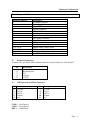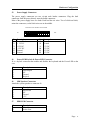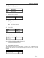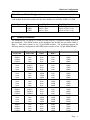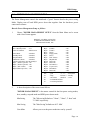
1
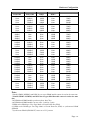
INTEL VX PENTIUM PCI MAINBOARD USER’S MANUAL Version #7502/004/1196 P/N #73-75021040-000 Trademark Acknowledgments Trademark Acknowledgments: • • • • • • IBM PC, PC/XT and PC/AT all are registered trademarks of International Business Machines Corporation. Pentium is a trademark of Intel Corporation. AMD is a registered trademark of Advanced Micro Devices Inc. AWARD is a registered trademark of Award Software Inc. PCI is registered trademark of PCI Special Interest Group. MS-DOS and WINDOWS NT are registered trademarks of Microsoft Corporation. The manufacturer reserves the right to modify any product’s specifications in order to meet advances in hardware and software technology. Table of Content Table of Content 1. INTRODUCTION .............................................................................................................1 1.1 OVERVIEW................................................................................................................1 1.2 GREEN PC POWER MANAGEMENT.......................................................................3 1.3 CHECKLIST ...............................................................................................................5 1.4 PT-7502-2 SYSTEM BOARD SPECIFICATIONS......................................................6 1.5 STATIC ELECTRICITY PRECAUTION....................................................................8 2. HARDWARE CONFIGURATION..................................................................................10 MAINBOARD COMPONENT LOCATIONS .....................................................................10 2.1 JUMPERS & CONNECTORS ...................................................................................13 2.2 EXTERNAL CACHE CONFIGURATION................................................................26 2.3 MEMORY INSTALLATION ....................................................................................27 3 AWARD BIOS SETUP ...................................................................................................33 3.1 STANDARD CMOS SETUP.....................................................................................36 3.2 BIOS FEATURES SETUP .......................................................................................41 3.3 CHIPSET FEATURES SETUP ................................................................................51 3.4 POWER MANAGEMENT SETUP...........................................................................55 3.5 PNP/PCI SLOT CONFIGURATION ........................................................................60 3.6 LOAD SETUP DEFAULTS .....................................................................................63 3.7 INTEGRATED PERIPHERALS SETUP..................................................................65 3.8 USER PASSWORD SETTING.................................................................................65 3.9 IDE HDD AUTO DETECTION ...............................................................................65 3.10 SAVE & EXIT SETUP...........................................................................................25 3.11 EXIT WITHOUT SAVING ....................................................................................25 Statements "This is an ENERGY STARTM compliant product." The Environmental Protection Agency ENERGY STARTM program defines that as an Ally of this program the specified manufacturer must produce systems, or system components which enable a computer system to operate and draw 30 watts or less of power in idle mode. Although the EPA do not endorse any particular product or service, the program is designed to offer a cooperative effort between the EPA and the component manufacturer (Ally) to provide energy saving products and education to customers." "FCC Approval" The PT-7502-2 motherboard has been approved for FCC Class B when properly installed in a barebone configuration using the following case/power supply: Brand Procase Model PC-109 SM Procase PC-609 T/M Procase PC-709 T/M FCC ID JPJPINE429G1 09 JPJPINE429G6 09 JPJPINE429G7 09 FCC Notice: Information to the User This equipment has been tested and found to comply with the limits for a Class B digital device, pursuant to Part 15 of FCC Rules. These limits are designed to provide reasonable protection against harmful interference in a residential installation. This equipment generates, uses and can radiate radio frequency energy and, if not installed and used in accordance with the instructions, may cause harmful interference to radio communications. Should you experience interference to radio or television reception then the user is encouraged to try to correct this interference by one or more of the following measures: Re-locate the receiving antenna. Increase the separation between the equipment and receiver. Connect the equipment into an outlet on a circuit different from that to which the receiver is connected. Consult the dealer or an experienced radio/TV technician for help and for additional suggestions. The user may find the following booklet prepared by the Federal Communications Commission helpful: “How to identify and Resolve Radio-TV Interference Problems.” This booklet is available from the U.S. Government Printing Office, Washington, DC20402, Stock No. 004-00000345-4. FCC Warning The user is cautioned that changes or modifications not expressly approved by the manufacturer could void the user’s authority to operate this equipment. Note : In order for the installation of this product to maintain compliance with the limits for a Class B device, shielded Introduction 1. Introduction 1.1 Overview • The PT-7502-2 motherboard offers 64-bit programming architecture compatible with the software base of 486 and 586 microprocessors. It is a reliable motherboard, using a Intel i430VX chipset and a multi-layer printed circuit board. The chipset consists of a TVX (Host Bridge & Cache Memory Controller), two TDX (Write Buffer Data Path Controller), and 82371SB, PIIX3 (ISA Bridge & System I/O Controller). • The PT-7502-2 is a PCI Local Bus motherboard. The four Master Mode PCI Local Bus slots fully comply with the PCI (Peripheral Component Interconnect) Local Bus Specification Rev. 2.1. The speed of I/O peripherals can be dramatically increased by connecting PCI compatible interface cards to the PCI Local Bus slots on the PT-7502-2. PINE is a member of PCI SIG (Special Interest Group). • The PT-7502-2 is a ‘green’ design motherboard which means if there is no system activity for a specific period of time (this period is software programmable), the PT-7502-2 will slow down its original working frequency to zero. This will help to save power consumption, reduce energy related pollution and protect our environment. • The PT-7502-2 has the full complement of I/O on-board: FDC, PCI local bus Enhanced IDE, printer port, COM ports, and dual USB port as well. 1.2 Green PC Power Management The Green PC mode is a state that minimizes power consumption. There are two different levels of Green PC modes : • Standby mode. The spin motor of the HDD can be turned off. • Inactive mode / Sleep Mode. The PT-7502-2 can stop the CPU clock under this mode. The PT-7502-2 will be placed into Green PC mode as a result of one of the following events : When the SMI header is connected to a momentary switch, pressing the switch will put PT-7502-2 into Green mode. Expiration of the internal Green PC Timer. The Green PC Timer is software programmable which can configure in the "Power Management Setup" option of the BIOS CMOS setup. The power management feature will be enabled as default; however, the timing may differ due to production control. It is recommended that you re-adjust these timings according to your personal requirements/set-up. Through system activity monitoring and management, the PT-7502-2 will not go into Green PC mode if any of the following activity is detected: • • • • • PCI Master 0 activity PCI Master 1 activity PCI Master 2 activity LPT port activity COM port activity • • • • • COM port activity ISA master & DMA activity IDE activity Floppy activity Keyboard activity Page 1 Introduction 1.3 Checklist Please check your PT-7502-2 package to ensure that it contains the following items : • PT-7502-2 Main Board • PT-7502-2 User Manual • Jumper Setting List • Cable Pack included 1 x 40 way flat cables 1 x FDC flat cable 1 x DB9 flat cable and one DB25 flat cable with a bracket (COM 1 & COM 2) 1 x DB25 flat cable with a bracket (Printer port) • Cache Module (either 512KB , 256KB or not bundle) If any of these items are missing or damaged, please contact your local dealer or sales representative for assistance. 1.4 • • • • • • • • • • • • • • • • • PT-7502-2 System Board Specifications Intel i430VX PCIsetTM chipset Support either 75/90/100/120/133/166/180/200 MHz PENTIUMTM CPUs with 321 pin ZIF socket Support Pentium P55C Support Dual Voltage Regulator Module Support Cyrix 6x86, AMD K5 CPUs Uses 72-pin SIMM modules x 4 auto banking in multiple configuration up to 128MB Support Both Fast Page Mode and Extended DATA Output (EDO) DRAM module Support SDRAM/EDO DRAM/Page Mode DRAM use 168-pin DIMMx2 Support cache module socket, cache module options 256KB or 512KB pipeline burst SRAM module 4 PCI Local Bus slots, and 3 x 16 bits ISA Bus slots All 4 PCI slots support Master mode System BIOS support 4 IDE harddisk drivers that don't need device driver for S/W application, the capacity each harddisk can large than 528MB up to 8.4GB PCI Bus master IDE interface on board with two connectors support 4 IDE devices in 2 channel, the PCI IDE Controller supports PIO mode 0 to Mode 4 at maximum transfer rate of 16.67 MB/s and Bus master IDE DMA Mode 2. On board super Multi-I/O chip that support 2 serial port with 16550 Fast UART compatible, 1 parallel port with SPP, EPP and ECP capabilities, and a floppy disk drive interface. Support PS/2TM connector. Support the Universal Serial Bus (U.S.B.) (option) System BIOS supports NCR810 SCSI BIOS firmware and Green feature function, Plug and Play Flash ROM Page 2 Introduction 1.5 Static Electricity Precaution Static electricity can easily damage your PT-7502-2 mainboard. Observing a few basic precautions can help you safeguard against damage that could result in expensive repairs. Follow the measures below to protect your equipment from static discharge: - Keep the mainboard and other system components in their anti-static packaging until you are ready to install them. - Touch a grounded surface before you remove any system component from its protective anti-static packaging. A grounded surface within easy reach is the expansion slot covers at the rear of the system case or any other unpainted portion of the system chassis. - During configuration and installation, touch a grounded surface frequently to discharge any static electric charge that may build up in your body. Another option is to wear a grounding wrist strap. - When handling a mainboard or an adapter card, avoid touching its components. Handle the mainboard and adapter cards either by the edges or by the mounting bracket that attaches to the slot opening in the case. Page 3 Hardware Configuration 2. Hardware Configuration Mainboard Component Locations Page 4 Hardware Configuration 2.1 Jumpers & Connectors Jumpers/Connector J2 J3 J6 J6 J7 J7 J7 J8 JP1 JP4 JP5 JP7A, JP7B JP8A, JP8B JP9A, JP9B JP10 Description Keyboard Connector Power Supply Connector Power-LED Keylock & Connector Speaker Connector HDD LED Connector Reset Switch External Battery Selector PS/2 Mouse Connector Clear CMOS AT Bus Clock Selector FlashRom Voltage Selector DIMM Socket Voltage Select CPU Speed Selectors CPU Internal Clock Speed Selectors P54C/P55C CPU Voltage Selectors J2 Keyboard Connectors A standard five-pin female DIN keyboard connector is located at the rear of the board J2. Pin 1 2 3 4 5 J2 Pin 1 2 3 4 5 Description Keyboard Clock Keyboard Data N.C. Ground +5VDC USB Universal Serial Bus Connector Description +5 VDC DATA DATA + Ground N.C. Pin 7 8 9 10 11 Description +5 VDC DATA DATA + Ground N.C. COM 1 : Serial port #1 COM 2 : Serial port #2 PRN 1 : Parallel port Page 5 Hardware Configuration J3 Power Supply Connectors The power supply connectors are two six-pin male header connectors. Plug the dual connectors from the power directly onto the board connectors. Most of the power supply have two leads. Each lead has six wires. Two of which are black, orient the connectors, so the black wires are in the middle. The black wires should be in the middle P1 Pin 1 2 3 4 5 6 P12 Description Power Good + 5V DC +12V DC - 12V DC Ground Ground Pin 7 8 9 10 11 12 Description Ground Ground - 5V DC +5V DC +5V DC +5V DC J6 Power-LED Keylock & Power-LED Connector J6 is a keylock connector that enables and disables the keyboard and the Power-LED on the case. Pin 1 2 3 4 Description LED Output NC Ground Keylock J6 SPK Speaker Connectors Attach the system speaker to connector J6. Pin 1 2 3 4 J7 Pin 1 2 Description DATA Out NC Ground + 5V HDD LED Connector Description 5V Active Low Page 6 Hardware Configuration J7 Reset Switch Connector Attach the Reset switch cable to this connector. Setting Open Short J7 Description Normal Mode Reset System External Battery Selectors Description Normal Mode (default) J8 J7 Open PS/2 Mouse Connector 2 x 4 pin header PS1 : PS/2 Mouse Connector JP1 Clear CMOS Setting Open Short JP4 Description Default Clear CMOS AT Bus Clock Selector Description PCI Clock/4 PCI Clock/3 JP4 (default) 1-2 2-3 Note: CPU Speed=60MHz or 66MHz JP4 set to 1-2 CPU Speed=50MHz JP4 set to 2-3 JP5 Flash ROM Voltage Selector The mainboard can uses two types of Flash ROM - 5 volt and 12 volt. Set the mainboard for either type with jumper JP5. You can update both types with new BIOS files as they come available. Description 12 volt Flash ROM 5 volt Flash ROM JP5 1-2 2-3 Page 7 Hardware Configuration JP7A, JP7B DIMM Socket Voltage Selectors Voltage Selectors 3.3V 5.0V Note: All synchronous DRAM JP7 must be set to 3.3V position. JP8A, JP8B CPU Speed Selectors The mainboard has a clock generator that lets you choose the CPU frequency by settings jumpers JP8A, JP8B. You can set the CPU speed to 50/60MHz or 66MHz as shown below. Jumpers JP8A JP8B CPU Speed 60MHz Open Shut 66MHz Shut Open 55MHz Open Open 50MHz Shut Shut Note : Default set at 66Mhz JP9A, JP9B CPU Internal Clock Speed Selectors Intel x2.0 x1.5 x2.5 x3.0 (default) Cyrix x2.0 Reserved Reserved Reserved AMD Reserved x1.5 Reserved Reserved JP9A Shut Open Shut Open JP9B Open Open Shut Shut Note: CPU Internal Clock Speed = External Input Clock x (table list) factor. JP10 P54C/P55C CPU Voltage Selectors JP10 3.5V 2.9V 2.8V ON A B C A B C D E A B C D E A B C D E 2.7V 3.3V D E A B C D E A B C D E (default) Note : JP10 all OFF : 2.5V Page 8 Hardware Configuration 2.2 External Cache Configuration This mainboard supports a cache module socket you can install pipeline burst SRAM on a cache module in the cache module slot, the cache module size can either 256KB or 512KB. Cache Type Pipeline Burst 2.3 Size 256KB 512KB 512KB Data Chip Size 32k 32 x 2pcs 32k 32 x 4pcs 64k 32 x 2pcs Tag Chip Size 8k 8, 16k 8 or 32k 8 x 1pc 16k 8 or 32k 8 x 1pc 16k 8 or 32k 8 x 1pc Memory Installation The mainboard lets you add up to 128MB of system memory via SIMM & DIMM sockets on the mainboard. Four SIMM sockets on the mainboard are divided into two banks: Bank 0, Bank 1. Each bank consists of two 72-pin SIMM modules. The mainboard supports the following memory configurations and DIMM socket consists of one 168-pin DIMM Module. SIMM Socket 1&2 4MBx2 8MBx2 16MBx2 32MBx2 None None None None None None None None None None None None 4MBx2 8MBx2 16MBx2 32MBx2 None None None None 4MBx2 8MBx2 16MBx2 32MBx2 SIMM Socket 3&4 None None None None 4MBx2 8MBx2 16MBx2 32MBx2 None None None None None None None None 4MBx2 8MBx2 16MBx2 32MBx2 None None None None None None None None DIMM DIM 1 None None None None None None None None 8MB 16MB 32MB 64MB None None None None None None None None 8MB 16MB 32MB 64MB None None None None DIMM DIM 2 None None None None None None None None None None None None 8MB 16MB 32MB 64MB None None None None 8MB 16MB 32MB 64MB 8MB 16MB 32MB 64MB Total Memory 8MB 16MB 32MB 64MB 8MB 16MB 32MB 64MB 8MB 16MB 32MB 64MB 8MB 16MB 32MB 64MB 16MB 32MB 64MB 128MB 16MB 32MB 64MB 128MB 16MB 32MB 64MB 128MB Page 9 Hardware Configuration SIMM Socket 1&2 None None None None None None None None 8MBx2 8MBx2 8MBx2 8MBx2 16MBx2 16MBx2 16MBx2 16MBx2 None None None None 16MBx2 16MBx2 16MBx2 16MBx2 32MBx2 32MBx2 32MBx2 32MBx2 32MBx2 32MBx2 32MBx2 32MBx2 None None None None SIMM Socket 3&4 4MBx2 8MBx2 16MBx2 32MBx2 8MBx2 8MBx2 8MBx2 8MBx2 None None None None 4MBx2 8MBx2 16MBx2 32MBx2 16MBx2 16MBx2 16MBx2 16MBx2 None None None None 4MBx2 8MBx2 16MBx2 32MBx2 None None None None 32MBx2 32MBx2 32MBx2 32MBx2 DIMM DIM 1 8MB 16MB 32MB 64MB 8MB 16MB 32MB 64MB None None None None None None None None 8MB 16MB 32MB 64MB None None None None None None None None None None None None 8MB 16MB 32MB 64MB DIMM DIM 2 None None None None None None None None 8MB 16MB 32MB 64MB None None None None None None None None 8MB 16MB 32MB 64MB None None None None 8MB 16MB 32MB 64MB None None None None Total Memory 16MB 32MB 64MB 128MB 24MB 32MB 48MB 80MB 24MB 32MB 48MB 80MB 40MB 48MB 64MB 96MB 40MB 48MB 64MB 96MB 40MB 48MB 64MB 96MB 72MB 80MB 96MB 128MB 72MB 80MB 96MB 128MB 72MB 80MB 96MB 128MB Note: 1. Bank0 (SIMM1 &SIMM2) and DIM1 the two types DRAM module cannot be used at the same time. 2. Bank0 (SIMM3 & SIMM4) and DIM2 the two types DRAM module cannot be used at the same time. 3.All SIMMs and DIMM module speed must faster than 70ns. 4.All SIMMs and DIMM module can use either 1-sided or 2-sides 5.SIMM socket DRAM type: Fast Page Mode or Extend DATA Out (EDO) 6. DIMM socket DRAM type Fast Page Mode or Extend Data Out (EDO) or synchronous DRAM (SDRAM) 7. Synchronous DRAM (SDRAM JP7) must set to 3.3V position Page 10 BIOS Setup 3 . Award BIOS Setup Enter the Award Setup program's Main Menu as follows: 1. Turn on or reboot the system. The following message appears at the bottom of the screen: "Press <DEL> to enter setup, ESC to skip memory test" 2. Press the <DEL> key to enter the Award BIOS setup program and the following screen appears: ROM PCI / ISA BIOS (2A59GF51) CMOS SETUP UTILITY AWARD SOFTWARE, INC. STANDARD CMOS SETUP INTEGRATED PERIPHERALS BIOS FEATURES SETUP PASSWORD SETTING CHIPSET FEATURES SETUP IDE HDD AUTO DETECTION POWER MANAGEMENT SETUP SAVE & EXIT SETUP PNP/PCI CONFIGURATION EXIT WITHOUT SAVING LOAD SETUP DEFAULTS Esc F10 ↑↓ → ← : Select Item (Shift) F2 : Change Color : Quit : Save & Exit Setup Abandon all dates & Exit SETUP 3. Choose an option and press <ENTER>. Modify the system parameters to reflect the options installed in the system. (See the following sections for more information.) 4. Press <ESC> at anytime to return to the Main Menu. 5. In the Main Menu, choose "SAVE AND EXIT SETUP" or <F10> to save your changes and reboot the system. Choosing "EXIT WITHOUT SAVING" or <ESC> ignores your changes and exits the program. Page 11 BIOS Setup 3.1 STANDARD CMOS SETUP Run the Standard CMOS Setup as follows: 1. Choose "STANDARD CMOS SETUP" from the Main Menu and a screen with a list of items appears. ROM PCI/ISA BIOS (2A59GF51) CMOS SETUP UTILITY AWARD SOFTWARE, INC. Date (mm:dd:yy) : Thu, May 6 1996 Time (hh:mm:ss) : 17 : 54 : 42 HARD DISKS TYPE SIZE Primary Master : AUTO 0 Primary Slave : NONE 0 Secondary Master : NONE 0 Secondary Slave : NONE 0 CYLS 0 0 0 0 HEAD 0 0 0 0 PRECOMP LANDZ SECTOR MODE 0 0 AUTO 0 0 0 --------0 0 0 --------0 0 0 --------- Drive A : 1.44M, 3.5 in. Drive B : None Video : EGA/VGA Halt On : All Errors Esc F1 2. : Quit : Help ↑↓ → ← : Select Item (Shift) F2 : Change Color Base Memory : Extended Memory : Other Memory : 640K 15360K 384K Total Memory : 16384K PU/PD/+/- : Modify Use the arrow keys to move between items and to select values. Modify the selected fields using PgUp/PgDn/+/-keys. Some fields let you enter numeric values directly. Data (mm/dd/yy) Type the current date Time (hh:mm:ss) Type the current time Primary master and slave Secondary master and slave Choose from the standard hard disk types 1 to 46, or "User" defined. IF you choose "User", run the IDE HDD Auto detection function from the Main Menu, or enter the HDD information directly from the keyboard and press <Enter>. If you use Auto mode the BIOS can Auto detect HDD type and do not enter any HDD information from the keyboard. Drive A & B Choose 360KB 5 1/4" 1.2MB 5 1/4" 720MB 3 1/2" 1.44MB 3 1/2" Not installed Page 12 BIOS Setup Video Choose Monochrome, Color 40x25 VGA/PGA/EGA, Color 80x25, or Not installed Halt On Choose All Errors (Default) No Errors All, But Keyboard All, But Diskette All, But Disk/Key 3. After you have finished with the Standard CMOS Setup program, press the <ESC> key to return to the Main Menu. Page 13 BIOS Setup 3 .2 BIOS FEATURES SETUP Run the BIOS Features Setup as follows. 1. Choose "BIOS FEATURES SETUP" from the Main Menu and a screen with a list of items appears. ROM PCI / ISA BIOS (2A59GF51) BIOS FEATURES SETUP AWARD SOFTWARE, INC. Virus Warning Internal cache External Cache Quick Power On Self Test Boot Sequence Swap Floppy Drive Boot Up Floppy Seek Boot Up NumLock Status Boot Up System Speed Gate A20 Option Typematic Rate Setting Typematic Delay (Chars/sec) Typematic Delay (Msec) Security Option Assign IRQ VGA : : : : : : : : : : : : : : : Disabled Enabled Enabled Enabled C,A Disabled Disabled On High Fast Disabled 6 250 Setup Disabled Video BIOS shadow C8000-CBFFF Shadow CC000-CFFFF Shadow D0000-D3FFF Shadow D4000-D7FFF Shadow D8000-DBFFF Shadow DC000-DFFFF Shadow : : : : : : : Enabled Disabled Disabled Disabled Disabled Disabled Disabled Esc: Quit ↑↓ → ← : Select Item F1: Help PU/PD/+/- : Modify F5: Old Value (Shift) F2 : Color F6: Load BIOS Defaults F7: Load Setup Defaults 2 Use the arrow keys to move between items and to select values. Modify the selected fields using the PgUp/PgDn/+/-Keys. An explanation of <F> keys follows: <F1>: "Help" gives options available for each item. <F2>: Change color <F5>: Get the old values. The user started the current session with these values. <F6>: Load all options in the BIOS Features Setup with the BIOS Default values. <F7>: Load all options in the BIOS Features Setup with the Setup Default values. Page 14 BIOS Setup A short description of the screen items follows: Virus Warning Choose Enabled or Disabled. Enable this option and a SYSTEM WARNING MESSAGE appears when the system detects a virus. CPU Internal Cache Choose Enabled or Disabled. This option lets you enable the CPU's internal cache memory. External Cache Choose Enabled or Disabled. This option lets you enable the external cache memory. For better performance, make sure you always choose "Enabled." Quick Power On Self Test Choose Enabled or Disabled. Enabled provides a fast POST and boot-up speed. Boot Sequence The default setting first to boot from drive C: You can reverse this sequence with "A:C:", will then drive A: boot directly. Swap Floppy Driver Choose Enabled or Disabled. When Enabled Floppy drives A & B are swapped under DOS. Boot Up Floppy Seek Choose Enabled or Disabled. "Disabled" provides a fast boot and reduces the possibility of damage to the heads. Boot Up Num Lock Status Choose On or Off. On puts numeric keypad in Num Lock mode at boot-up. Off puts this keypad in arrow key mode at boot-up. Boot Up System Speed Choose High or Low. This option lets you choose system bootup speed. The default is High. Gate A20 Option Choose Fast or Normal. This item lets you use the GA20 from the chipset or the keyboard controller. Typematic Rate Setting Choose Enabled or Disabled. Enable this option to adjust the keystroke repeat rate. Typematic Rate (chars/Sec) Choose the rate a character keeps repeating. Typematic Delay (Msec) Choose how long after you press a key that a character begins repeating. Page 15 BIOS Setup Security Option Choose Setup, or System. Use this feature to prevent unauthorized system boot-up or unauthorized use of BIOS Setup. "System" - Each time the system boots the password prompt appears. "Setup" - Password prompt only appears if you attempt to enter the Setup program. Assign IRQ for VGA Choose Enable or Disable, when Enable, assign IRQ for VGA Video BIOS Shadow VIDEO shadow copies BIOS code from slower ROM to faster RAM. BIOS can then execute from RAM. 3. After you have finished with the BIOS Features Setup program, press the <ESC> key and then follow screen instructions to save or disregard your settings. Page 16 BIOS Setup 3.3 CHIPSET FEATURES SETUP The "CHIPSET FEATURES SETUP" is used to control the values of the chipset registers. These registers control most of the system options in the computer. Run the Chipset Features Setup as follows: 1. Choose "CHIPSET FEATURES SETUP" from the Main Menu and a screen with a list of items appears. ROM PCI / ISA BIOS (2A59GF51) CHIPSET FEATURES SETUP AWARD SOFTWARE, INC. DRAM RAS# Precharge Time DRAM R/W Leadoff Timing Fast RAS To CAS Delay DRAM Rasd Burst (EDO/FP) DRAM Write Burst Timing Fast MA to RAS# Delay CLK Fast EDO Path Select Refresh RAS# Assertion ISA Bus Clock SDRAM (CAS Lat/RAS-to-CAS) System BIOS Cacheable Video BIOS Cacheable 8 Bit I/O Recovery Time 16 Bit I/O Recovery Time Peer Concurrence Chipset NA# Asserted 2. :4 :7 :3 : x222/x333 : x333 :2 : Enabled : 5 Clks : PCICLK/4 : 3/3 : Diabled : Disabled :2 :1 : Enabled : Enabled Esc F1 F5 F6 F7 : : : : : Quit ↑↓ → ← : Select Item Help PU/PD/+/- : Modify Old Value (Shift) F2 : Color Load BIOS Defaults Load Setup Defaults The first ten items are optimal setting for this mainboard, you should not change them unless you are familiar with the Intel chipset. Page 17 BIOS Setup 3.4 POWER MANAGEMENT SETUP The Power Management controls the mainboard a "green" features that for the power saving Mode, Display turn off and HDD power down that together form the hardware power conservation scheme. Run the Power Management Setup as follows: 1. Choose "POWER MANAGEMENT SETUP" from the Main Menu and a screen with a list of items appears. ROM PCI / ISA BIOS (2A59GF51) POWER MANAGEMENT SETUP AWARD SOFTWARE, INC. Power Management PM Control By APM Video Off Method : Disable : Yes : Blank screen Doze Mode : Disabled Standby Mode : Disabled Suspend Mode : Disabled HDD Power Down : Disabled **Wake UpEvents in doze & Standby** IRQ3 (Wake-Up Event): ON IRQ4 (Wake-Up Event): ON IRQ8 (RTC Alarm) : OFF IRQ12(Wake-Up Event) : ON **Power down & Resume Events** IRQ3 (COM2) : IRQ4 (COM1) : IRQ5 (LPT2) : IRQ6 (Floppy Disk) : IRQ7 (LPT1) : IRQ8 (RTC Alarm) : IRQ9 (IRQ2 Redir) : IRQ10 (Reserved) : IRQ11 (Reserved) : IRQ12 (PS/2 Mouse) : IRQ13 (Coprocessor) : IRQ14 (Hard Disk) : IRQ15 (Reserved) : ESC F1 F5 F6 F7 2. : : : : : ON ON ON ON ON OFF OFF OFF OFF OFF OFF ON OFF Quit ↑↓ → ← : Select Item Help PU/PD/+/- : Modify Old Values (Shift) F2 : Color Load BIOS Defaults Load Setup Defaults A short description of the screen items follows: "POWER MANAGEMENT" is the master control for the four power saving modes, doze, standby, suspend mode and HDD power down mode.. Min Saving The "Min saving"defaults as "1 hour", "1 hour", "1 hour" and "15 Min" respectively. Max Saving The "Max Saving" defaults are all "1 Min" User define Allows you to set the power mode time-out by yourself Page 18 BIOS Setup Disable Turn off all power saving time-outs. Doze mode Put the system performance down to 20% Stand by mode Turn off the video signal and cause CPU enter SMM mode Suspend mode Turn off the video signal and cause CPU enter SMM mode and shut down any IDE hard disk drivers connected to the system. HDD Power down Shut down any IDE hard disk drivers in the system if they are not accessed. Note: HDD Power down does not effect SCSI hard disks. Individual IRQ wake-up Event The setting in this group determine if a system IRQ is monitored for activity so as to wake up the system if an interrupt request is generated by a device using, if an IRQ is not use, there is no effect. Page 19 BIOS Setup 3.5 PNP/PCI SLOT CONFIGURATION The "PNP/PCI SLOT CONFIGURATION" sets the system for use with PCI bus cards. Run the PNP/PCI Slot Configuration program as follows. 1. Choose "PCI SLOT CONFIGURATION" from the Main Menu and a screen with a list of items appears. ROM PCI / ISA BIOS (2A59GF51) PCI CONFIGURATION SETUP AWARD SOFTWARE, INC. Resources Controlled by : Auto Reset Configuration Data : Disable PCI IRQ Actived By PCI IDE IRQ Map To ESC F1 F5 F6 F7 2. 4. : : : : : : Level : ISA Quit ↑↓ → ← : Select Item Help PU/PD/+/: Modify Old Values (Shift) F2 : Color Load BIOS Defaults Load Setup Defaults Use the arrow keys to move between items and to select values. Modify the selected fields using the PgUp/PgDn/+/-keys. <F> keys are explained below: <F1>: "Help" gives options available for each item. <F2>: Change color <F5>: Get the old values. The user started the current session with these values. <F6>: Load all options in the BIOS Features Setup with the BIOS Default values. <F7>: Load all options in the BIOS Features Setup with the Setup Default values. After you have finished with the PCI Slot Configuration program, press the <ESC> key and then follow screen instructions to save or disregard your settings. Page 20 BIOS Setup 3.6 LOAD SETUP DEFAULTS This Main Menu item loads the default system values. These settings are recommended for optimum performance. If the CMOS is corrupted when enter BIOS setup utility you must load setup default again. Choose this item and the following message appears: "Load "SETUP Defaults (Y/N)? N" To use the Setup defaults, change the prompt to "Y" and press <ENTER>. Page 21 BIOS Setup 3.7 INTEGRATED PERIPHERALS SETUP The "INTEGRATED PERIPHERALS" is used to control the values of the I/O chipset registers. These registers control the mode of HDD type and I/O address port. Run the Integrated Peripherals as follows: 1. Choose "INTEGRATED PERIPHERALS" from the Main Menu and a screen with a list of items appears. ROM PCI / ISA BIOS (2A59GF51) PCI/GREEN FUNCTION SETUP AWARD SOFTWARE, INC. IDE HDD Block Mode IDE Primary Master PIO IDE Primary Slave PIO IDE Secondary Master PIO IDE Secondary Slave PIO On-Chip Primary PCI IDE On-Chip Secondary PCI IDE PCI Slot IDE 2nd Channel USB Controller Onboard FDD Controller Onboard Serial Port 1 Onboard Serial Port 2 Onboard Parallel Port Onboard Parallel Mode ECP Mode Use DMA : Enabled : AUTO : AUTO : AUTO : AUTO : Enabled : Enabled : Enabled : Disabled : Enabled : AUTO : AUTO : 378H/IRQ7 : ECP/EPP :3 ESC F1 F5 F6 F7 : : : : : Quit ↑↓ → ← : Select Item Help PU/PD/+/: Modify Old Values (Shift) F2 : Color Load BIOS Defaults Load Setup Defaults IDE Hard Disk Drive Mode Setting The BIOS support two kind of methods to set up your IDE Hard Disk Drive Mode. One is auto, the other is manual mode. In auto mode BIOS can auto detect HDD's mode, but in some old type HDD that can't meet ATA specification, the BIOS will detect wrong Mode and cause system boot fail. You must change auto mode to manual mode and try a proper mode that can meet your HDD specification. There are five modes defined in manual mode. They are mode 0,1,2,3,4. The default setting for on board timing is auto mode that it will provide optimum performance for your HDD. Page 22 BIOS Setup IDE HDD Block Mode Choose Enabled or Disabled. If your IDE HDD supports BLOCK MODE, then you can enable this function to speed up the HDD Access time. If not, please disable this function to avoid an HDD Access Error. Onboard PCI IDE Controller The on Chip PCI IDE controller is default "Enable" setting, if you disable On-Chip primary and secondary PCI IDE, it will disable the on board IDE controller. Make sure you do this if you want to use an IDE controller other than on the mainboard IDE controller. Onboard FDD Controller The default setting for the "Onboard FDC Controller" is "Enabled". This setting allows you to connect your floppy disk drives to the onboard "Floppy" connector. Choose the "Disabled" setting if you want to use a separate controller card. Serial Port The "Onboard Serial Port 1" and "Onboard serial Port 2" lines control the assignments for the mainboard's two onboard serial connectors. They can be assigned as COM1, COM2, COM3, COM4 for serial Port 1 and serial Port 2, or disable. Parallel Port The options for "Onboard Parallel Port" is 378H. This item controls the on-board parallel port connector, if you are using an I/O card with a parallel port, make sure the address don't conflict. Parallel Port Mode The options for "Onboard LPT Port Mode" is default ECP/EPP mode, you can select EPP, ECP, and SPP Mode just change setting, if you have a parallel interface peripheral device, use one of the parallel port enhancements and set this line for the enhanced mode that your peripheral supports. ECP Mode Use DMA The option for "ECP Mode use DMA" is default DMA3 if your system has ECP peripheral device, when you are using some I/O card, make sure the DMA channel don't conflict. When you have done with this section, press the <ESC> key to go back to the main screen. Page 23 BIOS Setup 3.8 USER PASSWORD SETTING This Main Menu item lets you configure the system so that a password is required every time the system boots or an attempt is made to enter the Setup program. The password cannot be longer than 8 characters. ROM PCI / ISA BIOS (2A59GF51) CMOS SETUP UTILITY AWARD SOFTWARE, INC. STANDARD CMOS SETUP PASSWORD SETTING BIOS FEATURES SETUP IDE HDD AUTO DETECTION CHIPSET FEATURES SETUP SAVE & EXIT SETUP POWER MANAGEMENT SETUP PCI CONFIGURATION Enter Password: SAVE & E EXIT WITHOUT SAVING LOAD SETUP DEFAULTS Esc F10 ↑↓ → ← : Select Item (Shift) F2 : Change Color : Quit : Save & Exit Setup Change/Set/Disable Password Important: Keep a safe record of the new password. If you forget or lose the password, the only way to access the system is to discharge CMOS memory using jumper J7. Page 24 BIOS Setup 3.9 IDE HDD AUTO DETECTION 1. If your system has an IDE hard drive, you can use this utility to detect its parameters and automatically enter them into the Standard CMOS Setup. ROM PCI / ISA BIOS (2A59GF51) IDE HDD AUTO DETECTION AWARD SOFTWARE, INC. HARD DISKS TYPE SIZE Primary Master: CYLS HEAD PRECOMP LANDZ SECTOR MODE Select Primary Master Option (N=Skip):N OPTIONS 2(Y) 1 2 SIZE 21 722 721 CYLS 699 1399 699 HEAD 32 16 32 PRECOMP 0 65535 65535 LANDZ SECTOR 1398 63 1398 63 1398 63 MODE LBA NORMAL LARGE ESC : SKIP For IDE hard disk driver, the BIOS provide three modes to support both normal IDE hard disk and also drivers large than 528MB, a short description of three modes as follows: a. Normal mode: b. Large mode: c. LBA mode: 3. For drivers small than 528MB For drivers larger than 528MB that do not use LBA. There can only be used with MS-Dos operating system. For drivers larger than 528MB and upto 8.4GB that use logic block addressing mode. Normally we recommend to select LBA Mode if your HDD drivers large than 528MB. This utility will autodetect as many as four IDE drivers. 3.10 SAVE & EXIT SETUP Select this item from the main menu and type "Y" to save the values entered during the current session and then exit the BIOS Setup program. Type "N" to return to the Setup program. 3.11 EXIT WITHOUT SAVING Select this item from the main menu and type "Y" to exit the BIOS Setup program without saving the values entered during the current session. Type "N" to return to the Setup program. Page 25