1
NetFi
Final Design Report
Prepared By:
Mike Ajax, Alex Izzo, Mike Grant and Adam Chaulklin
Presented To:
Dr. Stephen Williams
EECS Department
Milwaukee School of Engineering
Report Submitted: 16 December 2011
Abstract
NetFi is a project that allows for real-time uncompressed CD-quality audio across a network. The project
is designed to be easy for customers to install and use while also being environmentally friendly. The main
goal of the project is to provide audio to receivers wirelessly over a network. The receivers will maintain
a wired connection with any speakers or other audio-output devices as desired by the user. This solution
allows for audio to be played from many locations within range of the network to the stationary receivers
within the range of the network.
At this stage in the project, microcontroller throughput and SPI capabilities have been verified. Some communication over a network using the User Datagram Protocol (UDP) has also been accomplished. The three
main subsystems of the project have also been designed.
The first subsystem is the Personal Computer (PC) software. First of all, the PC aspect of the design involves capturing any and all audio that is being played on the computer. This audio is then to be formed
into UDP packets and sent over the network. The next subsystem is the embedded software, which will run
on the microcontroller. This subsystem was designed to receive UDP packets from the network, check for
dropped packets, and maintain synchronization between the PC and microcontroller. The embedded software also was designed to transmit audio data to the third subsystem, the hardware aspect of the project.
The hardware subsystem performs all necessary operations on the audio data in order to make the data
compatible with a standard RCA line level output.
With all audio data properly transmitted, received, and processed, users should be able to listen to real-time
uncompressed CD-quality audio without having to maintain a wired connection from their PC to speakers
or other audio-output devices.
Contents
1
2
Description of Problem
9
1.1
Problem Statement . . . . . . . . . . . . . . . . . . . . . . . . . . . . . . . . . . . . . . . . . . .
9
1.2
Solution Requirements . . . . . . . . . . . . . . . . . . . . . . . . . . . . . . . . . . . . . . . . .
9
1.3
Stakeholders and Needs . . . . . . . . . . . . . . . . . . . . . . . . . . . . . . . . . . . . . . . .
9
1.4
Competing Solutions . . . . . . . . . . . . . . . . . . . . . . . . . . . . . . . . . . . . . . . . . .
10
1.4.1
Overview . . . . . . . . . . . . . . . . . . . . . . . . . . . . . . . . . . . . . . . . . . . .
10
1.4.2
Costs . . . . . . . . . . . . . . . . . . . . . . . . . . . . . . . . . . . . . . . . . . . . . . .
11
1.4.3
Apple AirPlay . . . . . . . . . . . . . . . . . . . . . . . . . . . . . . . . . . . . . . . . . .
11
Description of Solution Approach
12
2.1
Solution Description . . . . . . . . . . . . . . . . . . . . . . . . . . . . . . . . . . . . . . . . . .
12
2.2
Detailed Block Diagram & Details . . . . . . . . . . . . . . . . . . . . . . . . . . . . . . . . . .
13
2.2.1
Live PC Audio . . . . . . . . . . . . . . . . . . . . . . . . . . . . . . . . . . . . . . . . .
13
2.2.2
UDP Server . . . . . . . . . . . . . . . . . . . . . . . . . . . . . . . . . . . . . . . . . . .
13
2.2.3
Switch/Router . . . . . . . . . . . . . . . . . . . . . . . . . . . . . . . . . . . . . . . . .
13
2.2.4
Physical Network Interface Hardware . . . . . . . . . . . . . . . . . . . . . . . . . . . .
13
2.2.5
Microchip TCP/IP Stack . . . . . . . . . . . . . . . . . . . . . . . . . . . . . . . . . . . .
14
2.2.6
Manage Asynchronous Clocks, Handle Dropped Packets . . . . . . . . . . . . . . . . .
14
2.2.7
44.1kHz Interrupt . . . . . . . . . . . . . . . . . . . . . . . . . . . . . . . . . . . . . . . .
14
2.2.8
Digital-to-Analog Converter . . . . . . . . . . . . . . . . . . . . . . . . . . . . . . . . .
14
2.2.9
Analog Filter/Output Buffer Amplifier . . . . . . . . . . . . . . . . . . . . . . . . . . .
14
1
3
2.2.10 Power Supply . . . . . . . . . . . . . . . . . . . . . . . . . . . . . . . . . . . . . . . . . .
14
2.3
Specifications . . . . . . . . . . . . . . . . . . . . . . . . . . . . . . . . . . . . . . . . . . . . . .
15
2.4
Applicable Standards . . . . . . . . . . . . . . . . . . . . . . . . . . . . . . . . . . . . . . . . . .
16
2.5
Safety and Environment Considerations . . . . . . . . . . . . . . . . . . . . . . . . . . . . . . .
17
PC Software Design
19
3.1
Introduction . . . . . . . . . . . . . . . . . . . . . . . . . . . . . . . . . . . . . . . . . . . . . . .
19
3.1.1
Overview . . . . . . . . . . . . . . . . . . . . . . . . . . . . . . . . . . . . . . . . . . . .
19
3.1.2
Subsystem Requirements . . . . . . . . . . . . . . . . . . . . . . . . . . . . . . . . . . .
19
Research . . . . . . . . . . . . . . . . . . . . . . . . . . . . . . . . . . . . . . . . . . . . . . . . .
20
3.2.1
Background Research . . . . . . . . . . . . . . . . . . . . . . . . . . . . . . . . . . . . .
20
3.2.2
Design Considerations Research . . . . . . . . . . . . . . . . . . . . . . . . . . . . . . .
22
Design . . . . . . . . . . . . . . . . . . . . . . . . . . . . . . . . . . . . . . . . . . . . . . . . . .
24
3.3.1
Design Consideration Analysis . . . . . . . . . . . . . . . . . . . . . . . . . . . . . . . .
24
3.3.2
Design Requirements . . . . . . . . . . . . . . . . . . . . . . . . . . . . . . . . . . . . .
24
3.3.3
Design Description . . . . . . . . . . . . . . . . . . . . . . . . . . . . . . . . . . . . . . .
24
3.2
3.3
4
Embedded Software Design I
28
4.1
Introduction . . . . . . . . . . . . . . . . . . . . . . . . . . . . . . . . . . . . . . . . . . . . . . .
28
4.1.1
Overview . . . . . . . . . . . . . . . . . . . . . . . . . . . . . . . . . . . . . . . . . . . .
28
4.1.2
Subsystem Requirements . . . . . . . . . . . . . . . . . . . . . . . . . . . . . . . . . . .
28
Research . . . . . . . . . . . . . . . . . . . . . . . . . . . . . . . . . . . . . . . . . . . . . . . . .
29
4.2.1
Background Research . . . . . . . . . . . . . . . . . . . . . . . . . . . . . . . . . . . . .
29
4.2.2
Design Considerations Research . . . . . . . . . . . . . . . . . . . . . . . . . . . . . . .
30
Design . . . . . . . . . . . . . . . . . . . . . . . . . . . . . . . . . . . . . . . . . . . . . . . . . .
30
4.3.1
Design Requirements . . . . . . . . . . . . . . . . . . . . . . . . . . . . . . . . . . . . .
30
4.3.2
Design Description . . . . . . . . . . . . . . . . . . . . . . . . . . . . . . . . . . . . . . .
30
4.2
4.3
5
Embedded Software Design II
36
5.1
36
Introduction . . . . . . . . . . . . . . . . . . . . . . . . . . . . . . . . . . . . . . . . . . . . . . .
2
5.2
5.3
6
Overview . . . . . . . . . . . . . . . . . . . . . . . . . . . . . . . . . . . . . . . . . . . .
36
5.1.2
Subsystem Requirements . . . . . . . . . . . . . . . . . . . . . . . . . . . . . . . . . . .
37
Research . . . . . . . . . . . . . . . . . . . . . . . . . . . . . . . . . . . . . . . . . . . . . . . . .
38
5.2.1
Background Research . . . . . . . . . . . . . . . . . . . . . . . . . . . . . . . . . . . . .
38
5.2.2
Design Considerations Research . . . . . . . . . . . . . . . . . . . . . . . . . . . . . . .
42
Design . . . . . . . . . . . . . . . . . . . . . . . . . . . . . . . . . . . . . . . . . . . . . . . . . .
44
5.3.1
Design Consideration Analysis . . . . . . . . . . . . . . . . . . . . . . . . . . . . . . . .
44
5.3.2
Design Requirements . . . . . . . . . . . . . . . . . . . . . . . . . . . . . . . . . . . . .
44
5.3.3
Design Description . . . . . . . . . . . . . . . . . . . . . . . . . . . . . . . . . . . . . . .
45
Hardware Design
56
6.1
Introduction . . . . . . . . . . . . . . . . . . . . . . . . . . . . . . . . . . . . . . . . . . . . . . .
56
6.1.1
Overview . . . . . . . . . . . . . . . . . . . . . . . . . . . . . . . . . . . . . . . . . . . .
56
6.1.2
Subsystem Requirements . . . . . . . . . . . . . . . . . . . . . . . . . . . . . . . . . . .
56
Research . . . . . . . . . . . . . . . . . . . . . . . . . . . . . . . . . . . . . . . . . . . . . . . . .
57
6.2.1
Power Supply . . . . . . . . . . . . . . . . . . . . . . . . . . . . . . . . . . . . . . . . . .
57
6.2.2
Network Interface . . . . . . . . . . . . . . . . . . . . . . . . . . . . . . . . . . . . . . .
61
6.2.3
DAC/Analog Output Stages . . . . . . . . . . . . . . . . . . . . . . . . . . . . . . . . .
64
Design . . . . . . . . . . . . . . . . . . . . . . . . . . . . . . . . . . . . . . . . . . . . . . . . . .
71
6.3.1
Power Supply . . . . . . . . . . . . . . . . . . . . . . . . . . . . . . . . . . . . . . . . . .
71
6.3.2
Network Interface . . . . . . . . . . . . . . . . . . . . . . . . . . . . . . . . . . . . . . .
75
6.3.3
DAC/Analog Output Stages . . . . . . . . . . . . . . . . . . . . . . . . . . . . . . . . .
76
6.2
6.3
7
5.1.1
Subsystem Test
80
7.1
Subsystem Test Objectives . . . . . . . . . . . . . . . . . . . . . . . . . . . . . . . . . . . . . . .
80
7.2
Subsystem Specifications . . . . . . . . . . . . . . . . . . . . . . . . . . . . . . . . . . . . . . . .
80
7.3
Subsystem Test Plan . . . . . . . . . . . . . . . . . . . . . . . . . . . . . . . . . . . . . . . . . .
81
7.3.1
Required Equipment . . . . . . . . . . . . . . . . . . . . . . . . . . . . . . . . . . . . . .
81
7.3.2
Subsystem Test Plan Details . . . . . . . . . . . . . . . . . . . . . . . . . . . . . . . . . .
81
3
7.4
7.5
8
7.3.3
Test Implementation/Preparation Checklist . . . . . . . . . . . . . . . . . . . . . . . .
83
7.3.4
Test Procedure . . . . . . . . . . . . . . . . . . . . . . . . . . . . . . . . . . . . . . . . .
85
7.3.5
Test Plan Diagram . . . . . . . . . . . . . . . . . . . . . . . . . . . . . . . . . . . . . . .
86
7.3.6
Expected Results . . . . . . . . . . . . . . . . . . . . . . . . . . . . . . . . . . . . . . . .
86
7.3.7
Tools and Techniques for Analyzing Data . . . . . . . . . . . . . . . . . . . . . . . . . .
87
7.3.8
Statistical Methodology . . . . . . . . . . . . . . . . . . . . . . . . . . . . . . . . . . . .
87
Subsystem Test Results . . . . . . . . . . . . . . . . . . . . . . . . . . . . . . . . . . . . . . . . .
88
7.4.1
Raw Data . . . . . . . . . . . . . . . . . . . . . . . . . . . . . . . . . . . . . . . . . . . .
88
7.4.2
Calculated Data . . . . . . . . . . . . . . . . . . . . . . . . . . . . . . . . . . . . . . . . .
92
7.4.3
Improvements To Analysis Plan . . . . . . . . . . . . . . . . . . . . . . . . . . . . . . .
94
7.4.4
Analysis of Results . . . . . . . . . . . . . . . . . . . . . . . . . . . . . . . . . . . . . . .
94
Conclusion . . . . . . . . . . . . . . . . . . . . . . . . . . . . . . . . . . . . . . . . . . . . . . . .
98
Summary
99
8.1
Next Tasks . . . . . . . . . . . . . . . . . . . . . . . . . . . . . . . . . . . . . . . . . . . . . . . .
99
8.2
Work Assignment / Project Schedule . . . . . . . . . . . . . . . . . . . . . . . . . . . . . . . . .
99
8.2.1
Mike Ajax . . . . . . . . . . . . . . . . . . . . . . . . . . . . . . . . . . . . . . . . . . . .
99
8.2.2
Alex Izzo . . . . . . . . . . . . . . . . . . . . . . . . . . . . . . . . . . . . . . . . . . . . . 100
8.2.3
Mike Grant . . . . . . . . . . . . . . . . . . . . . . . . . . . . . . . . . . . . . . . . . . . 100
8.2.4
Adam Chaulklin . . . . . . . . . . . . . . . . . . . . . . . . . . . . . . . . . . . . . . . . 101
8.2.5
Common Tasks . . . . . . . . . . . . . . . . . . . . . . . . . . . . . . . . . . . . . . . . . 101
8.3
Acknowledgments . . . . . . . . . . . . . . . . . . . . . . . . . . . . . . . . . . . . . . . . . . . 102
Appendix A
103
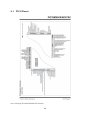
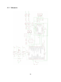
A.1 PIC32 Pinout . . . . . . . . . . . . . . . . . . . . . . . . . . . . . . . . . . . . . . . . . . . . . . . 104
A.2 Rated TCP/IP Stack Performance . . . . . . . . . . . . . . . . . . . . . . . . . . . . . . . . . . . 105
A.3 Schematic . . . . . . . . . . . . . . . . . . . . . . . . . . . . . . . . . . . . . . . . . . . . . . . . 106
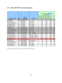
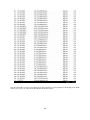
A.4 Bill Of Materials . . . . . . . . . . . . . . . . . . . . . . . . . . . . . . . . . . . . . . . . . . . . . 107
A.5 Bias Adjustment Simulations . . . . . . . . . . . . . . . . . . . . . . . . . . . . . . . . . . . . . 109
4
A.6 Gain Compensation Simulations . . . . . . . . . . . . . . . . . . . . . . . . . . . . . . . . . . . 111
A.7 Embedded Software Pseudocode . . . . . . . . . . . . . . . . . . . . . . . . . . . . . . . . . . . 112
5
List of Figures
2.1
Design Specifications . . . . . . . . . . . . . . . . . . . . . . . . . . . . . . . . . . . . . . . . . .
15
2.2
List of RFC Documents [42, p. 91] . . . . . . . . . . . . . . . . . . . . . . . . . . . . . . . . . . .
17
3.1
High Level PC Software Flowchart . . . . . . . . . . . . . . . . . . . . . . . . . . . . . . . . . .
20
3.2
C Sharp Platform Flowchart . . . . . . . . . . . . . . . . . . . . . . . . . . . . . . . . . . . . . .
21
3.3
PC Software Flowchart . . . . . . . . . . . . . . . . . . . . . . . . . . . . . . . . . . . . . . . . .
25
4.1
High Level Embedded Software Flowchart . . . . . . . . . . . . . . . . . . . . . . . . . . . . .
29
4.2
Data Register Format . . . . . . . . . . . . . . . . . . . . . . . . . . . . . . . . . . . . . . . . . .
32
4.3
DAC Driver Flowchart . . . . . . . . . . . . . . . . . . . . . . . . . . . . . . . . . . . . . . . . .
32
4.4
PWM Driver Flowchart . . . . . . . . . . . . . . . . . . . . . . . . . . . . . . . . . . . . . . . . .
34
5.1
High Level Embedded Software Flowchart . . . . . . . . . . . . . . . . . . . . . . . . . . . . .
37
5.2
Microchip TCP/IP Stack Reference Model [2] . . . . . . . . . . . . . . . . . . . . . . . . . . . .
38
5.3
IP Header [60] . . . . . . . . . . . . . . . . . . . . . . . . . . . . . . . . . . . . . . . . . . . . . .
39
5.4
UDP Header [60] . . . . . . . . . . . . . . . . . . . . . . . . . . . . . . . . . . . . . . . . . . . .
40
5.5
Encapsulation Reference Model [60, p. 161] . . . . . . . . . . . . . . . . . . . . . . . . . . . . .
41
5.6
Main Embedded Software Routine . . . . . . . . . . . . . . . . . . . . . . . . . . . . . . . . . .
45
5.7
Packet Structure . . . . . . . . . . . . . . . . . . . . . . . . . . . . . . . . . . . . . . . . . . . . .
46
5.8
Dropped Packet Handling Flowchart . . . . . . . . . . . . . . . . . . . . . . . . . . . . . . . . .
49
5.9
Interrupt Routine Flowchart . . . . . . . . . . . . . . . . . . . . . . . . . . . . . . . . . . . . . .
50
5.10 Clock Management Flowchart . . . . . . . . . . . . . . . . . . . . . . . . . . . . . . . . . . . . .
53
5.11 Timer Value Calculations . . . . . . . . . . . . . . . . . . . . . . . . . . . . . . . . . . . . . . . .
55
6
6.1
High Level Hardware Flowchart . . . . . . . . . . . . . . . . . . . . . . . . . . . . . . . . . . .
57
6.2
Bipolar Full-Wave Rectifier Circuit [9] . . . . . . . . . . . . . . . . . . . . . . . . . . . . . . . .
58
6.3
Half-Wave vs. Full-Wave Rectification [14] . . . . . . . . . . . . . . . . . . . . . . . . . . . . .
58
6.4
Bipolar Half-Wave Rectifier Circuit [28] . . . . . . . . . . . . . . . . . . . . . . . . . . . . . . .
59
6.5
LM78xx/uA78xx Regulator Circuit [24] . . . . . . . . . . . . . . . . . . . . . . . . . . . . . . .
60
6.6
Buck Converter Operation [55] . . . . . . . . . . . . . . . . . . . . . . . . . . . . . . . . . . . .
61
6.7
Buck Converter Schematic [47] . . . . . . . . . . . . . . . . . . . . . . . . . . . . . . . . . . . .
61
6.8
RMII Interface Connection [48] . . . . . . . . . . . . . . . . . . . . . . . . . . . . . . . . . . . .
63
6.9
Microstrip Dimensioning [50] . . . . . . . . . . . . . . . . . . . . . . . . . . . . . . . . . . . . .
64
6.10 Analog Output Stages [56] . . . . . . . . . . . . . . . . . . . . . . . . . . . . . . . . . . . . . . .
65
6.11 I2 C Signaling [56] . . . . . . . . . . . . . . . . . . . . . . . . . . . . . . . . . . . . . . . . . . . .
66
6.12 SPI Signaling [46] . . . . . . . . . . . . . . . . . . . . . . . . . . . . . . . . . . . . . . . . . . . .
67
6.13 Magnitude Response [25] . . . . . . . . . . . . . . . . . . . . . . . . . . . . . . . . . . . . . . .
68
6.14 Group Delay [25] . . . . . . . . . . . . . . . . . . . . . . . . . . . . . . . . . . . . . . . . . . . .
68
6.15 Inverting Summing Amplifier [18] . . . . . . . . . . . . . . . . . . . . . . . . . . . . . . . . . .
69
6.16 Inverting Amplifier [18] . . . . . . . . . . . . . . . . . . . . . . . . . . . . . . . . . . . . . . . .
70
6.17 LM2675 Schematic [51] . . . . . . . . . . . . . . . . . . . . . . . . . . . . . . . . . . . . . . . . .
72
6.18 LM2941 Schematic [52] . . . . . . . . . . . . . . . . . . . . . . . . . . . . . . . . . . . . . . . . .
73
6.19 LM2991 Schematic [53] . . . . . . . . . . . . . . . . . . . . . . . . . . . . . . . . . . . . . . . . .
73
6.20 Network Transceiver Schematic [29] . . . . . . . . . . . . . . . . . . . . . . . . . . . . . . . . .
75
6.21 Magnetics, Oscillator and LED Schematic [29] . . . . . . . . . . . . . . . . . . . . . . . . . . . .
76
6.22 Bias Circuit Schematic . . . . . . . . . . . . . . . . . . . . . . . . . . . . . . . . . . . . . . . . .
78
6.23 Gain Circuit Schematic . . . . . . . . . . . . . . . . . . . . . . . . . . . . . . . . . . . . . . . . .
79
7.1
Subsystem Test Block Diagram . . . . . . . . . . . . . . . . . . . . . . . . . . . . . . . . . . . .
86
7.2
Test 1 Task Times . . . . . . . . . . . . . . . . . . . . . . . . . . . . . . . . . . . . . . . . . . . .
88
7.3
Test 1 Packet Times . . . . . . . . . . . . . . . . . . . . . . . . . . . . . . . . . . . . . . . . . . .
88
7.4
Test 2 Task Times . . . . . . . . . . . . . . . . . . . . . . . . . . . . . . . . . . . . . . . . . . . .
89
7.5
Test 2 Packet Times . . . . . . . . . . . . . . . . . . . . . . . . . . . . . . . . . . . . . . . . . . .
89
7
7.6
Test 3 Task Times . . . . . . . . . . . . . . . . . . . . . . . . . . . . . . . . . . . . . . . . . . . .
90
7.7
Test 3 Packet Times . . . . . . . . . . . . . . . . . . . . . . . . . . . . . . . . . . . . . . . . . . .
90
7.8
Test 4 Task Times . . . . . . . . . . . . . . . . . . . . . . . . . . . . . . . . . . . . . . . . . . . .
91
7.9
Test 4 Packet Times . . . . . . . . . . . . . . . . . . . . . . . . . . . . . . . . . . . . . . . . . . .
91
7.10 Test 5 Task Times . . . . . . . . . . . . . . . . . . . . . . . . . . . . . . . . . . . . . . . . . . . .
92
7.11 Test 1 Calculated Data . . . . . . . . . . . . . . . . . . . . . . . . . . . . . . . . . . . . . . . . .
92
7.12 Test 2 Calculated Data . . . . . . . . . . . . . . . . . . . . . . . . . . . . . . . . . . . . . . . . .
93
7.13 Test 3 Calculated Data . . . . . . . . . . . . . . . . . . . . . . . . . . . . . . . . . . . . . . . . .
93
7.14 Test 4 Calculated Data . . . . . . . . . . . . . . . . . . . . . . . . . . . . . . . . . . . . . . . . .
94
7.15 Microcontroller Output at 125 Samples per Packet . . . . . . . . . . . . . . . . . . . . . . . . .
97
A.1 Minimum Bias Voltage . . . . . . . . . . . . . . . . . . . . . . . . . . . . . . . . . . . . . . . . . 109
A.2 Maximum Bias Voltage . . . . . . . . . . . . . . . . . . . . . . . . . . . . . . . . . . . . . . . . . 109
A.3 Simulation of Final Application . . . . . . . . . . . . . . . . . . . . . . . . . . . . . . . . . . . . 110
A.4 Minimum Gain . . . . . . . . . . . . . . . . . . . . . . . . . . . . . . . . . . . . . . . . . . . . . 111
A.5 Maximum Gain . . . . . . . . . . . . . . . . . . . . . . . . . . . . . . . . . . . . . . . . . . . . . 111
A.6 Simulation of Final Application . . . . . . . . . . . . . . . . . . . . . . . . . . . . . . . . . . . . 111
8
Chapter 1
Description of Problem
1.1
Problem Statement
There is no commercially-available system that allows real-time uncompressed CD-quality audio transmission across a small- to large-range network.
1.2
Solution Requirements
The envisioned solution is to transmit digital audio from a PC to an embedded microcontroller (or multiple
at once) via the User Datagram Protocol (UDP). By utilizing UDP, it is possible to send real-time audio to
an essentially unlimited number of receivers via UDP broadcasting [19]. The received audio data will be
stored in a live buffer on the microcontroller and then loaded into a Digital-to-Analog Converter (DAC)
operating at the frequency of the incoming audio signal (typically 44.1kHz). Potential applications of this
system could include, but are not limited to, playback of audio from a laptop or PC on a home theater
system, multi-room distribution, arena audio systems, and outdoor audio. The benefits of this solution
compared to others on the market are real-time transmission, distance limited only by the physical network
size, and uncompressed, CD-quality sound. The real-time nature of the system would allow users to enjoy
video content without audio delays, as well as listen to their music wherever they would like, all with the
high audio quality they expect.
1.3
Stakeholders and Needs
Four potential stakeholders have been identified along with this project, as well as their needs from the
system. These stakeholders are described below:
Stakeholder 1: Individual Consumers
• Provide high quality audio
• Affordable
9
• Reliable
• Convenient to use
Stakeholder 2: Commercial
• Support multiple receivers
• Sustain frequent heavy usage (reliable)
• Convenient for operator
Stakeholder 3: Sales and Marketing
• Aesthetically pleasing to customer
• Functions properly and is easy to set up
• Unique feature(s) to advertise
Stakeholder 4: Third Party Manufacturer and Marketing (Linksys or other network equipment companies)
• Compatible with wide range of network equipment
• Company could optimize their product to work with our product, which would be mutually beneficial
1.4
1.4.1
Competing Solutions
Overview
Many solutions exist that allow digital audio to be transmitted either wirelessly or over an IP network.
Bluetooth A2DP and Kleer are two point-to-point wireless standards that allow for audio transfer. Bluetooth
uses the subband codec (SBC) for audio transmission, which leads to large amounts of compression artifacts
causing poor sound quality [11]. Kleer is similar to Bluetooth in its operation, but transmits uncompressed
CD-quality audio [58]. Both systems are vulnerable to interference and offer limited range. The two major
competitors in IP-based audio transmission are DLNA and Apple’s Airplay. DLNA can be better described
as a file sharing protocol than a streaming protocol - it simply serves audio, video and picture files to a
receiver which is tasked with decoding the file [4]. It is not viable as a real-time audio transmission system.
Airplay is the closest to the planned design, as it transmits uncompressed audio across an IP network
via the UDP protocol [10]. However, tests have shown issues with audio delays, there are known issues
with the ability to stream to multiple speakers at once , and Apple imposes licensing fees - Airplay is not an
open source implementation, severely limiting its potential and increasing costs of Airplay-based streaming
systems [44]. The biggest downside with Airplay, however, is that the protocol is designed for streaming of
media files from a PC or portable Apple device. It does not support streaming all live audio from a PC in
real time.
10
1.4.2
Costs
Costs of competing systems vary significantly depending on the underlying technology. Of the point-topoint wireless systems, Bluetooth receivers can be purchased for around $35 [37], and a Kleer transmitter
and receiver pair can be purchased for around $120 [5]. Note that the Kleer system mentioned above is
only compatible with Sleek Audio brand earbuds. Of the network-based systems, a DLNA receiver can be
purchased for around $80 [63], and an AirPlay receiver can be purchased for around $100 [6].
1.4.3
Apple AirPlay
Although there are numerous existing solutions that involve sending audio wirelessly to speakers or amplifiers, the solution that is most similar to the proposed solution is Apple’s AirPlay. Unfortunately, published
specifications from Apple were unable to be found. However, on-line research did yield some specifications
that third parties found by reverse engineering the protocol [8]. Note that the author refers to AirTunes 2
as the protocol rather than AirPlay. AirPlay used to be an audio-only protocol named AirTunes 2 and was
renamed to AirPlay once other media streaming was made possible [10].
AirPlay maintains synchronization with the device(s) it is sending information to using a shared clock.
Devices occasionally re-sync their clock to the source to maintain real-time playback and synchronization.
Audio is streamed at 44.1 kHz in packets of 352 samples with a 12-byte header. The audio data is encrypted,
but the 12-byte header is not encrypted. A 20-byte playback synchronization packet is sent back to the host
about once every second. A five step process is listed that describes the behavior of both the host and
receiver. Before audio is sent, the host sends a request to start streaming. Then the devices perform 3 time
synchronizations, one after another, after they receive a request from the host. The devices then reply to
the request from the host. The host then sends out its first playback synchronization packet. Finally, the
host begins the audio stream. The first 4 steps of this process allegedly take 2 seconds, which is a noticeable
delay every time a song is fast-forwarded or a new song is selected [8].
11
Chapter 2
Description of Solution Approach
2.1
Solution Description
After the user installs the PC software, configures it for their computer’s sound card, and turns it on via the
user interface, all audio being played on the computer will be broadcast to a UDP port on the local network.
This captured audio will be 16-bit, 2-channel audio at 44.1 kHz. Multiple samples will be formed into UDP
packets and then passed on to the Windows TCP/IP stack so it can be broadcasted across the local network
subnet. There will be 126 audio samples per packet, allowing enough audio data to be transmitted per
packet to keep the number of packets per second low while also maintaining real-time transmission.
A third party router will be listening for the packets and broadcasting them to the entire subnet. The
router will be connected to the receiver by an Ethernet cable, which will connect to the physical network
interface attached to the microcontroller. This physical network interface hardware is an integrated circuit
that bridges the physical Ethernet connection to the MAC layer embedded inside the microcontroller. The
MAC layer bridges hardware and software, allowing the data to be handled in software via Microchip
TCP/IP stack.
This software is configured to listen for data directed to the microcontroller on the specified UDP port. Once
the data is read, the TCP/IP stack will be called to store the packet data into RAM. From RAM, the CPU
will read the right and left channel data at a data rate of 44.1 kHz, sending it to a digital-to-analog converter
via the Serial Peripheral Interface (SPI) on the microcontroller. The digital-to-analog converter will receive
bits
the 16 channel
data and convert it to a voltage output of 0V to 2.5V. This voltage will then be passed to an
analog filter/output buffer amplifier, which will convert the signal to a line-level analog output of approximately 0.3162VRM S that will be output through an RCA stereo jack. The analog output specifications are
a frequency range of 20Hz - 20kHz, a signal-to-noise ratio (SNR) greater than or equal to 80 dB, and a total
harmonic distortion (THD) less than 0.1%.
12
2.2
2.2.1
Detailed Block Diagram & Details
Live PC Audio
Data Rate: 44.1kHz
Bit Rate: 16-bits
Channels: 2
Description: This subsystem captures audio as it is played on a PC using a Visual Studio .NET Library.
2.2.2
UDP Server
bits
Audio Sample Size: 32-bit (2 channels x 16 channel
)
Packet Size: 126 Audio Samples + 32-bit control
Description: This subsystem collects captured audio, forms into a UDP packet and passes on to the Windows TCP/IP stack for broadcasting across the network.
2.2.3
Switch/Router
Specified Source Data Rate: 54Mbps (or higher) WiFi or 100Mbps Ethernet
Specified Output Data Rate: 100Mbps Ethernet
Description: This is a 3rd party subsystem that is used for transmitting the data packets across the network
from the source PC to the receiver(s).
2.2.4
Physical Network Interface Hardware
Input Protocol: 100Mbps Ethernet
Output Protocol: RMII Interface
Description: This subsystem is an IC that bridges the physical Ethernet connection to the MAC layer inside
the microcontroller.
13
2.2.5
Microchip TCP/IP Stack
Input: UDP data from MAC layer: 126 Audio Samples + 32-bit control
Output: Write raw data to registers: 4065 bits
Description: This subsystem is software that reads data from the network, and is configured to listen for a
UDP packet directed at this device.
2.2.6
Manage Asynchronous Clocks, Handle Dropped Packets
Input: Raw audio data in registers
Output: Processed audio data
Description: This subsystem is the main task for the microcontroller to perform. It manages the DAC write
rate to maintain real-time playback and generates audio data to fill in for data lost to dropped packets.
2.2.7
44.1kHz Interrupt
Input: Processed audio data
bits
x 2 channels)
Output: Write to SPI registers: 48-bits (24 channel
Description: This interrupt is generated by the internal timer of the microcontroller and controls the SPI
peripheral to write processed audio samples to the DAC.
2.2.8
Digital-to-Analog Converter
bits
writes
Input: SPI Data, 48 write
at 44,100 second
Output: Analog Voltage, 0-2.5VDC
bits
Description: This subsystem will receive the 16 channel
data and convert it to a quantized analog voltage
output of 0 to 2.5V
2.2.9
Analog Filter/Output Buffer Amplifier
Input: 0-3VDC Analog Voltage
Output: 0.3162VRM S line-level audio, 20-20kHz Frequency Response, >80dB SNR, <0.1% THD
Description: This subsystem will pass the audio through a low-pass filter (LPF) to reduce quantization
jaggedness on the output, adjust the bias of the output signal to be centered about 0V, and buffer it to
accommodate a wide range of receiver input impedances without voltage drop.
2.2.10
Power Supply
Input: 6-10VAC, <10W
Output: Regulated +3.3VDC and ±5VDC
Description: This subsystem will take a 7V ACRM S input and provide a regulated 3.3VDC and ±5VDC
output to power the digital and analog components, respectively.
14
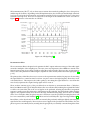
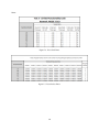
2.3
Specifications
Figure 2.1: Design Specifications
*Target value was determined by delaying audio of a video until the delay was perceivable.
**Target value was determined by removing samples from audio until the pause caused by the removed
samples was noticeable. Note that the audio was zeroed and not maintained, which makes the removed
samples more noticeable.
***Target value was determined by suggestion from Dr. Mossbrucker on general good quality audio in his
experience.
15
Selecting specifications that would ensure high quality audio along with meeting other solution requirements was essential. For the measurable audio characteristics, such as total harmonic distortion, signalto-noise ratio, and frequency range, it was difficult to find generally accepted standards. Therefore, Dr.
Mossbrucker, who is an expert in the field, was contacted. He was able to provide goals for each of these
audio characteristics from the High Fidelity Deutsches Institut fur Normung (Hi-fi DIN) 45500. He stated
that although this standard was from 1974, many of its specifications can still be used for requirements for
high quality audio.
The specifications for the two other high quality audio requirements (real-time audio transmission and preventing audible silence) were determined using qualitative testing. For the real-time audio specification,
audio was increasingly delayed within a video file until the video and audio became perceivably asynchronous. For the preventing audible silence specification, samples were increasingly removed from an
audio file until the pause caused by the removed samples were audible. The specifications for each of the
requirements were chosen to be below the threshold values at which the problem was noticeable.
2.4
Applicable Standards
Meeting industry standards and user standards is an important consideration in the design of the final
project. It is important to ensure the product to be designed does not infringe upon any standard regulations.
The standards for designing and implementing a TCP/IP suite for use in networking are defined by a
series of documents referred to as Request for Comments (RFCs). Many RFCs describe network services
and protocols as well as their implementation, but other RFCs describe policies. The standards within
RFCs are not established by a committee, but are instead established by consensus. Any person can submit
a document to be published as an RFC. These submitted documents are reviewed by technical experts, a
task force, or an RFC editor that are a part of the Internet Activities Board and are then assigned a status
that specifies whether a document is being considered as a standard [33]. There is also a maturity level
for each proposed document that ranks the stability of the information within the document. A list and
description of maturity levels can be observed at the source cited above.
The entire group of RFCs defines the standards by which a TCP/IP suite, among other networking suites,
should be created. Microchip’s TCP/IP stack adheres to the standards set forth by many RFCs. The most
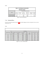
relevant RFCs for implementing the Microchip TCP/IP stack are shown in Figure 2.2.
Note that every published RFC can be observed at the sources listed in the caption of Figure 2.2.
The Federal Communications Commission (FCC) regulates the broadcasting of information over any medium.
Although this project requires UDP packets to be broadcasted over a network, the packets will only be
broadcasted to the devices within each user’s private network, or subnet. Therefore, FCC regulations are
not a concern for this project because a broadcast to a public network is not occurring.
The National Electric Code is a generally accepted standard for safe installation of electrical wiring and
equipment [17]. The only products that are to be provided by this project are the receiver, which is connected to an external router and amplifier, and the software to run on a PC. All connections, cables, and
other hardware are to be provided by the user. Therefore, it is assumed that all products that will be used
with the designed product will follow National Electric Code rules and regulations. It is important to make
sure that the designed receiver enclosure allows for proper ventilation in order to prevent internal circuitry
from reaching high temperatures. It is assumed that the designed product will not be operating in hazardous locations, such as areas having flammable gases or vapors; therefore, any concern with heat inside
16
Figure 2.2: List of RFC Documents [42, p. 91]
the enclosure is only due to the need to prevent the circuitry from malfunctioning [38]. Temperatures high
enough to damage circuitry will likely not be reached inside the enclosure, but this is still important to
consider when designing the enclosure.
2.5
Safety and Environment Considerations
This project provides minor safety concerns, if any. The only safety concern is the playing of excessively
loud audio for extended periods of time. The user may indeed choose to play audio very loudly; however,
the possible safety concern could occur if a lot of audio data is lost in transmission. This could cause
unpredictable audio to be played at very high volumes, which could be unpleasant and potentially unsafe
to the user. To combat this issue, if the quality of data transmission is very low, the product will simply stop
outputting audio data until the connection is reliably restored.
This project does not provide any real environmental concerns. Obviously, the product runs on electricity,
but it runs on little electricity in general. In order to minimize the amount of energy that the product uses, a
17
powersave mode will be activated when it is not in use. This powersave mode will turn off all functions of
the product except for a periodic check for network activity. This mode allows for energy to be saved when
the product is not performing its only function, which is to play audio.
18
Chapter 3
PC Software Design
3.1
3.1.1
Introduction
Overview
Within the PC design of the project, the main design implementations will be the capture of audio using
NAudio which is an open source .NET audio library, and the creation and sending of a UDP packet using
the built in .NET socket networking library. NAudio will be used to capture all audio being output through
the sound card and store it in an array. The array will contain 126 left and right channel 16-bit audio samples
bits
(32 sample
). This array will then be sent across the network as a packet, plus one “sample” containing a 32bit counter for error detection. The audio capture will continuously run, capturing 2-channel, 16-bit audio,
and will run simultaneously with the UDP server. This array will then be passed to the UDP server for
transmission across the network to any listening device every time the array has been filled.
This will be done so that a fast and reliable audio signal can be captured and sent across a network. The
packet size was, as previously mentioned, chosen to be large enough to minimize network and CPU utilization, and small enough so that if a packet is somehow lost or corrupted, the audible effect is minimized.
This will also facilitate real-time audio transmission, as the larger the packet becomes, the less real-time the
transmission becomes.
A GUI must also be created that the user can interact with. This is so that the user has control over the
starting and stopping of the audio transmission. Depending on time, other user controls of the receiver can
be designed, such as the ability to remotely mute individual receivers, but are not necessary for the initial
implementation. However, due to the GUI being a system integration component, it will not be designed
or built until the spring quarter.
3.1.2
Subsystem Requirements
• Capture live digital audio from a PC
– 16-bit samples at 44.1kHz, 2 channels
• Create UDP packets size of 127
19
bits
– 126 samples will be 32-bit two channel samples at 16 channel
, 1 sample will contain the packet
count
• Broadcast the UDP packet across the network to a router
• Maintain a timely broadcast of packets to allow for the receiver to output audio at a 44.1kHz rate
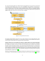
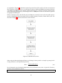
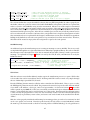
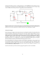
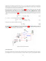
The flowchart in Figure 3.1 illustrates the embedded software at a very high level. More specific flowcharts
can be observed later in this section of the report.
Figure 3.1: High Level PC Software Flowchart
3.2
3.2.1
Research
Background Research
The PC software section revolves around the audio capture of raw data played by the computer being
placed into an array that will act as a local buffer. Then, a UDP server will send that data out over a
network to the receivers. Each section has its own design considerations to consider, such as the different
audio capture tools and the different ways to send the data over the network.
Audio capture will be used within this project to record directly from the PC audio output. This is a stereo,
16-bit digital signal at a sample rate of 44.1 kHz. These specifications were developed for the Compact
Disc by Sony and Phillips, which came to be known as the “Red Book” specifications. The Red Book was
published in 1980 and lays out the standards and specifications for audio CDs [62]. This sample rate was
chosen mainly due to human hearing range. This is a range from 20 to 20,000Hz, making the sampling rate
need to be at least 40 kHz in order to adhere to the Nyquist criterion and be able to successfully recreate
the analog audio signal without aliasing [45]. At the time of creation of the Red Book, the professional
audio sampling rate was set to 48 kHz due to the easy multiple of frequencies which is common in other
formats. The chosen Red Book sample frequency for consumer audio set the rate to 44.1kHz for two reasons.
First, 44.1kHz is claimed to make copying more difficult. Secondly, and perhaps more importantly, at the
time of creation, equipment that was used to make CDs was based upon video tapes, which was only
capable of storing 44,100 digital bits per second. For the project, the audio data will follow the Red Book
consumer audio standard since, despite being inferior to 48kHz, it is widely used by almost all audio
content. Resampling to 48kHz would cause a loss in quality, so there is no use in doing that [7].
The code will be written in Microsoft Visual Studio using the C# programming language. C# was developed
by Microsoft in 2001 to utilize a common language infrastructure when writing software. This common language infrastructure is the Microsoft .NET framework. This type of development enables the use of external
libraries (also called namespaces) and allows different programming languages to work together with the
same common components with very little disruption between the two. When built, C# compiles into assembly language, allowing it to be an intermediate language. When executing, the C# program loads into
20
the a virtual environment, Microsoft’s .NET Common Language Runtime. The system allows for managed
code which provides multiple services, such as cross compatibility amongst Windows environments, resource management, etc. This makes the execution of a C# program very similar to a Java program running
in the Java virtual machine. The Common Language Runtime will then convert the intermediate language
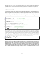
code to machine instruction. The flow chart shown below was taken from the Microsoft Developer Network
(MSDN) and provides a top level view of how the code is compiled:
Figure 3.2: C Sharp Platform Flowchart
In reviewing sample NAudio code, there were two terms used that were not fully understood. These
were garbage collection and constructors. As a result, these two topics were investigated in more depth to
provide a greater understanding of the language and the NAudio library.
Garbage collection (GC) is one of Microsoft’s attempts to simplify coding in C#. In many programming
languages, the user has to manually manage memory usage, especially when creating and removing objects.
For example, if an instance of a class is created, used, then removed, the user would have to manually
free up the memory used by that instance. C#, however, has built-in garbage collection. This allows the
developer to ignore the tracking of memory usage and knowing when to free memory. GC automatically
looks for objects or applications not being used and removes them. When this starts running it assumes
that all applications are garbage. It then begins following the roots of the program looking at all the objects
that are connected to the roots. Once the GC is performed, anything that’s not garbage will be compacted,
and anything that is will be removed [43].
Within the C# programming aspect of this project constructors are going to be heavily used. Constructors
are described as “class methods that executed when an object of a class or struct is created” [30]. Construc-
21
tors are mainly used to in the initialization of data members of a new object and with the same name as the
class itself. Constructors build a class by taking the parameters of classes and structs through a base statement. One main base statement is the “new” operator. This allows a new class or struct to occur that has the
specified parameters dedicated to that singular instance. For example, to create an instance of NAudio’s
waveIn class named audioIn, the code would be waveIn audioIn = new waveIn(44100,2). This specifies that
an object (audioIn) of type waveIn is a new instance of the waveIn class given parameters 44100 and 2.
3.2.2
Design Considerations Research
Audio Capture
There are a few different ways to implement the audio capture portion of this subsystem. One of which
is the creation of an audio driver using Microsoft Visual Studio. This would mean that the code would
be written manually that would specifically capture all audio being played on the PC and format the data
in such a way that would be more beneficial to the packet creation. This would create a virtual hardware
device that the computer would recognize and easily interact with. However, this requires a large amount
of programming experience and understanding of the Windows Audio API, kernel-level driver hooks,
and many more advanced topics to be brought in. Custom code would certainly provide a wide range
of design options for user convenience and code performance optimization. Unfortunately, this option
would be beyond the scope of feasibility for this project and require much greater experience with software
engineering to create. While this option may not be currently feasible for the project, it would be the ideal
solution if the project were to be turned into a production product.
A more feasible option for this project would be to use pre-written audio software that could capture or
record the sound directly from the sound card. The most versatile open source audio library that could
be found is NAudio. There are two main Windows application programming interfaces (APIs) that can be
used as recording devices with NAudio. These are the WaveOut or Windows Audio Session API (WASAPI)
[21].
WaveOut is a class that provides methods for recording from a sound card input. The Wave file format
allows for the capture of raw uncompressed audio data. The code provided by NAudio can capture the
data within a wave file or, with modification, into a RAM buffer array. The advantage of this is that the
data can easily be captured in the required format for transmission across the network to the receiver(s).
However, the disadvantage of this is that it captures the data transmitted to the speakers via a sound card
loopback [31]. This can cause configuration difficulties to the end user, and isn’t guaranteed to be supported
by every sound card on the market.
NAudio’s WASAPI class can interact directly with the Windows software audio mixer. This means that
the data can captured before being sent to the sound card. A major advantage of WASAPI is that the
audio capture is not at all dependent on the sound card model (or its existence, for that matter) [32]. The
disadvantages of this class are that NAudio has just gained support for WASAPI capture and currently does
not contain any sample code or documentation on how to initialize an instance of the WASAPI capture class
[20]. On top of that, WASAPI is only available in Windows Vista and Windows 7, so if the capture software
were to use WASAPI, it would no longer be compatible with Windows XP.
22
UDP Server
In the sending of the audio data over the network, one protocol that could be used is the Transmission Control Protocol (TCP). TCP is used for guaranteed delivery of data. If a packet is dropped or malformed, the
protocol will retransmit the packet until it successfully reaches its destination. The protocol will establish
a connection between two points with data reliability controls providing the guaranteed delivery. Because
of this control algorithm, TCP can only send to any one receiver at any one time, which is a downfall considering the packets may need to be sent to multiple receivers at once. Due to the guaranteed delivery, this
could introduce transmission delays from making sure the data got through, making TCP a poor choice
for real time audio streaming. On top of this, both the PC and the microcontroller would be tasked with
the additional work of implementing the TCP algorithm - something that the microcontroller may not be
capable of handling in a reasonable timeframe. This method would be an ideal method if the audio was not
required to be transmitted in real time [35].
UDP is a very simple stateless protocol that is being considered. The packet that this protocol creates is
much simpler in that it only contains the source and destination ports, length of header and data, and an
optional checksum. The checksum is the only item used in determining if the packet is malformed or not
due to the transmission. This is the only source of packet transmission error checking that UDP offers.
With this protocol, because there is no handshaking between the client and server, a packet is able to be
simultaneously transmitted to multiple receivers listening on the same port. UDP is also inherently fast,
making it ideal for real audio transmission. One of the major disadvantages of UDP is that there that there
is a chance a packet will get dropped or will not make it in the order in which the packets were sent.
This provides very little control over the transmission of the data. Although UDP can lose data through
dropped/corrupt packets, the amount of data lost in one packet and the amount of packets lost will be
small enough to minimize audible effects, as proven both on a private and congested public network in the
subsystem test detailed in Chapter 7. UDP fits into what this design will entail in that real time audio will
need to be transmitted in a fast efficient way to any number of receivers [35].
Both TCP and UDP are explained in much greater detail in Section 5.2.1.
A primary decision with a UDP server is whether to use broadcasting or multicasting. Broadcasting is the
server sending packets to all hosts on the network whether the host wants the packet or not. The server
will indiscriminately send the data to a certain port and all other hosts will have to handle the packet. The
advantage of broadcasting is that it is simple to implement both on the server-side and client-side, and is
universally supported amongst network switches. Broadcasting to an entire subnet can be accomplished
by simply addressing a packet to the IP address 255.255.255.255 [36].
The other UDP communication method is multicasting. This is done using the UDP server to send packets
to multiple clients simultaneously, but only ones that want to receive the packet. The difficulty in implementing this comes into play on the receiver side, and the switch/router must support it. The server simply
needs to address the packet to a multicast group IP address, such as an address within 239.255.0.0/16 [16]. It
is then up to the switch/router to route those packets appropriately to the devices registered in the multicast
group. However, as explained in Chapter 5, there are technical challenges with the PIC32 and Microchip’s
TCP/IP stack that must be overcome to enable mutlicasting with the receivers.
23
3.3
3.3.1
Design
Design Consideration Analysis
Audio Capture
For the audio capture, the initial design will use the NAudio library and the WaveIn class for maximum
compatibility amongst all common operating systems. This method is currently the most feasible option
due to the fact that sample code and documentation is available. If time permits, and the library can be
figured out, WASAPI capture will be investigated as a better option for the server application when running
under the Windows Vista or 7 operating system.
UDP Server
The simplest and fastest method to implement the UDP server is to use the System.Net.Sockets library
within the Microsoft .NET Framework. Broadcasting data to the local subnet will be used to allow for any
receiver listening be able to pick up the packet.
3.3.2
Design Requirements
The libraries and functions provided by NAudio will allow for the solution requirements to be met by
capturing CD quality audio. An instance of the WaveIn class will be created, capturing 2 channel audio at
a 44.1kHz sampling rate. This captured audio will then be stored in a RAM buffer, and a second thread
will be started that contains a UDP server and a packet counter that will be transmitted with each packet of
data.
As previously mentioned, the UDP server will be configured to broadcast the data to the subnet. Using an
instance of the IPAddress class, the destination IP address can be specified to be a subnet broadcast using the
IPAddress.Broadcast field. The IPAddress class can be combined with the port number to create an instance
of the IPEndPoint class. Finally, this class instance can be passed on to an instance of the UdpClient class,
allowing data to be transmitted across a network.
Each packet sent will contain 126 audio samples, plus a 32-bit counter that resets to zero upon overflow.
A timer will be used within the UDP server thread to so that the buffer on the microcontroller will not be
flooded with a large amount of data in bursts, instead receiving a steady flow of audio data. The structure
of the packet is the 32-bit counter followed by the 126 audio samples, left channel followed by right channel.
This is described in detail in Section 5.3.3.
3.3.3
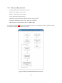
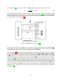
Design Description
The top level block diagram below shows how the PC software will be implemented. This shows a more
detailed flow of how the program will run.
24
Figure 3.3: PC Software Flowchart
To begin, the first thing will need to be the initialization for audio capture and the UDP server. What needs
to done first is to add the libraries given by Microsoft and NAudio that are not already given from the initial
creation of a program, as shown in the following pseudocode.
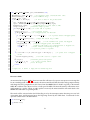
1
2
3
4
5
6
// l i b r a r i e s used f o r audio c a p t u r e
using NAudio . Wave ;
using A u d i o I n t e r f a c e ;
// l i b r a r i e s used f o r network f u n c t i o n s
using System . Net ;
using System . Net . S o c k e t s ;
25
7 // l i b r a r i e s used f o r d e l a y s i n sending o f p a c k e t s and t h r e a d i n g
8 using System . Threading ;
The following code shows the initialization of a basic UDP server. The first line shows the creation of a new
instance of the UdpClient class that will be used within the code to send the data.
Note that the .NET Framework UdpClient class contains both the methods required to act as a UDP client
and/or a UDP server.
The next line sets up the destination address of what will receive the data. In the current design, a specific
IP address is not needed because the client will broadcast to every device on the network. The following
line sets up the header of the packets that will be created with the destination address and the port number
that can be anywhere between 49152 to 65535. All other ports are reserved. For this project, port 50000 was
chosen. The final line is the initialization of the background worker that will work to send the packets a set
time.
1 s t a t i c UdpClient udpClient = new UdpClient ( ) ;
// s e t s up UDP s e r v e r
2 s t a t i c IPAddress i p a d d r e s s = IPAddress . B r o a d c a s t ;
// s e t s t h e IP Address t o a b r o a d c a s t
3 s t a t i c IPEndPoint ipen dpoint = new IPEndPoint ( ipaddress , 5 0 0 0 0 ) ; // s e t s up t h e endpoint t o t h e IP
address and p o r t 50000
4 p r i v a t e System . ComponentModel . BackgroundWorker backgroundWorker1 ; // i n i t i a l i z e s t h e background
worker
Next, to set up the audio capture, the following lines will set up instance of the WaveIn Class.
1 // WaveIn Streams f o r r e c o r d i n g
2 WaveIn waveInStream ;
3 WaveFileWriter w r i t e r ;
To actually capture audio, the following code will need be used to initialize the WaveIn class for the desired
sample rate and number of channels being used. The second line indicates that the data will then be saved
in a wave format file. This is used for testing, and will be replaced with a RAM array feeding the UDP
server in the final version of the software.
1
2
3
4
// s e t s audio
waveInStream
// w r i t e s t h e
w r i t e r = new
c a p t u r e t o 44100 Hz with 2 c h a n n e l s
= new WaveIn ( 4 4 1 0 0 , 2 ) ;
audiostream i n a wave format t o t h e f i l e
WaveFileWriter ( outputFilename , waveInStream . WaveFormat ) ;
The following code will create an event handler for when NAudio has data available in its buffer. This
initializes the waveInStream DataAvailable() function for handling that data.
1 waveInStream . D a t a A v a i l a b l e += new EventHandler<WaveInEventArgs >( waveInStream DataAvailable ) ;
The collection of the audio data will be incorporated within the waveInStream DataAvailable function that
is called above. The code will save the data into a buffer with 4410 (100ms) audio samples called “e”. The
following code will implement the data collection. This code saves the raw data to a text file for processing
with MATLAB, which will not exist in the final version of the software.
1 void waveInStream DataAvailable ( o b j e c t sender , WaveInEventArgs e )
2 {
3
//s a v e s recorded data i n t o a b u f f e r
4
byte [ ] b u f f e r = e . B u f f e r ;
5
// r e c o r d s t h e amout o f b y t e s a r e i n t h e recorded data
26
6
7
8
9
10
11
12
13
14
15
16
17
18
19
20
21
22
23
24
25
i n t bytesRecorded = e . BytesRecorded ;
//s a v e s data i n t o an audio . t x t f i l e
StreamWriter f i l e = new StreamWriter ( ” audio . t x t ” , t r u e ) ;
// r e c o r d s data f o r t h e r i g h t and l e f t c h a n n e l s
f o r ( i n t index = 0 ; index < bytesRecorded ; index += 4 )
{
// l e f t channel
s h o r t samplel = ( s h o r t ) ( ( b u f f e r [ index + 1 ] << 8 ) |
b u f f e r [ index + 0 ] ) ;
// r i g h t channel
s h o r t sampler = ( s h o r t ) ( ( b u f f e r [ index + 3 ] << 8 ) |
b u f f e r [ index + 2 ] ) ;
//s a v e s data i n c o r r e c t format i n t h e t e x t f i l e
f i l e . Write ( Convert . T o S t r i n g ( samplel ) +”\ t ”+Convert . T o S t r i n g ( sampler ) +”\n” ) ;
}
// c l o s e s t h e f i l e
f i l e . Close ( ) ;
//s a v e s t h e amount o f seconds t h a t were recorded
i n t secondsRecorded = ( i n t ) ( w r i t e r . Length / w r i t e r . WaveFormat . AverageBytesPerSecond ) ;
}
The next code portion sets up a background worker that will execute the UDP packet creation and sending
of the data at a synchronized pace. Background Workers are the .NET implementation of threading/multitasking and allow different code to execute simultaneously. The code presented below shows the set up of
the background worker. The initialization of the function will be set up to respond when a certain action is
taken, in this case when the array is full.
1
2
3
4
p r i v a t e void I n i t i a l i z e B a c k g r o u n d W o r k e r ( )
{
//Placement o f code t h a t w i l l i n i t i a t e t h e background worker when t h e a r r a y i s f i l l e d
}
After initialization, the background worker function will need to be written. This will be started using the
following lines, and contained within the function will be the code to send the data across the network.
1 p r i v a t e void backgroundWorker ( )
2 {
3
// a r e a t h a t w i l l c o n t a i n UDP data t r a n s m i s s i o n code
4 }
Finally, within the above background worker function, a UDP server will send a 32-bit packet followed by
the 126 audio samples in the buffer. The code will then wait approximately 2.5ms to send the next packet.
This time was determined due to a full array having 100ms of data, which will be broken down to 35 packets
of 126 samples. This will repeat itself 35 times before the thread completes processing and is ready to be
re-started when NAudio provides the next full buffer.
1
2
3
4
5
6
7
8
9
10
11
12
13
14
for ( i n t i =0; i
{
p a c k e t c o u n t e r ++;
Byte [ ] sendBytes
//The l i n e below
sendBytes
< 3 5 ; i ++)
//increment pa cket c o u n t e r
= p a c k e t c o u n t e r // s t a r t p acket with t h e packet c o u n t e r
i s t h e code t h a t w i l l add t h e audio data t o t h e packet
+= Encoding . ASCII . GetBytes ( ∗ 1 2 6 audio sample a r r a y ∗ ) ;
udpClient . Connect ( ipen dpoint ) ;
// c o n n e c t s t o network
udpClient . Send ( sendBytes , sendBytes . Length ) ;
//sends data
Thread . S l e e p ( 2 . 5 ) ;
//puts loop i n t o a s l e e p f o r 2 . 5 ms
i f p a c k e t c o u n t e r ==0 x100000000
packetcounter =0;
// r e s e t pa cket c o u n t e r i f a t max value
}
27
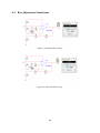
Chapter 4
Embedded Software Design I
4.1
4.1.1
Introduction
Overview
In order for functionality to be met, the microcontroller must be initialized correctly. This includes setting
up the peripheral bus and I/O pins. In order for the solution requirements to be met, the microcontroller
must also be configured so that a UDP client can run to receive audio packets from the PC software. Also,
the PIC32 must be initialized to send the received audio packets to the digital to analog converter in order
to convert the digital sound data into an analog signal, thus allowing for the data to be played through an
amplified speaker system.
For the DAC interface, it was previously mentioned that the SPI peripheral needs to be configured for
certain specifications. The audio data will be sent to the DAC via SPI and in order for the DAC to properly
receive the data, the SPI must be configured in a format which is compatible with the DAC. The DAC of
choice for this design will be the DAC8563 from Texas Instruments, as detailed in Section 6.3.3.
There is also an analog low-pass filter used by the analog reconstruction circuitry. However, this filter is
unique in the fact that it has a PWM-controlled cutoff frequency. As a result, a Timer and Output Compare
module in the PIC32 will be used to design a function for setting the cutoff frequency of the filter, called the
filter driver.
4.1.2
Subsystem Requirements
• The PIC32 core peripheral bus must be configured to run at optimal performance
• The TCP/IP stack must be initialized and configured to support a UDP Client (see Section 5.3.3)
• The SPI peripheral must be initialized to meet requirements for integration with the DAC
• The Timer and Output Compare peripherals must be configured to generate a PWM signal
• Drivers must be written to send data to the DAC and adjust the PWM frequency
28
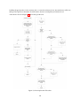
The flowchart in Figure 4.1 illustrates the embedded software at a very high level. More specific flowcharts
can be observed later in this section of the report.
Figure 4.1: High Level Embedded Software Flowchart
4.2
4.2.1
Research
Background Research
The PIC must be initialized such that general purpose I/O pins (GPIOs) are easily accessible in code, specifically pins to be used by the SPI interface and LEDs. To accomplish this, the TRIS register corresponding
to the physical pin must be configured so the port can be setup as an input or output port. It is also important to configure the PIC so that interrupts are enabled and so that the peripheral bus operates at its
maximum speed (80MHz - equal to the main CPU speed) for communications between peripherals and the
CPU. There are two functions that are used to configure the peripheral bus for optimal performance and set
the peripheral bus prescaler. These are SYSTEMConfigPerformance() and mOSCSetPBDIV(), respectively.
On top of that, Microchip’s TCP/IP Stack, as described in Section 5.2.1, will be used for data transmission
across a network. To accomplish this, the stack must be initialized. This is done by the function StackInit().
The initialization will set up the configuration for the MAC address and DHCP Client functionality to allow
the network interface to be brought up and ready for the audio task to open a UDP client. Since interrupts
will be utilized for both the stack as well as by the custom code, interrupts must be enabled using the
INTEnableSystemMultiVectoredInt() function.
SPI communications, as used by the DAC, require a clock, a Master output/Slave input, a Master input/Slave output, and a slave select. Data is able to be transferred at high speeds, in the tens of megahertz.
There is no pre-defined data transfer protocol, instead allowing manufacturers to implement any desired
data protocol over the generic SPI interface. If applicable for the application, data can be shifted in full
duplex, meaning that data can be transmitted simultaneously between the slave and master. SPI on the
PIC32 is easily implemented by using the peripheral library, and can be initialized using the SpiChnOpen()
function.
A filter with a PWM-adjustable cutoff frequency will be used for audio playback as detailed in Section
6.2.3. The requirements necessary for functionality would be to adjust cutoff frequency of the filter using
the PWM peripheral on the PIC32 to generate a PWM signal at a 50% duty cycle. The filter that will be
used is the Maxim MAX292, which acts as a standard low-pass analog filter. The frequency of the signal
required to operate the filter must be 100 times the desired cutoff frequency. This means that with a desired
cutoff frequency of 25 kHz, the operational frequency must be 2.5MHz. This can be accomplished using a
Timer and Output Compare module on the PIC32, which can be configured using the OpenTimerX() and
OpenOCX() functions, respectively.
29
4.2.2
Design Considerations Research
Since the code written for the tasks in this section is primarily written to support other functions, there
is very little design considerations that can be made. Instead, this code is responsible for facilitating the
operation of the code in Chapter 5, where the design considerations have been made.
4.3
4.3.1
Design
Design Requirements
I/O pins on the device will be used for communication with devices or debugging. Many of these will
automatically be configured appropriately by hardware, such as the SPI ports D0 and D10 and the PWM
output pin D1. There are also five pins that will be controlled by software. These are D4, D5, D6, B0 and B1.
The first 3 pins are used for DAC control and are the CLR, Slave Select and LDAC pins, respectively. Pin B0
allows the microcontroller to drive the on/off pin of the linear regulators for when the receiver enters low
power mode, and B1 is used for the main power LED. Pins C1-C3 will also be configured as outputs for use
during debugging due to their ease of access on the breakout board and previous use as debug pins during
the subsystem test.
For configuration of the peripheral bus and initialization of the TCP/IP Stack, the peripheral bus must be
configured for optimal performance with a 1:1 prescaler. Then, the stack must be initialized and interrupts
must be enabled.
For the SPI communications, it is desired to communicate with the DAC at a rate of 20MHz, with 8 bits
being sent per transmission. The driver must accept a 16-bit left and right channel input, and write that,
along with control bits, to the DAC whenever called.
Finally, the filter is adjustable from 0.1Hz to 25kHz. Since the PWM frequency must be 100x higher, the
PWM must be software-controllable between 10Hz and 2.5MHz.
4.3.2
Design Description
PIC32 and Ethernet Initialization
For the initialization of the PIC32, first pins will be configured for ease of accessibility. The PIC32 has
multiple pins which can be configured to meet either output or input specification. An example of this for
the LDAC pin is shown below:
1 # d e f i n e LDAC TRIS ( TRISDbits . TRISD6 ) //in pu t or output p o r t type r e g i s t e r
2 # d e f i n e LDAC ( LATDbits . LATD6)
Once the pins mask is defined, it can then set to be either input or output pins, as shown below:
1 LDAC TRIS = 0 ; // s e t as output
For the design, port C will also be used for testing purposes (general purpose registers). The mast names
will correspond to the pin on the breakout board for code readability purposes.
30
1 # d e f i n e PIN35 TRIS ( TRISCbits . TRISC1 )
2 # d e f i n e PIN35 IO ( LATCbits . LATC1)
Next, the stack and interrupts must be initialized.
1 StackInit () ;
2 INTEnableSystemMultiVectoredInt ( ) ; // t h i s f u n c t i o n w i l l e n a b l e m u l t i p l e i n t e r r u p t s t o be
u t i l i z e d by t h e PIC32
Finally, in order for the system to perform at optimal speed, the following will be implemented to set the
peripheral bus prescaler to 1:1:
1 SYSTEMConfigPerformance ( GetSystemClock ( ) ) ;
a t 80MHz
2 mOSCSetPBDIV ( OSC PB DIV 1 ) ;
// Use 1 : 1 CPU Core : P e r i p h e r a l c l o c k s , c l o c k s a r e
SPI and DAC Driver
As previously mentioned, the PIC32 main clock speed is 80MHz. Since the peripheral bus was configured for maximum performance above, the SPI peripheral will be initialized at the same clock speed. The
following code will retrieve the peripheral clock speed, and use it to configure the SPI peripheral for 8-bit
transmissions to the DAC at 20MHz. 20MHz is a somewhat arbitrary speed that will most likely be adjusted
during the implementation of this system, and especially during the PCB design. The DAC8563 operates at
a peak SPI bus speed of 50MHz, and the faster that the data can be written, the less time the main CPU has
to wait for the SPI peripheral to finish writing the data before it can continue with its tasks. As explained
in Section 6.2.3, the minimum bus speed is 2.1168MHz, which 20MHz is clearly much higher than.
1 i n t srcClk = GetPeripheralClock ( ) ;
2 SpiChnOpen ( SPI CHANNEL1 , SPI OPEN MSTEN | SPI OPEN SMP END | SPI OPEN MODE8 , s r c C l k /20000000) ;
The PIC32’s SPI peripheral needs to be the master device on the bus, and the DAC must be the slave. This
is done using the SPI MSTEN and SPI OPEN SMP END flags. SPI OPEN MODE8 will set the SPI to send
out data 8 bits at a time. The source clock is shown divided above, because this will set the bit rate. The bit
rate for this design is 20MHz.
The digital to analog converter that was chosen was the DAC8563. As explained in Chapter 6, it is a 16 bit
DAC (will be needed for audio data transfer) and can operate at clock rates of up to 50MHz. The interface
of the DAC is compatible with any standard SPI master device, meaning that it will also interface with the
PIC32 SPI since it is not unique in functionality.
On the DAC8563, the input data register is 24 bits wide, containing the following:
• 3 command bits
• 3 address bits
• 16 data bits
All bits are loaded left aligned into the DAC. The first 24 are latched to the register and any further clocking
is then ignored. The DAC driver function will be passed two variables, either left or right. The variables
will contain 16-bit audio data each corresponding to the audio channel being written to.
31
For the DAC design, the LDAC pin on the DAC will be utilized. Within the PIC32 configuration, the port
RD6 will be configured as an output to the DAC, this output will control the LDAC level. Whenever the
LDAC pin is pulled low, the data that is written to the DAC will be sent out, leaving the DAC open for
information/data. This means that the DAC will stay one sample behind for maximum synchronization to
the 44.1kHz sample rate. This way, the last sample in the DAC buffer is updated into the DAC hardware,
then the next sample is loaded into the DAC buffer.
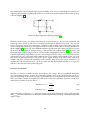
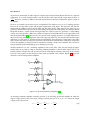
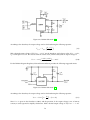
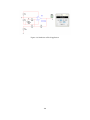
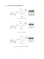
The DAC8563 uses the data input register format shown in Figure 4.2.
Figure 4.2: Data Register Format
The data sheet for the DAC8563 also shows which bit configuration would be best suited for specific design
functionalities. The design concept for the DAC driver is shown in Figure 4.3.
Figure 4.3: DAC Driver Flowchart
32
Before data can be sent to the DAC, the location of the data must first be specified. The SpiChnPutC()
function will send 8 bits at a time to the DAC. The first 8 bits will consist of two don’t care bits, three
command bits(C2-C0), and three address bits(A2-A0). The command bits will be used to tell the DAC to
write to the input buffer register, and the address bits will be configured to write to either DAC A (left
channel) or DAC B (right channel).
The next 16 bits will be used for the audio. However, only 8 bits can be sent at a time. Therefore, the audio
data will have to be split, as shown in the code sample below:
1 Unsigned audio Data ( l e f t / r i g h t ) ;
//audio data f o r l e f t or r i g h t channel
2 Char audio dataMSB = audio Data >> 8 ; // t h i s w i l l s h i f t t h e most s i g n i f i c a n t b i t s o f t h e audio
t o t h e r i g h t then t r u n c a t e
3 Char audio dataLSB = audio Data ;
// l e a s t s i g n i f i c a n t b i t s w i l l be s e n t w r i t t e n t o t h e
r e g i s t e r , o t h e r b i t s w i l l be t r u n c a t e d
For the overall functionality of this design, the LDAC must be triggered at the beginning of the function.
This will clear the DAC and allow data to be received. Then the configuration of the DAC must be performed in order to send to either DAC A or to DAC B based on the called value of left or right channel
audio. Once the configuration is complete, the most significant bits will be written to the DAC first, followed by the least significant bits. Then configuration for the opposite channel will be done, as well as the
writing of the data to the DAC channel. This process will be performed every time the DAC driver is called.
The DAC data will always be sent before it is received due to the LDAC being pulled low at the beginning
of this process.
Code showing the actual transmission of data is given below:
1 void WriteDAC ( u i n t 1 6 l e f t , u i n t 1 6 r i g h t )
2 {
3
LDAC= 0 ;
//Toggle LDAC low t o w r i t e pr ev i ou s b u f f e r t o DAC outputs
4
DelayMs = 1 ; //Wait a b i t b e f o r e r e l e a s i n g t h e pin
5
LDAC= 1 ;
// R e l e a s e LDAC pin
6
7
char leftMSB = l e f t >>8;
8
char l e f t L S B = l e f t ;
9
char rightMSB = r i g h t >>8;
10
char r i g h t L S B = r i g h t ;
11
12
DAC SS = 0 ; // s l a v e s e l e c t t h e DAC
13
SpiChnPutC ( SPI CHANNEL1 , 0 b000000 ) ;
//command t o update l e f t channel (DAC A)
14
SpiChnPutC ( SPI CHANNEL1 , leftMSB ) ;
// w r i t e MSB o f l e f t channel
15
SpiChnPutC ( SPI CHANNEL1 , l e f t L S B ) ;
// w r i t e lSB o f l e f t channel
16
SpiChnPutC ( SPI CHANNEL1 , 0 b000001 ) ;
//command t o update r i g h t channel (DAC B)
17
SpiChnPutC ( SPI CHANNEL1 , rightMSB ) ;
// w r i t e MSB o f r i g h t channel
18
SpiChnPutC ( SPI CHANNEL1 , r i g h t L S B ) ;
// w r i t e lSB o f r i g h t channel
19
DAC SS = 1 ; // r e l e a s e s l a v e s e l e c t
20 }
PWM Driver/Filter Frequency Control
In order to control the cutoff frequency of the filter, the PIC32 output compare module will be utilized
along with a timer module to generate a PWM signal. For this design, OC2 on the PIC32 will be used per
the schematic in Appendix A.3. In order for design to function, the desired frequency must be set to the
timer period for the output compare. OC2 will then be required to trigger on the timer. The function that
will be used, Freq ADJ() will be required to pass a variable, the desired cutoff frequency, in order to operate
correctly.
33
As explained in Chapter 6, the MAX292 switched capacitor filter will be used for the DAC reconstruction
filter. This filter is adjustable to have a cutoff frequency between 0.1Hz and 25kHz by providing a 50% duty
cycle PWM clock 100 times faster than the desired cutoff frequency. Therefore, this driver function must
take the desired cutoff frequency (a 16-bit integer from 1 to 25000) and use that to set the timer to generate
an appropriate PWM signal.
Timer1 is already in use by the TCP/IP stack, and Timer3 is reserved for use in the main audio processing task of Embedded Software Design II for the 44.1kHz interrupt. Therefore, Timer2 will be used. The
flowchart in Figure 4.4 illustrates the behavior of this function.
Figure 4.4: PWM Driver Flowchart
When using the Microchip Peripheral Library, calculating the timer period is as simple as passing the following calculation to the OpenTimer2() function:
t2tick =
P eripheralBusSpeed
DesiredF requency
(4.1)
It is also desired to use the internal peripheral bus clock as the timer source with a 1:1 prescaler. Therefore,
the timer can be initialized as follows:
1 OpenTimer2 ( T2 ON | T2 SOURCE INT | T2 PS 1 1 , t 2 t i c k ) ;
34
It is then desired to configure the output compare module to attach to the Timer2 in 16-bit mode (since
Timer2 is a 16-bit timer) and output to the OC2 pin using half the timer period to achieve a 50% duty cycle.
To do this, the OpenOC2 function will be used as follows:
1 OpenOC2 ( OC ON | OC TIMER MODE16 | OC TIMER2 SRC | OC CONTINUE PULSE | OC LOW HIGH , t 2 t i c k ,
t 2 t i c k /2 ) ;
The following code example will show how the set LPF frequency() function will be written to accomplish
this:
1 i n t set LPF frequency ( i n t desired frequency )
2 {
3
t 2 t i c k = s r c C l k /(100∗ d e s i r e d f r e q u e n c y ) ;
4
OpenTimer2 ( T2 ON | T2 SOURCE INT | T2 PS 1 1 , t 2 t i c k ) ;
5
OpenOC2 ( OC ON | OC TIMER MODE16 | OC TIMER2 SRC | OC CONTINUE PULSE | OC LOW HIGH , t 2 t i c k ,
t 2 t i c k /2 ) ;
6 }
By default, the filter will be setup for a cutoff frequency of 21kHz - below the Nyquist rate, but above the
desired cutoff frequency to compensate for the premature rolloff of the Bessel filter, as described in Section
6.2.3. This value will be adjusted for optimal behavior during the subsystem testing. Also note that the
function can be called at any time, allowing dynamic adjustment to the cutoff frequency.
35
Chapter 5
Embedded Software Design II
5.1
5.1.1
Introduction
Overview
This aspect of the embedded software has multiple tasks to perform. First of all, a UDP client must be
designed along with a function that can retrieve a packet and store it in memory. Upon being received,
UDP packets need to be read from the hardware receive buffer and stored in a software buffer so that
the main routine can access the audio data that was transmitted. The main routine to be executed in the
embedded software must call the previously mentioned retrieve function in order to retrieve transmitted
packets from the hardware receive buffer when a new packet is received.
Additionally, the main routine needs to be designed to detect and handle dropped packets as well as maintain clock synchronization between the asynchronous clocks of the PC and microcontroller. Dropped packets are inevitable when networking so it is important to create an efficient method of masking dropped
audio in order to minimize the effect it has on the listener. Numerous options for masking dropped audio
packets will be analyzed later in this section of the report and will be tested for effectiveness during winter
quarter.
Maintaining clock synchronization is possibly the most crucial aspect of all of the embedded software.
Unmanaged asynchronous clocks will either cause the audio to eventually fall out of real time or cause the
audio to have noticeable pauses. More specifically, if the microcontroller clock is slower than the PC clock,
there will be a buildup of audio data in the microcontroller buffer. Over long periods of time, this buildup
will cause the audio to not be output in real time because the microcontroller is gradually falling further
and further behind the PC. Additionally, the buffer would eventually overflow, causing transmitted data
to be lost until the buffer had enough space to receive another packet. Conversely, if the microcontroller
clock is faster than the PC clock, the microcontroller will run out of audio data to play back between every
received packet. Running out of data will cause lower quality audio as pauses or clicks may be heard.
In order to prevent the problems explained above and accomplish the goals of this project, maintaining
clock synchronization is imperative. Like the handling of dropped packets, multiple options to maintain
clock synchronization between the PC and microcontroller will be analyzed later in this section of the report
and tested for effectiveness during winter quarter.
36
5.1.2
Subsystem Requirements
• Initialize UDP Client to listen for audio data
• Check if new packet was received
• Retrieve packet and store in memory
• Detect and handle dropped packets
• Maintain clock synchronization between microcontroller and PC
• Interrupt at 44.1kHz in order to write audio data to the DAC
• Enter powersave mode when no data is available to play
The flowchart in Figure 5.1 illustrates the embedded software at a very high level. More specific flowcharts
can be observed later in this section of the report.
Figure 5.1: High Level Embedded Software Flowchart
37
5.2
5.2.1
Research
Background Research
Microchip’s provided TCP/IP stack software greatly simplifies the use of network communication within
the microcontroller. Even though this provided software will be used to implement the code for this project,
it is important to have a general understanding of the operation of the TCP/IP stack as well as the UDP
protocol.
In order to create a TCP/IP stack, a general TCP/IP reference model is followed. This reference model
consists of four different layers that perform certain functions and that work with layers that are above and
below. The image in Figure 5.2 illustrates the TCP/IP reference model on the left as well as the Microchip
TCP/IP stack implementation of the model on the right.
Figure 5.2: Microchip TCP/IP Stack Reference Model [2]
The top layer contains data that can be used by software on a device and the bottom layer is the connection
between one device and another that allows for communication. Every device that communicates over a
network must have some variation of the model of layers on the left in the above image. The tasks of each
of these layers will be explained shortly. In order to send data from one device to another over a network,
the following generic steps must be followed:
1. Use software in device 1 to generate data to be sent (top layer)
2. Process data down through each layer in device 1 as described in the next few pages
3. Send data across the network
38
4. Receive data in device 2 (bottom layer)
5. Process data up through each layer in device 2 as described in the next few pages
6. Data can be used by device 2 software (top layer)
The Host-to-Network layer is the lowest layer in the TCP/IP model and it allows for communication by
creating a connection between two devices over a serial line [27, p. 199]. Microchip implements this layer
using Media Access Control (MAC), which performs the necessary procedures to control access to the network medium. Many networks could use a shared medium; therefore, it is essential to control access to
the medium in order to avoid conflicts [27, p. 171]. The interpretation of transmitted packets is completed
by analyzing the Ethernet frame in which the packet was sent. An Ethernet frame encapsulates all other
information that will be eventually passed up to the next layer. For further understanding of an Ethernet
frame, refer to the Encapsulation Reference Model detailed later and shown in Figure 5.5. An Ethernet
frame header consists of a destination MAC address and a source MAC address. The MAC layer on a given
device checks to see if the frame was intended for it and passes it on to the next layer if it was or discards it
if the frame was not intended for the device.
Moving upward, the next layer is the Internet layer, which contains the Internet Protocol (IP). IP encapsulates data from above layers in sending data and breaks down packets from below layers in receiving data.
In encapsulating data from above layers, a packet is formed that consists of the data to be sent, the header
information from the above layer, and another header that the IP layer creates. For further understanding
of an IP packet (also sometimes referred to as an IP datagram), refer to the Encapsulation Reference Model.
Some important information included in the IP header is the protocol, source IP address, and destination
IP address. A sample IP packet can be observed in Figure 5.3
Figure 5.3: IP Header [60]
Like the Host-to-Network layer, the Internet layer interprets transmitted packets so they can be passed on to
the next layer appropriately. The header information is analyzed to ensure a matching destination address.
39
Additionally, the header information contains the protocol being used to transmit data, which needs to be
known in order to properly pass the packet to either TCP or UDP in the next layer.
For sending packets, once a packet is formed, it is passed on to the Host-to-Network layer where it is
additionally encapsulated using an Ethernet frame as explained previously in this report and as illustrated
in the Encapsulation Reference Model.
IP also provides connectionless delivery of transport layer messages over a TCP/IP network [27, p. 200].
Additionally, IP addresses and routes outgoing packets as well as analyzes this information for each received packet [27, p. 173]. Microchip’s implementation of IP allows for the previously explained functions
of IP to occur.
The next layer of the TCP/IP model is the Transport layer. This layer contains the necessary protocols to be
used in host-to-host communication. The two main protocols are TCP and User Datagram Protocol UDP,
which were explained in Section 3.2.2.
To briefly review the difference between the two, TCP ensures that each packet will reach its destination
using bidirectional communication between the two devices that are communicating. On the other hand,
UDP does not use bidirectional communication to ensure that packets were received. It simply sends data
from one device to other(s) with no knowledge of whether or not it was received. The advantage of UDP,
however, is that data can be sent faster because the communication is unidirectional.
In receiving data, each protocol interprets their respective header information of a received packet and
makes the data accessible to the above layer. In transmitting data, this layer forms the data into a packet
(sometimes referred to as a segment) consisting of header information, such as packet length, source, and
destination port, followed by the data to be transmitted. For further understanding of a UDP packet, refer
to the Encapsulation Reference Model in Figure 5.5. A sample UDP packet can be observed in Figure 5.4.
Figure 5.4: UDP Header [60]
Once this packet is formed, it is passed on to the Internet layer where it is additionally encapsulated using
an IP header as explained seen in Figure 5.3 and as explained below.
In order to further illustrate the encapsulation process from one layer to the next, the diagram in Figure 5.5
can be observed. Notice that the top layer is the least complicated and each time the packet moves down
the stack, it is encapsulated and another header is added to it. Conversely, when a packet is received on
the bottom layer, it is stripped of headers as it moves up the stack until it reaches the top layer in which the
data can finally be accessed by the application that it was intended for. Note that for this project, the TCP
segment in the image would actually be a UDP segment.
40
Figure 5.5: Encapsulation Reference Model [60, p. 161]
The top layer of the TCP/IP model is the Application layer, which finally uses the data that has been
received from network communication. This layer could also provide data to be sent over a network, but
the data would need to be encapsulated by each layer before being transmitted as explained previously.
The Application layer establishes, manages, and ends sessions of communication between devices. A session is defined to be “a persistent logical thinking of two software application processes, to allow them to
exchange data over a prolonged period of time” [60, p. 177]. The ability to control a session is usually
provided through sets of commands called application program interfaces (APIs)
In the case of the Microchip TCP/IP stack, sockets are used to control sessions and retrieve data. An internet
socket is defined to be “an endpoint of a bidirectional communication flow across an IP-based computer
network”. A socket consists of a local IP address and a port number [15]. It also consists of a transport
protocol, in this case UDP. These properties of a socket will be set in code using functions provided by
Microchip in the TCP/IP stack.
There are many different types of sockets, but in the case of UDP, a datagram socket is used. This socket type
is connectionless, which means communicating devices need not establish a logical connection before data
is exchanged. Because of this, “each packet transmitted or received on a datagram socket is individually
addressed and routed” [13]. Therefore, as previously stated, the use of UDP is less reliable than TCP because
if a UDP packet does not get through to the receiver, it is simply dropped without the receiver’s knowledge
41
of the packet ever existing.
After a socket has been configured to receive UDP packets, TCP/IP stack functions can be used to monitor
the status of the socket and retrieve data upon receiving it. In order to check the socket for received data, the
UDPIsGetReady() function must be called. This function returns the number of bytes that can be read from
the specified socket. When this function returns the desired number of bytes, data can then be read from
the socket. The main function to be used in order to retrieve data from UDP packet(s) within the socket is
the UDPGetArray() function. This function is passed two parameters: the buffer that is to receive the data
that is being read and the number of bytes to be read. After the data has been stored in the software buffer,
the count of remaining bytes that can be read from the socket is decremented so the next time the socket
is read it will read from the next byte of unread data. With data now stored in a software buffer, it can be
processed appropriately and written to the DAC as desired.
When communicating over a network, there are different types of communication that can be used. Communication can be either peer-to-peer or client-server. In peer-to-peer networking, every device is equal
within in the network and is considered to be a peer of every other device. Devices do not have an assigned
role, and each device runs similar software. Any device can send requests to and receive requests from
any other devices on the network. In client-server networking, one or more computers are designated as
servers, which provide services to one or more user machines that are referred to as clients. Servers are
normally more powerful than clients [60, p. 79]. In the case of this project, this is true as the server is a PC
and the client is a microcontroller. As stated previously in the report, the PC will provide audio data to the
microcontroller via network communication in a client-server relationship.
Another variation of communication over a network is the number of locations in which data is being sent.
For example, transmitted data can be sent as a broadcast, multicast, or unicast. A broadcast is sent from
one device to every other device on the network. A multicast is sent from a device to a set of devices joined
to a multicast group on the network, and a unicast is sent from one device to another single device.
The benefit of multicasting over of broadcasting for this project is that only devices that the audio packets
are intended for would receive the packets. With broadcasting, every device on the network will receive the
audio packets whether they are intended for the device or not. This will slightly decrease the performance
of devices on the network that packets are not intended for because these devices now have to receive,
analyze, and discard audio packets in addition to performing their normal tasks.
Multicasting was considered for this project but was found to not be feasible due to the fact that an Internet
Group Management Protocol (IGMP) client is needed for the microcontroller to be able to join a multicast
group on the router/switch. Microchip’s TCP/IP stack does not provide this client, and the amount of
work that it would take to code it from scratch cannot be justified for the limited additional functionality
that it will bring the final project. Therefore, this project will use UDP broadcasting from a PC to every
device on the network.
5.2.2
Design Considerations Research
Because the two primary problems addressed in the main routine of the embedded software are handling
dropped packets and maintaining clock synchronization, these are the two areas in which multiple design
options were considered.
For handling dropped packets, one design consideration was to hold the last outputted value for an entire
packet length until the next packet is received. This option would be very easy to implement, but would not
mask the dropped packet very well. Also, because holding speakers at a constant value (for example with
the cone of the speaker out) for extended periods of time can damage the speakers. Dropping numerous
42
packets in a row while implementing this dropped packet masking method could produce this damaging
effect.
Another method considered to mask dropped packets was zeroing the audio for the entirety of a dropped
packet. This method is very simple and would not damage speakers in the event of numerous consecutive
dropped packets. However, audible pauses and/or clicks in the audio may be evident. To make this choice
more preferable, a low-pass filter could be briefly enabled in order to prevent a rapid change from the
current audio data to the zero value, which is the source of popping/clicking noises.
Another considered alternative for masking dropped packets was making a straight line approximation of
audio data from the last outputted value to the first value of the next packet. Compared to the previous two
options, this method is the most difficult to implement. The microcontroller would need to have multiple
packets stored in a buffer so that the first value of the packet after the dropped packet could be used in order
to create the straight-line approximation. Therefore, this method would only be effective if the maximum
number of consecutive dropped packets is less than the size of the buffer of stored packets.
An additional considered alternative for masking dropped packets was to repeat the previous packet that
had just been outputted. Consecutive packets should contain reasonably similar data which makes this a
viable option for masking dropped packets. A low-pass filter would be enabled briefly at the two transition
points between packets in order to prevent abrupt jumps in audio data that may occur. If this method is
implemented, dropped packets would need to be recognized at least one packet in advance in order to
allow for the packet ahead of the dropped packet to be copied so it can be outputted again. This should not
be an issue as the intended design plans to maintain a small buildup of received packets in order to check
for dropped packets.
It is important to note that the effectiveness of each of these methods is unknown and will need to be tested
in order to confirm any assumptions about effectiveness that were made above.
In order to detect a dropped packet, a count will be sent from the PC within each transmitted packet. There
are two options to monitor this count that will most likely be used in conjunction with each other. The
first option is to have multiple packets stored in a buffer, as mentioned previously, so that the counts of
consecutive packets can be compared to each other. However, as explained before, this method will only
function properly if the number of consecutive dropped packets is less than the size of the buffer. Therefore,
in order to ensure that all dropped packets are detected and handled, another method of checking for a
dropped packet will be used. If the buffer is ever empty, the microcontroller will simply output zeroes.
This method will be used in this situation because it is not desirable to repeat the previous packet multiple
times in a row because it will eventually become noticeable to the listener.
For maintaining clock synchronization between the PC and microcontroller, the first design that was considered was to eliminate samples once there was a significant buildup. This method would require the
microcontroller frequency to be slightly slower than the PC sampling frequency, which would cause the
afore mentioned buildup. After a pre-determined number of packets have been received, the number of
leftover samples would be checked and then discarded if it exceeded a certain amount. This solution is
not ideal because some audio data would be ignored, which will affect the quality of audio every time a
buildup occurs.
A better option was to use the idea of adaptive control. The microcontroller frequency would again start
at a slightly lower frequency than the PC clock. After a pre-determined number of packets have been
received, the number of leftover samples would be checked and the frequency would be adjusted such that
the number of samples would approach a chosen number. For example, the desired number of leftover
samples may be ten, so this method may adjust the frequency such that the number of samples was always
between eight and twelve samples at any given moment. This method would prevent the elimination of
43
samples altogether by speeding up or slowing down the frequency at which the interrupt to write to the
DAC occurs. The disadvantage of this solution is that it is more difficult to implement; however, it is
definitely feasible.
5.3
5.3.1
Design
Design Consideration Analysis
Dropped Packet Handling
From the considerations that were previously discussed, preliminary decisions were made on which option to design and implement. For masking dropped packets, repeating the previous packet while briefly
sending transitioning data through a low pass filter will be used as the primary option. However, as stated
before, if the number of consecutive packets dropped exceeds a certain threshold, the microcontroller will
simply zero the audio signal rather than continuing to repeat the same packet for extended periods of time.
The zeroing of the signal will continue until the buffer is again sufficiently filled with packets.
Clock Synchronization
For maintaining clock synchronization, the chosen technique was adaptive rate control. This idea should
be relatively straightforward to implement and provides the least impact on audio quality. It affects audio
quality minimally by playing all samples at a slightly varying rate instead of having to eliminate samples
once a buildup occurs.
5.3.2
Design Requirements
Microchip’s TCP/IP stack will be a key design aspect that allows for the solution requirements of this
subsystem to be met. The UDPIsGetReady() function will be utilized to check if a new packet was received
on a specified socket. The UDPGetArray() function will be utilized to retrieve the packet data and store it in
a user-defined buffer so the data can be used. A packet count will be monitored on each received packet in
order to detect dropped packets. In addition to this count, if the buffer of received packets becomes empty,
it will be assumed that a packet was dropped (or the song is over) and zeroes will be output.
After dropped packets are detected, they will be masked by repeating the previous packet that was outputted. The previous packet data should be fairly similar to the dropped packet data, which means the
dropped packet should be masked fairly well. In order to prevent abrupt jumps in audio data when transitioning between packets, a low pass filter will be enabled at these times. Zeroing audio data may need to
be used as a backup method of masking dropped packets if too many packets are dropped consecutively.
Adaptive rate control, as described previously, will be utilized in order to maintain clock synchronization
between the microcontroller and the PC. In order to write audio data to the DAC using SPI, an interrupt
will break the main routine at approximately 44.1kHz. The detection and masking of dropped packets and
the adjustment of interrupt frequency does not need to occur in between each sample; but rather, these
functions can execute in between the occurrence of multiple interrupts.
44
5.3.3
Design Description
In accordance with the High Level Embedded Software Flowchart, a slightly more detailed flow chart was
created to demonstrate the functionality of the main routine.
Figure 5.6: Main Embedded Software Routine
45
Variable/Structure Initialization
The first task that the main routine must perform is to initialize the UDP Client and all of the variables/structures. One item that needs to be created is a software buffer to store received packets in an organized
manner. In order to properly define this buffer, the format of received packets needs to be known. It was
decided that packets sent from the PC would contain a 32-bit packet counter followed by 126 audio samples. Each audio sample is to be 32 bits long with the 16-bit left channel audio data first followed by the
16-bit right channel audio data. An example packet is shown in Figure 5.7.
Figure 5.7: Packet Structure
Note that each division is 32 bits long and the L and R represent 16-bit audio data for the left and right
channel. Sample 0, the count, will be provided by the PC software and will be a 32-bit counter that resets
to zero upon overflow.
For the sake of code organization and readability, multiple structures will be defined in order to create this
buffer. First of all, a structure that represents the left channel 16 bits and right channel 16 bits of a sample
needs to be created.
1 typedef s t r u c t {
2
uint16 t
left ;
3
uint16 t right ;
4
}sample
The above structure will be used within another structure that defines an entire packet, as shown below.
1 typedef s t r u c t {
2
u i n t 3 2 t count ;
3
sample
audio data [ 1 2 6 ] ;
4
} Packet
An array of type Packets can then be created, which will be used as the software receive buffer.
1 Packet
RxBuffer [ 1 0 ] ;
//Rx b u f f e r t h a t i s 10 p a c k e t s long
Received packets can easily be stored in the buffer by writing to “RxBuffer[x].count”, which is the first 32-bit
block of each packet. The count can be read from the buffer by reading from “RxBuffer[x].count”, and audio
data can be read from the buffer in 32-bit or 16-bit intervals. To read an entire sample, “RxBuffer[x].audio data[y]”
should be used, and to read the 16-bit left channel data of a sample, “RxBuffer[x].audio data[y].left” should
be used. Note that global write pointers and read pointers will be necessary in maintaining the buffer and
are represented by x and y in the explanations in this paragraph. These global pointers are defined and
initialized to zero in the below pseudocode.
1 u i n t 8 t Rx wr ptr = 0 ;
2 uint8 t Rx rd ptr = 0;
3 u i n t 8 t samples rd ptr = 0;
// t o be used as index o f RxBuffer [ ]
// t o be used as index o f RxBuffer [ ]
// t o be used as index o f a u d i o d a t a [ ]
The following global variables were defined for multiple uses as described in the comments that accompany
each declaration below.
46
1
2
3
4
5
uint32 t audio out freq ;
// t i m e r value t h a t determines frequency o f i n t e r r u p t
u i n t 8 t dropped packet ;
// i n d i c a t e s whether dropped p acket was d e t e c t e d /handled
u i n t 8 t dropped packet ptr ;
//index o f pa cket b e f o r e dropped p acket
uint8 t after drop ptr ;
//index o f packet a f t e r dropped packe t
u i n t 8 t reset LPF ;
// i n d i c a t e s when LPF c u t o f f needs t o be r e s e t t o Nyquist
The software buffer that was just described is a first in, first out (FIFO) ring buffer. In order to properly use
this buffer, whenever a packet is written to the buffer the RxBuffer write pointer (which is not a pointer but
rather is an index of the RxBuffer array) must be incremented. Whenever an audio sample is transmitted
to the DAC, the audio data read pointer (which again is an index of the audio data array) is incremented.
Once all 126 audio samples of a packet have been transmitted, the read pointer of the RxBuffer array is then
incremented and the process repeats. After the last available space in each array is full, the pointers need to
roll over and start back at an index of 0, hence this is a ring buffer. Due to frequency management of audio
data transmission that was explained in the Designs Considerations section, there should not be significant
buildup in the buffer that causes the write pointer to loop around and overwrite unread values. Therefore,
the buffer will be treated as empty when the read pointer is equal to the write pointer.
44.1kHz Interrupt
An additional step in the initialization process is setting an interrupt to occur at 44.1kHz. This is very easily
accomplished through the use of provided functions in Microchip’s peripheral library. The code to initialize
this interrupt can be observed below. Note that an internal timer module, Timer2, is used to generate the
interrupt. As explained in Chapter 3, Timer1 is in use by the TCP/IP stack, and Timer3 is in use by the
PWM filter driver.
1
2
3
4
5
6
# d e f i n e FREQUENCY 44100
// d e s i r e d i n t e r r u p t frequency
i n t t 1 t i c k = s r c C l k / (FREQUENCY) ;
// d e f i n e t i c k r a t e − modified from p e r i p h e r a l
// l i b r a r y documentation − assuming 1 : 1 p r e s c a l e r
OpenTimer3 ( T3 ON | T3 SOURCE INT | T3 PS 1 1 , t 1 t i c k ) ; //turn on TMR3, i n t e r n a l c l o c k source ,
// 1 : 1 p r e s c a l e r , period d e f i n e d above
ConfigIntTimer3 ( T3 INT ON | T3 INT PRIOR 2 ) ;
//e n a b l e i n t e r r u p t v e c t o r
UDP Client
With the software receive buffer defined, another step in the initialization process is to open a UDP socket
so that audio data can be received from the PC. Working with UDP sockets is made very simple through
the use of Microchip’s provided TCP/IP stack.
First the UDPInit() function must be called in order to initialize the UDP module. Then, to open a socket,
the UDPOpenEx() function must be called. The parameters that need to be passed to this function include
a host MAC or IP address, a host type, and a local port number. As chosen in Section 3.3.3, the socket
will be opened on port 50000. If a socket was successfully created from the given information, the function
returns a socket handle that can be used for future use of that socket. If unsuccessful, the function returns
a value to notify the program that a socket was not successfully created. Note that a detailed description
of each function, its parameters, return values, and source code can be found on the attached CD in the file
“UDP.c”.
With the socket properly initialized and listening for incoming packets, it needs to be monitored to find
out if a new packet was received. From this point forward, all code will be executed indefinitely within
the main loop. The function used to check for received packets is UDPIsGetReady(). Its only parameter is
47
the socket that is to be checked, and it returns the number of bytes that are available to be read from the
specified socket. If a packet has not been received, the program moves on to check for a dropped packet.
Dropped Packet Handling
If a full packet is waiting in the hardware receive buffer ready to be retrieved, a function is called to retrieve it and store it into a software buffer. The function used to retrieve packets from the socket is the
UDPGetArray() function. The parameters of this function are the location of the software buffer to receive
the data and the number of bytes to be read from the socket. The function returns the number of bytes that
were successfully read from the socket. Pseudocode for retrieving data from a received UDP packet can be
observed below.
1
2
3
4
5
6
7
8
9
10
11
12
13
14
15
16
17
b y t e s i n b u f f e r = UDPIsGetReady ( s o c k e t ) ;
i f ( b y t e s i n b u f f e r == 5 0 8 )
{
prev count = current count ;
new packet received = 1 ;
NoData= f a l s e ;
// i f pa cket i s i n b u f f e r
//save count t o compare n ext pack et ’ s count
// c l e a r NoData f l a g
b y t e s r e a d = UDPGetArray ( RxBuffer [ Rx wr ptr ] . count ) ;
c u r r e n t c o u n t = RxBuffer [ Rx wr ptr ] . count ;
Rx wr ptr ++;
i f ( Rx wr ptr >= 1 0 )
Rx wr ptr = 0 ;
//save packe t count
//increment w r i t e p o i n t e r
// i f wr ptr a t end o f b u f f e r
// r e s e t wr ptr t o beginning
}
After storing the packet data into the software buffer, the program will check to see if a packet was dropped
by comparing the count of the previously received packet to the count of the packet that was just received. If
a packet was indeed dropped, a function will be called to store information pertinent to handle the dropped
packet. This check for a dropped packet is illustrated in pseudocode below. Note that the pseudocode
does not take into account the rollover of the counter or ignoring that the first packet sent will not have a
preceding packet. These minor issues will be taken into account during implementation.
1 i f ( ( p r e v c o u n t +1) ! = c u r r e n t c o u n t )
2 {
3
handle dropped ( ) ;
4 }
This function will store the current write pointer as well as the current write pointer decremented by one.
These two pointer values will correspond to the packet before the dropped packet and the packet after
the dropped packet. The packet before the dropped packet will need to be repeated in order to mask
the dropped packet. Both pointers will be used in controlling a low pass filter that is enabled during the
masking of a dropped packet. This low pass filter will be explained later in the report. This function will
also set a global variable that indicates that a packet was dropped. A flowchart of the handle dropped()
function can be observed below as well as pseudocode.
48
Figure 5.8: Dropped Packet Handling Flowchart
1 void handle dropped ( void )
2 {
3
//save p o i n t e r o f pa cket b e f o r e dropped p acket
4
i f ( Rx wr ptr == 0 )
5
{
6
dropped packet ptr = 8 ;
7
}
8
else
9
{
10
d r o p p e d p a c k e t p t r = Rx wr ptr − 2 ;
11
}
12
13
a f t e r d r o p p t r = Rx wr ptr −1;
//save p o i n t e r o f packe t a f t e r dropped pack et
14
15
dropped packet = 1 ;
// g l o b a l t o i n d i c a t e dropped p acket
16
17
18
return ;
19 }
Note that the function does not need to be passed any parameters. This is because the pointers to the
buffer need to be global variables because the interrupt needs access to them as well as the main routine.
Therefore, this subroutine simply writes values to three global variables. Currently, there is a single pointer
for each of the packets before and after a dropped packet. These pointers control when the low pass filter
will be adjusted as explained in the next two paragraphs. Although consecutive packets were not dropped
in subsystem testing, if consecutive dropped packets occur, a slightly more complicated implementation is
needed. These single global variable pointers would need to be stored in a small array of dropped packet
pointers in order to properly handle all dropped packets. This is a relatively simple adjustment and will be
taken into account in implementation if necessary.
Within the interrupt to write to the DAC, the “dropped packet” global variable will be monitored at the
end of each packet transmittal. If a packet was dropped and the “dropped packet pointer” corresponds to
the packet that was just transmitted, the read pointer will be set such that it repeats the packet in order to
mask the dropped packet which should be playing next. A low pass filter will be enabled just before the
transitions of the pointer to the repeated packet and next packet in order to smooth out any abrupt jumps
in audio data from one packet to the next. The two pointers set in the handle dropped() function will be
used to enable and disable the low pass filter. After the pointer is reset to repeat the previous packet, the
global variables indicating the dropped packet must be cleared because now the dropped packet has been
handled.
Originally, the low pass filter mentioned above was going to be implemented in software, but a better
solution was discovered. As will be explained in the hardware section of this report, the audio signal will
pass through a low pass filter with a cutoff frequency of approximately the Nyquist rate. Although the filter
is a hardware filter, the cutoff frequency of this filter will be controlled by software. Instead of implementing
a separate low pass filter in software for handling dropped packets, the hardware filter can be used. When
a dropped packet is detected, software can simply adjust the cutoff frequency of the hardware filter to be
lower. After the dropped packet is handled, software can readjust the cutoff frequency of the hardware
filter back to the Nyquist rate. Note that the cutoff frequency shown in the sample code is 7kHz when
49
handling dropped packets. At the moment, this is a somewhat arbitrary choice, but simulations will be ran
during winter quarter to determine the ideal balance between sound quality and click removal.
A flowchart is shown in Figure 5.9 followed by pseudocode.
Figure 5.9: Interrupt Routine Flowchart
50
1 void
I S R ( TIMER 3 VECTOR , i p l 2 ) Timer3Handler ( void )
2 {
3
OpenTimer3 ( 0 , a u d i o o u t f r e q ) ; // s e t frequency using c a l c u l a t e d t i m e r value
4
mT3ClearIntFlag ( ) ;
// c l e a r TMR3 i n t f l a g
5
uint16 t left , right ;
6
i f ( Rx wr ptr ! = R x r d p t r )
// i f t h e r e i s data i n t h e packe t b u f f e r
7
{
8
l e f t = RxBuffer [ R x r d p t r ] . a u d i o d a t a [ s a m p l e s r d p t r ] . l e f t ;
9
r i g h t = RxBuffer [ R x r d p t r ] . a u d i o d a t a [ s a m p l e s r d p t r ] . r i g h t ;
10
WriteDAC ( l e f t , r i g h t ) ;
// c a l l DAC d r i v e r t o w r i t e audio t o DAC
11
s a m p l e s r d p t r ++;
//increment samples p o i n t e r
12
i f ( s a m p l e s r d p t r >= 1 2 6 ) // i f a t t h e end o f a pa cket
13
{
14
samples rd ptr = 0;
// r e s e t samples p o i n t e r
15
i f ( dropped packet == 1 ) // i f a dropped pa cket was d e t e c t e d
16
{
17
i f ( ( d r o p p e d p a c k e t p t r − 1 ) == R x r d p t r )
// i f 2 p a c k e t s ahead o f dropped packe t
18
{
19
s e t L P F f r e q u e n c y ( 7 0 0 0 ) ; // a d j u s t LPF c u t o f f f r e q t o 7kHz
20
}
21
i f ( d r o p p e d p a c k e t p t r == R x r d p t r )
// i f t h e would−be n ex t pa cket was dropped
22
{
23
dropped packet = 0 ;
// i n d i c a t e s dropped p acket was handled
24
reset LPF = 1;
// i n d i c a t e s LPF needs t o be r e a d j u s t e d back t o Nyquist r a t e
25
return ;
// r e t u r n without i n c r e m e n t i n g R x r d p t r
26
// so pr ev i ou s p acket i s r e p e a t e d
27
}
28
}
29
i f ( ( r e s e t L P F == 1 ) & ( a f t e r d r o p p t r == R x r d p t r ) )
// i f packet a f t e r a dropped
pack et
30
{
31
set LPF frequency (21000) ;
// r e s e t LPF c u t o f f t o o r i g i n a l value
32
}
33
R x r d p t r ++;
//increment packe t read p o i n t e r
34
i f ( R x r d p t r >= 1 0 )
// i f a t end o f pac ket b u f f e r
35
Rx rd ptr = 0;
// r e s e t R x r d p t r
36
return ;
37
}
38
}
39
//output zero i f b u f f e r i s empty and s e t NoData f l a g = t r u e
40 }
Powersave Mode
As mentioned in Chapters 3 and 6, the microcontroller will enter a low-power state upon not receiving data
for an extended period of time. In this mode, the microcontroller will shut down the analog output circuitry
and change the CPU/peripheral bus clock source from the 80MHz Phase Locked Loop (PLL) to the internal
8MHz RC oscillator with a divisor of 8 for a clock speed of 1MHz. The network interface will remain active
and listening for a packet. When an audio packet is received, the microcontroller will switch back to the
80MHz PLL and return to operating mode.
This mode will be activated when the NoData flag is set by the interrupt routine detecting an excess lack
of incoming data, and deactivated upon the flag being cleared by the UDP client. Pseudocode for the
operation of this mode is included below:
1 void Powersave mode ( )
2 {
3
i f ( NoData== t r u e )
4
{
51
5
6
7
8
9
10
11
LINREG= 1 ; //turn o f f analog r e g u l a t o r s
OSCConfig ( OSC FRC DIV , 0 , 0 , OSC FRC POST 8 ) ; //reduce c l o c k r a t e t o 1MHz
12
13 }
}
else
{
LINREG= 0 ; //turn on analog r e g u l a t o r s
OSCConfig ( OSC PLL MULT 20 , 0 , 0 , OSC PLL POST 2 ) // r e s t o r e c l o c k r a t e t o 80MHz ( 8MHz c r y s t a l
∗ 20 / 2 )
}
Clock Synchronization
The final task of the main routine is to maintain synchronization between the sampling frequency of the PC
and the frequency at which writes occur to the DAC from the microcontroller. As previously mentioned,
this task will be accomplished through the use of adaptive control. Initially, the frequency of the interrupt
that writes to the DAC will be set to occur at a slightly slower rate than the sampling frequency of the PC.
This slight difference in frequency will cause a buildup of audio samples to occur in the software receive
buffer. This buildup can easily be monitored by checking the difference between the read pointer and the
write pointer of the buffer.
Synchronization between the PC and microcontroller does not need to be measured every packet because
there would be a very small buildup, if any, after just one packet. Therefore, synchronization will be checked
and frequency will be adjusted every ten packets. Pseudocode that represents this check once every ten
packets is shown below.
1
2
3
4
5
6
7
8
9
10
11
12
13
14
15
16
17
18
i f ( ten received count = 9)
// i f 10 p a c k e t s have been r e c e i v e d s i n c e
{
// l a s t s y n c h r o n i z a t i o n check
i f ( n e w p a c k e t r e c e i v e d == 1 )
// i f a new packet was r e c e i v e d
{
ten received count = 0;
// r e s t a r t count o f 10 p a c k e t s
manage clocks ( ) ;
// c a l l f u n c t i o n t o manage c l o c k s
new packet received = 0 ;
// r e s e t new packet a l e r t v a r i a b l e
}
}
else
{
i f ( n e w p a c k e t r e c e i v e d == 1 )
{
t e n r e c e i v e d c o u n t ++;
new packet received = 0 ;
}
}
// i f a new packet was r e c e i v e d
// i n c r e a s e packe t count
// r e s e t new packet a l e r t v a r i a b l e
The difference between the read pointer and the write pointer is not solely caused by the asynchronous
clocks of the PC and microcontroller. It also depends on the number of packets received as well as the
number of samples that have been transmitted to the DAC. Because of these additional variables, the index
of both the audio data array and Rx Buffer array must be taken into account in order to calculate the difference between the pointers that is being caused by the asynchronous clocks. Because these pointers need
to be global variables for both the interrupt and main routine to access, it is not necessary to pass them
as parameters to the function. A flowchart of the frequency management function can be observed below
along with pseudocode.
52
Figure 5.10: Clock Management Flowchart
1 void manage clocks ( void )
2 {
3
u i n t 1 6 t write value , write sample count ;
4
u i n t 1 6 t read value , read sample count ;
5
u i n t 1 6 t sample buildup ;
6
7
u i n t 1 6 t m o s t s a m p l e s p o s s i b l e = 10 ∗ 1 2 6 ;
// b u f f e r max . samples
8
9
i f ( Rx wr ptr > R x r d p t r )
10
{
11
w r i t e v a l u e = Rx wr ptr − 1 ;
// g e t t r u e value o f Rx wr ptr
12
w r i t e s a m p l e c o u n t = w r i t e v a l u e ∗ 1 2 6 ; // t o t a l # o f samples t h a t have been saved
13
14
r e a d v a l u e = R x r d p t r − 1 ; //# o f p a c k e t s t h a t were f u l l y t r a n s m i t t e d t o DAC
15
r e a d s a m p l e c o u n t = r e a d v a l u e ∗ 1 2 6 ; //# o f samples t r a n s . by f u l l y t r a n s . p a c k e t s
16
17
//now add samples from p a r t i a l l y read p acket t h a t i s c u r r e n t l y being t r a n s m i t t e d
53
18
19
20
21
22
23
24
25
26
27
28
29
30
31
32
33
34
35
36
37
38
39
40
41
42
43
44
45
46
47
48
49
50
51
52
53
54
55
56
57 }
read sample count = read sample count + samples rd ptr ;
sample buildup = w r i t e s a m p l e c o u n t − r e a d s a m p l e c o u n t ;
i f ( sample buildup < 2 6 2 )
{
frequency = 4 4 0 7 0 ;
}
i f ( sample buildup > 3 4 2 )
{
frequency = 4 4 1 0 0 ;
}
// f i n d buildup o f samples
// i f sample buildup i s too low
// d e c r e a s e frequency o f i n t e r r u p t
// i f sample buildup i s too high
// i n c r e a s e frequency o f i n t e r r u p t
}
e l s e i f ( Rx wr ptr < R x r d p t r )
{
w r i t e v a l u e = Rx wr ptr − 1 ;
// g e t t r u e value o f Rx wr ptr
w r i t e s a m p l e c o u n t = w r i t e v a l u e ∗ 1 2 6 ; // t o t a l # o f samples t h a t have been saved
read value = Rx rd ptr − 1 ;
//# o f p a c k e t s t h a t were f u l l y t r a n s m i t t e d t o DAC
r e a d s a m p l e c o u n t = r e a d v a l u e ∗ 1 2 6 ; //# o f samples t r a n s . by f u l l y t r a n s . p a c k e t s
//now add samples from p a r t i a l l y read p acket t h a t i s c u r r e n t l y being t r a n s m i t t e d
read sample count = read sample count + samples rd ptr ;
// c a l c u l a t e buildup o f samples
sample buildup = ( m o s t s a m p l e s p o s s i b l e − r e a d s a m p l e c o u n t ) + w r i t e s a m p l e c o u n t :
i f ( sample buildup < 2 6 2 )
{
frequency = 4 4 0 7 0 ;
}
i f ( sample buildup > 3 4 2 )
{
frequency = 4 4 1 0 0 ;
}
// i f sample buildup i s too low
// d e c r e a s e frequency o f i n t e r r u p t
// i f sample buildup i s too high
// i n c r e a s e frequency o f i n t e r r u p t
}
a u d i o o u t f r e q = s r c C l k /frequency ;
return ;
// c a l c u l a t e t i m e r value
Notice that there are two possible relationships between the read pointer and the write pointer. Because
the write pointer is always ahead of the read pointer it is logically assumed that the write pointer value is
always higher than the read pointer value. However, this may not be true once the write pointer wraps
back around to the beginning of the ring buffer. Therefore, the difference between the two pointer values
must be calculated in a different manner, as shown in the above pseudocode, depending on the relationship
of the pointers to one another.
Another key aspect of pseudocode to note are the values within the “if” statements that determine if the
sample buildup is too high or too low. These values do not exactly match the values given in the flowchart
but they do correspond to the flowchart values. As mentioned previously, it is planned that the microcontroller will allow a small buildup of packets before it starts transmitting samples to the DAC. In this
pseudocode example, a buildup of two packets, or 252 samples, was assumed. Therefore, for the sample
buildup to stay between 20 samples and 90 samples, the difference between the read pointer and write
pointer must stay between 262 and 342.
An additional portion of the pseudocode to note is the selection of frequencies within the previously mentioned “if” statements. Notice the fast frequency is 44,100Hz and the slow frequency is 44,070Hz. These
values were chosen because in adjusting the frequency of the interrupt, only integer precision is possible.
54
Many frequencies yield the same value for the timer to count to before triggering an interrupt because the
C programming language truncates in performing integer calculations. The following calculations demonstrate this.
Peripheral Bus Clock
(5.1)
Timer Value =
Frequency
For example, the above can be calculated for a frequency of 44.1kHz:
Timer Value =
80MHz
= 1814.059 = 1814
44.1kHz
(5.2)
Figure 5.11: Timer Value Calculations
The above table demonstrates that any values within a certain range will result in the same timer value
because of truncation. Therefore, the values chosen in the pseudocode will result in a timer value of either
1814 or 1815, and will switch in accordance with the size of the sample buildup in the buffer.
As illustrated in the above table, a timer value of 1814 will output about 25 more samples per second than
will a timer value of 1815. Therefore, checking the sample buildup every ten samples will be more than
often enough to be able to adjust the frequency before the buildup reaches values that will negatively affect
audio. The timer value is calculated and stored in the global variable “audio freq out” as shown in the
pseudocode. This global variable is accessed by the interrupt each time it is executed so the frequency at
which the interrupt occurs is properly adjusted. The interrupt pseudocode can be observed earlier in this
section of the report.
At this point, all of the tasks to be executed by the main routine have been executed and the process will
be repeated within an indefinite loop. Pseudocode of the main routine in its entirety can be observed in
Appendix A.7.
55
Chapter 6
Hardware Design
6.1
6.1.1
Introduction
Overview
The hardware portion of this project is comprised of three main sections; there is the power supply, the
network interface, and the audio output stage. The power supply portion must take an AC input voltage
and provide a regulated DC voltage supply for the microcontroller and the analog hardware. The network
interface provides the physical connection between the microcontroller and the Ethernet network. Finally,
the audio output stage takes the digital audio signal coming from the microcontroller and converts it back to
a line-level analog audio signal that is compatible with any consumer audio receiver or other self-amplified
speaker system.
As shown in Figure 2.1, there are multiple design specifications that must be met by the hardware. The
power supply section, for example, must be capable of providing enough power to power the microcontroller, network transceiver and all of the analog output stage hardware. To ensure sufficient audio quality,
analog quality specifications were defined to provide a THD<0.1%, an SNR≥80dB and a frequency response of 20Hz-20kHz.
Another area of concern is power consumption and efficiency of the circuit. Fortunately, the power consumption of this project is very low, estimated to be under 10W, so energy efficiency is not a major concern.
However, methods to reduce that energy consumption even further will be researched and implemented
whenever possible. In particular, the analog stage will be disabled and shut down by the microcontroller
whenever the microcontroller enters powersave mode as defined in the Embedded Software Design II section. This will reduce power consumption to a minimum when there is no audio data being streamed.
6.1.2
Subsystem Requirements
• Provide clean, regulated power to the hardware components
• Provide Ethernet network connectivity to the microcontroller
• Provide high-quality digital-to-analog audio conversion
56
• Minimize power consumption without sacrificing performance or simplicity of use
The following flowchart shows the hardware design at a very high level. Note that for ease of understanding, data/signal flow is illustrated with black arrows, while power flow is illustrated with red arrows. More
specific flowcharts and schematics can be observed later in this section of the report.
Figure 6.1: High Level Hardware Flowchart
6.2
6.2.1
Research
Power Supply
The power supply portion of the project is required to generate a unipolar regulated DC voltage for the
microcontroller and all digital circuitry, and a bipolar regulated DC voltage for the analog output stage
circuitry.
Power Source Considerations
For the source of power to the receiver, there are three primary possible sources. First, an internal AC power
supply could be used, in which 120VAC is provided to the device to be stepped down and converted to DC
internally. Secondly, a wall-wart transformer could be used to convert the 120VAC input to a lower voltage
AC input to be provided to the device for rectification and regulation. Finally, Power-over-Ethernet (PoE)
could be used to provide a DC voltage to the receiver over the Ethernet cable, allowing the device to regulate
the voltage internally.
An internal AC power supply would be the ideal solution. By using a center-tapped transformer and a fullwave bridge rectifier, it is possible to generate a bipolar DC power supply that can be used as the source for
57
the regulators responsible for generating the specific voltages required by the digital and analog sections of
the circuit. A circuit showing the implementation of this topology is shown in Figure 6.2:
Figure 6.2: Bipolar Full-Wave Rectifier Circuit [9]
The advantage of the above circuit is that it is a full-wave rectifier, meaning that both the positive and
negative supplies contain both polarities of the incoming AC signal. As a result, the time between peaks of
the rectifier output is minimized with a full wave rectifier. This is a benefit when attempting to convert the
rectified AC waveform into a DC waveform. To smooth the waveform out, it is necessary to use smoothing
capacitors. As will be explained later, the required capacitance to achieve a certain amount of ripple in the
DC output for a given load can be cut in half by using a full-wave rectifier topology as opposed to a half
wave topology. A visualization of the output waveform of half-wave and full-wave rectifiers with respect
to time is shown in Figure 6.3.
Figure 6.3: Half-Wave vs. Full-Wave Rectification [14]
The next possible solution actually uses a half-wave rectifier topology, and is the solution obtained by
using an AC wall-wart to provide power to the circuit. A wall-wart is a very nice solution due widespread
availability, moderately cheap, able to generate a low-voltage AC output and have a built-in fuse. On top of
58
that, internal part count is reduced, improving the reliability of the receiver and making most failed power
supply repairs as simple as replacing the wall-wart. A circuit showing the implementation of this topology
is shown in Figure 6.4:
Figure 6.4: Bipolar Half-Wave Rectifier Circuit [28]
The final possible solution is to utilize PoE technology as mentioned above. As previously mentioned, this
technology allows both data and power to be delivered through the Ethernet connection. This way, the
receiver would only require two connections - an Ethernet cable and the output audio cable going to the
receiver. Integrated Circuits (ICs) that implement PoE are widely available, such as the National Semiconductor LM5071 [54]. PoE is part of the IEEE 802.3 Ethernet specification and requires negotiation between
the network device (called the Portable Device, or PD) and the PoE enabled switch [22]. Therefore, this
IC implements the required negotiations as well as provides a PWM flyback/buck-boost DC-DC converter
controller for building a high-efficiency power source using PoE. However, there are two major downsides
to using PoE. First, it is only useful when combined with a very expensive PoE-enabled switch - not available in any consumer-grade router. Second, the power supply circuitry in the PD becomes much more
complex and prone to failure when building a PoE controller. Since the receiver will be connected to an
amplifier that will most likely be near a spare AC outlet and since PoE-enabled switches are so expensive
and rare, it may become hard to justify using PoE.
Filtering Considerations
Once the AC voltage is rectified, it must be smoothed into a DC voltage. This is accomplished through the
use of smoothing capacitors, of which the minimum required values can be calculated using one of two
equations depending on the rectifier topology. As mentioned above, the required capacitance when using a
half-wave rectifier is double that required for a full-wave rectifier. The capacitance equations for half-wave
and full-wave rectifiers are shown below:
Half Wave: Cmin =
IM AX
f Vripple
(6.1)
Full Wave: Cmin =
IM AX
2f Vripple
(6.2)
When followed by a regulator, Vripple equals the supply voltage minus the dropout voltage of the regulator,
and IM AX equals the current draw of the regulator under full load when operating at the minimum possible
supply voltage.
59
Regulator Considerations
There are two regulator topologies being considered for this application - linear regulators and switching
regulators.
Linear regulators are the traditional type of DC voltage regulator. They essentially act as a continuously
varying resistor that adjust their resistance to maintain a certain voltage under a varying load. They are
the most inefficient type of regulator, and dissipate heat equivalent to roughly the current across a voltage
drop of the source DC supply minus the output voltage. There are, of course, other losses in the internal
circuitry, but the above statement gives a rough estimate of how much energy is dissipated as heat in a
linear regulator. However, despite their inefficiencies, they provide a very clean, accurate voltage output
that is ideal for analog circuits. The simplicity of linear regulators combined with the clean output voltages
they can provide make them an excellent choice for low-power applications where the heat dissipation
is manageable. A complete schematic for a positive voltage regulator built around the industry-standard
LM78xx/uA78xx regulator is shown in Figure 6.5 for reference:
Figure 6.5: LM78xx/uA78xx Regulator Circuit [24]
Switching regulators are the newer type of DC voltage regulator. These types of regulators, often referred
to as an SMPS (short for Switch-Mode Power Supply), utilize high-frequency switching of the input voltage
through a circuit of reactive elements to allow regulation of the power rather than the voltage. According
to Maxim Integrated Products, a leading manufacturer of SMPS ICs, “A switching regulator is a circuit that
uses a power switch, an inductor, and a diode to transfer energy from input to output” [40]. By regulating
energy transfer, however, voltage can still be regulated. There are three main topologies of SMPS’s - boost,
buck, and buck-boost. Boost regulators are designed to increase the output DC voltage with respect to the
input voltage at maximum efficiency. Buck converters are designed to decrease the output DC voltage at
maximum efficiency. Buck-boost converters are a combination of the two that allow for either reducing
or increasing the voltage output with respect to the input DC voltage at the cost of slightly less overall
efficiency.
For this application, a buck converter would be most useful, since the input voltage can be chosen, and
there would be no need to boost the voltage. A buck converter is a moderately simple device in theory.
Essentially, current is rapidly switched on and off and exchanged between inductors and capacitors to provide a desired voltage output. The duty cycle at which this switching occurs can be adjusted to effectively
control the voltage at the load. Figure 6.6 shows the behavior of the circuit, particularly the current flow,
when the switch is on and off.
60
Figure 6.6: Buck Converter Operation [55]
When the switch (usually a MOSFET in a practical regulator) is on, there is a difference in voltage across
the inductor, causing current to flow through it. That current then goes to the load, as well as to charge the
capacitor as the system attempts to reach a steady-state condition where there is zero voltage drop across
the inductor. When the switch is turned off, there is no longer a voltage at the input of the inductor, but the
inductor still has current flowing through it, which creates a voltage drop across it. As a result, the diode
becomes forward biased and current flows through the capacitor and load as shown above [55].
The end result of a buck converter is an extremely high-efficiency design that can reach power efficiencies
in the range of mid to high 90% range. However, there are some issues with SMPS’s that have prevented
them from becoming the standard type of regulator in all cases. First of all, the part count to implement an
SMPS is higher - in the simplest implementation, an inductor, diode and two capacitors is required on top
of an IC. The simplest implementation available is the Simple Switcher series from National Semiconductor,
an example being the LM2591 which can operate with only the above mentioned external components [47],
as shown in Figure 6.7:
Figure 6.7: Buck Converter Schematic [47]
However, there are two other potential issues that can arise with the use of switching regulators. First,
they are inherently more prone to failure than a linear regulator due to the high switching frequency that
often leads to a short lifespan of the capacitor in the switching circuitry with respect to a comparable linear
regulator. Secondly, with a buck design, there is a danger of providing the supply voltage to the load should
the switching transistor fail to a permanently “on” state or the circuitry fail and leave the transistor on. If
this occurred, there would be almost absolute certainty that the circuitry powered by the regulator would
be damaged. This is, of course, a problem not exclusive to switching regulators and can certainly occur
with a linear regulator, but the only isolation between the source and the load in a switching regulator is a
single transistor.
6.2.2
Network Interface
The network interface is the hardware that physically bridges the microcontroller to an Ethernet network.
As described in the Embedded Software Design section, there are multiple layers in the Open Systems
61
Interconnection (OSI) model for networks. At the highest level, there are layers that contain the communication protocol and data as described previously. However, as each layer is encapsulated, the lowest two
layers are the data link layer and the physical layer. These two layers are implemented in hardware and are
responsible for allowing the software to actually communicate over the network.
In many embedded Ethernet solutions, the data link layer and physical layer are often integrated in a
single IC, requiring only connections to the physical network jack/magnetics and the microcontroller via
SPI. However, on the PIC32MX795F512L, only the data link layer is integrated into the microcontroller,
while the physical layer must be implemented externally.
Data Link Layer
The data link layer is the last layer in the encapsulation process of a network message. At this level, the
actual data link method, such as Ethernet or WiFi is implemented. Since all design work involving networking will be over an Ethernet interface on the receiver, only Ethernet data link layers will be described.
As mentioned above, the data link layer implements the actual Ethernet protocol. This is done through
two stages - Logical Link Control (LLC) and Media Access Control (MAC). LLC adds transparency of the
physical medium to the higher layers by providing a common interface to the higher layers regardless of
the actual medium. This is crucial to allow a network-enabled device to be compatible with any network
topology with only minor changes [27].
The MAC stage, on the other hand, is where all of the major work of the data link layer occurs. All devices
on a network have a unique hardware address, called a MAC address. One of the main tasks of the MAC
layer is to determine what MAC address(es) the packet should be sent to, and encapsulate the data into
an Ethernet frame that is ready to transmit over the network. This stage is also responsible for detecting
when the network is free for transmission of the frame, requesting the physical layer to actually transmit
the packet, and then performing error detection and handling to ensure that the packet is sent or received
without error.
Physical (PHY) Layer
The PHY is the absolute lowest level in a network following the OSI model, and is responsible for taking the
Ethernet frame produced by the data link layer and actually transmitting it across the network. According
to the OSI model, the PHY is responsible for implementing the hardware of an Ethernet network, handling
the network signaling, and being capable of transmitting and receiving the data [27]. Therefore, it is often
referred to as an Ethernet transceiver.
The interface between the data link layer and the PHY has been standardized as the Media Independent
Interface (MII). This is a common interface used on all IEEE certified Ethernet devices, and consists of a total
of 16 pins per port. Eight of these pins are used for data transfer, and the other eight are used for control. Of
the eight data bits, four are used for receiving (RX) and four are used for transmitting (TX), meaning that
each write to the PHY is 4-bits [48]. Therefore, to achieve 100Mbps, the clock rate must be:
Clock =
100M bps
= 25M Hz
4bits
(6.3)
To provide the same functionality with less data pins, the Reduced Media Independent Interface (RMII) was
developed. This interface provides the exact same functionality as MII, but with half the pins. There are
only four data pins, three control pins and one optional control pin for a total of seven pins, eight including
62
the optional pin [48]. As a result, to achieve a 100Mbps Ethernet rate, the clock rate must now be:
Clock =
100M bps
= 50M Hz
2bits
(6.4)
One of the most common PHY IC’s is National Semiconductor’s DP83848. This PHY IC supports both the
MII and RMII interface to the data link layer within the PIC32MX795F512L [49]. When operating in RMII
mode, the connection between the data link layer (referred to as simply the MAC by National Semiconductor) and the PHY is shown in Figure 6.8.
Figure 6.8: RMII Interface Connection [48]
Note that the spare TX pins are pulled down to ground to avoid noise from them floating, and the RX DV
pin is pulled up to Vdd as it is not necessary for operation of the RMII interface and is provided by National
Semiconductor for convenience in application-specific uses of the DP83848.
As seen in Figure 6.8, there are eight pins connected between the MAC and the PHY. Four of these eight are
the self-explanatory RX and TX pins, and the remaining pins are TX EN, CRS DV, RX ER and REF CLK.
TX EN is the Transmit Enable pin, and is a signal from the MAC telling the PHY that it is presenting a twobit signal on th TX pins for transmission across the network. CRS DV stands for Carrier Sense/Receive Data
Valid, and toggled upon receiving two-bit signals from the MAC. This is used to detect if the received data is
valid or not. RX ER is the Receive Error pin, which is toggles high for at least one clock cycle when an error
is detected in the received data. This pin is optional due to the DP83848 automatically replacing corrupted
data with a fixed pattern that will be flagged by the MAC’s error checking. Finally, the REF CLK pin is
the clock used to provide the clock that the data is synchronized to. For the RMII interface, as mentioned
above, the clock must be 50MHz, and a crystal is not supported as in the MII configuration running at
25MHz. Instead, a CMOS oscillator circuit must be used to generate the clock signal per the datasheet for
the DP83848 [49].
63
PCB Considerations
While the PCB design will not be completed until spring quarter, it is essential to consider the potential PCB
design complications that may arise when designing high-frequency circuits. Since the network interface
will be signaling at either 25MHz or 50MHz, designing the system with PCB design implications in mind
is essential. It is generally known that as frequencies increase, the effect of the characteristic impedance
of the interconnecting cable increases. The copper traces on a PCB are these interconnecting cables which,
when considering a double-sided PCB with a ground plane below the high-speed traces, can be treated as
a microstrip, using the following equation for characteristic impedance:
H
87
ln 5.98
(6.5)
Zo = √
0.8W + T
Er + 1.41
The illustration in Figure 6.9 defines the measurements:
Figure 6.9: Microstrip Dimensioning [50]
National Semiconductor provides plenty of PCB layout guidelines, such as to minimize trace length, avoid
vias and other abrupt changes in the signal path such as stubs. Some more application-specific guidelines
are also suggested, such as matching lengths of signal pairs such as TX and RX as well as running those
traces parallel to each other. By doing that, the characteristic impedance is kept as constant as possible
through the signal path, and the delay on the line pairs is minimized. This is especially important in this
application, where serial information is being transmitted over a two- or four-pin parallel connection. It is
crucial for the parallel words being sent through the PCB to reach their destination at the same time.
Regardless of using MII or RMII, high-speed PCB design considerations must be made, and the only choice
is which of those two interfaces to be used. MII provides the benefit of having half the frequency to handle
and can operate using a crystal oscillator rather than a CMOS oscillator. However, while RMII runs at
a higher frequency, making PCB layout even more important, it offers the advantage of having to route
less high-speed paths than MII does. Therefore, both interfaces have their pros and cons, and neither one
eliminates all issues.
6.2.3
DAC/Analog Output Stages
The DAC and Analog Output Stage is responsible for converting the digital audio stream back into a linelevel analog audio output. There are essentially four stages in this - there is the digital-to-analog converter,
a low-pass reconstruction filter, DC bias removal, and gain compensation. Overall, the analog output stage
is to perform the tasks illustrated in Figure 6.10.
64
Figure 6.10: Analog Output Stages [56]
DAC
The DAC takes the digital audio waveform and converts it back into a quantized analog voltage. Most
DACs are unipolar devices, and are capable of outputting either a current or a voltage proportional to
the digital input. For this application, the audio is being streamed as a 2-channel, 16-bit stream, with 0
representing −VM AX , 32768 representing 0V, and 65536 representing +VM AX . Therefore, a 2-channel, 16bit voltage output DAC is necessary for this project.
65
DACs are offered with multiple interfaces. The two standards are Inter-Integrated Circuit (I2 C) and Serial
Peripheral Interface (SPI). Both interfaces offer their own pros and cons, and depending on the application,
one may make more sense than the other.
I2 C is a standard that was developed by Phillips Semiconductor (now known as NXT Semiconductor) in
1982, and has gone through revisions in the years to increase maximum speeds and reduce supply voltages.
I2 C is an addressing protocol that operates over a two-wire (plus ground) bus, consisting of a serial clock
line (SCL) and serial data line (SDA). Each device on an I2 C bus has a unique hardware address which
transmissions are addressed to. By doing this, it is possible to have multiple devices on the same bus
and control which devices listen to the data being transmitted. There are also parity bits, allowing the
transmitter and/or receiver to detect when data was not successfully transmitted across the bus.
I2 C transmissions occur by the master device sending a start command to the system by pulling the clock
high and the data line low. After this, the master begins signaling the clock and data to write eight bits
to the receiver, and continues the clock to listen for an acknowledgment signal on the SDA line from the
slave. At this point, the slave can choose to hold the clock line low to tell the master to wait, or it can begin
transmitting reply data across the line. At the end of this transmission, the master sends an acknowledge
bit to the slave. The slave can then choose to send another 8-bit write, or can send a stop command to the
master, alerting the master that it is done communicating. Figure 6.11 shows how data is transmitted using
I2 C:
Figure 6.11: I2 C Signaling [56]
However, there are some downsides to I2 C that may make it less than ideal in every application. For
starters, the addressing and parity bits require additional bandwidth to transmit the same amount of data,
and I2 C is designed more for situations in which multiple devices are on the bus and are actively sending
and receiving data. I2 C, in its fastest operating mode, can only transmit data at 3.4Mbps per NXT’s specifications [56]. As shown in Chapter 3, the DAC requires 48 bits of data to be written upon every 44.1kHz
interrupt. Therefore, the bare minimum bandwidth is (44.1kHz)(48bits) = 2.1168Mbps. While this is still
under the minimum, it is not far under it. However, even more importantly, unless DMA is utilized by the
microcontroller, the CPU must wait for the transmission to finish. Therefore, the faster the data is transmitted, the longer the CPU is occupied. Therefore, the highest possible bus speed is desired.
The alternative is Serial Peripheral Interface, or SPI, from Motorola (now called Freescale Semiconductor).
Unlike I2 C, SPI does not use software addressing, uses four lines - Master In Slave Out (MISO), Master
Out Slave In (MOSI), Serial Clock Line (SCL) and Slave Select (SS), and does not have any error detection
method implemented into the protocol. Rather than utilizing software addressing, the slave device for communications is selected by the master by pulling the SS line of the slave low. By having an MISO and MOSI
pin, it is possible for simultaneous bi-directional signaling, or full-duplex mode. Therefore, SPI communications are extremely simple and require little overhead at the cost of additional lines and the loss of error
detection. However, the SPI architecture is especially well-suited to unidirectional transmissions. There are
also no speed restrictions, making SPI the de-facto choice for high-speed data transmission between devices
[46].
66
SPI communications, like I2 C, rely on the master to initiate data transfer by pulling the slave select pin low
and driving the clock line. Depending on the SPI implementation, the clock may be default-high or defaultlow. Data is read on the clock transition, and continues until the clock is stopped and the slave select pin is
returned to the high level. There are no restrictions to the length of the transmission as there are with I2 C.
Figure 6.12 illustrates a data transfer on a SPI bus:
Figure 6.12: SPI Signaling [46]
Reconstruction Filter
The reconstruction filter is designed to de-quantize the DAC output and remove images of the audio signal
centered at multiples of the sampling rate. Of course, since any frequencies above 20kHz are outside of the
human hearing range, those aliases would not effect the perceived audio. However, they are important to
remove due to the potential for influencing the amplifier or other circuitry further down the signal path [39,
p. 98].
The primary duty of this filter, however, is to remove those quantization artifacts for purposes of converting
the signal back into a continuous time waveform - not just to remove the high frequency aliases they create
as described above. This improves the audio quality by smoothing the signal back into a waveform that
most closely represents the original analog signal used to create it.
There are three common types of low-pass filters that can function as reconstruction filters - Chebyshev,
Bessel, and Butterworth. Type I Chebyshev filters offer an excellent rolloff, reducing the required filter order
to achieve the same effect, but at the cost of ripples in the passband, meaning that the filter’s magnitude
response is not flat across the entire range of frequencies in the passband. Type II Chebyshev filters shift the
ripples to the stopband which, when cut off at the edge of human hearing range, does not have an audible
effect. For a Chebyshev filter, the phase response is not linear across the passband, meaning that there will
be a non-constant delay with this filter [12]. This is true for both Chebyshev Type I and Type II filters [57].
Bessel filters, on the other hand, do not have an extremely flat passband, and begin slightly attenuating the
signal before the cutoff frequency. However, there are no ripples in the passband of a Bessel filter. Also, the
phase response is maximally linear, meaning that the group delay is essentially constant through the entire
67
frequency range - an excellent characteristic in an audio system.
Finally, Butterworth filters are, to some extent, a compromise between Chebyshev and Bessel filters. The
linearity of their phase response lies almost right in the middle of the Bessel and Chebyshev filter. They
also provide a maximally flat magnitude response throughout the passband, meaning that the response is
as flat as possible without rippling - another good characteristic to have in an audio system.
Figures 6.13 and 6.14 show the magnitude and delay of all three types of filters, respectively. Note that the
Chebyshev filter shown is a Chebyshev Type I filter.
Figure 6.13: Magnitude Response [25]
Figure 6.14: Group Delay [25]
68
Bias Removal
As previously mentioned, an audio signal is a bipolar signal centered about 0V, but the DAC is a unipolar
component. As a result, sampled audio is stored such that a 0V signal will be output from the DAC as
VDAC
2 . Therefore, a DC bias is added to the audio signal that must be removed before the signal is output to
an amplifier.
There are two simple ways that this can be accomplished. The simplest way is to use a coupling capacitor
between the low-pass filter output and the gain compensation stage input. This capacitor will, after the
initial transient condition, remove the DC offset and only allow the AC audio signal to pass. However, it is
generally considered that capacitors in an audio signal path degrade the audio quality. According to Maxim
Integrated Products, “signal current flowing through the capacitor, however, generates a corresponding
voltage across the capacitor’s ESR. Any nonlinear component of that ESR sums in at the appropriate level
and can degrade THD” [61]. There are also size concerns with coupling capacitors - as output impedance of
the previous stage and input impedance of the following stage decreases, the capacitor must become larger
and larger to avoid acting as a high-pass filter and attenuating lower-frequency components of the audio
signal. At the same time, too large of a capacitance will increase the transient time, causing DC components
to reach the amplifier for longer periods of time before reaching a steady-state condition. This can lead to
loud, potentially speaker-damaging, pops or thumps at power-up.
Another alternative is to use a summing amplifier to remove the offset. This can most simply be implemented using an op-amp by using an inverting summing amplifier to sum the filter output with an adjustable reference voltage. This will, of course, invert the audio signal, requiring a later stage in the circuitry
to invert it once again to ensure the phase of the audio is returned to the original. Figure 6.15 shows the
schematic of an inverting summer amplifier:
Figure 6.15: Inverting Summing Amplifier [18]
An inverting summing amplifier essentially operates as an inverting operational amplifier in which the
output voltage equals a sum of the input voltages scaled by the ratio of Rf to Rx . As a result, the output
voltage can be expressed as:
Rf
Rf
Rf
Vo = −
V1 + −
V2 + ... + −
Vn
(6.6)
R1
R2
Rn
69
Theoretically, the inverting summer amplifier operates by establishing a virtual ground at the negative pin
of the operational amplifier. Therefore, the current flowing through resistors R1 through Rn is equal to the
voltage drop over the resistor value. These currents sum at the junction, and since, theoretically, no current
flows into the op-amp, that current flows through Rf , causing Vout to equal the current flowing into the
junction times Rf .
A non-inverting summer could technically be used, however, it is a poor design. The reason for this is
that a non-inverting summer is really a passive summer followed by a non-inverting amplifier. As a result,
there is no virtual ground that the currents flow into, meaning that the behavior of the system can change
drastically depending on the voltage and/or impedance of the previous stage(s). An inverting summer,
on the other hand, has the virtual ground at the negative input pin of the op-amp, causing the individual
voltage inputs to behave as if they’re isolated from each other.
Gain Compensation
Once the signal has been filtered and the DC bias has been removed, the final step is to adjust the gain to
output a standard consumer line-level signal. The output of the DAC will be a 0-2.5V signal, converted to a
-1.25<V<1.25 signal after removing the DC bias. Consumer line-level audio is defined to have a peak value
of -10dBV [59]. With 1VRM S defined as 1dBV, -10dBV can be calculated as:
− 10dBV = 10
−10dBV
20
= 0.3162VRM S = 0.447VP K−P K
(6.7)
In the previous stage, the signal is inverted, so an inverting amplifier will be used to invert it back to the
original phase, while also being able to adjust the gain. The schematic in figure 6.16 shows a standard
inverting amplifier circuit:
Figure 6.16: Inverting Amplifier [18]
The circuit behaves identically to an inverting summing with only one voltage input. Therefore, Vout can
be calculated using the following equation:
Vout = −
Rf
Vin
Rin
70
(6.8)
6.3
6.3.1
Design
Power Supply
Power Requirements
The most important factor for choosing an appropriate voltage regulator is the ability for the regulator
to provide the required power for the application. Therefore, it is important to approximate the power
consumption of each device to ensure an adequate regulator and power source is chosen.
For the digital supply, the PIC32 datasheet specifies a maximum power consumption of 120mA at 80MHz
for the core itself. Since there will be devices such as LEDs sourcing power from the microcontroller, a generous safety margin of 120mA is added, so a total of 240mA is alloted for the microcontroller. The DP83848
transceiver also draws from the digital supply. According to the datasheet, the typical power consumption
is 81mA - once again doubled to roughly 160mA for a margin of safety. Finally, the DAC requires only
1.3mA, so it is unnecessary to consider the draw of the DAC due to the exceptionally large buffer given
for the other two components. From this, the digital power supply must be capable of producing 3.3V at
400mA.
For the analog supply, the total power consumption is that of the filter circuit, operational amplifier circuits, and the load due to the input impedance of the amplifier following it. According to the datasheet
of the MAX292, the filter chosen for this project, the maximum current consumption is 22mA, which will
be estimated as 40mA for calculations. For the operational amplifiers, typical quiescent currents have been
found to be around 5mA per channel, and the consumption under load varies depending on the application, making it hard to estimate. As a result, 25mA per amplifier, including the quiescent current, will be
assumed. Since there will be a maximum of four operational amplifiers in the circuit, the total current is
90mA. Finally, the input impedance of consumer audio equipment is specified to be 18kΩ at 1kHz. Therefore, the absolute peak load from the amplifier is 0.447V
18kΩ = 0.0248mA, an insignificant load [59]. As a result,
the analog power supply must be capable of producing ±5V at 140mA.
Power Source and Rectification
For simplicity and the safety of not having to deal with line voltage, an AC-output wall-wart with a dual
polarity half-wave rectifier was chosen for the power supply. This is a feasible solution due to the power
consumption of the circuit being low. The required voltage and smoothing capacitance will be calculated
later based upon the required supply voltages for the regulators at full load.
Digital Power Supply
Since the digital power supply will be active whenever the receiver is turned on, regardless of if it is in use,
it is especially important to consider the power draw of this supply when designing it. Due to that and the
moderately high power consumption of this system as calculated above, a switching regulator was chosen
for this. Due to simplicity, high efficiency, and minimal part count, the LM2675 from National Semiconductor was chosen. This specific regulator is capable of producing 3.3V at 1A with only four capacitors, one
diode and one inductor. It is also available in both an 8-pin DIP or SOIC package, neither of which require
a heatsink due to the maximum efficiency of 86% [51]. The guaranteed continuous output current of 1A is
considerably above the minimum power requirements of the circuit.
71
National Semiconductor provides a web-based design tool, called WEBENCH, which facilitates the automated design of a regulator based on the LM2675 regulator. For a voltage input of 8V and a output voltage
of 3.3V at 400mA, the following schematic is suggested by National Semiconductor:
Figure 6.17: LM2675 Schematic [51]
In the above figure, Cin is not necessary due to the power supply filtering capacitors being right before the
regulator, however Cinx is a necessary decoupling capacitor that will be placed as close to the regulator as
possible. The rest of the components are critical for operation of the switching power supply.
Analog Power Supply
For the analog power supply, as shown above, the power consumption is rather low. It is also unnecessary
for the analog stages to be powered on when the receiver is inactive, and the voltage should be as clean as
possible to prevent any possible negative consequences on the audio quality. Therefore, a linear regulator
will be used for this task. The specific regulators that have been chosen are the LM2941 positive regulator
and LM2991 negative regulator. Both of these are adjustable low dropout (LDO) regulators capable of
providing a continuous 1A of output current - well over the required minimum current. As an added
benefit, they both have an on/off input that is compatible with both CMOS and TTL logic levels. Therefore,
the microcontroller can directly control whether the analog system is on or off.
Due to being adjustable, the analog power supplies will be flexible for adjusting the voltage output if need
be. The dropout voltage on both regulators is, at worse, 1V, which must be taken into consideration when
determining the minimum supply voltage. However, at the minimum supply voltage of 8V required to
power the digital power supply, the maximum possible voltage from these regulators would be 7V - well
over the maximum that would be needed.
National Semiconductor provides the following suggested application circuit for the LM2941:
72
Figure 6.18: LM2941 Schematic [52]
According to the datasheet, the output voltage can be calculated using the following equation:
R1 + R2
VOU T = VREF
R1
(6.9)
With a desired output voltage of 5V, VREF = 1.275V per the datasheet, and a chosen value of R1 = 8.2kΩ,
R2 would equal 23.957kΩ. The closest common value is 24kΩ, which would yield an output voltage of:
8.2kΩ + 24kΩ
= 5.007V
(6.10)
VOU T = 1.275
8.2kΩ
For the LM2991 Negative Regulator, National Semiconductor provides the following suggested circuit:
Figure 6.19: LM2991 Schematic [53]
According to the datasheet, the output voltage can be calculated using the following equation:
R2
VOU T = VREF 1 +
− (IADJ R2 )
R1
(6.11)
Since IADJ is given in the datasheet as 60nA, and the precision of the output voltage is not of utmost
concern, it can be ignored to simplify calculations. With a desired output voltage of -5V, VREF = −1.21V
73
per the datasheet, and a chosen value of R1 = 15kΩ, R2 would equal 46.983kΩ. The closest common value
is 47kΩ, which would yield an output voltage of:
47kΩ
= −5.001V
(6.12)
VOU T = −1.21V 1 +
15kΩ
AC Input Voltage & Filtering Capacitors
With a required minimum DC voltage of 8V for the digital power supply, the wall-wart and capacitors will
be specified to provide 8.25V at full load. Since AC wall-warts are rated as RMS voltage out, the peak DC
voltage is actually √22 = 1.414 times larger than the wall-wart’s output rating, minus approximately 0.7V
due to the diode rectifiers.
However, the voltage fluctuates with the line voltage, which must be taken into consideration as well. For
example, a wall-wart rated at 120V/6V will only produce 5.5V at 110V input. Therefore, a transformer
must be specified above the minimum value to account for situations where line voltage drops. To get in
the rough range, the minimum voltage can be said to be 8.5V, and then converted to AC RMS voltage as
follows:
√
(8.5V + 0.7V ) 2
VAC =
= 6.505V
(6.13)
2
Note that 0.7V was added to compensate for the diode drop, leading to a minimum RMS voltage of 6.505V.
Therefore, the minimum transformer will be specified as a 110V/7V transformer. This transformer will
produce a peak DC output voltage of:
2
VP EAK = 7V √ = 9.899V
2
(6.14)
Through the diode, this gives a peak DC voltage of 9.199V. With a desired minimum voltage of 8.5V under
load, VRIP P LE = 9.199V − 8.5V = 0.699V . For the analog supply, it is assumed that the full load current
would be the current drawn by the load plus a peak quiescent current of 60mA in the regulator at full load,
for a total of 200mA.
The digital supply is a bit trickier to calculate, due to the fact that as supply voltage increases, current consumption decreases compared to a linear regulator where current consumption remains constant regardless
of supply voltage. Therefore, input current will be estimated using the efficiency of the converter and the
supply voltage. With 400mA output at 3.3V, 1.32W of power is being consumed. With a peak efficiency of
86% when producing 3.3V from an input voltage of approximately 8-9V, the worst case efficiency will be assumed to be 80%. Therefore, 1.32W
80% = 1.65W of power will be assumed to be drawn from the power supply.
At 8.5V supply, the current draw will be 1.65W
8.5V = 194mA. From this, IM AX = 194mA + 200mA = 394mA.
Using equation 6.1, the required capacitance can be calculated as follows:
Cmin =
394mA
= 772.549µF
60Hz ∗ 8.5V
(6.15)
Since some assumptions were made in the calculations, and this capacitor value is moderately small to
begin with, a much larger value will be used. A 1500 µF capacitor rated at 16V is a common value that will
provide much more capacitance than the required minimum, while also remaining moderately small.
From this, the transformer specification can be completed to be a 110V/7V AC transformer at 400mA or
larger.
74
6.3.2
Network Interface
As mentioned above, the DP83848 Ethernet transceiver has already been chosen for this project due to
it being the transceiver used by the development kit from Microchip. The schematic for this system is
provided by National Semiconductor and is used by Microchip on their development board.
This section will only briefly be described in this report, and will instead be described in detail in the final
report. This is due to this section not being part of this quarter’s work, and will instead be part of the PCB
design. For this quarter, the network interface built into the PIC32 Ethernet Development Board will be
used.
Network Transceiver
Due to the software already being configured for the RMII interface, the use of this interface by Microchip
in their development board, and National Semiconductor suggests to use it in order to route less high speed
lines on a PCB, the RMII interface will be used. Therefore, the schematic from Microchip that was used in
the development board will be used. This schematic is shown in Figure 6.20.
Figure 6.20: Network Transceiver Schematic [29]
75
In the above schematic, the P32 VDD flag is equivalent to the 3.3V power supply, and the PFOUT flag is
local among the transceiver for the power feedback circuit as described in the DP83848 manual [49]. The
remaining flags are used to connect to the microcontroller pins as shown in Appendix A.1, or the Ethernet
jack or LEDs as explained below and shown in Figure 6.21.
The purpose of the 33Ω resistors on the connections to the microcontroller is not given, but their function is
likely to limit transient current. Finally, the pull-up resistors are either used to set options such as the RMII
mode, or for pull-up on the MDIO interface that the TCP/IP stack uses to configure the DP83848.
The following schematic shows the LED, Ethernet jack and oscillator connections used by the development
kit. These will be used by the project, with the exception of LED SPEED. Most routers will display the connection speed, most consumers do not understand or care what speed things are running at, and the system
should be capable of operating just as well on a 10Mbps network as on a 100Mbps network. Therefore, it is
not necessary to have a dedicated LED to display the network speed.
Figure 6.21: Magnetics, Oscillator and LED Schematic [29]
6.3.3
DAC/Analog Output Stages
DAC
The chosen DAC was a Texas Instruments DAC8563. This specific DAC is a 16-bit, two channel voltage output DAC. It communicates over SPI, supports data clock rates of up to 50MHz, and has a built-in precision
2.5V reference voltage, meaning that the output can swing between 0 and 2.5V. The DAC8563 is designed
to power up to mid-scale voltage, making it an excellent fit for this application. Finally, it supports synchronous mode, in which the data for both DACs can be loaded into memory and then triggered on a falling
edge of the LDAC pin.
The DAC will be connected directly to the SPI bus of the PIC microcontroller, and a GPIO pin will be used
to manage the slave select and LDAC.
76
Reconstruction Filter
To maintain the most accurate signal with minimal phase distortion from the filter, a Bessel filter was chosen. However, due to the slower frequency rolloff than a Chebyshev filter, a higher-order filter must be
used to obtain a high rolloff with a Bessel filter. As a result, a switched capacitor filter was chosen. These
filters use high frequency switching of capacitors to obtain a desired cutoff frequency. The benefits of this
design is that a very high order filter can be integrated into a single package and that the cutoff frequency
can be changed by simply changing the clock frequency driving the switched capacitor filter.
The specific filter chosen was a MAX292 filter, which is an eighth order switched capacitor low-pass Bessel
filter. The cutoff frequency of the filter is programmable between 0.1Hz and 25kHz via a clock input. The
clock input is a CMOS (5V) level clock, where the clock frequency is 100 times larger than the desired
cutoff frequency. Unfortunately, the datasheet specifies that the minimum voltage is 4V, greater than the
3.3V TTL logic levels as used by the PIC. As a result, a logic level shifter will have to be implemented [41].
For this, a standard 74LS04 Hex inverter will be used, powered off of the 5V analog supply. This inverter
considers 2V or higher to be a logic “1”, and 0.7V or lower to be a logic “0”. Therefore, by using two of
them in a row, a non-inverting logic-level converter will be created. Per the datasheet, the maximum turn
on and turn off delay is both 15ns, meaning the maximum frequency that can be switched per inverter is
1
15ns+15ns = 33.333MHz. Since there will be two inverters in a row, the worst-case peak frequency would
cut in half to 16.667MHz [34]. To accomplish the peak cutoff frequency of the MAX292, the frequency
must be (25kHz)(100) = 2.5MHz, far under the maximum of 16.667MHz. As a result, this will serve as an
adequate logic level shifter.
There are two caveats that exist with the MAX292. First, since the switched capacitor topology relies on high
frequency switching, it can be thought of as a sampled system, with a Nyquist rate of half the switching
frequency. This can lead to the switched capacitor filter failing to attenuate high frequency aliases from the
DAC output, making their way back into the audio output. Fortunately, this high frequency content would
be above the human range of hearing, but, as mentioned in the research section, it may still interfere with
audio equipment further down the signal path. Therefore, this issue will have to be analyzed in subsystem
testing this quarter. The other potential issue with this filter is beat frequencies aliasing into the audible
range due to mismatched clocks between the DAC and switched capacitor filter. The datasheet recommends
using a prescaler of the DAC clock to drive the filter to avoid this issue. However, since the DAC clock is
driven by an interrupt in software, it is not possible to derive the DAC clock from a higher speed clock
being used for the switched capacitor filter. Therefore, the current plan will have to be implemented, and if
problems are discovered during winter quarter, there is a spare op-amp in the switched capacitor filter. This
op-amp can be used to implement a low-pass analog filter between the DAC and the switched capacitor
filter, preventing beat frequencies [41].
Bias Removal
Before outputting to the amplifier, it is crucial to remove any DC bias in the circuit. This is done using an
inverting summing amplifier to sum the output of the filter (currently a 0-2.5V signal) with a fixed offset to
remove the DC bias. This means that if there is no audio being played, there needs to be no DC component
at the output. Many amplifiers will couple the audio input to the amplifier through a capacitor, making this
step unimportant, but many will not and instead have a straight through DC path between the input and
output. If an input with a DC bias was connected to this type of amplifier, that DC bias would get amplified
and the amplifier would apply a large, damaging DC level to the speaker.
For both the Bias Removal circuit and the Gain Compensation circuit in the next section, the Texas Instruments OPA4134 operational amplifier will be used. This is a quad op-amp designed specifically for audio
77
applications. It is capable of operating off of as low as a ±2.5V supply and is available in an SO-14 surface
mount package. For each channel, two op-amps will be needed for the bias and gain stages, meaning that
only one physical IC will be needed for both channels.
The generic schematic of this system is shown in Figure 6.15. The desired voltage gain of the audio signal
(V1 ) at this stage is -1. Therefore, Rf = R1 . V2 will be connected to the -5V supply, where R2 is a 5kΩ
potentiometer followed by a fixed value resistor (still called R2 ) to allow an adjustable offset. Since a
voltage offset of -1.25V must be added to this system, the desired range of adjustment is chosen to be from
-1.5V to -1V. From this and equation 6.6, the following simultaneous equations can be setup to solve for Rf
and R2 :
(
5kΩV omin = −V omin R2 − 5V Rf
(6.16)
0
= −V omax R2 − 5V Rf
V omin and V omax can be substituted into equation 6.16:
(
(5kΩ) − (−1V ) = −(−1V )(R2 ) − 5V Rf
0
= −(−1.5V )(R2 ) − 5V Rf
(6.17)
Solving the above equations yields the following:
R2 = 10kΩ
(6.18)
Rf = 3kΩ
(6.19)
The schematic of this bias adjustment circuit is shown in Figure 6.22. Simulation results are shown in
Appendix A.5, with source Multisim files available on the CD. Note that the component designators do not
correspond to the final schematic or bill of materials.
Figure 6.22: Bias Circuit Schematic
Gain Compensation
The output of the bias removal circuit will be an inverted audio waveform with 0V DC bias and a peak-topeak amplitude of 2.5V. As previously mentioned, consumer audio has a peak-to-peak amplitude of 0.447V.
78
Therefore, the required gain of this stage is − 0.447V
2.5V = −0.1788. This stage will be built using the schematic
in Figure 6.16. As component tolerances can vary, this section will once again be designed so that the gain
is adjustable by replacing Rin with a 10kΩ potentiometer and a resistor Rin . The desired range of gains will
be set between -0.1 and -0.3.
(
−10kΩGmin = Rin Gmin + Rf
(6.20)
0
= Rin Gmax + Rf
Gmin and Gmax can be substituted into equation 6.20:
(
−(10kΩ)(−0.1) = Rin (−0.1) + Rf
0
= Rin (−0.3) + Rf
(6.21)
Solving the above equations yields the following:
Rin = 5kΩ
(6.22)
Rf = 1.5kΩ
(6.23)
The schematic of this bias adjustment circuit is shown in Figure 6.23. Simulation results are shown in
Appendix A.6, with source Multisim files available on the CD. Note that the component designators do not
correspond to the final schematic or bill of materials.
Figure 6.23: Gain Circuit Schematic
79
Chapter 7
Subsystem Test
7.1
Subsystem Test Objectives
R Ethernet Starter Kit
1. Ensure sending of UDP packets over a network from the PIC32
• Note that the important test for the actual project is the ability for the microcontroller to receive
UDP packets. In the actual project, the microcontroller will be receiving packets and not sending them; however, because it was less complex and throughput was assumed to be the same
whether the microcontroller was sending or receiving packets, the PIC32 will send packets for
this subsystem test.
2. Measure the throughput of the UDP packets at various packet lengths (from 25 to 175 32-bit samples
per packet in increments of 25)
3. Determine an estimated percentage of dropped packets out of a sample of 500
4. Verify microcontroller can write to SPI and execute floating point calculations, while maintaining
desired network and SPI throughput
5. Measure duration for microcontroller to process TCP/IP Stack Tasks, Low-Pass Filter (LPF), and the
Interrupt Routine/SPI Writes
7.2
Subsystem Specifications
• Send data using UDP
• At least 1.4112 Mbps of throughput ( 44,1001/s * 16bits/channel * 2 channels)
– 3 times this value (4.234 Mbps) is desired so that there is some overhead room
• Send 48-bits of data via SPI on an 44.1kHz Interrupt
• Less than 5% average packet loss
80
7.3
7.3.1
Subsystem Test Plan
Required Equipment
• PIC32 Ethernet Starter Kit
• PIC32 breakout board (Digi-Key part #876-1000-ND), with 0.1” pitch male headers installed
• Ribbon cables with 0.1” pitch female header
• Computer with the following installed:
– Microchip MPLAB Integrated Development Environment (IDE) for writing code and programming PIC32 (http://www.microchip.com)
– Microchip TCP/IP Stack and TCP/IP configuration utilities
– WireShark (packet sniffing software) (http://www.wireshark.org/)
– Agilent Drivers and Intuilink Data Capture Utility
• Access to a public LAN (MSOE network in Room S-310) and a consumer-grade router (Linksys
WRT54G used)
• Agilent MSO6012A Oscilloscope with Logic Analyzer cables
7.3.2
Subsystem Test Plan Details
Microcontroller Software Preparation
Both tests will be run using code based upon Microchip’s TCP/IP Demo Application (installed with the
TCP/IP Stack from Microchips website). This code is designed to support a wide range of devices and
connectivity options for example, the TCP/IP Stack supports WiFi, LCD displays, UART TCP bridges, and
provides support for the PIC18/24/32 and dsPIC33. None of the above mentioned features or processors
besides the PIC32 (PIC32MX795F512L) will be used, so a common starting set of code will be created in
which the code for the above features/devices will be removed. Also, to reduce clutter in the main file, the
InitializeBoard() and InitAppConfig() functions will be moved to separate files.
The Demo App code will then be modified to accomplish the test objectives. To provide UDP transmission
functionality, Microchip’s “UDP Performance Test” code exists and is designed to transmit 1024 UDP packets, each with a 1024-byte payload, upon boot. However, the code stops sending these packets after the
initial 1024 packets have been sent, unless a button is held down. To make the sample code continuously
send UDP packets, the “if” statement that exits the function unless the button is pressed will be removed.
Timer3 will be implemented to provide an interrupt at approximately 44.1kHz that will trigger a 48-bit SPI
write to simulate writing to the DAC. The DACs currently being considered for use receive data for each
channel in 24-bit writes (8-bits of configuration, 16-bits of data), so sending 48-bits will simulate writing to
the actual DAC. In the final project, triggering the DACs at exactly 44.1kHz is crucial. Since 44.1kHz is not
an even divisible of the 80MHz CPU clock, the final project will most likely have to use a precise external
interrupt clock. However, for the purposes of a proof-of-concept test, an internally generated interrupt at
approximately 44.1kHz will suffice.
A digital filter will then be implemented into the code to measure a realistic CPU load that may exist in the
final project. This code will simulate a second-order digital Infinite Impulse Response (IIR) low-pass filter,
81
and will utilize floating-point calculation of randomly-generated data. The code will also be modified so
that three General Purpose I/Os (GPIO) will be masked to simple names and set as output ports. Therefore,
it will be possible to toggle a GPIO high during the interrupt routine, stack processing, and low-pass filter
processing for purposes of being able to measure task duration.
Software Performance Test
At this point, a code fork will be created. All of the code up until this point will be common to both sets
of code. The purpose of creating two sets of code is to evaluate the feasibility of running other TCP/IP
services such as a web server for configuration/system status alongside the main audio processing task.
One code set (referred to from this point on as the full-functionality code) will evaluate the throughput
with the following services enabled in the TCP/IP Stack Configuration file:
• Server(s): HTTP, mDNS (zeroconf/Bonjour), ICMP (ping) and UDP
• Client(s): DHCP, ICMP, NetBIOS, AutoIP, Announce and Remote Reboot
The other code set (referred from this point on as the limited-functionality code) will evaluate throughput
with the following services enabled:
• Server(s): UDP
• Client(s): DHCP
Performing the Test
The subsystem test will consist of five individual tests. Tests 1-4 will follow the same test procedure, and
Test 5 will follow a slightly different procedure.
1. Full-functionality code running on the MSOE network
2. Full-functionality code running on a private network
3. Limited-functionality code running on the MSOE network
4. Limited-functionality code running on a private network
5. Full- and Limited-functionality code running without a network connection
For Tests 1-4, the first trial of this test will send 175 audio samples per packet, and then the test procedure
will be repeated for packet sizes decreasing in increments of 25 audio samples. This will continue until 25
audio samples are being sent per packet or the minimum throughput approaches three times the calculated
minimum throughput needed (4.234 Mbps), whichever comes first. Using the oscilloscope’s logic analyzer
feature, the SPI clock and data lines (SCK1 and SCL1) will be monitored along with the GPIO pins linked
to the SPI code, filter code, and stack code. Using the oscilloscope’s cursors, the time for the stack to
R packet
process, the interrupt to process, and the filter code to process can be easily measured. Wireshark
sniffing software will be used to verify the data, measure the time between packets, and check for any
dropped/corrupt packets. For Test 5, there will be no network connection, so it will only be necessary to
measure the time to process the three tasks. Interrupts will often occur while the tasks are active, so it is
important to measure the total task time as well as the number of interrupts encountered during the task to
obtain the true task time.
82
Analysis of Test Results
R the transmitted packets, the number of dropped packets, and the time between each
Using Wireshark,
R out
packet will be observed. The number of dropped or corrupted packets (as determined by Wireshark)
of a sample of 500 consecutive packets will be counted. Then, by measuring the time between received
UDP packets, the throughput of the PIC32 can be calculated using the following equation:
T hroughput
bits
sec
=
bytes
bits
N ∗ 32 sample
∗ 8 byte
∆t(sec)
(7.1)
where N is the number of audio samples (where one sample is defined as 32 bytes or 256 bits) per UDP
packet and ∆t is the measured time between each received packet. Due to varying network conditions,
there will be a small variation in ∆t values. In order to account for this variation, 10 different ∆t values
will be measured between 10 different pairs of received messages. Using Excel, the throughput will be
calculated for the lowest ∆t value (peak throughput), the highest ∆t value (minimum throughput) and the
average ∆t value (average throughput).
The raw LPF and task times that will be measured by the oscilloscope will not represent the true task time
if an interrupt occurs during the task. Therefore, the actual task time can be calculated as follows:
tactual = tmeasured − (#interrupts ∗ tinterrupt )
(7.2)
To determine the impact on stack processing time when sending packets of various sizes, a ∆t value will
be calculated between the actual stack processing time for each sample size in Tests 1-4 calculated with
equation 7.2 and the reference time from Test 5 calculated with the same equation. ∆tstack is calculated as
follows:
(7.3)
∆tstack = tstack actual − tref actual
7.3.3
Test Implementation/Preparation Checklist
Software/Hardware Preparation
Download and install MPLAB IDE and the Microchip TCP/IP Stack Package from Microchip’s website (http://www.microchip.com)
Download and install Wireshark (http://www.wireshark.org/download.html)
Configure a router to disable any service except DHCP and basic router functionality (ex. Disable
WiFi, UPnP, port forwarding, etc.)
Embedded Software Common Optimization
Remove PIC18/24 and dsPIC33 code from MainDemo.c, leaving only PIC32 code. This can be done
by removing any #define and if statements specific to the above mentioned controllers.
Remove TCP/IP Stack’s UART, LCD Display and WiFi code, using the same procedure as the previous
step.
Move InitializeBoard() and InitAppConfig() functions to separate files to reduce clutter. This can be
done by moving the function prototypes and definitions to a separate file and including it within
MainDemo.c
83
Test-Specific Code Changes
Add code to map 3 GPIO pins to simple mask names and initialize as output ports (i.e. PIN35 IO,
PIN37 IO and PIN39 IO).
Code to add in “HWP PIC32 ETH SK ETH795.h” to define port names:
#define PINxx TRIS (TRISxbits.TRISxx)
#define PINxx IO (LATxbits.LATxx)
Code to add in “InitializeBoard.c” to set to output ports:
PINxx TRIS = 0;
Main Co-Operative Multitasking Loop
Perform Stack Tasks - toggle PIN37 during the task
Simulate Low-Pass Filter - toggle PIN39 during the calculation
Timer 3 Interrupt at 44.1kHz rate, Interrupt Vector to perform the following:
Send 48 bits via SPI - toggle PIN35 while the processor is busy writing to the SPI peripheral.
Send 0xAA for an alternating ’10’ pattern, and use a bit rate of 10MHz
UDP Server Modification for Continuous Packet Transmission
Locate the UDPPerformanceTask() function and delete the first if statement. Note that this if
statement uses BUTTON3 IO to enable the performance test after the initial 1024 packets are
sent at boot
Modify the dwCounter to begin at 50000 and reset to 50000 after 51000
Remove UDPPutArray() call to write dwCounter to the packet
Modify the source port on UDPOpenEx() call to use dwCounter as the source port rather than 0
Creation of Full- and Limited-Functionality Code
Make two copies of the current development folder, one named “full” and the other named “limited”
Use the Microchip TCP/IP Stack Configuration Wizard to edit the “TCPIP ETH795.h” configuration
to disable all but the following services:
“full” configuration with all the TCP/IP services that have a potential use in the project:
HTTP, mDNS, ICMP and UDP Performance Test Servers enabled and active
DHCP, ICMP, NetBIOS, AutoIP, Announce and Remote Reboot Clients enabled and active
“limited” configuration with the bare minimum services for the project:
UDP Performance Test Server enabled and active
DHCP Client enabled and active
84
7.3.4
Test Procedure
Test Preparation
1. Connect the logic analyzer to PIN70 (SCK1), PIN72 ( SDO1), PIN35 (GPIO), PIN37 (GPIO) and PIN39
(GPIO) on the breakout board.
2. Configure the logic analyzer for D0-D5 to be enabled.
3. Connect the PIC32 development board to the PC and open MPLAB.
4. Connect the GPIB interface to the PC and open Agilent Intuilink.
Test 1-4
1. Connect the development board to the PC running MPLAB, and open the full-functionality code.
2. Build and download it to the board.
3. Connect the laptop to the network in room S-310, and then connect the development board as well.
4. Open the command prompt on the computer and type “ping mchpboard” in order to ping the development board.
(a) The board should respond and its IP address will be shown in its response.
R 82577LM Gigabit Network Connection”
5. Open WireShark and start a new capture by selecting “Intel
from the interface list, or whatever Ethernet interface is to be used
6. Filter the capture data by typing “udp&&ip.src==(board’s IP address)” into the filter textbox.
(a) UDP packets from the development board should be scrolling past the screen as they are captured
7. Stop the capture after 20 seconds and save the data to be used in the analysis.
8. Stop the oscilloscope, and use the cursors to measure the SPI time, stack task time and low-pass filter
time. Also verify that the SPI data is the correct 48-bit alternating ‘10’ pattern.
9. Use Intuilink to capture a screenshot of the oscilloscope and save the Wireshark data.
10. Repeat steps 1-8 on a private network rather than the MSOE network for test 2.
11. Repeat steps 1-9 using the limited-functionality code for tests 3 and 4.
Test 5
1. Remove the network connection.
2. Stop the oscilloscope, and use the cursors to measure the SPI time, stack task time and low-pass filter
time. Also verify that the SPI data is the correct 48-bit alternating ‘10’ pattern.
3. Re-program the board with the full-functionality code and perform step 2 again.
85
Analysis of Test Results
1. Using Wireshark, measure the time between 10 consecutive packets, entering it to Excel for calculations of minimum, maximum and peak throughput.
2. Also in Wireshark, look at 500 consecutive packets for any dropped or malformed packets. The source
port increments by one on every packet, so it is convenient for checking for dropped packets. Record
the number of dropped packets into Excel.
3. Enter all measured times from the individual experiments.
4. Look for any cases in which the minimum throughput drops below the minimum accepted value of
4.234Mbps.
7.3.5
Test Plan Diagram
Figure 7.1: Subsystem Test Block Diagram
7.3.6
Expected Results
The datasheet for the TCP/IP stack specifies a UDP throughput of about 8 Mbps (see Appendix A.2). Obviously, the throughput is going to decrease as the packet size is decreased, but values are expected to be at or
86
above the specified 8 Mbps until the packet size becomes very small. It is also expected that more dropped
packets and lower throughput will be encountered on the public local network due to other traffic on the
public network.
It is assumed that the time to process the SPI writes and low-pass filter will not change significantly in any
test. The filter time will change slightly if the interrupt routine is called during the filter processing, but
overall should be constant from test to test. The area of question is the time to process the stack, which will
vary depending on amount of packets to send and if the stack has to wait for the Ethernet line to be free
before writing the packet to the network.
7.3.7
Tools and Techniques for Analyzing Data
R will be used to capture the UDP packets and measure the time in
As previously mentioned, Wireshark
R is capable of filtering networks based on IP address
between consecutively received packets. Wireshark
and on protocol, which is useful in this test process. Using equation 7.1, the measured times can be used
to calculate the network throughput. Additionally, a new source port is used for each packet that is broadR to be used to see if any UDP packets
casted. These ports are opened sequentially, allowing Wireshark
are being dropped by observing the port numbers that each packet is broadcasted from. A logic analyzer
oscilloscope will be used to monitor the SPI bus in order to ensure writes are occurring. This can be done
by monitoring the SPI clock and data output lines on pins 70 (RD10) and 72 (RD0), respectively. A pinout
of the PIC32MX795F512L microcontroller can be seen in Appendix A. The logic analyzer will also be used
to monitor the GPIO pins chosen in software to measure the time it takes for the microcontroller to perform
each task.
7.3.8
Statistical Methodology
It is important to note that tests run on an isolated, private network should provide consistent, repeatable
results. However, on a public network, additional testing will be needed in order to produce results that
are deterministic, repeatable, and account for varying public network traffic effects. Therefore, the results
obtained when running on the MSOE network represent a one-time trial of the network, and do not model
realistic varying network conditions. These potential conditions include excess devices on the network
and excess bandwidth being consumed by other devices. As a result, the data obtained on the MSOE
network for this test will only represent one single sample, and not an accurate statistical model of both
average and worst-case conditions that the system might have to be able to operate under. Therefore,
further investigation and consultations with experts in the field will be performed to ensure the public
network data is as representative of real-life conditions as possible in further tests.
As previously mentioned, measuring the time difference between 10 pairs of packets for each trial and
using the largest value will ensure that the worst case throughput is calculated. Furthermore, having the
microprocessor execute floating point calculations through a simulated digital low pass filter and perform
writes to the SPI will slow it down and make it perform under realistic conditions rather than solely sending UDP packets. By measuring throughput and physical time to complete various tasks, the performance
impact of different configurations and, to a certain extent, network conditions, can be analyzed. Additionally, for this subsystem test, the port is opened and closed each time a UDP packet is sent. The actual project
will open a port only once and then receive all UDP packets on that same port. The constant opening and
closing of ports can only decrease throughput, which again means the test results should yield the worst
case throughput.
87
7.4
Subsystem Test Results
The test was ran as proposed by the test plan above, with the exception of running Test 5 first. To ensure
the code was working properly, it was tested without being connected to the network at the start of the test,
so the data for Test 5 was collected at the same time to reduce overall test time.
7.4.1
Raw Data
The raw data acquired in the test is shown below for all 5 tests.
Test 1
Figure 7.2: Test 1 Task Times
Figure 7.3: Test 1 Packet Times
88
Test 2
Figure 7.4: Test 2 Task Times
Figure 7.5: Test 2 Packet Times
89
Test 3
Figure 7.6: Test 3 Task Times
Figure 7.7: Test 3 Packet Times
90
Test 4
Figure 7.8: Test 4 Task Times
Figure 7.9: Test 4 Packet Times
91
Test 5
Figure 7.10: Test 5 Task Times
7.4.2
Calculated Data
Using the methods described in Section 7.3.2, network throughput, task time, and packet loss were calculated for Tests 1-4.
Test 1
Figure 7.11: Test 1 Calculated Data
92
Test 2
Figure 7.12: Test 2 Calculated Data
Test 3
Figure 7.13: Test 3 Calculated Data
93
Test 4
Figure 7.14: Test 4 Calculated Data
7.4.3
Improvements To Analysis Plan
Before analyzing data, Dr. Chandler was consulted for his expert opinion on the proposed analysis methods. Dr. Chandler confirmed that recording ten different time measurements between ten different pairs
of received packets was a statistically sound method of measuring the time between received packets. He
stated that as long as the transmittal of packets was reasonably constant (±10-20% peak difference), taking
ten different time measurements was an acceptable method to provide data that was representative of the
subsystem’s behavior.
Dr. Chandler also confirmed that searching a random block of 500 received packets for any dropped or
malformed packets would be representative of the number of dropped or malformed packets for the trial
as a whole.
Because the effects of performing this test on a private or public network were unknown, the test was
performed on both a public and private network. However, note that in order to ensure functionality on
some other network, additional testing would be needed as each network may have different amounts of
traffic at a given time and may affect the subsystem test differently than the two networks already tested.
Dr. Chandler will be consulted in the future for assistance in developing a statistical model of a public
network.
7.4.4
Analysis of Results
Network Throughput
As expected, the throughput of the system decreased as packet size decreased because the packet size decreased more than the speed of transmission increased. The throughput values for each trial were much
higher than the specified 8 Mbps from the TCP/IP Stack Reference Manual. The throughput while sending large packets exceeded 40 Mbps and even when the packet size was decreased to 25 audio samples
per packet, the throughput never dropped below 6 Mbps. These high throughput values were a pleasant
94
surprise because such excessive overhead means there is plenty of room to work with.
As shown in the tables above, all calculated throughput values for all tests - the minimum, average and
maximum - were above the required minimum throughput of 4.234 Mbps. These values proved that the
microcontroller theoretically has the ability to provide enough throughput for the final project with any of
the tested packet sizes. However, there are some practical considerations that must be accounted for when
choosing the final packet size to be used in the system design. The main consideration is that the PC serving
the packets in the final design must be able to keep up with the chosen rate, and the less samples are sent
per packet, the more packets the PC has to generate and send. Therefore, the load on the PC and its network
interface goes up with smaller packet sizes. Also, the network load increases with a decreased packet size.
This is due to the UDP packet header size being constant regardless of the payload size. Therefore, sending
more packets increases network bandwidth consumption. At the same time, the larger the packet becomes,
the less real-time the system becomes, and the greater loss of data in the event of a dropped packet. As a
result, a“happy medium” value must be chosen during the design phase of the project.
Although testing theoretically proves that any of the packet sizes tested on either a public or private network will maintain sufficient throughput, there were variations in results between different tests. On a
public network, the stack time was faster, the throughput was higher, and the ∆t times were generally
more consistent (lower standard deviation) than on a private network. This contradicts the expected results, so the potential source of this was researched and found to be due to the design of the router. It was
found that the Linksys WRT54G router has independent connections to the individual Ethernet ports, and
the packet routing is handled by the CPU in the router (Layer 3 switching). As a result, the code running
on the router is an additional unknown factor in network performance. Dedicated unmanaged network
switches like those used by MSOE often use hardware-based Layer 2 switching. Therefore, on consumerlevel networking equipment, performance could vary slightly depending on the switch hardware used in
the router [1].
R For example, in many situations, a
Another area of concern is the reliability of the timing from Wireshark.
R
seemingly large time is often measured followed by a seemingly short time. According to the Wireshark
wiki, “the timestamp on a packet isn’t a high-accuracy measurement of when the first bit or the last bit of the
R relying on a software driver (WinPcap)
packet arrived at the network adapter.” This is due to Wireshark
to generate timestamps based on an interrupt when the packet is received. Therefore, if some other process
running on the computer takes longer to finish, there may be a delay between the packet being received and
the interrupt being handled. Therefore, there will be a large time followed by a short time before getting
back onto the correct rate [3]. Due to this, the most accurate calculation is the average throughput, as the
potentially erroneous instantaneous ∆t measurements throw off the minimum and maximum throughput
measurements.
Dropped Packets
The number of dropped packets in a random block of 500 packets was observed for each trial and is noted
in the data tables. There was never more than one dropped packet in the group of 500 for any trial, and
some trials did not have any dropped packets. Accordingly, it was calculated that 0.2% or less of all sent
packets were not successfully transmitted. This observation was encouraging for the final project as such a
small percentage of audio dropped would likely not be detectable by the listener.
The private network tests also averaged more dropped packets than the public network tests. Once again,
this is believed to be due to the way that all data must be handled by the processor within the consumergrade router. Since the test is stressing the network and transmitting larger amounts of data than usually
handled by a consumer-grade router, it is possible that the CPU cannot always keep up and drops packets
as a result.
95
Code Performance
Overall, the measured results were similar to the expected results. As expected, the time measurements
for the execution of the simulated digital low pass filter and for the interrupt that processed the SPI writes
were constant. The only significant variation in filter execution time was caused by the interrupt task being
executed during filter execution, but this was also expected. The stack time for each trial decreased as
packet size decreased, which was expected because there was less information for the stack to process. The
stack time within each trial remained constant, but like the filter time, varied slightly depending on the
number of interrupts that were executed per stack execution. These measured stack times can be observed
in the data tables as well as the number of interrupts per respective execution, and were used to calculate
the stack ∆t measurement.
The measured transmittal times (peak stack times) only varied based on the number of interrupts that
occurred during stack execution. Therefore, because each interrupt only took about 4.2µs to execute and
every stack execution took more than ten times the interrupt length, the peak stack times were all within
10% of each other. This fact meant that taking ten time measurements between ten pairs of received packets
was a statistically viable way of recording data per Dr. Chandler’s suggested criteria.
The stack time for each trial within each test decreased as the packet size decreased. This observation
made sense because with smaller packets, the stack has less to process and should therefore execute more
quickly. Accordingly, if the stack is executing more quickly, UDP packets should be being sent out more
quickly and received more quickly. This situation was also illustrated in the recorded data. For each trial,
it was observed that the packet size was decreasing more quickly than the time between received packets
(∆t), which made sense because there is a finite limit on how fast the stack can process. Because of this
relationship and in accordance with Equation 7.1, the throughput of each trial within a test decreased as the
packet size decreased.
The stack time was measured on the oscilloscope as well as the low pass filter execution time and the time
it took for SPI writes to occur within an interrupt. The filter time and SPI write interrupt time remained
roughly constant for each trial and for each test because they were not dependent on packet size or network
type. A screenshot showing the output of the microcontroller when sending 125-sample packets on the
MSOE network with the full-functionality code is shown on the next page.
96
Figure 7.15: Microcontroller Output at 125 Samples per Packet
From top to bottom, the stack time is shown, followed by the LPF time, the interrupt time, the SPI data and
the SPI clock. Note that the first LPF task was not interrupted by an interrupt, but the second one was and
took longer to complete as a result.
Without any network connection, the stack time was three to four times faster than either type of network
because the microcontroller was not actually broadcasting the UDP packets. Furthermore, the limitedfunctionality code was able to execute the stack more quickly than the full-functionality code. On the
whole, the stack time of the limited-functionality code was 15-25% faster than the full-functionality code.
After analyzing the data, one flaw in testing was identified, and that was the fact that the LPF would
need to be executed on two channels for every audio sample. Therefore, the calculation length would
double and need to be ran on every interrupt. By looking at the oscilloscope screenshot above, it is clear
that the microcontroller would not be fast enough to process the filter at a 44.1kHz sampling rate, and
therefore a digital floating-point filter cannot be implemented into the system. However, it may be possible
to implement an integer-based filter at the cost of a loss of precision and decreased SNR. However, the only
practical use of a digital filter in this project would be if the system was being used for a subwoofer channel,
in which the loss of precision in an integer-based filter would probably not be noticeable.
It is also worth noting that, as long as the DACs support it and the circuit board layout can tolerate it, the
97
SPI bus frequency could be increased, reducing the interrupt length. For example, the Texas Instruments
DAC8532 [23] and DAC8563 [26] DACs being considered support 30MHz and 50MHz bus frequencies,
respectively. Increasing the SPI clock to 20MHz from 10MHz would cut the interrupt time in half. In the
unlikely event that the clock cycles being used to write to the SPI need to be reduced even further, the SPI
peripheral can be controlled by the DMA peripheral, allowing the main processor to only have to quickly
write the data to registers and ask the DMA controller to process the actual SPI writes.
7.5
Conclusion
Overall, the results of the test demonstrate that the desired throughput is more than feasible, even while
performing other key tasks on the microcontroller. The number of dropped packets observed seemed to
be a small enough amount such that audio would be unaffected or minimally effected. Successful sending
of UDP packets from the PIC32 starter kit was verified as well as successful writing of data to the SPI bus.
The duration of microcontroller execution of the TCP/IP Stack, a low-pass filter, and SPI writes was also
measured and recorded. It was found that the microcontroller was capable of handling network data and
writing to the SPI peripheral at rates much higher than required for a 16-bit, 44.1kHz stereo audio stream
to be received and processed. The lowest average throughput was found to be 8.889Mbps, still over double
the desired minimum bandwidth, or nearly 6 times the absolute required bandwidth. However, it was
found that the microcontroller is not fast enough to handle the calculations for a 2-channel floating point
digital filter when ran on a 44.1kHz interrupt. Therefore, DSP implementations will not be attempted on
the receivers, with the potential exception of a low-pass integer-based filter for bass applications in which
frequency response is most likely of more importance than sampling accuracy.
98
Chapter 8
Summary
This section of the report summarizes the current status on the project and provides the plan going forward
for the team to complete the project within the required timeframe.
8.1
Next Tasks
At this stage in the project, the scope of the project has been defined, needs have been identified, and the
individual subsystem design has been laid out. Therefore, the primary remaining work is to implement
the subsystems, integrate the subsystems together and design the PCB and enclosure, as well as complete
common tasks such as presentations and reports.
8.2
Work Assignment / Project Schedule
The work assignments and deadlines for each team member are shown below. Please see the attached CD
R Project file providing additional details.
for the full Microsoft
8.2.1
Mike Ajax
Mike’s primary role is to design the hardware and PCB for the project. This includes the following specific
duties:
• Implementation of Power Supply
– Implement +3.3V and ±5V supplies: 1/8/12
– Test power supply for voltage regulation under load: 1/15/12
• Implementation of Analog Stage
– Implement DAC, de-quantization filter, bias compensation and gain adjustment: 1/22/12
99
– Test analog stage voltage gain: 1/25/12
– Test THD, SNR and Frequency Response: 1/29/12
• PCB Design (3rd quarter task)
– Research design software and fabrication services: 4/1/12
– Layout board and send to fabrication service: 4/1/12
– Assemble board: 4/15/12
– Test circuit board: 4/22/12
8.2.2
Alex Izzo
Alex’s primary role is to design the embedded software for managing the audio data being received from
the PC software and control the writing of audio data to the DAC. This includes the following specific
duties:
• Implementation of Ethernet Audio Driver
– Implement UDP Client and method to retrieve raw audio data: 1/15/12
– Test by lighting an LED when a specific test pattern is received from the PC: 1/22/12
• Implementation of Buffer/Timing Loop (3rd quarter task)
– Implement method to manage asynchronous clocks: 3/25/12
– Implement method to handle dropped packets: 3/25/12
– Test DAC conversion rate is 44.1kHz: 4/5/12
• Enclosure Design (3rd quarter task)
– Design enclosure, send for fabrication: 4/15/12
– Mount project within enclosure: 5/6/12
8.2.3
Mike Grant
Mike’s primary duty is to design the PC software for capturing and sending the live audio data from the
PC to the receiver. This includes the following specific duties:
• Implementation of UDP Server
– Implement UDP Server: 1/29/12
– Test packet integrity and timing when sending a known test pattern: 2/5/12
• Implementation of Audio Capture
– Implement live audio capture to memory: 1/29/12
– Test captured audio local playback: 2/5/12
• Integration of Audio Capture/UDP Server (3rd quarter task)
100
– Implement UDP server source to be captured audio: 4/1/12
– Implement GUI for configuration: 4/1/12
– Test packet timing and contents on another PC: 4/16/12
– Test GUI functionality and compatibility: 4/16/12
8.2.4
Adam Chaulklin
Adam’s primary duty is to design the embedded software for configuring the microcontroller and its peripherals and designing a driver for the DAC. This includes the following specific duties:
• Microcontroller Configuration
– Configure microcontroller core, SPI, Timer, Output Compare and Ethernet peripherals: 1/6/12
• DAC Driver
– Implement driver to write audio data to DAC: 1/15/12
– Implement driver to control filter PWM: 1/15/12
– Test SPI data on oscilloscope: 1/22/12
– Test DAC output voltage: 1/22/12
– Test PWM output on oscilloscope: 1/22/12
8.2.5
Common Tasks
The following tasks are those that must be completed within a deadline, but involve the entire team rather
than specific individuals:
• All Subsystems Test
– Prepare all subsystems test plan: 1/22/12
– Execute test and write report: 2/9/12
– Prepare and give demonstration: 2/10/12
• Subsystem Integration
– Integrate hardware, embedded software and PC software: 4/29/12
– Test ability to stream audio from PC to receiver: 5/18/12
• Compliance Testing
– Prepare compliance test plan: 5/5/12
– Execute test and write report: 5/17/12
– Prepare and give demonstration: 5/17/12
• Engineering Project Report
– Complete report: 5/15/12
101
– Complete proofreading and revisions: 5/21/12
• SEED Show
– Prepare project poster: 5/17/12
– Prepare demonstration: 5/23/12
– Prepare booth: 5/25/12
8.3
Acknowledgments
We would like to thank the following individuals for their contributions to the project, in alphabetical order
by last name:
• Dr. Edward Chandler, for assistance with networking protocols and operation
• Joseph Izzo, for assistance with embedded programming
• Dr. Joerg Mossbrucker, for assistance with audio circuit design
• Dr. Sheila Ross, for assistance with digital to analog conversion circuit design
• Dr. Stephen Williams, for overall project supervision and general project support
102
Appendix A
103
A.1
PIC32 Pinout
Source: Microchip PIC32MX5XX/6XX/7XX Datasheet
104
A.2
Rated TCP/IP Stack Performance
Source: Microchip TCP/IP Stack Help, ”Stack Performance” section
105
A.3
Schematic
106
A.4
Bill Of Materials
107
Note that the PCB costs are not accounted for in this calculation, as they depend on the design of the PCB,
such as size, layers, etc. This will be determined in the final report.
108
A.5
Bias Adjustment Simulations
Figure A.1: Minimum Bias Voltage
Figure A.2: Maximum Bias Voltage
109
Figure A.3: Simulation of Final Application
110
A.6
Gain Compensation Simulations
Figure A.4: Minimum Gain
Figure A.5: Maximum Gain
Figure A.6: Simulation of Final Application
111
A.7
1
2
3
4
5
6
7
8
9
10
11
12
13
14
15
16
17
18
19
20
21
22
23
24
25
26
27
28
29
30
31
32
33
34
35
36
37
38
39
40
41
42
43
44
45
46
47
48
49
50
51
52
53
54
55
56
57
58
59
60
61
62
Embedded Software Pseudocode
//////Global v a r i a b l e s ///////////////////////////////////
typedef s t r u c t {
uint16 t
left ;
uint16 t right ;
}sample
typedef s t r u c t {
u i n t 3 2 t count ;
sample
audio data [ 1 2 6 ] ;
} Packet
Packet
RxBuffer [ 1 0 ] ;
//Rx b u f f e r t h a t i s 10 p a c k e t s long
u i n t 8 t Rx wr ptr = 0 ;
uint8 t Rx rd ptr = 0;
u i n t 8 t samples rd ptr = 0;
// t o be used as index o f RxBuffer [ ]
// t o be used as index o f RxBuffer [ ]
// t o be used as index o f a u d i o d a t a [ ]
uint32 t audio out freq ;
// t i m e r value t h a t determines frequency o f i n t e r r u p t
u i n t 8 t dropped packet ;
// i n d i c a t e s whether dropped p acket was d e t e c t e d /handled
u i n t 8 t dropped packet ptr ;
//index o f pa cket b e f o r e dropped p acket
uint8 t after drop ptr ;
//index o f packet a f t e r dropped packe t
u i n t 8 t reset LPF ;
// i n d i c a t e s when LPF c u t o f f needs t o be r e s e t t o Nyquist
bool NoData= f a l s e ;
//////end o f Global Vars d e c l a r a t i o n s ////////////////////////////
main ( )
{
while ( 1 )
{
b y t e s i n b u f f e r = UDPIsGetReady ( s o c k e t ) ;
i f ( b y t e s i n b u f f e r == 5 0 8 )
{
prev count = current count ;
// r e t u r n s number o f b y t e s i n t h e hardware b u f f e r
// i f pa cket i s i n b u f f e r
//save count t o compare n ext packe t ’ s count
new packet received = 1 ;
NoData= f a l s e ;
b y t e s r e a d = UDPGetArray ( RxBuffer [ Rx wr ptr ] . count ) ;
c u r r e n t c o u n t = RxBuffer [ Rx wr ptr ] . count ;
Rx wr ptr ++;
i f ( Rx wr ptr >= 1 0 )
Rx wr ptr = 0 ;
//save packet count
//increment w r i t e p o i n t e r
// i f wr ptr a t end o f b u f f e r
// r e s e t wr ptr t o beginning
i f ( ( p r e v c o u n t +1) ! = c u r r e n t c o u n t )
{
handle dropped ( ) ;
}
Powersave mode ( ) ;
i f ( ten received count = 9)
// i f 10 p a c k e t s have been r e c e i v e d s i n c e
{
// l a s t s y n c h r o n i z a t i o n check
i f ( n e w p a c k e t r e c e i v e d == 1 )
// i f a new packe t was r e c e i v e d
{
ten received count = 0;
// r e s t a r t count o f 10 p a c k e t s
manage clocks ( ) ;
// c a l l f u n c t i o n t o manage c l o c k s
112
63
new packet received = 0 ;
// r e s e t new packe t a l e r t v a r i a b l e
64
}
65
}
66
else
67
{
68
i f ( n e w p a c k e t r e c e i v e d == 1 )
// i f a new packe t was r e c e i v e d
69
{
70
t e n r e c e i v e d c o u n t ++;
// i n c r e a s e packe t count
71
new packet received = 0 ;
// r e s e t new packe t a l e r t v a r i a b l e
72
}
73
}
74
75
76
}
77
78
}
79
80 }
81
82 void Powersave mode ( )
83 {
84
i f ( NoData== t r u e )
85
{
86
LINREG= 1 ; //turn o f f analog r e g u l a t o r s
87
OSCConfig ( OSC FRC DIV , 0 , 0 , OSC FRC POST 8 ) ; //reduce c l o c k r a t e t o 1MHz
88
}
89
else
90
{
91
LINREG= 0 ; //turn on analog r e g u l a t o r s
92
OSCConfig ( OSC PLL MULT 20 , 0 , 0 , OSC PLL POST 2 ) // r e s t o r e c l o c k r a t e t o 80MHz ( 8MHz c r y s t a l
∗ 20 / 2 )
93
}
94 }
95
96 void handle dropped ( void )
97 {
98
//save p o i n t e r o f pa cket b e f o r e dropped p acket
99
i f ( Rx wr ptr == 0 )
100
{
101
dropped packet ptr = 8 ;
102
}
103
else
104
{
105
d r o p p e d p a c k e t p t r = Rx wr ptr − 2 ;
106
}
107
108
a f t e r d r o p p t r = Rx wr ptr − 1 ;
//save p o i n t e r o f pa cket a f t e r dropped p acket
109
110
dropped packet = 1 ;
// g l o b a l t o i n d i c a t e dropped p acket
111
112
return ;
113 }
114
115
116 void manage clocks ( void )
117 {
118
u i n t 1 6 t write value , write sample count ;
119
u i n t 1 6 t read value , read sample count ;
120
u i n t 1 6 t sample buildup , frequency ;
121
122
u i n t 1 6 t m o s t s a m p l e s p o s s i b l e = 10 ∗ 1 2 6 ;
// b u f f e r max . samples
123
124
i f ( Rx wr ptr > R x r d p t r )
125
{
126
w r i t e v a l u e = Rx wr ptr − 1 ;
// g e t t r u e value o f Rx wr ptr
113
127
128
129
130
131
132
133
134
135
136
137
138
139
140
141
142
143
144
145
146
147
148
149
150
151
152
153
154
155
156
157
158
159
160
161
162
163
164
165
166
167
168
169
170
171
172
173
174
175
176
177
178
179
180
181
182
183
184
185
186
187
188
189
190
191
w r i t e s a m p l e c o u n t = w r i t e v a l u e ∗ 1 2 6 ; // t o t a l # o f samples t h a t have been saved
read value = Rx rd ptr − 1 ;
//# o f p a c k e t s t h a t were f u l l y t r a n s m i t t e d t o DAC
r e a d s a m p l e c o u n t = r e a d v a l u e ∗ 1 2 6 ; //# o f samples t r a n s . by f u l l y t r a n s . p a c k e t s
//now add samples from p a r t i a l l y read p acket t h a t i s c u r r e n t l y being t r a n s m i t t e d
read sample count = read sample count + samples rd ptr ;
sample buildup = w r i t e s a m p l e c o u n t − r e a d s a m p l e c o u n t ;
i f ( sample buildup < 2 6 2 )
{
frequency = 4 4 0 7 0 ;
}
i f ( sample buildup > 3 4 2 )
{
frequency = 4 4 1 0 0 ;
}
// f i n d buildup o f samples
// i f sample buildup i s too low
// d e c r e a s e frequency o f i n t e r r u p t
// i f sample buildup i s too high
// i n c r e a s e frequency o f i n t e r r u p t
}
e l s e i f ( Rx wr ptr < R x r d p t r )
{
w r i t e v a l u e = Rx wr ptr − 1 ;
// g e t t r u e value o f Rx wr ptr
w r i t e s a m p l e c o u n t = w r i t e v a l u e ∗ 1 2 6 ; // t o t a l # o f samples t h a t have been saved
read value = Rx rd ptr − 1 ;
//# o f p a c k e t s t h a t were f u l l y t r a n s m i t t e d t o DAC
r e a d s a m p l e c o u n t = r e a d v a l u e ∗ 1 2 6 ; //# o f samples t r a n s . by f u l l y t r a n s . p a c k e t s
//now add samples from p a r t i a l l y read p acket t h a t i s c u r r e n t l y being t r a n s m i t t e d
read sample count = read sample count + samples rd ptr ;
// c a l c u l a t e buildup o f samples
sample buildup = ( m o s t s a m p l e s p o s s i b l e − r e a d s a m p l e c o u n t ) + w r i t e s a m p l e c o u n t :
i f ( sample buildup < 2 6 2 )
{
frequency = 4 4 0 7 0 ;
}
i f ( sample buildup > 3 4 2 )
{
frequency = 4 4 1 0 0 ;
}
// i f sample buildup i s too low
// d e c r e a s e frequency o f i n t e r r u p t
// i f sample buildup i s too high
// i n c r e a s e frequency o f i n t e r r u p t
}
a u d i o o u t f r e q = s r c C l k /frequency ;
// c a l c u l a t e t i m e r value
return ;
}
///////// i n t e r r u p t pseudo code///////////////////////////
void
I S R ( TIMER 3 VECTOR , i p l 2 ) Timer3Handler ( void )
{
OpenTimer3 ( 0 , a u d i o o u t f r e q ) ;
// s e t frequency using c a l c u l a t e d t i m e r value
mT3ClearIntFlag ( ) ;
// c l e a r TMR3 i n t f l a g
uint8 t left , right ;
i f ( Rx wr ptr ! = R x r d p t r )
// i f t h e r e i s data i n t h e packe t b u f f e r
{
l e f t = RxBuffer [ R x r d p t r ] . a u d i o d a t a [ s a m p l e s r d p t r ] . l e f t ;
r i g h t = RxBuffer [ R x r d p t r ] . a u d i o d a t a [ s a m p l e s r d p t r ] . r i g h t ;
114
192
193
194
195
196
197
198
199
200
201
202
203
204
205
206
207
208
209
210
211
212
213
214
215
216
217
218
WriteDAC ( l e f t , r i g h t ) ;
s a m p l e s r d p t r ++;
//increment samples p o i n t e r
i f ( s a m p l e s r d p t r >= 1 2 6 ) // i f a t t h e end o f a pa cket
{
samples rd ptr = 0;
// r e s e t samples p o i n t e r
i f ( dropped packet == 1 ) // i f a dropped pa cket was d e t e c t e d
{
i f ( ( d r o p p e d p a c k e t p t r − 1 ) == R x r d p t r )
// i f 2 p a c k e t s ahead o f dropped packe t
{
s e t L P F f r e q u e n c y ( 7 0 0 0 ) ; // a d j u s t LPF c u t o f f f r e q t o 7kHz
}
i f ( d r o p p e d p a c k e t p t r == R x r d p t r )
// i f t h e would−be n ex t pa cket was dropped
{
dropped packet = 0 ;
// i n d i c a t e s dropped p acket was handled
reset LPF = 1;
// i n d i c a t e s LPF needs t o be r e a d j u s t e d back t o Nyquist r a t e
return ;
// r e t u r n without i n c r e m e n t i n g R x r d p t r
// so pr ev io u s pa cket i s r e p e a t e d
}
}
i f ( ( r e s e t L P F == 1 ) & ( a f t e r d r o p p t r == R x r d p t r ) )
// i f packet a f t e r a dropped
pack et
{
set LPF frequency (21000) ;
// r e s e t LPF c u t o f f t o o r i g i n a l value
}
219
220
221
222
223
R x r d p t r ++;
//increment packe t read p o i n t e r
224
225
i f ( R x r d p t r >= 1 0 )
// i f a t end o f pac ket b u f f e r
226
Rx rd ptr = 0;
// r e s e t R x r d p t r
227
228
return ;
229
230
}
231
232
}
233
234
//output zero i f b u f f e r i s empty and s e t NoData= t r u e ;
235
236 }
237 ///////////////////////////////////////////////////////////////
115
Bibliography
[1] Internetwork Design Guide - Internetworking Design Basics.
techsoftcomputing.com/internetworkdesign/nd2002.html.
URL:
http://www.
[2] Microchip TCP/IP Stack Application Notes. URL: http://ww1.microchip.com/downloads/en/
appnotes/00833b.pdf.
[3] Timestamps - The Wireshark Wiki. April 2008. URL: http://wiki.wireshark.org/Timestamps.
[4] Digital Living Network Aliance. How It Works - DLNA. September 2011. URL: http://www.dlna.
org/digital_living/how_it_works/.
[5] Amazon. Sleek Audio W-1 Wireless Earphone Transmitter (Black): Electronics. September 2011. URL:
http://www.amazon.com/Sleek-Audio-W-1-Wireless-Transmitter/dp/B002OIJXYK.
[6] Inc Apple. Apple TV. September 2011. URL: http://www.apple.com/appletv/.
[7] Stas Bekman. Why 44.1khz? The Ultimate Learn and Resource Center, 2001. URL: http://stason.
org/TULARC/pc/cd-recordable/2-35-Why-44-1KHz-Why-not-48KHz.html.
[8] Julien Blache. AirTunes v2 UDP streaming protocol. Free as in Speech, September 2011. URL: http:
//blog.technologeek.org/airtunes-v2.
[9] All About Circuits.
Rectifier circuits.
All About Circuits, 2011.
allaboutcircuits.com/vol_3/chpt_3/4.html.
URL: http://www.
[10] Wikipedia Contributers. AirPlay. Wikipedia, September 2011. URL: http://en.wikipedia.org/
wiki/AirPlay.
[11] Wikipedia Contributers. Bluetooth profile. Wikipedia, September 2011.
wikipedia.org/wiki/Bluetooth_profile.
URL: http://en.
[12] Wikipedia Contributers. Chebyshev filter. Wikipedia, 2011. URL: http://en.wikipedia.org/
wiki/Chebyshev_filter.
[13] Wikipedia Contributers. Datagram socket. Wikipedia, 2011. URL: http://en.wikipedia.org/
wiki/Datagram_socket.
[14] Wikipedia Contributers. Diode bridge. Wikipedia, 2011. URL: http://en.wikipedia.org/wiki/
Diode_bridge.
[15] Wikipedia Contributers. Internet socket. Wikipedia, 2011. URL: http://en.wikipedia.org/wiki/
Internet_socket.
[16] Wikipedia Contributers. Multicast address. Wikipedia, 2011. URL: http://en.wikipedia.org/
wiki/Multicast_address.
116
[17] Wikipedia Contributers. National electrical code. Wikipedia, 2011. URL: http://en.wikipedia.
org/wiki/National_Electrical_Code.
[18] Wikipedia Contributers. Operational amplifier applications. Wikipedia, 2011. URL: http://en.
wikipedia.org/wiki/Operational_amplifier_applications.
[19] Wikipedia Contributers. User Datagram Protocol. Wikipedia, September 2011. URL: http://en.
wikipedia.org/wiki/User_Datagram_Protocol.
[20] Mark Heath. What’s up with wasapi. Sound Code, 2008. URL: (http://mark-dot-net.blogspot.
com/2008/06/what-up-with-wasapi.html.
[21] Mark Heath. Naudio. Codeplex, 2011. URL: http://naudio.codeplex.com/.
[22] IEEE. Ieee 802.3: Ethernet. IEEE Standards Association, 2011. URL: http://standards.ieee.org/
about/get/802/802.3.html.
[23] Texas Instruments.
DAC8532 Datasheet, May 2003.
sbas246a/sbas246a.pdf.
URL: http://www.ti.com/lit/ds/
[24] Texas Instruments. ua78xx datasheet. Linear Regulators, 2003. URL: http://www.sparkfun.com/
datasheets/Components/LM7805.pdf.
[25] Texas Instruments. Butterworth filters. Design Support, 2011. URL: http://www-k.ext.ti.com/
SRVS/Data/ti/KnowledgeBases/analog/document/faqs/bu.htm.
[26] Texas Instruments. DAC8563 Datasheet, June 2011. URL: http://www.ti.com/lit/ds/symlink/
dac8562.pdf.
[27] Charles M. Kozierok. The TCP/IP Guide. Kozierok, Charles M., 2005.
[28] MetroAmp. Half wave dual polarity rectifier. Metropoulos Amplification, 2011. URL: http://
metroamp.com/wiki/index.php/Half_Wave_Dual_Polarity_Rectifier.
[29] Microchip. Pic32 ethernet starter kit. User’s Guides, 2010.
[30] Microsoft. Constructors. MSDN, 2010. URL: http://msdn.microsoft.com/en-us/library/
ace5hbzh.aspx.
[31] Microsoft. Recording and playing sound with the waveform audio interface. MSDN, 2010. URL:
http://msdn.microsoft.com/en-us/library/aa446573.aspx.
[32] Microsoft. About wasapi. Windows Dev Center, 2011. URL: http://msdn.microsoft.com/en-us/
library/windows/desktop/dd371455(v=vs.85).aspx.
[33] Microsoft. Tcp/ip standards. TechNet, 2011. URL: http://technet.microsoft.com/en-us/
library/cc958809.aspx.
[34] Motorola.
74ls04.
sn74ls04rev5.pdf.
Logic IC’s, 2011.
URL: http://ecee.colorado.edu/˜mcclurel/
[35] Inc. Network Sorcery. Tcp. RFC Sourcebook, 2011. URL: http://www.networksorcery.com/enp/
protocol/tcp.htm.
[36] Lay Networks. Comparative analysis - tcp - udp. Networking, 2010. URL: http://www.
laynetworks.com/Comparative%20analysis_TCP%20Vs%20UDP.htm.
117
[37] Newegg. Belkin Bluetooth Music Receiver for iPhone 3G/3GS / iPhone 4 / iPod touch 2nd Gen
(F8Z492-P). September 2011. URL: http://www.newegg.com/Product/Product.aspx?Item=
N82E16855995461.
[38] United States Department of Labor. Hazardous (classified) locations. OSHA, 2011. URL: http:
//www.osha.gov/doc/outreachtraining/htmlfiles/hazloc.html.
[39] Ken C. Pohlman. Principles of Digital Audio. McGraw-Hill, 2005.
[40] Maxim Integrated Products. Dc-dc converter tutorial. Power-Supply Circuits, 2001. URL: http://
www.maxim-ic.com/app-notes/index.mvp/id/2031.
[41] Maxim Integrated Products. Max292. Filters (Analog), 2011. URL: http://www.maxim-ic.com/
datasheet/index.mvp/id/1370.
[42] Nilesh Rajbharti. The microchip tcp/ip stack. Application Notes, 2002.
microchip.com/downloads/en/appnotes/00833b.pdf.
URL: http://ww1.
[43] Jeffrey Richter. Garbage collection: Automatic memory management in the microsoft .net framework.
MSDN Magazine, 2000. URL: http://msdn.microsoft.com/en-us/magazine/bb985010.
aspx.
[44] Terrence Russell. Roundup: Wireless Streaming Speakers Tested and Rated. Yahoo! Shopping,
September 2011. URL: http://shopping.yahoo.com/articles/yshoppingarticles/675/
roundup-wireless-streaming-speakers-tested-and-rated/.
[45] Henning Schltzrinne. Explaination of 44.1khz cd sampling rate. Audio Encoding, 2008. URL: http:
//www.cs.columbia.edu/˜hgs/audio/44.1.html.
[46] Freescale Semiconductor. Spi block guide. Freescale Semiconductor, 2003. URL: http://www.ee.nmt.
edu/˜teare/ee308l/datasheets/S12SPIV3.pdf.
[47] National Semiconductor. Lm2591. Buck Converters, 2003. URL: http://www.national.com/mpf/
LM/LM2591HV.html.
[48] National Semiconductor. Dp83848 rmii mode. Application Notes, 2005.
[49] National Semiconductor. Dp83848c datasheet.
national.com/ds/DP/DP83848C.pdf.
Ethernet Interfaces, 2008.
URL: http://www.
[50] National Semiconductor. Phyter design and layout guide. Application Notes, 2008. URL: http://
www.national.com/an/AN/AN-1469.pdf.
[51] National Semiconductor. Lm2675. Buck Converters, 2011. URL: http://www.national.com/pf/
LM/LM2675.html.
[52] National Semiconductor. Lm2991. Linear/LDO Regulators, 2011. URL: http://www.national.com/
pf/LM/LM2991.html.
[53] National Semiconductor. Lm2991. Linear/LDO Regulators, 2011. URL: http://www.national.com/
pf/LM/LM2991.html.
[54] National Semiconductor. Lm5071. Power over Ethernet (POE) Solutions, 2011. URL: http://www.
national.com/pf/LM/LM5071.html.
[55] National Semiconductor. Switching regulators. Application Notes, 2011.
national.com/assets/en/appnotes/f5.pdf.
118
URL: http://www.
[56] NXT Semiconductor. I2c-bus specification and user manual. NXT Semiconductor, 2007. URL: http:
//www.nxp.com/documents/user_manual/UM10204.pdf.
[57] Julian O. Smith. Group delay examples in matlab. Stanford University, 2007. URL: https://ccrma.
stanford.edu/˜jos/fp/Group_Delay_Examples_Matlab.html.
[58] Smsc. Kleer Brochure. September 2011. URL: http://www.smsc.com/media/Downloads/
Product_Brochures/Kleer_Wireless_Audio.pdf.
[59] SSTRAN. New sstran amt5000 specifications overview. SSTRAN, 2011. URL: http://sstran.com/
public/AMT5000%20Specification%20Overview.pdf.
[60] W. Richard Stephens. TCP/IP Illustrated, Volume 1: Tor Protocols. Addison-Wesley Publishing Company,
1994. URL: http://www.utdallas.edu/˜cantrell/ee6345/pocketguide.pdf.
[61] Maxim Integrated Systems. Do passive components degrade audio quality in your portable device?
Application Notes, 2004. URL: http://www.maxim-ic.com/app-notes/index.mvp/id/3171.
[62] TechTarget. Red book. SearchStorage, 2000. URL: http://searchstorage.techtarget.com/
definition/Red-Book.
[63] Walmart. Sony SMP-N100 Wi-Fi Network Internet Media Player. September 2011. URL: http://
www.walmart.com/ip/Sony-SMP-N100-Network-Media-Player-with-WiFi/15773499.
119