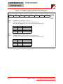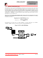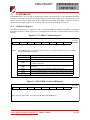
1
Santa Clara University
DEPARTMENT of COMPUTER ENGINEERING
Date: June 6, 2003
I HEREBY RECOMMEND THAT THE THESIS PREPARED UNDER MY
SUPERVISION BY
David Cuccias, Nick Foster, and Matt Strathman
ENTITLED
Wirelessly Controlled Power Outlets
BE ACCEPTED IN PARTIAL FULFILLMENT OF THE REQUIREMENTS FOR THE
DEGREE OF
BACHELOR OF SCIENCE IN COMPUTER ENGINEERING
______________________
THESIS ADVISOR
______________________
DEPARTMENTCHAIR
Wirelessly Controlled Power Outlets
by
David Cuccias, Nick Foster, and Matt Strathman
SENIOR DESIGN PROJECT REPORT
Submitted in partial fulfillment of the requirements
for the degree of
Bachelor of Science in Computer Engineering
School of Engineering
Santa Clara University
Santa Clara, California
June 6, 2003
Wirelessly Controlled Power Outlets
David Cuccias, Nick Foster, and Matt Strathman
Department of Computer Engineering
Santa Clara University
2003
ABSTRACT
Currently home and business owners are limited to manipulating power outlets with hard
wired switches and are blind to where power is consumed in a building. In attempt to
solve this problem we created a system using advanced wireless and circuit technology to
allow the user to manipulate his or her wall outlets via Intranet and WAP capable cell
phones as well as viewing power consumption totals to monitor individual outlets. We
were able to produce a system to accomplish this goal with a control box that
communicates to circuitry implanted in each outlet and accessible via a web site hosted
on the control box. The implementation what we used was not necessarily the best or
most cost effective, for mass production other considerations would need to be
considered in order to make the product more viable.
Keywords: Wireless Communication, Power Regulation, Embedded Circuitry, COM
Port Communication, ODBC, Software UART, Firmware Development
________________________________________________________________________
Senior Design:
Outlet Power Regulation
________________________________________________________________________
Senior Design:
Acknowledgements
We would like to thank Neil Quinn, our professor, for his guidance and help
throughout this entire process. We wouldn’t have completed it on time without his
extensive knowledge and helpful attitude.
We would also like to thank Michael Strathman for his help in designing the circuitry for
the wall unit. Without his knowledge and previous experience our project would have
never gotten off the ground.
________________________________________________________________________
Senior Design:
Table of Contents
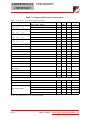
TABLE OF CONTENTS ............................................................................................................................. 3
TABLE OF FIGURES ................................................................................................................................. 6
INTRODUCTION ........................................................................................................................................ 7
DESIGN OVERVIEW ............................................................................................................................... 11
1. OVERVIEW........................................................................................................................................... 11
USER MANUAL ........................................................................................................................................ 14
1. SYSTEM REQUIREMENTS ........................................................................................................... 14
2. MANAGE SYSTEM BY WALL UNITS ......................................................................................... 14
2.1 ADD WALL UNIT ....................................................................................................................... 14
2.2 DELETE WALL UNIT ................................................................................................................ 17
2.3 EDIT WALL UNIT ...................................................................................................................... 19
3. MANAGE SYSTEM BY EVENT SEQUENCE.............................................................................. 21
3.1 ADD EVENT SEQUENCE ......................................................................................................... 21
3.2 DELETE EVENT SEQUENCE .................................................................................................. 23
3.3 EDIT EVENT SEQUENCE ........................................................................................................ 25
4. MANAGE SYSTEM BY IMMEDIATE ACTIONS ....................................................................... 27
4.1 WALL UNIT IMMEDIATE ACTIONS ...................................................................................... 27
4.2 EVENT SEQUENCE IMMEDIATE ACTIONS ........................................................................ 27
5. VIEW SYSTEM................................................................................................................................. 30
5.1 VIEW INDIVIDUAL WALL UNITS .......................................................................................... 30
5.1 VIEW INDIVIDUAL ERRORS................................................................................................... 33
USER INTERFACE ................................................................................................................................... 34
1. OVERVIEW........................................................................................................................................... 34
2. BASIC FUNCTIONALITY....................................................................................................................... 34
2.1.1 Adding/Deleting/Editing Events & Schemes...................................................................................... 35
2.1.2 View Events & Schemes....................................................................................................................... 35
2.1.3 Providing Security................................................................................................................................ 36
3. EXPLANATIONS AND OPTIONS ............................................................................................................ 36
3.1 Choosing a Web Site ..................................................................................................................... 36
3.2 Creating the Web Pages................................................................................................................ 37
3.3 User Requirements........................................................................................................................ 37
4. CELL PHONE INTERFACE .................................................................................................................... 37
4.1 Software Involved......................................................................................................................... 37
4.1.1WAP ....................................................................................................................................................... 38
4.1.2WML...................................................................................................................................................... 38
4.2
Development Software ......................................................................................................... 38
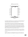
CONTROL BOX SPECIFICATION........................................................................................................ 39
1
OVERVIEW ...................................................................................................................................... 39
2
HARDWARE .................................................................................................................................... 39
2.1
SERVER ...................................................................................................................................... 40
2.1.1
CPU ...................................................................................................................................... 40
2.1.2
Memory................................................................................................................................. 40
2.1.3
Hard Disk ............................................................................................................................. 40
2.1.4
Network................................................................................................................................. 41
2.1.4.1
2.1.4.2
Ethernet...................................................................................................................................... 41
Serial Port .................................................................................................................................. 41
2.2
WIRELESS................................................................................................................................... 42
2.2.1
Component............................................................................................................................ 42
2.2.2
Hardware side Protocols ...................................................................................................... 42
2.3
UNIVERSAL BACKUP SYSTEM .................................................................................................... 42
3
SOFTWARE...................................................................................................................................... 43
3.1
OPERATING SYSTEM................................................................................................................... 44
3.1.1
Web Server............................................................................................................................ 45
3.1.2
WAP Wireless Cell Phone WML Server ............................................................................... 45
3.1.3
ODBC Drivers ...................................................................................................................... 45
3.2
PROGRAM ................................................................................................................................... 45
3.2.1
CheckES................................................................................................................................ 48
3.2.2
Poll ....................................................................................................................................... 49
3.2.3
Immediate ............................................................................................................................. 50
3.2.4
TODO_Handler .................................................................................................................... 51
3.2.5
ToDo ..................................................................................................................................... 51
3.2.6
CheckTODO ......................................................................................................................... 51
3.2.7
Response ............................................................................................................................... 53
3.2.8
SerialIO ................................................................................................................................ 54
3.2.9
Database............................................................................................................................... 55
3.2.10
System Checks.................................................................................................................. 56
3.2.11
System Setup..................................................................................................................... 57
3.3
SOFTWARE SIDE PROTOCOLS ...................................................................................................... 58
3.3.1
Ethernet ................................................................................................................................ 58
3.3.2
Wireless ................................................................................................................................ 58
3.3.2.1
3.3.2.2
3.3.2.3
3.3.2.4
3.3.3
Control Box Sending ................................................................................................................. 59
Control Box Receiving .............................................................................................................. 59
Sending Packets ......................................................................................................................... 59
Sending Report .......................................................................................................................... 60
OP code ................................................................................................................................ 61
4
DATABASE....................................................................................................................................... 62
5
ALTERNATIVES ............................................................................................................................. 63
5.1
HARDWARE ALTERNATIVES ....................................................................................................... 64
5.1.1
Alternative Computer options............................................................................................... 64
5.1.2
Alternative Wireless options ................................................................................................. 64
5.2
SOFTWARE ALTERNATIVES ........................................................................................................ 64
5.2.1
Alternative Operating systems .............................................................................................. 64
5.2.1.1
5.2.2
Linux/Unix................................................................................................................................. 64
Alternative Compiling software ............................................................................................ 65
5.2.2.1
5.2.2.2
Other C++ compilers ................................................................................................................. 65
Other Languages ........................................................................................................................ 65
6
PREVIOUS IMPLEMENTATION ................................................................................................. 65
7
SYSTEM CHANGES ....................................................................................................................... 68
8
GOLD PLATTING ADDITIONS.................................................................................................... 69
8.1
8.2
DYNAMIC LIGHT SWITCHES ....................................................................................................... 69
FULL DUPLEX COMM COMMUNICATION ..................................................................................... 69
WALL UNIT SPECIFICATION .............................................................................................................. 70
2. BASIC FUNCTIONALITY....................................................................................................................... 70
2.1 Microcontroller Functionality ..................................................................................................... 71
2.2.1 Voltage Sampling ................................................................................................................................. 74
2.2.2 Current Sampling ................................................................................................................................ 75
2.3 Triac Control ................................................................................................................................ 76
SENIOR DESIGN: ..................................................................................................................................... 79
OTHER ISSUES ......................................................................................................................................... 79
2. SOCIAL................................................................................................................................................. 79
3. POLITICAL ........................................................................................................................................... 79
4. ECONOMIC .......................................................................................................................................... 79
5. HEALTH AND SAFETY.......................................................................................................................... 80
6. MANUFACTURABILITY ........................................................................................................................ 80
7. SUSTAINABILITY.................................................................................................................................. 80
8. ENVIRONMENTAL IMPACT .................................................................................................................. 80
9. USABILITY ........................................................................................................................................... 80
10, LIFELONG LEARNING ....................................................................................................................... 80
CONCLUSION ........................................................................................................................................... 82
________________________________________________________________________
Senior Design:
Table of Figures
FIGURE 1: ADD WALL UNIT .......................................................................................................................... 16
FIGURE 2: DELETE WALL UNIT ..................................................................................................................... 18
FIGURE 3: EDIT WALL UNIT .......................................................................................................................... 20
FIGURE 4: ADD EVENT SEQUENCE ................................................................................................................ 22
FIGURE 5: DELETE EVENT SEQUENCE ........................................................................................................... 24
FIGURE 6: EDIT EVENT SEQUENCE ................................................................................................................ 26
FIGURE 7: IMMEDIATE ACTION ..................................................................................................................... 29
FIGURE 8: VIEW WALL UNIT ......................................................................................................................... 32
FIGURE 9: CONTROL BOX FLOW CHART ....................................................................................................... 44
FIGURE 10: CONTROL BOX USE CASE ........................................................................................................... 46
FIGURE 11: CONTROL BOX OBJECT MODEL DIAGRAM ................................................................................. 47
FIGURE 12: CHECK EVENT SEQUENCE UML DIAGRAM ................................................................................ 48
FIGURE 13: POLLING UML DIAGRAM ........................................................................................................... 49
FIGURE 14: IMMEDIATE ACTION UML DIAGRAM ......................................................................................... 50
FIGURE 15: CHECK TODO QUEUE UML DIAGRAM ....................................................................................... 52
FIGURE 16: RESPONSE UML DIAGRAM ........................................................................................................ 53
FIGURE 17: SERIAL I/O UML DIAGRAM ....................................................................................................... 54
FIGURE 18: DATABASE CONNECTION UML DIAGRAM ................................................................................. 55
FIGURE 19: SYSTEM CHECKS UML DIAGRAM .............................................................................................. 56
FIGURE 20: SYSTEM SETUP UML DIAGRAM ................................................................................................. 57
FIGURE 21: 40 BIT SEND COMMAND ............................................................................................................. 60
FIGURE 22: ACK/NAK COMMAND ................................................................................................................. 60
FIGURE 23: REPORT COMMAND .................................................................................................................... 61
FIGURE 24: DATABASE RELATIONSHIPS ........................................................................................................ 63
FIGURE 25: WALL UNIT BLOCK DIAGRAM .................................................................................................... 71
FIGURE 26: VOLTAGE SAMPLING .................................................................................................................. 74
FIGURE 27: CURRENT SAMPLING .................................................................................................................. 75
FIGURE 28: TRIAC BLOCK DIAGRAM............................................................................................................. 76
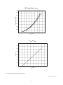
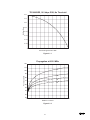
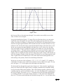
FIGURE 29: TRIAC IV CHARACTERISTICS ...................................................................................................... 77
________________________________________________________________________
Senior Design:
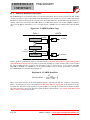
Introduction
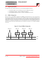
Proximity limits the amount of control people have over their wall switches and
the appliances attached to them. We developed a system that controls and monitors the
power flowing through wall outlets allowing users to have complete control over their
homes and businesses no matter where in the world they are. Additionally, our system
will show the power usage history of each individual outlet allowing the user to better
understand specifics of power usage in their home or business. The system is able to
control all wall outlets in a building and actively communicate with them gaining
information and storing it in a database for later retrieval. The main goal of the project
was to combine as many disciplines that we have learned from Santa Clara University
together and learn and include others as well.
Similar systems are already on the market; however they don’t include everything
ours has to offer. These systems use X-10 technology which uses existing power lines to
send bits of information slowly. These systems do not offer power regulation like our
system would provide, and they do not gain power information to be stored for later
reference. Our main goal behind this project was not to build a better competing system
to be placed on the market but to learn and use as many technologies as possible.
To complete these goals the following steps were completed to produce our system.
Embedded Circuitry: A circuit was designed capable of dropping the input voltage
from the “hot” wire of a power outlet down to a measurable level. Measurements
taken are proportional to the actual value, in order to be converted back to a
useable value when transmitted to the control box. This circuitry had to be
integrated with a microcontroller capable of communicating with the control box
to provide a programmable interface with the circuitry and a link between the
base station and the wall units. All components purchased for power control and
sampling had to be integrated together, including a transceiver, a microcontroller,
an optically isolated TRIAC for each outlet, and each of the sampling networks to
completely implement all necessary functionality of the embedded component.
Firmware for Wall Units: The hardware cannot control itself and needed software
running on the chip to perform specified functions. This software is called the
firmware for the embedded circuitry. The firmware for the wall units was created
so that after receiving a command it performs the appropriate task. This includes
all UART communication and PIN control on the chip. This software was
developed using the Cygnal development kit that was purchased with the Cygnal
chip that was used.
Wireless Communication: The design decision was made to use wireless
communication between the wall units and the control box to gain a better
understanding and practical usage of this new technology. We preformed
extensive research on wireless communication so that we could learn how to
harness the technology. Once research was completed we decided to use the
TR1000 wireless transceiver because of its development kit and the simplicity of
how to connect it to the rest of the embedded circuitry. After installing the device
we had to start to take baby steps in understanding exactly how to send bytes of
information from one transceiver to another.
Wireless Packet Protocols: we had to create protocols for ending all the wall unit
information and command structure. We had to take into account some wireless
limitations as well as limit the number of bits being sent across the airwaves. We
developed a simple set of command structures including opcodes and check sums
to ensure that all the data reached its destination correctly.
Building Control Box Hardware: Before any work could start on the control box we
had to choose the hardware and build it. The hardware was chosen to both
optimize the performance and limit the cost. We decided on a basic Athalon
chipset with 512 Mb of RAM and a 20 Gb hard drive. We also needed to choose
software to perform low level program handling tasks to allow the many separate
parts of the software to communicate. We choose to use Microsoft Windows
2000 Advanced Server because of its capabilities and our prior knowledge setting
it up and using it.
Creating Database Tables: System information has to be stored in a safe and protected
way, a database provides this function. The specifics of the database had to be
created including all tables, relationships and variables. Power consumption
totals has to be stored for each outlet so that users can learn about power usage for
the system. Other system information includes name, location, and address for
each wall unit and event sequence. Microsoft Access was chosen to meet this
requirement because of the simple connectivity to the Microsoft ODBC drivers
used with Windows 2000 Server.
Designing Program to Interface with Database and Serial Communication: A
program had to be created to provide the main functionality of the control box.
The program has to interface with the database and relay all commands to the
serial port so that the wireless transceiver can send them out the wall outlets. In
addition the program had to keep track of the time to know when to send
commands. This program was developed using Rhapsody 4.0 C++ UML
development kit. It allowed for simple tread creation and auto generation of code
from graphical UML drawings.
Creating User Interfaces: Design the dynamic website and WAP interface to allow the
user to view and manage the system. These interfaces had to be simple enough for
even the most non-technical user to use hassle-free. The dynamic webpage was
created using Microsoft .NET software which allowed for easy on the fly
generated websites. The WAP WML cell phone website was created using a trial
version of MobileDev studio which allowed a graphical implementation of WML
code. Both systems interface with the database to provide on the fly generated
sites for the user to view and manipulate the system.
________________________________________________________________________
Senior Design:
Design Overview
1. Overview
As we develop technology to make, what used to be impossible, tasks
simpler, we in turn make our lives more complicated. There used to be a time
where all we had to remember was when to feed the stock animals and when to
plow the fields to survive. However as we have moved away from the simple
fields and into a down town metropolis our lives have been over whelmed with
responsibilities which may seem simple but by the mere magnitude of them they
become dizzying to any person. Tasks like turning off lights as one leave a room,
or waiting to use the washer and dryer until after 7pm to conserve power are
things that many don’t have time to remember let alone complete.
These easy
tasks can actually cost people lots of money if high power appliances are left on
while owners are on vacations and some can actually cause disaster. In these
complicated times there is a way to help people handle all the burdens that
technology puts on us, or at least some of them. Our project does exactly this, by
allowing users to manage the power using appliances in their house.
To solve the problem we propose a system to help users take
charge of their appliances in their household. We propose a system that takes
charge of a users home to allow the user to relax and let computers handle these
tasks. The system needs to be compiled of three major parts, a browser on the
users home PC to interface the system, a central control box to manipulate the
system, and all the devices implanted into the wall sockets. These devices allow
power to flow through them when turned on by the main control and restrict
power when turned off, main control can also tell the devices to regulate the
power flowing across. The main control box needs to be connected to both of the
other components so that it function correctly. It needs to be able to receive
information from the devices, send commands to the devices and receive
information from the home users PC. The control box must be able to keep track
of each device and store information about the device including hardware address,
device pass code (so device knows its talking to central box), users given name
for outlet, location of device given by user, current total of power flowed across.
Main control also must keep track of user events that manipulate any number of
devices, and main control must be able to complete an event’s tasks when the start
time occurs. Each event will have a start time and a list of devices and what to do
with them. These events are created by the user and can be edited from the home
PC at the users whim.
The devices must be small enough to fit into a wall socket and be able to
pass the current fire safety code. Each device must be connected to the main
control so that it can receive any orders and be able to send its current power flow
information when asked. The device must be able to calculate the amount of
power that is flowing across the outlet when polled and send it back. The devices
must be able to know that they are communicating with the main control and not
some other computer. The devices must be within 100ft of the central box so that
they can be assured of talking to control box and not another computer. The
device needs to be able to restrict power flowing across the outlet so it can
comply with the instructions of main control and the user. The device needs to be
inexpensive because of the number of devices needed will make the price of the
entire system enormous.
The software that will run on the users home PC must be easy to use and
understand. It must give the user an easy way to interface the network of devices
in the outlets. The PC must be connected to the control box so that information
can be passed back and forth. The software must allow capabilities to edit, delete,
or create new schemes, turn on or off any device in the house, setup up the house
graphically, change the attributes of any of the devices and change any user
information.
________________________________________________________________________
Senior Design:
User Manual
1. SYSTEM REQUIREMENTS
Once the wall units have been installed and the server is up and running use any
type of web browser to access your system. Accessing your system can be broken
down into two categories; Managing and Viewing your system.
2. MANAGE SYSTEM BY WALL UNITS
There are two main categories of system management; by Wall Unit and by Event
Sequence. The features for both are the same but have different requests.
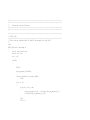
2.1 ADD WALL UNIT
By clicking on the button in the left-hand side menu that says “Add Wall
Unit” you send a command for the system to search through every wall
unit present.
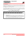
WARNING
This may take some time and your system will
be temporarily out of service during this search.
Once the search has completed the wall units that were found will appear
with input boxes. These input boxes are to allow you to name your wall
units and give them a location. These attributes will make it easier in the
future to know which wall unit you are managing and viewing.
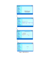
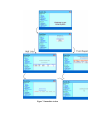
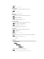
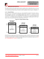
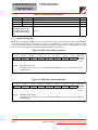
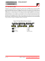
See Flow Chart below for the web pages in sequence.
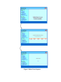
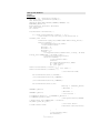
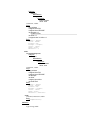
Figure 1: Add Wall Unit
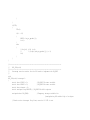
2.2 DELETE WALL UNIT
By clicking the button in the left-hand side menu that says “Delete Wall
Unit” you go to a table of the attributes of all the wall units that are in your
system. On the right side of the table there is a column titled “Delete?”
To delete a wall unit simply click on the “Delete” button in the “Delete?”
column of the desired wall unit.
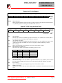
See Flow Chart below for the web pages in sequence.
Figure 2: Delete Wall Unit
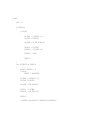
2.3 EDIT WALL UNIT
By clicking the button in the left-hand side menu that says “Edit Wall
Unit” you go to a table of the attributes of all the wall units that are in your
system. On the right side of the table there is a column titled “Edit?”
To edit a wall unit simply click on the “Edit” button in the “Edit?” column
of the desired wall unit.
The selected wall unit information will appear with the current
information entered. To change an attribute simply delete the current
information and type in the changes. To reset all the values click on
“Reset”. Click on the “Submit” button at the bottom when you have made
the changes.
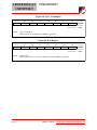
See Flow Chart below for the web pages in sequence.
Figure 3: Edit Wall Unit
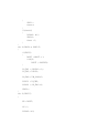
3. MANAGE SYSTEM BY EVENT SEQUENCE
3.1 ADD EVENT SEQUENCE
When you click the button in the left-hand side menu that says “Add
Event Sequence” a form will appear. Enter the values for the event
sequence name, start time, start date, end date, and the days for it to
operate on.
When you are done click on the “Submit” button.
Another selection appears that shows all the available wall units to add to
this event sequence. To select a wall unit for operation left click your
mouse on the name of the desired wall unit. To select multiple wall units
hold down the ‘Ctrl’ while clicking on the wall unit names.
Once all the desired wall units are selected click on the “Wall Units
Selected” button.
The table that appears will list all the selected wall units and the possible
operations; Turn On, Turn Off, Low Power, Low/Medium Power,
Medium Power, High/Medium Power, High Power.
Click on the desired operation for each wall unit and they will perform
that action at the time the event sequence starts.
Click on the “Submit” button to add the event sequence.
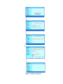
See Flow Chart below for the web pages in sequence.
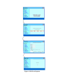
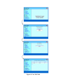
Figure 4: Add Event Sequence
3.2 DELETE EVENT SEQUENCE
By clicking the button in the left-hand side menu that says “Delete Event
Sequence” you go to a table of the attributes of all the event sequences and
their related wall units that are in your system. On the right side of the
table there is a column titled “Delete?”
To delete a event sequence simply click on the “Delete” button in the
“Delete?” column of the desired event sequence.
See Flow Chart below for the web pages in sequence.
Figure 5: Delete Event Sequence
3.3 EDIT EVENT SEQUENCE
By clicking the button in the left-hand side menu that says “Edit Event
Sequence” you go to a table of the attributes of all the event sequences that
are in your system. On the right side of the table there is a column titled
“Edit?”
To edit a event sequence simply click on the “Edit” button in the “Edit?”
column of the desired event sequence.
The selected event sequence information will appear with the current
information entered. To change an attribute simply delete the current
information and type in the changes. To reset all the values click on
“Reset”. Click on the “Submit” button at the bottom when you have made
the changes.
See Flow Chart below for the web pages in sequence.
Figure 6: Edit Event Sequence
4. MANAGE SYSTEM BY IMMEDIATE ACTIONS
Immediate actions operate selected wall units and event sequences in real time.
4.1 WALL UNIT IMMEDIATE ACTIONS
Click on the “Immediate Action” button on the left-hand side menu.
Click on the “Wall Unit” button in the center of the page to operate
individual wall units.
A table appears with all the wall units and their attributes in the system.
Select the desired wall unit.
A form appears with the options for operating the specified wall unit.
These options are Turn On, Turn Off, Low Power, Low/Medium Power,
Medium Power, High/Medium Power, High Power.
Once the option is selected click on the “Operate” button.
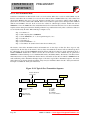
See Flow Chart below for the web pages in sequence.
4.2 EVENT SEQUENCE IMMEDIATE ACTIONS
Click on the “Immediate Action” button on the left-hand side menu.
Click on the “Event Sequence” button in the center of the page to operate
individual event sequence.
A table appears with all the event sequences and their attributes in the
system.
Select the desired event sequence.
This will run the wall units and their specific operations that are defined in
the selected event sequence.
See Flow Chart below for the web pages in sequence.
Figure 7: Immediate Action
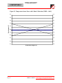
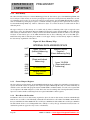
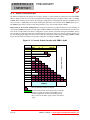
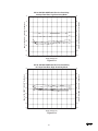
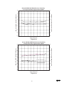
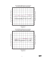
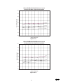
5. VIEW SYSTEM
You can view the system performance in terms of Power, Voltage, and Current
consumption for wall units.
5.1 VIEW INDIVIDUAL WALL UNITS
Click on the “View Individual Wall Units” on the left-hand side menu.
A list will appear showing all the different filters for selecting the wall
units; “by Name”, “by Location”, and “by ID”.
Each of these buttons will display a list of all the attribute you selected.
For example if you selected the “by Name”, a list of all the wall units will
appear and the names will be the buttons.
Select on the desired wall unit.
A list of dates will appear. These dates are the dates that this wall unit was
active.
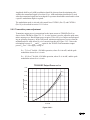
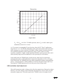
Select on the desired date to view its performance.
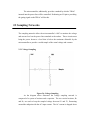
A graph will appear with the selected wall unit’s power consumption
throughout the course of the selected date.
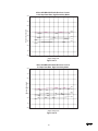
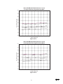
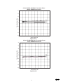
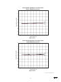
NOTICE
The power consumption graph is the default graph. To view
different graphs for the selected wall unit click on the buttons below.
The “Current” button will show the current consumed by this wall unit
during the selected date. The “Voltage” button will show the voltage
consumed by this wall unit during the selected date.
See Flow Chart below for the web pages in sequence.
Figure 8: View Wall Unit
5.1 VIEW INDIVIDUAL ERRORS
Click on the “Error Log” on the left-hand side menu.
A list will appear showing all the errors the system collected.
________________________________________________________________________
Senior Design:
User Interface
1. Overview
User interfaces allow a user to control a system or device. In this manner our user
interface will allow the customer to manage, view, and operate their system of devices.
This document explores the implementation details of the user interface, as well as
specifics concerning design decisions regarding components, protocols, and performance.
2. Basic Functionality
The user interface is meant to provide the customer with a method for
interaction with the system through the control box. The control box will host a
web site that will provide this functionality. This web page will be on the Internet
either home or business. The web site will allow the user to operate the system on
any operating system and computer with a browser.
2.1 User Interface Functionality
The user interface serves several purposes, including:
§
Add events & schemes (An event is a scheduled operation to a specific
device. Schemes contain multiple events and execute them
concurrently.)
§
Deleting events & schemes
§
Editing events & schemes
§
View events & schemes by:
Ø Types of devices
Ø Individual devices
Ø Individual schemes
Ø Overall
§
Providing Security
§
Notify user on specified events
2.1.1 Adding/Deleting/Editing Events & Schemes
The user can create an event with the attributes; Name of Device, Time of
Operation, Devices & What they do, Days of the Week, Reoccurring
(Y/N), and Length of Operation. These will be sent to the control box for
storage and scheduling.
Deleting an event or scheme will send the control box the information to
delete said event or scheme from storage.
Editing events or schemes will update the control box with the necessary
information. The user can edit events individually, or by schemes.
2.1.2 View Events & Schemes
The web site displays the following scenarios for viewing the system and
it’s devices. This will also show the devices’ information, including the
power usage, schemes, name, location, and status.
2.1.2.1 Types of Devices
There are different types of devices (fluorescent lights, incandescent
lights, and machinery). This option allows the user to view all the devices’
information and their schemes according to their type.
2.1.2.2 Individual Devices
This option allows the user to single out a specific device and view it’s
information.
2.1.2.3 Individual Schemes
This option allows the user to single out a specific scheme and view its
devices and their information.
2.1.2.4 Overall
This option shows all the devices and their information.
2.1.3 Providing Security
First the web page will require a user login and password. We will use
security constraints to ensure that the system isn’t tampered with. We will
force the login name and the password to be different from each other. The
control box then checks login/password combinations that are basic hacker
attempts such as ROOT/ROOT and GUEST/GUEST. The web page will lock
for a, yet to be determined, time if there are ten consecutive incorrect login
attempts within a certain amount of time. These measures block attempts to
break into the system and provide the user with peace of mind and confidence
in the system.
3. Explanations and Options
3.1 Choosing a Web Site
The system controller could be in the form of a program installed onto the
user’s PC. This would require various versions of the program for different
computers’ requirements. The issue of connecting the control box to the users
PC through the COMM port is a complex issue when taking into account the
different types of computers on the market today. Setting up a web site for the
system controller allows any user with a PC that can browse the Internet to
use the system.
3.2 Creating the Web Pages
The web site was created using Microsoft Development Studios Professional
.NET. The control box will host the web pages. Any other web design
program would be acceptable for the development of the web site.
3.3 User Requirements
The user’s home computer would require an Ethernet card, which can be
purchased for a relatively low cost. The Ethernet card is needed to
communicate with the control box.
4. Cell Phone Interface
In order to allow users to manipulate the system from outside their homes there
needs to be a interface that can be accessed almost anywhere. We chose to use a
cell phone to interface the system because of the accessibility of cell phones.
However this is not an easy feature to include. To accomplish this task we would
either need to attach the control box to a phone line and have the user call into and
access the server or use a Wireless Access Protocol (WAP) enabled server to host
a cell phone web page. We chose to use a WAP enabled server because there is
no requirement for a modem or a hard dedicated phone line to the server.
4.1 Software Involved
This cell phone functionality requires some extra software be added to the
control box as well as a few software protocols that need to be observed.
All cell phones that can access the web use a special internet to access the
web. These sites are WAP enabled to limit the amount of information that
needs to be passed between the cell phone and the site.
4.1.1WAP
Wireless Access Protocol. This is the current protocol used by cell
phones to pass information over the cell phone web. We have to
observe this protocol if we want to send information to to a cell
phone and if we want to send information back to the site. Luckily
WAP does allow for ASP pages to be enabled for cell phone web
use.
4.1.2WML
Wireless Markup Language. This is the current language that cell
phone web browsers can understand. It is a subset of XML with a
pre-defined set of tags. We used WML version 1.1 which is the
latest version enabled on all phones. The tags have been predefined to limit the amount of software needed on the cell phone.
4.2 Development Software
We used a development suite to create and manage our cell phone web
site. It is called MobileDev Studio and offers many features helping a user
create a cell phone web site. It offers a graphical relationship view which
helps visually create the site including how a visitor would move from one
page to the next. It also offered a set of templates in creating a page that
helped with lots of the low lever WML functionality. However this software
was very frustrating because it would reject code that was correct but not in
the prefect pre-defined order. So it was very tough to learn their pre-defined
order but after the few speed bumps our site was up and running in no time.
________________________________________________________________________
Senior Design:
Control Box Specification
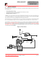
1 Overview
The main control box acts as the central point between the other two portions of
the system. It communicates to the Wall Units, send commands to them and
receive power information from them. It also is to be able to communicate with
the users home PC so that it can receive commands from the user and send
information about the house’s wall units when requested. The system is able to
perform these functions within a few seconds but, if any function gets delayed the
system can handle an extra second or two wait, and even up to a delay of less than
30 seconds. The system cannot have delays of over 30 seconds because every 30
seconds polling orders are sent to the devices, so if the delay was over 30 seconds
the orders queue could become bigger and exceed space limitations. The central
control box has two major components, the hardware and the software. There are
no size requirements for the central control box, and there are relatively few other
requirements and restrictions but those that do exist will be discussed in the
appropriate section. The cost of the box should be minimized as much as possible
to allow the feasibility of placing the final product on the market for consumers to
buy.
2 Hardware
The hardware is composed of individual components that allow software to run.
The hardware has little requirements that need to be considered. Those that do
exist are met with the hardware that we chose. The three main requirements are: a
connection between the central control box and the wall units, another is the cost
of the hardware, and finally the central control box needs be connected with the
users home PC. They will be discussed later in the section. To limit cost and
complexity, most of the control box will be composed of software to complete the
required tasks. The hardware’s only responsibility is to run the software and
provide the control box with appropriate ways of communicating with the rest of
the system.
2.1
Server
The hardware needs to meet all the requirements for the control box. We
choose to use a Microsoft server to act as the back ground operating
system. We need to have hardware to meet the minimum hardware
requirements of Windows 2000 server. However we also want to choose
hardware better then the minimum to allow the server to function better
and faster. There are 4 major parts of the server that we had to consider:
CPU, Memory, Extra Disk, and Network.
2.1.1 CPU
The minimum CPU to run windows server is a Intel Pentium 100
MHz. However this would offer slow performance, we decided to use
an AMD Athalon 2000+ XP. This chip offers us all the computing
power that we Windows 2000 Server needs and also allows for fast
speeds.
2.1.2
Memory
The configuration that we have chosen does require a fair amount of
RAM. We have chosen to use 512Mb which should be more than
enough to complete all the functions of the control box.
2.1.3
Hard Disk
Windows Server requires at least 2 Gigabytes of hard disk space to
run, but with the database software that we have chosen to use much
more hard disk space is needed to perform correctly. The system that
we bought offered a 60 Gigabyte hard drive. This will be more then
enough to let our system run well.
2.1.4
Network
The central control box needs to be connected with both the wall
devices and the users home PC. The wall devices will be connected
wirelessly. The wireless component is connected to the server via the
serial port so the network between the hardware and the wall units is
done by RS232 communication. The users PC will be connected to
the hardware via Ethernet connection to allow a fast connection.
2.1.4.1
Ethernet
The board computer comes with Ethernet capability built into it.
This is what connects the users home pc to the central control box
and allows the user to interact with the system. Ethernet was
chosen because the User Interface that was chosen is web based
and Ethernet is the networking system of the Internet. Using the
Ethernet port simplifies the connection of the users home PC to the
system and lowers the cost because now we do not have to add a
wireless component to the users PC and we don’t have to install
new software.
2.1.4.2
Serial Port
The serial port is built into the board computer. This is the
component that will connect the central computer with the wall
units via the added wireless component. Using the serial port for
the connection of the wireless component allows us to buy a prebuilt wireless board with serial connection, which limits the work
involved when connecting the components. Because the
2.2
Wireless
The connection between the central computer and the Wall Units will be
done via wireless communication. This was decided to avoid re-wiring of
the users home. We could also have chosen to use X-10 technology
however we wanted to gain experience with wireless technology and
therefore made the decision to use it. The wireless portion of the hardware
can be broken down into the Component and the Protocols used to send
data across this network.
2.2.1
Component
The Component is a simple chip and connected antenna to send out the
data. The chip receives data over the RS232 port and then modifies
the data to be in conformance of the protocols needed to send it across
the wireless network. This chip was chosen because it was the most
affordable with the best development kit that we could find. It only
uses 900 MHz technology which is not top of the line, and if this were
to be developed 2.4 GHz should be considered.
2.2.2
Hardware side Protocols
The wireless component uses the data that is being sent across the
network to charge the capacitor. Therefore we need an equal number
of 1’s and 0’s so that we don’t over or under charge the capacitor.
2.3
Universal Backup System
The database automatically saves any updates that are made. However if
there is a power failure we want to make sure that the system shuts down
correctly. This is why we included a backup system with the box. Instead
of building one we purchased a 5 minute APC backup power supply. The
APC not only provides an extra 5 minutes of power but it also provides
software to create a proper shutdown sequence.
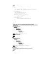
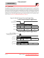
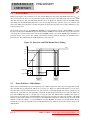
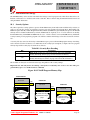
3 Software
The software side of the system provides all the functionality of the system that the
hardware doesn’t. The main functionality of the software is to check for event
sequences, keep track of time, send commands to the devices, poll the devices for
current power information, and host the user interface. We are using Microsoft’s
CTime function in the AFX classes to handle keeping track of time. Event
sequences handling are discussed in section 3.2.1. Commands are sent via the
RS232 port with the SerialIO thread in section 3.2.8. The devices are polled every
30 seconds and the information is stored in the database. The user interface is hosted
by the system with the internet hosting service provided by windows 2000 advanced
server.
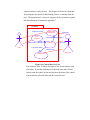
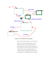
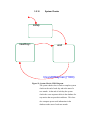
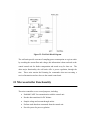
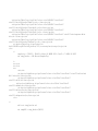
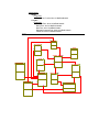
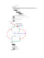
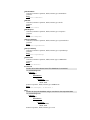
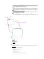
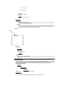
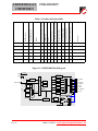
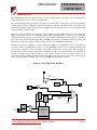
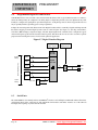
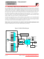
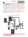
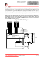
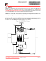
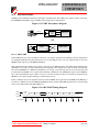
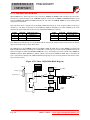
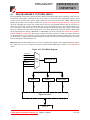
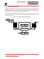
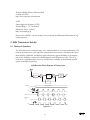
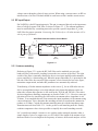
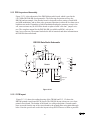
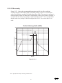
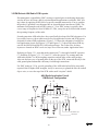
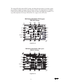
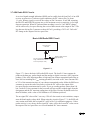
Figure 9: Control Box Flow Chart
This is the control box flow chart. The program interacts with the database and
reacts to the information. It checks the database at specified intervals to do different
tasks and create a todo object which is then executed and sent out through the
serialIO thread and inserted into the response queue.
3.1
Operating System
The central control box will be powered by Microsoft Windows 2000
server, which will in turn run the program that allows the system to
function. Windows Server is a well-defined operating system that is
compatible with many sets of hardware including the one that we have
chosen. We needed an operating system that could host a web page for
the user interface, keep up the database, and run the program.
3.1.1 Web Server
Because of our decision to use an intranet web site as the user
interface the server needs be capable of serving the web page.
Microsoft 2000 Advanced server accomplishes this function. It
uses web hosting software to allow information to be passed when
requested for on specified ports. We used port 80 which is the
default web port.
3.1.2 WAP Wireless Cell Phone WML Server
Because we wanted to offer a service to allow users to manipulate
their system anywhere in the world we needed to develop a cell
phone web page system that could perform basic tasks. However
we couldn’t just use the web page that we already created because
it uses a much different technology and contains way too much
information to send to a cell phone. We used a development studio
to create the WML pages called MobileDev. This allowed us to
create the pages using default templates and then make
modifications after creation. It also gave a graphical flow chart of
how the site goes from one state to the next.
3.1.3 ODBC Drivers
Microsoft Windows 2000 Advanced server also offers drivers that
connect databases to other running programs including web sites.
We used these drivers to connect and interact with the database. It
stands for Open DataBase Connectivity.
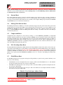
3.2
Program
The program will be the main functionality of the central computer. It will
handle keeping track of everything, including time and the event
sequences that are set by the user. The program will also be responsible
for hosting the user interface and listening for new commands from the
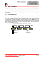
user. The program has 11 classes to complete all the operations required.
Full documentation is included in appendix C.
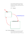
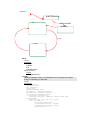
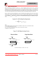
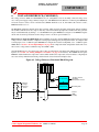
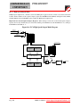
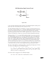
ControlBox
creates and edits
user
interface
interacts with <<display>>
User
<<requests data>>
network link
events and
sequences
commands
<<add/delete and schedule>>
system
commands
collects data
Wall_Unit
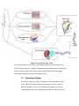
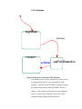
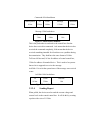
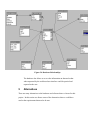
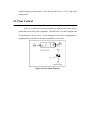
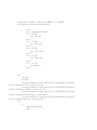
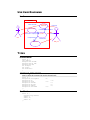
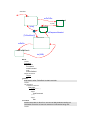
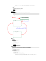
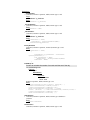
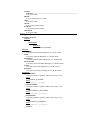
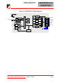
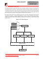
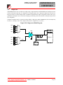
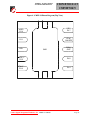
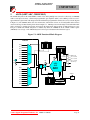
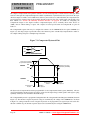
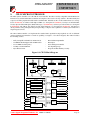
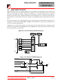
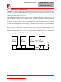
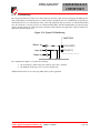
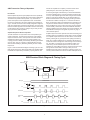
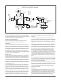
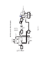
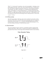
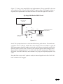
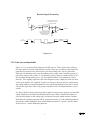
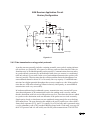
Figure 10: Control Box Use Case
This is the use case. It shows how parts of our system interact with
each other. It provides information on how the user and wall unit
interact with the control system and also how the parts of the control
system interact with each other and the external actors.
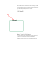
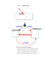
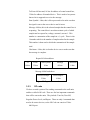
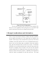
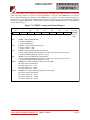
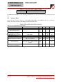
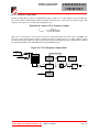
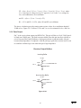
Figure 11: Control Box Object Model Diagram
This is the object model diagram. It shows how the system uses each
class and how they interact together. Each class has a special function
discussed in a section below. These duties range form database
communication to creating polling commands.
We have chosen to write the program in the C++ language through the
Rhapsody compiler. This allows us to create our program visually and
then transform it into code.
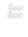
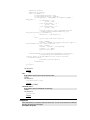
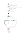
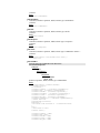
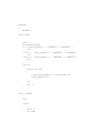
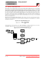
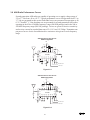
3.2.1 CheckES
waitToConnect
evConnected1
wait
tm((60 - TimeSeconds()) * 1000)
checkDB>
Figure 12: Check Event Sequence UML Diagram
The CheckES class checks the database at the start of every
minute to see if an event sequence needs to start. This class
interfaces the database and receives information about all
the event sequences stored within. When an event
sequence is started this class creates a ToDo through the
TODO_Handler with the opcode in the database.
3.2.2 Poll
waitFORconnect
wait
evConnected2
tm((TimeSeconds())*1000)
create_TODO>
Figure 13: Polling UML Diagram
This class creates polling commands for every wall unit in
the database. It performs this operation on every half-
minute mark. When it needs to poll the devices it creates a
ToDo through the TODO_Handler with a polling opcode.
3.2.3 Immediate
waitFORconnect
wait
evConnected3
clearDB>
tm(1000)
checkDB>
Figure 14: Immediate Action UML Diagram
This class continuly checks the database to see if there are
any immediate action commands that the user has initiated.
If there are then this class creates the required todo’s and
initiates the process of executing the command. It also has
two special immediate actions, one starts a search for new
wall units and the other immediately starts an event
sequence.
3.2.4 TODO_Handler
This class handles the creation and handing out of
assignments to be done. When either of the CheckES or
Poll class needs to create a todo so the system can send the
command to a device they use the NewTODO() function
within the TODO_Handler. Then the TODO_Handler
creates a todo it sends an event to the checkTODO class.
CHeckTODO then uses the getNextTODO function to get
the attributes of the next todo in the queue.
3.2.5 ToDo
This class holds the attributes of a command that need to be
completed. The TODO_Handler creates and keeps track of
the current ToDo’s.
3.2.6 CheckTODO
wait
evDoToDo
secondwait
tm(1000)
[else]
getToDos
C
evResponseNeeded
[ToDosExist()]
sendCommand>
evReDo
waitForReSend>
tm(1000)
Figure 15: Check ToDo Queue UML Diagram
This class waits in an idle state for an event to let it know
that there are todo’s in the queue that need to be done.
When it receives the event it continues and runs the
function todosexist() which returns a true if todos exist or
false if they don’t. If a false is returned it goes back to the
idle state until it receives the event again. If a true is
returned it proceeds and builds the command to be sent to
the effected device. CheckTODO then uses the serialIO
class to send the built command to the respected device.
On the successful completion of sending the command,
CheckTODO creates sends the information about the todo
to the response class.
3.2.7
Response
wait
evWaitforResponse
getResponse>
Figure 16: Response UML Diagram
After a command has been sent out this class is signaled.
This class waits for a response on the serial port and
compares the response to what is expected. This class uses
the serialIO class to read and write on the serial port. If the
read fails response then re-creates the todo that failed and it
goes back through the queue to be sent out.
3.2.8 SerialIO
startIO
Figure 17: Serial I/O UML Diagram
This class operates the communication to the serial port. It
is always in a running state incase CheckTODO or
Response need to send or receive something on the port.
3.2.9 Database
beginState
[OKtoStart]
connect>
evSetup
waitForDBdetection
Figure 18: Database Connection UML Diagram
The database class is used to connect every other class in
the program that needs to access the database to the
database. It simply sets up the ODBC connection using a
pre-defined name and the Microsoft ODBC drivers to
connect. Then classes use functions to create a database
object, execute a SQL command, and execute a SQL
command with requesting information back.
3.2.10
System Checks
setup
newDay>
wait
tm(endOfDayCalc()*1000)
Figure 19: System Checks UML Diagram
The system checks class is used to complete system
checks at the end of each day and at the start of a
new month. At the end of each day the system
checks the event sequence tables in the database for
any entries that are past their end dates. This class
also compacts power total information in the
database at the start of each new month.
3.2.11
System Setup
detect>
[entries]
C
[else]
findDevices>
systemGO>
evFIND
Figure 20: System Setup UML Diagram
The system setup class is used to check the database when
the power is turned on to check to see if there are any wall
unit entries. If no this means that it is the first time the
system has been turned on or there has been a major error.
In either case the system needs to search for wall units. It
does this by systematically checking each possible address
combination for each 8 bit portion of the wall unit address.
Then it combines an answers to find out the entire address
for each wall unit. This function can also be induced by the
user from the web page.
3.3
Software side Protocols
There are certain protocols that need to be followed to make sure that
everything can communicate correctly. Talking over a network needs to
be regulated to make sure that messages are sent across the network
correctly.
3.3.1
Ethernet
The connection between the control box and the users pc will be
running over regular Ethernet and therefore must take on the protocols
of an Ethernet network. It will be using TCP/IP to allow the user to
access the hosted interface easily with only using an IP address. The
system must manipulate the data being sent over the Ethernet to adhere
to the standards of Ethernet and TCP/IP protocols.
3.3.2
Wireless
There are many protocols that need to be considered when sending out
commands to and from these wall units wirelessly. The main one is to
make sure that commands don’t come in on top of each other. This is
important because the system needs to be able to receive single
packets at a time not, and not garbage of many packets on top of one
another.
3.3.2.1
Control Box Sending
The control box will send out commands to the devices at given
intervals. The system will then wait to receive an Ack or a Nak
from the devices. If no Ack is received the system will re-send the
data again. This will happen 5 times, and if after 5 times the
device can still not receive data an error message will be logged
and shown to the user next time they log onto the user interface.
3.3.2.2
Control Box Receiving
The Control box doesn’t need to send an Ack or a Nak after it
receives information from the device because the device will
assume that the control box received the information. If there is
something wrong with the checksum or the packet is not received
then the control box will simply re-send the command to request
information.
3.3.2.3
Sending Packets
This is what is sent out to the wall devices by the control box when
a command is processed. 70 bits will be sent out over the wireless
network.
To/From: 48 bits, what is used to tell the devices where the
message is from and to single out the device that needs to be
commanded: 16 bits for the “from” part and 32 bits for the “to”
portion.
Start Symbol: 8 bits like a password to let the device know the
message is for it and it starts right afterwards.
Message: 12 bits, 3 for the OP code, 8 for the raise/lower offset,
and one bit to let the device know which outlet is being changed.
Checksum: This is what the device uses to confirm the message is
complete. The size will be 12 bits to.
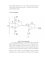
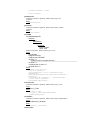
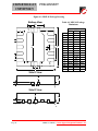
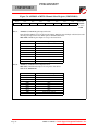
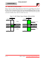
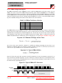
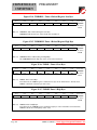
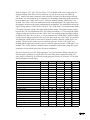
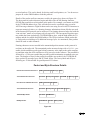
Command 40 bit breakdown
Start Symbol
To
From
Message
Checksum
8 bits
32 bits
16 bits
12 bits
12 bits
Message 12 bit breakdown
OpCode
Offset
Outlet select
3 bits
8 bits
1 bit
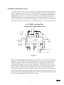
Figure 21: 40 Bit Send Command
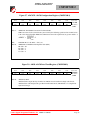
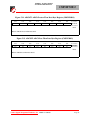
This is the packet that is sent back to the control box after the
device has received its commands. Ack means that the device has
received the command completely; Nak means that the device
received something intended for it but there was a problem during
the transmission. They both have the same format of 14 bits.
To/From: 48 bits total; 16 bits for address of central control box,
32 bits for address of intended device. This is used to let systems
know who is supposed to receive the message.
Ack/Nak: 1 bit to let the system know if the message was received
or not.
Ack/Nak 14 bit breakdown
To
From
Ack/Nak
16 bits
32 bits
1 bit
Figure 22: Ack/Nak Command
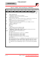
3.3.2.4
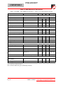
Sending Report
When polled, the devices need to send the current voltage and
current levels to the central control box. It will do this by creating
a packet with a size of 112 bits.
To/From: 48 bits total; 16 bits for address of central control box,
32 bits for address of intended device. This is used to let systems
know who is supposed to receive the message.
Start Symbol: 8 bits; this is like a password to let make sure that
the signal is sent to the correct device and is in tact.
Message: 48 bits; this is the selected sample that the control box is
requesting. The control box is on a three minute cycle of which
sample total to request for; voltage, current 0, current 1. This
number is a summation of the sample in a ½ cycle. There is also
16 number which is the number of samples taken for the sample.
This number is then used to divide the summation of the sample
total.
Checksum: 8 bits; this is what the device uses to make sure that
the message is complete.
Report 96 bit breakdown
To
From
Start Symbol
Message
Checksum
16 bits
32 bits
8 bits
48 bits
8 bits
Message 64 bit breakdown
Selected Sample
Num Samples
32 bits
16 bits
Figure 23: Report Command
3.3.3
OP code
We have created a protocol for sending commands to the wall units
and have called it OP code. There are few but important commands
that will be sent to the units. They include: Turn On, Turn Off,
Regulate Power Level, and Report. There are only 4 commands that
need to be sent to devices, so the OP Code can consist of 3 bits:
000: Report
010:Turn On
011:Turn Off
100:Regulate Power
his implementation allows us to easily check to see what the command
is by bit comparison. If the command is a raise power or lower power
command then an extra 8 bits will be attached for the amount needed
to raise or lower. This will be the phase angle needed to have the
TRIAC on the device cut the power curve at the right points.
4
Database
Data storage on the control box will be down with an Access database.
Using a database allows a safe, reliable way to store all the information
that the system will need and access. The database allows us to relate the
data together. Through the ODBC drivers our program can use
Microsoft’s afx classes to communicate between the database and the
program. The data relationships are shown below.
Figure 24: Database Relationships
The database also allows us to save the information on demand so that
when requested by the web based user interface could be queried and
reported to the user.
5
Alternatives
There are many alternatives to the hardware and software that we choose for this
project. In this section we discuss some of the alternatives that we could have
used or the requirements that need to be met.
5.1
Hardware Alternatives
5.1.1
Alternative Computer options
The central control box doesn’t have many requirements that it needs
to fill. Almost any hardware would have worked yet we choose the
AMD chipset and Windows server and the capabilities it has. Also
being a component we will be buying, we don’t want to have to worry
about issues of combining incompatible hardware together.
5.1.2
Alternative Wireless options
There are many wireless options out there and most would work for
this system. We chose this one because it seems the best for the cost
was available and dev kit gave two devices and better value for the
money and satisfied requirements.
5.2
Software Alternatives
5.2.1
Alternative Operating systems
Any Operating system that offered web hosting abilities and database
connection techniques could be used. Linux was our other option but
we made the decision to go with Microsoft because of simplicity.
5.2.1.1
Linux/Unix
Linux could have been used, it is an excellent choice to run web
applications. It also is a good operating system to host a database
however our group has more experience using Microsoft products
and the connection techniques.
5.2.2
Alternative Compiling software
5.2.2.1
Other C++ compilers
We could use another compiling program to help us create our
system but we feel that Rhapsody is better because it allows us to
compile the written UML code, which is used to design the system,
into a working program. This saves a step of work. This makes
the process easier to create our project.
5.2.2.2
Other Languages
Other languages could be used, but because the devices will be
written in C we feel it best to write the system in C++. Plus the
school has a license for Rhapsody with C++ only.
6
Previous Implementation
This hardware implementation was not the first we thought of but this it was the
one that satisfied the goals of the project. We originally were going to use a more
embedded set of hardware including a single board computer with limited space
and resources. However we ran into limitations; disk space to store system
information, VxWorks operating system transfer failures, and Webify web server
short comings. These problems were not found until the third week of the second
quarter and therefore the change to a new set of hardware was needed quickly.
This is the main reason why we choose to use the windows 2000 advanced server
setup because it was easy to obtain through the school and we all understood how
it functioned. Here is the previous set of design decisions.
Here is the previous implementation design document.
2 Hardware
The hardware is composed of individual components that allow
software to run. The hardware has little requirements that need to be
considered. Those that do exist are met with the hardware that we
chose. The three main requirements are: a connection between the
central control box and the wall units, another is the cost of the
hardware, and finally the central control box needs be connected with
the users home PC. They will be discussed later in the section. To limit
cost and complexity, most of the control box will be composed of
software to complete the required tasks. The hardware’s only
responsibility is to run the software and provide the control box with
appropriate ways of communicating with the rest of the system.
2.1 Board Computer
The board computer will be the hardware for our central control box. It
is a 386 PC based computer. The size is small enough that the home
user can put it anywhere in their home. The board computer can be
mounted into a box just bigger then the size of a hardback book. The
cost is minimized to a couple hundred dollars. The board computer is
an all in one 386 PC with Ethernet and serial connections built in. The
gain for buying the already built computer is that it limits the
compatibility issues involved with combining different hardware
components. There are 4 major parts of the hardware: CPU, Memory,
Extra Disk, and Network. Full manufacture technical specs can be
viewed in an Appendix.
2.1.1 CPU
The CPU that comes with the board computer is a 386 chip. Speed
was not a requirement that we had to consider and this chip is plenty
fast for our central control box. This chip offers more than enough
performance power with a small cost and is compatible with most PC
based hardware and software on the market.
2.1.2 Memory
There is 512 kilobytes of RAM. This will be plenty of space to store
the software of the central control box and all of the data that the
system needs. If more is needed, then swapping to the flash disk will
be necessary.
2.1.3 Flash/Extra Disk
There is 512 kilobytes of Flash Disk. This will allow us to write the
software and data to save incase the system goes down due to loss of
power. The Flash Disk has a limit on the number of writes that can be
executed, only 10,000 writes are guaranteed before the disk starts to
degrade to the point where writing and reading are not possible. We
have chosen to write to the disk once a week when changes have been
made to backup the system as well as the simple UPS system when
power is detected as unavailable. If 512K is not enough, an extra
32Mb Flash Disk can be used for additional storage, but it has the
same constraints of the onboard Flash Disk.
2.1.4 Network
Same as current implementation.
2.1.4.1 Ethernet
Same as current implementation.
2.1.4.2 Serial Port
Same as current implementation.
2.2 Wireless
Same as current implementation.
2.3 Universal Backup System
Same as current implementation.
3 Software
The software side of the system provides all the functionality of the
system that the hardware doesn’t. The main functionality of the
software is to check for event sequences, keep track of time, send
commands to the devices, poll the devices for current power
information, and host the user interface. A simple thread discussed in
section 3.2.1.1 will handle keeping track of time. Event sequences
handling are discussed in section 3.2.1.2. Commands are sent via the
RS232 port. The devices are polled every 30 seconds and the
information is stored on the central computer. The user interface is
hosted by the system through the Webify component of Rhapsody; this
is discussed in section 3.2.1.4.
3.1 Operating System
The central control box will be powered by VxWorks, which will in
turn run the program that allows the system to function. VxWorks is a
well defined operating system that is compatible with many sets of
hardware including the one that we have chosen. VxWorks also gives
us libraries to connect our software to the ports and hardware that our
system needs to function. It also provides a powerful set of debugging
tools that will help us perfect our system. Due to storage limitations
we needed to choose an operating system that could be contained in a
very small amount of space. We approximate that VxWorks kernel and
the bare trimmings of extra software needed to run the system can be
contained in less than 128K of disk space. (Plus, the school has a
license for it so we wouldn’t have to buy any software.)
7
System Changes
Currently the system design that we used to complete this project is not the most
optimal. This design is too costly for a user to buy and insert into his or her
home. The product would need to be smaller and reduced in scope to limit cost.
The control box doesn’t need to have all the functionality of a full server. All the
control box needs is a web server, a database, and a limited OS to handle
multithreaded applications. The control box would most likely look like a small
box about the size of a Linksys switch router. In fact the control box would
probably offer other functions such as a router and a switch. This way we could
sell the box as an all in one unit that the user would just need to plug into the
incoming internet connection and offer a home network to the user.
8
Gold Platting additions
During the process of contemplating and creating this system, we came up with
many extra parts that could be added to the system to make it have more
functionality or a better product for purchase but there wasn’t enough time to
implement them. In this section we will discuss the gold plating additions that
could be added with more work or new hardware.
8.1
Dynamic Light Switches
One possible addition to our project would be to add the functionality to
light switches. This would require removing them from the hardwire on
and off to an outlet and making them work through the control box. This
would allow for dynamic re-allocation of switches. It would save home
owners from the pesky light switch that people always seem to turn off
that resets the alarm clock or turns off the TV. This would require a little
tinkering with the software because currently it is only listening for
communication after a command has been sent out and this new feature
would require constant listening.
8.2
Full Duplex Comm communication
Currently we are using half duplex communication which is a major
limitation because we can not send and receive at the same time. In future
versions full duplex communication would be desired to limit problems of
communicating on the same wires for both sending and receiving.
________________________________________________________________________
Senior Design:
Wall Unit Specification
1. Overview
The “wall unit” is a piece of hardware that is inserted into an outlet or
switch fixture located in the wall of a house or place of business, and is implanted
in such a way that it is connected to the incoming power cables in order to
monitor and regulate the power consumption. This information is then passed
back to a central “command unit,” which in turn performs a series of
computations and stores the data for later use in regulation schemes and power
consumption graphs. This document explores the implementation details of the
“wall unit,” as well as specifics concerning design decisions regarding
components, protocols, and performance.
2. Basic Functionality
Figure 25: Wall Unit Block Diagram
The wall units provide a means of sampling power consumption on a given outlet
by recording the current flow and voltage, this information is then sent back to the
central control unit for further computation and stored away for later use. The
other major functionality the wall units offer is power regulation, through the
triac. These units remain idol listening for commands when not executing a
received instruction and are slaves to the central control unit.
2.1 Microcontroller Functionality
The micro-controller serves several purposes, including:
•
Establish UART for communication with the control unit
•
Encode data transitions for DC balance
•
Sample voltage and current through outlets
•
Perform tasks based on commands form the control unit
•
Provide system for power regulation
2.1.1 UART
The wall unit uses a software implementation for the UART.
Additionally, the UART is required to run at 2400 baud to allow for integration
with the wireless ASH transceiver that we have chosen to use. It is not essential
to have high-speed data rates because the amount of information being
transmitted will not be overwhelming, thus 2400 baud is sufficient.
UART transmission begins with a two byte preamble followed by an
automatically appended start symbol to the beginning of every packet. Another
start symbol is used at the beginning of every 32 bit word in order to guard
against random data reception. In the receive direction the UART waits for
reception of these two unique start symbols in order to begin data reception.
Once a packet is either transmitted or received a flag is raised in order to notify
completion and signal to start processing data in the case of a received packet.
2.1.2 Encoding Transactions for DC Balance
The wireless transceiver we have picked requires data to be DC balanced
in order to achieve accurate sampling and data slicing over the course of a receive
or transmit. This is due to the way in which the transceiver is designed; it uses an
AC-coupled capacitor to maintain precision while performing data slicing. The
problem with this scheme is, if the capacitor’s charge becomes skewed to either
the ‘1’ or the ‘0’ side of the information stream, data corruption becomes more
and more likely; thus, a method of balancing transaction must be implemented.
There are two popular methods of achieving this balance, Manchester
encoding and symbol conversion tables.
Manchester coding, unfortunately,
doubles the length of a transaction because a one is represented by a ‘1’ followed
by a ‘0’ and a zero is represented by the exact opposite. On the other hand,
conversion tables only require a 6:4 ratio of encoded data to original data.
Symbol tables will usually, either be base on converting a byte or a nibble at time,
into a DC balanced pattern. Also, these schemes must take into account the
number of consecutive ones or zeros allowed during transmission. Manchester
coding does this without any additional thought because it uses both a one and a
zero for each data bit, affectively limiting the reoccurrence of successive ones or
zeros to one. Symbol tables on the other hand, look to balance over the course of
a bytes transmission, by applying consideration for balance during development
of the symbols used and limiting the number of reoccurring successive ones or
zeros.
We have implemented Manchester encoding in our system by sending out
a bit followed by its inverse in the transmit direction and receiving only every
other byte in the receive direction.
2.1.3 Analog Sampling of Current and Voltage
The microcontroller is required to have an onboard analog to digital
converter. The resolution of the ADC is not overly important because we can
increase accuracy using over sampling and averaging. Additionally, this is
possible because we are sampling a signal of such low frequency (60 Hz) that
over sampling was not be a problem.
The chip we have selected has an onboard ADC with 8 bit resolution, and
inputs can be programmed from any of the eight I/O pins supplied. One pin is
used to sample voltage for both outlets, and another two pins sample current, one
for each outlet.
The microcontroller samples the current and voltage values
evenly over one half cycle and stores the summation of these samples into
memory for transmission back to the control station when polled.
2.1.4 Decipher and Execute Commands
The microcontroller receives commands in the form of opcodes, packaged
inside the payload of packets. These opcodes are deciphered upon reception, and
the individual commands are executed. Commands include: turn on, turn off,
regulate power to a given level, and return voltage and current data.
2.1.5 System for Regulating Power
The microcontroller, additionally, provides a method by which a TRIAC
inserted into the power line will be controlled. Dedicating an I/O pin to providing
the gating signal on the TRIAC will do this.
2.2 Sampling Networks
The sampling networks allow the microcontroller’s ADC to monitor the voltage
and current level on the power lines attached to the outlets. These circuits must
bring the power down to a level that is below the maximum allowable by the
microcontroller to provide a scaled sample of the actual voltage and currents.
2.2.1 Voltage Sampling
Figure 26: Voltage Sampling
As the diagram above illustrates the voltage sampling network is
composed of a system of resistors and a capacitor. The two vertical resistors, R2
and R3, are used to keep the sampled voltage between 0V and 3V, fluctuating
around the midpoint with the AC input current. The AC current is dropped down
from its original value by the R1 to +/-1.5V, in order use the entire spectrum of
voltage values provided by the on chip ADC. The capacitor is used to strip DC
voltage off the input voltage.
2.2.2 Current Sampling
Figure 27: Current Sampling
The Current sampling network is based around a high common-mode
difference amplifier balanced for unity gain. However, for our purposes we have
added a resistor to the negative input in order to provide a +30X gain. This is
necessary because the difference between our positive and negative input pins is
only 50mV, effectively lessening the resolution of our ADC by not utilizing the
full range of values available.
The gain, additionally, allows for maximum
resolution because we are again using the two resistors and 3VDC to keep the
sampled voltage between 0 and 3 volts; this gain allows for +/-1.5V swing at the
sample point.
2.3 Triac Control
A triac is a solid-state switch consisting of a pnpn junction and a gate to
control the on/off state of the component. Pictured below is a block diagram and
IV characteristics of the device. In our design the triac will be responsible for
regulating the current flow to an outlet controlled by our devices.
Figure 28: Triac Block Diagram
Figure 29: Triac IV Characteristics
The triac needs to be gated on and it will latch on for the remainder of the
half cycle, so power regulation is done by firing the triac at a given phase angle
and the average power allowed to pass is dropped based on the angle.
3. Design Considerations and Alternatives
There are many microcontroller alternatives available with similar capabilities,
but the simplicity and package size of the Cygnal chip were ultimately more
desirable. Maxim chips were also considered for our project; they fit the criteria
of additions, such as ADC and 8051 or PIC core for a standardized instruction set.
However, the cost of the Maxim chips was prohibitive, because they tended to
offer a little more horsepower than is necessary for our project. The Motorola
DSP56F801 was also considered, and this chip is a little more robust in that is has
dual ADC for sampling current and voltage at the same time and component
available onboard able to be configured into a power line modem, but the chip is a
little more complex and a bit more expensive. Additionally, the development kit
offered by Cygnal cost substantially less and offers much more. The Cygnal
development environment offer great debug tools over JTAG cable, and excellent
control of the internal workings of the chip.
As for the transceiver, there was a more limited selection. The major deciding factor was
the development kit.
The RFM TR100 development kit contains two transceivers
programmed to talk to each other right out of the box, and they can be detached from the
base microcontroller board. This allows for the transceiver to be attached easily to our
Cygnal chip, to speed up the development process. This transceiver, also, operates in the
correct frequency band and has adequate range to satisfy our needs. The cost of this
component is be a bit impractical, but the experience may be invaluable.
________________________________________________________________________
Senior Design:
Other Issues
________________________________________________________________________
1. Ethical
The only ethical issue that develops from our project is a concern for more
security. If these wall units were installed into businesses, factories, and homes then a
person could potentially breech the system and essentially take control of the wall units
overriding the owner’s wishes. In this regard the lack of ultimate security could be an
ethical issue.
2. Social
The social effect our product would have is added flexibility in personal lives and
more efficient businesses. Home users can use this product to turn on appliances at a
home before they arrive. Business owners can maximize profit by eliminating excessive
electric bills by using the precise amount for their production.
3. Political
There are no political considerations for our product.
4. Economic
Other options that are mentioned previously like using X-10 instead of wireless
technology would reduce the cost of each wall unit and subsequently the overall cost of
the system. The cost of product development would be significantly lower than the initial
presentable due to the cost of development kits.
5. Health and Safety
The only Health and Safety issue would be an appliance that is left on for more
time than deemed safe. An example would be a toaster or oven left on would be a threat
to a home.
6. Manufacturability
This product has been built and can be built smaller to better fit into a wall outlet.
The development time issue is negligible. Potential problems that would arise are getting
individual Microsoft Servers for each user and automating the manufacturing for each
wall unit.
7. Sustainability
Our wall units are built to handle the maximum allowable current and voltage that
is supplied to a home or business by power companies. For there to be any issues, the
power supplier would have to alter the standard.
8. Environmental Impact
There are no environmental concerns with our product.
9. Usability
Our product is very user-friendly. Once the wall units are installed it is a step-bystep process to set the system up.
10, Lifelong Learning
The development and research of this product forced us to learn material not
covered at Santa Clara University. We did however use most of what we have learned at
Santa Clara University on top of the new material in the development of this product.
________________________________________________________________________
Senior Design:
Conclusion
Many technologies were incorporated in the development of this project, most of
which we had a base for reference but some forced us to start from scratch and
completely broaden our scope of knowledge. Among the technologies disciplines
included in this system were wireless communications, embedded systems programming,
circuit design, ASP pages, WML, multithreaded program development, serial
communications, and ODBC commands. All of these components were combined to
produce a system that allows an end user to interface and control his/her outlets thought
the use of a web interface, ether on a cell phone or computer. Additionally, power totals
can be displayed, to allow the user to monitor power consumption across individual
outlets.
This project allowed us the opportunity to make design decisions based on many
factors including funding, time, component integration, and design requirements. The
final design was the result of tough choices in some cases and obvious decisions in
others. Additional factors considered in design were quality of development kits in the
case of hardware, where robust development kits were able to accelerate the design
process tremendously. In particular the Cygnal IDE included with the C8051F300
development kit was indispensable, allowing viewing of registers in the chip, stepping
through firmware code, and activating break points. Without this software product
development may have been impossible in the allotted amount of time. In addition, the
rigid time table forced us to budget time, and make decisions concerning scope based on
the issues with time pressure.
The design, although an overall success, could be improved if redone or revised.
Ideally, the control box would not be a conventional computer running Windows 2000
Server; instead, it would be some form of box running a cheaper OS capable of
supporting multithreaded applications, hosting web pages and a database. The circuitry
in the wall units could also be improved to handle different types of loads on the outlets
more effectively, and would probably not be implemented with a wireless data link due to
issues with cost.
This experience gained while implementing this project was invaluable to our
growth as engineers and will be an important reference in the years to come.
________________________________________________________________________
Senior Design:
Appendix A
Foundation.asp
<%@ Language=VBScript %>
<HTML>
<HEAD>
<TITLE>Menu Page</TITLE>
<META http-equiv="PICS-Label" content='(PICS-1.1 "http://www.icra.org/ratingsv02.html" l gen
true for "http://www.elizabeth-carson.com" r (ca 1 lz 1 na 1 nb 1 nc 1 nd 1 ne 1 nf 1 ng 1 nh 1 oz 1 vz 1)
"http://www.rsac.org/ratingsv01.html" l gen true for "http://www.elizabeth-carson.com" r (n 4 s 4 v 0 l
0))'>
<meta http-equiv="Content-Type" content="text/html; charset=windows-1252">
<meta name="publisher" content="ScotchInc">
<meta name="owner" content="ScotchInc">
<meta name="author" content="ScotchInc">
<meta name="copyright" content="Copyright(c)2003 by ScotchInc / all rights reserved">
<meta name="GENERATOR" content="Microsoft FrontPage 5.0">
</HEAD>
<body bgcolor=#0066cc>
<Table bgcolor=#66ccff width="100%">
<tr>
<td bgcolor=#66ccff><font size="14" face="TimesNewRoman">Scotch Inc.</font></td>
<td bgcolor=#66ccff align=right height="12"><IMG alt="flag" src="flagus.gif"></td>
</tr>
</Table>
<table border="1" bgcolor="#0033cc" width="100%">
<tr>
<td width="25%" colspan="15" bgcolor="#99ffff"><H2><u>Manage System</u></H2>
<strong>Wall Units</strong><br>
<strong>-></strong><A
href="MS_WU_add2.asp"><strong>Add
Wall Unit </strong>
<br>
</A> <strong>-></strong><A
href="MS_WU_Delete2.asp"><strong>Delete
Wall Unit </strong>
<br>
</A> <strong>-></strong><A
href="MS_WU_edit2.asp"><strong>Edit
Wall Unit </strong>
<br>
</A> <strong>Event Sequences </strong>
<br>
<strong>-></strong><A
href="MS_ES_add2.asp"><strong>Add
Event Sequence </strong>
<br>
</A> <strong>-></strong><A
href="MS_ES_Delete2.asp"><strong>Delete
Event Sequence </strong>
<br>
</A> <strong>-></strong><A
href="MS_ES_edit2.asp"><strong>Edit
Event Sequence </strong>
<br>
</A> <strong>Immediate Action </strong>
<br>
<stong>-></stong><A href="IAWU2.asp"><strong>Immediate Action
Commands</strong><br>
<br>
</A>
<H2><u>View System</u></H2>
<strong>Wall Units Information</strong><br>
<strong>-></strong><A
href="IWUPage2.asp"><strong>Individual
Wall Units</strong><br>
</A> <strong>-></strong><A
href="AllWU2.asp"><strong>All
Wall Units</strong><br>
</A> <strong>Event Sequences' Information</strong><br>
<strong>-></strong><A
href="IEventPage2.asp"><strong>Individual
Event Sequences</strong><br>
</A> <strong>-></strong><A
href="Events2.asp"><strong>All
Event Sequences</strong></A>
<br> <strong><A href="errorpage.asp">Error Log</strong></a><br>
</td>
<% ' ====================================================== WELCOME PAGE
=================================== %>
<td align="center" width="80%" bgcolor="#ccffff">
<img src="squirrels.jpg"><br>
<font align="center" size="24" color="#330033" face="Arial">Welcome to your
</font>
<br>
<font align="center" size="24" color="#330033" face="Arial">Home System
</font>
</td>
</tr>
</table>
</body>
AllWU2.asp
<%@ Language=VBScript %>
<HTML>
<HEAD>
<TITLE>Menu Page</TITLE>
<META http-equiv="PICS-Label" content='(PICS-1.1 "http://www.icra.org/ratingsv02.html" l gen
true for "http://www.elizabeth-carson.com" r (ca 1 lz 1 na 1 nb 1 nc 1 nd 1 ne 1 nf 1 ng 1 nh 1 oz 1 vz 1)
"http://www.rsac.org/ratingsv01.html" l gen true for "http://www.elizabeth-carson.com" r (n 4 s 4 v 0 l
0))'>
<meta http-equiv="Content-Type" content="text/html; charset=windows-1252">
<meta name="publisher" content="ScotchInc">
<meta name="owner" content="ScotchInc">
<meta name="author" content="ScotchInc">
<meta name="copyright" content="Copyright(c)2003 by ScotchInc / all rights reserved">
<meta name="GENERATOR" content="Microsoft FrontPage 5.0">
</HEAD>
<body bgcolor=#0066cc>
<Table bgcolor=#66ccff width="100%">
<tr>
<td bgcolor=#66ccff><font size="14" face="TimesNewRoman">Scotch Inc.</font></td>
<td bgcolor=#66ccff align=right height="12"><IMG alt="flag" src="flagus.gif"></td>
</tr>
</Table>
<table border="1" bgcolor="#0033cc" width="100%">
<tr>
<td width="25%" colspan="15" bgcolor="#99ffff"><H2><u>Manage System</u></H2>
<strong>Wall Units</strong><br>
<strong>-></strong><A
href="MS_WU_add2.asp"><strong>Add
Wall Unit </strong>
<br>
</A> <strong>-></strong><A
href="MS_WU_Delete2.asp"><strong>Delete
Wall Unit </strong>
<br>
</A> <strong>-></strong><A
href="MS_WU_edit2.asp"><strong>Edit
Wall Unit </strong>
<br>
</A> <strong>Event Sequences </strong>
<br>
<strong>-></strong><A
href="MS_ES_add2.asp"><strong>Add
Event Sequence </strong>
<br>
</A> <strong>-></strong><A
href="MS_ES_Delete2.asp"><strong>Delete
Event Sequence </strong>
<br>
</A> <strong>-></strong><A
href="MS_ES_edit2.asp"><strong>Edit
Event Sequence </strong>
<br>
</A> <strong>Immediate Action </strong>
<br>
<stong>-></stong><A href="IAWU2.asp"><strong>Immediate Action
Commands</strong><br>
<br>
</A>
<H2><u>View System</u></H2>
<strong>Wall Units Information</strong><br>
<strong>-></strong><A
href="IWUPage2.asp"><strong>Individual
Wall Units</strong><br>
</A> <strong>-></strong><A
href="AllWU2.asp"><strong>All
Wall Units</strong><br>
</A> <strong>Event Sequences' Information</strong><br>
<strong>-></strong><A
href="IEventPage2.asp"><strong>Individual
Event Sequences</strong><br>
</A> <strong>-></strong><A
href="Events2.asp"><strong>All
Event Sequences</strong></A>
<br> <strong><A href="errorpage.asp">Error Log</strong></a><br>
</td>
<% ' ====================================================== WELCOME PAGE
=================================== %>
<td align="center" width="80%" bgcolor="#ccffff">
<strong>The Table Below Is The Information Of Every Wall Unit</strong>
<%
Set DB = Server.CreateObject("ADODB.connection")
DB.Open "CB"
SearchString = "SELECT * FROM Wall_Unit ORDER BY ID"
Set DB_Results = DB.Execute(SearchString)
'temporary table just to handle Date problems
'makeTable = "CREATE TABLE tempDate (id NUMBER, Date CHAR(10))"
'set try = DB.Execute(makeTable)
'response.Write(makeTable)
%>
<table border="0" width="60%" height="50%" ID="Table1">
<tr>
<table bgcolor=#cccccc border="1" cellPadding="1" cellSpacing="1" width="100%" ID="Table2">
<tr bgcolor=lightblue>
<td bgcolor=LightBlue><p align="left"><font color="blue" face="Arial"
size="3"><b>ID</b></font></p></td>
<td bgcolor=LightBlue><p align="left"><font color="blue" face="Arial"
size="3"><b>Name</b></font></p></td>
<td bgcolor=LightBlue><p align="left"><font color="blue" face="Arial"
size="3"><b>Location</b></font></p></td>
<td bgcolor=LightBlue><p align="left"><font color="blue" face="Arial" size="3"><b>Power
Graph</b></font></p></td>
</tr>
<%
while not DB_Results.eof
set thisID = DB_Results("ID")
'get the date in the Power_Totals table
getDate = "SELECT * FROM Voltage_Total WHERE WUID = " & thisID & " ORDER BY ID"
set gotDate = DB.Execute(getDate)
set thisDate = gotDate("Date")
%>
<tr bgcolor=white>
<td bgcolor=White><p align="left"><font color="#000000" face="Arial" size="3"><%response.Write (thisID)
%></font></p></td>
<td bgcolor=White><p align="left"><font color="#000000" face="Arial" size="3"><%=DB_Results("Name")%>
</font></p></td>
<td bgcolor=White><p align="left"><font color="#000000" face="Arial"
size="3"><%=DB_Results("Location")%> </font></p></td>
<td bgcolor=White><p align="left"><a href=graphIWUDate.asp?WUID=<%response.Write
(thisID)%>>Isolated</a> or <a
href=graphAllWU.asp?WUID=<%response.Write(thisID)%>>Related</a></p></td>
</tr>
<%
DB_Results.MoveNext
wend
%>
</table>
<br><br><br>
<a href=foundation.asp><strong>BACK</strong></a></td>
</tr>
</table>
</body>
Errorpage.asp
<%@ Language=VBScript %>
<HTML>
<HEAD>
<TITLE>Menu Page</TITLE>
<META http-equiv="PICS-Label" content='(PICS-1.1 "http://www.icra.org/ratingsv02.html" l gen
true for "http://www.elizabeth-carson.com" r (ca 1 lz 1 na 1 nb 1 nc 1 nd 1 ne 1 nf 1 ng 1 nh 1 oz 1 vz 1)
"http://www.rsac.org/ratingsv01.html" l gen true for "http://www.elizabeth-carson.com" r (n 4 s 4 v 0 l
0))'>
<meta http-equiv="Content-Type" content="text/html; charset=windows-1252">
<meta name="publisher" content="ScotchInc">
<meta name="owner" content="ScotchInc">
<meta name="author" content="ScotchInc">
<meta name="copyright" content="Copyright(c)2003 by ScotchInc / all rights reserved">
<meta name="GENERATOR" content="Microsoft FrontPage 5.0">
</HEAD>
<body bgcolor=#0066cc>
<Table bgcolor=#66ccff width="100%">
<tr>
<td bgcolor=#66ccff><font size="14" face="TimesNewRoman">Scotch Inc.</font></td>
<td bgcolor=#66ccff align=right height="12"><IMG alt="flag" src="flagus.gif"></td>
</tr>
</Table>
<table border="1" bgcolor="#0033cc" width="100%">
<tr valign=top>
<td width="25%" colspan="15" bgcolor="#99ffff"><H2><u>Manage System</u></H2>
<strong>Wall Units</strong><br>
<strong>-></strong><A
href="MS_WU_add2.asp"><strong>Add
Wall Unit </strong>
<br>
</A> <strong>-></strong><A
href="MS_WU_Delete2.asp"><strong>Delete
Wall Unit </strong>
<br>
</A> <strong>-></strong><A
href="MS_WU_edit2.asp"><strong>Edit
Wall Unit </strong>
<br>
</A> <strong>Event Sequences </strong>
<br>
<strong>-></strong><A
href="MS_ES_add2.asp"><strong>Add
Event Sequence </strong>
<br>
</A> <strong>-></strong><A
href="MS_ES_Delete2.asp"><strong>Delete
Event Sequence </strong>
<br>
</A> <strong>-></strong><A
href="MS_ES_edit2.asp"><strong>Edit
Event Sequence </strong>
<br>
</A> <strong>Immediate Action </strong>
<br>
<stong>-></stong><A href="IAWU2.asp"><strong>Immediate Action
Commands</strong><br>
<br>
</A>
<H2><u>View System</u></H2>
<strong>Wall Units Information</strong><br>
<strong>-></strong><A
href="IWUPage2.asp"><strong>Individual
Wall Units</strong><br>
</A> <strong>-></strong><A
href="AllWU2.asp"><strong>All
Wall Units</strong><br>
</A> <strong>Event Sequences' Information</strong><br>
<strong>-></strong><A
href="IEventPage2.asp"><strong>Individual
Event Sequences</strong><br>
</A> <strong>-></strong><A
href="Events2.asp"><strong>All
Event Sequences</strong></A>
</td>
<% ' ====================================================== WELCOME PAGE
=================================== %>
<td align="center" width="80%" bgcolor="#ccffff">
<strong>The Table Below Is The Information Of Wall Units With ID = </strong>
<%
Set DB = Server.CreateObject("ADODB.connection")
DB.Open "CB"
Set DB_Results = DB.Execute("SELECT * FROM ErrorLog")
%>
<table border="0" width="100%" height="100%" ID="Table1">
<tr>
<td colspan="2" height="10" align="middle">
<br></td>
</tr>
<tr>
<td width="120" valign="top">
</td>
<td width="100%" valign="top">
<div align="left">
<table border="1" cellPadding="1" cellSpacing="1" width="100%" ID="Table2">
<tr bgcolor=lightblue>
<td>
<p align="left"><font color="blue" face="Arial" size="3"><b>Error Code</b></font></p></td>
<td>
<p align="left"><font color="blue" face="Arial" size="3"><b>Error Text</b></font></p></td>
<td>
<p align="left"><font color="blue" face="Arial" size="3"><b>Error Date</b></font></p> </td>
</tr>
<%
while not DB_Results.eof %>
<tr bgcolor=white>
<td>
<p align="left"><font color="#000000" face="Arial"
size="3"><%=DB_Results("Error_Code")%></font></p></td>
<td>
<p align="left"><font color="#000000" face="Arial" size="3"><%=DB_Results("Error_Text")%>
</font></p></td>
<td>
<p align="left"><font color="#000000" face="Arial" size="3"><%=DB_Results("Error_Date")%>
</font></p></td>
</tr>
<%
DB_Results.MoveNext
wend
%>
</table>
<br><br><br>
<a href=foundation.asp><srtong>BACK</srtong></a>
</td>
</tr>
</table>
</body>
ES_AddInsert2.asp
<%@ Language=VBScript %>
<HTML>
<HEAD>
<TITLE>Menu Page</TITLE>
<META http-equiv="PICS-Label" content='(PICS-1.1 "http://www.icra.org/ratingsv02.html" l gen
true for "http://www.elizabeth-carson.com" r (ca 1 lz 1 na 1 nb 1 nc 1 nd 1 ne 1 nf 1 ng 1 nh 1 oz 1 vz 1)
"http://www.rsac.org/ratingsv01.html" l gen true for "http://www.elizabeth-carson.com" r (n 4 s 4 v 0 l
0))'>
<meta http-equiv="Content-Type" content="text/html; charset=windows-1252">
<meta name="publisher" content="ScotchInc">
<meta name="owner" content="ScotchInc">
<meta name="author" content="ScotchInc">
<meta name="copyright" content="Copyright(c)2003 by ScotchInc / all rights reserved">
<meta name="GENERATOR" content="Microsoft FrontPage 5.0">
</HEAD>
<body bgcolor=#0066cc>
<Table bgcolor=#66ccff width="100%" ID="Table3">
<tr>
<td bgcolor=#66ccff><font size="14" face="TimesNewRoman">Scotch Inc.</font></td>
<td bgcolor=#66ccff align=right height="12"><IMG alt="flag" src="flagus.gif"></td>
</tr>
</Table>
<table border="1" bgcolor="#0033cc" width="100%">
<tr>
<td width="25%" colspan="15" bgcolor="#99ffff"><H2><u>Manage System</u></H2>
<strong>Wall Units</strong><br>
<strong>-></strong><A
href="MS_WU_add2.asp"><strong>Add
Wall Unit </strong>
<br>
</A> <strong>-></strong><A
href="MS_WU_Delete2.asp"><strong>Delete
Wall Unit </strong>
<br>
</A> <strong>-></strong><A
href="MS_WU_edit2.asp"><strong>Edit
Wall Unit </strong>
<br>
</A> <strong>Event Sequences </strong>
<br>
<strong>-></strong><A
href="MS_ES_add2.asp"><strong>Add
Event Sequence </strong>
<br>
</A> <strong>-></strong><A
href="MS_ES_Delete2.asp"><strong>Delete
Event Sequence </strong>
<br>
</A> <strong>-></strong><A
href="MS_ES_edit2.asp"><strong>Edit
Event Sequence </strong>
<br>
</A> <strong>Immediate Action </strong>
<br>
<stong>-></stong><A href="IAWU2.asp"><strong>Immediate Action
Commands</strong><br>
<br>
</A>
<H2><u>View System</u></H2>
<strong>Wall Units Information</strong><br>
<strong>-></strong><A
href="IWUPage2.asp"><strong>Individual
Wall Units</strong><br>
</A> <strong>-></strong><A
href="AllWU2.asp"><strong>All
Wall Units</strong><br>
</A> <strong>Event Sequences' Information</strong><br>
<strong>-></strong><A
href="IEventPage2.asp"><strong>Individual
Event Sequences</strong><br>
</A> <strong>-></strong><A
href="Events2.asp"><strong>All
Event Sequences</strong></A>
<br> <strong><A href="errorpage.asp">Error Log</strong></a><br>
</td>
<% ' ====================================================== WELCOME PAGE
=================================== %>
<td align="center" width="80%" bgcolor="#ccffff">
<%
' get data from registration form
set fName = Request.Form("SName")
'
'
'
'
set fSDm = Request.Form("MonthSD")
response.Write fSDm
set fSDd = Request.Form("DaySD")
response.Write fSDd
set fSDy = Request.Form("YearSD")
response.Write fSDy
set fEDm = Request.Form("MonthED")
set fEDd = Request.Form("DayED")
set fEDy = Request.Form("YearED")
set fSTh = Request.Form("HourST")
set fSTm = Request.Form("MinST")
set fAM = Request.Form("AM")
set fPM = Request.Form("PM")
set fDRY = Request.Form("Yes")
set fDRN = Request.Form("No")
response.Write (fDRY)
set fS
=
set fM
=
set fT
=
set fW
=
set fR
=
set fF
=
set fSat
'
'
'
'
'
'
'
'
Request.Form("Sun")
Request.Form("Mon")
Request.Form("Tues")
Request.Form("Wed")
Request.Form("Thur")
Request.Form("Fri")
= Request.Form("Sat")
response.Write
response.write
response.Write
response.write
response.Write
response.write
response.Write
response.Write
Dim thisOpcode
thisOpcode = 0
(fPM)
(fS)
(fM)
(fT)
(fW)
(fR)
(fF)
(fSat)
If (fDRY="DRY") Then
'
response.Write "it gets here"
thisOpcode = thisOpcode + &H80
end If
If (fS = "Sun") Then
thisOpcode = thisOpcode + &H40
end If
If (fM = "Mon") Then
thisOpcode = thisOpcode + &H20
end If
If (fT = "Tues") Then
thisOpcode = thisOpcode + &H10
end If
If (fW = "Wed") Then
thisOpcode = thisOpcode + &H08
end If
If (fR = "Thur") Then
thisOpcode = thisOpcode + &H04
end If
If (fF = "Fri") Then
thisOpcode = thisOpcode + &H02
end If
If (fSat = "Sat") Then
thisOpcode = thisOpcode + &H01
end If
If (fPM = "pm") Then
fSTh = fSTh +12
end If
'response.Write fAM
%><br><%
'response.Write fPM
' Check for invalid Info---------------------------------------------' DO THIS NEXT QUARTER
'
' Display the Wall Units and the related Op Codes
Set DB = Server.CreateObject("ADODB.connection")
DB.Open "CB"
' Insert values in database adding the ES
InsertString = "INSERT INTO event_sequence (StartDate, Name, StartTime, DailyRepeat, EndDate)"
InsertString = InsertString & " VALUES (" &"'" &fSDm & "/"& fSDd &"/"& fSDy & "',"
InsertString = InsertString & "'" & fName & "', "
InsertString = InsertString & "'" & fSTh & ":" & fSTm &"',"
InsertString = InsertString & "'" & thisOpcode & "', "
InsertString = InsertString & "'"&fEDm & "/"& fEDd &"/"& fEDy & "')"
'response.write InsertString & "<BR>"
DB.Execute(InsertString)
'get the ID of the event Sequence
SearchString = "Select * FROM event_sequence WHERE ID ="
SearchString = SearchString & "(Select MAX(ID) FROM event_sequence)"
Set DB_Results = DB.Execute(SearchString)
'Set thisID = DB_Results("ID")
' Insert values in database adding the Daily Repeat days and it's opcode
InsertString2 = "INSERT INTO IA_effects_WU (WUID, offset) VALUES "
InsertString2 = InsertString2 & "(" & "NULL, " & thisID & ")"
'DB.Execute(InsertString2)
%>
<strong>THIS IS THE NEWLY ADDED EVENT SEQUENCE...</strong>
<br><br><br><br><br><br>
<table border="0" width="100%" height="100%" ID="Table1">
<tr>
<td colspan="2" height="10" align="middle">
<br></td>
</tr>
<tr>
<td width="120" valign="top"></td>
<td width="100%" valign="top">
<div align="left">
<table border="1" cellPadding="1" cellSpacing="1" width="100%" ID="Table2">
<tr bgcolor="#ffbe9c">
<td><p align="left"><font color="red" face="Arial" size="3"><b>ID</b></font></p></td>
<td><p align="left"><font color="red" face="Arial" size="3"><b>Name</b></font></p></td>
<td><p align="left"><font color="red" face="Arial" size="3"><b>Start Date</b></font></p></td>
<td><p align="left"><font color="red" face="Arial" size="3"><b>End Date</b></font></p> </td>
<td><p align="left"><font color="red" face="Arial" size="3"><b>Start Time</b></font></p></td>
</tr>
<%
while not DB_Results.eof
Dim thisID
thisID =DB_Results("ID")
%>
<tr bgcolor=white>
<td><p align="left"><font
<td><p align="left"><font
</font></p></td>
<td><p align="left"><font
</font></p></td>
<td><p align="left"><font
</font></p></td>
<td><p align="left"><font
</font></p></td>
</tr>
color="#000000" face="Arial" size="3"><%=DB_Results("ID")%></font></p></td>
color="#000000" face="Arial" size="3"><%=DB_Results("Name")%>
color="#000000" face="Arial" size="3"><%=DB_Results("StartDate")%>
color="#000000" face="Arial" size="3"><%=DB_Results("EndDate")%>
color="#000000" face="Arial" size="3"><%=DB_Results("StartTime")%>
<%
DB_Results.MoveNext
wend
%>
</table>
<br><br><br><br><br><br><br>
<a href=\MS_ES_pickWUs2.asp?eID=<%response.Write thisID%>><strong>Select Wall Units</strong></a>
</div>
</td>
</tr>
</table>
</td>
</tr>
</table>
</body>
ES_DeleteInsert2.asp
<%@ Language=VBScript %>
<HTML>
<HEAD>
<TITLE>Menu Page</TITLE>
<META http-equiv="PICS-Label" content='(PICS-1.1 "http://www.icra.org/ratingsv02.html" l gen
true for "http://www.elizabeth-carson.com" r (ca 1 lz 1 na 1 nb 1 nc 1 nd 1 ne 1 nf 1 ng 1 nh 1 oz 1 vz 1)
"http://www.rsac.org/ratingsv01.html" l gen true for "http://www.elizabeth-carson.com" r (n 4 s 4 v 0 l
0))'>
<meta http-equiv="Content-Type" content="text/html; charset=windows-1252">
<meta name="publisher" content="ScotchInc">
<meta name="owner" content="ScotchInc">
<meta name="author" content="ScotchInc">
<meta name="copyright" content="Copyright(c)2003 by ScotchInc / all rights reserved">
<meta name="GENERATOR" content="Microsoft FrontPage 5.0">
</HEAD>
<body bgcolor=#0066cc>
<Table bgcolor=#66ccff width="100%">
<tr>
<td bgcolor=#66ccff><font size="14" face="TimesNewRoman">Scotch Inc.</font></td>
<td bgcolor=#66ccff align=right height="12"><IMG alt="flag" src="flagus.gif"></td>
</tr>
</Table>
<table border="1" bgcolor="#0033cc" width="100%">
<tr>
<td width="25%" colspan="15" bgcolor="#99ffff"><H2><u>Manage System</u></H2>
<strong>Wall Units</strong><br>
<strong>-></strong><A
href="MS_WU_add2.asp"><strong>Add
Wall Unit </strong>
<br>
</A> <strong>-></strong><A
href="MS_WU_Delete2.asp"><strong>Delete
Wall Unit </strong>
<br>
</A> <strong>-></strong><A
href="MS_WU_edit2.asp"><strong>Edit
Wall Unit </strong>
<br>
</A> <strong>Event Sequences </strong>
<br>
<strong>-></strong><A
href="MS_ES_add2.asp"><strong>Add
Event Sequence </strong>
<br>
</A> <strong>-></strong><A
href="MS_ES_Delete2.asp"><strong>Delete
Event Sequence </strong>
<br>
</A> <strong>-></strong><A
href="MS_ES_edit2.asp"><strong>Edit
Event Sequence </strong>
<br>
</A> <strong>Immediate Action </strong>
<br>
<stong>-></stong><A href="IAWU2.asp"><strong>Immediate Action
Commands</strong><br>
<br>
</A>
<H2><u>View System</u></H2>
<strong>Wall Units Information</strong><br>
<strong>-></strong><A
href="IWUPage2.asp"><strong>Individual
Wall Units</strong><br>
</A> <strong>-></strong><A
href="AllWU2.asp"><strong>All
Wall Units</strong><br>
</A> <strong>Event Sequences' Information</strong><br>
<strong>-></strong><A
href="IEventPage2.asp"><strong>Individual
Event Sequences</strong><br>
</A> <strong>-></strong><A
href="Events2.asp"><strong>All
Event Sequences</strong></A>
<br> <strong><A href="errorpage.asp">Error Log</strong></a><br>
</td>
<% ' ====================================================== WELCOME PAGE
=================================== %>
<td align="center" width="80%" bgcolor="#ccffff">
<%
Set DB = Server.CreateObject("ADODB.connection")
DB.Open "CB"
' get data from registration form
set fID = Request.QueryString("ESID")
' update values in database
InsertString = "DELETE FROM event_sequence WHERE ID = " & fID
DB.Execute(InsertString)
%>
<h3>Deletion Successful!</h3>
<br>
<br>
<br>
<a href=MS_ES_Delete2.asp><strong>BACK</strong></a>
</td>
</tr>
</table>
</body>
ES_EditInsert2.asp
<%@ Language=VBScript %>
<HTML>
<HEAD>
<TITLE>Menu Page</TITLE>
<META http-equiv="PICS-Label" content='(PICS-1.1 "http://www.icra.org/ratingsv02.html" l gen
true for "http://www.elizabeth-carson.com" r (ca 1 lz 1 na 1 nb 1 nc 1 nd 1 ne 1 nf 1 ng 1 nh 1 oz 1 vz 1)
"http://www.rsac.org/ratingsv01.html" l gen true for "http://www.elizabeth-carson.com" r (n 4 s 4 v 0 l
0))'>
<meta http-equiv="Content-Type" content="text/html; charset=windows-1252">
<meta name="publisher" content="ScotchInc">
<meta name="owner" content="ScotchInc">
<meta name="author" content="ScotchInc">
<meta name="copyright" content="Copyright(c)2003 by ScotchInc / all rights reserved">
<meta name="GENERATOR" content="Microsoft FrontPage 5.0">
</HEAD>
<body bgcolor=#0066cc>
<Table bgcolor=#66ccff width="100%">
<tr>
<td bgcolor=#66ccff><font size="14" face="TimesNewRoman">Scotch Inc.</font></td>
<td bgcolor=#66ccff align=right height="12"><IMG alt="flag" src="flagus.gif"></td>
</tr>
</Table>
<table border="1" bgcolor="#0033cc" width="100%">
<tr>
<td width="25%" colspan="15" bgcolor="#99ffff"><H2><u>Manage System</u></H2>
<strong>Wall Units</strong><br>
<strong>-></strong><A
href="MS_WU_add2.asp"><strong>Add
Wall Unit </strong>
<br>
</A> <strong>-></strong><A
href="MS_WU_Delete2.asp"><strong>Delete
Wall Unit </strong>
<br>
</A> <strong>-></strong><A
href="MS_WU_edit2.asp"><strong>Edit
Wall Unit </strong>
<br>
</A> <strong>Event Sequences </strong>
<br>
<strong>-></strong><A
href="MS_ES_add2.asp"><strong>Add
Event Sequence </strong>
<br>
</A> <strong>-></strong><A
href="MS_ES_Delete2.asp"><strong>Delete
Event Sequence </strong>
<br>
</A> <strong>-></strong><A
href="MS_ES_edit2.asp"><strong>Edit
Event Sequence </strong>
<br>
</A> <strong>Immediate Action </strong>
<br>
<stong>-></stong><A href="IAWU2.asp"><strong>Immediate Action
Commands</strong><br>
<br>
</A>
<H2><u>View System</u></H2>
<strong>Wall Units Information</strong><br>
<strong>-></strong><A
href="IWUPage2.asp"><strong>Individual
Wall Units</strong><br>
</A> <strong>-></strong><A
href="AllWU2.asp"><strong>All
Wall Units</strong><br>
</A> <strong>Event Sequences' Information</strong><br>
<strong>-></strong><A
href="IEventPage2.asp"><strong>Individual
Event Sequences</strong><br>
</A> <strong>-></strong><A
href="Events2.asp"><strong>All
Event Sequences</strong></A>
<br> <strong><A href="errorpage.asp">Error Log</strong></a><br>
</td>
<% ' ====================================================== WELCOME PAGE
=================================== %>
<td align="center" width="80%" bgcolor="#ccffff">
<%
Set DB = Server.CreateObject("ADODB.connection")
DB.Open "CB"
thisID = Request.QueryString("EVID")
'get the information without having it sent here
SearchString = "SELECT * FROM event_sequence Where ID="&thisID
'response.write SearchString & "<BR>"
Set DB_Results = DB.Execute(SearchString)
set dr = DB_Results("DailyRepeat")
Dim n
n = 0
dim
dim
dim
dim
dim
dim
drt
sun
mon
tues
wed
thur
dim fri
dim sat
dim
dim
dim
dim
dim
dim
dim
dim
tdrt
tsun
tmon
ttues
twed
tthur
tfri
tsat
drt = 0
sun =0
mon =0
tues=0
wed =0
thur=0
fri =0
sat =0
dim moddr
moddr = dr -254
'response.Write(moddr)
Dim subNum
subNum =0
if ((dr MOD 128)>0) then
subNum = 128
drt = 1
end if
if ((dr-subNum)>0) AND(((dr - subNum) MOD 64)>0) then
subNum = subNum +64
sun = 1
end if
if ((dr-subNum)>0) AND(((dr - subNum) MOD 32)>0) then
subNum = subNum +32
mon = 1
end if
if ((dr-subNum)>0) AND(((dr
subNum = subNum +16
tues = 1
end if
if ((dr-subNum)>0) AND(((dr
subNum = subNum +8
wed = 1
end if
if ((dr-subNum)>0) AND(((dr
subNum = subNum +4
thur = 1
end if
if ((dr-subNum)>0) AND(((dr
subNum = subNum +2
fri = 1
end if
if ((dr-subNum)=1) then
subNum = subNum +1
sat = 1
end if
- subNum) MOD 16)>0) then
- subNum) MOD 8)>0) then
- subNum) MOD 4)>0) then
- subNum) MOD 2)>0) then
%>
<strong>COMPLETE FORM TO EDIT THE EVENT SEQUENCE...</strong>
<br><br><br><br>
<table border="0" width="100%" ID="Table1">
<tr>
<td width="120" valign="top"></td>
<td width="100%" valign="top">
<form action="ES_EditUpdate2.asp?ID=<%response.Write thisID%>" id="WallUnitEntry" method="post"
name="Form1">
</form>
<div align="left"><table border="1" cellPadding="2" cellSpacing="1" width="100%" ID="Table2">
<tr>
<td><div align="right"><p> Event ID </td>
<td><div align="left"><p><strong><%=DB_Results("ID")%></strong></td>
</tr>
<tr>
<td><div align="right"><p> Event Name </td>
<td><div align="left"><p><font color="#000000" face="Arial" size="3"><input
value="<%=DB_Results("Name")%>" name="WUName" size="30" ID="Text1"></font></td>
</tr>
<tr>
<td><div align="right"><p> Event Start Time </td>
<td><div align="left"><p><font color="#000000" face="Arial" size="3"><input
value="<%=DB_Results("StartTime")%>" name="WUST" size="30" ID="Text2"></font></td>
</tr>
<tr>
<td><div align="right"><p> Event Start Date </td>
<td><div align="left"><p><font color="#000000" face="Arial" size="3"><input
value="<%=DB_Results("StartDate")%>" name="WUSD" size="30" ID="Text3"></font></td>
</tr>
<tr>
<td><div align="right"><p> Event End Date </td>
<td><div align="left"><p><font color="#000000" face="Arial" size="3"><input
value="<%=DB_Results("EndDate")%>" name="WUED" size="30" ID="Text4"></font></td>
</tr>
<tr>
<td><div align="right"><p> Event Daily Repeat? </td>
<td><div align="left"><p><font color="#000000" face="Arial" size="3">
<input type="checkbox" name="DR" <%
If drt = "1" Then
Response.Write " checked=""checked"""
end If %>
size="30" ID="Text5" value="ON"></font></td>
</tr>
<tr>
<td><div align="right"><p> Days To Repeat </td>
<td>Sun<INPUT type="checkbox" ID="Checkbox11" NAME="Sun" <%
If sun = "1" Then
Response.Write " checked=""checked"""
end If %> value="ON"> Mon<INPUT type="checkbox" ID="Checkbox3"
NAME="Mon" <%
If mon = "1" Then
Response.Write " checked=""checked"""
end If %> value="ON"> Tues<INPUT type="checkbox" ID="Checkbox6"
NAME="Tues" <%
If tues = "1" Then
Response.Write " checked=""checked"""
end If %> value="ON"> Wed<INPUT type="checkbox" ID="Checkbox7"
NAME="Wed" <%
If wed = "1" Then
Response.Write " checked=""checked"""
end If %> value="ON"> Thur<INPUT type="checkbox" ID="Checkbox8"
NAME="Thur" <%
If thur = "1" Then
Response.Write " checked=""checked"""
end If %> value="ON"> Fri<INPUT type="checkbox" ID="Checkbox9"
NAME="Fri" <%
If fri = "1" Then
Response.Write " checked=""checked"""
end If %> value="ON"> Sat<INPUT type="checkbox" ID="Checkbox10"
NAME="Sat" <%
If sat = "1" Then
Response.Write " checked=""checked"""
end If %> value="ON"></td>
</tr>
<%
set allWallUnits = DB.Execute("SELECT * FROM ES_effects_WU WHERE ESID = " & thisID)
set getWallUnits = DB.Execute("SELECT * FROM Wall_Unit WHERE ID = (SELECT WUID FROM
ES_effects_WU WHERE ESID = " & thisID & ")")
dim op
'op = getWallUnits("OPCODE")
%>
</table>
<table border="1" cellPadding="2" cellSpacing="1" width="100%" ID="Table3">
<tr>
<td><div align="right"><p> Wall Unit Operations </td>
<tr>
<%
while not getWallUnits.eof
%>
<td align=right bgcolor=white> <%response.Write (getWallUnits("Name"))%></td>
<td align=right> Turn On<input align=right type=radio name="turnOn" value=125
ID="Radio2"> </td>
<td align=right>
Turn Off<input align=right type=radio name="turnOff" value=100
<td align=right>
Low<input align=right type=radio name="c" value=125 ID="Checkbox1">
ID="Radio3"> </td>
</td>
<td align=right> Low Medium<input align=right type=radio name="c" value=100
ID="Checkbox2"> </td>
<td align=right> Medium<input align=right type=radio name="c" value=75 ID="Radio1">
</td>
<td align=right> High Medium<input align=right type=radio name="c" value=50
ID="Checkbox4"> </td>
<td align=right> High<input align=right type=radio name="c" value=10 ID="Checkbox5">
</td>
</tr>
<%
getWallUnits.MoveNext
wend
%>
</tr>
<tr>
</table>
<table border="1" cellPadding="2" cellSpacing="1" width="100%" ID="Table4">
<td><div align="center"><center><p><input id="reset1" name="reset1" type="reset"
value="Reset"></td>
<td><div align="center"><center><p><input id="submit1" name="submit1" type="submit"
value="Submit"></td>
</tr>
</table>
</div>
</form>
</td>
</tr>
</table>
</td>
</tr>
</table>
</body>
ES_EditUpdate2.asp
<%@ Language=VBScript %>
<HTML>
<HEAD>
<TITLE>Menu Page</TITLE>
<META http-equiv="PICS-Label" content='(PICS-1.1 "http://www.icra.org/ratingsv02.html" l gen
true for "http://www.elizabeth-carson.com" r (ca 1 lz 1 na 1 nb 1 nc 1 nd 1 ne 1 nf 1 ng 1 nh 1 oz 1 vz 1)
"http://www.rsac.org/ratingsv01.html" l gen true for "http://www.elizabeth-carson.com" r (n 4 s 4 v 0 l
0))'>
<meta http-equiv="Content-Type" content="text/html; charset=windows-1252">
<meta name="publisher" content="ScotchInc">
<meta name="owner" content="ScotchInc">
<meta name="author" content="ScotchInc">
<meta name="copyright" content="Copyright(c)2003 by ScotchInc / all rights reserved">
<meta name="GENERATOR" content="Microsoft FrontPage 5.0">
</HEAD>
<body bgcolor=#0066cc>
<Table bgcolor=#66ccff width="100%">
<tr>
<td bgcolor=#66ccff><font size="14" face="TimesNewRoman">Scotch Inc.</font></td>
<td bgcolor=#66ccff align=right height="12"><IMG alt="flag" src="flagus.gif"></td>
</tr>
</Table>
<table border="1" bgcolor="#0033cc" width="100%">
<tr>
<td width="25%" colspan="15" bgcolor="#99ffff"><H2><u>Manage System</u></H2>
<strong>Wall Units</strong><br>
<strong>-></strong><A
href="MS_WU_add2.asp"><strong>Add
Wall Unit </strong>
<br>
</A> <strong>-></strong><A
href="MS_WU_Delete2.asp"><strong>Delete
Wall Unit </strong>
<br>
</A> <strong>-></strong><A
href="MS_WU_edit2.asp"><strong>Edit
Wall Unit </strong>
<br>
</A> <strong>Event Sequences </strong>
<br>
<strong>-></strong><A
href="MS_ES_add2.asp"><strong>Add
Event Sequence </strong>
<br>
</A> <strong>-></strong><A
href="MS_ES_Delete2.asp"><strong>Delete
Event Sequence </strong>
<br>
</A> <strong>-></strong><A
href="MS_ES_edit2.asp"><strong>Edit
Event Sequence </strong>
<br>
</A> <strong>Immediate Action </strong>
<br>
<stong>-></stong><A href="IAWU2.asp"><strong>Immediate Action
Commands</strong><br>
<br>
</A>
<H2><u>View System</u></H2>
<strong>Wall Units Information</strong><br>
<strong>-></strong><A
href="IWUPage2.asp"><strong>Individual
Wall Units</strong><br>
</A> <strong>-></strong><A
href="AllWU2.asp"><strong>All
Wall Units</strong><br>
</A> <strong>Event Sequences' Information</strong><br>
<strong>-></strong><A
href="IEventPage2.asp"><strong>Individual
Event Sequences</strong><br>
</A> <strong>-></strong><A
href="Events2.asp"><strong>All
Event Sequences</strong></A>
<br> <strong><A href="errorpage.asp">Error Log</strong></a><br>
</td>
<% ' ====================================================== WELCOME PAGE
=================================== %>
<td align="center" width="80%" bgcolor="#ccffff">
<%
Set DB = Server.CreateObject("ADODB.connection")
DB.Open "CB"
'
'tempID = Request.QueryString("WUID")
set thisID = Request.QueryString("ID")
response.Write(thisID)
' get data from registration form
set fName = Request.Form("WUName")
set sdm = Request.Form("WUSD")
Dim
fSDm
Dim fSDd
Dim fSDy
fSDm = month(sdm)
fSDd = day(sdm)
fSDy = year(sdm)
set ed = Request.Form("WUED")
Dim
fEDm
Dim fEDd
Dim fEDy
fEDm = month(ed)
fEDd = day(ed)
fEDy = year(ed)
set st = Request.Form("WUST")
Dim
fSTh
Dim fSTm
fSTh = hour(st)
fSTm = minute(st)
'
'
set fAM = Request.Form("AM")
set fPM = Request.Form("PM")
set fDRY = Request.Form("DR")
set fDRN = Request.Form("No")
response.Write (fDRY)
set fS
=
set fM
=
set fT
=
set fW
=
set fR
=
set fF
=
set fSat
'
'
'
'
'
'
'
'
Request.Form("Sun")
Request.Form("Mon")
Request.Form("Tues")
Request.Form("Wed")
Request.Form("Thur")
Request.Form("Fri")
= Request.Form("Sat")
response.Write
response.Write
response.write
response.Write
response.write
response.Write
response.write
response.Write
(fPM)
(fDRY)
(fS)
(fM)
(fT)
(fW)
(fR)
(fF)
'
response.Write (fSat)
Dim thisOpcode
thisOpcode = 0
If (fDRY="on") Then
'
response.Write "it gets here"
thisOpcode = thisOpcode + &H80
end If
If (fS = "on") Then
thisOpcode = thisOpcode + &H40
end If
If (fM = "on") Then
thisOpcode = thisOpcode + &H20
end If
If (fT = "on") Then
thisOpcode = thisOpcode + &H10
end If
If (fW = "on") Then
thisOpcode = thisOpcode + &H08
end If
If (fR = "on") Then
thisOpcode = thisOpcode + &H04
end If
If (fF = "on") Then
thisOpcode = thisOpcode + &H02
end If
If (fSat = "on") Then
thisOpcode = thisOpcode + &H01
end If
If (fPM = "on") Then
fSTh = fSTh +12
end If
'response.Write fAM
%><br><%
'response.Write fPM
' Check for invalid Info---------------------------------------------' DO THIS NEXT QUARTER
'
' Display the Wall Units and the related Op Codes
' Update the ES
InsertString = "UPDATE event_sequence SET Name ="&"'"& fName&"'" & " WHERE ID="&thisID
InsertString2 = "UPDATE event_sequence SET StartDate ="&"'" &fSDm & "/"& fSDd &"/"& fSDy & "'" & "
WHERE ID="&thisID
InsertString3 = "UPDATE event_sequence SET StartTime ="& "'" & fSTh & ":" & fSTm &"'" & " WHERE
ID="&thisID
InsertString4 = "UPDATE event_sequence SET DailyRepeat ="&"'" & thisOpcode & "'" & " WHERE
ID="&thisID
'
response.Write(InsertString4)
InsertString5 = "UPDATE event_sequence SET EndDate ="& "'" &fEDm & "/"& fEDd &"/"& fEDy & "'" & "
WHERE ID="&thisID
DB.Execute(InsertString)
DB.Execute(InsertString2)
DB.Execute(InsertString3)
DB.Execute(InsertString4)
DB.Execute(InsertString5)
'get the ID of the event Sequence
SearchString = "Select * FROM event_sequence WHERE ID =" & thisID
'Set DB_Results = DB.Execute(SearchString)
'Set thisID = DB_Results("ID")
' Insert values in database adding the Daily Repeat days and it's opcode
'InsertString2 = "INSERT INTO IA_effects_WU (WUID, offset) VALUES "
'InsertString2 = InsertString2 & "(" & "NULL, " & thisID & ")"
'DB.Execute(InsertString2)
%>
<h3>Edit Successful!</h3>
<br><br><br>
<a href=foundation.asp><strong>BACK</strong></a></td>
</tr>
</table>
</body>
EventIDlist2.asp
<%@ Language=VBScript %>
<HTML>
<HEAD>
<TITLE>Menu Page</TITLE>
<META http-equiv="PICS-Label" content='(PICS-1.1 "http://www.icra.org/ratingsv02.html" l gen
true for "http://www.elizabeth-carson.com" r (ca 1 lz 1 na 1 nb 1 nc 1 nd 1 ne 1 nf 1 ng 1 nh 1 oz 1 vz 1)
"http://www.rsac.org/ratingsv01.html" l gen true for "http://www.elizabeth-carson.com" r (n 4 s 4 v 0 l
0))'>
<meta http-equiv="Content-Type" content="text/html; charset=windows-1252">
<meta name="publisher" content="ScotchInc">
<meta name="owner" content="ScotchInc">
<meta name="author" content="ScotchInc">
<meta name="copyright" content="Copyright(c)2003 by ScotchInc / all rights reserved">
<meta name="GENERATOR" content="Microsoft FrontPage 5.0">
</HEAD>
<body bgcolor=#0066cc>
<Table bgcolor=#66ccff width="100%">
<tr>
<td bgcolor=#66ccff><font size="14" face="TimesNewRoman">Scotch Inc.</font></td>
<td bgcolor=#66ccff align=right height="12"><IMG alt="flag" src="flagus.gif"></td>
</tr>
</Table>
<table border="1" bgcolor="#0033cc" width="100%">
<tr>
<td width="25%" colspan="15" bgcolor="#99ffff"><H2><u>Manage System</u></H2>
<strong>Wall Units</strong><br>
<strong>-></strong><A
href="MS_WU_add2.asp"><strong>Add
Wall Unit </strong>
<br>
</A> <strong>-></strong><A
href="MS_WU_Delete2.asp"><strong>Delete
Wall Unit </strong>
<br>
</A> <strong>-></strong><A
href="MS_WU_edit2.asp"><strong>Edit
Wall Unit </strong>
<br>
</A> <strong>Event Sequences </strong>
<br>
<strong>-></strong><A
href="MS_ES_add2.asp"><strong>Add
Event Sequence </strong>
<br>
</A> <strong>-></strong><A
href="MS_ES_Delete2.asp"><strong>Delete
Event Sequence </strong>
<br>
</A> <strong>-></strong><A
href="MS_ES_edit2.asp"><strong>Edit
Event Sequence </strong>
<br>
</A> <strong>Immediate Action </strong>
<br>
<stong>-></stong><A href="IAWU2.asp"><strong>Immediate Action
Commands</strong><br>
<br>
</A>
<H2><u>View System</u></H2>
<strong>Wall Units Information</strong><br>
<strong>-></strong><A
href="IWUPage2.asp"><strong>Individual
Wall Units</strong><br>
</A> <strong>-></strong><A
href="AllWU2.asp"><strong>All
Wall Units</strong><br>
</A> <strong>Event Sequences' Information</strong><br>
<strong>-></strong><A
href="IEventPage2.asp"><strong>Individual
Event Sequences</strong><br>
</A> <strong>-></strong><A
href="Events2.asp"><strong>All
Event Sequences</strong></A>
<br> <strong><A href="errorpage.asp">Error Log</strong></a><br>
</td>
<% ' ====================================================== WELCOME PAGE
=================================== %>
<td align="center" width="80%" bgcolor="#ccffff">
<%
Set DB = Server.CreateObject("ADODB.connection")
DB.Open "CB"
'
SearchString1 = "SELECT DISTINCT ID FROM event_sequence ORDER BY ID"
response.write SearchString & "<BR>"
Set DB_Results = DB.Execute(SearchString1)
%>
<strong>Select An Event Sequence ID...</strong>
<br><br>Click on the different cases below:<BR><br><br>
<table border="0" width="50%" height="50%" ID="Table1">
<tr>
<div align="center">
<table border="1" cellPadding="1" cellSpacing="2" width="50%" ID="Table2">
<tr bgcolor=#ffbe9c>
<td>
<p align="center"><font color="red" face="Arial" size="3"><b>ID Numbers</b></font></p></td>
</tr>
<%
while not DB_Results.eof %>
<tr bgcolor=white>
<td>
<p align="center"><A
href=\EventsID2.asp?thisID=<%=DB_Results("ID")%>><strong><%=DB_Results("ID")%></strong></A></p>
</td>
</tr>
<%
DB_Results.MoveNext
wend
%>
</table>
</div>
</td>
</tr>
</table>
</td>
</tr>
</table>
</body>
EventINameList2.asp
<%@ Language=VBScript %>
<HTML>
<HEAD>
<TITLE>Menu Page</TITLE>
<META http-equiv="PICS-Label" content='(PICS-1.1 "http://www.icra.org/ratingsv02.html" l gen
true for "http://www.elizabeth-carson.com" r (ca 1 lz 1 na 1 nb 1 nc 1 nd 1 ne 1 nf 1 ng 1 nh 1 oz 1 vz 1)
"http://www.rsac.org/ratingsv01.html" l gen true for "http://www.elizabeth-carson.com" r (n 4 s 4 v 0 l
0))'>
<meta http-equiv="Content-Type" content="text/html; charset=windows-1252">
<meta name="publisher" content="ScotchInc">
<meta name="owner" content="ScotchInc">
<meta name="author" content="ScotchInc">
<meta name="copyright" content="Copyright(c)2003 by ScotchInc / all rights reserved">
<meta name="GENERATOR" content="Microsoft FrontPage 5.0">
</HEAD>
<body bgcolor=#0066cc>
<Table bgcolor=#66ccff width="100%">
<tr>
<td bgcolor=#66ccff><font size="14" face="TimesNewRoman">Scotch Inc.</font></td>
<td bgcolor=#66ccff align=right height="12"><IMG alt="flag" src="flagus.gif"></td>
</tr>
</Table>
<table border="1" bgcolor="#0033cc" width="100%">
<tr>
<td width="25%" colspan="15" bgcolor="#99ffff"><H2><u>Manage System</u></H2>
<strong>Wall Units</strong><br>
<strong>-></strong><A
href="MS_WU_add2.asp"><strong>Add
Wall Unit </strong>
<br>
</A> <strong>-></strong><A
href="MS_WU_Delete2.asp"><strong>Delete
Wall Unit </strong>
<br>
</A> <strong>-></strong><A
href="MS_WU_edit2.asp"><strong>Edit
Wall Unit </strong>
<br>
</A> <strong>Event Sequences </strong>
<br>
<strong>-></strong><A
href="MS_ES_add2.asp"><strong>Add
Event Sequence </strong>
<br>
</A> <strong>-></strong><A
href="MS_ES_Delete2.asp"><strong>Delete
Event Sequence </strong>
<br>
</A> <strong>-></strong><A
href="MS_ES_edit2.asp"><strong>Edit
Event Sequence </strong>
<br>
</A> <strong>Immediate Action </strong>
<br>
<stong>-></stong><A href="IAWU2.asp"><strong>Immediate Action
Commands</strong><br>
<br>
</A>
<H2><u>View System</u></H2>
<strong>Wall Units Information</strong><br>
<strong>-></strong><A
href="IWUPage2.asp"><strong>Individual
Wall Units</strong><br>
</A> <strong>-></strong><A
href="AllWU2.asp"><strong>All
Wall Units</strong><br>
</A> <strong>Event Sequences' Information</strong><br>
<strong>-></strong><A
href="IEventPage2.asp"><strong>Individual
Event Sequences</strong><br>
</A> <strong>-></strong><A
href="Events2.asp"><strong>All
Event Sequences</strong></A>
<br> <strong><A href="errorpage.asp">Error Log</strong></a><br>
</td>
<% ' ====================================================== WELCOME PAGE
=================================== %>
<td align="center" width="80%" bgcolor="#ccffff">
<%
Set DB = Server.CreateObject("ADODB.connection")
DB.Open "CB"
'
SearchString1 = "SELECT DISTINCT ID FROM event_sequence ORDER BY ID"
response.write SearchString & "<BR>"
Set DB_Results = DB.Execute(SearchString1)
%>
<strong>Select An Event Sequence ID...</strong>
<br><br>Click on the different cases below:<BR><br><br>
<table border="0" width="50%" height="50%" ID="Table1">
<tr>
<div align="center">
<table border="1" cellPadding="1" cellSpacing="2" width="50%" ID="Table2">
<tr bgcolor=#ffbe9c>
<td>
<p align="center"><font color="red" face="Arial" size="3"><b>ID Numbers</b></font></p></td>
</tr>
<%
while not DB_Results.eof %>
<tr bgcolor=white>
<td>
<p align="center"><A
href=\EventsID2.asp?thisID=<%=DB_Results("ID")%>><strong><%=DB_Results("ID")%></strong></A></p>
</td>
</tr>
<%
DB_Results.MoveNext
wend
%>
</table>
</div>
</td>
</tr>
</table>
</td>
</tr>
</table>
</body>
Events2.asp
<%@ Language=VBScript %>
<HTML>
<HEAD>
<TITLE>Menu Page</TITLE>
<META http-equiv="PICS-Label" content='(PICS-1.1 "http://www.icra.org/ratingsv02.html" l gen
true for "http://www.elizabeth-carson.com" r (ca 1 lz 1 na 1 nb 1 nc 1 nd 1 ne 1 nf 1 ng 1 nh 1 oz 1 vz 1)
"http://www.rsac.org/ratingsv01.html" l gen true for "http://www.elizabeth-carson.com" r (n 4 s 4 v 0 l
0))'>
<meta http-equiv="Content-Type" content="text/html; charset=windows-1252">
<meta name="publisher" content="ScotchInc">
<meta name="owner" content="ScotchInc">
<meta name="author" content="ScotchInc">
<meta name="copyright" content="Copyright(c)2003 by ScotchInc / all rights reserved">
<meta name="GENERATOR" content="Microsoft FrontPage 5.0">
</HEAD>
<body bgcolor=#0066cc>
<Table bgcolor=#66ccff width="100%">
<tr>
<td bgcolor=#66ccff><font size="14" face="TimesNewRoman">Scotch Inc.</font></td>
<td bgcolor=#66ccff align=right height="12"><IMG alt="flag" src="flagus.gif"></td>
</tr>
</Table>
<table border="1" bgcolor="#0033cc" width="100%">
<tr valign=top>
<td width="25%" colspan="15" bgcolor="#99ffff"><H2><u>Manage System</u></H2>
<strong>Wall Units</strong><br>
<strong>-></strong><A
href="MS_WU_add2.asp"><strong>Add
Wall Unit </strong>
<br>
</A> <strong>-></strong><A
href="MS_WU_Delete2.asp"><strong>Delete
Wall Unit </strong>
<br>
</A> <strong>-></strong><A
href="MS_WU_edit2.asp"><strong>Edit
Wall Unit </strong>
<br>
</A> <strong>Event Sequences </strong>
<br>
<strong>-></strong><A
href="MS_ES_add2.asp"><strong>Add
Event Sequence </strong>
<br>
</A> <strong>-></strong><A
href="MS_ES_Delete2.asp"><strong>Delete
Event Sequence </strong>
<br>
</A> <strong>-></strong><A
href="MS_ES_edit2.asp"><strong>Edit
Event Sequence </strong>
<br>
</A> <strong>Immediate Action </strong>
<br>
<stong>-></stong><A href="IAWU2.asp"><strong>Immediate Action
Commands</strong><br>
<br>
</A>
<H2><u>View System</u></H2>
<strong>Wall Units Information</strong><br>
<strong>-></strong><A
href="IWUPage2.asp"><strong>Individual
Wall Units</strong><br>
</A> <strong>-></strong><A
href="AllWU2.asp"><strong>All
Wall Units</strong><br>
</A> <strong>Event Sequences' Information</strong><br>
<strong>-></strong><A
href="IEventPage2.asp"><strong>Individual
Event Sequences</strong><br>
</A> <strong>-></strong><A
href="Events2.asp"><strong>All
Event Sequences</strong></A>
<br> <strong><A href="errorpage.asp">Error Log</strong></a><br>
</td>
<% ' ====================================================== WELCOME PAGE
=================================== %>
<td align="center" width="80%" bgcolor="#ccffff">
<strong>The Table Below Is The Information Of Every Event Sequence</strong>
<br>
<br>
<font color="red" face="Arial" size="3"><strong>Red = Event Sequence Information</strong>
<br>
<font color="blue" face="Arial" size="2"><strong>Blue = Corresponding Wall Unit Information</strong>
<%
Set DB = Server.CreateObject("ADODB.connection")
DB.Open "CB"
SearchString = "SELECT * FROM event_sequence "
Set DB_Results = DB.Execute(SearchString)
Set DB2 = Server.CreateObject("ADODB.connection")
DB2.Open "CB"
%>
<table border="0" width="100%" height="100%" ID="Table1">
<tr>
<td colspan="2" height="10" align="middle">
<br></td>
</tr>
<tr>
<td width="120" valign="top">
</td>
<td width="100%" valign="top">
<div align="left">
<table bgcolor="#cccccc" border="1" cellPadding="1" cellSpacing="1" width="100%" ID="Table2">
<%
while not DB_Results.eof
'================================= GO THROUGH EVENT SEQUENCE
TABLE
set esID = DB_Results("ID")
%>
<tr></tr>
<tr></tr>
<tr></tr>
<tr></tr>
<tr></tr>
<tr></tr>
<tr>
<td bgcolor=#ffbe9c><p align="left"><font color="red" face="Arial" size="3"><b>ID</b></font></p></td>
<td bgcolor=#ffbe9c><p align="left"><font color="red" face="Arial" size="3"><b>Start
Date</b></font></p></td>
<td bgcolor=#ffbe9c><p align="left"><font color="red" face="Arial" size="3"><b>Name</b></font></p></td>
<td bgcolor=#ffbe9c><p align="left"><font color="red" face="Arial" size="3"><b>Start
Time</b></font></p></td>
<td bgcolor=#ffbe9c><p align="left"><font color="red" face="Arial" size="3"><b>Daily
Repeat?</b></font></p> </td>
<td bgcolor=#ffbe9c><p align="left"><font color="red" face="Arial" size="3"><b>End
Date</b></font></p></td>
</tr>
<%
Dim dr
If (DB_Results("DailyRepeat") = 0) Then
dr = "No"
Else
dr = "Yes"
end IF
%>
<tr>
<td bgcolor="White"><p align="left"><font color="#000000" face="Arial" size="3"><b><%response.Write
esID%></b></font></p></td>
<td bgcolor="White"><p align="left"><font color="#000000" face="Arial"
size="3"><b><%=DB_Results("StartDate")%></b></font></p></td>
<td bgcolor="White"><p align="left"><font color="#000000" face="Arial"
size="3"><b><%=DB_Results("Name")%></b> </font></p></td>
<td bgcolor="White"><p align="left"><font color="#000000" face="Arial"
size="3"><b><%=DB_Results("StartTime")%></b> </font></p></td>
<td bgcolor="White"><p align="left"><font color="#000000" face="Arial" size="3"><b><%response.Write
dr%></b> </font></p></td>
<td bgcolor="White"><p align="left"><font color="#000000" face="Arial"
size="3"><b><%=DB_Results("EndDate")%></b> </font></p></td>
</tr>
<%
tempString = "SELECT * FROM ES_effects_WU WHERE ESID ="&esID & " ORDER BY WUID"
set temp_Results = DB2.Execute(tempString)
%>
<tr></tr>
<tr></tr>
<tr>
<td></td>
<td bgcolor=LightBlue><p align="center"><font color="Blue" face="Arial" size="2"><b>Involved
Wall Units</b></font></p></td>
<td bgcolor=LightBlue><p align="center"><font color="Blue" face="Arial"
size="2"><b>ID</b></font></p></td>
<td bgcolor=LightBlue><p align="center"><font color="Blue" face="Arial"
size="2"><b>Name</b></font></p></td>
<td bgcolor=LightBlue><p align="center"><font color="Blue" face="Arial"
size="2"><b>Location</b></font></p></td>
<td bgcolor=LightBlue><p align="center"><font color="Blue" face="Arial"
size="2"><b>Operation</b></font></p></td>
</tr>
<%
while not temp_Results.eof
set tempWUID = temp_Results("WUID")
SearchString2 = "SELECT * FROM Wall_Unit WHERE ID =" & tempWUID
set DB_Results2 = DB2.Execute(SearchString2)
Dim op
set t = temp_Results("OPCODE")
If (t = 2) Then
op = "Turn On"
end If
If (t = 3)
op =
end If
If (t = 4)
op =
end If
If (t = 5)
op =
end If
If (t = 0)
op =
end If
Then
"Turn Off"
Then
"Raise Power"
Then
"Lower Off"
Then
"Report"
%>
<tr>
<td></td>
<td></td>
<td bgcolor="White"><p align="center"><font
size="2"><%=DB_Results2("ID")%></font></p></td>
<td bgcolor="White"><p align="center"><font
size="2"><%=DB_Results2("Name")%> </font></p></td>
<td bgcolor="White"><p align="center"><font
size="2"><%=DB_Results2("Location")%> </font></p></td>
<td bgcolor="White"><p align="center"><font
size="2"><%response.Write op%> </font></p></td>
</tr>
<%
temp_Results.MoveNext
wend
%>
<%
DB_Results.MoveNext
wend
%>
</table>
<br>
color="#000000" face="Arial"
color="#000000" face="Arial"
color="#000000" face="Arial"
color="#000000" face="Arial"
<br>
<br>
<a href=foundation.asp><font color=black><strong>BACK</strong></font></a>
</tr>
</table>
</body>
</td>
EventsID2.asp
<%@ Language=VBScript %>
<HTML>
<HEAD>
<TITLE>Menu Page</TITLE>
<META http-equiv="PICS-Label" content='(PICS-1.1 "http://www.icra.org/ratingsv02.html" l gen
true for "http://www.elizabeth-carson.com" r (ca 1 lz 1 na 1 nb 1 nc 1 nd 1 ne 1 nf 1 ng 1 nh 1 oz 1 vz 1)
"http://www.rsac.org/ratingsv01.html" l gen true for "http://www.elizabeth-carson.com" r (n 4 s 4 v 0 l
0))'>
<meta http-equiv="Content-Type" content="text/html; charset=windows-1252">
<meta name="publisher" content="ScotchInc">
<meta name="owner" content="ScotchInc">
<meta name="author" content="ScotchInc">
<meta name="copyright" content="Copyright(c)2003 by ScotchInc / all rights reserved">
<meta name="GENERATOR" content="Microsoft FrontPage 5.0">
</HEAD>
<body bgcolor=#0066cc>
<Table bgcolor=#66ccff width="100%">
<tr>
<td bgcolor=#66ccff><font size="14" face="TimesNewRoman">Scotch Inc.</font></td>
<td bgcolor=#66ccff align=right height="12"><IMG alt="flag" src="flagus.gif"></td>
</tr>
</Table>
<table border="1" bgcolor="#0033cc" width="100%">
<tr>
<td width="25%" colspan="15" bgcolor="#99ffff"><H2><u>Manage System</u></H2>
<strong>Wall Units</strong><br>
<strong>-></strong><A
href="MS_WU_add2.asp"><strong>Add
Wall Unit </strong>
<br>
</A> <strong>-></strong><A
href="MS_WU_Delete2.asp"><strong>Delete
Wall Unit </strong>
<br>
</A> <strong>-></strong><A
href="MS_WU_edit2.asp"><strong>Edit
Wall Unit </strong>
<br>
</A> <strong>Event Sequences </strong>
<br>
<strong>-></strong><A
href="MS_ES_add2.asp"><strong>Add
Event Sequence </strong>
<br>
</A> <strong>-></strong><A
href="MS_ES_Delete2.asp"><strong>Delete
Event Sequence </strong>
<br>
</A> <strong>-></strong><A
href="MS_ES_edit2.asp"><strong>Edit
Event Sequence </strong>
<br>
</A> <strong>Immediate Action </strong>
<br>
<stong>-></stong><A href="IAWU2.asp"><strong>Immediate Action
Commands</strong><br>
<br>
</A>
<H2><u>View System</u></H2>
<strong>Wall Units Information</strong><br>
<strong>-></strong><A
href="IWUPage2.asp"><strong>Individual
Wall Units</strong><br>
</A> <strong>-></strong><A
href="AllWU2.asp"><strong>All
Wall Units</strong><br>
</A> <strong>Event Sequences' Information</strong><br>
<strong>-></strong><A
href="IEventPage2.asp"><strong>Individual
Event Sequences</strong><br>
</A> <strong>-></strong><A
href="Events2.asp"><strong>All
Event Sequences</strong></A>
<br> <strong><A href="errorpage.asp">Error Log</strong></a><br>
</td>
<% ' ====================================================== WELCOME PAGE
=================================== %>
<td align="center" width="80%" bgcolor="#ccffff">
<strong>The Table Below Is The Information Of Event Sequences With ID =
</strong>
<%
Set DB = Server.CreateObject("ADODB.connection")
DB.Open "CB"
pageID = Request.QueryString("thisID")
response.Write(pageID)
Set DB_Results = DB.Execute("SELECT * FROM event_sequence WHERE ID = " & pageID)
%>
<table border="0" width="100%" height="100%" ID="Table1">
<tr>
<div align="left">
<table border="1" cellPadding="1" cellSpacing="1" width="100%" ID="Table2">
<tr bgcolor=#ffbe9c>
<td><p align="left"><font color="red"
<td><p align="left"><font color="red"
<td><p align="left"><font color="red"
<td><p align="left"><font color="red"
<td><p align="left"><font color="red"
<td><p align="left"><font color="red"
</tr>
<%
while not DB_Results.eof %>
face="Arial"
face="Arial"
face="Arial"
face="Arial"
face="Arial"
face="Arial"
size="3"><b>ID</b></font></p></td>
size="3"><b>Start Date</b></font></p></td>
size="3"><b>Name</b></font></p></td>
size="3"><b>Start Time</b></font></p></td>
size="3"><b>Daily Repeat?</b></font></p> </td>
size="3"><b>End Date</b></font></p></td>
<tr bgcolor=white>
<td><p align="left"><font color="#000000" face="Arial" size="3"><%=DB_Results("ID")%></font></p></td>
<td><p align="left"><font color="#000000" face="Arial"
size="3"><%=DB_Results("StartDate")%></font></p></td>
<td><p align="left"><font color="#000000" face="Arial" size="3"><%=DB_Results("Name")%>
</font></p></td>
<td><p align="left"><font color="#000000" face="Arial" size="3"><%=DB_Results("StartTime")%>
</font></p></td>
<td><p align="left"><font color="#000000" face="Arial" size="3"><%=DB_Results("DailyRepeat")%>
</font></p></td>
<td><p align="left"><font color="#000000" face="Arial" size="3"><%=DB_Results("EndDate")%>
</font></p></td>
</tr>
<%
tempString = "SELECT * FROM ES_effects_WU WHERE ESID ="& pageID & " ORDER BY WUID"
set temp_Results = DB.Execute(tempString)
%>
<tr></tr>
<tr></tr>
<tr>
<td></td>
<td bgcolor=LightBlue><p align="center"><font color="Blue" face="Arial" size="2"><b>Involved
Wall Units</b></font></p></td>
<td bgcolor=LightBlue><p align="center"><font color="Blue" face="Arial"
size="2"><b>ID</b></font></p></td>
<td bgcolor=LightBlue><p align="center"><font color="Blue" face="Arial"
size="2"><b>Name</b></font></p></td>
<td bgcolor=LightBlue><p align="center"><font color="Blue" face="Arial"
size="2"><b>Location</b></font></p></td>
<td bgcolor=LightBlue><p align="center"><font color="Blue" face="Arial"
size="2"><b>Operation</b></font></p></td>
</tr>
<%
while not temp_Results.eof
set tempWUID = temp_Results("WUID")
SearchString2 = "SELECT * FROM Wall_Unit WHERE ID =" & tempWUID
set DB_Results2 = DB.Execute(SearchString2)
Dim op
set t = temp_Results("OPCODE")
If (t = 2) Then
op = "Turn On"
end If
If (t = 3) Then
op = "Turn Off"
end If
If (t = 4) Then
op = "Raise Power"
end If
If (t = 5) Then
op = "Lower Off"
end If
If (t = 0) Then
op = "Report"
end If
If (DB_Results2("ID") = "") Then
%>
<tr>
<td></td>
<td></td>
<td bgcolor="White"><p align="center"><font
size="2">There </font></p></td>
<td bgcolor="White"><p align="center"><font
size="2">Are No </font></p></td>
<td bgcolor="White"><p align="center"><font
size="2">Wall </font></p></td>
<td bgcolor="White"><p align="center"><font
size="2">Units</font></p></td>
</tr>
<%
color="#000000" face="Arial"
color="#000000" face="Arial"
color="#000000" face="Arial"
color="#000000" face="Arial"
Else
%>
<tr>
<td></td>
<td></td>
<td bgcolor="White"><p align="center"><font
size="2"><%=DB_Results2("ID")%></font></p></td>
<td bgcolor="White"><p align="center"><font
size="2"><%=DB_Results2("Name")%> </font></p></td>
<td bgcolor="White"><p align="center"><font
size="2"><%=DB_Results2("Location")%> </font></p></td>
<td bgcolor="White"><p align="center"><font
size="2"><%response.Write op%> </font></p></td>
</tr>
<%
end If
temp_Results.MoveNext
wend
%>
<%
DB_Results.MoveNext
wend
%>
</table>
</div>
</td>
</tr>
</table>
</td>
</tr>
</table>
</body>
EventsName2.asp
<%@ Language=VBScript %>
color="#000000" face="Arial"
color="#000000" face="Arial"
color="#000000" face="Arial"
color="#000000" face="Arial"
<HTML>
<HEAD>
<TITLE>Menu Page</TITLE>
<META http-equiv="PICS-Label" content='(PICS-1.1 "http://www.icra.org/ratingsv02.html" l gen
true for "http://www.elizabeth-carson.com" r (ca 1 lz 1 na 1 nb 1 nc 1 nd 1 ne 1 nf 1 ng 1 nh 1 oz 1 vz 1)
"http://www.rsac.org/ratingsv01.html" l gen true for "http://www.elizabeth-carson.com" r (n 4 s 4 v 0 l
0))'>
<meta http-equiv="Content-Type" content="text/html; charset=windows-1252">
<meta name="publisher" content="ScotchInc">
<meta name="owner" content="ScotchInc">
<meta name="author" content="ScotchInc">
<meta name="copyright" content="Copyright(c)2003 by ScotchInc / all rights reserved">
<meta name="GENERATOR" content="Microsoft FrontPage 5.0">
</HEAD>
<body bgcolor=#0066cc>
<Table bgcolor=#66ccff width="100%">
<tr>
<td bgcolor=#66ccff><font size="14" face="TimesNewRoman">Scotch Inc.</font></td>
<td bgcolor=#66ccff align=right height="12"><IMG alt="flag" src="flagus.gif"></td>
</tr>
</Table>
<table border="1" bgcolor="#0033cc" width="100%">
<tr>
<td width="25%" colspan="15" bgcolor="#99ffff"><H2><u>Manage System</u></H2>
<strong>Wall Units</strong><br>
<strong>-></strong><A
href="MS_WU_add2.asp"><strong>Add
Wall Unit </strong>
<br>
</A> <strong>-></strong><A
href="MS_WU_Delete2.asp"><strong>Delete
Wall Unit </strong>
<br>
</A> <strong>-></strong><A
href="MS_WU_edit2.asp"><strong>Edit
Wall Unit </strong>
<br>
</A> <strong>Event Sequences </strong>
<br>
<strong>-></strong><A
href="MS_ES_add2.asp"><strong>Add
Event Sequence </strong>
<br>
</A> <strong>-></strong><A
href="MS_ES_Delete2.asp"><strong>Delete
Event Sequence </strong>
<br>
</A> <strong>-></strong><A
href="MS_ES_edit2.asp"><strong>Edit
Event Sequence </strong>
<br>
</A> <strong>Immediate Action </strong>
<br>
<stong>-></stong><A href="IAWU2.asp"><strong>Immediate Action
Commands</strong><br>
<br>
</A>
<H2><u>View System</u></H2>
<strong>Wall Units Information</strong><br>
<strong>-></strong><A
href="IWUPage2.asp"><strong>Individual
Wall Units</strong><br>
</A> <strong>-></strong><A
href="AllWU2.asp"><strong>All
Wall Units</strong><br>
</A> <strong>Event Sequences' Information</strong><br>
<strong>-></strong><A
href="IEventPage2.asp"><strong>Individual
Event Sequences</strong><br>
</A> <strong>-></strong><A
href="Events2.asp"><strong>All
Event Sequences</strong></A>
</td>
<% ' ====================================================== WELCOME PAGE
=================================== %>
<td align="center" width="80%" bgcolor="#ccffff">
<strong>The Table Below Is The Information Of Event Sequences With Name = </strong>
<%
Set DB = Server.CreateObject("ADODB.connection")
DB.Open "CB"
'
Dim pageName
pageName = Request.QueryString("thisName")
response.Write pageName
'SearchString = "SELECT * FROM event_sequence WHERE Name="& pageName
' response.write SearchString & "<BR>"
Set DB_Results = DB.Execute("SELECT * FROM event_sequence WHERE Name = "&"'"& pageName&"'")
%>
<table border="0" width="100%" height="100%" ID="Table1">
<tr>
<div align="left">
<table border="1" cellPadding="1" cellSpacing="1" width="100%" ID="Table2">
<tr bgcolor=#ffbe9c>
<td><p align="left"><font color="red" face="Arial" size="3"><b>ID</b></font></p></td>
<td><p align="left"><font color="red" face="Arial" size="3"><b>Start Date</b></font></p></td>
<td><p align="left"><font color="red" face="Arial" size="3"><b>Name</b></font></p></td>
<td><p align="left"><font color="red" face="Arial" size="3"><b>Start Time</b></font></p></td>
<td><p align="left"><font color="red" face="Arial" size="3"><b>Daily Repeat?</b></font></p> </td>
<td><p align="left"><font color="red" face="Arial" size="3"><b>End Date</b></font></p></td>
</tr>
<%
while not DB_Results.eof %>
<tr bgcolor=white>
<td><p align="left"><font color="#000000" face="Arial" size="3"><%=DB_Results("ID")%></font></p></td>
<td><p align="left"><font color="#000000" face="Arial"
size="3"><%=DB_Results("StartDate")%></font></p></td>
<td><p align="left"><font color="#000000" face="Arial" size="3"><%=DB_Results("Name")%>
</font></p></td>
<td><p align="left"><font color="#000000" face="Arial" size="3"><%=DB_Results("StartTime")%>
</font></p></td>
<td><p align="left"><font color="#000000" face="Arial" size="3"><%=DB_Results("DailyRepeat")%>
</font></p></td>
<td><p align="left"><font color="#000000" face="Arial" size="3"><%=DB_Results("EndDate")%>
</font></p></td>
</tr>
<%
set getID = DB.Execute("SELECT * FROM event_sequence WHERE Name = " & "'" &pageName & "'")
'response.Write(getID("ID"))
tempString = "SELECT * FROM ES_effects_WU WHERE ESID ="& getID("ID") & " ORDER BY WUID"
'response.Write (tempString)
set temp_Results = DB.Execute(tempString)
%>
<tr></tr>
<tr></tr>
<tr>
<td></td>
<td bgcolor=LightBlue><p align="center"><font color="Blue" face="Arial" size="2"><b>Involved
Wall Units</b></font></p></td>
<td bgcolor=LightBlue><p align="center"><font color="Blue" face="Arial"
size="2"><b>ID</b></font></p></td>
<td bgcolor=LightBlue><p align="center"><font color="Blue" face="Arial"
size="2"><b>Name</b></font></p></td>
<td bgcolor=LightBlue><p align="center"><font color="Blue" face="Arial"
size="2"><b>Location</b></font></p></td>
<td bgcolor=LightBlue><p align="center"><font color="Blue" face="Arial"
size="2"><b>Operation</b></font></p></td>
</tr>
<%
while not temp_Results.eof
set tempWUID = temp_Results("WUID")
SearchString2 = "SELECT * FROM Wall_Unit WHERE ID =" & tempWUID
set DB_Results2 = DB.Execute(SearchString2)
Dim op
set t = temp_Results("OPCODE")
If (t = 2) Then
op = "Turn On"
end If
If (t = 3) Then
op = "Turn Off"
end If
If (t = 4) Then
op = "Raise Power"
end If
If (t = 5) Then
op = "Lower Off"
end If
If (t = 0) Then
op = "Report"
end If
If (DB_Results2("ID") = "") Then
%>
<tr>
<td></td>
<td></td>
<td bgcolor="White"><p align="center"><font
size="2">There </font></p></td>
<td bgcolor="White"><p align="center"><font
size="2">Are No </font></p></td>
<td bgcolor="White"><p align="center"><font
size="2">Wall </font></p></td>
<td bgcolor="White"><p align="center"><font
size="2">Units</font></p></td>
</tr>
<%
Else
%>
<tr>
<td></td>
color="#000000" face="Arial"
color="#000000" face="Arial"
color="#000000" face="Arial"
color="#000000" face="Arial"
<td></td>
<td bgcolor="White"><p align="center"><font
size="2"><%=DB_Results2("ID")%></font></p></td>
<td bgcolor="White"><p align="center"><font
size="2"><%=DB_Results2("Name")%> </font></p></td>
<td bgcolor="White"><p align="center"><font
size="2"><%=DB_Results2("Location")%> </font></p></td>
<td bgcolor="White"><p align="center"><font
size="2"><%response.Write op%> </font></p></td>
</tr>
<%
end If
temp_Results.MoveNext
wend
%>
color="#000000" face="Arial"
color="#000000" face="Arial"
color="#000000" face="Arial"
color="#000000" face="Arial"
<%
DB_Results.MoveNext
wend
%>
</table>
</div>
</td>
</tr>
</table></td>
</tr>
</table>
</body>
graphAllWU.asp
<%@ Language=VBScript %>
<HTML>
<HEAD>
<TITLE>Menu Page</TITLE>
<META http-equiv="PICS-Label" content='(PICS-1.1 "http://www.icra.org/ratingsv02.html" l gen
true for "http://www.elizabeth-carson.com" r (ca 1 lz 1 na 1 nb 1 nc 1 nd 1 ne 1 nf 1 ng 1 nh 1 oz 1 vz 1)
"http://www.rsac.org/ratingsv01.html" l gen true for "http://www.elizabeth-carson.com" r (n 4 s 4 v 0 l
0))'>
<meta http-equiv="Content-Type" content="text/html; charset=windows-1252">
<meta name="publisher" content="ScotchInc">
<meta name="owner" content="ScotchInc">
<meta name="author" content="ScotchInc">
<meta name="copyright" content="Copyright(c)2003 by ScotchInc / all rights reserved">
<meta name="GENERATOR" content="Microsoft FrontPage 5.0">
</HEAD>
<body bgcolor=#0066cc>
<Table bgcolor=#66ccff width="100%">
<tr>
<td bgcolor=#66ccff><font size="14" face="TimesNewRoman">Scotch Inc.</font></td>
<td bgcolor=#66ccff align=right height="12"><IMG alt="flag" src="flagus.gif"></td>
</tr>
</Table>
<table border="1" bgcolor="#0033cc" width="100%">
<tr>
<td width="25%" colspan="15" bgcolor="#99ffff"><H2><u>Manage System</u></H2>
<strong>Wall Units</strong><br>
<strong>-></strong><A
href="MS_WU_add2.asp"><strong>Add
Wall Unit </strong>
<br>
</A> <strong>-></strong><A
href="MS_WU_Delete2.asp"><strong>Delete
Wall Unit </strong>
<br>
</A> <strong>-></strong><A
href="MS_WU_edit2.asp"><strong>Edit
Wall Unit </strong>
<br>
</A> <strong>Event Sequences </strong>
<br>
<strong>-></strong><A
href="MS_ES_add2.asp"><strong>Add
Event Sequence </strong>
<br>
</A> <strong>-></strong><A
href="MS_ES_Delete2.asp"><strong>Delete
Event Sequence </strong>
<br>
</A> <strong>-></strong><A
href="MS_ES_edit2.asp"><strong>Edit
Event Sequence </strong>
<br>
</A> <strong>Immediate Action </strong>
<br>
<stong>-></stong><A href="IAWU2.asp"><strong>Immediate Action
Commands</strong><br>
<br>
</A>
<H2><u>View System</u></H2>
<strong>Wall Units Information</strong><br>
<strong>-></strong><A
href="IWUPage2.asp"><strong>Individual
Wall Units</strong><br>
</A> <strong>-></strong><A
href="AllWU2.asp"><strong>All
Wall Units</strong><br>
</A> <strong>Event Sequences' Information</strong><br>
<strong>-></strong><A
href="IEventPage2.asp"><strong>Individual
Event Sequences</strong><br>
</A> <strong>-></strong><A
href="Events2.asp"><strong>All
Event Sequences</strong></A>
<br> <strong><A href="errorpage.asp">Error Log</strong></a><br>
</td>
<% ' ====================================================== WELCOME PAGE
=================================== %>
<td align="center" width="80%" bgcolor="#ccffff">
graph of stacked bar or pie graph
<%
set var = Request.QueryString("WUID")
%>
<br>
<br>
<br>
<a href=AllWU2.asp><strong>BACK</strong></a>
</td>
</tr>
</table>
</body>
graphIWU.asp
<%@ Language=VBScript %>
<HTML>
<HEAD>
<TITLE>Menu Page</TITLE>
<META http-equiv="PICS-Label" content='(PICS-1.1 "http://www.icra.org/ratingsv02.html" l gen
true for "http://www.elizabeth-carson.com" r (ca 1 lz 1 na 1 nb 1 nc 1 nd 1 ne 1 nf 1 ng 1 nh 1 oz 1 vz 1)
"http://www.rsac.org/ratingsv01.html" l gen true for "http://www.elizabeth-carson.com" r (n 4 s 4 v 0 l
0))'>
<meta http-equiv="Content-Type" content="text/html; charset=windows-1252">
<meta name="publisher" content="ScotchInc">
<meta name="owner" content="ScotchInc">
<meta name="author" content="ScotchInc">
<meta name="copyright" content="Copyright(c)2003 by ScotchInc / all rights reserved">
<meta name="GENERATOR" content="Microsoft FrontPage 5.0">
</HEAD>
<body bgcolor="#0066cc">
<Table bgcolor="#66ccff" width="100%">
<tr>
<td bgcolor="#66ccff"><font size="14" face="TimesNewRoman">Scotch Inc.</font></td>
<td bgcolor="#66ccff" align="right" height="12"><IMG alt="flag"
src="flagus.gif"></td>
</tr>
</Table>
<table border="1" bgcolor="#0033cc" width="100%">
<tr>
<td width="25%" colspan="15" bgcolor="#99ffff"><H2><u>Manage System</u></H2>
<strong>Wall Units</strong><br>
<strong>-></strong><A
href="MS_WU_add2.asp"><strong>Add
Wall Unit </strong>
<br>
</A> <strong>-></strong><A
href="MS_WU_Delete2.asp"><strong>Delete
Wall Unit </strong>
<br>
</A> <strong>-></strong><A
href="MS_WU_edit2.asp"><strong>Edit
Wall Unit </strong>
<br>
</A> <strong>Event Sequences </strong>
<br>
<strong>-></strong><A
href="MS_ES_add2.asp"><strong>Add
Event Sequence </strong>
<br>
</A> <strong>-></strong><A
href="MS_ES_Delete2.asp"><strong>Delete
Event Sequence </strong>
<br>
</A> <strong>-></strong><A
href="MS_ES_edit2.asp"><strong>Edit
Event Sequence </strong>
<br>
</A> <strong>Immediate Action </strong>
<br>
<stong>-></stong><A href="IAWU2.asp"><strong>Immediate Action
Commands</strong><br>
<br>
</A>
<H2><u>View System</u></H2>
<strong>Wall Units Information</strong><br>
<strong>-></strong><A
href="IWUPage2.asp"><strong>Individual
Wall Units</strong><br>
</A> <strong>-></strong><A
href="AllWU2.asp"><strong>All
Wall Units</strong><br>
</A> <strong>Event Sequences' Information</strong><br>
<strong>-></strong><A
href="IEventPage2.asp"><strong>Individual
Event Sequences</strong><br>
</A> <strong>-></strong><A
href="Events2.asp"><strong>All
Event Sequences</strong></A>
<br> <strong><A href="errorpage.asp">Error Log</strong></a><br>
</td>
<% ' ====================================================== WELCOME PAGE
=================================== %>
<td align="center" width="80%" bgcolor="#ccffff">
graph of single wall unit...
<% ' ====================================================== graph
=================================== %>
<%
Sub ShowChart(ByRef aValues, ByRef aLabels, ByRef strTitle, ByRef strXAxisLabel, ByRef strYAxisLabel)
' Some user changable graph defining constants
' All units are in screen pixels
Const GRAPH_WIDTH = 450 ' The width of the body of the graph
Const GRAPH_HEIGHT = 250 ' The heigth of the body of the graph
Const GRAPH_BORDER = 5
' The size of the black border
Const GRAPH_SPACER = 2
' The size of the space between the bars
' Debugging constant so I can eaasily switch on borders in case
' the tables get messed up. Should be left at zero unless you're
' trying to figure out which table cells doing what.
Const TABLE_BORDER = 0
'Const TABLE_BORDER = 10
' Declare our variables
Dim I
Dim iMaxValue
Dim iBarWidth
Dim iBarHeight
' Get the maximum value in the data set
iMaxValue = 0
For I = 0 To UBound(aValues)
If iMaxValue < aValues(I) Then iMaxValue = aValues(I)
Next 'I
'Response.Write iMaxValue ' Debugging line
' Calculate the width of the bars
' Take the overall width and divide by number of items and round down.
' I then reduce it by the size of the spacer so the end result
' should be GRAPH_WIDTH or less!
iBarWidth = (GRAPH_WIDTH \ (UBound(aValues) + 1)) - GRAPH_SPACER
'Response.Write iBarWidth ' Debugging line
' Start drawing the graph
%>
<TABLE BORDER="<%= TABLE_BORDER %>" CELLSPACING="0" CELLPADDING="0"
ID="Table1">
<TR>
<TD COLSPAN="3" ALIGN="center"><H2><%= strTitle %></H2>
</TD>
</TR>
<TR>
<TD VALIGN="center"><B><%= strYAxisLabel %></B></TD>
<TD VALIGN="top">
<TABLE BORDER="<%= TABLE_BORDER %>" CELLSPACING="0"
CELLPADDING="0" ID="Table2">
<TR>
<TD ROWSPAN="2"><IMG SRC="./images/spacer.gif"
BORDER="0" WIDTH="1" HEIGHT="<%= GRAPH_HEIGHT %>"></TD>
<TD VALIGN="top" ALIGN="right"><%= iMaxValue
%> </TD>
</TR>
<TR>
<TD VALIGN="bottom" ALIGN="right">0 </TD>
</TR>
</TABLE>
</TD>
<TD>
<TABLE BORDER="<%= TABLE_BORDER %>" CELLSPACING="0"
CELLPADDING="0" ID="Table3">
<TR>
<TD VALIGN="bottom"><IMG SRC="black.bmp"
BORDER="0" WIDTH="<%= GRAPH_BORDER %>" HEIGHT="<%= GRAPH_HEIGHT %>"></TD>
<%
' We're now in the body of the chart. Loop through the data showing the
bars!
For I = 0 To UBound(aValues)
iBarHeight = Int((aValues(I) / iMaxValue) * GRAPH_HEIGHT)
' This is a hack since browsers ignore a 0 as an image dimension!
If iBarHeight = 0 Then iBarHeight = 1
%>
<TD VALIGN="bottom"><IMG SRc="blue.bmp"
BORDER="0" WIDTH="<%= GRAPH_SPACER %>" HEIGHT="1"></TD>
<TD VALIGN="bottom"><IMG SRC="blue.bmp"
BORDER="0" WIDTH="<%= iBarWidth %>" HEIGHT="<%= iBarHeight %>" ALT="<%= aValues(I) %>"></TD>
<%
Next 'I
%>
</TR>
<!-- I was using GRAPH_BORDER + GRAPH_WIDTH but it
was moving the last x axis label -->
<TR>
<TD COLSPAN="<%= (2 * (UBound(aValues) + 1)) +
1 %>"><IMG SRC="black.bmp" BORDER="0" WIDTH="<%= GRAPH_BORDER + ((UBound(aValues) + 1) * (iBarWidth +
GRAPH_SPACER)) %>" HEIGHT="<%= GRAPH_BORDER %>"></TD>
</TR>
<% ' The label array is optional and is really only
useful for small data sets with very short labels! %>
;
<% If IsArray(aLabels) Then %>
<TR>
<TD><!-- Spacing for Left Border Column -></TD>
<% For I = 0 To UBound(aValues) %>
<TD><!-- Spacing for Spacer Column --></TD>
<TD ALIGN="center"><FONT SIZE="1"><%=
aLabels(I) %></FONT></TD>
<% Next 'I %>
;
</TR>
<% End If %>
</TABLE>
</TD>
</TR>
<TR>
<TD COLSPAN="2"><!-- Place holder for X Axis label centering-></TD>
<TD ALIGN="center"><BR>
<B>
<%= strXAxisLabel %>
</B>
</TD>
</TR>
</TABLE>
<%
End Sub
%>
<%
Dim timeArray(24)
Dim i
FOR i=0 TO 24
timeArray(i) = 0
Next
Dim thisDate
Dim theDate
set thisID = Request.QueryString("WUID")
thisDate = Request.QueryString("thisSD")
Set DB = Server.CreateObject("ADODB.connection")
DB.Open "CB"
Dim counter
counter = 0
set bob = DB.Execute("SELECT * FROM Voltage_Total WHERE WUID= "&thisID)
'response.Write(Day(bob("Date")))
'set DB_Results = DB.Execute(SelectCount)
while not bob.eof
theDate = Day(bob("Date"))
theHour = Hour(bob("Date"))
if (int (thisDate)= int (theDate)) then
set thisV = bob("Voltage")
set tempString = DB.Execute("INSERT INTO tempDate(Hour,Voltage) VALUES(" & theHour & ", "
& thisV & ")")
end if
bob.MoveNext
wend
set DB_Results = DB.Execute("SELECT DISTINCT Hour FROM tempDate")
while not DB_Results.eof
set hour1 = DB.Execute("SELECT Voltage FROM tempDate WHERE Hour = " & DB_Results("Hour"))
timeArray( DB_Results("Hour") ) = 0
counter = 0
while not hour1.eof
timeArray( DB_Results("Hour") ) = timeArray( DB_Results("Hour") ) + hour1("Voltage")
counter = counter + 1
hour1.MoveNext
wend
timeArray( DB_Results("Hour") ) = timeArray( DB_Results("Hour") ) / counter
DB_Results.MoveNext
wend
'
response.Write (SelectCount)
'
'
response.Write "this is the count: "
response.Write (thisCount)
'
'
'
SelectV = "SELECT (A Voltage FROM Power_Totals WHERE ID=" & thisID
SelectI1 = "SELECT Current1 FROM Power_Totals WHERE ID=" & thisID
SelectI2 = "SELECT Current2 FROM Power_Totals WHERE ID=" & thisID
'
'
'
set thisV = DB.Execute(SelectV)
set thisC1 = DB.Execute(SelectI1)
set thisC2 = DB.Execute(SelectI2)
'
set thisC = thisC1 + thisC2
' Static Chart (with Bar Labels)
ShowChart Array(timeArray(1), timeArray(2), timeArray(3), timeArray(4), timeArray(5), timeArray(6),
timeArray(7), timeArray(8), timeArray(9), timeArray(10), timeArray(11), timeArray(12), timeArray(13),
timeArray(14), timeArray(15), timeArray(16), timeArray(17), timeArray(18), timeArray(19), timeArray(20),
timeArray(21), timeArray(22), timeArray(23), timeArray(24) ), Array("1", "2", "3", "4", "5", "6", "7", "8",
"9", "10", "11", "12", "13", "14", "15", "16", "17", "18", "19", "20", "21", "22", "23", "24"), "Voltage
(V)", "Time (Hrs)", "Power Levels"
' Spacing
Response.Write "<BR>" & vbCrLf
Response.Write "<BR>" & vbCrLf
Response.Write "<BR>" & vbCrLf
' Random number chart
'Dim I
'Dim aTemp(49)
'Randomize
'For I = 0 to 49
'
aTemp(I) = Int((50 + 1) * Rnd)
'Next 'I
' Chart made from random numbers (without Bar Labels)
'ShowChart aTemp, "Note that this isn't an Array!", "Chart of 50 Random Numbers", "Index", "Value"
%>
<br>
<br>
<br>
<a href="AllWU2.asp"><strong>BACK</strong></a></td>
</tr>
</table>
</body>
IAChoose2.asp
<%@ Language=VBScript %>
<HTML>
<HEAD>
<TITLE>Menu Page</TITLE>
<META http-equiv="PICS-Label" content='(PICS-1.1 "http://www.icra.org/ratingsv02.html" l gen
true for "http://www.elizabeth-carson.com" r (ca 1 lz 1 na 1 nb 1 nc 1 nd 1 ne 1 nf 1 ng 1 nh 1 oz 1 vz 1)
"http://www.rsac.org/ratingsv01.html" l gen true for "http://www.elizabeth-carson.com" r (n 4 s 4 v 0 l
0))'>
<meta http-equiv="Content-Type" content="text/html; charset=windows-1252">
<meta name="publisher" content="ScotchInc">
<meta name="owner" content="ScotchInc">
<meta name="author" content="ScotchInc">
<meta name="copyright" content="Copyright(c)2003 by ScotchInc / all rights reserved">
<meta name="GENERATOR" content="Microsoft FrontPage 5.0">
</HEAD>
<body bgcolor=#0066cc>
<Table bgcolor=#66ccff width="100%">
<tr>
<td bgcolor=#66ccff><font size="14" face="TimesNewRoman">Scotch Inc.</font></td>
<td bgcolor=#66ccff align=right height="12"><IMG alt="flag" src="flagus.gif"></td>
</tr>
</Table>
<table border="1" bgcolor="#0033cc" width="100%">
<tr>
<td width="25%" colspan="15" bgcolor="#99ffff"><H2><u>Manage System</u></H2>
<strong>Wall Units</strong><br>
<strong>-></strong><A
href="MS_WU_add2.asp"><strong>Add
Wall Unit </strong>
<br>
</A> <strong>-></strong><A
href="MS_WU_Delete2.asp"><strong>Delete
Wall Unit </strong>
<br>
</A> <strong>-></strong><A
href="MS_WU_edit2.asp"><strong>Edit
Wall Unit </strong>
<br>
</A> <strong>Event Sequences </strong>
<br>
<strong>-></strong><A
href="MS_ES_add2.asp"><strong>Add
Event Sequence </strong>
<br>
</A> <strong>-></strong><A
href="MS_ES_Delete2.asp"><strong>Delete
Event Sequence </strong>
<br>
</A> <strong>-></strong><A
href="MS_ES_edit2.asp"><strong>Edit
Event Sequence </strong>
<br>
</A> <strong>Immediate Action </strong>
<br>
<stong>-></stong><A href="IAWU2.asp"><strong>Immediate Action
Commands</strong><br>
<br>
</A>
<H2><u>View System</u></H2>
<strong>Wall Units Information</strong><br>
<strong>-></strong><A
href="IWUPage2.asp"><strong>Individual
Wall Units</strong><br>
</A> <strong>-></strong><A
href="AllWU2.asp"><strong>All
Wall Units</strong><br>
</A> <strong>Event Sequences' Information</strong><br>
<strong>-></strong><A
href="IEventPage2.asp"><strong>Individual
Event Sequences</strong><br>
</A> <strong>-></strong><A
href="Events2.asp"><strong>All
Event Sequences</strong></A>
<br> <strong><A href="errorpage.asp">Error Log</strong></a><br>
</td>
<% ' ====================================================== WELCOME PAGE
=================================== %>
<td align="center" width="80%" bgcolor="#ccffff">
<strong>The Table Below Is The Wall Units To
Operate</strong><br><br><br>
<p>Click on the Wall Unit To Run...</p>
<%
Set DB = Server.CreateObject("ADODB.connection")
DB.Open "CB"
SearchString = "SELECT * FROM Wall_Unit ORDER BY ID"
'response.write SearchString & "<BR>"
Set DB_Results = DB.Execute(SearchString)
%>
<form action="IAWUSelect.asp" id="WallUnitEditEntry" method="post" name="Form1">
<br>
<div align="left"><table border="1" cellPadding="2" cellSpacing="1" width="100%" ID="Table4">
<tr bgcolor=lightblue>
<td><p align="center"><font color="blue" face="Arial" size="3"><b>ID</b></font></p></td>
<td><p align="center"><font color="blue" face="Arial" size="3"><b>Name</b></font></p></td>
<td><p align="center"><font color="blue" face="Arial" size="3"><b>Address</b></font></p></td>
<td><p align="center"><font color="blue" face="Arial" size="3"><b>Location</b></font></p></td>
<td><p align="center"><font color="blue" face="Arial" size="3"><b>Top/Bottom</b></font></p></td>
<td><p align="center"><font color="blue" face="Arial" size="3"><b>Run Now?</b></font></p></td>
</tr>
<%
dim loc
while not DB_Results.eof
loc = DB_Results("Location")
%>
<tr bgcolor=white>
<td><p align="center"><font color="#000000" face="Arial" size="3"><%=DB_Results("ID")%></font></p></td>
<td><p align="center"><font color="#000000" face="Arial" size="3"><%=DB_Results("Name")%>
</font></p></td>
<td><p align="center"><font color="#000000" face="Arial" size="3"><%=DB_Results("address")%>
</font></p></td>
<td><p align="center"><font color="#000000" face="Arial" size="3"><%response.Write(loc)%>
</font></p></td>
<td><p align="center"><font color="#000000" face="Arial" size="3"><%response.Write "Top"%>
</font></p></td>
<td><p align="center"><A
href=\IAWUSelect2.asp?HL=1&WUID=<%=DB_Results("ID")%>><strong>Yes</strong></A></p></td>
</tr>
<tr bgcolor=white>
<td><p align="center"><font color="#000000" face="Arial" size="3"><%=DB_Results("ID")%></font></p></td>
<td><p align="center"><font color="#000000" face="Arial" size="3"><%=DB_Results("Name")%>
</font></p></td>
<td><p align="center"><font color="#000000" face="Arial" size="3"><%=DB_Results("address")%>
</font></p></td>
<td><p align="center"><font color="#000000" face="Arial" size="3"><%response.Write(loc)%>
</font></p></td>
<td><p align="center"><font color="#000000" face="Arial" size="3"><%response.Write "Bottom" %>
</font></p></td>
<td><p align="center"><A
href=\IAWUSelect2.asp?HL=0&WUID=<%=DB_Results("ID")%>><strong>Yes</strong></A></p></td>
</tr>
<%
DB_Results.MoveNext
wend
%>
</div>
</td>
</tr></td>
</tr>
</table>
</body>
IAES2.asp
<%@ Language=VBScript %>
<HTML>
<HEAD>
<TITLE>Menu Page</TITLE>
<META http-equiv="PICS-Label" content='(PICS-1.1 "http://www.icra.org/ratingsv02.html" l gen
true for "http://www.elizabeth-carson.com" r (ca 1 lz 1 na 1 nb 1 nc 1 nd 1 ne 1 nf 1 ng 1 nh 1 oz 1 vz 1)
"http://www.rsac.org/ratingsv01.html" l gen true for "http://www.elizabeth-carson.com" r (n 4 s 4 v 0 l
0))'>
<meta http-equiv="Content-Type" content="text/html; charset=windows-1252">
<meta name="publisher" content="ScotchInc">
<meta name="owner" content="ScotchInc">
<meta name="author" content="ScotchInc">
<meta name="copyright" content="Copyright(c)2003 by ScotchInc / all rights reserved">
<meta name="GENERATOR" content="Microsoft FrontPage 5.0">
</HEAD>
<body bgcolor=#0066cc>
<Table bgcolor=#66ccff width="100%">
<tr>
<td bgcolor=#66ccff><font size="14" face="TimesNewRoman">Scotch Inc.</font></td>
<td bgcolor=#66ccff align=right height="12"><IMG alt="flag" src="flagus.gif"></td>
</tr>
</Table>
<table border="1" bgcolor="#0033cc" width="100%">
<tr valign=top>
<td width="25%" colspan="15" bgcolor="#99ffff"><H2><u>Manage System</u></H2>
<strong>Wall Units</strong><br>
<strong>-></strong><A
href="MS_WU_add2.asp"><strong>Add
Wall Unit </strong>
<br>
</A> <strong>-></strong><A
href="MS_WU_Delete2.asp"><strong>Delete
Wall Unit </strong>
<br>
</A> <strong>-></strong><A
href="MS_WU_edit2.asp"><strong>Edit
Wall Unit </strong>
<br>
</A> <strong>Event Sequences </strong>
<br>
<strong>-></strong><A
href="MS_ES_add2.asp"><strong>Add
Event Sequence </strong>
<br>
</A> <strong>-></strong><A
href="MS_ES_Delete2.asp"><strong>Delete
Event Sequence </strong>
<br>
</A> <strong>-></strong><A
href="MS_ES_edit2.asp"><strong>Edit
Event Sequence </strong>
<br>
</A> <strong>Immediate Action </strong>
<br>
<stong>-></stong><A href="IAWU2.asp"><strong>Immediate Action
Commands</strong><br>
<br>
</A>
<H2><u>View System</u></H2>
<strong>Wall Units Information</strong><br>
<strong>-></strong><A
href="IWUPage2.asp"><strong>Individual
Wall Units</strong><br>
</A> <strong>-></strong><A
href="AllWU2.asp"><strong>All
Wall Units</strong><br>
</A> <strong>Event Sequences' Information</strong><br>
<strong>-></strong><A
href="IEventPage2.asp"><strong>Individual
Event Sequences</strong><br>
</A> <strong>-></strong><A
href="Events2.asp"><strong>All
Event Sequences</strong></A>
<br> <strong><A href="errorpage.asp">Error Log</strong></a><br>
</td>
<% ' ====================================================== WELCOME PAGE
=================================== %>
<td align="center" width="80%" bgcolor="#ccffff">
<strong>The Table Below Is The Information Of Every Event Sequence</strong>
<br>
<br>
<font color="red" face="Arial" size="3"><strong>Red = Event Sequence Information</strong>
<br>
<font color="blue" face="Arial" size="2"><strong>Blue = Corresponding Wall Unit Information</strong>
<%
Set DB = Server.CreateObject("ADODB.connection")
DB.Open "CB"
SearchString = "SELECT * FROM event_sequence "
Set DB_Results = DB.Execute(SearchString)
Set DB2 = Server.CreateObject("ADODB.connection")
DB2.Open "CB"
%>
<table border="0" width="100%" height="100%" ID="Table1">
<tr>
<td colspan="2" height="10" align="middle">
<br></td>
</tr>
<tr>
<td width="120" valign="top">
</td>
<td width="100%" valign="top">
<div align="left">
<table bgcolor="#cccccc" border="1" cellPadding="1" cellSpacing="1" width="100%" ID="Table2">
<%
while not DB_Results.eof
'================================= GO THROUGH EVENT SEQUENCE
TABLE
set esID = DB_Results("ID")
%>
<tr></tr>
<tr></tr>
<tr></tr>
<tr></tr>
<tr></tr>
<tr></tr>
<tr>
<td bgcolor=#ffbe9c><p align="left"><font color="red" face="Arial" size="3"><b>Name</b></font></p></td>
<td bgcolor=#ffbe9c><p align="left"><font color="red" face="Arial" size="3"><b>Start
Date</b></font></p></td>
<td bgcolor=#ffbe9c><p align="left"><font color="red" face="Arial" size="3"><b>Start
Time</b></font></p></td>
<td bgcolor=#ffbe9c><p align="left"><font color="red" face="Arial" size="3"><b>Daily
Repeat?</b></font></p> </td>
<td bgcolor=#ffbe9c><p align="left"><font color="red" face="Arial" size="3"><b>End
Date</b></font></p></td>
<td bgcolor=#ffbe9c><p align="left"><font color="red" face="Arial" size="3"><b>Run
Now?</b></font></p></td>
</tr>
<%
Dim dr
If (DB_Results("DailyRepeat") = 0) Then
dr = "No"
Else
dr = "Yes"
end IF
%>
<tr>
<td bgcolor="White"><p align="left"><font color="#000000" face="Arial"
size="3"><b><%=DB_Results("Name")%></b> </font></p></td>
<td bgcolor="White"><p align="left"><font color="#000000" face="Arial"
size="3"><b><%=DB_Results("StartDate")%></b></font></p></td>
<td bgcolor="White"><p align="left"><font color="#000000" face="Arial"
size="3"><b><%=DB_Results("StartTime")%></b> </font></p></td>
<td bgcolor="White"><p align="left"><font color="#000000" face="Arial" size="3"><b><%response.Write
dr%></b> </font></p></td>
<td bgcolor="White"><p align="left"><font color="#000000" face="Arial"
size="3"><b><%=DB_Results("EndDate")%></b> </font></p></td>
<td bgcolor="white"><p align="center"><A
href=\IAESOP2.asp?ESID=<%=DB_Results("ID")%>><strong>Yes</strong></A></p></td>
</tr>
<%
tempString = "SELECT * FROM ES_effects_WU WHERE ESID ="&esID & " ORDER BY WUID"
set temp_Results = DB2.Execute(tempString)
%>
<tr></tr>
<tr></tr>
<tr>
<td></td>
<td bgcolor=LightBlue><p align="center"><font color="Blue" face="Arial" size="2"><b>Involved
Wall Units</b></font></p></td>
<td bgcolor=LightBlue><p align="center"><font color="Blue" face="Arial"
size="2"><b>ID</b></font></p></td>
<td bgcolor=LightBlue><p align="center"><font color="Blue" face="Arial"
size="2"><b>Name</b></font></p></td>
<td bgcolor=LightBlue><p align="center"><font color="Blue" face="Arial"
size="2"><b>Location</b></font></p></td>
<td bgcolor=LightBlue><p align="center"><font color="Blue" face="Arial"
size="2"><b>Operation</b></font></p></td>
</tr>
<%
while not temp_Results.eof
set tempWUID = temp_Results("WUID")
SearchString2 = "SELECT * FROM Wall_Unit WHERE ID =" & tempWUID
set DB_Results2 = DB2.Execute(SearchString2)
Dim op
set t = temp_Results("OPCODE")
If (t = 2) Then
op = "Turn On"
end If
If (t = 3) Then
op = "Turn Off"
end If
If (t = 4) Then
op = "Raise Power"
end If
If (t = 5) Then
op = "Lower Off"
end If
If (t = 0) Then
op = "Report"
end If
%>
<tr>
<td></td>
<td></td>
<td bgcolor="White"><p align="center"><font
size="2"><%=DB_Results2("ID")%></font></p></td>
<td bgcolor="White"><p align="center"><font
size="2"><%=DB_Results2("Name")%> </font></p></td>
<td bgcolor="White"><p align="center"><font
size="2"><%=DB_Results2("Location")%> </font></p></td>
<td bgcolor="White"><p align="center"><font
size="2"><%response.Write op%> </font></p></td>
</tr>
<%
temp_Results.MoveNext
wend
color="#000000" face="Arial"
color="#000000" face="Arial"
color="#000000" face="Arial"
color="#000000" face="Arial"
%>
<%
DB_Results.MoveNext
wend
%>
</table>
</tr>
</table>
</body>
IAESOP2.asp
<%@ Language=VBScript %>
<HTML>
<HEAD>
<TITLE>Menu Page</TITLE>
<META http-equiv="PICS-Label" content='(PICS-1.1 "http://www.icra.org/ratingsv02.html" l gen
true for "http://www.elizabeth-carson.com" r (ca 1 lz 1 na 1 nb 1 nc 1 nd 1 ne 1 nf 1 ng 1 nh 1 oz 1 vz 1)
"http://www.rsac.org/ratingsv01.html" l gen true for "http://www.elizabeth-carson.com" r (n 4 s 4 v 0 l
0))'>
<meta http-equiv="Content-Type" content="text/html; charset=windows-1252">
<meta name="publisher" content="ScotchInc">
<meta name="owner" content="ScotchInc">
<meta name="author" content="ScotchInc">
<meta name="copyright" content="Copyright(c)2003 by ScotchInc / all rights reserved">
<meta name="GENERATOR" content="Microsoft FrontPage 5.0">
</HEAD>
<body bgcolor="#0066cc">
<Table bgcolor="#66ccff" width="100%">
<tr>
<td bgcolor="#66ccff"><font size="14" face="TimesNewRoman">Scotch Inc.</font></td>
<td bgcolor="#66ccff" align="right" height="12"><IMG alt="flag"
src="flagus.gif"></td>
</tr>
</Table>
<table border="1" bgcolor="#0033cc" width="100%">
<tr>
<td width="25%" colspan="15" bgcolor="#99ffff"><H2><u>Manage System</u></H2>
<strong>Wall Units</strong><br>
<strong>-></strong><A
href="MS_WU_add2.asp"><strong>Add
Wall Unit </strong>
<br>
</A> <strong>-></strong><A
href="MS_WU_Delete2.asp"><strong>Delete
Wall Unit </strong>
<br>
</A> <strong>-></strong><A
href="MS_WU_edit2.asp"><strong>Edit
Wall Unit </strong>
<br>
</A> <strong>Event Sequences </strong>
<br>
<strong>-></strong><A
href="MS_ES_add2.asp"><strong>Add
Event Sequence </strong>
<br>
</A> <strong>-></strong><A
href="MS_ES_Delete2.asp"><strong>Delete
Event Sequence </strong>
<br>
</A> <strong>-></strong><A
href="MS_ES_edit2.asp"><strong>Edit
Event Sequence </strong>
<br>
</A> <strong>Immediate Action </strong>
<br>
<stong>-></stong><A href="IAWU2.asp"><strong>Immediate Action
Commands</strong><br>
<br>
</A>
<H2><u>View System</u></H2>
<strong>Wall Units Information</strong><br>
<strong>-></strong><A
href="IWUPage2.asp"><strong>Individual
Wall Units</strong><br>
</A> <strong>-></strong><A
href="AllWU2.asp"><strong>All
Wall Units</strong><br>
</A> <strong>Event Sequences' Information</strong><br>
<strong>-></strong><A
href="IEventPage2.asp"><strong>Individual
Event Sequences</strong><br>
</A> <strong>-></strong><A
href="Events2.asp"><strong>All
Event Sequences</strong></A>
<br> <strong><A href="errorpage.asp">Error Log</strong></a><br>
</td>
<% ' ====================================================== WELCOME PAGE
=================================== %>
<td align="center" width="80%" bgcolor="#ccffff">
<%
Set DB = Server.CreateObject("ADODB.connection")
DB.Open "CB"
'
tempID = Request.QueryString("ESID")
response.Write tempID
'
set getWUs = DB.Execute("SELECT * FROM ES_effects_WU WHERE ESID = "& tempID)
Dim InsertString
InsertString = "INSERT INTO IA_effects_WU (WUID, OPCODE, offset, HI_LOW) VALUES (0, 200, " & tempID &
", 0)"
'
DB.Execute(InsertString)
response.Write InsertString
'
while not getWUs.eof
'
set InsertString = DB.Execute("INSERT INTO IA_effects_WU (WUID, OPCODE, offset) VALUES (" &
getWUs("WUID") & "," & getWUs("OPCODE") & ", '" & getWUs("offset") & "')")
'
getWUs.MoveNext
'
wend
%>
<strong>ACTION PERFORMED SUCCESSFULLY!</strong>
<br>
<br>
<br>
<a href="foundation.asp"><font
color="black"><strong>BACK</strong></font></a></td>
</tr>
</table>
</body>
IAOP2.asp
<%@ Language=VBScript %>
<HTML>
<HEAD>
<TITLE>Menu Page</TITLE>
<META http-equiv="PICS-Label" content='(PICS-1.1 "http://www.icra.org/ratingsv02.html" l gen
true for "http://www.elizabeth-carson.com" r (ca 1 lz 1 na 1 nb 1 nc 1 nd 1 ne 1 nf 1 ng 1 nh 1 oz 1 vz 1)
"http://www.rsac.org/ratingsv01.html" l gen true for "http://www.elizabeth-carson.com" r (n 4 s 4 v 0 l
0))'>
<meta http-equiv="Content-Type" content="text/html; charset=windows-1252">
<meta name="publisher" content="ScotchInc">
<meta name="owner" content="ScotchInc">
<meta name="author" content="ScotchInc">
<meta name="copyright" content="Copyright(c)2003 by ScotchInc / all rights reserved">
<meta name="GENERATOR" content="Microsoft FrontPage 5.0">
</HEAD>
<body bgcolor=#0066cc>
<Table bgcolor=#66ccff width="100%">
<tr>
<td bgcolor=#66ccff><font size="14" face="TimesNewRoman">Scotch Inc.</font></td>
<td bgcolor=#66ccff align=right height="12"><IMG alt="flag" src="flagus.gif"></td>
</tr>
</Table>
<table border="1" bgcolor="#0033cc" width="100%">
<tr>
<td width="25%" colspan="15" bgcolor="#99ffff"><H2><u>Manage System</u></H2>
<strong>Wall Units</strong><br>
<strong>-></strong><A
href="MS_WU_add2.asp"><strong>Add
Wall Unit </strong>
<br>
</A> <strong>-></strong><A
href="MS_WU_Delete2.asp"><strong>Delete
Wall Unit </strong>
<br>
</A> <strong>-></strong><A
href="MS_WU_edit2.asp"><strong>Edit
Wall Unit </strong>
<br>
</A> <strong>Event Sequences </strong>
<br>
<strong>-></strong><A
href="MS_ES_add2.asp"><strong>Add
Event Sequence </strong>
<br>
</A> <strong>-></strong><A
href="MS_ES_Delete2.asp"><strong>Delete
Event Sequence </strong>
<br>
</A> <strong>-></strong><A
href="MS_ES_edit2.asp"><strong>Edit
Event Sequence </strong>
<br>
</A> <strong>Immediate Action </strong>
<br>
<stong>-></stong><A href="IAWU2.asp"><strong>Immediate Action
Commands</strong><br>
<br>
</A>
<H2><u>View System</u></H2>
<strong>Wall Units Information</strong><br>
<strong>-></strong><A
href="IWUPage2.asp"><strong>Individual
Wall Units</strong><br>
</A> <strong>-></strong><A
href="AllWU2.asp"><strong>All
Wall Units</strong><br>
</A> <strong>Event Sequences' Information</strong><br>
<strong>-></strong><A
href="IEventPage2.asp"><strong>Individual
Event Sequences</strong><br>
</A> <strong>-></strong><A
href="Events2.asp"><strong>All
Event Sequences</strong></A>
<br> <strong><A href="errorpage.asp">Error Log</strong></a><br>
</td>
<% ' ====================================================== WELCOME PAGE
=================================== %>
<td align="center" width="80%" bgcolor="#ccffff">
<%
Set DB = Server.CreateObject("ADODB.connection")
DB.Open "CB"
tempID = Request.QueryString("wuid")
tempOp = Request.QueryString("op")
tempoffset = Request.Form("c")
thisHL = Request.QueryString("HL")
'response.Write tempID
'response.Write tempoffset
If (tempOp = "t") Then
InsertString = "INSERT INTO IA_effects_WU (WUID, OPCODE, HI_LOW) VALUES (" & "'" & tempID &
"'," & hex(2) & ",'" & thisHL & "')"
end If
If (tempOp = "f") Then
InsertString = "INSERT INTO IA_effects_WU (WUID, OPCODE, HI_LOW) VALUES (" & "'" & tempID &
"'," & hex(3) & ", '" & thisHL & "')"
end If
If (tempOp = "r") Then
InsertString = "INSERT INTO IA_effects_WU (WUID, OPCODE, offset, HI_LOW) VALUES (" & "'" &
tempID & "'," & hex(4) & ",'" & tempoffset & "','" & thisHL & "')"
end If
'response.Write InsertString
DB.Execute(InsertString)
%>
<strong>ACTION PERFORMED SUCCESSFULLY!</strong>
<br>
<br>
<br>
<a href=foundation.asp><font color=black><strong>BACK</strong></font></a></td>
</tr>
</table>
</body>
IAWU2.asp
<%@ Language=VBScript %>
<HTML>
<HEAD>
<TITLE>Menu Page</TITLE>
<META http-equiv="PICS-Label" content='(PICS-1.1 "http://www.icra.org/ratingsv02.html" l gen
true for "http://www.elizabeth-carson.com" r (ca 1 lz 1 na 1 nb 1 nc 1 nd 1 ne 1 nf 1 ng 1 nh 1 oz 1 vz 1)
"http://www.rsac.org/ratingsv01.html" l gen true for "http://www.elizabeth-carson.com" r (n 4 s 4 v 0 l
0))'>
<meta http-equiv="Content-Type" content="text/html; charset=windows-1252">
<meta name="publisher" content="ScotchInc">
<meta name="owner" content="ScotchInc">
<meta name="author" content="ScotchInc">
<meta name="copyright" content="Copyright(c)2003 by ScotchInc / all rights reserved">
<meta name="GENERATOR" content="Microsoft FrontPage 5.0">
</HEAD>
<body bgcolor=#0066cc>
<Table bgcolor=#66ccff width="100%">
<tr>
<td bgcolor=#66ccff><font size="14" face="TimesNewRoman">Scotch Inc.</font></td>
<td bgcolor=#66ccff align=right height="12"><IMG alt="flag" src="flagus.gif"></td>
</tr>
</Table>
<table border="1" bgcolor="#0033cc" width="100%">
<tr>
<td width="25%" colspan="15" bgcolor="#99ffff"><H2><u>Manage System</u></H2>
<strong>Wall Units</strong><br>
<strong>-></strong><A
href="MS_WU_add2.asp"><strong>Add
Wall Unit </strong>
<br>
</A> <strong>-></strong><A
href="MS_WU_Delete2.asp"><strong>Delete
Wall Unit </strong>
<br>
</A> <strong>-></strong><A
href="MS_WU_edit2.asp"><strong>Edit
Wall Unit </strong>
<br>
</A> <strong>Event Sequences </strong>
<br>
<strong>-></strong><A
href="MS_ES_add2.asp"><strong>Add
Event Sequence </strong>
<br>
</A> <strong>-></strong><A
href="MS_ES_Delete2.asp"><strong>Delete
Event Sequence </strong>
<br>
</A> <strong>-></strong><A
href="MS_ES_edit2.asp"><strong>Edit
Event Sequence </strong>
<br>
</A> <strong>Immediate Action </strong>
<br>
<stong>-></stong><A href="IAWU2.asp"><strong>Immediate Action
Commands</strong><br>
<br>
</A>
<H2><u>View System</u></H2>
<strong>Wall Units Information</strong><br>
<strong>-></strong><A
href="IWUPage2.asp"><strong>Individual
Wall Units</strong><br>
</A> <strong>-></strong><A
href="AllWU2.asp"><strong>All
Wall Units</strong><br>
</A> <strong>Event Sequences' Information</strong><br>
<strong>-></strong><A
href="IEventPage2.asp"><strong>Individual
Event Sequences</strong><br>
</A> <strong>-></strong><A
href="Events2.asp"><strong>All
Event Sequences</strong></A>
<br> <strong><A href="errorpage.asp">Error Log</strong></a><br>
</td>
<% ' ====================================================== WELCOME PAGE
=================================== %>
<td align="center" width="80%" bgcolor="#ccffff">
<strong>Perform Immediate Action ...</strong>
<br><br>Click on a different choice below:<BR><br><br>
<table border="0" width="50%" height="50%" ID="Table1">
<tr>
<td width="50%" valign="top">
<div align="center">
<table bgcolor=#cccccc border="1" cellPadding="3" cellSpacing="2" width="70%" ID="Table2">
<tr>
<td bgcolor=LightBlue><p align="center"><font color="blue" face="Arial" size="3"><b>Immediate Action
Choices</b></font></p></td>
</tr>
<tr>
<td bgcolor=White><p align="center"><A href=IAChoose2.asp><font color="black" face="Arial"
size="3"><strong>Wall Units</strong></font></A></p></td>
</tr>
<tr>
<td bgcolor=White><p align="center"><A href=IAES2.asp><font color="black" face="Arial"
size="3"><strong>Event Sequences</strong></A></p></td>
</tr>
</table>
</tr>
</table>
</body>
IAWUSelect2.asp
<%@ Language=VBScript %>
<HTML>
<HEAD>
<TITLE>Menu Page</TITLE>
<META http-equiv="PICS-Label" content='(PICS-1.1 "http://www.icra.org/ratingsv02.html" l gen
true for "http://www.elizabeth-carson.com" r (ca 1 lz 1 na 1 nb 1 nc 1 nd 1 ne 1 nf 1 ng 1 nh 1 oz 1 vz 1)
"http://www.rsac.org/ratingsv01.html" l gen true for "http://www.elizabeth-carson.com" r (n 4 s 4 v 0 l
0))'>
<meta http-equiv="Content-Type" content="text/html; charset=windows-1252">
<meta name="publisher" content="ScotchInc">
<meta name="owner" content="ScotchInc">
<meta name="author" content="ScotchInc">
<meta name="copyright" content="Copyright(c)2003 by ScotchInc / all rights reserved">
<meta name="GENERATOR" content="Microsoft FrontPage 5.0">
</HEAD>
<body bgcolor=#0066cc>
<Table bgcolor=#66ccff width="100%">
<tr>
<td bgcolor=#66ccff><font size="14" face="TimesNewRoman">Scotch Inc.</font></td>
<td bgcolor=#66ccff align=right height="12"><IMG alt="flag" src="flagus.gif"></td>
</tr>
</Table>
<table border="1" bgcolor="#0033cc" width="100%">
<tr>
<td width="25%" colspan="15" bgcolor="#99ffff"><H2><u>Manage System</u></H2>
<strong>Wall Units</strong><br>
<strong>-></strong><A
href="MS_WU_add2.asp"><strong>Add
Wall Unit </strong>
<br>
</A> <strong>-></strong><A
href="MS_WU_Delete2.asp"><strong>Delete
Wall Unit </strong>
<br>
</A> <strong>-></strong><A
href="MS_WU_edit2.asp"><strong>Edit
Wall Unit </strong>
<br>
</A> <strong>Event Sequences </strong>
<br>
<strong>-></strong><A
href="MS_ES_add2.asp"><strong>Add
Event Sequence </strong>
<br>
</A> <strong>-></strong><A
href="MS_ES_Delete2.asp"><strong>Delete
Event Sequence </strong>
<br>
</A> <strong>-></strong><A
href="MS_ES_edit2.asp"><strong>Edit
Event Sequence </strong>
<br>
</A> <strong>Immediate Action </strong>
<br>
<stong>-></stong><A href="IAWU2.asp"><strong>Immediate Action
Commands</strong><br>
<br>
</A>
<H2><u>View System</u></H2>
<strong>Wall Units Information</strong><br>
<strong>-></strong><A
href="IWUPage2.asp"><strong>Individual
Wall Units</strong><br>
</A> <strong>-></strong><A
href="AllWU2.asp"><strong>All
Wall Units</strong><br>
</A> <strong>Event Sequences' Information</strong><br>
<strong>-></strong><A
href="IEventPage2.asp"><strong>Individual
Event Sequences</strong><br>
</A> <strong>-></strong><A
href="Events2.asp"><strong>All
Event Sequences</strong></A>
<br> <strong><A href="errorpage.asp">Error Log</strong></a><br>
</td>
<% ' ====================================================== WELCOME PAGE
=================================== %>
<td align="center" width="80%" bgcolor="#ccffff">
<%
Set DB = Server.CreateObject("ADODB.connection")
DB.Open "CB"
tempID = Request.QueryString("WUID")
thisTB = Request.QueryString("tb")
thisHL = Request.QueryString("HL")
%>
<br><br><br><br>
<a href=\IAOP2.asp?HL=<%response.Write thisHL%>&op=t&wuid=<%response.Write tempID%>><strong>TURN THIS WALL
UNIT ON</strong></a>
<br><br>
<a href=\IAOP2.asp?HL=<%response.Write thisHL%>&op=f&wuid=<%response.Write tempID%>><strong>TURN THIS WALL
UNIT OFF</strong></a>
<br><br>
<form action="IAOP2.asp?HL=<%response.Write thisHL%>&op=r&wuid=<%response.Write tempID%>"
id="WallUnitEntry" method="post" name="Form1">
<div align="left"><table border="1" cellPadding="2" cellSpacing="1" width="100%" ID="Table2">
<tr>
<td><div align="center"><center><p><input id="submit1" name="submit1" type="submit"
value="CHANGE POWER"></td>
<td> low
<input type=radio name="c" value=125 ID="Checkbox1"> </td>
<td> Low Medium <input type=radio name="c" value=100 ID="Checkbox2"> </td>
<td> Medium
<input type=radio name="c" value=75 ID="Checkbox3"> </td>
<td> High Medium <input type=radio name="c" value=50 ID="Checkbox4"> </td>
<td> High
<input type=radio name="c" value=10 ID="Checkbox5"> </td>
</tr></td>
</tr>
</table>
</body>
IEventPage2.asp
<%@ Language=VBScript %>
<HTML>
<HEAD>
<TITLE>Menu Page</TITLE>
<META http-equiv="PICS-Label" content='(PICS-1.1 "http://www.icra.org/ratingsv02.html" l gen
true for "http://www.elizabeth-carson.com" r (ca 1 lz 1 na 1 nb 1 nc 1 nd 1 ne 1 nf 1 ng 1 nh 1 oz 1 vz 1)
"http://www.rsac.org/ratingsv01.html" l gen true for "http://www.elizabeth-carson.com" r (n 4 s 4 v 0 l
0))'>
<meta http-equiv="Content-Type" content="text/html; charset=windows-1252">
<meta name="publisher" content="ScotchInc">
<meta name="owner" content="ScotchInc">
<meta name="author" content="ScotchInc">
<meta name="copyright" content="Copyright(c)2003 by ScotchInc / all rights reserved">
<meta name="GENERATOR" content="Microsoft FrontPage 5.0">
</HEAD>
<body bgcolor=#0066cc>
<Table bgcolor=#66ccff width="100%">
<tr>
<td bgcolor=#66ccff><font size="14" face="TimesNewRoman">Scotch Inc.</font></td>
<td bgcolor=#66ccff align=right height="12"><IMG alt="flag" src="flagus.gif"></td>
</tr>
</Table>
<table border="1" bgcolor="#0033cc" width="100%">
<tr>
<td width="25%" colspan="15" bgcolor="#99ffff"><H2><u>Manage System</u></H2>
<strong>Wall Units</strong><br>
<strong>-></strong><A
href="MS_WU_add2.asp"><strong>Add
Wall Unit </strong>
<br>
</A> <strong>-></strong><A
href="MS_WU_Delete2.asp"><strong>Delete
Wall Unit </strong>
<br>
</A> <strong>-></strong><A
href="MS_WU_edit2.asp"><strong>Edit
Wall Unit </strong>
<br>
</A> <strong>Event Sequences </strong>
<br>
<strong>-></strong><A
href="MS_ES_add2.asp"><strong>Add
Event Sequence </strong>
<br>
</A> <strong>-></strong><A
href="MS_ES_Delete2.asp"><strong>Delete
Event Sequence </strong>
<br>
</A> <strong>-></strong><A
href="MS_ES_edit2.asp"><strong>Edit
Event Sequence </strong>
<br>
</A> <strong>Immediate Action </strong>
<br>
<stong>-></stong><A href="IAWU2.asp"><strong>Immediate Action
Commands</strong><br>
<br>
</A>
<H2><u>View System</u></H2>
<strong>Wall Units Information</strong><br>
<strong>-></strong><A
href="IWUPage2.asp"><strong>Individual
Wall Units</strong><br>
</A> <strong>-></strong><A
href="AllWU2.asp"><strong>All
Wall Units</strong><br>
</A> <strong>Event Sequences' Information</strong><br>
<strong>-></strong><A
href="IEventPage2.asp"><strong>Individual
Event Sequences</strong><br>
</A> <strong>-></strong><A
href="Events2.asp"><strong>All
Event Sequences</strong></A>
<br> <strong><A href="errorpage.asp">Error Log</strong></a><br>
</td>
<% ' ====================================================== WELCOME PAGE
=================================== %>
<td align="center" width="80%" bgcolor="#ccffff">
<strong>VIEW INDIVIDUAL EVENT SEQUENCES BY...</strong>
<br><br>Click on the different cases below:<BR><br><br>
<table border="0" width="50%" height="50%" ID="Table1">
<tr>
<td width="50%" valign="top">
<table border="1" cellPadding="1" cellSpacing="2" width="90%" ID="Table2">
<tr>
<td bgcolor=#ffbe9c><p align="center"><font color="red" face="Arial" size="3"><b>Event Sequence
Views</b></font></p></td>
</tr><tr></tr><tr></tr><tr></tr>
<tr>
<td bgcolor=white><p align="center"><A href=EventIDlist2.asp><font color="black" face="Arial"
size="3"><b>By IDs</b></A></p></td>
</tr><tr></tr><tr></tr>
<tr>
<td bgcolor=white><p align="center"><A href=EventINameList2.asp><font color="black" face="Arial"
size="3"><b>By Names</b></A></p></td>
</tr><tr></tr><tr></tr>
</table>
</td>
</tr>
</table>
</body>
IWUPage2.asp
<%@ Language=VBScript %>
<HTML>
<HEAD>
<TITLE>Menu Page</TITLE>
<META http-equiv="PICS-Label" content='(PICS-1.1 "http://www.icra.org/ratingsv02.html" l gen
true for "http://www.elizabeth-carson.com" r (ca 1 lz 1 na 1 nb 1 nc 1 nd 1 ne 1 nf 1 ng 1 nh 1 oz 1 vz 1)
"http://www.rsac.org/ratingsv01.html" l gen true for "http://www.elizabeth-carson.com" r (n 4 s 4 v 0 l
0))'>
<meta http-equiv="Content-Type" content="text/html; charset=windows-1252">
<meta name="publisher" content="ScotchInc">
<meta name="owner" content="ScotchInc">
<meta name="author" content="ScotchInc">
<meta name="copyright" content="Copyright(c)2003 by ScotchInc / all rights reserved">
<meta name="GENERATOR" content="Microsoft FrontPage 5.0">
</HEAD>
<body bgcolor=#0066cc>
<Table bgcolor=#66ccff width="100%">
<tr>
<td bgcolor=#66ccff><font size="14" face="TimesNewRoman">Scotch Inc.</font></td>
<td bgcolor=#66ccff align=right height="12"><IMG alt="flag" src="flagus.gif"></td>
</tr>
</Table>
<table border="1" bgcolor="#0033cc" width="100%">
<tr>
<td width="25%" colspan="15" bgcolor="#99ffff"><H2><u>Manage System</u></H2>
<strong>Wall Units</strong><br>
<strong>-></strong><A
href="MS_WU_add2.asp"><strong>Add
Wall Unit </strong>
<br>
</A> <strong>-></strong><A
href="MS_WU_Delete2.asp"><strong>Delete
Wall Unit </strong>
<br>
</A> <strong>-></strong><A
href="MS_WU_edit2.asp"><strong>Edit
Wall Unit </strong>
<br>
</A> <strong>Event Sequences </strong>
<br>
<strong>-></strong><A
href="MS_ES_add2.asp"><strong>Add
Event Sequence </strong>
<br>
</A> <strong>-></strong><A
href="MS_ES_Delete2.asp"><strong>Delete
Event Sequence </strong>
<br>
</A> <strong>-></strong><A
href="MS_ES_edit2.asp"><strong>Edit
Event Sequence </strong>
<br>
</A> <strong>Immediate Action </strong>
<br>
<stong>-></stong><A href="IAWU2.asp"><strong>Immediate Action
Commands</strong><br>
<br>
</A>
<H2><u>View System</u></H2>
<strong>Wall Units Information</strong><br>
<strong>-></strong><A
href="IWUPage2.asp"><strong>Individual
Wall Units</strong><br>
</A> <strong>-></strong><A
href="AllWU2.asp"><strong>All
Wall Units</strong><br>
</A> <strong>Event Sequences' Information</strong><br>
<strong>-></strong><A
href="IEventPage2.asp"><strong>Individual
Event Sequences</strong><br>
</A> <strong>-></strong><A
href="Events2.asp"><strong>All
Event Sequences</strong></A>
<br> <strong><A href="errorpage.asp">Error Log</strong></a><br>
</td>
<% ' ====================================================== WELCOME PAGE
=================================== %>
<td align="center" width="80%" bgcolor="#ccffff">
<strong>VIEW INDIVIDUAL WALL UNITS BY...</strong>
<br><br>Click on a different view below:<BR><br><br>
<table border="0" width="50%" height="50%" ID="Table1">
<tr>
<td width="50%" valign="top">
<div align="center">
<table bgcolor=#cccccc border="1" cellPadding="3" cellSpacing="2" width="70%" ID="Table2">
<tr>
<td bgcolor=LightBlue><p align="center"><font color="blue" face="Arial" size="3"><b>Wall Unit
Views</b></font></p></td>
</tr>
<tr>
<td bgcolor=White><p align="center"><A href=WUIDlist2.asp><font color="black" face="Arial"
size="3"><strong>By IDs</strong></font></A></p></td>
</tr>
<tr>
<td bgcolor=White><p align="center"><A href=WUNameList2.asp><font color="black" face="Arial"
size="3"><strong>By Names</strong></A></p></td>
</tr>
</table>
<br>
</tr>
</table>
</body>
MS_ES_add2.asp
<%@ Language=VBScript %>
<HTML>
<HEAD>
<TITLE>Menu Page</TITLE>
<META http-equiv="PICS-Label" content='(PICS-1.1 "http://www.icra.org/ratingsv02.html" l gen
true for "http://www.elizabeth-carson.com" r (ca 1 lz 1 na 1 nb 1 nc 1 nd 1 ne 1 nf 1 ng 1 nh 1 oz 1 vz 1)
"http://www.rsac.org/ratingsv01.html" l gen true for "http://www.elizabeth-carson.com" r (n 4 s 4 v 0 l
0))'>
<meta http-equiv="Content-Type" content="text/html; charset=windows-1252">
<meta name="publisher" content="ScotchInc">
<meta name="owner" content="ScotchInc">
<meta name="author" content="ScotchInc">
<meta name="copyright" content="Copyright(c)2003 by ScotchInc / all rights reserved">
<meta name="GENERATOR" content="Microsoft FrontPage 5.0">
</HEAD>
<body>
<body bgcolor=#0066cc>
<Table bgcolor=#66ccff width="100%" ID="Table3">
<tr>
<td bgcolor=#66ccff><font size="14" face="TimesNewRoman">Scotch Inc.</font></td>
<td bgcolor=#66ccff align=right height="12"><IMG alt="flag" src="flagus.gif"></td>
</tr>
</Table>
<table border="1" bgcolor="#0033cc" width="100%">
<tr>
<td width="25%" colspan="15" bgcolor="#99ffff"><H2><u>Manage System</u></H2>
<strong>Wall Units</strong><br>
<strong>-></strong><A
href="MS_WU_add2.asp"><strong>Add
Wall Unit </strong>
<br>
</A> <strong>-></strong><A
href="MS_WU_Delete2.asp"><strong>Delete
Wall Unit </strong>
<br>
</A> <strong>-></strong><A
href="MS_WU_edit2.asp"><strong>Edit
Wall Unit </strong>
<br>
</A> <strong>Event Sequences </strong>
<br>
<strong>-></strong><A
href="MS_ES_add2.asp"><strong>Add
Event Sequence </strong>
<br>
</A> <strong>-></strong><A
href="MS_ES_Delete2.asp"><strong>Delete
Event Sequence </strong>
<br>
</A> <strong>-></strong><A
href="MS_ES_edit2.asp"><strong>Edit
Event Sequence </strong>
<br>
</A> <strong>Immediate Action </strong>
<br>
<stong>-></stong><A href="IAWU2.asp"><strong>Immediate Action
Commands</strong><br>
<br>
</A>
<H2><u>View System</u></H2>
<strong>Wall Units Information</strong><br>
<strong>-></strong><A
href="IWUPage2.asp"><strong>Individual
Wall Units</strong><br>
</A> <strong>-></strong><A
href="AllWU2.asp"><strong>All
Wall Units</strong><br>
</A> <strong>Event Sequences' Information</strong><br>
<strong>-></strong><A
href="IEventPage2.asp"><strong>Individual
Event Sequences</strong><br>
</A> <strong>-></strong><A
href="Events2.asp"><strong>All
Event Sequences</strong></A>
<br> <strong><A href="errorpage.asp">Error Log</strong></a><br>
</td>
<% ' ====================================================== WELCOME PAGE
=================================== %>
<td align="center" width="80%" bgcolor="#ccffff">
<%
Set DB = Server.CreateObject("ADODB.connection")
DB.Open "CB"
SearchString = "Select * FROM Wall_Unit ORDER BY ID"
Set DB_Results = DB.Execute(SearchString)
%>
<strong>COMPLETE FORM TO ADD AN EVENT SEQUENCE...</strong>
<br><br><br><br>
<table border="0" width="100%" ID="Table1">
<tr>
<td width="120" valign="top"></td>
<td width="100%" valign="top">
<form action="ES_AddInsert2.asp" id="WallUnitEntry" method="post" name="Form1">
</form>
<div align="left"><table border="1" cellPadding="2" cellSpacing="1" width="100%" ID="Table2">
<tr>
<td><div align="right"><p> Sequence Name </td>
<td><div align="left"><p><font color="#000000" face="Arial" size="3"><input name="SName"
size="30" ID="Text1"></font></td>
</tr>
<tr>
<td><div align="right"><p> Sequence Start Date </td>
<td>Month:(mm)<INPUT type="text" Size="1" ID="Text2" NAME="MonthSD"> Day:(dd)<INPUT
type="text" size="1" ID="Text8" NAME="DaySD"> Year:(yyyy)<INPUT type="text" size="2" ID="Text9"
NAME="YearSD"></td>
</tr>
<tr>
<td><div align="right"><p> Sequence End Date </td>
<td>Month:(mm)<INPUT type="text" Size="1" ID="Hour" NAME="MonthED"> Day:(dd)<INPUT
type="text" size="1" ID="Text4" NAME="DayED"> Year:(yyyy)<INPUT type="text" size="2" ID="Text5"
NAME="YearED"></td>
</tr>
<tr>
<td><div align="right"><p> Sequence Start Time </td>
<td>Hour:<INPUT type="text" Size="1" ID="Text3" NAME="HourST"> Minute:<INPUT
type="text" size="1" ID="Text6" NAME="MinST"> AM<INPUT type="radio"
ID="Checkbox4" NAME="PM" value="am"> PM<INPUT type="radio" ID="Checkbox5" NAME="PM"
value="pm"></td>
</tr>
<tr>
<td><div align="right"><p> Daily Repeat? </td>
<td>Yes<INPUT type=radio ID="Checkbox1" NAME="Yes" value="DRY"> No<INPUT
type=radio ID="Checkbox2" NAME="Yes" value="DRN"></td>
</tr>
<tr>
<td><div align="right"><p> Days To Repeat </td>
<td>Sun<INPUT type="checkbox" ID="Checkbox11" NAME="Sun" value="Sun">
Mon<INPUT type="checkbox" ID="Checkbox3" NAME="Mon" value="Mon"> Tues<INPUT
type="checkbox" ID="Checkbox6" NAME="Tues" value="Tues"> Wed<INPUT type="checkbox"
ID="Checkbox7" NAME="Wed" value="Wed"> Thur<INPUT type="checkbox" ID="Checkbox8"
NAME="Thur" value="Thur"> Fri<INPUT type="checkbox" ID="Checkbox9" NAME="Fri"
value="Fri"> Sat<INPUT type="checkbox" ID="Checkbox10" NAME="Sat" value="Sat"></td>
</tr>
</tr>
<tr>
<td><div align="center"><center><p><input id="reset1" name="reset1" type="reset"
value="Reset"></td>
<td><div align="center"><center><p><input id="submit1" name="submit1" type="submit"
value="Submit"></td>
</tr>
</table>
</div>
</form>
</td>
</tr>
</table>
</td>
</tr>
</table>
</body>
MS_ES_delete2.asp
<%@ Language=VBScript %>
<HTML>
<HEAD>
<TITLE>Menu Page</TITLE>
<META http-equiv="PICS-Label" content='(PICS-1.1 "http://www.icra.org/ratingsv02.html" l gen
true for "http://www.elizabeth-carson.com" r (ca 1 lz 1 na 1 nb 1 nc 1 nd 1 ne 1 nf 1 ng 1 nh 1 oz 1 vz 1)
"http://www.rsac.org/ratingsv01.html" l gen true for "http://www.elizabeth-carson.com" r (n 4 s 4 v 0 l
0))'>
<meta http-equiv="Content-Type" content="text/html; charset=windows-1252">
<meta name="publisher" content="ScotchInc">
<meta name="owner" content="ScotchInc">
<meta name="author" content="ScotchInc">
<meta name="copyright" content="Copyright(c)2003 by ScotchInc / all rights reserved">
<meta name="GENERATOR" content="Microsoft FrontPage 5.0">
</HEAD>
<body bgcolor=#0066cc>
<Table bgcolor=#66ccff width="100%">
<tr>
<td bgcolor=#66ccff><font size="14" face="TimesNewRoman">Scotch Inc.</font></td>
<td bgcolor=#66ccff align=right height="12"><IMG alt="flag" src="flagus.gif"></td>
</tr>
</Table>
<table border="1" bgcolor="#0033cc" width="100%">
<tr>
<td width="25%" colspan="15" bgcolor="#99ffff"><H2><u>Manage System</u></H2>
<strong>Wall Units</strong><br>
<strong>-></strong><A
href="MS_WU_add2.asp"><strong>Add
Wall Unit </strong>
<br>
</A> <strong>-></strong><A
href="MS_WU_Delete2.asp"><strong>Delete
Wall Unit </strong>
<br>
</A> <strong>-></strong><A
href="MS_WU_edit2.asp"><strong>Edit
Wall Unit </strong>
<br>
</A> <strong>Event Sequences </strong>
<br>
<strong>-></strong><A
href="MS_ES_add2.asp"><strong>Add
Event Sequence </strong>
<br>
</A> <strong>-></strong><A
href="MS_ES_Delete2.asp"><strong>Delete
Event Sequence </strong>
<br>
</A> <strong>-></strong><A
href="MS_ES_edit2.asp"><strong>Edit
Event Sequence </strong>
<br>
</A> <strong>Immediate Action </strong>
<br>
<stong>-></stong><A href="IAWU2.asp"><strong>Immediate Action
Commands</strong><br>
<br>
</A>
<H2><u>View System</u></H2>
<strong>Wall Units Information</strong><br>
<strong>-></strong><A
href="IWUPage2.asp"><strong>Individual
Wall Units</strong><br>
</A> <strong>-></strong><A
href="AllWU2.asp"><strong>All
Wall Units</strong><br>
</A> <strong>Event Sequences' Information</strong><br>
<strong>-></strong><A
href="IEventPage2.asp"><strong>Individual
Event Sequences</strong><br>
</A> <strong>-></strong><A
href="Events2.asp"><strong>All
Event Sequences</strong></A>
<br> <strong><A href="errorpage.asp">Error Log</strong></a><br>
</td>
<% ' ====================================================== WELCOME PAGE
=================================== %>
<td align="center" width="80%" bgcolor="#ccffff">
<strong>The Table Below Is The Information Of Event Sequences</strong><br><br><br>
<p>Click on the Event Sequence To Delete...</p>
<%
Set DB = Server.CreateObject("ADODB.connection")
DB.Open "CB"
SearchString = "SELECT * FROM event_sequence ORDER BY ID"
Set DB_Results = DB.Execute(SearchString)
%>
<%'
<td colspan="2" height="10" align="middle">
%>
<form action="WU_DeleteInsert.asp" id="WallUnitDeleteEntry" method="post" name="Form1">
<br>
<%
' <td width="120" valign="top">
' </td>
' <td width="100%" valign="top">
%>
<div align="left"><table border="1" cellPadding="2" cellSpacing="1" width="100%" ID="Table4">
<tr bgcolor=#ffbe9c>
<td><p align="center"><font color="red" face="Arial" size="3"><b>ID</b></font></p></td>
<td><p align="center"><font color="red" face="Arial" size="3"><b>Name</b></font></p></td>
<td><p align="center"><font color="red" face="Arial" size="3"><b>Start Time</b></font></p></td>
<td><p align="center"><font color="red" face="Arial" size="3"><b>Start Date</b></font></p> </td>
<td><p align="center"><font color="red" face="Arial" size="3"><b>End Date</b></font></p></td>
<td><p align="center"><font color="red" face="Arial" size="3"><b>Delete?</b></font></p></td>
</tr>
<%
while not DB_Results.eof %>
<tr bgcolor=white>
<td><p align="center"><font color="#000000" face="Arial" size="3"><%=DB_Results("ID")%></font></p></td>
<td> <p align="center"><font color="#000000" face="Arial" size="3"><%=DB_Results("Name")%>
</font></p></td>
<td><p align="center"><font color="#000000" face="Arial" size="3"><%=DB_Results("StartTime")%>
</font></p></td>
<td><p align="center"><font color="#000000" face="Arial" size="3"><%=DB_Results("StartDate")%>
</font></p></td>
<td><p align="center"><font color="#000000" face="Arial" size="3"><%=DB_Results("EndDate")%>
</font></p></td>
<td> <p align="center"><A
href=\ES_DeleteInsert2.asp?ESID=<%=DB_Results("ID")%>><strong>Yes</strong></A></p></td>
</tr>
<%
DB_Results.MoveNext
wend
%>
</div>
</td>
</tr>
</td>
</tr>
</table>
</body>
MS_ES_edit2.asp
<%@ Language=VBScript %>
<HTML>
<HEAD>
<TITLE>Menu Page</TITLE>
<META http-equiv="PICS-Label" content='(PICS-1.1 "http://www.icra.org/ratingsv02.html" l gen
true for "http://www.elizabeth-carson.com" r (ca 1 lz 1 na 1 nb 1 nc 1 nd 1 ne 1 nf 1 ng 1 nh 1 oz 1 vz 1)
"http://www.rsac.org/ratingsv01.html" l gen true for "http://www.elizabeth-carson.com" r (n 4 s 4 v 0 l
0))'>
<meta http-equiv="Content-Type" content="text/html; charset=windows-1252">
<meta name="publisher" content="ScotchInc">
<meta name="owner" content="ScotchInc">
<meta name="author" content="ScotchInc">
<meta name="copyright" content="Copyright(c)2003 by ScotchInc / all rights reserved">
<meta name="GENERATOR" content="Microsoft FrontPage 5.0">
</HEAD>
<body bgcolor=#0066cc>
<Table bgcolor=#66ccff width="100%">
<tr>
<td bgcolor=#66ccff><font size="14" face="TimesNewRoman">Scotch Inc.</font></td>
<td bgcolor=#66ccff align=right height="12"><IMG alt="flag" src="flagus.gif"></td>
</tr>
</Table>
<table border="1" bgcolor="#0033cc" width="100%">
<tr>
<td width="25%" colspan="15" bgcolor="#99ffff"><H2><u>Manage System</u></H2>
<strong>Wall Units</strong><br>
<strong>-></strong><A
href="MS_WU_add2.asp"><strong>Add
Wall Unit </strong>
<br>
</A> <strong>-></strong><A
href="MS_WU_Delete2.asp"><strong>Delete
Wall Unit </strong>
<br>
</A> <strong>-></strong><A
href="MS_WU_edit2.asp"><strong>Edit
Wall Unit </strong>
<br>
</A> <strong>Event Sequences </strong>
<br>
<strong>-></strong><A
href="MS_ES_add2.asp"><strong>Add
Event Sequence </strong>
<br>
</A> <strong>-></strong><A
href="MS_ES_Delete2.asp"><strong>Delete
Event Sequence </strong>
<br>
</A> <strong>-></strong><A
href="MS_ES_edit2.asp"><strong>Edit
Event Sequence </strong>
<br>
</A> <strong>Immediate Action </strong>
<br>
<stong>-></stong><A href="IAWU2.asp"><strong>Immediate Action
Commands</strong><br>
<br>
</A>
<H2><u>View System</u></H2>
<strong>Wall Units Information</strong><br>
<strong>-></strong><A
href="IWUPage2.asp"><strong>Individual
Wall Units</strong><br>
</A> <strong>-></strong><A
href="AllWU2.asp"><strong>All
Wall Units</strong><br>
</A> <strong>Event Sequences' Information</strong><br>
<strong>-></strong><A
href="IEventPage2.asp"><strong>Individual
Event Sequences</strong><br>
</A> <strong>-></strong><A
href="Events2.asp"><strong>All
Event Sequences</strong></A>
<br> <strong><A href="errorpage.asp">Error Log</strong></a><br>
</td>
<% ' ====================================================== WELCOME PAGE
=================================== %>
<td align="center" width="80%" bgcolor="#ccffff">
<strong>The Table Below Is The Information Of Event
Sequences</strong><br><br><br>
<p>Click on the Event Sequence To Edit...</p>
<%
Set DB = Server.CreateObject("ADODB.connection")
DB.Open "CB"
SearchString = "SELECT * FROM event_sequence ORDER BY ID"
'response.write SearchString & "<BR>"
Set DB_Results = DB.Execute(SearchString)
%>
<%'
<td colspan="2" height="10" align="middle">
%>
<form action="ES_EditInsert.asp" id="WallUnitDeleteEntry" method="post" name="Form1">
<br>
<%
'
<td width="120" valign="top">
'
'
</td>
<td width="100%" valign="top">
%>
<div align="left"><table border="1" cellPadding="2" cellSpacing="1" width="100%" ID="Table4">
<tr bgcolor=#ffbe9c>
<td>
<p align="center"><font color="red" face="Arial" size="3"><b>ID</b></font></p></td>
<td>
<p align="center"><font color="red" face="Arial" size="3"><b>Name</b></font></p></td>
<td>
<p align="center"><font color="red" face="Arial" size="3"><b>Start Time</b></font></p></td>
<td>
<p align="center"><font color="red" face="Arial" size="3"><b>Start Date</b></font></p> </td>
<td>
<p align="center"><font color="red" face="Arial" size="3"><b>End Date</b></font></p></td>
<td>
<p align="center"><font color="red" face="Arial" size="3"><b>Edit?</b></font></p></td>
</tr>
<%
while not DB_Results.eof %>
<tr bgcolor=white>
<td>
<p align="center"><font color="#000000" face="Arial" size="3"><%=DB_Results("ID")%></font></p></td>
<td>
<p align="center"><font color="#000000" face="Arial" size="3"><%=DB_Results("Name")%>
</font></p></td>
<td>
<p align="center"><font color="#000000" face="Arial" size="3"><%=DB_Results("StartTime")%>
</font></p></td>
<td>
<p align="center"><font color="#000000" face="Arial" size="3"><%=DB_Results("StartDate")%>
</font></p></td>
<td>
<p align="center"><font color="#000000" face="Arial" size="3"><%=DB_Results("EndDate")%>
</font></p></td>
<td>
<p align="center"><A
href=\ES_EditInsert2.asp?EVID=<%=DB_Results("ID")%>><strong>Yes</strong></A></p></td>
</tr>
<%
DB_Results.MoveNext
wend
%>
</div>
</td>
</tr></td>
</tr>
</table>
</body>
MS_ES_pickedWUs2.asp
<%@ Language=VBScript %>
<HTML>
<HEAD>
<TITLE>Menu Page</TITLE>
<META http-equiv="PICS-Label" content='(PICS-1.1 "http://www.icra.org/ratingsv02.html" l gen
true for "http://www.elizabeth-carson.com" r (ca 1 lz 1 na 1 nb 1 nc 1 nd 1 ne 1 nf 1 ng 1 nh 1 oz 1 vz 1)
"http://www.rsac.org/ratingsv01.html" l gen true for "http://www.elizabeth-carson.com" r (n 4 s 4 v 0 l
0))'>
<meta http-equiv="Content-Type" content="text/html; charset=windows-1252">
<meta name="publisher" content="ScotchInc">
<meta name="owner" content="ScotchInc">
<meta name="author" content="ScotchInc">
<meta name="copyright" content="Copyright(c)2003 by ScotchInc / all rights reserved">
<meta name="GENERATOR" content="Microsoft FrontPage 5.0">
</HEAD>
<body bgcolor=#0066cc>
<Table bgcolor=#66ccff width="100%">
<tr>
<td bgcolor=#66ccff><font size="14" face="TimesNewRoman">Scotch Inc.</font></td>
<td bgcolor=#66ccff align=right height="12"><IMG alt="flag" src="flagus.gif"></td>
</tr>
</Table>
<table border="1" bgcolor="#0033cc" width="100%">
<tr>
<td width="25%" colspan="15" bgcolor="#99ffff"><H2><u>Manage System</u></H2>
<strong>Wall Units</strong><br>
<strong>-></strong><A
href="MS_WU_add2.asp"><strong>Add
Wall Unit </strong>
<br>
</A> <strong>-></strong><A
href="MS_WU_Delete2.asp"><strong>Delete
Wall Unit </strong>
<br>
</A> <strong>-></strong><A
href="MS_WU_edit2.asp"><strong>Edit
Wall Unit </strong>
<br>
</A> <strong>Event Sequences </strong>
<br>
<strong>-></strong><A
href="MS_ES_add2.asp"><strong>Add
Event Sequence </strong>
<br>
</A> <strong>-></strong><A
href="MS_ES_Delete2.asp"><strong>Delete
Event Sequence </strong>
<br>
</A> <strong>-></strong><A
href="MS_ES_edit2.asp"><strong>Edit
Event Sequence </strong>
<br>
</A> <strong>Immediate Action </strong>
<br>
<stong>-></stong><A href="IAWU2.asp"><strong>Immediate Action
Commands</strong><br>
<br>
</A>
<H2><u>View System</u></H2>
<strong>Wall Units Information</strong><br>
<strong>-></strong><A
href="IWUPage2.asp"><strong>Individual
Wall Units</strong><br>
</A> <strong>-></strong><A
href="AllWU2.asp"><strong>All
Wall Units</strong><br>
</A> <strong>Event Sequences' Information</strong><br>
<strong>-></strong><A
href="IEventPage2.asp"><strong>Individual
Event Sequences</strong><br>
</A> <strong>-></strong><A
href="Events2.asp"><strong>All
Event Sequences</strong></A>
<br> <strong><A href="errorpage.asp">Error Log</strong></a><br>
</td>
<% ' ====================================================== WELCOME PAGE
=================================== %>
<td align="center" width="80%" bgcolor="#ccffff">
<strong>Addition Successful!</strong>
<%
Set DB = Server.CreateObject("ADODB.connection")
DB.Open "CB"
String1 = "Select * FROM Wall_Unit WHERE Op = '1'"
set DB_Results = DB.Execute(String1)
Set EDB = Server.CreateObject("ADODB.connection")
EDB.Open "CB"
while not DB_Results.eof
'
response.Write "hi there"
Dim thisN
thisN =DB_Results("Name")
Set Effects = Server.CreateObject("ADODB.connection")
Effects.Open "CB"
SString = "Select * FROM Wall_Unit WHERE Name =" & "'" & thisN & "'"
Wall Unit IDs
set Eff_Results = Effects.Execute(SString)
tempWUID = Eff_Results("ID")
'================== Find The
Dim op
dim opt
opt = Request.Form("ct")
op = Request.Form("c")
Dim OpTOn
Dim OpTOff
Dim OpRP
OpTOn = Hex(2)
OpTOff = Hex(3)
OpRP = Hex(4)
thisID = Request.QueryString("EVID")
'response.Write thisReport
Set LoopRun = Server.CreateObject("ADODB.connection")
LoopRun.Open "CB"
Dim highLow
highLow = 0
if (opt = "ont") OR (opt = "offt") OR (opt = "125t") OR (opt = "100t") OR (opt = "75") OR (opt =
"50t") OR (opt = "10t") then
highLow = 1
end if
%><br><%
If (op="ont") OR (op="onb") Then
'============================ If there is a Turn ON
selected
'response.Write "It did not get clicked ON"
'
Else
'response.Write "It got turned ON"
StringT= "Insert INTO ES_effects_WU (ESID, WUID, OPCODE, HI_LOW) VALUES "
StringT = StringT & "('"&thisID&"',"& "'" &tempWUID&"'," & "'" & OpTOn & "', " & highLow & ")"
'response.Write StringT
LoopRun.Execute(StringT)
end If
If (op="offt") OR (op="offb") Then
'============================ If there is a Turn Off
selected
'response.Write ""
'
Else
StringTf= "Insert INTO ES_effects_WU (ESID, WUID, OPCODE, HI_LOW) VALUES "
StringTf = StringTf & "('"&thisID&"',"& "'" &tempWUID&"'," & "'" & OpTOff & "', " & highLow &
")"
'response.Write StringTf
LoopRun.Execute(StringTf)
end If
If (op="125t") OR (op="125b") Then
'============================ If there is a Raise Power
selected
'response.Write ""
'
Else
StringPR= "Insert INTO ES_effects_WU (ESID, WUID, OPCODE, offset, HI_LOW) VALUES "
StringPR = StringPR & "('"&thisID&"',"& "'" &tempWUID&"'," & "'" & OpRP & "', 125, " & highLow
& ")"
'response.Write StringPR
LoopRun.Execute(StringPR)
end If
If (op="100t") OR (op="100b") Then
'============================ If there is a Raise Power
selected
'response.Write ""
'
Else
StringPR= "Insert INTO ES_effects_WU (ESID, WUID, OPCODE, offset, HI_LOW) VALUES "
StringPR = StringPR & "('"&thisID&"',"& "'" &tempWUID&"'," & "'" & OpRP & "', 100, " & highLow
& ")"
'response.Write StringPR
LoopRun.Execute(StringPR)
end If
If (op="75t") OR (op="75b") Then
'============================ If there is a Raise Power
selected
'response.Write ""
'
Else
StringPR= "Insert INTO ES_effects_WU (ESID, WUID, OPCODE, offset, HI_LOW) VALUES "
StringPR = StringPR & "('"&thisID&"',"& "'" &tempWUID&"'," & "'" & OpRP & "', 75, " & highLow
& ")"
'response.Write StringPR
LoopRun.Execute(StringPR)
end If
If (op="50t") OR (op="50b") Then
'============================ If there is a Raise Power
selected
'response.Write ""
'
Else
StringPR= "Insert INTO ES_effects_WU (ESID, WUID, OPCODE, offset, HI_LOW) VALUES "
StringPR = StringPR & "('"&thisID&"',"& "'" &tempWUID&"'," & "'" & OpRP & "', 50, " & highLow
& ")"
'response.Write StringPR
LoopRun.Execute(StringPR)
end If
If (op="10t") OR (op="10b") Then
'============================ If there is a Raise Power
selected
'response.Write ""
'
Else
StringPR= "Insert INTO ES_effects_WU (ESID, WUID, OPCODE, offset, HI_LOW) VALUES "
StringPR = StringPR & "('"&thisID&"',"& "'" &tempWUID&"'," & "'" & OpRP & "', 10, " & highLow
& ")"
'response.Write StringPR
LoopRun.Execute(StringPR)
end If
DB_Results.MoveNext
wend
%><br><%
InsertString3 = "UPDATE Wall_Unit SET OP = '0';"
EDB.Execute(InsertString3)
%></td>
</tr>
</table>
</body>
MS_ES_pickWUs2.asp
<%@ Language=VBScript %>
<HTML>
<HEAD>
<TITLE>Menu Page</TITLE>
<META http-equiv="PICS-Label" content='(PICS-1.1 "http://www.icra.org/ratingsv02.html" l gen
true for "http://www.elizabeth-carson.com" r (ca 1 lz 1 na 1 nb 1 nc 1 nd 1 ne 1 nf 1 ng 1 nh 1 oz 1 vz 1)
"http://www.rsac.org/ratingsv01.html" l gen true for "http://www.elizabeth-carson.com" r (n 4 s 4 v 0 l
0))'>
<meta http-equiv="Content-Type" content="text/html; charset=windows-1252">
<meta name="publisher" content="ScotchInc">
<meta name="owner" content="ScotchInc">
<meta name="author" content="ScotchInc">
<meta name="copyright" content="Copyright(c)2003 by ScotchInc / all rights reserved">
<meta name="GENERATOR" content="Microsoft FrontPage 5.0">
</HEAD>
<body bgcolor=#0066cc>
<Table bgcolor=#66ccff width="100%">
<tr>
<td bgcolor=#66ccff><font size="14" face="TimesNewRoman">Scotch Inc.</font></td>
<td bgcolor=#66ccff align=right height="12"><IMG alt="flag" src="flagus.gif"></td>
</tr>
</Table>
<table border="1" bgcolor="#0033cc" width="100%">
<tr valign=top>
<td width="25%" colspan="15" bgcolor="#99ffff"><H2><u>Manage System</u></H2>
<strong>Wall Units</strong><br>
<strong>-></strong><A
href="MS_WU_add2.asp"><strong>Add
Wall Unit </strong>
<br>
</A> <strong>-></strong><A
href="MS_WU_Delete2.asp"><strong>Delete
Wall Unit </strong>
<br>
</A> <strong>-></strong><A
href="MS_WU_edit2.asp"><strong>Edit
Wall Unit </strong>
<br>
</A> <strong>Event Sequences </strong>
<br>
<strong>-></strong><A
href="MS_ES_add2.asp"><strong>Add
Event Sequence </strong>
<br>
</A> <strong>-></strong><A
href="MS_ES_Delete2.asp"><strong>Delete
Event Sequence </strong>
<br>
</A> <strong>-></strong><A
href="MS_ES_edit2.asp"><strong>Edit
Event Sequence </strong>
<br>
</A> <strong>Immediate Action </strong>
<br>
<stong>-></stong><A href="IAWU2.asp"><strong>Immediate Action
Commands</strong><br>
<br>
</A>
<H2><u>View System</u></H2>
<strong>Wall Units Information</strong><br>
<strong>-></strong><A
href="IWUPage2.asp"><strong>Individual
Wall Units</strong><br>
</A> <strong>-></strong><A
href="AllWU2.asp"><strong>All
Wall Units</strong><br>
</A> <strong>Event Sequences' Information</strong><br>
<strong>-></strong><A
href="IEventPage2.asp"><strong>Individual
Event Sequences</strong><br>
</A> <strong>-></strong><A
href="Events2.asp"><strong>All
Event Sequences</strong></A>
<br> <strong><A href="errorpage.asp">Error Log</strong></a><br>
</td>
<% ' ====================================================== WELCOME PAGE
=================================== %>
<td align="center" width="80%" bgcolor="#ccffff">
<strong>PLEASE SELECT THE WALL UNITS FOR THE EVENT SEQUENCE BELOW...</strong>
<%
response.Write "firstbase"
Set DB = Server.CreateObject("ADODB.connection")
DB.Open "CB"
SearchString = "Select * FROM event_sequence WHERE ID ="
SearchString = SearchString & "(Select MAX(ID) FROM event_sequence)"
Set DB_Results = DB.Execute(SearchString)
'response.Write (DB_Results("ID"))
String1 = "SELECT * FROM Wall_Unit WHERE Op = '1'"
set getWU = DB.Execute(String1)
'
Dim maxid
maxid = DB_Results("ID")
response.Write maxid
Dim more
more = Request.QueryString("more")
if (more=1) then
response.Write "secondbase"
while not getWU.eof
response.Write "thirdbase"
Dim thisN
thisN =getWU("Name")
SString = "Select * FROM Wall_Unit WHERE Name =" & "'" & thisN & "'"
'================== Find The Wall Unit IDs
set Eff_Results = DB.Execute(SString)
'response.Write SString
tempWUID = Eff_Results("ID")
Dim op
dim opt
opt = Request.Form("ct")
op = Request.Form("c")
response.Write opt
response.Write op
Dim OpTOn
Dim OpTOff
Dim OpRP
OpTOn = Hex(2)
OpTOff = Hex(3)
OpRP = Hex(4)
Set LoopRun = Server.CreateObject("ADODB.connection")
LoopRun.Open "CB"
Dim highLow
highLow = 0
if (opt = "ont") OR (opt = "offt") OR (opt = "125t") OR (opt = "100t") OR (opt = "75") OR
(opt = "50t") OR (opt = "10t") then
highLow = 1
end if
If (op="ont") OR (op="onb") Then
'============================ If there is a Turn ON
selected
'response.Write "It did not get clicked ON"
'
Else
'response.Write "It got turned ON"
StringT= "Insert INTO ES_effects_WU (ESID, WUID, OPCODE, HI_LOW) VALUES "
StringT = StringT & "('"&maxid&"',"& "'" &tempWUID&"'," & "'" & OpTOn & "', " & highLow & ")"
response.Write StringT
LoopRun.Execute(StringT)
end If
If (op="offt") OR (op="offb") Then
'============================ If there is a Turn Off
selected
'response.Write ""
'
Else
StringTf= "Insert INTO ES_effects_WU (ESID, WUID, OPCODE, HI_LOW) VALUES "
StringTf = StringTf & "('"&maxid&"',"& "'" &tempWUID&"'," & "'" & OpTOff & "', " & highLow &
")"
'response.Write StringTf
LoopRun.Execute(StringTf)
end If
If (op="125t") OR (op="125b") Then
'============================ If there is a Raise Power
selected
'response.Write ""
'
Else
StringPR= "Insert INTO ES_effects_WU (ESID, WUID, OPCODE, offset, HI_LOW) VALUES "
StringPR = StringPR & "('"&maxid&"',"& "'" &tempWUID&"'," & "'" & OpRP & "', 125, " & highLow
& ")"
'response.Write StringPR
LoopRun.Execute(StringPR)
end If
If (op="100t") OR (op="100b") Then
'============================ If there is a Raise Power
selected
'response.Write ""
'
Else
StringPR= "Insert INTO ES_effects_WU (ESID, WUID, OPCODE, offset, HI_LOW) VALUES "
StringPR = StringPR & "('"&maxid&"',"& "'" &tempWUID&"'," & "'" & OpRP & "', 100, " & highLow
& ")"
'response.Write StringPR
LoopRun.Execute(StringPR)
end If
If (op="75t") OR (op="75b") Then
'============================ If there is a Raise Power
selected
'response.Write ""
'
Else
StringPR= "Insert INTO ES_effects_WU (ESID, WUID, OPCODE, offset, HI_LOW) VALUES "
StringPR = StringPR & "('"&maxid&"',"& "'" &tempWUID&"'," & "'" & OpRP & "', 75, " & highLow &
")"
'response.Write StringPR
LoopRun.Execute(StringPR)
end If
If (op="50t") OR (op="50b") Then
'============================ If there is a Raise Power
selected
'response.Write ""
'
Else
StringPR= "Insert INTO ES_effects_WU (ESID, WUID, OPCODE, offset, HI_LOW) VALUES "
StringPR = StringPR & "('"&maxid&"',"& "'" &tempWUID&"'," & "'" & OpRP & "', 50, " & highLow &
")"
'response.Write StringPR
LoopRun.Execute(StringPR)
end If
If (op="10t") OR (op="10b") Then
selected
'============================ If there is
a Raise Power
'response.Write ""
'
Else
StringPR= "Insert INTO ES_effects_WU (ESID, WUID, OPCODE, offset, HI_LOW) VALUES "
StringPR = StringPR & "('"&maxid&"',"& "'" &tempWUID&"'," & "'" & OpRP & "', 10, "
& highLow &
")"
'response.Write StringPR
LoopRun.Execute(StringPR)
end If
getWU.MoveNext
wend
end if
InsertString3 = "UPDATE Wall_Unit SET OP = '0';"
DB.Execute(InsertString3)
%>
<br><br>
<table border="0" width="100%" height="100%" ID="Table2">
<tr>
<td colspan="2" height="10" align="middle">
<br></td>
</tr>
<tr>
<td width="120" valign="top"></td>
<td width="100%" valign="top">
<div align="left">
<table border="1" cellPadding="1" cellSpacing="1" width="100%" ID="Table3">
<tr bgcolor="#ffbe9c">
<td><p align="left"><font
<td><p align="left"><font
<td><p align="left"><font
<td><p align="left"><font
color="red"
color="red"
color="red"
color="red"
face="Arial"
face="Arial"
face="Arial"
face="Arial"
size="3"><b>ID</b></font></p></td>
size="3"><b>Name</b></font></p></td>
size="3"><b>Start Date</b></font></p></td>
size="3"><b>End Date</b></font></p> </td>
<td><p align="left"><font color="red" face="Arial" size="3"><b>Start Time</b></font></p></td>
</tr>
<%
while not DB_Results.eof
Dim thisID
thisID =DB_Results("ID")
%>
<tr bgcolor=WHITE>
<td><p align="left"><font color="#000000"
thisID%></font></p></td>
<td><p align="left"><font color="#000000"
</font></p></td>
<td><p align="left"><font color="#000000"
</font></p></td>
<td><p align="left"><font color="#000000"
</font></p></td>
<td><p align="left"><font color="#000000"
</font></p></td>
</tr>
<%
DB_Results.MoveNext
wend
%>
face="Arial" size="3"><%response.Write
face="Arial" size="3"><%=DB_Results("Name")%>
face="Arial" size="3"><%=DB_Results("StartDate")%>
face="Arial" size="3"><%=DB_Results("EndDate")%>
face="Arial" size="3"><%=DB_Results("StartTime")%>
</table>
<p><b>Select Wall Units Involved</b></p>
(Hold down Control to select multiple Units)
<table ID="Table1">
<tr>
<td>
<% ' --------------==========================------------------------===================== wall units
table%>
<%
Set SDB = Server.CreateObject("ADODB.connection")
SDB.Open "CB"
SearchString1 = "Select * FROM Wall_Unit"
Set SDB_Results = SDB.Execute(SearchString1)
Dim
Dim
Dim
Dim
Dim
intNumberSelected
strSelectedTeams
arrSelectedTeams
I
WallUnitsIDs
'
'
'
'
Count of items selected
String returned from QS (or Form)
Variable to hold team array
Looping variable
' Retrieve the count of items selected
intNumberSelected = Request.Form("WallUnits").Count
WallUnitsIDs = Request.Form("WallUnits")
%>
<BR>
<FORM ACTION="MS_ES_pickWUs2.asp" METHOD="post" ID="Form1">
</form>
<SELECT NAME="WallUnits" MULTIPLE SIZE="5" ID="Select1">
<%
while not SDB_Results.eof
Dim thisName
thisName =SDB_Results("Name")
response.Write thisName
%>
<OPTION><%response.Write thisName%></OPTION>
<%
SDB_Results.MoveNext
wend
If intNumberSelected = 0 Then
%>
</SELECT>
<BR>
<div align="center"><center><p><input id="reset1" name="reset1" type="reset"
value="Reset">
<INPUT type="submit" value="Units Selected" ID="Submit1" NAME="Submit1">
</FORM>
<%
Else
strSelectedTeams = Request.Form("WallUnits")
arrSelectedTeams = Split(strSelectedTeams, ", ", -1, 1)
%>
</select>
</form>
<FORM ACTION="MS_ES_pickedWUs2.asp?EVID=<%response.Write thisID%>" METHOD="post"
ID="Form2">
<TABLE BORDER="1" ID="Table4"><br>
<p><H3>Choose the Operation For Each Wall Unit</H3></p>
<TR bgcolor=lightblue>
<td><font color="blue" face="Arial" size="3"><b>Wall Unit Name<b></font></p></td>
</TR>
<%
Set EDB = Server.CreateObject("ADODB.connection")
EDB.Open "CB"
Dim multiSelect
multiSelect = 0
For I = LBound(arrSelectedTeams) To UBound(arrSelectedTeams)
<TR >
<%
Dim theseNames
theseNames = arrSelectedTeams(I)
theseR = theseNames &"R"
theseTon = theseNames &"Ton"
theseToff = theseNames &"Toff"
thesePr = theseNames &"Pr"
thesePl = theseNames &"Pl"
%>
InsertString3 = "UPDATE Wall_Unit SET OP = '1' WHERE Name =" & "'"
&theseNames&"'"
'
response.Write InsertString3
EDB.Execute(InsertString3)
%>
<FORM ACTION="MS_ES_pickWUs2.asp?more=1" METHOD="post" ID="Form3">
</form>
<TD bgcolor=white><%response.Write theseNames & "
<td align=right>
Turn On
<td align=right>
Turn Off
(top)" %></TD>
<INPUT type=radio ID="Checkbox6" NAME="ct"
value="ont"></TD>
<INPUT type=radio ID="Checkbox7" NAME="ct"
value="offt"></TD>
<td align=right> Low
<input align=right type=radio name="ct"
value="125t" ID="Checkbox1"> </td>
<td align=right> Low Medium <input align=right type=radio name="ct" value="100t"
ID="Radio1"> </td>
<td align=right> Medium
<input align=right type=radio name="ct"
value="75t" ID="Radio2"> </td>
<td align=right> High Medium <input align=right type=radio name="ct" value="50t"
ID="Checkbox4"> </td>
<td align=right> High
<input align=right type=radio name="ct" value="10t"
ID="Checkbox5"> </td>
</tr>
<tr>
<TD bgcolor=white><%response.Write theseNames & "
(bottom)" %></TD>
<td align=right>
Turn On
<td align=right>
Turn Off
<INPUT type=radio ID="Radio3" NAME="c"
value="onb"></TD>
<INPUT type=radio ID="Radio4" NAME="c"
value="offb"></TD>
<td align=right>
value="125b" ID="Radio5"> </td>
Low
<input align=right type=radio name="c"
<td align=right>
Low Medium
<input align=right type=radio name="c" value="100b"
ID="Radio6"> </td>
<td align=right>
value="75b" ID="Radio7"> </td>
<td align=right>
ID="Radio8"> </td>
<td align=right>
ID="Radio9"> </td>
</TR>
<%
Next 'I
%>
</TABLE>
Medium
<input align=right type=radio name="c"
High Medium <input align=right type=radio name="c" value="50b"
High
<input align=right type=radio name="c" value="10b"
<div align="center"><center><p>
<input id="Reset2" name="reset1" type="reset" value="Reset">
<INPUT type="submit" value="Operations Selected" ID="Submit2" NAME="Submit1">
</form>
<!-<FORM ACTION="MS_ES_pickWUs2.asp?more=1" METHOD="post" ID="Form3">
<INPUT type="submit" value="Select More Operations" ID="Submit3" NAME="Submit1">
</form>
-->
<%
</td>
</tr>
</table>
End If
%>
</td>
</tr>
</table>
</body>
MS_WU_add2.asp
<%@ Language=VBScript %>
<HTML>
<HEAD>
<TITLE>Menu Page</TITLE>
<META http-equiv="PICS-Label" content='(PICS-1.1 "http://www.icra.org/ratingsv02.html" l gen
true for "http://www.elizabeth-carson.com" r (ca 1 lz 1 na 1 nb 1 nc 1 nd 1 ne 1 nf 1 ng 1 nh 1 oz 1 vz 1)
"http://www.rsac.org/ratingsv01.html" l gen true for "http://www.elizabeth-carson.com" r (n 4 s 4 v 0 l
0))'>
<meta http-equiv="Content-Type" content="text/html; charset=windows-1252">
<meta name="publisher" content="ScotchInc">
<meta name="owner" content="ScotchInc">
<meta name="author" content="ScotchInc">
<meta name="copyright" content="Copyright(c)2003 by ScotchInc / all rights reserved">
<meta name="GENERATOR" content="Microsoft FrontPage 5.0">
</HEAD>
<body bgcolor=#0066cc>
<Table bgcolor=#66ccff width="100%" ID="Table1">
<tr>
<td bgcolor=#66ccff><font size="14" face="TimesNewRoman">Scotch Inc.</font></td>
<td bgcolor=#66ccff align=right height="12"><IMG alt="flag" src="flagus.gif"></td>
</tr>
</Table>
<table border="1" bgcolor=#0033cc width="100%" ID="Table2">
<tr>
<td width="25%" colspan="15" bgcolor="#99ffff"><H2><u>Manage System</u></H2>
<strong>Wall Units</strong><br>
<strong>-></strong><A href=MS_WU_add2.asp><strong>Add Wall Unit
</strong><br></A>
<strong>-></strong><A href=MS_WU_Delete2.asp><strong>Delete Wall Unit </strong><br></A>
<strong>-></strong><A href=MS_WU_edit2.asp><strong>Edit Wall Unit </strong><br></A>
<strong>Event Sequences </strong><br>
<strong>-></strong><A href=MS_ES_add2.asp><strong>Add Event Sequence
</strong><br></A>
<strong>-></strong><A href=MS_ES_Delete2.asp><strong>Delete Event Sequence
</strong><br></A>
<strong>-></strong><A href=MS_ES_edit2.asp><strong>Edit Event Sequence </strong><br></A>
<strong>Immediate Action </strong><br>
<stong>-></stong><A href=IAWU2.asp><strong>Immediate Action Commands</strong><br><br></A>
<H2><u>View System</u></H2>
<strong>Wall Units Information</strong><br>
<strong>-></strong><A href=IWUPage2.asp><strong>Individual Wall Units</strong><br></A>
<strong>-></strong><A href=AllWU2.asp><strong>All Wall Units</strong><br></A>
<strong>Event Sequences' Information</strong><br>
<strong>-></strong><A href=IEventPage2.asp><strong>Individual Event Sequences</strong><br></A>
<strong>-></strong><A href=Events2.asp><strong>All Event Sequences</strong></A>
<br> <strong><A href="errorpage.asp">Error Log</strong></a><br>
</td>
<% ' ====================================================== ms_wu_ADD PAGE
=================================== %>
<td width="80%" bgcolor=#ccffff >
<br><br><br><br>
<table align=center border="0" width="70%" height="50%" ID="Table3">
<tr>
<td width="7%" valign="top">
<div align="center">
<table align=center bgcolor=#cccccc border="1" cellPadding="3" cellSpacing="2" width="70%" ID="Table4">
<tr>
<td bgcolor=RED><div align="center"> <b>WARNING</b> </td>
</tr>
<tr>
<td bgcolor=red><div align="center"><b>THIS MAY TAKE OVER AN HOUR TO PROCESS</b></td>
</tr>
<tr>
<td bgcolor=red><div align="center"><b>REGULARLY SCHEDULED EVENTS WILL <u>NOT</u>
PERFORM</b></td>
</tr>
<tr></tr>
<tr></tr>
<tr></tr>
<tr></tr>
<tr>
<td bgcolor=red><div align="center"><b>ARE YOU SURE YOU WANT TO CONTINUE?</b></td>
</tr>
<tr></tr>
<tr></tr>
<tr></tr>
<tr></tr>
<tr></tr>
<tr>
<td bgcolor=red><div align="center"><a href=FOUNDATION.asp><img src="No.bmp"</a><a
href=searching1.asp?add=0><img src="Yes.bmp"></a></div></td>
</tr>
</table>
<%
'<form action="WU_AddInsert2.asp" id="WallUnitEntry" method="post" name="Form1">
'
<div align="left"><table border="1" cellPadding="2" cellSpacing="1" width="100%" ID="Table4">
'
<tr>
'
<td bgcolor=white><div align="right"><p> Wall Unit Name </td>
'
<td><div align="left"><p><font color="#000000" face="Arial" size="3"><input name="WUName"
size="30" ID="Text1"></font></td>
'
</tr>
'
<tr>
'
<td bgcolor=white><div align="right"><p> Wall Unit PW </td>
'
<td><div align="left"><p><font color="#000000" face="Arial" size="3"><input name="WUPW"
size="10" ID="Text3"></font></td>
'
</tr>
'
<tr>
'
<td bgcolor=white><div align="right"><p> Wall Unit Location </td>
'
<td><div align="left"><p><font color="#000000" face="Arial" size="3"><input name="WULocation"
size="50" ID="Text4"></font></td>
'
</tr>
'
<tr bgcolor=#ccffff>
'
<td><div align="center"><center><p><input id="reset1" name="reset1" type="reset"
value="Reset"></td>
'
<td><div align="center"><center><p><input id="submit1" name="submit1" type="submit"
value="Submit"></td>
'
</tr>
'
</table>
'
</div>
'
</form>
'
</td>
' </tr>
%>
</table>
</td>
</table>
</body>
MS_WU_delete2.asp
<%@ Language=VBScript %>
<HTML>
<HEAD>
<TITLE>Menu Page</TITLE>
<META http-equiv="PICS-Label" content='(PICS-1.1 "http://www.icra.org/ratingsv02.html" l gen
true for "http://www.elizabeth-carson.com" r (ca 1 lz 1 na 1 nb 1 nc 1 nd 1 ne 1 nf 1 ng 1 nh 1 oz 1 vz 1)
"http://www.rsac.org/ratingsv01.html" l gen true for "http://www.elizabeth-carson.com" r (n 4 s 4 v 0 l
0))'>
<meta http-equiv="Content-Type" content="text/html; charset=windows-1252">
<meta name="publisher" content="ScotchInc">
<meta name="owner" content="ScotchInc">
<meta name="author" content="ScotchInc">
<meta name="copyright" content="Copyright(c)2003 by ScotchInc / all rights reserved">
<meta name="GENERATOR" content="Microsoft FrontPage 5.0">
</HEAD>
<body bgcolor=#0066cc>
<Table bgcolor=#66ccff width="100%" ID="Table1">
<tr>
<td bgcolor=#66ccff><font size="14" face="TimesNewRoman">Scotch Inc.</font></td>
<td bgcolor=#66ccff align=right height="12"><IMG alt="flag" src="flagus.gif"></td>
</tr>
</Table>
<table border="1" bgcolor=#0033cc width="100%">
<tr valign=top>
<td width="25%" colspan="15" bgcolor="#99ffff"><H2><u>Manage System</u></H2>
<strong>Wall Units</strong><br>
<strong>-></strong><A href=MS_WU_add2.asp><strong>Add Wall Unit
</strong><br></A>
<strong>-></strong><A href=MS_WU_Delete2.asp><strong>Delete Wall Unit </strong><br></A>
<strong>-></strong><A href=MS_WU_edit2.asp><strong>Edit Wall Unit </strong><br></A>
<strong>Event Sequences </strong><br>
<strong>-></strong><A href=MS_ES_add2.asp><strong>Add Event Sequence
</strong><br></A>
<strong>-></strong><A href=MS_ES_Delete2.asp><strong>Delete Event Sequence
</strong><br></A>
<strong>-></strong><A href=MS_ES_edit2.asp><strong>Edit Event Sequence </strong><br></A>
<strong>Immediate Action </strong><br>
<stong>-></stong><A href=IAWU2.asp><strong>Immediate Action Commands</strong><br><br></A>
<H2><u>View System</u></H2>
<strong>Wall Units Information</strong><br>
<strong>-></strong><A href=IWUPage2.asp><strong>Individual Wall Units</strong><br></A>
<strong>-></strong><A href=AllWU2.asp><strong>All Wall Units</strong><br></A>
<strong>Event Sequences' Information</strong><br>
<strong>-></strong><A href=IEventPage2.asp><strong>Individual Event Sequences</strong><br></A>
<strong>-></strong><A href=Events2.asp><strong>All Event Sequences</strong></A>
<br> <strong><A href="errorpage.asp">Error Log</strong></a><br>
</td>
<% ' ====================================================== WELCOME PAGE
=================================== %>
<td width="80%" bgcolor=#ccffff>
<strong>The Table Below Is The Information Of Wall Units</strong><br><br><br>
<p>Click on the Wall Unit To Delete...</p>
<%
Set DB = Server.CreateObject("ADODB.connection")
DB.Open "CB"
SearchString = "SELECT * FROM Wall_Unit ORDER BY ID"
'response.write SearchString & "<BR>"
Set DB_Results = DB.Execute(SearchString)
%>
<%'
<td colspan="2" height="10" align="middle">
%>
<form action="WU_DeleteInsert2.asp" id="WallUnitDeleteEntry" method="post" name="Form1">
<% ' <br>
'
<td width="120" valign="top">
'
'
</td>
<td width="100%" valign="top">
%>
<div align="left"><table bgcolor=#ccffff border="1" cellPadding="2" cellSpacing="1" width="100%"
ID="Table4">
<tr bgcolor=lightblue>
<td><p align="center"><font color="blue" face="Arial" size="3"><b>ID</b></font></p></td>
<td><p align="center"><font color="blue" face="Arial" size="3"><b>Name</b></font></p></td>
<%'
<td><p align="center"><font color="red" face="Arial" size="3"><b>PW</b></font></p> </td>
<td><p align="center"><font color="blue" face="Arial" size="3"><b>Location</b></font></p></td>
<td><p align="center"><font color="blue" face="Arial" size="3"><b>Top/Bottom</b></font></p></td>
<td><p align="center"><font color="blue" face="Arial" size="3"><b>Delete?</b></font></p></td>
%>
</tr>
<%
while not DB_Results.eof
dim top
if (DB_Results("statusHIGH") = "ON") then
top = "Top"
else
top = "Bottom"
end if
%>
<tr bgcolor=white>
<td><p align="center"><font color="#000000" face="Arial" size="3"><%=DB_Results("ID")%></font></p></td>
<td><p align="center"><font color="#000000" face="Arial" size="3"><%=DB_Results("Name")%>
</font></p></td>
<%'
<td><p align="center"><font color="#000000" face="Arial" size="3"><%=DB_Results("PW")%><%'
</font></p></td>
%>
<td><p align="center"><font color="#000000" face="Arial" size="3"><%=DB_Results("Location")%>
</font></p></td>
<td><p align="center"><font color="#000000" face="Arial" size="3"><%response.Write (top)%>
</font></p></td>
<td><p align="center"><A
href=\WU_DeleteInsert2.asp?WUID=<%=DB_Results("ID")%>><strong>Yes</strong></A></p></td>
</tr>
<%
DB_Results.MoveNext
wend
%>
</div>
</td>
</tr>
</td>
</table>
</body>
MS_WU_edit2.asp
<%@ Language=VBScript %>
<HTML>
<HEAD>
<TITLE>Menu Page</TITLE>
<META http-equiv="PICS-Label" content='(PICS-1.1 "http://www.icra.org/ratingsv02.html" l gen
true for "http://www.elizabeth-carson.com" r (ca 1 lz 1 na 1 nb 1 nc 1 nd 1 ne 1 nf 1 ng 1 nh 1 oz 1 vz 1)
"http://www.rsac.org/ratingsv01.html" l gen true for "http://www.elizabeth-carson.com" r (n 4 s 4 v 0 l
0))'>
<meta http-equiv="Content-Type" content="text/html; charset=windows-1252">
<meta name="publisher" content="ScotchInc">
<meta name="owner" content="ScotchInc">
<meta name="author" content="ScotchInc">
<meta name="copyright" content="Copyright(c)2003 by ScotchInc / all rights reserved">
<meta name="GENERATOR" content="Microsoft FrontPage 5.0">
</HEAD>
<body bgcolor=#0066cc>
<Table bgcolor=#66ccff width="100%" ID="Table1">
<tr>
<td bgcolor=#66ccff><font size="14" face="TimesNewRoman">Scotch Inc.</font></td>
<td bgcolor=#66ccff align=right height="12"><IMG alt="flag" src="flagus.gif"></td>
</tr>
</Table>
<table border="1" bgcolor=#0033cc width="100%">
<tr>
<td width="25%" colspan="15" bgcolor="#99ffff"><H2><u>Manage System</u></H2>
<strong>Wall Units</strong><br>
<strong>-></strong><A href=MS_WU_add2.asp><strong>Add Wall Unit
</strong><br></A>
<strong>-></strong><A href=MS_WU_Delete2.asp><strong>Delete Wall Unit </strong><br></A>
<strong>-></strong><A href=MS_WU_edit2.asp><strong>Edit Wall Unit </strong><br></A>
<strong>Event Sequences </strong><br>
<strong>-></strong><A href=MS_ES_add2.asp><strong>Add Event Sequence
</strong><br></A>
<strong>-></strong><A href=MS_ES_Delete2.asp><strong>Delete Event Sequence
</strong><br></A>
<strong>-></strong><A href=MS_ES_edit2.asp><strong>Edit Event Sequence </strong><br></A>
<strong>Immediate Action </strong><br>
<stong>-></stong><A href=IAWU2.asp><strong>Immediate Action Commands</strong><br><br></A>
<H2><u>View System</u></H2>
<strong>Wall Units Information</strong><br>
<strong>-></strong><A href=IWUPage2.asp><strong>Individual Wall Units</strong><br></A>
<strong>-></strong><A href=AllWU2.asp><strong>All Wall Units</strong><br></A>
<strong>Event Sequences' Information</strong><br>
<strong>-></strong><A href=IEventPage2.asp><strong>Individual Event Sequences</strong><br></A>
<strong>-></strong><A href=Events2.asp><strong>All Event Sequences</strong></A>
<br> <strong><A href="errorpage.asp">Error Log</strong></a><br>
</td>
<% ' ====================================================== WELCOME PAGE
=================================== %>
<td width="80%" bgcolor=#ccffff>
<strong>The Table Below Is The Information Of Wall Units</strong><br><br><br>
<p>Click on the Wall Unit To Edit...</p>
<%
Set DB = Server.CreateObject("ADODB.connection")
DB.Open "CB"
SearchString = "SELECT * FROM Wall_Unit ORDER BY ID"
'response.write SearchString & "<BR>"
Set DB_Results = DB.Execute(SearchString)
%>
<%'
<td colspan="2" height="10" align="middle">
%>
<form action="WU_EditInsert.asp" id="WallUnitEditEntry" method="post" name="Form1">
</form>
<% ' <br>
'
<td width="120" valign="top">
'
</td>
'
<td width="100%" valign="top">
%>
<div align="left"><table bgcolor=#ccffff border="1" cellPadding="2" cellSpacing="1" width="100%"
ID="Table4">
<tr bgcolor=lightblue>
<td><p align="center"><font color="blue" face="Arial" size="3"><b>ID</b></font></p></td>
<td><p align="center"><font color="blue" face="Arial" size="3"><b>Name</b></font></p></td>
<%'
<td><p align="center"><font color="red" face="Arial" size="3"><b>PW</b></font></p> </td>
<td><p align="center"><font color="blue" face="Arial" size="3"><b>Location</b></font></p></td>
<td><p align="center"><font color="blue" face="Arial" size="3"><b>Top/Bottom</b></font></p></td>
<td><p align="center"><font color="blue" face="Arial" size="3"><b>Edit?</b></font></p></td>
</tr>
<%
while not DB_Results.eof
%>
dim top
if (DB_Results("statusHIGH") = "ON") then
top = "Top"
else
top = "Bottom"
end if
%>
<tr bgcolor=white>
<td><p align="center"><font color="#000000" face="Arial" size="3"><%=DB_Results("ID")%></font></p></td>
<td><p align="center"><font color="#000000" face="Arial" size="3"><%=DB_Results("Name")%>
</font></p></td>
<%'
<td><p align="center"><font color="#000000" face="Arial" size="3"><%=DB_Results("PW")%><%'
</font></p></td>
%>
<td><p align="center"><font color="#000000" face="Arial" size="3"><%=DB_Results("Location")%>
</font></p></td>
<td><p align="center"><font color="#000000" face="Arial" size="3"><%response.Write (top)%>
</font></p></td>
<td><p align="center"><A
href=\WU_EditInsert2.asp?WUID=<%=DB_Results("ID")%>><strong>Yes</strong></A></p></td>
</tr>
<%
DB_Results.MoveNext
wend
%>
</div>
</td>
</tr>
</form>
</td>
</tr>
</body>
SearchDone.asp
<%@ Language=VBScript %>
<HTML>
<HEAD>
<TITLE>Menu Page</TITLE>
<META http-equiv="PICS-Label" content='(PICS-1.1 "http://www.icra.org/ratingsv02.html" l gen
true for "http://www.elizabeth-carson.com" r (ca 1 lz 1 na 1 nb 1 nc 1 nd 1 ne 1 nf 1 ng 1 nh 1 oz 1 vz 1)
"http://www.rsac.org/ratingsv01.html" l gen true for "http://www.elizabeth-carson.com" r (n 4 s 4 v 0 l
0))'>
<meta http-equiv="Content-Type" content="text/html; charset=windows-1252">
<meta name="publisher" content="ScotchInc">
<meta name="owner" content="ScotchInc">
<meta name="author" content="ScotchInc">
<meta name="copyright" content="Copyright(c)2003 by ScotchInc / all rights reserved">
<meta name="GENERATOR" content="Microsoft FrontPage 5.0">
</HEAD>
<body bgcolor=#0066cc>
<Table bgcolor=#66ccff width="100%" ID="Table3">
<tr>
<td bgcolor=#66ccff><font size="14" face="TimesNewRoman">Scotch Inc.</font></td>
<td bgcolor=#66ccff align=right height="12"><IMG alt="flag" src="flagus.gif"></td>
</tr>
</Table>
<table border="1" bgcolor="#0033cc" width="100%">
<tr valign=top>
<td width="25%" colspan="15" bgcolor="#99ffff"><H2><u>Manage System</u></H2>
<strong>Wall Units</strong><br>
<strong>-></strong><A
href="MS_WU_add2.asp"><strong>Add
Wall Unit </strong>
<br>
</A> <strong>-></strong><A
href="MS_WU_Delete2.asp"><strong>Delete
Wall Unit </strong>
<br>
</A> <strong>-></strong><A
href="MS_WU_edit2.asp"><strong>Edit
Wall Unit </strong>
<br>
</A> <strong>Event Sequences </strong>
<br>
<strong>-></strong><A
href="MS_ES_add2.asp"><strong>Add
Event Sequence </strong>
<br>
</A> <strong>-></strong><A
href="MS_ES_Delete2.asp"><strong>Delete
Event Sequence </strong>
<br>
</A> <strong>-></strong><A
href="MS_ES_edit2.asp"><strong>Edit
Event Sequence </strong>
<br>
</A> <strong>Immediate Action </strong>
<br>
<stong>-></stong><A href="IAWU2.asp"><strong>Immediate Action
Commands</strong><br>
<br>
</A>
<H2><u>View System</u></H2>
<strong>Wall Units Information</strong><br>
<strong>-></strong><A
href="IWUPage2.asp"><strong>Individual
Wall Units</strong><br>
</A> <strong>-></strong><A
href="AllWU2.asp"><strong>All
Wall Units</strong><br>
</A> <strong>Event Sequences' Information</strong><br>
<strong>-></strong><A
href="IEventPage2.asp"><strong>Individual
Event Sequences</strong><br>
</A> <strong>-></strong><A
href="Events2.asp"><strong>All
Event Sequences</strong></A>
<br> <strong><A href="errorpage.asp">Error Log</strong></a><br>
</td>
<% ' ====================================================== WELCOME PAGE
=================================== %>
<td align="center" width="80%" bgcolor="#ccffff">
<%
Set DB = Server.CreateObject("ADODB.connection")
DB.Open "CB"
'
thisID = Request.QueryString("WUID")
'get the information without having it sent here
'SearchString = "SELECT * FROM Wall_Unit Where Name=''"
'response.write SearchString & "<BR>"
Set DB_Results = DB.Execute("SELECT * FROM Wall_Unit Where Name= '' ")
'get data not from form
set pLocation = DB_Results("Location")
' get data from registration form
set fName = Request.QueryString("SName")
set fPW = Request.QueryString("SelPW")
set fLocation = Request.QueryString("SLocation")
Dim thisID
if DB_Results.eof then
%>
<h1>THERE ARE NO NEW WALL UNITS</h1>
<%
else
%>
<strong>COMPLETE FORM TO ADD A WALL UNIT...</strong>
<br><br><br><br>
<%
while not DB_Results.eof
thisID = DB_Results("ID")
%>
<table border="0" width="100%" ID="Table1">
<tr>
<td width="120" valign="top"></td>
<td width="100%" valign="top">
<form action="WU_EditUpdate2.asp?WUID=<%response.Write thisID%>" id="WallUnitEntry" method="post"
name="Form1">
</form>
<div align="left"><table border="1" cellPadding="2" cellSpacing="1" width="100%" ID="Table2">
<tr>
<td><div align="right"><p> Wall Unit ID </td>
<td><div align="left"><p><strong><%=DB_Results("ID")%></strong></td>
</tr>
<tr>
<td><div align="right"><p> Wall Unit Name </td>
<td><div align="left"><p><font color="#000000" face="Arial" size="3"><input
value="<%=DB_Results("Name")%>" name="WUName" size="30" ID="Text1"></font></td>
</tr>
<tr>
<td><div align="right"><p> Wall Unit Address </td>
<td><div align="left"><p><strong><%=DB_Results("address")%></strong></td>
</tr>
<tr>
<td><div align="right"><p> Wall Unit Location </td>
<td><div align="left"><p><font color="#000000" face="Arial" size="3"><input
value="<%=DB_Results("Location")%>" name="WULocation" size="30" ID="Text4"></font></td>
</tr>
<tr>
<td><div align="right"><p> Wall Unit Top/Bottom </td>
<td>Top<INPUT type="checkbox" ID="Top" NAME="Top"
value="ON"> Bottom<INPUT type="checkbox" ID="Bottom" NAME="Bottom"
value="ON"></td>
</tr>
<tr>
<td><div align="center"><center><p><input id="reset1" name="reset1" type="reset"
value="Reset"></td>
<td><div align="center"><center><p><input id="submit1" name="submit1" type="submit"
value="Submit"></td>
</tr>
</table>
</div>
</form>
</td>
</tr>
</table>
<%
DB_Results.MoveNext
wend
end if
%>
</td>
</tr>
</table>
</body>
Searching1.asp
<%@ Language=VBScript %>
<HTML>
<HEAD>
<TITLE>Menu Page</TITLE>
<META http-equiv="PICS-Label" content='(PICS-1.1 "http://www.icra.org/ratingsv02.html" l gen
true for "http://www.elizabeth-carson.com" r (ca 1 lz 1 na 1 nb 1 nc 1 nd 1 ne 1 nf 1 ng 1 nh 1 oz 1 vz 1)
"http://www.rsac.org/ratingsv01.html" l gen true for "http://www.elizabeth-carson.com" r (n 4 s 4 v 0 l
0))'>
<meta http-equiv="Content-Type" content="text/html; charset=windows-1252">
<meta name="publisher" content="ScotchInc">
<meta name="owner" content="ScotchInc">
<meta name="author" content="ScotchInc">
<meta name="copyright" content="Copyright(c)2003 by ScotchInc / all rights reserved">
<meta name="GENERATOR" content="Microsoft FrontPage 5.0">
</HEAD>
<body bgcolor=#0066cc>
<Table bgcolor=#66ccff width="100%">
<tr>
<td bgcolor=#66ccff><font size="14" face="TimesNewRoman">Scotch Inc.</font></td>
<td bgcolor=#66ccff align=right height="12"><IMG alt="flag" src="flagus.gif"></td>
</tr>
</Table>
<table border="1" bgcolor="#0033cc" width="100%">
<tr>
<td width="25%" colspan="15" bgcolor="#99ffff"><H2><u>Manage System</u></H2>
<strong>Wall Units</strong><br>
<strong>-></strong><A
href="MS_WU_add2.asp"><strong>Add
Wall Unit </strong>
<br>
</A> <strong>-></strong><A
href="MS_WU_Delete2.asp"><strong>Delete
Wall Unit </strong>
<br>
</A> <strong>-></strong><A
href="MS_WU_edit2.asp"><strong>Edit
Wall Unit </strong>
<br>
</A> <strong>Event Sequences </strong>
<br>
<strong>-></strong><A
href="MS_ES_add2.asp"><strong>Add
Event Sequence </strong>
<br>
</A> <strong>-></strong><A
href="MS_ES_Delete2.asp"><strong>Delete
Event Sequence </strong>
<br>
</A> <strong>-></strong><A
href="MS_ES_edit2.asp"><strong>Edit
Event Sequence </strong>
<br>
</A> <strong>Immediate Action </strong>
<br>
<stong>-></stong><A href="IAWU2.asp"><strong>Immediate Action
Commands</strong><br>
<br>
</A>
<H2><u>View System</u></H2>
<strong>Wall Units Information</strong><br>
<strong>-></strong><A
href="IWUPage2.asp"><strong>Individual
Wall Units</strong><br>
</A> <strong>-></strong><A
href="AllWU2.asp"><strong>All
Wall Units</strong><br>
</A> <strong>Event Sequences' Information</strong><br>
<strong>-></strong><A
href="IEventPage2.asp"><strong>Individual
Event Sequences</strong><br>
</A> <strong>-></strong><A
href="Events2.asp"><strong>All
Event Sequences</strong></A>
<br> <strong><A href="errorpage.asp">Error Log</strong></a><br>
</td>
<% ' ====================================================== WELCOME PAGE
=================================== %>
<td align="center" width="80%" bgcolor="#ccffff">
<%
Set DB = Server.CreateObject("ADODB.connection")
DB.Open "CB"
tempID = Request.QueryString("ESID")
tempOffset = 100
set insert = Request.QueryString("add")
if (insert = 0) then
InsertString = "INSERT INTO IA_effects_WU (WUID, OPCODE) VALUES (" & "NULL," & tempOffset & ")"
setupString = "INSERT INTO WebSiteInfo VALUES ('NULL')"
DB.Execute(InsertString)
end if
%>
<h1><i>PROCESSING...</i></h1>
<img align=middle src="s1.bmp">
<html>
<head>
<META content="1;url='searching2.asp'" http-equiv=refresh delay="1">
</head>
<body>
<script type=text/javascript>
function goNow() {
document.location=_l;
}
function setUp() {
setTimeout("goNow()",_time);// 3 seconds
}
var _l = "/searching2.asp";
var _time = 3000;// msecs.
onLoad='setUp()';
</script>
</td>
</tr>
</table>
</body>
Searching2.asp
<%@ Language=VBScript %>
<HTML>
<HEAD>
<TITLE>Menu Page</TITLE>
<META http-equiv="PICS-Label" content='(PICS-1.1 "http://www.icra.org/ratingsv02.html" l gen
true for "http://www.elizabeth-carson.com" r (ca 1 lz 1 na 1 nb 1 nc 1 nd 1 ne 1 nf 1 ng 1 nh 1 oz 1 vz 1)
"http://www.rsac.org/ratingsv01.html" l gen true for "http://www.elizabeth-carson.com" r (n 4 s 4 v 0 l
0))'>
<meta http-equiv="Content-Type" content="text/html; charset=windows-1252">
<meta name="publisher" content="ScotchInc">
<meta name="owner" content="ScotchInc">
<meta name="author" content="ScotchInc">
<meta name="copyright" content="Copyright(c)2003 by ScotchInc / all rights reserved">
<meta name="GENERATOR" content="Microsoft FrontPage 5.0">
</HEAD>
<body bgcolor=#0066cc>
<Table bgcolor=#66ccff width="100%">
<tr>
<td bgcolor=#66ccff><font size="14" face="TimesNewRoman">Scotch Inc.</font></td>
<td bgcolor=#66ccff align=right height="12"><IMG alt="flag" src="flagus.gif"></td>
</tr>
</Table>
<table border="1" bgcolor="#0033cc" width="100%">
<tr>
<td width="25%" colspan="15" bgcolor="#99ffff"><H2><u>Manage System</u></H2>
<strong>Wall Units</strong><br>
<strong>-></strong><A
href="MS_WU_add2.asp"><strong>Add
Wall Unit </strong>
<br>
</A> <strong>-></strong><A
href="MS_WU_Delete2.asp"><strong>Delete
Wall Unit </strong>
<br>
</A> <strong>-></strong><A
href="MS_WU_edit2.asp"><strong>Edit
Wall Unit </strong>
<br>
</A> <strong>Event Sequences </strong>
<br>
<strong>-></strong><A
href="MS_ES_add2.asp"><strong>Add
Event Sequence </strong>
<br>
</A> <strong>-></strong><A
href="MS_ES_Delete2.asp"><strong>Delete
Event Sequence </strong>
<br>
</A> <strong>-></strong><A
href="MS_ES_edit2.asp"><strong>Edit
Event Sequence </strong>
<br>
</A> <strong>Immediate Action </strong>
<br>
<stong>-></stong><A href="IAWU2.asp"><strong>Immediate Action
Commands</strong><br>
<br>
</A>
<H2><u>View System</u></H2>
<strong>Wall Units Information</strong><br>
<strong>-></strong><A
href="IWUPage2.asp"><strong>Individual
Wall Units</strong><br>
</A> <strong>-></strong><A
href="AllWU2.asp"><strong>All
Wall Units</strong><br>
</A> <strong>Event Sequences' Information</strong><br>
<strong>-></strong><A
href="IEventPage2.asp"><strong>Individual
Event Sequences</strong><br>
</A> <strong>-></strong><A
href="Events2.asp"><strong>All
Event Sequences</strong></A>
<br> <strong><A href="errorpage.asp">Error Log</strong></a><br>
</td>
<% ' ====================================================== WELCOME PAGE
=================================== %>
<td align="center" width="80%" bgcolor="#ccffff">
<h1><i>PROCESSING...</i></h1>
<img align=middle src="s2.bmp">
<html>
<head>
<!-This file retrieved from the JS-Examples archives
http://www.js-examples.com
1000s of free ready to use scripts, tutorials, forums.
Author: JS-Examples - http://www.js-examples.com/
-->
<META content="1;url='searching3.asp'" http-equiv=refresh delay="1">
</head>
<body>
<script type=text/javascript>
function goNow() {
document.location=_l;
}
function setUp() {
setTimeout("goNow()",_time);// 3 seconds
}
//var _l = "http://www.js-examples.com/js/";
var _l = "/searching3.asp";
var _time = 3000;// msecs.
onLoad='setUp()';
</script>
<!--<center><a href='searching2.asp'>JS-Examples.com</a></center> -->
</td>
</tr>
</table>
</body>
Searching3.asp
<%@ Language=VBScript %>
<HTML>
<HEAD>
<TITLE>Menu Page</TITLE>
<META http-equiv="PICS-Label" content='(PICS-1.1 "http://www.icra.org/ratingsv02.html" l gen
true for "http://www.elizabeth-carson.com" r (ca 1 lz 1 na 1 nb 1 nc 1 nd 1 ne 1 nf 1 ng 1 nh 1 oz 1 vz 1)
"http://www.rsac.org/ratingsv01.html" l gen true for "http://www.elizabeth-carson.com" r (n 4 s 4 v 0 l
0))'>
<meta http-equiv="Content-Type" content="text/html; charset=windows-1252">
<meta name="publisher" content="ScotchInc">
<meta name="owner" content="ScotchInc">
<meta name="author" content="ScotchInc">
<meta name="copyright" content="Copyright(c)2003 by ScotchInc / all rights reserved">
<meta name="GENERATOR" content="Microsoft FrontPage 5.0">
</HEAD>
<body bgcolor=#0066cc>
<Table bgcolor=#66ccff width="100%">
<tr>
<td bgcolor=#66ccff><font size="14" face="TimesNewRoman">Scotch Inc.</font></td>
<td bgcolor=#66ccff align=right height="12"><IMG alt="flag" src="flagus.gif"></td>
</tr>
</Table>
<table border="1" bgcolor="#0033cc" width="100%">
<tr>
<td width="25%" colspan="15" bgcolor="#99ffff"><H2><u>Manage System</u></H2>
<strong>Wall Units</strong><br>
<strong>-></strong><A
href="MS_WU_add2.asp"><strong>Add
Wall Unit </strong>
<br>
</A> <strong>-></strong><A
href="MS_WU_Delete2.asp"><strong>Delete
Wall Unit </strong>
<br>
</A> <strong>-></strong><A
href="MS_WU_edit2.asp"><strong>Edit
Wall Unit </strong>
<br>
</A> <strong>Event Sequences </strong>
<br>
<strong>-></strong><A
href="MS_ES_add2.asp"><strong>Add
Event Sequence </strong>
<br>
</A> <strong>-></strong><A
href="MS_ES_Delete2.asp"><strong>Delete
Event Sequence </strong>
<br>
</A> <strong>-></strong><A
href="MS_ES_edit2.asp"><strong>Edit
Event Sequence </strong>
<br>
</A> <strong>Immediate Action </strong>
<br>
<stong>-></stong><A href="IAWU2.asp"><strong>Immediate Action
Commands</strong><br>
<br>
</A>
<H2><u>View System</u></H2>
<strong>Wall Units Information</strong><br>
<strong>-></strong><A
href="IWUPage2.asp"><strong>Individual
Wall Units</strong><br>
</A> <strong>-></strong><A
href="AllWU2.asp"><strong>All
Wall Units</strong><br>
</A> <strong>Event Sequences' Information</strong><br>
<strong>-></strong><A
href="IEventPage2.asp"><strong>Individual
Event Sequences</strong><br>
</A> <strong>-></strong><A
href="Events2.asp"><strong>All
Event Sequences</strong></A>
<br> <strong><A href="errorpage.asp">Error Log</strong></a><br>
</td>
<% ' ====================================================== WELCOME PAGE
=================================== %>
<td align="center" width="80%" bgcolor="#ccffff">
<h1><i>PROCESSING...</i></h1>
<img align=middle src="s3.bmp">
<html>
<head>
<META content="1;url='searching4.asp'" http-equiv=refresh delay="1">
</head>
<body>
<script type=text/javascript>
function goNow() {
document.location=_l;
}
function setUp() {
setTimeout("goNow()",_time);// 3 seconds
}
var _l = "/searching4.asp";
var _time = 3000;// msecs.
onLoad='setUp()';
</script>
</td>
</tr>
</table>
</body>
Searching4.asp
<%@ Language=VBScript %>
<HTML>
<HEAD>
<TITLE>Menu Page</TITLE>
<META http-equiv="PICS-Label" content='(PICS-1.1 "http://www.icra.org/ratingsv02.html" l gen
true for "http://www.elizabeth-carson.com" r (ca 1 lz 1 na 1 nb 1 nc 1 nd 1 ne 1 nf 1 ng 1 nh 1 oz 1 vz 1)
"http://www.rsac.org/ratingsv01.html" l gen true for "http://www.elizabeth-carson.com" r (n 4 s 4 v 0 l
0))'>
<meta http-equiv="Content-Type" content="text/html; charset=windows-1252">
<meta name="publisher" content="ScotchInc">
<meta name="owner" content="ScotchInc">
<meta name="author" content="ScotchInc">
<meta name="copyright" content="Copyright(c)2003 by ScotchInc / all rights reserved">
<meta name="GENERATOR" content="Microsoft FrontPage 5.0">
</HEAD>
<body bgcolor=#0066cc>
<Table bgcolor=#66ccff width="100%">
<tr>
<td bgcolor=#66ccff><font size="14" face="TimesNewRoman">Scotch Inc.</font></td>
<td bgcolor=#66ccff align=right height="12"><IMG alt="flag" src="flagus.gif"></td>
</tr>
</Table>
<table border="1" bgcolor="#0033cc" width="100%">
<tr>
<td width="25%" colspan="15" bgcolor="#99ffff"><H2><u>Manage System</u></H2>
<strong>Wall Units</strong><br>
<strong>-></strong><A
href="MS_WU_add2.asp"><strong>Add
Wall Unit </strong>
<br>
</A> <strong>-></strong><A
href="MS_WU_Delete2.asp"><strong>Delete
Wall Unit </strong>
<br>
</A> <strong>-></strong><A
href="MS_WU_edit2.asp"><strong>Edit
Wall Unit </strong>
<br>
</A> <strong>Event Sequences </strong>
<br>
<strong>-></strong><A
href="MS_ES_add2.asp"><strong>Add
Event Sequence </strong>
<br>
</A> <strong>-></strong><A
href="MS_ES_Delete2.asp"><strong>Delete
Event Sequence </strong>
<br>
</A> <strong>-></strong><A
href="MS_ES_edit2.asp"><strong>Edit
Event Sequence </strong>
<br>
</A> <strong>Immediate Action </strong>
<br>
<stong>-></stong><A href="IAWU2.asp"><strong>Immediate Action
Commands</strong><br>
<br>
</A>
<H2><u>View System</u></H2>
<strong>Wall Units Information</strong><br>
<strong>-></strong><A
href="IWUPage2.asp"><strong>Individual
Wall Units</strong><br>
</A> <strong>-></strong><A
href="AllWU2.asp"><strong>All
Wall Units</strong><br>
</A> <strong>Event Sequences' Information</strong><br>
<strong>-></strong><A
href="IEventPage2.asp"><strong>Individual
Event Sequences</strong><br>
</A> <strong>-></strong><A
href="Events2.asp"><strong>All
Event Sequences</strong></A>
<br> <strong><A href="errorpage.asp">Error Log</strong></a><br>
</td>
<% ' ====================================================== WELCOME PAGE
=================================== %>
<td align="center" width="80%" bgcolor="#ccffff">
<h1><i>PROCESSING...</i></h1>
<img align=middle src="s4.bmp">
<html>
<head>
<META content="1;url='searching5.asp'" http-equiv=refresh delay="1">
</head>
<body>
<script type=text/javascript>
function goNow() {
document.location=_l;
}
function setUp() {
setTimeout("goNow()",_time);// 3 seconds
}
var _l = "/searching5.asp";
var _time = 3000;// msecs.
onLoad='setUp()';
</script>
</td>
</tr>
</table>
</body>
Searching5.asp
<%@ Language=VBScript %>
<HTML>
<HEAD>
<TITLE>Menu Page</TITLE>
<META http-equiv="PICS-Label" content='(PICS-1.1 "http://www.icra.org/ratingsv02.html" l gen
true for "http://www.elizabeth-carson.com" r (ca 1 lz 1 na 1 nb 1 nc 1 nd 1 ne 1 nf 1 ng 1 nh 1 oz 1 vz 1)
"http://www.rsac.org/ratingsv01.html" l gen true for "http://www.elizabeth-carson.com" r (n 4 s 4 v 0 l
0))'>
<meta http-equiv="Content-Type" content="text/html; charset=windows-1252">
<meta name="publisher" content="ScotchInc">
<meta name="owner" content="ScotchInc">
<meta name="author" content="ScotchInc">
<meta name="copyright" content="Copyright(c)2003 by ScotchInc / all rights reserved">
<meta name="GENERATOR" content="Microsoft FrontPage 5.0">
</HEAD>
<body bgcolor=#0066cc>
<Table bgcolor=#66ccff width="100%">
<tr>
<td bgcolor=#66ccff><font size="14" face="TimesNewRoman">Scotch Inc.</font></td>
<td bgcolor=#66ccff align=right height="12"><IMG alt="flag" src="flagus.gif"></td>
</tr>
</Table>
<table border="1" bgcolor="#0033cc" width="100%">
<tr>
<td width="25%" colspan="15" bgcolor="#99ffff"><H2><u>Manage System</u></H2>
<strong>Wall Units</strong><br>
<strong>-></strong><A
href="MS_WU_add2.asp"><strong>Add
Wall Unit </strong>
<br>
</A> <strong>-></strong><A
href="MS_WU_Delete2.asp"><strong>Delete
Wall Unit </strong>
<br>
</A> <strong>-></strong><A
href="MS_WU_edit2.asp"><strong>Edit
Wall Unit </strong>
<br>
</A> <strong>Event Sequences </strong>
<br>
<strong>-></strong><A
href="MS_ES_add2.asp"><strong>Add
Event Sequence </strong>
<br>
</A> <strong>-></strong><A
href="MS_ES_Delete2.asp"><strong>Delete
Event Sequence </strong>
<br>
</A> <strong>-></strong><A
href="MS_ES_edit2.asp"><strong>Edit
Event Sequence </strong>
<br>
</A> <strong>Immediate Action </strong>
<br>
<stong>-></stong><A href="IAWU2.asp"><strong>Immediate Action
Commands</strong><br>
<br>
</A>
<H2><u>View System</u></H2>
<strong>Wall Units Information</strong><br>
<strong>-></strong><A
href="IWUPage2.asp"><strong>Individual
Wall Units</strong><br>
</A> <strong>-></strong><A
href="AllWU2.asp"><strong>All
Wall Units</strong><br>
</A> <strong>Event Sequences' Information</strong><br>
<strong>-></strong><A
href="IEventPage2.asp"><strong>Individual
Event Sequences</strong><br>
</A> <strong>-></strong><A
href="Events2.asp"><strong>All
Event Sequences</strong></A>
<br> <strong><A href="errorpage.asp">Error Log</strong></a><br>
</td>
<% ' ====================================================== WELCOME PAGE
=================================== %>
<td align="center" width="80%" bgcolor="#ccffff">
<h1><i>PROCESSING...</i></h1>
<img align=middle src="s5.bmp">
<%
Set DB = Server.CreateObject("ADODB.connection")
DB.Open "CB"
set finished = DB.Execute("Select text FROM WebSiteInfo")
if(finished("text")="Searching") then
%>
<html>
<head>
<META content="1;url='searching1.asp?add=1'" http-equiv=refresh delay="1">
</head>
<body>
<script type=text/javascript>
function goNow() {
document.location=_l;
}
function setUp() {
setTimeout("goNow()",_time);// 3 seconds
}
var _l = "/searching1.asp";
var _time = 3000;// msecs.
onLoad='setUp()';
</script>
<%
elseIf (finished("text")="done") then
%>
<html>
<head>
<META content="1;url='searchDone.asp?add=1'" http-equiv=refresh delay="1">
</head>
<body>
<script type=text/javascript>
function goNow() {
document.location=_l;
}
function setUp() {
setTimeout("goNow()",_time);// 3 seconds
}
var _l = "/searchDone.asp";
var _time = 3000;// msecs.
onLoad='setUp()';
</script>
<%
end if
%>
</td>
</tr>
</table>
</body>
WU_AddInsert2.asp
<%@ Language=VBScript %>
<HTML>
<HEAD>
<TITLE>Menu Page</TITLE>
<META http-equiv="PICS-Label" content='(PICS-1.1 "http://www.icra.org/ratingsv02.html" l gen
true for "http://www.elizabeth-carson.com" r (ca 1 lz 1 na 1 nb 1 nc 1 nd 1 ne 1 nf 1 ng 1 nh 1 oz 1 vz 1)
"http://www.rsac.org/ratingsv01.html" l gen true for "http://www.elizabeth-carson.com" r (n 4 s 4 v 0 l
0))'>
<meta http-equiv="Content-Type" content="text/html; charset=windows-1252">
<meta name="publisher" content="ScotchInc">
<meta name="owner" content="ScotchInc">
<meta name="author" content="ScotchInc">
<meta name="copyright" content="Copyright(c)2003 by ScotchInc / all rights reserved">
<meta name="GENERATOR" content="Microsoft FrontPage 5.0">
</HEAD>
<body bgcolor=#0066cc>
<Table bgcolor=#66ccff width="100%" ID="Table1">
<tr>
<td bgcolor=#66ccff><font size="14" face="TimesNewRoman">Scotch Inc.</font></td>
<td bgcolor=#66ccff align=right height="12"><IMG alt="flag" src="flagus.gif"></td>
</tr>
</Table>
<table border="1" bgcolor="#0033cc" width="100%" ID="Table2">
<tr>
<td width="25%" colspan="15" bgcolor="#99ffff"><H2><u>Manage System</u></H2>
<strong>Wall Units</strong><br>
<strong>-></strong><A
href="MS_WU_add2.asp"><strong>Add
Wall Unit </strong>
<br>
</A> <strong>-></strong><A
href="MS_WU_Delete2.asp"><strong>Delete
Wall Unit </strong>
<br>
</A> <strong>-></strong><A
href="MS_WU_edit2.asp"><strong>Edit
Wall Unit </strong>
<br>
</A> <strong>Event Sequences </strong>
<br>
<strong>-></strong><A
href="MS_ES_add2.asp"><strong>Add
Event Sequence </strong>
<br>
</A> <strong>-></strong><A
href="MS_ES_Delete2.asp"><strong>Delete
Event Sequence </strong>
<br>
</A> <strong>-></strong><A
href="MS_ES_edit2.asp"><strong>Edit
Event Sequence </strong>
<br>
</A> <strong>Immediate Action </strong>
<br>
<stong>-></stong><A href="IAWU2.asp"><strong>Immediate Action
Commands</strong><br>
<br>
</A>
<H2><u>View System</u></H2>
<strong>Wall Units Information</strong><br>
<strong>-></strong><A
href="IWUPage2.asp"><strong>Individual
Wall Units</strong><br>
</A> <strong>-></strong><A
href="AllWU2.asp"><strong>All
Wall Units</strong><br>
</A> <strong>Event Sequences' Information</strong><br>
<strong>-></strong><A
href="IEventPage2.asp"><strong>Individual
Event Sequences</strong><br>
</A> <strong>-></strong><A
href="Events2.asp"><strong>All
Event Sequences</strong></A>
<br> <strong><A href="errorpage.asp">Error Log</strong></a><br>
</td>
<% ' ====================================================== ms_wu_ADD PAGE
=================================== %>
<td align="center" width="80%" bgcolor="#ccffff">
<%
Set DB = Server.CreateObject("ADODB.connection")
DB.Open "CB"
' get data from registration form
set fName = Request.Form("WUName")
set fPW = Request.Form("WUPW")
set fLocation = Request.Form("WULocation")
' Insert values in database
InsertString
InsertString
InsertString
InsertString
=
=
=
=
"INSERT INTO
InsertString
InsertString
InsertString
Wall_Unit (Name, PW, Location)"
& " VALUES ('" & fName & "', "
& "'" & fPW & "', "
& "'" & fLocation & "')"
DB.Execute(InsertString)
%>
<p><h3>Addition Successful !</h3>
</p>
<br>
<br>
<br>
<p><a href="foundation.asp"><strong>BACK</strong></a></p>
</td>
</table>
</body>
WU_DeleteInsert2.asp
<%@ Language=VBScript %>
<HTML>
<HEAD>
<TITLE>Menu Page</TITLE>
<META http-equiv="PICS-Label" content='(PICS-1.1 "http://www.icra.org/ratingsv02.html" l gen
true for "http://www.elizabeth-carson.com" r (ca 1 lz 1 na 1 nb 1 nc 1 nd 1 ne 1 nf 1 ng 1 nh 1 oz 1 vz 1)
"http://www.rsac.org/ratingsv01.html" l gen true for "http://www.elizabeth-carson.com" r (n 4 s 4 v 0 l
0))'>
<meta http-equiv="Content-Type" content="text/html; charset=windows-1252">
<meta name="publisher" content="ScotchInc">
<meta name="owner" content="ScotchInc">
<meta name="author" content="ScotchInc">
<meta name="copyright" content="Copyright(c)2003 by ScotchInc / all rights reserved">
<meta name="GENERATOR" content="Microsoft FrontPage 5.0">
</HEAD>
<body bgcolor=#0066cc>
<Table bgcolor=#66ccff width="100%" ID="Table1">
<tr>
<td bgcolor=#66ccff><font size="14" face="TimesNewRoman">Scotch Inc.</font></td>
<td bgcolor=#66ccff align=right height="12"><IMG alt="flag" src="flagus.gif"></td>
</tr>
</Table>
<table border="1" bgcolor="#0033cc" width="100%">
<tr>
<td width="25%" colspan="15" bgcolor="#99ffff"><H2><u>Manage System</u></H2>
<strong>Wall Units</strong><br>
<strong>-></strong><A
href="MS_WU_add2.asp"><strong>Add
Wall Unit </strong>
<br>
</A> <strong>-></strong><A
href="MS_WU_Delete2.asp"><strong>Delete
Wall Unit </strong>
<br>
</A> <strong>-></strong><A
href="MS_WU_edit2.asp"><strong>Edit
Wall Unit </strong>
<br>
</A> <strong>Event Sequences </strong>
<br>
<strong>-></strong><A
href="MS_ES_add2.asp"><strong>Add
Event Sequence </strong>
<br>
</A> <strong>-></strong><A
href="MS_ES_Delete2.asp"><strong>Delete
Event Sequence </strong>
<br>
</A> <strong>-></strong><A
href="MS_ES_edit2.asp"><strong>Edit
Event Sequence </strong>
<br>
</A> <strong>Immediate Action </strong>
<br>
<stong>-></stong><A href="IAWU2.asp"><strong>Immediate Action
Commands</strong><br>
<br>
</A>
<H2><u>View System</u></H2>
<strong>Wall Units Information</strong><br>
<strong>-></strong><A
href="IWUPage2.asp"><strong>Individual
Wall Units</strong><br>
</A> <strong>-></strong><A
href="AllWU2.asp"><strong>All
Wall Units</strong><br>
</A> <strong>Event Sequences' Information</strong><br>
<strong>-></strong><A
href="IEventPage2.asp"><strong>Individual
Event Sequences</strong><br>
</A> <strong>-></strong><A
href="Events2.asp"><strong>All
Event Sequences</strong></A>
<br> <strong><A href="errorpage.asp">Error Log</strong></a><br>
</td>
<% ' ====================================================== WELCOME PAGE
=================================== %>
<td align="center" width="80%" bgcolor="#ccffff"><br>
<%
Set DB = Server.CreateObject("ADODB.connection")
DB.Open "CB"
' get data from registration form
set fID = Request.QueryString("WUID")
'set fAddress = Request.Form("WUAddress")
'set fPW = Request.Form("WUPW")
'set fLocation = Request.Form("WULocation")
'
'
response.Write "hi there "
response.Write fID
' update values in database
InsertString = "DELETE FROM Wall_Unit WHERE ID = " & fID
'(Name, address, PW, Location)"
'InsertString = InsertString & " VALUES ('" & fName & "', "
'InsertString = InsertString & "'" & fAddress & "', "
'InsertString = InsertString & "'" & fPW & "', "
'InsertString = InsertString & "'" & fLocation & "')"
DB.Execute(InsertString)
%>
<p><h3>Deletion Successful !</h3>
</p>
<br>
<br>
<br>
<a href="MS_WU_Delete2.asp"><strong>BACK</strong></a>
</td>
</table>
</body>
WU_EditInsert2.asp
<%@ Language=VBScript %>
<HTML>
<HEAD>
<TITLE>Menu Page</TITLE>
<META http-equiv="PICS-Label" content='(PICS-1.1 "http://www.icra.org/ratingsv02.html" l gen
true for "http://www.elizabeth-carson.com" r (ca 1 lz 1 na 1 nb 1 nc 1 nd 1 ne 1 nf 1 ng 1 nh 1 oz 1 vz 1)
"http://www.rsac.org/ratingsv01.html" l gen true for "http://www.elizabeth-carson.com" r (n 4 s 4 v 0 l
0))'>
<meta http-equiv="Content-Type" content="text/html; charset=windows-1252">
<meta name="publisher" content="ScotchInc">
<meta name="owner" content="ScotchInc">
<meta name="author" content="ScotchInc">
<meta name="copyright" content="Copyright(c)2003 by ScotchInc / all rights reserved">
<meta name="GENERATOR" content="Microsoft FrontPage 5.0">
</HEAD>
<body bgcolor=#0066cc>
<Table bgcolor=#66ccff width="100%" ID="Table3">
<tr>
<td bgcolor=#66ccff><font size="14" face="TimesNewRoman">Scotch Inc.</font></td>
<td bgcolor=#66ccff align=right height="12"><IMG alt="flag" src="flagus.gif"></td>
</tr>
</Table>
<table border="1" bgcolor="#0033cc" width="100%">
<tr valign=top>
<td width="25%" colspan="15" bgcolor="#99ffff"><H2><u>Manage System</u></H2>
<strong>Wall Units</strong><br>
<strong>-></strong><A
href="MS_WU_add2.asp"><strong>Add
Wall Unit </strong>
<br>
</A> <strong>-></strong><A
href="MS_WU_Delete2.asp"><strong>Delete
Wall Unit </strong>
<br>
</A> <strong>-></strong><A
href="MS_WU_edit2.asp"><strong>Edit
Wall Unit </strong>
<br>
</A> <strong>Event Sequences </strong>
<br>
<strong>-></strong><A
href="MS_ES_add2.asp"><strong>Add
Event Sequence </strong>
<br>
</A> <strong>-></strong><A
href="MS_ES_Delete2.asp"><strong>Delete
Event Sequence </strong>
<br>
</A> <strong>-></strong><A
href="MS_ES_edit2.asp"><strong>Edit
Event Sequence </strong>
<br>
</A> <strong>Immediate Action </strong>
<br>
<stong>-></stong><A href="IAWU2.asp"><strong>Immediate Action
Commands</strong><br>
<br>
</A>
<H2><u>View System</u></H2>
<strong>Wall Units Information</strong><br>
<strong>-></strong><A
href="IWUPage2.asp"><strong>Individual
Wall Units</strong><br>
</A> <strong>-></strong><A
href="AllWU2.asp"><strong>All
Wall Units</strong><br>
</A> <strong>Event Sequences' Information</strong><br>
<strong>-></strong><A
href="IEventPage2.asp"><strong>Individual
Event Sequences</strong><br>
</A> <strong>-></strong><A
href="Events2.asp"><strong>All
Event Sequences</strong></A>
<br> <strong><A href="errorpage.asp">Error Log</strong></a><br>
</td>
<% ' ====================================================== WELCOME PAGE
=================================== %>
<td align="center" width="80%" bgcolor="#ccffff">
<%
Set DB = Server.CreateObject("ADODB.connection")
DB.Open "CB"
thisID = Request.QueryString("WUID")
'get the information without having it sent here
SearchString = "SELECT * FROM Wall_Unit Where ID="&thisID
'response.write SearchString
& "<BR>"
Set DB_Results = DB.Execute(SearchString)
'get data not from form
set pLocation = DB_Results("Location")
' get data from registration form
set fName = Request.QueryString("SName")
set fPW = Request.QueryString("SelPW")
set fLocation = Request.QueryString("SLocation")
dim topY
topY = DB_Results("statusHIGH")
%>
<strong>COMPLETE FORM TO EDIT A WALL UNIT...</strong>
<br><br><br><br>
<table border="0" width="100%" ID="Table1">
<tr>
<td width="120" valign="top"></td>
<td width="100%" valign="top">
<form action="WU_EditUpdate2.asp?WUID=<%response.Write thisID%>" id="WallUnitEntry" method="post"
name="Form1">
</form>
<div align="left"><table border="1" cellPadding="2" cellSpacing="1" width="100%" ID="Table2">
<tr>
<td><div align="right"><p> Wall Unit ID </td>
<td><div align="left"><p><strong><%=DB_Results("ID")%></strong></td>
</tr>
<tr>
<td><div align="right"><p> Wall Unit Name </td>
<td><div align="left"><p><font color="#000000" face="Arial" size="3"><input
value="<%=DB_Results("Name")%>" name="WUName" size="30" ID="Text1"></font></td>
</tr>
<tr>
<td><div align="right"><p> Wall Unit Address </td>
<td><div align="left"><p><strong><%=DB_Results("address")%></strong></td>
</tr>
<tr>
<td><div align="right"><p> Wall Unit Location </td>
<td><div align="left"><p><font color="#000000" face="Arial" size="3"><input
value="<%=DB_Results("Location")%>" name="WULocation" size="30" ID="Text4"></font></td>
</tr>
<tr>
<td><div align="right"><p> Wall Unit Top/Bottom </td>
<td>Top<INPUT type="checkbox" ID="Top" NAME="Top" <%
If (topY = "ON") Then
Response.Write " checked=""checked"""
end If %> value="ON"
> Bottom<INPUT type="checkbox" ID="Bottom"
NAME="Bottom" <%
If (topY = "OFF") Then
Response.Write " checked=""checked"""
end If %> value="ON"></td>
</tr>
<tr>
<td><div align="center"><center><p><input id="reset1" name="reset1" type="reset"
value="Reset"></td>
<td><div align="center"><center><p><input id="submit1" name="submit1" type="submit"
value="Submit"></td>
</tr>
</table>
</div>
</form>
</td>
</tr>
</table>
</td>
</tr>
</table>
</body>
WU_EditUpdate2.asp
<%@ Language=VBScript %>
<HTML>
<HEAD>
<TITLE>Menu Page</TITLE>
<META http-equiv="PICS-Label" content='(PICS-1.1 "http://www.icra.org/ratingsv02.html" l gen
true for "http://www.elizabeth-carson.com" r (ca 1 lz 1 na 1 nb 1 nc 1 nd 1 ne 1 nf 1 ng 1 nh 1 oz 1 vz 1)
"http://www.rsac.org/ratingsv01.html" l gen true for "http://www.elizabeth-carson.com" r (n 4 s 4 v 0 l
0))'>
<meta http-equiv="Content-Type" content="text/html; charset=windows-1252">
<meta name="publisher" content="ScotchInc">
<meta name="owner" content="ScotchInc">
<meta name="author" content="ScotchInc">
<meta name="copyright" content="Copyright(c)2003 by ScotchInc / all rights reserved">
<meta name="GENERATOR" content="Microsoft FrontPage 5.0">
</HEAD>
<body>
<body bgcolor=#0066cc>
<Table bgcolor=#66ccff width="100%" ID="Table1">
<tr>
<td bgcolor=#66ccff><font size="14" face="TimesNewRoman">Scotch Inc.</font></td>
<td bgcolor=#66ccff align=right height="12"><IMG alt="flag" src="flagus.gif"></td>
</tr>
</Table>
<table border="1" bgcolor="#0033cc" width="100%">
<tr>
<td width="25%" colspan="15" bgcolor="#99ffff"><H2><u>Manage System</u></H2>
<strong>Wall Units</strong><br>
<strong>-></strong><A
href="MS_WU_add2.asp"><strong>Add
Wall Unit </strong>
<br>
</A> <strong>-></strong><A
href="MS_WU_Delete2.asp"><strong>Delete
Wall Unit </strong>
<br>
</A> <strong>-></strong><A
href="MS_WU_edit2.asp"><strong>Edit
Wall Unit </strong>
<br>
</A> <strong>Event Sequences </strong>
<br>
<strong>-></strong><A
href="MS_ES_add2.asp"><strong>Add
Event Sequence </strong>
<br>
</A> <strong>-></strong><A
href="MS_ES_Delete2.asp"><strong>Delete
Event Sequence </strong>
<br>
</A> <strong>-></strong><A
href="MS_ES_edit2.asp"><strong>Edit
Event Sequence </strong>
<br>
</A> <strong>Immediate Action </strong>
<br>
<stong>-></stong><A href="IAWU2.asp"><strong>Immediate Action
Commands</strong><br>
<br>
</A>
<H2><u>View System</u></H2>
<strong>Wall Units Information</strong><br>
<strong>-></strong><A
href="IWUPage2.asp"><strong>Individual
Wall Units</strong><br>
</A> <strong>-></strong><A
href="AllWU2.asp"><strong>All
Wall Units</strong><br>
</A> <strong>Event Sequences' Information</strong><br>
<strong>-></strong><A
href="IEventPage2.asp"><strong>Individual
Event Sequences</strong><br>
</A> <strong>-></strong><A
href="Events2.asp"><strong>All
Event Sequences</strong></A>
<br> <strong><A href="errorpage.asp">Error Log</strong></a><br>
</td>
<% ' ====================================================== WELCOME PAGE
=================================== %>
<td align="center" width="80%" bgcolor="#ccffff">
<%
Set DB = Server.CreateObject("ADODB.connection")
DB.Open "CB"
'
tempID = Request.QueryString("WUID")
response.Write tempID
' get data from registration form
set fName = Request.Form("WUName")
set fLocation = Request.Form("WULocation")
set top = Request.Form("Top")
if (top= "on") then
InsertString4
InsertString5
else
InsertString4
InsertString5
end if
= "UPDATE Wall_Unit SET statusHIGH = 'ON' WHERE ID="&tempID
= "UPDATE Wall_Unit SET statusLOW = 'OFF' WHERE ID="&tempID
= "UPDATE Wall_Unit SET statusHIGH = 'OFF' WHERE ID="&tempID
= "UPDATE Wall_Unit SET statusLOW = 'ON' WHERE ID="&tempID
InsertString = "UPDATE Wall_Unit SET Name ="&"'"& fName&"'" & " WHERE ID="&tempID
InsertString3 = "UPDATE Wall_Unit SET Location ="& "'"&fLocation &"'" &"WHERE ID="&tempID
DB.Execute(InsertString)
DB.Execute(InsertString3)
DB.Execute(InsertString4)
DB.Execute(InsertString5)
%>
<p><h3>Edit Successful!</h3></p>
<br><br><br>
<a href=foundation.asp><strong>BACK</strong></a>
</td>
</tr>
</table>
</body>
WUIDList2.asp
<%@ Language=VBScript %>
<HTML>
<HEAD>
<TITLE>Menu Page</TITLE>
<META http-equiv="PICS-Label" content='(PICS-1.1 "http://www.icra.org/ratingsv02.html" l gen
true for "http://www.elizabeth-carson.com" r (ca 1 lz 1 na 1 nb 1 nc 1 nd 1 ne 1 nf 1 ng 1 nh 1 oz 1 vz 1)
"http://www.rsac.org/ratingsv01.html" l gen true for "http://www.elizabeth-carson.com" r (n 4 s 4 v 0 l
0))'>
<meta http-equiv="Content-Type" content="text/html; charset=windows-1252">
<meta name="publisher" content="ScotchInc">
<meta name="owner" content="ScotchInc">
<meta name="author" content="ScotchInc">
<meta name="copyright" content="Copyright(c)2003 by ScotchInc / all rights reserved">
<meta name="GENERATOR" content="Microsoft FrontPage 5.0">
</HEAD>
<body bgcolor=#0066cc>
<Table bgcolor=#66ccff width="100%">
<tr>
<td bgcolor=#66ccff><font size="14" face="TimesNewRoman">Scotch Inc.</font></td>
<td bgcolor=#66ccff align=right height="12"><IMG alt="flag" src="flagus.gif"></td>
</tr>
</Table>
<table border="1" bgcolor="#0033cc" width="100%">
<tr>
<td width="25%" colspan="15" bgcolor="#99ffff"><H2><u>Manage System</u></H2>
<strong>Wall Units</strong><br>
<strong>-></strong><A
href="MS_WU_add2.asp"><strong>Add
Wall Unit </strong>
<br>
</A> <strong>-></strong><A
href="MS_WU_Delete2.asp"><strong>Delete
Wall Unit </strong>
<br>
</A> <strong>-></strong><A
href="MS_WU_edit2.asp"><strong>Edit
Wall Unit </strong>
<br>
</A> <strong>Event Sequences </strong>
<br>
<strong>-></strong><A
href="MS_ES_add2.asp"><strong>Add
Event Sequence </strong>
<br>
</A> <strong>-></strong><A
href="MS_ES_Delete2.asp"><strong>Delete
Event Sequence </strong>
<br>
</A> <strong>-></strong><A
href="MS_ES_edit2.asp"><strong>Edit
Event Sequence </strong>
<br>
</A> <strong>Immediate Action </strong>
<br>
<stong>-></stong><A href="IAWU2.asp"><strong>Immediate Action
Commands</strong><br>
<br>
</A>
<H2><u>View System</u></H2>
<strong>Wall Units Information</strong><br>
<strong>-></strong><A
href="IWUPage2.asp"><strong>Individual
Wall Units</strong><br>
</A> <strong>-></strong><A
href="AllWU2.asp"><strong>All
Wall Units</strong><br>
</A> <strong>Event Sequences' Information</strong><br>
<strong>-></strong><A
href="IEventPage2.asp"><strong>Individual
Event Sequences</strong><br>
</A> <strong>-></strong><A
href="Events2.asp"><strong>All
Event Sequences</strong></A>
<br> <strong><A href="errorpage.asp">Error Log</strong></a><br>
</td>
<% ' ====================================================== WELCOME PAGE
=================================== %>
<td align="center" width="80%" bgcolor="#ccffff">
<%
Set DB = Server.CreateObject("ADODB.connection")
DB.Open "CB"
'
SearchString1 = "SELECT DISTINCT ID FROM Wall_Unit ORDER BY ID"
response.write SearchString & "<BR>"
Set DB_Results = DB.Execute(SearchString1)
%>
<strong>Select A Wall Unit ID...</strong>
<br><br>Click on the different cases below:<BR><br><br>
<table border="0" width="50%" height="50%" ID="Table1">
<tr>
<td width="50%" valign="top">
<div align="center">
<table border="1" cellPadding="1" cellSpacing="2" width="50%" ID="Table2">
<tr>
<td bgcolor=LightBlue>
<p align="center"><font color="blue" face="Arial" size="3"><b>IDs</b></font></p></td>
</tr>
<%
while not DB_Results.eof %>
<tr>
<td bgcolor=white>
<p align="center"><A
href=\WUsID2.asp?thisID=<%=DB_Results("ID")%>><strong><%=DB_Results("ID")%></strong></A></p>
</td>
</tr>
<%
DB_Results.MoveNext
wend
%>
</table>
</div>
</td>
</tr>
</table></td>
</tr>
</table>
</body>
WUNameList2.asp
<%@ Language=VBScript %>
<HTML>
<HEAD>
<TITLE>Menu Page</TITLE>
<META http-equiv="PICS-Label" content='(PICS-1.1 "http://www.icra.org/ratingsv02.html" l gen
true for "http://www.elizabeth-carson.com" r (ca 1 lz 1 na 1 nb 1 nc 1 nd 1 ne 1 nf 1 ng 1 nh 1 oz 1 vz 1)
"http://www.rsac.org/ratingsv01.html" l gen true for "http://www.elizabeth-carson.com" r (n 4 s 4 v 0 l
0))'>
<meta http-equiv="Content-Type" content="text/html; charset=windows-1252">
<meta name="publisher" content="ScotchInc">
<meta name="owner" content="ScotchInc">
<meta name="author" content="ScotchInc">
<meta name="copyright" content="Copyright(c)2003 by ScotchInc / all rights reserved">
<meta name="GENERATOR" content="Microsoft FrontPage 5.0">
</HEAD>
<body bgcolor=#0066cc>
<Table bgcolor=#66ccff width="100%">
<tr>
<td bgcolor=#66ccff><font size="14" face="TimesNewRoman">Scotch Inc.</font></td>
<td bgcolor=#66ccff align=right height="12"><IMG alt="flag" src="flagus.gif"></td>
</tr>
</Table>
<table border="1" bgcolor="#0033cc" width="100%">
<tr>
<td width="25%" colspan="15" bgcolor="#99ffff"><H2><u>Manage System</u></H2>
<strong>Wall Units</strong><br>
<strong>-></strong><A
href="MS_WU_add2.asp"><strong>Add
Wall Unit </strong>
<br>
</A> <strong>-></strong><A
href="MS_WU_Delete2.asp"><strong>Delete
Wall Unit </strong>
<br>
</A> <strong>-></strong><A
href="MS_WU_edit2.asp"><strong>Edit
Wall Unit </strong>
<br>
</A> <strong>Event Sequences </strong>
<br>
<strong>-></strong><A
href="MS_ES_add2.asp"><strong>Add
Event Sequence </strong>
<br>
</A> <strong>-></strong><A
href="MS_ES_Delete2.asp"><strong>Delete
Event Sequence </strong>
<br>
</A> <strong>-></strong><A
href="MS_ES_edit2.asp"><strong>Edit
Event Sequence </strong>
<br>
</A> <strong>Immediate Action </strong>
<br>
<stong>-></stong><A href="IAWU2.asp"><strong>Immediate Action
Commands</strong><br>
<br>
</A>
<H2><u>View System</u></H2>
<strong>Wall Units Information</strong><br>
<strong>-></strong><A
href="IWUPage2.asp"><strong>Individual
Wall Units</strong><br>
</A> <strong>-></strong><A
href="AllWU2.asp"><strong>All
Wall Units</strong><br>
</A> <strong>Event Sequences' Information</strong><br>
<strong>-></strong><A
href="IEventPage2.asp"><strong>Individual
Event Sequences</strong><br>
</A> <strong>-></strong><A
href="Events2.asp"><strong>All
Event Sequences</strong></A>
<br> <strong><A href="errorpage.asp">Error Log</strong></a><br>
</td>
<% ' ====================================================== WELCOME PAGE
=================================== %>
<td align="center" width="80%" bgcolor="#ccffff">
<%
Set DB = Server.CreateObject("ADODB.connection")
DB.Open "CB"
'
SearchString1 = "SELECT DISTINCT Name FROM Wall_Unit "
response.write SearchString & "<BR>"
Set DB_Results = DB.Execute(SearchString1)
%>
<strong>Select A Wall Unit Name...</strong>
<br><br>Click on the different cases below:<BR><br><br>
<table border="0" width="50%" height="50%" ID="Table1">
<tr>
<div align="center">
<table border="1" cellPadding="1" cellSpacing="2" width="50%" ID="Table2">
<tr>
<td bgcolor=lightblue>
<p align="center"><font color="blue" face="Arial" size="3"><b>Names</b></font></p></td>
</tr>
<%
while not DB_Results.eof %>
<tr>
<td bgcolor=white>
<p align="center"><A
href=\WUsName2.asp?thisName=<%=DB_Results("Name")%>><strong><%=DB_Results("Name")%></strong></A></p>
</td>
</tr>
<%
DB_Results.MoveNext
wend
%>
</table></td>
</tr>
</table>
</body>
WUsID2.asp
<%@ Language=VBScript %>
<HTML>
<HEAD>
<TITLE>Menu Page</TITLE>
<META http-equiv="PICS-Label" content='(PICS-1.1 "http://www.icra.org/ratingsv02.html" l gen
true for "http://www.elizabeth-carson.com" r (ca 1 lz 1 na 1 nb 1 nc 1 nd 1 ne 1 nf 1 ng 1 nh 1 oz 1 vz 1)
"http://www.rsac.org/ratingsv01.html" l gen true for "http://www.elizabeth-carson.com" r (n 4 s 4 v 0 l
0))'>
<meta http-equiv="Content-Type" content="text/html; charset=windows-1252">
<meta name="publisher" content="ScotchInc">
<meta name="owner" content="ScotchInc">
<meta name="author" content="ScotchInc">
<meta name="copyright" content="Copyright(c)2003 by ScotchInc / all rights reserved">
<meta name="GENERATOR" content="Microsoft FrontPage 5.0">
</HEAD>
<body bgcolor=#0066cc>
<Table bgcolor=#66ccff width="100%">
<tr>
<td bgcolor=#66ccff><font size="14" face="TimesNewRoman">Scotch Inc.</font></td>
<td bgcolor=#66ccff align=right height="12"><IMG alt="flag" src="flagus.gif"></td>
</tr>
</Table>
<table border="1" bgcolor="#0033cc" width="100%">
<tr>
<td width="25%" colspan="15" bgcolor="#99ffff"><H2><u>Manage System</u></H2>
<strong>Wall Units</strong><br>
<strong>-></strong><A
href="MS_WU_add2.asp"><strong>Add
Wall Unit </strong>
<br>
</A> <strong>-></strong><A
href="MS_WU_Delete2.asp"><strong>Delete
Wall Unit </strong>
<br>
</A> <strong>-></strong><A
href="MS_WU_edit2.asp"><strong>Edit
Wall Unit </strong>
<br>
</A> <strong>Event Sequences </strong>
<br>
<strong>-></strong><A
href="MS_ES_add2.asp"><strong>Add
Event Sequence </strong>
<br>
</A> <strong>-></strong><A
href="MS_ES_Delete2.asp"><strong>Delete
Event Sequence </strong>
<br>
</A> <strong>-></strong><A
href="MS_ES_edit2.asp"><strong>Edit
Event Sequence </strong>
<br>
</A> <strong>Immediate Action </strong>
<br>
<stong>-></stong><A href="IAWU2.asp"><strong>Immediate Action
Commands</strong><br>
<br>
</A>
<H2><u>View System</u></H2>
<strong>Wall Units Information</strong><br>
<strong>-></strong><A
href="IWUPage2.asp"><strong>Individual
Wall Units</strong><br>
</A> <strong>-></strong><A
href="AllWU2.asp"><strong>All
Wall Units</strong><br>
</A> <strong>Event Sequences' Information</strong><br>
<strong>-></strong><A
href="IEventPage2.asp"><strong>Individual
Event Sequences</strong><br>
</A> <strong>-></strong><A
href="Events2.asp"><strong>All
Event Sequences</strong></A>
<br> <strong><A href="errorpage.asp">Error Log</strong></a><br>
</td>
<% ' ====================================================== WELCOME PAGE
=================================== %>
<td align="center" width="80%" bgcolor="#ccffff">
<strong>The Table Below Is The Information Of Wall Units With ID = </strong>
<%
Set DB = Server.CreateObject("ADODB.connection")
DB.Open "CB"
Dim pageID
pageID = Request.QueryString("thisID")
response.Write pageID
Set DB_Results = DB.Execute("SELECT * FROM Wall_Unit WHERE ID="& pageID)
%>
<table border="0" width="100%" height="100%" ID="Table1">
<tr>
<td colspan="2" height="10" align="middle">
<br></td>
</tr>
<tr>
<td width="120" valign="top">
</td>
<td width="100%" valign="top">
<div align="left">
<table border="1" cellPadding="1" cellSpacing="1" width="100%" ID="Table2">
<tr bgcolor=lightblue>
<td><p align="center"><font color="blue" face="Arial" size="3"><b>ID</b></font></p></td>
<td><p align="center"><font color="blue" face="Arial" size="3"><b>Name</b></font></p></td>
<td><p align="center"><font color="blue" face="Arial" size="3"><b>PW</b></font></p> </td>
<td><p align="center"><font color="blue" face="Arial" size="3"><b>Location</b></font></p></td>
<td><p align="center"><font color="blue" face="Arial" size="3"><b>Top/Bottom</b></font></p></td>
</tr>
<%
while not DB_Results.eof
dim top
if (DB_Results("statusHIGH") = "ON") then
top = "Top"
else
top = "Bottom"
end if
%>
<tr bgcolor=white>
<td><p align="center"><font
<td><p align="center"><font
</font></p></td>
<td><p align="center"><font
</font></p></td>
<td><p align="center"><font
</font></p></td>
<td><p align="center"><font
</font></p></td>
</tr>
color="#000000" face="Arial" size="3"><%=DB_Results("ID")%></font></p></td>
color="#000000" face="Arial" size="3"><%=DB_Results("Name")%>
color="#000000" face="Arial" size="3"><%=DB_Results("PW")%>
color="#000000" face="Arial" size="3"><%=DB_Results("Location")%>
color="#000000" face="Arial" size="3"><%response.Write (top)%>
<%
DB_Results.MoveNext
wend
%>
</table>
<br><br><br>
<a href=IWUpage2.asp><srtong>BACK</srtong></a>
</td>
</tr>
</table>
</body>
WUsName2.asp
<%@ Language=VBScript %>
<HTML>
<HEAD>
<TITLE>Menu Page</TITLE>
<META http-equiv="PICS-Label" content='(PICS-1.1 "http://www.icra.org/ratingsv02.html" l gen
true for "http://www.elizabeth-carson.com" r (ca 1 lz 1 na 1 nb 1 nc 1 nd 1 ne 1 nf 1 ng 1 nh 1 oz 1 vz 1)
"http://www.rsac.org/ratingsv01.html" l gen true for "http://www.elizabeth-carson.com" r (n 4 s 4 v 0 l
0))'>
<meta http-equiv="Content-Type" content="text/html; charset=windows-1252">
<meta name="publisher" content="ScotchInc">
<meta name="owner" content="ScotchInc">
<meta name="author" content="ScotchInc">
<meta name="copyright" content="Copyright(c)2003 by ScotchInc / all rights reserved">
<meta name="GENERATOR" content="Microsoft FrontPage 5.0">
</HEAD>
<body bgcolor=#0066cc>
<Table bgcolor=#66ccff width="100%">
<tr>
<td bgcolor=#66ccff><font size="14" face="TimesNewRoman">Scotch Inc.</font></td>
<td bgcolor=#66ccff align=right height="12"><IMG alt="flag" src="flagus.gif"></td>
</tr>
</Table>
<table border="1" bgcolor="#0033cc" width="100%">
<tr>
<td width="25%" colspan="15" bgcolor="#99ffff"><H2><u>Manage System</u></H2>
<strong>Wall Units</strong><br>
<strong>-></strong><A
href="MS_WU_add2.asp"><strong>Add
Wall Unit </strong>
<br>
</A> <strong>-></strong><A
href="MS_WU_Delete2.asp"><strong>Delete
Wall Unit </strong>
<br>
</A> <strong>-></strong><A
href="MS_WU_edit2.asp"><strong>Edit
Wall Unit </strong>
<br>
</A> <strong>Event Sequences </strong>
<br>
<strong>-></strong><A
href="MS_ES_add2.asp"><strong>Add
Event Sequence </strong>
<br>
</A> <strong>-></strong><A
href="MS_ES_Delete2.asp"><strong>Delete
Event Sequence </strong>
<br>
</A> <strong>-></strong><A
href="MS_ES_edit2.asp"><strong>Edit
Event Sequence </strong>
<br>
</A> <strong>Immediate Action </strong>
<br>
<stong>-></stong><A href="IAWU2.asp"><strong>Immediate Action
Commands</strong><br>
<br>
</A>
<H2><u>View System</u></H2>
<strong>Wall Units Information</strong><br>
<strong>-></strong><A
href="IWUPage2.asp"><strong>Individual
Wall Units</strong><br>
</A> <strong>-></strong><A
href="AllWU2.asp"><strong>All
Wall Units</strong><br>
</A> <strong>Event Sequences' Information</strong><br>
<strong>-></strong><A
href="IEventPage2.asp"><strong>Individual
Event Sequences</strong><br>
</A> <strong>-></strong><A
href="Events2.asp"><strong>All
Event Sequences</strong></A>
<br> <strong><A href="errorpage.asp">Error Log</strong></a><br>
</td>
<% ' ====================================================== WELCOME PAGE
=================================== %>
<td align="center" width="80%" bgcolor="#ccffff">
<strong>The Table Below Is The Information Of Wall Units With Name =
</strong>
<%
Set DB = Server.CreateObject("ADODB.connection")
DB.Open "CB"
Dim pageName
pageName = Request.QueryString("thisName")
response.Write pageName
Set DB_Results = DB.Execute("SELECT * FROM Wall_Unit WHERE Name = "&"'"&pageName&"'")
%>
<table border="0" width="100%" height="100%" ID="Table1">
<tr>
<td colspan="2" height="10" align="middle">
<br></td>
</tr>
<tr>
<td width="120" valign="top">
</td>
<td width="100%" valign="top">
<div align="left">
<table border="1" cellPadding="1" cellSpacing="1" width="100%" ID="Table2">
<tr bgcolor=lightblue>
<td><p align="center"><font color="blue" face="Arial" size="3"><b>ID</b></font></p></td>
<td><p
<td><p
<td><p
<td><p
</tr>
<%
align="center"><font
align="center"><font
align="center"><font
align="center"><font
color="blue"
color="blue"
color="blue"
color="blue"
face="Arial"
face="Arial"
face="Arial"
face="Arial"
size="3"><b>Name</b></font></p></td>
size="3"><b>PW</b></font></p> </td>
size="3"><b>Location</b></font></p></td>
size="3"><b>Top/Bottom</b></font></p></td>
while not DB_Results.eof
dim top
if (DB_Results("statusHIGH") = "ON") then
top = "Top"
else
top = "Bottom"
end if
%>
<tr bgcolor=white>
<td><p align="center"><font color="#000000"
<td><p align="center"><font color="#000000"
</font></p></td>
<td><p align="center"><font color="#000000"
</font></p></td>
<td><p align="center"><font color="#000000"
</font></p></td>
<td><p align="center"><font color="#000000"
</font></p></td>
</tr>
<%
DB_Results.MoveNext
wend
%>
</table>
<br><br><br>
<a href=IWUpage2.asp><srtong>BACK</srtong></a>
</td>
</tr>
</table>
face="Arial" size="3"><%=DB_Results("ID")%></font></p></td>
face="Arial" size="3"><%=DB_Results("Name")%>
face="Arial" size="3"><%=DB_Results("PW")%>
face="Arial" size="3"><%=DB_Results("Location")%>
face="Arial" size="3"><%response.Write (top)%>
</body>
________________________________________________________________________
Senior Design:
Appendix B
Welcome.asp
<%@ language=VBScript%>
<% 'Document generated by MobileDev 3.00 %>
<% 'for Microsoft Active Application Server (ASP) %>
<% 'on Tuesday, Apr 22 2003 at 14:13:24 %>
<% '@ENVIRONMENT:Begin %>
<% Response.ContentType = "text/vnd.wap.wml" %>
<% '@ENVIRONMENT:End %>
<% '@QUERYSTRING:Begin %>
<%
Dim WallUnit
WallUnit = Request.QueryString("WallUnit")
%>
<% '@QUERYSTRING:End %>
<% '@PROCESSING:Begin %>
<!-- #include file="Welcome.tmpl" -->
<% '@PROCESSING:End %>
Welcome.tmpl
<?xml version="1.0" encoding="ISO-8859-1"?>
<!DOCTYPE wml PUBLIC "-//WAPFORUM//DTD WML 1.1//EN"
"http://www.wapforum.org/DTD/wml_1.1.xml">
<!-- Document generated by MobileDev 3.00 -->
<!-- for a Nokia 7110 WML 1.1 browser -->
<!-- on Tuesday, Apr 22 2003 at 14:13:24 -->
<wml>
<head>
<meta http-equiv="Cache-Control" content="max-age=0"/>
</head>
<card id="Welcome" title="wirelessWAP">
<p id="Welcome:" mode="wrap">
Welcome to the wirelessly controlled outlets WAP page
<a id="Welcome:Continue" href="/cgibin/wirelessWAP/GetWallUnit.asp">Continue</a>
</p>
</card>
</wml>
WallUnit.asp
<%@ language=VBScript%>
<% 'Document generated by MobileDev 3.00 %>
<% 'for Microsoft Active Application Server (ASP) %>
<% 'on Wednesday, Apr 23 2003 at 11:30:04 %>
<% '@ENVIRONMENT:Begin %>
<% Response.ContentType = "text/vnd.wap.wml" %>
<% '@ENVIRONMENT:End %>
<% '@QUERYSTRING:Begin %>
<% '@QUERYSTRING:End %>
<% '@PROCESSING:Begin %>
<!-- #include file="WallUnit.tmpl" -->
<% '@PROCESSING:End %>
WallUnit.tmpl
<?xml version="1.0" encoding="ISO-8859-1"?>
<!DOCTYPE wml PUBLIC "-//WAPFORUM//DTD WML 1.1//EN"
"http://www.wapforum.org/DTD/wml_1.1.xml">
<!-- Document generated by MobileDev 3.00 -->
<!-- for a Nokia 7110 WML 1.1 browser -->
<!-- on Wednesday, Apr 23 2003 at 11:30:04 -->
<wml>
<head>
<meta http-equiv="Cache-Control" content="max-age=0"/>
</head>
<card id="WallUnit" title="wirelessWAP">
<do type="prev"><prev/></do>
<p id="WallUnit:" mode="wrap">
<%
Set DB = Server.CreateObject("ADODB.connection")
DB.Open "CB"
Set DB_Results = DB.Execute("SELECT ID, Name FROM Wall_Unit")
%>
Please Select The Wall Unit you want to Turn on or off<br></br>
<% while not DB_Results.eof %>
<A href =" /cgi-bin/wirelessWAP/OutletState.asp?WUID=
<%=DB_Results("ID")%> "> <%=DB_Results("Name")%> </A><br></br>
<%
DB_Results.MoveNext
wend
DB_Results.Close
DB.Close
%>
</p>
</card>
</wml>
OutletState.asp
<%@ language=VBScript%>
<% 'Document generated by MobileDev 3.00 %>
<% 'for Microsoft Active Application Server (ASP) %>
<% 'on Tuesday, Apr 22 2003 at 21:11:45 %>
<% '@ENVIRONMENT:Begin %>
<% Response.ContentType = "text/vnd.wap.wml" %>
<% '@ENVIRONMENT:End %>
<% '@QUERYSTRING:Begin %>
<% '@QUERYSTRING:End %>
<% '@PROCESSING:Begin %>
<!-- #include file="OutletState.tmpl" -->
<% '@PROCESSING:End %>
OutletState.tmpl
<?xml version="1.0" encoding="ISO-8859-1"?>
<!DOCTYPE wml PUBLIC "-//WAPFORUM//DTD WML 1.1//EN"
"http://www.wapforum.org/DTD/wml_1.1.xml">
<!-- Document generated by MobileDev 3.00 -->
<!-- for a Nokia 7110 WML 1.1 browser -->
<!-- on Tuesday, Apr 22 2003 at 21:11:45 -->
<wml>
<head>
<meta http-equiv="Cache-Control" content="max-age=0"/>
</head>
<template>
<do type="prev"><prev/></do>
</template>
<card id="OPCODE" title="wirelessWAP">
<p id="OPCODE:">
On of Off<select name="OPCODE" title="On or Off?"
value="2"><option title="OK" value="2">Turn On</option><option
title="OK" value="3">Turn Off</option></select>
<br></br>
<a id="OPCODE:Continue" href="/cgibin/wirelessWAP/GetOutlet.asp?OPCODE=$(OPCODE)&WUID=<%=Request.Quer
yString("WUID")%>">Continue</a>
</p>
</card>
</wml>
GetOutlet.asp
<%@ language=VBScript%>
<% 'Document generated by MobileDev 3.00 %>
<% 'for Microsoft Active Application Server (ASP) %>
<% 'on Tuesday, Apr 22 2003 at 21:12:59 %>
<% '@ENVIRONMENT:Begin %>
<% Response.ContentType = "text/vnd.wap.wml" %>
<% '@ENVIRONMENT:End %>
<% '@QUERYSTRING:Begin %>
<% '@QUERYSTRING:End %>
<% '@PROCESSING:Begin %>
<!-- #include file="GetOutlet.tmpl" -->
<% '@PROCESSING:End %>
GetOutlet.tmpl
<?xml version="1.0" encoding="ISO-8859-1"?>
<!DOCTYPE wml PUBLIC "-//WAPFORUM//DTD WML 1.1//EN"
"http://www.wapforum.org/DTD/wml_1.1.xml">
<!-- Document generated by MobileDev 3.00 -->
<!-- for a Nokia 7110 WML 1.1 browser -->
<!-- on Tuesday, Apr 22 2003 at 21:12:59 -->
<wml>
<head>
<meta http-equiv="Cache-Control" content="max-age=0"/>
</head>
<template>
<do type="prev"><prev/></do>
</template>
<card id="HILOW" title="wirelessWAP">
<p id="HILOW:">
Hi or Low<select name="HILOW" title="Which Outlet?"
value="0"><option title="OK" value="1">Upper Outlet</option><option
title="OK" value="0">Lower Outlet</option></select>
<br></br>
<a id="HILOW:Continue" href="/cgibin/wirelessWAP/Finshed.asp?HILOW=$(HILOW)&WUID=<%=Request.QueryStr
ing("WUID")%>&OPCODE=<%=Request.QueryString("OPCODE")%>">Continue</
a>
</p>
</card>
</wml>
Finished.asp
<%@ language=VBScript%>
<% 'Document generated by MobileDev 3.00 %>
<% 'for Microsoft Active Application Server (ASP) %>
<% 'on Tuesday, Apr 22 2003 at 20:57:55 %>
<% '@ENVIRONMENT:Begin %>
<% Response.ContentType = "text/vnd.wap.wml" %>
<% '@ENVIRONMENT:End %>
<% '@QUERYSTRING:Begin %>
<%
Dim HILOW, WUID, OPCODE
HILOW = Request.QueryString("HILOW")
WUID = Request.QueryString("WUID")
OPCODE = Request.QueryString("OPCODE")
%>
<% '@QUERYSTRING:End %>
<% '@PROCESSING:Begin %>
<%
Dim Choices
Set Choices = CreateObject("Scripting.Dictionary")
Dim Action, Choice
Set objConnection = Server.CreateObject("ADODB.Connection")
objConnection.Open "Provider=MSDASQL.1;Persist Security Info=False;Data
Source=CB;Mode=ReadWrite"
' Prepare query statement...
objConnection.Execute("INSERT INTO IA_effects_WU (WUID,OPCODE,HI_LOW)
VALUES('"&WUID&"','"&OPCODE&"','"&HILOW&"')")
objConnection.Close
Set objConnection = Nothing
%>
<!-- #include file="Finshed.tmpl" -->
<% '@PROCESSING:End %>
Finished.tmpl
<?xml version="1.0" encoding="ISO-8859-1"?>
<!DOCTYPE wml PUBLIC "-//WAPFORUM//DTD WML 1.1//EN"
"http://www.wapforum.org/DTD/wml_1.1.xml">
<!-- Document generated by MobileDev 3.00 -->
<!-- for a Nokia 7110 WML 1.1 browser -->
<!-- on Tuesday, Apr 22 2003 at 20:57:55 -->
<wml>
<head>
<meta http-equiv="Cache-Control" content="max-age=0"/>
</head>
<card id="Finshed" title="wirelessWAP" ontimer="/cgibin/wirelessWAP/GetWallUnit.asp">
<timer value="50"/>
<p id="Finshed:">
Action Completed. <br></br> This page will automaticly refresh
to Wall Unit Selection in 5 seconds.
</p>
</card>
</wml>
________________________________________________________________________
Senior Design:
Appendix C
ControlBox
Report on Configuration
DefaultConfig
Overridden Properties
Subjects:
General
Metaclasses:
Model
Properties:
SourceFont: Courier New 16 NoBold NoItalic
ModelCodeAssociativityFineTune: RoundTrip
Graphics
Properties:
ClassBoxFont: Arial 16 NoBold NoItalic
NameFont: Arial 16 NoBold NoItalic
NoteFont: Arial 16 NoBold NoItalic
DiagramConnectorFont: Arial 16 NoBold NoItalic
LabelFont: Arial 16 NoBold NoItalic
PACKAGES
ControlBox
The control-box is the portion of the system that provides an interface between the user
and the outlets. The control-box is responsible for recieving user input in the form of
events and regulation data, and scheduling the events as well as seeing to it that the
regulation of outlets is occomplished. Additionally, the box is resposible for polling the wall
outlets for information concerning current and voltage values at regular intervals to be
used in compiling graphs and power regulation tasks. The box is also the commander of
the network link, meaning that it originates all commands and receives acknowldgement
that they have been completed correctly.
Overridden Properties
Subjects:
CG
Metaclasses:
CGGeneral
Properties:
GeneratedCodeInBrowser: True
General
Metaclasses:
Model
Properties:
SourceFont: Courier New 16 NoBold NoItalic
Graphics
Properties:
ClassBoxFont: Arial 16 NoBold NoItalic
NameFont: Arial 16 NoBold NoItalic
NoteFont: Arial 16 NoBold NoItalic
DiagramConnectorFont: Arial 16 NoBold NoItalic
LabelFont: Arial 16 NoBold NoItalic
WebComponents
Metaclasses:
Class
Properties:
WebManaged: False
Operation
Properties:
WebManaged: False
File
Properties:
WebManaged: False
Attribute
Properties:
WebManaged: False
OBJECT MODEL DIAGRAMS:
Overridden Properties
Subjects:
General
Metaclasses:
Model
Properties:
SourceFont: Courier New 16 NoBold NoItalic
Graphics
Properties:
ClassBoxFont: Arial 16 NoBold NoItalic
NameFont: Arial 16 NoBold NoItalic
NoteFont: Arial 16 NoBold NoItalic
DiagramConnectorFont: Arial 16 NoBold NoItalic
LabelFont: Arial 16 NoBold NoItalic
OMD
1
1
:Immediate
1
1
:checkES
1
1
1
1
1
1
:TODO_Handler
1
1
:Poll
1
:systemChecks
*
1
1
1
:ToDo
1
1
1
:response
1
1
1
1
1
1
1
:systemSetup1
1
1
1
:database
1
1
:checkTODO
1
1
1
1
1
1
1
1
1
1
1
:Serial_IO 1
USE CASE DIAGRAMS:
UseCase
ControlBox
creates and edits
user interface
events and
sequences
<<add/delete and schedule>>
interacts with <<display>>
User
commands
<<requests data>>
system
commands
collects data
Wall_Unit
network link
TYPES
todoattributes
struct %s {
long address;
unsigned char OPCODE;
unsigned char HI_LOW;
unsigned char PW;
int attempts;
int offset;
int whatToPoll;
}
COMMAND_STRUCTURE
used to create the command to send to the wall units
struct %s {
unsigned int
unsigned int
unsigned int
unsigned int
unsigned int
unsigned int
unsigned int
};
StartSymbol
To
From
OPCODE
HI_LOW
OFFSet
CheckSUM
SentTotals
struct %s {
unsigned long address;
double v;
double c1;
double c2;
};
: 8;
: 32;
: 16;
: 3;
: 1;
: 8;
: 12;
EVENTS:
evConnected
evConnected1
event used to let checkes know when it is oaky to start operation
evConnected2
evConnected3
evDoToDo
evFIND
evReDo
Args:
todoattributes tempAtts
evResponseNeeded
evSetup
evWaitforResponse
Args:
todoattributes atts
atts of the expected response
GLOBALS:
Relations:
itsCheckES
Composition of checkES, Multiplicity of 1, Uni-directional
itsPoll
Composition of Poll, Multiplicity of 1, Uni-directional
itsTODO_Handler
Composition of TODO_Handler, Multiplicity of 1, Uni-directional
itsToDo
Composition of ToDo, Multiplicity of 1, Uni-directional
itsImmediate
Composition of Immediate, Multiplicity of 1, Uni-directional
itsCheckTODO
Composition of checkTODO, Multiplicity of 1, Uni-directional
itsResponse
Composition of response, Multiplicity of 1, Uni-directional
itsSerial_IO
Composition of Serial_IO, Multiplicity of 1, Uni-directional
itsDatabase
Composition of database, Multiplicity of 1, Uni-directional
itsSystemSetup
Composition of systemSetup, Multiplicity of 1, Uni-directional
itsSystemChecks
Composition of systemChecks, Multiplicity of 1, Uni-directional
Instantiated Relations:
itsTODO_Handler
of itsCheckES with itsTODO_Handler
itsCheckES
of itsTODO_Handler with itsCheckES
itsTODO_Handler
of itsPoll with itsTODO_Handler
itsPoll
of itsTODO_Handler with itsPoll
itsToDo
of itsTODO_Handler with itsToDo
itsTODO_Handler
of itsToDo with itsTODO_Handler
itsTODO_Handler
of itsImmediate with itsTODO_Handler
itsImmediate
of itsTODO_Handler with itsImmediate
itsCheckTODO
of itsTODO_Handler with itsCheckTODO
itsTODO_Handler
of itsCheckTODO with itsTODO_Handler
itsResponse
of itsCheckTODO with itsResponse
itsCheckTODO
of itsResponse with itsCheckTODO
itsResponse
of itsTODO_Handler with itsResponse
itsTODO_Handler
of itsResponse with itsTODO_Handler
itsSerial_IO
of itsCheckTODO with itsSerial_IO
itsCheckTODO
of itsSerial_IO with itsCheckTODO
itsSerial_IO
of itsResponse with itsSerial_IO
itsResponse
of itsSerial_IO with itsResponse
itsDatabase
of itsCheckES with itsDatabase
itsCheckES
of itsDatabase with itsCheckES
itsDatabase
of itsPoll with itsDatabase
itsPoll
of itsDatabase with itsPoll
itsDatabase
of itsResponse with itsDatabase
itsResponse
of itsDatabase with itsResponse
itsDatabase
of itsImmediate with itsDatabase
itsImmediate
of itsDatabase with itsImmediate
itsDatabase
of itsSystemSetup with itsDatabase
itsSystemSetup
of itsDatabase with itsSystemSetup
itsSerial_IO
of itsSystemSetup with itsSerial_IO
itsSystemSetup
of itsSerial_IO with itsSystemSetup
itsSystemSetup
of itsImmediate with itsSystemSetup
itsImmediate
of itsSystemSetup with itsImmediate
itsDatabase
of itsSystemChecks with itsDatabase
itsSystemChecks
of itsDatabase with itsSystemChecks
Functions:
ControlBox_initRelations
Generated , Primitive-operation , Protected, Return type is void
Body
itsCheckES = new checkES;
itsCheckTODO = new checkTODO;
itsDatabase = new database;
itsImmediate = new Immediate;
itsPoll = new Poll;
itsResponse = new response;
itsSerial_IO = new Serial_IO;
itsSystemChecks = new systemChecks;
itsSystemSetup = new systemSetup;
itsTODO_Handler = new TODO_Handler;
itsToDo = new ToDo;
itsCheckES->setItsTODO_Handler(itsTODO_Handler);
itsPoll->setItsTODO_Handler(itsTODO_Handler);
itsImmediate->setItsTODO_Handler(itsTODO_Handler);
itsTODO_Handler->setItsCheckTODO(itsCheckTODO);
itsCheckTODO->setItsResponse(itsResponse);
itsTODO_Handler->setItsResponse(itsResponse);
itsCheckTODO->setItsSerial_IO(itsSerial_IO);
itsResponse->setItsSerial_IO(itsSerial_IO);
itsCheckES->setItsDatabase(itsDatabase);
itsPoll->setItsDatabase(itsDatabase);
itsResponse->setItsDatabase(itsDatabase);
itsImmediate->setItsDatabase(itsDatabase);
itsSystemSetup->setItsDatabase(itsDatabase);
itsSystemSetup->setItsSerial_IO(itsSerial_IO);
itsImmediate->setItsSystemSetup(itsSystemSetup);
itsSystemChecks->setItsDatabase(itsDatabase);
ControlBox_startBehavior
Generated , Primitive-operation , Public, Return type is OMBoolean
Body
OMBoolean done = FALSE;
itsCheckES->startBehavior();
itsCheckTODO->startBehavior();
itsDatabase->startBehavior();
itsImmediate->startBehavior();
itsPoll->startBehavior();
itsResponse->startBehavior();
itsSerial_IO->startBehavior();
itsSystemChecks->startBehavior();
itsSystemSetup->startBehavior();
return done;
CLASSES:
checkES
This class operates at the start of every minute and checks the database to see if
there is any new event sequences that are scheduled to be done this minute
Overridden Properties
Subjects:
CG
Metaclasses:
Class
Properties:
Concurrency: active
Relations:
itsTODO_Handler
Association with TODO_Handler, Multiplicity of 1, Bi-directional
itsDatabase
Association with database, Multiplicity of 1, Bi-directional
Operations:
__setItsDatabase
Generated , Primitive-operation , Public, Return type is void
Args:
'database*' p_database
Body
itsDatabase = p_database;
__setItsTODO_Handler
Generated , Primitive-operation , Public, Return type is void
Args:
'TODO_Handler*' p_TODO_Handler
Body
itsTODO_Handler = p_TODO_Handler;
_clearItsDatabase
Generated , Primitive-operation , Public, Return type is void
Body
itsDatabase = NULL;
_clearItsTODO_Handler
Generated , Primitive-operation , Public, Return type is void
Body
itsTODO_Handler = NULL;
_setItsDatabase
Generated , Primitive-operation , Public, Return type is void
Args:
'database*' p_database
Body
if(itsDatabase != NULL)
itsDatabase->__setItsCheckES(NULL);
__setItsDatabase(p_database);
_setItsTODO_Handler
Generated , Primitive-operation , Public, Return type is void
Args:
'TODO_Handler*' p_TODO_Handler
Body
if(itsTODO_Handler != NULL)
itsTODO_Handler->__setItsCheckES(NULL);
__setItsTODO_Handler(p_TODO_Handler);
checkES
Generated , Constructor , Public
cleanUpRelations
Generated , Primitive-operation , Protected, Return type is void
Body
if(itsDatabase != NULL)
{
checkES* p_checkES = itsDatabase->getItsCheckES();
if(p_checkES != NULL)
itsDatabase->__setItsCheckES(NULL);
itsDatabase = NULL;
}
if(itsTODO_Handler != NULL)
{
checkES* p_checkES = itsTODO_Handler->getItsCheckES();
if(p_checkES != NULL)
itsTODO_Handler->__setItsCheckES(NULL);
itsTODO_Handler = NULL;
}
evConnected
Event
evConnected1
event used to let checkes know when it is oaky to start operation
Event
getItsDatabase
Generated , Primitive-operation , Public, Return type is 'database*'
Constant
Body
return itsDatabase;
getItsTODO_Handler
Generated , Primitive-operation , Public, Return type is 'TODO_Handler*'
Constant
Body
return itsTODO_Handler;
setItsDatabase
Generated , Primitive-operation , Public, Return type is void
Args:
'database*' p_database
Body
if(p_database != NULL)
p_database->_setItsCheckES(this);
_setItsDatabase(p_database);
setItsTODO_Handler
Generated , Primitive-operation , Public, Return type is void
Args:
'TODO_Handler*' p_TODO_Handler
Body
if(p_TODO_Handler != NULL)
p_TODO_Handler->_setItsCheckES(this);
_setItsTODO_Handler(p_TODO_Handler);
startBehavior
Virtual, Generated , Primitive-operation , Public, Return type is OMBoolean
Body
OMBoolean done = FALSE;
done = OMReactive::startBehavior();
if(done)
start();
return done;
TimeSeconds
function to find the number of seconds until the start of the next minute
Overridden Properties
Subjects:
CPP_CG
Metaclasses:
Operation
Properties:
Kind: common
Inline: none
Primitive-operation , Public, Return type is int
Body
return (CTime::GetCurrentTime().GetSecond());
~checkES
Generated , Destructor , Public
Body
cleanUpRelations();
Statechart
waitToConnect
evConnected1
wait
tm((60 - TimeSeconds()) * 1000)
checkDB>
ROOT
Or-state
Substates:
checkDB
wait
waitToConnect
Default Transition
Target:
waitToConnect
checkDB
this function checks the database and checks the start time for each event
sequence that exists. If there is something that needs to be initiated then it
creates a todo for that function
Or-state
EntryAction
CString errorStr;
char exeStr[200];
char timebuf[20];
CString temp;
CRecordset rs( (itsDatabase->getDB()));
CRecordset rs1( (itsDatabase->getDB()));
CRecordset rs2( (itsDatabase->getDB()));
if (itsDatabase->isConnected()) {
itsDatabase->query(&rs,"SELECT StartTime, ID, StartDate,
DailyRepeat FROM event_sequence");
CDBVariant varValue;
CDBVariant OPCODE, DAILY;
CString tempString;
CDBVariant password, address, offset, hi_low;
CString temp;
TIMESTAMP_STRUCT *ts;
while (!rs.IsEOF()) {
rs.GetFieldValue(short(2), varValue);
if (varValue.m_dwType == DBVT_DATE) {
ts = varValue.m_pdate;
if( ((*ts).year < CTime::GetCurrentTime().GetYear())
||
(
((*ts).year ==
CTime::GetCurrentTime().GetYear()) &&
((*ts).month <
CTime::GetCurrentTime().GetMonth()) ) ||
(
((*ts).year ==
CTime::GetCurrentTime().GetYear()) &&
((*ts).month ==
CTime::GetCurrentTime().GetMonth()) &&
((*ts).day <=
CTime::GetCurrentTime().GetDay()) )
) {
cout<<"less than startdate"<<endl;
rs.GetFieldValue(short(0), varValue);
rs.GetFieldValue(short(3), DAILY);
if (varValue.m_dwType == DBVT_DATE) {
ts = varValue.m_pdate;
if((*ts).hour ==
CTime::GetCurrentTime().GetHour()) {
if((*ts).minute ==
CTime::GetCurrentTime().GetMinute()) {
cout<<"Daily :
"<<(int)DAILY.m_chVal<<" with and shit : "<<(DAILY.m_chVal & ( 0x1 << (
CTime::GetCurrentTime().GetDayOfWeek() - 1) ) )<<endl;
if(
(DAILY.m_chVal & ( 0x1 << ( CTime::GetCurrentTime().GetDayOfWeek() - 1)
) ) != 0x00 ) {
cout<<"damn this biatch works"<<endl;
rs.GetFieldValue(short(1), tempString);
itsDatabase->query(&rs1,_T("SELECT WUID, OPCODE, offset, HI_LOW
from ES_effects_WU where ESID = " + tempString));
//cout<<"does it get past this query"<<endl;
if(!rs1.IsEOF()) {
while (!rs1.IsEOF()) {
rs1.GetFieldValue(short(1), OPCODE);
rs1.GetFieldValue(short(0), temp);
rs1.GetFieldValue(short(2), offset);
rs1.GetFieldValue(short(3), hi_low);
cout<<"trying to get offset"<<endl;
cout<<":::"<<offset.m_lVal<<endl;
itsDatabase->query(&rs2,_T("SELECT PW, address from Wall_Unit where
ID = " + temp));
if(!rs2.IsEOF()) {
rs2.GetFieldValue(short(0), password);
rs2.GetFieldValue(short(1), address);
if ( (password.m_dwType == DBVT_UCHAR) && (address.m_dwType
== DBVT_LONG) && (hi_low.m_dwType == DBVT_UCHAR) && (offset.m_dwType ==
DBVT_LONG) ) {
//check PW and address are of correct type
while (!rs2.IsEOF()) {
cout<<"creating a todo"<<endl;
itsTODO_Handler>NewTODO(address.m_lVal,password.m_chVal,OPCODE.m_chVal,0,offset.m_lVal
,hi_low.m_chVal,5);
rs2.MoveNext();
}
rs2.Close();
}
else {
//keep track of error
//types are not correct
/*
temp = "ERROR";
errorStr = "INSERT into ErrorLog values(3,'Types of
password and address are not correct from CheckES' ,'";
temp = timebuf;
errorStr = errorStr + CString(temp);
errorStr += "' ,NULL)";
cout<<errorStr<<endl;
*/
strftime(timebuf,20,"%c",CTime::GetCurrentTime().GetLocalTm());
(void)sprintf(exeStr,"INSERT into ErrorLog
values(3,'Types of password and address are not correct from CheckES'
,'%s',NULL)",timebuf);
itsDatabase->execute(exeStr);
}
}
rs1.MoveNext();
}
rs1.Close();
}
else {
//there is no es_effects_wu so send error and delete the es
/*
cout<<"here we have the error"<<endl;
temp = "ERROR";
errorStr = "INSERT into ErrorLog values(5,'Event sequence is not
complete deleting' ,'";
temp = timebuf;
errorStr = errorStr + CString(temp);
errorStr += "' ,NULL)";
cout<<errorStr<<endl;
*/
strftime(timebuf,20,"%c",CTime::GetCurrentTime().GetLocalTm());
(void)sprintf(exeStr,"INSERT into ErrorLog values(5,'Event sequence
is not complete deleting' ,'%s',NULL)",timebuf);
itsDatabase->execute(exeStr);
(void)sprintf(exeStr,"DELETE * FROM event_sequence WHERE ID =
%s",tempString);
//cout<<"deleting non repeated es : "<<exeStr<<endl;
itsDatabase->execute(exeStr);
}
if (
(DAILY.m_chVal & 0x80) != 0x80) {
//need to delete the event sequence cuase its not a repeater
(void)sprintf(exeStr,"DELETE * FROM ES_effects_WU WHERE ESID =
%s",tempString);
//cout<<"deleting non repeated es : "<<exeStr<<endl;
itsDatabase->execute(exeStr);
(void)sprintf(exeStr,"DELETE * FROM event_sequence WHERE ID =
%s",tempString);
//cout<<"deleting non repeated es : "<<exeStr<<endl;
itsDatabase->execute(exeStr);
}
}
}
}
}
else {
//track error
//type of StartTime is not
correct
/*
temp = "ERROR";
errorStr = "INSERT into
ErrorLog values(3,'Type of StartTime are not correct from CheckES' ,'";
temp = timebuf;
errorStr = errorStr +
CString(temp);
errorStr += "' ,NULL";
cout<<errorStr<<endl;
*/
strftime(timebuf,20,"%c",CTime::GetCurrentTime().GetLocalTm());
(void)sprintf(exeStr,"INSERT
into ErrorLog values(3,'Type of StartTime are not correct from CheckES'
,'%s',NULL)",timebuf);
itsDatabase->execute(exeStr);
}
}
}
else {
//track error
//type of StartDate is not correct
/*
temp = "ERROR";
errorStr = "INSERT into ErrorLog values(3,'Type of
StartDate are not correct from CheckES' ,'";
temp = timebuf;
errorStr = errorStr + CString(temp);
errorStr += "' ,NULL";
cout<<errorStr<<endl;
*/
strftime(timebuf,20,"%c",CTime::GetCurrentTime().GetLocalTm());
(void)sprintf(exeStr,"INSERT into ErrorLog
values(3,'Type of StartDate are not correct from CheckES'
,'%s',NULL)",timebuf);
itsDatabase->execute(exeStr);
}
rs.MoveNext();
}
}
else {
//write error file to db
//CODE 01 could not operate select statement "Select StartTime, ID,
StartDate FROM event_Sequence"
strftime(timebuf,20,"%c",CTime::GetCurrentTime().GetLocalTm());
(void)sprintf(exeStr,"INSERT into ErrorLog values(1,'could not operate
select statement |Select StartTime, ID, StartDate FROM event_Sequence|'
,'%s',NULL)",timebuf);
itsDatabase->execute(exeStr);
}
rs.Close();
Out Transition
Target:
wait
wait
temp state until the minute starts
Or-state
Out Transition
tm((60 - TimeSeconds()) * 1000)
Target:
checkDB
waitToConnect
dummy state to allow for an event to start the functionality of the class
Or-state
Out Transition
evConnected1
Target:
wait
checkTODO
this class checks to see if there are todos in the queue and if there are it sends
them out to the wall units and creates a response queue
Overridden Properties
Subjects:
CG
Metaclasses:
Class
Properties:
Concurrency: active
Relations:
itsTODO_Handler
Association with TODO_Handler, Multiplicity of 1, Bi-directional
itsResponse
Association with response, Multiplicity of 1, Bi-directional
itsSerial_IO
Association with Serial_IO, Multiplicity of 1, Bi-directional
Operations:
__setItsResponse
Generated , Primitive-operation , Public, Return type is void
Args:
'response*' p_response
Body
itsResponse = p_response;
__setItsSerial_IO
Generated , Primitive-operation , Public, Return type is void
Args:
'Serial_IO*' p_Serial_IO
Body
itsSerial_IO = p_Serial_IO;
__setItsTODO_Handler
Generated , Primitive-operation , Public, Return type is void
Args:
'TODO_Handler*' p_TODO_Handler
Body
itsTODO_Handler = p_TODO_Handler;
_clearItsResponse
Generated , Primitive-operation , Public, Return type is void
Body
itsResponse = NULL;
_clearItsSerial_IO
Generated , Primitive-operation , Public, Return type is void
Body
itsSerial_IO = NULL;
_clearItsTODO_Handler
Generated , Primitive-operation , Public, Return type is void
Body
itsTODO_Handler = NULL;
_setItsResponse
Generated , Primitive-operation , Public, Return type is void
Args:
'response*' p_response
Body
if(itsResponse != NULL)
itsResponse->__setItsCheckTODO(NULL);
__setItsResponse(p_response);
_setItsSerial_IO
Generated , Primitive-operation , Public, Return type is void
Args:
'Serial_IO*' p_Serial_IO
Body
if(itsSerial_IO != NULL)
itsSerial_IO->__setItsCheckTODO(NULL);
__setItsSerial_IO(p_Serial_IO);
_setItsTODO_Handler
Generated , Primitive-operation , Public, Return type is void
Args:
'TODO_Handler*' p_TODO_Handler
Body
if(itsTODO_Handler != NULL)
itsTODO_Handler->__setItsCheckTODO(NULL);
__setItsTODO_Handler(p_TODO_Handler);
BuildCommand
This function builds a command that is to be sent out to a device. There are
special ways the command needs to be formatted so it needs to be
completed before sending out to a device
Overridden Properties
Subjects:
CPP_CG
Metaclasses:
Operation
Properties:
Kind: common
Inline: none
Primitive-operation , Public, Return type is 'unsigned char *'
Args:
'COMMAND_STRUCTURE * %s' COMMAND
Body
#define byteswap32(a)
((a<<24)&0xff000000)|((a<<8)&0x00ff0000)|((a>>8)&0x0000ff00)|((a>>24
)&0x000000ff)
#define byteswap16(a) ((a>>8)&0x00ff)|((a<<8)&0xff00)
//char tmpStr[10];
//tmpStr[0] = 'E';
tmpStr[0] = (COMMAND->StartSymbol & 0xFF);
*((long*)&tmpStr[1]) = ((long)byteswap32(COMMAND->To));
*((int*)&tmpStr[5]) = ((int)byteswap16(COMMAND->From));
tmpStr[7] = (char)((COMMAND->OPCODE << 5) & 0xE0);
tmpStr[7] |= (char)((COMMAND->HI_LOW << 4) & 0x10);
tmpStr[7] |= (char)((COMMAND->OFFSet >> 4) & 0x0F);
tmpStr[8] = (char)((COMMAND->OFFSet << 4) & 0xF0);
tmpStr[8] |= (char)((COMMAND->CheckSUM >> 8) & 0x0F);
unsigned char byte = 0;
for(int i=1;i<9;i++) {
byte = byte ^ (unsigned char)tmpStr[i];
//cout<<"byte : "<<byte<<" | (unsigned char)ToSend[i]) : "<< (
(unsigned char)ToSend[i] ) <<endl;
}
(unsigned char)tmpStr[9] = byte;
printf("command: ");
for(i = 0; i < 10; i++) {
printf("%.02x ",tmpStr[i]);
}
printf("");
return tmpStr;
checkTODO
Generated , Constructor , Public
cleanUpRelations
Generated , Primitive-operation , Protected, Return type is void
Body
if(itsResponse != NULL)
{
checkTODO* p_checkTODO = itsResponse->getItsCheckTODO();
if(p_checkTODO != NULL)
itsResponse->__setItsCheckTODO(NULL);
itsResponse = NULL;
}
if(itsSerial_IO != NULL)
{
checkTODO* p_checkTODO = itsSerial_IO->getItsCheckTODO();
if(p_checkTODO != NULL)
itsSerial_IO->__setItsCheckTODO(NULL);
itsSerial_IO = NULL;
}
if(itsTODO_Handler != NULL)
{
checkTODO* p_checkTODO = itsTODO_Handler->getItsCheckTODO();
if(p_checkTODO != NULL)
itsTODO_Handler->__setItsCheckTODO(NULL);
itsTODO_Handler = NULL;
}
evDoToDo
Event
evReDo
Event
evResponseNeeded
Event
getAtts
Generated , Primitive-operation , Public, Return type is todoattributes
Constant
Body
return atts;
getCOMMAND
Generated , Primitive-operation , Public, Return type is COMMAND_STRUCTURE
Constant
Body
return COMMAND;
getItsResponse
Generated , Primitive-operation , Public, Return type is 'response*'
Constant
Body
return itsResponse;
getItsSerial_IO
Generated , Primitive-operation , Public, Return type is 'Serial_IO*'
Constant
Body
return itsSerial_IO;
getItsTODO_Handler
Generated , Primitive-operation , Public, Return type is 'TODO_Handler*'
Constant
Body
return itsTODO_Handler;
getTmpStr
Generated , Primitive-operation , Public, Return type is 'unsigned char'
Args:
'int' i1
Constant
Body
return tmpStr[i1];
setAtts
Generated , Primitive-operation , Public, Return type is todoattributes
Args:
todoattributes p_atts
Body
atts = p_atts;
setCOMMAND
Generated , Primitive-operation , Public, Return type is COMMAND_STRUCTURE
Args:
COMMAND_STRUCTURE p_COMMAND
Body
COMMAND = p_COMMAND;
setItsResponse
Generated , Primitive-operation , Public, Return type is void
Args:
'response*' p_response
Body
if(p_response != NULL)
p_response->_setItsCheckTODO(this);
_setItsResponse(p_response);
setItsSerial_IO
Generated , Primitive-operation , Public, Return type is void
Args:
'Serial_IO*' p_Serial_IO
Body
if(p_Serial_IO != NULL)
p_Serial_IO->_setItsCheckTODO(this);
_setItsSerial_IO(p_Serial_IO);
setItsTODO_Handler
Generated , Primitive-operation , Public, Return type is void
Args:
'TODO_Handler*' p_TODO_Handler
Body
if(p_TODO_Handler != NULL)
p_TODO_Handler->_setItsCheckTODO(this);
_setItsTODO_Handler(p_TODO_Handler);
setTmpStr
Generated , Primitive-operation , Public, Return type is 'void'
Args:
'int' i1
'unsigned char' p_tmpStr
Body
tmpStr[i1] = p_tmpStr;
startBehavior
Virtual, Generated , Primitive-operation , Public, Return type is OMBoolean
Body
OMBoolean done = FALSE;
done = OMReactive::startBehavior();
if(done)
start();
return done;
ToDosExist
function used to see if there are any todos in the queue that need to be
completed
true - yes
false - no
Overridden Properties
Subjects:
CPP_CG
Metaclasses:
Operation
Properties:
Kind: common
Inline: none
Primitive-operation , Public, Return type is OMBoolean
Body
if(itsTODO_Handler->getTODOcount() > 0) {
atts = itsTODO_Handler->getNextTODO();
cout<<"cool"<<endl;
//cout<<"atts : addr: "<<atts.address<<" PW: "<<atts.PW<<" OPCODE:
"<<atts.OPCODE<<endl;
return true;
}
return false;
~checkTODO
Generated , Destructor , Public
Body
cleanUpRelations();
Attributes:
atts
a structure holding all the important information about a todo.
Type of todoattributes, Public
COMMAND
the command to send to a device
Type of COMMAND_STRUCTURE, Public
tmpStr
a temerary string used for various functions
Type of 'unsigned char %s[12];', Public
Statechart
wait
evDoToDo
secondwait
tm(1000)
getToDos
[else]
C
evResponseNeeded
[ToDosExist()]
sendCommand>
evReDo
waitForReSend>
tm(1000)
ROOT
Or-state
Substates:
getToDos
secondwait
sendCommand
wait
waitForReSend
Default Transition
Target:
wait
getToDos
temp state to allow ToDosExist to obtain next todo
Or-state
Out Transition
Condition Connector
Branches:
[ToDosExist()]
Target:
sendCommand
[else]
Target:
wait
secondwait
another temp state to allow for a one second delay between sending out
commands to devices to lower the ammount of information being sent
Or-state
Out Transition
tm(1000)
Target:
getToDos
sendCommand
create and send command over RS232
add to response queue
Or-state
EntryAction
cout<<"we have a todo"<<endl;
int RecieveType;
unsigned char * ToSend;
//while(!itsSerial_IO->getReady()){/*cant do anything until serial port
is open*/}
cout<<"build command"<<endl;
//need to build the command
cout<<"opcode:::"<<atts.OPCODE<<endl;
cout<<"offset:::"<<atts.offset<<endl;
COMMAND.StartSymbol = 0xDB;
COMMAND.To = atts.address;
COMMAND.From = 0x0001;
COMMAND.OPCODE = ((atts.OPCODE)&0x7);
COMMAND.HI_LOW = (atts.HI_LOW)&0x1;
if (COMMAND.OPCODE == 0x4) {
COMMAND.OFFSet = atts.offset;
}
else {
COMMAND.OFFSet = 0xFF;
}
if(COMMAND.OPCODE == 0) {
RecieveType = 2;
}
else {
RecieveType = 1;
}
COMMAND.CheckSUM = 0xE00; //E is the constant and the rest will be
calculated after been through Build Command
//if ack is wanted
//RecieveType = 1;
//if poll is wanted
//RecieveType = 2;
cout<<endl<<"command built"<<endl;
ToSend = BuildCommand(&COMMAND);
/*
for(int l = 0; l < 10; l++) {
printf("%.02x ",(unsigned char)ToSend[l]);
}
printf("");
*/
/*
unsigned char byte = 0;
for(int i=1;i<9;i++) {
byte = byte ^ (unsigned char)ToSend[i];
//cout<<"byte : "<<byte<<" | (unsigned char)ToSend[i]) : "<< (
(unsigned char)ToSend[i] ) <<endl;
}
(unsigned char)ToSend[9] = byte;
*/
//cout<<"Command with checksum"<<endl;
/*
for(int l = 0; l < 10; l++) {
printf("%.02x ",(unsigned char)ToSend[l]);
}
printf("");
*/
if(itsSerial_IO->WRITE(ToSend)) {
cout<<"yahoo"<<endl;
itsResponse->GEN(evWaitforResponse(atts));
}
else {
cout<<"shibby^2: didnt write command"<<endl;
//re-create todo
GEN(evResponseNeeded);
}
Out Transition
evResponseNeeded
Target:
getToDos
Out Transition
evReDo
Target:
waitForReSend
wait
temp state used to wait until there is something to do
Or-state
Out Transition
evDoToDo
Target:
secondwait
waitForReSend
wait to see if there needs to be a re-sending of the command
Or-state
EntryAction
atts = params->tempAtts;
Out Transition
tm(1000)
Target:
sendCommand
database
function used to interact with the database
Overridden Properties
Subjects:
CG
Metaclasses:
Class
Properties:
Concurrency: active
Relations:
itsCheckES
Association with checkES, Multiplicity of 1, Bi-directional
itsPoll
Association with Poll, Multiplicity of 1, Bi-directional
itsResponse
Association with response, Multiplicity of 1, Bi-directional
itsImmediate
Association with Immediate, Multiplicity of 1, Bi-directional
itsSystemSetup
Association with systemSetup, Multiplicity of 1, Bi-directional
itsSystemChecks
Association with systemChecks, Multiplicity of 1, Bi-directional
Operations:
__setItsCheckES
Generated , Primitive-operation , Public, Return type is void
Args:
'checkES*' p_checkES
Body
itsCheckES = p_checkES;
__setItsImmediate
Generated , Primitive-operation , Public, Return type is void
Args:
'Immediate*' p_Immediate
Body
itsImmediate = p_Immediate;
__setItsPoll
Generated , Primitive-operation , Public, Return type is void
Args:
'Poll*' p_Poll
Body
itsPoll = p_Poll;
__setItsResponse
Generated , Primitive-operation , Public, Return type is void
Args:
'response*' p_response
Body
itsResponse = p_response;
__setItsSystemChecks
Generated , Primitive-operation , Public, Return type is void
Args:
'systemChecks*' p_systemChecks
Body
itsSystemChecks = p_systemChecks;
__setItsSystemSetup
Generated , Primitive-operation , Public, Return type is void
Args:
'systemSetup*' p_systemSetup
Body
itsSystemSetup = p_systemSetup;
_clearItsCheckES
Generated , Primitive-operation , Public, Return type is void
Body
itsCheckES = NULL;
_clearItsImmediate
Generated , Primitive-operation , Public, Return type is void
Body
itsImmediate = NULL;
_clearItsPoll
Generated , Primitive-operation , Public, Return type is void
Body
itsPoll = NULL;
_clearItsResponse
Generated , Primitive-operation , Public, Return type is void
Body
itsResponse = NULL;
_clearItsSystemChecks
Generated , Primitive-operation , Public, Return type is void
Body
itsSystemChecks = NULL;
_clearItsSystemSetup
Generated , Primitive-operation , Public, Return type is void
Body
itsSystemSetup = NULL;
_setItsCheckES
Generated , Primitive-operation , Public, Return type is void
Args:
'checkES*' p_checkES
Body
if(itsCheckES != NULL)
itsCheckES->__setItsDatabase(NULL);
__setItsCheckES(p_checkES);
_setItsImmediate
Generated , Primitive-operation , Public, Return type is void
Args:
'Immediate*' p_Immediate
Body
if(itsImmediate != NULL)
itsImmediate->__setItsDatabase(NULL);
__setItsImmediate(p_Immediate);
_setItsPoll
Generated , Primitive-operation , Public, Return type is void
Args:
'Poll*' p_Poll
Body
if(itsPoll != NULL)
itsPoll->__setItsDatabase(NULL);
__setItsPoll(p_Poll);
_setItsResponse
Generated , Primitive-operation , Public, Return type is void
Args:
'response*' p_response
Body
if(itsResponse != NULL)
itsResponse->__setItsDatabase(NULL);
__setItsResponse(p_response);
_setItsSystemChecks
Generated , Primitive-operation , Public, Return type is void
Args:
'systemChecks*' p_systemChecks
Body
if(itsSystemChecks != NULL)
itsSystemChecks->__setItsDatabase(NULL);
__setItsSystemChecks(p_systemChecks);
_setItsSystemSetup
Generated , Primitive-operation , Public, Return type is void
Args:
'systemSetup*' p_systemSetup
Body
if(itsSystemSetup != NULL)
itsSystemSetup->__setItsDatabase(NULL);
__setItsSystemSetup(p_systemSetup);
cleanUpRelations
Generated , Primitive-operation , Protected, Return type is void
Body
if(itsCheckES != NULL)
{
database* p_database = itsCheckES->getItsDatabase();
if(p_database != NULL)
itsCheckES->__setItsDatabase(NULL);
itsCheckES = NULL;
}
if(itsImmediate != NULL)
{
database* p_database = itsImmediate->getItsDatabase();
if(p_database != NULL)
itsImmediate->__setItsDatabase(NULL);
itsImmediate = NULL;
}
if(itsPoll != NULL)
{
database* p_database = itsPoll->getItsDatabase();
if(p_database != NULL)
itsPoll->__setItsDatabase(NULL);
itsPoll = NULL;
}
if(itsResponse != NULL)
{
database* p_database = itsResponse->getItsDatabase();
if(p_database != NULL)
itsResponse->__setItsDatabase(NULL);
itsResponse = NULL;
}
if(itsSystemChecks != NULL)
{
database* p_database = itsSystemChecks->getItsDatabase();
if(p_database != NULL)
itsSystemChecks->__setItsDatabase(NULL);
itsSystemChecks = NULL;
}
if(itsSystemSetup != NULL)
{
database* p_database = itsSystemSetup->getItsDatabase();
if(p_database != NULL)
itsSystemSetup->__setItsDatabase(NULL);
itsSystemSetup = NULL;
}
database
setup up the database connection
Overridden Properties
Subjects:
CPP_CG
Metaclasses:
Operation
Properties:
Kind: common
Inline: none
Constructor , Public
Body
//cout<<"opening database connection"<<endl;
char * dsnSTR = "DSN=CB";
try {
DB.OpenEx(dsnSTR,0);
//cout<<"connected sort of"<<endl;
//send commands to start other classes Database is now operating
OKtoStart = true;
}
catch(CDBException) {
//cout<<"attempt didnt work"<<endl;
//put error message up,
//and give option to select DSN
try{
DB.OpenEx("",CDatabase::forceOdbcDialog);
//sorry for inconvience
OKtoStart = true;
}
catch(CDBException){
//cout<<"database not opened"<<endl;
//big error message and shut down program
}
}
evSetup
Event
execute
function used to execute a sql statement with no desire for getting
information back
Overridden Properties
Subjects:
CPP_CG
Metaclasses:
Operation
Properties:
Kind: common
Inline: none
Primitive-operation , Public, Return type is void
Args:
'CString %s' Estring
Body
DB.ExecuteSQL(Estring);
getDB
Overridden Properties
Subjects:
CPP_CG
Metaclasses:
Operation
Properties:
Kind: common
Inline: none
Primitive-operation , Public, Return type is 'CDatabase *'
Body
return &DB;
getItsCheckES
Generated , Primitive-operation , Public, Return type is 'checkES*'
Constant
Body
return itsCheckES;
getItsImmediate
Generated , Primitive-operation , Public, Return type is 'Immediate*'
Constant
Body
return itsImmediate;
getItsPoll
Generated , Primitive-operation , Public, Return type is 'Poll*'
Constant
Body
return itsPoll;
getItsResponse
Generated , Primitive-operation , Public, Return type is 'response*'
Constant
Body
return itsResponse;
getItsSystemChecks
Generated , Primitive-operation , Public, Return type is 'systemChecks*'
Constant
Body
return itsSystemChecks;
getItsSystemSetup
Generated , Primitive-operation , Public, Return type is 'systemSetup*'
Constant
Body
return itsSystemSetup;
getOKtoStart
Generated , Primitive-operation , Public, Return type is OMBoolean
Constant
Body
return OKtoStart;
isConnected
function to let other classes know if the databasse is connected
Overridden Properties
Subjects:
CPP_CG
Metaclasses:
Operation
Properties:
Kind: common
Inline: none
Primitive-operation , Public, Return type is OMBoolean
Body
return (DB.IsOpen() && OKtoStart );
query
function to query the database using a recordset to view requested data
Overridden Properties
Subjects:
CPP_CG
Metaclasses:
Operation
Properties:
Kind: common
Inline: none
Primitive-operation , Public, Return type is void
Args:
'CRecordset * %s' rSet
'CString %s' SQLStatement
Body
rSet->Open(CRecordset::forwardOnly, SQLStatement);
setItsCheckES
Generated , Primitive-operation , Public, Return type is void
Args:
'checkES*' p_checkES
Body
if(p_checkES != NULL)
p_checkES->_setItsDatabase(this);
_setItsCheckES(p_checkES);
setItsImmediate
Generated , Primitive-operation , Public, Return type is void
Args:
'Immediate*' p_Immediate
Body
if(p_Immediate != NULL)
p_Immediate->_setItsDatabase(this);
_setItsImmediate(p_Immediate);
setItsPoll
Generated , Primitive-operation , Public, Return type is void
Args:
'Poll*' p_Poll
Body
if(p_Poll != NULL)
p_Poll->_setItsDatabase(this);
_setItsPoll(p_Poll);
setItsResponse
Generated , Primitive-operation , Public, Return type is void
Args:
'response*' p_response
Body
if(p_response != NULL)
p_response->_setItsDatabase(this);
_setItsResponse(p_response);
setItsSystemChecks
Generated , Primitive-operation , Public, Return type is void
Args:
'systemChecks*' p_systemChecks
Body
if(p_systemChecks != NULL)
p_systemChecks->_setItsDatabase(this);
_setItsSystemChecks(p_systemChecks);
setItsSystemSetup
Generated , Primitive-operation , Public, Return type is void
Args:
'systemSetup*' p_systemSetup
Body
if(p_systemSetup != NULL)
p_systemSetup->_setItsDatabase(this);
_setItsSystemSetup(p_systemSetup);
setOKtoStart
Generated , Primitive-operation , Public, Return type is OMBoolean
Args:
OMBoolean p_OKtoStart
Body
OKtoStart = p_OKtoStart;
startBehavior
Virtual, Generated , Primitive-operation , Public, Return type is OMBoolean
Body
OMBoolean done = FALSE;
done = OMReactive::startBehavior();
if(done)
start();
return done;
~database
Generated , Destructor , Public
Body
cleanUpRelations();
Attributes:
DB
an object that uses microsoft ODBC drivers to handle the database
Overridden Properties
Subjects:
CG
Metaclasses:
Attribute
Properties:
IsConst: False
CPP_CG
Metaclasses:
Attribute
Properties:
MutatorGenerate: False
Type of 'CDatabase %s;', Public
OKtoStart
boolean to let the class know if it is okay to start system functions
Type of OMBoolean, Public, Initial Value: false
Statechart
beginState
[OKtoStart]
connect>
evSetup
waitForDBdetection
ROOT
Or-state
Substates:
beginState
connect
waitForDBdetection
Default Transition
Target:
beginState
beginState
temp state to check to see if it is okay to start connection
Or-state
Out Transition
[OKtoStart]
Target:
waitForDBdetection
connect
send out start commands to active classes
Or-state
EntryAction
//cout<<"okay starting serviceis"<<endl;
itsCheckES->GEN(evConnected1);
itsPoll->GEN(evConnected2);
itsImmediate->GEN(evConnected3);
//cout<<"servicies started"<<endl;
waitForDBdetection
temp state waiting for assured connection to database
Or-state
Out Transition
evSetup
Target:
connect
Immediate
this class checks the database every second to see if the user has created and
immediate action commands from the web site
Overridden Properties
Subjects:
CG
Metaclasses:
Class
Properties:
Concurrency: active
Relations:
itsTODO_Handler
Association with TODO_Handler, Multiplicity of 1, Bi-directional
itsDatabase
Association with database, Multiplicity of 1, Bi-directional
itsSystemSetup
Association with systemSetup, Multiplicity of 1, Bi-directional
Operations:
__setItsDatabase
Generated , Primitive-operation , Public, Return type is void
Args:
'database*' p_database
Body
itsDatabase = p_database;
__setItsSystemSetup
Generated , Primitive-operation , Public, Return type is void
Args:
'systemSetup*' p_systemSetup
Body
itsSystemSetup = p_systemSetup;
__setItsTODO_Handler
Generated , Primitive-operation , Public, Return type is void
Args:
'TODO_Handler*' p_TODO_Handler
Body
itsTODO_Handler = p_TODO_Handler;
_clearItsDatabase
Generated , Primitive-operation , Public, Return type is void
Body
itsDatabase = NULL;
_clearItsSystemSetup
Generated , Primitive-operation , Public, Return type is void
Body
itsSystemSetup = NULL;
_clearItsTODO_Handler
Generated , Primitive-operation , Public, Return type is void
Body
itsTODO_Handler = NULL;
_setItsDatabase
Generated , Primitive-operation , Public, Return type is void
Args:
'database*' p_database
Body
if(itsDatabase != NULL)
itsDatabase->__setItsImmediate(NULL);
__setItsDatabase(p_database);
_setItsSystemSetup
Generated , Primitive-operation , Public, Return type is void
Args:
'systemSetup*' p_systemSetup
Body
if(itsSystemSetup != NULL)
itsSystemSetup->__setItsImmediate(NULL);
__setItsSystemSetup(p_systemSetup);
_setItsTODO_Handler
Generated , Primitive-operation , Public, Return type is void
Args:
'TODO_Handler*' p_TODO_Handler
Body
if(itsTODO_Handler != NULL)
itsTODO_Handler->__setItsImmediate(NULL);
__setItsTODO_Handler(p_TODO_Handler);
cleanUpRelations
Generated , Primitive-operation , Protected, Return type is void
Body
if(itsDatabase != NULL)
{
Immediate* p_Immediate = itsDatabase->getItsImmediate();
if(p_Immediate != NULL)
itsDatabase->__setItsImmediate(NULL);
itsDatabase = NULL;
}
if(itsSystemSetup != NULL)
{
Immediate* p_Immediate = itsSystemSetup->getItsImmediate();
if(p_Immediate != NULL)
itsSystemSetup->__setItsImmediate(NULL);
itsSystemSetup = NULL;
}
if(itsTODO_Handler != NULL)
{
Immediate* p_Immediate = itsTODO_Handler->getItsImmediate();
if(p_Immediate != NULL)
itsTODO_Handler->__setItsImmediate(NULL);
itsTODO_Handler = NULL;
}
evConnected
Event
evConnected3
Event
getItsDatabase
Generated , Primitive-operation , Public, Return type is 'database*'
Constant
Body
return itsDatabase;
getItsSystemSetup
Generated , Primitive-operation , Public, Return type is 'systemSetup*'
Constant
Body
return itsSystemSetup;
getItsTODO_Handler
Generated , Primitive-operation , Public, Return type is 'TODO_Handler*'
Constant
Body
return itsTODO_Handler;
Immediate
Generated , Constructor , Public
setItsDatabase
Generated , Primitive-operation , Public, Return type is void
Args:
'database*' p_database
Body
if(p_database != NULL)
p_database->_setItsImmediate(this);
_setItsDatabase(p_database);
setItsSystemSetup
Generated , Primitive-operation , Public, Return type is void
Args:
'systemSetup*' p_systemSetup
Body
if(p_systemSetup != NULL)
p_systemSetup->_setItsImmediate(this);
_setItsSystemSetup(p_systemSetup);
setItsTODO_Handler
Generated , Primitive-operation , Public, Return type is void
Args:
'TODO_Handler*' p_TODO_Handler
Body
if(p_TODO_Handler != NULL)
p_TODO_Handler->_setItsImmediate(this);
_setItsTODO_Handler(p_TODO_Handler);
startBehavior
Virtual, Generated , Primitive-operation , Public, Return type is OMBoolean
Body
OMBoolean done = FALSE;
done = OMReactive::startBehavior();
if(done)
start();
return done;
~Immediate
Generated , Destructor , Public
Body
cleanUpRelations();
Statechart
waitFORconnect
wait
evConnected3
clearDB>
tm(1000)
checkDB>
ROOT
Or-state
Substates:
checkDB
clearDB
wait
waitFORconnect
Default Transition
Target:
waitFORconnect
checkDB
check the database, if there is a immediate action to complete then create a
todo for it otherwise go to wait state
Or-state
EntryAction
CString errorStr;
char tempStr[250];
char timebuf[20];
CString temp;
CDBVariant OPCODE, offset;
CRecordset rs( itsDatabase->getDB());
CRecordset rs1( itsDatabase->getDB());
//cout<<"here in immediate"<<endl;
if( itsDatabase->isConnected()) {
itsDatabase->query(&rs, "SELECT ID, OPCODE, offset FROM
IA_effects_WU");
CDBVariant val1, val2, val3, val4, hi_low;
while (!rs.IsEOF()) {
cout<<"first while"<<endl;
rs.GetFieldValue(short(1), OPCODE);
rs.GetFieldValue(short(2), offset);
if(OPCODE.m_chVal <= 10) {
itsDatabase->query(&rs1, ("SELECT Wall_Unit.PW,
Wall_Unit.address, OPCODE, offset, HI_LOW from Wall_Unit, IA_effects_WU
where WUID = Wall_Unit.ID") );
while(!rs1.IsEOF()) {
cout<<"second while"<<endl;
rs1.GetFieldValue(short(0), val1);
rs1.GetFieldValue(short(1), val2);
rs1.GetFieldValue(short(2), val3);
rs1.GetFieldValue(short(3), val4);
rs1.GetFieldValue(short(4), hi_low);
if( (val1.m_dwType == DBVT_UCHAR) &&
(val2.m_dwType == DBVT_LONG) && (val3.m_dwType == DBVT_UCHAR) &&
(val4.m_dwType == DBVT_SHORT) && (hi_low.m_dwType == DBVT_UCHAR) ) {
cout<<"--------------------offset:opcode"<<val4.m_iVal<<":"<<val3.m_chVal<<endl;
itsTODO_Handler>NewTODO(val2.m_lVal,val1.m_chVal,val3.m_chVal,0,val4.m_iVal,hi_low.m_c
hVal,5);
}
else {
//error types dont match
temp = "ERROR";
errorStr = "INSERT into ErrorLog
values(3,'Types of PW and address and OPCODE are not correct from
Immediate' ,'";
strftime(timebuf,20,"%c",CTime::GetCurrentTime().GetLocalTm());
temp = timebuf;
errorStr = errorStr + CString(temp);
errorStr += "' ,NULL";
cout<<errorStr<<endl;
itsDatabase->execute(errorStr);
}
rs1.MoveNext();
}
rs1.Close();
}else {
if(OPCODE.m_chVal == 100) {
itsSystemSetup->GEN(evFIND);
}
if(OPCODE.m_chVal == 200) {
//do immediate event sequence
cout<<"opcode of 200"<<endl;
(void)sprintf(tempStr,"SELECT OPCODE,
offset, HI_LOW, Wall_Unit.address FROM ES_effects_WU, Wall_Unit WHERE
Wall_Unit.ID = WUID AND ESID = %d",offset.m_iVal);
itsDatabase->query(&rs1,tempStr);
while(!rs1.IsEOF()) {
rs1.GetFieldValue(short(0), val1);
rs1.GetFieldValue(short(1), val2);
rs1.GetFieldValue(short(2), val3);
rs1.GetFieldValue(short(3), val4);
cout<<"i keep making new
todos"<<endl;
itsTODO_Handler>NewTODO(val4.m_lVal,(unsigned char)
1,val1.m_chVal,0,val2.m_iVal,val3.m_chVal,5);
rs1.MoveNext();
}
rs1.Close();
}
}
rs.MoveNext();
}
itsDatabase->execute("Delete * from IA_effects_WU");
rs.Close();
}
Out Transition
Target:
wait
clearDB
we need to clear all immediate actions that were created with the system not
running because they are errors
Or-state
EntryAction
if(itsDatabase->isConnected()) {
itsDatabase->execute("DELETE * FROM IA_effects_WU");
}
Out Transition
Target:
wait
wait
temp state to wait until the next second
Or-state
Out Transition
tm(1000)
Target:
checkDB
waitFORconnect
temp state to wait for the confirmation if can start
Or-state
Out Transition
evConnected3
Target:
clearDB
Poll
class that operates at every 30 second mark anc creates a polling command for
each wall unit in the database. It works on a three minute cycle to request the totals
for voltage, current high, and current low. WE do this to lower teh ammount of
information being sent accross the wireless connection every minute
Overridden Properties
Subjects:
CG
Metaclasses:
Class
Properties:
Concurrency: active
Relations:
itsTODO_Handler
Association with TODO_Handler, Multiplicity of 1, Bi-directional
itsDatabase
Association with database, Multiplicity of 1, Bi-directional
Operations:
__setItsDatabase
Generated , Primitive-operation , Public, Return type is void
Args:
'database*' p_database
Body
itsDatabase = p_database;
__setItsTODO_Handler
Generated , Primitive-operation , Public, Return type is void
Args:
'TODO_Handler*' p_TODO_Handler
Body
itsTODO_Handler = p_TODO_Handler;
_clearItsDatabase
Generated , Primitive-operation , Public, Return type is void
Body
itsDatabase = NULL;
_clearItsTODO_Handler
Generated , Primitive-operation , Public, Return type is void
Body
itsTODO_Handler = NULL;
_setItsDatabase
Generated , Primitive-operation , Public, Return type is void
Args:
'database*' p_database
Body
if(itsDatabase != NULL)
itsDatabase->__setItsPoll(NULL);
__setItsDatabase(p_database);
_setItsTODO_Handler
Generated , Primitive-operation , Public, Return type is void
Args:
'TODO_Handler*' p_TODO_Handler
Body
if(itsTODO_Handler != NULL)
itsTODO_Handler->__setItsPoll(NULL);
__setItsTODO_Handler(p_TODO_Handler);
cleanUpRelations
Generated , Primitive-operation , Protected, Return type is void
Body
if(itsDatabase != NULL)
{
Poll* p_Poll = itsDatabase->getItsPoll();
if(p_Poll != NULL)
itsDatabase->__setItsPoll(NULL);
itsDatabase = NULL;
}
if(itsTODO_Handler != NULL)
{
Poll* p_Poll = itsTODO_Handler->getItsPoll();
if(p_Poll != NULL)
itsTODO_Handler->__setItsPoll(NULL);
itsTODO_Handler = NULL;
}
evConnected
Event
evConnected2
Event
getItsDatabase
Generated , Primitive-operation , Public, Return type is 'database*'
Constant
Body
return itsDatabase;
getItsTODO_Handler
Generated , Primitive-operation , Public, Return type is 'TODO_Handler*'
Constant
Body
return itsTODO_Handler;
getWhatToPoll
Generated , Primitive-operation , Public, Return type is int
Constant
Body
return whatToPoll;
Poll
Generated , Constructor , Public
setItsDatabase
Generated , Primitive-operation , Public, Return type is void
Args:
'database*' p_database
Body
if(p_database != NULL)
p_database->_setItsPoll(this);
_setItsDatabase(p_database);
setItsTODO_Handler
Generated , Primitive-operation , Public, Return type is void
Args:
'TODO_Handler*' p_TODO_Handler
Body
if(p_TODO_Handler != NULL)
p_TODO_Handler->_setItsPoll(this);
_setItsTODO_Handler(p_TODO_Handler);
setWhatToPoll
Generated , Primitive-operation , Public, Return type is int
Args:
int p_whatToPoll
Body
whatToPoll = p_whatToPoll;
startBehavior
Virtual, Generated , Primitive-operation , Public, Return type is OMBoolean
Body
OMBoolean done = FALSE;
done = OMReactive::startBehavior();
if(done)
start();
return done;
TimeSeconds
function returning the number of seconds until the next 30 second mark
Overridden Properties
Subjects:
CPP_CG
Metaclasses:
Operation
Properties:
Kind: common
Inline: none
Primitive-operation , Public, Return type is int
Body
if( CTime::GetCurrentTime().GetSecond() < 30 ) {
return (30 - CTime::GetCurrentTime().GetSecond());
}
else {
return (30 + (60 - CTime::GetCurrentTime().GetSecond()));
}
~Poll
Generated , Destructor , Public
Body
cleanUpRelations();
Attributes:
whatToPoll
keeps track of what needs to be polled this minute
Type of int, Public
Statechart
waitFORconnect
wait
evConnected2
tm((TimeSeconds())*1000)
create_TODO>
ROOT
Or-state
Substates:
create_TODO
wait
waitFORconnect
Default Transition
Target:
waitFORconnect
create_TODO
create a poll command for each wall unit in the database
Or-state
EntryAction
CString errorStr;
char timebuf[20];
char exeStr[200];
unsigned char opcode = 0x00;
CString temp;
if(itsDatabase->isConnected()) {
CRecordset rs( itsDatabase->getDB());
itsDatabase->query(&rs,"SELECT PW, address FROM Wall_Unit");
CDBVariant varValue;
CDBVariant PW, Address;
while (!rs.IsEOF()) {
rs.GetFieldValue(short(0), PW);
rs.GetFieldValue(short(1), Address);
if( (PW.m_dwType == DBVT_UCHAR) && (Address.m_dwType ==
DBVT_LONG) ) {
if (whatToPoll == 0) {
opcode = 0x00;
}else if(whatToPoll == 1) {
opcode = 0x05;
}else if(whatToPoll == 2) {
opcode = 0x06;
}
cout<<"poll what to poll: "<<whatToPoll<<endl;
//itsTODO_Handler->NewTODO(Address.m_lVal,
PW.m_chVal,opcode,0,0,0,whatToPoll);
whatToPoll = (++whatToPoll)%3;
}
else {
//error types dont match report it
/*
temp = "ERROR";
errorStr = "INSERT into ErrorLog values(3,'Types of
PW amd Address are not correct from Poll' ,'";
temp = timebuf;
errorStr = errorStr + CString(temp);
errorStr += "' ,NULL";
cout<<errorStr<<endl;
*/
strftime(timebuf,20,"%c",CTime::GetCurrentTime().GetLocalTm());
(void)sprintf(exeStr,"INSERT into ErrorLog
values(3,'Types of PW amd Address are not correct from Poll'
,'%s',NULL)",timebuf);
itsDatabase->execute(exeStr);
}
rs.MoveNext();
}
rs.Close();
}
Out Transition
Target:
wait
wait
temp state to wait for the next 30 second mark
Or-state
Out Transition
tm((TimeSeconds())*1000)
Target:
create_TODO
waitFORconnect
temp state to wait for database connectivity
Or-state
Out Transition
evConnected2
Target:
wait
response
class that waits for a response from the wall units, if none occurs then the command
needs to be sent out once again
Overridden Properties
Subjects:
CG
Metaclasses:
Class
Properties:
Concurrency: active
Relations:
itsTODO_Handler
Association with TODO_Handler, Multiplicity of 1, Bi-directional
itsCheckTODO
Association with checkTODO, Multiplicity of 1, Bi-directional
itsSerial_IO
Association with Serial_IO, Multiplicity of 1, Bi-directional
itsDatabase
Association with database, Multiplicity of 1, Bi-directional
Operations:
__setItsCheckTODO
Generated , Primitive-operation , Public, Return type is void
Args:
'checkTODO*' p_checkTODO
Body
itsCheckTODO = p_checkTODO;
__setItsDatabase
Generated , Primitive-operation , Public, Return type is void
Args:
'database*' p_database
Body
itsDatabase = p_database;
__setItsSerial_IO
Generated , Primitive-operation , Public, Return type is void
Args:
'Serial_IO*' p_Serial_IO
Body
itsSerial_IO = p_Serial_IO;
__setItsTODO_Handler
Generated , Primitive-operation , Public, Return type is void
Args:
'TODO_Handler*' p_TODO_Handler
Body
itsTODO_Handler = p_TODO_Handler;
_clearItsCheckTODO
Generated , Primitive-operation , Public, Return type is void
Body
itsCheckTODO = NULL;
_clearItsDatabase
Generated , Primitive-operation , Public, Return type is void
Body
itsDatabase = NULL;
_clearItsSerial_IO
Generated , Primitive-operation , Public, Return type is void
Body
itsSerial_IO = NULL;
_clearItsTODO_Handler
Generated , Primitive-operation , Public, Return type is void
Body
itsTODO_Handler = NULL;
_setItsCheckTODO
Generated , Primitive-operation , Public, Return type is void
Args:
'checkTODO*' p_checkTODO
Body
if(itsCheckTODO != NULL)
itsCheckTODO->__setItsResponse(NULL);
__setItsCheckTODO(p_checkTODO);
_setItsDatabase
Generated , Primitive-operation , Public, Return type is void
Args:
'database*' p_database
Body
if(itsDatabase != NULL)
itsDatabase->__setItsResponse(NULL);
__setItsDatabase(p_database);
_setItsSerial_IO
Generated , Primitive-operation , Public, Return type is void
Args:
'Serial_IO*' p_Serial_IO
Body
if(itsSerial_IO != NULL)
itsSerial_IO->__setItsResponse(NULL);
__setItsSerial_IO(p_Serial_IO);
_setItsTODO_Handler
Generated , Primitive-operation , Public, Return type is void
Args:
'TODO_Handler*' p_TODO_Handler
Body
if(itsTODO_Handler != NULL)
itsTODO_Handler->__setItsResponse(NULL);
__setItsTODO_Handler(p_TODO_Handler);
BuildCommand
build the command to send to wall units
Overridden Properties
Subjects:
CPP_CG
Metaclasses:
Operation
Properties:
Kind: common
Inline: none
Primitive-operation , Public, Return type is 'unsigned char *'
Args:
'COMMAND_STRUCTURE * %s' COMMAND
Body
#define byteswap32(a)
((a<<24)&0xff000000)|((a<<8)&0x00ff0000)|((a>>8)&0x0000ff00)|((a>>24
)&0x000000ff)
#define byteswap16(a) ((a>>8)&0x00ff)|((a<<8)&0xff00)
//char tmpStr[10];
//tmpStr[0] = 'E';
tmpStr[0] = (COMMAND->StartSymbol & 0xFF);
*((long*)&tmpStr[1]) = ((long)byteswap32(COMMAND->To));
*((int*)&tmpStr[5]) = ((int)byteswap16(COMMAND->From));
tmpStr[7] = (char)((COMMAND->OPCODE << 5) & 0xE0);
tmpStr[7] |= (char)((COMMAND->HI_LOW << 4) & 0x10);
tmpStr[7] |= (char)((COMMAND->OFFSet >> 4) & 0x0F);
tmpStr[8] = (char)((COMMAND->OFFSet << 4) & 0xF0);
tmpStr[8] |= (char)((COMMAND->CheckSUM >> 8) & 0x0F);
unsigned char byte = 0;
for(int i=1;i<9;i++) {
byte = byte ^ (unsigned char)tmpStr[i];
//cout<<"byte : "<<byte<<" | (unsigned char)ToSend[i]) : "<< (
(unsigned char)ToSend[i] ) <<endl;
}
(unsigned char)tmpStr[9] = byte;
printf("command: ");
for(i = 0; i < 10; i++) {
printf("%.02x ",tmpStr[i]);
}
printf("");
return tmpStr;
cleanUpRelations
Generated , Primitive-operation , Protected, Return type is void
Body
if(itsCheckTODO != NULL)
{
response* p_response = itsCheckTODO->getItsResponse();
if(p_response != NULL)
itsCheckTODO->__setItsResponse(NULL);
itsCheckTODO = NULL;
}
if(itsDatabase != NULL)
{
response* p_response = itsDatabase->getItsResponse();
if(p_response != NULL)
itsDatabase->__setItsResponse(NULL);
itsDatabase = NULL;
}
if(itsSerial_IO != NULL)
{
response* p_response = itsSerial_IO->getItsResponse();
if(p_response != NULL)
itsSerial_IO->__setItsResponse(NULL);
itsSerial_IO = NULL;
}
if(itsTODO_Handler != NULL)
{
response* p_response = itsTODO_Handler->getItsResponse();
if(p_response != NULL)
itsTODO_Handler->__setItsResponse(NULL);
itsTODO_Handler = NULL;
}
decifer
function used to decifier a response that has come in
Overridden Properties
Subjects:
CPP_CG
Metaclasses:
Operation
Properties:
Kind: common
Inline: none
Primitive-operation , Public, Return type is int
Args:
'unsigned char * %s' Command
int whatToPoll
Body
#define byteswap32(a)
((a<<24)&0xff000000)|((a<<8)&0x00ff0000)|((a>>8)&0x0000ff00)|((a>>24
)&0x000000ff)
#define byteswap16(a) ((a>>8)&0x00ff)|((a<<8)&0xff00)
#define byteswap8(a) ((a>>4)&0xf)|((a<<4)&0xf0)
unsigned long Voltage;
double DBVolt, DBCurrent;
unsigned char checksum=0;
int chk;
unsigned int numSamples1;
//cout<<"trying int"<<endl;
cout<<"whatPoll: "<<whatToPoll<<endl;
for(int i =0 ; i < 16; i++) {
printf(" %.02x ",Command[i]);
}
cout<<endl;
if( Command[0] == 0xDB) {
//voltage
//cout<<"good start symbol"<<endl;
//printf("right is Nick : %.04x",*((unsigned int*)&(Command[1])));
for(chk=0;chk<13;chk++) {
checksum = checksum ^ Command[chk];
}
//if(byteswap8(Command[15]) == checksum) {
if( whatToPoll == 0) {
if( byteswap16( *((unsigned int*)&(Command[1])) ) ==
0x0001) {
cout<<"good addressV"<<endl;
// if address is good
Totals.address = byteswap32(
*((unsigned long*)&(Command[3])) );
//cout<<"addr recieved :
"<<Totals.address<<endl;
Voltage = byteswap32( *((unsigned
long*)&(Command[7])) );
cout<<"voltage: "<<Voltage<<endl;
//cout<< "pre swap samples :
"<<*((unsigned int*)&(Command[11]))<<endl;
numSamples1 = byteswap16( *((unsigned
int*)&(Command[11])) );
cout<<"samplesV :
"<<numSamples1<<endl;
if (numSamples1 != 0) {
DBVolt =
(double)((double)Voltage / (double)numSamples1+1);
cout<<"V2: "<<DBVolt<<endl;
DBVolt = (double)(DBVolt /
(double)(.00419947506562));
cout<<"V1: "<<DBVolt<<endl;
DBVolt = (double) (DBVolt *
(double)( (double)(.0083333333) / (double)(85.3) ) );
cout<<"V is :
"<<DBVolt<<endl;
Totals.v =
(double)(DBVolt*79);
}
else
Totals.v = (double)(120.6);
Totals.c1= 0.0;
Totals.c2 = 0.0;
//if checksum is good
return 0;
//else
//return -1;
}
}else if(whatToPoll == 1) {
//current1
if( byteswap16( *((unsigned int*)&(Command[1])) ) ==
0x0001) {
//cout<<"good address"<<endl;
// if address is good
Totals.address = byteswap32(
*((unsigned long*)&(Command[3])) );
//cout<<"addr recieved :
"<<Totals.address<<endl;
Voltage = byteswap32( *((unsigned
long*)&(Command[7])) );
cout<<"voltage: "<<Voltage<<endl;
//cout<< "pre swap samples :
"<<*((unsigned int*)&(Command[11]))<<endl;
numSamples1 = byteswap16( *((unsigned
int*)&(Command[11])) );
cout<<"samplesC :
"<<numSamples1<<endl;
if (numSamples1 != 0) {
DBCurrent =
(double)((double)Voltage / (double)numSamples1+1);
cout<<"C2:
"<<DBCurrent<<endl;
DBCurrent = (double)
(DBCurrent * (double)( (double)(.0083333333) / (double)(85.3) ) );
cout<<"C is :
"<<DBCurrent<<endl;
DBCurrent =
(double)(DBCurrent / (double)(.00419947506562));
cout<<"C1:
"<<DBCurrent<<endl;
Totals.c1 =
((double)((DBCurrent/30)/.005));
}
else
Totals.c1 = 0.0;
Totals.v= 0.0;
Totals.c2 = 0.0;
//if checksum is good
return 0;
//else
//return -1;
}
}else if(whatToPoll == 2) { //current 2
if( byteswap16( *((unsigned int*)&(Command[1])) ) ==
0x0001) {
//cout<<"good address"<<endl;
// if address is good
Totals.address = byteswap32(
*((unsigned long*)&(Command[3])) );
//cout<<"addr recieved :
"<<Totals.address<<endl;
Voltage = byteswap32( *((unsigned
long*)&(Command[7])) );
cout<<"voltage: "<<Voltage<<endl;
//cout<< "pre swap samples :
"<<*((unsigned int*)&(Command[11]))<<endl;
numSamples1 = byteswap16( *((unsigned
int*)&(Command[11])) );
cout<<"samplesC2 :
"<<numSamples1<<endl;
if (numSamples1 != 0) {
DBCurrent =
(double)((double)Voltage / (double)numSamples1+1);
cout<<"V2:
"<<DBCurrent<<endl;
DBCurrent =
(double)(DBCurrent / (double)(.00419947506562));
cout<<"V1:
"<<DBCurrent<<endl;
DBCurrent = (double)
(DBCurrent * (double)( (double)(.0083333333) / (double)(85.3) ) );
cout<<"V is :
"<<DBCurrent<<endl;
Totals.c2 =
((double)((DBCurrent/30)/.005));
}
else
Totals.c2 = 0.0;
Totals.c1= 0.0;
Totals.v = 0.0;
//if checksum is good
return 0;
//else
//return -1;
}
}
//}
//else {
//cout<<"Command[15]: "<<Command[15]<<endl;
//cout<<"checksum
: "<<checksum<<endl;
printf("byteswap8(Command[15]): %.02x
",byteswap8(Command[15]));
printf("checksum
: %.02x ",checksum);
cout<<"bad checksum"<<endl;
//}
return -1;
}
else if( (unsigned)Command[0] == 0xBD ) {
//ack
cout<<"got ack"<<endl;
if( byteswap16( *((unsigned int*)&(Command[1])) ) == 0x0001) {
cout<<"good address"<<endl;
// if address is good
Totals.address = byteswap32( *((unsigned
long*)&(Command[3])) );
cout<<"addr recieved : "<<Totals.address<<endl;
Totals.v = 0.0;
Totals.c1 = 0.0;
Totals.c2 = 0.0;
return 1;
}
else {
Totals.v = 0.0;
Totals.c1 = 0.0;
Totals.c2 = 0.0;
return -1;
}
}
else {
Totals.v = 0.0;
Totals.c1 = 0.0;
Totals.c2 = 0.0;
return -1;
}
evWaitforResponse
Event
getCOMMAND
Generated , Primitive-operation , Public, Return type is COMMAND_STRUCTURE
Constant
Body
return COMMAND;
getItsCheckTODO
Generated , Primitive-operation , Public, Return type is 'checkTODO*'
Constant
Body
return itsCheckTODO;
getItsDatabase
Generated , Primitive-operation , Public, Return type is 'database*'
Constant
Body
return itsDatabase;
getItsSerial_IO
Generated , Primitive-operation , Public, Return type is 'Serial_IO*'
Constant
Body
return itsSerial_IO;
getItsTODO_Handler
Generated , Primitive-operation , Public, Return type is 'TODO_Handler*'
Constant
Body
return itsTODO_Handler;
getTempAtts
Generated , Primitive-operation , Public, Return type is todoattributes
Constant
Body
return tempAtts;
getTmpStr
Generated , Primitive-operation , Public, Return type is 'unsigned char'
Args:
'int' i1
Constant
Body
return tmpStr[i1];
getTotals
Generated , Primitive-operation , Public, Return type is SentTotals
Constant
Body
return Totals;
response
Generated , Constructor , Public
setCOMMAND
Generated , Primitive-operation , Public, Return type is COMMAND_STRUCTURE
Args:
COMMAND_STRUCTURE p_COMMAND
Body
COMMAND = p_COMMAND;
setItsCheckTODO
Generated , Primitive-operation , Public, Return type is void
Args:
'checkTODO*' p_checkTODO
Body
if(p_checkTODO != NULL)
p_checkTODO->_setItsResponse(this);
_setItsCheckTODO(p_checkTODO);
setItsDatabase
Generated , Primitive-operation , Public, Return type is void
Args:
'database*' p_database
Body
if(p_database != NULL)
p_database->_setItsResponse(this);
_setItsDatabase(p_database);
setItsSerial_IO
Generated , Primitive-operation , Public, Return type is void
Args:
'Serial_IO*' p_Serial_IO
Body
if(p_Serial_IO != NULL)
p_Serial_IO->_setItsResponse(this);
_setItsSerial_IO(p_Serial_IO);
setItsTODO_Handler
Generated , Primitive-operation , Public, Return type is void
Args:
'TODO_Handler*' p_TODO_Handler
Body
if(p_TODO_Handler != NULL)
p_TODO_Handler->_setItsResponse(this);
_setItsTODO_Handler(p_TODO_Handler);
setTempAtts
Generated , Primitive-operation , Public, Return type is todoattributes
Args:
todoattributes p_tempAtts
Body
tempAtts = p_tempAtts;
setTmpStr
Generated , Primitive-operation , Public, Return type is 'void'
Args:
'int' i1
'unsigned char' p_tmpStr
Body
tmpStr[i1] = p_tmpStr;
setTotals
Generated , Primitive-operation , Public, Return type is SentTotals
Args:
SentTotals p_Totals
Body
Totals = p_Totals;
startBehavior
Virtual, Generated , Primitive-operation , Public, Return type is OMBoolean
Body
OMBoolean done = FALSE;
done = OMReactive::startBehavior();
if(done)
start();
return done;
~response
Generated , Destructor , Public
Body
cleanUpRelations();
Attributes:
COMMAND
structure used to hold the information of the command that has been sent out
Type of COMMAND_STRUCTURE, Public
tempAtts
structure holding the attributes of the command that got sent out so updates
can be made and then it can get sent back to the todo queue if necessary
Type of todoattributes, Public
tmpStr
temp string used for various functions
Type of 'unsigned char %s[12];', Public
Totals
structure holding the totals of current and voltage for a given outlet
Type of SentTotals, Public
Statechart
wait
evWaitforResponse
getResponse>
ROOT
Or-state
Substates:
getResponse
wait
Default Transition
Target:
wait
getResponse
wait here for response
Or-state
EntryAction
unsigned char sRecieved[128];
unsigned char * ToSend;
CString errorStr, statusStr;
CString ID, total;
CDBVariant newID, errorDate;
CString TotalUpdate;
char * temp = "0";
char timebuf[20];
CRecordset rs( (itsDatabase->getDB()));
CString getIDStr;
int attempts = 0;
char errStr[200];
int tempADDR;
CString tempCS;
char tempStr[200];
char statusSTR[10];
int errorCount = 0;
TIMESTAMP_STRUCT *ts;
int statusInt;
//while(!itsSerial_IO->getReady()){/*cant do anything until serial port
is open*/}
//while (attempts < 2) {
cout<<"startWHILE"<<endl;
if(itsSerial_IO->READ(sRecieved)) {
cout<<"got something back in allotted amount of
time"<<endl;
//cout<<"first byte : "<<sRecieved[0]<<endl;
/*
for(int i =0 ; i < 14; i++) {
printf("attempt %d: %.02x",i,sRecieved[i]);
}
*/
switch(decifer(sRecieved,params->atts.whatToPoll)) {
case 0: // poll
//cout<<"got polling command"<<endl;
if (itsDatabase->isConnected()) {
(void)sprintf(tempStr,"SELECT
ID FROM Wall_Unit where address = %d",params->atts.address);
itsDatabase>query(&rs,tempStr);
if(!rs.IsEOF()) {
rs.GetFieldValue(short(0), ID);
}
}
rs.Close();
if(params->atts.whatToPoll == 0) {
//voltage
(void)sprintf(tempStr,"INSERT
into Voltage_Total (WUID,Voltage) Values ( %s, %f)",ID,Totals.v);
cout<<tempStr<<endl;
//itsDatabase>execute(tempStr);
}else if(params->atts.whatToPoll ==
1) {
//voltage
(void)sprintf(tempStr,"INSERT
into Current1_Total (WUID,Current) Values ( %s, %f)",ID,Totals.c1);
cout<<tempStr<<endl;
//itsDatabase>execute(tempStr);
}else if(params->atts.whatToPoll ==
2) {
//voltage
(void)sprintf(tempStr,"INSERT
into Current2_Total (WUID,Current) Values ( %s, %f)",ID,Totals.c2);
cout<<tempStr<<endl;
//itsDatabase>execute(tempStr);
}
//(void)sprintf(tempStr,"INSERT into
Power_Totals (Date) Values ( '%s' ) WHERE WUID = %s",timebuf,ID);
//cout<<tempStr<<endl;
//itsDatabase->execute(tempStr);
attempts = 5; //some number bigger
then two
itsCheckTODO->GEN(evResponseNeeded);
break;
case 1: // ack
//cout<<"got ack command"<<endl;
cout<<"should have to do
nothing"<<endl;
switch (params->atts.OPCODE) {
case 2 :
(void)sprintf(statusSTR,"ON");
break;
case 3 :
(void)sprintf(statusSTR,"OFF");
break;
case 4 :
(void)sprintf(statusSTR,"%d",(int)params->atts.offset);
break;
default :
(void)sprintf(statusSTR,"ERROR");
break;
}
cout<<"new shit on ack"<<endl;
if(params->atts.HI_LOW != 0) {
(void)sprintf(tempStr,"UPDATE
Wall_Unit SET statusHIGH = '%s' WHERE address = %d",statusSTR,params>atts.address);
}else {
(void)sprintf(tempStr,"UPDATE
Wall_Unit SET statusLOW = '%s' WHERE address = %d",statusSTR,params>atts.address);
}
cout<<"new shit:"<<tempStr<<endl;
attempts = 5; //some number bigger
then two
//itsCheckTODO>GEN(evResponseNeeded);
itsDatabase->execute(tempStr);
itsCheckTODO->GEN(evResponseNeeded);
break;
default : //shitty
cout<<"bad news bears"<<endl;
//if ( attempts == 1 ) {
if(params->atts.attempts < 2)
{
//itsTODO_Handler>NewTODO(params->atts.address,params->atts.PW,params>atts.OPCODE,((params->atts.attempts)+1),params->atts.offset,params>atts.HI_LOW,params->atts.whatToPoll);
tempAtts = params>atts;
tempAtts.attempts +=
1;
itsCheckTODO>GEN(evReDo(tempAtts));
}
else {
if(itsDatabase>isConnected()) {
COMMAND.StartSymbol = 0xDB;
COMMAND.To = params->atts.address;
COMMAND.From = 0x0001;
COMMAND.OPCODE = 0x1;
COMMAND.HI_LOW = 0x1;
COMMAND.OFFSet = 0xFF;
COMMAND.CheckSUM = 0xE00; //E is the constant and the rest will be
calculated after been through Build Command
ToSend = BuildCommand(&COMMAND);
//itsSerial_IO->WRITE(ToSend);
(void)sprintf(tempStr,"SELECT ID FROM Wall_Unit where address =
%d",params->atts.address);
itsDatabase>query(&rs,tempStr);
if(!rs.IsEOF()) {
rs.GetFieldValue(short(0),newID);
tempADDR =
newID.m_lVal;
}
else {
tempADDR = -1;
}
rs.Close();
strftime(timebuf,20,"%c",CTime::GetCurrentTime().GetLocalTm());
(void)sprintf(errStr,"INSERT into
ErrorLog values(2,'Attempted 3 times to send command : %d on unit :
%d','%s',%d)",params->atts.OPCODE,tempADDR,timebuf,/*tempADDR*/2);
itsDatabase->execute(errStr);
if(params>atts.whatToPoll != 5) {
if
(itsDatabase->isConnected()) {
(void)sprintf(tempStr,"SELECT ID FROM Wall_Unit WHERE address =
%d",params->atts.address);
cout<<"line: "<<tempStr<<endl;
itsDatabase->query(&rs,tempStr);
if(!rs.IsEOF()) {
rs.GetFieldValue(short(0), ID);
rs.Close();
//cout<<"switch
statement"<<endl;
switch(params->atts.whatToPoll) {
case 0:
if (itsDatabase->isConnected()) {
/*(void)sprintf(tempStr,"SELECT Voltage FROM Voltage_Total WHERE
WUID = %s",ID);
//cout<<"switch:
"<<tempStr<<endl;
itsDatabase>query(&rs,tempStr);
if(!rs.IsEOF()) {
//cout<<"doing the
shit"<<endl;
while(!rs.IsEOF()) {
rs.GetFieldValue(short(0), total);
rs.MoveNext();
}
rs.Close();*/
(void)sprintf(errStr,"INSERT into Voltage_Total (WUID,Voltage)
Values ( %s, %f)",ID,0.0);
itsDatabase>execute(errStr);
//}
}
break;
case 1:
if (itsDatabase->isConnected()) {
/*(void)sprintf(tempStr,"SELECT Current FROM Current1_Total WHERE
WUID = %s",ID);
itsDatabase>query(&rs,tempStr);
if(!rs.IsEOF()) {
while(!rs.IsEOF()) {
rs.GetFieldValue(short(0), total);
rs.MoveNext();
}
rs.Close();*/
(void)sprintf(errStr,"INSERT INTO Current1_Total (WUID,Current)
VALUES (%s,%f)",ID,0.0);
itsDatabase>execute(errStr);
//}
}
break;
case 2:
if (itsDatabase->isConnected()) {
/*(void)sprintf(tempStr,"SELECT Current FROM Current2_Total WHERE
WUID = %s",ID);
itsDatabase>query(&rs,tempStr);
if(!rs.IsEOF()) {
while(!rs.IsEOF()) {
rs.GetFieldValue(short(0), total);
rs.MoveNext();
}
rs.Close(); */
(void)sprintf(errStr,"INSERT INTO Current2_Total (WUID,Current)
VALUES (%s,%f)",ID,0.0);
itsDatabase>execute(errStr);
//}
}
break;
default :
cout<<"bad news"<<endl;
break;
}
//cout<<"doen with switch statement"<<endl;
}//if eof
}//if
database
}//params what
to poll !=5
}
itsCheckTODO->GEN(evResponseNeeded);
}
//itsCheckTODO>GEN(evResponseNeeded);
}
else {
//}
//attempts ++;
break; //break for default
} //close switch
// if serial read
cout<<"nothing back"<<endl;
//if(attempts == 1) {
//cout<<"local attempts = 2"<<endl;
if(params->atts.attempts < 2) {
//cout<<"total attempts < 2"<<endl;
//itsTODO_Handler->NewTODO(params>atts.address,params->atts.PW,params->atts.OPCODE,((params>atts.attempts)+1),params->atts.offset,params->atts.HI_LOW,params>atts.whatToPoll);
tempAtts = params->atts;
tempAtts.attempts += 1;
itsCheckTODO->GEN(evReDo(tempAtts));
}
else {
//cout<<"total attempts > 3"<<endl;
if(itsDatabase->isConnected()) {
//cout<<"the address :
"<<params->atts.address<<endl;
(void)sprintf(tempStr,"SELECT
ID FROM Wall_Unit where address = %d",params->atts.address);
//cout<<"this sql statement
"<<tempStr<<endl;
itsDatabase-
>query(&rs,tempStr);
//cout<<"did that sql
statement"<<endl;
if(!rs.IsEOF()) {
rs.GetFieldValue(short(0),newID);
tempADDR =
newID.m_lVal;
}
else {
tempADDR = -1;
}
rs.Close();
errorCount = 0;
cout<<"about to check to see if there are many
errors"<<endl;
(void)sprintf(tempStr,"SELECT
Error_Date FROM ErrorLog WHERE WUID = %d",tempADDR);
itsDatabase>query(&rs,tempStr);
while(!rs.IsEOF()) {
//cout<<"thre are some
errors checking"<<endl;
rs.GetFieldValue(short(0),errorDate);
ts =
errorDate.m_pdate;
if( ((*ts).year <
CTime::GetCurrentTime().GetYear()) ||
(
((*ts).year == CTime::GetCurrentTime().GetYear()) &&
((*ts).month < CTime::GetCurrentTime().GetMonth()) ) ||
(
((*ts).year == CTime::GetCurrentTime().GetYear()) &&
((*ts).month == CTime::GetCurrentTime().GetMonth()) &&
((*ts).day <= CTime::GetCurrentTime().GetDay()) )
) {
if((*ts).hour == CTime::GetCurrentTime().GetHour() ) {
cout<<"found one in this hour"<<endl;
errorCount++;
}
rs.MoveNext();
}
}
rs.Close();
if(errorCount >= 3) {
//reset the device
cout<<"more then three
in this hour"<<endl;
COMMAND.StartSymbol =
0xDB;
COMMAND.To = params>atts.address;
COMMAND.From = 0x0001;
COMMAND.OPCODE = 0x1;
COMMAND.HI_LOW = 0x1;
COMMAND.OFFSet = 0xFF;
COMMAND.CheckSUM =
0xE00; //E is the constant and the rest will be calculated after been
through Build Command
ToSend =
BuildCommand(&COMMAND);
//itsSerial_IO>WRITE(ToSend);
//now need to re-send
last known state
if(params->atts.HI_LOW
== 1) {
(void)sprintf(tempStr,"SELECT statusHIGH FROM Wall_Unit WHERE ID =
%d",tempADDR);
itsDatabase>query(&rs,tempStr);
if(!rs.IsEOF()) {
rs.GetFieldValue(short(0),statusStr);
if(statusStr.Compare("ON") == 0 ) {
//send on command
//itsTODO_Handler->NewTODO(params->atts.address,params>atts.PW,0x2,0,params->atts.offset,1,params->atts.whatToPoll);
cout<<"built on reset command should be sending next"<<endl;
}
else
if(statusStr.Compare("ON") == 0 ) {
//itsTODO_Handler->NewTODO(params->atts.address,params>atts.PW,0x3,0,params->atts.offset,1,params->atts.whatToPoll);
cout<<"built off reset command should be sending next"<<endl;
}
else {
statusInt = atoi(statusStr);
//itsTODO_Handler->NewTODO(params->atts.address,params>atts.PW,statusInt,0,params->atts.offset,1,params->atts.whatToPoll);
}
}
}
else {
(void)sprintf(tempStr,"SELECT statusLOW FROM Wall_Unit WHERE ID =
%d",tempADDR);
itsDatabase>query(&rs,tempStr);
if(!rs.IsEOF()) {
rs.GetFieldValue(short(0),statusStr);
cout<<endl<<"THe status string is : "<<statusStr<<endl<<endl;
if(statusStr.Compare("ON") == 0 ) {
COMMAND.StartSymbol = 0xDB;
COMMAND.To = params->atts.address;
COMMAND.From = 0x0001;
COMMAND.OPCODE = 0x2;
COMMAND.HI_LOW = 0x1;
COMMAND.OFFSet = 0xFF;
COMMAND.CheckSUM = 0xE00;
//ToSend = BuildCommand(&COMMAND);
//itsSerial_IO->WRITE(ToSend);
//send on command
//itsTODO_Handler->NewTODO(params->atts.address,params>atts.PW,0x2,0,params->atts.offset,0,params->atts.whatToPoll);
cout<<"built on reset command should be sending next"<<endl;
}
else
if(statusStr.Compare("OFF") == 0 ) {
COMMAND.StartSymbol = 0xDB;
COMMAND.To = params->atts.address;
COMMAND.From = 0x0001;
COMMAND.OPCODE = 0x3;
COMMAND.HI_LOW = 0x1;
COMMAND.OFFSet = 0xFF;
COMMAND.CheckSUM = 0xE00;
//ToSend = BuildCommand(&COMMAND);
//itsSerial_IO->WRITE(ToSend);
//itsTODO_Handler->NewTODO(params->atts.address,params>atts.PW,0x3,0,params->atts.offset,0,params->atts.whatToPoll);
cout<<"built off reset command should be sending next"<<endl;
}
else {
COMMAND.StartSymbol = 0xDB;
COMMAND.To = params->atts.address;
COMMAND.From = 0x0001;
COMMAND.OPCODE = 0x2;
COMMAND.HI_LOW = 0x4;
COMMAND.OFFSet = atoi(statusStr);
COMMAND.CheckSUM = 0xE00;
//ToSend = BuildCommand(&COMMAND);
//itsSerial_IO->WRITE(ToSend);
//statusInt = atoi(statusStr);
//itsTODO_Handler->NewTODO(params->atts.address,params>atts.PW,statusInt,0,params->atts.offset,0,params->atts.whatToPoll);
}
}
rs.Close();
}
}
errorCount = 0;
//cout<<"got the id"<<endl;
strftime(timebuf,20,"%c",CTime::GetCurrentTime().GetLocalTm());
//cout<<"got the time"<<endl;
if(tempADDR == -1) {
(void)sprintf(errStr,"INSERT into
ErrorLog(Error_Code,Error_Text,Error_Date) values (2, 'Attempted 3
times to send command : %d on unit : %d','%s')",params>atts.OPCODE,tempADDR,timebuf);
}
else {
(void)sprintf(errStr,"INSERT into ErrorLog
values(2,'Attempted 3 times to send command : %d on unit :
%d','%s',%d)",params->atts.OPCODE,tempADDR,timebuf,tempADDR);
}
cout<<"made the string"<<endl<<errStr<<endl;
itsDatabase->execute(errStr);
cout<<"executed the statement"<<endl;
if(params->atts.whatToPoll !=
5) {
if (itsDatabase>isConnected()) {
(void)sprintf(tempStr,"SELECT ID FROM Wall_Unit WHERE address =
%d",params->atts.address);
cout<<"line:
"<<tempStr<<endl;
itsDatabase>query(&rs,tempStr);
if(!rs.IsEOF()) {
rs.GetFieldValue(short(0), ID);
rs.Close();
cout<<"switch
statement1"<<endl;
switch(params>atts.whatToPoll) {
case 0:
if (itsDatabase->isConnected()) {
/*(void)sprintf(tempStr,"SELECT Voltage FROM
Voltage_Total WHERE WUID = %s",ID);
//cout<<"switch: "<<tempStr<<endl;
itsDatabase->query(&rs,tempStr);
//cout<<"did statement"<<endl;
if(!rs.IsEOF()) {
//cout<<"doing shit"<<endl;
while(!rs.IsEOF()) {
rs.GetFieldValue(short(0),
total);
rs.MoveNext();
}
rs.Close(); */
(void)sprintf(errStr,"INSERT INTO
Voltage_Total (WUID,Voltage) VALUES (%s,%f)",ID,0.0);
//itsDatabase->execute(errStr);
//}
}
break;
case 1:
if (itsDatabase->isConnected()) {
/*(void)sprintf(tempStr,"SELECT Current FROM
Current1_Total WHERE WUID = %s",ID);
cout<<"switch: "<<tempStr<<endl;
itsDatabase->query(&rs,tempStr);
while(!rs.IsEOF()) {
rs.GetFieldValue(short(0), total);
rs.MoveNext();
}
rs.Close();
*/
(void)sprintf(errStr,"INSERT INTO Current2_Total
(WUID,Current) VALUES (%s,%f)",ID,0.0);
//itsDatabase->execute(errStr);
}
break;
case 2:
if (itsDatabase->isConnected()) {
/*(void)sprintf(tempStr,"SELECT Current FROM
Current2_Total WHERE WUID = %s",ID);
cout<<"switch: "<<tempStr<<endl;
itsDatabase->query(&rs,tempStr);
while(!rs.IsEOF()) {
rs.GetFieldValue(short(0), total);
rs.MoveNext();
}
rs.Close(); */
(void)sprintf(errStr,"INSERT INTO Current2_Total
(WUID,Current) VALUES (%s,%f)",ID,0.0);
//itsDatabase->execute(errStr);
}
break;
default :
//cout<<"bad news"<<endl;
//error message into database
break;
}
//cout<<"doen with switch statement1"<<endl;
}
}
}
//itsCheckTODO->GEN(evResponseNeeded);
}
itsCheckTODO->GEN(evResponseNeeded);
}
//itsCheckTODO->GEN(evResponseNeeded);
//}
attempts++;
}//end of els for read
//} // end of function while
//cout<<"cout of while moving on"<<endl;
//itsCheckTODO->GEN(evResponseNeeded);
cout<<"okay its not in response i think"<<endl;
Out Transition
Target:
wait
wait
temp state for waiting until a response is comming
Or-state
Out Transition
evWaitforResponse
Target:
getResponse
Serial_IO
this class offers serial communication. functions to be used are read and write
Overridden Properties
Subjects:
CG
Metaclasses:
Class
Properties:
Concurrency: active
Relations:
itsCheckTODO
Association with checkTODO, Multiplicity of 1, Bi-directional
itsResponse
Association with response, Multiplicity of 1, Bi-directional
itsSystemSetup
Association with systemSetup, Multiplicity of 1, Bi-directional
Operations:
__setItsCheckTODO
Generated , Primitive-operation , Public, Return type is void
Args:
'checkTODO*' p_checkTODO
Body
itsCheckTODO = p_checkTODO;
__setItsResponse
Generated , Primitive-operation , Public, Return type is void
Args:
'response*' p_response
Body
itsResponse = p_response;
__setItsSystemSetup
Generated , Primitive-operation , Public, Return type is void
Args:
'systemSetup*' p_systemSetup
Body
itsSystemSetup = p_systemSetup;
_clearItsCheckTODO
Generated , Primitive-operation , Public, Return type is void
Body
itsCheckTODO = NULL;
_clearItsResponse
Generated , Primitive-operation , Public, Return type is void
Body
itsResponse = NULL;
_clearItsSystemSetup
Generated , Primitive-operation , Public, Return type is void
Body
itsSystemSetup = NULL;
_setItsCheckTODO
Generated , Primitive-operation , Public, Return type is void
Args:
'checkTODO*' p_checkTODO
Body
if(itsCheckTODO != NULL)
itsCheckTODO->__setItsSerial_IO(NULL);
__setItsCheckTODO(p_checkTODO);
_setItsResponse
Generated , Primitive-operation , Public, Return type is void
Args:
'response*' p_response
Body
if(itsResponse != NULL)
itsResponse->__setItsSerial_IO(NULL);
__setItsResponse(p_response);
_setItsSystemSetup
Generated , Primitive-operation , Public, Return type is void
Args:
'systemSetup*' p_systemSetup
Body
if(itsSystemSetup != NULL)
itsSystemSetup->__setItsSerial_IO(NULL);
__setItsSystemSetup(p_systemSetup);
cleanUpRelations
Generated , Primitive-operation , Protected, Return type is void
Body
if(itsCheckTODO != NULL)
{
Serial_IO* p_Serial_IO = itsCheckTODO->getItsSerial_IO();
if(p_Serial_IO != NULL)
itsCheckTODO->__setItsSerial_IO(NULL);
itsCheckTODO = NULL;
}
if(itsResponse != NULL)
{
Serial_IO* p_Serial_IO = itsResponse->getItsSerial_IO();
if(p_Serial_IO != NULL)
itsResponse->__setItsSerial_IO(NULL);
itsResponse = NULL;
}
if(itsSystemSetup != NULL)
{
Serial_IO* p_Serial_IO = itsSystemSetup->getItsSerial_IO();
if(p_Serial_IO != NULL)
itsSystemSetup->__setItsSerial_IO(NULL);
itsSystemSetup = NULL;
}
getHComm
Generated , Primitive-operation , Public, Return type is 'HANDLE '
Constant
Body
return hComm;
getItsCheckTODO
Generated , Primitive-operation , Public, Return type is 'checkTODO*'
Constant
Body
return itsCheckTODO;
getItsResponse
Generated , Primitive-operation , Public, Return type is 'response*'
Constant
Body
return itsResponse;
getItsSystemSetup
Generated , Primitive-operation , Public, Return type is 'systemSetup*'
Constant
Body
return itsSystemSetup;
getReady
Generated , Primitive-operation , Public, Return type is OMBoolean
Constant
Body
return Ready;
READ
funciton used to read data from the serial port
Overridden Properties
Subjects:
CPP_CG
Metaclasses:
Operation
Properties:
Kind: common
Inline: none
Primitive-operation , Public, Return type is OMBoolean
Args:
'unsigned char *' sResult
Body
BOOL
DWORD
DWORD
char
bReadRC;
iBytesRead;
dwError;
sMsg[512];
//cout<<"here reading"<<endl;
Ready = false;
bReadRC = ReadFile(hComm, (char*)sResult, 30, &iBytesRead, NULL);
if (bReadRC && iBytesRead > 0)
{
//sResult = sBuffer;
}
else
{
dwError = GetLastError();
sprintf(sMsg, "Read length failed: RC=%d Bytes read=%d, "
"Error=%d ",
bReadRC, iBytesRead, dwError);
//AfxMessageBox(sMsg);
//cout<<"nothing to read, matt fix your shit"<<endl;
Ready = true;
return false;
} // end if
//cout<<"bytes read are : "<<sResult<<endl;
Ready = true;
return true;
Serial_IO
Constructor , Public
Body
//HANDLE hComm;
DWORD
dwError;
DWORD
dwRC;
char
sMsg[512];
BOOL m_bPortReady = TRUE;
DCB
m_dcb;
COMMTIMEOUTS m_CommTimeouts;
//int timer = 0;
hComm = CreateFile( "Com1",
GENERIC_READ | GENERIC_WRITE,
0,
NULL,
OPEN_EXISTING,
0,
NULL);
if (hComm == INVALID_HANDLE_VALUE) {
//cout<<"error read comm"<<endl;
dwError = GetLastError();
dwError = GetLastError();
// example error code expansion follows
LPVOID lpMsgBuf;
lpMsgBuf = NULL;
dwRC = FormatMessage(
FORMAT_MESSAGE_ALLOCATE_BUFFER |
FORMAT_MESSAGE_FROM_SYSTEM |
FORMAT_MESSAGE_IGNORE_INSERTS,
NULL,
dwError, // from GetLastError(),
MAKELANGID(LANG_NEUTRAL, SUBLANG_DEFAULT), //
Default language
(LPTSTR) &lpMsgBuf,
0,
NULL);
if (dwRC && lpMsgBuf)
{
sprintf(sMsg, "COM open failed: Port=%s Error=%d %s",
hComm, dwError, lpMsgBuf);
AfxMessageBox(sMsg);
}
else
{
//sprintf(sMsg, "COM open failed: Port=%s Error=%d
",
//hComm, dwError);
//AfxMessageBox(sMsg);
cout<<"there is something using your com1 port
please fix and restart"<<endl;
} // end if
//error opening port; abort
m_bPortReady = FALSE;
}
if (m_bPortReady)
{
m_bPortReady = SetupComm(hComm,
1200, 1200); // set buffer sizes
if (!m_bPortReady)
{
dwError = GetLastError();
sprintf(sMsg, "SetupComm failed: Port=%s Error=%d",
"Com1", dwError);
AfxMessageBox(sMsg);
} // end if
} // end if
if (m_bPortReady)
{
m_bPortReady = GetCommState(hComm, &m_dcb);
if (!m_bPortReady)
{
dwError = GetLastError();
sprintf(sMsg, "GetCommState failed: Port=%s
Error=%d",
"Com1", dwError);
AfxMessageBox(sMsg);
} // end if
} // end if
if (m_bPortReady)
{
m_dcb.BaudRate = CBR_2400;
m_dcb.fParity = FALSE;
m_dcb.fDsrSensitivity = FALSE;
m_dcb.fOutxCtsFlow = FALSE;
m_dcb.fOutX = FALSE;
m_dcb.fInX = FALSE;
m_dcb.fOutxDsrFlow = FALSE;
m_dcb.fDtrControl = DTR_CONTROL_DISABLE;
m_dcb.fRtsControl = RTS_CONTROL_DISABLE;
m_dcb.ByteSize = 8;
m_dcb.Parity = NOPARITY;
m_dcb.StopBits = ONESTOPBIT;
m_dcb.fAbortOnError = TRUE;
m_bPortReady = SetCommState(hComm, &m_dcb);
if (!m_bPortReady)
{
dwError = GetLastError();
sprintf(sMsg, "SetCommState failed: Port=%s Error =
%d",
"Com1", dwError);
AfxMessageBox(sMsg);
}
} // end if
if (m_bPortReady)
{
m_bPortReady = GetCommTimeouts (hComm, &m_CommTimeouts);
if (!m_bPortReady)
{
dwError = GetLastError();
sprintf(sMsg, "GetCommTimeouts failed: Port=%s Error
= %d",
"Com1", dwError);
AfxMessageBox(sMsg);
} // end if
} // end if
if (m_bPortReady)
{
m_CommTimeouts.ReadIntervalTimeout = 40;
m_CommTimeouts.ReadTotalTimeoutConstant = 3000;
m_CommTimeouts.ReadTotalTimeoutMultiplier = 1;
//cout<<"now we have set the timeout"<<endl;
m_CommTimeouts.WriteTotalTimeoutConstant = 50;
m_CommTimeouts.WriteTotalTimeoutMultiplier = 10;
m_bPortReady = SetCommTimeouts (hComm, &m_CommTimeouts);
if (!m_bPortReady)
{
dwError = GetLastError();
sprintf(sMsg, "SetCommTimeouts failed: Port=%s Error
= %d",
"Com1", dwError);
AfxMessageBox(sMsg);
} // end if
} // end if
if (m_bPortReady) {
Ready = true;
cout<<"ready"<<endl;
}
else {
Ready = false;
cout<<"notready"<<endl;
}
setHComm
Generated , Primitive-operation , Public, Return type is 'void'
Args:
'HANDLE %s' p_hComm
Body
hComm = p_hComm;
setItsCheckTODO
Generated , Primitive-operation , Public, Return type is void
Args:
'checkTODO*' p_checkTODO
Body
if(p_checkTODO != NULL)
p_checkTODO->_setItsSerial_IO(this);
_setItsCheckTODO(p_checkTODO);
setItsResponse
Generated , Primitive-operation , Public, Return type is void
Args:
'response*' p_response
Body
if(p_response != NULL)
p_response->_setItsSerial_IO(this);
_setItsResponse(p_response);
setItsSystemSetup
Generated , Primitive-operation , Public, Return type is void
Args:
'systemSetup*' p_systemSetup
Body
if(p_systemSetup != NULL)
p_systemSetup->_setItsSerial_IO(this);
_setItsSystemSetup(p_systemSetup);
setReady
Generated , Primitive-operation , Public, Return type is OMBoolean
Args:
OMBoolean p_Ready
Body
Ready = p_Ready;
startBehavior
Virtual, Generated , Primitive-operation , Public, Return type is OMBoolean
Body
OMBoolean done = FALSE;
done = OMReactive::startBehavior();
if(done)
start();
return done;
WRITE
function used to write data to the serial port
Overridden Properties
Subjects:
CPP_CG
Metaclasses:
Operation
Properties:
Kind: common
Inline: none
Primitive-operation , Public, Return type is OMBoolean
Args:
'unsigned char * %s' sWrite
Body
DWORD
iBytesWritten;
BOOL
bWriteRC;
DWORD
dwError;
char
sMsg[512];
char * DataTOsend = "Hello Matt";
Ready = false;
cout<<"lets see"<<endl;
/*(char*)&DataTOsend[0] = (char*)sWrite.StartSymbol;
(char*)&DataTOsend[0] = DataTOsend + *((char*)sWrite.To);
(char*)&DataTOsend[0] = DataTOsend + *((char*)sWrite.From);
(char*)&DataTOsend[0] = DataTOsend + *((char*)sWrite.HI_LOW);
(char*)&DataTOsend[0] = DataTOsend + *((char*)sWrite.OPCODE);
(char*)&DataTOsend[0] = DataTOsend + *((char*)sWrite.OFFSet);
(char*)&DataTOsend[0] = DataTOsend + *((char*)sWrite.CheckSUM);
*/
cout<<"hmmm2mmmm"<<endl;
iBytesWritten = 0;
bWriteRC = WriteFile(hComm,
sWrite/*DataTOsend*/,12,&iBytesWritten,NULL);
if (!bWriteRC || iBytesWritten == 0)
{
dwError = GetLastError();
sprintf(sMsg, "Write of length query failed: RC=%d, "
"Bytes Written=%d, Error=%d",
bWriteRC, iBytesWritten, dwError);
AfxMessageBox(sMsg);
Ready = true;
return false;
} // end if
Ready = true;
return true;
~Serial_IO
Destructor , Public
Body
CloseHandle(hComm);
cleanUpRelations();
Attributes:
hComm
handle to the comm port
Type of 'HANDLE %s;', Public
Ready
boolean to let the system know if the serial port is ready for communication
Type of OMBoolean, Public, Initial Value: FALSE
Statechart
startIO
ROOT
Or-state
Substates:
startIO
Default Transition
Target:
startIO
startIO
temp state to start the class
Or-state
systemChecks
thsi class waits for the end of each day and then cleans up the database. if it is the
end of the month then if reduces the voltage and current totals into one entry
Overridden Properties
Subjects:
CG
Metaclasses:
Class
Properties:
Concurrency: active
Relations:
itsDatabase
Association with database, Multiplicity of 1, Bi-directional
Operations:
__setItsDatabase
Generated , Primitive-operation , Public, Return type is void
Args:
'database*' p_database
Body
itsDatabase = p_database;
_clearItsDatabase
Generated , Primitive-operation , Public, Return type is void
Body
itsDatabase = NULL;
_setItsDatabase
Generated , Primitive-operation , Public, Return type is void
Args:
'database*' p_database
Body
if(itsDatabase != NULL)
itsDatabase->__setItsSystemChecks(NULL);
__setItsDatabase(p_database);
cleanUpRelations
Generated , Primitive-operation , Protected, Return type is void
Body
if(itsDatabase != NULL)
{
systemChecks* p_systemChecks = itsDatabase>getItsSystemChecks();
if(p_systemChecks != NULL)
itsDatabase->__setItsSystemChecks(NULL);
itsDatabase = NULL;
}
endOfDayCalc
function to calculate the number of seconds until the end of the day
Overridden Properties
Subjects:
CPP_CG
Metaclasses:
Operation
Properties:
Kind: common
Inline: none
Primitive-operation , Public, Return type is int
Body
//cout<<"seconds till end of day"<<( (24*60*60) - (
(CTime::GetCurrentTime().GetHour()*60*60) +
(CTime::GetCurrentTime().GetMinute()*60) +
CTime::GetCurrentTime().GetSecond() ) )<<endl;
return ( (24*60*60) - ( (CTime::GetCurrentTime().GetHour()*60*60) +
(CTime::GetCurrentTime().GetMinute()*60) +
CTime::GetCurrentTime().GetSecond() ) );
getItsDatabase
Generated , Primitive-operation , Public, Return type is 'database*'
Constant
Body
return itsDatabase;
setItsDatabase
Generated , Primitive-operation , Public, Return type is void
Args:
'database*' p_database
Body
if(p_database != NULL)
p_database->_setItsSystemChecks(this);
_setItsDatabase(p_database);
startBehavior
Virtual, Generated , Primitive-operation , Public, Return type is OMBoolean
Body
OMBoolean done = FALSE;
done = OMReactive::startBehavior();
if(done)
start();
return done;
systemChecks
Generated , Constructor , Public
~systemChecks
Generated , Destructor , Public
Body
cleanUpRelations();
Statechart
setup
newDay>
wait
tm(endOfDayCalc()*1000)
ROOT
Or-state
Substates:
newDay
setup
wait
Default Transition
Target:
setup
newDay
clean up the database
Or-state
EntryAction
CRecordset rs( (itsDatabase->getDB()));
CRecordset rs1( (itsDatabase->getDB()));
char exeStr[200];
CDBVariant WUID,DATE,VOLTAGE,CURRENT1,CURRENT2, ID;
TIMESTAMP_STRUCT *ts;
double MVoltage, MCurrent1, MCurrent2;
char timebuf[20];
int counter;
if(itsDatabase->isConnected()) {
if ( CTime::GetCurrentTime().GetDay() == 26 ) {
//this means its the first day of the month time to
condense power totals
itsDatabase->query(&rs,"SELECT WUID FROM Voltage_Total");
while(!rs.IsEOF()) {
rs.GetFieldValue(short(0),WUID);
//cout<<"here1"<<endl;
MVoltage = 0;
MCurrent1 = 0;
MCurrent2 = 0;
counter = 0;
(void)sprintf(exeStr,"SELECT Date, Voltage, ID FROM
Voltage_Total WHERE WUID = %d",WUID.m_lVal);
itsDatabase->query(&rs1,exeStr);
while(!rs1.IsEOF()) {
//cout<<"here2"<<endl;
counter++;
rs1.GetFieldValue(short(0),DATE);
ts = DATE.m_pdate;
if( (*ts).year ==
CTime::GetCurrentTime().GetYear() ) {
if ( (*ts).month ==
CTime::GetCurrentTime().GetMonth() ) {
//cout<<"here3"<<endl;
rs1.GetFieldValue(short(1),VOLTAGE);
//rs1.GetFieldValue(short(2),CURRENT1);
//rs1.GetFieldValue(short(3),CURRENT2);
rs1.GetFieldValue(short(2),ID);
MVoltage += VOLTAGE.m_dblVal;
//MCurrent1 +=
CURRENT1.m_dblVal;
//MCurrent2 +=
CURRENT2.m_dblVal;
//cout<<"values :
"<<VOLTAGE.m_dblVal<<" : "<<CURRENT1.m_dblVal<<" :
"<<CURRENT2.m_dblVal<<endl;
(void)sprintf(exeStr,"DELETE
* FROM Voltage_Total WHERE WUID = %d AND ID =
%d",WUID.m_lVal,ID.m_lVal);
//cout<<"the delete :
"<<endl<<exeStr<<endl;
itsDatabase->execute(exeStr);
}
}
//cout<<"here4"<<endl;
rs1.MoveNext();
}
rs1.Close();
//cout<<"trying this time thing"<<endl;
CTime
time(CTime::GetCurrentTime().GetYear(),CTime::GetCurrentTime().GetMonth
(),1,0,0,0,-1);
strftime(timebuf,20,"%c",time.GetLocalTm());
MVoltage = MVoltage / counter;
//MCurrent1 = MCurrent1 / counter;
//MCurrent2 = MCurrent2 / counter;
(void)sprintf(exeStr,"INSERT into Voltage_Monthly
VALUES (%d,'%s',%f)",WUID.m_lVal,timebuf,MVoltage);
//cout<<"it should explain itself
:"<<endl<<exeStr<<endl;
itsDatabase->execute(exeStr);
//cout<<"died"<<endl;
rs.MoveNext();
}
rs.Close();
//cout<<"voltage done"<<endl;
//*************************************CURRENT1********************
**************************
itsDatabase->query(&rs,"SELECT WUID FROM Current1_Total");
while(!rs.IsEOF()) {
rs.GetFieldValue(short(0),WUID);
//cout<<"here1"<<endl;
MVoltage = 0;
MCurrent1 = 0;
MCurrent2 = 0;
counter = 0;
(void)sprintf(exeStr,"SELECT Date, Current, ID FROM
Current1_Total WHERE WUID = %d",WUID.m_lVal);
itsDatabase->query(&rs1,exeStr);
while(!rs1.IsEOF()) {
//cout<<"here2"<<endl;
counter++;
rs1.GetFieldValue(short(0),DATE);
ts = DATE.m_pdate;
if( (*ts).year ==
CTime::GetCurrentTime().GetYear() ) {
if ( (*ts).month ==
CTime::GetCurrentTime().GetMonth() ) {
//cout<<"here3"<<endl;
//rs1.GetFieldValue(short(1),VOLTAGE);
rs1.GetFieldValue(short(1),CURRENT1);
//rs1.GetFieldValue(short(3),CURRENT2);
rs1.GetFieldValue(short(2),ID);
//MVoltage +=
VOLTAGE.m_dblVal;
MCurrent1 +=
CURRENT1.m_dblVal;
//MCurrent2 +=
CURRENT2.m_dblVal;
//cout<<"values :
"<<VOLTAGE.m_dblVal<<" : "<<CURRENT1.m_dblVal<<" :
"<<CURRENT2.m_dblVal<<endl;
(void)sprintf(exeStr,"DELETE
* FROM Current1_Total WHERE WUID = %d AND ID =
%d",WUID.m_lVal,ID.m_lVal);
//cout<<"the delete :
"<<endl<<exeStr<<endl;
itsDatabase->execute(exeStr);
}
}
//cout<<"here4"<<endl;
rs1.MoveNext();
}
rs1.Close();
//cout<<"trying this time thing"<<endl;
CTime
time(CTime::GetCurrentTime().GetYear(),CTime::GetCurrentTime().GetMonth
(),1,0,0,0,-1);
strftime(timebuf,20,"%c",time.GetLocalTm());
//MVoltage = MVoltage / counter;
MCurrent1 = MCurrent1 / counter;
//MCurrent2 = MCurrent2 / counter;
(void)sprintf(exeStr,"INSERT into Current1_Monthly
VALUES (%d,'%s',%f)",WUID.m_lVal,timebuf,MCurrent1);
//cout<<"it should explain itself
:"<<endl<<exeStr<<endl;
itsDatabase->execute(exeStr);
//cout<<"died"<<endl;
rs.MoveNext();
}
rs.Close();
//cout<<"current1 done"<<endl;
//*************************************CURRENT2********************
**************************
itsDatabase->query(&rs,"SELECT WUID FROM Current2_Total");
while(!rs.IsEOF()) {
rs.GetFieldValue(short(0),WUID);
//cout<<"here1"<<endl;
MVoltage = 0;
MCurrent1 = 0;
MCurrent2 = 0;
counter = 0;
(void)sprintf(exeStr,"SELECT Date, Current, ID FROM
Current2_Total WHERE WUID = %d",WUID.m_lVal);
itsDatabase->query(&rs1,exeStr);
while(!rs1.IsEOF()) {
//cout<<"here2"<<endl;
counter++;
rs1.GetFieldValue(short(0),DATE);
ts = DATE.m_pdate;
if( (*ts).year ==
CTime::GetCurrentTime().GetYear() ) {
if ( (*ts).month ==
CTime::GetCurrentTime().GetMonth() ) {
//cout<<"here3"<<endl;
//rs1.GetFieldValue(short(1),VOLTAGE);
//rs1.GetFieldValue(short(2),CURRENT1);
rs1.GetFieldValue(short(1),CURRENT2);
rs1.GetFieldValue(short(2),ID);
//MVoltage +=
VOLTAGE.m_dblVal;
//MCurrent1 +=
CURRENT1.m_dblVal;
MCurrent2 +=
CURRENT2.m_dblVal;
//cout<<"values :
"<<VOLTAGE.m_dblVal<<" : "<<CURRENT1.m_dblVal<<" :
"<<CURRENT2.m_dblVal<<endl;
(void)sprintf(exeStr,"DELETE
* FROM Current2_Total WHERE WUID = %d AND ID =
%d",WUID.m_lVal,ID.m_lVal);
//cout<<"the delete :
"<<endl<<exeStr<<endl;
itsDatabase->execute(exeStr);
}
}
//cout<<"here4"<<endl;
rs1.MoveNext();
}
rs1.Close();
//cout<<"trying this time thing"<<endl;
CTime
time(CTime::GetCurrentTime().GetYear(),CTime::GetCurrentTime().GetMonth
(),1,0,0,0,-1);
strftime(timebuf,20,"%c",time.GetLocalTm());
//MVoltage = MVoltage / counter;
//MCurrent1 = MCurrent1 / counter;
MCurrent2 = MCurrent2 / counter;
(void)sprintf(exeStr,"INSERT into Current2_Monthly
VALUES (%d,'%s',%f)",WUID.m_lVal,timebuf,MCurrent2);
//cout<<"it should explain itself
:"<<endl<<exeStr<<endl;
itsDatabase->execute(exeStr);
//cout<<"died"<<endl;
rs.MoveNext();
}
rs.Close();
}
//monthly totals are done, now we can check for event sequences
that are past date
cout<<"deleteing event sequences"<<endl;
itsDatabase->query(&rs,"SELECT EndDate, ID FROM event_sequence");
while(!rs.IsEOF()) {
rs.GetFieldValue(short(0), DATE);
rs.GetFieldValue(short(1), ID);
if (DATE.m_dwType == DBVT_DATE) {
ts = DATE.m_pdate;
if(
((*ts).year ==
CTime::GetCurrentTime().GetYear()) &&
((*ts).month ==
CTime::GetCurrentTime().GetMonth()) &&
((*ts).day ==
CTime::GetCurrentTime().GetDay()-1)
) {
(void)sprintf(exeStr,"DELETE * FROM
ES_effects_WU WHERE ESID = %d",ID.m_lVal);
itsDatabase->execute(exeStr);
(void)sprintf(exeStr,"DELETE * FROM
event_sequence WHERE ID = %d",ID.m_lVal);
itsDatabase->execute(exeStr);
}
}
rs.MoveNext();
}
rs.Close();
}
Out Transition
Target:
wait
setup
dummy start state
Or-state
Out Transition
Target:
wait
wait
wait untilt the end of the day
Or-state
Out Transition
tm(endOfDayCalc()*1000)
Target:
newDay
systemSetup
function that checks if there are wall unit entries in the database when the system is
turned on. if not then it searches for wall units. this can also be iniciated by the
user with an immediate action
Overridden Properties
Subjects:
CG
Metaclasses:
Class
Properties:
Concurrency: active
Relations:
itsDatabase
Association with database, Multiplicity of 1, Bi-directional
itsSerial_IO
Association with Serial_IO, Multiplicity of 1, Bi-directional
itsImmediate
Association with Immediate, Multiplicity of 1, Bi-directional
Operations:
__setItsDatabase
Generated , Primitive-operation , Public, Return type is void
Args:
'database*' p_database
Body
itsDatabase = p_database;
__setItsImmediate
Generated , Primitive-operation , Public, Return type is void
Args:
'Immediate*' p_Immediate
Body
itsImmediate = p_Immediate;
__setItsSerial_IO
Generated , Primitive-operation , Public, Return type is void
Args:
'Serial_IO*' p_Serial_IO
Body
itsSerial_IO = p_Serial_IO;
_clearItsDatabase
Generated , Primitive-operation , Public, Return type is void
Body
itsDatabase = NULL;
_clearItsImmediate
Generated , Primitive-operation , Public, Return type is void
Body
itsImmediate = NULL;
_clearItsSerial_IO
Generated , Primitive-operation , Public, Return type is void
Body
itsSerial_IO = NULL;
_setItsDatabase
Generated , Primitive-operation , Public, Return type is void
Args:
'database*' p_database
Body
if(itsDatabase != NULL)
itsDatabase->__setItsSystemSetup(NULL);
__setItsDatabase(p_database);
_setItsImmediate
Generated , Primitive-operation , Public, Return type is void
Args:
'Immediate*' p_Immediate
Body
if(itsImmediate != NULL)
itsImmediate->__setItsSystemSetup(NULL);
__setItsImmediate(p_Immediate);
_setItsSerial_IO
Generated , Primitive-operation , Public, Return type is void
Args:
'Serial_IO*' p_Serial_IO
Body
if(itsSerial_IO != NULL)
itsSerial_IO->__setItsSystemSetup(NULL);
__setItsSerial_IO(p_Serial_IO);
BuildCommand
Overridden Properties
Subjects:
CPP_CG
Metaclasses:
Operation
Properties:
Kind: common
Inline: none
Primitive-operation , Public, Return type is 'unsigned char *'
Args:
'COMMAND_STRUCTURE * %s' COMMAND
Body
#define byteswap32(a)
((a<<24)&0xff000000)|((a<<8)&0x00ff0000)|((a>>8)&0x0000ff00)|((a>>24
)&0x000000ff)
#define byteswap16(a) ((a>>8)&0x00ff)|((a<<8)&0xff00)
//char tmpStr[10];
//tmpStr[0] = 'E';
tmpStr[0] = (COMMAND->StartSymbol & 0xFF);
*((long*)&tmpStr[1]) = ((long)byteswap32(COMMAND->To));
*((int*)&tmpStr[5]) = ((int)byteswap16(COMMAND->From));
tmpStr[7] = (char)((COMMAND->OPCODE << 5) & 0xE0);
tmpStr[7] |= (char)((COMMAND->HI_LOW << 4) & 0x10);
tmpStr[7] |= (char)((COMMAND->OFFSet >> 4) & 0x0F);
tmpStr[8] = (char)((COMMAND->OFFSet << 4) & 0xF0);
tmpStr[8] |= (char)((COMMAND->CheckSUM >> 8) & 0x0F);
unsigned char byte = 0;
for(int i=1;i<9;i++) {
byte = byte ^ (unsigned char)tmpStr[i];
//cout<<"byte : "<<byte<<" | (unsigned char)ToSend[i]) : "<< (
(unsigned char)ToSend[i] ) <<endl;
}
(unsigned char)tmpStr[9] = byte;
printf("command: ");
for(i = 0; i < 10; i++) {
printf("%.02x ",tmpStr[i]);
}
printf("");
return tmpStr;
cleanUpRelations
Generated , Primitive-operation , Protected, Return type is void
Body
if(itsDatabase != NULL)
{
systemSetup* p_systemSetup = itsDatabase>getItsSystemSetup();
if(p_systemSetup != NULL)
itsDatabase->__setItsSystemSetup(NULL);
itsDatabase = NULL;
}
if(itsImmediate != NULL)
{
systemSetup* p_systemSetup = itsImmediate>getItsSystemSetup();
if(p_systemSetup != NULL)
itsImmediate->__setItsSystemSetup(NULL);
itsImmediate = NULL;
}
if(itsSerial_IO != NULL)
{
systemSetup* p_systemSetup = itsSerial_IO>getItsSystemSetup();
if(p_systemSetup != NULL)
itsSerial_IO->__setItsSystemSetup(NULL);
itsSerial_IO = NULL;
}
evFIND
Event
getCOMMAND
Generated , Primitive-operation , Public, Return type is COMMAND_STRUCTURE
Constant
Body
return COMMAND;
getEntries
Generated , Primitive-operation , Public, Return type is OMBoolean
Constant
Body
return entries;
getItsDatabase
Generated , Primitive-operation , Public, Return type is 'database*'
Constant
Body
return itsDatabase;
getItsImmediate
Generated , Primitive-operation , Public, Return type is 'Immediate*'
Constant
Body
return itsImmediate;
getItsSerial_IO
Generated , Primitive-operation , Public, Return type is 'Serial_IO*'
Constant
Body
return itsSerial_IO;
getTmpStr
Generated , Primitive-operation , Public, Return type is 'unsigned char'
Args:
'int' i1
Constant
Body
return tmpStr[i1];
setCOMMAND
Generated , Primitive-operation , Public, Return type is COMMAND_STRUCTURE
Args:
COMMAND_STRUCTURE p_COMMAND
Body
COMMAND = p_COMMAND;
setEntries
Generated , Primitive-operation , Public, Return type is OMBoolean
Args:
OMBoolean p_entries
Body
entries = p_entries;
setItsDatabase
Generated , Primitive-operation , Public, Return type is void
Args:
'database*' p_database
Body
if(p_database != NULL)
p_database->_setItsSystemSetup(this);
_setItsDatabase(p_database);
setItsImmediate
Generated , Primitive-operation , Public, Return type is void
Args:
'Immediate*' p_Immediate
Body
if(p_Immediate != NULL)
p_Immediate->_setItsSystemSetup(this);
_setItsImmediate(p_Immediate);
setItsSerial_IO
Generated , Primitive-operation , Public, Return type is void
Args:
'Serial_IO*' p_Serial_IO
Body
if(p_Serial_IO != NULL)
p_Serial_IO->_setItsSystemSetup(this);
_setItsSerial_IO(p_Serial_IO);
setTmpStr
Generated , Primitive-operation , Public, Return type is 'void'
Args:
'int' i1
'unsigned char' p_tmpStr
Body
tmpStr[i1] = p_tmpStr;
startBehavior
Virtual, Generated , Primitive-operation , Public, Return type is OMBoolean
Body
OMBoolean done = FALSE;
done = OMReactive::startBehavior();
if(done)
start();
return done;
systemSetup
Generated , Constructor , Public
~systemSetup
Generated , Destructor , Public
Body
cleanUpRelations();
Attributes:
COMMAND
Type of COMMAND_STRUCTURE, Public
entries
true = wall unit entries in the database
false = no entries
Type of OMBoolean, Public, Initial Value: true
tmpStr
Type of 'unsigned char %s[12]', Public
Statechart
detect>
[entries]
C
[else]
findDevices>
systemGO>
evFIND
ROOT
Or-state
Substates:
detect
findDevices
systemGO
Default Transition
Target:
detect
detect
check to see if there are any wall unit entries
Or-state
EntryAction
CRecordset rs( itsDatabase->getDB());
if( itsDatabase->isConnected()) {
itsDatabase->query(&rs, "SELECT ID FROM Wall_Unit");
if (rs.IsEOF()) {
entries = false;
}
else {
entries = true;
}
}
Out Transition
Condition Connector
Branches:
[entries]
Target:
systemGO
[else]
Target:
findDevices
findDevices
used to find wall units. searches every possible combination of 8 bit address
and then combines the replies to figure out the real address of the wall units
Or-state
EntryAction
unsigned char * ToSend;
unsigned char response[128];
char tableName[10];
char exeStr[50];
CString toSend;
int re_do = 0;
int ugly=0;
CRecordset rs( itsDatabase->getDB());
CRecordset rs1 (itsDatabase->getDB());
if( itsDatabase->isConnected()) {
CDBVariant temp, temp1;
itsDatabase->setOKtoStart(false); //haults any other threads from
continueing
itsDatabase->execute("INSERT INTO WebSiteInfo VALUES
('Searching')");
do {
for(int delTable = 0; delTable <= 6; delTable++) {
(void)sprintf(exeStr,"Delete * from table%d",delTable);
itsDatabase->execute(exeStr);
}
//cout<<"now tables deleted"<<endl;
for (int bytes = 0; bytes < 4; bytes++) {
//this loop will go through each of the 4 bytes in the
addresses
//cout<<"0-4 for loop"<<endl;
//create table in db
//assign name to variable tableName
(void)sprintf(tableName,"table%d",bytes);
//cout<<"table name :"<<tableName<<endl;
(void)sprintf(exeStr,"Create Table %s ( addrByte int
)",tableName);
toSend = exeStr;
//itsDatabase->execute(toSend);
for(int bits = 0; bits < 256; bits++) {
if(bits == 12) {
break;
}
//this loop goes through each possible pattern in
the byte
//cout<<"0-256 for loop"<<endl;
//create a todo that has the search command with the
data of bytes and bits
COMMAND.StartSymbol = 0xDB;
COMMAND.To = (unsigned char) bits << ( (bytes*8)
&~(0xFF << (bytes*8)) ); // THis wont work need to talk to strath about
it
//cout<<"the to: "<<COMMAND.To<<endl;
COMMAND.From = 0x001;
COMMAND.OPCODE = 0x7;
COMMAND.HI_LOW = 0x1;
COMMAND.OFFSet = (unsigned char) bytes;
COMMAND.CheckSUM = 0x101;
ToSend = BuildCommand(&COMMAND);
//cout<<"passed build command"<<endl;
ugly = 0;
if(itsSerial_IO->WRITE(ToSend)) { //we sent out the
find command lets see if there are any out there
//cout<<"bout to read"<<endl;
if (itsSerial_IO->READ(response)) {
//got something back which means
there is a device out there with that part of address
//check to make sure not garbage or
should we???? I think we should just assume
(void)sprintf(exeStr,"Insert into %s
values (%d)",tableName,bits);
toSend = exeStr;
cout<<"got something back :
"<<toSend<<endl;
ugly = 1;
//itsDatabase->execute(exeStr);
}
cout<<"im done reading"<<endl;
}
if(itsSerial_IO->WRITE(ToSend)) { //we sent out the
find command lets see if there are any out there
//cout<<"bout to read"<<endl;
if (itsSerial_IO->READ(response)) {
//got something back which means
there is a device out there with that part of address
//check to make sure not garbage or
should we???? I think we should just assume
(void)sprintf(exeStr,"Insert into %s
values (%d)",tableName,bits);
toSend = exeStr;
//cout<<"got something back :
"<<toSend<<endl;
ugly = 1;
//itsDatabase->execute(exeStr);
}
//cout<<"im done reading"<<endl;
}
if (ugly == 1 ) {
itsDatabase->execute(exeStr);
}
ugly = 0;
}
(void)sprintf(exeStr,"SELECT COUNT(addrByte) FROM
table%d",bytes);
//cout<<exeStr<<endl;
toSend = exeStr;
itsDatabase->query(&rs,exeStr);
//cout<<"its not what i think it is"<<endl;
if(!rs.IsEOF()) {
rs.GetFieldValue(short(0),temp);
/*
switch(temp.m_dwType) {
case DBVT_NULL : cout<<"Null"<<endl; break;
case DBVT_BOOL : cout<<"Bool"<<endl; break;
case DBVT_UCHAR : cout<<"Char"<<endl; break;
case DBVT_SHORT : cout<<"Short"<<endl;
break;
case DBVT_LONG : cout<<"Long"<<endl; break;
case DBVT_SINGLE : cout<<"Single"<<endl;
break;
case DBVT_DOUBLE : cout<<"double"<<endl;
break;
case DBVT_DATE : cout<<"date"<<endl; break;
case DBVT_STRING : cout<<"string"<<endl;
break;
case DBVT_BINARY : cout<<"binary"<<endl;
break;
default : cout<<"fuck"<<endl; break;
}*/ //code to determine what the type of the databse
variable really is
//cout<<"is it"<<endl;
if(temp.m_lVal <= 0) {
bytes--;
//this
means that there were no devices found so we had an error so re-check
(void)sprintf(exeStr,"Drop Table
table%d",bytes+1);
//cout<<exeStr<<endl;
//itsDatabase->execute(exeStr);
}
//cout<<"yeah its dying where i think it is"<<endl;
}
//cout<<"i bet i know what it is"<<endl;
rs.Close();
}
// next set of shit to do for putting these things together
do {
//cout<<"starting do while for table 4"<<endl;
itsDatabase->query(&rs,"SELECT addrByte FROM table0");
while(!rs.IsEOF()) {
//cout<<"first table check"<<endl;
rs.GetFieldValue(short(0), temp);
itsDatabase->query(&rs1,"SELECT addrByte FROM
table1");
while(!rs1.IsEOF()) {
//cout<<"second table check"<<endl;
COMMAND.StartSymbol = 0xDB;
rs1.GetFieldValue(short(0), temp1);
//cout<<"got second value"<<endl;
COMMAND.To = (unsigned long) ( temp.m_iVal |
temp1.m_iVal << 8) ; // THis wont work need to talk to strath about it
//cout<<"the to: "<<COMMAND.To<<endl;
COMMAND.From = 0x001;
COMMAND.OPCODE = 0x7;
COMMAND.HI_LOW = 0x1;
COMMAND.OFFSet = 0x10;
COMMAND.CheckSUM = 0x101;
ToSend = BuildCommand(&COMMAND);
ugly = 0;
if(itsSerial_IO->WRITE(ToSend)) { //we sent
out the find command lets see if there are any out there
//cout<<"wrote it"<<endl;
if (itsSerial_IO->READ(response)) {
//got something back which
means there is a device out there with that part of address
//check to make sure not
garbage or should we???? I think we should just assume
(void)sprintf(exeStr,"Insert
into table4 values (%d)",( temp.m_iVal | temp1.m_iVal << 8));
ugly = 1;
}
}
if(ugly ==1) {
itsDatabase->execute(exeStr);
}
ugly = 0;
rs1.MoveNext();
}
rs1.Close();
rs.MoveNext();
}
rs.Close();
itsDatabase->query(&rs,"SELECT COUNT(addrWord) FROM
table4");
if(!rs.IsEOF()) {
rs.GetFieldValue(short(0),temp);
}
rs.Close();
//cout<<"at the end of do while"<<endl;
}while(temp.m_lVal <=0);
//cout<<"do we get here?"<<endl;
do {
itsDatabase->query(&rs,"SELECT addrWord FROM table4");
while(!rs.IsEOF()) {
//cout<<"first table check"<<endl;
rs.GetFieldValue(short(0), temp);
itsDatabase->query(&rs1,"SELECT addrByte FROM
table2");
while(!rs1.IsEOF()) {
//cout<<"second table check"<<endl;
COMMAND.StartSymbol = 0xDB;
rs1.GetFieldValue(short(0), temp1);
//cout<<"got second value"<<endl;
COMMAND.To = (unsigned long) ( temp.m_lVal |
temp1.m_iVal << 16) ; // THis wont work need to talk to strath about it
//cout<<"the to: "<<COMMAND.To<<endl;
COMMAND.From = 0x001;
COMMAND.OPCODE = 0x7;
COMMAND.HI_LOW = 0x1;
COMMAND.OFFSet = 0x20;
COMMAND.CheckSUM = 0x101;
ToSend = BuildCommand(&COMMAND);
ugly = 0;
if(itsSerial_IO->WRITE(ToSend)) { //we sent
out the find command lets see if there are any out there
//cout<<"wrote it"<<endl;
if (itsSerial_IO->READ(response)) {
//got something back which
means there is a device out there with that part of address
//check to make sure not
garbage or should we???? I think we should just assume
(void)sprintf(exeStr,"Insert
into table5 values (%d)",( temp.m_lVal | temp1.m_iVal << 16));
ugly = 1;
}
}
if(ugly == 1) {
itsDatabase->execute(exeStr);
}
ugly = 0;
rs1.MoveNext();
}
rs1.Close();
rs.MoveNext();
}
rs.Close();
itsDatabase->query(&rs,"SELECT COUNT(addrWord_byte) FROM
table5");
if(!rs.IsEOF()) {
rs.GetFieldValue(short(0),temp);
}
rs.Close();
//cout<<"at the end of do while"<<endl;
}while(temp.m_lVal <=0);
do {
itsDatabase->query(&rs,"SELECT addrWord_byte FROM table5");
while(!rs.IsEOF()) {
//cout<<"first table check"<<endl;
rs.GetFieldValue(short(0), temp);
itsDatabase->query(&rs1,"SELECT addrByte FROM
table3");
while(!rs1.IsEOF()) {
//cout<<"second table check"<<endl;
COMMAND.StartSymbol = 0xDB;
rs1.GetFieldValue(short(0), temp1);
//cout<<"got second value"<<endl;
COMMAND.To = (unsigned long) ( temp.m_lVal |
temp1.m_iVal << 24) ; // THis wont work need to talk to strath about it
//cout<<"the to: "<<COMMAND.To<<endl;
COMMAND.From = 0x001;
COMMAND.OPCODE = 0x7;
COMMAND.HI_LOW = 0x1;
COMMAND.OFFSet = 0x30;
COMMAND.CheckSUM = 0x101;
ToSend = BuildCommand(&COMMAND);
ugly = 0;
if(itsSerial_IO->WRITE(ToSend)) { //we sent
out the find command lets see if there are any out there
if (itsSerial_IO->READ(response)) {
//got something back which
means there is a device out there with that part of address
//check to make sure not
garbage or should we???? I think we should just assume
(void)sprintf(exeStr,"Insert
into table6 values (%d)",( temp.m_lVal | temp1.m_iVal << 24));
ugly = 1;
}
}
if(ugly = 1) {
itsDatabase->execute(exeStr);
}
ugly = 0;
rs1.MoveNext();
}
rs1.Close();
rs.MoveNext();
}
rs.Close();
itsDatabase->query(&rs,"SELECT COUNT(addrDWord) FROM
table6");
if(!rs.IsEOF()) {
rs.GetFieldValue(short(0),temp);
}
rs.Close();
//cout<<"at the end of do while"<<endl;
}while(temp.m_lVal <=0);
itsDatabase->query(&rs,"SELECT addrDWord FROM table6");
while(!rs.IsEOF()) {
COMMAND.StartSymbol = 0xDB;
rs.GetFieldValue(short(0), temp);
//cout<<"got second value"<<endl;
COMMAND.To = (unsigned long)temp.m_lVal; // THis wont work
need to talk to strath about it
//cout<<"the to: "<<COMMAND.To<<endl;
COMMAND.From = 0x001;
COMMAND.OPCODE = 0x7;
COMMAND.HI_LOW = 0x1;
COMMAND.OFFSet = 0x40;
COMMAND.CheckSUM = 0x101;
ToSend = BuildCommand(&COMMAND);
ugly = 0;
if(itsSerial_IO->WRITE(ToSend)) { //we sent out the find
command lets see if there are any out there
//cout<<"wrote it"<<endl;
if (itsSerial_IO->READ(response)) {
ugly = 1;
}
}
if(itsSerial_IO->WRITE(ToSend)) { //we sent out the find
command lets see if there are any out there
//cout<<"wrote it"<<endl;
if (itsSerial_IO->READ(response)) {
ugly = 1;
}
}
if(ugly = 1) {
rs.MoveNext();
}
ugly = 0;
}
rs.Close();
//cout<<"done checking sending the fucked up restart check"<<endl;
COMMAND.StartSymbol = 0xDB;
COMMAND.To = (unsigned long)0x00000000; // THis wont work need to
talk to strath about it
//cout<<"the to: "<<COMMAND.To<<endl;
COMMAND.From = 0x001;
COMMAND.OPCODE = 0x7;
COMMAND.HI_LOW = 0x1;
COMMAND.OFFSet = 0x50;
COMMAND.CheckSUM = 0x101;
ToSend = BuildCommand(&COMMAND);
if(itsSerial_IO->WRITE(ToSend)) { //we sent out the find command
lets see if there are any out there
//cout<<"wrote it"<<endl;
if (itsSerial_IO->READ(response)) {
re_do = 1;
}
}
if(itsSerial_IO->WRITE(ToSend)) { //we sent out the find command
lets see if there are any out there
// cout<<"wrote it"<<endl;
if (itsSerial_IO->READ(response)) {
re_do = 1;
}
}
}while(re_do == 1);
re_do=0;
itsDatabase->query(&rs,"SELECT addrDWord FROM table6");
while(!rs.IsEOF()) {
rs.GetFieldValue(short(0),temp);
itsDatabase->query(&rs1,"SELECT address FROM Wall_Unit");
while(!rs1.IsEOF()) {
rs1.GetFieldValue(short(0),temp1);
if(temp.m_lVal == temp1.m_lVal) {
(void)sprintf(exeStr,"Delete addrDWord FROM
table6 WHERE addrDWord = %d",temp.m_lVal);
itsDatabase->execute(exeStr);
}
else {
}
rs1.MoveNext();
}
rs1.Close();
rs.MoveNext();
}
rs.Close();
itsDatabase->query(&rs,"SELECT addrDWord FROM table6");
while(!rs.IsEOF()) {
rs.GetFieldValue(short(0),temp);
(void)sprintf(exeStr,"INSERT into Wall_Unit (address)
Values( %d )",temp.m_lVal);
itsDatabase->execute(exeStr);
rs.MoveNext();
}
rs.Close();
//here goes the last part where we insert into wall_unit
for(int delTable = 0; delTable <= 6; delTable++) {
(void)sprintf(exeStr,"Delete * from table%d",delTable);
toSend = exeStr;
itsDatabase->execute(exeStr);
}
//cout<<"now tables deleted"<<endl;
itsDatabase->execute("DELETE * FROM WebSiteInfo");
itsDatabase->execute("INSERT INTO WebSiteInfo VALUES ('done')");
itsDatabase->setOKtoStart(true);
}
Out Transition
Target:
systemGO
systemGO
start system and wait
Or-state
EntryAction
itsDatabase->GEN(evSetup);
Out Transition
evFIND
Target:
findDevices
ToDo
Relations:
itsTODO_Handler
Association with TODO_Handler, Multiplicity of 1, Bi-directional
Operations:
__setItsTODO_Handler
Generated , Primitive-operation , Public, Return type is void
Args:
'TODO_Handler*' p_TODO_Handler
Body
itsTODO_Handler = p_TODO_Handler;
_clearItsTODO_Handler
Generated , Primitive-operation , Public, Return type is void
Body
itsTODO_Handler = NULL;
_setItsTODO_Handler
Generated , Primitive-operation , Public, Return type is void
Args:
'TODO_Handler*' p_TODO_Handler
Body
if(itsTODO_Handler != NULL)
itsTODO_Handler->_removeItsToDo(this);
__setItsTODO_Handler(p_TODO_Handler);
cleanUpRelations
Generated , Primitive-operation , Protected, Return type is void
Body
if(itsTODO_Handler != NULL)
{
TODO_Handler* current = itsTODO_Handler;
if(current != NULL)
current->_removeItsToDo(this);
itsTODO_Handler = NULL;
}
getAddress
Generated , Primitive-operation , Public, Return type is long
Constant
Body
return Address;
getAttempts
Generated , Primitive-operation , Public, Return type is int
Constant
Body
return Attempts;
getHILOW
Generated , Primitive-operation , Public, Return type is 'unsigned char '
Constant
Body
return HILOW;
getItsTODO_Handler
Generated , Primitive-operation , Public, Return type is 'TODO_Handler*'
Constant
Body
return itsTODO_Handler;
getOffset
Generated , Primitive-operation , Public, Return type is int
Constant
Body
return Offset;
getOPCode
Generated , Primitive-operation , Public, Return type is unsigned char
Constant
Body
return OPCode;
getPassWord
Generated , Primitive-operation , Public, Return type is unsigned char
Constant
Body
return PassWord;
getWhatToPoll
Generated , Primitive-operation , Public, Return type is int
Constant
Body
return WhatToPoll;
setAddress
Generated , Primitive-operation , Public, Return type is long
Args:
long p_Address
Body
Address = p_Address;
setAttempts
Generated , Primitive-operation , Public, Return type is int
Args:
int p_Attempts
Body
Attempts = p_Attempts;
setHILOW
Generated , Primitive-operation , Public, Return type is 'void'
Args:
'unsigned char %s' p_HILOW
Body
HILOW = p_HILOW;
setItsTODO_Handler
Generated , Primitive-operation , Public, Return type is void
Args:
'TODO_Handler*' p_TODO_Handler
Body
if(p_TODO_Handler != NULL)
p_TODO_Handler->_addItsToDo(this);
_setItsTODO_Handler(p_TODO_Handler);
setOffset
Generated , Primitive-operation , Public, Return type is int
Args:
int p_Offset
Body
Offset = p_Offset;
setOPCode
Generated , Primitive-operation , Public, Return type is unsigned char
Args:
unsigned char p_OPCode
Body
OPCode = p_OPCode;
setPassWord
Generated , Primitive-operation , Public, Return type is unsigned char
Args:
unsigned char p_PassWord
Body
PassWord = p_PassWord;
setWhatToPoll
Generated , Primitive-operation , Public, Return type is int
Args:
int p_WhatToPoll
Body
WhatToPoll = p_WhatToPoll;
ToDo
Generated , Constructor , Public
ToDo
Overridden Properties
Subjects:
CPP_CG
Metaclasses:
Operation
Properties:
Kind: common
Inline: none
Constructor , Public
Args:
long address
unsigned char PW
unsigned char OPCODE
int attempts = 0
number of tries
int offset = 0
'unsigned char %s' hilow = 1
Body
Address = address;
OPCode = OPCODE;
PassWord = PW;
Attempts = attempts;
Offset = offset;
HILOW = hilow;
WhatToPoll = 5;
ToDo
Overridden Properties
Subjects:
CPP_CG
Metaclasses:
Operation
Properties:
Kind: common
Inline: none
Constructor , Public
Args:
long address
unsigned char PW
unsigned char OPCODE
int attempts
int offset
unsigned char hilow
int whatToPoll
Body
Address = address;
OPCode = OPCODE;
PassWord = PW;
Attempts = attempts;
Offset = offset;
HILOW = hilow;
WhatToPoll = whatToPoll;
~ToDo
Generated , Destructor , Public
Body
cleanUpRelations();
Attributes:
Address
Type of long, Public
Attempts
num tries
Type of int, Public
HILOW
Type of 'unsigned char %s', Public
Offset
Type of int, Public
OPCode
Type of unsigned char, Public
PassWord
Type of unsigned char, Public
WhatToPoll
Type of int, Public
TODO_Handler
Overridden Properties
Subjects:
CG
Metaclasses:
Class
Properties:
Concurrency: sequential
Relations:
itsCheckES
Association with checkES, Multiplicity of 1, Bi-directional
itsPoll
Association with Poll, Multiplicity of 1, Bi-directional
itsImmediate
Association with Immediate, Multiplicity of 1, Bi-directional
itsCheckTODO
Association with checkTODO, Multiplicity of 1, Bi-directional
itsToDo
Association with ToDo, Multiplicity of *, Bi-directional
itsResponse
Association with response, Multiplicity of 1, Bi-directional
Operations:
__setItsCheckES
Generated , Primitive-operation , Public, Return type is void
Args:
'checkES*' p_checkES
Body
itsCheckES = p_checkES;
__setItsCheckTODO
Generated , Primitive-operation , Public, Return type is void
Args:
'checkTODO*' p_checkTODO
Body
itsCheckTODO = p_checkTODO;
__setItsImmediate
Generated , Primitive-operation , Public, Return type is void
Args:
'Immediate*' p_Immediate
Body
itsImmediate = p_Immediate;
__setItsPoll
Generated , Primitive-operation , Public, Return type is void
Args:
'Poll*' p_Poll
Body
itsPoll = p_Poll;
__setItsResponse
Generated , Primitive-operation , Public, Return type is void
Args:
'response*' p_response
Body
itsResponse = p_response;
_addItsToDo
Generated , Primitive-operation , Public, Return type is void
Args:
'ToDo*' p_ToDo
Body
itsToDo.add(p_ToDo);
_clearItsCheckES
Generated , Primitive-operation , Public, Return type is void
Body
itsCheckES = NULL;
_clearItsCheckTODO
Generated , Primitive-operation , Public, Return type is void
Body
itsCheckTODO = NULL;
_clearItsImmediate
Generated , Primitive-operation , Public, Return type is void
Body
itsImmediate = NULL;
_clearItsPoll
Generated , Primitive-operation , Public, Return type is void
Body
itsPoll = NULL;
_clearItsResponse
Generated , Primitive-operation , Public, Return type is void
Body
itsResponse = NULL;
_clearItsToDo
Generated , Primitive-operation , Public, Return type is void
Body
itsToDo.removeAll();
_removeItsToDo
Generated , Primitive-operation , Public, Return type is void
Args:
'ToDo*' p_ToDo
Body
itsToDo.remove(p_ToDo);
_setItsCheckES
Generated , Primitive-operation , Public, Return type is void
Args:
'checkES*' p_checkES
Body
if(itsCheckES != NULL)
itsCheckES->__setItsTODO_Handler(NULL);
__setItsCheckES(p_checkES);
_setItsCheckTODO
Generated , Primitive-operation , Public, Return type is void
Args:
'checkTODO*' p_checkTODO
Body
if(itsCheckTODO != NULL)
itsCheckTODO->__setItsTODO_Handler(NULL);
__setItsCheckTODO(p_checkTODO);
_setItsImmediate
Generated , Primitive-operation , Public, Return type is void
Args:
'Immediate*' p_Immediate
Body
if(itsImmediate != NULL)
itsImmediate->__setItsTODO_Handler(NULL);
__setItsImmediate(p_Immediate);
_setItsPoll
Generated , Primitive-operation , Public, Return type is void
Args:
'Poll*' p_Poll
Body
if(itsPoll != NULL)
itsPoll->__setItsTODO_Handler(NULL);
__setItsPoll(p_Poll);
_setItsResponse
Generated , Primitive-operation , Public, Return type is void
Args:
'response*' p_response
Body
if(itsResponse != NULL)
itsResponse->__setItsTODO_Handler(NULL);
__setItsResponse(p_response);
addItsToDo
Generated , Primitive-operation , Public, Return type is void
Args:
'ToDo*' p_ToDo
Body
if(p_ToDo != NULL)
p_ToDo->_setItsTODO_Handler(this);
_addItsToDo(p_ToDo);
cleanUpRelations
Generated , Primitive-operation , Protected, Return type is void
Body
if(itsCheckES != NULL)
{
TODO_Handler* p_TODO_Handler = itsCheckES>getItsTODO_Handler();
if(p_TODO_Handler != NULL)
itsCheckES->__setItsTODO_Handler(NULL);
itsCheckES = NULL;
}
if(itsCheckTODO != NULL)
{
TODO_Handler* p_TODO_Handler = itsCheckTODO>getItsTODO_Handler();
if(p_TODO_Handler != NULL)
itsCheckTODO->__setItsTODO_Handler(NULL);
itsCheckTODO = NULL;
}
if(itsImmediate != NULL)
{
TODO_Handler* p_TODO_Handler = itsImmediate>getItsTODO_Handler();
if(p_TODO_Handler != NULL)
itsImmediate->__setItsTODO_Handler(NULL);
itsImmediate = NULL;
}
if(itsPoll != NULL)
{
TODO_Handler* p_TODO_Handler = itsPoll>getItsTODO_Handler();
if(p_TODO_Handler != NULL)
itsPoll->__setItsTODO_Handler(NULL);
itsPoll = NULL;
}
if(itsResponse != NULL)
{
TODO_Handler* p_TODO_Handler = itsResponse>getItsTODO_Handler();
if(p_TODO_Handler != NULL)
itsResponse->__setItsTODO_Handler(NULL);
itsResponse = NULL;
}
{
OMIterator<ToDo*> iter(itsToDo);iter.reset();
while (*iter){
TODO_Handler* p_TODO_Handler = (*iter)>getItsTODO_Handler();
if(p_TODO_Handler != NULL)
(*iter)->__setItsTODO_Handler(NULL);
iter++;
}
itsToDo.removeAll();
}
clearItsToDo
Generated , Primitive-operation , Public, Return type is void
Body
OMIterator<ToDo*> iter(itsToDo);iter.reset();
while (*iter){
(*iter)->_clearItsTODO_Handler();
iter++;
}
_clearItsToDo();
getAttributes
Generated , Primitive-operation , Public, Return type is todoattributes
Constant
Body
return attributes;
getItsCheckES
Generated , Primitive-operation , Public, Return type is 'checkES*'
Constant
Body
return itsCheckES;
getItsCheckTODO
Generated , Primitive-operation , Public, Return type is 'checkTODO*'
Constant
Body
return itsCheckTODO;
getItsImmediate
Generated , Primitive-operation , Public, Return type is 'Immediate*'
Constant
Body
return itsImmediate;
getItsPoll
Generated , Primitive-operation , Public, Return type is 'Poll*'
Constant
Body
return itsPoll;
getItsResponse
Generated , Primitive-operation , Public, Return type is 'response*'
Constant
Body
return itsResponse;
getItsToDo
Generated , Primitive-operation , Public, Return type is 'OMIterator<ToDo*>'
Constant
Body
OMIterator<ToDo*> iter(itsToDo);iter.reset();
return iter;
getNextTODO
gets the next set of attributes from the todo's
Overridden Properties
Subjects:
CPP_CG
Metaclasses:
Operation
Properties:
Kind: common
Inline: none
Primitive-operation , Public, Return type is todoattributes
Body
OMIterator<ToDo*> todoIter(itsToDo);
//todoIter.reset();
if(*todoIter) {
attributes.address = (*todoIter)->getAddress();
attributes.PW = (*todoIter)->getPassWord();
attributes.OPCODE = (*todoIter)->getOPCode();
attributes.attempts = (*todoIter)->getAttempts();
attributes.offset = (*todoIter)->getOffset();
attributes.HI_LOW = (*todoIter)->getHILOW();
attributes.whatToPoll = (*todoIter)->getWhatToPoll();
//remove this todo
removeItsToDo(*todoIter);
TODOcount--;
cout<<"TODO count decresed to : "<<TODOcount<<endl;
}
else {
//this means no todos
todoIter.reset();
attributes.address = NULL;
attributes.PW = NULL;
attributes.OPCODE = NULL;
attributes.offset = NULL;
attributes.HI_LOW = NULL;
attributes.whatToPoll = NULL;
}
return attributes;
getTODOcount
Generated , Primitive-operation , Public, Return type is int
Constant
Body
return TODOcount;
getTodoIter
Generated , Primitive-operation , Public, Return type is 'ToDo* '
Constant
Body
return todoIter;
NewTODO
Overridden Properties
Subjects:
CPP_CG
Metaclasses:
Operation
Properties:
Kind: common
Inline: none
Primitive-operation , Public, Return type is void
Args:
long address
unsigned char PW
unsigned char OPCODE
int count = 0
number of tried to complete this todo
int offset = 0
'unsigned char %s' hilow = 1
int whatToPoll = 5
Body
//create a todo here with
//the three attributes
cout<<"handler what to poll: "<<whatToPoll<<endl;
addItsToDo(new
ToDo(address,PW,OPCODE,count,offset,hilow,whatToPoll));
TODOcount++;
cout<<"TODO count increased to : "<<TODOcount<<endl;
//create event in checkTODO
itsCheckTODO->GEN(evDoToDo);
removeItsToDo
Generated , Primitive-operation , Public, Return type is void
Args:
'ToDo*' p_ToDo
Body
if(p_ToDo != NULL)
p_ToDo->__setItsTODO_Handler(NULL);
_removeItsToDo(p_ToDo);
setAttributes
Generated , Primitive-operation , Public, Return type is todoattributes
Args:
todoattributes p_attributes
Body
attributes = p_attributes;
setItsCheckES
Generated , Primitive-operation , Public, Return type is void
Args:
'checkES*' p_checkES
Body
if(p_checkES != NULL)
p_checkES->_setItsTODO_Handler(this);
_setItsCheckES(p_checkES);
setItsCheckTODO
Generated , Primitive-operation , Public, Return type is void
Args:
'checkTODO*' p_checkTODO
Body
if(p_checkTODO != NULL)
p_checkTODO->_setItsTODO_Handler(this);
_setItsCheckTODO(p_checkTODO);
setItsImmediate
Generated , Primitive-operation , Public, Return type is void
Args:
'Immediate*' p_Immediate
Body
if(p_Immediate != NULL)
p_Immediate->_setItsTODO_Handler(this);
_setItsImmediate(p_Immediate);
setItsPoll
Generated , Primitive-operation , Public, Return type is void
Args:
'Poll*' p_Poll
Body
if(p_Poll != NULL)
p_Poll->_setItsTODO_Handler(this);
_setItsPoll(p_Poll);
setItsResponse
Generated , Primitive-operation , Public, Return type is void
Args:
'response*' p_response
Body
if(p_response != NULL)
p_response->_setItsTODO_Handler(this);
_setItsResponse(p_response);
setTODOcount
Generated , Primitive-operation , Public, Return type is int
Args:
int p_TODOcount
Body
TODOcount = p_TODOcount;
setTodoIter
Generated , Primitive-operation , Public, Return type is 'void'
Args:
'ToDo* %s' p_todoIter
Body
todoIter = p_todoIter;
TODO_Handler
Generated , Constructor , Public
~TODO_Handler
Generated , Destructor , Public
Body
cleanUpRelations();
Attributes:
attributes
temp variable to return todo attributes when called
Type of todoattributes, Public
TODOcount
the number of current todos in the queue
Type of int, Public, Initial Value: 0
todoIter
Type of 'ToDo* %s;', Public
ACTORS:
User
The user in this case is composed of both a home computer which provides a
display device for the user interface, as well as input devices such as a mouse and
a keyboard for opperator input. The opperator is responsible for interacting with the
user interface and inputing sequences events and viewing results.
Relations:
itsEvents and sequences
The user creates and edits events for the system.
creates and edits
Association with events and sequences, Multiplicity of 1, Bi-directional
itsUser interface
The user interacts with the user interface, allowing him/her to perform
functional tasks such as creating events, viewing power data, and entering
regulation information.
interacts with
Association with user interface, Multiplicity of 1, Bi-directional
Operations:
User
Generated , Constructor , Public
~User
Generated , Destructor , Public
Wall_Unit
The wall units consist of devices that are installed into wall sockets, having the
capability of collecting data on voltage and current and tramitting this information
back to the system via the network link upon request. Additionally, these units are
responsable for recieving commands through the network conduit and executing the
commands.
Relations:
itsEvents and sequences
The events command the wall unit to perform a specified task and the wall
unit must respond by executing that task.
commands
Association with events and sequences, Multiplicity of 1, Bi-directional
itsSystem
The system send out the command for the wall unit through the network link,
which is in turn executed by the wall unit.
commands
Association with system, Multiplicity of 1, Bi-directional
itsNetwork link
The network link is the conduit by which data and commands are passed
between the wall units and the control-box system.
collects data
Association with network link, Multiplicity of 1, Bi-directional
Operations:
Wall_Unit
Generated , Constructor , Public
~Wall_Unit
Generated , Destructor , Public
USE CASES:
events and sequences
Events and sequences are tasks to be scheduled by the control box for execution
through the system. Events are individual actions, where as sequences are a group
of actions. Events and sequences must either be stored for later use or scheduled
for emidiate execution. A sequence may include turn off wall unit 1, 2 , 4 and turn
on unit 3 at 8:00am every day. This event would be created by the user, through
the UI and would then be sent to the system for scheduling. Events can come be
labled as single occurance, recurring (daily, weekly, monthly), or as part of a
sequence.
Relations:
itsUser
itsWall_Unit
SubUseCases:
system
network link
The network link provides a connection between the wall units collecting voltage
and current data for computation and allows for the data to be requested and
received for system use.
Relations:
itsWall_Unit
SubUseCases:
system
system
The system is responsible for recieving all event and sequence information and
allocating time for them with some form of scheduling algorithm. Also, the system
must request and store data from the network link to be computed and stored for
use in power charts and power regulation. Power charts will be displayed on the
user interface, and power regulation of outlets can be user defined or based on user
parameters, such as limit power on outlet one or restrict power to outlet four.
Relations:
itsWall_Unit
SuperUseCases:
network link
Public
Stereotype: requests data
events and sequences
Public
Stereotype: add/delete and schedule
SubUseCases:
user interface
user interface
Display user interface and allow for user interaction with system for power
regulation, event scheduling.
Relations:
itsUser
SuperUseCases:
system
Public
Stereotype: display
COMPONENTS
DefaultComponent
COMPONENT SETTINGS:
Build type: Executable
CONFIGURATIONS:
DefaultConfig
Overridden Properties
Subjects:
WebComponents
Metaclasses:
WebFramework
Properties:
GenerateInstrumentationCode: False
Scope type: Explicit
Instrumentation type: None
Time-model type: Real-time
Statechart generation type: Flat
Standard headers: afxdb.h,afxwin.h,afx.h,conio.h,stdio.h,string.h,iostream.h,iomanip.h
Include path: "C:\Program Files\Microsoft Visual Studio\VC98\MFC\Include"
FILES AND FOLDERS:
________________________________________________________________________
Senior Design:
Appendix D
Wallunit.c
//----------------------------------------------------------------------------// wallunit.c
//----------------------------------------------------------------------------//----------------------------------------------------------------------------// Includes
//----------------------------------------------------------------------------#include <c8051f300.h>
// SFR declarations
//----------------------------------------------------------------------------// SFR Definitions for 'F30x
//----------------------------------------------------------------------------sfr16
sfr16
sfr16
sfr16
sfr16
sfr16
sfr16
sfr
DP
TMR2RL
TMR2
PCA0CP1
PCA0CP2
PCA0
PCA0CP0
EIP1
=
=
=
=
=
=
=
=
0x82;
0xca;
0xcc;
0xe9;
0xeb;
0xf9;
0xfb;
0xF6;
//
//
//
//
//
//
//
//
data pointer
Timer2 reload value
Timer2 counter
PCA0 Module 1 Capture/Compare
PCA0 Module 2 Capture/Compare
PCA0 counter
PCA0 Module 0 Capture/Compare
EXTENDED INTERRUPT PRIORITY
//----------------------------------------------------------------------------// Global CONSTANTS
//----------------------------------------------------------------------------#define SYSCLK
#define ON 1
#define OFF 2
#define REG 3
//#define PASS 0
//#define FAIL 1
//SW_UART TIMING VARIABLES
#define BAUD_RATE
#define TIME_COUNT
#define TH_TIME_COUNT
24500000/4
2400
SYSCLK/BAUD_RATE/4
TIME_COUNT*3/2
// SYSCLK frequency in Hz
#define MY_ADDRESS
0x09060502
//----------------------------------------------------------------------------// Global Variables
//----------------------------------------------------------------------------bit ADDRESS_OK=0;
//Sample gloables
typedef struct
{
unsigned long voltage;
unsigned short vsamples;
//unsigned long current[2];
//unsigned short csamples[2];
}sample_t;
sample_t sample;
unsigned long result = 0L;
unsigned short index = 0;
unsigned char crossing = 0;
bit START_SAMPLE = 0;
//bit SAMPLE_COMPLETE = 0;
bit SAMPLING=0;
unsigned short EIE1_TEMP=0x80;
unsigned short AMX0SL_PIN=0x82;
//unsigned short adc_timeout=0;
//Packet TX/RX gloables
unsigned long transmit_packet[4];
unsigned long receive_packet[4];
//Software UART gloables
bit SRI=0;
bit STI=0;
bit STXBUSY;
bit SW_DONE;
bit SREN;
//bit SES;
sbit SW_RX = P0^0;
sbit SW_TX = P0^1;
unsigned long TDR;
unsigned long RDR;
short rx_index=0;
short tx_index=0;
bit first_word = 0;
//Power Regulation gloables
bit REGULATE0=0;
bit REGULATE1=0;
char TRIACSTATE[2]=OFF;
sbit TRIAC0 = P0^6;
sbit TRIAC1 = P0^4;
unsigned char counts[2] = 130;
//----------------------------------------------------------------------------// Function PROTOTYPES
//----------------------------------------------------------------------------void SYSCLK_Init (void);
void PORT_Init (void);
void Timer0_Init(unsigned char counts);
void Timer1_Init (unsigned char counts);
void Timer2_Init (int counts);
void ADC_Init (void);
void ADC_Window_ISR (void);
void ADC_Complete_ISR (void);
void SWUART_Init(void);
void SWUART_Enable(void);
void descifer_command(char * command);
void check_sample(void);
void build_packet(void);
void Timer0_ISR(void);
void Timer1_ISR(void);
void build_ack(void);
void build_nack(void);
unsigned char calculate_checksum(unsigned char *, unsigned char);
//----------------------------------------------------------------------------// MAIN Routine
//----------------------------------------------------------------------------void
main (void)
{
int i=0, j=0, delay=0;
PCA0MD &= ~0x40;
SYSCLK_Init ();
PORT_Init ();
//WDTE = 0 (clear watchdog timer
// Initialize system clock to
// (24.5)/4MHz
// Initialize crossbar and GPIO
Timer2_Init (5);
ADC_Init ();
SWUART_Init();
SWUART_Enable();
CKCON &= ~0x09;
CKCON |= 0x02;
REGULATE0 = 0;
REGULATE1 = 0;
TRIAC0 = 0;
TRIAC1 = 0;
TRIACSTATE[0] = OFF;
TRIACSTATE[1] = OFF;
SREN = 1;
//
//
//
// triac
// triac
not regulating power
signal on pin 6 is 0; triac off
signal on pin 7 is 0; triac off
is in off state initially
is in off state initially
EA
= 1;
// enable global interrupts
while (1)
{
if(START_SAMPLE)
{
START_SAMPLE=0;
SAMPLING=1;
// spin forever
AMX0SL=AMX0SL_PIN;
//sample_data();
}
//else if(SAMPLING)
else//if(!START_SAMPLE)
{
if(SRI && SREN)
{
SRI=0;
receive_packet[rx_index]=RDR;
if((receive_packet[0] & 0xdb000000)==0xdb000000)
rx_index+=1;
if(rx_index == 4)
{
descifer_command(receive_packet);
rx_index=0;
}
}
if(STI)
{
STI=0;
if(tx_index==0)
{
STXBUSY=0;
SW_TX = 1;
P0 |= 0x08;
while((delay++)<100)
{
}
delay=0;
}
if(tx_index<4)
{
if(tx_index == 1)
first_word = 1;
STXBUSY = 1;
TDR = transmit_packet[tx_index];
tx_index+=1;
CCF1 = 1;
}
else
{
P0 &=~0x08;
SW_DONE = 1;
tx_index = 0;
first_word = 0;
}
}
//AMX0SL=0x82;
}
}
}
//----------------------------------------------------------------------------// SYSCLK_Init
//----------------------------------------------------------------------------//
// This routine initializes the system clock to use the internal 24.5MHz / 4
// oscillator as its clock source. Also enables missing clock detector reset.
//
void
SYSCLK_Init (void)
{
OSCICN = 0x05;
// configure internal oscillator for
// its lowest frequency
RSTSRC = 0x04;
// enable missing clock detector
}
//----------------------------------------------------------------------------// PORT_Init
//----------------------------------------------------------------------------//
// Configure the Crossbar and GPIO ports.
// P0.0 - SW_RX
// P0.1 - SW_TX
// P0.2 - VOLTAGE SAMPLE
// P0.3 - TX/RX CONTROL
// P0.4 - TRIAC 0
// P0.5 - CURRENT SAMPLE 0
// P0.6 - TRIAC 1
// P0.7 - CURRENT SAMPLE 1; C2D
//
void
PORT_Init (void)
{
XBR0
= 0x2C;
// skip P0.3
XBR1
= 0x40;
// PCA and UART peripherals selected
XBR2
= 0xC0;
// weak pull-ups and cross bar enabled
P0
= 0x00;
// initialize all port pins to zero
P0MDOUT = 0x5A;
// enable digital output on pins 1, 3, 6, 4
P0MDIN &= ~0xA4;
// anolog inputs on pins 2, 5, 7
}
//----------------------------------------------------------------------------// Timer2_Init
//----------------------------------------------------------------------------//
// Configure Timer2 to 16-bit auto-reload and generate an interrupt at
// interval specified by <counts> using SYSCLK/48 as its time base.
//
void
Timer2_Init (int counts)
{
TMR2CN = 0x01;
// Stop Timer2; Clear TF2;
// use SYSCLK/12 as timebase
CKCON |= 0x60;
// Timer2 clocked based on T2XCLK;
TMR2RL
TMR2
ET2
TR2
//PT2
=
=
=
=
-counts;
0xffff;
1;
1;
= 1;
}
void
Timer0_Init (char counts)
{
TCON &= ~0x30;
TCON |= 0x01;
TMOD
TMOD
&= ~0x0F;
|= 0x02;
TH0 = 0xff - counts;
TL0 = 0xff - counts;
ET0 = 1;
IP |= 0x02;
TCON |= 0x10;
}
void
Timer1_Init (char counts)
// Init reload values
// set to reload immediately
// enable Timer2 interrupts
// start Timer2
{
TCON
TCON
&= ~0xC0;
|= 0x04;
TMOD
TMOD
&= ~0xF0;
|= 0x20;
TH1 = 0xff - counts;
TL1 = 0xff - counts;
ET1 = 1;
IP |= 0x08;
TCON |= 0x40;
}
//---------------------------------------------------------------------------// void SWUART_Init(void)
//---------------------------------------------------------------------------// Initializes Software UART for use on base station controller, used to
// establish the link to the wall units
//
void
SWUART_Init(void)
{
PCA0CPM0 = 0x10; //Module 0 in negative capture mode; interrupt disabled
PCA0CPM1 = 0x48; //Module 1 in time capture compare mode; interrupt disabled
PCA0CN
PCA0MD
= 0x00;
= 0x02;
//clear all interrupt flags that may be pending
//SYSCLK/12; timer overflow interrupts disable
CCF0
CCF1
= 0x0 ;
= 0x0 ;
//clear capture module0 interrupt flag
//clear capture module1 interrupt flag
SRI
STI
= 0x0 ;
= 0x0 ;
//clear SWUART receive flag
//clear SWUART transmit flag
SW_TX
STXBUSY
= 0x1 ;
= 0x0 ;
//set SWUART TX pin high
//set TXBSY to 0
}
//---------------------------------------------------------------------------//
void SWUART_Enable(void)
//---------------------------------------------------------------------------//
Enable the SWUART for transmit and receive
//
void
SWUART_Enable(void)
{
PCA0CPM0 |= 0x01; //Enable module 0 (receive) interrupt
PCA0CPM1 |= 0x01; //Enable module 1 (transmit) interrupt
CR
= 1;
EIE1 |= 0x08;
EIP1 |= 0x08;
//Start PCA counter
//Enable PCA interrupts
}
//----------------------------------------------------------------------------// ADC_Init
//----------------------------------------------------------------------------//
// Configure ADC to sample when signal is above 1.5V
//
void
ADC_Init (void)
{
REF0CN = 0x0A;
// Set VREF to VDD
AMX0SL = 0x82;
//AMX0SL = 0x81;
// Sample Voltage on Port 3
// Select single ended mode by making GRND the
// the lower bound, also selects P0.1 as
input signal
ADC0GT = 0x7a;//80;
ADC0LT = 0x00;
// Set greater than reg (lower window bound) to
// VREF*(128/256)
// Set less than reg (upper window bound ) to
// VREF*(255/256)
ADC0CF = 0x01;
ADC0CN = 0x82;
inside
// SYSCLK/8;
// Set interupt to be generated when sample is
// spec window, and enables ADC
EIP1
EIE1
|= 0x06;
|= 0x02;
}
//----------------------------------------------------------------------------//----------------------------------------------------------------------------//
Interrupt Service Routines
//----------------------------------------------------------------------------//----------------------------------------------------------------------------//----------------------------------------------------------------------------// ADC_Window_ISR
//----------------------------------------------------------------------------// This routine takes the ADC0 performs the opperation result += sample every 128 times
//
void
ADC_Window_ISR (void) interrupt 7
{
if(SAMPLING)
crossing+=1;
if(ADC0GT == 0x7a)
{
ADC0GT = 0xFF;
ADC0LT = 0x7a;//0xFF - ADC0;
while(ADC0GT != 0xff)
{
// Set greater than reg (upper window bound) to
// VREF*(128/256)
// Set less than reg (lower window bound) to
// ADC0
}
AD0WINT = 0;
if(crossing == 3)
{
if(ADC0>0x7a)
{
EIE1_TEMP=EIE1;
EIE1=0x04;
result= ADC0-0x7a;
AD0INT = 0;
}
else
crossing=0;
}
}
else
{
ADC0GT = 0x7a;//0x80;
ADC0LT = 0x00;
while(ADC0GT != 0x7a)
{
}
AD0WINT = 0;
if(crossing > 3)
{
//SAMPLE_COMPLETE=1;
crossing=0;
}
}
// Set greater than reg (upper window bound) to
// VREF*(128/256)
// Set less than reg (lower window bound) to
// ADC0
//adc_timeout+=1;
//if(AMX0SL==0x82)
{
if(REGULATE0)
{
Timer0_Init(5);
}
if(REGULATE1)
{
Timer1_Init(5);
}
}
return;
}
//----------------------------------------------------------------------------// ADC_Complete_ISR
//----------------------------------------------------------------------------// This routine takes the ADC0 performs the opperation result += ADC0 within
// one crossing
void
ADC_Complete_ISR(void) interrupt 8
{
AD0INT = 0;
if(crossing==3)
{
index+=1;
if(ADC0 >= 0x7a)
result += ADC0 - 0x7a;
else
{
result +=(0x7a - ADC0);
SAMPLING=0;
//SAMPLE_COMPLETE=1;
EIE1 &= ~0x04;
AD0WINT = 0;
crossing=0;
EIE1=EIE1_TEMP;
check_sample();
//build_packet();
}
}
else
{
//timeout=0;
SAMPLING=0;
//SAMPLE_COMPLETE=1;
EIE1 &= ~0x04;
//AMX0SL = 0x82;
AD0WINT = 0;
//EIE1 |= 0x02;
crossing=0;
EIE1=EIE1_TEMP;
}
}
//---------------------------------------------------------------------------//
PCA_ISR(void)
//---------------------------------------------------------------------------//
Interrupt service routine for the PCA used to implement the SW_UART
//
void
PCA_ISR(void) interrupt 9
{
static char SUTXST = 0;
//SW_UART TX state variable
static char SURXST = 0;
//SW_UART RX state variable
static char timeout = 0;
static unsigned long RXSHIFT; //SW_UART RX shift register
unsigned short PCA_TEMP;
//Temporary storage variable for
//manipulating PCA module high & low bytes
//if(!START_SAMPLE)
//{
//Check receive interrupt flag first; service if CCF0 is set
if(CCF0)
{
CCF0 = 0;
if(SURXST==0)
{
if(SREN & ~SW_RX)
{
PCA_TEMP = (PCA0CPH0 << 8);
PCA_TEMP |= PCA0CPL0;
PCA_TEMP += TH_TIME_COUNT*9/4;
PCA0CPL0
PCA0CPH0
= PCA_TEMP;
= (PCA_TEMP >>8);
PCA0CPM0
|= 0x48;
SURXST++;
}
}
else if(SURXST>0 && SURXST<9)
{
RXSHIFT = RXSHIFT >> 1;
if(SW_RX)
RXSHIFT |= 0x80000000;
PCA_TEMP
= (PCA0CPH0 << 8);
PCA_TEMP |= PCA0CPL0;
PCA_TEMP += TIME_COUNT*4/3;
PCA0CPL0
PCA0CPH0
= PCA_TEMP;
= (PCA_TEMP >>8);
SURXST++;
if((SURXST==9)&&((RXSHIFT & 0x96000000)!=0x96000000))
{
SURXST--;
timeout++;
}
if(timeout>8)
{
PCA0CPM0 = 0x11;
SURXST=0;
timeout = 0;
}
}
else if(SURXST>8 && SURXST<73)
{
if(SURXST%2)
{
RXSHIFT = RXSHIFT >> 1;
if(SW_RX)
RXSHIFT |= 0x80000000;
}
PCA_TEMP = (PCA0CPH0 << 8);
PCA_TEMP |= PCA0CPL0;
PCA_TEMP += TIME_COUNT*4/3;
PCA0CPL0
PCA0CPH0
= PCA_TEMP;
= (PCA_TEMP >>8);
SURXST++;
}
else if(SURXST>72)
{
RDR = RXSHIFT;
SRI = 1;
PCA0CPM0 = 0x11;
SURXST = 0;
}
}
else if(CCF1)
{
CCF1 = 0;
if(SUTXST<12)
{
if(SUTXST==1 || SUTXST==3 || SUTXST==5)
SW_TX = 1;
else if(SUTXST==0 || SUTXST==2 || SUTXST==4)
SW_TX = 0;
else if(SUTXST==6)
SW_TX = 1;
else if(SUTXST==7)
SW_TX = 0;
else if(SUTXST==8)
SW_TX = 1;
else if(SUTXST==9)
SW_TX = 0;
else if(SUTXST==10)
SW_TX = 0;
else if(SUTXST==11)
SW_TX = 1;
PCA_TEMP
= PCA0L;
PCA_TEMP |= (PCA0H << 8);
if(SUTXST==0)
PCA_TEMP += TH_TIME_COUNT;
else
PCA_TEMP += TIME_COUNT;
PCA0CPL1
PCA0CPH1
= PCA_TEMP;
= (PCA_TEMP >> 8);
if(SUTXST == 0)
PCA0CPM1 = 0x49;
SUTXST++;
}
else if(SUTXST>11 && SUTXST<76)
{
if(SUTXST%2)
{
SW_TX =
TDR >>=
TDR |=
}
else
SW_TX =
!(TDR & 0x01);
1;
0x80000000;
(TDR & 0x01);
PCA_TEMP = PCA0L;
PCA_TEMP |= (PCA0H << 8);
PCA_TEMP += TIME_COUNT;
PCA0CPL1
PCA0CPH1
SUTXST++;
}
= PCA_TEMP;
= (PCA_TEMP >> 8);
else if(SUTXST>75)
{
SUTXST
= 0;
SW_TX
= 1;
PCA0CPM1 = 0x01;
STXBUSY = 0;
STI
= 1;
}
}
}
void
Timer0_ISR(void) interrupt 1
{
static unsigned char turn_on = 0;
TF0 = 0;
turn_on+=1;
if(turn_on==counts[0])
{
TRIAC0 = 1;
}
if(turn_on>(counts[0]))
{
turn_on =0;
ET0
TR0
=0;
=0;
TRIAC0
=0;
}
return;
}
void
Timer1_ISR(void) interrupt 3
{
static unsigned char turn_on = 0;
TF1 = 0;
turn_on+=1;
if(turn_on==counts[1])
{
TRIAC1 = 1;
}
if(turn_on>(counts[1]))
{
turn_on =0;
ET1
TR1
=0;
=0;
TRIAC1
=0;
}
return;
}
void
descifer_command(char * command)
{
unsigned char temp_counts;
long delay=0;
bit hi_low = 0;
delay= (((command[8]>>4) & 0x0F)*8);
if((command[8]&0xe) && command[9]==calculate_checksum(command, 8))
{
if (((command[7]>>5)&0x7)==0x7)
{
switch(((command[7])&0xf))
{
case 0:
ADDRESS_OK=0;
if(((MY_ADDRESS >> (((command[8]>>4) & 0x0F)*8)) & 0xff)== (((*((long
*)&command[1])) >> (((command[8]>>4) & 0x0F)*8)) & 0xff))
{
build_ack();
}
break;
case 1:
if((MY_ADDRESS & 0xffff)== ((*((long *)&command[1])) & 0xffff))
{
build_ack();
}
break;
case 2:
if((MY_ADDRESS & 0x00ffffff)== ((*((long *)&command[1])) & 0x00ffffff))
{
build_ack();
}
break;
case 3:
if(MY_ADDRESS== *((long *)&command[1]))
{
build_ack();
}
break;
case 4:
if(MY_ADDRESS== *((long *)&command[1]))
{
build_ack();
ADDRESS_OK=1;
}
break;
default:
if(((MY_ADDRESS >> (((command[8]>>4) & 0x0F)*8)) & 0xff)== (((*((long
*)&command[1])) >> (((command[8]>>4) & 0x0F)*8)) & 0xff))
{
build_ack();
}
}
}
else if(MY_ADDRESS == *((long *)&command[1]))
{
if(command[7]&0x10)
hi_low = 1;
else
hi_low = 0;
switch((command[7]>>5)&0x7)
{
case 0x0:
AMX0SL_PIN = 0x82;
//SAMPLE_COMPLETE = 0;
START_SAMPLE = 1;
//sample_data();
command[0]='e';
break;
case 0x1:
RSTSRC|=0x10;
//SAMPLE_COMPLETE=1;
break;
case 0x2:
if(hi_low)
{
REGULATE1 = 0;
ET1
= 0;
IP
&= ~0x08;
TCON &= ~0x40;
TRIAC1 = 1;
}
else
{
REGULATE0 = 0;
ET0
= 0;
IP
&= ~0x02;
// Sample Voltage on Port 3
TCON &= ~0x10;
TRIAC0 = 1;
}
TRIACSTATE[hi_low]=ON;
build_ack();
command[0]='e';
break;
case 0x3:
if(hi_low)
{
REGULATE1 = 0;
ET1
= 0;
IP
&= ~0x08;
TCON &= ~0x40;
TRIAC1 = 0;
}
else
{
REGULATE0 = 0;
ET0
= 0;
IP
&= ~0x02;
TCON &= ~0x10;
TRIAC0 = 0;
}
TRIACSTATE[hi_low]=OFF;
build_ack();
command[0]='e';
break;
case 0x4:
temp_counts = 0;
temp_counts = (command[7]<<4) & 0xF0;
temp_counts |= (command[8]>>4) & 0x0F;
counts[hi_low]=temp_counts;
if(hi_low)
REGULATE1 = 1;
else
REGULATE0 = 1;
TRIACSTATE[hi_low]=REG;
build_ack();
command[0]='e';
break;
case 0x5:
AMX0SL_PIN=0x82;
index=0;
result=0;
//SAMPLE_COMPLETE = 0;
START_SAMPLE = 1;
//sample_data();
command[0]='e';
break;
case 0x6:
AMX0SL_PIN = 0x82;
index=0;
result=0;
//SAMPLE_COMPLETE = 0;
START_SAMPLE = 1;
//sample_data();
command[0]='e';
break;
default:
build_nack();
command[0]='e';
break;
// Sample Voltage on Port 3
}
}
}
//else
//
build_nack();
}
//----------------------------------------------------------------------------//
void sample_data()
//-----------------------------------------------------------------------------
// Samples voltage and current data and stores them in the sample struct for
// transmission back to the control unit
//
void
check_sample(void)
{
static char samples=0;
SAMPLING=0;
sample.voltage = result;
sample.vsamples = index;
index = 0;
result=0;
// Store Sample in Sample Structure for Transmit
samples+=1;
if(sample.vsamples >200 && sample.vsamples <450 && (sample.voltage)<30000)
{
samples=0;
build_packet();
//return(PASS);
}
else if((samples)>1)
{
crossing=0;
AD0WINT = 0;
EIE1=EIE1_TEMP;
while(EIE1!=EIE1_TEMP){}
build_nack();
samples=0;
AMX0SL = 0x82;
while(AMX0SL != 0x82){};
//return(FAIL);
}
else
SAMPLING=1;
//AMX0SL
= 0x82;
return;
}
void
build_packet(void)
{
//unsigned char i=0, check_sum=0;
unsigned char temp=0;
if(!STXBUSY)
{
transmit_packet[0] = (unsigned long)((0xDB000000)|(0x0100)|(MY_ADDRESS>>24));
transmit_packet[1] = (unsigned long)((MY_ADDRESS<<8)|(sample.voltage>>24));
transmit_packet[2] = (unsigned long)((sample.voltage<<8)|(sample.vsamples>>8));
(unsigned short)transmit_packet[3] = sample.vsamples<<8;
temp = calculate_checksum((unsigned char *)(transmit_packet), 12);
//for(i=1; i<=12; i++)
//
check_sum ^= transmit_packet[i];
//((unsigned char *)&(transmit_packet))[15]|= check_sum;
transmit_packet[15]|= temp;
STI = 1;
}
}
void
build_ack(void)
{
transmit_packet[0] = (unsigned long)((0xBD000000)|(0x0100)|(MY_ADDRESS>>24));
transmit_packet[1] = (unsigned long)(MY_ADDRESS<<8);
STI =1;
return;
}
void
build_nack(void)
{
transmit_packet[0] = (unsigned long)((0xBB000000)|(0x0100)|(MY_ADDRESS>>24));
transmit_packet[1] = (unsigned long)(MY_ADDRESS<<8);
STI = 1;
return;
}
unsigned char
calculate_checksum(unsigned char *ptr, unsigned char num_bytes)
{
unsigned char i=0, check_sum=0;
for(i=1; i<=num_bytes; i++)
check_sum ^= ptr[i];
return(check_sum);
}
Baseunit.c
//----------------------------------------------------------------------------// baseunit.c
//----------------------------------------------------------------------------// This code is to be used to control the wall unit for our senior design project.
// It will eventually be sampling an anolog signal, to compute the power disipated
// in a wall socket. Also, there will eventually be the ability to regulate the power
// for apliances and lights, etc.
//
//----------------------------------------------------------------------------// Includes
//----------------------------------------------------------------------------#include <c8051f300.h>
// SFR declarations
//----------------------------------------------------------------------------// SFR Definitions for 'F30x
//----------------------------------------------------------------------------sfr16
sfr16
sfr16
sfr16
sfr16
sfr16
sfr16
sfr
DP
TMR2RL
TMR2
PCA0CP1
PCA0CP2
PCA0
PCA0CP0
EIP1
=
=
=
=
=
=
=
=
0x82;
0xca;
0xcc;
0xe9;
0xeb;
0xf9;
0xfb;
0xF6;
//
//
//
//
//
//
//
//
data pointer
Timer2 reload value
Timer2 counter
PCA0 Module 1 Capture/Compare
PCA0 Module 2 Capture/Compare
PCA0 counter
PCA0 Module 0 Capture/Compare
EXTENDED INTERRUPT PRIORITY
//----------------------------------------------------------------------------// Global CONSTANTS
//----------------------------------------------------------------------------#define SYSCLK
//SW_UART TIMING VARIABLES
#define BAUD_RATE
#define TIME_COUNT
#define TH_TIME_COUNT
24500000/4
2400
SYSCLK/BAUD_RATE/4
TIME_COUNT*3/2
// SYSCLK frequency in Hz
//
#define MAX_PACKET_LENGTH
#define MY_ADDRESS
//#define ESCAPE_CHAR
15
0x00000004
//----------------------------------------------------------------------------// Global Variables
//----------------------------------------------------------------------------//Sample gloables
typedef struct
{
unsigned long voltage;
unsigned short vsamples;
unsigned long current[2];
}sample_t;
sample_t sample;
//Packet
unsigned
unsigned
unsigned
unsigned
TX/RX gloables
long relay_rx_packet[4];
long relay_tx_packet[4];
char hw_rx_packet[16];
char hw_tx_packet[16];
//Software UART gloables
bit SRI;
bit STI;
bit STXBUSY;
bit SW_DONE;
bit SREN = 0;
bit SES;
bit first_word=0;
sbit SW_RX = P0^0;
sbit SW_TX = P0^1;
unsigned long TDR;
unsigned long RDR;
bit HW_DONE;
//----------------------------------------------------------------------------// Function PROTOTYPES
//----------------------------------------------------------------------------void SYSCLK_Init (void);
void PORT_Init (void);
void Timer1_Init(void);
void UART_Init(void);
void UART_ISR(void);
void SWUART_Init(void);
void SWUART_Enable(void);
void sample_data(void);
void build_packet(void);
unsigned char balanced_byte(unsigned char unbalanced_byte);
//----------------------------------------------------------------------------// MAIN Routine
//----------------------------------------------------------------------------void
main (void)
{
int x=0, j=0, delay=0, p=0;
PCA0MD &= ~0x40;
SYSCLK_Init ();
PORT_Init ();
//WDTE = 0 (clear watchdog timer
// Initialize system clock to
// (24.5)/4MHz
// Initialize crossbar and GPIO
Timer1_Init();
UART_Init();
SWUART_Init();
SWUART_Enable();
SREN = 0x1;
EA
= 1;
while (1)
// enable global interrupts
// spin forever
{
if(HW_DONE)
{
HW_DONE=0;
}
if(SRI && SREN)
{
SRI=0;
relay_rx_packet[p]=RDR;
if ( ( ( relay_rx_packet[0] ) & ( 0xdb000000 ) ) == 0xdb000000 ) {
p+=1;
} else if ( ( ( relay_rx_packet[0] ) & ( 0xbd000000 ) ) == 0xbd000000 ) {
p+=1;
} else if ( ( ( relay_rx_packet[0] ) & ( 0xbb000000 ) ) == 0xbb000000 ) {
p+=1;
}
if(p == 4)
{
for(j=0; j<16; j+=4)
{
*((long*)(&hw_tx_packet[j])) = relay_rx_packet[j/4];
relay_rx_packet[j/4]=0;
}
p=0;
TI0 = 1;
}
}
if(STI && !STXBUSY)
{
STI=0;
if(x==0)
{
SW_TX = 1;
P0 |= 0x08;
while((delay++)<100)
{
}
delay=0;
}
if(x<4)
{
if(x == 1)
first_word = 1;
STXBUSY = 1;
TDR = relay_tx_packet[x];
x+=1;
CCF1 = 1;
}
else
{
//for(j=0; j<16; j+=4)
//
*((long*)(&relay_tx_packet[j])) = 0;
P0 &=~0x08;
SW_DONE = 1;
x = 0;
first_word = 0;
}
}
}
}
//----------------------------------------------------------------------------// SYSCLK_Init
//----------------------------------------------------------------------------//
// This routine initializes the system clock to use the internal 24.5MHz / 4
// oscillator as its clock source. Also enables missing clock detector reset.
//
void
SYSCLK_Init (void)
{
OSCICN = 0x05;
RSTSRC = 0x04;
// configure internal oscillator for
// its lowest frequency
// enable missing clock detector
}
//----------------------------------------------------------------------------// PORT_Init
//----------------------------------------------------------------------------//
// Configure the Crossbar and GPIO ports.
// P0.0 - SW_RX
// P0.1 - SW_TX
// P0.2 // P0.3 - CONTROL
// P0.4 - TX
// P0.5 - RX
// P0.6 // P0.7 - C2D
//
void
PORT_Init (void)
{
XBR0
= 0x08;
// skip P0.3
XBR1
= 0x43;
// PCA and UART peripherals selected
XBR2
= 0xc0;
// weak pull-ups and cross bar enabled
P0
= 0x00;
// initialize all pins to 0
P0MDOUT = 0x1a;
// enable digital output on pins 1, 3, 4
P0MDIN &= ~0x00;
// all inputs are digital
}
//----------------------------------------------------------------------------// Timer1_Init
//----------------------------------------------------------------------------//
// Configur Timer1 to 8 bit auto-reload for use with the UART clock generation
//
void
Timer1_Init(void)
{
TMOD |= 0x28;
CKCON &= ~0x03;
TL1
TH1
= 0x96;
= 0x96;
TCON
|= 0x40;
IE
|= 0x08;
}
//----------------------------------------------------------------------------// UART_Init
//----------------------------------------------------------------------------//
// Configure the UART for single processor comms, ignoring stop bit logic level
// and enable recieve
//
void
UART_Init(void)
{
//enable revceive
SCON0 = 0x10;
IE
|= 0x10;
RI0
= 0;
TI0
= 0;
IP
= 0x10;
HW_DONE = 0;
}
//---------------------------------------------------------------------------// void SWUART_Init(void)
//----------------------------------------------------------------------------
// Initializes Software UART for use on base station controller, used to
// establish the link to the wall units
//
void
SWUART_Init(void)
{
PCA0CPM0 = 0x10; //Module 0 in negative capture mode; interrupt disabled
PCA0CPM1 = 0x48; //Module 1 in time capture compare mode; interrupt disabled
PCA0CN
PCA0MD
= 0x00;
= 0x02;
//clear all interrupt flags that may be pending
//SYSCLK/4; timer overflow interrupts disable
CCF0
CCF1
= 0x0 ;
= 0x0 ;
//clear capture module0 interrupt flag
//clear capture module1 interrupt flag
SRI
STI
= 0x0 ;
= 0x0 ;
//clear SWUART receive flag
//clear SWUART transmit flag
SW_TX
STXBUSY
//SREN
= 0x1 ; //set SWUART TX pin high
= 0x0 ; //set TXBSY to 0
= 0x0 ;
}
//---------------------------------------------------------------------------//
void SWUART_Enable(void)
//---------------------------------------------------------------------------//
Enable the SWUART for transmit and receive
//
void
SWUART_Enable(void)
{
PCA0CPM0 |= 0x01; //Enable module 0 (receive) interrupt
PCA0CPM1 |= 0x01; //Enable module 1 (transmit) interrupt
CR
= 1;
EIE1 |= 0x08;
EIP1 |= 0x08;
}
//Start PCA counter
//Enable PCA interrupts
//----------------------------------------------------------------------------//----------------------------------------------------------------------------//
Interrupt Service Routines
//----------------------------------------------------------------------------//----------------------------------------------------------------------------//----------------------------------------------------------------------------// UART_ISR()
//----------------------------------------------------------------------------// This routine handles both TX and RX interrupts for the UART
//
void
UART_ISR(void) interrupt 4
{
static idata char u=0;
static int i=0;
int j =0;
if(RI0)
{
RI0=0;
hw_rx_packet[u]=SBUF0;
if(hw_rx_packet[0]==(char)(0xDB))
u+=1;
if(u == 10)
{
for(j=0; j<16; j+=4)
{
relay_tx_packet[j/4] = *((long*)(&hw_rx_packet[j]));
*((long*)(&hw_rx_packet[j]))=0;
}
u=0;
STI = 1;
}
}
if(TI0)
{
TI0=0;
if(i < 16)
{
SBUF0 = hw_tx_packet[i];
i=i+1;
}
else
{
//for(j=0; j<16; j+=4)
//
*((long*)(&hw_tx_packet[j])) = 0;
i=0;
}
}
}
//---------------------------------------------------------------------------//
PCA_ISR(void)
//---------------------------------------------------------------------------//
Interrupt service routine for the PCA used to implement the SW_UART
//
void
PCA_ISR(void) interrupt 9
{
static char SUTXST = 0;
//SW_UART TX state variable
static char SURXST = 0;
//SW_UART RX state variable
static char timeout = 0;
static unsigned long RXSHIFT; //SW_UART RX shift register
unsigned short PCA_TEMP;
//Temporary storage variable for
//manipulating PCA module high & low bytes
//Check receive interrupt flag first; service if CCF0 is set
if(CCF0)
{
CCF0 = 0;
if(SURXST==0)
{
if(~SW_RX)
{
PCA_TEMP = (PCA0CPH0 << 8);
PCA_TEMP |= PCA0CPL0;
PCA_TEMP += TH_TIME_COUNT*9/4;
PCA0CPL0
PCA0CPH0
= PCA_TEMP;
= (PCA_TEMP >>8);
PCA0CPM0
|= 0x48;
SURXST++;
}
}
else if(SURXST>0 && SURXST<9)
{
RXSHIFT = RXSHIFT >> 1;
if(SW_RX)
RXSHIFT |= 0x80000000;
PCA_TEMP = (PCA0CPH0 << 8);
PCA_TEMP |= PCA0CPL0;
PCA_TEMP += TIME_COUNT*4/3;
PCA0CPL0
PCA0CPH0
= PCA_TEMP;
= (PCA_TEMP >>8);
SURXST++;
if((SURXST==9)&&((RXSHIFT & 0x96000000)!=0x96000000))
{
SURXST--;
timeout++;
}
if(timeout>8)
{
PCA0CPM0 = 0x11;
SURXST=0;
timeout = 0;
}
}
else if(SURXST>8 && SURXST<73)
{
if(SURXST%2)
{
RXSHIFT = RXSHIFT >> 1;
if(SW_RX)
RXSHIFT |= 0x80000000;
}
PCA_TEMP = (PCA0CPH0 << 8);
PCA_TEMP |= PCA0CPL0;
PCA_TEMP += TIME_COUNT*4/3;
PCA0CPL0
PCA0CPH0
= PCA_TEMP;
= (PCA_TEMP >>8);
SURXST++;
}
else if(SURXST>72)
{
RDR = RXSHIFT;
SRI = 1;
PCA0CPM0 = 0x11;
SURXST = 0;
}
}
else if(CCF1)
{
CCF1 = 0;
if(SUTXST<12)
{
if(SUTXST==1 || SUTXST==3 || SUTXST==5)
SW_TX = 1;
else if(SUTXST==0 || SUTXST==2 || SUTXST==4)
SW_TX = 0;
else if(SUTXST==6)
SW_TX = 1;
else if(SUTXST==7)
SW_TX = 0;
else if(SUTXST==8)
SW_TX = 1;
else if(SUTXST==9)
SW_TX = 0;
else if(SUTXST==10)
SW_TX = 0;
else if(SUTXST==11)
SW_TX = 1;
PCA_TEMP = PCA0L;
PCA_TEMP |= (PCA0H << 8);
if(SUTXST==0)
PCA_TEMP += TH_TIME_COUNT;
else
PCA_TEMP += TIME_COUNT;
PCA0CPL1
PCA0CPH1
= PCA_TEMP;
= (PCA_TEMP >> 8);
if(SUTXST == 0)
PCA0CPM1 = 0x49;
SUTXST++;
}
else if(SUTXST>11 && SUTXST<76)
{
if(SUTXST%2)
{
SW_TX =
TDR >>=
TDR |=
}
else
SW_TX =
!(TDR & 0x01);
1;
0x80000000;
(TDR & 0x01);
PCA_TEMP = PCA0L;
PCA_TEMP |= (PCA0H << 8);
PCA_TEMP += TIME_COUNT;
PCA0CPL1
PCA0CPH1
= PCA_TEMP;
= (PCA_TEMP >> 8);
SUTXST++;
}
else if(SUTXST>75)
{
SUTXST
= 0;
SW_TX
= 1;
PCA0CPM1 = 0x01;
STXBUSY = 0;
STI
= 1;
}
}
}
c8051f300.h
/*--------------------------------------------------------------------------;
Copyright (C) 2001 CYGNAL INTEGRATED PRODUCTS, INC.
;
All rights reserved.
;
;
;
FILE NAME
: C8051F300.H
;
TARGET MCUs : C8051F300, 'F301, 'F302, 'F303
;
DESCRIPTION : Register/bit definitions for the C8051F30x product family.
;
;
REVISION 1.1
;
;---------------------------------------------------------------------------*/
/*
sfr
sfr
sfr
sfr
sfr
sfr
sfr
sfr
sfr
sfr
sfr
sfr
sfr
sfr
sfr
sfr
sfr
sfr
sfr
sfr
sfr
sfr
BYTE Registers */
P0
= 0x80;
SP
= 0x81;
DPL
= 0x82;
DPH
= 0x83;
PCON
= 0x87;
TCON
= 0x88;
TMOD
= 0x89;
TL0
= 0x8A;
TL1
= 0x8B;
TH0
= 0x8C;
TH1
= 0x8D;
CKCON
= 0x8E;
PSCTL
= 0x8F;
SCON0
= 0x98;
SBUF0
= 0x99;
CPT0MD
= 0x9D;
CPT0MX
= 0x9F;
P0MDOUT = 0xA4;
IE
= 0xA8;
OSCXCN
= 0xB1;
OSCICN
= 0xB2;
OSCICL
= 0xB3;
/*
/*
/*
/*
/*
/*
/*
/*
/*
/*
/*
/*
/*
/*
/*
/*
/*
/*
/*
/*
/*
/*
PORT 0
STACK POINTER
DATA POINTER - LOW BYTE
DATA POINTER - HIGH BYTE
POWER CONTROL
TIMER CONTROL
TIMER MODE
TIMER 0 - LOW BYTE
TIMER 1 - LOW BYTE
TIMER 0 - HIGH BYTE
TIMER 1 - HIGH BYTE
CLOCK CONTROL
PROGRAM STORE R/W CONTROL
SERIAL PORT 0 CONTROL
SERIAL PORT 0 BUFFER
COMPARATOR 0 MODE
COMPARATOR 0 MUX
PORT 0 OUTPUT MODE
INTERRUPT ENABLE
EXTERNAL OSCILLATOR CONTROL
INTERNAL OSCILLATOR CONTROL
INTERNAL OSCILLATOR CALIBRATION
*/
*/
*/
*/
*/
*/
*/
*/
*/
*/
*/
*/
*/
*/
*/
*/
*/
*/
*/
*/
*/
*/
sfr
sfr
sfr
sfr
sfr
sfr
sfr
sfr
sfr
sfr
sfr
sfr
sfr
sfr
sfr
sfr
sfr
sfr
sfr
sfr
sfr
sfr
sfr
sfr
sfr
sfr
sfr
sfr
sfr
sfr
sfr
sfr
sfr
sfr
sfr
sfr
sfr
sfr
FLKEY
IP
AMX0SL
ADC0CF
ADC0
SMB0CN
SMB0CF
SMB0DAT
ADC0GT
ADC0LT
TMR2CN
TMR2RLL
TMR2RLH
TMR2L
TMR2H
PSW
REF0CN
PCA0CN
PCA0MD
PCA0CPM0
PCA0CPM1
PCA0CPM2
ACC
XBR0
XBR1
XBR2
IT01CF
EIE1
ADC0CN
PCA0CPL1
PCA0CPH1
PCA0CPL2
PCA0CPH2
RSTSRC
B
P0MDIN
CPT0CN
PCA0L
=
=
=
=
=
=
=
=
=
=
=
=
=
=
=
=
=
=
=
=
=
=
=
=
=
=
=
=
=
=
=
=
=
=
=
=
=
=
0xB7;
0xB8;
0xBB;
0xBC;
0xBE;
0xC0;
0xC1;
0xC2;
0xC4;
0xC6;
0xC8;
0xCA;
0xCB;
0xCC;
0xCD;
0xD0;
0xD1;
0xD8;
0xD9;
0xDA;
0xDB;
0xDC;
0xE0;
0xE1;
0xE2;
0xE3;
0xE4;
0xE6;
0xE8;
0xE9;
0xEA;
0xEB;
0xEC;
0xEF;
0xF0;
0xF1;
0xF8;
0xF9;
/*
/*
/*
/*
/*
/*
/*
/*
/*
/*
/*
/*
/*
/*
/*
/*
/*
/*
/*
/*
/*
/*
/*
/*
/*
/*
/*
/*
/*
/*
/*
/*
/*
/*
/*
/*
/*
/*
FLASH LOCK & KEY
INTERRUPT PRIORITY
ADC 0 MUX CHANNEL SELECTION
ADC 0 CONFIGURATION
ADC 0 DATA
SMBUS CONTROL
SMBUS CONFIGURATION
SMBUS DATA
ADC0 GREATER-THAN
ADC0 LESS-THAN
TIMER 2 CONTROL
TIMER 2 RELOAD LOW
TIMER 2 RELOAD HIGH
TIMER 2 LOW BYTE
TIMER 2 HIGH BYTE
PROGRAM STATUS WORD
VOLTAGE REFERENCE 0 CONTROL
PCA0 CONTROL
PCA0 MODE
PCA0 MODULE 0 MODE
PCA0 MODULE 1 MODE
PCA0 MODULE 2 MODE
ACCUMULATOR
DIGITAL CROSSBAR CONFIGURATION REGISTER 0
DIGITAL CROSSBAR CONFIGURATION REGISTER 1
DIGITAL CROSSBAR CONFIGURATION REGISTER 2
INT0/INT1 CONFIGURATION
EXTERNAL INTERRUPT ENABLE 1
ADC 0 CONTROL
PCA0 MODULE 1 CAPTURE/COMPARE REGISTER LOW BYTE
PCA0 MODULE 1 CAPTURE/COMPARE REGISTER HIGH BYTE
PCA0 MODULE 2 CAPTURE/COMPARE REGISTER LOW BYTE
PCA0 MODULE 2 CAPTURE/COMPARE REGISTER HIGH BYTE
RESET SOURCE
B REGISTER
PORT 0 INPUT MODE REGISTER
COMPARATOR 0 CONTROL
PCA0 COUNTER REGISTER LOW BYTE
*/
*/
*/
*/
*/
*/
*/
*/
*/
*/
*/
*/
*/
*/
*/
*/
*/
*/
*/
*/
*/
*/
*/
*/
*/
*/
*/
*/
*/
*/
*/
*/
*/
*/
*/
*/
*/
*/
sfr PCA0H
= 0xFA;
sfr PCA0CPL0 = 0xFB;
sfr PCA0CPH0 = 0xFC;
/*
BIT Registers
/* TCON
sbit IT0
sbit IE0
sbit IT1
sbit IE1
sbit TR0
sbit TF0
sbit TR1
sbit TF1
0x88
=
=
=
=
=
=
=
=
/* PCA0 COUNTER REGISTER HIGH BYTE
/* PCA MODULE 0 CAPTURE/COMPARE REGISTER LOW BYTE
/* PCA MODULE 0 CAPTURE/COMPARE REGISTER HIGH BYTE
*/
*/
*/
*/
*/
TCON
TCON
TCON
TCON
TCON
TCON
TCON
TCON
/* SCON0 0x98 */
sbit RI0
= SCON0
sbit TI0
= SCON0
sbit RB80
= SCON0
sbit TB80
= SCON0
sbit REN0
= SCON0
sbit MCE0
= SCON0
sbit S0MODE = SCON0
^
^
^
^
^
^
^
^
0;
1;
2;
3;
4;
5;
6;
7;
^
^
^
^
^
^
^
/* IE 0xA8
sbit EX0
sbit ET0
sbit EX1
sbit ET1
sbit ES0
sbit ET2
sbit EA
*/
= IE
= IE
= IE
= IE
= IE
= IE
= IE
/* IP 0xB8
sbit PX0
sbit PT0
sbit PX1
*/
= IP ^ 0;
= IP ^ 1;
= IP ^ 2;
^
^
^
^
^
^
^
0;
1;
2;
3;
4;
5;
7;
0;
1;
2;
3;
4;
5;
7;
/*
/*
/*
/*
/*
/*
/*
/*
EXT INTERRUPT 0 TYPE
EXT INTERRUPT 0 EDGE FLAG
EXT INTERRUPT 1 TYPE
EXT INTERRUPT 1 EDGE FLAG
TIMER 0 ON/OFF CONTROL
TIMER 0 OVERFLOW FLAG
TIMER 1 ON/OFF CONTROL
TIMER 1 OVERFLOW FLAG
*/
*/
*/
*/
*/
*/
*/
*/
/*
/*
/*
/*
/*
/*
/*
RECEIVE INTERRUPT FLAG
TRANSMIT INTERRUPT FLAG
RECEIVE BIT 8
TRANSMIT BIT 8
RECEIVE ENABLE
MULTIPROCESSOR COMMUNICATION ENABLE
SERIAL MODE CONTROL BIT 0
*/
*/
*/
*/
*/
*/
*/
/*
/*
/*
/*
/*
/*
/*
EXTERNAL INTERRUPT 0 ENABLE
TIMER 0 INTERRUPT ENABLE
EXTERNAL INTERRUPT 1 ENABLE
TIMER 1 INTERRUPT ENABLE
UART0 INTERRUPT ENABLE
TIMER 2 INTERRUPT ENABLE
GLOBAL INTERRUPT ENABLE
*/
*/
*/
*/
*/
*/
*/
/* EXTERNAL INTERRUPT 0 PRIORITY
/* TIMER 0 PRIORITY
/* EXTERNAL INTERRUPT 1 PRIORITY
*/
*/
*/
sbit PT1
sbit PS0
sbit PT2
= IP ^ 3;
= IP ^ 4;
= IP ^ 5;
/* SMB0CN 0xC0
sbit SI
=
sbit ACK
=
sbit ARBLOST =
sbit ACKRQ
=
sbit STO
=
sbit STA
=
sbit TXMODE =
sbit MASTER =
/* TIMER 1 PRIORITY
/* UART0 PRIORITY
/* TIMER 2 PRIORITY
*/
*/
*/
*/
SMB0CN
SMB0CN
SMB0CN
SMB0CN
SMB0CN
SMB0CN
SMB0CN
SMB0CN
^
^
^
^
^
^
^
^
0;
1;
2;
3;
4;
5;
6;
7;
/*
/*
/*
/*
/*
/*
/*
/*
SMBUS0 INTERRUPT FLAG
ACKNOWLEDGE FLAG
ARBITRATION LOST INDICATOR
ACKNOWLEDGE REQUEST
STOP FLAG
START FLAG
TRANSMIT MODE INDICATOR
MASTER/SLAVE INDICATOR
*/
*/
*/
*/
*/
*/
*/
*/
/* TMR2CN 0xC8 */
sbit T2XCLK = TMR2CN
sbit TR2
= TMR2CN
sbit T2SPLIT = TMR2CN
sbit TF2LEN = TMR2CN
sbit TF2L
= TMR2CN
sbit TF2H
= TMR2CN
^
^
^
^
^
^
0;
2;
3;
5;
6;
7;
/*
/*
/*
/*
/*
/*
TIMER
TIMER
TIMER
TIMER
TIMER
TIMER
*/
*/
*/
*/
*/
*/
/*
/*
/*
/*
/*
/*
/*
/*
ACCUMULATOR PARITY FLAG
USER FLAG 1
OVERFLOW FLAG
REGISTER BANK SELECT 0
REGISTER BANK SELECT 1
USER FLAG 0
AUXILIARY CARRY FLAG
CARRY FLAG
/* PSW 0xD0
sbit P
sbit F1
sbit OV
sbit RS0
sbit RS1
sbit F0
sbit AC
sbit CY
*/
= PSW
= PSW
= PSW
= PSW
= PSW
= PSW
= PSW
= PSW
^
^
^
^
^
^
^
^
0;
1;
2;
3;
4;
5;
6;
7;
/* PCA0CN 0xD8H */
sbit CCF0
= PCA0CN ^ 0; /* PCA0
sbit CCF1
= PCA0CN ^ 1; /* PCA0
sbit CCF2
= PCA0CN ^ 2; /* PCA0
sbit CR
= PCA0CN ^ 6; /* PCA0
sbit CF
= PCA0CN ^ 7; /* PCA0
2
2
2
2
2
2
EXTERNAL CLOCK SELECT
ON/OFF CONTROL
SPLIT MODE ENABLE
LOW BYTE INTERRUPT ENABLE
LOW BYTE OVERFLOW FLAG
HIGH BYTE OVERFLOW FLAG
MODULE 0 CAPTURE/COMPARE FLAG
MODULE 1 CAPTURE/COMPARE FLAG
MODULE 2 CAPTURE/COMPARE FLAG
COUNTER RUN CONTROL
COUNTER OVERFLOW FLAG
*/
*/
*/
*/
*/
*/
*/
*/
*/
*/
*/
*/
*/
/* ADC0CN 0xE8H */
sbit AD0CM0 = ADC0CN
sbit AD0CM1 = ADC0CN
sbit AD0CM2 = ADC0CN
sbit AD0WINT = ADC0CN
sbit AD0BUSY = ADC0CN
sbit AD0INT = ADC0CN
sbit AD0TM
= ADC0CN
sbit AD0EN
= ADC0CN
^
^
^
^
^
^
^
^
0;
1;
2;
3;
4;
5;
6;
7;
/*
/*
/*
/*
/*
/*
/*
/*
ADC0
ADC0
ADC0
ADC0
ADC0
ADC0
ADC0
ADC0
/* CPT0CN 0xF8H */
sbit CP0HYN0 = CPT0CN
sbit CP0HYN1 = CPT0CN
sbit CP0HYP0 = CPT0CN
sbit CP0HYP1 = CPT0CN
sbit CP0FIF = CPT0CN
sbit CP0RIF = CPT0CN
sbit CP0OUT = CPT0CN
sbit CP0EN
= CPT0CN
^
^
^
^
^
^
^
^
0;
1;
2;
3;
4;
5;
6;
7;
/*
/*
/*
/*
/*
/*
/*
/*
COMPARATOR
COMPARATOR
COMPARATOR
COMPARATOR
COMPARATOR
COMPARATOR
COMPARATOR
COMPARATOR
CONVERSION MODE SELECT 0
CONVERSION MODE SELECT 1
CONVERSION MODE SELECT 2
WINDOW COMPARE INTERRUPT FLAG
BUSY FLAG
CONVERISION COMPLETE INTERRUPT FLAG
TRACK MODE
ENABLE
0
0
0
0
0
0
0
0
NEGATIVE HYSTERESIS 0
NEGATIVE HYSTERESIS 1
POSITIVE HYSTERESIS 0
POSITIVE HYSTERESIS 1
FALLING-EDGE INTERRUPT FLAG
RISING-EDGE INTERRUPT FLAG
OUTPUT STATE
ENABLE
*/
*/
*/
*/
*/
*/
*/
*/
*/
*/
*/
*/
*/
*/
*/
*/
________________________________________________________________________
Senior Design:
Appendix E
C8051F300/1/2/3
C8051F304/5
PRELIMINARY
Mixed-Signal ISP FLASH MCU Family
ANALOG PERIPHERALS
- 8-Bit ADC
• Up to 500 ksps
• Up to 8 External Inputs
• Programmable Amplifier Gains of 4, 2, 1, & 0.5
• VREF from External Pin or VDD
• Built-in Temperature Sensor
• External Conversion Start Input
- Comparator
• Programmable Hysteresis and Response Time
• Configurable as Interrupt or Reset Source
• Low Current (< 0.5µA)
ON-CHIP DEBUG
- On-Chip Debug Circuitry Facilitates Full Speed,
Sectors
DIGITAL PERIPHERALS
- 8 Port I/O; All 5 V tolerant with High Sink Current
- Hardware Enhanced UART and SMBus™ Serial Ports
- Three General Purpose 16-Bit Counter/Timers
- 16-Bit Programmable Counter Array (PCA) with Three
Non-Intrusive In-System Debug (No Emulator
Required!)
Provides Breakpoints, Single Stepping, Inspect/Modify
Memory and Registers
Superior Performance to Emulation Systems Using
ICE-Chips, Target Pods, and Sockets
Complete Development Kit: $99
SUPPLY VOLTAGE 2.7V TO 3.6V
- Typical Operating Current: 5mA @ 25 MHz;
-
-
CLOCK SOURCES
- Internal Oscillator: 24.5 MHz with ±2% Accuracy Sup-
11µA @ 32 kHz
Typical Stop Mode Current: 0.1 µA
Temperature Range: -40°C to +85°C
Capture/Compare Modules
Real Time Clock Mode using PCA or Timer and External
Clock Source
ports UART Operation
External Oscillator: Crystal, RC, C, or Clock (1 or 2 Pin
Modes)
Can Switch Between Clock Sources on-the-fly; Useful in
Power Saving Modes
11-PIN MICRO LEAD PACKAGE
- 3x3mm PWB Footprint; Actual MLP Size:
ANALOG
PERIPHERALS
A
M
U
X
PGA
UART
SMBus
PCA
Timer 0
Timer 1
+
-
8-bit
500ksps
ADC
DIGITAL I/O
VOLTAGE
COMPARATOR
TEMP
SENSOR
I/O Port
-
Instructions in 1 or 2 System Clocks
- Up to 25 MIPS Throughput with 25 MHz Clock
- Expanded Interrupt Handler
MEMORY
- 256 Bytes Internal Data RAM
- 8k Bytes FLASH; In-System Programmable in 512 byte
CROSSBAR
-
HIGH SPEED 8051 µC Core
- Pipe-lined Instruction Architecture; Executes 70% of
Timer 2
PROGRAMMABLE PRECISION INTERNAL
OSCILLATOR
HIGH-SPEED CONTROLLER CORE
8KB
ISP FLASH
12
INTERRUPTS
DS004-2.2 APR 03
8051 CPU
(25MIPS)
DEBUG
CIRCUITRY
256 B SRAM
POR
CYGNAL Integrated Products, Inc. © 2003
WDT
Page 1
C8051F300/1/2/3
C8051F304/5
PRELIMINARY
Notes
Page 2
DS004-2.2 APR 03 © 2003 Cygnal Integrated Products, Inc.
PRELIMINARY
C8051F300/1/2/3
C8051F304/5
TABLE OF CONTENTS
1. SYSTEM OVERVIEW .........................................................................................................11
1.1. CIP-51™ Microcontroller Core ......................................................................................14
1.1.1. Fully 8051 Compatible ..........................................................................................14
1.1.2. Improved Throughput ............................................................................................14
1.1.3. Additional Features................................................................................................15
1.2. On-Chip Memory ............................................................................................................16
1.3. On-Chip Debug Circuitry ................................................................................................17
1.4. Programmable Digital I/O and Crossbar .........................................................................18
1.5. Serial Ports.......................................................................................................................18
1.6. Programmable Counter Array .........................................................................................19
1.7. 8-Bit Analog to Digital Converter (C8051F300/2 Only) ................................................20
1.8. Comparator ......................................................................................................................21
2. ABSOLUTE MAXIMUM RATINGS ..................................................................................22
3. GLOBAL DC ELECTRICAL CHARACTERISTICS ......................................................23
4. PINOUT AND PACKAGE DEFINITIONS........................................................................24
5. ADC0 (8-BIT ADC, C8051F300/2).......................................................................................31
5.1. Analog Multiplexer and PGA..........................................................................................32
5.2. Temperature Sensor.........................................................................................................33
5.3. Modes of Operation.........................................................................................................35
5.3.1. Starting a Conversion.............................................................................................35
5.3.2. Tracking Modes .....................................................................................................36
5.3.3. Settling Time Requirements ..................................................................................37
5.4. Programmable Window Detector ....................................................................................41
5.4.1. Window Detector In Single-Ended Mode .............................................................41
5.4.2. Window Detector In Differential Mode.................................................................42
6. VOLTAGE REFERENCE (C8051F300/2)..........................................................................45
7. COMPARATOR0 ..................................................................................................................47
8. CIP-51 MICROCONTROLLER..........................................................................................53
8.1. INSTRUCTION SET ......................................................................................................55
8.1.1. Instruction and CPU Timing..................................................................................55
8.1.2. MOVX Instruction and Program Memory.............................................................55
8.2. MEMORY ORGANIZATION........................................................................................59
8.2.1. Program Memory ...................................................................................................59
8.2.2. Data Memory .........................................................................................................60
8.2.3. General Purpose Registers .....................................................................................60
8.2.4. Bit Addressable Locations .....................................................................................60
8.2.5. Stack ...................................................................................................................61
8.2.6. Special Function Registers.....................................................................................61
8.2.7. Register Descriptions .............................................................................................64
8.3. Interrupt Handler .............................................................................................................67
8.3.1. MCU Interrupt Sources and Vectors .....................................................................67
8.3.2. External Interrupts .................................................................................................68
8.3.3. Interrupt Priorities..................................................................................................68
© 2003 Cygnal Integrated Products, Inc. DS004-2.2 APR 03
Page 3
C8051F300/1/2/3
C8051F304/5
PRELIMINARY
8.3.4. Interrupt Latency....................................................................................................68
8.3.5. Interrupt Register Descriptions ..............................................................................70
8.4. Power Management Modes .............................................................................................75
8.4.1. Idle Mode ...............................................................................................................75
8.4.2. Stop Mode..............................................................................................................75
9. RESET SOURCES ................................................................................................................77
9.1. Power-On Reset...............................................................................................................78
9.2. Power-Fail Reset / VDD Monitor....................................................................................78
9.3. External Reset..................................................................................................................79
9.4. Missing Clock Detector Reset .........................................................................................79
9.5. Comparator0 Reset ..........................................................................................................79
9.6. PCA Watchdog Timer Reset ...........................................................................................79
9.7. FLASH Error Reset .........................................................................................................79
9.8. Software Reset.................................................................................................................80
10. FLASH MEMORY ................................................................................................................83
10.1.Programming The FLASH Memory ...............................................................................83
10.1.1. FLASH Lock and Key Functions ..........................................................................83
10.1.2. FLASH Erase Procedure........................................................................................83
10.1.3. FLASH Write Procedure .......................................................................................84
10.2.Non-volatile Data Storage ...............................................................................................85
10.3.Security Options ..............................................................................................................85
11. OSCILLATORS.....................................................................................................................89
11.1.Programmable Internal Oscillator ...................................................................................89
11.2.External Oscillator Drive Circuit.....................................................................................91
11.3.System Clock Selection...................................................................................................91
11.4.External Crystal Example................................................................................................93
11.5.External RC Example ......................................................................................................93
11.6.External Capacitor Example............................................................................................93
12. PORT INPUT/OUTPUT .......................................................................................................95
12.1.Priority Crossbar Decoder ...............................................................................................96
12.2.Port I/O Initialization.......................................................................................................98
12.3.General Purpose Port I/O...............................................................................................101
13. SMBUS..................................................................................................................................103
13.1.Supporting Documents ..................................................................................................104
13.2.SMBus Configuration....................................................................................................104
13.3.SMBus Operation ..........................................................................................................105
13.3.1. Arbitration............................................................................................................105
13.3.2. Clock Low Extension...........................................................................................106
13.3.3. SCL Low Timeout ...............................................................................................106
13.3.4. SCL High (SMBus Free) Timeout.......................................................................106
13.4.Using the SMBus...........................................................................................................107
13.4.1. SMBus Configuration Register............................................................................108
13.4.2. SMB0CN Control Register ..................................................................................111
13.4.3. Data Register........................................................................................................114
13.5.SMBus Transfer Modes.................................................................................................115
Page 4
DS004-2.2 APR 03 © 2003 Cygnal Integrated Products, Inc.
PRELIMINARY
C8051F300/1/2/3
C8051F304/5
13.5.1. Master Transmitter Mode ....................................................................................115
13.5.2. Master Receiver Mode.........................................................................................116
13.5.3. Slave Receiver Mode ...........................................................................................117
13.5.4. Slave Transmitter Mode.......................................................................................118
13.6.SMBus Status Decoding................................................................................................119
14. UART0 ..................................................................................................................................123
14.1.Enhanced Baud Rate Generation...................................................................................124
14.2.Operational Modes ........................................................................................................125
14.2.1. 8-Bit UART .........................................................................................................125
14.2.2. 9-Bit UART .........................................................................................................126
14.3.Multiprocessor Communications...................................................................................127
15. TIMERS................................................................................................................................133
15.1.Timer 0 and Timer 1......................................................................................................133
15.1.1. Mode 0: 13-bit Counter/Timer.............................................................................133
15.1.2. Mode 1: 16-bit Counter/Timer.............................................................................134
15.1.3. Mode 2: 8-bit Counter/Timer with Auto-Reload .................................................135
15.1.4. Mode 3: Two 8-bit Counter/Timers (Timer 0 Only) ...........................................136
15.2.Timer 2 .......................................................................................................................141
15.2.1. 16-bit Timer with Auto-Reload ...........................................................................141
15.2.2. 8-bit Timers with Auto-Reload............................................................................142
16. PROGRAMMABLE COUNTER ARRAY .......................................................................145
16.1.PCA Counter/Timer.......................................................................................................146
16.2.Capture/Compare Modules............................................................................................147
16.2.1. Edge-triggered Capture Mode .............................................................................148
16.2.2. Software Timer (Compare) Mode........................................................................149
16.2.3. High Speed Output Mode ....................................................................................150
16.2.4. Frequency Output Mode ......................................................................................151
16.2.5. 8-Bit Pulse Width Modulator Mode ....................................................................152
16.2.6. 16-Bit Pulse Width Modulator Mode ..................................................................153
16.3.Watchdog Timer Mode..................................................................................................154
16.3.1. Watchdog Timer Operation .................................................................................154
16.3.2. Watchdog Timer Usage .......................................................................................155
16.4.Register Descriptions for PCA ......................................................................................156
17. C2 INTERFACE ..................................................................................................................161
17.1.C2 Interface Registers ...................................................................................................161
17.2.C2 Pin Sharing...............................................................................................................163
© 2003 Cygnal Integrated Products, Inc. DS004-2.2 APR 03
Page 5
C8051F300/1/2/3
C8051F304/5
PRELIMINARY
Notes
Page 6
DS004-2.2 APR 03 © 2003 Cygnal Integrated Products, Inc.
PRELIMINARY
C8051F300/1/2/3
C8051F304/5
LIST OF FIGURES AND TABLES
1. SYSTEM OVERVIEW
Table 1.1. Product Selection Guide ......................................................................................12
Figure 1.1. C8051F300/2 Block Diagram..............................................................................12
Figure 1.2. C8051F301/3/4/5 Block Diagram .......................................................................13
Figure 1.3. Comparison of Peak MCU Execution Speeds.....................................................14
Figure 1.4. On-Chip Clock and Reset....................................................................................15
Figure 1.5. On-chip Memory Map (C8051F300/1/2/3 shown)..............................................16
Figure 1.6. Development/In-System Debug Diagram ...........................................................17
Figure 1.7. Digital Crossbar Diagram....................................................................................18
Figure 1.8. PCA Block Diagram............................................................................................19
Figure 1.9. PCA Block Diagram............................................................................................19
Figure 1.10. 8-Bit ADC Block Diagram..................................................................................20
Figure 1.11. Comparator Block Diagram ................................................................................21
2. ABSOLUTE MAXIMUM RATINGS
Table 2.1. Absolute Maximum Ratings*..............................................................................22
3. GLOBAL DC ELECTRICAL CHARACTERISTICS
Table 3.1. Global DC Electrical Characteristics...................................................................23
4. PINOUT AND PACKAGE DEFINITIONS
Table 4.1. Pin Definitions for the C8051F300/1/2/3/4/5......................................................24
Figure 4.1. MLP-11 Pinout Diagram (Top View) .................................................................25
Figure 4.2. MLP-11 Package Drawing ..................................................................................26
Table 4.2. MLP-11 Package Diminsions..............................................................................26
Figure 4.3. Typical MLP-11 Solder Mask .............................................................................27
Figure 4.4. Typical MLP-11 Landing Diagram .....................................................................28
5. ADC0 (8-BIT ADC, C8051F300/2)
Figure 5.1. ADC0 Functional Block Diagram .......................................................................31
Figure 5.2. Typical Temperature Sensor Transfer Function..................................................33
Figure 5.3. Temperature Sensor Error with 1-Point Calibration (VREF = 2.40 V) ..............34
Figure 5.4. 8-Bit ADC Track and Conversion Example Timing...........................................36
Figure 5.5. ADC0 Equivalent Input Circuits .........................................................................37
Figure 5.6. AMX0SL: AMUX0 Channel Select Register (C8051F300/2)............................38
Figure 5.7. ADC0CF: ADC0 Configuration Register (C8051F300/2)..................................39
Figure 5.8. ADC0: ADC0 Data Word Register (C8051F300/2) ...........................................39
Figure 5.9. ADC0CN: ADC0 Control Register (C8051F300/2) ...........................................40
Figure 5.10. ADC Window Compare Examples, Single-Ended Mode ...................................41
Figure 5.11. ADC Window Compare Examples, Differential Mode ......................................42
Figure 5.12. ADC0GT: ADC0 Greater-Than Data Byte Register (C8051F300/2) .................43
Figure 5.13. ADC0LT: ADC0 Less-Than Data Byte Register (C8051F300/2) ......................43
Table 5.1. ADC0 Electrical Characteristics..........................................................................44
6. VOLTAGE REFERENCE (C8051F300/2)
Figure 6.1. Voltage Reference Functional Block Diagram....................................................45
Figure 6.2. REF0CN: Reference Control Register ................................................................46
Table 6.1. External Voltage Reference Circuit Electrical Characteristics ...........................46
© 2003 Cygnal Integrated Products, Inc. DS004-2.2 APR 03
Page 7
C8051F300/1/2/3
C8051F304/5
PRELIMINARY
7. COMPARATOR0
Figure 7.1. Comparator0 Functional Block Diagram ............................................................47
Figure 7.2. Comparator Hysteresis Plot.................................................................................48
Figure 7.3. CPT0CN: Comparator0 Control Register ...........................................................49
Figure 7.4. CPT0MX: Comparator0 MUX Selection Register..............................................50
Figure 7.5. CPT0MD: Comparator0 Mode Selection Register..............................................51
Table 7.1. Comparator0 Electrical Characteristics...............................................................52
8. CIP-51 MICROCONTROLLER
Figure 8.1. CIP-51 Block Diagram ........................................................................................53
Table 8.1. CIP-51 Instruction Set Summary.........................................................................55
Figure 8.2. Program Memory Maps.......................................................................................59
Figure 8.3. Data Memory Map ..............................................................................................60
Table 8.2. Special Function Register (SFR) Memory Map..................................................62
Table 8.3. Special Function Registers ..................................................................................62
Figure 8.4. DPL: Data Pointer Low Byte ..............................................................................64
Figure 8.5. DPH: Data Pointer High Byte .............................................................................64
Figure 8.6. SP: Stack Pointer .................................................................................................65
Figure 8.7. PSW: Program Status Word ................................................................................65
Figure 8.8. ACC: Accumulator..............................................................................................66
Figure 8.9. B: B Register .......................................................................................................66
Table 8.4. Interrupt Summary...............................................................................................69
Figure 8.10. IE: Interrupt Enable .............................................................................................70
Figure 8.11. IP: Interrupt Priority ............................................................................................71
Figure 8.12. EIE1: Extended Interrupt Enable 1 .....................................................................72
Figure 8.13. EIP1: Extended Interrupt Priority 1.....................................................................73
Figure 8.14. IT01CF: INT0/INT1 Configuration Register ......................................................74
Figure 8.15. PCON: Power Control Register ..........................................................................76
9. RESET SOURCES
Figure 9.1. Reset Sources.......................................................................................................77
Figure 9.2. Power-On and VDD Monitor Reset Timing .......................................................78
Table 9.1. User Code Space Address Limits ........................................................................79
Table 9.2. Reset Electrical Characteristics ...........................................................................80
Figure 9.3. RSTSRC: Reset Source Register.........................................................................81
10. FLASH MEMORY
Table 10.1. FLASH Electrical Characteristics .......................................................................84
Table 10.2. Security Byte Decoding.......................................................................................85
Figure 10.1. FLASH Program Memory Map ..........................................................................85
Figure 10.2. PSCTL: Program Store R/W Control ..................................................................86
Figure 10.3. FLKEY: FLASH Lock and Key Register ...........................................................87
Figure 10.4. FLSCL: FLASH Scale Register ..........................................................................87
11. OSCILLATORS
Figure 11.1. Oscillator Diagram ..............................................................................................89
Figure 11.2. OSCICL: Internal Oscillator Calibration Register ..............................................90
Figure 11.3. OSCICN: Internal Oscillator Control Register ...................................................90
Table 11.1. Internal Oscillator Electrical Characteristics.......................................................91
Page 8
DS004-2.2 APR 03 © 2003 Cygnal Integrated Products, Inc.
PRELIMINARY
C8051F300/1/2/3
C8051F304/5
Figure 11.4. OSCXCN: External Oscillator Control Register.................................................92
12. PORT INPUT/OUTPUT
Figure 12.1. Port I/O Functional Block Diagram ....................................................................95
Figure 12.2. Port I/O Cell Block Diagram...............................................................................95
Figure 12.3. Crossbar Priority Decoder with XBR0 = 0x00 ...................................................96
Figure 12.4. Crossbar Priority Decoder with XBR0 = 0x44 ...................................................97
Figure 12.5. XBR0: Port I/O Crossbar Register 0 ...................................................................99
Figure 12.6. XBR1: Port I/O Crossbar Register 1 ...................................................................99
Figure 12.7. XBR2: Port I/O Crossbar Register 2 .................................................................100
Figure 12.8. P0: Port0 Register..............................................................................................101
Figure 12.9. P0MDIN: Port0 Input Mode Register ...............................................................101
Figure 12.10. P0MDOUT: Port0 Output Mode Register.......................................................102
Table 12.1. Port I/O DC Electrical Characteristics ..............................................................102
13. SMBUS
Figure 13.1. SMBus Block Diagram .....................................................................................103
Figure 13.2. Typical SMBus Configuration ..........................................................................104
Figure 13.3. SMBus Transaction ...........................................................................................105
Table 13.1. SMBus Clock Source Selection.........................................................................108
Figure 13.4. Typical SMBus SCL Generation.......................................................................108
Table 13.2. Minimum SDA Setup and Hold Times .............................................................109
Figure 13.5. SMB0CF: SMBus Clock/Configuration Register .............................................110
Figure 13.6. SMB0CN: SMBus Control Register .................................................................112
Table 13.3. Sources for Hardware Changes to SMB0CN ....................................................113
Figure 13.7. SMB0DAT: SMBus Data Register ...................................................................114
Figure 13.8. Typical Master Transmitter Sequence...............................................................115
Figure 13.9. Typical Master Receiver Sequence ...................................................................116
Figure 13.10. Typical Slave Receiver Sequence ...................................................................117
Figure 13.11. Typical Slave Transmitter Sequence ...............................................................118
Table 13.4. SMBus Status Decoding....................................................................................119
14. UART0
Figure 14.1. UART0 Block Diagram.....................................................................................123
Figure 14.2. UART0 Baud Rate Logic ..................................................................................124
Figure 14.3. UART Interconnect Diagram ............................................................................125
Figure 14.4. 8-Bit UART Timing Diagram ...........................................................................125
Figure 14.5. 9-Bit UART Timing Diagram ...........................................................................126
Figure 14.6. UART Multi-Processor Mode Interconnect Diagram .......................................127
Figure 14.7. SCON0: Serial Port 0 Control Register.............................................................128
Figure 14.8. SBUF0: Serial (UART0) Port Data Buffer Register .........................................129
Table 14.1. Timer Settings for Standard Baud Rates Using The Internal Oscillator ...........130
Table 14.2. Timer Settings for Standard Baud Rates Using an External Oscillator.............130
Table 14.3. Timer Settings for Standard Baud Rates Using an External Oscillator.............131
Table 14.4. Timer Settings for Standard Baud Rates Using an External Oscillator.............131
Table 14.5. Timer Settings for Standard Baud Rates Using an External Oscillator.............132
Table 14.6. Timer Settings for Standard Baud Rates Using an External Oscillator.............132
15. TIMERS
© 2003 Cygnal Integrated Products, Inc. DS004-2.2 APR 03
Page 9
C8051F300/1/2/3
C8051F304/5
PRELIMINARY
Figure 15.1. T0 Mode 0 Block Diagram................................................................................134
Figure 15.2. T0 Mode 2 Block Diagram................................................................................135
Figure 15.3. T0 Mode 3 Block Diagram................................................................................136
Figure 15.4. TCON: Timer Control Register.........................................................................137
Figure 15.5. TMOD: Timer Mode Register...........................................................................138
Figure 15.6. CKCON: Clock Control Register......................................................................139
Figure 15.7. TL0: Timer 0 Low Byte ....................................................................................140
Figure 15.8. TL1: Timer 1 Low Byte ....................................................................................140
Figure 15.9. TH0: Timer 0 High Byte ...................................................................................140
Figure 15.10. TH1: Timer 1 High Byte .................................................................................140
Figure 15.11. Timer 2 16-Bit Mode Block Diagram .............................................................141
Figure 15.12. Timer 2 8-Bit Mode Block Diagram ...............................................................142
Figure 15.13. TMR2CN: Timer 2 Control Register ..............................................................143
Figure 15.14. TMR2RLL: Timer 2 Reload Register Low Byte ............................................144
Figure 15.15. TMR2RLH: Timer 2 Reload Register High Byte ...........................................144
Figure 15.16. TMR2L: Timer 2 Low Byte ............................................................................144
Figure 15.17. TMR2H Timer 2 High Byte ............................................................................144
16. PROGRAMMABLE COUNTER ARRAY
Figure 16.1. PCA Block Diagram..........................................................................................145
Figure 16.2. PCA Counter/Timer Block Diagram .................................................................146
Table 16.1. PCA Timebase Input Options............................................................................146
Figure 16.3. PCA Interrupt Block Diagram...........................................................................147
Table 16.2. PCA0CPM Register Settings for PCA Capture/Compare Modules..................147
Figure 16.4. PCA Capture Mode Diagram ............................................................................148
Figure 16.5. PCA Software Timer Mode Diagram................................................................149
Figure 16.6. PCA High Speed Output Mode Diagram ..........................................................150
Figure 16.7. PCA Frequency Output Mode ...........................................................................151
Figure 16.8. PCA 8-Bit PWM Mode Diagram ......................................................................152
Figure 16.9. PCA 16-Bit PWM Mode ...................................................................................153
Figure 16.10. PCA Module 2 with Watchdog Timer Enabled ..............................................154
Table 16.3. Watchdog Timer Timeout Intervals† ................................................................155
Figure 16.11. PCA0CN: PCA Control Register ....................................................................156
Figure 16.12. PCA0MD: PCA Mode Register ......................................................................157
Figure 16.13. PCA0CPMn: PCA Capture/Compare Mode Registers ...................................158
Figure 16.14. PCA0L: PCA Counter/Timer Low Byte .........................................................159
Figure 16.15. PCA0H: PCA Counter/Timer High Byte ........................................................159
Figure 16.16. PCA0CPLn: PCA Capture Module Low Byte ................................................160
Figure 16.17. PCA0CPHn: PCA Capture Module High Byte ...............................................160
17. C2 INTERFACE
Figure 17.1. C2ADD: C2 Address Register ..........................................................................161
Figure 17.2. DEVICEID: C2 Device ID Register .................................................................161
Figure 17.3. REVID: C2 Revision ID Register .....................................................................162
Figure 17.4. FPCTL: C2 FLASH Programming Control Register ........................................162
Figure 17.5. FPDAT: C2 FLASH Programming Data Register ............................................162
Figure 17.6. Typical C2 Pin Sharing .....................................................................................163
Page 10
DS004-2.2 APR 03 © 2003 Cygnal Integrated Products, Inc.
PRELIMINARY
1.
C8051F300/1/2/3
C8051F304/5
SYSTEM OVERVIEW
C8051F300/1/2/3/4/5 devices are fully integrated mixed-signal System-on-a-Chip MCUs. Highlighted features are
listed below. Refer to Table 1.1 on page 12 for specific product feature selection.
•
•
•
•
•
•
•
•
•
•
•
•
High-speed pipelined 8051-compatible microcontroller core (up to 25 MIPS)
In-system, full-speed, non-intrusive debug interface (on-chip)
True 8-bit 500 ksps 11-channel ADC with programmable gain pre-amplifier and analog multiplexer
Precision programmable 25 MHz internal oscillator
2/4/8k bytes of on-chip FLASH memory
256 bytes of on-chip RAM
SMBus/I2C and Enhanced UART serial interfaces implemented in hardware
Three general-purpose 16-bit timers
Programmable Counter/Timer Array (PCA) with three capture/compare modules and Watchdog Timer function
On-chip Power-On Reset, VDD Monitor, and Temperature Sensor
On-chip Voltage Comparator
Byte-wide I/O Port (5V tolerant)
With on-chip Power-On Reset, VDD monitor, Watchdog Timer, and clock oscillator, the C8051F300/1/2/3/4/5
devices are truly stand-alone System-on-a-Chip solutions. The FLASH memory can be reprogrammed even in-circuit, providing non-volatile data storage, and also allowing field upgrades of the 8051 firmware. User software has
complete control of all peripherals, and may individually shut down any or all peripherals for power savings.
The on-chip Cygnal 2-Wire (C2) Development Interface allows non-intrusive (uses no on-chip resources), full speed,
in-circuit debugging using the production MCU installed in the final application. This debug logic supports inspection and modification of memory and registers, setting breakpoints, single stepping, run and halt commands. All analog and digital peripherals are fully functional while debugging using C2. The two C2 interface pins can be shared
with user functions, allowing in-system debugging without occupying package pins.
Each device is specified for 2.7 V-to-3.6 V operation over the industrial temperature range (-45°C to +85°C). The
Port I/O and /RST pins are tolerant of input signals up to 5 V. The C8051F300/1/2/3/4/5 are available in the 11-pin
MLP package shown in Figure 4.2.
© 2003 Cygnal Integrated Products, Inc. DS004-2.2 APR 03
Page 11
C8051F300/1/2/3
C8051F304/5
PRELIMINARY
MIPS (Peak)
FLASH Memory
RAM
Calibrated Internal Oscillator
SMBus/I2C
UART
Timers (16-bit)
Programmable Counter Array
Digital Port I/Os
8-bit 500ksps ADC
Temperature Sensor
Analog Comparators
Package
Table 1.1. Product Selection Guide
C8051F300
25
8k
256
3
3
3
3
3
8
3
3
1
MLP-11
C8051F301
25
8k
256
3
3
3
3
3
8
-
-
1
MLP-11
C8051F302
25
8k
256
-
3
3
3
3
8
3
3
1
MLP-11
C8051F303
25
8k
256
-
3
3
3
3
8
-
-
1
MLP-11
C8051F304
25
4k
256
-
3
3
3
3
8
-
-
1
MLP-11
C8051F305
25
2k
256
-
3
3
3
3
8
-
-
1
MLP-11
Figure 1.1. C8051F300/2 Block Diagram
VDD
Analog/Digital
Power
Port I/O Mode
& Config.
GND
C2D
Debug HW
Reset
/RST/C2CK
POR
XTAL1
XTAL2
External
Oscillator
Circuit
Precision
Internal
Oscillator
BrownOut
System Clock
8
0
5
1
Port 0
Latch
8kbyte
FLASH
256 byte
SRAM
C
o SFR Bus
r
e
PCA/
WDT
x4
P0.6/CNVSTR
P0.7/C2D
CP0
XBAR
Control
ADC
Config. &
Control
P0.3/XTAL2
P0.4/TX
P0.5/RX
D
r
v
x2
SMBus
C2D
VDD
+
-
VREF
Temp
8-bit
500ksps
ADC
CNVSTR
Page 12
P
0
X
B
A
R
Timer 0, 1
CP0
Clock & Reset
Configuration
P0.0/VREF
P0.1
P0.2/XTAL1
x2
UART
PGA
A
M
U
X
AIN0-AIN7
VDD
DS004-2.2 APR 03 © 2003 Cygnal Integrated Products, Inc.
C8051F300/1/2/3
C8051F304/5
PRELIMINARY
Figure 1.2. C8051F301/3/4/5 Block Diagram
VDD
Analog/Digital
Power
Port I/O Mode
& Config.
GND
C2D
Debug HW
Reset
/RST/C2CK
POR
XTAL1
XTAL2
External
Oscillator
Circuit
Precision
Internal
Oscillator
BrownOut
System Clock
8
0
5
1
8k/4k/2k
byte
FLASH
256 byte
SRAM
C
o SFR Bus
r
e
Port 0
Latch
UART
P0.0/VREF
x2
Timer 0, 1
PCA/
WDT
SMBus
x4
P
0
X
B
A
R
D
r
v
x2
CP0
P0.1
P0.2/XTAL1
P0.3/XTAL2
P0.4/TX
P0.5/RX
P0.6
P0.7/C2D
XBAR
Control
C2D
CP0
+
-
Clock & Reset
Configuration
© 2003 Cygnal Integrated Products, Inc. DS004-2.2 APR 03
Page 13
C8051F300/1/2/3
C8051F304/5
PRELIMINARY
1.1.
CIP-51™ Microcontroller Core
1.1.1.
Fully 8051 Compatible
The C8051F300/1/2/3/4/5 family utilizes Cygnal's proprietary CIP-51 microcontroller core. The CIP-51 is fully compatible with the MCS-51™ instruction set; standard 803x/805x assemblers and compilers can be used to develop software. The CIP-51 core offers all the peripherals included with a standard 8052, including two standard 16-bit
counter/timers, one enhanced 16-bit counter/timer with external oscillator input, a full-duplex UART with extended
baud rate configuration, 256 bytes of internal RAM, 128 byte Special Function Register (SFR) address space, and a
byte-wide I/O Port.
1.1.2.
Improved Throughput
The CIP-51 employs a pipelined architecture that greatly increases its instruction throughput over the standard 8051
architecture. In a standard 8051, all instructions except for MUL and DIV take 12 or 24 system clock cycles to execute with a maximum system clock of 12-to-24 MHz. By contrast, the CIP-51 core executes 70% of its instructions in
one or two system clock cycles, with only four instructions taking more than four system clock cycles.
The CIP-51 has a total of 109 instructions. The table below shows the total number of instrutions that require each
execution time.
Clocks to Execute
1
2
2/3
3
3/4
4
4/5
5
8
Number of Instructions
26
50
5
14
7
3
1
2
1
With the CIP-51's maximum system clock at 25 MHz, it has a peak throughput of 25 MIPS. Figure 1.3 shows a comparison of peak throughputs for various 8-bit microcontroller cores with their maximum system clocks.
Figure 1.3. Comparison of Peak MCU Execution Speeds
25
MIPS
20
15
10
5
Cygnal
Microchip
Philips
ADuC812
CIP-51
PIC17C75x
80C51
8051
(25MHz clk) (33MHz clk) (33MHz clk) (16MHz clk)
Page 14
DS004-2.2 APR 03 © 2003 Cygnal Integrated Products, Inc.
C8051F300/1/2/3
C8051F304/5
PRELIMINARY
1.1.3.
Additional Features
The C8051F300/1/2/3/4/5 SoC family includes several key enhancements to the CIP-51 core and peripherals to
improve performance and ease of use in end applications.
The extended interrupt handler provides 12 interrupt sources into the CIP-51 (as opposed to 7 for the standard 8051),
allowing numerous analog and digital peripherals to interrupt the controller. An interrupt driven system requires less
intervention by the MCU, giving it more effective throughput. The extra interrupt sources are very useful when building multi-tasking, real-time systems.
Eight reset sources are available: power-on reset circuitry (POR), an on-chip VDD monitor (forces reset when power
supply voltage drops below 2.7 V), a Watchdog Timer, a Missing Clock Detector, a voltage level detection from
Comparator0, a forced software reset, an external reset pin, and an illegal FLASH read/write protection circuit. Each
reset source except for the POR, Reset Input Pin, or FLASH protection may be disabled by the user in software. The
WDT may be permanently enabled in software after a power-on reset during MCU initialization.
The internal oscillator is available as a factory calibrated 24.5 MHz ±2% (C8051F300/1 devices); an uncalibrated
version is available on C8051F302/3/4/5 devices. On all C8051F300/1/2/3/4/5 devices, the internal oscillator period
may be user programmed in ~0.5% increments. An external oscillator drive circuit is also included, allowing an
external crystal, ceramic resonator, capacitor, RC, or CMOS clock source to generate the system clock. If desired, the
system clock source may be switched on-the-fly to the external oscillator circuit. An external oscillator can be
extremely useful in low power applications, allowing the MCU to run from a slow (power saving) external crystal
source, while periodically switching to the fast (up to 25 MHz) internal oscillator as needed.
Figure 1.4. On-Chip Clock and Reset
VDD
Supply
Monitor
+
-
Enable
Power On
Reset
Comparator 0
P0.x
'0'
(wired-OR)
/RST
+
-
P0.y
C0RSEF
Missing
Clock
Detector
(oneshot)
EN
Reset
Funnel
PCA
WDT
(Software Reset)
SWRSF
Illegal
FLASH
Operation
Internal
Oscillator
XTAL1
XTAL2
External
Oscillator
Drive
System
Clock
Clock Select
WDT
Enable
MCD
Enable
EN
CIP-51
Microcontroller
Core
System Reset
Extended Interrupt
Handler
© 2003 Cygnal Integrated Products, Inc. DS004-2.2 APR 03
Page 15
C8051F300/1/2/3
C8051F304/5
1.2.
PRELIMINARY
On-Chip Memory
The CIP-51 has a standard 8051 program and data address configuration. It includes 256 bytes of data RAM, with the
upper 128 bytes dual-mapped. Indirect addressing accesses the upper 128 bytes of general purpose RAM, and direct
addressing accesses the 128 byte SFR address space. The lower 128 bytes of RAM are accessible via direct and indirect addressing. The first 32 bytes are addressable as four banks of general purpose registers, and the next 16 bytes
can be byte addressable or bit addressable.
The C8051F300/1/2/3 includes 8k bytes of FLASH program memory (the C8051F304 includes 4k bytes; the
C8051F305 includes 2k bytes). This memory may be reprogrammed in-system in 512 byte sectors, and requires no
special off-chip programming voltage. See Figure 1.5 for the C8051F300/1/2/3 system memory map.
Figure 1.5. On-chip Memory Map (C8051F300/1/2/3 shown)
PROGRAM MEMORY
DATA MEMORY
INTERNAL DATA ADDRESS SPACE
0xFF
0x1E00
RESERVED
0x1DFF
0x80
0x7F
(Direct and Indirect
Addressing)
8k bytes
FLASH
(In-System
Programmable in 512
Byte Sectors)
Upper 128 RAM
(Indirect Addressing
Only)
0x30
0x2F
0x20
0x1F
0x00
Bit Addressable
Special Function
Register's
(Direct Addressing Only)
Lower 128 RAM
(Direct and Indirect
Addressing)
General Purpose
Registers
0x0000
Page 16
DS004-2.2 APR 03 © 2003 Cygnal Integrated Products, Inc.
PRELIMINARY
1.3.
C8051F300/1/2/3
C8051F304/5
On-Chip Debug Circuitry
The C8051F300/1/2/3/4/5 devices include on-chip Cygnal 2-Wire (C2) debug circuitry that provides non-intrusive,
full speed, in-circuit debugging of the production part installed in the end application.
Cygnal's debugging system supports inspection and modification of memory and registers, breakpoints, and single
stepping. No additional target RAM, program memory, timers, or communications channels are required. All the digital and analog peripherals are functional and work correctly while debugging. All the peripherals (except for the
ADC and SMBus) are stalled when the MCU is halted, during single stepping, or at a breakpoint in order to keep
them synchronized.
The C8051F300DK development kit provides all the hardware and software necessary to develop application code
and perform in-circuit debugging with the C8051F300/1/2/3/4/5 MCUs. The kit includes software with a developer's
studio and debugger, an integrated 8051 assembler, and an RS-232 to C2 serial adapter. It also has a target application
board with the associated MCU installed and large prototyping area, plus the RS-232 and C2 cables, and wall-mount
power supply. The Development Kit requires a Windows 95/98/NT/ME/2000 computer with one available RS-232
serial port. As shown in Figure 1.6, the PC is connected via RS-232 to the Serial Adapter. A six-inch ribbon cable
connects the Serial Adapter to the user's application board, picking up the two C2 pins and VDD and GND. The
Serial Adapter takes its power from the application board; it requires roughly 20 mA at 2.7-3.6V. For applications
where there is not sufficient power available from the target board, the provided power supply can be connected
directly to the Serial Adapter.
The Cygnal IDE interface is a vastly superior developing and debugging configuration, compared to standard MCU
emulators that use on-board "ICE Chips" and require the MCU in the application board to be socketed. Cygnal's
debug paradigm increases ease of use and preserves the performance of the precision analog peripherals.
Figure 1.6. Development/In-System Debug Diagram
CYGNAL Integrated
Development Environment
WINDOWS 95/98/NT/ME/2000
RS-232
Serial
Adapter
C2 (x2), VDD, GND
VDD
GND
TARGET PCB
C8051F300
© 2003 Cygnal Integrated Products, Inc. DS004-2.2 APR 03
Page 17
C8051F300/1/2/3
C8051F304/5
1.4.
PRELIMINARY
Programmable Digital I/O and Crossbar
C8051F300/1/2/3/4/5 devices include a byte-wide I/O Port that behaves like a typical 8051 Port with a few enhancements. Each Port pin may be configured as an analog input or a digital I/O pin. Pins selected as digital I/Os may additionally be configured for push-pull or open-drain output. The “weak pull-ups” that are fixed on typical 8051 devices
may be globally disabled, providing power savings capabilities.
Perhaps the most unique Port I/O enhancement is the Digital Crossbar. This is essentially a digital switching network
that allows mapping of internal digital system resources to Port I/O pins (See Figure 1.7). On-chip counter/timers,
serial buses, HW interrupts, comparator output, and other digital signals in the controller can be configured to appear
on the Port I/O pins specified in the Crossbar Control registers. This allows the user to select the exact mix of general
purpose Port I/O and digital resources needed for the particular application.
Figure 1.7. Digital Crossbar Diagram
XBR0, XBR1,
XBR2 Registers
P0MDOUT,
P0MDIN Registers
Priority
Decoder
Highest
Priority
UART
(Internal Digital Signals)
SMBus
CP0
Outputs
2
2
Digital
Crossbar
2
8
SYSCLK
PCA
T0, T1
P0
I/O
Cells
P0.0
P0.7
4
2
8
Lowest
Priority
1.5.
Port Latch
P0
(P0.0-P0.7)
Serial Ports
The C8051F300/1/2/3/4/5 Family includes an SMBus/I2C interface and a full-duplex UART with enhanced baud rate
configuration. Each of the serial buses is fully implemented in hardware and makes extensive use of the CIP-51's
interrupts, thus requiring very little CPU intervention.
Page 18
DS004-2.2 APR 03 © 2003 Cygnal Integrated Products, Inc.
PRELIMINARY
1.6.
C8051F300/1/2/3
C8051F304/5
Programmable Counter Array
An on-chip Programmable Counter/Timer Array (PCA) is included in addition to the three 16-bit general purpose
counter/timers. The PCA consists of a dedicated 16-bit counter/timer time base with three programmable capture/compare modules. The PCA clock is derived from one of six sources: the system clock divided by 12, the system
clock divided by 4, Timer 0 overflows, an External Clock Input (ECI), the system clock, or the external oscillator
clock source divided by 8. The external clock source selection is useful for real-time clock functionality, where the
PCA is clocked by an external source while the internal oscillator drives the system clock.
Each capture/compare module can be configured to operate in one of six modes: Edge-Triggered Capture, Software
Timer, High Speed Output, 8- or 16-bit Pulse Width Modulator, or Frequency Output. Additionally, Capture/Compare
Module 2 offers watchdog timer (WDT) capabilities. Following a system reset, Module 2 is configured and enabled
in WDT mode. The PCA Capture/Compare Module I/O and External Clock Input may be routed to Port I/O via the
Digital Crossbar.
Figure 1.8. PCA Block Diagram
SYSCLK/12
SYSCLK/4
Timer 0 Overflow
ECI
PCA
CLOCK
MUX
16-Bit Counter/Timer
SYSCLK
External Clock/8
Capture/Compare
Module 0
Capture/Compare
Module 1
Capture/Compare
Module 2
CEX2
CEX1
CEX0
ECI
Digital Crossbar
Port I/O
© 2003 Cygnal Integrated Products, Inc. DS004-2.2 APR 03
Page 19
C8051F300/1/2/3
C8051F304/5
1.7.
PRELIMINARY
8-Bit Analog to Digital Converter (C8051F300/2 Only)
The C8051F300/2 includes an on-chip 8-bit SAR ADC with a 10-channel differential input multiplexer and programmable gain amplifier. With a maximum throughput of 500 ksps, the ADC offers true 8-bit accuracy with an INL of
±1LSB. The ADC system includes a configurable analog multiplexer that selects both positive and negative ADC
inputs. Each Port pin is available as an ADC input; additionally, the on-chip Temperature Sensor output and the
power supply voltage (VDD) are available as ADC inputs. User firmware may shut down the ADC to save power.
The integrated programmable gain amplifier (PGA) amplifies the the ADC input by 0.5, 1, 2, or 4 as defined by user
software. The gain stage is especially useful when different ADC input channels have widely varied input voltage
signals, or when it is necessary to "zoom in" on a signal with a large DC offset.
Conversions can be started in five ways: a software command, an overflow of Timer 0, 1, or 2, or an external convert
start signal. This flexibility allows the start of conversion to be triggered by software events, a periodic signal (timer
overflows), or external HW signals. Conversion completions are indicated by a status bit and an interrupt (if enabled).
The resulting 8-bit data word is latched into an SFR upon completion of a conversion.
Window compare registers for the ADC data can be configured to interrupt the controller when ADC data is either
within or outside of a specified range. The ADC can monitor a key voltage continuously in background mode, but not
interrupt the controller unless the converted data is within/outside the specified range.
Figure 1.9. 8-Bit ADC Block Diagram
Analog Multiplexer
P0.0
P0.1
P0.2
Configuration, Control, and Data Registers
P0.3
P0.4
P0.5
10-to-1
AMUX
Software Write
T0 Overflow
Start
Conversion
P0.6
TMR2 Overflow
P0.7
Temp
Sensor
Programmable Gain
Amplifier
VDD
VDD
X
P0.0
+
-
T1 Overflow
8-Bit
SAR
ADC
External
Convert Start
8
ADC Data
Register
P0.1
P0.2
P0.3
P0.4
9-to-1
AMUX
End of
Conversion
Interrupt
Window Compare
Logic
Window
Compare
Interrupt
P0.5
P0.6
P0.7
DGND
Page 20
DS004-2.2 APR 03 © 2003 Cygnal Integrated Products, Inc.
C8051F300/1/2/3
C8051F304/5
PRELIMINARY
1.8.
Comparator
C8051F300/1/2/3/4/5 devices include an on-chip voltage comparator that is enabled/disabled and configured via user
software. All Port I/O pins may be configurated as comparator inputs. Two comparator outputs may be routed to a
Port pin if desired: a latched output and/or an unlatched (asynchronous) output. Comparator response time is programmable, allowing the user to select between high-speed and low-power modes. Positive and negative hysteresis is
also configurable.
Comparator interrupts may be generated on rising, falling, or both edges. When in IDLE mode, these interrupts may
be used as a “wake-up” source. The comparator may also be configured as a reset source.
Figure 1.10. Comparator Block Diagram
P0.0
P0.2
P0.4
CP0 +
Interrupt
Handler
VDD
P0.6
+
D
-
CLR
P0.5
P0.7
Q
Q
D
SET
CLR
Q
Q
Crossbar
P0.1
P0.3
SET
(SYNCHRONIZER)
CP0 -
GND
Reset
Decision
Tree
© 2003 Cygnal Integrated Products, Inc. DS004-2.2 APR 03
Page 21
C8051F300/1/2/3
C8051F304/5
2.
PRELIMINARY
ABSOLUTE MAXIMUM RATINGS
Table 2.1. Absolute Maximum Ratings*
PARAMETER
CONDITIONS
MIN
TYP
MAX
UNITS
Ambient temperature under bias
-55
125
°C
Storage Temperature
-65
150
°C
Voltage on any Port I/O Pin or /RST with respect
to GND
-0.3
5.8
V
Voltage on VDD with respect to GND
-0.3
4.2
V
Maximum Total current through VDD and GND
500
mA
Maximum output current sunk by /RST or any
Port pin
100
mA
*
Note: stresses above those listed under “Absolute Maximum Ratings” may cause permanent damage to the device.
This is a stress rating only and functional operation of the devices at those or any other conditions above those indicated in the operation listings of this specification is not implied. Exposure to maximum rating conditions for
extended periods may affect device reliability.
Page 22
DS004-2.2 APR 03 © 2003 Cygnal Integrated Products, Inc.
C8051F300/1/2/3
C8051F304/5
PRELIMINARY
3.
GLOBAL DC ELECTRICAL CHARACTERISTICS
Table 3.1. Global DC Electrical Characteristics
-40°C to +85°C, 25 MHz System Clock unless otherwise specified.
PARAMETER
CONDITIONS
Digital Supply Voltage
MIN
TYP
MAX
UNITS
2.7
3.0
3.6
V
Digital Supply Current with
CPU active
VDD=2.7V, Clock=25MHz
VDD=2.7V, Clock=1MHz
VDD=2.7V, Clock=32kHz
5.8
0.34
12
mA
mA
µA
Digital Supply Current with
CPU inactive (not accessing
FLASH)
VDD=2.7V, Clock=25MHz
VDD=2.7V, Clock=1MHz
VDD=2.7V, Clock=32kHz
2.1
83
2.8
mA
µA
µA
Digital Supply Current (shutdown)
Oscillator not running
< 0.1
µA
1.5
V
Digital Supply RAM Data
Retention Voltage
Specified Operating Temperature Range
-40
+85
°C
SYSCLK (system clock frequency)
0†
25
MHz
Tsysl (SYSCLK low time)
18
ns
Tsysh (SYSCLK high time)
18
ns
†
SYSCLK must be at least 32 kHz to enable debugging.
© 2003 Cygnal Integrated Products, Inc. DS004-2.2 APR 03
Page 23
C8051F300/1/2/3
C8051F304/5
4.
PRELIMINARY
PINOUT AND PACKAGE DEFINITIONS
Table 4.1. Pin Definitions for the C8051F300/1/2/3/4/5
Pin Number
Name
Type
Description
1
VREF /
A In
External Voltage Reference Input.
P0.0
D I/O or
A In
Port 0.0. See Section 12 for complete description.
2
P0.1
D I/O or
A In
Port 0.1. See Section 12 for complete description.
3
VDD
4
XTAL1 /
A In
Crystal Input. This pin is the external oscillator circuit return for a
crystal or ceramic resonator. See Section 11.2.
D I/O or
A In
Port 0.2. See Section 12 for complete description.
XTAL2 /
A Out
Crystal Input/Output. For an external crystal or resonator, this pin
is the excitation driver. This pin is the external clock input for
CMOS, capacitor, or RC network configurations. See Section
11.2.
P0.3
D I/O
Port 0.3. See Section 12 for complete description.
6
P0.4
D I/O or
A In
Port 0.4. See Section 12 for complete description.
7
P0.5
D I/O or
A In
Port 0.5. See Section 12 for complete description.
8
C2CK /
D I/O
Clock signal for the C2 Development Interface.
/RST
D I/O
Device Reset. Open-drain output of internal POR or VDD monitor. An external source can initiate a system reset by driving this
pin low for at least 10 µs.
P0.6 /
D I/O or
A In
Port 0.6. See Section 12 for complete description.
CNVSTR
D I/O
ADC External Convert Start Input Strobe.
C2D /
D I/O
Data signal for the C2 Development Interface.
D I/O or
A In
Port 0.7. See Section 12 for complete description.
P0.2
5
9
10
P0.7
11
Page 24
Power Supply Voltage.
GND
Ground.
DS004-2.2 APR 03 © 2003 Cygnal Integrated Products, Inc.
PRELIMINARY
C8051F300/1/2/3
C8051F304/5
Figure 4.1. MLP-11 Pinout Diagram (Top View)
VREF /
P0.0
C2D /
P0.7
P0.1
P0.6 /
CNVSTR
VDD
GND
C2CK /
/RST
XTAL1 /
P0.2
P0.5
XTAL2 /
P0.3
P0.4
© 2003 Cygnal Integrated Products, Inc. DS004-2.2 APR 03
Page 25
C8051F300/1/2/3
C8051F304/5
PRELIMINARY
Figure 4.2. MLP-11 Package Drawing
Bottom View
LT
b
Table 4.2. MLP-11 Package
Diminsions
E2
E3
D2
D3
D
b
L
LB
k
D4
e
R
e
E
A
A1
A2
A3
b
D
D2
D3
D4
E
E2
E3
e
k
L
LB
LT
R
MIN
0.80
0
0
0.18
0.45
MM
TYP
0.90
0.02
0.65
0.25
0.23
3.00
2.20
2.00
0.386
3.00
1.36
1.135
0.5
0.27
0.55
0.36
0.37
MAX
1.00
0.05
1.00
0.30
2.25
0.65
0.09
e
A1
A3
A
A2
Side E View
e
Page 26
A1
A3
A
A2
Side D View
DS004-2.2 APR 03 © 2003 Cygnal Integrated Products, Inc.
PRELIMINARY
C8051F300/1/2/3
C8051F304/5
Figure 4.3. Typical MLP-11 Solder Mask
0.10 mm
b
0.10 mm
LT
0.50 mm
D4
0.35 mm
0.50 mm
0.30 mm
0.35 mm
0.20 mm
L
0.30 mm
D
b
D2
0.20 mm
E2
0.70 mm
e
0.60 mm
0.20 mm
0.30 mm
D4
LB
k
e
E
© 2003 Cygnal Integrated Products, Inc. DS004-2.2 APR 03
Page 27
C8051F300/1/2/3
C8051F304/5
PRELIMINARY
Figure 4.4. Typical MLP-11 Landing Diagram
0.10 mm
b
0.10 mm
0.35 mm
D4
LT
0.50 mm
0.30 mm
D
D2
L
b
0.20 mm
e
E2
0.20 mm
0.30 mm
D4
LB
k
0.10 mm
e
E
.
Page 28
DS004-2.2 APR 03 © 2003 Cygnal Integrated Products, Inc.
PRELIMINARY
C8051F300/1/2/3
C8051F304/5
Notes
© 2003 Cygnal Integrated Products, Inc. DS004-2.2 APR 03
Page 29
C8051F300/1/2/3
C8051F304/5
Page 30
PRELIMINARY
DS004-2.2 APR 03 © 2003 Cygnal Integrated Products, Inc.
PRELIMINARY
5.
C8051F300/2
ADC0 (8-BIT ADC, C8051F300/2)
The ADC0 subsystem for the C8051F300/2 consists of two analog multiplexers (referred to collectively as AMUX0)
with 11 total input selections, a differential programmable gain amplifier (PGA), and a 500 ksps, 8-bit successiveapproximation-register ADC with integrated track-and-hold and programmable window detector (see block diagram
in Figure 5.1). The AMUX0, PGA, data conversion modes, and window detector are all configurable under software
control via the Special Function Registers shown in Figure 5.1. ADC0 operates in both Single-ended and Differential
modes, and may be configured to measure any Port pin, the Temperature Sensor output, or VDD with respect to any
Port pin or GND. The ADC0 subsystem is enabled only when the AD0EN bit in the ADC0 Control register
(ADC0CN) is set to logic 1. The ADC0 subsystem is in low power shutdown when this bit is logic 0.
Figure 5.1. ADC0 Functional Block Diagram
AMUX0
P0.0
ADC0CN
AD0EN
AD0TM
AD0INT
AD0BUSY
AD0WINT
AD0CM2
AD0CM1
AD0CM0
P0.1
AMX0N2
AMX0N1
AMX0N0
AMX0P3
AMX0P2
AMX0P1
AMX0P0
AMX0N3
AMX0SL
P0.2
P0.3
P0.4
P0.5
10-to-1
AMUX
VDD
Start
Conversion
P0.6
P0.7
8-Bit
SAR
VDD
X
+
-
ADC0
Temp
Sensor
VDD
ADC
P0.0
000
AD0BUSY (W)
001
Timer 0 Overflow
010
Timer 2 Overflow
011
Timer 1 Overflow
1xx
CNVSTR Input
8
SYSCLK
REF
P0.1
P0.2
P0.3
P0.6
P0.7
ADC0CF
AMP0GN1
AMP0GN0
P0.5
AD0SC4
AD0SC3
AD0SC2
AD0SC1
AD0SC0
P0.4
AD0WINT
9-to-1
AMUX
16
Comb.
Logic
ADC0LT
ADC0GT
GND
© 2003 Cygnal Integrated Products, Inc. DS004-2.2 APR 03
Page 31
C8051F300/2
5.1.
PRELIMINARY
Analog Multiplexer and PGA
The analog multiplexers (AMUX0) select the positive and negative inputs to the PGA, allowing any Port pin to be
measured relative to any other Port pin or GND. Additionally, the on-chip temperature sensor or the positive power
supply (VDD) may be selected as the positive PGA input. When GND is selected as the negative input, ADC0
operates in Single-ended Mode; all other times, ADC0 operates in Differential Mode. The ADC0 input channels
are selected in the AMX0SL register as described in Figure 5.6.
The conversion code format differs in Single-ended versus Differential modes, as shown below. When in Singleended Mode (negative input is selected GND), conversion codes are represented as 8-bit unsigned integers. Inputs are
measured from ‘0’ to VREF * 255/256. Example codes are shown below.
Input Voltage
VREF * 255/256
VREF * 128/256
VREF * 64/256
0
ADC0 Output (Conversion Code)
0xFF
0x80
0x40
0x00
When in Differential Mode (negative input is not selected as GND), conversion codes are represented as 8-bit signed
2’s complement numbers. Inputs are measured from -VREF to VREF * 127/128. Example codes are shown below.
Input Voltage
VREF * 127/128
VREF * 64/128
0
-VREF * 64/128
- VREF
ADC0 Output (Conversion Code)
0x7F
0x40
0x00
0xC0
0x80
Important Note About ADC0 Input Configuration: Port pins selected as ADC0 inputs should be configured as
analog inputs and should be skipped by the Digital Crossbar. To configure a Port pin for analog input, set to ‘0’ the
corresponding bit in register P0MDIN. To force the Crossbar to skip a Port pin, set to ‘1’ the corresponding bit in register XBR0. See Section “12. Port Input/Output” on page 95 for more Port I/O configuration details.
The PGA amplifies the AMUX0 output signal as defined by the AMP0GN1-0 bits in the ADC0 Configuration register (Figure 5.7). The PGA is software-programmable for gains of 0.5, 1, 2, or 4. The gain defaults to 0.5 on reset.
Page 32
DS004-2.2 APR 03 © 2003 Cygnal Integrated Products, Inc.
PRELIMINARY
5.2.
C8051F300/2
Temperature Sensor
The typical temperature sensor transfer function is shown in Figure 5.2. The output voltage (VTEMP) is the positive
PGA input when the temperature sensor is selected by bits AMX0P2-0 in register AMX0SL; this voltage will be
amplified by the PGA according to the user-programmed PGA settings.
Figure 5.2. Typical Temperature Sensor Transfer Function
(mV)
1200
1100
1000
900
VTEMP = 3.35*(TEMPC) + 897 mV
800
700
-50
0
50
100
(Celsius)
The uncalibrated temperature sensor output is extremely linear and suitable for relative temperature measurements
(see Table 5.1 for linearity specifications). For absolute temperature measurements, gain and/or offset calibration is
recommended. Typically a 1-point calibration includes the following steps:
Step 1. Control/measure the ambient temperature (this temperature must be known).
Step 2. Power the device, and delay for a few seconds to allow for self-heating.
Step 3. Perform an ADC conversion with the temperature sensor selected as the positive input and GND
selected as the negative input.
Step 4. Calculate the offset and/or gain characteristics, and store these values in non-volatile memory for
use with subsequent temperature sensor measurements.
Figure 5.3 shows the typical temperature sensor error assuming a 1-point calibration at 25 °C. Note that parameters
which affect ADC measurement, in particular the voltage reference value, will also affect temperature measurement.
© 2003 Cygnal Integrated Products, Inc. DS004-2.2 APR 03
Page 33
C8051F300/2
PRELIMINARY
Error (degrees C)
Figure 5.3. Temperature Sensor Error with 1-Point Calibration (VREF = 2.40 V)
5.00
5.00
4.00
4.00
3.00
3.00
2.00
2.00
1.00
1.00
0.00
-40.00
-20.00
40.00
0.00
20.00
60.00
0.00
80.00
-1.00
-1.00
-2.00
-2.00
-3.00
-3.00
-4.00
-4.00
-5.00
-5.00
Temperature (degrees C)
Page 34
DS004-2.2 APR 03 © 2003 Cygnal Integrated Products, Inc.
PRELIMINARY
5.3.
C8051F300/2
Modes of Operation
ADC0 has a maximum conversion speed of 500 ksps. The ADC0 conversion clock is a divided version of the system
clock, determined by the AD0SC bits in the ADC0CF register (system clock divided by (AD0SC + 1) for
0 ≤ AD0SC ≤ 31).
5.3.1.
Starting a Conversion
A conversion can be initiated in one of five ways, depending on the programmed states of the ADC0 Start of Conversion Mode bits (AD0CM2-0) in register ADC0CN. Conversions may be initiated by one of the following:
1.
2.
3.
4.
5.
Writing a ‘1’ to the AD0BUSY bit of register ADC0CN
A Timer 0 overflow (i.e. timed continuous conversions)
A Timer 2 overflow
A Timer 1 overflow
A rising edge on the CNVSTR input signal (pin P0.6)
Writing a ‘1’ to AD0BUSY provides software control of ADC0 whereby conversions are performed "on-demand".
During conversion, the AD0BUSY bit is set to logic 1 and reset to logic 0 when the conversion is complete. The falling edge of AD0BUSY triggers an interrupt (when enabled) and sets the ADC0 interrupt flag (AD0INT). Note: When
polling for ADC conversion completions, the ADC0 interrupt flag (AD0INT) should be used. Converted data is available in the ADC0 data register, ADC0, when bit AD0INT is logic 1. Note that when Timer 2 overflows are used as
the conversion source, Timer 2 Low Byte overflows are used if Timer 2 is in 8-bit mode; Timer 2 High byte overflows are used if Timer 2 is in 16-bit mode. See Section “15. Timers” on page 133 for timer configuration.
Important Note About Using CNVSTR: The CNVSTR input pin also functions as Port pin P0.6. When the
CNVSTR input is used as the ADC0 conversion source, Port pin P0.6 should be skipped by the Digital Crossbar. To
configure the Crossbar to skip P0.6, set to ‘1’ Bit6 in register XBR0. See Section “12. Port Input/Output” on
page 95 for details on Port I/O configuration.
© 2003 Cygnal Integrated Products, Inc. DS004-2.2 APR 03
Page 35
C8051F300/2
5.3.2.
PRELIMINARY
Tracking Modes
The AD0TM bit in register ADC0CN controls the ADC0 track-and-hold mode. In its default state, the ADC0 input is
continuously tracked except when a conversion is in progress. When the AD0TM bit is logic 1, ADC0 operates in
low-power track-and-hold mode. In this mode, each conversion is preceded by a tracking period of 3 SAR clocks
(after the start-of-conversion signal). When the CNVSTR signal is used to initiate conversions in low-power tracking
mode, ADC0 tracks only when CNVSTR is low; conversion begins on the rising edge of CNVSTR (see Figure 5.4).
Tracking can also be disabled (shutdown) when the device is in low power standby or sleep modes. Low-power trackand-hold mode is also useful when AMUX or PGA settings are frequently changed, due to the settling time requirements described in Section “5.3.3. Settling Time Requirements” on page 37.
Figure 5.4. 8-Bit ADC Track and Conversion Example Timing
A. ADC Timing for External Trigger Source
CNVSTR
(AD0CM[2:0]=1xx)
1
2
3
4
5
6
7
8
9
SAR Clocks
AD0TM=1
AD0TM=0
Low Power
or Convert
Track
Track or Convert
Convert
Low Power Mode
Convert
Track
B. ADC Timing for Internal Trigger Source
Write '1' to AD0BUSY,
Timer 0, Timer 2, Timer 1 Overflow
(AD0CM[2:0]=000, 001, 010, 011)
1
2
3
4
5
6
7
8
9
10 11 12
SAR Clocks
AD0TM=1
Low Power
or Convert
Track
1
2
3
Convert
4
5
6
7
8
Low Power Mode
9
SAR Clocks
AD0TM=0
Page 36
Track or
Convert
Convert
Track
DS004-2.2 APR 03 © 2003 Cygnal Integrated Products, Inc.
PRELIMINARY
5.3.3.
C8051F300/2
Settling Time Requirements
When the ADC0 input configuration is changed (i.e., a different AMUX0 or PGA selection is made), a minimum
tracking time is required before an accurate conversion can be performed. This tracking time is determined by the
AMUX0 resistance, the ADC0 sampling capacitance, any external source resistance, and the accuracy required for
the conversion. Note that in low-power tracking mode, three SAR clocks are used for tracking at the start of every
conversion. For most applications, these three SAR clocks will meet the minimum tracking time requirements.
Figure 5.5 shows the equivalent ADC0 input circuits for both Differential and Single-ended modes. Notice that the
equivalent time constant for both input circuits is the same. The required ADC0 settling time for a given settling
accuracy (SA) may be approximated by Equation 5.1. When measuring the Temperature Sensor output or VDD with
respect to GND, RTOTAL reduces to RMUX. See Table 5.1 for ADC0 minimum settling time (track/hold time) requirements.
Equation 5.1. ADC0 Settling Time Requirements
n
2
t = ln ------- × R TOTAL C SAMPLE
SA
Where:
SA is the settling accuracy, given as a fraction of an LSB (for example, 0.25 to settle within 1/4 LSB)
t is the required settling time in seconds
RTOTAL is the sum of the AMUX0 resistance and any external source resistance.
n is the ADC resolution in bits (8).
Figure 5.5. ADC0 Equivalent Input Circuits
Differential Mode
Single-Ended Mode
MUX Select
MUX Select
P0.x
P0.x
RMUX = 5k
RMUX = 5k
CSAMPLE = 5pF
RCInput= RMUX * CSAMPLE
CSAMPLE = 5pF
RCInput= RMUX * CSAMPLE
CSAMPLE = 5pF
P0.y
RMUX = 5k
MUX Select
Note: When the PGA gain is set to 0.5, CSAMPLE = 3pF
© 2003 Cygnal Integrated Products, Inc. DS004-2.2 APR 03
Page 37
C8051F300/2
PRELIMINARY
Figure 5.6. AMX0SL: AMUX0 Channel Select Register (C8051F300/2)
R/W
R/W
R/W
R/W
AMX0N3 AMX0N2 AMX0N1 AMX0N0
Bit7
Bit6
Bit5
Bit4
R/W
R/W
R/W
R/W
Reset Value
AMX0P3
AMX0P2
AMX0P1
AMX0P0
00000000
Bit3
Bit2
Bit1
Bit0
SFR Address:
0xBB
Bits7-4:
AMX0N3-0: AMUX0 Negative Input Selection.
Note that when GND is selected as the Negative Input, ADC0 operates in Single-ended mode. For all
other Negative Input selections, ADC0 operates in Differential mode.
0000-1000b: ADC0 Negative Input selected per the chart below.
AMX0N3-0
0000
0001
0010
0011
0100
0101
0110
0111
1xxx
Bits3-0:
AMX0P3-0: AMUX0 Positive Input Selection.
0000-1001b: ADC0 Positive Input selected per the chart below.
1010-1111b: RESERVED.
AMX0P3-0
0000
0001
0010
0011
0100
0101
0110
0111
1000
1001
Page 38
ADC0 Negative Input
P0.0
P0.1
P0.2
P0.3
P0.4
P0.5
P0.6
P0.7
GND (ADC in Single-Ended Mode)
ADC0 Positive Input
P0.0
P0.1
P0.2
P0.3
P0.4
P0.5
P0.6
P0.7
Temperature Sensor
VDD
DS004-2.2 APR 03 © 2003 Cygnal Integrated Products, Inc.
PRELIMINARY
C8051F300/2
Figure 5.7. ADC0CF: ADC0 Configuration Register (C8051F300/2)
R/W
R/W
R/W
R/W
R/W
R/W
AD0SC4
AD0SC3
AD0SC2
AD0SC1
AD0SC0
-
Bit7
Bit6
Bit5
Bit4
Bit3
Bit2
R/W
R/W
Reset Value
AMP0GN1 AMP0GN0 11111000
Bit1
Bit0
SFR Address:
0xBC
Bits7-3:
AD0SC4-0: ADC0 SAR Conversion Clock Period Bits.
SAR Conversion clock is derived from system clock by the following equation, where AD0SC refers
to the 5-bit value held in bits AD0SC4-0. SAR Conversion clock requirements are given in Table 5.1.
SYSCLK
AD0SC = ---------------------- – 1
CLK SAR
Bit2:
Bits1-0:
UNUSED. Read = 0b; Write = don’t care.
AMP0GN1-0: ADC0 Internal Amplifier Gain (PGA).
00: Gain = 0.5
01: Gain = 1
10: Gain = 2
11: Gain = 4
Figure 5.8. ADC0: ADC0 Data Word Register (C8051F300/2)
R/W
R/W
R/W
R/W
R/W
R/W
R/W
R/W
Reset Value
00000000
Bit7
Bit6
Bit5
Bit4
Bit3
Bit2
Bit1
Bit0
SFR Address:
0xBE
Bits7-0:
ADC0 Data Word.
ADC0 holds the output data byte from the last ADC0 conversion. When in Single-ended mode,
ADC0 holds an 8-bit unsigned integer. When in Differential mode, ADC0 holds a 2’s complement
signed 8-bit integer.
© 2003 Cygnal Integrated Products, Inc. DS004-2.2 APR 03
Page 39
C8051F300/2
PRELIMINARY
Figure 5.9. ADC0CN: ADC0 Control Register (C8051F300/2)
R/W
R/W
AD0EN
AD0TM
Bit7
Bit6
R/W
R/W
R/W
R/W
AD0INT AD0BUSY AD0WINT AD0CM2
Bit5
Bit4
Bit3
Bit2
R/W
R/W
Reset Value
AD0CM1
AD0CM0
00000000
Bit0
SFR Address:
Bit1
(bit addressable)
Bit7:
Bit6:
Bit5:
Bit4:
Bit3:
Bits2-0:
Page 40
0xE8
AD0EN: ADC0 Enable Bit.
0: ADC0 Disabled. ADC0 is in low-power shutdown.
1: ADC0 Enabled. ADC0 is active and ready for data conversions.
AD0TM: ADC0 Track Mode Bit.
0: Normal Track Mode: When ADC0 is enabled, tracking is continuous unless a conversion is in
progress.
1: Low-power Track Mode: Tracking Defined by AD0CM2-0 bits (see below).
AD0INT: ADC0 Conversion Complete Interrupt Flag.
0: ADC0 has not completed a data conversion since the last time AD0INT was cleared.
1: ADC0 has completed a data conversion.
AD0BUSY: ADC0 Busy Bit.
Read: Unused.
Write:
0: No Effect.
1: Initiates ADC0 Conversion if AD0CM2-0 = 000b
AD0WINT: ADC0 Window Compare Interrupt Flag.
0: ADC0 Window Comparison Data match has not occurred since this flag was last cleared.
1: ADC0 Window Comparison Data match has occurred.
AD0CM2-0: ADC0 Start of Conversion Mode Select.
When AD0TM = 0:
000: ADC0 conversion initiated on every write of ‘1’ to AD0BUSY.
001: ADC0 conversion initiated on overflow of Timer 0.
010: ADC0 conversion initiated on overflow of Timer 2.
011: ADC0 conversion initiated on overflow of Timer 1.
1xx: ADC0 conversion initiated on rising edge of external CNVSTR.
When AD0TM = 1:
000: Tracking initiated on write of ‘1’ to AD0BUSY and lasts 3 SAR clocks, followed by conversion.
001: Tracking initiated on overflow of Timer 0 and lasts 3 SAR clocks, followed by conversion.
010: Tracking initiated on overflow of Timer 2 and lasts 3 SAR clocks, followed by conversion.
011: Tracking initiated on overflow of Timer 1 and lasts 3 SAR clocks, followed by conversion.
1xx: ADC0 tracks only when CNVSTR input is logic low; conversion starts on rising CNVSTR
edge.
DS004-2.2 APR 03 © 2003 Cygnal Integrated Products, Inc.
PRELIMINARY
5.4.
C8051F300/2
Programmable Window Detector
The ADC Programmable Window Detector continuously compares the ADC0 output to user-programmed limits, and
notifies the system when a desired condition is detected. This is especially effective in an interrupt-driven system,
saving code space and CPU bandwidth while delivering faster system response times. The window detector interrupt
flag (AD0WINT in register ADC0CN) can also be used in polled mode. The ADC0 Greater-Than (ADC0GT) and
Less-Than (ADC0LT) registers hold the comparison values. Example comparisons for Single-ended and Differential
modes are shown in Figure 5.10 and Figure 5.11, respectively. Notice that the window detector flag can be programmed to indicate when measured data is inside or outside of the user-programmed limits depending on the contents of the ADC0LT and ADC0GT registers.
5.4.1.
Window Detector In Single-Ended Mode
Figure 5.10 shows two example window comparisons for Single-ended mode, with ADC0LT = 0x20 and
ADC0GT = 0x10. Notice that in Single-ended mode, the codes vary from 0 to VREF*(255/256) and are represented
as 8-bit unsigned integers. In the left example, an AD0WINT interrupt will be generated if the ADC0 conversion
word (ADC0) is within the range defined by ADC0GT and ADC0LT (if 0x10 < ADC0 < 0x20). In the right example,
and AD0WINT interrupt will be generated if ADC0 is outside of the range defined by ADC0GT and ADC0LT
(if ADC0 < 0x10 or ADC0 > 0x20).
Figure 5.10. ADC Window Compare Examples, Single-Ended Mode
ADC0
ADC0
Input Voltage
(P0.x - GND)
REF x (255/256)
Input Voltage
(P0.x - GND)
0xFF
REF x (255/256)
0xFF
AD0WINT
not affected
AD0WINT=1
0x21
REF x (32/256)
0x20
0x1F
0x21
ADC0LT
REF x (32/256)
0x20
0x1F
AD0WINT=1
0x11
REF x (16/256)
0x10
0x11
ADC0GT
REF x (16/256)
0x0F
0x10
0x00
AD0WINT
not affected
ADC0LT
0x0F
AD0WINT=1
AD0WINT
not affected
0
ADC0GT
0
© 2003 Cygnal Integrated Products, Inc. DS004-2.2 APR 03
0x00
Page 41
C8051F300/2
5.4.2.
PRELIMINARY
Window Detector In Differential Mode
Figure 5.11 shows two example window comparisons for differential mode, with ADC0LT = 0x10 (+16d) and
ADC0GT = 0xFF (-1d). Notice that in Differential mode, the codes vary from -VREF to VREF*(127/128) and are
represented as 8-bit 2’s complement signed integers. In the left example, an AD0WINT interrupt will be generated if
the ADC0 conversion word (ADC0L) is within the range defined by ADC0GT and ADC0LT (if 0xFF (-1d) < ADC0
< 0x10 (16d)). In the right example, an AD0WINT interrupt will be generated if ADC0 is outside of the range defined
by ADC0GT and ADC0LT (if ADC0 < 0xFF (-1d) or ADC0 > 0x10 (+16d)).
Figure 5.11. ADC Window Compare Examples, Differential Mode
ADC0
ADC0
Input Voltage
(P0.x - P0.y)
REF x (127/128)
Input Voltage
(P0.x - P0.y)
REF x (127/128)
0x7F (127d)
0x7F (127d)
AD0WINT
not affected
AD0WINT=1
0x11 (17d)
REF x (16/128)
0x10 (16d)
0x11 (17d)
ADC0LT
REF x (16/128)
0x0F (15d)
0x10 (16d)
0x0F (15d)
AD0WINT=1
0x00 (0d)
REF x (-1/256)
0xFF (-1d)
0x00 (0d)
ADC0GT
REF x (-1/256)
0xFE (-2d)
0xFF (-1d)
Page 42
0x80 (-128d)
ADC0LT
0xFE (-2d)
AD0WINT=1
AD0WINT
not affected
-REF
ADC0GT
AD0WINT
not affected
-REF
0x80 (-128d)
DS004-2.2 APR 03 © 2003 Cygnal Integrated Products, Inc.
PRELIMINARY
C8051F300/2
Figure 5.12. ADC0GT: ADC0 Greater-Than Data Byte Register (C8051F300/2)
R/W
R/W
R/W
R/W
R/W
R/W
R/W
R/W
Reset Value
Bit7
Bit6
Bit5
Bit4
Bit3
Bit2
Bit1
Bit0
SFR Address:
11111111
0xC4
Bits7-0: ADC0 Greater-Than Data Word.
Figure 5.13. ADC0LT: ADC0 Less-Than Data Byte Register (C8051F300/2)
R/W
R/W
R/W
R/W
R/W
R/W
R/W
R/W
Reset Value
Bit7
Bit6
Bit5
Bit4
Bit3
Bit2
Bit1
Bit0
SFR Address:
00000000
0xC6
Bits7-0: ADC0 Less-Than Data Word.
© 2003 Cygnal Integrated Products, Inc. DS004-2.2 APR 03
Page 43
C8051F300/2
PRELIMINARY
Table 5.1. ADC0 Electrical Characteristics
VDD = 3.0 V, VREF = 2.40 V (REFSL=0), PGA Gain = 1, -40°C to +85°C unless otherwise specified
PARAMETER
CONDITIONS
MIN
TYP
MAX
UNITS
DC ACCURACY
Resolution
8
Integral Nonlinearity
bits
±0.5
±1
LSB
±0.5
±1
LSB
Differential Nonlinearity
Guaranteed Monotonic
Offset Error
Note 1
0.5±0.6
LSB
Full Scale Error
Differential mode; See Note 1
-1±0.5
LSB
TBD
ppm/°C
Offset Temperature Coefficient
DYNAMIC PERFORMANCE (10 kHz sine-wave Differential input, 1 dB below Full Scale, 500 ksps)
Signal-to-Noise Plus Distortion
Total Harmonic Distortion
45
Up to the 5th harmonic
Spurious-Free Dynamic Range
48
dB
-56
dB
58
dB
CONVERSION RATE
SAR Conversion Clock
6
Conversion Time in SAR Clocks
Track/Hold Acquisition Time
MHz
8
clocks
300
ns
Throughput Rate
500
ksps
VREF
V
ANALOG INPUTS
Input Voltage Range
0
Input Capacitance
5
pF
TEMPERATURE SENSOR
Linearity
Notes 1, 2, 3
±0.5
°C
Gain
Notes 1, 2, 3
3350
±110
µV / °C
Offset
Notes 1, 2, 3 (Temp = 0 °C)
897±31
mV
Operating Mode, 500 ksps
400
POWER SPECIFICATIONS
Power Supply Current (VDD supplied to ADC0)
Power Supply Rejection
±0.3
900
µA
mV/V
Note 1: Represents one standard deviation from the mean.
Note 2: Measured with PGA Gain = 2.
Note 3: Includes ADC offset, gain, and linearity variations.
Page 44
DS004-2.2 APR 03 © 2003 Cygnal Integrated Products, Inc.
PRELIMINARY
6.
C8051F300/2
VOLTAGE REFERENCE (C8051F300/2)
The voltage reference MUX on C8051F300/2 devices is configurable to use an externally connected voltage reference or the power supply voltage, VDD (see Figure 6.1). The REFSL bit in the Reference Control register (REF0CN)
selects the reference source. For an external source, REFSL should be set to ‘0’; For VDD as the reference source,
REFSL should be set to ‘1’.
The BIASE bit enables the internal voltage bias generator, which is used by the ADC, Temperature Sensor, and Internal Oscillator. This bit is forced to logic 1 when any of the aforementioned peripherals is enabled. The bias generator
may be enabled manually by writing a ‘1’ to the BIASE bit in register REF0CN; see Figure 6.2 for REF0CN register
details. The electrical specifications for the voltage reference circuit are given in Table 6.1.
Important Note About the VREF Input: Port pin P0.0 is used as the external VREF input. When using an external
voltage reference, P0.0 should be configured as analog input and skipped by the Digital Crossbar. To configure P0.0
as analog input, set to ‘1’ Bit0 in register P0MDIN. To configure the Crossbar to skip P0.0, set to ‘1’ Bit0 in register
XBR0. Refer to Section “12. Port Input/Output” on page 95 for complete Port I/O configuration details. The external reference voltage must be within the range 0 ≤ VREF ≤ VDD.
On C8051F300/2 devices, the temperature sensor connects to the highest order input of the ADC0 positive input multiplexer (see Section “5.1. Analog Multiplexer and PGA” on page 32 for details). The TEMPE bit in register
REF0CN enables/disables the temperature sensor. While disabled, the temperature sensor defaults to a high impedance state and any ADC0 measurements performed on the sensor result in meaningless data.
Figure 6.1. Voltage Reference Functional Block Diagram
BIASE
REFSL
TEMPE
REF0CN
EN
Bias Generator
To ADC, Internal
Oscillator,
Temperature Sensor
IOSCEN
VDD
R1
External
Voltage
Reference
Circuit
EN
VREF
Temp Sensor
To Analog Mux
0
Internal
VREF
(to ADC)
GND
VDD
1
© 2003 Cygnal Integrated Products, Inc. DS004-2.2 APR 03
Page 45
C8051F300/2
PRELIMINARY
Figure 6.2. REF0CN: Reference Control Register
R/W
R/W
R/W
R/W
R/W
R/W
R/W
R/W
Reset Value
-
-
-
-
REFSL
TEMPE
BIASE
-
00000000
Bit7
Bit6
Bit5
Bit4
Bit3
Bit2
Bit1
Bit0
SFR Address:
0xD1
Bits7-3:
Bit3:
Bit2:
Bit1:
Bit0:
UNUSED. Read = 00000b; Write = don’t care.
REFSL: Voltage Reference Select.
This bit selects the source for the internal voltage reference.
0: VREF input pin used as voltage reference.
1: VDD used as voltage reference.
TEMPE: Temperature Sensor Enable Bit.
0: Internal Temperature Sensor off.
1: Internal Temperature Sensor on.
BIASE: Internal Analog Bias Generator Enable Bit. (Must be ‘1’ if using ADC).
0: Internal Bias Generator off.
1: Internal Bias Generator on.
UNUSED. Read = 0b. Write = don’t care.
Table 6.1. External Voltage Reference Circuit Electrical Characteristics
VDD = 3.0 V; -40°C to +85°C unless otherwise specified
PARAMETER
CONDITIONS
Input Voltage Range
Input Current
Page 46
MIN
TYP
0
Sample Rate = 500 ksps; VREF = 3.0 V
12
MAX
UNITS
VDD
V
µA
DS004-2.2 APR 03 © 2003 Cygnal Integrated Products, Inc.
C8051F300/1/2/3
C8051F304/5
PRELIMINARY
7.
COMPARATOR0
C8051F300/1/2/3/4/5 devices include an on-chip programmable voltage comparator, which is shown in Figure 7.1.
Comparator0 offers programmable response time and hysteresis, an analog input multiplexer, and two outputs that are
optionally available at the Port pins: a synchronous “latched” output (CP0), or an asynchronous “raw” output
(CP0A). The asynchronous CP0A signal is available even when the system clock is not active. This allows
Comparator0 to operate and generate an output with the device in STOP mode. When assigned to a Port pin, the
Comparator0 output may be configured as open drain or push-pull (see Section “12.2. Port I/O Initialization” on
page 98). Comparator0 may also be used as a reset source (see Section “9.5. Comparator0 Reset” on page 79).
The inputs for Comparator0 are selected in the CPT0MX register (Figure 7.4). The CMX0P1-CMX0P0 bits select the
Comparator0 positive input; the CMX0N1-CMX0N0 bits select the Comparator0 negative input.
Important Note About Comparator Inputs: The Port pins selected as comparator inputs should be configured as
analog inputs in their associated Port configuration register, and configured to be skipped by the Crossbar (for details
on Port configuration, see Section “12.3. General Purpose Port I/O” on page 101).
CPT0CN
CPT0MX
Figure 7.1. Comparator0 Functional Block Diagram
CMX0N1
CMX0N0
CMX0P1
CMX0P0
CP0EN
CP0OUT
CP0RIF
VDD
CP0FIF
CP0HYP1
CP0HYP0
CP0HYN1
CP0HYN0
CP0
Rising-edge
Interrupt Flag
P0.0
CP0
Falling-edge
Interrupt Flag
P0.2
P0.4
CP0 +
Interrupt
Logic
P0.6
CP0
+
D
-
CLR
Q
Q
D
SET
CLR
Q
Q
Crossbar
P0.1
P0.3
SET
(SYNCHRONIZER)
CP0 -
P0.5
GND
CP0A
Reset
Decision
Tree
CPT0MD
P0.7
CP0MD1
CP0MD0
© 2003 Cygnal Integrated Products, Inc. DS004-2.2 APR 03
Page 47
C8051F300/1/2/3
C8051F304/5
PRELIMINARY
The output of Comparator0 can be polled in software, used as an interrupt source, and/or routed to a Port pin. When
routed to a Port pin, the Comparator0 output is available asynchronous or synchronous to the system clock; the asynchronous output is available even in STOP mode (with no system clock active). When disabled, the Comparator0 output (if assigned to a Port I/O pin via the Crossbar) defaults to the logic low state, and its supply current falls to less
than 100 nA. See Section “12.1. Priority Crossbar Decoder” on page 96 for details on configuring the
Comparator0 output via the digital Crossbar. Comparator0 inputs can be externally driven from -0.25 V to
(VDD) + 0.25 V without damage or upset. The complete electrical specifications for Comparator0 are given in
Table 7.1.
The Comparator0 response time may be configured in software via the CP0MD1-0 bits in register CPT0MD (see
Figure 7.5). Selecting a longer response time reduces the amount of power consumed by Comparator0. See Table 7.1
for complete timing and power consumption specifications.
Figure 7.2. Comparator Hysteresis Plot
VIN+
VIN-
CP0+
CP0-
+
CP0
_
OUT
CIRCUIT CONFIGURATION
Positive Hysteresis Voltage
(Programmed with CP0HYP Bits)
VIN-
INPUTS
Negative Hysteresis Voltage
(Programmed by CP0HYN Bits)
VIN+
VOH
OUTPUT
VOL
Negative Hysteresis
Disabled
Positive Hysteresis
Disabled
Maximum
Negative Hysteresis
Maximum
Positive Hysteresis
The hysteresis of Comparator0 is software-programmable via its Comparator0 Control register (CPT0CN). The user
can program both the amount of hysteresis voltage (referred to the input voltage) and the positive and negative-going
symmetry of this hysteresis around the threshold voltage.
The Comparator0 hysteresis is programmed using Bits3-0 in the Comparator0 Control Register CPT0CN (shown in
Figure 7.3). The amount of negative hysteresis voltage is determined by the settings of the CP0HYN bits. As shown
in Figure 7.2, settings of 20, 10 or 5 mV of negative hysteresis can be programmed, or negative hysteresis can be disabled. In a similar way, the amount of positive hysteresis is determined by the setting the CP0HYP bits.
Page 48
DS004-2.2 APR 03 © 2003 Cygnal Integrated Products, Inc.
PRELIMINARY
C8051F300/1/2/3
C8051F304/5
Comparator0 interrupts can be generated on both rising-edge and falling-edge output transitions. (For Interrupt
enable and priority control, see Section “8.3. Interrupt Handler” on page 67). The CP0FIF flag is set to logic 1
upon a Comparator0 falling-edge interrupt, and the CP0RIF flag is set to logic 1 upon the Comparator0 rising-edge
interrupt. Once set, these bits remain set until cleared by software. The output state of Comparator0 can be obtained at
any time by reading the CP0OUT bit. Comparator0 is enabled by setting the CP0EN bit to logic 1, and is disabled by
clearing this bit to logic 0.
Figure 7.3. CPT0CN: Comparator0 Control Register
R/W
R
R/W
R/W
CP0EN
CP0OUT
CP0RIF
CP0FIF
Bit7
Bit6
Bit5
Bit4
R/W
R/W
R/W
R/W
Reset Value
CP0HYP1 CP0HYP0 CP0HYN1 CP0HYN0 00000000
Bit3
Bit2
Bit1
Bit0
SFR Address:
0xF8
Bit7:
Bit6:
Bit5:
Bit4:
Bits3-2:
Bits1-0:
CP0EN: Comparator0 Enable Bit.
0: Comparator0 Disabled.
1: Comparator0 Enabled.
CP0OUT: Comparator0 Output State Flag.
0: Voltage on CP0+ < CP0-.
1: Voltage on CP0+ > CP0-.
CP0RIF: Comparator0 Rising-Edge Interrupt Flag.
0: No Comparator0 Rising Edge Interrupt has occurred since this flag was last cleared.
1: Comparator0 Rising Edge Interrupt has occurred.
CP0FIF: Comparator0 Falling-Edge Interrupt Flag.
0: No Comparator0 Falling-Edge Interrupt has occurred since this flag was last cleared.
1: Comparator0 Falling-Edge Interrupt has occurred.
CP0HYP1-0: Comparator0 Positive Hysteresis Control Bits.
00: Positive Hysteresis Disabled.
01: Positive Hysteresis = 5 mV.
10: Positive Hysteresis = 10 mV.
11: Positive Hysteresis = 20 mV.
CP0HYN1-0: Comparator0 Negative Hysteresis Control Bits.
00: Negative Hysteresis Disabled.
01: Negative Hysteresis = 5 mV.
10: Negative Hysteresis = 10 mV.
11: Negative Hysteresis = 20 mV.
© 2003 Cygnal Integrated Products, Inc. DS004-2.2 APR 03
Page 49
C8051F300/1/2/3
C8051F304/5
PRELIMINARY
Figure 7.4. CPT0MX: Comparator0 MUX Selection Register
R/W
R/W
R/W
R/W
R/W
R/W
R/W
R/W
Reset Value
-
-
CMX0N1
CMX0N0
-
-
CMX0P1
CMX0P0
00000000
Bit7
Bit6
Bit5
Bit4
Bit3
Bit2
Bit1
Bit0
SFR Address:
0x9F
Bits7-6:
Bits6-4:
UNUSED. Read = 00b, Write = don’t care.
CMX0N1-CMX0N0: Comparator0 Negative Input MUX Select.
These bits select which Port pin is used as the Comparator0 negative input.
CMX0N1 CMX0N0
0
0
0
1
1
0
1
1
Bits3-2:
Bits1-0:
UNUSED. Read = 00b, Write = don’t care.
CMX0P1-CMX0P0: Comparator0 Positive Input MUX Select.
These bits select which Port pin is used as the Comparator0 positive input.
CMX0P1 CMX0P0
0
0
0
1
1
0
1
1
Page 50
Negative Input
P0.1
P0.3
P0.5
P0.7
Positive Input
P0.0
P0.2
P0.4
P0.6
DS004-2.2 APR 03 © 2003 Cygnal Integrated Products, Inc.
PRELIMINARY
C8051F300/1/2/3
C8051F304/5
Figure 7.5. CPT0MD: Comparator0 Mode Selection Register
R/W
R/W
R/W
R/W
R/W
R/W
R/W
R/W
Reset Value
-
-
-
-
-
-
CP0MD1
CP0MD0
00000000
Bit7
Bit6
Bit5
Bit4
Bit3
Bit2
Bit1
Bit0
SFR Address:
0x9D
Bits7-2:
Bits1-0:
UNUSED. Read = 000000b, Write = don’t care.
CP0MD1-CP0MD0: Comparator0 Mode Select.
These bits select the response time for Comparator0.
Mode
0
1
2
3
CP0MD1
0
0
1
1
CP0MD0 CP0 Response Time (TYP)
0
100 ns
1
175 ns
0
320 ns
1
1050 ns
© 2003 Cygnal Integrated Products, Inc. DS004-2.2 APR 03
Page 51
C8051F300/1/2/3
C8051F304/5
PRELIMINARY
Table 7.1. Comparator0 Electrical Characteristics
VDD = 3.0 V, -40°C to +85°C unless otherwise specified.
PARAMETER
CONDITIONS
MIN
TYP
MAX
UNITS
Response Time:
Mode 0, Vcm† = 1.5 V
CP0+ - CP0- = 100 mV
100
ns
CP0+ - CP0- = -100 mV
250
ns
Response Time:
Mode 1, Vcm† = 1.5 V
CP0+ - CP0- = 100 mV
175
ns
CP0+ - CP0- = -100 mV
500
ns
Response Time:
Mode 2, Vcm† = 1.5 V
CP0+ - CP0- = 100 mV
320
ns
CP0+ - CP0- = -100 mV
1100
ns
Response Time:
Mode 3, Vcm† = 1.5 V
CP0+ - CP0- = 100 mV
1050
ns
CP0+ - CP0- = -100 mV
5200
ns
Common-Mode Rejection Ratio
1.5
4
mV/V
0
1
mV
Positive Hysteresis 1
CP0HYP1-0 = 00
Positive Hysteresis 2
CP0HYP1-0 = 01
3
5
7
mV
Positive Hysteresis 3
CP0HYP1-0 = 10
7
10
15
mV
Positive Hysteresis 4
CP0HYP1-0 = 11
15
20
25
mV
Negative Hysteresis 1
CP0HYN1-0 = 00
0
1
mV
Negative Hysteresis 2
CP0HYN1-0 = 01
3
5
7
mV
Negative Hysteresis 3
CP0HYN1-0 = 10
7
10
15
mV
Negative Hysteresis 4
CP0HYN1-0 = 11
15
20
25
mV
VDD +
0.25
V
Inverting or Non-Inverting Input
Voltage Range
-0.25
Input Capacitance
7
Input Bias Current
-5
Input Offset Voltage
-5
0.001
pF
+5
nA
+5
mV
1
mV/V
POWER SUPPLY
Power Supply Rejection
0.1
Power-up Time
10
µs
Mode 0
7.6
µA
Mode 1
3.2
µA
Mode 2
1.3
µA
Mode 3
0.4
µA
Supply Current at DC
†
Vcm is the common-mode voltage on CP0+ and CP0-.
Page 52
DS004-2.2 APR 03 © 2003 Cygnal Integrated Products, Inc.
C8051F300/1/2/3
C8051F304/5
PRELIMINARY
8.
CIP-51 MICROCONTROLLER
The MCU system controller core is the CIP-51 microcontroller. The CIP-51 is fully compatible with the MCS-51™
instruction set; standard 803x/805x assemblers and compilers can be used to develop software. The MCU family has
a superset of all the peripherals included with a standard 8051. Included are three 16-bit counter/timers (see description in Section 15), an enhanced full-duplex UART (see description in Section 14), 256 bytes of internal RAM,
128 byte Special Function Register (SFR) address space (Section 8.2.6), and one byte-wide I/O Port (see description
in Section 12). The CIP-51 also includes on-chip debug hardware (see description in Section 17), and interfaces
directly with the analog and digital subsystems providing a complete data acquisition or control-system solution in a
single integrated circuit.
The CIP-51 Microcontroller core implements the standard 8051 organization and peripherals as well as additional
custom peripherals and functions to extend its capability (see Figure 8.1 for a block diagram). The CIP-51 includes
the following features:
-
Fully Compatible with MCS-51 Instruction Set
25 MIPS Peak Throughput with 25 MHz Clock
0 to 25 MHz Clock Frequency
256 Bytes of Internal RAM
Byte-Wide I/O Port
-
Extended Interrupt Handler
Reset Input
Power Management Modes
On-chip Debug Logic
Program and Data Memory Security
Figure 8.1. CIP-51 Block Diagram
D8
D8
ACCUMULATOR
STACK POINTER
TMP1
TMP2
SRAM
ADDRESS
REGISTER
PSW
D8
D8
D8
ALU
SRAM
(256 X 8)
D8
DATA BUS
B REGISTER
D8
D8
D8
DATA BUS
DATA BUS
SFR_ADDRESS
BUFFER
D8
DATA POINTER
D8
D8
SFR
BUS
INTERFACE
SFR_CONTROL
SFR_WRITE_DATA
SFR_READ_DATA
DATA BUS
PC INCREMENTER
PROGRAM COUNTER (PC)
PRGM. ADDRESS REG.
MEM_ADDRESS
D8
MEM_CONTROL
A16
MEMORY
INTERFACE
MEM_WRITE_DATA
MEM_READ_DATA
PIPELINE
RESET
D8
CONTROL
LOGIC
SYSTEM_IRQs
CLOCK
D8
STOP
IDLE
POWER CONTROL
REGISTER
INTERRUPT
INTERFACE
EMULATION_IRQ
D8
© 2003 Cygnal Integrated Products, Inc. DS004-2.2 APR 03
Page 53
C8051F300/1/2/3
C8051F304/5
PRELIMINARY
Performance
The CIP-51 employs a pipelined architecture that greatly increases its instruction throughput over the standard 8051
architecture. In a standard 8051, all instructions except for MUL and DIV take 12 or 24 system clock cycles to execute, and usually have a maximum system clock of 12 MHz. By contrast, the CIP-51 core executes 70% of its instructions in one or two system clock cycles, with no instructions taking more than eight system clock cycles.
With the CIP-51's maximum system clock at 25 MHz, it has a peak throughput of 25 MIPS. The CIP-51 has a total of
109 instructions. The table below shows the total number of instrutions that require each execution time.
Clocks to Execute
1
2
2/3
3
3/4
4
4/5
5
8
Number of Instructions
26
50
5
14
7
3
1
2
1
Programming and Debugging Support
In-system programming of the FLASH program memory and communication with on-chip debug support logic is
accomplished via the Cygnal 2-Wire Development Interface (C2). Note that the re-programmable FLASH can also be
read and changed a single byte at a time by the application software using the MOVC and MOVX instructions. This
feature allows program memory to be used for non-volatile data storage as well as updating program code under software control.
The on-chip debug support logic facilitates full speed in-circuit debugging, allowing the setting of hardware breakpoints, starting, stopping and single stepping through program execution (including interrupt service routines), examination of the program's call stack, and reading/writing the contents of registers and memory. This method of on-chip
debugging is completely non-intrusive, requiring no RAM, Stack, timers, or other on-chip resources. C2 details can
be found in Section “17. C2 Interface” on page 161.
The CIP-51 is supported by development tools from Cygnal Integrated Products and third party vendors. Cygnal provides an integrated development environment (IDE) including editor, macro assembler, debugger and programmer.
The IDE's debugger and programmer interface to the CIP-51 via the C2 interface to provide fast and efficient in-system device programming and debugging. Third party macro assemblers and C compilers are also available.
Page 54
DS004-2.2 APR 03 © 2003 Cygnal Integrated Products, Inc.
PRELIMINARY
8.1.
C8051F300/1/2/3
C8051F304/5
INSTRUCTION SET
The instruction set of the CIP-51 System Controller is fully compatible with the standard MCS-51™ instruction set.
Standard 8051 development tools can be used to develop software for the CIP-51. All CIP-51 instructions are the
binary and functional equivalent of their MCS-51™ counterparts, including opcodes, addressing modes and effect on
PSW flags. However, instruction timing is different than that of the standard 8051.
8.1.1.
Instruction and CPU Timing
In many 8051 implementations, a distinction is made between machine cycles and clock cycles, with machine cycles
varying from 2 to 12 clock cycles in length. However, the CIP-51 implementation is based solely on clock cycle timing. All instruction timings are specified in terms of clock cycles.
Due to the pipelined architecture of the CIP-51, most instructions execute in the same number of clock cycles as there
are program bytes in the instruction. Conditional branch instructions take one less clock cycle to complete when the
branch is not taken as opposed to when the branch is taken. Table 8.1 is the CIP-51 Instruction Set Summary,
which includes the mnemonic, number of bytes, and number of clock cycles for each instruction.
8.1.2.
MOVX Instruction and Program Memory
The MOVX instruction is typically used to access external data memory (Note: the C8051F300/1/2/3/4/5 does not
support external data or program memory). In the CIP-51, the MOVX instruction accesses the on-chip program memory space implemented as re-programmable FLASH memory. This feature provides a mechanism for the CIP-51 to
update program code and use the program memory space for non-volatile data storage. Refer to Section “10. FLASH
Memory” on page 83 for further details.
Table 8.1. CIP-51 Instruction Set Summary
Mnemonic
Description
ADD A, Rn
ADD A, direct
ADD A, @Ri
ADD A, #data
ADDC A, Rn
ADDC A, direct
ADDC A, @Ri
ADDC A, #data
SUBB A, Rn
SUBB A, direct
SUBB A, @Ri
SUBB A, #data
INC A
INC Rn
INC direct
INC @Ri
DEC A
DEC Rn
DEC direct
DEC @Ri
INC DPTR
ARITHMETIC OPERATIONS
Add register to A
Add direct byte to A
Add indirect RAM to A
Add immediate to A
Add register to A with carry
Add direct byte to A with carry
Add indirect RAM to A with carry
Add immediate to A with carry
Subtract register from A with borrow
Subtract direct byte from A with borrow
Subtract indirect RAM from A with borrow
Subtract immediate from A with borrow
Increment A
Increment register
Increment direct byte
Increment indirect RAM
Decrement A
Decrement register
Decrement direct byte
Decrement indirect RAM
Increment Data Pointer
© 2003 Cygnal Integrated Products, Inc. DS004-2.2 APR 03
Bytes
Clock
Cycles
1
2
1
2
1
2
1
2
1
2
1
2
1
1
2
1
1
1
2
1
1
1
2
2
2
1
2
2
2
1
2
2
2
1
1
2
2
1
1
2
2
1
Page 55
C8051F300/1/2/3
C8051F304/5
PRELIMINARY
Table 8.1. CIP-51 Instruction Set Summary
Mnemonic
Description
MUL AB
DIV AB
DA A
Multiply A and B
Divide A by B
Decimal adjust A
LOGICAL OPERATIONS
AND Register to A
AND direct byte to A
AND indirect RAM to A
AND immediate to A
AND A to direct byte
AND immediate to direct byte
OR Register to A
OR direct byte to A
OR indirect RAM to A
OR immediate to A
OR A to direct byte
OR immediate to direct byte
Exclusive-OR Register to A
Exclusive-OR direct byte to A
Exclusive-OR indirect RAM to A
Exclusive-OR immediate to A
Exclusive-OR A to direct byte
Exclusive-OR immediate to direct byte
Clear A
Complement A
Rotate A left
Rotate A left through Carry
Rotate A right
Rotate A right through Carry
Swap nibbles of A
DATA TRANSFER
Move Register to A
Move direct byte to A
Move indirect RAM to A
Move immediate to A
Move A to Register
Move direct byte to Register
Move immediate to Register
Move A to direct byte
Move Register to direct byte
Move direct byte to direct byte
Move indirect RAM to direct byte
Move immediate to direct byte
Move A to indirect RAM
Move direct byte to indirect RAM
Move immediate to indirect RAM
ANL A, Rn
ANL A, direct
ANL A, @Ri
ANL A, #data
ANL direct, A
ANL direct, #data
ORL A, Rn
ORL A, direct
ORL A, @Ri
ORL A, #data
ORL direct, A
ORL direct, #data
XRL A, Rn
XRL A, direct
XRL A, @Ri
XRL A, #data
XRL direct, A
XRL direct, #data
CLR A
CPL A
RL A
RLC A
RR A
RRC A
SWAP A
MOV A, Rn
MOV A, direct
MOV A, @Ri
MOV A, #data
MOV Rn, A
MOV Rn, direct
MOV Rn, #data
MOV direct, A
MOV direct, Rn
MOV direct, direct
MOV direct, @Ri
MOV direct, #data
MOV @Ri, A
MOV @Ri, direct
MOV @Ri, #data
Page 56
1
1
1
Clock
Cycles
4
8
1
1
2
1
2
2
3
1
2
1
2
2
3
1
2
1
2
2
3
1
1
1
1
1
1
1
1
2
2
2
2
3
1
2
2
2
2
3
1
2
2
2
2
3
1
1
1
1
1
1
1
1
2
1
2
1
2
2
2
2
3
2
3
1
2
2
1
2
2
2
1
2
2
2
2
3
2
3
2
2
2
Bytes
DS004-2.2 APR 03 © 2003 Cygnal Integrated Products, Inc.
PRELIMINARY
C8051F300/1/2/3
C8051F304/5
Table 8.1. CIP-51 Instruction Set Summary
Mnemonic
Description
MOV DPTR, #data16
MOVC A, @A+DPTR
MOVC A, @A+PC
MOVX A, @Ri
MOVX @Ri, A
MOVX A, @DPTR
MOVX @DPTR, A
PUSH direct
POP direct
XCH A, Rn
XCH A, direct
XCH A, @Ri
XCHD A, @Ri
Load DPTR with 16-bit constant
Move code byte relative DPTR to A
Move code byte relative PC to A
Move external data (8-bit address) to A
Move A to external data (8-bit address)
Move external data (16-bit address) to A
Move A to external data (16-bit address)
Push direct byte onto stack
Pop direct byte from stack
Exchange Register with A
Exchange direct byte with A
Exchange indirect RAM with A
Exchange low nibble of indirect RAM with A
BOOLEAN MANIPULATION
Clear Carry
Clear direct bit
Set Carry
Set direct bit
Complement Carry
Complement direct bit
AND direct bit to Carry
AND complement of direct bit to Carry
OR direct bit to carry
OR complement of direct bit to Carry
Move direct bit to Carry
Move Carry to direct bit
Jump if Carry is set
Jump if Carry is not set
Jump if direct bit is set
Jump if direct bit is not set
Jump if direct bit is set and clear bit
PROGRAM BRANCHING
Absolute subroutine call
Long subroutine call
Return from subroutine
Return from interrupt
Absolute jump
Long jump
Short jump (relative address)
Jump indirect relative to DPTR
Jump if A equals zero
Jump if A does not equal zero
Compare direct byte to A and jump if not equal
Compare immediate to A and jump if not equal
Compare immediate to Register and jump if not equal
CLR C
CLR bit
SETB C
SETB bit
CPL C
CPL bit
ANL C, bit
ANL C, /bit
ORL C, bit
ORL C, /bit
MOV C, bit
MOV bit, C
JC rel
JNC rel
JB bit, rel
JNB bit, rel
JBC bit, rel
ACALL addr11
LCALL addr16
RET
RETI
AJMP addr11
LJMP addr16
SJMP rel
JMP @A+DPTR
JZ rel
JNZ rel
CJNE A, direct, rel
CJNE A, #data, rel
CJNE Rn, #data, rel
© 2003 Cygnal Integrated Products, Inc. DS004-2.2 APR 03
3
1
1
1
1
1
1
2
2
1
2
1
1
Clock
Cycles
3
3
3
3
3
3
3
2
2
1
2
2
2
1
2
1
2
1
2
2
2
2
2
2
2
2
2
3
3
3
1
2
1
2
1
2
2
2
2
2
2
2
2/3
2/3
3/4
3/4
3/4
2
3
1
1
2
3
2
1
2
2
3
3
3
3
4
5
5
3
4
3
3
2/3
2/3
3/4
3/4
3/4
Bytes
Page 57
C8051F300/1/2/3
C8051F304/5
PRELIMINARY
Table 8.1. CIP-51 Instruction Set Summary
Mnemonic
Description
Bytes
CJNE @Ri, #data, rel
DJNZ Rn, rel
DJNZ direct, rel
NOP
Compare immediate to indirect and jump if not equal
Decrement Register and jump if not zero
Decrement direct byte and jump if not zero
No operation
3
2
3
1
Clock
Cycles
4/5
2/3
3/4
1
Notes on Registers, Operands and Addressing Modes:
Rn - Register R0-R7 of the currently selected register bank.
@Ri - Data RAM location addressed indirectly through R0 or R1.
rel - 8-bit, signed (two’s complement) offset relative to the first byte of the following instruction. Used by SJMP
and all conditional jumps.
direct - 8-bit internal data location’s address. This could be a direct-access Data RAM location (0x00-0x7F) or an
SFR (0x80-0xFF).
#data - 8-bit constant
#data16 - 16-bit constant
bit - Direct-accessed bit in Data RAM or SFR
addr11 - 11-bit destination address used by ACALL and AJMP. The destination must be within the same 2K-byte
page of program memory as the first byte of the following instruction.
addr16 - 16-bit destination address used by LCALL and LJMP. The destination may be anywhere within the 8Kbyte program memory space.
There is one unused opcode (0xA5) that performs the same function as NOP.
All mnemonics copyrighted © Intel Corporation 1980.
Page 58
DS004-2.2 APR 03 © 2003 Cygnal Integrated Products, Inc.
PRELIMINARY
8.2.
C8051F300/1/2/3
C8051F304/5
MEMORY ORGANIZATION
The memory organization of the CIP-51 System Controller is similar to that of a standard 8051. There are two separate memory spaces: program memory and data memory. Program and data memory share the same address space but
are accessed via different instruction types. The CIP-51 memory organization is shown in Figure 8.2 and Figure 8.3.
8.2.1.
Program Memory
The CIP-51 core has a 64k-byte program memory space. The C8051F300/1/2/3 implements 8192 bytes of this program memory space as in-system, re-programmable FLASH memory, organized in a contiguous block from
addresses 0x0000 to 0x1FFF. Note: 512 bytes (0x1E00 - 0x1FFF) of this memory are reserved for factory use and are
not available for user program storage. The C8051F304 implements 4096 bytes of re-programmable FLASH program
memory space; the C8051F305 implements 2048 bytes of re-programmable FLASH program memory space.
Figure 8.2 shows the program memory maps for C8051F300/1/2/3/4/5 devices.
Figure 8.2. Program Memory Maps
C8051F300/1/2/3
(8k FLASH)
0x1E00
0x1DFF
C8051F304
(4k FLASH)
RESERVED
FLASH
0x1000
0x0FFF
FLASH
(In-System
Programmable in 512
Byte Sectors)
0x0000
C8051F305
(2k FLASH)
RESERVED
0x0800
0x07FF
(In-System
Programmable in 512
Byte Sectors)
0x0000
0x0000
RESERVED
FLASH
(In-System
Programmable in 512
Byte Sectors)
Program memory is normally assumed to be read-only. However, the CIP-51 can write to program memory by setting
the Program Store Write Enable bit (PSCTL.0) and using the MOVX instruction. This feature provides a mechanism
for the CIP-51 to update program code and use the program memory space for non-volatile data storage. Refer to Section “10. FLASH Memory” on page 83 for further details.
© 2003 Cygnal Integrated Products, Inc. DS004-2.2 APR 03
Page 59
C8051F300/1/2/3
C8051F304/5
8.2.2.
PRELIMINARY
Data Memory
The CIP-51 includes 256 bytes of internal RAM mapped into the data memory space from 0x00 through 0xFF. The
lower 128 bytes of data memory are used for general purpose registers and scratch pad memory. Either direct or indirect addressing may be used to access the lower 128 bytes of data memory. Locations 0x00 through 0x1F are addressable as four banks of general purpose registers, each bank consisting of eight byte-wide registers. The next 16 bytes,
locations 0x20 through 0x2F, may either be addressed as bytes or as 128 bit locations accessible with the direct
addressing mode.
The upper 128 bytes of data memory are accessible only by indirect addressing. This region occupies the same
address space as the Special Function Registers (SFR) but is physically separate from the SFR space. The addressing
mode used by an instruction when accessing locations above 0x7F determines whether the CPU accesses the upper
128 bytes of data memory space or the SFRs. Instructions that use direct addressing will access the SFR space.
Instructions using indirect addressing above 0x7F access the upper 128 bytes of data memory. Figure 8.3 illustrates
the data memory organization of the CIP-51.
Figure 8.3. Data Memory Map
INTERNAL DATA ADDRESS SPACE
0xFF
0x80
0x7F
Upper 128 RAM
(Indirect Addressing
Only)
(Direct and Indirect
Addressing)
0x30
0x2F
0x20
0x1F
0x00
8.2.3.
Bit Addressable
Special Function
Register's
(Direct Addressing Only)
Lower 128 RAM
(Direct and Indirect
Addressing)
General Purpose
Registers
General Purpose Registers
The lower 32 bytes of data memory, locations 0x00 through 0x1F, may be addressed as four banks of general-purpose
registers. Each bank consists of eight byte-wide registers designated R0 through R7. Only one of these banks may be
enabled at a time. Two bits in the program status word, RS0 (PSW.3) and RS1 (PSW.4), select the active register bank
(see description of the PSW in Figure 8.7). This allows fast context switching when entering subroutines and interrupt service routines. Indirect addressing modes use registers R0 and R1 as index registers.
8.2.4.
Bit Addressable Locations
In addition to direct access to data memory organized as bytes, the sixteen data memory locations at 0x20 through
0x2F are also accessible as 128 individually addressable bits. Each bit has a bit address from 0x00 to 0x7F. Bit 0 of
the byte at 0x20 has bit address 0x00 while bit 7 of the byte at 0x20 has bit address 0x07. Bit 7 of the byte at 0x2F has
bit address 0x7F. A bit access is distinguished from a full byte access by the type of instruction used (bit source or
destination operands as opposed to a byte source or destination).
Page 60
DS004-2.2 APR 03 © 2003 Cygnal Integrated Products, Inc.
PRELIMINARY
C8051F300/1/2/3
C8051F304/5
The MCS-51™ assembly language allows an alternate notation for bit addressing of the form XX.B where XX is the
byte address and B is the bit position within the byte. For example, the instruction:
MOV
C, 22.3h
moves the Boolean value at 0x13 (bit 3 of the byte at location 0x22) into the Carry flag.
8.2.5.
Stack
A programmer's stack can be located anywhere in the 256-byte data memory. The stack area is designated using the
Stack Pointer (SP, 0x81) SFR. The SP will point to the last location used. The next value pushed on the stack is placed
at SP+1 and then SP is incremented. A reset initializes the stack pointer to location 0x07. Therefore, the first value
pushed on the stack is placed at location 0x08, which is also the first register (R0) of register bank 1. Thus, if more
than one register bank is to be used, the SP should be initialized to a location in the data memory not being used for
data storage. The stack depth can extend up to 256 bytes.
8.2.6.
Special Function Registers
The direct-access data memory locations from 0x80 to 0xFF constitute the special function registers (SFRs). The
SFRs provide control and data exchange with the CIP-51's resources and peripherals. The CIP-51 duplicates the SFRs
found in a typical 8051 implementation as well as implementing additional SFRs used to configure and access the
sub-systems unique to the MCU. This allows the addition of new functionality while retaining compatibility with the
MCS-51™ instruction set. Table 8.2 lists the SFRs implemented in the CIP-51 System Controller.
The SFR registers are accessed anytime the direct addressing mode is used to access memory locations from 0x80 to
0xFF. SFRs with addresses ending in 0x0 or 0x8 (e.g. P0, TCON, SCON0, IE, etc.) are bit-addressable as well as
byte-addressable. All other SFRs are byte-addressable only. Unoccupied addresses in the SFR space are reserved for
future use. Accessing these areas will have an indeterminate effect and should be avoided. Refer to the corresponding
pages of the datasheet, as indicated in Table 8.3, for a detailed description of each register.
© 2003 Cygnal Integrated Products, Inc. DS004-2.2 APR 03
Page 61
C8051F300/1/2/3
C8051F304/5
PRELIMINARY
Table 8.2. Special Function Register (SFR) Memory Map
F8
F0
E8
E0
D8
D0
C8
C0
B8
B0
A8
A0
98
90
88
80
CPT0CN
B
ADC0CN
ACC
PCA0CN
PSW
TMR2CN
SMB0CN
IP
PCA0L
PCA0H
PCA0CPL0 PCA0CPH0
P0MDIN
PCA0CPL1 PCA0CPH1 PCA0CPL2 PCA0CPH2
XBR0
XBR1
XBR2
IT01CF
PCA0MD PCA0CPM0 PCA0CPM1 PCA0CPM2
REF0CN
TMR2RLL TMR2RLH
TMR2L
SMB0CF SMB0DAT
ADC0GT
AMX0SL
ADC0CF
OSCXCN
OSCICN
OSCICL
EIP1
RSTSRC
EIE1
TMR2H
ADC0LT
ADC0
FLSCL
FLKEY
IE
P0MDOUT
SCON0
SBUF0
TCON
P0
0(8)
TMOD
SP
1(9)
CPT0MD
TL0
DPL
2(A)
TL1
DPH
3(B)
CPT0MX
TH0
TH1
CKCON
4(C)
5(D)
6(E)
PSCTL
PCON
7(F)
(bit addressable)
Table 8.3. Special Function Registers
SFRs are listed in alphabetical order. All undefined SFR locations are reserved
Register
Address
Description
Accumulator
ACC
0xE0
ADC0CF
0xBC
ADC0 Configuration
ADC0CN
0xE8
ADC0 Control
ADC0GT
0xC4
ADC0 Greater-Than Compare Word
ADC0LT
0xC6
ADC0 Less-Than Compare Word
ADC0
0xBE
ADC0 Data Word
AMX0SL
0xBB
ADC0 Multiplexer Channel Select
B
0xF0
B Register
CKCON
0x8E
Clock Control
CPT0CN
0xF8
Comparator0 Control
CPT0MD
0x9D
Comparator0 Mode Selection
CPT0MX
0x9F
Comparator0 MUX Selection
DPH
0x83
Data Pointer High
DPL
0x82
Data Pointer Low
EIE1
0xE6
Extended Interrupt Enable 1
EIP1
0xF6
External Interrupt Priority 1
Page 62
Page No.
66
39
40
43
43
39
38
66
139
49
51
50
64
64
72
73
DS004-2.2 APR 03 © 2003 Cygnal Integrated Products, Inc.
PRELIMINARY
C8051F300/1/2/3
C8051F304/5
Table 8.3. Special Function Registers
Register
FLKEY
FLSCL
IE
IP
IT01CF
OSCICL
OSCICN
OSCXCN
P0
P0MDIN
P0MDOUT
PCA0CN
PCA0MD
PCA0CPH0
PCA0CPH1
PCA0CPH2
PCA0CPL0
PCA0CPL1
PCA0CPL2
PCA0CPM0
PCA0CPM1
PCA0CPM2
PCA0H
PCA0L
PCON
PSCTL
PSW
REF0CN
RSTSRC
SBUF0
SCON0
SMB0CF
SMB0CN
SMB0DAT
SP
TMR2CN
TCON
TH0
TH1
TL0
TL1
TMOD
TMR2RLH
TMR2RLL
TMR2H
TMR2L
Address
0xB7
0xB6
0xA8
0xB8
0xE4
0xB3
0xB2
0xB1
0x80
0xF1
0xA4
0xD8
0xD9
0xFC
0xEA
0xEC
0xFB
0xE9
0xEB
0xDA
0xDB
0xDC
0xFA
0xF9
0x87
0x8F
0xD0
0xD1
0xEF
0x99
0x98
0xC1
0xC0
0xC2
0x81
0xC8
0x88
0x8C
0x8D
0x8A
0x8B
0x89
0xCB
0xCA
0xCD
0xCC
Description
FLASH Lock and Key
FLASH Scale
Interrupt Enable
Interrupt Priority
INT0/INT1 Configuration Register
Internal Oscillator Calibration
Internal Oscillator Control
External Oscillator Control
Port 0 Latch
Port 0 Input Mode Configuration
Port 0 Output Mode Configuration
PCA Control
PCA Mode
PCA Capture 0 High
PCA Capture 1 High
PCA Capture 2 High
PCA Capture 0 Low
PCA Capture 1 Low
PCA Capture 2 Low
PCA Module 0 Mode Register
PCA Module 1 Mode Register
PCA Module 2 Mode Register
PCA Counter High
PCA Counter Low
Power Control
Program Store R/W Control
Program Status Word
Voltage Reference Control
Reset Source Configuration/Status
UART 0 Data Buffer
UART 0 Control
SMBus Configuration
SMBus Control
SMBus Data
Stack Pointer
Timer/Counter 2 Control
Timer/Counter Control
Timer/Counter 0 High
Timer/Counter 1 High
Timer/Counter 0 Low
Timer/Counter 1 Low
Timer/Counter Mode
Timer/Counter 2 Reload High
Timer/Counter 2 Reload Low
Timer/Counter 2 High
Timer/Counter 2 Low
© 2003 Cygnal Integrated Products, Inc. DS004-2.2 APR 03
Page
87
87
70
71
74
90
90
92
101
101
102
156
157
160
160
160
160
160
160
158
158
158
159
159
76
86
65
45
81
129
128
110
112
114
65
143
137
140
140
140
140
138
144
144
144
144
Page 63
C8051F300/1/2/3
C8051F304/5
PRELIMINARY
Table 8.3. Special Function Registers
Register
Address
XBR0
0xE1
XBR1
0xE2
XBR2
0xE3
0x97, 0xAE, 0xAF, 0xB4,
0xB6, 0xBF, 0xCE, 0xD2,
0xD3, 0xD4, 0xD5, 0xD6,
0xD7, 0xDD, 0xDE, 0xDF,
0xF5
8.2.7.
Description
Port I/O Crossbar Control 0
Port I/O Crossbar Control 1
Port I/O Crossbar Control 2
Page
99
99
100
Reserved
Register Descriptions
Following are descriptions of SFRs related to the operation of the CIP-51 System Controller. Reserved bits should not
be set to logic l. Future product versions may use these bits to implement new features in which case the reset value
of the bit will be logic 0, selecting the feature's default state. Detailed descriptions of the remaining SFRs are included
in the sections of the datasheet associated with their corresponding system function.
Figure 8.4. DPL: Data Pointer Low Byte
R/W
R/W
R/W
R/W
R/W
R/W
R/W
R/W
Reset Value
Bit7
Bit6
Bit5
Bit4
Bit3
Bit2
Bit1
Bit0
SFR Address:
00000000
0x82
Bits7-0:
DPL: Data Pointer Low.
The DPL register is the low byte of the 16-bit DPTR. DPTR is used to access indirectly addressed
FLASH memory.
Figure 8.5. DPH: Data Pointer High Byte
R/W
R/W
R/W
R/W
R/W
R/W
R/W
R/W
Reset Value
00000000
Bit7
Bit6
Bit5
Bit4
Bit3
Bit2
Bit1
Bit0
SFR Address:
0x83
Bits7-0:
Page 64
DPH: Data Pointer High.
The DPH register is the high byte of the 16-bit DPTR. DPTR is used to access indirectly addressed
FLASH memory.
DS004-2.2 APR 03 © 2003 Cygnal Integrated Products, Inc.
PRELIMINARY
C8051F300/1/2/3
C8051F304/5
Figure 8.6. SP: Stack Pointer
R/W
R/W
R/W
R/W
R/W
R/W
R/W
R/W
Reset Value
00000111
Bit7
Bit6
Bit5
Bit4
Bit3
Bit2
Bit1
Bit0
SFR Address:
0x81
Bits7-0:
SP: Stack Pointer.
The Stack Pointer holds the location of the top of the stack. The stack pointer is incremented before
every PUSH operation. The SP register defaults to 0x07 after reset.
Figure 8.7. PSW: Program Status Word
R/W
R/W
R/W
R/W
R/W
R/W
R/W
R
Reset Value
CY
AC
F0
RS1
RS0
OV
F1
PARITY
00000000
Bit7
Bit6
Bit5
Bit4
Bit3
Bit2
Bit1
Bit0
SFR Address:
(bit addressable)
Bit7:
Bit6:
Bit5:
Bits4-3:
CY: Carry Flag.
This bit is set when the last arithmetic operation resulted in a carry (addition) or a borrow (subtraction). It is cleared to logic 0 by all other arithmetic operations.
AC: Auxiliary Carry Flag
This bit is set when the last arithmetic operation resulted in a carry into (addition) or a borrow from
(subtraction) the high order nibble. It is cleared to logic 0 by all other arithmetic operations.
F0: User Flag 0.
This is a bit-addressable, general purpose flag for use under software control.
RS1-RS0: Register Bank Select.
These bits select which register bank is used during register accesses.
RS1
0
0
1
1
Bit2:
Bit1:
Bit0:
0xD0
RS0
0
1
0
1
Register Bank
0
1
2
3
Address
0x00 - 0x07
0x08 - 0x0F
0x10 - 0x17
0x18 - 0x1F
OV: Overflow Flag.
This bit is set to logic 1 if the last arithmetic operation resulted in a carry (addition), borrow (subtraction), or overflow (multiply or divide). It is cleared to logic 0 by all other arithmetic operations.
F1: User Flag 1.
This is a bit-addressable, general purpose flag for use under software control.
PARITY: Parity Flag.
This bit is set to logic 1 if the sum of the eight bits in the accumulator is odd and cleared if the sum is
even.
© 2003 Cygnal Integrated Products, Inc. DS004-2.2 APR 03
Page 65
C8051F300/1/2/3
C8051F304/5
PRELIMINARY
Figure 8.8. ACC: Accumulator
R/W
R/W
R/W
R/W
R/W
R/W
R/W
R/W
ACC.7
ACC.6
ACC.5
ACC.4
ACC.3
ACC.2
ACC.1
ACC.0
00000000
Bit7
Bit6
Bit5
Bit4
Bit3
Bit2
Bit1
Bit0
SFR Address:
(bit addressable)
Bits7-0:
Reset Value
0xE0
ACC: Accumulator.
This register is the accumulator for arithmetic operations.
Figure 8.9. B: B Register
R/W
R/W
R/W
R/W
R/W
R/W
R/W
R/W
B.7
B.6
B.5
B.4
B.3
B.2
B.1
B.0
00000000
Bit7
Bit6
Bit5
Bit4
Bit3
Bit2
Bit1
Bit0
SFR Address:
(bit addressable)
Bits7-0:
Page 66
Reset Value
0xF0
B: B Register.
This register serves as a second accumulator for certain arithmetic operations.
DS004-2.2 APR 03 © 2003 Cygnal Integrated Products, Inc.
PRELIMINARY
8.3.
C8051F300/1/2/3
C8051F304/5
Interrupt Handler
The CIP-51 includes an extended interrupt system supporting a total of 12 interrupt sources with two priority levels.
The allocation of interrupt sources between on-chip peripherals and external inputs pins varies according to the specific version of the device. Each interrupt source has one or more associated interrupt-pending flag(s) located in an
SFR. When a peripheral or external source meets a valid interrupt condition, the associated interrupt-pending flag is
set to logic 1.
If interrupts are enabled for the source, an interrupt request is generated when the interrupt-pending flag is set. As
soon as execution of the current instruction is complete, the CPU generates an LCALL to a predetermined address to
begin execution of an interrupt service routine (ISR). Each ISR must end with an RETI instruction, which returns program execution to the next instruction that would have been executed if the interrupt request had not occurred. If
interrupts are not enabled, the interrupt-pending flag is ignored by the hardware and program execution continues as
normal. (The interrupt-pending flag is set to logic 1 regardless of the interrupt's enable/disable state.)
Each interrupt source can be individually enabled or disabled through the use of an associated interrupt enable bit in
an SFR (IE-EIE1). However, interrupts must first be globally enabled by setting the EA bit (IE.7) to logic 1 before the
individual interrupt enables are recognized. Setting the EA bit to logic 0 disables all interrupt sources regardless of
the individual interrupt-enable settings.
Some interrupt-pending flags are automatically cleared by the hardware when the CPU vectors to the ISR. However,
most are not cleared by the hardware and must be cleared by software before returning from the ISR. If an interruptpending flag remains set after the CPU completes the return-from-interrupt (RETI) instruction, a new interrupt
request will be generated immediately and the CPU will re-enter the ISR after the completion of the next instruction.
8.3.1.
MCU Interrupt Sources and Vectors
The MCUs support 12 interrupt sources. Software can simulate an interrupt by setting any interrupt-pending flag to
logic 1. If interrupts are enabled for the flag, an interrupt request will be generated and the CPU will vector to the ISR
address associated with the interrupt-pending flag. MCU interrupt sources, associated vector addresses, priority order
and control bits are summarized in Table 8.4 on page 69. Refer to the datasheet section associated with a particular
on-chip peripheral for information regarding valid interrupt conditions for the peripheral and the behavior of its interrupt-pending flag(s).
© 2003 Cygnal Integrated Products, Inc. DS004-2.2 APR 03
Page 67
C8051F300/1/2/3
C8051F304/5
8.3.2.
PRELIMINARY
External Interrupts
The /INT0 and /INT1 external interrupt sources are configurable as active high or low, edge or level sensitive. The
IN0PL (/INT0 Polarity) and IN1PL (/INT1 Polarity) bits in the IT01CF register select active high or active low; the
IT0 and IT1 bits in TCON (Section “15.1. Timer 0 and Timer 1” on page 133) select level or edge sensitive. The
table below lists the possible configurations.
IT0
1
1
0
0
IN0PL
0
1
0
1
/INT0 Interrupt
Active low, edge sensitive
Active high, edge sensitive
Active low, level sensitive
Active high, level sensitive
IT1
1
1
0
0
IN1PL
0
1
0
1
/INT1 Interrupt
Active low, edge sensitive
Active high, edge sensitive
Active low, level sensitive
Active high, level sensitive
/INT0 and /INT1 are assigned to Port pins as defined in the IT01CF register (see Figure 8.14). Note that /INT0 and
/INT0 Port pin assignments are independent of any Crossbar assignments. /INT0 and /INT1 will monitor their
assigned Port pins without disturbing the peripheral that was assigned the Port pin via the Crossbar. To assign a Port
pin only to /INT0 and/or /INT1, configure the Crossbar to skip the selected pin(s). This is accomplished by setting the
associated bit in register XBR0 (see Section “12.1. Priority Crossbar Decoder” on page 96 for complete details on
configuring the Crossbar).
IE0 (TCON.1) and IE1 (TCON.3) serve as the interrupt-pending flags for the /INT0 and /INT1 external interrupts,
respectively. If an /INT0 or /INT1 external interrupt is configured as edge-sensitive, the corresponding interruptpending flag is automatically cleared by the hardware when the CPU vectors to the ISR. When configured as level
sensitive, the interrupt-pending flag remains logic 1 while the input is active as defined by the corresponding polarity
bit (IN0PL or IN1PL); the flag remains logic 0 while the input is inactive. The external interrupt source must hold the
input active until the interrupt request is recognized. It must then deactivate the interrupt request before execution of
the ISR completes or another interrupt request will be generated.
8.3.3.
Interrupt Priorities
Each interrupt source can be individually programmed to one of two priority levels: low or high. A low priority interrupt service routine can be preempted by a high priority interrupt. A high priority interrupt cannot be preempted. Each
interrupt has an associated interrupt priority bit in an SFR (IP or EIP1) used to configure its priority level. Low priority is the default. If two interrupts are recognized simultaneously, the interrupt with the higher priority is serviced
first. If both interrupts have the same priority level, a fixed priority order is used to arbitrate, given in Table 8.4.
8.3.4.
Interrupt Latency
Interrupt response time depends on the state of the CPU when the interrupt occurs. Pending interrupts are sampled
and priority decoded each system clock cycle. Therefore, the fastest possible response time is 5 system clock cycles:
1 clock cycle to detect the interrupt and 4 clock cycles to complete the LCALL to the ISR. If an interrupt is pending
when a RETI is executed, a single instruction is executed before an LCALL is made to service the pending interrupt.
Therefore, the maximum response time for an interrupt (when no other interrupt is currently being serviced or the
new interrupt is of greater priority) occurs when the CPU is performing an RETI instruction followed by a DIV as the
next instruction. In this case, the response time is 18 system clock cycles: 1 clock cycle to detect the interrupt, 5 clock
cycles to execute the RETI, 8 clock cycles to complete the DIV instruction and 4 clock cycles to execute the LCALL
to the ISR. If the CPU is executing an ISR for an interrupt with equal or higher priority, the new interrupt will not be
serviced until the current ISR completes, including the RETI and following instruction.
Page 68
DS004-2.2 APR 03 © 2003 Cygnal Integrated Products, Inc.
C8051F300/1/2/3
C8051F304/5
PRELIMINARY
Interrupt
Vector
Priority
Pending Flag
Order
Reset
0x0000
Top
External Interrupt 0 (/INT0)
Timer 0 Overflow
External Interrupt 1 (/INT1)
Timer 1 Overflow
0x0003
0x000B
0x0013
0x001B
0
1
2
3
UART0
0x0023
4
Timer 2 Overflow
0x002B
5
SMBus Interface
0x0033
6
ADC0 Window Compare
0x003B
7
ADC0 Conversion Complete
0x0043
8
Programmable Counter Array
0x004B
9
Comparator0 Falling Edge
0x0053
10
Comparator0 Rising Edge
0x005B
11
Cleared by HW?
Interrupt Source
Bit addressable?
Table 8.4. Interrupt Summary
Enable
Flag
Priority
Control
Always
Highest
PX0 (IP.0)
PT0 (IP.1)
PX1 (IP.2)
PT1 (IP.3)
IE0 (TCON.1)
TF0 (TCON.5)
IE1 (TCON.3)
TF1 (TCON.7)
RI0 (SCON0.0)
TI0 (SCON0.1)
TF2H
(TMR2CN.7)
TF2L
(TMR2CN.6)
Y
Y
Y
Y
Y
Y
Y
Y
Always
Enabled
EX0 (IE.0)
ET0 (IE.1)
EX1 (IE.2)
ET1 (IE.3)
Y
N
ES0 (IE.4)
PS0 (IP.4)
Y
N
ET2 (IE.5)
PT2 (IP.5)
SI (SMB0CN.0)
Y
N
Y
N
Y
N
ESMB0
(EIE1.0)
EWADC0
(EIE1.1)
EADC0C
(EIE1.2)
PSMB0
(EIP1.0)
PWADC0
(EIP1.1)
PADC0C
(EIP1.2)
Y
N
EPCA0
(EIE1.3)
PPCA0
(EIP1.3)
N
N
N
N
ECP0F
(EIE1.4)
ECP0R
(EIE1.5)
PCP0F
(EIP1.4)
PCP0R
(EIP1.5)
None
AD0WINT
(ADC0CN.3)
AD0INT
(ADC0CN.5)
CF (PCA0CN.7)
CCFn
(PCA0CN.n)
CP0FIF
(CPT0CN.4)
CP0RIF
(CPT0CN.5)
© 2003 Cygnal Integrated Products, Inc. DS004-2.2 APR 03
N/A N/A
Page 69
C8051F300/1/2/3
C8051F304/5
8.3.5.
PRELIMINARY
Interrupt Register Descriptions
The SFRs used to enable the interrupt sources and set their priority level are described below. Refer to the datasheet
section associated with a particular on-chip peripheral for information regarding valid interrupt conditions for the
peripheral and the behavior of its interrupt-pending flag(s).
Figure 8.10. IE: Interrupt Enable
R/W
R/W
R/W
R/W
R/W
R/W
R/W
R/W
Reset Value
EA
IEGF0
ET2
ES0
ET1
EX1
ET0
EX0
00000000
Bit7
Bit6
Bit5
Bit4
Bit3
Bit2
Bit1
Bit0
SFR Address:
(bit addressable)
Bit7:
Bit6:
Bit5:
Bit4:
Bit3:
Bit2:
Bit1:
Bit0:
Page 70
0xA8
EA: Enable All Interrupts.
This bit globally enables/disables all interrupts. It overrides the individual interrupt mask settings.
0: Disable all interrupt sources.
1: Enable each interrupt according to its individual mask setting.
IEGF0: General Purpose Flag 0.
This is a general purpose flag for use under software control.
ET2: Enable Timer 2 Interrupt.
This bit sets the masking of the Timer 2 interrupt.
0: Disable Timer 2 interrupt.
1: Enable interrupt requests generated by the TF2L or TF2H flags.
ES0: Enable UART0 Interrupt.
This bit sets the masking of the UART0 interrupt.
0: Disable UART0 interrupt.
1: Enable UART0 interrupt.
ET1: Enable Timer 1 Interrupt.
This bit sets the masking of the Timer 1 interrupt.
0: Disable all Timer 1 interrupt.
1: Enable interrupt requests generated by the TF1 flag.
EX1: Enable External Interrupt 1.
This bit sets the masking of external interrupt 1.
0: Disable external interrupt 1.
1: Enable interrupt requests generated by the /INT1 input.
ET0: Enable Timer 0 Interrupt.
This bit sets the masking of the Timer 0 interrupt.
0: Disable all Timer 0 interrupt.
1: Enable interrupt requests generated by the TF0 flag.
EX0: Enable External Interrupt 0.
This bit sets the masking of external interrupt 0.
0: Disable external interrupt 0.
1: Enable interrupt requests generated by the /INT0 input.
DS004-2.2 APR 03 © 2003 Cygnal Integrated Products, Inc.
PRELIMINARY
C8051F300/1/2/3
C8051F304/5
Figure 8.11. IP: Interrupt Priority
R/W
R/W
R/W
R/W
R/W
R/W
R/W
R/W
-
-
PT2
PS0
PT1
PX1
PT0
PX0
11000000
Bit7
Bit6
Bit5
Bit4
Bit3
Bit2
Bit1
Bit0
SFR Address:
(bit addressable)
Bits7-6:
Bit5:
Bit4:
Bit3:
Bit2:
Bit1:
Bit0:
Reset Value
0xB8
UNUSED. Read = 11b, Write = don't care.
PT2: Timer 2 Interrupt Priority Control.
This bit sets the priority of the Timer 2 interrupt.
0: Timer 2 interrupt priority determined by default priority order.
1: Timer 2 interrupts set to high priority level.
PS0: UART0 Interrupt Priority Control.
This bit sets the priority of the UART0 interrupt.
0: UART0 interrupt priority determined by default priority order.
1: UART0 interrupts set to high priority level.
PT1: Timer 1 Interrupt Priority Control.
This bit sets the priority of the Timer 1 interrupt.
0: Timer 1 interrupt priority determined by default priority order.
1: Timer 1 interrupts set to high priority level.
PX1: External Interrupt 1 Priority Control.
This bit sets the priority of the External Interrupt 1 interrupt.
0: External Interrupt 1 priority determined by default priority order.
1: External Interrupt 1 set to high priority level.
PT0: Timer 0 Interrupt Priority Control.
This bit sets the priority of the Timer 0 interrupt.
0: Timer 0 interrupt priority determined by default priority order.
1: Timer 0 interrupt set to high priority level.
PX0: External Interrupt 0 Priority Control.
This bit sets the priority of the External Interrupt 0 interrupt.
0: External Interrupt 0 priority determined by default priority order.
1: External Interrupt 0 set to high priority level.
© 2003 Cygnal Integrated Products, Inc. DS004-2.2 APR 03
Page 71
C8051F300/1/2/3
C8051F304/5
PRELIMINARY
Figure 8.12. EIE1: Extended Interrupt Enable 1
R/W
R/W
R/W
R/W
R/W
R/W
R/W
R/W
Reset Value
-
-
ECP0R
ECP0F
EPCA0
EADC0C
EWADC0
ESMB0
00000000
Bit7
Bit6
Bit5
Bit4
Bit3
Bit2
Bit1
Bit0
SFR Address:
0xE6
Bits7-6:
Bit5:
Bit4:
Bit3:
Bit2:
Bit1:
Bit0:
Page 72
UNUSED. Read = 00b. Write = don’t care.
ECP0R: Enable Comparator0 (CP0) Rising Edge Interrupt.
This bit sets the masking of the CP0 Rising Edge interrupt.
0: Disable CP0 Rising Edge interrupt.
1: Enable interrupt requests generated by the CP0RIF flag.
ECP0F: Enable Comparator0 (CP0) Falling Edge Interrupt.
This bit sets the masking of the CP0 Falling Edge interrupt.
0: Disable CP0 Falling Edge interrupt.
1: Enable interrupt requests generated by the CP0FIF flag .
EPCA0: Enable Programmable Counter Array (PCA0) Interrupt.
This bit sets the masking of the PCA0 interrupts.
0: Disable all PCA0 interrupts.
1: Enable interrupt requests generated by PCA0.
EADC0C: Enable ADC0 Conversion Complete Interrupt.
This bit sets the masking of the ADC0 Conversion Complete interrupt.
0: Disable ADC0 Conversion Complete interrupt.
1: Enable interrupt requests generated by the AD0INT flag.
EWADC0: Enable Window Comparison ADC0 Interrupt.
This bit sets the masking of ADC0 Window Comparison interrupt.
0: Disable ADC0 Window Comparison interrupt.
1: Enable interrupt requests generated by ADC0 Window Compare flag.
ESMB0: Enable SMBus Interrupt.
This bit sets the masking of the SMBus interrupt.
0: Disable all SMBus interrupts.
1: Enable interrupt requests generated by the SI flag.
DS004-2.2 APR 03 © 2003 Cygnal Integrated Products, Inc.
PRELIMINARY
C8051F300/1/2/3
C8051F304/5
Figure 8.13. EIP1: Extended Interrupt Priority 1
R/W
R/W
R/W
R/W
R/W
R/W
R/W
R/W
Reset Value
-
-
PCP0R
PCP0F
PPCA0
PADC0C
PWADC0
PSMB0
11000000
Bit7
Bit6
Bit5
Bit4
Bit3
Bit2
Bit1
Bit0
SFR Address:
0xF6
Bits7-6:
Bit5:
Bit4:
Bit3:
Bit2:
Bit1:
Bit0:
UNUSED. Read = 11b. Write = don’t care.
PCP0R: Comparator0 (CP0) Rising Interrupt Priority Control.
This bit sets the priority of the CP0 rising-edge interrupt.
0: CP0 rising interrupt set to low priority level.
1: CP0 rising interrupt set to high priority level.
PCP0F: Comparator0 (CP0) Falling Interrupt Priority Control.
This bit sets the priority of the CP0 falling-edge interrupt.
0: CP0 falling interrupt set to low priority level.
1: CP0 falling interrupt set to high priority level.
PPCA0: Programmable Counter Array (PCA0) Interrupt Priority Control.
This bit sets the priority of the PCA0 interrupt.
0: PCA0 interrupt set to low priority level.
1: PCA0 interrupt set to high priority level.
PADC0C ADC0 Conversion Complete Interrupt Priority Control
This bit sets the priority of the ADC0 Conversion Complete interrupt.
0: ADC0 Conversion Complete interrupt set to low priority level.
1: ADC0 Conversion Complete interrupt set to high priority level.
PWADC0: ADC0 Window Comparator Interrupt Priority Control.
This bit sets the priority of the ADC0 Window interrupt.
0: ADC0 Window interrupt set to low priority level.
1: ADC0 Window interrupt set to high priority level.
PSMB0: SMBus Interrupt Priority Control.
This bit sets the priority of the SMBus interrupt.
0: SMBus interrupt set to low priority level.
1: SMBus interrupt set to high priority level.
© 2003 Cygnal Integrated Products, Inc. DS004-2.2 APR 03
Page 73
C8051F300/1/2/3
C8051F304/5
PRELIMINARY
Figure 8.14. IT01CF: INT0/INT1 Configuration Register
R/W
R/W
R/W
R/W
R/W
R/W
R/W
R/W
Reset Value
IN1PL
IN1SL2
IN1SL1
IN1SL0
IN0PL
IN0SL2
IN0SL1
IN0SL0
00000001
Bit7
Bit6
Bit5
Bit4
Bit3
Bit2
Bit1
Bit0
SFR Address:
0xE4
Note: Refer to Figure 15.4 for INT0/1 edge- or level-sensitive interrupt selection.
Bit7:
Bits6-4:
IN1PL: /INT1 Polarity
0: /INT1 input is active low.
1: /INT1 input is active high.
IN1SL2-0: /INT1 Port Pin Selection Bits
These bits select which Port pin is assigned to /INT1. Note that this pin assignment is independent of
the Crossbar; /INT1 will monitor the assigned Port pin without disturbing the peripheral that has been
assigned the Port pin via the Crossbar. The Crossbar will not assign the Port pin to a peripheral if it is
configured to skip the selected pin (accomplished by setting to ‘1’ the corresponding bit in register
XBR0).
IN1SL2-0
000
001
010
011
100
101
110
111
Bit3:
Bits2-0:
IN0PL: /INT0 Polarity
0: /INT0 interrupt is active low.
1: /INT0 interrupt is active high.
INT0SL2-0: /INT0 Port Pin Selection Bits
These bits select which Port pin is assigned to /INT0. Note that this pin assignment is independent of
the Crossbar. /INT0 will monitor the assigned Port pin without disturbing the peripheral that has been
assigned the Port pin via the Crossbar. The Crossbar will not assign the Port pin to a peripheral if it is
configured to skip the selected pin (accomplished by setting to ‘1’ the corresponding bit in register
XBR0).
IN0SL2-0
000
001
010
011
100
101
110
111
Page 74
/INT1 Port Pin
P0.0
P0.1
P0.2
P0.3
P0.4
P0.5
P0.6
P0.7
/INT0 Port Pin
P0.0
P0.1
P0.2
P0.3
P0.4
P0.5
P0.6
P0.7
DS004-2.2 APR 03 © 2003 Cygnal Integrated Products, Inc.
PRELIMINARY
8.4.
C8051F300/1/2/3
C8051F304/5
Power Management Modes
The CIP-51 core has two software programmable power management modes: Idle and Stop. Idle mode halts the CPU
while leaving the peripherals and clocks active. In Stop mode, the CPU is halted, all interrupts and timers (except the
Missing Clock Detector) are inactive, and the system clock is stopped (analog peripherals remain in their selected
states). Since clocks are running in Idle mode, power consumption is dependent upon the system clock frequency and
the number of peripherals left in active mode before entering Idle. Stop mode consumes the least power. Figure 1.15
describes the Power Control Register (PCON) used to control the CIP-51's power management modes.
Although the CIP-51 has Idle and Stop modes built in (as with any standard 8051 architecture), power management
of the entire MCU is better accomplished by enabling/disabling individual peripherals as needed. Each analog peripheral can be disabled when not in use and placed in low power mode. Digital peripherals, such as timers or serial
buses, draw little power when they are not in use. Turning off the oscillators lowers power consuption considerably;
however a reset is required to restart the MCU.
8.4.1.
Idle Mode
Setting the Idle Mode Select bit (PCON.0) causes the CIP-51 to halt the CPU and enter Idle mode as soon as the
instruction that sets the bit completes execution. All internal registers and memory maintain their original data. All
analog and digital peripherals can remain active during Idle mode.
Idle mode is terminated when an enabled interrupt is asserted or a reset occurs. The assertion of an enabled interrupt
will cause the Idle Mode Selection bit (PCON.0) to be cleared and the CPU to resume operation. The pending interrupt will be serviced and the next instruction to be executed after the return from interrupt (RETI) will be the instruction immediately following the one that set the Idle Mode Select bit. If Idle mode is terminated by an internal or
external reset, the CIP-51 performs a normal reset sequence and begins program execution at address 0x0000.
If enabled, the Watchdog Timer (WDT) will eventually cause an internal watchdog reset and thereby terminate the
Idle mode. This feature protects the system from an unintended permanent shutdown in the event of an inadvertent
write to the PCON register. If this behavior is not desired, the WDT may be disabled by software prior to entering the
Idle mode if the WDT was initially configured to allow this operation. This provides the opportunity for additional
power savings, allowing the system to remain in the Idle mode indefinitely, waiting for an external stimulus to wake
up the system. Refer to Section “16.3. Watchdog Timer Mode” on page 154 for more information on the use and
configuration of the WDT.
8.4.2.
Stop Mode
Setting the Stop Mode Select bit (PCON.1) causes the CIP-51 to enter Stop mode as soon as the instruction that sets
the bit completes execution. In Stop mode the internal oscillator, CPU, and all digital peripherals are stopped; the
state of the external oscillator circuit is not affected. Each analog peripheral (including the external oscillator circuit)
may be shut down individually prior to entering Stop Mode. Stop mode can only be terminated by an internal or
external reset. On reset, the CIP-51 performs the normal reset sequence and begins program execution at address
0x0000.
If enabled, the Missing Clock Detector will cause an internal reset and thereby terminate the Stop mode. The Missing
Clock Detector should be disabled if the CPU is to be put to in STOP mode for longer than the MCD timeout of
100 µsec.
© 2003 Cygnal Integrated Products, Inc. DS004-2.2 APR 03
Page 75
C8051F300/1/2/3
C8051F304/5
PRELIMINARY
Figure 8.15. PCON: Power Control Register
R/W
R/W
R/W
R/W
R/W
R/W
R/W
R/W
Reset Value
GF5
GF4
GF3
GF2
GF1
GF0
STOP
IDLE
00000000
Bit7
Bit6
Bit5
Bit4
Bit3
Bit2
Bit1
Bit0
SFR Address:
0x87
Bits7-2:
Bit1:
Bit0:
Page 76
GF5-GF0: General Purpose Flags 5-0.
These are general purpose flags for use under software control.
STOP: Stop Mode Select.
Setting this bit will place the CIP-51 in Stop mode. This bit will always be read as 0.
1: CPU goes into Stop mode (turns off internal oscillator).
IDLE: Idle Mode Select.
Setting this bit will place the CIP-51 in Idle mode. This bit will always be read as 0.
1: CPU goes into Idle mode (shuts off clock to CPU, but clock to Timers, Interrupts, Serial Ports, and
Analog Peripherals are still active).
DS004-2.2 APR 03 © 2003 Cygnal Integrated Products, Inc.
C8051F300/1/2/3
C8051F304/5
PRELIMINARY
9.
RESET SOURCES
Reset circuitry allows the controller to be easily placed in a predefined default condition. On entry to this reset state,
the following occur:
•
•
•
•
CIP-51 halts program execution
Special Function Registers (SFRs) are initialized to their defined reset values
External Port pins are forced to a known state
Interrupts and timers are disabled.
All SFRs are reset to the predefined values noted in the SFR detailed descriptions. The contents of internal data memory are unaffected during a reset; any previously stored data is preserved. However, since the stack pointer SFR is
reset, the stack is effectively lost even though the data on the stack is not altered.
The Port I/O latches are reset to 0xFF (all logic ones) in open-drain mode. Weak pull-ups are enabled during and after
the reset. For VDD Monitor and power-on resets, the /RST pin is driven low until the device exits the reset state.
On exit from the reset state, the program counter (PC) is reset, and the system clock defaults to the internal oscillator.
Refer to Section “11. Oscillators” on page 89 for information on selecting and configuring the system clock source.
The Watchdog Timer is enabled with the system clock divided by 12 as its clock source (Section “16.3. Watchdog
Timer Mode” on page 154 details the use of the Watchdog Timer). Once the system clock source is stable, program
execution begins at location 0x0000.
Figure 9.1. Reset Sources
VDD
Supply
Monitor
+
-
Enable
Power On
Reset
Comparator 0
P0.x
'0'
(wired-OR)
/RST
+
-
P0.y
C0RSEF
Missing
Clock
Detector
(oneshot)
EN
Reset
Funnel
PCA
WDT
(Software Reset)
SWRSF
Illegal
FLASH
Operation
Internal
Oscillator
XTAL1
XTAL2
External
Oscillator
Drive
System
Clock
Clock Select
WDT
Enable
MCD
Enable
EN
CIP-51
Microcontroller
Core
System Reset
Extended Interrupt
Handler
© 2003 Cygnal Integrated Products, Inc. DS004-2.2 APR 03
Page 77
C8051F300/1/2/3
C8051F304/5
9.1.
PRELIMINARY
Power-On Reset
During power-up, the device is held in a reset state and the /RST pin is driven low until VDD settles above VRST. A
delay occurs before the device is released from reset; the delay decreases as the VDD ramp time increases (VDD
ramp time is defined as how fast VDD ramps from 0 V to 2.7 V). Figure 9.2. plots the power-on and VDD monitor
reset timing. The maximum VDD ramp time is 1 ms; slower ramp times may cause the device to be released from
reset before VDD reaches the VRST level. For ramp times less than 1 ms, the power-on reset delay (TPORDelay) is typically less than 0.3 ms.
On exit from a power-on reset, the PORSF flag (RSTSRC.1) is set by hardware to logic 1. When PORSF is set, all of
the other reset flags in the RSTSRC Register are indeterminate (PORSF is cleared by all other resets). Since all resets
cause program execution to begin at the same location (0x0000) software can read the PORSF flag to determine if a
power-up was the cause of reset. The content of internal data memory should be assumed to be undefined after a
power-on reset. The VDD monitor is disabled following a power-on reset.
volts
Figure 9.2. Power-On and VDD Monitor Reset Timing
VDD
2.70
2.55
VRST
VD
D
2.0
1.0
t
Logic HIGH
Logic LOW
/RST
TPORDelay
Power-On
Reset
9.2.
VDD
Monitor
Reset
Power-Fail Reset / VDD Monitor
When a power-down transition or power irregularity causes VDD to drop below VRST, the power supply monitor will
drive the /RST pin low and hold the CIP-51 in a reset state (see Figure 9.2). When VDD returns to a level above
VRST, the CIP-51 will be released from the reset state. Note that even though internal data memory contents are not
altered by the power-fail reset, it is impossible to determine if VDD dropped below the level required for data retention. If the PORSF flag reads ‘1’, the data may no longer be valid. The VDD monitor is disabled after power-on
resets; however its defined state (enabled/disabled) is not altered by any other reset source. For example, if the VDD
monitor is enabled and a software reset is performed, the VDD monitor will still be enabled after the reset. The VDD
monitor is enabled by writing a ‘1’ to the PORSF bit in register RSTSRC. See Figure 9.2 for VDD monitor timing;
note that the reset delay is not incurred after a VDD monitor reset. See Table 9.2 for electrical characteristics of the
VDD monitor.
Page 78
DS004-2.2 APR 03 © 2003 Cygnal Integrated Products, Inc.
PRELIMINARY
C8051F300/1/2/3
C8051F304/5
Important Note: Enabling the VDD monitor will immediately generate a system reset. The device will then return
from the reset state with the VDD monitor enabled. Writing a logic ‘1’ to the PORSF flag when the VDD monitor
is enabled does not cause a system reset.
9.3.
External Reset
The external /RST pin provides a means for external circuitry to force the device into a reset state. Asserting an
active-low signal on the /RST pin generates a reset; an external pull-up and/or decoupling of the /RST pin may be
necessary to avoid erroneous noise-induced resets. See Table 9.2 for complete /RST pin specifications. The PINRSF
flag (RSTSRC.0) is set on exit from an external reset.
9.4.
Missing Clock Detector Reset
The Missing Clock Detector (MCD) is a one-shot circuit that is triggered by the system clock. If the system clock
remains high or low for more than 100 µs, the one-shot will time out and generate a reset. After a MCD reset, the
MCDRSF flag (RSTSRC.2) will read ‘1’, signifying the MCD as the reset source; otherwise, this bit reads ‘0’. Writing a ‘1’ to the MCDRSF bit enables the Missing Clock Detector; writing a ‘0’ disables it. The state of the /RST pin
is unaffected by this reset.
9.5.
Comparator0 Reset
Comparator0 can be configured as a reset source by writing a ‘1’ to the C0RSEF flag (RSTSRC.5). Comparator0
should be enabled and allowed to settle prior to writing to C0RSEF to prevent any turn-on chatter on the output from
generating an unwanted reset. The Comparator0 reset is active-low: if the non-inverting input voltage (on CP0+) is
less than the inverting input voltage (on CP0-), the device is put into the reset state. After a Comparator0 reset, the
C0RSEF flag (RSTSRC.5) will read ‘1’ signifying Comparator0 as the reset source; otherwise, this bit reads ‘0’. The
state of the /RST pin is unaffected by this reset.
9.6.
PCA Watchdog Timer Reset
The programmable Watchdog Timer (WDT) function of the Programmable Counter Array (PCA) can be used to prevent software from running out of control during a system malfunction. The PCA WDT function can be enabled or
disabled by software as described in Section “16.3. Watchdog Timer Mode” on page 154; the WDT is enabled and
clocked by SYSCLK / 12 following any reset. If a system malfunction prevents user software from updating the
WDT, a reset is generated and the WDTRSF bit (RSTSRC.5) is set to ‘1’. The state of the /RST pin is unaffected by
this reset.
9.7.
FLASH Error Reset
If a FLASH read/write/erase or program read targets an illegal address, a system reset is generated. This may occur
due to any of the following:
•
•
•
A FLASH write or erase is attempted above user code space. This occurs when PSWE is set to ‘1’ and a MOVX
operation is attempted above the user code space address limit.
A FLASH read is attempted above user code space. This occurs when a MOVC operation is attempted above the
user code space address limit.
A Program read is attempted above user code space. This occurs when user code attempts to branch to an address
above the user code space address limit.
Table 9.1. User Code Space Address Limits
Device
C8051F300/1/2/3
C8051F304
User Code Space Address Limit
0x1DFF
0x0FFF
© 2003 Cygnal Integrated Products, Inc. DS004-2.2 APR 03
Page 79
C8051F300/1/2/3
C8051F304/5
PRELIMINARY
Table 9.1. User Code Space Address Limits
Device
C8051F305
User Code Space Address Limit
0x07FF
The FERROR bit (RSTSRC.6) is set following a FLASH error reset. The state of the /RST pin is unaffected by this
reset.
9.8.
Software Reset
Software may force a reset by writing a ‘1’ to the SWRSF bit (RSTSRC.4). The SWRSF bit will read ‘1’ following a
software forced reset. The state of the /RST pin is unaffected by this reset.
Table 9.2. Reset Electrical Characteristics
-40°C to +85°C unless otherwise specified.
PARAMETER
CONDITIONS
IOL = 8.5 mA, VDD = 2.7 V to 3.6 V
/RST Output Low Voltage
MIN
TYP
0.7 x
VDD
/RST Input High Voltage
2.40
25
2.55
0.3 x
VDD
40
2.70
µA
V
Missing Clock Detector Timeout
100
220
500
µs
Reset Time Delay
Minimum /RST Low Time to
Generate a System Reset
Page 80
/RST = 0.0 V
Time from last system clock rising
edge to reset initiation
Delay between release of any reset
source and code execution at location
0x0000
UNITS
V
V
/RST Input Low Voltage
/RST Input Leakage Current
VDD POR Threshold (VRST)
MAX
0.6
5.0
µs
15
µs
DS004-2.2 APR 03 © 2003 Cygnal Integrated Products, Inc.
PRELIMINARY
C8051F300/1/2/3
C8051F304/5
Figure 9.3. RSTSRC: Reset Source Register
R
R
R/W
R/W
-
FERROR
C0RSEF
SWRSF
Bit7
Bit6
Bit5
Bit4
R
R/W
WDTRSF MCDRSF
Bit3
R/W
R
PORSF
PINRSF
Variable
Bit1
Bit0
SFR Address:
Bit2
Reset Value
0xEF
(Note: Do not use read-modify-write operations (ORL, ANL) on this register)
Bit7:
Bit6:
Bit5:
Bit4:
Bit3:
Bit2:
Bit1:
Bit0:
UNUSED. Read = 0. Write = don’t care.
FERROR: FLASH Error Indicator.
0: Source of last reset was not a FLASH read/write/erase error.
1: Source of last reset was a FLASH read/write/erase error.
C0RSEF: Comparator0 Reset Enable and Flag.
Write
0: Comparator0 is not a reset source.
1: Comparator0 is a reset source (active-low).
Read
0: Source of last reset was not Comparator0.
1: Source of last reset was Comparator0.
SWRSF: Software Reset Force and Flag.
Write
0: No Effect.
1: Forces a system reset.
Read
0: Source of last reset was not a write to the SWRSF bit.
1: Source of last was a write to the SWRSF bit.
WDTRSF: Watchdog Timer Reset Flag.
0: Source of last reset was not a WDT timeout.
1: Source of last reset was a WDT timeout.
MCDRSF: Missing Clock Detector Flag.
Write:
0: Missing Clock Detector disabled.
1: Missing Clock Detector enabled; triggers a reset if a missing clock condition is detected.
Read:
0: Source of last reset was not a Missing Clock Detector timeout.
1: Source of last reset was a Missing Clock Detector timeout.
PORSF: Power-On Reset Force and Flag.
This bit is set anytime a power-on reset occurs. This may be due to a true power-on reset or a VDD
monitor reset. In either case, data memory should be considered indeterminate following the reset.
Writing this bit enables/disables the VDD monitor.
Write:
0: VDD monitor disabled.
1: VDD monitor enabled.
Read:
0: Last reset was not a power-on or VDD monitor reset.
1: Last reset was a power-on or VDD monitor reset; all other reset flags indeterminate.
PINRSF: HW Pin Reset Flag.
0: Source of last reset was not /RST pin.
1: Source of last reset was /RST pin.
© 2003 Cygnal Integrated Products, Inc. DS004-2.2 APR 03
Page 81
C8051F300/1/2/3
C8051F304/5
PRELIMINARY
Notes
Page 82
DS004-2.2 APR 03 © 2003 Cygnal Integrated Products, Inc.
PRELIMINARY
10.
C8051F300/1/2/3
C8051F304/5
FLASH MEMORY
On-chip, re-programmable FLASH memory is included for program code and non-volatile data storage. The FLASH
memory can be programmed in-system, a single byte at a time, through the C2 interface or by software using the
MOVX instruction. Once cleared to logic 0, a FLASH bit must be erased to set it back to logic 1. FLASH bytes would
typically be erased (set to 0xFF) before being reprogrammed. The write and erase operations are automatically timed
by hardware for proper execution; data polling to determine the end of the write/erase operation is not required. Code
execution is stalled during a FLASH write/erase operation. Refer to Table 10.1 for complete FLASH memory electrical characteristics.
10.1.
Programming The FLASH Memory
The simplest means of programming the FLASH memory is through the C2 interface using programming tools provided by Cygnal or a third party vendor. This is the only means for programming a non-initialized device. For details
on the C2 commands to program FLASH memory, see Section “17. C2 Interface” on page 161.
To ensure the integrity of FLASH contents, it is strongly recommended that the on-chip VDD Monitor be
enabled in any system that includes code that writes and/or erases FLASH memory from software.
10.1.1. FLASH Lock and Key Functions
FLASH writes and erases by user software are protected with a lock and key function; FLASH reads by user software
are unrestricted. The FLASH Lock and Key Register (FLKEY) must be written with the correct key codes, in
sequence, before FLASH operations may be performed. The key codes are: 0xA5, 0xF1. The timing does not matter,
but the codes must be written in order. If the key codes are written out of order, or the wrong codes are written,
FLASH writes and erases will be disabled until the next system reset. FLASH writes and erases will also be disabled
if a FLASH write or erase is attempted before the key codes have been written properly. The FLASH lock resets after
each write or erase; the key codes must be written again before a following FLASH operation can be performed. The
FLKEY register is detailed in Figure 10.3.
10.1.2. FLASH Erase Procedure
The FLASH memory can be programmed by software using the MOVX instruction with the address and data byte to
be programmed provided as normal operands. Before writing to FLASH memory using MOVX, FLASH write operations must be enabled by: (1) setting the PSWE Program Store Write Enable bit (PSCTL.0) to logic 1 (this directs the
MOVX writes to target FLASH memory); and (2) Writing the FLASH key codes in sequence to the FLASH Lock
register (FLKEY). The PSWE bit remains set until cleared by software.
A write to FLASH memory can clear bits but cannot set them; only an erase operation can set bits in FLASH. A byte
location to be programmed should be erased before a new value is written. The 8k byte FLASH memory is organized in 512-byte pages. The erase operation applies to an entire page (setting all bytes in the page to 0xFF). To erase
an entire 512-byte page, perform the following steps:
Step 5. Disable interrupts (recommended).
Step 6. Set the Program Store Erase Enable bit (PSEE in the PSCTL register).
Step 7. Set the Program Store Write Enable bit (PSWE in the PSCTL register).
Step 8. Write the first key code to FLKEY: 0xA5.
Step 9. Write the second key code to FLKEY: 0xF1.
Step 10. Using the MOVX instruction, write a data byte to any location within the 512-byte page to be
erased.
© 2003 Cygnal Integrated Products, Inc. DS004-2.2 APR 03
Page 83
C8051F300/1/2/3
C8051F304/5
PRELIMINARY
10.1.3. FLASH Write Procedure
FLASH bytes are programmed by software with the following sequence:
Step 1. Disable interrupts (recommended).
Step 2. Erase the 512-byte FLASH page containing the target location, as described in Section 10.1.2.
Step 3. Set the PSWE bit in PSCTL.
Step 4. Clear the PSEE bit in PSCTL.
Step 5. Write the first key code to FLKEY: 0xA5.
Step 6. Write the second key code to FLKEY: 0xF1.
Step 7. Using the MOVX instruction, write a single data byte to the desired location within the 512-byte
sector.
Steps 5-7 must be repeated for each byte to be written. After FLASH writes are complete, PSWE should be cleared so
that MOVX instructions do not target program memory.
Table 10.1. FLASH Electrical Characteristics
PARAMETER
FLASH Size
FLASH Size
FLASH Size
Endurance
Erase Cycle Time
Write Cycle Time
SYSCLK Frequency
(FLASH writes from
application code)
†
CONDITIONS
C8051F300/1/2/3
C8051F304
C8051F305
25 MHz System Clock
25 MHz System Clock
MIN
TYP
MAX
100k
15
55
20
70
†
8192
4096
2048
20k
10
40
100
UNITS
bytes
bytes
bytes
Erase/Write
ms
µs
kHz
Note: 512 bytes at location 0x1E00 to 0x1FFF are reserved for factory use
Page 84
DS004-2.2 APR 03 © 2003 Cygnal Integrated Products, Inc.
PRELIMINARY
10.2.
C8051F300/1/2/3
C8051F304/5
Non-volatile Data Storage
The FLASH memory can be used for non-volatile data storage as well as program code. This allows data such as calibration coefficients to be calculated and stored at run time. Data is written using the MOVX instruction and read
using the MOVC instruction.
10.3.
Security Options
The CIP-51 provides security options to protect the FLASH memory from inadvertent modification by software as
well as to prevent the viewing of proprietary program code and constants. The Program Store Write Enable (bit
PSWE in register PSCTL) and the Program Store Erase Enable (bit PSEE in register PSCTL) bits protect the FLASH
memory from accidental modification by software. PSWE must be explicitly set to ‘1’ before software can modify
the FLASH memory; both PSWE and PSEE must be set to ‘1’ before software can erase FLASH memory. Additional
security features prevent proprietary program code and data constants from being read or altered across the C2 interface.
A security lock byte stored at the last byte of FLASH user space protects the FLASH program memory from being
read or altered across the C2 interface. See Table 10.2 for the security byte description; see Figure 10.1 for a program
memory map and the security byte locations for each device.
Table 10.2. Security Byte Decoding
Bits
7-4
3-0
Description
Write Lock: Clearing any of these bits to logic 0 prevents all FLASH
memory from being written or page-erased across the C2 interface
Read/Write Lock: Clearing any of these bits to logic 0 prevents all FLASH
memory from being read, written, or page-erased across the C2 interface.
The lock bits can always be read and cleared to logic 0 regardless of the security settings.
Important note: The only means of removing a lock (write or read/write) once set is to erase the entire program memory space via a C2 Device Erase command.
Figure 10.1. FLASH Program Memory Map
C8051F300/1/2/3
Reserved
C8051F304
0x1E00
Lock Byte
0x1DFF
0x1DFE
C8051F305
Reserved
0x1000
Lock Byte
0x0FFF
Reserved
0x0800
0x0FFE
Lock Byte
FLASH memory
organized in 512-byte
pages
FLASH memory
organized in 512-byte
pages
0x0000
0x07FF
0x07FE
FLASH memory
organized in 512-byte
pages
0x0000
© 2003 Cygnal Integrated Products, Inc. DS004-2.2 APR 03
0x0000
Page 85
C8051F300/1/2/3
C8051F304/5
PRELIMINARY
Figure 10.2. PSCTL: Program Store R/W Control
R/W
R/W
R/W
R/W
R/W
R/W
R/W
R/W
Reset Value
-
-
-
-
-
-
PSEE
PSWE
00000000
Bit7
Bit6
Bit5
Bit4
Bit3
Bit2
Bit1
Bit0
SFR Address:
0x8F
Bits7-2:
Bit1:
Bit0:
Page 86
UNUSED: Read = 000000b, Write = don’t care.
PSEE: Program Store Erase Enable
Setting this bit (in combination with PSWE) allows an entire page of FLASH program memory to be
erased. If this bit is logic 1 and FLASH writes are enabled (PSWE is logic 1), a write to FLASH
memory using the MOVX instruction will erase the entire page that contains the location addressed
by the MOVX instruction. The value of the data byte written does not matter.
0: FLASH program memory erasure disabled.
1: FLASH program memory erasure enabled.
PSWE: Program Store Write Enable
Setting this bit allows writing a byte of data to the FLASH program memory using the MOVX
instruction. The FLASH location should be erased before writing data.
0: Writes to FLASH program memory disabled.
1: Writes to FLASH program memory enabled; the MOVX instruction targets FLASH memory.
DS004-2.2 APR 03 © 2003 Cygnal Integrated Products, Inc.
PRELIMINARY
C8051F300/1/2/3
C8051F304/5
Figure 10.3. FLKEY: FLASH Lock and Key Register
R/W
R/W
R/W
R/W
R/W
R/W
R/W
R/W
Reset Value
00000000
Bit7
Bit6
Bit5
Bit4
Bit3
Bit2
Bit1
Bit0
SFR Address:
0xB7
Bits7-0:
FLKEY: FLASH Lock and Key Register
Write:
This register must be written to before FLASH writes or erases can be performed. FLASH remains
locked until this register is written to with the following key codes: 0xA5, 0xF1. The timing of the
writes does not matter, as long as the codes are written in order. The key codes must be written for
each FLASH write or erase operation. FLASH will be locked until the next system reset if the wrong
codes are written or if a FLASH operation is attempted before the codes have been written correctly.
Read:
When read, bits 1-0 indicate the current FLASH lock state.
00: FLASH is write/erase locked.
01: The first key code has been written (0xA5).
10: FLASH is unlocked (writes/erases allowed).
11: FLASH writes/erases disabled until the next reset.
Figure 10.4. FLSCL: FLASH Scale Register
R/W
R/W
R/W
R/W
R/W
R/W
R/W
R/W
Reset Value
FOSE
Reserved
Reserved
Reserved
Reserved
Reserved
Reserved
Reserved
10000000
Bit7
Bit6
Bit5
Bit4
Bit3
Bit2
Bit1
Bit0
SFR Address:
0xB6
Bits7:
Bits6-0:
FOSE: FLASH One-shot Enable
This bit enables the 50 ns FLASH read one-shot. When the FLASH one-shot disabled, the FLASH
sense amps are enabled for a full clock cycle during FLASH reads.
0: FLASH one-shot disabled.
1: FLASH one-shot enabled.
RESERVED. Read = 0. Must Write 0.
© 2003 Cygnal Integrated Products, Inc. DS004-2.2 APR 03
Page 87
C8051F300/1/2/3
C8051F304/5
PRELIMINARY
Notes
Page 88
DS004-2.2 APR 03 © 2003 Cygnal Integrated Products, Inc.
C8051F300/1/2/3
C8051F304/5
PRELIMINARY
11.
OSCILLATORS
C8051F300/1/2/3/4/5 devices include a programmable internal oscillator and an external oscillator drive circuit. The
internal oscillator can be enabled/disabled and calibrated using the OSCICN and OSCICL registers, as shown in
Figure 11.1. The system clock can be sourced by the external oscillator circuit, the internal oscillator, or a scaled version of the internal oscillator. The internal oscillator's electrical specifications are given in Table 11.1 on page 91.
Figure 11.1. Oscillator Diagram
OSCICN
IFRDY
CLKSL
IOSCEN
IFCN1
IFCN0
OSCICL
Option 3
XTAL2
Option 4
EN
XTAL2
Option 2
VDD
Programmable
Internal Clock
Generator
n
SYSCLK
Option 1
XTAL1
Input
Circuit
10MΩ
XTAL2
OSC
XFCN2
XFCN1
XFCN0
XTLVLD
XOSCMD2
XOSCMD1
XOSCMD0
XTAL2
OSCXCN
11.1.
Programmable Internal Oscillator
All C8051F300/1/2/3/4/5 devices include a programmable internal oscillator that defaults as the system clock after a
system reset. The internal oscillator period can be adjusted via the OSCICL register as defined by Figure 11.2. On
C8051F300/1 devices, OSCICL is factory calibrated to obtain a 24.5 MHz frequency. On C8051F302/3/4/5 devices,
the oscillator frequency is a nominal 20 MHz and may vary ±20% from device-to-device.
Electrical specifications for the precision internal oscillator are given in Table 11.1 on page 91. The programmed
internal oscillator frequency must not exceed 25 MHz. Note that the system clock may be derived from the programmed internal oscillator divided by 1, 2, 4, or 8, as defined by the IFCN bits in register OSCICN. The divide value
defaults to 8 following a reset.
© 2003 Cygnal Integrated Products, Inc. DS004-2.2 APR 03
Page 89
C8051F300/1/2/3
C8051F304/5
PRELIMINARY
Figure 11.2. OSCICL: Internal Oscillator Calibration Register
R/W
R/W
R/W
R/W
R/W
R/W
R/W
R/W
Bit7
Reset Value
Variable
Bit6
Bit5
Bit4
Bit3
Bit2
Bit1
Bit0
SFR Address:
0xB3
Bit7:
Bits 6-0:
UNUSED. Read = 0. Write = don’t care.
OSCICL: Internal Oscillator Calibration Register.
This register calibrates the internal oscillator period. The reset value for OSCICL defines the internal
oscillator base frequency. On C8051F300/1 devices, the reset value is factory calibrated to generate
an internal oscillator frequency of 24.5 MHz.
Figure 11.3. OSCICN: Internal Oscillator Control Register
R/W
R/W
R/W
R
R/W
R/W
R/W
R/W
Reset Value
-
-
-
IFRDY
CLKSL
IOSCEN
IFCN1
IFCN0
00010100
Bit7
Bit6
Bit5
Bit4
Bit3
Bit2
Bit1
Bit0
SFR Address:
0xB2
Bits7-5:
Bit4:
Bit3:
Bit2:
Bits1-0:
Page 90
UNUSED. Read = 000b, Write = don't care.
IFRDY: Internal Oscillator Frequency Ready Flag.
0: Internal Oscillator is not running at programmed frequency.
1: Internal Oscillator is running at programmed frequency.
CLKSL: System Clock Source Select Bit.
0: SYSCLK derived from the Internal Oscillator, and scaled as per the IFCN bits.
1: SYSCLK derived from the External Oscillator circuit.
IOSCEN: Internal Oscillator Enable Bit.
0: Internal Oscillator Disabled.
1: Internal Oscillator Enabled.
IFCN1-0: Internal Oscillator Frequency Control Bits.
00: SYSCLK derived from Internal Oscillator divided by 8.
01: SYSCLK derived from Internal Oscillator divided by 4.
10: SYSCLK derived from Internal Oscillator divided by 2.
11: SYSCLK derived from Internal Oscillator divided by 1.
DS004-2.2 APR 03 © 2003 Cygnal Integrated Products, Inc.
PRELIMINARY
C8051F300/1/2/3
C8051F304/5
Table 11.1. Internal Oscillator Electrical Characteristics
-40°C to +85°C unless otherwise specified
PARAMETER
CONDITIONS
Calibrated Internal Oscillator
C8051F300/1 devices
Frequency
Uncalibrated Internal Oscillator
C8051F302/3/4/5 devices
Frequency
Internal Oscillator Supply Current
OSCICN.2 = 1
(from VDD)
11.2.
MIN
TYP
24
24.5
25
MHz
16
20
24
MHz
450
MAX
UNITS
µA
External Oscillator Drive Circuit
The external oscillator circuit may drive an external crystal, ceramic resonator, capacitor, or RC network. A CMOS
clock may also provide a clock input. For a crystal or ceramic resonator configuration, the crystal/resonator must be
wired across the XTAL1 and XTAL2 pins as shown in Option 1 of Figure 11.1. A 10 MΩ resistor also must be wired
across the XTAL2 and XTAL1 pins for the crystal/resonator configuration. In RC, capacitor, or CMOS clock configuration, the clock source should be wired to the XTAL2 pin as shown in Option 2, 3, or 4 of Figure 11.1. The type of
external oscillator must be selected in the OSCXCN register, and the frequency control bits (XFCN) must be selected
appropriately (see Figure 11.4).
Important Note on External Oscillator Usage: Port pins must be configured when using the external oscillator circuit. When the external oscillator drive circuit is enabled in crystal/resonator mode, Port pins P0.2 and P0.3 are occupied as XTAL1 and XTAL2 respectively. When the external oscillator drive circuit is enabled in capacitor, RC, or
CMOS clock mode, Port pin P0.3 is occupied as XTAL2. The Port I/O Crossbar should be configured to skip the
occupied Port pins; see Section “12.1. Priority Crossbar Decoder” on page 96 for Crossbar configuration. Additionally, when using the external oscillator circuit in crystal/resonator, capacitor, or RC mode, the associated Port pins
should be configured as analog inputs. In CMOS clock mode, the associated pin should be configured as a digital
input. See Section “12.2. Port I/O Initialization” on page 98 for details on Port input mode selection.
11.3.
System Clock Selection
The CLKSL bit in register OSCICN selects which oscillator is used as the system clock. CLKSL must be set to ‘1’ for
the system clock to run from the external oscillator; however the external oscillator may still clock peripherals (timers, PCA) when the internal oscillator is selected as the system clock. The system clock may be switched on-the-fly
between the internal and external oscillator, so long as the selected oscillator is enabled and has settled. The internal
oscillator requires little start-up time and may be enabled and selected as the system clock in the same write to
OSCICN. External crystals and ceramic resonators typically require a start-up time before they are settled and ready
for use as the system clock. The Crystal Valid Flag (XTLVLD in register OSCXCN) is set to ‘1’ by hardware when
the external oscillator is settled. To avoid reading a false XTLVLD, in crystal mode software should delay at least
1 ms between enabling the external oscillator and checking XTLVLD. RC and C modes typically require no startup
time.
© 2003 Cygnal Integrated Products, Inc. DS004-2.2 APR 03
Page 91
C8051F300/1/2/3
C8051F304/5
PRELIMINARY
Figure 11.4. OSCXCN: External Oscillator Control Register
R
R/W
R/W
R/W
XTLVLD XOSCMD2 XOSCMD1 XOSCMD0
Bit7
Bit6
Bit5
Bit4
R
R/W
R/W
R/W
Reset Value
-
XFCN2
XFCN1
XFCN0
00000000
Bit3
Bit2
Bit1
Bit0
SFR Address:
0xB1
Bit7:
Bits6-4:
Bit3:
Bits2-0:
XTLVLD: Crystal Oscillator Valid Flag.
(Read only when XOSCMD = 11x.)
0: Crystal Oscillator is unused or not yet stable.
1: Crystal Oscillator is running and stable.
XOSCMD2-0: External Oscillator Mode Bits.
00x: External Oscillator circuit off.
010: External CMOS Clock Mode.
011: External CMOS Clock Mode with divide by 2 stage.
100: RC Oscillator Mode with divide by 2 stage.
101: Capacitor Oscillator Mode with divide by 2 stage.
110: Crystal Oscillator Mode.
111: Crystal Oscillator Mode with divide by 2 stage.
RESERVED. Read = 0, Write = don't care.
XFCN2-0: External Oscillator Frequency Control Bits.
000-111: See table below:
XFCN
000
001
010
011
100
101
110
111
Crystal (XOSCMD = 11x)
f ≤ 32kHz
32kHz < f ≤ 84kHz
84kHz < f ≤ 225kHz
225kHz < f ≤ 590kHz
590kHz < f ≤ 1.5MHz
1.5MHz < f ≤ 4MHz
4MHz < f ≤ 10MHz
10MHz < f ≤ 30MHz
RC (XOSCMD = 10x)
f ≤ 25kHz
25kHz < f ≤ 50kHz
50kHz < f ≤ 100kHz
100kHz < f ≤ 200kHz
200kHz < f ≤ 400kHz
400kHz < f ≤ 800kHz
800kHz < f ≤ 1.6MHz
1.6MHz < f ≤ 3.2MHz
C (XOSCMD = 10x)
K Factor = 0.87
K Factor = 2.6
K Factor = 7.7
K Factor = 22
K Factor = 65
K Factor = 180
K Factor = 664
K Factor = 1590
CRYSTAL MODE (Circuit from Figure 11.1, Option 1; XOSCMD = 11x)
Choose XFCN value to match crystal frequency.
RC MODE (Circuit from Figure 11.1, Option 2; XOSCMD = 10x)
Choose XFCN value to match frequency range:
f = 1.23(103) / (R * C), where
f = frequency of oscillation in MHz
C = capacitor value in pF
R = Pull-up resistor value in kΩ
C MODE (Circuit from Figure 11.1, Option 3; XOSCMD = 10x)
Choose K Factor (KF) for the oscillation frequency desired:
f = KF / (C * VDD), where
f = frequency of oscillation in MHz
C = capacitor value the XTAL2 pin in pF
VDD = Power Supply on MCU in volts
Page 92
DS004-2.2 APR 03 © 2003 Cygnal Integrated Products, Inc.
PRELIMINARY
11.4.
C8051F300/1/2/3
C8051F304/5
External Crystal Example
If a crystal or ceramic resonator is used as an external oscillator source for the MCU, the circuit should be configured
as shown in Figure 11.1, Option 1. The External Oscillator Frequency Control value (XFCN) should be chosen from
the Crystal colum of the table in Figure 11.4 (OSCXCN register). For example, an 11.0592 MHz crystal requires an
XFCN setting of 111b.
When the crystal oscillator is first enabled, the oscillator amplitude detection circuit requires a settling time to
achieve proper bias. Introducing a delay of 1 ms between enabling the oscillator and checking the XTLVLD bit will
prevent a premature switch to the external oscillator as the system clock. Switching to the external oscillator before
the crystal oscillator has stabilized can result in unpredictable behavior. The recommended procedure is:
Step 1.
Step 2.
Step 3.
Step 4.
Enable the external oscillator.
Wait at least 1 ms.
Poll for XTLVLD => ‘1’.
Switch the system clock to the external oscillator.
Important Note on External Crystals: Crystal oscillator circuits are quite sensitive to PCB layout. The crystal
should be placed as close as possible to the XTAL pins on the device. The traces should be as short as possible and
shielded with ground plane from any other traces which could introduce noise or interference.
11.5.
External RC Example
If an RC network is used as an external oscillator source for the MCU, the circuit should be configured as shown in
Figure 11.1, Option 2. The capacitor should be no greater than 100 pF; however for very small capacitors, the total
capacitance may be dominated by parasitic capacitance in the PCB layout. To determine the required External Oscillator Frequency Control value (XFCN) in the OSCXCN Register, first select the RC network value to produce the
desired frequency of oscillation. If the frequency desired is 100 kHz, let R = 246 kΩ and C = 50 pF:
f = 1.23( 103 ) / RC = 1.23 ( 103 ) / [ 246 * 50 ] = 0.1 MHz = 100 kHz
Referring to the table in Figure 11.4, the required XFCN setting is 010b.
11.6.
External Capacitor Example
If a capacitor is used as an external oscillator for the MCU, the circuit should be configured as shown in Figure 11.1,
Option 3. The capacitor should be no greater than 100 pF; however for very small capacitors, the total capacitance
may be dominated by parasitic capacitance in the PCB layout. To determine the required External Oscillator Frequency Control value (XFCN) in the OSCXCN Register, select the capacitor to be used and find the frequency of
oscillation from the equations below. Assume VDD = 3.0 V and C = 50 pF:
f = KF / ( C * VDD ) = KF / ( 50 * 3 ) MHz
f = KF / 150 MHz
If a frequency of roughly 150 kHz is desired, select the K Factor from the table in Figure 11.4 as KF = 22:
f = 22 / 150 = 0.146 MHz, or 146 kHz
Therefore, the XFCN value to use in this example is 011b.
© 2003 Cygnal Integrated Products, Inc. DS004-2.2 APR 03
Page 93
C8051F300/1/2/3
C8051F304/5
PRELIMINARY
Notes
Page 94
DS004-2.2 APR 03 © 2003 Cygnal Integrated Products, Inc.
C8051F300/1/2/3
C8051F304/5
PRELIMINARY
12.
PORT INPUT/OUTPUT
Digital and analog resources are available through a byte-wide digital I/O Port, Port0. Each of the Port pins can be
defined as general-purpose I/O (GPIO), analog input, or assigned to one of the internal digital resources as shown in
Figure 12.3. The designer has complete control over which functions are assigned, limited only by the number of
physical I/O pins. This resource assignment flexibility is achieved through the use of a Priority Crossbar Decoder.
Note that the state of a Port I/O pin can always be read in the corresponding Port latch, regardless of the Crossbar settings.
The Crossbar assigns the selected internal digital resources to the I/O pins based on the Priority Decoder (Figure 12.3
and Figure 12.4). The registers XBR0, XBR1, and XBR2, defined in Figure 12.5, Figure 12.6, and Figure 12.7 are
used to select internal digital functions.
All Port I/Os are 5 V tolerant (refer to Figure 12.2 for the Port cell circuit). The Port I/O cells are configured as either
push-pull or open-drain in the Port0 Output Mode register (P0MDOUT). Complete Electrical Specifications for Port
I/O are given in Table 12.1 on page 102.
Figure 12.1. Port I/O Functional Block Diagram
XBR0, XBR1,
XBR2 Registers
P0MDOUT,
P0MDIN Registers
Priority
Decoder
Highest
Priority
UART
(Internal Digital Signals)
SMBus
CP0
Outputs
2
2
Digital
Crossbar
2
SYSCLK
PCA
T0, T1
P0.0
P0
I/O
Cells
8
P0.7
4
2
8
Lowest
Priority
Port Latch
P0
(P0.0-P0.7)
Figure 12.2. Port I/O Cell Block Diagram
/WEAK-PULLUP
VDD
PUSH-PULL
/PORT-OUTENABLE
VDD
(WEAK)
PORT
PAD
PORT-OUTPUT
Analog Select
GND
ANALOG INPUT
PORT-INPUT
© 2003 Cygnal Integrated Products, Inc. DS004-2.2 APR 03
Page 95
C8051F300/1/2/3
C8051F304/5
12.1.
PRELIMINARY
Priority Crossbar Decoder
The Priority Crossbar Decoder (Figure 12.3) assigns a priority to each I/O function, starting at the top with UART0.
When a digital resource is selected, the least-significant unassigned Port pin is assigned to that resource (excluding
UART0, which is always at pins 4 and 5). If a Port pin is assigned, the Crossbar skips that pin when assigning the next
selected resource. Additionally, the Crossbar will skip Port pins whose associated bits in the XBR0 register are set.
The XBR0 register allows software to skip Port pins that are to be used for analog input or GPIO.
Important Note on Crossbar Configuration: If a Port pin is claimed by a peripheral without use of the Crossbar, its
corresponding XBR0 bit should be set. This applies to P0.0 if VREF is enabled, P0.3 and/or P0.2 if the external oscillator circuit is enabled, P0.6 if the ADC is configured to use the external conversion start signal (CNVSTR), and any
selected ADC or Comparator inputs. The Crossbar skips selected pins as if they were already assigned, and moves to
the next unassigned pin. Figure 12.3 shows the Crossbar Decoder priority with no Port pins skipped (XBR0 = 0x00);
Figure 12.4 shows the Crossbar Decoder priority with pins 6 and 2 skipped (XBR0 = 0x44).
Figure 12.3. Crossbar Priority Decoder with XBR0 = 0x00
P0
SF Signals VREF
PIN I/O
0
1
x1
2
0
0
x2
3
4
5
0
0
0
CNVSTR
6
7
TX0
RX0
Signals Unavailable
SDA
SCL
CP0
CP0A
SYSCLK
CEX0
CEX1
CEX2
ECI
T0
T1
0
0
0
XBR0[0:7]
Port pin potentially available to peripheral
SF Signals Special Function Signals are not assigned by the crossbar.
When these signals are enabled, the CrossBar must be
manually configured to skip their corresponding port pins.
Note: x1 refers to the XTAL1 signal; x2 refers to the XTAL2
signal.
Page 96
DS004-2.2 APR 03 © 2003 Cygnal Integrated Products, Inc.
PRELIMINARY
C8051F300/1/2/3
C8051F304/5
Figure 12.4. Crossbar Priority Decoder with XBR0 = 0x44
P0
SF Signals VREF
PIN I/O
0
1
x1
2
0
1
x2
3
4
5
0
0
0
CNVSTR
6
7
TX0
Signals Unavailable
RX0
SDA
SCL
CP0
CP0A
SYSCLK
CEX0
CEX1
CEX2
ECI
T0
T1
0
1
0
XBR0[0:7]
Port pin potentially available to peripheral
Port pin skipped by CrossBar
SF Signals
Special Function Signals are not assigned by the crossbar. When
these signals are enabled, the CrossBar must be manually
configured to skip their corresponding port pins. Note: x1 refers to
the XTAL1 signal; x2 refers to the XTAL2 signal.
Registers XBR1 and XBR2 are used to assign the digital I/O resources to the physical I/O Port pins. Note that when
the SMBus is selected, the Crossbar assigns both pins associated with the SMBus (SDA and SCL). Either or both of
the UART signals may be selected by the Crossbar. UART0 pin assignments are fixed for bootloading purposes:
when UART TX0 is selected, it is always assigned to P0.4; when UART RX0 is selected, it is always assigned to
P0.5. Standard Port I/Os appear contiguously after the prioritized functions have been assigned. For example, if
assigned functions that take the first 3 Port I/O (P0.[2:0]), 5 Port I/O are left for analog or GPIO use.
© 2003 Cygnal Integrated Products, Inc. DS004-2.2 APR 03
Page 97
C8051F300/1/2/3
C8051F304/5
PRELIMINARY
12.2. Port I/O Initialization
Port I/O initialization consists of the following steps:
Step 1. Select the input mode (analog or digital) for all Port pins, using the Port0 Input Mode register
(P0MDIN).
Step 2. Select the output mode (open-drain or push-pull) for all Port pins, using the Port0 Output Mode
register (P0MDOUT).
Step 3. Set XBR0 to skip any pins selected as analog inputs or special functions.
Step 4. Assign Port pins to desired peripherals.
Step 5. Enable the Crossbar.
All Port pins must be configured as either analog or digital inputs. Any pins to be used as Comparator or ADC inputs
should be configured as an analog inputs. When a pin is configured as an analog input, its weak pull-up, digital driver,
and digital receiver is disabled. This process saves power and reduces noise on the analog input. Pins configured as
digital inputs may still be used by analog peripherals; however this practice is not recommended.
Additionally, all analog input pins should be configured to be skipped by the Crossbar (accomplished by setting the
associated bits in XBR0). Port input mode is set in the P0MDIN register, where a ‘1’ indicates a digital input, and a
‘0’ indicates an analog input. All pins default to digital inputs on reset. See Figure 12.9 for the P0MDIN register
details.
The output driver characteristics of the I/O pins are defined using the Port0 Output Mode register P0MDOUT (see
Figure 12.10). Each Port Output driver can be configured as either open drain or push-pull. This selection is required
even for the digital resources selected in the XBRn registers, and is not automatic. The only exception to this is the
SMBus (SDA, SCL) pins, which are configured as open-drain regardless of the P0MDOUT settings. When the
WEAKPUD bit in XBR2 is ‘0’, a weak pull-up is enabled for all Port I/O configured as open-drain. WEAKPUD does
not affect the push-pull Port I/O. Furthermore, the weak pull-up is turned off on an open-drain output that is driving a
‘0’ to avoid unnecessary power dissipation.
Registers XBR0, XBR1 and XBR2 must be loaded with the appropriate values to select the digital I/O functions
required by the design. Setting the XBARE bit in XBR2 to ‘1’ enables the Crossbar. Until the Crossbar is enabled, the
external pins remain as standard digital inputs (output drivers disabled) regardless of the XBRn Register settings. For
given XBRn Register settings, one can determine the I/O pin-out using the Priority Decode Table; as an alternative,
the Configuration Wizard utility of the Cygnal IDE software will determine the Port I/O pin-assignments based on the
XBRn Register settings.
Page 98
DS004-2.2 APR 03 © 2003 Cygnal Integrated Products, Inc.
PRELIMINARY
C8051F300/1/2/3
C8051F304/5
Figure 12.5. XBR0: Port I/O Crossbar Register 0
R/W
R/W
R/W
R/W
R/W
R/W
R/W
R/W
Reset Value
-
XSKP6
XSKP5
XSKP4
XSKP3
XSKP2
XSKP1
XSKP0
00000000
Bit7
Bit6
Bit5
Bit4
Bit3
Bit2
Bit1
Bit0
SFR Address:
0xE1
Bit7:
Bits6-0:
UNUSED. Read = 0b; Write = don’t care.
XSKP[6:0]: Crossbar Skip Enable Bits
These bits select Port pins to be skipped by the Crossbar Decoder. Port pins used as analog inputs (for
ADC or Comparator) or used as special functions (VREF input, external oscillator circuit, CNVSTR
input) should be skipped by the Crossbar.
0: Corresponding P0.n pin is not skipped by the Crossbar.
1: Corresponding P0.n pin is skipped by the Crossbar.
Figure 12.6. XBR1: Port I/O Crossbar Register 1
R/W
R/W
PCA0ME
Bit7
Bit6
R/W
R/W
CP0AOEN CP0OEN
Bit5
Bit4
R/W
R/W
R/W
SYSCKE SMB0OEN URX0EN
Bit3
Bit2
Bit1
R/W
Reset Value
UTX0EN
00000000
Bit0
SFR Address:
0xE2
Bits7-6:
Bit5:
Bit4:
Bit3:
Bit2:
Bit1:
Bit0:
PCA0ME: PCA Module I/0 Enable Bits
00: All PCA I/O unavailable at Port pins.
01: CEX0 routed to Port pin.
10: CEX0, CEX1 routed to Port pins.
11: CEX0, CEX1, CEX2 routed to Port pins.
CP0AOEN: Comparator0 Asynchronous Output Enable
0: Asynchronous CP0 unavailable at Port pin.
1: Asynchronous CP0 routed to Port pin.
CP0OEN: Comparator0 Output Enable
0: CP0 unavailable at Port pin.
1: CP0 routed to Port pin.
SYSCKE: /SYSCLK Output Enable
0: /SYSCLK unavailable at Port pin.
1: /SYSCLK output routed to Port pin.
SMB0OEN: SMBus I/O Enable
0: SMBus I/O unavailable at Port pins.
1: SDA, SCL routed to Port pins.
URX0EN: UART RX Enable
0: UART RX0 unavailable at Port pin.
1: UART RX0 routed to Port pin P0.5.
UTX0EN: UART TX Output Enable
0: UART TX0 unavailable at Port pin.
1: UART TX0 routed to Port pin P0.4.
© 2003 Cygnal Integrated Products, Inc. DS004-2.2 APR 03
Page 99
C8051F300/1/2/3
C8051F304/5
PRELIMINARY
Figure 12.7. XBR2: Port I/O Crossbar Register 2
R/W
R/W
WEAKPUD XBARE
Bit7
Bit6
R/W
R/W
R/W
R/W
R/W
R/W
Reset Value
-
-
-
T1E
T0E
ECIE
00000000
Bit5
Bit4
Bit3
Bit2
Bit1
Bit0
SFR Address:
0xE3
Bit7:
Bit6:
Bits5-3:
Bit2:
Bit1:
Bit0:
Page 100
WEAKPUD: Port I/O Weak Pull-up Disable.
0: Weak Pull-ups enabled (except for Ports whose I/O are configured as push-pull).
1: Weak Pull-ups disabled.
XBARE: Crossbar Enable.
0: Crossbar disabled.
1: Crossbar enabled.
UNUSED: Read=000b. Write = don’t care.
T1E: T1 Enable.
0: T1 unavailable at Port pin.
1: T1 routed to Port pin.
T0E: T0 Enable.
0: T0 unavailable at Port pin.
1: T0 routed to Port pin.
ECIE: PCA0 Counter Input Enable.
0: ECI unavailable at Port pin.
1: ECI routed to Port pin.
DS004-2.2 APR 03 © 2003 Cygnal Integrated Products, Inc.
PRELIMINARY
C8051F300/1/2/3
C8051F304/5
12.3. General Purpose Port I/O
Port pins that remain unassigned by the Crossbar and are not used by analog peripherals can be used for general purpose I/O. Port0 is accessed through a corresponding special function register (SFR) that is both byte addressable and
bit addressable. When writing to a Port, the value written to the SFR is latched to maintain the output data value at
each pin. When reading, the logic levels of the Port's input pins are returned regardless of the XBRn settings (i.e.,
even when the pin is assigned to another signal by the Crossbar, the Port register can always read its corresponding
Port I/O pin). The exception to this is the execution of the read-modify-write instructions. The read-modify-write
instructions when operating on a Port SFR are the following: ANL, ORL, XRL, JBC, CPL, INC, DEC, DJNZ and
MOV, CLR or SET, when the destination is an individual bit in a Port SFR. For these instructions, the value of the
register (not the pin) is read, modified, and written back to the SFR.
Figure 12.8. P0: Port0 Register
R/W
R/W
R/W
R/W
R/W
R/W
R/W
R/W
P0.7
P0.6
P0.5
P0.4
P0.3
P0.2
P0.1
P0.0
11111111
Bit7
Bit6
Bit5
Bit4
Bit3
Bit2
Bit1
Bit0
SFR Address:
(bit addressable)
Bits7-0:
Reset Value
0x80
P0.[7:0]
Write - Output appears on I/O pins per XBR0, XBR1, and XBR2 Registers
0: Logic Low Output.
1: Logic High Output (open-drain if corresponding P0MDOUT.n bit = 0)
Read - Always reads ‘1’ if selected as analog input in register P0MDIN. Directly reads Port pin when
configured as digital input.
0: P0.n pin is logic low.
1: P0.n pin is logic high.
Figure 12.9. P0MDIN: Port0 Input Mode Register
R/W
R/W
R/W
R/W
R/W
R/W
R/W
R/W
Reset Value
Bit7
Bit6
Bit5
Bit4
Bit3
Bit2
Bit1
Bit0
SFR Address:
11111111
0xF1
Bits7-0:
Input Configuration Bits for P0.7-P0.0 (respectively)
Port pins configured as analog inputs have their weak pull-up, digital driver, and digital receiver disabled.
0: Corresponding P0.n pin is configured as an analog input.
1: Corresponding P0.n pin is configured as a digital input.
© 2003 Cygnal Integrated Products, Inc. DS004-2.2 APR 03
Page 101
C8051F300/1/2/3
C8051F304/5
PRELIMINARY
Figure 12.10. P0MDOUT: Port0 Output Mode Register
R/W
R/W
R/W
R/W
R/W
R/W
R/W
R/W
Reset Value
00000000
Bit7
Bit6
Bit5
Bit4
Bit3
Bit2
Bit1
Bit0
SFR Address:
0xA4
Bits7-0:
Output Configuration Bits for P0.7-P0.0 (respectively): ignored if corresponding bit in register
P0MDIN is logic 0.
0: Corresponding P0.n Output is open-drain.
1: Corresponding P0.n Output is push-pull.
(Note: When SDA and SCL appear on any of the Port I/O, each are open-drain regardless of the value
of P0MDOUT).
Table 12.1. Port I/O DC Electrical Characteristics
VDD = 2.7 to 3.6V, -40°C to +85°C unless otherwise specified
PARAMETERS
CONDITIONS
IOH = -3mA, Port I/O push-pull
IOH = -10µA, Port I/O push-pull
Output High Voltage
IOH = -10mA, Port I/O push-pull
IOL = 8.5mA
IOL = 10µA
Output Low Voltage
IOL = 25mA
Input High Voltage
Input Low Voltage
Weak Pull-up Off
Input Leakage Current
Weak Pull-up On, VIN = 0 V
Page 102
MIN
TYP
MAX
VDD-0.7
VDD-0.1
UNITS
V
VDD-0.8
0.6
0.1
V
1.0
2.0
25
0.8
±1
40
V
V
µA
DS004-2.2 APR 03 © 2003 Cygnal Integrated Products, Inc.
PRELIMINARY
13.
C8051F300/1/2/3
C8051F304/5
SMBUS
The SMBus I/O interface is a two-wire, bi-directional serial bus. The SMBus is compliant with the System Management Bus Specification, version 1.1, and compatible with the I2C serial bus. Reads and writes to the interface by the
system controller are byte oriented with the SMBus interface autonomously controlling the serial transfer of the data.
Data can be transferred at up to 1/10th of the system clock operating as master or slave (this can be faster than
allowed by the SMBus specification, depending on the system clock used). A method of extending the clock-low
duration is available to accommodate devices with different speed capabilities on the same bus.
The SMBus interface may operate as a master and/or slave, and may function on a bus with multiple masters. The
SMBus provides control of SDA (serial data), SCL (serial clock) generation and synchronization, arbitration logic,
and START/STOP control and generation. Three SFRs are associated with the SMBus: SMB0CF configures the
SMBus; SMB0CN controls the status of the SMBus; and SMB0DAT is the data register, used for both transmitting
and receiving SMBus data and slave addresses.
Figure 13.1. SMBus Block Diagram
SMB0CN
MT S S A A A S
A X T T CRC I
SMAOK B K
T O
R L
E D
QO
R E
S
T
SMB0CF
E I B E S S S S
N N U XMMMM
S H S T B B B B
M Y H T F CC
B
OOT S S
L E E 1 0
D
00
T0 Overflow
01
T1 Overflow
10
TMR2H Overflow
11
TMR2L Overflow
SMBUS CONTROL LOGIC
Interrupt
Request
Arbitration
SCL Synchronization
SCL Generation (Master Mode)
SDA Control
Data Path
IRQ Generation
Control
SCL
FILTER
SCL
Control
C
R
O
S
S
B
A
R
N
SDA
Control
SMB0DAT
7 6 5 4 3 2 1 0
Port I/O
SDA
FILTER
N
© 2003 Cygnal Integrated Products, Inc. DS004-2.2 APR 03
Page 103
C8051F300/1/2/3
C8051F304/5
PRELIMINARY
13.1. Supporting Documents
It is assumed the reader is familiar with or has access to the following supporting documents:
1.
2.
3.
13.2.
The I2C-Bus and How to Use It (including specifications), Philips Semiconductor.
The I2C-Bus Specification -- Version 2.0, Philips Semiconductor.
System Management Bus Specification -- Version 1.1, SBS Implementers Forum.
SMBus Configuration
Figure 13.2 shows a typical SMBus configuration. The SMBus specification allows any recessive voltage between
3.0 V and 5.0 V; different devices on the bus may operate at different voltage levels. The bi-directional SCL (serial
clock) and SDA (serial data) lines must be connected to a positive power supply voltage through a pull-up resistor or
similar circuit. Every device connected to the bus must have an open-drain or open-collector output for both the SCL
and SDA lines, so that both are pulled high (recessive state) when the bus is free. The maximum number of devices
on the bus is limited only by the requirement that the rise and fall times on the bus not exceed 300 ns and 1000 ns,
respectively.
Figure 13.2. Typical SMBus Configuration
VDD = 5V
VDD = 3V
VDD = 5V
VDD = 3V
Master
Device
Slave
Device 1
Slave
Device 2
SDA
SCL
Page 104
DS004-2.2 APR 03 © 2003 Cygnal Integrated Products, Inc.
C8051F300/1/2/3
C8051F304/5
PRELIMINARY
13.3.
SMBus Operation
Two types of data transfers are possible: data transfers from a master transmitter to an addressed slave receiver
(WRITE), and data transfers from an addressed slave transmitter to a master receiver (READ). The master device initiates both types of data transfers and provides the serial clock pulses on SCL. The SMBus interface may operate as a
master or a slave, and multiple master devices on the same bus are supported. If two or more masters attempt to initiate a data transfer simultaneously, an arbitration scheme is employed with a single master always winning the arbitration. Note that it is not necessary to specify one device as the Master in a system; any device that transmits a
START and a slave address becomes the master for the duration of that transfer.
A typical SMBus transaction consists of a START condition followed by an address byte (Bits7-1: 7-bit slave
address; Bit0: R/W direction bit), one or more bytes of data, and a STOP condition. Each byte that is received (by a
master or slave) must be acknowledged (ACK) with a low SDA during a high SCL (see Figure 13.3). If the receiving
device does not ACK, the transmitting device will read a NACK (not acknowledge), which is a high SDA during a
high SCL.
The direction bit (R/W) occupies the least-significant bit position of the address byte. The direction bit is set to
logic 1 to indicate a "READ" operation and cleared to logic 0 to indicate a "WRITE" operation.
All transactions are initiated by a master, with one or more addressed slave devices as the target. The master generates the START condition and then transmits the slave address and direction bit. If the transaction is a WRITE operation from the master to the slave, the master transmits the data a byte at a time waiting for an ACK from the slave at
the end of each byte. For READ operations, the slave transmits the data waiting for an ACK from the master at the
end of each byte. At the end of the data transfer, the master generates a STOP condition to terminate the transaction
and free the bus. Figure 13.3 illustrates a typical SMBus transaction.
Figure 13.3. SMBus Transaction
SCL
SDA
SLA6
START
SLA5-0
Slave Address + R/W
R/W
D7
ACK
D6-0
Data Byte
NACK
STOP
13.3.1. Arbitration
A master may start a transfer only if the bus is free. The bus is free after a STOP condition or after the SCL and SDA
lines remain high for a specified time (see Section “13.3.4. SCL High (SMBus Free) Timeout” on page 106). In the
event that two or more devices attempt to begin a transfer at the same time, an arbitration scheme is employed to
force one master to give up the bus. The master devices continue transmitting until one attempts a HIGH while the
other transmits a LOW. Since the bus is open-drain, the bus will be pulled LOW. The master attempting the HIGH
will detect a LOW SDA and lose the arbitration. The winning master continues its transmission without interruption;
the losing master becomes a slave and receives the rest of the transfer if addressed. This arbitration scheme is nondestructive: one device always wins, and no data is lost.
© 2003 Cygnal Integrated Products, Inc. DS004-2.2 APR 03
Page 105
C8051F300/1/2/3
C8051F304/5
PRELIMINARY
13.3.2. Clock Low Extension
SMBus provides a clock synchronization mechanism, similar to I2C, which allows devices with different speed capabilities to coexist on the bus. A clock-low extension is used during a transfer in order to allow slower slave devices to
communicate with faster masters. The slave may temporarily hold the SCL line LOW to extend the clock low period,
effectively decreasing the serial clock frequency.
13.3.3. SCL Low Timeout
If the SCL line is held low by a slave device on the bus, no further communication is possible. Furthermore, the master cannot force the SCL line high to correct the error condition. To solve this problem, the SMBus protocol specifies
that devices participating in a transfer must detect any clock cycle held low longer than 25 ms as a “timeout” condition. Devices that have detected the timeout condition must reset the communication no later than 10 ms after detecting the timeout condition.
When the SMBTOE bit in SMB0CF is set, Timer 2 is used to detect SCL low timeouts. Timer 2 is forced to reload
when SCL is high, and allowed to count when SCL is low. With Timer 2 enabled and configured to overflow after
25 ms (and SMBTOE set), the Timer 2 interrupt service routine can be used to reset (disable and re-enable) the
SMBus in the event of an SCL low timeout. Timer 2 configuration details can be found in Section “15.2. Timer 2”
on page 141.
13.3.4. SCL High (SMBus Free) Timeout
The SMBus specification stipulates that if the SCL and SDA lines remain high for more that 50 µs, the bus is designated as free. When the SMBFTE bit in SMB0CF is set, the bus will be considered free if SCL and SDA remain high
for more than 10 SMBus clock source periods. If the SMBus is waiting to generate a Master START, the START will
be generated following this timeout. Note that a clock source is required for free timeout detection, even in a slaveonly implementation.
Page 106
DS004-2.2 APR 03 © 2003 Cygnal Integrated Products, Inc.
PRELIMINARY
13.4.
C8051F300/1/2/3
C8051F304/5
Using the SMBus
The SMBus can operate in both Master and Slave modes. The interface provides timing and shifting control for serial
transfers; higher level protocol is determined by user software. The SMBus interface provides the following application-independent features:
•
•
•
•
•
•
•
Byte-wise serial data transfers
Clock signal generation on SCL (Master Mode only) and SDA data synchronization
Timeout/bus error recognition, as defined by the SMB0CF configuration register
START/STOP timing, detection, and generation
Bus arbitration
Interrupt generation
Status information
SMBus interrupts are generated for each data byte or slave address that is transferred. When transmitting, this interrupt is generated after the ACK cycle so that software may read the received ACK value; when receiving data, this
interrupt is generated before the ACK cycle so that software may define the outgoing ACK value. See Section
“13.5. SMBus Transfer Modes” on page 115 for more details on transmission sequences.
Interrupts are also generated to indicate the beginning of a transfer when a master (START generated), or the end of a
transfer when a slave (STOP detected). Software should read the SMB0CN (SMBus Control register) to find the
cause of the SMBus interrupt. The SMB0CN register is described in Section “13.4.2. SMB0CN Control Register”
on page 111; Table 13.4 provides a quick SMB0CN decoding reference.
SMBus configuration options include:
•
•
•
•
Timeout detection (SCL Low Timeout and/or Bus Free Timeout)
SDA setup and hold time extensions
Slave event enable/disable
Clock source selection
These options are selected in the SMB0CF register, as described in Section “13.4.1. SMBus Configuration Register” on page 108.
© 2003 Cygnal Integrated Products, Inc. DS004-2.2 APR 03
Page 107
C8051F300/1/2/3
C8051F304/5
PRELIMINARY
13.4.1. SMBus Configuration Register
The SMBus Configuration register (SMB0CF) is used to enable the SMBus Master and/or Slave modes, select the
SMBus clock source, and select the SMBus timing and timeout options. When the ENSMB bit is set, the SMBus is
enabled for all master and slave events. Slave events may be disabled by setting the INH bit. With slave events inhibited, the SMBus interface will still monitor the SCL and SDA pins; however, the interface will NACK all received
addresses and will not generate any slave interrupts. When the INH bit is set, all slave events will be inhibited following the next START (interrupts will continue for the duration of the current transfer).
Table 13.1. SMBus Clock Source Selection
SMBCS1 SMBCS0 SMBus Clock Source
0
0
Timer 0 Overflow
0
1
Timer 1 Overflow
1
0
Timer 2 High Byte Overflow
1
1
Timer 2 Low Byte Overflow
The SMBCS1-0 bits select the SMBus clock source, which is used only when operating as a master or when the Free
Timeout detection is enabled. When operating as a master, overflows from the selected source determine the absolute
minimum SCL low and high times as defined in Equation 13.1. Note that the selected clock source may be shared by
other peripherals so long as the timer is left running at all times. For example, Timer 1 overflows may generate the
SMBus and UART baud rates simultaneously. Timer configuration is covered in Section “15. Timers” on page 133.
Equation 13.1. Minimum SCL High and Low Times
1
T HighMin = T LowMin = ---------------------------------------------f ClockSourceOverflow
The selected clock source should be configured to establish the minimum SCL High and Low times as per
Equation 13.1. When the interface is operating as a master (and SCL is not driven or extended by any other devices
on the bus), the typical SMBus bit rate is approximated by Equation 13.2.
Equation 13.2. Typical SMBus Bit Rate
f ClockSourceOverflow
BitRate = ---------------------------------------------3
Figure 13.4 shows the typical SCL generation described by Equation 13.2. Notice that THIGH is typically twice as
large as TLOW. The actual SCL output may vary due to other devices on the bus (SCL may be extended low by slower
slave devices, or driven low by contending master devices). The bit rate when operating as a master will never exceed
the limits defined by equation Equation 13.1.
Figure 13.4. Typical SMBus SCL Generation
Timer Source
Overflows
SCL
TLow
Page 108
THigh
SCL High Timeout
DS004-2.2 APR 03 © 2003 Cygnal Integrated Products, Inc.
PRELIMINARY
C8051F300/1/2/3
C8051F304/5
Setting the EXTHOLD bit extends the minimum setup and hold times for the SDA line. The minimum SDA setup
time defines the absolute minimum time that SDA is stable before SCL transitions from low-to-high. The minimum
SDA hold time defines the absolute minimum time that the current SDA value remains stable after SCL transitions
from high-to-low. EXTHOLD should be set so that the minimum setup and hold times meet the SMBus Specification
requirements of 250 ns and 300 ns, respectively. Table 13.2 shows the minimum setup and hold times for the two
EXTHOLD settings. Setup and hold time extensions are typically necessary when SYSCLK is above 10 MHz.
Table 13.2. Minimum SDA Setup and Hold Times
EXTHOLD
Minimum SDA Setup Time
Tlow - 4 system clocks
Minimum SDA Hold Time
0
OR
3 system clocks
1
1 system clock + s/w delay†
11 system clocks
12 system clocks
†
Setup Time for ACK bit transmissions and the MSB of all data transfers. The s/w delay
occurs between the time SMB0DAT or ACK is written and when SI is cleared. Note that if
SI is cleared in the same write that defines the outgoing ACK value, s/w delay is zero.
With the SMBTOE bit set, Timer 2 should be configured to overflow after 25 ms in order to detect SCL low timeouts
(see Section “13.3.3. SCL Low Timeout” on page 106). The SMBus interface will force Timer 2 to reload while
SCL is high, and allow Timer 2 to count when SCL is low. The Timer 2 interrupt service routine should be used to
reset SMBus communication by disabling and re-enabling the SMBus. Timer 2 configuration is described in Section
“15.2. Timer 2” on page 141.
SMBus Free Timeout detection can be enabled by setting the SMBFTE bit. When this bit is set, the bus will be considered free if SDA and SCL remain high for more than 10 SMBus clock source periods (see Figure 13.4). When a
Free Timeout is detected, the interface will respond as if a STOP was detected (an interrupt will be generated, and
STO will be set).
© 2003 Cygnal Integrated Products, Inc. DS004-2.2 APR 03
Page 109
C8051F300/1/2/3
C8051F304/5
PRELIMINARY
Figure 13.5. SMB0CF: SMBus Clock/Configuration Register
R/W
R/W
R
ENSMB
INH
BUSY
Bit7
Bit6
Bit5
R/W
R/W
EXTHOLD SMBTOE
Bit4
Bit3
R/W
R/W
R/W
Reset Value
SMBFTE
SMBCS1
SMBCS0
00000000
Bit2
Bit1
Bit0
SFR Address:
0xC1
Bit7:
Bit6:
Bit5:
Bit4:
Bit3:
Bit2:
Bits1-0:
ENSMB: SMBus Enable.
This bit enables/disables the SMBus interface. When enabled, the interface constantly monitors the
SDA and SCL pins.
0: SMBus interface disabled.
1: SMBus interface enabled.
INH: SMBus Slave Inhibit.
When this bit is set to logic 1, the SMBus does not generate an interrupt when slave events occur.
This effectively removes the SMBus slave from the bus. Master Mode interrupts are not affected.
0: SMBus Slave Mode enabled.
1: SMBus Slave Mode inhibited.
BUSY: SMBus Busy Indicator.
This bit is set to logic 1 by hardware when a transfer is in progress. It is cleared to logic 0 when a
STOP or free-timeout is sensed.
EXTHOLD: SMBus Setup and Hold Time Extension Enable.
This bit controls the SDA setup and hold times according to Table 13.2.
0: SDA Extended Setup and Hold Times disabled.
1: SDA Extended Setup and Hold Times enabled.
SMBTOE: SMBus SCL Timeout Detection Enable.
This bit enables SCL low timeout detection. If set to logic 1, the SMBus forces Timer 2 to reload
while SCL is high and allows Timer 2 to count when SCL goes low. Timer 2 should be programmed
to generate interrupts at 25 ms, and the Timer 2 interrupt service routine should reset SMBus communication.
SMBFTE: SMBus Free Timeout Detection Enable.
When this bit is set to logic 1, the bus will be considered free if SCL and SDA remain high for more
than 10 SMBus clock source periods.
SMBCS1-SMBCS0: SMBus Clock Source Selection.
These two bits select the SMBus clock source, which is used to generate the SMBus bit rate. The
selected device should be configured according to Equation 13.1.
SMBCS1
0
0
1
1
Page 110
SMBCS0
0
1
0
1
SMBus Clock Source
Timer 0 Overflow
Timer 1 Overflow
Timer 2 High Byte Overflow
Timer 2 Low Byte Overflow
DS004-2.2 APR 03 © 2003 Cygnal Integrated Products, Inc.
PRELIMINARY
C8051F300/1/2/3
C8051F304/5
13.4.2. SMB0CN Control Register
SMB0CN is used to control the interface and to provide status information (see Figure 13.6). The higher four bits of
SMB0CN (MASTER, TXMODE, STA, and STO) form a status vector that can be used to jump to service routines.
MASTER and TXMODE indicate the master/slave state and transmit/receive modes, respectively.
The STA bit indicates that a START has been detected or generated since the last SMBus interrupt. When set to ‘1’,
the STA bit will cause the SMBus to enter Master mode and generate a START when the bus becomes free. STA is
not cleared by hardware after the START is generated; it must be cleared by software.
As a master, writing the STO bit will cause the hardware to generate a STOP condition and end the current transfer
after the next ACK cycle. STO is cleared by hardware after the STOP condition is generated. As a slave, STO indicates that a STOP condition has been detected since the last SMBus interrupt. STO is also used in slave mode to manage the transition from slave receiver to slave transmitter; see Section 13.5.4 for details on this procedure.
If STO and STA are both set to ‘1’ (while in Master Mode), a STOP followed by a START will be generated.
As a receiver, writing the ACK bit defines the outgoing ACK value; as a transmitter, reading the ACK bit indicates
the value received on the last ACK cycle. ACKRQ is set each time a byte is received, indicating that an outgoing
ACK value is needed. When ACKRQ is set, software should write the desired outgoing value to the ACK bit before
clearing SI. A NACK will be generated if software does not write the ACK bit before clearing SI. SDA will reflect
the defined ACK value immediately following a write to the ACK bit; however SCL will remain low until SI is
cleared. If a received slave address is not acknowledged, further slave events will be ignored until the next START is
detected.
The ARBLOST bit indicates that the interface has lost an arbitration. This may occur anytime the interface is transmitting (master or slave). A lost arbitration while operating as a slave indicates a bus error condition. ARBLOST is
cleared by hardware each time SI is cleared.
The SI bit (SMBus Interrupt Flag) is set at the beginning and end of each transfer, after each byte frame, or when an
arbitration is lost; see Table 13.3 for more details.
Important Note About the SI Bit: The SMBus interface is stalled while SI is set; thus SCL is held low, and the bus
is stalled until software clears SI.
Table 13.3 lists all sources for hardware changes to the SMB0CN bits. Refer to Table 13.4 for SMBus status decoding
using the SMB0CN register.
© 2003 Cygnal Integrated Products, Inc. DS004-2.2 APR 03
Page 111
C8051F300/1/2/3
C8051F304/5
PRELIMINARY
Figure 13.6. SMB0CN: SMBus Control Register
R
R
MASTER TXMODE
Bit7
Bit6
R/W
R/W
STA
STO
Bit5
Bit4
R
R
ACKRQ ARBLOST
Bit3
Bit2
R/W
R/W
ACK
SI
00000000
Bit1
Bit0
SFR Address:
(bit addressable)
Bit7:
Bit6:
Bit5:
Bit4:
Bit3:
Bit2:
Bit1:
Bit0:
Page 112
Reset Value
0xC0
MASTER: SMBus Master/Slave Indicator.
This read-only bit indicates when the SMBus is operating as a master.
0: SMBus operating in Slave Mode.
1: SMBus operating in Master Mode.
TXMODE: SMBus Transmit Mode Indicator.
This read-only bit indicates when the SMBus is operating as a transmitter.
0: SMBus in Receiver Mode.
1: SMBus in Transmitter Mode.
STA: SMBus Start Flag.
Write:
0: No Start generated.
1: When operating as a master, a START condition is transmitted if the bus is free (If the bus is not
free, the START is transmitted after a STOP is received or a free timeout is detected). If STA is set by
software as an active Master, a repeated START will be generated after the next ACK cycle.
Read:
0: No Start or repeated Start detected.
1: Start or repeated Start detected.
STO: SMBus Stop Flag.
Write:
As a master, setting this bit to ‘1’ causes a STOP condition to be transmitted after the next ACK
cycle. STO is cleared to ‘0’ by hardware when the STOP is generated.
As a slave, software manages this bit when switching from Slave Receiver to Slave Transmitter
mode. See Section 13.5.4 for details.
Read:
0: No Stop condition detected.
1: Stop condition detected (if in Slave Mode) or pending (if in Master Mode).
ACKRQ: SMBus Acknowledge Request.
This read-only bit is set to logic 1 when the SMBus has received a byte and needs the ACK bit to be
written with the correct ACK response value.
ARBLOST: SMBus Arbitration Lost Indicator.
This read-only bit is set to logic 1 when the SMBus loses arbitration while operating as a transmitter.
A lost arbitration while a slave indicates a bus error condition.
ACK: SMBus Acknowledge Flag.
This bit defines the out-going ACK level and records incoming ACK levels. It should be written each
time a byte is received (when ACKRQ=1), or read after each byte is transmitted.
0: A "not acknowledge" has been received (if in Transmitter Mode) OR will be transmitted (if in
Receiver Mode).
1: An "acknowledge" has been received (if in Transmitter Mode) OR will be transmitted (if in
Receiver Mode).
SI: SMBus Interrupt Flag.
This bit is set by hardware under the conditions listed in Table 13.3. SI must be cleared by software.
While SI is set, SCL is held low and the SMBus is stalled.
DS004-2.2 APR 03 © 2003 Cygnal Integrated Products, Inc.
PRELIMINARY
C8051F300/1/2/3
C8051F304/5
Table 13.3. Sources for Hardware Changes to SMB0CN
Bit
MASTER
TXMODE
STA
STO
ACKRQ
ARBLOST
ACK
SI
Set by Hardware When:
• A START is generated.
Cleared by Hardware When:
• A STOP is generated.
• Arbitration is lost.
• START is generated.
• A START is detected.
• The SMBus interface enters transmitter mode
• Arbitration is lost.
(after SMB0DAT is written before the start of an
• SMB0DAT is not written before the start
SMBus frame).
of an SMBus frame.
• A START followed by an address byte is received. • Must be cleared by software.
• A STOP is detected while addressed as a slave.
• A pending STOP is generated.
• Arbitration is lost due to a detected STOP.
• A byte has been received and an ACK response
• After each ACK cycle.
value is needed.
• A repeated START is detected as a MASTER when • Each time SI is cleared.
STA is low (unwanted repeated START).
• SCL is sensed low while attempting to generate a
STOP or repeated START condition.
• SDA is sensed low while transmitting a ‘1’
(excluding ACK bits).
• The incoming ACK value is low (ACKNOWL• The incoming ACK value is high (NOT
EDGE).
ACKNOWLEDGE).
• A START has been generated.
• Must be cleared by software.
• Lost arbitration.
• A byte has been transmitted and an ACK/NACK
received.
• A byte has been received.
• A START or repeated START followed by a slave
address + R/W has been received.
• A STOP has been received.
© 2003 Cygnal Integrated Products, Inc. DS004-2.2 APR 03
Page 113
C8051F300/1/2/3
C8051F304/5
PRELIMINARY
13.4.3. Data Register
The SMBus Data register SMB0DAT holds a byte of serial data to be transmitted or one that has just been received.
Software may safely read or write to the data register when the SI flag is set. Software should not attempt to access
the SMB0DAT register when the SMBus is enabled and the SI flag is cleared to logic 0, as the interface may be in the
process of shifting a byte of data into or out of the register.
Data in SMB0DAT is always shifted out MSB first. After a byte has been received, the first bit of received data is
located at the MSB of SMB0DAT. While data is being shifted out, data on the bus is simultaneously being shifted in.
SMB0DAT always contains the last data byte present on the bus. In the event of lost arbitration, the transition from
master transmitter to slave receiver is made with the correct data or address in SMB0DAT.
Figure 13.7. SMB0DAT: SMBus Data Register
R/W
R/W
R/W
R/W
R/W
R/W
R/W
R/W
Reset Value
00000000
Bit7
Bit6
Bit5
Bit4
Bit3
Bit2
Bit1
Bit0
SFR Address:
0xC2
Bits7-0:
Page 114
SMB0DAT: SMBus Data.
The SMB0DAT register contains a byte of data to be transmitted on the SMBus serial interface or a
byte that has just been received on the SMBus serial interface. The CPU can read from or write to this
register whenever the SI serial interrupt flag (SMB0CN.0) is set to logic one. The serial data in the
register remains stable as long as the SI flag is set. When the SI flag is not set, the system may be in
the process of shifting data in/out and the CPU should not attempt to access this register.
DS004-2.2 APR 03 © 2003 Cygnal Integrated Products, Inc.
C8051F300/1/2/3
C8051F304/5
PRELIMINARY
13.5.
SMBus Transfer Modes
The SMBus interface may be configured to operate as master and/or slave. At any particular time, it will be operating
in one of the following four modes: Master Transmitter, Master Receiver, Slave Transmitter, or Slave Receiver. The
SMBus interface enters Master Mode any time a START is generated, and remains in Master Mode until it loses arbitration or generates a STOP. An SMBus interrupt is generated at the end of all SMBus byte frames; however, note that
the interrupt is generated before the ACK cycle when operating as a receiver, and after the ACK cycle when operating
as a transmitter.
13.5.1. Master Transmitter Mode
Serial data is transmitted on SDA while the serial clock is output on SCL. The SMBus interface generates the START
condition and transmits the first byte containing the address of the target slave and the data direction bit. In this case
the data direction bit (R/W) will be logic 0 (WRITE). The master then transmits one or more bytes of serial data.
After each byte is transmitted, an acknowledge bit is generated by the slave. The transfer is ended when the STO bit
is set and a STOP is generated. Note that the interface will switch to Master Receiver Mode if SMB0DAT is not written following a Master Transmitter interrupt. Figure 13.8 shows a typical Master Transmitter sequence. Two transmit
data bytes are shown, though any number of bytes may be transmitted. Notice that the ‘data byte transferred’ interrupts occur after the ACK cycle in this mode.
Figure 13.8. Typical Master Transmitter Sequence
S
SLA
W
Interrupt
A
Interrupt
Data Byte
A
Data Byte
Interrupt
Received by SMBus
Interface
Transmitted by
SMBus Interface
© 2003 Cygnal Integrated Products, Inc. DS004-2.2 APR 03
A
P
Interrupt
S = START
P = STOP
A = ACK
W = WRITE
SLA = Slave Address
Page 115
C8051F300/1/2/3
C8051F304/5
PRELIMINARY
13.5.2. Master Receiver Mode
Serial data is received on SDA while the serial clock is output on SCL. The SMBus interface generates the START
condition and transmits the first byte containing the address of the target slave and the data direction bit. In this case
the data direction bit (R/W) will be logic 1 (READ). Serial data is then received from the slave on SDA while the
SMBus outputs the serial clock. The slave transmits one or more bytes of serial data. After each byte is received,
ACKRQ is set to ‘1’ and an interrupt is generated. Software must write the ACK bit (SMB0CN.1) to define the outgoing acknowledge value (Note: writing a ‘1’ to the ACK bit generates an ACK; writing a ‘0’ generates a NACK).
Software should write a ‘0’ to the ACK bit after the last byte is received, to transmit a NACK. The interface exits
Master Receiver Mode after the STO bit is set and a STOP is generated. Note that the interface will switch to Master
Transmitter Mode if SMB0DAT is written while an active Master Receiver. Figure 13.9 shows a typical Master
Receiver sequence. Two received data bytes are shown, though any number of bytes may be received. Notice that the
‘data byte transferred’ interrupts occur before the ACK cycle in this mode.
Figure 13.9. Typical Master Receiver Sequence
S
SLA
R
Interrupt
A
Interrupt
Received by SMBus
Interface
Transmitted by
SMBus Interface
Page 116
Data Byte
A
Interrupt
Data Byte
N
P
Interrupt
S = START
P = STOP
A = ACK
N = NACK
R = READ
SLA = Slave Address
DS004-2.2 APR 03 © 2003 Cygnal Integrated Products, Inc.
PRELIMINARY
C8051F300/1/2/3
C8051F304/5
13.5.3. Slave Receiver Mode
Serial data is received on SDA and the clock is received on SCL. When slave events are enabled (INH = 0), the interface enters Slave Receiver Mode when a START followed by a slave address and direction bit (WRITE in this case)
is received. Upon entering Slave Receiver Mode, an interrupt is generated and the ACKRQ bit is set. Software
responds to the received slave address with an ACK, or ignores the received slave address with a NACK. If the
received slave address is ignored, slave interrupts will be inhibited until the next START is detected. If the received
slave address is acknowledged, zero or more data bytes are received. Software must write the ACK bit after each
received byte to ACK or NACK the received byte. The interface exits Slave Receiver Mode after receiving a STOP.
Note that the interface will switch to Slave Transmitter Mode if SMB0DAT is written while an active Slave Receiver;
see Section 13.5.4 for details on this procedure. Figure 13.10 shows a typical Slave Receiver sequence. Two received
data bytes are shown, though any number of bytes may be received. Notice that the ‘data byte transferred’ interrupts
occur before the ACK cycle in this mode.
Figure 13.10. Typical Slave Receiver Sequence
Interrupt
S
SLA
W
A
Interrupt
Data Byte
A
Interrupt
Received by SMBus
Interface
Transmitted by
SMBus Interface
© 2003 Cygnal Integrated Products, Inc. DS004-2.2 APR 03
Data Byte
A
P
Interrupt
S = START
P = STOP
A = ACK
R = READ
SLA = Slave Address
Page 117
C8051F300/1/2/3
C8051F304/5
PRELIMINARY
13.5.4. Slave Transmitter Mode
Serial data is transmitted on SDA and the clock is received on SCL. When slave events are enabled (INH = 0), the
interface enters Slave Receiver Mode (to receive the slave address) when a START followed by a slave address and
direction bit (READ in this case) is received. Software responds to the received slave address with an ACK, or
ignores the received slave address with a NACK. If the received address is ignored, slave interrupts will be inhibited
until the next START is detected. If the received slave address is acknowledged, software should write data to
SMB0DAT to force the SMBus into Slave Transmitter Mode. The switch from Slave Receiver to Slave Transmitter
requires software management. Software should perform the steps outlined below only when a valid slave address is
received (indicated by the label “RX-to-TX Steps” in Figure 13.11).
Step 1.
Step 2.
Step 3.
Step 4.
Step 5.
Step 6.
Step 7.
Set ACK to ‘1’.
Write outgoing data to SMB0DAT.
Check SMB0DAT.7; if ‘1’, do not perform steps 4, 6 or 7.
Set STO to ‘1’.
Clear SI to ‘0’.
Poll for TXMODE => ‘1’.
Clear STO to ‘0’ (must be done before the next ACK cycle).
The interface enters Slave Transmitter Mode and transmits one or more bytes of data (the above steps are only
required before the first byte of the transfer). After each byte is transmitted, the master sends an acknowledge bit; if
the acknowledge bit is an ACK, SMB0DAT should be written with the next data byte. If the acknowledge bit is a
NACK, SMB0DAT should not be written to before SI is cleared (Note: an error condition may be generated if
SMB0DAT is written following a received NACK while in Slave Transmitter Mode). The interface exits Slave Transmitter Mode after receiving a STOP. Note that the interface will switch to Slave Receiver Mode if SMB0DAT is not
written following a Slave Transmitter interrupt. Figure 13.11 shows a typical Slave Transmitter sequence. Two transmitted data bytes are shown, though any number of bytes may be transmitted. Notice that the ‘data byte transferred’
interrupts occur after the ACK cycle in this mode.
Figure 13.11. Typical Slave Transmitter Sequence
Perform RX-to-TX
Steps Here
S
SLA
R
A
Interrupt
Received by SMBus
Interface
Transmitted by
SMBus Interface
Page 118
Interrupt
Data Byte
A
Data Byte
Interrupt
N
P
Interrupt
S = START
P = STOP
N = NACK
W = WRITE
SLA = Slave Address
DS004-2.2 APR 03 © 2003 Cygnal Integrated Products, Inc.
PRELIMINARY
13.6.
C8051F300/1/2/3
C8051F304/5
SMBus Status Decoding
The current SMBus status can be easily decoded using the SMB0CN register. In the table below, STATUS VECTOR
refers to the four upper bits of SMB0CN: MASTER, TXMODE, STA, and STO. Note that the shown response
options are only the typical responses; application-specific procedures are allowed as long as they conform with the
SMBus specification. Highlighted responses are allowed but do not conform to the SMBus specification.
Table 13.4. SMBus Status Decoding
VALUES
WRITTEN
ARBLOST
ACK
0
X A master START was generated.
0
0
0
A master data or address byte was
transmitted; NACK received.
1100
0
1000
1
0
0
1
A master data or address byte was
transmitted; ACK received.
A master data byte was received;
X
ACK requested.
© 2003 Cygnal Integrated Products, Inc. DS004-2.2 APR 03
ACK
ACKRQ
0
TYPICAL RESPONSE
OPTIONS
STO
STATUS
VECTOR
1110
CURRENT SMBUS STATE
STA
MASTER RECEIVER
MASTER TRANSMITTER
MODE
VALUES READ
Load slave address + R/W into
SMB0DAT.
0
0
X
Set STA to restart transfer.
1
0
X
Abort transfer.
0
1
X
Load next data byte into
SMB0DAT
0
0
X
End transfer with STOP
0
1
X
End transfer with STOP and
start another transfer.
1
1
X
Send repeated START
1
0
X
Switch to Master Receiver
Mode (clear SI without writing
new data to SMB0DAT).
0
0
X
Acknowledge received byte;
Read SMB0DAT.
0
0
1
Send NACK to indicate last
byte, and send STOP.
0
1
0
Send NACK to indicate last
byte, and send STOP followed
by START.
1
1
0
Send ACK followed by
repeated START.
1
0
1
Send NACK to indicate last
byte, and send repeated START.
1
0
0
Send ACK and switch to Master Transmitter Mode (write
to SMB0DAT before clearing
SI).
0
0
1
Send NACK and switch to
Master Transmitter Mode
(write to SMB0DAT before
clearing SI).
0
0
0
Page 119
C8051F300/1/2/3
C8051F304/5
PRELIMINARY
Table 13.4. SMBus Status Decoding
VALUES
WRITTEN
Page 120
ACK
STA
STO
ACK
0101
ARBLOST
STATUS
VECTOR
0100
TYPICAL RESPONSE
OPTIONS
ACKRQ
SLAVE TRANSMITTER
MODE
VALUES READ
0
0
0
A slave byte was transmitted; NACK No action required (expecting
received.
STOP condition).
0
0
X
0
0
1
A slave byte was transmitted; ACK
received.
Load SMB0DAT with next data
byte to transmit.
0
0
X
0
1
X
A Slave byte was transmitted; error
detected.
No action required (expecting
Master to end transfer).
0
0
X
0
X
X
A STOP was detected while an
addressed Slave Transmitter.
No action required (transfer
complete).
0
0
X
CURRENT SMBUS STATE
DS004-2.2 APR 03 © 2003 Cygnal Integrated Products, Inc.
PRELIMINARY
C8051F300/1/2/3
C8051F304/5
Table 13.4. SMBus Status Decoding
VALUES
WRITTEN
ACK
TYPICAL RESPONSE
OPTIONS
STO
CURRENT SMBUS STATE
STA
ACK
ARBLOST
ACKRQ
STATUS
VECTOR
MODE
VALUES READ
0
0
1
0
0
0
0
0
1
Acknowledge received address
(received slave address match,
R/W bit = READ).
0
0
1
Do not acknowledge received
address.
0
0
0
Acknowledge received address,
and switch to transmitter mode
(received slave address match,
R/W bit = WRITE); see Section
13.5.4 for procedure.
0
0
1
Reschedule failed transfer; do
not acknowledge received
address
1
0
0
Acknowledge received address
(received slave address match,
R/W bit = READ).
1
0
Do not acknowledge received
A slave address was received; ACK address.
X
requested.
Acknowledge received address,
and switch to transmitter mode
(received slave address match,
R/W bit = WRITE); see Section
13.5.4 for procedure.
SLAVE RECEIVER
0010
1
0010
0001
1
X
Lost arbitration as master; slave
address received; ACK requested.
0
1
X
Lost arbitration while attempting a
repeated START.
Abort failed transfer.
0
0
X
Reschedule failed transfer.
1
0
X
1
1
X
Lost arbitration while attempting a
STOP.
No action required (transfer
complete/aborted).
0
0
0
0
0
X
A STOP was detected while an
addressed slave receiver.
No action required (transfer
complete).
0
0
X
0
1
X
Lost arbitration due to a detected
STOP.
Abort transfer.
0
0
X
Reschedule failed transfer.
1
0
X
Acknowledge received byte;
Read SMB0DAT.
0
0
1
0
A slave byte was received; ACK
X
requested.
Do not acknowledge received
byte.
0
0
0
0
0
0
1
0
0
1
0000
1
1
X
Lost arbitration while transmitting a Abort failed transfer.
data byte as master.
Reschedule failed transfer.
© 2003 Cygnal Integrated Products, Inc. DS004-2.2 APR 03
Page 121
C8051F300/1/2/3
C8051F304/5
PRELIMINARY
Notes
Page 122
DS004-2.2 APR 03 © 2003 Cygnal Integrated Products, Inc.
C8051F300/1/2/3
C8051F304/5
PRELIMINARY
14.
UART0
UART0 is an asynchronous, full duplex serial port offering modes 1 and 3 of the standard 8051 UART. Enhanced
baud rate support allows a wide range of clock sources to generate standard baud rates (details in Section
“14.1. Enhanced Baud Rate Generation” on page 124). Received data buffering allows UART0 to start reception
of a second incoming data byte before software has finished reading the previous data byte.
UART0 has two associated SFRs: Serial Control Register 0 (SCON0) and Serial Data Buffer 0 (SBUF0). The single
SBUF0 location provides access to both transmit and receive registers. Reading SBUF0 accesses the buffered
Receive register; writing SBUF0 accesses the Transmit register.
With UART0 interrupts enabled, an interrupt is generated each time a transmit is completed (TI0 is set in SCON0), or
a data byte has been received (RI0 is set in SCON0). The UART0 interrupt flags are not cleared by hardware when
the CPU vectors to the interrupt service routine. They must be cleared manually by software, allowing software to
determine the cause of the UART0 interrupt (transmit complete or receive complete).
Figure 14.1. UART0 Block Diagram
SFR Bus
Write to
SBUF
TB8
SBUF
(TX Shift)
SET
D
Q
TX
CLR
Crossbar
Zero Detector
Stop Bit
Shift
Start
Data
Tx Control
Tx Clock
Send
Tx IRQ
SCON0
TI
Serial
Port
Interrupt
MCE0
REN0
TB80
RB80
TI0
RI0
S0MODE
UART Baud
Rate Generator
Port I/O
RI
Rx IRQ
Rx Clock
Rx Control
Start
Shift
0x1FF
RB8
Load
SBUF
Input Shift Register
(9 bits)
Load SBUF0
SBUF
(RX Latch)
Read
SBUF
SFR Bus
© 2003 Cygnal Integrated Products, Inc. DS004-2.2 APR 03
RX
Crossbar
Page 123
C8051F300/1/2/3
C8051F304/5
14.1.
PRELIMINARY
Enhanced Baud Rate Generation
The UART0 baud rate is generated by Timer 1 in 8-bit auto-reload mode. The TX clock is generated by TL1; the RX
clock is generated by a copy of TL1 (shown as RX Timer in Figure 14.2), which is not user-accessible. Both TX and
RX Timer overflows are divided by two to generate the TX and RX baud rates. The RX Timer runs when Timer 1 is
enabled, and uses the same reload value (TH1). However, an RX Timer reload is forced when a START condition is
detected on the RX pin. This allows a receive to begin any time a START is detected, independent of the TX Timer
state.
Figure 14.2. UART0 Baud Rate Logic
Timer 1
TL1
UART0
Overflow
2
TX Clock
Overflow
2
RX Clock
TH1
Start
Detected
RX Timer
Timer 1 should be configured for Mode 2, 8-bit auto-reload (see Section “15.1.3. Mode 2: 8-bit Counter/Timer
with Auto-Reload” on page 135). The Timer 1 reload value should be set so that overflows will occur at two times
the desired UART baud rate frequency. Note that Timer 1 may be clocked by one of five sources: SYSCLK,
SYSCLK / 4, SYSCLK / 12, SYSCLK / 48, or the external oscillator clock / 8. For any given Timer 1 clock source,
the UART0 baud rate is determined by Equation 14.1.
Equation 14.1. UART0 Baud Rate
T1 CLK
1
UartBaudRate = ------------------------------- × --( 256 – T1H ) 2
Where T1CLK is the frequency of the clock supplied to Timer 1, and T1H is the high byte of Timer 1 (reload value).
Timer 1 clock frequency is selected as described in Section “15.2. Timer 2” on page 141. A quick reference for typical baud rates and system clock frequencies is given in Tables 14.1 through 14.6. Note that the internal oscillator
may still generate the system clock when the external oscillator is driving Timer 1 (see Section “15.1. Timer 0 and
Timer 1” on page 133 for more details).
Page 124
DS004-2.2 APR 03 © 2003 Cygnal Integrated Products, Inc.
C8051F300/1/2/3
C8051F304/5
PRELIMINARY
14.2. Operational Modes
UART0 provides standard asynchronous, full duplex communication. The UART mode (8-bit or 9-bit) is selected by
the S0MODE bit (SCON0.7). Typical UART connection options are shown below.
Figure 14.3. UART Interconnect Diagram
TX
RS-232
LEVEL
XLTR
RS-232
RX
C8051Fxxx
OR
TX
TX
RX
RX
MCU
C8051Fxxx
14.2.1. 8-Bit UART
8-Bit UART mode uses a total of 10 bits per data byte: one start bit, eight data bits (LSB first), and one stop bit. Data
are transmitted LSB first from the TX pin and received at the RX pin. On receive, the eight data bits are stored in
SBUF0 and the stop bit goes into RB80 (SCON0.2).
Data transmission begins when software writes a data byte to the SBUF0 register. The TI0 Transmit Interrupt Flag
(SCON0.1) is set at the end of the transmission (the beginning of the stop-bit time). Data reception can begin any
time after the REN0 Receive Enable bit (SCON0.4) is set to logic 1. After the stop bit is received, the data byte will
be loaded into the SBUF0 receive register if the following conditions are met: RI0 must be logic 0, and if MCE0 is
logic 1, the stop bit must be logic 1. In the event of a receive data overrun, the first received 8 bits are latched into the
SBUF0 receive register and the following overrun data bits are lost.
If these conditions are met, the eight bits of data is stored in SBUF0, the stop bit is stored in RB80 and the RI0 flag is
set. If these conditions are not met, SBUF0 and RB80 will not be loaded and the RI0 flag will not be set. An interrupt
will occur if enabled when either TI0 or RI0 is set.
Figure 14.4. 8-Bit UART Timing Diagram
MARK
SPACE
START
BIT
D0
D1
D2
D3
D4
D5
D6
D7
STOP
BIT
BIT TIMES
BIT SAMPLING
© 2003 Cygnal Integrated Products, Inc. DS004-2.2 APR 03
Page 125
C8051F300/1/2/3
C8051F304/5
PRELIMINARY
14.2.2. 9-Bit UART
9-bit UART mode uses a total of eleven bits per data byte: a start bit, 8 data bits (LSB first), a programmable ninth
data bit, and a stop bit. The state of the ninth transmit data bit is determined by the value in TB80 (SCON0.3), which
is assigned by user software. It can be assigned the value of the parity flag (bit P in register PSW) for error detection,
or used in multiprocessor communications. On receive, the ninth data bit goes into RB80 (SCON0.2) and the stop bit
is ignored.
Data transmission begins when an instruction writes a data byte to the SBUF0 register. The TI0 Transmit Interrupt
Flag (SCON0.1) is set at the end of the transmission (the beginning of the stop-bit time). Data reception can begin
any time after the REN0 Receive Enable bit (SCON0.4) is set to ‘1’. After the stop bit is received, the data byte will
be loaded into the SBUF0 receive register if the following conditions are met: (1) RI0 must be logic 0, and (2) if
MCE0 is logic 1, the 9th bit must be logic 1 (when MCE0 is logic 0, the state of the ninth data bit is unimportant). If
these conditions are met, the eight bits of data are stored in SBUF0, the ninth bit is stored in RB80, and the RI0 flag is
set to ‘1’. If the above conditions are not met, SBUF0 and RB80 will not be loaded and the RI0 flag will not be set to
‘1’. A UART0 interrupt will occur if enabled when either TI0 or RI0 is set to ‘1’.
Figure 14.5. 9-Bit UART Timing Diagram
MARK
SPACE
START
BIT
D0
D1
D2
D3
D4
D5
D6
D7
D8
STOP
BIT
BIT TIMES
BIT SAMPLING
Page 126
DS004-2.2 APR 03 © 2003 Cygnal Integrated Products, Inc.
PRELIMINARY
14.3.
C8051F300/1/2/3
C8051F304/5
Multiprocessor Communications
9-Bit UART mode supports multiprocessor communication between a master processor and one or more slave processors by special use of the ninth data bit. When a master processor wants to transmit to one or more slaves, it first
sends an address byte to select the target(s). An address byte differs from a data byte in that its ninth bit is logic 1; in
a data byte, the ninth bit is always set to logic 0.
Setting the MCE0 bit (SCON.5) of a slave processor configures its UART such that when a stop bit is received, the
UART will generate an interrupt only if the ninth bit is logic one (RB80 = 1) signifying an address byte has been
received. In the UART interrupt handler, software will compare the received address with the slave's own assigned 8bit address. If the addresses match, the slave will clear its MCE0 bit to enable interrupts on the reception of the following data byte(s). Slaves that weren't addressed leave their MCE0 bits set and do not generate interrupts on the
reception of the following data bytes, thereby ignoring the data. Once the entire message is received, the addressed
slave resets its MCE0 bit to ignore all transmissions until it receives the next address byte.
Multiple addresses can be assigned to a single slave and/or a single address can be assigned to multiple slaves,
thereby enabling "broadcast" transmissions to more than one slave simultaneously. The master processor can be configured to receive all transmissions or a protocol can be implemented such that the master/slave role is temporarily
reversed to enable half-duplex transmission between the original master and slave(s).
Figure 14.6. UART Multi-Processor Mode Interconnect Diagram
Master
Device
Slave
Device
Slave
Device
Slave
Device
+5V
RX
TX
RX
TX
RX
TX
© 2003 Cygnal Integrated Products, Inc. DS004-2.2 APR 03
RX
TX
Page 127
C8051F300/1/2/3
C8051F304/5
PRELIMINARY
Figure 14.7. SCON0: Serial Port 0 Control Register
R/W
R/W
R/W
R/W
R/W
R/W
R/W
R/W
S0MODE
-
MCE0
REN0
TB80
RB80
TI0
RI0
00000000
Bit7
Bit6
Bit5
Bit4
Bit3
Bit2
Bit1
Bit0
SFR Address:
(bit addressable)
Bit7:
Bit6:
Bit5:
Bit4:
Bit3:
Bit2:
Bit1:
Bit0:
Page 128
Reset Value
0x98
S0MODE: Serial Port 0 Operation Mode.
This bit selects the UART0 Operation Mode.
0: Mode 0: 8-bit UART with Variable Baud Rate
1: Mode 1: 9-bit UART with Variable Baud Rate
UNUSED. Read = 1b. Write = don’t care.
MCE0: Multiprocessor Communication Enable.
The function of this bit is dependent on the Serial Port 0 Operation Mode.
Mode 0: Checks for valid stop bit.
0: Logic level of stop bit is ignored.
1: RI0 will only be activated if stop bit is logic level 1.
Mode 1: Multiprocessor Communications Enable.
0: Logic level of ninth bit is ignored.
1: RI0 is set and an interrupt is generated only when the ninth bit is logic 1.
REN0: Receive Enable.
This bit enables/disables the UART receiver.
0: UART0 reception disabled.
1: UART0 reception enabled.
TB80: Ninth Transmission Bit.
The logic level of this bit will be assigned to the ninth transmission bit in 9-bit UART Mode. It is not
used in 8-bit UART Mode. Set or cleared by software as required.
RB80: Ninth Receive Bit.
RB80 is assigned the value of the STOP bit in Mode 0; it is assigned the value of the 9th data bit in
Mode 1.
TI0: Transmit Interrupt Flag.
Set by hardware when a byte of data has been transmitted by UART0 (after the 8th bit in 8-bit UART
Mode, or at the beginning of the STOP bit in 9-bit UART Mode). When the UART0 interrupt is
enabled, setting this bit causes the CPU to vector to the UART0 interrupt service routine. This bit
must be cleared manually by software
RI0: Receive Interrupt Flag.
Set to ‘1’ by hardware when a byte of data has been received by UART0 (set at the STOP bit sampling time). When the UART0 interrupt is enabled, setting this bit to ‘1’ causes the CPU to vector to
the UART0 interrupt service routine. This bit must be cleared manually by software.
DS004-2.2 APR 03 © 2003 Cygnal Integrated Products, Inc.
PRELIMINARY
C8051F300/1/2/3
C8051F304/5
Figure 14.8. SBUF0: Serial (UART0) Port Data Buffer Register
R/W
R/W
R/W
R/W
R/W
R/W
R/W
R/W
Reset Value
00000000
Bit7
Bit6
Bit5
Bit4
Bit3
Bit2
Bit1
Bit0
SFR Address:
0x99
Bits7-0:
SBUF0[7:0]: Serial Data Buffer Bits 7-0 (MSB-LSB)
This SFR accesses two registers; a transmit shift register and a receive latch register. When data is
written to SBUF0, it goes to the transmit shift register and is held for serial transmission. Writing a
byte to SBUF0 is what initiates the transmission. A read of SBUF0 returns the contents of the receive
latch.
© 2003 Cygnal Integrated Products, Inc. DS004-2.2 APR 03
Page 129
C8051F300/1/2/3
C8051F304/5
PRELIMINARY
SYSCLK from
Internal Osc.
Table 14.1. Timer Settings for Standard Baud Rates Using The Internal Oscillator
Frequency: 24.5 MHz
Target
Baud Rate
(bps)
230400
115200
57600
28800
14400
9600
2400
1200
Baud Rate
% Error
-0.32%
-0.32%
0.15%
-0.32%
0.15%
-0.32%
-0.32%
0.15%
X = Don’t care
†SCA1-SCA0
Oscillator
Divide
Factor
106
212
426
848
1704
2544
10176
20448
Timer Clock SCA1-SCA0
Source
(pre-scale select)†
SYSCLK
SYSCLK
SYSCLK
SYSCLK / 4
SYSCLK / 12
SYSCLK / 12
SYSCLK / 48
SYSCLK / 48
XX
XX
XX
01
00
00
10
10
T1M† Timer 1
Reload
Value (hex)
1
0xCB
1
0x96
1
0x2B
0
0x96
0
0xB9
0
0x96
0
0x96
0
0x2B
and T1M bit definitions can be found in Section 15.1.
SYSCLK from
Internal Osc.
SYSCLK from
External Osc.
Table 14.2. Timer Settings for Standard Baud Rates Using an External Oscillator
Frequency: 25.0 MHz
Target
Baud Rate
(bps)
230400
115200
57600
28800
14400
9600
2400
1200
57600
28800
14400
9600
Baud Rate
% Error
-0.47%
0.45%
-0.01%
0.45%
-0.01%
0.15%
0.45%
-0.01%
-0.47%
-0.47%
0.45%
Oscillator
Divide
Factor
108
218
434
872
1736
2608
10464
20832
432
864
1744
0.15%
2608
Timer Clock SCA1-SCA0
Source
(pre-scale select)†
SYSCLK
SYSCLK
SYSCLK
SYSCLK / 4
SYSCLK / 4
EXTCLK / 8
SYSCLK / 48
SYSCLK / 48
EXTCLK / 8
EXTCLK / 8
EXTCLK / 8
XX
XX
XX
01
01
11
10
10
11
11
11
EXTCLK / 8
11
T1M† Timer 1
Reload
Value (hex)
1
0xCA
1
0x93
1
0x27
0
0x93
0
0x27
0
0x5D
0
0x93
0
0x27
0
0xE5
0
0xCA
0
0x93
0
0x5D
X = Don’t care
†SCA1-SCA0
Page 130
and T1M bit definitions can be found in Section 15.1.
DS004-2.2 APR 03 © 2003 Cygnal Integrated Products, Inc.
PRELIMINARY
C8051F300/1/2/3
C8051F304/5
SYSCLK from
Internal Osc.
SYSCLK from
External Osc.
Table 14.3. Timer Settings for Standard Baud Rates Using an External Oscillator
Frequency: 22.1184 MHz
Target
Baud Rate
(bps)
230400
115200
57600
28800
14400
9600
2400
1200
230400
115200
57600
28800
14400
9600
Baud Rate
% Error
0.00%
0.00%
0.00%
0.00%
0.00%
0.00%
0.00%
0.00%
0.00%
0.00%
0.00%
0.00%
0.00%
0.00%
X = Don’t care
†
Oscillator
Divide
Factor
96
192
384
768
1536
2304
9216
18432
96
192
384
768
1536
2304
Timer Clock SCA1-SCA0
Source
(pre-scale select)†
SYSCLK
SYSCLK
SYSCLK
SYSCLK / 12
SYSCLK / 12
SYSCLK / 12
SYSCLK / 48
SYSCLK / 48
EXTCLK / 8
EXTCLK / 8
EXTCLK / 8
EXTCLK / 8
EXTCLK / 8
EXTCLK / 8
XX
XX
XX
00
00
00
10
10
11
11
11
11
11
11
T1M† Timer 1
Reload
Value (hex)
1
0xD0
1
0xA0
1
0x40
0
0xE0
0
0xC0
0
0xA0
0
0xA0
0
0x40
0
0xFA
0
0xF4
0
0xE8
0
0xD0
0
0xA0
0
0x70
SCA1-SCA0 and T1M bit definitions can be found in Section 15.1.
SYSCLK from
Internal Osc.
SYSCLK from
External Osc.
Table 14.4. Timer Settings for Standard Baud Rates Using an External Oscillator
Frequency: 18.432 MHz
Target
Baud Rate
(bps)
230400
115200
57600
28800
14400
9600
2400
1200
230400
115200
57600
28800
14400
9600
Baud Rate
% Error
0.00%
0.00%
0.00%
0.00%
0.00%
0.00%
0.00%
0.00%
0.00%
0.00%
0.00%
0.00%
0.00%
0.00%
X = Don’t care
†
Oscillator
Divide
Factor
80
160
320
640
1280
1920
7680
15360
80
160
320
640
1280
1920
Timer Clock SCA1-SCA0
Source
(pre-scale select)†
SYSCLK
SYSCLK
SYSCLK
SYSCLK / 4
SYSCLK / 4
SYSCLK / 12
SYSCLK / 48
SYSCLK / 48
EXTCLK / 8
EXTCLK / 8
EXTCLK / 8
EXTCLK / 8
EXTCLK / 8
EXTCLK / 8
XX
XX
XX
01
01
00
10
10
11
11
11
11
11
11
T1M† Timer 1
Reload
Value (hex)
1
0xD8
1
0xB0
1
0x60
0
0xB0
0
0x60
0
0xB0
0
0xB0
0
0x60
0
0xFB
0
0xF6
0
0xEC
0
0xD8
0
0xB0
0
0x88
SCA1-SCA0 and T1M bit definitions can be found in Section 15.1.
© 2003 Cygnal Integrated Products, Inc. DS004-2.2 APR 03
Page 131
C8051F300/1/2/3
C8051F304/5
PRELIMINARY
SYSCLK from
Internal Osc.
SYSCLK from
External Osc.
Table 14.5. Timer Settings for Standard Baud Rates Using an External Oscillator
Frequency: 11.0592 MHz
Target
Baud Rate
(bps)
230400
115200
57600
28800
14400
9600
2400
1200
230400
115200
57600
28800
14400
9600
Baud Rate
% Error
0.00%
0.00%
0.00%
0.00%
0.00%
0.00%
0.00%
0.00%
0.00%
0.00%
0.00%
0.00%
0.00%
0.00%
X = Don’t care
†
Oscillator
Divide
Factor
48
96
192
384
768
1152
4608
9216
48
96
192
384
768
1152
Timer Clock SCA1-SCA0
Source
(pre-scale select)†
SYSCLK
SYSCLK
SYSCLK
SYSCLK
SYSCLK / 12
SYSCLK / 12
SYSCLK / 12
SYSCLK / 48
EXTCLK / 8
EXTCLK / 8
EXTCLK / 8
EXTCLK / 8
EXTCLK / 8
EXTCLK / 8
XX
XX
XX
XX
00
00
00
10
11
11
11
11
11
11
T1M† Timer 1
Reload
Value (hex)
1
0xE8
1
0xD0
1
0xA0
1
0x40
0
0xE0
0
0xD0
0
0x40
0
0xA0
0
0xFD
0
0xFA
0
0xF4
0
0xE8
0
0xD0
0
0xB8
SCA1-SCA0 and T1M bit definitions can be found in Section 15.1.
SYSCLK from
Internal Osc.
SYSCLK from
External Osc.
Table 14.6. Timer Settings for Standard Baud Rates Using an External Oscillator
Frequency: 3.6864 MHz
Target
Baud Rate
(bps)
230400
115200
57600
28800
14400
9600
2400
1200
230400
115200
57600
28800
14400
9600
Baud Rate
% Error
0.00%
0.00%
0.00%
0.00%
0.00%
0.00%
0.00%
0.00%
0.00%
0.00%
0.00%
0.00%
0.00%
0.00%
X = Don’t care
†
Page 132
Oscillator
Divide
Factor
16
32
64
128
256
384
1536
3072
16
32
64
128
256
384
Timer Clock SCA1-SCA0
Source
(pre-scale select)†
SYSCLK
SYSCLK
SYSCLK
SYSCLK
SYSCLK
SYSCLK
SYSCLK / 12
SYSCLK / 12
EXTCLK / 8
EXTCLK / 8
EXTCLK / 8
EXTCLK / 8
EXTCLK / 8
EXTCLK / 8
XX
XX
XX
XX
XX
XX
00
00
11
11
11
11
11
11
T1M† Timer 1
Reload
Value (hex)
1
0xF8
1
0xF0
1
0xE0
1
0xC0
1
0x80
1
0x40
0
0xC0
0
0x80
0
0xFF
0
0xFE
0
0xFC
0
0xF8
0
0xF0
0
0xE8
SCA1-SCA0 and T1M bit definitions can be found in Section 15.1.
DS004-2.2 APR 03 © 2003 Cygnal Integrated Products, Inc.
PRELIMINARY
15.
C8051F300/1/2/3
C8051F304/5
TIMERS
Each MCU includes 3 counter/timers: two are 16-bit counter/timers compatible with those found in the standard
8051, and one is a 16-bit auto-reload timer for use with the ADC, SMBus, or for general purpose use. These timers
can be used to measure time intervals, count external events and generate periodic interrupt requests. Timer 0 and
Timer 1 are nearly identical and have four primary modes of operation. Timer 2 offers 16-bit and split 8-bit timer
functionality with auto-reload.
Timer 0 and Timer 1 Modes:
Timer 2 Modes:
13-bit counter/timer
16-bit timer with auto-reload
16-bit counter/timer
8-bit counter/timer with auto-reload
Two 8-bit timers with auto-reload
Two 8-bit counter/timers (Timer 0 only)
Timers 0 and 1 may be clocked by one of five sources, determined by the Timer Mode Select bits (T1M-T0M) and
the Clock Scale bits (SCA1-SCA0). The Clock Scale bits define a pre-scaled clock from which Timer 0 and/or
Timer 1 may be clocked (See Figure 15.6 for pre-scaled clock selection).
Timer 0/1 may then be configured to use this pre-scaled clock signal or the system clock. Timer 2 may be clocked by
the system clock, the system clock divided by 12, or the external oscillator clock source divided by 8.
Timer 0 and Timer 1 may also be operated as counters. When functioning as a counter, a counter/timer register is
incremented on each high-to-low transition at the selected input pin. Events with a frequency of up to one-fourth the
system clock's frequency can be counted. The input signal need not be periodic, but it should be held at a given level
for at least two full system clock cycles to ensure the level is properly sampled.
15.1.
Timer 0 and Timer 1
Each timer is implemented as 16-bit register accessed as two separate bytes: a low byte (TL0 or TL1) and a high byte
(TH0 or TH1). The Counter/Timer Control register (TCON) is used to enable Timer 0 and Timer 1 as well as indicate
their status. Timer 0 interrupts can be enabled by setting the ET0 bit in the IE regitser (Section “8.3.5. Interrupt
Register Descriptions” on page 70); Timer 1 interrupts can be enabled by setting the ET1 bit in the IE register (Section 8.3.5). Both counter/timers operate in one of four primary modes selected by setting the Mode Select bits T1M1T0M0 in the Counter/Timer Mode register (TMOD). Each timer can be configured independently. Each operating
mode is described below.
15.1.1. Mode 0: 13-bit Counter/Timer
Timer 0 and Timer 1 operate as 13-bit counter/timers in Mode 0. The following describes the configuration and operation of Timer 0. However, both timers operate identically, and Timer 1 is configured in the same manner as
described for Timer 0.
The TH0 register holds the eight MSBs of the 13-bit counter/timer. TL0 holds the five LSBs in bit positions TL0.4TL0.0. The three upper bits of TL0 (TL0.7-TL0.5) are indeterminate and should be masked out or ignored when reading. As the 13-bit timer register increments and overflows from 0x1FFF (all ones) to 0x0000, the timer overflow flag
TF0 (TCON.5) is set and an interrupt will occur if Timer 0 interrupts are enabled.
The C/T0 bit (TMOD.2) selects the counter/timer's clock source. When C/T0 is set to logic 1, high-to-low transitions
at the selected Timer 0 input pin (T0) increment the timer register (Refer to Section “12.1. Priority Crossbar
Decoder” on page 96 for information on selecting and configuring external I/O pins). Clearing C/T selects the clock
defined by the T0M bit (CKCON.3). When T0M is set, Timer 0 is clocked by the system clock. When T0M is
cleared, Timer 0 is clocked by the source selected by the Clock Scale bits in CKCON (see Figure 15.6).
© 2003 Cygnal Integrated Products, Inc. DS004-2.2 APR 03
Page 133
C8051F300/1/2/3
C8051F304/5
PRELIMINARY
Setting the TR0 bit (TCON.4) enables the timer when either GATE0 (TMOD.3) is logic 0 or the input signal /INT0 is
active as defined by bit IN0PL in register INT01CF (see Figure 8.14). Setting GATE0 to ‘1’ allows the timer to be
controlled by the external input signal /INT0 (see Section “8.3.5. Interrupt Register Descriptions” on page 70),
facilitating pulse width measurements.
TR0
GATE0
0
X
1
0
1
1
1
1
X = Don't Care
/INT0
X
X
0
1
Counter/Timer
Disabled
Enabled
Disabled
Enabled
Setting TR0 does not force the timer to reset. The timer registers should be loaded with the desired initial value before
the timer is enabled.
TL1 and TH1 form the 13-bit register for Timer 1 in the same manner as described above for TL0 and TH0. Timer 1
is configured and controlled using the relevant TCON and TMOD bits just as with Timer 0. The input signal /INT1 is
used with Timer 1; the /INT1 polarity is defined by bit IN1PL in register INT01CF (see Figure 8.14).
Figure 15.1. T0 Mode 0 Block Diagram
CKCON
TTTT
2 2 1 0
MMMM
HL
Pre-scaled Clock
TMOD
SS
CC
AA
1 0
G
A
T
E
1
C
/
T
1
T TG
1 1 A
MM T
1 0 E
0
C
/
T
0
INT01CF
T T
0 0
MM
1 0
I
N
1
P
L
I
N
1
S
L
2
I
N
1
S
L
1
I
N
1
S
L
0
I
N
0
P
L
I
N
0
S
L
2
I
N
0
S
L
1
I
N
0
S
L
0
0
0
SYSCLK
1
1
TR0
GATE0
Crossbar
/INT0
IN0PL
TCLK
TL0
(5 bits)
TH0
(8 bits)
TCON
T0
TF1
TR1
TF0
TR0
IE1
IT1
IE0
IT0
Interrupt
XOR
15.1.2. Mode 1: 16-bit Counter/Timer
Mode 1 operation is the same as Mode 0, except that the counter/timer registers use all 16 bits. The counter/timers are
enabled and configured in Mode 1 in the same manner as for Mode 0.
Page 134
DS004-2.2 APR 03 © 2003 Cygnal Integrated Products, Inc.
C8051F300/1/2/3
C8051F304/5
PRELIMINARY
15.1.3. Mode 2: 8-bit Counter/Timer with Auto-Reload
Mode 2 configures Timer 0 and Timer 1 to operate as 8-bit counter/timers with automatic reload of the start value.
TL0 holds the count and TH0 holds the reload value. When the counter in TL0 overflows from all ones to 0x00, the
timer overflow flag TF0 (TCON.5) is set and the counter in TL0 is reloaded from TH0. If Timer 0 interrupts are
enabled, an interrupt will occur when the TF0 flag is set. The reload value in TH0 is not changed. TL0 must be initialized to the desired value before enabling the timer for the first count to be correct. When in Mode 2, Timer 1 operates
identically to Timer 0.
Both counter/timers are enabled and configured in Mode 2 in the same manner as Mode 0. Setting the TR0 bit
(TCON.4) enables the timer when either GATE0 (TMOD.3) is logic 0 or when the input signal /INT0 is active as
defined by bit IN0PL in register INT01CF (see Section “8.3.2. External Interrupts” on page 68 for details on the
external input signals /INT0 and /INT1).
Figure 15.2. T0 Mode 2 Block Diagram
CKCON
TTTT
22 1 0
MMMM
HL
Pre-scaled Clock
TMOD
SS
CC
AA
1 0
G
A
T
E
1
C
/
T
1
T TG
1 1 A
MM T
1 0 E
0
C
/
T
0
INT01CF
T T
0 0
MM
1 0
I
N
1
P
L
I
N
1
S
L
2
I
N
1
S
L
1
I
N
1
S
L
0
I
N
0
P
L
I
N
0
S
L
2
I
N
0
S
L
1
I
N
0
S
L
0
0
0
SYSCLK
1
1
T0
TL0
(8 bits)
TCON
TCLK
TR0
Crossbar
GATE0
TH0
(8 bits)
/INT0
IN0PL
TF1
TR1
TF0
TR0
IE1
IT1
IE0
IT0
Interrupt
Reload
XOR
© 2003 Cygnal Integrated Products, Inc. DS004-2.2 APR 03
Page 135
C8051F300/1/2/3
C8051F304/5
PRELIMINARY
15.1.4. Mode 3: Two 8-bit Counter/Timers (Timer 0 Only)
In Mode 3, Timer 0 is configured as two separate 8-bit counter/timers held in TL0 and TH0. The counter/timer in TL0
is controlled using the Timer 0 control/status bits in TCON and TMOD: TR0, C/T0, GATE0 and TF0. TL0 can use
either the system clock or an external input signal as its timebase. The TH0 register is restricted to a timer function
sourced by the system clock or prescaled clock. TH0 is enabled using the Timer 1 run control bit TR1. TH0 sets the
Timer 1 overflow flag TF1 on overflow and thus controls the Timer 1 interrupt.
Timer 1 is inactive in Mode 3. When Timer 0 is operating in Mode 3, Timer 1 can be operated in Modes 0, 1 or 2, but
cannot be clocked by external signals nor set the TF1 flag and generate an interrupt. However, the Timer 1 overflow
can be used to generate baud rates for the SMBus and/or UART, and/or initiate ADC conversions. While Timer 0 is
operating in Mode 3, Timer 1 run control is handled through its mode settings. To run Timer 1 while Timer 0 is in
Mode 3, set the Timer 1 Mode as 0, 1, or 2. To disable Timer 1, configure it for Mode 3.
Figure 15.3. T0 Mode 3 Block Diagram
CKCON
T T T T
2 2 1 0
MMMM
HL
Pre-scaled Clock
TMOD
S
C
A
1
S
C
A
0
G
A
T
E
1
C
/
T
1
T
1
M
1
T
1
M
0
G
A
T
E
0
C
/
T
0
T T
0 0
MM
1 0
0
TR1
SYSCLK
TH0
(8 bits)
1
TCON
0
TF1
TR1
TF0
TR0
IE1
IT1
IE0
IT0
Interrupt
Interrupt
1
T0
TL0
(8 bits)
TR0
Crossbar
/INT0
Page 136
GATE0
IN0PL
XOR
DS004-2.2 APR 03 © 2003 Cygnal Integrated Products, Inc.
PRELIMINARY
C8051F300/1/2/3
C8051F304/5
Figure 15.4. TCON: Timer Control Register
R/W
R/W
R/W
R/W
R/W
R/W
R/W
R/W
TF1
TR1
TF0
TR0
IE1
IT1
IE0
IT0
00000000
Bit7
Bit6
Bit5
Bit4
Bit3
Bit2
Bit1
Bit0
SFR Address:
(bit addressable)
Bit7:
Bit6:
Bit5:
Bit4:
Bit3:
Bit2:
Bit1:
Bit0:
Reset Value
0x88
TF1: Timer 1 Overflow Flag.
Set by hardware when Timer 1 overflows. This flag can be cleared by software but is automatically
cleared when the CPU vectors to the Timer 1 interrupt service routine.
0: No Timer 1 overflow detected.
1: Timer 1 has overflowed.
TR1: Timer 1 Run Control.
0: Timer 1 disabled.
1: Timer 1 enabled.
TF0: Timer 0 Overflow Flag.
Set by hardware when Timer 0 overflows. This flag can be cleared by software but is automatically
cleared when the CPU vectors to the Timer 0 interrupt service routine.
0: No Timer 0 overflow detected.
1: Timer 0 has overflowed.
TR0: Timer 0 Run Control.
0: Timer 0 disabled.
1: Timer 0 enabled.
IE1: External Interrupt 1.
This flag is set by hardware when an edge/level of type defined by IT1 is detected. It can be cleared
by software but is automatically cleared when the CPU vectors to the External Interrupt 1 service
routine if IT1 = 1. When IT1 = 0, this flag is set to ‘1’ when /INT1 is active as defined by bit IN1PL
in register INT01CF (see Figure 8.14).
IT1: Interrupt 1 Type Select.
This bit selects whether the configured /INT1 interrupt will be edge or level sensitive. /INT1 is configured active low or high by the IN1PL bit in the IT01CF register (see Figure 8.14).
0: /INT1 is level triggered.
1: /INT1 is edge triggered.
IE0: External Interrupt 0.
This flag is set by hardware when an edge/level of type defined by IT0 is detected. It can be cleared
by software but is automatically cleared when the CPU vectors to the External Interrupt 0 service
routine if IT0 = 1. When IT0 = 0, this flag is set to ‘1’ when /INT0 is active as defined by bit IN0PL
in register INT01CF (see Figure 8.14).
IT0: Interrupt 0 Type Select.
This bit selects whether the configured /INT0 interrupt will be edge or level sensitive. /INT0 is configured active low or high by the IN0PL bit in register IT01CF (see Figure 8.14).
0: /INT0 is level triggered.
1: /INT0 is edge triggered.
© 2003 Cygnal Integrated Products, Inc. DS004-2.2 APR 03
Page 137
C8051F300/1/2/3
C8051F304/5
PRELIMINARY
Figure 15.5. TMOD: Timer Mode Register
R/W
R/W
R/W
R/W
R/W
R/W
R/W
R/W
Reset Value
GATE1
C/T1
T1M1
T1M0
GATE0
C/T0
T0M1
T0M0
00000000
Bit7
Bit6
Bit5
Bit4
Bit3
Bit2
Bit1
Bit0
SFR Address:
0x89
Bit7:
Bit6:
Bits5-4:
GATE1: Timer 1 Gate Control.
0: Timer 1 enabled when TR1 = 1 irrespective of /INT1 logic level.
1: Timer 1 enabled only when TR1 = 1 AND /INT1 is active as defined by bit IN1PL in register
INT01CF (see Figure 8.14).
C/T1: Counter/Timer 1 Select.
0: Timer Function: Timer 1 incremented by clock defined by T1M bit (CKCON.4).
1: Counter Function: Timer 1 incremented by high-to-low transitions on external input pin (T1).
T1M1-T1M0: Timer 1 Mode Select.
These bits select the Timer 1 operation mode.
T1M1
0
0
1
1
Bit3:
Bit2:
Bits1-0:
Mode
Mode 0: 13-bit counter/timer
Mode 1: 16-bit counter/timer
Mode 2: 8-bit counter/timer with auto-reload
Mode 3: Timer 1 inactive
GATE0: Timer 0 Gate Control.
0: Timer 0 enabled when TR0 = 1 irrespective of /INT0 logic level.
1: Timer 0 enabled only when TR0 = 1 AND /INT0 is active as defined by bit IN0PL in register
INT01CF (see Figure 8.14).
C/T0: Counter/Timer Select.
0: Timer Function: Timer 0 incremented by clock defined by T0M bit (CKCON.3).
1: Counter Function: Timer 0 incremented by high-to-low transitions on external input pin (T0).
T0M1-T0M0: Timer 0 Mode Select.
These bits select the Timer 0 operation mode.
T0M1
0
0
1
1
Page 138
T1M0
0
1
0
1
T0M0
0
1
0
1
Mode
Mode 0: 13-bit counter/timer
Mode 1: 16-bit counter/timer
Mode 2: 8-bit counter/timer with auto-reload
Mode 3: Two 8-bit counter/timers
DS004-2.2 APR 03 © 2003 Cygnal Integrated Products, Inc.
PRELIMINARY
C8051F300/1/2/3
C8051F304/5
Figure 15.6. CKCON: Clock Control Register
R/W
R/W
R/W
R/W
R/W
R/W
R/W
R/W
-
T2MH
T2ML
T1M
Bit7
Bit6
Bit5
Bit4
Reset Value
T0M
-
SCA1
SCA0
00000000
Bit3
Bit2
Bit1
Bit0
SFR Address:
0x8E
Bit7:
Bit6:
Bit5:
Bit4:
Bit3:
Bit2:
Bits1-0:
UNUSED. Read = 0b, Write = don’t care.
T2MH: Timer 2 High Byte Clock Select
This bit selects the clock supplied to the Timer 2 high byte if Timer 2 is configured in split 8-bit timer
mode. T2MH is ignored if Timer 2 is in any other mode.
0: Timer 2 high byte uses the clock defined by the T2XCLK bit in TMR2CN.
1: Timer 2 high byte uses the system clock.
T2ML: Timer 2 Low Byte Clock Select
This bit selects the clock supplied to Timer 2. If Timer 2 is configured in split 8-bit timer mode, this
bit selects the clock supplied to the lower 8-bit timer.
0: Timer 2 low byte uses the clock defined by the T2XCLK bit in TMR2CN.
1: Timer 2 low byte uses the system clock.
T1M: Timer 1 Clock Select.
This select the clock source supplied to Timer 1. T1M is ignored when C/T1 is set to logic 1.
0: Timer 1 uses the clock defined by the prescale bits, SCA1-SCA0.
1: Timer 1 uses the system clock.
T0M: Timer 0 Clock Select.
This bit selects the clock source supplied to Timer 0. T0M is ignored when C/T0 is set to logic 1.
0: Counter/Timer 0 uses the clock defined by the prescale bits, SCA1-SCA0.
1: Counter/Timer 0 uses the system clock.
UNUSED. Read = 0b, Write = don’t care.
SCA1-SCA0: Timer 0/1 Prescale Bits
These bits control the division of the clock supplied to Timer 0 and/or Timer 1 if configured to use
prescaled clock inputs.
SCA1
SCA0 Prescaled Clock
0
0
System clock divided by 12
0
1
System clock divided by 4
1
0
System clock divided by 48
1
1
External clock divided by 8
Note: External clock divided by 8 is synchronized with the
system clock, and the external clock must be less than or
equal to the system clock to operate in this mode.
© 2003 Cygnal Integrated Products, Inc. DS004-2.2 APR 03
Page 139
C8051F300/1/2/3
C8051F304/5
PRELIMINARY
Figure 15.7. TL0: Timer 0 Low Byte
R/W
R/W
R/W
R/W
R/W
R/W
R/W
R/W
Reset Value
00000000
Bit7
Bit6
Bit5
Bit4
Bit3
Bit2
Bit1
Bit0
SFR Address:
0x8A
Bits 7-0:
TL0: Timer 0 Low Byte.
The TL0 register is the low byte of the 16-bit Timer 0
Figure 15.8. TL1: Timer 1 Low Byte
R/W
R/W
R/W
R/W
R/W
R/W
R/W
R/W
Reset Value
Bit7
Bit6
Bit5
Bit4
Bit3
Bit2
Bit1
Bit0
SFR Address:
00000000
0x8B
Bits 7-0:
TL1: Timer 1 Low Byte.
The TL1 register is the low byte of the 16-bit Timer 1.
Figure 15.9. TH0: Timer 0 High Byte
R/W
R/W
R/W
R/W
R/W
R/W
R/W
R/W
Reset Value
00000000
Bit7
Bit6
Bit5
Bit4
Bit3
Bit2
Bit1
Bit0
SFR Address:
0x8C
Bits 7-0:
TH0: Timer 0 High Byte.
The TH0 register is the high byte of the 16-bit Timer 0.
Figure 15.10. TH1: Timer 1 High Byte
R/W
R/W
R/W
R/W
R/W
R/W
R/W
R/W
Reset Value
Bit7
Bit6
Bit5
Bit4
Bit3
Bit2
Bit1
Bit0
SFR Address:
00000000
0x8D
Bits 7-0:
Page 140
TH1: Timer 1 High Byte.
The TH1 register is the high byte of the 16-bit Timer 1.
DS004-2.2 APR 03 © 2003 Cygnal Integrated Products, Inc.
C8051F300/1/2/3
C8051F304/5
PRELIMINARY
15.2.
Timer 2
Timer 2 is a 16-bit timer formed by two 8-bit SFRs: TMR2L (low byte) and TMR2H (high byte). Timer 2 may operate in 16-bit auto-reload mode or (split) 8-bit auto-reload mode. The T2SPLIT bit (TMR2CN.3) defines the Timer 2
operation mode.
Timer 2 may be clocked by the system clock, the system clock divided by 12, or the external oscillator source divided
by 8. The external clock mode is ideal for real-time clock (RTC) functionality, where the internal oscillator drives the
system clock while Timer 2 (and/or the PCA) is clocked by an external precison oscillator. Note that the external
oscillator source divided by 8 is synchronized with the system clock.
15.2.1. 16-bit Timer with Auto-Reload
When T2SPLIT (TMR2CN.3) is zero, Timer 2 operates as a 16-bit timer with auto-reload. Timer 2 can be clocked by
SYSCLK, SYSCLK divided by 12, or the external oscillator clock source divided by 8. As the 16-bit timer register
increments and overflows from 0xFFFF to 0x0000, the 16-bit value in the Timer 2 reload registers (TMR2RLH and
TMR2RLL) is loaded into the Timer 2 register as shown in Figure 15.11, and the Timer 2 High Byte Overflow Flag
(TMR2CN.7) is set. If Timer 2 interrupts are enabled (if IE.5 is set), an interrupt will be generated on each Timer 2
overflow. Additionally, if Timer 2 interrupts are enabled and the TF2LEN bit is set (TMR2CN.5), an interrupt will be
generated each time the lower 8 bits (TL2) overflow from 0xFF to 0x00.
Figure 15.11. Timer 2 16-Bit Mode Block Diagram
CKCON
SYSCLK / 12
SS
CC
AA
1 0
TMR2L
Overflow
0
TR2
External Clock / 8
SYSCLK
To ADC,
SMBus
To SMBus
0
1
TCLK
TMR2L
TMR2H
TMR2CN
T2XCLK
TTTT
2 2 1 0
MMMM
HL
1
TF2H
TF2L
TF2LEN
Interrupt
T2SPLIT
TR2
T2XCLK
TMR2RLL TMR2RLH
Reload
© 2003 Cygnal Integrated Products, Inc. DS004-2.2 APR 03
Page 141
C8051F300/1/2/3
C8051F304/5
PRELIMINARY
15.2.2. 8-bit Timers with Auto-Reload
When T2SPLIT is set, Timer 2 operates as two 8-bit timers (TMR2H and TMR2L). Both 8-bit timers operate in autoreload mode as shown in Figure 15.12. TMR2RLL holds the reload value for TMR2L; TMR2RLH holds the reload
value for TMR2H. The TR2 bit in TMR2CN handles the run control for TMR2H. TMR2L is always running when
configured for 8-bit Mode.
Each 8-bit timer may be configured to use SYSCLK, SYSCLK divided by 12, or the external oscillator clock source
divided by 8. The Timer 2 Clock Select bits (T2MH and T2ML in CKCON) select either SYSCLK or the clock
defined by the Timer 2 External Clock Select bit (T2XCLK in TMR2CN), as follows:
T2MH
0
0
1
T2XCLK
0
1
X
TH2 Clock Source
SYSCLK / 12
External Clock / 8
SYSCLK
T2ML
0
0
1
T2XCLK
0
1
X
TL2 Clock Source
SYSCLK / 12
External Clock / 8
SYSCLK
Note: External clock divided by 8 is synchronized with the system clock, and the external clock must be less than or
equal to the system clock to operate in this mode.
The TF2H bit is set when TMR2H overflows from 0xFF to 0x00; the TF2L bit is set when TMR2L overflows from
0xFF to 0x00. When Timer 2 interrupts are enabled (IE.5), an interrupt is generated each time TMR2H overflows. If
Timer 2 interrupts are enabled and TF2LEN (TMR2CN.5) is set, an interrupt is generated each time either TMR2L or
TMR2H overflows. When TF2LEN is enabled, software must check the TF2H and TF2L flags to determine the
source of the Timer 2 interrupt. The TF2H and TF2L interrupt flags are not cleared by hardware and must be manually cleared by software.
Figure 15.12. Timer 2 8-Bit Mode Block Diagram
CKCON
TTTT
2 2 1 0
MMMM
HL
T2XCLK
SYSCLK / 12
0
External Clock / 8
1
SS
CC
AA
1 0
TMR2RLH
Reload
To SMBus
0
TCLK
TR2
TMR2H
TMR2RLL
SYSCLK
Reload
TMR2CN
1
TF2H
TF2L
TF2LEN
Interrupt
T2SPLIT
TR2
T2XCLK
1
TCLK
TMR2L
To ADC,
SMBus
0
Page 142
DS004-2.2 APR 03 © 2003 Cygnal Integrated Products, Inc.
PRELIMINARY
C8051F300/1/2/3
C8051F304/5
Figure 15.13. TMR2CN: Timer 2 Control Register
R/W
R/W
R/W
R/W
R/W
R/W
R/W
R/W
Reset Value
TF2H
TF2L
TF2LEN
-
T2SPLIT
TR2
-
T2XCLK
00000000
Bit7
Bit6
Bit5
Bit4
Bit3
Bit2
Bit1
Bit0
SFR Address:
(bit addressable)
Bit7:
Bit6:
Bit5:
Bit4:
Bit3:
Bit2:
Bit1:
Bit0:
0xC8
TF2H: Timer 2 High Byte Overflow Flag
Set by hardware when the Timer 2 high byte overflows from 0xFF to 0x00. In 16 bit mode, this will
occur when Timer 2 overflows from 0xFFFF to 0x0000. When the Timer 2 interrupt is enabled, setting this bit causes the CPU to vector to the Timer 2 interrupt service routine. TF2H is not automatically cleared by hardware and must be cleared by software.
TF2L: Timer 2 Low Byte Overflow Flag
Set by hardware when the Timer 2 low byte overflows from 0xFF to 0x00. When this bit is set, an
interrupt will be generated if TF2LEN is set and Timer 2 interrupts are enabled. TF2L will set when
the low byte overflows regardless of the Timer 2 mode. This bit is not automatically cleared by hardware.
TF2LEN: Timer 2 Low Byte Interrupt Enable.
This bit enables/disables Timer 2 Low Byte interrupts. If TF2LEN is set and Timer 2 interrupts are
enabled, an interrupt will be generated when the low byte of Timer 2 overflows. This bit should be
cleared when operating Timer 2 in 16-bit mode.
0: Timer 2 Low Byte interrupts disabled.
1: Timer 2 Low Byte interrupts enabled.
UNUSED. Read = 0b. Write = don’t care.
T2SPLIT: Timer 2 Split Mode Enable
When this bit is set, Timer 2 operates as two 8-bit timers with auto-reload.
0: Timer 2 operates in 16-bit auto-reload mode.
1: Timer 2 operates as two 8-bit auto-reload timers.
TR2: Timer 2 Run Control.
This bit enables/disables Timer 2. In 8-bit mode, this bit enables/disables TH2 only; TL2 is always
enabled in this mode.
0: Timer 2 disabled.
1: Timer 2 enabled.
UNUSED. Read = 0b. Write = don’t care.
T2XCLK: Timer 2 External Clock Select
This bit selects the external clock source for Timer 2. If Timer 2 is in 8-bit mode, this bit selects the
external oscillator clock source for both timer bytes. However, the Timer 2 Clock Select bits (T2MH
and T2ML in register CKCON) may still be used to select between the external clock and the system
clock for either timer.
0: Timer 2 external clock selection is the system clock divided by 12.
1: Timer 2 external clock selection is the external clock divided by 8. Note that the external oscillator
source divided by 8 is synchronized with the system clock.
© 2003 Cygnal Integrated Products, Inc. DS004-2.2 APR 03
Page 143
C8051F300/1/2/3
C8051F304/5
PRELIMINARY
Figure 15.14. TMR2RLL: Timer 2 Reload Register Low Byte
R/W
R/W
R/W
R/W
R/W
R/W
R/W
R/W
Reset Value
Bit7
Bit6
Bit5
Bit4
Bit3
Bit2
Bit1
Bit0
SFR Address:
00000000
0xCA
Bits 7-0:
TMR2RLL: Timer 2 Reload Register Low Byte.
TMR2RLL holds the low byte of the reload value for Timer 2.
Figure 15.15. TMR2RLH: Timer 2 Reload Register High Byte
R/W
R/W
R/W
R/W
R/W
R/W
R/W
R/W
Reset Value
00000000
Bit7
Bit6
Bit5
Bit4
Bit3
Bit2
Bit1
Bit0
SFR Address:
0xCB
Bits 7-0:
TMR2RLH: Timer 2 Reload Register High Byte.
The TMR2RLH holds the high byte of the reload value for Timer 2.
Figure 15.16. TMR2L: Timer 2 Low Byte
R/W
R/W
R/W
R/W
R/W
R/W
R/W
R/W
Reset Value
00000000
Bit7
Bit6
Bit5
Bit4
Bit3
Bit2
Bit1
Bit0
SFR Address:
0xCC
Bits 7-0:
TMR2L: Timer 2 Low Byte.
In 16-bit mode, the TMR2L register contains the low byte of the 16-bit Timer 2. In 8-bit mode,
TMR2L contains the 8-bit low byte timer value.
Figure 15.17. TMR2H Timer 2 High Byte
R/W
R/W
R/W
R/W
R/W
R/W
R/W
R/W
Reset Value
00000000
Bit7
Bit6
Bit5
Bit4
Bit3
Bit2
Bit1
Bit0
SFR Address:
0xCD
Bits 7-0:
Page 144
TMR2H: Timer 2 High Byte.
In 16-bit mode, the TMR2H register contains the high byte of the 16-bit Timer 2. In 8-bit mode,
TMR2H contains the 8-bit high byte timer value.
DS004-2.2 APR 03 © 2003 Cygnal Integrated Products, Inc.
PRELIMINARY
16.
C8051F300/1/2/3
C8051F304/5
PROGRAMMABLE COUNTER ARRAY
The Programmable Counter Array (PCA0) provides enhanced timer functionality while requiring less CPU intervention than the standard 8051 counter/timers. The PCA consists of a dedicated 16-bit counter/timer and three 16-bit
capture/compare modules. Each capture/compare module has its own associated I/O line (CEXn) which is routed
through the Crossbar to Port I/O when enabled (See Section “12.1. Priority Crossbar Decoder” on page 96 for
details on configuring the Crossbar). The counter/timer is driven by a programmable timebase that can select between
six sources: system clock, system clock divided by four, system clock divided by twelve, the external oscillator clock
source divided by 8, Timer 0 overflow, or an external clock signal on the ECI input pin. Each capture/compare module may be configured to operate independently in one of six modes: Edge-Triggered Capture, Software Timer, HighSpeed Output, Frequency Output, 8-Bit PWM, or 16-Bit PWM (each mode is described in Section “16.2. Capture/
Compare Modules” on page 147). The external oscillator clock option is ideal for real-time clock (RTC) functionality, allowing the PCA to be clocked by a precision external oscillator while the internal oscillator drives the system
clock. The PCA is configured and controlled through the system controller's Special Function Registers. The basic
PCA block diagram is shown in Figure 16.1.
Important Note: The PCA Module 2 may be used as a watchdog timer (WDT), and is enabled in this mode following a system reset. Access to certain PCA registers is restricted while WDT mode is enabled. See Section 16.3 for
details.
Figure 16.1. PCA Block Diagram
SYSCLK/12
SYSCLK/4
Timer 0 Overflow
ECI
PCA
CLOCK
MUX
16-Bit Counter/Timer
SYSCLK
External Clock/8
Capture/Compare
Module 0
Capture/Compare
Module 1
Capture/Compare
Module 2 / WDT
CEX2
CEX1
CEX0
ECI
Digital Crossbar
Port I/O
© 2003 Cygnal Integrated Products, Inc. DS004-2.2 APR 03
Page 145
C8051F300/1/2/3
C8051F304/5
PRELIMINARY
16.1. PCA Counter/Timer
The 16-bit PCA counter/timer consists of two 8-bit SFRs: PCA0L and PCA0H. PCA0H is the high byte (MSB) of the
16-bit counter/timer and PCA0L is the low byte (LSB). Reading PCA0L automatically latches the value of PCA0H
into a “snapshot” register; the following PCA0H read accesses this “snapshot” register. Reading the PCA0L Register first guarantees an accurate reading of the entire 16-bit PCA0 counter. Reading PCA0H or PCA0L does not
disturb the counter operation. The CPS2-CPS0 bits in the PCA0MD register select the timebase for the counter/timer
as shown in Table 16.1. Note that in ‘External oscillator source divided by 8’ mode, the external oscillator
source is synchronized with the system clock, and must have a frequency less than or equal to the system clock.
When the counter/timer overflows from 0xFFFF to 0x0000, the Counter Overflow Flag (CF) in PCA0MD is set to
logic 1 and an interrupt request is generated if CF interrupts are enabled. Setting the ECF bit in PCA0MD to logic 1
enables the CF flag to generate an interrupt request. The CF bit is not automatically cleared by hardware when the
CPU vectors to the interrupt service routine, and must be cleared by software (Note: PCA0 interrupts must be globally enabled before CF interrupts are recognized. PCA0 interrupts are globally enabled by setting the EA bit and the
EPCA0 bit to logic 1). Clearing the CIDL bit in the PCA0MD register allows the PCA to continue normal operation
while the CPU is in Idle mode.
Table 16.1. PCA Timebase Input Options
CPS2
0
0
0
0
1
1
†
CPS1
0
0
1
1
0
0
CPS0
0
1
0
1
0
1
Timebase
System clock divided by 12
System clock divided by 4
Timer 0 overflow
High-to-low transitions on ECI (max rate = system clock divided by 4)
System clock
External oscillator source divided by 8†
External oscillator source divided by 8 is synchronized with the system clock.
Figure 16.2. PCA Counter/Timer Block Diagram
IDLE
PCA0MD
CWW
I D D
D T L
L E C
K
C
P
S
2
CCE
PPC
SSF
1 0
PCA0CN
CC
FR
C
C
F
2
CC
CC
F F
1 0
To SFR Bus
PCA0L
read
Snapshot
Register
SYSCLK/12
SYSCLK/4
Timer 0 Overflow
ECI
SYSCLK
External Clock/8
Page 146
000
001
010
0
011
1
100
101
PCA0H
PCA0L
Overflow
To PCA Interrupt System
CF
To PCA Modules
DS004-2.2 APR 03 © 2003 Cygnal Integrated Products, Inc.
PRELIMINARY
16.2.
C8051F300/1/2/3
C8051F304/5
Capture/Compare Modules
Each module can be configured to operate independently in one of six operation modes: Edge-triggered Capture,
Software Timer, High Speed Output, Frequency Output, 8-Bit Pulse Width Modulator, or 16-Bit Pulse Width Modulator. Each module has Special Function Registers (SFRs) associated with it in the CIP-51 system controller. These
registers are used to exchange data with a module and configure the module's mode of operation.
Table 16.2 summarizes the bit settings in the PCA0CPMn registers used to select the PCA capture/compare module’s
operating modes. Setting the ECCFn bit in a PCA0CPMn register enables the module's CCFn interrupt. Note: PCA0
interrupts must be globally enabled before individual CCFn interrupts are recognized. PCA0 interrupts are globally
enabled by setting the EA bit and the EPCA0 bit to logic 1. See Figure 16.3 for details on the PCA interrupt configuration.
Table 16.2. PCA0CPM Register Settings for PCA Capture/Compare Modules
PWM16 ECOM
CAPP CAPN
MAT
TOG
PWM ECCF
X
X
1
0
0
0
0
X
X
X
0
1
0
0
0
X
X
X
1
1
0
0
0
X
0
0
0
0
0
1
1
X
X
X
0
1
1
0
0
0
0
1
1
1
X
X
X
X
X
X
X
X
0
1
1
0
1
0
1
0
1
0
1
0
X = Don’t Care
Operation Mode
Capture triggered by positive edge on
CEXn
Capture triggered by negative edge on
CEXn
Capture triggered by transition on
CEXn
Software Timer
High Speed Output
Frequency Output
8-Bit Pulse Width Modulator
16-Bit Pulse Width Modulator
Figure 16.3. PCA Interrupt Block Diagram
(for n = 0 to 2)
PCA0CPMn
P ECCMT P E
WC A A A OWC
MOPP TGMC
1 MP N n n n F
n
6 n n n
n
PCA0CN
CC
FR
CCC
CCC
FFF
2 1 0
PCA0MD
C WW
I DD
DT L
L EC
K
CCCE
PPPC
SSSF
2 1 0
0
PCA Counter/
Timer Overflow
1
EPCA0
ECCF0
0
PCA Module 0
(CCF0)
1
EA
0
0
1
1
Interrupt
Priority
Decoder
ECCF1
0
PCA Module 1
(CCF1)
1
ECCF2
PCA Module 2
(CCF2)
0
1
© 2003 Cygnal Integrated Products, Inc. DS004-2.2 APR 03
Page 147
C8051F300/1/2/3
C8051F304/5
PRELIMINARY
16.2.1. Edge-triggered Capture Mode
In this mode, a valid transition on the CEXn pin causes the PCA to capture the value of the PCA counter/timer and
copy it into the corresponding module's 16-bit capture/compare register (PCA0CPLn and PCA0CPHn). The CAPPn
and CAPNn bits in the PCA0CPMn register are used to select the type of transition that triggers the capture: low-tohigh transition (positive edge), high-to-low transition (negative edge), or either transition (positive or negative edge).
When a capture occurs, the Capture/Compare Flag (CCFn) in PCA0CN is set to logic 1 and an interrupt request is
generated if CCF interrupts are enabled. The CCFn bit is not automatically cleared by hardware when the CPU vectors to the interrupt service routine, and must be cleared by software. If both CAPPn and CAPNn bits are set to
logic 1, then the state of the Port pin associated with CEXn can be read directly to determine whether a rising-edge or
falling-edge caused the capture.
Figure 16.4. PCA Capture Mode Diagram
PCA Interrupt
PCA0CPMn
P ECCMT P E
WC A A AOWC
MOPP TGMC
1 MPN n n n F
6 n n n
n
n
0 0 0 x
0
Port I/O
Crossbar
CEXn
CCC
CCC
FFF
2 1 0
(to CCFn)
x 0
PCA0CN
CC
FR
1
PCA0CPLn
PCA0CPHn
Capture
0
1
PCA
Timebase
PCA0L
PCA0H
Note: The CEXn input signal must remain high or low for at least 2 system clock cycles to be recognized by the hardware.
Page 148
DS004-2.2 APR 03 © 2003 Cygnal Integrated Products, Inc.
PRELIMINARY
C8051F300/1/2/3
C8051F304/5
16.2.2. Software Timer (Compare) Mode
In Software Timer mode, the PCA counter/timer value is compared to the module's 16-bit capture/compare register
(PCA0CPHn and PCA0CPLn). When a match occurs, the Capture/Compare Flag (CCFn) in PCA0CN is set to
logic 1 and an interrupt request is generated if CCF interrupts are enabled. The CCFn bit is not automatically cleared
by hardware when the CPU vectors to the interrupt service routine, and must be cleared by software. Setting the
ECOMn and MATn bits in the PCA0CPMn register enables Software Timer mode.
Important Note About Capture/Compare Registers: When writing a 16-bit value to the PCA0 Capture/Compare
registers, the low byte should always be written first. Writing to PCA0CPLn clears the ECOMn bit to ‘0’; writing to
PCA0CPHn sets ECOMn to ‘1’.
Figure 16.5. PCA Software Timer Mode Diagram
Write to
PCA0CPLn
0
ENB
Reset
Write to
PCA0CPHn
PCA Interrupt
ENB
1
PCA0CPMn
P ECCMT P E
WC A A AOWC
MOPP TGMC
1 MP N n n n F
6 n n n
n
n
x
0 0
PCA0CN
PCA0CPLn
CC
FR
PCA0CPHn
CCC
CCC
FFF
2 1 0
0 0 x
Enable
16-bit Comparator
PCA
Timebase
PCA0L
© 2003 Cygnal Integrated Products, Inc. DS004-2.2 APR 03
Match
0
1
PCA0H
Page 149
C8051F300/1/2/3
C8051F304/5
PRELIMINARY
16.2.3. High Speed Output Mode
In High Speed Output mode, a module’s associated CEXn pin is toggled each time a match occurs between the PCA
Counter and the module's 16-bit capture/compare register (PCA0CPHn and PCA0CPLn) Setting the TOGn, MATn,
and ECOMn bits in the PCA0CPMn register enables the High-Speed Output mode.
Important Note About Capture/Compare Registers: When writing a 16-bit value to the PCA0 Capture/Compare
registers, the low byte should always be written first. Writing to PCA0CPLn clears the ECOMn bit to ‘0’; writing to
PCA0CPHn sets ECOMn to ‘1’.
Figure 16.6. PCA High Speed Output Mode Diagram
Write to
PCA0CPLn
0
ENB
Reset
Write to
PCA0CPHn
PCA0CPMn
P ECCMT P E
WC A A AOWC
MOPP TGMC
1 MP N n n n F
n
6 n n n
n
ENB
1
x
0 0
0 x
PCA Interrupt
PCA0CN
PCA0CPLn
Enable
CC
FR
PCA0CPHn
16-bit Comparator
Match
CCC
CCC
FFF
2 1 0
0
1
TOGn
Toggle
PCA
Timebase
Page 150
0 CEXn
1
PCA0L
Crossbar
Port I/O
PCA0H
DS004-2.2 APR 03 © 2003 Cygnal Integrated Products, Inc.
C8051F300/1/2/3
C8051F304/5
PRELIMINARY
16.2.4. Frequency Output Mode
Frequency Output Mode produces a programmable-frequency square wave on the module’s associated CEXn pin.
The capture/compare module high byte holds the number of PCA clocks to count before the output is toggled. The
frequency of the square wave is then defined by Equation 16.1.
Equation 16.1. Square Wave Frequency Output
F PCA
F CEXn = ----------------------------------------2 × PCA0CPHn
Where FPCA is the frequency of the clock selected by the CPS2-0 bits in the PCA mode register, PCA0MD. The
lower byte of the capture/compare module is compared to the PCA counter low byte; on a match, CEXn is toggled
and the offset held in the high byte is added to the matched value in PCA0CPLn. Frequency Output Mode is enabled
by setting the ECOMn, TOGn, and PWMn bits in the PCA0CPMn register.
Figure 16.7. PCA Frequency Output Mode
Write to
PCA0CPLn
0
ENB
Reset
PCA0CPMn
Write to
PCA0CPHn
ENB
1
P ECCMT P E
WC A A A OW C
MOPP TGMC
1 MPN n n n F
6 n n n
n
n
x
0 0 0
PCA0CPLn
8-bit Adder
PCA0CPHn
Adder
Enable
TOGn
Toggle
x
Enable
PCA Timebase
8-bit
Comparator
match
0 CEXn
1
Crossbar
Port I/O
PCA0L
© 2003 Cygnal Integrated Products, Inc. DS004-2.2 APR 03
Page 151
C8051F300/1/2/3
C8051F304/5
PRELIMINARY
16.2.5. 8-Bit Pulse Width Modulator Mode
Each module can be used independently to generate a pulse width modulated (PWM) output on its associated CEXn
pin. The frequency of the output is dependent on the timebase for the PCA counter/timer. The duty cycle of the PWM
output signal is varied using the module's PCA0CPLn capture/compare register. When the value in the low byte of the
PCA counter/timer (PCA0L) is equal to the value in PCA0CPLn, the output on the CEXn pin will be set to ‘1’. When
the count value in PCA0L overflows, the CEXn output will be set to ‘0’ (see Figure 16.8). Also, when the counter/
timer low byte (PCA0L) overflows from 0xFF to 0x00, PCA0CPLn is reloaded automatically with the value stored in
the module’s capture/compare high byte (PCA0CPHn) without software intervention. Setting the ECOMn and
PWMn bits in the PCA0CPMn register enables 8-Bit Pulse Width Modulator mode. The duty cycle for 8-Bit PWM
Mode is given by Equation 16.2.
Important Note About Capture/Compare Registers: When writing a 16-bit value to the PCA0 Capture/Compare
registers, the low byte should always be written first. Writing to PCA0CPLn clears the ECOMn bit to ‘0’; writing to
PCA0CPHn sets ECOMn to ‘1’.
Equation 16.2. 8-Bit PWM Duty Cycle
( 256 – PCA0CPHn )
DutyCycle = --------------------------------------------------256
Using Equation 16.2, the largest duty cycle is 100% (PCA0CPHn = 0), and the smallest duty cycle is 0.39%
(PCA0CPHn = 0xFF). A 0% duty cycle may be generated by clearing the ECOMn bit to ‘0’.
Figure 16.8. PCA 8-Bit PWM Mode Diagram
Write to
PCA0CPLn
0
PCA0CPHn
ENB
Reset
Write to
PCA0CPHn
ENB
1
PCA0CPMn
P ECCMT P E
WC A A A OWC
MOPP TGMC
1 MP N n n n F
6 n n n
n
n
0
0 0 x 0
PCA0CPLn
x
Enable
8-bit
Comparator
match
S
R
PCA Timebase
SET
CLR
Q
CEXn
Crossbar
Port I/O
Q
PCA0L
Overflow
Page 152
DS004-2.2 APR 03 © 2003 Cygnal Integrated Products, Inc.
C8051F300/1/2/3
C8051F304/5
PRELIMINARY
16.2.6. 16-Bit Pulse Width Modulator Mode
A PCA module may also be operated in 16-Bit PWM mode. In this mode, the 16-bit capture/compare module defines
the number of PCA clocks for the low time of the PWM signal. When the PCA counter matches the module contents,
the output on CEXn is set to ‘1’; when the counter overflows, CEXn is set to ‘0’. To output a varying duty cycle, new
value writes should be synchronized with PCA CCFn match interrupts. 16-Bit PWM Mode is enabled by setting the
ECOMn, PWMn, and PWM16n bits in the PCA0CPMn register. For a varying duty cycle, match interrupts should be
enabled (ECCFn = 1 AND MATn = 1) to help synchronize the capture/compare register writes. The duty cycle for 16Bit PWM Mode is given by Equation 16.3.
Important Note About Capture/Compare Registers: When writing a 16-bit value to the PCA0 Capture/Compare
registers, the low byte should always be written first. Writing to PCA0CPLn clears the ECOMn bit to ‘0’; writing to
PCA0CPHn sets ECOMn to ‘1’.
Equation 16.3. 16-Bit PWM Duty Cycle
( 65536 – PCA0CPn )
DutyCycle = ----------------------------------------------------65536
Using Equation 16.3, the largest duty cycle is 100% (PCA0CPn = 0), and the smallest duty cycle is 0.0015%
(PCA0CPn = 0xFFFF). A 0% duty cycle may be generated by clearing the ECOMn bit to ‘0’.
Figure 16.9. PCA 16-Bit PWM Mode
Write to
PCA0CPLn
0
ENB
Reset
Write to
PCA0CPHn
ENB
1
PCA0CPMn
P ECCMT P E
WC A A AOWC
MOPP TGMC
1 MPN n n n F
6 n n n
n
n
1
0 0 x 0
PCA0CPHn
PCA0CPLn
x
Enable
16-bit Comparator
match
S
R
PCA Timebase
PCA0H
SET
CLR
Q
CEXn
Crossbar
Port I/O
Q
PCA0L
Overflow
© 2003 Cygnal Integrated Products, Inc. DS004-2.2 APR 03
Page 153
C8051F300/1/2/3
C8051F304/5
16.3.
PRELIMINARY
Watchdog Timer Mode
A programmable watchdog timer (WDT) function is available through the PCA Module 2. The WDT is used to generate a reset if the time between writes to the WDT update register (PCA0CPH2) exceed a specified limit. The WDT
can be configured and enabled/disabled as needed by software.
With the WDTE bit set in the PCA0MD register, Module 2 operates as a watchdog timer (WDT). The Module 2 high
byte is compared to the PCA counter high byte; the Module 2 low byte holds the offset to be used when WDT updates
are performed. The Watchdog Timer is enabled on reset. Writes to some PCA registers are restricted while the
Watchdog Timer is enabled.
16.3.1. Watchdog Timer Operation
While the WDT is enabled:
•
•
•
•
•
•
PCA counter is forced on.
Writes to PCA0L and PCA0H are not allowed.
PCA clock source bits (CPS2-CPS0) are frozen.
PCA Idle control bit (CIDL) is frozen.
Module 2 is forced into software timer mode.
Writes to the module 2 mode register (PCA0CPM2) are disabled.
While the WDT is enabled, writes to the CR bit will not change the PCA counter state; the counter will run until the
WDT is disabled. The PCA counter run control (CR) will read zero if the WDT is enabled but user software has not
enabled the PCA counter. If a match occurs between PCA0CPH2 and PCA0H while the WDT is enabled, a reset will
be generated. To prevent a WDT reset, the WDT may be updated with a write of any value to PCA0CPH2. Upon a
PCA0CPH2 write, PCA0H plus the offset held in PCA0CPL2 is loaded into PCA0CPH2 (See Figure 16.10).
Figure 16.10. PCA Module 2 with Watchdog Timer Enabled
PCA0MD
CWW
I DD
DT L
L E C
K
CCCE
PPPC
SSSF
2 1 0
PCA0CPH2
Enable
PCA0CPL2
Write to
PCA0CPH2
Page 154
8-bit Adder
8-bit
Comparator
PCA0H
Match
Reset
PCA0L Overflow
Adder
Enable
DS004-2.2 APR 03 © 2003 Cygnal Integrated Products, Inc.
PRELIMINARY
C8051F300/1/2/3
C8051F304/5
Note that the 8-bit offset held in PCA0CPH2 is compared to the upper byte of the 16-bit PCA counter. This offset
value is the number of PCA0L overflows before a reset. Up to 256 PCA clocks may pass before the first PCA0L
overflow occurs, depending on the value of the PCA0L when the update is performed. The total offset is then given
(in PCA clocks) by Equation 16.4, where PCA0L is the value of the PCA0L register at the time of the update.
Equation 16.4. Watchdog Timer Offset in PCA Clocks
Offset = ( 256 × PCA0CPL2 ) + ( 256 – PCA0L )
The WDT reset is generated when PCA0L overflows while there is a match between PCA0CPH2 and PCA0H. Software may force a WDT reset by writing a ‘1’ to the CCF2 flag (PCA0CN.2) while the WDT is enabled.
16.3.2. Watchdog Timer Usage
To configure the WDT, perform the following tasks:
•
•
•
•
•
Disable the WDT by writing a ‘0’ to the WDTE bit.
Select the desired PCA clock source (with the CPS2-CPS0 bits).
Load PCA0CPL2 with the desired WDT update offset value.
Configure the PCA Idle mode (set CIDL if the WDT should be suspended while the CPU is in Idle mode).
Enable the WDT by setting the WDTE bit to ‘1’.
The PCA clock source and Idle mode select cannot be changed while the WDT is enabled. The Watchdog Timer is
enabled by setting the WDTE or WDLCK bits in the PCA0MD register. When WDLCK is set, the WDT cannot be
disabled until the next system reset. If WDLCK is not set, the WDT is disabled by clearing the WDTE bit.
The WDT is enabled following any reset. The PCA0 counter clock defaults to the system clock divided by 12,
PCA0L defaults to 0x00, and PCA0CPL2 defaults to 0x00. Using Equation 16.4, this results in a WDT timeout interval of 3072 system clock cycles. Table 16.3 lists some example timeout intervals for typical system clocks, assuming
SYSCLK / 12 as the PCA clock source.
Table 16.3. Watchdog Timer Timeout Intervals†
System Clock (Hz)
24,500,000
24,500,000
24,500,000
18,432,000
18,432,000
18,432,000
11,059,200
11,059,200
11,059,200
3,060,000††
PCA0CPL2
255
128
32
255
128
32
255
128
32
255
Timeout Interval (ms)
32.1
16.2
4.1
42.7
21.5
5.5
71.1
35.8
9.2
257
3,060,000††
128
129.5
3,060,000††
32
255
128
32
33.1
24576
12384
3168
32,000
32,000
32,000
†
Assumes SYSCLK / 12 as the PCA clock source, and a PCA0L value of 0x00 at the update
time.
††
Internal oscillator reset frequency.
© 2003 Cygnal Integrated Products, Inc. DS004-2.2 APR 03
Page 155
C8051F300/1/2/3
C8051F304/5
16.4.
PRELIMINARY
Register Descriptions for PCA
Following are detailed descriptions of the special function registers related to the operation of the PCA.
Figure 16.11. PCA0CN: PCA Control Register
R/W
R/W
R/W
R/W
R/W
R/W
R/W
R/W
Reset Value
CF
CR
-
-
-
CCF2
CCF1
CCF0
00000000
Bit7
Bit6
Bit5
Bit4
Bit3
Bit2
Bit1
Bit0
SFR Address:
(bit addressable)
Bit7:
Bit6:
Bits5-3:
Bit2:
Bit1:
Bit0:
Page 156
0xD8
CF: PCA Counter/Timer Overflow Flag.
Set by hardware when the PCA Counter/Timer overflows from 0xFFFF to 0x0000. When the
Counter/Timer Overflow (CF) interrupt is enabled, setting this bit causes the CPU to vector to the
PCA interrupt service routine. This bit is not automatically cleared by hardware and must be cleared
by software.
CR: PCA Counter/Timer Run Control.
This bit enables/disables the PCA Counter/Timer.
0: PCA Counter/Timer disabled.
1: PCA Counter/Timer enabled.
UNUSED. Read = 000b, Write = don't care.
CCF2: PCA Module 2 Capture/Compare Flag.
This bit is set by hardware when a match or capture occurs. When the CCF2 interrupt is enabled, setting this bit causes the CPU to vector to the PCA interrupt service routine. This bit is not automatically cleared by hardware and must be cleared by software.
CCF1: PCA Module 1 Capture/Compare Flag.
This bit is set by hardware when a match or capture occurs. When the CCF1 interrupt is enabled, setting this bit causes the CPU to vector to the PCA interrupt service routine. This bit is not automatically cleared by hardware and must be cleared by software.
CCF0: PCA Module 0 Capture/Compare Flag.
This bit is set by hardware when a match or capture occurs. When the CCF0 interrupt is enabled, setting this bit causes the CPU to vector to the PCA interrupt service routine. This bit is not automatically cleared by hardware and must be cleared by software.
DS004-2.2 APR 03 © 2003 Cygnal Integrated Products, Inc.
PRELIMINARY
C8051F300/1/2/3
C8051F304/5
Figure 16.12. PCA0MD: PCA Mode Register
R/W
R/W
R/W
R/W
R/W
R/W
R/W
R/W
CIDL
WDTE
Bit7
Bit6
Reset Value
WDLCK
-
CPS2
CPS1
CPS0
ECF
01000000
Bit5
Bit4
Bit3
Bit2
Bit1
Bit0
SFR Address:
0xD9
Bit7:
Bit6:
Bit5:
Bit4:
Bits3-1:
CIDL: PCA Counter/Timer Idle Control.
Specifies PCA behavior when CPU is in Idle Mode.
0: PCA continues to function normally while the system controller is in Idle Mode.
1: PCA operation is suspended while the system controller is in Idle Mode.
WDTE: Watchdog Timer Enable
If this bit is set, PCA Module 2 is used as the Watchdog Timer.
0: Watchdog Timer disabled.
1: PCA Module 2 enabled as Watchdog Timer.
WDLCK: Watchdog Timer Lock
This bit locks/unlocks the Watchdog Timer Enable. When WDLCK is set, the Watchdog Timer may
not be disabled until the next system reset.
0: Watchdog Timer Enable unlocked.
1: Watchdog Timer Enable locked.
UNUSED. Read = 0b, Write = don't care.
CPS2-CPS0: PCA Counter/Timer Pulse Select.
These bits select the clock source for the PCA counter
†
Bit0:
CPS2
0
0
0
CPS1
0
0
1
CPS0
0
1
0
0
1
1
1
1
1
1
0
0
1
1
0
1
0
1
Timebase
System clock divided by 12
System clock divided by 4
Timer 0 overflow
High-to-low transitions on ECI (max rate = system clock divided
by 4)
System clock
External clock divided by 8†
Reserved
Reserved
External oscillator source divided by 8 is synchronized with the system clock.
ECF: PCA Counter/Timer Overflow Interrupt Enable.
This bit sets the masking of the PCA Counter/Timer Overflow (CF) interrupt.
0: Disable the CF interrupt.
1: Enable a PCA Counter/Timer Overflow interrupt when CF (PCA0CN.7) is set.
Note: When the WDTE bit is set to ‘1’, the PCA0MD register cannot be modified. To change the contents
of the PCA0MD register, the Watchdog Timer must first be disabled.
© 2003 Cygnal Integrated Products, Inc. DS004-2.2 APR 03
Page 157
C8051F300/1/2/3
C8051F304/5
PRELIMINARY
Figure 16.13. PCA0CPMn: PCA Capture/Compare Mode Registers
R/W
R/W
R/W
R/W
R/W
R/W
R/W
R/W
Reset Value
PWM16n
ECOMn
CAPPn
CAPNn
MATn
TOGn
PWMn
ECCFn
00000000
Bit7
Bit6
Bit5
Bit4
Bit3
Bit2
Bit1
Bit0
SFR Address:
0xDA, 0xDB,
0xDC
PCA0CPMn Address:
Bit7:
Bit6:
Bit5:
Bit4:
Bit3:
Bit2:
Bit1:
Bit0:
Page 158
PCA0CPM0 = 0xDA (n = 0)
PCA0CPM1 = 0xDB (n = 1)
PCA0CPM2 = 0xDC (n = 2)
PWM16n: 16-bit Pulse Width Modulation Enable.
This bit selects 16-bit mode when Pulse Width Modulation mode is enabled (PWMn = 1).
0: 8-bit PWM selected.
1: 16-bit PWM selected.
ECOMn: Comparator Function Enable.
This bit enables/disables the comparator function for PCA Module n.
0: Disabled.
1: Enabled.
CAPPn: Capture Positive Function Enable.
This bit enables/disables the positive edge capture for PCA Module n.
0: Disabled.
1: Enabled.
CAPNn: Capture Negative Function Enable.
This bit enables/disables the negative edge capture for PCA Module n.
0: Disabled.
1: Enabled.
MATn: Match Function Enable.
This bit enables/disables the match function for PCA Module n. When enabled, matches of the PCA
counter with a module's capture/compare register cause the CCFn bit in PCA0MD register to be set to
logic 1.
0: Disabled.
1: Enabled.
TOGn: Toggle Function Enable.
This bit enables/disables the toggle function for PCA Module n. When enabled, matches of the PCA
counter with a module's capture/compare register cause the logic level on the CEXn pin to toggle. If
the PWMn bit is also set to logic 1, the module operates in Frequency Output Mode.
0: Disabled.
1: Enabled.
PWMn: Pulse Width Modulation Mode Enable.
This bit enables/disables the PWM function for PCA Module n. When enabled, a pulse width modulated signal is output on the CEXn pin. 8-bit PWM is used if PWM16n is cleared; 16-bit mode is used
if PWM16n is set to logic 1. If the TOGn bit is also set, the module operates in Frequency Output
Mode.
0: Disabled.
1: Enabled.
ECCFn: Capture/Compare Flag Interrupt Enable.
This bit sets the masking of the Capture/Compare Flag (CCFn) interrupt.
0: Disable CCFn interrupts.
1: Enable a Capture/Compare Flag interrupt request when CCFn is set.
DS004-2.2 APR 03 © 2003 Cygnal Integrated Products, Inc.
PRELIMINARY
C8051F300/1/2/3
C8051F304/5
Figure 16.14. PCA0L: PCA Counter/Timer Low Byte
R/W
R/W
R/W
R/W
R/W
R/W
R/W
R/W
Reset Value
Bit7
Bit6
Bit5
Bit4
Bit3
Bit2
Bit1
Bit0
SFR Address:
00000000
0xF9
Bits 7-0:
PCA0L: PCA Counter/Timer Low Byte.
The PCA0L register holds the low byte (LSB) of the 16-bit PCA Counter/Timer.
Figure 16.15. PCA0H: PCA Counter/Timer High Byte
R/W
R/W
R/W
R/W
R/W
R/W
R/W
R/W
Reset Value
00000000
Bit7
Bit6
Bit5
Bit4
Bit3
Bit2
Bit1
Bit0
SFR Address:
0xFA
Bits 7-0:
PCA0H: PCA Counter/Timer High Byte.
The PCA0H register holds the high byte (MSB) of the 16-bit PCA Counter/Timer.
© 2003 Cygnal Integrated Products, Inc. DS004-2.2 APR 03
Page 159
C8051F300/1/2/3
C8051F304/5
PRELIMINARY
Figure 16.16. PCA0CPLn: PCA Capture Module Low Byte
R/W
R/W
R/W
R/W
R/W
R/W
R/W
R/W
Reset Value
Bit7
Bit6
Bit5
Bit4
Bit3
Bit2
Bit1
Bit0
SFR Address:
00000000
0xFB, 0xE9,
0xEB
PCA0CPLn Address:
Bits7-0:
PCA0CPL0 = 0xFB (n = 0)
PCA0CPL1 = 0xE9 (n = 1)
PCA0CPL2 = 0xEB (n = 2)
PCA0CPLn: PCA Capture Module Low Byte.
The PCA0CPLn register holds the low byte (LSB) of the 16-bit capture Module n.
Figure 16.17. PCA0CPHn: PCA Capture Module High Byte
R/W
R/W
R/W
R/W
R/W
R/W
R/W
R/W
Reset Value
00000000
Bit7
Bit6
Bit5
Bit4
Bit3
Bit2
Bit1
Bit0
SFR Address:
0xFC, 0xEA,
0xEC
PCA0CPHn Address:
Bits7-0:
Page 160
PCA0CPH0 = 0xFC (n = 0)
PCA0CPH1 = 0xEA (n = 1)
PCA0CPH2 = 0xEC(n = 2)
PCA0CPHn: PCA Capture Module High Byte.
The PCA0CPHn register holds the high byte (MSB) of the 16-bit capture Module n.
DS004-2.2 APR 03 © 2003 Cygnal Integrated Products, Inc.
PRELIMINARY
17.
C8051F300/1/2/3
C8051F304/5
C2 INTERFACE
C8051F300/1/2/3/4/5 devices include an on-chip Cygnal 2-Wire (C2) debug interface to allow FLASH programming,
boundary scan functions, and in-system debugging with the production part installed in the end application. The C2
interface operates similar to JTAG, where the three JTAG data signals (TDI, TDO, TMS) are mapped into one bidirectional C2 data signal (C2D). See the C2 Interface Specification for details on the C2 protocol.
17.1.
C2 Interface Registers
The following describes the C2 registers necessary to perform FLASH programming and boundary scan functions
through the C2 interface. All C2 registers are accessed through the C2 interface as described in the C2 Interface Specification.
Figure 17.1. C2ADD: C2 Address Register
Reset Value
00000000
Bit7
Bits7-0:
Bit6
Bit5
Bit4
Bit3
Bit2
Bit1
Bit0
The C2ADD register is accessed via the C2 interface to select the target Data register for C2 Data
Read and Data Write commands.
Address
0x00
0x01
0x02
0xB4
0x80
0xF1
0xA4
Description
Selects the Device ID register for Data Read instructions
Selects the Revision ID register for Data Read instructions
Selects the C2 FLASH Programming Control register for Data
Read/Write instructions
Selects the C2 FLASH Programming Data register for Data Read/Write
instructions
Selects the Port0 register for Data Read/Write instructions
Selects the Port0 Input Mode register for Data Read/Write instructions
Selects the Port0 Output Mode register for Data Read/Write instructions
Figure 17.2. DEVICEID: C2 Device ID Register
Reset Value
00000100
Bit7
Bit6
Bit5
Bit4
Bit3
Bit2
Bit1
Bit0
This read-only register returns the 8-bit device ID: 0x04 (C8051F300/1/2/3).
© 2003 Cygnal Integrated Products, Inc. DS004-2.2 APR 03
Page 161
C8051F300/1/2/3
C8051F304/5
PRELIMINARY
Figure 17.3. REVID: C2 Revision ID Register
Reset Value
00000000
Bit7
Bit6
Bit5
Bit4
Bit3
Bit2
Bit1
Bit0
This read-only register returns the 8-bit revision ID: 0x00 (Revision A)
Figure 17.4. FPCTL: C2 FLASH Programming Control Register
Reset Value
00000000
Bit7
Bits7-0
Bit6
Bit5
Bit4
Bit3
Bit2
Bit1
Bit0
FPCTL: FLASH Programming Control Register
This register is used to enable FLASH programming via the C2 interface. To enable C2 FLASH
programming, the following codes must be written in order: 0x02, 0x01. Note that once C2 FLASH
programming is enabled, a system reset must be issued to resume normal operation.
Figure 17.5. FPDAT: C2 FLASH Programming Data Register
Reset Value
00000000
Bit7
Bits7-0:
Bit6
Bit4
Bit3
Bit2
Bit1
Bit0
FPDAT: C2 FLASH Programming Data Register
This register is used to pass FLASH commands, addresses, and data during C2 FLASH accesses.
Valid commands are listed below.
Code
0x06
0x07
0x08
0x03
Page 162
Bit5
Command
FLASH Block Read
FLASH Block Write
FLASH Page Erase
Device Erase
DS004-2.2 APR 03 © 2003 Cygnal Integrated Products, Inc.
PRELIMINARY
17.2.
C8051F300/1/2/3
C8051F304/5
C2 Pin Sharing
The C2 protocol allows the C2 pins to be shared with user functions so that in-system debugging, FLASH programming, and boundary scan functions may be performed. This is possible because C2 communication is typically performed when the device is in the halt state, where all on-chip peripherals and user software are stalled. In this halted
state, the C2 interface can safely ‘borrow’ the C2CK (normally /RST) and C2D (normally P0.7) pins. In most applications, external resistors are required to isolate C2 interface traffic from the user application. A typical isolation configuration is shown in Figure 17.6.
Figure 17.6. Typical C2 Pin Sharing
C8051F300
/Reset (a)
Input (b)
C2CK (/RST)
C2D (P0.7)
Output (c)
The configuration in Figure 17.6 assumes the following:
1.
2.
The user input (b) cannot change state while the target device is halted.
The /RST pin on the target device is used as an input only.
Additional resistors may be necessary depending on the specific application.
© 2003 Cygnal Integrated Products, Inc. DS004-2.2 APR 03
Page 163
C8051F300/1/2/3
C8051F304/5
PRELIMINARY
Disclaimers
Life support: These products are not designed for use in life support appliances or systems where malfunction of
these products can reasonably be expected to result in personal injury. Cygnal Integrated Products customers using or
selling these products for use in such applications do so at their own risk and agree to fully indemnify Cygnal Integrated Products for any damages resulting from such applications.
Right to make changes: Cygnal Integrated Products reserves the right to make changes, without notice, in the products, including circuits and/or software, described or contained herein in order to improve design and/or performance.
Cygnal Integrated Products assumes no responsibility or liability for the use of any of these products, conveys no
license or title under any patent, copyright, or mask work right to these products, and makes no representations or
warranties that these products are free from patent, copyright, or mask work infringement, unless otherwise specified.
CIP-51 is a trademark of Cygnal Integrated Products, Inc.
MCS-51 and SMBus are trademarks of Intel Corporation.
I2C is a trademark of Philips Semiconductor.
CYGNAL INTEGRATED PRODUCTS
4301 Westbank Drive
Suite B-100
Austin, TX 78746
www.cygnal.com
Page 164
DS004-2.2 APR 03 © 2003 Cygnal Integrated Products, Inc.
________________________________________________________________________
Senior Design:
Appendix F
TR1000
®
· Designed for Short-Range Wireless Data Communications
· Supports RF Data Transmission Rates Up to 115.2 kbps
· 3 V, Low Current Operation plus Sleep Mode
· Stable, Easy to Use, Low External Parts Count
The TR1000 hybrid transceiver is ideal for short-range wireless data applications where robust
operation, small size, low power consumption and low cost are required. The TR1000 employs
RFM’s amplifier-sequenced hybrid (ASH) architecture to achieve this unique blend of characteristics. All critical RF functions are contained in the hybrid, simplifying and speeding design-in.
The receiver section of the TR1000 is sensitive and stable. A wide dynamic range log detector,
in combination with digital AGC and a compound data slicer, provide robust performance in the
presence of on-channel interference or noise. Two stages of SAW filtering provide excellent receiver out-of-band rejection. The transmitter includes provisions for both on-off keyed (OOK)
and amplitude-shift keyed (ASK) modulation. The transmitter employs SAW filtering to suppress
output harmonics, facilitating compliance with FCC 15.249 and similar regulations.
916.50 MHz
Hybrid
Transceiver
Absolute Maximum Ratings
Rating
Value
Units
Power Supply and All Input/Output Pins
-0.3 to +4.0
Non-Operating Case Temperature
-50 to +100
o
230
o
Soldering Temperature (10 seconds)
V
C
C
Electrical Characteristics (typical values given for 3.0 Vdc power supply, 25 oC)
Characteristic
Sym
Maximum
Units
916.70
MHz
OOK Data Rate
30
kbps
ASK Data Rate
115.2
kbps
Operating Frequency
Notes
Minimum
Typical
916.30
fO
Modulation Type
OOK/ASK
Receiver Performance, High Sensitivity Mode
Sensitivity, 2.4 kbps, 10-3 BER, AM Test Method
1
-106
dBm
Sensitivity, 2.4 kbps, 10-3 BER, Pulse Test Method
1
-100
dBm
Current, 2.4 kbps (RPR = 330 K)
2
3.0
mA
Sensitivity, 19.2 kbps, 10-3 BER, AM Test Method
1
-101
dBm
Sensitivity, 19.2 kbps, 10-3 BER, Pulse Test Method
1
-95
dBm
Current, 19.2 kbps (RPR = 330 K)
2
3.1
mA
Sensitivity, 115.2 kbps, 10-3 BER, AM Test Method
1
-97
dBm
Sensitivity, 115.2 kbps, 10-3 BER, Pulse Test Method
1
-91
dBm
3.8
mA
Current, 115.2 kbps
Receiver Performance, Low Current Mode
Sensitivity, 2.4 kbps, 10-3 BER, AM Test Method
1
-104
dBm
Sensitivity, 2.4 kbps, 10-3 BER, Pulse Test Method
1
-98
dBm
Current, 2.4 kbps (RPR = 1100 K)
2
1.8
mA
Receiver Out-of-Band Rejection, ±5% fO
R±5%
3
80
dB
Receiver Ultimate Rejection
RULT
3
100
dB
1
Electrical Characteristics (typical values given for 3.0 Vdc power supply, 25 oC)
Characteristic
Sym
Notes
Minimum
Typical
Peak RF Output Power, 450 µA TXMOD Current
PO
3
1.5
Peak Current, 450 µA TXMOD Current
ITP
3
12
Maximum
Units
Transmitter Performance
dBm
mA
2nd - 4th Harmonic Outputs
3
-50
dBm
5th - 10th Harmonic Outputs
3
-55
dBm
Non-harmonic Spurious Outputs
3
-50
dBm
OOK Turn On/Turn Off Times
ASK Output Rise/Fall Times
Sleep Mode Current
tON/tOFF
4
12/6
µs
tTR/tTF
4
1.1/1.1
µs
0.7
IS
Power Supply Voltage Range
µs
2.2
VCC
Power Supply Votage Ripple
Ambient Operating Temperature
TA
-40
3.7
Vdc
10
mVP-P
85
o
C
Notes:
1. Typical sensitivity data is based on a 10-3 bit error rate (BER), using DC-balanced data. There are two test methods commonly used to
measure OOK/ASK receiver sensitivity, the “100% AM” test method and the “Pulse” test method. Sensitivity data is given for both test methods. See Appendix 3.8 in the ASH Transceiver Designer’s Guide for the details of each test method, and for sensitivity curves for a 2.2 to
3.7 V supply voltage range at five operating temperatures. The application/test circuit and component values are shown on the next page and
in the Designer’s Guide.
2. At low data rates it is possible to adjust the ASH pulse generator to trade-off some receiver sensitivity for lower operating current. Sensitivity data and receiver current are given at 2.4 kbps for both high sensitivity operation (RPR = 330 K) and low current operation (RPR = 1100 K).
3. Data is given with the ASH radio matched to a 50 ohm load. Matching component values are given on the next page.
4. See Table 1 on Page 8 for additional information on ASH radio event timing.
A S H T r a n s c e iv e r P in O u t
S M -2 0 H P a c k a g e D r a w in g
0 .2 7 "
(6 .8 6 )
0 .0 8 "
(2 .0 3 )
1
0 .0 2 "
(0 .5 1 )
0 .0 6 "
(1 .5 2 )
G N D 3
3
1 8
C N T R L 0
P K D E T
4
1 7
C N T R L 1
B B O U T
5
1 6
V C C 2
C M P IN
6
1 5
P W ID T H
R X D A T A
7
1 4
P R A T E
1 3
T H L D 1
1 2
T H L D 2
L P F A D J
8
9
1 0
G N D 2
2
1 9
A G C C A P
T X M O D
0 .1 3 "
(3 .3 0 )
2 0
2
V C C 1
0 .0 4 "
(1 .0 2 )
0 .4 0 "
(1 0 .1 )
R F IO
G N D 1
0 .0 7 "
(1 .8 0 )
1 1
R R E F
A S H T r a n s c e iv e r A p p lic a tio n C ir c u it
A S K C o n fig u r a tio n
A S H T r a n s c e iv e r A p p lic a tio n C ir c u it
O O K C o n fig u r a tio n
+ 3
V D C
+ 3
V D C
R
C
R F B 2
R F B
R
C
T /R
1 9
L
2 0
L
E S D
R
1 8
G N D
3
R F IO
A T
1 7
C N T
R L 0
C
D C B
+
1 6
C N T
R L 1
V C C
2
R
R
P W
T H 1
1 5
1 4
1 3
1 2
P
R A T E
T H L D
1
T H L D
2
R R E F
T O P V IE W
1
G N D 1
V C C
1
A G C
C A P
2
P K
D E T
B B
O U T
4
5
3
L
R F B
+ 3
V D C
R X
D A T A
6
T X
M O D
7
8
R
B B O
R F B 1
C
C
R
1 9
T H 2
L
1 1
R
2 0
1 7
C N T
R L 0
1 0
E S D
V C C
2
1
2
L
A G C
C A P
P K
D E T
B B
O U T
1 5
1 4
1 3
1 2
P
W ID T H
P
R A T E
T H L D
1
T H L D
2
R R E F
3
4
5
C M P
IN
6
R F B 1
M o d u la tio n In p u t
+ 3
V D C
R X
D A T A
T X
M O D
7
8
G N D 2
L P F
A D J
C
A G C
C
B B O
R
R
T H 2
1 1
R
R E F
1 0
9
R
C
C
T H 1
P R
R F B
T X M
B B O
R
R
T O P V IE W
G N D 1
V C C
1
L P F
L P F
D C B
P W
1 6
C N T
R L 1
R E F
L
+
R
1 8
G N D
3
R F IO
A T
9
R
R
C
C M P
IN
G N D 2
L P F
A D J
C
T R M o d e
C o n tro l
P R
P
W ID T H
R F B
R F B 2
L P F
T X M
M o d u la tio n In p u t
P K D
D a ta O u tp u t
D a ta O u tp u t
Transceiver Set-Up, 3.0 Vdc, -40 to +85 0C
Item
Encoded Data Rate
Symbol
OOK
OOK
ASK
Units
Notes
DRNOM
2.4
19.2
115.2
kbps
see pages 1 & 2
Minimum Signal Pulse
SPMIN
416.67
52.08
8.68
µs
single bit
Maximum Signal Pulse
SPMAX
1666.68
208.32
34.72
µs
4 bits of same value
CAGC
-
-
2200
pF
±10% ceramic
AGCCAP Capacitor
PKDET Capacitor
CPKD
-
-
0.001
µF
±10% ceramic
BBOUT Capacitor
CBBO
0.1
0.015
0.0027
µF
±10% ceramic
BBOUT Resistor
RBBO
12
0
0
K
±5%
LPFAUX Capacitor
CLPF
0.0047
-
-
µF
±5%
TXMOD Resistor
RTXM
4.7
4.7
4.7
K
±5%, for 1.5 dBm output
LPFADJ Resistor
RLPF
330
100
15
K
±5%
RREF Resistor
RREF
100
100
100
K
±1%
THLD2 Resistor
RTH2
-
-
100
K
±1%, for 6 dB below peak
THLD1 Resistor
RTH1
0
0
10
K
±1%, typical values
PRATE Resistor
RPR
330
330
160
K
±5%
PWIDTH Resistor
RPW
270 to GND
270 to GND
1000 to Vcc
K
±5%
DC Bypass Capacitor
CDCB
4.7
4.7
4.7
µF
tantalum
RF Bypass Capacitor 1
CRFB1
27
27
27
pF
±5% NPO
RF Bypass Capacitor 2
CRFB2
100
100
100
pF
±5% NPO
RF Bypass Bead
LRFB
Fair-Rite
Fair-Rite
Fair-Rite
vendor
2506033017YO or equivalent
Series Tuning Inductor
LAT
10
10
10
nH
50 ohm antenna
Shunt Tuning/ESD Inductor
LESD
100
100
100
nH
50 ohm antenna
CAUTION: Electrostatic Sensitive Device. Observe precautions when handling.
3
ASH Transceiver Theory of Operation
that the two amplifiers are coupled by a surface acoustic wave
(SAW) delay line, which has a typical delay of 0.5 µs.
An incoming RF signal is first filtered by a narrow-band SAW filter,
and is then applied to RFA1. The pulse generator turns RFA1 ON
for 0.5 µs. The amplified signal from RFA1 emerges from the SAW
delay line at the input to RFA2. RFA1 is now switched OFF and
RFA2 is switched ON for 0.55 µs, amplifying the RF signal further.
The ON time for RFA2 is usually set at 1.1 times the ON time for
RFA1, as the filtering effect of the SAW delay line stretches the signal pulse from RFA1 somewhat. As shown in the timing diagram,
RFA1 and RFA2 are never on at the same time, assuring excellent
receiver stability. Note that the narrow-band SAW filter eliminates
sampling sideband responses outside of the receiver passband, and
the SAW filter and delay line act together to provide very high receiver ultimate rejection.
Introduction
RFM’s amplifier-sequenced hybrid (ASH) transceiver is specifically
designed for short-range wireless data communication applications.
The transceiver provides robust operation, very small size, low
power consumption and low implementation cost. All critical RF
functions are contained in the hybrid, simplifying and speeding design-in. The ASH transceiver can be readily configured to support a
wide range of data rates and protocol requirements. The transceiver
features excellent suppression of transmitter harmonics and virtually
no RF emissions when receiving, making it easy to certify to shortrange (unlicensed) radio regulations.
Amplifier-Sequenced Receiver Operation
Amplifier-sequenced receiver operation has several interesting characteristics that can be exploited in system design. The RF amplifiers
in an amplifier-sequenced receiver can be turned on and off almost
instantly, allowing for very quick power-down (sleep) and wake-up
times. Also, both RF amplifiers can be off between ON sequences
to trade-off receiver noise figure for lower average current consumption. The effect on noise figure can be modeled as if RFA1 is on
continuously, with an attenuator placed in front of it with a loss
equivalent to 10*log10(RFA1 duty factor), where the duty factor is the
average amount of time RFA1 is ON (up to 50%). Since an
amplifier-sequenced receiver is inherently a sampling receiver, the
overall cycle time between the start of one RFA1 ON sequence and
The ASH transceiver’s unique feature set is made possible by its
system architecture. The heart of the transceiver is the amplifiersequenced receiver section, which provides more than 100 dB of
stable RF and detector gain without any special shielding or decoupling provisions. Stability is achieved by distributing the total RF
gain over time. This is in contrast to a superheterodyne receiver,
which achieves stability by distributing total RF gain over multiple
frequencies.
Figure 1 shows the basic block diagram and timing cycle for an amplifier-sequenced receiver. Note that the bias to RF amplifiers RFA1
and RFA2 are independently controlled by a pulse generator, and
A S H R e c e iv e r B lo c k D ia g r a m
& T im in g C y c le
A n te n n a
S A W
F ilte r
S A W
D e la y L in e
R F A 1
P 1
P 2
P u ls e
G e n e ra to r
R F In p u t
R F D a ta P u ls e
tP
W 1
tP
P 1
tP
R I
R C
R F A 1 O u t
D e la y L in e
O u t
tP
R F A 2
W 2
P 2
Figure 1
4
D e te c to r &
L o w -P a s s
F ilte r
D a ta
O u t
A S H T r a n s c e iv e r B lo c k D ia g r a m
T X
IN
C N
C N
T R L 1 T R L 0
R
T X M O D
8
T X M
1 7
T X A 2
A n te n n a
R F IO
2 0
T u n in g
S A W
C R F ilte r
P o w e r D o w n
C o n tro l
T X A 1
1 :
2 :
1 :
2 :
3 :
F :
IN :
P in
P in
P in
P in
P in
P in
P in
2
1 6
1
1 0
1 9
1 1
6
L o g
S A W
D e la y L in e
R F A 1
V C C
V C C
G N D
G N D
G N D
R R E
C M P
1 8
M o d u la tio n
& B ia s C o n tr o l
R F A 2
B B O U T
L o w -P a s s
F ilte r
D e te c to r
L P F A D J
T u n in g /E S D
B B
5
9
R
R
4
C
d B B e lo w
P e a k T h ld
P K D
P W ID T H
R
A G C R e s e t
A G C
C o n tro l
A G C C A P
3
C
A N D
R X D A T A
T h ld
T h r e s h o ld
C o n tro l
T H L D 1
A G C
P W
7
D S 1
R e f
1 5
P R
P K D E T
A G C
P u ls e G e n e r a to r
& R F A m p B ia s
1 4
B B O
D S 2
R e f
P e a k
D e te c to r
L P F
A G C S e t
G a in S e le c t
P R A T E
C
6
1 1
1 3
R
1 2
R
T H 1
R
T H L D 2
T H 2
R E F
Figure 2
the start of the next RFA1 ON sequence should be set to sample
the narrowest RF data pulse at least 10 times. Otherwise, significant
edge jitter will be added to the detected data pulse.
range in RFA1, more than 100 dB of receiver dynamic range is
achieved.
The detector output drives a gyrator filter. The filter provides a
three-pole, 0.05 degree equiripple low-pass response with excellent
group delay flatness and minimal pulse ringing. The 3 dB bandwidth
of the filter can be set from 4.5 kHz to 1.8 MHz with an external resistor.
ASH Transceiver Block Diagram
Figure 2 is the general block diagram of the ASH transceiver.
Please refer to Figure 2 for the following discussions.
Antenna Port
The filter is followed by a base-band amplifier which boosts the detected signal to the BBOUT pin. When the receiver RF amplifiers
are operating at a 50%-50% duty cycle, the BBOUT signal changes
about 10 mV/dB, with a peak-to-peak signal level of up to 685 mV.
For lower duty cycles, the mV/dB slope and peak-to-peak signal
level are proportionately less. The detected signal is riding on a
1.1 Vdc level that varies somewhat with supply voltage, temperature, etc. BBOUT is coupled to the CMPIN pin or to an external data
recovery process (DSP, etc.) by a series capacitor. The correct
value of the series capacitor depends on data rate, data run length,
and other factors as discussed in the ASH Transceiver Designer’s
Guide.
The only external RF components needed for the transceiver are
the antenna and its matching components. Antennas presenting an
impedance in the range of 35 to 72 ohms resistive can be satisfactorily matched to the RFIO pin with a series matching coil and a shunt
matching/ESD protection coil. Other antenna impedances can be
matched using two or three components. For some impedances,
two inductors and a capacitor will be required. A DC path from RFIO
to ground is required for ESD protection.
Receiver Chain
The output of the SAW filter drives amplifier RFA1. This amplifier includes provisions for detecting the onset of saturation (AGC Set),
and for switching between 35 dB of gain and 5 dB of gain (Gain Select). AGC Set is an input to the AGC Control function, and Gain Select is the AGC Control function output. ON/OFF control to RFA1
(and RFA2) is generated by the Pulse Generator & RF Amp Bias
function. The output of RFA1 drives the SAW delay line, which has
a nominal delay of 0.5 µs.
When an external data recovery process is used with AGC, BBOUT
must be coupled to the external data recovery process and CMPIN
by separate series coupling capacitors. The AGC reset function is
driven by the signal applied to CMPIN.
When the transceiver is placed in power-down (sleep) or in a transmit mode, the output impedance of BBOUT becomes very high. This
feature helps preserve the charge on the coupling capacitor to minimize data slicer stabilization time when the transceiver switches
back to the receive mode.
The second amplifier, RFA2, provides 51 dB of gain below saturation. The output of RFA2 drives a full-wave detector with 19 dB of
threshold gain. The onset of saturation in each section of RFA2 is
detected and summed to provide a logarithmic response. This is
added to the output of the full-wave detector to produce an overall
detector response that is square law for low signal levels, and transitions into a log response for high signal levels. This combination
provides excellent threshold sensitivity and more than 70 dB of
detector dynamic range. In combination with the 30 dB of AGC
Data Slicers
The CMPIN pin drives two data slicers, which convert the analog
signal from BBOUT back into a digital stream. The best data slicer
choice depends on the system operating parameters. Data slicer
DS1 is a capacitively-coupled comparator with provisions for an adjustable threshold. DS1 provides the best performance at low
5
signal-to-noise conditions. The threshold, or squelch, offsets the
comparator’s slicing level from 0 to 90 mV, and is set with a resistor
between the RREF and THLD1 pins. This threshold allows a tradeoff between receiver sensitivity and output noise density in the
no-signal condition. For best sensitivity, the threshold is set to 0. In
this case, noise is output continuously when no signal is present.
This, in turn, requires the circuit being driven by the RXDATA pin to
be able to process noise (and signals) continuously.
the PRATE and PWIDTH input pins, and the Power Down (sleep)
Control Signal from the Modulation & Bias Control function.
In the low data rate mode, the interval between the falling edge of
one RFA1 ON pulse to the rising edge of the next RFA1 ON pulse
tPRI is set by a resistor between the PRATE pin and ground. The interval can be adjusted between 0.1 and 5 µs. In the high data rate
mode (selected at the PWIDTH pin) the receiver RF amplifiers operate at a nominal 50%-50% duty cycle. In this case, the start-to-start
period tPRC for ON pulses to RFA1 are controlled by the PRATE resistor over a range of 0.1 to 1.1 µs.
This can be a problem if RXDATA is driving a circuit that must
“sleep” when data is not present to conserve power, or when it its
necessary to minimize false interrupts to a multitasking processor.
In this case, noise can be greatly reduced by increasing the threshold level, but at the expense of sensitivity. The best 3 dB bandwidth
for the low-pass filter is also affected by the threshold level setting of
DS1. The bandwidth must be increased as the threshold is increased to minimize data pulse-width variations with signal amplitude.
In the low data rate mode, the PWIDTH pin sets the width of the ON
pulse tPW1 to RFA1 with a resistor to ground (the ON pulse width
tPW2 to RFA2 is set at 1.1 times the pulse width to RFA1 in the low
data rate mode). The ON pulse width tPW1 can be adjusted between
0.55 and 1 µs. However, when the PWIDTH pin is connected to Vcc
through a 1 M resistor, the RF amplifiers operate at a nominal
50%-50% duty cycle, facilitating high data rate operation. In this
case, the RF amplifiers are controlled by the PRATE resistor as described above.
Data slicer DS2 can overcome this compromise once the signal
level is high enough to enable its operation. DS2 is a “dB-belowpeak” slicer. The peak detector charges rapidly to the peak value of
each data pulse, and decays slowly in between data pulses (1:1000
ratio). The slicer trip point can be set from 0 to 120 mV below this
peak value with a resistor between RREF and THLD2. A threshold
of 60 mV is the most common setting, which equates to “6 dB below
peak” when RFA1 and RFA2 are running a 50%-50% duty cycle.
Slicing at the “6 dB-below-peak” point reduces the signal amplitude
to data pulse-width variation, allowing a lower 3 dB filter bandwidth
to be used for improved sensitivity.
Both receiver RF amplifiers are turned off by the Power Down Control Signal, which is invoked in the sleep and transmit modes.
Transmitter Chain
The transmitter chain consists of a SAW delay line oscillator followed by a modulated buffer amplifier. The SAW filter suppresses
transmitter harmonics to the antenna. Note that the same SAW devices used in the amplifier-sequenced receiver are reused in the
transmit modes.
DS2 is best for ASK modulation where the transmitted waveform
has been shaped to minimize signal bandwidth. However, DS2 is
subject to being temporarily “blinded” by strong noise pulses, which
can cause burst data errors. Note that DS1 is active when DS2 is
used, as RXDATA is the logical AND of the DS1 and DS2 outputs.
DS2 can be disabled by leaving THLD2 disconnected. A non-zero
DS1 threshold is required for proper AGC operation.
Transmitter operation supports two modulation formats, on-off
keyed (OOK) modulation, and amplitude-shift keyed (ASK) modulation. When OOK modulation is chosen, the transmitter output turns
completely off between “1” data pulses. When ASK modulation is
chosen, a “1” pulse is represented by a higher transmitted power
level, and a “0” is represented by a lower transmitted power level.
OOK modulation provides compatibility with first-generation ASH
technology, and provides for power conservation. ASK modulation
must be used for high data rates (data pulses less than 30 µs). ASK
modulation also reduces the effects of some types of interference
and allows the transmitted pulses to be shaped to control modulation bandwidth.
AGC Control
The output of the Peak Detector also provides an AGC Reset signal
to the AGC Control function through the AGC comparator. The purpose of the AGC function is to extend the dynamic range of the receiver, so that two transceivers can operate close together when
running ASK and/or high data rate modulation. The onset of saturation in the output stage of RFA1 is detected and generates the AGC
Set signal to the AGC Control function. The AGC Control function
then selects the 5 dB gain mode for RFA1. The AGC Comparator
will send a reset signal when the Peak Detector output (multiplied by
0.8) falls below the threshold voltage for DS1.
The modulation format is chosen by the state of the CNTRL0 and
the CNTRL1 mode control pins, as discussed below. When either
modulation format is chosen, the receiver RF amplifiers are turned
off. In the OOK mode, the delay line oscillator amplifier TXA1 and
buffer amplifier TXA2 are turned off when the voltage to the TXMOD
input falls below 220 mV. In the OOK mode, the data rate is limited
by the turn-on and turn-off times of the delay line oscillator, which
are 12 and 6 µs respectively. In the ASK mode TXA1 is biased ON
continuously, and the output of TXA2 is modulated by the TXMOD
input current. Minimum output power occurs in the ASK mode when
the modulation driver sinks about 10 µA of current from the TXMOD
pin.
A capacitor at the AGCCAP pin avoids AGC “chattering” during the
time it takes for the signal to propagate through the low-pass filter
and charge the peak detector. The AGC capacitor also allows the
hold-in time to be set longer than the peak detector decay time to
avoid AGC chattering during runs of “0” bits in the received data
stream. Note that AGC operation requires the peak detector to be
functioning, even if DS2 is not being used. AGC operation can be
defeated by connecting the AGCCAP pin to Vcc. The AGC can be
latched ON once engaged by connecting a 150 kilohm resistor between the AGCCAP pin and ground in lieu of a capacitor.
The transmitter RF output power is proportional to the input current
to the TXMOD pin. A series resistor is used to adjust the peak transmitter output power. 1.5 dBm of output power requires about 450 µA
of input current.
Receiver Pulse Generator and RF Amplifier Bias
Transceiver Mode Control
The receiver amplifier-sequence operation is controlled by the Pulse
Generator & RF Amplifier Bias module, which in turn is controlled by
The four transceiver operating modes – receive, transmit ASK,
transmit OOK, and power-down (sleep), are controlled by the Modulation & Bias Control function, and are selected with the CNTRL1
6
and CNTRL0 control pins. Setting CNTRL1 and CNTRL0 both high
place the unit in the receive mode. Setting CNTRL1 high and
CNTRL0 low place the unit in the ASK transmit mode. Setting
CNTRL1 low and CNTRL0 high place the unit in the OOK transmit
mode. Setting CNTRL1 and CNTRL0 both low place the unit in the
power-down (sleep) mode. Note that the resistor driving TXMOD
must be low in the receive and power-down modes. The PWIDTH
resistor must also be low in the power down mode to minimize current. CNTRL1 and CNTRL0 are CMOS compatible inputs. These inputs must be held at a logic level; they cannot be left unconnected.
The maximum time required to switch from the sleep mode to either
transmit mode (tSTO and tSTA) is 16 µs. Most of this time is due to the
start-up of the transmitter oscillator.
AGC Timing
The maximum AGC engage time tAGC is 5 µs after the reception of a
-30 dBm RF signal with a 1 µs envelope rise time.
The minimum AGC hold-in time is set by the value of the capacitor
at the AGCCAP pin. The hold-in time tAGH = CAGC/19.1, where tAGH is
in µs and CAGC is in pF.
Transceiver Event Timing
Peak Detector Timing
Transceiver event timing is summarized in Table 1. Please refer to
this table for the following discussions.
The Peak Detector attack time constant is set by the value of the capacitor at the PKDET pin. The attack time tPKA = CPKD/4167, where
tPKA is in µs and CPKD is in pF. The Peak Detector decay time constant tPKD = 1000*tPKA.
Turn-On Timing
The maximum time tPR required for the receive function to become
operational at turn on is influenced by two factors. All receiver circuitry will be operational 5 ms after the supply voltage reaches
2.2 Vdc. The BBOUT-CMPIN coupling-capacitor is then DC stabilized in 3 time constants (3*tBBC). The total turn-on time to stable receiver operation for a 10 ms power supply rise time is:
Pulse Generator Timing
In the low data rate mode, the interval tPRI between the falling edge
of an ON pulse to the first RF amplifier and the rising edge of the
next ON pulse to the first RF amplifier is set by a resistor RPR between the PRATE pin and ground. The interval can be adjusted between 0.1 and 5 µs with a resistor in the range of 51 K to 2000 K.
The value of the RPR is given by:
tPR = 15 ms + 3*tBBC
The maximum time required for either the OOK or ASK transmitter
mode to become operational is 5 ms after the supply voltage
reaches 2.2 Vdc.
RPR = 404* tPRI + 10.5, where tPRI is in µs, and RPR is in kilohms
In the high data rate mode (selected at the PWIDTH pin) the receiver RF amplifiers operate at a nominal 50%-50% duty cycle. In
this case, the period tPRC from the start of an ON pulse to the first
RF amplifier to the start of the next ON pulse to the first RF amplifier
is controlled by the PRATE resistor over a range of 0.1 to 1.1 µs using a resistor of 11 K to 220 K. In this case RPR is given by:
Receive-to-Transmit Timing
After turn on, the maximum time required to switch from receive to
either transmit mode is 12 µs. Most of this time is due to the start-up
of the transmitter oscillator.
Transmit-to-Receive Timing
RPR = 198* tPRC - 8.51, where tPRC is in µs and RPR is in kilohms
The maximum time required to switch from the OOK or ASK transmit mode to the receive mode is 3*tBBC, where tBBC is the BBOUTCMPIN coupling-capacitor time constant. When the operating temperature is limited to 60 oC, the time required to switch from transmit
to receive is dramatically less for short transmissions, as less
charge leaks away from the BBOUT-CMPIN coupling capacitor.
In the low data rate mode, the PWIDTH pin sets the width of the ON
pulse to the first RF amplifier tPW1 with a resistor RPW to ground (the
ON pulse width to the second RF amplifier tPW2 is set at 1.1 times
the pulse width to the first RF amplifier in the low data rate mode).
The ON pulse width tPW1 can be adjusted between 0.55 and 1 µs
with a resistor value in the range of 200 K to 390 K. The value of
RPW is given by:
Sleep and Wake-Up Timing
RPW = 404* tPW1 - 18.6, where tPW1 is in µs and RPW is in kilohms
The maximum transition time from the receive mode to the
power-down (sleep) mode tRS is 10 µs after CNTRL1 and CNTRL0
are both low (1 µs fall time).
However, when the PWIDTH pin is connected to Vcc through a 1 M
resistor, the RF amplifiers operate at a nominal 50%-50% duty cycle, facilitating high data rate operation. In this case, the RF amplifiers are controlled by the PRATE resistor as described above.
The maximum transition time from either transmit mode to the sleep
mode (tTOS and tTAS) is 10 µs after CNTRL1 and CNTRL0 are both
low (1 µs fall time).
LPF Group Delay
The maximum transition time tSR from the sleep mode to the receive
mode is 3*tBBC, where tBBC is the BBOUT-CMPIN coupling-capacitor
time constant. When the operating temperature is limited to 60 oC,
the time required to switch from sleep to receive is dramatically less
for short sleep times, as less charge leaks away from the BBOUTCMPIN coupling capacitor.
The low-pass filter group delay is a function of the filter 3 dB bandwidth, which is set by a resistor RLPF to ground at the LPFADJ pin.
The minimum 3 dB bandwidth fLPF = 1445/RLPF, where fLPF is in kHz,
and RLPF is in kilohms.
The maximum group delay tFGD = 1750/fLPF = 1.21*RLPF, where tFGD
is in µs, fLPF in kHz, and RLPF in kilohms.
7
tPKD
PKDET Decay Time Constant
tPRC
tPWH
tFGD
fLPF
tBBC
PWIDTH High (RFA1 & RFA2)
LPF Group Delay
LPF 3 dB Bandwidth
BBOUT-CMPIN Time Constant
tPW2
PWIDTH RFA2
PRATE Cycle
tPRI
tPW1
PRATE Interval
PWIDTH RFA1
range
range
max
min
min
0.1 to 1.1 µs
1750/fLPF
1445/RLPF
0.064*CBBO
range
1.1*tPW1
0.05 to 0.55 µs
range
range
0.1 to 5 µs
0.55 to 1 µs
min
tPKA
1000*tPKA
min
CAGC/19.1
tAGH
AGC Hold-In
PKDET Attack Time Constant
min
max
5 µs
tAGC
CPKD/4167
max
AGC Engage
max
10 µs
tTAS
TXASK to Sleep
10 µs
tTOS
TXOOK to Sleep
max
10 µs
tRS
max
RX to Sleep
max
16 µs
tSTA
16 µs
tSTO
Sleep to TXOOK
Sleep to TXASK
max
3*tBBC
tSR
max
Sleep to RX
max
TXASK to RX
3*tBBC
tTAR
TXOOK to RX
3*tBBC
tTOR
RX to TXASK
max
tRTA
RX to TXOOK
12 µs
tPTA
tRTO
Turn On to TXASK
max
Table 1
max
15 ms
max
max
12 µs
tPTO
Turn On to TXOOK
Min/Max
Time
3*tBBC + 15 ms
15 ms
tPR
Symbol
Turn On to Receive
Event
Transceiver Event Timing, 3.0 Vdc, -40 to +85 0C
Test Conditions
tBBC in µs, CBBO in pF
fLPF in kHz, RLPF in kilohms
tFGD in µs, fLPF in kHz
high data rate mode
high data rate mode
low data rate mode
low data rate mode
low data rate mode
tPKD and tPKA in µs
CPKD in pF, tPKA in µs
CAGC in pF, tAGH in µs
1 µs rise time, -30 dBm signal
1 µs CNTRL1 fall time
1 µs CNTRL0 fall time
1µs CNTRL0/CNTROL1 fall times
1 µs CNTRL1 rise time
1 µs CNTRL0 rise time
1µs CNTRL0/CNTROL1 rise times
1 µs CNTRL0 rise time
1 µs CNTRL1 rise time
1 µs CNTRL0 fall time
1 µs CNTRL1 fall time
10 ms supply voltage rise time
10 ms supply voltage rise time
10 ms supply voltage rise time
Notes
user selected
user selected
user selected
user selected mode
user selected mode
user selected mode
user selected mode
user selected mode
slaved to attack time
user selected
user selected; longer than tPKD
RFA1 switches from 35 to 5 dB gain
time until transceiver is in power-down mode
time until transceiver is in power-down mode
time until transceiver is in power-down mode
time until TXMOD can modulate transmitter
time until TXMOD can modulate transmitter
time until receiver operational
time until receiver operational
time until receiver operational
TXMOD low 1 µs before CNTRL0 falls
TXMOD low 1 µs before CNTRL1 falls
time until TXMOD can modulate transmitter
time until TXMOD can modulate transmitter
time until receiver operational
Pin Descriptions
Pin
Name
Description
1
GND1
GND1 is the RF ground pin. GND2 and GND3 should be connected to GND1 by short, low-inductance traces.
2
VCC1
VCC1 is the positive supply voltage pin for the transmitter output amplifier and the receiver base-band circuitry.
VCC1 is usually connected to the positive supply through a ferrite RF decoupling bead, which is bypassed by an
RF capacitor on the supply side. See the ASH Transceiver Designer’s Guide for additional information.
This pin controls the AGC reset operation. A capacitor between this pin and ground sets the minimum time the
AGC will hold-in once it is engaged. The hold-in time is set to avoid AGC chattering. For a given hold-in time tAGH,
the capacitor value CAGC is:
CAGC = 19.1* tAGH, where tAGH is in µs and CAGC is in pF
3
AGCCAP
A ±10% ceramic capacitor should be used at this pin. The value of CAGC given above provides a hold-in time between tAGH and 2.65* tAGH, depending on operating voltage, temperature, etc. The hold-in time is chosen to allow
the AGC to ride through the longest run of zero bits that can occur in a received data stream. The AGC hold-in
time can be greater than the peak detector decay time, as discussed below. However, the AGC hold-in time
should not be set too long, or the receiver will be slow in returning to full sensitivity once the AGC is engaged by
noise or interference. The use of AGC is optional when using OOK modulation with data pulses of at least 30 µs.
AGC operation can be defeated by connecting this pin to Vcc. Active or latched AGC operation is required for
ASK modulation and/or for data pulses of less than 30 µs. The AGC can be latched on once engaged by connecting a 150 K resistor between this pin and ground, instead of a capacitor. AGC operation depends on a functioning
peak detector, as discussed below. The AGC capacitor is discharged in the receiver power-down (sleep) mode
and in the transmit modes.
This pin controls the peak detector operation. A capacitor between this pin and ground sets the peak detector attack and decay times, which have a fixed 1:1000 ratio. For most applications, these time constants should be coordinated with the base-band time constant. For a given base-band capacitor CBBO, the capacitor value CPKD is:
CPKD = 0.33* CBBO , where CBBO and CPKD are in pF
4
PKDET
A ±10% ceramic capacitor should be used at this pin. This time constant will vary between tPKA and 1.5* tPKA with
variations in supply voltage, temperature, etc. The capacitor is driven from a 200 ohm “attack” source, and decays
through a 200 K load. The peak detector is used to drive the “dB-below-peak” data slicer and the AGC release
function. The AGC hold-in time can be extended beyond the peak detector decay time with the AGC capacitor, as
discussed above. Where low data rates and OOK modulation are used, the “dB-below-peak” data slicer and the
AGC are optional. In this case, the PKDET pin and the THLD2 pin can be left unconnected, and the AGC pin can
be connected to Vcc to reduce the number of external components needed. The peak detector capacitor is discharged in the receiver power-down (sleep) mode and in the transmit modes.
BBOUT is the receiver base-band output pin. This pin drives the CMPIN pin through a coupling capacitor CBBO for
internal data slicer operation. The time constant tBBC for this connection is:
tBBC = 0.064*CBBO , where tBBC is in µs and CBBO is in pF
5
BBOUT
6
CMPIN
7
RXDATA
A ±10% ceramic capacitor should be used between BBOUT and CMPIN. The time constant can vary between tBBC
and 1.8*tBBC with variations in supply voltage, temperature, etc. The optimum time constant in a given circumstance will depend on the data rate, data run length, and other factors as discussed in the ASH Transceiver Designer’s Guide. A common criteria is to set the time constant for no more than a 20% voltage droop during SPMAX.
For this case:
CBBO = 70*SPMAX, where SPMAX is the maximum signal pulse width in µs and CBBO is in pF
The output from this pin can also be used to drive an external data recovery process (DSP, etc.). The nominal output impedance of this pin is 1 K. When the receiver RF amplifiers are operating at a 50%-50% duty cycle, the
BBOUT signal changes about 10 mV/dB, with a peak-to-peak signal level of up to 685 mV. For lower duty cycles,
the mV/dB slope and peak-to-peak signal level are proportionately less. The signal at BBOUT is riding on a
1.1 Vdc value that varies somewhat with supply voltage and temperature, so it should be coupled through a capacitor to an external load. A load impedance of 50 K to 500 K in parallel with no more than 10 pF is recommended. When an external data recovery process is used with AGC, BBOUT must be coupled to the external
data recovery process and CMPIN by separate series coupling capacitors. The AGC reset function is driven by
the signal applied to CMPIN. When the transceiver is in power-down (sleep) or in a transmit mode, the output impedance of this pin becomes very high, preserving the charge on the coupling capacitor.
This pin is the input to the internal data slicers. It is driven from BBOUT through a coupling capacitor. The input
impedance of this pin is 70 K to 100 K.
RXDATA is the receiver data output pin. This pin will drive a 10 pF, 500 K parallel load. The peak current available
from this pin increases with the receiver low-pass filter cutoff frequency. In the power-down (sleep) or transmit
modes, this pin becomes high impedance. If required, a 1000 K pull-up or pull-down resistor can be used to establish a definite logic state when this pin is high impedance. If a pull-up resistor is used, the positive supply end
should be connected to a voltage no greater than Vcc + 200 mV.
9
Pin
8
Name
TXMOD
Description
The transmitter RF output voltage is proportional to the input current to this pin. A series resistor is used to adjust
the peak transmitter output voltage. 1.5 dBm of output power requires about 450 µA of input current. In the ASK
mode, minimum output power occurs when the modulation driver sinks about 10 µA of current from this pin. In the
OOK mode, input signals less than 220 mV completely turn the transmitter oscillator off. Internally, this pin appears to be a diode in series with a small resistor. Peak transmitter output power PO for a 3 Vdc supply voltage is
approximately:
PO = 7*(ITXM)2, where PO is in mW, and the peak modulation current ITXM is in mA
A ±5% resistor value is recommended. In the OOK mode, this pin is usually driven with a logic-level data input
(unshaped data pulses). OOK modulation is practical for data pulses of 30 µs or longer. In the ASK mode, this pin
accepts analog modulation (shaped or unshaped data pulses). ASK modulation is practical for data pulses 8.7 µs
or longer. The resistor driving this pin must be low in the receive and power-down (sleep) modes. Please refer to
the ASH Transceiver Designer’s Guide for additional information on modulation techniques.
This pin is the receiver low-pass filter bandwidth adjust. The filter bandwidth is set by a resistor RLPF between this
pin and ground. The resistor value can range from 330 K to 820 ohms, providing a filter 3 dB bandwidth fLPF from
4.5 kHz to 1.8 MHz. The resistor value is determined by:
RLPF = 1445/ fLPF, where RLPF is in kilohms, and fLPF is in kHz
9
LPFADJ
10
GND2
GND2 is an IC ground pin. It should be connected to GND1 by a short, low inductance trace.
RREF
RREF is the external reference resistor pin. A 100 K reference resistor is connected between this pin and ground.
A ±1% resistor tolerance is recommended. It is important to keep the total capacitance between ground, Vcc and
this node to less than 5 pF to maintain current source stability. If THLD1 and/or THDL2 are connected to RREF
through resistor values less that 1.5 K, their node capacitance must be added to the RREF node capacitance and
the total should not exceed 5 pF.
11
12
THLD2
A ±5% resistor should be used to set the filter bandwidth. This will provide a 3 dB filter bandwidth between fLPF
and 1.3* fLPF with variations in supply voltage, temperature, etc. The filter provides a three-pole, 0.05 degree
equiripple phase response. The peak drive current available from RXDATA increases in proportion to the filter
bandwidth setting.
THLD2 is the “dB-below-peak” data slicer (DS2) threshold adjust pin. The threshold is set by a 0 to 200 K resistor
RTH2 between this pin and RREF. Increasing the value of the resistor decreases the threshold below the peak detector value (increases difference) from 0 to 120 mV. For most applications, this threshold should be set at 6 dB
below peak, or 60 mV for a 50%-50% RF amplifier duty cycle. The value of the THLD2 resistor is given by:
RTH2 = 1.67*V, where RTH2 is in kilohms and the threshold V is in mV
A ±1% resistor tolerance is recommended for the THLD2 resistor. Leaving the THLD2 pin open disables the
dB-below-peak data slicer operation.
13
THLD1
The THLD1 pin sets the threshold for the standard data slicer (DS1) through a resistor RTH1 to RREF. The threshold is increased by increasing the resistor value. Connecting this pin directly to RREF provides zero threshold.
The value of the resistor depends on whether THLD2 is used. For the case that THLD2 is not used, the acceptable range for the resistor is 0 to 100 K, providing a THLD1 range of 0 to 90 mV. The resistor value is given by:
RTH1 = 1.11*V, where RTH1 is in kilohms and the threshold V is in mV
For the case that THLD2 is used, the acceptable range for the THLD1 resistor is 0 to 200 K, again providing a
THLD1 range of 0 to 90 mV. The resistor value is given by:
RTH1 = 2.22*V, where RTH1 is in kilohms and the threshold V is in mV
A ±1% resistor tolerance is recommended for the THLD1 resistor. Note that a non-zero DS1 threshold is required
for proper AGC operation.
The interval between the falling edge of an ON pulse to the first RF amplifier and the rising edge of the next ON
pulse to the first RF amplifier tPRI is set by a resistor RPR between this pin and ground. The interval tPRI can be adjusted between 0.1 and 5 µs with a resistor in the range of 51 K to 2000 K. The value of RPR is given by:
RPR = 404* tPRI + 10.5, where tPRI is in µs, and RPR is in kilohms
14
PRATE
A ±5% resistor value is recommended. When the PWIDTH pin is connected to Vcc through a 1 M resistor, the RF
amplifiers operate at a nominal 50%-50% duty cycle, facilitating high data rate operation. In this case, the period
tPRC from start-to-start of ON pulses to the first RF amplifier is controlled by the PRATE resistor over a range of 0.1
to 1.1 µs using a resistor of 11 K to 220 K. In this case the value of RPR is given by:
RPR = 198* tPRC - 8.51, where tPRC is in µs and RPR is in kilohms
A ±5% resistor value should also be used in this case. Please refer to the ASH Transceiver Designer’s Guide for
additional amplifier duty cycle information. It is important to keep the total capacitance between ground, Vcc and
this pin to less than 5 pF to maintain stability.
10
Pin
Name
Description
The PWIDTH pin sets the width of the ON pulse to the first RF amplifier tPW1 with a resistor RPW to ground (the ON
pulse width to the second RF amplifier tPW2 is set at 1.1 times the pulse width to the first RF amplifier). The ON
pulse width tPW1 can be adjusted between 0.55 and 1 µs with a resistor value in the range of 200 K to 390 K. The
value of RPW is given by:
RPW = 404* tPW1 - 18.6, where tPW1 is in µs and RPW is in kilohms
15
PWIDTH
16
VCC2
VCC2 is the positive supply voltage pin for the receiver RF section and transmitter oscillator. Pin 16 must be bypassed with an RF capacitor, and must also be bypassed with a 1 to 10 µF tantalum or electrolytic capacitor. See
the ASH Transceiver Designer’s Guide for additional information.
CNTRL1
CNTRL1 and CNTRL0 select the receive and transmit modes. CNTRL1 and CNTRL0 both high place the unit in
the receive mode. CNTRL1 high and CNTRL0 low place the unit in the ASK transmit mode. CNTRL1 low and
CNTRL0 high place the unit in the OOK transmit mode. CNTRL1 and CNTRL0 both low place the unit in the
power-down (sleep) mode. CNTRL1 is a high-impedance input (CMOS compatible). An input voltage of 0 to
300 mV is interpreted as a logic low. An input voltage of Vcc - 300 mV or greater is interpreted as a logic high. An
input voltage greater than Vcc + 200 mV should not be applied to this pin. A logic high requires a maximum
source current of 40 µA. A logic low requires a maximum sink current of 25 µA (1 µA in sleep mode). This pin
must be held at a logic level; it cannot be left unconnected.
18
CNTRL0
CNTRL0 is used with CNTRL1 to control the receive and transmit modes of the transceiver. CNTRL0 is a
high-impedance input (CMOS compatible). An input voltage of 0 to 300 mV is interpreted as a logic low. An input
voltage of Vcc - 300 mV or greater is interpreted as a logic high. An input voltage greater than Vcc + 200 mV
should not be applied to this pin. A logic high requires a maximum source current of 40 µA. A logic low requires a
maximum sink current of 25 µA (1 µA in sleep mode). This pin must be held at a logic level; it cannot be left unconnected.
19
GND3
GND3 is an IC ground pin. It should be connected to GND1 by a short, low inductance trace.
RFIO
RFIO is the RF input/output pin. This pin is connected directly to the SAW filter transducer. Antennas presenting
an impedance in the range of 35 to 72 ohms resistive can be satisfactorily matched to this pin with a series matching coil and a shunt matching/ESD protection coil. Other antenna impedances can be matched using two or three
components. For some impedances, two inductors and a capacitor will be required. A DC path from RFIO to
ground is required for ESD protection.
.1 6 2 5
.1 8 7 5
.1 2 2 5
.1 4 7 5
.4 3 5
.3 7 0
.3 4 5
.3 0 5
.2 6 5
.2 2 5
.1 8 5
.1 4 5
.0 9
.1 0 5
D im e n s io n s in in c h e s .
S M -2 0 H P C B P a d L a y o u t
11
.3 1 0
0 .0 0 0
.2 2 0
.0 6 5
.0 9 0
20
0 .0 0 0
17
A ±5% resistor value is recommended. When this pin is connected to Vcc through a 1 M resistor, the RF amplifiers operate at a nominal 50%-50% duty cycle, facilitating high data rate operation. In this case, the RF amplifier
ON times are controlled by the PRATE resistor as described above. It is important to keep the total capacitance
between ground, Vcc and this node to less than 5 pF to maintain stability. When using the high data rate operation
with the sleep mode, connect the 1 M resistor between this pin and CNTRL1 (Pin 17), so this pin is low in the
sleep mode.
R F O u tp u t P o w e r v s IT
X M
1 .0 0 0
0 .8 7 5
3 .5 V
2 .7 V
O u tp u t P o w e r in m W
0 .7 5 0
0 .6 2 5
0 .5 0 0
0 .3 7 5
0 .2 5 0
0 .1 2 5
0
0 .0 5
0 .1 0
0 .1 5
0 .2 0
0 .2 5
IT
V
0 .3 0
0 .3 5
0 .4 0
0 .4 5
0 .5 0
in m A
X M
v s IT
T X M
X M
1 .0 0
0 .9 8
0 .9 6
0 .9 2
V
T X M
in V
0 .9 4
0 .9 0
0 .8 8
0 .8 6
0
0 .0 5
0 .1 0
0 .1 5
0 .2 0
0 .2 5
IT
X M
0 .3 0
0 .3 5
0 .4 0
0 .4 5
0 .5 0
in m A
Note: Specifications subject to change without notice.
file: tr1000t.vp, 2003.04.06 rev
12
________________________________________________________________________
Senior Design:
Appendix G
ASH Transceiver Designer’s Guide
Updated 2003.02.22
®
ASH Transceiver Designer’s Guide
1 Introduction
1.1
1.2
1.3
1.4
Short-Range Wireless Data Communications
Operating Authorities
Operating Distance
Key System Issues
1.4.1 Fail-safe system design
1.4.2 Antennas and propagation
1.4.3 Data coding for radio transmission
1.4.4 Packet communication protocols
1.4.5 Noise control
1.4.6 Regulatory certification
2 ASH Transceiver Set-Up
2.1 Theory of Operation
2.2 Power Supply Requirements
2.2.1 Low voltage set-up
2.3 RF Input/Output
2.3.1 Antenna matching
2.3.2 ESD protection
2.4 Pulse Generator
2.4.1 Pulse rate and pulse width
2.4.2 Low data rate set-up
2.4.3 High data rate set-up
2.5 Low-Pass Filter
2.5.1 3 dB bandwidth adjustment
2.5.2 Bandwidth selection
2.6 Base-Band Coupling
2.6.1 Base-band coupling capacitor selection
2.6.2 Base-band output signal levels
2.7 Data Slicers
2.7.1 Data slicer 1 threshold selection
2.7.2 Data slicer 2 enable and threshold
2.8 AGC
2.8.1 Hold-in capacitor
2.8.2 AGC disabling or latching
2
®
2.9 Transmitter Modulation
2.9.1 OOK/ASK selection
2.9.2 Transmitter power adjustment
2.9.3 ASK modulation depth adjustment
2.10 Data Output
2.10.1 Buffering options
2.11 Mode Control and Timing
2.11.1 Mode control lines
2.11.2 Turn-on timing
2.11.3 Transmit-to-receive timing
2.11.4 Receive-to-transmit timing
2.11.5 Power-down and wake-up timing
2.12 Application Circuits
2.12.1 Minimum OOK configuration
2.12.2 Standard OOK/ASK configuration
2.12.3 Receive-only configuration (OOK)
2.12.4 Transmit-only configuration (OOK)
2.12.5 Set-up table
2.13 PCB Layout and Assembly
2.13.1 PCB layout
2.13.2 PCB assembly
3 Appendices
3.1
3.2
3.3
3.4
3.5
3.6
3.7
3.8
Example Operating Distance Estimate
PCB Pad Layouts
Byte to 12-Bit DC-Balanced Symbol Conversion
Second-Generation ASH Transmitters and Receivers
EMI Robust ASH Radio PCB Layouts
Modulation Bandwidth Control
ASH Radio RSSI Circuits
ASH Radio Performance Curves
3
®
Tables
Table 1.3.1
Table 2.3.1.1
Table 2.12.5
Table 3.6.1
Table 3.8.1
Typical 916.5 MHz Operating Distance
ASH Transceiver Matching
TR1000 Transceiver Set-Up
TXMOD Low-Pass Filter Set-Up
Test Circuit Component Values
Drawings
Figure 1.4.3.1
Figure 1.4.3.2
Figure 1.4.4.1
Figure 2.1.1
Figure 2.1.2
Figure 2.1.3
Figure 2.3.1
Figure 2.4.1.1
Figure 2.9.2.1
Figure 2.9.2.2
Figure 2.9.3.1
Figure 2.10.1
Figure 2.11.3.1
Figure 2.12.1
Figure 2.12.2
Figure 2.12.3
Figure 2.12.4
Figure 2.13.1
Figure 2.13.1.1
Figure 2.13.1.2
Figure 2.13.2.1
Figure 3.1.1
Figure 3.1.2
Figure 3.2.1
Figure 3.2.2
Figure 3.5.1
Figure 3.5.2
Figure 3.5.3
Bit Coding and Receiver Bandwidth
Receiver Signal Processing
Virtual Wire RF Link Packet Format
ASH Receiver Block Diagram & Timing Cycle
ASH Transceiver Block Diagram
ASH Transceiver Pin Out
ASH Radio Antenna Interface Circuit Model
Pulse Generator Timing
RF Output Power vs ITXM
VTXM vs ITXM
ASK Modulation Depth Control Circuit
Receiver Output Buffers
Receive-Mode Timing
Minimum OOK Configuration
Standard OOK/ASK Configuration
Receive-Only Configuration
Transmit-Only Configuration
DR1200 Data Radio Schematic
ASH Transceiver Outline Drawing
DR1200 Circuit Board Layout
Production Soldering Profile
ASH Transceiver BER, 19.2 kbps OOK, no Threshold
Propagation at 916.5 MHz
SM-20H Pad Layout
SM-20L Pad Layout
EMI Robust Application Circuit
EMI Robust PCB Layout, SM-20H Package
EMI Robust PCB Layout, SM-20L Package
4
®
Figure 3.6.1
Figure 3.6.2
Figure 3.7.1
Figure 3.7.2
Figure 3.8.1
Figure 3.8.2
Figure 3.8.3
Figure 3.8.4
Figure 3.8.5
Figure 3.8.6
Figure 3.8.7
Figure 3.8.8
Figure 3.8.9
Figure 3.8.10
Figure 3.8.11
Figure 3.8.12
Figure 3.8.13
Figure 3.8.14
Figure 3.8.15
Figure 3.8.16
Figure 3.8.17
Figure 3.8.18
R-C TXMOD Low-Pass Filter
Active R-C TXMOD Low-Pass Filter
Basic ASH Radio RSSI Circuit
Op Amp ASH Radio RSSI Circuit
ASH Transceiver Test Circuit, OOK Configuration
ASH Transceiver Test Circuit, ASK Configuration
850 to 950 MHz ASH Radio Receiver Sensitivity,
2.4 kbps Data Rate, High Sensitivity Mode
850 to 950 MHz ASH Radio Receiver Sensitivity,
19.2 kbps Data Rate, High Sensitivity Mode
850 to 950 MHz ASH Radio Receiver Sensitivity,
115.2 kbps Data Rate, High Sensitivity Mode
300 to 450 MHz ASH Radio Receiver Sensitivity,
2.4 kbps Data Rate, High Sensitivity Mode
300 to 450 MHz ASH Radio Receiver Sensitivity,
19.2 kbps Data Rate, High Sensitivity Mode
300 to 450 MHz ASH Radio Receiver Sensitivity,
115.2 kbps Data Rate, High Sensitivity Mode
850 to 950 MHz ASH Radio Receiver Current,
2.4 kbps Data Rate, High Sensitivity Mode
850 to 950 MHz ASH Radio Receiver Current,
19.2 kbps Data Rate, High Sensitivity Mode
850 to 950 MHz ASH Radio Receiver Current,
115.2 kbps Data Rate, High Sensitivity Mode
300 to 450 MHz ASH Radio Receiver Current,
2.4 kbps Data Rate, High Sensitivity Mode
300 to 450 MHz ASH Radio Receiver Current,
19.2 kbps Data Rate, High Sensitivity Mode
300 to 450 MHz ASH Radio Receiver Current,
115.2 kbps Data Rate, High Sensitivity Mode
850 to 950 MHz ASH Radio Transmitter Power,
450 uA TXMOD Drive Current
850 to 950 MHz ASH Radio Transmitter Power,
50 uA TXMOD Drive Current
300 to 450 MHz ASH Radio Transmitter Power,
250 uA TXMOD Drive Current
3000 to 450 MHz ASH Radio Transmitter Power,
50 uA TXMOD Drive Current
5
®
1 Introduction
1.1 Short-Range Wireless Data Communications
Short-range wireless systems transmit 0.0001 to 10 mW of RF power on frequencies
from 300 to 960 MHz, and operate over distances of 3 to 100 meters (single hop). Once
certified to comply with local communications regulations, they do not require a license
or “air-time fee” for operation. Short-range wireless systems can be designed to operate
from small batteries for extended periods of time. More than 150 million products will be
manufactured this year that utilize short-range wireless for security, control and data
transmission. Many new applications are emerging, and RFM estimates that more than
250 million short-range wireless products will be manufactured in 2005.
The classical uses for short-range wireless systems are one-way remote control and alarm
links, including garage door openers, automotive “keyless entry” transmitters, and home
security systems. Recently, a strong interest has also developed in two-way data communications applications. Short-range wireless data systems are used to eliminate nuisance
cables on all types of digital products, much as cordless phones have eliminated cumbersome phone wires.
The following list of example applications demonstrates the diversity of uses for
short-range wireless data systems:
•
•
•
•
•
•
•
•
•
•
•
•
•
Wireless bar-code and credit-card readers
Wireless and bar-code label printers and credit-card receipt printers
Smart ID tags for inventory tracking and identification
Wireless automatic utility meter reading systems
Communications links for hand-held terminals, HPCs and PDAs
Wireless keyboards, joysticks, mice and game controls
Portable and field data logging
Location tracking (follow-me phone extensions, etc.)
Sports and medical telemetry
Surveying system data links
Engine diagnostic links
Polled wireless security alarm sensors
Authentication and access control tags
RFM’s second-generation amplifier-sequenced hybrid (ASH) radios are specifically designed for short-range wireless applications. These radios provide robust operation, very
small size, low power consumption and low implementation cost. All critical RF functions are contained in the hybrids, simplifying and speeding design-in. ASH radios can be
readily configured to support a wide range of data rates and protocol requirements. These
radios features excellent suppression of transmitter harmonics and virtually no RF emissions when receiving, making them easy to certify to short-range radio regulations. The
ASH transceiver is the flagship of RFM’s second-generation ASH radio product line.
6
®
While this designer’s guide focuses on the ASH transceiver, most of the information provided is directly applicable to second-generation ASH transmitters and receivers. The exceptions are discussed in section 3.4 of the Appendix.
1.2 Operating Authorities
Low-power wireless products do not have to be individually licensed, but they are subject
to regulation. Before low-power wireless systems can be marketed in most countries, they
must be certified to comply with specific technical regulations. While these regulations
vary from country to country, they follow the same general philosophy of assuring that
short-range wireless systems will not significantly interfere with licensed radio systems.
Regulations specify limitations on transmitted power, harmonic and spurious emission
levels, transmitter frequency stability, and modulation bandwidth. See section 1.4.6 below for additional details.
1.3 Operating Distance
The operating distance of a low-power wireless system depends on transmitter power, receiver sensitivity, choice of antennas, data encoding, data rate, bit error rate (BER) requirements, the communication protocol used, the threshold (squelch) level used, the
required fading margin, and especially the propagation environment. A “textbook” approach to estimating operating distance is as follows:
1. Determine the acceptable “clear channel” packet error rate (PER) you would
like your system to achieve.
2. Estimate the bit error rate BER = PER/(number of bits per packet) based on the
protocol used.
3. Estimate the signal-to-noise ratio (per bit) required to achieve the BER.
4. Estimate the needed signal strength at the receiver from the signal-to-noise
ratio, receiver noise figure, implementation loss and receiver filter bandwidth.
5. Estimate the allowed path loss by adding the transmitter power (dB) to the
transmitter and receiver antenna gains, and subtracting the fading margin and
the required receiver signal strength.
6. Estimate the operating distance from the allowed path loss and the propagation
characteristics of the local (application) environment.
This procedure is obviously complex, and many factors have to be estimated to make the
calculation. The propagation loss of the local environment is especially difficult to estimate. Propagation loss in “free space” is proportional to 1/d2, but can be higher than 1/d4
in dense cubical office space. In many cases, a better estimate of operating distance can
be made by using a Virtual Wire® Development Kit as a propagation survey tool.
7
®
An example operating distance calculation based on the above procedure is provided in
the Appendix. Table 1.3.1 gives interference-free operating distance estimates for a number of environments. We stress again that it is very important to conduct “real world”
range testing in several locations for your application in making an assessment of operating range.
Typical 916.5 MHz Operating Distances vs Data Rate, Byte to 12-bit Symbol Encoding, 20 dB Fade Margin
Environment
Free Space
Large Open Area, 1.5 m height
Open Office/Retail, 1.5 meter height
Dense Cubical office space
2.4 kbps
meters
feet
19.2 kbps
meters
feet
117.0
45.3
24.0
10.8
104.0
40.1
21.8
10.2
385.0
149.0
78.7
35.6
339.0
132.0
72.2
33.0
57.6 kbps
meters
feet
92.3
37.3
20.4
9.6
302.0
122.0
67.0
31.5
115.2 kbps
meters
feet
65.3
28.3
16.2
8.1
214.0
92.9
53.2
26.5
Notes:
1. 2.4 and 19.2 kbps data rate using OOK with DS1 low noise threshold
2. 57.6 and 115.2 kbps data rate using ASK with 6 dB below peak DS2 threshold
3. Transmitter power level based on FCC 15.249 limit
Table 1.3.1
1.4 Key System Issues
RFM supports hundreds of customers that engineer and manufacture short-range wireless
products. The most successful customers approach their short-range wireless designs
from a system point of view. In addition to the choice of radio technology, there are six
other key system issues to consider in developing a short-range wireless product:
1.4.1 Fail-safe system design
Most short-range wireless systems operate with few interference problems. However,
these systems operate on shared radio channels, so interference can occur at any place
and at any time. Products that incorporate short-range wireless technology must be designed so that a loss of communications due to radio interference or any other reason
will not create a dangerous situation, damage equipment or property, or cause loss of
valuable data. The single most important consideration in designing a product that uses
any short-range wireless technology is safety.
1.4.2 Antennas and propagation
Antenna choice and location - suitable antennas are crucial to the success of a low-power
wireless application. Here are several key points to consider in using antennas in your application:
• Where possible, the antenna should be placed on the outside of the product.
Also, try to place the antenna on the top of the product. If the product is “body
worn”, try to get the antenna away from the body as far as possible.
8
®
• Regulatory agencies prefer antennas that are permanently fixed to the product.
In some cases, antennas can be supplied with a cable, provided a non-standard
connector is used to discourage antenna substitution (these connectors are often
referred to as “Part 15” connectors).
• An antenna can not be placed inside a metal case, as the case will shield it.
Also, some plastics (and coatings) significantly attenuate RF signals and these
materials should not be used for product cases, if the antenna is going to be
inside the case.
• Many suitable antenna designs are possible, but efficient antenna development
requires access to antenna test equipment such as a network analyzer, calibrated
test antenna, antenna range, etc. Unless you have access to this equipment, the
use of a standard antenna design or a consultant is recommended.
• A patch or slot antenna can be used in some applications where an external
antenna would be subject to damage.
The human body readily absorbs RF radiation in the UHF frequency range, especially
above 750 MHz. The signal from a body-worn transmitter can be attenuated 20 to 30 dB
in any direction that passes through the user’s body. When designing body-worn products, you have to plan for this extra attenuation.
Mounting the antenna close to the user’s body will also reduce signal strength in directions away from the user’s body. Try not to mount the antenna any closer than 1.5 cm
from the user’s body, with 2 to 3 cm preferred.
RF Propagation - indoor radio propagation is an issue for special consideration. In most
indoor locations, “dead spots” can be found where reception is very difficult. These can
occur even if there appears to be a line-of-sight relationship between the transmitter and
receiver locations. These “dead spots”, or nulls, are due to multiple transmission paths
existing between two points because of reflections off metal objects such as steel beams,
concrete rebar, metal door, window and ceiling tile frames, etc. Nulls occur when the
path lengths effectively differ by an odd half-wavelength. Deep nulls are usually very localized, and can be avoided by moving slightly. Hand-held applications usually involve
some movement, so automatic packet retransmission often succeeds in completing the
transmission as hand motion moves the node through the null and back into a good transmission point.
Diversity reception systems - diversity reception techniques are very helpful in reducing
indoor null problems. Many short-range wireless systems involve communications between a master and multiple slave units. In this case, the master transmission can be sent
twice; first from one master and then again from a second master in a different location.
The nulls for each master will tend to be in different locations, so a slave is very likely to
hear the transmission from one or the other master. Likewise, a transmission from a slave
is likely to be heard by at least one of the masters.
9
®
For further information, see RFM’s application note, Antennas for Low Power Applications, on RFM’s web site (http://www.rfm.com). The application note includes test results on eleven types of antennas for short-range wireless applications, along with an
introductory tutorial on antennas and techniques for antenna testing and tuning.
1.4.3 Data coding for radio transmission
Data streams must be encoded to add the characteristics needed for efficient radio transmission. As a minimum, encoding must make it possible to AC-couple the transmitted
signal. This greatly simplifies the design of a radio system and helps to improve its performance. The encoding technique should also produce frequent transitions in the transmitted signal, which facilitates data clock synchronization and efficient data recovery at
the receiver.
Radio transmissions must be bandwidth limited to control the signal-to-noise ratio observed at the receiver, as the noise power added during a radio transmission is proportional to the receiver bandwidth. The bandwidth required to transmit a data stream
depends both on its data rate and how it has been encoded. Figure 1.4.3.1 shows three encoding schemes for single bits. Note that although the data rate is the same in each case,
B it C o d in g a n d R e c e iv e r B a n d w id th
N o B it
E n c o d in g
M a n c h e s te r
E n c o d in g
P u ls e W id th
E n c o d in g
M in
P u ls e
M in
P u ls e
M in
P u ls e
B it
P e r io d
T h e r e q u ir e
d e te r m in e d
w id th in
n o
d r e c e iv
b y th e
th e e n c
t th e d a
e r b a n d w id th is
m in im u m p u ls e
o d e d s ig n a l,
ta ra te
Figure 1.4.3.1
the minimum pulse width in the encoded signals vary 3:1. The minimum bandwidth that
can be used in the receiver depends on the minimum pulse (or gap) width in the encoded
data stream, not the data rate. It should be noted that encoding does not have to be done
at the bit level, it can be done over a range of bits, such as a byte. Bit level encoding can
10
®
usually be considered a modulation technique. Encoding over a range of bits is frequently
referred to as symbolization.
The performance of a radio system depends on how well the data encoding scheme conditions the signal for AC-coupling. The encoding scheme should achieve DC-balance,
which means that the encoded signal has a “1” value 50% of the time, and a “0” value
50% of the time. The encoding scheme should also limit the run length, or for how many
bit periods the encoded signal remains at a “1” (or a “0”) value. The run length determines the maximum pulse (or gap) width that can occur in the transmitted signal.
As shown in Figure 1.4.3.2, the way the receiver processes the transmitted signal depends
on the minimum and maximum width of the pulses or gaps in the signal, not the underlying encoded data rate.
R e c e iv e r S ig n a l P r o c e s s in g
C o u p lin g c a p a c ito r s iz e
d e te r m in e d b y m a x im u m
s ig n a l p u ls e w id th
R X
D e te c to r
L o w -P a s s
F ilte r
G a in
L o w -p a
d e te rm
s ig n a
th r
s s filte
in d e d
l p u ls e
e s h o ld
r b a n d
b y m in
w id th
s e ttin
g
D a ta
S lic e r
w id th
im u m
a n d
D a ta O u t
T h r e s h o ld
M in
P u ls e W id th
M a x
P u ls e W id th
D a ta s ig n a l ( N R Z b it c o d in g s h o w n )
Figure 1.4.3.2
The ASH transceiver is AC-coupled between the receiver base-band output (Pin 5) and
the comparator input (Pin 6). For this reason, the data bit stream being received should be
encoded or modulated for good DC-balance, as explained above.
DC-balance can be accomplished a number of ways. Two of the most popular techniques
for achieving DC-balance are Manchester encoding and symbol conversion. Manchester
encoding is accomplished by encoding a “1” bit as a “1” + “0” signal pulse sequence, and
encoding a “0” bit as a “0” + “1” pulse sequence. From another point of view, Manchester encoding is a form of BPSK modulation. This encoding scheme is very robust, but
doubles the number of data bits that must be transmitted to send a message.
11
®
Another popular choice is byte to 12-bit symbol conversion, where each byte of a message is encoded as 12 bits, always with six “1” bits and six “0” bits. This encoding
scheme is almost as robust as Manchester encoding, but only increases the number of
data bits that must be transmitted to send a message by 50%. Refer to the program
DC_BAL.BAS in the Appendix for an example of “byte to 12-bit conversion”. In this example, conversion is done by mapping between nibbles (4 bits) and 6-bit half-symbols,
using a lookup table.
Closely related to the need for DC-balance is the need to limit the number of “1” pulses
or “0” pulses that occur together (run length), or in high concentration, in the transmitted
signal. Note that Manchester encoding does an excellent job, limiting the run length to
just two encoded bits. Using the byte to 12-bit symbol conversion technique shown in the
Appendix, the run length is limited to 4 bits, which is also satisfactory.
Scrambling algorithms are also used on occasion to encode transmitted data. The advantage of scrambling is that there is no increase in the number of bits transmitted to send a
message.
Scrambling does ensure frequent bit transitions and average DC-balance. However,
scrambling does not control run length and bit concentration very well. This limits its use
as an encoding scheme to applications where data rate is more important than transmission range.
As mentioned above, the reason that data is encoded to provide DC-balance and to control bit concentration and run length is receiver performance. Data encoding provides for
maximum noise rejection. DC-balance charges the capacitor between Pin 5 and Pin 6 on
the ASH transceiver to a value that makes the comparator “slice” the signal at a voltage
halfway between the average value for a “1” and a “0”. This means that the encoded data
will be recovered error free so long as the noise level is less than one-half the voltage
value between a “1” and a “0” pulse. When a received signal is unbalanced and a strong
bias toward a “1” or a “0” value develops, noise rejection is severely reduced.
The value of the capacitor between Pin 5 and Pin 6 must be “tuned” for best receiver performance. It is desirable that this capacitor value not be too large, so that it quickly
charges to the correct DC value for best noise performance when it starts receiving a
transmission. On the other hand, it has to be large enough to pass the maximum signal
run length without developing a strong bias in its slicing level. Thus, the optimum capacitor value depends on the message encoding scheme. Section 2.6.1 below discusses the
specifics of selecting the base-band coupling capacitor for the ASH transceiver.
1.4.4 Packet communication protocols
All radio channels are subject to noise, interference and fading. In many cases, radio
channels are shared by several users or services. Packet communication protocols are
12
®
widely used to achieve error-free communications over imperfect and/or shared communication channels. Communication systems that use packet protocols include:
•
•
•
•
•
The Internet
Local area networks
PC telephone modems
Spread spectrum radios and wireless LANs
Digital cellular phones and cellular modems (CDPD, etc.)
Almost all short-range wireless data communications use some form of packet protocol to
automatically assure information is received correctly at the correct destination. A packet
is a data structure that generally includes a training preamble, a start symbol, routing information (to/from, etc.) a packet ID, all or part of a message and error detection bits.
Other information may be included depending on the protocol.
Figure 1.4.4.1 shows one of the packet formats used in RFM’s Virtual Wire® Development Kits. The structure begins with a training preamble, which improves weak signal
detection at the receiver by “training” the data slicer for best noise immunity, and providing signal transitions to train the clock recovery process. The training preamble usually
consists of several bytes of a 1-0-1-0-1-0 … sequence. The length of the preamble needed
depends on the receiver base-band coupling time constant, tBBC. The time constant, in
turn, depends on the data coding scheme used, as discussed in section 1.4.3 above, and
section 2.6.1 below. A typical preamble is three-four bytes long.
G e n e r a l V ir tu a l W ir e R F L in k P a c k e t F o r m a t
P r e a m b le
S ta rt
S y m b o l
T o
B y te
F ro m
B y te
P a c k e t
N u m b e r
S iz e /S ta tu s
B y te *
M e s s a g e
F C S
H ig h B y te
F C S
L o w B y te
G e n e r a l V ir tu a l W ir e C o m p u te r L in k P a c k e t F o r m a t
T o
B y te
F ro m
B y te
P a c k e t
N u m b e r
S iz e /S ta tu s
B y te *
M e s s a g e
Figure 1.4.4.1
13
®
The preamble is followed by a start symbol (often called a start vector), which is a distinct pattern of bits marking the start of the information section of the packet. The longer
the start symbol, the lower the probability that a random noise pattern will match the start
symbol and trigger a false packet reception. A 12 to 16 bit start symbol provides reasonable discrimination.
The start symbol is followed by “to” and “from” address information. RFM uses 4 bit and
8 bit “to” and “from” addresses in its protocols. It is a common practice to reserve one
address for broadcasting to all nodes in a packet system. If a very large number of unique
addresses are needed, 48 or more address bits may be used. The packet (ID) number allows specific packets to be identified and their error-free reception to be acknowledged.
The packet ID number also makes it possible to assemble a multi-packet message when
the packets are received out of sequence. In the RFM protocol, the packet ID is followed
by message size or status information.
The message then follows. The last two bytes of the packet comprise a 16 bit error checking code (frame check sequence), based on the X.25 packet standard (ISO 3309). The error checking code is recomputed at the destination to confirm error-free detection. The
ISO 3309 frame check sequence provides very high confidence of error detection for
packets up to 256 bytes in length.
In summary, RFM Virtual Wire® protocols provides the following features:
16-bit ISO 3309 error detection calculation to test message integrity
• To/from address routing with programmable node addresses
• ASCII or binary message support
• Automatic packet retransmission until an acknowledgment is received; up to 8
retries with semi-random back off plus “acknowledge” and “link failure” alarm
messages.
•
Each byte transmitted by the radio is converted into a 12 bit, DC-balanced symbol.
DC-balance promotes good noise immunity by keeping the data slicer threshold set half
way between a “1” and “0” value. The DC-balanced symbols used have no more than 4
bits of the same value in a row. This limited “run length” allows the receiver data slicer to
be tuned to recover quickly from a heavy noise burst or strong interfering signal.
Further information on data encoding and packet protocols, plus a discussion of software
techniques for clock and data recovery can be found in the ASH Transceiver Software
Designer’s Guide. The Software Guide includes tutorial source code examples. Also,
no-cost source code licenses are available from RFM for several versions of the Virtual
Wire® data link layer protocol. Contact RFM’s application engineering group for additional information.
14
®
1.4.5 Noise control
Short-range wireless systems are especially sensitive to RF noise in the passband of the
receiver, because the desired signals are transmitted at relatively low power levels. Commonly encountered internal noise sources include microcontrollers (for both control functions and data functions), brush-type motors and high-speed logic circuits. If the rise
times and/or fall times of the clocking in a microcontroller are fast enough to produce
harmonics in the frequency range of the receiver input and a harmonics fall directly
within the passband of the receiver, special care must be taken to reduce the level of the
harmonic at the antenna port of the receiver. If you have the option, choose a microprocessor with the slowest rise and fall time you can use for the application to minimize the
generation of harmonics in the UHF band.
If possible, brush-type motors should be avoided in your application, since arcing of the
brushes on the commutator makes a very effective spark-gap transmitter. If it is necessary
to use a brush-type motor, spark suppression techniques must be used. Brush motors can
often be purchased with spark suppression built-in. If the motor does not have built-in
spark suppression, bypass capacitors, series resistors and shielding can be employed.
High-speed logic circuits produce noise similar to microprocessors. Once again, you
should use logic with the slowest rise and fall times that will work in your application.
The items listed below should be considered for an application that has one or more of
the above noise sources included. It may not be possible to follow all of these guidelines
in a particular application.
•
•
•
•
•
•
•
Locate the RF transceiver and its antenna as far from the noise source as possible.
If the transceiver must be enclosed with the noise source, locate the antenna
remotely using a coaxial cable.
Terminate high-speed logic circuits with their characteristic impedance and use
microstrip interconnect lines designed for that impedance.
Keep line lengths at a minimum that carry high-speed logic signals or supply
brush-type motors. Such lines are antennas that radiate the unwanted noise.
If possible, enclose the noise source in a grounded metal box and use RF
decoupling on the input/output lines.
Avoid using the same power lines for the RF transceiver and the noise source
or at least thoroughly filter (RF decouple) the power lines. It is advisable to use
separate voltage regulators, if possible.
If the antenna cannot be remotely located, place it as far from the noise source
as possible (on the opposite end of the PC board). Orient the antenna such that
its axis is in the same plane with the PC board containing the noise source. Do
not run wires that supply the noise source in close proximity to the antenna.
Microcontroller clock frequency selection - you should check the computer or
microcontroller clocks being used in your system to be sure they are not at or near a
15
®
subharmonic of the receiver operating frequency. (For example, a 30.55 MHz clock
would be the 30th subharmonic of 916.5 MHz.) It can be very difficult to suppress RF
noise that is a harmonic of a clock being used in a digital system (especially odd harmonics). It is far better to chose a clock frequency that avoids this problem in the beginning.
Many microprocessors and microcontrollers “count down” the clock internally by factors
such as 4, 8, etc. If this is the case with the processor you are using, confirm that the
“count down” frequency is also not at or near a subharmonic of your RF input frequency.
1.4.6 Regulatory certification
Worldwide, man-made electromagnetic (radio) emissions are controlled by international
treaty and the ITU (International Telecommunications Union) committee recommendations. These treaties require countries within a geographical region to use comparable tables for channel allocations and emission limits, to assure that all users can operate with
minimum levels of interference.
Recognizing a need to protect their limited frequency resources, most countries have additional local laws, regulations and government decrees for acceptable emission levels
from various types of electronic equipment, both military and commercial. By requiring
that each model of equipment be tested and an authorization permit issued after the payment of a fee, governmental bodies prevent the sale of poor quality equipment and also
create a record of equipment manufacturers.
Technical regulations and enforcement criteria vary from location to location. The USA,
Canada and most European countries have adopted ITU tables for their respective radio
regions. Australia, Hong Kong and Japan also have extensive rules and regulations for
short-range transmitters and receivers, but with significant differences in the tables for
their geographic regions. Most other countries have a set of less formal regulations, often
modeled on either USA or EU regulations.
In any country, it is important to contact the Ministry of Telecommunications or Postal
Services to determine the local allocations, regulations and required certifications prior to
marketing your product there. The mildest penalty is often total loss of your import, export and foreign exchange privileges.
These laws and requirements are applicable to a finished product in the configuration that
it will be sold the general public or the end user. OEM components often can not be certified, since they require additional non-standard attachments before they have any functional purpose.
Unless otherwise marked, RFM modules (such as development kits) have not been certified to any particular set of regulations. Each module has suggested countries for use, depending on current allocations and technical limits.
16
®
Product certification - general requirements for emissions and ingressions (called electromagnetic susceptibility) are controlled by engineering standards of performance, regulations, and the customer’s expectations.
In USA and Canada, for example, you must formally measure your product’s emissions,
file for and receive a certification or authorization, and affix a permanent marking label
to every device prior to retail sale. Regulations allow you to build a small number of
products (usually 5 pieces) for testing and in-company use before certification and marketing. Trade shows and product announcements can be a problem for marketing, when
the products are advertised without proper disclaimers. With Internet access, go to
“www.fcc.org” for USA information or “www.ic.gc.ca” for Canada. The Canadian rules
are RCC-210, Revision 2. FCC CFR 47, Parts 2 and 15, contains the needed information
for USA sales.
European Union (EU) requirements allow self-certification of some systems but require
formal measurement reports for other systems. In all cases, however, the directives demand that a “CE mark” be added to all compliant devices before they can be freely
shipped in commerce. In the EU, the EMC Directive also adds various tests and expectations for levels of signal that will permit acceptable operation.
In April of 2000, the Radio Equipment and Telecommunications Terminal Equipment
(R&TTE) Directive was issued that greatly simplifies short-range radio certification requirements in Europe. The R&TTE requires manufacturers to take full responsibility for
the conformance of their equipment, but it also greatly streamlines the certification process.
A good general discussion of the introduction of the R&TTE Directive is available on the
web site of the UK Radiocommunications Agency. The link to this discussion is:
http://www.radio.gov.uk/document/misc/rtte/rtteman/rtteman.htm
Additional information can be found on the European Radiocommunications Office
(ERO) web site at:
http://www.ero.dk
RFM recommends you check these sites frequently as some additional changes to the
ETSI short-range device specifications and EMC specifications are expected in the near
future.
Certification testing
The emissions are measured in a calibrated environment defined by the regulations. USA
and Canada use an “open field” range with 3 meters between the device under test (DUT)
and the antenna. The range is calibrated by measurement of known signal sources to generate range attenuation (correction) curves in accordance with ANSI C63.4-1992.
17
®
EU measurement rules are based on a similar arrangement, but a “standard dipole” antenna is substituted for the DUT to calibrate the range attenuation. Since the EU measurements are comparison or substitution rules, they are often easier to follow for informal
pre-testing by the designer. ETSI-300-220 has drawings to completely describe a typical
test configuration.
The USA and Canadian requirements are contained in ANSI C63.4-1992, including a
step-by-step test calibration and measurement procedure. Since these rules include range
attenuation factors, one must make twice the measurements of the EU test method. Other
countries follow one of these two techniques, with exception for a 10 meter range (separation) measurement or a different group of test frequencies.
Each of the listed contacts will have resources to provide current regulations and certification forms. They can also suggest sources for your formal tests, either commercial labs
or the government testing office. Unless you want to invest in a qualified radiated signals
test range, the commercial labs can help you with preliminary measurements and some
expertise in correcting any difficulties that are noted.
Contacts for further information and current test facilities listings:
ANSI
Institute of Electrical & Electronics Engineers,
345 East 47th Street, New York, NY 10017 USA
http://www.ansi.org
ETSI
European Telecommunications Standard Institute
F-06921 Sophia Antipolis Cedex FRANCE
http://www.etsi.fr
FCC
Federal Communications Commission
Washington DC 20554 USA
http://www.fcc.gov
Canada DOC
Industrie Canada
Attn: Certification, Engineering and Operations Section,
1241 Clyde Avenue, Ottawa K1A 0C8 CANADA
http://info.ic.gc.ca
UNITED KINGDOM
Radiocommunications Agency
18
®
Waterloo Bridge House, Waterloo Road
London SE1 8UA
http://www.open.gov.uk/radiocom
JATE
Japan Approvals Institute (JATE)
Isomura Bldg, 1-1-3 Toranomon
Minato-ku Tokyo JAPAN
http://www.mpt.go.jp
Please refer to RFM’s web site at http://www.rfm.com for additional information on regulatory agencies.
2 ASH Transceiver Set-Up
2.1 Theory of Operation
The ASH transceiver’s unique feature set is made possible by its system architecture. The
heart of the transceiver is the amplifier-sequenced receiver section, which provides more
than 100 dB of stable RF and detector gain without any special shielding or decoupling
provisions. Stability is achieved by distributing the total RF gain over time. This is in
contrast to a superheterodyne receiver, which achieves stability by distributing total RF
gain over multiple frequencies.
A S H R e c e iv e r B lo c k D ia g r a m
& T im in g C y c le
A n te n n a
S A W
F ilte r
S A W
D e la y L in e
R F A 1
P 1
R F A 2
P 2
D e te c to r &
L o w -P a s s
F ilte r
D a ta
O u t
P u ls e
G e n e ra to r
R F D a ta P u ls e
R F In p u t
tP
W 1
tP
P 1
tP
R I
R C
R F A 1 O u t
D e la y L in e
O u t
tP
W 2
P 2
Figure 2.1.1
19
®
Figure 2.1.1 shows the basic block diagram and timing cycle for an amplifier-sequenced
receiver. Note that the bias to RF amplifiers RFA1 and RFA2 are independently controlled by a pulse generator, and that the two amplifiers are coupled by a surface acoustic
wave (SAW) delay line, which has a typical delay of 0.5 µs.
An incoming RF signal is first filtered by a narrow-band SAW filter, and is then applied
to RFA1. The pulse generator turns RFA1 ON for 0.5 µs. The amplified signal from
RFA1 emerges from the SAW delay line at the input to RFA2. RFA1 is now switched
OFF and RFA2 is switched ON for 0.55 µs, amplifying the RF signal further. The ON
time for RFA2 is usually set at 1.1 times the ON time for RFA1, as the filtering effect of
the SAW delay line stretches the signal pulse from RFA1 somewhat. As shown in the
timing diagram, RFA1 and RFA2 are never on at the same time, assuring excellent receiver stability. Note that the narrow-band SAW filter eliminates sampling sideband responses outside of the receiver passband, and the SAW filter and delay line act together
to provide very high receiver ultimate rejection.
Amplifier-sequenced receiver operation has several interesting characteristics that can be
exploited in system design. The RF amplifiers in an amplifier-sequenced receiver can be
turned on and off almost instantly, allowing for very quick power-down (sleep) and
wake-up times. Also, both RF amplifiers can be off between ON sequences to trade-off
receiver noise figure for lower average current consumption. The effect on noise figure
can be modeled as if RFA1 is on continuously, with an attenuator placed in front of it
with a loss equivalent to 10*log10(RFA1 duty factor), where the duty factor is the average
amount of time RFA1 is ON (up to 50%). Since an amplifier-sequenced receiver is inherently a sampling receiver, the overall cycle time between the start of one RFA1 ON sequence and the start of the next RFA1 ON sequence should be set to sample the
narrowest RF data pulse at least 10 times. Otherwise, significant edge jitter will be added
to the detected data pulse.
Figure 2.1.2 is the overall block diagram of the ASH transceiver, and Figure 2.1.3 is the
pin-out diagram. Please refer to these figures for the following discussions.
Antenna port - The only external RF components needed for the transceiver are the antenna and its matching components. Antennas presenting an impedance in the range of
35 to 72 ohms resistive can be satisfactorily matched to the RFIO pin with a series matching coil and a shunt matching/ESD protection coil. Other antenna impedances can be
matched using two or three components. For some impedances, two inductors and a capacitor will be required. A DC path from RFIO to ground is required for ESD protection.
Receiver chain - the SAW RF filter has a nominal insertion loss of 3.5 dB, a 3 dB
band-width of 600 kHz, and an ultimate rejection of 55 dB. The output of the SAW filter
drives amplifier RFA1. This amplifier includes provisions for detecting the onset of saturation (AGC Set), and for switching between 35 dB of gain and 5 dB of gain (Gain Select). AGC Set is an input to the AGC Control function, and Gain Select is the AGC
Control function output. ON/OFF control to RFA1 (and RFA2) is generated by the Pulse
Generator & RF Amp Bias function. The output of RFA1 drives the low-loss SAW delay
20
®
T u n in g /E S D
T u n in g
R F IO
2 0
A n te n n a
S A W
C R F ilte r
R F A 1
T X A 2
T X M O D
R
8
T X M
1 7
P R A T E
R
1 4
P R
1 5
R
P W
P W ID T H
P u ls e G e n e r a to r
& R F A m p B ia s
A G C S e t
G a in S e le c t
S A W
D e la y L in e
T X A 1
1 8
C N
C N
T R L 1 T R L 0
M o d u la tio n
& B ia s C o n tr o l
T X
IN
R F A 2
3
C
A G C
C o n tro l
D e te c to r
A G C C A P
L o g
P o w e r D o w n
C o n tro l
1 6
1
1 0
1 9
1 1
6
2
R
B B
A G C R e s e t
L P F
Figure 2.1.2
9
L o w -P a s s
F ilte r
P in
P in
P in
P in
P in
P in
P in
L P F A D J
2 :
1 :
2 :
3 :
F :
IN :
1 :
A G C
V C C
V C C
G N D
G N D
G N D
R R E
C M P
5
C
B B O
A S H T r a n s c e iv e r B lo c k D ia g r a m
6
P K D E T
C
P K D
T H L D 1
A G C
4
P e a k
D e te c to r
B B O U T
1 3
R
R e f
R e f
T h ld
T H 1
R
1 1
R E F
R
T h r e s h o ld
C o n tro l
D S 1
T H 2
1 2
d B B e lo w
P e a k T h ld
D S 2
T H L D 2
A N D
7
R X D A T A
A S H T r a n s c e iv e r P in O u t
R F IO
G N D 1
1
2 0
2
V C C 1
1 9
G N D 3
A G C C A P
3
1 8
C N T R L 0
P K D E T
4
1 7
C N T R L 1
B B O U T
5
1 6
V C C 2
C M P IN
6
1 5
P W ID T H
R X D A T A
7
1 4
P R A T E
1 3
T H L D 1
1 2
T H L D 2
8
T X M O D
L P F A D J
9
1 0
1 1
R R E F
G N D 2
Figure 2.1.3
line, which has a nominal delay of 0.5 µs, an insertion loss of 6 dB, and an ultimate rejection of 50 dB. Note that the combined out-of-band rejection of the SAW RF filter and
SAW delay line provides excellent receiver ultimate rejection.
The second amplifier, RFA2, provides 51 dB of gain below saturation. The output of
RFA2 drives a full-wave (rectifier) detector with 19 dB of threshold gain. The onset of
saturation in each section of RFA2 is detected and summed to provide a logarithmic response. This is added to the output of the full-wave detector to produce an overall detector response that is square law for low signal levels, and transitions into a log response
for high signal levels. This combination provides excellent threshold sensitivity and more
than 70 dB of detector dynamic range. In combination with the 30 dB of AGC range in
RFA1, more than 100 dB of receiver dynamic range is achieved.
The detector output drives a gyrator filter. The filter provides a three-pole, 0.05 degree
equiripple low-pass response with excellent group delay flatness and minimal pulse ringing. The 3 dB bandwidth of the filter can be set from 4.5 kHz to 1.8 MHz with an external resistor.
The filter is followed by a base-band amplifier which boosts the detected signal to the
BBOUT pin. When the receiver RF amplifiers are operating at a 50%-50% duty cycle,
22
®
the BBOUT signal changes about 10 mV/dB, with a peak-to-peak signal level of up to
685 mV. For lower duty cycles, the mV/dB slope and peak-to-peak signal level are proportionately less. The detected signal is riding on a 1.1 Vdc level that varies somewhat
with supply voltage, temperature, etc. BBOUT is coupled to the CMPIN pin or to an external data recovery process (DSP, etc.) by a series capacitor.
When an external data recovery process is used with AGC, BBOUT must be coupled to
the external data recovery process and CMPIN by separate series coupling capacitors.
The AGC reset function is driven by the signal applied to CMPIN.
When the transceiver is placed in power-down or in a transmit mode, the output impedance of BBOUT becomes very high. This feature helps preserve the charge on the coupling capacitor to minimize data slicer stabilization time when the transceiver switches
back to the receive mode.
Data Slicers - The CMPIN pin drives two data slicers, which convert the analog signal
from BBOUT back into a digital stream. The best data slicer choice depends on the system operating parameters. Data slicer DS1 is a capacitor-coupled comparator with provisions for an adjustable threshold. DS1 provides the best performance at low signalto-noise conditions. The threshold, or squelch, offsets the comparator’s slicing level from
0 to 90 mV, and is set with a resistor between the RREF and THLD1 pins. This threshold
allows a trade-off between receiver sensitivity and output noise density in the no-signal
condition.
DS2 is a “dB-below-peak” slicer. The peak detector charges rapidly to the peak value of
each data pulse, and decays slowly in between data pulses (1:1000 ratio). The DS2 slicer
trip point can be set from 0 to 120 mV below this peak value with a resistor between
RREF and THLD2. A threshold of 60 mV is the most common setting, which equates to
“6 dB below peak” when RFA1 and RFA2 are running a 50%-50% duty cycle. DS2 is
best for ASK modulation where the transmitted waveform has been shaped to minimize
signal bandwidth. However, DS2 can be temporarily “blinded” by strong noise pulses,
which causes burst data errors. Note that DS1 is active when DS2 is used, as RXDATA is
the logical AND of the DS1 and DS2 outputs. DS1 and DS2 must both be high to generate a high RXDATA output. DS2 can be disabled by leaving THLD2 disconnected.
AGC Control - The output of the Peak Detector also provides an AGC Reset signal to the
AGC Control function through the AGC comparator. The purpose of the AGC function is
to extend the dynamic range of the receiver, so that two transceivers can operate close together when running ASK and/or high data rate modulation. The AGC also prevents receiver saturation by a strong in-band interfering signal, allowing operation to continue at
short range in the presence of the interference. The onset of saturation in the output stage
of RFA1 is detected and generates the AGC Set signal to the AGC Control function. The
AGC Control function then selects the 5 dB gain mode for RFA1. The AGC Comparator
will send a reset signal when the Peak Detector output (multiplied by 0.8) falls below the
threshold voltage for DS1 (note that the DS1 threshold must be greater than zero for correct AGC operation).
23
®
A capacitor at the AGCCAP pin avoids AGC “chattering” during the time it takes for the
signal to propagate through the low-pass filter and charge the peak detector. The AGC
capacitor also allows the AGC hold-in time to be set longer than the peak detector decay
time to avoid AGC chattering during runs of “0” bits in the received data stream.
Note that AGC operation requires the peak detector to be functioning, even if DS2 is not
being used. AGC operation can be defeated by connecting the AGCCAP pin to Vcc. The
AGC can be latched on once engaged by connecting a 150 kilohm resistor between the
AGCCAP pin and ground in lieu of a capacitor.
Receiver pulse generator and RF amplifier bias - The receiver amplifier-sequence operation is controlled by the Pulse Generator & RF Amplifier Bias module, which in turn is
controlled by the PRATE and PWIDTH input pins, and the Power Down Control Signal
from the Modulation & Bias Control function.
In the low data rate mode, the interval between the falling edge of one RFA1 ON pulse to
the rising edge of the next RFA1 ON pulse tPRI is set by a resistor between the PRATE
pin and ground. The interval can be adjusted between 0.1 and 5 µs. In the high data rate
mode (selected at the PWIDTH pin) the receiver RF amplifiers operate at a nominal
50%-50% duty cycle. In this case, the start-to-start period tPRC for ON pulses to RFA1 are
controlled by the PRATE resistor over a range of 0.1 to 1.1 µs.
In the low data rate mode, the PWIDTH pin sets the width of the ON pulse tPW1 to RFA1
with a resistor to ground (the ON pulse width tPW2 to RFA2 is set at 1.1 times the pulse
width to RFA1 in the low data rate mode). The ON pulse width tPW1 can be adjusted between 0.55 and 1 µs. However, when the PWIDTH pin is connected to Vcc through a
1 M resistor, the RF amplifiers operate at a nominal 50%-50% duty cycle, facilitating
high data rate operation. In this case, the RF amplifiers are controlled by the PRATE resistor as described above.
Both receiver RF amplifiers are turned off by the Power Down Control Signal, which is
invoked in the power-down and transmit modes.
Transmitter chain - the transmitter chain consists of a SAW delay line oscillator followed
by a modulated buffer amplifier. The SAW filter suppresses transmitter harmonics to the
antenna. Note that the same SAW devices used in the amplifier-sequenced receiver are
reused in the transmit modes.
Transmitter operation supports two modulation formats, on-off keyed (OOK) modulation,
and amplitude-shift keyed (ASK) modulation. When OOK modulation is chosen, the
transmitter output turns completely off between “1” data pulses. When ASK modulation
is chosen, a “1” pulse is represented by a higher transmitted power level, and a “0” is represented by a lower transmitted power level. OOK modulation provides compatibility
with first-generation ASH technology, and provides for power conservation. ASK modulation must be used for high data rates (data pulses less than 30 µs). ASK modulation also
24
®
reduces the effects of some types of interference and allows the transmitted pulses to be
shaped to control modulation bandwidth.
The modulation format is chosen by the state of the CNTRL0 and the CNTRL1 mode
control pins, as discussed below. When either modulation format is chosen, the receiver
RF amplifiers are turned off. In the OOK mode, the delay line oscillator amplifier TXA1
and the output buffer amplifier TXA2 are turned off when the voltage to the TXMOD input falls below 220 mV. In the OOK mode, the data rate is limited by the turn-on and
turn-off times of the delay line oscillator. In the ASK mode TXA1 is biased ON continuously, and the output of TXA2 is modulated by the TXMOD input current.
The transmitter RF output power is proportional to the input current to the TXMOD pin.
A resistor in series with the TXMOD pin is used to adjust the peak transmitter output
power. Rated output power requires 250 to 450 µA of input current, depending on the frequency of operation.
The four transceiver operating modes - receive, transmit ASK, transmit OOK, and
power-down (“sleep”), are controlled by the Modulation & Bias Control function, and are
selected with the CNTRL1 and CNTRL0 control pins. Setting CNTRL1 and CNTRL0
both high place the unit in the receive mode. Setting CNTRL1 high and CNTRL0 low
place the unit in the ASK transmit mode. Setting CNTRL1 low and CNTRL0 high place
the unit in the OOK transmit mode. Setting CNTRL1 and CNTRL0 both low place the
unit in the power-down (sleep) mode. CNTRL1 and CNTRL0 are CMOS compatible inputs. These inputs must be held at a logic level; they cannot be left unconnected.
2.2 Power Supply Requirements
As shown in Figure 2.1.3, VCC1 (Pin 2) is the positive supply voltage pin for the transmitter output amplifier and the receiver base-band circuitry. Pin 2 is usually connected to
the positive supply through a ferrite RF decoupling bead which is bypassed by an RF capacitor on the supply side. The ferrite bead eliminates the possibility of RF feedback from
the antenna to Pin 2 and should be used except for specific “EMI robust” layouts. VCC2
(Pin 16) is the positive supply voltage pin for the receiver RF section and transmitter oscillator. Pin 16 must be bypassed with an RF capacitor, and must also be bypassed with a
1 to 10 µF tantalum or electrolytic capacitor. The power supply voltage range for standard operation is now characterized from 2.2 to 3.7 Vdc. Power supply ripple must be
less than 10 mV peak-to-peak.
2.2.1. Low voltage set-up
Second-generation ASH radios were characterized for operation from 2.2 to 3.7 Vdc over
the temperature range of -40 to +85 oC in the Summer of 2002 (see section 3.8 in the Appendix). Where transmitter output power stability is important over this extended voltage
range, the TXMOD input (Pin 8) should be driven from a true current source rather than a
25
®
voltage source through a relatively large resistor. When using a current source, an RF isolation resistor of at least 220 ohms should be used between Pin 8 and the current source.
2.3 RF Input/Output
Pin 20 (RFIO) is the RF input/output pin. This pin is connected directly to the input transducer of a high-Q quartz SAW filter, as shown in Figure 2.3.1. The antenna impedance
must be transformed by a matching network to present a specific impedance ZL to the
SAW filter for proper operation. Connecting Pin 20 directly to a 50 ohm antenna will result in poor performance.
A S H
L
R a d io A n te n n a In te r fa c e C ir c u it M o d e l
Z
L
A T
A
C
A n te n n a
Im p e d a n c e
A T
L
E S D
C
IN
E x te rn a l
M a tc h in g
N e tw o rk
R F S A W
F ilte r
( In te r n a l)
T u n in g
R F
C o il
A m p s
( In te r n a l)
Figure 2.3.1
2.3.1 Antenna matching
Referring to Figure 2.3.1 again, the RF SAW filter can be modeled as a two-pole
band-pass filter with acoustic coupling between the two sections of the filter. The right
section of the filter is internally matched to the receiver input amplifier and transmitter
power amplifier by a shunt tuning coil. When the proper impedance ZL is presented to the
left side of the filter, the correct RF filter response, receiver match for low noise figure,
transmitter output match, and other RF parameters are automatically achieved.
Transforming a 50 ohm antenna impedance to the correct ZL for an ASH radio can usually be accomplished using a series chip inductor and a shunt chip inductor on the antenna side (a shunt chip capacitor is also used for the TR1100 and TR3100.) The values
for these impedance matching components are listed in Table 2.3.1.1. However, many applications will involve interfacing an ASH radio to an antenna whose impedance is not
50 ohms. To accomplish this task, first measure the input impedance of the antenna using
a network analyzer. Next, determine the matching network to transform the antenna impedance to 50 ohms. Cascade this antenna matching network with the impedance transformation network from Table 2.3.1.1 to the get the overall matching network. Finally,
combine component values where possible to simplify the overall matching network.
Let’s consider an example. Assume we are working with a monopole antenna, either a
simple length of wire or a copper trace on a PC board. If the length of the antenna is less
than one-fourth of a wavelength at the frequency of interest, the network analyzer will in-
26
®
dictate that the impedance is of the form, R - jX , or that the impedance is equivalent to a
resistor in series with a capacitor. This antenna can be matched by using a series inductor
whose reactance is equal to the reactance X of the capacitor. This results in a matched antenna impedance of R. For such an antenna, the value of R is usually some where between 35 and 72 ohms. This is close enough to 50 ohms to avoid significant impedance
mismatch loss. Once the antenna matching inductance value has been determined, the
overall matching network is developed by combining the antenna matching inductance
value with the matching component values listed in Table 2.3.1.1. In most cases, this allows using two chip inductors to transform the antenna impedance to the required ZL.
ASH Radio Matching Component Values for a 50 ohm Antenna
Part Number
Frequency
LAT *
LESD
CAT
ZL
YL
MHz
nH
nH
pF
ohms
mmho
TR1100
916.50
18
100
6.8
13 + j83
1.8 - j11.8
TR1000, TX6000, RX6000
916.50
10
100
-
51 + j62
7.9 - j9.7
TR1004, TX6004, RX6004
914.00
10
100
-
51 + j62
7.9 - j9.7
TR1001, TX6001, RX6001
868.35
10
100
-
51 + j59
8.4 - j9.8
RX6501
868.35
10
100
-
51 + j59
8.4 - j9.8
TR3100
433.92
68
220
6.8
31 + j160
1.1 - j6.0
TR3000, TX5000, RX5000
433.92
56
220
-
53 + j157
1.9 - j5.7
RX5500
433.92
56
220
-
53 + j157
1.9 - j5.7
TR3002, TX5002, RX5002
418.00
56
220
-
52 + j151
2.0 - j5.9
TR3001, TX5001, RX5001
315.00
82
33
-
35 + j186
1.0 - j5.2
RX5501
315.00
82
33
-
35 + j186
1.0 - j5.2
TR3003, TX5003, RX5003
303.83
82
33
-
33 + j180
1.0 - j5.4
* Q of at least 50
Table 2.3.1.1
Another example is matching a monopole antenna whose length is greater than onefourth of a wavelength. The impedance of such an antenna will be of the form R + jX,
indicating that the impedance is equivalent to a resistor in series with an inductor. This
antenna can be matched by using a series capacitor whose reactance is equal to the
reactance X of the inductor, resulting in a matched antenna impedance of R. Once again,
the value of R will usually be close enough to 50 ohms to avoid significant mismatch
loss. The negative reactance of this matching capacitor can then be combined with the
reactances of the matching components listed in Table 2.3.1.1 to obtain the reactance of
the matching components that will match the antenna to the ASH radio. Of course, if the
resulting reactance is negative, the matching components will include a capacitor rather
than an inductor.
For more information (plus examples) on developing matching networks starting with the
component values for matching an ASH radio to a 50 ohm antenna, see the ASH Transceiver Antenna Impedance Matching paper in the application notes section of RFM’s web
site at www.rfm.com.
27
®
Table 2.3.1.1 also lists the ZL impedance values and corresponding YL admittance values
for all standard ASH radios. These values can be transferred directly to a Smith Chart or
RF CAD package to support the design and evaluation of various antenna matching network topologies. Note that it is desirable to use a matching network topology that includes a series inductor LAT in the matching network. LAT and the RF SAW filter input
capacitance CIN (Figure 2.3.1) form a low-pass filter above the operating frequency of the
ASH radio, providing additional high-side signal rejection. Also, a shunt inductor across
the antenna must be present in the matching network for ESD protection, as discussed in
section 2.3.2 below.
2.3.2 ESD protection
The SAW input transducer (Pin 20) is static sensitive and must be protected by a shunt
RF choke to GND1 (Pin 1). The ESD choke may also function as part of the antenna tuning network as shown in Table 2.3.1.1. To provide further ESD protection, externally
mounted antennas should have an insulating jacket. The ESD choke should have a very
low series resistance (less than 0.1 ohm) to be fully effective.
2.4 Pulse Generator
The receiver amplifier-sequence operation is controlled by the Pulse Generator & RF
Amplifier Bias module, which in turn is controlled by the PRATE and PWIDTH input
pins, and the Power Down Control Signal from the Modulation & Bias Control function.
P u ls e G e n e r a to r T im in g
tP
W 1
R F A 1 O N
P u ls e
tP
tP
R I
tP
W 2
R C
R F A 2 O N
P u ls e
Figure 2.4.1.1
28
®
Both receiver RF amplifiers are turned off by the Power Down Control Signal, which is
invoked in the power-down and transmit modes.
2.4.1 Pulse rate and pulse width
The pulse generator timing terminology is shown in Figure 2.4.1.1. The pulse generator
has two operating modes; one for low data rate (low current) applications and one for
high data rate (high sensitivity) applications. In the low data rate mode, the interval between the falling edge of one RFA1 ON pulse to the rising edge of the next RFA1 ON
pulse tPRI is set by a resistor between the PRATE pin and ground. The interval can be adjusted between 0.1 and 5 µs.
In the high data rate mode (selected at the PWIDTH pin) the receiver RF amplifiers operate at a nominal 50%-50% duty cycle. In this case, the start-to-start period tPRC for ON
pulses to RFA1 are controlled by the PRATE resistor over a range of 0.1 to 1.1 µs.
In the low data rate mode, the PWIDTH pin sets the width of the ON pulse tPW1 to RFA1
with a resistor to ground (the ON pulse width tPW2 to RFA2 is set at 1.1 times the pulse
width to RFA1 in the low data rate mode). The ON pulse width tPW1 can be adjusted between 0.55 and 1 µs.
However, when the PWIDTH pin is connected to Vcc through a 1 M resistor, the RF amplifiers operate at a nominal 50%-50% duty cycle, facilitating high data rate operation. In
this case, the RF amplifiers are controlled by the PRATE resistor as described above.
2.4.2 Low data rate set-up
The interval between the falling edge of an ON pulse to the first RF amplifier and the rising edge of the next ON pulse to the first RF amplifier tPRI is set by resistor RPR between
Pin 14 and ground. The interval tPRI can be adjusted between 0.1 and 5 µs with a resistor
in the range of 51 K to 2000 K. The value of RPR is given by:
RPR = 404* tPRI + 10.5, where tPRI is in µs, and RPR is in kilohms
A ±5% resistor value is recommended. It is important to keep the total capacitance between ground, Vcc and this pin to less than 5 pF to maintain stability.
Pin 15 (PWIDTH) sets the width of the ON pulse to the first RF amplifier tPW1 with a resistor RPW to ground (the ON pulse width to the second RF amplifier tPW2 is set at 1.1
times the pulse width to the first RF amplifier). The ON pulse width tPW1 can be adjusted
between 0.55 and 1 µs with a resistor value in the range of 200 K to 390 K. The value of
RPW is given by:
RPW = 404* tPW1 - 18.6, where tPW1 is in µs and RPW is in kilohms
29
®
A ±5% resistor value is recommended. It is important to keep the total capacitance between ground, Vcc and this node to less than 5 pF to maintain stability.
Testing has shown that setting tPW1 to 0.7 µs matches the SAW delay line pulse response
characteristics for best sensitivity. In this case, the interval tPRI is normally set between
0.77 µs and 2.5 µs. Setting tPRI at 0.77 µs provides maximum sensitivity; 2.5 µs provides
a 55% reduction in average RF amplifier current in trade-off for a 3.6 dB reduction in
sensitivity. A tPRI setting of 2.5 µs or less also assures a sequential-amplifier sampling
rate of 333 ksps or more, providing at least 10 samples of the narrowest OOK pulse width
of 30 µs. The low data rate set-up is recommended for signal pulse widths of 17.4 µs of
greater. The high data rate set-up is recommended for signal pulse widths less than
17.4 µs.
2.4.3 High data rate set-up
When Pin 15 (PWIDTH) is connected to Vcc through a 1 M resistor, the RF amplifiers
operate at a nominal 50%-50% duty cycle, facilitating high data rate operation. In this
case, the period tPRC from start-to-start of ON pulses to the first RF amplifier is controlled
by the PRATE resistor (Pin 14) over a range of 0.1 to 1.1 µs using a resistor of 11 K to
220 K. In this case the value of RPR is given by:
RPR = 198* tPRC - 8.51, where tPRC is in µs and RPR is in kilohms
A ±5% resistor value should also be used in this case.
For minimum signal pulse widths between 8.7 and 17.4 µs, tPRC should be set to 0.87 µs.
This value provides a nominal sampling rate of 10 samples for an 8.7 µs signal pulse, and
takes advantage of the pulse stretching through the SAW delay line to provide
near-optimum RF gain.
2.5 Low-Pass Filter
The low-pass filter used in the ASH transceiver is a three-pole, 0.05 degree equiripple design which features excellent group delay flatness and minimal pulse ringing.
2.5.1 3 dB bandwidth adjustment
Pin 9 is the receiver low-pass filter bandwidth adjust. The filter bandwidth is set by a resistor RLPF between this pin and ground. The resistor value can range from 330 kilohms
to 820 ohms, providing a filter 3 dB bandwidth fLPF from 4.4 kHz to 1.8 MHz. The resistor value is determined by:
RLPF = 1445/ fLPF, where RLPF is in kilohms, and fLPF is in kHz
A ±5% resistor should be used to set the filter bandwidth. This will provide a 3 dB filter
bandwidth between fLPF and 1.3* fLPF with variations in supply voltage, temperature, etc.
30
®
It should be noted that the peak drive current available from RXDATA increases in proportion to the filter bandwidth setting. RLPF cannot be larger than 330 kilohms (4.4 kHz
bandwidth). For low data rate operation a simple external R-C filter can be added at Pin 5
to further improve receiver sensitivity. See Figure 4.2 in the ASH Transceiver Software
Designer’s Guide for additional details.
2.5.2 Bandwidth selection
When using data slicer DS2 or data slicer DS1 with no threshold, the recommended 3 dB
bandwidth of the filter for DC-balanced data (12-bit symbol or Manchester encoding) is:
fLPF = 750/SPMIN, where fLPF is in kHz and minimum signal pulse width SPMIN is
in µs
The recommended 3 dB bandwidth when using DS1 (only) with a mild threshold is:
fLPF = 1000/SPMIN
The recommended 3 dB bandwidth when using DS1 (only) with a strong threshold is:
fLPF = 2500/SPMIN
2.6 Base-Band Coupling
Pin 5 is the receiver base-band output pin (BBOUT). This pin drives the CMPIN (Pin 6)
through coupling capacitor CBBO for internal data slicer operation. The time constant tBBC
for this connection is:
tBBC = 0.064*CBBO , where tBBC is in µs and CBBO is in pF
A ±10% ceramic capacitor should be used between BBOUT and CMPIN. The time constant can vary between tBBC and 1.8*tBBC with variations in supply voltage, temperature,
etc. The optimum time constant in a given circumstance will depend on the data rate, data
run length, and other factors as discussed in section 2.6.1 below.
When the transceiver is in power-down or in a transmit mode, the output impedance of
Pin 5 becomes very high. This feature helps preserve the charge on the coupling capacitor
to minimize data slicer stabilization time when the transceiver switches back to the receive mode.
2.6.1 Base-band coupling capacitor selection
The correct value of the base-band coupling capacitor depends on the maximum pulse
width (or gap) that can occur in the signal. The maximum pulse width, in turn, depends
31
®
on the data stream encoding, the data rate, and the maximum run length that occurs in the
data. If no data stream encoding is used, the maximum pulse width is equal to a bit period
multiplied by the maximum run length. If byte to 12-bit symbol encoding is used, the
maximum pulse width is four encoded bit periods. For Manchester encoding, the maximum pulse width is two encoded bit periods.
Time constant tBBC should be chosen so that the signal “droops” no more than 20% during
a maximum pulse width event, or:
tBBC = 4.48*SPMAX, where tBBC and maximum signal pulse width SPMAX are in µs
CBBO = 15.625*tBBC, where tBBC is in µs and CBBO is in pF, or
CBBO = 70*SPMAX, where SPMAX is in µs and CBBO is in pF
It takes a packet training preamble equal to 1.6 times tBBC to train CBBO to a voltage of
80% of its optimum slicing value. Using Manchester encoding, this equates to nominally
two AA hex bytes. Using byte to 12-bit symbolization, this equates to four AA hex bytes.
Attempting to transmit data with an SPMAX of 16 bits or more requires an impracticably
long training preamble. This is one reason that data encoding is important.
2.6.2 Base-band output signal levels
BBOUT can also be used to drive an external data recovery process (DSP, etc.). When
the receiver RF amplifiers are operating at a 50%-50% duty cycle, the BBOUT signal
changes about 10 mV/dB, with a peak-to-peak signal level of up to 685 mV. For lower
duty cycles, the mV/dB slope and peak-to-peak signal level are proportionately less. The
detected signal is riding on a 1.1 Vdc level that varies somewhat with supply voltage,
temperature, etc. BBOUT is coupled to the CMPIN pin or to an external data recovery
process by a series capacitor. The nominal output impedance of this pin is 1 K. A load
impedance of 50 K to 500 K in parallel with no more than 10 pF is recommended.
When an external data recovery process is used with AGC, BBOUT must be coupled to
the external data recovery process and CMPIN by separate series coupling capacitors.
The AGC reset function is derived from the Peak Detector Circuit which is driven by the
signal applied to CMPIN.
2.7 Data Slicers
CMPIN (Pin 6) drives two data slicers, which convert the analog signal from BBOUT
back into a digital stream. The best data slicer choice depends on the system operating
parameters. Data slicer DS1 is a capacitor-coupled comparator with provisions for an adjustable threshold. DS1 provides the best performance at low signal-to-noise conditions.
The threshold, or squelch, offsets the comparator’s slicing level from 0 to 90 mV, and is
set with a resistor between the RREF and THLD1 pins. This threshold allows a trade-off
between receiver sensitivity and output noise density in the no-signal condition. For best
32
®
sensitivity, the threshold is set to 0. In this case, noise is output continuously when no
signal is present. This, in turn, requires the circuit being driven by the RXDATA pin to
be able to process noise (and signals) continuously.
This can be a problem if RXDATA is driving a circuit that must “sleep” when data is not
present to conserve power, or when it is necessary to minimize false interrupts to a
multitasking processor. In this case, noise can be greatly reduced by increasing the
threshold level, but at the expense of sensitivity. A threshold of 50 mV provides a good
trade-off between excessive false interrupts and excessive loss of sensitivity for a filter
bandwidth of 48 kHz (19.2 kbps NRZ data rate). If you are using a different filter bandwidth, start with a threshold value of:
V = 7.2*(fLPF)½ where V is in mV and fLPF is in kHz
Thresholds of 60 to 90 mV may be required to suppress hash from some computers.
Note that the best 3 dB bandwidth for the low-pass filter is affected by the threshold level
setting of DS1, as discussed in section 2.5.2. Also note that the AGC reset operation requires a non-zero threshold on DS1.
Data slicer DS2 can substantially overcome the compromise between the DS1 threshold
value and filter bandwidth once the signal level is high enough to enable its operation.
DS2 is a “dB-below-peak” slicer. The peak detector charges rapidly to the peak value of
each data pulse, and decays slowly in between data pulses (1:1000 ratio). The DS2 slicer
trip point can be set from 0 to 120 mV below this peak value with a resistor between
RREF and THLD2. A threshold of 60 mV is the most common setting, which equates to
“6 dB below peak” when RFA1 and RFA2 are running a 50%-50% duty cycle. Slicing at
the “6 dB-below-peak” point reduces the signal amplitude to data pulse-width variation,
allowing a lower 3 dB filter bandwidth to be used for improved sensitivity.
DS2 is used with high data rate ASK modulation and/or to reject weak interference.
However, DS2 can be temporarily “blinded” by strong noise pulses, which causes burst
data errors. Note that DS1 is active when DS2 is used, as RXDATA is the logical AND
of the DS1 and DS2 outputs. When DS2 is used, the DS1 threshold is usually set to less
than 60 mV (25 mV typical). DS2 is disabled by leaving THLD2 disconnected.
2.7.1 Data slicer 1 threshold selection
RREF is the external reference resistor pin. A 100 K reference resistor is connected between this pin and ground. A ±1% resistor tolerance is recommended. It is important to
keep the total capacitance between ground, Vcc and this node to less than 5 pF to maintain current source stability. If THLD1 and/or THDL2 are connected to RREF through resistor values less that 1.5 K, their node capacitance must be added to the RREF node
capacitance and the total should not exceed 5 pF.
The THLD1 pin sets the threshold for the standard data slicer through a resistor RTH1 to
RREF. The threshold is increased by increasing the value of the resistor. Connecting this
33
®
pin directly to RREF provides zero threshold. The value of the resistor depends on
whether THLD2 is used. For the case that THLD2 is not used, the acceptable range for
the resistor is 0 to 100 K, providing a THLD1 range of 0 to 90 mV. The resistor value is
given by:
RTH1 = 1.11*V, where RTH1 is in kilohms and the threshold V is in mV
For the case that THLD2 is used, the acceptable range for the THLD1 resistor is 0 to
200 K, again providing a THLD1 range of 0 to 90 mV. The resistor value is given by:
RTH1 = 2.22*V, where RTH1 is in kilohms and the threshold V is in mV
A ±1% resistor tolerance is recommended for the THLD1 resistor.
2.7.2 Data slicer 2 enable and threshold
The operation of data slicer 2 and the AGC depend on the peak detector circuit. Pin 4
controls the peak detector operation. A capacitor between this pin and ground sets the
peak detector attack and decay times, which have a fixed 1:1000 ratio. For most applications, these time constants should be coordinated with the base-band time constant. For a
given base-band capacitor CBBO, the capacitor value CPKD is:
CPKD = 0.33*CBBO , where CPKD and CBBO are in pF
A ±10% ceramic capacitor should be used at this pin. This time constant will vary between 1:1 and 1.5:1 with variations in supply voltage, temperature, etc. The capacitor is
driven from a 200 ohm “attack” source, and decays through a 200 K load. The peak detector is used to drive the “dB-below-peak” data slicer and the AGC release function. The
AGC hold-in time can be extended beyond the peak detector decay time with the AGC
capacitor, as discussed in section 2.8.1. Where low data rates and OOK modulation are
used, the “dB-below-peak” data slicer and the AGC are optional. In this case, the PKDET
pin and the THLD2 pin can be left unconnected, and the AGC pin can be connected to
Vcc to reduce the number of external components needed. The peak detector capacitor is
discharged in the receiver power-down mode and in the transmit modes.
THLD2 is the “dB-below-peak” data slicer threshold adjust pin. The threshold is set by a
0 to 200 K resistor RTH2 between this pin and RREF. Increasing the value of the resistor
decreases the threshold below the peak detector value (increases difference) from 0 to
120 mV. For most applications, this threshold should be set at 6 dB below peak, or
60 mV for a 50%-50% RF amplifier duty cycle. The value of the THLD2 resistor is given
by:
RTH2 = 1.67*V, where RTH2 is in kilohms and the threshold V is in mV.
A ±1% resistor tolerance is recommended for the THLD2 resistor. Leaving the THLD2
pin open disables the dB-below-peak data slicer operation.
34
®
2.8 AGC
The purpose of the AGC function is to extend the dynamic range of the receiver, so that
two transceivers can operate close together when running ASK and/or high data rate
modulation. The AGC also allows limited-range operation when using either ASK or
OOK modulation in the presence of strong interference that would otherwise saturate the
receiver. If operating distances are always short, the AGC can be latched on to deliberately limit operating range and reduce susceptibility to interference, as described in section 2.8.2.
The AGC circuit operates as follows. The output of the Peak Detector provides an AGC
Reset signal to the AGC Control function through the AGC comparator. The onset of saturation in the output stage of RFA1 is detected and generates the AGC Set signal to the
AGC Control function. The AGC Control function then selects the 5 dB gain mode for
the first RX amplifier. The AGC Comparator will send a reset signal when the Peak Detector output (multiplied by 0.8) falls below the threshold voltage for DS1 (the DS1
threshold must be greater than zero for proper AGC operation). A capacitor at the
AGCCAP input (Pin 3) stabilizes the AGC “set” operation, and allows the AGC hold-in
time to be set longer than the peak detector decay time. This feature can be used to avoid
AGC chattering during runs of “0” bits in the received data stream. Note that AGC operation requires the peak detector to be functioning, even if DS2 is not being used.
2.8.1 Hold-in capacitor
As discussed, Pin 3 controls the AGC set and reset operations. A capacitor between this
pin and ground sets the minimum time the AGC will hold-in once it is engaged. The
hold-in time is set to avoid AGC chattering. For a given hold-in time tAGH, the capacitor
value CAGC is:
CAGC = 19.1* tAGH, where tAGH is in µs and CAGC is in pF
A ±10% ceramic capacitor should be used at this pin. The value of CAGC given above provides a hold-in time between tAGH and 2.65* tAGH, depending on operating voltage, temperature, etc. The hold-in time is chosen to allow the AGC to ride through the longest run
of zero bits that can occur in a received data stream. The AGC hold-in time can be greater
than the peak detector decay time, as discussed above. However, the AGC hold-in time
should not be set too long, or the receiver will be slow in returning to full sensitivity once
the AGC is engaged by noise or interference.
The use of AGC is optional when using OOK modulation with data pulses of at least
30 µs. AGC operation can be defeated by connecting this pin to Vcc. Active or latched
AGC operation is required for ASK modulation and/or for data pulses of less than 30 µs.
The AGC can be latched on once engaged by connecting a resistor between this pin and
ground (see 2.8.2 below). AGC operation depends on a functioning peak detector, as
35
®
discussed above. The AGC capacitor is discharged in the receiver power-down mode and
in the transmit modes.
The maximum AGC engage time tAGC is 5 µs after the reception of a -30 dBm RF signal
with a 1 µs envelope rise time.
2.8.2 AGC disabling or latching
AGC operation can be defeated by connecting the AGCCAP pin to Vcc. The AGC can be
latched on once engaged by connecting a 150 kilohm resistor between the AGCCAP pin
and ground in lieu of a capacitor. Latched AGC operation minimizes noise and interference sensitivity where the operating range is always short.
2.9 Transmitter Modulation
The transmitter chain consists of a SAW delay line oscillator followed by a modulated
buffer amplifier. The SAW filter suppresses transmitter harmonics to the antenna. Note
that the same SAW devices used in the amplifier-sequenced receiver are reused in the
transmit modes.
Transmitter operation supports two modulation formats, on-off keyed (OOK) modulation,
and amplitude-shift keyed (ASK) modulation. When OOK modulation is chosen, the
transmitter output turns completely off between “1” data pulses. When ASK modulation
is chosen, a “1” pulse is represented by a higher transmitted power level, and a “0” is represented by a lower transmitted power level. OOK modulation provides compatibility
with first-generation ASH technology, and provides for power conservation. ASK modulation must be used for high data rates (data pulses less than 30 µs). ASK modulation also
reduces the effects of some types of interference and allows the transmitted pulses to be
shaped to control modulation bandwidth.
The modulation format is chosen by the state of the CNTRL0 and the CNTRL1 mode
control pins. When either modulation format is chosen, the receiver RF amplifiers are
turned off. In the OOK mode, the delay line oscillator amplifier TXA1 and the output
buffer amplifier TXA2 are turned off when the voltage to the TXMOD input falls below
220 mV. In the OOK mode, the data rate is limited by the turn-on and turn-off times of
the delay line oscillator, which are 12 and 6 µs respectively . In the ASK mode TXA1 is
biased ON continuously, and TXA2 is modulated by the TXMOD input current.
2.9.1 OOK/ASK selection
On-off keyed (OOK) modulation should be chosen when compatibility with RFM’s
HX-series transmitters and RX-series receivers is desired. OOK modulation also provides
some power savings in the transmit mode, and can be used when the minimum pulse
width in the transmitted signal is 30 µs or greater.
36
®
Amplitude-shift keyed (ASK) modulation should be chosen when the minimum pulse
width in the transmitted signal is less than 30 µs. ASK modulation should also be used
when the transmitted signal has been shaped for spectrum bandwidth control and/or when
a specific modulation depth is required.
The modulation mode is selected with control lines CNTRL1 (Pin 17) and CNTRL0
(Pin 18), as described in section 2.11.1 below.
2.9.2 Transmitter power adjustment
Transmitter output power is proportional to the input current to TXMOD (Pin 8) as
shown for the TR1000 in Figure 2.9.2.1. A series resistor is used to adjust the peak transmitter output power. Rated output power requires 250 to 450 µA of input current depending on operating frequency. In the ASK mode, minimum output power occurs when the
modulation driver sinks about 10 µA of current from this pin. Figure 2.9.2.2 shows the
relationship between VTXM and ITXM, again for the TR1000. Peak transmitter output
power PO for a 3 Vdc supply voltage is:
PO = 7*(ITXM)2 for 800 - 930 MHz operation, where PO is in mW, and the peak
modulation current ITXM is in mA
PO = 16*(ITXM)2 for 400 - 450 MHz operation, where PO is in mW, and the peak
modulation current ITXM is in mA
T R 1 0 0 0 R F O u tp u t P o w e r v s IT
X M
1 .0 0 0
0 .8 7 5
3 .5 V
2 .7 V
O u tp u t P o w e r in m W
0 .7 5 0
0 .6 2 5
0 .5 0 0
0 .3 7 5
0 .2 5 0
0 .1 2 5
0
0 .0 5
0 .1 0
0 .1 5
0 .2 0
0 .2 5
IT
X M
0 .3 0
0 .3 5
0 .4 0
0 .4 5
0 .5 0
in m A
Figure 2.9.2.1
37
®
V
v s IT
T X M
X M
1 .0 0
0 .9 8
0 .9 6
0 .9 2
V
T X M
in V
0 .9 4
0 .9 0
0 .8 8
0 .8 6
0
0 .0 5
0 .1 0
0 .1 5
0 .2 0
0 .2 5
IT
X M
0 .3 0
0 .3 5
0 .4 0
0 .4 5
0 .5 0
in m A
Figure 2.9.2.2
PO = 24*(ITXM)2 for 300 - 330 MHz operation, where PO is in mW, and the peak
modulation current ITXM is in mA
A ±5% resistor is recommended. Typical resistor values for FCC Part 15 applications
range from 4.7 to 11 K (TR1000), depending on the gain of the antenna used. Peak transmitter output power varies somewhat with supply voltage. Products operating from batteries should be adjusted for peak output power using a “fresh” battery to assure
regulatory compliance. Supply voltage regulation should be used in systems where maximum operating range must be maintained over the operating life of the battery.
In the OOK mode, the TXMOD pin is usually driven with a logic-level data input
(unshaped data pulses). OOK modulation is practical for data pulses of 30 µs or longer.
In the ASK mode, the TXMOD pin accepts analog modulation (shaped or unshaped data
pulses). As discussed above, ASK modulation is used for data pulses shorter than 30 µs.
Note that the TXMOD input must be low in the power-down (sleep) mode.
ASK modulation depth adjustment
If the ASK transmitter mode is being used to allow the transmission of data pulses shorter
than 30 µs, the same simple resistor calculation described above can be used to set peak
transmitter output power. When the signal to the TXMOD resistor is brought close to
38
®
A S K M o d u la tio n D e p th C o n tr o l C ir c u it
R 2
T X /R X
C M O S
M o d u la tio n
C M O S
R 1
T X M O D
Figure 2.9.3.1
0 volts, maximum modulation depth is obtained. The modulation depth is usually greater
than 45 dB, and is determined by the OFF isolation of TXA2.
The ASK modulation depth can be controlled over a range of 30 dB with relatively simple circuitry, as shown in Figure 2.9.3.1. Limiting ASK modulation depth is useful in improving system performance when certain types of weak interference are constantly
present on an operating channel. Refer to RFM’s application note, Comparison of OOK,
ASK and FSK Modulation, at http://www.rfm.com for further information on this topic.
Referring to Figure 2.9.3.1, to control ASK modulation depth it is necessary to provide
one TXMOD input current level (IMAX) for peak output power, and a second input level
(IMIN) for the minimum output power. One approach to achieving this uses two CMOS
buffers. The “TX/RX” buffer is held at a logic 1 during transmit and at a logic 0 during
receive. The “Modulation” buffer is driven high and low by the transmit pulse stream.
When the modulation buffer output is low, the transmitter output power is determined by
the current through R1 minus the current going back into R2. The peak transmitter power
is determined by the sum of the currents supplied by both gates through R1 and R2.
The values of R1 and R2 are calculated as follows. Using the peak output power PO from
2.9.2 above as the high power level (TR1000 example):
IMAX = (VTXH - VTXMH)/RTXM, so GTXM = G1 + G2 = IMAX/(VTXH - VTXMH), where
IMAX is in mA, GTXM, G1 and G2 are in millimho, and VTXH is the logic 1 voltage,
and VTXMH is the VTXM voltage for IMAX
Next choose the low output power level (TR1000 example) :
IMIN = (PMIN / 4.8)0.5, where PMIN is in mW and IMIN is in mA
39
®
G2 = (IMIN - (IMAX * ((VTXL - VTXML) / (VTXH - VTXML)))) / (VTXH - VTXL), where
VTXL is the logic 0 voltage level (0.2 V typical), VTXML is the VTXM voltage for
IMIN, and conductances are in millimho
and G1 = ((IMAX / (VTXH - VTXMH)) - G2)
R1 = 1/G1, and R2 = 1/(G2), where R1 and R2 are in kilohms
The above calculation provides starting point resistor values for a modulation depth of
30 dB or less. Figure 2.9.2.2 allows VTXMH and VTXML to be estimated for IMAX and IMIN.
2.10 Data Output
Pin 7 is the receiver data output pin (RXDATA). This pin will drive a 10 pF, 500 K parallel load (one CMOS gate). The peak current available from this pin increases with the receiver low-pass filter cutoff frequency. In the power-down or transmit modes, this pin
becomes high impedance. If required, a 1000 K pull-up or pull-down resistor can be used
to establish a definite logic state when this pin is high impedance.
R e c e iv e r O u tp u t B u ffe r s
In v e r tin g B u ffe r
+ 3 V d c
4 7 K
4 7 0 K
In v e rte d D a ta O u t
P in 7
M M B T 2 2 2 2
N o n - In v e r tin g B u ffe r
+ 3 V d c
P in 7
2 2 K
M M B T 2 2 2 2
D a ta O u t
4 7 K
Figure 2.10.1
40
®
2.10.1 Buffering options
Figure 2.10.1 shows inverting and non-inverting buffer amplifiers for RXDATA. The
buffers are suitable for driving loads down to 10 kilohms. Data communication through
an ASH transceiver is non inverting; a positive data pulse transmits a (larger) radio signal
that is output from the receiver as a positive pulse. The inverting buffer amplifier can be
used to invert the RXDATA signal when desired.
2.11 Mode Control and Timing
The four transceiver operating modes – receive, transmit ASK, transmit OOK and
power-down (sleep), are controlled by the Modulation & Bias Control function, and are
selected with the CNTRL1 (Pin 17) and CNTRL0 (Pin 18) inputs. CNTRL1 and
CNTRL0 are CMOS compatible. These inputs must be held at a logic level (not floating).
2.11.1 Mode control lines
Setting CNTRL1 and CNTRL0 both high place the unit in the receive mode. Setting
CNTRL1 high and CNTRL0 low place the unit in the ASK transmit mode. Setting
CNTRL1 low and CNTRL0 high place the unit in the OOK transmit mode. Setting
CNTRL1 and CNTRL0 both low place the unit in the power-down (sleep) mode. Note
that the resistor driving TXMOD (Pin 8) must be low in the receive and sleep modes.
PWIDTH (Pin 15) must also be low in the sleep mode to minimize power supply current.
When using the pulse generator in the high data rate mode, connect the 1 M resistor from
the PWIDTH pin to the CNTRL1 pin, so that the “hot” side of the resistor is brought low
when CNTRL1 and CNTRL0 are brought low to select the sleep mode.
2.11.2 Turn-on timing
The maximum time tPR required for the receive function to become operational at turn on
is influenced by two factors. All receiver circuitry will be operational 5 ms after the supply voltage reaches 2.7 Vdc. The BBOUT-CMPIN coupling-capacitor is then DC stabilized in 3 time constants. The total turn-on time tPR to stable receiver operation for a
10 ms power supply rise time is 15 ms + 3*tBBC, where tBBC is coupling capacitor time
constant (see section 2.6). The transceiver should be turned on in the receive mode until
the supply voltage reaches 2.7 Vdc..
The maximum time required for either the OOK or ASK transmitter mode to become operational is 5 ms after the supply voltage reaches 2.7 Vdc (switch from receive mode).
2.11.3 Transmit-to-receive timing
The maximum time required to switch from the OOK or ASK transmit mode to the receive mode is 3*tBBC, where tBBC is the BBOUT-CMPIN coupling-capacitor time constant. When the operating temperature is limited to 60 oC, the time required to switch
41
®
R e c e iv e -M o d e T im in g , 1 1 5 .2 k b p s , 6 0
-7 6 d B m In p u t (tB B C = 1 7 3 µ s )
0
C ,
2 4 0
R e c e iv e M o d e R e c o v e r y T im e in µ s
2 1 0
1 8 0
1 5 0
1 2 0
9 0
6 0
3 0
0
1 5 0
3 0 0
4 5 0
6 0 0
7 5 0
9 0 0
1 0 5 0
1 2 0 0
1 3 5 0
1 5 0 0
T r a n s m it/S le e p T im e in m s
Figure 2.11.3.1
from transmit to receive is dramatically less for short transmissions, as less charge leaks
away from the BBOUT-CMPIN coupling capacitor. Figure 2.11.3.1 shows a typical
curve for operation at 115.2 kbps
2.11.4 Receive-to-transmit timing
After turn-on stabilization, the maximum time required to switch from receive to either
transmit mode is 12 µs. Most of this time is the start-up of the transmitter oscillator.
2.11.5 Power-down and wake-up timing
The maximum transition time from the receive mode to the power-down (sleep) mode tRS
is 10 µs after CNTRL1 and CNTRL0 are both low (1 µs fall time). The maximum transition time from either transmit mode to the power-down mode (tTOS and tTAS) is 10 µs after
CNTRL1 and CNTRL0 are both low (1 µs fall time).
The maximum transition time tSR from the sleep mode to the receive mode is 3*tBBC,
where tBBC is the BBOUT-CMPIN coupling-capacitor time constant. When the operating
temperature is limited to 60 oC, the time required to switch from sleep to receive is dramatically less for short sleep times, as less charge leaks away from the BBOUT- CMPIN
coupling capacitor. Figure 2.11.3.1 shows a typical curve for operation at 115.2 kbps.
42
®
The maximum time required to switch from the sleep mode to either transmit mode (tSTO
and tSTA) is 16 µs. Most of this time is due to the start-up of the transmitter oscillator.
2.12 Application Circuits
The ASH transceiver can be tailored to a wide variety of applications requirements, allowing emphasis to be placed on simplicity or high performance. The four most common
application circuit configurations are presented below.
2.12.1 Minimum OOK configuration
The minimum OOK configuration is shown in Figure 2.12.1. This circuit is suitable for
transmitting data with a minimum pulse width of 30 µs. The power-down mode is not implemented, allowing a single control line (CNTRL1) to select OOK transmit or receive.
Data slicer DS1 is implemented with threshold. Data slicer DS2 and AGC are not implemented. Only 14 external components are required to implement this transceiver configuration. This configuration is compatible with first-generation HX/RX technology.
A S H T r a n s c e iv e r A p p lic a tio n C ir c u it
M in im u m O O K C o n fig u r a tio n
C
+ 3
V D C
R F B 2
C
D C B
+
T /R
1 9
L
2 0
L
E S D
1 8
G N D
3
R F IO
A T
R
1 7
C N T
R L 0
1 6
C N T
R L 1
V C C
2
R
R
P W
T H 1
P R
1 5
1 4
1 3
1 2
P
W ID T H
P
R A T E
T H L D
1
T H L D
2
R R E F
1
T O P V IE W
G N D 1
V C C
1
2
L
+ 3
V D C
A G C
C A P
P K
D E T
B B
O U T
3
4
5
C M P
IN
6
R X
D A T A
T X
M O D
7
8
G N D 2
L P F
A D J
C
C
B B O
R
R
R E F
1 0
9
R
R F B
1 1
L P F
T X M
R F B 1
M o d u la tio n In p u t
D a ta O u tp u t
Figure 2.12.1
2.12.2 Standard OOK/ASK configuration
The standard OOK/ASK configuration is shown in Figure 2.12.2. This circuit is suitable
for transmitting OOK data with a minimum pulse width of 30 µs, or ASK data at any data
rate supported by the ASH transceiver being used. Both control lines to the transceiver
can be toggled, allowing for the selection of receive, power-down, OOK transmit and
43
®
A S H T r a n s c e iv e r A p p lic a tio n C ir c u it
S ta n d a r d O O K /A S K C o n fig u r a tio n
C
R F B 2
+ 3
V D C
C
R
T /R /S
1 9
L
2 0
L
E S D
1 8
G N D
3
R F IO
A T
1 7
C N T
R L 0
C N T
R L 1
1 6
V C C
2
1 5
P
R
R
P W
1 4
1 3
1 2
R A T E
T H L D
1
T H L D
2
R R E F
P
W ID T H
T H 1
P R
R
1 1
T O P V IE W
G N D 1
V C C
1
1
2
L
A G C
C A P
P K
D E T
B B
O U T
3
4
5
C M P
IN
R F B 1
R X
D A T A
6
T X
M O D
7
G N D 2
L P F
A D J
8
+ 3
V D C
C
A G C
C
B B O
R
R E F
1 0
R
R
T H 2
9
R F B
C
C
D C B
+
L P F
T X M
M o d u la tio n In p u t
P K D
D a ta O u tp u t
Figure 2.12.2
A S H R a d io A p p lic a tio n C ir c u it
R e c e iv e -O n ly C o n fig u r a tio n (O O K )
+ 3
V D C
C
R F B
R
R /S
1 9
L
G N D
3
R F IO
A T
2 0
L
E S D
1 8
C N T
R L 0
1 7
C N T
R L 1
1 6
V C C
2
R
P W
R
T H 1
P R
1 5
1 4
1 3
1 2
P
W ID T H
P
R A T E
T H L D
1
T H L D
2
R R E F
1
T O P V IE W
G N D 1
V C C
1
2
A G C
C A P
P K
D E T
B B
O U T
3
4
5
C M P
IN
6
R X
D A T A
7
T X
M O D
8
G N D 2
L P F
A D J
R
R E F
1 0
9
R
C
1 1
L P F
B B O
+ 3
V D C
D a ta O u tp u t
Figure 2.12.3
44
®
ASK transmit. Data slicer DS2 is implemented for good performance at higher data rates.
AGC is also implemented for high dynamic range ASK operation, and to support limited-range OOK or ASK operation in the presence of strong interference. Seventeen external components are required to implement this flexible configuration.
2.12.3 Receive-only configuration (OOK)
Figure 2.12.3 shows the receive-only configuration for OOK. It can be used with either
an ASH transceiver or a second-generation ASH receiver. Receive and sleep modes are
implemented using a single control line, which can be tied to Vcc for continuous operation. Data slicer DS1 is implemented with threshold. Data slicer DS2 and AGC are not
implemented. Only nine external components are required to implement the OOK receive-only configuration.
2.12.4 Transmit-only configuration (OOK)
Figure 2.12.4 shows the transmit-only configuration (OOK). It can be used with either an
ASH transceiver or a second-generation ASH transmitter. Only eight external components are required to implement this configuration. The modulation input line must held
below 220 mV between transmissions to minimize transmitter current consumption.
A S H R a d io A p p lic a tio n C ir c u it
T r a n s m it-O n ly C o n fig u r a tio n (O O K )
C
R F B 2
+ 3
V D C
C
D C B
+
1 9
L
2 0
L
E S D
1 8
G N D
3
R F IO
A T
1 7
C N T
R L 0
C N T
R L 1
1 6
V C C
2
1 5
1 4
1 3
1 2
P
W ID T H
P
R A T E
T H L D
1
T H L D
2
R R E F
1
T O P V IE W
G N D 1
V C C
1
2
L
+ 3
V D C
A G C
C A P
P K
D E T
B B
O U T
3
4
5
C M P
IN
6
R X
D A T A
T X
M O D
7
8
G N D 2
L P F
A D J
1 1
1 0
9
R F B
C
R
R F B 1
T X M
M o d u la tio n In p u t
Figure 2.12.4
2.12.5 Set-up table
Table 2.12.5 provides component values for the above configurations at a number of
standard data rates. Component values for other data rates can be computed using the formulas provided above and in the ASH transceiver data sheets.
45
®
Nominal NRZ Data Rate
Minimum Signal Pulse
Maximim Signal Pulse
AGCCAP Capacitor
PKDET Capacitor
BBOUT Capacitor
TXMOD Resistor
LPFADJ Resistor
RREF Resistor
THLD2 Resistor
THLD1 Resistor
PRATE Resistor
PWIDTH Resistor
RF Bypass Resistor
DC Bypass Capacitor
RF Bypass Capacitor 1
RF Bypass Capacitor 2
Antenna Tuning Inductor
ESD Choke
RF Bypass Bead
LPF 3 dB Bandwidth
LPF Group Delay
BBOUT Time Const
Samples/bit
PWIDTH RFA1
PWIDTH RFA2
RFA1 % ON Time
PRATE Interval
PRATE Cycle
PWIDTH High (RFA1/2)
PKDET Attack Time Const
PKDET Decay Time Const
AGC Hold-In
TXOOK to RX
TXASK to RX
Sleep to RX
TX Peak Output Power
Item
OOK
2.4
416.67
1666.68
0.1
8.2
240
100
10
1100
270 to GND
100
10
27
100
10
100
2506033017YO
6
292
6400
126
0.71
0.79
21
2.6
19.2
19.2
19.2
0.25
Symbol
DRNOM
SPMIN
SPMAX
CAGC
CPKD
CBBO
RTXM
RLPF
RREF
RTH2
RTH1
RPR
RPW
RRFB
CDCB
CRFB1
CRFB2
LAT
LESD
LRFB
fLPF
tFGD
tBBC
fB
tPW1
tPW2
tPO1
tPRI
tPRC
tPWH
tPKA
tPKD
tAGH
tTOR
tTAR
tSR
POP
TR1000 Transceiver Set-Up, 3 Vdc, -40 to +85 deg C
57.6
17.36
69.44
4700
0.002
0.0056
8.2
25
100
100
100
160
1000 to VCC
100
10
27
100
10
100
2506033017YO
57.6
30
358
20
0.435
0.435
50
0.87
0.435
480
0.48
246
1.1
1.1
1.1
0.25
ASK
Table 2.12.5
19.2
52.08
208.32
0.015
8.2
30
100
27
330
270 to GND
100
10
27
100
10
100
2506033017YO
48
36
960
34.7
0.71
0.79
47
0.79
2.9
2.9
2.9
0.25
OOK
115.2
8.68
34.72
2200
0.001
0.0027
8.2
12
100
100
100
160
1000 to VCC
100
10
27
100
10
100
2506033017YO
115.2
15
173
10
0.435
0.435
50
0.87
0.435
240
0.24
115
0.52
0.52
0.52
0.25
ASK
kbps
µs
µs
pF
µF
µF
K
K
K
K
K
K
K
ohm
µF
pF
pF
nH
nH
P/N
kHz
µs
µs
spb
µs
µs
%
µs
µs
µs
µs
ms
µs
ms
ms
ms
mW
Units
~16 bit hold-in
see section 2.11.3
see section 2.11.3
see section 2.11.5
typical for FCC 15.249
~20% bit period
1000*tPKA
single bit
4 bits of same value
±10% ceramic
±10% ceramic
±10% ceramic
±5%, for 0.25 mW output
±5%
±1%
±1%, for 6 dB below peak
±1%, typical values
±5%
±5% (see section 2.11.1)
±5%
Tantalum
±5% NPO Ceramic
±5% NPO Ceramic
50 ohm antenna
50 ohm antenna
Fair-Rite or equivalent
see section 2.5.2
1750/fLPF
less than 20% "droop" for SPMAX
Notes
2.13 PCB Layout and Assembly
Figure 2.13.1 is the schematic of the DR1200 data radio board, which is used in the
916.5 MHz DR1200-DK development kit. The following discussions will use the
DR1200 and an example. Note that the board is designed to allow testing of both OOK
and ASK modulation, and to allow pulse generator operation in either the low data rate or
high data rate mode. Depending on which modulation and pulse generator set-up is chosen, some resistors may be left off the board or replaced with “zero ohm” jumper resistors. The complete manual for the DR1200-DK is available on RFM’s web site at
http://www.rfm.com. The manual includes the bill of materials and other information on
the DR1200 data radio board.
D R 1 2 0 0 D a ta R a d io S c h e m a tic
+ 3 V D C
P 1 -2
P T T
P 1 -3
R 1 8
R 1
Q 1
R 2
C 1
C 7
+
A N T
R 1 5
L 1
L 2
R 3
R 4
1 9
1 8
R 5
R 6
1 7
1 6
R 1 6
R 7
R 8
1 5
1 4
R 9
P 1
R 1 0
1 3
1 2
8
D a ta O u t
7
V c c
R 1 1
2 0
1 1
T R 1 0 0 0
C 8
6
N o t U s e d
5
G N D
4
V c c
1
1 0
3
P T T
2
V c c
L 3
+ 3 V D C
P 1 -2
2
3
C 2
4
C 4
5
C 6
6
7
8
9
R 1 3
R 1 2
D a ta In
1
C 5
R 1 7
* R 1 4
+ 3 V D C
P 1 -2
P T T
P 1 -3
M o
P 1
D a
P 1
d u la tio n In p u t
-1
ta O u tp u t
-8
Figure 2.13.1
2.13.1 PCB layout
Figure 2.13.1.1 shows the outline drawing of the TR1000 and 2.13.1.2 shows the
DR1200 printed circuit board (PCB) layout. The DR1200 layout is done on a two-layer
printed circuit board. The bottom of the board is a solid ground plane. Ground connections are made from the top of the circuit board to the ground plane using plated-through
holes. Note the special care used in the layout to keep all PCB traces as short as possible.
47
®
Pin 2 is the power supply pin to TXA2, and is decoupled with a ferrite bead. The D1
component shown on the layout is an optional ESD protection diode for severe ESD environments. The C8 component shown in the layout is an optional RF capacitor that can be
used to tune reactive antennas.
A S H T r a n s c e iv e r S M -2 0 H O u tlin e D r a w in g
0 .2 8 "
(7 .0 6 )
0 .0 8 "
(2 .0 3 )
0 .0 7 "
(1 .8 0 )
0 .0 2 "
(0 .5 1 )
0 .4 0 "
(1 0 .2 )
0 .0 4 "
(1 .0 2 )
0 .1 3 "
(3 .3 0 )
Figure 2.13.1.1
Figure 2.13.1.2
48
®
2.13.2 PCB assembly
Figure 2.13.2.1 shows the recommended temperature profile for reflow soldering
second-generation ASH radio hybrids. The hybrid package consists of a ceramic base
with a metal lid that is attached with high-temperature solder. The transceiver package is
hermetic and the solder seal must not be compromised with excessive heat in assembly. It
is critical that the transceiver package is never heated above 250 oC. It is recommended
that the transceiver package be heated no higher than 240 oC for no more than 10 seconds.
R e flo w
S o ld e r in g P r o file (S N 6 3 )
2 5 0
P e a k te m p e ra tu re : 2 1 0 to 2 3 5 d e g C
2 0 0
T e m p e ra tu re (d e g C )
L iq u id u s : 1 8 3 d e g C
1 5 0
P r e - d r y in g : 1 2 0 to 1 5 0 d e g C
1 0 0
5 0
T im e a b o v e liq u id u s ~ 3 0 s e c o n d s
1
2
3
M in u te s
4
5
Figure 2.13.2.1
Note: Specifications subject to change without notice.
49
®
3 Appendices
3.1 Example Operating Distance Calculation
This example estimates the operating distance of a short-range wireless system transmitting 12-bit encoded data at 19.2 kbps using OOK modulation and no threshold at the receiver. A 3 dB filter bandwidth of 14.4 kHz is used (noise BW = 1.25 * 3 dB BW).
Average transmitter output power is -9 dBm. A receiver noise figure of 7.5 dB is assumed. Antennas with 1 dB of gain are used. A 20 dB fade margin is chosen (99% Rayleigh probability). Packets are 38 bytes long (excluding preamble), or 456 bits. The
system goal is to achieve 90% packet reads on the first try. The operating frequency is
916.5 MHz. Estimate the interference-free operating range:
A single bit error will result in a packet error. Only one bit error in 10 packets can be accepted or:
BER = 1/(456*10) = 2.193E-4
The required signal-to-noise ratio to achieve this BER using non-coherent detection of
OOK modulation is:
10*log10(-2*ln(2*BER)) = 12 dB
adding 7.5 dB for receiver noise figure, 3 dB for sampling loss and 7 dB for implementation loss:
12 + 17.5 = 29.5 dB
The detected noise power (double sideband) through the 14.4 kHz filter is:
N = -174 dBm + 10*log10(2*1.25*14400) = -128.4 dBm
The signal level required is then:
-128.4 + 29.5 = -98.9 dBm
The allowed path loss is:
LPATH = PO + GATX + GARX - LFADE - SRX
where PO is the transmitter peak output power, GATX is the transmitter antenna gain (over
isotropic), GARX is the receiver antenna gain, LFADE is the fade margin, and SRX is the required received signal strength. Assuming a 20 dB fade margin:
LPATH = -9 dBm + 1 dB + 1 dB - 20 dB - (-98.9 dBm) = 71.9 dB
50
®
Now comes the trickiest part of the estimate. For ideal free space propagation, path loss is
directly proportional to the square of the distance, or 20*log10(D), and is also directly
proportional to the square of the operating frequency, or 20*log10(f). The equation for
distance in meters is:
LPATH = -27.6 dB + 20*log10(f) + 20*log10(D), where f is in MHz and D is in m
71.9 = -27.6 dB + 59.2 + 20*log10(D); D = 103.5 meters, or 339.4 feet
Again, this range can only be achieved under ideal free space conditions, approximated
by mounting your equipment at the top of two 100 meter towers spaced 103.5 meters
apart. Down on the ground, and especially in dense cubical office space where propagation loss can be higher than 1/d4, the practical operating range is much less. One of the
more commonly used propagation models for near ground and/or indoor use is the simplified Keenan-Motley (IBM Zurich) equation:
LPATH = -27.6 dB + 20*log10(f) + N*10*log10(D), where N is 2 or greater, f is in
MHz and D is in m
As before, N = 2 for free space propagation. N = 2.5 is typical for UHF propagation
1.5 meter above the ground in an open field or large, open indoor space. N = 3 is typical
for indoor open office and retail space, and N = 4 is typical of dense cubical office space.
For N = 2.5, N = 3 and N = 4 our estimated operating distance is:
N = 2.5:
71.9 = -27.6 dB + 59.2 + 25*log10(D); D = 40.9 meters, or 134.1 feet
N = 3:
71.9 = -27.6 dB + 59.2 + 30*log10(D); D = 22.0 meters, or 72.2 feet
N = 4:
71.9 = -27.6 dB + 59.2 + 40*log10(D); D = 10.2 meters, or 33.0 feet
These range estimates are generally less than “real world” observations made using RFM
Virtual Wire Development Kits as propagation survey tools. This is due to the conservative choice of a 20 dB fade margin, and the stringent packet error rate performance criteria used in these calculations.
51
®
T R 1 0 0 0 B E R , 1 9 .2 k b p s O O K , N o T h r e s h o ld
E -2
E -4
B it E r r o r R a te
E -6
E -8
E -1 0
E -1 2
E -1 4
E -1 6
-1 0 2
-1 0 1
-1 0 0
-9 9
-9 8
-9 7
-9 6
-9 5
-9 4
-9 3
-9 2
8 0
9 0
1 0 0
R e c e iv e d s ig n a l le v e l in d B m
Figure 3.1.1
P r o p a g a tio n a t 9 1 6 .5 M H z
1 2 0
1 1 0
1 0 0
1 /d
4
1 /d
3
P a th lo s s in d B
9 0
8 0
1 /d
7 0
1 /d
2 .5
2
6 0
5 0
4 0
3 0
2 0
0
1 0
2 0
3 0
4 0
5 0
6 0
D is ta n c e in m e te r s
7 0
Figure 3.1.2
52
®
3.2 PCB Pad Layouts
.1 6 2 5
.1 8 7 5
.1 4 7 5
.1 2 2 5
The SM-20H is the high frequency (800 - 1000 MHz) ASH radio package. The SM20-L
is the low frequency (300 - 450 MHz) ASH radio package.
.4 3 5
.3 7 0
.3 4 5
.3 0 5
.2 6 5
.2 2 5
.1 8 5
.1 4 5
.0 9
.1 0 5
0 .0 0 0
.3 1 0
.2 2 0
.0 9 0
0 .0 0 0
.0 6 5
D im e n s io n s in in c h e s .
.2 3 7 5
.1 7 2 5
.1 9 7 5
.2 1 2 5
S M -2 0 H P C B P a d L a y o u t
Figure 3.2.1
.4 6 0 0
.3 8 2 5
.3 5 7 5
.3 1 7 5
.2 7 7 5
.2 3 7 5
.1 9 7 5
.1 5 7 5
.4 1 0
.2 7 0
.1 4 0
0 .0 0 0
.1 1 7 5
.1 0 2 5
.0 7 7 5
0 .0 0 0
D im e n s io n s in in c h e s
S M -2 0 L P C B P a d L a y o u t
Figure 3.2.2
53
®
3.3 Byte to 12-Bit DC-Balanced Symbol Conversion
The QuickBasic program below is an example of DC-balanced encoding and decoding.
Encoding and decoding are done by mapping between nibbles (4 bits) and 6-bit
half-symbols using a look-up table.
‘ DC_BAL.BAS 2000.12.22 @ 10:00 CST
‘ Copyright 2000, RF Monolithics, Inc.
‘ Converts any 4-bit pattern to 6-bit DC-balanced pattern
SCREEN 0
WIDTH 80
CLS
DEFINT A-Z
DIM BTbl(0 TO 15)
GOSUB BldTbl
‘ 16 bit integers
‘ BTbl holds 6-bit patterns
‘ build symbol BTbl
DO
INPUT “Input nibble (0 to 15): ”, N
‘ get test nibble
IF (N < 0) OR (N > 15) THEN EXIT DO
‘ exit if out of range
S = BTbl(N)
‘ get half-symbol from table
PRINT
PRINT N; “maps to”; S; “(”; HEX$(S); “ Hex)” ‘ print nibble and half-symbol
GOSUB GetNibl
‘ now get nibble back from half-symbol
PRINT
PRINT S; “maps back to”; NN; “(”; HEX$(NN); “ Hex)”
PRINT
LOOP
PRINT
PRINT “Input out of range”
END
GetNibl:
Q = 0
DO
IF S = BTbl(Q) THEN
EXIT DO
END IF
Q = Q + 1
IF Q > 15 THEN
PRINT “ Not in table!”
END
END IF
LOOP
NN = Q
‘
‘
‘
‘
zero table index
nibble look-up loop
look-up test
got match so exit
‘
‘
‘
‘
else increment index
if not in table
print warning
exit program
‘ Q is decoded nibble
RETURN
BldTbl:
BTbl(0) = 13
BTbl(1) = 14
BTbl(2) = 19
BTbl(3) = 21
BTbl(4) = 22
BTbl(5) = 25
BTbl(6) = 26
BTbl(7) = 28
BTbl(8) = 35
BTbl(9) = 37
BTbl(10) = 38
BTbl(11) = 41
BTbl(12) = 42
BTbl(13) = 44
BTbl(14) = 50
BTbl(15) = 52
‘
‘
‘
‘
‘
‘
‘
‘
‘
‘
‘
‘
‘
‘
‘
‘
0D
1E
13
15
16
19
1A
1C
23
25
26
29
2A
2C
32
34
hex
hex
hex
hex
hex
hex
hex
hex
hex
hex
hex
hex
hex
hex
hex
hex
RETURN
54
®
3.4 Second-Generation ASH Transmitters and Receivers
The same technology developed for the ASH transceiver is used in the second-generation
ASH transmitter and receiver hybrids to support demanding one-way control and telemetry applications. All second-generation ASH radios utilize a standardized 20 pin layout.
Pins related to the transmit function are in the same location and have the same input/output electrical characteristics on both second-generation ASH transmitters and transceivers. Likewise, all active pins related to the receive function are in the same location and
have the same input/output electrical characteristics on both second-generation ASH receivers and transceivers. This makes it possible to do a single PCB layout and build it as
a transmitter, receiver or transceiver.
There are a few differences between second-generation ASH transmitter operation and
ASH transceiver operation in the transmit mode. In the OOK mode, the transmit turn-on
and the turn-off times are greater in the ASH transmitter than in the ASH transceiver (in
ASK mode, turn-on and turn-off times are comparable). Also, the transmit-to-sleep and
sleep-to-transmit times are greater for the ASH transmitter than for the ASH transceiver.
Second-generation ASH receivers with RX50xx and RX60xx part numbers operate identically to ASH transceivers in the receive mode. Second-generation ASH receivers with
RX55xx and RX65xx part numbers do not have data slicer DS2, the peak detector or the
AGC implemented. RX55xx and RX65xx receivers are intended for operation with encoded data rates up to 19.2 kbps. RX55xx and RX65xx receivers are also characterized
using test methods common to control rather than data applications.
Please refer to the individual product data sheets for further information.
55
®
3.5 EMI Robust ASH Radio PCB Layouts
Electromagnetic compatibility (EMC) testing is required prior to marketing short-range
wireless devices in Europe, and for certain industrial applications worldwide. EMC testing is done by applying an RF field of a specific strength (measured in V/m) to confirm
the product’s operation is not disrupted due to electromagnetic interference (EMI). The
minimum field strength used in EMC testing is 3 V/m. EMC testing is typically done
over a range of frequencies from 10 MHz to 1 GHz, except for an exclusion band around
the operating frequency of the radio.
Second-generation ASH radios have been specifically developed for EMI robustness. For
best results, however, these radios must be used in application circuits and PCB layouts
designed for robust EMI performance. Figure 3.5.1 shows the schematic of an EMI robust application circuit, and Figures 3.5.2 and Figures 3.5.3 show EMI robust PCB layouts for the SM-20H and SM-20L ASH radio packages. The Gerber files for these
layouts are located on RFM’s web site, http://www.rfm.com, under Application Notes.
Referring to Figure 3.5.1, note that mode control pin 17 is decoupled with RF capacitor
C7. Referring to Figures 3.5.1, 3.5.2 and 3.5.3, note the special Vcc routing under the
ASH radio and the Vcc RF decoupling capacitors on both sides of the radio package.
Also note the heavy use of ground plane on the top of the PCB, connected directly to the
solid ground plane underneath with many feed-through connections.
For EMC testing at 3 V/m, special grounding of the ASH radio hybrid lid is not usually
required. But for higher field strengths, it may be necessary to ground the lid with a small
clip or wire, or cover the top of the PCB with a small “tin plate” shield.
A S H R a d io A p p lic a tio n C ir c u it
E M I R o b u s t C o n fig u r a tio n
+ 3
V D C
T /R
C 4
C 7
R 1
1 9
L 1
2 0
G N D
3
R F IO
C 1
L 2
1 8
C N T
R L 0
1 7
C N T
R L 1
1 6
V C C
2
1 5
P
W ID T H
R 3
R 2
1 4
1 3
1 2
R A T E
T H L D
1
T H L D
2
R R E F
P
1
T O P V IE W
G N D 1
V C C
1
2
A G C
C A P
P K
D E T
B B
O U T
3
4
5
C M P
IN
6
R 7
+ 3
V D C
R X
D A T A
7
G N D 2
L P F
A D J
T X
M O D
8
1 1
R 4
1 0
9
R 5
R 6
C 3
C 2
C 5
C 8
M o d u la tio n In p u t
D a ta O u tp u t
Figure 3.5.1
56
®
The strong RF fields used in EMC testing can disrupt the operation of op-amps, regulators, analog-to-digital converters and even logic circuits. It is important to use compact
PCB layouts and adequate RF decoupling in the electronics throughout the product. It is
especially important to decoupe RF from the Vcc supply to the ASH radio.
E M I R o b u s t A S H R a d io P C B L a y o u t
S M -2 0 H P a c k a g e
G N D
G N D
R F IO
V C C
G N D
G N D
T /R
G N D
G N D
D A T A O U T
G N D
D A T A IN
G N D
G N D
G N D
G N D
Figure 3.5.2
E M I R o b u s t A S H R a d io P C B
S M -2 0 L P a c k a g e
G N D
G N D
L a y o u t
R F IO
V C C
G N D
G N D
T /R
G N D
G N D
D A T A O U T
G N D
D A T A IN
G N D
G N D
G N D
G N D
Figure 3.5.3
57
®
Bill of Materials, 868.35 MHz (SM-20H Package)
Part Identifier
sm20hemi.pho
TR1001
500-0619-100
500-0619-101
500-0621-101
500-0621-104
500-0675-106
500-0620-274
500-0620-472
500-0828-104
500-0620-334
500-0620-000
N/A
Description
Printed Circuit Board
ASH Transceiver, 868.35 MHz
Inductor, 0603 SMT, 10 nH, ±10%
Inductor, 0603 SMT, 100 nH, ±10%
Capacitor, 0603 SMT, 100 pF
Capacitor, 0805 SMT, 0.1 µF
Capacitor, SMT, 10 µF, Kermit T491B106K006AS
Resistor, 0603 SMT, 270 K, 1/16 W
Resistor, 0603 SMT, 4.7 K, 1/16 W
Resistor, 0603 SMT, 100 K, 1/16 W
Resistor, 0603 SMT, 330 K, 1/16 W
Resistor, 0603 SMT, 0 K, 1/16 W
Not Used
Qty/Assy
1
1
1
1
3
1
1
1
2
1
2
1
N/A
Reference
PCB1
U1
L1
L2
C2, C4, C7
C3
C5
R1
R3, R5
R4
R2, R6
R7
C1, C6, C8
Qty/Assy
1
1
1
1
1
3
1
1
1
2
1
2
1
N/A
Reference
PCB1
U1
L1
L2
C1
C2, C4, C7
C3
C5
R1
R3, R5
R4
R2, R6
R7
C6, C8
Bill of Materials, 433.92 MHz (SM-20L Package)
Part Identifier
sm20lemi.pho
TR3000
500-0619-680
500-0619-101
500-0621-080
500-0621-101
500-0621-104
500-0675-106
500-0620-274
500-0620-472
500-0828-104
500-0620-334
500-0620-000
N/A
Description
Printed Circuit Board
ASH Transceiver, 433.92 MHz
Inductor, 0603 SMT, 68 nH, ±10%
Inductor, 0603 SMT, 100 nH, ±10%
Capacitor, 0603 SMT, 8 pF
Capacitor, 0603 SMT, 100 pF
Capacitor, 0805 SMT, 0.1 µF
Capacitor, SMT, 10 µF, Kermit T491B106K006AS
Resistor, 0603 SMT, 270 K, 1/16 W
Resistor, 0603 SMT, 4.7 K, 1/16 W
Resistor, 0603 SMT, 100 K, 1/16 W
Resistor, 0603 SMT, 330 K, 1/16 W
Resistor, 0603 SMT, 0 K, 1/16 W
Not Used
58
®
3.6 Modulation Bandwidth Control
To comply with ETSI EN 300 220-1 regulations, SRD transmitter modulation sidebands
must be suppressed to at least 250 nW (-36 dBm) outside of the band or sub-band of operation (see EN 300 220-1 Section 8.6 for test details). The modulation bandwidth of an
ASH transmitter or transceiver can be controlled by low-pass filtering the signal to the
TXMOD input (Pin 8). For transmitted data rates up to 20 kbps (data pulses 50.0 µs or
greater), the simple low-pass filter shown in Figure 3.6.1 below can be used to meet ETSI
requirements under most circumstances. The filter in Figure 3.6.1 can be used with either
R -C T X M O D L o w -P a s s F ilte r
fo r M o d u la tio n B a n d w id th C o n tr o l
+ 3
V D C
T /R
C 4
C 7
R 1
1 9
L 1
2 0
C 1
L 2
1
G N D
3
R F IO
1 8
C N T
R L 0
1 7
C N T
R L 1
1 6
V C C
2
1 5
P
W ID T H
R 3
R 2
1 4
1 3
1 2
R A T E
T H L D
1
T H L D
2
R R E F
P
T O P V IE W
G N D 1
V C C
1
2
A G C
C A P
P K
D E T
B B
O U T
3
4
5
C M P
IN
6
R X
D A T A
7
T X
M O D
8
R 7
+ 3
V D C
G N D 2
L P F
A D J
1 1
R 4
1 0
9
R 5
R 6
C 3
C 2
C 5
C 8
C 9
R 8
M o d u la tio n In p u t
D a ta O u tp u t
Figure 3.6.1
OOK or ASK modulation. When designing a low-pass filter, note that the dynamic input
impedance of the TXMOD Pin is about 350 ohms. This value will vary some with temperature and drive level. For consistent filter behavior, a resistor of several kilohms is
used between the capacitor in the low-pass filter and the TXMOD Pin. Table 3.6.1 provides starting-point filter values for a range of data rates. The driving point impedance of
the data source will influence the component values used in the low-pass filter. If the
driving point impedance is relatively high, the value of C9 in Table 3.6.1 will need to be
reduced. Note that the driving point voltage, driving point impedance, and the values of
resistors R5 and R8 set the peak TXMOD current. Refer to the individual ASH radio data
sheets for recommended peak TXMOD current values.
59
®
ASH Radio
Data Rate, bps
SPMIN, µs
R8
C9
R5
TR1001/TX6001
TR1001/TX6001
TR1001/TX6001
TR1001/TX6001
TR1001/TX6001
1200
2400
4800
9600
19200
833.3
416.7
208.3
104.2
52.1
2.4 K
2.4 K
2.4 K
2.4 K
2.4 K
0.1 µF
0.056 µF
0.027 µF
0.015 µF
0.0068 µF
2.4 K
2.4 K
2.4 K
2.4 K
2.4 K
TR3000/TX5000
TR3000/TX5000
TR3000/TX5000
TR3000/TX5000
TR3000/TX5000
1200
2400
4800
9600
19200
833.3
416.7
208.3
104.2
52.1
4.3 K
4.3 K
4.3 K
4.3 K
4.3 K
0.056 µF
0.027 µF
0.015 µF
0.0068 µF
0.0033 µF
3.9 K
3.9 K
3.9 K
3.9 K
3.9 K
Table 3.6.1
For data rates above 20 kbps, a more sophisticated low-pass filter may be required for
some ETSI bands (868.00 - 868.60 MHz, etc.), such as the filter shown in Figure 3.6.2. In
this example, an active RC filter is used to implement a 4-pole Bessel low-pass filter. The
component values given are for a 26.8 kHz 3 dB bandwidth, which is suitable for a
50 kbps data rate. The Bessel transfer function is chosen because of its relatively flat
group delay. The ASH radio must be operated in the ASK transmit mode at this data rate.
A c tiv e R -C T X M O D L o w -P a s s F ilte r ,
4 P o le B e s s e l, 2 6 .6 k H z 3 d B B W ,
5 0 k b p s D a ta R a te
V c c
C 1
1 1 0 0 p F
D a ta In p u t
R 2
4 .0 3 K
4 .0 3 K
R 6
4 .7 K
6
5
2
R 1
V c c
C 3
1 4 7 0 p F
L M 3 5 8
3
4
1
R 3
R 4
4 .0 3 K
4 .0 3 K
C 2
1 0 0 0 p F
R 5
5
C 4
5 7 0 p F
7
1 K
R 8
4 .7 K
M M B R 2 2 2 2
T o T X M O D (P in 8 )
R 7
2 0 0
Figure 3.6.2
60
®
3.7 ASH Radio RSSI Circuits
A received signal strength indication (RSSI) can be readily derived from Pin 5 of an ASH
receiver or transceiver. Under no-signal conditions, the DC value at Pin 5 is about
1.1 volts. When a signal is received, the voltage at Pin 5 increases 10 mV/dB, assuming
the PRATE and PWIDTH resistors are set for maximum receiver sensitivity, or for high
data rate operation. When DC-balanced data encoding is used, a 5 mV/dB DC change
will be observed by low-pass filtering the received data stream at the output of Pin 5. The
log detector driving Pin 5 saturates at about 685 mV, providing a 342.5 mV “full scale”
DC change at the output of the low-pass filter.
B a s ic A S H
R a d io R S S I C ir c u it
A S H T r a n s c e iv e r
o r R e c e iv e r
5
6
C
B B O
R
S iz e R - C fo r d a ta r a te a n d p a c k e t
le n g th ; r e a d R S S I a t o r n e a r th e
e n d o f th e p a c k e t (R > 5 0 K )
A n a lo g - to - d ig ita l c o n v e r te r
( h ig h im p e d a n c e )
C
Figure 3.7.1
Figure 3.7.1 shows the basic ASH radio RSSI circuit. The best R-C time constant depends on the data rate, packet length and the analog-to-digital converter (ADC) input impedance. If the ADC input impedance is high and your shortest transmitted packet has at
least 100 bits including the CBBO training preamble, start with an R-C time constant 20%
to 35% of the transmission time of your shortest transmitted packet. Make the RSSI measurement at or near the end of the packet, so that the DC value at the output of the
low-pass filter has maximum time to settle. If you are sending packets shorter than 100
bits, set the R-C time constant for the best trade-off between the residual ripple from the
data pattern and the DC transient settling time of the filter. Resistor R should not be less
than 50 kilohms, with a value of 100 kilohms to 470 kilohms preferred.
The no-signal DC value at Pin 5 can vary ±250 mV due to unit-to-unit variations, temperature drift and supply voltage drift. When using the circuit in Figure 3.7.1, the RSSI software routine must track the no-signal DC value at Pin 5 for calibration purposes. Unless
packet activity is very dense, the no-signal DC value will be the lowest DC value seen at
the output of the low-pass filter over several hundred R-C time constants.
61
®
Figure 3.7.2 shows an op amp RSSI circuit implementation. The no-signal DC value seen
at the cathode of D1 is close to 24.4% of the DC supply voltage. If the supply voltage is
regulated, the requirement for the RSSI software to track the no-signal DC value is re-
O p A m p A S H R a d io R S S I C ir c u it
A S H T r a n s c e iv e r
o r R e c e iv e r
5
C
6
B B O
V c c
V c c
4 7 K
3 1 0 K
5
2
C 1
L M 3 5 8
3
M a k e C 1 th e s a m e
s iz e a s C B B O
4 .7 K
D 1
1
4
1 0 0 K
A n a lo g - to - d ig ita l c o n v e r te r
( h ig h im p e d a n c e )
4 7 0 K
C 2
S iz e C 2
a n d p a c
re a d R S
th e e n d
fo r d a
k e t le n
S I a t o
o f th e
ta
g
r
p
ra te
th ;
n e a r
a c k e t
Figure 3.7.2
laxed. The op amp circuit acts as a fast attack/slow decay peak detector. The attack time
constant is close to 4.7K*C2, and the decay time constant is close to 470K*C2. Again the
RSSI measurement should be made at or near the end of the received packet to allow the
transients in the circuit to settle. The decay time constant must be short enough to allow
the preamble training transient at C1 to settle before the ADC measurement. This is usually not an issue unless the decay time constant is very large or the packet payload is very
small.
Note that if the receiver AGC option is used, the detected signal level at Pin 5 will “fall
back” when the AGC engages.
62
®
3.8 ASH Radio Performance Curves
Second-generation ASH radios are capable of operating over a supply voltage range of
2.2 to 3.7 Vdc from -40 to +85 oC. Typical performance curves for operation from 2.2 to
3.7 Vdc are presented in this section. Individual curves are presented for operation at -40,
0, 25, 70 and 85 oC. Note that data sets are presented for second-generation ASH radios
operating in the 850 to 950 MHz frequency range (SM-20H package) and in the 300 to
450 MHz frequency range (SM-20L package). Curves are given for receiver sensitivity
and receiver current for encoded data rates of 2.4, 19.2 and 115.2 kbps. Transmitter output power for two levels of modulation drive current are also given for each frequency
range.
A S H T r a n s c e iv e r T e s t C ir c u it
O O K C o n fig u r a tio n
+ 3
V D C
R
C
R F B
R F B 2
C
D C B
+
T /R
1 9
L
2 0
L
1 8
G N D
3
R F IO
A T
R
1 7
C N T
R L 0
1 6
C N T
R L 1
V C C
2
R
R
P W
T H 1
P R
1 5
1 4
1 3
1 2
P
W ID T H
P
R A T E
T H L D
1
T H L D
2
R R E F
R
1 1
T O P V IE W
G N D 1
V C C
1
E S D
1
A G C
C A P
2
P K
D E T
B B
O U T
4
5
3
L
R F B
+ 3
V D C
R X
D A T A
6
T X
M O D
7
G N D 2
L P F
A D J
8
R
B B O
R F B 1
C
C
R
R E F
1 0
9
R
R
C
C M P
IN
T H 2
L P F
T X M
B B O
M o d u la tio n In p u t
L P F
D a ta O u tp u t
Figure 3.8.1
A S H T r a n s c e iv e r T e s t C ir c u it
A S K C o n fig u r a tio n
+ 3
V D C
R
C
R F B
C
R F B 2
R
T R M o d e
C o n tro l
1 9
L
2 0
L
E S D
1 8
G N D
3
R F IO
A T
1 7
C N T
R L 0
C N T
R L 1
1 6
V C C
2
G N D 1
V C C
1
2
R
R
P W
T H 1
P R
1 5
1 4
1 3
1 2
P
W ID T H
P
R A T E
T H L D
1
T H L D
2
R R E F
L
A G C
C A P
P K
D E T
B B
O U T
3
4
5
C M P
IN
6
+ 3
V D C
R X
D A T A
T X
M O D
7
8
G N D 2
L P F
A D J
C
A G C
C
B B O
R
R
1 1
T H 2
R
R E F
1 0
9
R
R F B
C
R F B 1
D C B
T O P V IE W
1
C
+
L P F
T X M
P K D
M o d u la tio n In p u t
D a ta O u tp u t
Figure 3.8.2
63
®
Refer to Figures 3.8.1 and 3.8.2 plus Table 3.8.1 for details of the test circuits used for
characterization. Note that receiver sensitivity is given for a bit error rate (BER) of
10E-3, which is the most commonly used sensitivity reference for short-range radio applications. Two test methods are in common use for making short-range radio sensitivity
measurements, the “100% AM” (or 99% AM) test method, and the “OOK Pulse” test
method. The “100% AM” test method starts with a unmodulated (CW) signal level and
then applies the data to the signal with amplitude modulation. The modulation swings the
signal voltage almost ±100% of the CW level. The “OOK Pulse” test method starts with a
CW signal level and “chops” the signal with the data stream. The signal voltage swings
between the CW level and almost zero. For both test methods a “0” bit swings the signal
voltage to almost zero. However, the “100% AM” test method swings the signal voltage
to almost twice the CW level for a “1” bit in contrast to the “OOK Pulse” method which
sets the signal voltage to just the CW level. For this reason, the “100% AM” test method
will make any OOK/ASK receiver look 6 dB more sensitive than the “OOK Pulse” test
method. The left scales on the receiver sensitivity plots are for the “100% AM” test
method and the right scales on the receiver sensitivity plots are for the “OOK Pulse” test
method. The “100% AM test” method is more commonly used because many RF signal
generators do not include provisions for pulse modulation.
Receiver current is given for “high sensitivity” receiver operation. When using the low
data rate pulse generator set-up, the PRATE resistor RPR can be adjusted to trade-off
some receiver sensitivity for reduced current operation. Please see section 2.4.2 for additional information on this topic.
Parameter
Encoded Data Rate
Minimum Signal Pulse
Maximum Signal Pulse
AGCCAP Capacitor
PKDET Capacitor
BBOUT Capacitor
BBOUT Resistor
LPFAUX Capacitor
TXMOD Resistor
LPFADJ Resistor
RREF Resistor
THLD1 Resistor
THLD2 Resistor
PRATE Resistor
PWIDTH Resistor
DC Bypass Capacitor
RF Bypass Capacitor 1
RF Bypass Capacitor 2
RF Bypass Bead
Series Tuning Inductor (see table)
Shunt Tuning/ESD Inductor (see table)
Symbol
DRNOM
SPMIN
SPMAX
CAGC
CPKD
CBBO
RBBO
CLPF
RTXM
RLPF
RREF
RTH1
RTH2
RPR
RPW
CDCB
CRFB1
CRFB2
LRFB
LAT
LESD
OOK
OOK
ASK
2.4
19.2
115.2
416.67
52.08
8.68
1666.67
208.33
34.72
2200
0.001
0.1
0.015
0.0027
12
0
0
0.0047
adjusted
adjusted
adjusted
330
100
15
100
100
100
0
0
10
100
330
330
160
270 to GND 270 to GND 1000 to Vcc
4.7
4.7
4.7
27/100*
27/100*
27/100*
100
100
100
Fair-Rite
Fair-Rite
Fair-Rite
2.3.1.1
2.3.1.1
2.3.1.1
2.3.1.1
2.3.1.1
2.3.1.1
Units
kbps
µs
µs
pF
pF
µF
K
µF
K
K
K
K
K
K
K
µF
pF
pF
vendor
nH
nH
* 27 pF for SM-20H, 100 pF for SM-20L
Table 3.8.1
64
®
-8 5
-9 4
-8 8
-9 7
-9 1
-1 0 0
-9 4
8 5 C
-1 0 3
-9 7
7 0 C
2 5 C
-1 0 6
-1 0 0
0 C
-4 0 C
-1 0 9
-1 0 3
-1 1 2
-1 0 6
d B m
fo r 1 0 E -3 B E R , " O O K P u ls e " T e s t M e th o d
-9 1
d B m
fo r 1 0 E -3 B E R , " 1 0 0 %
A M " T e s t M e th o d
8 5 0 to 9 5 0 M H z A S H R a d io R e c e iv e r S e n s itiv ity
2 .4 k b p s D a ta R a te , H ig h S e n s itiv ity M o d e
-1 1 5
2 .0
2 .2
2 .4
2 .6
2 .8
3 .0
3 .2
S u p p ly V o lta g e , V d c
3 .4
3 .6
3 .8
4 .0
-1 0 9
Figure 3.8.3
-8 2
-9 1
-8 5
-9 4
-8 8
-9 7
-9 1
8 5 C
7 0 C
-4 0 C
2 5 C
0 C
-1 0 0
-9 4
-1 0 3
-9 7
-1 0 6
-1 0 0
-1 0 9
-1 0 3
d B m
fo r 1 0 E 3 B E R , " O O K P u ls e " T e s t M e th o d
-8 8
d B m
fo r 1 0 E -3 B E R , " 1 0 0 %
A M " T e s t M e th o d
8 5 0 to 9 5 0 M H z A S H R a d io R e c e iv e r S e n s itiv ity
1 9 .2 k b p s D a ta R a te , H ig h S e n s itiv ity M o d e
-1 1 2
-1 0 6
2 .0
2 .2
2 .4
2 .6
2 .8
3 .0
3 .2
S u p p ly V o lta g e , V d c
3 .4
3 .6
3 .8
4 .0
Figure 3.8.4
65
®
-7 9
-8 8
-8 2
-9 1
-8 5
-9 4
-8 8
8 5 C
7 0 C
-9 7
-9 1
0 C
-4 0 C
2 5 C
-1 0 0
-9 4
-1 0 3
-9 7
-1 0 6
-1 0 0
d B m
fo r 1 0 E -3 B E R , " O O K P u ls e " T e s t M e th o d
-8 5
d B m
fo r 1 0 E -3 B E R , " 1 0 0 %
A M " T e s t M e th o d
8 5 0 to 9 5 0 M H z A S H R a d io R e c e iv e r S e n s itiv ity
1 1 5 .2 k b p s D a ta R a te , H ig h S e n s itiv ity M o d e
-1 0 9
2 .0
2 .2
2 .4
2 .6
2 .8
3 .0
3 .2
3 .4
3 .6
3 .8
4 .0
-1 0 3
S u p p ly V o lta g e , V d c
Figure 3.8.5
-8 8
-9 7
-9 1
-1 0 0
-9 4
8 5 C
7 0 C
-1 0 3
-9 7
-1 0 6
-1 0 0
0 C
-1 0 9
-1 0 3
2 5 C
-4 0 C
-1 1 2
-1 0 6
-1 1 5
-1 0 9
d B m
fo r 1 0 E -3 B E R , " O O K P u ls e " T e s t M e th o d
-9 4
d B m
fo r 1 0 E -3 B E R , " 1 0 0 %
A M " T e s t M e th o d
3 0 0 to 4 5 0 M H z A S H R a d io R e c e iv e r S e n s itiv ity
2 .4 k b p s D a ta R a te , H ig h S e n s itiv ity M o d e
-1 1 8
2 .0
2 .2
2 .4
2 .6
2 .8
3 .0
3 .2
S u p p ly V o lta g e , V d c
3 .4
3 .6
3 .8
4 .0
-1 1 2
Figure 3.8.6
66
®
-8 5
-9 4
-8 8
-9 7
-9 1
-1 0 0
-9 4
8 5 C
-1 0 3
7 0 C
-9 7
-1 0 6
0 C
2 5 C
-4 0 C
-1 0 0
-1 0 9
-1 0 3
-1 1 2
-1 0 6
1 0 E -3 B E R , " O O K P u ls e " T e s t M e th o d
-9 1
d B m
fo r 1 0 E -3 B E R , " 1 0 0 %
A M " T e s t M e th o d
3 0 0 to 4 5 0 M H z A S H R a d io R e c e iv e r S e n s itiv ity
1 9 .2 k b p s D a ta R a te , H ig h S e n s itiv ity M o d e
-1 1 5
2 .0
2 .2
2 .4
2 .6
2 .8
3 .0
3 .2
S u p p ly V o ltg e , V d c
3 .4
3 .6
3 .8
4 .0
-1 0 9
Figure 3.8.7
-8 2
-9 1
-8 5
-9 4
-8 8
-9 7
-9 1
8 5 C
7 0 C
-1 0 0
-9 4
2 5 C
0 C
-4 0 C
-1 0 3
-9 7
-1 0 6
-1 0 0
-1 0 9
-1 0 3
1 0 E -3 B E R , " O O K P u ls e " T e s t M e th o d
-8 8
d B m
fo r `1 0 E -3 B E R , " 1 0 0 %
A M " T e s t M e th o d
3 0 0 to 4 5 0 M H z A S H R a d io R e c e iv e r S e n s itiv ity
1 1 5 .2 k b p s D a ta R a te , H ig h S e n s itiv ity M o d e
-1 1 2
2 .0
2 .2
2 .4
2 .6
2 .8
3 .0
3 .2
S u p p ly V o lta g e , V d c
3 .4
3 .6
3 .8
4 .0
-1 0 6
Figure 3.8.8
67
®
8 5 0 to 9 5 0 M H z A S H R a d io R e c e iv e r C u r r e n t
2 .4 k b p s D a ta R a te , H ig h S e n s itiv ity M o d e
8 .0 0
7 .0 0
R e c e iv e r C u r r e n t, m A
6 .0 0
5 .0 0
8 5 C
4 .0 0
7 0 C
2 5 C
3 .0 0
0 C
-4 0 C
2 .0 0
1 .0 0
0 .0 0
2 .0
2 .2
2 .4
2 .6
2 .8
3 .0
3 .2
S u p p ly V o lta g e , V d c
3 .4
3 .6
3 .8
4 .0
Figure 3.8.9
8 5 0 to 9 5 0 M H z A S H R a d io R e c e iv e r C u r r e n t
1 9 .2 k b p s D a ta R a te , H ig h S e n s itiv ity M o d e
8 .0 0
7 .0 0
R e c e iv e r C u r r e n t, m A
6 .0 0
5 .0 0
4 .0 0
8 5 C
7 0 C
3 .0 0
2 5 C
0 C
-4 0 C
2 .0 0
1 .0 0
0 .0 0
2 .0
2 .2
2 .4
2 .6
2 .8
3 .0
3 .2
S u p p ly V o lta g e , V d c
3 .4
3 .6
3 .8
4 .0
Figure 3.8.10
68
®
8 5 0 to 9 5 0 M H z A S H R a d io R e c e iv e r C u r r e n t
1 1 5 .2 k b p s D a ta R a te , H ig h S e n s itiv ity M o d e
8 .0 0
7 .0 0
R e c e iv e r C u r r e n t, m A
6 .0 0
5 .0 0
8 5 C
7 0 C
4 .0 0
2 5 C
0 C
3 .0 0
-4 0 C
2 .0 0
1 .0 0
0 .0 0
2 .0
2 .2
2 .4
2 .6
2 .8
3 .0
3 .2
S u p p ly V o lta g e , V d c
3 .4
3 .6
3 .8
4 .0
Figure 3.8.11
3 0 0 to 4 5 0 M H z A S H R a d io R e c e iv e r C u r r e n t
2 .4 k b p s D a ta R a te , H ig h S e n s itiv ity M o d e
8 .0 0
7 .0 0
R e c e iv e r C u r r e n t, m A
6 .0 0
5 .0 0
8 5 C
4 .0 0
7 0 C
2 5 C
3 .0 0
0 C
-4 0 C
2 .0 0
1 .0 0
0 .0 0
2 .0
2 .2
2 .4
2 .6
2 .8
3 .0
3 .2
S u p p ly V o lta g e , V d c
3 .4
3 .6
3 .8
4 .0
Figure 3.8.12
69
®
3 0 0 to 4 5 0 M H z A S H R a d io R e c e iv e r C u r r e n t
1 9 .2 k b p s D a ta R a te , H ig h S e n s itiv ity M o d e
8 .0 0
7 .0 0
R e c e iv e r C u r r e n t, m A
6 .0 0
5 .0 0
4 .0 0
8 5 C
7 0 C
3 .0 0
2 5 C
0 C
-4 0 C
2 .0 0
1 .0 0
0 .0 0
2 .0
2 .2
2 .4
2 .6
2 .8
3 .0
3 .2
S u p p ly V o lta g e , V d c
3 .4
3 .6
3 .8
4 .0
Figure 3.8.13
3 0 0 to 4 5 0 M H z A S H R a d io R e c e iv e r C u r r e n t
1 1 5 .2 k b p s D a ta R a te , H ig h S e n s itiv ity M o d e
8 .0 0
7 .0 0
R e c e iv e r C u r r e n t, m A
6 .0 0
5 .0 0
8 5 C
7 0 C
4 .0 0
2 5 C
0 C
3 .0 0
-4 0 C
2 .0 0
1 .0 0
0 .0 0
2 .0
2 .2
2 .4
2 .6
2 .8
3 .0
3 .2
S u p p ly V o lta g e , V d c
3 .4
3 .6
3 .8
4 .0
Figure 3.8.14
70
®
8 5 0 to 9 5 0 M H z A S H R a d io T r a n s m itte r P o w e r
4 5 0 µ A T X M O D D r iv e C u r r e n t
1 2 .0
9 .0
T r a n s m itte r P o w e r , d B m
6 .0
3 .0
-4 0 C
0 C
2 5 C
7 0 C
8 5 C
0 .0
-3 .0
-6 .0
-9 .0
-1 2 .0
2 .0
2 .2
2 .4
2 .6
2 .8
3 .0
3 .2
S u p p ly V o lta g e , V d c
3 .4
3 .6
3 .8
4 .0
Figure 3.8.15
8 5 0 to 9 5 0 M H z A S H R a d io T r a n s m itte r P o w e r
5 0 µ A T X M O D D r iv e C u r r e n t
-3 .0
-6 .0
T r a n s m itte r P o w e r , d B m
-9 .0
-1 2 .0
-4 0 C
2 5 C
0 C
7 0 C
8 5 C
-1 5 .0
-1 8 .0
-2 1 .0
-2 4 .0
-2 7 .0
2 .0
2 .2
2 .4
2 .6
2 .8
3 .0
3 .2
S u p p ly V o lta g e , V d c
3 .4
3 .6
3 .8
4 .0
Figure 3.8.16
71
®
3 0 0 to 4 5 0 M H z A S H R a d io T r a n s m itte r P o w e r
2 5 0 µ A T X M O D D r iv e C u r r e n t
1 2 .0
9 .0
T r a n s m itte r P o w e r , d B m
6 .0
3 .0
2 5 C
0 C
-4 0 C
7 0 C
8 5 C
0 .0
-3 .0
-6 .0
-9 .0
-1 2 .0
2 .0
2 .2
2 .4
2 .6
2 .8
3 .0
3 .2
S u p p ly V o lta g e , V d c
3 .4
3 .6
3 .8
4 .0
Figure 3.8.17
3 0 0 to 4 5 0 M H z A S H R a d io T r a n s m itte r P o w e r
5 0 µ A T X M O D D r iv e C u r r e n t
-3 .0
-6 .0
T r a n s m itte r P o w e r , d B m
-9 .0
-1 2 .0
2 5
7 0
8 5
-4 0
-1 5 .0
0 C
C
C
C
C
-1 8 .0
-2 1 .0
-2 4 .0
-2 7 .0
2 .0
2 .2
2 .4
2 .6
2 .8
3 .0
3 .2
S u p p ly V o lta g e , V d c
3 .4
3 .6
3 .8
4 .0
Figure 3.8.18
file: tr_des41.vp, 2003.02.22 rev
72
®
________________________________________________________________________
Senior Design:
Appendix H
ASH Transceiver Software
Designer’s Guide
Updated 2002.08.07
®
ASH Transceiver Software Designer’s Guide
1 Introduction
1.1 Why Not Just Use a UART?
1.2 The Radio Channel – Magic and Imperfect
1.2.1 Modeling a radio system
1.2.2 Data rate and bandwidth
1.2.3 Noise and interference
1.2.4 Indoor RF propagation
1.2.5 Regulatory considerations
2 Key Software Design Issues
2.1
2.2
2.3
2.4
Fail-Safe System Design
Message Encoding for Robust RF Transmission
Clock and Data Recovery
Communication Protocols
2.4.1 Digital command transmissions
2.4.2 Data transmissions using packet protocols
3 IC1000 “Radio UART”
3.1 IC1000 Description
3.2 IC1000 Application
4 Example Data Link Layer Protocol
4.1
4.2
4.3
4.4
Link Layer Protocol Source Code
Terminal Program Source
Variations and Options
Test Results
5 Source Code Listings
5.1
5.2
5.3
5.4
DK200A.ASM
V110T30C.FRM
DK110K.ASM
V110T05B.FRM
6 Revisions and Disclaimers
2
®
Drawings
Figure 1.2.1
Figure 1.2.2
Figure 1.2.3.1
Figure 1.2.3.2
Figure 1.2.3.3
Figure 1.2.3.4
Figure 1.2.3.5
Figure 2.2.1
Figure 2.2.2
Figure 2.4.1
Figure 3.2.1
Figure 4.1
Figure 4.2
Figure 4.3
Figure 4.4
Radio System Model
Receiver Signal Processing
Noise Amplitude Probability Distribution
Signal Reception with No Noise
Signal Reception with Moderate Noise
Signal Reception with Heavy Noise
Reception with Heavy Noise (expanded scale)
Noise Reception with No Signal and No Threshold
Signal Reception with No Signal and Moderate Threshold
ASH Receiver Application Circuit – Keyloq Configuration
Typical IC1000 Application
ASH Transceiver Application Circuit – Low Data Rate OOK
Radio Board Modification Detail
Jumper Pin Detail
Packet and Byte Structure Details
3
®
1 Introduction
1.1 Why Can’t I Just Use a UART?
Why can’t I just use a UART and a couple of transistors to invert the TX and RX data
signals to and from your ASH transceiver and get my application on the air? Well, you
can if you don’t need maximum performance and you make the necessary provisions in
your software for the characteristics of radio communications. But, you are going to leave
a lot of performance on the table. A radio link is a type of communication channel, and it
has specific properties and characteristics, just as an ordinary phone line is another type
of communication channel with its own properties and characteristics. To get usable data
communications over your phone line, you place a modem between your PC’s UART and
the phone line. And to get good performance from your ASH radio link, you are going to
need to put something more than a couple of transistors between the UART and the transceiver.
1.2 The Radio Channel – Magic and Imperfect
Radio is magic. It allows commands, data, messages, voice, pictures and other information to be conveyed with no physical or visible connection. A radio wave can penetrate
most materials, and it can get around most barriers it cannot directly penetrate. It is arguably the most useful electronic communication channel so far discovered.
But from a software developer’s point of view, a radio channel has some aggravating
properties and characteristics. The good news is there are strategies for dealing with
them.
1.2.1 Modeling a radio system
Figure 1.2.1 is a block diagram of a radio system. The antenna on the transmitter
launches energy into the RF channel, and the antenna on the receiver retrieves some of
the energy and amplifies it back to a useful level. No big deal, right? Well its no small
deal either.
R a d io S y s te m
T r a n s m itte r
R F C h a n n e l
M o d e l
R e c e iv e r
Figure 1.2.1
4
®
R e c e iv e r S ig n a l P r o c e s s in g
C o u p lin g c a p a c ito r s iz e
d e te r m in e d b y m a x im u m
s ig n a l p u ls e w id th
R X
D e te c to r
L o w -P a s s
F ilte r
G a in
L o w -p a
d e te rm
s ig n a
th r
s s filte
in d e d
l p u ls e
e s h o ld
r b a n d
b y m in
w id th
s e ttin
g
D a ta
S lic e r
w id th
im u m
a n d
M in
P u ls e W id th
D a ta O u t
T h r e s h o ld
M a x
P u ls e W id th
E n c o d e d D a ta S ig n a l
Figure 1.2.2
1.2.2 Data rate and bandwidth
Figure 1.2.2 is a generic block diagram of an RF receiver. This is where most of the action takes place in a radio communication system. There are two filters in this block diagram that you need to know about before you start writing code. The low-pass filter
limits the rate that data can be sent through the radio system. And it also has a major impact on the range of the system. As you probably guessed, there is a trade-off here. For a
fixed amount of transmitter power, you can transmit farther if you transmit at a lower
data rate. The coupling capacitor in the block diagram creates a high-pass filter (in other
words, your signal is AC coupled). You have to choose a data rate and use a data encoding scheme that lets your information flow successfully through these two filters. And if
you get this right, these filters will greatly contribute to the overall performance of your
system.
It is best to think in terms of the most narrow pulse (or most narrow gap) in your encoded
signal, which must match the bandwidth of the low-pass filter, and the widest pulse in
your encoded signal (or the widest gap), which must correctly match the time constant
formed by the coupling capacitor and its associated circuitry. It is the minimum and maximum pulse widths (and gaps) in the encoded data that must be “in tune” with the filters
in the receiver – not the underlying data rate.
5
®
1.2.3 Noise and interference
Unlicensed radio regulations, such as FCC regulation 15.249, limit the amount of RF
power you can transmit to roughly 0.001% of the power dissipated in a 25 watt light bulb.
But you only need to capture about 0.00000002% of this transmitted power level to receive properly encoded data at 2000 bps under typical conditions. Using decent antennas
chest-high above the ground, this equates to more than one-eighth of a mile of range outdoors and much farther if one or both ends of the system are elevated.
There is a limit on how weak an RF signal can get and still convey information. This
limit is due to electrical noise. One source of noise is everywhere present on the surface
of the earth and is due to thermally-generated random electrical voltages and currents.
Any device with electrical resistance becomes a source of this noise. Two other noise
contributors are important in RF communications – semiconductor noise and attenuation.
Semiconductor devices such as RF amplifiers contain noise generation mechanisms in
addition to resistive thermal noise. Also, any component that attenuates a signal and is a
thermal noise generator itself reduces the signal-to-noise ratio by the amount of the attenuation. An RF filter is an example of this type of component.
A signal transmitted through a radio system will be at its lowest power level when it
reaches the first amplifier stage in the receiver. The noise added to the signal at this point
places an upper limit on the signal-to-noise ratio that can be achieved by the receiver (for
a given low-pass filter bandwidth). A good antenna helps keep the signal-to-noise ratio
up by delivering more signal power. In addition, using a low-loss RF filter between the
antenna and the first amplifier helps keep the signal-to-noise ratio up by minimizing signal attenuation. Using RF IC technology with low inherent RF semiconductor noise minimizes the amount of noise that is added to the signal beyond the ever-present resistive
thermal noise. And yes, there are software tricks to take maximum advantage of whatever
signal-to-noise ratio the hardware guys get for you.
Figure 1.2.3.1 shows the probability distribution, or histogram, of the noise voltage you
would see at the base-band output of the ASH transceiver (RLPF = 330 K). Notice that the
noise has a Gaussian probability distribution. About 70% of the time the noise voltage
will be between ±9 mV, or one standard deviation. Occasionally, noise spikes will reach
±18 mV, or two standard deviations. On rare occasions, spikes will reach ±27 mV, and
on very rare occasions noise spikes will reach ±36 mV or more. So every now and then a
noise spike or “pop” will occur that is strong enough to corrupt even a strong received
signal. This characteristic of thermal noise (and thermal-like semiconductor noise) means
that no RF channel can be perfectly error free. You have to plan for data transmission errors when designing your software.
From DC to frequencies much higher than RF, thermal noise exhibits a flat power spectrum. The power spectrum of semiconductor noise can also be considered flat across the
RF bandwidth of a typical receiver. If you halve the bandwidth of the low-pass filter in a
receiver, you halve the thermal noise power that comes through it. This is why you can
transmit longer distances at a lower data rate. It allows you to reduce the bandwidth of
6
®
N o is e A m p litu d e P r o b a b ility D is tr ib u tio n
0 .4
0 .3
0 .2
0 .1
-4 5
-3 6
-2 7
-1 8
-9
0
9
1 8
2 7
3 6
4 5
m illiv o lts
Figure 1.2.3.1
the low-pass filter so less noise gets through. You can then successfully recover data
from a weaker received signal.
Lets go back and look at Figure 1.2.2 again. The job of the data slicer is to convert the
signal that comes through the low-pass filter and coupling capacitor back into a data
stream. And when everything is set up properly, the data slicer will output almost perfect
data from an input signal distorted with so much noise that it is hard to tell there is a signal there at all. For the time being, assume the threshold voltage to the data slicer is zero.
In this case, anytime the signal applied to the data slicer is zero volts or less, the data
slicer will output a logic 0. Anytime the signal is greater than zero volts, the data slicer
will output a logic 1. Through software techniques, you can assure that the signal reaching the data slicer swings symmetrically about 0 volts. Noise spikes, either positive or
negative, that are slightly less than one half of the peak-to-peak voltage of the desired signal will not appear as spikes in the data output. The ability to recover almost perfect data
from a signal with a lot of added noise is one of the main reasons that digital has overtaken analog as the primary format for transmitting information.
In the way of a preview, look at Figures 1.2.3.2, 1.2.3.3, 1.2.3.4 and 1.2.3.5, which are
simulations of a radio system with various amounts of noise added to the signal. The top
trace in Figure 1.2.3.2 is the signal seen at the input to the data slicer.
The horizontal line through this signal is the slicing level. Notice that the signal droops
down as it starts from left to right, so that is swinging symmetrically around the slicing
level by about the fifth vertical grid line. This is the transient response of the base-band
coupling capacitor, and its associated circuitry, as it starts blocking the DC component of
the received signal. The steady 1-0-1-0… bit pattern seen to the left of the fifth grid line
is a training preamble. It sets up the slicing symmetry. To the right of the fifth grid line
there is a 12 bit start symbol and then the encoded message bits, etc. You will notice that
7
®
Figure 1.2.3.2
S o ftw a re R e c o v e re d D a ta
R e c e iv e r D a ta O u tp u t
C o m p a r a to r In p u t
S ig n a l R e c e p tio n w ith N o N o is e
Figure 1.2.3.3
S o ftw a re R e c o v e re d D a ta
R e c e iv e r D a ta O u tp u t
C o m p a r a to r In p u t
S ig n a l R e c e p tio n w ith M o d e r a te N o is e
Figure 1.2.3.4
S o ftw a re R e c o v e re d D a ta
R e c e iv e r D a ta O u tp u t
C o m p a r a to r In p u t
S ig n a l R e c e p tio n w ith H e a v y N o is e
Figure 1.2.3.5
S o ftw a re R e c o v e re d D a ta
R e c e iv e r D a ta O u tp u t
C o m p a r a to r In p u t
R e c e p tio n w ith H e a v y N o is e
(e x p a n d e d s c a le )
the signal has been “rounded off” so that the 1-0-1-0… bit sequences almost look sinusoidal. This shaping effect is due to the low-pass filter. If you set the bandwidth of the filter
too low for a given data rate, it will start seriously reducing the amplitude of these
1-0-1-0… bit sequences and/or smearing them into each other.
The output of the data slicer is the middle trace, and the output of the software recovery
subroutine is the bottom trace. Notice that the bottom trace is shifted to the right one bit
period. This is because the software “studies” the receiver data output for a complete bit
period before estimating the bit value. It will soon become apparent why this is done.
Figure 1.2.3.3 shows the same signal with a moderate amount of noise added. You now
have to look at the top trace carefully to see the data pattern (look right at the slicing
level). The middle trace shows the output of the data slicer, which has recovered the data
accurately other than for some jitter in the width of the bits. The data recovered by the
software matches the middle trace again, shifted one bit period to the right.
Figure 1.2.3.4 shows the signal with heavy noise added. The data pattern has become
even more obscure in the top trace. With this much noise, the output from the data slicer
shows occasional errors. Note that the software subroutine has been able to overcome
these errors by deciding the most likely bit value at the end of each bit period. Figure
1.2.3.5 is a section of 1.2.3.4 on an expanded scale to show more bit-by-bit detail.
Interference is defined as an unwanted RF signal radiated by another system (RF or digital). Like noise, interference that is not too strong can be eliminated by the data slicer
and/or software subroutine. Of course, the data has to be encoded so that it swings symmetrically around the slicing level to get maximum noise and interference rejection.
1.2.4 Indoor RF propagation
It is intuitive that the farther away from a transmitter you get, the less power you can capture from it with your receiver. This is what you would see in free space, far away from
the ground and other physical objects. But on the ground, and especially indoors, you
will find that the signal strength varies up and down rapidly as the distance between the
transmitter and the receiver is steadily increased. The reason this happens is both good
news and bad news. It turns out that the radio waves from the transmitter antenna are taking many different paths to the receiver antenna. Radio waves strongly reflect off the
ground and off metal surfaces as light reflects off a mirror. And radio waves will also
partially reflect off non-metallic walls, etc. as light does off a window pane. The good
news is that all this bouncing around allows radio waves to diffuse around barriers they
cannot directly penetrate. The bad news is that all the bouncing around makes the RF
power you receive vary rapidly (flutter) as you move around and hit small reception
“dead spots”. You can even see reception flutter if you stand still and other people, vehicles, etc. move nearby. Any radio system that operates near the ground (mobile phones,
wireless microphones, broadcast radios in cars, etc.) must deal with this multi-path flutter
problem. And yes, it is a consideration when you start writing your code.
12
®
Studies on indoor propagation show that you will find only a few spots in a room that
have really bad reception, and these severe “dead spots” tend to occupy a very small
space. Mild dead spots are far more common, and you will also find some places where
reception is especially good. As a rule of thumb, you need 100 times more transmitted
power indoors than in free space to get adequate reception at comparable distances. This
is called a 20 dB fading margin, and it provides about 99% coverage indoors. If you are
in a severe dead spot at UHF frequencies, moving just an inch or two gets you out of it.
When you look at a professional wireless microphone, you will notice that the base unit is
equipped with a “rabbit ear” antenna. Actually, there are two separate antennas and two
separate receivers in the wireless microphone base unit, with the antennas at right angles
to each other. This arrangement provides diversity reception, which greatly mitigates the
dead spot problem indoors. Since the paths between the two base station antennas and the
microphone are different, it is unlikely that the microphone will hit a dead spot for both
antennas at the same time. Mobile phone base stations also use diversity reception as do
many other radio systems, including a number of ASH transceiver systems.
1.2.5 Regulatory considerations
Systems based on ASH transceiver technology operate under various low power, unlicensed UHF radio regulations. From a software point of view, the main differences in
these regulations are the maximum power you are allowed to transmit, and the allowed
transmitter duty cycle. European regulations (ETSI) allow the most transmitted power,
American regulations are in the middle, and Japan allows the least transmitted power. At
lower power levels, you have to transmit at a low data rate to get a useful amount of
range. At higher power levels you have more flexibility.
Duty cycle refers to the percentage of time each transmitter in your system can be on.
Some regulations, such as FCC 15.249 place no restrictions on duty cycle. Some bands in
Europe also have no current duty cycle limit - for example, the 433.92 MHz band. Other
bands in Europe do have a duty cycle limit. At 868.35 MHz, the duty cycle limit is 36
seconds in any 60 minute interval. Duty cycle requirements influence the choice of band
to operate in, and the design of your software. RFM’s web site has links to many radio
regulatory sites. Be sure to thoroughly familiarize yourself with the regulations in each
geographical market for your product. We have seen cases where a customer had to redo
a well-engineered system to accommodate a regulatory subtlety.
2 Key Software Design Issues
There are at least four key issues to consider in designing ASH transceiver software. You
may identify others depending on the specifics of your product’s application. It is worth
giving it some thought before you start designing your code.
13
®
2.1 Fail-Safe System Design
Most unlicensed UHF radio systems operate with few interference problems. However,
these systems operate on shared radio channels, so interference can occur at any time and
at any place. Products that incorporate unlicensed UHF radio technology must be designed so that a loss of communications due to radio interference or any other reason
will not create a dangerous situation, damage equipment or property, or cause loss of
valuable data. The single most important consideration in designing a product that uses
unlicensed radio technology is safety.
2.2 Message Encoding for Robust RF Transmission
Look at Figure 1.2.2 again, and note the threshold input to the data slicer. When you set
the threshold voltage to a value greater than zero you move the slicing level up. This provides a noise squelching action. Compare Figures 2.2.1 and 2.2.2. In Figure 2.2.1, the
threshold is set to zero. With no signal present, noise is continuously present at the receiver data output, and at the output of the software data recovery routine. Software
downstream of the data recovery subroutine has to be able to distinguish between noise
and a desired signal. Figure 2.2.2 shows the effect of adding a moderate threshold. Notice
that just a few noise spikes appear at the receiver data output and no noise spikes come
out of the software data recovery routine (it could still happen occasionally). As we raise
the threshold more, even fewer noise spikes will appear at the receiver data output. Don’t
expect to eliminate all noise spikes – noise amplitude has that Gaussian probability distribution we discussed earlier. Even using a very heavy threshold, you have to plan for
noise spikes now and then, as well as strong bursts of interference.
As you raise the threshold from zero, you reduce the receiver’s sensitivity to desired signals, and you make it more vulnerable to propagation flutter. If you need all the range and
system robustness possible, you will want to use little or no threshold. On the other hand,
using a threshold can reduce the amount of work your software has to do on data recovery. This allows you to support a higher data rate with the same processing power, or reduce average processor current consumption in applications where this is critical. If you
decide to use an ordinary UART on the radio side, a strong threshold is a must. Also,
some remote control decoder chips will not tolerate much noise.
The ASH transceiver is equipped with two thresholds, DS1 and DS2. DS1 works basically as shown in Figures 1.2.2, 2.2.1, and 2.2.2. DS2 is used in conjunction with DS1
and its primary job is to support high data rate transmissions. The details on how to adjust
these thresholds are given in the ASH Transceiver Designer’s Guide, Sections 2.7.1 and
2.7.2.
Your message encoding strategy and several adjustments on the ASH transceiver depend
on whether you use a threshold, and on how strongly the threshold is set. Let’s start with
the “no threshold” case, which offers the best potential performance. Referring to Figure
1.2.3.2, we start the transmission with a 1-0-1-0… training preamble. This preamble
needs to be long enough to establish good signal slicing symmetry at the input to the
14
®
Figure 2.2.1
S o ftw a r e R e c o v e r e d N o is e
R e c e iv e r D a ta O u tp u t
C o m p a r a to r In p u t
N o is e R e c e p tio n w ith N o S ig n a l a n d N o T h r e s h o ld
Figure 2.2.2
S o ftw a r e R e c o v e r e d N o is e
R e c e iv e r D a ta O u tp u t
C o m p a r a to r In p u t
N o is e R e c e p tio n w ith N o S ig n a l a n d M o d e r a te T h r e s h o ld
comparator. The preamble is followed by a specific pattern of bits that will not occur anywhere else in the message. This pattern is often called a “sync vector”, and makes it possible to distinguish data from noise with high reliability (the sync vector is 12 bits in this
example). The balance of the message consists of encoded data and error detection bits.
The purpose of encoding your data is to maintain good slicing symmetry at the input to
the comparator. This is called DC-balanced encoding. Look at Figure 1.2.3.2 again. There
are five bit periods between each vertical grid line. Notice that you will not find more
than three 1 or 0 bits in a row in the data shown, and that there are always six ones and
six zeros in any sequence of 12 bits. This is because each message byte has been encoded
as 12 bits, always with six ones and six zeros, and with no more than four bits of the
same type in a row for any combination of adjacent encoded characters. This is one type
of coding that maintains good dynamic DC balance, and is similar to techniques used in
fiber-optic data transmissions. Another popular encoding scheme is Manchester encoding, which encodes each 1 bit in the message as a 1-0 bit sequence, and each 0 bit in the
message as a 0-1 bit sequence. Both 12-bit encoding and Manchester encoding work
well. Manchester encoding has a maximum of two bits of the same type in a row, but requires 16 bits to encode a byte. 12-bit encoding can have up to 4 bits of the same type in
a row, and requires, of course, 12 bits to encode a byte. By the way, your start vector
should also be dynamically DC balanced in most cases.
The data rate and the encoding scheme you use affects two adjustments on the ASH
transceiver (or vice versa). The most narrow pulse or gap in your encoded data sets the
low-pass filter bandwidth. For the two encoding schemes we have discussed, this is one
encoded bit period. Once you know the bit period, Section 2.5 in the ASH Transceiver
Designer’s Guide explains how to set the low-pass filter bandwidth. The widest pulse or
gap in your encoded data sets the value of the coupling capacitor. Once you know the
maximum number of 1 bits or 0 bits that can occur in a row, you know the width of the
maximum pulse or gap that can occur in your encoded data. Section 2.6 in the ASH
Transceiver Designer’s Guide explains how to determine the coupling capacitor value
and the required training preamble length from the maximum pulse or gap width.
Trying to send data without encoding is generally a disaster. Without a threshold, any
long sequence of 1’s or 0’s in your data will charge or discharge the coupling capacitor,
unbalancing the symmetry of the signal into the data slicer and ruining the noise rejection
performance.
When you use one of the data encoding schemes discussed above with no slicer threshold, the coupling-capacitor transient response automatically adjusts the slicing symmetry
as variations occur in received signal strength. This greatly improves system robustness
to signal flutter. You usually want to make the coupling-capacitor value no larger than
needed, so that fast signal fluctuations can be followed.
Let’s now consider message encoding schemes and ASH transceiver adjustments when a
threshold is used. Again, a threshold trades-off sensitivity and flutter robustness for less
noise in the no-signal condition. If you are using a strong threshold, you may decide you
17
®
do not need a training preamble or start vector (this depends on the way you design your
code). But if you are using AGC and/or data slicer DS2 in your ASH transceiver, you will
need at least one 1-0-1-0… preamble byte for training these hardware functions. The
threshold in DS1 has a built-in hysteresis. When the input voltage to the data slicer exceeds the threshold level, DS1 will output a logic 1, and it will continue to output a logic
1 until the input voltage swings below zero. The DC-balanced data encoding methods already discussed work satisfactorily with the DS1 hysteresis. Again, once you know the
bit period of your encoded data, Section 2.5 in the ASH Transceiver Designer’s Guide
explains how to set the low-pass filter bandwidth. Note that a larger bandwidth is recommended for the same bit period when a threshold is used. Using the coupling capacitor
value as determined in Section 2.6 of the ASH Transceiver Designer’s Guide is a good
default choice. When you use a threshold, 1 bits tend to drop out of weak and/or fluttering signals at the data slicer. Message patterns that contain a few less 1 bits than 0 bits
work somewhat better with a strong threshold than classical DC-balanced codes. In some
cases you may work with encoder and decoder chips designed to send command codes.
Some of these chips send code messages with short preambles and relatively large gaps
between the messages. These chips often work better if you use a moderate threshold and
a relatively large coupling capacitor, so it is worth doing some experimenting.
2.3 Clock and Data Recovery
The clock and data recovery techniques used at the receiver are critical to overall system
performance. Even at moderate signal-to-noise ratios, the output of the data slicer will exhibit some jitter in the position of the logic transitions. At lower signal-to-noise ratios, the
jitter will become more severe and spikes of noise will start to appear at the data slicer
output, as shown in Figure1.2.3.5. The better your clock and data recovery techniques can
handle edge jitter and occasional noise spikes, the more robust your radio link will be.
There is some good news about edge jitter due to Gaussian noise. The average position of
the logic transitions are in the same place as the noise-free case. This allows you to use a
phase-locked loop (PLL) that hones in on the average position of the data edges for clock
recovery. Once your clock recovery PLL is lined up, you can use the logic state at the
middle of each bit period, or the dominant logic state across each bit period as your recovered bit value. Testing mid-bit works best when the low-pass filter is well-matched to
the data rate. On the other hand, determining the dominant logic state across a bit period
can improve performance when the low-pass filter is not so well matched. The dominant
logic state is often determined using an “integrate and dump” algorithm, which is a type
of averaging filter itself.
It is possible to use simple data recovery techniques for less demanding applications
(close operating range so the signal-to-noise ratio is high). The standard protocol software that comes in the DR1200-DK, DR1201-DK and DR1300-DK Virtual Wire® Development Kits uses a simplified data recovery technique to achieve air transmission rates
of 22.5 kbps with a modest microcontroller. And yes, ordinary UARTs are being used
successfully in non-demanding applications. But a word of caution. It appears the UARTs
built into some microcontroller chips really don’t like even moderate edge jitter. If you
18
®
are considering using a built-in UART on the radio side, do some testing before you commit your design to that direction.
About now you may be wondering if anybody builds an “RF UART”, which is designed
for low signal-to-noise ratio applications. The IC1000 discussed below is one example of
this concept.
2.4 Communication Protocols
So far, we have discussed message encoding techniques for robust RF data transmission,
and clock and data recovery techniques that can work with some noise-induced edge jitter
and occasional noise spikes. Even so, transmission errors and drop outs will occur. The
main job of your communication protocol is to achieve near-perfect communications over
an imperfect RF communication channel, or to alarm you when a communication problem occurs. And channel sharing is often another requirement.
A protocol is a set of standard structures and procedures for communicating digital information. A complete protocol is often visualized as a stack of structures and procedures
that are very specific to the communication hardware and channel characteristics at the
bottom, and more general-purpose and/or application oriented at the top.
Packet-based protocols are widely used for digital RF communications (and for sending
data on many other types of communications channels.) Even simple command transmissions usually employ a packet-style data structure.
2.4.1 Digital command transmissions
In addition to ASH transceivers, RFM’s second-generation ASH radio product line includes transmitter and receiver derivatives for one-way RF communications. Most
one-way command applications are actually two-way; RF in one direction and audible or
visual in the other direction. For example, you press the “open” button until you see the
garage door or gate start moving. The data encoding and data recovery techniques discussed above can be used to build a robust one-way RF communications system. But often, off-the-shelf command encoder and decoder ICs are used. Among the most popular
are the Microchip KeeLoqTM ICs. Figure 2.4.1 shows RFM’s suggested application circuit for second-generation ASH receivers driving KeeLoqTM decoders. You can usually
derive enough information from the data sheets of other encoder and decoder ICs to calculate the component values to use with second-generation ASH receivers. The calculations are the same as discussed in the ASH Transceiver Designer’s Guide.
There is a growing trend to replace one-way RF communication links with two-way links
for added system integrity. This is especially true for one-way RF communication links
that are not activated by the user. Wireless home security systems are one example.
19
®
A S H R e c e iv e r A p p lic a tio n C ir c u it
K e e L o q C o n fig u r a tio n
+ 3
V D C
1 0 µ F
+
R /S
1 9
L
G N D
3
R F IO
A T
2 0
L
E S D
1 8
2 7 0 K
C N T
R L 0
1 7
C N T
R L 1
1 6
V C C
2
4 .7 K
3 3 0 K
1 5
P
W ID T H
1 4
1 3
1 2
R A T E
T H L D
1
T H L D
2
R R E F
P
1
T O P V IE W
G N D 1
V C C
1
2
A G C
C A P
P K
D E T
B B
O U T
3
4
5
C M P
IN
R X
D A T A
6
7
N C
G N D 2
L P F
A D J
8
1 1
1 0 0 K
1 0
9
3 3 0 K
0 .1 µ F
+ 3
V D C
1 0 0 p F
D a ta O u tp u t
Figure 2.4.1
2.4.2 Data transmissions using packet protocols
A packet structure generally includes a training preamble, start symbol, routing information (to/from, etc.) packet ID, all or part of a message, and error detection bits. Other information may be included depending on the protocol. Communications between nodes
in a packet-based system may be uncoordinated (talk when you want to) or coordinated
(talk only when it is your turn). In the case of uncoordinated transmissions, packet collisions are possible. Theorists note that the collision problem limits the throughput of an
uncoordinated channel to about 18% of its steady one-way capacity. Coordinated transmissions have higher potential throughput but are more complex to code. Many applications that use ASH radio technology transmit relatively infrequently, so uncoordinated
transmissions work very successfully.
In both uncoordinated and coordinated systems, transmission errors can and will occur.
An acknowledgment (ACK) transmission back to the sending node is used to confirm
that the destination node has received the packet error free. Error-detection bits are added
to a packet so the destination node can determine if the packet was received accurately.
Simple parity checks or checksums are not considered strong enough for error checking
RF transmissions. The error-detection bits added to the end of a packet are often called a
frame check sequence (FCS). An FCS is usually 16 to 24 bits long, and is generated using
a cyclic redundancy code (CRC) method. IBM developed such a code many years ago for
their X.25 protocol and it is still widely used for RF packet transmissions. The ISO3309
20
®
Standard details the generation of this error detection code, and it is used in the protocol
code example below.
It is time to bring up the real challenge in designing and writing protocol software. Events
can happen in any sequence, and data coming into the protocol software can be corrupted
in any bit or in every bit (remember, short packets work best on a low signal-to-noise radio channel). It is worth doing a careful “what if” study relevant to your protocol and
your application before doing the detailed design and coding of your software. Consider
how you can force unlikely sequences of events in your testing. Thorough front end planning can avoid a lot of downstream problems.
3 IC1000 “Radio UART”
RFM has introduced the IC1000 to support fast-track product development cycles using
ASH radio technology. The IC1000 implements the clock and data recovery tasks that often constitute a lot of the learning curve in your first RF protocol project. The IC1000 is
designed to operate with no threshold, which is the key to good system sensitivity.
3.1 IC1000 Description
The IC1000 is implemented in an industrial temperature range PIC12LC508A-04I\SN
microcontroller using internal clocking. Nominal operating current is 450 µA, consistent
with the low operating current emphasis of the second-generation ASH radio product
line. The IC1000 is provided in a miniature eight-pin SMT package.
3.2 IC1000 Application
A typical IC1000 application is shown in Figure 3.2.1. The data (slicer) output from the
second-generation ASH transceiver is buffered by an inverting buffer and is applied to
Pin 3 of the IC1000 and the Data In pin of the host microprocessor. When the IC1000 detects the presence of a specific start-of-data pulse sequence, it outputs a Start Detect pulse
on Pin 2. This pulse is applied to an interrupt pin on the host processor. The IC1000 generates data clocking (data valid) pulses in the middle of each following bit period using
an oversampled clock extraction method. The IC1000 is designed to tolerate continuous
input noise while searching for a start-of-data pulse sequence.
The IC1000 supports four data rates - 2400, 4800, 9600, and 19200 bits per second (bps).
The data rate is selected by setting the logic input levels to Pin 6 (Speed 1) and Pin 7
(Speed 0). Please refer to the IC1000 data sheet for additional information.
4 Example Data Link Layer Protocol
The data link protocol discussed below is tuned for high-sensitivity, low data rate requirements. The protocol code is designed to run on the ATMEL AT89C2051 microcontroller
used in the DR1200-DK/DR1200A-DK Series Virtual Wire® Development Kits. The
“A” version kits (DR1200A-DK, etc.) ship with this software and require no hardware
21
®
T y p ic a l IC 1 0 0 0 A p p lic a tio n
T X M o d u la tio n
T X M O D
8 .2 K
S p e e d 0
7
T R -S e r ie s
A S H
T r a n s c e iv e r
S p e e d 1
6
IC 1 0 0 0
S O P D e te c t
2
4 7 K
3
D a ta O u t
R X C lo c k
5
H o s t
µ P
IR Q
D a ta S tro b e
R X D A T A
4 7 0 K
R X D a ta
D a ta In
M M B T 2 2 2 2
Figure 3.2.1
modifications. It is necessary to replace the radio boards used in the standard kits with
“A” version radio boards before using this code, or to modify the standard radio boards as
detailed below. Figure 4.1 shows the circuit modification used between the ASH transceiver base-band output, Pin 5, and the comparator (data-slicer) input, Pin 6. Figure 4.2
shows how these components are installed and their values. This modification reduces the
A S H T r a n s c e iv e r A p p lic a tio n C ir c u it
L o w D a ta R a te O O K
C
+ 3
V D C
R F B 2
C
D C B
+
T /R
1 9
L
2 0
L
E S D
1 8
G N D
3
R F IO
A T
R
1 7
C N T
R L 0
1 6
C N T
R L 1
V C C
2
R
R
P W
T H 1
P R
1 5
1 4
1 3
1 2
P
W ID T H
P
R A T E
T H L D
1
T H L D
2
R R E F
1
T O P V IE W
G N D 1
V C C
1
A G C
C A P
2
3
L
+ 3
V D C
P K
D E T
B B
O U T
4
5
R
R F B
C
C M P
IN
R X
D A T A
6
8
R
C
C
7
1 1
R
R E F
1 0
9
R
B B O
R F B 1
T X
M O D
G N D 2
L P F
A D J
L P F
T X M
B B O
L P F
M o d u la tio n In p u t
D a ta O u tp u t
Figure 4.1
22
®
R
C
L P F
B B O
= 1 2 K
= 0 .0 0 6 8 µ F
= 0 .1
+ 0 .0 5 µ F
C
B B O
Figure 4.2
noise bandwidth of the receiver. In addition, R9 on the DR1200, DR1201 and DR1300
radio boards should be changed to a zero-ohm jumper (no DS1 threshold). R12 should be
changed to 330 K on all three radio boards. Note that the DR1200A, DR1201A and
DR1300A already incorporate these modifications.
4.1 Link Layer Protocol Source Code
The link layer protocol is implemented in 8051 assembly language and the source,
DK200A.ASM (RFM P/N SW0012.V01), is compatible with the popular TASM 3.01
shareware assembler. You can get TASM 3.01 at www.rehn.org/YAM51/files.shtml.
By the way, this “A” link layer protocol uses the programming pins differently than the
protocol supplied in the standard development kits. See Picture 4.3. Placing a jumper next
to the “dot” end (ID0) enables the AutoSend mode (do this on one protocol board only).
Placing a jumper at the far end (ID3) strips the packet framing and header characters off
ID 3
ID 0
Figure 4.3
23
®
received packets. This can be handy for driving small serial printers, etc. You do not use
jumpers to set the FROM address with this protocol.
Details of the packet and byte structures used by the protocol are shown in Figure 4.4.
The host-protocol packet structure begins and ends with a 0C0H framing character
(FEND) that cannot be used elsewhere in the packet. For example, you cannot use 0C0H
in the TO/FROM address byte. This will otherwise not be a problem using seven-bit
ASCII message characters. Eight-bit data can be sent using seven-bit ASCII characters to
represent numerical values, or a framing character substitution scheme like the one used
in the Internet SLIP protocol can be employed. The framing character helps deal with the
“non real time” nature of serial ports on your typical PC. The host-protocol packet structure within the frame includes the TO/FROM address byte, with the high nibble the TO
address and the low nibble the FROM address. The ID byte indicates which packet this
is. Each packet can hold up to 24 additional message bytes. As mentioned, short packets
should be used on radio channels.
Framing characters are not needed in the transmitted packet structure as the protocol is
real time on the radio side. The transmitted packet structure beings with a 1-0-1-0… preamble which establishes good signal slicing symmetry at the input to the radio comparator and then trains the clock and data recovery processes in the software. The preamble is
followed by a 12-bit start symbol that provides good discrimination to random noise patterns. The number of bytes in the packet (beyond the start symbol), the TO/FROM address, packet ID, message bytes and FCS then follow. The start symbol and all bytes
following are 12-bit encoded for good dynamic DC balance.
P a c k e t a n d B y te S tr u c tu r e D e ta ils
H o s t-P r o to c o l P a c k e t S tr u c tu r e :
F E N D
T r a n s m itte d P a c k e t S tr u c tu r e :
P r e a m b le
H o s t-P r o to c o l A C K /N A K
F E N D
S tru c tu re :
T O /F R O M
ID
M e s s a g e
S ta rt S y m b o l # B y te s
T O /F R O M
ID S
T r a n s m itte d A C K S tr u c tu r e :
P r e a m b le
S ta rt S y m b o l
T O /F R O M
T O
F R O M
B y te D e ta il:
ID S B y te D e ta il:
N ib b le
A C K /N A K
F E N D
T O /F R O M
ID
M e s s a g e
F C S
F E N D
6 9
T O /F R O M
ID
F C S
N ib b le
B it 3 ID B its
4 R e tr y # B its
Figure 4.4
24
®
ACK and NAK packets contain an IDS byte which is detailed in Figure 4.4. The most
significant bit in this byte is set to 1 for an ACK or 0 for a NAK. The next three bits are
the packet ID, and the lower nibble of the byte holds the retry number for the ACK.
On power up the program is initialized by a call to the setup subroutine. The program
then begins running in the main loop. The tick subroutine is called every 104.18 microseconds through t_isr, the interrupt service routine for timer T0. The tick subroutine always runs, and provides support for data reception, data transmission and event
timing. The tick subroutine has a number of operating modes, controlled by the state of
several flags.
Most of the time, tick will call pll, the receiver clock and data recovery subroutine.
The pll subroutine uses two simple but effective signal processing techniques for accurately recovering bits from a data input steam with edge jitter and occasional noise
spikes. The first signal processing technique is PLL clock alignment and the second technique is integrate-and-dump (I&D) bit estimation.
Register R2 acts as a modulo 0 to 159 ramp counter that wraps on overflow about every 8
sampling ticks, (one bit period). This provides an 500 microsecond bit period, which
equates to a nominal RF data rate of 2000 bits per second. Unless an edge occurs in the
incoming bit stream, the ramp is incremented by 12.5% on each tick. If an edge occurs
(change of logic state between ticks), the ramp is incremented 6.875% if the ramp value
is below 80, or is incremented 18.125% if the ramp value is equal to or greater than 80.
This causes the ramp period to gradually slide either backward or forward into alignment
with the average bit period of the incoming data. After alignment, the position of the
ramp can only change ±5.625% on each incoming data edge. Moderate edge jitter and occasional noise spikes will not seriously affect the ramp’s alignment with the incoming
data. Note that a preamble is needed to train the PLL (slide it into alignment).
Once the ramp is aligned, the I&D bit estimate becomes meaningful. The count in buffer
RXID is incremented on each tick within a bit period if input sample RXSMP is a logic 1.
At the end of the bit period (R2 overflow wrap), the incoming bit is estimated to be a 0 if
the count is four or less, or a 1 if the count is five or more. RXID is then cleared
(dumped) in preparation for the next bit estimate. Integrate-and-dump estimation provides additional noise filtering by effectively averaging the value of the input samples
within a bit period.
Once a bit value is determined, subroutine pll either inputs it into a 12-bit buffer (lower
nibble of RXBH plus RXBL) used to detect the message start symbol, or adds it to buffer
RXBB, which collects six-bit half symbols from the incoming encoded message. Flag
SOPFLG controls which of these actions are taken.
You will notice that tick samples the RX input pin near the start of the subroutine, and
when transmitting, outputs a TX bit sample as one of the first tasks. This helps minimize
changes in the delay between timer T0 activating t_isr and these input/output events.
If these activities are placed further down in the tick code or in the pll subroutine, an
25
®
effect similar to adding extra noise-induced jitter can occur as different branches are
taken through the code.
In addition to supporting data reception and transmission, the tick subroutine runs
several timer functions. One timer provides a time-out for partial messages arriving from
the host. The AutoSend timer and the transmit retry timer are also part of the tick subroutine.
The other interrupt service routine used by the protocol software is s_isr, which supports serial port interrupts by calling srio. The function of srio is to provide priority
reception of messages from the host. An acknowledgment back to the host confirms the
serial interrupt was enabled and the protocol received the host’s message.
As mentioned, the code starts running in the main loop. A number of subroutines can be
called from this loop, depending on the state of their associated control flags. Here are
these subroutines and what they do:
The do_as subroutine automatically transmits a “Hello” test message paced by a timer
in tick. This AutoSend function is activated by a call from setup if a jumper is detected across the pins near the “dot” end on the protocol board, as discussed above.
The do_rt subroutine retransmits a message if an ACK has not been received.
Retransmissions are paced by a timer in tick. The timer is randomly loaded with one of
eight different delays, which helps reduce the possibility of repeated collisions between
two nodes trying to transmit a message at the same time. The protocol will attempt to
transmit a message up to eight times. The do_rt subroutine manages attempts two
through eight as needed.
The aksnd subroutine sends an ACK/NAK message back to the protocol’s host to indicate the outcome of attempting to transmit a message. When called directly from the
main subroutine, it sends a NAK message. When called from do_rx, it sends an ACK.
The rxsop subroutine detects the message start symbol (SOP) by comparing the bit pattern in the 12-bit correlation buffer updated by pll to the start symbol pattern. When
the SOP pattern is detected, rxsop modifies flag states and clears buffers in preparation
for receiving the encoded message. As mentioned, this protocol uses 12-bit encoding to
achieve dynamic DC balance. The start symbol is not one of the 12-bit symbols used in
the encoding table, but it is also DC balanced.
The do_rx subroutine receives and decodes the incoming message, tests the FCS for
message accuracy, returns an ACK to the sender if it has received an error-free data message for this node, sends an ACK message to the host if it has received an ACK message
for this node, and sends an error-free data message to the host if the message is for this
node. These tasks are done by calling subroutines from do_rx. Here are these subroutines and what they do:
26
®
The rxmsg subroutine receives each six-bit half symbol from pll and converts it to a
decoded nibble using the smbl table near the end of the listing. Decoded nibbles are assembled into bytes and added to the received message buffer. When all the message is received, control is returned to do_rx. If a message length overflow occurs, rxmsg fakes
a short message that will fail the FCS test.
The rxfcs subroutine tests the message for errors by recalculating the FCS with the
transmitted FCS bits included in the calculation. If there are no errors, the received FCS
calculation will equal 0F0B8H. The rxfcs subroutine uses calls to b_rfcs and
a_rfcs to do the FCS calculation and to test the results.
The acktx subroutine determines if the received message is an ACK for a packet (ID)
being transmitted from this node. If so, acktx idles transmission attempts and signals
rxmsg to send an ACK message to the host by setting flag states.
When called from rxsmg, aksnd sends an ACK message to the host. Notice that when
aksnd is called from main, it sends a NAK message.
The ackrx subroutine transmits an ACK message back to the sending node when it receives a valid data message from the sending node addressed to it. The subroutines used
by ackrx are “borrowed” from the transmit side of the protocol and will be discussed
later.
The rxsnd subroutine sends a received data message to the host, provided the message
is for its node and has passed the FCS test.
The rxrst subroutine resets flags and initializes buffers in preparation for receiving the
next packet.
The first byte of a packet sent from the host triggers the serial interrupt service routine
t_isr which calls subroutine srio. The serial interrupt is disabled and the do_tx subroutine is called. This subroutine takes in the message from the host, computes the FCS,
turns the transmitter on, sends the preamble and start symbol, encodes and sends the message, and turns the transmitter off. The do_tx subroutine accomplishes these actions by
calling other subroutines. Here are these transmit subroutines and what they do:
The txget subroutine receives the message from the host and loads it into the transmit
message buffer. Provisions are made in txget to exit on a null message (just two
FENDs), time-out on partial messages, or send the first part of an incoming message that
is overflowing in length. Since the serial interrupt service routine is disabled from
time-to-time, a short packet transfer acknowledgment message (PAC) is sent back to the
host to confirm the protocol has the message and is attempting to transmit it. No PAC is
sent on a null message or a time-out as there is nothing to send.
27
®
The txfcs subroutine calculates the FCS that will be used for error detection at the receive end. It uses calls to b_tfcs and a_tfcs to do the FCS calculation and to add the
results to the message.
The txpre subroutine turns on the transmitter and after a short delay sends the preamble
and start symbol using the data in the tstrt table near the end of the listing. Note that
txpre is supported by tick to provide sample-by-sample bit transmission.
The txmsg subroutine encodes the message bytes as 12-bit symbols and transmits them
in cooperation with tick. This subroutine uses the smbl table to encode each nibble in
each message byte into six bits.
The txrst subroutine can either reset to send the same message again or can reset to receive a new message from the host, based on flag states.
The do_tx subroutine receives a message from the host and attempts to transmit it once.
Additional transmit attempts are done by do_rt, which is called from main as needed.
The do_rt subroutine uses most of the same subroutines as do_tx. The do_as subroutine can also be called from main to provide the AutoSend test transmission and it
also uses many of the same subroutines as do_tx. And as mentioned earlier, ackrx
uses several of these subroutines to transmit an ACK back for a received message.
4.2 Terminal Program Source
V110T30C.FRM is the Visual Basic source code for the companion terminal program to
DK200A.ASM. After initializing flags, variables, etc., the form window is shown and the
program starts making periodic calls to the Timer1_Timer “heartbeat” subroutine. The
Xfer subroutine provides time-outs for PAC, ACK or NAK messages expected back
from the protocol. Xfer is also handy for reminding you to turn on the power switch or
put fresh batteries in the protocol board. The PC’s serial input buffer is set up for polling
(no interrupts) and is serviced by calling RxPtk from Timer1_Timer. The terminal
program also has an AutoSend subroutine, ASPkt, that is called from Timer1_Timer
when AutoSend is active. (No, you are not supposed to use the AutoSend feature in the
protocol and the host program at the same time.) Here is a listing of the terminal program
subroutines and what they do:
RxPkt is called from Timer1_Timer when bytes are found in the serial port input
buffer. RxPkt calls two other subroutines, InCom and ShowPkt.
InCom collects bytes from the serial port input buffer for a period of time set by the
InDel! variable. These bytes are added to the end of the RPkt$ string variable, which
acts as byte FIFO.
28
®
ShowPkt is then called to display or otherwise process the bytes in RPkt$. The outer
Do, Loop Until (J = 0) structure takes advantage of the framing characters to
separate individual packets in RPkt$. This avoids the need for reading the PC’s serial
port input buffer at precise times which you probably can’t do anyway. As each packet is
removed from the left side of RPkt$, it is checked to see if it is a one-character PAC
(0FFH character), a two-character ACK or NAK, or a data message of three or more
characters. Flags TFlag, ANFlag, NAFlag and TNFlag are reset by ShowPkt as appropriate and are used by the Xfer monitoring subroutine to confirm messages are flowing back from the protocol in a timely manner. The NAFlag enables the next AutoSend
transmission. The ShwACK flag selects either to display inbound messages (and PID
Skips) only, or inbound messages plus PAC, ACK/NAK, TO/FROM and ID information.
Text1_KeyPress is used to build messages for transmission. Editing is limited to
backspacing, and the message is sent by pressing the Enter key or entering the 240th character.
SndPkt breaks the message into packets, adds the framing characters, the TO/FROM
address and the ID number to each packet and sends them out. SndPkt sets the TFlag
and ANFlag flags and clears the value of several variables. NxtPkt is a small subroutine
used by SndPkt that picks a new ID number for each packet.
Xfer monitors the elapsed time from when a packet is sent out (to the protocol) and a
PAC is received back, and the elapsed time from when a packet is sent out and an ACK
or NAK is received back. Xfer will display error messages and reset control flags and
other variables through ReSetTX if these elapsed times get too long.
ASPkt automatically sends test packets using the NxtPkt and SndPkt subroutines. It
is paced by the state of the NAFlag.
GetPkt is a small subroutine that supplies ASPkt with a message. Until the first message is typed in, GetPkt provides a default message. It otherwise provides the last message typed in.
LenTrap clears a text window when 32,000 bytes of text have accumulated in it.
The remaining subroutines in the terminal program are classical event procedures related
to mouse clicks on the terminal program window. Most of these relate to the Menu bar.
The three top level choices on the Menu bar are File, Edit and View. Under File you can
choose to Exit the terminal program. Under Edit, the next level of choices are the To Address and the From Address. Under the To Address you can choose Nodes 1, 2, 3, or 4,
with Node 2 the default. Under the From Address you can choose Nodes 1, 2, 3, or 4,
again with Node 2 the default.
29
®
Under View you can choose Clear (screen), Show RX Dups, Show ACK/NAK, and
AutoSend, as discussed earlier. The status bar and its embedded progress bar at the bottom of the form monitors outbound packets even when Show ACK/NAK is not enabled.
4.3 Variations and Options
In most real world applications, s_isr, srio, txget, rxsnd and aksnd would be
replaced with resident application subroutines. Your real-world application is left as a
homework assignment. Test, test, test!
Another pair of programs are provided for your experimentation. DK110K.ASM is a simplified “shell” protocol that transmits a message received from the host (once) and sends
any message received with a valid FCS to the host. PAC/ACK/NAK handshaking between the host and the protocol and between protocol nodes is not implemented. Also, no
TO/FROM address filtering is provided at the protocol level. This gives you the flexibility to add these types of features either to the protocol or the terminal program yourself.
Terminal Program V110T05B.FRM works with DK110K.ASM and provides a simple
implementation of ACK/NAK handshaking at the host level. Of course, DK110K.ASM is
not intended to work with V110T30C.FRM and DK200A.ASM is not intended to work
with V110T05B.FRM.
4.4 Test Results
Laboratory tests show that a 916.5 MHz ASH radio system using the example software
achieves a bit-error-rate between 10-4 and 10-3 at a received signal level of -101 dBm using pulse modulation (or -107 dBm using 100% amplitude modulation). Open-field range
tests using commercial half-wave dipole antennas (Astron Antenna Model AXH9NSMS)
demonstrate good performance chest-high at distances of one-eighth mile or more.
30
®
5 Source Code Listings
5.1 DK200A.ASM
;
;
;
;
;
;
;
;
DK200A.ASM 2002.07.31 @ 20:00 CST
See RFM Virtual Wire(r) Development Kit Warranty & License for terms of use
Experimental software - NO representation is
made that this software is suitable for any purpose
Copyright(c) 2000 - 2002, RF Monolithics, Inc.
AT89C2051 assembler source code file (TASM 3.01 assembler)
Low signal-to-noise protocol for RFM ASH transceiver
Integrate & dump PLL (I&D) - 62.40 us tick
.NOLIST
#INCLUDE “8051.H”
.LIST
;
;
tasm 8051 include file
constants:
ITMOD
ITICK
ISMOD
IBAUD
ISCON
.EQU
.EQU
.EQU
.EQU
.EQU
022H
141
080H
0FAH
050H
;
;
;
;
;
set timers 0 and 1 to mode 2
set timer T0 for 62.40 us tick
SMOD = 1 in PCON
19.2 kbps @ 22.1184 MHz, SMOD = 1
UART mode 1
RMPT
RMPW
RMPS
RMPI
RMPA
RMPR
.EQU
.EQU
.EQU
.EQU
.EQU
.EQU
159
159
80
20
29
11
;
;
;
;
;
;
PLL
PLL
PLL
PLL
PLL
PLL
AKMB
TXMB
TFTX
IDTX
RXMB
TFRX
IDRX
FEND
SOPL
SOPH
TXR0
.EQU
.EQU
.EQU
.EQU
.EQU
.EQU
.EQU
.EQU
.EQU
.EQU
.EQU
03EH
043H
044H
045H
061H
062H
063H
0C0H
08AH
0B3H
026H
;
;
;
;
;
;
;
;
;
;
;
ACK message buffer start address
TX message buffer start address
TO/FROM TX message buffer address
packet ID TX message buffer address
RX message buffer start address
TO/FROM RX message buffer address
packet ID RX message buffer address
FEND framing character (192)
SOP low correlator pattern
SOP high correlator pattern
TX retry timer count
FCSS
FCSH
FCSL
FCVH
FCVL
.EQU
.EQU
.EQU
.EQU
.EQU
0FFH
084H
08H
0F0H
0B8H
;
;
;
;
;
FCS
FCS
FCS
FCS
FCS
;
stack:
;
bit labels:
ramp top value (modulo 0 to 159)
ramp reset (wrap) value
ramp switch value
ramp increment value
5.625% advance increment value (20 + 9)
5.625% retard increment value (20 - 9)
seed
high XOR mask
low XOR mask
valid high byte pattern
valid low byte pattern
08H - 021H (26 bytes)
WBFLG
PLLON
RXISM
RXSMP
LRXSM
RXBIT
RXBFLG
SOPFLG
RXSFLG
RM
OKFLG
.EQU
.EQU
.EQU
.EQU
.EQU
.EQU
.EQU
.EQU
.EQU
.EQU
.EQU
010H
011H
012H
013H
014H
015H
016H
017H
018H
019H
01AH
;
;
;
;
;
;
;
;
;
;
;
warm boot flag (future use)
RX PLL control flag
RX inverted input sample
RX input sample
last RX input sample
RX input bit
RX input bit flag
SOP detect flag
RX symbol flag
RX FCS message bit
RX FCS OK flag
SIFLG
TSFLG
TXBIT
TM
TXFLG
TMFLG
TOFLG
.EQU
.EQU
.EQU
.EQU
.EQU
.EQU
.EQU
01BH
01CH
01DH
01EH
01FH
020H
021H
;
;
;
;
;
;
;
serial in active flag
output TX sample flag
TX message bit
TX FCS message bit
TX active flag
TX message flag
get message time out flag
AMFLG
ASFLG
ANFLG
.EQU
.EQU
.EQU
022H
023H
024H
;
;
;
AutoSend message flag
AutoSend active flag
ACK/NAK status flag
31
®
SAFLG
NHFLG
.EQU
.EQU
025H
026H
;
;
send ACK/NAK flag
no RX FEND/header flag
SFLG1
SFLG2
SFLG3
SFLG4
SFLG5
SFLG6
SFLG7
SFLG8
SFLG9
.EQU
.EQU
.EQU
.EQU
.EQU
.EQU
.EQU
.EQU
.EQU
027H
028H
029H
02AH
02BH
02CH
02DH
02EH
02FH
;
;
;
;
;
;
;
;
;
spare
spare
spare
spare
spare
spare
spare
spare
spare
;
register usage:
;
;
;
;
;
;
;
;
R0
R1
R2
R3
R4
R5
R6
R7
;
byte labels:
flag
flag
flag
flag
flag
flag
flag
flag
flag
1
2
3
4
5
6
7
8
9
RX data pointer
TX data pointer
PLL ramp buffer
RX FCS buffer A
not used
TX FCS buffer A
TX FCS buffer B
RX FCS buffer B
BOOT
.EQU
022H
;
1st byte of flags
RXID
RXBL
RXBH
RXBB
RMDC
RMBIC
RMBYC
RMFCS
RMSBC
RMLPC
RMFCC
.EQU
.EQU
.EQU
.EQU
.EQU
.EQU
.EQU
.EQU
.EQU
.EQU
.EQU
026H
027H
028H
029H
02AH
02BH
02CH
02DH
02EH
02FH
030H
;
;
;
;
;
;
;
;
;
;
;
RX
RX
RX
RX
RX
RX
RX
RX
RX
RX
RX
TMFCC
TXSMC
TMBIC
TMBYT
TMBYC
TXSL
TXSH
TMFCS
TXTL
TXTH
TXCNT
IDBUF
TFBUF
.EQU
.EQU
.EQU
.EQU
.EQU
.EQU
.EQU
.EQU
.EQU
.EQU
.EQU
.EQU
.EQU
031H
032H
033H
034H
035H
036H
037H
038H
039H
03AH
03BH
03CH
03DH
;
;
;
;
;
;
;
;
;
;
;
;
;
TX timer & loop counter
TX output sample counter
TX message bit counter
TX message byte buffer
TX message byte counter
TX message symbol low buffer
TX message symbol high buffer
TX FCS byte buffer
TX timer low byte
TX timer high byte
TX retry counter
packet ID buffer
TO/FROM address buffer
;
integrate & dump buffer
low buffer, SOP correlator, etc.
high buffer, SOP correlator, etc.
symbol decode byte buffer
symbol decode loop counter
symbol decode index pointer
message byte counter
FCS byte buffer
symbol bit counter
message loop counter
message FCS counter, etc.
I/O pins:
MAX
.EQU
P1.6
;
Maxim 218 power (on = 1)
RXPIN
TXPIN
PTT
.EQU
.EQU
.EQU
P3.2
P3.3
P1.7
;
;
;
RX input pin (inverted data)
TX output pin (on = 1)
transmit enable (TX = 0)
PCRCV
RFRCV
RXI
.EQU
.EQU
.EQU
P3.7
P3.5
P3.4
;
;
;
PC (host) input LED (on = 0)
RX FCS OK LED (on = 0)
RX activity LED (on = 0)
ID0
ID1
ID2
ID3
.EQU
.EQU
.EQU
.EQU
P1.2
P1.3
P1.4
P1.5
;
;
;
;
jumper
jumper
jumper
jumper
.ORG
SETB
AJMP
00H
WBFLG
start
;
;
;
hardware reset
set warm boot flag
jump to start
.ORG
ACALL
RETI
0BH
tick
;
;
;
timer 0 interrupt vector
sampling tick subroutine
interrupt done
;
input
input
input
input
bit
bit
bit
bit
0 (dot end)
1
2
3
start of code:
reset:
t_isr:
32
®
s_isr:
start:
main:
mn0:
mn1:
mn2:
mn_d:
do_rx:
rx0:
rx1:
rx2:
rx_d:
tick:
tic0:
tic1:
tic2:
tic3:
.ORG
ACALL
CLR
CLR
RETI
023H
srio
TI
RI
;
;
;
;
;
serial interrupt vector
serial I/O subroutine
clear TI (byte sent) flag
clear RI (byte received) flag
interrupt done
.ORG
ACALL
040H
setup
;
;
above interrupt code space
initialization code
JNB
CLR
ACALL
SETB
AJMP
JNB
CLR
ACALL
SETB
JNB
ACALL
ACALL
JNB
ACALL
AJMP
AMFLG,mn0
PCRCV
do_as
PCRCV
mn1
TMFLG,mn1
PCRCV
do_rt
PCRCV
SAFLG,mn2
aksnd
rxsop
SOPFLG,main
do_rx
main
;
;
;
;
;
;
;
;
;
;
;
;
;
;
;
skip if AutoSend idle
else turn PCRCV LED on
do AutoSend
turn PCRCV LED off
and jump to RX SOP detect
skip if TX message idle
else turn PCRCV LED on
do TX retry
turn PCRCV LED off
skip if send ACK/NAK flag reset
else send NAK to host
do RX SOP detect
if not SOP loop to main
else do RX message
and loop to main
CLR
ACALL
CLR
ACALL
JNB
JNB
ACALL
JNB
ACALL
AJMP
JB
ACALL
ACALL
ACALL
SETB
CLR
CLR
SETB
RET
ES
rxmsg
PLLON
rxfcs
OKFLG,rx2
TXFLG,rx0
acktx
SAFLG,rx0
aksnd
rx2
ASFLG,rx1
ackrx
rxsnd
rxrst
PLLON
TI
RI
ES
;
;
;
;
;
;
;
;
;
;
;
;
;
;
;
;
;
;
;
deactivate serial interrupts
decode RX message
idle RX PLL
test RX message FCS
reset if FCS error
skip if send TX idle
if TX ACK, set send ACK flag
skip if send ACK/NAK flag reset
else send ACK message to host
and jump to reset RX
don’t ACK AutoSend
ACK RX message
send RX message to host
reset for next RX message
enable RX PLL
clear TI flag
clear RI flag
activate serial interrupts
RX done
PUSH
PUSH
MOV
MOV
JNB
MOV
JZ
MOV
MOV
DEC
JNB
ACALL
JNB
INC
MOV
CJNE
CLR
MOV
INC
MOV
JNZ
JNB
DJNZ
SETB
MOV
MOV
AJMP
JNB
DJNZ
SETB
MOV
MOV
ANL
MOVC
MOV
MOV
PSW
ACC
C,RXPIN
RXISM,C
TSFLG,tic0
A,TXSMC
tic0
C,TXBIT
TXPIN,C
TXSMC
PLLON,tic1
pll
TOFLG,tic2
TMFCC
A,TMFCC
A,#50,tic2
TOFLG
TMFCC,#0
TXTL
A,TXTL
tick_d
ASFLG,tic3
TXTH,tick_d
AMFLG
TXTL,#0
TXTH,#TXR0
tick_d
TXFLG,tick_d
TXTH,tick_d
TMFLG
DPTR,#delay
A,TL1
A,#07H
A,@A+DPTR
TXTH,A
TXTL,#0
;
;
;
;
;
;
;
;
;
;
;
;
;
;
;
;
;
;
;
;
;
;
;
;
;
;
;
;
;
;
;
;
;
;
;
;
push status
push accumulator
read RX input pin
store as inverted RX sample
skip if TX sample out idle
else get sample count
skip if 0
else load TX bit
into TX output pin
decrement sample count
skip if PLL idle
else run RX PLL
skip if get message timeout idle
else bump timeout counter
get counter
skip if counter <> 50 (5.2 ms)
else reset time out flag
reset counter
bump TX timer low
load TX timer low
done if no rollover
skip if AutoSend idle
decrement TXTH, done if <> 0
else set AM message flag
clear TX delay low
reload TX delay high
and jump to tic6
skip if TX idle
decrement TXTH, done if <> 0
else set TM message flag
point to delay table
get random table offset
mask out upper 5 bits
load byte from table
into TX delay high
clear TX delay low
33
®
tick_d:
pll:
pll0:
pll1:
pll2:
pll3:
pll4:
pll5:
pll6:
pll7:
pll8:
pll9:
pllA:
pllB:
pllC:
pllD:
pll_d:
MOV
CJNE
CLR
CLR
SETB
CLR
POP
POP
RET
A,TXCNT
A,#9,tick_d
TMFLG
ANFLG
SAFLG
TXFLG
ACC
PSW
;
;
;
;
;
;
;
;
;
load retry count
if <> 9 jump to tick_d
else reset send TX message
reset ACK/NAK flag (NAK)
set send ACK/NAK flag
reset TX active flag
pop accumulator
pop status
tick done
MOV
MOV
MOV
CPL
MOV
JNC
INC
JNB
CPL
JNC
MOV
CLR
SUBB
JC
MOV
ADD
MOV
AJMP
MOV
ADD
MOV
AJMP
MOV
ADD
MOV
CLR
MOV
SUBB
JC
MOV
CLR
SUBB
MOV
CLR
MOV
SUBB
JNC
CLR
SETB
MOV
AJMP
SETB
SETB
MOV
JB
MOV
CLR
RRC
JNB
SETB
MOV
MOV
RRC
MOV
AJMP
MOV
CLR
RRC
JNB
SETB
MOV
INC
MOV
CJNE
MOV
MOV
SETB
AJMP
CLR
RET
C,RXSMP
LRXSM,C
C,RXISM
C
RXSMP,C
pll0
RXID
LRXSM,pll1
C
pll4
A,R2
C
A,#RMPS
pll3
A,R2
A,#RMPA
R2,A
pll5
A,R2
A,#RMPR
R2,A
pll5
A,R2
A,#RMPI
R2,A
C
A,R2
A,#RMPT
pllD
A,R2
C
A,#RMPW
R2,A
C
A,RXID
A,#5
pll7
RXBIT
RXBFLG
RXID,#0
pll8
RXBIT
RXBFLG
RXID,#0
SOPFLG,pllA
A,RXBH
C
A
RXBIT,pll9
ACC.7
RXBH,A
A,RXBL
A
RXBL,A
pll_d
A,RXBL
C
A
RXBIT,pllB
ACC.5
RXBL,A
RMSBC
A,RMSBC
A,#6,pllC
RXBB,RXBL
RMSBC,#0
RXSFLG
pll_d
RXBFLG
;
;
;
;
;
;
;
;
;
;
;
;
;
;
;
;
;
;
;
;
;
;
;
;
;
;
;
;
;
;
;
;
;
;
;
;
;
;
;
;
;
;
;
;
;
;
;
;
;
;
;
;
;
;
;
;
;
;
;
;
;
;
;
;
;
;
;
;
;
;
load RX sample
into last RX sample
get inverted RX sample
invert sample
and store RX sample
if <> 1 jump to pll0
else increment I&D
if last sample 1
invert current sample
if no edge jump to pll4
else get PLL value
clear borrow
subtract ramp switch value
if < 0 then retard PLL
else get PLL value
add (RMPI + 5.625%)
store PLL value
and jump to pll5
get PLL value
add (RMPI - 5.625%)
store PLL value
and jump to pll5
get PLL value
add ramp increment
store new PLL value
clear borrow
get PLL ramp value
subtract ramp top
if < 0 don’t wrap
else get PLL value
clear borrow
subtract reset value
and store result
clear borrow
get I&D buffer
subtract 5
if I&D count => 5 jump to pll7
else RX bit = 0 for I&D count < 5
set new RX bit flag
clear the I&D buffer
and jump to pll8
RX bit = 1 for I&D count => 5
set new RX bit flag
clear the I&D buffer
skip after SOP detect
else get RXBH
clear carry
rotate right
if bit = 0 jump to pll9
else set 7th bit
store RXBH
get RXBL
shift and pull in carry
store RXBL
done for now
get RXBL
clear carry
shift right
if bit = 0 jump to pllB
else set 5th bit
store RXBL
bump bit counter
get counter
if <> 6 jump to pllC
else get symbol
reset counter
set symbol flag
done for now
clear RXBFLG
PLL done
34
®
rxsop:
sop_d:
rxmsg:
rxm1:
rxm2:
rxm3:
rxm4:
rxm5:
rxm6:
rxm7:
rxm8:
rxm_d:
rxfcs:
rxf0:
rxf_d:
acktx:
atx_d:
JNB
CLR
MOV
CJNE
MOV
CJNE
CLR
MOV
MOV
MOV
CLR
SETB
CLR
RET
RXBFLG,sop_d
RXBFLG
A,RXBL
A,#SOPL,sop_d
A,RXBH
A,#SOPH,sop_d
A
RXBL,A
RXBH,A
RMSBC,A
RXSFLG
SOPFLG
RXI
;
;
;
;
;
;
;
;
;
;
;
;
;
;
done if no RX bit flag
else clear RX bit flag
get low RX buffer
done if <> SOPL
else get high RX buffer
done if <> SOPH
else clear A
clear RX low buffer
clear RX high buffer
clear RX symbol bit counter
clear RX symbol flag
set SOP detected flag
RXI LED on
SOP detect done
JNB
CLR
MOV
MOV
MOV
MOV
MOVC
XRL
JZ
INC
DJNZ
MOV
SWAP
MOV
JNB
CLR
MOV
MOV
MOV
MOV
MOVC
XRL
JZ
INC
DJNZ
MOV
ORL
SWAP
MOV
MOV
CJNE
MOV
ANL
MOV
MOV
CLR
SUBB
JC
MOV
MOV
INC
DJNZ
MOV
SETB
RET
RXSFLG,rxmsg
RXSFLG
DPTR,#smbl
RMDC,#16
RMBIC,#0
A,RMBIC
A,@A+DPTR
A,RXBB
rxm3
RMBIC
RMDC,rxm2
A,RMBIC
A
RXBH,A
RXSFLG,rxm4
RXSFLG
DPTR,#smbl
RMDC,#16
RMBIC,#0
A,RMBIC
A,@A+DPTR
A,RXBB
rxm7
RMBIC
RMDC,rxm6
A,RMBIC
A,RXBH
A
RXBH,A
@R0,RXBH
R0,#RXMB,rxm8
A,RXBH
A,#63
RMBYC,A
RMFCC,A
C
A,#30
rxm8
RMBYC,#4
RMFCC,#4
R0
RMFCC,rxmsg
R0,#RXMB
RXI
;
;
;
;
;
;
;
;
;
;
;
;
;
;
;
;
;
;
;
;
;
;
;
;
;
;
;
;
;
;
;
;
;
;
;
;
;
;
;
;
;
;
;
;
;
wait for RX symbol flag
clear RX symbol flag
point to RX symbol decode table
16 symbol decode table entries
index into symbol table
load index into A
get table entry
XOR to compare with RXBB
exit loop with decoded nibble
else bump index
and try to decode again
get decoded nibble
swap to high nibble
into RXBH (low nibble is high)
wait for symbol flag
clear flag
point to symbol decode table
16 symbol decode table entries
reset symbol table index
load index into A
get table entry
XOR to compare with RXBB
exit loop with decoded nibble
else bump index
and try to decode again
get decoded nibble
add RXBH low
nibbles now in right order
store in RXBH
and store in RX message buffer
skip if not 1st message byte
else get 1st byte
mask upper 2 bits
load message byte counter
and RX message loop counter
clear borrow
compare number of bytes to 30
skip if < 30
else force byte counter to 4
and force loop counter to 4
bump pointer
if <> 0 get another byte
reset RX message pointer
turn LED off
RX message done
MOV
MOV
INC
ACALL
DJNZ
ACALL
RET
RMFCC,RMBYC
RMFCS,@R0
R0
b_rfcs
RMFCC,rxf0
a_rfcs
;
;
;
;
;
;
;
move byte count to loop counter
get next message byte
bump pointer
build FCS
loop for next byte
test FCS
RX FCS done
A,RXMB
A,#64
A,#64,atx_d
A,TFBUF
A
A,TFRX,atx_d
A,IDBUF
A,IDRX,atx_d
ANFLG
SAFLG
TXFLG
;
;
;
;
;
;
;
;
;
;
;
;
get 1st RX byte
mask ACK bit
done if <> ACK
else get TX TO/FROM
swap for FROM/TO
done if <> RX TO/FROM
else get TX packet ID
done if <> TX ID
else set ACK/NAK flag (ACK)
set send ACK/NAK message flag
clear TX active flag
ACK TX done
MOV
ANL
CJNE
MOV
SWAP
CJNE
MOV
CJNE
SETB
SETB
CLR
RET
35
®
ackrx:
arx0:
arx_d:
rxsnd:
rxs0:
rxs1:
rxs2:
rxs3:
rxs4:
rxs_d:
aksnd:
MOV
ANL
MOV
MOV
SWAP
ANL
CJNE
MOV
MOV
MOV
ACALL
INC
MOV
SWAP
MOV
MOV
ACALL
INC
MOV
MOV
MOV
ACALL
INC
ACALL
MOV
PUSH
MOV
ACALL
ACALL
CLR
MOV
MOV
MOV
MOV
MOV
POP
SETB
RET
A,TFBUF
A,#15
B,A
A,TFRX
A
A,#15
A,B,arx0
R1,#AKMB
@R1,#69
TMFCS,#69
b_tfcs
R1
A,TFRX
A
@R1,A
TMFCS,A
b_tfcs
R1
A,IDRX
@R1,A
TMFCS,A
b_tfcs
R1
a_tfcs
R1,#AKMB
TMBYC
TMBYC,#5
txpre
txmsg
A
TMBYT,A
TXSMC,A
TXSL,A
TXSH,A
R1,#TXMB
TMBYC
RFRCV
;
;
;
;
;
;
;
;
;
;
;
;
;
;
;
;
;
;
;
;
;
;
;
;
;
;
;
;
;
;
;
;
;
;
;
;
;
;
get local TO/FROM address
mask to get local FROM address
store FROM address
get T/F address from RX buffer
swap - FROM/TO
mask to get TO address
done if not to this node
load ACK pointer
ACK bit + 5 bytes
load TX message FCS byte
and build FCS
bump pointer
get TO/FROM byte
swap TO/FROM addresses
add to ACK buffer
load TX message FCS byte
and build FCS
bump pointer
get packet ID byte
add ID to ACK message
load TX message FCS byte
and build FCS
bump pointer
add FCS
reset ACK pointer
push TX message TMBYC
5 bytes in ACK
send TX preamble
send TX message
reset for next TX
clear TX message byte
clear TX out count
clear TX symbol low
clear TX symbol high
point R1 to message start
restore TX message TMBYC
turn FCS LED off
RX ACK done (rxsnd sets ES)
CLR
MOV
ANL
MOV
MOV
SWAP
ANL
CJNE
DEC
DEC
MOV
MOV
JNB
INC
DEC
INC
DEC
INC
DEC
CLR
MOV
JNB
CLR
INC
DJNZ
JB
MOV
JNB
CLR
SETB
SETB
RET
PCRCV
A,TFBUF
A,#15
B,A
A,TFRX
A
A,#15
A,B,rxs4
RMBYC
RMBYC
R0,#RXMB
@R0,#FEND
NHFLG,rxs0
R0
RMBYC
R0
RMBYC
R0
RMBYC
TI
SBUF,@R0
TI,rxs2
TI
R0
RMBYC,rxs1
NHFLG,rxs4
SBUF,#FEND
TI,rxs3
TI
RFRCV
PCRCV
;
;
;
;
;
;
;
;
;
;
;
;
;
;
;
;
;
;
;
;
;
;
;
;
;
;
;
;
;
;
;
;
turn PC LED on
get local TO/FROM address
mask to get local FROM address
store FROM address
get T/F address from RX buffer
swap - FROM/TO
mask to get TO address
if <> don’t send to host
don’t send
the 2 FCS bytes
reset RX message pointer
replace # bytes with 1st FEND
skip if no FEND/header flag reset
bump past FEND
decrement byte count
bump past TO/FROM
decrement byte count
bump past ID
decrement byte count
clear TI flag
send byte
wait until byte sent
clear TI flag
bump pointer
loop to echo message
skip if no FEND/header flag set
add 2nd FEND
wait until byte sent
clear TI flag
turn FCS LED off
turn PC LED off
send RX message done
CLR
CLR
CLR
CLR
MOV
ANL
SWAP
ADD
JNB
ES
PCRCV
SAFLG
TXFLG
A,IDBUF
A,#7
A
A,TXCNT
ANFLG,aks0
;
;
;
;
;
;
;
;
;
disable serial interrupts
turn PC LED on
reset send ACK/NAK flag
reset TX active flag
get local ID
mask unused bits
swap ID to upper IDS nibble
add retry count to IDS
skip if NAK
36
®
aks0:
aks1:
aks2:
aks3:
aks4:
aks_d:
rxrst:
rxr_d:
b_rfcs:
brf0:
brf1:
brf2:
brfcs_d:
a_rfcs:
arf0:
arfcs_d:
srio:
sr_0:
ADD
MOV
MOV
SWAP
CLR
MOV
JNB
CLR
MOV
JNB
CLR
MOV
JNB
CLR
MOV
JNB
ACALL
SETB
SETB
CLR
CLR
SETB
RET
A,#128
B,A
A,TFBUF
A
TI
SBUF,#FEND
TI,aks1
TI
SBUF,A
TI,aks2
TI
SBUF,B
TI,aks3
TI
SBUF,#FEND
TI,aks4
txrst
RFRCV
PCRCV
TI
R