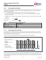
1
XMC 1000, XMC 4000
32-bit Microcontroller Series for Industrial Applications
Captu re Compare Un it 4 (CCU4)
AP32287
Application Note
About this document
Scope and purpose
This application note provides a brief introduction to the key features of the CCU4 module and typical
application examples. It also includes hints on its usage for users who wish to develop motor control
application with XMC microcontroller family.
Intended audience
This document is intended for engineers who are familiar with the XMC Microcontroller series.
Applicable Products
XMC1000
XMC4000
DAVE ™
References
The User’s Manual can be downloaded from http://www.infineon.com/XMC.
DAVE™ and its resources can be downloaded from http://www.infineon.com/DAVE
V1.0
1
2015-07
Capture Compare Unit 4 (CCU4)
AP32287
Table of Contents
Table of Contents
About this document .....................................................................................................................1
Table of Contents ..........................................................................................................................2
1
1.1
1.2
1.3
1.4
1.4.1
1.4.2
1.4.3
1.4.4
1.4.5
1.5
1.6
1.6.1
1.6.2
1.7
1.7.1
1.7.2
1.7.3
1.7.4
1.7.5
1.7.6
1.7.7
1.8
1.8.1
1.8.2
1.8.3
1.8.4
1.8.5
1.8.6
Introduction to the CCU4 ...............................................................................................4
Basic Timer Functions ......................................................................................................................... 4
CCU4 Use Cases ................................................................................................................................... 6
Additional CCU4 Features ................................................................................................................... 8
CCU4 Input Control ............................................................................................................................. 8
Synchronized Control of CAPCOM Units on External Events ....................................................... 8
External Control Basics ................................................................................................................. 9
External Events Control ................................................................................................................ 9
External Event Sources ................................................................................................................. 9
External Event Input Functions .................................................................................................. 10
Capture Basics ................................................................................................................................... 10
CCU4 Output Control ........................................................................................................................ 11
External Control by Timer Events ............................................................................................... 11
Top-Level Control of Event Request to/from a Timer Slice ....................................................... 11
Compare Basics ................................................................................................................................. 12
CCU4 Shadow Transfers.............................................................................................................. 12
Shadow Transfer of Compare Register values ........................................................................... 12
Asymmetric Compare Events ..................................................................................................... 13
Shadow Transfers in General – Compound Shadow Transfers ................................................. 13
CCU4 Output State and Output Pin PASSIVE/ACTIVE Level Control ......................................... 13
How to Start a Timer ................................................................................................................... 13
Global Start of CCU4 ................................................................................................................... 14
Example Use Case: Periodically changing the PWM Duty Cycle ...................................................... 15
Deriving the Period and Compare Values .................................................................................. 15
Macro and variable Settings ....................................................................................................... 16
XMC Lib Peripheral Configuration Structure .............................................................................. 16
Interrupt Service Routine Function Implementation ................................................................ 17
Main Function Implementation .................................................................................................. 17
Implementation to Start timer by Software .............................................................................. 19
2
2.1
2.1.1
2.1.2
2.1.3
2.1.4
2.1.5
2.1.6
2.2
2.2.1
2.2.2
2.2.3
2.2.4
Output Pattern Generation with CCU4 .......................................................................... 20
The Principle Compare Blocks .......................................................................................................... 20
PWM Range 0 – 100 % in Up-Count Mode................................................................................... 20
PWM Range 0 – 100 % in Down-Count Mode .............................................................................. 20
PWM Range 0 – 100 % in Center Aligned Mode .......................................................................... 21
Compare Reload with Shadow Transfer Rules .......................................................................... 21
CCU4 Output Control Compare Mode ........................................................................................ 24
Event Request in Compare Mode ............................................................................................... 24
Example Use Case: CCU4 as Digital-to-Analog Converter (DAC) ..................................................... 26
Theory of operation .................................................................................................................... 27
Deriving the Period Value ........................................................................................................... 28
Generating a Look-Up Table ....................................................................................................... 28
Circuit Diagram and Signals ....................................................................................................... 30
Application Note
2
V1.0, 2015-07
Capture Compare Unit 4 (CCU4)
AP32287
Table of Contents
2.2.5
2.2.6
2.2.7
2.2.8
Macro and variable Settings ....................................................................................................... 30
XMC Lib Peripheral Configuration Structure .............................................................................. 31
Interrupt Service Routine Function Implementation ................................................................ 32
Main Function Implementation .................................................................................................. 32
3
3.1
3.1.1
3.1.2
3.1.3
3.1.4
3.1.5
3.1.6
3.2
3.2.1
3.2.2
3.2.3
3.2.4
Advanced Signal Measurement .................................................................................... 34
Capture Mode .................................................................................................................................... 34
Slice Timer Setup in Capture Mode ............................................................................................ 34
The Capture Algorithm................................................................................................................ 34
Capture by Externals Events Control .......................................................................................... 35
Timer Inputs from Capture ......................................................................................................... 35
External Control by Capture Events ........................................................................................... 36
Top-Level Control of Event Requests to/from a Timer in Capture Mode .................................. 36
Example Use Case: CCU4 Capture Mode to Measure PWM Duty Cycle ............................................ 36
Macro and variable Settings ....................................................................................................... 38
XMC Lib Peripheral Configuration Structure .............................................................................. 38
Interrupt Service Routine Function Implementation ................................................................ 39
Main Function Implementation .................................................................................................. 40
4
4.1
4.1.1
4.1.2
4.1.3
4.1.4
4.1.5
4.1.6
4.2
4.2.1
4.2.2
4.2.3
4.2.4
Event Trigger Delay by Single Shot ............................................................................... 43
Introduction....................................................................................................................................... 43
Timer Setup in Single Shot Mode ............................................................................................... 43
Using Timer Single Shot Delay for Noise Rejection ................................................................... 44
Timer-Start in Single Shot Mode by External Event Control ..................................................... 44
Timer Inputs for Start and Stop Facilities .................................................................................. 44
External Control by Single-Shot Events ..................................................................................... 45
Top-Level Control of Event Request to/from a Timer in Single-Shot Mode ............................. 45
Example Use Case: Triggering ADC Conversion using CCU4 Single Shot ........................................ 46
Macro and variable Settings ....................................................................................................... 46
XMC Lib Peripheral Configuration Structure .............................................................................. 47
Interrupt Service Routine Function Implementation ................................................................ 50
Main Function Implementation .................................................................................................. 50
5
Revision History .......................................................................................................... 53
Application Note
3
V1.0, 2015-07
Capture Compare Unit 4 (CCU4)
AP32287
Introduction to the CCU4
1
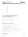
Introduction to the CCU4
The CAPCOM4 (CCU40/../43) is a multi-purpose timer unit for signal monitoring/conditioning and Pulse
Width Modulation (PWM) signal generation. It is designed with repetitive structures and multiple timer slices
that have the same base functionality. The internal modularity of CCU4 translates into a software friendly
system for fast code development and portability between applications.
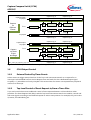
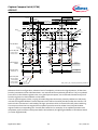
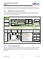
The following image shows the main function blocks of one of the four CC4y slices on a CCU4x.
CCU4x
x=0-3
CC4y
Service
44 Service
Request
Requests
Request Lines
Lines
DMA
Slice y
Reset- / Power
y=0-3
Control
Prescaler /
Floating
Prescaler
Prescaler
Clock Control
Period Shadow Reg.
4 x Capture
Service
Period Register
Edge /
Center
Align
Timer 16-bit
Single
Shot
Multi Channel
Pattern
Generation
Output Pin
Status Bit
Input Matrix
Compare Shadow Reg.
Compare Register
Modulation
Control
Active /
Passive
Control
PWM
3 x Input
Selector
Function Control
by 16 External
Event Sources
DEV_CCU4_00_Basics_Slice.vsd
Figure 1
The Timer Slice Block Diagram
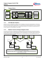
1.1
Basic Timer Functions
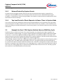
Each CCU4x has four 16-bit timer slices CC4y (y = 3-0) which can be concatenated up to 64-bits. Each slice
has:
1 Timer
4 Capture registers
1 Period register
1 Compare register
Both the Period and Compare registers have shadow registers. Each slice can work independently in
different modes, but they can also be synchronized, even to other CCU4x slices. They perform
multichannel/multi-phase pattern generation with parallel updates.
Each timer slice can be configured to handle the basic functions illustrated in the figure below.
Application Note
4
V1.0, 2015-07
Capture Compare Unit 4 (CCU4)
AP32287
Introduction to the CCU4
Timer
Compare
Capture
Free Running Mode
Option: Reset / Gate
Edge Aligned Mode
PWM generation
Time Measurement
Period
Period
Interrupt
Interrupt
Capture!
Capture!
Compare
0
t1 – t0
0
Time
Reset (Clear):
Time
PWM:
t0
Gate Input:
T1
T2
Counter
Compare
Option: Up/Down Count Control
Center Aligned Mode
Symmetric or Asymmetric PWM
Single Shot
Period
Count
Time
t1
Period
Asymmetric
6
5
4
3
2
1
0
Compare Level (II)
Symmetric
Compare
Level (I)
0
0
Time
Count Input:
U/D Control
Input:
Count Down
Count Up
Time
PWM:
T1
T2
T3 T1
Time
t1 – t0 = <period>
t0
Start
t1
Stop
DEV_CCU4_00_Basics.vsd
Figure 2
Basic functions of each Timer Slice
Application Note
5
V1.0, 2015-07
Capture Compare Unit 4 (CCU4)
AP32287
Introduction to the CCU4
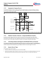
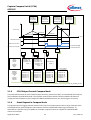
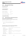
The CAPCOM4 ”RACK”
CCU41
CCU40
CC40
CC40
CC40
CC40
Service
44 Service
Request
Requests
Lines
Slice 0
Prescaler /
Prescaler
Floating
Prescaler
40
Period Shadow PRS3
0
1
0
1
0
1
2
3
2
3
one
Period PR3
Period Shadow PRS3
Switch
Control
Comp. oneComp.
Period PR3
Timer T43
Multi Channel
Comp. oneComp.
Period PR3
Period Shadow PRS0
ModulaEdgeCRS3
/
Comp. Comp. Pattern / Update /
Compare
2
Timer
T43 Shadow
Comp. tion
Comp.
Center
Period
PR0Compare CR3
Transfer Request
3
Control Comp.
zero
Comp.
Align
Compare
Timer
T43 Shadow CRS3
Active /
OUTPUT40
Compare
CR3 Single
zero
Passive
Comp.
Compare
Timer
T40 Shadow CRS3 ShotComp.Control
STATUS0
Compare CR3
zero
INPUT0
Compare Shadow CRS0
Period Shadow PRS3
PWM 0
Compare CR0
3 x Input
Selector
Function Control
by 16 External
Event Sources
Multi Channel
CC41
Slice 1
4 x Capture
CC41SR
[3 : 0]
PRS1
CC41PSC
PR1
Edge /
Center
Align
T41
Single
Shot
CRS1
PWM 1
CR1
Modulation
Control
Active /
Passive
Control
3 x Input
Selector
MCI1 / PS1 /
CCU40MCSS
CCU40OUT41
CCU40ST1
INPUT1
CCU40IN1
[P : A]
Timer Concatenation
Multi Channel
CC42
Slice 2
4 x Capture
CC42SR
[3 : 0]
PRS2
CC42PSC
PR2
Edge /
Center
Align
T42
Single
Shot
CRS2
PWM 2
CR2
Modulation
Control
Active /
Passive
Control
3 x Input
Selector
MCI2 / PS2 /
CCU40MCSS
CCU40OUT42
CCU40ST2
Interface to
System Top-Level Interconnection
Matrix
Timer Concatenation
INPUT2
CCU40IN2
[P : A]
Timer Concatenation
Multi Channel
CC43
CC43SR
[3 : 0]
Slice 3
PRS3
4 x Capture
- - - Reset / Power Control - - - Clock Control - - - Service Request Lines - - - DMA - - -
G
lo
ba
lC
CCU42
4 x Capture
4 x Capture
4 x Capture
4 x Capture
4 x Capture
4 x Capture
4 x Capture
on
tro
l
CCU43
CC43PSC
PR3
Edge /
Center
Align
T43
Single
Shot
CRS3
PWM 3
CR3
Modulation
Control
Active /
Passive
Control
3 x Input
Selector
MCI3 / PS3 /
CCU40MCSS
CCU40OUT43
CCU40ST3
INPUT3
CCU40IN3
[P : A]
DEV_CCU4_00_CCU4xCC4y_Slices_rev1.vsd
Figure 3
The Four Capture/Compare unit CCU40-CCU43 basic system for CAPCOM4
1.2
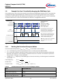
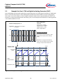
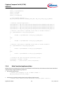
CCU4 Use Cases
Here are some typical example use cases that demonstrate the various capabilities of the CAPCOM timer
slices of the CCU4:
1. Simple Time Base with synchronization option by external events control
2. Power Conversion System (PFC, SMPS) using Single Shot Mode
Application Note
6
V1.0, 2015-07
Capture Compare Unit 4 (CCU4)
AP32287
Introduction to the CCU4
3. Feedback Sensor Event monitoring and Revolution by Capture, Count and Position Interface facilities
(POSIF)
4. Multi-Signal Pattern on Output Pins, created by parallel Multi-Channel Control
5. Drive & Motor Control with Multi-Phase System, Phase Adjustment and Trap Handling
6. 3-Level PWM for Inverters and Direct Torque Control (DTC) of AC Motors and High Precision Synchronous
Motors
7. External Events Control of Timer Input Functions by requests from external system units
8. Dithering PWM or period for DC-Level precision, Reduced EMI, Fractional Split of Reriods into Micro Step
9. Auto Adjusting Time Base by Floating Prescaler for adaption of time measurement to a wide range of
dynamics
The same use cases are illustrated in the following figure:
2
Simple Time Base
Single Shots in PFC & SMPS
Reject
I
IL
ID
Ton
IL
Vin
Vout
5
- Parallel Control of Output Pins by single pattern
Stall Detection (via BEMF)
Bipolar Stepper with Micro Steps:
T
C
POSIF
6
Multi Phase Control
- 3-Phase Motor Control
- N Phase Power Supplies
- Asymmetric PWM (CCU8x) for Phase Shift
- Trap
PWM1
Encoder
D
C
Multi Channel Control
Toff
ID
L
Event
Quadrature Encoder
- Event Counting
- Up/Down Counting
- Revolution Monitoring
- Velocity on Tick/ Velocity on Time Stamp
- Tick Compare
- Comprehensive Single Shots Handling
- Interrupt Request on the Period Match
- Synchronize on External Event Control
4
3
Reject
1
CCU4/8
3-Level PWM
- For Higher Resolution, EMC quality & Efficiency
Compare 3
Asymm. Comp. 2
Compare 1
Polarity1
PWM2
PWM 3
Asymm. PWM 2
PWM 1
Polarity2
7
Event Controlled Timer Functions
- Synchronous Control of Timers by other Units
Event
Source
Select
GPIO
ERU1
POSIF
CAN
CCU4x
USIC
ADC
CCU8x
SCU
Up to 3 Event Function
Profiles Select of Inputs
Select
Edge or Level
H
Event0
Detect
L
Event0
true
false
3 Events
Control Connect
2
1
0
Inputs
External
Event
Sources
Target
Timer
Slice
start
stop
capture 0,1
capture 2,3
gate clock
up/down
load Timer
count
override bit
trap
modulate
8
9
Dithering
- EMI Reduction by spectrum broadening
- Fractional Period Time Division into Micro Ticks
- DC-Level average precision (from 16 to 20 bits)
E.g: How to achieve an average value of 28,9H
by a Buck Converter with 200 kHz sampling
rate, performing 10 bit DC-Level on average
Auto Adjusting Time Base
- Adaption to unknown measurement dynamics
- Reduction of the SW read activities
- Floating Prescaler Mode, individual in All Timers
timer count
Vout
Vin
L
PWM
D
T
2T
C
T=2
4T
zero
<timer>/<period+1> x 8T T
tcapture
PS Init
Dither
Capture
event
<period>
<timer>
<PSIV>
PS Init
x (<period>+1) / fCCU;
2T
t
next tcapture
<PSIV> = 0-15
DEV_CCU4_00_Use_Cases.vsd
Figure 4
Some features and Use Cases (1-9) characterizing an CAPCOM Unit (CCU) Features
Application Note
7
V1.0, 2015-07
Capture Compare Unit 4 (CCU4)
AP32287
Introduction to the CCU4
1.3
Additional CCU4 Features
Table 1
Summary of additional CCU4 features
Features
Operation
Single Shot
If a slice is set in Timer Single Shot Mode (CC4yTC.TSSM), the Timer and its Run
Bit (TRB) is cleared by the Period/One match that occurs next to when the TSSM
bit was set. As a result, the timer is stopped.
Timer Concatenation
Any timer slice can be concatenated with an adjacent timer slice by setting
CC4yTC.TCE = 1.
Dithering PWM
It can be used with very slow control loops that cannot update the
period/compare values in a fast manner. The precision can be maintained on long
run.
Dithering Period Time
Micro ticks can be used in the Interpolation between sensor pulses to achieve
higher precision position monitoring.
Floating Prescaler
By successive changing of the timer clock frequency periodically (no
compare/capture event), the dynamic range is autonomously adapted to any
time length.
External Modulation
The output pin signal of a slice is modulated by external events.
Output State Override
An external input signal source may override a slice’s status bit (CC4yST) on an
edge event by other external input signal source.
Multi-Channel Control
The output state of Timer Slices PWM signal(s) can be controlled in parallel by a
single pattern.
External Load
Each slice of CCU4 allows the user to select an external signal as a trigger for
reloading the timer value with current compare/period register value.
Trap Function
The function forces PWM output into a predefined state, preset in the
active/passive PSL bit. The power device can then be safely switched off.
1.4
CCU4 Input Control
1.4.1
Synchronized Control of CAPCOM Units on External Events
External Events Control distribution to CCUs (including CCU8) starts for advanced applications with
synchronized timer control. For example, in motor drive and power control, where 3-Level Inverters might
require 12 synchronized PWM. The limits are the realizable topography or timing pattern complexity range.
Application Note
8
V1.0, 2015-07
Capture Compare Unit 4 (CCU4)
AP32287
Introduction to the CCU4
1.4.2
External Control Basics
A slice has its input functions controlled by external sources. The external source(s), active mode(s) and
input function(s) should be mapped to the 3 inputs of the slice in the CC4yINS and CC4yCMC registers.
Function mode extension alternatives can be added by selecting them in the CC4yTC Timer Slice Control
register.
1.4.3
External Events Control
An external event control request can be an edge or level signal from a peripheral unit or a GPIO. It can be
linked to the input selection stage of a CCU4xCC4y slice by using a comprehensive connection matrix. A slice
with any of its 3 events setup detects a considered source-event-input profile and can be function controlled
“remotely” this way.
CCU4x
x=0-3
CC4y
Service
Period Shadow Reg.
Request Lines
DMA
4 x Capture
Service
44 Service
Request
Requests
Lines
Slice y
Reset- / Power
Control
Clock Control
Event
Source
Select
Single
Shot
Up to 3 Events
Profile Selectable
Edge or Level
Event0
true
2
1
0
Event0
Detect
false
3 Events
Control Connect Matrix
PWM
3 x Input
Selector
Timer Input Functions
that may be controlled
by the Events 0, 1 or 2
Function
of Inputs
Select
L
Modulation
Control
Active /
Passive
Control
Multi Channel
Pattern
Generation
Output Pin
Status Bit
Input Matrix
Compare Shadow Reg.
Compare Register
H
GPIO
ERU1
POSIF
CAN
CCU4x
USIC
ADC
CCU8x
SCU
---
Timer 16-bit
Inputs
External
Event
Sources
y=0-3
Prescaler /
Floating
Prescaler
Prescaler
Period Register
Edge /
Center
Align
Edge signal to start the timer
Edge signal to stop the timer
Edge signal to capture into reg. 0 & 1
Edge signal to capture into reg. 2 & 3
Level signal to gate the timer clock
Level signal to up/down count direction
Edge signal to load the Timer
Edge signal to count events
Status bit override with an input value
Level signal to trap for fail-safe op.
Level signal to modulate the output
Function Control
by 16 External
Event Sources
Target
Timer
Slice
Period Reg.
Timer Reg.
Compare Reg.
DEV_CCU4_00_Basics_External_Events_Control_Komplex.vsd
Figure 5
External Control of Timer Input Functions on Events by an External Units
1.4.4
External Event Sources
CCU4xCC4y input functions can be linked to external trigger requests from sources such as: GPIO, ERU,
POSIF, CAN, CCU4x, USIC, ADC, CCU8x or SCU. Signal connections are given by the top-level interconnect
matrix and the CC4yINS Input Select vector. The CC4yCMC register is used for function selection.
Application Note
9
V1.0, 2015-07
Capture Compare Unit 4 (CCU4)
AP32287
Introduction to the CCU4
1.4.5
External Event Input Functions
There are 11 timer input functions (such as ‘Start the Timer ’ for example), controllable by external events
via 3 selectable input lines with configurable source-event profile conditions to the Timer Slices CC4y (y=0-3)
of a CCU4x unit for Start, Stop, Capture0-3, Gate, Up/Down, Load, Count, Bit Override, Trap and Modulate
Output Control.
There are also some Extended Input Functions in the register CC4yTC for Extended Start, Stop with
Flush/Start, Flush/Stop or Flush or Extended Capture Mode. Together, with a read access register (ECRD),
these simplify the administration of capture registers and full-flags when more than one slice is used in
Capture mode.
1.5
Capture Basics
Each CAPCOM4 (CCU4x) has 4 timer-slices. Each slice has 4 capture value registers, split into 2 pairs that
capture on selected event control input: Capt0 or Capt1, according to 2 possible pair schemes: either as 2
pairs for different events respectively to Capt0 and Capt1, or cascaded for the same event via Capt1.
CCU4x
x=0-3
CC4y
Request Lines
DMA
Service
44 Service
Request
Requests
Lines
Slice y
Reset- / Power
Control
Clock Control
y=0-3
Prescaler /
Floating
Prescaler
Prescaler
Period Shadow Reg.
4 x Capture
Service
Period Register
Edge /
Center
Align
Timer 16-bit
Single
Shot
Multi Channel
Pattern
Generation
Output Pin
Status Bit
Input Matrix
Compare Shadow Reg.
Compare Register
Modulation
Control
Active /
Passive
Control
PWM
3 x Input
Selector
Function Control
by 16 External
Event Sources
DEV_CCU4_00_Basics_Slice_Capture.vsd
Figure 6
Timer Slice with four Capture Registers
Application Note
10
V1.0, 2015-07
Capture Compare Unit 4 (CCU4)
AP32287
Introduction to the CCU4
Capture reg. 3:
Capture Inputs:
CCycapt1
Capture
on
Different
Events
fCCU4
Capture Trigger Distribution & Full-Flag Handling Logic
Full/
Empty
Full/
Empty
CC4yC3V
CC4yC2V
CC4yC1V
CC4yC0V
T4y
Full/
Empty
CCycapt0
fCCU4
Full/
Empty
Capture Trigger Distribution & Full-Flag Handling Logic
Capture Input:
CCycapt1
Capture
on Same
Event
and Edge
Capture reg. 2:
Capture reg. 1:
Capture reg. 0:
Capture reg. 3:
Capture reg. 2:
Capture Trigger Distribution & Full-Flag Handling Logic
T4y
Full/
Empty
Full/
Empty
CC4yC3V
CC4yC2V
CC4yC1V
CC4yC0V
Full/
Empty
Full/
Empty
Capture Trigger Distribution & Full-Flag Handling Logic
Capture reg. 1:
DEV_CCU4_00_Capture_Logic.vsd
Capture reg. 0:
Figure 7
Basic Capture Mechanism – setup in two possible scheme alternatives
1.6
CCU4 Output Control
1.6.1
External Control by Timer Events
A timer event can trigger external actions via the Top-Level Interconnect matrix or on request for an
Interrupt. Each CAPCOM4 has four Service Request Lines and each slice has a dedicated output signal
CC4ySR[3…0], selectable to a line by CC4ySRS. This means timer slice events can request direct peripheral
actions or an interrupt.
1.6.2
Top-Level Control of Event Request to/from a Timer Slice
Top-Level control also means conditional control of event requests between a slice and other action
providers. The Event Request Unit (ERU1) and the Top-Level Interconnect matrix can combine, control and
link event signals according to user defined request-to-action event patterns. For example, they can invoke
I/O states, Time Windowing etc.
Application Note
11
V1.0, 2015-07
Capture Compare Unit 4 (CCU4)
AP32287
Introduction to the CCU4
1.7
Compare Basics
CCU4x
x=0-3
CC4y
Period Shadow Reg.
Service
44 Service
Request
Requests
Lines
Request Lines
DMA
Slice y
y=0-3
Prescaler /
Floating
Prescaler
Prescaler
Reset- / Power
Control
Clock Control
4 x Capture
Service
Period Register
Edge /
Center
Align
Timer 16-bit
Single
Shot
Pattern
Generation
Output Pin
Status Bit
Input Matrix
Compare Shadow Reg.
Compare Register
Multi Channel
Modulation
Control
Active /
Passive
Control
3 x Input
Selector
PWM
Function Control
by 16 External
Event Sources
DEV_CCU4_00_Basics_Slice_Compare.vsd
Figure 8
Timer Slice Compare Registers and PWM related Blocks
1.7.1
CCU4 Shadow Transfers
Whatever the slice configuration, whatever level of complexity, whatever the signal patterns, all the timer
function parameters of the CAPCOM4 timers are assured coherent update by hardware. They are updated
from values in the shadow registers that, on a global preset request, are transferred simultaneously to all
function registers at a Period Match or One Match.
1.7.2
Shadow Transfer of Compare Register values
The compare values that are targeted for an update operation have to be written into both the CC4yCRS
shadow registers and the corresponding Slice Transfer Set Enable bits. For example, SySE in GCSS must be
preset before Period Match (in Edge Aligned Mode) or Period/One Match (in Center Aligned Mode) for an
update operation to be completed.
Shadow TrAnsfer
on Period-Match
and REquest is
cleared by HW
No Shadow
Transfer since
No request
No Shadow
Transfer since
No request
Shadow TrAnsfer
on One-Match
and REquest is
cleared by HW
Timer CC4y
SW
CC40CRS = 10
CC41CRS = 20
CC42CRS = 30
SySE = 1
HW
SW
HW
CC40CRS = 20
CC41CRS = 40
CC42CRS = 60
SySE = 1
CC40CR = 10
CC41CR = 20
CC42CR = 30
CC40CR = 20
CC41CR = 40
CC42CR = 60
Shadow transfer mechanism:
Coherent update of compare registers by HW.
SW can write asynchronously to the timer state. After all values are updated the shadow transfer is
requested by setting SySE. At every Period-Match or One-Match event the HW can perform the
transfer and clears the request.
DEV_CCU4_00_Shadow_Transfer_with_Compare_Registers.vsd
Figure 9
Basic Shadow Transfer Mechanism for Compare Registers Values
Application Note
12
V1.0, 2015-07
Capture Compare Unit 4 (CCU4)
AP32287
Introduction to the CCU4
1.7.3
Asymmetric Compare Events
The benefit of shadow transfers on both Period Match and One Match is to allow asymmetric compare
events to be provided in Center Aligned Mode. The real-time conditions are similar to handling shadow
value updates in Edge Aligned Mode.
SW
HW
CRS = value2
SySE = 1
by Service Req.
CR = value2
by Shadow
Transfer
Timer (TRy)
Period (PR)
Asymm. Comp. (||)
(Symm. Compare)
CR value2
CR value1
Asymm. Comp. (|)
time
Symmetric PWM
Asymm. PWM
(y = 0 - 3)
Phase Shift
DEV_CCU4_00_Basics_Asymmetric_PWM_by_SW_Center_Aligned.vsd
Figure 10
Asymmetric Compare by Shadow Transfers on both Period Match and One Match
1.7.4
Shadow Transfers in General – Compound Shadow Transfers
Beside the Compare register (CR) values, there is also the timer Period register (PR) and the PWM
Active/Passive control bit (PSL) that is updated simultaneously on the SySE flag. Dithering or Floating
Prescaler values are able to get a simultaneous update via the SyDSE and SyPSE request flags.
1.7.5
CCU4 Output State and Output Pin PASSIVE/ACTIVE Level Control
The PASSIVE/ACTIVE state of a slice’s internal output CCUxSTy (i.e. status bit CC4yST) is controlled by the
compare level and the External Modulation Mode. The CC4yPSL Passive/Active bit PSL controls whether the
external output pin state CCU4xOUTy (e.g. the PWM) is Passive Low / Active High or vice-versa.
1.7.6
How to Start a Timer
There are two ways to start a timer:
Directly by software, by setting the Timer Run Bit Set (TRBS)
Indirectly by hardware when a specific event occurs in an external unit as determined by the Top-Level
Connection Matrix for External Events Control for CAN, ADC, USIC, IO, CCU4/8, ERU1, POSIF etc.
Application Note
13
V1.0, 2015-07
Capture Compare Unit 4 (CCU4)
AP32287
Introduction to the CCU4
1.7.7
Global Start of CCU4
To achieve a synchronized start, the CCU4 uses either:
A global start by software, with CCUx Global Start Control bits in the CCUCON Global Start Control
register
A global start by hardware, indirectly with External Events Control using the CC4yINS and CC4yCMC
registers
The Global Start command enables almost an unlimited number of timers to be started, independently of
the CAPCOM unit they belong to. The global start means that the timers are synchronized and all timing can
be controlled in parallel, with many different kinds of generated output patterns.
CCUCON
GSC80
GSC41
CC40INS
GSC40
Select Considered
Source-Event Profiles
CC40CMC
CC40
CC80
CC41
CC81
CC42
CC82
CC43
CC83
CCU80
CCU40
This mechanism allows synchronous start of different timer slices within
one CCU but also different slices from different CCUs
DEV_CCU4_00_StartTimer.vsd
Figure 11
External Event Control with Global Start Command
Application Note
14
V1.0, 2015-07
Capture Compare Unit 4 (CCU4)
AP32287
Introduction to the CCU4
1.8
Example Use Case: Periodically changing the PWM Duty Cycle
This example uses a slice of CCU4 (CCU40 Slice 0) to generate a PWM signal (output to P0.0). The CCU4 slice
is configured in edge-aligned mode with a frequency of 1Hz. An interrupt is generated on every compare
match event, which alternates the PWM duty cycle between 33.3% and 66.7%. The CCU4 slice is started by
an external start event on Event 0 connected to SCU.GSC40. It is targeted for XMC1200.
CCU40.CC40
SLICE Configuration:
XMC1200
System Clock = 32MHz
Peripheral Clock = 64MHz
PWM frequency = 1Hz
Mode = Edge aligned
Period (PR)
CR (33.33% DC)
CR (66.67% DC)
#2
#1: SCU.GSC40 is connected to the
input of Event 0. It is set high by
software and starts CCU40.40 timer on
an external start event on Event 0.
CMUS
Compare Match
#2 – An interrupt is triggered on every
compare match event. In this ISR, the
compare value is updated between
33.33% and 66.67% duty cycle.
CCU40.OUT0, P0.0
Note: New compare value is updated at
each period match event for this
example.
#1
SCU.GSC40
Figure 12
Example: Periodic duty cycle update
1.8.1
Deriving the Period and Compare Values
The clock relationship between 𝑓𝑃𝑊𝑀 , 𝑓𝑡𝑐𝑙𝑘 and 𝑓𝑐𝑐𝑢4 is calculated as shown below:
𝑓𝑐𝑐𝑢4 is the frequency of the CCU4 peripheral clock . It is the input to the PWM module.
𝑓𝑡𝑐𝑙𝑘 is the timer resolution used to increment a timer counter. Each timer slice supports a dedicated
prescaler value selector. In this example, a prescaler factor of 10 is chosen. This results in a prescaler
value of 1024, resulting in a 16 us resolution.
In order for, 𝑓𝑃𝑊𝑀 , frequency of the PWM signal, to be 1Hz, the CCU4_CC40.PRS register is loaded with
value 62499.
𝑓𝑐𝑐𝑢4
Timer frequency:
𝑓𝑡𝑐𝑙𝑘 =
Period value:
𝐶𝐶𝑈4𝐶𝐶40 . 𝑃𝑅𝑆 =
Compare value:
𝐶𝐶𝑈4𝐶𝐶40 . 𝐶𝑅𝑆 = (1 − 𝐷𝐶) ∗ (𝑃𝑅𝑆 + 1)
Table 2
𝑃𝑟𝑒𝑠𝑐𝑎𝑙𝑒𝑟
𝑓𝑡𝑐𝑙𝑘
𝑓𝑃𝑊𝑀
−1
Calculated Prescaler factor, Period and Compare Values
Type
Calculated value
Prescaler value
210 = 1024
Period @1Hz frequency
62499
Compare value @33.33% DC
41668
Compare value @66.67% DC
20831
Application Note
15
V1.0, 2015-07
Capture Compare Unit 4 (CCU4)
AP32287
Introduction to the CCU4
1.8.2
Macro and variable Settings
XMC Lib Project includes:
#include <xmc_ccu4.h>
#include <xmc_gpio.h>
#include <xmc_scu.h>
Project Macro definitions:
#define MODULE_PTR
#define MODULE_NUMBER
CCU40
(0U)
#define SLICE0_PTR
#define SLICE0_NUMBER
#define SLICE0_OUTPUT
CCU40_CC40
(0U)
P0_0
Project Variables Definition:
volatile uint8_t count=1;
uint16_t comparevalue[]=
{
/* Calculated based on PCLK of 64MHz */
20831U, /* 66.67% duty cycle */
41668U /* 33.33% duty cycle */
};
1.8.3
XMC Lib Peripheral Configuration Structure
XMC System Clock Unit (SCU) Configuration:
PWM period is calculated based on PCLK which is equivalent to 64 MHz.
XMC_SCU_CLOCK_CONFIG_t clock_config =
{
.pclk_src = XMC_SCU_CLOCK_PCLKSRC_DOUBLE_MCLK,
.rtc_src = XMC_SCU_CLOCK_RTCCLKSRC_DCO2,
.fdiv = 0,
.idiv = 1,
};
XMC Capture/Compare Unit 4 (CCU4) Configuration:
XMC_CCU4_SLICE_COMPARE_CONFIG_t SLICE0_config =
{
.timer_mode = (uint32_t) XMC_CCU4_SLICE_TIMER_COUNT_MODE_EA,
.monoshot = (uint32_t) false,
.shadow_xfer_clear = (uint32_t) 0,
.dither_timer_period = (uint32_t) 0,
.dither_duty_cycle = (uint32_t) 0,
.prescaler_mode = (uint32_t) XMC_CCU4_SLICE_PRESCALER_MODE_NORMAL,
.mcm_enable = (uint32_t) 0,
.prescaler_initval = (uint32_t) 10, /* in this case, prescaler = 2^10 */
.float_limit = (uint32_t) 0,
Application Note
16
V1.0, 2015-07
Capture Compare Unit 4 (CCU4)
AP32287
Introduction to the CCU4
.dither_limit = (uint32_t) 0,
.passive_level = (uint32_t) XMC_CCU4_SLICE_OUTPUT_PASSIVE_LEVEL_LOW,
.timer_concatenation = (uint32_t) 0
};
XMC_CCU4_SLICE_EVENT_CONFIG_t SLICE0_event0_config=
{
.mapped_input = XMC_CCU4_SLICE_INPUT_I,
/* mapped to SCU.GSC40 */
.edge = XMC_CCU4_SLICE_EVENT_EDGE_SENSITIVITY_RISING_EDGE,
.level = XMC_CCU4_SLICE_EVENT_LEVEL_SENSITIVITY_ACTIVE_HIGH,
.duration = XMC_CCU4_SLICE_EVENT_FILTER_3_CYCLES
};
XMC GPIO Configuration:
XMC_GPIO_CONFIG_t SLICE0_OUTPUT_config =
{
.mode = XMC_GPIO_MODE_OUTPUT_PUSH_PULL_ALT4,
.input_hysteresis = XMC_GPIO_INPUT_HYSTERESIS_STANDARD,
.output_level = XMC_GPIO_OUTPUT_LEVEL_LOW,
};
1.8.4
Interrupt Service Routine Function Implementation
The CCU40 interrupt handler function is created to periodically modify the timer compare match values to
achieve a PWM duty cycle between 33.3% and 66.7%.
void CCU40_0_IRQHandler(void)
{
/* Clear pending interrupt */
XMC_CCU4_SLICE_ClearEvent(SLICE0_PTR,XMC_CCU4_SLICE_IRQ_ID_COMPARE_MATCH_UP);
/* Set new duty cycle value */
XMC_CCU4_SLICE_SetTimerCompareMatch(SLICE0_PTR, comparevalue[count]);
count++;
if(count==2)
{
count=0;
}
/* Enable shadow transfer for the new PWM value update */
XMC_CCU4_EnableShadowTransfer(MODULE_PTR, XMC_CCU4_SHADOW_TRANSFER_SLICE_0);
}
1.8.5
Main Function Implementation
Before the start and execution of the timer slice software for the first time, the CCU4 must have been
initialized appropriately using the following sequence:
Set up the system clock
/* Ensure clock frequency is set at 64MHz (2*MCLK) */
XMC_SCU_CLOCK_Init(&clock_config);
Application Note
17
V1.0, 2015-07
Capture Compare Unit 4 (CCU4)
AP32287
Introduction to the CCU4
Enable clock, enable prescaler block and configure global control
/* Enable clock, enable prescaler block and configure global control */
XMC_CCU4_Init(MODULE_PTR, XMC_CCU4_SLICE_MCMS_ACTION_TRANSFER_PR_CR);
/* Start the prescaler and restore clocks to slices */
XMC_CCU4_StartPrescaler(MODULE_PTR);
/* Start of CCU4 configurations */
/* Ensure fCCU reaches CCU40 */
XMC_CCU4_SetModuleClock(MODULE_PTR, XMC_CCU4_CLOCK_SCU);
Configure Slice(s) Functions, Interrupts and Start-up
/* Initialize the Slice */
XMC_CCU4_SLICE_CompareInit(SLICE0_PTR, &SLICE0_config);
/* Program duty cycle = 33.33% at 1Hz frequency */
XMC_CCU4_SLICE_SetTimerCompareMatch(SLICE0_PTR, comparevalue[count]);
XMC_CCU4_SLICE_SetTimerPeriodMatch(SLICE0_PTR, 62499U);
/* Enable shadow transfer */
XMC_CCU4_EnableShadowTransfer(MODULE_PTR,
\
(uint32_t)(XMC_CCU4_SHADOW_TRANSFER_SLICE_0|
\
XMC_CCU4_SHADOW_TRANSFER_PRESCALER_SLICE_0));
/* Enable External Start to Event 0 */
XMC_CCU4_SLICE_ConfigureEvent(SLICE0_PTR, \
XMC_CCU4_SLICE_EVENT_0, &SLICE0_event0_config);
XMC_CCU4_SLICE_StartConfig(SLICE0_PTR, XMC_CCU4_SLICE_EVENT_0, \
XMC_CCU4_SLICE_START_MODE_TIMER_START_CLEAR);
/* Enable compare match events */
XMC_CCU4_SLICE_EnableEvent(SLICE0_PTR, XMC_CCU4_SLICE_IRQ_ID_COMPARE_MATCH_UP);
/* Connect compare match event to SR0 */
XMC_CCU4_SLICE_SetInterruptNode(SLICE0_PTR, \
XMC_CCU4_SLICE_IRQ_ID_COMPARE_MATCH_UP, XMC_CCU4_SLICE_SR_ID_0);
/* Set NVIC priority */
NVIC_SetPriority(CCU40_0_IRQn, 3U);
/* Enable IRQ */
NVIC_EnableIRQ(CCU40_0_IRQn);
/* Enable CCU4 PWM output */
XMC_GPIO_Init(SLICE0_OUTPUT, &SLICE0_OUTPUT_config);
/* Get the slice out of idle mode */
XMC_CCU4_EnableClock(MODULE_PTR, SLICE0_NUMBER);
Application Note
18
V1.0, 2015-07
Capture Compare Unit 4 (CCU4)
AP32287
Introduction to the CCU4
Start Timer Running
/* Create a low to high transition on SCU.GSC40 to start timer */
XMC_SCU_SetCcuTriggerLow(XMC_SCU_CCU_TRIGGER_CCU40);
XMC_SCU_SetCcuTriggerHigh(XMC_SCU_CCU_TRIGGER_CCU40);
1.8.6
Implementation to Start timer by Software
Alternatively, the timer can be started directly by software, setting the Timer Run Bit Set (TRBS).
/* Start the TImer*/
XMC_CCU4_SLICE_StartTimer(SLICE0_PTR);
Application Note
19
V1.0, 2015-07
Capture Compare Unit 4 (CCU4)
AP32287
Output Pattern Generation with CCU4
2
Output Pattern Generation with CCU4
2.1
The Principle Compare Blocks
y=0-3
PRy
Compare
TRy
Compare Register
CRy
Period Register
DEV_CCU4_01_Compare_Principle_Blocks.vsd
Figure 13
The Compare Blocks
2.1.1
PWM Range 0 – 100 % in Up-Count Mode
The Up-Count Mode of Compare Rule is very simple: As long as the timer register value is equal or greater
than the compare register value, the Status Bit (CCST or even named CCU4xSTy) is set to one. Otherwise it is
set to zero. The dynamic PWM range can be set to any value from 0% up to 100%.
(CR) > (PR)
Period (PR)
0 < (CR) < (PR)
Compare Level
Timer (TR)
(CR) == 0
time
Duty Cycle = 100 %
Duty Cycle
Status Bit – (PWM)
Duty Cycle = 0 %
DEV_CCU4_01_Compare_PWM_Range_Edge_Aligned_in_Up_Count_Mode.vsd
Figure 14
PWM Range in Up-Count Mode
2.1.2
PWM Range 0 – 100 % in Down-Count Mode
The Down-Count Mode of Compare Rule is the same as in Up-Count Mode: When the timer register value is
equal or greater than the compare register value, the Status Bit (CCST, CCU4xSTy) is set to one. Otherwise it
is set to zero. The dynamic PWM range can be set to any value from 0% to 100%.
Application Note
20
V1.0, 2015-07
Capture Compare Unit 4 (CCU4)
AP32287
Output Pattern Generation with CCU4
(CR) > (PR)
Period (PR)
0 < (CR) < (PR)
Compare Level
Timer (TR)
(CR) == 0
time
Duty Cycle
Status Bit – (PWM)
Duty Cycle = 100 %
Duty Cycle = 0 %
DEV_CCU4_01_Compare_PWM_Range_Edge_Aligned_in_Down_Count_Mode.vsd
Figure 15
PWM Range in Down-Count Mode
2.1.3
PWM Range 0 – 100 % in Center Aligned Mode
The Center Aligned Mode of Compare Rule is the same as Up or Down Count Modes: When the timer register
value is equal or greater than the compare register value, the Status Bit (CCST or CCU4xSTy) is set to one.
Otherwise it is set to zero. The PWM value can be varied from 0% to 100%.
(CR) > (PR)
Period (PR)
Compare Level
0 < (CR) < (PR)
Timer (TR)
(CR) == 0
time
Duty Cycle
Status Bit – (PWM)
Duty Cycle = 100 %
Duty Cycle = 0 %
DEV_CCU4_01_Compare_PWM_Duty_Cycle_Range_Center_Aligned_Mode.vsd
Figure 16
PWM Range 0% - 100% in Center Aligned Mode
2.1.4
Compare Reload with Shadow Transfer Rules
A reload of registers by Shadow Transfers from the associated shadow registers occurs according to the
following rules:
In the next clock cycle after a Period Match while counting up
In the next clock cycle after a One Match while counting down
Immediately if the timer is stopped and a transfer request was triggered
Application Note
21
V1.0, 2015-07
Capture Compare Unit 4 (CCU4)
AP32287
Output Pattern Generation with CCU4
Count Direction (CDIR):
CCTclk:
”Period
Match”
Period Value1 +1
”Period
Match”
”Period
Match”
Period Value1
Period Value1 -1
Period Value1
Period Value2
Timer:
Compare Value2
Compare Value1
Compare Value3
Zero
”One
Match”
One
Zero
CCST Bit Status:
CCCM_U
Interrupt
CCOM_D
Interrupt
CCCM_U
Interrupt
upper limit
CCPM_U
Interrupt
”One
Match”
One
Zero
CCCM_U
Interrupt
CCCM_D
Interrupt
CCCM_U
Interrupt
upper limit
CCPM_U
Interrupt
CCCM_D
Interrupt
upper limit
CCOM_D
Interrupt
Service Req. SW:
Shadow Update
SW Dead-Lines
CCTclk:
CCTclk:
Shadow Registers
Values:
Shadow
Values 2
Shadow
Values 3
Register Values:
e.g. CR/PR/PSL/..etc
Values
1
Values
2
Values
3
Shadow
Values 2
Shadow
Values 3
Shadow
Values 4
Values
1
Values
2
Value
3
Service Req. SW:
Shadow Updates
on Period-Match
Shadow Updates
on Compare-Match
Figure 17
Last CCTclk Cycle
DEV_CCU4_01_Compare_Schemes_Reload.vsd
Compare Reload Scheme in Detail
Whatever the slice configuration, whatever level of complexity, whatever the signal patterns, all the timer
function parameters of the CAPCOM4 timers are assured coherent update by hardware. They are updated
from values in the shadow registers that, on a global preset request, are transferred simultaneously to all
function registers at a Period Match or One Match.
There is a global register, GCSS, carrying all enable-flags that have to be preset by software to selectively
activate the targeted Shadow Transfer Requests which will be cleared by hardware after the transfer. The
total real-time correctness is achieved by the logic operations which is essential for safe power switching.
The compare values that are targeted for an update operation must be written into CC4yCRS shadow
register and the corresponding slice Transfer Set Enable bit. For example, for an update operation to be
completed, SySE in GCSS must be preset before Period Match (in Edge Aligned Mode) or Period/One Match
(in Center Aligned Mode).
Application Note
22
V1.0, 2015-07
Capture Compare Unit 4 (CCU4)
AP32287
Output Pattern Generation with CCU4
Shadow TrAnsfer
on Period-Match
and REquest is
cleared by HW
No Shadow
Transfer since
No request
No Shadow
Transfer since
No request
Shadow TrAnsfer
on One-Match
and REquest is
cleared by HW
Timer CC4y
SW
CC40CRS = 10
CC41CRS = 20
CC42CRS = 30
SySE = 1
HW
SW
CC40CRS = 20
CC41CRS = 40
CC42CRS = 60
SySE = 1
CC40CR = 10
CC41CR = 20
CC42CR = 30
HW
CC40CR = 20
CC41CR = 40
CC42CR = 60
Shadow transfer mechanism:
Coherent update of compare registers by HW.
SW can write asynchronously to the timer state. After all values are updated the shadow transfer is
requested by setting SySE. At every Period-Match or One-Match event the HW can perform the
transfer and clears the request.
DEV_CCU4_01_Shadow_Transfer_with_Compare_Registers.vsd
Figure 18
Shadow Transfer Mechanism with Compare Registers
Beside the Compare (CR) values, there are also the timer Period register (PR) and the PWM Active/Passive
control bit (PSL) that are updated simultaneously on the SySE flag. Dithering or Floating Prescaler values
can also be simultaneously updated by the SyDSE and SyPSE request flags.
Application Note
23
V1.0, 2015-07
Capture Compare Unit 4 (CCU4)
AP32287
Output Pattern Generation with CCU4
Shadow
Transfers on
Period-Match
and Requests
cleared by HW
Shadow
Transfers on
One-Match
and Requests
cleared by HW
Shadow
Transfers on
Period-Match
and Requests
cleared by HW
No shadow
Transfers since
No requests
CC40CR=80
Timer CC4y:
CC40CR=40
CC40CR=20
CC40CR=10
time
Status Bit CC40ST:
PWM out from Port Pin:
Output Passiv High
Passive Level CC4yPSL:
Output Passiv Low
HW
SW
New
Shadow
Values
+
Transfer
Request
Flags
CC40CRS = 40
CC41CRS = 50
CC42CRS = 60
SySE = 1
HW
HW
SW
SW
CC40CRS = 20
CC41CRS = 25
CC42CRS = 30
CC4yPRS = 120
CC4yPSL = 1
SySE = 1
CC40CRS = 80
SySE = 1
Only CC40CR
has changed!
Registers
Updated
by Shadow
Values
&
Transfer
Requests
Cleared
CC40CR = 10
CC41CR = 20
CC42CR = 30
CC4yPR = 60
CC4yPSL = 0
CC40CR = 40
CC41CR = 50
CC42CR = 60
CC4yPR = 60
CC4yPSL = 0
CC40CR = 20
CC41CR = 25
CC42CR = 30
CC4yPR = 120
CC4yPSL = 1
CC40CR = 80
CC41CR = 25
CC42CR = 30
CC4yPR = 120
CC4yPSL = 1
y=0-2
y=0-2
y=0-2
y=0-2
DEV_CCU4_01_Shadow_Transfer_in_General_v1.vsd
Figure 19
Compound Shadow Transfer Mechanism with Coherent Update of PWM
2.1.5
CCU4 Output Control Compare Mode
The Passive/Active state of a slice internal output CCUxSTy (status bit CC4yST) is controlled by the compare
level and External Modulation Mode. The CC4yPSL Passive/Active bit PSL controls whether the external
output pin state CCU4xOUTy (for example, the PWM) should be Passive Low / Active High or vice versa.
2.1.6
Event Request in Compare Mode
A compare event can trigger external actions via the Top-Level Interconnect matrix or by an interrupt. Each
CAPCOM4 has four Service Request Lines and each slice has a dedicated output signal CC4ySR[3…0],
selectable to a specific line by CC4ySRS. For example, compare events can request for immediate ADC
actions or interrupts.
Application Note
24
V1.0, 2015-07
Capture Compare Unit 4 (CCU4)
AP32287
Output Pattern Generation with CCU4
Top-Level control also means conditional control of event requests between a slice and other action
providers. The Event Request Unit (ERU1) can be combined with the Top-Level Interconnect matrix to
control and link event signals according to user defined request-to-action event patterns. For example, ADC
triggering combined on I/O events.
A slice interface to ERU1 and to the Top-Level Interconnect matrix can be represented by a simplified
scheme. To complete the picture of the possible interaction, this scheme also shows how operations can be
extended to involve DMA transfers (by the GPDMA), triggered by a handler (DLR) on the Service Request
Lines (SRn).
If an application requires ADC conversion to start on timer events under specific conditions rather than
directly via a Top-Level Interconnect matrix path, then the ERU1 is able to offer an alternate signal path. This
may involve dependence on a port pin, a time window from a second timer, or a certain sequence of event
patterns.
CHIP EXTERNAL EVENTS
GPDMA
GPIO
Ack
DLR
GPIO
NVIC.SRn
SR5-8
Req
ERU1
CCU4xCC4y
Service
Requests
Slice xy
x=0-3
y=0-3
Prescaler
4 x Capture
CHIP INTERNAL EVENTS
- Select
ERU1_xA[3:0]
- Combine
x - Detect y
- CrossConnect
ERU1_xB[3:0]
- Gate
x=0-3
ERU1_IOUTy
TRIGGER
ERU1_PDOUTy
y=0-3
LEVEL
Edge /
Center
Align
Period Shadow Reg.
Period Register
Single
Shot
Timer 16-bit
Compare Shadow Reg.
Compare Register
PWM
Modulation
Control
Active /
Passive
Control
3 x Input
Selector
Multi Channel
Pattern
Generation
Output Pin
Status Bit
Input Matrix
Function Control
by 16 External
Event Sources
E.g.PWM
E.g. ADC
Top-Level
Cross
Interconnect
DEV_CCU4_01_Compare_Top_Level_Interconnect_with_CCU4_Slice_and_ERU.vsd
Figure 20
Using CCU4 and ERU1 for delayed ADC Start Controlled by an IO
The above example shows CCU4xCC4y is a single shot delay timer. Status Bit (red) is delayed and set by the
compare event, and delays an ADC-start when triggered by a PWM timer (blue) on a GPIO state (orange). The
ERU1 combines, detects and links it all as a trigger (green) via the delay timer and the Top-Level
Interconnect matrix to the ADC.
Application Note
25
V1.0, 2015-07
Capture Compare Unit 4 (CCU4)
AP32287
Output Pattern Generation with CCU4
2.2
Example Use Case: CCU4 as Digital-to-Analog Converter (DAC)
Many embedded microcontroller applications require generation of analog signals. Sometimes, a dedicated
DAC IC is used for this purpose. In fact, PWM signals can often be used to create DC and AC analog signals
with CCU4. CCU4 can be used as a form of signal modulation where data is represented by the ratio of the
ON time (T1) to the period (also known as the duty cycle). In this example, the CCU4 timer is used to generate
a sinusoidal waveform of 1 kHz.
SLICE Configuration:
XMC1200
System Clock = 32MHz
Peripheral Clock = 64MHz
PWM frequency = 24Hz
Mode = Edge aligned
Number of Sample points = 24
Angle Step = 360 / Number of Samples
= 15 degree
3.3V
Settings for this example
PWM frequency = 24 KHz
Generated sinusoidal frequency = 1KHz
(based on 24 sample points in lookup
table)
1.65V
0V
0
90
180
270
360
#1: Based on a pre-generated lookup
table, the new compare value is loaded
during a compare match event ISR.
Angle
CCU40.CC40
30
45
60
75
90
Period (PR)
(2665)
667
390
179
45
0
45
#1
CMUS
Compare Match
CCU40.OUT0, P0.0
Figure 21
Example: Generating a Sinusoidal Waveform
Application Note
26
V1.0, 2015-07
Capture Compare Unit 4 (CCU4)
AP32287
Output Pattern Generation with CCU4
2.2.1
Theory of operation
CCU40_CC40
Period (PR)
T1 is the ON period
TPWM is the PWM period
CR value
0
Time
PWM
TPWM
Figure 22
T1
Duty Cycle =
T1
TPWM
CCU4 PWM Signal with Variable Duty Cycle
A given ON time (T1) corresponds to an average DC voltage, which is linearly proportional to the duty cycle.
In the implementation of DAC using CCU4, the duty cycle can be varied while fixing the period value, or vice
versa. Theoretically if the duty cycle of CCU4 is varied with time, the signal is filtered, the output of the filter
is an analog signal. In fact, passing the CCU4 PWM signal through a low-pass filter (LPF) removes a
reasonable amount of ripple. A simple RC low-pass filter circuit or built-in LPF function in signal
measurement equipments could be used to eliminate the inherent noise components.
Amplitude
100
50
{…, 0, 0, 15, 58, 83, 69, 25, -20, -33, -24, -8, -1, …}
0
Time
-50
Analog
ADC
DAC
Time
Time
Figure 23
Filter
Analog
Time
Process involves ADC to DAC conversion
Application Note
27
V1.0, 2015-07
Capture Compare Unit 4 (CCU4)
AP32287
Output Pattern Generation with CCU4
2.2.2
Deriving the Period Value
In this example, the frequency of the sinusoidal waveform generated is fixed at 1 kHz with 24 sample points.
Therefore, the PWM frequency is fixed at 24 kHz. The clock relationship between 𝑓𝑃𝑊𝑀 , 𝑓𝑡𝑐𝑙𝑘 and 𝑓𝑐𝑐𝑢4 is
calculated as shown below:
𝑓𝑐𝑐𝑢4 is the frequency of the CCU4 peripheral clock. It is the input to the PWM module.
𝑓𝑡𝑐𝑙𝑘 is the timer resolution used to increment a timer counter. Each timer slice supports a dedicated
prescaler value selector.
In order for, 𝑓𝑃𝑊𝑀 , frequency of the PWM signal, to be 24 kHz, the CCU4_CC40.PRS register is loaded with
value 2667.
𝑓𝑐𝑐𝑢4
Timer frequency:
𝑓𝑡𝑐𝑙𝑘 =
Period value:
𝐶𝐶𝑈4𝐶𝐶40 . 𝑃𝑅𝑆 =
Table 3
𝑃𝑟𝑒𝑠𝑐𝑎𝑙𝑒𝑟
𝑓𝑡𝑐𝑙𝑘
𝑓𝑃𝑊𝑀
-1
Calculated Prescaler factor and Period values
Type
Calculated value
Prescaler value
20 = 1
Period @24 kHz frequency
2665
2.2.3
Generating a Look-Up Table
DAC resolution is the smallest increment in the analog output voltage that corresponds to an increment in
the DAC digital count. In other words, the finest increment of output voltage level is directly proportional to
incrementing the CCU4 PWM duty cycle value.
In general, the resolution increases with the increase of sample points in the PWM signal.
Angle Step
Number of Sample points = 24
3.3V
Angle Step
= 360 / Number of Samples
= 15 degree
Sine Value
= Sine (Angel Step)
Sine Value with Offset
= (Sine Value * Vpeak) + Offset
Vpeak
1.65V
Signal
Voltage
Offset
0V
0
90
180
270
360
degree
Figure 24
Deriving the Sine Value with reference to Signal Voltage
In this example, the sinuoisodal waveform is divided into 24 sample points. Each change in PWM duty cycle
is the equivalent of one DAC sample.The CCU4 period is fixed at 24 kHz. The calculation for the look-up table
is as shown below:
Application Note
28
V1.0, 2015-07
Capture Compare Unit 4 (CCU4)
AP32287
Output Pattern Generation with CCU4
Signal frequency:
Signal frequency = 𝑓𝑃𝑊𝑀 ∗ 𝑁𝑢𝑚𝑏𝑒𝑟 𝑜𝑓 𝑆𝑎𝑚𝑝𝑙𝑒𝑠
Duty Cycle:
𝐷𝐶 =
Compare value:
𝐶𝐶𝑈4𝐶𝐶40 . 𝐶𝑅𝑆 = (1 − 𝐷𝐶) ∗ ( 𝑃𝑅𝑆 + 1 )
Table 4
𝑆𝑖𝑛𝑒 𝑉𝑎𝑙𝑢𝑒 𝑤𝑖𝑡ℎ 𝑜𝑓𝑓𝑠𝑒𝑡
𝑆𝑖𝑔𝑛𝑎𝑙 𝑉𝑜𝑙𝑡𝑎𝑔𝑒
Calculated Look-Up Table for Compare Values
Angle Step
Sine Value
(degree)
Sine Value
Duty Cycle
Compare Value
with Offset
(%)
(CRS)
0 or 360
0.000
1.650
50.00
1333
15
0.259
2.077
62.94
988
30
0.500
2.475
75.00
667
45
0.707
2.817
85.36
390
60
0.866
3.079
93.30
179
75
0.966
3.244
98.30
45
90
1.000
3.300
100.00
0
105
0.966
3.244
98.30
45
120
0.866
3.079
93.30
179
135
0.707
2.817
85.36
390
150
0.500
2.475
75.00
667
165
0.259
2.077
62.94
988
180
0.000
1.650
50.00
1333
195
-0.259
1.223
37.06
1678
210
-0.500
0.825
25.00
2000
225
-0.707
0.483
14.64
2276
240
-0.866
0.221
6.70
2487
255
-0.966
0.056
1.70
2621
270
-1.000
0.000
0.00
2666
285
-0.966
0.056
1.70
2621
300
-0.866
0.221
6.70
2487
315
-0.707
0.483
14.64
2276
330
-0.500
0.825
25.00
2000
345
-0.259
1.223
37.06
1678
Application Note
29
V1.0, 2015-07
Capture Compare Unit 4 (CCU4)
AP32287
Output Pattern Generation with CCU4
2.2.4
Circuit Diagram and Signals
To achieve DAC conversion, the output of CAPCOM4 (CCU40.OUT0) is internally connected to the pull-up
register. The RC low pass filter can be added externally as shown in the figure. Another option is to use the
internal RC filter that is built-in in many oscilloscopes.
Internal Pull-up
RC Low Pass Filter
Duty Cycle Vary
XMC
Output Signal
R1
P0.0/CCU40.OUT0
C
Figure 25
Low Pass RC circuit with XMC CCU40.OUT0 to attenuate high frequency
2.2.5
Macro and variable Settings
XMC Lib Project includes:
#include <xmc_ccu4.h>
#include <xmc_gpio.h>
#include <xmc_scu.h>
Project Macro definitions:
#define MODULE_PTR
#define MODULE_NUMBER
CCU40
(0U)
#define SLICE0_PTR
#define SLICE0_NUMBER
#define SLICE0_OUTPUT
CCU40_CC40
(0U)
P0_0
Project Variables Definition:
volatile uint8_t count=0;
uint16_t comparevalue[24]=
{
1333U,
988U,
667U,
390U,
179U,
45U,
0U,
45U,
Application Note
/* sine table for duty cycle*/
30
V1.0, 2015-07
Capture Compare Unit 4 (CCU4)
AP32287
Output Pattern Generation with CCU4
179U,
390U,
667U,
988U,
1333U,
1678U,
2000U,
2276U,
2487U,
2621U,
2666U,
2621U,
2487U,
2276U,
2000U,
1678U,
};
2.2.6
XMC Lib Peripheral Configuration Structure
XMC System Clock Unit (SCU) Configuration:
PWM period is calculated based on PCLK which is equivalent to 64 MHz.
XMC_SCU_CLOCK_CONFIG_t clock_config =
{
.pclk_src = XMC_SCU_CLOCK_PCLKSRC_DOUBLE_MCLK,
.rtc_src = XMC_SCU_CLOCK_RTCCLKSRC_DCO2,
.fdiv = 0,
.idiv = 1,
};
XMC Capture/Compare Unit 4 (CCU4) Configuration:
XMC_CCU4_SLICE_COMPARE_CONFIG_t SLICE0_config =
{
.timer_mode = (uint32_t) XMC_CCU4_SLICE_TIMER_COUNT_MODE_EA,
.monoshot = (uint32_t) false,
.shadow_xfer_clear = (uint32_t) 0,
.dither_timer_period = (uint32_t) 0,
.dither_duty_cycle = (uint32_t) 0,
.prescaler_mode = (uint32_t) XMC_CCU4_SLICE_PRESCALER_MODE_NORMAL,
.mcm_enable = (uint32_t) 0,
.prescaler_initval = (uint32_t) 0,
/* in this case, prescaler = 2^0 = 1 */
.float_limit = (uint32_t) 0,
.dither_limit = (uint32_t) 0,
.passive_level = (uint32_t) XMC_CCU4_SLICE_OUTPUT_PASSIVE_LEVEL_LOW,
.timer_concatenation = (uint32_t) 0
};
XMC GPIO Configuration:
XMC_GPIO_CONFIG_t SLICE0_OUTPUT_config =
Application Note
31
V1.0, 2015-07
Capture Compare Unit 4 (CCU4)
AP32287
Output Pattern Generation with CCU4
{
.mode = XMC_GPIO_MODE_OUTPUT_PUSH_PULL_ALT4,
.input_hysteresis = XMC_GPIO_INPUT_HYSTERESIS_STANDARD,
.output_level = XMC_GPIO_OUTPUT_LEVEL_LOW,
};
2.2.7
Interrupt Service Routine Function Implementation
The CCU40 interrupt handler function is created to update the timer compare match values to achieve a sine
signal.
void CCU40_0_IRQHandler(void)
{
/* Clear pending interrupt */
XMC_CCU4_SLICE_ClearEvent(SLICE0_PTR,XMC_CCU4_SLICE_IRQ_ID_COMPARE_MATCH_UP);
/* Set new duty cycle value */
XMC_CCU4_SLICE_SetTimerCompareMatch(SLICE0_PTR, comparevalue[count]);
count++;
if(count==24)
{
count=0;
}
/* Enable shadow transfer for the new PWM value update */
XMC_CCU4_EnableShadowTransfer(MODULE_PTR, XMC_CCU4_SHADOW_TRANSFER_SLICE_0);
}
2.2.8
Main Function Implementation
Before the start and execution of timer slice software for the first time, the CCU4 must be initialized
appropriately using the following sequence:
Set up the system clock
/* Ensure clock frequency is set at 64MHz (2*MCLK) */
XMC_SCU_CLOCK_Init(&clock_config);
Enable clock, enable prescaler block and configure global control
/* Enable clock, enable prescaler block and configure global control */
XMC_CCU4_Init(MODULE_PTR, XMC_CCU4_SLICE_MCMS_ACTION_TRANSFER_PR_CR);
/* Start the prescaler and restore clocks to slices */
XMC_CCU4_StartPrescaler(MODULE_PTR);
/* Start of CCU4 configurations */
/* Ensure fCCU reaches CCU40 */
XMC_CCU4_SetModuleClock(MODULE_PTR, XMC_CCU4_CLOCK_SCU);
Application Note
32
V1.0, 2015-07
Capture Compare Unit 4 (CCU4)
AP32287
Output Pattern Generation with CCU4
Configure Slice(s) Functions, Interrupts and Start-up
/* Initialize the Slice */
XMC_CCU4_SLICE_CompareInit(SLICE0_PTR, &SLICE0_config);
/* Program 100kHz frequency */
XMC_CCU4_SLICE_SetTimerCompareMatch(SLICE0_PTR, comparevalue[count]);
XMC_CCU4_SLICE_SetTimerPeriodMatch(SLICE0_PTR, 2665U);
/* Enable shadow transfer */
XMC_CCU4_EnableShadowTransfer(MODULE_PTR,
\
(uint32_t)(XMC_CCU4_SHADOW_TRANSFER_SLICE_0|
\
XMC_CCU4_SHADOW_TRANSFER_PRESCALER_SLICE_0));
/* Enable compare match event */
XMC_CCU4_SLICE_EnableEvent(SLICE0_PTR, XMC_CCU4_SLICE_IRQ_ID_COMPARE_MATCH_UP);
/* Connect compare match event to SR0 */
XMC_CCU4_SLICE_SetInterruptNode(SLICE0_PTR, \
XMC_CCU4_SLICE_IRQ_ID_COMPARE_MATCH_UP, XMC_CCU4_SLICE_SR_ID_0);
/* Set NVIC priority */
NVIC_SetPriority(CCU40_0_IRQn, 3U);
/* Enable IRQ */
NVIC_EnableIRQ(CCU40_0_IRQn);
/* Enable CCU4 PWM output */
XMC_GPIO_Init(SLICE0_OUTPUT, &SLICE0_OUTPUT_config);
/* Get the slice out of idle mode */
XMC_CCU4_EnableClock(MODULE_PTR, SLICE0_NUMBER);
Start Timer Running
/* Start the TImer*/
XMC_CCU4_SLICE_StartTimer(SLICE0_PTR);
Application Note
33
V1.0, 2015-07
Capture Compare Unit 4 (CCU4)
AP32287
Advanced Signal Measurement
3
Advanced Signal Measurement
3.1
Capture Mode
3.1.1
Slice Timer Setup in Capture Mode
Each CCU4x has 4 timer-slices. Each slice has 4 capture value registers, split into 2 pairs that capture on
selected event control input either Capt0 or Capt1, according to 2 possible pair schemes: either as 2 pairs for
different events for Capt0 with respect to Capt1, or cascaded for the same event via Capt1.
Capture reg. 3:
Capture Inputs:
CCycapt1
Capture
on
Different
Events
fCCU4
Capture Trigger Distribution & Full-Flag Handling Logic
Full/
Empty
Full/
Empty
CC4yC3V
CC4yC2V
CC4yC1V
CC4yC0V
T4y
Full/
Empty
CCycapt0
fCCU4
Full/
Empty
Capture Trigger Distribution & Full-Flag Handling Logic
Capture Input:
CCycapt1
Capture
on Same
Event
and Edge
Capture reg. 2:
Capture reg. 1:
Capture reg. 0:
Capture reg. 3:
Capture reg. 2:
Capture Trigger Distribution & Full-Flag Handling Logic
T4y
Full/
Empty
Full/
Empty
CC4yC3V
CC4yC2V
CC4yC1V
CC4yC0V
Full/
Empty
Full/
Empty
Capture Trigger Distribution & Full-Flag Handling Logic
Capture reg. 1:
Capture reg. 0:
DEV_CCU4_02_Capture_Logic.vsd
Figure 26
Slice Capture Logic
3.1.2
The Capture Algorithm
Each capture register has a Full-Flag that is set on a capture to the register and cleared on a read from the
register.
At a Capture Input Event (Capt1 or Capt0), each register captures data from the next higher indexed register
only if that higher register is full and also a lower indexed register is empty. The timer is seen as the highest
index.
Application Note
34
V1.0, 2015-07
Capture Compare Unit 4 (CCU4)
AP32287
Advanced Signal Measurement
Continuous capturing without any effect from any Full-Flags is enabled by changing the bit CC4yTC.CCS = 1.
When set, registers capture data on the Capture Input Events without taking account of the Full Flag status.
3.1.3
Capture by Externals Events Control
This scenario involves linking the Capture0 or the Capture1 register pairs to external trigger request from
any of the following: GPIO, ERU, POSIF, CAN, CCU4x, USIC, ADC, CCU8x or SCU. A connection pin table is
given by the Top-Level Interconnection Matrix.
CCU4x
x=0-3
CC4y
Service
Period Shadow Reg.
Request Lines
DMA
4 x Capture
Service
44 Service
Request
Requests
Lines
Slice y
Reset- / Power
Control
Clock Control
Event
Source
Select
Single
Shot
Up to 3 Events
Profile Selectable
Edge or Level
Event0
true
2
1
0
Event0
Detect
false
3 Events
Control Connect Matrix
PWM
3 x Input
Selector
Timer Input Functions
that may be controlled
by the Events 0, 1 or 2
Function
of Inputs
Select
L
Modulation
Control
Active /
Passive
Control
Multi Channel
Pattern
Generation
Output Pin
Status Bit
Input Matrix
Compare Shadow Reg.
Compare Register
H
GPIO
ERU1
POSIF
CAN
CCU4x
USIC
ADC
CCU8x
SCU
---
Timer 16-bit
Inputs
External
Event
Sources
y=0-3
Prescaler /
Floating
Prescaler
Prescaler
Period Register
Edge /
Center
Align
Edge signal to start the timer
Edge signal to stop the timer
Edge signal to capture into reg. 0 & 1
Edge signal to capture into reg. 2 & 3
Level signal to gate the timer clock
Level signal to up/down count direction
Edge signal to load the Timer
Edge signal to count events
Status bit override with an input value
Level signal to trap for fail-safe op.
Level signal to modulate the output
Function Control
by 16 External
Event Sources
Target
Timer
Slice
Period Reg.
Timer Reg.
Compare Reg.
DEV_CCU4_02_Capture_External_Events_Control_Komplex.vsd
Figure 27
Capture by External Events Control
3.1.4
Timer Inputs from Capture
There are 3 selectable input lines with configurable source-event-condition profiles available for Capture by
external event control functions, extendable in the CC4yTC register. There is also a read access register,
ECRD that simplifies the administration of capture registers and full-flags, when more than 1 slice is used
Capture mode.
Application Note
35
V1.0, 2015-07
Capture Compare Unit 4 (CCU4)
AP32287
Advanced Signal Measurement
3.1.5
External Control by Capture Events
A capture event can trigger external actions via the Top-Level Interconnect matrix or request for an
interrupt. Each CAPCOM4 has four Service Request Lines and each slice has a dedicated output signal
CC4ySR[3…0] selectable to a line by using CC4ySRS. For example, a capture event may request action from
some other unit for an interrupt.
3.1.6
Top-Level Control of Event Requests to/from a Timer in Capture Mode
Top-Level control means conditional control of event requests between a slice and other action providers.
The event request unit (ERU1) and the Top-Level Interconnect matrix may combine, control and link event
signals according to user defined request-to-action event patterns. For example, capture on timer and other
event status.
3.2
Example Use Case: CCU4 Capture Mode to Measure PWM Duty Cycle
Each timer slice can make use of two or four capture registers. By using only two capture registers, one
event is linked to a capture trigger. To use four capture registers, both capture triggers need to be mapped
to an Event - it can be same signal with different edge selection or two different signals. The CC4yTC.SCE
needs to be set to one, which enables the linking of the 4 capture registers. The internal slice mechanism for
capturing is the same for the capture trigger one or capture trigger zero.
In this example, based on XMC1200, a PWM signal is generated on CCU40.40 slice for 24 kHz frequency with a
33.33% duty cycle. The PWM output is generated on Port 0.0. This signal shall be connected manually to
P0.1, which is the External Capture input for CCU40.41 slice. This slice is configured as a capture slice, where
the timer is cleared on every capture event. On a rising edge event, a capture event stores the timer value to
C2V or C3V. On a falling edge event, a capture event stores the timer value to C0V or C1V. The duty cycle for
this waveform is calculated based on the values read.
Application Note
36
V1.0, 2015-07
Capture Compare Unit 4 (CCU4)
AP32287
Advanced Signal Measurement
CCU40.CC41
(Capture Slice)
SLICE Configuration:
XMC1200
System Clock = 32MHz
Peripheral Clock = 64MHz
Mode = Edge aligned
#2
CCcapt0
(COV,C1V)
#1 – A rising edge on the input PWM
triggers Event0 for a capture event to
store the captured timing in C2V, C3V.
CCcapt1
(C2V,3V)
#2 – Timer is cleared on a capture
event
#3 – A falling edge on the input PWM
triggers Event1 for a capture event to
store the captured timing in C0V, C1V.
Also, this triggers an interrupt event
and enters the ISR to calculate the
captured duty based on the ontime and
offtime.
E1AS, Event 1 SR
CCU40.CC40
(PWM Input)
Period
CV (33.33% DC)
#1
Note: INPUT PWM can be either a
generated output from a function
generator output or a CCU slice as
shown in this example.
#3
CCU40.OUT0, P0.0
Figure 28
Example: Triggering an ADC conversion using CCU4 Single Shot
Application Note
37
V1.0, 2015-07
Capture Compare Unit 4 (CCU4)
AP32287
Advanced Signal Measurement
3.2.1
Macro and variable Settings
XMC Lib Project includes:
#include <xmc_ccu4.h>
#include <xmc_gpio.h>
#include <xmc_scu.h>
Project Macro definitions:
#define MODULE_PTR
#define MODULE_NUMBER
CCU40
(0U)
#define SLICE0_PTR
#define SLICE0_NUMBER
#define SLICE0_OUTPUT
CCU40_CC40
(0U)
P0_0
#define CAPTURE_SLICE_PTR
#define CAPTURE_SLICE_NUMBER
CCU40_CC41
(1U)
Project Variables Definition:
volatile float captureduty;
3.2.2
XMC Lib Peripheral Configuration Structure
XMC System Clock Unit (SCU) Configuration:
PWM period is calculated based on PCLK which is equivalent to 64 MHz:
XMC_SCU_CLOCK_CONFIG_t clock_config =
{
.pclk_src = XMC_SCU_CLOCK_PCLKSRC_DOUBLE_MCLK,
.rtc_src = XMC_SCU_CLOCK_RTCCLKSRC_DCO2,
.fdiv = 0,
.idiv = 1,
};
XMC Capture/Compare Unit 4 (CCU4) Configuration for PWM input:
XMC_CCU4_SLICE_COMPARE_CONFIG_t SLICE0_config =
{
.timer_mode
= (uint32_t) XMC_CCU4_SLICE_TIMER_COUNT_MODE_EA,
.monoshot
= (uint32_t) false,
.shadow_xfer_clear
= (uint32_t) 0,
.dither_timer_period = (uint32_t) 0,
.dither_duty_cycle
= (uint32_t) 0,
.prescaler_mode
= (uint32_t) XMC_CCU4_SLICE_PRESCALER_MODE_NORMAL,
.mcm_enable
= (uint32_t) 0,
.prescaler_initval
= (uint32_t) 0, /* range: 0 to 15; 2^prescaler */
.float_limit
= (uint32_t) 0,
.dither_limit
= (uint32_t) 0,
.passive_level
= (uint32_t) XMC_CCU4_SLICE_OUTPUT_PASSIVE_LEVEL_LOW,
.timer_concatenation = (uint32_t) 0
Application Note
38
V1.0, 2015-07
Capture Compare Unit 4 (CCU4)
AP32287
Advanced Signal Measurement
};
XMC Capture/Compare Unit 4 (CCU4) Configuration for Capture:
/* Capture Slice configuration */
XMC_CCU4_SLICE_CAPTURE_CONFIG_t capture_config =
{
.fifo_enable
= false,
.timer_clear_mode
= XMC_CCU4_SLICE_TIMER_CLEAR_MODE_ALWAYS,
.same_event
= false,
.ignore_full_flag
= true,
.prescaler_mode
= XMC_CCU4_SLICE_PRESCALER_MODE_NORMAL,
.prescaler_initval
= (uint32_t) 0,
.float_limit
= (uint32_t) 0,
.timer_concatenation = (uint32_t) 0
};
XMC_CCU4_SLICE_EVENT_CONFIG_t capture_event0_config = //off time capture
{
.mapped_input = XMC_CCU4_SLICE_INPUT_C,
//CAPTURE on P0.1
.edge
= XMC_CCU4_SLICE_EVENT_EDGE_SENSITIVITY_RISING_EDGE,
.level
= XMC_CCU4_SLICE_EVENT_LEVEL_SENSITIVITY_ACTIVE_HIGH,
.duration
= XMC_CCU4_SLICE_EVENT_FILTER_7_CYCLES
};
XMC_CCU4_SLICE_EVENT_CONFIG_t capture_event1_config = //on time capture
{
.mapped_input = XMC_CCU4_SLICE_INPUT_C,
//CAPTURE on P0.1
.edge
= XMC_CCU4_SLICE_EVENT_EDGE_SENSITIVITY_FALLING_EDGE,
.level
= XMC_CCU4_SLICE_EVENT_LEVEL_SENSITIVITY_ACTIVE_HIGH,
.duration
= XMC_CCU4_SLICE_EVENT_FILTER_7_CYCLES
};
XMC GPIO Configuration:
XMC_GPIO_CONFIG_t SLICE0_OUTPUT_config =
{
.mode
= XMC_GPIO_MODE_OUTPUT_PUSH_PULL_ALT4,
.input_hysteresis
= XMC_GPIO_INPUT_HYSTERESIS_STANDARD,
.output_level
= XMC_GPIO_OUTPUT_LEVEL_LOW,
};
3.2.3
Interrupt Service Routine Function Implementation
The CCU40 interrupt handler function reads the captured values to calculate the duty cycle on Event 1:
/* Interrupt handler - at event 1 to read the captured on-time and off-time to calculate
the captured duty cycle value*/
void CCU40_2_IRQHandler(void)
{
uint32_t capturedvalue0;
uint32_t capturedvalue1;
uint32_t capturedvalue2;
Application Note
39
V1.0, 2015-07
Capture Compare Unit 4 (CCU4)
AP32287
Advanced Signal Measurement
uint32_t
uint32_t
uint32_t
uint32_t
capturedvalue3;
offtime;
ontime;
totalperiod;
/* Clear pending interrupt */
XMC_CCU4_SLICE_ClearEvent(CAPTURE_SLICE_PTR, XMC_CCU4_SLICE_IRQ_ID_EVENT1);
/* Read the captured registered */
capturedvalue0 = XMC_CCU4_SLICE_GetCaptureRegisterValue(CAPTURE_SLICE_PTR,0U);
capturedvalue1 = XMC_CCU4_SLICE_GetCaptureRegisterValue(CAPTURE_SLICE_PTR,1U);
capturedvalue2 = XMC_CCU4_SLICE_GetCaptureRegisterValue(CAPTURE_SLICE_PTR,2U);
capturedvalue3 = XMC_CCU4_SLICE_GetCaptureRegisterValue(CAPTURE_SLICE_PTR,3U);
/* Check if a new value is captured, store value to offtime variable */
if ( capturedvalue0 & CCU4_CC4_CV_FFL_Msk )
{
offtime = capturedvalue0 & CCU4_CC4_CV_CAPTV_Msk;
}
else
{
offtime = capturedvalue1 & CCU4_CC4_CV_CAPTV_Msk;
}
/* Check if a new value is captured, store value to ontime variable */
if ( capturedvalue2 & CCU4_CC4_CV_FFL_Msk )
{
ontime = capturedvalue2 & CCU4_CC4_CV_CAPTV_Msk;
}
else
{
ontime = capturedvalue3 & CCU4_CC4_CV_CAPTV_Msk;
}
/* Calculate the total period and capture duty cycle*/
totalperiod = offtime + ontime;
captureduty = ((float)ontime /(float)totalperiod);
}
3.2.4
Main Function Implementation
Before the start and execution of timer slice software for the first time, the CCU4 must have been initialized
appropriately using the following sequence:
Set up the system clock
/* Ensure clock frequency is set at 64MHz (2*MCLK) */
XMC_SCU_CLOCK_Init(&clock_config);
Enable clock, enable prescaler block and configure global control
/* Enable clock, enable prescaler block and configure global control */
Application Note
40
V1.0, 2015-07
Capture Compare Unit 4 (CCU4)
AP32287
Advanced Signal Measurement
XMC_CCU4_Init(MODULE_PTR, XMC_CCU4_SLICE_MCMS_ACTION_TRANSFER_PR_CR);
/* Start the prescaler and restore clocks to slices */
XMC_CCU4_StartPrescaler(MODULE_PTR);
/* Start of CCU4 configurations */
/* Ensure fCCU reaches CCU40 */
XMC_CCU4_SetModuleClock(MODULE_PTR, XMC_CCU4_CLOCK_SCU);
Configure Slice(s) Functions, Interrupts and Start-up:
/* Initialize the Slice */
XMC_CCU4_SLICE_CompareInit(SLICE0_PTR, &SLICE0_config);
XMC_CCU4_SLICE_CaptureInit(CAPTURE_SLICE_PTR, &capture_config);
/* Program duty cycle[33.3%] and frequency [24 KHz] */
XMC_CCU4_SLICE_SetTimerCompareMatch(SLICE0_PTR, 1777);
XMC_CCU4_SLICE_SetTimerPeriodMatch(SLICE0_PTR, 2665U);
/* Enable shadow transfer for PWM and Capture Slices */
XMC_CCU4_EnableShadowTransfer(MODULE_PTR, \
(uint32_t)(XMC_CCU4_SHADOW_TRANSFER_SLICE_0| \
XMC_CCU4_SHADOW_TRANSFER_SLICE_1));
/* Configure events */
XMC_CCU4_SLICE_Capture0Config(CAPTURE_SLICE_PTR, XMC_CCU4_SLICE_EVENT_0);
XMC_CCU4_SLICE_Capture1Config(CAPTURE_SLICE_PTR, XMC_CCU4_SLICE_EVENT_1);
XMC_CCU4_SLICE_ConfigureEvent(CAPTURE_SLICE_PTR, \
XMC_CCU4_SLICE_EVENT_0, &capture_event0_config);
XMC_CCU4_SLICE_ConfigureEvent(CAPTURE_SLICE_PTR, \
XMC_CCU4_SLICE_EVENT_1, &capture_event1_config);
/* Enable events */
XMC_CCU4_SLICE_EnableEvent(CAPTURE_SLICE_PTR, XMC_CCU4_SLICE_IRQ_ID_EVENT1);
/* Connect capture on event 1 to SR2 */
XMC_CCU4_SLICE_SetInterruptNode(CAPTURE_SLICE_PTR, \
XMC_CCU4_SLICE_IRQ_ID_EVENT1, XMC_CCU4_SLICE_SR_ID_2);
/* Configure NVIC */
/* Set priority */
NVIC_SetPriority(CCU40_2_IRQn, 3U);
/* Enable IRQ */
NVIC_EnableIRQ(CCU40_2_IRQn);
/*Enable CCU4 PWM output*/
XMC_GPIO_Init(SLICE0_OUTPUT, & SLICE0_OUTPUT_config);
Application Note
41
V1.0, 2015-07
Capture Compare Unit 4 (CCU4)
AP32287
Advanced Signal Measurement
/* Get the slices out of idle mode */
XMC_CCU4_EnableClock(MODULE_PTR, SLICE0_NUMBER);
XMC_CCU4_EnableClock(MODULE_PTR, CAPTURE_SLICE_NUMBER);
Start Timer Running:
XMC_CCU4_SLICE_StartTimer(SLICE0_PTR);
XMC_CCU4_SLICE_StartTimer(CAPTURE_SLICE_PTR);
Application Note
42
V1.0, 2015-07
Capture Compare Unit 4 (CCU4)
AP32287
Event Trigger Delay by Single Shot
4
Event Trigger Delay by Single Shot
4.1
Introduction
A timer in Single Shot mode has a specific role for applications where a certain delay has to be invoked
between trigger events and operations that should be triggered. For example, noise rejection in shunt
current signal measurement. Any CAPCOM4 timer could be setup in this mode to co-operate with other
timers, ADC, or other modules.
4.1.1
Timer Setup in Single Shot Mode
A slice can be set into Timer Single Shot Mode (TSSM). Both the timer and its Run Bit (TRB) is cleared by a
Timer Period End that occurs after the TSSM bit is set, and the timer is stopped. A time frame, for example, a
Single Shot Delay, is set by the timer start conditions, selected counting mode and the period (PR) value.
Single Shot in Center Aligned Mode
(TCM=1)
Single Shot in Edge Aligned Mode
(TCM=0)
Timer is Running
<PR>
Timer is
Stopped
Timer is Running
<PR>
Timer is
Stopped
<CR>
<CR>
CCST
CCST
TRB
TRB
TSSM
TSSM
PR: Period Register
CR: Compare Register
TRB: Timer Run Bit
TCM: Timer Counting Mode
CCST: Status Bit
Figure 29
Timer Single Shot Mode
can be set anytime here
DEV_CCU4_03_Single_Shot.vsd
Timer in Single Shot Mode for Edge Aligned and Center Aligned Mode
Application Note
43
V1.0, 2015-07
Capture Compare Unit 4 (CCU4)
AP32287
Event Trigger Delay by Single Shot
4.1.2
Using Timer Single Shot Delay for Noise Rejection
Control
Signal
Trigger
Event
Trigger
Event
Noise
Noise
Shunt
Current
ADC
Delayed
Start
ADC
Delayed
Start
Timer
Start
Single
Shot
Start
Single
Shot
Timer
Stop
Timer
Stop
DEV_CCU4_03_Single_Shot_Usage_Example.vsd
Figure 30
Timer in Single Shot Mode for Noise Rejection in Shunt-Current Measurement
4.1.3
Timer-Start in Single Shot Mode by External Event Control
A timer-start in Single Shot Mode can be linked to external triggers from sources such as: GPIO, ERU, POSIF,
CAN, CCU4x, USIC, ADC, CCU8x or SCU. Pin connections are given by the Top-Level Interconnect matrix and
the CC4yINS[P:A] Input Select vector and Function Select by the CC4yCMC register.
4.1.4
Timer Inputs for Start and Stop Facilities
A timer has 3 selectable function inputs with configurable source-event-condition profiles. These 3 function
inputs can each have up to 16 sources for External Events Control, such as Timer Start or Stop. The extended
functions such as Flush/Start, Flush/Stop or Flush only can also be added in Single-Shot mode via the
CC4yTC register.
Application Note
44
V1.0, 2015-07
Capture Compare Unit 4 (CCU4)
AP32287
Event Trigger Delay by Single Shot
CCU4x
x=0-3
CC4y
Service
Period Shadow Reg.
Request Lines
DMA
4 x Capture
Service
44 Service
Request
Requests
Lines
Slice y
Reset- / Power
Control
Clock Control
Event
Source
Select
Single
Shot
Up to 3 Events
Profile Selectable
Edge or Level
PWM
Event0
true
2
1
0
Event0
Detect
false
3 Events
Control Connect Matrix
3 x Input
Selector
Timer Input Functions
that may be controlled
by the Events 0, 1 or 2
Function
of Inputs
Select
L
Modulation
Control
Active /
Passive
Control
Multi Channel
Pattern
Generation
Output Pin
Status Bit
Input Matrix
Compare Shadow Reg.
Compare Register
H
GPIO
ERU1
POSIF
CAN
CCU4x
USIC
ADC
CCU8x
SCU
---
Timer 16-bit
Inputs
External
Event
Sources
y=0-3
Prescaler /
Floating
Prescaler
Prescaler
Period Register
Edge /
Center
Align
Edge signal to start the timer
Edge signal to stop the timer
Edge signal to capture into reg. 0 & 1
Edge signal to capture into reg. 2 & 3
Level signal to gate the timer clock
Level signal to up/down count direction
Edge signal to load the Timer
Edge signal to count events
Status bit override with an input value
Level signal to trap for fail-safe op.
Level signal to modulate the output
Function Control
by 16 External
Event Sources
Target
Timer
Slice
Period Reg.
Timer Reg.
Compare Reg.
DEV_CCU4_02_Capture_External_Events_Control_Komplex.vsd
Figure 31
Single Shot Triggering on External Events
4.1.5
External Control by Single-Shot Events
Single-Shot events trigger external actions via the Top-Level Interconnection matrix or they can request an
interrupt. Each CAPCOM4 has four Service Request Lines and each slice has a dedicated output signal
CC4ySR[3…0] selectable to a line via CC4ySRS. Therefore, Single-Shot can act as a delayed trigger for ADC
actions or interrupts.
4.1.6
Top-Level Control of Event Request to/from a Timer in Single-Shot
Mode
Top-Level control also means conditional control of event requests between a slice and other action
providers. The Event Request Unit (ERU1) and the Top-Level Interconnect matrix could combine, control
and link event signal according to user defined request-to-action event patterns, such as ADC triggering
limited by time windows.
Application Note
45
V1.0, 2015-07
Capture Compare Unit 4 (CCU4)
AP32287
Event Trigger Delay by Single Shot
4.2
Example Use Case: Triggering ADC Conversion using CCU4 Single Shot
In this example, based on XMC1200, a Push Button is connected to P0.0 to simulate a trigger event used to
start a timer in Single Shot mode. This starts the timer and a Period Match Event is generated at the end of
the timer count. This triggers an ADC Queue conversion request. A conversion takes place on the selected
pin once it is triggered. The result is stored in the ADC result register corresponding to selected channel. An
interrupt is generated after the completion of a conversion.
CCU40.CC40
SLICE Configuration:
XMC1200
System Clock = 32MHz
Peripheral Clock = 64MHz
PWM Frequency = 24kHz
Mode = Edge aligned
Period (PR)
#2
#3
#1: A falling edge on PUSH BUTTON
(P0.0) triggers starts CCU40.40 timer on
an external start event on Event 0.
PMUS
VADC G0CH1
#2 – An period match event starts an
ADC Queue Conversion on P2.5. At the
end of the conversion, a channel event
is generated. The value will be based
on the ADC input value.
Queue Conversion
Channel Event
#1
#3 – A falling edge on PUSH BUTTON
(P0.0) is detected, after the timer is
started. Since the external start event is
configured as “clears the timer and
start timer”. The timer is cleared and
restarted.
PUSH BUTTON
(P0.0)
POTENTIOMETER
(P2.5)
Figure 32
Example: Triggering an ADC conversion using CCU4 Single Shot
4.2.1
Macro and variable Settings
XMC Lib Project includes:
#include <xmc_ccu4.h>
#include <xmc_vadc.h>
Project Macro definitions:
/* CCU4 Macros*/
#define MODULE_PTR
#define MODULE_NUMBER
CCU40
(0U)
#define SLICE0_PTR
#define SLICE0_NUMBER
CCU40_CC40
(0U)
Application Note
46
V1.0, 2015-07
Capture Compare Unit 4 (CCU4)
AP32287
Event Trigger Delay by Single Shot
/* VADC
#define
#define
#define
#define
#define
4.2.2
Macros */
RES_REG_NUMBER
CHANNEL_NUMBER
VADC_GROUP_PTR
VADC_GROUP_ID
IRQ_PRIORITY
(0)
(7U)
(VADC_G1) /* P2.5 */
(1)
(10U)
XMC Lib Peripheral Configuration Structure
XMC System Clock Unit (SCU) Configuration:
PWM period is calculated based on PCLK which is equivalent to 64 MHz:
XMC_SCU_CLOCK_CONFIG_t clock_config =
{
.pclk_src = XMC_SCU_CLOCK_PCLKSRC_DOUBLE_MCLK,
.rtc_src = XMC_SCU_CLOCK_RTCCLKSRC_DCO2,
.fdiv = 0,
.idiv = 1,
};
XMC Versatile Analog-to-Digital Converter (VADC) Configuration:
XMC_VADC_GLOBAL_CONFIG_t g_global_handle =
{
.disable_sleep_mode_control = false,
.clock_config = {
.analog_clock_divider
.msb_conversion_clock
.arbiter_clock_divider
},
.class0 = {
.conversion_mode_standard
.sample_time_std_conv
.conversion_mode_emux
.sampling_phase_emux_channel
},
.class1 = {
.conversion_mode_standard
.sample_time_std_conv
.conversion_mode_emux
.sampling_phase_emux_channel
},
.data_reduction_control = 0,
.wait_for_read_mode
= true,
.event_gen_enable
= false,
.boundary0
= 0,
.boundary1
= 0
};
Application Note
47
= 3,
= 0,
= 1
=
=
=
=
XMC_VADC_CONVMODE_12BIT,
3U,
XMC_VADC_CONVMODE_12BIT,
3U
=
=
=
=
XMC_VADC_CONVMODE_12BIT,
3U,
XMC_VADC_CONVMODE_12BIT,
3U
V1.0, 2015-07
Capture Compare Unit 4 (CCU4)
AP32287
Event Trigger Delay by Single Shot
/* Initialization data of a VADC group */
XMC_VADC_GROUP_CONFIG_t g_group_handle =
{
.class0 = {
.conversion_mode_standard
= XMC_VADC_CONVMODE_12BIT,
.sample_time_std_conv
= 3U,
.conversion_mode_emux
= XMC_VADC_CONVMODE_12BIT,
.sampling_phase_emux_channel
= 3U
},
.class1 = {
.conversion_mode_standard
= XMC_VADC_CONVMODE_12BIT,
.sample_time_std_conv
= 3U,
.conversion_mode_emux
= XMC_VADC_CONVMODE_12BIT,
.sampling_phase_emux_channel
= 3U
},
.arbitration_round_length
= 0x0U,
.arbiter_mode
= XMC_VADC_GROUP_ARBMODE_ALWAYS,
.boundary0
= 0, /* Boundary-0 */
.boundary1
= 0, /* Boundary-1 */
.emux_config = {
.emux_mode
= XMC_VADC_GROUP_EMUXMODE_SWCTRL,
.stce_usage
= 0,
.emux_coding
= XMC_VADC_GROUP_EMUXCODE_BINARY,
.starting_external_channel = 0,
.connected_channel
= 0
}
};
/* Identifier of the hardware group */
XMC_VADC_GROUP_t *g_group_identifier =VADC_GROUP_PTR;
/* Channel configuration data */
XMC_VADC_CHANNEL_CONFIG_t g_channel_handle =
{
.channel_priority
= 1U,
.input_class
= XMC_VADC_CHANNEL_CONV_GROUP_CLASS1,
.alias_channel
= (uint8_t)-1,
.bfl
= 0,
.event_gen_criteria
= XMC_VADC_CHANNEL_EVGEN_ALWAYS,
.alternate_reference
= XMC_VADC_CHANNEL_REF_INTREF,
.result_reg_number
= (uint8_t) RES_REG_NUMBER,
.sync_conversion
= false,
/* Sync Feature disabled*/
.result_alignment
= XMC_VADC_RESULT_ALIGN_RIGHT,
.use_global_result
= false,
.broken_wire_detect_channel
= false,
.broken_wire_detect
= false
};
Application Note
48
V1.0, 2015-07
Capture Compare Unit 4 (CCU4)
AP32287
Event Trigger Delay by Single Shot
/* Result configuration data */
XMC_VADC_RESULT_CONFIG_t g_result_handle = {
.post_processing_mode
= XMC_VADC_DMM_REDUCTION_MODE,
.data_reduction_control = 0,
.part_of_fifo
= false,
/* No FIFO */
.wait_for_read_mode
= true,
/* WFS */
.event_gen_enable
= false
/* No result event */
};
/* Queue hardware configuration data */
XMC_VADC_QUEUE_CONFIG_t g_queue_handle =
{
.req_src_priority
= (uint8_t)3, /* Highest Priority = 3, Lowest = 0 */
.conv_start_mode
= XMC_VADC_STARTMODE_WFS,
.external_trigger
= (bool) true, /* External trigger enabled*/
.trigger_signal
= XMC_CCU_40_SR2,
.trigger_edge
= XMC_VADC_TRIGGER_EDGE_FALLING,
.gate_signal
= XMC_VADC_REQ_GT_A,
.timer_mode
= (bool) false, /* No timer mode */
};
/* Queue Entry */
XMC_VADC_QUEUE_ENTRY_t
{
.channel_num
.refill_needed
.generate_interrupt
.external_trigger
};
g_queue_entry =
=
=
=
=
CHANNEL_NUMBER,
true, /* Refill is needed */
true, /* Interrupt generation is needed */
true /* External trigger is required */
XMC Capture/Compare Unit 4 (CCU4) Configuration:
XMC_CCU4_SLICE_COMPARE_CONFIG_t SLICE0_config =
{
.timer_mode
= (uint32_t) XMC_CCU4_SLICE_TIMER_COUNT_MODE_EA,
.monoshot
= (uint32_t) true,
.shadow_xfer_clear
= (uint32_t) 0,
.dither_timer_period = (uint32_t) 0,
.dither_duty_cycle
= (uint32_t) 0,
.prescaler_mode
= (uint32_t) XMC_CCU4_SLICE_PRESCALER_MODE_NORMAL,
.mcm_enable
= (uint32_t) 0,
.prescaler_initval
= (uint32_t) 0,
.float_limit
= (uint32_t) 0,
.dither_limit
= (uint32_t) 0,
.passive_level
= (uint32_t) XMC_CCU4_SLICE_OUTPUT_PASSIVE_LEVEL_LOW,
.timer_concatenation = (uint32_t) 0
};
Application Note
49
V1.0, 2015-07
Capture Compare Unit 4 (CCU4)
AP32287
Event Trigger Delay by Single Shot
XMC_CCU4_SLICE_EVENT_CONFIG_t SLICE0_event0_config =
{
.mapped_input = XMC_CCU4_SLICE_INPUT_C,
//P0.0
.edge = XMC_CCU4_SLICE_EVENT_EDGE_SENSITIVITY_FALLING_EDGE,
.level = XMC_CCU4_SLICE_EVENT_LEVEL_SENSITIVITY_ACTIVE_HIGH,
.duration = XMC_CCU4_SLICE_EVENT_FILTER_7_CYCLES
};
4.2.3
Interrupt Service Routine Function Implementation
The ADC interrupt handler function is created to read the ADC conversion result. In this example, the ADC
result is stored to a local variable:
void VADC0_G1_0_IRQHandler(void)
{
XMC_VADC_RESULT_SIZE_t result;
/* Read the result register */
result = XMC_VADC_GROUP_GetResult(g_group_identifier,RES_REG_NUMBER);
/* Clear result event */
XMC_VADC_GROUP_ClearResultEvent(g_group_identifier,RES_REG_NUMBER);
/* Acknowledge the interrupt */
XMC_VADC_GROUP_QueueClearReqSrcEvent(g_group_identifier);
result = result;
/* Application specific code using ADC result can added */
}
4.2.4
Main Function Implementation
Before the start and execution of timer slice software for the first time, the CCU4 must be initialized
appropriately using the following sequence:
Set up the system clock
/* Ensure clock frequency is set at 64MHz (2*MCLK) */
XMC_SCU_CLOCK_Init(&clock_config);
Enable clock, enable prescaler block and configure global control
/* Enable clock, enable prescaler block and configure global control */
XMC_CCU4_Init(MODULE_PTR, XMC_CCU4_SLICE_MCMS_ACTION_TRANSFER_PR_CR);
/* Start the prescaler and restore clocks to slices */
XMC_CCU4_StartPrescaler(MODULE_PTR);
/* Start of CCU4 configurations */
/* Ensure fCCU reaches CCU40 */
XMC_CCU4_SetModuleClock(MODULE_PTR, XMC_CCU4_CLOCK_SCU);
Application Note
50
V1.0, 2015-07
Capture Compare Unit 4 (CCU4)
AP32287
Event Trigger Delay by Single Shot
Configure Slice(s) Functions, Interrupts and Start-up:
/* Initialize the Slice */
XMC_CCU4_SLICE_CompareInit(SLICE0_PTR, &SLICE0_config);
/* Program duty cycle[33.3%] and frequency [24 KHz] */
XMC_CCU4_SLICE_SetTimerCompareMatch(SLICE0_PTR, 1777);
XMC_CCU4_SLICE_SetTimerPeriodMatch(SLICE0_PTR, 2665U);
/* Enable shadow transfer for PWM Slice */
XMC_CCU4_EnableShadowTransfer(MODULE_PTR, \
(uint32_t)XMC_CCU4_SHADOW_TRANSFER_SLICE_0);
/* Configure events – external Start */
XMC_CCU4_SLICE_ConfigureEvent(SLICE0_PTR, \
XMC_CCU4_SLICE_EVENT_0, &SLICE0_event0_config);
XMC_CCU4_SLICE_StartConfig(SLICE0_PTR, \
XMC_CCU4_SLICE_EVENT_0, XMC_CCU4_SLICE_START_MODE_TIMER_START_CLEAR);
/* Enable events */
XMC_CCU4_SLICE_EnableEvent(SLICE0_PTR, XMC_CCU4_SLICE_IRQ_ID_EVENT0);
/* Connect event to SR2 to trigger an ADC conversion*/
XMC_CCU4_SLICE_SetInterruptNode(SLICE0_PTR, \
XMC_CCU4_SLICE_IRQ_ID_EVENT0, XMC_CCU4_SLICE_SR_ID_2);
/* Get the slice out of idle mode */
XMC_CCU4_EnableClock(MODULE_PTR, SLICE0_NUMBER);
Configure the ADC:
/* Initialize the VADC global registers */
XMC_VADC_GLOBAL_Init(VADC, &g_global_handle);
/* Configure a conversion kernel */
XMC_VADC_GROUP_Init(g_group_identifier, &g_group_handle);
/* Configure the queue request source of the aforesaid conversion kernel */
XMC_VADC_GROUP_QueueInit(g_group_identifier, &g_queue_handle);
/* Configure a channel belonging to the aforesaid conversion kernel */
XMC_VADC_GROUP_ChannelInit(g_group_identifier,CHANNEL_NUMBER, &g_channel_handle);
/* Configure a result resource belonging to the aforesaid conversion kernel */
XMC_VADC_GROUP_ResultInit(g_group_identifier, RES_REG_NUMBER, &g_result_handle);
/* Add the channel to the queue */
XMC_VADC_GROUP_QueueInsertChannel(g_group_identifier, g_queue_entry);
Application Note
51
V1.0, 2015-07
Capture Compare Unit 4 (CCU4)
AP32287
Event Trigger Delay by Single Shot
/* Set priority of NVIC node meant to e connected to Kernel Request source event */
NVIC_SetPriority(VADC0_G1_0_IRQn, IRQ_PRIORITY);
/* Connect RS Event to the NVIC nodes */
XMC_VADC_GROUP_QueueSetReqSrcEventInterruptNode(g_group_identifier, \
XMC_VADC_SR_GROUP_SR0);
/* Configure NVIC */
/* Set priority */
NVIC_SetPriority(VADC0_G1_0_IRQn, 3U);
/* Enable IRQ */
NVIC_EnableIRQ(VADC0_G1_0_IRQn);
/* Enable the analog converters */
XMC_VADC_GROUP_SetPowerMode(g_group_identifier, XMC_VADC_GROUP_POWERMODE_NORMAL);
/* Perform calibration of the converter */
XMC_VADC_GLOBAL_StartupCalibration(VADC);
Application Note
52
V1.0, 2015-07
Capture Compare Unit 4 (CCU4)
AP32287
Revision History
5
Revision History
Current Version is V1.0, 2015-07
Page or Reference
Description of change
V1.0, 2015-07
Initial Version
Application Note
53
V1.0, 2015-07
Trademarks of Infineon Technologies AG
AURIX™, C166™, CanPAK™, CIPOS™, CIPURSE™, CoolGaN™, CoolMOS™, CoolSET™, CoolSiC™, CORECONTROL™, CROSSAVE™, DAVE™, DI-POL™, DrBLADE™,
EasyPIM™, EconoBRIDGE™, EconoDUAL™, EconoPACK™, EconoPIM™, EiceDRIVER™, eupec™, FCOS™, HITFET™, HybridPACK™, ISOFACE™, IsoPACK™, iWafer™, MIPAQ™, ModSTACK™, my-d™, NovalithIC™, OmniTune™, OPTIGA™, OptiMOS™, ORIGA™, POWERCODE™, PRIMARION™, PrimePACK™,
PrimeSTACK™, PROFET™, PRO-SIL™, RASIC™, REAL3™, ReverSave™, SatRIC™, SIEGET™, SIPMOS™, SmartLEWIS™, SOLID FLASH™, SPOC™, TEMPFET™,
thinQ!™, TRENCHSTOP™, TriCore™.
Other Trademarks
Advance Design System™ (ADS) of Agilent Technologies, AMBA™, ARM™, MULTI-ICE™, KEIL™, PRIMECELL™, REALVIEW™, THUMB™, µVision™ of ARM
Limited, UK. ANSI™ of American National Standards Institute. AUTOSAR™ of AUTOSAR development partnership. Bluetooth™ of Bluetooth SIG Inc. CATiq™ of DECT Forum. COLOSSUS™, FirstGPS™ of Trimble Navigation Ltd. EMV™ of EMVCo, LLC (Visa Holdings Inc.). EPCOS™ of Epcos AG. FLEXGO™ of
Microsoft Corporation. HYPERTERMINAL™ of Hilgraeve Incorporated. MCS™ of Intel Corp. IEC™ of Commission Electrotechnique Internationale. IrDA™ of
Infrared Data Association Corporation. ISO™ of INTERNATIONAL ORGANIZATION FOR STANDARDIZATION. MATLAB™ of MathWorks, Inc. MAXIM™ of Maxim
Integrated Products, Inc. MICROTEC™, NUCLEUS™ of Mentor Graphics Corporation. MIPI™ of MIPI Alliance, Inc. MIPS™ of MIPS Technologies, Inc., USA.
muRata™ of MURATA MANUFACTURING CO., MICROWAVE OFFICE™ (MWO) of Applied Wave Research Inc., OmniVision™ of OmniVision Technologies, Inc.
Openwave™ of Openwave Systems Inc. RED HAT™ of Red Hat, Inc. RFMD™ of RF Micro Devices, Inc. SIRIUS™ of Sirius Satellite Radio Inc. SOLARIS™ of Sun
Microsystems, Inc. SPANSION™ of Spansion LLC Ltd. Symbian™ of Symbian Software Limited. TAIYO YUDEN™ of Taiyo Yuden Co. TEAKLITE™ of CEVA, Inc.
TEKTRONIX™ of Tektronix Inc. TOKO™ of TOKO KABUSHIKI KAISHA TA. UNIX™ of X/Open Company Limited. VERILOG™, PALLADIUM™ of Cadence Design
Systems, Inc. VLYNQ™ of Texas Instruments Incorporated. VXWORKS™, WIND RIVER™ of WIND RIVER SYSTEMS, INC. ZETEX™ of Diodes Zetex Limited.
Last Trademarks Update 2014-07-17
www.infineon.com
Edition 2015-07
Published by
Infineon Technologies AG
81726 Munich, Germany
© 2015 Infineon Technologies AG.
All Rights Reserved.
Do you have a question about any
aspect of this document?
Email: [email protected]
Document reference
AP32287
Legal Disclaimer
THE INFORMATION GIVEN IN THIS APPLICATION
NOTE (INCLUDING BUT NOT LIMITED TO
CONTENTS OF REFERENCED WEBSITES) IS GIVEN
AS A HINT FOR THE IMPLEMENTATION OF THE
INFINEON TECHNOLOGIES COMPONENT ONLY
AND SHALL NOT BE REGARDED AS ANY
DESCRIPTION OR WARRANTY OF A CERTAIN
FUNCTIONALITY, CONDITION OR QUALITY OF THE
INFINEON TECHNOLOGIES COMPONENT. THE
RECIPIENT OF THIS APPLICATION NOTE MUST
VERIFY ANY FUNCTION DESCRIBED HEREIN IN THE
REAL APPLICATION. INFINEON TECHNOLOGIES
HEREBY DISCLAIMS ANY AND ALL WARRANTIES
AND LIABILITIES OF ANY KIND (INCLUDING
WITHOUT LIMITATION WARRANTIES OF NONINFRINGEMENT OF INTELLECTUAL PROPERTY
RIGHTS OF ANY THIRD PARTY) WITH RESPECT TO
ANY AND ALL INFORMATION GIVEN IN THIS
APPLICATION NOTE.
Information
For further information on technology, delivery terms
and conditions and prices, please contact the nearest
Infineon Technologies Office (www.infineon.com).
Warnings
Due to technical requirements, components may
contain dangerous substances. For information on
the types in question, please contact the nearest
Infineon Technologies Office. Infineon Technologies
components may be used in life-support devices or
systems only with the express written approval of
Infineon Technologies, if a failure of such components
can reasonably be expected to cause the failure of
that life-support device or system or to affect the
safety or effectiveness of that device or system. Life
support devices or systems are intended to be
implanted in the human body or to support and/or
maintain and sustain and/or protect human life. If
they fail, it is reasonable to assume that the health of
the user or other persons may be endangered.