1
XMC 10 00, XMC 4000
32-bit Microcontroller Series for Industrial Applications
Captu re Compare Un it 8 (CCU8)
AP32288
Application Note
About this document
Scope and purpose
This application note provides a brief introduction to the key features of the Capture Compare Unit (CCU8)
module and some typical application examples. It also provides hints for users who wish to use the CCU8 to
develop motor control applications with XMC microcontroller family.
Intended audience
This document is intended for engineers who are familiar with the XMC microcontrollers.
Applicable Products
XMC1000
XMC4000
DAVE ™
References
The User’s Manual can be downloaded from http://www.infineon.com/XMC.
DAVE™ and its resources can be downloaded from http://www.infineon.com/DAVE
V1.0
1
2015-07
Capture Compare Unit 8 (CCU8)
AP32288
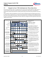
Table of Contents
Table of Contents
About this document .....................................................................................................................1
Table of Contents ..........................................................................................................................2
1
1.1
1.2
1.3
1.4
1.5
1.6
1.6.1
1.6.2
1.6.3
1.6.4
1.6.5
1.7
1.8
1.8.1
1.8.2
1.9
1.9.1
1.9.2
1.9.3
1.10
1.10.1
1.10.2
1.10.3
1.10.4
1.10.5
Introduction to the CCU8 Basic Features .........................................................................4
CCU8 Basics ......................................................................................................................................... 4
Basic Timer Functions ......................................................................................................................... 4
The Comound CAPCOM8 System........................................................................................................ 5
CCU8 Use Cases ................................................................................................................................... 6
Additional CCU8 Features ................................................................................................................... 7
CCU8 Input Control ............................................................................................................................. 8
Synchronized Control of CAPCOM Units on External Events ....................................................... 8
External Control Basics ................................................................................................................. 9
External Events Control ................................................................................................................ 9
External Event Sources ................................................................................................................. 9
External Event Input Functions .................................................................................................... 9
Capture Basics ..................................................................................................................................... 9
CCU8 Output Control ........................................................................................................................ 10
External Control by Timer Events ............................................................................................... 10
Top-Level Control of Event Request to/from a Timer Slice ....................................................... 10
Compare Basics ................................................................................................................................. 11
CCU8 Shadow Transfers.............................................................................................................. 12
Shadow Transfer of Compare Register values ........................................................................... 12
CCU8 Output State and Output Pin PASSIVE/ACTIVE Level Control ......................................... 13
How to Start a Timer ......................................................................................................................... 13
Initialization Sequence ............................................................................................................... 13
Start-up Enable ........................................................................................................................... 14
Start Timer Running .................................................................................................................... 14
Global Start of CCU8 ................................................................................................................... 14
Global Start of the CCU4 and CCU8 CAPCOM Units ................................................................... 14
2
2.1
2.1.1
2.1.2
2.1.3
2.1.4
2.1.5
2.1.6
2.2
2.2.2
2.2.3
2.2.4
2.2.5
2.2.6
2.3
2.3.1
Dynamic Control of Timer Functions on External Events ................................................ 16
Introduction....................................................................................................................................... 16
External Control Basics ............................................................................................................... 16
Selection of External Events Control Sources ............................................................................ 17
Selection of External Events Control of Input Functions ........................................................... 17
Extended Slice Input Functions .................................................................................................. 17
External Control by Timer Events ............................................................................................... 17
Top-Level Control of Event Request to/from a Timer Slice ....................................................... 18
Example Use Case: Triggering an ADC Conversion to change CCU8 Duty Cycle ............................. 19
Deriving the Period and Compare Values .................................................................................. 20
Macro and variable Settings ....................................................................................................... 21
XMC Lib Peripheral Configuration Structure .............................................................................. 21
Interrupt Service Routine Function Implementation ................................................................ 24
Main Function Implementation .................................................................................................. 25
Example Use Case: Generating a CCU8 TRAP with ADC Fast Compare ........................................... 28
Theory of Operation .................................................................................................................... 28
Application Note
2
V1.0, 2015-07
Capture Compare Unit 8 (CCU8)
AP32288
Table of Contents
2.3.2
2.3.3
2.3.4
2.3.5
Deriving the Period and Compare Values .................................................................................. 29
Macro and variable Settings ....................................................................................................... 30
XMC Lib Peripheral Configuration Structure .............................................................................. 30
Main Function Implementation .................................................................................................. 34
3
3.1
3.1.1
3.1.2
3.1.3
3.1.4
3.2
3.2.1
3.2.2
3.2.3
3.2.4
3.2.5
3.2.6
3.2.7
Multi Phase Output Pattern Generation ........................................................................ 37
Introduction....................................................................................................................................... 37
CCU8 Shadow Transfer for Coherent Signal Pattern Update .................................................... 40
The Global Shadow Transfer Set Enable Register ..................................................................... 40
Shadow Transfer of Compare Register values ........................................................................... 40
Compound Shadow Transfers .................................................................................................... 40
Example Use Case: CCU8 Initialization for 3 Phase Motor Drive ..................................................... 41
Theory of Operation .................................................................................................................... 42
Deriving the Period and Compare Values .................................................................................. 42
Deriving the Dead-Time .............................................................................................................. 43
Macro and variable Settings ....................................................................................................... 44
XMC Lib Peripheral Configuration Structure .............................................................................. 44
Interrupt Service Routine Function Implementation ................................................................ 46
Main Function Implementation .................................................................................................. 46
4
Revision History .......................................................................................................... 49
Application Note
3
V1.0, 2015-07
Capture Compare Unit 8 (CCU8)
AP32288
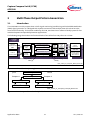
Introduction to the CCU8 Basic Features
1
Introduction to the CCU8 Basic Features
1.1
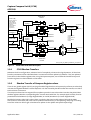
CCU8 Basics
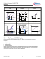
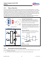
The CAPCOM8 is a multi-purpose timer unit for signal monitoring/conditioning and Pulse Width Modulation
(PWM) signal generation. It is designed with repetitive structures with multiple timer slices that have the
same base functionality. The internal modularity of CCU8, translates into a software friendly system for fast
code development and portability between applications.
The following image shows the main function blocks of one of the four CC8y slices on a CCU8x.
CCU8x
x=0-1
CC8y
4 Service
Request
Lines
Request Lines
DMA
Slice y
Reset- / Power
y=0-3
Control
Prescaler /
Floating
Prescaler
Clock Control
Period Register
Edge /
Center
Align
Timer 16-bit
Single
Shot
Period Shadow Register
4 x Capture
Service
Asymmetr.
Compare Shadow Reg. 1/2
Compare Register 2/2
Compare Register 1/2
PWM 1/2
PWM 1/2
Modulation
Control
Active /
Passive
Control
Dead-time
3 x Input
Selector
Multi Channel
Pattern
Generation
2x Compl. Outputs
Status Bit
Input Matrix
Function Control
by 16 External
Event Sources
DEV_CCU8_00_Basics_Slice.vsd
Figure 1
1.2
The Timer Slice Block Diagram
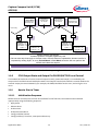
Basic Timer Functions
Each timer slice can handle all the basic modes and the typical options illustrated in the figure below.
Application Note
4
V1.0, 2015-07
Capture Compare Unit 8 (CCU8)
AP32288
Introduction to the CCU8 Basic Features
Timer
Compare
Capture
Free Running Mode
Option: Reset / Gate
Edge Aligned Mode
Symmetric or Asymmetric PWM
Time Measurement
Period
Period
Interrupt
Interrupt
Interrupt
Interrupt
Compare
Register 2
Interrupt
Interrupt
Capture!
Capture!
Compare
Register 1
0
Time
Reset (Clear):
Gate Input:
Interrupt
t1 – t0
0
Alternatives:
Time
Asymmetric
PWM:
T1
Normal
PWM:
T1
T2
T3
t0
Time
t1
T2
Counter
Compare
Option: Up/Down Count Control
Center Aligned Mode
Symmetric or Asymmetric PWM
Single Shot
Period
Count
Period
Interrupt
Asymmetric
6
5
4
3
2
1
0
Interrupt
Interrupt
Interrupt
Compare Level (II)
Symmetric
Compare
Level (I)
0
0
Time
Count Input:
Time
PWM:
U/D Control
Input:
Count Down
Count Up
T1
T2
T3 T1
Time
t1 – t0 = <period>
Interrupt
t0
Start
t1
Stop
DEV_CCU8_00_Counting_Schemes_Basics.vsd
Figure 2
1.3
Basic Functions of each Timer Slice
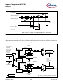
The Comound CAPCOM8 System
Each CCU8x has four 16-bit timer slices CC8y (y=3-0), which can be concatenated up to 64-bit.
A slice has:
1 Timer
4 Capture registers
1 Period register
2 Compare registers
Both the Period and Compare registers have shadow registers. Each slice can work independently in
different modes, but they can also be synchronized, even to other CCU8 slices. They perform multichannel/multi-phase pattern generation with parallel updates.
Application Note
5
V1.0, 2015-07
Capture Compare Unit 8 (CCU8)
AP32288
Introduction to the CCU8 Basic Features
The ”CAPCOM8 RACK”
Slice y
y =Prescaler
0
Prescaler /
Floating
Prescaler
Prescaler
ModulaEdge /
tion
Center
Control
Edge /Align ModulationActive /
Center
Period Register
AlignSingle Control
Passive
Timer 16-bit
Shot
ActiveControl
/
Single
Asymmetr. Passive
Dead-time
Timer Shadow
T80 Reg. 1/2
Shot
Compare
Control
PWM 1/2
3 x Input
Compare
Register
2/2Asymmetr. Dead-time
Selector
Compare
ShadowRegister
Reg. 1/2 1/2
Compare
PWM 1/2
PWM 1/2
3 x Input
Compare Register 2/2
Selector
Compare Register 1/2
PWM 1/2
Period Shadow Register
Period Register
Period Shadow Register
Multi Channel
Patterns / Update /
Transfer Request
2x Compl. Outputs
Status Bits 0/0A/0B
Input Matrix
Function Control
by 16 External
Event Sources
Timer Concatenation
CC81
Slice y
y=1
4 x Capture
CC81SR
[3 : 0]
PR1
Edge /
Center
Align
Timer T81
Single
Shot
Period Shadow PRS1
CC81PSC
Asymmetr.
Compare Shadow CR1S1/2S1
CR11 / CR21
PWM 1/2
PWM 1/2
Modulation
Control
Active /
Passive
Control
Dead-time
3 x Input
Selector
Multi Channel
MCI1[3:0] / PS1 /
CCU80MCSS
CCU8xOUT1[3...0
CCU80ST1/-1A/-1B
Input Matrix
CCU80IN1
[P : A]
Timer Concatenation
CC82
Slice y
y=2
PR2
Edge /
Center
Align
Timer T82
Single
Shot
Period Shadow PRS2
4 x Capture
CC82SR
[3 : 0]
CC82PSC
Asymmetr.
Compare Shadow CR1S2/2S2
CR12 / CR22
PWM 1/2
PWM 1/2
Modulation
Control
Active /
Passive
Control
Dead-time
3 x Input
Selector
Multi Channel
MCI2[3:0] / PS2 /
CCU80MCSS
CCU8xOUT2[3...0]
CCU80ST2/-2A/-2B
Input Matrix
CCU80IN2
[P : A]
Timer Concatenation
CC83
CC83SR
[3 : 0]
Slice y
y=3
PR3
Edge /
Center
Align
Timer T83
Single
Shot
Period Shadow PRS3
CC83PSC
Asymmetr.
Compare Shadow CR1S3/2S3
CR13 / CR23
PWM 1/2
PWM 1/2
Modulation
Control
Active /
Passive
Control
Dead-time
3 x Input
Selector
Interface to the System Top-Level Interconnect Matrix
4 Service
Requests
4 Service
Request
Requests
Slice y
Lines
y=0-3
CC80
4 x Capture
CCU80
Switch
Control
CC80
4 x Capture
CCU81
4 x Capture
- - - Reset- / Power Control - - - Clock Control - - - Service Request Lines - - - DMA - - -
Global
Control
Multi Channel
MCI3[3:0] / PS3 /
CCU80MCSS
CCU8xOUT3[3...0
CCU80ST3/-3A/-3B
Input Matrix
CCU80IN3
[P : A]
DEV_CCU8_00_Slices.vsd
Figure 3
1.4
The Capture/Compare unit basic system of CAPCOM8
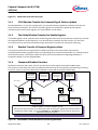
CCU8 Use Cases
Here are some typical example use cases that demonstrate the various capabilities of the CAPCOM timer
slices of the CCU8:
1. Simple Time Base with synchronization option by external events control
2. Power Conversion System (PFC, SMPS) using Single Shot Mode
Application Note
6
V1.0, 2015-07
Capture Compare Unit 8 (CCU8)
AP32288
Introduction to the CCU8 Basic Features
3. Feedback Sensor Event monitoring and Revolution by Capture, Count and Position Interface facilities
(POSIF)
4. Multi-Signal Pattern on Output Pins, created by parallel Multi-Channel Control
5. Drive & Motor Control with Multi-Phase System, Phase Adjustment and Trap Handling
6. 3-Level PWM for Inverters and Direct Torque Control (DTC) of AC Motors and High Precision Synchronous
Motors
7. External Events Control of Timer Input Functions by requests from external system units
8. Dithering PWM or period for DC-Level precision, Reduced EMI, Fractional Split of Reriods into Micro Step
9. Auto Adjusting Time Base by Floating Prescaler for adaption of time measurement to a wide range of
dynamics
The same use cases are illustrated in the following figure:
2
Simple Time Base
Single Shots in PFC & SMPS
Reject
I
IL
ID
Ton
IL
Vin
Vout
5
- Parallel Control of Output Pins by single pattern
Stall Detection (via BEMF)
Bipolar Stepper with Micro Steps:
T
C
POSIF
6
Multi Phase Control
CCU4/8
3-Level PWM
- For Higher Resolution, EMC quality & Efficiency
- 3-Phase Motor Control
- N Phase Power Supplies
- Asymmetric PWM for Phase Shift
- Trap
PWM1
Encoder
D
C
Multi Channel Control
Toff
ID
L
Event
Quadrature Encoder
- Event Counting
- Up/Down Counting
- Revolution Monitoring
- Velocity on Tick/ Velocity on Time Stamp
- Tick Compare
- Comprehensive Single Shots Handling
- Interrupt Request on the Period Match
- Synchronize on External Event Control
4
3
Reject
1
Compare 3
Asymm. Comp. 2
Compare 1
Polarity1
PWM2
PWM 3
Asymm. PWM 2
PWM 1
Polarity2
7
Event Controlled Timer Functions
- Synchronous Control of Timers by other Units
Event
Source
Select
GPIO
ERU1
POSIF
CAN
CCU4x
USIC
ADC
CCU8x
SCU
Up to 3 Event Function
Profiles Select of Inputs
Select
Edge or Level
H
Event0
Detect
L
Event0
true
false
3 Events
Control Connect
2
1
0
Inputs
External
Event
Sources
Target
Timer
Slice
start
stop
capture 0,1
capture 2,3
gate clock
up/down
load Timer
count
override bit
trap
modulate
8
9
Dithering
- EMI Reduction by spectrum broadening
- Fractional Period Time Division into Micro Ticks
- DC-Level average precision (from 16 to 20 bits)
E.g: How to achieve an average value of 28,9H
by a Buck Converter with 200 kHz sampling
rate, performing 10 bit DC-Level on average
Auto Adjusting Time Base
- Adaption to unknown measurement dynamics
- Reduction of the SW read activities
- Floating Prescaler Mode, individual in All Timers
timer count
Vout
Vin
L
D
PWM
T
C
PS Init
Dither
Capture
event
<period>
<timer>
2T
4T
zero
<timer>/<period+1> x 8T T
tcapture
PS Init
T = 2<PSIV> x (<period>+1) / fCCU;
2T
t
next tcapture
<PSIV> = 0-15
DEV_CCU8_00_Use_Cases.vsd
Figure 4
1.5
Some Features and Use Cases (1-9) characterizing an CAPCOM Unit (CCU) Features
Additional CCU8 Features
Features
Application Note
Operation
7
V1.0, 2015-07
Capture Compare Unit 8 (CCU8)
AP32288
Introduction to the CCU8 Basic Features
Features
Operation
Single Shot
If a slice is set in Timer Single Shot Mode (CC8yTC.TSSM), the Timer and its Run
Bit (TRB) is cleared by the Period/One match that occurs next to when the TSSM
bit was set. As a result, the timer stops running.
Timer Concatenation
Any timer slice can be concatenated with an adjacent timer slice by setting
CC8yTC.TCE = 1.
Dithering PWM
It can be used with very slow control loops that cannot update the
period/compare values in a fast manner. The precision can be maintained on long
runs.
Dithering Period Time
Micro ticks can be used in the Interpolation between sensor pulses to achieve
higher precision position monitoring.
Floating Prescaler
By changing of the timer clock frequency periodically (no compare/capture
event), the dynamic range is autonomously adapted to any time length.
External Modulation
The output pin signal of a slice is modulated by external events.
Output State Override
An external input signal source can override a slice’s status bit (CC8yST) on an
edge event by other external input signal source.
Multi-Channel Control
The output state of Timer Slices PWM signal(s) can be controlled in parallel by a
single pattern.
External Load
Each slice of CCU8 allows the user to select an external signal as the trigger for
reloading the timer value with current compare/period register value.
Trap Function
The function forces PWM output into a predefined state, preset in the
active/passive PSL bit. This allows the power device to be safely switched off.
1.6
CCU8 Input Control
1.6.1
Synchronized Control of CAPCOM Units on External Events
External Events Control distribution to CCUs (including CCU8) allows for synchronized timer control in
advanced applications. For example, in Motor Drive and Power Control, where 3-Level Inverters might
require 12 synchronized PWM. The limits are the realizable topography or timing pattern complexity range.
Application Note
8
V1.0, 2015-07
Capture Compare Unit 8 (CCU8)
AP32288
Introduction to the CCU8 Basic Features
1.6.2
External Control Basics
A slice can have its input functions controlled by external sources. The external source(s), active mode(s)
and input function(s) should be mapped to the 3 inputs of the slice in the CC8yINS and CC8yCMC registers.
Function mode extension alternatives can be added by selections in the CC8yTC Timer Slice Control register.
1.6.3
External Events Control
An external event control request can be an edge or level event signal from a peripheral unit or a GPIO. It can
be linked to the CCU8xCC8y slices input selection stages via a comprehensive matrix. A slice with any of its 3
events setups, detects a considered source-event-input profile, can be function controlled "remotely” this
way.
1.6.4
External Event Sources
CCU8xCC8y Input Functions can be linked to external trigger requests from sources such as: GPIO, ERU,
POSIF, CAN, CCU4x, USIC, ADC, CCU8x or SCU. Pin Connections are given by the Top-Level Interconnect
matrix and the CC8yINS[P:A] Input Select vector. The CC8yCMC register is used for the function selection.
1.6.5
External Event Input Functions
There are 11 Timer Input Functions (such as ‘Start the Timer’ for example), controllable by external events
via 3 selectable input lines with configurable source-event profile conditions to the Timer Slices CC8y (y=0-3)
of a CCU8x unit for Start, Stop, Capture0-3, Gate, Up/Down, Load, Count, Bit Override, Trap and Modulate
Output control.
There are also some Extended Input Functions in the register CC8yTC for Extended Start, Stop with
Flush/Start, Flush/Stop or Flush or Extended Capture Mode. Together, with a read access register (ECRD),
these simplifyadministration of capture registers and full-flags when more than one slice is used in Capture
mode.
1.7
Capture Basics
Each CAPCOM8 (CCU8x) has 4 timer-slices. Each slice has 4 capture value registers, split into 2 pairs that
capture on the selected event control input: Capt0 or Capt1, according to 2 possible pair schemes: either as
2 pairs for different events respectively to Capt0 and Capt1, or cascaded for the same event via Capt1.
CCU8x
x=0-1
CC8y
Request Lines
DMA
Service
44 Service
Request
Requests
Lines
Slice y
Reset- / Power
y=0-3
Control
Prescaler /
Prescaler
Floating
Prescaler
Clock Control
Period Register
Edge /
Center
Align
Timer 16-bit
Single
Shot
Period Shadow Register
4 x Capture
Service
Asymmetr.
Compare Shadow Reg. 1/2
Compare Register 2/2
Compare Register 1/2
PWM 1/2
PWM 1/2
Modulation
Control
Active /
Passive
Control
Dead-time
3 x Input
Selector
Multi Channel
Pattern
Generation
2x Compl. Outputs
Status Bit
Input Matrix
Function Control
by 16 External
Event Sources
DEV_CCU8_00_Basics_Slice_Capture.vsd
Figure 5
Timer Slice with four Capture Registers
Application Note
9
V1.0, 2015-07
Capture Compare Unit 8 (CCU8)
AP32288
Introduction to the CCU8 Basic Features
Capture reg. 3:
Capture Inputs:
CCycapt1
Capture
on
Different
Events
fCCU8
Capture Trigger Distribution & Full-Flag Handling Logic
Full/
Empty
Full/
Empty
CC8yC3V
CC8yC2V
CC8yC1V
CC8yC0V
T8y
Full/
Empty
CCycapt0
fCCU8
Full/
Empty
Capture Trigger Distribution & Full-Flag Handling Logic
Capture Input:
CCycapt1
Capture
on Same
Event
and Edge
Capture reg. 2:
Capture reg. 1:
Capture reg. 0:
Capture reg. 3:
Capture reg. 2:
Capture Trigger Distribution & Full-Flag Handling Logic
T8y
Full/
Empty
Full/
Empty
CC8yC3V
CC8yC2V
CC8yC1V
CC8yC0V
Full/
Empty
Full/
Empty
Capture Trigger Distribution & Full-Flag Handling Logic
Capture reg. 1:
Capture reg. 0:
DEV_CCU8_00_Capture_Logic.vsd
Figure 6
Basic Capture Mechanism – setup in two possible scheme alternatives
1.8
CCU8 Output Control
1.8.1
External Control by Timer Events
A timer event can trigger external actions via the Top-Level Interconnect matrix or on request for an
Interrupt. Each CAPCOM8 has four Service Request Lines and each slice has a dedicated output signal
CC8ySR[3...0], selectable to a line by CC8ySRS. This mean timer slice events can request direct peripheral
actions or an interrupt.
1.8.2
Top-Level Control of Event Request to/from a Timer Slice
Top-Level control also means conditional control of event requests between a slice and other action
providers. The Event Request Unit (ERU1) and the Top-Level Interconnect matrix can combine, control and
link event signals according to user defined request-to-action event patterns. For example, invoke I/O
states, Time Windowing etc.
Application Note
10
V1.0, 2015-07
Capture Compare Unit 8 (CCU8)
AP32288
Introduction to the CCU8 Basic Features
1.9
Compare Basics
CCU8x
x=0-1
CC8y
Service
44 Service
Request
Requests
Request Lines
Lines
DMA
Slice y
Reset- / Power
y=0-3
Control
Prescaler /
Prescaler
Floating
Prescaler
Clock Control
Period Register
Edge /
Center
Align
Timer 16-bit
Single
Shot
Period Shadow Register
4 x Capture
Service
Modulation
Control
Active /
Passive
Control
Dead-time
Asymmetr.
Compare Shadow Reg. 1/2
Compare Register 2/2
Compare Register 1/2
Shadow Reg. CR1Sy
CR1y
PWM 1/2
3 x Input
Selector
PWM 1/2
Multi Channel
Pattern
Generation
2x Compl. Outputs
Status Bits
Input Matrix
Function Control
by 16 External
Event Sources
Shadow Reg. CR2Sy
CR2y
DEV_CCU8_00_Basics_Slice_Compare.vsd
Figure 7
Timer Slice Compare Registers and PWM related Blocks
y=0-3
PRy
Period
Compare 1
TRy
Compare 2
CR1y
CR2y
Dead Time 1y
Dead Time 2y
DEV_CCU8_00_Basics_Slice_Compare_principle_0.vsd
Figure 8
Basic Blocks for Symmetric/Asymmetric PWM generation with Dead-Time
Application Note
11
V1.0, 2015-07
Capture Compare Unit 8 (CCU8)
AP32288
Introduction to the CCU8 Basic Features
Dead Time
Control
Timer TRy
Counting Scheme:
- Edge Aligned
- Center Aligned
Direction Control:
- Up/Down
Compare Mode:
- Symmetric
- Asymmetric
Status Bit 1
Control
set
clear
CCST1
CCST1
CCST1 & DTR1n
&
CCST1 & DTR1
CCU8xOUTy1
DTR1
Compare
Channel 1
DTR1n
DTR-trigger
set
DTF-trigger
clear
DT1R
Set/Clear
Switch
Control
Timer TRy
set
clear
DT1F
Dead Time
Generator 1
- Active/Passive
Control
- External Events
Control
- Multi Channel
Control
fDclk
DT2Rise
DTR-trigger
Dead Time
Generator 2
DT2Fall
DTF-trigger
Compare
Channel 2
DTR2n
DTR2
CCU8xOUTy2
CCST2 & DTR2
set
clear
&
CCST2 & DTR2n
Status Bit 2
Control
fTclk
CCU8xOUTy0
Output
Modulation
/n
Output
Modulation
CCU8xOUTy3
CCST2
CCST2
fDclk
Dead Time
Control
DEV_CCU8_00_Basics_DeadTime_principle.vsd
Figure 9
1.9.1
Dead-Time Generation Principles
CCU8 Shadow Transfers
Whatever the slice configuration, whatever level of complexity, whatever the signal patterns, all the timer
function parameters of the CAPCOM4 timers are assured coherent update by hardware. They are updated
from values in the shadow registers that, on a global preset request, are transferred simultaneously to all
function registers at a Period Match or One Match.
1.9.2
Shadow Transfer of Compare Register values
There is one, global register (GCSS) carrying all enable-flags that have to be preset by software to selectively
activate the targeted Shadow Transfer Requests. It is also cleared by hardware after the transfer, to achieve
total real time correctness.
The compare values that are targeted for an update operation have to be written into the CC8yCR1S/CR2S
shadow registers AND the corresponding Slice Transfer Set Enable bits. For example SySE in GCSS, must be
preset before Period Match (in Edge Aligned Mode) or Period/One Match (in Center Aligned Mode).
Beside the Compare (CR1/CR2) values, there are also the the timer Period register (PR) and the PWM
Active/Passive control bit (PSL) that can be updated simultaneously on the SySE flag. Dithering or Floating
Prescaler values are able to get a simultaneous update via the SyDSE and SyPSE request flags.
Application Note
12
V1.0, 2015-07
Capture Compare Unit 8 (CCU8)
AP32288
Introduction to the CCU8 Basic Features
Shadow TrAnsfer
on Period-Match
and REquest is
cleared by HW
No Shadow
Transfer since
No request
No Shadow
Transfer since
No request
Shadow TrAnsfer
on One-Match
and REquest is
cleared by HW
Timer CC8y
SW
HW
CC80CR1S = 10
CC80CR2S = 20
CC81CR1S = 30
SySE = 1
SW
CC80CR1S = 20
CC80CR2S = 80
CC81CR1S = 60
SySE = 1
CC80CR1 = 10
CC80CR2 = 20
CC81CR1 = 30
HW
CC80CR1 = 20
CC80CR2 = 80
CC81CR1 = 60
Shadow transfer mechanism:
Coherent update of compare registers by HW.
SW can write asynchronously to the timer state. After all values are updated the shadow transfer is
requested by setting SySE. At every Period-Match or One-Match event the HW can perform the
transfer and clears the request.
DEV_CCU8_00_Shadow_Transfer_with_Compare_Registers.vsd
Figure 10
1.9.3
Basic Shadow Transfer Mechanism for Compare Register Values
CCU8 Output State and Output Pin PASSIVE/ACTIVE Level Control
The PASSIVE/ACTIVE state of a slice’s internal output CCUxSTy (status bit CC8yST) is controlled by the
compare level and the External Modulation Mode. The CC8yPSL Passive/Active bit PSL controls whether the
external output pin state CCU8xOUTy (for example, the PWM) should be Passive Low / Active High or viceversa.
1.10
How to Start a Timer
1.10.1
Initialization Sequence
Before the start and execution of timer slice software for the first time, the CCU8 must be initialized
appropriately using the following sequence:
Apply Reset
Release Reset
Enable Clock
Enable Prescaler Block
Configure Global Control
Configure Slice(s) Functions, Interrupts and Start-up
Application Note
13
V1.0, 2015-07
Capture Compare Unit 8 (CCU8)
AP32288
Introduction to the CCU8 Basic Features
1.10.2
Start-up Enable
In the last part of the CCU8 Initialization Sequence the startup value(s) for a specific Compare Channel
Status of the Timer Slice(s) could be configured by the respective GCSS.SyTS bit. After that, the default IDLE
mode has to be removed from the Timer Slice(s) in the GIDLC register and then Start or Global Start can be
initiated.
1.10.3
Start Timer Running
There are two ways to start a timer:
Directly by software setting the Timer Run Bit Set (TRBS)
Indirectly by hardware when a specific event occurs in an external unit as determined by the Top-Level
Connection Matrix of External Events Control for CAN, ADC, USIC, IO, CCU4/8, ERU1, POSIF and so on.
1.10.4
Global Start of CCU8
There is a way to get a synchronized start of CAPCOM Units, both for CCU4x and CCU8x:
To achieve a synchronized start of both CAPCOM Units (CCU4x and CCU8x) use either
A global start by software, with the CCUx Global Start Control bits in the CCUCON Global Start Control
register
A global start by hardware, indirectly with External Events Control using the CC8yINS and CC8yCMC
registers.
1.10.5
Global Start of the CCU4 and CCU8 CAPCOM Units
The Global Start command enables timers to be started, independently of the CAPCOM unit they belong to.
The global start means that the timers are synchronized and all timing can be controlled in parallel, with
many different kinds of generated output patterns.
Application Note
14
V1.0, 2015-07
Capture Compare Unit 8 (CCU8)
AP32288
Introduction to the CCU8 Basic Features
CCUCON
GSC80
GSC41
CC40INS
GSC40
Select Considered
Source-Event Profiles
CC40CMC
CC40
CC80
CC41
CC81
CC42
CC82
CC43
CC83
CCU80
CCU40
DEV_CCU8_00_StartTimer.vsd
This mechanism allows synchronous start of different timer slices within
one CCU but also different slices from different CCUs
DEV_CCU8_00_StartTimer.vsd
Figure 11
External Event Control with Global Start Command
Application Note
15
V1.0, 2015-07
Capture Compare Unit 8 (CCU8)
AP32288
Dynamic Control of Timer Functions on External Events
2
Dynamic Control of Timer Functions on External
Events
2.1
Introduction
The External Events Control distribution to CCUs (including CCU8) allows for advanced applications with
synchronized timer control. For example, in Motor Drive and Power Control such as 3-Level Inverters
requiring 12 synchronized PWMs.
2.1.1
External Control Basics
A slice can have its input functions controlled by external sources. The external source(s), active mode(s)
and input function(s) should be mapped to the 3 inputs of the slice in the CC8yINS and CC8yCMC registers.
Function mode extending alternatives can be added by selections in the CC8yTC Timer Slice Control
register.
CCU8x
x=0-1
CC8y
Request Lines
DMA
Slice y
Reset- / Power
y=0-3
Control
Prescaler /
Prescaler
Floating
Prescaler
Clock Control
Event
Source
Select
Single
Shot
Asymmetr.
Compare Shadow Reg. 1/2
Compare Register 2/2
Compare Register 1/2
Up to 3 Events
Profile Selectable
Edge or Level
H
GPIO
ERU1
POSIF
CAN
CCU4x
USIC
ADC
CCU8x
SCU
---
Timer 16-bit
L
Event0
true
2
1
0
Event0
Detect
false
3 Events
Control Connect Matrix
PWM 1/2
PWM 1/2
Modulation
Control
Active /
Passive
Control
Dead-time
3 x Input
Selector
Timer Input Functions
that may be controlled
by the Events 0, 1 or 2
Function
of Inputs
Select
Inputs
External
Event
Sources
Period Register
Edge /
Center
Align
Period Shadow Register
Service
44 Service
Request
Requests
Lines
4 x Capture
Service
Edge signal to start the timer
Edge signal to stop the timer
Edge signal to capture into reg. 0 & 1
Edge signal to capture into reg. 2 & 3
Level signal to gate the timer clock
Level signal to up/down count direction
Edge signal to load the Timer
Edge signal to count events
Status bit override with an input value
Level signal to trap for fail-safe op.
Level signal to modulate the output
Multi Channel
Pattern
Generation
2x Compl. Outputs
Status Bit
Input Matrix
Function Control
by 16 External
Event Sources
Target
Timer
Slice
PRy
Timer TRy
CR1y
CR2y
DEV_CCU8_00_Basics_External_Events_Control_Komplex.vsd
Figure 12
Timer Slice Input Functions Control on External Events via the System Interconnect Matrix
An external event control request can be an edge or level event signal from a peripheral unit or a GPIO. It can
be linked to the CCU8xCC8y slice’s input selection stages via a comprehensive matrix. A slice with any of its 3
Application Note
16
V1.0, 2015-07
Capture Compare Unit 8 (CCU8)
AP32288
Dynamic Control of Timer Functions on External Events
events setup detects a considered source-event-input profile and can be function controlled “remotely” this
way.
2.1.2
Selection of External Events Control Sources
CCU8xCC8y Input Functions can be linked to external trigger requests from sources such as: GPIO, ERU,
POSIF, CAN, CCU4x, USIC, ADC, CCU8x or SCU. Pin Connections are given by the Top-Level Interconnect
matrix and the CC8yINS[P:A] Input Select vector - and Function Select by the CC8yCMC register.
A CC8y internal event is also regarded as External Event. This means a CC8y can control itself by its own
events.
2.1.3
Selection of External Events Control of Input Functions
There are 11 Timer Input Functions (such as Start the Timer), controlable by external events via 3 selectable
input lines with configurable source-event profile conditions to the Timer Slices CC8y (y=0-3) of a CCU8x unit
for Start, Stop, Capture0-3, Gate, Up/Down, Load, Count, Bit Override, Trap and Modulate Output control.
The Input Functions are, due to their nature, controlled by either event edge or event level signals.
2.1.4
Extended Slice Input Functions
There are some Extended Input Functions in the CC8yTC register, for the options Flush/Start, Flush/Stop or
just Flush the timer and for an Extended Capture Mode option that via a read access register (ECRD) setup
simplifies administration of capture registers and full-flags, when more than one slice is used in Capture
mode.
Slice CCU8xCC8y (x = 0 – 1, y = 0 – 3)
Select:
External EVENT z
Source
Inputs
E.g.:
CCU8xINy A
CCU8xINy B
CCU8xINy C
CCU8xINy D
CCU8xINy E
CCU8xINy F
CCU8xINy G
CCU8xINy H
CCU8xINy I
CCU8xINy J
CCU8xINy K
CCU8xINy L
CCU8xINy M
CCU8xINy N
CCU8xINy O
CCU8xINy P
GPIO
ERU1
POSIF
CAN
CCU4x
USIC
ADC
CCU8x
SCU
Select:
External
Event
Source
Select:
Considered
Event
Edge or Level
H
LPF
Event z
Detect
Slice
Input
Function
Edge signal to start the timer
Edge signal to stop the timer
Edge signal to capture into reg. 0 & 1
Edge signal to capture into reg. 2 & 3
Level signal to gate the timer clock
Level signal to up/down count direction
Edge signal to load the Timer
Edge signal to count events
Status bit override with an input value
Level signal to trap for fail-safe op.
Level signal to modulate the output
L
true
false
CC8y
EVENT z Control
(nop)
PRy
Timer TRy
CR1y
CR2y
Event z Control Matrix
z=0-2
Concatenation Logic Excluded
DEV_CCU8_04_External_Events_Control_Principle.vsd
Figure 13
2.1.5
Principle Block Diagram illustrating External Event Control of a CCU8y Timer Slice
External Control by Timer Events
A timer event can either trigger external actions via the Top-Level Interconnect matrix or request for an
Interrupt. Each CAPCOM8 has four Service Request Lines and each slice has a dedicated output signal
CC8ySR[3...0] selectable to a line via CC8ySRS. This means timer slice events can request for direct
peripheral actions or request an interrupt.
Application Note
17
V1.0, 2015-07
Capture Compare Unit 8 (CCU8)
AP32288
Dynamic Control of Timer Functions on External Events
2.1.6
Top-Level Control of Event Request to/from a Timer Slice
Top-Level control also means conditional control of events requests between a slice and other action
providers. The Event Request Unit (ERU1) together with the Top-Level Interconnect matrix can combine,
control and link event signals according to user defined request-to-action event patterns, such as invoke I/O
states, Time Windowing etc.
Slice CC8y
Select:
External EVENT 0
Source
Inputs
E.g.:
CCU8xINy A
CCU8xINy B
CCU8xINy C
CCU8xINy D
CCU8xINy E
CCU8xINy F
CCU8xINy G
CCU8xINy H
CCU8xINy I
CCU8xINy J
CCU8xINy K
CCU8xINy L
CCU8xINy M
CCU8xINy N
CCU8xINy O
CCU8xINy P
GPIO
ERU1
POSIF
CAN
CCU4x
USIC
ADC
CCU8x
SCU
Select:
External
Event
Source
Select:
Considered
Event
Edge or Level
H
LPF
Event
Detect
Slice
Input
Function
Edge signal to start the timer
Edge signal to stop the timer
Edge signal to capture into reg. 0 & 1
Edge signal to capture into reg. 2 & 3
Level signal to gate the timer clock
Level signal to up/down count direction
Edge signal to load the Timer
Edge signal to count events
Status bit override with an input value
Level signal to trap for fail-safe op.
Level signal to modulate the output
L
true
false
CC8y
EVENT 0 Control
(nop)
PRy
Timer TRy
CR1y
CR2y
Event 0 Control Matrix
z=0-2
External EVENT 1
Event 1 Control Matrix
EVENT 1 Control
External EVENT 2
Event 2 Control Matrix
EVENT 2 Control
Concatenation Logic Excluded
CCU8xGPy0 , -1 , -2
DEV_CCU8_04_External_Events_Control_Implementation.vsd
Figure 14
Block Diagram of the External Event Control Implementation
Application Note
18
V1.0, 2015-07
Capture Compare Unit 8 (CCU8)
AP32288
Dynamic Control of Timer Functions on External Events
2.2
Example Use Case: Triggering an ADC Conversion to change CCU8 Duty
Cycle
In this example, the CCU80.80 slice is configured in edge-aligned mode with frequency = 24 kHz and a 50%
duty on both channel 1 and 2. Each compare match event on channel 1, triggers an ADC Queue Conversion.
An ADC channel event is triggered if the conversion result is within the set boundary limits (Upper boundary
= 4000, Lower boundary = 1000). In the ADC channel event, the ADC conversion result is saved and a software
variable, ADC_INBOUND, is set. This is used as a marker that an ADC conversion has occurred. During a
period match event, if ADC_INBOUND is set, the duty cycle on channel 2 is updated. This example is based
on XMC4500.
CCU80.CC80
SLICE Configuration:
XMC4500
System Clock = 120 MHz
Frequency = 24 kHz
CV1 updated based on ADC
CV2 = 50% Duty Cycle
Mode = Edge-aligned, Counting up
Period
CV1
CV2
#1
CMU2S
#2
#1: Compare Match while counting up
on compare channel 2 triggers an ADC
queue conversion. A Channel event
does not occur as the ADC result does is
not within the boundary set.
#4
PMUS
CCU80.OUT00
(P0.5)
#2: Similar to #1, an ADC queue
conversion is triggered. A Channel event
does occur as the ADC result is within
the boundary set.
VADC G0CH1
ADC_INBOUND
#3: In the ADC Channel Event ISR, a
variable, ADC_INBOUND, is set. This is
used as a marker that an ADC
conversion has occurred.
Queue Conversion
Channel Event
#3
#4: In the Period Match Event ISR,
compare value for channel 1 (CV1) is
updated if ADC_INBOUND=1. Once
updated, ADC_INBOUND is cleared.
POTENTIOMETER
(P14.1)
4000
1000
Figure 15
Example: Triggering an ADC conversion to change CCU8 Duty Cycle
Application Note
19
V1.0, 2015-07
Capture Compare Unit 8 (CCU8)
AP32288
Dynamic Control of Timer Functions on External Events
2.2.2
Deriving the Period and Compare Values
The clock relationship between 𝑓𝑃𝑊𝑀 , 𝑓𝑡𝑐𝑙𝑘 and 𝑓𝑐𝑐𝑢8 is calculated as shown below:
𝑓𝑐𝑐𝑢8 is the frequency of the CCU8 peripheral clock. It is the input to the PWM module.
𝑓𝑡𝑐𝑙𝑘 is the timer resolution used to increment a timer counter. Each timer slice supports a dedicated
prescaler value selector. In this example, the default prescaler factor 0 is used. This results in a prescaler
value of 1 and a timer resolution of 8.33 ns.
In order for, 𝑓𝑃𝑊𝑀 , frequency of the PWM signal, to be 24 kHz, the CCU8_CC80.PRS register is loaded with
value 4999.
𝑓𝑐𝑐𝑢8
Timer frequency:
𝑓𝑡𝑐𝑙𝑘 =
Period value:
𝐶𝐶𝑈8𝐶𝐶80 . 𝑃𝑅𝑆 =
Compare value:
𝐶𝐶𝑈8𝐶𝐶80 . 𝐶𝑅𝑆 = (1 − 𝐷𝐶) ∗ (𝑃𝑅𝑆 + 1 )
Table 1
𝑃𝑟𝑒𝑠𝑐𝑎𝑙𝑒𝑟
𝑓𝑡𝑐𝑙𝑘
𝑓𝑃𝑊𝑀
-1
Calculated Prescaler factor, Period and Compare Values
Type
Calculated value
Prescaler value
20 = 0
Period @1Hz frequency
4999
Compare value @50% DC
2500
(At initialization, CV1 = CV2 )
Application Note
20
V1.0, 2015-07
Capture Compare Unit 8 (CCU8)
AP32288
Dynamic Control of Timer Functions on External Events
2.2.3
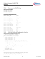
Macro and variable Settings
XMC Lib Project includes:
#include
#include
#include
#include
<xmc_ccu8.h>
<xmc_gpio.h>
<xmc_scu.h>
<xmc_vadc.h>
Project Macro definitions for CCU8:
#define
#define
#define
#define
#define
MODULE_PTR
MODULE_NUMBER
SLICE0_PTR
SLICE0_NUMBER
SLICE0_OUTPUT00
CCU80
(0U)
CCU80_CC80
(0U)
P0_5
Project Macro definitions for ADC:
#define
#define
#define
#define
#define
RES_REG_NUMBER
CHANNEL_NUMBER
VADC_GROUP_PTR
VADC_GROUP_ID
IRQ_PRIORITY
(0)
(1U)
(VADC_G0) /* P14.1 */
(0)
(10U)
Project Variables Definition:
volatile uint16_t CURRENT_PWM;
volatile bool ADC_INBOUND = 1;
2.2.4
XMC Lib Peripheral Configuration Structure
XMC System Clock Unit (SCU) Configuration:
/* XMC Clock configuration structure */
XMC_SCU_CLOCK_CONFIG_t clock_config = {
.syspll_config.n_div = 80U,
.syspll_config.p_div = 2U,
.syspll_config.k_div = 4U,
.syspll_config.mode = XMC_SCU_CLOCK_SYSPLL_MODE_NORMAL,
.syspll_config.clksrc = XMC_SCU_CLOCK_SYSPLLCLKSRC_OSCHP,
.enable_oschp = true,
.enable_osculp = false,
.calibration_mode = XMC_SCU_CLOCK_FOFI_CALIBRATION_MODE_FACTORY,
.fstdby_clksrc = XMC_SCU_HIB_STDBYCLKSRC_OSI,
.fsys_clksrc = XMC_SCU_CLOCK_SYSCLKSRC_PLL,
.fsys_clkdiv = 1U,
.fcpu_clkdiv = 1U,
.fccu_clkdiv = 1U,
.fperipheral_clkdiv = 1U
};
XMC Capture/Compare Unit 8 (CCU8) Configuration for SLICE0:
XMC_CCU8_SLICE_COMPARE_CONFIG_t SLICE_config =
Application Note
21
V1.0, 2015-07
Capture Compare Unit 8 (CCU8)
AP32288
Dynamic Control of Timer Functions on External Events
{
.timer_mode
.monoshot
.shadow_xfer_clear
.dither_timer_period
.dither_duty_cycle
.mcm_ch1_enable
.mcm_ch2_enable
.slice_status
.prescaler_mode
.passive_level_out0
.passive_level_out1
.passive_level_out2
.passive_level_out3
.asymmetric_pwm
.invert_out0
.invert_out1
.invert_out2
.invert_out3
.prescaler_initval
.float_limit
.dither_limit
.timer_concatenation
=
=
=
=
=
=
=
=
=
=
=
=
=
=
=
=
=
=
=
=
=
=
(uint32_t)
(uint32_t)
(uint32_t)
(uint32_t)
(uint32_t)
(uint32_t)
(uint32_t)
(uint32_t)
(uint32_t)
(uint32_t)
(uint32_t)
(uint32_t)
(uint32_t)
(uint32_t)
(uint32_t)
(uint32_t)
(uint32_t)
(uint32_t)
(uint32_t)
(uint32_t)
(uint32_t)
(uint32_t)
XMC_CCU8_SLICE_TIMER_COUNT_MODE_EA,
false,
0U,
0U,
0U,
false,
false,
XMC_CCU8_SLICE_STATUS_CHANNEL_1,
XMC_CCU8_SLICE_PRESCALER_MODE_NORMAL,
XMC_CCU8_SLICE_OUTPUT_PASSIVE_LEVEL_LOW,
XMC_CCU8_SLICE_OUTPUT_PASSIVE_LEVEL_LOW,
XMC_CCU8_SLICE_OUTPUT_PASSIVE_LEVEL_LOW,
XMC_CCU8_SLICE_OUTPUT_PASSIVE_LEVEL_LOW,
0U,
0U,
1U,
0U,
1U,
0U,
0U,
0U,
0U
};
XMC GPIO Configuration:
// Configuration for A2 class pads: Port0.5
XMC_GPIO_CONFIG_t OUTPUT_strong_sharp_config =
{
.mode
= XMC_GPIO_MODE_OUTPUT_PUSH_PULL_ALT3,
.output_level
= XMC_GPIO_OUTPUT_LEVEL_LOW,
.output_strength = XMC_GPIO_OUTPUT_STRENGTH_STRONG_SOFT_EDGE
};
XMC VADC Configuration:
/* Initialization data of VADC Global resources */
XMC_VADC_GLOBAL_CONFIG_t g_global_handle =
{
.disable_sleep_mode_control = false,
.clock_config = {
.analog_clock_divider
= 3U,
.msb_conversion_clock
= 0U,
.arbiter_clock_divider = 1U
},
.class0
= {
.conversion_mode_standard
= XMC_VADC_CONVMODE_12BIT,
.sample_time_std_conv
= 3U,
.conversion_mode_emux
= XMC_VADC_CONVMODE_12BIT,
.sampling_phase_emux_channel
= 3U
},
.class1
= {
Application Note
22
V1.0, 2015-07
Capture Compare Unit 8 (CCU8)
AP32288
Dynamic Control of Timer Functions on External Events
.conversion_mode_standard
.sample_time_std_conv
.conversion_mode_emux
.sampling_phase_emux_channel
},
.data_reduction_control = 0,
.wait_for_read_mode
= true,
.event_gen_enable
= false,
.boundary0
= 0,
.boundary1
= 0
};
=
=
=
=
XMC_VADC_CONVMODE_12BIT,
3U,
XMC_VADC_CONVMODE_12BIT,
3U
/* Initialization data of a VADC group */
XMC_VADC_GROUP_CONFIG_t g_group_handle =
{
.class0
= {
.conversion_mode_standard
= XMC_VADC_CONVMODE_12BIT,
.sample_time_std_conv
= 3U,
.conversion_mode_emux
= XMC_VADC_CONVMODE_12BIT,
.sampling_phase_emux_channel
= 3U
},
.class1
= {
.conversion_mode_standard
= XMC_VADC_CONVMODE_12BIT,
.sample_time_std_conv
= 3U,
.conversion_mode_emux
= XMC_VADC_CONVMODE_12BIT,
.sampling_phase_emux_channel
= 3U
},
.arbitration_round_length
= 0x0U,
.arbiter_mode
= XMC_VADC_GROUP_ARBMODE_ALWAYS,
.boundary0
= 1000U, /* Boundary-0 */
.boundary1
= 4000U, /* Boundary-1 */
.emux_config
= {
.emux_mode
= XMC_VADC_GROUP_EMUXMODE_SWCTRL,
.stce_usage
= 0,
.emux_coding
= XMC_VADC_GROUP_EMUXCODE_BINARY,
.starting_external_channel = 0,
.connected_channel
= 0
}
};
/* Identifier of the hardware group */
XMC_VADC_GROUP_t *g_group_identifier =VADC_GROUP_PTR;
/* Channel configuration data */
XMC_VADC_CHANNEL_CONFIG_t g_channel_handle =
{
.channel_priority
= 1U,
.input_class
= XMC_VADC_CHANNEL_CONV_GROUP_CLASS1,
.lower_boundary_select
= XMC_VADC_CHANNEL_BOUNDARY_GROUP_BOUND0,
.upper_boundary_select
= XMC_VADC_CHANNEL_BOUNDARY_GROUP_BOUND1,
.alias_channel
= (uint8_t)-1,
.bfl
= 0,
Application Note
23
V1.0, 2015-07
Capture Compare Unit 8 (CCU8)
AP32288
Dynamic Control of Timer Functions on External Events
.event_gen_criteria
.alternate_reference
.result_reg_number
.sync_conversion
.result_alignment
.use_global_result
.broken_wire_detect_channel
.broken_wire_detect
=
=
=
=
=
=
=
=
XMC_VADC_CHANNEL_EVGEN_INBOUND,
XMC_VADC_CHANNEL_REF_INTREF,
(uint8_t) RES_REG_NUMBER,
false,
/* Sync Feature disabled*/
XMC_VADC_RESULT_ALIGN_RIGHT,
false,
false,
false
};
/* Result configuration data */
XMC_VADC_RESULT_CONFIG_t g_result_handle = {
.post_processing_mode
= XMC_VADC_DMM_REDUCTION_MODE,
.data_reduction_control = 0,
.part_of_fifo
= false, /* No FIFO */
.wait_for_read_mode
= false, /* WFS */
.event_gen_enable
= false /* No result event */
};
/* Queue hardware configuration data */
XMC_VADC_QUEUE_CONFIG_t g_queue_handle =
{
.req_src_priority = (uint8_t)3U, /* Highest Priority = 3, Lowest = 0 */
.conv_start_mode = XMC_VADC_STARTMODE_WFS,
.external_trigger = (bool) true, /* External trigger enabled*/
.trigger_signal
= XMC_CCU_80_SR2,
.trigger_edge
= XMC_VADC_TRIGGER_EDGE_RISING,
.gate_signal
= XMC_VADC_REQ_GT_A,
.timer_mode
= (bool) false, /* No timer mode */
};
/* Queue Entry */
XMC_VADC_QUEUE_ENTRY_t
{
.channel_num
.refill_needed
.generate_interrupt
.external_trigger
};
2.2.5
g_queue_entry =
=
=
=
=
CHANNEL_NUMBER,
true, /* Refill is needed */
false, /* Interrupt generation is needed */
true /* External trigger is required */
Interrupt Service Routine Function Implementation
The CCU80 interrupt handler function to update the duty cycle on channel 1 at every period match event:
/* Interrupt handler - Period Match Interrupt; Updates the PWM frequency as long as ADC
conversion within boundary limits set */
void CCU80_0_IRQHandler(void)
{
/* Acknowledge Period Match event*/
XMC_CCU8_SLICE_ClearEvent(SLICE0_PTR, XMC_CCU8_SLICE_IRQ_ID_PERIOD_MATCH);
Application Note
24
V1.0, 2015-07
Capture Compare Unit 8 (CCU8)
AP32288
Dynamic Control of Timer Functions on External Events
/* Set up new PWM value */
if(ADC_INBOUND==1)
{
XMC_CCU8_SLICE_SetTimerCompareMatch(SLICE0_PTR, \
XMC_CCU8_SLICE_COMPARE_CHANNEL_1, CURRENT_PWM);
XMC_CCU8_EnableShadowTransfer(MODULE_PTR, XMC_CCU8_SHADOW_TRANSFER_SLICE_0);
ADC_INBOUND=0;
}
}
The VADC interrupt handler function generates a channel event when the value is within the boundary limit
defined:
/* Interrupt handler - Channel Interrupt; this is entered if the boundary set is in
boundary limits set*/
void VADC0_G0_0_IRQHandler(void)
{
XMC_VADC_RESULT_SIZE_t result;
/* Read the result register */
result = XMC_VADC_GROUP_GetResult(g_group_identifier,RES_REG_NUMBER);
/* Clear result event */
XMC_VADC_GROUP_ChannelClearEvent(g_group_identifier,CHANNEL_NUMBER);
/* Set marker for PWM duty cycle update*/
if(ADC_INBOUND == 0 )
{
CURRENT_PWM = result;
ADC_INBOUND = 1;
}
}
2.2.6
Main Function Implementation
Before the start and execution of timer slice software for the first time, the CCU8 must be initialized
appropriately using the following sequence:
Clock setup
/* Ensure clock frequency is set at 120 MHz */
XMC_SCU_CLOCK_Init(&clock_config);
Enable clock, enable prescaler block and configure global control:
/* Enable CCU8 module */
XMC_CCU8_Init(MODULE_PTR, XMC_CCU8_SLICE_MCMS_ACTION_TRANSFER_PR_CR);
/* Start the prescaler */
XMC_CCU8_StartPrescaler(MODULE_PTR);
/* Ensure fCCU reaches CCU80 */
XMC_CCU8_SetModuleClock(MODULE_PTR, XMC_CCU8_CLOCK_SCU);
Application Note
25
V1.0, 2015-07
Capture Compare Unit 8 (CCU8)
AP32288
Dynamic Control of Timer Functions on External Events
Configure Slice(s) Functions, Interrupts and Start-up:
/* Configure CCU8x_CC8y slice as timer */
XMC_CCU8_SLICE_CompareInit(SLICE0_PTR, &SLICE_config);
/* Set period match value of the timer */
XMC_CCU8_SLICE_SetTimerPeriodMatch(SLICE0_PTR, 4999U);
/* Set timer compare match value for channel 1 - 50% duty */
XMC_CCU8_SLICE_SetTimerCompareMatch(SLICE0_PTR, \
XMC_CCU8_SLICE_COMPARE_CHANNEL_1, 2500U);
/* Set timer compare match value for channel 2 - 50% duty */
XMC_CCU8_SLICE_SetTimerCompareMatch(SLICE0_PTR, \
XMC_CCU8_SLICE_COMPARE_CHANNEL_2, 2500U);
/* Transfer value from shadow timer registers to actual timer registers */
XMC_CCU8_EnableShadowTransfer(MODULE_PTR, XMC_CCU8_SHADOW_TRANSFER_SLICE_0);
/* Configure events */
/* Enable events: Period Match and Compare Match-Ch2 */
XMC_CCU8_SLICE_EnableEvent(SLICE0_PTR, XMC_CCU8_SLICE_IRQ_ID_PERIOD_MATCH);
XMC_CCU8_SLICE_EnableEvent(SLICE0_PTR, \
XMC_CCU8_SLICE_IRQ_ID_COMPARE_MATCH_UP_CH_2);
/* Connect event to SR0 and SR2 */
XMC_CCU8_SLICE_SetInterruptNode(SLICE0_PTR, \
XMC_CCU8_SLICE_IRQ_ID_PERIOD_MATCH, XMC_CCU8_SLICE_SR_ID_0);
XMC_CCU8_SLICE_SetInterruptNode(SLICE0_PTR,\
XMC_CCU8_SLICE_IRQ_ID_COMPARE_MATCH_UP_CH_2, XMC_CCU8_SLICE_SR_ID_2);
/* Configure NVIC */
/* Set priority */
NVIC_SetPriority(CCU80_0_IRQn, 63U);
/* Enable IRQ */
NVIC_EnableIRQ(CCU80_0_IRQn);
/*Initializes the GPIO*/
XMC_GPIO_Init(SLICE0_OUTPUT00, &OUTPUT_strong_sharp_config);
Configure ADC Queue Settings:
/* Initialize the VADC global registers */
XMC_VADC_GLOBAL_Init(VADC, &g_global_handle);
/* Configure a conversion kernel */
XMC_VADC_GROUP_Init(g_group_identifier, &g_group_handle);
/* Configure the queue request source of the aforesaid conversion kernel */
Application Note
26
V1.0, 2015-07
Capture Compare Unit 8 (CCU8)
AP32288
Dynamic Control of Timer Functions on External Events
XMC_VADC_GROUP_QueueInit(g_group_identifier, &g_queue_handle);
/* Configure a channel belonging to the aforesaid conversion kernel */
XMC_VADC_GROUP_ChannelInit(g_group_identifier,CHANNEL_NUMBER, &g_channel_handle);
/* Configure a result resource belonging to the aforesaid conversion kernel */
XMC_VADC_GROUP_ResultInit(g_group_identifier, RES_REG_NUMBER, &g_result_handle);
/* Set priority of NVIC node meant to be connected to Kernel Request source event*/
NVIC_SetPriority(VADC0_G0_0_IRQn, IRQ_PRIORITY);
/* Connect RS Event to the NVIC nodes */
XMC_VADC_GROUP_ChannelSetEventInterruptNode \
(g_group_identifier, CHANNEL_NUMBER, XMC_VADC_SR_GROUP_SR0);
/* Enable IRQ */
NVIC_EnableIRQ(VADC0_G0_0_IRQn);
/* Enable the analog converters */
XMC_VADC_GROUP_SetPowerMode(g_group_identifier, XMC_VADC_GROUP_POWERMODE_NORMAL);
/* Perform calibration of the converter */
XMC_VADC_GLOBAL_StartupCalibration(VADC);
/* Add the channel to the queue */
XMC_VADC_GROUP_QueueInsertChannel(g_group_identifier, g_queue_entry);
Start Timer Running:
/* Get the slice out of idle mode */
XMC_CCU8_EnableClock(MODULE_PTR, SLICE0_NUMBER);
/* Start the timer */
XMC_CCU8_SLICE_StartTimer(SLICE0_PTR);
Application Note
27
V1.0, 2015-07
Capture Compare Unit 8 (CCU8)
AP32288
Dynamic Control of Timer Functions on External Events
2.3
Example Use Case: Generating a CCU8 TRAP with ADC Fast Compare
All applications are defined with a set of operating conditions so that they function normally. The usual way
to achieve this is to monitor certain signals (for example, input voltages, feedback current) to ensure that
the application is functioning within the boundary conditions set.
In this example, based on XMC4500, we are using the VADC fast compare mode to monitor a signal input
voltage to ensure that it does not exceed the upper boundary limits (of 4000) that has been set. Once this
happens, a boundary flag is set. The boundary flag is used as an input for an external trap event. Once the
external trap event is triggered, the output signals (CCU80.OUT00 and CCU80.OUT02) are set to passive
output state. The trap exit condition selected allows the trap to be exited automatically by hardware once
the signal input voltage is within the boundary again.
CCU80.CC80
SLICE Configuration:
XMC4500
System Clock = 120 MHz
Frequency = 24 kHz
CV1 = 50% Duty Cycle
CV2 = 50% Duty Cycle
Mode = Edge-aligned, Counting up
Period
CV1, CV2
CCU80.OUT00
CCU80.OUT02
#2
#4
#1: ADC is set to Fast Compare Mode.
The boundary flag (BFL) reflects the
result of the comparisons. BFL is set
when it is above the fast comparevalue
of 4000.
Event 2, E2AS
VADC G0CH1
#3
ADC BFL
POTENTIOMETER
(P14.1)
#2: On BFL, a trap event is triggered and
the PWM OUT00 is set to passive level.
#3: BFL=0 when it goes below the fast
compare value of 4000.
#1
4000
#4: The trap exit is configured to be
synchronized with the PWM period of
the trap state and exited automatically.
The CCU80.OUT00 and CCU80.OUT02
are enabled.
3000
Figure 16
Example: Generating a CCU8 Trap with ADC Fast Compare
2.3.1
Theory of Operation
With the limit checking feature of VADC on XMC series, every digital conversion result can be automatically
compare to an Upper and a Lower Boundary value. A channel event can be generated when the result of a
conversion is inside or outside of a user-defined band, enabling a service request to only be issued under
certain pre-defined conditions (depending on the boundary definition). This feature supports automatic
range monitoring and minimizes the CPU load by issuing CCU8 TRAP service requests only under certain
predefined conditions.
The boundary flags exist to monitor if a value has crossed the activation boundary. These flags can be
represented as a change in the bitfield BFLy of the Boundary Flag Register (GxBFL), and can act as a trigger
signal for CCU8 TRAP to protect the hardware.
Application Note
28
V1.0, 2015-07
Capture Compare Unit 8 (CCU8)
AP32288
Dynamic Control of Timer Functions on External Events
Compare value
Compare Signal
Boundary Flag
Results below the
reference value
Results above the
reference value
VADC_Fast_Compare_BF.jpg
Figure 17
Boundary Flag in Fast Compare Mode
The TRAP functionality allows the PWM outputs to react on the state of an input pin. This functionality can
be used to switch off the power devices if the TRAP input becomes active. When a TRAP condition is
detected at the selected input pin, both the Trap Flag and the Trap State bit are set to 1B. The Trap State is
entered immediately by setting the CCU8xOUTy into the programmed PASSIVE state.
Timer
Compare
Value
CCtrap
TRPS\
E2AS
”Zero
Match”
TRPSE = 1
CCU8x.OUTy
Figure 18
Trap Synchronization with PWM signal
It is also possible to synchronize the exiting of the TRAP state with the PWM signal as shown in Figure 18.
This function is enabled when the bitfield CC8yTC.TRPSE = 1B.
2.3.2
Deriving the Period and Compare Values
The clock relationship between 𝑓𝑃𝑊𝑀 , 𝑓𝑡𝑐𝑙𝑘 and 𝑓𝑐𝑐𝑢8 is calculated as shown below:
𝑓𝑐𝑐𝑢8 is the frequency of the CCU8 peripheral clock. It is the input to the PWM module.
𝑓𝑡𝑐𝑙𝑘 is the timer resolution used to increment a timer counter. Each timer slice supports a dedicated
prescaler value selector. In this example, the default prescaler factor 0. This results in a prescaler value of
1 and a timer resolution of 8.33 ns.
Application Note
29
V1.0, 2015-07
Capture Compare Unit 8 (CCU8)
AP32288
Dynamic Control of Timer Functions on External Events
In order for, 𝑓𝑃𝑊𝑀 , frequency of the PWM signal, to be 24 kHz, the CCU8_CC80.PRS register is loaded with
the value 4999.
𝑓𝑐𝑐𝑢8
Timer frequency:
𝑓𝑡𝑐𝑙𝑘 =
Period value:
𝐶𝐶𝑈8𝐶𝐶80 . 𝑃𝑅𝑆 =
Compare value:
𝐶𝐶𝑈8𝐶𝐶80 . 𝐶𝑅𝑆 = (1 − 𝐷𝐶) ∗ (𝑃𝑅𝑆 + 1)
Table 2
𝑃𝑟𝑒𝑠𝑐𝑎𝑙𝑒𝑟
𝑓𝑡𝑐𝑙𝑘
𝑓𝑃𝑊𝑀
-1
Calculated Prescaler factor, Period and Compare Values
Type
Calculated value
Prescaler factor
20 = 0
Period @24 kHz frequency
4999
Compare value @50% DC
2500
(At initialization, CV1 = CV2 )
2.3.3
Macro and variable Settings
XMC Lib Project includes:
#include
#include
#include
#include
<xmc_ccu8.h>
<xmc_gpio.h>
<xmc_scu.h>
<xmc_vadc.h>
Project Macro definitions for CCU8:
#define
#define
#define
#define
#define
#define
MODULE_PTR
MODULE_NUMBER
SLICE0_PTR
SLICE0_NUMBER
SLICE0_OUTPUT00
SLICE0_OUTPUT02
CCU80
(0U)
CCU80_CC80
(0U)
P0_5
P0_10
Project Macro definitions for ADC:
#define
#define
#define
#define
#define
#define
2.3.4
RES_REG_NUMBER
CHANNEL_NUMBER
VADC_GROUP_PTR
VADC_GROUP_ID
IRQ_PRIORITY
FAST_COMPARE_VAL
(0)
(1U)
(VADC_G0) /* P14.1 */
(0)
(10U)
(4000U)
XMC Lib Peripheral Configuration Structure
XMC System Clock Unit (SCU) Configuration:
/* XMC Clock configuration structure */
XMC_SCU_CLOCK_CONFIG_t clock_config = {
.syspll_config.n_div = 80U,
.syspll_config.p_div = 2U,
Application Note
30
V1.0, 2015-07
Capture Compare Unit 8 (CCU8)
AP32288
Dynamic Control of Timer Functions on External Events
.syspll_config.k_div = 4U,
.syspll_config.mode = XMC_SCU_CLOCK_SYSPLL_MODE_NORMAL,
.syspll_config.clksrc = XMC_SCU_CLOCK_SYSPLLCLKSRC_OSCHP,
.enable_oschp = true,
.enable_osculp = false,
.calibration_mode = XMC_SCU_CLOCK_FOFI_CALIBRATION_MODE_FACTORY,
.fstdby_clksrc = XMC_SCU_HIB_STDBYCLKSRC_OSI,
.fsys_clksrc = XMC_SCU_CLOCK_SYSCLKSRC_PLL,
.fsys_clkdiv = 1U,
.fcpu_clkdiv = 1U,
.fccu_clkdiv = 1U,
.fperipheral_clkdiv = 1U
};
XMC Capture/Compare Unit 8 (CCU8) Configuration for SLICE0:
XMC_CCU8_SLICE_COMPARE_CONFIG_t SLICE_config =
{
.timer_mode
= (uint32_t) XMC_CCU8_SLICE_TIMER_COUNT_MODE_EA,
.monoshot
= (uint32_t) false,
.shadow_xfer_clear
= (uint32_t) 0U,
.dither_timer_period = (uint32_t) 0U,
.dither_duty_cycle
= (uint32_t) 0U,
.mcm_ch1_enable
= (uint32_t) false,
.mcm_ch2_enable
= (uint32_t) false,
.slice_status
= (uint32_t) XMC_CCU8_SLICE_STATUS_CHANNEL_1,
.prescaler_mode
= (uint32_t) XMC_CCU8_SLICE_PRESCALER_MODE_NORMAL,
.passive_level_out0
= (uint32_t) XMC_CCU8_SLICE_OUTPUT_PASSIVE_LEVEL_LOW,
.passive_level_out1
= (uint32_t) XMC_CCU8_SLICE_OUTPUT_PASSIVE_LEVEL_LOW,
.passive_level_out2
= (uint32_t) XMC_CCU8_SLICE_OUTPUT_PASSIVE_LEVEL_LOW,
.passive_level_out3
= (uint32_t) XMC_CCU8_SLICE_OUTPUT_PASSIVE_LEVEL_LOW,
.asymmetric_pwm
= (uint32_t) 0U,
.invert_out0
= (uint32_t) 0U,
.invert_out1
= (uint32_t) 1U,
.invert_out2
= (uint32_t) 0U,
.invert_out3
= (uint32_t) 1U,
.prescaler_initval
= (uint32_t) 0U,
.float_limit
= (uint32_t) 0U,
.dither_limit
= (uint32_t) 0U,
.timer_concatenation = (uint32_t) 0U
};
XMC_CCU8_SLICE_EVENT_CONFIG_t TRAP_config =
{
.mapped_input = XMC_CCU8_SLICE_INPUT_I,
/* VADC.GOBFL0 */
.edge = XMC_CCU8_SLICE_EVENT_EDGE_SENSITIVITY_NONE,
.level = XMC_CCU8_SLICE_EVENT_LEVEL_SENSITIVITY_ACTIVE_HIGH,
.duration = XMC_CCU8_SLICE_EVENT_FILTER_DISABLED
};
Application Note
31
V1.0, 2015-07
Capture Compare Unit 8 (CCU8)
AP32288
Dynamic Control of Timer Functions on External Events
XMC GPIO Configuration:
// Configuration for A2 class pads: Port0.5
XMC_GPIO_CONFIG_t OUTPUT_strong_sharp_config =
{
.mode
= XMC_GPIO_MODE_OUTPUT_PUSH_PULL_ALT3,
.output_level
= XMC_GPIO_OUTPUT_LEVEL_LOW,
.output_strength
= XMC_GPIO_OUTPUT_STRENGTH_STRONG_SHARP_EDGE
};
// Configuration for A1+ class pads: Port0.10
XMC_GPIO_CONFIG_t OUTPUT_strong_soft_config =
{
.mode
= XMC_GPIO_MODE_OUTPUT_PUSH_PULL_ALT3,
.output_level
= XMC_GPIO_OUTPUT_LEVEL_LOW,
.output_strength = XMC_GPIO_OUTPUT_STRENGTH_STRONG_SOFT_EDGE
};
XMC VADC Configuration:
/* Initialization data of VADC Global resources */
XMC_VADC_GLOBAL_CONFIG_t g_global_handle =
{
.disable_sleep_mode_control = false,
.clock_config = {
.analog_clock_divider
= 3U,
.msb_conversion_clock
= 0U,
.arbiter_clock_divider = 1U
},
.class0 = {
.conversion_mode_standard
= XMC_VADC_CONVMODE_12BIT,
.sample_time_std_conv
= 3U,
.conversion_mode_emux
= XMC_VADC_CONVMODE_12BIT,
.sampling_phase_emux_channel
= 3U
},
.class1 = {
.conversion_mode_standard
= XMC_VADC_CONVMODE_12BIT,
.sample_time_std_conv
= 3U,
.conversion_mode_emux
= XMC_VADC_CONVMODE_12BIT,
.sampling_phase_emux_channel
= 3U
},
.data_reduction_control = 0U,
.wait_for_read_mode
= true,
.event_gen_enable
= false,
.boundary0
= 0U,
.boundary1
= 0U
};
/* Initialization data of a VADC group */
XMC_VADC_GROUP_CONFIG_t g_group_handle =
{
// .group_num = VADC_GROUP_ID,
.class0 = {
Application Note
32
V1.0, 2015-07
Capture Compare Unit 8 (CCU8)
AP32288
Dynamic Control of Timer Functions on External Events
.conversion_mode_standard
.sample_time_std_conv
.conversion_mode_emux
.sampling_phase_emux_channel
},
=
=
=
=
XMC_VADC_CONVMODE_12BIT,
3U,
XMC_VADC_CONVMODE_12BIT,
3U
.class1 = {
.conversion_mode_standard
= XMC_VADC_CONVMODE_FASTCOMPARE,
.sample_time_std_conv
= 3U,
.conversion_mode_emux
= XMC_VADC_CONVMODE_12BIT,
.sampling_phase_emux_channel
= 3U
},
.arbitration_round_length
= 0x0U,
.arbiter_mode
= XMC_VADC_GROUP_ARBMODE_ALWAYS,
.boundary0
= 1000U, /* Boundary-0 */
.boundary1
= 4000U, /* Boundary-1 */
.emux_config = {
.emux_mode
= XMC_VADC_GROUP_EMUXMODE_SWCTRL,
.stce_usage
= 0U,
.emux_coding
= XMC_VADC_GROUP_EMUXCODE_BINARY,
.starting_external_channel = 0U,
.connected_channel
= 0U
}
};
/* Identifier of the hardware group */
XMC_VADC_GROUP_t *g_group_identifier =VADC_GROUP_PTR;
/* Channel configuration data */
XMC_VADC_CHANNEL_CONFIG_t g_channel_handle =
{
.channel_priority
= 1U,
.input_class
= XMC_VADC_CHANNEL_CONV_GROUP_CLASS1,
.lower_boundary_select
= XMC_VADC_CHANNEL_BOUNDARY_GROUP_BOUND0,
.upper_boundary_select
= XMC_VADC_CHANNEL_BOUNDARY_GROUP_BOUND1,
.alias_channel
= (uint8_t)-1,
.boundary_flag_output_ch0
= 1,
.event_gen_criteria
= XMC_VADC_CHANNEL_EVGEN_COMPHIGH,
.alternate_reference
= XMC_VADC_CHANNEL_REF_INTREF,
.result_reg_number
= (uint8_t) RES_REG_NUMBER,
.sync_conversion
= false,
/* Sync Feature disabled*/
.result_alignment
= XMC_VADC_RESULT_ALIGN_RIGHT,
.use_global_result
= false,
.broken_wire_detect_channel
= false,
.broken_wire_detect
= false
};
/* Result configuration data */
XMC_VADC_RESULT_CONFIG_t g_result_handle = {
.post_processing_mode
= XMC_VADC_DMM_REDUCTION_MODE,
.data_reduction_control = 0,
.part_of_fifo
= false, /* No FIFO */
.wait_for_read_mode
= false, /* WFS */
Application Note
33
V1.0, 2015-07
Capture Compare Unit 8 (CCU8)
AP32288
Dynamic Control of Timer Functions on External Events
.event_gen_enable
= false
/* No result event */
};
/* Queue hardware configuration data */
XMC_VADC_QUEUE_CONFIG_t g_queue_handle =
{
.req_src_priority
= (uint8_t)3U, /* Highest Priority = 3, Lowest = 0 */
.conv_start_mode
= XMC_VADC_STARTMODE_WFS,
.external_trigger
= (bool) false, /* External trigger enabled*/
.trigger_edge
= XMC_VADC_TRIGGER_EDGE_NONE,
.gate_signal
= XMC_VADC_REQ_GT_A,
.timer_mode
= (bool) false, /* No timer mode */
};
/* Queue Entry */
XMC_VADC_QUEUE_ENTRY_t
{
.channel_num
.refill_needed
.generate_interrupt
.external_trigger
};
2.3.5
g_queue_entry =
=
=
=
=
CHANNEL_NUMBER,
true, /* Refill is needed */
false, /* Interrupt generation is needed */
false /* External trigger is required */
Main Function Implementation
Before the start and execution of timer slice software for the first time, the CCU8 must be initialized
appropriately using the following sequence:
Clock setup:
/* Ensure clock frequency is set at 120 MHz */
XMC_SCU_CLOCK_Init(&clock_config);
Enable clock, enable prescaler block and configure global control:
/* Enable CCU8 module */
XMC_CCU8_Init(MODULE_PTR, XMC_CCU8_SLICE_MCMS_ACTION_TRANSFER_PR_CR);
/* Get the slice out of idle mode */
XMC_CCU8_EnableClock(MODULE_PTR, SLICE0_NUMBER);
/* Start the prescaler */
XMC_CCU8_StartPrescaler(MODULE_PTR);
Configure Slice(s) Functions, Interrupts and Start-up:
/* Configure CCU8x_CC8y slice as timer */
XMC_CCU8_SLICE_CompareInit(SLICE0_PTR, &SLICE_config);
/* Set period match value of the timer */
XMC_CCU8_SLICE_SetTimerPeriodMatch(SLICE0_PTR, 4999U);
/* Set timer compare match value for channel 1 - 50% duty */
Application Note
34
V1.0, 2015-07
Capture Compare Unit 8 (CCU8)
AP32288
Dynamic Control of Timer Functions on External Events
XMC_CCU8_SLICE_SetTimerCompareMatch(SLICE0_PTR, \
XMC_CCU8_SLICE_COMPARE_CHANNEL_1, 2500);
/* Set timer compare match value for channel 2 - 50% duty */
XMC_CCU8_SLICE_SetTimerCompareMatch(SLICE0_PTR, \
XMC_CCU8_SLICE_COMPARE_CHANNEL_2, 2500);
/* Transfer value from shadow timer registers to actual timer registers */
XMC_CCU8_EnableShadowTransfer(MODULE_PTR, XMC_CCU8_SHADOW_TRANSFER_SLICE_0);
/* Configure events */
/* Trap exit is synchronized to PWM signal*/
XMC_CCU8_SLICE_TrapConfig(SLICE0_PTR, XMC_CCU8_SLICE_TRAP_EXIT_MODE_AUTOMATIC, 1U);
XMC_CCU8_SLICE_ConfigureEvent(SLICE0_PTR,XMC_CCU8_SLICE_EVENT_2, &TRAP_config);
/* Enable events: Trap*/
XMC_CCU8_SLICE_EnableEvent(SLICE0_PTR, XMC_CCU8_SLICE_IRQ_ID_EVENT2);
XMC_CCU8_SLICE_EnableTrap(SLICE0_PTR, \
(uint32_t) (XMC_CCU8_SLICE_OUTPUT_0| \
XMC_CCU8_SLICE_OUTPUT_2));
/*Initializes the GPIO*/
XMC_GPIO_Init(SLICE0_OUTPUT00, &OUTPUT_strong_sharp_config);
XMC_GPIO_Init(SLICE0_OUTPUT02, &OUTPUT_strong_soft_config);
Configure ADC Queue Settings:
/* Initialize the VADC global registers */
XMC_VADC_GLOBAL_Init(VADC, &g_global_handle);
/* Configure a conversion kernel */
XMC_VADC_GROUP_Init(g_group_identifier, &g_group_handle);
/* Configure the queue request source of the aforesaid conversion kernel */
XMC_VADC_GROUP_QueueInit(g_group_identifier, &g_queue_handle);
/* Configure a channel belonging to the aforesaid conversion kernel */
XMC_VADC_GROUP_ChannelInit(g_group_identifier,CHANNEL_NUMBER, &g_channel_handle);
/* Configure a result resource belonging to the aforesaid conversion kernel */
XMC_VADC_GROUP_ResultInit(g_group_identifier, RES_REG_NUMBER, &g_result_handle);
/* Enable the analog converters */
XMC_VADC_GROUP_SetPowerMode(g_group_identifier, XMC_VADC_GROUP_POWERMODE_NORMAL);
/* Set Group Fast Compare value*/
XMC_VADC_GROUP_SetResultFastCompareValue(g_group_identifier, \
RES_REG_NUMBER, (XMC_VADC_RESULT_SIZE_t)(FAST_COMPARE_VAL));
/* Perform calibration of the converter */
XMC_VADC_GLOBAL_StartupCalibration(VADC);
Application Note
35
V1.0, 2015-07
Capture Compare Unit 8 (CCU8)
AP32288
Dynamic Control of Timer Functions on External Events
/* Add the channel to the queue */
XMC_VADC_GROUP_QueueInsertChannel(g_group_identifier, g_queue_entry);
Start Timer Running:
/* Get the slice out of idle mode */
XMC_CCU8_EnableClock(MODULE_PTR, SLICE0_NUMBER);
/* Start the CCU8 timer */
XMC_CCU8_SLICE_StartTimer(SLICE0_PTR);
Application Note
36
V1.0, 2015-07
Capture Compare Unit 8 (CCU8)
AP32288
Multi Phase Output Pattern Generation
3
Multi Phase Output Pattern Generation
3.1
Introduction
The CAPCOM8 is a multi-purpose timer unit for signal monitoring/conditioning and Pulse Width Modulation
(PWM) signal generation. It is designed with repetitive structures with multiple timer slices that have the
same base functionality. The internal modularity of CCU8, translates into a software friendly system for fast
code development and portability between applications.
The following image shows the main function blocks of one of the four CC8y slices on a CCU8x.
CCU8x
x=0-1
CC8y
Service
44 Service
Request
Requests
Request Lines
Lines
DMA
Slice y
Reset- / Power
y=0-3
Control
Prescaler /
Prescaler
Floating
Prescaler
Clock Control
Period Register
Edge /
Center
Align
Timer 16-bit
Single
Shot
Period Shadow Register
4 x Capture
Service
Asymmetr.
Compare Shadow Reg. 1/2
Compare Register 2/2
Compare Register 1/2
Shadow Reg. CR1Sy
CR1y
PWM 1/2
PWM 1/2
Modulation
Control
Active /
Passive
Control
Dead-time
3 x Input
Selector
Multi Channel
Pattern
Generation
2x Compl. Outputs
Status Bits
Input Matrix
Function Control
by 16 External
Event Sources
Shadow Reg. CR2Sy
CR2y
DEV_CCU8_01_Compare_Basics_Slice.vsd
Timer Slice Compare Registers and PWM related Blocks
Figure 19
y=0-3
PRy
Period
Compare 1
TRy
Compare 2
CR1y
CR2y
Dead Time 1y
Dead Time 2y
DEV_CCU8_01_Compare_Principle_Blocks.vsd
Figure 20
Two Compare Channels Principle Blocks
Application Note
37
V1.0, 2015-07
Capture Compare Unit 8 (CCU8)
AP32288
Multi Phase Output Pattern Generation
CCU8xSTyA
CCST1
STOS
PRy
Period
Compare 1
TRy
Compare 2
CR1y
CR2y
Dead Time 1y
Dead Time 2y
CCU8xSTyB
CCST2
Default =0
CCST1
0
CCST2
1
CCST1 & CCST2
2
Figure 21
y=0-3
CCU8xSTy
DEV_CCU8_01_Compare_Principle_Blocks_Status_Bits.vsd
Two Compare Channels Status Bits
Asymmetric Compare
The benefit of shadow transfers on both Period-Match and One-Match, allows an asymmetric compare to be
performed in center aligned mode by software. In addition, the CCU8x slice offers two compare registers
(CC8yCR1/CR2) and the aggregated shadow registers (CC8yCR1S/CR2S). These allow asymmetric compare
to be performed by hardware only.
Timer (TRy)
Period (PRy)
Asymm. Comp. (2)
(CR2y == CR1y)
(Symm. Compare)
Asymm. Comp. (1)
CR2y > CR1y
CR2y
CR1y
time
Symmetric PWM
Asymm. PWM
(y = 0 - 3)
Phase Shift
DEV_CCU8_01_Compare_Asymmetric_PWM_Center_Aligned.vsd
Figure 22
Symmetric PWM and Asymmetric PWM (Center Aligned Mode)
Application Note
38
V1.0, 2015-07
Capture Compare Unit 8 (CCU8)
AP32288
Multi Phase Output Pattern Generation
Timer (TRy)
Period (PRy)
PRy > CR2y > CR1y
Asymm. Comp. (2)
(CR2y == CR1y)
(Symm. Compare)
Asymm. Comp. (1)
CR1y
time
Symmetric PWM
Asymm. PWM
(y = 0 - 3)
Phase Shift
DEV_CCU8_01_Compare_Asymmetric_PWM_Edge_Aligned.vsd
Figure 23
Symmetric PWM and Asymmetric PWM (Edge Aligned Mode)
Dead-Time Generation
Each CAPCOM8 timer slice offers two interdependent 8-bit Dead-time Counters that can generate
independent dead time values for rising transitions and falling transitions in the two compare channels. This
can be used to prevent a short circuit in the power stage.
Dead Time
Control
Timer TRy
Counting Scheme:
- Edge Aligned
- Center Aligned
Direction Control:
- Up/Down
Compare Mode:
- Symmetric
- Asymmetric
Status Bit 1
Control
set
clear
CCST1
CCST1
CCST1 & DTR1n
&
CCST1 & DTR1
CCU8xOUTy1
DTR1
Compare
Channel 1
DTR1n
DTR-trigger
set
DTF-trigger
clear
DT1R
Set/Clear
Switch
Control
Timer TRy
set
clear
DT1F
Dead Time
Generator 1
- Active/Passive
Control
- External Events
Control
- Multi Channel
Control
fDclk
DT2Rise
DTR-trigger
Dead Time
Generator 2
DT2Fall
DTF-trigger
Compare
Channel 2
DTR2n
DTR2
CCST2 & DTR2
set
clear
&
CCST2 & DTR2n
Status Bit 2
Control
fTclk
CCU8xOUTy0
Output
Modulation
/n
fDclk
CCU8xOUTy2
Output
Modulation
CCU8xOUTy3
CCST2
CCST2
Dead Time
Control
DEV_CCU8_01_Compare_DeadTime_principle.vsd
Application Note
39
V1.0, 2015-07
Capture Compare Unit 8 (CCU8)
AP32288
Multi Phase Output Pattern Generation
Figure 24
Dead-Time Generation Principle
3.1.1
CCU8 Shadow Transfer for Coherent Signal Pattern Update
All CAPCOM8 timers, in any slice configuration, are assured coherent update by hardware of all relevant
timer function parameters. The values in shadow registers are updated on a global preset request
simultaneously to all function registers at a Period-Match or One-Match.
3.1.2
The Global Shadow Transfer Set Enable Register
The Global register, GCSS, contains all the enable-flags that have to be set by software to selectively activate
the targeted Shadow Transfer Requests. It can be cleared by hardware after the transfer. The real-time
correctness that can be achieved with these logic operations is essential for safe power switching.
3.1.3
Shadow Transfer of Compare Register values
The compare values that are targeted for an update operation have to be written into both the
CC8yCR1S/CR2S shadow registers and the corresponding Slice Transfer Set Enable bits. For example SySE in
GCSS must be preset, at the latest, within the clock cycle of Period Match (in Edge Aligned Mode) or
Period/One Match (in Center Aligned Mode).
3.1.4
Compound Shadow Transfers
Besides the Compare (CR) values, there is also the timer Period register (PR) and the PWM output
Active/Passive control bit (PSL) that are updated simultaneously on the SySE flag. The Dithering or Floating
Prescaler values can also be simultaneous updated via the SyDSE and SyPSE request flags.
Shadow Transfer
on Period-Match
and REquest is
cleared by HW
No Shadow
Transfer since
No request
No Shadow
Transfer since
No request
Shadow Transfer
on One-Match
and REquest is
cleared by HW
Timer CC8y
SW
CC80CR1S = 10
CC80CR2S = 20
CC81CR1S = 30
SySE = 1
HW
SW
CC80CR1S = 20
CC80CR2S = 80
CC81CR1S = 60
SySE = 1
CC80CR1 = 10
CC80CR2 = 20
CC81CR1 = 30
HW
CC80CR1 = 20
CC80CR2 = 80
CC81CR1 = 60
Shadow transfer mechanism:
Coherent update of compare registers by HW.
SW can write asynchronously to the timer state. After all values are updated the shadow transfer is
requested by setting SySE. At every Period-Match or One-Match event the HW can perform the
transfer and clears the request.
DEV_CCU8_12_Multi_Channel_Mode_Shadow_Transfer_with_Compare_Registers.vsd
Figure 25
The Shadow Transfer Mechanism (Center Aligned Mode)
Application Note
40
V1.0, 2015-07
Capture Compare Unit 8 (CCU8)
AP32288
Multi Phase Output Pattern Generation
3.2
Example Use Case: CCU8 Initialization for 3 Phase Motor Drive
Space vector modulation (SVM) is an algorithm for the control of pulse width modulation (PWM) outputs. It
is most commonly used to drive 3 phase motor drive. Based upon the angle (sector) and amplitude, it
decides which outputs need to be active and the duration (duty cycle) for which they should be in the active
state.
In this example, based on the XMC4500, 3 slices of CCU8 are configured to generate 6 PWM outputs that can
be used to connect to gate switches. For the purposes of illustration, the frequency of the PWM generated by
the 3 slices is set to 20 kHz and compare values are initialized to 30%, 60% and 80% of the Slice period value.
On Slice 0, 2 interrupt events (period match and one match) are configured and user application code can be
added to these routines.
TPWM
SLICE Configuration:
XMC4500
System Clock = 120 MHz
PWM Frequency = 10 kHz
Mode = Center-aligned
TSlice
Period
30%
#
CV1
60%
80%
#4
Period Match,
PMUS
#5
One Match, OMUS
CCU80.CC80
#2: Rising edge transition for dead time
on Channel 1 is configured to 200ns.
This is configured on all 3 slices.
200ns
#2
OUT00, (P0.5)
100ns
#3
OUT01, (P0.2)
CCU80.CC81
200ns
#2
OUT10, (P0.4)
100ns
#3
OUT11, (P0.1)
CCU80.CC82
200ns
#2
OUT20, (P0.3)
#1: SCU.GSC80 is connected to the
input of Event 0 for all 3 Slices of
CCU80. This is to allow them to start at
the same time. It is set high by writing
to the CCUCON SFR. This starts all 3
slices of the CCU80.80, .81, .82 timers
on an external start event on Event 0.
100ns
#3: Falling edge transition#2
for dead
time on Channel 1 is configured to
100ns.This is configured on all 3 slices.
#4: Period Match Event occurs; An ISR
can be triggered to update the duty
cycle. Calculation of the new duty cycle
value depends on the selected motor
control algorithm used in the
application.
#5: One Match Event occurs; An ISR
can be triggered to restart all the slices
if the slices are previously connected in
monoshot mode. In this example, this
ISR is not required as the slices are all
in continuous mode.
#
#3
OUT21, (P0.0)
#1
SCU.GSC80
Figure 26
For this example, Compare value for
Channel 1 are assigned duty cycle of
30%, 60% and 80%. In an actual
application, these are usually assigned
based on the selected algorithm.
Example: CCU8 Initialization for 3 Phase Motor Drive
Application Note
41
V1.0, 2015-07
Capture Compare Unit 8 (CCU8)
AP32288
Multi Phase Output Pattern Generation
3.2.1
Theory of Operation
Space Vector Modulation (SVM) is an algorithm for the control of the CCU8 PWM modulation. It is used to
control 3 phase motors by modulating the voltage and duty cycle. A three leg voltage source motor contains
six MOSFET or IGBTs which act as switches. The switches connected to the positive supply rail are called
high side switches (HS) and the switches connected to the negative rail of the power supply are called low
side switches (LS). The switches are controlled by PWM inputs. It must be ensured that both switches in the
same leg are not turned on at the same time or else the DC supply would be shorted.
By switching the high side and low side switches on and off, there are eight possible states. These states
should not cause cross current but msut allow a current following to and from the motor.
Controlling the Switching using PWM
In the figure, a three leg voltage source motor contains six
MOSFET or IGBTs which act as switches. The switches are
connected to positive supply rail are called high side switches
(HS) and the switches connected to the negative rail of the
power supply are called low side switches (LS).
HS
LS
These switches must be controlled to ensure that no time are
both switches in the same leg turned on or else the DC supply
would be shorted. By switching the high side and low side
switches on and off, there are eight possible states. These states
should not cause cross current, but allow a current to flow to
and from the motor.
hs switch is turned on
HS
PWM-1A
Gate
Driver
PWM-1B
Dead-Time Configuration:
Depending on the hardware used, the deadtime must be
configured correctly in order to avoid shoot through between
high side and low side transistor within the motor.
Dead Time
U
LS
PWM-1A
PWM-1B
200ns
ls switch is turned off
100ns
Example:
Dead Time rising edge = 200ns
Dead Time falling edge = 100ns
Figure 27
Controlling the Switching using PWM
3.2.2
Deriving the Period and Compare Values
The counting mode has been set to center aligned mode and the clock relationship between 𝑓𝑃𝑊𝑀 , 𝑓𝑡𝑐𝑙𝑘 and
𝑓𝑐𝑐𝑢8 is calculated as shown below:
𝑓𝑐𝑐𝑢8 is the frequency of the CCU8 peripheral clock. It is the input to the PWM module.
Application Note
42
V1.0, 2015-07
Capture Compare Unit 8 (CCU8)
AP32288
Multi Phase Output Pattern Generation
𝑓𝑡𝑐𝑙𝑘 is the timer resolution used to increment a timer counter. Each timer slice supports a dedicated
prescaler value selector. In this example, the default prescaler factor is 0. This results in a prescaler value
of 1 and a timer resolution of 8.33 ns.
𝑓𝑃𝑊𝑀 , the frequency of the PWM signal, is 10 kHz. Given that it is in center aligned mode, the actual slice
frequency is two times the PWM signal frequency because it consists of the count up to period match and
count down to one match. Hence, the frequency is on the count up to the CCU8_CC80. The PRS register is
loaded with value 5999.
𝑓𝑐𝑐𝑢8
Timer frequency:
𝑓𝑡𝑐𝑙𝑘 =
Period value:
𝐶𝐶𝑈8𝐶𝐶80 . 𝑃𝑅𝑆 =
Compare value:
𝐶𝐶𝑈8𝐶𝐶80 . 𝐶𝑅𝑆 = (1 − 𝐷𝐶) ∗ (𝑃𝑅𝑆 + 1)
Table 3
𝑃𝑟𝑒𝑠𝑐𝑎𝑙𝑒𝑟
𝑓𝑡𝑐𝑙𝑘
2 ∗ 𝑓𝑃𝑊𝑀
-1
Calculated Prescaler factor, Period and Compare Values
Type
Calculated value
Prescaler factor
20 = 1
Period @20 kHz frequency
5999
Compare value @80% Duty Cycle
1200
Compare value @60% Duty Cycle
2400
Compare value @30% Duty Cycle
4200
3.2.3
Deriving the Dead-Time
The dead time for the rising edge and falling edge is calculated as shown below:
𝑓𝑡𝑐𝑙𝑘 is the timer resolution used to increment a timer counter. Each timer slice supports a dedicated
prescaler value selector. In this example, a prescaler value of 1 and a timer resolution of 8.33 ns, is used.
DTCC is the divider factor for the prescaler clock configuration of the dead time counter. It supports
divider factor on ftclk of 1/2/4/8.
𝑓𝑑𝑐𝑙𝑘 is the frequency of the deadtime clock generator.
𝑓𝑡𝑐𝑙𝑘
Dead time clock:
𝑓𝑑𝑐𝑙𝑘 =
Dead time counter:
DTxR, DTxF = 𝐷𝑒𝑠𝑖𝑟𝑒𝑑 𝐷𝑒𝑎𝑑 𝑡𝑖𝑚𝑒 ∗ 𝑓𝑑𝑐𝑙𝑘
Table 4
𝐷𝑇𝐶𝐶
Calculated Dead-Time Values
Type
Calculated value
DTCC, prescaler divider factor
1
DT1R (Rise value for dead time of 200ns on channel 1)
24
DT1F (Fall value for dead time of 100ns on channel 1)
12
Application Note
43
V1.0, 2015-07
Capture Compare Unit 8 (CCU8)
AP32288
Multi Phase Output Pattern Generation
3.2.4
Macro and variable Settings
XMC Lib Project includes:
#include <xmc_ccu8.h>
#include <xmc_gpio.h>
#include <xmc_scu.h>
Project Macro definitions for CCU8:
#define MODULE_PTR
#define MODULE_NUMBER
CCU80
(0U)
#define
#define
#define
#define
SLICE0_PTR
SLICE0_NUMBER
SLICE0_OUTPUT00
SLICE0_OUTPUT01
CCU80_CC80
(0U)
P0_5
P0_2
#define
#define
#define
#define
SLICE1_PTR
SLICE1_NUMBER
SLICE1_OUTPUT10
SLICE1_OUTPUT11
CCU80_CC81
(1U)
P0_4
P0_1
#define
#define
#define
#define
SLICE2_PTR
SLICE2_NUMBER
SLICE2_OUTPUT20
SLICE2_OUTPUT21
CCU80_CC82
(2U)
P0_3
P0_0
3.2.5
XMC Lib Peripheral Configuration Structure
XMC System Clock Unit (SCU) Configuration:
/* XMC Clock configuration structure */
XMC_SCU_CLOCK_CONFIG_t clock_config =
{
.syspll_config.n_div = 80U,
.syspll_config.p_div = 2U,
.syspll_config.k_div = 4U,
.syspll_config.mode = XMC_SCU_CLOCK_SYSPLL_MODE_NORMAL,
.syspll_config.clksrc = XMC_SCU_CLOCK_SYSPLLCLKSRC_OSCHP,
.enable_oschp = true,
.enable_osculp = false,
.calibration_mode = XMC_SCU_CLOCK_FOFI_CALIBRATION_MODE_FACTORY,
.fstdby_clksrc = XMC_SCU_HIB_STDBYCLKSRC_OSI,
.fsys_clksrc = XMC_SCU_CLOCK_SYSCLKSRC_PLL,
.fsys_clkdiv = 1U,
.fcpu_clkdiv = 1U,
.fccu_clkdiv = 1U,
.fperipheral_clkdiv = 1U
};
XMC Capture/Compare Unit 8 (CCU8) Configuration for the 3 Slices:
XMC_CCU8_SLICE_COMPARE_CONFIG_t SLICE_config
{
Application Note
=
44
V1.0, 2015-07
Capture Compare Unit 8 (CCU8)
AP32288
Multi Phase Output Pattern Generation
.timer_mode
.monoshot
.shadow_xfer_clear
.dither_timer_period
.dither_duty_cycle
.prescaler_mode
.mcm_ch1_enable
.mcm_ch2_enable
.slice_status
.passive_level_out0
.passive_level_out1
.passive_level_out2
.passive_level_out3
.asymmetric_pwm
.invert_out0
.invert_out1
.invert_out2
.invert_out3
.prescaler_initval
.float_limit
.dither_limit
.timer_concatenation
=
=
=
=
=
=
=
=
=
=
=
=
=
=
=
=
=
=
=
=
=
=
(uint32_t)XMC_CCU8_SLICE_TIMER_COUNT_MODE_CA,
(uint32_t)XMC_CCU8_SLICE_TIMER_REPEAT_MODE_REPEAT,
0U,
0U,
0U,
(uint32_t)XMC_CCU8_SLICE_PRESCALER_MODE_NORMAL,
0U,
0U,
(uint32_t)XMC_CCU8_SLICE_STATUS_CHANNEL_1,
(uint32_t)XMC_CCU8_SLICE_OUTPUT_PASSIVE_LEVEL_LOW,
(uint32_t)XMC_CCU8_SLICE_OUTPUT_PASSIVE_LEVEL_LOW,
(uint32_t)XMC_CCU8_SLICE_OUTPUT_PASSIVE_LEVEL_LOW,
(uint32_t)XMC_CCU8_SLICE_OUTPUT_PASSIVE_LEVEL_LOW,
0U,
0U,
1U,
0U,
1U,
0U,
0U,
0U,
0U,
};
XMC_CCU8_SLICE_EVENT_CONFIG_t SLICE_event0_config =
{
.mapped_input
= XMC_CCU8_SLICE_INPUT_H,
//Connected to SCU.GSC80
.edge
= XMC_CCU8_SLICE_EVENT_EDGE_SENSITIVITY_RISING_EDGE,
.level
= XMC_CCU8_SLICE_EVENT_LEVEL_SENSITIVITY_ACTIVE_LOW,
.duration
= XMC_CCU8_SLICE_EVENT_FILTER_DISABLED,
};
/* Dead time configuration structure*/
XMC_CCU8_SLICE_DEAD_TIME_CONFIG_t SLICE_dt_config =
{
.enable_dead_time_channel1
= 1U,
.enable_dead_time_channel2
= 0U,
.channel1_st_path
= 1U,
.channel1_inv_st_path
= 1U,
.channel2_st_path
= 0U,
.channel2_inv_st_path
= 0U,
.div
= (uint32_t) XMC_CCU8_SLICE_DTC_DIV_1,
.channel1_st_rising_edge_counter = 24U, //200ns
.channel1_st_falling_edge_counter = 12U, //100ns
.channel2_st_rising_edge_counter = 0U,
//0ns
.channel2_st_falling_edge_counter = 0U,
//0ns
};
Application Note
45
V1.0, 2015-07
Capture Compare Unit 8 (CCU8)
AP32288
Multi Phase Output Pattern Generation
XMC GPIO Configuration:
// Configuration for A2 class pads: Port0.2, 0.3, 0.4, 0.5
XMC_GPIO_CONFIG_t OUTPUT_strong_sharp_config =
{
.mode
= XMC_GPIO_MODE_OUTPUT_PUSH_PULL_ALT3,
.output_level
= XMC_GPIO_OUTPUT_LEVEL_LOW,
.output_strength
= XMC_GPIO_OUTPUT_STRENGTH_STRONG_SHARP_EDGE
};
// Configuration for A1+ class pads: Port0.0, 0.1
XMC_GPIO_CONFIG_t OUTPUT_strong_soft_config =
{
.mode
= XMC_GPIO_MODE_OUTPUT_PUSH_PULL_ALT3,
.output_level
= XMC_GPIO_OUTPUT_LEVEL_LOW,
.output_strength = XMC_GPIO_OUTPUT_STRENGTH_STRONG_SOFT_EDGE
};
3.2.6
Interrupt Service Routine Function Implementation
The CCU80 interrupt handler function for period match or one match event. In the interrupt routine, the
specific application code can be added as needed:
/* Period Match ISR Handler */
void CCU80_0_IRQHandler(void)
{
XMC_CCU8_SLICE_ClearEvent (SLICE0_PTR, XMC_CCU8_SLICE_IRQ_ID_PERIOD_MATCH);
/*
Application specific code */
}
/* One Match ISR Handler */
void CCU80_1_IRQHandler(void)
{
XMC_CCU8_SLICE_ClearEvent (SLICE0_PTR, XMC_CCU8_SLICE_IRQ_ID_ONE_MATCH);
/*
Application specific code */
}
3.2.7
Main Function Implementation
Before the start and execution of timer slice software for the first time, the CCU8 must be initialized
appropriately using the following sequence:
Clock setup:
/* Ensure clock frequency is set at 120 MHz */
XMC_SCU_CLOCK_Init(&clock_config);
Enable clock, enable prescaler block and configure global control:
/* Enable CCU8 module */
XMC_CCU8_Init(MODULE_PTR, XMC_CCU8_SLICE_MCMS_ACTION_TRANSFER_PR_CR);
Application Note
46
V1.0, 2015-07
Capture Compare Unit 8 (CCU8)
AP32288
Multi Phase Output Pattern Generation
/* Start the prescaler */
XMC_CCU8_StartPrescaler(MODULE_PTR);
/* Ensure fCCU reaches CCU80 */
XMC_CCU8_SetModuleClock(MODULE_PTR, XMC_CCU8_CLOCK_SCU);
Configure Slice(s) Functions, Interrupts and Start-up:
/* Configure CCU8x_CC8y slice as timer
XMC_CCU8_SLICE_CompareInit(SLICE0_PTR,
XMC_CCU8_SLICE_CompareInit(SLICE1_PTR,
XMC_CCU8_SLICE_CompareInit(SLICE2_PTR,
*/
&SLICE_config);
&SLICE_config);
&SLICE_config);
/* Set period match value of the timer */
XMC_CCU8_SLICE_SetTimerPeriodMatch(SLICE0_PTR, 5999U);
XMC_CCU8_SLICE_SetTimerPeriodMatch(SLICE1_PTR, 5999U);
XMC_CCU8_SLICE_SetTimerPeriodMatch(SLICE2_PTR, 5999U);
/* Set timer compare match value for channel 1 - (80%, 60%, 30%) Duty Cycle */
XMC_CCU8_SLICE_SetTimerCompareMatch(SLICE0_PTR, \
XMC_CCU8_SLICE_COMPARE_CHANNEL_1, 1200U);
XMC_CCU8_SLICE_SetTimerCompareMatch(SLICE1_PTR, \
XMC_CCU8_SLICE_COMPARE_CHANNEL_1, 2400U);
XMC_CCU8_SLICE_SetTimerCompareMatch(SLICE2_PTR, \
XMC_CCU8_SLICE_COMPARE_CHANNEL_1, 4200U);
/* Transfer value from shadow timer registers to actual timer registers */
XMC_CCU8_EnableShadowTransfer(MODULE_PTR, XMC_CCU8_SHADOW_TRANSFER_SLICE_0);
XMC_CCU8_EnableShadowTransfer(MODULE_PTR, XMC_CCU8_SHADOW_TRANSFER_SLICE_1);
XMC_CCU8_EnableShadowTransfer(MODULE_PTR, XMC_CCU8_SHADOW_TRANSFER_SLICE_2);
/* Configure events */
XMC_CCU8_SLICE_ConfigureEvent(SLICE0_PTR, XMC_CCU8_SLICE_EVENT_0, \
&SLICE_event0_config);
XMC_CCU8_SLICE_ConfigureEvent(SLICE1_PTR, XMC_CCU8_SLICE_EVENT_0, \
&SLICE_event0_config);
XMC_CCU8_SLICE_ConfigureEvent(SLICE2_PTR, XMC_CCU8_SLICE_EVENT_0, \
&SLICE_event0_config);
XMC_CCU8_SLICE_StartConfig(SLICE0_PTR, XMC_CCU8_SLICE_EVENT_0, \
XMC_CCU8_SLICE_START_MODE_TIMER_START_CLEAR);
XMC_CCU8_SLICE_StartConfig(SLICE1_PTR, XMC_CCU8_SLICE_EVENT_0, \
XMC_CCU8_SLICE_START_MODE_TIMER_START_CLEAR);
XMC_CCU8_SLICE_StartConfig(SLICE2_PTR, XMC_CCU8_SLICE_EVENT_0, \
XMC_CCU8_SLICE_START_MODE_TIMER_START_CLEAR);
/* Enable events */
XMC_CCU8_SLICE_EnableEvent(SLICE0_PTR, XMC_CCU8_SLICE_IRQ_ID_PERIOD_MATCH);
XMC_CCU8_SLICE_EnableEvent(SLICE0_PTR, XMC_CCU8_SLICE_IRQ_ID_ONE_MATCH);
/* Connect period match event to SR0 */
XMC_CCU8_SLICE_SetInterruptNode(SLICE0_PTR, \
XMC_CCU8_SLICE_IRQ_ID_PERIOD_MATCH, XMC_CCU8_SLICE_SR_ID_0);
Application Note
47
V1.0, 2015-07
Capture Compare Unit 8 (CCU8)
AP32288
Multi Phase Output Pattern Generation
/* Connect one match event to SR1 */
XMC_CCU8_SLICE_SetInterruptNode(SLICE0_PTR, \
XMC_CCU8_SLICE_IRQ_ID_ONE_MATCH, XMC_CCU8_SLICE_SR_ID_1);
/* Set NVIC priority */
NVIC_SetPriority(CCU80_0_IRQn, 63U);
NVIC_SetPriority(CCU80_1_IRQn, 63U);
/* Enable IRQ */
NVIC_EnableIRQ(CCU80_0_IRQn);
NVIC_EnableIRQ(CCU80_1_IRQn);
/* Deadtime initialisation*/
XMC_CCU8_SLICE_DeadTimeInit(SLICE0_PTR, &SLICE_dt_config);
XMC_CCU8_SLICE_DeadTimeInit(SLICE1_PTR, &SLICE_dt_config);
XMC_CCU8_SLICE_DeadTimeInit(SLICE2_PTR, &SLICE_dt_config);
/*Initializes the GPIO*/
XMC_GPIO_Init(SLICE0_OUTPUT00, &OUTPUT_strong_sharp_config);
XMC_GPIO_Init(SLICE0_OUTPUT01, &OUTPUT_strong_sharp_config);
XMC_GPIO_Init(SLICE1_OUTPUT10, &OUTPUT_strong_sharp_config);
XMC_GPIO_Init(SLICE1_OUTPUT11, &OUTPUT_strong_soft_config);
XMC_GPIO_Init(SLICE2_OUTPUT20, &OUTPUT_strong_sharp_config);
XMC_GPIO_Init(SLICE2_OUTPUT21, &OUTPUT_strong_soft_config);
Start Timer Running on external start event:
/* Get the slice out of idle mode */
XMC_CCU8_EnableClock(MODULE_PTR, SLICE0_NUMBER);
XMC_CCU8_EnableClock(MODULE_PTR, SLICE1_NUMBER);
XMC_CCU8_EnableClock(MODULE_PTR, SLICE2_NUMBER);
/* Start the PWM on a rising edge on SCU.GSC80 */
XMC_SCU_SetCcuTriggerHigh(XMC_SCU_CCU_TRIGGER_CCU80);
Application Note
48
V1.0, 2015-07
Capture Compare Unit 8 (CCU8)
AP32288
Revision History
4
Revision History
Current Version is V1.0, 2015-07
Page or Reference
Description of change
V1.0, 2015-07
Initial Version
Application Note
49
V1.0, 2015-07
Trademarks of Infineon Technologies AG
AURIX™, C166™, CanPAK™, CIPOS™, CIPURSE™, CoolGaN™, CoolMOS™, CoolSET™, CoolSiC™, CORECONTROL™, CROSSAVE™, DAVE™, DI-POL™, DrBLADE™,
EasyPIM™, EconoBRIDGE™, EconoDUAL™, EconoPACK™, EconoPIM™, EiceDRIVER™, eupec™, FCOS™, HITFET™, HybridPACK™, ISOFACE™, IsoPACK™, iWafer™, MIPAQ™, ModSTACK™, my-d™, NovalithIC™, OmniTune™, OPTIGA™, OptiMOS™, ORIGA™, POWERCODE™, PRIMARION™, PrimePACK™,
PrimeSTACK™, PROFET™, PRO-SIL™, RASIC™, REAL3™, ReverSave™, SatRIC™, SIEGET™, SIPMOS™, SmartLEWIS™, SOLID FLASH™, SPOC™, TEMPFET™,
thinQ!™, TRENCHSTOP™, TriCore™.
Other Trademarks
Advance Design System™ (ADS) of Agilent Technologies, AMBA™, ARM™, MULTI-ICE™, KEIL™, PRIMECELL™, REALVIEW™, THUMB™, µVision™ of ARM
Limited, UK. ANSI™ of American National Standards Institute. AUTOSAR™ of AUTOSAR development partnership. Bluetooth™ of Bluetooth SIG Inc. CATiq™ of DECT Forum. COLOSSUS™, FirstGPS™ of Trimble Navigation Ltd. EMV™ of EMVCo, LLC (Visa Holdings Inc.). EPCOS™ of Epcos AG. FLEXGO™ of
Microsoft Corporation. HYPERTERMINAL™ of Hilgraeve Incorporated. MCS™ of Intel Corp. IEC™ of Commission Electrotechnique Internationale. IrDA™ of
Infrared Data Association Corporation. ISO™ of INTERNATIONAL ORGANIZATION FOR STANDARDIZATION. MATLAB™ of MathWorks, Inc. MAXIM™ of Maxim
Integrated Products, Inc. MICROTEC™, NUCLEUS™ of Mentor Graphics Corporation. MIPI™ of MIPI Alliance, Inc. MIPS™ of MIPS Technologies, Inc., USA.
muRata™ of MURATA MANUFACTURING CO., MICROWAVE OFFICE™ (MWO) of Applied Wave Research Inc., OmniVision™ of OmniVision Technologies, Inc.
Openwave™ of Openwave Systems Inc. RED HAT™ of Red Hat, Inc. RFMD™ of RF Micro Devices, Inc. SIRIUS™ of Sirius Satellite Radio Inc. SOLARIS™ of Sun
Microsystems, Inc. SPANSION™ of Spansion LLC Ltd. Symbian™ of Symbian Software Limited. TAIYO YUDEN™ of Taiyo Yuden Co. TEAKLITE™ of CEVA, Inc.
TEKTRONIX™ of Tektronix Inc. TOKO™ of TOKO KABUSHIKI KAISHA TA. UNIX™ of X/Open Company Limited. VERILOG™, PALLADIUM™ of Cadence Design
Systems, Inc. VLYNQ™ of Texas Instruments Incorporated. VXWORKS™, WIND RIVER™ of WIND RIVER SYSTEMS, INC. ZETEX™ of Diodes Zetex Limited.
Last Trademarks Update 2014-07-17
www.infineon.com
Edition 2015-07
Published by
Infineon Technologies AG
81726 Munich, Germany
© 2015 Infineon Technologies AG.
All Rights Reserved.
Do you have a question about any
aspect of this document?
Email: [email protected]
Document reference
AP32288
Legal Disclaimer
THE INFORMATION GIVEN IN THIS APPLICATION
NOTE (INCLUDING BUT NOT LIMITED TO
CONTENTS OF REFERENCED WEBSITES) IS GIVEN
AS A HINT FOR THE IMPLEMENTATION OF THE
INFINEON TECHNOLOGIES COMPONENT ONLY
AND SHALL NOT BE REGARDED AS ANY
DESCRIPTION OR WARRANTY OF A CERTAIN
FUNCTIONALITY, CONDITION OR QUALITY OF THE
INFINEON TECHNOLOGIES COMPONENT. THE
RECIPIENT OF THIS APPLICATION NOTE MUST
VERIFY ANY FUNCTION DESCRIBED HEREIN IN THE
REAL APPLICATION. INFINEON TECHNOLOGIES
HEREBY DISCLAIMS ANY AND ALL WARRANTIES
AND LIABILITIES OF ANY KIND (INCLUDING
WITHOUT LIMITATION WARRANTIES OF NONINFRINGEMENT OF INTELLECTUAL PROPERTY
RIGHTS OF ANY THIRD PARTY) WITH RESPECT TO
ANY AND ALL INFORMATION GIVEN IN THIS
APPLICATION NOTE.
Information
For further information on technology, delivery terms
and conditions and prices, please contact the nearest
Infineon Technologies Office (www.infineon.com).
Warnings
Due to technical requirements, components may
contain dangerous substances. For information on
the types in question, please contact the nearest
Infineon Technologies Office. Infineon Technologies
components may be used in life-support devices or
systems only with the express written approval of
Infineon Technologies, if a failure of such components
can reasonably be expected to cause the failure of
that life-support device or system or to affect the
safety or effectiveness of that device or system. Life
support devices or systems are intended to be
implanted in the human body or to support and/or
maintain and sustain and/or protect human life. If
they fail, it is reasonable to assume that the health of
the user or other persons may be endangered.