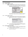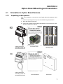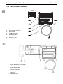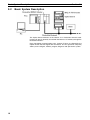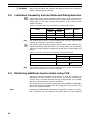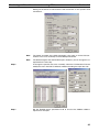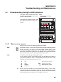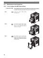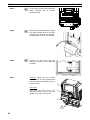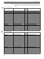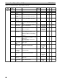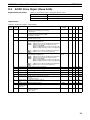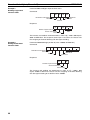
1
Cat. No. I112E-EN-02 Cat. No. I112E-EN-02 Austria Tel: +43 (0) 2236 377 800 www.industrial.omron.at France Tel: +33 (0) 1 56 63 70 00 www.industrial.omron.fr Norway Tel: +47 (0) 22 65 75 00 www.industrial.omron.no Spain Tel: +34 913 777 900 www.industrial.omron.es Belgium Tel: +32 (0) 2 466 24 80 www.industrial.omron.be Germany Tel: +49 (0) 2173 6800 0 www.industrial.omron.de Poland Tel: +48 (0) 22 645 78 60 www.industrial.omron.com.pl Sweden Tel: +46 (0) 8 632 35 00 www.industrial.omron.se Czech Republic Tel: +420 234 602 602 www.industrial.omron.cz Hungary Tel: +36 (0) 1 399 30 50 www.industrial.omron.hu Portugal Tel: +351 21 942 94 00 www.industrial.omron.pt Switzerland Tel: +41 (0) 41 748 13 13 www.industrial.omron.ch Denmark Tel: +45 43 44 00 11 www.industrial.omron.dk Italy Tel: +39 02 326 81 www.industrial.omron.it Russia Tel: +7 495 648 94 50 www.industrial.omron.ru Turkey Tel: +90 212 467 30 00 www.industrial.omron.com.tr Finland Tel: +358 (0) 207 464 200 www.industrial.omron.fi Netherlands Tel: +31 (0) 23 568 11 00 www.industrial.omron.nl South Africa Tel: +27 (0) 11 608 30 41 www.industrial.omron.co.za United Kingdom Tel: +44 (0) 870 752 08 61 www.industrial.omron.co.uk MX2/RX DeviceNet Option Board OMRON EUROPE B.V. Wegalaan 67-69, NL-2132 JD, Hoofddorp, The Netherlands. Tel: +31 (0) 23 568 13 00 Fax: +31 (0) 23 568 13 88 www.industrial.omron.eu USER’S MANUAL Note: Specifications subject to change without notice. Cat. No. I112E-EN-02 MX2/RX DeviceNet Option Board Model:3G3AX-MX2-DRT-E 3G3AX-RX-DRT-E USER’S MANUAL Notice: OMRON products are manufactured for use according to proper procedures by a qualified operator and only for the purposes described in this manual. The following conventions are used to indicate and classify precautions in this manual. Always heed the information provided with them. Failure to heed precautions can result in injury to people or damage to property. OMRON Product References All OMRON products are capitalized in this manual. The word "Unit" is also capitalized when it refers to an OMRON product, regardless of whether or not it appears in the proper name of the product. Trademarks and Copyrights Other product names and company names in this manual are trademarks or registered trademarks of their respective companies. The copyright of the 3G3AX-MX2-DRT-E and 3G3AX-RX-DRT-E Option Boards belong to OMRON Corporation. Intended Audience This manual is intended for the following personnel, who must also have knowledge of electrical systems (an electrical engineer or the equivalent). • Personnel in charge of installing FA systems. • Personnel in charge of designing FA systems. • Personnel in charge of managing FA systems and facilities. • Personnel in charge of maintaining FA systems. OMRON, 2011 All rights reserved. No part of this publication may be reproduced, stored in a retrieval system, or transmitted, in any form, or by any means, mechanical, electronic, photocopying, recording, or otherwise, without the prior written permission of OMRON. No patent liability is assumed with respect to the use of the information contained herein. Moreover, because OMRON is constantly striving to improve its high-quality products, the information contained in this manual is subject to change without notice. Every precaution has been taken in the preparation of this manual. Nevertheless, OMRON assumes no responsibility for errors or omissions. Neither is any liability assumed for damages resulting from the use of the information contained in this publication. ii About this Manual This manual describes the: • 3G3AX-MX2-DRT-E DeviceNet Option Board for OMRON's MX2 Inverter • 3G3AX-RX-DRT-E DeviceNet Option Board for OMRON's RX Inverter It also describes how to install and operate the Units. Please read this manual carefully so that you understand the information provided before installing or using the Option Board. Start with the precautions in the following section. They describe the operating environment and application safety measures which must be observed prior to and when using the Option Board. For the remainder of this manual, both the 3G3AX-MX2-DRT-E DeviceNet Option Board as the 3G3AX-RX-DRT-E DeviceNet Option Board will be referred as Option Board or Unit. The MX2 and RX Inverters will be referred as Inverter. In case information is especially for the MX2 or for the RX Inverter, a clear notification will be included for which the note is meant. If information especially is meant for the MX2, this symbol is shown: If information especially is meant for the RX, this symbol is shown: Please be sure to read the related user manuals to use the Option Board safely and properly. Be sure you are using the most current version of the manual: Manual MX2 User's Manual RX User's Manual DeviceNet Operation Manual DeviceNet CS/CJ Series Units Operation Manual Contents Describes the installation and operation of the MX2 Inverter Describes the installation and operation of the RX Inverter Describes the configuration and construction of a DeviceNet network, including installation procedures and specifications for cables, connectors, and other connection devices, as well as information on functions, operating procedures, and applications. Describes the models, specifications, functions, operating procedures, and applications of CS-series and CJ-series DeviceNet Master Units. Cat No. I570 I560 W267 W380 iii Warranty and Limitations of Liability WARRANTY OMRON's exclusive warranty is that the products are free from defects in materials and workmanship for a period of one year (or other period if specified) from date of sale by OMRON. OMRON MAKES NO WARRANTY OR REPRESENTATION, EXPRESS OR IMPLIED, REGARDING NONINFRINGEMENT, MERCHANTABILITY, OR FITNESS FOR PARTICULAR PURPOSE OF THE PRODUCTS. ANY BUYER OR USER ACKNOWLEDGES THAT THE BUYER OR USER ALONE HAS DETERMINED THAT THE PRODUCTS WILL SUITABLY MEET THE REQUIREMENTS OF THEIR INTENDED USE. OMRON DISCLAIMS ALL OTHER WARRANTIES, EXPRESS OR IMPLIED. LIMITATIONS OF LIABILITY OMRON SHALL NOT BE RESPONSIBLE FOR SPECIAL, INDIRECT, OR CONSEQUENTIAL DAMAGES, LOSS OF PROFITS OR COMMERCIAL LOSS IN ANY WAY CONNECTED WITH THE PRODUCTS, WHETHER SUCH CLAIM IS BASED ON CONTRACT, WARRANTY, NEGLIGENCE, OR STRICT LIABILITY. In no event shall the responsibility of OMRON for any act exceed the individual price of the product on which liability is asserted. IN NO EVENT SHALL OMRON BE RESPONSIBLE FOR WARRANTY, REPAIR, OR OTHER CLAIMS REGARDING THE PRODUCTS UNLESS OMRON'S ANALYSIS CONFIRMS THAT THE PRODUCTS WERE PROPERLY HANDLED, STORED, INSTALLED, AND MAINTAINED AND NOT SUBJECT TO CONTAMINATION, ABUSE, MISUSE, OR INAPPROPRIATE MODIFICATION OR REPAIR. Application Considerations SUITABILITY FOR USE OMRON shall not be responsible for conformity with any standards, codes, or regulations that apply to the combination of products in the customer's application or use of the products. At the customer's request, OMRON will provide applicable third party certification documents identifying ratings and limitations of use that apply to the products. This information by itself is not sufficient for a complete determination of the suitability of the products in combination with the end product, machine, system, or other application or use. The following are some examples of applications for which particular attention must be given. This is not intended to be an exhaustive list of all possible uses of the products, nor is it intended to imply that the uses listed may be suitable for the products: o Outdoor use, uses involving potential chemical contamination or electrical interference, or conditions or uses not described in this manual. o Nuclear energy control systems, combustion systems, railroad systems, aviation systems, medical equipment, amusement machines, vehicles, safety equipment, and installations subject to separate industry or government regulations. o Systems, machines, and equipment that could present a risk to life or property. Please know and observe all prohibitions of use applicable to the products. NEVER USE THE PRODUCTS FOR AN APPLICATION INVOLVING SERIOUS RISK TO LIFE OR PROPERTY WITHOUT ENSURING THAT THE SYSTEM AS A WHOLE HAS BEEN DESIGNED TO ADDRESS THE RISKS, AND THAT THE OMRON PRODUCTS ARE PROPERLY RATED AND INSTALLED FOR THE INTENDED USE WITHIN THE OVERALL EQUIPMENT OR SYSTEM. iv PROGRAMMABLE PRODUCTS OMRON shall not be responsible for the user's programming of a programmable product, or any consequence thereof. Disclaimers CHANGE IN SPECIFICATIONS Product specifications and accessories may be changed at any time based on improvements and other reasons. It is our practice to change model numbers when published ratings or features are changed, or when significant construction changes are made. However, some specifications of the products may be changed without any notice. When in doubt, special model numbers may be assigned to fix or establish key specifications for your application on your request. Please consult with your OMRON representative at any time to confirm actual specifications of purchased products. DIMENSIONS AND WEIGHTS Dimensions and weights are nominal and are not to be used for manufacturing purposes, even when tolerances are shown. PERFORMANCE DATA Performance data given in this manual is provided as a guide for the user in determining suitability and does not constitute a warranty. It may represent the result of OMRON's test conditions, and the users must correlate it to actual application requirements. Actual performance is subject to the OMRON Warranty and Limitations of Liability. ERRORS AND OMISSIONS The information in this manual has been carefully checked and is believed to be accurate; however, no responsibility is assumed for clerical, typographical, or proofreading errors, or omissions. v vi Table of contents Safety Messages . . . . . . . . . . . . . . . . . . . . . . . . . . . . . . . . . . . . . . . . . . . . . . . . . . . . ix 1 2 3 4 5 6 7 8 ix x xi xi xii xiii xiii xiii Hazardous High Voltage . . . . . . . . . . . . . . . . . . . . . . . . . . . . . . . . . . . . . . . . . . . . . . . . . . . . . . . . . General Precautions - Read These First! . . . . . . . . . . . . . . . . . . . . . . . . . . . . . . . . . . . . . . . . . . . . . Installation Precautions . . . . . . . . . . . . . . . . . . . . . . . . . . . . . . . . . . . . . . . . . . . . . . . . . . . . . . . . . . Configuration Precautions . . . . . . . . . . . . . . . . . . . . . . . . . . . . . . . . . . . . . . . . . . . . . . . . . . . . . . . . Application Precautions . . . . . . . . . . . . . . . . . . . . . . . . . . . . . . . . . . . . . . . . . . . . . . . . . . . . . . . . . . Operating Environment Precautions . . . . . . . . . . . . . . . . . . . . . . . . . . . . . . . . . . . . . . . . . . . . . . . . Handling, Storage and Disposal . . . . . . . . . . . . . . . . . . . . . . . . . . . . . . . . . . . . . . . . . . . . . . . . . . . . Compliance with EC Directives . . . . . . . . . . . . . . . . . . . . . . . . . . . . . . . . . . . . . . . . . . . . . . . . . . . . SECTION 1 Getting Started . . . . . . . . . . . . . . . . . . . . . . . . . . . . . . . . . . . . . . . . . . . . . . . . . . . . . . 1 1-1 Introduction . . . . . . . . . . . . . . . . . . . . . . . . . . . . . . . . . . . . . . . . . . . . . . . . . . . . . . . . . . . . . . . . . . . . 1-2 Option Board Specifications . . . . . . . . . . . . . . . . . . . . . . . . . . . . . . . . . . . . . . . . . . . . . . . . . . . . . . . 1-3 Introduction to DeviceNet . . . . . . . . . . . . . . . . . . . . . . . . . . . . . . . . . . . . . . . . . . . . . . . . . . . . . . . . . 1 3 5 SECTION 2 Option Board Mounting and Installation . . . . . . . . . . . . . . . . . . . . . . . . . . . . . . . . . 7 2-1 Orientation to Option Board Features . . . . . . . . . . . . . . . . . . . . . . . . . . . . . . . . . . . . . . . . . . . . . . . 2-2 Basic System Description . . . . . . . . . . . . . . . . . . . . . . . . . . . . . . . . . . . . . . . . . . . . . . . . . . . . . . . . . 2-3 How to mount the Option Board on the Inverter . . . . . . . . . . . . . . . . . . . . . . . . . . . . . . . . . . . . . . . . 7 10 11 SECTION 3 Configuring Drive Parameters and Option Board . . . . . . . . . . . . . . . . . . . . . . . . . . 25 3-1 Installation of EDS files . . . . . . . . . . . . . . . . . . . . . . . . . . . . . . . . . . . . . . . . . . . . . . . . . . . . . . . . . . 3-2 Configuring the Option Board . . . . . . . . . . . . . . . . . . . . . . . . . . . . . . . . . . . . . . . . . . . . . . . . . . . . . . 3-3 Configuring the Network . . . . . . . . . . . . . . . . . . . . . . . . . . . . . . . . . . . . . . . . . . . . . . . . . . . . . . . . . . 25 25 29 SECTION 4 Operations and Monitoring . . . . . . . . . . . . . . . . . . . . . . . . . . . . . . . . . . . . . . . . . . . . 33 4-1 4-2 4-3 4-4 4-5 4-6 4-7 4-8 4-9 33 34 36 36 38 38 39 42 42 Setting up inverter . . . . . . . . . . . . . . . . . . . . . . . . . . . . . . . . . . . . . . . . . . . . . . . . . . . . . . . . . . . . . . Operating the Motor . . . . . . . . . . . . . . . . . . . . . . . . . . . . . . . . . . . . . . . . . . . . . . . . . . . . . . . . . . . . . Overriding Inverter inputs . . . . . . . . . . . . . . . . . . . . . . . . . . . . . . . . . . . . . . . . . . . . . . . . . . . . . . . . . Controlling Inverter Torque . . . . . . . . . . . . . . . . . . . . . . . . . . . . . . . . . . . . . . . . . . . . . . . . . . . . . . . . Faults and Trips . . . . . . . . . . . . . . . . . . . . . . . . . . . . . . . . . . . . . . . . . . . . . . . . . . . . . . . . . . . . . . . . Accessing Parameters . . . . . . . . . . . . . . . . . . . . . . . . . . . . . . . . . . . . . . . . . . . . . . . . . . . . . . . . . . . Flexible Format . . . . . . . . . . . . . . . . . . . . . . . . . . . . . . . . . . . . . . . . . . . . . . . . . . . . . . . . . . . . . . . . . Limitations Caused by Inverter Mode and Rating Selection . . . . . . . . . . . . . . . . . . . . . . . . . . . . . . . Monitoring additional Inverter status using COS . . . . . . . . . . . . . . . . . . . . . . . . . . . . . . . . . . . . . . . SECTION 5 Troubleshooting and Maintenance . . . . . . . . . . . . . . . . . . . . . . . . . . . . . . . . . . . . . 45 5-1 Troubleshooting Using the LED Indicators . . . . . . . . . . . . . . . . . . . . . . . . . . . . . . . . . . . . . . . . . . . . 5-2 Other Error Causes and Error Procedures . . . . . . . . . . . . . . . . . . . . . . . . . . . . . . . . . . . . . . . . . . . . 5-3 Maintenance and Inspection . . . . . . . . . . . . . . . . . . . . . . . . . . . . . . . . . . . . . . . . . . . . . . . . . . . . . . 45 49 50 APPENDIX A Glossary . . . . . . . . . . . . . . . . . . . . . . . . . . . . . . . . . . . . . . . . . . . . . . . . . . . . . . . . . . . 59 vii Table of contents APPENDIX B Assembly Specification . . . . . . . . . . . . . . . . . . . . . . . . . . . . . . . . . . . . . . . . . . . . . . . 61 B-1 B-2 B-3 B-4 B-5 B-6 Basic Speed Control IO (20/70) . . . . . . . . . . . . . . . . . . . . . . . . . . . . . . . . . . . . . . . . . . . . . . . . . . . Extended Speed Control IO (21/71) . . . . . . . . . . . . . . . . . . . . . . . . . . . . . . . . . . . . . . . . . . . . . . . . Extended Speed and Torque Control IO (123/173) . . . . . . . . . . . . . . . . . . . . . . . . . . . . . . . . . . . . Special IO (100/150) . . . . . . . . . . . . . . . . . . . . . . . . . . . . . . . . . . . . . . . . . . . . . . . . . . . . . . . . . . . . Extended Control IO (101/151/153) . . . . . . . . . . . . . . . . . . . . . . . . . . . . . . . . . . . . . . . . . . . . . . . . Extended Speed and Acceleration Control IO (110/111) . . . . . . . . . . . . . . . . . . . . . . . . . . . . . . . . 61 63 65 67 69 72 APPENDIX C General Object Specification . . . . . . . . . . . . . . . . . . . . . . . . . . . . . . . . . . . . . . . . . . 75 C-1 C-2 C-3 C-4 C-5 C-6 C-7 C-8 Identity Object (Class 0x01) . . . . . . . . . . . . . . . . . . . . . . . . . . . . . . . . . . . . . . . . . . . . . . . . . . . . . . Message Router Object (Class 0x02) . . . . . . . . . . . . . . . . . . . . . . . . . . . . . . . . . . . . . . . . . . . . . . . DeviceNet Object (Class 0x03) . . . . . . . . . . . . . . . . . . . . . . . . . . . . . . . . . . . . . . . . . . . . . . . . . . . . Assembly Object (Class 0x04) . . . . . . . . . . . . . . . . . . . . . . . . . . . . . . . . . . . . . . . . . . . . . . . . . . . . Connection Object (Class 0x05) . . . . . . . . . . . . . . . . . . . . . . . . . . . . . . . . . . . . . . . . . . . . . . . . . . . Discrete Input Point Object (Class 0x08) . . . . . . . . . . . . . . . . . . . . . . . . . . . . . . . . . . . . . . . . . . . . Discrete Output Point Object (Class 0x09) . . . . . . . . . . . . . . . . . . . . . . . . . . . . . . . . . . . . . . . . . . . Unit Parameter Object (Class 0x94) . . . . . . . . . . . . . . . . . . . . . . . . . . . . . . . . . . . . . . . . . . . . . . . . 75 78 79 80 81 85 86 87 APPENDIX D AC Drive Object Specification . . . . . . . . . . . . . . . . . . . . . . . . . . . . . . . . . . . . . . . . . . 89 D-1 Motor Data Object (Class 0x28) . . . . . . . . . . . . . . . . . . . . . . . . . . . . . . . . . . . . . . . . . . . . . . . . . . . D-2 Control Supervisor Object (Class 0x29) . . . . . . . . . . . . . . . . . . . . . . . . . . . . . . . . . . . . . . . . . . . . . D-3 AC/DC Drive Object (Class 0x2A) . . . . . . . . . . . . . . . . . . . . . . . . . . . . . . . . . . . . . . . . . . . . . . . . . 89 90 93 APPENDIX E DeviceNet Explicit Messages . . . . . . . . . . . . . . . . . . . . . . . . . . . . . . . . . . . . . . . . . . 95 E-1 E-2 E-3 E-4 Basic Format of Explicit Messages . . . . . . . . . . . . . . . . . . . . . . . . . . . . . . . . . . . . . . . . . . . . . . . . . Function Code Object (Class 0x65) . . . . . . . . . . . . . . . . . . . . . . . . . . . . . . . . . . . . . . . . . . . . . . . . Modbus Register Object (Class 0x64) . . . . . . . . . . . . . . . . . . . . . . . . . . . . . . . . . . . . . . . . . . . . . . Explicit Message Error Codes . . . . . . . . . . . . . . . . . . . . . . . . . . . . . . . . . . . . . . . . . . . . . . . . . . . . . 95 97 99 101 APPENDIX F Flexible Format . . . . . . . . . . . . . . . . . . . . . . . . . . . . . . . . . . . . . . . . . . . . . . . . . . . . . . 103 Table index . . . . . . . . . . . . . . . . . . . . . . . . . . . . . . . . . . . . . . . . . . . . . . . . . . . . . . . . . 105 Revision history . . . . . . . . . . . . . . . . . . . . . . . . . . . . . . . . . . . . . . . . . . . . . . . . . . . . . 108 viii Hazardous High Voltage Safety Messages For the best results with the Inverter, carefully read this manual and all of the warning labels attached to the Inverter before installing and operating it, and follow the instructions exactly. Keep this manual handy for quick reference. Definitions and Symbols A safety instruction (message) includes a "Safety Alert Symbol" and a signal word or phrase such as WARNING or CAUTION. Each signal word has the following meaning: !Caution Indicates a potentially hazardous situation which, if not avoided, could result in electric shock. It calls your attention to items or operations that could be dangerous to you and other persons operating this equipment. Read the message and follow the instructions carefully. 1 !WARNING Indicates a potentially hazardous situation which, if not avoided, could result in death or serious injury. Additionally, there may be severe property damage. !Caution Indicates a potentially hazardous situation, which, if not avoided, may result in minor or moderate injury, or property damage. Step 1 Indicates a step in a series of action steps required to accomplish a goal. The number of the step will be contained in the step symbol. Note Notes indicate an area or subject of special merit, emphasizing either the product's capability or common errors in operation or maintenance. Tip Tips give a special instruction that can save time or provide other benefits while installing or using the product. The tip calls attention to an idea that may not be obvious if you are a first-time user of the product. Hazardous High Voltage !HIGH VOLTAGE Motor control equipment and electronic controllers are connected to hazardous line voltages. When servicing drives and electronic controllers, there may be exposed components with housing or protrusions at or above line potential. Extreme care should be taken to protect against shock. Stand on an insulating pad and make it a habit to use only one hand when checking components. Always work with another person in case an emergency occurs. Disconnect power before checking controllers or performing maintenance. Be sure equipment is properly grounded. Wear safety glasses whenever working on electronic controllers or rotating machinery. ix General Precautions - Read These First! 2 General Precautions - Read These First! !WARNING Failure to read and understand the information provided in this manual may result in personal injury or death, damage to the product, or product failure. Please read each section in its entirety and be sure you understand the information provided in the section and related sections before attempting any of the procedures or operations given. !WARNING This equipment should be installed, adjusted, and serviced by qualified electrical maintenance personnel familiar with the construction and operation of the equipment and the hazards involved. Failure to observe this precaution could result in bodily injury. !WARNING Wiring, maintenance or inspection must be performed by authorized personnel. Not doing so may result in electrical shock or fire. !WARNING Hazard of electrical shock! Disconnect incoming power before working on the Option Board or the Inverter. !HIGH VOLTAGE Turn the power supply OFF and wait for the time specified on the Option Board front cover before performing wiring, maintenance or inspection. Not doing so may result in electrical shock. The Option Board is attached to an Inverter. Dangerous voltage exists until the Inverter power light is OFF. !HIGH VOLTAGE Do not touch the conductive parts such as the internal PCB, terminals or connector while power is being supplied. Doing so may result in electrical shock. x !WARNING Do not attempt to take an Option Board apart or touch any internal parts while the power is being supplied. Doing so may result in electric shock. !WARNING Do not attempt to disassemble, repair, or modify an Option Board. Any attempt to do so may result in malfunction, fire, or electric shock. !WARNING Provide emergency stop circuits, interlock circuits, limit circuits and similar safety measures in external circuits (NOT in the Option Board). This ensures safety in the system if an abnormality occurs due to malfunction of the Option Board or another external factor affecting the Option Board operation. Not doing so may result in serious accidents. !WARNING Fail-safe measures must be taken by the customer to ensure safety in the event of incorrect, missing, or abnormal signals caused by broken signal lines, momentary power interruptions, or other causes. Not doing so may result in serious accidents. !Caution Do not touch the Inverter during power on, and immediately after power off. Hot surface may cause injury. Installation Precautions !Caution 3 The product will be used to control an adjustable speed drive connected to high voltage sources and rotating machinery that is inherently dangerous if not operated safely. Interlock all energy sources, hazardous locations, and guards in order to restrict the exposure of personnel to hazards. The adjustable speed drive may start the motor without warning. Signs on the equipment installation must be posted to this effect. A familiarity with auto-restart settings is a requirement when controlling adjustable speed drives. Failure of external or ancillary components may cause intermittent system operation, i.e., the system may start the motor without warning or may not stop on command. Improperly designed or improperly installed system interlocks and permissives may render a motor unable to start or stop on command. Installation Precautions !WARNING Always connect the grounding cable to one of the ground terminals of the Inverter. Failure to abide could lead to serious or possibly fatal injury. !Caution Failure to observe these precautions could lead to faulty operation of the Option Board or the Inverter, or could damage either of the two. Always read these precautions. • Install external breakers and take other safety measures against short-circuits in external wiring. Not observing this may result in burning. • Be sure that all cable connector screws are tightened to the torque specified in the relevant manuals. Incorrect tightening torque may result in malfunction. • Do not allow metal clippings to enter either Option Board or Inverter when wiring or installing the unit. • Follow the network configuration and wiring instructions provided in the DeviceNet Operation Manual (Cat. No. W267): • Wire the DeviceNet cables and connectors correctly. Incorrect wiring may result in burning. • Always connect a Terminating Resistor at the prescribed locations of the DeviceNet network to ensure the quality of the transmission path. Do not apply termination anywhere else. • Be sure that the Option Board is mounted correctly. Improper mounting may result in malfunction. • Disconnect the grounding cable when performing withstand-voltage tests. Not disconnecting the grounding cable may result in burning. 4 Configuration Precautions !Caution Failure to observe these precautions could lead to unexpected operation of the Option Board or the Inverter. Always read these precautions. • Check the network related Inverter settings regarding DeviceNet node address and DeviceNet remote I/O allocation. Not doing so may result in unexpected operation. • When replacing an Inverter be sure that all Inverter settings of the Inverter being replaced are restored to the replacement. • Restoring parameters stored in the remote operator also restores the DeviceNet node address. Always check the node address and other network related Inverter settings after restore. xi Application Precautions 5 Application Precautions !WARNING Before using the product under conditions which are not described in the manual or applying the product to nuclear control systems, railroad systems, aviation systems, vehicles, combustion systems, medical equipment, amusement machines, safety equipment, and other systems, machines, and equipment that may have a serious influence on lives and property if used improperly, consult your OMRON representative. !WARNING It is extremely important that the Unit is used for its specified purpose and under the specified conditions, especially in applications that can directly or indirectly affect human life. You must consult your OMRON representative before using it in a system in the above-mentioned applications. !WARNING Failure to observe these precautions could lead to serious or possibly fatal injury. Always read these precautions. • Check any user program in the system that acts as a DeviceNet Master before actually running it. Not checking the program may result in unexpected operation. • For safe operation clear the run command via DeviceNet as soon as a trip condition is detected. • In the event the Inverter is in a Trip state, be sure to investigate the cause of this Trip state thoroughly before clearing the Trip. Not checking the cause may result in unexpected operation. !Caution Failure to observe these precautions could lead to faulty operation of the Option Board or the Inverter, or could damage to either of the two. Always read these precautions. • Check the Inverter settings for proper Inverter behaviour before actually operating the Inverter remotely via the DeviceNet network. • Check the Inverter's EzSQ program and its interaction with the DeviceNet Master before actually running it on the Inverter. Not checking the program may result in unexpected operation. • Confirm that no adverse effect will occur at the moment the DeviceNet Master stops communicating with the Inverter or at the moment the DeviceNet Master has not yet started communicating to the Inverter. • Confirm that no adverse effect will occur in the Inverter before force-setting/force-resetting any bit in the system that acts as a DeviceNet Master. xii Operating Environment Precautions 6 Operating Environment Precautions !Caution Do not operate the Inverter with a mounted Option Board in the following locations (doing so may result in malfunction, electric shock or burning): • Locations subject to direct sunlight • Locations subject to temperatures or humidity outside the range specified in the specifications • Locations subject to condensation as the result of severe changes in temperature • Locations subject to corrosive or flammable gases • Locations subject to dust (especially iron dust) or salts • Locations subject to exposure to water, oil, or chemicals • Locations subject to shock or vibration !Caution Take appropriate and sufficient countermeasures when installing systems in the following locations (doing so may result in malfunction): • Locations subject to static electricity or other forms of noise • Locations subject to strong electromagnetic fields • Locations subject to possible exposure to radioactivity • Locations close to power supplies !Caution 7 The operating environment of the Inverter with a mounted Option Board can have a large effect on the longevity and reliability of the system. Improper operating environments can lead to malfunction, failure, and other unforeseeable problems with the system. Make sure that the operating environment is within the specified conditions at installation and remains within the specified conditions during the life of the system. Handling, Storage and Disposal !Caution Failure to observe these precautions could lead to faulty operation of or damage to the Option Board. Always read these precautions. • Before touching the Option Board or Inverter, be sure to first touch a grounded metallic object in order to discharge any static built-up. Not doing so may result in malfunction or damage. • When transporting or storing the Option Board, keep the product within the specified storage temperature range. !Caution 8 Never dispose electrical components by incineration. Contact your state environmental agency for details on disposal of electrical components and packaging in your area. Compliance with EC Directives This product complies with EC Directives when mounted to an Inverter with the grounding cable connected. xiii Compliance with EC Directives xiv SECTION 1 Getting Started 1-1 1-1-1 Introduction Main Features The 3G3AX-MX2-DRT-E Option Board and the 3G3AX-RX-DRT-E Option Board allow controlling, monitoring and parameterization of an MX2 Inverter or RX Inverter via a DeviceNet network. The Option Board serves as a gateway that passes communicated register values from the DeviceNet network to the Inverter and vice versa. The Option Board adheres to the DeviceNet / CIP AC Drive profile. The following functions are available via DeviceNet communication by installing the Option Board: Cyclic Data Exchange The DeviceNet Master and Option Board can exchange data via a DeviceNet Remote I/O connection: • Output data (from DeviceNet Master to Option Board): E.g. Run/stop, Reference frequency and Fault reset. • Input data (from Option Board to DeviceNet Master): E.g. Inverter status, Output frequency and Output current, etc. Inverter Parameter Access The DeviceNet Master can read and write parameter data via the Option Board using the explicit message communication. The inverter parameters are accessible in multiple ways: • Access based on Function code • Access based on the Modbus register address Several AC Drive profile attributes can also be accessed using the explicit message mechanism. Simplified Start-up The Option Board can be set up easily, just by wiring the Unit, setting the DeviceNet node address (P192) and the default connection path (P046) and restarting the Unit. The Unit’s configuration is read automatically when the power is turned ON or after a reset. It is not necessary to make any settings with a special Programming Device. Simplified Replacement All parameters required by the Option Board are stored in the MX2 Inverter or RX Inverter. The Option Board can be replaced, requiring no re-configuration. Automatic Baud Rate Recognition The Option Board automatically detects the Master’s communication baud rate, and no user configuration is required. 1 Introduction 1-1-2 1-1-2-1 Section 1-1 Inverter Support Inverter support for the MX2 The 3G3AX-MX2-DRT-E Option Board supports the MX2 Inverter with minimum revision of AAAA. An Inverter that supports the 3G3AX-MX2-DRT-E Option Board can be recognized from the Inverter type label. Please check that your Inverter type label displays revision characters in the bottom right corner where the is displayed in this illustration. @@@@ Please note if these characters are absent, your Inverter does not support the 3G3AX-MX2-DRT-E, so please contact your local OMRON representative. 1-1-2-2 Inverter support for the RX The 3G3AX-RX-DRT-E Option Board supports the RX Inverter with minimum revision of RX-@-E1F or RX-@-V1. An RX Inverter that supports the 3G3AX-RX-DRT-E Option Board can be recognized from the Inverter type label. Note 1-1-3 If your RX Inverter has no postfix on type label (e.g.RX-A4004) or the EF postfix (e.g. RX-A4004-EF) the 3G3AX-RX-DRT-E option is not supported, so please contact your local OMRON representative. Inverter Safety (ISO 13849-1) An MX2 Inverter provides a Gate Suppress function to perform a safe stop according to the EN60204-1, stop category 0. The Option Board has been designed not to interfere with this safety function. Note 2 The 3G3AX-MX2-DRT-E Option Board is not a safety device and does not implement any safety protocols. Option Board Specifications 1-2 Section 1-2 Option Board Specifications Table 1 Option Board Specification Item Installation Unit type MX2 Model Dimensions (W x H x D) Weight Installation RX Unit type Model Dimensions (W x H x D) Weight Environment Ambient operating temperature Ambient operating humidity Ambient storage temperature Vibration resistance Dielectric strength Conformance to EMC and Electrical safety standards DeviceNet Interface Enclosure rating Communications protocol Certification DeviceNet Profile Supported connections Communications power supply Unit device address range Baud rates supported DeviceNet Configuration Default Connection path Supported Assemblies EDS file Specification MX2 Series Option Board 3G3AX-MX2-DRT-E 68 x 58 x 45 mm 170g (typical) RX Series Option Board 3G3AX-RX-DRT-E 80 x 67 x 49 mm 170 g (typical) -10 to 55°C (no icing or condensation) 20 to 90%RH -20 to 65°C (no icing or condensation) 5.9m/s2 (0.6G) at 10…55Hz 500 VAC (between isolated circuits) EN61800-3: 2004 (2004/108/EC) Second environment, Category C3 EN61800-5-1: 2007 (2006/95/EC) SELV IP 20 DeviceNet DeviceNet Conformance Tested AC Drive (0x02) Remote I/O: Master-Slave connection Poll Bit-Strobe COS Cyclic Explicit Messages Conform to DeviceNet specifications 11 to 25 VDC MAC ID 0 to 63, set with inverter parameter P192 125, 250 or 500 kbps. Automatically detecting baud rate of Master Unit Supported, set with inverter parameter P046 Basic Remote IO (Output assembly 20, Input assembly 70) Extended Speed IO (21, 71) Extended Speed and Torque Control (123, 173) Special IO (100, 150) Extended Control IO (101, 151) Extended Control IO and Multi function IO monitor (101, 153) Flexible Format (139, 159) Extended Speed and Acceleration Control (110, 111) In case the DeviceNet master is configured using user allocation, only the input / output pairs can be configured. Depending on the Inverter model (see below) Note 1 The derated- or ambient operating temperature of the Inverter takes precedence over that of the Option Board. Note 2 In case the Option Board is connected to the Inverter, it is not supported to connect any external devices to the RS485 (Modbus) interface. 3 Option Board Specifications Section 1-2 In case the 3G3AX-MX2-DRT-E Option Board is connected to the MX2 Inverter, it is not supported to connect any external devices the RJ45 port (Optional operator port) of the Inverter. The required EDS file for the Option Board depends on the model of the MX2 or RX inverter. Table 2 MX2 Device List MX2-AB001-E MX2-A2001-E MX2-AB002-E MX2-A2002-E MX2-AB004-E MX2-A2004-E MX2-AB007-E MX2-A2007-E MX2-AB015-E MX2-A2015-E MX2-AB022-E MX2-A2022-E 3G3AX-MX2-DRT-AB001_A2001-E.eds Product Code 1880 3G3AX-MX2-DRT-AB002_A2002-E.eds 1881 3G3AX-MX2-DRT-AB004_A2004-E.eds 1882 3G3AX-MX2-DRT-AB007_A2007-E.eds 1884 3G3AX-MX2-DRT-AB015_A2015-E.eds 1886 3G3AX-MX2-DRT-AB022_A2022-E.eds 1887 MX2-A2037-E MX2-A2055-E MX2-A2075-E MX2-A2110-E MX2-A2150-E MX2-A4004-E MX2-A4007-E 3G3AX-MX2-DRT-A2037-E.eds 3G3AX-MX2-DRT-A2055-E.eds 3G3AX-MX2-DRT-A2075-E.eds 3G3AX-MX2-DRT-A2110-E.eds 3G3AX-MX2-DRT-A2150-E.eds 3G3AX-MX2-DRT-A4004-E.eds 3G3AX-MX2-DRT-A4007-E.eds 1889 1891 1892 1893 1894 1902 1904 MX2-A4015-E MX2-A4022-E MX2-A4030-E MX2-A4040-E MX2-A4055-E MX2-A4075-E MX2-A4110-E MX2-A4150-E 3G3AX-MX2-DRT-A4015-E.eds 3G3AX-MX2-DRT-A4022-E.eds 3G3AX-MX2-DRT-A4030-E.eds 3G3AX-MX2-DRT-A4040-E.eds 3G3AX-MX2-DRT-A4055-E.eds 3G3AX-MX2-DRT-A4075-E.eds 3G3AX-MX2-DRT-A4110-E.eds 3G3AX-MX2-DRT-A4150-E.eds 1906 1907 1908 1910 1911 1912 1913 1914 MX2 Model name Name of EDS file Table 3 RX Device List RX-A2004-E RX-A2007-E RX-A2015-E RX-A2022-E RX-A2037-E RX-A2055-E RX-A2075-E RX-A2110-E RX-A2150-E RX-A2185-E 3G3AX-RX-DRT-A2004-E.eds 3G3AX-RX-DRT-A2007-E.eds 3G3AX-RX-DRT-A2015-E.eds 3G3AX-RX-DRT-A2022-E.eds 3G3AX-RX-DRT-A2037-E.eds 3G3AX-RX-DRT-A2055-E.eds 3G3AX-RX-DRT-A2075-E.eds 3G3AX-RX-DRT-A2110-E.eds 3G3AX-RX-DRT-A2150-E.eds 3G3AX-RX-DRT-A2185-E.eds Product Code 2149 2150 2151 2152 2153 2154 2155 2156 2157 2158 RX-A2220-E RX-A2300-E RX-A2370-E RX-A2450-E 3G3AX-RX-DRT-A2220-E.eds 3G3AX-RX-DRT-A2300-E.eds 3G3AX-RX-DRT-A2370-E.eds 3G3AX-RX-DRT-A2450-E.eds 2159 2160 2161 2162 RX Model name 4 Name of EDS file Introduction to DeviceNet Section 1-3 Table 3 RX Device List (continued) RX Model name RX-A2550-E RX-A4004-E RX-A4007-E RX-A4015-E RX-A4022-E RX-A4040-E RX-A4055-E RX-A4075-E RX-A4110-E RX-A4150-E RX-A4185-E RX-A4220-E RX-A4300-E RX-A4370-E RX-A4450-E RX-A4550-E RX-B4750-E RX-B4900-E RX-B411K-E RX-B413K-E 1-3 1-3-1 Name of EDS file 3G3AX-RX-DRT-A2550-E.eds 3G3AX-RX-DRT-A4004-E.eds 3G3AX-RX-DRT-A4007-E.eds 3G3AX-RX-DRT-A4015-E.eds 3G3AX-RX-DRT-A4022-E.eds 3G3AX-RX-DRT-A4040-E.eds 3G3AX-RX-DRT-A4055-E.eds 3G3AX-RX-DRT-A4075-E.eds 3G3AX-RX-DRT-A4110-E.eds 3G3AX-RX-DRT-A4150-E.eds 3G3AX-RX-DRT-A4185-E.eds 3G3AX-RX-DRT-A4220-E.eds 3G3AX-RX-DRT-A4300-E.eds 3G3AX-RX-DRT-A4370-E.eds 3G3AX-RX-DRT-A4450-E.eds 3G3AX-RX-DRT-A4550-E.eds 3G3AX-RX-DRT-B4750-E.eds 3G3AX-RX-DRT-B4900-E.eds 3G3AX-RX-DRT-B411K-E.eds 3G3AX-RX-DRT-B413K-E.eds Product Code 2163 2176 2177 2178 2179 2180 2181 2182 2183 2184 2185 2186 2187 2188 2189 2190 2191 2192 2193 2194 Introduction to DeviceNet Overview of DeviceNet DeviceNet is a multi-bit, multi-vendor network that combines control and monitoring on a machine/line-control level and that conforms to DeviceNet open field network specifications. DeviceNet is a member of a family of networks that implements the Common Industrial Protocol (CIP) at its upper layers. Two types of communications are supported to provide a single point of connection for both control and configuration: 1. Time-critical control remote I/O communications that automatically transfer between the Master Unit/CPU Unit and the remote Slave Units, and 2. Explicit message communications that read/write messages, control operation, or perform other functions to the Slave Units. Message communications are achieved by executing specific instructions from the program in the CPU Unit to which the Master Unit is mounted. 1-3-2 What is the AC Drive profile Within DeviceNet/CIP standard, multiple device profiles have been defined. Therefore the devices which adhere to a certain device profile are compatible and replaceable in a multi-vendor environment. The AC Drive device profile (profile code 0x02) supplements the DeviceNet/ CIP standard. It defines a unified behaviour and technique to access Inverter and drive device data. All drives supporting the AC Drive profile respond the same way to control instructions. 5 Introduction to DeviceNet 6 Section 1-3 Option Board with Grounding Cable and DeviceNet connector Option Board with Grounding Cable and DeviceNet connector Instruction Sheet 9RU,QVWDOODWLRQ+DQGEXFKOHVHQ 1DFK7UHQQHQYRP1HW]0LQXWHQ ZDUWHQELVGLH.DSD]LWtHQHQWODGHQVLQG $'9(57(1&,$ 5LHVJRGH FKRTXHHOFWULFR /HHUHOPDQXDODQWHVGHODLQVWDODFLQ (VSHUDUPLQXWRVSDUDGHVFDUJDUORVFRQGHQ VDGRUHVGHVSXVGHFRUWDUODDOLPHQWDFLQ $99(57(1=$ 3HULFRORGL VFRVVDHOHWWULFD /HJJHUHLOPDQXDOHSULPDGHOOvLQVWDOOD]LRQH $VSHWWDUHPLQXWLSHUVFDULFDUHLOFRQGHQ VDWRUHGRSRDYHUVFROOHJDWROvDOLPHQWD]LRQH !!"# ! ! ɈɋɌɈɊɈɀɇɈ :$5181* 5LVLNRHLQHV HOHNWULVFKHQ6FKODJHV /LVH]OHPDQXHODYDQWLQVWDOODWLRQ $WWHQGH]PLQXWHVTXHOHVFDSDFLWVVH GFKDUJHQWDYDQWGHGFRQQHFWHUOvDOLPHQWDWLRQ 2-1-1 $ 2-1 $9(57,66(0(17 5LVTXHGH FKRFOHFWULTXH SECTION 2 Option Board Mounting and Installation Orientation to Option Board Features Unpacking and Inspection Take a few moments to unpack your new Option Board and perform these steps: 1. Look for any damage that may have occurred during transportation. 2. Verify the contents of the box. 3. Inspect the markings on the Option Board. Make sure it matches the product part number you ordered. Instruction Sheet Warning Labels Blind cover 7 Orientation to Option Board Features 2-1-2 Section 2-1 Main Physical Features underside A F B G C A - Option Board connector B - LED indicators (MS, NS) C - Warning label D - Fieldbus connector E - Grounding cable F - Housing G - Mounting screw A - 8 Option Board Inverter connector B - LED indicators (MS, NS) C - Option Board Cable D - Fieldbus connector E - Grounding cable F - Housing G - Mounting screw D E Orientation to Option Board Features Section 2-1 The LED indicators (B) allow easy diagnosis. An attached grounding cable (E) is sized to reach the ground terminals on all Inverter models. A feature in the housing (F) will retain the mounting screw (G) when the Option Board is not mounted to the Inverter. The orientation of the Fieldbus connector (D) allows unstrained connection and removal of the DeviceNet connector. Please pay attention to the Option Board Inverter connector: It must be properly connected with the Inverter Interface Connector. 2-1-3 LED Indicators The LED indicators on the front indicate the operational mode and status of the Option Board and the network. Table 4 LED Indicators Indicator MS (Module status) Colour Status Not lit Green Red Lit Lit NS (Network status) Green Meaning • Power is not supplied to the Option Board • Option Board is being reset Normal operation Unrecoverable fault: • Option Board hardware error • Unsupported Inverter version Flashing Recoverable fault: • Network power is OFF • Node address changed • Illegal Flexible configuration • Option Board parameters out of range or cannot be read • Option Board detects consecutive communication errors Not lit • Power not supplied (check Module Status LED) • Network power is OFF or DeviceNet connector unplugged • Checking for node address duplication (intermediate state) Lit Network is operating normally (communications established) Flashing Network is operating normally, but communications have not been established. Red Lit Option Board detects network communication not possible due to Communications error: • Node address duplication • Bus–off error Flashing Option Board detects communication lost. One or more Connections are in time-out state. Note Refer to section 5-1 for Troubleshooting using the LED indicators on page 45. 9 Basic System Description 2-2 Section 2-2 Basic System Description The Option Board connects to the Master via a DeviceNet network cable. Inverter I/O data is generally shared with the Master's I/O memory through the DeviceNet network. Every DeviceNet communication cycle, Inverter I/O data is collected by the Option Board and exchanged with the Master. The PC (personal computer) allows you to configure, monitor, program, diagnose and operate the system. 10 How to mount the Option Board on the Inverter 2-3 Section 2-3 How to mount the Option Board on the Inverter !HIGH VOLTAGE Always switch OFF the mains power supply to the Inverter before removing any covers. Wait for the time specified on the Inverter front cover for the capacitors to discharge. Not doing so may result in electrical shock. !HIGH VOLTAGE Never operate the Inverter with the terminal block cover or backing plate removed. !WARNING Always connect the grounding cable to one of the ground terminals of the Inverter. Failure to abide could lead to serious or possibly fatal injury. !WARNING Provide emergency stop circuits, interlock circuits, limit circuits and similar safety measures in external circuits (NOT in the Option Board). This ensures safety in the system if an abnormality occurs due to malfunction of the Option Board or another external factor affecting the Option Board operation. Not doing so may result in serious accidents. !Caution Never touch the heat sink during or just after operation; it can be very hot. !Caution Be sure that the Option Board is mounted correctly. Improper mounting may result in malfunction. !Caution Be sure that all cable connector screws are tightened to the torque specified in the relevant manuals. Incorrect tightening torque may result in malfunction. Note Illustrations are only provided for one Inverter size. The instructions however are generic, and may be followed for all Inverter sizes. Please refer to the MX2 Inverter manual (Cat. No. I570) section 2-1-3 for details on assembly and disassembly of the Inverter. Please refer to the RX Inverter manual (Cat. No. I560) section 2 for details on assembly and disassembly of the Inverter. 11 How to mount the Option Board on the Inverter 2-3-1 Step 1 Section 2-3 Mounting sequence of the Option Board on the MX2 Inverter Loosen the screw of the Option Board cover. Remove the cover and put the cover aside. Step 2 For Inverters up to 4.0 kW only: loosen the screws of the terminal block cover Remove the cover to enable access to the chassis ground terminal screws. Step 3 Secure the Option Board grounding cable to the MX2-A@ Inverter with a mounting screw. 1-phase 200 V 0.1 - 2.2 kW 3-phase 200 V 0.1 - 3.7 kW 3-phase 400 V 0.4 - 4.0 kW 12 3-phase 200 V 5.5 - 15 kW 3-phase 400 V 5.5 - 15 kW How to mount the Option Board on the Inverter Step 4 If removed in Step 2, mount the terminal cover again and tighten the screw(s). Step 5 Push the Option Board into the previous location of the Option Board cover until it clicks into place Step 6 Press down on the indicated corner of the Option Board housing to ensure proper connection of the Option Board connector Step 7 Check that there is no gap between the top edges of the Option Board and the Inverter casing. Section 2-3 13 How to mount the Option Board on the Inverter Section 2-3 Step 8 Secure the Option Board in place with the mounting screw (do not overtighten). Step 9 Select the right warning language from the warning label sheet and replace the English warning if appropriate. Refer to section 2-1-3 in the MX2 User's Manual (Cat. No. I570) for operations related to assembly and disassembly of the MX2-A@ Inverter. Note Some Inverter models do not include a screw for the grounding cable. Please supply the recommended screw, lock-washer and washer to attach the grounding cable. Table 5 Ground cable screw selection MX2 Inverter models 3-phase 200 V 5.5 – 7.5 kW 3-phase 400 V 5.5 – 7.5 kW 3-phase 200 V 11 – 15 kW 3-phase 400 V 11 – 15 kW 14 Grounding Cable Attachment Screw M4 x 6 M5 x 6 How to mount the Option Board on the Inverter 2-3-2 2-3-2-1 Section 2-3 How to install the Option Board on the RX Inverter Preparation When the Option Board is mounted on the RX Inverter, the Digital Operator Display can not be directly connected back on the RX Inverter. There are two solutions: Commissioning with Digital Operator Display This option is recommended, however it does require a straight Ethernet cable. Step 1 Mount the Option Board according paragraph 2-3-2-2 Mounting sequence of the Option Board on the RX Inverter on page 16. Step 2 Connect the Digital Operator Display using the 3G3AX CAJOP300-EE cable or straight Ethernet cable. Step 3 Set the desired parameters of the RX Inverter with the Digital Operator Display. Commissioning via DeviceNet Step 1 Configure DeviceNet communication parameters before mounting the Option Board. See also paragraph 3-2 Configuring the Option Board on page 25: • Step 3 on page 25: Set the DeviceNet node number. • Step 4 on page 25: Set the Inverter parameter P046 Default Connection Path. Step 2 Mount the Option Board according paragraph 2-3-2-2 Mounting sequence of the Option Board on the RX Inverter on page 16. Set the desired parameters of the Inverter (Also referenced in this paragraph) Step 3 Configure the Inverter without Digital Operator: •Use the OMRON CX-Drive tool, or •Use CX-Integrator with the unit’s EDS file (see paragraph 4-1 Setting up inverter on page 33), or •Use Explicit messages to access the parameters directly (refer to Appendix E-1 Basic Format of Explicit Messages on page 95). 15 How to mount the Option Board on the Inverter 2-3-2-2 Step 1 Mounting sequence of the Option Board on the RX Inverter Remove from the RX- Inverter: 1. Digital Operator Display 2. Terminal cover 3. Front Cover 4. Operator connector. Step 2 Cut out the 2 plastic break-outs from the Front Cover. Make sure no sharp edges remain. Step 3 16 Remount the Front Cover and tighten the screws Section 2-3 How to mount the Option Board on the Inverter Step 4 Section 2-3 Purpose: mount the Inverter Connector (no.1) of the Option Board onto the interface connector (no.5) of the RX Inverter. How to do: First align the small hole of the Inverter connector (no.2) with the guide-post (no.4) in the Inverter. Then align the larger hole on the Inverter connector (no.3) with the threaded hole (no.6) in the Inverter. Push the Inverter connector into place. Step 5 Move the Option Board Cable (no.2) to the left with your finger, so the Option Board Cable is not pinched between the Option Board and the Inverter Front Cover. Note Prevent a pinched Option Board Cable, as shown in position A. Note Do not pull on the Option Board Cable. 3 2 1 A 17 How to mount the Option Board on the Inverter Note Section 2-3 Do not let the Option Board hang on the Option Board Cable. 4 4 ±1cm 2 1 Insert the Option Board approximately 1 cm above the down-position into the Front cover of the Inverter. See figure 1above. Slide the Option Board down. See figure 2 above. The snap-fits of the Option Board (no.5) will be locked by the snap-fits in the Front cover (no.4). Option Board bottom side Connector 5 3 Step 6 Press down carefully the two locking pins (no. 1) of the Option Board. Press carefully the top of the Option Board in the Inverter. Check the Option Board is being locked by the locking pins (no.1). 18 How to mount the Option Board on the Inverter Step 7 Section 2-3 Insert the screw (no. 1) into the upper right hole in the Option Board (no.2). Tighten the screw into place (do not over tighten). 1 2 Fix the Option Board grounding cable to the chassis ground of the RXInverter under an already fixed chassis grounding bold. See the bold with the grounding figure. The position of the chassis ground vary from inverter type. Illustrations are only provided for one Inverter size. The instructions however are generic and may be followed for all Inverter sizes. G 19 How to mount the Option Board on the Inverter Step 8 Section 2-3 Unscrew the mounting screws of the Terminal cover nearly completely from the plastic rings (no.1). Remount the Terminal cover under the Option Board onto the Inverter (no.2). Tighten the two screws (no.1). Step 9 Connect the Digital Operator Display via a 3G3AX CAJOP300-EE cable or via a straight EtherNet cable with the RJ45 connector in the Inverter. Step 10 Define needed and desired parameters of the Inverter and set them according SECTION 3 Configuring Drive Parameters and Option Board on page 25 and also according SECTION 4 Operations and Monitoring on page 33. 20 How to mount the Option Board on the Inverter Section 2-3 If the desired parameters of the Inverter have been set succesfully, disconnect the 3G3AX CAJOP300-EE cable or straight EtherNet cable from the Inverter. Step 11 Push the blind cover (no.1) into place. 1 Note 2-3-3 Refer to section 2 in the RX User's Manual (Cat. No. I560) for operations related to assembly and disassembly of the RX Inverter. Installation Environment Clearance In addition to this, provide sufficient clearance to allow connection and removal of the DeviceNet connector. Please adhere to the requirements of section 2-1 in the MX2 User's manual (Cat. No. I570) on “Installation Environment”. Please adhere to the requirements of section 2-1 in the RX User's manual (Cat. No. I560) on “Installation Environment”. No unnecessary strain should be placed on the DeviceNet cable or connector that could be transferred to the Option Board. 2-3-4 DeviceNet network connector The Option Board is supplied with a multi-drop DeviceNet connector with colour coded lines. Connect the DeviceNet network's communications cable to the DeviceNet communications connector. 21 How to mount the Option Board on the Inverter Section 2-3 No termination is provided inside the Option Board. Red (+V, 24 V) White (CAN H) Shield Blue (CAN L) Black (-V) Table 6 DeviceNet connector signals Colour Red White Blue Black 22 Signal +V CAN H Shield CAN L -V Description Communications power supply (24VDC) Communications data lines (high) Cable shielding Communications data lines (low) Communications power supply (0VDC) Note 1 Make sure that there are 121- terminators connected at both ends of the trunk line. Connect 121- terminators if the wrong resistance is being used. Note 2 Connect cable shielding to the connectors on both ends of the cable. Note 3 Refer to Section 2-3 of DeviceNet Operation manual (Cat. No. W267) for details about cables and connectors. !Caution In a DeviceNet system, use DeviceNet cables that conform to the DeviceNet specifications. How to mount the Option Board on the Inverter Option Board Dimensions w d3 d4 h d1 d c 2-3-5 Section 2-3 d2 Table 7 Option Board Dimensions on the MX2 Inverter Item h w Dimension Item 57.9 mm 67.6 mm c d d11 Dimension Item 18.7 mm 52.6 mm 26.4 mm d2 d3 d4 Dimension 31.3 mm 44.8 mm 28.4 mm 1. Dimension d1 gives the increase in MX2 Inverter dimension D when the Option Board is fitted. Please refer to section 2-3 of the MX2 User's manual (Cat. No. I570). Table 8 Option Board Dimensions on the RX Inverter Item p q Dimension 35.1 mm 79.8 mm Item r s t Dimension 43.9 mm 66.5 mm 66.1 mm Item u v w Dimension 31.7 mm 32.7 mm 48.1 mm 23 How to mount the Option Board on the Inverter 24 Section 2-3 SECTION 3 Configuring Drive Parameters and Option Board 3-1 Installation of EDS files For each of the Inverter models and capacities, a specific EDS file exists for the Option Board. The EDS files contain specific parameter data (default, ranges) depending on the model. Perform the following steps to install the EDS files prior to configure the network. Step 1 Download the EDS files named [email protected] and/or [email protected] for the Option Board via the Omron website (http:// industrial.omron.eu). Step 2 Install / add these EDS files to the DeviceNet Master Unit configuration program used to configure your DeviceNet master. 3-2 Configuring the Option Board All Option Board parameters are stored in the Inverter. This allows for easy replacement of the Option Board without the need to reconfigure. After connecting the Option Board to an Inverter for the first time however, proceed with the following steps: Step 3 Set the DeviceNet node address of the inverter on parameter P192. Use either the Inverter keypad or any other method of configuring the inverter parameters. See note 1. Table 9 Configuration of Node Number Param P192 Step 4 Description DeviceNet Node Address Setting 0 to 63 (default: 63) If you use the automatic / fixed allocation mechanism of the DeviceNet Master Unit, choose the required Output and Input assembly pair using inverter parameter P046 Default Connection Path. Table 10 Default Connection Path Step 5 P046 value Description 0 1 2 3 4 5 6 7 Basic Speed IO Extended Speed IO (default) Extended Speed and Torque Control Special IO Extended Control IO Extended Control IO and Multi Function IO Monitor Flexible Format Extended Speed and Acceleration Control Assembly nr (Hex) Output Input 20 70 21 71 123 173 100 150 101 151 101 153 139 159 110 111 It is recommended to set C102 = 3 to prevent the Inverter reset input (RS) and Stop/reset button from interfering with Option Board during operation. Setting C102 to another value causes the Option Board to reset when a trip condition is cleared. See the Inverter User’s manual (MX2: Cat. No. I570, RX: Cat. No. I560) for details on this parameter. 25 Configuring the Option Board Section 3-2 Table 11 Configuration of Inverter Reset Mode Selection Param C102 Step 6 Description Setting Reset mode selection Set to 3 "Resetting only trip" (recommended setting) Inverter registers P044, P045 and P048 configure the DeviceNet networkrelated parameters. Adjust these to configure required action in case a fieldbus network IDLE mode behaviour and/or a fieldbus failure occurs. Table 12 Configuration of DeviceNet Parameters Param Step 7 Description P044 Network Error Timer P045 Action on Network Error P048 Action on Network Idle Mode Setting Communication watchdog timer while running. Note additional to DeviceNet inactivity / watchdog timer. 0 to 9999 in 0.1 s unit. Set to 0 to disable. Set to 0 for inverter trip (Default) Set to 1 for deceleration and trip Set to 2 for no action Set to 3 for stop due to free-run Set to 4 for deceleration and stop Set to 0 for inverter trip (Default) Set to 1 for deceleration and trip Set to 2 for no action Set to 3 for stop due to free-run Set to 4 for deceleration and stop Registers A001 and A002 are used by the Inverter to adjust the frequency source and control source. If the second motor parameter set is used, registers A201 and A202 also have to be set. Apply the source selection parameters according the following table for the MX2 Option Board: Table 13 Configuration of Source Selection MX2 Parameters Param A001 A002 Description Motor 1 Frequency Source Motor 1 Run Command Source Setting For Option Board as source: Set to 4 "Option Board Interface" for all assemblies except Flexible format (P046 is not 6) Set to 3 "Modbus network input" in case of Flexible format (P046 is 6) Apply the source selection parameters according the following table for the RX Option Board: Table 14 Configuration of Source Selection RX Parameters Param A001 A002 Step 8 Description Motor 1 Frequency Source Motor 1 Run Command Source Setting For Option Board as source: Set to 5 "Option Board Interface 2" for all assemblies except Flexible format (P046 is not 6) Set to 3 "Modbus network input" in case of Flexible format (P046 is 6) Registers are used by the Inverter to adjust some Inverter function sources. If required, adjust the selection parameter in accordance with the following table for MX2: 26 Configuring the Option Board Section 3-2 Table 15 Configuration of Other Selection MX2 Parameters Param P033 Description Torque Command Source P036 Torque Bias Mode C021 Output Terminal 11 Source Output Terminal 12 Source Alarm Relay Source C022 C026 Setting For Option Board as source: Set to 6 "Option Board Interface" for all assemblies except Flexible format (P046 is not 6) Set to 3 "Digital Operator input" for Flexible format (P046 is 6) For Option Board as source: Set to 5 "Option Board Interface" for all assemblies except Flexible format (P046 is not 6) Set to 0 "Digital Operator input" for Flexible format (P046 is 6) Set to 63 for Option Board as source Set to 63 for Option Board as source Set to 63 for Option Board as source (optional) If required, adjust the selection parameter in accordance with the following table for RX: Table 16 Configuration of Other Selection RX Parameters Param P033 Description Torque Command Source P036 Torque Bias Mode C021 Output Terminal 11 Source Output Terminal 12 Source Output Terminal 13 Source Output Terminal 14 Source Output Terminal 15 Source Alarm Relay Source C022 C023 C024 C025 C026 Step 9 Setting For Option Board as source: Set to 7 "Option Board Interface 2" for all assemblies except Flexible format (P046 is not 6) Set to 3 "Digital Operator input" for Flexible format (P046 is 6) For Option Board as source: Set to 6 "Option Board Interface 2" for all assemblies except Flexible format (P046 is not 6) Set to 0 "Digital Operator input" for Flexible format (P046 is 6) Set to 63 for Option Board as source Set to 63 for Option Board as source Set to 63 for Option Board as source Set to 63 for Option Board as source Set to 63 for Option Board as source Set to 63 for Option Board as source (optional) The Flexible format (assembly 139/159) gives you the freedom to select any Inverter Modbus register for Cyclic Data Exchange. Inverter registers P160 – P179 are used to configure and map the exchanged Modbus registers. Please refer to APPENDIX F Flexible Format on page 103 for more detail. Table 17 Configuration of Flexible Mapping Param P160 Description Output Register 1 contents Setting Modbus register mapped into flexible output word 1 P161 Output Register 2 contents Modbus register mapped into flexible output word 2 P162 Output Register 3 contents Modbus register mapped into flexible output word 3 27 Configuring the Option Board Section 3-2 Table 17 Configuration of Flexible Mapping Step 10 Param P163 Description Output Register 4 contents Setting Modbus register mapped into flexible output word 4 P164 Output Register 5 contents Modbus register mapped into flexible output word 5 P165 Output Register 6 contents Modbus register mapped into flexible output word 6 P166 Output Register 7 contents Modbus register mapped into flexible output word 7 P167 Output Register 8 contents Modbus register mapped into flexible output word 8 P168 Output Register 9 contents Modbus register mapped into flexible output word 9 P169 Output Register 10 contents Modbus register mapped into flexible output word 10 P170 Input Register 1 contents Modbus register mapped into flexible input word 1 P171 Input Register 2 contents Modbus register mapped into flexible input word 2 P172 Input Register 3 contents Modbus register mapped into flexible input word 3 P173 Input Register 4 contents Modbus register mapped into flexible input word 4 P174 Input Register 5 contents Modbus register mapped into flexible input word 5 P175 Input Register 6 contents Modbus register mapped into flexible input word 6 P176 Input Register 7 contents Modbus register mapped into flexible input word 7 P177 Input Register 8 contents Modbus register mapped into flexible input word 8 P178 Input Register 9 contents Modbus register mapped into flexible input word 9 P179 Input Register 10 contents Modbus register mapped into flexible input word 10 Restart the Inverter for the changes to take effect. See note 1 and 2. Note 1 Alternative ways for configuring inverter parameters and resetting the inverter are: • Use the OMRON CX-Drive tool, or • Use CX-Integrator with the unit’s EDS file (see SECTION 4 Operations and Monitoring on page 33), or • Use Explicit messages to access the parameters directly (refer to APPENDIX E DeviceNet Explicit Messages on page 95). 28 Note 2 When restarting the Inverter, wait for the Inverter power indicator to go out before switching on again. Note the time to wait may vary depending on the Inverter model. Note 3 Some DeviceNet Master Units in market may send Idle messages during specific events (start-up, PLC program mode, etc). In this case, consider to put Action to Network Idle Mode (P048) to value 2 (no action). !Caution Check the network related Inverter settings regarding DeviceNet node address and other settings. Not doing so may result in unexpected operation. Configuring the Network Section 3-3 The EDS file contains the access data for most of the Inverter’s parameters. This enables DeviceNet configurators such as CX-Integrator to configure the Inverter. The defaults of the parameters have been selected specifically for the Option Board and not necessarily the same as the Inverter parameter's default value. Please note that the write access of the Inverter parameters may depend on the Inverter mode. Also make sure the Inverter is not in trip state before downloading the parameters. !WARNING 3-3 During the parameter initialization (Inverter parameter b180), operating the Inverter is not prevented automatically and doing so may lead to un predicted behavior. Be sure to not operate the Inverter and do not write any Inverter parameter during the parameter initialization by Option Board or any other interface. Configuring the Network The slaves will be allocated data in the I/O Memory of the Master Unit or CPU Unit the Master Unit is mounted to. They are allocated using one of the following methods: 1. Fixed allocations 2. User-set allocations For details about configuring the OMRON CJ1W-DRM21 and CS1W-DRM21 Master Unit’s using CX-Integrator as configurable software, refer to DeviceNet Unit Operation Manual (Cat. No. W380). Fixed Allocation Steps Step 1 Turn ON the communications, inverter(s), and Master Unit or PLC power supplies. Step 2 Confirm the Option Board’s node number (inverter parameter P192) and Default Connection Path (inverter parameter P046) are set properly. See explanation in previous section. Step 3 Perform the Fixed allocation sequence as defined for the Master Unit. Step 4 Once the network is re-started with the new settings, check that the Option Board LED indicators indicate proper operation: If the MS (Module Status) LED and the NS (Network Status) LED are green both, everything is correctly configured. If the LED indicators are displaying a different pattern, please refer to section 5-1 Troubleshooting Using the LED Indicators for troubleshooting any configuration errors. Tip In case of any errors during configuring the network, please refer to SECTION 5 Troubleshooting and Maintenance. For the fixed allocations, the configuration can be done without the DeviceNet configurator. The output and input data of the slaves are allocated strictly in order of node address in the areas. The Master Unit will check the Default connection path of the actual Slave to select which assemblies will be used for the configuration. User-set Allocation Steps Step 1 The following steps are based on configuration of the OMRON CJ1W-DRM21 Master Unit using CX-Integrator tool. Connect CX-Integrator to the network through a serial line or other interface. 29 Configuring the Network Section 3-3 Step 2 Turn ON the communications, inverter(s), and Master Unit or PLC power supplies. Step 3 Open the Configurator and perform the User-set allocation sequence as defined for the Master Unit. Step 4 Create network topology by either • offline operation adding Master Unit and Slaves or • uploading connected network. Be sure to match the project’s Slave node numbers with the actual numbers of the Unit’s (as set with inverter parameter P192). Step 5 In the Master Unit’s Edit Device Parameter window (General tab), register the Device List for the connected Devices. Step 6 Use the Advanced setting for the Slave to select the connection and assemblies required. See note. Step 7 Go to the I/O allocation (IN/OUT) tabs to allocate the IO assemblies of the Slaves to PLC memory. Step 8 Save and download the configuration to your DeviceNet Master Unit. Step 9 Once the network is re-started with the new settings, check that the Option Board LED indicators indicate proper operation: If the MS (Module Status) LED and the NS (Network Status) LED are green both, everything is correctly configured. If the LED indicators are displaying a different pattern, please refer to section 5-1 Troubleshooting Using the LED Indicators for troubleshooting any configuration errors. 30 Note 1 For a particular connection type (Poll, COS, Cyclic), only one of the predefined pairs as listed for the Default Connection Path (P046) can be configured. Please note in case a non-matching pair is selected, no error is generated. For either the input or output assembly, the matching pair will be configured. Note 2 Third party masters may require to set the inverter parameter P046 Default Connection Path corresponding to the User-set selection. Configuring the Network Section 3-3 Note 3 When using only COS or Cyclic connection, be sure to put the Network Error Timer P044 in the Inverter higher than the COS/Cyclic Heart beat timer. Tip In case of any errors during configuring the network, please refer to SECTION 5 Troubleshooting and Maintenance. For the user-set allocation, the DeviceNet configurator is used. The output and input data assemblies of the slaves can be allocated freely to the Master Units IO blocks. Also specific connection variants (Poll, Bit-Strobe, COS, Cyclic) can be selected based on the settings in the EDS file. 31 Configuring the Network 32 Section 3-3 SECTION 4 Operations and Monitoring This section provides some common usage examples to help you get started. 4-1 Setting up inverter Unless otherwise specified, all usage examples make use of the Extended Speed IO format as the default connection path (Refer to section 3-1 Installation of EDS files, Step 2). Prepare the Inverter and Option Board before starting with the usage examples: Step 1 Initialize the Inverter mode to Induction Motor, Constant Torque: Set b049 = 0, b171 = 1 and then b180 = 1. Refer to MX2 User’s manual (Cat. No. I570) section 3-6-24. Set b049 = 0, b084 = 2 and then b180 = 1. Refer to RX User’s manual (Cat. No. I560) section 4-2 Parameter Initialization). Step 2 Configure the Option Board and Network as explained in sections 3-1 Installation of EDS files and 3-2 Configuring the Option Board with Extended Speed IO (Output assembly 21, Input assembly 71). There are two options: • When using Fixed allocation method of configuring the master, select P046 = 1. • When using User-set allocation, select the two Extended Speed IO assemblies. If you configured everything correctly, your output and input I/O words should contain the following data: Table 14 Extended Speed I/O Output Words Word Bit Allocation 7 6 5 15 14 13 4 12 3 11 2 10 1 9 0 8 Instance ID 21: Extended Speed Control Output n REF CTR RST REV FWD n + 1 Rotational Speed Reference (default [0.01 Hz]) Rotational Speed Reference Bit Name FWD Forward/Stop REV Reverse/Stop RST Fault Reset CTR NetCtrl REF NetRef Description 0: Stop 1: Forward 0: Stop 1: Reverse Reset Fault/Trip condition on transition from 0 to 1 Run command selection. 0: Setting of A002 1: Network controlled Speed reference selection. 0: Setting of A001 1: Network controlled 33 Operating the Motor Section 4-2 Table 15 Extended Speed I/O Input Words Word Bit Allocation 7 6 5 15 14 13 4 12 3 11 2 10 1 9 0 8 Instance ID 71: Extended Speed Control Input n ARF RFN CFN RDY DRR DFR WR FLT Drive Status (see below) n + 1 Rotational Speed Monitor (default [0.01 Hz]) Rotational Speed Monitor 4-2 4-2-1 Bit FLT Name Fault Description 0: Normal 1: Fault/Trip WR Warning 0: Normal 1: Warning DFR During forward run 0: Stop/reverse 1: During forward run DRR During reverse run 0: Stop/forward 1: During reverse run RDY Inverter ready 0: Inverter not ready 1: Inverter ready CFN Ctrl from Net Run command input selection 0: Local 1: DeviceNet reference RFN Ref from Net Speed reference input selection 0: Local 1: DeviceNet reference ARF At reference 0: Accel/decel phase 1: At reference Drive Status Value Description 1 Startup 2 Not ready 3 Ready 4 Enabled 5 Stopping 6 Fault/Trip Stop 7 Faulted/Tripped !Caution Check the Inverter settings for proper Inverter behavior before actually operating the Inverter remotely via the network. !Caution The product will be used to control an adjustable speed drive connected to high voltage sources and rotating machinery that is inherently dangerous if not operated safely. Interlock all energy sources, hazardous locations, and guards in order to restrict the exposure of personnel to hazards. The adjustable speed drive may start the motor without warning. Signs on the equipment installation must be posted to this effect. A familiarity with auto-restart settings is a requirement when controlling adjustable speed drives. Failure of external or ancillary components may cause intermittent system operation, i.e., the system may start the motor without warning or may not stop on command. Improperly designed or improperly installed system interlocks and permissions may render a motor unable to start or stop on command. Operating the Motor Starting the Motor Step 1 Set A001 = 4 and A002 = 4 for the MX2 Inverter, so that the Inverter can be controlled using the DeviceNet Option Board. Set A001 = 5 and A002 = 5 for the RX Inverter, so that the Inverter can be controlled using the DeviceNet Option Board. Note The net control (CTR) and net reference (REF) override bits in the 1st output word can be used to override A001 and A002. When the CRT and REF override bits are set, it has the same effect as temporarily setting A001 and A002 to Inverter control. Clearing the CRT and REF bits removes the override, and the Inverter sources are once again determined by the A001 and A002 register values. In case the Inverter has version AAAA, override is not supported for A002=2. The change of control using the Option Board is not possible. Step 2 Set F002 and F003 for adjusting the acceleration and deceleration time of the motor. Refer to MX2 User’s manual (Cat. No. I570) section B-4 or RX User’s manual (Cat. No. I560) section 4.2. Step 3 Set the Rotation Speed Reference (see Appendix B) of the Inverter in the 2nd I/O output word to 10.00 Hz. 34 Operating the Motor Step 4 Section 4-2 Set the FWD bit to put the Inverter in run mode. The RUN indicator on the Inverter should light up at this point. If this is not the case, check your source selection (please refer to section 3-2 step 5). The motor accelerates until it reaches the desired frequency. Notice that the ARF bit is set once the inverter has reached the desired Rotation Speed Reference. 4-2-2 Changing Direction Step 5 Clear the FWD bit and set the REV bit. The motor decelerates stops and then accelerates in the opposite direction. ARF bit clears as soon as the Rotation Speed Reference is changed. Once the new Rotation Speed Reference is reached, ARF bit is set again. 4-2-3 Stopping the Motor – Decelerated stop Step 6 Clear the run bits (FWD or REV) to bring the motor to a controlled (decelerated) stop. The motor decelerates, and comes to a stop. ARF bit clears as soon as the run bit is cleared. Before continuing set Rotation Speed Reference to 0 Hz. Note 4-2-4 The motor can also be brought to a stop by setting Rotation Speed Reference to 0 Hz and leaving the run bits set. The Inverter will however stay in run mode once the motor has reached 0 Hz. Stopping the Motor – Free-running An alternative to Clear the run bits (FWD or REV) to bring the motor to a controlled (decelerated) stop of step 6 is a free-run stop. The Inverter stops controlling the motor, and the motor coasts to a stop. Set C001 = 11 (FRS: freerun stop) to assign intelligent input terminal 1 as free-run stop enable. Restart the Inverter or reset the Option Board for the new settings to take effect. Set the terminal input 1 to ON to enable free-run stop. During a free-run stop, Rotation Speed Monitor immediately drops to 0 and ARF bit is cleared. 4-2-5 Changing Speed Reference and Speed Monitor Scaling Rotational Speed Reference and Rotational Speed Monitor are word registers. The scaling of these values depend on the inverter's Motor poles setting P049: 1. In case P049 has non-zero value, the Unit is RPM. 2. In case P049 is set to zero, the Unit depends on the inverter mode. If the inverter is in High Frequency (HF) mode, the Unit is 0.1 Hz. The unit will be 0.01 Hz in other modes. For the second option (Unit is either 0.1 Hz or 0.01 Hz), the maximum frequency which can be set is 400.00 Hz. Please refer to MX2 User's manual (Cat. No. I570) for instructions about inverter modes and parameter P049. Rotational Speed Reference and Rotational Speed Monitor are word registers. The scaling of these values depend on the inverter's Motor poles setting P049: 1. In case P049 has non-zero value, the Unit is RPM. 2. In case P049 is set to zero, the Unit is 0.01 Hz. 35 Overriding Inverter inputs 4-3 Section 4-3 Overriding Inverter inputs By using the Option Boards input override functionality, the Inverter Intelligent Terminal Functions can be controlled from the network. The following example explains how to make use of the Option Board to override the input function Free Run Stop (FRS) using the IO data. Step 1 Configure the Option Board and Network as explained in sections 3-1 Installation of EDS files on page 25 and 3-2 Configuring the Option Board on page 25 with Extended Control IO and Multi-function IO monitor (Output assembly 101, Input assembly 151). There are two options: • When using Fixed allocation method of configuring the Master, select P046 = 4. • When using User-set allocation, select the Extended Control IO and Multifunction IO monitor assemblies. Step 2 Set C003 = 11 (FRS: Free Run Stop) to assign intelligent input terminal 3. Step 3 The output words of assembly 101 contain the CI3 bit (see table 16), which overrides input terminal 3. Set this bit to enable the free run stop. Please note that as an alternative to override inputs using this assembly with bits CI3 to CI7, also the explicit message writing the Discrete Input Point Object (0x08) can be used. Please refer to APPENDIX B Assembly Specification on page 61 and APPENDIX E DeviceNet Explicit Messages on page 95). Please note that as an alternative to override inputs using this assembly with bits CI3 to CI8, also the explicit message writing the Discrete Input Point Object (0x08) can be used. Please refer to APPENDIX B Assembly Specification on page 61 and APPENDIX E DeviceNet Explicit Messages on page 95). 4-4 Controlling Inverter Torque In addition to Speed control, the MX2 Inverter and/or the RX Inverter allows direct control of the motor torque. !Caution Before following this example, disconnect your motor from any load to prevent injury or damage to property. The following example explains how to make use of the Option Board to control the motor torque: Step 1 Configure the Option Board and Network as explained in sections 3-1 Installation of EDS files and 3-2 Configuring the Option Board with Control IO and Multi function IO monitor (Output assembly 101, Input assembly 151). There are two options: • When using Fixed allocation method of configuring the master, select P046 = 4. • When using User-set allocation, select the two Extended Control IO and Multi-function IO monitor assemblies. Step 2 Set C003 = 52 (ATR: permission of torque command input) to assign intelligent input terminal 3 as torque enable. See also section 4-3 Overriding Inverter inputs Step 3 Prepare the Inverter for torque mode: • Set parameter A044=3 to enable Sensorless Vector Control (SLV). • Refer to section 4-3 of the RX User manual (I560) to set the torque mode. 36 Controlling Inverter Torque Step 4 Section 4-4 Set parameter P033=6 to assign Torque command input selection to the Option Board Interface. Set parameter P033=7 to assign Torque command input selection to the Option Board Interface 2. Step 5 Restart the Inverter or reset the Option Board for the new settings to take effect. Note The Inverter will only allow setting of torque related registers if it is configured to operate with CT rating in Std. IM mode. Your input and output process words areas should now have the following layout: RX only Table 16 Extended Speed Torque I/O Output Words Word Bit Allocation 7 6 5 15 14 13 4 12 3 11 2 10 1 9 0 8 Instance ID 101: Extended Speed and Torque Control Output n CI8 CI7 CI6 CI5 CI4 CI3 REV FWD CO2 CO1 CR C05 C04 C03 RST FFL n + 1 Rotational Speed Reference (default [0.01 Hz]) Rotational Speed Reference n + 2 Torque Reference [1 %] Torque Reference n + 3 Torque Compensation Bias [1 %] Torque Compensation Bias Bit FWD Name Forward/Stop REV Reverse/Stop RST FFL CI3 to CI7 Fault Reset Force Fault Control/Override Input CI8 Control/Override Input CR Set Relay Output CO1, CO2 Set Transistor Output CO3 to CO5 Set Transistor Output Description 0: Stop 1: Forward 0: Stop 1: Reverse Reset Fault/Trip condition on transition from 0 to 1 Force external fault/trip from network 0: Reset 1: Set override for Multi Function input 3 to 7 0: Reset 1: Set override for Multi Function input 8 0: Reset 1: Set Relay Output 0: Reset 1: Set Multi Function 1 to 2 0: Reset 1: Set Multi Function 3 to 5 RX only Table 17 Extended Speed Torque I/O Input Words Word Bit Allocation 7 6 5 15 14 13 4 12 3 11 2 10 1 9 0 8 Instance ID 151: Extended Speed Control Input n FLT WR RDY ARF - DRR DZS DFR MO4 MO3 MO2 MO1 MR CFN n + 1 Rotational Speed Monitor (default [0.01 Hz]) Rotational Speed Monitor n + 2 Torque actual [1%] Torque actual n + 3 Output current monitor [0.1 A] Output current monitor Bit DFR Name During forward run DZS During zero speed DRR During reverse run ARF At reference RDY Inverter ready WR Warning FLT Fault CFN Control from net MO1, MO2 Monitor outputs MO3, MO4 Monitor outputs MR Monitor Relay outputs Description 0: Stop/reverse 1: During forward run 0: Non-zero speed 1: During zero speed 0: Stop/forward 1: During reverse run 0: Accel/decel phase 1: At reference 0: Inverter not ready 1: Inverter ready 0: Normal 1: Warning 0: Normal 1: Fault/Trip Run command input selection 0: local 1: DeviceNet 0: OFF 1: ON 0: OFF 1: ON 0: OFF 1: ON Step 6 Set the maximum allowable output frequency in torque mode by configuring P039 and P040 for the forward and reverse run directions. Be careful to select safe limits for your test setup. Step 7 Set the Rotation Speed Reference (see APPENDIX B Assembly Specification on page 61) of the Inverter in the 2nd I/O output word to 10.00 Hz. Step 8 Set the Torque Reference of the Inverter in the 3rd I/O output word to 20%. Step 9 Set the FWD bit to put the Inverter in run mode. The motor will accelerate to a constant forward output frequency. 37 Faults and Trips Section 4-5 Step 10 Override the input terminal 3 (CI3) to enable torque command input. The output torque is given by d012. Step 11 To change the torque command direction, clear the FWD bit and set the REV bit. Note 4-5 4-5-1 As an alternative for the overriding of input terminal 3 from the network at step 10, also the physical input terminal can be used. Faults and Trips External Trip You may want to trip the Inverter from your PLC program. Not all assemblies support setting the external trip by using a bit in IO Data. Basically there are two options: • Select an assembly which support this trip set in the output data. • Using explicit message to set the Force Fault/Trip attribute in the Control Supervisor Object ( Class 29 Hex, Instance 01 Hex, Attribute 11 Hex). The two Extended Control IO assemblies (Output 101, Input 151) contains the FFL (Force Fault/Trip) bit and can be used for this feature. Step 1 Follow the instructions sections 3-1 Installation of EDS files and 3-2 Configuring the Option Board to configure the assemblies. Step 2 Set bit 8 (FFL) of the first word of the output data to trip the Inverter. The alternative is to use the explicit message mechanism to generate the external trip. Please refer to APPENDIX E DeviceNet Explicit Messages example 3 for a description how to do this. 4-5-2 Clearing a Trip When the inverter trips due to a fault condition first analyse the trip cause as explained in section 5-1 Troubleshooting Using the LED Indicators on page 45 or section 5-3 Maintenance and Inspection on page 50. Notice that the FLT bit is set (present in all output assemblies) when the Inverter trips. !WARNING In the event the Inverter is in a Trip state, be sure to investigate the cause of this Trip state thoroughly before clearing the Trip. Not checking the cause may result in unexpected operation. Step 1 Please clear the FWD and REV bits in your PLC program when a rising edge is detected on FLT. Step 2 Set the RST bit of the output assembly to clear the trip. !WARNING 4-6 Always clear the run bits FWD and REV in your PLC program on the rising edge of the FLT bit. Not doing so may result in the motor starting unexpectedly when the trip is cleared via DeviceNet or the „Stop/reset“ button on the Inverter Accessing Parameters DeviceNet explicit messages sent from the Master Unit to the Option Board can be used to access any parameter from the Unit or the Inverter. Please refer to the APPENDIX E DeviceNet Explicit Messages on page 95 for details and examples. 38 Flexible Format Section 4-7 Refer to the DeviceNet Master Units Operation manual (Cat. No. W380) for details on how to send the explicit messages to the Option Board. Below are examples for usage of the OMRON CJ1W-DRM21 Master Unit with the FINS Explicit Message Send command (2801). 4-6-1 Accessing General (AC Drive Profile) Objects Reading the value of Inverter input terminal [4]. Command: 28 01 0E 00 Command Code Destination node address 08 00 04 03 Class ID Instance ID Service Code Attribute ID Response: 28 01 00 00 03 8E Command Code End Code No. of bytes received 01 Data Service code Source node address The value of input terminal [4] is ON. 4-6-2 Accessing Inverter parameter using Function Code Object Writing the value of the acceleration time (F002) to 3.00 seconds (012C Hex). The parameter F002 corresponds to address 5002 (138A Hex). Please note the swapping of the data following CIP data type encoding. Command: 28 01 10 Command Code Destination node address 00 65 00 13 8A Class ID Instance ID Service Code 2C 01 00 00 Data Attribute ID Response: 28 01 00 00 02 Command Code End Code No. of bytes received 90 Service code Source node address 4-7 Flexible Format The Flexible format lets you operate the Inverter using the Modbus registers directly. Parameters P160 to P169 and P170 to P179 can be used to map Modbus registers into the cyclically exchanged IO data. User parameters P160 to P169 configure the output data words where parameters P170 to P179 configure the input data words. Please refer to the APPENDIX F Flexible Format on page 103 for details on the flexible mode. 4-7-1 Step 1 Typical Configuration Configure the Option Board and Network as explained in sections 3-1 Installation of EDS files and 3-2 Configuring the Option Board. 39 Flexible Format Section 4-7 Step 2 Set parameters P160 to 1F01h to map coil data 0 as the first output word. Step 3 Set parameters P161 and P162 to 0001h and 0002h to map the Modbus frequency reference (F001) as the 2nd and 3rd output words. Step 4 Set parameter P170 to 0005h to map Inverter status C as the first input word. Step 5 Set parameter P171 to 1E01h to map coil data 1 (coil no 0010h to 001Fh) into the second input word. Step 6 Set parameters P172 and P173 to 1001h and 1002h to map the Modbus frequency monitor (d001) as the third and fourth input word. Step 7 Restart the Inverter or reset the Option Board for the new settings to take effect. If you configured everything correctly, your output and input words should have the following mapping: Table 18 Flex Mode Output Area with Typical Configuration Word offset +0 +1 +2 Register Coil data 0 F001 (0001h/0002h) 0 0 dec Value 0000 0000 0000 hex Bit 15 Name Value 0 Opr Dir EXT RS In1 In2 13 12 11 10 9 +4 0 0000 8 7 In8*RX In7 In6 In5 In4 In3 In2 In1 0 0 0 0 0 0 0 0 Operation command Rotation direction command External Trip Trip reset Intelligent input terminal [1] Intelligent input terminal [2] *RX - Note 14 +3 0 0000 +5 0 0000 6 5 0 0 In3 In4 In5 In6 In7 In8*RX Note +6 0 0000 4 3 +7 0 0000 2 1 RS EXT Dir Opr 0 0 0 0 0 0 Intelligent input terminal [3] Intelligent input terminal [4] Intelligent input terminal [5] Intelligent input terminal [6] Intelligent input terminal [7] Intelligent input terminal [8]*RX See Note BIT 15 below : Is only applicable for the RX Inverter Do not set bit 15 of the Coil data 0 to ON. The operation status coil (000Fh) cannot be used in the output process area. Table 19 Flex Mode Input Area with Typical Configuration Word offset +0 +1 +2 +3 Register Invstat C Coil data 1 d001 (1001h/1002h) 1 2 0 dec Value 0002 0000 hex 0001 0000 Bit Name Value Dir Rdy RUN FA1 FA2 OL OD 15 14 13 12 ONT RNT TRQ UV 0 0 0 0 +4 0 0000 +5 0 0000 +6 0 0000 +7 0 0000 11 10 9 8 7 6 5 4 3 2 - OTQ FA3 AL OD OL FA2 FA1 RUN 0 0 0 0 0 0 0 0 0 0 Rotation direction Inverter ready Running Constant-speed reached Set frequency overreached Overload advance notice Output deviation for PID control AL FA3 OTQ UV TRQ RNT ONT +8 0 0000 +9 0 0000 1 0 Rdy Dir 1 0 Alarm signal Set frequency reached Over-torque Undervoltage Torque limited Operation time over Plug-in time over Invstat C MX2: Inverter status C (Refer to Inverter Manual section B-4-2) RX : Inverter status C (Refer to Inverter Manual section 4-4 Communication Function) Confirm the Output has a data size of 3 words and the Input has 4 words. This is because P163 to P169 and P174 to P179 are all set to zero. 40 Flexible Format 4-7-2 Section 4-7 Operating the Motor Step 8 Set A001 = 3 and A002 = 3 so that the Inverter can be controlled using the Modbus registers in Flexible mode. Step 9 Set the Opr bit to put the Inverter in run mode. The RUN indicator on the Inverter should light up at this point. If this is not the case, check your source selection. Step 10 Change F001 in the Output data to the desired frequency (E.g. 1000 for 10.00 Hz) Table 20 Flex Mode Output Area with Motor Running Forward Word offset +0 +1 +2 Register Coil data 0 F001 (0001h/0002h) dec +1000 2 Value hex 03E8 0002 0000 Bit Name Value +3 0 0000 +4 0 0000 15 14 13 12 11 10 9 8 7 *RX - In8 In7 In6 In5 In4 In3 In2 In1 0 0 0 0 0 0 0 0 0 +5 0 0000 6 0 5 0 +6 0 0000 +7 0 0000 4 3 2 1 RS EXT Dir Opr 0 0 0 1 0 0 The motor accelerates until it reaches the desired frequency. Notice that the FA1 bit is set once the inverter has reached the desired reference frequency. Table 21 Flex Mode Input Area with Motor Running Forward :RUGRIIVHW 5HJLVWHU !"#"$ GHF 9DOXH KH[ $ ( %LW 1DPH 9DOXH Step 11 Set Dir to reverse the direction of the motor. The motor decelerates, stops and then accelerates in the opposite direction. The FA1 bit clears as soon as the reference frequency is changed. Once the new reference frequency is reached, the FA1 bit is once again set. Step 12 Clear the Opr bit to stop the motor. The motor decelerates and comes to a halt. 4-7-3 Faults and Trips User trips can be generated by setting the EXT bit in coil data 0. You must always immediately clear the Opr bit in your PLC program when the Unit indicates it is in Trip status (for example when AL bit is set ON). If the Opr bit is set when the trip condition is cleared, the Inverter will immediately start running! !WARNING Always clear the Opr bit in your PLC program when the AL bit is set ON by the Inverter. Not doing so may result in the motor starting unexpectedly when the trip is cleared. Set and clear the RS bit in coil data 0 to clear a trip. 41 Limitations Caused by Inverter Mode and Rating Selection !WARNING 4-8 Section 4-8 Always clear the RS bit after setting it. Not doing so will result in new trip conditions automatically being cleared. Limitations Caused by Inverter Mode and Rating Selection The Inverter mode and rating selection directly affects several aspects of the Option Board usage. Refer to the MX2 User’s manual section 3-6-24. The following table lists the most common consequences of the various Inverter modes and ratings: Table 22 Limitations Caused by Inverter Mode and Rating Selection MX2 Inverter Mode and Rating Standard Induction Motor High Frequency Constant Variable Torque Torque d060 0 (1-C) 1 (1-v) 2 (H-1) Rotational speed scaling 0.01 Hz 0.1 Hz Torque-related registers Available Not available (see note) Note Permanent Magnet 3 (P) 0.01 Hz The Inverter will trip due to a cyclic mapping fault if you use torque-related registers in the process area when not available. The Inverter mode and rating selection directly affects several aspects of the Option Board usage. Refer to the RX User’s manual section 4-2. The following table lists the most common consequences of the various Inverter modes and ratings: Table 23 Limitations Caused by Inverter Mode and Rating Selection RX Inverter Mode and Rating d060 Rotational speed scaling Torque-related registers Note 4-9 Standard Induction Motor Constant Torque Variable Torque 0 (1-C) 1 (1-v) 0.01 Hz Available Not available (see note) The Inverter will trip due to a cyclic mapping fault if you use torque-related registers in the process area when not available. Monitoring additional Inverter status using COS Typically the default DeviceNet Poll connection is used for controlling and monitoring the main functions of the Inverter. For specific monitoring of Inverter states, a second connection Change of State (COS) can be added. We will use the Flexible format for this connection. The following steps are based on configuration of the OMRON CJ1W-DRM21 Master Unit using CX-Integrator tool. The configuration must be done using the user-set allocation method. Step 1 42 Configure the Option Board and Network as explained in sections 3-1 Installation of EDS files and 3-2 Configuring the Option Board. Use the Advanced Monitoring additional Inverter status using COS Section 4-9 Setting for the Slave to select both the Poll connection as the specific COS connections. Note The output assembly of the COS connection is the same as for the Poll connection, in this case assembly 21 Extended Speed Control. Note The default length of the 159 Flexible input is 20 bytes, you can change this as explained in the next step. Step 2 To change the specific size of the assembly, select the I/O Allocation Tab and modify the size in the Edit I/O Allocate window according the input data size. Step 3 Set the Flexible format parameter P170 to P179 to the Modbus address required. For example: 43 Monitoring additional Inverter status using COS Section 4-9 Table 24 COS Parameters Parameter P170 P171 P172 P173 Allocated Modbus register Trip cause of current Inverter trip d002: Output current monitor d012: Torque monitor d013: Output voltage monitor Value 0012 Hex 1003 Hex 1010 Hex 1011 Hex Note the other parameters P160 to P169 and P174 to P179 are zero. Step 4 Download the configuration to the Master Unit and also restart the Inverter to apply the new values of the parameters. The resulting configuration will have additional monitoring of inverter status specifically to the application’s requirements. Please note that for the COS also Bit-Strobe can be used as an alternative. 44 SECTION 5 Troubleshooting and Maintenance 5-1 Troubleshooting Using the LED Indicators The Option Board provide information about the network mode and network status by LED indicators. MX2 - Digital Operator Display - Option Board The RX Digital Operator Display and RX Option Board shows similar information. MS 5-1-1 NS When an error occurs When an error occurs, the Option Board trips the Inverter. Step 1 At the MX2 Inverter, an error code is displayed on the Digital Operator Display. At the RX Inverter, you need to connect the Digital Operator Display to the Inverter with an Ethernet cable. Then you can see the error code on the display. Note: if despite the problem it is still possible to communicate with the unit, the latest error code can also be read in parameter d081. Step 2 Use the error code to help troubleshoot the error. In the following sections typical LED indicator and four-digit Inverter display patterns are provided to assist in troubleshooting. To show the status of the indicators, the following conventions are used: Tip MS OFF MS RED Inverter error code MS GREEN Not important (Ignore) MS Flashing MS Not important (Ignore) Do not clear the trip before you are finished troubleshooting an error. When you clear the trip, the error code is cleared from the four-digit display. You may therefore lose the error information before you are able to start troubleshooting. Checking data in trip history is still an option in this case. 45 Troubleshooting Using the LED Indicators 5-1-2 Section 5-1 Option Board or Inverter Errors MS NS During the Initialization process the MS and NS indicator shortly light GREEN and RED to show correct operation of the indicator. Once the initialization has been completed correctly, the MS indicator will light GREEN and the NS indicator will be OFF. The table below shows the indicator and display patterns caused by Option Board or Inverter Errors. Table 25 Option Board or Inverter Errors on the Inverter MX2 Display & Indicators RX Display & Indicators Possible Cause(s) The Inverter does not power up. MS NS The Option Board connector is damaged The Inverter RS input is ON The Option Board encountered a fatal error during Power-on MS NS MS NS The Inverter does not support the Option Board (Refer to section 5-1-3 Configuration Errors) The Option Board connector is damaged The Option Board encountered a fatal error during Operation. MS MS MS 46 NS NS NS MS NS MS NS The Inverter is tripped with the Force external Fault/Trip through the fieldbus. MS NS The Inverter detected a fatal error in the operation of the Option Board. Corrective Action Follow the instruction provided in the MX2 User’s manual (Cat. No. I570) section 6-1-4 or to troubleshoot. Follow the instruction provided in the RX User’s manual (Cat. No. I560) section 5-1 to troubleshoot. 1. Replace the Option Board. 1. Switch the Inverter RS input OFF. 1. Check if the Option Board is mounted properly. 2. Restart the Option Board. 3. If the problem persists, replace the Option Board. 1. Replace the Inverter with a later version. 1. Replace the Option Board. 1. Check if the option is mounted properly. 2. Restart the Option Board. 3. If the problem persists, replace the Option Board 1. Clear the FFL Force external fault bit. 2. Reset the trip. 1. Check if the option is mounted properly; 2. Restart the Option Board. 3. If the problem persists, replace the Option Board Troubleshooting Using the LED Indicators 5-1-3 Section 5-1 Configuration Errors MS NS If the Option Board is correctly configured, the MS indicator will light GREEN. The table below shows the indicator and display patterns caused by configuration errors. Table 26 Configuration Errors on the Inverter MX2 Display & Indicators MS NS RX Display & Indicators MS NS Possible Cause(s) Corrective Action One of the configuration Check (and correct) the following items: parameters P160 – STEP I: P179 has been rejected • Is one of the parameters P160 – P179 specifying a by the Inverter. Modbus register that does not exist? • If one of the parameters P160 – P169 is specifying a double-word Modbus register: Are both the low- and high-words specified in sequence by two consecutive parameters? • If one of the parameters P170 – P179 is specifying a double-word Modbus register: Are both the high- and low-words specified in sequence by two consecutive parameters? • Is a specific Modbus register specified twice in the output parameter registers P160 – P169? • Is one of the output parameters P160 – P169 specifying a Modbus register that is read only? A register is read-only if it has an ‘R’ in the ‘R/ W’ column in section B-4-2 of the MX2 User’s manual (Cat. No. I570). A register is read-only if it has an ‘R’ in the ‘R/ W’ column of the register list in section 4-4 of the RX User’s manual (Cat. No. I560). • Is one of the output parameters P160 – P169 specifying a Modbus register of which the parameter is not run-mode editable? A parameter is not run-mode editable if it has an ‘’ in the ‘Run Mode Edit’ column in section 3 of the MX2 User’s manual. A parameter is not run-mode editable if it has an ‘No’ in the ‘Change during operation’ column in Appendix 1 of the RX User’s manual. STEP II: Restart the system by one of the following methods: • Power OFF and ON • Press the stop button on the Operator panel. • Use the RS function of the intelligent input terminal. Recovery via the fieldbus: • Use Modbus Class Object to set the Trip reset coil (04h) in coil register 0x1F01. 1. Check P046 value in range [0..7]; MS NS MS NS Your Inverter settings are not compatible with 2. Restart unit; this version of the 3. Reset the Inverter to factory defaults; Option Board. 4. If the problem persists, contact your local OMRON representative for assistance. 47 Troubleshooting Using the LED Indicators 5-1-4 Section 5-1 DeviceNet Errors MS NS If the DeviceNet master is correctly configured and there are no wiring errors, the NS indicator will lit GREEN. The table below shows the indicator patterns caused by configuration DeviceNet errors. Table 27 DeviceNet Errors on the Inverter RX MX2 Display & Display & Indicators Indicators MS MS MS MS NS NS Possible Cause(s) Waiting for connection - Device Node address (P192) does not match current online address of the Unit. The DeviceNet master cannot communicate with the Option Board because the node address is already is use. The Option Board detects: communication idle or communication timeout during RUN mode (P044). 1. Restart the Unit. NS NS MS NS MS NS Network power failure. MS NS MS NS Critical link failure. MS NS Corrective Action MS NS The Option Board detects too many communication errors. (CAN bus off.) • Check (and correct) the following items: • Does the Master Unit or any other slave device on the DeviceNet network also have the same node address? • Check (and correct) the following items: • Is the DeviceNet master sending IDLE messages? Check P048 to select the Action on Network Idle. • Increase the value of P044, the timeout value. (COS/ Cyclic connections require the P044 time-out to be set to a value larger than the heart-beat timer). • Check (and correct) the following items: • Are the correct pins wired on the DeviceNet connector? • Are there any short circuits or line interruptions? • Is the correct power supplied (between 11 and 25V)? • Check (and correct) the following items: • Are the correct pins wired on the DeviceNet connector? • Are there any short circuits or line interruptions? • Is the ground cable of the Option Board connected with a ground terminal of the Inverter? • Are the installation guidelines to comply with EMC recommendations properly implemented? MX2: refer to MX2 User’s manual (Cat. No. I570) section D-1 RX: refer to RX User’s manual (Cat. No. I560) section D-2 Are you using the correct cable type? Connection time-out. MS 48 NS MS NS The Option Board detects communication lost. • If you have branches from the DeviceNet cable main line: Are any of these branches too long? • Are the terminators mounted on both ends of the trunk only? • Is noise interference excessive? Check (and correct) the following items: Are the correct pins wired on the DeviceNet connector? Are there any short circuits or line interruptions? Other Error Causes and Error Procedures 5-1-5 Section 5-2 Commissioning Mode When using one of the OMRON tools during commissioning time, the Option Board can be set into commissioning mode. A clear indication will be given by the tool. Commissioning mode is NOT an error, but it can influence normal system operation. During commissioning mode, Inverter parameter access takes priority over cyclic data exchange. Accessing Inverter parameters will therefore delay cyclic data exchange causing unexpected latencies. !Caution 5-2 Make sure that commissioning mode is disabled before operating the system. Other Error Causes and Error Procedures This section explains about errors which are not shown as specific LED indicator states. Table 28 Other errors Error event Within CX-Integrator, the download or upload of the parameters of the Unit fail. Explicit message access of the parameters (using Function Code object or Modbus Register object) fail. Possible cause and procedure The Inverter may have limited write access to the parameters based on the Inverter mode selected. The Inverter may be in Trip state, which prevents parameters to be downloaded. Check the proper Inverter mode and state before attempting downloading again. The Inverter may have limited write access to the parameters based on the Inverter mode selected. The Inverter may be in Trip state, which prevents parameters to be downloaded. Check the proper Inverter mode and state before attempting downloading again. 49 Maintenance and Inspection 5-3 Maintenance and Inspection 5-3-1 How to replace the MX2 Option Board !HIGH VOLTAGE Always Switch OFF the mains power supply to the Inverter before removing the Option Board. Wait for the time specified on the Inverter front cover for the capacitors to discharge. Not doing so may result in electrical shock. Step 1 Loosen the faulty Option Board mounting screw. Step 2 Pull the faulty Option Board straight out of the Inverter while pushing down on the indicated sides to release the snap-fits. Step 3 For Inverters up to 4.0 kW only: loosen the screw(s) of the terminal block cover and remove the cover to enable access to the chassis ground terminal screws. 50 Section 5-3 Maintenance and Inspection Step 4 Unscrew and remove the faulty Option Board grounding cable. Keep the screw and washers, but set the faulty Option Board aside. 1-phase 200 V 0.1 - 2.2 kW 3-phase 200 V 0.1 - 3.7 kW 3-phase 400 V 0.4 - 4.0 kW Step 5 Section 5-3 3-phase 200 V 5.5 - 15 kW 3-phase 400 V 5.5 - 15 kW Secure the replacement Option Board grounding cable to the Inverter using the mounting screw. Unscrew and remove the faulty Option Board grounding cable. Keep the screw and washers, but set the faulty Option Board aside. Step 6 If removed in Step 3, mount the terminal cover again and tighten the screw(s). Step 7 Push the replacement Option Board into Inverter to replace the removed Option Board until it clicks into place 51 Maintenance and Inspection Step 8 Press down on the indicated corner of the replacement Option Board housing to ensure proper connection of the Option Board connector Step 9 Check that there is no gap between the top edges of the replacement Option Board and the Inverter casing. Step 10 Secure the replacement Option Board in place with the mounting screw (do not over-tighten). !Caution 52 Section 5-3 When replacing an Inverter be sure that all Inverter settings of the Inverter being replaced are restored to the replacement. Maintenance and Inspection 5-3-2 Section 5-3 How to replace the RX Option Board !HIGH VOLTAGE Always Switch OFF the mains power supply to the Inverter before removing the Option Board. Wait for the time specified on the Inverter front cover for the capacitors to discharge. Not doing so may result in electrical shock. Step 1 Remove the blind cover by pushing the lip on the top Step 2 Unscrew the screw on the top-right of the Option Board. Step 3 Remove the Terminal cover from the inverter. 53 Maintenance and Inspection Step 4 Section 5-3 Unscrew the Option Board grounding cable, mounted with an Inverter grounding bold. G Step 5 Gently pull the Option Board straight out while pushing down on the indicated spots to release the snap-fits.. Be careful not to stress the flex cable Step 6 Remove the flex cable from the inverter by pulling on the indicated locations. Step 7 Purpose: mount the new Inverter Connector (no.1) of the Option Board onto the interface connector (no.5) of the RX Inverter. 3 How to do: First align the small hole of the Inverter connector (no.2) with the guide-post (no.4) in the Inverter. 2 1 A 54 Maintenance and Inspection Section 5-3 Then align the larger hole on the Inverter connector (no.3) with the threaded hole (no.6) in the Inverter. Push the Inverter connector into place. Step 8 Move the Option Board Cable (no.2) to the left with your finger, so the Option Board Cable is not pinched between the Option Board and the Inverter Front Cover. Note Prevent a pinched Option Board Cable, as shown in position A. Note Do not pull on the Option Board Cable. Note Do not let the Option Board hang on the Option Board Cable. 4 4 ±1cm 2 1 Insert the Option Board approximately 1 cm above the down-position into the Front cover of the Inverter. See figure 1above. Slide the Option Board down. See figure 2 above. The snap-fits of the Option Board (no.5) will be locked by the snap-fits in the Front cover (no.4). Option Board bottom side Connector 5 3 55 Maintenance and Inspection Step 9 Section 5-3 Press down carefully the two locking pins (no. 1) of the Option Board. Press carefully the top of the Option Board in the Inverter. Check the replacement Option Board is being locked by the locking pins (no.1). Step 10 Insert the screw (no. 1) into the upper right hole in the Option Board (no.2). Tighten the screw into place (do not over tighten). 1 2 Fix the Option Board grounding cable to the chassis ground of the RXInverter under an already fixed chassis grounding bold. See the bold with the grounding figure. The position of the chassis ground vary from inverter type. Illustrations are only provided for one Inverter size. The instructions however are generic and may be followed for all Inverter sizes. G 56 Maintenance and Inspection Step 11 Section 5-3 Unscrew the mounting screws of the Terminal cover nearly completely from the plastic rings (no.1). Remount the Terminal cover under the Option Board onto the Inverter (no.2). Tighten the two screws (no.1). Step 12 Push the blind cover (no.1) into place. 1 Note Refer to section 2 in the RX User's Manual (Cat. No. I560) for operations related to assembly and disassembly of the RX Inverter. 57 Maintenance and Inspection 58 Section 5-3 APPENDIX A Glossary Bit Strobe In case a Slave unit is configured for bit strobe data exchange, it will send data immediately when it has received a broadcast request (Input only). Bus off A bus off condition occurs when an large range of errors is detected on the CAN bus by the device. The device can no longer receive or transmit messages on the network. This condition is often caused by noise on the network or incorrect data rate setting. Change of state (COS) In case a Slave unit is configured for change of state data exchange, it will send data immediately when its data has changed. This mechanism reduces the network traffic as unchanged data does not need to be transmitted. The mechanism does have a maximum time interval after which unchanged data will be transferred. Cyclic I/O In case a Slave unit is configured for cyclic I/O data exchange, it will send data at a fixed user-configurable time interval. Electronic Data Sheet (EDS) Files Text files which are used by network configuration tools such as CX-Integrator to configure the system. The configuration consists of DeviceNet network related settings and may contain additional configurable parameters. Explicit Messaging Explicit messages are acyclic communication messages used for configuration or monitoring the devices over DeviceNet Inverter A device that electronically changes DC to AC current through an alternating process of switching the input to the output, inverted and non-inverted. It contains three inverter circuits to generate 3-phase output to the motor. Polled I/O In case a Slave unit is configure for Polled I/O data exchange, it will send data immediately when it has received a request for the data. Torque The rotational force exerted by a motor shaft. The units of measurement consist of the distance (radius from shaft center axis) and force (weight) applied at that distance. Units are usually given as pound-feet, ounce-inches, or Newton-meters. Trip event An event that causes the inverter to stop operation is called a "trip" event (as in tripping a circuit breaker). The inverter keeps a history log of trip events. They also require an action to clear. 59 APPENDIX A 60 APPENDIX B Assembly Specification B-1 Basic Speed Control IO (20/70) Assembly ID 20: Basic Speed Control Output Table B-1 Word Basic Speed Control Output - Assembly 20 Allocation Byte n 0 1 2 3 n+1 Table B-2 Bit 7 - Bit Allocation Bit 6 Bit 5 Bit 4 Bit 3 Bit 2 Bit 1 RST Rotational Speed Reference (Low Byte) Rotational Speed Reference (High Byte) Bit 0 FWD - Basic Speed Control Output - Assembly 20 Description Name FWD Description Forward run command 0: Stop 1: Forward run RST Rotational Speed Reference Fault reset Reset fault / trip condition on transition from 0 to 1 Reference rotational speed. Unit: [RPM]/[0.1 Hz]/[0.01 Hz]. If Motor poles setting for RPM (inverter parameter P049) is set to zero, the Unit depends on the inverter mode (d060): d060 = 2 (High Frequency mode): Unit is [0.1 Hz] d060 != 2 (High Frequency mode): Unit is [0.01 Hz] If Motor poles setting for RPM (inverter parameter P049) is set to zero, the Unit is [0.01 Hz]. Note Assembly ID 70: Basic Speed Control Input For safety reasons, the FWD, REV and RST command operation requires a rising edge (0 to 1 transition) after power on and fault/trip reset. Table B-3 Basic Speed Control Input - Assembly 70 Allocation Word Byte n 0 1 2 3 n+1 Table B-4 Bit 7 - Bit Allocation Bit 6 Bit 5 Bit 4 Bit 3 Bit 2 Bit 1 DFR Rotational Speed Monitor (Low Byte) Rotational Speed Monitor (High Byte) Basic Speed Control Input - Assembly 70 Description Name FLT Bit 0 FLT - Description Fault 0: Normal 1: Fault/trip 61 Basic Speed Control IO (20/70) Table B-4 APPENDIX B Basic Speed Control Input - Assembly 70 Description (continued) Name DFR Rotational Speed Monitor Description During forward run 0: Stop/reverse 1: During forward run Actual rotational speed monitor. Unit: [RPM]/[0.1 Hz]/[0.01 Hz]. If Motor poles setting for RPM (inverter parameter P049) is set to zero, the Unit depends on the inverter mode (d060): d060 = 2 (High Frequency mode): Unit is [0.1 Hz] d060 != 2 (High Frequency mode): Unit is [0.01 Hz] If Motor poles setting for RPM (inverter parameter P049) is set to zero, the Unit is [0.01 Hz]. 62 Extended Speed Control IO (21/71) B-2 APPENDIX B Extended Speed Control IO (21/71) Assembly ID 21: Extended Speed Control Output Table B-5 Word Extended Speed Control Output - Assembly 21 Allocation Byte Bit Allocation Bit 6 Bit 5 Bit 4 Bit 3 Bit 2 REF CTR RST Rotational Speed Reference (Low Byte) Rotational Speed Reference (High Byte) Bit 7 n n+1 0 1 2 3 Table B-6 Bit 1 REV - Bit 0 FWD - Extended Speed Control Output - Assembly 21 Description Name FWD Description REV RST CTR REF Rotational Speed Reference Forward run command 0: Stop 1: Forward run Reverse run command 0: Stop 1: Reverse run Fault reset Reset fault / trip condition on transition from 0 to 1 NetCtrl run command selection 0: Setting of inverter parameter A002 1: Network controlled NetRef speed reference selection 0: Setting of inverter parameter A001 1: Network controlled Reference rotational speed. Unit: [RPM]/[0.1 Hz]/[0.01 Hz]. If Motor poles setting for RPM (inverter parameter P049) is set to zero, the Unit depends on the inverter mode (d060): d060 = 2 (High Frequency mode): Unit is [0.1 Hz] d060 != 2 (High Frequency mode): Unit is [0.01 Hz] If Motor poles setting for RPM (inverter parameter P049) is set to zero, the Unit is [0.01 Hz]. Note Assembly ID 71: Extended Speed Control Input For safety reasons, the FWD, REV and RST command operation requires a rising edge (0 to 1 transition) after power on and fault/trip reset. Table B-7 Extended Speed Control Input - Assembly 71 Allocation Word Byte n 0 1 2 3 n+1 Table B-8 Bit 7 ARF Bit Allocation Bit 6 Bit 5 Bit 4 Bit 3 Bit 2 Bit 1 RFN CFN RDY DRR DFR WR Drive status Rotational Speed Monitor (Low Byte) Rotational Speed Monitor (High Byte) Extended Speed Control Input - Assembly 71 Description Name FLT WR DFR Bit 0 FLT Description Fault 0: Normal 1: Fault/trip Warning 0: Normal 1: Warning During forward run 0: Stop/reverse 1: During forward run 63 Extended Speed Control IO (21/71) Table B-8 APPENDIX B Extended Speed Control Input - Assembly 71 Description (continued) Name DRR RDY CFN RFN ARF Drive Status Rotational Speed Monitor Description During reverse run 0: Stop/forward 1: During reverse run Inverter ready status 0: Inverter not ready 1: Inverter ready Ctrl from net: run command input selection 0: Local 1: DeviceNet reference Ref from net: speed reference input selection 0: Local 1: DeviceNet reference At reference 0: Acceleration or deceleration phase 1: At reference Drive Status 1: Startup 2: Not ready 3: Ready 4: Enabled 5: Stopping 6: Fault / trip stop 7: Faulted / tripped Actual rotational speed monitor. Unit: [RPM]/[0.1 Hz]/[0.01 Hz]. If Motor poles setting for RPM (inverter parameter P049) is set to zero, the Unit depends on the inverter mode (d060): d060 = 2 (High Frequency mode): Unit is [0.1 Hz] d060 != 2 (High Frequency mode): Unit is [0.01 Hz] If Motor poles setting for RPM (inverter parameter P049) is set to zero, the Unit is [0.01 Hz]. 64 Extended Speed and Torque Control IO (123/173) B-3 APPENDIX B Extended Speed and Torque Control IO (123/173) Assembly ID 123: Extended Speed and Torque Control Output Table B-9 Word Extended Speed and Torque Control Output - Assembly 123 Allocation Byte n 0 1 2 3 4 5 n+1 n+2 Bit 7 - Bit Allocation Bit 6 Bit 5 Bit 4 Bit 3 Bit 2 Bit 1 REF CTR RST REV Rotational Speed Reference (Low Byte) Rotational Speed Reference (High Byte) Torque Reference (Low Byte) Torque Reference (High Byte) Bit 0 FWD - Table B-10 Extended Speed and Torque Control Output - Assembly 123 Description Name FWD Description REV RST CTR REF Rotational Speed Reference Torque Reference Note Assembly ID 173: Extended Speed and Torque Control Input Forward run command 0: Stop 1: Forward run Reverse run command 0: Stop 1: Reverse run Fault reset Reset fault / trip condition on transition from 0 to 1 NetCtrl run command selection 0: Setting of inverter parameter A002 1: Network controlled NetRef speed reference selection 0: Setting of inverter parameter A001 1: Network controlled Reference rotational speed. Unit: [RPM]/[0.1 Hz]/[0.01 Hz]. If Motor poles setting for RPM (inverter parameter P049) is set to zero, the Unit depends on the inverter mode (d060): d060 = 2 (High Frequency mode): Unit is [0.1 Hz] d060 != 2 (High Frequency mode): Unit is [0.01 Hz] If Motor poles setting for RPM (inverter parameter P049) is set to zero, the Unit is [0.01 Hz]. Reference torque. Unit: [%] For safety reasons, the FWD, REV and RST command operation requires a rising edge (0 to 1 transition) after power on and fault/trip reset. Table B-11 Extended Speed and Torque Control Input - Assembly 173 Allocation Word n n+1 n+2 Byte 0 1 2 3 4 5 Bit 7 ARF Bit 6 RFN Bit Allocation Bit 4 Bit 3 Bit 2 Bit 1 RDY DRR DFR WR Drive status Rotational Speed Monitor (Low Byte) Rotational Speed Monitor (High Byte) Torque Actual (Low Byte) Torque Actual (High Byte) Bit 5 CFN Bit 0 FLT 65 Extended Speed and Torque Control IO (123/173) APPENDIX B Table B-12 Extended Speed and Torque Control Input - Assembly 173 Description Name FLT WR DFR DRR RDY CFN RFN ARF Drive Status Rotational Speed Monitor Description Fault 0: Normal 1: Fault/trip Warning 0: Normal 1: Warning During forward run 0: Stop/reverse 1: During forward run During reverse run 0: Stop/forward 1: During reverse run Inverter ready status 0: Inverter not ready 1: Inverter ready Ctrl from net: run command input selection 0: Local 1: DeviceNet reference Ref from net: speed reference input selection 0: Local 1: DeviceNet reference At reference 0: Acceleration or deceleration phase 1: At reference Drive Status 1: Startup 2: Not ready 3: Ready 4: Enabled 5: Stopping 6: Fault / trip stop 7: Faulted / tripped Actual rotational speed monitor. Unit: [RPM]/[0.1 Hz]/[0.01 Hz]. If Motor poles setting for RPM (inverter parameter P049) is set to zero, the Unit depends on the inverter mode (d060): d060 = 2 (High Frequency mode): Unit is [0.1 Hz] d060 != 2 (High Frequency mode): Unit is [0.01 Hz] If Motor poles setting for RPM (inverter parameter P049) is set to zero, the Unit is [0.01 Hz]. Torque Actual 66 Actual torque monitor. Unit: [%] Special IO (100/150) B-4 APPENDIX B Special IO (100/150) Assembly ID 100: Special Output Table B-13 Special Output - Assembly 100 Allocation Word Byte Bit 7 n n+1 n+2 n+3 Bit 6 0 1 2 3 4 5 6 7 Bit Allocation Bit 4 Bit 3 Bit 2 Function Code Register Number (Low Byte) Register Number (High Byte) Register Data Word 0 (Low Byte) Register Data Word 0 (High Byte) Register Data Word 1 (Low Byte) Register Data Word 1 (High Byte) Bit 5 Bit 1 Bit 0 Table B-14 Special Output - Assembly 100 Description Name Function Code Register Number Register Data Word 0 / 1 Assembly ID 150: Special Input Description Special IO function code (in Hex): 03 Read single word 10 Write single word 43 Read double word 50 Write double word Note these codes are not the same as the explicit message service code. The modbus register number corresponding to a specific inverter parameter to be written. The data to write to the specified register. Word 0 is the least significant word. Word 1 is the most significant word (zero in case of single word write). Table B-15 Special Input - Assembly 150 Allocation Word Byte Bit 7 n n+1 n+2 n+3 Bit 6 0 1 2 3 4 5 6 7 Bit Allocation Bit 4 Bit 3 Bit 2 Function Code Register Number (Low Byte) Register Number (High Byte) Register Data Word 0 (Low Byte) Register Data Word 0 (High Byte) Register Data Word 1 (Low Byte) Register Data Word 1 (High Byte) Bit 5 Bit 1 Bit 0 Table B-16 Special Input - Assembly 150 Description Word n n+1 n+2 Byte 0 Write success 0x10 / 0x50 1 2 3 4 - 5 - - Read success 0x03 / 0x43 Failure Function code OR'ed with 0x80 Register Number (Low Byte) Register Number (High Byte) Register Data Word Fault code 0 (Low Byte) Register Data Word 0 (High Byte) 67 Special IO (100/150) APPENDIX B Table B-16 Special Input - Assembly 150 Description Word Byte Write success Read success Failure n+3 6 - - 7 - Register Data Word 1 (Low Byte) Register Data Word 1 (High Byte) - The error codes for the Special IO operation are listed here below. Table B-17 Special Input - Assembly 150 Errors 68 Fault code 01 Hex Name Function code error 02 Hex Register number error 04 Hex 21 Hex Slave device failure Data setting error 22 Hex 23 Hex Writing mode error Register size error. Description A code other than 03 / 10 / 43 or 50 Hex has been set as function code. The specified register number does not exist. Option inverter communication failure An upper or lower limit for the write data setting range was exceeded The inverter is in the wrong mode Used 2 bytes read/write on 4 bytes register or 4 bytes read/write on 2 bytes register Extended Control IO (101/151/153) B-5 APPENDIX B Extended Control IO (101/151/153) Assembly ID 101: Extended Control Output Table B-18 Extended Control Output - Assembly 101 Allocation Word Byte n n+1 n+2 n+3 0 1 2 3 4 5 6 7 Bit 5 Bit Allocation Bit 4 Bit 3 Bit 7 Bit 6 Bit 2 Bit 1 Bit 0 CI8 CO2 CI7 CI6 CI5 CI4 CI3 REV CO1 CR CO5 CO4 CO3 RST Rotational Speed Reference (Low Byte) Rotational Speed Reference (High Byte) Torque Reference (Low Byte) Torque Reference (High Byte) Torque Compensation Bias (Low Byte) Torque Compensation Bias (High Byte) FWD FFL Table B-19 Extended Control Output - Assembly 101 Description Name FWD REV CI3 - CI7 CI8 FFL RST C01- C02 C03-C05 CR Reference Rotational Speed Reference Torque Torque Compensation Bias Note Description Forward run command 0: Stop 1: Forward run Reverse run command 0: Stop 1: Reverse run Control / override for multi function input terminal [3] to [7] 0: Reset 1: Override input Control / override for multi function input terminal [8] 0: Reset 1: Set override for Multi Function input 8 Force external fault/trip Set external fault / trip state on transition from 0 to 1 Fault reset Reset fault / trip condition on transition from 0 to 1 Set output 0: Reset 1: Set multi function output [1] to [2] Set output 0: Reset 1: Set multi function output [3] to [5] Set relay output 0: Reset 1: Set relay output CR Reference rotational speed. Unit: [RPM]/[0.1 Hz]/[0.01 Hz]. If Motor poles setting for RPM (inverter parameter P049) is set to zero, the Unit depends on the inverter mode (d060): d060 = 2 (High Frequency mode): Unit is [0.1 Hz] d060 != 2 (High Frequency mode): Unit is [0.01 Hz] If Motor poles setting for RPM (inverter parameter P049) is set to zero, the Unit is [0.01 Hz]. Reference torque. Unit [%] Compensation bias torque. Unit: [%] For safety reasons, the FWD, REV and RST command operation requires a rising edge (0 to 1 transition) after power on and fault/trip reset. 69 Extended Control IO (101/151/153) Assembly ID 151: Extended Control Input APPENDIX B Table B-20 Extended Control Input - Assembly 151 Allocation Word Byte n 0 1 n+1 2 3 4 5 6 7 n+2 n+3 Bit 7 FLT Bit 6 WR MO4 MO3 Bit 5 RDY Bit Allocation Bit 4 Bit 3 ARF - Bit 2 DRR MO2 MO1 MR CFN Rotational Speed Monitor (Low Byte) Rotational Speed Monitor (High Byte) Torque Actual (Low Byte) Torque Actual (High Byte) Output Current Monitor (Low Byte) Output Current Monitor (High Byte) Bit 1 DZS Bit 0 DFR - - Table B-21 Extended Control Input - Assembly 151 Description Name DFR DZS DRR ARF RDY WR FLT CFN MO1, MO2 MO3, MO4 MR Rotational Speed Monitor Description During forward run 0: Stop/reverse 1: During forward run During zero speed 0: Non-zero speed 1: During zero speed During reverse run 0: Stop/forward 1: During reverse run At reference 0: Acceleration or deceleration phase 1: At reference Inverter ready status 0: Inverter not ready 1: Inverter ready Warning 0: Normal 1: Warning Fault 0: Normal 1: Fault/trip Ctrl from net: run command input selection 0: Local 1: DeviceNet reference Monitor outputs [1] to [2] 0: OFF 1: ON Monitor outputs [3] to [4] 0: OFF 1: ON Monitor relay output 0: OFF 1: ON Actual rotational speed monitor. Unit: [RPM]/[0.1 Hz]/[0.01 Hz]. If Motor poles setting for RPM (inverter parameter P049) is set to zero, the Unit depends on the inverter mode (d060): d060 = 2 (High Frequency mode): Unit is [0.1 Hz] d060 != 2 (High Frequency mode): Unit is [0.01 Hz] Torque Actual Output current monitor 70 If Motor poles setting for RPM (inverter parameter P049) is set to zero, the Unit is [0.01 Hz]. Actual torque monitor. Unit: [%] Output current monitor. Unit: [0.1 A] Extended Control IO (101/151/153) Assembly ID 153: Extended Control + Multi Function Input APPENDIX B Table B-22 Extended Control + Multi Function Input - Assembly 153 Allocation Word Byte n 0 1 n+1 2 3 4 5 6 7 8 n+2 n+3 n+4 Bit 7 FLT Bit 6 WR MO4 MO3 MI8 Bit 5 RDY Bit Allocation Bit 4 Bit 3 ARF - Bit 2 DRR Bit 1 DZS MO2 MO1 MR CFN Rotational Speed Monitor (Low Byte) Rotational Speed Monitor (High Byte) Torque Actual (Low Byte) Torque Actual (High Byte) Output Current Monitor (Low Byte) Output Current Monitor (High Byte) MI7 MI6 MI5 MI4 MI3 MI2 Bit 0 DFR - MI1 Table B-23 Extended Control + Multi Function Input - Assembly 153 Description Name DFR DZS DRR ARF RDY WR FLT CFN MO1, MO2 MO3, MO4 MR Rotational Speed Monitor Description During forward run 0: Stop/reverse 1: During forward run During zero speed 0: Non-zero speed 1: During zero speed During reverse run 0: Stop/forward 1: During reverse run At reference 0: Acceleration or deceleration phase 1: At reference Inverter ready status 0: Inverter not ready 1: Inverter ready Warning 0: Normal 1: Warning Fault 0: Normal 1: Fault/trip Ctrl from net: run command input selection 0: Local 1: DeviceNet reference Monitor outputs [1] to [2] 0: OFF 1: ON Monitor outputs [3] to [4] 0: OFF 1: ON Monitor relay output 0: OFF 1: ON Actual rotational speed monitor. Unit: [RPM]/[0.1 Hz]/[0.01 Hz]. If Motor poles setting for RPM (inverter parameter P049) is set to zero, the Unit depends on the inverter mode (d060): d060 = 2 (High Frequency mode): Unit is [0.1 Hz] d060 != 2 (High Frequency mode): Unit is [0.01 Hz] Torque Actual If Motor poles setting for RPM (inverter parameter P049) is set to zero, the Unit is [0.01 Hz]. Actual torque monitor. Unit: [%] 71 Extended Speed and Acceleration Control IO (110/111) APPENDIX B Table B-23 Extended Control + Multi Function Input - Assembly 153 Description Name Description Output current monitor MI1 to MI7 MI8 B-6 Output current monitor. Unit: [0.1 A] Monitor multi function inputs [1] to [7] 0: OFF 1: ON Monitor multi function inputs to [8] 0: OFF 1: ON Extended Speed and Acceleration Control IO (110/111) Assembly ID 110: Extended Speed and Acceleration Control Output Table B-24 Extended Speed and Acceleration Control Output - Assembly 110 Allocation Word Byte n 0 1 2 3 4 5 6 7 n+1 n+2 n+3 Bit 7 - Bit Allocation Bit 6 Bit 5 Bit 4 Bit 3 Bit 2 Bit 1 REF CTR FRS RST REV Rotational Speed Reference (Low Byte) Rotational Speed Reference (High Byte) Acceleration Time (Low Byte) Acceleration Time (High Byte) Deceleration Time (Low Byte) Deceleration Time (High Byte) Bit 0 FWD - Table B-25 Extended Speed and Acceleration Control Output - Assembly 110 Description Name FWD REV RST FRS CTR REF Rotational Speed Reference Description Forward run command 0: Stop 1: Forward run Reverse run command 0: Stop 1: Reverse run Fault reset Reset fault / trip condition on transition from 0 to 1 Activate Free run stop (coasting) 0: No action 1: Free run stop NetCtrl run command selection 0: Setting of inverter parameter A002 1: Network controlled NetRef speed and acceleration/deceleration reference selection 0: Setting of inverter parameters A001, F002 and F003 1: Network controlled Actual rotational speed monitor. Unit: [RPM]/[0.1 Hz]/[0.01 Hz]. If Motor poles setting for RPM (inverter parameter P049) is set to zero, the Unit depends on the inverter mode (d060): d060 = 2 (High Frequency mode): Unit is [0.1 Hz] d060 != 2 (High Frequency mode): Unit is [0.01 Hz] If Motor poles setting for RPM (inverter parameter P049) is set to zero, the Unit is [0.01 Hz]. 72 Extended Speed and Acceleration Control IO (110/111) APPENDIX B Table B-25 Extended Speed and Acceleration Control Output - Assembly 110 Description (continued) Name Acceleration time Description Reference acceleration time. Unit: [0.1 s] Range of setting [0.1 to 3600.0] Deceleration time Be sure to set the REF bit to control the acceleration or deceleration time using this assembly. Otherwise the F002 and F003 will be used independent of parameter A001. Reference deceleration time. Unit: [0.1 s] Range of setting [0.1 to 3600.0] Be sure to set the REF bit to control the acceleration or deceleration time using this assembly. Otherwise the F002 and F003 will be used independent of parameter A001. Note Assembly ID 111: Extended Speed and Acceleration Control Input For safety reasons, the FWD, REV and RST command operation requires a rising edge (0 to 1 transition) after power on and fault/trip reset. Table B-26 Extended Speed and Acceleration Control Input - Assembly 111 Allocation Word Byte n 0 1 2 3 4 5 6 7 n+1 n+2 n+3 Bit 7 MI3 RFN Bit Allocation Bit 6 Bit 5 Bit 4 Bit 3 Bit 2 Bit 1 MI2 MI1 ARF FLT DRR Drive Status Detail Rotational Speed Monitor (Low Byte) Rotational Speed Monitor (High Byte) Output Current Monitor (Low Byte) Output Current Monitor (High Byte) Trip Cause CFN FWT MI8 MI7 MI6 MI5 Bit 0 DFR MI4 Table B-27 Extended Speed and Acceleration Control Input - Assembly 111 Description Name DFR DRR FLT ARF MI1 to MI7 MI8 CFN Description During forward run 0: Stop/reverse 1: During forward run During reverse run 0: Stop/forward 1: During reverse run Fault 0: Normal 1: Fault/trip At reference 0: Acceleration or deceleration phase 1: At reference Monitor multi function inputs [1] to [7] 0: OFF 1: ON Monitor multi function inputs [8] 0: OFF 1: ON Ctrl from net: run command input selection 0: Local 1: DeviceNet reference 73 Extended Speed and Acceleration Control IO (110/111) APPENDIX B Table B-27 Extended Speed and Acceleration Control Input - Assembly 111 Description (continued) Name RFN FWT Drive Status Detail Rotational Speed Monitor Description Ref from net: speed reference input selection 0: Local 1: DeviceNet reference Forward Terminal state 0: OFF 1: ON Drive Status Detail 0: Stopping 1: Running 2: Jogging 3: Free running (coasting) 4: Direct current DC braking 5: Pickup (Decelerated stop) 7: During pickup (Retry) 8: Waiting (Retry) 10: Trip condition 11: Under-voltage condition Actual rotational speed monitor. Unit: [RPM]/[0.1 Hz]/[0.01 Hz]. If Motor poles setting for RPM (inverter parameter P049) is set to zero, the Unit depends on the inverter mode (d060): d060 = 2 (High Frequency mode): Unit is [0.1 Hz] d060 != 2 (High Frequency mode): Unit is [0.01 Hz] If Motor poles setting for RPM (inverter parameter P049) is set to zero, the Unit is [0.01 Hz]. Output current Output current monitor. Unit: [0.1 A] monitor Trip Cause Returns direct trip cause. Value 1 to 99 decimal correspond to trip E01 to E99. 74 APPENDIX C General Object Specification C-1 Identity Object (Class 0x01) Supported Service Codes Table C-1 Identity Object - Supported Service Codes Service Code No. (hex) 0E 05 Service Get attribute single Reset (return to initial status) Object Details Table C-2 Identity Object - Object Details Instance Attribute Name (hex) (hex) 01 01 Vendor ID 02 Device Type 03 Product Code 04 Revision 05 Status 06 Serial Number 07 Product Name 09 Configuration Consistency Value Content Indicates the manufacturer's ID Indicates the DeviceNet profile classification Product code depending on the inverter model. See note. Indicates overall software revision for DeviceNet Option Board and Inverter Note this attribute depends on both the Option Board and the Inverter. Be sure to match the correct EDS file to this revision for configuration. Indicates communications status for DeviceNet Option Board Bit allocation: 0: Always ON 8: Minor Recoverable Fault 9: Minor Unrecoverable Fault 10: Major Recoverable Fault 11: Major Unrecoverable Fault Indicates the serial number of the DeviceNet Option Board Product name depending on the Inverter model. See note. Indicates the consistency value which is incremented if an inverter parameter is changed and stored to EEPROM through the Option Board interface. Setting Default range ---47 (OMRON Corporation) ---2 (AC Drive) Get Set Size Yes No UINT Yes No UINT Depending on inverter Depending on unit Yes No UINT Yes No WORD ---- 0 Hex Yes No UINT ---- Unique for each unit Depending on inverter 0 Hex Yes No LONG Yes No UINT Yes No UINT Depending on unit Yes No WORD ------- ------- Please note changes using the other Inverter interfaces (Serial, Digital operator) will not influence this attribute. 65 Writing to EEPROM save (Modbus address 0900 Hex, class 64 Hex, instance 09 Hex, attribute 0 Hex) will also increment this value. Firmware Revi- Indicates software version of the DeviceNet Option Board. sion Option Board ---- 75 Identity Object (Class 0x01) Note APPENDIX C The product code and the product name depend on the model of inverter being used, as shown in the following two tables for MX2 Inverters and RX Inverters. Table C-3 Model List MX2 MX2-A@ Model Name Product Name Product Code (Dec) EDS File MX2-AB001-E, MX2-A2001-E MX2-AB002-E, MX2-A2002-E MX2-AB004-E, MX2-A2004-E MX2-AB007-E, MX2-A2007-E MX2-AB015-E, MX2-A2015-E MX2-AB022-E, MX2-A2022-E MX2-A2037-E MX2-A2055-E MX2-A2075-E MX2-A2110-E MX2-A2150-E MX2-A4004-E MX2-A4007-E MX2-A4015-E MX2-A4022-E MX2-A4030-E MX2-A4040-E MX2-A4055-E MX2-A4075-E MX2-A4110-E MX2-A4150-E 3G3AX-MX2-DRT-AB001_A2001-E 3G3AX-MX2-DRT-AB002_A2002-E 3G3AX-MX2-DRT-AB004_A2004-E 3G3AX-MX2-DRT-AB007_A2007-E 3G3AX-MX2-DRT-AB015_A2015-E 3G3AX-MX2-DRT-AB022_A2022-E 3G3AX-MX2-DRT-A2037-E 3G3AX-MX2-DRT-A2055-E 3G3AX-MX2-DRT-A2075-E 3G3AX-MX2-DRT-A2110-E 3G3AX-MX2-DRT-A2150-E 3G3AX-MX2-DRT-A4004-E 3G3AX-MX2-DRT-A4007-E 3G3AX-MX2-DRT-A4015-E 3G3AX-MX2-DRT-A4022-E 3G3AX-MX2-DRT-A4030-E 3G3AX-MX2-DRT-A4040-E 3G3AX-MX2-DRT-A4055-E 3G3AX-MX2-DRT-A4075-E 3G3AX-MX2-DRT-A4110-E 3G3AX-MX2-DRT-A4150-E 1880 1881 1882 1884 1886 1887 1889 1891 1892 1893 1894 1902 1904 1906 1907 1908 1910 1911 1912 1913 1914 3G3AX-MX2-DRT-AB001_A2001-E.eds 3G3AX-MX2-DRT-AB002_A2002-E.eds 3G3AX-MX2-DRT-AB004_A2004-E.eds 3G3AX-MX2-DRT-AB007_A2007-E.eds 3G3AX-MX2-DRT-AB015_A2015-E.eds 3G3AX-MX2-DRT-AB022_A2022-E.eds 3G3AX-MX2-DRT-A2037-E.eds 3G3AX-MX2-DRT-A2055-E.eds 3G3AX-MX2-DRT-A2075-E.eds 3G3AX-MX2-DRT-A2110-E.eds 3G3AX-MX2-DRT-A2150-E.eds 3G3AX-MX2-DRT-A4004-E.eds 3G3AX-MX2-DRT-A4007-E.eds 3G3AX-MX2-DRT-A4015-E.eds 3G3AX-MX2-DRT-A4022-E.eds 3G3AX-MX2-DRT-A4030-E.eds 3G3AX-MX2-DRT-A4040-E.eds 3G3AX-MX2-DRT-A4055-E.eds 3G3AX-MX2-DRT-A4075-E.eds 3G3AX-MX2-DRT-A4110-E.eds 3G3AX-MX2-DRT-A4150-E.eds Product Name EDS File 3G3AX-RX-DRT-A2004-E.eds 3G3AX-RX-DRT-A2007-E.eds 3G3AX-RX-DRT-A2015-E.eds 3G3AX-RX-DRT-A2022-E.eds 3G3AX-RX-DRT-A2037-E.eds 3G3AX-RX-DRT-A2055-E.eds 3G3AX-RX-DRT-A2075-E.eds 3G3AX-RX-DRT-A2110-E.eds 3G3AX-RX-DRT-A2150-E.eds 3G3AX-RX-DRT-A2185-E.eds 3G3AX-RX-DRT-A2220-E.eds 3G3AX-RX-DRT-A2300-E.eds 3G3AX-RX-DRT-A2370-E.eds 3G3AX-RX-DRT-A2450-E.eds 3G3AX-RX-DRT-A2550-E.eds 3G3AX-RX-DRT-A4004-E.eds 3G3AX-RX-DRT-A4007-E.eds 3G3AX-RX-DRT-A4015-E.eds 3G3AX-RX-DRT-A4022-E.eds 3G3AX-RX-DRT-A4040-E.eds Table C-4 Model List RX RX-@ Model Name RX-A2004-E RX-A2007-E RX-A2015-E RX-A2022-E RX-A2037-E RX-A2055-E RX-A2075-E RX-A2110-E RX-A2150-E RX-A2185-E RX-A2220-E 3G3AX-RX-DRT-A2004-E 3G3AX-RX-DRT-A2007-E 3G3AX-RX-DRT-A2015-E 3G3AX-RX-DRT-A2022-E 3G3AX-RX-DRT-A2037-E 3G3AX-RX-DRT-A2055-E 3G3AX-RX-DRT-A2075-E 3G3AX-RX-DRT-A2110-E 3G3AX-RX-DRT-A2150-E 3G3AX-RX-DRT-A2185-E 3G3AX-RX-DRT-A2220-E Product Code (Dec) 2149 2150 2151 2152 2153 2154 2155 2156 2157 2158 2159 RX-A2300-E RX-A2370-E RX-A2450-E RX-A2550-E RX-A4004-E RX-A4007-E RX-A4015-E RX-A4022-E RX-A4040-E 3G3AX-RX-DRT-A2300-E 3G3AX-RX-DRT-A2370-E 3G3AX-RX-DRT-A2450-E 3G3AX-RX-DRT-A2550-E 3G3AX-RX-DRT-A4004-E 3G3AX-RX-DRT-A4007-E 3G3AX-RX-DRT-A4015-E 3G3AX-RX-DRT-A4022-E 3G3AX-RX-DRT-A4040-E 2160 2161 2162 2163 2176 2177 2178 2179 2180 76 Identity Object (Class 0x01) APPENDIX C Table C-4 Model List RX RX-@ Model Name RX-A4055-E RX-A4075-E RX-A4110-E RX-A4150-E RX-A4185-E RX-A4220-E RX-A4300-E RX-A4370-E RX-A4450-E RX-A4550-E RX-B4750-E RX-B4900-E RX-B411K-E RX-B413K-E Product Name 3G3AX-RX-DRT-A4055-E 3G3AX-RX-DRT-A4075-E 3G3AX-RX-DRT-A4110-E 3G3AX-RX-DRT-A4150-E 3G3AX-RX-DRT-A4185-E 3G3AX-RX-DRT-A4220-E 3G3AX-RX-DRT-A4300-E 3G3AX-RX-DRT-A4370-E 3G3AX-RX-DRT-A4450-E 3G3AX-RX-DRT-A4550-E 3G3AX-RX-DRT-B4750-E 3G3AX-RX-DRT-B4900-E 3G3AX-RX-DRT-B411K-E 3G3AX-RX-DRT-B413K-E Product Code (Dec) 2181 2182 2183 2184 2185 2186 2187 2188 2189 2190 2191 2192 2193 2194 EDS File 3G3AX-RX-DRT-A4055-E.eds 3G3AX-RX-DRT-A4075-E.eds 3G3AX-RX-DRT-A4110-E.eds 3G3AX-RX-DRT-A4150-E.eds 3G3AX-RX-DRT-A4185-E.eds 3G3AX-RX-DRT-A4220-E.eds 3G3AX-RX-DRT-A4300-E.eds 3G3AX-RX-DRT-A4370-E.eds 3G3AX-RX-DRT-A4450-E.eds 3G3AX-RX-DRT-A4550-E.eds 3G3AX-RX-DRT-B4750-E.eds 3G3AX-RX-DRT-B4900-E.eds 3G3AX-RX-DRT-B411K-E.eds 3G3AX-RX-DRT-B413K-E.eds 77 Message Router Object (Class 0x02) C-2 Message Router Object (Class 0x02) Object Details 78 No vendor specific attributes are supported. APPENDIX C DeviceNet Object (Class 0x03) C-3 APPENDIX C DeviceNet Object (Class 0x03) Supported Service Codes Table C-5 DeviceNet Object - Supported Service Codes Service Code No. (hex) 0E 10 Service Get attribute single Set attribute single Object Details Table C-6 DeviceNet Object - Object Details Instance Attribute Name (hex) (hex) 01 01 MAC ID 02 Baud rate 03 04 05 06 08 BOI Bus-Off Counter Allocation Information MAC ID Switch Changed MAC ID Switch Value Content Node address of Option Board Baud rate of Option Board: 0: 125 kbit/s 1: 250 kbit/s 2: 500 kbit/s BOI Bus-Off interruption Number of Bus-Off detection DeviceNet communication connection information Node address changed after power-on or reset Node address setting actual value Setting range 0-63 0-2 Default Get Set Size 63 0 Yes Yes Yes No USINT UINT ------- 0 0 Yes Yes No No BOOL USINT ---- 0 Yes No WORD ---- 0 Yes No BOOL ---- 63 Yes No UINT 79 Assembly Object (Class 0x04) C-4 APPENDIX C Assembly Object (Class 0x04) Supported Service Codes Table C-7 Assembly Object - Supported Service Codes Service Code No. (hex) 0E 10 Service Get attribute single Set attribute single Object Details Table C-8 Assembly Object - Object Details Instance Attribute Name (hex) (hex) 14 03 Remote I/O Data 15 03 Remote I/O Data 46 03 Remote I/O Data 47 03 Remote I/O Data 64 03 Remote I/O Data 65 03 Remote I/O Data 6E 03 Remote I/O Data 80 Content Data same as Basic Speed IO (Output) Data same as Extended Speed IO (Output) Data same as Basic Speed IO (Input) Data same as Extended Speed IO (Input) Data same as Special IO (Output) Setting range ---- Default Get Set 00 00 00 00 Yes ---- 00 00 00 00 Yes ---- 00 00 00 00 Yes ---- 00 00 00 00 Yes ---- 00 00 00 00 00 00 00 00 00 00 00 00 00 00 00 00 00 00 00 00 00 00 00 00 Yes Yes BYTE x 4 Yes BYTE x 4 No BYTE x 4 No BYTE x 4 Yes BYTE x 8 Yes BYTE x 8 Yes BYTE x 8 Data same as Extended Control IO (Output) Data same as Extended Speed and Acceleration Control (Output) ------- Yes Yes Size 6F 03 Remote I/O Data Data same as Extended Speed and Acceleration Control (Input) ---- 00 00 00 00 00 00 00 00 Yes No 7B 03 Remote I/O Data Data same as Extended Speed and Torque Control (Output) ---- 00 00 00 00 00 00 Yes Yes BYTE x 6 8B 03 Remote I/O Data Flexible IO (Output) ---- Yes Yes BYTE x 20 max (see note 2) 96 03 Data same as Special IO (Input) ---- Yes No 97 03 Yes No 03 Data same as Extended Control IO (Input) Data same as Extended Control IO and Multi-Function monitor (Input) ---- 99 Remote I/O Data Remote I/O Data Remote I/O Data Yes No 9F 03 Flexible IO (Input) ---- 00 00 00 00 00 00 00 00 00 00 00 00 00 00 00 00 00 00 00 00 00 00 00 00 00 00 00 00 00 00 00 00 00 00 00 00 00 00 00 00 00 00 00 00 00 00 00 00 00 00 00 00 00 00 00 00 00 00 00 00 00 00 00 00 00 Yes No Remote I/O Data ---- BYTE x 8 BYTE x 8 BYTE x 8 BYTE x 9 BYTE x 20 max (see note 2) Note 1 The data allocation of the assembly in this objects are the same as defined in Appendix B. Note 2 The size of the Flexible IO assemblies are depending on the actual configuration. Connection Object (Class 0x05) C-5 APPENDIX C Connection Object (Class 0x05) Supported Service Codes Table C-9 Connection Object - Supported Service Codes Service Code No. (hex) 0E 10 Service Get attribute single Set attribute single Object Details Table C-10 Connection Object - Object Details Instance Attribute Name (hex) (hex) 01 01 State Explicit 02 Instance type 03 TransportClass _Trigger 04 05 06 DeviceNet_Pro duced_Connec tion_ID DeviceNet_Co nsumed_Conn ection_ID Initial Comm characteristics 07 Produced connection size 08 Consumed connection size Expected packet rate 09 0C Watchdog timeout action 0D Produced connection path length Produced connection path 0E 0F 10 11 12 Content Setting range ---------- Default Get Set Size 3 0 83 Hex Yes Yes Yes No No No USINT USINT BYTE Label indicating communication ID as set by DeviceNet master Unit. ---- ---- Yes No UINT Label indicating communication ID as set by DeviceNet master Unit. ---- ---- Yes No UINT Indicates the communication configuration for the DeviceNet master Unit. Indicates the maximum number of bytes for transmission. ---- 21 Hex Yes No BYTE ---- 260 Yes No UINT Indicates the maximum number of bytes for reception. Indicates the length of the internal processing timeout when a communication request is received (incremented by 10 ms units) Indicates the action for internal processing timeout related to communications. 00: Retain timeout status (until reset or cleared) 01: Cut connection automatically 02: Operate again with same connection as is 03: Will stay in Deferred state if any child is in Established state. Number of bytes for produced connection path. No data for explicit messages Specifies the application object for produced connection path. No data for explicit messages ---- 260 Yes No UINT 065535 0 Yes Yes UINT ---- 1 Yes Yes USINT ---- 0 Yes No UINT ---- Empty Yes No ARRAY Status of the instance Type of the instance Defines behaviour of the connection Consumed connection path length Consumed connection path Number of bytes for consumed connection path. No data for explicit messages Specifies the application object for consumed connection path. No data for explicit messages ---- 0 Yes No UINT ---- Empty Yes No ARRAY Production inhibit time Connection timeout multiplier Specifies the production inhibit timer value. Specifies the multiplier for the connection timeout event. ---- 0 Yes No UINT ---- Fixed to 0 (Multiplier of 4) Yes No USINT 81 Connection Object (Class 0x05) APPENDIX C Table C-10 Connection Object - Object Details (continued) Instance Attribute (hex) (hex) 02 Polled I/O Name Content Setting range Default Get Set Size State Instance type TransportClass _Trigger DeviceNet_Pro duced_Connec tion_ID DeviceNet_Co nsumed_Conn ection_ID Initial Comm characteristics Status of the instance Type of the instance Defines behaviour of the connection Label indicating communication ID as set by DeviceNet master Unit ---------- ---1 82 Hex Yes Yes Yes No No No USINT USINT BYTE ---- ---- Yes No UINT Label indicating communication ID as set by DeviceNet master Unit ---- ---- Yes No UINT ---- 01 Hex Yes No BYTE 07 Produced connection size Indicates the communication configuration for the DeviceNet master Unit Indicates the maximum number of bytes for transmission ---- Yes No UINT 08 Consumed Indicates the maximum number of connection size bytes for reception ---- Yes No UINT 09 Expected packet rate Depending on assembly configured Depending on assembly configured 0 Yes Yes UINT 0C Watchdog timeout action ---- 0 Yes No USINT 0D Produced connection path length Produced connection path 01 02 03 04 05 06 0E 0F 10 11 12 82 Indicates the length of the internal processing timeout when a communication request is received. Unit is ms, value is set as multiple of 10 ms. Indicates the action for internal processing timeout related to communications. 00: Retain timeout status (until reset or cleared) Number of bytes for produced connection path 065535 ---- 3 Yes No UINT Specifies the application object for produced connection path ---- Yes No ARRAY Consumed connection path length Consumed connection path Number of bytes for consumed connection path ---- Depending on Default Connection Path 3 Yes No UINT Specifies the application object for consumed connection path ---- Yes No ARRAY Production inhibit time Connection timeout multiplier Specifies the production inhibit timer value. Specifies the multiplier for the connection timeout event. ---- Depending on Default Connection Path 0 Yes No UINT Fixed to 0 (Multiplier of 4) Yes No USINT ---- Connection Object (Class 0x05) APPENDIX C Table C-10 Connection Object - Object Details (continued) Instance Attribute (hex) (hex) 03 BitStrobe 01 02 03 04 05 06 Name Content Setting range Default Get Set Size State Instance type TransportClass _Trigger DeviceNet_Pro duced_Connec tion_ID DeviceNet_Co nsumed_Conn ection_ID Initial Comm characteristics Status of the instance Type of the instance Defines behaviour of the connection Label indicating communication ID as set by DeviceNet master Unit ---------- ---1 82 Hex Yes Yes Yes No No No USINT USINT BYTE ---- ---- Yes No UINT Label indicating communication ID as set by DeviceNet master Unit ---- ---- Yes No UINT Indicates the communication configuration for the DeviceNet master Unit Indicates the maximum number of bytes for transmission ---- 02 Hex Yes No BYTE ---- Yes No UINT ---- Depending on assembly configured 0 Yes No UINT 065535 0 Yes Yes UINT 07 Produced connection size 08 Consumed connection size Expected packet rate Indicates the maximum number of bytes for reception Indicates the length of the internal processing timeout when a communication request is received. Unit is ms, value is set as multiple of 10 ms. 0C Watchdog timeout action ---- 0 Yes No USINT 0D Produced connection path length Indicates the action for internal processing timeout related to communications. 00: Retain timeout status (until reset or cleared) Number of bytes for produced connection path ---- 3 Yes No UINT 0E Produced connection path Specifies the application object for produced connection path ---- No ARRAY 0F Consumed connection path length Consumed connection path Production inhibit time Connection timeout multiplier Number of bytes for consumed connection path ---- Default: Flex- Yes ible IO (Input) 62 39 46 0 Yes No UINT Specifies the application object for consumed connection path ---- ---- Yes No ARRAY Specifies the production inhibit timer value. Specifies the multiplier for the connection timeout event. ---- 0 Yes No UINT ---- Fixed to 0 (Multiplier of 4) Yes No USINT 09 10 11 12 83 Connection Object (Class 0x05) APPENDIX C Table C-10 Connection Object - Object Details (continued) Instance Attribute (hex) (hex) 04 ChangeOfState Cyclic I/O 01 02 03 04 05 06 Content Setting range Default Get Set Size State Instance type TransportClass _Trigger DeviceNet_Pro duced_Connec tion_ID DeviceNet_Co nsumed_Conn ection_ID Initial Comm characteristics Status of the instance Type of the instance Defines behaviour of the connection Label indicating communication ID as set by DeviceNet master Unit ---------- ---1 82 Hex Yes Yes Yes No No No USINT USINT BYTE ---- ---- Yes No UINT Label indicating communication ID as set by DeviceNet master Unit ---- ---- Yes No UINT Indicates the communication configuration for the DeviceNet master Unit Indicates the maximum number of bytes for transmission ---- 01 Hex Yes No BYTE ---- Yes No UINT ---- Depending on assembly configured 0 Yes No UINT 065535 0 Yes Yes UINT 07 Produced connection size 08 Consumed connection size Expected packet rate Indicates the maximum number of bytes for reception Indicates the length of the internal processing timeout when a communication request is received. Unit is ms, value is set as multiple of 10 ms. 0C Watchdog timeout action ---- 0 Yes No USINT 0D Produced connection path length Indicates the action for internal processing timeout related to communications. 00: Retain timeout status (until reset or cleared) Number of bytes for produced connection path ---- 3 Yes No UINT 0E Produced connection path Specifies the application object for produced connection path ---- No ARRAY 0F Consumed connection path length Consumed connection path Number of bytes for consumed connection path ---- Default: Flex- Yes ible IO (Input) 62 39 46 4 Yes No UINT Specifies the application object for consumed connection path ---- Production inhibit time Connection timeout multiplier Specifies the production inhibit timer value. Specifies the multiplier for the connection timeout event. ---- 09 10 11 12 84 Name ---- Acknowledge Handler Object 20 2B 24 01 0 Yes No ARRAY Yes Yes UINT Fixed to 0 (Multiplier of 4) Yes No USINT Discrete Input Point Object (Class 0x08) C-6 APPENDIX C Discrete Input Point Object (Class 0x08) Supported Service Codes Table C-11 Discrete Input Point Object - Supported Service Codes Service Code No. (hex) 0E 10 Service Get attribute single Set attribute single Object Details Table C-12 Discrete Input Point Object - Object Details Instance Attribute Name (hex) (hex) 01 to 09 03 Value (See note) 69 Override Content Read input point value 0: Off 1: On Override input point value 0: Off 1: On Setting range ---- Default Get Set Size ---- Yes No BOOL ---- ---- Yes Yes BOOL Note The instance 1 to 7 correspond to the MX2 inverter input terminal [1] to [7]. Note The instance 1 to 8 correspond to the RX inverter input terminal [1] to [8]. Instance 9 corresponds to the FW input terminal. 85 Discrete Output Point Object (Class 0x09) C-7 APPENDIX C Discrete Output Point Object (Class 0x09) Supported Service Codes Table C-13 Discrete Output Point Object - Supported Service Codes Service Code No. (hex) 0E 10 Service Get attribute single Set attribute single Object Details Table C-14 Discrete Output Point Object - Object Details Instance Attribute Name (hex) (hex) 01 to 06 03 Value (See note) 86 Content Control the output point value 0: Off 1: On Setting range ---- Default Get Set Size ---- Yes Yes BOOL Note The instance 1 to 3 correspond to the Inverter output terminals respectively output [11], output [12] and alarm relay contacts (AL0, AL1, AL2). See MX2 User Manual Section 4-6-3. Note The instance 1 to 6 correspond to the RX inverter output terminals respectively output 1 [11] to output 5 [15] and alarm relay contacts (AL0, AL1, AL2). See RX User Manual section 4-2, “Specifications of the Relay Output Terminals” Unit Parameter Object (Class 0x94) C-8 APPENDIX C Unit Parameter Object (Class 0x94) Supported Service Codes Table C-15 Unit Parameter Object - Supported Service Codes Service Code No. (hex) 0E 10 Service Get attribute single Set attribute single Object Details Table C-16 Unit Parameter Object - Object Details Instance Attribute Name (hex) (hex) 01 64 Default Connection Path Content Setting range 0-7 Selection of the default connection path. Actual value is read and written to inverter parameter P046. Default Get Set Size 1 Yes Yes USINT Please refer to SECTION 3 Configuring Drive Parameters and Option Board for details on P046. 87 Unit Parameter Object (Class 0x94) 88 APPENDIX C APPENDIX D AC Drive Object Specification D-1 Motor Data Object (Class 0x28) Supported Service Codes Table D-1 Motor Data Object - Supported Service Codes Service Code No. (hex) 0E 10 Service Get attribute single Set attribute single Object Details Table D-2 Motor Data Object - Object Details Instance Attribute (hex) (hex) 01 03 Name Motor Type Content Depends on the motor control mode which is selected for the Inverter. The motor control mode can be read by inverter parameter d060. Setting range Default Get Set Size ---- 7 Yes Yes US INT Get values: 3: PM synchronous motor (d060 = 3) 7: Squirrel cage induction motor (d060 != 3) Set values: 3: in case inverter control mode is not in this mode, the inverter will be set to PM synchronous mode (d060 = 3). 7: in case inverter control mode is PM synchronous mode (d060 = 3), the inverter will be set to ND mode (d060 = 1). See also note. For the RX Inverter, the Motor Type is fixed to value 7. 06 Rated Current Motor rated current. Unit: [0.1 A] ---- Depend- Yes ing on inverter type Yes UINT 07 Rated Voltage Motor rated voltage. Unit: [V] ---- Depend- Yes ing on inverter type Yes UINT ---- Depend- Yes ing on inverter type Yes UINT Set: Only defined set of values as indicated for Inverter parameter A082 (AVR voltage select) are accepted. 08 Rated Power Motor rated power. Unit: [W] Set: Only defined set of values as indicated for inverter parameter H003 (Motor capacity selection) are accepted. 09 Rated Frequency Motor rated frequency. Unit: [Hz]. 300 - MaxSpeed 50 Yes Yes UINT 0B MaxSpeed Maximum allowed motor speed. Unit: [RPM] Depending on motor control mode 50 Yes Yes UINT 0C PoleCount Number of poles in the motor. (speed conversion only) 0 - 38 0 Yes Yes UINT Only even number of poles are valid. Note A change of the Motor Type value will cause an inverter and DeviceNet Option Board reset. This is equivalent to setting inverter parameters b171 (Inverter mode selection) and b180 (Parameter initialization trigger). 89 Control Supervisor Object (Class 0x29) D-2 APPENDIX D Control Supervisor Object (Class 0x29) Supported Service Codes Table D-3 Control Supervisor Object - Supported Service Codes Service Code No. (hex) 0E 10 Service Get attribute single Set attribute single Object Details Table D-4 Control Supervisor Object - Object Details Instance Attribute (hex) (hex) 01 90 Name Content Setting range Default Get Set Size 03 Run1 Run Forward 0: Stop 1: Run Forward ---- 0 Yes Yes BOOL 04 Run2 Run Reverse 0: Stop 1: Run Reverse ---- 0 Yes Yes BOOL 05 Net Ctrl Run command input is set 0: Setting of inverter parameter A002 1: DeviceNet reference ---- 0 Yes Yes BOOL 06 State Drive status: 1: Startup 2: Not ready 3: Ready 4: Enabled 5: Stopping 6: Fault / trip stop 7: Faulted / tripped ---- ---- Yes No UINT 07 Running1 Forward Running 0: Stop 1: Forward Running ---- ---- Yes No BOOL 08 Running2 Reverse Running 0: Stop 1: Reverse Running ---- ---- Yes No BOOL 09 Ready Inverter ready 0: Not ready 1: Ready ---- ---- Yes No UINT 0A Faulted Inverter fault / trip 0: No inverter fault / trip 1: Inverter fault / trip ---- ---- Yes No BOOL 0B Warning Inverter warning 0: No inverter warning 1: Inverter warning ---- ---- Yes No BOOL 0C Fault Rst Reset fault / trip state of inverter when written to 1. ---- 0 Yes Yes BOOL 0D Fault Code Current fault / trip state code. See note. ---- ---- Yes No UINT 0F Ctrl From Net Run command input selection 0: Setting of A002 1: DeviceNet controlled ---- ---- Yes No BOOL 10 Net Fault Mode Inverter action on network error 0: Inverter fault / trip and stop (P045 = 1) 1: Ignore (P045 = 2) 2: Vendor specific. ---- 2 Yes Yes UINT 11 Force Fault Force external fault / trip state for inverter on rising edge. ---- 0 Yes Yes BOOL 12 Force Status Status external fault forced 0: Fault not forced 1: Fault forced ---- 0 Yes No BOOL 14 Net Idle Mode Inverter action on network idle mode 0: Stop (P048 = 4) 1: Ignore (P048 = 2) 2: Vendor specific. ---- 2 Yes Yes USINT Control Supervisor Object (Class 0x29) APPENDIX D Table D-4 Control Supervisor Object - Object Details (continued) Instance Attribute (hex) (hex) 01 64 Name Content Setting range Default Get Set No Size Drive State Detail Drive State Detail value: 0: Stopping 1: Running 2: Jogging 3: Free running (coasting) 4: Direct current DC braking 5: Pickup (Decelerated stop) 7: During pickup (Retry) 8: Waiting (Retry) 10: Trip condition 11: Under-voltage condition ---- ---- Yes 65 Trip Cause Returns direct trip cause (E01 to E99) ---- ---- Yes No USINT 66 Free Run Activate Free run stop (coasting) 0: No action 1: Free run stop ---- 0 Yes Yes BOOL Note USINT The following table shows the conversion between the Inverter Error or Trip code and the CIP Fault and Warning codes. Table D-5 Error Code Conversion Error/Trip code Code Name E01 Over-current event while at constant speed E02 Over-current event during deceleration E03 Over-current event during acceleration E04 Over-current event during other conditions E05 Overload protection E06 Braking resistor overload protection E07 Over-voltage protection E08 EEPROM error E09 Under-voltage error E10 Current detection error E11 CPU error E12 External trip E13 USP E14 Ground fault E15 Input over-voltage E16 Momentary electricity failure protection E20 Temperature error with cooling fan frequency lowering E21 Inverter thermal trip E22 CPU error E24 Phase Failure E25 Main circuit error E30 Driver error E35 Thermistor E36 Braking error E37 Safe Stop E38 Low-speed overload protection E40 Operator connection E41 Modbus communication error CIP Fault and Warning Code Code Name 2200 Current Inside the Device 2214 Overcurrent during Slowdown 2213 Overcurrent during Startup 2200 Current Inside the Device 2220 Continuous Overcurrent 7112 Brake Chopper overcurrent 3210 6320 3220 5210 6100 9000 9000 2120 3110 3120 Overvoltage inside the device Parameter Error Undervoltage inside the Device Measurement Circuit Internal Software External Malfunction External Malfunction Short to Earth Mains overvoltage Mains undervoltage 4000 Temperature 4200 5000 3130 5410 5400 7300 9000 9000 2221 5300 7500 Device Temperature Device Hardware Phase Failure Output Stages Power section Sensor External Malfunction External Malfunction Continuous Overcurrent no1 Operator control circuit Communication 91 Control Supervisor Object (Class 0x29) APPENDIX D Table D-5 Error Code Conversion (continued) Code E43 E44 E45 E50... 59 E51 E52 E53 E54 E55 E56 E57 E58 E59 E60 E61 E62 E63 E64 E65 E66 E67 E68 E69 E70 E71 E72 E73 E74 E75 E76 E77 E78 E79 E80 E81 E82 E83 92 Error/Trip code Name Code CIP Fault and Warning Code Name EzSQ invalid instruction EzSQ nesting count error EzSQ instruction error EzSQ user trip (0 to 9) 6200 6200 6200 6200 User Software User Software User Software User Software EzSQ user trip (0 to 9) EzSQ user trip (0 to 9) EzSQ user trip (0 to 9) EzSQ user trip (0 to 9) EzSQ user trip (0 to 9) EzSQ user trip (0 to 9) EzSQ user trip (0 to 9) EzSQ user trip (0 to 9) EzSQ user trip (0 to 9) Option error (inverter communications error) Option error (Duplicated MAC ID) Option error (External trip) DRT/CRT Communication lost / idle Illegal flexible mapping Option error (reserved) Option error (reserved) Option error (reserved) Option error (reserved) Option error (inverter communication lost error) Option error (inverter communications error) Option error (Duplicated MAC ID) Option error (External trip) DRT/CRT Communication lost / idle Illegal flexible mapping Option error (reserved) Option error (reserved) Option error (reserved) Option error (reserved) Option error (inverter communication lost error) Encoder disconnection Excessive speed Positioning error Position control range error 6200 6200 6200 6200 6200 6200 6200 6200 6200 7510 User Software User Software User Software User Software User Software User Software User Software User Software User Software Serial Interface No 1 7510 Serial Interface No 1 7510 Serial Interface No 1 7510 Serial Interface No 1 6320 7510 7510 7510 7510 7510 Parameter error Serial Interface No 1 Serial Interface No 1 Serial Interface No 1 Serial Interface No 1 Serial Interface No 1 7510 Serial Interface No 2 7510 Serial Interface No 2 7510 Serial Interface No 2 7510 Serial Interface No 2 6320 7510 7510 7510 7510 7510 Parameter error Serial Interface No 2 Serial Interface No 2 Serial Interface No 2 Serial Interface No 2 Serial Interface No 2 7305 8401 8500 8501 Incremental Encoder 1 Defective Velocity following error Position Position Following Error AC/DC Drive Object (Class 0x2A) D-3 APPENDIX D AC/DC Drive Object (Class 0x2A) Supported Service Codes Table D-6 AC/DC Drive Object - Supported Service Codes Service Code No. (hex) 0E 10 Service Get attribute single Set attribute single Object Details Table D-7 AC/DC Drive Object - Object Details Instance Attribute (hex) (hex) 1 Name Content Setting range Default Get Set Size 03 At Reference Status indication for at reference 0: Stopped, accelerating or decelerating 1: At reference ---- ---- Yes No BOOL 04 Net Ref Speed reference selection 0: Setting of inverter parameter A002 1: Network controlled 0-1 0 Yes Yes BOOL 06 Drive Mode Fixed to value: 0: Vendor specific mode 0 0 Yes Yes USIN T 07 Speed Actual Actual rotational speed monitor. ---Unit: [RPM]/[0.1 Hz]/[0.01 Hz]. If Motor poles setting for RPM (Inverter parameter P049 is set to zero, the Unit depends on the inverter mode (d060): d060 = 2 (High Frequency mode): Unit is [0.1 Hz] d060 != 2 (High Frequency mode): Unit is [0.01 Hz] ---- Yes No 0 Yes Yes INT INT If Motor poles setting for RPM (Inverter parameter P049) is set to zero, the Unit is [0.01 Hz]. 08 Speed Ref Reference rotational speed. 0 - Max Unit: [RPM]/[0.1 Hz]/[0.01 Hz]. Speed If Motor poles setting for RPM (Inverter parameter P049 is set to zero, the Unit depends on the inverter mode (d060): d060 = 2 (High Frequency mode): Unit is [0.1 Hz] d060 != 2 (High Frequency mode): Unit is [0.01 Hz] If Motor poles setting for RPM (Inverter parameter P049) is set to zero, the Unit is [0.01 Hz]. 09 Current Actual Output current monitor. Unit: [0.1 A] ---- ---- Yes No 0F Power Actual Output power monitor. Unit: [W] ---- ---- Yes No INT INT 11 Output Voltage Output voltage monitor. Unit: [V] ---- ---- Yes No INT 12 Accel Time Acceleration time. Unit: [ms] 10 - 3600000 10000 Yes Yes UINT 13 Decel Time Deceleration time. Unit: [ms] 10 - 3600000 10000 Yes Yes UINT 1D Ref From Net Speed reference input selection monitor: 0: Local 1: Network reference 0-1 0 Yes No 77 Torque Actual Rel Actual torque monitor. Unit: [%] ---- ---- Yes Yes INT BOOL 78 Torque Ref Rel Reference torque. Unit [%] 0 - 200 0 Yes Yes INT 79 Torque Compensation bias torque. Unit: [%] Compensation Bias Rel -200 - 200 0 Yes Yes INT 7A At Zero Speed Status indication at zero speed 0: Non-zero speed 1: Zero speed ---- ---- Yes No BOOL 93 AC/DC Drive Object (Class 0x2A) 94 APPENDIX D APPENDIX E DeviceNet Explicit Messages E-1 Basic Format of Explicit Messages The basic format of each command and response is shown below. Command: Destination node address Service code Class ID Service Data Instance ID Response: No. of bytes received Service Data Source node address Service code Service codes supported by the Unit are Table E-1 Service Codes Service Command Normal response Example 1: Reset the Unit Read 0E Hex 8E Hex Write Reset 05 Hex 85 Hex 10 Hex 90 Hex Command: 05 01 01 Destination node address Service code Class ID Instance ID Response: 02 85 No. of bytes received Source node address Example 2: Reading USINT Object Trip Cause Service code Parameter:Class 29 Hex, Instance 01 Hex, Attribute 65 Hex Command: 0E Destination node address Service code Class ID 29 01 65 Attribute ID Instance ID 95 Basic Format of Explicit Messages APPENDIX E Response: 03 8E 3E No. of bytes received Data Source node address Service code The latest trip of the inverter has been caused by E62 (value 3E Hex). This is Force fault/trip from the option board. Example 3: Writing BOOL Object ForceFault/Trip Parameter:Class 29 Hex, Instance 01 Hex, Attribute 11 Hex Command: 10 29 01 Destination node address Service code Class ID 11 01 Data Attribute ID Instance ID Response: 02 90 No. of bytes received Source node address Example 4: Read INT SpeedActual Service code Parameter:Class 2A Hex, Instance 01 Hex, Attribute 07 Hex Command: 0E 2A 01 Destination node address Service code Class ID 07 Attribute ID Instance ID Response: 04 No. of bytes received Source node address 8E 64 00 Data Service code The actual speed is read as 10.0 Hz (0064 Hex). Please note the swapping of the data following CIP data type encoding. 96 Function Code Object (Class 0x65) E-2 E-2-1 APPENDIX E Function Code Object (Class 0x65) Supported Service Codes Table E-2 Function Code Object (Class 0x65) Supported Service Codes Service Code No. (hex) Service Get attribute single Set attribute single 0E 10 E-2-2 Supported Instance and Attribute Codes The inverter parameter Function code are mapped to the object's instance and attributes. Function Code Object Instance ID XX Inverter function code XX YY Attribute ID YY The instance and attribute are calculated using a sequence number of the function group (A = 0, B = 1, etc) * 1000 plus the function code value. The resulting value is allocated to the instance (high byte) and attribute (low byte). Table E-3 Function Code Object (Class 0x65) Supported Instance and Attribute Codes Function Code A001 - A999 b001 - b999 C001 - C999 d001 - d999 F001 - F999 H001 - H999 P001 - P999 U001 - U999 Note 1 Decimal base 0 1000 2000 3000 5000 7000 15000 20000 Decimal range 1 - 999 1000 - 1999 2001 - 2999 3001 - 3999 5001 - 5999 7001 - 7999 15001 - 15999 20001 - 20999 Hexadecimal range 0001 - 03E7 03E9 - 07CF 07D1 - 0BB7 0BB9 - 0F9F 1389 - 176F 1B59 - 1F3F 3A99 - 3E7F 4E21 - 5207 Please refer to Appendix B of the MX2 User's Manual (Cat. No. I570) Section 4.4 (Register number list) of the RX User's Manual (Cat. No. I560) for details about Function code references and data sizes. Note 2 All data written by Function Code or Modbus Register object are stored temporary in the memory of the inverter. Be sure to execute the ENTER command at the end of writing sequence to store the value in EEPROM. The ENTER command is executed by writing to EEPROM (write 01 Hex to Modbus address 0900 Hex). This operation can be performed by using Modbus Register Object Class. Function code F001 can not be written using the Function code object. The Function code B127 has a data size of 2 words (different from the Modbus register size of 1 word). 97 Function Code Object (Class 0x65) Example 1: Reading single word Function Code APPENDIX E Parameter:d005 Intelligent input terminal status Command: 0E 65 0B Destination node address Service code BD Attribute ID Instance ID Class ID Response: 03 8E Number of bytes received Source node address Service code 01 00 Data The instance and attribute are determined as value 3 (d) * 1000 + 005 equals 3005 or 0BBD Hex. The response shows input 1 has been set. Please note the swapping of the data following CIP data type encoding. Example 2: Writing double word Function Code Parameter:P060 Multistage position 0 (value 128000, 01F400 Hex) Command: 10 65 3A Destination node address Service code Class ID D4 00 F4 01 00 Data Attribute ID Instance ID Response: 02 90 Number of bytes received Source node address Service code The instance and attribute are determined as value 15 (P) * 1000 + 060 equals 15060 or 3AD4 Hex. Please note the swapping of the data following CIP data type encoding to set decimal value 128000. 98 Modbus Register Object (Class 0x64) E-3 APPENDIX E Modbus Register Object (Class 0x64) E-3-1 Supported Service Codes Table E-4 Modbus Register Object (0x64) Supported Service Codes Service Code No. (hex) 0E 10 E-3-2 Service Get attribute single Set attribute single Supported Instance and Attribute Codes For this Object, the corresponding Modbus register of the inverter parameter are mapped to the object's instance and attribute. Modbus Register Object Instance ID XX Modbus register address . XXYY Hex High byte Low byte Attribute ID YY In case of the Modbus Address XXYY Hex, the instance of the object is mapped to XX and the attribute is mapped to YY. Note 1 Please refer to Appendix B of the MX2 User's Manual (Cat. No. I570). Note 2 Please refer to Section 4.4 (Register number list) of the RX User's Manual (Cat. No. I560) for details about Modbus registers and data sizes. Note 3 All data written by Function Code or Modbus Register object are stored temporary in the memory of the inverter. Be sure to execute the ENTER command at the end of writing sequence to store the value in EEPROM. The ENTER command is executed by writing to EEPROM (write 01 Hex to Modbus address 0900 Hex). This operation can be performed by using Modbus Register Object Class. 99 Modbus Register Object (Class 0x64) Example 1: Reading single word Modbus register APPENDIX E Parameter:Coil data 1 (address 1E01 Hex) Command: 0E 64 1E Destination node address Service code 01 Attr: Low byte register Inst: High byte register Class ID Response: 04 8E Number of bytes received Source node address Service code 06 00 Data Please note the swapping of the data following CIP data type encoding. Example 2: Writing single word Modbus register Parameter:EEPROM Save parameter 0900 Hex (value 1 Hex) Command: 10 64 09 Destination node address Service code Class ID 00 01 Data Attr: Low byte register Inst: High byte register Response: 02 Number of bytes received Source node address Service code 100 00 90 Explicit Message Error Codes E-4 APPENDIX E Explicit Message Error Codes When an error response has been returned for the executed explicit message, this response will have the following format. 04 No. of bytes received Source node address 94 Error Code Service code Within the frame, one of the following error codes will be included. Table E-5 Error Response Response Code 02@@ Error Name Resource unavailable 08@@ 09@@ Service not supported Invalid attribute value 0C@@ Object state conflict 0E@@ Attribute not settable 10@@ Device state conflict 13@@ Not enough data 14@@ Attribute not supported 15@@ Too much data 16@@ Object does not exist 1F@@ Vendor specific 20@@ Invalid parameter Cause An internal communication error between Option Board and Inverter The service code is incorrect. The specified attribute / inverter parameter value is not supported. The data written is outside range. The specified command cannot be executed due to an internal error. An attribute ID supported only for reading has been executed for a write service code. The specified command cannot be executed in this inverter mode. The data is smaller than the specified size (accessing only high word of double word). The attribute or inverter parameter does not exists. The data is larger than the specified size (accessing single word with double word data). The specified Instance ID is not supported. This code is returned in case of an Inverter error. The specified operation command data is not supported. 101 Explicit Message Error Codes 102 APPENDIX E APPENDIX F Flexible Format The Flexible Format implements I/O data exchange that supports direct mapping of Inverter Modbus registers in the I/O area. The Flexible Format provides 1. User configurable allocation of the IO Data to any Modbus register 2. Flexibility to set the size of the IO data to only transfer the necessary data, minimising fieldbus traffic. This offers fieldbus- and profile-independent control of the Inverter. The exchanged registers are configured by setting Inverter registers P160 – P179 to the appropriate Inverter Modbus addresses. Note The Inverter places some restrictions on the Modbus register selection. • For a Modbus Register to be mapped for output data exchange, it must be both run-mode editable and writable. • Inverter parameters may not be accessible depending on the Inverter’s mode (Constant Torque mode, Variable Torque mode, etc). Refer to the MX2 User’s manual, section 3-2-3 and Appendix B-4-2. Refer to the RX User’s manual Section “4.4 Register number list” and Appendix 1. Tip The Inverter parameter B031 (Sofware Lock Mode) determines the various protection levels. Be sure to set the appropriate value B031 = 10 to be able to set parameter during run-mode. Tip When using Flexible Format, the Inverter is controlled via Modbus registers. Set A001/A201 = 3 and A002/A202 = 3 to make use of the Modbus control registers for typical Flexible Format use. Flexible I/O Mapping Table F-1 Flexible Format I/O Mapping Word Offset +0 +1 +2 +3 +4 +5 +6 +7 +8 +9 Flexible I/O Settings Content Output Area Modbus register set by P160 Modbus register set by P161 Modbus register set by P162 Modbus register set by P163 Modbus register set by P164 Modbus register set by P165 Modbus register set by P166 Modbus register set by P167 Modbus register set by P168 Modbus register set by P169 Input Area Modbus register set by P170 Modbus register set by P171 Modbus register set by P172 Modbus register set by P173 Modbus register set by P174 Modbus register set by P175 Modbus register set by P176 Modbus register set by P177 Modbus register set by P178 Modbus register set by P179 Please consider the following notes when setting the parameters P160 to P179. Note 1 The parameters P160 to P179 determine the size of the input and output data. The IO size is determined by the highest non-zero parameter. For example for output: if P164 is the highest non-zero parameter, the output data size will be 5 words. Both output as input size should have a minimum size of 1 word. 103 APPENDIX F Note 2 Setting specific parameters in the range to 0 (not at the end), can be used to reserve IO memory. If set to 0 (zero), an output register is ignored and a 0 (zero) is mapped into an input register. Note 3 Double-word Inverter registers should be mapped with two modbus registers in sequence: high-word following low-word. Mapping only the low word in output data will write zero in the high word of the Inverter register. Mapping only the low word in input data is not allowed. Note 4 It is not allowed to map the same register more than once in the output area. Note 5 An incorrect setting of P160 to 179 will lead to a Major Recoverable Fault (MS blinking Red) and Inverter trip state E64 (MX2) or E74 (RX). In such case, correct the parameter values and restart (or reset, see APPENDIX E DeviceNet Explicit Messages) the Unit. Tip In case the trip state E64 for MX2 Inverter or E74 for RX is generated, multiple incorrect settings in range P160 - 179 can have caused this error. If the error persists after some changes: it would be convenient to start with a small configuration which is correct and add a new register one by one (checking by restarting the Unit). Tip Set the following register values: • P160 = 1F01h: This gives you control over Modbus Coils 0000h through 000Fh using the first output word. These coils implement all the important control functions of the Inverter. • P161 = 0001h and P162 = 0002h: This gives you control over the frequency reference using output words 2 and 3. • P170 = 1E01h: This allows you to monitor Modbus Coils 0010h through 001Fh as the first input word. These coils implement the most important status information of the Inverter. • P171 = 1001h and P172 = 1002h: This allows you to monitor the output frequency using input words 2 and 3. In case the output data is required to be as small as possilbe, please consider to only use register 0002h (instead of both 0001h and 0002h) as frequency reference. The resulting configuration is P160 = 1F01h and P161 = 0002h. The Modbus coil definitions for the MX2 Inverter are listed in section B-4-1 of the MX2 User's manual (Cat. No. I570). The Modbus coil definitions for the RX Inverter are listed in section 4.4 of the RX User's manual (Cat. No. I560). 104 Table index Table 1 Table 2 Table 3 Table 4 Table 5 Table 6 Table 7 Table 8 Table 9 Table 10 Table 11 Table 12 Table 13 Table 14 Table 15 Table 16 Table 17 Table 14 Table 15 Table 16 Table 17 Table 18 Table 19 Table 20 Table 21 Table 22 Table 23 Table 24 Table 25 Table 26 Table 27 Table 28 Table B-1 Table B-2 Table B-3 Table B-4 Table B-5 Table B-6 Table B-7 Table B-8 Table B-9 Table B-10 Table B-11 Table B-12 Table B-13 Table B-14 Table B-15 Table B-16 Table B-17 Table B-18 Table B-19 Table B-20 Table B-21 Table B-22 Table B-23 Option Board Specification . . . . . . . . . . . . . . . . . . . . . . . . . . . . . . . . . . . . . . . . . . . . . . . . . . . . . 3 MX2 Device List . . . . . . . . . . . . . . . . . . . . . . . . . . . . . . . . . . . . . . . . . . . . . . . . . . . . . . . . . . . . . 4 RX Device List. . . . . . . . . . . . . . . . . . . . . . . . . . . . . . . . . . . . . . . . . . . . . . . . . . . . . . . . . . . . . . . 4 LED Indicators. . . . . . . . . . . . . . . . . . . . . . . . . . . . . . . . . . . . . . . . . . . . . . . . . . . . . . . . . . . . . . . 9 Ground cable screw selection MX2. . . . . . . . . . . . . . . . . . . . . . . . . . . . . . . . . . . . . . . . . . . . . . 14 DeviceNet connector signals. . . . . . . . . . . . . . . . . . . . . . . . . . . . . . . . . . . . . . . . . . . . . . . . . . . 22 Option Board Dimensions on the MX2 Inverter. . . . . . . . . . . . . . . . . . . . . . . . . . . . . . . . . . . . . 23 Option Board Dimensions on the RX Inverter . . . . . . . . . . . . . . . . . . . . . . . . . . . . . . . . . . . . . . 23 Configuration of Node Number . . . . . . . . . . . . . . . . . . . . . . . . . . . . . . . . . . . . . . . . . . . . . . . . . 25 Default Connection Path . . . . . . . . . . . . . . . . . . . . . . . . . . . . . . . . . . . . . . . . . . . . . . . . . . . . . . 25 Configuration of Inverter Reset Mode Selection . . . . . . . . . . . . . . . . . . . . . . . . . . . . . . . . . . . . 26 Configuration of DeviceNet Parameters . . . . . . . . . . . . . . . . . . . . . . . . . . . . . . . . . . . . . . . . . . 26 Configuration of Source Selection MX2 Parameters. . . . . . . . . . . . . . . . . . . . . . . . . . . . . . . . . 26 Configuration of Source Selection RX Parameters . . . . . . . . . . . . . . . . . . . . . . . . . . . . . . . . . . 26 Configuration of Other Selection MX2 Parameters . . . . . . . . . . . . . . . . . . . . . . . . . . . . . . . . . . 27 Configuration of Other Selection RX Parameters . . . . . . . . . . . . . . . . . . . . . . . . . . . . . . . . . . . 27 Configuration of Flexible Mapping. . . . . . . . . . . . . . . . . . . . . . . . . . . . . . . . . . . . . . . . . . . . . . . 27 Extended Speed I/O Output Words. . . . . . . . . . . . . . . . . . . . . . . . . . . . . . . . . . . . . . . . . . . . . . 33 Extended Speed I/O Input Words . . . . . . . . . . . . . . . . . . . . . . . . . . . . . . . . . . . . . . . . . . . . . . . 34 Extended Speed Torque I/O Output Words . . . . . . . . . . . . . . . . . . . . . . . . . . . . . . . . . . . . . . . 37 Extended Speed Torque I/O Input Words . . . . . . . . . . . . . . . . . . . . . . . . . . . . . . . . . . . . . . . . . 37 Flex Mode Output Area with Typical Configuration. . . . . . . . . . . . . . . . . . . . . . . . . . . . . . . . . . 40 Flex Mode Input Area with Typical Configuration . . . . . . . . . . . . . . . . . . . . . . . . . . . . . . . . . . . 40 Flex Mode Output Area with Motor Running Forward. . . . . . . . . . . . . . . . . . . . . . . . . . . . . . . . 41 Flex Mode Input Area with Motor Running Forward . . . . . . . . . . . . . . . . . . . . . . . . . . . . . . . . . 41 Limitations Caused by Inverter Mode and Rating Selection MX2 . . . . . . . . . . . . . . . . . . . . . . . 42 Limitations Caused by Inverter Mode and Rating Selection RX . . . . . . . . . . . . . . . . . . . . . . . . 42 COS Parameters. . . . . . . . . . . . . . . . . . . . . . . . . . . . . . . . . . . . . . . . . . . . . . . . . . . . . . . . . . . . 44 Option Board or Inverter Errors on the Inverter. . . . . . . . . . . . . . . . . . . . . . . . . . . . . . . . . . . . . 46 Configuration Errors on the Inverter . . . . . . . . . . . . . . . . . . . . . . . . . . . . . . . . . . . . . . . . . . . . . 47 DeviceNet Errors on the Inverter. . . . . . . . . . . . . . . . . . . . . . . . . . . . . . . . . . . . . . . . . . . . . . . . 48 Other errors. . . . . . . . . . . . . . . . . . . . . . . . . . . . . . . . . . . . . . . . . . . . . . . . . . . . . . . . . . . . . . . . 49 Basic Speed Control Output - Assembly 20 Allocation . . . . . . . . . . . . . . . . . . . . . . . . . . . . . . . 61 Basic Speed Control Output - Assembly 20 Description. . . . . . . . . . . . . . . . . . . . . . . . . . . . . . 61 Basic Speed Control Input - Assembly 70 Allocation . . . . . . . . . . . . . . . . . . . . . . . . . . . . . . . . 61 Basic Speed Control Input - Assembly 70 Description . . . . . . . . . . . . . . . . . . . . . . . . . . . . . . . 61 Extended Speed Control Output - Assembly 21 Allocation. . . . . . . . . . . . . . . . . . . . . . . . . . . . 63 Extended Speed Control Output - Assembly 21 Description . . . . . . . . . . . . . . . . . . . . . . . . . . 63 Extended Speed Control Input - Assembly 71 Allocation . . . . . . . . . . . . . . . . . . . . . . . . . . . . . 63 Extended Speed Control Input - Assembly 71 Description . . . . . . . . . . . . . . . . . . . . . . . . . . . . 63 Extended Speed and Torque Control Output - Assembly 123 Allocation . . . . . . . . . . . . . . . . . 65 Extended Speed and Torque Control Output - Assembly 123 Description . . . . . . . . . . . . . . . . 65 Extended Speed and Torque Control Input - Assembly 173 Allocation . . . . . . . . . . . . . . . . . . 65 Extended Speed and Torque Control Input - Assembly 173 Description . . . . . . . . . . . . . . . . . 66 Special Output - Assembly 100 Allocation . . . . . . . . . . . . . . . . . . . . . . . . . . . . . . . . . . . . . . . . 67 Special Output - Assembly 100 Description . . . . . . . . . . . . . . . . . . . . . . . . . . . . . . . . . . . . . . . 67 Special Input - Assembly 150 Allocation . . . . . . . . . . . . . . . . . . . . . . . . . . . . . . . . . . . . . . . . . . 67 Special Input - Assembly 150 Description. . . . . . . . . . . . . . . . . . . . . . . . . . . . . . . . . . . . . . . . . 67 Special Input - Assembly 150 Errors. . . . . . . . . . . . . . . . . . . . . . . . . . . . . . . . . . . . . . . . . . . . . 68 Extended Control Output - Assembly 101 Allocation . . . . . . . . . . . . . . . . . . . . . . . . . . . . . . . . 69 Extended Control Output - Assembly 101 Description . . . . . . . . . . . . . . . . . . . . . . . . . . . . . . . 69 Extended Control Input - Assembly 151 Allocation . . . . . . . . . . . . . . . . . . . . . . . . . . . . . . . . . . 70 Extended Control Input - Assembly 151 Description. . . . . . . . . . . . . . . . . . . . . . . . . . . . . . . . . 70 Extended Control + Multi Function Input - Assembly 153 Allocation . . . . . . . . . . . . . . . . . . . . 71 Extended Control + Multi Function Input - Assembly 153 Description . . . . . . . . . . . . . . . . . . . 71 105 Table index Table B-24 Table B-25 Table B-26 Table B-27 Table C-1 Table C-2 Table C-3 Table C-4 Table C-5 Table C-6 Table C-7 Table C-8 Table C-9 Table C-10 Table C-11 Table C-12 Table C-13 Table C-14 Table C-15 Table C-16 Table D-1 Table D-2 Table D-3 Table D-4 Table D-5 Table D-6 Table D-7 Table E-1 Table E-2 Table E-3 Table E-4 Table E-5 Table F-1 106 Extended Speed and Acceleration Control Output - Assembly 110 Allocation . . . . . . . . . . . . . 72 Extended Speed and Acceleration Control Output - Assembly 110 Description . . . . . . . . . . . . 72 Extended Speed and Acceleration Control Input - Assembly 111 Allocation . . . . . . . . . . . . . . 73 Extended Speed and Acceleration Control Input - Assembly 111 Description . . . . . . . . . . . . . 73 Identity Object - Supported Service Codes . . . . . . . . . . . . . . . . . . . . . . . . . . . . . . . . . . . . . . . . 75 Identity Object - Object Details . . . . . . . . . . . . . . . . . . . . . . . . . . . . . . . . . . . . . . . . . . . . . . . . . 75 Model List MX2 . . . . . . . . . . . . . . . . . . . . . . . . . . . . . . . . . . . . . . . . . . . . . . . . . . . . . . . . . . . . . 76 Model List RX . . . . . . . . . . . . . . . . . . . . . . . . . . . . . . . . . . . . . . . . . . . . . . . . . . . . . . . . . . . . . . 76 DeviceNet Object - Supported Service Codes . . . . . . . . . . . . . . . . . . . . . . . . . . . . . . . . . . . . . 79 DeviceNet Object - Object Details . . . . . . . . . . . . . . . . . . . . . . . . . . . . . . . . . . . . . . . . . . . . . . . 79 Assembly Object - Supported Service Codes . . . . . . . . . . . . . . . . . . . . . . . . . . . . . . . . . . . . . . 80 Assembly Object - Object Details . . . . . . . . . . . . . . . . . . . . . . . . . . . . . . . . . . . . . . . . . . . . . . . 80 Connection Object - Supported Service Codes . . . . . . . . . . . . . . . . . . . . . . . . . . . . . . . . . . . . . 81 Connection Object - Object Details . . . . . . . . . . . . . . . . . . . . . . . . . . . . . . . . . . . . . . . . . . . . . . 81 Discrete Input Point Object - Supported Service Codes . . . . . . . . . . . . . . . . . . . . . . . . . . . . . . 85 Discrete Input Point Object - Object Details . . . . . . . . . . . . . . . . . . . . . . . . . . . . . . . . . . . . . . . 85 Discrete Output Point Object - Supported Service Codes . . . . . . . . . . . . . . . . . . . . . . . . . . . . . 86 Discrete Output Point Object - Object Details . . . . . . . . . . . . . . . . . . . . . . . . . . . . . . . . . . . . . . 86 Unit Parameter Object - Supported Service Codes. . . . . . . . . . . . . . . . . . . . . . . . . . . . . . . . . . 87 Unit Parameter Object - Object Details . . . . . . . . . . . . . . . . . . . . . . . . . . . . . . . . . . . . . . . . . . . 87 Motor Data Object - Supported Service Codes . . . . . . . . . . . . . . . . . . . . . . . . . . . . . . . . . . . . . 89 Motor Data Object - Object Details . . . . . . . . . . . . . . . . . . . . . . . . . . . . . . . . . . . . . . . . . . . . . . 89 Control Supervisor Object - Supported Service Codes . . . . . . . . . . . . . . . . . . . . . . . . . . . . . . . 90 Control Supervisor Object - Object Details . . . . . . . . . . . . . . . . . . . . . . . . . . . . . . . . . . . . . . . . 90 Error Code Conversion . . . . . . . . . . . . . . . . . . . . . . . . . . . . . . . . . . . . . . . . . . . . . . . . . . . . . . . 91 AC/DC Drive Object - Supported Service Codes . . . . . . . . . . . . . . . . . . . . . . . . . . . . . . . . . . . 93 AC/DC Drive Object - Object Details . . . . . . . . . . . . . . . . . . . . . . . . . . . . . . . . . . . . . . . . . . . . . 93 Service Codes . . . . . . . . . . . . . . . . . . . . . . . . . . . . . . . . . . . . . . . . . . . . . . . . . . . . . . . . . . . . . . 95 Function Code Object (Class 0x65) Supported Service Codes. . . . . . . . . . . . . . . . . . . . . . . . . 97 Function Code Object (Class 0x65) Supported Instance and Attribute Codes . . . . . . . . . . . . . 97 Modbus Register Object (0x64) Supported Service Codes . . . . . . . . . . . . . . . . . . . . . . . . . . . . 99 Error Response . . . . . . . . . . . . . . . . . . . . . . . . . . . . . . . . . . . . . . . . . . . . . . . . . . . . . . . . . . . . 101 Flexible Format I/O Mapping . . . . . . . . . . . . . . . . . . . . . . . . . . . . . . . . . . . . . . . . . . . . . . . . . . 103 107 Revision history A manual revision code appears as a suffix to the catalog number on the front cover of the manual. Cat. No. I112E-EN-02 Revision code The following table outlines the changes made to the manual during each revision. Page numbers refer to the previous version. Revision code 02 01 108 Date Aug 2011 Jul 2010 Revised content Added RX Option Board 3G3AX-RX-DRT-E description Original production