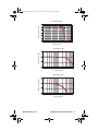
1
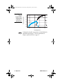
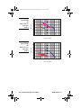
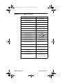
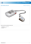
21x7 10MHz Adj Blncd Rcvr revA.fm Page 1 Friday, January 7, 2005 12:22 PM
USER’S GUIDE
10-MHz Adjustable
Balanced Photoreceivers
Models 2107 & 2117
2584 Junction Avenue • San Jose, CA 95134-1902 • USA
phone: (408) 919–1500 • e-mail: [email protected] • www.newfocus.com
21x7 10MHz Adj Blncd Rcvr revA.fm Page 2 Friday, January 7, 2005 12:22 PM
Warranty
New Focus, Inc. guarantees its products to be free of defects for one year from
the date of shipment. This is in lieu of all other guarantees, expressed or implied,
and does not cover incidental or consequential loss.
Information in this document is subject to change without notice.
Copyright 2004, New Focus, Inc., a division of Bookham Technology plc. All
rights reserved.
The
logo and NEW FOCUS, Inc. are trademarks or registered
trademarks of Bookham Technology plc in the U.S.A or other countries.
Products described in this document may be covered by one or more patents in
the U.S.A. and abroad.
Document Number 200331 Rev. A
21x7 10MHz Adj Blncd Rcvr revA.fm Page 3 Friday, January 7, 2005 12:22 PM
Contents
Operation
5
Introduction . . . . . . . . . . . . . . . . . . . . . . . . . . . . . . . . . . . . . . . . . . . 5
Using the Photoreceiver. . . . . . . . . . . . . . . . . . . . . . . . . . . . . . . . . 7
Checking the Battery. . . . . . . . . . . . . . . . . . . . . . . . . . . . . . . . . . . . 8
General Features & Principles
9
Photoreceiver Circuitry . . . . . . . . . . . . . . . . . . . . . . . . . . . . . . . . . 9
Optical Power and Output Voltage . . . . . . . . . . . . . . . . . . . . . 10
Frequency Response and Noise
13
Measuring Bandwidth. . . . . . . . . . . . . . . . . . . . . . . . . . . . . . . . . . 13
Measuring Noise. . . . . . . . . . . . . . . . . . . . . . . . . . . . . . . . . . . . . . . 13
Performance Data for Frequency Response. . . . . . . . . . . . . . 16
Performance Data for Noise . . . . . . . . . . . . . . . . . . . . . . . . . . . . 18
Common Mode Rejection . . . . . . . . . . . . . . . . . . . . . . . . . . . . . . 19
Characteristics
21
Physical Specifications . . . . . . . . . . . . . . . . . . . . . . . . . . . . . . . . . 21
Model 2107 Specifications . . . . . . . . . . . . . . . . . . . . . . . . . . . . . 22
Model 2117 Specifications . . . . . . . . . . . . . . . . . . . . . . . . . . . . . 23
Customer Service
24
Technical Support . . . . . . . . . . . . . . . . . . . . . . . . . . . . . . . . . . . . . 24
Service . . . . . . . . . . . . . . . . . . . . . . . . . . . . . . . . . . . . . . . . . . . . . . . . 24
Models 2107 & 2117
Contents • 3
21x7 10MHz Adj Blncd Rcvr revA.fm Page 4 Friday, January 7, 2005 12:22 PM
4 • Contents
NEW FOCUS, Inc.
21x7 10MHz Adj Blncd Rcvr revA.fm Page 5 Friday, January 7, 2005 12:22 PM
Operation
Introduction
The Model 21X7 is a general-purpose balanced
photoreceiver with adjustable gain and bandwidth.
These receivers can be powered by batteries or by an
external ±15-V power supply. There are two models
available, each based on a different photodetector.
Free-space (FS) and fiber-coupled (FC) versions are
available for each model:
Note:
Model
Wavelength
Diode
Type
Active Area
2107-FC
300–1070 nm
silicon
0.8 mm2
2107-FS
300–1070 nm
silicon
0.8 mm2
2117-FC
900–1700 nm
InGaAs
0.0078 mm2
2117-FS
900–1700 nm
InGaAs
0.08 mm2
Complete specifications begin on page 21.
The 10-MHz three-stage transimpedance amplifier
includes selectable gain and selectable low- and highpass filters for easy signal optimization.
Models 2107 & 2117
Operation • 5
21x7 10MHz Adj Blncd Rcvr revA.fm Page 6 Friday, January 7, 2005 12:22 PM
1.0
2117
Responsivity (A/W)
Figure 1:
Typical
responsivities
of the Model
2107 & 2117
photodiodes
0.8
0.6
2107
0.4
0.2
0.0
400
800
1200
1600
Wavelength (nm)
Note:
6 • Operation
To obtain the value of the “response factor” in V/mW, divide the
photodiode responsivity by 1.5. For more information on
frequency response and noise, see page 13.
NEW FOCUS, Inc.
21x7 10MHz Adj Blncd Rcvr revA.fm Page 7 Friday, January 7, 2005 12:22 PM
Using the Photoreceiver
1. Mount the photoreceiver. Use the 8-32 thread
(M4 for metric versions) on the bottom of the casing to mount the photoreceiver to a post or pedestal.
2. Supply power. Power the Model 21X7 using
either two 9-volt alkaline batteries or a ±15-V lownoise linear power supply (such as the New Focus
Model 0901).
3. Connect the receiver output. Connect your
voltmeter, oscilloscope, or other instrument to the
Output SMA connector on the receiver.
If you wish to connect to a BNC cable, you can purchase a
BNC-to-SMA adapter such as the New Focus Model
1225.
Note:
4. Turn on the photoreceiver power. For external
power, use ±15 VDC ON; for battery, use Batt Mode
ON.
5. Align optical beams onto the detectors.
The photodiodes are not very large, so take care
when aligning each beam.
6. Adjust the gain. Use the knob and rocker switch
on the receiver to set the gain. The bandwidths
vary with the gain setting (see table on page 10).
7. Adjust the filters. Select low-pass and high-pass
corner frequencies using the knobs on the receiver.
8. Balance the optical input levels. Alternately
block each diode and observe the signal strength.
When they are approximately equal and opposite,
adjust their relative intensity until the balanced
output is zero volts.
9. Turn off the photoreceiver power. When you
are finished with the receiver, place the power
switch in the ±15 VDC ON position and switch off
or unplug the external power supply.
Models 2107 & 2117
Operation • 7
21x7 10MHz Adj Blncd Rcvr revA.fm Page 8 Friday, January 7, 2005 12:22 PM
Checking the Batteries
The Model 21X7 can be powered by two standard 9volt alkaline batteries. Under normal operating
conditions with low light levels and a high impedance
load attached to the BNC connector, the photoreceiver
draws about 20 mA from the batteries, and the battery
lifetime is approximately 24 hours.
To check the condition of the battery:
1. Turn on the photoreceiver using the power switch.
2. Set the Low Frequency adjustment to DC.
3. Set the Gain to 3x10⁴.
4. Focus at least 1 µW of optical power on the
detector (or place the detector in front of a desk
lamp).
The output should be greater than 7 V. If it is not,
replace the batteries with fresh ones.
Replacing the Batteries
The Model 21X7 is shipped with two fresh 9-V
batteries installed. To avoid confusion due to low
batteries, replace the batteries on a monthly basis
when the receiver is in frequent use, or use an external
linear power supply such as the New Focus
Model 0901.
1. Turn off the receiver using the power switch.
2. Use a Phillips-head screwdriver to remove the
two screws on the back panel of the photoreceiver.
3. Remove the back panel.
4. Replace the used 9-V batteries with fresh ones.
5. Replace the back panel and the two screws.
6. Recheck the battery level as described above.
8 • Operation
NEW FOCUS, Inc.
21x7 10MHz Adj Blncd Rcvr revA.fm Page 9 Friday, January 7, 2005 12:22 PM
General Features & Principles
Photoreceiver Circuitry
The circuitry inside the Model 21X7 consists of two
photodiodes followed by a three-stage transimpedance
amplifier. The gain can be adjusted from 626 V/A to
18.8x10⁶ V/A in 5-dB steps. The low-noise amplifier
design is optimized to maximize bandwidth at each
gain setting. At the higher gain settings, the bandwidth
is limited by amplifier gain-bandwidth product. The
plots of Figure 3 show the typical frequency responses
for the different gain settings.
Figure 2:
Functional
schematic of
the Model 21X7
circuitry
+15 V
+9 V REG
+9 V
BATT
9V
-9 V
GND
BATT
9V
-15 V
+9 V
-9 V REG
ADJUSTABLE-GAIN
STAGE
x104
INDEPENDENTLY
x103
ADJUSTABLE 6-dB/OCTAVE
x102
HIGH- AND LOW-PASS FILTERS
x10
x1
f_L
-9 V
Models 2107 & 2117
ADJUSTABLE-GAIN
STAGE
x3
x1
SMA
f_H
DETECTOR
HOUSING IS
GROUNDED
General Features & Principles • 9
21x7 10MHz Adj Blncd Rcvr revA.fm Page 10 Friday, January 7, 2005 12:22 PM
The following table summarizes the bandwidth at each
gain setting. The bandwidth on the 3x settings is
somewhat lower than the 1x settings, and significantly
decreases at the highest gain settings. There is little
difference in frequency response between the visible
(Model 2107) and IR (Model 2117) models. The plots of
Figure 3 show the frequency-response details for each
gain setting.
Gain
Setting
Specification
Typical Performance
1x1
10 MHz
12 MHz
3x1
NA
6 MHz
1x10
NA
12 MHz
3x10
NA
6 MHz
1x10²
NA
8 MHz
3x10²
NA
6 MHz
1x10³
NA
700 kHz
3x10³
NA
700 kHz
1x10⁴
NA
250 kHz
3x10⁴
150 kHz
250 kHz
Optical Power and Output Voltage
The typical operating range for these receivers is from
a few nanowatts up to 2 to 5 mW (depending on the
model and gain setting). Be careful to keep the
differential optical power below the maximum optical
power difference of 10 mW to avoid damaging the
photoreceiver.
To compute the approximate output voltage for a given
input optical power use the relationship
Vout = (P+-P-)·R·G,
10 • General Features & Principles
NEW FOCUS, Inc.
21x7 10MHz Adj Blncd Rcvr revA.fm Page 11 Friday, January 7, 2005 12:22 PM
where P+ and P- are the input optical powers in Watts
on the right and left photodiodes respectively, R is the
photodetector’s response factor in V/mW, and G is the
amplifier’s gain setting.
Note:
Estimate the value of the response factor by dividing the
responsivity shown in Figure 1 by 1.5.
For example, the Model 2107 on the 1x10³ gain setting
and with 10 µW of optical power at 900 nm on one
photodiode will have an output voltage of
approximately
(0.01 mW)·(0.35 V/mW)·(1x103) = 3.5 V.
The maximum differential optical power that can be
detected by the photoreceiver is determined by the
input optical power at which either stage of the
transimpedance gain saturates. We can calculate the
saturation power at 900 nm for the Model 2107 at its
maximum output voltage of ±7 V with fresh batteries
or operating from an external ±15 VDC power supply.
Using the expression 7 V = Psat·R·G, the Model 2107 has
a differential saturation power of 20 mW for the lowest
gain setting up to 0.7 µW for the highest gain setting.
At other wavelengths where the responsivity is lower,
the saturation power increases inversely with response
factor.
Models 2107 & 2117
General Features & Principles • 11
21x7 10MHz Adj Blncd Rcvr revA.fm Page 12 Friday, January 7, 2005 12:22 PM
12 • General Features & Principles
NEW FOCUS, Inc.
21x7 10MHz Adj Blncd Rcvr revA.fm Page 13 Friday, January 7, 2005 12:22 PM
Frequency Response and Noise
Measuring Bandwidth
The frequency response and noise characteristics of
the photoreceiver depend on the selected gain. The
figures beginning on page 16 give the typical
frequency response and noise behavior for the
photoreceivers at each of the gain settings. The
frequency response of the transimpedance gain is
plotted using the expression
20·log[Gain(ƒ)/Gain(0)],
where ƒ is the frequency and Gain(0) is the gain at DC.
The photoreceiver’s bandwidth is defined as the
frequency where the gain has decreased by 3 dB, or a
factor of 2 .
Measuring Noise
The photoreceiver noise is characterized using the
noise equivalent power (NEP), which is a measure of
the weakest optical signal that the photoreceiver can
detect. The NEP is the optical power which will
produce a signal-to-noise ratio of 1 in a 1-Hz
bandwidth. The minimum detectable optical power
can be found using the relationship
Minimum Optical Power = NEP · BW ,
where BW is the bandwidth. Note that NEP is a
wavelength-dependent quantity that changes with the
photodetector’s responsivity.
Models 2107 & 2117
Frequency Response and Noise • 13
21x7 10MHz Adj Blncd Rcvr revA.fm Page 14 Friday, January 7, 2005 12:22 PM
Another way to characterize the noise is with the
photocurrent noise (In), which is related to NEP by
In = R · NEP,
where R is the photodetector’s responsivity (in A/W).
The photocurrent noise is independent of wavelength
because it gives the noise of the photoreceiver with the
photodetector’s responsivity factored out.
To characterize the noise of the photoreceiver, the
output electrical noise spectrum is measured with a
spectrum analyzer. This voltage noise spectrum is
converted to an equivalent optical photocurrent noise
by dividing the voltage noise by the transimpedance
gain (V/A). The photocurrent noise, In(ƒ), has units of
pA/ Hz and is plotted in Figure 3 and Figure 4 using
the expression 20·log[In(ƒ)/1 A].
Calculating NEP
The noise equivalent power (NEP) can be calculated by
dividing the photocurrent noise by R, the detector’s
responsivity (see page 6).
From DC to 150 kHz the average photocurrent noise
for the Model 2107 on the high gain setting is about
0.4 pA/ Hz , corresponding to an average NEP at
900 nm of 0.8 pW/ Hz. The integrated noise
equivalent power from DC to 150 kHz is then obtained
by multiplying the average NEP by BW , the square
root of the bandwidth.
The expression BW = 2πƒ3-dB/4 for a one-pole lowpass filter is useful for calculating the equivalent noise
bandwidth. Using the high-pass filter set 1 decade
below the low-pass cutoff reduces noise-equivalent
bandwidth by approximately 10 %. For the Model 2107
with a 3-dB bandwidth of 150 kHz, the equivalent
noise bandwidth is 235 kHz. This gives an optical noise
equivalent power of about 390 pW, so the minimum
detectable optical signal at 900 nm (with a signal-tonoise ratio of 1) for the Model 2107 on the highest gain
14 • Frequency Response and Noise
NEW FOCUS, Inc.
21x7 10MHz Adj Blncd Rcvr revA.fm Page 15 Friday, January 7, 2005 12:22 PM
setting is 390 pW when operating at full detector
bandwidth.
You can further improve your signal-to-noise ratio by
using optical modulators or choppers with lock-in
amplifiers to limit the detection bandwidth. Using
such techniques you can reduce equivalent bandwidth
to 1 Hz or less.
Calculating Output-Voltage Noise
The output-voltage noise can be calculated from
G · R · NEP · BW ,
where G is the gain (V/V), R is the photodiode response
factor (V/mW), NEP is the average noise equivalent
power, and BW is the bandwidth. This gives an output
noise voltage for the Model 2107 on the high gain
setting of
(3x10⁴ V/V) · (0.35 V/mW) · (0.8x10⁻⁹ mW/ Hz )
3
------ ⋅ 150 × 10 Hz =4 mVrms.
· 2π
4
The Johnson noise at the input of a 100-MHz bandwidth
oscilloscope with 1-MΩ input impedance is 1.6 mVrms . This is
often the limiting factor in broadband measurements.
Summary
With the Model 2107 on the highest gain setting the
minimum NEP is 0.8 pW/ Hz , and this yields an
output noise voltage of 4 mVrms. Viewed another way,
for operation at the peak responsivity wavelength of
900 nm and for the high gain setting, you will achieve a
signal-to-noise ratio of unity if the input power is
390 pW.
For the Model 2117 with an InGaAs photodiode, the
NEP at peak response wavelength of 1500 nm is
0.4 pW/ Hz over the 150-kHz bandwidth. The full
Models 2107 & 2117
Frequency Response and Noise • 15
21x7 10MHz Adj Blncd Rcvr revA.fm Page 16 Friday, January 7, 2005 12:22 PM
bandwidth signal-to-noise ratio of 1 is achieved
around 200 pW.
Note that this assumes operation without any postphotoreceiver filtering and with the full photoreceiver
bandwidth. By using the built-in electronic band-pass
filter or an optical chopper and a lock-in amplifier, the
receiver can detect significantly weaker optical signals.
Performance Data for Frequency Response
The 3-dB frequency bandwidth is defined as the
frequency where the photoreceiver’s transimpedance
gain has decreased by a factor of 2 . The typical
frequency responses for the Model 2107 and Model
2117 are shown in the following figures.
Gain Setting=1
3
Normalized Gain (dB)
Figure 3:
Typical
frequency
response for
Model 21X7 at
each gain
setting
0
-3
x1
-6
-9
x3
-12
-15
0.01
0.1
1
10
100
Frequency (MHz)
Gain Setting=10
Normalized Gain (dB)
3
0
x1
-3
-6
-9
x3
-12
0.01
0.1
1
10
100
Frequency (MHz)
16 • Frequency Response and Noise
NEW FOCUS, Inc.
21x7 10MHz Adj Blncd Rcvr revA.fm Page 17 Friday, January 7, 2005 12:22 PM
Gain Setting=102
Normalized Gain (dB)
3
0
-3
x1
-6
-9
-12
x3
-15
0.01
0.1
1
10
100
Frequency (MHz)
Gain Setting=103
Normalized Gain (dB)
3
0
x3
x1
-3
-6
0.01
0.1
1
Frequency (MHz)
Gain Setting=104
Normalized Gain (dB)
3
0
x1
x3
-3
-6
0.01
0.1
1
Frequency (MHz)
Models 2107 & 2117
Frequency Response and Noise • 17
21x7 10MHz Adj Blncd Rcvr revA.fm Page 18 Friday, January 7, 2005 12:22 PM
Performance Data for Noise
Figure 4 shows the typical noise spectrum expressed as
photocurrent noise for Model 21X7 photoreceivers on
the highest gain setting.
To derive the receiver’s Noise Equivalent Power (NEP),
divide the photocurrent noise by the photodiode
responsivity. To convert to output voltage noise (RMS),
multiply the photocurrent noise by the gain setting
from the 21X7 front label, then by 630 V/A (the scaling
factor between the gain setting labels and the actual
amplifier transimpedance gain).
For example, the output voltage noise (RMS) for Model
2117 in the 3x10³ setting is approximately:
0.4 pA/ Hz x 3 x 103 x 630 V/A = 0.75 µVrms/ Hz .
For the 700 kHz of amplifier bandwidth in the 3x10³
gain setting, the equivalent noise bandwidth is:
( 2 x π/4 ) x 700 x 103 Hz = 1.1 MHz,
so the predicted output noise voltage is approximately
0.75 µVrms/ Hz x 1.1 × 10⁶ Hz = 0.8 mVrms.
Because the NEP is listed at the highest gain setting,
some additional considerations add to the NEP at lower
gain settings. First, the noise spectrum (Figure 4) is not
flat, rising at frequencies above 100 kHz. This
contributes an extra 20% to the output noise voltage in
the 3 x 10³ setting compared to 3 x 10⁴. Also, as the
output noise voltage approaches 1 mVrms, the Johnson
noise limit of your measurement instrument will
become important. Note that the Johnson noise for an
oscilloscope with 100-MHz bandwidth (assuming
perfect roll off) and 1-MΩ input impedance is
1.2 mVrms.
18 • Frequency Response and Noise
NEW FOCUS, Inc.
21x7 10MHz Adj Blncd Rcvr revA.fm Page 19 Friday, January 7, 2005 12:22 PM
21X7 Output Noise Current
0.40
Noise (pA/ Hz)
Figure 4:
Typical noise
spectrum for
Model 21X7
Spec
0.35
Gain = 3 x 10⁴
0.30
0.25
0.20
0
10
20 30
40
50
60
70 80
90 100
Frequency (KHz)
Common Mode Rejection
Using the Model 21X7 balanced photoreceivers with
equal signal powers on each photodiode results in an
output with reduced common mode signal. The
common-mode rejection ratio, or CMRR, is a
measurement of the effectiveness of the balanced
subtraction.
Figure 5 shows the CMRR of each model using the
following definition:
CMRR = -20 · log((Vout1 - Vout2)/Vout1).
Because the common mode subtraction occurs before
the first amplifier stage, the only practical bandwidth
limitation on common mode rejection is the
photodiode bandwidth. Thus, as seen in the following
figures, the CMRR for higher gain settings is relatively
flat to frequencies well beyond the useful frequency
response of the gain setting.
Models 2107 & 2117
Frequency Response and Noise • 19
21x7 10MHz Adj Blncd Rcvr revA.fm Page 20 Friday, January 7, 2005 12:22 PM
50
1x10³ - 3x10³
45
CMRR (dB)
Figure 5:
Typical CMRR
for
Model 2107 in
each gain
setting
40
1 - 3x10²
35
30
1x10⁴ - 3x10⁴
25
20
0.01
0.1
1
10
100
10
100
Frequency (MHz)
50
45
40
CMRR (dB)
Figure 6:
Typical CMRR
for
Model 2117 in
each gain
setting
35
1 - 3x10²
1x10³ - 3x10³
30
1x10⁴ - 3x10⁴
25
20
0.01
0.1
1
Frequency (MHz)
20 • Frequency Response and Noise
NEW FOCUS, Inc.
21x7 10MHz Adj Blncd Rcvr revA.fm Page 21 Friday, January 7, 2005 12:22 PM
Characteristics
Physical Specifications
Figure 7:
Mechanical
drawing of the
Model 21X7
casing
low freq.
corner
adjust
knob
gain
knob
external
power
input
(±15VDC)
power
switch
1.78"
(45.2)
high freq.
corner
adjust
knob
gain
multiplier
switch
Models 2107 & 2117
1.00"
(25.4)
photodetectors
5.17"
(131.2)
SMA
output
connector
8-32 (M4)
THD
0.66"
(16.7)
2.50"
(63.5)
1.24"
(31.5)
2.31" (58.6)
Characteristics • 21
21x7 10MHz Adj Blncd Rcvr revA.fm Page 22 Friday, January 7, 2005 12:22 PM
Model 2107 Specifications
Model 2107
Wavelength Range
300–1070 nm
3-dB Bandwidth
10 MHz, 5 MHz, 150 kHz
Typical Common-Mode Rejection
25 dB
Rise Time
80 ns
Peak Conversion Gain
9.4 x 10⁶ V/W
Typical Max. Responsivity
0.5 A/W
Max. Transimpedance Gain
18.8 x 10⁶ V/A
Output Impedance
16 Ω
Minimum NEP
0.8 pW/ Hz
CW Saturation Power
20 mW @ 850 nm
Max. Differential Power
20 mW @ 850 nm
Max. Power per Photodiode if
balanced (damage threshold)
20 mW @ 850 nm
Detector Material/Type
Si/PIN
Detector Active Area
1.0 mm x 0.8 mm
Optical Input
FC or Free Space
Electrical Output
SMA
Power Requirements
±15 VDC <150 mA
External Power Supply
or Two 9-V Batteries
22 • Characteristics
NEW FOCUS, Inc.
21x7 10MHz Adj Blncd Rcvr revA.fm Page 23 Friday, January 7, 2005 12:22 PM
Model 2117 Specifications
Model 2117
Wavelength Range
900–1700 nm
3-dB Bandwidth
10 MHz, 5 MHz, 150 kHz
Typical Common-Mode Rejection
25 dB
Rise Time
80 ns
Peak Conversion Gain
18.8 x 10⁶ V/W
Typical Max. Responsivity
1 A/W
Max. Transimpedance Gain
18.8 x 10⁶ V/A
Output Impedance
16 Ω
Minimum NEP
0.4 pW/ Hz
CW Saturation Power
10 mW @ 1600 nm
Max. Differential Power
10 mW @ 1600 nm
Max. Power per Photodiode
(damage threshold)
10 mW @ 1600 nm
Detector Material/Type
InGaAs/PIN
Detector Active Area
0.3-mm diam. (FS)
0.1-mm diam. (FC)
Optical Input
FC or Free Space
Electrical Output
SMA
Power Requirements
±15 VDC <150 mA
External Power Supply
or Two 9-V Batteries
Models 2107 & 2117
Characteristics • 23
21x7 10MHz Adj Blncd Rcvr revA.fm Page 24 Friday, January 7, 2005 12:22 PM
Customer Service
Technical Support
Information and advice about the operation of any
New Focus product is available from our applications
engineers. For quickest response, ask for “Technical
Support” and know the model and serial numbers for
your product.
Hours: 8:00–5:00 PST, Monday through Friday
(excluding holidays).
Toll Free: 1-866-NUFOCUS (1-866-683-6287)
(from the USA & Canada only)
Phone: (408) 919-1500
Support is also available by fax and email:
Fax: (408) 980-8883
Email: [email protected]
We typically respond to faxes and email within one
business day.
Service
In the event that your photoreceiver malfunctions or
becomes damaged, please contact New Focus for a
return authorization number and instructions on
shipping the unit back for evaluation and repair.
24 • Customer Service
NEW FOCUS, Inc.