1
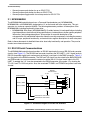
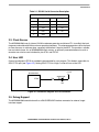
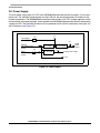
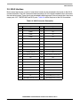
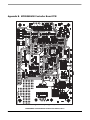
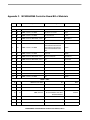
MC9S08AW60
Controller Board
User Manual
HCS08
Microcontrollers
DRM090
Rev.0
10/2007
freescale.com
Preface
0.1
0.2
0.3
0.4
0.5
Audience . . . . . . . . . . . . . . . . . . . . . . . . . . . . . . . . . . . . . . . . . . . . . . . . . . . . . . . . . . . . . . . . . . .
Organization. . . . . . . . . . . . . . . . . . . . . . . . . . . . . . . . . . . . . . . . . . . . . . . . . . . . . . . . . . . . . . . . .
Notation Conventions. . . . . . . . . . . . . . . . . . . . . . . . . . . . . . . . . . . . . . . . . . . . . . . . . . . . . . . . . .
Definitions, Acronyms, and Abbreviations . . . . . . . . . . . . . . . . . . . . . . . . . . . . . . . . . . . . . . . . . .
References. . . . . . . . . . . . . . . . . . . . . . . . . . . . . . . . . . . . . . . . . . . . . . . . . . . . . . . . . . . . . . . . . .
5
5
6
6
7
Chapter 1
Introduction
1.1
1.2
1.3
MC9S08AW60 Controller Board Architecture . . . . . . . . . . . . . . . . . . . . . . . . . . . . . . . . . . . . . . 10
MC9S08AW60 Controller Board Configuration Jumpers . . . . . . . . . . . . . . . . . . . . . . . . . . . . . . 11
MC9S08AW60 Controller Board Connections . . . . . . . . . . . . . . . . . . . . . . . . . . . . . . . . . . . . . . 13
Chapter 2
Technical Summary
2.1
2.2
2.3
2.4
2.5
2.5.1
2.6
2.7
2.8
2.9
2.9.1
2.10
2.11
2.11.1
2.11.2
2.12
2.13
2.14
2.15
2.16
2.16.1
2.16.2
2.16.3
2.16.4
2.16.5
2.16.6
2.16.7
2.16.8
2.16.9
2.17
MC9S08AW60 . . . . . . . . . . . . . . . . . . . . . . . . . . . . . . . . . . . . . . . . . . . . . . . . . . . . . . . . . . . . . .
RS-232 Serial Communications . . . . . . . . . . . . . . . . . . . . . . . . . . . . . . . . . . . . . . . . . . . . . . . . .
Clock Source . . . . . . . . . . . . . . . . . . . . . . . . . . . . . . . . . . . . . . . . . . . . . . . . . . . . . . . . . . . . . . .
User LED . . . . . . . . . . . . . . . . . . . . . . . . . . . . . . . . . . . . . . . . . . . . . . . . . . . . . . . . . . . . . . . . . .
Debug Support. . . . . . . . . . . . . . . . . . . . . . . . . . . . . . . . . . . . . . . . . . . . . . . . . . . . . . . . . . . . . .
BACKGROUND Header. . . . . . . . . . . . . . . . . . . . . . . . . . . . . . . . . . . . . . . . . . . . . . . . . . . .
RESET . . . . . . . . . . . . . . . . . . . . . . . . . . . . . . . . . . . . . . . . . . . . . . . . . . . . . . . . . . . . . . . . . . . .
General-Purpose Buttons and Run/Stop Switch . . . . . . . . . . . . . . . . . . . . . . . . . . . . . . . . . . . .
Power Supply. . . . . . . . . . . . . . . . . . . . . . . . . . . . . . . . . . . . . . . . . . . . . . . . . . . . . . . . . . . . . . .
UNI-3 Interface. . . . . . . . . . . . . . . . . . . . . . . . . . . . . . . . . . . . . . . . . . . . . . . . . . . . . . . . . . . . . .
UNI-3 BRAKE and PFC Signals. . . . . . . . . . . . . . . . . . . . . . . . . . . . . . . . . . . . . . . . . . . . . .
Motor Control PWM Signals and LEDs . . . . . . . . . . . . . . . . . . . . . . . . . . . . . . . . . . . . . . . . . . .
Motor Protection Logic . . . . . . . . . . . . . . . . . . . . . . . . . . . . . . . . . . . . . . . . . . . . . . . . . . . . . . . .
Over-Current and Over-Voltage Protection . . . . . . . . . . . . . . . . . . . . . . . . . . . . . . . . . . . . .
Temperature Sensing. . . . . . . . . . . . . . . . . . . . . . . . . . . . . . . . . . . . . . . . . . . . . . . . . . . . . .
DC Bus Current Sensing . . . . . . . . . . . . . . . . . . . . . . . . . . . . . . . . . . . . . . . . . . . . . . . . . . . . . .
Back-EMF Current Sensing . . . . . . . . . . . . . . . . . . . . . . . . . . . . . . . . . . . . . . . . . . . . . . . . . . . .
Quadrature Encoder/Hall-Effect Interface . . . . . . . . . . . . . . . . . . . . . . . . . . . . . . . . . . . . . . . . .
Tacho-Generator Interface. . . . . . . . . . . . . . . . . . . . . . . . . . . . . . . . . . . . . . . . . . . . . . . . . . . . .
Peripheral Expansion Connectors . . . . . . . . . . . . . . . . . . . . . . . . . . . . . . . . . . . . . . . . . . . . . . .
Encoder Expansion Connector . . . . . . . . . . . . . . . . . . . . . . . . . . . . . . . . . . . . . . . . . . . . . .
Tacho-Dynamo Expansion Connector . . . . . . . . . . . . . . . . . . . . . . . . . . . . . . . . . . . . . . . . .
Port A Header . . . . . . . . . . . . . . . . . . . . . . . . . . . . . . . . . . . . . . . . . . . . . . . . . . . . . . . . . . .
Port D Header . . . . . . . . . . . . . . . . . . . . . . . . . . . . . . . . . . . . . . . . . . . . . . . . . . . . . . . . . . .
PORT CE Header . . . . . . . . . . . . . . . . . . . . . . . . . . . . . . . . . . . . . . . . . . . . . . . . . . . . . . . .
ADC Header. . . . . . . . . . . . . . . . . . . . . . . . . . . . . . . . . . . . . . . . . . . . . . . . . . . . . . . . . . . . .
PWM Header . . . . . . . . . . . . . . . . . . . . . . . . . . . . . . . . . . . . . . . . . . . . . . . . . . . . . . . . . . . .
KBI Header. . . . . . . . . . . . . . . . . . . . . . . . . . . . . . . . . . . . . . . . . . . . . . . . . . . . . . . . . . . . . .
ZGB Header . . . . . . . . . . . . . . . . . . . . . . . . . . . . . . . . . . . . . . . . . . . . . . . . . . . . . . . . . . . . .
Test Points . . . . . . . . . . . . . . . . . . . . . . . . . . . . . . . . . . . . . . . . . . . . . . . . . . . . . . . . . . . . . . . . .
16
16
17
17
17
18
18
19
20
21
22
22
24
25
25
26
27
27
28
28
29
29
30
30
31
31
32
32
33
33
MC9S08AW60 Controller Board Hardware User Manual, Rev. 0. Draft A
Freescale Semiconductor
3
Appendix A. MC9S08AW60 Controller Board Schematics
Appendix B. MC9S08AW60 Controller Board PCB
Appendix C. MC9S08AW60 Controller Board Bill of Materials
MC9S08AW60 Controller Board Hardware User Manual, Rev. 0. Draft A
4
Freescale Semiconductor
Preface
This reference manual describes the hardware on the MC9S08AW60 controller board. The board is
designed for motor/motion control demos and supports specific customer needs, including the PWM
interface with dead-time insertion circuit and tacho-dynamo hardware interface.
0.1 Audience
This document is intended for application developers who are creating software for devices using the
MC9S08AWXX.
0.2 Organization
This manual is organized into two chapters and three appendixes.
• Introduction provides an overview of the board and its features.
• Technical Summary describes the MC9S08AW60 controller board hardware.
• MC9S08AW60 Controller Board Schematics contains the schematics of the MC9S08AW60
controller board.
• MC9S08AW60 Controller Board PCB contains details on the MC9S08AW60 printed circuit board
(PCB).
• MC9S08AW60 Controller Board Bill of Materials lists materials used on the MC9S08AW60
controller board.
MC9S08AW60 Controller Board Hardware User Manual, Rev. 0
Freescale Semiconductor
5
Preface
0.3 Notation Conventions
This document uses the following conventions:
Table 0-1. Notation Conventions
Term or Value
Symbol
Examples
Active high signals
(logic one)
No special symbol
attached to the signal
name
MOSI1
SCL1
Active low signals
(logic zero)
Noted with an
overbar in text and in
most figures
RESET
SS1
Hexadecimal values
Begin with a “$” symbol
$0FF0
$80
Decimal values
No special symbol
attached to the
number
10
34
Binary values
Begin with the letter “b”
attached to the number
b1010
b0011
Numbers
Considered positive
unless specifically noted
as a negative value
5
–10
Bold
Reference sources,
paths, emphasis
...see:
http://www.freescale.com/
mcu
Exceptions
In schematic drawings, active low
signals may be noted by a slash:
/RESET
Voltage is often shown as positive:
+3.3 V
0.4 Definitions, Acronyms, and Abbreviations
Definitions, acronyms, and abbreviations used in this document are defined below.
A/D
Analog to digital
D/A
Digital to analog
FLL
Frequency-locked loop
GPIO
General-purpose input and output port on Freescale Semiconductor’s
family of microcontrollers
IC
Integrated circuit
LED
Light-emitting diode
LQFP
Low-profile quad flat pack
MCU
Microcontroller unit
MC9S08AW60 Controller Board Hardware User Manual, Rev. 0
6
Freescale Semiconductor
References
MPIO
Multi-purpose input and output port on Freescale Semiconductor’s
family of microcontrollers; shares package pins with other peripherals
on the chip and can function as a GPIO
PCB
Printed circuit board
PWM
Pulse-width modulation
Quadrature encoder
Sensor for the measurement of position and speed based on optical
principles
RAM
Random access memory
R/C
Resistor/capacitor network
ROM
Read-only memory
SCI
Serial communications interface
SPI
Serial peripheral interface port on Freescale Semiconductor’s
microcontrollers
UART
Universal asynchronous receiver/transmitter
0.5 References
The following sources were referenced to produce this manual:
MC9S08AW60 Microcontroller Data Sheet, Freescale Semiconductor
MC9S08AW60 Controller Board Hardware User Manual, Rev. 0
Freescale Semiconductor
7
Preface
MC9S08AW60 Controller Board Hardware User Manual, Rev. 0
8
Freescale Semiconductor
Chapter 1
Introduction
The MC9S08AW60 controller board is used to demonstrate the abilities of the populated MC9S08AW60
part, which can be replaced by the pin compatible MC9S08AW48/32 in LQFP 64-pin footprint, based on
an optimized PCB and power-supply design. The MC9S08AW60 contoller board provides a hardware tool
allowing the development of applications that use the MC9S08AW60/48/32. This guide refers to
MC9S08AW60.
The MC9S08AW60 controller board is an evaluation module board that includes a MC9S08AW60 part,
PWM interface with hardware dead-time insertion circuit, encoder interface, tacho-generator interface,
communication options, digital and analog power supplies, and peripheral expansion connectors. The
expansion connectors are for signal monitoring and feature expansion. Test pads are provided for
monitoring critical signals and voltage levels.
The MC9S08AW60 controller board is designed to:
• Familiarize you with the features of the HCS08 architecture.
• Serve as a platform for real-time software development. The tool suite enables you to develop and
simulate routines, download the software to on-chip memory, run it, and debug it via the
BACKGROUND port. The breakpoint features enable you to easily specify complex break
conditions and to execute user-developed software at full speed, until the break conditions are
satisfied. The ability to examine and modify all user accessible registers, memory, and peripherals
through the BACKGROUND port facilitates the task of the developer.
• Serve as a platform for hardware development. The hardware platform enables you to connect
external hardware modules. The BACKGROUND port's unobtrusive design makes all memory on
the microcontroller chip available.
MC9S08AW60 Controller Board Hardware User Manual, Rev. 0
Freescale Semiconductor
9
Introduction
1.1 MC9S08AW60 Controller Board Architecture
The MC9S08AW60 controller board facilitates the evaluation of various MC9S08AW60 features. The
MC9S08AW60 controller board can be used to develop real-time software and hardware products based
on the MC9S08AW60. The MC9S08AW60 controller board provides the features necessary to write and
debug software, demonstrate the functionality of that software, and interface with application-specific
devices. The MC9S08AW60 controller board is flexible enough to allow you to exploit the
MC9S08AW60's features to optimize the performance of the product, as shown in Figure 1-1.
MC9S08AW60
D4
RS 232
interface
ZGB
header
BACKGROUND
header
F4 – 7
F0 – 3
PTF
SCI2 / PTC
E2, 3
PTE
Dead-time
insertion
circuit
PWM
HEADER
IRQ
PORT CE
HEADER
C0, 1
Toggle
switch
PWM
XTAL / PTG
C6
PTC
C2
RESET
button
PWM LEDs
E0, 1, 4 – 7
BKGD / MS
C4
CRYSTAL
(optional)
Encoder
interface
D0
RESET
User LED
Tacho-generator
Interface
UNI–3
expansion
connector
PORT D
HEADER
D1, 2, 3, 5
UNI–3
expansion
connector
PTD
ADC
HEADER
VDD
PTA
+12 V power
supply
DCBI PEAK &
AVERAGE
IRQ
PTG
PORT A
HEADER
DCBV
+3.3 V digital
power supply
DCBI
VDDAD
+5 V power
supply
BEMF
DCBI
DCBV
ADC / PTB
+3.3 V analog
power supply
PFC, BRAKE
Protection
logic
KBI
HEADER
UP, DOWN
buttons
Figure 1-1. Block Diagram of the MC9S08AW60 Controller Board
MC9S08AW60 Controller Board Hardware User Manual, Rev. 0
10
Freescale Semiconductor
MC9S08AW60 Controller Board Configuration Jumpers
1.2 MC9S08AW60 Controller Board Configuration Jumpers
Jumper groups and zero ohm resistors(1), shown in Figure 1-2, are used to configure various features on
the MC9S08AW60 controller board.
0
0
0
0
2
2
1
1
J18 J16
5 6
3 4
1 2
6
4
2
J22
R68 R69 R63 R62
5 6
3 4
1 2
J21
5
3
1
J20
1
2
3
JP3
R70, C50
0
R76
.....
0
R46
0
0
R43
R75, C55
1
2
3
JP2
1
2
3
JP1
3 2 1
JP4
R7x C5x
Figure 1-2. MC9S08AW60 Controller Board Jumper Options
1. Zero ohm resistors are used instead of standard jumpers to minimize distortion of analog signals and to achieve high signal-to-noise ratio.
MC9S08AW60 Controller Board Hardware User Manual, Rev. 0
Freescale Semiconductor
11
Introduction
Table 1-1. MC9S08AW60 Controller Board Jumper Options
#
Selector
Function
Connections
JP1
JP2
JP3
PWM
complementary
mode
Odd PWM channels generated by hardware from even PWM channels
1–2
Odd PWM channels generated by odd TPM1CHx channels
2–3
Tacho-dynamo
measurement
Analog sensing by TACHO analog input (AD1P8)
1–2
JP4
Digital sensing by digital input (GPIO PTC2)
2–3
J16
UNI–3 +5 V
Controller board digital power supply from UNI–3 +5 V
closed
J18
UNI–3 +15 V
Controller board analog power supply from UNI–3 +15 V
closed
J20
J21
J22
PWM mode
Complementary PWM mode
1–3, 2–4
Independent PWM mode
3–5, 4–6
DC bus current peak value sensed by the AD1P2 analog input
R43 present
AD1P2 input used as a universal analog input on the ADC header
R43 absent
DC bus current average value sensed by the AD1P3 analog input
R46 present
AD1P3 input used as a universal analogue input on the ADC header
R46 absent
UNI–3 BRAKE signal controlled by the PTD1 output pin
R62 present
PTD1 used as a universal GPIO pin on PORT D header
R62 absent
UNI–3 PFC PWM signal controlled by the PTD2 output pin
R63 present
PTD2 used as a universal GPIO pin on PORT D header
R63 absent
UNI–3 PFC zero cross output signal connected to the PTD3 input pin
R68 present
PTD3 used as a universal GPIO pin on PORT D header
R68 absent
UNI–3 PFC enable signal controlled by the PTD5 output pin
R69 present
PTD5 used as a universal GPIO pin on PORT D header
R69 absent
Encoder output connected to the TPM2CLK/PTD4 input
R76 present
TPM2CLK/PTD4 used as a universal GPIO pin on PORT D header
R76 absent
R43
R46
R62
R63
R68
R69
R76
MC9S08AW60 Controller Board Hardware User Manual, Rev. 0
12
Freescale Semiconductor
MC9S08AW60 Controller Board Connections
1.3 MC9S08AW60 Controller Board Connections
Figure 1-3 shows the connection between the PC, external 12 V DC power supply, and the
MC9S08AW60 controller board.
PC-compatible
computer
Parallel extension
cable
Parallel
command
converter*
MC9S08AW60CB
BACKGROUND
Power
Connect cable
to parallel/printer port
External with 2.1 mm,
12 V receptacle
power connector
* Use optoisolated PCC for high-voltage applications
Figure 1-3. Connecting the MC9S08AW60 Controller Board Cables
When optoisolation is needed to isolate the computer from the motor driver board and the controller
board, use the optoisolated parallel command converter instead of the non-isolated parallel command
converter. Command converters with ISA, PCI, USB, and ETHERNET interfaces are available.
To connect the MC9S08AW60 controller board cables:
1. Connect the parallel extension cable to the parallel port of the host computer.
2. Connect the other end of the parallel extension cable to the parallel command converter (see
Figure 1-3) and connect it to the BACKGROUND header on the MC9S08AW60 controller board.
Pin 1 on the command converter must be aligned with pin 1 on the controller board. This provides
the connection that allows the host computer to control the board.
3. Connect the 2.1 mm output power plug from the external power supply into the power jack (see
Figure 1-3) on the MC9S08AW60 controller board.
4. Apply power to the external power supply. The green power-on LED will illuminate when power is
correctly applied.
MC9S08AW60 Controller Board Hardware User Manual, Rev. 0
Freescale Semiconductor
13
Introduction
MC9S08AW60 Controller Board Hardware User Manual, Rev. 0
14
Freescale Semiconductor
Chapter 2
Technical Summary
The MC9S08AW60 controller board is designed as a versatile development card for developing real-time
software and hardware products to support a new generation of applications in servo and motor control,
SMPS, and other general purpose applications. The power of the 8-bit MC9S08AW60 microcontroller
unit, combined with the hall-effect/quadrature encoder interface, PWM interface with dead-time insertion
circuit, tacho-generator interface for digital/analog sensing, motor over-current logic, and motor
over-voltage logic, makes the MC9S08AW60 controller board ideal for developing and implementing
many motor controlling algorithms, and for learning the architecture and instruction set of the
MC9S08AW60 microcontroller.
The features of the MC9S08AW60 controller board include:
• MC9S08AW60 8-bit +3.3 V microcontroller operating at 40 MHz
• BACKGROUND interface header for an external debug host target interface
• RS-232 interface with galvanic isolation for easy connection to a host computer or PC master
development tool
• Header allowing you to attach a port A GPIO compatible peripheral
• Header allowing you to attach a port D (GPIO, ADC, KBI, TPM) compatible peripheral
• Header allowing you to attach a port CE (GPIO, IIC, SCI, SPI) compatible peripheral
• Header allowing you to attach a ADC compatible peripheral
• Header allowing you to attach a PWM compatible peripheral
• Header allowing you to attach a KBI / port G GPIO compatible peripheral
• Header allowing you to attach the ZigBee module or other SCI compatible peripheral
• On-board power regulation from an external 12 V DC supplied power input
• Light-emitting diode (LED) power indicator
• Six on-board PWM monitoring LEDs
• One on-board PWM fault monitoring LED
• One on-board general-purpose LED
• UNI-3 motor interface
– DC bus voltage sensing
– DC bus current sensing
– Back-EMF sensing
– Temperature sensing
– Pulse-width modulation
– BRAKE, PFC PWM signals
• Encoder/gall-effect interface
• Tacho-generator interface
• PWM dead-time insertion circuit
• DC bus over-current and over-voltage protection logic
• DC bus current peak detector and average value sensing
• Manual reset push-button
MC9S08AW60 Controller Board Hardware User Manual, Rev. 0
Freescale Semiconductor
15
Technical Summary
•
•
•
General-purpose push-button for up on GPIO PTG1
General-purpose push-button for down on GPIO PTG0
General-purpose toggle switch for run/stop control on GPIO PTC4
2.1 MC9S08AW60
The MC9S08AW60 controller board uses a Freescale Semiconductor part, MC9S08AW60,
MC9S08AW48, or MC9S08AW32, designated as U1 on the board and in the schematics. This part
operates at a maximum speed of 40 MHz. The following documents provide a full description of the
MC9S08AW60, including functionality information:
• MC9S08AW60 Data Sheet, (MC9S08AW60/D): Provides features list and specifications including
signal descriptions, electrical and timing specifications, pin descriptions, device specific peripheral
information, and package descriptions. Also provides an overview description of the
microcontroller unit and detailed information about the on-chip components, including the memory
and I/O maps, peripheral functionality, and control/status register descriptions for each subsystem.
Refer to these documents for detailed information about chip functionality and operation. They can be
found at www.freescale.com/mcu.
2.2 RS-232 Serial Communications
The MC9S08AW60 controller board provides an RS-232 interface by the use of RS-232 level converter
circuitry (see Figure 2-1). The RS-232 level converter transitions the SCI UART’s +3.3 V signal levels to
RS-232 compatible signal levels and connects to the host’s serial port via the DB9F connector. Table 2-1
lists the pinout of the RS232 connector. The RxD and TxD signals are also wired to the BACKGROUND
and ZGB headers so you can connect the external modules with 3.3 V signal levels logic to this SCI
UART. If needed, the +12 V can be connected to the RS232 connector, pin number 1, by shorting the
TP+12V1 and TP+12V2 test points. Also, the associated TPGND1 and TPGND2 test points have to be
shorted.
RS-232
Level interface
MC9S08AW60
TP+12V1
TP+12V2
RS-232
+12 V
1
x
PTC3 / TxD2
PTC5 / RxD2
TxD2
RxD2
2
7
Galvanic
isolation
x
x
TPGND1
6
3
8
4
9
5
TPGND2
J6
BACKGROUND, ZGB HEADER
BACKGROUND, ZGB HEADER
Figure 2-1. Schematic Diagram of the RS-232 Interface
MC9S08AW60 Controller Board Hardware User Manual, Rev. 0
16
Freescale Semiconductor
Clock Source
.
Table 2-1. RS-232 Serial Connector Description
J6
Pin #
Signal
Pin #
Signal
1
+12 V (optional)
6
NC
2
RxD
7
RTS
3
TxD
8
NC
4
DTR
9
NC
5
GND
2.3 Clock Source
The MC9S08AW60 uses its internal 243 kHz reference generator and internal FLL to multiply the input
frequency and achieve 40 MHz maximum operating frequency. This reference generator can be trimmed
for finer accuracy via software when a precisely timed event is input to the MCU. This provides a reliable,
low-cost clock source. As an MC9S08AW60 clock source, an optionally connected external crystal or
resonator can also be used, attached to pins XTAL and EXTAL.
2.4 User LED
One on-board green LED D8 is provided to be controlled by your program. This diode is accessible via
GPIO PTC6 port (see Figure 2-2). Setting GPIO PTC6 to a logic 1 value will turn on the LED.
+3.3 V
MC9S08AW60
GREEN LED
PTC6
LED
D8
Figure 2-2. Schematic Diagram of LED Connection
2.5 Debug Support
The MC9S08AW60 controller board has a BACKGROUND interface connector for external target
interface support.
MC9S08AW60 Controller Board Hardware User Manual, Rev. 0
Freescale Semiconductor
17
Technical Summary
2.5.1 BACKGROUND Header
The BACKGROUND header on the MC9S08AW60 controller board allows the connection of an external
host target interface for downloading programs and working with the MC9S08AW60’s registers. This
header is used to communicate with an external host target interface passing information and data back
and forth to a host processor running a debugger program. Table 2-2 shows the pinout for this header.
Table 2-2. BACKGROUND Header Description
J29
Pin #
Signal
Pin #
Signal
1
BKGD/MS
2
GND
3
RxD2
4
RESET
5
TxD2
6
+3.3V
2.6 RESET
A RESET push-button is provided for asserting the MC9S08AW60 RESET signal (see Figure 2-3). The
RESET signal is also attached to the BACKGROUND header J29, pin number 4.
MC9S08AW60
RESET
RESET
4
RESET
J29
BACKGROUND Header
Figure 2-3. RESET Button
MC9S08AW60 Controller Board Hardware User Manual, Rev. 0
18
Freescale Semiconductor
General-Purpose Buttons and Run/Stop Switch
2.7 General-Purpose Buttons and Run/Stop Switch
Two on-board push-button switches and one toggle switch are provided for program control. The
push-buttons (up, down) are directly connected to the port G GPIO signals PTG1 (up/SW2) and PTG0
(down/SW3). These signals are also attached to the KBI header. A run/stop toggle switch is connected to
the port C GPIO signal PTC4 (see Figure 2-4).
MC9S08AW60
UP
PTG1 / KBI1P1
START/STOP
KBI HEADER
PTC4
DOWN
PTG0 / KBI1P0
Figure 2-4. Schematic Diagram of the Buttons and Switch
Table 2-3. Connection Description of the Buttons and Switch
SWITCH
SIGNAL
DOWN (SW3)
GPIO PTG0
UP (SW2)
GPIO PTG1
RUN/STOP (SW4)
GPIO PTC4
MC9S08AW60 Controller Board Hardware User Manual, Rev. 0
Freescale Semiconductor
19
Technical Summary
2.8 Power Supply
The main power supply input 12 V DC to the MC9S08AW60 controller board is through a 2.1 mm coax
power jack. The controller board requires less than 100 mA; the remaining current is available via the
on-board connectors. The MC9S08AW60 controller board provides +3.3 V DC voltage regulation for the
microcontroller and supporting logic. Power applied to the MC9S08AW60 controller board is indicated by
a power-on LED. The controller board can also be powered from the UNI-3 interface by closing the J16
and J18 jumpers (see Figure 2-5).
TP6
J16
UNI-3 digital
+5 V supply
1 2
TP9
External
+12 V power input
supply
UNI-3
+15 V analog
supply
+5 V supply
Digital
power
supply
TP12
J18
1 2
+3.3 V supply
+3.3 VA supply
Analog power supply
+12 V
Figure 2-5. Power Supply
MC9S08AW60 Controller Board Hardware User Manual, Rev. 0
20
Freescale Semiconductor
UNI-3 Interface
2.9 UNI-3 Interface
Motor control signals from a family of motor driver boards can be connected to the board via the UNI-3
connector/interface. The UNI-3 connector/interface contains all of the signals needed to drive and control
the motor drive boards. These signals are connected to differing groups of the microcontroller’s input and
output ports: A/D, TIMER/PWM, and GPIO ports. Table 2-4 shows the pinout of the UNI-3 connector.
Table 2-4. UNI-3 Connector Description
J1
Pin #
Signal
Pin #
Signal
1
PWM0
2
NC
3
PWM1
4
NC
5
PWM2
6
NC
7
PWM3
8
NC
9
PWM4
10
NC
11
PWM5
12
GND
13
GND
14
+5.0 V DC
15
+5.0 V DC
16
NC
17
Analog GND
18
Analog GND
19
Analog +15V DC
20
NC
21
Motor DC bus voltage sense
22
Motor DC bus current sense
23
NC
24
NC
25
NC
26
Motor drive temperature sense
27
NC
28
NC
29
Motor drive brake control
30
NC
31
PFC PWM
32
PFC EN
33
PFC ZC
34
NC
35
NC
36
NC
37
NC
38
Back-EMF phase A sense
39
Back-EMF phase B sense
40
Back-EMF phase C sense
MC9S08AW60 Controller Board Hardware User Manual, Rev. 0
Freescale Semiconductor
21
Technical Summary
2.9.1 UNI-3 BRAKE and PFC Signals
Four control signals are connected to the UNI-3 interface: BRAKE, PFC PWM, PFC ENABLE outputs,
and PFC zero-cross input. These signals are connected to the MC9S08AW60 controller pins GPIO PTD1,
PTD2, PTD3, and PTD5 through the zero-ohm resistors (see Figure 2-6). MC9S08AW60 controller pins
GPIO PTD are also connected to the port D header. MC9S08AW60 has no other timer module, therefore
the PFCPWM and PFCZC signals are connected to the GPIO for general use.
MC9S08AW60
PTD1
PTD2
PTD3
PTD5
R62
0R
R63
0R
R68
0R
R69
0R
UNI-3 BRAKE
UNI-3 PFCPWM
UNI-3 PFCZC
UNI-3 PFCEN
PORT D
HEADER
Figure 2-6. Schematic Diagram of the UNI-3 BRAKE and PFC Signals Connection
2.10 Motor Control PWM Signals and LEDs
The MC9S08AW60 controller has two dedicated TIMER/PWM units. The first unit contains six
TIMER/PWM channels and the second unit contains two channels. On the MC9S08AW60 controller
board, the first unit with the six TIMER/PWM channels is used as the PWM output generator. The PWM
outputs can operate independently or in complementary pairs. Table 2-5 shows PWM jumper
configuration. When the jumpers J20, J21, and J22 are in positions 1–3, 2–4, and the jumpers JP1, JP2,
and JP3 are in position 1–2, the PWM outputs operate in complementary mode with hardware dead-time
insertion (see Figure 2-7). All the PWM outputs are driven by the even TIMER/PWM channels TPM1CH0,
TPM1CH2, and TPM1CH4 only. Odd PWM output channels complement their associated even channels.
When jumpers J20, J21, and J22 are in positions 1–3, 2–4, and jumpers JP1, JP2, and JP3 are in position
2–3, the PWM outputs operate in complementary mode, but each PWM output is connected to its
associated TPM1CHx channel (PWM0 is connected to TPM1CH0, PWM1 to TPM1CH1, etc.) with
hardware dead-time insertion. The complementary PWM outputs are protected against even and odd
active output TPM1CHx channels at the same time. When the even TPM1CHx channel is active, the odd
PWM output is inactive, regardless of the state on the odd TPM1CHx channel. This PWM mode of
operation can be useful while developing the software driver to control the PWM outputs in
complementary mode without external hardware. When the jumpers J20, J21, and J22 are in positions
3–5 and 4–6, the PWM outputs operate independently without hardware dead-time insertion. PWM
outputs are directly connected to their associated TPM1CHx channel outputs (PWM0 to TPM1CH0,
PWM1 to TPM1CH1, etc.). Dead-time insertion can be done by the MC9S08AW60 software.
MC9S08AW60 Controller Board Hardware User Manual, Rev. 0
22
Freescale Semiconductor
Motor Control PWM Signals and LEDs
MC9S08AW60
TPM1CH0
TPM1CH2
TPM1CH4
J20
J21
J22
Dead-time
insertion
1
3
5
JP1
JP2
JP3
Dead-time
insertion
1
Even PWM
channels
PWM0
PWM2
PWM4
PWM HEADER,
UNI-3
J20
J21
J22
2
3
2
TPM1CH1
TPM1CH3
TPM1CH5
4
6
Odd PWM
channels
PWM1
PWM3
PWM5
PWM HEADER,
UNI-3
Dead-time insertion circuit
OUT
IN
R
C
Rdis
Dead time = 0.6 * R * C
Figure 2-7. PWM Interface
Table 2-5. PWM Configuration Jumper Table
J20, J21, J22
JP1, JP2, JP3
HW dead time
PWM Operation Mode
1–3
2–4
1–2
Yes
Complementary mode: the odd PWM outputs
generated by PWM on-board circuitry
1–3
2–4
2–3
Yes
Complementary mode: each PWMx is generated by
associated TPM1CHx
3–5
4–6
—
No
Independent mode: PWMx outputs directly connected
to TPM1CHx
Dead time can be adjusted by changing the values of the associated R and C electronic components (see
Table 2-6).
MC9S08AW60 Controller Board Hardware User Manual, Rev. 0
Freescale Semiconductor
23
Technical Summary
Table 2-6. PWM Channels and Associated R and C Components
R
C
Associated PWM channel
R70
C50
PWM0
R71
C51
PWM1
R72
C52
PWM2
R73
C53
PWM3
R74
C54
PWM4
R75
C55
PWM5
For calculating the inserted dead time, the following formula should be used:
Dead time = 0.6 * R * C
PWM output group lines are connected to the UNI-3 interface connector and to a set of six PWM LEDs
via inverting buffers. These PWM LEDs indicate the status of the PWM group signals (see Figure 2-8).
PWM0
PWM1
PWM2
PWM3
PWM4
PWM5
PWM0
PWM1
PWM2
PWM3
PWM4
PWM5
UNI-3,
PWM HEADER
BUFFER
6x yellow LEDs
PWM0 PWM1 PWM2 PWM3 PWM4 PWM5
D7
D4
D2
D6
D9
D5
+3.3V
Figure 2-8. PWM LEDs
2.11 Motor Protection Logic
The MC9S08AW60 controller board contains a UNI-3 connector that interfaces with various motor drive
boards. The microcontroller can sense error conditions generated by the motor power stage boards via
signals on the UNI-3 connector.
MC9S08AW60 Controller Board Hardware User Manual, Rev. 0
24
Freescale Semiconductor
Motor Protection Logic
2.11.1 Over-Current and Over-Voltage Protection
The motor driver board’s DC bus voltage and DC bus current are sensed on the power stage board. The
conditioned signals are transferred to the MC9S08AW60 controller board via the UNI-3 connector. DC
bus voltage and DC bus current analog input signals are compared to a limit set by trimpots. If the input
analog signals are greater than the limit set by the trimpot, a 0 V fault signal is generated. A fault LED
monitors the fault states. The UNI-3 DC bus over-voltage and DC bus over-current fault signal is
connected to the microcontroller’s IRQ input (see Figure 2-9).
DC over-voltage
R29
+3.3VA
+5.0V
TP3
TP2
+
–
UNI-3 DCBV
LM393M
AD1P0
(PTB0)
ADC
FILTER
ADC HEADER
+3.3 V
DC over-current
MC9S08AW60
R32
+3.3VA
+5.0V
TP5
RED LED
D1
TP4
+
UNI-3 DCBI
–
ADC
FILTER
LM393M
FAULT
IRQ
AD1P1
(PTB1)
ADC HEADER
Figure 2-9. FAULT Protection Circuit
The DC bus over-voltage and DC bus over-current threshold levels can be adjusted by the trim-pots R29
and R32.
2.11.2 Temperature Sensing
Analog feedback signal for temperature of power module is transferred to the MC9S08AW60 controller
board via the UNI-3 connector. This signal is connected to the controller’s AD1P7 analog input.
MC9S08AW60 Controller Board Hardware User Manual, Rev. 0
Freescale Semiconductor
25
Technical Summary
2.12 DC Bus Current Sensing
The UNI-3 DC bus current value can be directly sensed by the ADC input pin AD1P1. The MC9S08AW60
controller board contains the hardware for sensing the peak and average values of the DC bus current.
Figure 2-10 shows the DCBI peak detector and DCBI average value sensing circuitry. DCBI peak current
value can be sensed by the ADC input pin AD1P2, and DCBI average value can be sensed by AD1P3.
These ADC input pins can also be used as universal analog input pins on the ADC header when the zero
ohm resistors R43 and R46 are not present.
DCBI peak detector
TP4
UNI-3 DCBI
TP21
+3.3VA
R43
+
–
0R
MC9S08AW60
MC33502D
ADC
HEADER
C57
330nF
R37
510k
τ = 150ms
DCBI average value sensing
TP4
UNI-3 DCBI
–
R40
MC33502D
AD1P2 (PTB2)
ADC
FILTER
AD1P3 (PTB3)
ADC
HEADER
TP22
+3.3VA
+
ADC
FILTER
10k
R46
0R
C58
100 nF
τ = 1 ms
Figure 2-10. DCBI Peak Detector and Average Value Sensing
MC9S08AW60 Controller Board Hardware User Manual, Rev. 0
26
Freescale Semiconductor
Back-EMF Current Sensing
2.13 Back-EMF Current Sensing
The UNI-3 connector supplies three back-EMF current signals. These back-EMF signals on the UNI-3
connector are derived from a resistor divider network contained in the motor drive unit. These resistors
scale down the attached motor’s back-EMF voltages to a 0 to +3.3 V level. The back-EMF signals are
connected to the controller’s AD1P4, AD1P5, and AD1P6 analog inputs (see Table 2-7).
Table 2-7. Back-EMF Signals and Associated Analog Inputs
Back-EMF signal
Associated Analog Input
BEMFA
AD1P4
BEMFB
AD1P5
BEMFC
AD1P6
2.14 Quadrature Encoder/Hall-Effect Interface
The MC9S08AW60 controller board has a quadrature encoder/hall-effect interface connected to the
microcontroller’s input pins PTF5, PTF6, and PTF7 for the position sensing. When any position changes
occur, the TPM2CH0 (PTF4) output turns over its logical value and can generate the interrupt for new
position sensing. This output can be optionally connected to the controller’s TPM2CLK (PTD4) input,
when the zero-ohm resistor R76 is present. This TPM2CLK input can be used for the speed calculation
(see Figure 2-11).
PORT D
HEADER
TP18
+5.0V
MC9S08AW60
R76
0R
FILTER
TP19
J7
1
2
3
4
5
6
TP20
TPM2CLK / PTD4
TPM2CH0 / PTF4
FILTER
TP1
Encoder
PIN 1:
PIN 2:
PIN 3:
PIN 4:
PIN 5:
PIN 6:
Exclusive-OR
gates
FILTER
PTF7
FILTER
PTF6
+5.0 V
GROUND
PHASE A
PHASE B
INDEX
HOME
PTF5
Figure 2-11. Encoder Interface
MC9S08AW60 Controller Board Hardware User Manual, Rev. 0
Freescale Semiconductor
27
Technical Summary
2.15 Tacho-Generator Interface
The MC9S08AW60 controller board contains a tacho-generator interface for digital/analogue sensing with
the external tacho-dynamo input. Input noise filtering is supplied on the input path, then the signal passes
through the voltage limiter to avoid damaging the follow on electrical circuitry. The signal can then be
passed through jumper JP4 to the ADC analog input AD1P8 for analog sensing if the jumper is in position
1–2, or to the comparator with hysteresis to PTC2 input for digital sensing if the jumper is in position 2–3
(see Figure 2-12). When jumper JP4 is in position 2–3 (digital sensing), the analog input AD1P8 can be
used as a universal analog input on the port D header.
Threshold level setting
R54
+3.3VA
+5.0V
Tacho dynamo
J13
1
2
LIMITER
JP4
–
3
FILTER
MC9S08AW60
+
LM393
PTC2
2
1
TP13
TACHO
ADC
FILTER
AD1P8 (PTD0)
PORT D HEADER
Figure 2-12. Tacho-Generator Interface
The R54 trimpot serves to adjust the working point of the comparator.
2.16 Peripheral Expansion Connectors
The MC9S08AW60 controller board contains a group of peripheral expansion connectors used to gain
access to the MC9S08AW60 resources. The following signal groups have expansion connectors:
• Encoder
• Tacho-dynamo input
• Port A header
• Port D header
• Port CE header
• ADC header
• PWM header
• KBI header
• ZGB header
MC9S08AW60 Controller Board Hardware User Manual, Rev. 0
28
Freescale Semiconductor
Peripheral Expansion Connectors
2.16.1 Encoder Expansion Connector
The quadrature encoder interface port is attached to this expansion connector. Table 2-8 shows
connection information.
Table 2-8. Encoder Connector Description
J7
Pin #
Signal
1
+5 V
2
GND
3
PHASE A
4
PHASE B
5
INDEX
6
HOME
2.16.2 Tacho-Dynamo Expansion Connector
The tacho-generator interface includes the tacho-dynamo input expansion connector (see Table 2-9).
Table 2-9. Tacho-Dynamo Connector Description
J13
Pin #
Signal
1
Tacho-dynamo Input 1
2
Tacho-dynamo Input 2
MC9S08AW60 Controller Board Hardware User Manual, Rev. 0
Freescale Semiconductor
29
Technical Summary
2.16.3 Port A Header
The general-purpose input/output port A is attached to this header. Table 2-10 shows connection
information
Table 2-10. Port A Header Description
J23
Pin #
Signal
Pin #
Signal
1
PTA0
2
PTA1
3
PTA2
4
PTA3
5
PTA4
6
PTA5
7
PTA6
8
PTA7
9
GND
10
+3.3 V
2.16.4 Port D Header
The general-purpose input/output port D is attached to this header. Eight pins are shared with ADC1, KBI1
modules, and TPM1 and TPM2 external clock inputs. Refer to Table 2-11 for connection information.
Table 2-11. Port D Header Description
J27
Pin #
Signal
Pin #
Signal
1
TACHO (PTD0 / AD1P8)
2
PTD1 / AD1P9
3
PTD2 / AD1P10 / KBI1P5
4
PTD3 / AD1P11 / KBI1P6
5
PTD4 / AD1P12 / TPM2CLK
6
PTD5 / AD1P13
7
PTD6 / AD1P14 / TPM1CLK
8
PTD7 / AD1P15 / KBI1P7
9
GND
10
+3.3 V
MC9S08AW60 Controller Board Hardware User Manual, Rev. 0
30
Freescale Semiconductor
Peripheral Expansion Connectors
2.16.5 PORT CE Header
Two general-purpose input/output port C pins and six port E pins are attached to this header. Two port C
pins are shared with IIC1 module, and six port E pins are shared with SCI1 and SPI1 modules. Table 2-12
shows connection information.
Table 2-12. Port CE Header Description
J28
Pin #
Signal
Pin #
Signal
1
SCL1 / PTC0
2
SDA1 / PTC1
3
TxD1 / PTE0
4
RxD1 / PTE1
5
/SS1 / PTE4
6
MISO1 / PTE5
7
MOSI1 / PTE6
8
SPSCK1 / PTE7
9
GND
10
+3.3 V
2.16.6 ADC Header
The eight input channels of the analog-to-digital conversion port are attached to this connector. Refer to
Table 2-13 for connection information. There is an RC network on each of the analog port input signals;
reference Figure 2-13.
Table 2-13. ADC Header Description
J24
Pin #
Signal
Pin #
Signal
1
UNI-3 DCBV (AD1P0)
2
UNI-3 DCBI (AD1P1)
3
DCBI PEAK (AD1P2)
4
DCBI AVERAGE (AD1P3)
5
UNI-3 BEMFA (AD1P4)
6
UNI-3 BEMFB (AD1P5)
7
UNI-3 BEMFC (AD1P6)
8
UNI-3 TEMP (AD1P7)
9
GNDA
10
+3.3 V
100 Ω
Analog input (UNI-3, ...)
To analog port (AD1Px)
2.2 nF *
*Note: some analog inputs
use the 33 pF capacitor value
instead of 2.2 nF
Figure 2-13. Typical Analog Input RC Filter
MC9S08AW60 Controller Board Hardware User Manual, Rev. 0
Freescale Semiconductor
31
Technical Summary
2.16.7 PWM Header
The six PWM interface output signals and one fault (IRQ) input signal are attached to this header.
Table 2-14 shows connection information.
Table 2-14. PWM Header Description
J25
Pin #
Signal
Pin #
Signal
1
PWM0
2
PWM1
3
PWM2
4
PWM3
5
PWM4
6
PWM5
7
NC
8
IRQ
9
GND
10
+3.3 V
2.16.8 KBI Header
Five general-purpose input/output port G pins are attached to this header. These pins are shared with
KBI1 module. Table 2-15 shows connection information.
Table 2-15. KBI Header Description
J26
Pin #
Signal
Pin #
Signal
1
KBI1P0 / PTG0
2
KBI1P1 / PTG1
3
KBI1P2 / PTG2
4
KBI1P3 / PTG3
5
KBI1P4 / PTG4
6
NC
9
GND
10
+3.3 V
MC9S08AW60 Controller Board Hardware User Manual, Rev. 0
32
Freescale Semiconductor
Test Points
2.16.9 ZGB Header
This header serves to connect the ZigBee module or other external peripherals that use the serial
communication protocol. Refer to Table 2-16 for connection information.
Table 2-16. ZGB Header Description
J30
Pin #
Signal
Pin #
Signal
1
NC
2
GND
3
RxD2
4
NC
5
TxD2
6
+3.3V
2.17 Test Points
The MC9S08AW60 controller board has 18 test pins. The four test pins are located near the corners of
the board and provide a digital ground (GND) signal for easy oscilloscope attachment.
MC9S08AW60 Controller Board Hardware User Manual, Rev. 0
Freescale Semiconductor
33
Technical Summary
MC9S08AW60 Controller Board Hardware User Manual, Rev. 0
34
Freescale Semiconductor
Appendix A. MC9S08AW60 Controller Board Schematics
MC9S08AW60 Controller Board Hardware User Manual, Rev.0
Freescale Semiconductor
35
R3 100
AD1P0
C5
33pF
U1
2
1
UNI-3 DCBV
GNDA
R4 100
C6
33pF
2
1
UNI-3 DCBI
AD1P1
GNDA
R5 100
AD1P2
C7
2.2nF
2
1
DCBI PEAK
GNDA
R6 100
AD1P3
C8
2.2nF
2
1
DCBI AVERAGE
GNDA
R7 100
C11
33pF
2
1
UNI-3 BEMFA
AD1P4
GNDA
R8 100
AD1P5
C12
33pF
2
1
UNI-3 BEMFB
GNDA
R9 100
C43
33pF
2
1
UNI-3 BEMFC
AD1P6
GNDA
R10 100
AD1P7
AD1P0
AD1P1
AD1P2
AD1P3
AD1P4
AD1P5
AD1P6
AD1P7
SCL1
SDA1
PTC2
TxD2
PTC4
RxD2
PTC6
AD1P8
PTD1
PTD2
PTD3
TPM2CLK
PTD5
PTD6
PTD7
TxD1
RxD1
TPM1CH0
TPM1CH1
/SS1
MISO1
MOSI1
SPSCK1
34
35
36
37
38
39
40
41
60
61
62
63
1
64
9
42
43
46
47
50
51
52
53
13
14
15
16
17
18
19
20
PTA0
PTA1
PTA2
PTA3
PTA4
PTA5
PTA6
PTA7
PTB0/AD1P0
PTB1/AD1P1
PTB2/AD1P2
PTB3/AD1P3
PTB4/AD1P4
PTB5/AD1P5
PTB6/AD1P6
PTB7/AD1P7
PTC0/SCL1
PTC1/SDA1
PTC2/MCLK
PTC3/TxD2
PTC4
PTC5/RxD2
PTC6
PTD0/AD1P8
PTD1/AD1P9
PTD2/AD1P10/KBI1P5
PTD3/AD1P11/KBI1P6
PTD4/AD1P12/TPM2CLK
PTD5/AD1P13
PTD6/AD1P14/TPM1CLK
PTD7/AD1P15/KBI1P7
PTF0/TPM1CH2
PTF1/TPM1CH3
PTF2/TPM1CH4
PTF3/TPM1CH5
PTF4/TPM2CH0
PTF5/TPM2CH1
PTF6
PTF7
PTG0/KBI1P0
PTG1/KBI1P1
PTG2/KBI1P2
PTG3/KBI1P3
PTG4/KBI1P4
PTG5/XTAL
PTG6/EXTAL
IRQ
RESET
BKGD/MS
4
5
6
7
8
11
12
10
TPM1CH2
TPM1CH3
TPM1CH4
TPM1CH5
TPM2CH0
PTF5
PTF6
PTF7
23
24
25
48
49
57
58
2
1
XTAL
/RESET
BKGD/MS
56
J29
VREFH
VDDAD
VSSAD
VREFL
PTE0/TxD1
PTE1/RxD1
PTE2/TPM1CH0
PTE3/TPM1CH1
PTE4/SS1
PTE5/MISO1
PTE6/MOSI1
PTE7/SPSCK1
MC9S08AW60/48/32
54
44
+3.3VA
BKGD/MS
RxD2
TxD2
1
3
5
2
4
6
GND
/RESET
+3.3V
BACKGROUND
45
55
GNDA
J30
VDD
VSS
VSS
22
+3.3V
RxD2
TxD2
1
3
5
2
4
6
ZGB
59
21
GND
C49
2.2nF
AD1P8
X100
8MHz
IRQ
3
Place filters as close to the MC chip as possible
C56
2.2nF
2
TACHO
R125
1M
XTAL
EXTAL
GNDA
R11 100
EXTAL
PTG0
PTG1
KBI1P2
KBI1P3
KBI1P4
2
1
UNI-3 TEMP
PTA0
PTA1
PTA2
PTA3
PTA4
PTA5
PTA6
PTA7
26
27
28
29
30
31
32
33
GNDA
Figure A-1. MC9S08AW60 Controller
GND
+3.3V
U29C
9
8
+5V
10
74HC86
U29D
R14
11
R15
R16
24
C13
470pF
13
TP18
74HC86
1.8K
GND
PTF5
2
+5V
1
1
1K
12
GND
+3.3V
14
R18
1K
R19
+5V
C14
470pF
6
GND
74HC86
1.8K
PTF6
GND
GND
R22
ENCODER 0
1K
R24
24
1
1
R23
C15
470pF
TP20
1.8K
PTF7
2
+5V
GND
R26
1
C16
470pF
TP1
1.8K
2
24
R28
1
1K
R27
U29B
4
2
7
24
1
+5V
GND
TP19
2
1
2
3
4
5
6
U29A
VCC
3
R20
1
J7
1
GND
Figure A-2. Encoder Interface
TPM2CH0
5
74HC86
R76
0R
TPM2CLK
Over Voltage
R29
10K
+3.3VA
1
+5V
3
DCBI PEAK DETECTOR
2
R31
1
3
1
+
U4A
LM393M
MC33502D
U30A
TP21
R43
DCBI PEAK
0R
MBR0520LT1
+3.3V
4
C18
360pF
1
2 -
-
2
15K
2
1
R30
UNI-3 DCBV
D28
3 +
UNI-3 DCBI
4
1
8
TP3
1K
1
TP2
+3.3VA
1M
R51
8
GNDA
GNDA
R33
GNDA
R37
510K
270
C57
330nF
2
GND
1
C17
100nF
1
2
D1
RED
GNDA
GNDA
Over Current
IRQ
R32
10K
+3.3VA
+3.3VA
8
GNDA
R77
R35
UNI-3 DCBI
TP5
1K
6 -
1M
6
15K
5
1
R34
C20
360pF
-
R40
MC33502D
U30B
10K
R46
C58
100nF
+
GNDA
7
U4B
LM393M
2
UNI-3 DCBI
7
2
1
4
1
TP4
TP22
5 +
1 1
C19
100nF
1
2
DCBI AVERAGE VALUE
FAULT
3
2
1
GNDA
Figure A-3. Fault and DCBI
GNDA
0R
DCBI AVERAGE
J23
PTA0
PTA2
PTA4
PTA6
GND
1
3
5
7
9
J24
2
4
6
8
10
PTA1
PTA3
PTA5
PTA7
+3.3V
UNI-3 DCBV
DCBI PEAK
UNI-3 BEMFA
UNI-3 BEMFC
GNDA
1
3
5
7
9
PORT A
PTG0
KBI1P2
KBI1P4
GND
PWM0
PWM2
PWM4
GND
PTG1
KBI1P3
+3.3V
TACHO
PTD2
TPM2CLK
PTD6
GND
1
3
5
7
9
2
4
6
8
10
PWM1
PWM3
PWM5
IRQ
+3.3V
2
4
6
8
10
SDA1
RxD1
MISO1
SPSCK1
+3.3V
PWM
J27
2
4
6
8
KBI
UNI-3 DCBI
DCBI AVERAGE
UNI-3 BEMFB
UNI-3 TEMP
+3.3VA
1
3
5
7
9
ADC
J26
1
3
5
7
J25
2
4
6
8
10
J28
2
4
6
8
10
PTD1
PTD3
PTD5
PTD7
+3.3V
PORT D
Figure A-4. Headers
SCL1
TxD1
/SS1
MOSI1
GND
1
3
5
7
9
PORT CE
+3.3V
14
PWM0
+5V
PWM0
1
U5A
VCC
2
D2
YELLOW
+3.3V
270
7
GND
74HC04D
R36
D3
GREEN
Power ON
SW1
1
2
GND
PWM1
3
4
U5B
/RESET
R38
RESET
PWM1
3
4
R39
D4
YELLOW
+3.3V
270
330
74HC04D
GND
PWM2
U5C
GND
SW2
R41
1
2
3
4
PWM2
5
6
PTG1
R42
+3.3V
270
1k8
74HC04D
UP
PWM3
GND
U5D
PWM3
SW3
R45
1
2
D5
YELLOW
3
4
9
D6
YELLOW
+3.3V
270
+3.3V
PTG0
8
R44
74HC04D
PWM4
1k8
R49
270
DOWN
GND
U5E
PWM4
11
10
R47
D7
YELLOW
+3.3V
270
USER LED
R48
SW4
1
PTC4
2
3
RUN/STOP
D8
GREEN
74HC04D
PWM5
U25D
U5F
1k8
PTC6
9
8
PWM5
13
12
R50
+3.3V
270
74HC04D
GND
Figure A-5. LEDs and Buttons
74HC04D
D9
YELLOW
1
INDUCTOR
L1
2
+5V
GND
1
GND
GND
2
+ C27
47uF
6.3V
GND
+3.3V
1
1
GND
C29
100nF
10V
MC33269DT_3.3
GND
GND
+ C28
47uF
6.3V
GND
C30
100nF
1
1
1
1
C26
100nF
10V
2
GND
TP9
2
VOUT
GND
1
GND
INDUCTOR
L2
1
2
1
3
1
TP12
2
VOUT
+3.3VA
GND
GNDA
2
MC33269DT_3.3
GNDA
1
1
GNDA
VIN
+ C33
47uF
6.3V
C34
100nF
2
1
C32
100nF
2
2
1
U8
+ C31
22uF
16V
GNDA
GNDA
D15
1N4448
+3.3VA MC33502D
2
2
2
74HC86
2
+3.3V
D17
1N4448
GND
GND
GND
GND
GNDA
+5V
C62
100nF
C59
100nF
C60
100nF
+3.3VA
+5V
LM393
+5V
+3.3V
74HC04
+3.3V
1
C44
100nF
C61
100nF
2
1
C47
100nF
2
1
C42
100nF
2
1
C41
100nF
2
1
+ C9
10uF
6.3V
2
C40
100nF
2
1
C39
100nF
2
C38
100nF
2
1
1
MC9S08AW60/48/32
GNDA
GND
GND
GND
GND
2
+ C37
2.2uF
50V
1
1
2
GND
GNDA
GROUND CONNECTION
C48
100nF
Encoder
+3.3V
INDUCTOR
L3
1
2
C63
100nF
1
+3.3V
74HC08
1
+3.3V
D16
1N4448
2
+3.3V
1
GNDA
1
GNDA
1
2
+ C36
330uF
16V
2
1
1
UNI-3 +15VA
C35
100nF
GND
GND
Figure A-6. Power Supply
TP8
TP11
GND
GND
D14
1N4448
+12V
TP7
1
GND
GND
C25
100nF
VIN
1
GND
2
2
D13
1N4448
VOUT
3
2
PWR_JACK
C24
330uF
16V
+
VIN
U7
3
2
1
C23
100nF
1
1
1
1
3
2
2
D12
FR1M
J12
TP6
U6
TL78005CKTE
1
GND
2
GND
D11
1N4448
D10
1N4448
2
2
+ C22
47uF
6.3V
2
C21
100nF
1
1
1
UNI-3 +5V
TP10
GND
U25E
+3.3V
14
11
1
3
R70
2
TPM1CH0
C50
220pF
GND
7
12
74HC04D
CONN/HDR/3X1
6
R71
4
U31B
D23
1
12k
U23B
C51
220pF
R81
1k
GND
PWM1
TPM1CH1
13
GND
5
U25A
VCC
2
GND
74HC04D
1
2
3
4
6
5
2
1
2
4
6
CONN/HDR/3X2
74HC08
14
1N4448
1
3
5
PWM0
TPM1CH0
GND
2
1k
+3.3V
J20
U23A
74HC08
7
D22
1
12k
74HC04D
U25F
JP1
GND
R80
10
VCC
1N4448
74HC08
GND
U23D
+3.3V
12
13
JP2
D24
1
12k
R82
1N4448
GND
2
4
6
1
2
3
PWM3
TPM1CH3
1
3
GND
CONN/HDR/3X1
9
GND
10
U31C
12k
1
D25
74HC04D
C53
220pF
R83
9
74HC08
U24C
8
1N4448
GND
14
1
3
JP3
1
R84
1N4448
GND
6
J22
U24A
74HC08
PWM4
TPM1CH4
GND
2
1k
C54
220pF
7
GND
12k
5
VCC
2
TPM1CH4
1
3
5
2
4
6
1
2
3
PWM5
TPM1CH5
CONN/HDR/3X2
U24B
4
6
R75
74HC04D
5
U31D
1
12k
D27
R85
C55
220pF
74HC08
12
11
13
2
1k
1N4448
GND
11
10
+3.3V
D26
12
8
13
74HC08
GND
R74
U24D
9
10
2
1k
U25C
U31A
74HC08
8
R73
4
VCC
2
GND
CONN/HDR/3X2
U23C
U25B
3
1
3
5
PWM2
TPM1CH2
2
1k
J21
74HC08
C52
220pF
7
TPM1CH2
14
11
R72
74HC08
Figure A-7. PWM Interface
CONN/HDR/3X1
74HC08
GND
74HC08
Isolation Barrier
D21
+3.3V
R64
U21
SFH6106
560
RS232
1N4448
J6
CON/CANNON9
D19
1N4448
4
4.7k
1
GND
2
GND
2
DTR
1
3
1
RxD2
TPGND1
+
D20
1N4448
1
C1 2.2uF/35V
GND
R67
U22
SFH6106
4.7k
4
1
R65
+3.3V
360
3
TP+12V2
Figure A-8. RS232 Interface
2
TxD2
TP+12V1
1
TXD
RTS
RXD
1
5
9
4
8
3
7
2
6
1
R66
TPGND2
+12V
6
-
5
+
+3.3VA
7
U9B
LM393M
GND
R52
+5V
+3.3V
3
7k5
+3.3VA
R54
4k7
R53
100k
2
82k
R58
8
JP4
CONN/HDR/3X1
TP13
2
1
R55
R57
1
2
3
R56
2
-
3
+
1
U9A
LM393M
2k2
C46
0,022uF
4
1
560k
C45
0,1uF
D18
HSMS-2802
R61
2
82k
2
R60
1
3
1k
R59
1
2
10k
+3.3VA
GNDA
10k
1
1
J13
Tacho Dy namo
GNDA
GND
GNDA
TACHO
Figure A-9. Tacho-generator Interface
PTC2
1
2
J16
HDR 2X1
UNI-3 +5V
J18
HDR 2X1
J1
UNI-3
PWM0
PWM1
PWM2
PWM3
PWM4
PWM5
GND
GNDA
1
2
UNI-3 +15VA
UNI-3 DCBV
UNI-3 BRAKE
UNI-3 PFCPWM
UNI-3 PFCZC
UNI-3 BEMFB
R62
0R
UNI-3 BRAKE
R63
0R
UNI-3 PFCPWM
R68
0R
UNI-3 PFCZC
R69
0R
UNI-3 PFCEN
PTD1
PTD2
PTD3
PTD5
1
3
5
7
9
11
13
15
17
19
21
23
25
27
29
31
33
35
37
39
Figure A-10. UNI-3 Connector
2
4
6
8
10
12
14
16
18
20
22
24
26
28
30
32
34
36
38
40
GND
GNDA
UNI-3 DCBI
UNI-3 TEMP
UNI-3 PFCEN
UNI-3 BEMFA
UNI-3 BEMFC
MC9S08AW60 Controller Board Hardware User Manual, Rev.0
46
Freescale Semiconductor
Appendix B. MC9S08AW60 Controller Board PCB
Figure B-1. Top Copper Layer
MC9S08AW60 Controller Board Hardware User Manual, Rev. 0
Freescale Semiconductor
47
Figure B-2. Bottom Copper Layer (Bottom View)
MC9S08AW60 Controller Board Hardware User Manual, Rev. 0
48
Freescale Semiconductor
Figure B-3. Drill Copper Map
MC9S08AW60 Controller Board Hardware User Manual, Rev. 0
Freescale Semiconductor
49
Figure B-4. Top Silk Screen Layer
MC9S08AW60 Controller Board Hardware User Manual, Rev. 0
50
Freescale Semiconductor
Figure B-5. Top Board View
MC9S08AW60 Controller Board Hardware User Manual, Rev. 0
Freescale Semiconductor
51
Figure B-6. Bottom Board View
MC9S08AW60 Controller Board Hardware User Manual, Rev. 0
52
Freescale Semiconductor
Appendix C. MC9S08AW60 Controller Board Bill of Materials
Item
Qty
Description
Reference Designators
Part #/ Value
Capacitors
1
1
SMD, Polarized, Aluminum, size B
C1
2.2 uF/35 V
2
5
SMD, Ceramic, size 0805
C5,C6,C11,C12,C43
33 pF
3
4
SMD, Ceramic, size 0805
C7,C8,C49,C56
2. 2nF
4
1
SMD, Polarized, Aluminium, size B
C9
10 uF/6.3 V
5
4
SMD, Ceramic, size 0805
C13,C14,C15,C16
470 pF
100 nF
6
25
SMD, Ceramic, size 0805
C17,C19,C21,C23,C25,C26,
C29,C30,C32,C34,C35,C38,
C39,C40,C41,C42,C44,C47,
C48,C58,C59,C60,C61,C62,
C63
7
2
SMD, Ceramic, size 0805
C18,C20
360 pF
8
4
SMD, Polarized, Aluminium, size C
C22,C27,C28,C33
47 uF/6.3 V
9
1
SMD, Polarized, Aluminium, size C
C31
22 uF/16 V
10
2
SMD, Polarized, Aluminium, size G
C24,C36
330 uF/16 V
11
1
SMD, Polarized, Aluminium, size B
C37
2.2 uF/50 V
12
1
SMD, Ceramic, size 1812
C45
0,1 uF
13
1
SMD, Ceramic, size 1210
C46
0,022 uF
14
6
SMD, Ceramic, size 0805
C50,C51,C52,C53,C54,C55
220 pF
15
1
SMD, Ceramic, size 0805
C57
330 nF
Diodes / LEDs
16
1
SMD LED, size 0805
D1
RED
17
6
SMD LED, size 0805
D2,D4,D5,D6,D7,D9
YELLOW
18
2
SMD LED, size 0805
D3,D8
GREEN
19
16
SMD, minimelf
D10,D11,D13,D14,D15,D16,
D17,D19,D20,D21,D22,D23,
D24,D25,D26,D27
1N4448
20
1
DO-214AAD
D12
FR1M
21
1
SMD, SOT-23
D18
HSMS-2802
22
1
SMD, SOD-123
D28
MBR0520LT1
MC9S08AW60 Controller Board Hardware User Manual, Rev. 0
Freescale Semiconductor
53
Item
Qty
Description
Reference Designators
Part #/ Value
Connectors / Jumpers
23
4
Header 3X1, male, 2.54 mm
JP1,JP2,JP3,JP4
CONN/HDR/3X1
24
1
MLW40G, 20X2 connector, male,
2.54 mm
J1
UNI-3
25
1
Cannon 9-pin DB9, 90° for PCB,
female
J6
CON/CANNON9
26
1
PSH02-06P, 6-pin connector with
key and lock
J7
ENCODER 0
27
1
Coax power connector, 2.1 mm,
min. 8 A
J12
PWR_JACK
28
1
ARK500/2, 2-pin connector
J13
Tach-dynamo
29
2
Header 2X1, male, 2.54 mm
J16,J18
HDR 2X1
30
5
Header 3X2, male, 2.54 mm
J20,J21,J22, J29, J30
CONN/HDR/3X2
31
5
Header 5X2, male, 2.54 mm
J23, J24, J25, J27, J28
CONN/HDR/5X2
32
1
Header 4X2, male, 2.54 mm
J26
CONN/HDR/4X2
Header 1X1, male
TP1,TP2,TP3,TP4,TP5,TP6,
TP7,TP8,TP9,TP10,TP11,
TP12,TP13,TP18,TP19,TP20,
TP21,TP22,
TEST POINT
33
18
Inductors
34
3
TH/2PIN_400X140 Ferrite core
bead, d3.8x5.3
L1,L2,L3
INDUCTOR
Resistors
35
9
SMD, size 0805
R3,R4,R5,R6,R7,R8,R9,R10,
R11
100R
36
13
SMD, size 0805
R14,R18,R22,R26,R51,R56,
R77,R80,R81,R82,R83,R84,
R85
1k
37
4
SMD, size 0805
R15,R19,R23,R27
24R
38
7
SMD, size 0805
R16,R20,R24,R28,R41,R45,
R48
1.8K
39
2
SMD, size 0805
R30,R34
15K
40
2
SMD, size 0805
R31,R35
1M
41
9
SMD, size 0805
R33,R36,R39,R42,R44,R47,
R49,R50
270R
42
1
SMD, size 0805
R38
330R
43
1
SMD, size 0805
R37
510K
MC9S08AW60 Controller Board Hardware User Manual, Rev. 0
54
Freescale Semiconductor
Item
Qty
Description
Reference Designators
Part #/ Value
44
3
SMD, size 0805
R40,R58,R61
10k
45
7
SMD, size 0805
R43,R46,R62,R63,R68,R69,R
76
0R
46
1
SMD, size 0805
R52
7k5
47
1
SMD, size 0805
R53
100k
48
2
SMD, size 1206
R55,R59
82k
49
1
SMD, size 0805
R57
2k2
50
1
SMD, size 0805
R60
560k
51
1
SMD, size 0805
R64
560
52
1
SMD, size 0805
R65
360
53
2
SMD, size 0805
R66,R67
4.7k
54
6
SMD, size 0805
R70,R71,R72,R73,R74,R75
12k
Trimmers
55
2
SMD trimmer
R29,R32
10K
56
1
SMD trimmer
R54
4k7
Switches / Push Buttons
57
1
SMD microswitch, push-button
SW1
RESET
58
1
SMD microswitch, push-button
SW2
UP
59
1
SMD microswitch, push-button
SW3
DOWN
60
1
Lever switch, MS244LC, P-B070B
SW4
RUN/STOP
Integrated Circuits
61
1
SMD, LQFP64
U1
MC9S08AW60/48/32
62
2
SMD, SOIC8
U4,U9
LM393M
63
2
SMD, SOIC14
U5,U25
74HC04D
64
1
SMD, D2PAK
U6
TL78005CKTE
65
2
SMD, DPAK
U7,U8
MC33269DT_3.3
66
2
SFH6106, Optocoupler, SMD
U21,U22
SFH6106
67
3
SMD, SOIC14
U23,U24,U31
74HC08
68
1
SMD, SOIC14
U29
74HC86
69
1
SMD, SOIC8
U30
MC33502D
MC9S08AW60 Controller Board Hardware User Manual, Rev. 0
Freescale Semiconductor
55
Item
Qty
Description
Reference Designators
Part #/ Value
NOT POPULATED PARTS
70
4
Header 1X1, male
TPGND1,TPGND2,TP+12V1,T
P+12V2
71
1
SMD, size 0805
R125
1M
72
1
8 MHz crystal, SD/HC49
X100
8 MHz
MC9S08AW60 Controller Board Hardware User Manual, Rev. 0
56
Freescale Semiconductor
How to Reach Us:
Home Page:
www.freescale.com
E-mail:
[email protected]
USA/Europe or Locations Not Listed:
Freescale Semiconductor
Technical Information Center, CH370
1300 N. Alma School Road
Chandler, Arizona 85224
+1-800-521-6274 or +1-480-768-2130
[email protected]
Europe, Middle East, and Africa:
Freescale Halbleiter Deutschland GmbH
Technical Information Center
Schatzbogen 7
81829 Muenchen, Germany
+44 1296 380 456 (English)
+46 8 52200080 (English)
+49 89 92103 559 (German)
+33 1 69 35 48 48 (French)
[email protected]
Japan:
Freescale Semiconductor Japan Ltd.
Headquarters
ARCO Tower 15F
1-8-1, Shimo-Meguro, Meguro-ku,
Tokyo 153-0064, Japan
0120 191014 or +81 3 5437 9125
[email protected]
Asia/Pacific:
Freescale Semiconductor Hong Kong Ltd.
Technical Information Center
2 Dai King Street
Tai Po Industrial Estate
Tai Po, N.T., Hong Kong
+800 2666 8080
[email protected]
For Literature Requests Only:
Freescale Semiconductor Literature Distribution Center
P.O. Box 5405
Denver, Colorado 80217
1-800-441-2447 or 303-675-2140
Fax: 303-675-2150
[email protected]
Information in this document is provided solely to enable system and
software implementers to use Freescale Semiconductor products. There are
no express or implied copyright licenses granted hereunder to design or
fabricate any integrated circuits or integrated circuits based on the
information in this document.
Freescale Semiconductor reserves the right to make changes without further
notice to any products herein. Freescale Semiconductor makes no warranty,
representation or guarantee regarding the suitability of its products for any
particular purpose, nor does Freescale Semiconductor assume any liability
arising out of the application or use of any product or circuit, and specifically
disclaims any and all liability, including without limitation consequential or
incidental damages. “Typical” parameters that may be provided in Freescale
Semiconductor data sheets and/or specifications can and do vary in different
applications and actual performance may vary over time. All operating
parameters, including “Typicals”, must be validated for each customer
application by customer’s technical experts. Freescale Semiconductor does
not convey any license under its patent rights nor the rights of others.
Freescale Semiconductor products are not designed, intended, or authorized
for use as components in systems intended for surgical implant into the body,
or other applications intended to support or sustain life, or for any other
application in which the failure of the Freescale Semiconductor product could
create a situation where personal injury or death may occur. Should Buyer
purchase or use Freescale Semiconductor products for any such unintended
or unauthorized application, Buyer shall indemnify and hold Freescale
Semiconductor and its officers, employees, subsidiaries, affiliates, and
distributors harmless against all claims, costs, damages, and expenses, and
reasonable attorney fees arising out of, directly or indirectly, any claim of
personal injury or death associated with such unintended or unauthorized
use, even if such claim alleges that Freescale Semiconductor was negligent
regarding the design or manufacture of the part.
Freescale™ and the Freescale logo are trademarks of Freescale
Semiconductor, Inc. All other product or service names are the property
of their respective owners. The ARM POWERED logo is a registered
trademark of ARM Limited. ARM7TDMI-S is a trademark of ARM Limited.
Java and all other Java-based marks are trademarks or registered
trademarks of Sun Microsystems, Inc. in the U.S. and other countries.
The Bluetooth trademarks are owned by their proprietor and used by
Freescale Semiconductor, Inc. under license.
© Freescale Semiconductor, Inc. 2004. All rights reserved.
DRM090
Rev. 0
10/2007