1
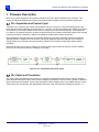
VE2ZAZ’S GPS-DERIVED 10MHZ FREQUENCY STANDARD USER MANUAL Version 1.1 Bertrand Zauhar, VE2ZAZ Gatineau, Québec,Canada Email : Web : http://ve2zaz.net 23/04/2013 Version 1.1 VE2ZAZ’s GPS-REFERENCED 10MHz FREQUENCY STANDARD - USER MANUAL 2 of 32 VE2ZAZ’s GPS-DERIVED 10MHz FREQUENCY STANDARD Change Record Version Date of Release Changes 1.0 November 2005 Initial document release. 1.1 April 2013 Update of email and website addresses Table 1: Change Record USER MANUAL - Version 1.1 3 of 32 VE2ZAZ’s GPS-DERIVED 10MHz FREQUENCY STANDARD Table of Contents 1. INTRODUCTION ........................................................................................................................................................... 6 2. PRINCIPLE OF OPERATION.......................................................................................................................................... 6 EXPECTED PERFORMANCE ......................................................................................................................................... 7 TARGET APPLICATIONS ............................................................................................................................................. 7 ASSUMPTIONS ............................................................................................................................................................ 7 PROJECT UPDATE LOCATION ..................................................................................................................................... 7 HARDWARE DESCRIPTION ...................................................................................................................................... 8 ON-BOARD HARDWARE ............................................................................................................................................ 8 2.1.1 VCXO Frequency acquisition ............................................................................................................................... 8 2.1.2 VCXO Frequency Control .................................................................................................................................... 9 2.1.3 Output References ................................................................................................................................................ 9 2.1.4 FLL Status LED .................................................................................................................................................... 9 2.1.5 Serial Port ............................................................................................................................................................ 9 2.1.6 +5 VDC Voltage Regulator ................................................................................................................................ 10 EXTERNAL HARDWARE ........................................................................................................................................... 10 2.2.1 Voltage Controlled Crystal Oscillator (VCXO) .................................................................................................. 10 2.2.2 GPS Receiver ...................................................................................................................................................... 10 2.2.3 DC Supply........................................................................................................................................................... 10 2.2.4 DAC Filter DC Supply Options .......................................................................................................................... 10 2.2.5 TTL-To-RS232 converter .................................................................................................................................... 10 2.2.6 Personal Computer ............................................................................................................................................. 11 3. SOFTWARE DESCRIPTION ...................................................................................................................................... 12 FLL ACQUISITION AND CONTROL CYCLE ................................................................................................................ 12 FLL STATES AND TRANSITIONS............................................................................................................................... 12 3.2.1 Locked ................................................................................................................................................................ 13 3.2.2 Holdover ............................................................................................................................................................. 13 3.2.3 Unlocked ............................................................................................................................................................. 14 3.2.4 Disabled.............................................................................................................................................................. 14 STATUS/ALARM LED OPERATION ........................................................................................................................... 14 3.3.1 Solid (Foreground) Colors ................................................................................................................................. 14 3.3.2 Flashing (Background) Colors ........................................................................................................................... 15 SERIAL PORT OPERATION ........................................................................................................................................ 15 4. HARDWARE CONFIGURATION ............................................................................................................................. 16 SUB-RATE SELECTION ............................................................................................................................................. 16 VCXO TUNING VOLTAGE RANGE ........................................................................................................................... 16 4.2.1 Filter Stages Supply Bypass ............................................................................................................................... 16 4.2.2 VCXO Tuning Voltage Gain ............................................................................................................................... 16 4.2.3 VCXO -5V Tuning Voltage Support .................................................................................................................... 16 5. SOFTWARE CONFIGURATION AND OPERATION ............................................................................................ 18 POWER UP ................................................................................................................................................................ 18 INITIAL SYSTEM SETUP ............................................................................................................................................ 18 5.2.1 VCXO Tuning Slope Sign Selection .................................................................................................................... 18 5.2.2 Manual Oscillator Tuning .................................................................................................................................. 18 5.2.3 Frequency Averaging Modes .............................................................................................................................. 19 5.2.3.1 5.2.3.2 Sample Summing Mode ............................................................................................................................................... 19 Sample Voting Mode ................................................................................................................................................... 19 USER MANUAL - Version 1.1 4 of 32 VE2ZAZ’s GPS-DERIVED 10MHz FREQUENCY STANDARD 5.2.4 “N”, “L”, “H”, “F” FLL Parameter Settings .................................................................................................. 19 5.2.5 “S” FLL Parameter Setting ............................................................................................................................... 20 5.2.6 Reference Output Control Setting ...................................................................................................................... 20 5.2.7 Alarm Latch Clearing......................................................................................................................................... 21 MAINTENANCE ........................................................................................................................................................ 21 6. SERIAL PORT OUTPUT STRINGS .......................................................................................................................... 22 FLL STATUS STRING .......................................................................................................................................... 22 6.1.1 FLL STATUS ...................................................................................................................................................... 22 6.1.2 ALARM LATCH ................................................................................................................................................. 22 6.1.3 DAC VALUE ...................................................................................................................................................... 23 6.1.4 FREQ.ADJ. SIGN............................................................................................................................................... 23 6.1.5 FINE / COARSE FREQ. ADJ. ............................................................................................................................ 23 6.1.6 FREQ. READOUT ............................................................................................................................................. 23 6.1.7 SAMPLE COUNTER .......................................................................................................................................... 23 6.1.8 ACCUM. FREQ. DIFF....................................................................................................................................... 23 6.1.9 TIMESTAMP ...................................................................................................................................................... 24 6.1.10 HOLDOVER COUNTER ........................................................................................................................... 24 FLL PARAMETER STRING ................................................................................................................................. 24 6.2.1 AVERAGING CYCLE SIZE ................................................................................................................................ 24 6.2.2 COARSE/FINE ADJ. THRESHOLD .................................................................................................................. 24 6.2.3 FLL LOCK LIMIT .............................................................................................................................................. 25 6.2.4 HOLDOVER LIMIT ........................................................................................................................................... 25 6.2.5 HOLDOVER CTR WAIT .................................................................................................................................... 25 6.2.6 FREQ. CHG. NEGATE THRESHOLD .............................................................................................................. 25 6.2.7 REF OUTPUT CTRL MODE ............................................................................................................................. 25 6.2.8 VCXO TUNING SLOPE SIGN ........................................................................................................................... 25 6.2.9 FREQ. AVERAGING MODE ............................................................................................................................. 25 7. SERIAL PORT USER COMMANDS ......................................................................................................................... 27 8. SECIFICATIONS ......................................................................................................................................................... 29 9. BOARD LAYOUT ........................................................................................................................................................ 30 10. CIRCUIT SCHEMATICS ....................................................................................................................................... 31 11. PARTS LIST ............................................................................................................................................................. 32 USER MANUAL - Version 1.1 5 of 32 VE2ZAZ’s GPS-DERIVED 10MHz FREQUENCY STANDARD 1. Introduction This manual provides a detailed description of VE2ZAZ’s GPS-Derived 10MHz Frequency Standard. The advent of Global Positioning System (GPS) has allowed a new approach in time and frequency accuracy. This system exploits the GPS approach. Several commercially available GPS receiving units provide a 1 Pulse-6 per-Second signal. This signal is typically accurate to 1us (1ppm or 1x10 ). By averaging it over a longer period, a much better accuracy can be achieved. This is merely what this project does: Trying to lock an external 10MHz signal source to the 1PPS GPS signal. Other GPS-referenced standards were designed in the past and are extensively documented in magazines and on the Internet. This design differentiates itself from other existing designs: It uses a simpler frequency measurement technique, as opposed to phase measurement, It provides on-board reference buffering and fan-out with 50 ohm output impedance, It provides the three most common reference frequencies of 10MHz, 5 MHz or 1MHz, It provides full software control of the frequency acquisition and control processes; no DIP switches, It has fewer components, does not require an external DAC or external input counter chips, It requires only one supply voltage: +5 VDC (excluding the VCXO supplies). Principle of Operation The system operates a hardware/firmware Frequency-Locked Loop (FLL). In essence, the system compares a local frequency source (an external oscillator) to a GPS-derived reference. It will adjust the local 10MHz variable source to match the GPS-derived 1PPS reference. The 10MHz source is kept aligned with respect the 1Hz GPS reference on a real-time basis by the firmware. The resulting 10MHz reference is fanned out, frequency-divided and provided to the user for higher accuracy applications. System control and monitoring is achieved using a bicolor LED and a serial port connected to a terminal (PC). Figure 1: GPS-Derived 10MHz Frequency Standard USER MANUAL - Version 1.1 6 of 32 VE2ZAZ’s GPS-DERIVED 10MHz FREQUENCY STANDARD Expected Performance -10 Test have shown that this system consistently produces a short-term reference accuracy in the 10 range. This grade of accuracy is much better than most of the standard built-in free-running accuracies seen in commercial test instruments. Of course, due to the experimental nature of this project, accuracy and traceability are not guaranteed. Target Applications The system can be used for the following typical applications: To perform an alignment of frequency counters, RF signal generators and function generators, As a clock source for feeding the external reference input of test instruments, providing a new degree of accuracy to these instruments, As a timebase for a video system (color burst, horizontal scan). Assumptions When consulting this document, the reader should keep the following assumptions in mind: This project was developed for non-commercial applications. In no case should the author be held liable for any event ,behavior or performance issue happening while assembling or using this design. For a better understanding, the user should have a good knowledge of hexadecimal numbering, including the two’s complement form, The user should have a good understanding of electronics fundamentals, including microprocessors, The user should understand the concept of frequency/time accuracy and traceability. Project Update Location Hardware and Firmware design files are available at the author’s Internet website: http://www3.sympatico.ca/b.zauhar USER MANUAL - Version 1.1 7 of 32 VE2ZAZ’s GPS-DERIVED 10MHz FREQUENCY STANDARD 2. Hardware Description This section describes the system hardware from a high level. The various functional hardware blocks are listed below. Figure 2 shows those hardware blocks. Figure 2: VE2ZAZ’s GPS-Derived Frequency Standard Block Diagram On-Board Hardware Please refer to Sections 8 and 9 for the board layout and circuit schematics. 2.1.1 VCXO Frequency acquisition The main operation consists of counting the number of rising edges produced by the 10MHz Voltage Controlled Crystal Oscillator (VCXO) signal over a 16-second period (16 GPS pulses. If the GPS and the VCXO are at the same frequency, exactly 160,000,000 pulses should be counted (+/- 1 pulse, inherent to counter technology). Prior to entering the microcontroller, the 10MHz VCXO signal is buffered and amplified by U1, a receiver chip. The buffered 10MHz signal is fanned out to several locations on the board. R1 is an optional termination and should match the VCXO ouput impedance. U4, the Microchip PIC18F2220 micro-controller, provides an integrated 16-bit counter incremented by an independent external source, the VCXO. The counter value is latched by another external signal rising edge, the GPS 1 PPS signal in our application. This process is totally autonomous and independent from firmware. USER MANUAL - Version 1.1 8 of 32 VE2ZAZ’s GPS-DERIVED 10MHz FREQUENCY STANDARD 2.1.2 VCXO Frequency Control The Microchip PIC18F2220 micro-controller does not have an integrated Digital-to-Analog Converter (DAC). In order to produce an adjustable voltage source to vary the VCXO frequency, the built-in 10-bit Pulse-Width Modulator (PWM) is used instead. A continuous square wave output is produced by the PWM. A downstream external 1Hz 2-stage low-pass filter (U5A, U5B and discrete components) is used to recover the average DC value of the square wave. By varying the duty cycle of this AC signal, it is possible to produce an accurate analog DC voltage. A DAC of 14-bit resolution is achieved by precisely controlling the duty cycle of the PWM output. This translates -12 to a tuning granularity of 6x10 per step for a VCXO that has a one Hertz tuning range. Achieving a 14-bit DAC using a 10-bit PWM requires additional firmware processing. The idea is to “dither” the pulse width within a 16cycle window. Those 16 cycles translate into an additional 4-bit resolution. For example, increasing the 14-bit DAC output by one step involves increasing the 10-bit PWM output width by one increment on one of the 16 pulses. Increasing the DAC by two steps means increasing the 10-bit PWM output width by one increment on two of the 16 pulses, and so on. In order to add flexibility for interfacing with various VCXO’s, the filtering stages have a supply bypass feature that allows you to feed the operational amplifiers with different upper and lower rail voltages. This is done by reconfiguring JP2 and C17. Remember though that the maximum voltage difference between upper and lower rails must be kept at 12V or less. Another feature, the second stage of low-pass filtering, allows for gain addition via R7/R8 if the VCXO operates on a larger tuning voltage range than the more standard 5V range. A 5V offset can also be added to the second stage using jumper JP3. This provides support for VCXO’s that have a -5V to +5V tuning range. Finally, the tuning slope sign can be set in firmware to accommodate both types of VCXO’s. 2.1.3 Output References The system provides up to four 10MHz references. In addition, it provides up to two references with a selectable rate of either 5MHz or 1MHz. These sub-rates are produced by U2, a synchronous counter. The active sub-rate is selected with an on-board jumper JP1. All these references are of 50-ohm output impedance and provide an amplitude of greater than 1V peak-peak with a square wave shape. These signals are provided by U3, a line driver chip. When the firmware feature is enabled, the reference outputs are inhibited when the FLL goes to Unlocked state. This ensures that the user does not use a reference of unknown quality. LED D2 provides an indication of the reference outputs state. 2.1.4 FLL Status LED The system provides basic FLL status and alarm conditions via a single bi-color LED (D1). Being a combined Green-Red LED pair in a single package, it can output three colors: Green, Red and Amber. The latter is produced when both green and red LEDs are simultaneously on. Additionally, the LED unit will flash to provide additional information. The LED control is designed to allow the user to learn about the current and past FLL status in a lapse of a single second. For more detail on the LED color significance refer to section 3.3. 2.1.5 Serial Port Since the FLL status LED only provides basic FLL status and alarm conditions, a serial port is also implemented. The serial port provides comprehensive control and monitoring of the FLL and other firmware features. When interfaced through a TTL-to-RS232 bi-directional converter, the serial port will connect directly to a personal computer. The serial port is ASCII-character-based and provides standard status test strings that can be interpreted and captured by the user. Refer to sections 5and 6 for more information on the serial port. USER MANUAL - Version 1.1 9 of 32 VE2ZAZ’s GPS-DERIVED 10MHz FREQUENCY STANDARD 2.1.6 +5 VDC Voltage Regulator In order to guarantee a “clean” voltage supply to the board, a separate +5 VDC fixed voltage regulator (VR1) is populated. A heatsink is required on the regulator. External Hardware 2.2.1 Voltage Controlled Crystal Oscillator (VCXO) Overall system performance is set to a large degree by the external 10MHz VCXO quality selected on this design. It is recommended that an Oven-Controlled VCXO (OCVCXO) be used to provide better short term stability. This project has been tested and proven with OCVCXO’s that have a 1Hz or a 10Hz tuning range over their entire control voltage. Different tuning slopes may require different firmware parameter settings in order to achieve optimum performance. The user will want to experiment with these. 2.2.2 GPS Receiver The GPS receiver used on this system must have a 1 PPS TTL-compatible output signal clocking on the rising edge of the pulse. Accuracy of this signal will influence overall accuracy of the system. Typical accuracy seen on -6 automotive-type units is in the order of 1microsecond (1x10 ) and this is satisfactory for our application. This design has been tested with the Garmin GPS-35 and the Motorola Oncore GT+ GPS receivers. Both meet the above mentioned accuracy. The Motorola Oncore GT+ GPS unit is actually specified as having a somewhat better accuracy on the 1PPS output. This did not materialize in better overall system accuracy during evaluation. In fact, the second-to-second “jitter” on the 1PPS signal happened to be greater than on the Garmin GPS-35, while still meeting the above specification. This jitter gets averaged out though by the FLL since many frequency samples are taken before making a VCXO frequency correction. For better accuracy, it is recommended to set the GPS unit to Fixed Position (Position Pinning) mode. In this mode, the GPS firmware assumes a fixed location. This translates into a more accurate 1PPS signal. Consult the GPS unit documentation for more details on the how to set the GPS unit in this mode. 2.2.3 DC Supply The external DC supply should meet the voltage range of +7 VDC to +15 VDC. The supply should be able to supply at least 200mA with minimum ripple. 2.2.4 DAC Filter DC Supply Options In order to accommodate VCXOs with different tuning voltage ranges, provision was made on the board to change the tuning high end and low end voltage limits. This can be done by using additional external power supplies. Refer to section 0 for more detail on how to configure the hardware to support various tuning voltage ranges. 2.2.5 TTL-To-RS232 converter This system provides a TTL-level serial I/O port. In order to interface to a standard RS232 port typically seen on a PC, the user will need to use a bi-directional TTL-to-RS232 converter. The converter should be of the inverting type, which is common in TTL-to-RS232 conversion. Converters based on Maxim’s MAX-232 family of chips or using discrete transistors for level translation are suitable for this application. DO NOT CONNECT A RS232 PORT DIRECTLY TO THE BOARD ! USER MANUAL - Version 1.1 10 of 32 VE2ZAZ’s GPS-DERIVED 10MHz FREQUENCY STANDARD 2.2.6 Personal Computer The PC is merely used as a RS232 TTY terminal with logging ability. Being able to capture the FLL status strings as they are sent allows the user to analyze FLL behavior and draw conclusions on the parameter settings. USER MANUAL - Version 1.1 11 of 32 VE2ZAZ’s GPS-DERIVED 10MHz FREQUENCY STANDARD 3. Firmware Description Much of the system is based on the firmware (software) that runs in the PIC18F2220 micro-controller. This section describes the GPS-Derived Frequency Standard system firmware from an operational perspective. FLL Acquisition and Control Cycle A simplified FLL acquisition and control cycle flowchart is shown in Figure 3. The process starts from the left hand side and repeats indefinitely as long as the FLL is enabled. The firmware samples the 10MHz VCXO signal for a duration of 16 seconds. Based on how close the sample is from the nominal frequency, it will update the FLL status. If the sampled frequency is within the specified limits, the firmware will add the sample to the average frequency calculation. Otherwise, it will drop the sample and start another sample acquisition. After updating the average frequency, the firmware verifies if the frequency averaging cycle has reached the specified number of samples. If it has, the DAC output gets updated to reflect the required VCXO frequency change based on the calculated average frequency. Otherwise, the firmware simply starts another sample acquisition. Whenever the DAC output value is changed, a 16-second pause gets inserted to allow the VCXO to stabilize before the next frequency frequency averaging cycle begins. Figure 3: FLL Acquisition and Control Cycle FLL States and Transitions The various states and transitions seen during FLL operation are described in this section. Figure 4 illustrates these states and transitions. Notice that colors are assigned to the states: Green for Locked, Amber for Holdover, Red for Unlocked and Disabled. These colors indicate the relative reliability level of the 10MHz reference output. These colors also correspond to the Status/Alarm LED colors used. LED operation is detailed in section 3.3. USER MANUAL - Version 1.1 12 of 32 VE2ZAZ’s GPS-DERIVED 10MHz FREQUENCY STANDARD Figure 4: FLL States and Transitions Diagram 3.2.1 Locked The Locked FLL state is encountered during normal “stabilized” operation. While in this state, the FLL provides a 10MHz frequency reference “locked” to the GPS 1 Pulse-per-Second (PPS) signal. The FLL will transition to this state: When in Unlocked state, if the averaged 10MHz frequency is measured to be less than the Locked Limit when compared to nominal (ideal) 10Mhz frequency. When in Holdover state, if the measured 10MHz frequency sample is less than the Locked Limit when compared to nominal (ideal) 10Mhz frequency. The FLL will leave this state when the 10MHz frequency sample is measured to be greater than the Holdover Limit when compared to nominal (ideal) 10Mhz frequency. The Locked limit and Holdover limit are parameters set by the user (see section 6: User commands for more detail). 3.2.2 Holdover The Holdover FLL state is encounter when / while the 10MHz frequency sample is measured to be greater than the Holdover Limit when compared to nominal (ideal) 10Mhz frequency. While in holdover, the FLL retains the last valid DAC setting, which holds a constant tuning voltage on the VCXO. This provides a stable free-running frequency reference, while the FLL waits for a valid 10MHz frequency sample. Note that, while in the holdover state, the reference is no longer “locked” to the GPS 1 Pulse-per-Second (PPS) signal. The FLL will leave the holdover state: USER MANUAL - Version 1.1 13 of 32 VE2ZAZ’s GPS-DERIVED 10MHz FREQUENCY STANDARD When the FLL detects that the 10MHz frequency sample is measured to be less than the Locked Limit if compared to nominal (ideal) 10Mhz frequency. In this case, it will transition back to the Locked state, When the Holdover Counter becomes greater or equal to the Holdover Counter Limit parameter. The FLL will transition to the Unlocked state. The Holdover Limit and Holdover Counter Limit are parameters set by the user (see section 6: User commands for more detail). 3.2.3 Unlocked The Unlocked FLL state indicates that the FLL cannot provide a reliable frequency reference “locked” to the GPS 1 Pulse-per-Second (PPS) signal. This state can be explained by one of the following reasons: Unreliable or missing 1 PPS GPS reference, Unreliable or missing 10MHZ VCXO reference, After the holdover period expires, the measured 10MHz frequency sample is still greater than the Holdover Limit when compared to nominal (ideal) 10Mhz frequency. FLL is in the process of acquiring a lock on the 1PPS GPS reference. FLL returns from the Disabled state. Assuming that the FLL is not disabled, it will transition from Unlocked to Locked state when the averaged 10MHz frequency is measured to be less than the Locked Limit when compared to nominal (ideal) 10Mhz frequency. 3.2.4 Disabled The Disabled FLL state is engaged when the user issues a “D” Disable command. In this state, the FLL is disabled; it does not attempt to adjust the DAC output to lock the 10MHz frequency reference “locked” to the GPS 1 Pulse-per-Second (PPS) signal. It merely maintains the current DAC value. While in Disabled state, manual DAC value changes can be performed via the “T” Tune command. The FLL will transition back to Unlocked state and will resume lock acquisition when the user issues an “E” Enable command. See section 6: User commands for more detail. Status/Alarm LED Operation The single multi-color LED displays FLL status and alarm conditions. It is designed to allow the user to learn about the current and past FLL status in a lapse of a single second. This may seem confusing to the user at first, but it is implemented in a very effective and logical manner. The user will quickly learn how to interpret the LED colors. 3.3.1 Solid (Foreground) Colors The following three solid colors indicate the current FLL state: GREEN: AMBER: RED: When the solid color is Green (Green/Flashing-off or Green/Flashing Red), it indicates that the FLL is currently in Locked state When the solid color is Amber (Amber, Amber/Flashing-off or Amber/Flashing Red), it indicates that the FLL is in Holdover state. When the solid color is Red (Red or Red/Flashing-off), this indicates that the FLL is in Unlocked state USER MANUAL - Version 1.1 14 of 32 VE2ZAZ’s GPS-DERIVED 10MHz FREQUENCY STANDARD 3.3.2 Flashing (Background) Colors When the following flashing colors are displayed, it indicates a past alarm condition. The alarm history stays latched and the LED will continue to flash a Red color until the Alarm latch is cleared by the user (see section 6: User commands for more detail). Note that the one pulse-per-second flashing rate is derived from GPS 1 Pulseper-Second (PPS) signal. The LED thus provides valuable information on GPS signal presence. . When the flashing color is off (Green/Flashing-off or Amber/Flashing off), it indicates that no alarms were latched since the last “A” Alarm Clear command was issued. When the flashing color is Red (Green/Flashing-Red or Amber/Flashing Red), it indicates that the FLL has latched an alarm condition since the last “A” Alarm Clear command was issued. When the solid color is Red and the flashing color is off, it indicates that the FLL is in Unlocked state. Since the Unlocked state forces an alarm condition, there is no need to indicate the alarm condition via Red flashing. When no flashing occurs, it indicates a loss of GPS 1 Pulse-per-Second (PPS) signal. FLASHING OFF: FLASHING RED: FLASHING OFF: NO FLASHING: Serial Port Operation The serial port provides comprehensive control and monitoring of the FLL and other firmware features. The port is ASCII-character-based and provides standard status text strings that can be interpreted and captured by the user. The port provides the following features: The FLL Status output string o Current FLL state, o Alarm Latch o Measured Frequency o Frequency adjustment o Event counter FLL Parameter output string o Various FLL limits and thresholds, o 10MHz output control, User commands o Parameter settings, o Firmware version display, o FLL state control, o Firmware Reset For more information on the serial port features, consult sections 4.5 and 6. USER MANUAL - Version 1.1 15 of 32 VE2ZAZ’s GPS-DERIVED 10MHz FREQUENCY STANDARD 4. Hardware Configuration This section provides additional information on setting up the various hardware options on VE2ZAZ’s GPSDerived Frequency Standard. Sub-Rate Selection The user will want to select the sub-rate, either 5MHz or 1MHz, that will be provided at the secondary outputs. This is achieved by installing a computer jumper (or a short piece of wire) in the proper position on JP1. The jumper must be installed so that it shorts out the center pin with either the left pin or right pin. This will select the sub-rate indicated on the jumper marking (5M or 1M). VCXO Tuning Voltage range In order to add flexibility for interfacing with various VCXO’s, several options are provided on the board. 4.2.1 Filter Stages Supply Bypass The filtering stages have a supply bypass feature that allows the user to feed the operational amplifiers with different upper and lower rail voltages.This step is required if the VCXO tuning voltage does not meet the standard 0V to 5V range. This is done by reconfiguring JP2 and C17 as per Table 2 below. Clean external voltage sources must be connected to the pad(s) marked “+Rail” and/or “-Rail” on the board. The “-Rail” source is required only if the tuning voltage is expected to go below ground (0V). The current drawn from these sources is dependent on the VCXO tuning pin current, but is not expected to be more than a few milliamps. The following points must be taken into account when using this option: The upper rail supply voltages must be equal or higher than the expected upper end VCXO tuning voltage. The lower rail supply voltages must be equal or lower than the expected lower end VCXO tuning voltage. The maximum voltage difference between upper and lower rail supplies must be of 12V or less. This limitation is set by the operational amplifiers electrical limits. 4.2.2 VCXO Tuning Voltage Gain The second stage of low-pass filtering allows for gain addition via R7/R8 if the VCXO operates on a larger tuning voltage range than the more standard 5V range. In order to accomplish this, the user must perform the following: o The jumper wire on R8 must be removed o External DC sources must be connected at the marked location(s) on the board. See section 4.2.1 above. o Gain resistors positions R7 and R8 must be populated with the proper resistor values. The equation: Gain= 1+ R8/R7 must correspond to the target gain setting. For example, let us assume that a 0 to 10 V VCXO tuning range is required. Since the available built-in voltage range is 0 to 5V, a gain of two (2) is required. Applying the formula reveals that R7 and R8 should have the same value, say 100Kohms. 4.2.3 VCXO -5V Tuning Voltage Support A -5V offset can also be added to the VCXO tuning range via jumper JP3 on the second filter stage. This provides support for VCXO’s that have a -5V to +5V tuning range. See Table 2 below for JP3 settings. USER MANUAL - Version 1.1 16 of 32 VE2ZAZ’s GPS-DERIVED 10MHz FREQUENCY STANDARD VCXO Tuning Range 0 to +5V # 0 to +8V # 0 to +10V -5V to +5V * R7 Gain setting Leave Open 100K 100K 100K R8 Gain seting Jumper wire 62K 100K 100K C17 - Decoupling Jumper wire Jumper wire Jumper wire 0.1uF JP2 Upper Rail Position A Position B Position B Position A JP3 Offset Leave Open Position A Position A Position B Table 2: Various VCXO Tuning Voltage Range Configurations #: A positive supply greater or equal to the upper tuning limit must be supplied to the +Rail point. *: A negative supply less or equal to the lower tuning limit must be supplied to the –Rail point. USER MANUAL - Version 1.1 17 of 32 VE2ZAZ’s GPS-DERIVED 10MHz FREQUENCY STANDARD Firmware Configuration and Operation This section provides additional information on setting up and operating the VE2ZAZ’s GPS-Derived Frequency Standard firmware. Power up 1. When power is applied to the system board, the microcontroller will start operating following a onesecond delay. This delay allows for the supply voltage to stabilize and provide reliable system operation. 2. The system will display a start-up prompt at the serial port, including firmware version. 3. It will then re-load the previously saved FLL parameter setting from data EEPROM memory. If the microcontroller is powered up for the first time after programming, default parameter values get loaded. 4. The system FLL will start from the Unlocked state and will try acquiring frequency samples automatically. VCXO Frequency adjustments will be made. After a sampling period that may last from minutes to hours, the system will transition to Locked state. Initial System Setup 4.4.1 VCXO Tuning Slope Sign Selection The user must configure the FLL firmware to match with the external VCXO tuning slope sign. When set to positive slope, an increased DAC output voltage will be output when a 10MHz VCXO frequency increase is required. When set to negative slope, a decreased DAC output voltage will be output when a 10MHz VCXO frequency increase is required. If a positive tuning slope VCXO is used, the user should type “X01” (default) at the serial port. Otherwise, a negative tuning slope VCXO is used and the user should type “X02” at the serial port. 4.4.2 Manual Oscillator Tuning The user may want to accelerate the initial acquisition process by manually tuning the FLL closer to the target DAC value that will yield a GPS-to-Oscillator “lock”. This is achieved by zero-beating the 10MHz oscillator to another known-good reference. NIST’s WWV / WWVH or NRC’s CHU shortwave radio stations are good sources to achieve this. Note that the system must have been running for at least 30 minutes before accomplishing this task. This provides enough time for the OCVCXO oven to warm up to a stable temperature. 1. Set the FLL to Disabled state. Type “D” at the serial port. 2. Set the 10MHz output control mode to disabled. Type “O01” at the serial port. 3. Tune in to the 10MHz WWV radio station. Verify that a good signal reception is achieved. 4. Add a short piece of wire to one of the system’s 10MHz reference output connectors. This will act as a transmitting antenna. 5. An heterodyne effect (signal nulling/peaking) should be seen on the radio’s signal meter and be heard on the speaker. Adjust the antenna length and/or position to get a clearly perceived effect. 6. Center the System’s DAC value. Type in the “T0200” command at the serial port. 7. Center the VCXO frequency by means of the mechanical screw (if any) on the VCXO. Try to slow down the signal nulling/peaking rate as much as possible. 8. Manually tune the oscillator (DAC value) to reduce even further the signal nulling/peaking rate. Use the “Tyyzz” command at the serial port, where yyzz is the DAC value in hexadecimal format. 9. Repeat step 8 until the nulling/peaking rate perceived is much better than 1Hz (one null per second). This effectively bring the frequency difference to less than 1Hz. USER MANUAL - Version 1.1 18 of 32 VE2ZAZ’s GPS-DERIVED 10MHz FREQUENCY STANDARD 10. Return the FLL to the Enabled state. Type “E” at the serial port. 11. If desired, re-enable the 10MHz output control mode. Type “O02” at the serial port. 4.4.3 Frequency Averaging Modes Two modes are offered for averaging the 10MHz frequency based on the 16-second samples. The two modes are called Sample Summing mode and Sample Voting Mode. These modes provide two slightly different approaches for the FLL to figure out whether or not a frequency change is required on the VCXO. Both modes -9 yield good accuracy (at least 1x10 ), but the choice of one mode or the other will ultimately impact system accuracy when trying to obtain the highest possible accuracy. 4.4.3.1 Sample Summing Mode This mode operates as follows. Whenever a 16-second frequency sample is taken, the actual sample difference (including sign) from nominal frequency 0x6800 (decimal 26624) is added to the Accumulated Frequency Difference value. So, for example, if two consecutive samples reads 0x6803 and 0x6802, the Accumulated Frequency Difference will be 0x0005. The Sample Summing mode is more effective when the frequency averaging cycle size “S” is smaller, for example 20 (0x0014) samples. This mode will be helpful in acquiring a lock at a faster pace. Tests have also shown that this mode will yield a good accuracy with shorter frequency averaging cycles. For the highest possible accuracy though, the user should select the Sample Voting mode and a longer frequency averaging cycle size. To select this mode, the user should type “M02” at the serial port. 4.4.3.2 Sample Voting Mode This mode acts as follows. Whenever a 16-second frequency sample is taken, the polarity of this frequency difference from nominal frequency 0x6800 is assessed. If the sample is greater than the nominal 0x6800, the Accumulated Frequency Difference value will be incremented by one. If the sample is less than 0x6800, the Accumulated Frequency Difference value will be decremented by one. Obviously, If the sample is equal to 0x6800, no change will be made to the Accumulated Frequency Difference. The Sample Voting mode allows the detection of a trend and is more effective when the frequency averaging cycle size “S” is large, for example greater than 100 (0x0064) samples. This mode will be helpful with GPS units that put out a 1PPS signal with significant second-to-second jitter, as the FLL does not care about the value of the frequency difference, but merely the sign. Tests have also shown that this mode yields the best accuracy. The Sample Voting mode should be used in conjunction with long frequency averaging cycles. To select this mode, the user should type “M01” (default) at the serial port. 4.4.4 “N”, “L”, “H”, “F” FLL Parameter Settings Figure 5 shows the relationship between the various FLL parameters that can be set by the user. These suggested values are typical for a system composed of a Garmin GPS-35 and a 10Hz tuning range VCXO, but different values may yield better FLL stability depending on the GPS receiving unit or the VCXO used. The user will want to experiment with these to optimize the FLL behavior. In general, the more sample-to-sample variability seen on the frequency readout field (see section 5.1.6), the higher the parameter values will have to be for the FLL to filter out this variability and provide a reliable reference. USER MANUAL - Version 1.1 19 of 32 VE2ZAZ’s GPS-DERIVED 10MHz FREQUENCY STANDARD Figure 5: Relationship between Parameter settings In any case, the general constraints listed below should still be met, otherwise erratic operation might occur. Note that value 0x00 is not supported on any of the FLL parameters. In fact, the parameter values are met by the FLL when the measured frequency difference is less than the parameter value. For example, a Locked limit set to 0x01 will allow the FLL to transition from Unlocked to Locked state only when the measured frequency difference is less than 0x01, that is 0x00. o The Frequency Change Negate threshold “N” should be small, typically set to a value of 0x02 or 0x03 (decimal 2 or 3). It should be the smallest in size. If this value is set too large, the FLL will not be able to track the small VCXO frequency drifts. o The Locked Limit “L” should also be set small. This ensures that the FLL transitions to Locked mode only when the GPS signal is truly stable. o The Holdover limit “H” should be set at a value larger than the Locked Limit. This will provide some hysteresis in the Locked-Holdover-Locked transitions. While occasional transitions to the Holdover state are acceptable, repeating events are symptomatic of incorrectly set Holdover Limit parameter or a defective VCXO or GPS. o The Coarse/Fine Frequency Change threshold “F” should be set as the largest value, typically larger that the Holdover limit. This will force the FLL to only make fine DAC (frequency) adjustments while in Locked state. 4.4.5 “S” FLL Parameter Setting The GPS 1PPS signal has a relatively poor short term accuracy compared to the accuracy this system can achieve. In order to cancel out this short term “noise”, several frequency samples are taken in a frequency averaging cycle by the firmware before making a VCXO adjustment. With regards to the frequency averaging cycle size “S” parameter, it can be stated that the more samples the system takes for averaging, the more accurate the frequency measurement will be. This ultimately has an impact on how meaningful the frequency adjustments will be while trying to match the “real frequency”. Experiments have shown that, on the setup used by the author, a cycle size “S” of 0x0200 (512 samples) yielded the expected accuracy with the Garmin GPS-35 receiver. This was accomplished in Sample Voting mode (see section 4.4.3.2). Obviously, there is a trade-off between expected accuracy and cycle duration. The user will want to experiment with the S parameter to find the best compromise between sampling size and accuracy. During initial setup, the user may want to reduce the Average Sample Size “S” parameter to accelerate frequency acquisition. A value of 0x000A (10 samples) is suggested. Once the system is in Locked state and stabilized, the user may increase S to a larger value, such as the one mentioned above. 4.4.6 Reference Output Control Setting The user will want to set up the 10MHz Reference output disabling mode. If output disabling is on, the 10MHz outputs will be disabled whenever the FLL is unlocked. The outputs will put out a signal only when the FLL is in USER MANUAL - Version 1.1 20 of 32 VE2ZAZ’s GPS-DERIVED 10MHz FREQUENCY STANDARD locked or in holdover state. If output disabling is off, the 10MHz outputs will always be active, regardless of the FLL state. The user should type “O01” (default) at the serial port to turn off output control. The user will type “O02” at the serial port to turn on output control. 4.4.7 Alarm Latch Clearing After initial acquisition or whenever a major system disturbance occurs, the alarm latch field will show an alarm and the LED will flash with a red color. To clear the alarm latch, the user will type “A” at the serial port. Maintenance Once the system is set up correctly, little user intervention is required. The user will still want to monitor the alarms via the LED for any critical event, such as: o FLL DAC value railing to the top or bottom voltage rail. When this occurs, the user should access the mechanical frequency adjustment screw on the VCXO and re-center 10MHz frequency. Section 4.4.2 should be performed to achieve this. o FLL going unlocked due to excessive holdover period. While occasional transitions to the Holdover state are acceptable, repeating events are symptomatic of incorrectly set Holdover Limit parameter or a defective VCXO or GPS. USER MANUAL - Version 1.1 21 of 32 VE2ZAZ’s GPS-DERIVED 10MHz FREQUENCY STANDARD 5. Serial Port Output Strings In order to inform the user of the status and settings of the FLL, the firmware sends two distinct strings of information. The strings are sent at a rate of 4800 baud, with 8 bits, one stop bit, no parity, no flow control. All commands are followed by a carriage return and a line feed. All numerical values are expressed in hexadecimal format. These strings are listed and detailed in the sub-sections below. FLL STATUS STRING This string is sent every 16 seconds to report frequency sampling results and FLL status. A typical string is shown below. String : L | U | 01FF6 | + | F | 67FC | 0120 | FFFD | 007D | 03 HOLDOVER COUNTER TIMESTAMP ACCUM. FREQ. DIFF. SAMPLE COUNTER FREQ. READOUT FINE / COARSE FREQ. ADJ. FREQ.ADJ. SIGN DAC VALUE 5.1.1 ALARM LATCH FLL STATUS Definition: FLL STATUS This field provides real-time status of the FLL. The following characters may be displayed: L Indicates that the FLL is in locked state. U Indicates that the FLL is in unlocked state. H Indicates that the FLL is in holdover state. D Indicates that the FLL is in disabled (manual) state. 5.1.2 ALARM LATCH This field provides a latched status of the FLL alarms. Any occurrence of an alarm will stay latched in this field until the “A” alarm clear command is issued (see section 6). The following characters may be displayed: U Indicates that the FLL went in Unlocked state at one point in time. B Indicates that the FLL reached the minimum tuning limit (bottom voltage rail) at one point in time. T Indicates that the FLL reached the maximum tuning limit (top voltage rail) at one point in time. H Indicates that the FLL reached the holdover counter limit and went into unlocked state at one point in time. . Indicates that no alarms were latched since the last alarm clear command. USER MANUAL - Version 1.1 22 of 32 VE2ZAZ’s GPS-DERIVED 10MHz FREQUENCY STANDARD 5.1.3 DAC VALUE This field displays the current DAC value setting the VCXO tuning voltage. Range is 14 bits expressed in hexadecimal from 0x00000 to 0x03FFF (0 to 16383 in decimal). 5.1.4 FREQ.ADJ. SIGN This field indicates the direction of frequency adjustment computed at the end of a frequency averaging cycle. The following characters may be displayed: + = . 5.1.5 Indicates that the FLL is increasing the frequency as a result of averaging. Indicates that the FLL is decreasing the frequency as a result of averaging. Indicates that no frequency change is required by the FLL as a result of averaging. Indicates that the FLL is currently in a frequency averaging cycle and is not updating the frequency. FINE / COARSE FREQ. ADJ. This field indicates the size of DAC adjustment (frequency change). The following characters may be displayed: C Indicates that the FLL is changing the frequency via its DAC value by a step of 16. This is called a Coarse adjustment. F Indicates that the FLL is changing the frequency via its DAC value by a step of 1. This is called a Fine adjustment. . Indicates that the FLL is currently in a frequency averaging cycle and is not updating the frequency. 5.1.6 FREQ. READOUT This field displays the current sampled frequency. Nominal value is 0x6800 (decimal 26624), which indicates that, during the 16-second sampling window, the counter measured exactly 160 000 000 pulses (10MHz x 16secs). 5.1.7 SAMPLE COUNTER This field displays the current 16-second averaging sample counter value. This value is compared to the Averaging Sample Size parameter (see section 5.2). When the two values match, the frequency averaging cycle ends and a DAC update (frequency change) is performed based on the accumulated frequency difference. 5.1.8 ACCUM. FREQ. DIFF. This field displays the current accumulated frequency difference. This value is analyzed at the end of the averaging cycle to determine the direction and size of DAC value adjustment. The field will behave differently depending on what Averaging mode the FLL is set to. This value is expressed in two’s complement hexadecimal. When in Sample Summing mode, this value is calculated by adding and substracting frequency offsets from the nominal 0x6800 at each sample. For example, if the first frequency sample shows 0x6801, the accumulated frequency difference will show 0x0001 (+1 in decimal). Then, if the second frequency sample shows 0x67FD, the accumulated frequency difference will show 0xFFFE (-2 in decimal). When in Sample Voting mode, this value is incremented or decremented by one step based on the frequency offset polarity from the nominal 0x6800 at each sample. For example, if the first frequency sample shows 0x6803, the accumulated frequency difference will show 0x0001 (+1 in decimal). Then, if the second frequency sample shows 0x67FF, the accumulated frequency difference will show 0x0000 (0 in decimal). USER MANUAL - Version 1.1 23 of 32 VE2ZAZ’s GPS-DERIVED 10MHz FREQUENCY STANDARD 5.1.9 TIMESTAMP This field provides a 16-bit sequential counter. This value is provided for tracking/logging purpose and is not involved in FLL functionality. The value of this counter is incremented once every 16 seconds. This value will roll over to 0x0000 when the 16-bit limit is reached. 5.1.10 HOLDOVER COUNTER This field displays the holdover counter value. This counter increments once at each frequency sample (once every 16 seconds) whenever the FLL is in holdover state. This counter value is compared to the Holdover Counter Wait parameter (see section 5.2). When the two values match, the holdover period ends and the FLL switches to unlocked state. This will force a re-acquisition of frequency lock and induce frequency changes. FLL PARAMETER STRING This string is sent every time a parameter is changed using a user command to confirm that the parameter got updated. As well, this string is sent when the “P” parameter user command is issued. See section 6 for more details on the user commands. A typical string is shown below. String: FREQ. AVERAGING MODE VALUE FREQ. AVERAGING MODE VCXO TUNING SLOPE SIGN VALUE VCXO TUNING SLOPE SIGN REF OUTPUT CTRL MODE VALUE REF OUTPUT CTRL MODE FREQ. CHG. NEGATE THRESHOLD FREQ. CHG. NEGATE HOLDOVER CTR WAIT VALUE HOLDOVER CTR WAIT HOLDOVER LIMIT VALUE HOLDOVER LIMIT FLL LOCK LIMIT VALUE FLL LOCK LIMIT COARSE ADJ. THRESHOLD VALUE COARSE/FINE ADJ. THRESHOLD AVERAGING CYCLE SIZE VALUE 5.2.1 AVERAGING CYCLE SIZE Definition: S 0128 | F 08 | L 04 | H 08 | W C8 | N 03 | O 02 | X 01 | M 01 AVERAGING CYCLE SIZE This parameter is labeled with letter S and displays the frequency averaging cycle size that the FLL uses to calculate average frequency. Value ranges from 0x0001 to 0xFFFF (1 to 65535 in decimal). Each increment of one represents a 16-second increase in the frequency averaging cycle. 5.2.2 COARSE/FINE ADJ. THRESHOLD This parameter is labeled with letter F and displays the Coarse/Fine DAC adjustment threshold value. Whenever a frequency change occurs, the accumulated frequency difference is compared against this parameter. If the accumulated frequency difference is greater or equal to this parameter, a coarse DAC change will occur, otherwise a fine DAC change will occur. Value ranges from 0x01 to 0xFF (0 to 255 in decimal). USER MANUAL - Version 1.1 24 of 32 VE2ZAZ’s GPS-DERIVED 10MHz FREQUENCY STANDARD 5.2.3 FLL LOCK LIMIT This parameter is labeled with letter L and displays the FLL Locked state limit value. This parameter is used when in Unlocked state. After a frequency averaging cycle is completed, the absolute accumulated frequency difference is compared to the nominal frequency (0x6800). If the absolute difference is less than this parameter, the FLL will enter Locked state. Otherwise, it stays in unlocked state. Value ranges from 0x01 to 0xFF (0 to 255 in decimal). This parameter is also used when in Holdover state. Whenever a frequency sample is taken, the frequency reading is compared to the nominal frequency (0x6800). If the absolute difference is less than this parameter, the FLL will revert back Locked state. Otherwise, it will stay in Holdover state. Normally, the Locked Limit parameter is set smaller than the Holdover Limit parameter. This provides a more reliable re-entry into Locked state as it verifies that any disturbances that caused the FLL to transition to Holdover are over. 5.2.4 HOLDOVER LIMIT This parameter is labeled with letter H and displays the FLL Holdover limit threshold value. Whenever a frequency sample is taken, the frequency reading is compared to the nominal frequency (0x6800). If the absolute difference is greater or equal to this parameter, the FLL will enter holdover state. Otherwise, it stays in locked state. Value ranges from 0x01 to 0xFF (0 to 255 in decimal). 5.2.5 HOLDOVER CTR WAIT This parameter is labeled with letter W and displays the Holdover Counter Wait value. Whenever the FLL is in holdover state, this value increase once every frequency sample. If the Holdover Counter becomes greater or equal to this parameter, the FLL will leave holdover state and will enter unlocked state. This counter resets when the FLL enters the holdover state. Value ranges from 0x01 to 0xFF (0 to 255 in decimal). 5.2.6 FREQ. CHG. NEGATE THRESHOLD This parameter is labeled with letter N and displays the Frequency Change Negate threshold value. Whenever the FLL is about to make a DAC value change, the absolute accumulated frequency difference is compared against this parameter. If the accumulated frequency difference is smaller than this parameter, the DAC value change will be negated (will not occur). Otherwise, the DAC value change will proceed. Value ranges from 0x01 to 0xFF (0 to 255 in decimal). 5.2.7 REF OUTPUT CTRL MODE This parameter is labeled with letter O and displays the Reference output disabling mode. If output disabling is on, the PIC microcontroller reference control pin (12) will go low to disable the 10MHz outputs whenever the FLL is unlocked. Pin (12) will go high whenever the FLL is locked. If output disabling is off, the 10MHz reference control pin will always be set high, regardless of the FLL state. Value ranges from 0x01 (control off) to 0x02 (control on). 5.2.8 VCXO TUNING SLOPE SIGN This parameter is labeled with letter X and displays the VCXO frequency Tuning Slope Sign mode. When set to positive slope, an increased DAC output voltage will be output when a 10MHz VCXO frequency increase is required. When set to negative slope, a decreased DAC output voltage will be output when a 10MHz VCXO frequency increase is required. Value ranges from 0x01 (positive slope) to 0x02 (negative slope). 5.2.9 FREQ. AVERAGING MODE This parameter is labeled with letter M and displays the FLL Frequency Averaging mode. When M is set to Sample Summing mode, the Accumulated Frequency difference is calculated by adding and substracting frequency offsets from the nominal 0x6800 at each sample. When in Sample Voting mode, the Accumulated Frequency difference is incremented or decremented by one based on sample offset polarity. Value ranges from USER MANUAL - Version 1.1 25 of 32 VE2ZAZ’s GPS-DERIVED 10MHz FREQUENCY STANDARD 0x01 (Voting mode) to 0x02 (Summing mode). For more detail on the Frequency Averaging modes, refer to sections 4.4.3 and 5.1.8. USER MANUAL - Version 1.1 26 of 32 VE2ZAZ’s GPS-DERIVED 10MHz FREQUENCY STANDARD 6. Serial Port User Commands The user interacts with the firmware using Serial Port commands. These commands provide control over several FLL parameters as well as overall FLL firmware status. The following requirements must be met: All commands must be sent at a rate of 4800 baud, with 8 bits, one stop bit, no parity, no flow control. All numeric values must be expressed in hexadecimal. Value ranges are provided in the table below. All alphabetic characters must be entered in uppercase, for example “T01FE”, otherwise the command will not be interpreted by firmware. All commands must be followed by a carriage return and a line feed <CR><LF>, otherwise the command will not be interpreted by firmware or may lead to erroneous entry. Finally, hexadecimal value 0x00 is not allowed in any of the serial port user commands listed as accepting parameter value xx. The following table lists all supported commands. ? Sends the Menu of User Commands string to the serial port. A Clears any latched alarms. C Clears the sample counter. D Disables FLL and enables Manual state. E Enables FLL and disables Manual state. Fxx Sets the Fine/Coarse DAC adjustment threshold parameter to hexadecimal xx. Allowed xx value range is 0x01 to 0xFF (8 bits). Firmware will send the FLL parameter string as a result of this command. Hxx Sets the Holdover Counter threshold parameter to hexadecimal xx. Allowed xx value range is 0x01 to 0xFF (8 bits). Firmware will send the FLL parameter string as a result of this command. Lxx Sets the Lock Limit parameter to hexadecimal xx. . Allowed xx value range is 0x01 to 0xFF (8 bits). Firmware will send the FLL parameter string as a result of this command. Mxx Sets Frequency Averaging mode. Allowed xx value ranges from 0x01 (Sample Voting mode) or 0x02 (Sample Summing mode). Firmware will send the FLL parameter string as a result of this command. Nxx Sets the Frequency Change Negate threshold parameter to hexadecimal xx. Allowed xx value range is 0x01 to 0xFF (8 bits). Firmware will send the FLL parameter string as a result of this command. Oxx Sets the reference output control pin mode. When turned on, PIC microcontroller pin 12 will go low to disable the reference outputs whenever the FLL is unlocked. Pin 12 will go high whenever the FLL is locked. When mode is turned off, the reference output control pin will always be set high, regardless of the FLL state. Allowed xx value ranges from 0x01 (control off) or 0x02 (control on). USER MANUAL - Version 1.1 27 of 32 VE2ZAZ’s GPS-DERIVED 10MHz FREQUENCY STANDARD P Sends the FLL parameter string to the serial port. R Soft Reset of the Microprocessor. From a firmware perspective, this is equivalent to a power down/up cycle. Syyzz Sets the frequency averaging cycle size parameter to hexadecimal yyzz (number of 16second samples averaged before adjusting DAC. Allowed yyzz value range is is 0x0001 to 0xFFFF (16 bits). Firmware will send the FLL parameter string as a result of this command. Tyyzz Tunes the DAC to hexadecimal value yyzz. Only applicable when the FLL is in Disabled State. Allowed yyzz value range is 0x0000 to 0x03FF (10 bits). This “Tune” DAC value change corresponds to a Coarse DAC adjustment. Fine DAC adjustments (least significant digit) are not supported in Disabled state. V Sends the firmware version information to the serial port. Wxx Sets the Holdover Counter Wait parameter to hexadecimal xx. Allowed xx value range is 0x01 to 0xFF (8 bits). Firmware will send the FLL parameter string as a result of this command. Xxx Sets the VCXO tuning slope mode. Allowed xx value ranges from 0x01 (positive) or 0x02 (negative). USER MANUAL - Version 1.1 28 of 32 VE2ZAZ’s GPS-DERIVED 10MHz FREQUENCY STANDARD 7. Secifications FREQUENCY ACQUISITION Expected 10MHz VCXO Frequency Range: Centered to 10.0000MHz, from 1Hz to 10Hz end-to-end tuning range with positive or negative slope. Other ranges may operate properly. User to experiment. 10MHz VCXO Input Amplitude Range: Minimum 100mV peak-peak. Maximum 5V peak-peak. GPS 1PPS Input: TTL levels, clocking on the rising edge, 1Hz. FREQUENCY CONTROL VCXO Tuning Voltage Output: Nominally 0 to +5 VDC, 14-bit resolution, monotonic, positive or negative tuning slope (slope configurable in firmware). Output slope gain, lower rail and upper rail voltage limits can be changed on the board using an external supply and/or by substituting resistors and moving jumper wires (see text). Maximum upperto-lower rail voltage difference is 12 VDC. Reference Outputs : 10MHz, 5MHz or 1MHz, Greater than 1V peak-to-peak, AC-coupled, square wave shape. GENERAL Serial Port: Format: 4800baud, with 8 bits, one stop bit, no parity, no flow control. TTL-Levels for Inputs and Outputs. For RS-232C support, a level converter (inverting type) is required. Microprocessor: Microchip PIC18F2220, DIP28 package. Clock speed: 8MHz, Instruction cycle frequency 2MHz. Supply Voltage: +7 VDC to +15 VDC, regulated on board down to +5 VDC. Supply Current: Less than 200 mADC, excluding GPS unit and VCXO supplies. USER MANUAL - Version 1.1 29 of 32 VE2ZAZ’s GPS-DERIVED 10MHz FREQUENCY STANDARD 8. Board Layout Figure 6: The board’s component layout USER MANUAL - Version 1.1 30 of 32 VE2ZAZ’s GPS-DERIVED 10MHz FREQUENCY STANDARD 9. Circuit Schematics Figure 7: The System’s Circuit Schematics USER MANUAL - Version 1.1 31 of 32 VE2ZAZ’s GPS-DERIVED 10MHz FREQUENCY STANDARD 10. Parts List Reference Description Part Number C1-C5, C9-C16 0.1uF, 10V or higher, radial Digikey: 478-2472-ND or equiv. C17 Piece of wire for a 0-5V VCXO tuning range. 0.1uF, 10V or higher, radial for some other ranges. See section 4.2. Digikey: 478-2472-ND or equiv. C6, C7 1uF, 10V or higher, radial Digikey: 478-2479-ND or equiv. C8 10uF, electrolytic, 25V of higher Digikey: P1176-ND or equiv. D1 Bi-color (Green-Red) LED, two leads. Digikey: MV6461A-ND or equiv. D2 Green LED Digikey: MV5477C-ND or equiv. JP1 1x3 Header, 0.1 inch spacing, One computer jumper required. Digikey: S1012-36-ND. Cut to size, or equiv. JP2 Piece of wire. Selects upper operational amplifier rail. See section 4.2. JP3 Piece of wire. See section 4.2. R1 51 ohm, 1/4W, axial. Optional. See text. R2,R6 47K, 1/4W, axial Digikey: P47KBACT-ND or equiv. R3, R9 470 Ohms, 1/4W, axial Digikey: P470BACT-ND or equiv. R4, R5 100K, 1/4W, axial Digikey: P100KBACT-ND or equiv. R7 Optional, do not populate for a 0-5V VCXO tuning range See section 4.2. R8 Piece of wire for a 0-5V VCXO tuning range. See section 4.2. U1 Linear Technology LTC1485, DIP-8 package Digikey: LTC1485CN8-ND U2 74HC390, DIP-16 package Digikey: 296-9199-5-ND U3 MC3487, DIP-16 package Digikey: 296-1408-5-ND U4 U5 Microchip PIC18F2220, DIP-28/0.3” package, programmed part Texas Instruments OPA2705, DIP-8 package Digikey: P51BACT-ND or equiv. Digikey: PIC18F2220-I/SP-ND Digikey: OPA2705PA-ND VR1 7805 Voltage Regulator, TO-220 package Sockets for U1, U5 IC Socket, 8-pin, 0.3” spacing, low profile, optional Digikey: ED3108-ND or equiv. Sockets for U2, U3 IC Socket, 16-pin, 0.3” spacing, low profile, optional Digikey: ED3116-ND or equiv. Socket for U4 IC Socket, 28-pin, 0.3” spacing, low profile, recommended Digikey: ED3128-ND or equiv. Heatsink for VR1 TO-220 Compact Heatsink, recommended Digikey: HS107-ND or equiv. USER MANUAL - Version 1.1 32 of 32 Digikey: LM7805CT-ND