1
CC2543/44/45 Development
Kits User’s Guide
swru318
swru318
Table of contents
CC2543/44/45 DEVELOPMENT KITS USER’S GUIDE ................................................................................. 1
1
ACRONYMS ............................................................................................................................................. 3
2
INTRODUCTION ..................................................................................................................................... 4
3
ABOUT THIS MANUAL ......................................................................................................................... 4
4
DEVELOPMENT KIT CONTENTS ...................................................................................................... 6
4.1
CC2543-CC2544DK ................................................................................................................................... 6
4.2
CC2545EMK .............................................................................................................................................. 8
5
GETTING STARTED .............................................................................................................................. 9
5.1
SETTING UP THE HARDWARE ........................................................................................................................ 9
5.2
RUNNING THE PREPROGRAMMED PACKET ERROR RATE TEST................................................................... 10
5.2.1
5.2.2
5.2.3
5.2.4
5.2.5
Introduction ...................................................................................................................................................................................... 10
Program Flow ................................................................................................................................................................................... 11
Set Up the CC254x Proprietary Mode Packet Error Rate Test ......................................................................................................... 15
CC254x Proprietary Mode Packet Error Rate Test Source Code ..................................................................................................... 15
Evaluate the CC2543/44/45 Radio using SmartRF Studio ................................................................................................................ 16
SETTING UP THE SOFTWARE DEVELOPMENT ENVIRONMENT ..................................................................... 18
5.3
6
RF TESTING........................................................................................................................................... 19
6.1
TX PARAMETER TESTING BASICS .............................................................................................................. 19
6.2
RX PARAMETER TESTING BASICS.............................................................................................................. 20
7
CC2543EM .............................................................................................................................................. 21
8
CC2545EM .............................................................................................................................................. 22
9
CC2544 USB DONGLE .......................................................................................................................... 23
10
SMARTRF05 EVALUATION BOARD ................................................................................................ 25
11
FREQUENTLY ASKED QUESTIONS ................................................................................................ 26
12
REFERENCES ........................................................................................................................................ 29
13
DOCUMENT HISTORY ........................................................................................................................ 29
APPENDIX A
SETTING UP THE SOFTWARE ENVIRONMENT ...................................................... 30
A.1
CREATE THE PROJECT ................................................................................................................................ 30
A.2
PROJECT OPTIONS ...................................................................................................................................... 31
A.3
SELECT DEVICE ......................................................................................................................................... 31
A.4
SELECT CODE AND DATA MODEL .............................................................................................................. 32
A.5
CONFIGURE THE LINKER ............................................................................................................................ 33
A.6
CONFIGURE THE DEBUGGER ...................................................................................................................... 34
A.7
WRITE SOFTWARE ..................................................................................................................................... 35
A.8
COMPILE AND DEBUG ................................................................................................................................ 36
A.9
DONE! ........................................................................................................................................................ 36
APPENDIX B
SCHEMATICS AND LAYOUT ........................................................................................ 37
2/37
swru318
1
Acronyms
DK
EB
EM
EMK
HID
IC
KB
LCD
LED
LPRF
MCU
NC
PER
RF
RX
SoC
TI
TX
UART
USB
MHz
Development Kit
Evaluation Board
Evaluation Module
Evaluation Module Kit
Human Interface Device
Integrated Circuit
Kilo Byte (1024 byte)
Liquid Crystal Display
Light Emitting Diode
Low Power RF
Micro Controller
Not connected
Packet Error Rate
Radio Frequency
Receive
System on Chip
Texas Instruments
Transmit
Universal Asynchronous Receive Transmit
Universal Serial Bus
Mega Hertz
3/37
swru318
2
Introduction
Thank you for purchasing a CC254x Development Kit. The current development kits in the CC254x
family described here are the CC2543-CC2544DK, the CC2545EMK and the CC2541EMK. The
Evaluation Module Kits (EMK) are supplementary to the CC2543-CC2544DK as they only consist of
two single Evaluation Modules (EM).
The CC2543, CC2544 and CC2545 devices are RF SoCs designated for the proprietary 2.4 GHz RF
market that can be used in any application, but are tailored for wireless HID applications. The CC2544
is tailored for the USB dongles, the CC2543 for peripheral devices such as wireless mouse
applications and the CC2545 for wireless keyboard applications.
The single-chip RF transceiver and MCU supports data rates up to 2Mbps, and has extensive
baseband automation, including auto-acknowledgement and address decoding. It provides excellent
link budget with programmable output power up to +5 dBm, which enables long range without external
front-ends.
The CC2543, CC2544 and CC2545 devices come with a two-channel DMA which reduces the need of
the MCU operating in active mode, hence significantly improves power consumption. In addition they
have one 16-bit and two 8-bit timers and 20mA drive strength on selected general purpose I/O pins.
They also have a 40-bit radio timer used by the Link Layer Engine.
The on-chip voltage regulator supports a wide range of supply voltages, and the CC2544 has a USB
5V to 3.3V regulator. The on-chip MCU is the High-Performance and Low-Power 8051 Microcontroller
with Code Prefetch.
The CC2544 has full speed USB support with 6 endpoints, separate 1kB FIFO memory, internal pullup and 5V to 3.3V regulator.
The CC2543 [1], CC2544 [2] and CC2545 [3] product folders on the web have more information, with
datasheets, user guides and application notes.
The CC2543-CC2544 Development Kit includes all the necessary hardware to properly evaluate,
demonstrate, prototype and develop software for proprietary applications
3
About this manual
This manual describes all the hardware included in the CC2543-CC2544 Development Kit (CC2543CC2544DK), the CC2545 Evaluation Module Kit (CC2545EMK) and points the user to other useful
information sources.
The CC2541 Evaluation Module Kit (CC2541EMK) is also compatible in similar fashion as the
CC2545EMK. The CC2541 device has two different modes of operation called “BlueTooth Low Energy
Mode” and “Proprietary Mode”. This user guide only covers the “proprietary Mode” of operation and it
does not detail the HW and specific details of the CC2541. The CC2541 has more system resources
available (256kB FLASH and 8kB RAM size to mention some). Proprietary applications that require
more system resources than what the CC2543/44/45 can offer might want to consider using the
CC2541. For more information about the CC2541 and the CC2541EMK please visit the product folder
page on web and the CC2541EMK web page.
Chapter 4 briefly describes the contents of the development kits and chapter 5 gives a quick
introduction to how to get started with the kit. In particular, it describes how to install SmartRF Studio
to get the required drivers for the evaluation board, how the hardware can be used, and lists the
software that is available for the development kit. Chapter 6 explains some simple methods for
performing practical RF testing with the development kit. Chapter 7, 8, and 10 describe the hardware
in the kit and where to find more information about how to use it. A troubleshooting guide can be found
in chapter 11.
4/37
swru318
Appendix A gives a detailed description of how to set up the software development environment for
the CC2543, CC2544 and CC2545.
The CC2543-CC2544DK Quick Start Guide [6] has a short tutorial on how to get started with the main
kit. The CC2545EMK also has a similar Quick Start Guide available on web [7].
The PC tools SmartRF Studio and SmartRF Flash Programmer have their own user manuals.
Please visit the CC2543-CC2544DK web page [4], CC2545EMK web page [5] and CC2543 [1],
CC2544 [2] and CC2545 [3] product pages for additional information. Further information can be found
on the TI LPRF Online Community [10].
See chapter 12 for a list of relevant documents and links.
5/37
swru318
4
4.1
Development Kit contents
CC2543-CC2544DK
The CC2543-CC2544 Development Kit (CC2543-CC2544DK) includes hardware and software that
allows quick testing of the CC2543 and CC2544 RF performance and offers a complete platform for
development of advanced prototype RF systems.
Evaluate the CC2543 and the CC2544 right out of the box. The kit can be used for range testing
using the pre-programmed PER test application running on the two devices.
Use SmartRF Studio to perform RF measurements. The radio can be easily configured to
measure sensitivity, output power and other RF parameters.
Prototype development. All I/O pins from the CC2543 are available on pin connectors on the
SmartRF05EB, allowing easy interconnection to peripherals on the EB board or other external
sensors and devices.
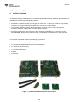
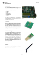
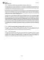
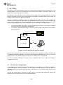
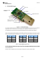
The CC2543-CC2544DK contains the following components
2 x SmartRF05EB (the two large boards)
2 x CC2543 Evaluation Modules (the two small boards)
2 x Antennas (Pulse W1010)
1 x CC2544 USB Dongle
Cables
Documents
Figure 1 - CC2543-CC2544 Development Kit Contents.
6/37
swru318
SmartRF05EB
The SmartRF05EB (evaluation board) is the
main board in the kit with a wide range of user
interfaces:
3x16 character serial LCD
Full speed USB 2.0 interface
UART
LEDs
Serial Flash
Potentiometer
Joystick
Buttons
The EB is the platform for the evaluation
modules (EM) and can be connected to the PC
via USB to control the EM.
CC2543EM
The CC2543EM (evaluation module) contains
the RF IC and necessary external components
and matching filters for getting the most out of
the radio. The module can be plugged into the
SmartRF05EB. Use the EM as reference
design for RF layout. The links for schematic
and layout files can be found in Appendix B.
CC2544 USB Dongle
The CC2544 USB Dongle is a fully operational
USB device that can be plugged into a PC.
The Dongle is however not compatible with the
SmartRF Protocol Packet Sniffer. The dongle
has 2 LEDs, two small push-buttons and
connector holes that allow connection of
external sensors or devices. The dongle also
has a connector for programming and
debugging of the CC2544 USB controller. The
links for schematic and layout files can be
found in Appendix B.
Antenna
The antenna, W1010 from Pulse, is a ¼ wave
dipole antenna with 2 dBi gain.
7/37
swru318
4.2
CC2545EMK
The CC2545 Evaluation Module Kit (CC2545EMK) is an add-on module to the CC2543-CC2544DK
and the latter must be acquired to be able to use the CC2545EM in the same manner as the
CC2543EM.
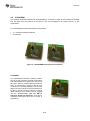
The CC2545EMK contains the following components
2 x CC2545 Evaluation Modules
Documents
Figure 2 - CC2545EMK Development Kit Contents.
CC2545EM
The CC2545EM (evaluation module) contains
the RF IC and necessary external components
and matching filters for getting the most out of
the radio. There is a PCB antenna (Inverted F)
which is connected by default to the RF pins
on the device. It is also possible to connect the
SMA connector instead of the PCB antenna to
be able to connect another antenna or coaxial
cable if desired. The module can be plugged
into the SmartRF05EB. Use the EM as
reference design for RF layout. The links for
schematic and layout files can be found in
Appendix B.
8/37
swru318
5
Getting started
5.1
Setting up the hardware
After opening the kit, make sure you have all components. Please contact your TI Sales
Representative or TI Support [9] if anything is missing.
Start by connecting the antennas to the SMA connector on the RF evaluation boards. Tighten the
antenna’s screw firmly on to the SMA connector. If not properly connected, you might get reduced RF
performance. It is also possible to connect the EM board to RF instruments via coax cables. The EM is
designed to match a 50 Ohm load at the SMA connector.
Next, the evaluation modules should be plugged in to the SmartRF05EB. Make sure to set the switch
P19 to “SOC/TRX” (right position). The purpose of the SmartRF05EB is to serve as a general I/O
board for testing of the various peripherals of the CC2543/45 microcontroller. The EB also contains a
separate USB controller, which is used as a bridge between the PC and the CC2543/44/45 for
programming the flash of these devices. It is also used for debugging the software running on the
devices.
The evaluation board can be powered from several different sources:
2 x 1.5V AA Non-rechargeable alkaline batteries
USB (via the USB connector)
DC power (4 to 10 Volt) (not included in this kit)
External regulated power source (not included in this kit)
The power source can be selected using jumper P11 on the SmartRF05EB. The SmartRF05EB User’s
Guide [11] provides more details.
After assembling the hardware, you now have several options for working with the CC2543/44/45:
Run the packet error rate (PER) test which is preprogrammed on the CC2543/44/45. The
PER test is a quick way to evaluate the range which can be achieved with the radio. Chapter
5.2 will guide you through the PER test.
Evaluate and explore the RF capabilities of the CC2543/44/45 using SmartRF Studio.
Chapter 5.2.5 provides the details how to do so.
Developing software for the CC2543/44/45. Install IAR Embedded Workbench for 8051 and
set up your first software project. Chapter 5.3 explains how.
9/37
swru318
5.2
Running the Preprogrammed Packet Error Rate Test
5.2.1
Introduction
The CC2543EM, CC2545EM and CC2544Dongle come pre-programmed with a Packet Error Rate
(PER) test application. The PER number is the ratio between number of packets being lost and the
total number of packets being sent. The PER relates to the more traditional Bit Error Rate (BER)
through the formula
PER 1 (1 BER ) packet _ length
A PER value of 1% is normally used as the limit for determining the sensitivity threshold of the radio.
The sensitivity threshold is the lowest input signal strength at which the receiver can decode the signal
with a reasonable degree of correctness.
By using the PER test on the CC2543/44/45, it is possible to perform practical range testing. Place the
transmitter at a fixed location and place the receiver at a given distance from the transmitter. Then run
the PER test to measure packet errors and monitor the signal strength. Read the description below for
an explanation how the PER and RSSI values are calculated. Repeat at different distances to get an
idea of the range that can be obtained.
To get an idea of the best performance of the device, the test should be performed outdoors on a
large field with no other RF sources to avoid fading, reflections, and uncontrolled interference.
Alternatively, the range test can be used to see what range is obtainable in the actual environment
where the RF system is going to be deployed. See “DN018 – Range Measurement in an Open Field
Environment” [14][14] for considerations and applicable theory for performing open field range
measurements.
The CC2543-CC2544DK Quick Start Guide (www.ti.com/lit/swru315) gives a detailed step-by-step
guide for running the PER test. We recommend following the steps in that guide.
Please note the following:
The most natural power source to use for range testing is batteries. There is a voltage
regulator on the SmartRF05EB that regulates the voltage to 3.3V on the board, regardless of
the voltage from the batteries.
Both boards have to be set up to operate on the same channel. The available channels are in
steps of 1 MHz from 2402 MHz up to 2480 MHz.
The PER value is calculated using the following formula:
PER
NumPacketsLost NumPacketsErrors
NumPacketsOK NumPacketsLost NumPacketsErrors
The software is looking at the sequence number of the received packet to determine how
many packets are lost since the last received packet. The PER value on the LCD shows the
number per 1000 to avoid time consuming floating point calculations on the controller. That is,
if the LCD shows a PER of 6 ‰, the PER value is 0.6%.
The RSSI value shown on the LCD is in dBm and represents a running average RSSI value
from the last 8 received packets. The RSSI value will never be the same for all packets even
though the boards are located at the same distance from each other. This is caused by
interfering signals, reflections, thermal noise etc.
The source code for the PER test, and an Intel HEX file ready to be programmed on the device is
available on the CC2543-CC2544DK web site [4].
10/37
swru318
5.2.2
Program Flow
The PER test has two modes of operation, MASTER mode and REMOTE mode. The CC2543/45 can
run both modes while the CC2544 can only run the MASTER mode. This is because the CC2544 is
mounted on the CC2544 USB Dongle board which has no graphical user interfaces (required for
configuration of REMOTE mode operation). When the CC2544Dongle is powered up it automatically
enters MASTER mode and no further action is required from the user. In this section the PER test will
be explained for the CC2543EM mounted on the SmartRF05EB. The CC2545EM comes
preprogrammed with the same program and can be used the same way as the CC2543EM. The
Source code is also compatible with the CC2541EM (CC2541 in proprietary mode).
To get a quick walkthrough on how to set up the PER test refer to the “CC2543-CC2544DK Quick
Start Guide” [6]. A printed copy of this is included in the kit. The source code for the PER test can be
downloaded from the kit product page [8].
When the preloaded PER test is running on the CC2543EM (mounted on the SmartRF05EB) the user
will be presented with a choice between the two modes of operation (MASTER and REMOTE). The
operations of these two modes are presented below.
5.2.2.1
MASTER Mode
When a device enters the MASTER mode it can be described as a MASTER device. When this mode
is started the program enters the state called “masterBeaconMode”. In this state the device configures
the radio in a default state (Modulation: GFSK, Data rate: 250kbps, Frequency: 2402 MHz) and starts
transmitting a beacon packet every 10 milliseconds. After every transmitted packet the MASTER
device listens for an acknowledgement packet containing configuration settings for a new PER test. If
this configuration packet is received, the MASTER device reads out the packet content and then
enters the “masterTxMode” state. In this state the radio is configured according the settings given in
the configuration packet. Then the radio starts transmitting the given number of packets at an interval
of 10 milliseconds. For every sent packet the REMOTE device will send an empty acknowledgement.
If the MASTER device receives these acknowledgements the bottom line on the LCD display will state
the following status: “Remote: ONLINE”. If the MASTER device does not receive these
acknowledgments the bottom line will show: “Remote: OFFLINE”. After the MASTER device is finished
transmitting all the packets, it will go back to the “masterBeaconMode” state and send a beacon
packet every 10 millisecond.
5.2.2.2
REMOTE Mode
When a device enters the REMOTE mode it can be described as a REMOTE device. When this mode
is started the program queries the user for a PER test configuration. It will ask the user to choose the
frequency, modulation type, packet length, number of packets to be sent and LNA gain (Only for data
rates ≠ 2Mpbs). All of these options will be stored in an array called “ackConfig”. The joystick (U1) and
button1 (S1) on the SmartRF05EB are used to change and select the different options for the test
configuration.
After the choices have been completed by the user, the program enters the state called
“remoteSetupMode”. In this state the REMOTE device configures the radio in a default state
(Modulation: GFSK, Data rate: 250kbps, Frequency: 2402 MHz) and starts to listen for beacon
packets from a MASTER device. If it receives a beacon packet, the REMOTE device will transmit an
acknowledgement containing the information previously stored in the “ackConfig” array. It will repeat
this whole process for 100 milliseconds in case the MASTER device does not receive some of the
initial acknowledgement packets. If it has not received a beacon packet and transmitted an
acknowledgement within 100 milliseconds, the LCD will display the following message: “No Beacon
Signal”. The user can then choose to retry by pushing button1 on the SmartRF05EB or to set up a
new test by pushing the joystick (U1) up and then pressing button1(S1).
11/37
swru318
If a beacon packet was received and an acknowledgement was sent the program enters the state
called “remoteRxMode”. In this state the REMOTE device go in to a Rx mode and continuously
updates the LCD on the SmartRF05EB with the packet error rate, the Received Signal Strength
Indication value (RSSI) and number of good packets received. When the test is finished the user is
presented with the final result. The user can then move the joystick up and down to access the other
result screens which contains more statistics and also settings used in the test. If the user pushes
button1 (S1) a choice between restarting the same test again or to set up a new test is presented.
5.2.2.3
Flow Chart
In “Figure 3 - Mode Selection Flow Chart.”, “Figure 4 - Simplified Flow Chart for Master Mode.” and
“Figure 5 - Simplified Flow Chart for Remote Mode.” a simplified flow chart describing the PER test
functionality is presented. Here the reader can see the program flow for the PER test running on the
CC2543EM mounted on a SmartRF05EB. Several minor details of the program are omitted.
Figure 3 - Mode Selection Flow Chart.
12/37
swru318
Figure 4 - Simplified Flow Chart for Master Mode.
13/37
swru318
Figure 5 - Simplified Flow Chart for Remote Mode.
14/37
swru318
5.2.3
Set Up the CC254x Proprietary Mode Packet Error Rate Test
The PER test can be set up between any combination of CC2543EM and CC2545EM. The
CC2544Dongle has no graphical user interface so it is limited to MASTER mode operation. It is set to
the MASTER mode by default when powered. This implies that only one single CC2544 dongle can be
used towards any of the CC2543/45 Evaluation Modules.
Make sure that only one MASTER device is running! The use of multiple MASTER devices will cause
the PER test to malfunction. This is because the REMOTE device will auto-acknowledge all beacon
signals from any MASTER device and multiple MASTER devices might then start transmitting
simultaneously. After a single MASTER device has been powered up, leave it on the desired test
location and continue setting up a REMOTE device.
The test can be set up and started remotely through the REMOTE device. If the user needs to restart
the test at any time while a test is running, simply press “Button 1” (S1) on the SmartRF05EB. While
the button is pressed the test is halted on the REMOTE device while the MASTER device continues
normal operation. When the button is released the REMOTE device remotely restarts the test for both
MASTER and REMOTE. If the user wants to set up a new test while a test is running, simply push the
joystick like a button. The REMOTE device will remotely make the MASTER abort the current test and
make it go back to beacon mode. At the REMOTE device the user will be queried for the configuration
for a new test. This happens when the joystick is pressed, there is no functionality linked to the release
of the joystick button. The REMOTE device achieves this by responding with a command character in
acknowledgement payload which is transmitted in response to a received packet from the MASTER
device.
5.2.4
CC254x Proprietary Mode Packet Error Rate Test Source Code
The Source code for CC254x Proprietary Packet Error Rate Test can be found here [8]. The
Application supports the CC2541EM, CC2543EM, CC2544Dongle and the CC2545EM. The source
code can be a good starting point for developing custom proprietary solutions.
5.2.4.1
Power Saving Feature
The power saving features in the packet error rate test application is disabled by default. To enable
the power saving feature, set the following define in the C/C++ Compiler Preprocessor Defined
symbols equal to 1 like this: “POWER_SAVING=1”. The power saving scheme implemented is not
optimized for the absolute lowest power consumption possible, but it is set up as an example on
different ways to enable the different power modes available on the CC254x devices.
15/37
swru318
5.2.5
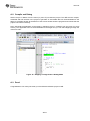
Evaluate the CC2543/44/45 Radio using SmartRF Studio
SmartRF Studio is a PC application developed for configuration and evaluation of many of the RF-IC
products from Texas Instruments, including the CC2543 and CC2544. The application communicates
with the CC2543/44/45 via the USB controller (the CC2511) on the SmartRF05EB board. The USB
controller uses the debug interface of the CC2543/44/45 to execute commands and to read and write
registers. Refer to Figure 12 - CC2544 USB Dongle connected to SmartRF05EB for a picture showing
how to connect the CC2544Dongle to the SmartRF05EB.
SmartRF Studio lets you explore the radio on the CC2543/44, as it gives you full overview and access
to the radio registers. The tool has a control interface for running basic radio performance tests from
the PC. SmartRF Studio also offers a flexible code export function of radio register settings for
software developers.
Before proceeding, please download and install the latest version of SmartRF Studio from the web
[12]. By installing Studio, the USB drivers needed for proper interaction between the PC and the
hardware of the CC2543-CC2544DK will also be installed.
In order to use the SmartRF Studio with CC2543/44/45, connect the CC2543/45EM or CC2544Dongle
to the SmartRF05EB. Next, connect the SmartRF05EB board to the PC via one of the USB cables
included in the kit. If you have installed SmartRF Studio, select automatic installation of driver in the
device wizard that appears. The device wizard will only pop up when you turn on the SmartRF05EB
and only once for each board. Allow Windows to complete the driver installation before proceeding.
With the board connected to the PC, you can start SmartRF Studio. The following window should
appear:
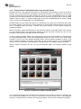
Figure 6 - CC2543 and CC2544 in SmartRF Studio
The connected evaluation board should be listed, showing that a CC2543 or CC2544 is available. The
list is dynamically updated as you connect or disconnect a board. Double click on the highlighted
CC2543 or CC2544 device icon and a new window will appear. We will use the CC2543 in this guide.
16/37
swru318
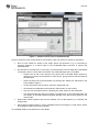
Figure 7 - CC2543 control panel in SmartRF Studio
Figure 7 shows the main control panel for the CC2543. It lets you perform a number of operations:
Run TX Test modes for testing of RF output power and spectrum; e.g. by connecting a
spectrum analyser or a power meter to the CC2543EM SMA connector to perform RF
measurements.
Run Packet TX and RX tests. For this test, you should either have two EBs with CC2543EMs
connected to the PC or two EBs connected to one CC2544Dongle and a CC243EM.
o
Double click on both of the devices in the device list in SmartRF Studio (Figure 6),
opening one “Device Control Panel” for each device, giving control of the two radios at
the same time.
o
Select one device to be the transmitter, by selecting the “Packet TX” tab shown in the
lower middle of Figure 7.
o
On the other device (the receiver), select the “Packet RX” tab.
o
Set up basic test parameters and press the “Start” button on the receiver.
o
Now you can start transmission by pressing the “Start” button for the transmitter.
o
The status window will show the number of packets sent on the transmitter side and
the number of received packets and signal strength of the last received packet on the
receiver side.
Read and/or modify registers and common settings, such as RF frequency (or channel) and
output power.
Export device register values in a user modifiable format by clicking the “Code export” button
in the Register view panel (on the left side).
The SmartRF Studio User Manual has more details.
17/37
swru318
5.3
Setting up the Software Development Environment
To develop software and debug an application on the CC2543/44/45, it is recommended to use IAR
Embedded Workbench. It supports debugging of CC2543/44/45 through the SmartRF05EB, so no
additional hardware is required.
IAR EW8051 is bundled with all the required files for CC2543/44/45 to start development:
Register definition header file
Linker command file
Driver and device description file needed for debugging and programming
Note that other compilers and linkers can be used, but these tools may have limited debugging
capabilities.
An evaluation version of IAR Embedded Workbench is included in the Development Kit. To install the
software, insert the CD and follow the instructions. You will be asked to register on IAR’s web site to
get a license key for the product. As the owner of a CC2543-CC2544 Development Kit, you are
entitled to a 60 day evaluation period. The evaluation version in the kit automatically gives you 30
days. Please contact your local IAR sales representative for the additional 30-days evaluation period.
For a list of sales offices and distributors in your country, please see this site:
http://www.iar.com/contact.
Appendix A in this document will guide you through the steps of setting up your own project from
scratch.
18/37
swru318
6
RF Testing
NB! When running RF performance tests, it is recommended to disable all other peripherals on the
SmartRF05EB in order to avoid unwanted noise on the on-board voltage. In particular, make sure the
RS232 level converter/line driver is disabled.
RF testing can be performed by using SmartRF Studio together with the Development Kit. The basic
set-up is described in section 5.2.5. As described in that chapter, SmartRF Studio can be used to set
up basic tests and tune RF registers accordingly.
Since the CC2543/45 evaluation module is equipped with an SMA connector, both radiated (via
antenna) and conducted (via cable) tests can be performed, and it is easy to hook the EM up to RF
measurement equipment. For the CC2544Dongle it is only possible with radiated tests as this device
has an on board PCB antenna. The RF equipment may be connected in two different ways.
To measure radiated performance, connect an appropriate antenna to the spectrum analyzer
or power meter and an antenna on the EM board.
To measure conducted performance, connect a 50 Ohm coaxial cable directly from the EM to
the RF equipment.
50 Ohm coax cable
Spectrum Analyser
CC2530EM
CC2543EM
SmartRF05EB
USB
Figure 8 - RF Test Set-Up with a Spectrum analyzer
By using good-quality RF cabling, the loss in the cabling should be negligible. However make sure that
the spectrum analyzer is calibrated. If possible, check it against a calibrated instrument such as an RF
signal generator. Un-calibrated spectrum analyzers can display errors of several dBs.
For more information regarding RF testing, refer to “Application Note 103 -- Basic RF Testing of
CCxxxx Devices” [15].
6.1
TX Parameter Testing Basics
To investigate the TX performance of the CC2543/44/45, you can either use a Spectrum Analyzer or
an RF Power Meter. Use the “Continuous TX” test mode in SmartRF Studio to set up the device to
transmit a signal at the desired frequency. Both a modulated or un-modulated carrier signal can be
generated.
Use the RF Power Meter to observe the output power or the spectrum analyzer to observe the
spectrum and to measure the error vector magnitude (EVM).
19/37
swru318
6.2
RX Parameter Testing Basics
To investigate the RX performance of the CC2543/44/45, you can use a signal generator or “Packet
TX” in SmartRF Studio (with another EB+EM) to generate the packets to receive. The receiver can be
configured by using the “Packet RX” test feature in SmartRF Studio.
By adding a jammer (a third node that generates either noise on the same channel or a strong signal
on an adjacent channel) it is also possible to measure co-channel rejection and selectivity/blocking
performance.
The PER test application, that was described in section 5.2, can be used for simple sensitivity
measurements with the CC2543EM, CC2545EM and/or with your own prototype hardware. In this
case, connect the unit you want to test to a known good transmitter with coaxial cables and
attenuators. Add more attenuators until the PER value is 1%. The signal strength at the receiver side
is then the sensitivity limit of the system.
For more information regarding sensitivity measurements, refer to “Design Note 2 – Practical
Sensitivity Testing” [13].
20/37
swru318
7
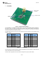
CC2543EM
SMA antenna
connector
32 MHz Crystal
CC2543
Figure 9 - CC2543 Evaluation Module
The CC2543EM is a complete RF module based on one of the recommended reference designs for
the CC2543 radio. The module is equipped with a 32 MHz crystal, external passive components for
the balun and antenna match filter, a SMA connector for the antenna or any other RF instrument
connection and general IO headers/connectors.
The table below shows the pin-out from the CC2543 to the two connectors on the backside of the
evaluation module.
CC2543
Signal
P1
P1
CC2543
Signal
CC2543
Signal
P2
P2
CC2543
Signal
GND
1
2
NC
NC
1
2
GND
P0.4
3
4
NC
NC
3
4
NC
P0.1
5
6
P1.0
NC
5
6
NC
P0.2
7
8
NC
VDD
7
8
NC
P0.3
9
10
P2.1
VDD
9
10
NC
P0.0
11
12
P2.2
NC
11
12
P0.6
NC
13
14
P1.1
NC
13
14
P0.7
P0.6
15
16
P1.2
RESET
15
16
NC
NC
17
18
P1.4
P0.7
17
18
P0.5
GND
19
20
P1.3
P2.0
19
20
NC
Table 1 - CC2543EM pin-out
The part number of the EM connector is SFM-110-02-SM-D-A-K-TR from Samtec. It mates with the
TFM-110-02-SM-D-A-K-TR, also from Samtec.
Follow the links in Appendix B to find the reference design files to get any further details.
21/37
swru318
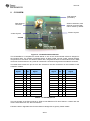
8
CC2545EM
PCB antenna,
(Inverted F)
SMA antenna
connector
Antenna Selection, PCB
antenna connected with
0-ohm resistor by default
32 MHz Crystal
32 kHz Crystal
CC2545
Figure 10 - CC2545 Evaluation Module
The CC2545EM is a complete RF module based on one of the recommended reference designs for
the CC2545 radio. The module is equipped with a 32 MHz crystal, 32 kHz crystal, external passive
components for the balun and antenna match filter, Integrated inverted F PCB antenna and a SMA
connector for the antenna or any other RF instrument connection and general IO headers/connectors.
The table below shows the pin-out from the CC2545 to the two connectors on the backside of the
evaluation module.
CC2545
Signal
P1
P1
CC2545
Signal
CC2545
Signal
P2
P2
CC2545
Signal
GND
1
2
P3.0
P3.6
1
2
GND
P0.4
3
4
P3.7
NC
3
4
P3.4
P0.1
5
6
P1.0
NC
5
6
P3.5
P0.2
7
8
P3.2
VDD
7
8
P1.5
P0.3
9
10
P1.3
VDD
9
10
P1.6
P0.0
11
12
P1.4
P3.1
11
12
P2.5
P1.1
13
14
P2.1
P3.3
13
14
P2.6
P0.6
15
16
P2.2
RESET
15
16
P2.4
P0.7
17
18
P2.7
P1.2
17
18
P0.5
GND
19
20
P2.3
P2.0
19
20
NC
Table 2 - CC2545EM pin-out
The part number of the EM connector is SFM-110-02-SM-D-A-K-TR from Samtec. It mates with the
TFM-110-02-SM-D-A-K-TR, also from Samtec.
Follow the links in Appendix B to find the reference design files to get any further details.
22/37
swru318
9
CC2544 USB Dongle
LED2
Button S2
Meandred Inverted
F-antenna
CC2544
Right IO test holes
LED1
Button S1
Debug connector
(underneath = bottom layer)
Left IO test holes
Figure 11 - CC2544 USB Dongle
The CC2544 USB dongle that is included in the kit comes preprogrammed such that it can be used as
a MASTER device in the PER test. The functionality of the PER test is described in section 5.2.
The USB dongle can also be used as a general development board for USB and RF software.
Table 3 shows which CC2544 signals are connected to what IO on the dongle. The IO holes on each
side of the CC2544Dongle are numbered from 1 to 4 where 1 is the one closest to the USB connector.
Left IO
Holes
CC2544
Right IO
CC2544
Holes
Dongle User
IO
CC2544
1
P1.0
1
P0.0
Green LED (LED1)
P0.2
2
P1.1
3
P1.2
2
P0.1
Red LED (LED2)
P0.1
3
P0.2
Button S1
P0.0
4
P1.3
4
P0.3
Button S2
P0.3
Table 3 - CC2544 USB Dongle Pin-out
In order to debug and program firmware on the CC2544, the CC2544 USB dongle can be connected
to the SmartRF05EB as shown in the picture below. The small adapter board and flat cable is included
in the development kit.
Follow the links in Appendix B to find the reference design files to get any further details.
23/37
swru318
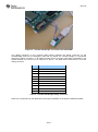
Figure 12 - CC2544 USB Dongle connected to SmartRF05EB
The debug connector on the CC2544 USB Dongle matches the debug connector on the
SmartRF05EB (and the CC Debugger). Note that, by default, the CC2544 dongle is not powered
through the debug connector, so an external power source must be used while programming. The
easiest solution is to connect it to a USB port on the PC. The table below shows the pin out of the
debug connector.
Pin # Connection
1
GND
2
VDD
3
CC2544 P1.2 (DC)
4
CC2544 P1.3 (DD)
5
NC
6
NC
7
CC2544 RESET
8
NC
9
NC
10
NC
Table 4 – CC2544 USB Dongle Debug Connector
Refer to the schematics (in the appendices) and layout (available on the web) for additional details.
24/37
swru318
10 SmartRF05 Evaluation Board
The SmartRF05 Evaluation Board is thoroughly described in the SmartRF05EB User’s Guide [11].
That document will describe the hardware features in detail and provide the schematics for the board.
25/37
swru318
11 Frequently Asked Questions
Q1
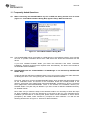
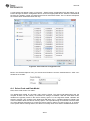
When connecting the SmartRF05EB to my PC via USB, the dialog window seen in below
(Figure 13 - Found New Hardware Dialog Box) appears. Why? What should I do?
Figure 13 - Found New Hardware Dialog Box
A1
The SmartRF05EB will be recognized as a USB device by the operating system, and it will ask
the user to provide information about which USB driver that should be associated with the
device.
If you have installed SmartRF Studio, just follow the instructions and select “Automatic
installation”. Windows should find the required driver automatically. The drivers are included in
the SmartRF Studio installation.
Q2
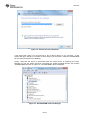
SmartRF05EB with the CC2543/45EM or CC2544Dongle is not detected by IAR/SmartRF
Studio. Why?
It might be that the USB driver installation failed. The most common reasons are either Windows
not finding the driver or the user ignoring the “Found New Hardware Wizard”.
First of all, make sure you have installed SmartRF Studio, which includes the appropriate drivers
for the evaluation board. The drivers for the evaluation board are normally located in the
directory C:\Program Files (x86)\Texas Instruments\SmartRF Tools\Drivers, where C:\Program
Files (x86)\Texas Instruments\SmartRF Tools\ is the default root installation directory for
SmartRF Studio. The path may be different if you have chosen a different installation directory
for SmartRF Studio.
Next, make sure you follow the steps in the hardware wizard. It is necessary to follow the steps
for driver installation for each new board that is connected to the PC. If the automatic driver
installation (as described in A1 above) fails, please select manual installation of drivers. When
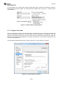
prompted by the wizard, select “Browse my computer for driver software”. You will see the
following window seen in Figure 14 - Browse for Driver Software.
26/37
swru318
Figure 14 - Browse for Driver Software
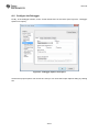
If the above fails, select “Let me pick from a list of device drivers on my computer.” A new
window will open, asking for a location of where drivers can be found. Locate the SmartRF05EB
file and select that driver for installation.
Finally, verify that the device is associated with the correct driver by opening the Device
Manager on your PC. When the EB is connected, the “Cebal controlled devices” list contains
“SmartRF05EB” like seen in Figure 15 - SmartRF05EB in Device Manager.
Figure 15 - SmartRF05EB in Device Manager
27/37
swru318
If the board is listed as an unknown device or associated with another driver, right click the
device in the Device Manager and select Uninstall. After uninstalling, unplug the board from the
PC and plug it in again. The “Found New Hardware Wizard” should re-appear. Follow the steps
as outlined in the beginning of this section.
Q3
How do I measure the current consumption of the CC2543/45?
A3
The easiest way to measure current consumption of the chip in various modes is to connect the
EM directly to the SmartRF05EB and disconnect everything on the board that consumes power
by removing all jumpers. The jumper on header P13 should not be removed. Connect the
ampere meter between the two terminals on P15. On P10, the jumper for the EM_RESET signal
(connector 35-36) should be mounted. On P1, no jumpers are required, but in order to control
the SoC from a debugger, mount a jumper between 19-20 (DBG_DD) and 21-22 (DBG_DD).
Make sure the RS232 Enable switch is in the “disable” position.
Use SmartRF Studio to set the radio in different modes (RX, TX, etc.), or download an
application on the CC2543 setting the device in the preferred state.
Q4
Can I use another compiler than IAR to develop software for CC2543/44/45?
A4
Yes, there are several tools available that can be used for CC2543/44/45. Any 8051 compiler
(e.g. Keil, GCC, and SDCC) can, in theory, be used. Note that these tools may have limited
debugging support for CC2543/44/45.
28/37
swru318
12 References
[1] CC2543 product web site
http://www.ti.com/product/cc2543
[2] CC2544 product web site
http://www.ti.com/product/cc2544
[3] CC2545 product web site
http://www.ti.com/product/cc2545
[4] CC2543-CC2544DK web site
http://www.ti.com/tool/cc2543-cc2544dk
[5] CC2545EMK web site
http://www.ti.com/tool/cc2545emk
[6] CC2543-CC2544DK Quick Start Guide
http://www.ti.com/lit/swru315
[7] CC2545EMK Quick Start Guide
http://www.ti.com/lit/swru320
[8] CC254x Proprietary Mode Packet Error Rate Test Source Code
http://www.ti.com/litv/zip/swrc251
[9] Texas Instruments Support
http://support.ti.com
[10] Texas Instruments Low Power RF Online Community
http://www.ti.com/lprf-forum
[11] SmartRF05EB User’s Guide
http://www.ti.com/lit/swru210
[12] SmartRF Studio
http://www.ti.com/smartrfstudio
[13] DN002 -- Practical Sensitivity Testing
http://www.ti.com/lit/swra097
[14] DN018 -- Range Measurements in an Open Field Environment
http://www.ti.com/lit/swra169
[15] AN103 -- Basic RF Testing of CCxxxx Devices
http://www.ti.com/lit/swra370
[16] IAR Embedded Workbench for 8051
http://www.iar.com
13 Document history
Revision
Date
A
B
2012-04-20
2013-04-26
2013-05-07
Description/Changes
First revision.
Added Description for the CC2545 and small updates to content.
Corrected content.
29/37
swru318
Appendix A
Setting up the Software Environment
This appendix will guide you through the initial steps of setting up a complete software development
environment with IAR Embedded Workbench for 8051. Version 8.10 (and newer) of the tool supports
CC2543/44/45 out-of-the-box. In this example we will explain how to set up a project for the CC2543.
The same procedure can be used for the CC2544/45 by simply replacing all references to “CC2543”
with “CC2544” or “CC2545”.
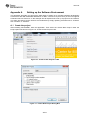
A.1 Create the project
After installing IAR EW8051, start the application. Then select the “Create New Project” under the
Project option like shown in Figure 16 - Create a New Project in IAR.
Figure 16 - Create a New Project in IAR
Figure 17 - Create New Project Dialog Box
30/37
swru318
Select Empty project and click OK as illustrated in Figure 17 - Create New Project Dialog Box. You will
now be asked to save the project. Select an appropriate name for the project and save it. The dialog
window will close and the project will be listed in the “workspace” panel at the left side of the IDE.
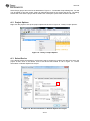
A.2 Project Options
Right click the project to set up the project options like shown in Figure 18 - "blinky" Project Options.
Figure 18 - "blinky" Project Options
A.3 Select Device
In the dialog window that appears, the first thing that is required is to select the device for which the
project is built. Click on the button next to the device field marked in red in Figure 19 - Device
Information in General Options for Project
Figure 19 - Device Information in General Options for Project
31/37
swru318
A new window will appear (seen in Figure 20 - Select Device Configuration File) that allows you to
browse through the device configuration files to choose an appropriate device. Select the CC2543F32
file from the <ew8051_install_dir>\8051\devices\Texas Instruments folder. This .i51 device description
file contains basic information about the chip.
Figure 20 - Select Device Configuration File
Back in the General Options view, you will see that CC2543 is now the selected device. “CPU core”
should be set to Plain.
A.4 Select Code and Data Model
Next, select code model. Use “Near”.
The default data model for the Near code model is Small. The data model determines how the
compiler & linker use the memory of the 8051 for storage of variables. With the small data model,
variables are typically stored in the DATA memory space. For the large data model, variables are
stored in XDATA. The CC254x User Guide and IAR 8051 C/C++ Compiler Reference Guide have
more information about the various memory spaces. The important thing to remember is that the 8051
core uses different instructions to access the various memory spaces. Access to DATA is, in general,
much quicker than accessing XDATA, but there is normally much more XDATA available than DATA.
32/37
swru318
For this example, we use Near code model and large data model. The stack can be placed in XDATA.
After setting up the above option, you should have the settings seen in Figure 21 - General Device
Target Options.
Figure 21 - General Device Target Options
A.5 Configure the Linker
Next, you will need to instruct the IDE what linker command file to use. The linker command file
contains information the linker uses in order to place code and variables in ram and flash. Thus, the
linker file must match the flash and ram size of device you are working with. Normally, the linker file
should be tailor-made to an application for optimum performance, but the default command file will
work with most applications.
Use the default configuration file (refer to setup in Figure 22 - Linker Options for Project).
Figure 22 - Linker Options for Project
33/37
swru318
A.6 Configure the Debugger
Finally, in the debugger section, chose “Texas Instruments” for the Driver (see Figure 23 - Debugger
Options for Project).
Figure 23 - Debugger Options for Project
All the other project options can be left as is and you can close the Project Options dialog by clicking
OK.
34/37
swru318
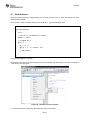
A.7 Write Software
At this point, the project is configured and you can write your first lines of code. We will show a small
blinking LED example.
In the project, create a new file that you save as blinky.c. Type the following code:
#include <ioCC2543.h>
int main(void)
{
int i;
// Set P1.0 of CC2543 as output
P1DIR |= 0x01;
// Toggle P1.0
for(;;)
{
P1_0 ^= 1;
for(i = 0; i < 10000; i++)
{
asm("NOP");
}
}
}
The code will toggle P1.0 quickly.
Add the file to the project by right clicking the project and selecting Add “blinky.c” as seen in Figure 24
- Add Source File to Project.
Figure 24 - Add Source File to Project
You are now ready to compile and download the code to the target!
35/37
swru318
A.8 Compile and Debug
Select “Project Make” from the menu (or press F7) to build the project. The IDE will now compile,
assemble and link the files in the project to generate an executable that can be downloaded to the
target. A message window at the bottom of the screen should show the progress and indicate that the
project was built successfully.
Next, download the application to the target by selecting “Project Debug” from the menu (or press
Ctrl+D). The application will now be downloaded to the target and you can start stepping through the
code from main.
Figure 25 - Stepping Through Code in Debug Mode
A.9 Done!
Congratulations! You have just made your first CC2543 software project in IAR.
36/37
swru318
Appendix B
Schematics and Layout
Please refer to the following pages for the schematics and/or layout for:
CC2543 Evaluation Module
http://www.ti.com/product/cc2544
CC2544 USB Dongle
http://www.ti.com/tool/cc2544em-rd
CC2545 Evaluation Module
http://www.ti.com/tool/cc2545em-rd
SmartRF05 Evaluation Board
http://www.ti.com/lit/swru210
37/37
EVALUATION BOARD/KIT/MODULE (EVM) ADDITIONAL TERMS
Texas Instruments (TI) provides the enclosed Evaluation Board/Kit/Module (EVM) under the following conditions:
The user assumes all responsibility and liability for proper and safe handling of the goods. Further, the user indemnifies TI from all claims
arising from the handling or use of the goods.
Should this evaluation board/kit not meet the specifications indicated in the User’s Guide, the board/kit may be returned within 30 days from
the date of delivery for a full refund. THE FOREGOING LIMITED WARRANTY IS THE EXCLUSIVE WARRANTY MADE BY SELLER TO
BUYER AND IS IN LIEU OF ALL OTHER WARRANTIES, EXPRESSED, IMPLIED, OR STATUTORY, INCLUDING ANY WARRANTY OF
MERCHANTABILITY OR FITNESS FOR ANY PARTICULAR PURPOSE. EXCEPT TO THE EXTENT OF THE INDEMNITY SET FORTH
ABOVE, NEITHER PARTY SHALL BE LIABLE TO THE OTHER FOR ANY INDIRECT, SPECIAL, INCIDENTAL, OR CONSEQUENTIAL
DAMAGES.
Please read the User's Guide and, specifically, the Warnings and Restrictions notice in the User's Guide prior to handling the product. This
notice contains important safety information about temperatures and voltages. For additional information on TI's environmental and/or safety
programs, please visit www.ti.com/esh or contact TI.
No license is granted under any patent right or other intellectual property right of TI covering or relating to any machine, process, or
combination in which such TI products or services might be or are used. TI currently deals with a variety of customers for products, and
therefore our arrangement with the user is not exclusive. TI assumes no liability for applications assistance, customer product design,
software performance, or infringement of patents or services described herein.
REGULATORY COMPLIANCE INFORMATION
As noted in the EVM User’s Guide and/or EVM itself, this EVM and/or accompanying hardware may or may not be subject to the Federal
Communications Commission (FCC) and Industry Canada (IC) rules.
For EVMs not subject to the above rules, this evaluation board/kit/module is intended for use for ENGINEERING DEVELOPMENT,
DEMONSTRATION OR EVALUATION PURPOSES ONLY and is not considered by TI to be a finished end product fit for general consumer
use. It generates, uses, and can radiate radio frequency energy and has not been tested for compliance with the limits of computing
devices pursuant to part 15 of FCC or ICES-003 rules, which are designed to provide reasonable protection against radio frequency
interference. Operation of the equipment may cause interference with radio communications, in which case the user at his own expense will
be required to take whatever measures may be required to correct this interference.
General Statement for EVMs including a radio
User Power/Frequency Use Obligations: This radio is intended for development/professional use only in legally allocated frequency and
power limits. Any use of radio frequencies and/or power availability of this EVM and its development application(s) must comply with local
laws governing radio spectrum allocation and power limits for this evaluation module. It is the user’s sole responsibility to only operate this
radio in legally acceptable frequency space and within legally mandated power limitations. Any exceptions to this are strictly prohibited and
unauthorized by Texas Instruments unless user has obtained appropriate experimental/development licenses from local regulatory
authorities, which is responsibility of user including its acceptable authorization.
For EVMs annotated as FCC – FEDERAL COMMUNICATIONS COMMISSION Part 15 Compliant
Caution
This device complies with part 15 of the FCC Rules. Operation is subject to the following two conditions: (1) This device may not cause
harmful interference, and (2) this device must accept any interference received, including interference that may cause undesired operation.
Changes or modifications not expressly approved by the party responsible for compliance could void the user's authority to operate the
equipment.
FCC Interference Statement for Class A EVM devices
This equipment has been tested and found to comply with the limits for a Class A digital device, pursuant to part 15 of the FCC Rules.
These limits are designed to provide reasonable protection against harmful interference when the equipment is operated in a commercial
environment. This equipment generates, uses, and can radiate radio frequency energy and, if not installed and used in accordance with the
instruction manual, may cause harmful interference to radio communications. Operation of this equipment in a residential area is likely to
cause harmful interference in which case the user will be required to correct the interference at his own expense.
FCC Interference Statement for Class B EVM devices
This equipment has been tested and found to comply with the limits for a Class B digital device, pursuant to part 15 of the FCC Rules.
These limits are designed to provide reasonable protection against harmful interference in a residential installation. This equipment
generates, uses and can radiate radio frequency energy and, if not installed and used in accordance with the instructions, may cause
harmful interference to radio communications. However, there is no guarantee that interference will not occur in a particular installation. If
this equipment does cause harmful interference to radio or television reception, which can be determined by turning the equipment off and
on, the user is encouraged to try to correct the interference by one or more of the following measures:
• Reorient or relocate the receiving antenna.
• Increase the separation between the equipment and receiver.
• Connect the equipment into an outlet on a circuit different from that to which the receiver is connected.
• Consult the dealer or an experienced radio/TV technician for help.
For EVMs annotated as IC – INDUSTRY CANADA Compliant
This Class A or B digital apparatus complies with Canadian ICES-003.
Changes or modifications not expressly approved by the party responsible for compliance could void the user’s authority to operate the
equipment.
Concerning EVMs including radio transmitters
This device complies with Industry Canada licence-exempt RSS standard(s). Operation is subject to the following two conditions: (1) this
device may not cause interference, and (2) this device must accept any interference, including interference that may cause undesired
operation of the device.
Concerning EVMs including detachable antennas
Under Industry Canada regulations, this radio transmitter may only operate using an antenna of a type and maximum (or lesser) gain
approved for the transmitter by Industry Canada. To reduce potential radio interference to other users, the antenna type and its gain should
be so chosen that the equivalent isotropically radiated power (e.i.r.p.) is not more than that necessary for successful communication.
This radio transmitter has been approved by Industry Canada to operate with the antenna types listed in the user guide with the maximum
permissible gain and required antenna impedance for each antenna type indicated. Antenna types not included in this list, having a gain
greater than the maximum gain indicated for that type, are strictly prohibited for use with this device.
Cet appareil numérique de la classe A ou B est conforme à la norme NMB-003 du Canada.
Les changements ou les modifications pas expressément approuvés par la partie responsable de la conformité ont pu vider l’autorité de
l'utilisateur pour actionner l'équipement.
Concernant les EVMs avec appareils radio
Le présent appareil est conforme aux CNR d'Industrie Canada applicables aux appareils radio exempts de licence. L'exploitation est
autorisée aux deux conditions suivantes : (1) l'appareil ne doit pas produire de brouillage, et (2) l'utilisateur de l'appareil doit accepter tout
brouillage radioélectrique subi, même si le brouillage est susceptible d'en compromettre le fonctionnement.
Concernant les EVMs avec antennes détachables
Conformément à la réglementation d'Industrie Canada, le présent émetteur radio peut fonctionner avec une antenne d'un type et d'un gain
maximal (ou inférieur) approuvé pour l'émetteur par Industrie Canada. Dans le but de réduire les risques de brouillage radioélectrique à
l'intention des autres utilisateurs, il faut choisir le type d'antenne et son gain de sorte que la puissance isotrope rayonnée équivalente
(p.i.r.e.) ne dépasse pas l'intensité nécessaire à l'établissement d'une communication satisfaisante.
Le présent émetteur radio a été approuvé par Industrie Canada pour fonctionner avec les types d'antenne énumérés dans le manuel
d’usage et ayant un gain admissible maximal et l'impédance requise pour chaque type d'antenne. Les types d'antenne non inclus dans
cette liste, ou dont le gain est supérieur au gain maximal indiqué, sont strictement interdits pour l'exploitation de l'émetteur.
SPACER
SPACER
SPACER
SPACER
SPACER
SPACER
SPACER
SPACER
【Important Notice for Users of this Product in Japan】
】
This development kit is NOT certified as Confirming to Technical Regulations of Radio Law of Japan
If you use this product in Japan, you are required by Radio Law of Japan to follow the instructions below with respect to this product:
1.
2.
3.
Use this product in a shielded room or any other test facility as defined in the notification #173 issued by Ministry of Internal Affairs and
Communications on March 28, 2006, based on Sub-section 1.1 of Article 6 of the Ministry’s Rule for Enforcement of Radio Law of
Japan,
Use this product only after you obtained the license of Test Radio Station as provided in Radio Law of Japan with respect to this
product, or
Use of this product only after you obtained the Technical Regulations Conformity Certification as provided in Radio Law of Japan with
respect to this product. Also, please do not transfer this product, unless you give the same notice above to the transferee. Please note
that if you could not follow the instructions above, you will be subject to penalties of Radio Law of Japan.
Texas Instruments Japan Limited
(address) 24-1, Nishi-Shinjuku 6 chome, Shinjuku-ku, Tokyo, Japan
http://www.tij.co.jp
【ご使用にあたっての注】
本開発キットは技術基準適合証明を受けておりません。
本製品のご使用に際しては、電波法遵守のため、以下のいずれかの措置を取っていただく必要がありますのでご注意ください。
1.
2.
3.
電波法施行規則第6条第1項第1号に基づく平成18年3月28日総務省告示第173号で定められた電波暗室等の試験設備でご使用いただく。
実験局の免許を取得後ご使用いただく。
技術基準適合証明を取得後ご使用いただく。
なお、本製品は、上記の「ご使用にあたっての注意」を譲渡先、移転先に通知しない限り、譲渡、移転できないものとします。
上記を遵守頂けない場合は、電波法の罰則が適用される可能性があることをご留意ください。
日本テキサス・インスツルメンツ株式会社
東京都新宿区西新宿6丁目24番1号
西新宿三井ビル
http://www.tij.co.jp
SPACER
SPACER
SPACER
SPACER
SPACER
SPACER
SPACER
SPACER
SPACER
SPACER
SPACER
SPACER
SPACER
SPACER
SPACER
SPACER
SPACER
EVALUATION BOARD/KIT/MODULE (EVM)
WARNINGS, RESTRICTIONS AND DISCLAIMERS
For Feasibility Evaluation Only, in Laboratory/Development Environments. Unless otherwise indicated, this EVM is not a finished
electrical equipment and not intended for consumer use. It is intended solely for use for preliminary feasibility evaluation in
laboratory/development environments by technically qualified electronics experts who are familiar with the dangers and application risks
associated with handling electrical mechanical components, systems and subsystems. It should not be used as all or part of a finished end
product.
Your Sole Responsibility and Risk. You acknowledge, represent and agree that:
1.
2.
3.
4.
You have unique knowledge concerning Federal, State and local regulatory requirements (including but not limited to Food and Drug
Administration regulations, if applicable) which relate to your products and which relate to your use (and/or that of your employees,
affiliates, contractors or designees) of the EVM for evaluation, testing and other purposes.
You have full and exclusive responsibility to assure the safety and compliance of your products with all such laws and other applicable
regulatory requirements, and also to assure the safety of any activities to be conducted by you and/or your employees, affiliates,
contractors or designees, using the EVM. Further, you are responsible to assure that any interfaces (electronic and/or mechanical)
between the EVM and any human body are designed with suitable isolation and means to safely limit accessible leakage currents to
minimize the risk of electrical shock hazard.
You will employ reasonable safeguards to ensure that your use of the EVM will not result in any property damage, injury or death, even
if the EVM should fail to perform as described or expected.
You will take care of proper disposal and recycling of the EVM’s electronic components and packing materials.
Certain Instructions. It is important to operate this EVM within TI’s recommended specifications and environmental considerations per the
user guidelines. Exceeding the specified EVM ratings (including but not limited to input and output voltage, current, power, and
environmental ranges) may cause property damage, personal injury or death. If there are questions concerning these ratings please contact
a TI field representative prior to connecting interface electronics including input power and intended loads. Any loads applied outside of the
specified output range may result in unintended and/or inaccurate operation and/or possible permanent damage to the EVM and/or
interface electronics. Please consult the EVM User's Guide prior to connecting any load to the EVM output. If there is uncertainty as to the
load specification, please contact a TI field representative. During normal operation, some circuit components may have case temperatures
greater than 60°C as long as the input and output are maintained at a normal ambient operating temperature. These components include
but are not limited to linear regulators, switching transistors, pass transistors, and current sense resistors which can be identified using the
EVM schematic located in the EVM User's Guide. When placing measurement probes near these devices during normal operation, please
be aware that these devices may be very warm to the touch. As with all electronic evaluation tools, only qualified personnel knowledgeable
in electronic measurement and diagnostics normally found in development environments should use these EVMs.
Agreement to Defend, Indemnify and Hold Harmless. You agree to defend, indemnify and hold TI, its licensors and their representatives
harmless from and against any and all claims, damages, losses, expenses, costs and liabilities (collectively, "Claims") arising out of or in
connection with any use of the EVM that is not in accordance with the terms of the agreement. This obligation shall apply whether Claims
arise under law of tort or contract or any other legal theory, and even if the EVM fails to perform as described or expected.
Safety-Critical or Life-Critical Applications. If you intend to evaluate the components for possible use in safety critical applications (such
as life support) where a failure of the TI product would reasonably be expected to cause severe personal injury or death, such as devices
which are classified as FDA Class III or similar classification, then you must specifically notify TI of such intent and enter into a separate
Assurance and Indemnity Agreement.
Mailing Address: Texas Instruments, Post Office Box 655303, Dallas, Texas 75265
Copyright © 2013, Texas Instruments Incorporated
IMPORTANT NOTICE
Texas Instruments Incorporated and its subsidiaries (TI) reserve the right to make corrections, enhancements, improvements and other
changes to its semiconductor products and services per JESD46, latest issue, and to discontinue any product or service per JESD48, latest
issue. Buyers should obtain the latest relevant information before placing orders and should verify that such information is current and
complete. All semiconductor products (also referred to herein as “components”) are sold subject to TI’s terms and conditions of sale
supplied at the time of order acknowledgment.
TI warrants performance of its components to the specifications applicable at the time of sale, in accordance with the warranty in TI’s terms
and conditions of sale of semiconductor products. Testing and other quality control techniques are used to the extent TI deems necessary
to support this warranty. Except where mandated by applicable law, testing of all parameters of each component is not necessarily
performed.
TI assumes no liability for applications assistance or the design of Buyers’ products. Buyers are responsible for their products and
applications using TI components. To minimize the risks associated with Buyers’ products and applications, Buyers should provide
adequate design and operating safeguards.
TI does not warrant or represent that any license, either express or implied, is granted under any patent right, copyright, mask work right, or
other intellectual property right relating to any combination, machine, or process in which TI components or services are used. Information
published by TI regarding third-party products or services does not constitute a license to use such products or services or a warranty or
endorsement thereof. Use of such information may require a license from a third party under the patents or other intellectual property of the
third party, or a license from TI under the patents or other intellectual property of TI.
Reproduction of significant portions of TI information in TI data books or data sheets is permissible only if reproduction is without alteration
and is accompanied by all associated warranties, conditions, limitations, and notices. TI is not responsible or liable for such altered
documentation. Information of third parties may be subject to additional restrictions.
Resale of TI components or services with statements different from or beyond the parameters stated by TI for that component or service
voids all express and any implied warranties for the associated TI component or service and is an unfair and deceptive business practice.
TI is not responsible or liable for any such statements.
Buyer acknowledges and agrees that it is solely responsible for compliance with all legal, regulatory and safety-related requirements
concerning its products, and any use of TI components in its applications, notwithstanding any applications-related information or support
that may be provided by TI. Buyer represents and agrees that it has all the necessary expertise to create and implement safeguards which
anticipate dangerous consequences of failures, monitor failures and their consequences, lessen the likelihood of failures that might cause
harm and take appropriate remedial actions. Buyer will fully indemnify TI and its representatives against any damages arising out of the use
of any TI components in safety-critical applications.
In some cases, TI components may be promoted specifically to facilitate safety-related applications. With such components, TI’s goal is to
help enable customers to design and create their own end-product solutions that meet applicable functional safety standards and
requirements. Nonetheless, such components are subject to these terms.
No TI components are authorized for use in FDA Class III (or similar life-critical medical equipment) unless authorized officers of the parties
have executed a special agreement specifically governing such use.
Only those TI components which TI has specifically designated as military grade or “enhanced plastic” are designed and intended for use in
military/aerospace applications or environments. Buyer acknowledges and agrees that any military or aerospace use of TI components
which have not been so designated is solely at the Buyer's risk, and that Buyer is solely responsible for compliance with all legal and
regulatory requirements in connection with such use.
TI has specifically designated certain components as meeting ISO/TS16949 requirements, mainly for automotive use. In any case of use of
non-designated products, TI will not be responsible for any failure to meet ISO/TS16949.
Products
Applications
Audio
www.ti.com/audio
Automotive and Transportation
www.ti.com/automotive
Amplifiers
amplifier.ti.com
Communications and Telecom
www.ti.com/communications
Data Converters
dataconverter.ti.com
Computers and Peripherals
www.ti.com/computers
DLP® Products
www.dlp.com
Consumer Electronics
www.ti.com/consumer-apps
DSP
dsp.ti.com
Energy and Lighting
www.ti.com/energy
Clocks and Timers
www.ti.com/clocks
Industrial
www.ti.com/industrial
Interface
interface.ti.com
Medical
www.ti.com/medical
Logic
logic.ti.com
Security
www.ti.com/security
Power Mgmt
power.ti.com
Space, Avionics and Defense
www.ti.com/space-avionics-defense
Microcontrollers
microcontroller.ti.com
Video and Imaging
www.ti.com/video
RFID
www.ti-rfid.com
OMAP Applications Processors
www.ti.com/omap
TI E2E Community
e2e.ti.com
Wireless Connectivity
www.ti.com/wirelessconnectivity
Mailing Address: Texas Instruments, Post Office Box 655303, Dallas, Texas 75265
Copyright © 2013, Texas Instruments Incorporated