1
CC2530 Development Kit
User’s Guide
swru208b
swru208b
Table of contents
CC2530 Development Kit User’s Guide ...........................................................................................1
1
Introduction ............................................................................................................................3
2
About this manual ..................................................................................................................3
3
Acronyms................................................................................................................................4
4
Development Kit contents......................................................................................................5
5
Getting started........................................................................................................................7
5.1
Setting up the hardware............................................................................................................7
5.2
Running the Preprogrammed PER Test on the CC2530EM ......................................................8
5.3
Evaluate the CC2530 Radio using SmartRF Studio...................................................................9
5.4
Setting up the Software Development Environment.................................................................11
6
RF Testing.............................................................................................................................12
6.1
TX Parameter Testing Basics .................................................................................................12
6.2
RX Parameter Testing Basics .................................................................................................13
7
CC2530EM.............................................................................................................................14
8
CC2531 USB Dongle.............................................................................................................15
9
SmartRF05 Evaluation Board...............................................................................................17
10
Frequently Asked Questions ...............................................................................................18
11
References............................................................................................................................21
12
Document history .................................................................................................................21
Appendix A
Setting up the Software Environment ................................................................22
A.1 Create the project ...................................................................................................................22
A.2 Project Options.......................................................................................................................23
A.3 Select Device .........................................................................................................................23
A.4 Select Code and Memory Model .............................................................................................24
A.5 Configure the Linker ...............................................................................................................26
A.6 Configure the Debugger .........................................................................................................27
A.7 Write Software........................................................................................................................28
A.8 Compile and Debug................................................................................................................29
A.9 Done! .....................................................................................................................................29
Appendix B
Software Solutions for CC2530 from TI..............................................................30
B.1 SimpliciTI™ Network Protocol.................................................................................................30
B.2 TIMAC Software .....................................................................................................................30
B.3 RemoTI™ Network Protocol ...................................................................................................31
B.4 Z-Stack™ Software ................................................................................................................31
Appendix C
Schematics..........................................................................................................33
2/33
swru208b
1
Introduction
Thank you for purchasing a CC2530 Development Kit.
The CC2530 is Texas Instrument’s second generation ZigBee/IEEE 802.15.4 compliant System-onChip with an optimized 8051 MCU core and radio for the 2.4 GHz unlicensed ISM/SRD band. This
device enables industrial grade applications by offering state-of-the-art noise immunity, excellent link
budget, operation up to 125 degrees and low voltage operation.
In addition, the CC2530 provides extensive hardware support for packet handling, data buffering, burst
transmissions, data encryption, data authentication, clear channel assessment, link quality indication
and packet timing information.
The CC2530 product folder on the web [1] has more information, with datasheets, user guides and
application notes.
The CC2530 Development Kit includes all the necessary hardware to properly evaluate, demonstrate,
prototype and develop software targeting not only IEEE802.15.4 or ZigBee compliant applications, but
also proprietary applications for which a DSSS radio is required or wanted.
2
About this manual
This manual describes all the hardware included in the CC2530 Development Kit (CC2530DK) and
points the user to other useful information sources.
Chapter 4 briefly describes the contents of the development kit and chapter 5 gives a quick
introduction to how to get started with the kit. In particular, it describes how to install SmartRF Studio
to get the required drivers for the evaluation board, how the hardware can be used, and lists the
software that is available for the development kit. Chapter 6 explains some simple methods for
performing practical RF testing with the development kit. Chapter 7, 8, and 9 describe the hardware in
the kit and where to find more information about how to use it. A troubleshooting guide can be found in
chapter 10.
Appendix A gives a detailed description of how to set up the software development environment for
the CC2530. Appendix B lists available software solutions for CC2530.
The CC2530DK Quick Start Guide [4] has a short tutorial on how to get started with the kit. The
CC2530 Software User’s Guide [5] provides details about the software examples and information
about other software options for the CC2530.
The PC tools SmartRF Studio and SmartRF Flash Programmer have their own user manuals.
Please visit the CC2530 development kit web page [3] and CC2530 product page [1] for additional
information. Further information can be found on the TI LPRF Online Community [7].
See chapter 11 for a list of relevant documents and links.
3/33
swru208b
3
Acronyms
ACM
ADC
CDC
DK
EB
EM
HID
IC
ISM
KB
LCD
LED
LPRF
MCU
NC
PER
RF
RX
SoC
SPI
SRD
TI
TX
UART
USB
Abstract Control Model
Analog to Digital Converter
Communications Device Class
Development Kit
Evaluation Board
Evaluation Module
Human Interface Device
Integrated Circuit
Industrial, Scientific and Medical
Kilo Byte (1024 byte)
Liquid Crystal Display
Light Emitting Diode
Low Power RF
Micro Controller
Not connected
Packet Error Rate
Radio Frequency
Receive
System on Chip
Serial Peripheral Interface
Short Range Device
Texas Instruments
Transmit
Universal Asynchronous Receive Transmit
Universal Serial Bus
4/33
swru208b
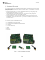
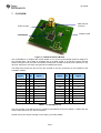
4
Development Kit contents
The CC2530 Development Kit (CC2530DK) includes hardware and software that allows quick testing
of the CC2530 RF performance and offers a complete platform for development of advanced
prototype RF systems.
Evaluate the CC2530 right out of the box. The kit can be used for range testing using the preprogrammed PER tester running on the CC2530.
Use SmartRF Studio to perform RF measurements. The radio can be easily configured to
measure sensitivity, output power and other RF parameters.
Prototype development. All I/O pins from the CC2530 are available on pin connectors on the
SmartRF05EB, allowing easy interconnection to peripherals on the EB board or other external
sensors and devices.
The CC2530DK contains the following components
2 x SmartRF05EB (the two large boards)
2 x CC2530 Evaluation Modules (the two small boards)
2 x Antennas
1 x CC2531 USB Dongle
Cables
Batteries
Documents
Figure 1 - CC2530 Development Kit Contents
5/33
swru208b
SmartRF05EB
The SmartRF05EB (evaluation board) is the
main board in the kit with a wide range of user
interfaces:
3x16 character serial LCD
Full speed USB 2.0 interface
UART
LEDs
Serial Flash
Potentiometer
Joystick
Buttons
The EB is the platform for the evaluation
modules (EM) and can be connected to the PC
via USB to control the EM.
CC2530EM
The CC2530EM (evaluation module) contains
the RF IC and necessary external components
and matching filters for getting the most out of
the radio. The module can be plugged into the
SmartRF05EB. Use the EM as reference
design for RF layout. The schematics are
included at the end of this document and the
layout files can be found on the web [1].
CC2531 USB Dongle
The CC2531 USB Dongle is a fully operational
USB device that can be plugged into a PC.
The dongle has 2 LEDs, two small pushbuttons and connector holes that allow
connection of external sensors or devices. The
dongle also has a connector for programming
and debugging of the CC2531 USB controller.
The dongle comes preprogrammed with
firmware such that it can be used as a packet
sniffer device.
Antenna
2.4 GHz antenna Titanis from Antenova.
6/33
swru208b
5
Getting started
5.1
Setting up the hardware
After opening the kit, make sure you have all components. Please contact your TI Sales
Representative or TI Support [6] if anything is missing.
Start by connecting the antennas to the SMA connector on the RF evaluation boards. Tighten the
antenna’s screw firmly on to the SMA connector. If not properly connected, you might see reduced RF
performance. It is also possible to connect the EM board to RF instruments via coax cables. The EM is
designed to match a 50 Ohm load at the SMA connector.
Next, the evaluation modules should be plugged in to the SmartRF05EB. The purpose of the
SmartRF05EB is to serve as a general I/O board for testing of the various peripherals of the CC2530
microcontroller. The EB also contains a separate USB controller, which is used as a bridge between
the PC and the CC2530 for programming the flash of the CC2530. It is also used for debugging the
software running on the CC2530.
The evaluation board can be powered from several different sources:
2 x 1.5V AA batteries (included in this kit)
USB (via the USB connector)
DC power (4 to 10 Volt) (not included in this kit)
External regulated power source (not included in this kit)
The power source can be selected using jumper P11 on the SmartRF05EB. The SmartRF05EB User’s
Guide [8] provides more details.
After assembling the hardware, you now have several options for working with the CC2530:
Run the packet error rate (PER) test which is preprogrammed on the CC2530. The PER
test is a quick way to evaluate the range which can be achieved with the radio. Chapter 5.2
will guide you through the PER test.
Evaluate and explore the RF capabilities of the CC2530 using SmartRF Studio. Chapter
5.3 provides the details how to do so.
Developing software for the CC2530. Install IAR Embedded Workbench for 8051 and set up
your first software project. Chapter 5.4 explains how.
7/33
swru208b
5.2
Running the Preprogrammed PER Test on the CC2530EM
The CC2530EM comes pre-programmed with a Packet Error Rate (PER) test application. The PER
number is the ratio between number of packets being lost and the total number of packets being sent.
The PER relates to the more traditional Bit Error Rate (BER) through the formula
PER 1 (1 BER) packet _ length
A PER value of 1% (when the packet length is 20 bytes) is normally used as the limit for determining
the sensitivity threshold of the radio. The sensitivity threshold is the lowest input signal strength at
which the receiver can decode the signal with a reasonable degree of correctness.
By using the PER test on the CC2530, it is possible to perform practical range testing. Place the
transmitter at a fixed location and place the receiver at a given distance from the transmitter. Then run
the PER test to measure packet errors and monitor the signal strength. Read the description below for
an explanation how the PER and RSSI values are calculated. Repeat at different distances to get an
idea of the range that can be obtained.
To get an idea of the best performance of the device, the test should be performed outdoors on a
large field with no other RF sources to avoid fading, reflections, and uncontrolled interference.
Alternatively, the range test can be used to see what range is obtainable in the actual environment
where the RF system is going to be deployed. See document [15] for considerations and applicable
theory for performing open field range measurements.
The CC2530DK Quick Start Guide (www.ti.com/lit/swra273) gives a detailed step-by-step guide for
running the PER test. We recommend following the steps in that guide.
Please note the following:
The most natural power source to use for range testing is batteries. There is a voltage
regulator on the SmartRF05EB that regulates the voltage to 3.3V on the board, regardless of
the voltage from the batteries. If the low batteries LED (LED D7 below the LCD) on the EB
board is turned on, the batteries should be changed.
Both boards have to be set up to operate on the same channel. The channel is one of the 16
IEEE802.15.4 channels. The first channel (channel number 11, per the IEEE specification) is
at 2405 MHz, followed by channels in steps of 5 MHz up to 2480 MHz.
For the best range, use the highest possible output power on the transmitter.
The PER value is calculated using the following formula:
PER
NumPacketsLost NumPacketsErrors
NumPacketsOK NumPacketsLost NumPacketsErrors
The software is looking at the sequence number of the received packet to determine how
many packets are lost since the last received packet. The PER value on the LCD shows the
number per 1000 to avoid time consuming floating point calculations on the controller. That is,
if the LCD shows a PER of 6 / 1000, the PER value is 0.6%.
The RSSI value shown on the LCD is in dBm and represents the average RSSI value from the
last 32 received packets. The RSSI value will never be the same for all packets even though
the boards are located at the same distance from each other. This is caused by interfering
signals, reflections, thermal noise etc.
The source code for the PER test, and a Intel HEX file ready to be programmed on the device, is
included in the CC2530 Software Examples, available on the CC2530DK web site [3].
8/33
swru208b
5.3
Evaluate the CC2530 Radio using SmartRF Studio
SmartRF Studio is a PC application developed for configuration and evaluation of many of the RF-IC
products from Texas Instruments, including the CC2530. The application communicates with the
CC2530 via the USB controller (the CC2511) on the SmartRF05EB board. The USB controller uses
the debug interface of the CC2530 to execute commands and to read and write registers.
SmartRF Studio lets you explore the radio on the CC2530, as it gives you full overview and access to
the radio registers. The tool has a control interface for running basic radio performance tests from the
PC. SmartRF Studio also offers a flexible code export function of radio register settings for software
developers.
Before proceeding, please download and install the latest version of SmartRF Studio from the web [9].
By installing Studio, the USB drivers needed for proper interaction between the PC and the hardware
of the CC2530DK will also be installed.
In order to use the SmartRF Studio with CC2530, connect the CC2530EM to the SmartRF05EB. Next,
connect the SmartRF05EB board to the PC via one of the USB cables included in the kit. If you have
installed SmartRF Studio, select automatic installation of driver in the device wizard that appears. The
device wizard will only pop up when you turn on the SmartRF05EB and only once for each board.
Allow Windows to complete the driver installation before proceeding.
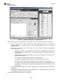
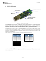
With the board connected to the PC, you can start SmartRF Studio. The following window should
appear:
Figure 2 - CC2530 and SmartRF Studio
The connected evaluation board should be listed, showing that a CC2530 is available. The list is
dynamically updated as you connect or disconnect a board. Double click on the highlighted CC2530
device icon and a new window will appear.
9/33
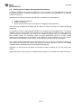
swru208b
Figure 3 - CC2530 control panel in SmartRF Studio
Figure 3 shows the main control panel for the CC2530. It lets you perform a number of operations:
Run TX Test modes for testing of RF output power and spectrum; e.g. by connecting a
spectrum analyser or a power meter to the CC2530EM SMA connector to perform RF
measurements.
Run Packet TX and RX tests. For this test, you should have two EBs with CC2530EMs
connected to the PC.
o
Double click on both of the devices in the device list in SmartRF Studio (Figure 2),
opening one “Device Control Panel” for each device, giving control of the two radios at
the same time.
o
Select one device to be the transmitter, by selecting the “Packet TX” tab shown in the
lower middle of Figure 3.
o
On the other device (the receiver), select the “Packet RX” tab.
o
Set up basic test parameters and press the “Start” button on the receiver.
o
Now you can start transmission by pressing the “Start” button for the transmitter.
o
The status window will show the number of packets sent on the transmitter side and
the number of received packets and signal strength of the last received packet on the
receiver side.
Read and/or modify registers and common settings, such as RF frequency (or channel) and
output power.
Export device register values in a user modifiable format by clicking the “Code export” button
in the Register view panel (on the left side).
The SmartRF Studio User Manual has more details.
10/33
swru208b
5.4
Setting up the Software Development Environment
To develop software and debug an application on the CC2530, it is recommended to use IAR
Embedded Workbench. It supports debugging of CC2530 through the SmartRF05EB, so no additional
hardware is required.
IAR EW8051 is bundled with all the required files for CC2530 to start development:
Register definition header file
Linker command file
Driver and device description file needed for debugging and programming
Note that other compilers and linkers can be used, but these tools may have limited debugging
capabilities.
An evaluation version of IAR Embedded Workbench is included in the Development Kit. To install the
software, insert the CD and follow the instructions. You will be asked to register on IAR’s web site to
get a license key for the product. As the owner of a CC2530 Development Kit, you are entitled to a 60
day evaluation period. The evaluation version in the kit automatically gives you 30 days. Please
contact your local IAR sales representative for the additional 30-days evaluation period. For a list of
sales offices and distributors in your country, please see this site: http://www.iar.com/contact.
The CC2530 Software Examples User’s Guide [5] will take you through the initial steps of starting up
IAR, setting up the project and compile and debug the software. Full source code for the software
examples can be downloaded from the CC2530DK web page [3].
Appendix A in this document will guide you through the steps of setting up your own project from
scratch.
Appendix B gives a brief overview of complete software solutions for CC2530 from Texas Instruments.
11/33
swru208b
6
RF Testing
NB! When running RF performance tests, it is recommended to disable all other peripherals on the
SmartRF05EB in order to avoid unwanted noise on the on-board voltage. In particular, make sure the
RS232 level converter/line driver is disabled.
RF testing can be performed by using SmartRF Studio together with the Development Kit. The basic
set-up is described in section 5.3. As described in that chapter, SmartRF Studio can be used to set up
basic tests and tune RF registers accordingly.
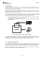
Since the CC2530 evaluation board is equipped with an SMA connector, both radiated (via antenna)
and conducted (via cable) tests can be performed, and it is easy to hook the EM up to RF
measurement equipment. The RF equipment may be connected in two different ways.
To measure radiated performance, connect an appropriate antenna to the spectrum analyzer
or power meter and an antenna on the EM board.
To measure conducted performance, connect a 50 Ohm coaxial cable directly from the EM to
the RF equipment.
Figure 4 - RF Test Set-Up with a Spectrum analyzer
By using good-quality RF cabling, the loss in the cabling should be negligible. However make sure that
the spectrum analyzer is calibrated. If possible, check it against a calibrated instrument such as an RF
signal generator. Uncalibrated spectrum analyzers can display errors of several dBs.
6.1
TX Parameter Testing Basics
To investigate the TX performance of the CC2530, you can either use a Spectrum Analyzer or an RF
Power Meter. Use the “Continuous TX” test mode in SmartRF Studio to set up the device to transmit a
signal at the desired frequency. Both a modulated or unmodulated carrier signal can be generated.
Use the RF Power Meter to observe the output power or the spectrum analyzer to observe the
spectrum and to measure the error vector magnitude (EVM).
12/33
swru208b
6.2
RX Parameter Testing Basics
To investigate the RX performance of the CC2530, you can use a signal generator or “Packet TX” in
SmartRF Studio (with another EB+EM) to generate the packets to receive. The receiver can be
configured by using the “Packet RX” test feature in SmartRF Studio.
By adding a jammer (a third node that generates either noise on the same channel or a strong signal
on an adjacent channel) it is also possible to measure co-channel rejection and selectivity/blocking
performance.
The PER test application, that was described in section 5.2, can be used for simple sensitivity
measurements with the CC2530EM and/or with your own prototype hardware. In this case, connect
the unit you want to test to a known good transmitter with coaxial cables and attenuators. Add more
attenuators until the PER value is 1%. The signal strength at the receiver side is then the sensitivity
limit of the system.
For more information regarding sensitivity measurements, refer to “Design Note 2 – Practical
Sensitivity Testing” [14].
13/33
swru208b
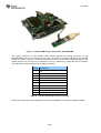
7
CC2530EM
SMA antenna
connector
32 kHz Crystal
32MHz Crystal
CC2530F256
Figure 5 - CC2530 Evaluation Module
The CC2530EM is a complete RF module based on one of the recommended reference designs for
the CC2530 radio. The module is equipped with a 32 MHz crystal, a 32.768 kHz crystal, external
passive components for the balun and antenna match filter, an SMA connector for the antenna or any
other RF instrument connection and general IO headers/connectors.
The table below shows the pin-out from the CC2530 to the two connectors on the backside of the
evaluation module.
CC2530
Signal
P1
P1
CC2530
Signal
CC2530
Signal
P2
P2
CC2530
Signal
GND
1
P0.4
3
2
NC
NC
1
2
NC
4
P1.3
NC
3
4
NC
P0.1
5
6
P1.0
NC
5
6
NC
P0.2
7
8
NC
VDD
7
8
NC
P0.3
9
10
P2.1
VDD
9
10
NC
P0.0
11
12
P2.2
NC
11
12
NC
P1.1
13
14
P1.4
NC
13
14
NC
P0.6
15
16
P1.5
RESET
15
16
NC
P0.7
17
18
P1.6
P1.2
17
18
P0.5
GND
19
20
P1.7
P2.0
19
20
NC
Table 1 - CC2530EM pin-out
The part number of the EM connector is SFM-110-02-SM-D-A-K-TR from Samtec. It mates with the
TFM-110-02-SM-D-A-K-TR, also from Samtec.
Please refer to the reference design on the web [1] for further details.
14/33
swru208b
8
CC2531 USB Dongle
Meandred F-antenna
IO Connector
CC2531F256
LEDs
Button S2
Button S1
Debug connector
Voltage regulator
Figure 6 - CC2531 USB Dongle
The USB dongle that is included in the kit comes preprogrammed such that it can be used together
with the SmartRF Packet Sniffer [10] to capture packets going over the air. To use the dongle as a
sniffer, just install the Packet Sniffer PC application (available on the web [10]), plug in the USB
dongle and start capturing packets. The Packet Sniffer User Manual [11] has more information.
The USB dongle can also be used as a general development board for USB and RF software. There
is a USB firmware library available from the TI web pages with an implementation of a complete USB
framework, including examples showing both HID and CDC ACM. There is a link to this library on the
CC2530 DK web pages [3].
Table 2 shows which CC2531 signals are connected to what IO on the dongle.
IO
Connector
CC2531
Dongle
User IO
CC2531
1
P0.2
Green LED
P0.0
2
P0.3
Red LED
P1.1
3
P0.4
Button S1
P1.2
4
P0.5
Button S2
P1.3
5
P1.7
6
P1.6
7
P1.5
8
P1.4
Table 2 - CC2531 USB Dongle Pinout
In order to debug and program firmware on the CC2531, the CC2531 USB dongle can be connected
to the SmartRF05EB as shown in the picture below. The small adapter board and flat cable is included
in the development kit.
15/33
swru208b
Figure 7 - CC2531 USB Dongle connected to SmartRF05EB
The debug connector on the CC2531 USB Dongle matches the debug connector on the
SmartRF05EB (and the CC Debugger). Note that, by default, the CC2531 dongle is not powered
through the debug connector, so an external power source must be used while programming. The
easiest solution is to connect it to a USB port on the PC. Alternatively, resistor R2 can be mounted.
The table below shows the pin out of the debug connector.
Pin # Connection
1
GND
2
VCC
3
CC2531 P2.2 (DC)
4
CC2531 P2.1 (DD)
5
NC
6
NC
7
CC2531 RESET
8
NC
9
Optional external VCC (R2 must be mounted)
10
NC
Table 3 – CC2531 USB Dongle Debug Connector
Refer to the schematics (in the appendices) and layout (available on the web) for additional details.
16/33
swru208b
9
SmartRF05 Evaluation Board
The SmartRF05 Evaluation Board is thoroughly described in the SmartRF05EB User’s Guide [8]. That
document will describe the hardware features in detail and provide the schematics for the board.
17/33
swru208b
10 Frequently Asked Questions
Q1
When connecting the SmartRF05EB to my PC via USB, the dialog window below appears.
Why? What should I do?
A1
The SmartRF05EB will be recognized as a USB device by the operating system, and it will ask
the user to provide information about which USB driver that should be associated with the
device.
If you have installed SmartRF Studio, just follow the instructions and select “Automatic
installation”. Windows should find the required driver (cebal.sys), as specified in an .inf file. Both
files (.inf and .sys) are included in the SmartRF Studio installation.
Q2
SmartRF05EB with the CC2530EM is not detected by IAR/SmartRF Studio. Why?
A2
First of all, note that Windows 7 64-bit and Windows Vista 64-bit are not yet supported.
It might be that the USB driver installation failed. The most common reasons are either Windows
not finding the driver or the user ignoring the “Found New Hardware Wizard”.
First of all, make sure you have installed SmartRF Studio, which includes the appropriate drivers
for the evaluation board. The drivers for the evaluation board are normally located in the
directory C:\Program Files\Texas Instruments\Extras\Drivers, where C:\Program Files\Texas
Instruments is the default root installation directory for SmartRF Studio. The path may be
different if you have chosen a different installation directory for SmartRF Studio.
Next, make sure you follow the steps in the hardware wizard. It is necessary to follow the steps
for driver installation for each new board that is connected to the PC. If the automatic driver
installation (as described in A1 above) fails, please select manual installation of drivers. When
prompted by the wizard, select “Install from a list or specific location (Advanced)”. You will see
the following window.
18/33
swru208b
If the above fails, select “Don’t search. I will choose the driver to install.” A new window will
open, asking for a location of where drivers can be found. Locate the srf05eb.inf file and select
that driver for installation.
Finally, verify that the device is associated with the correct driver by opening the Device
Manager on you PC. When the EB is connected, the “Cebal controlled devices” list contains
“SmartRF05EB”.
If the board is listed as an unknown device or associated with another driver, right click the
device in the Device Manager and select Uninstall. After uninstalling, unplug the board from the
PC and plug it in again. The “Found New Hardware Wizard” should re-appear. Follow the steps
as outlined in the beginning of this section.
Q3
How do I measure the current consumption of the CC2530?
A3
The easiest way to measure current consumption of the chip in various modes is to connect the
EM directly to the SmartRF05EB and disconnect everything on the board that consumes power
by removing all jumpers. The jumper on header P13 should not be removed. Connect the
ampere meter between the two terminals on P15. On P10, the jumper for the EM_RESET signal
19/33
swru208b
(connector 35-36) should be mounted. On P1, no jumpers are required, but in order to control
the SoC from a debugger, mount a jumper between 19-20 (DBG_DD) and 21-22 (DBG_DD).
Make sure the RS232 Enable switch is in the “disable” position.
Use SmartRF Studio to set the radio in different modes (RX, TX, etc.), or download an
application on the CC2530 setting the device in the preferred state.
Q4
Can I use another compiler than IAR to develop software for CC2530?
A4
Yes, there are several tools available that can be used for CC2530. Any 8051 compiler (e.g.
Keil, GCC, and SDCC) can, in theory, be used. Note that these tools may have limited
debugging support for CC2530.
20/33
swru208b
11 References
[1]
CC2530 product web site
http://focus.ti.com/docs/prod/folders/print/cc2530.html
[2]
CC2531 product web site
http://focus.ti.com/docs/prod/folders/print/cc2531.html
[3]
CC2530DK web site
http://focus.ti.com/docs/toolsw/folders/print/cc2530dk.html
[4]
CC2530DK Quick Start Guide
http://www.ti.com/lit/swra273
[5]
CC2530 Software Examples User’s Guide
http://www.ti.com/lit/swru137
[6]
Texas Instruments Support
http://support.ti.com
[7]
Texas Instruments Low Power RF Online Community
http://www.ti.com/lprf-forum
[8]
SmartRF05EB User’s Guide
http://www.ti.com/lit/swru210
[9]
SmartRF Studio
http://www.ti.com/smartrfstudio
[10] SmartRF Packet Sniffer
http://focus.ti.com/docs/toolsw/folders/print/packet-sniffer.html
[11] SmartRF Packet Sniffer User Manual
http://www.ti.com/lit/swru187
[12] TIMAC
http://www.ti.com/timac
[13] Z-Stack
http://www.ti.com/z-stack
[14] DN002 -- Practical Sensitivity Testing
http://www.ti.com/lit/swra097
[15] DN018 -- Range Measurements in an Open Field Environment
http://www.ti.com/lit/swra169
[16] IAR Embedded Workbench for 8051
http://www.iar.com
12 Document history
Revision
Date
B
2010-04-23
A
-
2009-04-20
2009-04-08
Description/Changes
Updated schematics. Use screenshots from SmartRF Studio 7. Added more details
about driver installation in the FAQ section. New recommended register mask for the
code bank configuration (appendix section A4).
Editorial update.
First revision.
21/33
swru208b
Appendix A
Setting up the Software Environment
This appendix will guide you through the initial steps of setting up a complete software development
environment with IAR Embedded Workbench for 8051. Version 7.51 (and newer) of the tool supports
CC2530 and CC2531 out-of-the-box.
A.1 Create the project
After installing IAR EW8051, start the application. The dialog window below should appear:
Select “Create new project in current workspace”
Select Empty project and click OK. You will now be asked to save the project. Select an appropriate
name for the project and save it. The dialog window will close and the project will be listed in the
“workspace” panel at the left side of the IDE.
22/33
swru208b
A.2 Project Options
Right click the project to set up the project options.
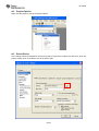
A.3 Select Device
In the dialog window that appears, the first thing that is required is to select the device for which the
project is built. Click on the button next to the device field.
23/33
swru208b
A new window will appear that allows you to browse through the device configuration files to choose
an appropriate device. Select the CC2530.i51 file from the <ew8051_install_dir>\8051\devices\Texas
Instruments folder. This .i51 device description file contains basic information about the chip.
Back in the General Options view, you will see that CC2530 is now the selected device. “CPU core”
should be set to Plain.
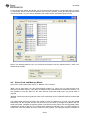
A.4 Select Code and Memory Model
Next, select code model. Either “Near” or “Banked” can be chosen.
“Near” can be used when you don’t need banking support, i.e. when you only need access to 64
kilobytes of the flash memory. This option is suitable for the CC253xF32 and CC253xF64 devices. It is
also possible to use this option for the other devices (F128 and F256) when only 64 kB flash is
required.
“Banked” should be used for getting access to the whole flash for the CC253xF128 and CC253xF256
devices.
The default data model for the Near code model is Small. For Banked, it is Large. The data model
determines how the compiler & linker use the memory of the 8051 for storage of variables. With the
small data model, variables are typically stored in the DATA memory space. For the large data model,
variables are stored in XDATA. The CC2530 User Guide and IAR 8051 C/C++ Compiler Reference
Guide have more information about the various memory spaces. The important thing to remember is
24/33
swru208b
that the 8051 core uses different instructions to access the various memory spaces. Access to IDATA
is, in general, much quicker than accessing XDATA, but there is normally much more XDATA
available than IDATA.
For this example, we use banked code model and large memory model to support the CC2530F256
device included in the development kit. The stack can be placed in XDATA. After setting up the above
option, you should have the following settings:
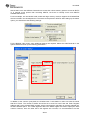
For the Banked code model, some additional settings are required. Select the Code Bank tab in the
options window and set up the following parameters:
In addition to the common (root) bank, the CC2530 uses 7 code banks in order to access the whole
256 kB of Flash. The number of banks should be set to 0x07 for both F128 and F256. Register
address 0x9F is the CC2530 FMAP register, which controls which code bank is currently mapped into
the 8051 address space. The 3 least significant bits in the FMAP register are used to specify the bank
number. However, since the other bits in this register are not used, it is recommended to set the
25/33
swru208b
register mask to 0xFF (instead of 0x07), which will allow IAR to use some bank switch macros with
less overhead.
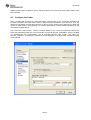
A.5 Configure the Linker
Next, you will need to instruct the IDE what linker command file to use. The linker command file
contains information the linker uses in order to place code and variables in ram and flash. Thus, the
linker file must match the flash and ram size of device you are working with. Normally, the linker file
should be tailor-made to an application for optimum performance, but the default command file will
work with most applications.
In the left menu, select “Linker”. Tick the “Override default” in the “Linker command file” section and
select the appropriate linker file. For this example, we will use lnk51ew_cc2530b.xcl, which is suitable
for CC253xF128 and CC253xF256. The b indicates banked code model. The other file,
lnk51ew_cc2530.xcl, is suitable for CC253xF32 and CC253xF64, or the larger flash variants if banking
is not required.
26/33
swru208b
A.6 Configure the Debugger
Finally, in the debugger section, chose “Texas Instruments” for the Driver.
All the other project options can be left as is and you can close the Project Options dialog by clicking
OK.
27/33
swru208b
A.7 Write Software
At this point, the project is configured and you can write your first lines of code. We will show a small
blinking LED example.
In the project, create a new file that you save as blinky.c. Type the following code:
#include <ioCC2530.h>
int main(void)
{
// Set P1.0 of CC2530 as output
P1DIR |= 0x01;
}
// Toggle P1.0
for(;;)
{
P1_0 ^= 1;
}
The code will toggle P1.0 (very quickly).
Add the file to the project by right clicking the project and selecting Add “blinky.c”.
You are now ready to compile and download the code to the target!
28/33
swru208b
A.8 Compile and Debug
Select “Project Make” from the menu (or press F7) to build the project. The IDE will now compile,
assemble and link the files in the project to generate an executable that can be downloaded to the
target. A message window at the bottom of the screen should show the progress and indicate that the
project was built successfully.
Next, download the application to the target by selecting “Project Debug” from the menu (or press
Ctrl+D). The application will now be downloaded to the target and you can start stepping through the
code from main.
A.9 Done!
Congratulations! You have just made your first CC2530 software project in IAR.
29/33
swru208b
Appendix B
Software Solutions for CC2530 from TI
B.1 SimpliciTI™ Network Protocol
The SimpliciTI network protocol is a low-power RF protocol (for sub-1 GHz, 2.4 GHz and IEEE
802.15.4 RF ICs) targeting simple, small RF networks. This open-source software is an excellent start
for building a network with battery-operated devices using a TI low-power RF System-on-Chip (SoC).
The SimpliciTI network protocol was designed for easy implementation and deployment out-of-the-box
on several TI RF platforms. It provides several sample applications.
Key Applications
Alarm and security: occupancy sensors, light sensors, carbon monoxide sensors, glassbreakage detectors
Smoke detectors
Automatic meter reading: gas meters, water meters, e-meters
Active RFID applications
Key Features
Low power: A TI-proprietary low-power network protocol
Flexible:
o Direct device-to-device communication
o Simple star with access point for store and forward to end device
o Range extenders to increase range to four hops
Simple: uses a five-command API
Low duty cycle
Ease of use
SimpliciTI is distributed as source code free of charge. For more information about the SimpliciTI
network protocol, see the Texas Instruments SimpliciTI network protocol web site
www.ti.com/simpliciti.
B.2 TIMAC Software
TIMAC software is an IEEE 802.15.4 medium-access-control software stack for TI’s IEEE 802.15.4
transceivers and System-on-Chips.
You can use TIMAC when you:
Need a wireless point-to-point or point-to-multipoint solution; e.g. multiple sensors reporting
directly to a master
Need a standardized wireless protocol
Have battery-powered and/or mains-powered nodes
Need support for acknowledgement and retransmission
Have low data-rate requirements (around 100-kbps effective data rate)
Features
Support for IEEE 802.15.4 standard
Support for beacon-enabled and non-beaconing systems
Multiple platforms
Easy application development
The TIMAC software stack is certified to be compliant with the IEEE 802.15.4 standard. TIMAC
software is distributed as object code free of charge. There are no royalties for using TIMAC software.
30/33
swru208b
For more information about TIMAC software, see the Texas Instruments TIMAC Web site
www.ti.com/timac.
B.3 RemoTI™ Network Protocol
Most existing remote controls use infrared technology to communicate commands to consumer
electronics devices. However, radio frequency (RF) remote controls enable non-line-of-sight operation
and provide more advanced features based on bidirectional RF communication.
ZigBee Radio Frequency for Consumer Electronics (RF4CE) is the result of a recent agreement
between the ZigBee Alliance and the RF4CE Consortium (http://www.zigbee.org/rf4ce) and has been
designed to be deployed in a wide range of remotely-controlled audio/visual consumer electronics
products, such as TVs and set-top boxes. ZigBee RF4CE key benefits:
Richer communication and increased reliability
Enhanced features and flexibility
Interoperability
No line-of-sight barrier
The RemoTI network protocol is Texas Instruments’ implementation of the ZigBee RF4CE standard. It
is a complete solution offering hardware and software support for TI’s low-power RF product portfolio.
With the RemoTI network protocol we provide:
An industry leading RF4CE-compliant stack featuring the interoperable CERC profile support,
a simple API, easy to understand sample application code, full development kits and reference
designs, and much more.
Operation on our best-in-class IEEE 802.15.4 compliant System-on-Chip, the CC2530, with
excellent RF co-existence and RF performance. The four flexible power modes include the
lowest current consumption power down mode for long battery in life low duty-cycle
applications.
Extensive worldwide support and tools to ensure that development of ZigBee RF4CE-based
products is simple, fast, and can be completed at minimal cost.
A Golden Unit platform; RemoTI it is used for testing other implementations of the ZigBee
RF4CE standard for standard compliance.
For more information on TI’s RemoTI network protocol, see the Texas Instruments RemoTI network
protocol web site www.ti.com/remoti or contact [email protected].
B.4 Z-Stack™ Software
The Z-Stack software is TI’s ZigBee-compliant protocol stack for a growing portfolio of IEEE 802.15.4
products and platforms. The Z-Stack software stack is compliant with both ZigBee-2006 and ZigBee2007 specification, supporting both the ZigBee and ZigBee PRO features sets. The Z-Stack software
includes implementation of two ZigBee application profiles – Smart Energy and Home Automation.
Other application profiles can easily be implemented by the user.
Z-Stack software notables include:
A fully compliant ZigBee and ZigBee PRO feature set
A range of sample applications including support for the ZigBee Smart Energy and ZigBee
Home Automation profiles
Over-the-air download and serial boot loader support
Can be used together with the RF front ends CC2590 and CC2591, which support 10 dBm
and 20 dBm output power respectively and improved receive sensitivity.
31/33
swru208b
The Z-Stack software has been awarded the ZigBee Alliance's golden-unit status for both the ZigBee
and ZigBee PRO stack profiles and is used by ZigBee developers world wide.
Z-Stack software is well suited for:
Smart energy (AMI)
Home automation
Commercial building automation
Medical, assisted living, or personal health and hospital care
Monitoring and control applications
Wireless sensor networks
Alarm and security
Asset tracking
Applications that require interoperability
For more information about Z-Stack software, see the Texas Instruments Z-Stack software web site
www.ti.com/z-stack.
32/33
swru208b
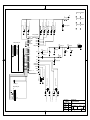
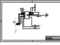
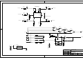
Appendix C
Schematics
Please refer to the following pages for the schematics for
CC2530 Evaluation Module
CC2531 USB Dongle
SmartRF05 Evaluation Board
The layout for the evaluation module and USB dongle can be found on the CC2530 [1] and CC2531
[2] web pages respectively.
33/33
2
C311
C_100N_0402_X5R_K_10
2
1
C272
C_220P_0402_NP0_J_50
2
1
C271
C_100N_0402_X5R_K_10
2
1
C241
C_100N_0402_X5R_K_10
2
1
C211
C_100N_0402_X5R_K_10
1
C101
C_100N_0402_X5R_K_10
2
C391
C_1U_0402_X5R_K_6P3
1
1
2
FIDUCIAL_MARK
FM4
FIDUCIAL_MARK
FM2
FIDUCIAL_MARK
FM5
FIDUCIAL_MARK
FM3
FIDUCIAL_MARK
FM6
VDD
L1
L_BEAD_102_0402
1
FIDUCIAL_MARK
FM1
2
1
2
C1
C_2U2_0402_X5R_M_4VDC
CC2530_TX_REDES
1
2
3
P1 SMD_SOCKET_2X10
4
AVDD1
AVDD4
AVDD_GUARD
27
28
18
17
16
15
P0.6 13
P0.7 12
RESET_N
1
32
2
33
C255
C_0402
1
1
C262
C_1P0_0402_NP0_C_50
1
XOSC32M_Q1
XOSC32M_Q2
DCOUPL
RBIAS
U1
GND
22
23
40
30
41
1
SMD_SOCKET_2X10
P2
1
3
1
2
4
1
C231
C_27P_0402_NP0_J_50
2
4
6
8
10
12
14
16
18 P0.5
20
2
2
P4
PINROW_1x2
1
3
VDD
5
7
9
11
13
Reset 15
P1.2 17
P2.0 19
1
2
P2_3
26
R301
R_56K_0402_F
20
P2_4
2
1
2
1
1
1
2
C_15P_0402_NP0_J_50
C321
37
19
RF_N
C253
C_0402
X_32.768/20/50/40/12
X2
38
2
2 3 4 5
L261
L_2N0_0402_S
C_15P_0402_NP0_J_50
C331
5
C261
C_18P_0402_NP0_J_50
C221
C_27P_0402_NP0_J_50
6
L251
L_0402
1
7
25
X1
X_32.000/10/15/30/16
8
P1.3
P1.4
P1.5
P1.6
P1.7
P0.0
P0.1
P0.2
P0.3
P0.4
RF_P
C401
C_1U_0402_X5R_K_6P3
9
C254
C_2P2_0402_NP0_C_50
1
L252
L_2N0_0402_S
C251
C_18P_0402_NP0_J_50
2
11
2
34
1
35
P2_0
P2_1
P2_2
P1_0
P1_1
P1_2
P1_3
P1_4
P1_5
P1_6
P1_7
P0_0
P0_1
P0_2
P0_3
P0_4
P0_5
P0_6
P0_7
2
P2.1
P2.2
P1.0
P1.1
14
1
2
C252
C_1P0_0402_NP0_C_50
31
1
36
P3
SMA_SMD
29
2
P1.3
P1.0
P2.1
P2.2
P1.4
P1.5
P1.6
P1.7
AVDD2
24
1
2
4
6
8
10
12
14
16
18
20
DGND_USB
USB_M
USB_P
DVDD_USB
21
2
P0.4
P0.1
P0.2
P0.3
P0.0
P1.1
P0.6
P0.7
1
3
5
7
9
11
13
15
17
19
DVDD
AVDD5/AVDD_SOC
AVDD_DREG
AVDD3
2
39
1
10
2
CONTRACT NO.
025104
APPROVALS
DATE
DRAWN
TIK
NN
CHECKED
ISSUED
COMPANY NAME
Texas Instruments
DWG
CC2530EM Discrete
SIZE
FSCM NO.
DWG NO.
A4
SCALE
SHEET
REV.
1.3.1
1 (1)
FIDUCIAL_MARK_1mm FIDUCIAL_MARK_1mm
FM1
FM2
FIDUCIAL_MARK_1mm
FM3
1
1
1
VOLTAGE REGULATOR
SoC periferials
Generated voltage:
3.3 V for CC2531
RF-SoC PART
Including PCB antenna
-
USB Connector
Buttons
LEDs
SMD sockets
RESET_N
RESET_N
P0_0
P0_0
P0_2
P0_3
P0_4
P0_5
P0_2
P0_3
P0_4
P0_5
P1_0/LED
P1_1/LED
P1_2
P1_3
P1_4
P1_5
P1_6
P1_7
P2_1
P2_2
PA_DM
PA_DP
P1_0/LED
P1_1/LED
P1_2
P1_3
P1_4
P1_5
P1_6
P1_7
P2_1
P2_2
PA_DM
PA_DP
CONTRACT NO.
025104
APPROVALS
DRAWN
CHECKED
ISSUED
DATE
TIK
MAP
COMPANY NAME
Texas Instruments
DWG
CC2531 USB dongle
SIZE
FSCM NO.
DWG NO.
SCALE
REV.
2.4
A4
SHEET
1(4)
To CC2531
VCC_EXT
3.3V
1
From PC
U2
TPS76933
R3
R_0_0402
1
In Out
VREG
C1
C_1U_0603_X5R_L_6P3
1
/EN
NC
1
Gnd
2
R2
R_0402
VBUS
C3
C_0402 1
2
2
C2
C_4U7_0603_X5R_K_6
2
2
1
R1
R_2_0402_F
2
Not mount: C3, R2
CONTRACT NO.
025104
APPROVALS
DATE
DRAWN
TIK
CHECKED
MAP
ISSUED
COMPANY NAME
Texas Instruments
DWG
CC2531 USB DONGLE VOLTAGE REGULATOR
SIZE
FSCM NO.
DWG NO.
SCALE
REV.
2.4
A4
SHEET
2(4)
VCC
L1
L_BEAD_102_0402
2
1
2
1
2
C311
C_100N_0402_X5R_K_10
2
1
C272
C_220P_0402_NP0_J_50
1
C271
C_100N_0402_X5R_K_10
2
C241
C_100N_0402_X5R_K_10
1
2
2
C211
C_100N_0402_X5R_K_10
2
1
C101
C_100N_0402_X5R_K_10
1
C391
C_1U_0402_X5R_K_6P3
1
C41
C_10P_0402_NP0_J_50
1
3.3V
2
1
2
C4
C_2U2_0402_X5R_M_4VDC
CC2531
10
39
1
2
PA_DP
3
PA_DM
4
DVDD2
DVDD1
AVDD5
DGND_USB
USB_P
USB_M
DVDD_USB
AVDD2
AVDD3
AVDD1
AVDD4
AVDD6
21
24
27
A2
ANTENNA_IIFA_1_LEFT
28
29
31
2
36
35
P2_1
34
P2_2
P1_0/LED
P1_1/LED
P1_2
P1_3
P1_4
P1_5
P1_6
P1_7
P0_0
11
9
8
7
6
5
38
37
19
18
17
P0_2
P0_3
P0_4
P0_5
16
15
14
13
R201
R_2K2_0402_G
20
2
RESET_N
RF_N
P2_4
P2_3
XOSC_Q1
XOSC_Q2
DCOUPL
RBIAS
U1
GND
25
4
1
JTI_2450BM15A0002
B1
26
3
C5
C_0P5_0402_NP0_B_50
2 5 6
32
33
22
23
40
30
41
X1
X_32.000/10/15/30/16
1
3
1
2
C221
C_27P_0402_NP0_J_50
2
1
C231
C_27P_0402_NP0_J_50
1
2
2
1
L301
L_6N8_0402_J
2
C401
C_1U_0402_X5R_K_6P3
1
R301
R_56K_0402_F
1
RF_P
C201
C_1N_0402_NP0_J_50
RESET_N
12
2 1
R9
R_0_0402
P2_0
P2_1
P2_2
P1_0
P1_1
P1_2
P1_3
P1_4
P1_5
P1_6
P1_7
P0_0
P0_1
P0_2
P0_3
P0_4
P0_5
P0_6
P0_7
CONTRACT NO.
025104
APPROVALS
DRAWN
CHECKED
ISSUED
DATE
TIK
MAP
COMPANY NAME
Texas Instruments
DWG
SIZE
CC2531 USB DONGLE RF-PART
FSCM NO.
DWG NO.
SCALE
REV.
2.4
A4
SHEET
3(4)
USB Interface
LED_Red
R11
R_270_0402_F
3.3V
1
2
R92
R_0402
2
R32
R_1K5_0402_G
2
R71
R_270_0402_F
P1_0/LED
P0_0
1
2
PA_DM
D+
3
1
2
PA_DP
GND
4
Shield
6
2
3.3V
1
R21
R_33_0402_G
2
5
2
D2 LED_EL19-21SYGC
D-
Shield
1
2
1
1
VBUS
LED_Green
R91
R_0_0402
1
P1
USB_A
P1_1/LED
D1 LED_EL19-21SURC
1
VBUS
2
1
R31
R_33_0402_G
1
2
button_P_1_2
S1
PUSH_BUTTON_SKRK
1
C21
C_47P_0402_NP0_J_50
2
C31
C_47P_0402_NP0_J_50
1
2
P1_2
button_P_1_3
S2
PUSH_BUTTON_SKRK
1
SoC debug/flash
P2_2
RESET_N
VCC_EXT
1
3
5
7
9
P1_3
Additional testpins
IO
BL_31_008U_NO_SILK
DEBUG
STL21
2
4
P2_1
6
8
10
2
3.3V
8
7
6
5
4
3
2
1
P1_4
P1_5
P1_6
P1_7
P0_5
P0_4
P0_3
P0_2
CONTRACT NO.
025104
APPROVALS
Not mount: R92, IO
DATE
DRAWN
TIK
CHECKED
MAP
ISSUED
COMPANY NAME
Texas Instruments
DWG
CC2531 USB dongle USB circuitry
SIZE
FSCM NO.
DWG NO.
SCALE
REV.
2.4
A4
SHEET
4(4)
PCB_FEET_19
H3
Power Supply
USB Interface
- Regulators
- Power jumpers
- Battery
- CC2511
- CC2511 debug
- USB port
PCB_FEET_19
H2
USB_UART_RTS
USB_UART_CTS
USB_UART_RX
USB_UART_TX
PCB_FEET_19
H1
USB_DBG_DD_DIR
USB_DBG_DC
USB_DBG_DD
USB_CS
USB_MISO
USB_MOSI
USB_SCLK
PCB_FEET_19
H4
USB MCU IO
jumpers
VCC_IO
Sheet 4
USB_IO_RESET
USB_EM_RESET
USB_JOY_MOVE
JOYSTICK_UP
JOYSTICK_DN
JOYSTICK_LT
JOYSTICK_RT
JOYSTICK_PUSH
JOY_MOVE
JOY_LEVEL
Sheet 2
- EM connection
- External SoC debug
EM_DBG_DD
EM_DBG_DC
EM_DBG_DD_DIR
EM_SNIFF_SFD
EM_SNIFF_MISO
EM_SNIFF_CLK
EM_SNIFF_DATA
- RS232 driver
- RS232 port
- On/Off jumper
EM_UART_TX
EM_UART_RX
EM_UART_TX
EM_UART_RX
EM_UART_CTS
EM_UART_RTS
EM_UART_CTS
EM_UART_RTS
JOYSTICK_UP
JOYSTICK_DN
JOYSTICK_LT
JOYSTICK_RT
JOYSTICK_PUSH
EM_JOY_MOVE
EM_JOY_LEVEL
EM_LCD_MODE
EM_LCD_CS
EM_MISO
EM_MOSI
EM_SCLK
EM_FLASH_CS
EM_BUTTON1/EM_LED4_SOC
EM_BUTTON2
EM_LED1
EM_LED2_MSP
EM_LED2_SOC
EM_LED3_MSP
EM_CS/EM_LED3_SOC
EM_LED4_MSP
EM_POT_R
EM_RESET
Sheet 7
P10
PINROW_2X18
1
3
5
7
9
11
13
15
17
19
21
23
25
27
29
31
33
35
2
4
6
8
10
12
14
16
18
20
22
24
26
28
30
32
34
36
-
LCD
Flash
Potmeter
Buttons
LEDs
USB_EM_RESET
USB_IO_RESET
IO_LCD_MODE
IO_LCD_CS
IO_MISO
VCC_IO
IO_MOSI
IO_SCLK
IO_FLASH_CS
IO_BUTTON1/IO_LED4_SOC
IO_BUTTON2
IO_LED1
IO_LED2_MSP
IO_LED2_SOC
IO_LED3_MSP
IO_LED3_SOC (EM_CS/EM_LED3_SOC)
IO_LED4_MSP
IO_POT_R
IO_EM_RESET
IO peripherals jumpers
All mount as default
Sheet 5
POWER_PS
VCC_EM
VCC_IO
Sheet 6
- Joystick
User Interface
EM Interface
RS-232
POWER_PS
Joystick
2
4
6
8
10
12
14
16
18
20
22
24
26
28
30
32
34
36
Default setting:
1-2: open
3-4: open
5-6: mount
7-8: mount
9-10: open
11-12: open
13-14: open
15-16: open
17-18: mount
19-20: mount
21-22: mount
23-24: mount
25-26: mount
27-28: mount
29-30: mount
31-32: mount
33-34: mount
35-36: mount
VCC_EM
VBUS
+3.3V USB
1
3
5
7
9
11
13
15
17
19
21
23
25
27
29
31
33
35
P1
PINROW_2X18
USB_LCD_CS
USB_LCD_MODE
VBUS
+3.3V USB
Sheet 3
FIDUCIAL_MARK FIDUCIAL_MARK FIDUCIAL_MARK
FM1
FM3
FM5
CONTRACT NO.
APPROVALS
DRAWN
FIDUCIAL_MARK FIDUCIAL_MARK FIDUCIAL_MARK
FM4
FM6
FM2
CHECKED
ISSUED
COMPANY NAME
TI Norway, LPW
02587
DATE
DWG
SmartRF05EB Top Level
PEH
SIZE
FSCM NO.
DWG NO.
A3
SCALE
REV.
1.8.1
SHEET
1(7)
+3.3V USB
USB SoC Debug
USB BUTTON
+3.3V USB
VCC_IO
L4
+3.3V USB
USB LED
1
D6
LED_CL150YCD
C_1U_0603_X5R_K_10
2
2
12
28
29
30
2 C16
1
U3
CC2511
DVDD
DVDD
DGUARD
AVDD_DREG
DCOUPL
AVDD
AVDD
AVDD
AVDD
19
22
25
26
4
3
1
36
35
34
33
32
RF_P
P1_0/LED
P1_1/LED
RF_N
P1_2
P1_3
P1_4
P1_5
P1_6
P2_3/XOSC32_Q1
P1_7
P2_4/XOSC32_Q2
23
5
6
7
8
9
13
P0_0/ATEST
P0_1
P0_2
P0_3
P0_4
P0_5
1 C36
1 C34
2
2
USB_DBG_DC
USB_UART_RTS
USB_UART_CTS
USB_UART_TX
USB_UART_RX
USB_DBG_DD_DIR
USB_DBG_DD
USB_JOY_MOVE
USB_EM_RESET
USB_CS
USB_SCLK
USB_MOSI
USB_MISO
24
17
18
31 RESET_N
USB_LCD_MODE
USB_LCD_CS
XOSC_Q1 21
XOSC_Q2 20
RBIAS 27
10 PADP
11 PADM
1
GND Exposed
R44
R_56K_0603_F
37
2
USB_RESET
Do Not Mount
C_33P_0603_NP0_J_50
1
1 2
1
2
C6
C_10N_0603_X7R_K_50
2
2
D+
3
GND
4
Shield
Shield
5
6
1
3
1
1
C20
2
GND
C19
4
2
2
R12
R_33_0603_G
1
2
1
2
R11
R_33_0603_G
1
2
1
2
C3
1
D-
C2
VBUS
2
C_47P_0603_NP0_J_50
P12
USB_B
C_47P_0603_NP0_J_50
R9
R_1K5_0603_G
VBUS
X1
X_48.000/15/18/60/16
S3
PUSH_BUTTON_SKRK
1
R10
R_0_0603
R18
R_0603
1
2
+3.3V USB
1 C37
2
14 P2_0
15 P2_1
16 P2_2
USB_IO_RESET
+3.3V USB
C_2U2_0603_X5R_K_10
1 C18
2
2
C_220P_0603_NP0_J_50
2
1 C35
1 C33
2
C_100N_0603_X7R_K_50
USB_RESET
1 C17
C_100N_0603_X7R_K_50
2
4
6
8
10
C_100N_0603_X7R_K_50
R43
R_270_0603_J
1
2
1
3
5
7
9
C_100N_0603_X7R_K_50
P2
PINROW_2X5
C_220P_0603_NP0_J_50
2
L_BEAD_102_0603
1
2
1
R52
R_10K_0603_G
2
1
2
R42
R_10K_0603_G
1
2
1
VCC_IO
R41
R_10K_0603_G
1 2
R60
R_10K_0603_G
VCC_IO
C_33P_0603_NP0_J_50
S4
PUSH_BUTTON_SKRK
CONTRACT NO.
APPROVALS
DRAWN
CHECKED
ISSUED
COMPANY NAME
TI Norway, LPW
02587
DATE
PEH
DWG
USB Interface
SIZE
FSCM NO.
DWG NO.
A3
SCALE
REV.
1.8.1
SHEET
2(7)
VCC_IO
SN74AVC4T245
1 VCCA
VCCB
2
1DIR
3
2DIR
4
1B1
1A1
5
1B2
1A2
6
2B1
2A1
7
2B2
2A2
8
GND
GND
EM_DBG_DD_DIR
EM_DBG_DD
EM_RESET
EM_DBG_DC
External SOC Debug
16
15
14
13
12
11
10
9
DUT_VCC
PINROW_2X5
P3
1
2
3
4
5
6
7
8
9
10
DUT_DD
PINROW_SMD_2X5_1.27MM
P4
1
2
DUT_VCC
3
4
DUT_DD
5
6
7
8
9
10
DUT_VCC
DUT_DD
VCC_EM
2
SMD_HEADER_2x10
P5
1
2
3
4
5
6
7
8
9
10
11
12
13
14
15
16
17
18
19
20
2
1 C29
2
Mount 0 ohm resistor in position R30
to power DUT from +3.3V USB through
connector P3
VCC_EM
SMD_HEADER_2x10
JOYSTICK_DN
EM_FLASH_CS
EM_LED1
JOYSTICK_RT
EM_DBG_DD
EM_DBG_DC
EM_CS/EM_LED3_SOC
EM_SCLK
EM_MOSI
EM_MISO
EM_SNIFF_CLK
EM_SNIFF_DATA
EM_SNIFF_SFD
1
3
5
7
9
11
13
15
17
19
2
4
6
8
10
12
14
16
18
20
JOYSTICK_PUSH
POWER_PS
VCC_EM
EM_SNIFF_MISO
JOYSTICK_UP
JOYSTICK_LT
EM_RESET
EM_LCD_CS
EM_JOY_MOVE
C_10U_0805_X5R_K_10
DO NOT MOUNT
EM Connectors
Debug Connectors
PINROW_2X10
2
EM_USB2
EM_USB1
EM_BUTTON2
EM_UART_RTS
EM_DBG_DD_DIR
1 C21 1 C28
2
2
R33 DO NOT MOUNT
P20
2
4
6
8
10
12
14
16
18
20
EM_FLASH_CS
EM_LED2_SOC
EM_DBG_DD
EM_DBG_DC
EM_MISO
EM_CS/EM_LED3_SOC
EM_SCLK
EM_MOSI
1
3
5
7
9
11
13
15
17
19
VCC_EM
POWER_PS
JOYSTICK_RT
JOYSTICK_DN
JOYSTICK_UP
JOYSTICK_LT
JOYSTICK_PUSH
EM_JOY_LEVEL
EM_JOY_MOVE
C_100N_0603_X7R_K_50
EM_USB1
EM_USB2
EM_BUTTON1/EM_LED4_SOC
EM_UART_RX
EM_UART_TX
EM_UART_CTS
EM_UART_RTS
EM_POT_R
EM_DBG_DD_DIR
EM_LED2_MSP
EM_LED3_MSP
EM_LED4_MSP
R33
R_0603
PINROW_2X10
P18
1
3
5
7
9
11
13
15
17
19
SMD_HEADER_2x10
P6
1
2
3
4
5
6
7
8
9
10
11
12
13
14
15
16
17
18
19
20
1
P22
C_100N_0603_X7R_K_50
EM_UART_CTS
EM_BUTTON1/EM_LED4_SOC
EM_UART_RX
EM_UART_TX
EM_LCD_MODE
EM_LED2_SOC
EM_JOY_LEVEL
EM_POT_R
R30
R_0603
1
C_100N_0603_X7R_K_50
C_100N_0603_X7R_K_50
U9
1 C27
2
4
6
8
10
12
14
16
18
20
EM_LED1
EM_LED2_MSP
EM_LED3_MSP
EM_LED4_MSP
EM_LCD_MODE
EM_RESET
EM_BUTTON2
EM_LCD_CS
1 C30
2
CONTRACT NO.
APPROVALS
DRAWN
CHECKED
ISSUED
COMPANY NAME
TI Norway, LPW
02587
DATE
DWG
EM Interface
PEH
SIZE
FSCM NO.
DWG NO.
A3
SCALE
REV.
1.8.1
SHEET
3(7)
2
LPS3015-222ML
2 L1
1
U4
1
R34
2
5
R_0_0603
1
C9
2
C_100N_0603_X7R_K_50
R45
R_1M0_0603_J
1
2
C_4U7_0805_X5R_K_25
8
6
1 C38
7
9
2
TPS63030
VCC_EM jumper
L1
L2
VIN
VOUT
2
STRAP_1
1 P15
1
R68
R_1M0_0603_J
2
1
VINA
EN
FB
PS/SYNC
PGND
GND
PPAD
10
3
11
1
2
1
2
2
VCC_EM
C11
C_10U_0805_X5R_K_10
4
2.2uH
C10
C_4U7_0805_X5R_K_25
Do Not Mount
R69
R70
R_0603
R_180K_0603_G
2
1
1
POWER_PS
VCC_IO jumper
1
STRAP_1
P13
2
VCC_IO
1
+
1xAA_1_5V
B1
2
Battery
1
1xAA_1_5V
B2
6 5 4
P8
Switch_6pin
R65
R_0603 Do
1
2
D8
BAT254
R2
R_0_0603
1
VBUS
2
A
K
1
R35
2
2
C_10U_0805_X5R_L_25
R_0_0603
Current is drawn from
input with highest voltage
P7
DC_JACK_2.5
1
2
3
Not Mount
D5
BAT254
A
K
1 C1
2
+3.3V USB
R7
R_0603
1
2
Do Not Mount
U2
TPS7A4501
In
1
Out 4
ADJ
1
5
2
3
R29
R_0_0603
1
P11
PINROW_1X3
1
2
3
Power source jumper:
1-2: Battery
2-3: USB/DC (default)
1 2 3
Gnd
Gnd 6
2
R63
R_6K2_0603_G
C_10U_0805_X5R_K_10
Power On/Off
R_3K6_0603_G
R64
2
1
+
2
TESTPOINT_PAD
TESTPOINT_PAD
TP1
TESTPOINT_PAD
TESTPOINT_PAD TP2
TP4
TP3
1 C8
2
CONTRACT NO.
APPROVALS
DRAWN
CHECKED
ISSUED
COMPANY NAME
TI Norway, LPW
02587
DATE
PEH
DWG
Power supply
SIZE
FSCM NO.
DWG NO.
A3
SCALE
REV.
1.8.1
SHEET
4(7)
BUTTON1_POWER_MSP
LCD
VCC_IO
P19
Switch_6pin
VCC_IO
1
1
R16
1
2
15
IO_LCD_MODE
4
7
9
12
BUTTON1_POWER_SOC
R_0_0603
R8
VCC_IO
U10
SN74CBTLV3257PW
2
VDD
1B1
3
GND
1B2
5
2B1
S
6
IO_LED1
IO_LED2_MSP
IO_LED2_SOC
2B2
OE
1A
3B1
2A
3B2
3A
4B1
4A
4B2
11
10
14
13
IO_LED3_MSP
IO_LED3_SOC
IO_LED4_MSP
IO_BUTTON1/IO_LED4_SOC
VCC_IO
S1
PUSH_BUTTON
8
SN74ALVC14
U11-D
2
Yellow
R21
R_10K_0603_G
2
BUTTON1_POWER_MSP
C_100N_0603_X7R_K_50
2
1
1
R_270_0603_J
Vss
BUTTON 1
1
R39
2
IO_MISO
2
5
6
SN74ALVC14
U11-C
1
C_100N_0603_X7R_K_50
2
1
VCC_IO
D
Q
C
S
TSL
Reset
Red
LED_CL150DCD
LED4
2
IO_MOSI
IO_SCLK
IO_FLASH_CS
3
4
SN74ALVC14
U11-B
R_270_0603_J
2
1
5
6
1
3
7
2
U5 M25PEx0
Vcc
1 C5
LED_CL150YCD
LED3
R38
1
8
IO_LCD_CS
2
VCC_IO
R37
Green
SN74ALVC14
U11-A 7
LED_CL150URCD
LED2
R_270_0603_J
2
VCC_IO
1
2
2
1
2
R_270_0603_J
1 C4
14
LED_CL150GCD
LED1
R36
VCC_IO
VCC_IO
16
8
1 2 3
1
R14
R_10K_0603_G
VCC_IO
6 5 4
2
USB_IO_RESET
FLASH
VCC_IO
LED
VCC_IO
1 C13
1
VCC_IO
C_1U_0603_X5R_K_10
1
2
3
4
5
6
7
8
9
10
11
12
13
14
15
16
1 - backlight supply 2 - backlight supply +
3 - logic power supply 4 - logic power supply +
5 - Reset (active low)
6 - register selection
9 - serial data in
10- serial clock input
11- chip select
2
P9
HMC_CON
LCD
7 - not use
8 - not use
12- not use
13- not use
14- not use
15- not use
16- not use
R_10K_0603_G
M1
HMC16311SF-PY
VCC_IO
VCC_IO
9
12 34
Orange
BUTTON1_POWER_SOC
POTMETER
1
R15
2
R_10K_0603_G
2
1
R_10K_0603_G
R13
4
USB_IO_RESET
BUTTON 2
12 34
S5
PUSH_BUTTON
VCC_IO
S2
PUSH_BUTTON
2
IO_BUTTON2
12 34
VCC_IO
11
2
USB_EM_RESET
10
SN74ALVC14
U11-E
IO_EM_RESET
C_100N_0603_X7R_K_50
EM RESET
12
SN74ALVC14
U11-F
1
13
IO_POT_R
1
CW
2
R53
R_100K_0603_F
2
3
1
RT1
R_0-10K_TRIM
R40
R_1K0_0603_J
1
R20
R_10K_0603_G
VCC_IO
VCC_IO
1 C7
2
CONTRACT NO.
APPROVALS
DRAWN
CHECKED
ISSUED
COMPANY NAME
TI Norway, LPW
02587
DATE
DWG
User Interface
PEH
SIZE
FSCM NO.
DWG NO.
A3
SCALE
REV.
1.8.1
SHEET
5(7)
R28
R_0_0603
C1+
V+
VCC
GND
C1FORCEON
R2OUTB
R1OUT
R2OUT
R3OUT
R4OUT
R5OUT
28
27
26
25
24
23
22
21
20
19
18
17
16
15
1
C25
C_100N_0603_X7R_K_50
2
1
C24
C_100N_0603_X7R_K_50
VCC_IO
2
R46
R_0_0603
1
4 5 6
C2+
C2VR1IN
R2IN
R3IN
R4IN
R5IN
T1OUT
T2OUT
T3OUT
T3IN
T2IN
T1IN
1
U6
SN65C3243DBR
1
2
3
4
5
6
7
8
9
10
11
12
13
14
1 C15
2
3 2
2
1 C14
2
2
EM_UART_RX
P16
DSUB_9F
Switch_6pin
P14
2
C23
C_100N_0603_X7R_K_50
C_1U_0603_X5R_K_10
C22
C_100N_0603_X7R_K_50
1
C_100N_0603_X7R_K_50
1
1
2
VCC_IO
5
9
4
8
3
R47
7
R_0_0603
2
6
1
1
2
EM_UART_CTS
R48
R_0_0603
1
2
EM_UART_TX
R49
R_0_0603
1
2
EM_UART_RTS
PC RS232-port
2-RXD
3-TXD
5-GND
7-RTS
8-CTS
CONTRACT NO.
APPROVALS
DRAWN
CHECKED
ISSUED
COMPANY NAME
TI Norway, LPW
02587
DATE
PEH
DWG
SIZE
RS-232 Interface
FSCM NO.
DWG NO.
A3
SCALE
SHEET
REV.
1.8.1
6(7)
UP
JOYSTICK
LT
R61
R_0_0603
CENTRE
push
2
JOYSTICK_RT
4
VCC_IO
5
1
COMMON
left
down
C
D
1 C31
C_100N_0603_X7R_K_50
2
U1
skrhab_e010
3
6
DN
2
R59
R_0_0603
2
JOYSTICK_DN
R26
R_100K_0603_F
1
2
1
2
1
R_100K_0603_F
R25
JOYSTICK_LT
1
2
2
R58
R_0_0603
1
B
right
2
1
R24
R_100K_0603_F
JOYSTICK_PUSH
A
up
PUSH
RT
1
2
1
1
R62
R_0_0603
R22
R_100K_0603_F
2
R_100K_0603_F
R23
JOYSTICK_UP
1
2
R57
R_0_0603
U7-A
SN74HC32
U7-B
SN74HC32
1
U7-C
SN74HC32
34
2
U7-D
SN74HC32
10
6
813
5
11
9
PUSH
VCC_IO
R6
R_100K_0603_F
1
UP
2
2
1
R_100K_0603_F
R3
U8-A
TLV272
V+
+
1
5
-
6
8
2
3
R17
R_200K_0603_F
2
DN
1
1
2
2
R50
R_330K_0603_F
R51
R_330K_0603_F
1
1
2
1
2
R5
R_100K_0603_F
1
2
VCC_IO
VCC_IO
U7-E
SN74HC32
POWER CONN.
1 C12
14
2
VDD
GND
7
C_100N_0603_X7R_K_50
C_100N_0603_X7R_K_50
2
VCC_IO
7
JOY_LEVEL
R56
R_10K_0603_G
R55
R_10K_0603_G
R4
R_100K_0603_F
2
+
1
2
1
2
2
R32
R_200K_0603_F
V4
R54
R_47K_0603_G
RT
R31
R_200K_0603_F
U8-B
TLV272
1
1
VCC_IO
R1
R_220K_0603_F
2
1
1
LT
JOY_MOVE
12
1 C32
2
C_100P_0603_NP0_J_50
C26
CONTRACT NO.
APPROVALS
DRAWN
CHECKED
ISSUED
COMPANY NAME
TI Norway, LPW
02587
DATE
DWG
Joystick
PEH
SIZE
FSCM NO.
DWG NO.
A3
SCALE
REV.
1.8.1
SHEET
7(7)
IMPORTANT NOTICE
Texas Instruments Incorporated and its subsidiaries (TI) reserve the right to make corrections, modifications, enhancements, improvements,
and other changes to its products and services at any time and to discontinue any product or service without notice. Customers should
obtain the latest relevant information before placing orders and should verify that such information is current and complete. All products are
sold subject to TI’s terms and conditions of sale supplied at the time of order acknowledgment.
TI warrants performance of its hardware products to the specifications applicable at the time of sale in accordance with TI’s standard
warranty. Testing and other quality control techniques are used to the extent TI deems necessary to support this warranty. Except where
mandated by government requirements, testing of all parameters of each product is not necessarily performed.
TI assumes no liability for applications assistance or customer product design. Customers are responsible for their products and
applications using TI components. To minimize the risks associated with customer products and applications, customers should provide
adequate design and operating safeguards.
TI does not warrant or represent that any license, either express or implied, is granted under any TI patent right, copyright, mask work right,
or other TI intellectual property right relating to any combination, machine, or process in which TI products or services are used. Information
published by TI regarding third-party products or services does not constitute a license from TI to use such products or services or a
warranty or endorsement thereof. Use of such information may require a license from a third party under the patents or other intellectual
property of the third party, or a license from TI under the patents or other intellectual property of TI.
Reproduction of TI information in TI data books or data sheets is permissible only if reproduction is without alteration and is accompanied
by all associated warranties, conditions, limitations, and notices. Reproduction of this information with alteration is an unfair and deceptive
business practice. TI is not responsible or liable for such altered documentation. Information of third parties may be subject to additional
restrictions.
Resale of TI products or services with statements different from or beyond the parameters stated by TI for that product or service voids all
express and any implied warranties for the associated TI product or service and is an unfair and deceptive business practice. TI is not
responsible or liable for any such statements.
TI products are not authorized for use in safety-critical applications (such as life support) where a failure of the TI product would reasonably
be expected to cause severe personal injury or death, unless officers of the parties have executed an agreement specifically governing
such use. Buyers represent that they have all necessary expertise in the safety and regulatory ramifications of their applications, and
acknowledge and agree that they are solely responsible for all legal, regulatory and safety-related requirements concerning their products
and any use of TI products in such safety-critical applications, notwithstanding any applications-related information or support that may be
provided by TI. Further, Buyers must fully indemnify TI and its representatives against any damages arising out of the use of TI products in
such safety-critical applications.
TI products are neither designed nor intended for use in military/aerospace applications or environments unless the TI products are
specifically designated by TI as military-grade or "enhanced plastic." Only products designated by TI as military-grade meet military
specifications. Buyers acknowledge and agree that any such use of TI products which TI has not designated as military-grade is solely at
the Buyer's risk, and that they are solely responsible for compliance with all legal and regulatory requirements in connection with such use.
TI products are neither designed nor intended for use in automotive applications or environments unless the specific TI products are
designated by TI as compliant with ISO/TS 16949 requirements. Buyers acknowledge and agree that, if they use any non-designated
products in automotive applications, TI will not be responsible for any failure to meet such requirements.
Following are URLs where you can obtain information on other Texas Instruments products and application solutions:
Products
Applications
Amplifiers
amplifier.ti.com
Audio
www.ti.com/audio
Data Converters
dataconverter.ti.com
Automotive
www.ti.com/automotive
DLP® Products
www.dlp.com
Communications and
Telecom
www.ti.com/communications
DSP
dsp.ti.com
Computers and
Peripherals
www.ti.com/computers
Clocks and Timers
www.ti.com/clocks
Consumer Electronics
www.ti.com/consumer-apps
Interface
interface.ti.com
Energy
www.ti.com/energy
Logic
logic.ti.com
Industrial
www.ti.com/industrial
Power Mgmt
power.ti.com
Medical
www.ti.com/medical
Microcontrollers
microcontroller.ti.com
Security
www.ti.com/security
RFID
www.ti-rfid.com
Space, Avionics &
Defense
www.ti.com/space-avionics-defense
RF/IF and ZigBee® Solutions www.ti.com/lprf
Video and Imaging
www.ti.com/video
Wireless
www.ti.com/wireless-apps
Mailing Address: Texas Instruments, Post Office Box 655303, Dallas, Texas 75265
Copyright © 2010, Texas Instruments Incorporated