1
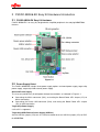
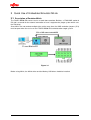
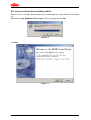
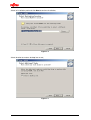
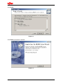
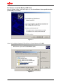
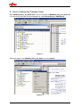
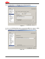
The following document contains information on Cypress products.
Colophon
The products described in this document are designed, developed and manufactured as contemplated for general use,
including without limitation, ordinary industrial use, general office use, personal use, and household use, but are not
designed, developed and manufactured as contemplated (1) for any use that includes fatal risks or dangers that, unless
extremely high safety is secured, could have a serious effect to the public, and could lead directly to death, personal injury,
severe physical damage or other loss (i.e., nuclear reaction control in nuclear facility, aircraft flight control, air traffic control,
mass transport control, medical life support system, missile launch control in weapon system), or (2) for any use where
chance of failure is intolerable (i.e., submersible repeater and artificial satellite). Please note that Spansion will not be liable
to you and/or any third party for any claims or damages arising in connection with above-mentioned uses of the products.
Any semiconductor devices have an inherent chance of failure. You must protect against injury, damage or loss from such
failures by incorporating safety design measures into your facility and equipment such as redundancy, fire protection, and
prevention of over-current levels and other abnormal operating conditions. If any products described in this document
represent goods or technologies subject to certain restrictions on export under the Foreign Exchange and Foreign Trade Law
of Japan, the US Export Administration Regulations or the applicable laws of any other country, the prior authorization by the
respective government entity will be required for export of those products.
Trademarks and Notice
The contents of this document are subject to change without notice. This document may contain information on a Spansion
product under development by Spansion. Spansion reserves the right to change or discontinue work on any product without
notice. The information in this document is provided as is without warranty or guarantee of any kind as to its accuracy,
completeness, operability, fitness for particular purpose, merchantability, non-infringement of third-party rights, or any other
warranty, express, implied, or statutory. Spansion assumes no liability for any damages of any kind arising out of the use of
the information in this document.
®
®
®
TM
Copyright © 2013 Spansion Inc. All rights reserved. Spansion , the Spansion logo, MirrorBit , MirrorBit Eclipse ,
TM
ORNAND and combinations thereof, are trademarks and registered trademarks of Spansion LLC in the United States and
other countries. Other names used are for informational purposes only and may be trademarks of their respective owners.
MCU-AN-510001-E-10
FM3
32-BIT MICROCONTROLLER
MB9B500 Series
FM3 EASY KIT USER MANUAL
APPLICATION NOTE
For more information for the FM3 microcontroller, visit the web site at:
http://www.fujitsu.com/global/services/microelectronics/product/micom/roadmap/industrial/fm3/
TM
ARM and Cortex-M3 are the trademarks of ARM Limited in the EU and other countries.
FUJITSU SEMICONDUCTOR (SHANGHAI) LIMITED
ALL RIGHTS RESERVED
The contents of this document are subject to change without notice.
Customers are advised to consult with sales representatives before ordering.
The information, such as descriptions of function and application circuit examples, in this document are
presented solely for the purpose of reference to show examples of operations and uses of FUJITSU
SEMICONDUCTOR device; FUJITSU SEMICONDUCTOR does not warrant proper operation of the device with
respect to use based on such information. When you develop equipment incorporating the device based on such
information, you must assume any responsibility arising out of such use of the information. FUJITSU
SEMICONDUCTOR assumes no liability for any damages whatsoever arising out of the use of the information.
Any information in this document, including descriptions of function and schematic diagrams, shall not be
construed as license of the use or exercise of any intellectual property right, such as patent right or copyright, or
any other right of FUJITSU SEMICONDUCTOR or any third party or does FUJITSU SEMICONDUCTOR warrant
non-infringement of any third-party's intellectual property right or other right by using such information. FUJITSU
SEMICONDUCTOR assumes no liability for any infringement of the intellectual property rights or other rights of
third parties which would result from the use of information contained herein.
The products described in this document are designed, developed and manufactured as contemplated for
general use, including without limitation, ordinary industrial use, general office use, personal use, and household
use, but are not designed, developed and manufactured as contemplated (1) for use accompanying fatal risks or
dangers that, unless extremely high safety is secured, could have a serious effect to the public, and could lead
directly to death, personal injury, severe physical damage or other loss (i.e., nuclear reaction control in nuclear
facility, aircraft flight control, air traffic control, mass transport control, medical life support system, missile launch
control in weapon system), or (2) for use requiring extremely high reliability (i.e., submersible repeater and
artificial
satellite).
Please note that FUJITSU SEMICONDUCTOR will not be liable against you and/or any third party for any claims
or damages arising in connection with above-mentioned uses of the products.
Please note that FUJITSU SEMICONDUCTOR will not be liable against you and/or any third party for any claims
or damages arising in connection with above-mentioned uses of the products.
Any semiconductor devices have an inherent chance of failure. You must protect against injury, damage or loss
from such failures by incorporating safety design measures into your facility and equipment such as redundancy,
fire protection, and prevention of over-current levels and other abnormal operating conditions.
Exportation/release of any products described in this document may require necessary procedures in accordance
with the regulations of the Foreign Exchange and Foreign Trade Control Law of Japan and/or US export control
laws.
The company names and brand names herein are the trademarks or registered trademarks of their respective
owners.
Copyright ©2010 FUJITSU SEMICONDUCTOR (SHANGHAI) LIMITED All rights reserved.
2
Revision History
Date
2010-12-29
Revision
V1.0
Change of Records
First version
3
Table of Contents
REVISION HISTORY ................................................................................................. 3
1 OVERVIEW OF THE FSSDC-9B506-EK EASY KIT .............................................. 5
1.1
Features.................................................................................................................. 5
1.2
FSSDC-9B506-EK Product Specifications............................................................... 5
2 FSSDC-9B506-EK EASY KIT HARDWARE INTRODUCTION ............................. 6
2.1
FSSDC-9B506-EK Easy Kit Hardware .................................................................... 6
2.2
Power Supply Select ............................................................................................... 6
2.3
Boot mode............................................................................................................... 7
2.4
Emulation Mode ...................................................................................................... 7
2.5
On-board Peripherals .............................................................................................. 7
3 QUICK USE OF EMBEDDED EMULATOR MLINK .............................................. 8
3.1
Description of Emulator MLink................................................................................. 8
3.2
How to Install the Driver for Manley MLink............................................................... 9
3.3
How to Install the Manley USB Driver.................................................................... 12
4 HOW TO INSTALL IAR (ON-LINE REGISTER LICENSE IS REQUIRED) ......... 15
5 HOW TO DEBUG THE SAMPLE CODE ............................................................. 20
6 HOW TO USE THE FSSDC-9B506-EK EASILY .................................................. 24
4
1 Overview of the FSSDC-9B506-EK Easy Kit
1.1 Features
The FSSDC-9B506-EK Easy Kit has following features:
Simple setup: power supply, emulation and development can be implemented with one
single USB wire;
Convenient platform for learning and development: The board has extended I/O pins and
peripheral pins;
Mono LCD module, including 128*64 pixels;
Based on the FM3 chip, equipped with multiple peripheral functions (Flash, SRAM, Timers,
ADCs, USB, CAN, UART, SIO, I2C, LIN, etc.);
User LED——demonstration of PWM driving function is available;
System reset button;
Potentiometer——using ADC to detect voltage;
Joystick——used to browse display screen;
Support a range of debugging options;
Integrated In-circuit Debugger (MLink);
Standard ARM® 20-pin JTAG debug connector;
External emulator(Only SWD mode);
Serial Writer Mode is available;
Fully compatible with the IAR Embedded Workbench (Version 6.0 or above) developing
environment.
1.2 FSSDC-9B506-EK Product Specifications
Power supply: The user can select power supply for FSSDC-9B506-EK from the two power
supply methods below.
MLink USB (Type-B) connector (the other end connecting to the PC)
MB9BF500 USB (Type-B) connector (the other end connecting to the PC)
Size of the easy kit (including the extended part of USB socket)
– 67.3mm x 120.5mm x 1.6mm
。
Reference voltage for analog sampling: AVcc = Vcc
Note: make sure to connect the ground of the two power supplies before connecting the
emulator to the target board if they are provided by two different power supplies.
5
2 FSSDC-9B506-EK Easy Kit Hardware Introduction
2.1 FSSDC-9B506-EK Easy Kit Hardware
FSSDC-9B506-EK is an easy kit, designed with simplified peripherals for studying MB9BF500
features.
Figure 2-1
2.2 Power Supply Select
The FSSDC-9B506-EK includes three power supply options: on-board power supply, target chip
power supply, target chip USB external power supply.
On-board Power Supply
The user can provide easy kit with power through two methods, as indicated in Figure 2-1.
Connecting the MLink connector (CN1), and setting the Board Power SEL Jumper (JP1) to
MLink connection;
Connecting the Device USB connector (CN4), and setting the Board Power SEL Jumper
(JP1) to USB connection.
Target Chip Power Supply
3.3V or 5V is supported.
Target Chip USB External Power Supply (USBVcc)
Set the USB Vcc jumper (JP3) to 3.3V. Please be noted not to set USB Vcc jumper (JP3) to VDD
for MB9BF500.
6
2.3 Boot mode
A setting jumper (JP5) is prepared on the easy kit for boot mode. The default setting (set JP5
open) makes the chip boots from the user program area (on-chip FLASH). The chip will boot
from boot code area when it is set to Serial Writer Mode. Users can download the code to the
chip using the corresponding I/O.
2.4 Emulation Mode
On-board MLink(debugging MB9BF500 on-board)
MLink performs debugging on-board system with SWD mode. Users don’t have to do anything
except confirming connection of the SWD debug jumper (JP4).
On-board MLink(debugging user target system)
MLink can connect to the user target system through the standard ARM® 20-pin JTAG socket.
On-board MLink supports JTAG and SWD mode. When use on-board MLink to debug user target
system, make sure SWD debug jumper (JP4) open.
External emulator (debugging MB9BF500 on-board)
MLink can connect to the user target system through the standard ARM® 20-pin JTAG socket
(CN3), thereby allowing the external emulator to emulate the FSSDC-9B506-EK (only SWD
mode is available).
1.
2.
3.
4.
5.
First switch off power supply of the easy kit, then connect the external emulator to CN3 of
the study board.
Make sure JP4 were shorted well.
Set jumper JP1 to the USB power supply mode and provide power to the easy kit via the
USB connector CN4.
Select the corresponding external emulator in the emulation developing environment.
Start debug.
2.5 On-board Peripherals
ADC
A potentiometer (RV1) is provided on the easy kit, used to demonstrate AD conversion.
Joystick
The Joystick (PB2) on the board, which is connected directly to the GPIO on the chip, is
used to browse menus and other human-machine interface.
System Reset (Reset Button)
Reset button (PB1) is used to reset the system.
Multiple Function LED (LEDs)
Three LEDs (LD3~LD5) are used to demonstrate the PWM driving function of the chip. The
dimmer of LEDs be controlled after powered-on.
Chip Extension Pin (Ext. device I/O)
The easy kit also takes into consideration of user’s self-development interests and
requirements, by opening all GPIO and special peripheral functions of the target chip. Users
can connect their self-defined module to the extended pins; therefore know more about the
FM3 chip.
Note: When using the extended ports, the user should take care of the chip to prevent
the study board being damaged, which means all I/O are extended.
7
3 Quick Use of Embedded Emulator MLink
3.1 Description of Emulator MLink
The FSSDC-9B506-EK can be used as a stand-alone emulator. Besides, a JTAG/SWD socket of
IDC-20 is reserved for the external connection of user’s target device (target system which uses
the FM3 chip).
Since MLink can not emulate multiple chips at the same time, the SWD emulation jumpers (JP4)
must be open when the user uses the FSSDC-9B506-EK to emulate other target system.
Figure 3-1
Before using MLink, the MLink driver and the Manley USB driver should be installed.
8
3.2 How to Install the Driver for Manley MLink
Open the disc or visit http://www.manley.com.cn to download the setup_MLINK.exe installation
file.
Double-click setup_MLINK.exe file to install, select a language and click OK,
Figure 3-2
Click Next,
Figure 3-3
9
Select an installation path and click Next to continue installation,
Figure 3-4
Select whether to create a desktop icon or not,
Figure 3-5
10
Click Install,
Figure 3-6
Click Finish to complete installation.
Figure 3-7
11
3.3 How to Install the Manley USB Driver
When the dialog window shown below pops up, select Install from a list or specific location
(Advanced) and click Next,
Figure 3-8
Select the installation directory of MLink driver as shown below and click OK,
Figure 3-9
12
If the driver is correctly installed, the window shown below pops up,
Figure 3-10
Click Finish to complete installation of MLink USB driver,
Figure 3-11
13
USB device is ready to use.
Figure 3-12
14
4 How to Install IAR (on-line register license is required)
Use the IAR6.10 installation file in the disc. After the display shown below pops up, select Install
IAR Embedded Workbench,
Figure 4-1
After entering Install IAR Embedded Workbench
installation ,
】
,select Get a license【required before
Figure 4-2
15
Please fill in the registration form. You will get a confirmation mail from IAR in your registered
mail box and get a License,
Figure 4-3
After obtaining the License, please return to the original installation window and select Install
IAR Embedded Workbench,
Figure 4-4
16
Select Next.
Figure 4-5
Select I accept the terms of the license agreement,
Figure 4-6
17
,
,
Fill in Name Company and License and select Next.
Figure 4-7
The IAR installation path selection is shown and click Next,
Figure 4-8
18
Click Finish to complete installation,
Figure 4-9
Note: The IAR Work Bench here is a 32K code limited version. Please purchase from IAR the
License for version without limitation.
19
5 How to Debug the Sample Code
Open MB9B500_Easy_Kit_Demo.eww under the directory of MB9B500_Easy_Kit_Demo-v10
in the disc and the window shown below pops up. Select Flash Debug or RAM Debug,
Figure 5-1
Right-click project name MB9B500_Easy_Kit_Demo and select Option,
Figure 5-2
20
Please set SetupDriver in the Debugger option to Third-Party Driver,
Figure 5-3
Set driver in the Third-Party Driver option to corresponding Mlink driver, browse the Mlink
driver installed before, and select the driver IAR_Mlink610.dll corresponding to IAR6.10,
Figure 5-4-a
21
Figure 5-4-b
After completing all settings, select Rebuild All for the project,
Figure 5-5
22
Click the Download and Debug icon
shown below. The executable code is downloaded to
Flash, operates to the main function and waits for the debug command.
Figure 5-6
Figure 5-7
23
6 How to Use the FSSDC-9B506-EK Easily
Connect the PC via CN1. The red LD2 indicates power is on and the green LD1 means
MLink is ready, otherwise it becomes flickering orange.
Open IAR EWARM (Version V6.0 or above), load MB9B500_Easy_Kit_Demo.eww under
directory of MB9B500_Easy_Kit_Demo-v10 in the disc attached with the board.
After confirming MB9B500_Easy_Kit_Demo.ewp is loaded, click debug and download
code for debugging, LCD first displays voltage monitoring for 2 seconds and then changes to
welcome to Fujitsu.
Test the LEDs indicator set. The dimmer of LED3 - LED5 could be controlled (PWM control).
Test Joystick. up, down, left, right, select is displayed on the screen with each press of
the button.
Test ADC. Voltage measurement (0mv - 3296mv) is displayed while the potentiometer is
tuned.
24